Pic32 Reference Manual
pic32_reference_manual
User Manual:
Open the PDF directly: View PDF ![]() .
.
Page Count: 1609 [warning: Documents this large are best viewed by clicking the View PDF Link!]
1. Introduction
2. CPU
3. Memory Organization
4. Prefetch Cache
5. Flash Programming
6. Oscillators
7. Resets
8. Interrupts
9. Watchdog Timer
10. Power Saving Modes
12. Digital I/O Ports
13. Parallel Master Port
14. Timers
15. Input Capture
16. Output Compare
17. 10-bit A/D
18. 12-bit A/D
19. Comparator
20. Comparator Voltage Reference
21. UART
23. SPI
24. I2C
27. USB
29. RTCC
31. DMA
32. Configuration
33. Programming and Debugging
34. CAN
35. Ethernet
37. CTMU
41. Prefetch with L1 Cache
42. Oscillator with Enhanced PLL
46. Serial Quad Interface (SQI)
47. External Bus Interface (EBI)
48. Memory Organization and Permissions
49. Crypto Engine and Random Number Generator
50. microAptiv Core
51. USB OTG
52. Flash Live Update

© 2007-2011 Microchip Technology Inc. DS61127D-page 1-1
Introduction
1
Section 1. Introduction
HIGHLIGHTS
This section of the manual contains the following topics:
1.1 Introduction .................................................................................................................... 1-2
1.2 Family Reference Manual Sections ............................................................................... 1-2
1.3 Device Structure.............................................................................................................1-2
1.4 Development Support .................................................................................................... 1-3
1.5 Style and Symbol Conventions ...................................................................................... 1-4
1.6 Related Documentation ................................................................................................. 1-5
1.7 Revision History .............................................................................................................1-6

PIC32 Family Reference Manual
DS61127D-page 1-2 © 2007-2011 Microchip Technology Inc.
1.1 INTRODUCTION
Microchip’s PIC32 series of 32-bit microcontrollers are designed to fulfill a customer’s
requirements for enhanced features and performance for their MCU-based applications.
Common attributes among all devices in the PIC32 series are:
•Pin, peripheral and source code compatibility
•Common software and hardware development tools
1.2 FAMILY REFERENCE MANUAL SECTIONS
The collective PIC32 family reference manual sections describe the PIC32 family series of 32-bit
microcontrollers. All sections that comprise the PIC32 Family Reference Manual are available
from the Microchip web site: www.microchip.com. These individual sections explain the PIC32
family architecture and operation of the peripheral modules, but do not cover the specifics of
each device in a particular family. Users should refer to the respective product data sheet for
device-specific details, such as:
•Pinout and packaging details
•Memory map
• List of peripherals included on the device, including multiple instances of peripherals
• Device-specific electrical specifications and characteristics
1.3 DEVICE STRUCTURE
The PIC32 architecture has been broken down into the following functional blocks:
•MCU Core
•System Memory
•System Integration
•Peripherals
1.3.1 MCU Core
The PIC32 MCU core is discussed in Section 2. “CPU” (DS61113).
1.3.2 System Memory
The system memory provides on-chip nonvolatile Flash memory and volatile SRAM memory,
featuring user and protected kernel-segment-partitioning for real-time operating systems.
Refer to the specific device data sheet for the list of applicable family reference manual sections
for this topic.
Note: This family reference manual section is meant to serve as a complement to device
data sheets. Depending on the device variant, this manual section may not apply to
all PIC32 devices.
Please consult the note at the beginning of the “Device Overview” chapter in the
current device data sheet to check whether this document supports the device you
are using.
Device data sheets and family reference manual sections are available for
download from the Microchip Worldwide Web site at: http://www.microchip.com

© 2007-2011 Microchip Technology Inc. DS61127D-page 1-3
Section 1. Introduction
Introduction
1
1.3.3 System Integration
System integration consists of a comprehensive set of modules and features that connect the
MCU core and peripheral modules into a single operational unit. System integration features also
provide these advantages:
• Decreased system cost, by bringing traditionally off-chip functions into the microcontroller
• Increased design flexibility, by adding a wider range of operating modes
•Increased system reliability, by enhancing the ability to recover from unexpected events
Refer to the specific device data sheet for the list of applicable family reference manual sections
for this topic.
1.3.4 Peripherals
The PIC32 devices have many peripherals that allow it to interface with the external world.
Refer to the specific device data sheet for the list of applicable family reference manual sections
for this topic.
1.4 DEVELOPMENT SUPPORT
Microchip offers a wide range of development tools that allow users to efficiently develop and
debug application code. Microchip’s development tools can be divided into four categories:
•Code generation
•Hardware/software debug
• Device programmer
•Product evaluation boards
As new tools are developed, the latest product briefs and user guides can be obtained from the
Microchip web site (www.microchip.com) or from your local Microchip Sales office.
Microchip offers other references and support to speed the development cycle. These include:
•Application notes
•Reference designs
•Local sales offices with field application support
•Corporate applications support line
•Getting started guides
•“How to” brochures
•MASTERs conferences
•Webinars
•Design centers
These can all be found on the Microchip web site (www.microchip.com). Also, the Microchip web
site lists other sites that may provide useful references.

PIC32 Family Reference Manual
DS61127D-page 1-4 © 2007-2011 Microchip Technology Inc.
1.5 STYLE AND SYMBOL CONVENTIONS
Throughout the individual family reference manual sections, certain style, format, and font
conventions are used to signal particular distinctions for the affected text. Tab l e 1- 1 lists these
conventions, specific symbols, and non-conventional word definitions and abbreviations.
1.5.1 Document Conventions
Tabl e 1-1 defines some of the symbols, terms and typographic conventions used in this manual.
Table 1-1: Document Conventions
Symbol or Term Description
Set To force a bit or register to a value of logic ‘1’.
Clear To force a bit or register to a value of logic ‘0’.
Reset 1) To force a register/bit to its default state.
2) A condition in which the device places itself after a device Reset
occurs. Some bits will be set to ‘0’ (such as interrupt enable bits), while
others will be set to ‘1’ (such as the I/O data direction bits).
0xnn or nnh Designates the number ‘nn’ in the hexadecimal number system. These
conventions are used in the code examples. For example, the
designation 0x13F or 13Fh may be used.
B‘bbbbbbbb’ Designates the number ‘bbbbbbbb’ in the binary number system. This
convention is used in the text, figures and tables. For example, the desig-
nation B‘10100000’ may be used.
R-M-W Read-Modify-Write. This occurs when a register or port is read, the value
is modified, and that value is then written back to the register or port. This
action can occur from a single instruction (such as bit set, BSET) or a
sequence of instructions.
: (colon) Used to specify a range or the concatenation of registers/bits/pins.
One example is TMR3:TMR2, which is the concatenation of two 16-bit
registers to form a 32-bit timer value.
Concatenation order (left-right) usually specifies a positional relationship
(MSb to LSb, higher to lower).
< > Specifies bit(s) locations in a particular register. One example is SRxMPT
(SPIxSTAT<5>), which specifies the abbreviation of bit and the register
name, and associated bits or bit positions.
MSb, LSb Indicates the Least/Most Significant bit in a field.
MSB, LSB Indicates the Least/Most Significant Byte in a field of bits.
mshw, lshw Most Significant half-word and lease significant half-word. A half-word is
16 bits wide.
msw, lsw Indicates the least/most significant word in a field of bits.
Courier New
Font
Used for code examples, binary numbers and for instruction mnemonics
that appear in the text.
Times New Roman
Font (Italics)
Used for equations.
Note A Note presents information that we want to re-emphasize, either to help
you avoid a common pitfall or to make you aware of operating differences
between some device family members. A Note can be in a box, or when
used in a table or figure, it is located at the bottom of the table or figure.
Register cells A bit reference that appears in a gray shaded cell of a register, signifies
that the bit is either unimplemented (instead of a name an EM dash (—)
is present) or is not relevant to the particular peripheral module.

© 2007-2011 Microchip Technology Inc. DS61127D-page 1-5
Section 1. Introduction
Introduction
1
1.5.2 Electrical Specifications
The individual family reference manual sections contain references to electrical specifications
and their parameter numbers. Tabl e 1-2 shows the parameter numbering convention for PIC32
devices. A parameter number represents a unique set of characteristics and conditions that is
consistent between every data sheet, although the actual parameter value may vary from device
to device.
To determine the parameter values for a specific device, users should refer to the “Electrical
Specifications” section of the specific device data sheet.
Table 1-2: Electrical Specification Parameter Numbering Convention
1.6 RELATED DOCUMENTATION
Microchip, as well as other sources, offers additional documentation to aid you as you develop
PIC32-based applications. The list below contains the most common documentation, but other
documents may also be available. Please check the Microchip web site (www.microchip.com) for
the latest published technical documentation.
1.6.1 Microchip Documentation
The following PIC32 documentation is available from Microchip. These documents provide
application-specific information that gives actual examples of using, programming, and designing
with PIC32 microcontrollers.
•PIC32 Family Reference Manual Sections
The individual family reference manual sections describe the PIC32 family architecture and
operation of the peripheral modules, but do not cover the specifics of each device in the
family.
•PIC32MX Product Data Sheets
These data sheets contain device-specific information, such as pinout and packaging
details, electrical specifications and memory maps.
• PIC32MX Programming Specification (DS61145)
The programming specification contains detailed descriptions of, and electrical and timing
specifications for, the programming process. Both In-Circuit Serial Programming™ (ICSP™)
and Enhanced ICSP are described in detail.
1.6.2 Third-Party Documentation
Microchip does not review third-party documentation for technical accuracy; however, these
references may be helpful to understand operation of the devices. Refer to the Microchip web
site for available information on third-party documentation.
Parameter Number Format Comment
Dxxx DC Specification
Axxx DC Specification for Analog Peripherals
xxx Timing (AC) Specification
PDxxx Device Programming DC Specification
Pxxx Device Programming Timing (AC) Specification
Legend: ‘xxx’ represents a parameter number.

PIC32 Family Reference Manual
DS61127D-page 1-6 © 2007-2011 Microchip Technology Inc.
1.7 REVISION HISTORY
Revision A (September 2007)
This is the initial version of this document.
Revision B (October 2007)
Updated document to remove Confidential status.
Revision C (April 2008)
Revised status to Preliminary; Revised Section 1.1.
Revision D (September 2011)
This revision includes the following updates:
• Removed the Preliminary status in the footer
•Added a note box with information on related family reference manual sections
•Updated the bulleted list in 1.1 “Introduction”
• Removed the feature list from 1.3.1 “MCU Core”
• Updated the family reference manual section information in these sections:
-1.3.2 “System Memory”
-1.3.3 “System Integration”
-1.3.4 “Peripherals”
•Updated the Document Conventions in Tabl e 1-1
• In addition, updates to formatting and minor text edits were incorporated throughout the
document
2007-2011 Microchip Technology Inc. DS61127D-page 1-7
Information contained in this publication regarding device
applications and the like is provided only for your convenience
and may be superseded by updates. It is your responsibility to
ensure that your application meets with your specifications.
MICROCHIP MAKES NO REPRESENTATIONS OR
WARRANTIES OF ANY KIND WHETHER EXPRESS OR
IMPLIED, WRITTEN OR ORAL, STATUTORY OR
OTHERWISE, RELATED TO THE INFORMATION,
INCLUDING BUT NOT LIMITED TO ITS CONDITION,
QUALITY, PERFORMANCE, MERCHANTABILITY OR
FITNESS FOR PURPOSE. Microchip disclaims all liability
arising from this information and its use. Use of Microchip
devices in life support and/or safety applications is entirely at
the buyer’s risk, and the buyer agrees to defend, indemnify and
hold harmless Microchip from any and all damages, claims,
suits, or expenses resulting from such use. No licenses are
conveyed, implicitly or otherwise, under any Microchip
intellectual property rights.
Trademarks
The Microchip name and logo, the Microchip logo, dsPIC,
KEELOQ, KEELOQ logo, MPLAB, PIC, PICmicro, PICSTART,
PIC32 logo, rfPIC and UNI/O are registered trademarks of
Microchip Technology Incorporated in the U.S.A. and other
countries.
FilterLab, Hampshire, HI-TECH C, Linear Active Thermistor,
MXDEV, MXLAB, SEEVAL and The Embedded Control
Solutions Company are registered trademarks of Microchip
Technology Incorporated in the U.S.A.
Analog-for-the-Digital Age, Application Maestro, chipKIT,
chipKIT logo, CodeGuard, dsPICDEM, dsPICDEM.net,
dsPICworks, dsSPEAK, ECAN, ECONOMONITOR,
FanSense, HI-TIDE, In-Circuit Serial Programming, ICSP,
Mindi, MiWi, MPASM, MPLAB Certified logo, MPLIB,
MPLINK, mTouch, Omniscient Code Generation, PICC,
PICC-18, PICDEM, PICDEM.net, PICkit, PICtail, REAL ICE,
rfLAB, Select Mode, Total Endurance, TSHARC,
UniWinDriver, WiperLock and ZENA are trademarks of
Microchip Technology Incorporated in the U.S.A. and other
countries.
SQTP is a service mark of Microchip Technology Incorporated
in the U.S.A.
All other trademarks mentioned herein are property of their
respective companies.
© 2007-2011, Microchip Technology Incorporated, Printed in
the U.S.A., All Rights Reserved.
Printed on recycled paper.
ISBN: 978-1-61341-599-3
Note the following details of the code protection feature on Microchip devices:
• Microchip products meet the specification contained in their particular Microchip Data Sheet.
• Microchip believes that its family of products is one of the most secure families of its kind on the market today, when used in the
intended manner and under normal conditions.
• There are dishonest and possibly illegal methods used to breach the code protection feature. All of these methods, to our
knowledge, require using the Microchip products in a manner outside the operating specifications contained in Microchip’s Data
Sheets. Most likely, the person doing so is engaged in theft of intellectual property.
• Microchip is willing to work with the customer who is concerned about the integrity of their code.
• Neither Microchip nor any other semiconductor manufacturer can guarantee the security of their code. Code protection does not
mean that we are guaranteeing the product as “unbreakable.”
Code protection is constantly evolving. We at Microchip are committed to continuously improving the code protection features of our
products. Attempts to break Microchip’s code protection feature may be a violation of the Digital Millennium Copyright Act. If such acts
allow unauthorized access to your software or other copyrighted work, you may have a right to sue for relief under that Act.
Microchip received ISO/TS-16949:2009 certification for its worldwide
headquarters, design and wafer fabrication facilities in Chandler and
Tempe, Arizona; Gresham, Oregon and design centers in California
and India. The Company’s quality system processes and procedures
are for its PIC® MCUs and dsPIC® DSCs, KEELOQ® code hopping
devices, Serial EEPROMs, microperipherals, nonvolatile memory and
analog products. In addition, Microchip’s quality system for the design
and manufacture of development systems is ISO 9001:2000 certified.

DS61127D-page 28 2011 Microchip Technology Inc.
AMERICAS
Corporate Office
2355 West Chandler Blvd.
Chandler, AZ 85224-6199
Tel: 480-792-7200
Fax: 480-792-7277
Technical Support:
http://www.microchip.com/
support
Web Address:
www.microchip.com
Atlanta
Duluth, GA
Tel: 678-957-9614
Fax: 678-957-1455
Boston
Westborough, MA
Tel: 774-760-0087
Fax: 774-760-0088
Chicago
Itasca, IL
Tel: 630-285-0071
Fax: 630-285-0075
Cleveland
Independence, OH
Tel: 216-447-0464
Fax: 216-447-0643
Dallas
Addison, TX
Tel: 972-818-7423
Fax: 972-818-2924
Detroit
Farmington Hills, MI
Tel: 248-538-2250
Fax: 248-538-2260
Indianapolis
Noblesville, IN
Tel: 317-773-8323
Fax: 317-773-5453
Los Angeles
Mission Viejo, CA
Tel: 949-462-9523
Fax: 949-462-9608
Santa Clara
Santa Clara, CA
Tel: 408-961-6444
Fax: 408-961-6445
Toronto
Mississauga, Ontario,
Canada
Tel: 905-673-0699
Fax: 905-673-6509
ASIA/PACIFIC
Asia Pacific Office
Suites 3707-14, 37th Floor
Tower 6, The Gateway
Harbour City, Kowloon
Hong Kong
Tel : 8 52 -24 01- 120 0
Fax: 852-2401-3431
Australia - Sydney
Tel : 6 1- 2-9 868 -67 33
Fax: 61-2-9868-6755
China - Beijing
Tel : 8 6- 10- 856 9-7 00 0
Fax: 86-10-8528-2104
China - Chengdu
Tel : 8 6- 28- 866 5-5 511
Fax: 86-28-8665-7889
China - Chongqing
Tel : 8 6- 23- 898 0-9 58 8
Fax: 86-23-8980-9500
China - Hangzhou
Tel : 8 6- 571 -28 19- 318 7
Fax: 86-571-2819-3189
China - Hong Kong SAR
Tel : 8 52 -24 01- 120 0
Fax: 852-2401-3431
China - Nanjing
Tel : 8 6- 25- 847 3-2 46 0
Fax: 86-25-8473-2470
China - Qingdao
Tel : 8 6- 532 -85 02- 735 5
Fax: 86-532-8502-7205
China - Shanghai
Tel : 8 6- 21- 540 7-5 53 3
Fax: 86-21-5407-5066
China - Shenyang
Tel : 8 6- 24- 233 4-2 82 9
Fax: 86-24-2334-2393
China - Shenzhen
Tel : 8 6- 755 -82 03- 266 0
Fax: 86-755-8203-1760
China - Wuhan
Tel : 8 6- 27- 598 0-5 30 0
Fax: 86-27-5980-5118
China - Xian
Tel : 8 6- 29- 883 3-7 25 2
Fax: 86-29-8833-7256
China - Xiamen
Tel: 86-592-2388138
Fax: 86-592-2388130
China - Zhuhai
Tel : 86- 75 6-3 21 004 0
Fax: 86-756-3210049
ASIA/PACIFIC
India - Bangalore
Tel : 9 1- 80- 309 0-4 44 4
Fax: 91-80-3090-4123
India - New Delhi
Tel : 9 1- 11- 416 0 -8 631
Fax: 91-11-4160-8632
India - Pune
Tel : 9 1- 20- 256 6-1 51 2
Fax: 91-20-2566-1513
Japan - Yokohama
Tel : 8 1- 45- 471 - 6 16 6
Fax: 81-45-471-6122
Korea - Daegu
Tel : 8 2- 53- 744 -43 01
Fax: 82-53-744-4302
Korea - Seoul
Tel : 8 2- 2-5 54- 72 0 0
Fax: 82-2-558-5932 or
82-2-558-5934
Malaysia - Kuala Lumpur
Tel : 6 0- 3-6 201 -9 8 57
Fax: 60-3-6201-9859
Malaysia - Penang
Tel : 6 0- 4-2 27- 88 7 0
Fax: 60-4-227-4068
Philippines - Manila
Tel : 6 3- 2-6 34- 90 6 5
Fax: 63-2-634-9069
Singapore
Tel : 6 5- 633 4-8 870
Fax: 65-6334-8850
Taiwan - Hsin Chu
Tel : 8 86 -3- 577 8-3 66
Fax: 886-3-5770-955
Taiwan - Kaohsiung
Tel : 8 86 -7- 536 -48 18
Fax: 886-7-330-9305
Taiwan - Taipei
Tel : 8 86 -2- 250 0-6 61 0
Fax: 886-2-2508-0102
Thailand - Bangkok
Tel : 6 6- 2-6 94- 13 5 1
Fax: 66-2-694-1350
EUROPE
Austria - Wels
Tel : 4 3- 72 42 -2 244 -3 9
Fax: 43-7242-2244-393
Denmark - Copenhagen
Tel : 4 5- 445 0-2 828
Fax: 45-4485-2829
France - Paris
Tel : 3 3- 1-6 9-5 3-6 3-2 0
Fax: 33-1-69-30-90-79
Germany - Munich
Tel : 4 9- 89 -62 7-1 44- 0
Fax: 49-89-627-144-44
Italy - Milan
Tel : 3 9- 03 31 -7 426 11
Fax: 39-0331-466781
Netherlands - Drunen
Tel : 3 1- 41 6- 690 399
Fax: 31-416-690340
Spain - Madrid
Tel : 3 4- 91 -70 8-0 8-9 0
Fax: 34-91-708-08-91
UK - Wokingham
Tel : 4 4- 118 -92 1- 5 869
Fax: 44-118-921-5820
Worldwide Sales and Service
08/02/11

© 2007-2012 Microchip Technology Inc. DS61113E-page 2-1
CPU for Devices
with M4K® Core
2
Section 2. CPU for Devices with M4K® Core
HIGHLIGHTS
This section of the manual contains the following topics:
2.1 Introduction................................................................................................................2-2
2.2 Architecture Overview ............................................................................................... 2-3
2.3 PIC32 CPU Details .................................................................................................... 2-6
2.4 Special Considerations When Writing to CP0 Registers ......................................... 2-11
2.5 Architecture Release 2 Details ................................................................................ 2-12
2.6 Split CPU bus .......................................................................................................... 2-12
2.7 Internal System Busses...........................................................................................2-13
2.8 Set/Clear/Invert........................................................................................................ 2-13
2.9 ALU Status Bits........................................................................................................ 2-14
2.10 Interrupt and Exception Mechanism ........................................................................ 2-14
2.11 Programming Model ................................................................................................ 2-14
2.12 Coprocessor 0 (CP0) Registers............................................................................... 2-21
2.13 MIPS16e® Execution ............................................................................................... 2-55
2.14 Memory Model......................................................................................................... 2-55
2.15 CPU Instructions, Grouped By Function.................................................................. 2-56
2.16 CPU Initialization ..................................................................................................... 2-59
2.17 Effects of a Reset .................................................................................................... 2-60
2.18 Related Application Notes ....................................................................................... 2-61
2.19 Revision History....................................................................................................... 2-62

PIC32 Family Reference Manual
DS61113E-page 2-2 © 2007-2012 Microchip Technology Inc.
2.1 INTRODUCTION
The PIC32 MCU is a complex system-on-chip (SoC) that is based on the M4K® Microprocessor
core from MIPS® Technologies. The M4K® is a state-of-the-art, 32-bit, low-power, RISC proces-
sor core with the enhanced MIPS32® Release 2 Instruction Set Architecture (ISA).
This chapter provides an overview of the CPU features and system architecture of the PIC32
family of microcontrollers that are based on the M4K® processor core.
2.1.1 Key Features
•Up to 1.5 DMIPS/MHz of performance
•Programmable prefetch cache memory to enhance execution from Flash memory (not
available on all devices; refer to the specific device data sheet to determine availability)
•16-bit Instruction mode (MIPS16e
®) for compact code
•Vectored interrupt controller with up to 96 interrupt sources
•Programmable User and Kernel modes of operation
•Atomic bit manipulations on peripheral registers (Single cycle)
• Multiply-Divide unit with a maximum issue rate of one 32 x 16 multiply per clock
•High-speed Microchip ICD port with hardware-based non-intrusive data monitoring and
application data streaming functions
•EJTAG debug port allows extensive third party debug, programming and test tools support
•Instruction controlled power management modes
• Five-stage pipelined instruction execution
•Internal code protection to help protect intellectual property
2.1.2 Related MIPS® Documentation
•MIPS32
® M4K® Processor Core Software User’s Manual – MD00249-2B-M4K-SUM
•MIPS
® Instruction Set – MD00086-2B-MIPS32BIS-AFP
•MIPS16e
® – MD00076-2B-MIPS1632-AFP
•MIPS32
® Privileged Resource Architecture – MD00090-2B-MIPS32PRA-AFP
Note: This family reference manual section is meant to serve as a complement to device
data sheets. Depending on the device variant, this manual section may not apply to
all PIC32 devices.
Please consult the note at the beginning of the “CPU” chapter in the current device
data sheet to check whether this document supports the device you are using.
Device data sheets and family reference manual sections are available for
download from the Microchip Worldwide Web site at: http://www.microchip.com

© 2007-2012 Microchip Technology Inc. DS61113E-page 2-3
Section 2. CPU for Devices with M4K® Core
CPU for Devices
with M4K® Core
2
2.2 ARCHITECTURE OVERVIEW
The PIC32 family of devices are complex systems-on-a-chip that contain many features.
Included in all processors of the PIC32 family is a high-performance RISC CPU, which can be
programmed in 32-bit and 16-bit modes, and even mixed modes. PIC32 devices contain a
high-performance interrupt controller, DMA controller, USB controller, in-circuit debugger,
high-performance switching matrix for high-speed data accesses to the peripherals, and on-chip
data RAM memory that holds data and programs. The unique prefetch cache and prefetch buffer
for the Flash memory, which hides the latency of the Flash, provides zero Wait state equivalent
performance.
Figure 2-1: PIC32 Block Diagram
JTAG/BSCAN Priority Interrupt
Controller LDO VREG
DMAC ICD
PIC32 CPU
IS DS
EJTAG INT
Bus Matrix
Prefetch Cache Data RAM
Peripheral
Flash Memory
Flash Controller
Clock Control/
Generation Reset Generation
PMP/PSP
PORTS
ADC
RTCC
Timers
Input Capture
PWM/Output
Compare
Dual Compare
SSP/SPI
I2C™
UART
128-bit
USB
Bridge
CAN(1)
Motor Control
PWM(1)
DAC(1)
CTMU(1)
Note 1: This peripheral is not available on all devices. Refer to the specific device data sheet for
availability.
ETH(1)
PIC32 Family Reference Manual
DS61113E-page 2-4 © 2007-2012 Microchip Technology Inc.
There are two internal busses in PIC32 devices for connection to all peripherals. The main
peripheral bus connects most of the peripheral units to the bus matrix through a peripheral
bridge. There is also a high-speed peripheral bridge that connects the interrupt controller, DMA
controller, in-circuit debugger, and USB peripherals.
The M4K® CPU core is the heart of some PIC32 MCUs. The CPU performs operations under
program control. Instructions are fetched by the CPU, decoded and executed synchronously.
Instructions exist in either Program Flash memory or Data RAM memory.
The PIC32 CPU is based on a load/store architecture and performs most operations on a set of
internal registers. Specific load and store instructions are used to move data between these
internal registers and the outside world.
Figure 2-2: M4K® Microprocessor Core Block Diagram
2.2.1 Busses
There are two separate busses on PIC32 devices. One bus is responsible for the fetching of
instructions to the CPU, and the other is the data path for load and store instructions. Both the
instruction, or I-side bus, and the data, or D-side bus, are connected to the bus matrix unit. The
bus matrix is a switch that allows multiple accesses to occur concurrently in a system. The bus
matrix allows simultaneous accesses between different bus masters that are not attempting
accesses to the same target. The bus matrix serializes accesses between different masters to
the same target through an arbitration algorithm.
Since the CPU has two different data paths to the bus matrix, the CPU is effectively two different
bus masters to the system. When running from Flash memory, load and store operations to
SRAM and the internal peripherals will occur in parallel to instruction fetches from Flash memory.
In addition to the CPU, and depending on the device variant, there are other bus masters in
PIC32 devices:
•DMA controller
•In-Circuit Debugger (ICD) unit
•USB controller
•CAN controller
•Ethernet controller
System
Co-processor
MDU
FMT
MMU
TAP
EJTAG
Power
Management
Off-Chip
Debug I/F
Execution
Core
(RF/ALU/Shift)
On-Chip
Memory
Trace
Off-Chip
Trace I/F
Memory
Interface Dual Memory
I/F

© 2007-2012 Microchip Technology Inc. DS61113E-page 2-5
Section 2. CPU for Devices with M4K® Core
CPU for Devices
with M4K® Core
2
2.2.2 Introduction to the Programming Model
The PIC32 processor has the following features:
•5-stage pipeline
•32-bit Address and Data Paths
•DSP-like Multiply-add and multiply-subtract instructions (MADD, MADDU, MSUB, MSUBU)
•Targeted multiply instruction (MUL)
•Zero and One detect instructions (CLZ, CLO)
•Wait instruction (WAIT)
•Conditional move instructions (MOVZ, MOVN)
• Implements MIPS32® Enhanced Architecture (Release 2)
•Vectored interrupts
•Programmable exception vector base
•Atomic interrupt enable/disable
•General Purpose Register (GPR) shadow sets
•Bit field manipulation instructions
•MIPS16e
® Application Specific Extension improves code density
•Special PC-relative instructions for efficient loading of addresses and constants
•Data type conversion instructions (ZEB, SEB, ZEH, SEH)
•Compact jumps
•Stack frame set-up and tear-down SAVE and RESTORE macro instructions
•Memory Management Unit with simple Fixed Mapping Translation (FMT)
•Processor to/from Coprocessor register data transfers
•Direct memory to/from Coprocessor register data transfers
•Performance-optimized Multiply-Divide Unit (High-performance build-time option)
•Maximum issue rate of one 32 x 16 multiply per clock
•Maximum issue rate of one 32 x 32 multiply every other clock
• Early-in divide control – 11 to 34 clock latency
•Low-Power mode (triggered by WAIT instruction)
• Software breakpoints via the SDBBP instruction
2.2.3 Core Timer
The PIC32 architecture includes a core timer that is available to application programs. This
timer is implemented in the form of two co-processor registers: the Count register, and the
Compare register. The Count register is incremented every two system clock (SYSCLK) cycles.
The incrementing of Count can be optionally suspended during Debug mode. The Compare
register is used to cause a timer interrupt if desired. An interrupt is generated when the
Compare register matches the Count register. An interrupt is taken only if it is enabled in the
Interrupt Controller module.
For more information on the core timer, see 2.12 “Coprocessor 0 (CP0) Registers” and
Section 8. “Interrupts.” (DS61108) in the “PIC32 Family Reference Manual”.

PIC32 Family Reference Manual
DS61113E-page 2-6 © 2007-2012 Microchip Technology Inc.
2.3 PIC32 CPU DETAILS
2.3.1 Pipeline Stages
The pipeline consists of five stages:
•Instruction (I) Stage
•Execution (E) Stage
•Memory (M) Stage
•Align (A) Stage
•Writeback (W) Stage
2.3.1.1 I STAGE – INSTRUCTION FETCH
During I stage:
•An instruction is fetched from the instruction SRAM
•MIPS16e
® instructions are converted into instructions that are similar to MIPS32®
instructions
2.3.1.2 E STAGE – EXECUTION
During E stage:
•Operands are fetched from the register file
•Operands from the M and A stage are bypassed to this stage
• The Arithmetic Logic Unit (ALU) begins the arithmetic or logical operation for
register-to-register instructions
• The ALU calculates the data virtual address for load and store instructions and the MMU
performs the fixed virtual-to-physical address translation
•The ALU determines whether the branch condition is true and calculates the virtual branch
target address for branch instructions
•Instruction logic selects an instruction address and the MMU performs the fixed
virtual-to-physical address translation
• All multiply divide operations begin in this stage
2.3.1.3 M STAGE – MEMORY FETCH
During M stage:
•The arithmetic or logic ALU operation completes
•The data SRAM access is performed for load and store instructions
•A 16 x 16 or 32 x 16 MUL operation completes in the array and stalls for one clock in the M
stage to complete the carry-propagate-add in the M stage
• A 32 x 32 MUL operation stalls for two clocks in the M stage to complete the second cycle
of the array and the carry-propagate-add in the M stage
• Multiply and divide calculations proceed in the MDU. If the calculation completes before the
IU moves the instruction past the M stage, then the MDU holds the result in a temporary
register until the IU moves the instructions to the A stage (and it is consequently known that
it will not be killed).
2.3.1.4 A STAGE – ALIGN
During A stage:
•A separate aligner aligns loaded data with its word boundary
•A MUL operation makes the result available for writeback. The actual register writeback is
performed in the W stage
•From this stage, load data or a result from the MDU are available in the E stage for
bypassing

© 2007-2012 Microchip Technology Inc. DS61113E-page 2-7
Section 2. CPU for Devices with M4K® Core
CPU for Devices
with M4K® Core
2
2.3.1.5 W STAGE – WRITEBACK
During W stage:
For register-to-register or load instructions, the result is written back to the register file.
The M4K® Microprocessor core implements a “bypass” mechanism that allows the result of an
operation to be sent directly to the instruction that needs it without having to write the result to
the register, and then read it back.
Figure 2-3: Simplified PIC32 CPU Pipeline
The results of using instruction pipelining in the PIC32 core is a fast, single-cycle instruction
execution environment.
Figure 2-4: Single-Cycle Execution Throughput
I Stage E Stage M Stage
A to E Bypass
M to E Bypass
A Stage W Stage
Load Data, HI/LO Data
or CP0 Data
ALU
MStage
ALU
EStage
Bypass
Multiplexers
Rt Read
Rd Write
Reg File
Rt Address
Rs Read
Rs Address
Instruction
EIMAW
EIMAW
EIMAW
EIMAW
EIMAW
One
Cycle
One
Cycle
One
Cycle
One
Cycle
One
Cycle
One
Cycle
One
Cycle
One
Cycle
One
Cycle

PIC32 Family Reference Manual
DS61113E-page 2-8 © 2007-2012 Microchip Technology Inc.
2.3.2 Execution Unit
The PIC32 Execution Unit is responsible for carrying out the processing of most of the instruc-
tions of the MIPS® instruction set. The Execution Unit provides single-cycle throughput for most
instructions by means of pipelined execution. Pipelined execution, sometimes referred to as
“pipelining”, is where complex operations are broken into smaller pieces called stages. Operation
stages are executed over multiple clock cycles.
The Execution Unit contains the following features:
•32-bit adder used for calculating the data address
•Address unit for calculating the next instruction address
•Logic for branch determination and branch target address calculation
•Load aligner
•Bypass multiplexers used to avoid stalls when executing instructions streams where data
producing instructions are followed closely by consumers of their results
•Leading Zero/One detect unit for implementing the CLZ and CLO instructions
•Arithmetic Logic Unit (ALU) for performing bit-wise logical operations
•Shifter and Store Aligner
2.3.3 MDU
The Multiply/Divide unit performs multiply and divide operations. The MDU consists of a 32 x 16
multiplier, result-accumulation registers (HI and LO), multiply and divide state machines, and all
multiplexers and control logic required to perform these functions. The high-performance, pipe-
lined MDU supports execution of a 16 x 16 or 32 x 16 multiply operation every clock cycle;
32 ×32 multiply operations can be issued every other clock cycle. Appropriate interlocks are
implemented to stall the issue of back-to-back 32 x 32 multiply operations. Divide operations are
implemented with a simple 1 bit per clock iterative algorithm and require 35 clock cycles in worst
case to complete. Early-in to the algorithm detects sign extension of the dividend, if it is actual
size is 24, 16, or 8 bit. the divider will skip 7, 15, or 23 of the 32 iterations. An attempt to issue a
subsequent MDU instruction while a divide is still active causes a pipeline stall until the divide
operation is completed.
The M4K® Microprocessor core implements an additional multiply instruction, MUL, which
specifies that lower 32-bits of the multiply result be placed in the register file instead of the HI/LO
register pair. By avoiding the explicit move from LO (MFLO) instruction, required when using the
LO register, and by supporting multiple destination registers, the throughput of multiply-intensive
operations is increased. Two instructions, multiply-add (MADD/MADDU) and multiply-subtract
(MSUB/MSUBU), are used to perform the multiply-add and multiply-subtract operations. The MADD
instruction multiplies two numbers and then adds the product to the current contents of the HI
and LO registers. Similarly, the MSUB instruction multiplies two operands and then subtracts the
product from the HI and LO registers. The MADD/MADDU and MSUB/MSUBU operations are
commonly used in Digital Signal Processor (DSP) algorithms.
2.3.4 Shadow Register Sets
The PIC32 processor implements a copy of the General Purpose Registers (GPR) for use by
high-priority interrupts. This extra bank of registers is known as a shadow register set. When a
high-priority interrupt occurs the processor automatically switches to the shadow register set
without software intervention. This reduces overhead in the interrupt handler and reduces
effective latency.
The shadow register set is controlled by registers located in the System Coprocessor (CP0) as
well as the interrupt controller hardware located outside of the CPU core.
For more information on shadow register sets, see Section 8. “Interrupts” (DS61108).

© 2007-2012 Microchip Technology Inc. DS61113E-page 2-9
Section 2. CPU for Devices with M4K® Core
CPU for Devices
with M4K® Core
2
2.3.5 Pipeline Interlock Handling
Smooth pipeline flow is interrupted when an instruction in a pipeline stage can not advance due
to a data dependency or a similar external condition. Pipeline interruptions are handled entirely
in hardware. These dependencies, are referred to as “interlocks”. At each cycle, interlock
conditions are checked for all active instructions. An instruction that depends on the result of a
previous instruction is an example of an interlock condition.
In general, MIPS® processors support two types of hardware interlocks:
•Stalls – These interlocks are resolved by halting the entire pipeline. All instructions currently
executing in each pipeline stage are affected by a stall
•Slips – These interlocks allow one part of the pipeline to advance while another part of the
pipeline is held static
In the PIC32 processor core, all interlocks are handled as slips. These slips are minimized by
grabbing results from other pipeline stages by using a method called register bypassing, which
is described below.
As shown in Figure 2-5, the sub instruction has a source operand dependency on register r3 with
the previous add instruction. The sub instruction slips by two clocks waiting until the result of the
add is written back to register r3. This slipping does not occur on the PIC32 family of processors.
Figure 2-5: Pipeline Slip (If Bypassing Was Not Implemented)
Note: To i llu str at e t h e c onc ept o f a p ipe lin e s lip , the fol low ing e xamp le i s w h at wou ld
happen if the PIC32 core did not implement register bypassing.
EIMW
ESLIPIMAWE
One
Cycle
One
Cycle
One
Cycle
One
Cycle
One
Cycle
One
Cycle
One
Cycle
One
Cycle
A
ESLIP
Add r3, r2, r1
(r3 r2 + r1
Sub r4, r3, r7
(r4 r3 – r7
PIC32 Family Reference Manual
DS61113E-page 2-10 © 2007-2012 Microchip Technology Inc.
2.3.6 Register Bypassing
As mentioned previously, the PIC32 processor implements a mechanism called register bypass-
ing that helps reduce pipeline slips during execution. When an instruction is in the E stage of the
pipeline, the operands must be available for that instruction to continue. If an instruction has a
source operand that is computed from another instruction in the execution pipeline, register
bypassing allows a shortcut to get the source operands directly from the pipeline. An instruction
in the E stage can retrieve a source operand from another instruction that is executing in either
the M stage or the A stage of the pipeline. As seen in Figure 2-6, a sequence of three instructions
with interdependencies does not slip at all during execution. This example uses both A to E, and
M to E register bypassing. Figure 2-7 shows the operation of a load instruction utilizing A to E
bypassing. Since the result of load instructions are not available until the A pipeline stage, M to
E bypassing is not needed.
The performance benefit of register bypassing is that instruction throughput is increased to the
rate of one instruction per clock for ALU operations, even in the presence of register
dependencies.
Figure 2-6: IU Pipeline M to E Bypass
Figure 2-7: IU Pipeline A to E Data Bypass
EIMW
EI WA
One
Cycle
One
Cycle
One
Cycle
One
Cycle
One
Cycle
One
Cycle
A
M
Add1
r3 = r2 + r1
Sub2
r4 = r3 – r7
Add3
r5 = r3 + r4EI AM
M to E Bypass A to E Bypass
M to E Bypass
EIMW
EI WA
One
Cycle
One
Cycle
One
Cycle
One
Cycle
One
Cycle
One
Cycle
A
M
Load Instruction
Consumer of Load Data Instruction EI AM
Data Bypass from A to E
One Clock
Load Delay

© 2007-2012 Microchip Technology Inc. DS61113E-page 2-11
Section 2. CPU for Devices with M4K® Core
CPU for Devices
with M4K® Core
2
2.4 SPECIAL CONSIDERATIONS WHEN WRITING TO CP0 REGISTERS
In general, the PIC32 core ensures that instructions are executed following a fully sequential pro-
gram model. Each instruction in the program sees the results of the previous instruction. There
are some deviations to this model. These deviations are referred to as “hazards”.
In privileged software, there are two different types of hazards:
•Execution Hazards
• Instruction Hazards
2.4.0.1 EXECUTION HAZARDS
Execution hazards are those created by the execution of one instruction, and seen by the
execution of another instruction. Tab le 2- 1 lists execution hazards.
Table 2-1: Execution Hazards
2.4.0.2 INSTRUCTION HAZARDS
Instruction hazards are those created by the execution of one instruction, and seen by the
instruction fetch of another instruction. Ta ble 2 -2 lists the instruction hazard.
Table 2-2: Instruction Hazards
Created By Seen By Hazard On Spacing
(Instructions)
MTC0 Coprocessor instruction
execution depends on the new
value of the CU0 bit (Status<28>)
CU0 bit (Status<28>) 1
MTC0 ERET EPC, DEPC, ErrorEPC 1
MTC0 ERET Status 0
MTC0, EI, DI Interrupted Instruction IE bit (Status<0>) 1
MTC0 Interrupted Instruction IP1 and IP0 bits
(Cause<1> and <0>)
3
MTC0 RDPGPR, WRPGPR PSS<3:0> bits
(SRSCtl<9:6>)
1
MTC0 Instruction is not seeing a Core
Timer interrupt
Compare update that
clears Core Timer Interrupt
4
MTC0 Instruction affected by change Any other CP0 register 2
Created By Seen By Hazard On
MTC0 Instruction fetch seeing the new value (including a change to
ERL followed by an instruction fetch from the useg segment)
Status

PIC32 Family Reference Manual
DS61113E-page 2-12 © 2007-2012 Microchip Technology Inc.
2.5 ARCHITECTURE RELEASE 2 DETAILS
The PIC32 CPU utilizes Release 2 of the MIPS® 32-bit processor architecture, and implements
the following Release 2 features:
•Vectored interrupts using and external-to-core interrupt controller:
Provide the ability to vector interrupts directly to a handler for that interrupt.
•Programmable exception vector base:
Allows the base address of the exception vectors to be moved for exceptions that occur
when StatusBEV is ‘0’. This allows any system to place the exception vectors in memory that
is appropriate to the system environment.
•Atomic interrupt enable/disable:
Two instructions have been added to atomically enable or disable interrupts, and return the
previous value of the Status register.
• The ability to disable the Count register for highly power-sensitive applications
•GPR shadow registers:
Provides the addition of GPR shadow registers and the ability to bind these registers to a
vectored interrupt or exception.
•Field, Rotate and Shuffle instructions:
Add additional capability in processing bit fields in registers.
•Explicit hazard management:
Provides a set of instructions to explicitly manage hazards, in place of the cycle-based
SSNOP method of dealing with hazards.
2.6 SPLIT CPU BUS
The PIC32 CPU core has two distinct busses to help improve system performance over a sin-
gle-bus system. This improvement is achieved through parallelism. Load and store operations
occur at the same time as instruction fetches. The two busses are known as the I-side bus which
is used for feeding instructions into the CPU, and the D-side bus used for data transfers.
The CPU fetches instructions during the I pipeline stage. A fetch is issued to the I-side bus and
is handled by the bus matrix unit. Depending on the address, the BMX will do one of the following:
•Forward the fetch request to the Prefetch Cache unit
•Forward the fetch request to the DRM unit or
•Cause an exception
Instruction fetches always use the I-side bus independent of the addresses being fetched. The
BMX decides what action to perform for each fetch request based on the address and the values
in the BMX registers. See 3.5 “Bus Matrix” in Section 3. “Memory Organization” (DS61115).
The D-side bus processes all load and store operations executed by the CPU. When a load or
store instruction is executed the request is routed to the BMX by the D-side bus. This operation
occurs during the M pipeline stage and is routed to one of several targets devices:
•Data Ram
•Prefetch Cache/Flash Memory
• Fast Peripheral Bus (Interrupt controller, DMA, Debug unit, USB, Ethernet, GPIO Ports)
• General Peripheral Bus (UART, SPI, Flash Controller, EPMP/EPSP, RTCC Timers, Input
Capture, PWM/Output Compare, ADC, Dual Compare, I2C, Clock, and Reset)

© 2007-2012 Microchip Technology Inc. DS61113E-page 2-13
Section 2. CPU for Devices with M4K® Core
CPU for Devices
with M4K® Core
2
2.7 INTERNAL SYSTEM BUSSES
The internal busses of the PIC32 processor connect the peripherals to the bus matrix unit. The
bus matrix routes bus accesses from different initiators to a set of targets utilizing several data
paths throughout the device to help eliminate performance bottlenecks.
Some of the paths that the bus matrix uses serve a dedicated purpose, while others are shared
between several targets.
The data RAM and Flash memory read paths are dedicated paths, allowing low-latency access
to the memory resources without being delayed by peripheral bus activity. The high-bandwidth
peripherals are placed on a high-speed bus. These include the Interrupt controller, debug unit,
DMA engine, the USB host/peripheral unit, and other high-bandwidth peripherals (i.e., CAN,
Ethernet engines).
Peripherals that do not require high-bandwidth are located on a separate peripheral bus to save
power.
2.8 SET/CLEAR/INVERT
To provide single-cycle bit operations on peripherals, the registers in the peripheral units can be
accessed in three different ways depending on peripheral addresses. Each register has four dif-
ferent addresses. Although the four different addresses appear as different registers, they are
really just four different methods to address the same physical register.
Figure 2-8: Four Addresses for a Single Physical Register
The base register address provides normal Read/Write access, while the other three provide
special write-only functions.
• Normal access
•Set bit atomic RMW access
•Clear bit atomic RMW access
•Invert bit atomic RMW access
Peripheral reads must occur from the base address of each peripheral register. Reading from a
Set/Clear/Invert address has an undefined meaning, and may be different for each peripheral.
Writing to the base address writes an entire value to the peripheral register. All bits are written.
For example, assume a register contains 0xAAAA5555 before a write of 0x000000FF. After the
write, the register will contain 0x000000FF (assuming that all bits are R/W bits).
Writing to the Set address for any peripheral register causes only the bits written as ‘1’s to be set
in the destination register. For example, assume that a register contains 0xAAAA5555 before a
write of 0x000000FF to the set register address. After the write to the Set register address, the
value of the peripheral register will contain 0xAAAA55FF.
Writing to the Clear address for any peripheral register causes only the bits written as ‘1’s to be
cleared to ‘0’s in the destination register. For example, assume that a register contains
0xAAAA5555 before a write of 0x000000FF to the Clear register address. After the write to the
Clear register address, the value of the peripheral register will contain 0xAAAA5500.
Writing to the Invert address for any peripheral register causes only the bits written as ‘1’s to be
inverted, or toggled, in the destination register. For example, assume that a register contains
0xAAAA5555 before a write of 0x000000FF to the invert register address. After the write to the
Invert register, the value of the peripheral register will contain 0xAAAA55AA.
Peripheral RegisterRegister Address
Register Address + 4
Register Address + 8
Register Address + 12
Clear Bits
Set Bits
Invert Bits

PIC32 Family Reference Manual
DS61113E-page 2-14 © 2007-2012 Microchip Technology Inc.
2.9 ALU STATUS BITS
Unlike most other PIC® microcontrollers, the PIC32 processor does not use Status register flags.
Condition flags are used on many processors to help perform decision making operations during
program execution. Flags are set based on the results of comparison operations or some arith-
metic operations. Conditional branch instructions on these machines then make decisions based
on the values of the single set of condition codes.
Instead, the PIC32 processor uses instructions that perform a comparison and stores a flag or
value into a General Purpose Register. A conditional branch is then executed with this general
purpose register used as an operand.
2.10 INTERRUPT AND EXCEPTION MECHANISM
The PIC32 family of processors implement an efficient and flexible interrupt and exception han-
dling mechanism. Interrupts and exceptions both behave similarly in that the current instruction
flow is changed temporarily to execute special procedures to handle an interrupt or exception.
The difference between the two is that interrupts are usually a result of normal operation, and
exceptions are a result of error conditions such as bus errors.
When an interrupt or exception occurs, the processor does the following:
1. The PC of the next instruction to execute after the handler returns is saved into a
co-processor register.
2. Cause register is updated to reflect the reason for exception or interrupt.
3. Status register EXL or ERL bit is set to cause Kernel mode execution.
4. Handler PC is calculated from Ebase and SPACING values.
5. Processor starts execution from new PC.
This is a simplified overview of the interrupt and exception mechanism. See Section 8.
“Interrupts” (DS61108) for more information regarding interrupt and exception handling.
2.11 PROGRAMMING MODEL
The PIC32 family of processors is designed to be used with a high-level language such as the C
programming language. It supports several data types and uses simple but flexible addressing
modes needed for a high-level language. There are 32 General Purpose Registers and two
special registers for multiplying and dividing.
There are three different formats for the machine language instructions on the PIC32 processor:
•Immediate or I-type CPU instructions
• Jump or J-type CPU instructions and
•Registered or R-type CPU instructions
Most operations are performed in registers. The register type CPU instructions have three
operands; two source operands and a destination operand.
Having three operands and a large register set allows assembly language programmers and
compilers to use the CPU resources efficiently. This creates faster and smaller programs by
allowing intermediate results to stay in registers rather than constantly moving data to and from
memory.
The immediate format instructions have an immediate operand, a source operand and a
destination operand. The jump instructions have a 26-bit relative instruction offset field that is
used to calculate the jump destination.
Note: Throughout this document, the terms “precise” and “imprecise” are used to describe
exceptions. A precise exception is one in which the EPC (CP0, Register 14, Select
0) can be used to identify the instruction that caused the exception. For imprecise
exceptions, the instruction that caused the exception cannot be identified. Most
exceptions are precise. Bus error exceptions may be imprecise.

© 2007-2012 Microchip Technology Inc. DS61113E-page 2-15
Section 2. CPU for Devices with M4K® Core
CPU for Devices
with M4K® Core
2
2.11.1 CPU Instruction Formats
A CPU instruction is a single 32-bit aligned word. The CPU instruction formats are:
•Immediate (see Figure 2-9)
• Jump (see Figure 2-10)
• Register (see Figure 2-11)
Tabl e 2-3 describes the fields used in these instructions.
Table 2-3: CPU Instruction Format Fields
Figure 2-9: Immediate (I-Type) CPU Instruction Format
Figure 2-10: Jump (J-Type) CPU Instruction Format
Figure 2-11: Register (R-Type) CPU Instruction Format
2.11.2 CPU Registers
The PIC32 architecture defines the following CPU registers:
•Thirty-two 32-bit General Purpose Registers (GPRs)
• Two special purpose registers to hold the results of integer multiply, divide, and
multiply-accumulate operations (HI and LO)
•A special purpose program counter (PC), which is affected only indirectly by certain
instructions; it is not an architecturally visible register
Field Description
opcode 6-bit primary operation code.
rd 5-bit specifier for the destination register.
rs 5-bit specifier for the source register.
rt 5-bit specifier for the target (source/destination) register or used to specify
functions within the primary opcode REGIMM.
immediate 16-bit signed immediate used for logical operands, arithmetic signed operands,
load/store address byte offsets, and PC-relative branch signed instruction
displacement.
instr_index 26-bit index shifted left two bits to supply the low-order 28 bits of the jump
target address.
sa 5-bit shift amount.
function 6-bit function field used to specify functions within the primary opcode
SPECIAL.
31 26 25 21 20 16 15 0
opcode rs rt immediate
655 16
31 26 25 21 20 16 15 11 10 6 5 0
opcode instr_index
626
31 26 25 21 20 16 15 11 10 6 5 0
opcode rs rt rd sa function
655556

PIC32 Family Reference Manual
DS61113E-page 2-16 © 2007-2012 Microchip Technology Inc.
2.11.2.1 CPU GENERAL PURPOSE REGISTERS
Two of the CPU General Purpose Registers have assigned functions:
• r0 – This register is hard-wired to a value of ‘0’, and can be used as the target register for
any instruction the result of which will be discarded. r0 can also be used as a source when
a ‘0’ value is needed.
• r31 – This is the destination register used by JAL, BLTZAL, BLTZALL, BGEZAL, and
BGEZALL, without being explicitly specified in the instruction word; otherwise, r31 is used
as a normal register
The remaining registers are available for general purpose use.
2.11.2.2 REGISTER CONVENTIONS
Although most of the registers in the PIC32 architecture are designated as General Purpose
Registers, as shown in Ta ble 2 -4, there are some recommended uses of the registers for correct
software operation with high-level languages such as the Microchip C compiler.
Table 2-4: Register Conventions
2.11.2.3 CPU SPECIAL PURPOSE REGISTERS
The CPU contains three special purpose registers:
•PC – Program Counter register
•HI – Multiply and Divide register higher result
•LO – Multiply and Divide register lower result:
-During a multiply operation, the HI and LO registers store the product of integer
multiply
-During a multiply-add or multiply-subtract operation, the HI and LO registers store the
result of the integer multiply-add or multiply-subtract
-During a division, the HI and LO registers store the quotient (in LO) and remainder (in
HI) of integer divide
-During a multiply-accumulate, the HI and LO registers store the accumulated result of
the operation
CPU
Register
Symbolic
Register Usage
r0 zero Always ‘0’(1)
r1 at Assembler Temporary
r2 - r3 v0-v1 Function Return Values
r4 - r7 a0-a3 Function Arguments
r8 - r15 t0-t7 Temporary – Caller does not need to preserve contents
r16 - r23 s0-s7 Saved Temporary – Caller must preserve contents
r24 - r25 t8-t9 Temporary – Caller does not need to preserve contents
r26 - r27 k0-k1 Kernel temporary – Used for interrupt and exception handling
r28 gp Global Pointer – Used for fast-access common data
r29 sp Stack Pointer – Software stack
r30 s8 or fp Saved Temporary – Caller must preserve contents OR
Frame Pointer – Pointer to procedure frame on stack
r31 ra Return Address(1)
Note 1: Hardware enforced, not just convention.

© 2007-2012 Microchip Technology Inc. DS61113E-page 2-17
Section 2. CPU for Devices with M4K® Core
CPU for Devices
with M4K® Core
2
Figure 2-12 shows the layout of the CPU registers.
Figure 2-12: CPU Registers
31 0 31 0
r0 (zero) HI
r1 (at) LO
r2 (v0)
r3 (v1)
r4 (a0)
r5 (a1)
r6 (a2)
r7 (a3)
r8 (t0)
r9 (t1)
r10 (t2)
r11 (t3)
r12 (t4)
r13 (t5)
r14 (t6)
r15 (t7)
r16 (s0)
r17 (s1)
r18 (s2)
r19 (s3)
r20 (s4)
r21 (s5)
r22 (s6)
r23 (s7)
r24 (t8)
r25 (t9)
r26 (k0)
r27 (k1)
r28 (gp)
r29 (sp)
r30 (s8 or fp) 31 0
r31 (ra) PC
General Purpose Registers Special Purpose Registers

PIC32 Family Reference Manual
DS61113E-page 2-18 © 2007-2012 Microchip Technology Inc.
Table 2-5: MIPS16e® Register Usage
Table 2-6: MIPS16e® Special Registers
2.11.3 How to Implement Stack/MIPS® Calling Conventions
The PIC32 CPU does not have hardware stacks. Instead, the processor relies on software to pro-
vide this functionality. Since the hardware does not perform stack operations itself, a convention
must exist for all software within a system to use the same mechanism. For example, a stack can
grow either toward lower address, or grow toward higher addresses. If one piece of software
assumes that the stack grows toward lower address, and calls a routine that assumes that the
stack grows toward higher address, the stack would become corrupted.
Using a system-wide calling convention prevents this problem from occurring. The Microchip C
compiler assumes the stack grows toward lower addresses.
2.11.4 Processor Modes
There are two operational modes and one special mode of execution in the PIC32 family CPUs;
User mode, Kernel mode, and Debug mode. The processor starts execution in Kernel mode, and
if desired, can stay in Kernel mode for normal operation. User mode is an optional mode that
allows a system designer to partition code between privileged and unprivileged software. Debug
mode is normally only used by a debugger or monitor.
One of the main differences between the modes of operation is the memory addresses that soft-
ware is allowed to access. Peripherals are not accessible in User mode. Figure 2-13 shows the
different memory maps for each mode. For more information on the processor’s memory map,
see Section 3. “Memory Organization” (DS61115).
MIPS16e®
Register
Encoding
32-bit MIPS®
Register
Encoding
Symbolic
Name Description
0 16 s0 General Purpose Register
1 17 s1 General Purpose Register
22v0General Purpose Register
33v1General Purpose Register
44a0General Purpose Register
55a1General Purpose Register
66a2General Purpose Register
77a3General Purpose Register
N/A 24 t8 MIPS16e® Condition Code register; implic-
itly referenced by the BTEQZ, BTNEZ, CMP,
CMPI, SLT, SLTU, SLTI, and SLTIU
instructions
N/A 29 sp Stack Pointer register
N/A 31 ra Return Address register
Symbolic
Name Purpose
PC Program counter. The PC-relative instructions can access this register as an
operand.
HI Contains high-order word of multiply or divide result.
LO Contains low-order word of multiply or divide result.

© 2007-2012 Microchip Technology Inc. DS61113E-page 2-19
Section 2. CPU for Devices with M4K® Core
CPU for Devices
with M4K® Core
2
Figure 2-13: CPU Modes
useg kuseg kuseg
kseg0
kseg1
kseg2
kseg3
kseg2
kseg1
kseg0
kseg3
kseg3
dseg
User Mode Kernel Mode Debug ModeVirtual Address
0x7FFF_FFFF
0x8000_0000
0x9FFF_FFFF
0xBFFF_FFFF
0xDFFF_FFFF
0xFF1F_FFFF
0xFF3F_FFFF
0xFFFF_FFFF
0xA000_0000
0xC000_0000
0xE000_0000
0xFF20_0000
0xFF40_0000
0x0000_0000

PIC32 Family Reference Manual
DS61113E-page 2-20 © 2007-2012 Microchip Technology Inc.
2.11.4.1 KERNEL MODE
In order to access many of the hardware resources, the processor must be operating in Kernel
mode. Kernel mode gives software access to the entire address space of the processor as well
as access to privileged instructions.
The processor operates in Kernel mode when the DM bit in the Debug register is ‘0’ and the
Status register contains one, or more, of the following values:
•UM = 0
•ERL = 1
•EXL = 1
When a non-debug exception is detected, EXL or ERL will be set and the processor will enter
Kernel mode. At the end of the exception handler routine, an Exception Return (ERET) instruction
is generally executed. The ERET instruction jumps to the Exception PC (EPC or ErrorPC
depending on the exception), clears ERL, and clears EXL if ERL= 0.
If UM = 1 the processor will return to User mode after returning from the exception when ERL
and EXL are cleared back to ‘0’.
2.11.4.2 USER MODE
When executing in User mode, software is restricted to use a subset of the processor’s
resources. In many cases it is desirable to keep application-level code running in User mode
where if an error occurs it can be contained and not be allowed to affect the Kernel mode code.
Applications can access Kernel mode functions through controlled interfaces such as the
SYSCALL mechanism.
As seen in Figure 2-13, User mode software has access to the USEG memory area.
To operate in User mode, the Status register must contain each the following bit values:
•UM = 1
•EXL = 0
•ERL = 0
2.11.4.3 DEBUG MODE
Debug mode is a special mode of the processor normally only used by debuggers and system
monitors. Debug mode is entered through a debug exception and has access to all the Kernel
mode resources as well as special hardware resources used to debug applications.
The processor is in Debug mode when the DM bit in the Debug register is ‘1’.
Debug mode is normally exited by executing a DERET instruction from the debug handler.

© 2007-2012 Microchip Technology Inc. DS61113E-page 2-21
Section 2. CPU for Devices with M4K® Core
CPU for Devices
with M4K® Core
2
2.12 COPROCESSOR 0 (CP0) REGISTERS
The PIC32 uses a special register interface to communicate status and control information
between system software and the CPU. This interface is called Coprocessor 0, or CP0. The
features of the CPU that are visible through Coprocessor 0 are:
•Core timer
•Interrupt and exception control
•Virtual memory configuration
•Shadow register set control
•Processor identification
•Debugger control
• Performance counters
System software accesses the registers in CP0 using coprocessor instructions such as MFC0
and MTC0. Tabl e 2-7 describes the CP0 registers found on PIC32 devices.
Table 2-7: CP0 Registers
Register
Number Register Name Function
0-6 Reserved Reserved in the M4K® Microprocessor core.
7HWREna Enables access via the RDHWR instruction to selected
hardware registers in Non-privileged mode.
8 BadVAddr Reports the address for the most recent address-related
exception.
9Count Processor cycle count.
10 Reserved Reserved in the M4K® Microprocessor core.
11 Compare Core timer interrupt control.
12 Status Processor status and control.
IntCtl Interrupt control of vector spacing.
SRSCtl Shadow register set control.
SRSMap Shadow register mapping control.
13 Cause Describes the cause of the last exception.
14 EPC Program counter at last exception.
15 PRID Processor identification and revision
Ebase Exception base address of exception vectors.
16 Config Configuration register.
Config1 Configuration register 1.
Config2 Configuration register 2.
Config3 Configuration register 3.
17-22 Reserved Reserved in the M4K® Microprocessor core.
23 Debug Debug control/exception status.
TraceControl EJTAG trace control.
TraceControl2 EJTAG trace control 2.
UserTraceData User format type trace record trigger.
TraceBPC Control tracing using an EJTAG Hardware breakpoint.
Debug2 Debug control/exception status 1.
24 DEPC Program counter at last debug exception.
25-29 Reserved Reserved in the M4K® Microprocessor core.
30 ErrorEPC Program counter at last error.
31 DeSAVE Debug handler scratchpad register.

PIC32 Family Reference Manual
DS61113E-page 2-22 © 2007-2012 Microchip Technology Inc.
2.12.1 HWREna Register (CP0 Register 7, Select 0)
The HWREna register contains a bit mask that determines which hardware registers are
accessible via the RDHWR instruction.
Register 2-1: HWREna: Hardware Accessibility Register; CP0 Register 7, Select 0
Bit
Range
Bit
31/23/15/7
Bit
30/22/14/6
Bit
29/21/13/5
Bit
28/20/12/4
Bit
27/19/11/3
Bit
26/18/10/2
Bit
25/17/9/1
Bit
24/16/8/0
31:24 U-0 U-0 U-0 U-0 U-0 U-0 U-0 U-0
— — — — — — — —
23:16 U-0 U-0 U-0 U-0 U-0 U-0 U-0 U-0
— — — — — — — —
15:8 U-0 U-0 U-0 U-0 U-0 U-0 U-0 U-0
— — — — — — — —
7:0 U-0 U-0 U-0 U-0 R/W-0 R/W-0 R/W-0 R/W-0
— — — —MASK<3:0>
Legend:
R = Readable bit W = Writable bit U = Unimplemented bit, read as ‘0’
-n = Value at POR ‘1’ = Bit is set ‘0’ = Bit is cleared x = Bit is unknown
bit 31-4 Unimplemented: Read as ‘0’
bit 3-0 MASK<3:0>: Bit Mask bits
1 = Access is enabled to corresponding hardware register
0 = Access is disabled
Each of these bits enables access by the RDHWR instruction to a particular hardware register (which may not
be an actual register). See the RDHWR instruction for a list of valid hardware registers.

© 2007-2012 Microchip Technology Inc. DS61113E-page 2-23
Section 2. CPU for Devices with M4K® Core
CPU for Devices
with M4K® Core
2
2.12.2 BadVAddr Register (CP0 Register 8, Select 0)
BadVAddr is a read-only register that captures the most recent virtual address that caused an
address error exception. Address errors are caused by executing load, store, or fetch operations
from unaligned addresses, and also by trying to access Kernel mode addresses from User mode.
BadVAddr does not capture address information for bus errors, because they are not addressing
errors.
Register 2-2: BadVAddr: Bad Virtual Address Register; CP0 Register 8, Select 0
Bit
Range
Bit
31/23/15/7
Bit
30/22/14/6
Bit
29/21/13/5
Bit
28/20/12/4
Bit
27/19/11/3
Bit
26/18/10/2
Bit
25/17/9/1
Bit
24/16/8/0
31:24 R-x R-x R-x R-x R-x R-x R-x R-x
BadVAddr<31:24>
23:16 R-x R-x R-x R-x R-x R-x R-x R-x
BadVAddr<23:16>
15:8 R-x R-x R-x R-x R-x R-x R-x R-x
BadVAddr<15:8>
7:0 R-x R-x R-x R-x R-x R-x R-x R-x
BadVAddr<7:0>
Legend:
R = Readable bit W = Writable bit U = Unimplemented bit, read as ‘0’
-n = Value at POR ‘1’ = Bit is set ‘0’ = Bit is cleared x = Bit is unknown
bit 31-0 BadVAddr<31:0>: Bad Virtual Address bits
Captures the virtual address that caused the most recent address error exception.

PIC32 Family Reference Manual
DS61113E-page 2-24 © 2007-2012 Microchip Technology Inc.
2.12.3 Count Register (CP0 Register 9, Select 0)
The Count register acts as a timer, incrementing at a constant rate, whether or not an instruction
is executed, retired, or any forward progress is made through the pipeline. The counter
increments every other clock, if the DC bit in the Cause register is ‘0’.
Count can be written for functional or diagnostic purposes, including at Reset or to synchronize
processors.
By writing the COUNTDM bit in the Debug register, it is possible to control whether Count
continues to increment while the processor is in Debug mode.
Register 2-3: Count: Interval Counter Register; CP0 Register 9, Select 0
Bit
Range
Bit
31/23/15/7
Bit
30/22/14/6
Bit
29/21/13/5
Bit
28/20/12/4
Bit
27/19/11/3
Bit
26/18/10/2
Bit
25/17/9/1
Bit
24/16/8/0
31:24 R/W-x R/W-x R/W-x R/W-x R/W-x R/W-x R/W-x R/W-x
COUNT<31:24>
23:16 R/W-x R/W-x R/W-x R/W-x R/W-x R/W-x R/W-x R/W-x
COUNT<23:16>
15:8 R/W-x R/W-x R/W-x R/W-x R/W-x R/W-x R/W-x R/W-x
COUNT<15:8>
7:0 R/W-x R/W-x R/W-x R/W-x R/W-x R/W-x R/W-x R/W-x
COUNT<7:0>
Legend:
R = Readable bit W = Writable bit U = Unimplemented bit, read as ‘0’
-n = Value at POR ‘1’ = Bit is set ‘0’ = Bit is cleared x = Bit is unknown
bit 31-0 COUNT<31:0>: Interval Counter bits
This value is incremented every other clock cycle.

© 2007-2012 Microchip Technology Inc. DS61113E-page 2-25
Section 2. CPU for Devices with M4K® Core
CPU for Devices
with M4K® Core
2
2.12.4 Compare Register (CP0 Register 11, Select 0)
The Compare register acts in conjunction with the Count register to implement a timer and timer
interrupt function. Compare maintains a stable value and does not change on its own.
When the value of Count equals the value of Compare, the CPU asserts an interrupt signal to the
system interrupt controller. This signal will remain asserted until Compare is written.
Register 2-4: Compare: Interval Count Compare Register; CP0 Register 11, Select 0
Bit
Range
Bit
31/23/15/7
Bit
30/22/14/6
Bit
29/21/13/5
Bit
28/20/12/4
Bit
27/19/11/3
Bit
26/18/10/2
Bit
25/17/9/1
Bit
24/16/8/0
31:24 R/W-x R/W-x R/W-x R/W-x R/W-x R/W-x R/W-x R/W-x
COMPARE<31:24>
23:16 R/W-x R/W-x R/W-x R/W-x R/W-x R/W-x R/W-x R/W-x
COMPARE<23:16>
15:8 R/W-x R/W-x R/W-x R/W-x R/W-x R/W-x R/W-x R/W-x
COMPARE<15:8>
7:0 R/W-x R/W-x R/W-x R/W-x R/W-x R/W-x R/W-x R/W-x
COMPARE<7:0>
Legend:
R = Readable bit W = Writable bit U = Unimplemented bit, read as ‘0’
-n = Value at POR ‘1’ = Bit is set ‘0’ = Bit is cleared x = Bit is unknown
bit 31-0 COMPARE<31:0>: Interval Count Compare Value bits
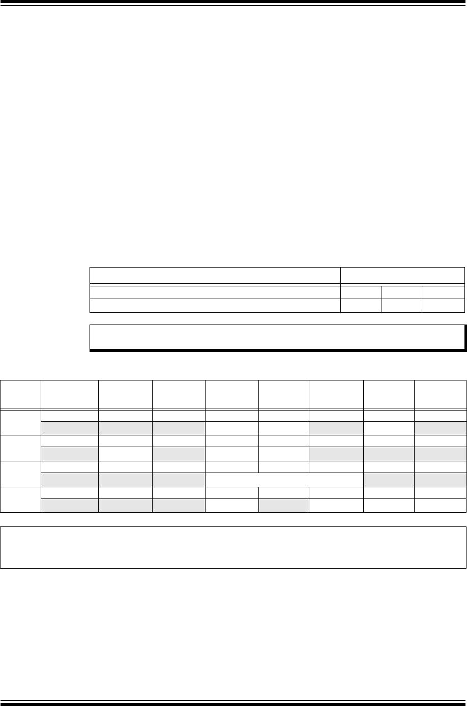
PIC32 Family Reference Manual
DS61113E-page 2-26 © 2007-2012 Microchip Technology Inc.
2.12.5 Status Register (CP0 Register 12, Select 0)
The read/write Status register contains the operating mode, interrupt enabling, and the diagnostic
states of the processor. The bits of this register combine to create operating modes for the
processor.
2.12.5.1 INTERRUPT ENABLE
Interrupts are enabled when all of the following conditions are true:
•IE = 1
•EXL = 0
•ERL = 0
•DM = 0
If these conditions are met, the settings of the IPL bits enable the interrupts.
2.12.5.2 OPERATING MODES
If the DM bit in the Debug register is ‘1’, the processor is in Debug mode; otherwise, the
processor is in either Kernel mode or User mode.
The CPU Status register bit settings shown in table determine User or Kernel mode:
Table 2-8: CPU Status Register Bits That Determine Processor Mode
Mode Bit/Setting
User (requires all of the following bits and values) UM = 1EXL = 0ERL = 0
Kernel (requires one or more of the following bit values) UM = 0EXL = 1ERL = 1
Note: The Status register CU0 bit (Status<28>) control coprocessor accessibility. If any
coprocessor is unusable, an instruction that accesses it generates an exception.
Register 2-5: Status: Status Register; CP0 Register 12, Select 0
Bit
Range
Bit
31/23/15/7
Bit
30/22/14/6
Bit
29/21/13/5
Bit
28/20/12/4
Bit
27/19/11/3
Bit
26/18/10/2
Bit
25/17/9/1
Bit
24/16/8/0
31:24 U-0 U-0 U-0 R/W-x R/W-0(1) U-0 R/W-x U-0
— — —CU0RP —RE—
23:16 U-0 R/W-1 U-0 R/W-1 R/W-0 U-0 U-0 U-0
—BEV—SRNMI— — —
15:8 U-0 U-0 U-0 R/W-x R/W-x R/W-x U-0 U-0
— — — IPL<2:0> — —
7:0 U-0 U-0 U-0 R/W-x U-0 R/W-x R/W-x R/W-x
— — —UM—ERLEXLIE
Legend:
R = Readable bit W = Writable bit U = Unimplemented bit, read as ‘0’
-n = Value at POR ‘1’ = Bit is set ‘0’ = Bit is cleared x = Bit is unknown
bit 31-29 Unimplemented: Read as ‘0’
bit 28 CU0: Coprocessor 0 Usable bit
Controls access to Coprocessor 0
1 = Access allowed
0 = Access not allowed
Coprocessor 0 is always usable when the processor is running in Kernel mode, independent of the state of
the CU0 bit.

© 2007-2012 Microchip Technology Inc. DS61113E-page 2-27
Section 2. CPU for Devices with M4K® Core
CPU for Devices
with M4K® Core
2
bit 27 RP: Reduced Power bit
1 = Enables Reduced Power mode
0 = Disables Reduced Power mode
bit 26 Unimplemented: Read as ‘0’
bit 25 RE: Reverse-endian Memory Reference Enable bit
Used to enable reverse-endian memory references while the processor is running in User mode
1 = User mode uses reversed endianness
0 = User mode uses configured endianness
Debug, Kernel, or Supervisor mode references are not affected by the state of this bit.
bit 24-23 Unimplemented: Read as ‘0’
bit 22 BEV: Bootstrap Exception Vector Control bit
Controls the location of exception vectors.
1 = Bootstrap
0 = Normal
bit 21 Unimplemented: Read as ‘0’
bit 20 SR: Soft Reset bit
Indicates that the entry through the Reset exception vector was due to a Soft Reset.
1 = Soft Reset; this bit is always set for any type of reset on the PIC32 core
0 = Not used on PIC32
Software can only write a ‘0’ to this bit to clear it and cannot force a ‘0’ to ‘1’ transition.
bit 19 NMI: Non-Maskable Interrupt bit
Indicates that the entry through the reset exception vector was due to a NMI.
1 = NMI
0 = Not NMI (Soft Reset or Reset)
Software can only write a ‘0’ to this bit to clear it and cannot force a ‘0’ to ‘1’ transition.
bit 18-13 Unimplemented: Read as ‘0’
bit 12-10 IPL<2:0>: Interrupt Priority Level bits
This bit is the encoded (0-7) value of the current IPL. An interrupt will be signaled only if the requested IPL
is higher than this value.
bit 9-5 Unimplemented: Read as ‘0’
bit 4 UM: User Mode bit
This bit denotes the base operating mode of the processor. On the encoding of this bit is:
1 = Base mode is User mode
0 = Base mode in Kernel mode
The processor can also be in Kernel mode if ERL or EXL is set, regardless of the state of the UM bit.
bit 3 Unimplemented: Read as ‘0’
bit 2 ERL: Error Level bit
Set by the processor when a Reset, Soft Reset, NMI or Cache Error exception are taken.
1 = Error level
0 = Normal level
When ERL is set:
•Processor is running in Kernel mode
•Interrupts are disabled
•ERET instruction will use the return address held in the ErrorEPC register instead of the EPC register
•Lower 2
29 bytes of kuseg are treated as an unmapped and uncached region. This allows main
memory to be accessed in the presence of cache errors. The operation of the processor is undefined if
the ERL bit is set while the processor is executing instructions from kuseg.
Register 2-5: Status: Status Register; CP0 Register 12, Select 0 (Continued)

PIC32 Family Reference Manual
DS61113E-page 2-28 © 2007-2012 Microchip Technology Inc.
bit 1 EXL: Exception Level bit
Set by the processor when any exception other than Reset, Soft Reset, or NMI exceptions is taken.
1 = Exception level
0 = Normal level
When EXL is set:
•Processor is running in Kernel mode
•Interrupts are disabled
EPC, BD, and SRSCtl will not be updated if another exception is taken.
bit 0 IE: Interrupt Enable bit
Acts as the master enable for software and hardware interrupts:
1 = Interrupts are enabled
0 = Interrupts are disabled
This bit may be modified separately via the DI and EI instructions
Register 2-5: Status: Status Register; CP0 Register 12, Select 0 (Continued)

© 2007-2012 Microchip Technology Inc. DS61113E-page 2-29
Section 2. CPU for Devices with M4K® Core
CPU for Devices
with M4K® Core
2
2.12.6 IntCtl: Interrupt Control Register (CP0 Register 12, Select 1)
The IntCtl register controls the vector spacing of the PIC32 architecture.
Register 2-6: IntCtl: Interrupt Control Register; CP0 Register 12, Select 1
Bit
Range
Bit
31/23/15/7
Bit
30/22/14/6
Bit
29/21/13/5
Bit
28/20/12/4
Bit
27/19/11/3
Bit
26/18/10/2
Bit
25/17/9/1
Bit
24/16/8/0
31:24 U-0 U-0 U-0 U-0 U-0 U-0 U-0 U-0
— — — — — — — —
23:16 U=0 U-0 U-0 U-0 U-0 U-0 U-0 U-0
— — — — — — — —
15:8 U-0 U-0 U-0 U-0 U-0 U-0 R/W-0 R/W-0
— — — — — —VS<4:4>
7:0 R/W-0 R/W-0 R/W-0 U-0 U-0 U-0 U-0 U-0
VS<2:0> — — — — —
Legend:
R = Readable bit W = Writable bit U = Unimplemented bit, read as ‘0’
-n = Value at POR ‘1’ = Bit is set ‘0’ = Bit is cleared x = Bit is unknown
bit 31-10 Unimplemented: Read as ‘0’
bit 9-5 VS<4:0>: Vector Spacing bits
These bits specify the spacing between each interrupt vector.
All other values are reserved. The operation of the processor is undefined if a reserved value is written to
these bits.
bit 4-0 Unimplemented: Read as ‘0’
Encoding Spacing Between Vectors
(hex)
Spacing Between Vectors
(decimal)
0x00 0x000 0x 0
0x01 0x020 32
0x02 0x040 64
0x04 0x080 128
0x08 0x100 256
0x10 0x200 512
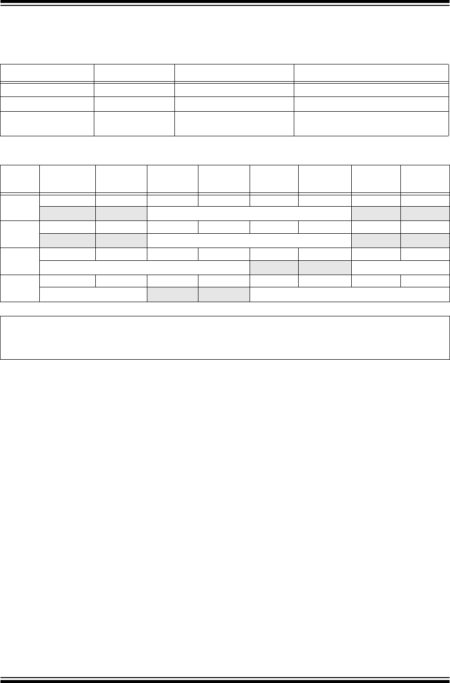
PIC32 Family Reference Manual
DS61113E-page 2-30 © 2007-2012 Microchip Technology Inc.
2.12.7 SRSCtl Register (CP0 Register 12, Select 2)
The SRSCtl register controls the operation of GPR shadow sets in the processor.
Table 2-9: Sources for New CSS on an Exception or Interrupt
Exception Type Bit Source Condition Comment
Exception ESS All —
Non-Vectored Interrupt ESS IV bit = 0 (Cause<23>) Treat as exception
Vectored EIC Interrupt EICSS IV bit = 1 (Cause<23>) and,
VEIC bit = 1 (Config3<6>)
Source is external interrupt controller.
Register 2-7: SRSCtl: Shadow Register Set Register; CP0 Register 12, Select 2
Bit
Range
Bit
31/23/15/7
Bit
30/22/14/6
Bit
29/21/13/5
Bit
28/20/12/4
Bit
27/19/11/3
Bit
26/18/10/2
Bit
25/17/9/1
Bit
24/16/8/0
31:24 U-0 U-0 R-0 R-0 R-0 R-1 U-0 U-0
——HSS<3:0>— —
23:16 U-0 U-0 R-x R-x R-x R-x U-0 U-0
— — EICSS<3:0> — —
15:8 R/W-0 R/W-0 R/W-0 R/W-0 U-0 U-0 R/W-0 R/W-0
ESS<3:0> ——PSS<3:2>
7:0 R/W-0 R/W-0 U-0 U-0 R-0 R-0 R-0 R-0
PSS<1:0> ——CSS<3:0>
Legend:
R = Readable bit W = Writable bit U = Unimplemented bit, read as ‘0’
-n = Value at POR ‘1’ = Bit is set ‘0’ = Bit is cleared x = Bit is unknown
bit 31-30 Unimplemented: Read as ‘0’
bit 29-26 HSS<3:0>: High Shadow Set bits
This bit contains the highest shadow set number that is implemented by this processor. A value of ‘0000’ in
these bits indicates that only the normal GPRs are implemented.
1111 = Reserved
•
•
•
0100 = Reserved
0011 = Four shadow sets are present
0010 = Reserved
0001 = Two shadow sets are present
0000 = One shadow set (normal GPR set) is present
The value in this bit also represents the highest value that can be written to the ESS<3:0>, EICSS<3:0>,
PSS<3:0>, and CSS<3:0> bits of this register, or to any of the bits of the SRSMap register. The operation
of the processor is undefined if a value larger than the one in this bit is written to any of these other bits.
bit 25-22 Unimplemented: Read as ‘0’
bit 21-18 EICSS<3:0>: External Interrupt Controller Shadow Set bits
EIC Interrupt mode shadow set. This bit is loaded from the external interrupt controller for each interrupt
request and is used in place of the SRSMap register to select the current shadow set for the interrupt.
bit 17-16 Unimplemented: Read as ‘0’

© 2007-2012 Microchip Technology Inc. DS61113E-page 2-31
Section 2. CPU for Devices with M4K® Core
CPU for Devices
with M4K® Core
2
bit 15-12 ESS<3:0>: Exception Shadow Set bits
This bit specifies the shadow set to use on entry to Kernel mode caused by any exception other than a vec-
tored interrupt. The operation of the processor is undefined if software writes a value into this bit that is
greater than the value in the HSS<3:0> bits.
bit 11-10 Unimplemented: Read as ‘0’
bit 9-6 PSS<3:0>: Previous Shadow Set bits
Since GPR shadow registers are implemented, this bit is copied from the CSS bit when an exception or
interrupt occurs. An ERET instruction copies this value back into the CSS bit if the BEV bit (Status<22>) = 0.
This bit is not updated on any exception which sets the ERL bit (Status<2>) to ‘1’ (i.e., Reset, Soft Reset,
NMI, cache error), an entry into EJTAG Debug mode, or any exception or interrupt that occurs with the EXL
bit (Status<1>) = 1, or BEV = 1. This bit is not updated on an exception that occurs while ERL = 1.
The operation of the processor is undefined if software writes a value into this bit that is greater than the
value in the HSS<3:0> bits.
bit 5-4 Unimplemented: Read as ‘0’
bit 3-0 CSS<3:0>: Current Shadow Set bits
Since GPR shadow registers are implemented, this bit is the number of the current GPR set. This bit is
updated with a new value on any interrupt or exception, and restored from the PSS bit on an ERET.
Tabl e 2-9 describes the various sources from which the CSS<3:0> bits are updated on an exception or
interrupt.
This bit is not updated on any exception which sets the ERL bit (Status<2>) to ‘1’ (i.e., Reset, Soft Reset,
NMI, cache error), an entry into EJTAG Debug mode, or any exception or interrupt that occurs with EXL bit
(Status<1>) = 1, or BEV = 1. Neither is it updated on an ERET with ERL = 1 or BEV = 1. This bit is not
updated on an exception that occurs while ERL = 1.
The value of the CSS<3:0> bits can be changed directly by software only by writing the PSS<3:0> bits and
executing an ERET instruction.
Register 2-7: SRSCtl: Shadow Register Set Register; CP0 Register 12, Select 2 (Continued)

PIC32 Family Reference Manual
DS61113E-page 2-32 © 2007-2012 Microchip Technology Inc.
2.12.8 SRSMap: Register (CP0 Register 12, Select 3)
The SRSMap register contains eight 4-bit bits that provide the mapping from an vector number
to the shadow set number to use when servicing such an interrupt. The values from this register
are not used for a non-interrupt exception, or a non-vectored interrupt (IV bit = 0, Cause<23> or
VS<4:0> bit = 0, IntCtl<9:5>). In such cases, the shadow set number comes from the ESS<3:0>
bits (SRSCtl<15:12>).
If the HSS<3:0> bits (SRSCTL29:26) are ‘0’, the results of a software read or write of this register
are unpredictable.
The operation of the processor is undefined if a value is written to any bit in this register that is
greater than the value of the HSS<3:0> bits.
The SRSMap register contains the shadow register set numbers for vector numbers 7-0. The
same shadow set number can be established for multiple interrupt vectors, creating a
many-to-one mapping from a vector to a single shadow register set number.
Register 2-8: SRSMap: Shadow Register Set Map Register; CP0 Register 12, Select 3
Bit
Range
Bit
31/23/15/7
Bit
30/22/14/6
Bit
29/21/13/5
Bit
28/20/12/4
Bit
27/19/11/3
Bit
26/18/10/2
Bit
25/17/9/1
Bit
24/16/8/0
31:24 R/W-0 R/W-0 R/W-0 R/W-0 R/W-0 R/W-0 R/W-0 R/W-0
SSV7<3:0> SSV6<3:0>
23:16 R/W-0 R/W-0 R/W-0 R/W-0 R/W-0 R/W-0 R/W-0 R/W-0
SSV5<3:0> SSV4<3:0>
15:8 R/W-0 R/W-0 R/W-0 R/W-0 R/W-0 R/W-0 R/W-0 R/W-0
SSV3<3:0> SSV2<3:0>
7:0 R/W-0 R/W-0 R/W-0 R/W-0 R/W-0 R/W-0 R/W-0 R/W-0
SSV1<3:0> SSV0<3:0>
Legend:
R = Readable bit W = Writable bit U = Unimplemented bit, read as ‘0’
-n = Value at POR ‘1’ = Bit is set ‘0’ = Bit is cleared x = Bit is unknown
bit 31-28 SSV7<3:0>: Shadow Set Vector 7 bits
Shadow register set number for Vector Number 7
bit 27-24 SSV6<3:0>: Shadow Set Vector 6 bits
Shadow register set number for Vector Number 6
bit 23-20 SSV5<3:0>: Shadow Set Vector 5 bits
Shadow register set number for Vector Number 5
bit 19-16 SSV4<3:0>: Shadow Set Vector 4 bits
Shadow register set number for Vector Number 4
bit 15-12 SSV3<3:0>: Shadow Set Vector 3 bits
Shadow register set number for Vector Number 3
bit 11-8 SSV2<3:0>: Shadow Set Vector 2 bits
Shadow register set number for Vector Number 2
bit 7-4 SSV1<3:0>: Shadow Set Vector 1 bits
Shadow register set number for Vector Number 1
bit 3-0 SSV0<3:0>: Shadow Set Vector 0 bit
Shadow register set number for Vector Number 0
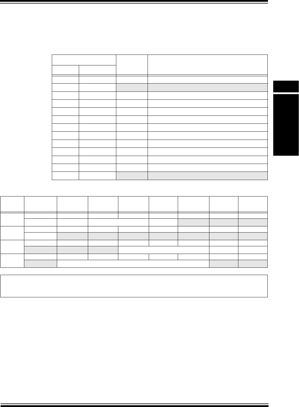
© 2007-2012 Microchip Technology Inc. DS61113E-page 2-33
Section 2. CPU for Devices with M4K® Core
CPU for Devices
with M4K® Core
2
2.12.9 Cause Register (CP0 Register 13, Select 0)
The Cause register primarily describes the cause of the most recent exception. In addition, bits
also control software interrupt requests and the vector through which interrupts are dispatched.
With the exception of the IP1, IP0, DC, and IV bits, all bits in the Cause register are read-only.
Table 2-10: Cause Register EXCCODE<4:0> Bits
Exception Code Value
Mnemonic Description
Decimal Hex
00x00 IntInterrupt
1-3 0x01 —Reserved
4 0x04 AdEL Address error exception (load or instruction fetch)
50x05AdESAddress error exception (store)
60x06IBEBus error exception (instruction fetch)
70x07DBEBus error exception (data reference: load or store)
80x08SysSyscall exception
90x09 BpBreakpoint exception
10 0x0A RI Reserved instruction exception
11 0x0B CPU Coprocessor Unusable exception
12 0x0C Ov Arithmetic Overflow exception
13 0x0D Tr Trap exception
14-31 0x0E-0x1F —Reserved
Register 2-9: Cause: Exception Cause Register; CP0 Register 13, Select 0
Bit
Range
Bit
31/23/15/7
Bit
30/22/14/6
Bit
29/21/13/5
Bit
28/20/12/4
Bit
27/19/11/3
Bit
26/18/10/2
Bit
25/17/9/1
Bit
24/16/8/0
31:24 R-x R-x R-x R-x R/W-0 U-0 U-0 U-0
BD TI CE<1:0> DC — — —
23:16 R/W-x U-0 U-0 U-0 U-0 U-0 U-0 U-0
IV — — — — — — —
15:8 U-0 U-0 U-0 R-x R-x R-x R/W-x R/W-x
— — — RIPL<2:0> IP1 IP0
7:0 U-0 R-x R-x R-x R-x R-x U-0 U-0
—EXCCODE<4:0>— —
Legend:
R = Readable bit W = Writable bit U = Unimplemented bit, read as ‘0’
-n = Value at POR ‘1’ = Bit is set ‘0’ = Bit is cleared x = Bit is unknown
bit 31 BD: Branch Delay bit
Indicates whether the last exception taken occurred in a branch delay slot:
1 = In delay slot
0 = Not in delay slot
The processor updates BD only if the EXL bit (Status<1>) was ‘0’ when the exception occurred.
bit 30 TI: Timer Interrupt bit
Timer Interrupt. This bit denotes whether a timer interrupt is pending (analogous to the IP bits for other
interrupt types):
1 = Timer interrupt is pending
0 = No timer interrupt is pending
bit 29-28 CE<1:0>: Coprocessor Exception bits
Coprocessor unit number referenced when a Coprocessor Unusable exception is taken. This bit is loaded
by hardware on every exception, but is unpredictable for all exceptions except for Coprocessor Unusable.

PIC32 Family Reference Manual
DS61113E-page 2-34 © 2007-2012 Microchip Technology Inc.
bit 27 DC: Disable Count Register bit
In some power-sensitive applications, the Count register is not used and can be stopped to avoid
unnecessary toggling.
1 = Disable counting of Count register
0 = Enable counting of Count register
bit 26-24 Unimplemented: Read as ‘0’
bit 23 IV: Interrupt Vector bit
Indicates whether an interrupt exception uses the general exception vector or a special interrupt vector
1 = Use the special interrupt vector (0x200)
0 = Use the general exception vector (0x180)
If the IV bit (Cause<23>) is ‘1’ and the BEV bit (Status<22>) is ‘0’, the special interrupt vector represents
the base of the vectored interrupt table.
bit 22-13 Unimplemented: Read as ‘0’
bit 12-10 RIPL<2:0>: Requested Interrupt Priority Level bits
This bit is the encoded (7-0) value of the requested interrupt. A value of ‘0’ indicates that no interrupt is
requested.
bit 9-8 IP<1:0>: Software Interrupt Request Control bits
Controls the request for software interrupts
1 = Request software interrupt
0 = No interrupt requested
These bits are exported to the system interrupt controller for prioritization in EIC Interrupt mode with other
interrupt sources.
bit 7 Unimplemented: Read as ‘0’
bit 6-2 EXCCODE<4:0>: Exception Code bits
See Tab l e 2- 10 for the list of Exception codes.
bit 1-0 Unimplemented: Read as ‘0’
Register 2-9: Cause: Exception Cause Register; CP0 Register 13, Select 0 (Continued)

© 2007-2012 Microchip Technology Inc. DS61113E-page 2-35
Section 2. CPU for Devices with M4K® Core
CPU for Devices
with M4K® Core
2
2.12.10 EPC Register (CP0 Register 14, Select 0)
The Exception Program Counter (EPC) is a read/write register that contains the address at which
processing resumes after an exception has been serviced. All bits of the EPC register are
significant and are writable.
For synchronous (precise) exceptions, the EPC contains one of the following:
•The virtual address of the instruction that was the direct cause of the exception
•The virtual address of the immediately preceding BRANCH or JUMP instruction, when the
exception causing instruction is in a branch delay slot and the Branch Delay bit in the
Cause register is set
On new exceptions, the processor does not write to the EPC register when the EXL bit in the
Status register is set, however, the register can still be written via the MTC0 instruction.
Since the PIC32 family implements MIPS16e® or microMIPS™ ASE, a read of the EPC register
(via MFC0) returns the following value in the destination GPR:
GPR[rt] ExceptionPC31..1 || ISAMode0
That is, the upper 31 bits of the exception PC are combined with the lower bit of the ISA<1:0>
bits (Config3<15:14>) and are written to the GPR.
Similarly, a write to the EPC register (via MTC0) takes the value from the GPR and distributes
that value to the exception PC and the ISA<1:0> bits (Config3<15:14>), as follows:
ExceptionPC GPR[rt]31..1 || 0
ISAMode 2#0 || GPR[rt]0
That is, the upper 31 bits of the GPR are written to the upper 31 bits of the exception PC, and the
lower bit of the exception PC is cleared. The upper bit of the ISA<1:0> bits (Config3<15:14>) is
cleared and the lower bit is loaded from the lower bit of the GPR.
Register 2-10: EPC: Exception Program Counter Register; CP0 Register 14, Select 0
Bit
Range
Bit
31/23/15/7
Bit
30/22/14/6
Bit
29/21/13/5
Bit
28/20/12/4
Bit
27/19/11/3
Bit
26/18/10/2
Bit
25/17/9/1
Bit
24/16/8/0
31:24 R/W-x R/W-x R/W-x R/W-x R/W-x R/W-x R/W-x R/W-x
EPC<31:24>
23:16 R/W-x R/W-x R/W-x R/W-x R/W-x R/W-x R/W-x R/W-x
EPC<23:16>
15:8 R/W-x R/W-x R/W-x R/W-x R/W-x R/W-x R/W-x R/W-x
EPC<15:8>
7:0 R/W-x R/W-x R/W-x R/W-x R/W-x R/W-x R/W-x R/W-x
EPC<7:0>
Legend:
R = Readable bit W = Writable bit U = Unimplemented bit, read as ‘0’
-n = Value at POR ‘1’ = Bit is set ‘0’ = Bit is cleared x = Bit is unknown
bit 31-0 EPC<31:0>: Exception Program Counter bits

PIC32 Family Reference Manual
DS61113E-page 2-36 © 2007-2012 Microchip Technology Inc.
2.12.11 PRID Register (CP0 Register 15, Select 0)
The Processor Identification (PRID) register is a 32-bit read-only register that contains
information identifying the manufacturer, manufacturer options, processor identification, and
revision level of the processor.
Register 2-11: PRID: Processor Identification Register; CP0 Register 15, Select 0
Bit
Range
Bit
31/23/15/7
Bit
30/22/14/6
Bit
29/21/13/5
Bit
28/20/12/4
Bit
27/19/11/3
Bit
26/18/10/2
Bit
25/17/9/1
Bit
24/16/8/0
31:24 U-0 U-0 R-0 U-0 U-0 U-0 U-0 U-0
— — — — — — — —
23:16 R-0 R-0 R-0 R-0 R-0 R-0 R-0 R-1
COMPANYID<23:16>
15:8 R-x R-x R-x R-x R-x R-x R-x R-x
PROCESSORID<15:8>
7:0 R-x R-x R-x R-x R-x R-x R-x R-x
MAJORREV<2:0> MINORREV<2:0> PATCHREV<1:0>
Legend: Legend:
R=Readable bit W=Writable bit P=Programmable bit r=Reserved bit
U=Unimplemented bit n=Bit Value at POR: (‘0’, ‘1’, x=Unknown)
bit 31-24 Unimplemented: Read as ‘0’
bit 23-16 COMPANYID<7:0>: Company Identification bits
In PIC32 devices, these bits contain a value of ‘1’ to indicate MIPS® Technologies, Inc. as the processor
manufacturer/designer.
bit 15-8 PROCESSORID<7:0>: Processor Identification bits
These bits allow software to distinguish between the various types of MIPS® Technologies processors. For
PIC32 devices with the M4K® core, this value is 0x87.
bit 7-5 MAJORREV<2:0>: Processor Major Revision Identification bits
These bits allow software to distinguish between one revision and another of the same processor type. This
number is increased on major revisions of the processor core.
bit 4-2 MINORREV<2:0>: Processor Minor Revision Identification bits
This number is increased on each incremental revision of the processor and reset on each new major
revision.
bit 1-0 PATCHREV<1:0>: Processor Patch Level Identification bits
If a patch is made to modify an older revision of the processor, the value of these bits will be incremented.

© 2007-2012 Microchip Technology Inc. DS61113E-page 2-37
Section 2. CPU for Devices with M4K® Core
CPU for Devices
with M4K® Core
2
2.12.12 Ebase Register (CP0 Register 15, Select 1)
The Ebase register is a read/write register containing the base address of the exception vectors
used when the BEV bit (Status<22>) equals ‘0’, and a read-only CPU number value that may be
used by software to distinguish different processors in a multi-processor system.
The Ebase register provides the ability for software to identify the specific processor within a
multi-processor system, and allows the exception vectors for each processor to be different,
especially in systems composed of heterogeneous processors. Bits 31-12 of the Ebase register
are concatenated with zeros to form the base of the exception vectors when the BEV bit is ‘0’.
The exception vector base address comes from the fixed defaults when the BEV bit is ‘1’, or for
any EJTAG Debug exception. The Reset state of bits 31-12 of the Ebase register initialize the
exception base register to 0x80000000.
Bits 31 and 30 of the Ebase Register are fixed with the value 2#10 to force the exception base
address to be in the kseg0 or kseg1 unmapped virtual address segments.
If the value of the exception base register is to be changed, this must be done with the BEV bit
equal to ‘1’. The operation of the processor is undefined if the Ebase<17:0> bits are written with
a different value when the BEV bit (Status<22>) is ‘0’.
Combining bits 31-20 of the Ebase register allows the base address of the exception vectors to
be placed at any 4 KB page boundary.
Register 2-12: Ebase: Exception Base Register; CP0 Register 15, Select 1
Bit
Range
Bit
31/23/15/7
Bit
30/22/14/6
Bit
29/21/13/5
Bit
28/20/12/4
Bit
27/19/11/3
Bit
26/18/10/2
Bit
25/17/9/1
Bit
24/16/8/0
31:24 U-1 U-0 R/W-0 R/W-0 R/W-0 R/W-0 R/W-0 R/W-0
— — EBASE<17:12>
23:16 R/W-0 R/W-0 R/W-0 R/W-0 R/W-0 R/W-0 R/W-0 R/W-0
EBASE<11:4>
15:8 R/W-0 R/W-0 R/W-0 R/W-0 U-0 U-0 R-0 R-0
EBASE<3:0> — —CPUNUM<9:8>
7:0 R-0 R-0 R-0 R-0 R-0 R-0 R-0 R-0
CPUNUM<7:0>
Legend:
R = Readable bit W = Writable bit U = Unimplemented bit, read as ‘0’
-n = Value at POR ‘1’ = Bit is set ‘0’ = Bit is cleared x = Bit is unknown
bit 31 Unimplemented: Read as ‘1’
bit 30 Unimplemented: Read as ‘0’
bit 29-12 EBASE<17:0>: Exception Vector Base Address bits
In conjunction with bits 31-30, these bits specify the base address of the exception vectors when the BEV
bit (Status<22>) is ‘0’.
bit 11-10 Unimplemented: Read as ‘0’
bit 9-0 CPUNUM<9:0>: CPU Number bits
These bits specify the number of CPUs in a multi-processor system and can be used by software to
distinguish a particular processor from others. In a single processor system, this value is set to ‘0’.
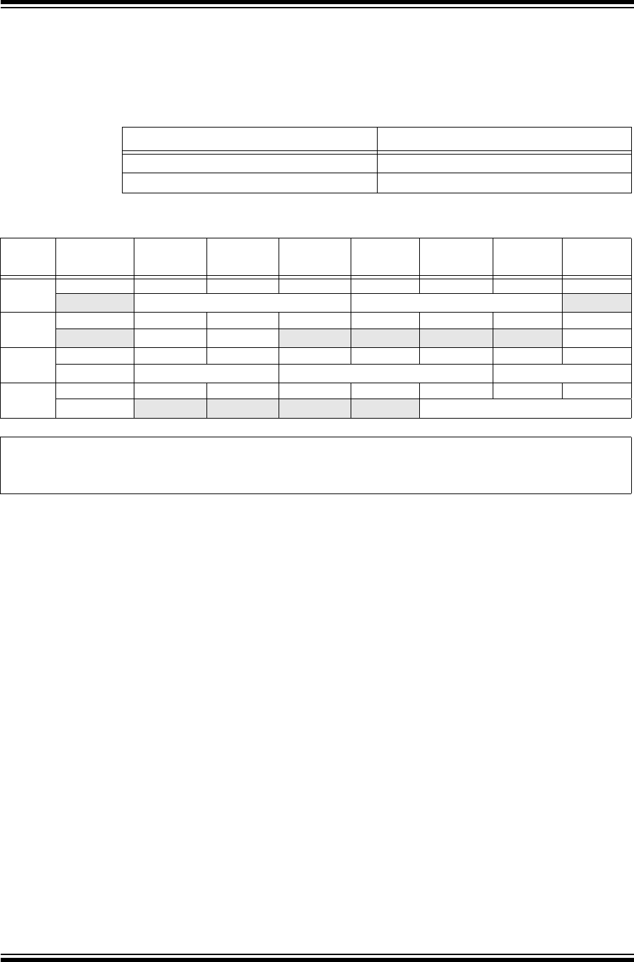
PIC32 Family Reference Manual
DS61113E-page 2-38 © 2007-2012 Microchip Technology Inc.
2.12.13 Config Register (CP0 Register 16, Select 0)
The Config register specifies various configuration and capabilities information. Most of the fields
in the Config register are initialized by hardware during the Reset exception process, or are
constant.
Table 2-11: Cache Coherency Attributes
K0<2:0> Value Cache Coherency Attribute
2 Uncached
3Cacheable
Register 2-13: Config: Configuration Register; CP0 Register 16, Select 0
Bit
Range
Bit
31/23/15/7
Bit
30/22/14/6
Bit
29/21/13/5
Bit
28/20/12/4
Bit
27/19/11/3
Bit
26/18/10/2
Bit
25/17/9/1
Bit
24/16/8/0
31:24 r-1 R-0 R-1 R-0 R/W-0 R/W-1 R/W-0 U-0
—K23<2:0> KU<2:0>—
23:16 U-0 R-0 R-0 r-0 U-0 U-0 U-0 R-1
—UDISB— — — —DS
15:8 R-0 R-0 R-0 R-0 R-0 R-1 R-0 R-1
BE AT<1:0> AR<2:0> MT<2:1>
7:0 R-1 U-0 U-0 U-0 U-0 R/W-0 R/W-1 R/W-0
MT<1> — — — —K0<2:0>
Legend: r = Reserved bit
R = Readable bit W = Writable bit U = Unimplemented bit, read as ‘0’
-n = Value at POR ‘1’ = Bit is set ‘0’ = Bit is cleared x = Bit is unknown
bit 31 Reserved: This bit is hardwired to ‘1’ to indicate the presence of the Config1 register.
bit 30-28 K23<2:0>: kseg2 and kseg3 bits
These bits control the cacheability of the kseg2 and kseg3 address segments.
Refer to Ta ble 2 -11 for the bit encoding.
bit 27-25 KU<2:0>: kuseg and useg bits
These bits control the cacheability of the kuseg and useg address segments.
Refer to Ta ble 2 -11 for the bit encoding.
bit 24-23 Unimplemented: Read as ‘0’
bit 22 UDI: User-Defined bit
This bit indicates that CorExtend User-Defined Instructions have been implemented.
1 = User-defined Instructions are implemented
0 = No User-defined Instructions are implemented
bit 21 SB: SimpleBE bit
This bit indicates whether SimpleBE Bus mode is enabled.
1 = Only simple byte enables allowed on internal bus interface
0 = No reserved byte enables on internal bus interface
bit 20 Reserved: This bit is hardwired to ‘0’ to indicate the Fast, High-Performance Multiply/Divide Unit (MDU)
bit 19-17 Unimplemented: Read as ‘0’
bit 16 DS: Dual SRAM bit
1 = Dual instruction/data SRAM internal bus interfaces
0 = Unified instruction/data SRAM internal bus interface
PIC32 devices based on the M4K® core use Dual SRAM-style interfaces internally.

© 2007-2012 Microchip Technology Inc. DS61113E-page 2-39
Section 2. CPU for Devices with M4K® Core
CPU for Devices
with M4K® Core
2
bit 15 BE: Big-Endian bit
Indicates the endian mode in which the processor is running, PIC32 is always little-endian.
1 = Big-endian
0 = Little-endian
bit 14-13 AT<1:0>: Architecture Type bits
Architecture type implemented by the processor. This bit is always ‘00’ to indicate the MIPS32®
architecture.
bit 12-10 AR<2:0>: Architecture Revision Level bits
Architecture revision level. This bit is always ‘001’ to indicate MIPS32® Release 2.
111 = Reserved
110 = Reserved
101 = Reserved
100 = Reserved
011 = Reserved
010 = Reserved
001 = Release 2
000 = Release 1
bit 9-7 MT<2:0>: MMU Type bits
111 = Reserved
110 = Reserved
101 = Reserved
100 = Reserved
011 = Fixed mapping
010 = Reserved
001 = Reserved
000 = Reserved
bit 6-3 Unimplemented: Read as ‘0’
bit 2-0 K0<2:0>: Kseg0 bits
Kseg0 coherency algorithm. Refer to Tab l e 2- 11 for the bit encoding.
Register 2-13: Config: Configuration Register; CP0 Register 16, Select 0 (Continued)

PIC32 Family Reference Manual
DS61113E-page 2-40 © 2007-2012 Microchip Technology Inc.
2.12.14 Config1 Register (CP0 Register 16, Select 1)
The Config1 register is an adjunct to the Config register and encodes additional information
about capabilities present on the core. All fields in the Config1 register are read-only.
Register 2-14: Config1: Configuration Register 1; CP0 Register 16, Select 1
Bit
Range
Bit
31/23/15/7
Bit
30/22/14/6
Bit
29/21/13/5
Bit
28/20/12/4
Bit
27/19/11/3
Bit
26/18/10/2
Bit
25/17/9/1
Bit
24/16/8/0
31:24 r-1 U-0 U-0 U-0 U-0 U-0 U-0 U-0
— — — — — — — —
23:16 U-0 U-0 U-0 U-0 U-0 U-0 U-0 U-0
— — — — — — — —
15:8 U-0 U-0 U-0 U-0 U-0 U-0 U-0 U-0
— — — — — — — —
7:0 U-0 U-0 U-0 U-0 U-0 R-1 R-x U-0
— — — — —CAEP—
Legend: r = Reserved bit
R = Readable bit W = Writable bit U = Unimplemented bit, read as ‘0’
-n = Value at POR ‘1’ = Bit is set ‘0’ = Bit is cleared x = Bit is unknown
bit 31 Reserved: This bit is hardwired to a ‘1’ to indicate the presence of the Config2 register.
bit 30-3 Unimplemented: Read as ‘0’
bit 2 CA: Code Compression Implemented bit
1 = MIPS16e® is implemented
0 = No MIPS16e® present
bit 1 EP: EJTAG Present bit
This bit is always set to ‘1’ indicate that the core implements EJTAG.
bit 0 Unimplemented: Read as ‘0’

© 2007-2012 Microchip Technology Inc. DS61113E-page 2-41
Section 2. CPU for Devices with M4K® Core
CPU for Devices
with M4K® Core
2
2.12.15 Config2 (CP0 Register 16, Select 2)
The Config2 register is an adjunct to the Config register and is reserved to encode additional
capabilities information. Config2 is allocated for showing the configuration of level 2/3 caches.
These bits are reset to ‘0’ because L2/L3 caches are not supported by the PIC32 core. All bits in
the Config2 register are read-only.
Register 2-15: Config2: Configuration Register 2; CP0 Register 16, Select 2
Bit
Range
Bit
31/23/15/7
Bit
30/22/14/6
Bit
29/21/13/5
Bit
28/20/12/4
Bit
27/19/11/3
Bit
26/18/10/2
Bit
25/17/9/1
Bit
24/16/8/0
31:24 r-1 U-0 U-0 U-0 U-0 U-0 U-0 U-0
— — — — — — — —
23:16 U-0 U-0 U-0 U-0 U-0 U-0 U-0 U-0
— — — — — — — —
15:8 U-0 U-0 U-0 U-0 U-0 U-0 U-0 U-0
— — — — — — — —
7:0 U-0 U-0 U-0 U-0 U-0 U-0 U-0 U-0
— — — — — — — —
Legend: r = Reserved bit
R = Readable bit W = Writable bit U = Unimplemented bit, read as ‘0’
-n = Value at POR ‘1’ = Bit is set ‘0’ = Bit is cleared x = Bit is unknown
bit 31 Reserved: This bit is hardwired to a ‘1’ to indicate the presence of the Config3 register.
bit 30-0 Unimplemented: Read as ‘0’

PIC32 Family Reference Manual
DS61113E-page 2-42 © 2007-2012 Microchip Technology Inc.
2.12.16 Config3 Register (CP0 Register 16, Select 3)
The Config3 register encodes additional capabilities. All fields in the Config3 register are
read-only.
Register 2-16: Config3: Configuration Register 3; CP0 Register 16, Select 3
Bit
Range
Bit
31/23/15/7
Bit
30/22/14/6
Bit
29/21/13/5
Bit
28/20/12/4
Bit
27/19/11/3
Bit
26/18/10/2
Bit
25/17/9/1
Bit
24/16/8/0
31:24 U-0 U-0 U-0 U-0 U-0 U-0 U-0 U-0
— — — — — — — —
23:16 U-0 U-0 U-0 U-0 U-0 U-0 U-0 U-0
— — — — — — — —
15:8 U-0 U-0 U-0 U-0 U-0 U-0 U-0 R-0
— — — — — — —ITL
7:0 U-0 R-1 R-1 U-0 U-0 U-0 U-0 U-0
— VEIC VINT — — — — —
Legend:
R = Readable bit W = Writable bit U = Unimplemented bit, read as ‘0’
-n = Value at POR ‘1’ = Bit is set ‘0’ = Bit is cleared x = Bit is unknown
bit 31-9 Unimplemented: Read as ‘0’
bit 8 ITL: Indicates that iFlowTrace hardware is present
1 = The iFlowTrace is implemented in the core
0 = The iFlowTrace is not implemented in the core
bit 7 Unimplemented: Read as ‘0’
bit 6 VEIC: External Vectored Interrupt Controller bit
Support for an external interrupt controller is implemented.
1 = Support for EIC Interrupt mode is implemented
0 = Support for EIC Interrupt mode is not implemented
PIC32 devices internally implement a MIPS® “external interrupt controller”; therefore, this bit reads ‘1’.
bit 5 VINT: Vector Interrupt bit
Vectored interrupts implemented. This bit indicates whether vectored interrupts are implemented.
1 = Vector interrupts are implemented
0 = Vector interrupts are not implemented
On the PIC32 core, this bit is always a ‘1’ since vectored interrupts are implemented.
bit 4-0 Unimplemented: Read as ‘0’

© 2007-2012 Microchip Technology Inc. DS61113E-page 2-43
Section 2. CPU for Devices with M4K® Core
CPU for Devices
with M4K® Core
2
2.12.17 Debug Register (CP0 Register 23, Select 0)
The Debug register is used to control the debug exception and provide information about the
cause of the debug exception and when re-entering at the debug exception vector due to a
normal exception in Debug mode. The read-only information bits are updated every time the
debug exception is taken or when a normal exception is taken when already in Debug mode.
Only the DM bit and the VER<2:0> bits are valid when read from non-Debug mode; the values
of all other bits and fields are unpredictable. Operation of the processor is undefined if the Debug
register is written from non-Debug mode.
Some of the bits and fields are only updated on debug exceptions and/or exceptions in Debug
mode, as follows:
•DSS, DBP, DDBL, DDBS, DIB, DINT are updated on both debug exceptions and on
exceptions in debug modes
•DEXCCODE<4:0> are updated on exceptions in Debug mode, and are undefined after a
debug exception
•HALT and DOZE are updated on a debug exception, and are undefined after an exception
in Debug mode
•DBD is updated on both debug and on exceptions in debug modes
All bits are undefined when read from Normal mode, except VER<2:0> and DM.
Register 2-17: Debug: Debug Exception Register; CP0 Register 23, Select 0
Bit
Range
Bit
31/23/15/7
Bit
30/22/14/6
Bit
29/21/13/5
Bit
28/20/12/4
Bit
27/19/11/3
Bit
26/18/10/2
Bit
25/17/9/1
Bit
24/16/8/0
31:24 R-0 R-0 R-0 R/W-0 U-0 U-0 R/W-1 R/W-0
DBD DM NODCR LSNM DOZE HALT COUNTDM IBUSEP
23:16 R-0 R-0 R/W-0 R/W-0 R-0 R-0 R-0 R-1
MCHECKP CACHEEP DBUSEP IEXI DDBSIMPR DDBLIMPR VER<2:1>
15:8 R-0 U-0 U-0 U-0 U-0 U-0 R-0 R/W-0
VER DEXCCODE<4:0> NOSST SST
7:0 U-0 R-x R-x R-x R-x R-x R-x R-x
—DIBIMPRDINT DIB DDBSDDBL DBP DSS
Legend:
R = Readable bit W = Writable bit U = Unimplemented bit, read as ‘0’
-n = Value at POR ‘1’ = Bit is set ‘0’ = Bit is cleared x = Bit is unknown
bit 31 DBD: Branch Delay Debug Exception bit
Indicates whether the last debug exception or exception in Debug mode, occurred in a branch delay slot:
1 = In delay slot
0 = Not in delay slot
bit 30 DM: Debug Mode bit
Indicates that the processor is operating in Debug mode:
1 = Processor is operating in Debug mode
0 = Processor is operating in non-Debug mode
bit 29 NODCR: Debug Control Register bit
Indicates whether the dseg memory segment is present and the Debug Control Register is accessible:
1 = No dseg present
0 = dseg is present

PIC32 Family Reference Manual
DS61113E-page 2-44 © 2007-2012 Microchip Technology Inc.
bit 28 LSNM: Load Store Access Control bit
Controls access of load/store between dseg and main memory:
1 = Load/stores in dseg address range goes to main memory
0 = Load/stores in dseg address range goes to dseg
bit 27 DOZE: Low-Power Mode Debug Exception bit
Indicates that the processor was in any kind of low-power mode when a debug exception occurred.
1 = Processor was in a low-power mode when a debug exception occurred
0 = Processor was not in a low-power mode when debug exception occurred
bit 26 HALT: System Bus Clock Stop bit
Indicates that the internal system bus clock was stopped when the debug exception occurred.
1 = Internal system bus clock running
0 = Internal system bus clock stopped
bit 25 COUNTDM: Count Register Behavior bit
Indicates the Count register behavior in Debug mode.
1 = Count register is running in Debug mode
0 = Count register stopped in Debug mode
bit 24 IBUSEP: Instruction Fetch Bus Error Exception Pending bit
Set when an instruction fetch bus error event occurs or if a ‘1’ is written to the bit by software. Cleared when
a Bus Error exception on instruction fetch is taken by the processor, and by Reset. If IBUSEP is set when
IEXI is cleared, a Bus Error exception on instruction fetch is taken by the processor, and IBUSEP is cleared.
bit 23 MCHECKP: Machine Check Exception Pending bit
All Machine Check exceptions are precise on the PIC32 processor so this bit will always read as ‘0’.
bit 22 CACHEEP: Cache Error Pending bit
Cache Errors cannot be taken by the PIC32 core so this bit will always read as ‘0’.
bit 21 DBUSEP: Data Access Bus Error Exception Pending bit
Covers imprecise bus errors on data access, similar to behavior of IBUSEP for imprecise bus errors on an
instruction fetch.
bit 20 IEXI: Imprecise Error Exception Inhibit Control bit
Controls exceptions taken due to imprecise error indications. Set when the processor takes a debug excep-
tion or exception in Debug mode. Cleared by execution of the DERET instruction; otherwise modifiable by
Debug mode software. When IEXI is set, the imprecise error exception from a bus error on an instruction
fetch or data access, cache error, or machine check is inhibited and deferred until the bit is cleared.
bit 19 DDBSIMPR: Debug Data Break Store Exception bit
Indicates that an imprecise Debug Data Break Store exception was taken. All data breaks are precise on
the PIC32 core, so this bit will always read as ‘0’.
bit 18 DDBLIMPR: Debug Data Break Load Exception bit
Indicates that an imprecise Debug Data Break Load exception was taken. All data breaks are precise on the
PIC32 core, so this bit will always read as ‘0’.
bit 17-15 VER<2:0>: EJTAG Version bit
Contains the EJTAG version number.
bit 14-10 DEXCCODE<4:0>: Latest Exception in Debug Mode bit
Indicates the cause of the latest exception in Debug mode. The bit is encoded as the EXCCODE<4:0> bits
in the Cause register for those normal exceptions that may occur in Debug mode. Value is undefined after
a debug exception.
bit 9 NOSST: Singe-step Feature Control bit
Indicates whether the single-step feature controllable by the SST bit is available in this implementation.
1 = No single-step feature available
0 = Single-step feature available
bit 8 SST: Debug Single-step Control bit
Controls if debug single-step exception is enabled.
1 = Debug single step exception enabled
0 = No debug single-step exception enabled
Register 2-17: Debug: Debug Exception Register; CP0 Register 23, Select 0 (Continued)

© 2007-2012 Microchip Technology Inc. DS61113E-page 2-45
Section 2. CPU for Devices with M4K® Core
CPU for Devices
with M4K® Core
2
bit 7 Unimplemented: Read as ‘0’
bit 6 DIBImpr: Imprecise Debug Instruction Break Exception bit
Indicates that an imprecise debug instruction break exception occurred (due to a complex breakpoint).
Cleared on exception in Debug mode.
bit 5 DINT: Debug Interrupt Exception bit
Indicates that a debug interrupt exception occurred. Cleared on exception in Debug mode.
1 = Debug interrupt exception
0 = No debug interrupt exception
bit 4 DIB: Debug Instruction Break Exception bit
Indicates that a debug instruction break exception occurred. Cleared on exception in Debug mode.
1 = Debug instruction exception
0 = No debug instruction exception
bit 3 DDBS: Debug Data Break Exception on Store bit
Indicates that a debug data break exception occurred on a store. Cleared on exception in Debug mode.
1 = Debug instruction exception on a store
0 = No debug data exception on a store
bit 2 DDBL: Debug Data Break Exception on Load bit
Indicates that a debug data break exception occurred on a load. Cleared on exception in Debug mode.
1 = Debug instruction exception on a load
0 = No debug data exception on a load
bit 1 DBP: Debug Software Breakpoint Exception bit
Indicates that a debug software breakpoint exception occurred. Cleared on exception in Debug mode.
1 = Debug software breakpoint exception
0 = No debug software breakpoint exception
bit 0 DSS: Debug Single-step Exception bit
Indicates that a debug single-step exception occurred. Cleared on exception in Debug mode.
1 = Debug single-step exception
0 = No debug single-step exception
Register 2-17: Debug: Debug Exception Register; CP0 Register 23, Select 0 (Continued)

PIC32 Family Reference Manual
DS61113E-page 2-46 © 2007-2012 Microchip Technology Inc.
2.12.18 TraceControl Register (CP0 Register 23, Select 1)
The TraceControl register enables software trace control and is only implemented on devices
with the EJTAG trace capability.
Register 2-18: TraceControl: Trace Control Register; CP0 Register 23, Select 1
Bit
Range
Bit
31/23/15/7
Bit
30/22/14/6
Bit
29/21/13/5
Bit
28/20/12/4
Bit
27/19/11/3
Bit
26/18/10/2
Bit
25/17/9/1
Bit
24/16/8/0
31:24 R/W-0 R/W-0 U-0 U-0 R/W-0 R/W-0 R/W-0 R/W-0
TS UT ——TB IO D
(1) E(1)
23:16 R/W-0 U-0 R/W-0 U-0 U-0 U-0 U-0 U-0
K(1) —U
(1) — — — — —
15:8 U-0 U-0 U-0 U-0 U-0 U-0 U-0 U-0
— — — — — — — —
7:0 U-0 U-0 U-0 U-1 R/W-0 R/W-0 R/W-0 R/W-0
————MODE<2:0> IB
Legend:
R = Readable bit W = Writable bit U = Unimplemented bit, read as ‘0’
-n = Value at POR ‘1’ = Bit is set ‘0’ = Bit is cleared x = Bit is unknown
bit 31 TS: Trace Select bit
This bit is used to select between the hardware and the software trace control bits.
1 = Selects the trace control bits
0 = Selects the external hardware trace block signals
bit 30 UT: User Type Select bit
This bit is used to indicate the type of user-triggered trace record.
1 = User type 2
0 = User type 1
bit 29-28 Unimplemented: Read as ‘0’
bit 27 TB: Trace Branch bit
1 = Trace the PC value for all taken branches
0 = Trace the PC value for branch targets with unpredictable static addresses
bit 26 IO: Inhibit Overflow bit
This signal is used to indicate to the core trace logic that slow but complete tracing is desired.
1 = Inhibit FIFO overflow or discard of trace data
0 = Allow FIFO overflow or discard of trace data
bit 25 D: Debug Mode Trace Enable bit(1)
1 = Enable tracing in Debug mode
0 = Disable tracing in Debug mode
bit 24 E: Exception Mode Trace Enable bit(1)
1 = Enable tracing in Exception mode
0 = Disable tracing in Exception mode
bit 23 K: Kernel Mode Trace Enable bit(1)
1 = Enable tracing in Kernel mode
0 = Disable tracing in Kernel mode
bit 22 Unimplemented: Read as ‘0’
Note 1: The ON bit must be set to ‘1’ to enable tracing.

© 2007-2012 Microchip Technology Inc. DS61113E-page 2-47
Section 2. CPU for Devices with M4K® Core
CPU for Devices
with M4K® Core
2
bit 21 U: User Mode Trace Enable bit(1)
1 = Enable tracing in User mode
0 = Disable tracing in User mode
bit 20-5 Unimplemented: Read as ‘0’
bit 4 Unimplemented: Read as ‘1’
bit 3-1 MODE<2:0>: Trace Mode Control bits
111 = Trace PC and both load and store address and data
110 = Trace PC and store address and data
101 = Trace PC and load address and data
100 = Trace PC and load data
011 = Trace PC and both load and store addresses
010 = Trace PC and store address
001 = Trace PC and load address
000 = Trace PC
bit 0 ON: Master Trace Enable bit
1 = Tracing is enabled when another trace enable bit is set to ‘1’
0 = Tracing is disabled
Register 2-18: TraceControl: Trace Control Register; CP0 Register 23, Select 1 (Continued)
Note 1: The ON bit must be set to ‘1’ to enable tracing.

PIC32 Family Reference Manual
DS61113E-page 2-48 © 2007-2012 Microchip Technology Inc.
2.12.19 TraceControl2 Register (CP0 Register 23, Select 2)
The TraceControl2 register provides additional control and status information. Note that some
fields in the TraceControl2 register are read-only, but have a reset state of “Undefined”. This is
because these values are loaded from the Trace Control Block (TCB). As such, these fields in
the TraceControl2 register will not have valid values until the TCB asserts these values.
Register 2-19: TraceControl2: Trace Control Register 2; CP0 Register 23, Select 2
Bit
Range
Bit
31/23/15/7
Bit
30/22/14/6
Bit
29/21/13/5
Bit
28/20/12/4
Bit
27/19/11/3
Bit
26/18/10/2
Bit
25/17/9/1
Bit
24/16/8/0
31:24 U-0 U-0 U-0 U-0 U-0 U-0 U-0 U-0
— — — — — — — —
23:16 U-0 U-0 U-0 U-0 U-0 U-0 U-0 U-0
— — — — — — — —
15:8 U-0 U-0 U-0 U-0 U-0 U-0 U-0 U-0
— — — — — — — —
7:0 U-0 R-1 R-0 R-x R-x R-x R-x R-x
—VALIDMODES<1:0>TBITBU SYP<2:0>
Legend:
R = Readable bit W = Writable bit U = Unimplemented bit, read as ‘0’
-n = Value at POR ‘1’ = Bit is set ‘0’ = Bit is cleared x = Bit is unknown
bit 31-7 Unimplemented: Read as ‘0’
bit 6-5 VALIDMODES<1:0>: Valid Trace Mode Select bits
11 = Reserved
10 = PC, load and store address, and load and store data
01 = PC and load and store address tracing only
00 = PC tracing only
bit 4 TBI: Trace Buffers Implemented bit
1 = On-chip and off-chip trace buffers are implemented by the TCB
0 = Only one trace buffer is implemented
bit 3 TBU: Trace Buffers Used bit
1 = Trace data is being sent to an off-chip trace buffer
0 = Trace data is being sent to an on-chip trace buffer
bit 2-0 SYP<2:0>: Synchronization Period bits
The “On-chip” column value is used when the trace data is being written to an on-chip trace buffer (e.g,
TraceControl2TBU = 0). Conversely, the “Off-chip” column is used when the trace data is being written to an
off-chip trace buffer (e.g, TraceControl2TBU = 1).
Bit
Setting On-chip Off-chip
111 = 2227
110 = 2328
101 = 2429
100 = 25210
011 = 26211
010 = 27212
001 = 28213
000 = 29214

© 2007-2012 Microchip Technology Inc. DS61113E-page 2-49
Section 2. CPU for Devices with M4K® Core
CPU for Devices
with M4K® Core
2
2.12.20 UserTraceData Register (CP0 Register 23, Select 3)
A software write to any bits in the UserTraceData register will trigger a trace record to be written
indicating a type 1 or type 2 user format. The type is based on the UT bit in the TraceControl
register. This register cannot be written in consecutive cycles. The trace output data is
unpredictable if this register is written in consecutive cycles.
This register is only implemented on devices with the EJTAG trace capability.
Register 2-20: UserTraceData: User Trace Data Control Register; CP0 Register 23, Select 3
Bit
Range
Bit
31/23/15/7
Bit
30/22/14/6
Bit
29/21/13/5
Bit
28/20/12/4
Bit
27/19/11/3
Bit
26/18/10/2
Bit
25/17/9/1
Bit
24/16/8/0
31:24 R/W-0 R/W-0 R/W-0 R/W-0 R/W-0 R/W-0 R/W-0 R/W-0
DATA<31:24>
23:16 R/W-0 R/W-0 R/W-0 R/W-0 R/W-0 R/W-0 R/W-0 R/W-0
DATA<23:10>
15:8 R/W-0 R/W-0 R/W-0 R/W-0 R/W-0 R/W-0 R/W-0 R/W-0
DATA<15:6>
7:0 R/W-0 R/W-0 R/W-0 R/W-0 R/W-0 R/W-0 R/W-0 R/W-0
DATA<7:0>
Legend:
R = Readable bit W = Writable bit U = Unimplemented bit, read as ‘0’
-n = Value at POR ‘1’ = Bit is set ‘0’ = Bit is cleared x = Bit is unknown
bit 31-0 DATA: Software Readable/Writable Data bits
When written, this register triggers a user format trace record out of the PDtrace interface that transmits the
Data bit to trace memory.

PIC32 Family Reference Manual
DS61113E-page 2-50 © 2007-2012 Microchip Technology Inc.
2.12.21 TraceBPC Register (CP0 Register 23, Select 4)
This register is used to control start and stop of tracing using an EJTAG Hardware breakpoint.
The Hardware breakpoint would then be set as a trigger source and optionally also as a Debug
exception breakpoint.
This register is only implemented on devices with both Hardware breakpoints and the EJTAG
trace capability.
Register 2-21: TraceBPC: Trace Breakpoint Control Register; CP0 Register 23, Select 4
Bit
Range
Bit
31/23/15/7
Bit
30/22/14/6
Bit
29/21/13/5
Bit
28/20/12/4
Bit
27/19/11/3
Bit
26/18/10/2
Bit
25/17/9/1
Bit
24/16/8/0
31:24 R/W-0 U-0 U-0 U-0 U-0 U-0 U-0 U-0
DE — — — — — — —
23:16 U-0 U-0 U-0 U-0 U-0 U-0 R/W-0 R/W-0
— — — — — —DBPO1DBPO0
15:8 R/W-0 U-0 U-0 U-0 U-0 U-0 U-0 U-0
IE — — — — — — —
7:0 U-0 U-0 R/W-0 R/W-0 R/W-0 R/W-0 R/W-0 R/W-0
——IBPO5IBPO4IBPO3IBPO2IBPO1
IBPO0
Legend:
R = Readable bit W = Writable bit U = Unimplemented bit, read as ‘0’
-n = Value at POR ‘1’ = Bit is set ‘0’ = Bit is cleared x = Bit is unknown
bit 31 DE: EJTAG Data Breakpoint Trigger Select bit
1 = Enable trigger signals from data breakpoints
0 = Disable trigger signals from data breakpoints
bit 15 IE: EJTAG Instruction Breakpoint Select bit
1 = Enable trigger signals from instruction breakpoints
0 = Disable trigger signals from instruction breakpoints
bit 14-6 Unimplemented: Read as ‘0’
bit 5 IBPO5: Instruction Breakpoint 6 bit
1 = Enable corresponding instruction breakpoint trigger to start tracing
0 = Disable tracing with the trigger signal
bit 4 IBPO4: Instruction Breakpoint 5 bit
1 = Enable corresponding instruction breakpoint trigger to start tracing
0 = Disable tracing with the trigger signal
bit 3 IBPO3: Instruction Breakpoint 4 bit
1 = Enable corresponding instruction breakpoint trigger to start tracing
0 = Disable tracing with the trigger signal
bit 2 IBPO2: Instruction Breakpoint 3 bit
1 = Enable corresponding instruction breakpoint trigger to start tracing
0 = Disable tracing with the trigger signal
bit 1 IBPO1: Instruction Breakpoint 2 bit
1 = Enable corresponding instruction breakpoint trigger to start tracing
0 = Disable tracing with the trigger signal
bit 0 IBPO0: Instruction Breakpoint 1 bit
1 = Enable corresponding instruction breakpoint trigger to start tracing
0 = Disable tracing with the trigger signal
Note 1: Refer to the specific device data sheet for the list of available trigger sources.

© 2007-2012 Microchip Technology Inc. DS61113E-page 2-51
Section 2. CPU for Devices with M4K® Core
CPU for Devices
with M4K® Core
2
2.12.22 Debug2 Register (CP0 Register 23, Select 5)
This register holds additional information about Complex Breakpoint exceptions. This register is
only implemented if complex hardware breakpoints are present.
Register 2-22: Debug2: Debug Breakpoint Exceptions Register; CP0 Register 23, Select 5
Bit
Range
Bit
31/23/15/7
Bit
30/22/14/6
Bit
29/21/13/5
Bit
28/20/12/4
Bit
27/19/11/3
Bit
26/18/10/2
Bit
25/17/9/1
Bit
24/16/8/0
31:24 r-1 U-0 U-0 U-0 U-0 U-0 U-0 U-0
— — — — — — — —
23:16 U-0 U-0 U-0 U-0 U-0 U-0 U-0 U-0
— — — — — — — —
15:8 U-0 U-0 U-0 U-0 U-0 U-0 U-0 U-0
— — — — — — — —
7:0 U-0 U-0 U-0 U-0 R-x R-x R-x R-x
— — — — PRM DQ TUP PACO
Legend: r = Reserved bit
R = Readable bit W = Writable bit U = Unimplemented bit, read as ‘0’
-n = Value at POR ‘1’ = Bit is set ‘0’ = Bit is cleared x = Bit is unknown
bit 31 Reserved: Read as ‘1’
bit 30-4 Unimplemented: Read as ‘0’
bit 3 PRM: Primed bit
Indicates whether a complex breakpoint with an active priming condition was seen on the last debug
exception.
bit 2 DQ: Data Qualified bit
Indicates whether a complex breakpoint with an active data qualifier was seen on the last debug exception.
bit 1 TUP: Tuple Breakpoint bit
Indicates whether a tuple breakpoint was seen on the last debug exception.
bit 0 PACO: Pass Counter bit
Indicates whether a complex breakpoint with an active pass counter was seen on the last debug exception.

PIC32 Family Reference Manual
DS61113E-page 2-52 © 2007-2012 Microchip Technology Inc.
2.12.23 DEPC Register (CP0 Register 24, Select 0)
The Debug Exception Program Counter (DEPC) register is a read/write register that contains the
address at which processing resumes after a debug exception or Debug mode exception has
been serviced.
For synchronous (precise) debug and Debug mode exceptions, the DEPC register contains
either:
•The virtual address of the instruction that was the direct cause of the debug exception, or
• The virtual address of the immediately preceding branch or jump instruction, when the
debug exception causing instruction is in a branch delay slot, and the Debug Branch Delay
(DBD) bit in the Debug register is set.
For asynchronous debug exceptions (debug interrupt), the DEPC register contains the virtual
address of the instruction where execution should resume after the debug handler code is
executed.
Since some of the devices in the PIC32 family implement the MIPS16e® ASE, a read of the
DEPC register (via MFC0) returns the following value in the destination GPR:
GPR[rt] = DebugExceptionPC31..1 || ISAMode0
That is, the upper 31 bits of the debug exception PC are combined with the lower bit of the
ISA<1:0> bits (Config3<15:14>)and are written to the GPR.
Similarly, a write to the DEPC register (via MTC0) takes the value from the GPR and distributes
that value to the debug exception PC and the ISA<1:0> bits (Config3<15:14>), as follows:
DebugExceptionPC = GPR[rt]31..1 || 0
ISAMode = 2#0 || GPR[rt]0
That is, the upper 31 bits of the GPR are written to the upper 31 bits of the debug exception PC,
and the lower bit of the debug exception PC is cleared. The upper bit of the ISA<1:0> bits
(Config3<15:14>) is cleared and the lower bit is loaded from the lower bit of the GPR.
Register 2-23: DEPC: Debug Exception Program Counter Register; CP0 Register 24, Select 0
Bit
Range
Bit
31/23/15/7
Bit
30/22/14/6
Bit
29/21/13/5
Bit
28/20/12/4
Bit
27/19/11/3
Bit
26/18/10/2
Bit
25/17/9/1
Bit
24/16/8/0
31:24 R/W-x R/W-x R/W-x R/W-x R/W-x R/W-x R/W-x R/W-x
DEPC<31:24>
23:16 R/W-x R/W-x R/W-x R/W-x R/W-x R/W-x R/W-x R/W-x
DEPC<23:16>
15:8 R/W-x R/W-x R/W-x R/W-x R/W-x R/W-x R/W-x R/W-x
DEPC<15:8>
7:0 R/W-x R/W-x R/W-x R/W-x R/W-x R/W-x R/W-x R/W-x
DEPC<7:0>
Legend:
R = Readable bit W = Writable bit U = Unimplemented bit, read as ‘0’
-n = Value at POR ‘1’ = Bit is set ‘0’ = Bit is cleared x = Bit is unknown
bit 31-0 DEPC<31:0>: Debug Exception Program Counter bits
The DEPC register is updated with the virtual address of the instruction that caused the debug exception. If
the instruction is in the branch delay slot, then the virtual address of the immediately preceding branch or jump
instruction is placed in this register.
Execution of the DERET instruction causes a jump to the address in the DEPC register.

© 2007-2012 Microchip Technology Inc. DS61113E-page 2-53
Section 2. CPU for Devices with M4K® Core
CPU for Devices
with M4K® Core
2
2.12.24 ErrorEPC (CP0 Register 30, Select 0)
The ErrorEPC register is a read/write register, similar to the EPC register, except that ErrorEPC
is used on error exceptions. All bits of the ErrorEPC register are significant and must be writable.
It is also used to store the program counter on Reset, Soft Reset, and non-maskable interrupt
(NMI) exceptions.
The ErrorEPC register contains the virtual address at which instruction processing can resume
after servicing an error. This address can be:
•The virtual address of the instruction that caused the exception
•The virtual address of the immediately preceding branch or jump instruction when the error
causing instruction is in a branch delay slot
Unlike the EPC register, there is no corresponding branch delay slot indication for the ErrorEPC
register.
Since some of the devices in the PIC32 family implement the MIPS16e® ASE, a read of the
ErrorEPC register (via MFC0) returns the following value in the destination GPR:
GPR[rt] = ErrorExceptionPC31..1 || ISAMode0
That is, the upper 31 bits of the error exception PC are combined with the lower bit of the
ISA<1:0> bits (Config3<15:14>) and are written to the GPR.
Similarly, a write to the ErrorEPC register (via MTC0) takes the value from the GPR and
distributes that value to the error exception PC and the ISA<1:0> bits (Config3<15:14>), as
follows:
ErrprExceptionPC = GPR[rt]31..1 || 0
ISAMode = 2#0 || GPR[rt]0
That is, the upper 31 bits of the GPR are written to the upper 31 bits of the error exception PC,
and the lower bit of the error exception PC is cleared. The upper bit of the ISA<1:0> bits
(Config3<15:14>) is cleared and the lower bit is loaded from the lower bit of the GPR.
Register 2-24: ErrorEPC: Error Exception Program Counter Register; CP0 Register 30, Select 0
Bit
Range
Bit
31/23/15/7
Bit
30/22/14/6
Bit
29/21/13/5
Bit
28/20/12/4
Bit
27/19/11/3
Bit
26/18/10/2
Bit
25/17/9/1
Bit
24/16/8/0
31:24 R/W-x R/W-x R/W-x R/W-x R/W-x R/W-x R/W-x R/W-x
ErrorEPC<31:24>
23:16 R/W-x R/W-x R/W-x R/W-x R/W-x R/W-x R/W-x R/W-x
ErrorEPC<23:16>
15:8 R/W-x R/W-x R/W-x R/W-x R/W-x R/W-x R/W-x R/W-x
ErrorEPC<15:8>
7:0 R/W-x R/W-x R/W-x R/W-x R/W-x R/W-x R/W-x R/W-x
ErrorEPC<7:0>
Legend:
R = Readable bit W = Writable bit U = Unimplemented bit, read as ‘0’
-n = Value at POR ‘1’ = Bit is set ‘0’ = Bit is cleared x = Bit is unknown
bit 31-0 ErrorEPC<31:0>: Error Exception Program Counter bits

PIC32 Family Reference Manual
DS61113E-page 2-54 © 2007-2012 Microchip Technology Inc.
2.12.25 DeSAVE Register (CP0 Register 31, Select 0)
The DeSAVE register is a read/write register that functions as a simple memory location. This
register is used by the debug exception handler to save one of the GPRs that is then used to
save the rest of the context to a predetermined memory area (such as in the EJTAG Probe). This
register allows the safe debugging of exception handlers and other types of code where the
existence of a valid stack for context saving cannot be assumed.
Register 2-25: DeSAVE: Debug Exception Save Register; CP0 Register 31, Select 0
Bit
Range
Bit
31/23/15/7
Bit
30/22/14/6
Bit
29/21/13/5
Bit
28/20/12/4
Bit
27/19/11/3
Bit
26/18/10/2
Bit
25/17/9/1
Bit
24/16/8/0
31:24 R/W-x R/W-x R/W-x R/W-x R/W-x R/W-x R/W-x R/W-x
DESAVE<31:24>
23:16 R/W-x R/W-x R/W-x R/W-x R/W-x R/W-x R/W-x R/W-x
DESAVE<23:16>
15:8 R/W-x R/W-x R/W-x R/W-x R/W-x R/W-x R/W-x R/W-x
DESAVE<15:8>
7:0 R/W-x R/W-x R/W-x R/W-x R/W-x R/W-x R/W-x R/W-x
DESAVE<7:0>
Legend:
R = Readable bit W = Writable bit U = Unimplemented bit, read as ‘0’
-n = Value at POR ‘1’ = Bit is set ‘0’ = Bit is cleared x = Bit is unknown
bit 31-0 DESAVE<31:0>: Debug Exception Save bits
Scratch Pad register used by Debug Exception code.
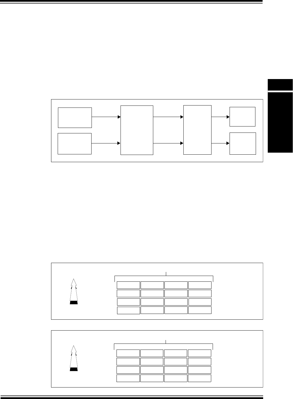
© 2007-2012 Microchip Technology Inc. DS61113E-page 2-55
Section 2. CPU for Devices with M4K® Core
CPU for Devices
with M4K® Core
2
2.13 MIPS16e® EXECUTION
When the core is operating in MIPS16e® mode, instruction fetches only require 16-bits of data to
be returned. However, for improved efficiency, the core will fetch 32-bits of instruction data when-
ever the address is word-aligned. Therefore, for sequential MIPS16e® code, fetches only occur
for every other instruction, resulting in better performance and reduced system power.
2.14 MEMORY MODEL
Virtual addresses used by software are converted to physical addresses by the memory
management unit (MMU) before being sent to the CPU busses. The PIC32 CPU uses a fixed
mapping for this conversion. For more information regarding the system memory model, see
Section 3. “Memory Organization” (DS61115).
Figure 2-14: Address Translation During SRAM Access
2.14.1 Cacheability
The CPU uses the virtual address of an instruction fetch, load or store to determine whether to
access the cache or not. Memory accesses within kseg0, or useg/kuseg can be cached, while
accesses within kseg1 are non-cacheable. The CPU uses the CCA bits in the Config register to
determine the cacheability of a memory segment. A memory access is cacheable if its
corresponding CCA = 0112. For more information on cache operation, see Section 4. “Prefetch
Cache Module” (DS61119).
2.14.1.1 LITTLE ENDIAN BYTE ORDERING
On CPUs that address memory with byte resolution, there is a convention for multi-byte data
items that specify the order of high-order to low-order bytes. Big-endian byte-ordering is where
the lowest address has the MSB. Little-endian ordering is where the lowest address has the LSB
of a multi-byte datum. The PIC32 CPU supports little-endian byte ordering.
Figure 2-15: Big-Endian Byte Ordering
Figure 2-16: Little-Endian Byte Ordering
SRAM
Interface
Instn
SRAM
Data
SRAM
FMT
Instruction
Address
Calculator
Data
Address
Calculator
Virtual
Address
Virtual
Address
Physical
Address
Physical
Address
Higher
Address Word
Address
Lower
Address
Bit #
} 1 word = 4 bytes
12
8
4
0
13
9
5
1
14
10
6
2
15
11
7
3
31 24 23 16 15 8 70
12
8
4
0
Higher
Address Word
Address
Lower
Address
Bit #
15
11
7
3
14
10
6
2
13
9
5
1
12
8
4
0
31 24 23 16 15 8 70
12
8
4
0

PIC32 Family Reference Manual
DS61113E-page 2-56 © 2007-2012 Microchip Technology Inc.
2.15 CPU INSTRUCTIONS, GROUPED BY FUNCTION
CPU instructions are organized into the following functional groups:
•Load and store
•Computational
• Jump and branch
•Miscellaneous
•Coprocessor
Each instruction is 32 bits long.
2.15.1 CPU Load and Store Instructions
MIPS® processors use a load/store architecture; all operations are performed on operands held
in processor registers and main memory is accessed only through load and store instructions.
2.15.1.1 TYPES OF LOADS AND STORES
There are several different types of load and store instructions, each designed for a different
purpose:
•Transferring variously-sized fields (for example, LB, SW)
•Trading transferred data as signed or unsigned integers (for example, LHU)
•Accessing unaligned fields (for example, LWR, SWL)
•Atomic memory update (read-modify-write: for instance, LL/SC)
2.15.1.2 LIST OF CPU LOAD AND STORE INSTRUCTIONS
The following data sizes (as defined in the AccessLength field) are transferred by CPU load and
store instructions:
•Byte
•Half-word
•Word
Signed and unsigned integers of different sizes are supported by loads that either sign-extend or
zero-extend the data loaded into the register.
Unaligned words and double words can be loaded or stored in just two instructions by using a
pair of special instructions. For loads a LWL instruction is paired with a LWR instruction. The load
instructions read the left-side or right-side bytes (left or right side of register) from an aligned word
and merge them into the correct bytes of the destination register.
2.15.1.3 LOADS AND STORES USED FOR ATOMIC UPDATES
The paired instructions, Load Linked and Store Conditional, can be used to perform an atomic
read-modify-write of word or double word cached memory locations. These instructions are used
in carefully coded sequences to provide one of several synchronization primitives, including
test-and-set, bit-level locks, semaphores, and sequencers and event counts.
2.15.1.4 COPROCESSOR LOADS AND STORES
If a particular coprocessor is not enabled, loads and stores to that processor cannot execute and
the attempted load or store causes a Coprocessor Unusable exception. Enabling a coprocessor
is a privileged operation provided by the System Control Coprocessor, CP0.

© 2007-2012 Microchip Technology Inc. DS61113E-page 2-57
Section 2. CPU for Devices with M4K® Core
CPU for Devices
with M4K® Core
2
2.15.2 Computational Instructions
Two’s complement arithmetic is performed on integers represented in 2s complement notation.
These are signed versions of the following operations:
•Add
•Subtract
•Multiply
•Divide
The add and subtract operations labelled “unsigned” are actually modulo arithmetic without
overflow detection.
There are also unsigned versions of multiply and divide, as well as a full complement of shift and
logical operations. Logical operations are not sensitive to the width of the register.
MIPS32® provides 32-bit integers and 32-bit arithmetic.
2.15.2.1 SHIFT INSTRUCTIONS
The ISA defines two types of shift instructions:
•Those that take a fixed shift amount from a 5-bit field in the instruction word (for instance,
SLL, SRL)
•Those that take a shift amount from the low-order bits of a general register (for instance,
SRAV, SRLV)
2.15.2.2 MULTIPLY AND DIVIDE INSTRUCTIONS
The multiply instruction performs 32-bit by 32-bit multiplication and creates either 64-bit or 32-bit
results. Divide instructions divide a 64-bit value by a 32-bit value and create 32-bit results. With
one exception, they deliver their results into the HI and LO special registers. The MUL instruction
delivers the lower half of the result directly to a GPR.
• Multiply produces a full-width product twice the width of the input operands; the low half is
loaded into LO and the high half is loaded into HI
•Multiply-Add and Multiply-Subtract produce a full-width product twice the width of the input
operations and adds or subtracts the product from the concatenated value of HI and LO.
The low half of the addition is loaded into LO and the high half is loaded into HI.
• Divide produces a quotient that is loaded into LO and a remainder that is loaded into HI
The results are accessed by instructions that transfer data between HI/LO and the general
registers.
2.15.3 Jump and Branch Instructions
2.15.3.1 TYPES OF JUMP AND BRANCH INSTRUCTIONS DEFINED BY THE ISA
The architecture defines the following jump and branch instructions:
•PC-relative conditional branch
•PC-region unconditional jump
•Absolute (register) unconditional jump
•A set of procedure calls that record a return link address in a general register
2.15.3.2 BRANCH DELAYS AND THE BRANCH DELAY SLOT
All branches have an architectural delay of one instruction. The instruction immediately following
a branch is said to be in the “branch delay slot”. If a branch or jump instruction is placed in the
branch delay slot, the operation of both instructions is undefined.
By convention, if an exception or interrupt prevents the completion of an instruction in the branch
delay slot, the instruction stream is continued by re-executing the branch instruction. To permit
this, branches must be restartable; procedure calls may not use the register in which the return
link is stored (usually GPR 31) to determine the branch target address.

PIC32 Family Reference Manual
DS61113E-page 2-58 © 2007-2012 Microchip Technology Inc.
2.15.3.3 BRANCH AND BRANCH LIKELY
There are two versions of conditional branches; they differ in the manner in which they handle
the instruction in the delay slot when the branch is not taken and execution falls through.
• Branch instructions execute the instruction in the delay slot
• Branch likely instructions do not execute the instruction in the delay slot if the branch is not
taken (they are said to nullify the instruction in the delay slot)
Although the Branch Likely instructions are included in this specification, software is strongly
encouraged to avoid the use of the Branch Likely instructions, as they will be removed from a
future revision of the MIPS® architecture.
2.15.4 Miscellaneous Instructions
2.15.4.1 INSTRUCTION SERIALIZATION (SYNC AND SYNCI)
In normal operation, the order in which load and store memory accesses appear to a viewer out-
side the executing processor (for instance, in a multiprocessor system) is not specified by the
architecture.
The SYNC instruction can be used to create a point in the executing instruction stream at which
the relative order of some loads and stores can be determined: loads and stores executed before
the SYNC are completed before loads and stores after the SYNC can start.
The SYNCI instruction synchronizes the processor caches with previous writes or other modifi-
cations to the instruction stream.
2.15.4.2 EXCEPTION INSTRUCTIONS
Exception instructions transfer control to a software exception handler in the kernel. There are
two types of exceptions, conditional and unconditional. Conditional exceptions are generated by
the trap instruction, based on the result of a comparison. Unconditional exceptions are gener-
ated using the syscall and break instructions.
2.15.4.3 CONDITIONAL MOVE INSTRUCTIONS
MIPS32® includes instructions to conditionally move one CPU general register to another, based
on the value in a third general register.
2.15.4.4 NOP INSTRUCTIONS
The NOP instruction is actually encoded as an all-zero instruction. MIPS® processors
special-case this encoding as performing no operation, and optimize execution of the instruction.
In addition, SSNOP instruction, takes up one issue cycle on any processor, including super-scalar
implementations of the architecture.
2.15.5 Coprocessor Instructions
2.15.5.1 WHAT COPROCESSORS DO
Coprocessors are alternate execution units, with register files separate from the CPU. In abstrac-
tion, the MIPS® architecture provides for up to four coprocessor units, numbered 0 to 3. Each
level of the ISA defines a number of these coprocessors. Coprocessor 0 is always used for sys-
tem control and coprocessor 1 and 3 are used for the floating point unit. Coprocessor 2 is
reserved for implementation-specific use.
A coprocessor may have two different register sets:
•Coprocessor general registers
•Coprocessor control registers
Each set contains up to 32 registers. Coprocessor computational instructions may use the
registers in either set.

© 2007-2012 Microchip Technology Inc. DS61113E-page 2-59
Section 2. CPU for Devices with M4K® Core
CPU for Devices
with M4K® Core
2
2.15.5.2 SYSTEM CONTROL COPROCESSOR 0 (CP0)
The system controller for all MIPS® processors is implemented as coprocessor 0 (CP0), the
System Control Coprocessor. It provides the processor control, memory management, and
exception handling functions.
2.15.5.3 COPROCESSOR LOAD AND STORE INSTRUCTIONS
Explicit load and store instructions are not defined for CP0; for CP0 only, the move to and from
coprocessor instructions must be used to write and read the CP0 registers. The loads and stores
for the remaining coprocessors are summarized in 2.15.1.4 “Coprocessor Loads and Stores”.
2.16 CPU INITIALIZATION
Software is required to initialize the following parts of the device after a Reset event.
2.16.1 General Purpose Registers
The CPU register file powers up in an unknown state with the exception of r0 which is always ‘0’.
Initializing the rest of the register file is not required for proper operation in hardware. However,
depending on the software environment, several registers may need to be initialized. Some of
these are:
• sp – Stack pointer
•gp – Global pointer
•fp – Frame pointer
2.16.2 Coprocessor 0 State
Miscellaneous CP0 states need to be initialized prior to leaving the boot code. There are various
exceptions that are blocked by ERL = 1 or EXL = 1, and which are not cleared by Reset. These
can be cleared to avoid taking spurious exceptions when leaving the boot code.
Table 2-12: CPU Initialization
2.16.3 Bus Matrix
The BMX should be initialized before switching to User mode or before executing from DRM. The
values written to the bus matrix are based on the memory layout of the application to be run.
CP0 Register Action
Cause WP (Watch Pending), SW0/1 (Software Interrupts) should be cleared.
Config Typically, the K0, KU and K23 fields should be set to the desired Cache
Coherency Algorithm (CCA) value prior to accessing the corresponding
memory regions.
Count(1) Should be set to a known value if Timer Interrupts are used.
Compare(1) Should be set to a known value if Timer Interrupts are used. The write to
Compare will also clear any pending Timer Interrupts (Thus, Count should
be set before Compare to avoid any unexpected interrupts).
Status Desired state of the device should be set.
Other CP0 state Other registers should be written before they are read. Some registers are
not explicitly writable, and are only updated as a by-product of instruction
execution or a taken exception. Uninitialized bits should be masked off after
reading these registers.
Note 1: When the Count register is equal to the Compare register a timer interrupt is
signaled. There is a mask bit in the interrupt controller to disable passing this
interrupt to the CPU if desired.

PIC32 Family Reference Manual
DS61113E-page 2-60 © 2007-2012 Microchip Technology Inc.
2.17 EFFECTS OF A RESET
2.17.1 Master Clear Reset
The PIC32 core is not fully initialized by a hardware Reset. Only a minimal subset of the
processor state is cleared. This is enough to bring the core up while running in unmapped and
uncached code space. All other processor state can then be initialized by software. Power-up
Reset brings the device into a known state. A Soft Reset can be forced by asserting the MCLR
pin. This distinction is made for compatibility with other MIPS® processors. In practice, both
resets are handled identically.
2.17.1.1 COPROCESSOR 0 STATE
Much of the hardware initialization occurs in Coprocessor 0, which are described in Tabl e 2-1 3.
Table 2-13: Bits Cleared or Set by Reset
2.17.1.2 BUS STATE MACHINES
All pending bus transactions are aborted and the state machines in the SRAM interface unit are
reset when a Reset or Soft Reset exception is taken.
2.17.2 Fetch Address
Upon Reset/Soft Reset, unless the EJTAGBOOT option is used, the fetch is directed to VA
0xBFC00000 (PA 0x1FC00000). This address is in kseg1, which is unmapped and uncached.
2.17.3 Watchdog Timer Reset
The status of the CPU registers after a Watchdog Timer (WDT) event depends on the operational
mode of the CPU prior to the WDT event.
If the device was not in Sleep a WDT event will force registers to a Reset value.
Register Name Bit Name Cleared
or Set Value Cleared or Set By
Status BEV Cleared 1Reset or Soft Reset
TS Cleared 0Reset or Soft Reset
SR Set 1Reset or Soft Reset
NMI Cleared 0Reset or Soft Reset
ERL Set 1Reset or Soft Reset
RP Cleared 0Reset or Soft Reset
All Configuration
Registers:
Config
Config1
Config2
Config3
Configuration fields
related to static
inputs
Set Input value Reset or Soft Reset
Config K0 Set 010
(uncached)
Reset or Soft Reset
KU Set 010
(uncached)
Reset or Soft Reset
K23 Set 010
(uncached)
Reset or Soft Reset
Debug DM Cleared 0Reset or Soft Reset(1)
LSNM Cleared 0Reset or Soft Reset
IBUSEP Cleared 0Reset or Soft Reset
IEXI Cleared 0Reset or Soft Reset
SSt Cleared 0Reset or Soft Reset
Note 1: Unless EJTAGBOOT option is used to boot into Debug mode.

© 2007-2012 Microchip Technology Inc. DS61113E-page 2-61
Section 2. CPU for Devices with M4K® Core
CPU for Devices
with M4K® Core
2
2.18 RELATED APPLICATION NOTES
This section lists application notes that are related to this section of the manual. These
application notes may not be written specifically for the PIC32 device family, but the concepts are
pertinent and could be used with modification and possible limitations. The current application
notes related to the PIC32 CPU for Devices with M4K® Core include the following:
Title Application Note #
No related application notes at this time. N/A
Note: Please visit the Microchip web site (www.microchip.com) for additional application
notes and code examples for the PIC32 family of devices.

PIC32 Family Reference Manual
DS61113E-page 2-62 © 2007-2012 Microchip Technology Inc.
2.19 REVISION HISTORY
Revision A (October 2007)
This is the initial released version of this document.
Revision B (April 2008)
Revised status to Preliminary; Revised Section 2.1 (Key Features); Revised Figure 2-1; Revised
U-0 to r-x.
Revision C (May 2008)
Revise Figure 2-1; Added Section 2.2.3, Core Timer; Change Reserved bits from “Maintain as”
to “Write”.
Revision D (August 2011)
This revision includes the following updates:
The document was updated as follows to reflect the addition of the M14K™ Microprocessor core
to certain variants of the PIC32 device family:
•Sections:
-Updated 2.1.1 “Key Features”
-Updated 2.1.2 “Related MIPS® Documentation”
-Updated 2.2.2 “Introduction to the Programming Model”
-Updated 2.3.1.1 “I Stage – Instruction Fetch”
-Updated 2.10 “Interrupt and Exception Mechanism”
- Added 2.14 “microMIPS™ EXECUTION (M14K™ only)”
- Added 2.15 “MCU™ ASE EXTENSION (M14K™ only)”
•Figures:
-Updated Figure2-1: PIC32 Block Diagram
-Updated Figure2-2: M4K
® and M14K™ Microprocessor Core Block Diagram
•Tables:
- Added Table 2-6: microMIPS™ 16-bit Instruction Register Usage (M14K™ Only)
-Updated Table2-8: CP0 Registers
- Added Table 2-14: Performance Countable Events
-Added Table2-15: Event Description
- Updated Table 2-17: Bits Cleared or Set by Reset
• Registers:
- Added Register 2-1, Register 2-10, Register 2-11, Register 2-13, Register 2-22,
Register 2-24, Register 2-25, Register 2-26, Register 2-27, Register 2-28,
Register 2-30, and Register 2-31
- Updated existing registers to reflect only those bits that are implemented for PIC32
devices with either the M4K® or M14K™ Microprocessor core
•Updates to formatting and minor text updates have been incorporated throughout the
document
Revision E (September 2012)
This revision includes the following updates:
•Document title has been changed
• All references to the M14K™ Microprocessor core were removed throughout the docu-
ment. This content will be available in a separate family reference manual section.
•Updates to formatting and minor text updates have been incorporated throughout the
document

2007-2012 Microchip Technology Inc. DS61113E-page 2-63
Information contained in this publication regarding device
applications and the like is provided only for your convenience
and may be superseded by updates. It is your responsibility to
ensure that your application meets with your specifications.
MICROCHIP MAKES NO REPRESENTATIONS OR
WARRANTIES OF ANY KIND WHETHER EXPRESS OR
IMPLIED, WRITTEN OR ORAL, STATUTORY OR
OTHERWISE, RELATED TO THE INFORMATION,
INCLUDING BUT NOT LIMITED TO ITS CONDITION,
QUALITY, PERFORMANCE, MERCHANTABILITY OR
FITNESS FOR PURPOSE. Microchip disclaims all liability
arising from this information and its use. Use of Microchip
devices in life support and/or safety applications is entirely at
the buyer’s risk, and the buyer agrees to defend, indemnify and
hold harmless Microchip from any and all damages, claims,
suits, or expenses resulting from such use. No licenses are
conveyed, implicitly or otherwise, under any Microchip
intellectual property rights.
Trademarks
The Microchip name and logo, the Microchip logo, dsPIC,
KEELOQ, KEELOQ logo, MPLAB, PIC, PICmicro, PICSTART,
PIC32 logo, rfPIC and UNI/O are registered trademarks of
Microchip Technology Incorporated in the U.S.A. and other
countries.
FilterLab, Hampshire, HI-TECH C, Linear Active Thermistor,
MXDEV, MXLAB, SEEVAL and The Embedded Control
Solutions Company are registered trademarks of Microchip
Technology Incorporated in the U.S.A.
Analog-for-the-Digital Age, Application Maestro, BodyCom,
chipKIT, chipKIT logo, CodeGuard, dsPICDEM,
dsPICDEM.net, dsPICworks, dsSPEAK, ECAN,
ECONOMONITOR, FanSense, HI-TIDE, In-Circuit Serial
Programming, ICSP, Mindi, MiWi, MPASM, MPLAB Certified
logo, MPLIB, MPLINK, mTouch, Omniscient Code
Generation, PICC, PICC-18, PICDEM, PICDEM.net, PICkit,
PICtail, REAL ICE, rfLAB, Select Mode, Total Endurance,
TSHARC, UniWinDriver, WiperLock and ZENA are
trademarks of Microchip Technology Incorporated in the
U.S.A. and other countries.
SQTP is a service mark of Microchip Technology Incorporated
in the U.S.A.
All other trademarks mentioned herein are property of their
respective companies.
© 2007-2012, Microchip Technology Incorporated, Printed in
the U.S.A., All Rights Reserved.
Printed on recycled paper.
ISBN: 978-1-62076-539-5
Note the following details of the code protection feature on Microchip devices:
• Microchip products meet the specification contained in their particular Microchip Data Sheet.
• Microchip believes that its family of products is one of the most secure families of its kind on the market today, when used in the
intended manner and under normal conditions.
• There are dishonest and possibly illegal methods used to breach the code protection feature. All of these methods, to our
knowledge, require using the Microchip products in a manner outside the operating specifications contained in Microchip’s Data
Sheets. Most likely, the person doing so is engaged in theft of intellectual property.
• Microchip is willing to work with the customer who is concerned about the integrity of their code.
• Neither Microchip nor any other semiconductor manufacturer can guarantee the security of their code. Code protection does not
mean that we are guaranteeing the product as “unbreakable.”
Code protection is constantly evolving. We at Microchip are committed to continuously improving the code protection features of our
products. Attempts to break Microchip’s code protection feature may be a violation of the Digital Millennium Copyright Act. If such acts
allow unauthorized access to your software or other copyrighted work, you may have a right to sue for relief under that Act.
Microchip received ISO/TS-16949:2009 certification for its worldwide
headquarters, design and wafer fabrication facilities in Chandler and
Tempe, Arizona; Gresham, Oregon and design centers in California
and India. The Company’s quality system processes and procedures
are for its PIC® MCUs and dsPIC® DSCs, KEELOQ® code hopping
devices, Serial EEPROMs, microperipherals, nonvolatile memory and
analog products. In addition, Microchip’s quality system for the design
and manufacture of development systems is ISO 9001:2000 certified.
QUALITY MANAGEMENT S
YSTEM
CERTIFIED BY DNV
== ISO/TS 16949 ==

DS61113E-page 2-64 2007-2012 Microchip Technology Inc.
AMERICAS
Corporate Office
2355 West Chandler Blvd.
Chandler, AZ 85224-6199
Tel: 480-792-7200
Fax: 480-792-7277
Technical Support:
http://www.microchip.com/
support
Web Address:
www.microchip.com
Atlanta
Duluth, GA
Tel: 678-957-9614
Fax: 678-957-1455
Boston
Westborough, MA
Tel: 774-760-0087
Fax: 774-760-0088
Chicago
Itasca, IL
Tel: 630-285-0071
Fax: 630-285-0075
Cleveland
Independence, OH
Tel: 216-447-0464
Fax: 216-447-0643
Dallas
Addison, TX
Tel: 972-818-7423
Fax: 972-818-2924
Detroit
Farmington Hills, MI
Tel: 248-538-2250
Fax: 248-538-2260
Indianapolis
Noblesville, IN
Tel: 317-773-8323
Fax: 317-773-5453
Los Angeles
Mission Viejo, CA
Tel: 949-462-9523
Fax: 949-462-9608
Santa Clara
Santa Clara, CA
Tel: 408-961-6444
Fax: 408-961-6445
Toronto
Mississauga, Ontario,
Canada
Tel: 905-673-0699
Fax: 905-673-6509
ASIA/PACIFIC
Asia Pacific Office
Suites 3707-14, 37th Floor
Tower 6, The Gateway
Harbour City, Kowloon
Hong Kong
Tel : 8 52 -24 01- 120 0
Fax: 852-2401-3431
Australia - Sydney
Tel : 6 1- 2-9 868 -67 33
Fax: 61-2-9868-6755
China - Beijing
Tel : 8 6- 10- 856 9-7 00 0
Fax: 86-10-8528-2104
China - Chengdu
Tel : 8 6- 28- 866 5-5 511
Fax: 86-28-8665-7889
China - Chongqing
Tel : 8 6- 23- 898 0-9 58 8
Fax: 86-23-8980-9500
China - Hangzhou
Tel : 8 6- 571 -28 19- 318 7
Fax: 86-571-2819-3189
China - Hong Kong SAR
Tel : 8 52 -24 01- 120 0
Fax: 852-2401-3431
China - Nanjing
Tel : 8 6- 25- 847 3-2 46 0
Fax: 86-25-8473-2470
China - Qingdao
Tel : 8 6- 532 -85 02- 735 5
Fax: 86-532-8502-7205
China - Shanghai
Tel : 8 6- 21- 540 7-5 53 3
Fax: 86-21-5407-5066
China - Shenyang
Tel : 8 6- 24- 233 4-2 82 9
Fax: 86-24-2334-2393
China - Shenzhen
Tel : 8 6- 755 -82 03- 266 0
Fax: 86-755-8203-1760
China - Wuhan
Tel : 8 6- 27- 598 0-5 30 0
Fax: 86-27-5980-5118
China - Xian
Tel : 8 6- 29- 883 3-7 25 2
Fax: 86-29-8833-7256
China - Xiamen
Tel: 86-592-2388138
Fax: 86-592-2388130
China - Zhuhai
Tel : 86- 75 6-3 21 004 0
Fax: 86-756-3210049
ASIA/PACIFIC
India - Bangalore
Tel : 9 1- 80- 309 0-4 44 4
Fax: 91-80-3090-4123
India - New Delhi
Tel : 9 1- 11- 416 0 -8 631
Fax: 91-11-4160-8632
India - Pune
Tel : 9 1- 20- 256 6-1 51 2
Fax: 91-20-2566-1513
Japan - Osaka
Tel : 8 1- 66- 152 -71 60
Fax: 81-66-152-9310
Japan - Yokohama
Tel : 8 1- 45- 471 - 6 16 6
Fax: 81-45-471-6122
Korea - Daegu
Tel : 8 2- 53- 744 -43 01
Fax: 82-53-744-4302
Korea - Seoul
Tel : 8 2- 2-5 54- 72 0 0
Fax: 82-2-558-5932 or
82-2-558-5934
Malaysia - Kuala Lumpur
Tel : 6 0- 3-6 201 -9 8 57
Fax: 60-3-6201-9859
Malaysia - Penang
Tel : 6 0- 4-2 27- 88 7 0
Fax: 60-4-227-4068
Philippines - Manila
Tel : 6 3- 2-6 34- 90 6 5
Fax: 63-2-634-9069
Singapore
Tel : 6 5- 633 4-8 870
Fax: 65-6334-8850
Taiwan - Hsin Chu
Tel : 8 86 -3- 577 8-3 66
Fax: 886-3-5770-955
Taiwan - Kaohsiung
Tel : 8 86 -7- 536 -48 18
Fax: 886-7-330-9305
Taiwan - Taipei
Tel : 8 86 -2- 250 0-6 61 0
Fax: 886-2-2508-0102
Thailand - Bangkok
Tel : 6 6- 2-6 94- 13 5 1
Fax: 66-2-694-1350
EUROPE
Austria - Wels
Tel : 4 3- 72 42 -2 244 -3 9
Fax: 43-7242-2244-393
Denmark - Copenhagen
Tel : 4 5- 445 0-2 828
Fax: 45-4485-2829
France - Paris
Tel : 3 3- 1-6 9-5 3-6 3-2 0
Fax: 33-1-69-30-90-79
Germany - Munich
Tel : 4 9- 89 -62 7-1 44- 0
Fax: 49-89-627-144-44
Italy - Milan
Tel : 3 9- 03 31 -7 426 11
Fax: 39-0331-466781
Netherlands - Drunen
Tel : 3 1- 41 6- 690 399
Fax: 31-416-690340
Spain - Madrid
Tel : 3 4- 91 -70 8-0 8-9 0
Fax: 34-91-708-08-91
UK - Wokingham
Tel : 4 4- 118 -92 1- 5 869
Fax: 44-118-921-5820
Worldwide Sales and Service
11/29/11

© 2010 Microchip Technology Inc. DS61115F-page 3-1
Memory
Organization
3
Section 3. Memory Organization
HIGHLIGHTS
This section of the manual contains the following topics:
3.1 Introduction................................................................................................................3-2
3.2 Control Registers....................................................................................................... 3-2
3.3 PIC32MX Memory Layout ....................................................................................... 3-13
3.4 PIC32MX Address Map ........................................................................................... 3-15
3.5 Bus Matrix................................................................................................................ 3-29
3.6 I/O Pin Control ......................................................................................................... 3-33
3.7 Operation in Power-Saving and Debug Modes ....................................................... 3-33
3.8 Code Examples ....................................................................................................... 3-34
3.9 Design Tips.............................................................................................................. 3-35
3.10 Related Application Notes ....................................................................................... 3-36
3.11 Revision History....................................................................................................... 3-37

PIC32MX Family Reference Manual
DS61115F-page 3-2 © 2010 Microchip Technology Inc.
3.1 INTRODUCTION
The PIC32MX microcontrollers provide 4 GB of unified virtual memory address space. All mem-
ory regions, including program memory, data memory, SFRs and Configuration registers reside
in this address space at their respective unique addresses. The program and data memories can
be optionally partitioned into user and kernel memories. In addition, the data memory can be
made executable, allowing the PIC32MX to execute from data memory.
Key features of PIC32MX memory organization include the following:
•32-bit native data width
• Separate User and Kernel mode address spaces
•Flexible program Flash memory partitioning
•Flexible data RAM partitioning for data and program space
• Separate boot Flash memory for protected code
• Robust bus-exception handling to intercept runaway code
•Simple memory mapping with Fixed Mapping Translation (FMT) unit
•Cacheable and non-cacheable address regions
3.2 CONTROL REGISTERS
This section lists the Special Function Registers (SFRs) used for setting the RAM and Flash
memory partitions for data and code (for both User and Kernel mode).
The following is a list of available SFRs:
•BMXCON: Configuration Register
•BMXxxxBA: Memory Partition Base Address Registers
•BMXDRMSZ: Data RAM Size Register
•BMXPFMSZ: Program Flash Size Register
•BMXBOOTSZ: Boot Flash Size Register
3.2.1 BMXCON Register
This register configures program Flash cacheability for DMA accesses, bus error exceptions,
data RAM wait states and arbitration modes.
3.2.2 BMXxxxBA Registers
These registers identify relative base addresses for kernel, User mode data and User mode
program space in RAM.
3.2.3 BMXDRMSZ Register
This read-only register identifies the size of the Data RAM in bytes.
3.2.4 BMXPFMSZ Register
This read-only register identifies the size of the Program Flash Memory in bytes.
3.2.5 BMXBOOTSZ Register
This read-only register identifies the size of the Boot Program Flash Memory in bytes.
Tabl e 3 -1 pr ov ide s a br i ef s um m ar y o f al l me mory organization-related registers. Corresponding
registers appear after the summary, followed by a detailed description of each register.
Note: This family reference manual section is meant to serve as a complement to device
data sheets. Depending on the device variant, this manual section may not apply
to all PIC32MX devices.
Please consult the note at the beginning of the “Memory” chapter in the current
device data sheet to check whether this document supports the device you are
using.
Device data sheets and family reference manual sections are available for
download from the Microchip Worldwide Web site at: http://www.microchip.com

© 2010 Microchip Technology Inc. DS61115F-page 3-3
Section 3. Memory Organization
Memory
Organization
3
Table 3-1: Memory Organization SFR Summary
Address
Offset Name Bit
Range
Bit
31/23/15/7
Bit
30/22/14/6
Bit
29/21/13/5
Bit
28/20/12/4
Bit
27/19/11/3
Bit
26/18/10/2
Bit
25/17/9/1
Bit
24/16/8/0
0x2000 BMXCON(1,2,3) 31:24 — — — — —BMXCHEDMA— —
23:16 — — — BMXERRIXI BMXERRICD BMXERRDMA BMXERRDS BMXERRIS
15:8 — — — — — — — —
7:0 —BMXWSDRM — — —BMXARB<2:0>
0x2010 BMXDKPBA(1,2,3) 31:24 — — — — — — — —
23:16 — — — — — — — —
15:8 BMXDKPBA<15:8>
7:0 BMXDKPBA<7:0>
0x2020 BMXDUDBA(1,2,3) 31:24 — — — — — — — —
23:16 — — — — — — — —
15:8 BMXDUDBA<15:8>
7:0 BMXDUDBA<7:0>
0x2030 BMXDUPBA(1,2,3) 31:24 — — — — — — — —
23:16 — — — — — — — —
15:8 BMXDUPBA<15:8>
7:0 BMXDUPBA<7:0>
0x2040 BMXDRMSZ 31:24 BMXDRMSZ<31:24>
23:16 BMXDRMSZ<23:16>
15:8 BMXDRMSZ<15:8>
7:0 BMXDRMSZ<7:0>
0x2050 BMXPUPBA(1,2,3) 31:24 — — — — — — — —
23:16 — — — — BMXPUPBA<19:16>
15:8 BMXPUPBA<15:8>
7:0 BMXPUPBA<7:0>
0x2060 BMXPFMSZ 31:24 BMXPFMSZ<31:24>
23:16 BMXPFMSZ<23:16>
15:8 BMXPFMSZ<15:8>
7:0 BMXPFMSZ<7:0>
0x2070 BMXBOOTSZ 31:24 BMXBOOTSZ<31:24>
23:16 BMXBOOTSZ<23:16>
15:8 BMXBOOTSZ<15:8>
7:0 BMXBOOTSZ<7:0>
Legend: — = unimplemented, read as ‘0’. Address offset values are shown in hexadecimal.
Note 1: This register has an associated Clear register at an offset of 0x4 bytes. These registers have the same name with CLR appended to the
end of the register name (e.g., BMXCONCLR). Writing a ‘1’ to any bit position in the Clear register will clear valid bits in the associated
register. Reads from the Clear register should be ignored.
2: This register has an associated Set register at an offset of 0x8 bytes. These registers have the same name with SET appended to the end
of the register name (e.g., BMXCONSET). Writing a ‘1’ to any bit position in the Set register will set valid bits in the associated register.
Reads from the Set register should be ignored.
3: This register has an associated Invert register at an offset of 0xC bytes. These registers have the same name with INV appended to the
end of the register name (e.g., BMXCONINV). Writing a ‘1’ to any bit position in the Invert register will invert valid bits in the associated
register. Reads from the Invert register should be ignored.

PIC32MX Family Reference Manual
DS61115F-page 3-4 © 2010 Microchip Technology Inc.
Register 3-1: BMXCON: Bus Matrix Configuration Register (1,2,3)
r-x r-x r-x r-x r-x R/W-0 r-x r-x
— — — — —BMXCHEDMA— —
bit 31 bit 24
r-x r-x r-x R/W-1 R/W-1 R/W-1 R/W-1 R/W-1
— — —BMXERRIXIBMXERRICDBMXERRDMABMXERRDSBMXERRIS
bit 23 bit 16
r-x r-x r-x r-x r-x r-x r-x r-x
— — — — — — — —
bit 15 bit 8
r-x R/W-1 r-x r-x r-x R/W-0 R/W-0 R/W-1
—BMXWSDRM— — — BMXARB<2:0>
bit 7 bit 0
Legend:
R=Readable bit W=Writable bit P=Programmable bit r=Reserved bit
U=Unimplemented bit n=Bit Value at POR: (‘0’, ‘1’, x=Unknown)
bit 31-27 Reserved: Write ‘0’; ignore read
bit 26 BMXCHEDMA: BMX PFM Cacheability for DMA Accesses bit
1= Enable program Flash memory (data) cacheability for DMA accesses
(requires cache to have data caching enabled)
0=Disable program Flash memory (data) cacheability for DMA accesses
(hits are still read from the cache, but misses do not update the cache)
bit 25-21 Reserved: Write ‘0’; ignore read
bit 20 BMXERRIXI: Enable Bus Error from IXI bit
1= Enable bus error exceptions for unmapped address accesses initiated from IXI shared bus
0=Disable bus error exceptions for unmapped address accesses initiated from IXI shared bus
bit 19 BMXERRICD: Enable Bus Error from ICD Debug Unit bit
1= Enable bus error exceptions for unmapped address accesses initiated from ICD
0=Disable bus error exceptions for unmapped address accesses initiated from ICD
bit 18 BMXERRDMA: Bus Error from DMA bit
1= Enable bus error exceptions for unmapped address accesses initiated from DMA
0=Disable bus error exceptions for unmapped address accesses initiated from DMA
bit 17 BMXERRDS: Bus Error from CPU Data Access bit (disabled in DEBUG mode)
1= Enable bus error exceptions for unmapped address accesses initiated from CPU data access
0=Disable bus error exceptions for unmapped address accesses initiated from CPU data access
bit 16 BMXERRIS: Bus Error from CPU Instruction Access bit (disabled in DEBUG mode)
1= Enable bus error exceptions for unmapped address accesses initiated from CPU instruction access
0=Disable bus error exceptions for unmapped address accesses initiated from CPU instruction access
Note 1: This register has an associated Clear register (BMXCONCLR) at an offset of 0x4 bytes. Writing a ‘1’ to any
bit position in the Clear register will clear valid bits in the associated register. Reads from the Clear register
should be ignored.
2: This register has an associated Set register (BMXCONSET) at an offset of 0x8 bytes. Writing a ‘1’ to any
bit position in the Set register will set valid bits in the associated register. Reads from the Set register should
be ignored.
3: This register has an associated Invert register (BMXCONINV) at an offset of 0xC bytes. Writing a ‘1’ to any
bit position in the Invert register will invert valid bits in the associated register. Reads from the Invert register
should be ignored.

© 2010 Microchip Technology Inc. DS61115F-page 3-5
Section 3. Memory Organization
Memory
Organization
3
bit 15-7 Reserved: Write ‘0’; ignore read
bit 6 BMXWSDRM: CPU Instruction or Data Access from Data RAM Wait State bit
1=Data RAM accesses from CPU have one wait state for address setup
0=Data RAM accesses from CPU have zero wait states for address setup
bit 5-3 Reserved: Write ‘0’; ignore read
bit 2-0 BMXARB<2:0>: Bus Matrix Arbitration Mode bits
111...011 = Reserved (using these Configuration modes will produce undefined behavior)
010 = Arbitration Mode 2
001 = Arbitration Mode 1 (default)
000 = Arbitration Mode 0
Register 3-1: BMXCON: Bus Matrix Configuration Register (1,2,3) (Continued)
Note 1: This register has an associated Clear register (BMXCONCLR) at an offset of 0x4 bytes. Writing a ‘1’ to any
bit position in the Clear register will clear valid bits in the associated register. Reads from the Clear register
should be ignored.
2: This register has an associated Set register (BMXCONSET) at an offset of 0x8 bytes. Writing a ‘1’ to any
bit position in the Set register will set valid bits in the associated register. Reads from the Set register should
be ignored.
3: This register has an associated Invert register (BMXCONINV) at an offset of 0xC bytes. Writing a ‘1’ to any
bit position in the Invert register will invert valid bits in the associated register. Reads from the Invert register
should be ignored.

PIC32MX Family Reference Manual
DS61115F-page 3-6 © 2010 Microchip Technology Inc.
Register 3-2: BMXDKPBA: Data RAM Kernel Program Base Address Register (1,2,3,4,5)
r-x r-x r-x r-x r-x r-x r-x r-x
— — — — — — — —
bit 31 bit 24
r-x r-x r-x r-x r-x r-x r-x r-x
— — — — — — — —
bit 23 bit 16
R/W-0 R/W-0 R/W-0 R/W-0 R/W-0 R-0 R-0 R-0
BMXDKPBA<15:8>
bit 15 bit 8
R-0 R-0 R-0 R-0 R-0 R-0 R-0 R-0
BMXDKPBA<7:0>
bit 7 bit 0
Legend:
R=Readable bit W=Writable bit P=Programmable bit r=Reserved bit
U=Unimplemented bit -n=Bit Value at POR: (‘0’, ‘1’, x=Unknown)
bit 31-16 Reserved: Write ‘0’; ignore read
bit 15-11 BMXDKPBA<15:11>: DRM Kernel Program Base Address bits
When non-zero, this value selects the relative base address for kernel program space in RAM
bit 10-0 BMXDKPBA<10:0>: Read-Only bits
Value is always ‘0’, which forces 2 KB increments
Note 1: This register has an associated Clear register (BMXDKPBACLR) at an offset of 0x4 bytes. Writing a ‘1’ to
any bit position in the Clear register will clear valid bits in the associated register. Reads from the Clear
register should be ignored.
2: This register has an associated Set register (BMXDKPBASET) at an offset of 0x8 bytes. Writing a ‘1’ to
any bit position in the Set register will set valid bits in the associated register. Reads from the Set register
should be ignored.
3: This register has an associated Invert register (BMXDKPBAINV) at an offset of 0xC bytes. Writing a ‘1’ to
any bit position in the Invert register will invert valid bits in the associated register. Reads from the Invert
register should be ignored.
4: At Reset, the value in this register is forced to zero, which causes all of the RAM to be allocated to Kernal
mode data usage.
5: The value in this register must be less than or equal to BMXDRMSZ.

© 2010 Microchip Technology Inc. DS61115F-page 3-7
Section 3. Memory Organization
Memory
Organization
3
Register 3-3: BMXDUDBA: Data RAM User Data Base Address Register (1,2,3,4,5)
r-x r-x r-x r-x r-x r-x r-x r-x
— — — — — — — —
bit 31 bit 24
r-x r-x r-x r-x r-x r-x r-x r-x
— — — — — — — —
bit 23 bit 16
R/W-0 R/W-0 R/W-0 R/W-0 R/W-0 R-0 R-0 R-0
BMXDUDBA<15:8>
bit 15 bit 8
R-0 R-0 R-0 R-0 R-0 R-0 R-0 R-0
BMXDUDBA<7:0>
bit 7 bit 0
Legend:
R=Readable bit W=Writable bit P=Programmable bit r=Reserved bit
U=Unimplemented bit -n=Bit Value at POR: (‘0’, ‘1’, x=Unknown)
bit 31-16 Reserved: Write ‘0’; ignore read
bit 15-11 BMXDUDBA<15:11>: DRM User Data Base Address bits
When non-zero, the value selects the relative base address for User mode data space in RAM
Note: If non-zero, the value must be greater than BMXDKPBA.
bit 10-0 BMXDUDBA<10:0>: Read-Only bits
Value is always ‘0’, which forces 2 KB increments
Note 1: This register has an associated Clear register (BMXDUDBACLR) at an offset of 0x4 bytes. Writing a ‘1’ to
any bit position in the Clear register will clear valid bits in the associated register. Reads from the Clear
register should be ignored.
2: This register has an associated Set register (BMXDUDBASET) at an offset of 0x8 bytes. Writing a ‘1’ to
any bit position in the Set register will set valid bits in the associated register. Reads from the Set register
should be ignored.
3: This register has an associated Invert register (BMXDUDBAINV) at an offset of 0xC bytes. Writing a ‘1’ to
any bit position in the Invert register will invert valid bits in the associated register. Reads from the Invert
register should be ignored.
4: At Reset, the value in this register is forced to zero, which causes all of the RAM to be allocated to Kernal
mode data usage.
5: The value in this register must be less than or equal to BMXDRMSZ.

PIC32MX Family Reference Manual
DS61115F-page 3-8 © 2010 Microchip Technology Inc.
Register 3-4: BMXDUPBA: Data RAM User Program Base Address Register (1,2,3,4,5)
r-x r-x r-x r-x r-x r-x r-x r-x
— — — — — — — —
bit 31 bit 24
r-x r-x r-x r-x r-x r-x r-x r-x
— — — — — — — —
bit 23 bit 16
R/W-0 R/W-0 R/W-0 R/W-0 R/W-0 R-0 R-0 R-0
BMXDUPBA<15:8>
bit 15 bit 8
R-0 R-0 R-0 R-0 R-0 R-0 R-0 R-0
BMXDUPBA<7:0>
bit 7 bit 0
Legend:
R=Readable bit W=Writable bit P=Programmable bit r=Reserved bit
U=Unimplemented bit -n=Bit Value at POR: (‘0’, ‘1’, x=Unknown)
bit 31-16 Reserved: Write ‘0’; ignore read
bit 15-11 BMXDUPBA<15:11>: DRM User Program Base Address bits
When non-zero, the value selects the relative base address for User mode program space in RAM
Note: If non-zero, BMXDUPBA must be greater than BMXDUDBA.
bit 10-0 BMXDUPBA<10:0>: Read-Only bits
Value is always ‘0’, which forces 2 KB increments
Note 1: This register has an associated Clear register (BMXDUPBACLR) at an offset of 0x4 bytes. Writing a ‘1’ to
any bit position in the Clear register will clear valid bits in the associated register. Reads from the Clear
register should be ignored.
2: This register has an associated Set register (BMXDUPBASET) at an offset of 0x8 bytes. Writing a ‘1’ to
any bit position in the Set register will set valid bits in the associated register. Reads from the Set register
should be ignored.
3: This register has an associated Invert register (BMXDUPBAINV) at an offset of 0xC bytes. Writing a ‘1’ to
any bit position in the Invert register will invert valid bits in the associated register. Reads from the Invert
register should be ignored.
4: At Reset, the value in this register is forced to zero, which causes all of the RAM to be allocated to Kernal
mode data usage.
5: The value in this register must be less than or equal to BMXDRMSZ.

© 2010 Microchip Technology Inc. DS61115F-page 3-9
Section 3. Memory Organization
Memory
Organization
3
Register 3-5: BMXDRMSZ: Data RAM Size Register
RRRRRRRR
BMXDRMSZ<31:24>
bit 31 bit 24
RRRRRRRR
BMXDRMSZ<23:16>
bit 23 bit 16
RRRRRRRR
BMXDRMSZ<15:8>
bit 15 bit 8
RRRRRRRR
BMXDRMSZ<7:0>
bit 7 bit 0
Legend:
R=Readable bit W=Writable bit P=Programmable bit r=Reserved bit
U=Unimplemented bit -n=Bit Value at POR: (‘0’, ‘1’, x=Unknown)
bit 31-0 BMXDRMSZ<31:0>: Data RAM Memory (DRM) Size bits
Static value that indicates the size of the Data RAM in bytes:
0x00002000 = device has 8 KB RAM
0x00004000 = device has 16 KB RAM
0x00008000 = device has 32 KB RAM
0x00010000 = device has 64 KB RAM
0x00020000 = device has 128 KB RAM

PIC32MX Family Reference Manual
DS61115F-page 3-10 © 2010 Microchip Technology Inc.
Register 3-6: BMXPUPBA: Program Flash (PFM) User Program Base Address Register (1,2,3,4,5)
r-x r-x r-x r-x r-x r-x r-x r-x
— — — — — — — —
bit 31 bit 24
r-x r-x r-x r-x R/W-0 R/W-0 R/W-0 R/W-0
— — — —BMXPUPBA<19:16>
bit 23 bit 16
R/W-0 R/W-0 R/W-0 R/W-0 R/W-0 R-0 R-0 R-0
BMXPUPBA<15:8>
bit 15 bit 8
R-0 R-0 R-0 R-0 R-0 R-0 R-0 R-0
BMXPUPBA<7:0>
bit 7 bit 0
Legend:
R=Readable bit W=Writable bit P=Programmable bit r=Reserved bit
U=Unimplemented bit -n=Bit Value at POR: (‘0’, ‘1’, x=Unknown)
bit 31-20 Reserved: Write ‘0’; ignore read
bit 19-11 BMXPUPBA<19:11>: Program Flash (PFM) User Program Base Address bits
bit 10-0 BMXPUPBA<10:0>: Read-Only bits
Value is always ‘0’, which forces 2 KB increments
Note 1: This register has an associated Clear register (BMXPUPBACLR) at an offset of 0x4 bytes. Writing a ‘1’ to
any bit position in the Clear register will clear valid bits in the associated register. Reads from the Clear
register should be ignored.
2: This register has an associated Set register (BMXPUPPBASET) at an offset of 0x8 bytes. Writing a ‘1’ to
any bit position in the Set register will set valid bits in the associated register. Reads from the Set register
should be ignored.
3: This register has an associated Invert register (BMXPUPBAINV) at an offset of 0xC bytes. Writing a ‘1’ to
any bit position in the Invert register will invert valid bits in the associated register. Reads from the Invert
register should be ignored.
4: At Reset, the value in this register is forced to zero, which causes all of the RAM to be allocated to Kernal
mode program usage.
5: The value in this register must be less than or equal to BMXPFMSZ.

© 2010 Microchip Technology Inc. DS61115F-page 3-11
Section 3. Memory Organization
Memory
Organization
3
Register 3-7: BMXPFMSZ: Program Flash (PFM) Size Register
RRRRRRRR
BMXPFMSZ<31:24>
bit 31 bit 24
RRRRRRRR
BMXPFMSZ<23:16>
bit 23 bit 16
RRRRRRRR
BMXPFMSZ<15:8>
bit 15 bit 8
RRRRRRRR
BMXPFMSZ<7:0>
bit 7 bit 0
Legend:
R=Readable bit W=Writable bit P=Programmable bit r=Reserved bit
U=Unimplemented bit -n=Bit Value at POR: (‘0’, ‘1’, x=Unknown)
bit 31-0 BMXPFMSZ<31:0>: Program Flash Memory (PFM) Size bits
Static value that indicates the size of the PFM in bytes:
0x00008000 = device has 32 KB Flash
0x00010000 = device has 64 KB Flash
0x00020000 = device has 128 KB Flash
0x00040000 = device has 256 KB Flash
0x00080000 = device has 512 KB Flash

PIC32MX Family Reference Manual
DS61115F-page 3-12 © 2010 Microchip Technology Inc.
Register 3-8: BMXBOOTSZ: Boot Flash (IFM) Size Register
RRRRRRRR
BMXBOOTSZ<31:24>
bit 31 bit 24
RRRRRRRR
BMXBOOTSZ<23:16>
bit 23 bit 16
RRRRRRRR
BMXBOOTSZ<15:8>
bit 15 bit 8
RRRRRRRR
BMXBOOTSZ<7:0>
bit 7 bit 0
Legend:
R=Readable bit W=Writable bit P=Programmable bit r=Reserved bit
U=Unimplemented bit -n=Bit Value at POR: (‘0’, ‘1’, x=Unknown)
bit 31-0 BMXBOOTSZ<31:0>: Boot Flash Memory (BFM) Size bits
Static value that indicates the size of the Boot PFM in bytes:
0x00003000 = device has 12 KB boot Flash
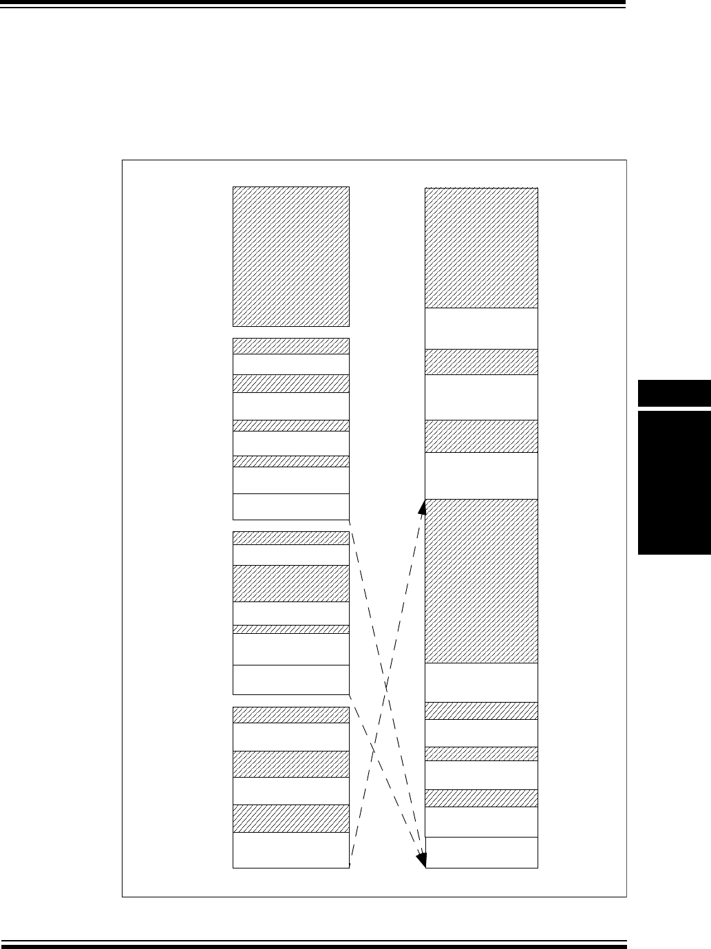
© 2010 Microchip Technology Inc. DS61115F-page 3-13
Section 3. Memory Organization
Memory
Organization
3
3.3 PIC32MX MEMORY LAYOUT
The PIC32MX microcontrollers implement two address spaces: virtual and physical. All hardware
resources, such as program memory, data memory and peripherals, are located at their respec-
tive physical addresses. Virtual addresses are exclusively used by the CPU to fetch and execute
instructions. Physical addresses are used by peripherals, such as DMA and Flash controllers,
that access memory independently of the CPU.
Figure 3-1: Virtual to Physical Fixed Memory Mapping
Virtual Memory Map Physical Memory Map
0xFFFFFFFF
0xC0000000
0xBFC00000
0xBF800000
0xAFFFFFFF
0xA0000000
0x9FC00000
0x9D000000
0x8FFFFFFF
0x80000000
0x7F000000
0xBD000000
0x7D000000+
BMXPUPBA
0x0FFFFFFF
0x00000000
0xFFFFFFFF
0xBF000000
+BMXDUBA
0xBD000000
+BMXPUPBA
0x4FFFFFFF
0x40000000
0x1FC00000
0x1F800000
0x1D000000
0x0FFFFFFF
BMXDUDBA
0x00000000
Internal Boot Flash
Internal Peripherals
Internal Program Flash
Reserved
Internal RAM
Internal Boot Flash
Internal Program Flash
Reserved
Internal RAM
Internal RAM
(User Partition)
Program Flash
(User Partition)
Reserved
Internal RAM
(User Partition)
Internal Flash
(User Partition)
Reserved
Internal Boot Flash
Internal Peripherals
Internal Program Flash
Reserved
Internal RAM
KSEG2/KSEG3KSEG1KSEG0USEG/KUSEG

PIC32MX Family Reference Manual
DS61115F-page 3-14 © 2010 Microchip Technology Inc.
The entire 4 GB virtual address space is divided into two primary regions: user and kernel space.
The lower 2 GB of space from the User mode segment is called USEG/KUSEG. A User mode
application must reside and execute in the USEG segment. The USEG segment is also available
to all Kernel mode applications, which is why it is also named KUSEG – to indicate that it is avail-
able to both User and Kernel modes. When operating in User mode, the bus matrix must be con-
figured to make part of the Flash and data memory available in the USEG/KUSEG segment. See
3.4 “PIC32MX Address Map” for more details.
Figure 3-2: User/Kernel Address Segments
The upper 2 GB of virtual address space forms the kernel only space. The kernel space is divided
into four segments of 512 MB each: KSEG0, KSEG1, KSEG2 and KSEG3. Only Kernel mode
applications can access kernel space memory. The kernel space includes all peripheral registers.
Consequently, only Kernel mode applications can monitor and manipulate peripherals. Only
KSEG0 and KSEG1 segments point to real memory resources. Segment KSEG2 is available to
the EJTAG probe debugger, as explained in the MIPS documentation (refer to the EJTAG
specification). The PIC32MX only uses KSEG0 and KSEG1 segments. The Boot Flash Memory
(BFM), Program Flash Memory (PFM), Data RAM Memory (DRM) and peripheral SFRs are
accessible from either KSEG0 or KSEG1.
The Fixed Mapping Translation (FMT) unit translates the memory segments into corresponding
physical address regions. Figure 3-1 illustrates the fixed mapping scheme implemented by the
PIC32MX core between the virtual and physical address space. A virtual memory segment may
also be cached, provided the cache module is available on the device. Please note that the
KSEG1 memory segment is not cacheable, while KSEG0 and USEG/KUSEG are cacheable.
The mapping of the memory segments depend on the CPU error level (set by the ERL bit in the
CPU Status register). Error Level is set (ERL = 1) by the CPU on a Reset, Soft Reset or NMI. In
this mode, the processor runs in Kernel mode and USEG/KUSEG are treated as unmapped and
uncached regions, and the mapping in Figure 3-1 does not apply. This mode is provided for
compatibility with other MIPS processor cores that use a TLB-based MMU. The C start-up code
clears the ERL bit to zero, so that when application software starts up, it sees the proper virtual
to physical memory mapping as illustrated in Figure 3-1.
Segments KSEG0 and KSEG1 are always translated to physical address 0x0. This translation
arrangement allows the CPU to access identical physical addresses from two separate virtual
addresses: one from KSEG0 and the other from KSEG1. As a result, the application can choose
to execute the same piece of code as either cached or uncached. See Section 4. “Prefetch
Cache Module” (DS61119) for more details. The on-chip peripherals are visible through KSEG1
segment only (uncached access).
Kernel
Segments
(KSEG0,1,2,3)
User/Kernel
Segment
(USEG/KUSEG)
0xFFFFFFFF
0x80000000
0x7FFFFFFF
0x00000000

© 2010 Microchip Technology Inc. DS61115F-page 3-15
Section 3. Memory Organization
Memory
Organization
3
3.4 PIC32MX ADDRESS MAP
The Program Flash Memory is divided into kernel and user partitions. The kernel program Flash
space starts at physical address 0x1D000000, whereas the user program Flash space starts at
physical address 0xBD000000 + BMXPUDBA register value. Similarly, the internal RAM is also
divided into kernel and user partitions. The kernel RAM space starts at physical address
0x00000000, whereas the user RAM space starts at physical address 0xBF000000 +
BMXDUDBA register value. By default, the full Flash memory and RAM are mapped to Kernel
mode application only.
Please note that the BMXxxxBA register settings must match the memory model of the target
software application. If the linked code does not match the register values, the program may not
run and may generate bus error exceptions on start-up.
3.4.1 Virtual to Physical Address Calculation (and Vice-Versa)
To tra ns l at e the k ern el a d dr e ss ( KSE G0 o r KSEG1) to a physical address, perform a “Bitwise
AND” operation of the virtual address with 0x1FFFFFFF:
•Physical Address = Virtual Address and 0x1FFFFFFF
For physical address to KSEG0 virtual address translation, perform a “Bitwise OR” operation of
the physical address with 0x80000000:
•KSEG0 Virtual Address = Physical Address | 0x80000000
For physical address to KSEG1 virtual address translation, perform a “Bitwise OR” operation of
the physical address with 0xA0000000:
•KSEG1 Virtual Address = Physical Address | 0xA0000000
To translate from KSEG0 to KSEG1 virtual address, perform a “Bitwise OR” operation of the
KSEG0 virtual address with 0x20000000:
•KSEG1 Virtual Address = KSEG0 Virtual Address | 0x20000000
Note: The Program Flash Memory is not writable through its address map. A write to the
PFM address range causes a bus error exception.

PIC32MX Family Reference Manual
DS61115F-page 3-16 © 2010 Microchip Technology Inc.
Table 3-2: PIC32MX Address Map
Memory Type
Virtual Addresses Physical Addresses Size in Bytes
Begin Address End Address Begin Address End Address Calculation
Kernal Address Space
Boot Flash 0xBFC00000 0xBFC02FFF 0x1FC00000 0x1FC02FFF 12 KB
Peripheral 0xBF800000 0xBF8FFFFF 0x1F800000 0x1F8FFFFF 4 KB
KSEG1
Program
Flash(1,3)
0xBD000000 0xBD000000 +
BMXPUPBA - 1
0x1D000000 0x1D00000 +
BMXPUPBA - 1
BMXPUPBA
KSEG1
Program
RAM(6)
0xA0000000 +
BMXDKPBA
0xA0000000 +
BMXDUDBA - 1
0x00000000 +
BMXDKPBA
0x00000000 +
BMXDUDBA - 1
BMXDUDBA -
BMXDKPBA
KSEG1 Data
RAM(6)
0xA0000000 0xA0000000 +
BMXDKPBA - 1
0x00000000 0x00000000 +
BMXDKPBA - 1
BMXPUPBA
KSEG0
Program
Flash(2,5)
0x9D000000 0x9D000000 +
BMXPUPBA - 1
0x1D000000 0x1D000000 +
BMXPUPBA - 1
BMXPUPBA
KSEG0 Pro-
gram RAM(6)
0x80000000 +
BMXDKPBA
0x80000000 +
BMXDUDBA - 1
0x00000000 +
BMXDKPBA
0x00000000 +
BMXDUDBA - 1
BMXDUDBA -
BMXDKPBA
KSEG0 Data
RAM(6)
0x80000000 0x80000000 +
BMXDKPBA - 1
0x00000000 0x00000000 +
BMXDKPBA - 1
BMXDKPBA
Memory Type
Virtual Addresses Physical Addresses Size in Bytes
Begin Address End Address Begin Address End Address Calculation
User Address Space
USEG/KSEG
Program
RAM(6)
0x7F000000 +
BMXDUPBA
0x7F000000 +
BMXDRMSZ -1(3)
0xBF000000 +
BMXDUPBA
0xBF000000 +
BMXDRMSZ(3) - 1
BMXDRMSZ(3) -
BMXDUPBA
USEG/KSEG
Data RAM(6)
0x7F000000 +
BMXDUDBA
0x7F000000 +
BMXDUPBA - 1
0xBF000000 +
BMXDUDBA
0xBF000000 +
BMXDUPBA - 1
BMXDUPBA -
BMXDUDBA
USEG/KSEG
Program
Flash(6)
0x7D000000 +
BMXPUPBA
0x7D000000 +
BMXPFMSZ(4) - 1
0xBD000000 +
BMXPUPBA
0xBF000000 +
BMXPFMSZ(4) - 1
BMXPFMSZ(4) -
BMXPUPBA
Note 1: Program Flash virtual addresses in the non-cacheable range (KSEG1).
2: Program Flash virtual addresses in the cacheable and prefetchable range (KSEG0).
3: The RAM size varies between PIC32MX device variants.
4: The Flash size varies between PIC32MX device variants.
5: When the BMXPUPBA register is equal to ‘0’, all program Flash is allocated to Kernal mode program
usage. This is the default state at Reset.
6: When the BMXDUDBA, BMXDUPBA, or BMXDKPBA register is equal to ‘0’, all RAM is allocated to Kernal
mode data usage. This is the default state at Reset.

© 2010 Microchip Technology Inc. DS61115F-page 3-17
Section 3. Memory Organization
Memory
Organization
3
3.4.2 Program Flash Memory Partitioning
The Program Flash Memory can be partitioned for User and Kernel mode programs as illustrated
in Figure 3-1.
At Reset, the User mode partition does not exist (BMXPUPBA is initialized to ‘0’). The entire
program Flash memory is mapped to Kernel mode program space starting at virtual address
KSEG1:0xBD000000 (or KSEG0:0x9D000000). To set up a partition for the User mode program,
initialize BMXPUPBA as follows:
•BMXPUPBA = BMXPFMSZ – USER_FLASH_PGM_SZ
The USER_FLASH_PGM_SZ is the partition size of the User mode program. BMXPFMSZ is the
bus matrix register that holds the total size of program Flash memory.
Example:
•Assuming the PIC32MX device has 512Kbytes of Flash memory, the BMXPFMSZ will
contain 0x00080000.
• To create a user Flash program partition of 20 Kbytes (0x5000):
• BMXPUPBA = 0x80000 – 0x5000 = 0x7B000
The size of the user Flash will be 20K and the size left for the kernel Flash will be
512 Kbytes – 20 Kbytes = 492 Kbytes.
The user Flash partition will extend from 0x7D07B000 to 0x7D07FFFF (virtual addresses).
The Kernel mode partition always starts from KSEG1:0xBD000000 or KSEG0:0x9D000000. In
the above example, the kernel partition will extend from 0xBD000000 to 0xBD07AFFF
(492 Kbytes in size).
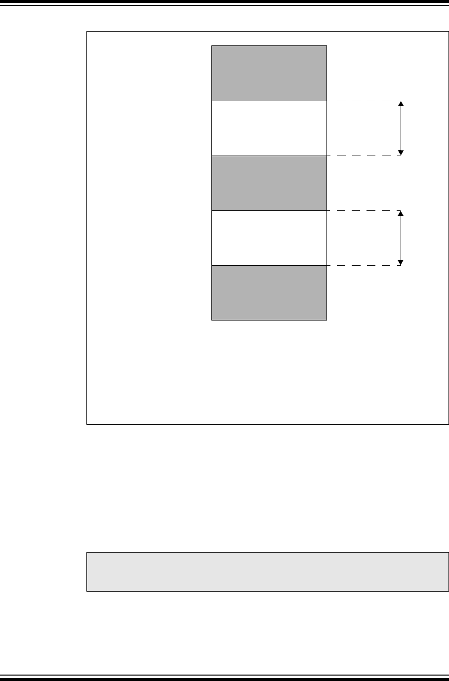
PIC32MX Family Reference Manual
DS61115F-page 3-18 © 2010 Microchip Technology Inc.
Figure 3-3: Flash Partitioning
3.4.3 RAM Partitioning
The RAM memory can be divided into four partitions. These are:
•Kernel Data
•Kernel Program
• User Data
•User Program
In order to execute from data RAM, a kernel or user program partition must be defined. At
Power-on Reset (POR), the entire data RAM is assigned to the kernel data partition. This partition
always starts from the base of the data RAM. See Figure 3-4 for details.
Note 1: To pro per ly par tit io n t he R AM, you h ave to program all of the following registers:
BMXDKPBA, BMXDUDBA and BMXDUPBA.
2: The size of the available RAM is given by the BMXDRMSZ register.
Note 1: Kernel Flash Size = BMXPUPBA.
2: User Flash Size = BMXPFMSZ-BMXPUPBA.
3: If BMXPUPBA is ‘0’, then:
K Flash Size = BMXPFMSZ (i.e., all the Flash)
User Flash Size = 0
Physical Address
0x1D000000
Virtual Address
KSEG0: 0x9D000000
+BMXPUPBA
+BMXPUPBA
KSEG1: 0xBD000000
KSEG0: 0x9D000000
KSEG1: 0xBD000000
0x7D000000+
BMXPUPBA
0x00000000
0xBD000000+
BMXPUPBA
Kernel Flash Size(1) User Flash Size(2)
Flash Partition for
Kernel Program
(KSEG 0/1)
Optional
Flash Partition for
User Program
(USEG/KUSEG)
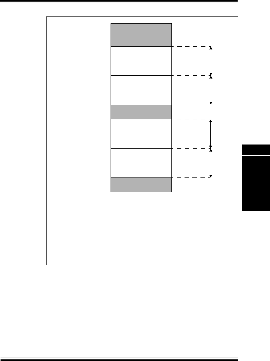
© 2010 Microchip Technology Inc. DS61115F-page 3-19
Section 3. Memory Organization
Memory
Organization
3
Figure 3-4: RAM Partitioning
Note 1: Kernel Data RAM Size = BMXDKPBA.
2: Kernel Program RAM Size = BMXDUDBA - BMXDKPBA.
3: User Data RAM Size = BMXDUPBA - BMXDUDBA.
4: User Program RAM Size = BMXDRMSZ - BMXDUPBA.
5: If BMXDKPBA, BMXDUDBA or BMXDUPBA is ‘0’, then:
Kernel Data RAM Size = BMXDRMSZ (i.e., all RAM)
Kernel Program RAM Size = 0
User Data RAM Size = 0
User Program RAM Size = 0
Physical Address
0x00000000
Virtual Address
KSEG0: 0x80000000
+BMXDUDBA
+BMXDUDBA
KSEG1: 0xA0000000
KSEG0: 0x80000000
KSEG1: 0xA0000000
0x7F000000
+BMXDUPBA
0x00000000
0xBF000000
+BMXDUPBA
Kernel Program User Program
Optional
Kernel Program Partition
KSEG 0/1
Kernel Data Partition
KSEG 0/1
+BMXDKPBA
+BMXDKPBA
KSEG0: 0x80000000
KSEG1: 0xA0000000
0x7F000000
+BMXDUDBA
+BMXDUDBA
0x00000000
0x00000000
0xBF000000
+BMXDKPBA
+BMXDUDBA
Kernel Data User Data
Optional
User Program RAM Partition
(USEG/KUSEG)
Optional
User RAM Partition
(USEG/KUSEG)
RAM Size(2) RAM Size(1) RAM Size(4) RAM Size(3)

PIC32MX Family Reference Manual
DS61115F-page 3-20 © 2010 Microchip Technology Inc.
3.4.3.1 Kernel Data RAM Partition
The kernel data RAM partition is located at virtual address KSEG0:0x80000000,
KSEG1:0xA0000000. It is always active and cannot be disabled.
Please note that if any of the BMXDKPBA, BMXDUDBA or BMXDUPBA register is ‘0’, then the
whole RAM is assigned to kernel data RAM (i.e., the size of the kernel data RAM partition is given
by the BMXDRMSZ register value; see Figure 3-5). Otherwise, the size of the kernel data RAM
partition is given by the value of the BMXDKPBA register (see Figure 3-6).
The kernel data RAM partition exists on Reset and takes up all the available RAM, as the
BMXDKPBA, BMXDUDBA and BMXDUPBA registers default to zero at any Reset.
Figure 3-5: RAM Partitioning When BMXDKPBA, BMXDUDBA or BMXDUPBA = 0
Note: Kernel Data RAM Size = BMXDRMSZ.
Physical Address
Virtual Address
Kernel Data RAM Partition
KSEG0/1
KSEG0: 0x80000000
KSEG1: 0xA0000000
BMXDRMSZ
Kernel Data RAM Size

© 2010 Microchip Technology Inc. DS61115F-page 3-21
Section 3. Memory Organization
Memory
Organization
3
Figure 3-6: Kernel Data RAM Partitioning
Note 1: Kernel Data RAM Size = BMXDKPBA.
2: None of the registers BMXDKPBA, BMXDUDBA or BMXDUPBA = 0.
Physical Address
Virtual Address
BMXDRMSZ
Other Data RAM Partitions
Kernel Data RAM Partition
KSEG0/KSEG1
Kernel Data RAM Size(1)
KSEG0: 0x80000000
KSEG1: 0xA0000000
+BMXDKPBA
+BMXDKPBA
KSEG0: 0x80000000
KSEG1: 0xA0000000
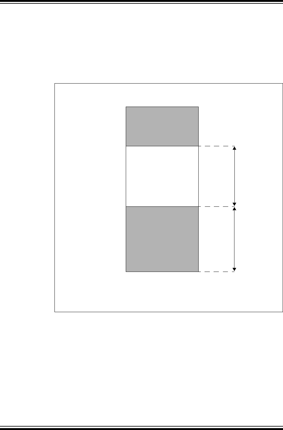
PIC32MX Family Reference Manual
DS61115F-page 3-22 © 2010 Microchip Technology Inc.
3.4.3.2 Kernel Program RAM Partition
The kernel program RAM partition is required if code needs to be executed from data RAM in
Kernel mode.
This partition starts at KSEG0:0x80000000 + BMXDKPBA (KSEG1:0xA0000000 +
BMXDKPBA), and its size is given by BMXDUDBA - BMXDKPBA. See Figure 3-7.
The kernel program RAM partition does not exist on Reset, as the BMXDKPBA and BMXDUDBA
registers default to zero at Reset.
Figure 3-7: Kernel Program RAM Partitioning
Note 1: Kernel Program RAM Size = BMXDUDBA - BMXDKPBA.
2: None of BMXDKPBA, BMXDUDBA or BMXDUPBA = 0.
Physical Address
Virtual Address
BMXDRMSZ
User Data RAM Partitions
Kernel Program RAM Partition
KSEG 0/1
Kernel Data RAM Partition
KSEG0/KSEG1
Kernel Program RAM Size(1) Kernel Data RAM Size
KSEG0: 0x80000000
KSEG1: 0xA0000000
+BMXDKPBA
+BMXDKPBA
KSEG0: 0x80000000
KSEG1: 0xA0000000
+BMXDUDBA
+BMXDUDBA
KSEG1: 0xA0000000
KSEG0: 0x80000000

© 2010 Microchip Technology Inc. DS61115F-page 3-23
Section 3. Memory Organization
Memory
Organization
3
3.4.3.3 User Data RAM Partition
For User mode applications, a User mode data partition in RAM is required. This partition starts
at address 0x7F000000 + BMXDUDBA, and its size is given by BMXDUPBA - BMXDUDBA (see
Figure 3-8).
The user data RAM partition does not exist on Reset, as the BMXDUDBA and BMXDUPBA
registers default to zero at Reset.
Figure 3-8: User Data RAM Partitioning
Note 1: User Data RAM Size = BMXDUPBA - BMXDUDBA.
2: None of the registers BMXDKPBA, BMXDUDBA or BMXDUPBA = 0.
Physical Address
Virtual Address
BMXDRMSZ
User Program RAM Partitions
User Data RAM Partitions
User Data RAM Size(1)
0x7F000000
+BMXDUDBA
0x7F000000
+BMXDUPBA

PIC32MX Family Reference Manual
DS61115F-page 3-24 © 2010 Microchip Technology Inc.
3.4.3.4 User Program RAM Partition
The user program partition in data RAM is required if code needs to be executed from data RAM
in User mode. This partition starts at address 0x7F000000 + BMXDUPBA, and its size is given
by BMXDRMSZ – BMXDUPBA. See Figure 3-9.
The User Program RAM partition does not exist on Reset, as the BMXDUPBA register defaults
to zero at Reset.
Figure 3-9: User Program RAM Partitioning
Note 1: User Program RAM Size = BMXDRMSZ - BMXDUPBA.
2: None of the registers BMXDKPBA, BMXDUDBA or BMXDUPBA = 0.
Physical Address
Virtual Address
BMXDRMSZ
User Program RAM Partition
User Data RAM Partition
User Program RAM Size(1)
0x7F000000
+BMXDUDBA
0x7F000000
+BMXDUPBA

© 2010 Microchip Technology Inc. DS61115F-page 3-25
Section 3. Memory Organization
Memory
Organization
3
3.4.3.5 RAM Partitioning Examples
This section provides the following practical examples of RAM partitioning:
•RAM Partitioned as Kernel Data
•RAM Partitioned as Kernel Data and Kernel Program
•RAM Partitioned as Kernel Data and User Data
•RAM Partitioned as Kernel Data, Kernel Program and User Data
•RAM Partitioned as Kernel Data, Kernel Program, User Data and User Program
Example 1. RAM Partitioned as Kernel Data
The entire RAM is partitioned as kernel data RAM after a Reset. No other programming is
required. Setting the BMXDKPBA, BMXDUDBA or BMXDUPBA register to ‘0’ will partition the
entire RAM space to a kernel data partition (see Figure 3-5).
Example 2. RAM Partitioned as Kernel Data and Kernel Program
For this example, assume that the available RAM on the PIC32MX device is 32 KB, of which
8KB kernel data RAM and 24KB of kernel program RAM are needed. In this example, the user
data RAM and user program RAM will have their sizes set to ‘0’.
Please note that a kernel data RAM partition is always required. See Figure 3-10 for details.
The values of the registers are as follows:
•BMXDRMSZ = 0x00008000 (read-only value)
•BMXDKPBA = 0x00002000 (i.e., 8KB kernel data)
•BMXDUDBA = 0x00008000 (i.e., 0x6000 kernel program)
• BMXDUPBA = 0x00008000 (i.e., user data size = 0, and user program size = 0)
Figure 3-10: RAM Partitioning for 8 KB Kernel Data and 16 KB Kernel Program
BMXDKPBA = 0x2000
BMXDUDBA = 0x8000
BMXDUPBA = 0x8000
Note: Only KSEG0 addresses are shown. For KSEG1 addresses, start at 0xA000000.
Physical Address
Virtual Address
BMXDRMSZ
Kernel Data RAM Partition
Kernel Program RAM Partition
Kernel Program RAM Size
= 0x80000000
+BMXDKPBA
KSEG0: 0x80008000
+BMXDUDBA
Kernel Data RAM Size
= 0x00008000
KSEG 0/1
24 KB
KSEG 0/1
8 KB
= 0x80000000
KSEG0: 0x80002000
KSEG0: 0x80000000
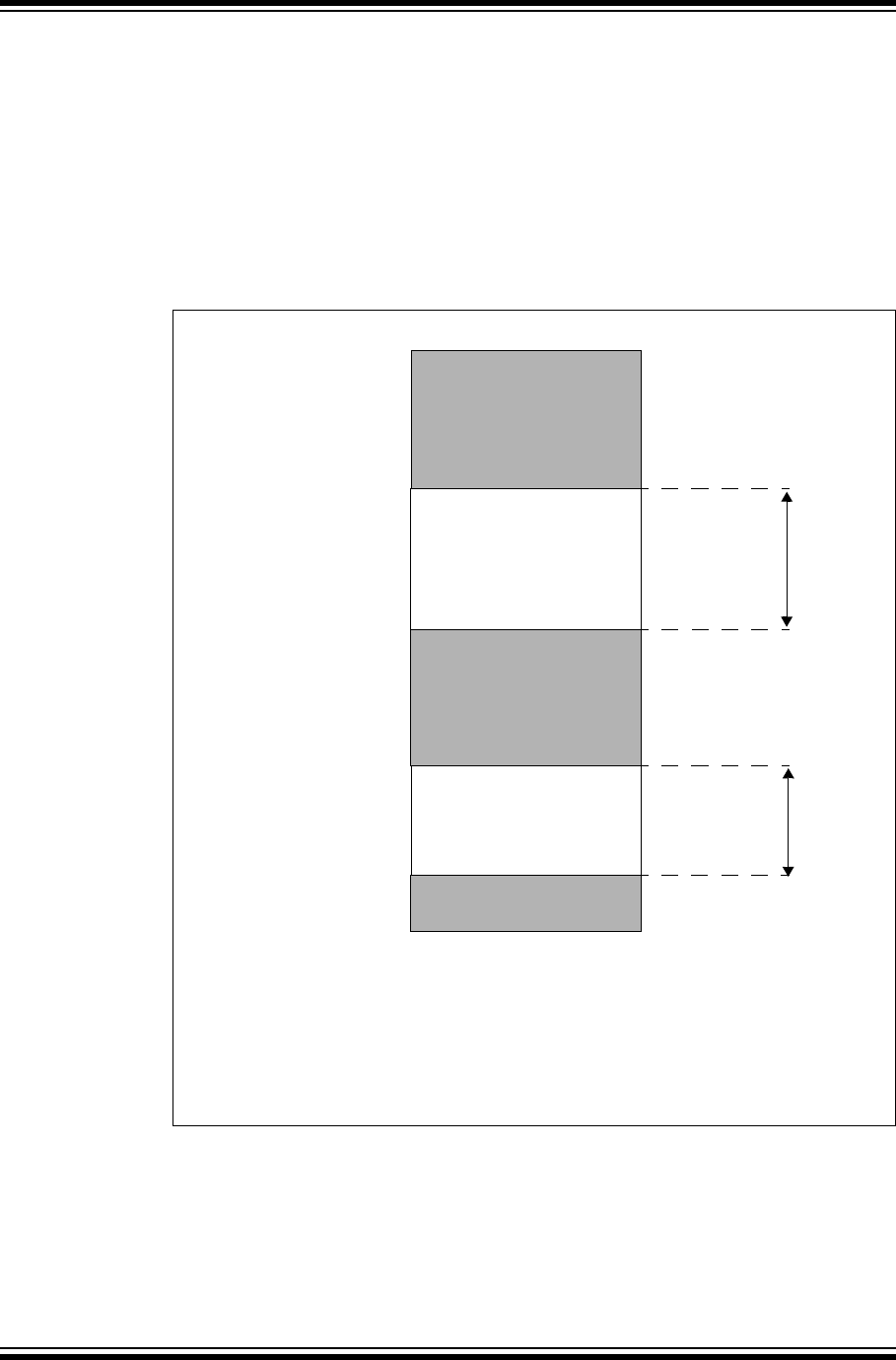
PIC32MX Family Reference Manual
DS61115F-page 3-26 © 2010 Microchip Technology Inc.
Example 3. RAM Partitioned as Kernel Data and User Data
For this example, assume that the available RAM on the PIC32MX device is 32 KB, of which
16 KB of kernel data RAM and 16 KB of user data RAM are needed. In this example, the kernel
program RAM and user program RAM will have their sizes set to ‘0’. See Figure 3-11 for details.
The values of the registers are as follows:
•BMXDRMSZ = 0x00008000 (read-only value)
•BMXDKPBA = 0x00004000 (i.e., 16KB kernel data)
•BMXDUDBA = 0x00004000 (i.e., 0 kernel program)
• BMXDUPBA = 0x00008000 (i.e., user data size = 16 KB, and user program size = 0)
Figure 3-11: RAM Partitioning for 16 KB Kernel Data and 16 KB User Data
BMXDKPBA = 0x4000
BMXDUDBA = 0x4000
BMXDUPBA = 0x8000
Note: Only KSEG0 addresses are shown. For KSEG1 addresses, start at 0xA0000000.
Physical Address
Virtual Address
KSEG0: 0x80004000
= 0x80000000
+BMXDKPBA
KSEG0: 0x80000000
0x7F008000
= 0x7F000000
+BMXDUPBA
0x00000000
Kernel Data RAM Size User Data RAM Size
User Data RAM
16 KB
Kernel Data RAM
16 KB
0x7F004000
= 0x7F000000
+BMXDUDBA

© 2010 Microchip Technology Inc. DS61115F-page 3-27
Section 3. Memory Organization
Memory
Organization
3
Example 4. RAM Partitioned as Kernel Data, Kernel Program and User Data
For this example, assume that the available RAM on the PIC32MX device is 32 KB, and 4 KB of
kernel data RAM, 6 KB of kernel program and 22 KB of user data RAM are needed. In this
example, the user program RAM will have its size set to ‘0’. See Figure 3-12 for details.
The values of the registers are as follows:
•BMXDRMSZ = 0x00008000 (read-only value)
•BMXDKPBA = 0x00001000 (i.e., 4KB kernel data)
•BMXDUDBA = 0x00002800 (i.e., 6KB kernel program)
• BMXDUPBA = 0x00008000 (i.e., user data size = 22 KB, and user program size = 0)
Figure 3-12: RAM Partitioning for 4 KB K-Data, 6 KB K-Program and 22 KB U-Data
BMXDKPBA = 0x1000
BMXDUDBA = 0x2800
BMXDUPBA = 0x8000
Note: Only KSEG0 addresses are shown. For KSEG1 addresses, start at 0xA0000000.
Physical Address
Virtual Address
KSEG0: 0x80002800
= 0x80000000
+BMXDUDBA
KSEG0: 0x80000000
0x7F008000
= 0x7F000000
+BMXDUPBA
0x00000000
Kernel Data User Data RAM Size
User Data RAM
22 KB
Kernel Program RAM
6 KB
0x7F002800
= 0x7F000000
+BMXDUDBA
Kernel Data RAM
4 KB
Kernel Program
RAM Size RAM Size
KSEG0: 0x80001000
= 0x80000000
+BMXDKPBA

PIC32MX Family Reference Manual
DS61115F-page 3-28 © 2010 Microchip Technology Inc.
Example 5. RAM Partitioned as Kernel Data, Kernel Program, User Data and User Program
For this example, assume that the available RAM on the PIC32MX device is 32 KB, and 6 KB of
kernel data RAM, 5 KB of kernel program RAM, 12 KB of user data RAM and 9 KB of user
program RAM are needed. See Figure 3-13 for details.
The values of the registers are as follows:
•BMXDRMSZ = 0x00008000 (read-only value)
•BMXDKPBA = 0x00001800 (i.e., 6KB kernel data)
•BMXDUDBA = 0x00002C00 (i.e., 5KB kernel program)
•BMXDUPBA = 0x00005C00 (i.e., user data size = 12 KB, and user program size = 9 KB)
Figure 3-13: RAM Partitioning for 6 KB K-Data, 5 KB K-Program, 12 KB U-Data and
9KB U-Program
BMXDKPBA = 0x1800
BMXDUDBA = 0x2c00
BMXDUPBA = 0x5c00
Note: Only KSEG0 addresses are shown. For KSEG1 addresses, start at 0xA0000000.
Physical Address
Virtual Address
KSEG0: 0x80002C00
= 0x80000000
+BMXDUDBA
KSEG0: 0x80000000
0x7F005C00
= 0x7F000000
+BMXDUPBA
0x00000000
Kernel Data User Data
User Program RAM
9 KB
Kernel Program RAM
5 KB
0x7F002C00
= 0x7F000000
+BMXDUDBA
Kernel Data RAM
6 KB
Kernel Program
RAM Size RAM Size
KSEG0: 0x80001800
= 0x80000000
+BMXDKPBA
User Data RAM
12 KB
RAM Size
User Program
RAM Size
0x7F008000
= 0x7F000000
+BMXDRMSZ
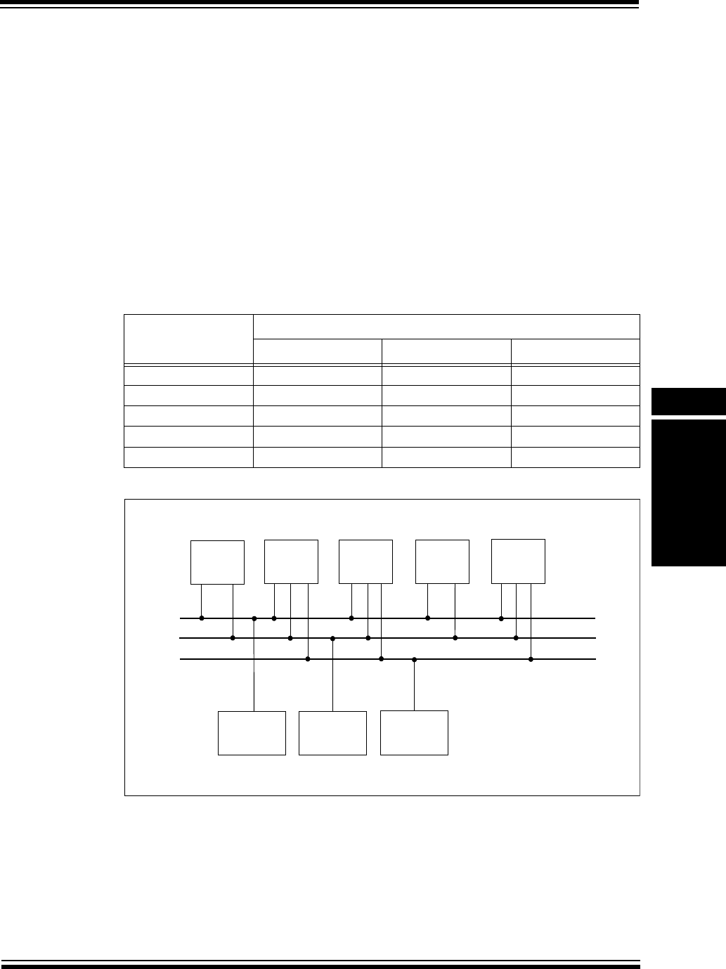
© 2010 Microchip Technology Inc. DS61115F-page 3-29
Section 3. Memory Organization
Memory
Organization
3
3.5 BUS MATRIX
The processor supports two modes of operation, Kernel mode and User mode. The Bus Matrix
controls the allocation of memory for each of these modes. It also controls the type of access,
program or data, for a given region of address space.
The Bus Matrix connects master devices, generically called initiators, to slave devices, generi-
cally called targets. The PIC32MX product family can have up to five initiators and three targets
(e.g., Flash, RAM, etc.) on the main bus structure.
Of the five possible initiators, the CPU Instruction Bus (CPU IS), CPU Data Bus (CPU DS),
In-Circuit Debug (ICD) and DMA Controller (DMA) are the default set of initiators and are always
present. The PIC32MX also includes an Initiator Expansion Interface (IXI) to support additional
initiators for future expansion.
The Bus Matrix decodes a general range of addresses that map to a target. The target (memory
or peripherals) may provide additional addresses depending on its functionality.
Tabl e 3 -3 lis ts t he ta rge ts w hich th e ini tia tor s can acc es s.
Table 3-3: Initiator Access Map
Figure 3-14: Bus Matrix Initiators and Targets
Initiator
Target
Flash RAM Peripheral Bus
CPU IS YYN
CPU DS YYY
DMA YYY
IXI YYN
ICD YYY
CPU IS CPU DS DMA Initiator
Expansion Debug
Module
PFM
DRM
Peripherals
Initiators
Tar gets
Program
Memory
Data RAM
Memory
Peripheral
(PBM)
Flash Bus

PIC32MX Family Reference Manual
DS61115F-page 3-30 © 2010 Microchip Technology Inc.
3.5.1 Initiator Arbitration Modes
Since there can be more than one initiator attempting to access the same target, an arbitration
scheme must be used to control access to the target. The arbitration modes assign priority levels
to all the initiators. The initiator with the higher priority level will always win target access over a
lower priority initiator.
3.5.1.1 Arbitration Mode 0
The fixed priority scheme in Arbitration Mode 0 is illustrated in Figure 3-15. The CPU data and
instruction access are given higher priority than DMA access. This mode can starve the DMA, so
chose this mode when DMA is not being used.
As illustrated in Figure 3-15, each initiator is assigned a fixed priority level. Programming the register
field BMXARB (BMXCON<2:0>) to ‘0’ selects Mode 0 operation.
Figure 3-15: Priority Assignment in Arbitration Mode 0
ICD/Debug
CPU Data
CPU
Instruction
Access
DMA
Initiator
Expansion
Higher Priority
Access
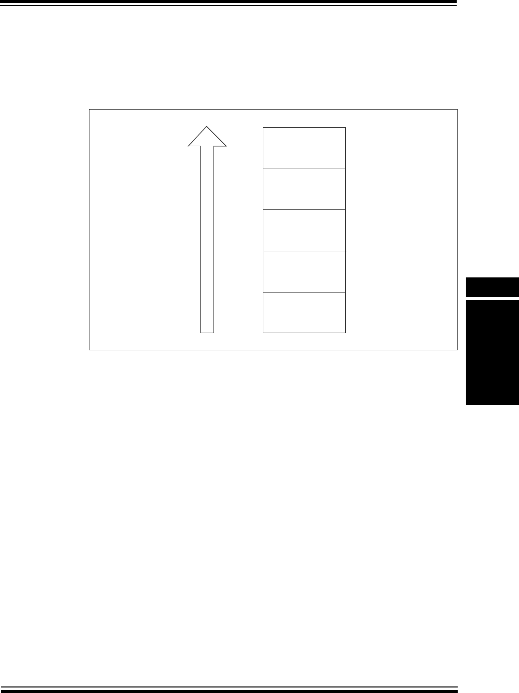
© 2010 Microchip Technology Inc. DS61115F-page 3-31
Section 3. Memory Organization
Memory
Organization
3
3.5.1.2 Arbitration Mode 1
Arbitration Mode 1 is a fixed priority scheme like Mode 0; however, the CPU IS is always the
lowest priority. Figure 3-16 illustrates the priority scheme in Mode 1. Mode 1 arbitration is the
default mode.
Programming the register field BMXARB (BMXCON<2:0>) to ‘1’ selects Mode 1 operation.
Figure 3-16: Priority Assignment in Arbitration Mode 1
ICD/Debug
CPU Data
DMA
Initiator
CPU
Instruction
Higher Priority
Access
Expansion
Access
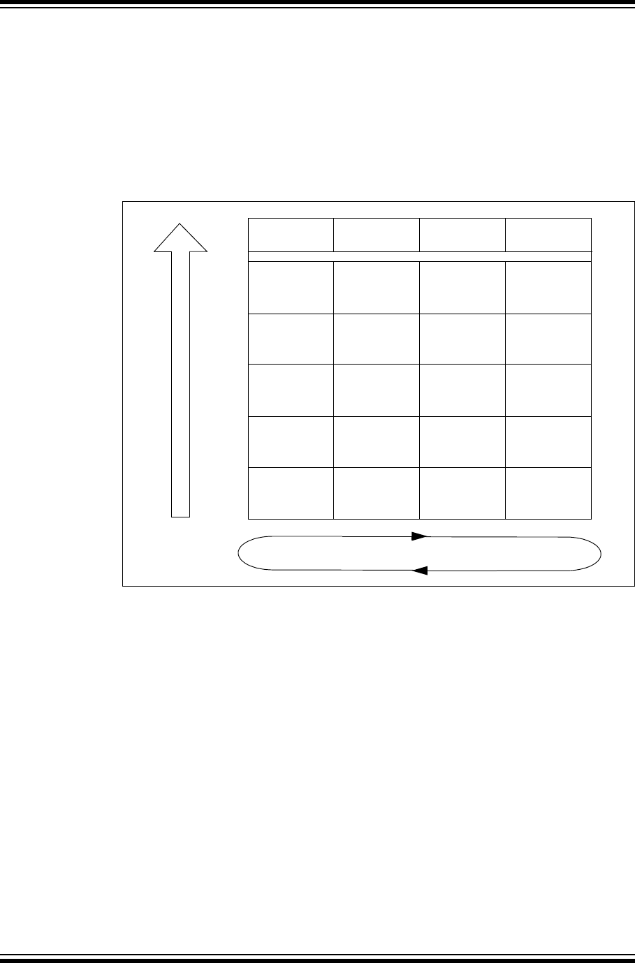
PIC32MX Family Reference Manual
DS61115F-page 3-32 © 2010 Microchip Technology Inc.
3.5.1.3 Arbitration Mode 2
Mode 2 arbitration supports rotating priority assignments to all initiators. Instead of a fixed prior-
ity assignment, each initiator is assigned the highest priority in a rotating fashion. In this mode,
the rotating priority is applied with the following exceptions:
1. CPU data is always selected over CPU instruction.
2. ICD is always the highest priority.
3. When the CPU is processing an exception (EXL = 1) or an error (ERL = 1), the arbiter
temporarily reverts to Mode 0.
Figure 3-17: Priority Assignments in Arbitration Mode 2
Note that priority sequence 2 is not selected in the rotating priority scheme if there is a pending
CPU data access. In this case, once the data access is complete, sequence 2 is selected.
Programming the register field BMXARB (BMXCON<2:0>) to ‘2’ selects Mode 2 operation.
3.5.2 Bus Error Exceptions
The Bus Matrix generates a bus error exception on:
• Any attempt to access unimplemented memory
• Any attempt to access an illegal target
•Any attempt to write to program Flash memory
Bus Error Exceptions may be temporarily disabled by clearing the BMXERRxxx bits in the
BMXCON register, which is not recommended.
The Bus Matrix disables bus error exceptions for accesses from CPU IS and CPU DS while in
DEBUG mode.
3.5.3 Break Exact Breakpoint Support
The PIC32MX supports break exact breakpoints by inserting one Wait state to data RAM access.
This method allows the CPU to stop execution just before the breakpoint address instruction.
This is useful in case of breakpointed store instructions. When the Wait state is not used, the
break will still occur at the store instruction, however, the DRM location is updated with the store
value. If the Wait state is enabled the DRM is not updated with the store value.
Priority
Sequence 1
Priority
Sequence 2
Priority
Sequence 3
Priority
Sequence 4
ICD/Debug
CPU Data
Access
CPU
Instruction
Access
DMA
Initiator
Expansion
ICD/Debug ICD/Debug ICD/Debug
CPU
Instruction
Access
CPU
Instruction
Access
CPU
Instruction
Access
CPU Data
Access
CPU Data
Access
DMA
DMA
DMA
Initiator
Expansion
Initiator
Expansion
Initiator
Expansion
CPU Data
Access
Rotating Priority Sequence
Higher Priority

© 2010 Microchip Technology Inc. DS61115F-page 3-33
Section 3. Memory Organization
Memory
Organization
3
3.6 I/O PIN CONTROL
There are no pins associated with this module.
3.7 OPERATION IN POWER-SAVING AND DEBUG MODES
3.7.1 Memory Operation on Power-up or Brown-out Reset (BOR):
•The contents of data RAM are undefined
•The BMXxxxBA registers are reset to ‘0’
•CPU is switched to Kernel mode
3.7.2 Memory Operation on Reset:
• The data RAM contents are retained. If the device is code-protected, the RAM contents are
cleared
•The BMX base address registers (BMXxxxBA) are set to ‘0’
•CPU is switched to Kernel mode
3.7.3 Memory Operation on Wake-up from Device Sleep or Idle Mode:
• The RAM contents are retained
•The BMX base address register (BMXxxxBA) contents are not changed
•CPU mode is unchanged

PIC32MX Family Reference Manual
DS61115F-page 3-34 © 2010 Microchip Technology Inc.
3.8 CODE EXAMPLES
Example 3-1: Create a User Mode Partition of 12K in Program Flash
Example 3-2: Create a Kernel Mode Data RAM Partition of 16K; Rest of RAM for
Kernel Program
Example 3-3 can be used to create the following partitions in RAM:
•Kernel mode data = 12K
•Kernel mode program = 6K
•User mode data = 8K
•User mode program = 6K
Example 3-3: Create RAM Partitions
BMXPUPBA = BMXPFMSZ - (12*1024); // User Mode Flash 12K,
// Kernel Mode Flash 500K (512K-12K)
BMXDKPBA = 16*1024;
BMXDUDBA = BMXDRMSZ;
BMXDUPBA = BMXDRMSZ;
BMXDKPBA = 12*1024; // Kernel Data Partition of 12K.
// Start offset of Kernel Program Partition
BMXDUDBA = BMXDKPBA + (6*1024); // Kernel Program Partition of 6K
// Start offset of User Data Partition
BMXDUPBA = BMXDUDBA + (8*1024); // User Data Partition of 8K
// Start offset of User Program Partition.
// This partition will go up to the size of
// RAM (32K). So the partition size will be
// 6K (32K - 8K - 6K - 12K)

© 2010 Microchip Technology Inc. DS61115F-page 3-35
Section 3. Memory Organization
Memory
Organization
3
3.9 DESIGN TIPS
Question 1: At Reset, in which mode is the CPU running?
Answer: The CPU starts in Kernel mode. The entire RAM is mapped to kernel data
segments in KSEG0 and KSEG1. Flash memory is mapped to kernel program
segments in KSEG0 and KSEG1. Also ERL = 1, which should be reset to zero
(normally in the C start-up code).
Question 2: Do I need to initialize the BMX registers?
Answer: Generally, no. You can leave the BMX registers at their default values, which
allows maximum RAM and Flash memories for Kernel mode applications. If you
want to run code from RAM or set up User mode partitions, you will need to
configure the BMX registers.
Question 3: What is the CPU Reset vector address?
Answer: The CPU Reset address is 0xBFC00000.
Question 4: What is a Bus-Error Exception?
Answer: Bus-error exceptions are generated when the CPU tries to access
unimplemented addresses. Also, when the CPU tries to execute a program from
RAM without defining a RAM program partition, a bus-error exception is
generated.

PIC32MX Family Reference Manual
DS61115F-page 3-36 © 2010 Microchip Technology Inc.
3.10 RELATED APPLICATION NOTES
This section lists application notes that are related to this section of the manual. These applica-
tion notes may not be written specifically for the PIC32MX device family, but the concepts are
pertinent and could be used with modification and possible limitations. The current application
notes related to the Memory Organization of the PIC32MX family include the following:
Title Application Note #
No related application notes at this time. N/A
Note: Please visit the Microchip web site (www.microchip.com) for additional application
notes and code examples for the PIC32MX family of devices.

© 2010 Microchip Technology Inc. DS61115F-page 3-37
Section 3. Memory Organization
Memory
Organization
3
3.11 REVISION HISTORY
Revision A (August 2007)
This is the initial released version of this document.
Revision B (October 2007)
Updated document to remove Confidential status.
Revision C (April 2008)
Revised status to Preliminary; Revised U-0 to r-x.
Revision D (June 2008)
Change Reserved bits from “Maintain as” to “Write”.
Revision E (July 2009)
This revision includes the following updates:
•Minor updates to the text and formatting have been incorporated throughout the document
• Added Notes 1, 2 and 3, which describe the Clear, Set and Invert registers to the following:
-Table3-1: Memory Organization SFR Summary
-Register3-1: BMXCON: Bus Matrix Configuration Register
-Register3-2: BMXDKPBA: Data RAM Kernel Program Base Address Register
-Register3-3: BMXDUDBA: Data RAM User Data Base Address Register
-Register3-4: BMXDUPBA: Data RAM User Program Base Address Register
-Register3-6: BMXPUPBA: Program Flash (PFM) User Program Base Address Register
•Removed all Clear, Set and Invert register descriptions
•Added additional bit value definition (0x0001000) to BMXDRMSZ: Data RAM Size Register
(see Register 3-5)
Revision F (July 2010)
This revision includes the following updates:
•Minor updates to the text and formatting have been incorporated throughout the document
•Added Notes 4 and 5 to the following registers:
- BMXDKPBA: Data RAM Kernel Program Base Address Register (see Register 3-2)
- BMXDUDBA: Data RAM User Data Base Address Register (see Register 3-3)
- BMXDUPBA: Data RAM User Program Base Address Register (see Register 3-4)
- BMXPUPBA: Program Flash (PFM) User Program Base Address Register (see
Register 3-6)
•Updated the PIC32MX Address Map (see Table3-2)

PIC32MX Family Reference Manual
DS61115F-page 3-38 © 2010 Microchip Technology Inc.
NOTES:

2010 Microchip Technology Inc. DS61115F-page 39
Information contained in this publication regarding device
applications and the like is provided only for your convenience
and may be superseded by updates. It is your responsibility to
ensure that your application meets with your specifications.
MICROCHIP MAKES NO REPRESENTATIONS OR
WARRANTIES OF ANY KIND WHETHER EXPRESS OR
IMPLIED, WRITTEN OR ORAL, STATUTORY OR
OTHERWISE, RELATED TO THE INFORMATION,
INCLUDING BUT NOT LIMITED TO ITS CONDITION,
QUALITY, PERFORMANCE, MERCHANTABILITY OR
FITNESS FOR PURPOSE. Microchip disclaims all liability
arising from this information and its use. Use of Microchip
devices in life support and/or safety applications is entirely at
the buyer’s risk, and the buyer agrees to defend, indemnify and
hold harmless Microchip from any and all damages, claims,
suits, or expenses resulting from such use. No licenses are
conveyed, implicitly or otherwise, under any Microchip
intellectual property rights.
Trademarks
The Microchip name and logo, the Microchip logo, dsPIC,
KEELOQ, KEELOQ logo, MPLAB, PIC, PICmicro, PICSTART,
PIC32 logo, rfPIC and UNI/O are registered trademarks of
Microchip Technology Incorporated in the U.S.A. and other
countries.
FilterLab, Hampshire, HI-TECH C, Linear Active Thermistor,
MXDEV, MXLAB, SEEVAL and The Embedded Control
Solutions Company are registered trademarks of Microchip
Technology Incorporated in the U.S.A.
Analog-for-the-Digital Age, Application Maestro, CodeGuard,
dsPICDEM, dsPICDEM.net, dsPICworks, dsSPEAK, ECAN,
ECONOMONITOR, FanSense, HI-TIDE, In-Circuit Serial
Programming, ICSP, Mindi, MiWi, MPASM, MPLAB Certified
logo, MPLIB, MPLINK, mTouch, Octopus, Omniscient Code
Generation, PICC, PICC-18, PICDEM, PICDEM.net, PICkit,
PICtail, REAL ICE, rfLAB, Select Mode, Total Endurance,
TSHARC, UniWinDriver, WiperLock and ZENA are
trademarks of Microchip Technology Incorporated in the
U.S.A. and other countries.
SQTP is a service mark of Microchip Technology Incorporated
in the U.S.A.
All other trademarks mentioned herein are property of their
respective companies.
© 2010, Microchip Technology Incorporated, Printed in the
U.S.A., All Rights Reserved.
Printed on recycled paper.
ISBN: 978-1-60932-385-1
Note the following details of the code protection feature on Microchip devices:
• Microchip products meet the specification contained in their particular Microchip Data Sheet.
• Microchip believes that its family of products is one of the most secure families of its kind on the market today, when used in the
intended manner and under normal conditions.
• There are dishonest and possibly illegal methods used to breach the code protection feature. All of these methods, to our
knowledge, require using the Microchip products in a manner outside the operating specifications contained in Microchip’s Data
Sheets. Most likely, the person doing so is engaged in theft of intellectual property.
• Microchip is willing to work with the customer who is concerned about the integrity of their code.
• Neither Microchip nor any other semiconductor manufacturer can guarantee the security of their code. Code protection does not
mean that we are guaranteeing the product as “unbreakable.”
Code protection is constantly evolving. We at Microchip are committed to continuously improving the code protection features of our
products. Attempts to break Microchip’s code protection feature may be a violation of the Digital Millennium Copyright Act. If such acts
allow unauthorized access to your software or other copyrighted work, you may have a right to sue for relief under that Act.
Microchip received ISO/TS-16949:2002 certification for its worldwide
headquarters, design and wafer fabrication facilities in Chandler and
Tempe, Arizona; Gresham, Oregon and design centers in California
and India. The Company’s quality system processes and procedures
are for its PIC® MCUs and dsPIC® DSCs, KEELOQ® code hopping
devices, Serial EEPROMs, microperipherals, nonvolatile memory and
analog products. In addition, Microchip’s quality system for the design
and manufacture of development systems is ISO 9001:2000 certified.

DS61115F-page 40 2010 Microchip Technology Inc.
AMERICAS
Corporate Office
2355 West Chandler Blvd.
Chandler, AZ 85224-6199
Te l: 4 80 -7 92- 72 00
Fax: 480-792-7277
Technical Support:
http://support.microchip.com
Web Address:
www.microchip.com
Atlanta
Duluth, GA
Tel: 678-957-9614
Fax: 678-957-1455
Boston
Westborough, MA
Tel: 774-760-0087
Fax: 774-760-0088
Chicago
Itasca, IL
Tel: 630-285-0071
Fax: 630-285-0075
Cleveland
Independence, OH
Tel: 216-447-0464
Fax: 216-447-0643
Dallas
Addison, TX
Tel: 972-818-7423
Fax: 972-818-2924
Detroit
Farmington Hills, MI
Tel: 248-538-2250
Fax: 248-538-2260
Kokomo
Kokomo, IN
Tel: 765-864-8360
Fax: 765-864-8387
Los Angeles
Mission Viejo, CA
Tel: 949-462-9523
Fax: 949-462-9608
Santa Clara
Santa Clara, CA
Tel: 408-961-6444
Fax: 408-961-6445
Toronto
Mississauga, Ontario,
Canada
Tel: 905-673-0699
Fax: 905-673-6509
ASIA/PACIFIC
Asia Pacific Office
Suites 3707-14, 37th Floor
Tower 6, The Gateway
Harbour City, Kowloon
Hong Kong
Tel : 8 52 - 24 0 1- 120 0
Fax: 852-2401-3431
Australia - Sydney
Tel : 6 1-2 -98 68- 6 73 3
Fax: 61-2-9868-6755
China - Beijing
Tel : 8 6-1 0-8 528 - 21 0 0
Fax: 86-10-8528-2104
China - Chengdu
Tel : 8 6-2 8-8 665 - 55 11
Fax: 86-28-8665-7889
China - Chongqing
Tel : 8 6-2 3-8 980 - 95 8 8
Fax: 86-23-8980-9500
China - Hong Kong SAR
Tel : 8 52 - 24 0 1- 120 0
Fax: 852-2401-3431
China - Nanjing
Tel : 8 6-2 5-8 473 - 24 6 0
Fax: 86-25-8473-2470
China - Qingdao
Tel : 8 6-5 32- 8502 -73 55
Fax: 86-532-8502-7205
China - Shanghai
Tel : 8 6-2 1-5 407 - 55 3 3
Fax: 86-21-5407-5066
China - Shenyang
Tel : 8 6-2 4-2 334 - 28 2 9
Fax: 86-24-2334-2393
China - Shenzhen
Tel : 8 6-7 55- 8203 -26 60
Fax: 86-755-8203-1760
China - Wuhan
Tel : 8 6-2 7-5 980 - 53 0 0
Fax: 86-27-5980-5118
China - Xian
Tel : 8 6-2 9-8 833 - 72 5 2
Fax: 86-29-8833-7256
China - Xiamen
Tel: 86-592-2388138
Fax: 86-592-2388130
China - Zhuhai
Tel : 86- 756 -3 210 04 0
Fax: 86-756-3210049
ASIA/PACIFIC
India - Bangalore
Tel : 9 1- 8 0- 309 0-4 444
Fax: 91-80-3090-4123
India - New Delhi
Tel : 9 1- 11 -41 60- 86 31
Fax: 91-11-4160-8632
India - Pune
Tel : 9 1- 2 0- 256 6-1 512
Fax: 91-20-2566-1513
Japan - Yokohama
Tel : 8 1- 4 5- 471 - 6 166
Fax: 81-45-471-6122
Korea - Daegu
Tel : 8 2- 5 3- 744 -43 01
Fax: 82-53-744-4302
Korea - Seoul
Tel : 8 2- 2 -5 54- 720 0
Fax: 82-2-558-5932 or
82-2-558-5934
Malaysia - Kuala Lumpur
Tel : 6 0- 3 -6 201 -98 57
Fax: 60-3-6201-9859
Malaysia - Penang
Tel : 6 0- 4 -2 27- 887 0
Fax: 60-4-227-4068
Philippines - Manila
Tel : 6 3- 2 -6 34- 906 5
Fax: 63-2-634-9069
Singapore
Tel : 65 - 63 3 4- 887 0
Fax: 65-6334-8850
Taiwan - Hsin Chu
Tel : 8 86 - 3- 657 8-3 00
Fax: 886-3-6578-370
Taiwan - Kaohsiung
Tel : 8 86 - 7- 536 -48 18
Fax: 886-7-536-4803
Taiwan - Taipei
Tel : 8 86 - 2- 250 0-6 610
Fax: 886-2-2508-0102
Thailand - Bangkok
Tel : 6 6- 2 -6 94- 135 1
Fax: 66-2-694-1350
EUROPE
Austria - Wels
Tel : 4 3- 7 24 2 -2 244 -39
Fax: 43-7242-2244-393
Denmark - Copenhagen
Tel : 4 5-4 450 -2 828
Fax: 45-4485-2829
France - Paris
Tel : 3 3-1 -6 9-5 3 -6 3-2 0
Fax: 33-1-69-30-90-79
Germany - Munich
Tel : 4 9- 8 9- 627 -14 4-0
Fax: 49-89-627-144-44
Italy - Milan
Tel : 3 9- 0 33 1 -7 426 11
Fax: 39-0331-466781
Netherlands - Drunen
Tel : 3 1- 4 16 - 690 3 99
Fax: 31-416-690340
Spain - Madrid
Tel : 3 4- 9 1- 708 -08 -90
Fax: 34-91-708-08-91
UK - Wokingham
Tel : 4 4- 11 8-9 21- 58 69
Fax: 44-118-921-5820
WORLDWIDE SALES AND SERVICE
01/05/10

© 2011 Microchip Technology Inc. DS61119E-page 4-1
Prefetch Cache
4
Section 4. Prefetch Cache
HIGHLIGHTS
This section of the manual contains the following major topics:
4.1 Introduction .................................................................................................................... 4-2
4.2 Cache Overview.............................................................................................................4-3
4.3 Control Registers ...........................................................................................................4-7
4.4 Cache Operation.......................................................................................................... 4-23
4.5 Cache Configurations .................................................................................................. 4-23
4.6 Coherency Support ......................................................................................................4-25
4.7 Effects of Reset............................................................................................................4-26
4.8 Operation in Power-Saving Modes .............................................................................. 4-26
4.9 Design Tip.................................................................................................................... 4-26
4.10 Related Application Notes............................................................................................ 4-27
4.11 Revision History ...........................................................................................................4-28

PIC32 Family Reference Manual
DS61119E-page 4-2 © 2011 Microchip Technology Inc.
4.1 INTRODUCTION
This section describes the features and operation of the Prefetch Cache module in the PIC32
device family. Prefetch cache features increase system performance for most applications.
Program Flash Memory (PFM) cache and the Prefetch Cache module increase performance for
applications that execute out of the cacheable PFM region by implementing the following
features:
• Instruction caching
The sixteen fully associative lockable 16-byte cache lines supply an instruction every clock,
for loops up to 256 bytes long.
•Data caching
Prefetch cache allows the allocation of up to four cache lines for data storage to provide
improved access for PFM-stored constant data.
•Predictive prefetching
The Prefetch Cache module provides instructions once per clock for linear code even with-
out caching by prefetching ahead of the current program counter, hiding the access time of
the PFM.
4.1.1 Additional Prefetch Cache Module Features
The Prefetch Cache module also include the following features:
•Up to four cache lines allocated to data
• Two cache lines with address mask to hold repeated instructions
• Pseudo Least-Recently-Used (LRU) replacement policy
•All cache lines are software-writable
• 16-byte parallel memory fetch
•Predictive instruction prefetch cache
Note: This family reference manual section is meant to serve as a complement to device
data sheets. Depending on the device variant, this manual section may not apply to
all PIC32 devices.
Please consult the note at the beginning of the “Prefetch Cache” chapter in the
current device data sheet to check whether this document supports the device you
are using.
Device data sheets and family reference manual sections are available for
download from the Microchip Worldwide Web site at: http://www.microchip.com
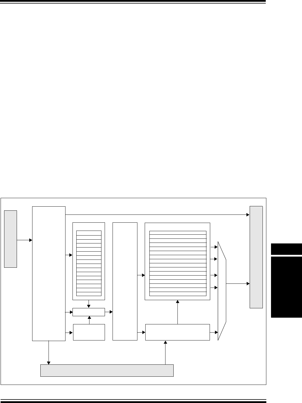
© 2011 Microchip Technology Inc. DS61119E-page 4-3
Section 4. Prefetch Cache
Prefetch Cache
4
4.2 CACHE OVERVIEW
The Prefetch Cache module is a performance enhancing module included in some processors
of the PIC32 family. When running at high-clock rates, Wait states must be inserted into PFM
read transactions to meet the access time of the PFM. Wait states can be hidden to the core by
prefetching and storing instructions in a temporary holding area that the CPU can access quickly.
Although the data path to the CPU is 32 bits wide, the data path to the PFM is 128 bits wide. This
wide data path provides the same bandwidth to the CPU as a 32-bit path running at four times
the frequency.
There are two main functions that the Prefetch Cache module performs: caching instructions
when they are accessed, and prefetching instructions from the PFM before they are needed.
The cache holds a subset of the cacheable memory in temporary holding spaces known as
cache lines. Each cache line has a tag describing what it is currently holding, and the address
where it is mapped. Normally, the cache lines just hold a copy of what is currently in memory to
make data available to the CPU without Wait states.
CPU requested data may or may not be in the cache. A cache-miss occurs if the CPU requests
cacheable data that is not in the cache. In this case, a read is performed to the PFM at the correct
address, the data is supplied to the cache and to the CPU. A cache-hit occurs if the cache
contains the data that the CPU requests. In the case of a cache-hit, data is supplied to the CPU
without Wait states.
The second main function of the Prefetch Cache module is to prefetch cache instructions. The
module calculates the address of the next cache line and performs a read of the PFM to get the
next 16-byte cache line. This line is placed into a 16-byte-wide prefetch cache buffer in
anticipation of executing straight-line code.
Figure 4-1 shows a block diagram of the Prefetch Cache module. Logically, the Prefetch Cache
module fits between the Bus Matrix (BMX) module and the PFM.
Figure 4-1: Prefetch Cache Block Diagram
Prefetch
Program Flash Memory (PFM)
Prefetch
Tag
Hit Logic
Tag Logic
CTRL
FSM
Bus
Cache
Prefetch
Hit LRU
Miss LRU
Cache Line
RDATA
Cache
Line
Address
Encode
BMX/CPU
RDATA
CTRL
BMX/CPU
Control
Control
Control
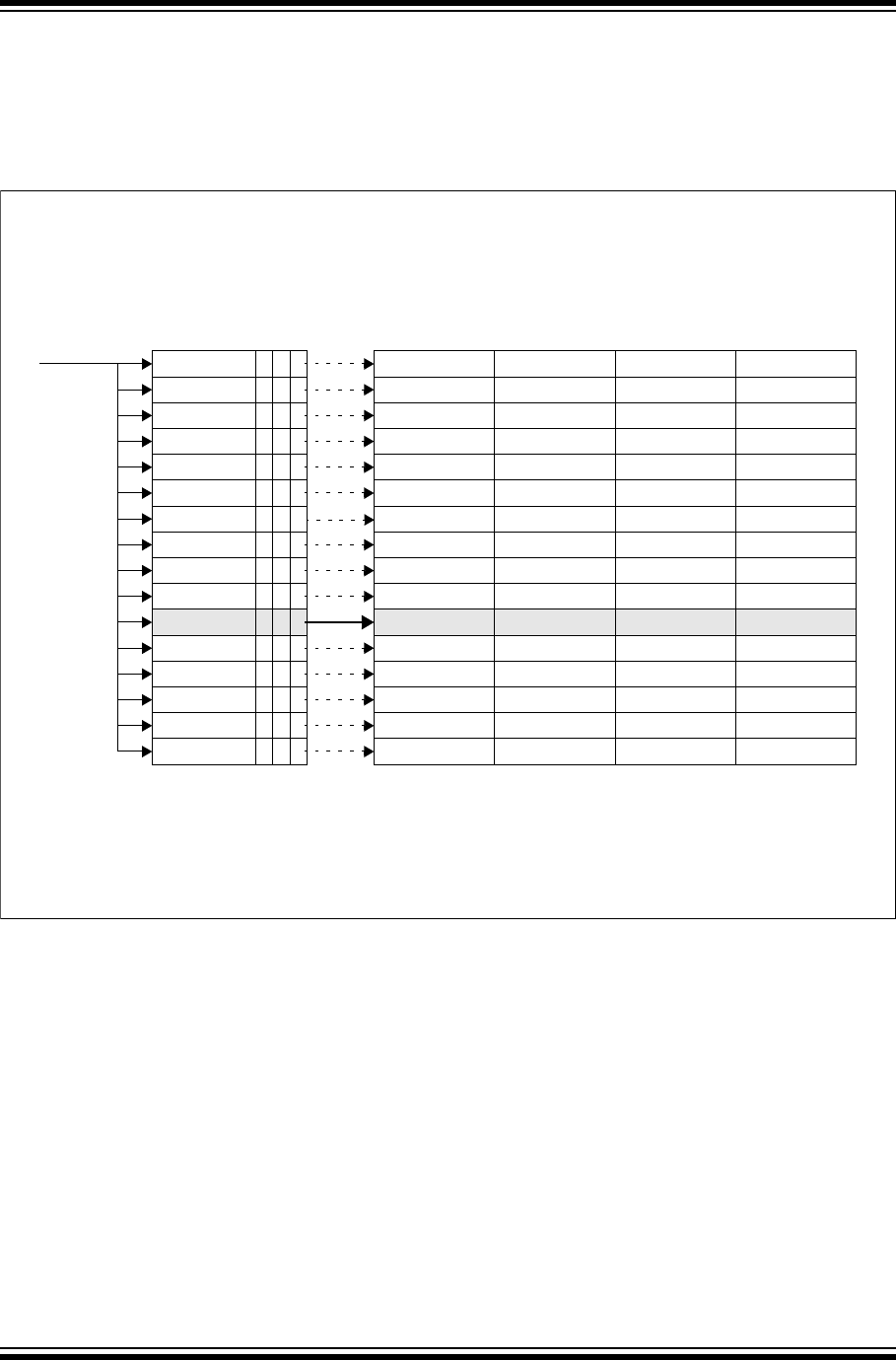
PIC32 Family Reference Manual
DS61119E-page 4-4 © 2011 Microchip Technology Inc.
To ill ust ra te the b asi c ope rat ion o f the p ref et ch ca che , Figure 4-2 shows an example of the CPU
requesting data from physical address 0x1FC01234. The prefetch cache simultaneously
compares this address to all of the tags marked ‘valid’. As the shaded entry below has this
address, and is marked as valid, this is a cache hit. The proper data word from the data array is
then directed to the CPU in a single clock period.
Figure 4-2: Cache Look-up Example(1)
⎫
⎪
⎪
⎪
⎪
⎪
⎪
⎪
⎪
⎬
⎪
⎪
⎪
⎪
⎪
⎪
⎪
⎪
⎭
0x1FC01234 0x00001000 WORD 3 WORD 0WORD 1WORD 2
WORD 3 WORD 0WORD 1WORD 2
WORD 3 WORD 0WORD 1WORD 2
WORD 3 WORD 0WORD 1WORD 2
WORD 3 WORD 0WORD 1WORD 2
WORD 3 WORD 0WORD 1WORD 2
WORD 3 WORD 0WORD 1WORD 2
WORD 3 WORD 0WORD 1WORD 2
WORD 3 WORD 0WORD 1WORD 2
WORD 3 WORD 0WORD 1WORD 2
WORD 3 WORD 0WORD 1WORD 2
WORD 3 WORD 0WORD 1WORD 2
WORD 3 WORD 0WORD 1WORD 2
WORD 3 WORD 0WORD 1WORD 2
WORD 3 WORD 0WORD 1WORD 2
WORD 3 WORD 0WORD 1WORD 2
0x00001300
0x00002200
0x0000a030
0x80001230
0x00002210
0x00002230
0x00002220
0x00001200
0x00001230
0x00001230
0x00001320
0x00001330
0x00001310
0x00001340
0x00001350
101
101
101
101
101
101
101
101
101
001
101
101
100
100
100
100
Cache
Data
LVALID
LLOCK
LTYPE
⎫
⎪
⎪
⎬
⎪
⎪
⎭
HIT
Cache Tags(2)
Note 1: Mask bits are not shown and are assumed to be ‘0’.
2: Bits 3-0 of the address in the Cache Tags register are always implied to be ‘0’.

© 2011 Microchip Technology Inc. DS61119E-page 4-5
Section 4. Prefetch Cache
Prefetch Cache
4
4.2.1 Cache Organization
The cache consists of two arrays: data and tag. A data array consists of program instructions or
program data. The cache is physically tagged and address matches are based on the physical
address, not the virtual address.
Each line in the tag array contains the following information:
•Mask – address mask value
• Tag – tag address to match against
•Valid bit
•Lock bit
•Type – an instruction and/or data type-indicator bit
Each line in the data array contains 16 bytes of program instruction, or program data,
depending on the value of the type-indicator bit.
Figure 4-3 illustrates the organization of a line. It should be noted that the LMASK<10:0> bits
(CHEMSK<15:5>) and the LTYPE bit (CHETAG<1>) are not programmable for every line. The
LTAG<20:0> bits (CHETAG<23:4>) only implement the number of bits needed to fully map to the
size of the PFM. For example, if the PFM size is 512 Kbytes, the LTAG<20:0> bits
(CHETAG<23:4>) only implement bits 15 through 0 (CHETAG<18:4>).
Figure 4-3: Mask Line
Figure 4-4: Tag Line
Figure 4-5: Data Line
31 16 15 5 4 0
U-0 LMASK<10:0> U-0
31 24 23 4 3 2 1 0
LTAGBOOT
U-0 LTAG<20:0>
LVALID
LLOCK
LTYPE
U-0
31 0
WORD 3
31 0
WORD 2
31 0
WORD 1
31 0
WORD 0

PIC32 Family Reference Manual
DS61119E-page 4-6 © 2011 Microchip Technology Inc.
Cache arrays are shown in Tabl e 4-1. Software can modify the values in both the Tag Line and
the Data Line of the cache. The CHEIDX<3:0> bits (CHEACC<3:0>) select a line for access.
That line can then be modified via the CHETAG, CHEMSK, CHEW0, CHEW1, CHEW2 and
CHEW3 registers.
It is recommended that the cache lines be modified while executing from non-cacheable
addresses, as the cache controller does not protect against modifying the cache while executing
from a cacheable address.
Not all bits are writable. The LMASK<10:0> bits (CHEMSK<15:5>) are only writable for lines A
and B, and the LTYPE bit (CHETAG<1>) is fixed to the instruction setting for lines 0 through B.
Note that lines allocated for Lock and Data affect the selection of the line to replace on a miss.
However, they do not affect the usage order or pseudo-LRU value.
Table 4-1: Cache Arrays
Line
Tag Array
Data Array(2)
Mask Flags
00x000(1) LTAG LVALID LLOCK LTYPE(3) Word 3 Word 2 Word 1 Word 0
10x000(1) LTAG LVALID LLOCK LTYPE(3) Word 3 Word 2 Word 1 Word 0
20x000(1) LTAG LVALID LLOCK LTYPE(3) Word 3 Word 2 Word 1 Word 0
30x000(1) LTAG LVALID LLOCK LTYPE(3) Word 3 Word 2 Word 1 Word 0
40x000(1) LTAG LVALID LLOCK LTYPE(3) Word 3 Word 2 Word 1 Word 0
50x000(1) LTAG LVALID LLOCK LTYPE(3) Word 3 Word 2 Word 1 Word 0
60x000(1) LTAG LVALID LLOCK LTYPE(3) Word 3 Word 2 Word 1 Word 0
70x000(1) LTAG LVALID LLOCK LTYPE(3) Word 3 Word 2 Word 1 Word 0
80x000(1) LTAG LVALID LLOCK LTYPE(3) Word 3 Word 2 Word 1 Word 0
90x000(1) LTAG LVALID LLOCK LTYPE(3) Word 3 Word 2 Word 1 Word 0
ALMASK LTAG LVALID LLOCK LTYPE(3) Word 3 Word 2 Word 1 Word 0
BLMASK LTAG LVALID LLOCK LTYPE(3) Word 3 Word 2 Word 1 Word 0
C0x000(1) LTAG LVALID LLOCK LTYPE Word 3 Word 2 Word 1 Word 0
D0x000(1) LTAG LVALID LLOCK LTYPE Word 3 Word 2 Word 1 Word 0
E0x000(1) LTAG LVALID LLOCK LTYPE Word 3 Word 2 Word 1 Word 0
F0x000(1) LTAG LVALID LLOCK LTYPE Word 3 Word 2 Word 1 Word 0
Note 1: Read-only bit.
2: Read ‘0’ when device is code-protected; otherwise, read/write.
3: Type is fixed as instruction.

© 2011 Microchip Technology Inc. DS61119E-page 4-7
Section 4. Prefetch Cache
Prefetch Cache
4
4.3 CONTROL REGISTERS
The Prefetch Cache module contains the following Special Functions Registers (SFRs):
•CHECON: Cache Control Register(1,2,3)
This register manages configuration of the prefetch cache and controls Wait states.
•CHEACC: Cache Access Register(1,2,3)
This register points to one of the 16 cache lines to access using the CHETAG, CHEMSK,
CHEW0, CHEW1, CHEW2, and CHEW3 registers.
•CHETAG: Cache TAG Register(1,2,3,4)
This register contains the address and type of information stored in a cache line.
•CHEMSK: Cache TAG Mask Register(1,2,3,4)
This register provides a mechanism to ignore the TAG bits in the CHETAG register.
•CHEW0: Cache Word 0 through CHEW3: Cache Word 3(1)
These four registers provide access to the prefetch cache data array.
•CHELRU: Cache LRU Register
This register indicates the pseudo-LRU state of the cache.
•CHEHIT: Cache Hit Statistics Register
This register contains the number of cache hits.
•CHEMIS: Cache Miss Statistics Register
This register contains the number of missed cache operations.
•CHEPFABT: Prefetch Cache Abort Statistics Register
This register contains the number of aborted prefetch cache operations.
Tabl e 4-2 provides a brief summary of prefetch cache-related registers. Corresponding registers
appear after the summary, followed by a detailed description of each register.
Note: Some devices in the PIC32 family do not contain a Prefetch Cache module. For
such devices, all prefetch cache register locations are unimplemented and should
not be accessed. Refer to the specific device data sheet to determine its
availability.

PIC32 Family Reference Manual
DS61119E-page 4-8 © 2011 Microchip Technology Inc.
Table 4-2: Prefetch Cache SFRs Summary
Name Bit
31/23/15/7
Bit
30/22/14/6
Bit
29/21/13/5
Bit
28/20/12/4
Bit
27/19/11/3
Bit
26/18/10/2
Bit
25/17/9/1
Bit
24/16/8/0
CHECON(1,2,3) 31:24 ——————— —
23:16 ———————CHECOH
15:8 — — — — — — DCSZ<1:0>
7:0 — — PREFEN<1:0> —PFMWS<2:0>
CHEACC(1,2,3) 31:24 CHEWEN —————— —
23:16 ——————— —
15:8 ——————— —
7:0 — — — — CHEIDX<3:0>
CHETAG(1,2,3) 31:24 LTAGBOOT —————— —
23:16 LTAG<19:12>
15:8 LTAG<11:4>
7:0 LTAG<3:0> LVALID LLOCK LTYPE —
CHEMSK(1,2,3) 31:24 ——————— —
23:16 ——————— —
15:8 LMASK<10:3>
7:0 LMASK<2:0> ———— —
CHEW0 31:24 CHEW0<31:24>
23:16 CHEW0<23:16>
15:8 CHEW0<15:8>
7:0 CHEW0<7:0>
CHEW1 31:24 CHEW1<31:24>
23:16 CHEW1<23:16>
15:8 CHEW1<15:8>
7:0 CHEW1<7:0>
CHEW2 31:24 CHEW2<31:24>
23:16 CHEW2<23:16>
15:8 CHEW2<15:8>
7:0 CHEW2<7:0>
CHEW3 31:24 CHEW3<31:24>
23:16 CHEW3<23:16>
15:8 CHEW3<15:8>
7:0 CHEW3<7:0>
CHELRU 31:24 ———————CHELRU<24>
23:16 CHELRU<23:16>
15:8 CHELRU<15:8>
7:0 CHELRU<7:0>>
Legend: — = unimplemented, read as ‘0’.
Note 1: This register has an associated Clear register at an offset of 0x4 bytes. The Clear register has the same name with CLR
appended to the register name (e.g., CHECONCLR). Writing a ‘1’ to any bit position in the Clear register will clear valid
bits in the associated register. Reads from the Clear register should be ignored.
2: This register has an associated Set register at an offset of 0x8 bytes. The Set register has the same name with SET
appended to the register name (e.g., CHECONSET). Writing a ‘1’ to any bit position in the Set register will set valid bits
in the associated register. Reads from the Set register should be ignored.
3: This register has an associated Invert register at an offset of 0xC bytes. The Invert register has the same name with INV
appended to the register name (e.g., CHECONINV). Writing a ‘1’ to any bit position in the Invert register will invert valid
bits in the associated register. Reads from the Invert register should be ignored.

© 2011 Microchip Technology Inc. DS61119E-page 4-9
Section 4. Prefetch Cache
Prefetch Cache
4
CHEHIT 31:24 CHEHIT<31:24>
23:16 CHEHIT<23:16>
15:8 CHEHIT<15:8>
7:0 CHEHIT<7:0>
CHEMIS 31:24 CHEMIS<31:24>
23:16 CHEMIS<23:16>
15:8 CHEMIS<15:8>
7:0 CHEMIS<7:0>
CHEPFABT 31:24 CHEPFABT<31:24>
23:16 CHEPFABT<23:16>
15:8 CHEPFABT<15:8>
7:0 CHEPFABT<7:0>
Table 4-2: Prefetch Cache SFRs Summary (Continued)
Name Bit
31/23/15/7
Bit
30/22/14/6
Bit
29/21/13/5
Bit
28/20/12/4
Bit
27/19/11/3
Bit
26/18/10/2
Bit
25/17/9/1
Bit
24/16/8/0
Legend: — = unimplemented, read as ‘0’.
Note 1: This register has an associated Clear register at an offset of 0x4 bytes. The Clear register has the same name with CLR
appended to the register name (e.g., CHECONCLR). Writing a ‘1’ to any bit position in the Clear register will clear valid
bits in the associated register. Reads from the Clear register should be ignored.
2: This register has an associated Set register at an offset of 0x8 bytes. The Set register has the same name with SET
appended to the register name (e.g., CHECONSET). Writing a ‘1’ to any bit position in the Set register will set valid bits
in the associated register. Reads from the Set register should be ignored.
3: This register has an associated Invert register at an offset of 0xC bytes. The Invert register has the same name with INV
appended to the register name (e.g., CHECONINV). Writing a ‘1’ to any bit position in the Invert register will invert valid
bits in the associated register. Reads from the Invert register should be ignored.

PIC32 Family Reference Manual
DS61119E-page 4-10 © 2011 Microchip Technology Inc.
Register 4-1: CHECON: Cache Control Register(1,2,3)
Bit Range Bit
31/23/15/7
Bit
30/22/14/6
Bit
29/21/13/5
Bit
28/20/12/4
Bit
27/19/11/3
Bit
26/18/10/2
Bit
25/17/9/1
Bit
24/16/8/0
31:24 U-0 U-0 U-0 U-0 U-0 U-0 U-0 U-0
— — — — — — — —
23:16 U-0 U-0 U-0 U-0 U-0 U-0 U-0 R/W-0
— — — — — — — CHECOH
15:8 U-0 U-0 U-0 U-0 U-0 U-0 R/W-0 R/W-0
— — — — — — DCSZ<1:0>
7:0 U-0 U-0 R/W-0 R/W-0 U-0 R/W-1 R/W-1 R/W-1
— — PREFEN<1:0> —PFMWS<2:0>
Legend:
R = Readable bit W = Writable bit P =Programmable bit
U = Unimplemented bit -n = Bit value at POR: (‘0’, ‘1’, x = Unknown)
bit 31-17 Unimplemented: Write ‘0’; ignore read
bit 16 CHECOH: Cache Coherency Setting on a PFM Program Cycle bit
1 = Invalidate all data and instruction lines
0 = Invalidate all data lnes and instruction lines that are not locked
bit 15-10 Unimplemented: Write ‘0’; ignore read
bit 9-8 DCSZ<1:0>: Data Cache Size in Lines bits
11 = Enable data caching with a size of 4 Lines
10 = Enable data caching with a size of 2 Lines
01 = Enable data caching with a size of 1 Line
00 = Disable data caching
Changing these bits induce all lines to be reinitialized to the “invalid” state.
bit 7-6 Unimplemented: Write ‘0’; ignore read
bit 5-4 PREFEN<1:0>: Predictive Prefetch Enable bits
11 = Enable predictive prefetch for both cacheable and non-cacheable regions
10 = Enable predictive prefetch for non-cacheable regions only
01 = Enable predictive prefetch for cacheable regions only
00 = Disable predictive prefetch
bit 3 Unimplemented: Write ‘0’; ignore read
Note 1: This register has an associated Clear register (CHECONCLR) at an offset of 0x4 bytes. Writing a ‘1’ to
any bit position in the Clear register will clear valid bits in the associated register. Reads from the Clear
register should be ignored.
2: This register has an associated Set register (CHECONSET) at an offset of 0x8 bytes. Writing a ‘1’ to any
bit position in the Set register will set valid bits in the associated register. Reads from the Set register
should be ignored.
3: This register has an associated Invert register (CHECONINV) at an offset of 0xC bytes. Writing a ‘1’ to any
bit position in the Invert register will invert valid bits in the associated register. Reads from the Invert
register should be ignored.

© 2011 Microchip Technology Inc. DS61119E-page 4-11
Section 4. Prefetch Cache
Prefetch Cache
4
bit 2-0 PFMWS<2:0>: PFM Access Time Defined in Te rms o f S YSL K Wait Sta t es bi ts
111 = Seven Wait states
110 = Six Wait states
101 = Five Wait states
100 = Four Wait states
011 = Three Wait states
010 = Two Wait states
001 = One Wait state
000 = Zero Wait state
Register 4-1: CHECON: Cache Control Register(1,2,3) (Continued)
Note 1: This register has an associated Clear register (CHECONCLR) at an offset of 0x4 bytes. Writing a ‘1’ to
any bit position in the Clear register will clear valid bits in the associated register. Reads from the Clear
register should be ignored.
2: This register has an associated Set register (CHECONSET) at an offset of 0x8 bytes. Writing a ‘1’ to any
bit position in the Set register will set valid bits in the associated register. Reads from the Set register
should be ignored.
3: This register has an associated Invert register (CHECONINV) at an offset of 0xC bytes. Writing a ‘1’ to any
bit position in the Invert register will invert valid bits in the associated register. Reads from the Invert
register should be ignored.

PIC32 Family Reference Manual
DS61119E-page 4-12 © 2011 Microchip Technology Inc.
Register 4-2: CHEACC: Cache Access Register(1,2,3)
Bit Range Bit
31/23/15/7
Bit
30/22/14/6
Bit
29/21/13/5
Bit
28/20/12/4
Bit
27/19/11/3
Bit
26/18/10/2
Bit
25/17/9/1
Bit
24/16/8/0
31:24 R/W-0 U-0 U-0 U-0 U-0 U-0 U-0 U-0
CHEWEN — — — — — — —
23:16 U-0 U-0 U-0 U-0 U-0 U-0 U-0 U-0
— — — — — — — —
15:8 U-0 U-0 U-0 U-0 U-0 U-0 U-0 U-0
— — — — — — — —
7:0 U-0 U-0 U-0 U-0 R/W-0 R/W-0 R/W-0 R/W-0
— — — — CHEIDX<3:0>
Legend:
R = Readable bit W = Writable bit P =Programmable bit
U = Unimplemented bit -n = Bit value at POR: (‘0’, ‘1’, x = Unknown)
bit 31 CHEWEN: Cache Access Enable bits for registers CHETAG, CHEMSK, CHEW0, CHEW1,
CHEW2, and CHEW3
1 = The cache line selected by CHEIDX<3:0> is writeable
0 = The cache line selected by CHEIDX<3:0> is not writeable
bit 30-4 Unimplemented: Write ‘0’; ignore read
bit 3-0 CHEIDX<3:0>: Cache Line Index bits
The value selects the cache line for reading or writing.
Note 1: This register has an associated Clear register (CHEACCCLR) at an offset of 0x4 bytes. Writing a ‘1’ to any
bit position in the Clear register will clear valid bits in the associated register. Reads from the Clear register
should be ignored.
2: This register has an associated Set register (CHEACCSET) at an offset of 0x8 bytes. Writing a ‘1’ to any
bit position in the Set register will set valid bits in the associated register. Reads from the Set register
should be ignored.
3: This register has an associated Invert register (CHEACCINV) at an offset of 0xC bytes. Writing a ‘1’ to any
bit position in the Invert register will invert valid bits in the associated register. Reads from the Invert
register should be ignored.

© 2011 Microchip Technology Inc. DS61119E-page 4-13
Section 4. Prefetch Cache
Prefetch Cache
4
Register 4-3: CHETAG: Cache TAG Register(1,2,3,4)
Bit Range Bit
31/23/15/7
Bit
30/22/14/6
Bit
29/21/13/5
Bit
28/20/12/4
Bit
27/19/11/3
Bit
26/18/10/2
Bit
25/17/9/1
Bit
24/16/8/0
31:24 R/W-0 U-0 U-0 U-0 U-0 U-0 U-0 U-0
LTAGBOOT — — — — — — —
23:16 R/W-x R/W-x R/W-x R/W-x R/W-x R/W-x R/W-x R/W-x
LTAG<19:12>
15:8 R/W-x R/W-x R/W-x R/W-x R/W-x R/W-x R/W-x R/W-x
LTAG<11:4>
7:0 R/W-x R/W-x R/W-x R/W-x R/W-0 R/W-0 R/W-1 U-0
LTAG<3:0> LVALID LLOCK LTYPE —
Legend:
R = Readable bit W = Writable bit P =Programmable bit
U = Unimplemented bit -n = Bit value at POR: (‘0’, ‘1’, x = Unknown)
bit 31 LTAGBOOT: Line TAG Address Boot bit
1 = The line is in the 0x1D000000 (physical) area of memory
0 = The line is in the 0x1FC00000 (physical) area of memory
bit 30-24 Unimplemented: Write ‘0’; ignore read
bit 23-4 LTAG<19:0>: Line TAG Address bits
LTAG<19:0> bits are compared against physical address to determine a hit. Because its address range
and position of PFM in kernel space and user space, the LTAG PFM address is identical for virtual
addresses, (system) physical addresses, and PFM physical addresses.
bit 3 LVALID: Line Valid bit
1 = The line is valid and is compared to the physical address for hit detection
0 = The line is not valid and is not compared to the physical address for hit detection
bit 2 LLOCK: Line Lock bit
1 = The line is locked and will not be replaced
0 = The line is not locked and can be replaced
bit 1 LTYPE: Line Type bit
1 = The line caches instruction words
0 = The line caches data words
bit 0 Unimplemented: Write ‘0’; ignore read
Note 1: This register has an associated Clear register (CHETAGCLR) at an offset of 0x4 bytes. Writing a ‘1’ to any
bit position in the Clear register will clear valid bits in the associated register. Reads from the Clear
register should be ignored.
2: This register has an associated Set register (CHETAGSET) at an offset of 0x8 bytes. Writing a ‘1’ to any
bit position in the Set register will set valid bits in the associated register. Reads from the Set register
should be ignored.
3: This register has an associated Invert register (CHETAGINV) at an offset of 0xC bytes. Writing a ‘1’ to any
bit position in the Invert register will invert valid bits in the associated register. Reads from the Invert
register should be ignored.
4: The TAG and Status of the Line pointed to by CHEIDX<3:0> bits (CHEACC<3:0>).

PIC32 Family Reference Manual
DS61119E-page 4-14 © 2011 Microchip Technology Inc.
Register 4-4: CHEMSK: Cache TAG Mask Register(1,2,3,4)
Bit Range Bit
31/23/15/7
Bit
30/22/14/6
Bit
29/21/13/5
Bit
28/20/12/4
Bit
27/19/11/3
Bit
26/18/10/2
Bit
25/17/9/1
Bit
24/16/8/0
31:24 U-0 U-0 U-0 U-0 U-0 U-0 U-0 U-0
— — — — — — — —
23:16 U-0 U-0 U-0 U-0 U-0 U-0 U-0 U-0
— — — — — — — —
15:8 R/W-0 R/W-0 R/W-0 R/W-0 R/W-0 R/W-0 R/W-0 R/W-0
LMASK<10:3>
7:0 R/W-0 R/W-0 R/W-0 U-0 U-0 U-0 U-0 U-0
LMASK<2:0> — — — —
Legend:
R = Readable bit W = Writable bit P =Programmable bit
U = Unimplemented bit -n = Bit value at POR: (‘0’, ‘1’, x = Unknown)
bit 31-16 Unimplemented: Write ‘0’; ignore read
bit 15-5 LMASK<10:0>: Line Mask bits
1 = Enables mask logic to force a match on the corresponding bit position in LTAG<19:0> bits
(CHETAG<23:4>) and the physical address.
0 = Only writeable for values of CHEIDX<3:0> bits (CHEACC<3:0>) equal to 0x0A and 0x0B.
Disables mask logic.
bit 4-0 Unimplemented: Write ‘0’; ignore read
Note 1: This register has an associated Clear register (CHEMSKCLR) at an offset of 0x4 bytes. Writing a ‘1’ to any
bit position in the Clear register will clear valid bits in the associated register. Reads from the Clear register
should be ignored.
2: This register has an associated Set register (CHEMSKSET) at an offset of 0x8 bytes. Writing a ‘1’ to any
bit position in the Set register will set valid bits in the associated register. Reads from the Set register
should be ignored.
3: This register has an associated Invert register (CHEMSKINV) at an offset of 0xC bytes. Writing a ‘1’ to any
bit position in the Invert register will invert valid bits in the associated register. Reads from the Invert
register should be ignored.
4: The TAG Mask of the line pointed to by CHEIDX<3:0> bits (CHEACC<3:0>).

© 2011 Microchip Technology Inc. DS61119E-page 4-15
Section 4. Prefetch Cache
Prefetch Cache
4
Register 4-5: CHEW0: Cache Word 0
Bit Range Bit
31/23/15/7
Bit
30/22/14/6
Bit
29/21/13/5
Bit
28/20/12/4
Bit
27/19/11/3
Bit
26/18/10/2
Bit
25/17/9/1
Bit
24/16/8/0
31:24 R/W-x R/W-x R/W-x R/W-x R/W-x R/W-x R/W-x R/W-x
CHEW0<31:24>
23:16 R/W-x R/W-x R/W-x R/W-x R/W-x R/W-x R/W-x R/W-x
CHEW0<23:16>
15:8 R/W-x R/W-x R/W-x R/W-x R/W-x R/W-x R/W-x R/W-x
CHEW0<15:8>
7:0 R/W-x R/W-x R/W-x R/W-x R/W-x R/W-x R/W-x R/W-x
CHEW0<7:0>
Legend:
R = Readable bit W = Writable bit P =Programmable bit
U = Unimplemented bit -n = Bit value at POR: (‘0’, ‘1’, x = Unknown)
bit 31-0 CHEW0<31:0>: Word 0 of the cache line selected by CHEIDX<3:0> bits (CHEACC<3:0>)
Readable only if the device is not code-protected.

PIC32 Family Reference Manual
DS61119E-page 4-16 © 2011 Microchip Technology Inc.
Register 4-6: CHEW1: Cache Word 1
Bit Range Bit
31/23/15/7
Bit
30/22/14/6
Bit
29/21/13/5
Bit
28/20/12/4
Bit
27/19/11/3
Bit
26/18/10/2
Bit
25/17/9/1
Bit
24/16/8/0
31:24 R/W-x R/W-x R/W-x R/W-x R/W-x R/W-x R/W-x R/W-x
CHEW1<31:24>
23:16 R/W-x R/W-x R/W-x R/W-x R/W-x R/W-x R/W-x R/W-x
CHEW1<23:16>
15:8 R/W-x R/W-x R/W-x R/W-x R/W-x R/W-x R/W-x R/W-x
CHEW1<15:8>
7:0 R/W-x R/W-x R/W-x R/W-x R/W-x R/W-x R/W-x R/W-x
CHEW1<7:0>
Legend:
R = Readable bit W = Writable bit P =Programmable bit
U = Unimplemented bit -n = Bit value at POR: (‘0’, ‘1’, x = Unknown)
bit 31-0 CHEW1<31:0>: Word 1 of the cache line selected by CHEIDX<3:0> bits (CHEACC<3:0>)
Readable only if the device is not code-protected.

© 2011 Microchip Technology Inc. DS61119E-page 4-17
Section 4. Prefetch Cache
Prefetch Cache
4
Register 4-7: CHEW2: Cache Word 2
Bit Range Bit
31/23/15/7
Bit
30/22/14/6
Bit
29/21/13/5
Bit
28/20/12/4
Bit
27/19/11/3
Bit
26/18/10/2
Bit
25/17/9/1
Bit
24/16/8/0
31:24 R/W-x R/W-x R/W-x R/W-x R/W-x R/W-x R/W-x R/W-x
CHEW2<31:24>
23:16 R/W-x R/W-x R/W-x R/W-x R/W-x R/W-x R/W-x R/W-x
CHEW2<23:16>
15:8 R/W-x R/W-x R/W-x R/W-x R/W-x R/W-x R/W-x R/W-x
CHEW2<15:8>
7:0 R/W-x R/W-x R/W-x R/W-x R/W-x R/W-x R/W-x R/W-x
CHEW2<7:0>
Legend:
R = Readable bit W = Writable bit P =Programmable bit
U = Unimplemented bit -n = Bit value at POR: (‘0’, ‘1’, x = Unknown)
bit 31-0 CHEW2<31:0>: Word 2 of the cache line selected by CHEIDX<3:0> bits (CHEACC<3:0>)
Readable only if the device is not code-protected.

PIC32 Family Reference Manual
DS61119E-page 4-18 © 2011 Microchip Technology Inc.
Register 4-8: CHEW3: Cache Word 3(1)
Bit Range Bit
31/23/15/7
Bit
30/22/14/6
Bit
29/21/13/5
Bit
28/20/12/4
Bit
27/19/11/3
Bit
26/18/10/2
Bit
25/17/9/1
Bit
24/16/8/0
31:24 R/W-x R/W-x R/W-x R/W-x R/W-x R/W-x R/W-x R/W-x
CHEW3<31:24>
23:16 R/W-x R/W-x R/W-x R/W-x R/W-x R/W-x R/W-x R/W-x
CHEW3<23:16>
15:8 R/W-x R/W-x R/W-x R/W-x R/W-x R/W-x R/W-x R/W-x
CHEW3<15:8>
7:0 R/W-x R/W-x R/W-x R/W-x R/W-x R/W-x R/W-x R/W-x
CHEW3<7:0>
Legend:
R = Readable bit W = Writable bit P =Programmable bit
U = Unimplemented bit -n = Bit value at POR: (‘0’, ‘1’, x = Unknown)
bit 31-0 CHEW3<31:0>: Word 3 of the cache line selected by CHEIDX<3:0> bits (CHEACC<3:0>)
Readable only if the device is not code-protected.
Note 1: This register is a window into the cache data array and is readable only if the device is not code-protected.

© 2011 Microchip Technology Inc. DS61119E-page 4-19
Section 4. Prefetch Cache
Prefetch Cache
4
Register 4-9: CHELRU: Cache LRU Register
Bit Range Bit
31/23/15/7
Bit
30/22/14/6
Bit
29/21/13/5
Bit
28/20/12/4
Bit
27/19/11/3
Bit
26/18/10/2
Bit
25/17/9/1
Bit
24/16/8/0
31:24 U-0 U-0 U-0 U-0 U-0 U-0 U-0 R-0
— — — — — — — CHELRU<24>
23:16 R-0 R-0 R-0 R-0 R-0 R-0 R-0 R-0
CHELRU<23:16>
15:8 R-0 R-0 R-0 R-0 R-0 R-0 R-0 R-0
CHELRU<15:8>
7:0 R-0 R-0 R-0 R-0 R-0 R-0 R-0 R-0
CHELRU<7:0>
Legend:
R = Readable bit W = Writable bit P =Programmable bit
U = Unimplemented bit -n = Bit value at POR: (‘0’, ‘1’, x = Unknown)
bit 31-25 Unimplemented: Write ‘0’; ignore read
bit 24-0 CHELRU<24:0>: Cache Least Recently Used State Encoding bits
Indicates the pseudo-LRU state of the cache.

PIC32 Family Reference Manual
DS61119E-page 4-20 © 2011 Microchip Technology Inc.
Register 4-10: CHEHIT: Cache Hit Statistics Register
Bit Range Bit
31/23/15/7
Bit
30/22/14/6
Bit
29/21/13/5
Bit
28/20/12/4
Bit
27/19/11/3
Bit
26/18/10/2
Bit
25/17/9/1
Bit
24/16/8/0
31:24 R/W-x R/W-x R/W-x R/W-x R/W-x R/W-x R/W-x R/W-x
CHEHIT<31:24>
23:16 R/W-x R/W-x R/W-x R/W-x R/W-x R/W-x R/W-x R/W-x
CHEHIT<23:16>
15:8 R/W-x R/W-x R/W-x R/W-x R/W-x R/W-x R/W-x R/W-x
CHEHIT<15:8>
7:0 R/W-x R/W-x R/W-x R/W-x R/W-x R/W-x R/W-x R/W-x
CHEHIT<7:0>
Legend:
R = Readable bit W = Writable bit P =Programmable bit
U = Unimplemented bit -n = Bit value at POR: (‘0’, ‘1’, x = Unknown)
bit 31-0 CHEHIT<31:0>: Cache Hit Count bits
Incremented each time the processor issues an instruction fetch or load that hits the prefetch cache from
a cacheable region. Non-cacheable accesses do not modify this value.

© 2011 Microchip Technology Inc. DS61119E-page 4-21
Section 4. Prefetch Cache
Prefetch Cache
4
Register 4-11: CHEMIS: Cache Miss Statistics Register
Bit Range Bit
31/23/15/7
Bit
30/22/14/6
Bit
29/21/13/5
Bit
28/20/12/4
Bit
27/19/11/3
Bit
26/18/10/2
Bit
25/17/9/1
Bit
24/16/8/0
31:24 R/W-x R/W-x R/W-x R/W-x R/W-x R/W-x R/W-x R/W-x
CHEMIS<31:24>
23:16 R/W-x R/W-x R/W-x R/W-x R/W-x R/W-x R/W-x R/W-x
CHEMIS<23:16>
15:8 R/W-x R/W-x R/W-x R/W-x R/W-x R/W-x R/W-x R/W-x
CHEMIS<15:8>
7:0 R/W-x R/W-x R/W-x R/W-x R/W-x R/W-x R/W-x R/W-x
CHEMIS<7:0>
Legend:
R = Readable bit W = Writable bit P =Programmable bit
U = Unimplemented bit -n = Bit value at POR: (‘0’, ‘1’, x = Unknown)
bit 31-0 CHEMIS<31:0>: Cache Miss Count bits
Incremented each time the processor issues an instruction fetch from a cacheable region that misses
the prefetch cache. Non-cacheable accesses do not modify this value.

PIC32 Family Reference Manual
DS61119E-page 4-22 © 2011 Microchip Technology Inc.
Register 4-12: CHEPFABT: Prefetch Cache Abort Statistics Register
Bit Range Bit
31/23/15/7
Bit
30/22/14/6
Bit
29/21/13/5
Bit
28/20/12/4
Bit
27/19/11/3
Bit
26/18/10/2
Bit
25/17/9/1
Bit
24/16/8/0
31:24 R/W-x R/W-x R/W-x R/W-x R/W-x R/W-x R/W-x R/W-x
CHEPFABT<31:24>
23:16 R/W-x R/W-x R/W-x R/W-x R/W-x R/W-x R/W-x R/W-x
CHEPFABT<23:16>
15:8 R/W-x R/W-x R/W-x R/W-x R/W-x R/W-x R/W-x R/W-x
CHEPFABT<15:8>
7:0 R/W-x R/W-x R/W-x R/W-x R/W-x R/W-x R/W-x R/W-x
CHEPFABT<7:0>
Legend:
R = Readable bit W = Writable bit P =Programmable bit
U = Unimplemented bit -n = Bit value at POR: (‘0’, ‘1’, x = Unknown)
bit 31-0 CHEPFABT<31:0>: Prefab Abort Count bits
Incremented each time an automatic prefetch cache is aborted due to a non-sequential
instruction fetch, load or store.

© 2011 Microchip Technology Inc. DS61119E-page 4-23
Section 4. Prefetch Cache
Prefetch Cache
4
4.4 CACHE OPERATION
The PFM cache and the Prefetch Cache module implement a fully associative 16-line cache.
Each line consists of 128 bits (16 bytes). The PFM cache and the Prefetch Cache module
request only 16-byte aligned instruction data from the PFM. If the CPU requested address is not
aligned to a 16-byte boundary, the module will align the address by dropping address bits 3
through 0. When configured only as a cache, the module loads multiple instructions into a line on
a miss. It uses the pseudo-LRU algorithm to select which line receives the new set of instructions.
The cache controller uses the Wait states values from PFMWS<2:0> bits (CHECON<2:0>) to
determine how long it must wait for a PFM access when it detects a miss. On a hit, the cache
returns data in zero Wait states. If the code is 100% linear, the Cache-only mode will provide
instructions back to the CPU with Wait states only on the first instruction of a cache line. For
32-bit linear code, Wait states are seen every four instructions. For 16-bit linear code, Wait states
occur only once for every eight instructions executed.
4.5 CACHE CONFIGURATIONS
The CHECON register controls the configurations available for instruction and data caching of
the PFM. Two parameters control the allocation of cache lines to specific features.
The DCSZ<1:0> bits (CHECON<9:8>) control the number of lines allocated to program data
caching. Ta ble 4-3 shows the cache line relationship for the values of the DCSZ<1:0> bits
(CHECON<9:8>). The data caching capability is for read-only data, for example, constants,
parameters, table data, and so on, that are not modified.
The PREFEN<1:0> bits (CHECON<5:4>) control predictive prefetching, which allows the cache
controller to speculatively fetch the next 16-byte aligned set of instructions.
4.5.1 Line Locking
Each line in the cache can be locked to hold its contents. A line is locked if both the LVALID bit
(CHETAG<3>) = 1 and the LLOCK bit (CHETAG<2>) = 1. If LVALID = 0 and LLOCK = 1, the
cache controller issues a preload request (see 4.5.3 “Preload Behavior”). Locking cache lines
may reduce the performance of general program flow. However, if one or two function calls
consume a significant percent of overall processing, locking their addresses can provide
improved performance.
Though any number of lines can be locked, the cache works more efficiently when locking either
1 or 4 lines. If locking 4 lines, choose those lines in which the line numbers, when divided by 4,
have the same quotient. This locks an entire LRU group, which benefits the LRU algorithm. For
example, lines 8, 9, A, and B each have a quotient of 2 when divided by 4.
Table 4-3: Program Data Cache
DCSZ<1:0> (CHECON<9:8>) Lines Allocated to Program Data
11 Cache Lines Number 12 through 15
10 Cache Lines Number 14 and 15
01 Cache Line Number 15
00 None

PIC32 Family Reference Manual
DS61119E-page 4-24 © 2011 Microchip Technology Inc.
4.5.2 Address Mask
Cache lines 10 and 11 allow masking of the CPU address, and the tag address, to force a match
on corresponding bits. The LMASK<10:0> bits (CHEMSK<15:5>) is set up to complement the
interrupt vector spacing field in the CPU. This feature allows boot code to lock the first four
instructions of a vector in the cache. If all vectors contain identical instructions in their first four
locations, setting the LMASK<10:0> bits (CHEMSK<15:5>) to match the vector spacing, and the
LTAG<19:0> bits (CHETAG<23:4>) to match the vector base address, causes all of the vector
addresses to hit the cache. The cache responds with zero Wait states and immediately initiates
a fetch of the next set of four instructions for the requesting vector if the prefetch cache is
enabled.
Using the LMASK<10:0> bits (CHEMSK<15:5>) is restricted to aligned address ranges. Its size
allows for a maximum range of 32 Kbytes and a minimum spacing of 32 bytes. Using the two
lines in conjunction provides the ability to have different ranges and different spacing.
Setting up the address mask such that more than one line will match an address causes
undefined results. Therefore, it is highly recommended that masking is set up before entering
the cacheable code.
4.5.3 Preload Behavior
Application code can direct the cache controller to preform a preload of a cache line and lock it
with instructions or data from the PFM. The preload function uses the CHEIDX<3:0> bits
(CHEACC<3:0>) to select the cache line into which the load is directed. Setting the CHEWEN bit
(CHEACC<31>) to ‘1’ enables writes to the CHETAG register.
Writing the LVALID bit (CHETAG<3>) = 0 and the LLOCK bit (CHETAG<2>) = 1 causes a
preload request to the cache controller. The controller acknowledges the request in the cycle
after the write and, if possible, stops any outstanding PFM access, and stalls any CPU load from
the cache or PFM.
When the controller has finished or stalled the previous transaction, it initiates a PFM read to
fetch the instructions, or data, requested using the address in LTAG<19:0> bits
(CHETAG<23:4>). After the programmed number of Wait states, as defined by the
PFMWS<2:0> bits (CHECON<2:0>), the controller updates the data array with the values read
from the PFM. On the update, it sets the LVALID bit (CHETAG<3>) = 1. The LRU state of the
line is not affected.
After the controller finishes updating the cache, it allows CPU requests to complete. If this
request misses the cache, the controller initiates a PFM read, which incurs the full PFM access
time.
4.5.4 Bypass Behavior
Processor accesses in which cache coherency attributes indicate uncacheable addresses
bypass the cache. In bypass, the module accesses the PFM for every instruction, incurring the
PFM access time as defined by the PFMWS<2:0> bits (CHECON<2:0>).

© 2011 Microchip Technology Inc. DS61119E-page 4-25
Section 4. Prefetch Cache
Prefetch Cache
4
4.5.5 Predictive Prefetch Cache Behavior
When configured for predictive prefetch cache on cacheable addresses, the Prefetch Cache
module predicts the next line address and returns it into the pseudo-LRU line of the cache. If
enabled, the prefetch cache function starts predicting based on the first CPU instruction fetch.
When the first line is placed in the cache, the module simply increments the address to the next
16-byte aligned address and starts a PFM access. When running linear code (i.e. no jumps), the
PFM returns the next set of instructions into the prefetch cache buffer on or before all
instructions can be executed from the previous line.
If, at any time during a predicted PFM access, a new CPU address does not match the predicted
one, the PFM access will be changed to the correct address. This behavior does not cause the
CPU access to take any longer than it does without prediction.
If an access that misses the cache hits the prefetch cache buffer, the instructions are placed in
the pseudo-LRU line, along with its address tag. The pseudo-LRU value is marked as the most
recently used line, and other lines are updated accordingly. If an access misses both the cache
and the prefetch cache buffer, the access passes to the PFM, and those returning instructions
are placed in the pseudo-LRU line.
When configured for predictive prefetch cache on non-cacheable addresses, the controller uses
only the prefetch cache buffer. The LRU cache line is not updated for hits or fills, so the cache
remains intact. For linear code, enabling predictive prefetch cache for non-cacheable addresses
allows the CPU to fetch instructions in zero Wait states.
It is not useful to use non-cacheable predictive prefetching when accesses to the PFM are set
for zero Wait states. The controller holds prefetched instructions on the output of the PFM for up
to three clock cycles (while the CPU is fetching from the buffer). This consumes more power,
without any benefit for zero Wait state PFM accesses.
Predictive data prefetching is not supported. However, a data access in the middle of a
predictive instruction fetch causes the cache controller to stop the PFM access for the
instruction fetch, and to start the data load from PFM. The predictive prefetch cache does not
resume, but instead, waits for another instruction fetch. When this occurs, it either fills the buffer
because of a miss, or starts a prefetch cache because of a hit.
4.5.6 Cache Replacement Policy
The cache controller uses a pseudo-LRU replacement policy for cache line fills that are caused
by a read miss. The policy allows any line in the last quarter of least recently used lines to be
replaced. Enabling locking and data caching affect the line to be replaced, but not the actual
value of the pseudo-LRU.
4.6 COHERENCY SUPPORT
It is not possible to execute out of cache while programming the PFM. The PFM controller stalls
the cache during the programming sequence. Therefore, user code that initiates a programming
sequence should not be located in a cacheable address region.
During a programming operation, the prefetch cache is flushed by invalidating either all, or
some of the cache lines.
If the CHECOH bit (CHECON<16>) is set, every cache line is invalidated and unlocked during a
PFM write operation. The cache tags and masks are also cleared for all lines.
If CHECOH is not set, only lines that are not locked are forced invalid. Lines that are locked are
retained.
Note: The user application should switch to a non-cacheable region before invalidating
the cache lines.

PIC32 Family Reference Manual
DS61119E-page 4-26 © 2011 Microchip Technology Inc.
4.7 EFFECTS OF RESET
4.7.1 On Reset
•All cache lines are invalidated
•All cache lines revert to instruction
•All cache lines are unlocked
•The LRU order is sequential, with line 0 being the least recently used
•All mask bits are cleared
•All registers revert to their reset state
4.7.2 After Reset
• The module operates as per the values in the CHECON register
• The cache obeys the core’s cache coherency attributes
4.8 OPERATION IN POWER-SAVING MODES
4.8.1 Sleep Mode
When the device enters Sleep mode, the prefetch cache is disabled and placed into a
low-power state where no clocking occurs in the Prefetch Cache module.
4.8.2 Idle Mode
When the device enters Idle mode, the cache and prefetch cache clock source remains
functional and the CPU stops executing code. Any outstanding prefetch cache completes
before the Prefetch Cache module stops its clock via automatic clock gating.
4.8.3 Debug Mode
The behavior of the prefetch cache is unaltered in Debug mode. Care must be taken to make
sure the cache remains coherent during Debug mode execution when using software
breakpoints. If a debugger places a software break instruction in the cache, the line should be
locked before returning control to the application. When a locked software breakpoint is
removed, the line should be unlocked and invalidated, causing the original instructions to be
reloaded from the PFM upon execution.
4.9 DESIGN TIP
Even while running at clock frequencies allowing for zero Wait state operation, the cache
function proves useful as a power-saving technique. Accesses to the PFM consume more
power than accesses to the cache.

© 2011 Microchip Technology Inc. DS61119E-page 4-27
Section 4. Prefetch Cache
Prefetch Cache
4
4.10 RELATED APPLICATION NOTES
This section lists application notes that are related to this section of the manual. These
application notes may not be written specifically for the PIC32 device family, but the concepts are
pertinent and could be used with modification and possible limitations. The current application
notes related to the Prefetch Cache module are:
Title Application Note #
No related application notes at this time. N/A
Note: Please visit the Microchip web site (www.microchip.com) for additional application
notes and code examples for the PIC32 family of devices.

PIC32 Family Reference Manual
DS61119E-page 4-28 © 2011 Microchip Technology Inc.
4.11 REVISION HISTORY
Revision A (October 2007)
This is the initial released version of this document.
Revision B (October 2007)
Updated document to remove Confidential status.
Revision C (April 2008)
Revised status to Preliminary; Revise U-0 to r-x.
Revision D (June 2008)
Change Reserved bits from “Maintain as” to “Write”.
Revision E (February 2011)
This revision includes the following updates:
• Changed the document running header from PIC32MX Family Reference Manual to PIC32
Family Reference Manual
•Changed the section name from Prefetch Cache Module to Prefetch Cache
•Changed all occurrences of PIC32MX to PIC32
•Updated the note describing the availability of the Prefetch Cache module in 4.3 “Control
Registers”
•Updated the Cache Arrays table (see Tabl e 4-1)
• Changed the PREFEN<1:0> bits definition from Predictive Prefetch Cache Enable bits to
Predictive Prefetch Enable bits in Register 4-1
•Renamed the bit, PFABT to CHEPFABT in Register 4-12
•Removed the following Clear, Set and Invert registers:
-CHECONCLR: CHECON Clear Register
-CHECONSET: CHECON Set Register
-CHECONINV: CHECON Invert Register
-CHEACCCLR: CHEACC Clear Register
- CHEACCSET: CHEACC Set Register
-CHEACCINV: CHEACC Invert Register
-CHETAGCLR: CHETAG Clear Register
- CHETAGSET: CHETAG Set Register
- CHETAGINV: CHETAG Invert Register
-CHEMSKCLR: CHEMSK Clear Register
-CHEMSKSET: CHEMSK Set Register
-CHEMSKINV: CHEMSK Invert Register
•Added notes to Register 4-1 through Register 4-4 describing the corresponding Set, Clear
and Invert registers.
• Changed all occurrences of r-0 and r-x to U-0 and updated the corresponding bit
descriptions
•Added a note in 4.6 “Coherency Support”
•Removed the note describing the distinction between power modes of the specific module
and the power modes of the device in 4.8 “Operation in Power-Saving Modes”
•Minor changes to the text and formatting have been incorporated throughout the document

© 2011 Microchip Technology Inc. DS61119E-page 4-29
Information contained in this publication regarding device
applications and the like is provided only for your convenience
and may be superseded by updates. It is your responsibility to
ensure that your application meets with your specifications.
MICROCHIP MAKES NO REPRESENTATIONS OR
WARRANTIES OF ANY KIND WHETHER EXPRESS OR
IMPLIED, WRITTEN OR ORAL, STATUTORY OR
OTHERWISE, RELATED TO THE INFORMATION,
INCLUDING BUT NOT LIMITED TO ITS CONDITION,
QUALITY, PERFORMANCE, MERCHANTABILITY OR
FITNESS FOR PURPOSE. Microchip disclaims all liability
arising from this information and its use. Use of Microchip
devices in life support and/or safety applications is entirely at
the buyer’s risk, and the buyer agrees to defend, indemnify and
hold harmless Microchip from any and all damages, claims,
suits, or expenses resulting from such use. No licenses are
conveyed, implicitly or otherwise, under any Microchip
intellectual property rights.
Trademarks
The Microchip name and logo, the Microchip logo, dsPIC,
KEELOQ, KEELOQ logo, MPLAB, PIC, PICmicro, PICSTART,
PIC32 logo, rfPIC and UNI/O are registered trademarks of
Microchip Technology Incorporated in the U.S.A. and other
countries.
FilterLab, Hampshire, HI-TECH C, Linear Active Thermistor,
MXDEV, MXLAB, SEEVAL and The Embedded Control
Solutions Company are registered trademarks of Microchip
Technology Incorporated in the U.S.A.
Analog-for-the-Digital Age, Application Maestro, CodeGuard,
dsPICDEM, dsPICDEM.net, dsPICworks, dsSPEAK, ECAN,
ECONOMONITOR, FanSense, HI-TIDE, In-Circuit Serial
Programming, ICSP, Mindi, MiWi, MPASM, MPLAB Certified
logo, MPLIB, MPLINK, mTouch, Omniscient Code
Generation, PICC, PICC-18, PICDEM, PICDEM.net, PICkit,
PICtail, REAL ICE, rfLAB, Select Mode, Total Endurance,
TSHARC, UniWinDriver, WiperLock and ZENA are
trademarks of Microchip Technology Incorporated in the
U.S.A. and other countries.
SQTP is a service mark of Microchip Technology Incorporated
in the U.S.A.
All other trademarks mentioned herein are property of their
respective companies.
© 2011, Microchip Technology Incorporated, Printed in the
U.S.A., All Rights Reserved.
Printed on recycled paper.
ISBN: 978-1-60932-908-2
Note the following details of the code protection feature on Microchip devices:
• Microchip products meet the specification contained in their particular Microchip Data Sheet.
• Microchip believes that its family of products is one of the most secure families of its kind on the market today, when used in the
intended manner and under normal conditions.
• There are dishonest and possibly illegal methods used to breach the code protection feature. All of these methods, to our
knowledge, require using the Microchip products in a manner outside the operating specifications contained in Microchip’s Data
Sheets. Most likely, the person doing so is engaged in theft of intellectual property.
• Microchip is willing to work with the customer who is concerned about the integrity of their code.
• Neither Microchip nor any other semiconductor manufacturer can guarantee the security of their code. Code protection does not
mean that we are guaranteeing the product as “unbreakable.”
Code protection is constantly evolving. We at Microchip are committed to continuously improving the code protection features of our
products. Attempts to break Microchip’s code protection feature may be a violation of the Digital Millennium Copyright Act. If such acts
allow unauthorized access to your software or other copyrighted work, you may have a right to sue for relief under that Act.
Microchip received ISO/TS-16949:2002 certification for its worldwide
headquarters, design and wafer fabrication facilities in Chandler and
Tempe, Arizona; Gresham, Oregon and design centers in California
and India. The Company’s quality system processes and procedures
are for its PIC® MCUs and dsPIC® DSCs, KEELOQ® code hopping
devices, Serial EEPROMs, microperipherals, nonvolatile memory and
analog products. In addition, Microchip’s quality system for the design
and manufacture of development systems is ISO 9001:2000 certified.

DS61119E-page 30 © 2011 Microchip Technology Inc.
AMERICAS
Corporate Office
2355 West Chandler Blvd.
Chandler, AZ 85224-6199
Tel: 480-792-7200
Fax: 480-792-7277
Technical Support:
http://www.microchip.com/
support
Web Address:
www.microchip.com
Atlanta
Duluth, GA
Tel: 678-957-9614
Fax: 678-957-1455
Boston
Westborough, MA
Tel: 774-760-0087
Fax: 774-760-0088
Chicago
Itasca, IL
Tel: 630-285-0071
Fax: 630-285-0075
Cleveland
Independence, OH
Tel: 216-447-0464
Fax: 216-447-0643
Dallas
Addison, TX
Tel: 972-818-7423
Fax: 972-818-2924
Detroit
Farmington Hills, MI
Tel: 248-538-2250
Fax: 248-538-2260
Indianapolis
Noblesville, IN
Tel: 317-773-8323
Fax: 317-773-5453
Los Angeles
Mission Viejo, CA
Tel: 949-462-9523
Fax: 949-462-9608
Santa Clara
Santa Clara, CA
Tel: 408-961-6444
Fax: 408-961-6445
Toronto
Mississauga, Ontario,
Canada
Tel: 905-673-0699
Fax: 905-673-6509
ASIA/PACIFIC
Asia Pacific Office
Suites 3707-14, 37th Floor
Tower 6, The Gateway
Harbour City, Kowloon
Hong Kong
Tel : 8 52 - 24 0 1- 120 0
Fax: 852-2401-3431
Australia - Sydney
Tel : 6 1-2 -98 68- 6 73 3
Fax: 61-2-9868-6755
China - Beijing
Tel : 8 6-1 0-8 528 - 21 0 0
Fax: 86-10-8528-2104
China - Chengdu
Tel : 8 6-2 8-8 665 - 55 11
Fax: 86-28-8665-7889
China - Chongqing
Tel : 8 6-2 3-8 980 - 95 8 8
Fax: 86-23-8980-9500
China - Hong Kong SAR
Tel : 8 52 - 24 0 1- 120 0
Fax: 852-2401-3431
China - Nanjing
Tel : 8 6-2 5-8 473 - 24 6 0
Fax: 86-25-8473-2470
China - Qingdao
Tel : 8 6-5 32- 8502 -73 55
Fax: 86-532-8502-7205
China - Shanghai
Tel : 8 6-2 1-5 407 - 55 3 3
Fax: 86-21-5407-5066
China - Shenyang
Tel : 8 6-2 4-2 334 - 28 2 9
Fax: 86-24-2334-2393
China - Shenzhen
Tel : 8 6-7 55- 8203 -26 60
Fax: 86-755-8203-1760
China - Wuhan
Tel : 8 6-2 7-5 980 - 53 0 0
Fax: 86-27-5980-5118
China - Xian
Tel : 8 6-2 9-8 833 - 72 5 2
Fax: 86-29-8833-7256
China - Xiamen
Tel: 86-592-2388138
Fax: 86-592-2388130
China - Zhuhai
Tel : 86- 756 -3 210 04 0
Fax: 86-756-3210049
ASIA/PACIFIC
India - Bangalore
Tel : 9 1- 8 0- 309 0-4 444
Fax: 91-80-3090-4123
India - New Delhi
Tel : 9 1- 11 -41 60- 86 31
Fax: 91-11-4160-8632
India - Pune
Tel : 9 1- 2 0- 256 6-1 512
Fax: 91-20-2566-1513
Japan - Yokohama
Tel : 8 1- 4 5- 471 - 6 166
Fax: 81-45-471-6122
Korea - Daegu
Tel : 8 2- 5 3- 744 -43 01
Fax: 82-53-744-4302
Korea - Seoul
Tel : 8 2- 2 -5 54- 720 0
Fax: 82-2-558-5932 or
82-2-558-5934
Malaysia - Kuala Lumpur
Tel : 6 0- 3 -6 201 -98 57
Fax: 60-3-6201-9859
Malaysia - Penang
Tel : 6 0- 4 -2 27- 887 0
Fax: 60-4-227-4068
Philippines - Manila
Tel : 6 3- 2 -6 34- 906 5
Fax: 63-2-634-9069
Singapore
Tel : 6 5- 6 33 4 -8 870
Fax: 65-6334-8850
Taiwan - Hsin Chu
Tel : 8 86 - 3- 657 8-3 00
Fax: 886-3-6578-370
Taiwan - Kaohsiung
Tel : 8 86 - 7- 213 -78 30
Fax: 886-7-330-9305
Taiwan - Taipei
Tel : 8 86 - 2- 250 0-6 610
Fax: 886-2-2508-0102
Thailand - Bangkok
Tel : 6 6- 2 -6 94- 135 1
Fax: 66-2-694-1350
EUROPE
Austria - Wels
Tel : 4 3- 7 24 2 -2 244 -39
Fax: 43-7242-2244-393
Denmark - Copenhagen
Tel : 4 5-4 450 -2 828
Fax: 45-4485-2829
France - Paris
Tel : 3 3-1 -6 9-5 3 -6 3-2 0
Fax: 33-1-69-30-90-79
Germany - Munich
Tel : 4 9- 8 9- 627 -14 4-0
Fax: 49-89-627-144-44
Italy - Milan
Tel : 3 9- 0 33 1 -7 426 11
Fax: 39-0331-466781
Netherlands - Drunen
Tel : 3 1- 4 16 - 690 3 99
Fax: 31-416-690340
Spain - Madrid
Tel : 3 4- 9 1- 708 -08 -90
Fax: 34-91-708-08-91
UK - Wokingham
Tel : 4 4- 11 8-9 21- 58 69
Fax: 44-118-921-5820
Worldwide Sales and Service
02/18/11

© 2007-2012 Microchip Technology Inc. DS61121F-page 5-1
Flash
Programming
5
Section 5. Flash Programming
HIGHLIGHTS
This section of the manual contains the following topics:
5.1 Introduction................................................................................................................5-2
5.2 Control Registers....................................................................................................... 5-3
5.3 Run-Time Self-Programming (RTSP) Operation ..................................................... 5-10
5.4 Lock-Out Feature..................................................................................................... 5-11
5.5 Word Programming Sequence ................................................................................ 5-13
5.6 Row Programming Sequence.................................................................................. 5-14
5.7 Page Erase Sequence............................................................................................. 5-15
5.8 Program Flash Memory Erase Sequence ............................................................... 5-15
5.9 Operation in Power-Saving and Debug Modes ....................................................... 5-16
5.10 Effects of Various Resets.........................................................................................5-16
5.11 Interrupts..................................................................................................................5-17
5.12 Related Application Notes ....................................................................................... 5-18
5.13 Revision History....................................................................................................... 5-19

PIC32 Family Reference Manual
DS61121F-page 5-2 © 2007-2012 Microchip Technology Inc.
5.1 INTRODUCTION
This section describes techniques for programming the Flash memory. PIC32 devices contain
internal Flash memory for executing user code. There are three methods by which the user can
program this memory:
• Run-Time Self-Programming (RTSP) – performed by the user’s software
•In-Circuit Serial Programming™ (ICSP™) – performed using a serial data connection to the
device, which allows much faster programming than RTSP
•Enhanced Joint Test Action Group Programming (EJTAG) – performed by an
EJTAG-capable programmer, using the EJTAG port of the device
RTSP techniques are described in this chapter. The ICSP and EJTAG methods are described in
the “PIC32MX Flash Programming Specification” (DS61145), which is available for download
from the Microchip web site (www.microchip.com).
Note: This family reference manual section is meant to serve as a complement to device
data sheets. Depending on the device variant, this manual section may not apply to
all PIC32 devices.
Please consult the note at the beginning of the “Flash Programming” chapter in
the current device data sheet to check whether this document supports the device
you are using.
Device data sheets and family reference manual sections are available for
download from the Microchip Worldwide Web site at: http://www.microchip.com
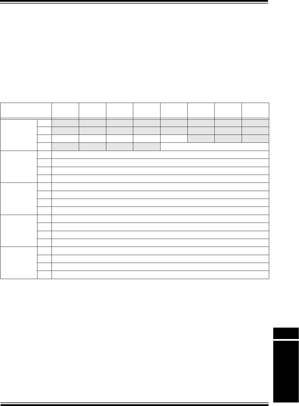
© 2007-2012 Microchip Technology Inc. DS61121F-page 5-3
Section 5. Flash Programming
Flash
Programming
5
5.2 CONTROL REGISTERS
Flash program and erase operations are controlled using the following Non-Volatile Memory
(NVM) control registers:
•NVMCON: Programming Control Register
•NVMKEY: Programming Unlock Register
•NVMADDR: Flash Address Register
•NVMDATA: Flash Program Data Register
•NVMSRCADDR: Source Data Address Register
Tabl e 5-1 provides a brief summary of all of the Flash-programming-related registers.
Corresponding registers appear after the summary, followed by a detailed description.
Table 5-1: Flash Controller SFR Summary
Name Bit
31/23/15/7
Bit
30/22/14/6
Bit
29/21/13/5
Bit
28/20/12/4
Bit
27/19/11/3
Bit
26/18/10/2
Bit
25/17/9/1
Bit
24/16/8/0
NVMCON(1) 31:24 ————————
23:16 ————————
15:8 WR WREN WRERR LVDERR LVDSTAT ———
7:0 ————NVMOP<3:0>
NVMKEY 31:24 NVMKEY<31:24>
23:16 NVMKEY<23:16>
15:8 NVMKEY<15:8>
7:0 NVMKEY<7:0>
NVMADDR(1) 31:24 NVMADDR<31:24>
23:16 NVMADDR<23:16>
15:8 NVMADDR<15:8>
7:0 NVMADDR<7:0>
NVMDATA 31:24 NVMDATA<31:24>
23:16 NVMDATA<23:16>
15:8 NVMDATA<15:8>
7:0 NVMDATA<7:0>
NVMSRCADDR 31:24 NVMSRCADDR<31:24>
23:16 NVMSRCADDR<23:16>
15:8 NVMSRCADDR<15:8>
7:0 NVMSRCADDR<7:0>
Legend: — = unimplemented, read as ‘0’.
Note 1: This register has an associated Clear, Set, and Invert register at an offset of 0x4, 0x8, and 0xC bytes, respectively. These registers have
the same name with CLR, SET, or INV appended to the end of the register name (e.g., NVMCONCLR). Writing a ‘1’ to any bit position in
these registers will clear, set, or invert valid bits in the associated register. Reads from these registers should be ignored.

PIC32 Family Reference Manual
DS61121F-page 5-4 © 2007-2012 Microchip Technology Inc.
5.2.1 NVMCON Register
The NVMCON register is the control register for Flash program/erase operations. This register
selects whether an erase or program operation can be performed and is used to start the
program or erase cycle.
The NVMCON register is shown in Register 5-1. The lower byte of NVMCON configures the type
of NVM operation that will be performed. A summary of the NVMCON setup values for various
program and erase operations is given in Ta bl e 5-2 .
Table 5-2: NVMCON Register Values
Operation NVMCON Value
Page Erase 0x8004
Program Word 0x8001
Program Row 0x8003
No Operation (NOP)0x8000
Register 5-1: NVMCON: Programming Control Register
U-0 U-0 U-0 U-0 U-0 U-0 U-0 U-0
— — — — — — — —
bit 31 bit 24
U-0 U-0 U-0 U-0 U-0 U-0 U-0 U-0
— — — — — — — —
bit 23 bit 16
HC, R/W-0 R/W-0 HS, R-0 HS, R-0 HS, HC, R-0 U-0 U-0 U-0
WR WREN(1) WRERR(2) LVDERR(2) LVDSTAT(2) — — —
bit 15 bit 8
U-0 U-0 U-0 U-0 R/W-0 R/W-0 R/W-0 R/W-0
— — — —NVMOP<3:0>
bit 7 bit 0
Legend: HS = Set by Hardware HC = Cleared by Hardware
R = Readable bit W = Writable bit U = Unimplemented bit, read as ‘0’
-n = Value at POR ‘1’ = Bit is set ‘0’ = Bit is cleared x = Bit is unknown
bit 31-16 Unimplemented: Read as ‘0’
bit 15 WR: Write Control bit
This bit is writable when WREN = 1 and the unlock sequence is followed.
1 = Initiate a Flash operation. Hardware clears this bit when the operation completes.
0 = Flash operation complete or inactive
bit 14 WREN: Write Enable bit(1)
1 = Enable writes to the WR bit and enables the Low-Voltage Detect (LVD) circuit
0 = Disable writes to the WR bit and disables LVD circuit
Note 1: This bit is reset by a device Reset.
2: This bit is cleared by setting NVMOP<3:0> = 0000, and initiating a Flash operation (i.e., WR).

© 2007-2012 Microchip Technology Inc. DS61121F-page 5-5
Section 5. Flash Programming
Flash
Programming
5
bit 13 WRERR: Write Error bit(2)
This bit is read-only and is automatically set by hardware.
1 = Program or erase sequence did not complete successfully
0 = Program or erase sequence completed normally
bit 12 LVDERR: Low-Voltage Detect Error bit (LVD circuit must be enabled)(2)
This bit is read-only and is automatically set by hardware.
1 = Low-voltage detected (possible data corruption, if WRERR is set)
0 = Voltage level is acceptable for programming
bit 11 LVDSTAT: Low-Voltage Detect Status bit (LVD circuit must be enabled)(2)
This bit is read-only and is automatically set, and cleared by hardware
1 = Low-voltage event active
0 = Low-voltage event NOT active
bit 10-4 Unimplemented: Read as ‘0’
bit 3-0 NVMOP<3:0>: NVM Operation bits
These bits are writable when WREN = 0.
1111 = Reserved
•
•
•
0111 = Reserved
0110 = No operation
0101 = Program Flash (PFM) erase operation: erases PFM, if all pages are not write-protected
0100 = Page erase operation: erases page selected by NVMADDR, if it is not write-protected
0011 = Row program operation: programs row selected by NVMADDR, if it is not write-protected
0010 = No operation
0001 = Word program operation: programs word selected by NVMADDR, if it is not write-protected
0000 = No operation
Register 5-1: NVMCON: Programming Control Register (Continued)
Note 1: This bit is reset by a device Reset.
2: This bit is cleared by setting NVMOP<3:0> = 0000, and initiating a Flash operation (i.e., WR).

PIC32 Family Reference Manual
DS61121F-page 5-6 © 2007-2012 Microchip Technology Inc.
5.2.2 NVMKEY Register
NVMKEY is a write-only register that is used to prevent accidental writes/erasures of Flash or
EEPROM memory. To start a programming or an erase sequence, the following steps must be
taken in the exact order shown:
1. Write 0xAA996655 to NVMKEY.
2. Write 0x556699AA to NVMKEY.
After this sequence, only the next transaction on the peripheral bus is allowed to write the
NVMCON register. In most cases, the user will simply need to set the WR bit in the NVMCON
register to start the program or erase cycle. Interrupts should be disabled during the unlock
sequence.
Register 5-2: NVMKEY: Programming Unlock Register
W-0 W-0 W-0 W-0 W-0 W-0 W-0 W-0
NVMKEY<31:24>
bit 31 bit 24
W-0 W-0 W-0 W-0 W-0 W-0 W-0 W-0
NVMKEY<23:16>
bit 23 bit 16
W-0 W-0 W-0 W-0 W-0 W-0 W-0 W-0
NVMKEY<15:8>
bit 15 bit 8
W-0 W-0 W-0 W-0 W-0 W-0 W-0 W-0
NVMKEY<7:0>
bit 7 bit 0
Legend:
R = Readable bit W = Writable bit U = Unimplemented bit, read as ‘0’
-n = Value at POR ‘1’ = Bit is set ‘0’ = Bit is cleared x = Bit is unknown
bit 31-0 NVMKEY<31:0>: Unlock Register bits
These bits are write-only, and read as ‘0’ on any read
Note: This register is used as part of the unlock sequence to prevent inadvertent writes to the PFM.

© 2007-2012 Microchip Technology Inc. DS61121F-page 5-7
Section 5. Flash Programming
Flash
Programming
5
5.2.3 NVMADDR Register
The NVM Address register selects the row for Flash memory writes, the address location for word
writes, and the page address for Flash memory erase operations.
Note: The NVM Address register must be loaded with the physical address of the Flash
memory and not the virtual address.
Register 5-3: NVMADDR: Flash Address Register
R/W-0 R/W-0 R/W-0 R/W-0 R/W-0 R/W-0 R/W-0 R/W-0
NVMADDR<31:24>
bit 31 bit 24
R/W-0 R/W-0 R/W-0 R/W-0 R/W-0 R/W-0 R/W-0 R/W-0
NVMADDR<23:16>
bit 23 bit 16
R/W-0 R/W-0 R/W-0 R/W-0 R/W-0 R/W-0 R/W-0 R/W-0
NVMADDR<15:8>
bit 15 bit 8
R/W-0 R/W-0 R/W-0 R/W-0 R/W-0 R/W-0 R-0 R-0
NVMADDR<7:0>
bit 7 bit 0
Legend:
R = Readable bit W = Writable bit U = Unimplemented bit, read as ‘0’
-n = Value at POR ‘1’ = Bit is set ‘0’ = Bit is cleared x = Bit is unknown
bit 31-0 NVMADDR<31:0>: Flash Address bits
Bulk/Chip/PFM Erase: Address is ignored
Page Erase: Address identifies the page to erase
Row Program: Address identifies the row to program
Word Program: Address identifies the word to program

PIC32 Family Reference Manual
DS61121F-page 5-8 © 2007-2012 Microchip Technology Inc.
5.2.4 NVMDATA Register
The NVM Data register holds the data to be programmed during Flash Word program operations.
Register 5-4: NVMDATA: Flash Program Data Register
R/W-0 R/W-0 R/W-0 R/W-0 R/W-0 R/W-0 R/W-0 R/W-0
NVMDATA<31:24>
bit 31 bit 24
R/W-0 R/W-0 R/W-0 R/W-0 R/W-0 R/W-0 R/W-0 R/W-0
NVMDATA<23:16>
bit 23 bit 16
R/W-0 R/W-0 R/W-0 R/W-0 R/W-0 R/W-0 R/W-0 R/W-0
NVMDATA<15:8>
bit 15 bit 8
R/W-0 R/W-0 R/W-0 R/W-0 R/W-0 R/W-0 R/W-0 R/W-0
NVMDATA<7:0>
bit 7 bit 0
Legend:
R = Readable bit W = Writable bit U = Unimplemented bit, read as ‘0’
-n = Value at POR ‘1’ = Bit is set ‘0’ = Bit is cleared x = Bit is unknown
bit 31-0 NVMDATA<31:0>: Flash Programming Data bits
Note: The bits in this register are only reset by a Power-on Reset (POR).

© 2007-2012 Microchip Technology Inc. DS61121F-page 5-9
Section 5. Flash Programming
Flash
Programming
5
5.2.5 NVMSRCADDR Register
The NVM Source Address register selects the source data buffer address in SRAM for
performing row programming operations.
Note: The address must be word-aligned.
Register 5-5: NVMSRCADDR: Source Data Address Register
R/W-0 R/W-0 R/W-0 R/W-0 R/W-0 R/W-0 R/W-0 R/W-0
NVMSRCADDR<31:24>
bit 31 bit 24
R/W-0 R/W-0 R/W-0 R/W-0 R/W-0 R/W-0 R/W-0 R/W-0
NVMSRCADDR<23:16>
bit 23 bit 16
R/W-0 R/W-0 R/W-0 R/W-0 R/W-0 R/W-0 R/W-0 R/W-0
NVMSRCADDR<15:8>
bit 15 bit 8
R/W-0 R/W-0 R/W-0 R/W-0 R/W-0 R/W-0 R-0 R-0
NVMSRCADDR<7:0>
bit 7 bit 0
Legend:
R = Readable bit W = Writable bit U = Unimplemented bit, read as ‘0’
-n = Value at POR ‘1’ = Bit is set ‘0’ = Bit is cleared x = Bit is unknown
bit 31-0 NVMSRCADDR<31:0>: Source Data Address bits
The system physical address of the data to be programmed into the Flash when the NVMOP<3:0> bits
(NVMCON<3:0>) are set to perform row programming.

PIC32 Family Reference Manual
DS61121F-page 5-10 © 2007-2012 Microchip Technology Inc.
5.3 RUN-TIME SELF-PROGRAMMING (RTSP) OPERATION
Run-Time Self-Programming (RTSP) allows the user code to modify Flash program memory
contents. The device Flash memory is divided into two logical Flash partitions: the program Flash
memory (PFM), and the boot Flash memory (BFM). The last page in boot Flash memory contains
the debug page, which is reserved for use by the debugger tool while debugging.
The program Flash array for the PIC32 device is built up of a series of rows to form a page. Refer
to the “Flash Program Memory” chapter of the specific device data sheet to determine the row
and page sizes. For example, a row may contain 128 32-bit instruction words or 512 bytes. A
group of 8 rows compose a page; which, therefore, contains 8 × 512 = 4096 bytes or 1024
instruction words. A page of Flash is the smallest unit of memory that can be erased at a single
time. The program Flash array can be programmed in one of two ways:
•Row programming, with 128 instruction words at a time
•Word programming, with 1 instruction word at a time
Performing an RTSP operation while executing (fetching) instructions from program Flash
memory, the CPU stalls (waits) until the programming operation is finished. The CPU will not
execute any instruction, or respond to interrupts, during this time. If any interrupts occur during
the programming cycle, they remain pending until the cycle completes.
Performing an RTSP operation while executing (fetching) instructions from RAM memory, the
CPU can continue to execute instructions and respond to interrupts during the programming
operation. Any executable code scheduled to execute during the RTSP operation must be placed
in RAM memory. This includes the relevant interrupt vector, and the interrupt service routine
instructions.
Note: A minimum VDD requirement for Flash erase and write operations is required. Refer
to the “Electrical Characteristics” chapter in the specific device data sheet for
more information.

© 2007-2012 Microchip Technology Inc. DS61121F-page 5-11
Section 5. Flash Programming
Flash
Programming
5
5.4 LOCK-OUT FEATURE
5.4.1 NVMWREN
A number of mechanisms exists within the device to ensure that inadvertent writes to program
Flash do not occur. The WREN bit (NVMCON<14>) should be zero, unless the software intends
to write to the program Flash. When WREN = 1, the Flash write control bit, WR (NVMCON<15>),
is writable and the Flash LVD circuit is enabled.
5.4.2 NVMKEY
In addition to the write protection provided by the WREN bit, an unlock sequence needs to be
performed before the WR bit (NVMCOM<15>) can be set. If the WR bit is not set on the next
peripheral bus transaction (read or write), WR is locked and the unlock sequence must be
restarted.
5.4.3 Unlock Sequence
To u nlo ck Fla sh op erat ion s, per for m ste ps 4 thr oug h 8 in order. If sequence is not followed, WR
is not set.
1. Suspend or disable all initiators that can access the Peripheral Bus and interrupt the
unlock sequence, e.g., DMA and interrupts.
2. Set WREN bit (NVMCON<14>) to allow writes to WR and set NVMOP<3:0> bit
(NVMCON<3:0>) to the desired operation with a single store instruction.
3. Wait for LVD to start-up.
4. Load 0xAA996655 to CPU register X.
5. Load 0x556699AA to CPU register Y.
6. Load 0x00008000 to CPU register Z.
7. Store CPU register X to NVMKEY.
8. Store CPU register Y to NVMKEY.
9. Store CPU register Z to NVMCONSET.
10. Wait for WR bit (NVMCON<15>) to be cleared.
11. Clear the WREN bit (NVMCON<14>).
12. Check the WRERR (NVMCON<13>) and LVDERR (NVMCON<12>) bits to ensure that
the program/erase sequence completed successfully.
When the WR bit is set, the program/erase sequence starts and the CPU is unable to execute
from Flash memory for the duration of the sequence.

PIC32 Family Reference Manual
DS61121F-page 5-12 © 2007-2012 Microchip Technology Inc.
Example 5-1: Unlock Example
unsigned int NVMUnlock (unsigned int nvmop)
{
unsigned int status;
// Suspend or Disable all Interrupts
asm volatile (“di %0” : “=r” (status));
// Enable Flash Write/Erase Operations and Select
// Flash operation to perform
NVMCON = nvmop;
// Write Keys
NVMKEY = 0xAA996655;
NVMKEY = 0x556699AA;
// Start the operation using the Set Register
NVMCONSET = 0x8000;
// Wait for operation to complete
while (NVMCON & 0x8000);
// Restore Interrupts
if (status & 0x00000001)
asm volatile (“ei”);
else
asm volatile (“di”);
// Disable NVM write enable
NVMCONCLR = 0x0004000;
// Return WRERR and LVDERR Error Status Bits
return (NVMCON & 0x3000);
}

© 2007-2012 Microchip Technology Inc. DS61121F-page 5-13
Section 5. Flash Programming
Flash
Programming
5
5.5 WORD PROGRAMMING SEQUENCE
The smallest block of data that can be programmed in a single operation is one 32-bit word. The
data to be programmed must be written to the NVMDATA register, and the address of the word
must be loaded into the NVMADDR register before the programming sequence is initiated. The
instruction word at the location pointed to by the NVMADDR register is then programmed.
A program sequence comprises the following steps:
1. Write 32-bit data to be programmed to the NVMDATA register.
2. Load the NVMADDR register with the address to be programmed.
3. Run the unlock sequence using the Word Program command (see Section 5.4.3 “Unlock
Sequence”).
The program sequence completes, and the WR bit (NVMCON<15>) is cleared by hardware.
Example 5-2: Word Program Example
unsigned int NVMWriteWord (void* address, unsigned int data)
{
unsigned int res;
// Load data into NVMDATA register
NVMDATA = data;
// Load address to program into NVMADDR register
NVMADDR = (unsigned int) address;
// Unlock and Write Word
res = NVMUnlock (0x4001);
// Return Result
return res;
}

PIC32 Family Reference Manual
DS61121F-page 5-14 © 2007-2012 Microchip Technology Inc.
5.6 ROW PROGRAMMING SEQUENCE
The largest block of data that can be programmed is 1 row, which equals to 512 bytes of data
(refer to the “Flash Program Memory” chapter in the specific device data sheet to determine
the row size). The row of data must first be loaded into a buffer in SRAM. The NVMADDR register
then points to the Flash address where the Flash controller will start programming the row of
data.
A row program sequence comprises the following steps:
1. Write the entire row of data to be programmed into system SRAM. The source address
must be word-aligned.
2. Set the NVMADDR register with the start address of the Flash row to be programmed.
3. Set the NVMSRCADDR register with the physical source address from step 1.
4. Run the unlock sequence using the Row Program command (see 5.4.3 “Unlock
Sequence”).
5. The program sequence completes, and the WR bit (NVMCON<15>) is cleared by
hardware.
Example 5-3: Row Program Example
Note: The Flash controller ignores the sub-row address bits and always starts
programming at the beginning of a row.
unsigned int NVMWriteRow (void* address, void* data)
{
unsigned int res;
// Set NVMADDR to Start Address of row to program
NVMADDR = (unsigned int) address;
// Set NVMSRCADDR to the SRAM data buffer Address
NVMSRCADDR = (unsigned int) data;
// Unlock and Write Row
res = NVMUnlock(0x4003);
// Return Result
return res;
}

© 2007-2012 Microchip Technology Inc. DS61121F-page 5-15
Section 5. Flash Programming
Flash
Programming
5
5.7 PAGE ERASE SEQUENCE
A page erase performs an erase of a single page of either PFM or BFM. Refer to the specific
device data sheet for the page size. The page to be erased is selected using the NVMADDR
register.
A page of Flash can only be erased if its associated page write protection is not enabled.
•All BFM pages are affected by the Boot write protection Configuration bit
• PFM pages are affected by the Program Flash write protection Configuration bits
If in Mission mode, the application must not be executing from the erased page.
A page erase sequence comprises the following steps:
1. Set the NVMADDR register with the address of the page to be erased.
2. Run the unlock sequence using the desired Erase command (see 5.4.3 “Unlock
Sequence”).
3. The erase sequence completes and the WR bit (NVMCON<15>) is cleared by hardware.
Example 5-4: Page Erase Example
5.8 PROGRAM FLASH MEMORY ERASE SEQUENCE
It is possible to erase the entire PFM area. This mode leaves the boot Flash intact and is intended
to be used by a field-upgradeable device.
The program Flash can be erased if all pages in the program Flash are not write-protected.
A PFM erase sequence comprises the following steps:
1. Run the unlock sequence using the program Flash memory erase command (see
5.4.3 “Unlock Sequence”).
2. The erase sequence completes and the WR bit (NVMCON<15>) is cleared by hardware.
Example 5-5: Program Flash Erase Example
Note: The lower bits of the address are ignored in page selection.
unsigned int NVMErasePage(void* address)
{
unsigned int res;
// Set NVMADDR to the Start Address of page to erase
NVMADDR = (unsigned int) address;
// Unlock and Erase Page
res = NVMUnlock(0x4004);
// Return Result
return res;
}
Note: The application must not be executing from the PFM address range.
unsigned int NVMErasePFM(void)
{
unsigned int res;
// Unlock and Erase Program Flash
res = NVMUnlock(0x4005);
// Return Result
return res;
}

PIC32 Family Reference Manual
DS61121F-page 5-16 © 2007-2012 Microchip Technology Inc.
5.9 OPERATION IN POWER-SAVING AND DEBUG MODES
5.9.1 Operation in Sleep Mode
When a PIC32 device enters Sleep mode, the system clock is disabled. The Flash controller
does not function in Sleep mode. If entry into Sleep mode occurs while an NVM operation is in
progress, the device will not go into Sleep mode until the NVM operation is complete.
5.9.2 Operation in Idle Mode
Idle mode has no effect on the Flash controller module when a programming operation is active.
The CPU continues to be stalled until the programming operation completes.
5.9.3 Operation in Debug Mode
The Flash controller does not provide debug freeze capability, and therefore, has no effect on the
Flash controller module when a programming operation is active. The CPU continues to be
stalled until the programming operation completes. Interrupting the normal programming
sequence could cause the device to latch-up. The only exception to this is the NVMKEY unlock
sequence, which is suspended when in Debug mode, allowing the user to single-step through
the unlock sequence.
5.10 EFFECTS OF VARIOUS RESETS
5.10.1 Device Reset
Only the NVMCON bits for WREN and LVDSTAT are reset on a device Reset. All other SFR bits
are only reset by a POR; however, the state of the NVMKEY is reset by a device Reset.
5.10.2 Power-on Reset
All Flash controller registers are forced to their reset states upon a POR.
5.10.3 Watchdog Timer Reset
All Flash controller registers are unchanged upon a Watchdog Timer Reset.

© 2007-2012 Microchip Technology Inc. DS61121F-page 5-17
Section 5. Flash Programming
Flash
Programming
5
5.11 INTERRUPTS
The Flash controller can generate an interrupt reflecting the events that occur during the
programming operations. The following interrupt can be generated:
•Flash Control Event Interrupt (FCEIF)
The interrupt flag must be cleared in software.The Flash controller is enabled as a source of
interrupt via the following bit:
•Flash Controller Interrupt Enable (FCEIE)
The interrupt priority-level bits and interrupt subpriority-level bits must also be configured:
•FCEIP
•FCEIS
Refer to Section 8. “Interrupts” (DS61108) in the “PIC32 Family Reference Manual” for details.
5.11.1 Interrupt Configuration
The Flash controller module has a dedicated interrupt flag bit, FCEIF, and a corresponding
interrupt enable/mask bit, FCEIE.
These two bits determine the source of an interrupt and enable or disable an individual interrupt
source. All the interrupt sources for a specific Flash controller module share one interrupt vector.
In addition, the FCEIF bit will be set without regard to the state of the corresponding enable bit,
and the FCEIF bit can be polled by software if desired.
The FCEIE bit is used to define the behavior of the Vector Interrupt Controller (VIC) when a
corresponding FCEIF bit is set. When the corresponding FCEIE bit is clear, the VIC module does
not generate a CPU interrupt for the event. If the FCEIE bit is set, the VIC module will generate
an interrupt to the CPU when the corresponding FCEIF bit is set (subject to the priority and
subpriority as outlined in the following paragraphs).
It is the responsibility of the user’s software routine that services a particular interrupt to clear the
appropriate Interrupt Flag bit before the service routine is complete.
The priority of the Flash Controller module can be set independently with the FCEIP<2:0> bits.
This priority defines the priority group to which the interrupt source is assigned. The priority
groups range from a value of 7 (the highest priority), to a value of 0, which does not generate an
interrupt. An interrupt being serviced is preempted by an interrupt in a higher priority group.
The subpriority bits allow setting the priority of a interrupt source within a priority group. The
values of the subpriority, FCEIS<1:0>, range from 3 (the highest priority), to 0 the lowest priority.
An interrupt with the same priority group but having a higher subpriority value, does not preempt
a lower subpriority interrupt that is in progress.
The priority group and subpriority bits allow more than one interrupt source to share the same
priority and subpriority. If simultaneous interrupts occur in this configuration, the natural order of
the interrupt sources within a priority/subpriority group pair determine the interrupt generated.
The natural priority is based on the vector numbers of the interrupt sources. The lower the vector
number, the higher the natural priority of the interrupt. Any interrupts that are overridden by
natural order generate their respective interrupts based on priority, subpriority, and natural order,
after the interrupt flag for the current interrupt is cleared.
After an enabled interrupt is generated, the CPU jumps to the vector assigned to that interrupt.
The vector number for the interrupt is the same as the natural order number. Then, the CPU
begins executing code at the vector address. The user’s code at this vector address should
perform any application-specific operations, clear the FCEIF interrupt flag, and then exit.
For more information on interrupts and the vector address table details, refer to Section 8.
“Interrupts” (DS61108) in the “PIC32 Family Reference Manual” and the “Interrupt
Controller” chapter of the specific device data sheet.

PIC32 Family Reference Manual
DS61121F-page 5-18 © 2007-2012 Microchip Technology Inc.
5.12 RELATED APPLICATION NOTES
This section lists application notes that are related to this section of the manual. These
application notes may not be written specifically for the PIC32 device family, but the concepts are
pertinent and could be used with modification and possible limitations. The current application
notes related to Flash Programming include the following:
Title Application Note #
No related application notes at this time. N/A
Note: Please visit the Microchip web site (www.microchip.com) for additional application
notes and code examples for the PIC32 family of devices.

© 2007-2012 Microchip Technology Inc. DS61121F-page 5-19
Section 5. Flash Programming
Flash
Programming
5
5.13 REVISION HISTORY
Revision A (September 2007)
This is the initial released version of this document.
Revision B (October 2007)
Updated document to remove Confidential status.
Revision C (April 2008)
Revised status to Preliminary; Revised U-0 to r-x.
Revision D (June 2008)
Revised Register 5-1, bit 14 NVMWREN; Add footnote 1 to Registers 5-12 through 5-14; Add
note to Section 5.3; Revise Section 5.4.1; Revised Example 5-1; Change Reserved bits “Maintain
as” to “Write”.
Revision E (December 2010)
This revision includes the following updates:
•Minor updates to the text and formatting have been incorporated throughout the document
• Added Notes 1, 2 and 3, which describe the Clear, Set and Invert registers to the following:
-Table5-1: Flash Controller SFR Summary
-Register5-1: NVMCON: Programming Control Register
(1,2,3)
-Register5-3: NVMADDR: Flash Address Register
(1,2,3)
•Removed all Clear, Set and Invert register descriptions
•Removed all Interrupt register references
•Renamed the following NVMCON register bit names were changed throughout the
document:
-NVMWR was renamed to WR
-NVMWREN was renamed to WREN
-NVMERR was renamed to WRERR
•Updated the third paragraph and added a new (fourth) paragraph to 5.3 “Run-Time Self-Pro-
gramming (RTSP) Operation”
•Updated the unlock Flash operations sequence by adding a new step 3 (see 5.4.3 “Unlock
Sequence”)
•Updated the code in the Unlock Example (see Example5-1)
•Removed Table 5-3
Revision F (July 2012)
This revision includes the following updates:
•Updated Note 1 and removed Notes 2 and 3 from the Flash Controller SFR Register
Summary (see Tabl e 5- 1 )
•Updated NVMCON (see Register 5-1)
•Removed Notes 1, 2, and 3 from NVMADDR (see Register 5-3)
•Updated the second paragraph of 5.3 “Run-Time Self-Programming (RTSP) Operation”
•Updated the first paragraph of 5.6 “Row Programming Sequence”
•Updated the first paragraph of 5.7 “Page Erase Sequence”
•Minor updates to the text and formatting have been incorporated throughout the document

PIC32 Family Reference Manual
DS61121F-page 5-20 © 2007-2012 Microchip Technology Inc.
NOTES:

2007-2012 Microchip Technology Inc. DS61121F-page 5-21
Information contained in this publication regarding device
applications and the like is provided only for your convenience
and may be superseded by updates. It is your responsibility to
ensure that your application meets with your specifications.
MICROCHIP MAKES NO REPRESENTATIONS OR
WARRANTIES OF ANY KIND WHETHER EXPRESS OR
IMPLIED, WRITTEN OR ORAL, STATUTORY OR
OTHERWISE, RELATED TO THE INFORMATION,
INCLUDING BUT NOT LIMITED TO ITS CONDITION,
QUALITY, PERFORMANCE, MERCHANTABILITY OR
FITNESS FOR PURPOSE. Microchip disclaims all liability
arising from this information and its use. Use of Microchip
devices in life support and/or safety applications is entirely at
the buyer’s risk, and the buyer agrees to defend, indemnify and
hold harmless Microchip from any and all damages, claims,
suits, or expenses resulting from such use. No licenses are
conveyed, implicitly or otherwise, under any Microchip
intellectual property rights.
Trademarks
The Microchip name and logo, the Microchip logo, dsPIC,
KEELOQ, KEELOQ logo, MPLAB, PIC, PICmicro, PICSTART,
PIC32 logo, rfPIC and UNI/O are registered trademarks of
Microchip Technology Incorporated in the U.S.A. and other
countries.
FilterLab, Hampshire, HI-TECH C, Linear Active Thermistor,
MXDEV, MXLAB, SEEVAL and The Embedded Control
Solutions Company are registered trademarks of Microchip
Technology Incorporated in the U.S.A.
Analog-for-the-Digital Age, Application Maestro, chipKIT,
chipKIT logo, CodeGuard, dsPICDEM, dsPICDEM.net,
dsPICworks, dsSPEAK, ECAN, ECONOMONITOR,
FanSense, HI-TIDE, In-Circuit Serial Programming, ICSP,
Mindi, MiWi, MPASM, MPLAB Certified logo, MPLIB,
MPLINK, mTouch, Omniscient Code Generation, PICC,
PICC-18, PICDEM, PICDEM.net, PICkit, PICtail, REAL ICE,
rfLAB, Select Mode, Total Endurance, TSHARC,
UniWinDriver, WiperLock and ZENA are trademarks of
Microchip Technology Incorporated in the U.S.A. and other
countries.
SQTP is a service mark of Microchip Technology Incorporated
in the U.S.A.
All other trademarks mentioned herein are property of their
respective companies.
© 2007-2012, Microchip Technology Incorporated, Printed in
the U.S.A., All Rights Reserved.
Printed on recycled paper.
ISBN: 978-1-62076-464-0
Note the following details of the code protection feature on Microchip devices:
• Microchip products meet the specification contained in their particular Microchip Data Sheet.
• Microchip believes that its family of products is one of the most secure families of its kind on the market today, when used in the
intended manner and under normal conditions.
• There are dishonest and possibly illegal methods used to breach the code protection feature. All of these methods, to our
knowledge, require using the Microchip products in a manner outside the operating specifications contained in Microchip’s Data
Sheets. Most likely, the person doing so is engaged in theft of intellectual property.
• Microchip is willing to work with the customer who is concerned about the integrity of their code.
• Neither Microchip nor any other semiconductor manufacturer can guarantee the security of their code. Code protection does not
mean that we are guaranteeing the product as “unbreakable.”
Code protection is constantly evolving. We at Microchip are committed to continuously improving the code protection features of our
products. Attempts to break Microchip’s code protection feature may be a violation of the Digital Millennium Copyright Act. If such acts
allow unauthorized access to your software or other copyrighted work, you may have a right to sue for relief under that Act.
Microchip received ISO/TS-16949:2009 certification for its worldwide
headquarters, design and wafer fabrication facilities in Chandler and
Tempe, Arizona; Gresham, Oregon and design centers in California
and India. The Company’s quality system processes and procedures
are for its PIC® MCUs and dsPIC® DSCs, KEELOQ® code hopping
devices, Serial EEPROMs, microperipherals, nonvolatile memory and
analog products. In addition, Microchip’s quality system for the design
and manufacture of development systems is ISO 9001:2000 certified.
QUALITYMANAGEMENT
S
YSTEM
CERTIFIEDBYDNV
== ISO/TS16949==

DS61121F-page 5-22 2007-2012 Microchip Technology Inc.
AMERICAS
Corporate Office
2355 West Chandler Blvd.
Chandler, AZ 85224-6199
Tel: 480-792-7200
Fax: 480-792-7277
Technical Support:
http://www.microchip.com/
support
Web Address:
www.microchip.com
Atlanta
Duluth, GA
Tel: 678-957-9614
Fax: 678-957-1455
Boston
Westborough, MA
Tel: 774-760-0087
Fax: 774-760-0088
Chicago
Itasca, IL
Tel: 630-285-0071
Fax: 630-285-0075
Cleveland
Independence, OH
Tel: 216-447-0464
Fax: 216-447-0643
Dallas
Addison, TX
Tel: 972-818-7423
Fax: 972-818-2924
Detroit
Farmington Hills, MI
Tel: 248-538-2250
Fax: 248-538-2260
Indianapolis
Noblesville, IN
Tel: 317-773-8323
Fax: 317-773-5453
Los Angeles
Mission Viejo, CA
Tel: 949-462-9523
Fax: 949-462-9608
Santa Clara
Santa Clara, CA
Tel: 408-961-6444
Fax: 408-961-6445
Toronto
Mississauga, Ontario,
Canada
Tel: 905-673-0699
Fax: 905-673-6509
ASIA/PACIFIC
Asia Pacific Office
Suites 3707-14, 37th Floor
Tower 6, The Gateway
Harbour City, Kowloon
Hong Kong
Tel : 8 52 -24 01- 120 0
Fax: 852-2401-3431
Australia - Sydney
Tel : 6 1- 2-9 868 -67 33
Fax: 61-2-9868-6755
China - Beijing
Tel : 8 6- 10- 856 9-7 00 0
Fax: 86-10-8528-2104
China - Chengdu
Tel : 8 6- 28- 866 5-5 511
Fax: 86-28-8665-7889
China - Chongqing
Tel : 8 6- 23- 898 0-9 58 8
Fax: 86-23-8980-9500
China - Hangzhou
Tel : 8 6- 571 -28 19- 318 7
Fax: 86-571-2819-3189
China - Hong Kong SAR
Tel : 8 52 -24 01- 120 0
Fax: 852-2401-3431
China - Nanjing
Tel : 8 6- 25- 847 3-2 46 0
Fax: 86-25-8473-2470
China - Qingdao
Tel : 8 6- 532 -85 02- 735 5
Fax: 86-532-8502-7205
China - Shanghai
Tel : 8 6- 21- 540 7-5 53 3
Fax: 86-21-5407-5066
China - Shenyang
Tel : 8 6- 24- 233 4-2 82 9
Fax: 86-24-2334-2393
China - Shenzhen
Tel : 8 6- 755 -82 03- 266 0
Fax: 86-755-8203-1760
China - Wuhan
Tel : 8 6- 27- 598 0-5 30 0
Fax: 86-27-5980-5118
China - Xian
Tel : 8 6- 29- 883 3-7 25 2
Fax: 86-29-8833-7256
China - Xiamen
Tel: 86-592-2388138
Fax: 86-592-2388130
China - Zhuhai
Tel : 86- 75 6-3 21 004 0
Fax: 86-756-3210049
ASIA/PACIFIC
India - Bangalore
Tel : 9 1- 80- 309 0-4 44 4
Fax: 91-80-3090-4123
India - New Delhi
Tel : 9 1- 11- 416 0 -8 631
Fax: 91-11-4160-8632
India - Pune
Tel : 9 1- 20- 256 6-1 51 2
Fax: 91-20-2566-1513
Japan - Osaka
Tel : 8 1- 66- 152 -71 60
Fax: 81-66-152-9310
Japan - Yokohama
Tel : 8 1- 45- 471 - 6 16 6
Fax: 81-45-471-6122
Korea - Daegu
Tel : 8 2- 53- 744 -43 01
Fax: 82-53-744-4302
Korea - Seoul
Tel : 8 2- 2-5 54- 72 0 0
Fax: 82-2-558-5932 or
82-2-558-5934
Malaysia - Kuala Lumpur
Tel : 6 0- 3-6 201 -9 8 57
Fax: 60-3-6201-9859
Malaysia - Penang
Tel : 6 0- 4-2 27- 88 7 0
Fax: 60-4-227-4068
Philippines - Manila
Tel : 6 3- 2-6 34- 90 6 5
Fax: 63-2-634-9069
Singapore
Tel : 6 5- 633 4-8 870
Fax: 65-6334-8850
Taiwan - Hsin Chu
Tel : 8 86 -3- 577 8-3 66
Fax: 886-3-5770-955
Taiwan - Kaohsiung
Tel : 8 86 -7- 536 -48 18
Fax: 886-7-330-9305
Taiwan - Taipei
Tel : 8 86 -2- 250 0-6 61 0
Fax: 886-2-2508-0102
Thailand - Bangkok
Tel : 6 6- 2-6 94- 13 5 1
Fax: 66-2-694-1350
EUROPE
Austria - Wels
Tel : 4 3- 72 42 -2 244 -3 9
Fax: 43-7242-2244-393
Denmark - Copenhagen
Tel : 4 5- 445 0-2 828
Fax: 45-4485-2829
France - Paris
Tel : 3 3- 1-6 9-5 3-6 3-2 0
Fax: 33-1-69-30-90-79
Germany - Munich
Tel : 4 9- 89 -62 7-1 44- 0
Fax: 49-89-627-144-44
Italy - Milan
Tel : 3 9- 03 31 -7 426 11
Fax: 39-0331-466781
Netherlands - Drunen
Tel : 3 1- 41 6- 690 399
Fax: 31-416-690340
Spain - Madrid
Tel : 3 4- 91 -70 8-0 8-9 0
Fax: 34-91-708-08-91
UK - Wokingham
Tel : 4 4- 118 -92 1- 5 869
Fax: 44-118-921-5820
Worldwide Sales and Service
11/29/11

© 2007-2012 Microchip Technology Inc. DS61112H-page 6-1
Oscillators
6
Section 6. Oscillators
HIGHLIGHTS
This section of the manual contains the following major topics:
6.1 Introduction .................................................................................................................... 6-2
6.2 Control Registers ...........................................................................................................6-4
6.3 Operation: Clock Generation and Clock Sources ........................................................ 6-12
6.4 Interrupts...................................................................................................................... 6-26
6.5 Operation in Power-Saving Modes .............................................................................. 6-27
6.6 Effects of Various Resets .............................................................................................6-27
6.7 Clocking Guidelines .....................................................................................................6-28
6.8 Related Application Notes............................................................................................6-31
6.9 Revision History ...........................................................................................................6-32

PIC32 Family Reference Manual
DS61112H-page 6-2 © 2007-2012 Microchip Technology Inc.
6.1 INTRODUCTION
This section describes the PIC32 oscillator system and its operation. The PIC32 oscillator system
has the following modules and features:
• Four external and internal oscillator options as clock sources
•On-chip Phase-Locked Loop (PLL) with a user-selectable input divider and multiplier, as
well as an output divider, to boost operating frequency on select internal and external
oscillator sources
•On-chip user-selectable divisor postscaler on select oscillator sources
• Software-controllable switching between various clock sources
• A Fail-Safe Clock Monitor (FSCM) that detects clock failure and permits safe application
recovery or shutdown
A block diagram of the PIC32 oscillator system is shown in Figure 6-1.
Note: This family reference manual section is meant to serve as a complement to device
data sheets. Depending on the device variant, this manual section may not apply to
all PIC32 devices.
Please consult the note at the beginning of the “Oscillator” chapter in the current
device data sheet to check whether this document supports the device you are
using.
Device data sheets and family reference manual sections are available for
download from the Microchip Worldwide Web site at: http://www.microchip.com

© 2007-2012 Microchip Technology Inc. DS61112H-page 6-3
Section 6. Oscillators
Oscillators
6
Figure 6-1: PIC32 Family Oscillator System Block Diagram
Note 1: A series resistor, RS, may be required for AT strip cut crystals or to eliminate clipping. Alternatively, to increase
oscillator circuit gain, add a parallel resistor, RP, with a value of 1 M.
2: The internal feedback resistor, RF, is typically in the range of 2 to 10 M
3: See 6.7.3.1 “Determining the Best Values for Oscillator Components”.
4: PBCLK is available on the OSC2 pin in certain clock modes.
5: This feature is not available on all PIC32 devices. Refer to the “Oscillator Configuration” chapter in the specific
device data sheet for more information.
Timer1, RTCC
Clock Control Logic
Fail-Safe
Clock
Monitor
FSCM INT
FSCM Event
COSC<2:0>
NOSC<2:0>
OSWEN
FCKSM<0>
PLL x M
Secondary Oscillator (SOSC)
SOSCEN and FSOSCEN
SOSCO
SOSCI
XTPLL, HSPLL,
POSC (XT, HS, EC)
CPU and Select Peripherals
Peripherals
FRCDIV<2:0>
WDT, PWRT
8 MHz typical
FRC
31.25 kHz typical
FRC
Oscillator
LPRC
Oscillator
SOSC
LPRC
FRCDIV
ECPLL, FRCPLL
TUN<5:0>
Postscaler
FPLLIDIV<2:0>
PBDIV<1:0>
FRC/16
Postscaler
COSC<2:0>
FIN
NN
PLLODIV<2:0>
32.768 kHz
PLLMULT<2:0>
PBCLK (TPB)
UFIN 4 MHz
PLL x 24
USB Clock (48 MHz)
2
UPLLEN
UFRCEN
N
UPLLIDIV<2:0>
UFIN
4 MHz FIN 5 MHz
C1
(3)
C2
(3)
XTAL
R
S
(1)
Enable
OSC2
(4)
OSC1
RF
(2)
To I nt er nal
Logic
USB PLL(5)
To A DC(5) SYSCLK
REFCLKI
REFC LKO
OE
RODIV<14:0> To S P I
ROSEL<3:0>
POSC
FRC
LPRC
SOSC
PBCLK
SYSCLK
XTPLL, HSPLL,
ECPLL, FRCPLL
Reference Clock(5)
216
N
N
(N)
(N) (N)
(M)
(N)
NM
512
----------+2()
(N)
ROTRIM<8:0>
(M)
Primary Oscillator (
P
OSC
)
R
P
(1)
(N)

PIC32 Family Reference Manual
DS61112H-page 6-4 © 2007-2012 Microchip Technology Inc.
6.2 CONTROL REGISTERS
The Oscillator module consists of the following Special Function Registers (SFRs):
•OSCCON: Oscillator Control Register(1,2)
This register controls clock switching and provides status information that allows current
clock source, PLL lock, and clock fail conditions to be monitored.
•OSCTUN: FRC Tuning Register
This register is used to tune the Internal FRC oscillator frequency in software. It allows the
FRC oscillator frequency to be adjusted over a range of ±12%.
•REFOCON: Reference Oscillator Control Register
This register controls the reference oscillator output.
•REFOTRIM: Reference Oscillator Trim Register
This register provides trim control of the Reference Clock Divider bits, RODIV<14:0>
(REFOCON<30:16>).
Two Device Configuration Word registers, DEVCFG1 and DEVCFG2, are also available to
provide additional configuration settings that are related to the Oscillator module. Refer to the
“Special Features” chapter in the specific device data sheet and Section 32. “Configuration”
(DS61124) for information on the Configuration registers, DEVCFG1 and DEVCFG2.
6.2.1 Special Function Register Summary
Tabl e 6-1 provides a brief summary of the related Oscillator module registers. Corresponding
registers appear after the summaries, followed by a detailed description of each register.
Table 6-1: Oscillators SFR Summary
Name Bit
Range
Bit
31/23/15/7
Bit
30/22/14/6
Bit
29/21/13/5
Bit
28/20/12/4
Bit
27/19/11/3
Bit
26/18/10/2
Bit
25/17/9/1
Bit
24/16/8/0
OSCCON(1) 31:24 — — PLLODIV<2:0> FRCDIV<2:0>
23:16 —SOSCRDY PBDIVRDY PBDIV<1:0> PLLMULT<2:0>
15:8 —COSC<2:0> —NOSC<2:0>
7:0 CLKLOCK ULOCK SLOCK SLPEN CF UFRCEN SOSCEN OSWEN
OSCTUN(1) 31:24 ————————
23:16 ————————
15:8 ————————
7:0 — — TUN<5:0>
REFOCON(1) 31:24 —RODIV<14:8>
23:16 RODIV<7:0>
15:8 ON —SIDL OE RSLP —DIVSWEN ACTIVE
7:0 — — — — ROSEL<3:0>
REFOTRIM(1) 31:24 ROTRIM<8:1>
23:16 ROTRIM<0> ———————
15:8 ————————
7:0 ————————
Note 1: This register has an associated Clear, Set, and Invert register at an offset of 0x4, 0x8, and 0xC bytes, respectively.
These registers have the same name, with CLR, SET, or INV appended to the end of the register name (e.g., OSCCO-
NCLR). Writing a ‘1’ to any bit position in these registers will clear, set, or invert valid bits in the associated register.
Reads from the these registers should be ignored.

© 2007-2012 Microchip Technology Inc. DS61112H-page 6-5
Section 6. Oscillators
Oscillators
6
Register 6-1: OSCCON: Oscillator Control Register(1,2)
Bit
Range
Bit
31/23/15/7
Bit
30/22/14/6
Bit
29/21/13/5
Bit
28/20/12/4
Bit
27/19/11/3
Bit
26/18/10/2
Bit
25/17/9/1
Bit
24/16/8/0
31:24 U-0 U-0 R/W-y R/W-y R/W-y R/W-0 R/W-0 R/W-1
——PLLODIV<2:0> FRCDIV<2:0>
23:16 U-0 R-0 R-1 R/W-y R/W-y R/W-y R/W-y R/W-y
—SOSCRDYPBDIVRDY PBDIV<1:0> PLLMULT<2:0>
15:8 U-0 R-0 R-0 R-0 U-0 R/W-y R/W-y R/W-y
—COSC<2:0>—NOSC<2:0>
7:0 R/W-0 R-0 R-0 R/W-0 R/W-0 R/W-0 R/W-y R/W-0
CLKLOCK ULOCK(1) SLOCK SLPEN CF(2) UFRCEN(1) SOSCEN OSWEN
Legend: y = Value set from Configuration bits on POR
R = Readable bit W = Writable bit U = Unimplemented bit, read as ‘0’
-n = Value at POR ‘1’ = Bit is set ‘0’ = Bit is cleared x = Bit is unknown
bit 31-30 Unimplemented: Read as ‘0’
bit 29-27 PLLODIV<2:0>: Output Divider for PLL
The POR default is set by the FPLLODIV<2:0> bits (DEVCFG2<18:16>). Do not change these bits if the
PLL is enabled. Refer to the “Special Features” chapter in the specific device data sheet for details.
111 = PLL output divided by 256
110 = PLL output divided by 64
101 = PLL output divided by 32
100 = PLL output divided by 16
011 = PLL output divided by 8
010 = PLL output divided by 4
001 = PLL output divided by 2
000 = PLL output divided by 1
bit 26-24 FRCDIV<2:0>: Internal Fast RC (FRC) Oscillator Clock Divider bits
111 = FRC divided by 256
110 = FRC divided by 64
101 = FRC divided by 32
100 = FRC divided by 16
011 = FRC divided by 8
010 = FRC divided by 4
001 = FRC divided by 2 (default setting)
000 = FRC divided by 1
bit 23 Unimplemented: Read as ‘0’
bit 22 SOSCRDY: Secondary Oscillator (SOSC) Ready Status bit
1 = Indicates that the Secondary Oscillator is running and is stable
0 = Secondary Oscillator is still warming up or is turned off
bit 21 PBDIVRDY: Peripheral Bus Clock (PBCLK) Divisor Ready bit
1 = PBDIV<1:0> bits can be written
0 = PBDIV<1:0> bits cannot be written
Note 1: This bit is not available on all devices. Refer to the “Oscillator Configuration” chapter in the specific
device data sheet for availability.
2: This bit is cleared during read operation.

PIC32 Family Reference Manual
DS61112H-page 6-6 © 2007-2012 Microchip Technology Inc.
bit 20-19 PBDIV<1:0>: Peripheral Bus Clock (PBCLK) Divisor bits
The POR default is set by the FPBDIV<1:0> bits (DEVCFG1<13:12>). Refer to the “Special Features”
chapter in the specific device data sheet for details.
11 = PBCLK is SYSCLK divided by 8 (default)
10 = PBCLK is SYSCLK divided by 4
01 = PBCLK is SYSCLK divided by 2
00 = PBCLK is SYSCLK divided by 1
bit 18-16 PLLMULT<2:0>: Phase-Locked Loop (PLL) Multiplier bits
The POR default is set by the FPLLMUL<2:0> bits (DEVCFG2<6:4>). Do not change these bits if the PLL
is enabled. Refer to the “Special Features” chapter in the specific device data sheet for details.
111 = Clock is multiplied by 24
110 = Clock is multiplied by 21
101 = Clock is multiplied by 20
100 = Clock is multiplied by 19
011 = Clock is multiplied by 18
010 = Clock is multiplied by 17
001 = Clock is multiplied by 16
000 = Clock is multiplied by 15
bit 15 Unimplemented: Read as ‘0’
bit 14-12 COSC<2:0>: Current Oscillator Selection bits
111 = Internal Fast RC (FRC) Oscillator divided by OSCCON<FRCDIV> bits
110 = Internal Fast RC (FRC) Oscillator divided by 16
101 = Internal Low-Power RC (LPRC) Oscillator
100 = Secondary Oscillator (SOSC)
011 = Primary Oscillator (POSC) with PLL module (XTPLL, HSPLL or ECPLL)
010 = Primary Oscillator (POSC) (XT, HS or EC)
001 = Internal Fast RC Oscillator with PLL module via Postscaler (FRCPLL)
000 = Internal Fast RC (FRC) Oscillator
bit 11 Unimplemented: Read as ‘0’
bit 10-8 NOSC<2:0>: New Oscillator Selection bits
111 = Internal Fast RC Oscillator (FRC) divided by OSCCON<FRCDIV> bits
110 = Internal Fast RC Oscillator (FRC) divided by 16
101 = Internal Low-Power RC (LPRC) Oscillator
100 = Secondary Oscillator (SOSC)
011 = Primary Oscillator with PLL module (XTPLL, HSPLL or ECPLL)
010 = Primary Oscillator (XT, HS or EC)
001 = Internal Fast Internal RC Oscillator with PLL module via Postscaler (FRCPLL)
000 = Internal Fast Internal RC Oscillator (FRC)
On Reset, these bits are set to the value of the FNOSC Configuration bits (DEVCFG1<2:0>).
bit 7 CLKLOCK: Clock Selection Lock Enable bit
If clock switching and monitoring is enabled (FCKSM<1:0> = 1x):
1 = Clock and PLL selections are locked
0 = Clock and PLL selections are not locked and may be modified
If clock switching and monitoring is enabled (FCKSM<1:0> = 0x):
Clock and PLL selections are never locked and may be modified.
bit 6 ULOCK: USB PLL Lock Status bit(1)
1 = Indicates that the USB PLL module is in lock or USB PLL module start-up timer is satisfied
0 = Indicates that the USB PLL module is out of lock or USB PLL module start-up timer is in progress or
USB PLL is disabled
Register 6-1: OSCCON: Oscillator Control Register(1,2) (Continued)
Note 1: This bit is not available on all devices. Refer to the “Oscillator Configuration” chapter in the specific
device data sheet for availability.
2: This bit is cleared during read operation.

© 2007-2012 Microchip Technology Inc. DS61112H-page 6-7
Section 6. Oscillators
Oscillators
6
bit 5 SLOCK: PLL Lock Status bit
1 = PLL module is in lock or PLL module start-up timer is satisfied
0 = PLL module is out of lock, PLL start-up timer is running or PLL is disabled
bit 4 SLPEN: Sleep Mode Enable bit
1 = Device will enter Sleep mode when a WAIT instruction is executed
0 = Device will enter Idle mode when a WAIT instruction is executed
bit 3 CF: Clock Fail Detect bit(2)
1 = FSCM has detected a clock failure
0 = No clock failure has been detected
bit 2 UFRCEN: USB FRC Clock Enable bit(1)
1 = Enable FRC as the clock source for the USB clock source
0 = Use the Primary Oscillator or USB PLL as the USB clock source
bit 1 SOSCEN: Secondary Oscillator (SOSC) Enable bit
1 = Enable Secondary Oscillator
0 = Disable Secondary Oscillator
bit 0 OSWEN: Oscillator Switch Enable bit
1 = Initiate an oscillator switch to selection specified by NOSC<2:0> bits
0 = Oscillator switch is complete
Register 6-1: OSCCON: Oscillator Control Register(1,2) (Continued)
Note 1: This bit is not available on all devices. Refer to the “Oscillator Configuration” chapter in the specific
device data sheet for availability.
2: This bit is cleared during read operation.
Note: Writes to this register require an unlock sequence. Refer to 6.3.7.2 “Oscillator
Switching Sequence” for details.

PIC32 Family Reference Manual
DS61112H-page 6-8 © 2007-2012 Microchip Technology Inc.
Register 6-2: OSCTUN: FRC Tuning Register
Bit
Range
Bit
31/23/15/7
Bit
30/22/14/6
Bit
29/21/13/5
Bit
28/20/12/4
Bit
27/19/11/3
Bit
26/18/10/2
Bit
25/17/9/1
Bit
24/16/8/0
31:24 U-0 U-0 U-0 U-0 U-0 U-0 U-0 U-0
————————
23:16 U-0 U-0 U-0 U-0 U-0 U-0 U-0 U-0
————————
15:8 U-0 U-0 U-0 U-0 U-0 U-0 U-0 U-0
————————
7:0 U-0 U-0 R/W-0 R/W-0 R/W-0 R/W-0 R/W-0 R/W-0
——TUN<5:0>
(1)
Legend: y = Value set from Configuration bits on POR
R = Readable bit W = Writable bit U = Unimplemented bit, read as ‘0’
-n = Value at POR ‘1’ = Bit is set ‘0’ = Bit is cleared x = Bit is unknown
bit 31-6 Unimplemented: Read as ‘0’
bit 5-0 TUN<5:0>: FRC Oscillator Tuning bits(1)
100000 = Center frequency -12.5%
100001 =
•
•
•
111111 =
000000 = Center frequency. Oscillator runs at minimal frequency (8 MHz)
000001 =
•
•
•
011110 =
011111 = Center frequency +12.5%
Note 1: OSCTUN functionality has been provided to help customers compensate for temperature effects on the
FRC frequency over a wide range of temperatures. The tuning step size is an approximation, and is nei-
ther characterized nor tested.
Note: Writes to this register require an unlock sequence. Refer to 6.3.7.2 “Oscillator
Switching Sequence” for more information.

© 2007-2012 Microchip Technology Inc. DS61112H-page 6-9
Section 6. Oscillators
Oscillators
6
Register 6-3: REFOCON: Reference Oscillator Control Register
Bit
Range
Bit
31/23/15/7
Bit
30/22/14/6
Bit
29/21/13/5
Bit
28/20/12/4
Bit
27/19/11/3
Bit
26/18/10/2
Bit
25/17/9/1
Bit
24/16/8/0
31:24
U-0 R/W-0 R/W-0 R/W-0 R/W-0 R/W-0 R/W-0 R/W-0
—RODIV<14:8>(1)
23:16
R/W-0 R/W-0 R/W-0 R/W-0 R/W-0 R/W-0 R/W-0 R/W-0
RODIV<7:0>(1)
15:8
R/W-0 U-0 R/W-0 R/W-0 R/W-0 U-0 R/W-0, HC R-0, HS, HC
ON —SIDLOE
RSLP(2) —DIVSWENACTIVE
7:0
U-0 U-0 U-0 U-0 R/W-0 R/W-0 R/W-0 R/W-0
— — — — ROSEL<3:0>(3)
Legend: HC = Hardware Clearable HS = Hardware Settable
R = Readable bit W = Writable bit U = Unimplemented bit, read as ‘0’
-n = Value at POR ‘1’ = Bit is set ‘0’ = Bit is cleared x = Bit is unknown
bit 31 Unimplemented: Read as ‘0’
bit 30-16 RODIV<14:0> Reference Clock Divider bits(1)
These bits select the reference clock divider bits. See Figure 6-1 for more information.
bit 15 ON: Output Enable bit
1 = Reference Oscillator Module enabled
0 = Reference Oscillator Module disabled
bit 14 Unimplemented: Read as ‘0’
bit 13 SIDL: Peripheral Stop in Idle Mode bit
1 = Discontinue module operation when device enters Idle mode
0 = Continue module operation in Idle mode
bit 12 OE: Reference Clock Output Enable bit
1 = Reference clock is driven out on REFCLKO pin
0 = Reference clock is not driven out on REFCLKO pin
bit 11 RSLP: Reference Oscillator Module Run in Sleep bit(2)
1 = Reference Oscillator Module output continues to run in Sleep
0 = Reference Oscillator Module output is disabled in Sleep
bit 10 Unimplemented: Read as ‘0’
bit 9 DIVSWEN: Divider Switch Enable bit
1 = Divider switch is in progress
0 = Divider switch is complete
bit 8 ACTIVE: Reference Clock Request Status bit
1 = Reference clock request is active
0 = Reference clock request is not active
bit 7-4 Unimplemented: Read as ‘0’
Note 1: While the ON bit (REFOCON<15>) is ‘1’, writes to these bits do not take effect until the DIVSWEN bit is set
to ‘1’.
2: This bit is ignored when the ROSEL<3:0> bits = 0000 or 0001.
3: The ROSEL<3:0> bits should not be written while the ACTIVE bit is ‘1’, as undefined behavior may result.

PIC32 Family Reference Manual
DS61112H-page 6-10 © 2007-2012 Microchip Technology Inc.
bit 3-0 ROSEL<3:0>: Reference Clock Source Select bits(3)
1111 = Reserved; do not use
•
•
•
1001 = Reserved; do not use
1000 = REFCLKI
0111 = System PLL
0110 = USB PLL output
0101 = SOSC
0100 = LPRC
0011 = FRC
0010 = POSC
0001 = PBCLK
0000 = SYSCLK
Register 6-3: REFOCON: Reference Oscillator Control Register (Continued)
Note 1: While the ON bit (REFOCON<15>) is ‘1’, writes to these bits do not take effect until the DIVSWEN bit is set
to ‘1’.
2: This bit is ignored when the ROSEL<3:0> bits = 0000 or 0001.
3: The ROSEL<3:0> bits should not be written while the ACTIVE bit is ‘1’, as undefined behavior may result.
Note: This register is not available on all devices. Refer to the “Oscillator
Configuration” chapter in the specific device data sheet for availability.

© 2007-2012 Microchip Technology Inc. DS61112H-page 6-11
Section 6. Oscillators
Oscillators
6
Register 6-4: REFOTRIM: Reference Oscillator Trim Register
Bit
Range
Bit
31/23/15/7
Bit
30/22/14/6
Bit
29/21/13/5
Bit
28/20/12/4
Bit
27/19/11/3
Bit
26/18/10/2
Bit
25/17/9/1
Bit
24/16/8/0
31:24 R/W-0 R/W-0 R/W-0 R/W-0 R/W-0 R/W-0 R/W-0 R/W-0
ROTRIM<8:1>
23:16 R/W-0 U-0 U-0 U-0 U-0 U-0 U-0 U-0
ROTRIM<0> ———————
15:8 U-0 U-0 U-0 U-0 U-0 U-0 U-0 U-0
— — — — — — — —
7:0 U-0 U-0 U-0 U-0 U-0 U-0 U-0 U-0
— — — — — — — —
Legend: y = Value set from Configuration bits on POR
R = Readable bit W = Writable bit U = Unimplemented bit, read as ‘0’
-n = Value at POR ‘1’ = Bit is set ‘0’ = Bit is cleared x = Bit is unknown
bit 31-23 ROTRIM<8:0>: Reference Oscillator Trim bits
111111111 = 511/512 divisor added to RODIV value
111111110 = 510/512 divisor added to RODIV value
•
•
•
100000000 = 256/512 divisor added to RODIV value
•
•
•
000000010 = 2/512 divisor added to RODIV value
000000001 = 1/512 divisor added to RODIV value
000000000 = 0/512 divisor added to RODIV value
bit 22-0 Unimplemented: Read as ‘0’
Note 1: While the ON bit (REFOCON<15>) is ‘1’, writes to this register do not take effect
until the DIVSWEN bit is set to ‘1’.
2: This register is not available on all devices. Refer to the “Oscillator
Configuration” chapter in the specific device data sheet for availability.

PIC32 Family Reference Manual
DS61112H-page 6-12 © 2007-2012 Microchip Technology Inc.
6.3 OPERATION: CLOCK GENERATION AND CLOCK SOURCES
The PIC32 family of devices has multiple internal clocks that are derived from internal or external
clock sources. Some of these clock sources have Phase-Locked Loops (PLLs), a programmable
output divider, or an input divider, to scale the input frequency to suit the application. The clock
source can be changed on-the-fly by software. The oscillator control register is locked by
hardware, it must be unlocked by a series of writes before software can perform a clock switch.
There are three main clocks in a PIC32 device:
•System Clock (SYSCLK), used by the CPU and some peripherals
•Peripheral Bus Clock (PBCLK), used by most peripherals
• USB Clock (USBCLK), used by the USB peripheral
The PIC32 clocks are derived from one of the following sources:
•Primary Oscillator (POSC) on the OSC1 and OSC2 pins
•Secondary Oscillator (SOSC) on the SOSCI and SOSCO pins
•Internal Fast RC (FRC) Oscillator
•Internal Low-Power RC (LPRC) Oscillator
Each of the clock sources has unique configurable options, such as a PLL, an input divider and/or
output divider, which are detailed in their respective sections.
There are up to four internal clocks depending on the specific device. The clocks are derived from
the currently selected oscillator source.
6.3.1 System Clock (SYSCLK) Generation
The SYSCLK is primarily used by the CPU and select peripherals such as DMA, Interrupt
Controller and Prefetch Cache. The SYSCLK is derived from one of the four clock sources:
•POSC
•SOSC
•Internal FRC Oscillator
•LPRC Oscillator
Some of the clock sources have specific clock multipliers and/or divider options.
No clock scaling is applied, other than the user-specified values.
The SYSCLK source is selected by the device configuration and can be changed by software
during operation. The ability to switch clock sources during operation allows the application to
reduce power consumption by reducing the clock speed.
Refer to Ta bl e 6-2 for a list of SYSCLK sources.
Note: Clock sources for peripherals that use external clocks, such as the Real-Time Clock
and Calendar (RTC) and Timer1, are covered in their respective family reference
manual sections.

© 2007-2012 Microchip Technology Inc. DS61112H-page 6-13
Section 6. Oscillators
Oscillators
6
6.3.1.1 PRIMARY OSCILLATOR (POSC)
The Primary Oscillator (POSC) has six operating modes, as summarized in Ta ble 6-3. Figure 6-2,
Figure 6-3, and Figure 6-4 show various configurations of the POSC.
Table 6-2: Clock Selection Configuration Bit Values
Oscillator Mode Oscillator
Source POSCMOD<1:0> FNOSC<2:0>
(See Note 4)
See
Note
FRC Oscillator with Postscaler
(FRCDIV)
Internal xx 111 1, 2
FRC Oscillator divided by 16
(FRCDIV16)
Internal xx 110 1
LPRC Oscillator Internal xx 101 1
SOSC (Timer1/RTCC) Secondary xx 100 1
POSC in HS mode with PLL Module
(HSPLL)
Primary 10 011 3
POSC in XT mode with PLL Module
(XTPLL)
Primary 01 011 3
POSC in EC mode with PLL Module
(ECPLL)
Primary 00 011 3
POSC in HS mode Primary 10 010 —
POSC in XT mode Primary 01 010 —
POSC in EC mode Primary 00 010 —
Internal FRC Oscillator with PLL
Module (FRCPLL)
Internal 10 001 1
Internal FRC Oscillator Internal xx 000 1
Note 1: OSC2 pin function, as PBCLK out or digital I/O, is determined by the OSCIOFNC
Configuration bit (DEVCFG1<9>). When the pin is not required by the oscillator
mode, it may be configured for one of these options.
2: Default oscillator mode for an unprogrammed (erased) device.
3: When using the PLL modes, the input divider must be chosen such that the
resulting frequency applied to the PLL is in the range of 4-5 MHz.
4: Refer to the “Special Features” chapter in the specific device data sheet and
Section 32. “Configuration” (DS61124) for information on the Configuration
registers, DEVCFG1 and DEVCFG2.
Table 6-3: Primary Oscillator Operating Modes
Oscillator Mode Description
HS High-speed crystal
XT Resonator, crystal or resonator
EC External clock input
HSPLL Crystal, PLL enabled
XTPLL Crystal resonator, PLL enabled
ECPLL External clock input, PLL enabled
Note: The clock applied to the CPU, after applicable prescalers, postscalers, and PLL
multipliers, must not exceed the maximum allowable processor frequency. Refer to
the “Electrical Characteristics” chapter in the specific device data sheet for
details.
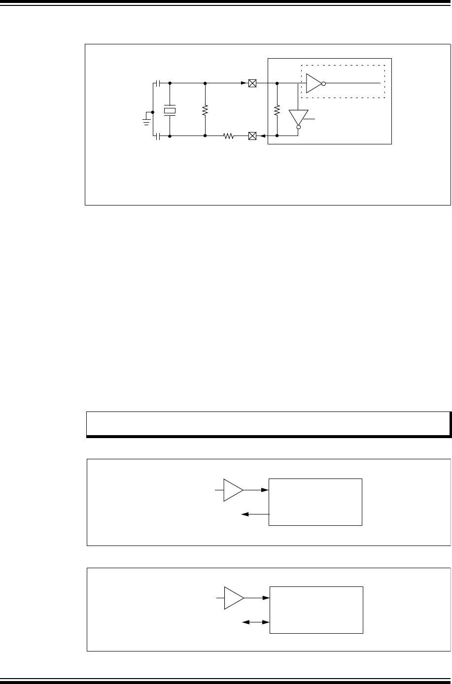
PIC32 Family Reference Manual
DS61112H-page 6-14 © 2007-2012 Microchip Technology Inc.
Figure 6-2: Crystal or Ceramic Resonator Operation (XT, XTPLL, HS, or HSPLL
Oscillator Mode)
The POSC is connected to the OSC1 and OSC2 pins in this device family. The POSC can be
configured for an external clock input, or an external crystal or resonator.
The XT, XTPLL, HS, and HSPLL modes are external crystal or resonator controller oscillator
modes. The XT and HS modes are functionally very similar. The primary difference is the gain of
the internal inverter of the oscillator circuit. The XT mode is a medium power, medium frequency
mode and has medium inverter gain. HS mode is higher power and provides the highest
oscillator frequencies and has the highest inverter gain. OSC2 provides crystal/resonator
feedback in both XT and HS Oscillator modes and hence is not available for use as a input or
output in these modes. The XTPLL and HSPLL modes have a Phase-Locked Loop (PLL) with a
user-selectable input divider and multiplier, and an output divider, to provide a wide range of
output frequencies. The oscillator circuit will consume more current when the PLL is enabled.
The External Clock modes, EC and ECPLL, allow the system clock to be derived from an external
clock source. The EC/ECPLL modes configure the OSC1 pin as a high-impedance input that can
be driven by a CMOS driver. The external clock can be used to drive the system clock directly
(EC) or the ECPLL module with prescaler and postscaler can be used to change the input clock
frequency (ECPLL). The External Clock mode also disables the internal feedback buffer allowing
the OSC2 pin to be used for other functions. In the External Clock mode, the OSC2 pin can be
used as an additional device I/O pin (see Figure 6-4) or a PBCLK output pin (see Figure 6-3).
Figure 6-3: External Clock Input Operation with Clock-Out (EC, ECPLL Mode)
Figure 6-4: External Clock Input Operation with No Clock-Out (EC, ECPLL Mode)
To Internal Logic
PIC32
Note 1: A series resistor, RS, may be required for AT strip cut crystals or to eliminate clipping. Alter-
natively, to increase oscillator circuit gain, add a parallel resistor, RP, with a value of 1 M.
2: The internal feedback resistor, RF, is typically in the range of 2 M to 10 M
3: See 6.7.3.1 “Determining the Best Values for Oscillator Components”.
C1
(3)
C2
(3)
XTAL
R
S
(1)
Enable
OSC2
OSC1
RF
(2)
RP
(1)
Note: When using the PLL modes, the input divider must be chosen such that the resulting
frequency applied to the PLL is in the range of 4 MHz to 5 MHz.
OSC1
OSC2 (Clock Out)
PBCLK
Clock from
External System PIC32
OSC1
I/O (OSC2)I/O
Clock from
External System PIC32

© 2007-2012 Microchip Technology Inc. DS61112H-page 6-15
Section 6. Oscillators
Oscillators
6
6.3.1.1.1 Primary Oscillator (POSC) Configuration
To c onf ig u re th e P OSC, perform the following steps:
1. Select the POSC as the default oscillator in the device Configuration register DEVCFG1 by
setting FNOSC<2:0> = 010 (without PLL) or to ‘011’ (with PLL).
2. Select the desired mode: HS, XT, or EC, using POSCMOD<1:0> in DEVCFG1.
3. If the PLL is to be used:
a) Select the appropriate Configuration bits for the PLL input divider to scale the input
frequency to be between 4 MHz and 5 MHz using FPLLIDIV<2:0> in DEVCFG2.
b) Select the desired PLL multiplier ratio using FPLLMUL<2:0> in DEVCFG2.
c) At runtime, select the desired PLL output divider using PLLODIV (OSCCON<29:27>)
to provide the desired clock frequency. The default value is set by DEVCFG1.
6.3.1.1.2 Oscillator Start-up Timer (OST)
To e nsur e tha t a c rys ta l osc il l at or ( or ce ram ic resonator) has started and stabilized, an Oscillator
Start-up Timer (OST) is provided. The OST is a simple 10-bit counter that counts 1024 TOSC
cycles before releasing the oscillator clock to the rest of the system. This time-out period is
designated as TOST. The amplitude of the oscillator signal must reach the VIL and VIH thresholds
for the oscillator pins before the OST can begin to count cycles.
The TOST interval is required every time the oscillator has to restart (i.e., on a Power-on Reset
(POR), Brown-out Reset (BOR) or a wake-up from Sleep mode). The OST is applied to the XT
and HS modes for the POSC, as well as the SOSC (see 6.3.1.2 “Secondary Oscillator (SOSC)”).
6.3.1.1.3 Primary Oscillator Start-up from Sleep Mode
To e nsu re r eli abl e w ake -up fro m S lee p mo de, c are must be taken to properly design the Primary
Oscillator circuit. This is because the load capacitors have both partially charged to some
quiescent value and phase differential at wake-up is minimal. Thus, more time is required to
achieve stable oscillation. Remember also that low voltage, high temperatures and the lower
frequency clock modes also impose limitations on loop gain, which in turn, affects start-up.
Each of the following factors increases the start-up time:
•Low-frequency design (with a Low Gain Clock mode)
•Quiet environment (such as a battery operated device)
•Operating in a shielded box (away from the noisy RF area)
•Low voltage
•High temperature
•Wake-up from Sleep mode
6.3.1.1.4 Primary Oscillator Pin Functionality
The Primary Oscillator pins (OSCI/OSCO) can be used for other functions when the oscillator is
not being used.
The POSCMD Configuration bits in the Oscillator Configuration (FOSC<1:0>) register determine
the oscillator pin function.
The OSCIOFNC bit determines the OSC2 pin function. Refer to the “Oscillator Configuration”
chapter in the specific device data sheet for OSCIOFNC functionality.
6.3.1.2 SECONDARY OSCILLATOR (SOSC)
The Secondary Oscillator (SOSC) is designed specifically for low-power operation with an
external 32.768 kHz crystal. The oscillator is located on the SOSCO and SOSCI device pins and
serves as a secondary crystal clock source for low-power operation. It can also drive Timer1
and/or the Real-Time Clock and Calendar (RTCC) module for Real-Time Clock (RTC)
applications.
Note: The oscillator start-up timer is disabled when POSC is configured for EC or ECPLL
mode.

PIC32 Family Reference Manual
DS61112H-page 6-16 © 2007-2012 Microchip Technology Inc.
6.3.1.2.1 Enabling the SOSC
The SOSC is hardware enabled by the FSOSCEN Configuration bit (DEVCFG1<5>). The
software can control the SOSC by modifying the SOSCEN bit (OSCCON<1>). Setting SOSCEN
enables the oscillator; the SOSCO and SOSCI pins are controlled by the oscillator and cannot
be used for port I/O or other functions.
The SOSC requires a warm-up period before it can be used as a clock source. When the oscillator
is enabled, a warm-up counter increments to 1024. When the counter expires the SOSCRDY bit
(OSCCON<22>) is set to ‘1’. Refer to 6.3.1.1.2 “Oscillator Start-up Timer (OST)”.
6.3.1.2.2 SOSC Continuous Operation
The SOSC is always enabled when SOSCEN bit (OSCCON<1>) is set. Leaving the oscillator
running at all times allows a fast switch to the 32 kHz system clock for lower power operation.
Returning to the faster main oscillator will still require an oscillator start-up time if it is a crystal
type source and/or uses the PLL (see 6.3.1.1.2 “Oscillator Start-up Timer (OST)”).
In addition, the oscillator will need to remain running at all times for Real-Time Clock applications
and may be required for Timer1. Refer to Section 14. “Timers” (DS61105) and
Section 29. “Real-Time Clock and Calendar” (DS61125) for further details.
Example 6-1: Enabling the SOSC
6.3.1.3 INTERNAL FAST RC (FRC) OSCILLATOR
The FRC Oscillator is a fast (8 MHz nominal), user-trimmable, internal RC oscillator with a
user-selectable input divider, PLL multiplier, and output divider. Refer to the specific device data
sheet for more information about the FRC Oscillator.
6.3.1.3.1 FRC Postscaler Mode (FRCDIV)
Users are not limited to the nominal 8 MHz FRC output if they want to use the fast internal
oscillator as a clock source. An additional FRC mode, FRCDIV, implements a selectable output
divider that allows the choice of a lower clock frequency from seven different options, plus the
direct 8 MHz output. The output divider is configured using the FRCDIV<2:0> bits
(OSCCON<26:24>). Assuming a nominal 8 MHz output, available lower frequency options range
from 4 MHz (divide-by-2) to 31 kHz (divide-by-256). The range of frequencies allows users the
ability to save power at any time in an application by simply changing the FRCDIV<2:0> bits. The
FRCDIV mode is selected whenever the COSC bits (OSCCON<14:12>) are ‘111’.
6.3.1.3.2 FRC Oscillator with PLL Mode (FRCPLL)
The output of the FRC may also be combined with a user-selectable PLL multiplier and output
divider to produce a SYSCLK across a wide range of frequencies. The FRC PLL mode is
selected whenever the COSC bits (OSCCON<14:12>) are ‘001’. In this mode, the PLL input
divider is forced to ‘2’ to provide a 4 MHz input to the PLL. The desired PLL multiplier and output
divider values can be chosen to provide the desired device frequency.
Note: An unlock sequence is required before a write to OSCCON can occur. Refer to
6.3.7.2 “Oscillator Switching Sequence” for more information.
SYSKEY = 0x0; // ensure OSCCON is locked
SYSKEY = 0xAA996655; // Write Key1 to SYSKEY
SYSKEY = 0x556699AA; // Write Key2 to SYSKEY
// OSCCON is now unlocked
// make the desired change
OSCCONSET = 2; // enable Secondary Oscillator
// Relock the SYSKEY
SYSKEY = 0x0; // Write any value other than Key1 or Key2
// OSCCON is relocked

© 2007-2012 Microchip Technology Inc. DS61112H-page 6-17
Section 6. Oscillators
Oscillators
6
6.3.1.3.3 Oscillator Tune Register (OSCTUN)
The FRC Oscillator Tuning register, OSCTUN, allows the user to fine tune the FRC Oscillator
over a range of approximately ±12% (typical). Each bit increment or decrement changes the
factory calibrated frequency of the FRC Oscillator by a fixed amount. Refer to the “Electrical
Characteristics” chapter of the specific device data sheet for additional information on the
available tuning range.
6.3.1.4 INTERNAL LOW-POWER RC (LPRC) OSCILLATOR
The LPRC Oscillator is separate from the FRC. It oscillates at a nominal frequency of 31.25 kHz.
The LPRC Oscillator is the clock source for the Power-up Timer (PWRT), Watchdog Timer
(WDT), Fail-Safe Clock Monitor (FSCM) and Phase-Locked Loop (PLL) reference circuits. It may
also be used to provide a low-frequency clock source option for the device in those applications
where power consumption is critical, and timing accuracy is not required.
6.3.1.4.1 Enabling the LPRC Oscillator
Since it serves the PWRT clock source, the LPRC Oscillator is enabled at a POR whenever the
on-board voltage regulator is enabled. After the PWRT expires, the LPRC Oscillator will remain
ON if one of the following is true:
•The Fail-Safe Clock Monitor is enabled
•The WDT is enabled
•The LPRC Oscillator is selected as the system clock (COSC2:COSC0 = 100)
If none of the above is true, the LPRC will shut off after the PWRT expires.
6.3.2 PLL Clock Generator
6.3.2.1 SYSTEM CLOCK PHASE-LOCKED LOOP (PLL)
The system clock PLL provides a user-configurable input divider and multiplier, and output
divider, which can be used with the XT, HS and EC POSC modes and with the Internal FRC
Oscillator mode to create a variety of clock frequencies from a single clock source.
The input divider, multiplier, and output divider control initial value bits are contained in the
DEVCFG2 Device Configuration register. The multiplier and output divider bits are also contained
in the OSCCON register. As part of a device Reset, values from the device configuration register
DEVCFG2 are copied to the OSCCON register. This allows the user to preset the input divider
to provide the appropriate input frequency to the PLL and set an initial PLL multiplier when
programming the device. At runtime, the multiplier and output divider can be changed by
software to scale the clock frequency to suit the application. The PLL input divider cannot be
changed at run time. This is to prevent applying an input frequency outside the specified limits to
the PLL.
To c onf ig u re th e P L L, us e t he fol low ing st eps:
1. Calculate the PLL input divider, PLL multiplier, and PLL output divider values.
2. Set the PLL input divider and the initial PLL multiplier value in the DEVCFG2 register when
programming the part.
3. At runtime, the PLL multiplier and PLL output divider can be changed to suit the
application.
Combinations of the PLL input divider, multiplier, and output divider provide a combined multiplier
of approximately 0.006 to 24 times the input frequency. For reliable operation, the output of the
PLL module must not exceed the maximum clock frequency of the device. The PLL input divider
value should be chosen to limit the input frequency to the PLL to the range of 4 MHz to 5 MHz.
Due to the time required for the PLL to provide a stable output, the SLOCK Status bit
(OSCCON<5>) is provided. When the clock input to the PLL is changed, this bit is driven low (‘0’).
After the PLL has achieved a lock or the PLL start-up timer has expired, the bit is set. The bit will
be set upon the expiration of the timer even if the PLL has not achieved a lock.
Note: An unlock sequence is required before a write to the OSCTUN register can occur.
Refer to 6.3.7.2 “Oscillator Switching Sequence” for more information.

PIC32 Family Reference Manual
DS61112H-page 6-18 © 2007-2012 Microchip Technology Inc.
6.3.2.2 PLL LOCK STATUS
The PLL Lock Status indicates the lock status of the PLL. It is set automatically after a typical
time delay for the PLL to achieve lock, also designated as TLOCK. If the PLL does not stabilize
properly during start-up, SLOCK may not reflect the actual status of the PLL lock, nor does it
detect when the PLL loses lock during normal operation. The SLOCK bit is cleared at a POR and
on clock switches when the PLL is selected as a destination clock source. It remains clear when
any clock source is not using the PLL is selected. Refer to the “Electrical Characteristics”
chapter in the specific device data sheet for more information on the PLL lock interval.
6.3.3 Peripheral Bus Clock (PBCLK) Generation
The PBCLK is derived from the System Clock (SYSCLK) divided by PBDIV<1:0>
(OSCCON<20:19>). The PBCLK Divisor bits PBDIV<1:0> allow postscalers of 1:1, 1:2, 1:4, and
1:8. Refer to the individual peripheral module section of the “PIC32 Family Reference Manual”
for information regarding which bus a specific peripheral uses.
Note 1: When the PBDIV divisor is set to a ratio of 1:1, the SYSCLK and PBCLK are
equivalent in frequency. The PBCLK frequency is never greater than the processor
clock frequency.
The effect of changing the PBCLK frequency on individual peripherals should be
considered when selecting or changing the PBDIV value.
Performing back-to-back operations on PBCLK peripheral registers when the PB
divisor is not set at 1:1 will cause the CPU to stall for a number of cycles. This stall
occurs to prevent an operation from occurring before the pervious one has
completed. The length of the stall is determined by the ratio of the CPU and PBCLK
and synchronizing time between the two busses.
Changing the PBCLK frequency has no effect on the SYSCLK peripherals
operation.
2: The peripheral bus frequency can be changed on the fly by writing a new value to
the PBDIV<1:0> bits in the OSCCON register. A state machine is used to control
the changing of the PB frequency. This state machine requires up to 60 CPU clocks
to perform a switch and be ready to receive a new PBDIV value. If a new value is
written to the PBDIV bits before the state machine has completed the operation, the
new value will be ignored and the PBDIV<1:0> bits will reflect the previous value.
The PBDIVRDY bit (OSCCON<21>) indicates whether a divisor switch is in
progress during which time the PBDIV<1:0> bits should not be written. Rewriting
the current value to the PBDIV<1:0> bits is ignored and has no effect.

© 2007-2012 Microchip Technology Inc. DS61112H-page 6-19
Section 6. Oscillators
Oscillators
6
6.3.4 USB Clock (USBCLK) Generation
The USBCLK can be derived from the 8 MHz internal FRC Oscillator, 48 MHz POSC, or the
96 MHz PLL from the POSC. For normal operation, the USB module requires exact 48 MHz
clock. When using 96 MHz PLL, the output is internally divided to obtain 48 MHz clock. The
FRC clock source is used to detect USB activity and bring USB module out of Suspend mode.
Once USB module is out of Suspend mode, it must use a 48 MHz clock to perform the USB
transactions. The internal FRC Oscillator is not used for normal USB module operation.
6.3.4.1 USB CLOCK PHASE-LOCKED LOOP (UPLL)
The USB Clock Phase-Locked Loop (UPLL) provides a user-configurable input divider, which
can be used with the XT, HS, and EC Primary Oscillator modes to create a variety of clock
frequencies from a clock source. The actual source must be able to provide a stable clock as
required by the USB specifications.
The UPLL Enable and Input Divider bits are contained in the DEVCFG2 register. The input to the
UPLL must be limited to 4 MHz only. An appropriate input divider must be selected to ensure that
the UPLL input is 4 MHz.
To c onf ig u re th e U PLL , t he fol low ing s t ep s a re re q ui red :
1. Enable the USB PLL by setting the UPLLEN bit in the DEVCFG2 register.
2. Based on the source clock, calculate the UPLL input divider value so that the PLL input is
4 MHz.
3. Set the USB PLL Input Divider (UPLLIDIV<2:0>) bits in the DEVCFG2 register when
programming the device.
6.3.4.2 USB PLL LOCK STATUS
The ULOCK bit (OSCCON<6>) is a read-only Status bit that indicates the lock status of the USB
PLL. It is automatically set after the typical time delay for the PLL to achieve lock, also designated
as TULOCK. If the PLL does not stabilize during start-up, ULOCK may not reflect the status of PLL
lock, nor does it detect when the PLL loses lock during normal operation.
The ULOCK bit is cleared at a POR. It remains clear when any clock source that is not using the
PLL is selected.
Refer to the “Electrical Characteristics” chapter in the specific device data sheet for more
information on the USB PLL lock interval.
6.3.4.3 USING INTERNAL FRC OSCILLATOR WITH USB
The internal 8 MHz FRC Oscillator is available as a clock source to detect any USB activity
during USB Suspend mode and bring the module out of the Suspend mode. To enable FRC for
USB usage, the UFRCEN bit (OSCCON<2>) must be set to ‘1’ before putting the USB module
in Suspend mode.
6.3.5 Two-Speed Start-up
Two-Speed Start-up mode can be used to reduce the device start-up latency when using all
external crystal POSC modes including PLL. Two-Speed Start-up uses the FRC clock as the
SYSCLK source until the Primary Oscillator (POSC) has stabilized. After the user selected
oscillator has stabilized, the clock source will switch to POSC. This allows the CPU to begin
running code, at a lower speed, while the oscillator is stabilizing. When the POSC has met the
start-up criteria, an automatic clock switch occurs to switch to POSC. This mode is enabled by the
Device Configuration bits FCKSM<1:0> (DEVCFG1<15:14>). Two-Speed Start-up operates after
a POR or on exit from Sleep. Software can determine the oscillator source currently in use by
reading the COSC<2:0> bits in the OSCCON register.
Note: Refer to Section 32. “Configuration” (DS61124) for detailed information on the
DEVCFG2 register.
Note: The Watchdog Timer (WDT), if enabled, will continue to count at the same rate
regardless of the SYSCLK frequency. Care must be taken to service the WDT
during Two-Speed Start-up, taking into account the change in SYSCLK.

PIC32 Family Reference Manual
DS61112H-page 6-20 © 2007-2012 Microchip Technology Inc.
6.3.6 Fail-Safe Clock Monitor (FSCM) Operation
The Fail-Safe Clock Monitor (FSCM) is designed to allow continued device operation if the
current oscillator fails. It is intended for use with the Primary Oscillator (POSC) and automatically
switches to the FRC Oscillator if a POSC failure is detected. The switch to the Fast Internal RC
Oscillator (FRC) allows continued device operation and the ability to retry the POSC or to execute
code appropriate for a clock failure.
The FSCM mode is controlled by the FCKSM<1:0> bits in the DEVCFG1 register. Any of the
POSC modes can be used with FSCM.
When a clock failure is detected with FSCM enabled and the FSCM Interrupt Enable (FSCMIE)
bit (IEC1<14>) set, the clock source will be switched from the POSC to the FRC. An oscillator fail
interrupt will be generated, with the CF bit (OSCCON<3>) set. This interrupt has a user-settable
Priority bits FSCMIP<2:0> (IPC8<12:10>) and Subpriority bits FSCMIS<1:0> (IPC8<9:8>). The
clock source will remain in FRC until a device Reset or a clock switch is performed. Failure to
enable the FSCM interrupt will not inhibit the actual clock switch.
The FSCM module takes the following actions when switching to the FRC Oscillator:
1. The COSC bits (OSCCON<14:12>) are loaded with ‘000’.
2. The CF bit (OSCCON<3>) is set to indicate the clock failure.
3. The OSWEN control bit (OSCCON<0>) is cleared to cancel any pending clock switches.
To e nab le the FS CM, pe rf o rm th e f oll owi ng ste ps :
1. Enable the FSCM in the DEVCFG1 register by configuring the FCKSM<1:0> bits:
•01 = Clock Switching is enabled, FSCM is disabled
•00 = Clock Switching and FSCM are enabled
2. Select the desired mode HS, XT, or EC using FNOSC<2:0> in DEVCFG1.
3. Select the POSC as the default oscillator in the device configuration DEVCFG1 by
configuring FNOSC<2:0> = 010 without PLL or ‘011’ with PLL.
If the PLL is to be used:
1. Select the appropriate Configuration bits for the PLL input divider to scale the input
frequency to be between 4 MHz and 5 MHz using FPLLIDIV<2:0> (DEVCFG2<2:0>).
2. Select the desired PLL multiplier using FPLLMUL<2:0> (DEVCFG2<6:4>).
3. Select the desired PLL output divider using FPLLODIV<2:0> (DEVCFG2<18:16>).
If an FSCM interrupt is desired when a FSCM event occurs, the following steps should be
performed during start-up code:
1. Clear the FSCM Interrupt bit FSCMIF (IFS1<14>).
2. Set the Interrupt Priority bits FSCMIP<2:0> (IPC8<12:10>) and the Subpriority bits
FSCMIS<1:0> (IPC8<9:8>).
3. Set the FSCM Interrupt Enable bit FSCMIE (IEC1<14>).
6.3.6.1 FSCM DELAY
On a POR, BOR, or wake from Sleep mode event, a nominal delay (TFSCM) may be inserted
before the FSCM begins to monitor the system clock source. The purpose of the FSCM delay is
to provide time for the oscillator and/or PLL to stabilize when the Power-up Timer (PWRT) is not
utilized. The FSCM delay will be generated after the internal System Reset signal, SYSRST, has
been released. Refer to Section 7. “Resets” (DS61118) for FSCM delay timing information.
The TFSCM interval is applied whenever the FSCM is enabled and the HS, HSPLL, XT, XTPLL,
or Secondary Oscillator modes are selected as the system clock.
Note: Refer to Section 32. “Configuration” (DS61124) for detailed information on the
DEVCFG1 and DEVCFG2 registers.
Note: The Watchdog Timer (WDT), if enabled, will continue to count at the same rate
regardless of the SYSCLK frequency. Care must be taken to service the WDT after
a Fail-Safe Clock Monitor event, taking into account the change in SYSCLK.
Note: Refer to the “Electrical Characteristics” chapter of the specific device data sheet
for TFSCM specification values.

© 2007-2012 Microchip Technology Inc. DS61112H-page 6-21
Section 6. Oscillators
Oscillators
6
6.3.6.2 FSCM AND SLOW OSCILLATOR START-UP
If the chosen device oscillator has a slow start-up time coming out of POR, BOR or Sleep mode,
it is possible that the FSCM delay will expire before the oscillator has started. In this case, the
FSCM will initiate a clock failure trap. As this happens, the COSC bits (OSCCON<14:12>) are
loaded with the FRC Oscillator selection. This will effectively shut off the original oscillator that
was trying to start. Software can detect a clock failure using a Interrupt Service Routine (SFR) or
by polling the clock fail interrupt flag, FSCMIF (IFS1<14>).
6.3.6.3 FSCM AND WDT
The FSCM and the WDT both use the LPRC Oscillator as their time base. In the event of a clock
failure, the WDT is unaffected and continues to run.
6.3.7 Clock Switching Operation
With few limitations, applications are free to switch between any of the four clock sources (POSC,
SOSC, FRC, and LPRC) under software control and at any time. To limit the possible side effects
that could result from this flexibility, PIC32 devices have a safeguard lock built into the switch
process.
6.3.7.1 ENABLING CLOCK SWITCHING
To en abl e cl o ck s wit ch ing, t he F CK S M1 C onfiguration bit (DEVCFG1<15>) must be
programmed to ‘0’. See Section 32. “Configuration” (DS61124) for further details. If the
FCKSM1 Configuration bit is unprogrammed (= 1), the clock switching function and Fail-Safe
Clock Monitor (FSCM) function are disabled. This is the default setting.
The NOSC<2:0> Control bits (OSCCON<10:8>) do not control the clock selection when clock
switching is disabled. However, the COSC<2:0> bits (OSCCON<14:12>) will reflect the clock
source selected by the FNOSC<2:0> Configuration bits.
The OSWEN Control bit (OSCCON<0>) has no effect when clock switching is disabled. It is held
at ‘0’ at all times.
6.3.7.2 OSCILLATOR SWITCHING SEQUENCE
At a minimum, performing a clock switch requires the following sequence:
1. If desired, read the COSC<2:0> bits (OSCCON<14:12>) to determine the current
oscillator source.
2. Perform the unlock sequence to allow a write to the OSCCON register. The unlock
sequence has critical timing requirements and should be performed with interrupts and
DMA disabled.
3. Write the appropriate value to the NOSC<2:0> control bits (OSCCON<10:8>) for the new
oscillator source.
4. Set the OSWEN bit (OSCCON<0>) to initiate the oscillator switch.
5. Optionally, perform the lock sequence to lock the OSCCON register. The lock sequence
must be performed separately from any other operation.
Note 1: Primary Oscillator mode has three different submodes (XT, HS, and EC) which are
determined by the POSCMOD Configuration bits in DEVCFG1. While an
application can switch to and from Primary Oscillator mode in software, it cannot
switch between the different primary submodes without reprogramming the device.
2: The device will not permit direct switching between PLL clock sources. The user
should not change the PLL multiplier values or postscaler values when running
from the affected PLL source. To perform either of the above clock switching
functions, the clock switch should be performed in two steps. The clock source
should first be switched to a non-PLL source, such as FRC, and then switched to
the desired source. This requirement only applies to PLL-based clock sources.
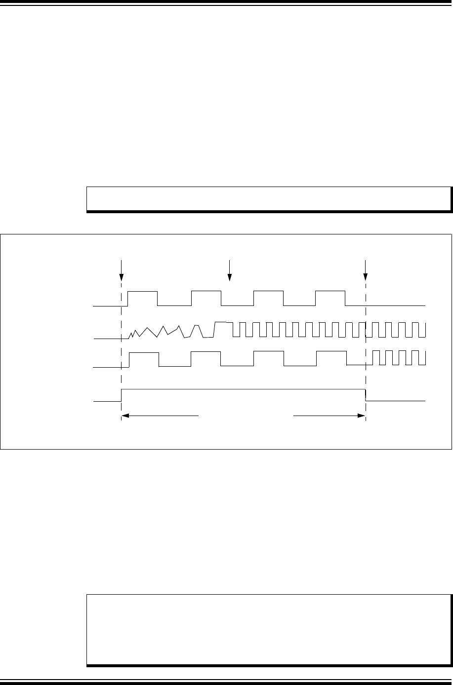
PIC32 Family Reference Manual
DS61112H-page 6-22 © 2007-2012 Microchip Technology Inc.
Once the basic sequence is completed, the system clock hardware responds automatically as
follows:
1. The clock switching hardware compares the COSC<2:0> Status bits with the new value
of the NOSC control bits. If they are the same, then the clock switch is a redundant
operation. In this case, the OSWEN bit is cleared automatically and the clock switch is
aborted.
2. The new oscillator is turned on by the hardware if it is not currently running. If a crystal
oscillator must be turned on, the hardware will wait until the Oscillator Start-up timer (OST)
expires. If the new source is using the PLL, then the hardware waits until a PLL lock is
detected (SLOCK = 1).
3. The hardware clears the OSWEN bit to indicate a successful clock transition. In addition,
the NOSC<2:0> bit values are transferred to the COSC<2:0> Status bits.
4. The old clock source is turned off at this time if the clock is not being used by any modules.
The transition timing between the clock sources is shown in Figure 6-5.
Figure 6-5: Clock Transition Timing Diagram
The following is a recommended code sequence for a clock switch:
1. Disable interrupts and DMA prior to the system unlock sequence.
2. Execute the system unlock sequence by writing the Key values of 0xAA996655 and
0x556699AA to the SYSKEY register in two back-to-back Assembly or ‘C’ instructions.
3. Write the new oscillator source value to the NOSC control bits.
4. Set the OSWEN bit in the OSCCON register to initiate the clock switch.
5. Write a non-key value (such as, 0x33333333) to the SYSKEY register to perform a lock.
Continue to execute code that is not clock-sensitive (optional).
6. Check to see if the OSWEN bit is ‘0’. If it is, the switch was successful. Loop until the bit
is ‘0’.
7. Re-enable interrupts and DMA.
Note: The processor will continue to execute code throughout the clock switching
sequence. Timing-sensitive code should not be executed during this time.
Old Clock Source
New Clock Source
SYSCLK
Both Oscillators Active
OSWEN bit
New Source
Enabled
New Source
Stable
Old Source
Disabled
Note: The SYSCLK can be any selected source (POSC, SOSC, FRC or LPRC).
Note: There are no timing requirements for the steps other than the initial back-to-back
writing of the Key values to perform the unlock sequence.
The unlock sequence unlocks all registers that are secured by the lock function. It
is recommended that the amount of time the system is unlocked is kept to a
minimum. For example code for unlocking the OSCCON register, refer to
Example 6-1.

© 2007-2012 Microchip Technology Inc. DS61112H-page 6-23
Section 6. Oscillators
Oscillators
6
6.3.7.3 CLOCK SWITCHING CONSIDERATIONS
When incorporating clock switching into an application, users should consider the following
issues when designing their code:
•The SYSLOCK unlock sequence is timing critical. The two key values must be written
back-to-back with no in-between peripheral register access. Prevent unintended peripheral
register accesses by disabling all interrupts and DMA transfers.
•The system will not relock automatically. Perform the relock sequence as soon as possible
after the clock switch
•The unlock sequence unlocks other registers such as the those related to Real-Time Clock
control
•If the destination clock source is a crystal oscillator, the clock switch time is dictated by the
oscillator start-up time
•If the new clock source does not start, or is not present, the OSWEN bit remains set
• A clock switch to a different frequency affects the clocks to peripherals. Peripherals may
require reconfiguration to continue operation at the same rate as they did before the clock
switch occurred
•If the new clock source uses the PLL, a clock switch does not occur until lock has been
achieved
• If the WDT is used, care must be taken to ensure it can be serviced in a timely manner at
the new clock rate
6.3.7.4 ENTERING SLEEP MODE DURING A CLOCK SWITCH
If, during a clock switch operation, the device enters Sleep mode, the clock switch operation is
not aborted. If the clock switch does not complete before the device enters Sleep mode, the
device will perform the switch when it exits Sleep; then, the WAIT instruction executes normally.
Note 1: When the Fail-Safe Clock Monitor is enabled, the application should not attempt to
switch to a clock that has a frequency lower than 100 kHz. Clock switching in these
instances may generate a false oscillator fail event and result in a switch to the
Internal Fast RC (FRC) oscillator.
2: The device will not permit direct switching between PLL clock sources. The user
should not change the PLL multiplier values or postscaler values when running
from the affected PLL source. To perform either of the above clock switching
functions, the clock switch should be performed in two steps. The clock source
should first be switched to a non-PLL source, such as FRC; and then, switched to
the desired source. This requirement only applies to PLL-based clock sources.

PIC32 Family Reference Manual
DS61112H-page 6-24 © 2007-2012 Microchip Technology Inc.
6.3.8 Real-Time Clock Oscillator
To provide accurate timekeeping, the Real-Time Clock and Calendar (RTCC) requires a precise
time base. To achieve this, the SOSC is used as the time base for the RTCC. The SOSC uses an
external 32.768 kHz crystal connected to the SOSCI and SOSCO pins.
6.3.8.1 SOSC CONTROL
The SOSC can be used by modules other than the RTCC, therefore, the SOSC is controlled by a
combination of software and hardware. Setting the SOSCEN bit (OSCCON<1>) to ‘1’ enables
the SOSC. The SOSC is disabled when it is not being used by the CPU module and the SOSCEN
bit is ‘0’. If the SOSC is being used as SYSCLK, such as after a clock switch, it cannot be disabled
by writing to the SOSCEN bit. If the SOSC is enabled by the SOSCEN bit, it will continue to
operate when the device is in Sleep. To prevent inadvertent clock changes, the OSCCON
register is locked. It must be unlocked prior to software enabling or disabling the SOSC.
6.3.9 Timer1 External Oscillator
The Timer1 module has the ability to use the SOSC as a clock source to increment Timer1. The
SOSC is designed to use an external 32.768 kHz crystal connected to the SOSCI and SOSCO
pins.
6.3.9.1 SOSC CONTROL
The SOSC can be used by modules other than Timer1, therefore, the SOSC is controlled by a
combination of software and hardware. Setting the SOSCEN bit (OSCCON<1>) to ‘1’ enables
the SOSC. The SOSC is disabled when it is not being used by the CPU module and the SOSCEN
bit is ‘0’. If the SOSC is being used as SYSCLK, such as after a clock switch, it cannot be disabled
by writing to the SOSCEN bit. If the SOSC is enabled by the SOSCEN bit, it will continue to
operate when the device is in Sleep. To prevent inadvertent clock changes the OSCCON register
is locked. It must be unlocked prior to software enabling or disabling the SOSC.
Note: If the RTCC is to be used when the CPU clock source is to be switched between
SOSC and another clock source, the SOSCEN bit should be set to ‘1’ in software.
Failure to set the bit will cause the SOSC to be disabled when the CPU is switched
to another clock source.
Due to the start-up time for an external crystal, the user should wait for stable
SOCSC oscillator output before enabling the RTCC. This typically requires a 32 ms
delay between enabling the SOSC and enabling the RTCC. The actual time required
will depend on the crystal in use and the application.
There are numerous system and peripheral registers that are protected from inad-
vertent writes by the SYSREG lock. Performing a lock or unlock affects all registers
protected by SYSREG including OSCCON.
Note: If the TIMER1 is to be used when the CPU clock source is to be switched between
SOSC and another clock source, the SOSCEN bit should be set to ‘1’ in software.
Failure to set the bit will cause the SOSC to be disabled when the CPU is switched
to another clock source.
Due to the start-up time for an external crystal the user should wait for stable
SOCSC oscillator output before attempting to use Timer1 for accurate
measurements. This typically requires a 10 ms delay between enabling the SOSC
and use of Timer1. The actual time required will depend on the crystal in use and
the application.
There are numerous system and peripheral registers that are protected from inad-
vertent writes by the SYSREG lock. Performing a lock or unlock affects all registers
protected by SYSREG including the OSCCON register.

© 2007-2012 Microchip Technology Inc. DS61112H-page 6-25
Section 6. Oscillators
Oscillators
6
6.3.10 Reference Clock Output
The reference clock output provides a clock signal on the REFCLKO pin. The reference clock
can be selected from various clock sources.
The ROSEL<3:0> bits (REFOCON<3:0>) select between these sources. The RODIV<14:0> bits
(REFOCON<30:16>) and the ROTRIM<8:0> bits (REFOTRIM<31:23>) are used to scale the
reference clock to the desired clock output. The DIVSWEN bit (REFOCON<9>) must be set to
initiate a clock switch to the new divider and trim values.
Refer to Figure 6-1 for a block diagram of the reference clock. See the REFOCON register
(Register 6-3) for the bits associated with the reference clock output.
Note: This feature is not available on all devices. See the “Oscillator Configuration”
chapter in the specific device data sheet for availability.

PIC32 Family Reference Manual
DS61112H-page 6-26 © 2007-2012 Microchip Technology Inc.
6.4 INTERRUPTS
The only interrupt generated by the Oscillator module is the FSCM event interrupt. When the
FSCM mode is enabled and the corresponding interrupts have been configured, a FSCM event
will generate an interrupt. This interrupt has both priority and subpriorities that must be
configured.
6.4.1 Interrupt Operation
The FSCM has a dedicated Interrupt bit, FSCMIF, and a corresponding Interrupt Enable/Mask
bit, FSCMIE, in the corresponding IFSx and IECx registers. These bits are used to determine the
source of an interrupt and to enable or disable an individual interrupt source. The priority level of
the FSCM can be set independently of other interrupt sources.
The FSCMIF bit is set when a FSCM detects a POSC clock failure. The FSCMIF bit will then be
set without regard to the state of the corresponding FSCMIE bit. The FSCMIF bit can be polled
by software if desired.
The FSCMIE bit controls the interrupt generation. If the FSCMIE bit is set, the CPU will be
interrupted whenever an FSCM event occurs (subject to the priority and subpriority as outlined
below). The FSCMIF bit will be set regardless of interrupt priority.
It is the responsibility of the routine that services a particular interrupt to clear the appropriate
Interrupt Flag bit before the service routine is complete.
The priority of the FSCM interrupt can be set independently via the FSCMIP<2:0> bits in the
corresponding IPCx register. This priority defines the priority group that interrupt source will be
assigned to. The priority groups range from a value of 7, the highest priority, to a value of 0, which
does not generate an interrupt. An interrupt being serviced will be preempted by an interrupt in
a higher priority group.
The subpriority bits allow setting the priority of a interrupt source within a priority group. The
values of the subpriority bits, FSCMIS<1:0>, range from 3, the highest priority, to 0 the lowest
priority. An interrupt with the same priority group but having a higher subpriority value will
preempt a lower subpriority interrupt that is in progress.
The priority group and subpriority bits allow more than one interrupt source to share the same
priority and subpriority. If simultaneous interrupts occur in this configuration, the natural order of
the interrupt sources within a priority/subgroup pair determine the interrupt generated. The
natural priority is based on the vector numbers of the interrupt sources. The lower the vector
number the higher the natural priority of the interrupt. Any interrupts that were overridden by
natural order will then generate their respective interrupts based on priority, subpriority, and
natural order after the interrupt flag for the current interrupt is cleared.
After an enabled interrupt is generated, the CPU will jump to the vector assigned to that interrupt.
The vector number for the interrupt is the same as the natural order number. The IRQ number is
not always the same as the vector number due to some interrupts sharing a single vector. The
CPU will then begin executing code at the vector address. The users code at this vector address
should perform an operations required, such as reloading the duty cycle, clear the interrupt flag,
and then exit. Refer to the “Interrupts” chapter in the specific device data sheet and Section 8.
“Interrupts” (DS61108) for the vector address table details and for more information on
interrupts.
Example 6-2: FSCM Interrupt Configuration
// FSCM must be enabled in the device configuration
// Set up the FSCM interrupt located in the users start-up code
if (OSCCON & 0x0008) // check for a FSCM during start-up
{// user handler for a FSCM event occurred during start-up
}
else
{ // normal start-up
IPC8CLR = 0x1F << 8; // clear the FSCM priority bits
IPC8SET = 7 << 10; // set the FSCM interrupt priority
IPC8SET = 3 << 8; // set the FSCM interrupt subpriority
IFS1CLR = 1 << 14; // clear the FSCM interrupt bit
IEC1SET = 1 << 14; // enable the FSCM interrupt
}
void __ISR(_FAIL_SAFE_MONITOR_VECTOR, ipl7) FSCM_HANDLER(void)
{ // interrupt handler
// insert user code here
IFS1CLR = 1 << 4; // clear the CMP2 interrupt flag
}

© 2007-2012 Microchip Technology Inc. DS61112H-page 6-27
Section 6. Oscillators
Oscillators
6
6.5 OPERATION IN POWER-SAVING MODES
6.5.1 Oscillator Operation in Sleep Mode
Clock sources are disabled in Sleep unless they are being used by a peripheral. The following
sections outline the behavior of each of the clock sources in Sleep.
6.5.1.1 PRIMARY OSCILLATOR IN SLEEP MODE
The POSC is always disabled in Sleep. Start-up delays apply when exiting Sleep.
6.5.1.2 SECONDARY OSCILLATOR IN SLEEP MODE
The SOSC is disabled in Sleep unless the SOSCEN bit is set or it is in use by an enabled module
that operates in Sleep. Start-up delays apply when exiting Sleep if the SOSC is not already
running.
6.5.1.3 FAST RC OSCILLATOR IN SLEEP MODE
The FRC oscillator is disabled in Sleep.
6.5.1.4 LOW-POWER OSCILLATOR IN SLEEP MODE
The LPRC Oscillator is disabled in Sleep if the WDT is disabled.
6.5.2 Oscillator Operation in Idle Mode
Clock sources are not disabled in Idle mode. Start-up delays do not apply when exiting Idle mode.
6.5.3 Oscillator Operation in Debug Mode
The Oscillator module continues to operate while the device is in Debug mode.
6.6 EFFECTS OF VARIOUS RESETS
On all forms of device Reset, OSCCON is set to the default value, and the COSC<2:0>,
PLLIDIV<2:0>, PLLMULT<2:0>, and UPLLIDIV<2:0> values are forced to the values defined in
the DEVCFG1 and DEVCFG2 registers. The oscillator source is transferred to the source as
defined in the DEVCFG1 register. Oscillator start-up delays will apply.
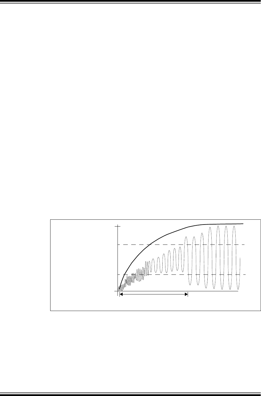
PIC32 Family Reference Manual
DS61112H-page 6-28 © 2007-2012 Microchip Technology Inc.
6.7 CLOCKING GUIDELINES
6.7.1 Crystal Oscillators and Ceramic Resonators
In HS and XT modes, a crystal or ceramic resonator is connected to the OSC1 and OSC2 pins
to establish oscillation. The PIC32 oscillator design requires the use of a parallel cut crystal.
Using a series cut crystal may give a frequency out of the crystal manufacturer’s specifications.
In general, users should select the oscillator option with the lowest possible gain that still meets
their specifications. This will result in lower dynamic currents (IDD). The frequency range of each
oscillator mode is the recommended frequency cut-off, but the selection of a different gain mode
is acceptable as long as a thorough validation is performed (voltage, temperature and
component variations, such as resistor, capacitor and internal oscillator circuitry).
6.7.2 Oscillator/Resonator Start-up
As the device voltage increases from VSS, the oscillator will start its oscillations. The time
required for the oscillator to start oscillating depends on many factors, including the following:
•Crystal/resonator frequency
• Capacitor values used
•Series resistor, if used, and its value and type
• Device VDD rise time
•System temperature
• Oscillator mode selection of device (selects the gain of the internal oscillator inverter)
•Crystal quality
•Oscillator circuit layout
•System noise
The course of a typical crystal or resonator start-up is shown in Figure 6-6. Notice that the time
to achieve stable oscillation is not instantaneous. Refer to the “Electrical Characteristics”
chapter in the specific device data sheet for further information regarding frequency range for
each crystal mode.
Figure 6-6: Example of Oscillator/Resonator Start-up Characteristics
Voltage
Crystal Start-up Time
Time
Device VDD
Maximum VDD of System
0V
VIL
VIH

© 2007-2012 Microchip Technology Inc. DS61112H-page 6-29
Section 6. Oscillators
Oscillators
6
6.7.3 Tuning the Oscillator Circuit
Since Microchip devices have wide operating ranges (frequency, voltage and temperature;
depending on the part and version ordered) and external components (crystals, capacitors, etc.)
of varying quality and manufacture, validation of operation needs to be performed to ensure that
the component selection will comply with the requirements of the application. There are many
factors that go into the selection and arrangement of these external components. Depending on
the application, these may include one of the following:
•Amplifier gain
•Desired frequency
•Resonant frequency of the crystal
•Temperature of operation
•Supply voltage range
•Start-up time
•Stability
•Crystal life
•Power consumption
•Simplification of the circuit
•Use of standard components
•Component count
6.7.3.1 DETERMINING THE BEST VALUES FOR OSCILLATOR COMPONENTS
The best method for selecting components is to apply a little knowledge and a lot of trial
measurement and testing. Crystals are usually selected by their parallel resonant frequency only;
however, other parameters may be important to your design, such as temperature or frequency
tolerance. The Microchip application note, AN588 “PIC® Microcontroller Oscillator Design Guide”
(DS00588), is an excellent reference from which to learn more about crystal operation and
ordering information.
The PIC32 internal oscillator circuit is a parallel oscillator circuit which requires a parallel
resonant crystal be selected. The load capacitance is usually specified in the 22 pF to 33 pF
range. The crystal will oscillate closest to the desired frequency with a load capacitance in this
range. It may be necessary to alter these values, as described later, to achieve other benefits.
The Clock mode is primarily chosen based on the desired frequency of the crystal oscillator. The
main difference between the XT and HS Oscillator modes is the gain of the internal inverter of
the oscillator circuit which allows the different frequency ranges. In general, use the oscillator
option with the lowest possible gain that still meets specifications. This will result in lower
dynamic currents (IDD). The frequency range of each Oscillator mode is the recommended
frequency cutoff, but the selection of a different gain mode is acceptable as long as a thorough
validation is performed (voltage, temperature and component variations, such as resistor,
capacitor and internal oscillator circuitry). C1 and C2 should also be initially selected based on
the load capacitance, as suggested by the crystal manufacturer, and the tables supplied in the
device data sheet. The values given in the device data sheet can only be used as a starting point
since the crystal manufacturer, supply voltage, PCB layout and other factors already mentioned
may cause your circuit to differ from the one used in the factory characterization process.
Ideally, the capacitance is chosen so that it will oscillate at the highest temperature and the lowest
VDD that the circuit will be expected to perform under. High-temperature and low VDD both have
a limiting effect on the loop gain, such that if the circuit functions at these extremes, the designer
can be more assured of proper operation at other temperatures and supply voltage
combinations. The output sine wave should not be clipped in the highest gain environment
(highest VDD and lowest temperature) and the sine output amplitude should be large enough in
the lowest gain environment (lowest VDD and highest temperature) to cover the logic input
requirements of the clock as listed in the “Oscillator Configuration” chapter in the specific
device data sheet.

PIC32 Family Reference Manual
DS61112H-page 6-30 © 2007-2012 Microchip Technology Inc.
A method for improving start-up is to use a value of C2 that is greater than the value of C1. This
causes a greater phase shift across the crystal at power-up which speeds oscillator start-up.
Besides loading the crystal for proper frequency response, these capacitors can have the effect
of lowering loop gain if their value is increased. C2 can be selected to affect the overall gain of
the circuit. A higher C2 can lower the gain if the crystal is being overdriven (also, see discussion
on Rs). Capacitance values that are too high can store and dump too much current through the
crystal, so C1 and C2 should not become excessively large. Unfortunately, measuring the
wattage through a crystal is difficult, but if you do not stray too far from the suggested values you
should not have to be concerned with this.
A series resistor, Rs, is added to the circuit if, after all other external components are selected to
satisfaction, the crystal is still being overdriven. This can be determined by looking at the OSC2
pin, which is the driven pin, with an oscilloscope. Connecting the probe to the OSC1 pin will load
the pin too much and negatively affect performance. Remember that a scope probe adds its own
capacitance to the circuit, so this may have to be accounted for in your design (i.e., if the circuit
worked best with a C2 of 22 pF and the scope probe was 10 pF, a 33 pF capacitor may actually
be called for). The output signal should not be clipping or flattened. Overdriving the crystal can
also lead to the circuit jumping to a higher harmonic level, or even, crystal damage.
The OSC2 signal should be a clean sine wave that easily spans the input minimum and maximum
of the clock input pin. An easy way to set this is to again test the circuit at the minimum
temperature and maximum VDD that the design will be expected to perform in, then look at the
output. This should be the maximum amplitude of the clock output. If there is clipping, or the sine
wave is distorted near VDD and VSS, increasing load capacitors may cause too much current to
flow through the crystal or push the value too far from the manufacturer’s load specification. To
adjust the crystal current, add a trimmer potentiometer between the crystal inverter output pin
and C2 and adjust it until the sine wave is clean. The crystal will experience the highest drive
currents at the low temperature and high VDD extremes.
The trimmer potentiometer should be adjusted at these limits to prevent overdriving. A series
resistor, Rs, of the closest standard value can now be inserted in place of the trimmer. If Rs is
too high, perhaps more than 20 k, the input will be too isolated from the output, making the clock
more susceptible to noise. If you find a value this high is needed to prevent overdriving the
crystal, try increasing C2 to compensate or changing the Oscillator Operating mode. Try to get a
combination where Rs is around 10 k or less and load capacitance is not too far from the
manufacturer’s specification.

© 2007-2012 Microchip Technology Inc. DS61112H-page 6-31
Section 6. Oscillators
Oscillators
6
6.8 RELATED APPLICATION NOTES
This section lists application notes that are related to this section of the manual. These
application notes may not be written specifically for the PIC32 device family, but the concepts are
pertinent and could be used with modification and possible limitations. The current application
notes related to the Oscillators module are:
Title Application Note #
Crystal Oscillator Basics and Crystal Selection for rfPIC® and PIC® MCU Devices AN826
Basic PIC® Microcontroller Oscillator Design AN849
Practical PIC® Microcontroller Oscillator Analysis and Design AN943
Making Your Oscillator Work AN949
Note: Please visit the Microchip web site (www.microchip.com) for additional application
notes and code examples for the PIC32 family of devices.

PIC32 Family Reference Manual
DS61112H-page 6-32 © 2007-2012 Microchip Technology Inc.
6.9 REVISION HISTORY
Revision A (October 2007)
This is the initial released version of this document.
Revision B (October 2007)
Updated document to remove Confidential status.
Revision C (April 2008)
Revised status to Preliminary; Revised U-0 to r-x; Revised Figure 6-1.
Revision D (May 2008)
Revised Figure 6-1; Table 6-1 (WDTCON); Revised Registers 6-9, 6-13, 6-14, 6-15; Revised
Example 6-3; Change Reserved bits from “Maintain as” to “Write”; Added Note to ON bit
(WDTCON Register).
Revision E (July 2008)
Revised Figure 6-1; Examples 6-1, 6-2, 6-3.
Revision F (June 2010)
This revision includes the following updates:
• Changed all occurrences of OSCI and OSCO to OSC1 and OSC2, respectively
• Changed all occurrences of POSCMD and LOCK to POSCMOD and SLOCK, respectively
• Updated the PIC32 Family Oscillator System Block Diagram (Figure 6-1)
•Oscillator Register Summary (Table 6-1):
- Removed all references to the Clear, Set, and Invert registers
- Added the Address Offset column
-Removed references to the IFS1, IEC1, and IPC8 registers
- Added Notes 1, 2, and 3, which describe the Clear, Set, and Invert registers
•Added the Device Configuration Word Register Summary (Table 6-2)
•Removed the WDTCON register
•Removed the IFS1, IEC1, IPC8 registers, including their corresponding CLR, SET, and INV
registers
•Added Notes which describe the Clear, Set, and Invert registers to the following registers:
-OSCCON register (see Register 6-1)
-OSCTUN register (see Register 6-2)
•Updated Figure 6-1
•Added Notes 1 and 2 to Register 6-1
•Added Note 1 to Register 6-2
•Deleted ADIV column from Table 6-3
•Updated Example 6-3 and Example 6-4
• Additional minor corrections such as language and formatting updates are incorporated
throughout the document

© 2007-2012 Microchip Technology Inc. DS61112H-page 6-33
Section 6. Oscillators
Oscillators
6
Revision G (September 2011)
This revision includes the following updates:
•Added Note 6 to the PIC32 Family Oscillator System Block Diagram (see Figure 6-1)
•Added the REFOCON and REFOTRIM registers to the Oscillators SFR Summary (see
Tabl e 6-1)
•Removed Note 1 from the Device Configuration Word Register Summary (see Table 6-2)
•Extensive updates were made to all Registers (see Register 6-1 through Register 6-6)
•Updated the following bit names throughout the document:
- FUPLLEN renamed as UPPLEN
-FPLLMULT renamed as FPLLMUL
-FUPLLIDIV renamed as UPLLIDIV
•Removed the first note in 6.3.1.1.1 “Primary Oscillator (POSC) Configuration”
•Removed 6.3.1.1.4 “USB PLL Lock Status”
•Relocated 6.3.1.1.3 to 6.3.2.1 “System Clock Phase-Locked Loop (PLL)”
•Added 6.3.1.1.4 “Primary Oscillator Pin Functionality”
•Relocated 6.3.2.1 “System Clock Phase-Locked Loop (PLL)”
•Relocated 6.3.2.2 “PLL Lock Status”
•Added a sentence at the end of Note 2 regarding the PBDIVRDY and PBDIV<1:0> bits in
6.3.3 “Peripheral Bus Clock (PBCLK) Generation”
•Added a sentence regarding the DIVSWEN bit to the second paragraph of
6.3.10 “Reference Clock Output”
•Removed Table 6-6: “FSCM Interrupt Vectors for Various Offsets with EBASE” in
6.4.1 “Interrupt Operation”
• Removed 6.5 “I/O Pins”
•Removed 6.8.4 “Frequently Asked Questions”
•Minor updates to text and formatting were incorporated throughout the document
Revision H (September 2012)
This revision of the document includes the following updates:
• Updated the PIC32 Family Oscillator System Block Diagram (see Figure 6-1)
•Updated the PLLODIV<2:0>, PBDIV<1:0>, and PLLMULT<2:0> bit descriptions (see
Register 6-1)
•Updated the RODIV<14:0> bit description (see Register 6-3)
• Added Note 4 to the Clock Selection Configuration Bit Values (see Ta ble 6-2)
•Updated 6.3.1.1 “Primary Oscillator (POSC)”
• Design Tips was renamed to 6.7 “Clocking Guidelines”
•The following content was removed:
-Table 6-2: Device Configuration Word Register Summary
-Device Configuration Registers (DEVCFG1 and DEVCFG2)
-Table 6-5: Net Multiplier Output for Selected PLL and Output Divider Values
- 6.3.7.4 “Aborting a Clock Switch”
•Minor updates to text and formatting were incorporated throughout the document

PIC32 Family Reference Manual
DS61112H-page 6-34 © 2007-2012 Microchip Technology Inc.
NOTES:

2007-2012 Microchip Technology Inc. DS61112H-page 35
Information contained in this publication regarding device
applications and the like is provided only for your convenience
and may be superseded by updates. It is your responsibility to
ensure that your application meets with your specifications.
MICROCHIP MAKES NO REPRESENTATIONS OR
WARRANTIES OF ANY KIND WHETHER EXPRESS OR
IMPLIED, WRITTEN OR ORAL, STATUTORY OR
OTHERWISE, RELATED TO THE INFORMATION,
INCLUDING BUT NOT LIMITED TO ITS CONDITION,
QUALITY, PERFORMANCE, MERCHANTABILITY OR
FITNESS FOR PURPOSE. Microchip disclaims all liability
arising from this information and its use. Use of Microchip
devices in life support and/or safety applications is entirely at
the buyer’s risk, and the buyer agrees to defend, indemnify and
hold harmless Microchip from any and all damages, claims,
suits, or expenses resulting from such use. No licenses are
conveyed, implicitly or otherwise, under any Microchip
intellectual property rights.
Trademarks
The Microchip name and logo, the Microchip logo, dsPIC,
KEELOQ, KEELOQ logo, MPLAB, PIC, PICmicro, PICSTART,
PIC32 logo, rfPIC and UNI/O are registered trademarks of
Microchip Technology Incorporated in the U.S.A. and other
countries.
FilterLab, Hampshire, HI-TECH C, Linear Active Thermistor,
MXDEV, MXLAB, SEEVAL and The Embedded Control
Solutions Company are registered trademarks of Microchip
Technology Incorporated in the U.S.A.
Analog-for-the-Digital Age, Application Maestro, BodyCom,
chipKIT, chipKIT logo, CodeGuard, dsPICDEM,
dsPICDEM.net, dsPICworks, dsSPEAK, ECAN,
ECONOMONITOR, FanSense, HI-TIDE, In-Circuit Serial
Programming, ICSP, Mindi, MiWi, MPASM, MPLAB Certified
logo, MPLIB, MPLINK, mTouch, Omniscient Code
Generation, PICC, PICC-18, PICDEM, PICDEM.net, PICkit,
PICtail, REAL ICE, rfLAB, Select Mode, Total Endurance,
TSHARC, UniWinDriver, WiperLock and ZENA are
trademarks of Microchip Technology Incorporated in the
U.S.A. and other countries.
SQTP is a service mark of Microchip Technology Incorporated
in the U.S.A.
All other trademarks mentioned herein are property of their
respective companies.
© 2007-2012, Microchip Technology Incorporated, Printed in
the U.S.A., All Rights Reserved.
Printed on recycled paper.
ISBN: 978-1-62076-568-5
Note the following details of the code protection feature on Microchip devices:
• Microchip products meet the specification contained in their particular Microchip Data Sheet.
• Microchip believes that its family of products is one of the most secure families of its kind on the market today, when used in the
intended manner and under normal conditions.
• There are dishonest and possibly illegal methods used to breach the code protection feature. All of these methods, to our
knowledge, require using the Microchip products in a manner outside the operating specifications contained in Microchip’s Data
Sheets. Most likely, the person doing so is engaged in theft of intellectual property.
• Microchip is willing to work with the customer who is concerned about the integrity of their code.
• Neither Microchip nor any other semiconductor manufacturer can guarantee the security of their code. Code protection does not
mean that we are guaranteeing the product as “unbreakable.”
Code protection is constantly evolving. We at Microchip are committed to continuously improving the code protection features of our
products. Attempts to break Microchip’s code protection feature may be a violation of the Digital Millennium Copyright Act. If such acts
allow unauthorized access to your software or other copyrighted work, you may have a right to sue for relief under that Act.
Microchip received ISO/TS-16949:2009 certification for its worldwide
headquarters, design and wafer fabrication facilities in Chandler and
Tempe, Arizona; Gresham, Oregon and design centers in California
and India. The Company’s quality system processes and procedures
are for its PIC® MCUs and dsPIC® DSCs, KEELOQ® code hopping
devices, Serial EEPROMs, microperipherals, nonvolatile memory and
analog products. In addition, Microchip’s quality system for the design
and manufacture of development systems is ISO 9001:2000 certified.
QUALITYMANAGEMENT
S
YSTEM
CERTIFIEDBYDNV
== ISO/TS16949==

DS61112H-page 6 -36 2007-2012 Microchip Technology Inc.
AMERICAS
Corporate Office
2355 West Chandler Blvd.
Chandler, AZ 85224-6199
Tel: 480-792-7200
Fax: 480-792-7277
Technical Support:
http://www.microchip.com/
support
Web Address:
www.microchip.com
Atlanta
Duluth, GA
Tel: 678-957-9614
Fax: 678-957-1455
Boston
Westborough, MA
Tel: 774-760-0087
Fax: 774-760-0088
Chicago
Itasca, IL
Tel: 630-285-0071
Fax: 630-285-0075
Cleveland
Independence, OH
Tel: 216-447-0464
Fax: 216-447-0643
Dallas
Addison, TX
Tel: 972-818-7423
Fax: 972-818-2924
Detroit
Farmington Hills, MI
Tel: 248-538-2250
Fax: 248-538-2260
Indianapolis
Noblesville, IN
Tel: 317-773-8323
Fax: 317-773-5453
Los Angeles
Mission Viejo, CA
Tel: 949-462-9523
Fax: 949-462-9608
Santa Clara
Santa Clara, CA
Tel: 408-961-6444
Fax: 408-961-6445
Toronto
Mississauga, Ontario,
Canada
Tel: 905-673-0699
Fax: 905-673-6509
ASIA/PACIFIC
Asia Pacific Office
Suites 3707-14, 37th Floor
Tower 6, The Gateway
Harbour City, Kowloon
Hong Kong
Tel : 8 52 -24 01- 120 0
Fax: 852-2401-3431
Australia - Sydney
Tel : 6 1- 2-9 868 -67 33
Fax: 61-2-9868-6755
China - Beijing
Tel : 8 6- 10- 856 9-7 00 0
Fax: 86-10-8528-2104
China - Chengdu
Tel : 8 6- 28- 866 5-5 511
Fax: 86-28-8665-7889
China - Chongqing
Tel : 8 6- 23- 898 0-9 58 8
Fax: 86-23-8980-9500
China - Hangzhou
Tel : 8 6- 571 -28 19- 318 7
Fax: 86-571-2819-3189
China - Hong Kong SAR
Tel : 8 52 -24 01- 120 0
Fax: 852-2401-3431
China - Nanjing
Tel : 8 6- 25- 847 3-2 46 0
Fax: 86-25-8473-2470
China - Qingdao
Tel : 8 6- 532 -85 02- 735 5
Fax: 86-532-8502-7205
China - Shanghai
Tel : 8 6- 21- 540 7-5 53 3
Fax: 86-21-5407-5066
China - Shenyang
Tel : 8 6- 24- 233 4-2 82 9
Fax: 86-24-2334-2393
China - Shenzhen
Tel : 8 6- 755 -82 03- 266 0
Fax: 86-755-8203-1760
China - Wuhan
Tel : 8 6- 27- 598 0-5 30 0
Fax: 86-27-5980-5118
China - Xian
Tel : 8 6- 29- 883 3-7 25 2
Fax: 86-29-8833-7256
China - Xiamen
Tel: 86-592-2388138
Fax: 86-592-2388130
China - Zhuhai
Tel : 86- 75 6-3 21 004 0
Fax: 86-756-3210049
ASIA/PACIFIC
India - Bangalore
Tel : 9 1- 80- 309 0-4 44 4
Fax: 91-80-3090-4123
India - New Delhi
Tel : 9 1- 11- 416 0 -8 631
Fax: 91-11-4160-8632
India - Pune
Tel : 9 1- 20- 256 6-1 51 2
Fax: 91-20-2566-1513
Japan - Osaka
Tel : 8 1- 66- 152 -71 60
Fax: 81-66-152-9310
Japan - Yokohama
Tel : 8 1- 45- 471 - 6 16 6
Fax: 81-45-471-6122
Korea - Daegu
Tel : 8 2- 53- 744 -43 01
Fax: 82-53-744-4302
Korea - Seoul
Tel : 8 2- 2-5 54- 72 0 0
Fax: 82-2-558-5932 or
82-2-558-5934
Malaysia - Kuala Lumpur
Tel : 6 0- 3-6 201 -9 8 57
Fax: 60-3-6201-9859
Malaysia - Penang
Tel : 6 0- 4-2 27- 88 7 0
Fax: 60-4-227-4068
Philippines - Manila
Tel : 6 3- 2-6 34- 90 6 5
Fax: 63-2-634-9069
Singapore
Tel : 6 5- 633 4-8 870
Fax: 65-6334-8850
Taiwan - Hsin Chu
Tel : 8 86 -3- 577 8-3 66
Fax: 886-3-5770-955
Taiwan - Kaohsiung
Tel : 8 86 -7- 536 -48 18
Fax: 886-7-330-9305
Taiwan - Taipei
Tel : 8 86 -2- 250 0-6 61 0
Fax: 886-2-2508-0102
Thailand - Bangkok
Tel : 6 6- 2-6 94- 13 5 1
Fax: 66-2-694-1350
EUROPE
Austria - Wels
Tel : 4 3- 72 42 -2 244 -3 9
Fax: 43-7242-2244-393
Denmark - Copenhagen
Tel : 4 5- 445 0-2 828
Fax: 45-4485-2829
France - Paris
Tel : 3 3- 1-6 9-5 3-6 3-2 0
Fax: 33-1-69-30-90-79
Germany - Munich
Tel : 4 9- 89 -62 7-1 44- 0
Fax: 49-89-627-144-44
Italy - Milan
Tel : 3 9- 03 31 -7 426 11
Fax: 39-0331-466781
Netherlands - Drunen
Tel : 3 1- 41 6- 690 399
Fax: 31-416-690340
Spain - Madrid
Tel : 3 4- 91 -70 8-0 8-9 0
Fax: 34-91-708-08-91
UK - Wokingham
Tel : 4 4- 118 -92 1- 5 869
Fax: 44-118-921-5820
Worldwide Sales and Service
11/29/11

© 2007-2013 Microchip Technology Inc. DS60001118G-page 7-1
Resets
7
Section 7. Resets
HIGHLIGHTS
This section of the manual contains the following topics:
7.1 Introduction................................................................................................................7-2
7.2 Control Registers.......................................................................................................7-3
7.3 Modes of Operation .................................................................................................7-10
7.4 Effects of Various Resets......................................................................................... 7-14
7.5 Related Application Notes .......................................................................................7-16
7.6 Revision History.......................................................................................................7-17
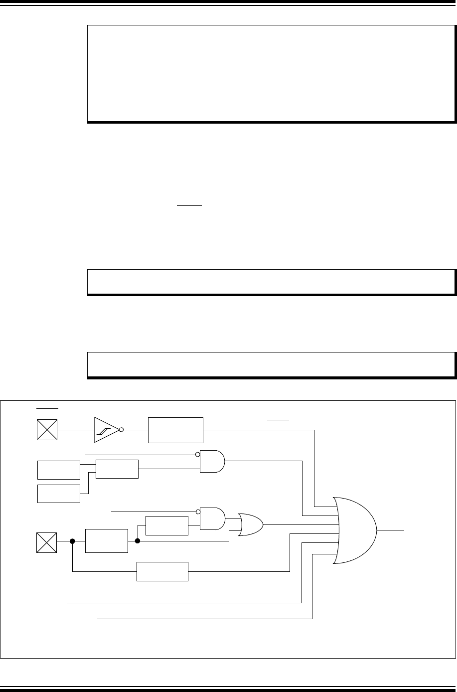
PIC32 Family Reference Manual
DS60001118G-page 7-2 © 2007-2013 Microchip Technology Inc.
7.1 INTRODUCTION
The Resets module combines all reset sources and controls the system reset signal SYSRST.
The following is a list of device Reset sources:
•Power-on Reset (POR)
•Brown-out Reset (BOR)
•Master Clear Reset (MCLR)
•Watchdog Time-out Reset (WDTR)
•Software Reset (SWR)
•Configuration Mismatch Reset (CMR)
•Deadman Timer Reset (DMTR)
A simplified block diagram of the Reset module is shown in Figure 7-1. Any active source of reset
will make the system reset signal active. Many registers associated with the CPU and peripherals
are forced to a known “reset state”. Most registers are unaffected by a reset; their status is
unknown on POR and unchanged by all other resets.
Figure 7-1: System Reset Block Diagram
Note: This family reference manual section is meant to serve as a complement to device
data sheets. Depending on the device variant, this manual section may not apply to
all PIC32 devices.
Please consult the note at the beginning of the “Resets” chapter in the current
device data sheet to check whether this document supports the device you are
using.
Device data sheets and family reference manual sections are available for
download from the Microchip Worldwide Web site at: http://www.microchip.com
Note: Not all reset sources exist on all devices. Refer to the “Resets” chapter in the
specific device data sheet to determine availability.
Note: For register reset states, refer to the specific peripheral or Section 2. “CPU”
(DS60001113) of the “PIC32 Family Reference Manual”.
MCLR
VDD
VDD Rise
Detect
POR
Sleep or Idle
DMT(1)
Time-out
Glitch Filter
BOR
Configuration
SYSRST
Software Reset
Power-up
Timer
Voltage Regulator Enabled
Reset
DMTR/WDTR
SWR
CMR
MCLR
Mismatch
NMI(1)
Time-out
WDT
Time-out
Brown-out
Reset
Note 1: This feature is not available on all devices. Refer to the “Resets” chapter in the specific device data sheet for
availability.

© 2007-2013 Microchip Technology Inc. DS60001118G-page 7-3
Section 7. Resets
Resets
7
7.2 CONTROL REGISTERS
Most types of device resets will set corresponding Status bits in the RCON register to indicate
the type of Reset (see Register 7-1). The one exception is the Non-maskable Interrupt (NMI)
time-out Reset, which is only available on certain devices (refer to the “Resets” chapter of the
specific device data sheet for availability). A Power-on Reset (POR) will clear all bits, except for
the BOR and POR bits (RCON<1:0>), which are set. The user software may set or clear any of
the bits at any time during code execution. The RCON bits serve only as Status bits. Setting a
particular Reset status bit in software will not cause a system Reset to occur.
The RCON register also has other bits associated with the Watchdog Timer (WDT) and device
power-saving states. For more information on the function of these bits, refer to 7.4.3 “Using the
RCON Status Bits”.
The RSWRST control register has only one bit, SWRST. This bit is used to force a software Reset
condition.
For those devices that have the NMI Reset, it becomes possible to delay either the WDT or DMT
Reset events by vectoring to a NMI instead of immediately forcing a reset. A delay equal to the
duration of the number of NMICNT system clocks begins as it is decremented to zero. During this
interval, the program can clear the WDT or DMT flag bits, if desired, to avoid a Reset. If the active
flag is not cleared, the device will be reset at the end of the interval. The NMICNT value can be
set to zero for no delay and up to 255 SYSCLK cycles.
The NMI interrupt can also be triggered by setting the SWNMI bit in software, or if the CF bit is
set by the FSCM, but these do not begin the countdown and do not automatically lead to a reset.
The PWRCON register, available on some PIC32 devices, provides an alternate location of the
VREGS bit, if it is not available in the RCON register.
The Resets module consists of the following Special Function Registers (SFRs):
•RCON: Reset Control Register
•RSWRST: Software Reset Register
•RNMICON: Non-Maskable Interrupt (NMI) Control Register
•PWRCON: Power Control Register

PIC32 Family Reference Manual
DS60001118G-page 7-4 © 2007-2013 Microchip Technology Inc.
Tabl e 7-1 summarizes all Resets-related registers. Corresponding registers appear after the summary, followed by a detailed description
of each register.
Table 7-1: Reset SFR Summary
Name Bit
Range Bit 31/15 Bit 30/14 Bit 29/13 Bit 28/12 Bit 27/11 Bit 26/10 Bit 25/9 Bit 24/8 Bit 23/7 Bit 22/6 Bit 21/5 Bit 20/4 Bit 19/3 Bit 118/2 Bit 17/1 Bit 16/0
RCON(1)
31:24 — — — — BCFGERR BCFGFAIL ——————————
23:16 — — — — — — CMR VREGS EXTR SWR DMTO WDTO SLEEP IDLE BOR POR
RSWRST(1)
31:24 — — — — — — — — — — — — — — — —
23:16 — — — — — — — — — — — — — — — SWRST
RNMICON(1)
31:24 — — — — — — DMTO WDTO SWNMI —————CF WDTS
23:16 — — — — — — — — — NMICNT<7:0>
PWRCON(1)
31:24 — — — — — — — — — — — — — — — —
23:16 — — — — — — — — — — — — — — — VREGS
Legend: — = unimplemented, read as ‘0’. Address offset values are shown in hexadecimal.
Note 1: This register has an associated Clear, Set, and Invert register at an offset of 0x4, 0x8, and 0xC bytes, respectively. The Clear, Set, and Invert registers have the same name with
CLR, SET, or INV appended to the register name (e.g., RCONCLR). Writing a ‘1’ to any bit position in these registers will clear, set, or invert valid bits in the associated register.
Reads from these registers should be ignored.

© 2007-2013 Microchip Technology Inc. DS60001118G-page 7-5
Section 7. Resets
Resets
7
Register 7-1: RCON: Reset Control Register
Bit
Range
Bit
31/23/15/7
Bit
30/22/14/6
Bit
29/21/13/5
Bit
28/20/12/4
Bit
27/19/11/3
Bit
26/18/10/2
Bit
25/17/9/1
Bit
24/16/8/0
31:24 U-0 U-0 U-0 U-0 RW-0, HC R/W-0, HC U-0 U-0
— — — — BCFGERR(4) BCFGFAIL(4) — —
23:16 U-0 U-0 U-0 U-0 U-0 U-0 U-0 U-0
— — — — — — — —
15:8 U-0 U-0 U-0 U-0 U-0 U-0 R/W-x R/W-x
— — — — — — CMR(1,3) VREGS(4)
7:0 R/W-0 R/W-0 R/W-0, HS R/W-0 R/W-0 R/W-0 R/W-1 R/W-1
EXTR(1,3) SWR(1,3) DMTO(4) WDTO(1,3) SLEEP(1,3) IDLE(1,3) BOR(1,2,3) POR(1,2,3)
Legend: U = Unimplemented bit, read as ‘0’
R = Readable bit W = Writable bit HC = Cleared by hardware
-n = Value at POR ‘1’ = Bit is set ‘0’ = Bit is cleared x = Bit is unknown
bit 31-28 Unimplemented: Read as ‘0’
bit 27 BCFGERR: Primary Configuration Registers Error Flag bit(4)
1 = An error occurred during a read of the primary configuration from registers
0 = No error occurred during a read of the primary configuration from registers
bit 26 BCFGFAIL: Primary/Secondary Configuration Registers Error Flag bit(4)
1 = An error occurred during a read of the primary and alternate configuration registers
0 = No error occurred during a read of the primary and alternate configuration registers
bit 25-10 Unimplemented: Read as ‘0’
bit 9 CMR: Configuration Mismatch Flag bit(1,3)
1 = A configuration mismatch reset has occurred
0 = A configuration mismatch reset has not occurred
bit 8 VREGS: Voltage Regulator Standby Enable bit
1 = The voltage regulator is enabled and is on during Sleep mode
0 = The voltage regulator is disabled and is off during Sleep mode
bit 7 EXTR: External Reset (MCLR) Pin Flag bit(1,3)
1 = A master clear (pin) reset has occurred
0 = A master clear (pin) reset has not occurred
bit 6 SWR: Software Reset Flag bit(1,3)
1 = A software reset was executed
0 = A software reset was not executed
bit 5 DMTO: Deadman Timer Time-out Flag bit(4)
1 = A Deadman Timer time-out has occurred
0 = A Deadman Timer time-out has not occurred
bit 4 WDTO: Watchdog Timer Time-out Flag bit(1,3)
1 = A Watchdog Timer time-out has occurred
0 = A Watchdog Timer time-out has not occurred
bit 3 SLEEP: Wake From Sleep Flag bit(1,3)
1 = The device was in Sleep mode
0 = The device was not in Sleep mode
Note 1: The RCON flag bits only serve as status bits. Setting a particular reset status bit in software will not cause
a device Reset to occur.
2: The BOR bit is also set after a Power-on Reset (POR).
3: This bit is set in hardware; it can only be cleared (= 0) in software.
4: This bit is not available on all devices. Refer to the “Resets” chapter in the specific device data sheet for
availability.

PIC32 Family Reference Manual
DS60001118G-page 7-6 © 2007-2013 Microchip Technology Inc.
bit 2 IDLE: Wake From Idle Flag bit(1,3)
1 = The device was in Idle mode
0 = The device was not in Idle mode
bit 1 BOR: Brown-out Reset Flag bit(1,2,3)
User software must clear this bit to view next detection.
1 = A Brown-out Reset has occurred
0 = A Brown-out Reset has not occurred
bit 0 POR: Power-on Reset Flag bit(1,2,3)
User software must clear this bit to view next detection.
1 = A Power-on Reset has occurred
0 = A Power-on Reset has not occurred
Register 7-1: RCON: Reset Control Register (Continued)
Note 1: The RCON flag bits only serve as status bits. Setting a particular reset status bit in software will not cause
a device Reset to occur.
2: The BOR bit is also set after a Power-on Reset (POR).
3: This bit is set in hardware; it can only be cleared (= 0) in software.
4: This bit is not available on all devices. Refer to the “Resets” chapter in the specific device data sheet for
availability.

© 2007-2013 Microchip Technology Inc. DS60001118G-page 7-7
Section 7. Resets
Resets
7
Register 7-2: RSWRST: Software Reset Register
Bit
Range
Bit
31/23/15/7
Bit
30/22/14/6
Bit
29/21/13/5
Bit
28/20/12/4
Bit
27/19/11/3
Bit
26/18/10/2
Bit
25/17/9/1
Bit
24/16/8/0
31:24 U-0 U-0 U-0 U-0 U-0 U-0 U-0 U-0
— — — — — — — —
23:16 U-0 U-0 U-0 U-0 U-0 U-0 U-0 U-0
— — — — — — — —
15:8 U-0 U-0 U-0 U-0 U-0 U-0 U-0 U-0
— — — — — — — —
7:0 U-0 U-0 U-0 U-0 U-0 U-0 U-0 W-0
— — — — — — — SWRST(1)
Legend:
R = Readable bit W = Writable bit U = Unimplemented bit, read as ‘0’
-n = Value at POR ‘1’ = Bit is set ‘0’ = Bit is cleared x = Bit is unknown
bit 31-1 Unimplemented: Read as ‘0’
bit 0 SWRST: Software Reset Trigger bit(1)
1 = Enable software Reset event
0 = No effect
Note 1: The system unlock sequence must be performed before the SWRST bit can be written. A read must follow
the write of this bit to generate a Reset. See 7.3.4 “Software Reset (SWR)” for more information.

PIC32 Family Reference Manual
DS60001118G-page 7-8 © 2007-2013 Microchip Technology Inc.
Register 7-3: RNMICON: Non-Maskable Interrupt (NMI) Control Register
Bit
Range
Bit
31/23/15/7
Bit
30/22/14/6
Bit
29/21/13/5
Bit
28/20/12/4
Bit
27/19/11/3
Bit
26/18/10/2
Bit
25/17/9/1
Bit
24/16/8/0
31:24 U-0 U-0 U-0 U-0 U-0 U-0 R/W-0 R/W-0
— — — — — — DMTO WDTO
23:16 R/W-0 U-0 U-0 U-0 U-0 U-0 R/W-0 R/W-0
SWNMI — — — — — CF WDTS
15:8 U-0 U-0 U-0 U-0 U-0 U-0 U-0 U-0
— — — — — — — —
7:0 U-0 U-0 U-0 U-0 U-0 U-0 U-0 U-0
NMICNT<7:0>
Legend:
R = Readable bit W = Writable bit U = Unimplemented bit, read as ‘0’
-n = Value at POR ‘1’ = Bit is set ‘0’ = Bit is cleared x = Bit is unknown
bit 31-26 Unimplemented: Read as ‘0’
bit 25 DMTO: Deadman Timer Time-out Flag bit
1 = DMT time-out has occurred and caused a NMI
0 = DMT time-out has not occurred
Setting this bit will cause a DMT NMI event, and NMICNT will begin counting.
bit 24 WDTO: Watchdog Timer Time-Out Flag bit
1 = WDT time-out has occurred and caused a NMI
0 = WDT time-out has not occurred
Setting this bit will cause a WDT NMI event, and MNICNT will begin counting.
bit 23 SWNMI: Software NMI Trigger
1 = An NMI will be generated
0 = An NMI will not be generated
bit 22-18 Unimplemented: Read as ‘0’
bit 17 CF: Clock Fail Detect bit
1 = FSCM has detected clock failure and caused an NMI
0 = FSCM has not detected clock failure
Setting this bit will cause a a CF NMI event, but will not cause a clock switch to the Back-up FRC.
bit 16 WDTS: Watchdog Timer Time-out in Sleep Mode Flag bit
1 = WDT time-out has occurred during Sleep mode and caused a wake-up from sleep
0 = WDT time-out has not occurred during Sleep mode
Setting this bit will cause a WDT NMI.
bit 15-8 Unimplemented: Read as ‘0’
bit 7-0 NMICNT<7:0>: NMI Reset Counter Value bits
These bits specify the reload value used by the NMI reset counter.
11111111-00000001 = Number of SYSCLK cycles before a device Reset occurs(1)
00000000 = No delay between NMI assertion and device Reset event
Note 1: If a Watchdog Timer NMI event (when not in Sleep mode) or a Deadman Timer NMI event is cleared
before this counter reaches ‘0’, no device Reset is asserted. This NMI reset counter is only applicable to
these two specific NMI events.
Note: This register is not available on all devices. Refer to the “Resets” chapter in the specific device data sheet
for availability.

© 2007-2013 Microchip Technology Inc. DS60001118G-page 7-9
Section 7. Resets
Resets
7
Register 7-4: PWRCON: Power Control Register
Bit
Range
Bit
31/23/15/7
Bit
30/22/14/6
Bit
29/21/13/5
Bit
28/20/12/4
Bit
27/19/11/3
Bit
26/18/10/2
Bit
25/17/9/1
Bit
24/16/8/0
31:24 U-0 U-0 U-0 U-0 U-0 U-0 U-0 U-0
— — — — — — — —
23:16 U-0 U-0 U-0 U-0 U-0 U-0 U-0 U-0
— — — — — — — —
15:8 U-0 U-0 U-0 U-0 U-0 U-0 U-0 U-0
— — — — — — — —
7:0 U-0 U-0 U-0 U-0 U-0 U-0 U-0 R/W
— — — — — — — VREGS
Legend:
R = Readable bit W = Writable bit U = Unimplemented bit, read as ‘0’
-n = Value at POR ‘1’ = Bit is set ‘0’ = Bit is cleared x = Bit is unknown
bit 31-1 Unimplemented: Read as ‘0’
bit 0 VERGS: Voltage Regulator Stand-by Enable bit
1 = Voltage regulator will remain active during Sleep
0 = Voltage regulator will go to Stand-by mode during Sleep
Note: This register is not available on all devices. Refer to the “Resets” chapter in the specific device data sheet
for availability.

PIC32 Family Reference Manual
DS60001118G-page 7-10 © 2007-2013 Microchip Technology Inc.
7.3 MODES OF OPERATION
7.3.1 System Reset (SYSRST)
The PIC32 Internal System Reset (SYSRST) can be generated from multiple Reset sources,
such as:
•Power-on Reset (POR)
•Brown-out Reset (BOR)
•Master Clear Reset (MCLR)
•Watchdog Time-out Reset (WDTO)
•Software Reset (SWR)
•Configuration Mismatch Reset (CMR)
•Deadman Timer Reset (DMTR)
A system reset is active at the first POR and asserted until device configuration settings are
loaded and the oscillator clock sources become stable. The system reset is then deasserted
allowing the CPU to start fetching code after eight system clock cycles (SYSCLK).
BOR, MCLR and WDTO resets are asynchronous events, and to avoid SFR and RAM
corruptions, the system reset is synchronized with the system clock. All other reset events are
synchronous.
7.3.2 Power-on Reset (POR)
A power-on event generates an internal POR pulse when a VDD rise is detected above VPOR.
The device supply voltage characteristics must meet the specified starting voltage and rise rate
requirements to generate the POR pulse. In particular, VDD must fall below VPOR before a new
POR is initiated. For more information on the VPOR and VDD rise-rate specifications, refer to the
“Electrical Characteristics” chapter of the specific device data sheet.
For those PIC32 devices that have the on-chip voltage regulator enabled, the Power-up Timer
(PWRT) is automatically disabled. For those PIC32 devices that have the on-chip voltage
regulator disabled, the core is supplied from an external power supply and the Power-up Timer
is automatically enabled and is used to extend the duration of a power-up sequence. The PWRT
adds a fixed 64 ms nominal delay at device start-up. Therefore, the Power-on delay can either
be the on-chip voltage regulator output delay, designated as TPU, or the power-up timer delay,
designated as TPWRT.
At this point the POR event has expired, but the device Reset is still asserted while device
configuration settings are loaded and the clock oscillator sources are configured. The clock
monitoring circuitry waits for the oscillator source to become stable. The clock source used
by PIC32 devices when exiting from Reset, is always selected from the FNOSC<2:0> bits
(DEVCFG1<2:0>). This additional delay depends on the clock and can include delays for
TOSC, TLOCK and TFSCM. For details on the oscillator, PLL and Fail-Safe Clock Monitoring
(FSCM). Depending on your device, refer to either 6.3.5 “Fail-Safe Clock Monitor
Operation” in Section 6. “Oscillator” (DS60001112) or 42.3.6 “Fail-Safe Clock Monitor
Operation” in Section 42. “Oscillators with Enhanced PLL”.
After these delays expire, the system reset, SYSRST, i s d eas se rte d. Bef or e a llo wi ng the CP U to
start code execution, eight system clock cycles are required before the synchronized reset to the
CPU core is deasserted.
The power-on event sets the BOR and POR status bits (RCON<1:0>).
For more information on the values of the delay parameters, refer to the “Electrical
Characteristics” chapter in the specific device data sheet.
Note: When the device exits the Reset condition (begins normal operation), the device
operating parameters (voltage, frequency, temperature, etc.) must be within their
operating ranges; otherwise, the device will not function correctly. The user software
must ensure that the delay between the time power is first applied and the time the
system reset is released is adequate to get all operating parameters within the
specification.

© 2007-2013 Microchip Technology Inc. DS60001118G-page 7-11
Section 7. Resets
Resets
7
7.3.3 Master Clear Reset (MCLR)
Whenever the master clear pin (MCLR) is driven low, the reset event is synchronized with the
system clock, SYSCLK, before asserting the system reset, SYSRST, provided the input pulse on
MCLR is longer than a certain minimum width, as specified in the “Electrical Characteristics”
chapter of the specific device data sheet.
The MCLR pin provides a filter to minimize the effects of noise and to avoid unwanted reset
events. The Status bit, EXTR (RCON<7>), is set to indicate the MCLR Reset.
7.3.4 Software Reset (SWR)
The PIC32 CPU core does not provide a specific RESET instruction; however, a hardware reset
can be performed in software (software reset) by executing a software reset command
sequence. The software reset acts like a MCLR Reset. The software reset sequence requires the
system unlock sequence to be executed before the SWRST bit (RSWRST<0>) can be written.
For system unlock details, see either 6.3.6 “Clock Switching Operation” in Section 6.
“Oscillator” (DS60001112) or 42.3.7 “Clock Switching Operation” in Section 42.
“Oscillators with Enhanced PLL”.
A software Reset is performed as follows:
1. Write the system unlock sequence.
2. Set the SWRST bit (RSWRST<0>) = 1.
3. Read the RSWRST register.
Follow with “while(1);” or four “NOP” instructions.
Writing a ‘1’ to the RSWRST register sets the SWRST bit, arming the software reset. The sub-
sequent read of the RSWRST register triggers the software reset, which should occur on the next
clock cycle following the read operation. To ensure no other user code is executed before the
reset event occurs, it is recommended that four “NOP” instructions or a “while(1);” statement
is placed after the READ instruction.
The SWR Status bit (RCON<6>) is set to indicate the software reset.
Example 7-1: Software Reset Command Sequence
7.3.5 Watchdog Timer Reset (WDTR)
A Watchdog Timer (WDT) reset event is synchronized with the system clock, SYSCLK, before
asserting the system reset.
The only bits affected are WDTO, and SLEEP or IDLE in the RCON register. For more information
on the WDT reset, refer to Section 9. “Watchdog Timer and Power-up Timer” (DS60001114).
Note: A WDT time-out during Sleep or Idle mode will wake-up the processor and branch to
the PIC32 reset vector, but does not Reset the processor.
/* The following code illustrates a software Reset */
// assume interrupts are disabled
// assume the DMA controller is suspended
// assume the device is locked
/* perform a system unlock sequence */
// starting critical sequence
SYSKEY = 0x00000000; //write invalid key to force lock
SYSKEY = 0xAA996655; //write key1 to SYSKEY
SYSKEY = 0x556699AA; //write key2 to SYSKEY
// OSCCON is now unlocked
/* set SWRST bit to arm reset */
RSWRSTSET = 1;
/* read RSWRST register to trigger reset */
unsigned int dummy;
dummy = RSWRST;
/* prevent any unwanted code execution until reset occurs*/
while(1);

PIC32 Family Reference Manual
DS60001118G-page 7-12 © 2007-2013 Microchip Technology Inc.
7.3.6 Brown-out Reset (BOR)
PIC32 family devices have a simple Brown-out Reset (BOR) capability. If the voltage supplied to
the regulator is inadequate to maintain a regulated level, the regulator Reset circuitry will generate
a BOR event, which is synchronized with the system clock, SYSCLK, before asserting the system
Reset. This event is captured by the BOR flag bit (RCON<1>). Refer to the “Electrical
Characteristics” chapter of the specific device data sheet for further details.
7.3.7 Configuration Mismatch Reset (CMR)
To mai ntain t h e i nt egr ity o f the st o re d c on fig uration values, all device Configuration bits are
loaded and implemented as a complementary set of bits. As the Configuration Words are being
loaded, for each bit loaded as ‘1’, a complementary value of ‘0’ is stored into its corresponding
background word location and vice versa. The bit pairs are compared every time the
Configuration Words are loaded, including Sleep mode. During this comparison, if the
Configuration bit values are not found opposite to each other, a configuration mismatch event is
generated, which causes a device Reset.
If a device Reset occurs as a result of a configuration mismatch, the CMR Status bit (RCON<9>) is
set.
7.3.8 Deadman Timer Reset (DMTR)
A Deadman Timer (DMT) reset is generated when the DMT count has expired.
The primary function of the DMT is to reset the processor in the event of a software malfunction. The
DMT is a free-running instruction fetch timer, which is clocked whenever an instruction fetch occurs
until a count match occurs. Instructions are not fetched when the processor is in Sleep mode.
The DMT consists of a 32-bit counter with a time-out count match value as specified by the
DMTCNT<3:0> bits in the DEVCFG1 Configuration register.
A DMT is typically used in mission critical and safety critical applications, where any single failure of
the software functionality and sequencing must be detected.
7.3.9 Non-maskable Interrupt (NMI) Timer
The NMI timer provides a delay between DMT or WDT events and a device Reset. Set the delay in
System Clock counts from 0 to 255 in the NMICNT<7:0> (RNMICON<7:0>) bits. If these bits are set
to zero, there will be no delay between the DMTO or WDTO flag and a device Reset. If set to a
non-zero value, the NMI interrupt has that number of system clocks to clear flags or save data for
debugging purposes.
The DMTO flag will be set if there is a DMT event. The DMTO flag can be cleared in software during
the NMI counter interval. If the DMTO flag is not cleared, the device will be reset after the NMI
counter expires.
The WDTO flag will be set if there is a WDT event. The WDTO flag can be cleared in software during
the NMI counter interval. If the WDTO flag is not cleared, the device will be reset after the NMI
counter expires.
The WDTS flag will be set if there is a WDT event during Sleep mode. The WDTS flag will trigger
the NMI interrupt, but will not start the NMI counter, nor cause a reset.
The CF (RNMICON<17>) bit may be set by the Fail-Safe Clock Monitor (FSCM) if there a clock
failure is detected. The CF flag will trigger the NMI interrupt, but will not start the timer, nor cause a
reset.
The SWNMI (RNMICON<23>) bit can be set in software to cause a NMI interrupt, but will not start
the NMI counter, nor cause a reset.
Note: This feature is not available on all devices. Refer to the “Resets” chapter in the
specific device data sheet to determine availability.

© 2007-2013 Microchip Technology Inc. DS60001118G-page 7-13
Section 7. Resets
Resets
7
7.3.10 Determining the Source of Device Reset
After a device Reset, the RCON register can be examined by initialization code to confirm the
source of the reset. In certain applications, this information can be used to take appropriate
action to correct the problem that caused the reset to occur.
All reset status bits in the RCON register should be cleared after reading them to ensure the
RCON value will provide meaningful results after the next device Reset.
Example 7-2 illustrates how to determine the source of device Reset using the RCON register.
Example 7-2: Determining the Source of Device Reset
int main(void)
{
//... perform application specific startup tasks
// next, check the cause of the Reset
if(RCON & 0x0003)
{
// execute a Power-on Reset handler
// ...
}
else if(RCON & 0x0002)
{
// execute a Brown-out Reset handler
// ...
}
else if(RCON & 0x0080)
{
// execute a Master Clear Reset handler
// ...
}
else if(RCON & 0x0040)
{
// execute a Software Reset handler
// ...
}
else if (RCON & 0x0200)
{
// execute a Configuration Mismatch Reset handler
// ...
}
else if (RCON & 0x0010)
{
// execute Watchdog Time-out Reset handler
// ...
}
else if (RCON & 0x0020)
{
// execute Deadman Timer time-out Reset handler
// ...
}
//... perform other application-specific tasks
while(1);
}
PIC32 Family Reference Manual
DS60001118G-page 7-14 © 2007-2013 Microchip Technology Inc.
7.4 EFFECTS OF VARIOUS RESETS
The Reset value for the Reset Control register, RCON, will depend on the type of device Reset,
as indicated in Ta bl e 7-2.
7.4.1 Special Function Register (SFR) Reset States
Most of the SFRs associated with the PIC32 CPU and peripherals are reset to a particular value
at a device Reset. Reset values are specified in Ta bl e 7-2.
The reset value for the Reset Control register, RCON, will depend on the type of device reset.
7.4.2 Configuration Word Register Reset States
All Reset conditions force the configuration settings to be reloaded. The POR sets all the
Configuration Word register locations to a ‘1’ before loading the configuration settings. For all
other Reset conditions, the Configuration Word register locations are not reset prior to being
reloaded. This difference in behavior accommodates MCLR assertions during Debug mode
without affecting the state of the debug operations.
Independent of the source of a reset, the system clock is always reloaded and is specified by the
FNOSC<2:0> bits (DEVCFG<2:0>). When the device is executing code, the user software may
change the primary system clock source by using the OSCCON register. For more information,
refer to Section 6. “Oscillator” (DS60001112) or Section 42. “Oscillators with Enhanced
PLL”.
Table 7-2: Status Bits, Their Significance and the Initialization Condition for RCON Register
Condition Program
Counter
EXTR
SWR
WDTO
DMTO
SLEEP
IDLE
CMR
BOR
POR
Power-on Reset 0xBFC0_0000 000000011
Brown-out Reset 00000001 u
MCLR Reset during Run Mode 1u u u u u u u u
MCLR Reset during Idle Mode 1uuuu 1(1) u u u
MCLR Reset during Sleep Mode 1uu u 1(1) u u u u
Software Reset Command u1uuuuuuu
Configuration Word Mismatch Reset uuuuuu1uu
WDT Time-out Reset during Run Mode uu1uuuuuu
WDT Time-out Reset during Idle Mode u u 1 u u 1(1) u u u
WDT Time-out Reset during Sleep Mode u u 1 u 1(1) u u u u
DMT Time-out Reset uuu1uuuuu
Interrupt Exit from Idle Mode Vector u u u u u 1(1))u u u
Interrupt Exit from Sleep Mode u u u u 1(1) u u u u
Legend: u = unchanged
Note 1: SLEEP and IDLE bits states are defined by previously executed WAIT instructions.

© 2007-2013 Microchip Technology Inc. DS60001118G-page 7-15
Section 7. Resets
Resets
7
7.4.3 Using the RCON Status Bits
The user software can read the RCON register after any system Reset to determine the cause
of the reset. Ta b l e 7-3 provides a summary of the reset flag bit operation.
Table 7-3: Reset Flag Bit Operation
7.4.4 Device Reset to Code Execution Start Time
The delay between the end of a reset event and when the device actually begins to execute code
is determined by two main factors: the type of reset, and the system clock source coming out of the
reset. The code execution start time for various types of device resets are summarized in Ta ble 7-4.
Individual delays are characterized in the “Electrical Characteristics” chapter of the specific
device data sheet.
Note: The Status bits in the RCON register should be cleared after they are read so that
the next RCON register value after a device Reset will be meaningful.
Flag Bit(1) Set by Cleared by
POR (RCON<0>) POR User Software
BOR (RCON<1>) POR, BOR User Software
EXTR (RCON<7>) MCLR Reset User Software, POR, BOR
SWR (RCON<6>) Software Reset command User Software, POR, BOR
CMR (RCON<9>) Configuration mismatch User Software, POR, BOR
WDTO (RCON<4>) WDT time-out User Software, POR, BOR
DMTO (RCON<5> DMT time-out User Software, POR, BOR
SLEEP (RCON<3>) WAIT instruction User Software, POR, BOR
IDLE (RCON<2>) WAIT instruction User Software, POR, BOR
Note 1: All reset flag bits may be set or cleared by the user software.
Table 7-4: Code Execution Start Time for Various Device Resets
Reset
Type Clock Source Power-Up Delay(1,2,3,4)
System
Clock
Delay(1,5,6)
FSCM
Delay(1,7)
POR EC, FRC, FRCDIV, LPRC (TPU OR TPWRT) + TSYSDLY — —
ECPLL, FRCPLL (TPU OR TPWRT) + TSYSDLY TLOCK TFSCM
XT, HS, SOSC (TPU OR TPWRT) + TSYSDLY TOST TFSCM
XTPLL, HSPLL (TPU OR TPWRT) + TSYSDLY TOST + TLOCK TFSCM
BOR EC, FRC, FRCDIV, LPRC TSYSDLY — —
ECPLL, FRCPLL TSYSDLY TLOCK TFSCM
XT, HS, SOSC TSYSDLY TOST TFSCM
XTPLL TSYSDLY TOST + TLOCK TFSCM
MCLR,
CMR,
SWR,
WDTO,
DMTO
Any Clock TSYSDLY — —
Note 1: For parameter specifications, see the “Electrical Characteristics” chapter of the specific
device data sheet.
2: TPU = Power-up Period with on-chip regulator enabled.
3: TPWRT = Power-up Period (Power-up Timer) with on-chip regulator disabled.
4: TSYSDLY = Time required to reload Device Configuration Fuses plus eight SYSCLK cycles.
5: TOST = Oscillator Start-up Timer.
6: TLOCK = PLL lock time.
7: TFSCM = Fail-Safe Clock Monitor delay.

PIC32 Family Reference Manual
DS60001118G-page 7-16 © 2007-2013 Microchip Technology Inc.
7.5 RELATED APPLICATION NOTES
This section lists application notes that are related to this section of the manual. These
application notes may not be written specifically for the PIC32 device family, but the concepts are
pertinent and could be used with modification and possible limitations. The current application
notes related to Resets are:
Title Application Note #
No related application notes at this time. N/A
Note: Please visit the Microchip web site (www.microchip.com) for additional application
notes and code examples for the PIC32 family of devices.

© 2007-2013 Microchip Technology Inc. DS60001118G-page 7-17
Section 7. Resets
Resets
7
7.6 REVISION HISTORY
Revision A (September 2007)
• This is the initial released version of this document.
Revision B (October 2007)
•Updated document to remove Confidential status.
Revision C (April 2008)
•Revised status to Preliminary; Revised U-0 to r-x.
Revision D (June 2008)
•Revised Figure 7-2; Deleted Figure 7-3; Revised Sections 7.3.2, 7.3.3, 7.3.4; Revised
Tabl e 7 -4; D ele te Fig ure 7. 2 a nd 7. 3 ; Cha nge Re served bits from “Maintain as” to “Write”.
Revision E (July 2008)
•Revised Section 7.3.2, 7.3.3, 7.3.6, 7.4.4.
Revision F (October 2011)
This revision includes the following updates:
•Added a Note at the beginning of the section, which provides information on the
complementary documentation
• Changed the document running header from PIC32MX Family Reference Manual to PIC32
Family Reference Manual
• Changed all occurrences of PIC32MX to PIC32
•Removed the following Clear, Set and Invert registers:
-RCONCLR: Reset Control Clear Register
-RCONSET: Reset Control Set Register
-RONINV: Reset Control Invert Register
- RSWRSTCLR: Software Reset Clear Register
-RSWRSTSET: Software Reset Set Register
-RSWRSTINV: Software Reset Invert Register
•Added Notes to Register 7-1 and Register 7-2 describing their corresponding Set, Clear
and Invert registers
• Updated all r-x bits as U-0 bits in Register 7-1 and Register 7-2
•Updated Example 7-1
•Relocated and renamed 7.5 “Design Tips” to 7.3.8 “Determining the Source of Device
Reset”
•Modifications to register formatting and minor text updates have been made throughout the
document

PIC32 Family Reference Manual
DS60001118G-page 7-18 © 2007-2013 Microchip Technology Inc.
Revision G (November 2013)
This revision includes the following updates:
•The document was updated to include Deadman Timer information
•Updated the system reset block diagram (see Figure 7-1)
•Updated the Reset SFR Summary (see Tabl e 7-1)
•Added new paragraphs describing the Non-maskable Interrupt Reset (see 7.2 “Control
Registers”)
•Updated the Reset Control Register (see Register 7-1)
•Updated the Software Reset Register (see Register 7-2)
•Added the Non-Maskable Interrupt (NMI) register (see Register 7-3)
•Added the Power Control Register (see Register 7-4)
•Added the WDTO Status bit and Reset information toTa bl e 7-2,Tab le 7-3, and Ta b le 7-4
•Added 7.3.8 “Deadman Timer Reset (DMTR)”
•Added 7.3.9 “Non-maskable Interrupt (NMI) Timer”
•Updated Example 7-2: Determining the Source of Device Reset
•Minor updates to text and formatting were incorporated throughout the document

2007-2013 Microchip Technology Inc. DS60001118G-page 7-19
Information contained in this publication regarding device
applications and the like is provided only for your convenience
and may be superseded by updates. It is your responsibility to
ensure that your application meets with your specifications.
MICROCHIP MAKES NO REPRESENTATIONS OR
WARRANTIES OF ANY KIND WHETHER EXPRESS OR
IMPLIED, WRITTEN OR ORAL, STATUTORY OR
OTHERWISE, RELATED TO THE INFORMATION,
INCLUDING BUT NOT LIMITED TO ITS CONDITION,
QUALITY, PERFORMANCE, MERCHANTABILITY OR
FITNESS FOR PURPOSE. Microchip disclaims all liability
arising from this information and its use. Use of Microchip
devices in life support and/or safety applications is entirely at
the buyer’s risk, and the buyer agrees to defend, indemnify and
hold harmless Microchip from any and all damages, claims,
suits, or expenses resulting from such use. No licenses are
conveyed, implicitly or otherwise, under any Microchip
intellectual property rights.
Trademarks
The Microchip name and logo, the Microchip logo, dsPIC,
FlashFlex, KEELOQ, KEELOQ logo, MPLAB, PIC, PICmicro,
PICSTART, PIC32 logo, rfPIC, SST, SST Logo, SuperFlash
and UNI/O are registered trademarks of Microchip Technology
Incorporated in the U.S.A. and other countries.
FilterLab, Hampshire, HI-TECH C, Linear Active Thermistor,
MTP, SEEVAL and The Embedded Control Solutions
Company are registered trademarks of Microchip Technology
Incorporated in the U.S.A.
Silicon Storage Technology is a registered trademark of
Microchip Technology Inc. in other countries.
Analog-for-the-Digital Age, Application Maestro, BodyCom,
chipKIT, chipKIT logo, CodeGuard, dsPICDEM,
dsPICDEM.net, dsPICworks, dsSPEAK, ECAN,
ECONOMONITOR, FanSense, HI-TIDE, In-Circuit Serial
Programming, ICSP, Mindi, MiWi, MPASM, MPF, MPLAB
Certified logo, MPLIB, MPLINK, mTouch, Omniscient Code
Generation, PICC, PICC-18, PICDEM, PICDEM.net, PICkit,
PICtail, REAL ICE, rfLAB, Select Mode, SQI, Serial Quad I/O,
Tota l E ndu ra nce , T SHA RC , U n iW inD riv er, Wi per Lo c k, ZE NA
and Z-Scale are trademarks of Microchip Technology
Incorporated in the U.S.A. and other countries.
SQTP is a service mark of Microchip Technology Incorporated
in the U.S.A.
GestIC and ULPP are registered trademarks of Microchip
Technology Germany II GmbH & Co. KG, a subsidiary of
Microchip Technology Inc., in other countries.
All other trademarks mentioned herein are property of their
respective companies.
© 2007-2013, Microchip Technology Incorporated, Printed in
the U.S.A., All Rights Reserved.
Printed on recycled paper.
ISBN: 978-1-62077-638-4
Note the following details of the code protection feature on Microchip devices:
• Microchip products meet the specification contained in their particular Microchip Data Sheet.
• Microchip believes that its family of products is one of the most secure families of its kind on the market today, when used in the
intended manner and under normal conditions.
• There are dishonest and possibly illegal methods used to breach the code protection feature. All of these methods, to our
knowledge, require using the Microchip products in a manner outside the operating specifications contained in Microchip’s Data
Sheets. Most likely, the person doing so is engaged in theft of intellectual property.
• Microchip is willing to work with the customer who is concerned about the integrity of their code.
• Neither Microchip nor any other semiconductor manufacturer can guarantee the security of their code. Code protection does not
mean that we are guaranteeing the product as “unbreakable.”
Code protection is constantly evolving. We at Microchip are committed to continuously improving the code protection features of our
products. Attempts to break Microchip’s code protection feature may be a violation of the Digital Millennium Copyright Act. If such acts
allow unauthorized access to your software or other copyrighted work, you may have a right to sue for relief under that Act.
Microchip received ISO/TS-16949:2009 certification for its worldwide
headquarters, design and wafer fabrication facilities in Chandler and
Tempe, Arizona; Gresham, Oregon and design centers in California
and India. The Company’s quality system processes and procedures
are for its PIC® MCUs and dsPIC® DSCs, KEELOQ® code hopping
devices, Serial EEPROMs, microperipherals, nonvolatile memory and
analog products. In addition, Microchip’s quality system for the design
and manufacture of development systems is ISO 9001:2000 certified.
QUALITY MANAGEMENT S
YSTEM
CERTIFIED BY DNV
== ISO/TS 16949 ==

DS60001118G-page 7 -20 2007-2013 Microchip Technology Inc.
AMERICAS
Corporate Office
2355 West Chandler Blvd.
Chandler, AZ 85224-6199
Tel: 480-792-7200
Fax: 480-792-7277
Technical Support:
http://www.microchip.com/
support
Web Address:
www.microchip.com
Atlanta
Duluth, GA
Tel: 678-957-9614
Fax: 678-957-1455
Austin, TX
Tel: 512-257-3370
Boston
Westborough, MA
Tel: 774-760-0087
Fax: 774-760-0088
Chicago
Itasca, IL
Tel: 630-285-0071
Fax: 630-285-0075
Cleveland
Independence, OH
Tel: 216-447-0464
Fax: 216-447-0643
Dallas
Addison, TX
Tel: 972-818-7423
Fax: 972-818-2924
Detroit
Novi, MI
Tel: 248-848-4000
Houston, TX
Tel: 281-894-5983
Indianapolis
Noblesville, IN
Tel: 317-773-8323
Fax: 317-773-5453
Los Angeles
Mission Viejo, CA
Tel: 949-462-9523
Fax: 949-462-9608
New York, NY
Tel: 631-435-6000
San Jose, CA
Tel: 408-735-9110
Canada - Toronto
Tel: 905-673-0699
Fax: 905-673-6509
ASIA/PACIFIC
Asia Pacific Office
Suites 3707-14, 37th Floor
Tower 6, The Gateway
Harbour City, Kowloon
Hong Kong
Tel : 8 52 -24 01- 120 0
Fax: 852-2401-3431
Australia - Sydney
Tel : 6 1- 2-9 868 -67 33
Fax: 61-2-9868-6755
China - Beijing
Tel : 8 6- 10- 856 9-7 00 0
Fax: 86-10-8528-2104
China - Chengdu
Tel : 8 6- 28- 866 5-5 511
Fax: 86-28-8665-7889
China - Chongqing
Tel : 8 6- 23- 898 0-9 58 8
Fax: 86-23-8980-9500
China - Hangzhou
Tel : 8 6- 571 -28 19- 318 7
Fax: 86-571-2819-3189
China - Hong Kong SAR
Tel : 8 52 -29 43- 510 0
Fax: 852-2401-3431
China - Nanjing
Tel : 8 6- 25- 847 3-2 46 0
Fax: 86-25-8473-2470
China - Qingdao
Tel : 8 6- 532 -85 02- 735 5
Fax: 86-532-8502-7205
China - Shanghai
Tel : 8 6- 21- 540 7-5 53 3
Fax: 86-21-5407-5066
China - Shenyang
Tel : 8 6- 24- 233 4-2 82 9
Fax: 86-24-2334-2393
China - Shenzhen
Tel : 8 6- 755 -88 64- 220 0
Fax: 86-755-8203-1760
China - Wuhan
Tel : 8 6- 27- 598 0-5 30 0
Fax: 86-27-5980-5118
China - Xian
Tel : 8 6- 29- 883 3-7 25 2
Fax: 86-29-8833-7256
China - Xiamen
Tel: 86-592-2388138
Fax: 86-592-2388130
China - Zhuhai
Tel : 86- 75 6-3 21 004 0
Fax: 86-756-3210049
ASIA/PACIFIC
India - Bangalore
Tel : 9 1- 80- 309 0-4 44 4
Fax: 91-80-3090-4123
India - New Delhi
Tel : 9 1- 11- 416 0 -8 631
Fax: 91-11-4160-8632
India - Pune
Tel : 9 1- 20- 301 9-1 50 0
Japan - Osaka
Tel : 8 1- 6-6 152 -7 1 60
Fax: 81-6-6152-9310
Japan - Tokyo
Tel : 8 1- 3-6 880 - 377 0
Fax: 81-3-6880-3771
Korea - Daegu
Tel : 8 2- 53- 744 -43 01
Fax: 82-53-744-4302
Korea - Seoul
Tel : 8 2- 2-5 54- 72 0 0
Fax: 82-2-558-5932 or
82-2-558-5934
Malaysia - Kuala Lumpur
Tel : 6 0- 3-6 201 -9 8 57
Fax: 60-3-6201-9859
Malaysia - Penang
Tel : 6 0- 4-2 27- 88 7 0
Fax: 60-4-227-4068
Philippines - Manila
Tel : 6 3- 2-6 34- 90 6 5
Fax: 63-2-634-9069
Singapore
Tel : 6 5- 633 4-8 870
Fax: 65-6334-8850
Taiwan - Hsin Chu
Tel : 8 86 -3- 577 8-3 66
Fax: 886-3-5770-955
Taiwan - Kaohsiung
Tel : 8 86 -7- 213 -78 30
Taiwan - Taipei
Tel : 8 86 -2- 250 8-8 60 0
Fax: 886-2-2508-0102
Thailand - Bangkok
Tel : 6 6- 2-6 94- 13 5 1
Fax: 66-2-694-1350
EUROPE
Austria - Wels
Tel : 4 3- 72 42 -2 244 -3 9
Fax: 43-7242-2244-393
Denmark - Copenhagen
Tel : 4 5- 445 0-2 828
Fax: 45-4485-2829
France - Paris
Tel : 3 3- 1-6 9-5 3-6 3-2 0
Fax: 33-1-69-30-90-79
Germany - Dusseldorf
Tel : 4 9- 21 29 -3 766 400
Germany - Munich
Tel : 4 9- 89 -62 7-1 44- 0
Fax: 49-89-627-144-44
Germany - Pforzheim
Tel : 4 9- 72 31 -4 247 50
Italy - Milan
Tel : 3 9- 03 31 -7 426 11
Fax: 39-0331-466781
Italy - Venice
Tel : 3 9- 04 9- 762 528 6
Netherlands - Drunen
Tel : 3 1- 41 6- 690 399
Fax: 31-416-690340
Poland - Warsaw
Tel : 4 8- 22 -33 257 37
Spain - Madrid
Tel : 3 4- 91 -70 8-0 8-9 0
Fax: 34-91-708-08-91
Sweden - Stockholm
Tel : 4 6- 8-5 090 -46 54
UK - Wokingham
Tel : 4 4- 118 -92 1- 5 800
Fax: 44-118-921-5820
Worldwide Sales and Service
10/28/13

© 2007-2012 Microchip Technology Inc. DS61108G-page 8-1
Interrupts
8
Section 8. Interrupts
HIGHLIGHTS
This section of the manual contains the following topics:
8.1 Introduction................................................................................................................8-2
8.2 Control Registers.......................................................................................................8-3
8.3 Operation................................................................................................................. 8-13
8.4 Single Vector Mode .................................................................................................8-14
8.5 Multi-Vector Modes..................................................................................................8-15
8.6 Interrupt Vector Address Calculation ....................................................................... 8-17
8.7 Interrupt Priorities ....................................................................................................8-19
8.8 Interrupts and Register Sets ....................................................................................8-20
8.9 Interrupt Processing ................................................................................................8-21
8.10 External Interrupts ...................................................................................................8-21
8.11 Temporal Proximity Interrupt Coalescing................................................................. 8-22
8.12 Effects of Interrupts After Reset............................................................................... 8-23
8.13 Operation in Power-Saving and Debug Modes ....................................................... 8-23
8.14 Related Application Notes ....................................................................................... 8-24
8.15 Revision History.......................................................................................................8-25
PIC32 Family Reference Manual
DS61108G-page 8-2 © 2007-2012 Microchip Technology Inc.
8.1 INTRODUCTION
The PIC32 generates interrupt requests in response to interrupt events from peripheral modules.
The Interrupt module exists external to the CPU logic and prioritizes the interrupt events before
presenting them to the CPU.
The PIC32 Interrupts module includes the following features:
•Up to 256 interrupt sources
•Single and Multi-Vector mode operations
•Up to five external interrupts with edge polarity control
•Interrupt proximity timer
• Seven user-selectable priority levels for each vector
• Four user-selectable subpriority levels within each priority
•User-configurable shadow set based on priority level (this feature is not available on all
devices; refer to the “Interrupt Controller” chapter in the specific device data sheet for
availability)
•Software can generate any interrupt
•User-configurable Interrupt Vector Table (IVT) location
•User-configurable interrupt vector spacing
Figure 8-1 shows the block diagram of the Interrupt Controller module.
Figure 8-1: Interrupt Controller Module
Note: This family reference manual section is meant to serve as a complement to device
data sheets. Depending on the device variant, this manual section may not apply to
all PIC32 devices.
Please consult the note at the beginning of the “Interrupt Controller” chapter in
the current device data sheet to check whether this document supports the device
you are using.
Device data sheets and family reference manual sections are available for
download from the Microchip Worldwide Web site at: http://www.microchip.com
Note: Several of the registers cited in this section are not in the Interrupt Controller
module. These registers (and bits) are associated with the CPU. Refer to Section
2. “CPU” (DS61113) for more details.
To avoid confusion, a typographic distinction is made for registers in the CPU. The
register names in this section, and all other sections of this manual, are signified by
uppercase letters only (except for cases in which variables are used). CPU register
names are signified by upper and lowercase letters. For example, INTSTAT is an
Interrupts register; whereas, IntCtl is a CPU register.
Interrupt Controller
Interrupt Requests (Sources)
Vector Number/Offset
CPU Core
Priority Level
Shadow Set Number
© 2007-2012 Microchip Technology Inc. DS61108G-page 8-3
Section 8. Interrupts
Interrupts
8
8.2 CONTROL REGISTERS
The Interrupts module consists of the following Special Function Registers (SFRs):
•INTCON: Interrupt Control Register
•PRISS: Priority Shadow Select Register
•INTSTAT: Interrupt Status Register
•IPTMR: Interrupt Proximity Timer Register
•IFSx: Interrupt Flag Status Register
•IECx: Interrupt Enable Control Register
•IPCx: Interrupt Priority Control Register
•OFFx: Interrupt Vector Address Offset Register
Tabl e 8-1 summarizes all Interrupts-related registers. Corresponding registers appear after the
summary, followed by a detailed description of each register.
Note: Each PIC32 device variant may have one or more Interrupt sources, and depending
on the device variant, the number of sources may be different. An ‘x’ used in the
names of control/status bits and registers denotes that there are multiple registers,
which have the same function, that can define these interrupt sources. Refer to the
specific device data sheet for more details.
Table 8-1: Interrupts Register Summary
Name Bit
Range
Bit
31/23/15/7
Bit
30/22/14/6
Bit
29/21/13/5
Bit
28/20/12/4
Bit
27/19/11/3
Bit
26/18/10/2
Bit
25/17/9/1
Bit
24/16/8/0
INTCON(1) 31:24 — — — — — — — —
23:16
—
VS<6:1>(2) VS<0>(2)
—SS0(2)
15:8 — — — MVEC —TPC<2:0>
7:0 — — — INT4EP INT3EP INT2EP INT1EP INT0EP
PRISS(1) 31:24 PRI7SS<3:0>(2) PRI6SS<3:0>(2)
23:16 PRI5SS<3:0>(2) PRI4SS<3:0>(2)
15:8 PRI3SS<3:0>(2) PRI2SS<3:0>(2)
7:0 PRI1SS<3:0>(2) — — — SS0(2)
INTSTAT(1) 31:24 — — — — — — — —
23:16 — — — — — — — —
15:8 — — — — — SRIPL<2:0>
7:0 — — VEC<5:0>(2)
SIRQ<7:0>(2)
IPTMR(1) 31:24 IPTMR<31:24>
23:16 IPTMR<23:16>
15:8 IPTMR<15:8>
7:0 IPTMR<7:0>
IFSx(1) 31:24 IFS31 IFS30 IFS29 IFS28 IFS27 IFS26 IFS25 IFS24
23:16 IFS23 IFS22 IFS21 IFS20 IFS19 IFS18 IFS17 IFS16
15:8 IFS15 IFS14 IFS13 IFS12 IFS11 IFS10 IFS09 IFS08
7:0 IFS07 IFS06 IFS05 IFS04 IFS03 IFS02 IFS01 IFS00
IECx(1) 31:24 IEC31 IEC30 IEC29 IEC28 IEC27 IEC26 IEC25 IEC24
23:16 IEC23 IEC22 IEC21 IEC20 IEC19 IEC18 IEC17 IEC16
15:8 IEC15 IEC14 IEC13 IEC12 IEC11 IEC10 IEC09 IEC08
7:0 IEC07 IEC06 IEC05 IEC04 IEC03 IEC02 IEC01 IEC00
Legend: — = unimplemented, read as ‘0’.
Note 1: This register has an associated Clear, Set, and Invert register at an offset of 0x4, 0x8, and 0xC bytes, respectively. These registers have
the same name with CLR, SET, or INV appended to the end of the register name (e.g., INTCONCLR). Writing a ‘1’ to any bit position in
these registers will clear valid bits in the associated register. Reads from these registers should be ignored.
2: These bits are not available on all devices. Refer to the “Interrupt Controller” chapter in the specific device data sheet for availability.

PIC32 Family Reference Manual
DS61108G-page 8-4 © 2007-2012 Microchip Technology Inc.
IPCx(1) 31:24 — — — IP03<2:0> IS03<1:0>
23:16 — — — IP02<2:0> IS02<1:0>
15:8 — — — IP01<2:0> IS01<1:0>
7:0 — — — IP00<2:0> IS00<1:0>
OFFx(1) 31:24 — — — — — — — —
23:16 — — — — — — VOFFx<17:16>
15:8 VOFFx<15:8>
7:0 VOFFx<7:0> —
Table 8-1: Interrupts Register Summary (Continued)
Name Bit
Range
Bit
31/23/15/7
Bit
30/22/14/6
Bit
29/21/13/5
Bit
28/20/12/4
Bit
27/19/11/3
Bit
26/18/10/2
Bit
25/17/9/1
Bit
24/16/8/0
Legend: — = unimplemented, read as ‘0’.
Note 1: This register has an associated Clear, Set, and Invert register at an offset of 0x4, 0x8, and 0xC bytes, respectively. These registers have
the same name with CLR, SET, or INV appended to the end of the register name (e.g., INTCONCLR). Writing a ‘1’ to any bit position in
these registers will clear valid bits in the associated register. Reads from these registers should be ignored.
2: These bits are not available on all devices. Refer to the “Interrupt Controller” chapter in the specific device data sheet for availability.

© 2007-2012 Microchip Technology Inc. DS61108G-page 8-5
Section 8. Interrupts
Interrupts
8
Register 8-1: INTCON: Interrupt Control Register
Bit
Range
Bit
31/23/15/7
Bit
30/22/14/6
Bit
29/21/13/5
Bit
28/20/12/4
Bit
27/19/11/3
Bit
26/18/10/2
Bit
25/17/9/1
Bit
24/16/8/0
31:24 U-0 U-0 U-0 U-0 U-0 U-0 U-0 U-0
— — — — — — — —
23:16
U-0 U-0 U-0 R/W-0 R/W-0 R/W-0 R/W-0 R/W-0
—VS<6:1>(1) VS<0>(1)
SS0(1)
15:8 U-0 U-0 U-0 R/W-0 U-0 R/W-0 R/W-0 R/W-0
— — — MVEC —TPC<2:0>
7:0 U-0 U-0 U-0 R/W-0 R/W-0 R/W-0 R/W-0 R/W-0
— — — INT4EP INT3EP INT2EP INT1EP INT0EP
Legend:
R = Readable bit W = Writable bit U = Unimplemented bit P = Programmable bit
-n = Bit Value at POR:(‘0’, ‘1’, x = Unknown)
bit 31-21 Unimplemented: Read as ‘0’
bit 22-16 VS<6:0>: Vector Spacing bits(1)
bit 16 SS0: Single Vector Shadow Register Set bit(1)
1 = Single vector is presented with a shadow register set
0 = Single vector is not presented with a shadow register set
bit 15-13 Unimplemented: Read as ‘0’
bit 12 MVEC: Multi Vector Configuration bit
1 = Interrupt controller configured for multi vectored mode
0 = Interrupt controller configured for single vectored mode
bit 11 Unimplemented: Read as ‘0’
bit 10-8 TPC<2:0>: Interrupt Proximity Timer Control bits
111 = Interrupts of group priority 7 or lower start the Interrupt Proximity timer
110 = Interrupts of group priority 6 or lower start the Interrupt Proximity timer
101 = Interrupts of group priority 5 or lower start the Interrupt Proximity timer
100 = Interrupts of group priority 4 or lower start the Interrupt Proximity timer
011 = Interrupts of group priority 3 or lower start the Interrupt Proximity timer
010 = Interrupts of group priority 2 or lower start the Interrupt Proximity timer
001 = Interrupts of group priority 1 start the Interrupt Proximity timer
000 = Disables Interrupt Proximity timer
bit 7-5 Unimplemented: Read as ‘0’
Note 1: This bit is not available on all devices. Refer to the “Interrupt Controller” chapter in the specific device
data sheet for availability.
Spacing Between Vectors
Bit Value Hexadecimal Decimal
1000000 0x200 512
0100000 0x100 256
0010000 0x080 128
0001000 0x040 64
0000100 0x020 32
0000010 0x010 16
0000001 0x001 8
0000000 0x000 0
Note: All other values are Reserved.

PIC32 Family Reference Manual
DS61108G-page 8-6 © 2007-2012 Microchip Technology Inc.
bit 4 INT4EP: External Interrupt 4 Edge Polarity Control bit
1 = Rising edge
0 = Falling edge
bit 3 INT3EP: External Interrupt 3 Edge Polarity Control bit
1 = Rising edge
0 = Falling edge
bit 2 INT2EP: External Interrupt 2 Edge Polarity Control bit
1 = Rising edge
0 = Falling edge
bit 1 INT1EP: External Interrupt 1 Edge Polarity Control bit
1 = Rising edge
0 = Falling edge
bit 0 INT0EP: External Interrupt 0 Edge Polarity Control bit
1 = Rising edge
0 = Falling edge
Register 8-1: INTCON: Interrupt Control Register (Continued)
Note 1: This bit is not available on all devices. Refer to the “Interrupt Controller” chapter in the specific device
data sheet for availability.

© 2007-2012 Microchip Technology Inc. DS61108G-page 8-7
Section 8. Interrupts
Interrupts
8
Register 8-2: PRISS: Priority Shadow Select Register
Bit
Range
Bit
31/23/15/7
Bit
30/22/14/6
Bit
29/21/13/5
Bit
28/20/12/4
Bit
27/19/11/3
Bit
26/18/10/2
Bit
25/17/9/1
Bit
24/16/8/0
31:24 R/W-0 R/W-0 R/W-0 R/W-0 R/W-0 R/W-0 R/W-0 R/W-0
PRI7SS<3:0> PRI6SS<3:0>
23:16 R/W-0 R/W-0 R/W-0 R/W-0 R/W-0 R/W-0 R/W-0 R/W-0
PRI5SS<3:0> PRI4SS<3:0>
15:8 R/W-0 R/W-0 R/W-0 R/W-0 R/W-0 R/W-0 R/W-0 R/W-0
PRI3SS<3:0> PRI2SS<3:0>
7:0 R/W-0 R/W-0 R/W-0 R/W-0 U-0 U-0 U-0 R/W-0
PRI1SS<3:0> — — — SS0
Legend:
R = Readable bit W = Writable bit U = Unimplemented bit P = Programmable bit
-n = Bit Value at POR: (‘0’, ‘1’, x = Unknown)
bit 31-4 PRIxSS<3:0>: Priority Shadow Select bits
If the MVEC bit in the INTCON register = 1:
1111 = Shadow register set 15 is used for priority level x
1110 = Shadow register set 14 is used for priority level x
•
•
•
0001 = Shadow register set 1 is used for priority level x
0000 = Shadow register set 0 is used for priority level x
bit 3-1 Unimplemented: Read as ‘0’
bit 0 SS0: Single Vector Shadow Register Set bit
1 = Single vector is presented with a shadow register set
0 = Single vector is not presented with a shadow register set
Note: This register is not available on all devices and is cleared on all forms of Reset. Refer to the “Interrupt
Controller” chapter in the specific device data sheet for availability.

PIC32 Family Reference Manual
DS61108G-page 8-8 © 2007-2012 Microchip Technology Inc.
Register 8-3: INTSTAT: Interrupt Status Register
Bit
Range
Bit
31/23/15/7
Bit
30/22/14/6
Bit
29/21/13/5
Bit
28/20/12/4
Bit
27/19/11/3
Bit
26/18/10/2
Bit
25/17/9/1
Bit
24/16/8/0
31:24 U-0 U-0 U-0 U-0 U-0 U-0 U-0 U-0
— — — — — — — —
23:16 U-0 U-0 U-0 U-0 U-0 U-0 U-0 U-0
— — — — — — — —
15:8 U-0 U-0 U-0 U-0 U-0 R-0 R-0 R-0
— — — — — SRIPL<2:0>(1)
7:0
U-0 U-0 R-0 R-0 R-0 R-0 R-0 R-0
— — VEC<5:0>(1,2)
SIRQ<7:0>(2)
Legend:
R = Readable bit W = Writable bit U = Unimplemented bit P = Programmable bit
-n = Bit Value at POR:(‘0’, ‘1’, x = Unknown)
bit 31-11 Unimplemented: Read as ‘0’
bit 10-8 SRIPL<2:0>: Requested Priority Level bits for Single Vector Mode bits(1)
000-111 = The priority level of the latest interrupt presented to the CPU
bit 7-6 Unimplemented: Read as ‘0’
bit 7-0 SIRQ<7:0>: Last Interrupt Request Serviced Status bits
These bits are used to determine the last interrupt request number serviced by the CPU.
bit 5-0 VEC<5:0>: Interrupt Vector bits(1,2)
11111-00000 = The interrupt vector that is presented to the CPU
Note 1: This value should only be used when the interrupt controller is configured for Single Vector mode.
2: These bits are not available on all devices. Refer to the “Interrupts Controller” chapter in the specific
device data sheet for availability.
Register 8-4: IPTMR: Interrupt Proximity Timer Register
Bit
Range
Bit
31/23/15/7
Bit
30/22/14/6
Bit
29/21/13/5
Bit
28/20/12/4
Bit
27/19/11/3
Bit
26/18/10/2
Bit
25/17/9/1
Bit
24/16/8/0
31:24 R/W-0 R/W-0 R/W-0 R/W-0 R/W-0 R/W-0 R/W-0 R/W-0
IPTMR<31:24>
23:16 R/W-0 R/W-0 R/W-0 R/W-0 R/W-0 R/W-0 R/W-0 R/W-0
IPTMR<23:16>
15:8 R/W-0 R/W-0 R/W-0 R/W-0 R/W-0 R/W-0 R/W-0 R/W-0
IPTMR<15:8>
7:0 R/W-0 R/W-0 R/W-0 R/W-0 R/W-0 R/W-0 R/W-0 R/W-0
IPTMR<7:0>
Legend:
R = Readable bit W = Writable bit U = Unimplemented bit P = Programmable bit
-n = Bit Value at POR:(‘0’, ‘1’, x = Unknown)
bit 31-0 IPTMR<31:0>: Interrupt Proximity Timer Reload bits
Used by the Interrupt Proximity Timer as a reload value when the Interrupt Proximity Timer is
triggered by an interrupt event.

© 2007-2012 Microchip Technology Inc. DS61108G-page 8-9
Section 8. Interrupts
Interrupts
8
Register 8-5: IFSx: Interrupt Flag Status Register
Bit
Range
Bit
31/23/15/7
Bit
30/22/14/6
Bit
29/21/13/5
Bit
28/20/12/4
Bit
27/19/11/3
Bit
26/18/10/2
Bit
25/17/9/1
Bit
24/16/8/0
31:24 R/W-0 R/W-0 R/W-0 R/W-0 R/W-0 R/W-0 R/W-0 R/W-0
IFS31 IFS30 IFS29 IFS28 IFS27 IFS26 IFS25 IFS24
23:16 R/W-0 R/W-0 R/W-0 R/W-0 R/W-0 R/W-0 R/W-0 R/W-0
IFS23 IFS22 IFS21 IFS20 IFS19 IFS18 IFS17 IFS16
15:8 R/W-0 R/W-0 R/W-0 R/W-0 R/W-0 R/W-0 R/W-0 R/W-0
IFS15 IFS14 IFS13 IFS12 IFS11 IFS10 IFS09 IFS08
7:0 R/W-0 R/W-0 R/W-0 R/W-0 R/W-0 R/W-0 R/W-0 R/W-0
IFS07 IFS06 IFS05 IFS04 IFS03 IFS02 IFS01 IFS00
Legend:
R = Readable bit W = Writable bit U = Unimplemented bit P = Programmable bit
-n = Bit Value at POR:(‘0’, ‘1’, x = Unknown)
bit 31-0 IFS31-IFS00: Interrupt Flag Status bits
1 = Interrupt request has occurred
0 = No interrupt request has occurred
Note: This register represents a generic definition of the IFSx register. Refer to the “Interrupt Controller”
chapter in the specific device data sheet to learn exact bit definitions.
Register 8-6: IECx: Interrupt Enable Control Register
Bit
Range
Bit
31/23/15/7
Bit
30/22/14/6
Bit
29/21/13/5
Bit
28/20/12/4
Bit
27/19/11/3
Bit
26/18/10/2
Bit
25/17/9/1
Bit
24/16/8/0
31:24 R/W-0 R/W-0 R/W-0 R/W-0 R/W-0 R/W-0 R/W-0 R/W-0
IEC31 IEC30 IEC29 IEC28 IEC27 IEC26 IEC25 IEC24
23:16 R/W-0 R/W-0 R/W-0 R/W-0 R/W-0 R/W-0 R/W-0 R/W-0
IEC23 IEC22 IEC21 IEC20 IEC19 IEC18 IEC17 IEC16
15:8 R/W-0 R/W-0 R/W-0 R/W-0 R/W-0 R/W-0 R/W-0 R/W-0
IEC15 IEC14 IEC13 IEC12 IEC11 IEC10 IEC09 IEC08
7:0 R/W-0 R/W-0 R/W-0 R/W-0 R/W-0 R/W-0 R/W-0 R/W-0
IEC07 IEC06 IEC05 IEC04 IEC03 IEC02 IEC01 IEC00
Legend:
R = Readable bit W = Writable bit U = Unimplemented bit P = Programmable bit
-n = Bit Value at POR:(‘0’, ‘1’, x = Unknown)
bit 31-0 IEC31-IEC00: Interrupt Enable Control bits
1 = Interrupt is enabled
0 = Interrupt is disabled
Note: This register represents a generic definition of the IFSx register. Refer to the “Interrupt Controller”
chapter in the specific device data sheet to learn exact bit definitions.

PIC32 Family Reference Manual
DS61108G-page 8-10 © 2007-2012 Microchip Technology Inc.
Register 8-7: IPCx: Interrupt Priority Control Register
Bit
Range
Bit
31/23/15/7
Bit
30/22/14/6
Bit
29/21/13/5
Bit
28/20/12/4
Bit
27/19/11/3
Bit
26/18/10/2
Bit
25/17/9/1
Bit
24/16/8/0
31:24 U-0 U-0 U-0 R/W-0 R/W-0 R/W-0 R/W-0 R/W-0
— — — IP03<2:0> IS03<1:0>
23:16 U-0 U-0 U-0 R/W-0 R/W-0 R/W-0 R/W-0 R/W-0
— — — IP02<2:0> IS02<1:0>
15:8 U-0 U-0 U-0 R/W-0 R/W-0 R/W-0 R/W-0 R/W-0
— — — IP01<2:0> IS01<1:0>
7:0 U-0 U-0 U-0 R/W-0 R/W-0 R/W-0 R/W-0 R/W-0
— — — IP00<2:0> IS00<1:0>
Legend:
R = Readable bit W = Writable bit U = Unimplemented bit P = Programmable bit
-n = Bit Value at POR:(‘0’, ‘1’, x = Unknown)
bit 31-29 Unimplemented: Read as ‘0’
bit 28-26 IP03<2:0>: Interrupt Priority bits
111 = Interrupt priority is 7
110 = Interrupt priority is 6
101 = Interrupt priority is 5
100 = Interrupt priority is 4
011 = Interrupt priority is 3
010 = Interrupt priority is 2
001 = Interrupt priority is 1
000 = Interrupt is disabled
bit 25-24 IS03<1:0>: Interrupt Subpriority bits
11 = Interrupt subpriority is 3
10 = Interrupt subpriority is 2
01 = Interrupt subpriority is 1
00 = Interrupt subpiority is 0
bit 23-21 Unimplemented: Read as ‘0’
bit 20-18 IP02<2:0>: Interrupt Priority bits
111 = Interrupt priority is 7
110 = Interrupt priority is 6
101 = Interrupt priority is 5
100 = Interrupt priority is 4
011 = Interrupt priority is 3
010 = Interrupt priority is 2
001 = Interrupt priority is 1
000 = Interrupt is disabled
bit 17-16 IS02<1:0>: Interrupt Subpriority bits
11 = Interrupt subpriority is 3
10 = Interrupt subpriority is 2
01 = Interrupt subpriority is 1
00 = Interrupt subpriority is 0
bit 15-13 Unimplemented: Read as ‘0’
Note: This register represents a generic definition of the IPCx register. Refer to the “Interrupt Controller”
chapter in the specific device data sheet to learn exact bit definitions.

© 2007-2012 Microchip Technology Inc. DS61108G-page 8-11
Section 8. Interrupts
Interrupts
8
bit 12-10 IP01<2:0>: Interrupt Priority bits
111 = Interrupt priority is 7
110 = Interrupt priority is 6
101 = Interrupt priority is 5
100 = Interrupt priority is 4
011 = Interrupt priority is 3
010 = Interrupt priority is 2
001 = Interrupt priority is 1
000 = Interrupt is disabled
bit 9-8 IS01<1:0>: Interrupt Subpriority bits
11 = Interrupt subpriority is 3
10 = Interrupt subpriority is 2
01 = Interrupt subpriority is 1
00 = Interrupt subpriority is 0
bit 7-5 Unimplemented: Read as ‘0’
bit 4-2 IP00<2:0>: Interrupt Priority bits
111 = Interrupt priority is 7
110 = Interrupt priority is 6
101 = Interrupt priority is 5
100 = Interrupt priority is 4
011 = Interrupt priority is 3
010 = Interrupt priority is 2
001 = Interrupt priority is 1
000 = Interrupt is disabled
bit 1-0 IS00<1:0>: Interrupt Subpriority bits
11 = Interrupt subpriority is 3
10 = Interrupt subpriority is 2
01 = Interrupt subpriority is 1
00 = Interrupt subpriority is 0
Register 8-7: IPCx: Interrupt Priority Control Register (Continued)
Note: This register represents a generic definition of the IPCx register. Refer to the “Interrupt Controller”
chapter in the specific device data sheet to learn exact bit definitions.

PIC32 Family Reference Manual
DS61108G-page 8-12 © 2007-2012 Microchip Technology Inc.
Register 8-8: OFFx: Interrupt Vector Address Offset Register
Bit
Range
Bit
31/23/15/7
Bit
30/22/14/6
Bit
29/21/13/5
Bit
28/20/12/4
Bit
27/19/11/3
Bit
26/18/10/2
Bit
25/17/9/1
Bit
24/16/8/0
31:24 U-0 U-0 U-0 U-0 U-0 U-0 U-0 U-0
— — — — — — — —
23:16 U-0 U-0 U-0 U-0 U-0 U-0 R/W-0 R/W-0
— — — — — — VOFFx<17:16>
15:8 R/W-0 R/W-0 R/W-0 R/W-0 R/W-0 R/W-0 R/W-0 R/W-0
VOFFx<15:8>
7:0 R/W-0 R/W-0 R/W-0 R/W-0 R/W-0 R/W-0 R/W-0 U-0
VOFFx<7:1> —
Legend:
R = Readable bit W = Writable bit U = Unimplemented bit P = Programmable bit
-n = Bit Value at POR: (‘0’, ‘1’, x = Unknown)
bit 31-18 Unimplemented: Read as ‘0’
bit 17-1 VOFFx<17:1>: Interrupt Vector Address Even Offset bits. Even byte aligned.
bit 0 Unimplemented: Read as ‘0’
Note: This register is not available on all devices. Refer to the “Interrupt Controller” chapter in the specific
device data sheet for availability.

© 2007-2012 Microchip Technology Inc. DS61108G-page 8-13
Section 8. Interrupts
Interrupts
8
8.3 OPERATION
The interrupt controller is responsible for preprocessing an Interrupt Request (IRQ) from a
number of on-chip peripherals and presenting them in the appropriate order to the processor.
The interrupt controller is designed to receive up to 256 IRQs from the processor core, on-chip
peripherals capable of generating interrupts, and five external inputs. All IRQs are sampled on
the rising edge of the SYSCLK and latched in associated IFSx registers. A pending IRQ is
indicated by the flag bit being equal to ‘1’ in an IFSx register. The pending IRQ will not cause
further processing if the corresponding IECx bit in the Interrupt Enable register is clear. The IECx
bits act to mask the interrupt flag. If the interrupt is enabled, all IRQs are encoded into a vector
number. Since there are more IRQs than available vector numbers, some IRQs share common
vector numbers. Each vector number is assigned an interrupt-priority-level and a shadow-set
number. The priority level is determined by the IPCx register setting of associated vector. In
Multi-Vector mode, the user can select a priority level to receive a dedicated shadow register set.
In Single Vector mode, all interrupts may receive a dedicated shadow set. The interrupt controller
selects the highest priority IRQ among all the pending IRQs and presents the associated vector
number, priority-level and shadow-set number to the processor core.
The processor core samples the presented vector information between the “E” and “M” stages
of the pipeline. If the vector’s priority level presented to the core is greater than the current priority
indicated by the CPU Interrupt Priority bits, IPL<2:0> (Status<12:10>), the interrupt is serviced;
otherwise, it will remain pending until the current priority is less than the interrupt’s priority. When
servicing an interrupt, the processor core pushes the Program Counter into the Exception
Program Counter (EPC) register in the CPU and sets the Exception Level (EXL) bit (Status<1>)
in the CPU. The EXL bit disables further interrupts until the application explicitly re-enables them
by clearing the EXL bit, and then it branches to the vector address calculated from the presented
vector number.
The INTSTAT register contains the interrupt request location and SRIPL<2:0> bits
(INTSTAT<10:8>) of the current pending interrupt. This may not be the same as the interrupt that
caused the core to diverge from normal execution.
The processor returns to the previous state when the Exception Return (ERET) instruction is
executed. The ERET instruction clears the EXL bit, restores the Program Counter, and reverts
the current shadow set to the previous one.
The PIC32 interrupt controller can be configured to operate in one of following modes:
•Single Vector mode – all interrupt requests will be serviced at one vector address (mode
out of reset)
•Multi-Vector mode – interrupt requests will be serviced at the calculated vector address
There are two types of interrupts found in PIC32 devices: persistent and non-persistent.
Persistent interrupts will remain active and the associated interrupt flag set until the issue causing
the interrupt is serviced. An example would be an interrupt declaring data in a UART receive
buffer. Until this data is read, the interrupt flag will remain set even if the flag is cleared in
software. ISRs for persistent interrupts should clear the interrupt flag after removing the condition
that caused the interrupt to ensure that the interrupt flag actually clears.
In non-persistent interrupts, the interrupt is recorded once to the interrupt controller which
presents it to the CPU. The CPU is only interrupted when a new interrupt has occurred.
For information on an interrupt type located in a device, refer to the Interrupt IRQ, Vector, and Bit
Location table in the “Interrupt Controller” chapter of the specific device data sheet. In this
table, there is a column that states whether or not an interrupt is persistent.
Notes: Reconfiguring the Interrupt Controller module from Vector to Multi-Vector mode (or
vice-versa), during run-time, is strongly discouraged. Changing interrupt controller
modes after initialization may result in an undefined behavior.
The PIC32 processor core supports several different interrupt processing modes.
The interrupt controller is designed to work in External Interrupt Controller mode.

PIC32 Family Reference Manual
DS61108G-page 8-14 © 2007-2012 Microchip Technology Inc.
8.4 SINGLE VECTOR MODE
On any form of reset, the interrupt controller initializes to Single Vector mode. When the MVEC
bit (INTCON<12>) is ‘0’, the interrupt controller operates in Single Vector mode. In this mode, the
CPU always vectors to the same address.
To co n fi gur e the C PU i n Sin gle Ve ctor m ode , the following CPU registers (Cause and Status) and
the INTCON register must be configured as follows:
•EBase 00000
•IV bit (Cause<23>) = 1
•MVEC bit (INTCON<12>) = 0
•IE bit (Status<0>) = 1
• Bev = 1
Example 8-1: Single Vector Mode Initialization
Note: Users familiar with the MIPS32® architecture must note that the core in PIC32
devices is still operating in External Interrupt Controller (EIC) mode. The PIC32
device achieves Single Vector mode by forcing all IRQs to use a vector number of
0x00. Because the core always operates in EIC mode, the single vector behavior
through “Interrupt Compatibility mode” as defined by the MIPS32 architecture is not
recommended.
/*
Set the CP0 registers for single-vector interrupt
Place EBASE at 0x9D01F000
This code example uses MPLAB C32 intrinsic functions to access CP0 registers.
Check your compiler documentation to find equivalent functions or use inline assembly
*/
unsigned int temp_CP0; // Temporary register for CP0 register storing
asm volatile(“di”); // Disable all interrupts
asm volatile(“ehb”); // Disable all interrupts
_CP0_SET_EBASE(0x9D01F000); // Set an EBase value of 0x9D01F000
temp_CP0 = _CP0_GET_CAUSE(); // Get Cause
temp_CP0 |= 0x00800000; // Set IV
_CP0_SET_CAUSE(temp_CP0); // Update Cause
INTCONCLR = _INTCON_MVEC_MASK; // Clear the MVEC bit

© 2007-2012 Microchip Technology Inc. DS61108G-page 8-15
Section 8. Interrupts
Interrupts
8
8.5 MULTI-VECTOR MODES
8.5.1 Computed Offset
If the OFFx registers are not present on the device, a computed offset Multi-Vector mode is used.
When the MVEC bit (INTCON<12>) is ‘1’, the interrupt controller operates in Multi-Vector mode.
In this mode, the CPU vectors to the address for each vector number. Each vector is located at
a specific offset, with respect to a base address specified by the Exception Base (EBase) register
in the CPU. The individual vector address offset is determined by the vector space that is
specified by the VS<6:0> bits (IntCtl<9:5> or INTCON<20:16>). The EBase and IntCtl registers
are CPU registers. For more information on the CPU registers, refer to Section 2. “CPU”
(DS61113).
To c on fig ure th e CPU in C omp ute d Offset mode, the following CPU registers (IntCtl, Cause and
Status) and the INTCON register must be configured as follows:
•EBase 00000
• VS<6:0> bits (IntCtl<9:5> or INTCON<20:16>) 00000
•IV bit (Cause<23>) = 1
•MVEC bit (INTCON<12>) = 1
•IE bit (Status<0>) = 1
• Bev = 1
Example 8-2: Computed Offset Mode Initialization
Note: If the VS<6:0> bits are present in the INTCON register, they must be used instead
of the IntCtl CPU register.
/* Set the CP0 registers for multi-vector interrupt
Place EBASE at 0x9D01F000
This code example uses MPLAB C32 intrinsic functions to access CP0 registers.
Check your compiler documentation to find equivalent functions or use inline assembly */
unsigned int temp_CP0; // Temporary register for CP0 reg storing
asm volatile(“di”); // Disable all interrupts
asm volatile(“ehb”); // Disable all interrupts
_CP0_SET_EBASE(0x9D01F000); // Set an EBase value of 0x9D01F000
temp_CP0 = _CP0_GET_CAUSE(); // Get Cause
temp_CP0 |= 0x00800000; // Set IV
_CP0_SET_CAUSE(temp_CP0); // Update Cause
INTCONCLR = _INTCON_MVEC_MASK; // Clear the MVEC bit

PIC32 Family Reference Manual
DS61108G-page 8-16 © 2007-2012 Microchip Technology Inc.
8.5.2 Variable Offset
If the OFFx registers are present in the device, a variable offset is used for vector spacing.
Variable Offset mode is similar to Computed Offset mode, but the interrupt vector spacing is now
configurable. A unique interrupt vector offset can be set for each vector using its associated
OFFx register. This mode also provides more controller flexibility and may free required memory
space from Interrupt Service Routines (ISRs). This mode is not available on all devices. Refer to
the “Interrupt Controller” chapter in the specific device data sheet for availability.
To con fi gur e the CP U in Va ria ble Off set mo de , the following CPU registers (Cause and Status)
and the OFFx registers must be configured as follows:
•EBase 00000
• OFFx 0
•IV bit (Cause<23>) = 1
•MVEC bit (INTCON<12>) = 1
•IE bit (Status<0>) = 1
• Bev = 1
Example 8-3: Variable Offset Mode Initialization
/* Set the CP0 registers for multi-vector interrupt
Place EBASE at 0x9D01F000
This code example uses MPLAB C32 intrinsic functions to access CP0 registers.
Check your compiler documentation to find equivalent functions or use inline assembly */
unsigned int temp_CP0; // Temporary register for CP0 register storing
asm volatile(“di”); // Disable all interrupts
asm volatile(“ehb”); // Disable all interrupts
_CP0_SET_EBASE(0x9D01F000); // Set an EBase value of 0x9D01F000
OFF0 = 0xfe; // Set a vector offset of 254 Bytes for VOFF0
temp_CP0 = _CP0_GET_CAUSE(); // Get Cause
temp_CP0 |= 0x00800000; // Set IV
_CP0_SET_CAUSE(temp_CP0); // Update Cause
INTCONSET = _INTCON_MVEC_MASK; // Set the MVEC bit

© 2007-2012 Microchip Technology Inc. DS61108G-page 8-17
Section 8. Interrupts
Interrupts
8
8.6 INTERRUPT VECTOR ADDRESS CALCULATION
The vector address for a particular interrupt depends on how the interrupt controller is
configured. If the interrupt controller is configured for Single Vector mode (see 8.4 “Single Vec-
tor Mode”), all interrupt vectors use the same vector address. When it is configured for
Multi-Vector mode (see 8.5 “Multi-Vector Modes”), each interrupt vector has a unique vector
address.
The vector address of a given interrupt is calculated using the Exception Base register
(EBase<31:12>) , which provides a 4 KB page-aligned base address value located in the kernel
segment (KSEG) address space.
8.6.1 Multi-Vector Modes Address Calculation
The Computed Offset mode address is calculated by using the EBase and VS<6:0> (IntCtl<9:5>
or INTCON<20:16>) values. The VS<6:0> bits provide the spacing between adjacent vector
addresses. Modifications to EBase and VS<6:0> values are only allowed when the BEV bit
(Status<22>) is ‘1’ in the CPU. Equation 8-1 shows the formula for calculating the vector address
in Computed Offset mode and Example 8-4 shows how a computed offset address is calculated
for Timer4 (vector 16).
Equation 8-1: Computed Offset Mode Vector Address Calculation Formula
Example 8-4: Vector Address for Vector Number 16 (Computed Offset)
If the OFFx register is present in the device, the vector address is calculated by adding the vector
offset to EBase. Equation 8-2 shows the formula for calculating the vector address in Variable
Offset mode. The vector address of Timer4 (vector 16) is being calculated, as shown in
Example 8-5.
Equation 8-2: Variable Offset Mode Vector Address Calculation Formula
Example 8-5: Vector Address for Vector Number 16 (Variable Offset)
Note: The Multi-Vector mode address calculation depends on the interrupt vector number.
Each PIC32 device family may have its own set of vector numbers depending on its
feature set. For vector numbers associated with each interrupt source, refer to the
“Interrupt Controller” chapter in the specific device data sheet.
Computed Offset Vector Address = Vector Spacing(VS<6:0) + EBase + 0x200
Exception Base is 0xBD000000
Vector Spacing(VS) is 64(0x40)
vector address(T4) = 0x10 X 0x40 + 0x200 + 0xBD000000
vector address(T4) = 0xBD000600
Variable Offset Vector Address = EBase + Vector Offset (OFFx)
Exception Base is 0x80000000
Vector offset(OFF8) is 0x0600
vector address(T4) = 0x80000000 + 0x600
vector address(T4) = 0x80000600

PIC32 Family Reference Manual
DS61108G-page 8-18 © 2007-2012 Microchip Technology Inc.
8.6.2 Single Vector Mode Address Calculation
The Single Vector mode address is calculated by using the EBase<17:0> bits (EBase<29:12>).
In Single Vector mode, the interrupt controller always presents a vector number of ‘0’. The
formula for Single Vector mode is shown in Equation 8-3. Example 8-6 shows how the single
vector address is calculated.
Equation 8-3: Single Vector Mode Address Calculation
Example 8-6: Single Vector Address
Single Vector Address = EBase + 0x200
Exception Base is 0x80000000
vector address = 0x80000200

© 2007-2012 Microchip Technology Inc. DS61108G-page 8-19
Section 8. Interrupts
Interrupts
8
8.7 INTERRUPT PRIORITIES
8.7.1 Interrupt Group Priority
The user can assign a group priority to each of the interrupt vectors. The group priority level bits
are located in the IPCx register. Each IPCx register contains group priority bits for four interrupt
vectors. The user-selectable priority levels range from 1 (lowest) to 7 (highest). If an interrupt
priority is set to zero, the interrupt vector is disabled for both interrupt and wake-up purposes.
Interrupt vectors with a higher priority level preempt lower priority interrupts. The user must move
the RIPL<2:0> bits (Cause<12:10>) into the IPL<2:0> bits (Status<12:10>) before re-enabling
interrupts. For more information on the Cause and Status registers, refer to Section 2. “CPU”
(DS61113). This action will disable all lower priority interrupts until the completion of the Interrupt
Service Routine (ISR).
Example 8-7: Setting Group Priority Level
8.7.2 Interrupt Subpriority
The user can assign a subpriority level within each group priority. The subpriority will not cause
preemption of an interrupt in the same priority; rather, if two interrupts with the same priority are
pending, the interrupt with the highest subpriority will be handled first. The subpriority bits are
located in the IPCx register. Each IPCx register contains subpriority bits for four of the interrupt
vectors. These bits define the subpriority within the priority level of the vector. The
user-selectable subpriority levels range from 0 (lowest) to 3 (highest).
Example 8-8: Setting Subpriority Level
8.7.3 Interrupt Natural Priority
When multiple interrupts are assigned to same group priority and subpriority, they are prioritized
by their natural priority. The natural priority is a fixed priority scheme, where the highest natural
priority starts at the lowest interrupt vector, meaning that interrupt vector 0 is the highest natural
priority. Refer to the Interrupt Vector Table (IVT) in the “Interrupt Controller” chapter of the
specific device data sheet to determine the natural priority order of each IRQ.
Note: The Interrupt Service Routine must clear the associated interrupt flag in the IFSx
register before lowering the interrupt priority level to avoid recursive interrupts.
/*
The following code example will set the priority to level 2.
Multi-Vector initialization must be performed (See Example 8-2)
*/
IPC0CLR = 0x0000001C; // clear the priority level
IPC0SET = 0x00000008; // set priority level to 2
/*
The following code example will set the subpriority to level 2.
Multi-Vector initialization must be performed (See Example 8-2)
*/
IPC0CLR = 0x00000003; // clear the subpriority level
IPC0SET = 0x00000002; // set the subpriority to 2

PIC32 Family Reference Manual
DS61108G-page 8-20 © 2007-2012 Microchip Technology Inc.
8.8 INTERRUPTS AND REGISTER SETS
The PIC32 family of devices employs two register sets, a primary register set for normal program
execution and a shadow register set for highest priority interrupt processing. Register set
selection is automatically performed by the interrupt controller. The exact method of register set
selection varies by the interrupt controller modes of operation.
In Single Vector and Multi-Vector modes of operation, the CSS bit in the SRSCtl register provides
the current number of the register set in use, while the PSS bit provides the number of the
previous register set. The SRSCtl register is a CPU register, refer to Section 2. “CPU”
(DS61113) for details. This information is useful to determine if the Stack and Global Data
Pointers should be copied to the new register set, or not. If the current and previous register set
are different, the interrupt handler prologue may need to copy the Stack and Global Data Pointers
from one set to another. Most C compilers supporting the PIC32 family of devices automatically
generate the necessary interrupt prologue code to handle this operation.
8.8.1 Shadow Register Set Selection in Single Vector Mode
In Single Vector mode, the SS0 bit (INTCON<16> or PRISS<0>) determines which register set
to be used. If SS0 bit is set to ‘1’, the interrupt controller will instruct the CPU to use a shadow
register set for all interrupts. If SS0 bit is set to ‘0’, the interrupt controller will instruct the CPU to
use only the first register set. Unlike Multi-Vector mode, there is no linkage between register set
and interrupt priority. The application decides whether the shadow set will be used at all.
8.8.2 Shadow Register Set Selection in Multi-Vector Mode
When a priority level interrupt matches a shadow set priority, the interrupt controller instructs the
CPU to use the shadow set.
Depending on the device, there are different ways that a priority level can match a shadow set.
For example, this can be done in the fuses of the configuration bits, it can be set to only one
priority level, or if the PRISS register is present, each priority level can be given its own shadow
set register. When using the PRISS register, if a value for a shadow set is given which is not
available, no shadow set will be used. Refer to the “Interrupt Controller” chapter in the specific
device data sheet for more information.
For all other interrupt priorities, the interrupt controller instructs the CPU to use the primary
register set. The interrupt priority that uses the shadow set will not need to perform any context
save and restore. This results in increased code throughput and decreases interrupt latency.

© 2007-2012 Microchip Technology Inc. DS61108G-page 8-21
Section 8. Interrupts
Interrupts
8
8.9 INTERRUPT PROCESSING
When the priority of a requested interrupt is greater than the current CPU priority, the interrupt
request is taken and the CPU branches to the vector address associated with the requested
interrupt. Depending on the priority of the interrupt, regardless of whether or not a shadow set
will be used, the prologue and epilogue of the interrupt handler must perform certain tasks before
executing any useful code.
The interrupt handler routine must generate a prologue and an epilogue to configure, save and
restore all of the core registers, along with General Purpose Registers. At a worst case, all of the
modifiable General Purpose Registers must be saved and restored by the prologue and the
epilogue, which is usually performed by the compiler.
8.10 EXTERNAL INTERRUPTS
The interrupt controller supports up to five external interrupt-request signals (INT4-INT0). These
inputs are edge sensitive, they require a low-to-high or a high-to-low transition to create an
interrupt request. The INTCON register has the INTxEP bits that select the polarity of the edge
detection circuitry.
Example 8-9: Setting External Interrupt Polarity
Note: Changing the external interrupt polarity may trigger an interrupt request. It is
recommended that before changing the polarity, the user disables that interrupt,
changes the polarity, clears the interrupt flag and re-enables the interrupt.
/*
The following code example will set INT3 to trigger on a high-to-low
transition edge. The CPU must be set up for either multi or single vector
interrupts to handle external interrupts
*/
IEC0CLR = 0x00008000; // disable INT3
INTCONCLR = 0x00000008; // clear the bit for falling edge trigger
IFS0CLR = 0x00008000; // clear the interrupt flag
IEC0SET = 0x00008000; // enable INT3
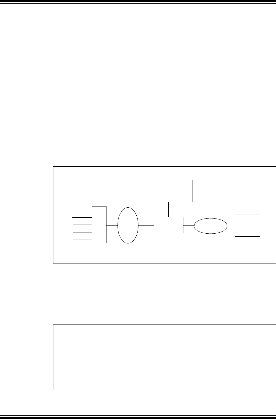
PIC32 Family Reference Manual
DS61108G-page 8-22 © 2007-2012 Microchip Technology Inc.
8.11 TEMPORAL PROXIMITY INTERRUPT COALESCING
The PIC32 CPU responds to interrupt events as if they are all immediately critical because the
interrupt controller asserts the interrupt request to the CPU when the interrupt request occurs.
The CPU immediately recognizes the interrupt if the current CPU priority is lower than the
pending priority. Entering and exiting an ISR consumes clock cycles for saving and restoring
context. Events are asynchronous with respect to the main program and have a limited possibility
of occurring simultaneously or close together in time. This prevents the ability of a shared ISR to
process multiple interrupts at a time.
The Temporal Proximity Interrupt uses the interrupt proximity timer, IPTMR, to create a temporal
window in which a group of interrupts of the same, or lower priority will be held off. This provides
an opportunity to queue these interrupt requests and process them using tail-chaining multiple
IRQs in a single ISR.
Figure 8-2 shows a block diagram of the temporal proximity interrupt coalescing. The interrupt
priority group level that triggers the temporal proximity timer is set up in the TPC<2:0> bits
(INTCON<10:8>). The TPC bits select the interrupt group priority value, and values below that
will trigger the temporal proximity timer to be reset and loaded with the value in the IPTMR
register. After the timer is loaded with the value in the IPTMR register, reads to the IPTMR will
indicate the current state of the timer. The timer decrements to zero on the rising edge of the
System Clock, SYSCLK. When the timer decrements to zero, the queued interrupt requests are
serviced if IPL<2:0> bits (Status<12:10>) are less than RIPL<2:0> bits (Cause<12:10>).
Figure 8-2: Temporal Proximity Interrupt Coalescing Block Diagram
The user can activate temporal proximity interrupt coalescing by performing the following steps:
1. Set the TPC to the preferred priority level (setting the TPC to zero will disable the proximity
timer).
2. Load the preferred 32-bit value to the IPTMR register.
The interrupt proximity timer will trigger when an interrupt request of a priority equal, lower,
matches the TPC value.
Example 8-10: Temporal Proximity Interrupt Coalescing Example
Interrupt
Registers
Interrupt
First
Detect
Timer
Proximity
Value
Latency
INTCON
Out
Time Interrupt
Request
Queued
/*
The following code example will set the Temporal Proximity Coalescing to
trigger on interrupt priority level of 3 or below and the temporal timer to
be set to 0x12345678.
*/
INTCONCLR = 0x00000700; // clear TPC
IPTMRCLR = 0xFFFFFFFF; // clear the timer
INTCONSET = 0x00000300; // set TPC->3
IPTMR = 0x12345678; // set the timer to 0x12345678

© 2007-2012 Microchip Technology Inc. DS61108G-page 8-23
Section 8. Interrupts
Interrupts
8
8.12 EFFECTS OF INTERRUPTS AFTER RESET
8.12.1 Device Reset
All interrupt controller registers are forced to their reset states upon a Device Reset.
8.12.2 Power-on Reset
All interrupt controller registers are forced to their reset states upon a Power-on Reset.
8.12.3 Watchdog Timer Reset
All interrupt controller registers are forced to their reset states upon a Watchdog Timer Reset.
8.13 OPERATION IN POWER-SAVING AND DEBUG MODES
8.13.1 Interrupt Operation in Sleep Mode
During Sleep mode, the interrupt controller will only recognize interrupts from peripherals that
can operate in Sleep mode. Peripherals such as RTCC, Change Notice, External Interrupts, ADC
and SPI Slave can continue to operate in Sleep mode and interrupts from these peripherals can
be used to wake-up the device. An interrupt with its Interrupt Enable bit set may switch the device
to either Run or Idle mode, subject to its Interrupt Enable bit status and priority level. An interrupt
event with its Interrupt Enable bit cleared or a priority of zero will not be recognized by the
interrupt controller and cannot change device status. If the priority of the interrupt request is
higher than the current processor priority level, the device will switch to Run mode and processor
will execute the corresponding interrupt request. If the proximity timer is enabled and the pending
interrupt priority is less than the temporal proximity priority, the processor does not remain in
sleep. It transitions to idle and then goes to run, once the TPT times out. If the priority of the
interrupt request is less than or equal to the current processor priority level, the device will switch
to Idle mode and the processor will remain halted.
8.13.2 Interrupt Operation in Idle Mode
During Idle mode, interrupt events, with their respective Interrupt Enable bits set, may switch the
device to Run mode subject to its Interrupt Enable bit status and priority level. An interrupt event
with its Interrupt Enable bit cleared or a priority of zero will not be recognized by the interrupt
controller and cannot change device status. If the priority of the interrupt request is higher than
the current CPU priority level, the device will switch to Run mode and the CPU will execute the
corresponding interrupt request. If the proximity timer is enabled and the pending interrupt
priority is less than the temporal proximity priority, the device will remain in Idle mode and the
processor will not take the interrupt until after the proximity time has expired. If the priority of the
interrupt request is less than or equal to the current CPU priority level, the device will remain in
Idle mode. The corresponding Interrupt Flag bits will remain set and the interrupt request will
remain pending.
8.13.3 Interrupt Operation in Debug Mode
While the CPU is executing in Debug Exception mode (i.e., the application is halted), all
interrupts, regardless of their priority level, are not taken and they will remain pending. Once the
CPU exits Debug Exception mode, all pending interrupts will be taken in their order of priority.

PIC32 Family Reference Manual
DS61108G-page 8-24 © 2007-2012 Microchip Technology Inc.
8.14 RELATED APPLICATION NOTES
This section lists application notes that are related to this section of the manual. These
application notes may not be written specifically for the PIC32 device family, but the concepts are
pertinent and could be used with modification and possible limitations. The current application
notes related to the Interrupts module are:
Title Application Note #
No related application notes at this time. N/A
Note: Please visit the Microchip web site (www.microchip.com) for additional application
notes and code examples for the PIC32 family of devices.

© 2007-2012 Microchip Technology Inc. DS61108G-page 8-25
Section 8. Interrupts
Interrupts
8
8.15 REVISION HISTORY
Revision A (August 2007)
This is the initial released version of this document.
Revision B (October 2007)
Updated document to remove Confidential status.
Revision C (April 2008)
Revised status to Preliminary; Revised U-0 to r-x.
Revision D (June 2008)
Revise Register 8-1, FRZ note; Revise Examples 8-1 and 8-2; Change Reserved bits from
“Maintain as” to “Write”.
Revision E (July 2009)
This revision includes the following updates:
•Minor updates to text and formatting have been implemented throughout the document
•Interrupts Register Summary (Table 8-1):
- Removed all references to the Clear, Set and Invert registers
- Added the Address Offset column
- Added Notes 1, 2 and 3, which describe the Clear, Set and Invert registers
•Added Notes describing the Clear, Set and Invert registers to the following registers:
-INTCON
- INTSTAT
- IPTMR
- IFSx
-IPCx
•Updated the note at the beginning of Section 8.2 “Control Registers”
•Updated the second sentence of the second paragraph in Section 8.3 “Operation” to clarify
the IRQ sources
•Updated the first paragraph of Section 8.8.2 “Register Set Selection in Multi-Vector Mode”
• Updated the answer to Question 2 in Section 8.14 “Design Tips”
Revision F (July 2011)
This revision includes the following updates:
•Added a Note at the beginning of the section, which provides information on the
complementary documentation
• Changed all occurrences of PIC32MX to PIC32
• Updated all r-x bits as U-0 bits in Register 8-1 through Register 8-7
•Updated the RIPL bit as the SRIPL bit in Register 8-3
•Updated Example 8-1 and Example 8-2
•Updated Temporal Proximity Timer register (TPTMR) as Interrupt Proximity Timer register
(IPTMR) in Register 8-4
•Added a sentence in the third paragraph of section 8.11 “Temporal Proximity Interrupt
Coalescing” about timer decrementing to zero on the rising edge of the SYSCLK
•Modifications to register formatting and minor updates have been made throughout the
document
• Removed Section 8.14 “Design Tips”

PIC32 Family Reference Manual
DS61108G-page 8-26 © 2007-2012 Microchip Technology Inc.
Revision G (April 2012)
This revision includes the following updates:
•Updated the maximum number interrupt sources from 96 to 256 (see 8.1 “Introduction”)
• Added the Vector Spacing bits (VS<6:0>) to the Interrupt Control register (see Tabl e 8-1
and Register 8-1)
•Added the Priority Shadow Select register (see Tabl e 8-1 and Register 8-2)
•Added the Interrupt Offset register (see Ta b l e 8-1 and Register 8-8)
•Minor updates to text and formatting were incorporated throughout the document

2007-2012 Microchip Technology Inc. DS61108G-page 8 -27
Information contained in this publication regarding device
applications and the like is provided only for your convenience
and may be superseded by updates. It is your responsibility to
ensure that your application meets with your specifications.
MICROCHIP MAKES NO REPRESENTATIONS OR
WARRANTIES OF ANY KIND WHETHER EXPRESS OR
IMPLIED, WRITTEN OR ORAL, STATUTORY OR
OTHERWISE, RELATED TO THE INFORMATION,
INCLUDING BUT NOT LIMITED TO ITS CONDITION,
QUALITY, PERFORMANCE, MERCHANTABILITY OR
FITNESS FOR PURPOSE. Microchip disclaims all liability
arising from this information and its use. Use of Microchip
devices in life support and/or safety applications is entirely at
the buyer’s risk, and the buyer agrees to defend, indemnify and
hold harmless Microchip from any and all damages, claims,
suits, or expenses resulting from such use. No licenses are
conveyed, implicitly or otherwise, under any Microchip
intellectual property rights.
Trademarks
The Microchip name and logo, the Microchip logo, dsPIC,
KEELOQ, KEELOQ logo, MPLAB, PIC, PICmicro, PICSTART,
PIC32 logo, rfPIC and UNI/O are registered trademarks of
Microchip Technology Incorporated in the U.S.A. and other
countries.
FilterLab, Hampshire, HI-TECH C, Linear Active Thermistor,
MXDEV, MXLAB, SEEVAL and The Embedded Control
Solutions Company are registered trademarks of Microchip
Technology Incorporated in the U.S.A.
Analog-for-the-Digital Age, Application Maestro, chipKIT,
chipKIT logo, CodeGuard, dsPICDEM, dsPICDEM.net,
dsPICworks, dsSPEAK, ECAN, ECONOMONITOR,
FanSense, HI-TIDE, In-Circuit Serial Programming, ICSP,
Mindi, MiWi, MPASM, MPLAB Certified logo, MPLIB,
MPLINK, mTouch, Omniscient Code Generation, PICC,
PICC-18, PICDEM, PICDEM.net, PICkit, PICtail, REAL ICE,
rfLAB, Select Mode, Total Endurance, TSHARC,
UniWinDriver, WiperLock and ZENA are trademarks of
Microchip Technology Incorporated in the U.S.A. and other
countries.
SQTP is a service mark of Microchip Technology Incorporated
in the U.S.A.
All other trademarks mentioned herein are property of their
respective companies.
© 2007-2012, Microchip Technology Incorporated, Printed in
the U.S.A., All Rights Reserved.
Printed on recycled paper.
ISBN: 978-1-62076-196-0
Note the following details of the code protection feature on Microchip devices:
• Microchip products meet the specification contained in their particular Microchip Data Sheet.
• Microchip believes that its family of products is one of the most secure families of its kind on the market today, when used in the
intended manner and under normal conditions.
• There are dishonest and possibly illegal methods used to breach the code protection feature. All of these methods, to our
knowledge, require using the Microchip products in a manner outside the operating specifications contained in Microchip’s Data
Sheets. Most likely, the person doing so is engaged in theft of intellectual property.
• Microchip is willing to work with the customer who is concerned about the integrity of their code.
• Neither Microchip nor any other semiconductor manufacturer can guarantee the security of their code. Code protection does not
mean that we are guaranteeing the product as “unbreakable.”
Code protection is constantly evolving. We at Microchip are committed to continuously improving the code protection features of our
products. Attempts to break Microchip’s code protection feature may be a violation of the Digital Millennium Copyright Act. If such acts
allow unauthorized access to your software or other copyrighted work, you may have a right to sue for relief under that Act.
Microchip received ISO/TS-16949:2009 certification for its worldwide
headquarters, design and wafer fabrication facilities in Chandler and
Tempe, Arizona; Gresham, Oregon and design centers in California
and India. The Company’s quality system processes and procedures
are for its PIC® MCUs and dsPIC® DSCs, KEELOQ® code hopping
devices, Serial EEPROMs, microperipherals, nonvolatile memory and
analog products. In addition, Microchip’s quality system for the design
and manufacture of development systems is ISO 9001:2000 certified.
QUALITYMANAGEMENT
S
YSTEM
CERTIFIEDBYDNV
== ISO/TS16949==

DS61108G-page 8 -28 2007-2012 Microchip Technology Inc.
AMERICAS
Corporate Office
2355 West Chandler Blvd.
Chandler, AZ 85224-6199
Tel: 480-792-7200
Fax: 480-792-7277
Technical Support:
http://www.microchip.com/
support
Web Address:
www.microchip.com
Atlanta
Duluth, GA
Tel: 678-957-9614
Fax: 678-957-1455
Boston
Westborough, MA
Tel: 774-760-0087
Fax: 774-760-0088
Chicago
Itasca, IL
Tel: 630-285-0071
Fax: 630-285-0075
Cleveland
Independence, OH
Tel: 216-447-0464
Fax: 216-447-0643
Dallas
Addison, TX
Tel: 972-818-7423
Fax: 972-818-2924
Detroit
Farmington Hills, MI
Tel: 248-538-2250
Fax: 248-538-2260
Indianapolis
Noblesville, IN
Tel: 317-773-8323
Fax: 317-773-5453
Los Angeles
Mission Viejo, CA
Tel: 949-462-9523
Fax: 949-462-9608
Santa Clara
Santa Clara, CA
Tel: 408-961-6444
Fax: 408-961-6445
Toronto
Mississauga, Ontario,
Canada
Tel: 905-673-0699
Fax: 905-673-6509
ASIA/PACIFIC
Asia Pacific Office
Suites 3707-14, 37th Floor
Tower 6, The Gateway
Harbour City, Kowloon
Hong Kong
Tel : 8 52 -24 01- 120 0
Fax: 852-2401-3431
Australia - Sydney
Tel : 6 1- 2-9 868 -67 33
Fax: 61-2-9868-6755
China - Beijing
Tel : 8 6- 10- 856 9-7 00 0
Fax: 86-10-8528-2104
China - Chengdu
Tel : 8 6- 28- 866 5-5 511
Fax: 86-28-8665-7889
China - Chongqing
Tel : 8 6- 23- 898 0-9 58 8
Fax: 86-23-8980-9500
China - Hangzhou
Tel : 8 6- 571 -28 19- 318 7
Fax: 86-571-2819-3189
China - Hong Kong SAR
Tel : 8 52 -24 01- 120 0
Fax: 852-2401-3431
China - Nanjing
Tel : 8 6- 25- 847 3-2 46 0
Fax: 86-25-8473-2470
China - Qingdao
Tel : 8 6- 532 -85 02- 735 5
Fax: 86-532-8502-7205
China - Shanghai
Tel : 8 6- 21- 540 7-5 53 3
Fax: 86-21-5407-5066
China - Shenyang
Tel : 8 6- 24- 233 4-2 82 9
Fax: 86-24-2334-2393
China - Shenzhen
Tel : 8 6- 755 -82 03- 266 0
Fax: 86-755-8203-1760
China - Wuhan
Tel : 8 6- 27- 598 0-5 30 0
Fax: 86-27-5980-5118
China - Xian
Tel : 8 6- 29- 883 3-7 25 2
Fax: 86-29-8833-7256
China - Xiamen
Tel: 86-592-2388138
Fax: 86-592-2388130
China - Zhuhai
Tel : 86- 75 6-3 21 004 0
Fax: 86-756-3210049
ASIA/PACIFIC
India - Bangalore
Tel : 9 1- 80- 309 0-4 44 4
Fax: 91-80-3090-4123
India - New Delhi
Tel : 9 1- 11- 416 0 -8 631
Fax: 91-11-4160-8632
India - Pune
Tel : 9 1- 20- 256 6-1 51 2
Fax: 91-20-2566-1513
Japan - Osaka
Tel : 8 1- 66- 152 -71 60
Fax: 81-66-152-9310
Japan - Yokohama
Tel : 8 1- 45- 471 - 6 16 6
Fax: 81-45-471-6122
Korea - Daegu
Tel : 8 2- 53- 744 -43 01
Fax: 82-53-744-4302
Korea - Seoul
Tel : 8 2- 2-5 54- 72 0 0
Fax: 82-2-558-5932 or
82-2-558-5934
Malaysia - Kuala Lumpur
Tel : 6 0- 3-6 201 -9 8 57
Fax: 60-3-6201-9859
Malaysia - Penang
Tel : 6 0- 4-2 27- 88 7 0
Fax: 60-4-227-4068
Philippines - Manila
Tel : 6 3- 2-6 34- 90 6 5
Fax: 63-2-634-9069
Singapore
Tel : 6 5- 633 4-8 870
Fax: 65-6334-8850
Taiwan - Hsin Chu
Tel : 8 86 -3- 577 8-3 66
Fax: 886-3-5770-955
Taiwan - Kaohsiung
Tel : 8 86 -7- 536 -48 18
Fax: 886-7-330-9305
Taiwan - Taipei
Tel : 8 86 -2- 250 0-6 61 0
Fax: 886-2-2508-0102
Thailand - Bangkok
Tel : 6 6- 2-6 94- 13 5 1
Fax: 66-2-694-1350
EUROPE
Austria - Wels
Tel : 4 3- 72 42 -2 244 -3 9
Fax: 43-7242-2244-393
Denmark - Copenhagen
Tel : 4 5- 445 0-2 828
Fax: 45-4485-2829
France - Paris
Tel : 3 3- 1-6 9-5 3-6 3-2 0
Fax: 33-1-69-30-90-79
Germany - Munich
Tel : 4 9- 89 -62 7-1 44- 0
Fax: 49-89-627-144-44
Italy - Milan
Tel : 3 9- 03 31 -7 426 11
Fax: 39-0331-466781
Netherlands - Drunen
Tel : 3 1- 41 6- 690 399
Fax: 31-416-690340
Spain - Madrid
Tel : 3 4- 91 -70 8-0 8-9 0
Fax: 34-91-708-08-91
UK - Wokingham
Tel : 4 4- 118 -92 1- 5 869
Fax: 44-118-921-5820
Worldwide Sales and Service
11/29/11

© 2007-2013 Microchip Technology Inc. DS60001114G-page 9-1
Watchdog, Deadman,
and Power-up Timers
9
Section 9. Watchdog, Deadman, and Power-up Timers
HIGHLIGHTS
This section of the manual contains the following major topics:
9.1 Introduction................................................................................................................9-2
9.2 Watchdog, Deadman, and Power-up Timers Control Registers ................................ 9-4
9.3 Watchdog Timer Operation...................................................................................... 9-12
9.4 DMT Operation ........................................................................................................ 9-16
9.5 Interrupt and Reset Generation ............................................................................... 9-18
9.6 I/O Pins....................................................................................................................9-21
9.7 Operation in Debug and Power-Saving Modes ....................................................... 9-21
9.8 Effects of Various Resets......................................................................................... 9-21
9.9 Related Application Notes ....................................................................................... 9-22
9.10 Revision History....................................................................................................... 9-23
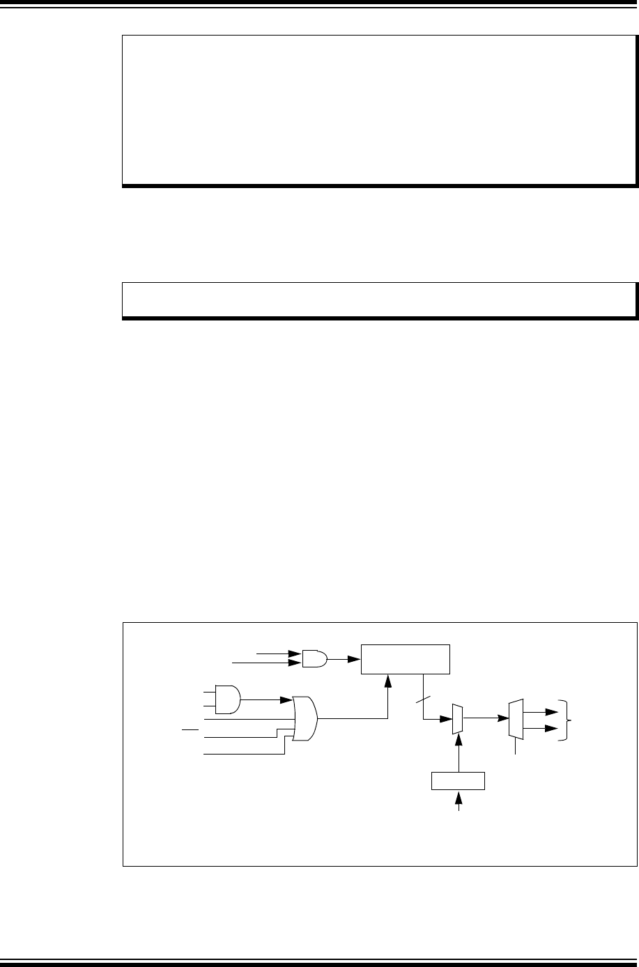
PIC32 Family Reference Manual
DS60001114G-page 9-2 © 2007-2013 Microchip Technology Inc.
9.1 INTRODUCTION
The PIC32 Watchdog Timer (WDT), Deadman Timer (DMT), and Power-up Timer (PWRT) mod-
ules are described in this section. Refer to Figure 9-1 for a block diagram of the WDT and PWRT
and Figure 9-2 for a block diagram of the DMT.
The WDT, when enabled, operates from the internal Low-Power RC (LPRC) Oscillator clock
source. The WDT can be used to detect system software malfunctions by resetting the device if
the WDT is not cleared periodically in software. The WDT can be configured in Windowed mode
or non-Windowed mode. Various WDT time-out periods can be selected using the WDT
postscaler. The WDT can also be used to wake the device from Sleep or Idle mode.
The DMT, when enabled, counts instruction fetches, and is able to cause a Reset if the DMT
counter is not cleared within a set number of instructions. Since it does not measure time, it can
remain active during sleep modes and continue after awakening.
The PWRT, when enabled, holds the device in Reset for a 64 millisecond period after the normal
Power-on Reset (POR) start-up period is complete. This allows additional time for the Primary
Oscillator (POSC) clock source and the power supply to stabilize. Like the WDT, the PWRT also
uses the LPRC as its clock source.
Following are some of the key features of the WDT, DMT, and PWRT modules:
•Configuration or software controlled
•User-configurable time-out period or instruction count
•Can wake the device from Sleep or Idle
Figure 9-1: Watchdog Timer and Power-up Timer Block Diagram
Note: This family reference manual section is meant to serve as a complement to device
data sheets. Depending on the device variant, this manual section may not apply to
all PIC32 devices.
Please consult the note at the beginning of the “Watchdog Timer”, “Deadman
Timer”, “Power-Saving Features” and “Special Features” chapters in the
current device data sheet to check whether this document supports the device you
are using.
Device data sheets and family reference manual sections are available for
download from the Microchip Worldwide Web site at: http://www.microchip.com
Note: The Deadman Timer is not available on all devices. Please refer to the “Deadman
Timer” chapter in the specific device data sheet to determine availability.
Wake
WDTCLR = 1
ON
Power Save
25-bit Counter
WDT Counter Reset
25
WDT Event
FWDTPS<4:0> (DEVCFG1<20:16>)
Clock
Decoder
0
1
ON
Reset Event
to NMI(1)
ON
LPRC
Note 1: Refer to the “Resets” chapter in the specific device data sheet for more information.

© 2007-2013 Microchip Technology Inc. DS60001114G-page 9-3
Section 9. Watchdog, Deadman, and Power-up Timers
Watchdog, Deadman,
and Power-up Timers
9
Figure 9-2: Deadman Timer Block diagram
32-bit counter
ON
PBCLK7
“Proper Clear Sequence” Flag
ON
Clock ON
DMT Count Reset Load
DMT event
System Reset
System Reset
Instruction Fetched Strobe Force DMT Event
“improper sequence” flag
32
(COUNTER) ≥ DMT Window Interval(2)
Window Interval Open
(COUNTER) = DMT Max Count(1)
Counter Initialization Value
Note 1: DMT Max Count is controlled by the DMTCNT<3:0> bits in the DEVCFG1 Configuration register.
2: DMT Window Interval is controlled by the DMTINTV<2:0> bits in the DEVCFG1 Configuration register.
3: Refer to the “Resets” chapter in the specific device data sheet for more information.
to NMI(3)

PIC32 Family Reference Manual
DS60001114G-page 9-4 © 2007-2013 Microchip Technology Inc.
9.2 WATCHDOG, DEADMAN, AND POWER-UP TIMERS CONTROL REGISTERS
The WDT, DMT, and PWRT modules consist of the following Special Function Registers (SFRs):
•WDTCON: Watchdog Timer Control Register
This register is used to enable or disable the Watchdog Timer, clear the WDT to prevent a
time-out, and enables or disables the windowed operation.
•RCON: Resets Control Register
This register indicates the cause of a reset.
•DMTCON: Deadman Timer Control Register
This register is used to enable or disable Deadman Timer.
•DMTPRECLR: Deadman Timer Preclear Register
This register is used to write a preclear key word to eventually clear the Deadman Timer.
•DMTCLR: Deadman Timer Clear Register
This register is used to write a clear key word after a preclear word has been written to the
DMTPRECLR register. The Deadman Timer will be cleared following a clear key word write.
•DMTSTAT: Deadman Timer Status Register
This register provides status for incorrect key word values or sequences, Deadman Timer
events, and whether or not the DMT clear window is open.
•DMTCNT: Deadman Timer Count Register
This register allows user software to read the contents of the DMT counter.
•DMTPSCNT: Post Status Configure DMT Count Status Register
This register provides the value of the DMTCNT Configuration bits in the DEVCFG1 register.
•DMTPSINTV: Post Status Configure DMT Interval Status Register
This register provides the value of the DMTINTV Configuration bits in the DEVCFG1 register.
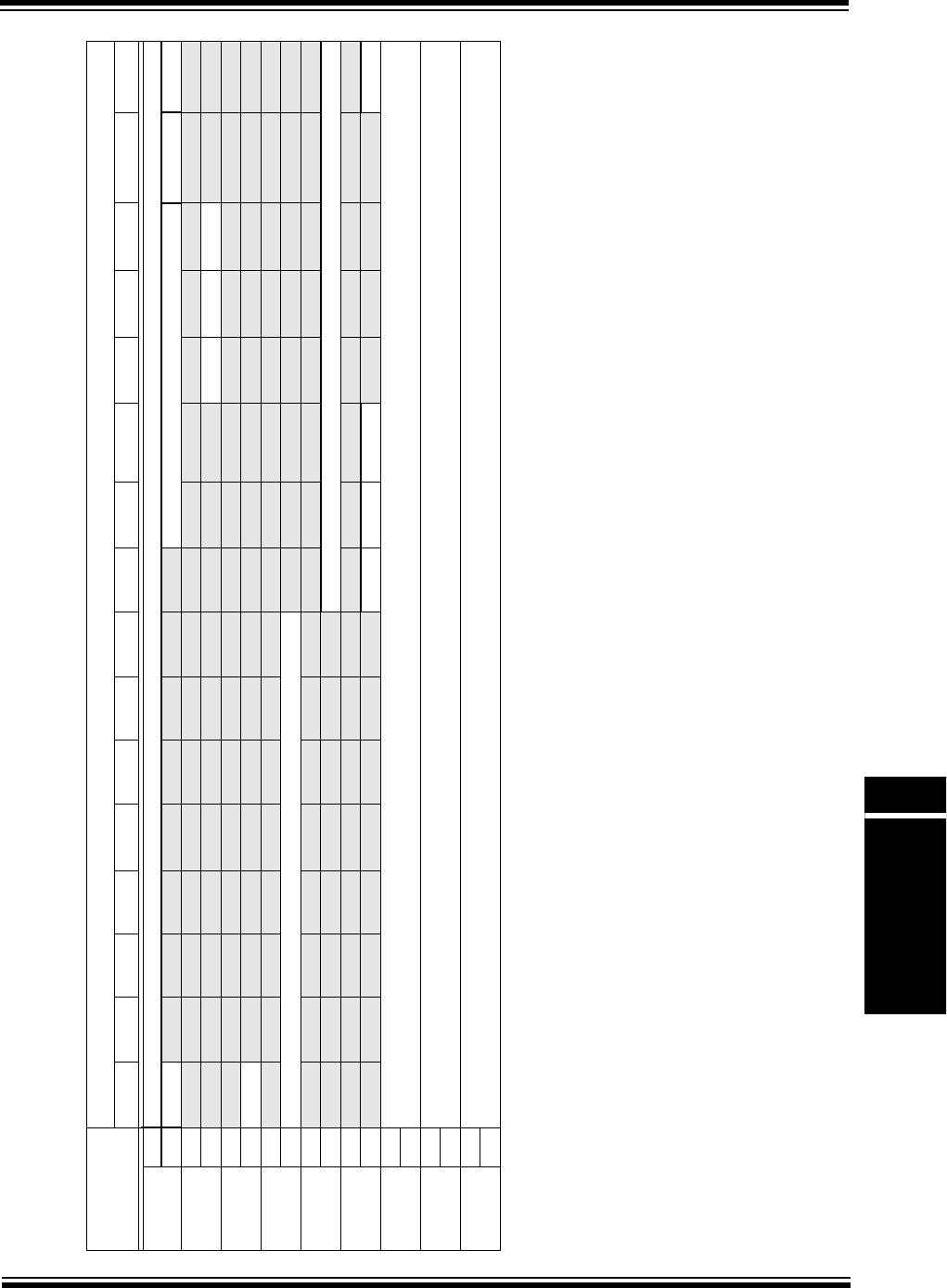
© 2007-2013 Microchip Technology Inc. DS60001114G-page 9-5
Section 9. Watchdog, Deadman, and Power-up Timers
Watchdog, Deadman,
and Power-up Timers
9
Tabl e 9-2 provides a brief summary of the related WDT, DMT, and PWRT module registers. Corresponding registers appear after the
summary, followed by a detailed description of each register.
Table 9-1: Watchdog, Deadman, and Power-up Timers Register Map
Register Name(1) Bits
31/15 30/14 29/13 28/12 27/11 26/10 25/9 24/8 23/7 22/6 21/5 20/4 19/3 18/2 17/1 16/0
WDTCON 31:16 WDTCLRKEY<15:0>(3)
15:0 ON — — — — — — — — SWDTPS<4:0> WDTWINEN
(3) WDTCLR(3)
RCON 31:16 — — — — — — — — — — — — — — — —
15:0 — — — — — — CM(2) WREGS(2) EXTR(2) SWR(2) —WDTOSLEEPIDLEBOR(2) POR(2)
DMTCON 31:16 — — — — — — — — — — — — — — — —
15:0 ON — — — — — — — — — — — — — — —
DMTPRECLR 31:16 — — — — — — — — — — — — — — — —
15:0 STEP1<7:0> — — — — — — — —
DMCLR 31:16 — — — — — — — — — — — — — — — —
15:0 — — — — — — — —STEP2<7:0>
DMTSTAT 31:16 — — — — — — — — — — — — — — — —
15:0 — — — — — — — —BAD1BAD2DMTEVENT— — — —WINOPN
DMTCNT 31:16 COUNTER<31:0>
15:0
DMTPSCNT 31:16 PSCNT<31:0>
15:0
DMTPSINTV 31:16 PSINTV<31:0>
15:0
Legend: — = unimplemented, read as ‘0’.
Note 1: All registers have an associated Clear, Set, and Invert register at an offset of 0x4, 0x8, and 0xC bytes, respectively. These registers have the same name with CLR, SET, or INV
appended to the end of the register name (e.g., WDTCONCLR). Writing a ‘1’ to any bit position in these registers will clear valid bits in the associated register. Reads from the
these registers should be ignored.
2: These bits are not associated with the WDT or PWRT modules. For complete register details, see Register 7-1: “RCON: Resets Control Register” in Section 6. “Resets”
(DS61118) of the “PIC32 Family Reference Manual”.
3: These bits are not available on all devices. Please refer to the “Watchdog Timer” chapter in the specific device data sheet for availability.

PIC32 Family Reference Manual
DS60001114G-page 9-6 © 2007-2013 Microchip Technology Inc.
Register 9-1: WDTCON: Watchdog Timer Control Register
Bit
Range
Bit
31/23/15/7
Bit
30/22/14/6
Bit
29/21/13/5
Bit
28/20/12/4
Bit
27/19/11/3
Bit
26/18/10/2
Bit
25/17/9/1
Bit
24/16/8/0
31:24 W-0 W-0 W-0 W-0 W-0 W-0 W-0 W-0
WDTCLRKEY<15:8>(3)
23:16 W-0 W-0 W-0 W-0 W-0 W-0 W-0 W-0
WDTCLRKEY<7:0>(3)
15:8 R/W-0 U-0 U-0 U-0 U-0 U-0 U-0 U-0
ON(1,2) — — — — — — —
7:0 U-0 R-y R-y R-y R-y R-y R/W-0 R/W-0
—SWDTPS<4:0>WDTWINEN
(3) WDTCLR(3)
Legend: y = Value from Configuration bit on POR
R = Readable bit W = Writable bit U = Unimplemented bit, read as ‘0’
-n = Value at POR ‘1’ = Bit is set ‘0’ = Bit is cleared x = Bit is unknown
bit 31-16 WDTCLRKEY: Watchdog Timer Clear Key bits(3)
To cl ear the Watc hd o g Tim er t o pr eve nt a t ime -ou t, s oft ware must write the value 0x5743 to this location
using a single 16-bit write.
bit 15 ON: Watchdog Timer Enable bit(1,2)
1 = Enables the Watchdog Timer if it is not enabled by the device configuration
0 = Disable the Watchdog Timer if it was enabled in software
bit 14-7 Unimplemented: Read as ‘0’
bit 6-2 SWDTPS<4:0>: Shadow Copy of Watchdog Timer Postscaler Value from Device Configuration bits
On reset, these bits are set to the values of the WDTPS<4:0> Configuration bits.
bit 1 WDTWINEN: Watchdog Timer Window Enable bit(3)
1 = Enable windowed Watchdog Timer
0 = Disable windowed Watchdog Timer
bit 0 WDTCLR: Watchdog Timer Reset bit(3)
1 = Writing a ‘1’ will clear the WDT
0 = Software cannot force this bit to a ‘0’
Note 1: A read of this bit will result in a ‘1’ if the WDT is enabled by the device configuration or by software.
2: When using the 1:1 PBCLK divisor, the user’s software should not read or write the peripheral’s SFRs in
the SYSCLK cycle immediately following the instruction that clears the module’s ON bit.
3: These bits are not available on all devices. Please refer to the “Watchdog Timer” chapter in the specific
device data sheet for availability.

© 2007-2013 Microchip Technology Inc. DS60001114G-page 9-7
Section 9. Watchdog, Deadman, and Power-up Timers
Watchdog, Deadman,
and Power-up Timers
9
Register 9-2: RCON: Resets Control Register
Bit
Range
Bit
31/23/15/7
Bit
30/22/14/6
Bit
29/21/13/5
Bit
28/20/12/4
Bit
27/19/11/3
Bit
26/18/10/2
Bit
25/17/9/1
Bit
24/16/8/0
31:24 U-0 U-0 U-0 U-0 U-0 U-0 U-0 U-0
— — — — — — — —
23:16 U-0 U-0 U-0 U-0 U-0 U-0 U-0 U-0
— — — — — — — —
15:8 U-0 U-0 U-0 U-0 U-0 U-0 R/W-0 R.W-0
— — — — — — CM(1) VREGS(1)
7:0 R/W-0 R/W-0 R/W-0, HS R/W-0 R/W-0 R/W-0 R/W-1 R/W-1
EXTR(1) SWR(1) DMTO(2) WDTO SLEEP IDLE BOR(1) POR(1)
Legend: HS = Set by hardware
R = Readable bit W = Writable bit U = Unimplemented bit, read as ‘0’
-n = Value at POR ‘1’ = Bit is set ‘0’ = Bit is cleared x = Bit is unknown
bit 5 DMTO: Deadman Timer Time-out bit(2)
1 = A Deadman Timer time-out has occurred
0 = A Deadman Timer time-out has not occurred
bit 4 WDTO: Watchdog Time-out bit
1 = A Watchdog Timer time-out has occurred since either the device was powered up or the WDTO
bit was last cleared by software
0 = A Watchdog Timer time-out has not occurred since either the WDTO bit was cleared by software
or the device was reset
bit 3 SLEEP: Sleep Event bit
1 = The device was in Sleep since either the device was powered up or the SLEEP bit was last
cleared by software
0 = The device was not in Sleep since either the SLEEP bit was cleared by software or the device
was reset
bit 2 IDLE: Idle Event bit
1 = The device has been in Idle mode since either the device was powered up or the IDLE bit was
last cleared by software
0 = The device has not been in Idle mode since either the IDLE bit was cleared by software or the
device was reset
Note 1: These bits are not associated with the WDT or PWRT modules. For complete register details, see
Register 7-1: “RCON: Resets Control Register” in Section 6. “Resets” (DS61118) of the “PIC32
Family Reference Manual”.
2: This bit is not available on all devices. Please refer to the “Watchdog Timer” chapter in the specific
device data sheet to determine availability.
PIC32 Family Reference Manual
DS60001114G-page 9-8 © 2007-2013 Microchip Technology Inc.
Register 9-3: DMTCON: Deadman Timer Control Register
Bit Range Bit
31/23/15/7
Bit
30/22/14/6
Bit
29/21/13/5
Bit
28/20/12/4
Bit
27/19/11/3
Bit
26/18/10/2
Bit
25/17/9/1
Bit
24/16/8/0
31:24 U-0 U-0 U-0 U-0 U-0 U-0 U-0 U-0
— — — — — — — —
23:16 U-0 U-0 U-0 U-0 U-0 U-0 U-0 U-0
— — — — — — — —
15:8 R/W-0 U-0 U-0 U-0 U-0 U-0 U-0 U-0
ON(1) — — — — — — —
7:0 U-0 U-0 U-0 U-0 U-0 U-0 U-0 U-0
— — — — — — — —
Legend:
R = Readable bit W = Writable bit U = Unimplemented bit
-n = Bit Value at POR: (‘0’, ‘1’, x = unknown) P = Programmable bit r = Reserved bit
bit 31-16 Unimplemented: Read as ‘0’
bit 15 ON: Deadman Timer Module Enable bit(1)
1 = Deadman Timer module is enabled
0 = Deadman Timer module is disabled
bit 14-0 Unimplemented: Read as ‘0’
Note 1: This bit only has control when FDMTEN (DEVCFG1<3>) = 0.
Register 9-4: DMTPRECLR: Deadman Timer Preclear Register
Bit Range Bit
31/23/15/7
Bit
30/22/14/6
Bit
29/21/13/5
Bit
28/20/12/4
Bit
27/19/11/3
Bit
26/18/10/2
Bit
25/17/9/1
Bit
24/16/8/0
31:24 U-0 U-0 U-0 U-0 U-0 U-0 U-0 U-0
— — — — — — — —
23:16 U-0 U-0 U-0 U-0 U-0 U-0 U-0 U-0
— — — — — — — —
15:8 R/W-0 R/W-0 R/W-0 R/W-0 R/W-0 R/W-0 R/W-0 R/W-0
STEP1<7:0>
7:0 U-0 U-0 U-0 U-0 U-0 U-0 U-0 U-0
— — — — — — — —
Legend:
R = Readable bit W = Writable bit U = Unimplemented bit
-n = Bit Value at POR: (‘0’, ‘1’, x = unknown) P = Programmable bit r = Reserved bit
bit 31-16 Unimplemented: Read as ‘0’
bit 15-8 STEP1<7:0>: Preclear Enable bits
01000000 = Enables the Deadman Timer Preclear (Step 1)
All other write patterns = Set BAD1 flag.
These bits are cleared when a DMT reset event occurs. STEP1<7:0> is also cleared if the
STEP2<7:0> bits are loaded with the correct value in the correct sequence.
bit 7-0 Unimplemented: Read as ‘0’

© 2007-2013 Microchip Technology Inc. DS60001114G-page 9-9
Section 9. Watchdog, Deadman, and Power-up Timers
Watchdog, Deadman,
and Power-up Timers
9
Register 9-5: DMTCLR: Deadman Timer Clear Register
Bit Range Bit
31/23/15/7
Bit
30/22/14/6
Bit
29/21/13/5
Bit
28/20/12/4
Bit
27/19/11/3
Bit
26/18/10/2
Bit
25/17/9/1
Bit
24/16/8/0
31:24 U-0 U-0 U-0 U-0 U-0 U-0 U-0 U-0
— — — — — — — —
23:16 U-0 U-0 U-0 U-0 U-0 U-0 U-0 U-0
— — — — — — — —
15:8 U-0 U-0 U-0 U-0 U-0 U-0 U-0 U-0
— — — — — — — —
7:0 R/W-0 R/W-0 R/W-0 R/W-0 R/W-0 R/W-0 R/W-0 R/W-0
STEP2<7:0>
Legend:
R = Readable bit W = Writable bit U = Unimplemented bit
-n = Bit Value at POR: (‘0’, ‘1’, x = unknown) P = Programmable bit r = Reserved bit
bit 31-8 Unimplemented: Read as ‘0’
bit 7-0 STEP2<7:0>: Clear Timer bits
00001000 = Clears STEP1<7:0>, STEP2<7:0> and the Deadman Timer if, and only if, preceded by cor-
rect loading of STEP1<7:0> bits in the correct sequence. The write to these bits may be
verified by reading DMTCNT and observing the counter being reset.
All other write patterns = Set BAD2 bit, the value of STEP1<7:0> will remain unchanged, and the new
value being written STEP2<7:0> will be captured. These bits are also cleared when a DMT reset event
occurs.

PIC32 Family Reference Manual
DS60001114G-page 9-10 © 2007-2013 Microchip Technology Inc.
Register 9-6: DMTSTAT: Deadman Timer Status Register
Bit Range Bit
31/23/15/7
Bit
30/22/14/6
Bit
29/21/13/5
Bit
28/20/12/4
Bit
27/19/11/3
Bit
26/18/10/2
Bit
25/17/9/1
Bit
24/16/8/0
31:24 U-0 U-0 U-0 U-0 U-0 U-0 U-0 U-0
— — — — — — — —
23:16 U-0 U-0 U-0 U-0 U-0 U-0 U-0 U-0
— — — — — — — —
15:8 U-0 U-0 U-0 U-0 U-0 U-0 U-0 U-0
— — — — — — — —
7:0 R-0, HC R-0, HC R-0, HC U-0 U-0 U-0 U-0 R-0
BAD1 BAD2 DMTEVENT — — — —WINOPN
Legend: HC = Cleared by Hardware
R = Readable bit W = Writable bit U = Unimplemented bit
-n = Bit Value at POR: (‘0’, ‘1’, x = unknown) P = Programmable bit r = Reserved bit
bit 31-8 Unimplemented: Read as ‘0’
bit 7 BAD1: Bad STEP1<7:0> Value Detect bit
1 = Incorrect STEP1<7:0> value was detected
0 = Incorrect STEP1<7:0> value was not detected
bit 6 BAD2: Bad STEP2<7:0> Value Detect bit
1 = Incorrect STEP2<7:0> value was detected
0 = Incorrect STEP2<7:0> value was not detected
bit 5 DMTEVENT: Deadman Timer Event bit
1 = Deadman timer event was detected (counter expired or bad STEP1<7:0> or STEP2<7:0> value was
entered prior to counter increment)
0 = Deadman timer event was not detected
bit 4-1 Unimplemented: Read as ‘0’
bit 0 WINOPN: Deadman Timer Clear Window bit
1 = Deadman timer clear window is open
0 = Deadman timer clear window is not open
Register 9-7: DMTCNT: Deadman Timer Count Register
Bit Range Bit
31/23/15/7
Bit
30/22/14/6
Bit
29/21/13/5
Bit
28/20/12/4
Bit
27/19/11/3
Bit
26/18/10/2
Bit
25/17/9/1
Bit
24/16/8/0
31:24 R-0 R-0 R-0 R-0 R-0 R-0 R-0 R-0
COUNTER<31:24>
23:16 R-0 R-0 R-0 R-0 R-0 R-0 R-0 R-0
COUNTER<23:16>
15:8 R-0 R-0 R-0 R-0 R-0 R-0 R-0 R-0
COUNTER<15:8>
7:0 R-0 R-0 R-0 R-0 R-0 R-0 R-0 R-0
COUNTER<7:0>
Legend:
R = Readable bit W = Writable bit U = Unimplemented bit
-n = Bit Value at POR: (‘0’, ‘1’, x = unknown) P = Programmable bit r = Reserved bit
bit 31-8 COUNTER<31:0>: Read current contents of DMT counter
© 2007-2013 Microchip Technology Inc. DS60001114G-page 9-11
Section 9. Watchdog, Deadman, and Power-up Timers
Watchdog, Deadman,
and Power-up Timers
9
Register 9-8: DMTPSCNT: Post Status Configure DMT Count Status Register
Bit Range Bit
31/23/15/7
Bit
30/22/14/6
Bit
29/21/13/5
Bit
28/20/12/4
Bit
27/19/11/3
Bit
26/18/10/2
Bit
25/17/9/1
Bit
24/16/8/0
31:24 R-0 R-0 R-0 R-0 R-0 R-0 R-0 R-0
PSCNT<31:24>
23:16 R-0 R-0 R-0 R-0 R-0 R-0 R-0 R-0
PSCNT<23:16>
15:8 R-0 R-0 R-0 R-0 R-0 R-0 R-0 R-0
PSCNT<15:8>
7:0 R-0 R-0 R-0 R-0 R-0 R-0 R-0 R-0
PSCNT<7:0>
Legend:
R = Readable bit W = Writable bit U = Unimplemented bit
-n = Bit Value at POR: (‘0’, ‘1’, x = unknown) P = Programmable bit r = Reserved bit
bit 31-8 PSCNT<31:0>: DMT Instruction Count Value Configuration Status bits
This is always the value of the DMTCNT<3:0> bits in the DEVCFG1 Configuration register.
Register 9-9: DMTPSINTV: Post Status Configure DMT Interval Status Register
Bit Range Bit
31/23/15/7
Bit
30/22/14/6
Bit
29/21/13/5
Bit
28/20/12/4
Bit
27/19/11/3
Bit
26/18/10/2
Bit
25/17/9/1
Bit
24/16/8/0
31:24 R-0 R-0 R-0 R-0 R-0 R-0 R-0 R-0
PSINTV<31:24>
23:16 R-0 R-0 R-0 R-0 R-0 R-0 R-0 R-0
PSINTV<23:16>
15:8 R-0 R-0 R-0 R-0 R-0 R-0 R-0 R-0
PSINTV<15:8>
7:0 R-0 R-0 R-0 R-0 R-0 R-0 R-0 R-0
PSINTV<7:0>
Legend:
R = Readable bit W = Writable bit U = Unimplemented bit
-n = Bit Value at POR: (‘0’, ‘1’, x = unknown) P = Programmable bit r = Reserved bit
bit 31-8 PSINTV<31:0>: DMT Window Interval Configuration Status bits
This is always the value of the DMTINTV<2:0> bits in the DEVCFG1 Configuration register.

PIC32 Family Reference Manual
DS60001114G-page 9-12 © 2007-2013 Microchip Technology Inc.
9.3 WATCHDOG TIMER OPERATION
The primary function of the Watchdog Timer (WDT) is to reset the processor in the event of a
software malfunction or wake-up the processor in the event of a time-out while in Sleep mode.
If enabled, the WDT will increment until it overflows or “times out”. A WDT time-out will force a
device Reset, except during Sleep or Idle modes. To prevent a WDT time-out Reset, the user
application must periodically clear the WDT by setting the WDTCLR bit (WDTCON<0>), or by
writing a key word 0x5743 to the WDTCLRKEY<15:0> bits (WDTCON<31:16>) through a single
16-bit write. Refer to the “Watchdog Timer” chapter in the specific device data sheet to deter-
mine availability of the WDTCLR bit and the WDTCLRKEY<15:0> bits.
The WDT module uses the LPRC Oscillator for reliability.
9.3.1 Modes of Operation
The WDT has two modes of operation: Non-Windowed and Programmable Windowed.
The Programmable Windowed mode can be enabled by setting the Watchdog Window
Enable (WDTWINEN) bit (WDTCON<1>). In Programmable Windowed mode, software can
clear the WDT only when the counter is in its final window before a period match occurs.
There are four window size options. This window is active when the timer counter is greater
than a predetermined value for each option. Depending on the device, any attempts to clear
the WDT when the window is not active will cause either a Non-maskable Interrupt (NMI) or
a device Reset. Refer to the “Power-Saving Features” chapter in the specific device data
sheet for more information on which type of reset occurs for your device. In Non-Windowed
mode, software can clear the WDT anytime before the period match occurs.
9.3.2 Enabling and Disabling the WDT
The WDT is enabled or disabled by the device configuration or controlled through software by
writing to the WDTCON register (Register 9-1).
9.3.3 Device Configuration Controlled WDT
If the FWDTEN Configuration bit is set, the WDT is always enabled. The ON control bit
(WDTCON<15>) will reflect this by reading a ‘1’. In this mode, the ON bit cannot be cleared in
software. The FWDTEN Configuration bit will not be cleared by any form of reset. To disable the
WDT, the configuration must be rewritten to the device.
The WINDIS Configuration bit can be used to enable or disable the Programmable Windowed
mode. The window size for the WDT Programmable Windowed mode can be configured using
the FWDTWINSZ Configuration bits.
9.3.4 Software Controlled WDT
If the FWDTEN Configuration bit is a ‘0’, the WDT module can be enabled or disabled (the default
condition) by software. In this mode, the ON bit (WDTCON<15>) reflects the status of the WDT
under software control. A ‘1’ indicates the WDT module is enabled and a ‘0’ indicates it is
disabled. If the WINDIS Configuration bit is a ‘0’, the WDT Programmable Windowed mode can
be enabled or disabled by software. The Programmable Windowed mode can be configured
using the WDTWINEN bit (WDTCON<2>). A ‘1’ indicates that Programmable Windowed mode
is enabled and ‘0’ indicates it is disabled. The window sizes can be configured by setting the
FWDTWINSZ configuration bits only, and cannot be set in software.
The WDT is enabled in software by setting the Watchdog Timer control bit, ON (WDTCON<15>).
The ON control bit is cleared on any device Reset. The bit is not cleared upon a wake from Sleep
or exit from Idle mode. The software WDT option allows the user to enable the WDT for critical
code segments and disable the WDT during noncritical segments for maximum power savings.
This bit can also be used to disable the WDT while the device is awake to eliminate the need for
WDT servicing, and then re-enable it before the device is put into Idle mode or Sleep mode to
wake the device at a later time. Example 9-1 shows the WDT initialization and servicing sample.
Note: The LPRC Oscillator is enabled whenever the WDT is enabled.
Note: The WDT is enabled by default on an unprogrammed device.

© 2007-2013 Microchip Technology Inc. DS60001114G-page 9-13
Section 9. Watchdog, Deadman, and Power-up Timers
Watchdog, Deadman,
and Power-up Timers
9
Example 9-1: Sample WDT Initialization and Servicing
9.3.4.1 WATCHDOG TIMER PROGRAMMABLE WINDOW
The window size is determined by the Configuration bits, FWDTWINSZ and WDTPS. In the
Programmable Windowed mode (WDTWINEN = 1), the WDT should be cleared based on the
setting of the Window Size Configuration bits (FWDTWINSZ<1:0>), see Figure 9-4. These bit
settings are:
•11 = WDT window is 25% of the WDT period
•10 = WDT window is 37.5% of the WDT period
•01 = WDT window is 50% of the WDT period
•00 = WDT window is 75% of the WDT period
Depending on the device, if the WDT is cleared before the allowed window, a system Reset or
NMI is immediately generated. Refer to the “Power-Saving Features” chapter in the specific
device data sheet for more information on which type of reset occurs for your device.
The Windowed mode is useful for resetting the device during unexpected quick or slow execution
of a critical portion of the code.
Figure 9-3: Non-Windowed WDT
Figure 9-4: Programmable Windowed WDT
Note: Window mode and its associated bits are not available on all devices. Please refer
to the specific device data sheet to determine availability.
//This code fragment assumes the WDT was not enabled by the device configuration
// The Postscaler value must be set with the device configuration
// In certain devices, software must write a 0x5743 to WDTCON<31:16> using a
// single 16-bit write.
WDTCONSET = 0x8000; // Turn on the WDT
main
{
WDTCONSET = 0x01; // Service the WDT
... User code goes here ...
}
Watchdog Time-out Period
(TWTO)
Allowed Window
Watchdog Time-out Period
(TWTO)
Allowed Window
Disallowed Window
([25, 37.5, 50, or 75%] x TWTO)
Note: The programmable windowed WDT feature is available on selected devices.
Refer to the specific device data sheet for availability of this feature.

PIC32 Family Reference Manual
DS60001114G-page 9-14 © 2007-2013 Microchip Technology Inc.
9.3.5 WDT Operation in Power-Saving Modes
The WDT, if enabled, will continue operation in Sleep mode or Idle mode. The WDT module may
be used to wake the device from Sleep mode or Idle mode. When the WDT times out in a
Power-Saving mode, a Non-Maskable Interrupt (NMI) is generated and the WDTO bit
(RCON<4>) is set. The NMI vectors execution to the CPU start-up address, but does not reset
registers or peripherals. If the device was in Sleep, the SLEEP status bit (RCON<3>) will also be
set. If the device was in Idle, the IDLE status bit (RCON<2>) will also be set. These bits allow the
start-up code to determine the cause of the wake-up.
9.3.6 WDT NMI Reset Delay
On those devices that have a NMI reset counter, it is possible to program a delay time between
a WDT event and a device Reset. Refer to the “Resets” chapter in the specific device data
sheet, and Section 7. “Resets” (DS60001118) in the “PIC32 Family Reference Manual” for
details.
9.3.7 Time Delays on Wake
There will be a time delay between the WDT event in Sleep and the beginning of code execution.
The duration of this delay consists of the start-up time for the oscillator in use and the power-up
timer delay, if it is enabled.
Unlike a wake-up from Sleep mode, there are no time delays associated with wake-up from Idle
mode. The system clock is running during Idle mode; therefore, no start-up delays are required
at wake-up.
9.3.8 Resetting the WDT
The WDT is cleared by any one of the following:
•On any device Reset
• By a WDTCONSET = 0x01 or equivalent instruction during normal execution
(device-dependent; refer to the “Watchdog Timer” chapter in the specific device data
sheet for availability)
•Execution of a DEBUG command
•Detection of a correct write value (0x5743) to the WDTCLRKEY<15:0> bits
(WDTCON<31:16>) (device-dependent; refer to the “Watchdog Timer” chapter in the
specific device data sheet for availability)
•Exiting from Idle or Sleep due to an interrupt
9.3.9 WDT Period Selection
The WDT can have an external clock source or the clock source is the internal LPRC Oscillator,
which has a nominal frequency of 32 kHz. This creates a nominal time-out period for the WDT
(TWDT) of 1 millisecond when no postscaler is used.
9.3.10 WDT Postscalers
The WDT has a 5-bit postscaler to create a wide variety of time-out periods. This postscaler
provides 1:1 through 1:1048576 divider ratios, see Tabl e 9-2 . Time-out periods that range
between 1 ms and 1048.576 seconds (nominal) can be achieved using the postscaler.
The postscaler settings are selected using the WDTPS<4:0> Configuration bits in the DEVCFG1
register. The time-out period of the WDT is calculated, as shown in Equation 9-1.
Note: The WDT is not reset when the device enters a Power-Saving mode. The WDT
module should be serviced prior to entering a Power-Saving mode.
Note: The WDT module time-out period is directly related to the frequency of the LPRC
Oscillator. The frequency of the LPRC Oscillator will vary as a function of device
operating voltage and temperature. Please refer to the specific device data sheet
for LPRC clock frequency specifications.

© 2007-2013 Microchip Technology Inc. DS60001114G-page 9-15
Section 9. Watchdog, Deadman, and Power-up Timers
Watchdog, Deadman,
and Power-up Timers
9
Equation 9-1: WDT Time-out Period Calculation
Table 9-2: WDT Time-out Period versus Postscaler Settings(1,2)
WDT Period = 1 ms • 2 Postscaler
WDTPS<4:0> Postscaler Ratio Time-out Period
(Windowed Mode)
Time-out Period
(Programmable
Windowed mode)(3)
00000 1:1 1 ms 0.75 ms
00001 1:2 2 ms 1.5 ms
00010 1:4 4 ms 3 ms
00011 1:8 8 ms 6 ms
00100 1:16 16 ms 12 ms
00101 1:32 32 ms 24 ms
00110 1:64 64 ms 48 ms
00111 1:128 128 ms 96 ms
01000 1:256 256 ms 192 ms
01001 1:512 512 ms 384 ms
01010 1:1024 1.024s 0.768s
01011 1:2048 2.048s 1.536s
01100 1:4096 4.096s 3.072s
01101 1:8192 8.192s 6.144s
01110 1:16384 16.384s 12.228s
01111 1:32768 32.768s 24.576s
10000 1:65536 65.536s 49.152s
10001 1:131072 131.072s 98.304s
10010 1:262144 262.144s 196.608s
10011 1:524288 524.288s 393.216s
10100 1:1045876 1048.576s 786.432s
Note 1: All other combinations will result in operation as if the postscaler was set to ‘10100’.
2: The periods listed are based on a 32 kHz (nominal) input clock.
3: In this case, FWDTWINSZ = 00. The WDT window is 75% of the selected WDT period.

PIC32 Family Reference Manual
DS60001114G-page 9-16 © 2007-2013 Microchip Technology Inc.
9.4 DMT OPERATION
9.4.1 Modes of Operation
The primary function of the Deadman Timer (DMT) is to reset the processor in the event of a
software malfunction. The DMT is a free-running instruction fetch timer, which is clocked
whenever an instruction fetch occurs until a count match occurs. Instructions are not fetched
when the processor is in Sleep mode.
The DMT consists of a 32-bit counter with a time-out count match value as specified by the
DMTCNT<3:0> bits in the DEVCFG1 Configuration register.
A Deadman Timer is typically used in mission critical and safety critical applications, where any
single failure of the software functionality and sequencing must be detected.
9.4.2 Enabling and Disabling the DMT
The DMT is enabled or disabled by the device configuration or controlled through software by
writing to the DMTCON register.
9.4.2.1 DEVICE CONFIGURATION CONTROLLED DMT
If the FDMTEN Configuration bit in the DEVCFG1 register is set, the DMT is always enabled. The
ON control bit (DMTCON<15>) will reflect this by reading a ‘1’. In this mode, the ON bit cannot
be cleared in software. To disable the DMT, the configuration must be rewritten to the device. If
FDMTEN is set to ‘0’, the DMT is disabled in hardware
9.4.2.2 SOFTWARE CONTROLLED DMT
Software can enable the DMT by setting the ON bit in the Deadman Timer Control (DMTCON)
register. However, for software control, the FDMTEN Configuration bit in the DEVCFG1 register
should be set to ‘0’.
9.4.3 DMT Count Windowed Interval
The DMT has a windowed operation mode. The DMTINTV<2:0> Configuration bits in the
DEVCFG1 register set the window interval value. In Windowed mode, software can clear the
WDT only when the counter is in its final window before a count match occurs. The window is
active when the counter is greater than a predetermined value for each option. If the DMT is
cleared before the allowed window an NMI is immediately generated.
9.4.4 DMT Operation in Power-saving Modes
Since the Deadman Timer is only incremented by instruction fetches, the count value will not
change when the core is inactive. The DMT remains inactive in Sleep and Idle modes.
9.4.5 Resetting the DMT
Clearing the DMT counter value requires a special sequence of operations in two steps:
1. The STEP1 bits in the DMTPRECLR register must be written as 01000000 (0x40). If any
other value is written, a BAD1 bit is set. This bit remains set until a device Reset. If STEP1
is done after another STEP1 without STEP2, the BAD1 bit is then set.
2. The STEP2 bits in the DMTCLR register must be written as 00001000 (0x08). This can
only be done if preceded by STEP 1.
If STEP2 is done without doing STEP1, the BAD2 bit is set. On the next clock, the DMTEVENT
bit will be set and the device will enter an NMI (refer to the “Resets” chapter in the specific device
data sheet) or a reset. If the NMI delay is used, the flags will remain active. The user may choose
to use the NMI routine to save the values of the status registers in non-volatile memory for
examination at a later time.
It is essential to have a STEP1 action followed by a STEP2 action with no other occurrences of
either step in the sequence to clear the DMT.
A system Reset also resets the Deadman Timer.

© 2007-2013 Microchip Technology Inc. DS60001114G-page 9-17
Section 9. Watchdog, Deadman, and Power-up Timers
Watchdog, Deadman,
and Power-up Timers
9
9.4.6 DMT Count Selection
The Deadman Timer count is set by the DMTCNT<3:0> bits in the DEVCFG1 register. The
current DMT count value can be obtained from the Deadman Timer Count register, DMTCNT.
The PSCNT<31:0> bits in the DMTPSCNT register allow the software to read the maximum
count selected for the Deadman Timer. The PSCNT bits hold the value of the DMTCNT
Configuration bits in the DEVCFG1 register.
The DMTINTV<2:0> bits in the DEVCFG1 register determine the interval number of instructions
between needing to clear the DMT.
The PSINTV<31:0> bits in DMTPSINTV register allow the software to read the DMT timer count
window interval.

PIC32 Family Reference Manual
DS60001114G-page 9-18 © 2007-2013 Microchip Technology Inc.
9.5 INTERRUPT AND RESET GENERATION
9.5.1 Watchdog Timer Reset
The WDT will cause a NMI or a device Reset when it expires. The Power-Saving mode of the
device determines which event occurs. The PWRT does not generate interrupts or resets.
When the WDT module expires and the device is not in Sleep mode or Idle mode, a device Reset
is generated. The CPU code execution jumps to the device reset vector and the registers and
peripherals are forced to their reset values.
To de tec t a W DT R es e t, the WDTO b it ( RCO N<4>), SLEEP bit (RCON<3>) and IDLE bit
(RCON<2>) must be tested. If the WDTO bit is a ‘1’, the event was due to a WDT time-out. The
SLEEP and IDLE bits can then be tested to determine if the WDT event occurred while the device
was awake or if it was in Sleep or Idle.
9.5.2 Watchdog Timer NMI
When the WDT module expires in Sleep or Idle, a NMI is generated. The NMI causes the CPU
code execution to jump to the device reset vector. Although the NMI shares the same vector as
a device Reset, registers and peripherals are not reset.
To detect a wake from a Power-Saving mode by the WDT, the WDTO bit (RCON<4>), SLEEP bit
(RCON<3>) and IDLE bit (RCON<2>) must be tested. If the WDTO bit is a ‘1’, the event was
caused by a WDT time-out. The SLEEP and IDLE bits can then be tested to determine if the WDT
event occurred in Sleep or Idle modes.
To cau se a WDT ti me -o ut in Sle ep mo d e t o act l ike an interrupt, a return from interrupt instruction
(RETFIE) may be used in the start-up code after the event was determined to be a WDT
wake-up. This will cause code execution to continue with the opcode following the WAIT
instruction that put the device into the Power-Saving mode (see Example 9-2).
Note: On those devices that have a NMI reset counter, it is possible to program a delay
time between a WDT event and a device Reset. Refer to the “Resets” chapter in
the specific device data sheet, and Section 7. “Resets” (DS60001118) in the
“PIC32 Family Reference Manual” for details.

© 2007-2013 Microchip Technology Inc. DS60001114G-page 9-19
Section 9. Watchdog, Deadman, and Power-up Timers
Watchdog, Deadman,
and Power-up Timers
9
Example 9-2: Sample Code to Determine the Cause of a WDT Event
9.5.3 Determining Device Status When a WDT Event Has Occurred
To d et ect a WDT R e se t, the WD TO b it (RC ON< 4>), SLEEP bit (RCON<3>), and IDLE bit
(RCON<2>) must be tested. If the WDTO bit is a ‘1’, the event was due to a WDT time-out. The
SLEEP and IDLE bits can then be tested to determine whether the WDT event occurred while
the device was awake or if it was in Sleep mode or Idle mode. The user should clear the WDTO,
SLEEP, and IDLE bits in the Interrupt Service Routine (ISR) to allow software to correctly
determine the source of a subsequent WDT event.
9.5.4 Wake From a Power-Saving Mode By a non-WDT Event
When the device is awakened from a Power-Saving mode by an interrupt, the WDT is cleared.
Practically, this extends the time until the next WDT generated device Reset occurs, so that an
unintended WDT event does not occur too soon after the interrupt that woke the device.
// sample code to determine the cause of a WDT event
// Unlock the OSCCON register
SYSKEY = 0x12345678; //write invalid key to force lock
SYSKEY = 0xAA996655; //write Key1 to SYSKEY
SYSKEY = 0x556699AA; //write Key2 to SYSKEY
// OSCCON is now unlocked
OSCCONSET = 0x10; // set power save mode to Sleep
// Alternate relock code in ‘C’
SYSREG = 0x33333333;
// OSCCON is relocked
WDTCONSET = 0x8000; //Enable WDT
while (1)
{
... user code ...
WDTCONSET = 0x01; // service the WDT
// In certain devices, software must write a 0x5743
// to WDTCON<31:16> using a single 16-bit write
tmp = RCON; // Perform a dummy read before WAIT instruction
asm volatile ( “wait” ); // put device into selected power-saving mode
// code execution will resume here after wake
... user code ...
}
// The following code fragment is at the top of the device start-up code
if (( RCON & 0x18 ) == 0x18)
{
// The WDT caused a wake from sleep
asm volatile ( “eret” ); // return from interrupt
}
if (( RCON & 0x14 ) == 0x14)
{
// The WDT caused a wake from idle
asm volatile ( “eret” ); // return from interrupt
}
if (( RCON & 0x10 ) == 0x10)
{
// WDT timed out (device may have been awake or may have been in Sleep/Idle mode)
}

PIC32 Family Reference Manual
DS60001114G-page 9-20 © 2007-2013 Microchip Technology Inc.
9.5.5 Deadman Timer Reset
A Deadman Timer event results when the device is not in Sleep or Idle mode and the DMT value
reaches the maximum count set by the DMTCNT<3:0> bits in the DEVCFG1 Configuration
register. A DMT event can also result if a proper sequence of key words are not used to clear the
DMT (see 9.4.4 “DMT Operation in Power-saving Modes”) or if the user software attempts to
clear the DMT outside of the clear window (set by the DMTINTV<2:0> Configuration bits). A DMT
event will force the device to enter into a NMI.
9.5.6 Determining Device Status When a DMT Event Has Occurred
To det ec t a D MT r e se t, th e D MTE VEN T bit ( DM STAT <5>) in register must be tested. If this bit is
set, it indicates a DMT event due to counter time-out or incorrect STEP1 or STEP2 values (used
for clearing the DMT). If the DMTO bit (RCON<5>) is set in the Reset Control register, it indicates
a DMT time-out. If the BAD1 bit (DMTSTAT<7>) is set, it indicates an incorrect STEP1 value. If
the BAD2 bit (DMTSTAT<6>) is set, it indicates an incorrect STEP2 value.

© 2007-2013 Microchip Technology Inc. DS60001114G-page 9-21
Section 9. Watchdog, Deadman, and Power-up Timers
Watchdog, Deadman,
and Power-up Timers
9
9.6 I/O PINS
The PWRT is disabled when the internal voltage regulator is enabled. A device without an
internal voltage regulator will always have the PWRT enabled. A device with an internal voltage
regulator will enable the PWRT when the VREG pin is tied to ground (to disable the regulator).
9.7 OPERATION IN DEBUG AND POWER-SAVING MODES
9.7.1 WDT Operation in Power-Saving Modes
The WDT can be used to wake the device from Sleep or Idle modes. The WDT continues to
operate in power-saving modes. A time-out can then be used to wake the device. This allows the
device to remain in Sleep mode until the WDT expires or another interrupt wakes the device.
If the device does not re-enter Sleep or Idle mode following a wake-up, the WDT must be
disabled or periodically serviced to prevent a device Reset.
9.7.2 WDT Operation in Sleep Mode
The WDT, if enabled, will continue operation in Sleep mode. The WDT may be used to wake the
device from Sleep mode. When the WDT times out in Sleep, a NMI is generated and the WDTO
bit (RCON<4>) is set. The NMI vectors execution to the CPU start-up address, but does not reset
registers or peripherals. The Sleep status bit (RCON<3>) will be set indicating the device was in
Sleep mode. These bits allow the start-up code to determine the cause of the wake-up.
9.7.3 WDT Operation in Idle Mode
The WDT, if enabled, will continue operation in Idle mode. The WDT may be used to wake the
device from Idle mode. When the WDT times out in Idle, a NMI is generated and the WDTO bit
(RCON<4>) is set. The NMI vectors execution to the CPU start-up address, but does not reset
registers or peripherals. The IDLE status bit (RCON<2>) will be set indicating the device was in
Idle mode. These bits allow the start-up code to determine the cause of the wake-up.
9.7.4 Time Delays During Wake-up
The delay between a WDT time-out and the beginning of code execution depends on the
Power-Saving mode.
There will be a time delay between the WDT event in Sleep mode and the beginning of code
execution. The duration of this delay consists of the start-up time for the oscillator in use and the
PWRT delay, if it is enabled.
Unlike a wake-up from Sleep mode, there are no time delays associated with wake-up from Idle
mode. The system clock is running during Idle mode; therefore, no start-up delays are required
at wake-up.
9.7.5 WDT Operation in Debug Mode
The WDT is always suspended in Debug mode, and therefore does not time-out.
9.7.6 DMT Operation in Sleep and Idle Modes
The DMT is inactive in Sleep and Idle modes as there are no instruction fetches.
9.8 EFFECTS OF VARIOUS RESETS
Any form of device Reset will clear the WDT. The reset will return the WDTCON register to the
default value and the WDT will be disabled unless it is enabled by the device configuration.
Note: After a device Reset, the WDT ON bit (WDTCON<15>) will reflect the state of the
FWDTEN bit (DEVCFG1<23>).

PIC32 Family Reference Manual
DS60001114G-page 9-22 © 2007-2013 Microchip Technology Inc.
9.9 RELATED APPLICATION NOTES
This section lists application notes that are related to this section of the manual. These
application notes may not be written specifically for the PIC32 device family, but the concepts are
pertinent and could be used with modification and possible limitations. The current application
notes related to the Watchdog, Deadman, and Power-up Timers module are:
Title Application Note #
No related application notes at this time. N/A
Note: Visit the Microchip web site (www.microchip.com) for additional application notes
and code examples for the PIC32 family of devices.

© 2007-2013 Microchip Technology Inc. DS60001114G-page 9-23
Section 9. Watchdog, Deadman, and Power-up Timers
Watchdog, Deadman,
and Power-up Timers
9
9.10 REVISION HISTORY
Revision A (October 2007)
This is the initial released version of this document.
Revision B (October 2007)
Updated document to remove Confidential status.
Revision C (April 2008)
Revised status to Preliminary; Revised U-0 to r-x.
Revision D (June 2008)
Revised Registers 29-1, bit 14; Revised Registers 29-26, 29-27, Footnote; Revised Examples
29-1 and 29-9; Change Reserved bits from “Maintain as” to “Write”; Added Note to ON bit
(RTCCON Register).
Revision E (November 2010)
This revision includes the following updates:
•Added information to 9.3.7 “Resetting the WDT”, which states that the Watchdog Timer
can be cleared by executing a DEBUG command
•Added a Note at the beginning of the section, which provides information on complemen-
tary documentation
•Added a Note regarding the shaded bit names in Register9-2
•Added Notes describing the Clear, Set and Invert registers associated with the WDTCON
and RCON registers in Table 9-1
•Revised Register9-1 and Register9-2
•The following registers were removed:
-RCONCLR, RCONSET, RCONINV
-WDTCONCLR, WDTCONSET, WDTCONINV
-DEVCFG1
•Updated the FWDTPS bit as WDTPS bit throughout the document
•Minor changes to the text and formatting have been incorporated throughout the document
Revision F (July 2011)
This revision includes the following updates:
•Added the WDTWINEN bit to the SFR summary table and the Watchdog Timer Control
Register (see Table 9-1 and Register 9-1)
• Updated the reset value definition for the SWDTPS<4:0> bits in the Watchdog Timer
Control Register (see Register 9-1)
•Removed the Notes describing the Clear, Set and Invert register from the WDTCON and
RCON registers (see Register 9-1 and Register 9-2)
•Updated Note 1 in the RCON register (see Register 9-2)
•Updated 9.3“Operation” to clarify the windowed modes of operation
• Added 9.3.1 “Modes of Operation”, which introduces information on windowed modes of
operation
•Updated 9.3.2“Enabling and Disabling the WDT” and 9.3.3 “Device Configuration Con-
trolled WDT” with information on windowed modes of operation
•Added 9.3.4.1“Watchdog Timer Programmable Window” with information on configuring Win-
dowed mode
•Added a new column, Time-out Period (Programmable Windowed mode), to the WDT
Time-out Period versus Postscaler Settings (see Table 9-2)
• Removed 9.8 “Design Tips”
•Modifications to register formatting and minor text updates have been incorporated
throughout the document

PIC32 Family Reference Manual
DS60001114G-page 9-24 © 2007-2013 Microchip Technology Inc.
Revision G (November 2013)
This revision includes the following updates:
•The entire document was updated to include content describing the Deadman Timer
•Minor updates to text and formatting were incorporated throughout the document

2007-2013 Microchip Technology Inc. DS60001114G-page 9-25
Information contained in this publication regarding device
applications and the like is provided only for your convenience
and may be superseded by updates. It is your responsibility to
ensure that your application meets with your specifications.
MICROCHIP MAKES NO REPRESENTATIONS OR
WARRANTIES OF ANY KIND WHETHER EXPRESS OR
IMPLIED, WRITTEN OR ORAL, STATUTORY OR
OTHERWISE, RELATED TO THE INFORMATION,
INCLUDING BUT NOT LIMITED TO ITS CONDITION,
QUALITY, PERFORMANCE, MERCHANTABILITY OR
FITNESS FOR PURPOSE. Microchip disclaims all liability
arising from this information and its use. Use of Microchip
devices in life support and/or safety applications is entirely at
the buyer’s risk, and the buyer agrees to defend, indemnify and
hold harmless Microchip from any and all damages, claims,
suits, or expenses resulting from such use. No licenses are
conveyed, implicitly or otherwise, under any Microchip
intellectual property rights.
Trademarks
The Microchip name and logo, the Microchip logo, dsPIC,
FlashFlex, KEELOQ, KEELOQ logo, MPLAB, PIC, PICmicro,
PICSTART, PIC32 logo, rfPIC, SST, SST Logo, SuperFlash
and UNI/O are registered trademarks of Microchip Technology
Incorporated in the U.S.A. and other countries.
FilterLab, Hampshire, HI-TECH C, Linear Active Thermistor,
MTP, SEEVAL and The Embedded Control Solutions
Company are registered trademarks of Microchip Technology
Incorporated in the U.S.A.
Silicon Storage Technology is a registered trademark of
Microchip Technology Inc. in other countries.
Analog-for-the-Digital Age, Application Maestro, BodyCom,
chipKIT, chipKIT logo, CodeGuard, dsPICDEM,
dsPICDEM.net, dsPICworks, dsSPEAK, ECAN,
ECONOMONITOR, FanSense, HI-TIDE, In-Circuit Serial
Programming, ICSP, Mindi, MiWi, MPASM, MPF, MPLAB
Certified logo, MPLIB, MPLINK, mTouch, Omniscient Code
Generation, PICC, PICC-18, PICDEM, PICDEM.net, PICkit,
PICtail, REAL ICE, rfLAB, Select Mode, SQI, Serial Quad I/O,
Tota l E ndu ra nce , T SHA RC , U n iW inD riv er, Wi per Lo c k, ZE NA
and Z-Scale are trademarks of Microchip Technology
Incorporated in the U.S.A. and other countries.
SQTP is a service mark of Microchip Technology Incorporated
in the U.S.A.
GestIC and ULPP are registered trademarks of Microchip
Technology Germany II GmbH & Co. KG, a subsidiary of
Microchip Technology Inc., in other countries.
All other trademarks mentioned herein are property of their
respective companies.
© 2007-2013, Microchip Technology Incorporated, Printed in
the U.S.A., All Rights Reserved.
Printed on recycled paper.
ISBN: 978-1-62077-639-1
Note the following details of the code protection feature on Microchip devices:
• Microchip products meet the specification contained in their particular Microchip Data Sheet.
• Microchip believes that its family of products is one of the most secure families of its kind on the market today, when used in the
intended manner and under normal conditions.
• There are dishonest and possibly illegal methods used to breach the code protection feature. All of these methods, to our
knowledge, require using the Microchip products in a manner outside the operating specifications contained in Microchip’s Data
Sheets. Most likely, the person doing so is engaged in theft of intellectual property.
• Microchip is willing to work with the customer who is concerned about the integrity of their code.
• Neither Microchip nor any other semiconductor manufacturer can guarantee the security of their code. Code protection does not
mean that we are guaranteeing the product as “unbreakable.”
Code protection is constantly evolving. We at Microchip are committed to continuously improving the code protection features of our
products. Attempts to break Microchip’s code protection feature may be a violation of the Digital Millennium Copyright Act. If such acts
allow unauthorized access to your software or other copyrighted work, you may have a right to sue for relief under that Act.
Microchip received ISO/TS-16949:2009 certification for its worldwide
headquarters, design and wafer fabrication facilities in Chandler and
Tempe, Arizona; Gresham, Oregon and design centers in California
and India. The Company’s quality system processes and procedures
are for its PIC® MCUs and dsPIC® DSCs, KEELOQ® code hopping
devices, Serial EEPROMs, microperipherals, nonvolatile memory and
analog products. In addition, Microchip’s quality system for the design
and manufacture of development systems is ISO 9001:2000 certified.
QUALITY MANAGEMENT S
YSTEM
CERTIFIED BY DNV
== ISO/TS 16949 ==

DS60001114G-page 9-26 2007-2013 Microchip Technology Inc.
AMERICAS
Corporate Office
2355 West Chandler Blvd.
Chandler, AZ 85224-6199
Tel: 480-792-7200
Fax: 480-792-7277
Technical Support:
http://www.microchip.com/
support
Web Address:
www.microchip.com
Atlanta
Duluth, GA
Tel: 678-957-9614
Fax: 678-957-1455
Austin, TX
Tel: 512-257-3370
Boston
Westborough, MA
Tel: 774-760-0087
Fax: 774-760-0088
Chicago
Itasca, IL
Tel: 630-285-0071
Fax: 630-285-0075
Cleveland
Independence, OH
Tel: 216-447-0464
Fax: 216-447-0643
Dallas
Addison, TX
Tel: 972-818-7423
Fax: 972-818-2924
Detroit
Novi, MI
Tel: 248-848-4000
Houston, TX
Tel: 281-894-5983
Indianapolis
Noblesville, IN
Tel: 317-773-8323
Fax: 317-773-5453
Los Angeles
Mission Viejo, CA
Tel: 949-462-9523
Fax: 949-462-9608
New York, NY
Tel: 631-435-6000
San Jose, CA
Tel: 408-735-9110
Canada - Toronto
Tel: 905-673-0699
Fax: 905-673-6509
ASIA/PACIFIC
Asia Pacific Office
Suites 3707-14, 37th Floor
Tower 6, The Gateway
Harbour City, Kowloon
Hong Kong
Tel : 8 52 -24 01- 120 0
Fax: 852-2401-3431
Australia - Sydney
Tel : 6 1- 2-9 868 -67 33
Fax: 61-2-9868-6755
China - Beijing
Tel : 8 6- 10- 856 9-7 00 0
Fax: 86-10-8528-2104
China - Chengdu
Tel : 8 6- 28- 866 5-5 511
Fax: 86-28-8665-7889
China - Chongqing
Tel : 8 6- 23- 898 0-9 58 8
Fax: 86-23-8980-9500
China - Hangzhou
Tel : 8 6- 571 -28 19- 318 7
Fax: 86-571-2819-3189
China - Hong Kong SAR
Tel : 8 52 -29 43- 510 0
Fax: 852-2401-3431
China - Nanjing
Tel : 8 6- 25- 847 3-2 46 0
Fax: 86-25-8473-2470
China - Qingdao
Tel : 8 6- 532 -85 02- 735 5
Fax: 86-532-8502-7205
China - Shanghai
Tel : 8 6- 21- 540 7-5 53 3
Fax: 86-21-5407-5066
China - Shenyang
Tel : 8 6- 24- 233 4-2 82 9
Fax: 86-24-2334-2393
China - Shenzhen
Tel : 8 6- 755 -88 64- 220 0
Fax: 86-755-8203-1760
China - Wuhan
Tel : 8 6- 27- 598 0-5 30 0
Fax: 86-27-5980-5118
China - Xian
Tel : 8 6- 29- 883 3-7 25 2
Fax: 86-29-8833-7256
China - Xiamen
Tel: 86-592-2388138
Fax: 86-592-2388130
China - Zhuhai
Tel : 86- 75 6-3 21 004 0
Fax: 86-756-3210049
ASIA/PACIFIC
India - Bangalore
Tel : 9 1- 80- 309 0-4 44 4
Fax: 91-80-3090-4123
India - New Delhi
Tel : 9 1- 11- 416 0 -8 631
Fax: 91-11-4160-8632
India - Pune
Tel : 9 1- 20- 301 9-1 50 0
Japan - Osaka
Tel : 8 1- 6-6 152 -7 1 60
Fax: 81-6-6152-9310
Japan - Tokyo
Tel : 8 1- 3-6 880 - 377 0
Fax: 81-3-6880-3771
Korea - Daegu
Tel : 8 2- 53- 744 -43 01
Fax: 82-53-744-4302
Korea - Seoul
Tel : 8 2- 2-5 54- 72 0 0
Fax: 82-2-558-5932 or
82-2-558-5934
Malaysia - Kuala Lumpur
Tel : 6 0- 3-6 201 -9 8 57
Fax: 60-3-6201-9859
Malaysia - Penang
Tel : 6 0- 4-2 27- 88 7 0
Fax: 60-4-227-4068
Philippines - Manila
Tel : 6 3- 2-6 34- 90 6 5
Fax: 63-2-634-9069
Singapore
Tel : 6 5- 633 4-8 870
Fax: 65-6334-8850
Taiwan - Hsin Chu
Tel : 8 86 -3- 577 8-3 66
Fax: 886-3-5770-955
Taiwan - Kaohsiung
Tel : 8 86 -7- 213 -78 30
Taiwan - Taipei
Tel : 8 86 -2- 250 8-8 60 0
Fax: 886-2-2508-0102
Thailand - Bangkok
Tel : 6 6- 2-6 94- 13 5 1
Fax: 66-2-694-1350
EUROPE
Austria - Wels
Tel : 4 3- 72 42 -2 244 -3 9
Fax: 43-7242-2244-393
Denmark - Copenhagen
Tel : 4 5- 445 0-2 828
Fax: 45-4485-2829
France - Paris
Tel : 3 3- 1-6 9-5 3-6 3-2 0
Fax: 33-1-69-30-90-79
Germany - Dusseldorf
Tel : 4 9- 21 29 -3 766 400
Germany - Munich
Tel : 4 9- 89 -62 7-1 44- 0
Fax: 49-89-627-144-44
Germany - Pforzheim
Tel : 4 9- 72 31 -4 247 50
Italy - Milan
Tel : 3 9- 03 31 -7 426 11
Fax: 39-0331-466781
Italy - Venice
Tel : 3 9- 04 9- 762 528 6
Netherlands - Drunen
Tel : 3 1- 41 6- 690 399
Fax: 31-416-690340
Poland - Warsaw
Tel : 4 8- 22 -33 257 37
Spain - Madrid
Tel : 3 4- 91 -70 8-0 8-9 0
Fax: 34-91-708-08-91
Sweden - Stockholm
Tel : 4 6- 8-5 090 -46 54
UK - Wokingham
Tel : 4 4- 118 -92 1- 5 800
Fax: 44-118-921-5820
Worldwide Sales and Service
10/28/13

© 2007-2011 Microchip Technology Inc. DS61130F-page 10-1
Power-Saving
Modes
10
Section 10. Power-Saving Modes
HIGHLIGHTS
This section of the manual contains the following major topics:
10.1 Introduction.............................................................................................................. 10-2
10.2 Power-Saving Modes Control Registers.................................................................. 10-3
10.3 Operation of Power-Saving Modes.......................................................................... 10-3
10.4 Interrupts..................................................................................................................10-8
10.5 I/O Pins Associated with Power-Saving Modes....................................................... 10-9
10.6 Operation in Debug Mode ....................................................................................... 10-9
10.7 Related Application Notes ..................................................................................... 10-10
10.8 Revision History..................................................................................................... 10-11

PIC32 Family Reference Manual
DS61130F-page 10-2 © 2007-2011 Microchip Technology Inc.
10.1 INTRODUCTION
This section describes the power-saving modes of operation for the PIC32 device family. PIC32
devices have nine low-power modes in two categories, that allow the user to balance power
consumption along with device performance. In all of the modes discussed in this section, the
device can select the desired power-saving mode through software.
10.1.1 CPU Running Modes
In the CPU running modes, the CPU is running and peripherals can optionally be switched ON
or OFF.
• Fast RC (FRC) Run mode: the CPU is clocked from the FRC clock source with or without
postscalers
•Low-Power RC (LPRC) Run mode: the CPU is clocked from the LPRC clock source
• Secondary Oscillator (SOSC) Run mode: the CPU is clocked from the SOSC clock source
•Peripheral Bus Scaling mode: Peripherals are clocked at programmable fraction of the
system clock (SYSCLK)
10.1.2 CPU Halted Modes
In the CPU halted modes, the CPU is halted. Depending on the mode, peripherals can continue
to operate or be halted.
•Primary Oscillator (P
OSC) Idle mode: the SYSCLK is derived from the POSC. SYSCLK
source continues to operate. Peripherals continue to operate, but can optionally be
individually disabled.
•FRC Idle mode: the SYSCLK is derived from the FRC with or without postscalers.
Peripherals continue to operate, but can optionally be individually disabled.
•S
OSC Idle mode: the SYSCLK is derived from the SOSC. Peripherals continue to operate,
but can optionally be individually disabled.
•LPRC Idle mode: the SYSCLK is derived from the LPRC. Peripherals continue to operate,
but can optionally be individually disabled. This is the lowest power mode for the device with
a clock running.
•Sleep mode: the CPU, the SYSCLK source and any peripherals that operate from the
SYSCLK source are halted. Some peripherals can operate while in Sleep mode using
specific clock sources. This is the lowest power mode for the device.
Note: This family reference manual section is meant to serve as a complement to device
data sheets. Depending on the device variant, this manual section may not apply to
all PIC32 devices.
Please consult the note at the beginning of the “Power-Saving Features” chapter
in the current device data sheet to check whether this document supports the device
you are using.
Device data sheets and family reference manual sections are available for
download from the Microchip Worldwide Web site at: http://www.microchip.com

© 2007-2011 Microchip Technology Inc. DS61130F-page 10-3
Power-Saving Modes
Power-Saving
Modes
10
10.2 POWER-SAVING MODES CONTROL REGISTERS
The Special Function Registers (SFRs) that can be used in support of power-saving modes are:
•Oscillator Control Register (OSCCON)
•Watchdog Timer Control Register (WDTCON)
•Resets Control Register (RCON)
Refer to the following family reference manual sections and the related chapter in the specific
device data sheet for descriptions of these registers and their available bits:
•Section 6. “Oscillators” (DS61112)
•Section 7. “Resets” (DS61118)
•Section 9. “Watchdog Timer (WDT) and Power-up Timer (PWRT)” (DS61114)
10.3 OPERATION OF POWER-SAVING MODES
The PIC32 device family consists of nine power-saving modes, the purpose of which is to reduce
power consumption by reducing the device clock frequency. To achieve this, multiple
low-frequency clock sources can be selected. In addition, the peripherals and CPU can be halted
or disabled to further reduce power consumption.
10.3.1 Sleep Mode
Sleep mode has the lowest power consumption of the device power-saving operating modes.
When a device is placed in Sleep mode, the CPU and most peripherals are halted. However,
selected peripherals can continue to operate and can be used to wake-up the device from Sleep
mode. Refer to the individual peripheral module family reference manual sections for
descriptions of behavior in Sleep mode.
The characteristics of Sleep mode are as follows:
• The CPU is halted
•The SYSCLK source is typically shut down. For more information, refer to
10.3.1.1 “Oscillator Shutdown in Sleep Mode”.
•There can be a wake-up delay based on the oscillator selection (see Ta b l e 1 0 - 1 )
•The Fail-Safe Clock Monitor (FSCM) does not operate during Sleep mode
•The Brown-out Reset (BOR) circuit remains operative during Sleep mode
•The Watchdog Timer (WDT), if enabled, is not automatically cleared prior to entering Sleep
mode
•Some peripherals can continue to operate in Sleep mode. These peripherals include I/O
pins that detect a change in the input signal, WDT, RTCC, ADC, and UART modules, and
the peripherals that use an external clock input or the internal LPRC oscillator.
• I/O pins continue to sink or source current in the same manner when the device is not in
Sleep mode
• The Universal Serial Bus (USB) module can override the disabling of the POSC or FRC. For
more information, refer to Section 27. “USB On-The-Go” (DS61126).
The processor will exit or wake-up from Sleep mode in one of the following events:
•On any interrupt from an enabled source that is operating in Sleep mode. The interrupt
priority must be greater than the current CPU priority.
•On any form of device Reset
•On a WDT time-out (see 10.4.2 “Wake-up from Sleep Mode or Idle Mode on Watchdog
Time-out (NMI)”)
If the interrupt priority is lower than or equal to the current priority, the CPU will remain halted, but
the Peripheral Bus Clock (PBCLK) will start running and the device will enter Idle mode.
Example 10-1 shows an example code for placing the device in Sleep mode and using the WDT
to wake the device.

PIC32 Family Reference Manual
DS61130F-page 10-4 © 2007-2011 Microchip Technology Inc.
Example 10-1: Placing the Device in Sleep mode and Using the WDT to Wake the
Device
10.3.1.1 Oscillator Shutdown in Sleep Mode
The oscillator behavior in Sleep mode is as follows:
•If the CPU clock source is P
OSC, the oscillator is turned OFF in Sleep mode
• If the CPU clock source is FRC, the oscillator is turned OFF in Sleep mode
•If the CPU clock source is S
OSC, the oscillator will be turned OFF if the SOSCEN bit is not
set
• If the CPU clock source is LPRC, the oscillator will be turned OFF if the clock source is not
being used by a peripheral that will be operating in Sleep mode, such as the WDT
10.3.1.2 Clock Selection on Wake-up from Sleep mode
The processor will resume code execution and use the same clock source that was active when
Sleep mode was entered. The device is subject to a start-up delay, if a crystal oscillator and/or
Phase-Locked Loop (PLL) is used as a clock source when the device exits Sleep mode.
10.3.1.3 Delay on Wake-up from Sleep mode
The Oscillator Start-up Timer (OST) and FSCM delays, if enabled, associated with wake-up from
Sleep mode, are shown in Ta ble 1 0-1 .
Table 10-1: Delay Times for Exit from Sleep Mode
Note: Refer to Ta bl e 10- 1 for applicable delays when waking from Sleep mode. The USB
module can override the disabling of the POSC or FRC. For more information, refer
to Section 27. “USB On-The-Go” (DS61126).
Clock Source Oscillator Delay FSCM Delay
EC, EXTRC — —
EC + PLL TLOCK TFSCM
XT + PLL TOST + TLOCK TFSCM
XT, HS, XTL TOST TFSCM
LP (OFF during Sleep) TOST TFSCM
LP (ON during Sleep) — —
FRC, LPRC — —
Note: Refer to the “Electrical Characteristics” section in the specific device data sheet
for the TPOR, TFSCM and TLOCK specification values.
// Code example to put the Device in sleep and then wake the device using
// the WDT
OSCCONSET = 0x10; // set Power-Saving mode to Sleep
WDTCONCLR = 0x0002; // Disable WDT window mode
WDTCONSET = 0x8000; // Enable WDT
// WDT time-out period is set in the device
// configuration
... user code ...
WDTCONSET = 0x01; // service the WDT
asm volatile( “wait” ); // put device in selected power-saving mode
// code execution will resume here after wake
... user code ...
// The following code fragment is at the beginning of the ‘C’ start-up code
// to find whether the wake from Sleep is due to the WDT
if ( RCON & 0x18 ) // The WDT caused a wake from Sleep
{
asm volatile( “eret” ); // return from interrupt
}

© 2007-2011 Microchip Technology Inc. DS61130F-page 10-5
Power-Saving Modes
Power-Saving
Modes
10
10.3.1.4 WAKE-UP FROM SLEEP MODE WITH CRYSTAL OSCILLATOR OR PLL
If the SYSCLK source is derived from a crystal oscillator and/or the PLL, the OST and/or PLL
lock times will be applied before the SYSCLK source is made available to the device. As an
exception to this rule, no oscillator delays are applied if the SYSCLK source is the POSC
oscillator, and it was running while in Sleep mode.
10.3.1.5 Fail-Safe Clock Monitor Delay and Sleep Mode
The FSCM does not operate while the device is in Sleep mode. If the FSCM is enabled, it will
resume operation when the device wakes from Sleep mode. A delay of TFSCM is applied to allow
the oscillator source to stabilize before the FSCM resumes monitoring.
When the following conditions are true, a delay of TFSCM will be applied when waking from Sleep
mode:
•The oscillator was shut down while in Sleep mode
• The SYSCLK is derived from a crystal oscillator source and/or the PLL
In most cases, the TFSCM delay provides time for the OST to expire and the PLL to stabilize
before device execution resumes. If the FSCM is enabled, it will begin to monitor the SYSCLK
source after the TFSCM delay expires.
10.3.1.6 Slow Oscillator Start-up
When an oscillator starts slowly, the OST and PLL lock times may not expire before the FSCM
time-out.
If the FSCM is enabled, the device will detect this condition as a clock failure and a clock fail trap
will occur. The device will switch to the FRC oscillator and the user can re-enable the crystal
oscillator source in the clock failure Interrupt Service Routine (ISR).
If the FSCM is not enabled, the device will simply not start executing the code until the clock is
stable. From the user perspective, the device will appear to be in Sleep mode until the oscillator
clock has started.
10.3.1.7 USB Peripheral Control of Oscillators in Sleep Mode
The USB module, when active, will prevent the clock source it is using from being disabled when
the device enters Sleep mode. Although the oscillator remains active, the CPU and peripherals
will remain halted.
Note: Regardless of the various delays applied, the crystal oscillator (and PLL) may not
be up and running at the end of the TOST or TLOCK delays. For proper operation, the
user must design the external oscillator circuit such that reliable oscillation will occur
within the delay period.

PIC32 Family Reference Manual
DS61130F-page 10-6 © 2007-2011 Microchip Technology Inc.
10.3.2 Peripheral Bus Scaling
Most of the peripherals on the device are clocked using the PBCLK. The peripheral bus can be
scaled relative to the SYSCLK to minimize the dynamic power consumed by the peripherals. The
PBCLK divisor is controlled by the PBDIV<1:0> bits (OSCCON<20:19>), allowing
SYSCLK-to-PBCLK ratios of 1:1, 1:2, 1:4 and 1:8. All peripherals using the PBCLK are affected
when the divisor is changed. Peripherals such as the Interrupt Controller, Direct Memory
Access (DMA), Bus Matrix and Prefetch Cache are clocked directly from the SYSCLK and as a
result, they are not affected by the PBCLK divisor changes.
Most of the peripherals on the device are clocked using the PBCLK. The peripheral bus can be
scaled relative to the SYSCLK to minimize the dynamic power consumed by the peripherals. The
PBCLK divisor is controlled by the PBDIV<1:0> bits (OSCCON<20:19>), allowing
SYSCLK-to-PBCLK ratios of 1:1, 1:2, 1:4 and 1:8. All peripherals using PBCLK are affected
when the divisor is changed. Peripherals such as the USB, Interrupt Controller, DMA, Bus Matrix
and Prefetch Cache are clocked directly from the SYSCLK and as a result, they are not affected
by PBCLK divisor changes.
Changing the PBCLK divisor affects:
•The CPU-to-peripheral access latency. The CPU has to wait for the next PBCLK edge for a
read to complete. In 1:8 mode, this results in a latency of one to seven SYSCLKs.
• The power consumption of the peripherals. Power consumption is directly proportional to
the frequency at which the peripherals are clocked. The greater the divisor, the lower the
power consumed by the peripherals.
To m ini miz e d yn a mi c po wer, t he PB CLK div is or sho uld be se lec te d t o r un the pe ri ph e ra l s at the
lowest frequency that provides acceptable system performance. When selecting a PBCLK
divisor, peripheral clock requirements such as baud rate accuracy should be considered. For
example, the UART peripheral may not be able to achieve all baud rate values at some PBCLK
divisor depending on the SYSCLK value.
10.3.2.1 Dynamic Peripheral Bus Scaling
The PBCLK can be scaled dynamically, in software, to save additional power when the device is
in a low activity mode. The following issues need to be considered when scaling the PBCLK:
•All the peripherals clocked from the PBCLK will scale at the same ratio and at the same
time. This needs to be accounted for in peripherals that need to maintain a constant baud
rate, or pulse period while in low-power modes.
•Any communication through a peripheral, on the peripheral bus that is in progress when the
PBCLK changes, may cause a data or protocol error due to a frequency change during
transmission or reception.
If the user intends to scale the PBCLK divisor dynamically, the following steps are recommended:
1. Disable all communication peripherals whose baud rate will be affected. Ensure that no
communication is currently in progress before disabling the peripherals as it may result in
protocol errors.
2. Update the Baud Rate Generator (BRG) settings for peripherals as required for operation
at the new PBCLK frequency.
3. Change the peripheral bus ratio to the desired value.
4. Enable all communication peripherals whose baud rate were affected.
Note: Modifying the peripheral baud rate is done by writing to the associated peripheral
SFRs. To minimize latency, the peripherals should be modified in the mode where
the PBCLK is running at its highest frequency.

© 2007-2011 Microchip Technology Inc. DS61130F-page 10-7
Power-Saving Modes
Power-Saving
Modes
10
10.3.3 Idle Modes
In an idle mode, the CPU is halted but the SYSCLK source is still enabled. This allows peripher-
als to continue to operate when the CPU is halted. Peripherals can be individually configured to
halt when entering an idle mode by setting their respective SIDL bit. Latency when exiting an idle
mode is very low due to the CPU oscillator source remaining active.
There are four idle modes of operation:
•POSC Idle mode: The SYSCLK is derived from the POSC. The CPU is halted, but the
SYSCLK source continues to operate. Peripherals continue to operate, but can optionally
be individually disabled. If the PLL is used, the multiplier value, which is controlled by the
PLLMULT<2:0> bits (OSCCON<18:16>), can also be lowered to reduce power
consumption by peripherals.
•FRC Idle mode: The SYSCLK is derived from the FRC. The CPU is halted. Peripherals
continue to operate, but can optionally be individually disabled. If the PLL is used, the
multiplier value, which is controlled using the PLLMULT<2:0> bits (OSCCON<18:16>), can
also be lowered to reduce power consumption by peripherals. The FRC clock can be
further divided by a postscaler using the RCDIV<2:0> bits (OSCCON<26:24>).
•SOSC Idle mode: The SYSCLK is derived from the SOSC and the CPU is halted.
Peripherals continue to operate, but can optionally be individually disabled.
•LPRC Idle mode: The SYSCLK is derived from the LPRC and the CPU is halted.
Peripherals continue to operate, but can optionally be individually disabled.
The device enters an idle mode when the SLPEN bit (OSCCON<4>) is clear and a WAIT
instruction is executed. The processor will wake-up or exit from an idle mode on the following
events:
• On any interrupt event for which the interrupt source is enabled. The priority of the interrupt
event must be greater than the current priority of CPU. If the priority of the interrupt event is
lower than or equal to current priority of CPU, the CPU will remain halted and the device
will remain in the selected idle mode.
•On any source of device Reset
•On a WDT time-out interrupt. Refer to 10.4.2 “Wake-up from Sleep Mode or Idle Mode
on Watchdog Time-out (NMI)” and Section 9. “Watchdog Timer and Power-up Timer”
(DS61114).
Example 10-2 provides the example code for placing the device in an idle mode and wake-up by
the ADC event.
Note 1: Changing the PBCLK divisor ratio requires recalculation of peripheral timing. For
example, assume the UART is configured for 9600 baud with a PBCLK ratio of 1:1
and a POSC of 8 MHz. When the PBCLK divisor of 1:2 is used, the input frequency
to the baud clock is divided into half; therefore, the baud rate is reduced to half its
former value. Due to numeric truncation in calculations (such as the baud rate
divisor), the actual baud rate may be a very small percentage and different than
expected. For this reason, any timing calculation required for a peripheral should
be performed with the new PBCLK frequency instead of scaling the previous value
based on a change in the PBCLK divisor ratio.
2: Oscillator start-up and PLL lock delays are applied when switching to a clock
source that was disabled and that uses a crystal and/or the PLL. For example,
assume the clock source is switched from the POSC to the LPRC before entering
Sleep mode in order to save power. No oscillator start-up delay would be applied
when exiting Idle mode. However, when switching back to the POSC, the
appropriate PLL and or oscillator start-up/lock delays would be applied.

PIC32 Family Reference Manual
DS61130F-page 10-8 © 2007-2011 Microchip Technology Inc.
Example 10-2: Placing the Device in an Idle Mode and Wake-up by ADC Event
10.4 INTERRUPTS
There are two sources of interrupts that will wake the device from a power-saving mode:
peripheral interrupts and a Non-maskable Interrupt (NMI) generated by the WDT while in a
power-saving mode.
10.4.1 Wake-up from Sleep mode or Idle mode on Peripheral Interrupt
Any source of interrupt that is individually enabled using the corresponding Interrupt Enabled (IE)
control bit in the IECx register, and is operational in the current power-saving mode, will be able
to wake the processor from Sleep mode or an idle mode. When the device wakes up, one of the
following events will occur based on the interrupt priority:
•If the assigned priority for the interrupt is less than or equal to the current CPU priority, the
CPU will remain halted and the device enters or remains in an idle mode.
•If the assigned priority level for the interrupt source is greater than the current CPU priority,
the device will wake up and the CPU will jump to the corresponding interrupt vector. Upon
completion of the ISR, CPU will start executing the next instruction after the WAIT
instruction.
The Idle Status bit (RCON<2>) is set upon wake-up from an idle mode. The Sleep Status bit
(RCON<3>) is set upon wake-up from Sleep mode.
// Code example to put the Device in Idle and then
// wake the device when the ADC completes a conversion
SYSKEY = 0x0; // Write invalid key to force lock
SYSKEY = 0xAA996655; // Write Key1 to SYSKEY
SYSKEY = 0x556699AA; // Write Key2 to SYSKEY
OSCCONCLR = 0x10; // Set the power-saving mode to an idle mode
SYSKEY = 0x0; // Write invalid key to force lock
asm volatile ( "wait" ); // Put device in selected power-saving mode
// Code execution will resume here after wake and
// the ISR is complete
... user code ...
// interrupt handler
void __ISR(_ADC_VECTOR, ipl7) ADC_HANDLER(void)
{
unsigned long int result;
result = ADC1BUF0; // Read the result
IFS1CLR = 2; // Clear ADC conversion interrupt flag
}
Note 1: The Idle Status bit (RCON<2>) will also become set upon wake-up from Sleep
mode.
2: A peripheral with an interrupt priority setting of Zero cannot wake up the device.
3: Any applicable oscillator start-up delays are applied before the CPU resumes code
execution.

© 2007-2011 Microchip Technology Inc. DS61130F-page 10-9
Power-Saving Modes
Power-Saving
Modes
10
10.4.2 Wake-up from Sleep Mode or Idle Mode on Watchdog Time-out
(NMI)
When the WDT times out in Sleep mode or an idle mode, an NMI is generated. The NMI causes
the CPU code execution to jump to the device reset vector. Although the CPU executes the reset
vector, it is not a device Reset – peripherals and most CPU registers do not change their states.
To d ete ct a wak e-u p f rom a pow er- sav in g m o de caused by WDT expiration, the WDTO
bit (RCON<4>), the SLEEP bit (RCON<3>) and the IDLE bit (RCON<2>) must be tested. If the
WDTO bit (RCON<4>) is ‘1’, the event was due to a WDT time-out. The SLEEP and IDLE bits
can then be tested to determine if the WDT event occurred in Sleep mode or an idle mode.
To u se a W DT t i me -out du ring Sle ep m od e as a w ake -up in terr upt , a ret ur n f rom in t err upt ( ERET)
instruction must be used in the start-up code after the event was determined to be a WDT
wake-up. This will cause code execution to continue from the instruction following the WAIT
instruction that put the device in a power-saving mode.
For more details on WDT operation, refer to Section 9. “Watchdog Timer and Power-up
Timer” (DS61114).
10.4.3 Interrupts Coincident with Power-Saving Instruction
Any peripheral interrupt that coincides with the execution of a WAIT instruction will be held until
entry into Sleep mode or an idle mode has completed. The device will then wake up from Sleep
mode or the selected idle mode.
10.5 I/O PINS ASSOCIATED WITH POWER-SAVING MODES
No device pins are associated with power-saving modes.
10.6 OPERATION IN DEBUG MODE
The user cannot change clock modes when the debugger is active. Clock source changes due
to the FSCM will still occur when the debugger is active.
Note: Any applicable oscillator start-up delays are applied before the CPU resumes code
execution.
Note: If a peripheral interrupt and WDT event occur simultaneously, or in close proximity,
the NMI may not occur, due to the device wake-up by the peripheral interrupt. To
avoid an unexpected WDT reset, the WDT is automatically cleared when the device
wakes up.

PIC32 Family Reference Manual
DS61130F-page 10-10 © 2007-2011 Microchip Technology Inc.
10.7 RELATED APPLICATION NOTES
This section lists application notes that are related to this section of the manual. These
application notes may not be written specifically for the PIC32 device family, but the concepts are
pertinent and could be used with modification and possible limitations. The current application
notes related to Power-Saving Modes include the following:
Title Application Note #
Low-Power Design using PIC® Microcontrollers AN606
Note: Please visit the Microchip web site (www.microchip.com) for additional application
notes and code examples for the PIC32 family of devices.

© 2007-2011 Microchip Technology Inc. DS61130F-page 10-11
Power-Saving Modes
Power-Saving
Modes
10
10.8 REVISION HISTORY
Revision A (October 2007)
This is the initial released version of this document.
Revision B (October 2007)
Updated document to remove Confidential status.
Revision C (April 2008)
Revised status to Preliminary; Revised U-0 to r-x.
Revision D (July 2008)
Revised Example 10-1 and 10-3; Revised Table 10-1; Revised Register 10-5 and 10-9; Revised
Section 10.3.2 (2nd para.); Change Reserved bits from “Maintain as” to “Write”; Added Note to
ON bit (WDTCON Register).
Revision E (July 2008)
Revised Examples 10-2, 10-3.
Revision F (August 2011)
• Examples:
-Updated Example 10-1
-Removed Example 10-2: Changing the PBCLK Divisor
-Updated Example 10-2
•Notes:
-Removed a note in the first paragraph, in 10.3 “Operation of Power-Saving Modes”
-Removed a note on Freeze mode in 10.3.1 “Sleep Mode”
- Added Note1 in 10.4.1 “Wake-up from Sleep mode or Idle mode on Peripheral
Interrupt”
• Registers:
- Removed Register 10-1 through Register 10-12
•Sections:
-Updated 10.2 “Power-Saving Modes Control Registers”
-Updated the characteristics of Sleep mode, in 10.3.1 “Sleep Mode”
-Updated 10.3.1.1 “Oscillator Shutdown in Sleep Mode”
-Removed Section 10.7 “Resets”
-Removed Section 10.8 “Design Tips”
•Tables:
- Removed Table 10-1: Power-Saving Modes SFR Summary
• All references to PIC32MX were updated to PIC32
•Removed the Preliminary document status
• Additional minor corrections such as text and formatting updates were incorporated
throughout the document

PIC32 Family Reference Manual
DS61130F-page 10-12 © 2007-2011 Microchip Technology Inc.
NOTES:

2007-2011 Microchip Technology Inc. DS61130F-page 10-13
Information contained in this publication regarding device
applications and the like is provided only for your convenience
and may be superseded by updates. It is your responsibility to
ensure that your application meets with your specifications.
MICROCHIP MAKES NO REPRESENTATIONS OR
WARRANTIES OF ANY KIND WHETHER EXPRESS OR
IMPLIED, WRITTEN OR ORAL, STATUTORY OR
OTHERWISE, RELATED TO THE INFORMATION,
INCLUDING BUT NOT LIMITED TO ITS CONDITION,
QUALITY, PERFORMANCE, MERCHANTABILITY OR
FITNESS FOR PURPOSE. Microchip disclaims all liability
arising from this information and its use. Use of Microchip
devices in life support and/or safety applications is entirely at
the buyer’s risk, and the buyer agrees to defend, indemnify and
hold harmless Microchip from any and all damages, claims,
suits, or expenses resulting from such use. No licenses are
conveyed, implicitly or otherwise, under any Microchip
intellectual property rights.
Trademarks
The Microchip name and logo, the Microchip logo, dsPIC,
KEELOQ, KEELOQ logo, MPLAB, PIC, PICmicro, PICSTART,
PIC32 logo, rfPIC and UNI/O are registered trademarks of
Microchip Technology Incorporated in the U.S.A. and other
countries.
FilterLab, Hampshire, HI-TECH C, Linear Active Thermistor,
MXDEV, MXLAB, SEEVAL and The Embedded Control
Solutions Company are registered trademarks of Microchip
Technology Incorporated in the U.S.A.
Analog-for-the-Digital Age, Application Maestro, chipKIT,
chipKIT logo, CodeGuard, dsPICDEM, dsPICDEM.net,
dsPICworks, dsSPEAK, ECAN, ECONOMONITOR,
FanSense, HI-TIDE, In-Circuit Serial Programming, ICSP,
Mindi, MiWi, MPASM, MPLAB Certified logo, MPLIB,
MPLINK, mTouch, Omniscient Code Generation, PICC,
PICC-18, PICDEM, PICDEM.net, PICkit, PICtail, REAL ICE,
rfLAB, Select Mode, Total Endurance, TSHARC,
UniWinDriver, WiperLock and ZENA are trademarks of
Microchip Technology Incorporated in the U.S.A. and other
countries.
SQTP is a service mark of Microchip Technology Incorporated
in the U.S.A.
All other trademarks mentioned herein are property of their
respective companies.
© 2007-2011, Microchip Technology Incorporated, Printed in
the U.S.A., All Rights Reserved.
Printed on recycled paper.
ISBN: 978-1-61341-484-2
Note the following details of the code protection feature on Microchip devices:
• Microchip products meet the specification contained in their particular Microchip Data Sheet.
• Microchip believes that its family of products is one of the most secure families of its kind on the market today, when used in the
intended manner and under normal conditions.
• There are dishonest and possibly illegal methods used to breach the code protection feature. All of these methods, to our
knowledge, require using the Microchip products in a manner outside the operating specifications contained in Microchip’s Data
Sheets. Most likely, the person doing so is engaged in theft of intellectual property.
• Microchip is willing to work with the customer who is concerned about the integrity of their code.
• Neither Microchip nor any other semiconductor manufacturer can guarantee the security of their code. Code protection does not
mean that we are guaranteeing the product as “unbreakable.”
Code protection is constantly evolving. We at Microchip are committed to continuously improving the code protection features of our
products. Attempts to break Microchip’s code protection feature may be a violation of the Digital Millennium Copyright Act. If such acts
allow unauthorized access to your software or other copyrighted work, you may have a right to sue for relief under that Act.
Microchip received ISO/TS-16949:2009 certification for its worldwide
headquarters, design and wafer fabrication facilities in Chandler and
Tempe, Arizona; Gresham, Oregon and design centers in California
and India. The Company’s quality system processes and procedures
are for its PIC® MCUs and dsPIC® DSCs, KEELOQ® code hopping
devices, Serial EEPROMs, microperipherals, nonvolatile memory and
analog products. In addition, Microchip’s quality system for the design
and manufacture of development systems is ISO 9001:2000 certified.

DS61130F-page 10-14 2011 Microchip Technology Inc.
AMERICAS
Corporate Office
2355 West Chandler Blvd.
Chandler, AZ 85224-6199
Tel: 480-792-7200
Fax: 480-792-7277
Technical Support:
http://www.microchip.com/
support
Web Address:
www.microchip.com
Atlanta
Duluth, GA
Tel: 678-957-9614
Fax: 678-957-1455
Boston
Westborough, MA
Tel: 774-760-0087
Fax: 774-760-0088
Chicago
Itasca, IL
Tel: 630-285-0071
Fax: 630-285-0075
Cleveland
Independence, OH
Tel: 216-447-0464
Fax: 216-447-0643
Dallas
Addison, TX
Tel: 972-818-7423
Fax: 972-818-2924
Detroit
Farmington Hills, MI
Tel: 248-538-2250
Fax: 248-538-2260
Indianapolis
Noblesville, IN
Tel: 317-773-8323
Fax: 317-773-5453
Los Angeles
Mission Viejo, CA
Tel: 949-462-9523
Fax: 949-462-9608
Santa Clara
Santa Clara, CA
Tel: 408-961-6444
Fax: 408-961-6445
Toronto
Mississauga, Ontario,
Canada
Tel: 905-673-0699
Fax: 905-673-6509
ASIA/PACIFIC
Asia Pacific Office
Suites 3707-14, 37th Floor
Tower 6, The Gateway
Harbour City, Kowloon
Hong Kong
Tel : 8 52 -24 01- 120 0
Fax: 852-2401-3431
Australia - Sydney
Tel : 6 1- 2-9 868 -67 33
Fax: 61-2-9868-6755
China - Beijing
Tel : 8 6- 10- 856 9-7 00 0
Fax: 86-10-8528-2104
China - Chengdu
Tel : 8 6- 28- 866 5-5 511
Fax: 86-28-8665-7889
China - Chongqing
Tel : 8 6- 23- 898 0-9 58 8
Fax: 86-23-8980-9500
China - Hangzhou
Tel : 8 6- 571 -28 19- 318 7
Fax: 86-571-2819-3189
China - Hong Kong SAR
Tel : 8 52 -24 01- 120 0
Fax: 852-2401-3431
China - Nanjing
Tel : 8 6- 25- 847 3-2 46 0
Fax: 86-25-8473-2470
China - Qingdao
Tel : 8 6- 532 -85 02- 735 5
Fax: 86-532-8502-7205
China - Shanghai
Tel : 8 6- 21- 540 7-5 53 3
Fax: 86-21-5407-5066
China - Shenyang
Tel : 8 6- 24- 233 4-2 82 9
Fax: 86-24-2334-2393
China - Shenzhen
Tel : 8 6- 755 -82 03- 266 0
Fax: 86-755-8203-1760
China - Wuhan
Tel : 8 6- 27- 598 0-5 30 0
Fax: 86-27-5980-5118
China - Xian
Tel : 8 6- 29- 883 3-7 25 2
Fax: 86-29-8833-7256
China - Xiamen
Tel: 86-592-2388138
Fax: 86-592-2388130
China - Zhuhai
Tel : 86- 75 6-3 21 004 0
Fax: 86-756-3210049
ASIA/PACIFIC
India - Bangalore
Tel : 9 1- 80- 309 0-4 44 4
Fax: 91-80-3090-4123
India - New Delhi
Tel : 9 1- 11- 416 0 -8 631
Fax: 91-11-4160-8632
India - Pune
Tel : 9 1- 20- 256 6-1 51 2
Fax: 91-20-2566-1513
Japan - Yokohama
Tel : 8 1- 45- 471 - 6 16 6
Fax: 81-45-471-6122
Korea - Daegu
Tel : 8 2- 53- 744 -43 01
Fax: 82-53-744-4302
Korea - Seoul
Tel : 8 2- 2-5 54- 72 0 0
Fax: 82-2-558-5932 or
82-2-558-5934
Malaysia - Kuala Lumpur
Tel : 6 0- 3-6 201 -9 8 57
Fax: 60-3-6201-9859
Malaysia - Penang
Tel : 6 0- 4-2 27- 88 7 0
Fax: 60-4-227-4068
Philippines - Manila
Tel : 6 3- 2-6 34- 90 6 5
Fax: 63-2-634-9069
Singapore
Tel : 6 5- 633 4-8 870
Fax: 65-6334-8850
Taiwan - Hsin Chu
Tel : 8 86 -3- 577 8-3 66
Fax: 886-3-5770-955
Taiwan - Kaohsiung
Tel : 8 86 -7- 536 -48 18
Fax: 886-7-330-9305
Taiwan - Taipei
Tel : 8 86 -2- 250 0-6 61 0
Fax: 886-2-2508-0102
Thailand - Bangkok
Tel : 6 6- 2-6 94- 13 5 1
Fax: 66-2-694-1350
EUROPE
Austria - Wels
Tel : 4 3- 72 42 -2 244 -3 9
Fax: 43-7242-2244-393
Denmark - Copenhagen
Tel : 4 5- 445 0-2 828
Fax: 45-4485-2829
France - Paris
Tel : 3 3- 1-6 9-5 3-6 3-2 0
Fax: 33-1-69-30-90-79
Germany - Munich
Tel : 4 9- 89 -62 7-1 44- 0
Fax: 49-89-627-144-44
Italy - Milan
Tel : 3 9- 03 31 -7 426 11
Fax: 39-0331-466781
Netherlands - Drunen
Tel : 3 1- 41 6- 690 399
Fax: 31-416-690340
Spain - Madrid
Tel : 3 4- 91 -70 8-0 8-9 0
Fax: 34-91-708-08-91
UK - Wokingham
Tel : 4 4- 118 -92 1- 5 869
Fax: 44-118-921-5820
Worldwide Sales and Service
08/02/11

© 2007-2011 Microchip Technology Inc. DS61120E-page 12-1
I/O Ports
12
Section 12. I/O Ports
HIGHLIGHTS
This section of the manual contains the following topics:
12.1 Introduction..............................................................................................................12-2
12.2 Control Registers.....................................................................................................12-3
12.3 Modes of Operation .................................................................................................12-8
12.4 Operation in Power-Saving Modes........................................................................ 12-17
12.5 Effects of Various Resets.......................................................................................12-17
12.6 Related Application Notes ..................................................................................... 12-18
12.7 Revision History..................................................................................................... 12-19
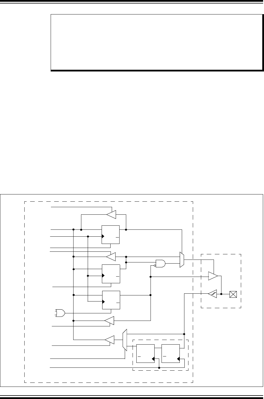
PIC32 Family Reference Manual
DS61120E-page 12-2 © 2007-2011 Microchip Technology Inc.
12.1 INTRODUCTION
The general purpose I/O pins can be considered the simplest of peripherals. These I/O pins allow
the PIC32 microcontroller to monitor and control other devices. To add flexibility and functionality
to a device, some pins are multiplexed with alternate function(s). These functions depend on
which peripheral features are on the device. In general, when a peripheral is functioning, that pin
may not be used as a general purpose I/O pin.
Following are some of the key features of the I/O Ports module:
•Individual output pin open-drain enable/disable
•Individual input pin pull-up enable/disable
• Monitor select inputs and generate interrupt on mismatch condition
•Operate during CPU Sleep and Idle modes
• Fast bit manipulation using CLR, SET and INV registers
A block diagram of a typical I/O port structure is shown in Figure 12-1. The diagram depicts the
many peripheral functions that can be multiplexed onto the I/O pin.
Figure 12-1: Typical Port Structure Block Diagram
Note: This family reference manual section is meant to serve as a complement to device
data sheets. Depending on the device variant, this manual section may not apply to
all PIC32 devices.
Please consult the note at the beginning of the “I/O Ports” chapter in the current
device data sheet to check whether this document supports the device you are
using.
Device data sheets and family reference manual sections are available for
download from the Microchip Worldwide Web site at: http://www.microchip.com
WR LATx
I/O pin
WR PORTx
Data Bus
RD LATx
RD PORTx
RD TRISx
WR TRISx
I/O Cell
Dedicated Port Module
0
1
RD ODCx
SYSCLK
QD
CK
EN Q
QD
CK
EN
Q
QD
CK
EN Q
QD
CK
Q
QD
CK
Q
0
1
Synchronization
SYSCLK
WR ODCx
ODCx
TRISx
LATx
SLEEP

© 2007-2011 Microchip Technology Inc. DS61120E-page 12-3
Section 12. I/O Ports
I/O Ports
12
12.2 CONTROL REGISTERS
Before reading and writing any I/O port, the desired pin(s) should be properly configured for the
application. Each I/O port has nine registers directly associated with the operation of the port and
one control register. Each I/O port pin has a corresponding bit in these registers. Throughout this
section, the letter ‘x’, denotes any or all port module instances. For example TRISx would repre-
sent TRISA, TRISB, TRISC, and so on. Any bit and its associated data and control registers that
is not valid for a particular device will be disabled and will read as zeros.
For additional information on the registers in this section, refer to the specific device data sheet.
12.2.1 Registers for Configuring Tri-state Functions (TRISx)
TRISx registers configure the data direction flow through port I/O pin(s). The TRISx register bits
determine whether a PORTx I/O pin is an input or an output:
• If data direction bit is ‘1’, the corresponding I/O port pin is an input
• If data direction bit is ‘0’, the corresponding I/O port pin is an output
•A read from a TRISx register reads the last value written to the TRISx register
• All I/O port pins are defined as inputs after a Power-on Reset
12.2.2 Registers for Configuring PORT Functions (PORTx)
PORTx registers allow I/O pins to be accessed:
•A write to a PORTx register writes to the corresponding LATx register (PORTx data latch).
Those I/O port pin(s) configured as outputs are updated.
•A write to a PORTx register is the effectively the same as a write to a LATx register
•A read from a PORTx register reads the synchronized signal applied to the port I/O pins
12.2.3 Registers for Configuring Latch Functions (LATx)
LATx registers (PORTx data latch) hold data written to port I/O pin(s):
•A write to a LATx register latches data to corresponding port I/O pins. Those I/O port pin(s)
configured as outputs are updated.
•A read from LATx register reads the data held in the PORTx data latch, not from the port
I/O pins
12.2.4 Registers for Open-Drain Configuration (ODCx)
Each I/O pin can be individually configured for either normal digital output or open-drain output.
This is controlled by the Open-Drain Control register, ODCx, associated with each I/O pin. If the
ODCx bit for an I/O pin is a ‘1’, the pin acts as an open-drain output. If the ODCx bit for an I/O
pin is a ‘0’, the pin is configured for a normal digital output (the ODCx bit is valid only for output
pins). After a Reset, the status of all the bits of the ODCx register is set to ‘0’.
The open- drain feature allows the generation of outputs higher than VDD (for example, 5V) on
any desired 5V-tolerant pins by using external pull-up resistors. The maximum open-drain
voltage allowed is the same as the maximum VIH specification. The ODCx register setting takes
effect in all the I/O modes, allowing the output to behave as an open-drain even if a peripheral is
controlling the pin. Although the user could achieve the same effect by manipulating the
corresponding LATx and TRISx bits, this procedure will not allow the peripheral to operate in
Open-Drain mode (except for the default operation of the I2C™ pins). Since I2C pins are already
open-drain pins, the ODCx settings do not affect the I2C pins. Also, the ODCx settings do not
affect the JTAG output characteristics as the JTAG scan cells are inserted between the ODCx
logic and the I/O.
Note: Not all registers and associated bits are available on all devices. Refer to the
specific device data sheet for further details.

PIC32 Family Reference Manual
DS61120E-page 12-4 © 2007-2011 Microchip Technology Inc.
12.2.5 Registers for Configuring Analog and Digital Port Pins
(ANSELx)
The ANSELx (or AD1PCFG) register controls the operation of the analog port pins. The port pins
that are to function as analog inputs must have their corresponding ANSEL and TRISx bits set
(or AD1PCFG cleared). In order to use port pins for I/O functionality with digital modules, like
Timers, UARTs, etc., the corresponding ANSELx bit must be cleared (or AD1PCFG set).
The ANSELx register has a default value of 0xFFFF (or 0x0000 for AD1PCFG); therefore, all pins
that share analog functions are analog (not digital) by default.
If the TRISx bit is cleared (output) while the ANSELx bit is set (or AD1PCFG is cleared), the
digital output level (VOH or VOL) is converted by an analog peripheral, such as the ADC module
or the Comparator module.
When the PORTx register is read, all pins configured as analog input channels are read as
cleared (a low level).
Pins configured as digital inputs do not convert an analog input. Analog levels on any pin defined
as a digital input (including the ANx pins) can cause the input buffer to consume current that
exceeds the device specifications.
12.2.6 Registers for Input Change Notification
The input Change Notification (CN) function of the I/O ports allows the PIC32 devices to generate
interrupt requests to the processor in response to a change-of-state on selected input pins. This
feature can detect input change-of-states even in Sleep mode, when the clocks are disabled.
Five control registers are associated with the CN functionality of each I/O port:
•Change Notice Enable (CNENx)
• Change Notice Status (CNSTATx)
•Change Notice Pull-up Enable (CNPUEx)
•Change Notice Pull-down Enable (CNPDx)
•Change Notice Control (CNCONx)
The CNENx registers contain the CN interrupt enable control bits for each of the input pins. Setting
any of these bits enables a CN interrupt for the corresponding pins.
The CNSTATx register indicates whether a change occurred on the corresponding pin since the
last read of the PORTx bit.
Each I/O pin also has a weak pull-up and a weak pull-down connected to it. The pull-ups act
as a current source or sink source connected to the pin, and eliminate the need for external
resistors when push-button or keypad devices are connected. The pull-ups and pull-downs
are enabled separately using the CNPUEx and the CNPDx registers, which contain the
control bits for each of the pins. Setting any of the control bits enables the weak pull-ups
and/or pull-downs for the corresponding pins.
An additional control register (CNCONx) is shown in Register 12-1.
12.2.7 Registers for Peripheral Pin Select
The Peripheral Pin Select [pin name]R register (Register 12-2) and the Peripheral Pin Select
Output (RPnR) register (Register 12-3) provide the control bits for peripheral pin select input and
output. See 12.3.1.4 “Input Mapping” and 12.3.1.5 “Output Mapping” for detailed information
on configuring these registers.
Note: Pull-ups and pull-downs on change notification pins should always be disabled
when the port pin is configured as a digital output.

© 2007-2011 Microchip Technology Inc. DS61120E-page 12-5
Section 12. I/O Ports
I/O Ports
12
12.2.8 SET, CLR, and INV I/O Port Registers
Every I/O module register has corresponding SET, CLR and INV register which provide atomic
bit manipulations. As the name of the register implies, a value written to a SET, CLR or INV reg-
ister effectively performs the implied operation, but only on the corresponding base register and
only bits specified as ‘1’ are modified. Bits specified as ‘0’ are not modified.
•Writing 0x0001 to TRISASET register sets only bit 0 in the base register TRISA
•Writing 0x0020 to PORTDCLR register clears only bit 5 in the base register PORTD
• Writing 0x9000 to LATCINV register inverts only bits 15 and 12 in the base register LATC
Reading SET, CLR and INV registers return an undefined value. To see the affects of a write
operation to a SET, CLR or INV register, the base register must be read instead.
The SET, CLR and INV registers are available for all modules and their registers, unless noted
in the specific device data sheet. A typical method to toggle an I/O pin requires a
read-modify-write operation performed on a PORTx register in software. For example, a read
from a PORTx register, mask and modify the desired output bit(s), write the resulting value back
to the PORTx register. This method is vulnerable to a read-modify-write issue where the port
value may change after it is read and before the modified data can be written back, thus changing
the previous state. This method also requires more instructions.
PORTA ^ = 0x0001;
A more efficient and atomic method uses the PORTxINV register. A write to the PORTxINV reg-
ister effectively performs a read-modify-write operation on the target base register, equivalent to
the software operation described above; however, it is done in hardware. To toggle an I/O pin
using this method, a ‘1’ is written to the corresponding bit in the PORTxINV register. This opera-
tion will read the PORTx register, invert only those bits specified as ‘1’ and write the resulting
value to the LATx register, thus toggling the corresponding I/O pin(s) all in a single atomic
instruction cycle.
PORTAINV = 0x0001;
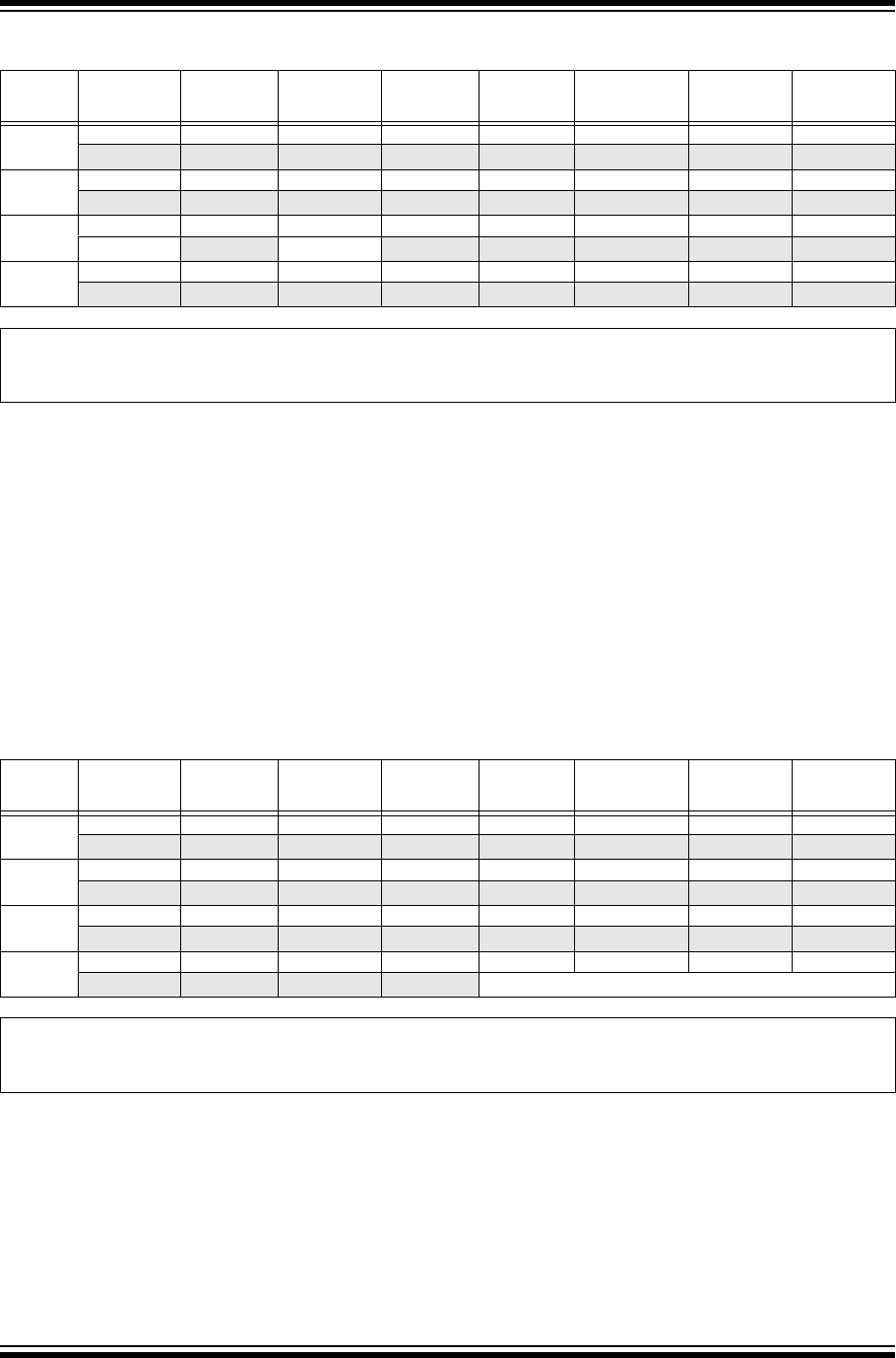
PIC32 Family Reference Manual
DS61120E-page 12-6 © 2007-2011 Microchip Technology Inc.
Register 12-1: CNCONx: Change Notice Control Register
Bit
Range
Bit
31/23/15/7
Bit
30/22/14/6
Bit
29/21/13/5
Bit
28/20/12/4
Bit
27/19/11/3
Bit
26/18/10/2
Bit
25/17/9/1
Bit
24/16/8/0
31:24 U-0 U-0 U-0 U-0 U-0 U-0 U-0 U-0
— — — — — — — —
23:16 U-0 U-0 U-0 U-0 U-0 U-0 U-0 U-0
— — — — — — — —
15:8 R/W-0 U-0 R/W-0 U-0 U-0 U-0 U-0 U-0
ON —SIDL — — — — —
7:0 U-0 U-0 U-0 U-0 U-0 U-0 U-0 U-0
— — — — — — — —
Legend:
R = Readable bit W = Writable bit U = Unimplemented bit, read as ‘0’
-n = Value at POR ‘1’ = Bit is set ‘0’ = Bit is cleared x = Bit is unknown
bit 31-16 Unimplemented: Read as ‘0’
bit 15 ON: Change Notice (CN) Control ON bit
1 = CN is enabled
0 = CN is disabled
bit 14 Unimplemented: Read as ‘0’
bit 13 SIDL: Stop in Idle Control bit
1 = CPU Idle Mode halts CN operation
0 = CPU Idle does not affect CN operation
bit 12-0 Unimplemented: Read as ‘0’
Register 12-2: [pin name]R: Peripheral Pin Select Input Register(1)
Bit
Range
Bit
31/23/15/7
Bit
30/22/14/6
Bit
29/21/13/5
Bit
28/20/12/4
Bit
27/19/11/3
Bit
26/18/10/2
Bit
25/17/9/1
Bit
24/16/8/0
31:24 U-0 U-0 U-0 U-0 U-0 U-0 U-0 U-0
— — — — — — — —
23:16 U-0 U-0 U-0 U-0 U-0 U-0 U-0 U-0
— — — — — — — —
15:8 U-0 U-0 U-0 U-0 U-0 U-0 U-0 U-0
— — — — — — — —
7:0 U-0 U-0 U-0 U-0 R/W-0 R/W-0 R/W-0 R/W-0
— — — — [pin name]R<3:0>
Legend:
R = Readable bit W = Writable bit U = Unimplemented bit, read as ‘0’
-n = Value at POR ‘1’ = Bit is set ‘0’ = Bit is cleared x = Bit is unknown
bit 31-4 Unimplemented: Read as ‘0’
bit 3-0 [pin name]R<3:0>: Peripheral Pin Select Input bits
Where [pin name] refers to the pins that are used to configure peripheral input mapping. See Tab le 12-1 for
input pin selection values.
Note 1: Register values can only be changed if the IOLOCK Configuration bit (CFGCON<13>) = 0.

© 2007-2011 Microchip Technology Inc. DS61120E-page 12-7
Section 12. I/O Ports
I/O Ports
12
Register 12-3: RPnR: Peripheral Pin Select Output Register(1)
Bit
Range
Bit
31/23/15/7
Bit
30/22/14/6
Bit
29/21/13/5
Bit
28/20/12/4
Bit
27/19/11/3
Bit
26/18/10/2
Bit
25/17/9/1
Bit
24/16/8/0
31:24 U-0 U-0 U-0 U-0 U-0 U-0 U-0 U-0
— — — — — — — —
23:16 U-0 U-0 U-0 U-0 U-0 U-0 U-0 U-0
— — — — — — — —
15:8 U-0 U-0 U-0 U-0 U-0 U-0 U-0 U-0
— — — — — — — —
7:0 U-0 U-0 U-0 U-0 R/W-0 R/W-0 R/W-0 R/W-0
— — — — RPnR<3:0>
Legend:
R = Readable bit W = Writable bit U = Unimplemented bit, read as ‘0’
-n = Value at POR ‘1’ = Bit is set ‘0’ = Bit is cleared x = Bit is unknown
bit 31-4 Unimplemented: Read as ‘0’
bit 3-0 RPnR<3:0>: Peripheral Pin Select Output bits
See Tab l e 12-2 for output pin selection values.
Note 1: Register values can only be changed if the IOLOCK Configuration bit (CFGCON<13>) = 1.

PIC32 Family Reference Manual
DS61120E-page 12-8 © 2007-2011 Microchip Technology Inc.
12.3 MODES OF OPERATION
12.3.1 Peripheral Pin Select (PPS)
A major challenge in general purpose devices is providing the largest possible set of peripheral
features while minimizing the conflict of features on I/O pins. The challenge is even greater on
low pin-count devices. In an application where more than one peripheral needs to be assigned
to a single pin, inconvenient work arounds in application code or a complete redesign may be the
only option.
Peripheral Pin Select (PPS) configuration provides an alternative to these choices by enabling
peripheral set selection and their placement on a wide range of I/O pins. By increasing the pinout
options available on a particular device, users can better tailor the device to their entire
application, rather than trimming the application to fit the device.
The PPS configuration feature operates over a fixed subset of digital I/O pins. Users may inde-
pendently map the input and/or output of most digital peripherals to these I/O pins. PPS is per-
formed in software and generally does not require the device to be reprogrammed. Hardware
safeguards are included that prevent accidental or spurious changes to the peripheral mapping
once it has been established.
12.3.1.1 AVAILABLE PINS
The number of available pins is dependent on the particular device and its pin count. Pins that
support the PPS feature include the designation “RPn” in their full pin designation, where “RP”
designates a remappable peripheral and “n” is the remappable port number.
12.3.1.2 AVAILABLE PERIPHERALS
The peripherals managed by the PPS are all digital-only peripherals. These include general
serial communications (UART and SPI), general purpose timer clock inputs, timer-related
peripherals (input capture and output compare) and interrupt-on-change inputs.
In comparison, some digital-only peripheral modules are never included in the PPS feature. This
is because the peripheral’s function requires special I/O circuitry on a specific port and cannot be
easily connected to multiple pins. These modules include I2C among others. A similar require-
ment excludes all modules with analog inputs, such as the ADC.
A key difference between remappable and non-remappable peripherals is that remappable
peripherals are not associated with a default I/O pin. The peripheral must always be assigned to
a specific I/O pin before it can be used. In contrast, non-remappable peripherals are always
available on a default pin, assuming that the peripheral is active and not conflicting with another
peripheral.
When a remappable peripheral is active on a given I/O pin, it takes priority over all other digital
I/O and digital communication peripherals associated with the pin. Priority is given regardless of
the type of peripheral that is mapped. Remappable peripherals never take priority over any
analog functions associated with the pin.
12.3.1.3 CONTROLLING PPS
PPS features are controlled through two sets of SFRs: one to map peripheral inputs, and one to
map outputs. Because they are separately controlled, a particular peripheral’s input and output
(if the peripheral has both) can be placed on any selectable function pin without constraint.
The association of a peripheral to a peripheral-selectable pin is handled in two different ways,
depending on whether an input or output is being mapped.
Note: See the specific device data sheet for availability.

© 2007-2011 Microchip Technology Inc. DS61120E-page 12-9
Section 12. I/O Ports
I/O Ports
12
12.3.1.4 INPUT MAPPING
The inputs of the PPS options are mapped on the basis of the peripheral. That is, a control register
associated with a peripheral dictates the pin it will be mapped to. The [pin name]R registers, where
[pin name] refers to the peripheral pins listed in Tab le 12-1, are used to configure peripheral input
mapping (see Register 12-2). Each register contains a set of four bit fields. Programming these
bit fields with an appropriate value, maps the RPn pin with the corresponding value to that
peripheral. Ta bl e 12-1 provides an example of the valid range of values for any bit field.
For example, Figure 12-2 illustrates the remappable pin selection for the U1RX input.
Figure 12-2: Remappable Input Example for U1RX
Note: See the specific device data sheet for Input Pin selection.
RPA2
RPB6
RPA4
0
1
2U1RX input
U1RXR<3:0>
to peripheral
RP
n
n
Note: For input only, PPS functionality does not have priority over TRISx settings. Therefore,
when configuring RPn pin for input, the corresponding bit in the TRISx register must also
be configured for input (set to ‘1’).

PIC32 Family Reference Manual
DS61120E-page 12-10 © 2007-2011 Microchip Technology Inc.
Table 12-1: Input Pin Selection(1)
Peripheral Pin [pin name]R SFR [pin name]R bits [pin name]R Value to
RPn Pin Selection
INT4 INT4R INT4R<3:0> 0000 = RPA0
0001 = RPB3
0010 = RPB4
0011 = RPB15
0100 = RPB7
0101 = RPC7
0110 = RPC0
0111 = RPC5
1000 = Reserved
•
•
•
1111 = Reserved
T2CK T2CKR T2CKR<3:0>
IC4 IC4R IC4R<3:0>
SS1 SS1R SS1R<3:0>
REFCLKI REFCLKIR REFCLKIR<3:0>
INT3 INT3R INT3R<3:0> 0000 = RPA1
0001 = RPB5
0010 = RPB1
0011 = RPB11
0100 = RPB8
0101 = RPA8
0110 = RPC8
0111 = RPA9
1000 = Reserved
•
•
•
1111 = Reserved
T3CK T3CKR T3CKR<3:0>
IC3 IC3R IC3R<3:0>
U1CTS U1CTSR U1CTSR<3:0>
U2RX U2RXR U2RXR<3:0>
SDI1 SDI1R SDI1R<3:0>
INT2 INT2R INT2R<3:0> 0000 = RPA2
0001 = RPB6
0010 = RPA4
0011 = RPB13
0100 = RPB2
0101 = RPC6
0110 = RPC1
0111 = RPC3
1000 = Reserved
•
•
•
1111 = Reserved
T4CK T4CKR T4CKR<3:0>
IC1 IC1R IC1R<3:0>
IC5 IC5R IC5R<3:0>
U1RX U1RXR U1RXR<3:0>
U2CTS U2CTSR U2CTSR<3:0>
SDI2 SDI2R SDI2R<3:0>
OCFB OCFBR OCFBR<3:0>
INT1 INT1R INT1R<3:0> 0000 = RPA3
0001 = RPB14
0010 = RPB0
0011 = RPB10
0100 = RPB9
0101 = RPC9
0110 = RPC2
0111 = RPC4
1000 = Reserved
•
•
•
1111 = Reserved
T5CK T5CKR T5CKR<3:0>
IC2 IC2R IC2R<3:0>
SS2 SS2R SS2R<3:0>
OCFA OCFAR OCFAR<3:0>
Note 1: This table provides an example of input pin selection. See the specific device data
sheet for available selections.

© 2007-2011 Microchip Technology Inc. DS61120E-page 12-11
Section 12. I/O Ports
I/O Ports
12
12.3.1.5 OUTPUT MAPPING
In contrast to inputs, the outputs of the PPS options are mapped on the basis of the pin. In
this case, a control register associated with a particular pin dictates the peripheral output to
be mapped. The RPnR registers (Register 12-3) are used to control output mapping. Like the
[pin name]R registers, each register contains a set of four bit fields. The value of the bit field
corresponds to one of the peripherals, and that peripheral’s output is mapped to the pin (see
Tabl e 12-2 and Figure 12-3).
A null output is associated with the output register reset value of ‘0’. This is done to ensure that
remappable outputs remain disconnected from all output pins by default.
Figure 12-3: Example of Multiplexing of Remappable Output for RPA0
12.3.1.6 CONTROLLING CONFIGURATION CHANGES
Because peripheral remapping can be changed during run time, some restrictions on peripheral
remapping are needed to prevent accidental configuration changes. PIC32 devices include two
features to prevent alterations to the peripheral map:
•Control register lock sequence
•Configuration bit select lock
12.3.1.6.1 Control Register Lock
Under normal operation, writes to the RPnR and [pin name]R registers are not allowed.
Attempted writes appear to execute normally, but the contents of the registers remain
unchanged. To change these registers, they must be unlocked in hardware. The register lock
is controlled by the IOLOCK Configuration bit (CFGCON<13>). Setting the IOLOCK bit
prevents writes to the control registers; clearing the IOLOCK bit allows writes.
To s et or cle ar the I OLO CK bit , a n u nlock sequence must be executed. Refer to Section 6.
“Oscillator” (DS61112) in the “PIC32 Family Reference Manual” for details.
12.3.1.6.2 Configuration Bit Select Lock
As an additional level of safety, the device can be configured to prevent more than one write ses-
sion to the RPnR and [pin name]R registers. The IOL1WAY Configuration bit (DEVCFG3<29>)
blocks the IOLOCK bit from being cleared after it has been set once. If the IOLOCK bit remains
set, the register unlock procedure does not execute, and the PPS control registers cannot be
written to. The only way to clear the bit and re-enable peripheral remapping is to perform a device
Reset.
In the default (unprogrammed) state, the IOL1WAY bit is set, restricting users to one write
session.
RPA0R<3:0>
0
15
1
Default
U1TX Output
U1RTS Output 2
14
Output Data
RPA0

PIC32 Family Reference Manual
DS61120E-page 12-12 © 2007-2011 Microchip Technology Inc.
Table 12-2: Output Pin Selection(1)
RPn Port Pin RPnR SFR RPnR bits RPnR Value to
Peripheral Selection
RPA0 RPA0R RPA0R<3:0> 0000 = No Connect
0001 = U1TX
0010 = U2RTS
0011 = SS1
0100 = Reserved
0101 = OC1
0110 = Reserved
0111 = C2OUT
1000 = Reserved
•
•
•
1111 = Reserved
RPB3 RPB3R RPB3R<3:0>
RPB4 RPB4R RPB4R<3:0>
RPB15 RPB15R RPB15R<3:0>
RPB7 RPB7R RPB7R<3:0>
RPC7 RPC7R RPC7R<3:0>
RPC0 RPC0R RPC0R<3:0>
RPC5 RPC5R RPC5R<3:0>
RPA1 RPA1R RPA1R<3:0> 0000 = No Connect
0001 = Reserved
0010 = Reserved
0011 = SDO1
0100 = SDO2
0101 = OC2
0110 = Reserved
•
•
•
1111 = Reserved
RPB5 RPB5R RPB5R<3:0>
RPB1 RPB1R RPB1R<3:0>
RPB11 RPB11R RPB11R<3:0>
RPB8 RPB8R RPB8R<3:0>
RPA8 RPA8R RPA8R<3:0>
RPC8 RPC8R RPC8R<3:0>
RPA9 RPA9R RPA9R<3:0>
RPA2 RPA2R RPA2R<3:0> 0000 = No Connect
0001 = Reserved
0010 = Reserved
0011 = SDO1
0100 = SDO2
0101 = OC4
0110 = OC5
0111 = REFCLKO
1000 = Reserved
•
•
•
1111 = Reserved
RPB6 RPB6R RPB6R<3:0>
RPA4 RPA4R RPA4R<3:0>
RPB13 RPB13R RPB13R<3:0>
RPB2 RPB2R RPB2R<3:0>
RPC6 RPC6R RPC6R<3:0>
RPC1 RPC1R RPC1R<3:0>
RPC3 RPC3R RPC3R<3:0>
RPA3 RPA3R RPA3R<3:0> 0000 = No Connect
0001 = U1RTS
0010 = U2TX
0011 = Reserved
0100 = SS2
0101 = OC3
0110 = Reserved
0111 = C1OUT
1000 = Reserved
•
•
•
1111 = Reserved
RPB14 RPB14R RPB14R<3:0>
RPB0 RPB0R RPB0R<3:0>
RPB10 RPB10R RPB10R<3:0>
RPB9 RPB9R RPB9R<3:0>
RPC9 RPC9R RPC9R<3:0>
RPC2 RPC2R RPC2R<3:0>
RPC4 RPC4R RPC4R<3:0>
RPC3 RPC3R RPC3R<3:0>
Note 1: This table provides an example of output pin selection. See the specific device data
sheet for available selections.

© 2007-2011 Microchip Technology Inc. DS61120E-page 12-13
Section 12. I/O Ports
I/O Ports
12
12.3.2 Peripheral Multiplexing
Many pins also support one or more peripheral modules. When configured to operate with a
peripheral, a pin may not be used for general input or output. In many cases, a pin must still be
configured for input or output, although some peripherals override the TRISx configuration.
Figure 12-4 shows how ports are shared with other peripherals, and the associated I/O pin to
which they are connected. For some PIC32 devices, multiple peripheral functions may be
multiplexed on each I/O pin. The priority of the peripheral function depends on the order of the
pin description in the pin diagram of the specific device data sheet.
Note that the output of a pin can be controlled by the TRISx register bit or, in some cases, by the
peripheral itself.
Figure 12-4: Block Diagram of a Typical Shared Port Structure(1)
Peripheral Output Data
Peripheral Module
Peripheral Output Enable
PI/O Module
Peripheral Module Enable
WR LATx
I/O pin
WR PORTx
Data Bus
RD LATx
RD PORTx
RD TRISx
WR TRISx
0
1
RD ODCx
SYSCLK
QD
CK
EN Q
QD
CK
EN Q
QD
CK
EN Q
QD
CK
Q
QD
CK
Q
0
1
SYSCLK
WR ODCx
ODCx
TRISx
LATx
SLEEP
1
0
1
0
Output Multiplexers
I/O Cell
Synchronization
R(2)
Peripheral Input
Note 1: This block diagram is a general representation of a shared port/peripheral structure for illustration purposes only.
The actual structure for any specific port/peripheral combination may be different than what is shown here.
2: R = Peripheral input buffer types may vary. Refer to the specific device data sheet for peripheral details.
Peripheral Input Buffer

PIC32 Family Reference Manual
DS61120E-page 12-14 © 2007-2011 Microchip Technology Inc.
12.3.2.1 MULTIPLEXED DIGITAL INPUT PERIPHERAL
The following conditions are characteristic of a multiplexed digital input peripheral:
•Peripheral does not control the TRISx register
Some peripherals require the pin be configured as an input by setting the corresponding
TRISx bit = 1
•Peripheral input path is independent of I/O input path and uses an input buffer that
is dependent on the peripheral
• PORTx register data input path is not affected and is able to read the pin value
12.3.2.2 MULTIPLEXING DIGITAL OUTPUT PERIPHERAL
The following conditions are characteristic of a multiplexed digital output peripheral:
• Peripheral controls the output data
Some peripherals require the pin be configured as an output by setting the corresponding
TRISx bit = 0
•If a peripheral pin has an automatic tri-state feature (e.g., PWM outputs), the peripheral has
the ability to tri-state the pin
•Pin output driver type could be affected by peripheral (e.g., drive strength, slew rate, etc.)
•PORTx register output data has no effect
12.3.2.3 MULTIPLEXING DIGITAL BIDIRECTIONAL PERIPHERAL
The following conditions are characteristic of a multiplexed digital bidirectional peripheral:
•Peripheral automatically configures the pin as an output, but not as an input
Some peripherals require the pin be configured as an input by setting the corresponding
TRISx bit = 1
•Peripherals control output data
•Pin output driver type could be affected by peripheral (e.g., drive strength, slew rate, etc.)
• PORTx register data input path is not affected and is able to read the pin value
•PORTx register output data has no effect
12.3.2.4 MULTIPLEXING ANALOG INPUT PERIPHERAL
The following condition is characteristic of a multiplexed analog input peripheral:
All digital port input buffers are disabled and PORTx registers read ‘0’ to prevent crowbar current.
12.3.2.5 MULTIPLEXING ANALOG OUTPUT PERIPHERAL
The following conditions are characteristic of a multiplexed analog output peripheral:
•All digital port input buffers are disabled and PORTx registers read ‘0’ to prevent
crowbar current
•Analog output is driven onto the pin independent of the associated TRISx setting
12.3.2.6 SOFTWARE INPUT PIN CONTROL
Some of the functions assigned to an I/O pin may be input functions that do not take control of
the pin output driver. An example of one such peripheral is the Input Capture module. If the I/O
pin associated with the input capture is configured as an output, using the appropriate
TRISx control bit, the user can manually affect the state of the input capture pin through its
corresponding LATx register. This behavior can be useful in some situations, especially for
testing purposes, when no external signal is connected to the input pin.
Note: In order to use pins that are multiplexed with the ADC module for digital I/O, the
corresponding bits in the AD1PCFG register, if present, must be set to ‘1’, even if
the ADC module is turned off.

© 2007-2011 Microchip Technology Inc. DS61120E-page 12-15
Section 12. I/O Ports
I/O Ports
12
As shown previously in Figure 12-4, the organization of the peripheral multiplexers determines
whether the peripheral input pin can be manipulated in software using the PORTx register. The
conceptual peripherals shown in this figure disconnect the PORTx data from the I/O pin when the
peripheral function is enabled.
In general, the following peripherals allow their input pins to be controlled manually through the
LATx registers:
•External Interrupts pins
•Input Capture pins
•Timer Clock input pins
•PWM Fault pins
Most serial communication peripherals, when enabled, take full control of the I/O pin so that the
input pins associated with the peripheral cannot be affected through the corresponding PORTx
registers. These peripherals include the following modules:
•SPI
•I
2C
•UART
12.3.3 Change Notification Pins
The Change Notification (CN) pins provide PIC32 devices the ability to generate interrupt
requests to the processor in response to a change of state on selected input pins (corresponding
TRISx bits must be = 1). The total number of available CN inputs is dependent on the selected
PIC32 device. Refer to the specific device data sheet for further details.
The enabled pin values are compared with the values sampled during the last read operation of
the designated PORTx register. If the pin value is different from the last value read, a mismatch
condition is generated. The mismatch condition can occur on any of the enabled input pins. The
mismatches are ORed together to provide a single interrupt-on-change signal. The enabled pins
are sampled on every internal system clock cycle, SYSCLK.
12.3.3.1 CN CONFIGURATION AND OPERATION
The CN pins are configured as follows:
1. Disable CPU interrupts.
2. Set desired CN I/O pin as input by setting corresponding TRISx register bits = 1.
3. Enable the CN Module ON bit (CNCON<15>) = 1.
4. Enable individual CN input pin(s), enable optional pull up(s) or pull down(s).
5. Read corresponding PORTx registers to clear mismatch condition on CN input pins.
6. Configure the CN interrupt priority bits, CNIP<2:0> (IPC6<20:18>), and subpriority bits
CNIS<1:0> (IPC6<17:16>).
7. Clear the CN interrupt flag bit, CNIF(IFS1<0>) = 0.
8. Enable the CN interrupt enable bit, CNIE (IEC1<0>) = 1.
9. Enable CPU interrupts.
When a CN interrupt occurs, the user should read the PORTx register associated with the CN
pin(s). This will clear the mismatch condition and set up the CN logic to detect the next pin change.
The current PORTx value can be compared to the PORTx read value obtained at the last CN inter-
rupt or during initialization, and used to determine which pin changed.The CN pins have a minimum
input pulse-width specification. Refer to the “Electrical Characteristics” chapter of the specific
device data sheet to learn more.
Note: If the I/O pin is shared with an analog peripheral, it may be necessary to configure
this pin as digital input.

PIC32 Family Reference Manual
DS61120E-page 12-16 © 2007-2011 Microchip Technology Inc.
12.3.4 Boundary Scan Cell Connections
The PIC32 devices support JTAG boundary scan. A Boundary Scan Cell (BSC) is inserted
between the internal I/O logic circuit and the I/O pin, as shown in Figure 12-5. Most of the I/O
pads have boundary scan cells; however, JTAG pads do not. For normal I/O operation, the BSC
is disabled, and therefore, bypassed. The output enable input of the BSC is directly connected
to the BSC output enable, and the output data input of the BSC is directly connected to the BSC
output data. The pads that do not have BSC are the power supply pads (VDD, VSS and
VCAP/VCORE) and the JTAG pads (TCK, TDI, TDO, and TMS).
Figure 12-5: Boundary Scan Cell Connections
I/O pin
1
0
1
0
I/O
Peripheral Output Enable
Output Multiplexers
Peripheral Module Enable
Boundary
Scan Cell
(BSC)
BSC Input
BSC Enable
0
1
Output
Enable
Output Data
BSC Output
Enable
BSC Output
Data
Peripheral Output Enable
Input Data
Output LATx Data
TRISx
Data
Open-Drain Selection

© 2007-2011 Microchip Technology Inc. DS61120E-page 12-17
Section 12. I/O Ports
I/O Ports
12
12.4 OPERATION IN POWER-SAVING MODES
12.4.1 I/O Port Operation in Sleep Mode
As the device enters Sleep mode, the system clock is disabled; however, the CN
module continues to operate. If one of the enabled CN pins changes state, the CNIF bit
(IFS1<0>) will be set. If the CNIE bit (IEC1<0>) is set, and its priority is greater than current CPU
priority, the device will wake from Sleep or Idle mode and execute the CN Interrupt Service
Routine.
If the assigned priority level of the CN interrupt is less than or equal to the current CPU priority
level, the CPU will not be awakened and the device will enter Idle mode.
12.4.2 I/O Port Operation in Idle Mode
As the device enters Idle mode, the system clock sources remain functional. The SIDL bit
(CNCON<13>) selects whether the module will stop or continue functioning in Idle mode.
•If SIDL = 1, the module will continue to sample Input CN I/O pins in Idle mode; however,
synchronization is disabled
•If SIDL = 0, the module will continue to synchronize and sample Input CN I/O pins in Idle
mode
12.5 EFFECTS OF VARIOUS RESETS
12.5.1 Device Reset
All I/O registers are forced to their reset states upon a device Reset.
12.5.2 Power-on Reset
All I/O registers are forced to their reset states upon a Power-on Reset.
12.5.3 Watchdog Reset
All I/O registers are unchanged upon a Watchdog Reset.

PIC32 Family Reference Manual
DS61120E-page 12-18 © 2007-2011 Microchip Technology Inc.
12.6 RELATED APPLICATION NOTES
This section lists application notes that are related to this section of the manual. These
application notes may not be written specifically for the PIC32 device family, but the concepts are
pertinent and could be used with modification and possible limitations. The current application
notes related to the I/O Ports are:
Title Application Note #
No related application notes at this time N/A
Note: Please visit the Microchip web site (www.microchip.com) for additional application
notes and code examples for the PIC32 family of devices.

© 2007-2011 Microchip Technology Inc. DS61120E-page 12-19
Section 12. I/O Ports
I/O Ports
12
12.7 REVISION HISTORY
Revision A (August 2007)
This is the initial released version of this document.
Revision B (October 2007)
Updated document to remove Confidential status.
Revision C (April 2008)
Revised status to Preliminary; Revised U-0 to r-x; Revised Register 12-13; Revised Figure 12-1
and 12-2.
Revision D (May 2008)
Revised Register 12-17, add note to FRZ; Add note to Registers 12-19, 12-30, 12-31; Revised
Example 12-1 and 12-2; Change Reserved bits from “Maintain as” to “Write”; Added Note to ON
bit (CNCONx Register).
Revision E (July 2011)
This revision includes the following changes:
•Added a note at the beginning of the section, which provides information on
complementary documentation
• Changed all occurrences of PIC32MX to PIC32
• Removed the paragraph about the I/O related SFRs in 12.1 “Introduction”
•Added 12.2.7 “Registers for Peripheral Pin Select”
•Removed all Interrupt registers
•Removed TRISx, PORTx, LATx, ODCx, CNEN, CNPUE registers and their associated
SET, INV, and CLR registers
•Removed the FRZ bit from the Change Notice Control register (see Register 12-1)
•Removed related Interrupts section and sub-sections
•Removed the operation of the I/O port in Debug mode from 12.4 “Operation in
Power-Saving Modes”
• Removed I/O Port Application, I/O Pin Control and Design Tips sections
•Removed 12.2.6 CN Control Registers section
•Renamed the section 12.2.5 ODCx Registers as 12.2.4 “Registers for Open-Drain Con-
figuration (ODCx)”
•Added section 12.2.5 “Registers for Configuring Analog and Digital Port Pins
(ANSELx)”
•Added section 12.2.6 “Registers for Input Change Notification”
•Added section 12.3.1 “Peripheral Pin Select (PPS)”
•In 12.3 “Modes of Operation”, removed sections on Digital Inputs, Analog Inputs, Digital
Outputs, Analog Outputs, Open-Drain Configuration and Port Descriptions
•Updated the note in the second point of 12.3.3.1 “CN Configuration and Operation”
•Modifications to register formatting and minor updates have been made throughout the
document

PIC32 Family Reference Manual
DS61120E-page 12-20 © 2007-2011 Microchip Technology Inc.
NOTES:

© 2007-2011 Microchip Technology Inc. DS61120E-page 12-21
Information contained in this publication regarding device
applications and the like is provided only for your convenience
and may be superseded by updates. It is your responsibility to
ensure that your application meets with your specifications.
MICROCHIP MAKES NO REPRESENTATIONS OR
WARRANTIES OF ANY KIND WHETHER EXPRESS OR
IMPLIED, WRITTEN OR ORAL, STATUTORY OR
OTHERWISE, RELATED TO THE INFORMATION,
INCLUDING BUT NOT LIMITED TO ITS CONDITION,
QUALITY, PERFORMANCE, MERCHANTABILITY OR
FITNESS FOR PURPOSE. Microchip disclaims all liability
arising from this information and its use. Use of Microchip
devices in life support and/or safety applications is entirely at
the buyer’s risk, and the buyer agrees to defend, indemnify and
hold harmless Microchip from any and all damages, claims,
suits, or expenses resulting from such use. No licenses are
conveyed, implicitly or otherwise, under any Microchip
intellectual property rights.
Trademarks
The Microchip name and logo, the Microchip logo, dsPIC,
KEELOQ, KEELOQ logo, MPLAB, PIC, PICmicro, PICSTART,
PIC32 logo, rfPIC and UNI/O are registered trademarks of
Microchip Technology Incorporated in the U.S.A. and other
countries.
FilterLab, Hampshire, HI-TECH C, Linear Active Thermistor,
MXDEV, MXLAB, SEEVAL and The Embedded Control
Solutions Company are registered trademarks of Microchip
Technology Incorporated in the U.S.A.
Analog-for-the-Digital Age, Application Maestro, chipKIT,
chipKIT logo, CodeGuard, dsPICDEM, dsPICDEM.net,
dsPICworks, dsSPEAK, ECAN, ECONOMONITOR,
FanSense, HI-TIDE, In-Circuit Serial Programming, ICSP,
Mindi, MiWi, MPASM, MPLAB Certified logo, MPLIB,
MPLINK, mTouch, Omniscient Code Generation, PICC,
PICC-18, PICDEM, PICDEM.net, PICkit, PICtail, REAL ICE,
rfLAB, Select Mode, Total Endurance, TSHARC,
UniWinDriver, WiperLock and ZENA are trademarks of
Microchip Technology Incorporated in the U.S.A. and other
countries.
SQTP is a service mark of Microchip Technology Incorporated
in the U.S.A.
All other trademarks mentioned herein are property of their
respective companies.
© 2007-2011, Microchip Technology Incorporated, Printed in
the U.S.A., All Rights Reserved.
Printed on recycled paper.
ISBN: 978-1-61341-374-6
Note the following details of the code protection feature on Microchip devices:
• Microchip products meet the specification contained in their particular Microchip Data Sheet.
• Microchip believes that its family of products is one of the most secure families of its kind on the market today, when used in the
intended manner and under normal conditions.
• There are dishonest and possibly illegal methods used to breach the code protection feature. All of these methods, to our
knowledge, require using the Microchip products in a manner outside the operating specifications contained in Microchip’s Data
Sheets. Most likely, the person doing so is engaged in theft of intellectual property.
• Microchip is willing to work with the customer who is concerned about the integrity of their code.
• Neither Microchip nor any other semiconductor manufacturer can guarantee the security of their code. Code protection does not
mean that we are guaranteeing the product as “unbreakable.”
Code protection is constantly evolving. We at Microchip are committed to continuously improving the code protection features of our
products. Attempts to break Microchip’s code protection feature may be a violation of the Digital Millennium Copyright Act. If such acts
allow unauthorized access to your software or other copyrighted work, you may have a right to sue for relief under that Act.
Microchip received ISO/TS-16949:2009 certification for its worldwide
headquarters, design and wafer fabrication facilities in Chandler and
Tempe, Arizona; Gresham, Oregon and design centers in California
and India. The Company’s quality system processes and procedures
are for its PIC® MCUs and dsPIC® DSCs, KEELOQ® code hopping
devices, Serial EEPROMs, microperipherals, nonvolatile memory and
analog products. In addition, Microchip’s quality system for the design
and manufacture of development systems is ISO 9001:2000 certified.

DS61120E-page 12- 22 © 2007-2011 Microchip Technology Inc.
AMERICAS
Corporate Office
2355 West Chandler Blvd.
Chandler, AZ 85224-6199
Tel: 480-792-7200
Fax: 480-792-7277
Technical Support:
http://www.microchip.com/
support
Web Address:
www.microchip.com
Atlanta
Duluth, GA
Tel: 678-957-9614
Fax: 678-957-1455
Boston
Westborough, MA
Tel: 774-760-0087
Fax: 774-760-0088
Chicago
Itasca, IL
Tel: 630-285-0071
Fax: 630-285-0075
Cleveland
Independence, OH
Tel: 216-447-0464
Fax: 216-447-0643
Dallas
Addison, TX
Tel: 972-818-7423
Fax: 972-818-2924
Detroit
Farmington Hills, MI
Tel: 248-538-2250
Fax: 248-538-2260
Indianapolis
Noblesville, IN
Tel: 317-773-8323
Fax: 317-773-5453
Los Angeles
Mission Viejo, CA
Tel: 949-462-9523
Fax: 949-462-9608
Santa Clara
Santa Clara, CA
Tel: 408-961-6444
Fax: 408-961-6445
Toronto
Mississauga, Ontario,
Canada
Tel: 905-673-0699
Fax: 905-673-6509
ASIA/PACIFIC
Asia Pacific Office
Suites 3707-14, 37th Floor
Tower 6, The Gateway
Harbour City, Kowloon
Hong Kong
Tel : 8 52 - 24 0 1- 120 0
Fax: 852-2401-3431
Australia - Sydney
Tel : 6 1-2 -98 68- 6 73 3
Fax: 61-2-9868-6755
China - Beijing
Tel : 8 6-1 0-8 569 - 70 0 0
Fax: 86-10-8528-2104
China - Chengdu
Tel : 8 6-2 8-8 665 - 55 11
Fax: 86-28-8665-7889
China - Chongqing
Tel : 8 6-2 3-8 980 - 95 8 8
Fax: 86-23-8980-9500
China - Hangzhou
Tel : 8 6-5 71- 2819 -31 80
Fax: 86-571-2819-3189
China - Hong Kong SAR
Tel : 8 52 - 24 0 1- 120 0
Fax: 852-2401-3431
China - Nanjing
Tel : 8 6-2 5-8 473 - 24 6 0
Fax: 86-25-8473-2470
China - Qingdao
Tel : 8 6-5 32- 8502 -73 55
Fax: 86-532-8502-7205
China - Shanghai
Tel : 8 6-2 1-5 407 - 55 3 3
Fax: 86-21-5407-5066
China - Shenyang
Tel : 8 6-2 4-2 334 - 28 2 9
Fax: 86-24-2334-2393
China - Shenzhen
Tel : 8 6-7 55- 8203 -26 60
Fax: 86-755-8203-1760
China - Wuhan
Tel : 8 6-2 7-5 980 - 53 0 0
Fax: 86-27-5980-5118
China - Xian
Tel : 8 6-2 9-8 833 - 72 5 2
Fax: 86-29-8833-7256
China - Xiamen
Tel: 86-592-2388138
Fax: 86-592-2388130
China - Zhuhai
Tel : 86- 756 -3 210 04 0
Fax: 86-756-3210049
ASIA/PACIFIC
India - Bangalore
Tel : 9 1- 8 0- 309 0-4 444
Fax: 91-80-3090-4123
India - New Delhi
Tel : 9 1- 11 -41 60- 86 31
Fax: 91-11-4160-8632
India - Pune
Tel : 9 1- 2 0- 256 6-1 512
Fax: 91-20-2566-1513
Japan - Yokohama
Tel : 8 1- 4 5- 471 - 6 166
Fax: 81-45-471-6122
Korea - Daegu
Tel : 8 2- 5 3- 744 -43 01
Fax: 82-53-744-4302
Korea - Seoul
Tel : 8 2- 2 -5 54- 720 0
Fax: 82-2-558-5932 or
82-2-558-5934
Malaysia - Kuala Lumpur
Tel : 6 0- 3 -6 201 -98 57
Fax: 60-3-6201-9859
Malaysia - Penang
Tel : 6 0- 4 -2 27- 887 0
Fax: 60-4-227-4068
Philippines - Manila
Tel : 6 3- 2 -6 34- 906 5
Fax: 63-2-634-9069
Singapore
Tel : 6 5- 6 33 4 -8 870
Fax: 65-6334-8850
Taiwan - Hsin Chu
Tel : 8 86 - 3- 657 8-3 00
Fax: 886-3-6578-370
Taiwan - Kaohsiung
Tel : 8 86 - 7- 213 -78 30
Fax: 886-7-330-9305
Taiwan - Taipei
Tel : 8 86 - 2- 250 0-6 610
Fax: 886-2-2508-0102
Thailand - Bangkok
Tel : 6 6- 2 -6 94- 135 1
Fax: 66-2-694-1350
EUROPE
Austria - Wels
Tel : 4 3- 7 24 2 -2 244 -39
Fax: 43-7242-2244-393
Denmark - Copenhagen
Tel : 4 5-4 450 -2 828
Fax: 45-4485-2829
France - Paris
Tel : 3 3-1 -6 9-5 3 -6 3-2 0
Fax: 33-1-69-30-90-79
Germany - Munich
Tel : 4 9- 8 9- 627 -14 4-0
Fax: 49-89-627-144-44
Italy - Milan
Tel : 3 9- 0 33 1 -7 426 11
Fax: 39-0331-466781
Netherlands - Drunen
Tel : 3 1- 4 16 - 690 3 99
Fax: 31-416-690340
Spain - Madrid
Tel : 3 4- 9 1- 708 -08 -90
Fax: 34-91-708-08-91
UK - Wokingham
Tel : 4 4- 11 8-9 21- 58 69
Fax: 44-118-921-5820
Worldwide Sales and Service
05/02/11

© 2007-2012 Microchip Technology Inc. DS61128G-page 13-1
Parallel Master
Port (PMP)
13
Section 13. Parallel Master Port (PMP)
HIGHLIGHTS
This section of the manual contains the following major topics:
13.1 Introduction .................................................................................................................. 13-2
13.2 Control Registers .........................................................................................................13-3
13.3 Master Modes of Operation .......................................................................................13-12
13.4 Slave Modes of Operation .........................................................................................13-33
13.5 Interrupts.................................................................................................................... 13-40
13.6 Operation in Power-Saving and Debug Modes.......................................................... 13-42
13.7 Effects of Various Resets ...........................................................................................13-42
13.8 Parallel Master Port Applications ............................................................................... 13-43
13.9 Parallel Slave Port Application................................................................................... 13-48
13.10 Direct Memory Access Support ................................................................................. 13-48
13.11 I/O Pin Control ...........................................................................................................13-49
13.12 Related Application Notes.......................................................................................... 13-51
13.13 Revision History ......................................................................................................... 13-52
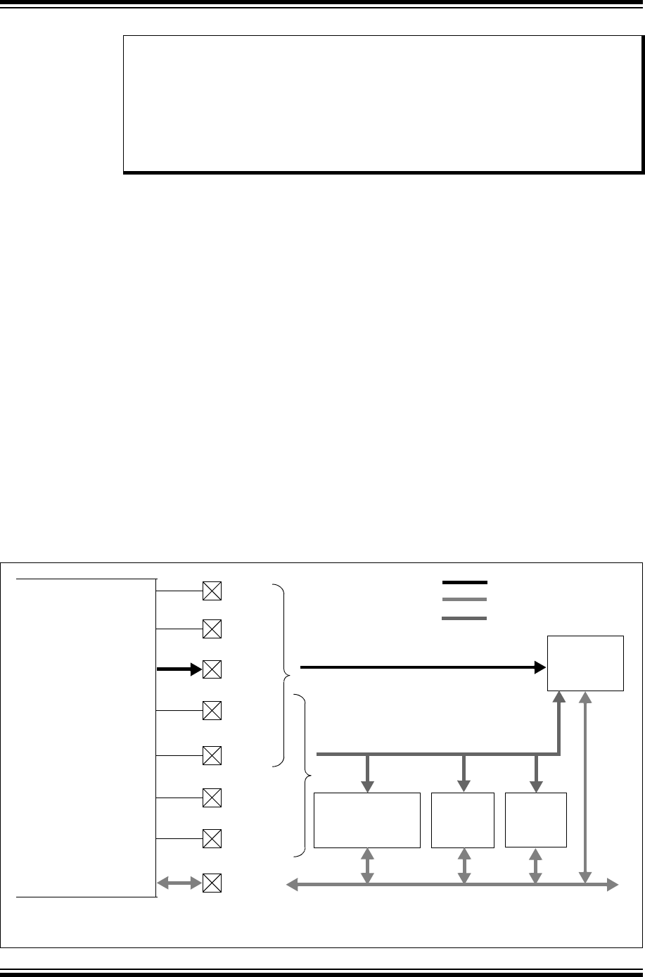
PIC32 Family Reference Manual
DS61128G-page 13-2 © 2007-2012 Microchip Technology Inc.
13.1 INTRODUCTION
The Parallel Master Port (PMP) is a parallel 8-bit/16-bit I/O module specifically designed to
communicate with a wide variety of parallel devices such as communications peripherals, LCDs,
external memory devices and microcontrollers. Because the interfaces to parallel peripherals
vary significantly, the PMP module is highly configurable.
Key features of the PMP module include:
•Up to 16 programmable address lines
•Up to two Chip Select lines
•Programmable strobe options
- Individual read and write strobes, or
-Read/write strobe with enable strobe
•Address auto-increment/auto-decrement
•Programmable address/data multiplexing
•Programmable polarity on control signals
•Legacy parallel slave port support
•Enhanced parallel slave support
- Address support
-4 bytes deep, auto-incrementing buffer
•Schmitt Trigger or TTL input buffers
•Programmable Wait states
•Freeze option for in-circuit debugging
Figure 13-1: PMP Module Pinout and Connections to External Devices
Note: This family reference manual section is meant to serve as a complement to device
data sheets. Depending on the device variant, this manual section may not apply to
all PIC32 devices.
Please consult the note at the beginning of the “Parallel Master Port (PMP)”
chapter in the current device data sheet to check whether this document supports
the device you are using.
Device data sheets and family reference manual sections are available for
download from the Microchip Worldwide Web site at: http://www.microchip.com
PMA0
PMA14
PMA15
PMRD
PMWR
PMENB
PMRD/PMWR
PMCS1
PMA1
PMA<13:2>
PMALL
PMALH
PMCS2
EEPROM
Address Bus
Data Bus
Control Lines
LCD FIFO
Microcontroller
8-bit/16-bit data (with or without multiplexed addressing)
Up to 16-bit address
buffer
PMD<15:8>(1)
PMA<7:0>
PMA<15:8>
PMD<7:0>
Parallel Master Port
PIC32
Note 1: The PMD<15:8> data pins are only available on PIC32 devices with 100 or more pins.

© 2007-2012 Microchip Technology Inc. DS61128G-page 13-3
Section 13. Parallel Master Port (PMP)
Parallel Master
Port (PMP)
13
13.2 CONTROL REGISTERS
The PMP module uses these Special Function Registers (SFRs):
•PMCON: Parallel Port Control Register
This register contains the bits that control much of the module’s basic functionality. A key bit
is the ON control bit, which is used to Reset, enable or disable the module.
When the module is disabled, all of the associated I/O pins revert to their designated I/O
function. In addition, any read or write operations active or pending are stopped, and the
BUSY bit is cleared. The data within the module registers is retained, including the data in
PMSTAT register. Therefore, the module could be disabled after a reception, and the last
received data and status would still be available for processing.
When the module is enabled, all buffer control logic is reset, along with PMSTAT.
All other bits in PMCON control address multiplexing enable various port control signals, and
select control signal polarity. These are discussed in detail in 13.3.1 “Parallel Master Port
Configuration Options”.
•PMMODE: Parallel Port Mode Register
This register contains bits that control the operational modes of the module. Master/Slave
mode selection and configuration options for both modes, are set by this register. It also
contains the universal status flag, BUSY, which is used in master modes to indicate that an
operation by the module is in progress.
Details on the use of the PMMODE bits to configure PMP operation are provided in
13.3 “Master Modes of Operation” and 13.4 “Slave Modes of Operation”.
•PMADDR: Parallel Port Address Register
This register functions as PMADDR in master modes. It contains the address to which
outgoing data is to be written, as well as the Chip Select control bits for addressing parallel
slave devices. The PMADDR register is not used in any of the Slave modes.
•PMDOUT: Parallel Port Data Output Register
This register is used only in Slave mode for buffered output data.
•PMDIN: Parallel Port Data Input Register
This register is used by the PMP module in both Master and Slave modes.
In Slave mode, this register is used to hold data that is asynchronously clocked in. Its
operation is described in 13.4.2 “Buffered Parallel Slave Port Mode”.
In Master mode, PMDIN is the holding register for both incoming and outgoing data. Its
operation in Master mode is described in 13.3.3 “Read Operation” and 13.3.4 “Write
Operation”.
•PMAEN: Parallel Port Pin Enable Register
This register controls the operation of address and Chip Select pins associated with the PMP
module. Setting these bits allocates the corresponding microcontroller pins to the PMP
module; clearing the bits allocates the pins to port I/O or other peripheral modules
associated with the pin.
•PMSTAT: Parallel Port Status Register (Slave modes only)
This register contains status bits associated with buffered operating modes when the port is
functioning as a slave port. This includes overflow, underflow and full flag bit.
These flags are discussed in detail in 13.4.2 “Buffered Parallel Slave Port Mode”.

PIC32 Family Reference Manual
DS61128G-page 13-4 © 2007-2012 Microchip Technology Inc.
13.2.1 PMP SFRs Summary
Tabl e 13-1 provides a brief summary of all PMP-module-related registers. Corresponding
registers appear after the summary with a detailed description of each bit.
Table 13-1: PMP SFRs Summary
Name Bit
31/23/15/7
Bit
30/22/14/6
Bit
29/21/13/5
Bit
28/20/12/4
Bit
27/19/11/3
Bit
26/18/10/2
Bit
25/17/9/1
Bit
24/16/8/0
PMCON(1,2,3) 31:24 — — — — — — — —
23:16 — — — — — — — —
15:8 ON —SIDL ADRMUX<1:0> PMPTTL PTWREN PTRDEN
7:0 CSF<1:0> ALP CS2P CS1P —WRSP RDSP
PMMODE(1,2,3) 31:24 — — — — — — — —
23:16 — — — — — — — —
15:8 BUSY IRQM<1:0> INCM<1:0> MODE16 MODE<1:0>
7:0 WAITB<1:0> WAITM<3:0> WAITE<1:0>
PMADDR(1,2,3) 31:24 — — — — — — — —
23:16 — — — — — — — —
15:8 CS2/A15 CS1/A14 ADDR<13:8>
7:0 ADDR<7:0>
PMDOUT(1,2,3) 31:24 DATAOUT<31:24>
23:16 DATAOUT<23:16>
15:8 DATAOUT<15:8>
7:0 DATAOUT<7:0>
PMDIN(1,2,3) 31:24 DATAIN<31:24>
23:16 DATAIN<23:16>
15:8 DATAIN<15:8>
7:0 DATAIN<7:0>
PMAEN(1,2,3) 31:24 — — — — — — — —
23:16 — — — — — — — —
15:8 PTEN<15:8>
7:0 PTEN<7:0>
PMSTAT 31:24 — — — — — — — —
23:16 — — — — — — — —
15:8 IBF IBOV — — IB3F IB2F IB1F IB0F
7:0 OBE OBUF — — OB3E OB2E OB1E OB0E
Legend: — = unimplemented, read as ‘0’. Address offset values are shown in hexadecimal.
Note 1: This register has an associated Clear, Set, and Invert registers at an offset of 0x4, 0x8, and 0xC bytes, respectively.
These registers have the same name with CLR, Set, or INV appended to the register name (e.g., PMCONCLR). Writing
a ‘1’ to any bit position in these registers will Clear, Set, and Invert valid bits in the associated register. Reads from these
register should be ignored.

© 2007-2012 Microchip Technology Inc. DS61128G-page 13-5
Section 13. Parallel Master Port (PMP)
Parallel Master
Port (PMP)
13
Register 13-1: PMCON: Parallel Port Control Register
Bit
Range
Bit
31/23/15/7
Bit
30/22/14/6
Bit
29/21/13/5
Bit
28/20/12/4
Bit
27/19/11/3
Bit
26/18/10/2
Bit
25/17/9/1
Bit
24/16/8/0
31:24 U-0 U-0 U-0 U-0 U-0 U-0 U-0 U-0
— — — — — — — —
23:16 U-0 U-0 U-0 U-0 U-0 U-0 U-0 U-0
— — — — — — — —
15:8 R/W-0 U-0 R/W-0 R/W-0 R/W-0 R/W-0 R/W-0 R/W-0
ON(1) —SIDL
ADRMUX<1:0>
PMPTTL PTWREN PTRDEN
7:0 R/W-0 R/W-0 R/W-0 R/W-0 R/W-0 U-0 R/W-0 R/W-0
CSF<1:0>(2) ALP(2) CS2P(2) CS1P(2) —WRSP RDSP
Legend:
R = Readable bit W = Writable bit U = Unimplemented bit, read as ‘0’
-n = Value at POR ‘1’ = Bit is set ‘0’ = Bit is cleared x = Bit is unknown
bit 31-16 Unimplemented: Write ‘0’; ignore read
bit 15 ON: Parallel Master Port Enable bit(1)
1 = PMP enabled
0 = PMP disabled, no off-chip access performed
bit 14 Unimplemented: Write ‘0’; ignore read
bit 13 SIDL: Stop in Idle Mode bit
1 = Discontinue module operation when device enters Idle mode
0 = Continue module operation in Idle mode
bit 12-11 ADRMUX<1:0>: Address/Data Multiplexing Selection bits
11 = All 16 bits of address are multiplexed on PMD<15:0> pins
10 = All 16 bits of address are multiplexed on PMD<7:0> pins
01 = Lower 8 bits of address are multiplexed on PMD<7:0> pins, upper 8 bits are on PMA<15:8>
00 = Address and data appear on separate pins
bit 10 PMPTTL: PMP Module TTL Input Buffer Select bit
1 = PMP module uses TTL input buffers
0 = PMP module uses Schmitt Trigger input buffer
bit 9 PTWREN: Write Enable Strobe Port Enable bit
1 = PMWR/PMENB port enabled
0 = PMWR/PMENB port disabled
bit 8 PTRDEN: Read/Write Strobe Port Enable bit
1 = PMRD/PMWR port enabled
0 = PMRD/PMWR port disabled
bit 7-6 CSF<1:0>: Chip Select Function bits(2)
11 = Reserved
10 = PMCS2 and PMCS1 function as Chip Select
01 = PMCS2 functions as Chip Select, PMCS1 functions as address bit 14
00 = PMCS2 and PMCS1 function as address bits 15 and 14
bit 5 ALP: Address Latch Polarity bit(2)
1 = Active-high (PMALL and PMALH)
0 = Active-low (PMALL and PMALH)
bit 4 CS2P: Chip Select 1 Polarity bit(2)
1 = Active-high (PMCS2)
0 = Active-low (PMCS2)
Note 1: When using 1:1 PBCLK divisor, the user’s software should not read/write the peripheral’s SFRs in the
SYSCLK cycle immediately following the instruction that clears the module’s ON control bit.
2: These bits have no effect when it’s corresponding pin is used as an address line.

PIC32 Family Reference Manual
DS61128G-page 13-6 © 2007-2012 Microchip Technology Inc.
bit 3 CS1P: Chip Select 0 Polarity bit(2)
1 = Active-high (PMCS1)
0 = Active-low (PMCS1)
bit 2 Unimplemented: Write ‘0’; ignore read
bit 1 WRSP: Write Strobe Polarity bit
For Slave Modes and Master mode 2 (PMMODE<9:8> = 00,01,10):
1 = Write strobe active-high (PMWR)
0 = Write strobe active-low (PMWR)
For Master mode 1 (PMMODE<9:8> = 11):
1 = Enable strobe active-high (PMENB)
0 = Enable strobe active-low (PMENB)
bit 0 RDSP: Read Strobe Polarity bit
For Slave modes and Master mode 2 (PMMODE<9:8> = 00,01,10):
1 = Read strobe active-high (PMRD)
0 = Read strobe active-low (PMRD)
For Master mode 1 (PMMODE<9:8> = 11):
1 = Read/write strobe active-high (PMRD/PMWR)
0 = Read/write strobe active-low (PMRD/PMWR)
Register 13-1: PMCON: Parallel Port Control Register (Continued)
Note 1: When using 1:1 PBCLK divisor, the user’s software should not read/write the peripheral’s SFRs in the
SYSCLK cycle immediately following the instruction that clears the module’s ON control bit.
2: These bits have no effect when it’s corresponding pin is used as an address line.

© 2007-2012 Microchip Technology Inc. DS61128G-page 13-7
Section 13. Parallel Master Port (PMP)
Parallel Master
Port (PMP)
13
Register 13-2: PMMODE: Parallel Port Mode Register
Bit
Range
Bit
31/23/15/7
Bit
30/22/14/6
Bit
29/21/13/5
Bit
28/20/12/4
Bit
27/19/11/3
Bit
26/18/10/2
Bit
25/17/9/1
Bit
24/16/8/0
31:24 U-0 U-0 U-0 U-0 U-0 U-0 U-0 U-0
— — — — — — — —
23:16 U-0 U-0 U-0 U-0 U-0 U-0 U-0 U-0
— — — — — — — —
15:8 R-0 R/W-0 R/W-0 R/W-0 R/W-0 R/W-0 R/W-0 R/W-0
BUSY IRQM<1:0> INCM<1:0> MODE16 MODE<1:0>
7:0 R/W-0 R/W-0 R/W-0 R/W-0 R/W-0 R/W-0 R/W-0 R/W-0
WAITB<1:0>(1) WAITM<3:0>(1) WAITE<1:0>(1)
Legend:
R = Readable bit W = Writable bit U = Unimplemented bit, read as ‘0’
-n = Value at POR ‘1’ = Bit is set ‘0’ = Bit is cleared x = Bit is unknown
bit 31-16 Unimplemented: Write ‘0’; ignore read
bit 15 BUSY: Busy bit (Master mode only)
1 = Port is busy
0 = Port is not busy
bit 14-13 IRQM<1:0>: Interrupt Request Mode bits
11 = Reserved, do not use
10 = Interrupt generated when Read Buffer 3 is read or Write Buffer 3 is written (Buffered PSP mode),
or on a read or write operation when PMA<1:0> = 11 (Addressable Slave mode only)
01 = Interrupt generated at the end of the read/write cycle
00 = No Interrupt generated
bit 12-11 INCM<1:0>: Increment Mode bits
11 = Slave mode read and write buffers auto-increment (PMMODE<1:0> = 00 only)
10 = Decrement ADDR<15:0> by 1 every read/write cycle(2,4)
01 = Increment ADDR<15:0> by 1 every read/write cycle(2,4)
00 = No increment or decrement of address
bit 10 MODE16: 8/16-bit Mode bit
1 = 16-bit mode: a read or write to the data register invokes a single 16-bit transfer
0 = 8-bit mode: a read or write to the data register invokes a single 8-bit transfer
bit 9-8 MODE<1:0>: Parallel Port Mode Select bits
11 = Master mode 1 (PMCSx, PMRD/PMWR, PMENB, PMA<x:0>, PMD<7:0> and PMD<8:15>(3))
10 = Master mode 2 (PMCSx, PMRD, PMWR, PMA<x:0>, PMD<7:0> and PMD<8:15>(3))
01 = Enhanced Slave mode, control signals (PMRD, PMWR, PMCS, PMD<7:0> and PMA<1:0>)
00 = Legacy Parallel Slave Port, control signals (PMRD, PMWR, PMCS and PMD<7:0>)
bit 7-6 WAITB<1:0>: Data Setup to Read/Write Strobe Wait States bits(1)
11 = Data wait of 4 TPB; multiplexed address phase of 4 TPB
10 = Data wait of 3 TPB; multiplexed address phase of 3 TPB
01 = Data wait of 2 TPB; multiplexed address phase of 2 TPB
00 = Data wait of 1 TPB; multiplexed address phase of 1 TPB (default)
Note 1: When WAITM<3:0> = 0000, the WAITB and WAITE bits are ignored and forced to 1 TPBCLK cycle for a
write operation; WAITB = 1 TPBCLK cycle, WAITE = 0 TPBCLK cycles for a read operation.
2: Address bit A15 and A14 are not subject to auto-increment/decrement if configured as Chip Select CS2
and CS1.
3: These pins are active when MODE16 = 1 (16-bit mode).
4: The PMPADDR register is always incremented/decremented by 1 regardless of the transfer data width.

PIC32 Family Reference Manual
DS61128G-page 13-8 © 2007-2012 Microchip Technology Inc.
bit 5-2 WAITM<3:0>: Data Read/Write Strobe Wait States bits(1)
1111 = Wait of 16 TPB
•
•
•
0001 = Wait of 2 TPB
0000 = Wait of 1 TPB (default)
bit 1-0 WAITE<1:0>: Data Hold After Read/Write Strobe Wait States bits(1)
11 = Wait of 4 TPB
10 = Wait of 3 TPB
01 = Wait of 2 TPB
00 = Wait of 1 TPB (default)
For read operations:
11 = Wait of 3 TPB
10 = Wait of 2 TPB
01 = Wait of 1 TPB
00 = Wait of 0 TPB (default)
Register 13-2: PMMODE: Parallel Port Mode Register (Continued)
Note 1: When WAITM<3:0> = 0000, the WAITB and WAITE bits are ignored and forced to 1 TPBCLK cycle for a
write operation; WAITB = 1 TPBCLK cycle, WAITE = 0 TPBCLK cycles for a read operation.
2: Address bit A15 and A14 are not subject to auto-increment/decrement if configured as Chip Select CS2
and CS1.
3: These pins are active when MODE16 = 1 (16-bit mode).
4: The PMPADDR register is always incremented/decremented by 1 regardless of the transfer data width.
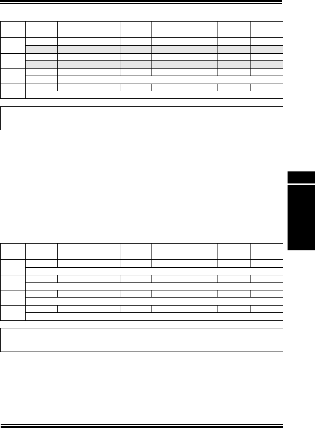
© 2007-2012 Microchip Technology Inc. DS61128G-page 13-9
Section 13. Parallel Master Port (PMP)
Parallel Master
Port (PMP)
13
Register 13-3: PMADDR: Parallel Port Address Register
Bit
Range
Bit
31/23/15/7
Bit
30/22/14/6
Bit
29/21/13/5
Bit
28/20/12/4
Bit
27/19/11/3
Bit
26/18/10/2
Bit
25/17/9/1
Bit
24/16/8/0
31:24 U-0 U-0 U-0 U-0 U-0 U-0 U-0 U-0
— — — — — — — —
23:16 U-0 U-0 U-0 U-0 U-0 U-0 U-0 U-0
— — — — — — — —
15:8 R/W-0 R/W-0 R/W-0 R/W-0 R/W-0 R/W-0 R/W-0 R/W-0
CS2 CS1 ADDR<13:8>
7:0 R/W-0 R/W-0 R/W-0 R/W-0 R/W-0 R/W-0 R/W-0 R/W-0
ADDR<7:0>
Legend:
R = Readable bit W = Writable bit U = Unimplemented bit, read as ‘0’
-n = Value at POR ‘1’ = Bit is set ‘0’ = Bit is cleared x = Bit is unknown
bit 31-16 Unimplemented: Write ‘0’; ignore read
bit 15 CS2: Chip Select 2 bit
1 = Chip Select 2 is active
0 = Chip Select 2 is inactive (pin functions as PMA<15>)
bit 14 CS1: Chip Select 1 bit
1 = Chip Select 1 is active
0 = Chip Select 1 is inactive (pin functions as PMA<14>)
bit 13-0 ADDR<13:0>: Destination Address bits
Register 13-4: PMDOUT: Parallel Port Data Output Register
Bit
Range
Bit
31/23/15/7
Bit
30/22/14/6
Bit
29/21/13/5
Bit
28/20/12/4
Bit
27/19/11/3
Bit
26/18/10/2
Bit
25/17/9/1
Bit
24/16/8/0
31:24 R/W-0 R/W-0 R/W-0 R/W-0 R/W-0 R/W-0 R/W-0 R/W-0
DATAOUT<31:24>
23:16 R/W-0 R/W-0 R/W-0 R/W-0 R/W-0 R/W-0 R/W-0 R/W-0
DATAOUT<23:16>
15:8 R/W-0 R/W-0 R/W-0 R/W-0 R/W-0 R/W-0 R/W-0 R/W-0
DATAOUT<15:8>
7:0 R/W-0 R/W-0 R/W-0 R/W-0 R/W-0 R/W-0 R/W-0 R/W-0
DATAOUT<7:0>
Legend:
R = Readable bit W = Writable bit U = Unimplemented bit, read as ‘0’
-n = Value at POR ‘1’ = Bit is set ‘0’ = Bit is cleared x = Bit is unknown
bit 31-0 DATAOUT<31:0>: Output Data Port bits for 8-bit write operations in Slave mode
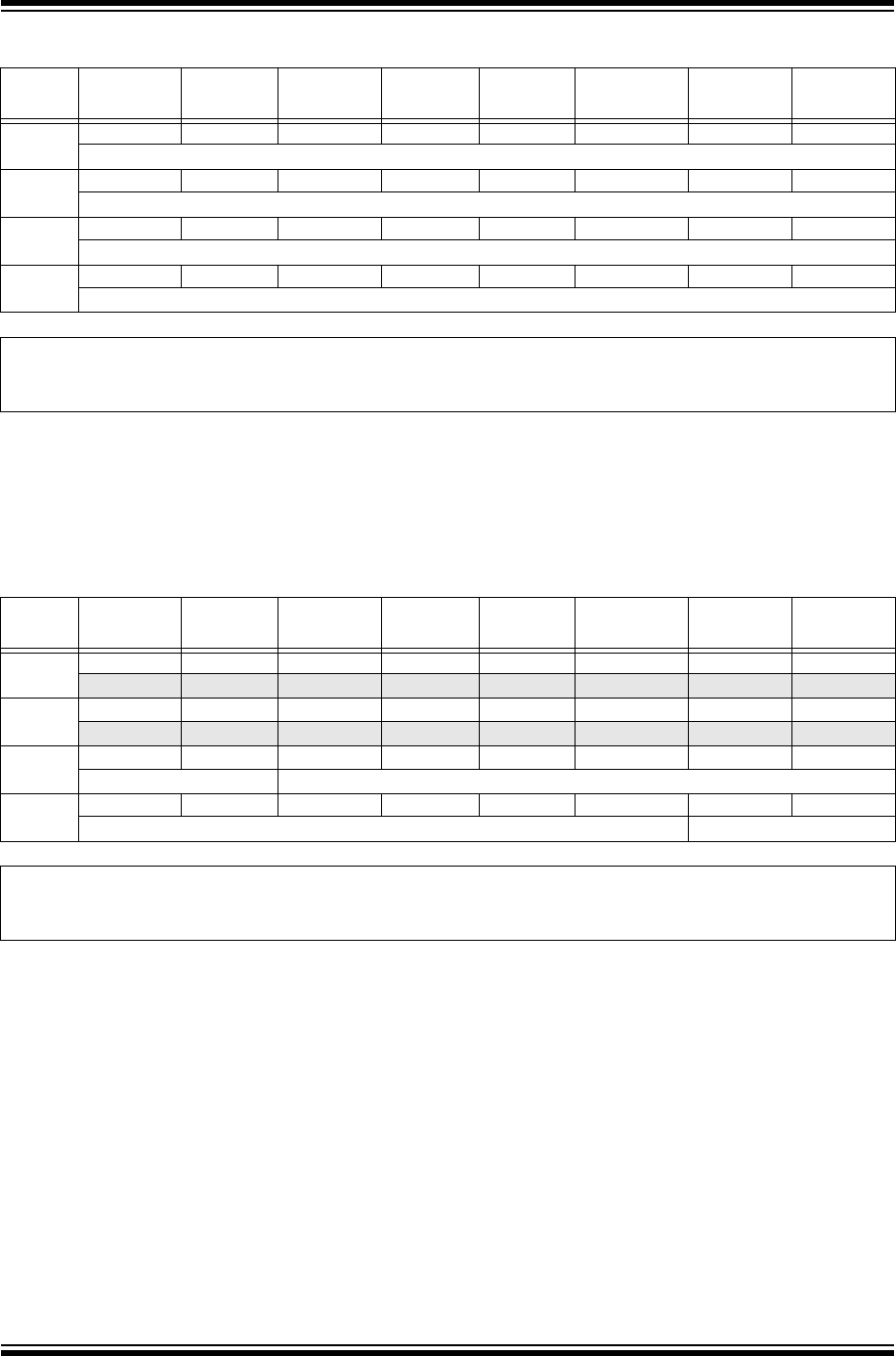
PIC32 Family Reference Manual
DS61128G-page 13-10 © 2007-2012 Microchip Technology Inc.
Register 13-5: PMDIN: Parallel Port Data Input Register
Bit
Range
Bit
31/23/15/7
Bit
30/22/14/6
Bit
29/21/13/5
Bit
28/20/12/4
Bit
27/19/11/3
Bit
26/18/10/2
Bit
25/17/9/1
Bit
24/16/8/0
31:24 R/W-0 R/W-0 R/W-0 R/W-0 R/W-0 R/W-0 R/W-0 R/W-0
DATAIN<31:24>
23:16 R/W-0 R/W-0 R/W-0 R/W-0 R/W-0 R/W-0 R/W-0 R/W-0
DATAIN<23:16>
15:8 R/W-0 R/W-0 R/W-0 R/W-0 R/W-0 R/W-0 R/W-0 R/W-0
DATAIN<15:8>
7:0 R/W-0 R/W-0 R/W-0 R/W-0 R/W-0 R/W-0 R/W-0 R/W-0
DATAIN<7:0>
Legend:
R = Readable bit W = Writable bit U = Unimplemented bit, read as ‘0’
-n = Value at POR ‘1’ = Bit is set ‘0’ = Bit is cleared x = Bit is unknown
bit 31-0 DATAIN<31:0>: Input/Output Data Port bits for 8-bit or 16-bit read/write operations in Master mode Input
Data Port for 8-bit read operations in Slave mode.
Register 13-6: PMAEN: Parallel Port Pin Enable Register
Bit
Range
Bit
31/23/15/7
Bit
30/22/14/6
Bit
29/21/13/5
Bit
28/20/12/4
Bit
27/19/11/3
Bit
26/18/10/2
Bit
25/17/9/1
Bit
24/16/8/0
31:24 U-0 U-0 U-0 U-0 U-0 U-0 U-0 U-0
— — — — — — — —
23:16 U-0 U-0 U-0 U-0 U-0 U-0 U-0 U-0
— — — — — — — —
15:8 R/W-0 R/W-0 R/W-0 R/W-0 R/W-0 R/W-0 R/W-0 R/W-0
PTEN<15:14> PTEN<13:8>
7:0 R/W-0 R/W-0 R/W-0 R/W-0 R/W-0 R/W-0 R/W-0 R/W-0
PTEN<7:2> PTEN<1:0>
Legend:
R = Readable bit W = Writable bit U = Unimplemented bit, read as ‘0’
-n = Value at POR ‘1’ = Bit is set ‘0’ = Bit is cleared x = Bit is unknown
bit 31-16 Unimplemented: Write ‘0’; ignore read
bit 15-14 PTEN<15:14>: PMCSx Strobe Enable bits
1 = PMA15 and PMA14 function as either PMA<15:14> or PMCS2 and PMCS1(1)
0 = PMA15 and PMA14 function as port I/O
bit 13-2 PTEN<13:2>: PMP Address Port Enable bits
1 = PMA<13:2> function as PMP address lines
0 = PMA<13:2> function as port I/O
bit 1-0 PTEN<1:0>: PMALH/PMALL Strobe Enable bits
1 = PMA1 and PMA0 function as either PMA<1:0> or PMALH and PMALL(2)
0 = PMA1 and PMA0 pads function as port I/O
Note 1: The use of these pins as PMA15/PMA14 or CS2/CS1 is selected by the CSF<1:0> bits (PMCON<7:6>).
2: The use of these pins as PMA1/PMA0 or PMALH/PMALL depends on the Address/Data Multiplex mode
selected by the ADRMUX<1:0> bits in the PMCON register.

© 2007-2012 Microchip Technology Inc. DS61128G-page 13-11
Section 13. Parallel Master Port (PMP)
Parallel Master
Port (PMP)
13
Register 13-7: PMSTAT: Parallel Port Status Register (Slave modes only)
Bit
Range
Bit
31/23/15/7
Bit
30/22/14/6
Bit
29/21/13/5
Bit
28/20/12/4
Bit
27/19/11/3
Bit
26/18/10/2
Bit
25/17/9/1
Bit
24/16/8/0
31:24 U-0 U-0 U-0 U-0 U-0 U-0 U-0 U-0
— — — — — — — —
23:16 U-0 U-0 U-0 U-0 U-0 U-0 U-0 U-0
— — — — — — — —
15:8 R-0 R/W-0 U-0 U-0 R-0 R-0 R-0 R-0
IBF IBOV — — IB3F IB2F IB1F IB0F
7:0 R-1 R/W-0 U-0 U-0 R-1 R-1 R-1 R-1
OBE OBUF — — OB3E OB2E OB1E OB0E
Legend:
R = Readable bit W = Writable bit U = Unimplemented bit, read as ‘0’
-n = Value at POR ‘1’ = Bit is set ‘0’ = Bit is cleared x = Bit is unknown
bit 31-16 Unimplemented: Write ‘0’; ignore read
bit 15 IBF: Input Buffer Full Status bit
1 = All writable input buffer registers are full
0 = Some or all of the writable input buffer registers are empty
bit 14 IBOV: Input Buffer Overflow Status bit
1 = A write attempt to a full input byte buffer occurred (must be cleared in software)
0 = No overflow occurred
This bit is set (= 1) in hardware; can only be cleared (= 0) in software.
bit 13-12 Unimplemented: Write ‘0’; ignore read
bit 11-8 IBnF: Input Buffer n Status Full bits
1 = Input Buffer contains data that has not been read (reading buffer will clear this bit)
0 = Input Buffer does not contain any unread data
bit 7 OBE: Output Buffer Empty Status bit
1 = All readable output buffer registers are empty
0 = Some or all of the readable output buffer registers are full
bit 6 OBUF: Output Buffer Underflow Status bit
1 = A read occurred from an empty output byte buffer (must be cleared in software)
0 = No underflow occurred
This bit is set (= 1) in hardware; can only be cleared (= 0) in software.
bit 5-4 Unimplemented: Write ‘0’; ignore read
bit 3-0 OBnE: Output Buffer n Status Empty bits
1 = Output buffer is empty (writing data to the buffer will clear this bit)
0 = Output buffer contains data that has not been transmitted

PIC32 Family Reference Manual
DS61128G-page 13-12 © 2007-2012 Microchip Technology Inc.
13.3 MASTER MODES OF OPERATION
In its master modes, the PMP module can provide a 8-bit or 16-bit data bus, up to 16 bits of
address, and all the necessary control signals to operate a variety of external parallel devices
such as memory devices, peripherals and slave microcontrollers. The PMP master modes
provide a simple interface for reading and writing data, but not executing program instructions
from external devices, such as SRAM or Flash memories.
Because there are a number of parallel devices with a variety of control methods, the PMP
module is designed for flexibility to accommodate a range of configurations. Some of these
features include:
•8-bit and 16-bit data modes
•Configurable address/data multiplexing
•Up to two Chip Select lines
•Up to 16 selectable address lines
•Address auto-increment and auto-decrement
• Selectable polarity on all control lines
•Configurable Wait states at different stages of the read/write cycle
13.3.1 Parallel Master Port Configuration Options
13.3.1.1 8-BIT AND 16-BIT DATA MODES
The PMP in Master mode supports data with widths of 8 and 16 bits. By default, the data width
is 8 bits wide, MODE16 bit (PMMODE<10>) = 0. To select a data width of 16 bits, set
MODE16 = 1. When configured in 8-bit Data mode, the upper 8 bits of the data bus, PMD<15:8>,
are not controlled by the PMP module and are available as general purpose I/O pins.
13.3.1.2 CHIP SELECT
Two Chip Select lines, PMCS1 and PMCS2, are available for master modes. These lines are
multiplexed with the Most Significant bits (MSbs) of the address bus A14 and A15. When a pin
is configured as a Chip Select, it is not included in any address auto-increment/decrement. It is
possible to enable both PMCS2 and PMCS1 as Chip Selects, or enable only PMCS2 as a Chip
Select, allowing PMCS1 to function strictly as address line A14. It is not possible to enable
PMCS1 alone. The Chip Select signals are configured using the Chip Select Function bits
CSF<1:0> (PMCON<7:6>).
13.3.1.3 PORT PIN CONTROL
There are several bits available to configure the presence or absence of control and address
signals in the module. These bits are PTWREN (PMCON<9>), PTRDEN (PMCON<8>) and
PTEN<15:0> (PMAEN<15:0>). They provide the ability to conserve pins for other functions and
allow flexibility to control the external address. When any one of these bits is set, the associated
function is present on its associated pin; when clear, the associated pin reverts to its defined I/O
port function.
Setting a PTEN bit will enable the associated pin as an address pin and drive the corresponding
data contained in the PMADDR register. Clearing any PTEN bit will force the pin to revert to its
original I/O function.
Note: The PMD<15:0> data pins are available on PIC32 devices with 100 or more pins.
For 64-pin device variants, only pins PMD<7:0> are available. For details, refer to
the specific PIC32 device data sheet.
Table 13-2: Chip Select Control
CSF<1:0> Function
10 PMCS2, PMCS1 = Enabled
01 PMCS2 = Enabled, PMCS1 = A14
00 PMCS2 = A15, PMCS1 = A14

© 2007-2012 Microchip Technology Inc. DS61128G-page 13-13
Section 13. Parallel Master Port (PMP)
Parallel Master
Port (PMP)
13
For the pins configured as Chip Select (PMCS1 or PMCS2) with the corresponding PTEN bit set,
Chip Select pins drive inactive data when a read or write operation is not being performed. The
PTEN0 and PTEN1 bits also control the PMALL and PMALH signals. When multiplexing is used,
the associated address latch signals should be enabled. For I/O pin configuration, see 13.11 “I/O
Pin Control”.
13.3.1.4 READ/WRITE CONTROL
The PMP module supports two distinct read/write signaling methods. In Master mode 1, read and
write strobe are combined into a single control line, PMRD/PMWR; a second control line,
PMENB, determines when a read or write action is to be taken. In Master mode 2, read and write
strobes (PMRD and PMWR) are supplied on separate pins.
13.3.1.5 CONTROL LINE POLARITY
All control signals (PMRD, PMWR, PMENB, PMALL, PMALH, PMCS1 and PMCS2) can be
individually configured for either positive or negative polarity. Configuration is controlled by
separate bits in the PMCON register, as shown in Tab le 13-3.
13.3.1.6 AUTO-INCREMENT/DECREMENT
While the PMP module is operating in one of the master modes, the INCM<1:0> bits
(PMMODE<12:11>) control the behavior of the address value. The address in the PMADDR
register can be made to automatically increment or decrement by 1, regardless of the transfer
data width, after each read and write operation is completed, and the BUSY bit (PMMODE<15>)
goes to ‘0’.
.
If the Chip Select signals are disabled and configured as address bits, the bits will participate in
the increment and decrement operations; otherwise, CS2 and CS1 bit values will be unaffected.
Table 13-3: Pin Polarity Configuration
Control
Pin
PMCON
Control Bit
Active-High
Select
Active-Low
Select
PMRD RDSP 1 0
PMWR WRSP 1 0
PMALL ALP 1 0
PMALH ALP 1 0
PMCS1 CS1P 1 0
PMCS2 CS2P 1 0
Note: The polarity of control signals that share the same output pin (for example, PMWR
and PMENB) are controlled by the same bit; the configuration depends on which
Master Port mode is being used.
Table 13-4: Address INC/DEC Control
INCM<1:0> Function
10 Decrement every R/W cycle
01 Increment every R/W cycle
00 No Increment – No Decrement
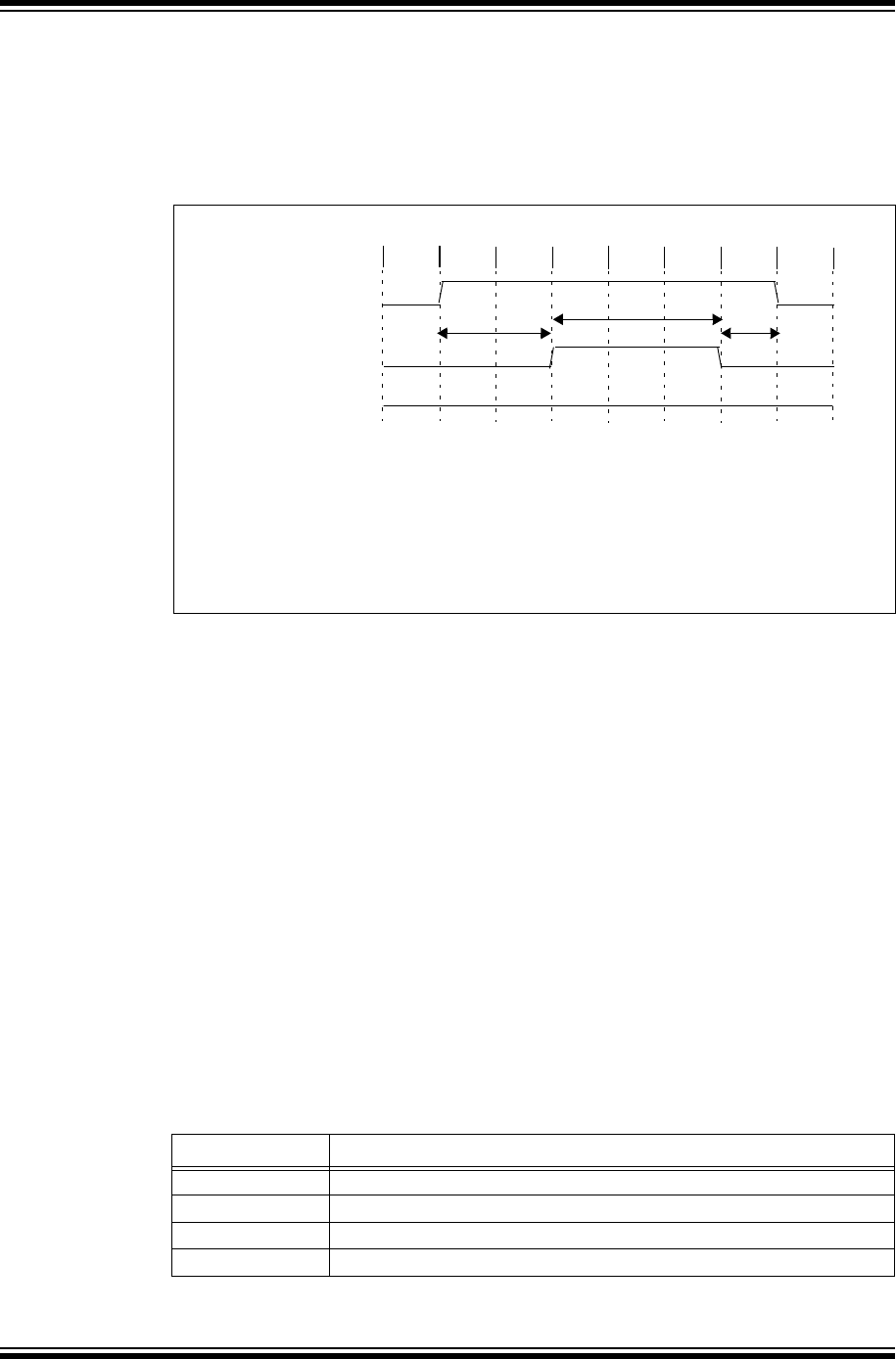
PIC32 Family Reference Manual
DS61128G-page 13-14 © 2007-2012 Microchip Technology Inc.
13.3.1.7 WAIT STATES
In Master mode, the user can control the duration of the read, write and address cycles by
configuring the module Wait states. One Wait state period is equivalent to one peripheral bus
clock cycle, TPBCLK. Figure 13-2 is an example of a Master mode 2 Read operation using Wait
states.
Figure 13-2: Read Operation, Wait States Enabled
Wait states can be added to the beginning, middle and end of any read or write cycle using the
corresponding WAITB, WAITM and WAITE bits in the PMMODE register.
The WAITB<1:0> bits (PMMODE<7:6>) define the number of wait cycles for the data setup prior
to the PMRD/PMWR strobe in Mode 10, or prior to the PMENB strobe in Mode 11. When
multiplexing the address and data bus, ADRMUX<1:0> bits (PMCON<12:11>) = 01, 10 or 11,
WAITB defines the number of wait cycles for which the addressing period is extended.
The WAITM<3:0> bits (PMMODE<5:2>) define the number of wait cycles for the PMRD/PMWR
strobe in Mode 10, or for the PMENB strobe in Mode 11. When this Wait state setting is ‘0000’,
WAITB and WAITE are ignored. The number of Wait states for the data setup time (WAITB)
defaults to one, while the number of Wait states for data hold time (WAITE) defaults to one during
a write operation and zero during a read operation.
The WAITE<1:0> bits (PMMODE<1:0>) define the number of wait cycles for the data hold time
after the PMRD/PMWR strobe in Mode 10, or after the PMENB strobe in Mode 11.
13.3.1.8 ADDRESS MULTIPLEXING
Address multiplexing allows some or all address line signals to be generated from the data bus
during the address cycle of a read/write operation. This can be a useful option for address lines
PMA<15:0> needed as general purpose I/O pins. The user application can select to multiplex the
lower 8 data bits, upper 8 data bits or full 16 data bits. These multiplexing modes are available in
both Master mode 1 and 2. For Multiplexing mode timing diagrams, see 13.3.8 “Master Mode
Timing”.
Table 13-5: Address Multiplex Configurations
ADRMUX<1:0> Address/Data Multiplex Modes
11 Fully multiplexed (16 data pins PMD<15:0>)
10 Fully multiplexed (lower eight data pins PMD<7:0>)
01 Partially multiplexed (lower eight data pins PMD<7:0>)
00 Demultiplexed
PMCS2/PMCS1
TPB TPB TPB TPB TPB TPB TPB
TPB
Legend:
B = WAITB<1:0> = 01 (2 Wait states)
M = WAITM<3:0> = 0010 (3 Wait states)
E = WAITE<1:0> = 01 (1 Wait state)
Note: If WAITM<3:0> = 0000, M is forced to 1 TPBCLK, WAITB is ignored (B forced
to 1 TPBCLK), and WAITE is ignored (E forced to 0 TPBCLK).
B
M
E
PMWR
PMRD

© 2007-2012 Microchip Technology Inc. DS61128G-page 13-15
Section 13. Parallel Master Port (PMP)
Parallel Master
Port (PMP)
13
13.3.1.8.1 Demultiplexed Mode
Demultiplexed mode is selected by configuring the ADRMUX<1:0> bits (PMCON<12:11>) = 00.
In this mode, address bits are presented on pins PMA<15:0>.
When PMCS2 is enabled, address pin PMA15 is not available. When PMCS1 is enabled,
address pin PMA14 is not available.
In 16-bit Data mode, data bits are presented on pins PMD<15:0>. In 8-bit Data mode, data bits
are presented on pins PMD<7:0>.
Figure 13-3: Demultiplexed Addressing Mode
Figure 13-4: Demultiplexed Addressing Example
Address Bus
Data Bus
Control Lines
PMRD
PMWR
PMD<7:0>
PMA14/PMCS1
PMA<13:0>
PMA15/PMCS2
PIC32
PMD<15:8>
ADRMUX<1:0> = 00
Note 1: Address pin PMA<15> is not available if PMCS2 is enabled.
Address pin PMA<14> is not available if PMCS1 is enabled.
See Note 1
PMA<14:0>
D<15:0>
A<14:0>
D<15:0>
A<14:0>
PMRD
PMWR
OE WR
CE
PIC32
PMCS2
PMD<15:0>
32K x 16-bit Device
Address Bus
Data Bus
Control Lines
Note: Master mode 2: MODE<1:0> bits (PMMODE<9:8>) = 10.
16-bit data width: MODE16 bit (PMMODE<10>) = 1.
Partial Multiplexed mode: ADRMUX<1:0> bits (PMCON<12:11>) = 00.
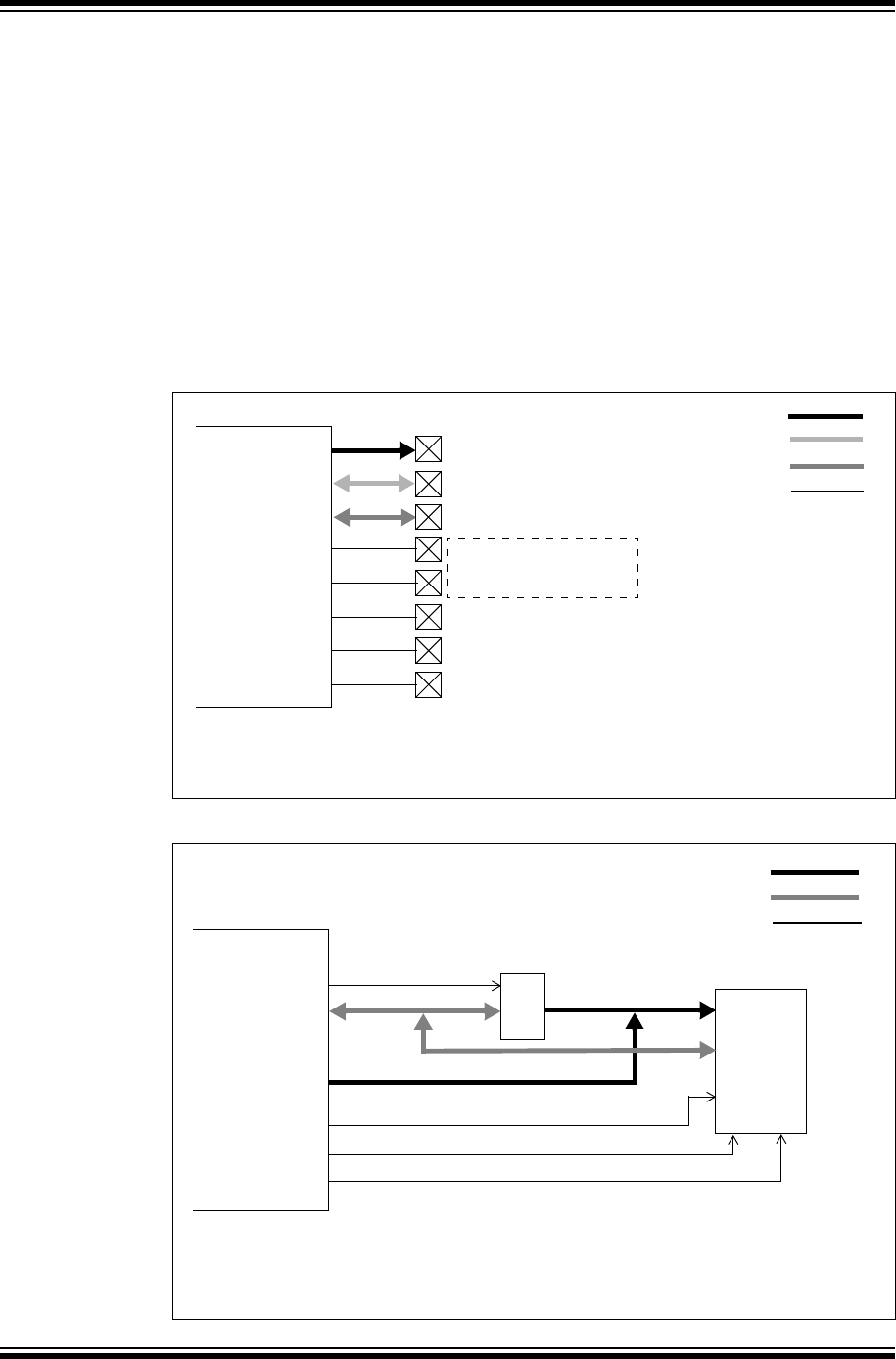
PIC32 Family Reference Manual
DS61128G-page 13-16 © 2007-2012 Microchip Technology Inc.
13.3.1.8.2 Partially Multiplexed Mode
Partially Multiplexed mode (8-bit data pins) is available in both 8-bit and 16-bit data bus
configurations and is selected by setting the ADRMUX<1:0> bits (PMCON<12:11>) = 01. In this
mode, the lower eight address bits are multiplexed with the lower eight data bus pins, PMD<7:0>.
The upper eight address bits are unaffected and are presented on PMA<15:8>. In this mode,
address pins PMA<7:1> are available as general purpose I/O pins.
Address pin PMA15 is not available when PMCS2 is enabled; address pin PMA14 is not
available when PMCS1 is enabled.
Address pin PMA<0> is used as an address latch enable strobe, PMALL, during which the lower
eight bits of the address are presented on the PMD<7:0> pins. Read and write sequences are
extended by at least three peripheral bus clock cycles (TPBCLK).
If WAITM<3:0> (PMMODE<5:2>) is non-zero, the PMALL strobe will be extended by
WAITB<1:0> (PMMODE<7:6>) Wait states.
Figure 13-5: Partial Multiplexed Addressing Mode
Figure 13-6: Partial Multiplexed Addressing Example
PMRD
PMWR
PMD<7:0>
PMA14/PMCS1
PMA<13:8>
PMA0/PMALL
PMA15/PMCS2
PIC32
Address Bus
Multiplexed Address/Data Bus
Data Bus
Control Lines
PMD<15:8>
ADRMUX<1:0> = 01
Note 1: Address pin PMA<15> is not available if PMCS2 is enabled.
Address pin PMA<14> is not available if PMCS1 is enabled.
See Note 1
PMA<14:8>
D<7:0> 373 A<14:0>
D<15:0>
A<7:0>
PMRD
PMWR
OE WR
CE
PIC32
PMCS2
PMALL
A<14:8>
PMD<15:0>
32K x 16-bit Device
D<15:0>
Note: Master mode 2: MODE<1:0> bits (PMMODE<9:8>) = 10.
16-bit data width: MODE16 bit (PMMODE<10>) = 1.
Partial Multiplexed mode: ADRMUX<1:0> bits (PMCON<12:11>) = 01.
The 373 shown in the diagram represents a generic 74XX family 373 latch.
Address Bus
Data Bus
Control Lines
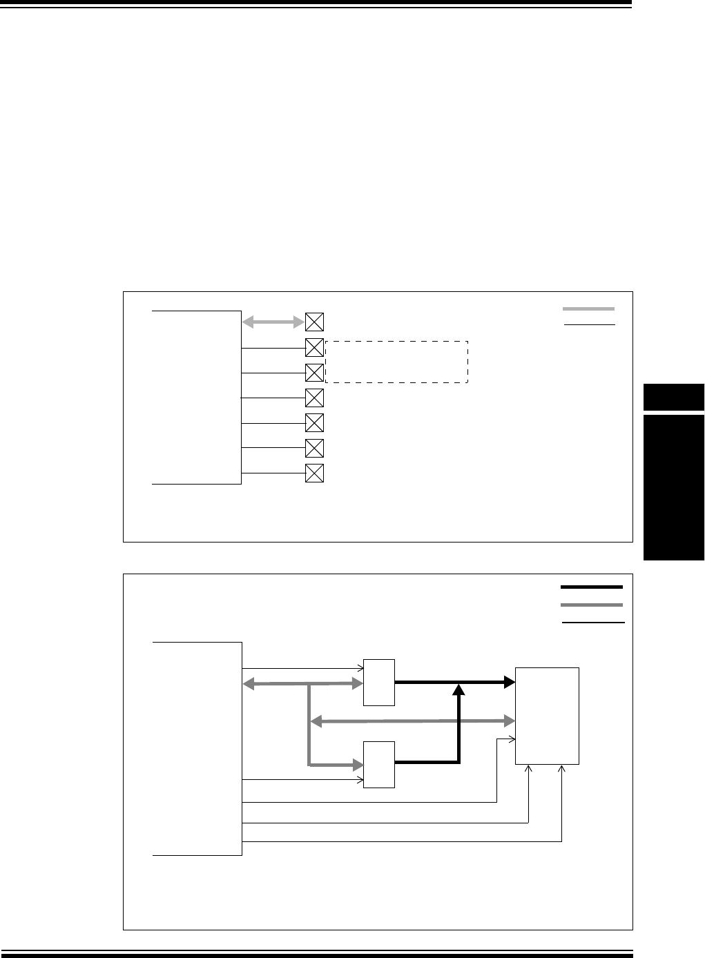
© 2007-2012 Microchip Technology Inc. DS61128G-page 13-17
Section 13. Parallel Master Port (PMP)
Parallel Master
Port (PMP)
13
13.3.1.8.3 Fully Multiplexed Mode (8-bit Data Pins)
Fully Multiplexed mode (8-bit data pins) is available in both 8-bit and 16-bit data bus
configurations and is selected by setting the ADRMUX<1:0> bits (PMCON<12:11>) = 10. In this
mode, the entire 16 bits of the address are multiplexed with the lower eight data bus pins,
PMD<7:0>. In this mode, PMA<13:2> pins are available as general purpose I/O pins.
If PMCS2/PMA15 or PMCS1/PMA14 are configured as Chip Select pins, the corresponding
address bit, PMADDR<15> or PMADDR<14> is automatically forced to ‘0’.
Address pins PMA<0> and PMA<1> are used as an address latch enable strobes, PMALL and
PMALH, respectively. During the first cycle, the lower eight address bits are presented on the
PMD<7:0> pins with the PMALL strobe active. During the second cycle, the upper eight address
bits are presented on the PMD<7:0> pins with the PMALH strobe active. The read and write
sequences are extended by at least six peripheral bus clock cycles (TPBCLK).
If WAITM<3:0> (PMMODE<5:2>) is non-zero, both PMALL and PMALH strobes will be extended
by WAITB<1:0> (PMMODE<7:6>) Wait states.
Figure 13-7: Fully Multiplexed Addressing Mode (8-bit Bus)
Figure 13-8: Fully Multiplexed Address Example (8-bit Bus)
Fully Multiplexed Address/Data Bus
Control Lines
PMRD
PMWR
PMD<7:0>
PMA14/ PMCS1
PMA1/PMALH
PMA15/ PMCS2
PIC32
PMA0/PMALL
ADRMUX<1:0> = 10
Note 1: Address bit PMADDR<15> is forced to ‘0’ when PMCS2 is enabled.
Address bit PMADDR<14> is forced to ‘0’ when PMCS1 is enabled.
See Note 1
Note: Master mode 2: MODE<1:0> bits (PMMODE<9:8>) = 10.
8-bit data width: MODE16 bit (PMMODE<10>) = 0.
Fully Multiplexed mode: ADRMUX<1:0> bits (PMCON<12:11>) = 10.
The block labeled 373 in the diagram represents a generic 74XX family 373 latch.
Address Bus
Data Bus
Control Lines
PMD<7:0>
PMALH
D<7:0>
373 A<14:0>
D<7:0>
A<7:0>
373
PMRD
PMWR
OE WR
CE
PIC32
PMCS2
PMALL
A<14:8>
32K x 8-bit Device
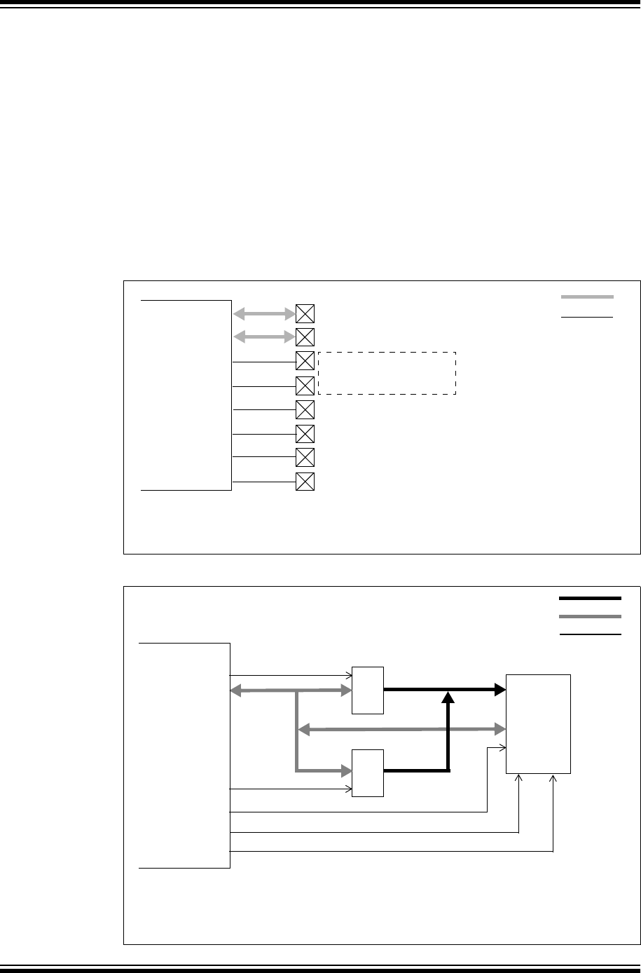
PIC32 Family Reference Manual
DS61128G-page 13-18 © 2007-2012 Microchip Technology Inc.
13.3.1.8.4 Fully Multiplexed Mode (16-bit Data Pins)
Fully Multiplexed mode (16-bit data pins) is only available in the 16-bit data bus configuration and
is selected by configuring the ADRMUX<1:0> bits (PMCON<12:11>) = 11. In this mode, the
entire 16 bits of the address are multiplexed with all 16 data bus pins, PMD<15:0>.
If PMCS2/PMA15 or PMCS1/PMA14 are configured as Chip Select pins, the corresponding
address bit, PMADDR<15> or PMADDR<14> is automatically forced to ‘0’.
Address pins PMA<0> and PMA<1> are used as an address latch enable strobes, PMALL and
PMALH, respectively, and at the same time. While the PMALL and PMALH strobes are active,
the lower eight address bits are presented on the PMD<7:0> pins and the upper eight address
bits are presented on the PMD<15:8> pins. The read and write sequences are extended by at
least 3 peripheral bus clock cycles (TPBCLK).
If WAITM<3:0> (PMMODE<5:2>) is non-zero, both PMALL and PMALH strobes will be extended
by WAITB<1:0> (PMMODE<7:6>) Wait states.
Figure 13-9: Fully Multiplexed Addressing Mode (16-bit Bus)
Figure 13-10: Fully Multiplexed Addressing Example (16-bit Bus)
PMRD
PMWR
PMA1/PMALH
PMA15/ PMCS2
PIC32
PMA0/PMALL
PMD<7:0>
PMD<15:8>
PMA14/ PMCS1
ADRMUX<1:0> = 11
Note 1: Address bit PMADDR<15> is forced to ‘0’ when PMCS2 is enabled.
Address bit PMADDR<14> is forced to ‘0’ when PMCS1 is enabled.
Fully Multiplexed Address/Data Bus
Control Lines
See Note 1
Note: Master mode 2: MODE<1:0> bits (PMMODE<9:8>) = 10.
16-bit data width: MODE16 bit (PMMODE<10>) = 1.
Fully Multiplexed mode: ADRMUX<1:0> bits (PMCON<12:11>) = 11.
The 373 shown in the diagram represents a generic 74XX family 373 latch.
Address Bus
Data Bus
Control Lines
PMD<15:0>
PMALH
D<15:0>
373 A<14:0>
D<15:0>
A<7:0>
373
PMRD
PMWR
OE WR
CE
PIC32
PMCS2
PMALL
A<14:8>
32K x 16-bit Device
D<15:8>
D<7:0>

© 2007-2012 Microchip Technology Inc. DS61128G-page 13-19
Section 13. Parallel Master Port (PMP)
Parallel Master
Port (PMP)
13
13.3.2 Master Mode Configuration
The Master mode configuration is determined primarily by the interface requirements to the
external device. Address multiplexing, control signal polarity, data width and Wait states typically
dictate the specific configuration of the PMP.
To us e th e PM P as a mas ter, th e mo dule m ust be enabled by setting the ON control bit
(PMCON<15>) = 1, and the mode must be set to one of two possible master modes. Control bits
MODE<1:0> (PMMODE<9:8>) = 10 for Master mode 2, or MODE<1:0> = 11 for Master mode 1.
The following Master mode initialization steps properly prepares the PMP port for communicating
with an external device.
1. If interrupts are used, disable the PMP interrupt by clearing the interrupt enable bit, PMPIE
(IEC1<2>) = 0.
2. Stop and reset the PMP module by clearing the ON control bit (PMCON<15>) = 0.
3. Configure the desired settings in the PMCON, PMMODE and PMAEN control registers.
4. If interrupts are used:
a) Clear the interrupt flag bit, PMPIF (IFS1<2>) = 0.
b) Configure the PMP interrupt priority bits PMPIP<2:0> (IPC7<4:2>) and the interrupt
subpriority bits PMPIS (IPC7<1:0>).
c) Enable the PMP interrupt by setting the interrupt enable bit, PMPIE = 1.
5. Enable the PMP master port by setting the ON control bit = 1.
The following list illustrates an example setup for a typical Master mode 2 operation:
1. Select Master mode 2: MODE<1:0> bits (PMMODE<9:8>) = 10.
2. Select 16-bit Data mode: MODE16 bit (PMMODE<10>) = 0.
3. Select partially multiplexed addressing: ADRMUX<1:0> bits (PMCON<12:11>) = 01.
4. Select auto address increment: INCM<1:0> bits (PMMODE<12:11>) = 01.
5. Enable Interrupt Request mode: IRQM<1:0> bits (PMMODE<14:13>) = 01.
6. Enable PMRD strobe: PTRDEN bit (PMCON<8>) = 1.
7. Enable PMWR strobe: PTWREN bit (PMCON<9>) = 1.
8. Enable PMCS2 and PMCS1 Chip Selects: CSF<1:0> bits (PMCON<7:6>) = 10.
9. Select PMRD active-low pin polarity: RDSP bit (PMCON<0>) = 0.
10. Select PMWR active-low pin polarity: WRSP bit (PMCON<1>) = 0.
11. Select PMCS2, PMCS1 active-low pin polarity: CS2P bit (PMCON<4>) = 0 and CS1P bit
(PMCON<3>) = 0.
12. Select 1 wait cycle for data setup: WAITB<1:0> bits (PMMODE<7:6>) = 00.
13. Select 2 wait cycles to extend PMRD/PMWR: WAITM<3:0> bits (PMMODE<5:2>) = 0001.
14. Select 1 wait cycle for data hold: WAITE<1:0> bits (PMMODE<1:0>) = 00.
15. Enable upper 8 PMA<15:8> address pins: PMAEN<15:8> = 1 (the lower 8 bits can be
used as general purpose I/O).
See the code shown in Example 13-1.
Example 13-1: Initialization for Master Mode 2, Demultiplexed Address, 16-bit Data
Note: It is recommended to wait for any pending read or write operation to be completed
before reconfiguring the PMP module.
/* Configuration Example: Master mode 2, 16-bit data, partially multiplexed
address/data, active-lo polarities. */
IEC1CLR = 0x0004 // Disable PMP interrupt
PMCON = 0x0000; // Stop PMP module and clear control register
PMCONSET = 0x0B80; // Configure the addressing and polarities
PMMODE = 0x2A40; // Configure the mode
PMAEN = 0xFF00; // Enable all address and Chip Select lines
IPC7SET = 0x001C; // Set priority level = 7 and
IPC7SET = 0x0003; // Set subpriority level = 3
// Could have also done this in single
// operation by assigning IPC7SET = 0x001F
IEC1SET = 0x0004; // Enable PMP interrupts
PMCONSET = 0x8000; // Enable the PMP module
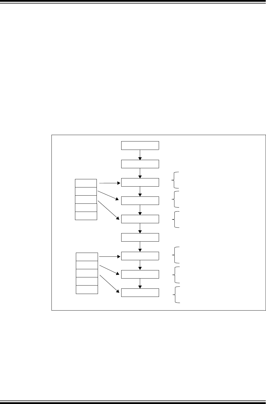
PIC32 Family Reference Manual
DS61128G-page 13-20 © 2007-2012 Microchip Technology Inc.
13.3.3 Read Operation
To p erf or m a re ad on the para lle l b us, th e u se r application reads the PMDIN register. The effect
of reading the PMDIN register retrieves the current value and causes the PMP to activate the
Chip Select lines and the address bus. The read line PMRD is strobed in Master mode 2,
PMRD/PMWR and PMENB lines in Master mode 1, and the new data is latched into the PMDIN
register making it available the next time the PMDIN register is read.
Note that the read data obtained from the PMDIN register is actually the read value from the
previous read operation. Therefore, the first user application read will be a dummy read to initiate
the first bus read and fill the read register. See Figure 13-11, which illustrates this sequence.
Also, the requested read value will not be ready until after the BUSY bit (PMMODE<15>) is
observed low. Therefore, in a back-to-back read operation, the data read from the register will be
the same for both reads. The next read of the register will yield the new value.
In 16-bit Data mode (MODE16 bit (PMMODE<10>) = 1), the read from the PMDIN register
causes the data bus PMD<15:0> to be read into PMDIN<15:0>. In 8-bit mode, MODE16 bit
(PMMODE<10>) = 0, the read from the PMDIN register causes the data bus PMD<7:0> to be
read into PMDIN<7:0>. The upper 8 bits, PMD<15:8>, are ignored.
Figure 13-11: Example Read Sequence Demonstrating ‘Dummy’ Read Operation
13.3.4 Write Operation
To perform a write on the parallel port, the user application writes to the PMDIN register (same
register as a read operation). This causes the PMP module to first activate the Chip Select lines
and the address bus. The write data from the PMDIN register is placed onto the PMD data bus
and the write line PMPWR is strobed in Master mode 2, PMRD/PMWR and PMENB lines in
Master Mode 1.
In 16-bit Data mode (MODE16 bit (PMMODE<10>) = 1), the write to the PMDIN register causes
PMDIN<15:0> to appear on the data bus, (PMD<15:0>). In 8-bit mode, MODE16 bit
(PMMODE<10>) = 0, the write to the PMDIN register causes PMDIN<7:0> to appear on the data
bus, PMD<7:0>. The upper 8 bits, PMD<15:8>, are ignored.
Set Initial Address = 0x4000
Dummy Read
Enable Auto-Address Increment
PMADDR = 0x4000
INCM<1:0> = 01
Read PMDIN
3. PMADDR = 0x4001
2. PMDIN updated = 0x02
0x4000 0x02
0x33
0xFA
0x7C
0x0A
1. User Reads PMDIN = (don’t care)
Read PMDIN
0x4001
0x4002
0x4003
0x4004
6. PMADDR = 0x4002
5. PMDIN updated = 0x33
4. User Reads PMDIN = 0x02
9. PMADDR = 0x4003
8. PMDIN updated = 0xFA
7. User Reads PMDIN = 0x33
Read PMDIN
PMADDR = 0x4100
0x4100 0x45
0x76
0x00
0x2A
0x93
0x4101
0x4102
0x4103
0x4104
Set New Address = 0x4100
3. PMADDR = 0x4101
2. PMDIN updated = 0x45
1. User Reads PMDIN = 0xFA (don’t care)
6. PMADDR = 0x4102
5. PMDIN updated = 0x76
4. User Reads PMDIN = 0x45
9. PMADDR = 0x4103
8. PMDIN updated = 0x00
7. User Reads PMDIN = 0x76
Dummy Read
Read PMDIN
Read PMDIN
Read PMDIN
Data in external device
memory or registers
Data in external device
memory or registers

© 2007-2012 Microchip Technology Inc. DS61128G-page 13-21
Section 13. Parallel Master Port (PMP)
Parallel Master
Port (PMP)
13
13.3.5 Master Mode Interrupts
In PMP master modes, the PMPIF bit is set on every read or write strobe. An interrupt request is
generated when the IRQM<1:0> bits (PMMODE<14:13>) are set = 01 and PMP interrupts are
enabled, PMPIE (IEC1<2>) = 1.
13.3.6 Parallel Master Port Status – The BUSY Bit
In addition to the PMP interrupt, the BUSY bit (PMMODE<15>) is provided to indicate the status
of the module. This bit is only used in Master mode.
While any read or write operation is in progress, the BUSY bit is set for all but the very last
peripheral bus cycle of the operation. This is helpful when Wait states are enabled or multiplexed
address/data is selected. While the bit is set, any request by the user to initiate a new operation
will be ignored (i.e., writing or reading the PMDIN register will not initiate a read or a write).
Since the system clock, SYSCLK, can operate faster than the peripheral bus clock in certain
configurations, or if a large number of Wait states are used, it is possible for the PMP module to
be in the process of completing a read or write operation when the next CPU instruction is
reading or writing to the PMP module. For this reason, it is highly recommended that the BUSY
bit be checked prior to any operation that accesses the PMDIN or PMADDR register.
Example 13-2 shows a polling operation of the BUSY bit prior to accessing the PMP module.
In most applications, the PMP module’s Chip Select pin(s) provide the Chip Select interface and
is under the timing control of the PMP module. However, some applications may require the PMP
Chip Select pin(s) to not be configured as a Chip Select, but as a high order address line, such
as PMA<14> or PMA<15>. In this situation, the application’s Chip Select function must be
provided by an available I/O port pin under software control. In these cases, it is especially
important that the user’s software poll the BUSY bit to ensure any read or write operation is
complete before deasserting the software controlled Chip Select.
Example 13-2: Example Code: Polling the BUSY Bit Flag
/* This example reads 256 16-bit words from an external device at address 0x4000 and copies
the data to a second external device at address 0x8000. The PMP port is operating in
Master mode 2. Note how the PMP’s BUSY bit is polled prior to all operations to the
PMDOUT, PMDIN or PMADDR register, except where noted. */
unsigned short DataArray<256>;
// Provide the setup code here including large Wait
// states, auto increment.
...
CopyData(); // A call to the copy function is made.
...
void CopyData()
{
PMADDR = 0x4000; // Initialize PMP address. First time, no need to poll BUSY bit
while(PMMODE & 0x8000); // Poll - if busy, wait before reading.
PMDIN; // Read the PMDIN to clear previous data and latch new
// data.
for(i=0; i<256; i++)
{
while(PMMODE & 0x8000); // Poll - if busy, wait before reading.
DataArray<i> = PMDIN; // Read the external device.
}
while(PMMODE & 0x8000); // Poll - if busy, wait before changing PMADDR.
PMADDR = 0x8000; // Address of second external device.
for(i=0; i<256; i++)
{
while(PMMODE & 0x8000); // Poll - if busy, wait before writing.
DataArray<i> = PMDIN; // Read the external device.
}
return();
}
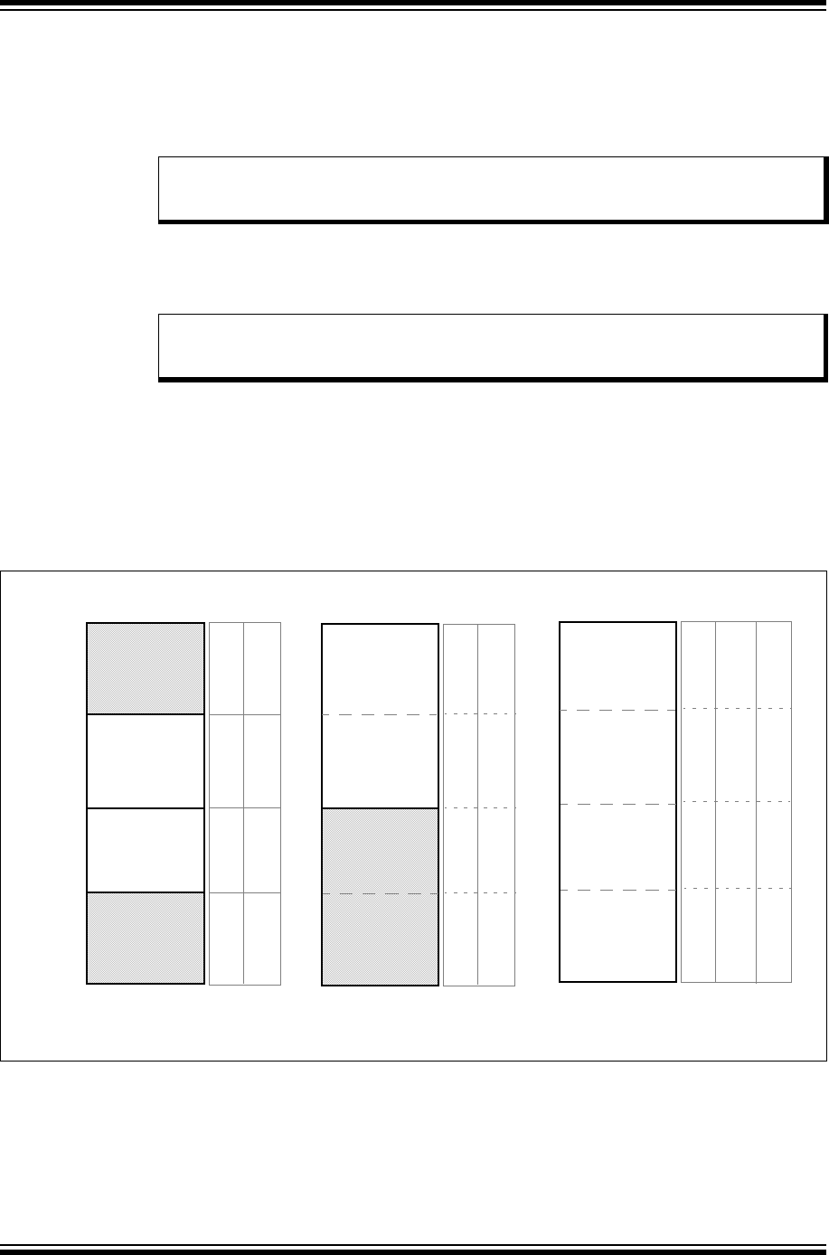
PIC32 Family Reference Manual
DS61128G-page 13-22 © 2007-2012 Microchip Technology Inc.
13.3.7 Addressing Considerations
The PMCS2 and PMCS1 Chip Select pins share functionality with address lines A15 and A14. It
is possible to enable both PMCS2 and PMCS1 as Chip Selects, or enable only PMCS2 as a Chip
Select; allowing PMCS1 to function strictly as address line A14. It is not possible to enable only
PMCS1.
When configured as Chip Selects, a ‘1’ must be written into bit position 15 or 14 of the PMADDR
register in order for PMCS2 or PMCS1 to become active during a read or write operation. Failing
to write a ‘1’ to PMCS2 or PMCS1 does not prevent address pins PMA<13:0> from being active
as the specified address appears; however, no Chip Select signal will be active.
In fully multiplexed modes, address bits PMADDR<15:0> are multiplexed with the data bus and
in the event address bits PMA15 or PMA14 are configured as Chip Selects, the corresponding
PMADDR<15:14> address bits are automatically forced to ‘0’. Disabling one or both PMCS2 and
PMCS1 makes these bits available as address bits PMADDR<15:14>.
In any of the master mode multiplexing schemes, disabling both Chip Select pins PMCS2 and
PMCS1 requires the user to provide Chip Select line control through some other I/O pin under
software control, as shown in Figure 13-12.
Figure 13-12: PMP Chip Select Address Maps
Note: Setting both A15 and A14 = 1 when PMCS2 and PMCS1 are enabled as Chip
Selects will cause both PMCS2 and PMCS1 to be active during a read or write
operation. This may enable two devices simultaneously and should be avoided.
Note: When using Auto-Increment Address mode, PMCS2 and PMCS1 do not participate
and must be controlled by the user’s software by writing to ‘1’ to PMADDR<15:14>
explicitly.
Device 2
Selected
PMCS2 = 1
Device 1
Selected
PMCS1 = 1
No Device
Selected
Both Devices
Selected
(INVALID)
0x0000
0x4000
0x8000
0xFFFF
0xC000
0
0
00
1
1
11
PMCS2, CS1
2 – 16K Address Ranges
2 – Chip Selects
Device
Selected
I/O-pin = 1
A15, A14, I/Opin
1
1 – 64K Address Range
I/O-pin = Software-controlled CS
0
1
1
0
0
01
11
1
1
Device
Selected
PMCS2 = 1
No Device
Selected
0
PMCS2, A14
1 – 32K Address Range
1 – Chip Select
1
1
0
0
01
1
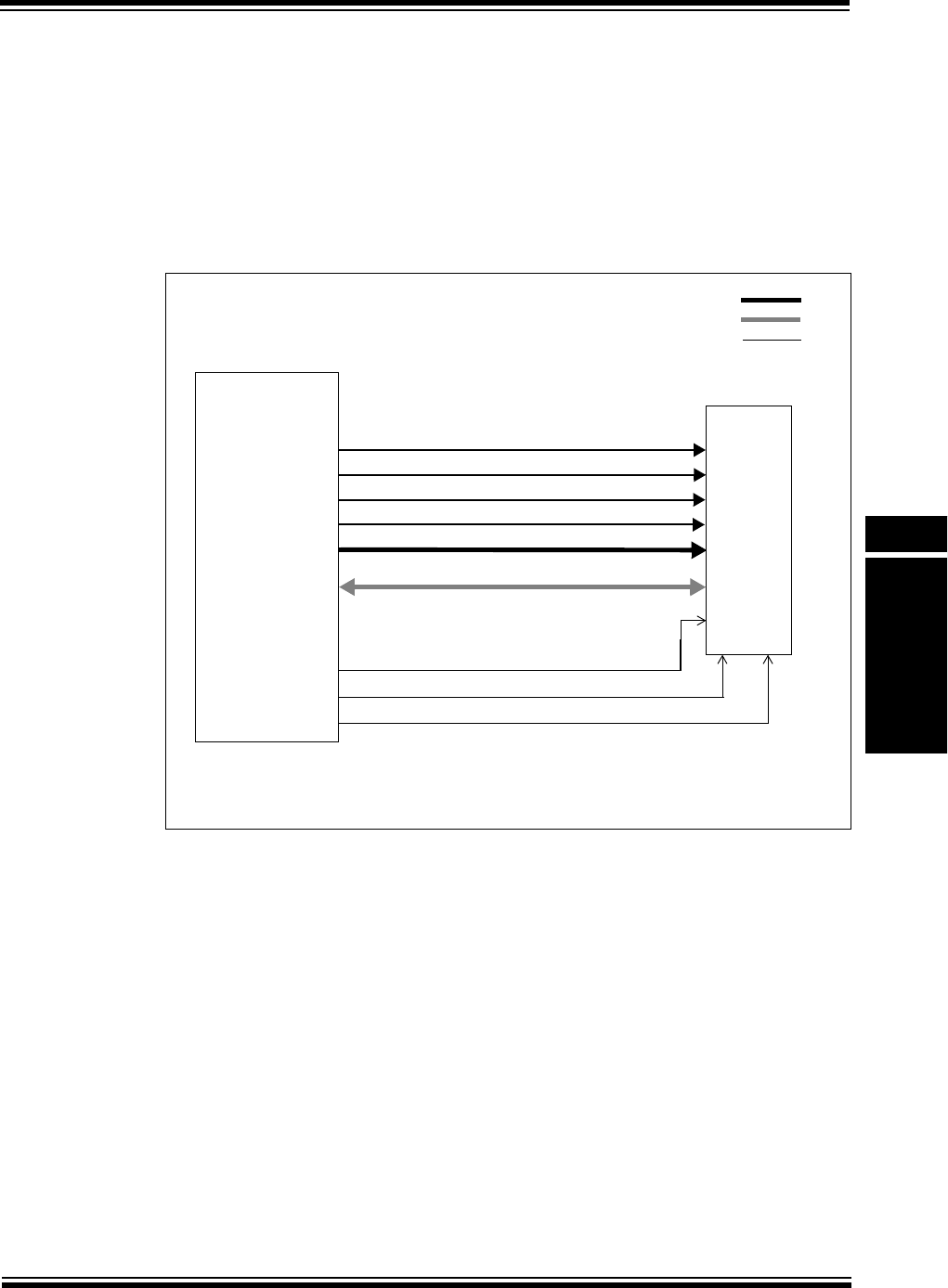
© 2007-2012 Microchip Technology Inc. DS61128G-page 13-23
Section 13. Parallel Master Port (PMP)
Parallel Master
Port (PMP)
13
13.3.7.1 ADDRESSING MEMORY DEVICES LARGER THAN 64K
When using the PMCS2 or PMCS1 Chip Select pins, the addressable range is limited to 16K or
32K locations, depending on the Chip Select pin being used. Disabling PMCS2 and PMCS1 as
Chip Selects allows these pins to function as address lines PMA15 and PMA14, increasing the
range to 64K addressable locations. A dedicated I/O pin is required to function as the Chip Select
and the user’s software must now control the function of this pin.
To interface to memory devices larger than 64K, use additional available I/O pins as the higher
order address lines A16, A17, A18, etc., as shown in Figure 13-13.
Figure 13-13: Interface to a 16 Megabit (1M x 16-bit) SRAM Memory Device
PMA<15:0>
D<15:0>
A<15:0>
D<15:0>
A<15:0>
PMRD
PMWR
OE WR
CE
PIC32
Address Bus
Data Bus
Control Lines
RG15
PMD<15:0>
Note: Master mode 2: MODE<1:0> bits (PMMODE<9:8>) = 10.
16-bit data width: MODE16 bit (PMMODE<10>) = 1.
Demultiplexed mode: ADRMUX<1:0> bits (PMCON<12:11>) = 00.
RD0
RD1
RD2
A<16>
A<17>
A<18>
A<19>
RD3
1024K x 16-bit
Device
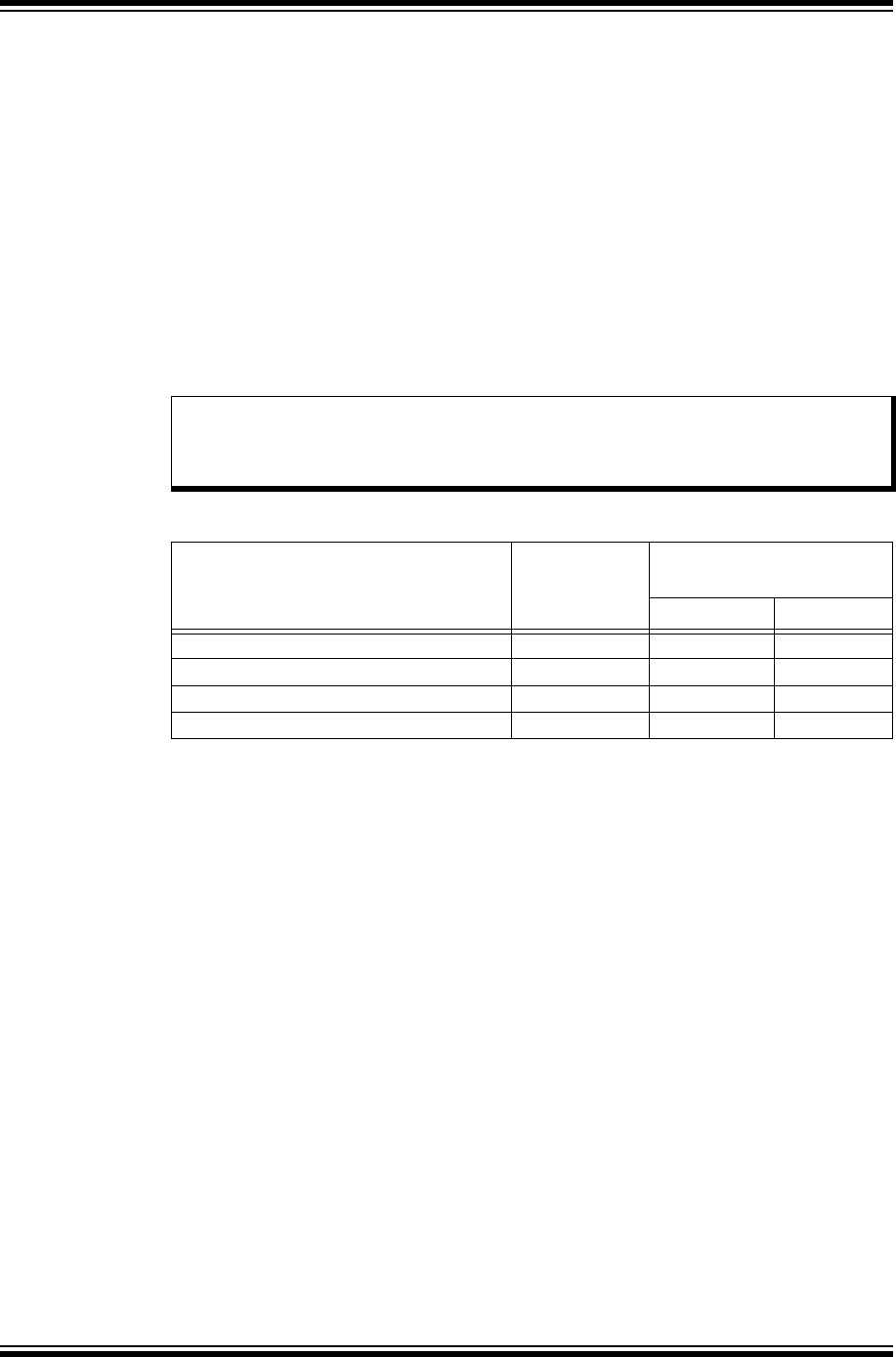
PIC32 Family Reference Manual
DS61128G-page 13-24 © 2007-2012 Microchip Technology Inc.
13.3.8 Master Mode Timing
A PMP Master mode cycle time is defined as the number of PBCLK cycles required by the PMP
to perform a read or write operation and is dependent on PBCLK clock speed, PMP
Address/Data Multiplexing modes, and the number of PMP wait states, if any. Refer to the
specific device data sheet for setup and hold timing characteristics.
A PMP Master mode read or write cycle is initiated by accessing (reading or writing) the PMDIN
register. Ta b l e 13-6 provides a summary of read and write PMP cycle times for each multiplex
configuration.
The actual data rate of the PMP (the rate at which the user’s code can perform a sequence of
read or write operations) will be highly dependent on several factors:
•User’s application code content
•Code optimization level
•Internal bus activity
•Other factors relating to the instruction execution speed
The following timing examples represent the common master mode configuration options. These
options vary from 8-bit to 16-bit data, non-multiplexed to fully multiplexed address, as well as with
and without Wait states. For illustration purposes only, all control signal polarities are shown as
“active-high”.
Note: During any Master mode read or write operation, the busy flag will always de-assert
1 peripheral bus clock cycle (TPBCLK), before the end of the operation, including Wait
states. The user’s application must check the status of the busy flag to ensure it is
equal to ‘0’ before initiating the next PMP operation.
Table 13-6: PMP Read/Write Cycle Times(1)
Address/Data Multiplex Configuration ADRMUX Bit
Settings
PMP Cycle Time
(PBCLK Cycles)
Read Write
Fully Multiplexed (16-bit data) 11 5 6
Fully Multiplexed (8-bit data) 10 8 9
Partial Multiplex 01 5 6
Demultiplexed 00 2 3
Note 1: Wait states are not enabled.
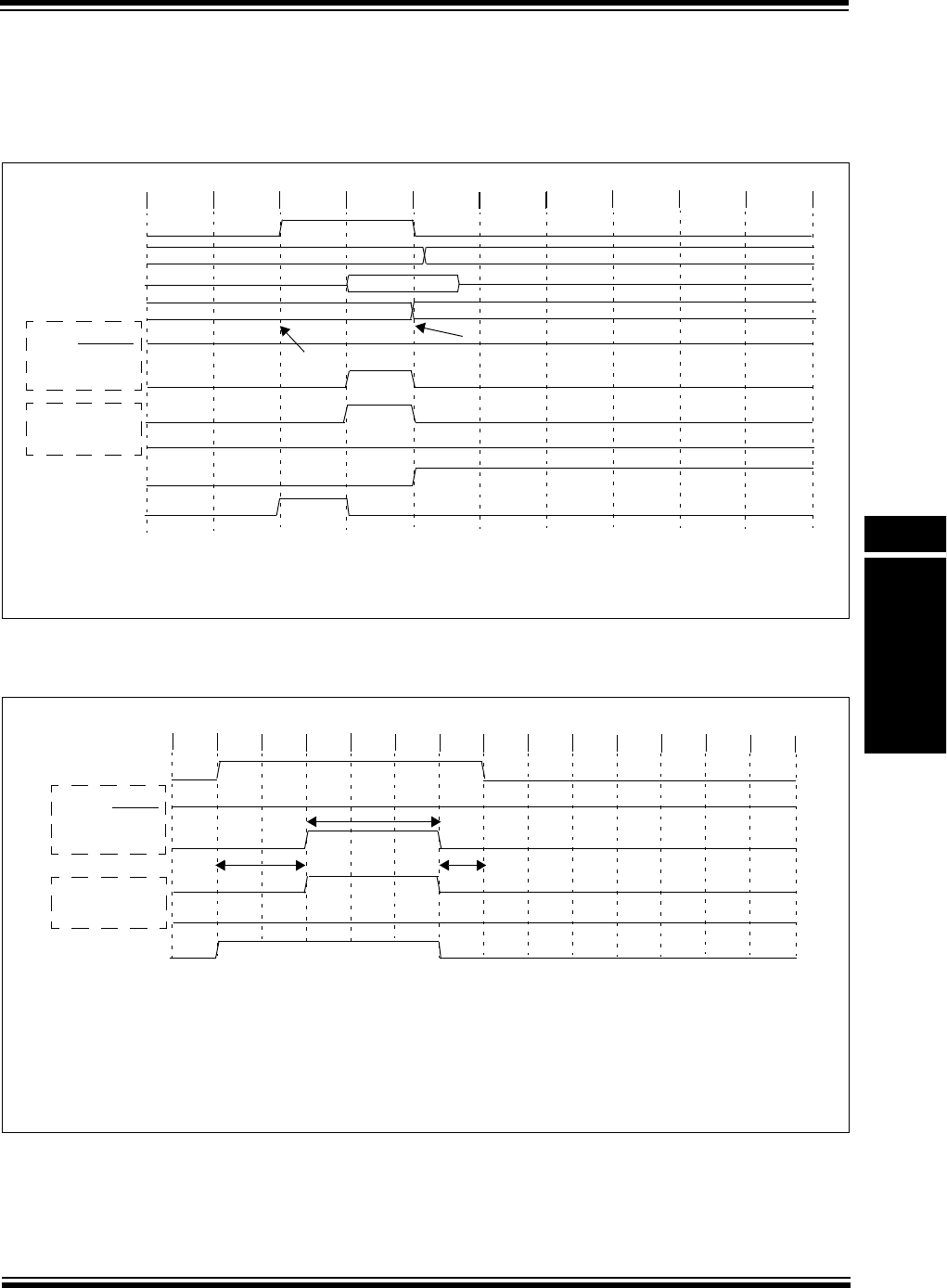
© 2007-2012 Microchip Technology Inc. DS61128G-page 13-25
Section 13. Parallel Master Port (PMP)
Parallel Master
Port (PMP)
13
13.3.8.1 DEMULTIPLEXED ADDRESS AND DATA TIMING
The timing diagram in Figure 13-14 illustrates the demultiplexed timing (separate address and
data bus) for a read operation with no Wait states. A read operation requires 2 TPBCLK, peripheral
bus clock cycles.
Figure 13-14: 8-bit, 16-bit Read Operations, ADRMUX = 00, No Wait States
In this timing diagram with Wait states, shown in Figure 13-15, the read operation requires
6 TPBCLK, peripheral bus clock cycles.
Figure 13-15: 8-bit, 16-bit Read Operations, ADRMUX = 00, Wait States Enabled
Data from Target
PMCS2/PMCS1
PMPENB
PMRD/PMPWR
PMD<15:0>(1)
PMA<13:0>
PMPIF
BUSY
Address<13:0>
TPB TPB TPBTPB TPB TPB TPB TPB TPB TPB
User Read from PMDIN(2)
Data latched into PMDIN
New Latched Data
PMDIN Previous Latched Data
Note 1: In 8-bit mode, PMD<15:8> are not implemented.
2: Read data obtained from the PMDIN register is actually the value from the previous read operation.
PMWR
PMRD
Mode 1
Mode 2
PMCS2/PMCS1
TPB TPB TPB TPB TPB TPB TPB TPB TPB TPB TPB TPB TPB
TPB
B
M
E
BUSY
PMENB
PMRD/PMWR
Mode 1
PMWR
PMRD
Mode 2
Legend:
B = WAITB<1:0> = 01 (2 Wait states)
M = WAITM<3:0> = 0010 (3 Wait states)
E = WAITE<1:0> = 01 (1 Wait state)
Note: If WAITM<3:0> = 0000, M is forced to 1 TPBCLK, WAITB is ignored (B forced to 1 TPBCLK), and WAITE is ignored (E forced
to 0 TPBCLK).
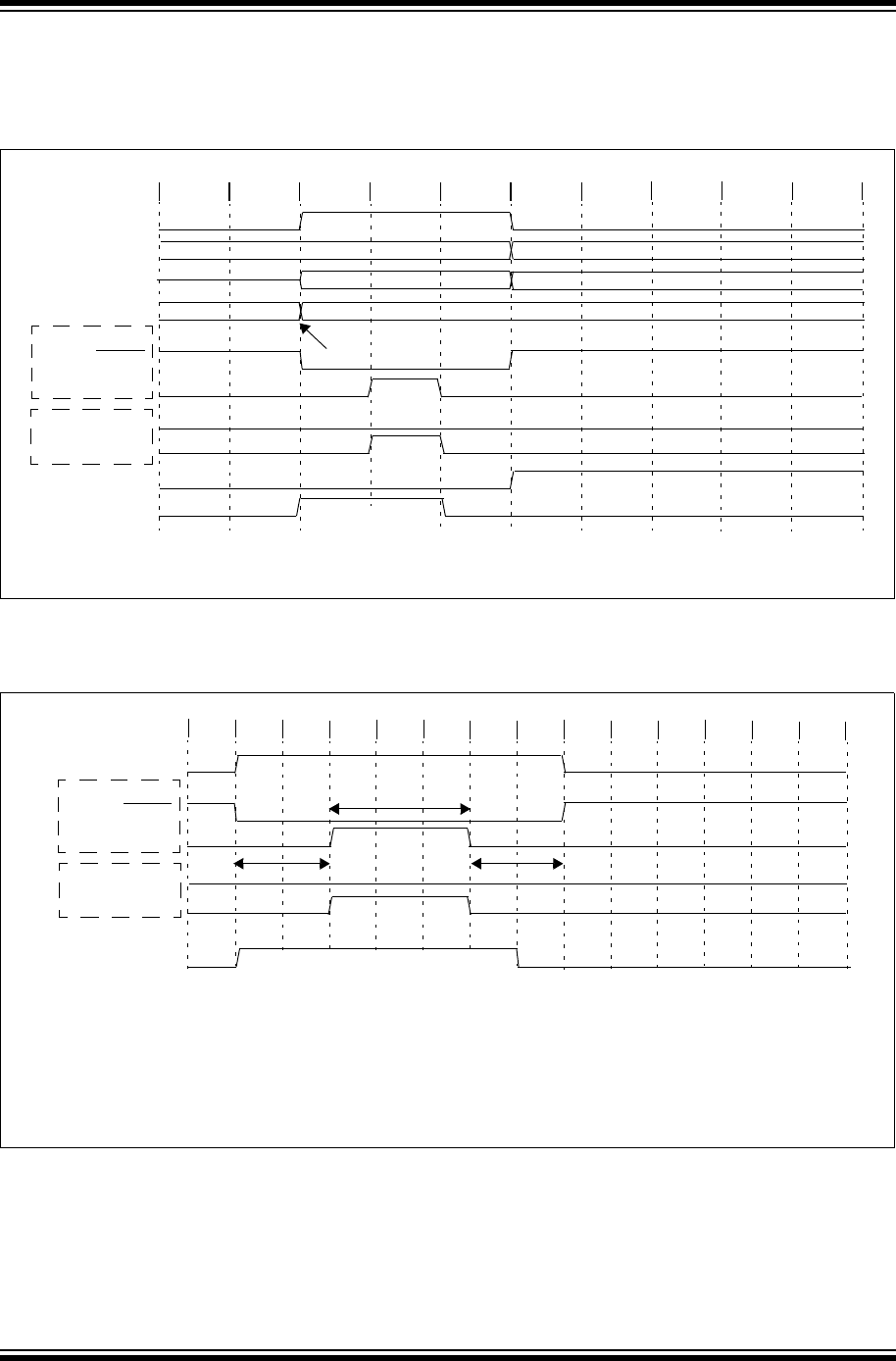
PIC32 Family Reference Manual
DS61128G-page 13-26 © 2007-2012 Microchip Technology Inc.
The timing diagram in Figure 13-16 illustrates demultiplexed timing (separate address and data
bus) for a write operation with no Wait states. A write operation requires 3 TPBCLK, peripheral bus
clock cycles.
Figure 13-16: 8-bit, 16-bit Write Operations, ADRMUX = 00, No Wait States
In this timing diagram with Wait states, shown in Figure 13-17, the write operation requires
7 TPBCLK, peripheral bus clock cycles.
Figure 13-17: 8-bit, 16-bit Write Operations, ADRMUX = 00, Wait States Enabled
Data to Target
PMCS2, PMCS1
PMD<15:0>(1)
PMA<13:0>
PMPIF
BUSY
Address<13:0>
TPB TPB TPBTPB TPB TPB TPB TPB TPB TPB
Note 1: In 8-bit mode, PMD<15:8> are not implemented.
New Data
PMDIN Previous Data
User Writes to PMDIN
PMENB
PMRD/PMWR
Mode 1
PMWR
PMRD
Mode 2
PMCS2/PMCS1
TPB TPB TPB TPB TPB TPB TPB TPB TPB TPB TPB TPB TPB
TPB
B
M
E
BUSY
PMENB
PMRD/PMWR
Mode 1
PMWR
PMRD
Mode 2
Legend:
B = WAITB<1:0> = 01 (2 Wait states)
M = WAITM<3:0> = 0010 (3 Wait states)
E = WAITE<1:0> = 01 (2 Wait states)
Note: If WAITM<3:0> = 0000, M is forced to 1 TPBCLK, WAITB is ignored (B forced to 1 TPBCLK), and WAITE is ignored
(E forced to 1 TPBCLK).
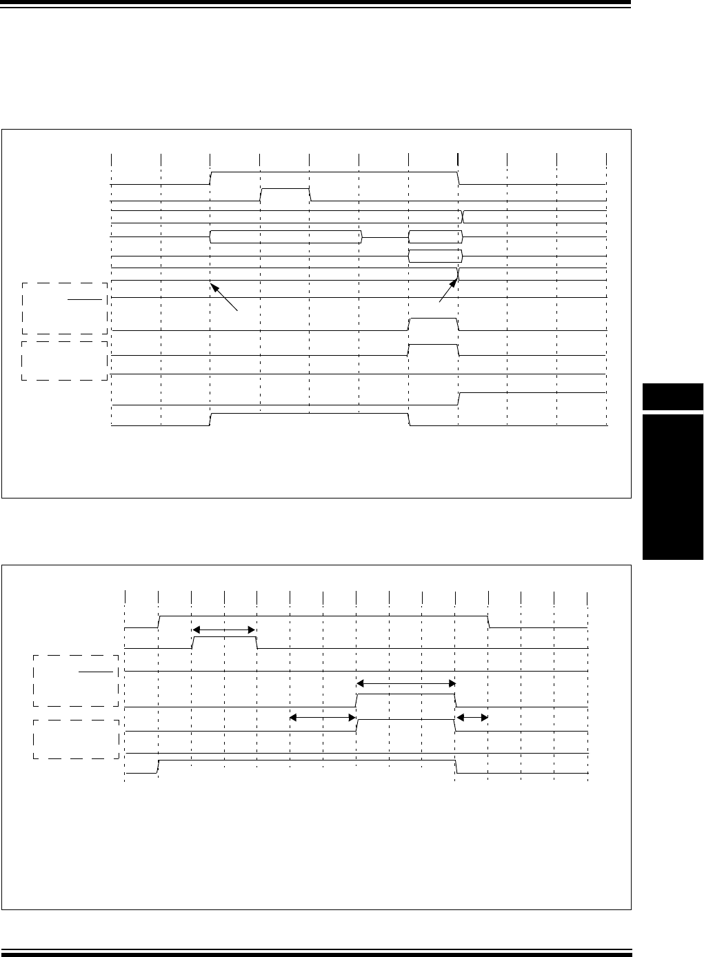
© 2007-2012 Microchip Technology Inc. DS61128G-page 13-27
Section 13. Parallel Master Port (PMP)
Parallel Master
Port (PMP)
13
13.3.8.2 PARTIALLY MULTIPLEXED ADDRESS AND DATA TIMING
The timing diagram shown in Figure 13-18 illustrates partially multiplexed timing (address bits
<7:0> multiplexed with data bus, PMD<7:0>) for a read operation with no Wait states. A read
operation requires 5 TPBCLK, peripheral bus clock cycles.
Figure 13-18: 8-bit, 16-bit Read Operations, ADRMUX = 01, No Wait States
In this timing diagram with Wait states, shown in Figure 13-19, the read operation requires
10 TPBCLK, peripheral bus clock cycles.
Figure 13-19: 8-bit, 16-bit Read Operations, ADRMUX = 01, Wait States Enabled
PMCS2, PMCS1
PMALL
PMD<7:0>
PMA<13:8>
PMPIF
ADDRESS<7:0> LSB
BUSY
TPB TPB TPBTPB TPB TPB TPB TPB TPB TPB
ADDRESS<13:8>
PMD<15:8>(2) MSB
Data from Target
New Latched Data
PMDIN Previous Latched Data
User Read from PMDIN(1) Data latched into PMDIN
Note 1: Read data obtained from the PMDIN register is actually the value from the previous read operation.
2: In 8-bit mode, PMD<15:8> are not implemented.
PMENB
PMRD/PMWR
Mode 1
PMWR
PMRD
Mode 2
PMCS2/PMCS1
TPB TPB TPB TPB TPB TPB TPB TPB TPB TPB TPB TPB TPB
TPB
B
M
E
PMALL
B
BUSY
PMWR
PMRD
Mode 2
PMENB
PMRD/PMWR
Mode 1
Legend:
B = WAITB<1:0> = 01 (2 Wait states)
M = WAITM<3:0> = 0010 (3 Wait states)
E = WAITE<1:0> = 01 (1 Wait state)
Note: If WAITM<3:0> = 0000, M is forced to 1 TPBCLK, WAITB is ignored (B forced to 1 TPBCLK), and WAITE is ignored (E forced
to 0 TPBCLK).
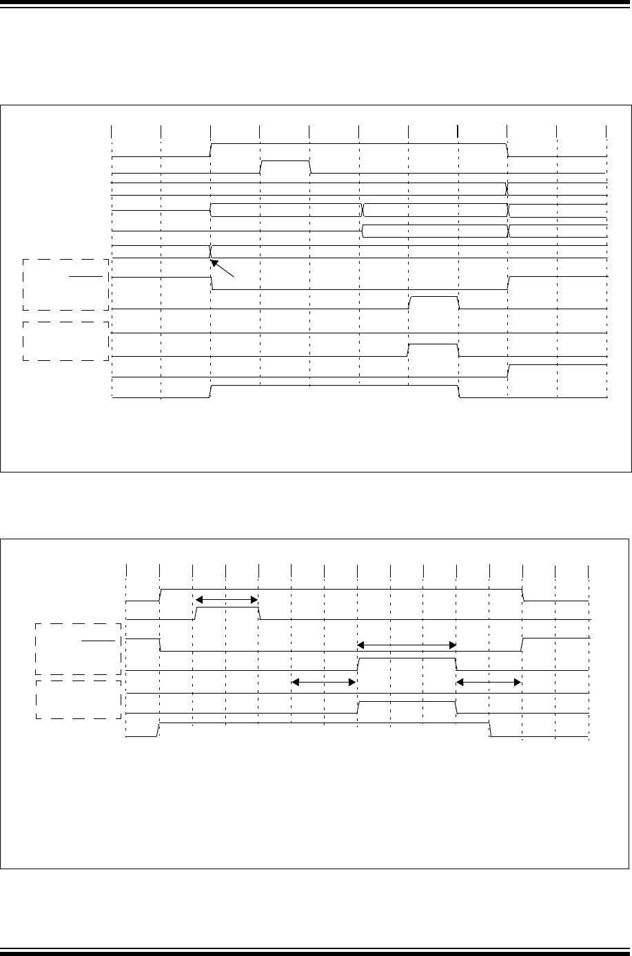
PIC32 Family Reference Manual
DS61128G-page 13-28 © 2007-2012 Microchip Technology Inc.
The timing diagram shown in Figure 13-20 illustrates partially multiplexed timing (address bits
<7:0> multiplexed with data bus, PMD<7:0>) for a write operation with no Wait states. A write
operation requires 6 TPBCLK, peripheral bus clock cycles.
Figure 13-20: 8-bit, 16-bit Write Operations, ADRMUX = 01, No Wait States
In this timing diagram with Wait states, shown in Figure 13-21, the write operation requires
11 TPBCLK, peripheral bus clock cycles.
Figure 13-21: 8-bit, 16-bit Write Operations, ADRMUX = 01, Wait States Enabled
PMCS2/PMCS1
PMALL
PMD<15:8>(2)
PMA<13:8>
PMPIF
MSB Data to Target
BUSY
TPB TPB TPBTPB TPB TPB TPB TPB TPB TPB
ADDRESS<13:8>
PMD<7:0> ADDRESS<7:0> LSB Data to Target
Note 1: During a write operation, there is one TPBCLK hold cycle following the PMWR signal.
2: In 8-bit mode, PMD<15:8> are not implemented.
New Data
PMDIN Previous Data
PMWR(1)
PMRD
Mode 2
User Writes to PMDIN
PMENB
PMRD/PMWR
Mode 1
PMCS2/PMCS1
TPB TPB TPB TPB TPB TPB TPB TPB TPB TPB TPB TPB TPB
TPB
B
M
E
PMALL
B
BUSY
PMWR
PMRD
Mode 2
PMENB
PMRD/PMWR
Mode 1
Legend:
B = WAITB<1:0> = 01 (2 Wait states)
M = WAITM<3:0> = 0010 (3 Wait states)
E = WAITE<1:0> = 01 (1 Wait state)
Note: If WAITM<3:0> = 0000, M is forced to 1 TPBCLK, WAITB is ignored (B forced to 1 TPBCLK), and WAITE is ignored (E forced
to 1 TPBCLK).
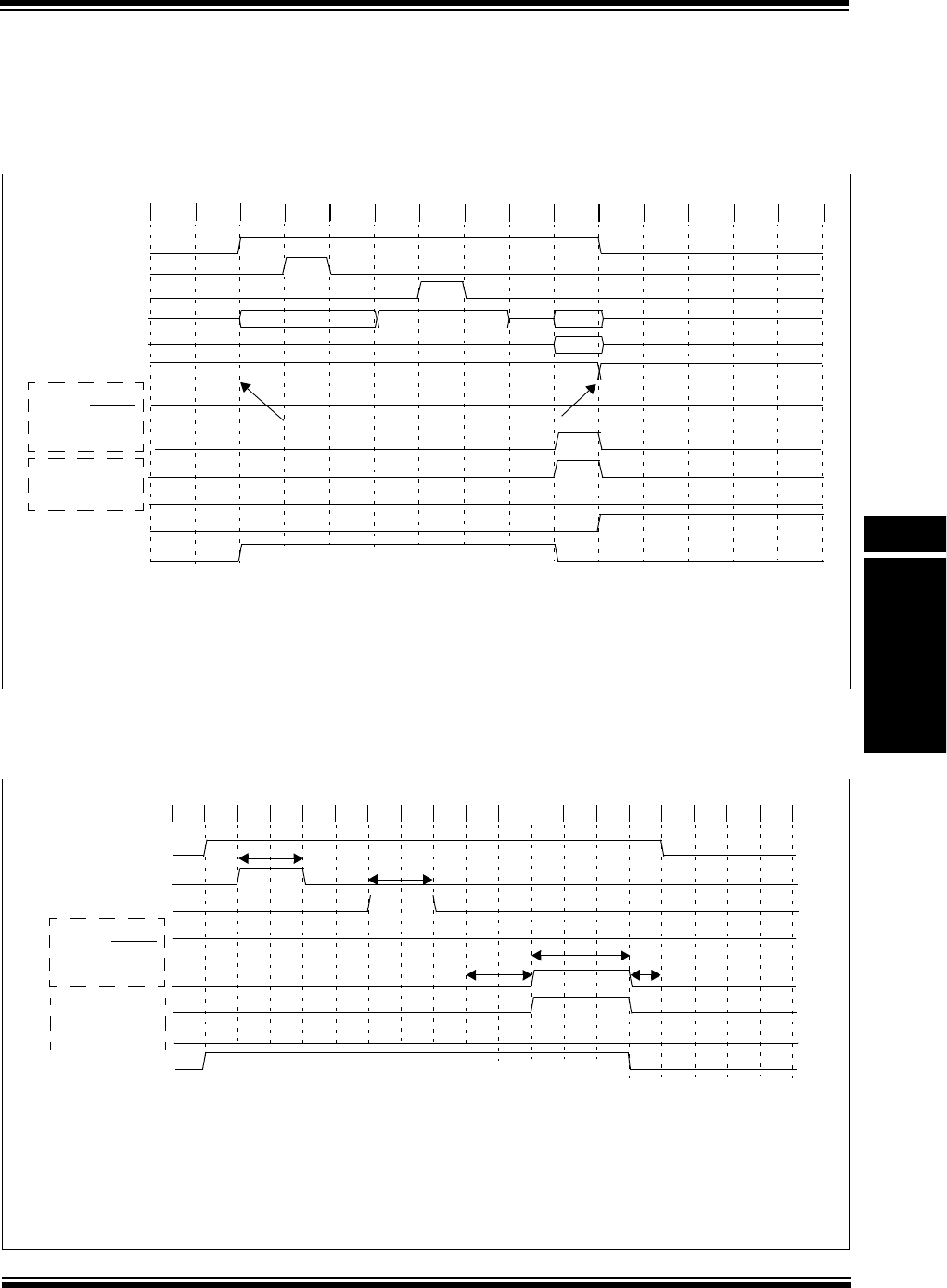
© 2007-2012 Microchip Technology Inc. DS61128G-page 13-29
Section 13. Parallel Master Port (PMP)
Parallel Master
Port (PMP)
13
13.3.8.3 FULLY MULTIPLEXED (8-BIT BUS) ADDRESS AND DATA TIMING
The timing diagram in Figure 13-22 illustrates fully multiplexed timing (address bits <15:0>
multiplexed with data bus, PMD<7:0>) for a read operation with no Wait states. A read operation
requires 8 TPBCLK, peripheral bus clock cycles.
Figure 13-22: 8-bit, 16-bit Read Operations, ADRMUX = 10, No Wait States
In this timing diagram with Wait states, shown in Figure 13-23, the read operation requires
14 TPBCLK, peripheral bus clock cycles.
Figure 13-23: 8-bit, 16-bit Read Operations, ADRMUX = 10, Wait States Enabled
PMCS2/PMCS1
PMD<15:8>(2)
PMPIF
BUSY
PMALL
PMALH
TPB TPB TPB TPB TPB TPB TPB TPB TPB TPB TPB TPB TPB TPB TPB
Data from Target
PMD<7:0>
MSB
LSB
ADDRESS<7:0> ADDRESS<13:8>(3)
New Latched Data
PMDIN Previous Latched Data
Note 1: Read data obtained from the PMDIN register is actually the value from the previous read operation.
2: In 8-bit mode, PMD<15:8> are not implemented.
3: PMADDR address bit A15 and A14 are forced to ‘0’ if PMCS2 and/or PMCS1 are enabled as Chip Selects.
PMENB
PMRD/PMWR
Mode 1
PMWR
PMRD
Mode 2
Data latched into PMDIN
User Read from PMDIN(1)
PMCS2/PMCS1
TPB
B
M
E
PMALL
B
BUSY
PMWR
PMRD
Mode 2
PMENB
PMRD/PMWR
Mode 1
PMALH
TPB TPB TPB TPB TPB TPB TPB TPB TPB TPB TPB TPB TPB TPB TPB TPB TPB TPB
B
Legend:
B = WAITB<1:0> = 01 (2 Wait states)
M = WAITM<3:0> = 0010 (3 Wait states)
E = WAITE<1:0> = 01 (1 Wait state)
Note: If WAITM<3:0> = 0000, M is forced to 1 TPBCLK, WAITB is ignored (B forced to 1 TPBCLK), and WAITE is ignored
(E forced to 0 TPBCLK).
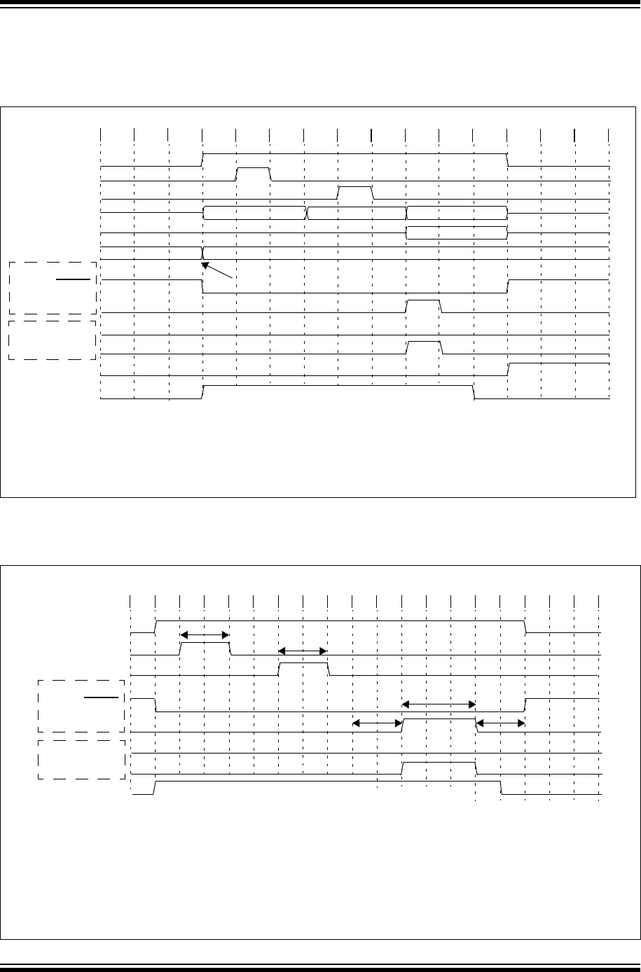
PIC32 Family Reference Manual
DS61128G-page 13-30 © 2007-2012 Microchip Technology Inc.
The timing diagram shown in Figure 13-24 illustrates fully multiplexed timing (address bits
<15:0> multiplexed with data bus, PMD<7:0>) for a write operation with no Wait states. A write
operation requires 9 TPBCLK, peripheral bus clock cycles.
Figure 13-24: 8-bit, 16-bit Write Operations, ADRMUX = 10, No Wait States
In this timing diagram with Wait states, shown in Figure 13-25, the write operation requires
15 TPBCLK, peripheral bus clock cycles.
Figure 13-25: 8-bit, 16-bit Write Operations, ADRMUX = 10, Wait States Enabled
PMCS2/PMCS1
PMD<15:8>(2)
PMPIF
BUSY
PMALL
PMALH
TPB TPB TPB TPB TPB TPB TPB TPB TPB TPB TPB TPB TPB TPB TPB
MSB DATA to Target
PMD<7:0> LSB DATA to Target
ADDRESS<7:0> ADDRESS<13:8>(3)
New Data
PMDIN Previous Data
Note 1: During a write operation, there is one TPBCLK hold cycle following the PMWR signal.
2: In 8-bit mode, PMD<15:8> are not implemented.
3: PMADDR address bit A15 and A14 are forced to ‘0’, if PMCS2 and/or PMCS1 are enabled as Chip Selects.
PMWR(1)
PMRD
Mode 2
User Writes to PMDIN
PMENB
PMRD/PMWR
Mode 1
PMCS2/PMCS1
TPB
B
M
E
PMALL
B
BUSY
PMWR
PMRD
Mode 2
PMENB
PMRD/PMWR
Mode 1
PMALH
TPB TPB TPB TPB TPB TPB TPB TPB TPB TPB TPB TPB TPB TPB TPB TPB TPB TPB
B
Legend:
B = WAITB<1:0> = 01 (2 Wait states)
M = WAITM<3:0> = 0010 (3 Wait states)
E = WAITE<1:0> = 01 (2 Wait states)
Note: If WAITM<3:0> = 0000, M is forced to 1 TPBCLK, WAITB is ignored (B forced to 1 TPBCLK), and WAITE is ignored
(E forced to 1 TPBCLK).

© 2007-2012 Microchip Technology Inc. DS61128G-page 13-31
Section 13. Parallel Master Port (PMP)
Parallel Master
Port (PMP)
13
13.3.8.4 FULLY MULTIPLEXED (16-BIT BUS) ADDRESS AND DATA TIMING
The timing diagram shown in Figure 13-26 illustrates fully multiplexed timing (address bits
<15:0> multiplexed with data bus, PMD<15:0>) for a read operation with no Wait states. A read
operation requires 5 TPBCLK, peripheral bus clock cycles.
Figure 13-26: 16-bit Read Operation, ADRMUX = 11, No Wait States
In this timing diagram with Wait states, shown in Figure 13-27, the read operation requires
10 TPBCLK, peripheral bus clock cycles.
Figure 13-27: 16-bit Read Operation, ADRMUX = 11, Wait States Enabled
PMCS2/PMCS1
PMD<15:8>
PMPIF
BUSY
PMALL
PMALH
TPB TPB TPB TPB TPB TPB TPB TPB TPB TPB TPB TPB TPB TPB TPB
MSB
PMD<7:0> ADDRESS<7:0>
ADDRESS<13:8>(2)
New Latched Data
PMDIN Previous Latched Data
LSB Data from Target
Note 1: Read data obtained from the PMDIN register is actually the value from the previous read operation.
2: PMADDR address bit A15 and A14 are forced to ‘0’ if PMCS2 and/or PMCS1 are enabled as Chip Selects.
PMENB
PMRD/PMWR
Mode 1
PMWR
PMRD
Mode 2
Data latched into PMDIN
User Read from PMDIN(1)
PMCS2/PMCS1
TPB TPB TPB TPB TPB TPB TPB TPB TPB TPB TPB TPB TPB
TPB
B
M
E
PMALL
B
BUSY
PMWR
PMRD
Mode 2
PMENB
PMRD/PMWR
Mode 1
PMALH
Legend:
B = WAITB<1:0> = 01 (2 Wait states)
M = WAITM<3:0> = 0010 (3 Wait states)
E = WAITE<1:0> = 01 (1 Wait state)
Note: If WAITM<3:0> = 0000, M is forced to 1 TPBCLK, WAITB is ignored (B forced to 1 TPBCLK), and WAITE is ignored
(E forced to 0 TPBCLK).

PIC32 Family Reference Manual
DS61128G-page 13-32 © 2007-2012 Microchip Technology Inc.
The timing diagram shown in Figure 13-28 illustrates fully multiplexed timing (address bits
<15:0> multiplexed with data bus, PMD<15:0>) for a write operation with no Wait states. A read
operation requires 6 TPBCLK, peripheral bus clock cycles.
Figure 13-28: 16-bit Write Operation, ADRMUX = 11, No Wait States
In this timing diagram with Wait states, shown in Figure 13-29, the write operation requires
11 TPBCLK, peripheral bus clock cycles.
Figure 13-29: 16-bit Write Operation, ADRMUX = 11, Wait States Enabled
PMCS2/PMCS1
PMPIF
BUSY
PMALL
PMALH
TPB TPB TPB TPB TPB TPB TPB TPB TPB TPB TPB TPB TPB TPB TPB
MSB DATA OUT
PMD<15:8>
PMD<7:0> LSB DATA OUTADDRESS<7:0>
ADDRESS<13:8>(2)
New Data
PMDIN Previous Data
User Writes to PMDIN
PMENB
PMRD/PMWR
Mode 1
PMWR(1)
PMRD
Mode 2
Note 1: During a write operation, there is one TPB hold cycle following the PMWR signal.
2: PMADDR address bit A15 and A14 are forced to ‘0’ if PMCS2 and/or PMCS1 are enabled as Chip Selects.
PMCS2/PMCS1
TPB TPB TPB TPB TPB TPB TPB TPB TPB TPB TPB TPB TPB
TPB
B
M
E
PMALL
B
BUSY
PMWR
PMRD
Mode 2
PMENB
PMRD/PMWR
Mode 1
PMALH
Legend:
B = WAITB<1:0> = 01 (2 Wait states)
M = WAITM<3:0> = 0010 (3 Wait states)
E = WAITE<1:0> = 01 (2 Wait states)
Note: If WAITM<3:0> = 0000, M is forced to 1 TPBCLK, WAITB is ignored (B forced to 1 TPBCLK), and WAITE is
ignored (E forced to 1 TPBCLK).
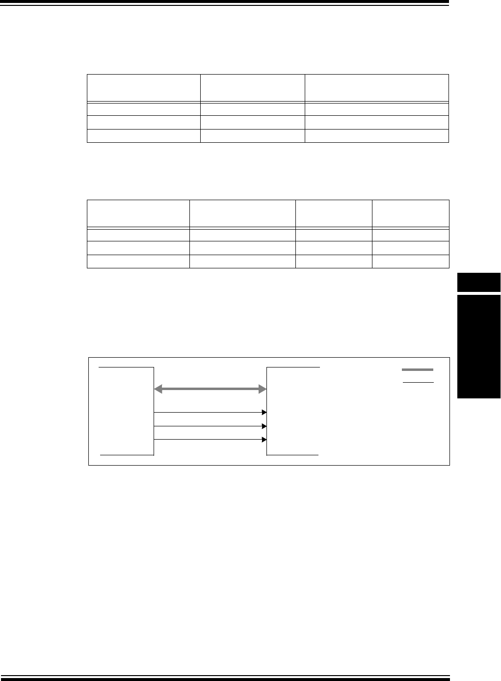
© 2007-2012 Microchip Technology Inc. DS61128G-page 13-33
Section 13. Parallel Master Port (PMP)
Parallel Master
Port (PMP)
13
13.4 SLAVE MODES OF OPERATION
The PMP module provides 8-bit (byte) legacy Parallel Slave Port (PSP) functionality as well as
new buffered and addressable slave modes.
All slave modes support 8-bit data only and the module control pins are automatically dedicated
when any of these modes are selected. The user application only needs to configure the polarity
of the PMCS1, PMRD and PMWR signals.
13.4.1 Legacy Slave Port Mode
In 8-bit PMP Legacy Slave mode, the module is configured as a PSP using control bits
MODE<1:0> (PMMODE<9:8>) = 00. In this mode, an external device such as another
microcontroller or microprocessor can asynchronously read and write data using the 8-bit data
bus PMD<7:0>, the read PMRD, write PMWR and Chip Select PMCS1 inputs.
Figure 13-30: Parallel Master/Slave Connection Example
13.4.1.1 INITIALIZATION STEPS
The following Slave mode initialization steps properly prepares the PMP port for communicating
with an external device.
1. Clear the ON control bit (PMCON<15> = 0) to disable the PMP module.
2. Select Legacy mode with the MODE<1:0> bits (PMMODE<9:8>) = 00.
3. Select the polarity of the Chip Select pin, CS1P (PMCON<3>).
4. Select the polarity of the control pins, WRSP (PMCON<1>) and RDSP (PMCON<0>).
5. If interrupts are used:
a) Clear the interrupt flag bit, PMPIF (IFS1<2>) = 0.
b) Configure the PMP interrupt priority bits, PMPIP<2:0> (IPC7<4:2>) and the interrupt
subpriority bits PMPIS (IPC7<1:0>).
c) Enable the PMP interrupt by setting the interrupt enable bit, PMPIE (IEC1<2>) = 1.
6. Set the ON control bit to ‘1’ to enable the PMP module.
Table 13-7: Slave Mode Selection
Slave Mode PMMODE<9:8> bits
(MODE<1:0>)
PMMODE<12:11> bits
(INCM<1:0>)
Addressable 01 x = don’t care
Legacy 00 x = don’t care
Buffered 00 11
Table 13-8: Slave Mode Pin Polarity Configuration
CONTROL
PIN
PMCON
Control Bit
Active-High
Select
Active-Low
Select
PMRD RDSP 1 0
PMWR WRSP 1 0
PMCS1 CS1P 1 0
Data Bus
Control Lines
D<7:0>
RD
WR
Master
CS
PMD<7:0>
PMRD
PMWR
PIC32 Slave
PMCS1

PIC32 Family Reference Manual
DS61128G-page 13-34 © 2007-2012 Microchip Technology Inc.
Example 13-3: Legacy Parallel Slave Port Initialization (Example Code)
13.4.1.2 WRITE TO SLAVE PORT
When Chip Select is active and a write strobe occurs, the data on the bus pins PMD<7:0> is
captured into the lower 8 bits of the PMDIN register, PMDIN<7:0>. The PMPIF (interrupt flag bit)
is set during the write strobe. The IB0F bit will remain set until the PMDIN register is read by the
user application. If a write operation occurs while the IB0F = 1, the write data will be ignored and
an overflow condition will be generated, IB0V = 1. See the timing diagrams in 13.4.4 “Slave
Mode Read and Write Timing Diagrams”.
13.4.1.3 READ FROM SLAVE PORT
When Chip Select is active and a read strobe occurs, the data from the lower 8 bits of the
PMDOUT register (PMDOUT<7:0>) is presented onto data bus pins PMD<7:0> and read by the
master device. The PMPIF (interrupt flag bit) is set during the read strobe. The OB0E bit will
remain set until the PMDOUT register is written to by the user application. If a read operation
occurs while the OB0E = 1, the read data will be the same as the previous read data and an
underflow condition will be generated, OBUF = 1. See the timing diagrams in 13.4.4 “Slave
Mode Read and Write Timing Diagrams”.
13.4.1.4 LEGACY MODE INTERRUPT OPERATION
In PMP Legacy Slave mode, the PMPIF bit is set every read or write strobe. If using interrupts,
the user’s application vectors to an Interrupt Service Routine (ISR) where the IBF and OBE
status bits can be examined to determine if the buffer is full or empty. If not using interrupts, the
user’s application should wait for PMPIF to be set before polling the IBF and OBE Status bits to
determine if the buffer is full or empty.
13.4.2 Buffered Parallel Slave Port Mode
The 8-bit Buffered Parallel Slave Port mode is functionally identical to the Legacy Parallel Slave
Port mode with one exception: the implementation of 4-level read and write buffers. Buffered
Slave mode is enabled by setting the MODE<1:0> bits (PMMODE<9:8>) = 00, and the
INCM<1:0> bits (PMMODE<12:11>) = 11.
When the buffered mode is active, the module uses the PMDIN register as write buffers and the
PMDOUT register as read buffers. Each register is divided into four 8-bit buffer registers, four
read buffers in PMDOUT and four write buffers in PMDIN. Buffers are numbered 0 through 3,
starting with the lower byte <7:0> and progressing upward through the high byte <31:24>.
Note: On persistent interrupt implementations of the PMP, the interrupt is generated on
the falling edge of the WR signal with the WR signal configured to active-high
polarity. On non-persistent interrupt implementations of the PMP, the interrupt is
generated on the rising edge of the WR signal with the WR signal configured to
active-high polarity. Firmware should poll the IBF or IBnF bit to ensure the data is
valid before attempting to read the data from the PMP module.
/*
Example configuration for Legacy Slave mode
*/
IEC1CLR = 0x0004; // Disable PMP interrupt in case it is already enabled
PMCON = 0x0008; // Stop and Configure PMCON register for Legacy mode
PMMODE = 0x0000; // Configure PMMODE register
IPC7SET = 0x001C; // Set priority level = 7 and
IPC7SET = 0x0003; // Set subpriority level = 3
// Could have also done this in single
// operation by assigning IPC7SET = 0x001F
IFS1CLR = 0x0004; // Clear the PMP interrupt status flag
IEC1SET = 0x0004; // Enable PMP interrupts
PMCONSET = 0x8000; // Enable PMP module
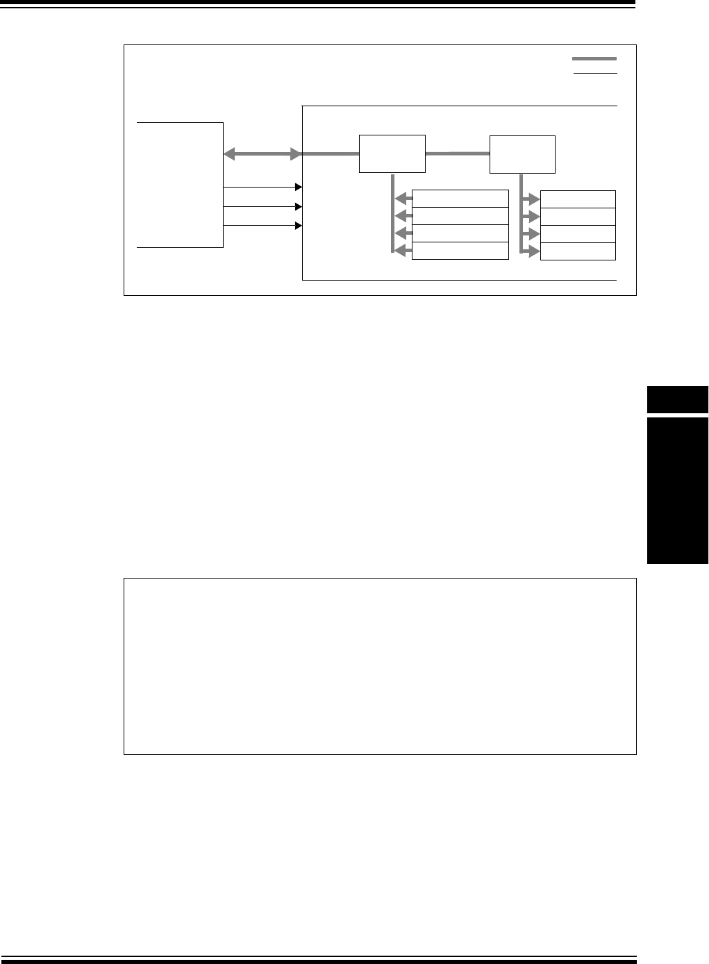
© 2007-2012 Microchip Technology Inc. DS61128G-page 13-35
Section 13. Parallel Master Port (PMP)
Parallel Master
Port (PMP)
13
Figure 13-31: Parallel Master/Slave Connection Buffered Example
13.4.2.1 INITIALIZATION STEPS
The following Buffered Slave mode initialization properly prepares the PMP port for
communicating with an external device.
1. Clear the ON control bit (PMCON<15> = 0) to disable the PMP module.
2. Select the Legacy mode with MODE<1:0> bits (PMMODE<9:8>) = 00.
3. Select Buffer mode with INCM<1:0> bits (PMMODE<12:11>) = 11.
4. Select the polarity of the Chip Select CS1P (PMCON<3>).
5. Select the polarity of the control pins WRSP (PMCON<1>) and RDSP (PMCON<0>).
6. If interrupts are used:
a) Clear interrupt flag bit PMPIF (IFS1<2>).
b) Configure interrupt priority and subpriority levels in IPC7.
c) Set interrupt enable bit PMPIE (IEC1<2>).
7. Set the ON control bit to ‘1’ to enable the PMP module.
Example 13-4: Buffered Parallel Slave Port Initialization (Example Code)
13.4.2.2 READ FROM SLAVE PORT
For read operations, the bytes will be sent out sequentially, starting with Buffer 0,
PMDOUT<7:0>, and ending with Buffer 3, PMDOUT<31:24>, for every read strobe. The module
maintains an internal pointer to keep track of which buffer is to be read.
Each of the buffers has a corresponding read Status bit, OBnE, in the PMSTAT register. This bit
is cleared when a buffer contains data that has not been written to the bus, and is set when data
is written to the bus. If the current buffer location being read from is empty, a buffer underflow is
generated, and the Buffer Overflow flag bit OBUF is set. If all four OBnE Status bits are set, the
Output Buffer Empty flag OBE will also be set. See the timing diagrams in 13.4.4 “Slave Mode
Read and Write Timing Diagrams”.
D<7:0>
RD
WR
Master
Data Bus
Control Lines
CS
PMRD
PMWR
PIC32 Slave
PMCS1
PMDOUT (0)
PMDOUT (1)
PMDOUT (2)
PMDOUT (3)
PMDIN (0)
PMDIN (1)
PMDIN (2)
PMDIN (3)
PMD<7:0> Write
Address
Pointer
Read
Address
Pointer
/* Example configuration for Buffered Slave mode */
IEC1CLR = 0x0004 // Disable PMP interrupt in case it is already enabled
PMCON = 0x0000 // Stop and configure PMCON register for Buffered mode
PMMODE = 0x1800 // Configure PMMODE register
IPC7SET = 0x001C; // Set priority level = 7 and
IPC7SET = 0x0003; // Set subpriority level = 3
// Could have also done this in single operation by
// by assigning IPC7SET = 0x001F
IFS1CLR = 0x0004; // Clear the PMP interrupt status flag
IEC1SET = 0x0004; // Enable PMP interrupts
PMCONSET = 0x8000; // Enable the PMP module
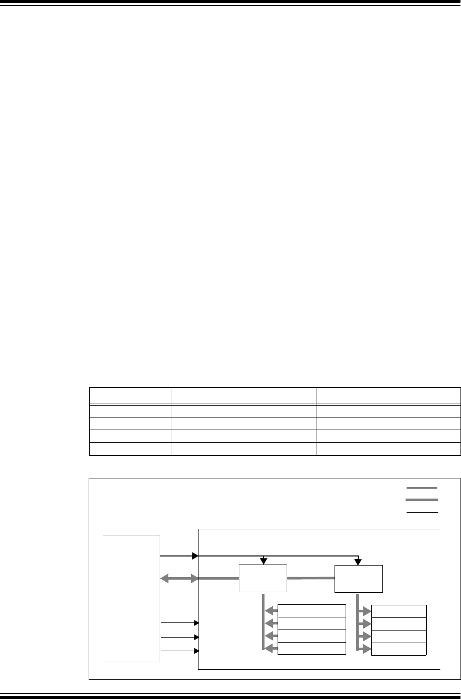
PIC32 Family Reference Manual
DS61128G-page 13-36 © 2007-2012 Microchip Technology Inc.
13.4.2.3 WRITE TO SLAVE PORT
For write operations, the data is be stored sequentially, starting with Buffer 0, PMDIN<7:0> and
ending with Buffer 3, PMDIN<31:24>. As with read operations, the module maintains an internal
pointer to the buffer that is to be written next.
The input buffers have their own write Status bits, IBnF. The bit is set when the buffer contains
unread incoming data, and cleared when the data has been read. The flag bit is set on the write
strobe. If a write occurs on a buffer when its associated IBnF bit is set, the Buffer Overflow flag
IBOV is set; any incoming data in the buffer will be lost. If all four IBnF flags are set, the Input
Buffer Full flag IBF is set. See the timing diagrams in 13.4.4 “Slave Mode Read and Write
Timing Diagrams”.
13.4.2.4 BUFFERED MODE INTERRUPT OPERATION
In Buffered Slave mode, the module can be configured to generate an interrupt on every read or
write strobe, IRQM<1:0> bits (PMMODE<14:13>) = 01. It can be configured to generate an
interrupt on a read from Read Buffer 3 or a write to Write Buffer 3, IRQM<1:0> = 10, which is
essentially an interrupt every fourth read or write strobe. When interrupting every fourth byte for
input data, all input buffer registers should be read to clear the IBnF flags. If these flags are not
cleared then there is a risk of hitting an overflow condition.
If using interrupts, the user’s application vectors to an Interrupt Service Routine (ISR) where the
IBF and OBE status bits can be examined to determine if the buffer is full or empty. If not using
interrupts, the user application should wait for PMPIF to be set before polling the IBF and OBE
status bits to determine if the buffer is full or empty.
13.4.3 Addressable Buffered Parallel Slave Port Mode
In the 8-bit Addressable Buffered Parallel Slave Port mode, the module is configured with two
extra inputs, PMA<1:0>. This makes the 4-byte buffer space directly addressable as fixed pairs
of read and write buffers. As with Buffered Legacy mode, data is output from register PMDOUT
and is input to register PMDIN. Ta b l e 13-9 shows the address resolution for the incoming address
to the input and output registers.
Figure 13-32: Parallel Master/Slave Connection Addressed Buffer Example
Table 13-9: Slave Mode Buffer Addresses
PMA<1:0> Output Register (Buffer) Input Register (Buffer)
11 PMDOUT<31:24> (3) PMDIN<31:24> (3)
10 PMDOUT<23:16> (2) PMDIN<23:16> (2)
01 PMDOUT<15:8> (1) PMDIN<15:8> (1)
00 PMDOUT<7:0> (0) PMDIN<7:0> (0)
D<7:0>
RD
WR
Master
CS
A<1:0>
Address Bus
Data Bus
Control Lines
PMRD
PMWR
PIC32 Slave
PMCS1
PMDOUT (0)
PMDOUT (1)
PMDOUT (2)
PMDOUT (3)
PMDIN (0)
PMDIN (1)
PMDIN (2)
PMDIN (3)
PMD<7:0> Write
Address
Decode
Read
Address
Decode
PMA<1:0>

© 2007-2012 Microchip Technology Inc. DS61128G-page 13-37
Section 13. Parallel Master Port (PMP)
Parallel Master
Port (PMP)
13
13.4.3.1 INITIALIZATION STEPS
The following Addressable Buffered Slave mode initialization steps properly prepares the PMP
port for communicating with an external device.
1. Clear the ON control bit (PMCON<15> = 0) to disable the PMP module.
2. Select the Legacy mode with MODE<1:0> bits (PMMODE<9:8) = 00.
3. Select the polarity of the Chip Select CS1P (PMCON<3>).
4. Select the polarity of the control pins WRSP (PMCON<1>) and RDSP (PMCON<0>).
5. If interrupts are used:
a) Clear interrupt flag bit PMPIF (IFS1<2>).
b) Configure interrupt priority and subpriority levels in IPC7.
c) Set interrupt enable bit PMPIE (IEC1<2>).
6. Set the ON control bit to ‘1’ to enable the PMP module.
Example 13-5: Addressable Parallel Slave Port Initialization (Example Code)
13.4.3.2 READ FROM SLAVE PORT
When Chip Select is active and a read strobe occurs, the data from one of the four output 8-bit
buffers is presented onto PMD<7:0>. The byte selected to be read depends on the 2-bit address
placed on PMA<1:0>. Tabl e 13-9 shows the corresponding output registers and their associated
address. When an output buffer is read, the corresponding OBnE bit is set. The OBE flag bit is
set when all the buffers are empty. If any buffer is already empty, OBnE = 1, the next read to that
buffer will generate an OBUF event. See the timing diagrams in 13.4.4 “Slave Mode Read and
Write Timing Diagrams”.
13.4.3.3 WRITE TO SLAVE PORT
When Chip Select is active and a write strobe occurs (PMCS = 1 and PMWR = 1), the data from
PMD<7:0> is captured into one of the four input buffer bytes. The byte selected to be written
depends on the 2-bit address placed on ADDR<1:0>. Ta b l e 13-9 shows the corresponding input
registers and their associated address.
When an input buffer is written, the corresponding IBnF bit is set. The IBF flag bit is set when all
the buffers are written. If any buffer is already written, IBnF = 1, the next write strobe to that buffer
will generate an IBOV event, and the byte will be discarded. See the timing diagrams in
13.4.4 “Slave Mode Read and Write Timing Diagrams”.
13.4.3.4 ADDRESSABLE BUFFERED MODE INTERRUPT OPERATION
In Addressable Slave mode, the module can be configured to generate an interrupt on every read
or write strobe, IRQM<1:0> bits (PMMODE<14:13>) = 01. It can also be configured to generate
an interrupt on any read from Read Buffer 3 or write to Write Buffer 3, IRQM<1:0> = 10; in other
words, an interrupt will occur whenever a read or write occurs when PMA<1:0> is ‘11’.
If using interrupts, the user application vectors to an Interrupt Service Routine (ISR) where the
IBF and OBE Status bits can be examined to determine if the buffer is full or empty. If not using
interrupts, the user application should wait for PMPIF to be set before polling the IBF and OBE
Status bits to determine if the buffer is full or empty.
/* Example configuration for Addressable Slave mode */
IEC1CLR = 0x0004 // Disable PMP interrupt in case it is already enabled
PMCON = 0x0000 // Stop and configure PMCON register for Address mode
PMMODE = 0x0100 // Configure PMMODE register
IPC7SET = 0x001C; // Set priority level = 7 and
IPC7SET = 0x0003; // Set subpriority level = 3
// Could have also done this in single operation
// by assigning IPC7SET = 0x001F
IFS1CLR = 0x0004; // Clear the PMP interrupt status flag
IEC1SET = 0x0004; // Enable PMP interrupts
PMCONSET = 0x8000; // Enable the PMP module
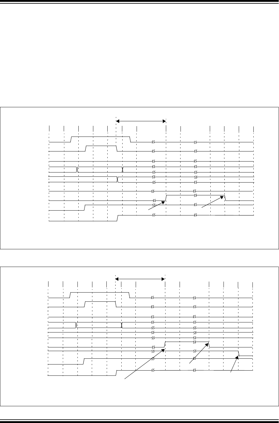
PIC32 Family Reference Manual
DS61128G-page 13-38 © 2007-2012 Microchip Technology Inc.
13.4.4 Slave Mode Read and Write Timing Diagrams
In all of the slave modes, an external master device is connected to the parallel slave port and is
controlling the read and write operations. When an external read or write operation is performed
by the external master device, the PMPIF bit (IFS1<2>) will be set on the active edge of PMRD
or PMWR pin.
• For any external write operation, the user’s application must poll the IBOV or IB0F buffer
Status bit to ensure adequate time for the write operation to be completed before accessing
the PMDIN register.
• For any external read operation, the user’s application must poll the OBUF or OB0E buffer
Status bit to ensure adequate time for the read operation to be completed before accessing
the PMDOUT register.
Figure 13-33: Parallel Slave Port Write Operation
Figure 13-34: Parallel Slave Port Write Operation – Buffer Full, Overflow Condition
PMCS1
PMWR
PMRD
IB0F
PMPIF
PMD<7:0> Data from Master
New Data
PMDIN Previous Data
TPB TPB TPB TPB TPB TPB TPB TPB TPB
TPB
User Reads PMDIN
Buffer Full, Ready to Read
IBOV
Note: Control signal polarity are configurable and are shown active-high in this example.
2-3 TPBCLK Cycles
(Non-Persistent
Interrupt)
PMPIF
(Persistent Interrupt)
PMCS1
PMWR
PMRD
IB0F
PMPIF
PMD<7:0> Data from Master
PMDIN Previous Data
T
PB
T
PB
T
PB
T
PB
T
PB
T
PB
T
PB
T
PB
T
PB
T
PB
User Reads PMDIN
Buffer Overflow Condition
IBOV
Note: Control signal polarity are configurable and are shown active-high in this example.
2-3
T
PBCLK
Cycles
User Clears IB0V
(Non-Persistent
Interrupt)
PMPIF
(Persistent Interrupt)
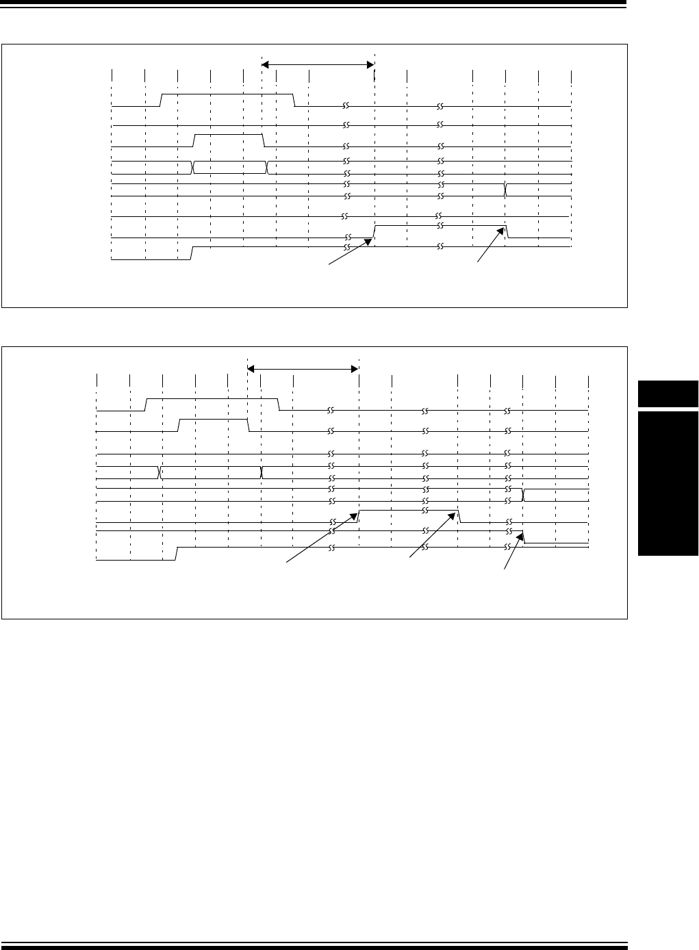
© 2007-2012 Microchip Technology Inc. DS61128G-page 13-39
Section 13. Parallel Master Port (PMP)
Parallel Master
Port (PMP)
13
Figure 13-35: Parallel Slave Port Read Operation
Figure 13-36: Parallel Slave Port Read Operation – Buffer Empty, Underflow Condition
PMCS1
PMWR
PMRD
OB0E
PMPIF
PMD<7:0> Data to Master
Same Data
PMDOUT Data
TPB TPB TPB TPB TPB TPB TPB TPB TPB
TPB
User Writes New Data to PMDIN
Buffer Empty, Ready to Write New Data
OBUF
Note: Control signal polarity are configurable and are shown active-high in this example.
2-3 TPBCLK Cycles
New Data
PMCS1
PMWR
PMRD
OB0E
PMPIF
PMD<7:0> Old Data to Master
PMDOUT Old Data
TPB TPB TPB TPB TPB TPB TPB TPB
TPB
User Writes PMDIN
Buffer Underflow Condition
OBUF
Note: Control signal polarity are configurable and are shown active-high in this example.
2-3 TPBCLK Cycles
User Clears OBUF
New Data
TPB

PIC32 Family Reference Manual
DS61128G-page 13-40 © 2007-2012 Microchip Technology Inc.
13.5 INTERRUPTS
The Parallel Master Port module has the ability to generate an interrupt, depending on the
selected operating mode.
• PMP (Master) mode:
Interrupt on every completed read or write operation.
•PSP (Legacy Slave) mode:
Interrupt on every read and write byte
•PSP (Buffered Slave) mode:
- Interrupt on every read and write byte
- Interrupt on read or write byte of Buffer 3 (PMDOUT<31:24>)
•EPSP (Enhanced Addressable Slave) mode:
- Interrupt on every read and write byte
- Interrupt on read or write byte of Buffer 3 (PMDOUT<31:24>), PMA<1:0> = 11.
The PMPIF bit must be cleared in software.
The PMP module is enabled as a source of interrupt via the PMP Interrupt Enable bit, PMPIE.
The Interrupt Priority bits (PMPIP<2:0>) and Interrupt Subpriority bits (PMPIS<1:0>) must also
be configured. For more details, refer to Section 8. “Interrupts” (DS61108).
13.5.1 Interrupt Configuration
The PMP module has a dedicated interrupt flag bit, PMPIF, and a corresponding interrupt
enable/mask bit, PMPIE. These bits are used to determine the source of an interrupt and to
enable or disable an individual interrupt source.
The PMPIE bit is used to define the behavior of the Vector Interrupt Controller or Interrupt
Controller when the PMPIF bit is set. When the PMPIE bit is clear, the Interrupt Controller module
does not generate a CPU interrupt for the event. If the PMPIE bit is set, the Interrupt Controller
module will generate an interrupt to the CPU when the PMPIF bit is set (subject to the priority
and subpriority as outlined below).
It is the responsibility of the user’s software routine that services a particular interrupt to clear the
appropriate Interrupt Flag bit before the service routine is complete.
The priority of PMP module can be set with the PMPIP<2:0> bits. This priority defines the priority
group to which the interrupt source will be assigned. The priority groups range from a value of 7,
the highest priority, to a value of 0, which does not generate an interrupt. An interrupt being
serviced will be preempted by an interrupt in a higher priority group.
The subpriority bits allow setting the priority of a interrupt source within a priority group. The
values of the subpriority, PMPIS<1:0>, range from 3, the highest priority, to 0 the lowest priority.
An interrupt with the same priority group but having a higher subpriority value will preempt a
lower subpriority interrupt that is in progress.
The priority group and subpriority bits allow more than one interrupt source to share the same
priority and subpriority. If simultaneous interrupts occur in this configuration, the natural order of
the interrupt sources within a priority/subgroup pair determine the interrupt generated. The
natural priority is based on the vector numbers of the interrupt sources. The lower the vector
number the higher the natural priority of the interrupt. Any interrupts that were overridden by
natural order will then generate their respective interrupts based on priority, subpriority and
natural order after the interrupt flag for the current interrupt is cleared.
After an enabled interrupt is generated, the CPU will jump to the vector assigned to that interrupt.
The vector number for the interrupt is the same as the natural order number. The CPU will then
begin executing code at the vector address. The user’s code at this vector address should
perform any application specific operations and clear the PMPIF interrupt flag, and then exit. For
more information on interrupts and the vector addresses, refer to Section 8. “Interrupts”
(DS61108).

© 2007-2012 Microchip Technology Inc. DS61128G-page 13-41
Section 13. Parallel Master Port (PMP)
Parallel Master
Port (PMP)
13
Example 13-6: PMP Module Interrupt Initialization Code Example
Example 13-7: PMP ISR Code Example
/* This code example illustrates a PMP interrupt configuration.
When the PMP interrupt is generated, the CPU will branch to the vector assigned to PMP
interrupt. */
// Configure PMP for desired mode of operation
...
// Configure the PMP interrupts
IPC7SET = 0x0014; // Set priority level = 5
IPC7SET = 0x0003; // Set subpriority level = 3
// Could have also done this in single
// operation by assigning IPC7SET = 0x0017
IFS1CLR = 0x0004; // Clear the PMP interrupt status flag
IEC1SET = 0x0004; // Enable PMP interrupts
PMCONSET = 0x8000; // Enable the PMP module
/* This code example demonstrates a simple Interrupt Service Routine for PMP
interrupts. The user’s code at this vector should perform any application specific
operations and must clear the PMP interrupt status flag before exiting. */
void __ISR(_PMP_VECTOR, ipl5) PMP_HANDLER(void)
{
... perform application specific operations in response to the interrupt
IFS1CLR = 0x0004; // Be sure to clear the PMP interrupt status
// flag before exiting the service routine.
}
Note: The PMP ISR code example shows MPLAB® C32 C compiler-specific syntax. Refer to your compiler
manual regarding support for ISRs.

PIC32 Family Reference Manual
DS61128G-page 13-42 © 2007-2012 Microchip Technology Inc.
13.6 OPERATION IN POWER-SAVING AND DEBUG MODES
13.6.1 PMP Operation in Sleep Mode
When the device enters Sleep mode, the system clock is disabled. The consequences of Sleep
mode depend on which mode the module is configured in at the time that Sleep mode is invoked.
13.6.1.1 PMP OPERATION – SLEEP IN MASTER MODE
If the device enters Sleep mode while the module is operating in Master mode, PMP operation
is suspended in its current state until clock execution resumes. As this may cause unexpected
control pin timings, users should avoid invoking Sleep mode when continuous use of the module
is needed.
13.6.1.2 PMP OPERATION – SLEEP IN SLAVE MODE
While the module is inactive, but enabled for any Slave mode operation, any read or write
operations occurring at that time will be able to complete without the use of the microcontroller
clock. Once the operation is completed, the module will issue an interrupt according to the setting
of the IRQM bits.
If the PMPIE bit is set, and its priority is greater than current CPU priority, the device will wake
from Sleep or Idle mode and execute the PMP interrupt service routine.
If the assigned priority level of the PMP interrupt is less than or equal to the current CPU priority
level, the CPU will not be awakened and the device will enter the Idle mode.
13.6.2 PMP Operation in Idle Mode
When the device enters Idle mode, the system clock sources remain functional. The SIDL bit
(PMCON<13>) selects whether the module will stop or continue functioning on Idle. If SIDL = 0,
the module will continue operation in Idle mode.
If SIDL = 1, the module will stop communications when the microcontroller enters Idle mode, in
the same manner as it does in Sleep mode. The current transaction in Slave modes will complete
and issue an interrupt, while the current transaction in Master mode will be suspended until
normal clocking resumes. As with Sleep mode, Idle mode should be avoided when using the
module in Master mode if continuous use of the module is required.
13.7 EFFECTS OF VARIOUS RESETS
13.7.1 Device Reset
All PMP module registers are forced to their reset states on a device Reset.
13.7.2 Power-on Reset (POR)
All PMP module registers are forced to their Reset states on a POR.
13.7.3 Watchdog Reset
All PMP module registers are forced to their reset states on a Watchdog reset.
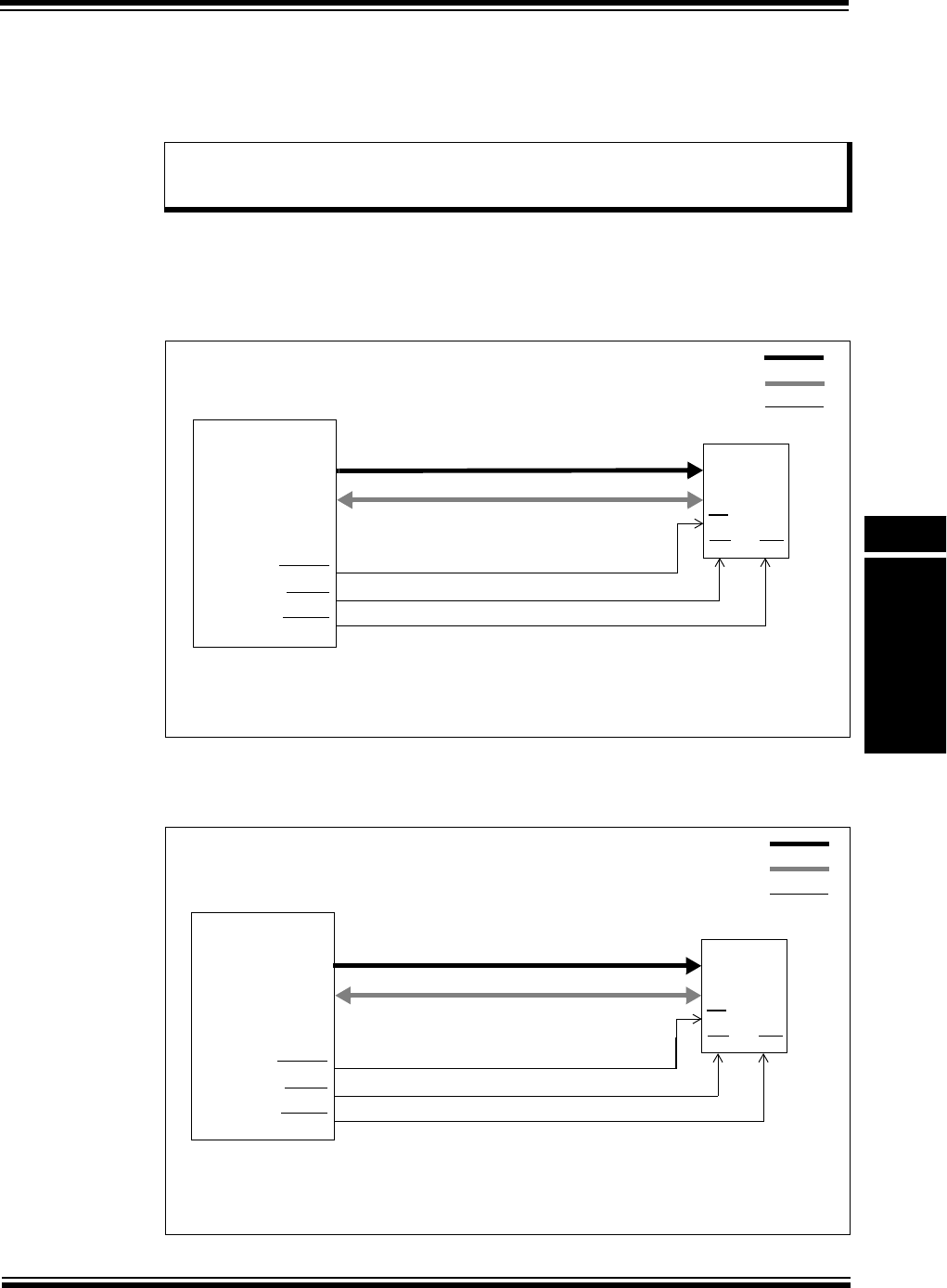
© 2007-2012 Microchip Technology Inc. DS61128G-page 13-43
Section 13. Parallel Master Port (PMP)
Parallel Master
Port (PMP)
13
13.8 PARALLEL MASTER PORT APPLICATIONS
This section illustrates typical interfaces between the PMP module and external devices for each
of the module’s multiplexing modes. Additionally, there are some potential applications shown for
the PMP module.
13.8.1 Demultiplexed Memory or Peripheral
Figure 13-37 illustrates the connections to an 8-bit memory or addressable peripheral in
Demultiplexed mode. This mode does not require any external latches.
Figure 13-37: Demultiplexed Addressing, 8-bit Data (Up to 15-bit Address)
Figure 13-38 illustrates the connections to a 16-bit memory or addressable peripheral in
Demultiplexed mode. This mode does not require any external latches.
Figure 13-38: Demultiplexed Addressing, 16-bit Data (Up to 15-bit Address)
Note: The PMD<15:0> data pins are available on PIC32 devices with 100 or more pins.
For all other devices, only pins PMD<7:0> are available. Refer to the specific PIC32
device data sheet for details.
PMA<14:0>
D<7:0>
A<14:0>
D<7:0>
A<14:0>
PMRD
PMWR
OE WR
CE
PIC32
Address Bus
Data Bus
Control Lines
PMCS2
PMD<7:0>
32K x 8-bit Device
Note: Master mode 2: MODE<1:0> bits (PMMODE<9:8>) = 10.
8-bit data width: MODE16 bit (PMMODE<10>) = 0.
Demultiplexed mode: ADRMUX<1:0> bits (PMCON<12:11>) = 00.
PMA<14:0>
D<15:0>
A<14:0>
D<15:0>
A<14:0>
PMRD
PMWR
OE WR
CE
PIC32
Address Bus
Data Bus
Control Lines
PMCS2
PMD<15:0>
32K x 16-bit Device
Note: Master mode 2: MODE<1:0> bits (PMMODE<9:8>) = 10.
16-bit data width: MODE16 bit (PMMODE<10>) = 1.
Demultiplexed mode: ADRMUX<1:0> bits (PMCON<12:11>) = 00.
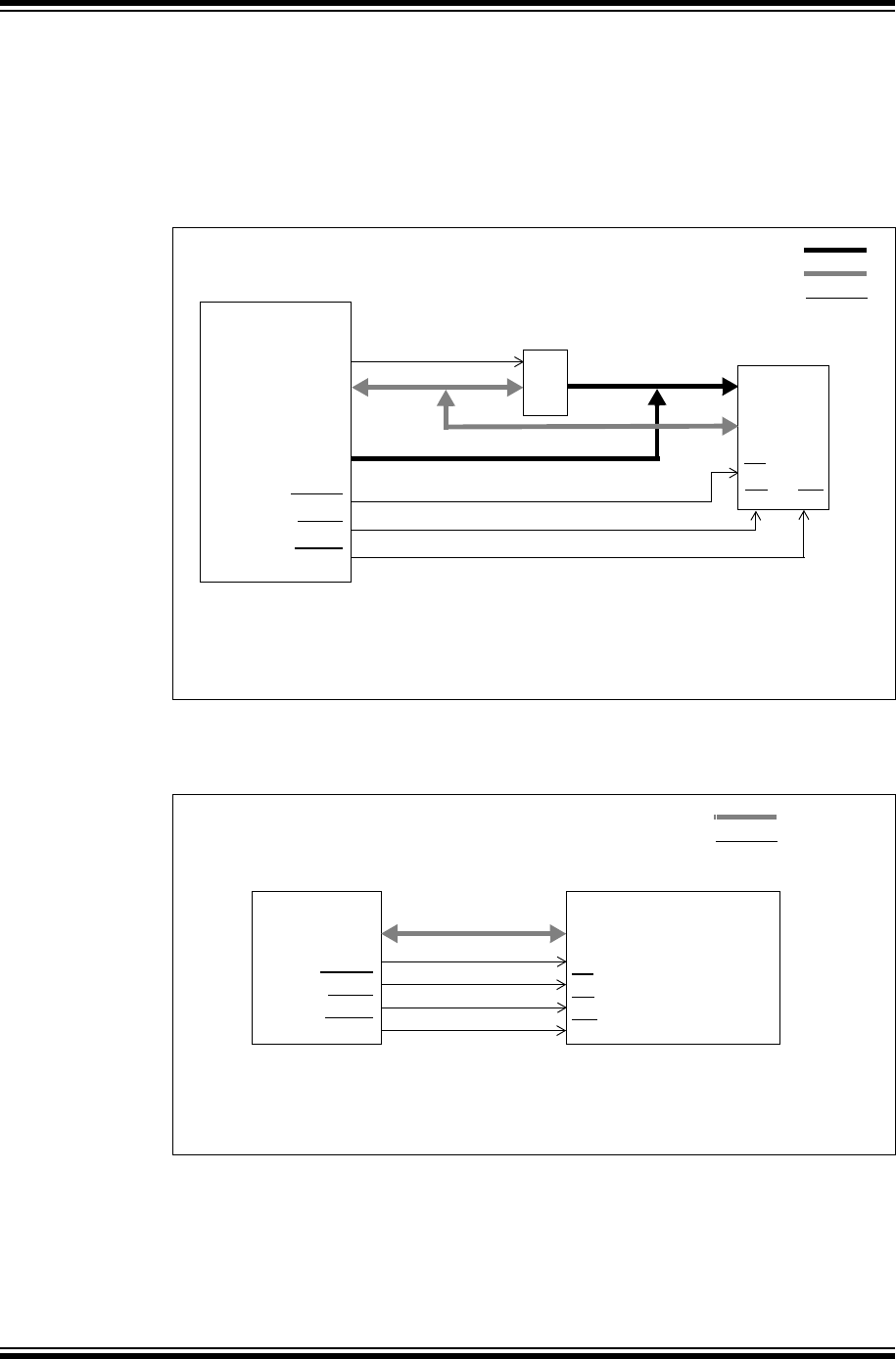
PIC32 Family Reference Manual
DS61128G-page 13-44 © 2007-2012 Microchip Technology Inc.
13.8.2 Partial Multiplexed Memory or Peripheral
Figure 13-39 illustrates the connections to an 8-bit memory or other addressable peripheral in
Partial Multiplex mode. In this mode, an external latch is required. Consequently, from the
microcontroller perspective, this mode achieves some pin savings over the Demultiplexed mode,
however, at the price of performance. The lower 8 bits of the address are multiplexed with the
PMD<7:0> data bus and require one extra peripheral bus clock cycle.
Figure 13-39: Partial Multiplexed Addressing, 8-bit Data (Up to 15-bit Address)
If the peripheral has internal latches as shown in Figure 13-40, no extra circuitry is required
except for the peripheral itself.
Figure 13-40: Partial Multiplexed Addressing, 8-bit Data
PMA<14:8>
D<7:0>
373 A<14:0>
D<7:0>
A<7:0>
PMRD
PMWR
OE WR
CE
PIC32
Address Bus
Data Bus
Control Lines
PMCS2
PMALL
A<14:8>
PMD<7:0>
32K x 8-bit Device
Note: Master mode 2: MODE<1:0> bits (PMMODE<9:8>) = 10.
8-bit data width: MODE16 bit (PMMODE<10>) = 0.
Partial Multiplexed mode: ADRMUX<1:0> bits (PMCON<12:11>) = 01.
The block labeled 373 in the diagram represents a generic 74XX family 373 latch.
D<7:0>
ALE
PMRD
PMWR
RD
WR
CS
PIC32
Data Bus
Control Lines
PMCS2
PMALL
PMD<7:0> AD<7:0>
Parallel Peripheral
8-bit Device
Note: Master mode 2: MODE<1:0> bits (PMMODE<9:8>) = 10.
8-bit data width: MODE16 bit (PMMODE<10>) = 0.
Partial Multiplexed mode: ADRMUX<1:0> bits (PMCON<12:11>) = 01.
© 2007-2012 Microchip Technology Inc. DS61128G-page 13-45
Section 13. Parallel Master Port (PMP)
Parallel Master
Port (PMP)
13
Figure 13-41 illustrates the connections to a 16-bit memory or other addressable peripheral in
Partial Multiplex mode. In this mode, an external latch is required. Consequently, from the
microcontroller perspective, this mode achieves some pin savings over the Demultiplexed mode,
however, at the price of performance. The lower 8 bits of address are multiplexed with the
PMD<7:0> data bus and require one extra peripheral bus clock cycle.
Figure 13-41: Partial Multiplexed Addressing, 16-bit Data (Up to 15-bit Address)
13.8.3 Full Multiplexed Memory or Peripheral
Figure 13-42 illustrates the connections to a memory or other addressable peripheral in full 8-bit
Multiplexed mode, ADRMUX<1:0> bits (PMCON<12:11>) = 10. Consequently, from the
microcontroller perspective, this mode achieves the best pin saving over the Demultiplexed
mode or Partially Multiplexed mode, however, at the price of performance. The lower 8 address
bits are multiplexed with the PMD<7:0> data bus followed by the upper 6 or 7 address bits (if
CS2, CS1 or both are enabled) and therefore require two extra peripheral bus clock cycles.
Figure 13-42: Fully Multiplexed Addressing, 8-bit Data (Up to 15-bit Address)
PMA<14:8>
D<7:0> 373 A<14:0>
D<15:0>
A<7:0>
PMRD
PMWR
OE WR
CE
PIC32
Address Bus
Data Bus
Control Lines
PMCS2
PMALL
A<14:8>
PMD<15:0>
Note: Master mode 2: MODE<1:0> bits (PMMODE<9:8>) = 10.
16-bit data width: MODE16 bit (PMMODE<10>) = 1.
Partial Multiplexed mode: ADRMUX<1:0> bits (PMCON<12:11>) = 01.
The block labeled 373 in the diagram represents a generic 74XX family 373 latch.
32K x 16-bit Device
D<15:0>
PMD<7:0>
PMALH
D<7:0>
373 A<14:0>
D<7:0>
A<7:0>
373
PMRD
PMWR
OE WR
CE
PIC32
Address Bus
Data Bus
Control Lines
PMCS2
PMALL
A<14:8>
Note: Master mode 2: MODE<1:0> bits (PMMODE<9:8>) = 10.
8-bit data width: MODE16 bit (PMMODE<10>) = 0.
Fully Multiplexed mode: ADRMUX<1:0> bits (PMCON<12:11>) = 10.
The blocks labeled 373 in the diagram represent a generic 74XX family 373 latch.
32K x 8-bit Device
PIC32 Family Reference Manual
DS61128G-page 13-46 © 2007-2012 Microchip Technology Inc.
Figure 13-43 illustrates the connections to a 16-bit memory or other addressable peripheral in
full 16-bit Multiplex mode, ADRMUX<1:0> bits (PMCON<12:11>) = 10. Consequently, from the
microcontroller perspective, this mode achieves the best pin saving over the Demultiplexed
mode or Partially Multiplexed mode, however, at the price of performance. The lower 8 address
bits are multiplexed with the PMD<7:0> data bus followed by the upper 6 or 7 address bits (if
CS2, CS1 or both are enabled) and therefore require two extra peripheral bus clock cycles.
Figure 13-43: Fully Multiplexed Addressing, 16-bit Data (Up to 15-bit Address)
Figure 13-44 illustrates the connections to a 16-bit memory or other addressable peripheral in
full 16-bit Multiplex mode, ADRMUX<1:0> bits (PMCON<12:11>) = 11. Consequently, from the
microcontroller perspective, this mode achieves the best pin saving over the Demultiplexed
mode or Partially Multiplexed mode, however, at the price of performance. Compared to the
previous Full Multiplex mode, ADRMUX = 10, this mode multiplexes 14 or 15 address bits (if
CS2, CS1 or both are enabled) simultaneously with the PMD<15:0> bus and therefore requires
only one extra peripheral bus clock cycle.
Figure 13-44: Fully Multiplexed Addressing, 16-bit Data (Up to 15-bit Address), Example 2
PMD<15:0>
PMALH
D<15:0>
373 A<14:0>
D<15:0>
A<7:0>
373
PMRD
PMWR
OE WR
CE
PIC32
Address Bus
Data Bus
Control Lines
PMCS2
PMALL
A<14:8>
Note: Master mode 2: MODE<1:0> bits (PMMODE<9:8>) = 10.
16-bit data width: MODE16 bit (PMMODE<10>) = 1.
Fully Multiplexed mode: ADRMUX<1:0> bits (PMCON<12:11>) = 10.
The blocks labeled 373 in the diagram represent a generic 74XX family 373 latch.
D<7:0>
D<7:0>
32K x 16-bit Device
PMD<15:0>
PMALH
D<15:0>
373 A<14:0>
D<15:0>
A<7:0>
373
PMRD
PMWR
OE WR
CE
PIC32
PMCS2
PMALL
A<14:8>
Note: Master mode 2: MODE<1:0> bits (PMMODE<9:8>) = 10.
16-bit data width: MODE16 bit (PMMODE<10>) = 1.
Fully Multiplexed mode: ADRMUX<1:0> bits (PMCON<12:11>) = 11.
The blocks labeled 373 in the diagram represent a generic 74XX family 373 latch.
D<15:8>
D<7:0>
32K x 16-bit Device
Address Bus
Data Bus
Control Lines
© 2007-2012 Microchip Technology Inc. DS61128G-page 13-47
Section 13. Parallel Master Port (PMP)
Parallel Master
Port (PMP)
13
13.8.4 8-bit LCD Controller Example
The PMP module can be configured to connect to a typical LCD controller interface as shown in
Figure 13-45. In this case, the PMP module is configured for Master mode 1, MODE<1:0> = 11
(PMMODE<9:8>), and uses active-high control signals as common LCD displays require
active-high control.
Figure 13-45: Demultiplexed Addressing, 8-bit Data, LCD Controller
PMD<7:0>
PMRD/WR
D<7:0>
PIC32
Address Line
Data Bus
Control Lines
PMA0
R/W
RS
E
LCD Controller
PMENB
Note: Master mode 1: MODE<1:0> bits (PMMODE<9:8>) = 11.
8-bit data width: MODE16 bit (PMMODE<10>) = 0.
Demultiplexed mode: ADRMUX<1:0> bits (PMCON<12:11>) = 00.
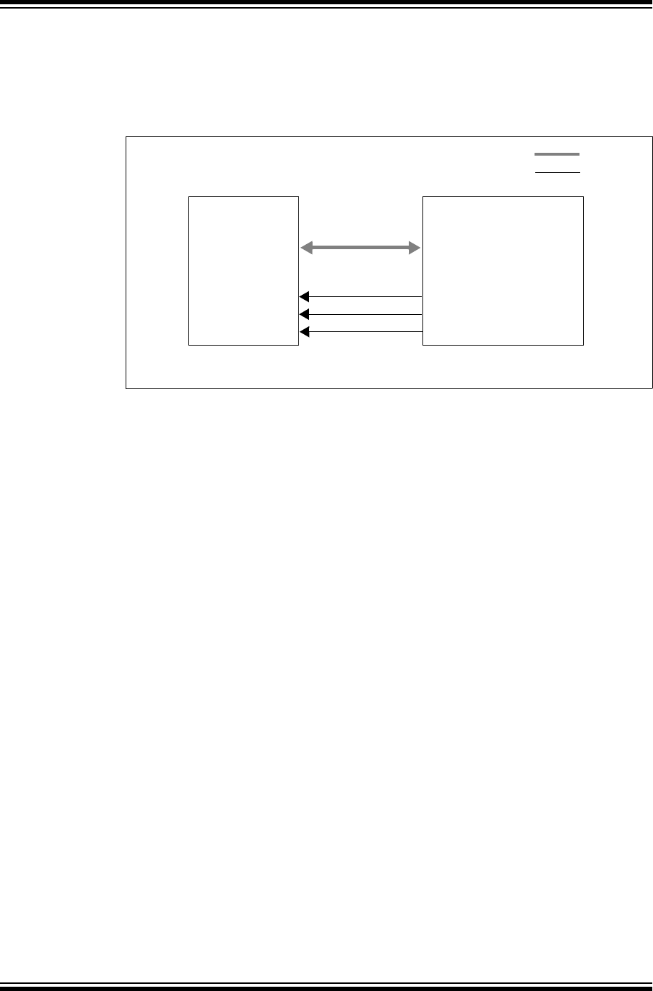
PIC32 Family Reference Manual
DS61128G-page 13-48 © 2007-2012 Microchip Technology Inc.
13.9 PARALLEL SLAVE PORT APPLICATION
Figure 13-46 illustrates the connections to a master peripheral in 8-bit Data mode as a slave,
MODE<1:0> bits (PMMODE<9:8>) = 00. The microcontroller’s PMP is controlled by a Chip
Select (PMCS1).
Figure 13-46: Legacy Mode Slave Port
13.10 DIRECT MEMORY ACCESS SUPPORT
Direct Memory Access (DMA) reads from and writes to the PMDIN register when the PMP
module is configured for Master mode. The following steps are to be performed for using DMA.
1. Set the CHSIRQ<7:0> bits (DCHxECON<15:8>) to the PMP IRQ number.
2. Configure the PMP module for the required mode (Master or Legacy Slave).
3. Set the IRQM<1:0> bits (PMMODE<14:13>) = 01 to generate the PMP interrupts on every
byte.
D<7:0>
PMRD
PMWR
OE
WR
CE
PIC32
PMCS1
PMD<7:0>
MASTER
Note: Legacy Slave mode: MODE<1:0> bits (PMMODE<9:8>) = 00.
Data Bus
Control Lines
© 2007-2012 Microchip Technology Inc. DS61128G-page 13-49
Section 13. Parallel Master Port (PMP)
Parallel Master
Port (PMP)
13
13.11 I/O PIN CONTROL
13.11.1 I/O Pin Resources
When enabling the PMP module for Master mode operations, the PMAEN register must be
configured (set to ‘1’) for the corresponding bits of the PMA<15:0> I/O pins to be controlled by
the PMP module. The I/O pins not configured for use by the PMP module remain as general
purpose I/O pins.
When enabling any of the PMP module for Slave mode operations, the PMPCS1, PMRD, PMWR
control pins and PMD<7:0> data pins are automatically enabled and configured. The user is,
however, responsible for selecting the appropriate polarity for these control lines.
Table 13-10: Required I/O Pin Resources for Master Modes
I/O Pin Name Demultiplex Partial
Multiplex
Full
Multiplex Functional Description
PMPCS2/PMA15 Yes(2) Yes(2) Yes(2) PMP Chip Select 2/Address
A15
PMPCS1/PMA14 Yes(2) Yes(2) Yes(2) PMP Chip Select 1/Address
A14
PMA<13:2> Yes(2) Yes(3) No(1) PMP Address A13...A2
PMA1/PALH No(1) No(1) Yes (4) PMP Address A1/Address
Latch High
PMA0/PALL No(1) Yes (3) Yes(4) PMP Address A0/Address
Latch Low
PMRD/PMWR Yes Yes Yes PMP Read/Write Control
PMWR/PMENB Yes Yes Yes PMP Write/Enable Control
PMD<15:0>(6) Yes(5) Yes(5) Yes (5) PMP Bidirectional Data Bus
D15...D0
Note 1: “No” indicates the pin is not required and is available as a general purpose I/O pin
when the corresponding PMAEN bit is cleared (= 0).
2: Depending on the application, not all PMA<15:0> or CS2, CS1 may be required.
3: When Partial Multiplex mode is selected (ADDRMUX<1:0> = 01), the lower 8
address lines are multiplexed with PMD<7:0>, PMA<0> becomes (ALL) and
PMA<7:1> are available as general purpose I/O pins.
4: When Full Multiplex mode is selected (ADDRMUX<1:0> = 10 or 11), all 16
address lines are multiplexed with PMD<15:0>, PMA<0> becomes (ALL), PMA<1>
becomes (ALH) and PMA<13:2> are available as general purpose I/O pins.
5: If MODE16 = 0, only PMD<7:0> are required. PMD<15:8> are available as general
purpose I/O pins.
6: Data pins PMD<15:0> are available on PIC32 devices with 100 or more pins. For
all other device variants, only pins PMD<7:0> are available. Refer to the specific
PIC32 device data sheet for details.
Table 13-11: Required I/O Pin Resources for Slave Modes
I/O Pin Name Legacy Buffered Enhanced Functional Description
PMPCS1/PMA14 Yes Yes Yes Chip Select
PMA1/PALH No(1) No(1) Ye s Address A1
PMA0/PALL No(1) No(1) Ye s Address A0
PMRD/PMWR Yes Yes Yes Read Control
PMWR/PMENB Yes Yes Yes Write Control
PMD<15:0> Yes(2) Yes(2) Yes(2) Bidirectional Data Bus D7...D0
Note 1: “No” indicates the pin is not required and is available as a general purpose I/O pin
when the corresponding PMAEN bit is cleared (= 0).
2: Slave modes use only PMD<7:0> pins. PMD<15:8> are available as general pur-
pose I/O pins. Control bit MODE16 (PMMODE<10>) is ignored.

PIC32 Family Reference Manual
DS61128G-page 13-50 © 2007-2012 Microchip Technology Inc.
13.11.2 I/O Pin Configuration
Tabl e 13-12 provides a summary of the settings required to enable the I/O pin resources used
with this module. The PMAEN register controls the functionality of pins PMA<15:0>. Setting any
PMAEN bit = 1 configures the corresponding PMA pin as an address line. The bits that are set
to ‘0’ remain as general purpose I/O pins.
Table 13-12: I/O Pin Configuration
I/O Pin Name Required(1) Bit Field TRIS Pin
Type
Buffer
Type Description
PMPCS2/PMA15 Yes CSF<1:0>,
CS2,
PTEN15
— O CMOS PMP Chip Select 2/
Address A15
PMPCS1/PMA14 Yes CSF<1:0>,
CS1
PTEN14
— O CMOS PMP Chip Select 1/
Address A14
PMA<13:2> Yes PTEN<13:2> — O CMOS PMP Address
A13... A2
PMA1/PALH Yes PTEN<1> — I(2), O CMOS PMP Address A1/
Address Latch High
PMA0/PALL Yes PTEN<0> — I(2), O CMOS PMP Address A0/
Address Latch Low
PMRD/PMWR Yes PTRDEN — O CMOS PMP Read/Write
Control
PMWR/PMENB Yes PTWREN — O CMOS PMP Write/
Enable Control
PMD<15:0> Yes MODE16,
ADRMUX<1:0>
— I(2), O CMOS PMP Bidirectional
Data Bus D15... D0
Legend: CMOS = CMOS-compatible input or output ST = Schmitt Trigger input
with CMOS levels
I = Input O = Output
Note 1: Depending on the PMP mode and the user’s application, these pins may not be
required. If not enabled, these pins can be used for general purpose I/O.
2: Input buffers can be Schmitt Trigger or TTL.

© 2007-2012 Microchip Technology Inc. DS61128G-page 13-51
Section 13. Parallel Master Port (PMP)
Parallel Master
Port (PMP)
13
13.12 RELATED APPLICATION NOTES
This section lists application notes that are related to this section of the manual. These
application notes may not be written specifically for the PIC32 device family, but the concepts are
pertinent and could be used with modification and possible limitations. The current application
notes related to the Parallel Master Port (PMP) module are:
Title Application Note #
No related application notes at this time. N/A
Note: Please visit the Microchip web site (www.microchip.com) for additional Application
Notes and code examples for the PIC32 family of devices.

PIC32 Family Reference Manual
DS61128G-page 13-52 © 2007-2012 Microchip Technology Inc.
13.13 REVISION HISTORY
Revision A (August 2007)
This is the initial released version of the document.
Revision B (October 2007)
Updated document to remove Confidential status.
Revision C (April 2008)
Revised status to Preliminary; Revised U-0 to r-x; Revised Table 13-10; Revised Section 13.3.1.6
and Section 13.3.8; Revised Register 13-5; Revised Figures 13-11, 13-37, 13-40, 13-41, 13-42,
13-43, 13-46; Revised Timing Diagram text for Figures 13-16, 13-18, 13-19.
Revision D (June 2008)
Revised Register 13-1, add note to FRZ; Revised Figures 13-4, 13-6, 13-8, 13-10, 13-36, 13-37,
13-38, 13-45; Revised Table 13-6; Revised Examples 13-6 and 13-7; Change Reserved bits from
“Maintain as” to “Write”; Added Note to ON bit (PMCON Register).
Revision E (October 2009)
This revision includes the following updates:
•Minor updates to text and formatting have been implemented throughout the document
•Added the following item to the key feature list: Schmitt Trigger or TTL input buffers (see
13.1 “Introduction”)
•Interrupts Register Summary (Ta ble 13-1):
- Removed all references to the Clear, Set and Invert registers
- Added the Address Offset column
- Added Notes 1, 2 and 3, which describe the Clear, Set and Invert registers
• Added Notes 1, 2 and 3, which describe the Clear, Set and Invert registers to the following
registers
- PMCON: Parallel Port Control Register (see Register 13-1)
- PMMODE: Parallel Port Mode Register (see Register 13-2)
- PMADDR: Parallel Port Address Register (see Register 13-3)
- PMDOUT: Parallel Port Data Output Register (see Register 13-4)
- PMDIN: Parallel Port Data Input Register (see Register 13-5)
- PMAEN: Parallel Port Pin Enable Register (see Register 13-6)
- PMSTAT: Parallel Port Status Register (Slave modes only) (see Register 13-7)
• Removed all references to Interrupt registers (IEC1, IFS1 and IPC7)
•Added a shaded note to 13.4.1.4 “Legacy Mode Interrupt Operation”
•Updated the 2-3 TPBCLK cycles duration in Figure 13-33, Figure 13-34, Figure 13-35 and
Figure 13-36
•Added Note 2 to the I/O Pin Configuration table (Ta ble 13-12)
Revision F (May 2011)
This revision includes the following updates:
• Changed all occurrences of PIC32MX to PIC32
•Updated the note in section 13.4.1.4 “Legacy Mode Interrupt Operation”
•Added a new section 13.10 “Direct Memory Access Support”
•Removed the Notes referencing the CLR, SET, and INV registers from all register tables
• Changed all occurrences of r-x to U-0 in all register tables
•Updated Figure 13-33 and Figure 13-34
•Removed the Module Control column from Tabl e 13-12

© 2007-2012 Microchip Technology Inc. DS61128G-page 13-53
Section 13. Parallel Master Port (PMP)
Parallel Master
Port (PMP)
13
Revision F (May 2011) (Continued)
•Removed the note from section 13.6.2 “PMP Operation in Idle Mode”
•Removed Table 13-10 and Table 13-11
•Minor changes to the text and formatting have been incorporated throughout the document
Revision G (April 2012)
This revision includes the following updates:
•Updated Example 13-3
•Added 13.3.7.1 “Addressing Memory Devices Larger Than 64K”
•Updated the second sentence of 13.4.1.2 “Write to Slave Port” (the reference to the input
buffer full flag was removed)
•Updated the second sentence of 13.4.2.2 “Read from Slave Port” (the reference to the
output buffer empty flag was removed)
•Removed the note box and updated step 2 in 13.10 “Direct Memory Access Support”
•Updated the PMRD/PMWR signal for 16-bit Write Operation (ADRMUX = 11, No Wait
States and Wait States Enabled) (see Figure 13-28 and Figure 13-29)
•Removed 13.12 “Design Tips”
•Minor changes to the text and formatting have been incorporated throughout the document

PIC32 Family Reference Manual
DS61128G-page 13-54 © 2007-2012 Microchip Technology Inc.
NOTES:

2007-2012 Microchip Technology Inc. DS61128G-page 13 -55
Information contained in this publication regarding device
applications and the like is provided only for your convenience
and may be superseded by updates. It is your responsibility to
ensure that your application meets with your specifications.
MICROCHIP MAKES NO REPRESENTATIONS OR
WARRANTIES OF ANY KIND WHETHER EXPRESS OR
IMPLIED, WRITTEN OR ORAL, STATUTORY OR
OTHERWISE, RELATED TO THE INFORMATION,
INCLUDING BUT NOT LIMITED TO ITS CONDITION,
QUALITY, PERFORMANCE, MERCHANTABILITY OR
FITNESS FOR PURPOSE. Microchip disclaims all liability
arising from this information and its use. Use of Microchip
devices in life support and/or safety applications is entirely at
the buyer’s risk, and the buyer agrees to defend, indemnify and
hold harmless Microchip from any and all damages, claims,
suits, or expenses resulting from such use. No licenses are
conveyed, implicitly or otherwise, under any Microchip
intellectual property rights.
Trademarks
The Microchip name and logo, the Microchip logo, dsPIC,
KEELOQ, KEELOQ logo, MPLAB, PIC, PICmicro, PICSTART,
PIC32 logo, rfPIC and UNI/O are registered trademarks of
Microchip Technology Incorporated in the U.S.A. and other
countries.
FilterLab, Hampshire, HI-TECH C, Linear Active Thermistor,
MXDEV, MXLAB, SEEVAL and The Embedded Control
Solutions Company are registered trademarks of Microchip
Technology Incorporated in the U.S.A.
Analog-for-the-Digital Age, Application Maestro, chipKIT,
chipKIT logo, CodeGuard, dsPICDEM, dsPICDEM.net,
dsPICworks, dsSPEAK, ECAN, ECONOMONITOR,
FanSense, HI-TIDE, In-Circuit Serial Programming, ICSP,
Mindi, MiWi, MPASM, MPLAB Certified logo, MPLIB,
MPLINK, mTouch, Omniscient Code Generation, PICC,
PICC-18, PICDEM, PICDEM.net, PICkit, PICtail, REAL ICE,
rfLAB, Select Mode, Total Endurance, TSHARC,
UniWinDriver, WiperLock and ZENA are trademarks of
Microchip Technology Incorporated in the U.S.A. and other
countries.
SQTP is a service mark of Microchip Technology Incorporated
in the U.S.A.
All other trademarks mentioned herein are property of their
respective companies.
© 2007-2012, Microchip Technology Incorporated, Printed in
the U.S.A., All Rights Reserved.
Printed on recycled paper.
ISBN: 978-1-62076-260-8
Note the following details of the code protection feature on Microchip devices:
• Microchip products meet the specification contained in their particular Microchip Data Sheet.
• Microchip believes that its family of products is one of the most secure families of its kind on the market today, when used in the
intended manner and under normal conditions.
• There are dishonest and possibly illegal methods used to breach the code protection feature. All of these methods, to our
knowledge, require using the Microchip products in a manner outside the operating specifications contained in Microchip’s Data
Sheets. Most likely, the person doing so is engaged in theft of intellectual property.
• Microchip is willing to work with the customer who is concerned about the integrity of their code.
• Neither Microchip nor any other semiconductor manufacturer can guarantee the security of their code. Code protection does not
mean that we are guaranteeing the product as “unbreakable.”
Code protection is constantly evolving. We at Microchip are committed to continuously improving the code protection features of our
products. Attempts to break Microchip’s code protection feature may be a violation of the Digital Millennium Copyright Act. If such acts
allow unauthorized access to your software or other copyrighted work, you may have a right to sue for relief under that Act.
Microchip received ISO/TS-16949:2009 certification for its worldwide
headquarters, design and wafer fabrication facilities in Chandler and
Tempe, Arizona; Gresham, Oregon and design centers in California
and India. The Company’s quality system processes and procedures
are for its PIC® MCUs and dsPIC® DSCs, KEELOQ® code hopping
devices, Serial EEPROMs, microperipherals, nonvolatile memory and
analog products. In addition, Microchip’s quality system for the design
and manufacture of development systems is ISO 9001:2000 certified.
QUALITYMANAGEMENT
S
YSTEM
CERTIFIEDBYDNV
== ISO/TS16949==

DS61128G-page 13 -56 2007-2012 Microchip Technology Inc.
AMERICAS
Corporate Office
2355 West Chandler Blvd.
Chandler, AZ 85224-6199
Tel: 480-792-7200
Fax: 480-792-7277
Technical Support:
http://www.microchip.com/
support
Web Address:
www.microchip.com
Atlanta
Duluth, GA
Tel: 678-957-9614
Fax: 678-957-1455
Boston
Westborough, MA
Tel: 774-760-0087
Fax: 774-760-0088
Chicago
Itasca, IL
Tel: 630-285-0071
Fax: 630-285-0075
Cleveland
Independence, OH
Tel: 216-447-0464
Fax: 216-447-0643
Dallas
Addison, TX
Tel: 972-818-7423
Fax: 972-818-2924
Detroit
Farmington Hills, MI
Tel: 248-538-2250
Fax: 248-538-2260
Indianapolis
Noblesville, IN
Tel: 317-773-8323
Fax: 317-773-5453
Los Angeles
Mission Viejo, CA
Tel: 949-462-9523
Fax: 949-462-9608
Santa Clara
Santa Clara, CA
Tel: 408-961-6444
Fax: 408-961-6445
Toronto
Mississauga, Ontario,
Canada
Tel: 905-673-0699
Fax: 905-673-6509
ASIA/PACIFIC
Asia Pacific Office
Suites 3707-14, 37th Floor
Tower 6, The Gateway
Harbour City, Kowloon
Hong Kong
Tel : 8 52 -24 01- 120 0
Fax: 852-2401-3431
Australia - Sydney
Tel : 6 1- 2-9 868 -67 33
Fax: 61-2-9868-6755
China - Beijing
Tel : 8 6- 10- 856 9-7 00 0
Fax: 86-10-8528-2104
China - Chengdu
Tel : 8 6- 28- 866 5-5 511
Fax: 86-28-8665-7889
China - Chongqing
Tel : 8 6- 23- 898 0-9 58 8
Fax: 86-23-8980-9500
China - Hangzhou
Tel : 8 6- 571 -28 19- 318 7
Fax: 86-571-2819-3189
China - Hong Kong SAR
Tel : 8 52 -24 01- 120 0
Fax: 852-2401-3431
China - Nanjing
Tel : 8 6- 25- 847 3-2 46 0
Fax: 86-25-8473-2470
China - Qingdao
Tel : 8 6- 532 -85 02- 735 5
Fax: 86-532-8502-7205
China - Shanghai
Tel : 8 6- 21- 540 7-5 53 3
Fax: 86-21-5407-5066
China - Shenyang
Tel : 8 6- 24- 233 4-2 82 9
Fax: 86-24-2334-2393
China - Shenzhen
Tel : 8 6- 755 -82 03- 266 0
Fax: 86-755-8203-1760
China - Wuhan
Tel : 8 6- 27- 598 0-5 30 0
Fax: 86-27-5980-5118
China - Xian
Tel : 8 6- 29- 883 3-7 25 2
Fax: 86-29-8833-7256
China - Xiamen
Tel: 86-592-2388138
Fax: 86-592-2388130
China - Zhuhai
Tel : 86- 75 6-3 21 004 0
Fax: 86-756-3210049
ASIA/PACIFIC
India - Bangalore
Tel : 9 1- 80- 309 0-4 44 4
Fax: 91-80-3090-4123
India - New Delhi
Tel : 9 1- 11- 416 0 -8 631
Fax: 91-11-4160-8632
India - Pune
Tel : 9 1- 20- 256 6-1 51 2
Fax: 91-20-2566-1513
Japan - Osaka
Tel : 8 1- 66- 152 -71 60
Fax: 81-66-152-9310
Japan - Yokohama
Tel : 8 1- 45- 471 - 6 16 6
Fax: 81-45-471-6122
Korea - Daegu
Tel : 8 2- 53- 744 -43 01
Fax: 82-53-744-4302
Korea - Seoul
Tel : 8 2- 2-5 54- 72 0 0
Fax: 82-2-558-5932 or
82-2-558-5934
Malaysia - Kuala Lumpur
Tel : 6 0- 3-6 201 -9 8 57
Fax: 60-3-6201-9859
Malaysia - Penang
Tel : 6 0- 4-2 27- 88 7 0
Fax: 60-4-227-4068
Philippines - Manila
Tel : 6 3- 2-6 34- 90 6 5
Fax: 63-2-634-9069
Singapore
Tel : 6 5- 633 4-8 870
Fax: 65-6334-8850
Taiwan - Hsin Chu
Tel : 8 86 -3- 577 8-3 66
Fax: 886-3-5770-955
Taiwan - Kaohsiung
Tel : 8 86 -7- 536 -48 18
Fax: 886-7-330-9305
Taiwan - Taipei
Tel : 8 86 -2- 250 0-6 61 0
Fax: 886-2-2508-0102
Thailand - Bangkok
Tel : 6 6- 2-6 94- 13 5 1
Fax: 66-2-694-1350
EUROPE
Austria - Wels
Tel : 4 3- 72 42 -2 244 -3 9
Fax: 43-7242-2244-393
Denmark - Copenhagen
Tel : 4 5- 445 0-2 828
Fax: 45-4485-2829
France - Paris
Tel : 3 3- 1-6 9-5 3-6 3-2 0
Fax: 33-1-69-30-90-79
Germany - Munich
Tel : 4 9- 89 -62 7-1 44- 0
Fax: 49-89-627-144-44
Italy - Milan
Tel : 3 9- 03 31 -7 426 11
Fax: 39-0331-466781
Netherlands - Drunen
Tel : 3 1- 41 6- 690 399
Fax: 31-416-690340
Spain - Madrid
Tel : 3 4- 91 -70 8-0 8-9 0
Fax: 34-91-708-08-91
UK - Wokingham
Tel : 4 4- 118 -92 1- 5 869
Fax: 44-118-921-5820
Worldwide Sales and Service
11/29/11

© 2007-2013 Microchip Technology Inc. DS61105F-page 14-1
Timers
14
Section 14. Timers
HIGHLIGHTS
This section of the manual contains the following topics:
14.1 Introduction .................................................................................................................. 14-2
14.2 Control Registers ......................................................................................................... 14-6
14.3 Modes of Operation ................................................................................................... 14-11
14.4 Interrupts.................................................................................................................... 14-25
14.5 Operation in Power-Saving Modes ............................................................................ 14-28
14.6 Effects of Various Resets ........................................................................................... 14-29
14.7 Peripherals Using Timer Modules.............................................................................. 14-29
14.8 I/O Pin Control ........................................................................................................... 14-30
14.9 Related Application Notes.......................................................................................... 14-31
14.10 Revision History ......................................................................................................... 14-32

PIC32 Family Reference Manual
DS61105F-page 14-2 © 2007-2013 Microchip Technology Inc.
14.1 INTRODUCTION
The PIC32 device family has two different types of timers, depending on the particular device.
Timers are useful for generating accurate time-based periodic interrupt events for software
applications or real-time operating systems. Other uses include counting external pulses or
accurate timing measurement of external events by using the timer’s gate feature.
With certain exceptions, all of the timers have the same functional circuitry. The timers are
broadly classified into two types, namely:
•Type A Timer (16-bit synchronous/asynchronous timer/counter with gate)
•Type B Timer (16-bit or 32-bit synchronous timer/counter with gate and Special Event
Trigger)
All timer modules include the following common features:
•16-bit timer/counter
•Software-selectable internal or external clock source
• Programmable interrupt generation and priority
•Gated external pulse counter
Apart from these common features, each timer type offers the following additional features:
•Type A:
- Asynchronous timer/counter with a built-in oscillator
-Operational during CPU Sleep mode
- Software selectable prescalers 1:1, 1:8, 1:64, and 1:256
•Type B:
- Ability to form a 32-bit timer/counter
- Software prescalers 1:1, 1:2, 1:4, 1:8, 1:16, 1:32, 1:64, and 1:256
- Event trigger capability
Tabl e 14- 1 provides a summary of timer features. Refer to the specific device data sheet for more
information on type and number of timers associated with a specific PIC32 device.
Note: This family reference manual section is meant to serve as a complement to device
data sheets. Depending on the device, this manual section may not apply to all
PIC32 devices.
Please consult the note at the beginning of the “Timers” chapters in the current
device data sheet to check whether this document supports the device you are
using.
Device data sheets and family reference manual sections are available for
download from the Microchip Worldwide Web site at: http://www.microchip.com
Table 14-1: Timer Features
Available
Timer
Types
Secondary
Oscillator
Asynchronous
External Clock
Synchronous
External Clock
16-bit
Synchronous
Timer/Counter
32-bit
Synchronous
Timer/Counter
(see Note 1)
Gated
Timer
Special
Event
Trigger
Type A Yes Yes Yes Yes No Yes No
Type B No No Yes Yes Yes Yes Yes
Note 1: 32-bit timer/counter configuration requires an even numbered timer combined with an adjacent odd
numbered timer, for example, Timer2 and Timer3, or Timer4 and Timer5, and so on.

© 2007-2013 Microchip Technology Inc. DS61105F-page 14-3
Section 14. Timers
Timers
14
14.1.1 Type A Timer
Most of the PIC32 family devices contain at least one Type A timer; usually, Timer1.
The Type A Timer module is distinct from other types of timers based on the following features:
•Operable from the external Secondary Oscillator (S
OSC)
• Operable in Asynchronous mode using an external clock source
•Operable during CPU Sleep mode
• Software selectable prescalers 1:1, 1:8, 1:64 and 1:256
The Type A timer does not support 32-bit mode.
The unique features of the Type A Timer module allow it to be used for Real-Time Clock (RTC)
applications. Figure 14-1 illustrates the block diagram of a Type A Timer module.
Figure 14-1: Type A Timer Block Diagram
ON (T1CON<15>)
Sync
SOSCI
SOSCO/T1CK
PR1
T1IF
Equal Comparator x 16
TMR1
Reset
Note 1: For information on enabling the 32 kHz Secondary Oscillator (SOSC), refer to Section 6. “Oscillators”
(DS61112).
2: The default state of the SOSCEN bit (OSCCON<1>) during a device Reset is controlled by the FSOSCEN bit
(DEVCFG1<5>).
SOSCEN
Event Flag
1
0
TSYNC (T1CON<2>)
TGATE (T1CON<7>)
TGATE (T1CON<7>)
TPBCLK
1
0
TCS (T1CON<1>)
Gate
Sync
TCKPS (T1CON<5:4>)
Prescaler
2
1, 8, 64, 256
x
1 0
0 0
Q
QD
(Type A Timers Only)
32 kHz Secondary Oscillator (SOSC)(1,2)
(Type A Timers Only)
1
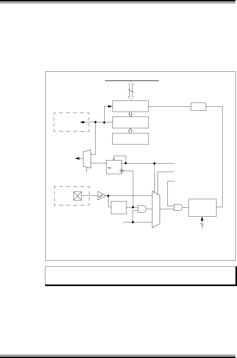
PIC32 Family Reference Manual
DS61105F-page 14-4 © 2007-2013 Microchip Technology Inc.
14.1.2 Type B Timer
The Type B timer is distinct from other types of timer based on the following features:
•Can be combined to form a 32-bit timer
•Software selectable prescalers 1:1, 1:2, 1:4, 1:8, 1:16, 1:32, 1:64 and 1:256
•Analog-to-Digital Converter (ADC) Event Trigger capability
The block diagrams of Type B timer (16-bit) and Type B timer (32-bit) are illustrated in
Figure 14-2 and Figure 14-3, respectively.
Figure 14-2: Type B Timer Block Diagram (16-bit)
Sync
TMRx
TxIF
Equal Comparator x 16
PRx
Reset
Event Flag
Q
QD
TGATE (TxCON<7>)
1
0
Gate
TxCK(1)
Sync
ON (TxCON<15>)
TGATE (TxCON<7>)
TCS (TxCON<1>)
TCKPS (TxCON<6:4>)
Prescaler
3
1, 2, 4, 8, 16,
32, 64, 256
X 1
1 0
0 0
TPBCLK
ADC Event
Trigger
Note 1: The TxCK pin is not available in certain devices in the PIC32 family. In such cases, the
timer must use the peripheral clock as its input clock. Refer to the “Timers” chapters in
the specific device data sheet for the I/O pin details.
Data Bus<31:0>
<15:0>
(Type B Timers Only)
(Timer3 Only)
Note: The timer configuration bit, T32 (TxCON<3>), must be set to ‘1’ for a 32-bit
timer/counter operation. All control bits are respective to the TxCON register, and
interrupt bits are respective to the TyCON register.

© 2007-2013 Microchip Technology Inc. DS61105F-page 14-5
Section 14. Timers
Timers
14
Figure 14-3: Type B Timer Block Diagram (32-bit)
TMRy TMRx
TyIF Event
Equal Comparator x 32
PRy PRx
Reset
least significant
most significant
Flag
Note 1: The TxCK pin is not available in certain PIC32MX family devices. In such cases, the
timer must use the peripheral clock as its input clock. Refer to the “Timers” chapters in
the specific device data sheet for the I/O pin details.
Data Bus<31:0>
TGATE (TxCON<7>)
0
1
TPBCLK
Gate
TxCK(1)
Sync
Sync
<31:0>
ADC Event
Trigger
ON (TxCON<15>)
TGATE (TxCON<7>)
TCS (TxCON<1>)
TCKPS (TxCON<6:4>)
Prescaler
3
1, 2, 4, 8, 16,
32, 64, 256
X 1
1 0
0 0
Q
QD
(Timer3 Only)
(Type B Timers Only)
half word half word
PIC32 Family Reference Manual
DS61105F-page 14-6 © 2007-2013 Microchip Technology Inc.
14.2 CONTROL REGISTERS
Each Timer module is a 16-bit timer/counter that consists of the following Special Function
Registers (SFRs), which are summarized in Table 1 4-2 :
•T1CON: Type A Timer Control Register
•TxCON: Type B Timer Control Register
•TMRx: Timer Register
•PRx: Period Register
Each Timer module also has the following associated bits for interrupt control:
•TxIE: Interrupt Enable Control bit in IEC0 interrupt register
• TxIF: Interrupt Flag Status bit in IFS0 interrupt register
• TxIP<2:0>: Interrupt Priority Control bits in IPC1, IPC2, IPC3, IPC4, and IPC5 interrupt
registers
• TxIS<1:0>: Interrupt Subpriority Control bits in IPC1, IPC2, IPC3, IPC4, and IPC5 interrupt
registers
Note: Each PIC32 family device may have one or more timer modules. An ‘x’ used in the
names of pins, control/status bits and registers denotes the particular module. For
more information, refer to the specific device data sheet.
Note: Refer to Section 8. “Interrupts” (DS61108) in the “PIC32 Family Reference
Manual” for more information on these registers.
Table 14-2: Timers SFR Summary
Register
Name(1)
Bit
Range
Bit
31/23/15/7
Bit
30/22/14/6
Bit
29/21/13/5
Bit
28/20/12/4
Bit
27/19/11/3
Bit
26/18/10/2
Bit
25/17/9/1
Bit
24/16/8/0
T1CON 31:24 — — — — — — — —
23:16 — — — — — — — —
15:8 ON —SIDLTWDISTWIP— — —
7:0 TGATE — TCKPS<1:0> —TSYNCTCS —
TxCON 31:24 — — — — — — — —
23:16 — — — — — — — —
15:8 ON —SIDL— — — — —
7:0 TGATE TCKPS<2:0>(2) T32(3) —TCS—
TMRx 31:24 — — — — — — — —
23:16 — — — — — — — —
15:8 TMRx<15:8>
7:0 TMRx<7:0>
PRx 31:24 — — — — — — — —
23:16 — — — — — — — —
15:8 PRx<15:8>
7:0 PRx<7:0>
Note 1: All registers have an associated Clear, Set, and Invert register at an offset of 0x4, 0x8, and 0xC bytes, respectively.
These registers have the same name with CLR, SET, or INV appended to the end of the register name (e.g.,
T1CONCLR). Writing a ‘1’ to any bit position in these registers will clear, set, or invert valid bits in the associated
register. Reads from these registers should be ignored.
2: The TCKPS<2:0> bits are available only on even numbered Type B timers. For example, Timer2 and Timer4 in 32-bit
Timer mode.
3: The T32 bit is available only on even numbered Type B timers, such as Timer2, Timer4, and so on.

© 2007-2013 Microchip Technology Inc. DS61105F-page 14-7
Section 14. Timers
Timers
14
Register 14-1: T1CON: Type A Timer Control Register
Bit Range Bit
31/23/15/7
Bit
30/22/14/6
Bit
29/21/13/5
Bit
28/20/12/4
Bit
27/19/11/3
Bit
26/18/10/2
Bit
25/17/9/1
Bit
24/16/8/0
31:24 U-0 U-0 U-0 U-0 U-0 U-0 U-0 U-0
— — — — — — — —
23:16 U-0 U-0 U-0 U-0 U-0 U-0 U-0 U-0
— — — — — — — —
15:8 R/W-0 U-0 R/W-0 R/W-0 R-0 U-0 U-0 U-0
ON(1) —SIDLTWDISTWIP— — —
7:0 R/W-0 U-0 R/W-0 R/W-0 U-0 R/W-0 R/W-0 U-0
TGATE — TCKPS<1:0> —TSYNCTCS —
Legend:
R = Readable bit W = Writable bit U = Unimplemented bit, read as ‘0’
-n = Value at POR ‘1’ = Bit is set ‘0’ = Bit is cleared x = Bit is unknown
bit 31-16 Unimplemented: Read as ‘0’
bit 15 ON: Timer On bit(1)
1 = Timer is enabled
0 = Timer is disabled
bit 14 Unimplemented: Read as ‘0’
bit 13 SIDL: Stop in Idle Mode bit
1 = Discontinue operation when device enters Idle mode
0 = Continue operation when device enters Idle mode
bit 12 TWDIS: Asynchronous Timer Write Disable bit
1 = Writes to TMR1 are ignored until pending write operation completes
0 = Back-to-back writes are enabled (Legacy Asynchronous Timer functionality)
bit 11 TWIP: Asynchronous Timer Write in Progress bit
In Asynchronous Timer mode:
1 = Asynchronous write to TMR1 register in progress
0 = Asynchronous write to TMR1 register complete
In Synchronous Timer mode:
This bit is read as ‘0’.
bit 10-8 Unimplemented: Read as ‘0’
bit 7 TGATE: Timer Gated Time Accumulation Enable bit
When TCS = 1:
This bit is ignored.
When TCS = 0:
1 = Gated time accumulation is enabled
0 = Gated time accumulation is disabled
bit 6 Unimplemented: Read as ‘0’
bit 5-4 TCKPS<1:0>: Timer Input Clock Prescale Select bits
11 = 1:256 prescale value
10 = 1:64 prescale value
01 = 1:8 prescale value
00 = 1:1 prescale value
bit 3 Unimplemented: Read as ‘0’
Note 1: When using 1:1 PBCLK divisor, the user’s software should not read/write the peripheral SFRs in the
SYSCLK cycle immediately following the instruction that clears the module’s ON bit.

PIC32 Family Reference Manual
DS61105F-page 14-8 © 2007-2013 Microchip Technology Inc.
bit 2 TSYNC: Timer External Clock Input Synchronization Selection bit
When TCS = 1:
1 = External clock input is synchronized
0 = External clock input is not synchronized
When TCS = 0:
This bit is ignored.
bit 1 TCS: Timer Clock Source Select bit
1 = External clock from TxCKI pin
0 = Internal peripheral clock
bit 0 Unimplemented: Read as ‘0’
Register 14-1: T1CON: Type A Timer Control Register (Continued)
Note 1: When using 1:1 PBCLK divisor, the user’s software should not read/write the peripheral SFRs in the
SYSCLK cycle immediately following the instruction that clears the module’s ON bit.

© 2007-2013 Microchip Technology Inc. DS61105F-page 14-9
Section 14. Timers
Timers
14
Register 14-2: TxCON: Type B Timer Control Register
Bit
Range
Bit
31/23/15/7
Bit
30/22/14/6
Bit
29/21/13/5
Bit
28/20/12/4
Bit
27/19/11/3
Bit
26/18/10/2
Bit
25/17/9/1
Bit
24/16/8/0
31:24 U-0 U-0 U-0 U-0 U-0 U-0 U-0 U-0
— — — — — — — —
23:16 U-0 U-0 U-0 U-0 U-0 U-0 U-0 U-0
— — — — — — — —
15:8 R/W-0 U-0 R/W-0 U-0 U-0 U-0 U-0 U-0
ON(1) — SIDL(2) — — — — —
7:0 R/W-0 R/W-0 R/W-0 R/W-0 R/W-0 U-0 R/W-0 U-0
TGATE TCKPS<2:0> T32(3) —TCS
(4) —
Legend:
R = Readable bit W = Writable bit U = Unimplemented bit, read as ‘0’
-n = Value at POR ‘1’ = Bit is set ‘0’ = Bit is cleared x = Bit is unknown
bit 31-16 Unimplemented: Read as ‘0’
bit 15 ON: Timer On bit(1)
1 = Module is enabled
0 = Module is disabled
bit 14 Unimplemented: Read as ‘0’
bit 13 SIDL: Stop in Idle Mode bit(2)
1 = Discontinue operation when device enters Idle mode
0 = Continue operation when device enters Idle mode
bit 12-8 Unimplemented: Read as ‘0’
bit 7 TGATE: Timer Gated Time Accumulation Enable bit
When TCS = 1:
This bit is ignored and is read as ‘0’.
When TCS = 0:
1 = Gated time accumulation is enabled
0 = Gated time accumulation is disabled
bit 6-4 TCKPS<2:0>: Timer Input Clock Prescale Select bits
111 = 1:256 prescale value
110 = 1:64 prescale value
101 = 1:32 prescale value
100 = 1:16 prescale value
011 = 1:8 prescale value
010 = 1:4 prescale value
001 = 1:2 prescale value
000 = 1:1 prescale value
bit 3 T32: 32-bit Timer Mode Select bit(3)
1 = TMRx and TMRy form a 32-bit timer
0 = TMRx and TMRy form separate 16-bit timer
bit 2 Unimplemented: Read as ‘0’
bit 1 TCS: Timer Clock Source Select bit(4)
1 = External clock from TxCK pin
0 = Internal peripheral clock
bit 0 Unimplemented: Read as ‘0’
Note 1: When using 1:1 PBCLK divisor, the user’s software should not read/write the peripheral SFRs in the
SYSCLK cycle immediately following the instruction that clears the module’s ON bit.
2: While operating in 32-bit mode, the SIDL bit (TxCON<13>) of consecutive odd number timers of the 32-bit
timer pair has an affect on the timer operation. All other bits in this register have no affect.
3: The T32 bit is available only on even numbered Type B timers, such as Timer2, Timer4, and so on.
4: The TxCK pin is not available on all timers. Refer to the “Timers” chapters in the specific device data
sheet for availability.
PIC32 Family Reference Manual
DS61105F-page 14-10 © 2007-2013 Microchip Technology Inc.
Register 14-3: TMRx: Timer Register
Bit Range Bit
31/23/15/7
Bit
30/22/14/6
Bit
29/21/13/5
Bit
28/20/12/4
Bit
27/19/11/3
Bit
26/18/10/2
Bit
25/17/9/1
Bit
24/16/8/0
31:24 U-0 U-0 U-0 U-0 U-0 U-0 U-0 U-0
— — — — — — — —
23:16 U-0 U-0 U-0 U-0 U-0 U-0 U-0 U-0
— — — — — — — —
15:8 R/W-0 R/W-0 R/W-0 R/W-0 R/W-0 R/W-0 R/W-0 R/W-0
TMR<15:8>
7:0 R/W-0 R/W-0 R/W-0 R/W-0 R/W-0 R/W-0 R/W-0 R/W-0
TMR<7:0>
Legend:
R = Readable bit W = Writable bit U = Unimplemented bit, read as ‘0’
-n = Value at POR ‘1’ = Bit is set ‘0’ = Bit is cleared x = Bit is unknown
bit 31-16 Unimplemented: Read as ‘0’
bit 15-0 TMR<15:0>: Timer Count Register bits
16-bit mode:
These bits represent the complete 16-bit timer count.
32-bit mode (Type B Timer only):
Timer2 and Timer4: These bits represent the least significant half word (16 bits) of the 32-bit timer count.
Timer3 and Timer5: These bits represent the most significant half word (16 bits) of the 32-bit timer count.
Register 14-4: PRx: Period Register
Bit
Range
Bit
31/23/15/7
Bit
30/22/14/6
Bit
29/21/13/5
Bit
28/20/12/4
Bit
27/19/11/3
Bit
26/18/10/2
Bit
25/17/9/1
Bit
24/16/8/0
31:24 U-0 U-0 U-0 U-0 U-0 U-0 U-0 U-0
— — — — — — — —
23:16 U-0 U-0 U-0 U-0 U-0 U-0 U-0 U-0
— — — — — — — —
15:8 R/W-1 R/W-1 R/W-1 R/W-1 R/W-1 R/W-1 R/W-1 R/W-1
PR<15:8>
7:0 R/W-1 R/W-1 R/W-1 R/W-1 R/W-1 R/W-1 R/W-1 R/W-1
PR<7:0>
Legend:
R = Readable bit W = Writable bit U = Unimplemented bit, read as ‘0’
-n = Value at POR ‘1’ = Bit is set ‘0’ = Bit is cleared x = Bit is unknown
bit 31-16 Unimplemented: Read as ‘0’
bit 15-0 PR<15:0>: Period Register bits
16-bit mode:
These bits represent the complete 16-bit period match.
32-bit mode (Type B Timer only):
Timer2 and Timer4: These bits represent the least significant half word (16 bits) of the 32-bit period match.
Timer3 and Timer5: These bits represent the most significant half word (16 bits) of the 32-bit period match.

© 2007-2013 Microchip Technology Inc. DS61105F-page 14-11
Section 14. Timers
Timers
14
14.3 MODES OF OPERATION
14.3.1 16-bit Modes
Type A and Type B timer modules support the following 16-bit modes:
•16-bit Synchronous Clock Counter
•16-bit Synchronous External Clock Counter
•16-bit Gated Timer
•16-bit Asynchronous External Counter (Type A Timer module only)
The 16-bit Timer modes are determined by the following bits:
• TCS (TxCON<1>): Timer Clock Source Control bit
• TGATE (TxCON<7>): Timer Gate Control bit
•TSYNC (T1CON<2>): Timer Synchronization Control bit (Type A Timer module only)
14.3.1.1 16-BIT TIMER CONSIDERATIONS
The following should be considered when using a 16-bit timer:
• All Timer module SFRs can be written to as a byte (8 bits) or as a half word (16 bits)
• All Timer module SFRs can be read from as a byte or as a half word
14.3.2 32-bit Modes (Type B Timer)
Only Type B timer modules support 32-bit modes of operation. A 32-bit Timer module is formed
by combining an even numbered Type B timer (referred to as TimerX) with a consecutive odd
numbered Type B timer (referred to as TimerY). For example, 32-bit timer combinations are
Timer2 and Timer3, Timer4 and Timer5, and so on. The number of timer pairs depends on the
particular PIC32 device.
The 32-bit timer pairs can operate in the following modes:
•32-bit Synchronous Clock Counter
•32-bit Synchronous External Clock Counter
•32-bit Gated Timer
The 32-bit Timer modes are determined by the following bits:
•T32 (TxCON<3>): 32-bit Timer Mode Select bit (TimerX only)
•TCS (TxCON<1>): Timer Clock Source Select bit
•TGATE (TxCON<7>): Timer Gated Time Accumulation Enable bit
Specific behavior in 32-bit Timer mode:
•TimerX is the master timer; TimerY is the slave timer
• TMRx count register is least significant half word of the 32-bit timer value
•TMRy count register is most significant half word of the 32-bit timer value
• PRx period register is least significant half word of the 32-bit period value
• PRy period register is most significant half word of the 32-bit period value
•TimerX control bits (TxCON) configure the operation for the 32-bit timer pair
• TimerY control bits (TyCON) have no effect
•TimerX interrupt and status bits are ignored
•TimerY provides the interrupt enable, interrupt flag and interrupt priority control bits

PIC32 Family Reference Manual
DS61105F-page 14-12 © 2007-2013 Microchip Technology Inc.
14.3.2.1 32-BIT TIMER CONSIDERATIONS
The following points should be considered when using a 32-bit timer:
•Ensure that the timer pair is configured for 32-bit mode by setting T32 (TxCON<3>) = 1,
before writing any 32-bit value to the TMRxy count registers or PRxy period registers
• All Timer module SFRs can be written to as a byte (8 bits), a half word (16 bits) or a word
(32 bits)
• All Timer module SFRs can be read from as a byte, a half word or a word
•TMRx and TMRy count register pairs can be read as well as written as a single 32-bit value
•PRx and PRy period register pairs can be read as well as written as a single 32-bit value
14.3.3 16-bit Synchronous Clock Counter Mode
The Synchronous Clock Counter operation provides the following capabilities:
•Elapsed time measurements
•Time delays
•Periodic timer interrupts
Type A and Type B timers have the ability to operate in Synchronous Clock Counter mode. In this
mode, the input clock source for the timer is the internal peripheral bus clock, PBCLK. It is
selected by clearing the clock source control bit, TCS (TxCON<1> = 0). Type A and Type B
timers automatically provide synchronization to the peripheral bus clock; therefore, the Type A
Timer Synchronous mode control bit TSYNC (T1CON<2>) is ignored in this mode.
Type A and Type B timers that use a 1:1 timer input clock prescale, operate at a timer clock rate
that is same as the PBCLK, and which increments the TMR count register on every rising timer
clock edge. The timer continues to increment until the TMR count register matches the PR period
register value. The TMR count register resets to 0x0000 on the next timer clock cycle, and then
continues to increment and repeats the period match until the timer is disabled. If the PR period
register value = 0x0000, the TMR count register resets to 0x0000 on the next timer clock cycle,
but does not continue to increment.
Type A and Type B timers using a timer input clock prescale = N (other than 1:1) operate at a
timer clock rate (PBCLK N), and the TMR count register increments on every Nth timer clock
rising edge. For example, if the timer input clock prescale is 1:8, the timer increments on every
eighth timer clock cycle. The timer continues to increment until the TMR count register matches
the PR period register value. The TMR count register then resets to 0x0000 after ‘N’ more timer
clock cycles, and then continues to increment and repeats the period match until the timer is
disabled. If the PR period register value = 0x0000, the TMR count register resets to 0x0000 on
the next Nth timer clock cycle, but will not continue to increment.
Type A timers generate a timer event one-half timer clock cycle (on the falling edge) after the
TMR count register matches the PR period register value. Type B timers generate a timer event
within one PBCLK, plus two SYSCLK system clock cycles after the TMR count register matches
the PR period register value. Both Type A and Type B timer interrupt flag bits, TxIF, are set within
one PBCLK, plus two SYSCLK cycles of this event, and if the timer interrupt enable bit TxIE is
set, an interrupt is generated.
14.3.3.1 16-BIT SYNCHRONOUS CLOCK COUNTER CONSIDERATIONS
The timer period is determined by the value in the PR period register. To initialize the timer period,
a user may write to the PR period register directly at any time while the timer is disabled,
ON bit = 0, or during a timer match Interrupt Service Routine (ISR) while the timer is enabled,
ON bit = 1. In all other cases, writing to the period register while the timer is enabled is not
recommended and may allow unintended period matches to occur. The maximum period that
can be loaded is 0xFFFF.
Writing 0x0000 to the PRx period register allows a TMRx match to occur; however, no interrupt
is generated.
Note: While operating in 32-bit mode, the SIDL bit (TxCON<13>) of consecutive odd
number timers of the 32-bit timer pair has an affect on the timer operation. All other
bits in this register have no affect.

© 2007-2013 Microchip Technology Inc. DS61105F-page 14-13
Section 14. Timers
Timers
14
14.3.4 32-bit Synchronous Clock Counter Mode (Type B Timer)
Only Type B timers have the ability to operate in 32-bit Synchronous Counter mode. To enable
32-bit Synchronous Clock Counter operation, Type B (TimerX) T32 control bit (TxCON<3>) must
be set (= 1). In this mode, the input clock source for the timer is the internal peripheral bus clock,
PBCLK, and is selected by clearing the clock source control bit TCS, (TxCON<1>) = 0. Type B
timers automatically provide synchronization to the peripheral bus clock.
Type B timers that use a 1:1 timer input clock prescale operate at a timer clock rate which is the
same as the PBCLK, and increments the TMRxy count register on every rising timer clock edge.
The timer continues to increment until the TMRxy count register matches the PRxy period
register value. The TMRxy count register resets to 0x00000000 on the next timer clock cycle, and
then continues to increment and repeats the period match until the timer is disabled. If the PR
period register value = 0x00000000, the TMR count register resets to 0x00000000 on the next
timer clock cycle, but does not continue to increment.
Type B timers using a timer input clock prescale = N (other than 1:1) operate at a timer clock rate
(PBCLK N), and the TMRxy count register increments on every Nth timer clock rising edge.
For example, if the timer input clock prescale is 1:8, the timer increments on every eight timer
clock cycle. The timer continues to increment until the TMRxy count register matches the PRxy
period register value. The TMRxy count register resets to 0x00000000 after ‘N’ more timer clock
cycles, and then continues to increment and repeats the period match until the timer is disabled.
Type B timers generate a timer event within one PBCLK, plus two SYSCLK system clock cycles
after the TMRxy count register matches the PRxy period register value. The Type B timer
interrupt flag bit, TyIF, is set within one PBCLK, plus two SYSCLK cycles of this event, and if the
timer interrupt enable bit TyIE is set, an interrupt is generated.
14.3.4.1 32-BIT SYNCHRONOUS CLOCK COUNTER CONSIDERATIONS
This section describes items that should be considered when using the 32-bit Synchronous
Clock Counter.
The timer period is determined by the value in the PRxy period register. To initialize the timer
period, a user may write to the PRxy period register directly at any time while the timer is
disabled, ON bit = 0, or during a timer match Interrupt Service Routine while the timer is enabled,
ON bit = 1. In all other cases, writing to the period register while the timer is enabled is not
recommended, and may allow unintended period matches to occur. The maximum period that
can be loaded is 0xFFFFFFFF.
Writing 0x00000000 to the PRxy period register allows a TMRxy match to occur; however, no
interrupt is generated.

PIC32 Family Reference Manual
DS61105F-page 14-14 © 2007-2013 Microchip Technology Inc.
14.3.4.2 16-BIT SYNCHRONOUS COUNTER INITIALIZATION STEPS
The following steps must be performed to configure the timer for 16-bit Synchronous Timer
mode.
1. Clear the ON control bit (TxCON<15> = 0) to disable the timer.
2. Clear the TCS control bit (TxCON<1> = 0) to select the internal PBCLK source.
3. Select the desired timer input clock prescale.
4. Load/Clear the timer register TMRx.
5. Load the period register PRx with the desired 16-bit match value.
6. If interrupts are used:
a) Clear the TxIF interrupt flag bit in the IFSx register.
b) Configure the interrupt priority and subpriority levels in the IPCx register.
c) Set the TxIE interrupt enable bit in the IECx register.
7. Set the ON control bit (TxCON<15> = 1) to enable the timer.
Example 14-1: 16-bit Synchronous Clock Counter Example Code
14.3.4.3 32-BIT SYNCHRONOUS CLOCK COUNTER INITIALIZATION STEPS
The following steps must be performed to configure the timer for 32-bit Synchronous Clock
Counter mode.
1. Clear the ON control bit (TxCON<15> = 0) to disable the timer.
2. Clear the TCS control bit (TxCON<1> = 0) to select the internal PBCLK source.
3. Set the T32 control bit (TxCON<3> = 1) to select 32-bit operations.
4. Select the desired timer input clock prescale.
5. Load/Clear the timer register TMRxy.
6. Load the period register PRxy with the desired 32-bit match value.
7. If interrupts are used:
a) Clear the TyIF interrupt flag bit in the IFSx register.
b) Configure the interrupt priority and subpriority levels in the IPCx register.
c) Set the TyIE interrupt enable bit in the IECx register.
8. Set the ON control bit (TxCON<15> = 1) to enable the timer.
Example 14-2: 32-bit Synchronous Clock Counter Example Code
T2CON = 0x0; // Stop timer and clear control register,
// set prescaler at 1:1, internal clock source
TMR2 = 0x0; // Clear timer register
PR2 = 0xFFFF; // Load period register
T2CONSET = 0x8000; // Start timer
T4CON = 0x0; // Stop any 16/32-bit Timer4 operation
T5CON = 0x0; // Stop any 16-bit Timer5 operation
T4CONSET = 0x0038; // Enable 32-bit mode, prescaler 1:8,
// internal peripheral clock source
TMR4 = 0x0; // Clear contents of the TMR4 and TMR5
PR4 = 0xFFFFFFFF; // Load PR4 and PR5 registers with 32-bit value
T4CONSET = 0x8000; // Start Timer4/5

© 2007-2013 Microchip Technology Inc. DS61105F-page 14-15
Section 14. Timers
Timers
14
14.3.5 16-bit Synchronous External Clock Counter Mode
The Synchronous External Clock Counter operation provides the following capabilities:
•Counting periodic or non-periodic pulses
•Use external clock as time base for timers
Type A and Type B timers have the ability to operate in Synchronous External Clock Counter
mode. In this mode, the input clock source for the timer is an external clock applied to the TxCK
pin. It is selected by setting the clock source control bit, TCS (TxCON<1>) = 1. Type B timers
automatically provide synchronization for the external clock source; however, the Type A timer
does not, and requires the external clock synchronization bit TSYNC (T1CON<2>) be set (= 1).
Type A and Type B timers that use a 1:1 timer input clock prescale increment the TMR count
register on every rising external clock edge after synchronization. The timer continues to
increment until the TMR count register matches the PR period register value. The TMR count
register resets to 0x0000 on the next rising external clock edge after synchronization. The timer
interrupt flag is set, and the CPU executes the timer interrupt service routine if the interrupt is
enabled. The TMR count register continues to increment and repeats the period match until the
timer is disabled. If the PR period register value = 0x0000, the TMR count register resets to
0x0000 on the next timer clock cycle, but will not continue to increment.
Type A and Type B timers using a timer input clock prescale = N (other than 1:1) operate at a
timer clock rate (external clock N), and the TMR count register increments on every Nth
external clock rising edge after synchronization. For example, if the timer input clock prescale is
1:8, the timer increments on every eight external clock cycle. The timer continues to increment
until the TMR count register matches the PR period register value. The TMR count register then
resets to 0x0000 after ‘N’ more external clock cycles, and then continues to increment and
repeats the period match until the timer is disabled. If the PR period register value = 0x0000, the
TMR count register resets to 0x0000 on the next external clock cycle, but does not continue to
increment.
Type A timers generate a timer event one-half timer clock cycle (on the falling edge) after the
TMR count register matches the PR period register value. Type B timers generate a timer event
within one PBCLK, plus two SYSCLK system clock cycles after the TMR count register matches
the PR period register value. Both Type A and Type B timer interrupt flag bits, TxIF, are set within
one PBCLK, plus two SYSCLK cycles of this event and if the timer interrupt enable bit TxIE is
set, an interrupt is generated.
14.3.5.1 16-BIT SYNCHRONOUS EXTERNAL CLOCK COUNTER
CONSIDERATIONS
This section describes items that should be considered when using the 16-bit Synchronous
External Clock Counter.
Type A or Type B timers operating from a synchronized external clock source will not operate in
Sleep mode, since the synchronization circuit is disabled during Sleep mode.
Type A and Type B timers using a timer input clock prescale = N (other than 1:1) require two to
three external clock cycles, after the ON bit = 1, before the TMR count register increments. For
more information, see 14.3.12 “Timer Latency Considerations”.
When operating the timer in Synchronous Counter mode, the external input clock must meet
certain minimum high time and low time requirements. Refer to the “Electrical Specifications”
section in the specific device data sheet for further details.

PIC32 Family Reference Manual
DS61105F-page 14-16 © 2007-2013 Microchip Technology Inc.
14.3.6 32-bit Synchronous External Clock Counter Mode
The 32-bit Synchronous External Clock Counter operation provides the following capabilities:
•Counting large number of periodic or non-periodic pulses
•Use external clock as large time base for timers
Only Type B timers have the ability to operate in 32-bit Synchronous External Clock Counter
mode. To enable 32-bit Synchronous External Clock Counter operation, a Type B (TimerX) T32
control bit (TxCON<3>) must be set (= 1). In this mode, the input clock source for the timer is an
external clock applied to the TxCK pin and is selected by setting the clock source control bit TCS
(TxCON<1>) = 1. Type B timers automatically provide synchronization for the external clock
source.
Type B timers that use a 1:1 timer input clock prescale increment the TMRxy count register on
every rising external clock edge after synchronization. The timer continues to increment until the
TMRxy count register matches the PRxy period register value. The TMRxy count register resets
to 0x0000 on the next rising external clock edge after synchronization. The timer interrupt flag is
set, and the CPU executes the timer interrupt service routine if the interrupt is enabled. The
TMRxy count register continues to increment and repeats the period match until the timer is
disabled. If the PRxy period register value = 0x0000, the TMRxy count register resets to
0x00000000 on the next timer clock cycle, but does not continue to increment.
Type B timers that use a timer input clock prescale = N (other than 1:1) operate at a timer clock
rate (external clock N), and the TMRxy count register increments on every Nth external clock
rising edge after synchronization. For example, if the timer input clock prescale is 1:8, the timer
increments on every eight external clock cycle. The timer continues to increment until the TMRxy
count register matches the PRxy period register value. The TMRxy count register resets to
0x0000 after ’N’ more external clock cycles, and then continues to increment and repeats the
period match until the timer is disabled. If the PRxy period register value = 0x00000000, the
TMRxy count register resets to 0x00000000 on the next external clock cycle, but does not
continue to increment.
Type B timers generate a timer event within one PBCLK, plus two SYSCLK system clock cycles
after the TMRxy count register matches the PRxy period register value. The Type B timer
interrupt flag bit, TyIF, is set within one PBCLK, plus two SYSCLK cycles of this event, and if the
timer interrupt enable bit TyIE is set, an interrupt is generated.
14.3.6.1 32-BIT SYNCHRONOUS EXTERNAL CLOCK COUNTER
CONSIDERATIONS
This section describes the items that should be considered when using the 32-bit Synchronous
External Clock Counter.
Type B timers operating from a synchronized external clock source will not operate in Sleep
mode, since the synchronization circuit is disabled during Sleep mode.
Type B timers using a timer input clock prescale = N (other than 1:1) require two to three external
clock cycles, after the ON bit = 1, before the TMR count register increments. For more
information, see 14.3.12 “Timer Latency Considerations”.
When operating the timer in Synchronous Counter mode, the external input clock must meet
certain minimum high-time and low-time requirements. For more information on these
requirements, refer to the “Electrical Specifications” section in the specific device data sheet.

© 2007-2013 Microchip Technology Inc. DS61105F-page 14-17
Section 14. Timers
Timers
14
14.3.6.2 16-BIT SYNCHRONOUS EXTERNAL COUNTER INITIALIZATION STEPS
The following steps must be performed to configure the timer for 16-bit Synchronous Counter
mode:
1. Clear the ON control bit (TxCON<15> = 0) to disable timer.
2. Set the TCS control bit (TxCON<1> = 1) to select external clock source.
3. If the Type A Timer is used, set the TSYNC control bit (T1CON<2> = 1) to enable clock
synchronization.
4. Select the desired timer input clock prescale.
5. Load/Clear the timer register TMRx.
6. If using period match:
a) Load the period register PRx with the desired 16-bit match value.
7. If interrupts are used:
a) Clear TxIF interrupt flag bit in the IFSx register.
b) Configure interrupt priority and subpriority levels in IPCx register.
c) Set the TxIE interrupt enable bit in the IECx register.
8. Set the ON control bit (TxCON<15> = 1) to enable the timer.
Example 14-3: 16-bit Synchronous External Counter Example Code
14.3.6.3 32-BIT SYNCHRONOUS EXTERNAL CLOCK COUNTER
INITIALIZATION STEPS
The following steps must be performed to configure the timer for 32-bit Synchronous External
Clock Counter mode:
1. Clear the ON control bit (TxCON<15> = 0) to disable timer.
2. Set the TCS control bit (TxCON<1> = 1) to select external clock source.
3. Set the T32 bit (TxCON<3> = 1) to enable 32-bit operations.
4. Select the desired timer input clock prescale.
5. Load/Clear timer register TMRxy.
6. Load the period register PRxy with the desired 32-bit match value.
7. If interrupts are used:
a) Clear the TyIF interrupt flag bit in the IFSx registers.
b) Configure the interrupt priority and subpriority levels in the IPCx register.
c) Set the TyIE interrupt enable bit in the IECx register.
8. Set the ON control bit (TxCON<15> = 1) to enable the timer.
Example 14-4: 32-bit Synchronous External Clock Counter Example Code
T3CON = 0x0; // Stop timer and clear control register
T3CONSET = 0x0072; // Set prescaler at 1:256, external clock source
TMR3 = 0x0; // Clear timer register
PR3 = 0x3FFF; // Load period register
T3CONSET = 0x8000; // Start timer
T4CON = 0x0; // Stop any 16/32-bit Timer4 operation
T5CON = 0x0; // Stop any 16-bit Timer5 operation
T4CONSET = 0x006A; // 32-bit mode, external clock, 1:64 prescale
TMR4 = 0x0; // Clear contents of the TMR4 and TMR5
PR4 = 0xFFFFFFFF; // Load PR4 and PR5 registers with 32-bit value
T4CONSET = 0x8000; // Start 32-bit timer

PIC32 Family Reference Manual
DS61105F-page 14-18 © 2007-2013 Microchip Technology Inc.
14.3.7 16-bit Gated Timer Mode
The Gate operation starts on a rising edge of the signal applied to the TxCK pin. The TMRx count
register increments while the external Gate signal remains high. The Gate operation terminates
on the falling edge of the signal applied to the TxCK pin. The timer interrupt flag, TxIF, is set.
Type A and Type B timers can operate in Gated Timer mode. The timer clock source is the
internal peripheral bus clock, PBCLK, and is selected by clearing the TCS control bit
(TxCON<1>) = 0. Type A and Type B timers automatically provide synchronization to the
peripheral bus clock, therefore, the Type A Timer Synchronous mode control bit TSYNC
(T1CON<2>) is ignored in this mode. In Gated Timer mode, the input clock is gated by the signal
applied to the TxCK pin. The Gated Timer mode is enabled by setting the TGATE control bit
(TxCON<7>) = 1.
Type A and Type B timers using a 1:1 timer input clock prescale operate at a timer clock rate
same as the PBCLK, and increment the TMR count register on every rising timer clock edge. The
timer continues to increment until the TMR count register matches the PR period register value.
The TMR count register then resets to 0x0000 on the next timer clock cycle, and then continues
to increment and repeats the period match until the falling edge of the Gate signal or the timer is
disabled. The timer does not generate an interrupt when a timer period match occurs.
Type A and Type B timers using a timer input clock prescale = N (other than 1:1) operate at a
timer clock rate (PBCLK N), and the TMR count register increments on every Nth timer clock
rising edge. For example, if the timer input clock prescale is 1:8, the timer increments on every
eight timer clock cycle. The timer continues to increment until the TMR count register matches
the PR period register value. The TMR count register then resets to 0x0000 after ’N’ more timer
clock cycles, and continues to increment and repeats the period match until the falling edge of
the Gate signal or the timer is disabled. The timer does not generate an interrupt when a timer
period match occurs.
On the falling edge of the Gate signal, the count operations terminates, a Timer event is
generated, and the interrupt flag bit (TxIF) is set one PBCLK, plus two SYSCLK system clock
cycles after the falling edge of the signal on the gate pin. The TMR count register is not reset to
0x0000. Reset the TMR count register if it is desired to start from zero on the next rising edge
gate input.
The resolution of the timer count is directly related to the timer clock period. When the timer input
clock prescale is 1:1, the timer clock period is one peripheral bus clock cycle TPBCLK. For a timer
input clock prescale of 1:8, the timer clock period is eight times the peripheral bus clock cycle.
14.3.7.1 SPECIAL GATED TIMER MODE CONSIDERATIONS
This section describes the items that should be considered when using the special Gated
Timer mode.
Gated Timer mode is overridden if the clock source bit (TCS) is set to external clock source,
TCS = 1. For Gated Timer operation, the internal clock source must be selected, TCS = 0.
Type A and Type B timers using a timer input clock prescale = N (other than 1:1) require two to
three timer clock cycles, after the ON bit = 1, before the TMR count register increments. For more
information, see 14.3.12 “Timer Latency Considerations”.
For details on gate width pulse requirements, refer to the “Electrical Specifications” section in
the specific device data sheet.

© 2007-2013 Microchip Technology Inc. DS61105F-page 14-19
Section 14. Timers
Timers
14
14.3.8 32-bit Gated Timer Mode
The Gate operation starts on a rising edge of the signal applied to the TxCK pin. The TMRx count
register increments while the external Gate signal remains high. The Gate operation terminates
on the falling edge of the signal applied to the TxCK pin. The timer interrupt flag, TyIF, is set.
Only Type B timers can operate in 32-bit Gated Timer mode. The timer clock source is the
internal peripheral bus clock, PBCLK, and is selected by clearing the TCS control bit
(TxCON<1> = 0). Type B timers automatically provide synchronization to the peripheral bus
clock. In 32-bit Gated Timer mode, the input clock is gated by the signal applied to the TxCK pin.
The Gated Timer mode is enabled by setting the TGATE control bit (TxCON<7>) = 1.
The Gate operation starts on a rising edge of the signal applied to the TxCK pin, and the TMRxy
count register increments while the external Gate signal remains high.
Type B timers using a 1:1 timer input clock prescale operate at a timer clock rate same as the
PBCLK, and increment the TMRxy count register on every rising timer clock edge. The timer
continues to increment until the TMRxy count register matches the PRxy period register value.
The TMRxy count register then resets to 0x00000000 on the next timer clock cycle, and then
continues to increment and repeats the period match until the falling edge of the Gate signal or
the timer is disabled. The timer does not generate an interrupt when a timer period match occurs.
Type B timers using a timer input clock prescale = N (other than 1:1) operate at a timer clock rate
(PBCLK N), and the TMRxy count register increments on every Nth timer clock rising edge.
For example, if the timer input clock prescale is 1:8, the timer increments on every eighth timer
clock cycle. The timer continues to increment until the TMRxy count register matches the PRxy
period register value. The TMRxy count register then resets to 0x00000000 after ’N’ more timer
clock cycles, and then continues to increment and repeats the period match until the falling edge
of the Gate signal or the timer is disabled. The timer does not generate an interrupt when a timer
period match occurs.
On the falling edge of the Gate signal, the count operations terminate, a timer event is generated,
and the interrupt flag bit (TyIF) is set one PBCLK, plus two SYSCLK system clock cycles after
the falling edge of the signal on the gate pin. The TMR count register is not reset to 0x00000000.
Reset the TMRxy count register if it is desired to start from zero on the next rising edge gate input.
The resolution of the timer count is directly related to the timer clock period. When the timer input
clock prescale is 1:1, the timer clock period is one PBCLK peripheral bus clock cycle. For a timer
input clock prescale of 1:8, the timer clock period is eight times the peripheral bus clock cycle.
14.3.8.1 32-BIT GATED TIMER MODE CONSIDERATIONS
This section describes the items that should be considered when using the 32-bit Gated
Timer mode.
Gated Timer mode is overridden if the clock source bit (TCS) is set to external clock source,
TCS = 1. For Gated Timer operation, the internal clock source must be selected, TCS = 0.
For details on gate width pulse requirements, refer to the “Electrical Specifications” section in
the specific device data sheet.

PIC32 Family Reference Manual
DS61105F-page 14-20 © 2007-2013 Microchip Technology Inc.
14.3.8.2 16-BIT GATED TIMER INITIALIZATION STEPS
The following steps must be performed to configure the timer for 16-bit Gated Timer mode:
1. Clear the ON control bit (TxCON<15> = 0) to disable the timer.
2. Set the TCS control bit (TxCON<1> = 0) to select the internal PBCLK source.
3. Set the TGATE control bit (T1CON<7> = 1) to enable Gated Timer mode.
4. Select the desired prescaler.
5. Clear the timer register TMRx.
6. Load the period register PRx with the desired 16-bit match value.
7. If interrupts are used:
a) Clear the TxIF interrupt flag bit in the IFSx register.
b) Configure the interrupt priority and subpriority levels in the IPCx register.
c) Set the TxIE interrupt enable bit in the IECx register.
8. Set the ON control bit (TxCON<15> = 1) to enable the timer.
Example 14-5: 16-bit Gated Timer Example Code
14.3.8.3 32-BIT GATED TIMER INITIALIZATION STEPS
The following steps must be performed to configure the timer for 32-bit Gated Timer
Accumulation mode:
1. Clear the ON control bit (TxCON<15> = 0) to disable Timer.
2. Clear the TCS control bit (TxCON<1> = 0) to select internal PBCLK source.
3. Set the T32 control bit (TxCON<3> = 1) to enable 32-bit operations.
4. Set the TGATE control bit (TxCON<7> = 1) to enable Gated Timer mode.
5. Select desired timer input clock prescale.
6. Load/Clear the timer register TMRx.
7. Load the period register PRx with the desired 32-bit match value.
8. If interrupts are used:
a) Clear the TyIF interrupt flag bit in the IFSx register.
b) Configure the interrupt priority and subpriority levels in the IPCx register.
c) Set the TyIE interrupt enable bit in the IECx registers.
9. Set the ON control bit (TxCON<15> = 1) to enable the timer.
Example 14-6: 32-bit Gated Timer Example Code
T4CON = 0x0; // Stop timer and clear control register
T4CON = 0x00E0; // Gated Timer mode, prescaler at 1:64, internal clock source
TMR4 = 0; // Clear timer register
PR4 = 0xFFFF; // Load period register with 16-bit match value
T4CONSET = 0x8000; // Start timer
T2CON = 0x0; // Stops any 16/32-bit Timer2 operation
T3CON = 0x0; // Stops any 16-bit Timer3 operation
T2CONSET = 0x00C8; // 32-bit mode, gate enable, internal clock, 1:16 prescale
TMR2 = 0x0; // Clear contents of the TMR2 and TMR3
PR2 = 0xFFFFFFFF; // Load PR2 and PR3 registers with 32-bit match value
T2CONSET = 0x8000; // Start 32-bit timer

© 2007-2013 Microchip Technology Inc. DS61105F-page 14-21
Section 14. Timers
Timers
14
14.3.9 Asynchronous Clock Counter Mode (Type A Timer Only)
The Asynchronous Timer operation provides the following capabilities:
•The timer can operate during Sleep mode and can generate an interrupt on period register
match that will wake the processor from Sleep or Idle mode
•The timer can be clocked from the secondary oscillator for real-time clock applications
The Type A timer has the ability to operate in an Asynchronous Counting mode, using an external
clock source connected to the T1CK pin, and is selected by setting the clock source control bit
TCS (TxCON<1>) = 1. This requires the external clock synchronization be disabled, by setting
the TSYNC bit (T1CON<2>) = 0. It is also possible to utilize the secondary oscillator with a
32 kHz crystal connected to SOSCI/SOSCO pins as an asynchronous clock source. For more
information, see 14.3.13 “Secondary Oscillator (SOSC)”.
Type A timer using a 1:1 timer input clock prescale operates at the same clock rate as the applied
external clock rate, and increments the TMR count register on every rising timer clock edge. The
timer continues to increment until the TMR count register matches the PR period register value.
The TMR count register resets to 0x0000 on the next timer clock cycle, and then continues to
increment and repeats the period match until the timer is disabled. If the PR period register
value = 0x0000, the TMR count register resets to 0x0000 on the next timer clock cycle, but will
not continue to increment.
Type A timers generate a timer event when the TMR count register matches the PR period
register value. The timer interrupt flag bit, TxIF is set within one PBCLK, plus two SYSCLK
system clock cycles of this event. If the timer interrupt enable bit is set, TxIE = 1, an interrupt is
generated.
14.3.9.1 ASYNCHRONOUS MODE TMR1 READ AND WRITE OPERATIONS
Due to the asynchronous nature of Timer1 operating in this mode, reading and writing to the
TMR1 count register requires synchronization between the asynchronous clock source and the
internal PBCLK peripheral bus clock. Timer1 features a control bit, the Asynchronous Timer Write
Disable bit (TWDIS), and a status bit, the Asynchronous Timer Write in Progress bit (TWIP) to
provide users with two options for safely writing to the TMR1 count register while Timer1 is
enabled. These bits have no effect in Synchronous Clock Counter modes.
Option 1 is the legacy Timer1 Write mode, TWDIS bit = 0. To determine when it is safe to write
to the TMR1 count register, it is recommended to poll the TWIP bit. When TWIP = 0, it is safe to
perform the next write operation to the TMR1 count register. When TWIP = 1, the previous Write
operation to the TMR1 count register is still being synchronized and any additional write
operations should wait until TWIP = 0.
Option 2 is the new synchronized Timer1 Write mode, TWDIS bit = 1. A write to the TMR1 count
register can be performed at any time. However, if the previous write operation to the TMR1
count register is still being synchronized, any additional write operations are ignored.
When performing a write to the TMR1 count register, two to three asynchronous external clock
cycles are required for the value to be synchronized into the register.
When performing a read from the TMR1 count register, synchronization requires two PBCLK
cycle delays between the current unsynchronized value in the TMR1 count register and the
synchronized value returned by the read operation. In other words, the value read is always two
PBCLK cycles behind the actual value in the TMR1 count register.
14.3.9.2 ASYNCHRONOUS CLOCK COUNTER CONSIDERATIONS
This section describes items that should be considered when using the Asynchronous
Clock Counter.
Regardless of the timer input clock prescale, Type A timers require two to three timer clock
cycles, after the ON bit = 1 before the TMR count register increments. For more information, see
14.3.12 “Timer Latency Considerations”.
The external input clock must meet certain minimum high-time and low-time requirements when
used in the Asynchronous Counter mode. For more information, refer to the “Electrical
Specifications” section in the specific device data sheet.
Note: A write to the TMR1 count register must be performed prior to configuring Timer1 for
Asynchronous mode.

PIC32 Family Reference Manual
DS61105F-page 14-22 © 2007-2013 Microchip Technology Inc.
14.3.9.3 ASYNCHRONOUS EXTERNAL CLOCK COUNTER INITIALIZATION
STEPS
The following steps must be performed to configure the timer for 16-bit Asynchronous Counter
mode.
1. Clear the ON control bit (T1CON<15> = 0) to disable the timer.
2. Set the TCS control bit (T1CON<1> = 1) to enable external clock source.
3. Clear the TSYNC control bit (T1CON<2> = 0) to disable clock synchronization.
4. Select the desired prescaler.
5. Load/Clear the timer register TMR1.
6. If using period match, load the period register PR1 with the desired 16-bit match value.
7. If interrupts are used:
a) Clear the T1IF interrupt flag bit in the IFSx register.
b) Configure the interrupt priority and subpriority levels in the IPCx register.
c) Set the T1IE interrupt enable bit in the IECx register.
8. Set the ON control bit (T1CON<15> = 1) to enable the timer.
Example 14-7: 16-bit Asynchronous Counter Mode Code Example
14.3.10 Timer Prescalers
Type A timers provide input clock (peripheral bus clock or external clock) prescale options of 1:1,
1:8, 1:64 and 1:256 which can be selected by using the TCKPS bits (TxCON<5:4>).
Type B timers provide input clock (peripheral bus clock or external clock) prescale options of 1:1,
1:2, 1:4, 1:8, 1:16, 1:32, 1:64 and 1:256, which can be selected by using the TCKPS bits
(TxCON<6:4>).
The prescaler counter is cleared when any of the following occurs:
•A write to the TMRx register
•Disabling the timer bit, ON (TxCON<15>) = 0
•Any device Reset, except Power-on Reset (POR)
/* 16-bit Asynchronous Counter Mode Example */
T1CON = 0x0; // Stops the Timer1 and resets the control register
TMR1 = 0x0; // Clear timer register
T1CON = 0x0042; // Set prescaler 1:16, external clock, asynchronous mode
PR1 = 0x7FFF; // Load period register
T1CONSET = 0x8000; // Start timer

© 2007-2013 Microchip Technology Inc. DS61105F-page 14-23
Section 14. Timers
Timers
14
14.3.11 Writing to TxCON, TMR and PR Registers
A timer is disabled and powered OFF when the ON bit (TxCON<15>) = 0, thus providing
maximum power savings.
To prevent unpredictable timer behavior, it is recommended that the timer be disabled, by setting
the ON bit = 0, before writing to any of the TxCON register bits or timer input clock prescale.
Attempting to set the ON bit = 1 and writing to any TxCON register bits in the same instruction
may cause erroneous timer operation.
The PRx period register can be written to while the module is operating. However, to prevent
unintended period matches, writing to the PRx period register while the timer is enabled
(ON bit = 1) is not recommended.
The TMRx count register can be written to while the module is operating. The user should be
aware of the following points when byte writes are performed:
•If the timer is incrementing and the low byte of the timer is written to, the upper byte of the
timer is not affected. If 0xFF is written into the low byte of the timer, the next timer count
clock after this write will cause the low byte to rollover to 0x00 and generate a carry into the
high byte of the timer.
•If the timer is incrementing and the high byte of the timer is written to, the low byte of the
timer is not affected. If the low byte of the timer contains 0xFF when the write occurs, the
next timer count clock will generate a carry from the timer low byte and this carry will cause
the upper byte of the timer to increment.
Additionally, TMR1 count register can be written to while the module is operating. For information
on Asynchronous Clock operations, see 14.3.9.1 “Asynchronous Mode TMR1 Read and Write
Operations”.
When the TMRx register is written to (a word, half word or byte) via an instruction, the TMRx
register increment is masked and does not occur during that instruction cycle.
A TMR count register is not reset to zero when the module is disabled.
14.3.12 Timer Latency Considerations
Since both Type A and Type B timers can use the Internal Peripheral Bus Clock (PBCLK) or an
external clock (Type A also supports asynchronous clock), there are considerations regarding
latencies of operations performed on the timer. These latencies represent the time delay
between the moment an operation is executed (read or write) and the moment its first effect
begins, as shown in Tab le 14 -3 and Ta b l e 1 4 - 4 .
For Type A and Type B timers, reading and writing the TxCON, TMRx and PRx registers in any
Synchronized Clock mode do not require synchronization of data between the main SYSCLK
clock domain and the Timer module clock domain. Therefore, the operation is immediate.
However, when operating Timer1 in Asynchronous Clock mode, reading the TMR1 count register
requires two PBCLK cycles for synchronization, while writing to theTMR1 count register requires
two to three timer clock cycles for synchronization.
For example, Timer1 is using an asynchronous clock source, and a read operation of TMR1
register is being executed. Two PBCLK peripheral bus clocks are required to synchronize this
data to the TMR1 count register. The effect is a value that is always two PBCLK cycles behind
the actual TMR1 count.
Additionally, any timer using an external clock source requires two to three external clock cycles,
after the ON bit (TxCON<15>) is set (= 1), before the timer starts incrementing.
The interrupt flag latency represents the time delay between the timer event and the moment the
timer interrupt flag is active.

PIC32 Family Reference Manual
DS61105F-page 14-24 © 2007-2013 Microchip Technology Inc.
14.3.13 Secondary Oscillator (SOSC)
In each PIC32 device, the Secondary Oscillator (SOSC) is available to the Type A Timer module
for Real-Time Clock (RTC) applications.
•The S
OSC (if enabled) becomes the clock source for the timer when the timer is configured
to use the external clock source
•The S
OSC is enabled by setting the SOSCEN control bit (OSCCON<1>) when the
FSOSCEN Configuration bit (DEVCFG1<5>) = 0
For more information, refer to Section 6. “Oscillators” (DS61112).
Table 14-3: Type A Timer Latencies
Operation PBCLK
Internal Clock
Synchronous
External Clock
Asynchronous
External Clock
Set ON = 1
(Enable Timer)
0 PBCLK 2-3 TMRCLKCY 2-3 TMRCLKCY
Set ON = 0
(Disable Timer)
0 PBCLK 2-3 TMRCLKCY 2-3 TMRCLKCY
Read PRx 0 PBCLK 0 PBCLK 0 PBCLK
Write PRx 0 PBCLK 0 PBCLK 0 PBCLK
Read TMRx 0 PBCLK 0 PBCLK 2 PBCLK
Write TMRx 0 PBCLK 0 PBCLK 2-3 TMRCLKCY
Interrupt Flag
INTF = 1
1 PBCLK +
2 to 3 SYSCLK
1 PBCLK +
2 to 3 SYSCLK
(TMRCLKCY 2) +
2 to 3 SYSCLK
Legend: TMRCLKCY = External synchronous or asynchronous timer clock cycles.
Table 14-4: Type B Timer Latencies
Operation PBCLK
Internal Clock
Synchronous
External Clock
Set ON = 1 (Enable Timer) 0 PBCLK 0 PBCLK
Set ON = 0 (Disable Timer) 0 PBCLK 0 PBCLK
Read PRx 0 PBCLK 0 PBCLK
Write PRx 0 PBCLK 0 PBCLK
Read TMRx 0 PBCLK 0 PBCLK
Write TMRx 0 PBCLK 0 PBCLK
Interrupt Flag INTF = 11 PBCLK + 2 to 3 SYSCLK 1 PBCLK + 2 to 3 SYSCLK

© 2007-2013 Microchip Technology Inc. DS61105F-page 14-25
Section 14. Timers
Timers
14
14.4 INTERRUPTS
A timer has the ability to generate an interrupt on a period match or falling edge of the external
Gate signal, depending on the operating mode.
The TxIF bit (TyIF bit in 32-bit mode) is set when one of the following conditions is true:
•When the timer count matches the respective period register, and the Timer module is not
operating in Gated Time Accumulation mode
•When the falling edge of the Gate signal is detected when the timer is operating in Gated
Time Accumulation mode
The TxIF bit (TyIF bit in 32-bit mode) must be cleared in software.
A timer is enabled as a source of interrupt via the respective timer interrupt enable bit, TxIE (TyIE
for 32-bit mode). The interrupt priority level bits TxIP<2:0> (TyIP<2:0> for 32-bit mode) and
interrupt subpriority level bits TxIS<1:0> (TyIS<1:0> for 32-bit mode) also must be configured.
For more information, refer to Section 8. “Interrupts” (DS61108).
14.4.1 Interrupt Configuration
Each time base module has a dedicated interrupt flag bit (TxIF) and a corresponding interrupt
enable/mask bit (TxIE). These bits determine the source of an interrupt, and enable or disable
an individual interrupt source. Each timer module can have its own priority level independent of
other timer modules.
The TxIF bit is set, when the timer count matches the respective period register and the timer
module is not operational in Gated Time Accumulation mode. This bit is also set, if the falling
edge of the Gate signal is detected when the timer is operating in Gated Time Accumulation
mode. The TxIF bit is set regardless of the state of the corresponding TxIE bit. If required, the
TxIF bit can be polled by software.
The TxIE bit is used to define the behavior of the interrupt controller when a corresponding TxIF
bit is set. When the TxIE bit is clear, the interrupt controller does not generate a CPU interrupt
for the event. If the TxIE bit is set, the interrupt controller generates an interrupt to the CPU when
the corresponding TxIF bit is set (subject to the interrupt priority and subpriority).
It is the responsibility of the user’s software routine that services a particular interrupt to clear the
appropriate Interrupt Flag bit before the service routine is complete.
The priority of each timer module can be set independently with the TxIP<2:0> bits. This priority
defines the priority group to which the interrupt source will be assigned. The priority groups range
from a value of 7 (the highest priority) to a value of 0 (which does not generate an interrupt). An
interrupt being serviced will be preempted by an interrupt in a higher priority group.
The subpriority bits allow setting the priority of a interrupt source within a priority group. The
values of the subpriority bits (TxIS<1:0>) range from 3 (the highest priority) to 0 (the lowest
priority). The subpriority will not cause pre-emption of an interrupt in the same priority; rather, if
two interrupts with the same priority are pending, the interrupt with the highest subpriority will be
handled first.
The priority group and subpriority bits allow more than one interrupt source to share the same
priority and subpriority. If simultaneous interrupts occur in this configuration, the natural order of
the interrupt sources within a priority/subgroup pair determines the interrupt generated. The
natural priority is based on the vector numbers of the interrupt sources. The lower the vector
number, the higher the natural priority of the interrupt. Any interrupts that were overridden by
natural order will then generate their respective interrupts based on priority, subpriority and
natural order after the interrupt flag for the current interrupt is cleared.
After an enabled interrupt is generated, the CPU will jump to the vector assigned to that interrupt.
The vector number for the interrupt is the same as the natural order number. The CPU will then
begin executing code at the vector address. The user’s code at this vector address should
perform any application specific operations and clear the TxIF interrupt flag, and then exit. For
more information on interrupts and vector address details, refer to Section 8. “Interrupts”
(DS61108).
Note: A special case occurs, when the period register is loaded with ‘0’, and the timer is
enabled. Timer interrupts are not generated for this configuration.

PIC32 Family Reference Manual
DS61105F-page 14-26 © 2007-2013 Microchip Technology Inc.
Example 14-8: 16-bit Timer Interrupt Initialization Code Example
Table 14-5: Timer Interrupt Vectors for Various Offsets with EBASE = 0x8000:0000
Interrupt Vector/Natural
Order
IRQ
Number
Vector
Address
IntCtl.VS
=0x01
Vector
Address
IntCtl.VS
=0x02
Vector
Address
IntCtl.VS
=0x04
Vector
Address
IntCtl.VS
=0x08
Vector
Address
IntCtl.VS
=0x10
Timer1 4 4 8000 0280 8000 0300 8000 0400 8000 0600 8000 0A00
Timer2 8 8 8000 0300 8000 0400 8000 0600 8000 0A00 8000 1200
Timer3 12 12 8000 0380 8000 0500 8000 0800 8000 0E00 8000 1A00
Timer4 16 16 8000 0400 8000 0600 8000 0A00 8000 1200 8000 2200
Timer5 20 20 8000 0480 8000 0700 8000 0C00 8000 1600 8000 2A00
Table 14-6: Example of Priority and Subpriority Assignment
Interrupt Priority Group Subpriority Vector/Natural Order
Timer1 7 3 4
Timer2 7 3 8
Timer3 7 2 12
Timer4 6 1 16
Timer5 0 3 20
/*
This code example enables the Timer2 interrupts, loads the Timer2 period
register, and starts the timer.
When a Timer2 period match interrupt occurs, the interrupt service routine must clear
the Timer2 interrupt status flag in software.
*/
T2CON = 0x0; // Stop the timer and clear the control register,
// prescaler at 1:1,internal clock source
TMR2 = 0x0; // Clear the timer register
PR2 = 0xFFFF; // Load the period register
IPC2SET = 0x0000000C; // Set priority level = 3
IPC2SET = 0x00000001; // Set subpriority level = 1
// Can be done in a single operation by assigning PC2SET = 0x0000000D
IFS0CLR = 0x00000100; // Clear the timer interrupt status flag
IEC0SET = 0x00000100; // Enable timer interrupts
T2CONSET = 0x8000; // Start the timer

© 2007-2013 Microchip Technology Inc. DS61105F-page 14-27
Section 14. Timers
Timers
14
Example 14-9: Timer ISR Code Example
Example 14-10: 32-bit Timer Interrupt Initialization Code Example
/*
This code example demonstrates a simple interrupt service routine for Timer
interrupts. The user’s code at this ISR handler should perform any application
specific operations and must clear the corresponding Timer interrupt status flag
before exiting.
*/
void __ISR(_Timer_1_Vector,ipl3)Timer1Handler(void)
{
... perform application specific operations in response to the interrupt
IFS0CLR = 0x00000010; // Be sure to clear the Timer1 interrupt status
}
Note: The Timer ISR code example shows syntax specific to the MPLAB® C-compiler for PIC32 MCUs. The user
should refer to their compiler manual for information on support for ISRs.
/*
This code example enables Timer5 interrupts, loads the Timer4:Timer5 period
register pair, and starts the 32-bit Timer module.
When a 32-bit period match interrupt occurs, the user must clear the Timer5 interrupt
status flag in software.
*/
T4CON = 0x0; // Stop 16-bit Timer4 and clear control register
T5CON = 0x0; // Stop 16-bit Timer5 and clear control register
T4CONSET = 0x0038; // Enable 32-bit mode, prescaler at 1:8,
// internal clock source
TMR4 = 0x0; // Clear contents of the TMR4 and TMR5
PR4 = 0xFFFFFFFF; // Load PR4 and PR5 registers with 32-bit value
IPC5SET = 0x00000004; // Set priority level = 1
IPC5SET = 0x00000001; // Set sub-priority level = 1
// Can be done in a single operation by assigning
// IPC5SET = 0x00000005
IFS0CLR = 0x00100000; // Clear the Timer5 interrupt status flag
IEC0SET = 0x00100000; // Enable Timer5 interrupts
T4CONSET = 0x8000; // Start the timer

PIC32 Family Reference Manual
DS61105F-page 14-28 © 2007-2013 Microchip Technology Inc.
14.5 OPERATION IN POWER-SAVING MODES
14.5.1 Timer Operation in Sleep Mode
As the device enters Sleep mode, the system clock (SYSCLK) and peripheral bus clock (PBCLK)
are disabled. For both timer types (A and B) operating in Synchronous mode, the Timer module
stops operating.
Type A Timer module is different from the Type B Timer module, because it can operate
asynchronously from an external clock source. Because of this distinction, the Type A Timer
module can continue to operate during Sleep mode.
To operate in Sleep mode, the Type A Timer module is configured as follows:
•Timer1 module is enabled, ON bit (T1CON<15>)=1
• Timer1 clock source is selected as external, TCS bit (T1CON<1>) = 1
•TSYNC bit (T1CON<2>) is set to a logic ‘0’ (Asynchronous Counter mode enabled)
When these conditions are met, Timer1 continues to count and detect period matches when the
device is in Sleep mode. When a match between the timer and the period register occurs, the
T1IF status bit is set. If the T1IE bit is set, and its priority is greater than current CPU priority, the
device wakes from Sleep or Idle mode and executes the Timer1 Interrupt Service Routine.
If the assigned priority level of the Timer1 interrupt is less than or equal to, the current CPU
priority level, the CPU is not awakened and the device enters Idle mode.
14.5.2 Timer Operation in Idle Mode
When the device enters Idle mode, the system clock sources remain functional and the CPU
stops executing code. The timer modules can optionally continue to operate in Idle mode.
The setting of the SIDL bit (TxCON<13>) determines whether the timer stops in Idle mode, or
continues to operate normally. If SIDL = 0, the timer continues operation in Idle mode. If
SIDL = 1, the timer stops in Idle mode.

© 2007-2013 Microchip Technology Inc. DS61105F-page 14-29
Section 14. Timers
Timers
14
14.6 EFFECTS OF VARIOUS RESETS
14.6.1 Device Reset
All timer registers are forced to their reset states on a device Reset.
14.6.2 Power-on Reset (POR)
All timer registers are forced to their reset states on a Power-on Reset (POR).
14.6.3 Watchdog Reset
All timer registers are forced to their reset states on a Watchdog reset.
14.7 PERIPHERALS USING TIMER MODULES
14.7.1 Time Base for Input Capture/Output Compare
The Input Capture and Output Compare peripherals can select one of the two timer modules or
a combined 32-bit timer as their timer source. For more information, refer to the specific device
data sheet, and to Section 15. “Input Capture” (DS61122) and Section 16. “Output
Compare” (DS61111).
14.7.2 Analog-to-Digital Special Event Trigger
On each PIC32 device, a Type B timer (Timer3 or Timer5) has the ability to generate a special
analog-to-digital conversion trigger signal on a period match in both 16-bit and 32-bit modes. The
Timer module provides a conversion Start signal to the analog-to-digital sampling logic.
•If T32=0, when a match occurs between the 16-bit timer register (TMRx) and the
respective 16-bit period register (PRx), an analog-to-digital Special Event Trigger signal is
generated
•If T32=1, when a match occurs between the 32-bit timer (TMRx:TMRy) and the 32-bit
respective combined period register (PRx:PRy), an analog-to-digital Special Event Trigger
signal is generated
The Special Event Trigger signal is always generated by the timer. The trigger source must be
selected in the ADC module control registers. For more information, refer to the
“Analog-to-Digital Converter (ADC)” chapter in the specific device data sheet, and to Section
17. “10-bit Analog-to-Digital Converter” (DS61104) or Section 18. “12-bit Analog-to-Digital
Converter”.

PIC32 Family Reference Manual
DS61105F-page 14-30 © 2007-2013 Microchip Technology Inc.
14.8 I/O PIN CONTROL
Enabling a timer module does not configure the I/O pin direction. When a timer module is enabled
and configured for external Clock or Gate operation, the user must ensure the I/O pin direction
is configured as an input by setting the corresponding TRIS control register bit (= 1).
On PIC32 family devices, the TxCK pins become the gate inputs:
•When Gated Timer mode is selected, TGATE bit (TxCON<7>)=1, and
• Internal peripheral bus clock (PBCLK) source is selected, TCS bit (TxCON<1>) = 0
The TxCK pins can be external clock inputs for other modes when the external clock source, TCS
bit (TxCON<1>) = 1 is selected. If the pins are not used as a gate or external clock input, they
can be used as a general purpose I/O pins.
14.8.1 I/O Pin Resources
A summary of timer/counter modes and the specific I/O pins required for each mode is provided
in Tabl e 14- 7. This table provides details of I/O pins required for a certain mode of operation.
Refer to Ta bl e 14- 8 to configure the I/O pins.
14.8.2 I/O Pin Configuration
Tabl e 14- 8 provides a summary of I/O pin resources associated with the timer modules. This
table also shows the settings required to make each I/O pin work with a specific timer module.
Table 14-7: Required I/O Pin Resources
I/O Pin
Name
16/32-bit Timer Modes 16/32-bit Counter Modes
Internal
Clock Source
(see Note 1)
External
Clock Source
Gate for Internal Clock
Source
External
Clock Source
T1CK No Yes Yes Yes
T2CK No Yes Yes Yes
T3CK No Yes Yes Yes
T4CK No Yes Yes Yes
T5CK No Yes Yes Yes
Note 1: “No” indicates the pin is not required and can be used as a general purpose I/O pin.
Table 14-8: I/O Pin Configuration for Use with Timer Modules
I/O Pin
Name
Required
(see Note 1)
Required Settings for Module
Pin Control
Pin Type Buffer
Type Description
Module
Control Bit Field TRIS
T1CK No ON TCS,TGATE Input Input ST Timer 1 External Clock/Gate Input
T2CK No ON TCS,TGATE Input Input ST Timer 2 External Clock/Gate Input
T3CK No ON TCS,TGATE Input Input ST Timer 3 External Clock/Gate Input
T4CK No ON TCS,TGATE Input Input ST Timer 4 External Clock/Gate Input
T5CK No ON TCS,TGATE Input Input ST Timer 5 External Clock/Gate Input
Legend: ST = Schmitt Trigger input with CMOS levels.
Note 1: These pins are only required for modes that use gated timer or external clock inputs. Otherwise, they can
be used for general purpose I/O by setting the corresponding TRIS control register bits.

© 2007-2013 Microchip Technology Inc. DS61105F-page 14-31
Section 14. Timers
Timers
14
14.9 RELATED APPLICATION NOTES
This section lists application notes that are related to this section of the manual. These
application notes may not be written specifically for the PIC32 device family, but the concepts are
pertinent and could be used with modification and possible limitations. The current application
notes related to the Timer modules are:
Title Application Note #
No related application notes at this time. N/A
Note: Please visit the Microchip web site (www.microchip.com) for additional application
notes and code examples for the PIC32 family family of devices.

PIC32 Family Reference Manual
DS61105F-page 14-32 © 2007-2013 Microchip Technology Inc.
14.10 REVISION HISTORY
Revision A (August 2007)
This is the initial released version of the document.
Revision B (October 2007)
Updated document to remove Confidential status.
Revision C (April 2008)
Revised status to Preliminary; Revised U-0 to r-x; Revised Table 14-2; Revised Register 14-1;
Revised Section 14.3.9.1
Revision D (May 2008)
Added note to Registers 14-17, 14-18, 14-19, 14-20, 14-21, 14-22 and 14-23; Revised Tables
14-1 and 14-5; Revised Examples 14-9 and 14-10; Revised Section 14.3.9.1 Title; Revised
Section 14.3.11; Change Reserved bits from “Maintain as” to “Write”; Added note to ON bit
(T1CON, TxCON registers).
Revision E (May 2010)
This revision includes the following updates:
•Added T1CON bit names row (15:8) in Tabl e 14- 2
•Updated the third paragraph of 14.3.5 “16-bit Synchronous External Clock Counter
Mode” and 14.3.6 “32-bit Synchronous External Clock Counter Mode”
•Added Note 4 to Register 14-2
•Timers Register Summary (Tabl e 14- 2):
- Removed all references to the Clear, Set and Invert registers
-Removed references to the IFS1, IEC1 and IPC8 registers
- Added Notes 3, 4 and 5, which describe the Clear, Set and Invert registers
•Deleted the following registers:
-IEC0: Interrupt Enable Control Register
-IFS0: Interrupt Flag Status Register 0
-IPC1: Interrupt Priority Control Register 1
-IPC2: Interrupt Priority Control Register 2
-IPC3: Interrupt Priority Control Register 3
-IPC4: Interrupt Priority Control Register 4
-IPC5: Interrupt Priority Control Register 5
• Removed the Preliminary marking from the footer of the document
•Minor text and formatting changes have been incorporated throughout the document
Revision F (January 2013)
This revision includes the following updates:
•All references to the FRZ bit were removed
•Updated the TGATE and TSYNC bit value definitions for TCS (see Register 14-1)
•The footnotes in the TxCON register were updated (see Register 14-2)
•A note was added to 14.3.9.1 “Asynchronous Mode TMR1 Read and Write Operations”
•The last sentence of the sixth paragraph in 14.4.1 “Interrupt Configuration” was updated
•Section 15.5.3 “Timer Operation in Debug Mode” was removed
• Section 14.9 “Design Tips” was removed
•Minor updates to text and formatting were incorporated throughout the document

2007-2013 Microchip Technology Inc. DS61105F-page 14-33
Information contained in this publication regarding device
applications and the like is provided only for your convenience
and may be superseded by updates. It is your responsibility to
ensure that your application meets with your specifications.
MICROCHIP MAKES NO REPRESENTATIONS OR
WARRANTIES OF ANY KIND WHETHER EXPRESS OR
IMPLIED, WRITTEN OR ORAL, STATUTORY OR
OTHERWISE, RELATED TO THE INFORMATION,
INCLUDING BUT NOT LIMITED TO ITS CONDITION,
QUALITY, PERFORMANCE, MERCHANTABILITY OR
FITNESS FOR PURPOSE. Microchip disclaims all liability
arising from this information and its use. Use of Microchip
devices in life support and/or safety applications is entirely at
the buyer’s risk, and the buyer agrees to defend, indemnify and
hold harmless Microchip from any and all damages, claims,
suits, or expenses resulting from such use. No licenses are
conveyed, implicitly or otherwise, under any Microchip
intellectual property rights.
Trademarks
The Microchip name and logo, the Microchip logo, dsPIC,
FlashFlex, KEELOQ, KEELOQ logo, MPLAB, PIC, PICmicro,
PICSTART, PIC32 logo, rfPIC, SST, SST Logo, SuperFlash
and UNI/O are registered trademarks of Microchip Technology
Incorporated in the U.S.A. and other countries.
FilterLab, Hampshire, HI-TECH C, Linear Active Thermistor,
MTP, SEEVAL and The Embedded Control Solutions
Company are registered trademarks of Microchip Technology
Incorporated in the U.S.A.
Silicon Storage Technology is a registered trademark of
Microchip Technology Inc. in other countries.
Analog-for-the-Digital Age, Application Maestro, BodyCom,
chipKIT, chipKIT logo, CodeGuard, dsPICDEM,
dsPICDEM.net, dsPICworks, dsSPEAK, ECAN,
ECONOMONITOR, FanSense, HI-TIDE, In-Circuit Serial
Programming, ICSP, Mindi, MiWi, MPASM, MPF, MPLAB
Certified logo, MPLIB, MPLINK, mTouch, Omniscient Code
Generation, PICC, PICC-18, PICDEM, PICDEM.net, PICkit,
PICtail, REAL ICE, rfLAB, Select Mode, SQI, Serial Quad I/O,
Tota l E ndu ra nce , T SHA RC , U n iW inD riv er, Wi per Lo c k, ZE NA
and Z-Scale are trademarks of Microchip Technology
Incorporated in the U.S.A. and other countries.
SQTP is a service mark of Microchip Technology Incorporated
in the U.S.A.
GestIC and ULPP are registered trademarks of Microchip
Technology Germany II GmbH & Co. & KG, a subsidiary of
Microchip Technology Inc., in other countries.
All other trademarks mentioned herein are property of their
respective companies.
© 2007-2013, Microchip Technology Incorporated, Printed in
the U.S.A., All Rights Reserved.
Printed on recycled paper.
ISBN: 978-1-62076-857-0
Note the following details of the code protection feature on Microchip devices:
• Microchip products meet the specification contained in their particular Microchip Data Sheet.
• Microchip believes that its family of products is one of the most secure families of its kind on the market today, when used in the
intended manner and under normal conditions.
• There are dishonest and possibly illegal methods used to breach the code protection feature. All of these methods, to our
knowledge, require using the Microchip products in a manner outside the operating specifications contained in Microchip’s Data
Sheets. Most likely, the person doing so is engaged in theft of intellectual property.
• Microchip is willing to work with the customer who is concerned about the integrity of their code.
• Neither Microchip nor any other semiconductor manufacturer can guarantee the security of their code. Code protection does not
mean that we are guaranteeing the product as “unbreakable.”
Code protection is constantly evolving. We at Microchip are committed to continuously improving the code protection features of our
products. Attempts to break Microchip’s code protection feature may be a violation of the Digital Millennium Copyright Act. If such acts
allow unauthorized access to your software or other copyrighted work, you may have a right to sue for relief under that Act.
Microchip received ISO/TS-16949:2009 certification for its worldwide
headquarters, design and wafer fabrication facilities in Chandler and
Tempe, Arizona; Gresham, Oregon and design centers in California
and India. The Company’s quality system processes and procedures
are for its PIC® MCUs and dsPIC® DSCs, KEELOQ® code hopping
devices, Serial EEPROMs, microperipherals, nonvolatile memory and
analog products. In addition, Microchip’s quality system for the design
and manufacture of development systems is ISO 9001:2000 certified.
QUALITY MANAGEMENT S
YSTEM
CERTIFIED BY DNV
== ISO/TS 16949 ==

DS61105F-page 14-34 2007-2013 Microchip Technology Inc.
AMERICAS
Corporate Office
2355 West Chandler Blvd.
Chandler, AZ 85224-6199
Tel: 480-792-7200
Fax: 480-792-7277
Technical Support:
http://www.microchip.com/
support
Web Address:
www.microchip.com
Atlanta
Duluth, GA
Tel: 678-957-9614
Fax: 678-957-1455
Boston
Westborough, MA
Tel: 774-760-0087
Fax: 774-760-0088
Chicago
Itasca, IL
Tel: 630-285-0071
Fax: 630-285-0075
Cleveland
Independence, OH
Tel: 216-447-0464
Fax: 216-447-0643
Dallas
Addison, TX
Tel: 972-818-7423
Fax: 972-818-2924
Detroit
Farmington Hills, MI
Tel: 248-538-2250
Fax: 248-538-2260
Indianapolis
Noblesville, IN
Tel: 317-773-8323
Fax: 317-773-5453
Los Angeles
Mission Viejo, CA
Tel: 949-462-9523
Fax: 949-462-9608
Santa Clara
Santa Clara, CA
Tel: 408-961-6444
Fax: 408-961-6445
Toronto
Mississauga, Ontario,
Canada
Tel: 905-673-0699
Fax: 905-673-6509
ASIA/PACIFIC
Asia Pacific Office
Suites 3707-14, 37th Floor
Tower 6, The Gateway
Harbour City, Kowloon
Hong Kong
Tel : 8 52 -24 01- 120 0
Fax: 852-2401-3431
Australia - Sydney
Tel : 6 1- 2-9 868 -67 33
Fax: 61-2-9868-6755
China - Beijing
Tel : 8 6- 10- 856 9-7 00 0
Fax: 86-10-8528-2104
China - Chengdu
Tel : 8 6- 28- 866 5-5 511
Fax: 86-28-8665-7889
China - Chongqing
Tel : 8 6- 23- 898 0-9 58 8
Fax: 86-23-8980-9500
China - Hangzhou
Tel : 8 6- 571 -28 19- 318 7
Fax: 86-571-2819-3189
China - Hong Kong SAR
Tel : 8 52 -29 43- 510 0
Fax: 852-2401-3431
China - Nanjing
Tel : 8 6- 25- 847 3-2 46 0
Fax: 86-25-8473-2470
China - Qingdao
Tel : 8 6- 532 -85 02- 735 5
Fax: 86-532-8502-7205
China - Shanghai
Tel : 8 6- 21- 540 7-5 53 3
Fax: 86-21-5407-5066
China - Shenyang
Tel : 8 6- 24- 233 4-2 82 9
Fax: 86-24-2334-2393
China - Shenzhen
Tel : 8 6- 755 -88 64- 220 0
Fax: 86-755-8203-1760
China - Wuhan
Tel : 8 6- 27- 598 0-5 30 0
Fax: 86-27-5980-5118
China - Xian
Tel : 8 6- 29- 883 3-7 25 2
Fax: 86-29-8833-7256
China - Xiamen
Tel: 86-592-2388138
Fax: 86-592-2388130
China - Zhuhai
Tel : 86- 75 6-3 21 004 0
Fax: 86-756-3210049
ASIA/PACIFIC
India - Bangalore
Tel : 9 1- 80- 309 0-4 44 4
Fax: 91-80-3090-4123
India - New Delhi
Tel : 9 1- 11- 416 0 -8 631
Fax: 91-11-4160-8632
India - Pune
Tel : 9 1- 20- 256 6-1 51 2
Fax: 91-20-2566-1513
Japan - Osaka
Tel : 8 1- 6-6 152 -7 1 60
Fax: 81-6-6152-9310
Japan - Tokyo
Tel : 8 1- 3-6 880 - 377 0
Fax: 81-3-6880-3771
Korea - Daegu
Tel : 8 2- 53- 744 -43 01
Fax: 82-53-744-4302
Korea - Seoul
Tel : 8 2- 2-5 54- 72 0 0
Fax: 82-2-558-5932 or
82-2-558-5934
Malaysia - Kuala Lumpur
Tel : 6 0- 3-6 201 -9 8 57
Fax: 60-3-6201-9859
Malaysia - Penang
Tel : 6 0- 4-2 27- 88 7 0
Fax: 60-4-227-4068
Philippines - Manila
Tel : 6 3- 2-6 34- 90 6 5
Fax: 63-2-634-9069
Singapore
Tel : 6 5- 633 4-8 870
Fax: 65-6334-8850
Taiwan - Hsin Chu
Tel : 8 86 -3- 577 8-3 66
Fax: 886-3-5770-955
Taiwan - Kaohsiung
Tel : 8 86 -7- 213 -78 28
Fax: 886-7-330-9305
Taiwan - Taipei
Tel : 8 86 -2- 250 8-8 60 0
Fax: 886-2-2508-0102
Thailand - Bangkok
Tel : 6 6- 2-6 94- 13 5 1
Fax: 66-2-694-1350
EUROPE
Austria - Wels
Tel : 4 3- 72 42 -2 244 -3 9
Fax: 43-7242-2244-393
Denmark - Copenhagen
Tel : 4 5- 445 0-2 828
Fax: 45-4485-2829
France - Paris
Tel : 3 3- 1-6 9-5 3-6 3-2 0
Fax: 33-1-69-30-90-79
Germany - Munich
Tel : 4 9- 89 -62 7-1 44- 0
Fax: 49-89-627-144-44
Italy - Milan
Tel : 3 9- 03 31 -7 426 11
Fax: 39-0331-466781
Netherlands - Drunen
Tel : 3 1- 41 6- 690 399
Fax: 31-416-690340
Spain - Madrid
Tel : 3 4- 91 -70 8-0 8-9 0
Fax: 34-91-708-08-91
UK - Wokingham
Tel : 4 4- 118 -92 1- 5 869
Fax: 44-118-921-5820
Worldwide Sales and Service
11/29/12

© 2010 Microchip Technology Inc. DS61122F-page 15-1
Input Capture
15
Section 15. Input Capture
HIGHLIGHTS
This section of the manual contains the following topics:
15.1 Introduction .............................................................................................................. 15-2
15.2 Input Capture Registers...........................................................................................15-4
15.3 Timer Selection........................................................................................................15-8
15.4 Input Capture Enable...............................................................................................15-8
15.5 Input Capture Event Modes .....................................................................................15-9
15.6 Capture Buffer Operation.......................................................................................15-14
15.7 Input Capture Interrupts.........................................................................................15-15
15.8 Operation in Power-Saving Modes ........................................................................15-17
15.9 Input Capture Operation in Debug Mode...............................................................15-18
15.10 I/O Pin Control .......................................................................................................15-18
15.11 Design Tips............................................................................................................15-18
15.12 Related Application Notes .....................................................................................15-19
15.13 Revision History.....................................................................................................15-20

PIC32 Family Reference Manual
DS61122F-page 15-2 © 2010 Microchip Technology Inc.
15.1 INTRODUCTION
This section describes the Input Capture module and its associated operational modes. The
Input Capture module is used to capture a timer value from one of two selectable time bases on
the occurrence of an event on an input pin. The Input Capture features are useful in applications
requiring frequency (Time Period) and pulse measurement. Figure 15-1 depicts a simplified
block diagram of the Input Capture module.
The Input Capture module has multiple operating modes, which are selected via the ICxCON
register. The operating modes include the following:
• Capture timer value on every falling edge of input applied at the ICx pin
• Capture timer value on every rising edge of input applied at the ICx pin
• Capture timer value on every fourth rising edge of input applied at the ICx pin
• Capture timer value on every sixteenth rising edge of input applied at the ICx pin
• Capture timer value on every rising and falling edge of input applied at the ICx pin
• Capture timer value on the specified edge and every edge thereafter
The Input Capture module has a four-level First In First Out (FIFO) buffer. The number of capture
events required to generate a CPU interrupt can be selected by the user application. An Input
Capture module can also be configured to generate a CPU interrupt on a rising edge of the
capture input when the device is in Sleep or Idle mode.
Note: This family reference manual section is meant to serve as a complement to device
data sheets. Depending on the device variant, this manual section may not apply to
all PIC32 devices.
Please consult the note at the beginning of the “Input Capture” chapter in the
current device data sheet to check whether this document supports the device you
are using.
Device data sheets and family reference manual sections are available for
download from the Microchip Worldwide Web site at: http://www.microchip.com
Note: Each PIC32 device variant may have one or more Input Capture modules. Refer to
the specific device data sheet for information on the number of Input Capture
modules available in a particular device.
All Input Capture modules are functionally identical. In this document, an ‘x’ used in
the names of pins, Control/Status bits, and registers denotes the specific Input
Capture module.
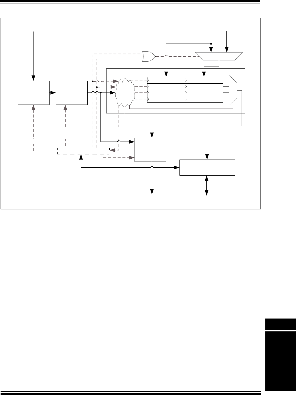
© 2010 Microchip Technology Inc. DS61122F-page 15-3
Section 15. Input Capture
Input Capture
15
Figure 15-1: Input Capture Module Block Diagram
Prescaler
1, 4, 16 Edge Detect
FIFO Control
Interrupt
Event
Generation
ICxBUF<31:16>
Interrupt
Timer3 Timer2
ICxCON
ICM<2:0>
ICM<2:0>
FEDGE
ICI<1:0>
ICBNE
ICOV
ICx Input
0 1
ICxBUF<15:0>
Data Space Interface
Peripheral Data Bus
ICTMR
C32

PIC32 Family Reference Manual
DS61122F-page 15-4 © 2010 Microchip Technology Inc.
15.2 INPUT CAPTURE REGISTERS
Each Input Capture module available on PIC32 devices has the following Special Function
Registers (SFRs):
•ICXCON: Input Capture X Control Register(1,2,3)
•ICXBUF: Input Capture X Buffer Register
Each Input Capture module also has the following associated bits for interrupt control:
• Interrupt Enable Control bit (ICxIE)
• Interrupt Flag Status bit (ICxIF)
• Interrupt Priority Control bits (ICxIP)
• Interrupt Subpriority Control bits (ICxIS)
Table 15-1 provides a brief summary of the Input Capture related registers, and is followed by a
detailed description of each register.
Table 15-1: Input Capture SFR Summary
Address
Offset Name Bit
31/23/15/7
Bit
30/22/14/6
Bit
29/21/13/5
Bit
28/20/12/4
Bit
27/19/11/3
Bit
26/18/10/2
Bit
25/17/9/1
Bit
24/16/8/0
0x00 ICxCON(1,2,3) 31:24 — — — — — — — —
23:16 — — — — — — — —
15:8 ON FRZ SIDL — — — FEDGE C32
7:0 ICTMR ICI<1:0> ICOV ICBNE ICM<2:0>
0x10 ICxBUF 31:24 ICxBUF<31:24>
23:16 ICxBUF<23:16>
15:8 ICxBUF<15:8>
7:0 ICxBUF<7:0>
Legend: — = unimplemented, read as ‘0’. Address offset values are shown in hexadecimal.
Note 1: This register has an associated Clear register at an offset of 0x4 bytes. These registers have the same name with CLR
appended to the end of the register name (e.g., ICxCONCLR). Writing a ‘1’ to any bit position in the Clear register will
clear valid bits in the associated register. Reads from the Clear register should be ignored.
2: This register has an associated Set register at an offset of 0x8 bytes. These registers have the same name with SET
appended to the end of the register name (e.g., ICxCONSET). Writing a ‘1’ to any bit position in the Set register will set
valid bits in the associated register. Reads from the Set register should be ignored.
3: This register has an associated Invert register at an offset of 0xC bytes. These registers have the same name with INV
appended to the end of the register name (e.g., ICxCONINV). Writing a ‘1’ to any bit position in the Invert register will
invert valid bits in the associated register. Reads from the Invert register should be ignored.

© 2010 Microchip Technology Inc. DS61122F-page 15-5
Section 15. Input Capture
Input Capture
15
Register 15-1: ICXCON: Input Capture X Control Register(1,2,3)
U-0 U-0 U-0 U-0 U-0 U-0 U-0 U-0
— — — — — — — —
bit 31 bit 24
U-0 U-0 U-0 U-0 U-0 U-0 U-0 U-0
— — — — — — — —
bit 23 bit 16
R/W-0 R/W-0 R/W-0 U-0 U-0 U-0 R/W-0 R/W-0
ON FRZ SIDL — — — FEDGE C32
bit 15 bit 8
R/W-0 R/W-0 R/W-0 R-0 R-0 R/W-0 R/W-0 R/W-0
ICTMR ICI<1:0> ICOV ICBNE ICM<2:0>
bit 7 bit 0
Legend:
R = Readable bit W = Writable bit P = Programmable bit r = Reserved bit
U = Unimplemented bit -n = Bit Value at POR: (‘0’, ‘1’, x = Unknown)
bit 31-16 Unimplemented: Read as ‘0’
bit 15 ON: Input Capture Module Enable bit
1 = Module enabled
0 = Disable and reset module, disable clocks, disable interrupt generation and allow SFR
modifications
Note: When using 1:1 PBCLK divisor, the user’s software should not read/write the peripheral’s
SFRs in the SYSCLK cycle immediately following the instruction that clears the module’s
ON bit.
bit 14 FRZ: Freeze in Debug Mode Control bit
1 = Freeze module operation when in Debug mode
0 = Do not freeze module operation when in Debug mode
Note: FRZ is writable in Debug Exception mode only, it is forced to ‘0’ in Normal mode.
bit 13 SIDL: Stop in Idle Control bit
1 = Halt in CPU Idle mode
0 = Continue to operate in CPU Idle mode
bit 12-10 Unimplemented: Read as ‘0’
bit 9 FEDGE: First Capture Edge Select bit (only used in mode 6, ICM<2:0> = 110)
1 = Capture rising edge first
0 = Capture falling edge first
Note 1: This register has an associated Clear register (ICxCONCLR) at an offset of 0x4 bytes. Writing a ‘1’ to any
bit position in the Clear register will clear valid bits in the associated register. Reads from the Clear register
should be ignored.
2: This register has an associated Set register (ICxCONSET) at an offset of 0x8 bytes. Writing a ‘1’ to any bit
position in the Set register will set valid bits in the associated register. Reads from the Set register should
be ignored.
3: This register has an associated Invert register (ICxCONINV) at an offset of 0xC bytes. Writing a ‘1’ to any bit
position in the Invert register will invert valid bits in the associated register. Reads from the Invert register
should be ignored.

PIC32 Family Reference Manual
DS61122F-page 15-6 © 2010 Microchip Technology Inc.
bit 8 C32: 32-bit Capture Select bit
1 = 32-bit timer resource capture
0 = 16-bit timer resource capture
bit 7 ICTMR: Timer Select bit (Does not affect timer selection when C32 (ICxCON<8>) is ‘1’)
0 = Timer3 is the counter source for capture
1 = Timer2 is the counter source for capture
bit 6-5 ICI<1:0>: Interrupt Control bits
11 = Interrupt on every fourth capture event
10 = Interrupt on every third capture event
01 = Interrupt on every second capture event
00 = Interrupt on every capture event
bit 4 ICOV: Input Capture Overflow Status Flag bit (read-only)
1 = Input capture overflow occurred
0 = No input capture overflow occurred
bit 3 ICBNE: Input Capture Buffer Not Empty Status bit (read-only)
1 = Input capture buffer is not empty; at least one more capture value can be read
0 = Input capture buffer is empty
bit 2-0 ICM<2:0>: Input Capture Mode Select bits
111 = Interrupt-Only mode (only supported while in Sleep mode or Idle mode)
110 = Simple Capture Event mode – every edge, specified edge first and every edge thereafter
101 = Prescaled Capture Event mode – every sixteenth rising edge
100 = Prescaled Capture Event mode – every fourth rising edge
011 = Simple Capture Event mode – every rising edge
010 = Simple Capture Event mode – every falling edge
001 = Edge Detect mode – every edge (rising and falling)
000 = Capture Disable mode
Register 15-1: ICXCON: Input Capture X Control Register(1,2,3) (Continued)
Note 1: This register has an associated Clear register (ICxCONCLR) at an offset of 0x4 bytes. Writing a ‘1’ to any
bit position in the Clear register will clear valid bits in the associated register. Reads from the Clear register
should be ignored.
2: This register has an associated Set register (ICxCONSET) at an offset of 0x8 bytes. Writing a ‘1’ to any bit
position in the Set register will set valid bits in the associated register. Reads from the Set register should
be ignored.
3: This register has an associated Invert register (ICxCONINV) at an offset of 0xC bytes. Writing a ‘1’ to any bit
position in the Invert register will invert valid bits in the associated register. Reads from the Invert register
should be ignored.

© 2010 Microchip Technology Inc. DS61122F-page 15-7
Section 15. Input Capture
Input Capture
15
Register 15-2: ICXBUF: Input Capture X Buffer Register
R-0 R-0 R-0 R-0 R-0 R-0 R-0 R-0
ICxBUF<31:24>
bit 31 bit 24
R-0 R-0 R-0 R-0 R-0 R-0 R-0 R-0
ICxBUF<23:16>
bit 23 bit 16
R-0 R-0 R-0 R-0 R-0 R-0 R-0 R-0
ICxBUF<15:8>
bit 15 bit 8
R-0 R-0 R-0 R-0 R-0 R-0 R-0 R-0
ICxBUF<7:0>
bit 7 bit 0
Legend:
R = Readable bit W = Writable bit P = Programmable bit r = Reserved bit
U = Unimplemented bit -n = Bit Value at POR: (‘0’, ‘1’, x = Unknown)
bit 31-0 ICxBUF<31:0>: Buffer Register bits
Value of the current captured input timer count.

PIC32 Family Reference Manual
DS61122F-page 15-8 © 2010 Microchip Technology Inc.
15.3 TIMER SELECTION
Each PIC32 device may have one or more Input Capture modules. Each module can select
between one of two 16-bit timers for the time base or one 32-bit timer, which is formed by
combining two 16-bit timers. Refer to the specific device data sheet for the timers that can be
selected.
For 16-bit Capture mode, setting ICTMR (ICxCON<7>) to ‘0’ selects Timer3 for capture. Setting
ICTMR (ICxCON<7>) to ‘1’ selects Timer2 for capture.
An Input Capture module configured to support 32-bit capture may use a 32-bit timer resource
for capture. By setting C32 (ICxCON<8>) to ‘1’, a 32-bit timer resource is captured. The 32-bit
timer resource is routed into the module using the existing 16-bit timer inputs. Timer2 provides
the lower 16 bits and Timer3 provides the upper 16 bits, as illustrated in Figure 15-2.
The timer’s clock can be set up using the internal peripheral clock source or a synchronized
external clock source applied at the TxCK pin.
Figure 15-2: 32-bit Timer Selection Block Diagram
15.4 INPUT CAPTURE ENABLE
After configuration, an Input Capture module is enabled by setting the ON bit (ICxCON<15>).
When this bit is cleared, the module is reset. Resetting the module has the following effects:
• Clears the Overflow Condition Flag
• Resets the FIFO to the empty state
• Resets the event count (for interrupt generation)
• Resets the prescaler count
Register reads and writes are allowed regardless of the ON bit (ICxCON<15>) state.
FIFO Control
ICxBUF<31:16> ICxBUF<15:0>
ICTMR = Don’t Care
C32 = 1
Timer3 Timer2
0 1
Value = 1

© 2010 Microchip Technology Inc. DS61122F-page 15-9
Section 15. Input Capture
Input Capture
15
15.5 INPUT CAPTURE EVENT MODES
The Input Capture module captures the value of the selected time base register when an event
occurs at the ICx pin. An Input Capture module can be configured in the following modes:
• Simple Capture Event modes:
- Capture timer value on every falling edge of input at ICx pin
- Capture timer value on every rising edge of input at ICx pin
- Capture timer value on every rising and falling edge of input at ICx pin, starting with a
specified edge
• Prescaled Capture Event modes:
- Capture timer value on every fourth rising edge of input at ICx pin
- Capture timer value on every sixteenth rising edge of input at ICx pin
• Edge Detect mode (See 15.5.3 “Edge Detect (Hall Sensor) Mode”)
• Interrupt-Only mode (See 15.5.4 “Interrupt-Only Mode”)
These input capture modes are configured by setting the appropriate Input Capture mode bits
ICM<2:0> (ICxCON<2:0>).
When the Input Capture module is disabled (ICM<2:0> = 000), the input capture logic ignores
incoming capture edges and does not generate further capture events or interrupts. The FIFO
continues to be operational for reading. Returning the module to any of the other modes resumes
operation. A state change on the capture input while capture is disabled does not cause a
capture event on exiting the Capture Disable mode.
15.5.1 Simple Capture Events
The Input Capture module can capture a timer count value based on the selected edge (rising,
falling or both, defined by mode) of the input applied to the ICx pin. Table 15-2 provides the mode
settings. In Simple Capture Event mode, the prescaler is not used. See Figure 15-3, Figure 15-4
and Figure 15-5 for simplified timing diagrams of a simple capture event.
Table 15-2: Input Capture Mode Settings
The input capture logic detects and synchronizes the rising or falling edge of the capture pin
signal on the peripheral clock. When the rising/falling edge has occurred, the Input Capture
module logic will write the current time base value to the capture buffer and signal the interrupt
generation logic.
An input capture interrupt event is generated after one, two, three or four timer count captures,
as configured by the ICI<1:0> bits (ICxCON<6:5>). See 15.7 “Input Capture Interrupts” for
further details.
Since the capture pin is sampled by the peripheral clock, the capture pulse high and low widths
must be greater than the peripheral clock period.
Note: The prescaler logic continues to run when the Input Capture module is in Capture
Disable mode.
ICM<2:0> Setting Capture Occurs On
001 Rising edge
010 Falling edge
110 Rising and falling edges(1)
Note 1: This capture begins with the edge specified by the FEDGE bit (ICxCON<9>).
Note: Since the capture input must be synchronized to the peripheral clock, the module
captures the timer count value that is valid 2-3 peripheral clock cycles (TPB) after
the capture event.
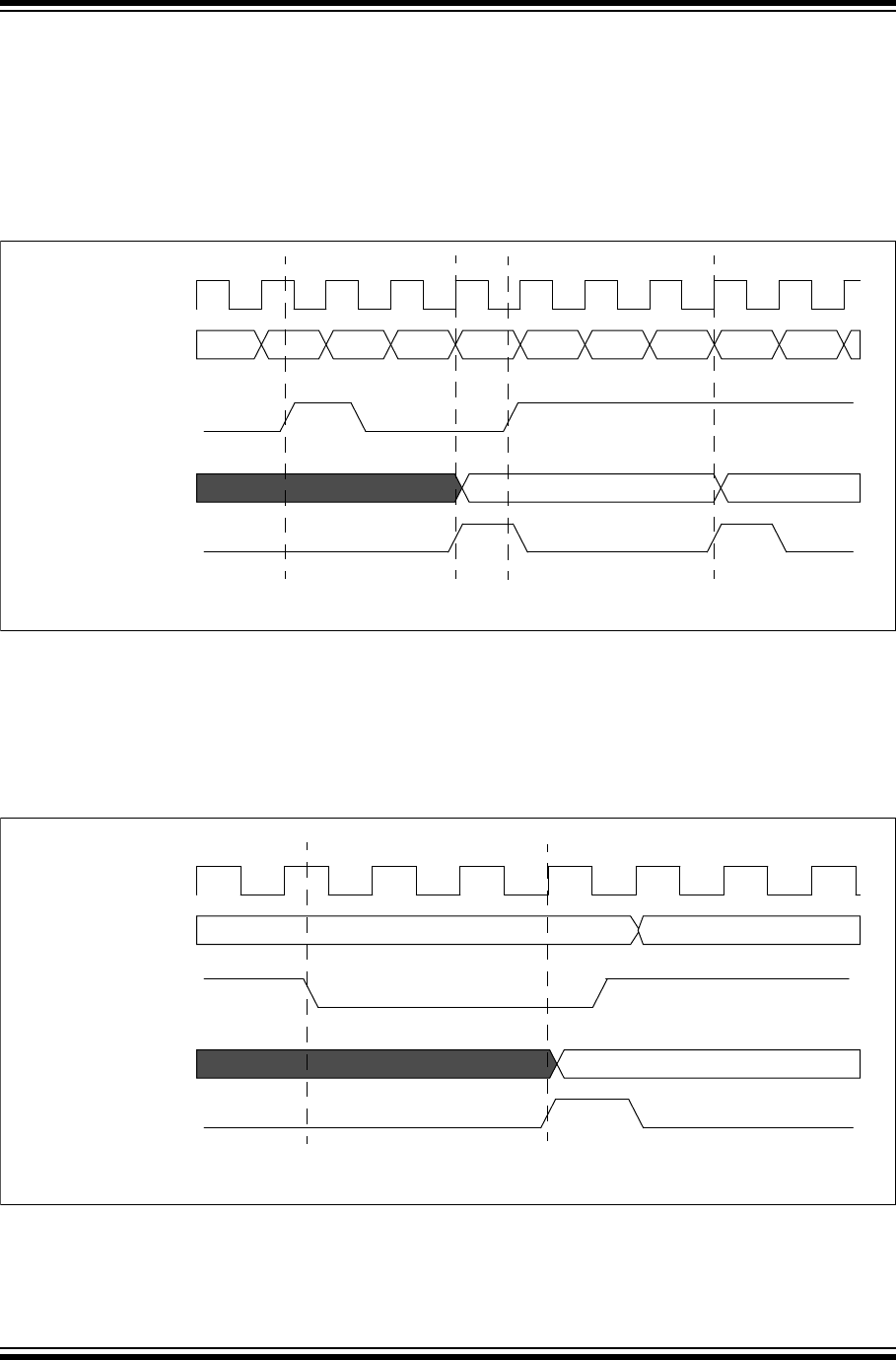
PIC32 Family Reference Manual
DS61122F-page 15-10 © 2010 Microchip Technology Inc.
Figure 15-3 depicts two capture events when the Input Capture module is in Simple Capture
mode configured to capture every rising edge, ICM<2:0> = 011 (ICxCON<2:0>), with interrupts
generated for every event, ICI<1:0> = 00 (ICxCON<6:5>).
The first capture event occurs when the timer value is ‘n’. Due to synchronization delay, timer
value ‘n + 2’ is stored in the capture buffer. The second capture event occurs when the timer
value is ‘m’. Note that ‘m + 3’ is stored in the capture buffer due to propagation delay as well as
the synchronization delay. Interrupt events are generated on each capture event.
Figure 15-3: Simple Capture Event Timing Diagram, Capture Every Rising Edge
Figure 15-4 depicts a capture event when the Input Capture module is in Simple Capture mode
configured to capture every falling edge, ICM<2:0> = 010 (ICxCON<2:0>), with interrupts
generated for every event, ICI<1:0> = 00 (ICxCON<6:5>). In this example, the timer frequency
is slower than the peripheral clock.
The capture event occurs when the timer value is ‘n’. Value ‘n’ is stored in the capture buffer and
an interrupt event is generated.
Figure 15-4: Simple Capture Event Timing Diagram, Capture Every Falling Edge
n n + 1 n + 2 m m + 1 m + 2 m + 3 m + 4 m + 5
n + 2 m + 3
Peripheral Clock
Timer Count
ICx Input
Capture Data
Capture Interrupt(1)
Note 1: This capture event flag is cleared by user software.
n n + 1
n
Peripheral Clock
Timer Count
ICx Input
Capture Data
Capture Interrupt(1)
Note 1: This capture event flag is cleared by user software.

© 2010 Microchip Technology Inc. DS61122F-page 15-11
Section 15. Input Capture
Input Capture
15
Figure 15-5 depicts a capture event when the Input Capture module is in Simple Capture mode
configured to capture every edge, ICM<2:0> = 011 (ICxCON<2:0>); starting with a falling edge,
FEDGE = 0 (ICxCON<9>), with interrupts generated for every second event, ICI<1:0> = 01
(ICxCON<6:5>).
The first falling edge occurs when the timer value is ‘n’. Value ‘n + 2’ is stored in the capture
buffer. A subsequent rising edge occurs when the timer value is ‘m’. Value ‘m + 2’ is stored in the
capture buffer and an interrupt event is generated.
Figure 15-5: Simple Capture Event Timing Diagram, Capture Every Edge, Falling Edge First
15.5.2 Prescaled Capture Event Mode
In Prescaled Capture Event mode, the Input Capture module triggers a capture event on either
every fourth or every sixteenth rising edge. Table 15-3 provides the Prescaled Capture Event
mode settings.
Table 15-3: Prescaled Capture Event Mode Settings
The capture prescaler counter is incremented on every rising edge on the capture input. When
the prescaler counter equals four or sixteen (depending on the mode selected), the counter
outputs a “valid” capture event signal. The valid capture event signal is then synchronized to the
peripheral clock. The synchronized capture event signal triggers a timer count capture.
An input capture interrupt is generated after one, two, three or four timer count captures, as
configured by the ICI<1:0> bits (ICxCON<6:5>). See 15.7 “Input Capture Interrupts” for further
details.
n n + 1 n + 2 m m + 1 m + 2 m + 3 m + 4
n + 2 m + 2
Peripheral Clock
Timer Count
ICx Input
Capture Data
Capture Interrupts(1)
Note 1: This capture event flag is cleared by user software.
ICM<2:0> Setting Number of Rising Edges Before Trigger
100 4
101 16
Note: Since the capture input must be synchronized to the peripheral clock, the module
captures the timer count value that is valid 2-3 peripheral clock cycles (TPB) after
the capture event.
Note: It is recommended that the user disable the capture module (i.e., clear the ON bit,
ICxCON<15>), before switching to Prescaler Capture Event mode. Simply switch-
ing to Prescaler Capture Event mode from another active mode does not reset the
prescaler and may cause an inadvertent capture event.
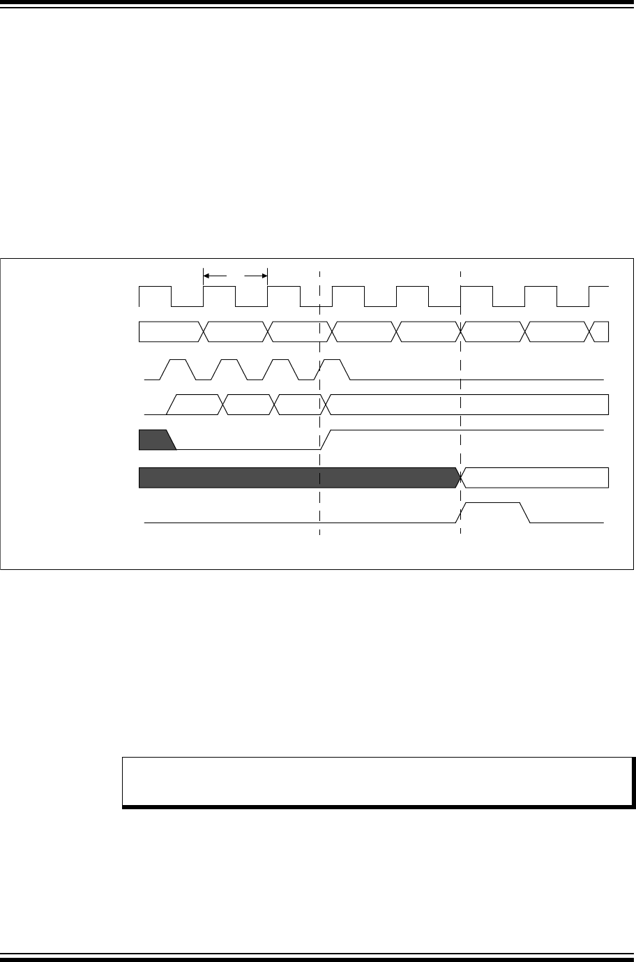
PIC32 Family Reference Manual
DS61122F-page 15-12 © 2010 Microchip Technology Inc.
The prescaler counter is cleared when the following events occur:
• The Input Capture module is turned off (i.e., ON = 0 (ICxCON<15>))
• The Input Capture module is reset
Since the capture pin triggers an internal flip-flop, the input capture pulse high and low widths are
not limited by the peripheral clock period. Refer to the “Electrical Characteristics” section in
the specific device data sheet for details on input capture electrical specifications.
Figure 15-6 depicts a capture event when the Input Capture module is in Prescaler Capture
Event mode. The prescaler is configured to capture a timer value for every fourth rising edge on
the capture input, ICM<2:0> = 100 (ICxCON<2:0>), with interrupts generated for every capture
event, ICI<1:0> = 00 (ICxCON<6:5>). The fourth rising edge on the capture input occurs at time
‘n’. The prescaler output is synchronized. Due to synchronization delay, timer value ‘n + 2’ is
stored in the capture buffer. An interrupt signal is generated due to the capture event.
Figure 15-6: Prescaler Capture Event Timing Diagram
15.5.3 Edge Detect (Hall Sensor) Mode
In Edge Detect mode, the Input Capture module captures a timer count value on every edge of
the capture input. Edge Detection mode is selected by setting the ICM<2:0> bits to ‘001’
(ICxCON<2:0>). In this mode, the capture prescaler is not used and the Input Capture Overflow
bit, ICOV (ICxCON<4>), is not updated. In this mode, the Interrupt Control bits, ICI<1:0>
(ICxCON<6:5>), are ignored and an interrupt event is generated for every timer count capture.
See Figure 15-7 for a simplified timing diagram.
As with the Simple Capture Event mode, the Input Capture logic detects and synchronizes the
rising and falling edge of the capture input signal on the peripheral clock. When a rising or falling
edge occurs, the Input Capture module writes the time base value to the capture buffer.
Since the capture pin is sampled by the peripheral clock, the capture pulse high and low widths
must be greater than the peripheral clock period.
n n + 1 n + 2 n + 3 n + 4
1 2 3 4
n + 2
TPB
Peripheral Clock
Timer Count
Capture Input
Prescaler Count
Prescaler Output
Capture Data
Capture Interrupt(1)
Note 1: This capture event flag is cleared by user software.
Note: Since the capture input must be synchronized to the peripheral clock, the module
captures the timer count value that is valid 2-3 peripheral clock cycles (TPB) after
the capture event.
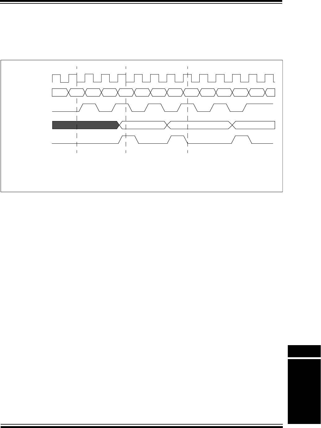
© 2010 Microchip Technology Inc. DS61122F-page 15-13
Section 15. Input Capture
Input Capture
15
Figure 15-7 depicts three capture events when the Input Capture module is in Edge Detect
mode, ICM<2:0> = 001 (ICxCON<2:0). Transitions on the capture input occur at times ‘n’, ‘n + 1’
and ‘n + 3’. Due to synchronization and propagation delay, timer values ‘n + 2’, ‘n + 4’ and ‘n + 5’
are stored in the capture buffer. Interrupt signals are generated due to each capture input
transition.
Figure 15-7: Edge Detect Capture Event Timing Diagram
15.5.4 Interrupt-Only Mode
Interrupt-Only mode does not function while the device is running, and only operates when the
device is in Sleep or Idle mode; however, during normal operation, when the device is in Sleep
or Idle mode and the Input Capture module is set for Interrupt-Only mode (ICM<2:0> = 111), the
Input Capture module functions as an interrupt pin. Any rising edge on the input capture triggers
an interrupt, which wakes the device. No timer values are captured and the FIFO buffer is not
updated.
Since no timer values are captured, the Timer Select bit, ICTMR (ICxCON<7>), is ignored and
there is no need to configure the timer source. The prescaler is not used in this mode, as the
wake-up interrupt is generated on the first rising edge. Therefore, the ICI<1:0> bits
(ICxCON<6:5>) are ignored. When the device leaves Sleep or Idle mode, the interrupt signal is
deasserted. This mode is used strictly as an external wake-up source.
Since the capture pin triggers on an internal flip-flop, the input capture pulse high and low widths
are not limited by the peripheral clock period. Refer to the “Electrical Characteristics” section
in the specific device data sheet for details on input capture electrical specifications.
n + 1 n + 2 n + 3 n + 4 n + 5 n + 6 n + 7 n + 8 n + 9 n + 10 n + 11
n + 5 n + 9
Peripheral Clock
Timer Count
Capture Input
Capture Data
Capture Interrupt(1)
Note 1: This capture event flag is cleared by user software.
2: On PIC32MX3XX and PIC32MX4XX devices, clearing only Interrupt 3 will also clear Interrupts 1 and 2. On
other PIC32 devices, each interrupt is persistent and must be cleared individually (up to the maximum interrupt
depth).
n
n + 2
12 3

PIC32 Family Reference Manual
DS61122F-page 15-14 © 2010 Microchip Technology Inc.
15.6 CAPTURE BUFFER OPERATION
Each Input Capture module has an associated four-level deep FIFO buffer. The buffer is
accessible to the user application via the buffer register (ICxBUF). ICxBUF is written by the input
capture logic and can only be read by the user application. Writes to ICxBUF are ignored.
There are two status flags that provide status on the FIFO buffer:
• ICBNE (ICxCON<3>) – Input Capture Buffer Not Empty
• ICOV (ICxCON<4>) – Input Capture Overrun
When the Input Capture module is disabled (i.e., ON = 0 (ICxCON<15>) or Reset), the status
flags are cleared and the buffer is cleared to the empty state.
The ICBNE flag is set on the first input capture event and remains set until all capture events
have been read from the FIFO. For example, if three capture events have occurred, three reads
of the capture FIFO buffer are required before the ICBNE flag is cleared. If four capture events
have occurred, four reads are required to clear the ICBNE flag.
Each read of the FIFO buffer adjusts the read pointer, allowing the remaining entries to move to
the next available top location of the FIFO. In 32-bit Capture mode, the upper 16 bits must be
read last if reading 16 bits at a time. The FIFO read pointer is advanced when reading the Most
Significant Byte (MSB).
If the FIFO is full with four capture events and a fifth capture event occurs prior to a read of the
FIFO, an overrun condition occurs and the ICOV bit (ICxCON<4>) is set to a logic ‘1’. The fifth
capture event is not recorded, subsequent capture events do not alter the current FIFO contents
until the overrun condition is cleared, and an input capture error interrupt will be generated.
The overflow condition is cleared in any of the following ways:
• Module is disabled (i.e., ON = 0 (ICxCON<15>))
• Capture buffer is read until ICBNE = 0 (ICxCON<3>)
• Device is Reset
If the Input Capture module is disabled and at some time re-enabled, the FIFO buffer contents
are not defined and a read may yield indeterminate results.
If a FIFO read is performed when no capture event has been received, the read yields
indeterminate results.
Note: Some PIC32 microcontrollers do not support the ICxE interrupt. Refer to the specific
device data sheet for availability.
Note: When ICI<1:0> = 00 or ICM<2:0> = 001, interrupts continue to occur and the ICOV
bit remains clear even after a buffer overflow has occurred.
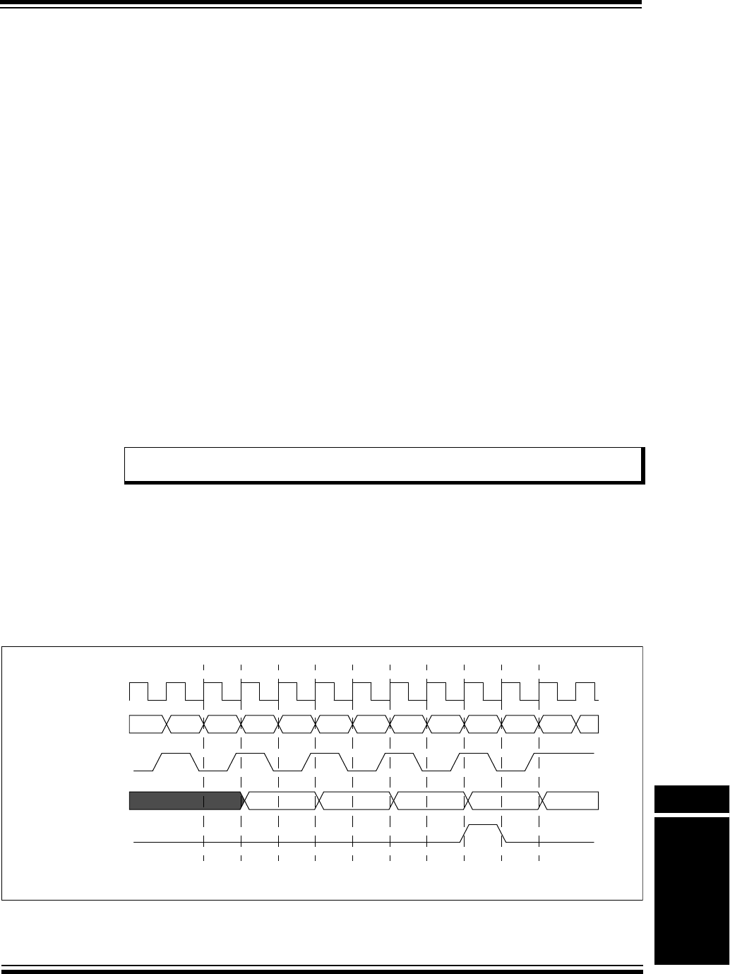
© 2010 Microchip Technology Inc. DS61122F-page 15-15
Section 15. Input Capture
Input Capture
15
15.7 INPUT CAPTURE INTERRUPTS
The Input Capture module has the ability to generate an interrupt event signal based upon the
selected number of capture events. A capture event is defined by the writing of a timer value into
the FIFO. The number of capture events required to trigger an interrupt event is set by the
ICI<1:0> control bits (ICxCON<6:5>) . If ICBNE = 0 (ICxCON<3>), the interrupt count is cleared.
This allows the user to synchronize the interrupt count to the FIFO status.
For example, assuming that ICI<1:0> = 01 (specifying an interrupt event every second capture
event), the following sequence could occur:
1. Turn on module, interrupt count = 0.
2. Capture event. FIFO contains one entry, interrupt count = 1.
3. Read FIFO. FIFO is empty, interrupt count = 0.
4. Capture event. FIFO contains one entry, interrupt count = 1.
5. Capture event. FIFO contains two entries, interrupt count = 2.
6. Interrupt issued. interrupt count = 0.
7. Capture event. FIFO contains three entries, interrupt count = 1.
8. Read FIFO three times. FIFO becomes empty, interrupt count = 0.
9. Capture event. FIFO contains one entry, interrupt count = 1.
10. Read FIFO. FIFO becomes empty, interrupt count = 0.
The first capture event is defined as the capture event occurring after a mode change from the
OFF mode or after ICBNE = 0.
When an overrun occurs (unless ICI<1:0> = 00 or ICM<2:0> = 001), the Input Capture module
will stop generating input capture events and generates an input capture error event instead. This
interrupt will persist until the overflow condition is cleared (see 15.6 “Capture Buffer
Operation” for details on how to clear the overflow condition).
Applications often dictate using the Input Capture pins as auxiliary external interrupt sources.
When ICI<1:0> = 00 or ICM<2:0> = 001, interrupt events occur regardless of FIFO overrun.
There is no need to perform a dummy read on the capture buffer to clear the event and prevent
an overflow in order to ensure that future interrupt events are not inhibited. The ICOV flag
(ICxCON<4>) is still set for the overflow condition.
Figure 15-8 depicts five capture events when the Input Capture module is configured to capture
timer values on every rising edge (ICM<2:0> = 011) and generate an interrupt for every four
captures (ICI<1:0> = 11). Note that the fourth capture causes the capture of value ‘n + 8’ and
triggers an interrupt event.
Figure 15-8: Interrupt Event, ICXCON.ICM<2:0> = 011, ICXCON.ICI<1:0> = 11
Note: Some PIC32 microcontrollers do not support the ICxE interrupt. Refer to the specific
device data sheet for availability.
n + 1 n + 2 n + 3 n + 4 n + 5 n + 6 n + 7 n + 8 n + 9 n + 10 n + 11
n + 2 n + 4 n + 6 n + 8 n + 10
Peripheral Clock
Timer Count
Capture Input
Capture Data
Capture Interrupt(1)
Note 1: This capture event flag is cleared by user software.

PIC32 Family Reference Manual
DS61122F-page 15-16 © 2010 Microchip Technology Inc.
15.7.1 Interrupt Control Bits
Each Input Capture module has interrupt flag status bits (ICxIF), interrupt error status bits (ICxE),
interrupt enable bits (ICxIE), interrupt priority control bits (ICxIP) and secondary interrupt priority
control bits (ICxIS). Refer to 8.2 “Control Registers” in Section 8. “Interrupts” (DS61108) for
further information on peripheral interrupts.
15.7.2 Interrupt Persistence
Input capture interrupts persist so long as the condition that caused them persists. In addition,
they will occur again immediately if the condition is not cleared. Table 15-4 describes the interrupt
persistence set and clear conditions.
Table 15-4: Interrupt Persistence Conditions
Note: Some PIC32 microcontrollers do not support the ICxE interrupt or persistent inter-
rupts. Refer to the specific device data sheet for availability.
ICxCON Value Set Condition Persistence
ICI<1:0> = 11 Interrupt on every fourth capture
event.
Interrupt is active if the number
of FIFO entries is equal to 4.
ICI<1:0> = 10 Interrupt on every third capture
event.
Interrupt is active if the number
of FIFO entries is greater than
or equal to 3.
ICI<1:0> = 01 Interrupt on every second
capture event.
Interrupt is active if the number
of FIFO entries is greater than
or equal to 2.
ICI<1:0> = 00
or
Edge Detect modes (see
the ICM<2:0> bits in the
ICxCON register
(Register 15-1))
Interrupt on every capture
event.
Interrupt is active if the number
of FIFO entries is greater than
or equal to 1.
ICOV = 1Interrupt on fifth capture event if
FIFO is full.
Interrupt is active until the error
condition flag (ICxCON.ICOV) is
cleared.

© 2010 Microchip Technology Inc. DS61122F-page 15-17
Section 15. Input Capture
Input Capture
15
15.8 OPERATION IN POWER-SAVING MODES
15.8.1 Input Capture Operation in Sleep Mode
When the device enters Sleep mode, the peripheral clock is disabled. In Sleep mode, the Input
Capture module can only function as an external interrupt source. This mode is enabled by
setting the ICM<2:0> control bits = 111 (ICxCON<2:0>), for Interrupt-Only mode. In this mode,
a rising edge on the capture pin will generate a device wake-up from Sleep. If the respective
module interrupt bit is enabled and the module’s priority is of the required priority level, an
interrupt will be generated. Refer to 15.5.4 “Interrupt-Only Mode” for more details.
If the Input Capture module has been configured for a mode other than ICM<2:0> = 111 and the
device enters Sleep mode, no external pin stimulus, rising or falling, will generate a wake-up from
Sleep.
15.8.2 Input Capture Operation in Idle Mode
When the device enters Idle mode, the peripheral clock sources remain functional and the CPU
stops executing code. The Sleep-In-Idle Control bit, SIDL (ICxCON<13>), determines whether
the module will stop in Idle mode or continue to operate.
If SIDL is ‘0’, the module continues normal operation in Idle mode. Although Interrupt-Only mode
(ICM<2:0> = 111) may generate an interrupt when in Idle mode if SIDL is ‘0’, an interrupt is not
generated when the processor is running. Refer to 15.5.4 “Interrupt-Only Mode” for further
details.
If SIDL is ‘1’, the module stops when the device is in Idle mode. The module performs the same
procedures when stopped in Idle mode as for Sleep mode. Refer to 15.5.4 “Interrupt-Only
Mode” for further details.
15.8.3 Device Wake-up on Sleep or Idle
While using Interrupt-Only mode, an input capture event can generate a device wake-up or
interrupt, if enabled, when the device is in Sleep or Idle mode. Refer to 15.5.4 “Interrupt-Only
Mode” for further details.

PIC32 Family Reference Manual
DS61122F-page 15-18 © 2010 Microchip Technology Inc.
15.9 INPUT CAPTURE OPERATION IN DEBUG MODE
The FRZ bit (ICxCON<14>) determines whether the Input Capture module will run or stop while
the CPU is executing Debug Exception code (i.e., the application is halted) in Debug mode.
When FRZ is ‘0’, the Input Capture module continues to run even when the application is halted
in Debug mode. When FRZ is ‘1’ and the application is halted in Debug mode, the Input Capture
module will freeze its operations and make no changes to its current state. The module will
resume its operation after the CPU resumes execution.
15.9.1 Capture Operation During Freeze (FRZ = 1)
When frozen, the capture operation does not cause changes to the module. The edge detection
logic prevents any state changes that occur during Freeze from being inadvertently detected
after leaving Freeze.
When frozen, the emulator is allowed to read the Input Capture FIFO; however, the FIFO status
flags as viewed by the user application do not change.
15.10 I/O PIN CONTROL
When the Input Capture module is enabled, the user application must ensure that the I/O pin
direction is configured for an input by setting the associated TRIS bit. The pin direction is not set
when the Input Capture module is enabled. Furthermore, all other peripherals multiplexed with
the input pin must be disabled.
15.11 DESIGN TIPS
Question 1: Can the Input Capture module be used to wake the device from Sleep
mode?
Answer: Yes. When the Input Capture module is configured to ICM<2:0> = 111
(ICxCON<2:0>) and the respective module interrupt enable bit is asserted
(ICIE = 1), a rising edge on the capture pin will wake the device from Sleep. (See
15.5.4 “Interrupt-Only Mode” for further details.)
Note: The FRZ bit is readable and writable only when the CPU is executing in Debug
Exception mode. In all other modes, the FRZ bit reads as ‘0’. If FRZ bit is changed
during Debug mode, the new value does not take effect until the current Debug
Exception mode is exited and re-entered. During the Debug Exception mode, the
FRZ bit reads the state of the peripheral when entering Debug mode.
Note: The prescaler logic is not frozen during Debug mode.

© 2010 Microchip Technology Inc. DS61122F-page 15-19
Section 15. Input Capture
Input Capture
15
15.12 RELATED APPLICATION NOTES
This section lists application notes that are related to this section of the manual. These
application notes may not be written specifically for the PIC32 device family, but the concepts are
pertinent and could be used with modification and possible limitations. The current application
notes related to the Input Capture module include the following:
Title Application Note #
Using the CCP Module(s) AN594
Implementing Ultrasonic Ranging AN597
Note: Please visit the Microchip web site (www.microchip.com) for additional application
notes and code examples for the PIC32 family of devices.

PIC32 Family Reference Manual
DS61122F-page 15-20 © 2010 Microchip Technology Inc.
15.13 REVISION HISTORY
Revision A (October 2007)
This is the initial released version of this document.
Revision B (October 2007)
Updated document to remove Confidential status.
Revision C (April 2008)
Revised status to Preliminary; Revised U-0 to r-x; Removed ‘x’ in bit names.
Revision D (June 2008)
Revised note for Registers 15-1, 15-3, 15-4, 15-5, 15-6, 15-7, 15-8, 15-9; Change Reserved bits
from “Maintain as” to “Write”; Added Note to ON bit (ICxCON Register).
Revision E (October 2009)
This revision includes the following updates:
• Minor updates to text and formatting have been incorporated throughout the document.
• Updated the following figures:
-Simple Capture Event Timing Diagram, Capture Every Rising Edge (Figure 15-3)
-Simple Capture Event Timing Diagram, Capture Every Falling Edge (Figure 15-4)
-Simple Capture Event Timing Diagram, Capture Every Edge, Falling Edge First
(Figure 15-5)
-Prescaler Capture Event Timing Diagram (Figure 15-6)
-Edge Detect Capture Event Timing Diagram (Figure 15-7)
-Interrupt Event, ICXCON.ICM<2:0> = 011, ICXCON.ICI<1:0> = 11 (Figure 15-8)
• Updated the shaded note in 15.1 “Introduction”.
• Removed the shaded note in 15.2 “Input Capture Registers”.
• Updated the Interrupts Register Summary (Table 15-1):
- Removed all references to the Clear, Set and Invert registers
- Added the Address Offset column
- Added Notes 1, 2 and 3, which describe the Clear, Set and Invert registers
• Added Notes 1, 2 and 3, which describe the Clear, Set and Invert registers to the ICxCON
register (see Register 15-1).
• Removed the IFS0, IEC0, IPC1, IPC2, IPC3, IPC4 and IPC5 registers.
• Updated the bit definition for ICM<2:0> = 111 in the ICxCON: Input Capture x Control
Register (Register 15-1).
• Updated the first paragraph of 15.3 “Timer Selection” to clarify the formation of the timers
used for the time base.
• Removed content from the first paragraph of 15.5.1 “Simple Capture Events”, which is
now presented in Table 15-2.
• Removed content from the first paragraph of 15.5.2 “Prescaled Capture Event Mode”,
which is now presented in Table 15-3.
• Updated all three paragraphs of 15.5.4 “Interrupt-Only Mode”.
• Added a shaded note and updated the sixth paragraph of 15.6 “Capture Buffer
Operation”.
• Updated the capture event sequence in 15.7 “Input Capture Interrupts”.
• Added a reference to the interrupt error status bits (ICxE) in 15.7.1 “Interrupt Control
Bits”.
• Added 15.7.2 “Interrupt Persistence”.
• Updated the second paragraph of 15.8.2 “Input Capture Operation in Idle Mode” to
clarify operation during Interrupt-Only mode.

© 2010 Microchip Technology Inc. DS61122F-page 15-21
Section 15. Input Capture
Input Capture
15
Revision E (October 2009) (Continued)
• Updated 15.8.3 “Device Wake-up on Sleep or Idle” to clarify operation during
Interrupt-Only mode.
• Updated the first paragraph of 15.9.1 “Capture Operation During Freeze (FRZ = 1)”, and
removed the second paragraph.
• Removed 15.9.2 “Operation of the Capture Buffer in Debug Mode”.
Revision F (November 2010)
This revision includes the following updates:
• Formatting updates and minor text changes have been incorporated throughout the
document
• The bit named ICFEDGE has been renamed to FEDGE
• The bit named ICC32 has been renamed to C32
• A new note box regarding interrupts has been added immediately after the last bullet item
in 15.6 “Capture Buffer Operation”

PIC32 Family Reference Manual
DS61122F-page 15-22 © 2010 Microchip Technology Inc.
NOTES:

© 2010 Microchip Technology Inc. DS61122F-page 15-23
Information contained in this publication regarding device
applications and the like is provided only for your convenience
and may be superseded by updates. It is your responsibility to
ensure that your application meets with your specifications.
MICROCHIP MAKES NO REPRESENTATIONS OR
WARRANTIES OF ANY KIND WHETHER EXPRESS OR
IMPLIED, WRITTEN OR ORAL, STATUTORY OR
OTHERWISE, RELATED TO THE INFORMATION,
INCLUDING BUT NOT LIMITED TO ITS CONDITION,
QUALITY, PERFORMANCE, MERCHANTABILITY OR
FITNESS FOR PURPOSE. Microchip disclaims all liability
arising from this information and its use. Use of Microchip
devices in life support and/or safety applications is entirely at
the buyer’s risk, and the buyer agrees to defend, indemnify and
hold harmless Microchip from any and all damages, claims,
suits, or expenses resulting from such use. No licenses are
conveyed, implicitly or otherwise, under any Microchip
intellectual property rights.
Trademarks
The Microchip name and logo, the Microchip logo, dsPIC,
KEELOQ, KEELOQ logo, MPLAB, PIC, PICmicro, PICSTART,
PIC32 logo, rfPIC and UNI/O are registered trademarks of
Microchip Technology Incorporated in the U.S.A. and other
countries.
FilterLab, Hampshire, HI-TECH C, Linear Active Thermistor,
MXDEV, MXLAB, SEEVAL and The Embedded Control
Solutions Company are registered trademarks of Microchip
Technology Incorporated in the U.S.A.
Analog-for-the-Digital Age, Application Maestro, CodeGuard,
dsPICDEM, dsPICDEM.net, dsPICworks, dsSPEAK, ECAN,
ECONOMONITOR, FanSense, HI-TIDE, In-Circuit Serial
Programming, ICSP, Mindi, MiWi, MPASM, MPLAB Certified
logo, MPLIB, MPLINK, mTouch, Omniscient Code
Generation, PICC, PICC-18, PICDEM, PICDEM.net, PICkit,
PICtail, REAL ICE, rfLAB, Select Mode, Total Endurance,
TSHARC, UniWinDriver, WiperLock and ZENA are
trademarks of Microchip Technology Incorporated in the
U.S.A. and other countries.
SQTP is a service mark of Microchip Technology Incorporated
in the U.S.A.
All other trademarks mentioned herein are property of their
respective companies.
© 2010, Microchip Technology Incorporated, Printed in the
U.S.A., All Rights Reserved.
Printed on recycled paper.
ISBN: 978-1-60932-682-1
Note the following details of the code protection feature on Microchip devices:
• Microchip products meet the specification contained in their particular Microchip Data Sheet.
• Microchip believes that its family of products is one of the most secure families of its kind on the market today, when used in the
intended manner and under normal conditions.
• There are dishonest and possibly illegal methods used to breach the code protection feature. All of these methods, to our
knowledge, require using the Microchip products in a manner outside the operating specifications contained in Microchip’s Data
Sheets. Most likely, the person doing so is engaged in theft of intellectual property.
• Microchip is willing to work with the customer who is concerned about the integrity of their code.
• Neither Microchip nor any other semiconductor manufacturer can guarantee the security of their code. Code protection does not
mean that we are guaranteeing the product as “unbreakable.”
Code protection is constantly evolving. We at Microchip are committed to continuously improving the code protection features of our
products. Attempts to break Microchip’s code protection feature may be a violation of the Digital Millennium Copyright Act. If such acts
allow unauthorized access to your software or other copyrighted work, you may have a right to sue for relief under that Act.
Microchip received ISO/TS-16949:2002 certification for its worldwide
headquarters, design and wafer fabrication facilities in Chandler and
Tempe, Arizona; Gresham, Oregon and design centers in California
and India. The Company’s quality system processes and procedures
are for its PIC® MCUs and dsPIC® DSCs, KEELOQ® code hopping
devices, Serial EEPROMs, microperipherals, nonvolatile memory and
analog products. In addition, Microchip’s quality system for the design
and manufacture of development systems is ISO 9001:2000 certified.

DS61122F-page 15-24 © 2010 Microchip Technology Inc.
AMERICAS
Corporate Office
2355 West Chandler Blvd.
Chandler, AZ 85224-6199
Tel: 480-792-7200
Fax: 480-792-7277
Technical Support:
http://support.microchip.com
Web Address:
www.microchip.com
Atlanta
Duluth, GA
Tel: 678-957-9614
Fax: 678-957-1455
Boston
Westborough, MA
Tel: 774-760-0087
Fax: 774-760-0088
Chicago
Itasca, IL
Tel: 630-285-0071
Fax: 630-285-0075
Cleveland
Independence, OH
Tel: 216-447-0464
Fax: 216-447-0643
Dallas
Addison, TX
Tel: 972-818-7423
Fax: 972-818-2924
Detroit
Farmington Hills, MI
Tel: 248-538-2250
Fax: 248-538-2260
Kokomo
Kokomo, IN
Tel: 765-864-8360
Fax: 765-864-8387
Los Angeles
Mission Viejo, CA
Tel: 949-462-9523
Fax: 949-462-9608
Santa Clara
Santa Clara, CA
Tel: 408-961-6444
Fax: 408-961-6445
Toronto
Mississauga, Ontario,
Canada
Tel: 905-673-0699
Fax: 905-673-6509
ASIA/PACIFIC
Asia Pacific Office
Suites 3707-14, 37th Floor
Tower 6, The Gateway
Harbour City, Kowloon
Hong Kong
Tel: 852-2401-1200
Fax: 852-2401-3431
Australia - Sydney
Tel: 61-2-9868-6733
Fax: 61-2-9868-6755
China - Beijing
Tel: 86-10-8528-2100
Fax: 86-10-8528-2104
China - Chengdu
Tel: 86-28-8665-5511
Fax: 86-28-8665-7889
China - Chongqing
Tel: 86-23-8980-9588
Fax: 86-23-8980-9500
China - Hong Kong SAR
Tel: 852-2401-1200
Fax: 852-2401-3431
China - Nanjing
Tel: 86-25-8473-2460
Fax: 86-25-8473-2470
China - Qingdao
Tel: 86-532-8502-7355
Fax: 86-532-8502-7205
China - Shanghai
Tel: 86-21-5407-5533
Fax: 86-21-5407-5066
China - Shenyang
Tel: 86-24-2334-2829
Fax: 86-24-2334-2393
China - Shenzhen
Tel: 86-755-8203-2660
Fax: 86-755-8203-1760
China - Wuhan
Tel: 86-27-5980-5300
Fax: 86-27-5980-5118
China - Xian
Tel: 86-29-8833-7252
Fax: 86-29-8833-7256
China - Xiamen
Tel: 86-592-2388138
Fax: 86-592-2388130
China - Zhuhai
Tel: 86-756-3210040
Fax: 86-756-3210049
ASIA/PACIFIC
India - Bangalore
Tel: 91-80-3090-4444
Fax: 91-80-3090-4123
India - New Delhi
Tel: 91-11-4160-8631
Fax: 91-11-4160-8632
India - Pune
Tel: 91-20-2566-1512
Fax: 91-20-2566-1513
Japan - Yokohama
Tel: 81-45-471- 6166
Fax: 81-45-471-6122
Korea - Daegu
Tel: 82-53-744-4301
Fax: 82-53-744-4302
Korea - Seoul
Tel: 82-2-554-7200
Fax: 82-2-558-5932 or
82-2-558-5934
Malaysia - Kuala Lumpur
Tel: 60-3-6201-9857
Fax: 60-3-6201-9859
Malaysia - Penang
Tel: 60-4-227-8870
Fax: 60-4-227-4068
Philippines - Manila
Tel: 63-2-634-9065
Fax: 63-2-634-9069
Singapore
Tel: 65-6334-8870
Fax: 65-6334-8850
Taiwan - Hsin Chu
Tel: 886-3-6578-300
Fax: 886-3-6578-370
Taiwan - Kaohsiung
Tel: 886-7-213-7830
Fax: 886-7-330-9305
Taiwan - Taipei
Tel: 886-2-2500-6610
Fax: 886-2-2508-0102
Thailand - Bangkok
Tel: 66-2-694-1351
Fax: 66-2-694-1350
EUROPE
Austria - Wels
Tel: 43-7242-2244-39
Fax: 43-7242-2244-393
Denmark - Copenhagen
Tel: 45-4450-2828
Fax: 45-4485-2829
France - Paris
Tel: 33-1-69-53-63-20
Fax: 33-1-69-30-90-79
Germany - Munich
Tel: 49-89-627-144-0
Fax: 49-89-627-144-44
Italy - Milan
Tel: 39-0331-742611
Fax: 39-0331-466781
Netherlands - Drunen
Tel: 31-416-690399
Fax: 31-416-690340
Spain - Madrid
Tel: 34-91-708-08-90
Fax: 34-91-708-08-91
UK - Wokingham
Tel: 44-118-921-5869
Fax: 44-118-921-5820
Worldwide Sales and Service
08/04/10

© 2011 Microchip Technology Inc. DS61111E-page 16-1
Output Compare
16
Section 16. Output Compare
HIGHLIGHTS
This section of the manual contains the following major topics:
16.1 Introduction .................................................................................................................. 16-2
16.2 Output Compare Registers ..........................................................................................16-3
16.3 Operation ..................................................................................................................... 16-6
16.4 Interrupts.................................................................................................................... 16-33
16.5 I/O Pin Control ...........................................................................................................16-34
16.6 Operation In Power-Saving and Debug Modes ......................................................... 16-35
16.7 Effects of Various Resets...........................................................................................16-35
16.8 Output Compare Application......................................................................................16-36
16.9 Design Tips ................................................................................................................16-38
16.10 Related Application Notes.......................................................................................... 16-39
16.11 Revision History .........................................................................................................16-40
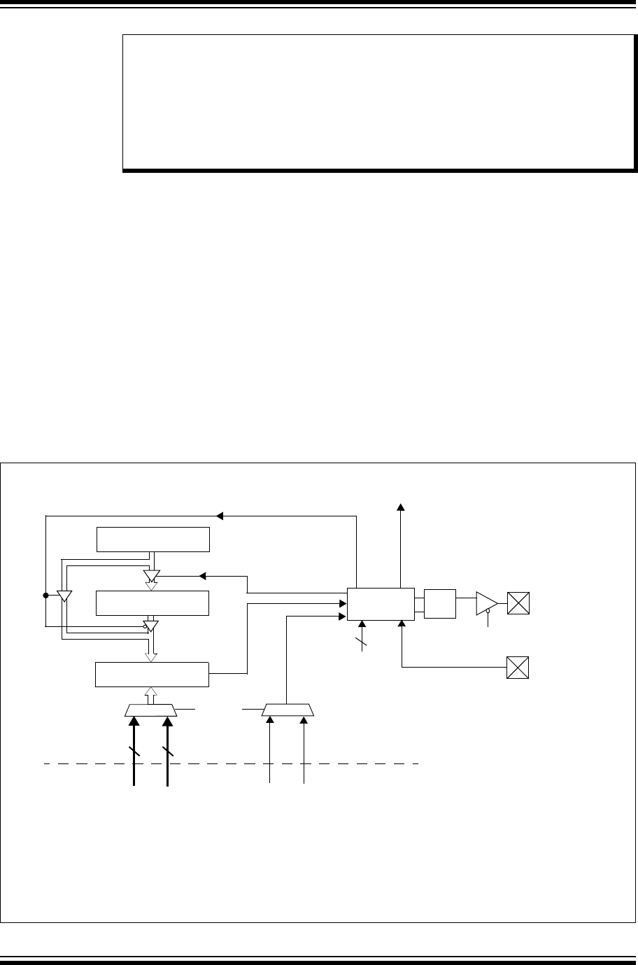
PIC32 Family Reference Manual
DS61111E-page 16-2 © 2011 Microchip Technology Inc.
16.1 INTRODUCTION
The Output Compare module is primarily used to generate a single pulse or a series of pulses in
response to selected time base events.
The following are some of the key features of the Output Compare module:
•Multiple Output Compare modules in a device
•Single and Dual Compare modes
•Single and continuous output pulse generation
•Pulse-Width Modulation (PWM) mode
•Programmable interrupt generation on compare event
•Hardware-based PWM Fault detection and automatic output disable
•Programmable selection of 16 or 32-bit time bases
• Operate from either of two available 16-bit time bases or a single 32-bit time base
Figure 16-1 illustrates the block diagram of an Output Compare module.
Figure 16-1: Output Compare Module Block Diagram
Note: This family reference manual section is meant to serve as a complement to device
data sheets. Depending on the device variant, this manual section may not apply to
all PIC32 devices.
Please consult the note at the beginning of the “Output Compare” chapter in the
current device data sheet to check whether this document supports the device you
are using.
Device data sheets and family reference manual sections are available for
download from the Microchip Worldwide Web site at: http://www.microchip.com
OCxR(1)
Comparator
Output
Logic
QS
R
OCM<2:0>
Output Enable
OCx(1)
Set Flag bit
OCxIF(1)
OCxRS(1)
Mode Select
3
Note 1: Where ‘x’ is shown, reference is made to the registers associated with the respective output compare
channels 1 through 5.
2: OCFA pin controls OC1-OC4 channels. OCFB pin controls OC5 channels.
3: Each output compare channel can use one of two selectable 16-bit time bases or a single 32-bit time base.
Refer to the specific device data sheet for the time bases associated with the module.
01
OCTSEL 01
16
16
OCFA or OCFB(2)
TMR register inputs
from time bases(3)
Period match signals
from time bases(3)
© 2011 Microchip Technology Inc. DS61111E-page 16-3
Section 16. Output Compare
Output Compare
16
16.2 OUTPUT COMPARE REGISTERS
Each Output Compare module consists of the following Special Function Registers (SFRs):
•OCxCON: Output Compare ‘x’ Control Register
•OCxR: Output Compare ‘x’ Compare Register
•OCxRS: Output Compare ‘x’ Secondary Compare Register
Tabl e 16-1 summarizes all output compare related registers. Corresponding registers appear
after the summary, followed by a detailed description of each register.
Note: Each PIC32 family device variant may have one or more Output Compare modules.
An ‘x’ used in the names of pins, control/status bits and registers denotes the
particular module. Refer to the specific device data sheets for more details.
Table 16-1: Output Compare SFR Summary
Name Bit
31/23/15/7
Bit
30/22/14/6
Bit
29/21/13/5
Bit
28/20/12/4
Bit
27/19/11/3
Bit
26/18/10/2
Bit
25/17/9/1
Bit
24/16/8/0
OCxCON(1,2,3) 31:24 — — — — — — — —
23:16 — — — — — — — —
15:8 ON —SIDL — — — — —
7:0 — — OC32 OCFLT OCTSEL OCM<2:0>
OCxR(1,2,3) 31:24 OCxR<31:24>
23:16 OCxR<23:16>
15:8 OCxR<15:8>
7:0 OCxR<7:0>
OCxRS(1,2,3) 31:24 OCxRS<31:24>
23:16 OCxRS<23:16>
15:8 OCxRS<15:8>
7:0 OCxRS<7:0>
Legend: — = unimplemented, read as ‘0’.
Note 1: This register has an associated Clear register at an offset of 0x4 bytes. The Clear register has the same name with CLR
appended to the register name (e.g., OCxCONCLR). Writing a ‘1’ to any bit position in the Clear register will clear valid
bits in the associated register. Reads from the Clear register should be ignored.
2: This register has an associated Set register at an offset of 0x8 bytes. The Set register has the same name with SET
appended to the register name (e.g., OCxCONSET). Writing a ‘1’ to any bit position in the Set register will set valid bits
in the associated register. Reads from the Set register should be ignored.
3: This register has an associated Invert register at an offset of 0xC bytes. The Invert register has the same name with INV
appended to the register name (e.g., OCxCONINV). Writing a ‘1’ to any bit position in the Invert register will invert valid
bits in the associated register. Reads from the Invert register should be ignored.

PIC32 Family Reference Manual
DS61111E-page 16-4 © 2011 Microchip Technology Inc.
Register 16-1: OCxCON: Output Compare ‘x’ Control Register
Bit
Range
Bit
31/23/15/7
Bit
30/22/14/6
Bit
29/21/13/5
Bit
28/20/12/4
Bit
27/19/11/3
Bit
26/18/10/2
Bit
25/17/9/1
Bit
24/16/8/0
31:24 U-0 U-0 U-0 U-0 U-0 U-0 U-0 U-0
— — — — — — — —
23:16 U-0 U-0 U-0 U-0 U-0 U-0 U-0 U-0
— — — — — — — —
15:8 R/W-0 U-0 R/W-0 U-0 U-0 U-0 U-0 U-0
ON(1) —SIDL — — — — —
7:0 U-0 U-0 R/W-0 R-0 R/W-0 R/W-0 R/W-0 R/W-0
— — OC32 OCFLT(2) OCTSEL OCM<2:0>
Legend:
R = Readable bit W = Writable bit U = Unimplemented bit, read as ‘0’
-n = Value at POR ‘1’ = Bit is set ‘0’ = Bit is cleared x = Bit is unknown
bit 31-16 Unimplemented: Read as ‘0’
bit 15 ON: Output Compare Peripheral On bit(1)
1 = Output compare peripheral is enabled
0 = Output compare peripheral is disabled and not drawing current. SFR modifications are allowed. The
status of other bits in this register are not affected by setting or clearing this bit
bit 14 Unimplemented: Read as ‘0’
bit 13 SIDL: Stop in Idle Mode bit
1 = Discontinue operation when CPU enters Idle mode
0 = Continue operation in Idle mode
bit 12-6 Unimplemented: Read as ‘0’
bit 5 OC32: 32-bit Compare Mode bit
1 = OCxR<31:0> and/or OCxRS<31:0> is used for comparisions to the 32-bit timer source
0 = OCxR<15:0> and OCxRS<15:0> are used for comparisons to the 16-bit timer source
bit 4 OCFLT: PWM Fault Condition Status bit(2)
1 = PWM Fault condition has occurred (cleared in hardware only)
0 = No PWM Fault condition has occurred
bit 3 OCTSEL: Output Compare Timer Select bit
1 = Timer3 is the clock source for this Output Compare module
0 = Timer2 is the clock source for this Output Compare module
Refer to the specific device data sheet for the time bases that are available to the Output Compare module.
bit 2-0 OCM<2:0>: Output Compare Mode Select bits
111 = PWM mode on OCx; Fault pin enabled
110 = PWM mode on OCx; Fault pin disabled
101 = Initialize OCx pin low; generate continuous output pulses on OCx pin
100 = Initialize OCx pin low; generate single output pulse on OCx pin
011 = Compare event toggles OCx pin
010 = Initialize OCx pin high; compare event forces OCx pin low
001 = Initialize OCx pin low; compare event forces OCx pin high
000 = Output compare peripheral is disabled but continues to draw current
Note 1: When using 1:1 PBCLK divisor, the user’s software should not read/write the peripheral’s SFRs in the
SYSCLK cycle immediately following the instruction that clears the module’s ON bit.
2: This bit is only used when OCM<2:0> = 111 and reads as ‘0’ in modes other than PWM mode.

© 2011 Microchip Technology Inc. DS61111E-page 16-5
Section 16. Output Compare
Output Compare
16
Register 16-2: OCxR: Output Compare ‘x’ Compare Register
Bit
Range
Bit
31/23/15/7
Bit
30/22/14/6
Bit
29/21/13/5
Bit
28/20/12/4
Bit
27/19/11/3
Bit
26/18/10/2
Bit
25/17/9/1
Bit
24/16/8/0
31:24 R/W-0 R/W-0 R/W-0 R/W-0 R/W-0 R/W-0 R/W-0 R/W-0
OCR<31:24>
23:16 R/W-0 R/W-0 R/W-0 R/W-0 R/W-0 R/W-0 R/W-0 R/W-0
OCR<23:16>
15:8 R/W-0 R/W-0 R/W-0 R/W-0 R/W-0 R/W-0 R/W-0 R/W-0
OCR<15:8>
7:0 R/W-0 R/W-0 R/W-0 R/W-0 R/W-0 R/W-0 R/W-0 R/W-0
OCR<7:0>
Legend:
R = Readable bit W = Writable bit U = Unimplemented bit, read as ‘0’
-n = Value at POR ‘1’ = Bit is set ‘0’ = Bit is cleared x = Bit is unknown
bit 31-16 OCxR<31:16>: Upper 16 bits of 32-bit compare value, when OC32 (OCxCON<5>) = 1
bit 15-0 OCxR<15:0>: Lower 16 bits of 32-bit compare value or entire 16 bits of 16-bit compare value when
OC32 = 0
Register 16-3: OCxRS: Output Compare ‘x’ Secondary Compare Register
Bit
Range
Bit
31/23/15/7
Bit
30/22/14/6
Bit
29/21/13/5
Bit
28/20/12/4
Bit
27/19/11/3
Bit
26/18/10/2
Bit
25/17/9/1
Bit
24/16/8/0
31:24 R/W-0 R/W-0 R/W-0 R/W-0 R/W-0 R/W-0 R/W-0 R/W-0
OCRS<31:24>
23:16 R/W-0 R/W-0 R/W-0 R/W-0 R/W-0 R/W-0 R/W-0 R/W-0
OCRS<23:16>
15:8 R/W-0 R/W-0 R/W-0 R/W-0 R/W-0 R/W-0 R/W-0 R/W-0
OCRS<15:8>
7:0 R/W-0 R/W-0 R/W-0 R/W-0 R/W-0 R/W-0 R/W-0 R/W-0
OCRS<7:0>
Legend:
R = Readable bit W = Writable bit U = Unimplemented bit, read as ‘0’
-n = Value at POR ‘1’ = Bit is set ‘0’ = Bit is cleared x = Bit is unknown
bit 31-16 OCxRS<31:16>: Upper 16 bits of 32-bit compare value when OC32 (OCxCON<5>) = 1
bit 15-0 OCxRS<15:0>: Lower 16 bits of 32-bit compare value or entire 16 bits of 16-bit compare value when
OC32 = 0

PIC32 Family Reference Manual
DS61111E-page 16-6 © 2011 Microchip Technology Inc.
16.3 OPERATION
Each Output Compare module has the following modes of operation:
•Single Compare Match mode
- With output drive high
- With output drive low
- With output drive toggles
•Dual Compare Match mode
-With single output pulse
-With continuous output pulses
•Simple Pulse-Width Modulation mode
-Without Fault protection input
-With Fault protection input
16.3.1 Single Compare Match Mode
When the OCM<2:0> control bits (OCxCON<2:0>) are set to ‘001’, ‘010’ or ‘011’, the selected
output compare channel is configured for one of three Single Output Compare Match modes. The
compare time base must also be enabled.
In the Single Compare mode, the OCxR register is loaded with a value and is compared to the
selected incrementing timer register, TMRy. On a compare match event, one of the following
events will take place:
•Compare forces OCx pin high; initial state of pin is low. Interrupt is generated on the single
compare match event.
•Compare forces OCx pin low; initial state of pin is high. Interrupt is generated on the single
compare match event.
•Compare toggles OCx pin. Toggle event is continuous and an interrupt is generated for
each toggle event.
Note 1: The Output Compare module must be turned OFF by the user application (i.e.,
clear the OCM<2:0> bits (OCxCON<2:0>)) before switching to a new mode.
Changing modes while the module is in operation may produce unexpected results.
2: In this section, a reference to any SFRs associated with the selected timer source
is indicated by a ‘y’ suffix. For example, PR2 is the Period register for the selected
timer source, while TyCON is the Timer Control register for the selected timer
source.

© 2011 Microchip Technology Inc. DS61111E-page 16-7
Section 16. Output Compare
Output Compare
16
16.3.1.1 Compare Mode Output Driven High
To con fig ure t he Ou tpu t Com pa re mo dul e for t h is mode, set the OCM<2:0> control bits to ‘001’.
The compare time base must also be enabled. Once this mode has been enabled, the output pin,
OCx, will be driven low and remain low until a match occurs between the TMRy and OCxR
registers. In Figure 16-2, note the following key timing events:
• The OCx pin is driven high one peripheral clock after the compare match occurs between
the compare time base and the OCxR register. The OCx pin will remain high until a mode
change has been made or the module is disabled.
•The compare time base will count up to the value contained in the associated period
register, and then reset to 0x0000 on the next PBCLK
•The respective channel interrupt flag, OCxIF (see the IFS0 register for the position of the
interrupt flag bit for each of the output compare channels), is asserted when the OCx pin is
driven high
Figure 16-2: Single Compare Mode: Set OCx High on Compare Match Event (16-Bit Mode)
Figure 16-3: Single Compare Mode: Set OCx High on Compare Match Event (32-Bit Mode)
OCxIF
4000 0001
3001 3002 3003 30043000
TMRy 0000
Cleared by User
1 PBCLK Period
4000
3002
PRy
OCxR
3FFF
OCx pin
TMRy Resets Here
Note: An ‘x’ represents the output compare channel number. A ‘y’ represents the time base number.
OCxIF
0004: 0000:
0003: 0003: 0003: 0003:0003:
TMRy 0000:
Cleared by User
1 PBCLK Period
0004:
0003:
PRy
OCxR
0003:
OCx pin
TMRy Resets Here
Note: An ‘x’ represents the output compare channel number. A ‘y’ represents the time base number.
0002
0000 0001 0002 0003 0004
0000
0000
FFFF 0000 0001
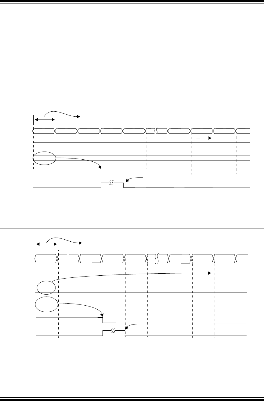
PIC32 Family Reference Manual
DS61111E-page 16-8 © 2011 Microchip Technology Inc.
16.3.1.2 Compare Mode Output Driven Low
To con fig ure t he Ou tpu t Com pa re mo dul e f or th is mode, set the OCM<2:0> control bits to ‘010’.
The compare time base must also be enabled. Once this mode has been enabled, the output pin,
OCx, will be driven high and remain high until a match occurs between the Timer and OCxR
registers. In Figure 16-4, note the following key timing events:
•The OCx pin is driven low by one PBCLK after the compare match occurs between the
compare time base and the OCxR register. The OCx pin will remain low until a mode
change has been made or the module is disabled.
•The compare time base will count up to the value contained in the associated period
register, and then reset to 0x0000 on the next PBCLK
•The respective channel interrupt flag, OCxIF, is asserted when the OCx pin is driven low
Figure 16-4: Single Compare Mode: Force OCx Low on Compare Match Event (16-Bit Mode)
Figure 16-5: Single Compare Mode: Set OCx Low on Compare Match Event (32-Bit Mode)
OCxIF
4C00 0001
47FF 4800 4801 480247FE
TMRy 0000
Cleared by User
1 PBCLK Period
4C00
4800
PRy
OCxR
4BFF
OCx pin
TMRy Resets Here
Note: An ‘x’ represents the output compare channel number. A ‘y’ represents the time base number.
OCxIF
0004: 0000:
0003: 0003: 0003: 0003:0003:
TMRy 0000:
Cleared by User
1 PBCLK Period
0004:
0003:
PRy
OCxR
0003:
OCx pin
TMRy Resets Here
Note: An ‘x’ represents the output compare channel number. A ‘y’ represents the time base number.
0002
0000 0001 0002 0003 0004
0000
0000
FFFF 0000 0001
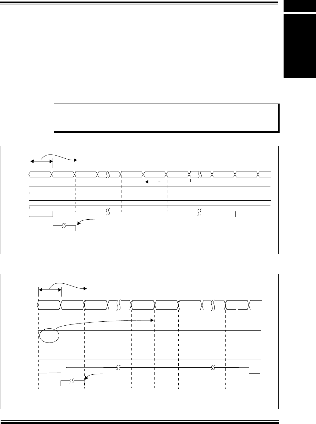
© 2011 Microchip Technology Inc. DS61111E-page 16-9
Section 16. Output Compare
Output Compare
16
16.3.1.3 Single Compare Mode Toggle Output
To con fig ure t he Ou tpu t Com pa re mo dul e for t h is mode, set the OCM<2:0> control bits to ‘011’.
In addition, Timer2 or Timer3 must be selected and enabled. Once this mode has been enabled,
the output pin, OCx, will be initially driven low, and then toggle on each and every subsequent
match event between the Timer and OCxR registers. In Figure 16-6 and Figure 16-8, note the
following key timing events:
•The OCx pin is toggled one PBCLK after the compare match occurs between the compare
time base and the OCxR register. The OCx pin will remain at this new state until the next
toggle event, or until a mode change has been made or the module is disabled.
•The compare time base will count up to the contents in the period register, and then reset to
0x0000 on the next PBCLK
• The respective channel interrupt flag, OCxIF, is asserted when the OCx pin is toggled
Figure 16-6: Single Compare Mode: Toggle Output on Compare Match Event (16-Bit Mode)
Figure 16-7: Single Compare Mode: Toggle Output on Compare Match Event (32-Bit Mode)
Note: The internal OCx pin output logic is set to a logic ‘0’ on a device Reset. However,
the operational OCx pin state for the Toggle mode can be set by the user application.
Example 16-1 shows a code example for defining the desired initial OCx pin state in
the Toggle mode of operation.
OCxIF
0500
0501 0502 0600
0500
TMRy
1 PBCLK Period
0600
0500
PRy
OCxR
0001
OCx pin
TMRy Resets Here
0000 0501 0502
Cleared by User
Note: An ‘x’ represents the output compare channel number. A ‘y’ represents the time base number.
OCxIF
0005:
0005: 0005: 0000:0006:0005:
TMRy 0005:
Cleared by User
1 PBCLK Period
0006:
0005:
PRy
OCxR
0000:
OCx pin
TMRy Resets Here
Note: An ‘x’ represents the output compare channel number. A ‘y’ represents the time base number.
0000
0000 0001 0002 00000000
0000
0001 0000 0001
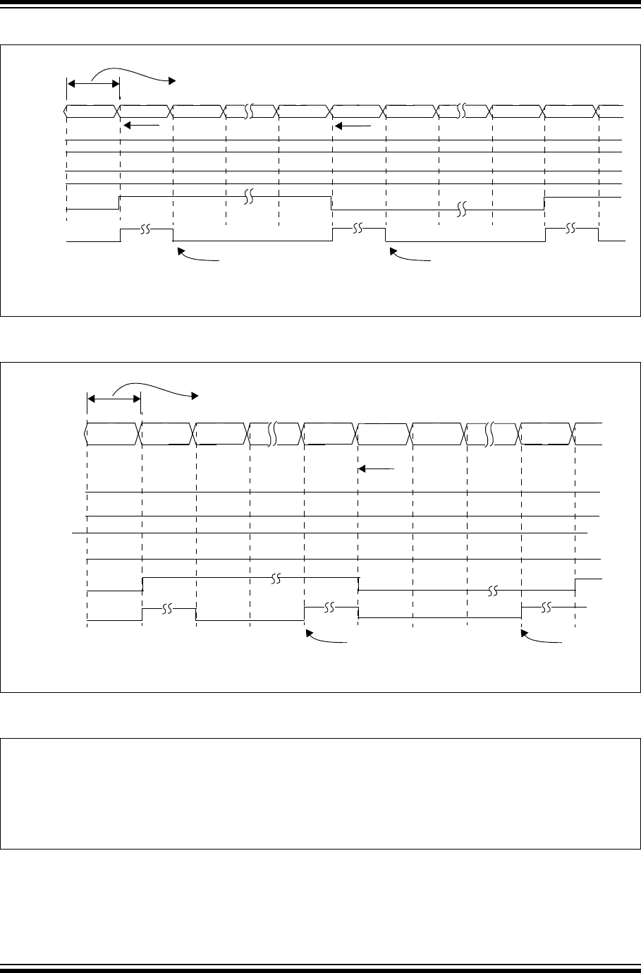
PIC32 Family Reference Manual
DS61111E-page 16-10 © 2011 Microchip Technology Inc.
Figure 16-8: Single Compare Mode: Toggle Output on Compare Match Event (PRy = OCxR, 16-Bit Mode)
Figure 16-9: Single Compare Mode: Toggle Output on Compare Match Event (PRy = OCxR, 32-Bit Mode)
Example 16-1: Compare Mode Toggle Mode Pin State Setup (16-Bit Mode)
OCxIF
0500
0000 0001 0500
0500
TMRy
1 PBCLK Period
0500
0500
PRy
OCxR
0001
OCx pin
TMRy Resets Here
0000 0000 0001
TMRy Resets Here
Note: An ‘x’ represents the output compare channel number. A ‘y’ represents the time base number.
Cleared by User Cleared by User
OCxIF
0000:
0000: 0000: 0000:
0005:0005:
TMRy 0005:
Cleared by User
1 PBCLK Period
0005:
0005:
PRy
OCxR
0000:
OCx pin
TMRy Resets Here
Note: An ‘x’ represents the output compare channel number. A ‘y’ represents the time base number.
0000
0000 0000 0001 0000
0000
0000
0001 0000 0000
Cleared by User
// The following code example illustrates how to define the initial
// OC1 pin state for the output compare toggle mode of operation.
// Toggle mode with initial OC1 pin state set low
OC1CON = 0x0001; // Configure module for OC1 pin low, toggle high
OC1CONSET = 0x8000; // Enable OC1 module

© 2011 Microchip Technology Inc. DS61111E-page 16-11
Section 16. Output Compare
Output Compare
16
Example 16-2: Compare Mode Toggle Mode Pin State Setup (32-Bit Mode)
Example 16-3 shows example code for the configuration and interrupt service of the Single
Compare mode toggle event.
Example 16-3: Compare Mode Toggle Setup and Interrupt Servicing (16-Bit Mode)
// The following code example illustrates how to define the initial
// OC1 pin state for the output compare toggle mode of operation.
// Toggle mode with initial OC1 pin state set low
OC1CON = 0x0021; // Configure module for OC1 pin low, toggle high,
// 32-bit mode
OC1CONSET = 0x8000; // Enable OC1 module
// The following code example will set the Output Compare 1 module
// for interrupts on the toggle event and select Timer2 as the clock
// source for the compare time base.
T2CON = 0x0010; // Configure Timer2 for a prescaler of 2
OC1CON = 0x0000; // Turn off OC1 while doing setup.
OC1CON = 0x0003; // Configure for compare toggle mode
OC1R = 0x0500; // Initialize Compare Register 1
PR2 = 0x0500; // Set period
// Configure int
IFS0CLR = 0x0040; // Clear the OC1 interrupt flag
IEC0SET = 0x040; // Enable OC1 interrupt
IPC1SET = 0x001C0000; // Set OC1 interrupt priority to 7,
// the highest level
IPC1SET = 0x00030000; // Set Subpriority to 3, maximum
T2CONSET = 0x8000; // Enable Timer2
OC1CONSET = 0x8000; // Enable OC1
// Example code for Output Compare 1 ISR:
void __ISR(_OUTPUT_COMPARE_1_VECTOR, ipl7) OC1_IntHandler (void)
{
// insert user code here
IFS0CLR = 0x0040; // Clear the OC1 interrupt flag
}

PIC32 Family Reference Manual
DS61111E-page 16-12 © 2011 Microchip Technology Inc.
Example 16-4: Compare Mode Toggle Setup and Interrupt Servicing (32-Bit Mode)
// The following code example will set the Output Compare 1 module
// for interrupts on the toggle event and select the Timer2/Timer3 pair as
// the 32-bit as the clock source for the compare time base.
T2CON = 0x0018; // Configure Timer2 for 32-bit operation
// with a prescaler of 2. The Timer2/Timer3
// pair is accessed via registers associated
// with the Timer2 register
OC1CON = 0x0000; // Turn off OC1 while doing setup.
OC1CON = 0x0023; // Configure for compare toggle mode
OC1R = 0x00500000; // Initialize Compare Register 1
PR2 = 0x00500000; // Set period (PR2 is now 32-bits wide)
// configure int
IFS0CLR = 0x00000040; // Clear the OC1 interrupt flag
IFS0SET = 0x00000040; // Enable OC1 interrupt
IPC1SET = 0x001C0000; // Set OC1 interrupt priority to 7,
// the highest level
IPC1SET = 0x00030000; // Set Subpriority to 3, maximum
T2CONSET = 0x8000; // Enable Timer2
OC1CONSET = 0x8000; // Enable OC1
// Example code for Output Compare 1 ISR:
void__ISR (_OUTPUT_COMPARE_1_VECTOR, ipl7) OC1_IntlHandler (void)
{
// Insert user code here
IFS0CLR = 0x0040; // Clear the OC1 interrupt flag
}

© 2011 Microchip Technology Inc. DS61111E-page 16-13
Section 16. Output Compare
Output Compare
16
16.3.2 Dual Compare Match Modes
When the OCM<2:0> control bits are set to ‘100’ or ‘101’, the selected output compare channel
is configured for one of two Dual Compare Match modes:
•Single Output Pulse mode
•Continuous Output Pulse mode
In these Dual Compare modes, the module uses both the OCxR and OCxRS registers for the
compare match events. The OCxR register is compared against the incrementing timer count,
TMRy, and the leading (rising) edge of the pulse is generated at the OCx pin on a compare match
event. The OCxRS register is then compared to the same incrementing timer count, TMRy, and
the trailing (falling) edge of the pulse is generated at the OCx pin on a compare match event.
16.3.2.1 Dual Compare Mode: Single Output Pulse
To c on f ig u re th e O ut put C ompare mo dul e fo r the Single Output Pulse mode, set the OCM<2:0>
control bits to ‘100’. In addition, the compare time base must be selected and enabled. Once this
mode has been enabled, the output pin, OCx, will be driven low and remain low until a match
occurs between the time base and OCxR registers. In Figure 16-10 and Figure 16-12, note the
following key timing events:
• The OCx pin is driven high one peripheral clock after the compare match occurs between
the compare time base and the OCxR register. The OCx pin will remain high until the next
match event occurs between the time base and the OCxRS register. At this time, the pin
will be driven low. The OCx pin will remain low until a mode change has been made or the
module is disabled.
•The compare time base will count up to the value contained in the associated period
register, and then reset to 0x0000 on the next instruction clock
•If the time base period register contents are less than the OCxRS register contents, no
falling edge of the pulse is generated. The OCx pin will remain high until OCxRS PR2, or
a mode change or Reset condition has occurred.
•The respective channel interrupt flag, OCxIF, is asserted when the OCx pin is driven low
(falling edge of single pulse)
Figure 16-10 depicts the General Dual Compare mode generating a single output pulse.
Figure 16-12 depicts another timing example where OCxRS > PR2. In this example, no falling
edge of the pulse is generated because the compare time base resets before counting up to
0x4100.
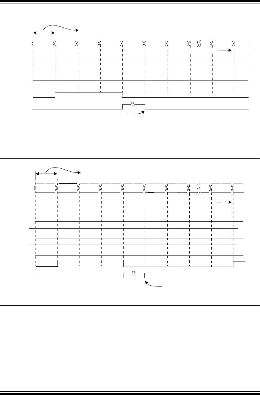
PIC32 Family Reference Manual
DS61111E-page 16-14 © 2011 Microchip Technology Inc.
Figure 16-10: Dual Compare Mode (16-Bit Mode)
Figure 16-11: Dual Compare Mode (32-Bit Mode)
OCxIF
0000
3001 3002 3003 30043000
TMRy 4000
Cleared by User
Note 1: An ‘x’ represents the output compare channel number. A ‘y’ represents the time base number.
2: OCxR = Compare Register; OCxRS = Secondary Compare Register.
1 PBCLK Period
4000
3000
PRy
OCxR
3006
OCx pin
TMRy Resets Here
3003
OCxRS
3005
OCxIF
0000:
0003: 0003: 0003:
0003:0003:
TMRy 0004:
1 PBCLK Period
0004:
0003:
PRy
OCxR
0003:
OCx pin
TMRy Resets Here
Note: An ‘x’ represents the output compare channel number. A ‘y’ represents the time base number.
0000
0000 0001 0002 0005
0004
0000
0006 0000 0000
Cleared by User
0003:
0003
0003:
OCxRS
0003

© 2011 Microchip Technology Inc. DS61111E-page 16-15
Section 16. Output Compare
Output Compare
16
Figure 16-12: Dual Compare Mode: Single Output Pulse (OCxRS > PRy, 16-Bit Mode)
Figure 16-13: Dual Compare Mode: Single Output Pulse (OCxRS > PRy, 32-Bit Mode)
OCxIF
0000
3001 3002 3003 30043000
TMRy 4000
1 PBCLK Period
4000
3000
PRy
OCxR
3006
OCx pin
TMRy Resets Here
4100
OCxRS
3005
Note 1: An ‘x’ represents the output compare channel number. A ‘y’ represents the time base number.
2: OCxR = Compare Register; OCxRS = Secondary Compare Register.
Compare Interrupt does not occur
OCxIF
0000:
0003: 0003: 0003:
0003:0003:
TMRy 0004:
1 PBCLK Period
0004:
0003:
PRy
OCxR
0003:
OCx pin
TMRy Resets Here
Note: An ‘x’ represents the output compare channel number. A ‘y’ represents the time base number.
0000
0000 0001 0002 0005
0004
0000
0006 0000 0000
0003:
0003
0004:
OCxRS
1000
No Compare Interrupt is generated

PIC32 Family Reference Manual
DS61111E-page 16-16 © 2011 Microchip Technology Inc.
16.3.2.2 Setup for Single Output Pulse Generation
When the OCM<2:0> control bits (OCxCON<2:0>) are set to ‘100’, the selected output compare
channel initializes the OCx pin to the low state and generates a single output pulse.
To gen era te a si n gl e o ut put p uls e, th e f ol low ing s teps are required (these steps assume the timer
source is initially turned off, but this is not a requirement for module operation):
1. Determine the peripheral clock cycle time.
2. Calculate the time to the rising edge of the output pulse relative to the TMRy start value
(0x0000).
3. Calculate the time to the falling edge of the pulse based on the desired pulse width and
the time to the rising edge of the pulse.
4. Write the values computed in steps 2 and 3 above into the compare register, OCxR, and
the secondary compare register, OCxRS, respectively.
5. Set the timer period register, PRy, to value equal to or greater than value in OCxRS, the
secondary compare register.
6. Set OCM<2:0> = 100 and the OCTSEL bit (OCxCON<3>) to the desired timer source.
The OCx pin state will now be driven low.
7. Set the ON bit (TyCON<15>) to ‘1’, to enable the timer.
8. Upon the first match between TMRy and OCxR, the OCx pin will be driven high.
9. When the incrementing timer, TMRy, matches the secondary compare register, OCxRS,
the second and trailing edge (high-to-low) of the pulse is driven onto the OCx pin. No
additional pulses are driven onto the OCx pin and it remains at low. As a result of the
second compare match event, the OCxIF interrupt flag bit is set, which will result in an
interrupt (if it is enabled by setting the OCxIE bit). For more information on peripheral
interrupts, refer to Section 8. “Interrupts” (DS61108).
10. To initiate another single pulse output, change the timer and compare register settings, if
needed, and then issue a write to set the OCM<2:0> control bits (OCxCON<2:0>) to ‘100’.
Disabling and re-enabling of the timer and clearing the TMRy register are not required, but
may be advantageous for defining a pulse from a known event time boundary.
The Output Compare module does not have to be disabled after the falling edge of the output
pulse. Another pulse can be initiated by rewriting the value of the OCxCON register.

© 2011 Microchip Technology Inc. DS61111E-page 16-17
Section 16. Output Compare
Output Compare
16
Examples 16-5 and 16-6 show example code for configuration of the single output pulse event.
Example 16-5: Single Output Pulse Setup and Interrupt Servicing (16-Bit Mode)
// The following code example will set the Output Compare 1 module
// for interrupts on the single pulse event and select Timer2
// as the clock source for the compare time base.
T2CON = 0x0010; // Configure Timer2 for a prescaler of 2
OC1CON = 0x0000; // Turn off OC1 while doing setup.
OC1CON = 0x0004; // Configure for single pulse mode
OC1R = 0x3000; // Initialize primary Compare Register
OC1RS = 0x3003; // Initialize secondary Compare Register
PR2 = 0x3003; // Set period (PR2 is now 32-bits wide)
// configure int
IFS0CLR = 0x00000040; // Clear the OC1 interrupt flag
IFS0SET = 0x00000040; // Enable OC1 interrupt
IPC1SET = 0x001C0000; // Set OC1 interrupt priority to 7,
// the highest level
IPC1SET = 0x00030000; // Set Subpriority to 3, maximum
T2CONSET = 0x8000; // Enable Timer2
OC1CONSET = 0x8000; // Enable OC1
// Example code for Output Compare 1 ISR:
void__ISR(_OUTPUT_COMPARE_1_VECTOR, ipl7) OC1_IntHandler (void)
{
// Insert user code here
IFS0CLR = 0x0040; // Clear the OC1 interrupt flag
}

PIC32 Family Reference Manual
DS61111E-page 16-18 © 2011 Microchip Technology Inc.
Example 16-6: Single Output Pulse Setup and Interrupt Servicing (32-Bit Mode)
// The following code example will set the Output Compare 1 module
// for interrupts on the single pulse event and select Timer2
// as the clock source for the compare time base.
T2CON = 0x0018; // Configure Timer2 for 32-bit operation
// with a prescaler of 2. The Timer2/Timer3
// pair is accessed via registers associated
// with the Timer2 register
OC1CON = 0x0000; // Turn off OC1 while doing setup.
OC1CON = 0x0004; // Configure for single pulse mode
OC1R = 0x00203000; // Initialize primary Compare Register
OC1RS = 0x00203003; // Initialize secondary Compare Register
PR2 = 0x00500000; // Set period (PR2 is now 32-bits wide)
// configure int
IFS0CLR = 0x00000040; // Clear the OC1 interrupt flag
IFS0SET = 0x00000040; // Enable OC1 interrupt
IPC1SET = 0x001C0000; // Set OC1 interrupt priority to 7,
// the highest level
IPC1SET = 0x00030000; // Set Subpriority to 3, maximum
T2CONSET = 0x8000; // Enable Timer2
OC1CONSET = 0x8000; // Enable OC1
// Example code for Output Compare 1 ISR:
void__ISR(_OUTPUT_COMPARE_1_VECTOR, ipl7) OC1_IntHandler (void)
{
// insert user code here
IFS0CLR = 0x0040; // Clear the OC1 interrupt flag
}

© 2011 Microchip Technology Inc. DS61111E-page 16-19
Section 16. Output Compare
Output Compare
16
16.3.2.3 Special Cases for Dual Compare Mode Generating a Single Output Pulse
Depending on the relationship of the OCxR, OCxRS and PRy values, the Output Compare
module has a few unique conditions that should be understood. These special conditions are
specified in Ta bl e 16-2, along with the resulting behavior of the module.
Table 16-2: Special Cases for Dual Compare Mode Generating a Single Output Pulse(1)
SFR Logical
Relationship
Special
Conditions Operation Output
at OCx
PRy OCxRS and
OCxRS > OCxR
OCxR = 0
Initialize TMRy = 0
In the first iteration of the TMRy counting from 0x0000 up
to PRy, the OCx pin remains low; no pulse is generated.
After the TMRy resets to zero (on period match), the OCx
pin goes high due to a match with OCxR. Upon the next
TMRy to OCxRS match, the OCx pin goes low and
remains there. The OCxIF bit will be set as a result of the
second compare.
There are two alternative initial conditions to consider:
1. Initialize TMRy = 0 and set OCxR 1.
2. Initialize TMRy = PRy (PRy > 0) and set OCxR = 0.
Pulse will be
delayed by the
value in the PRy
register,
depending on
setup
PRy OCxR and
OCxR OCxRS
OCxR 1 and
PRy 1
TMRy counts up to OCxR and on a compare match event
(i.e., TMRy = OCxR), the OCx pin is driven to a high
state. TMRy then continues to count and eventually
resets on a period match (i.e., PRy = TMRy). The timer
then restarts from 0x0000 and counts up to OCxRS. On a
compare match event (i.e., TMRy = OCxRS), the OCx pin
is driven to a low state. The OCxIF bit will be set as a
result of the second compare.
Pulse
OCxRS > PRy and
PRy OCxR
None Only the rising edge will be generated at the OCx pin.
The OCxIF will not be set.
Rising edge/
transition to high
OCxR > PRy None Unsupported mode; timer resets prior to match condition. Remains low
Legend: OCxR = Compare Register OCxRS = Secondary Compare Register TMRy = Timery Count
PRy = Timery Period Register
Note 1: In all of these cases, the TMRy register is assumed to be initialized to 0x0000.
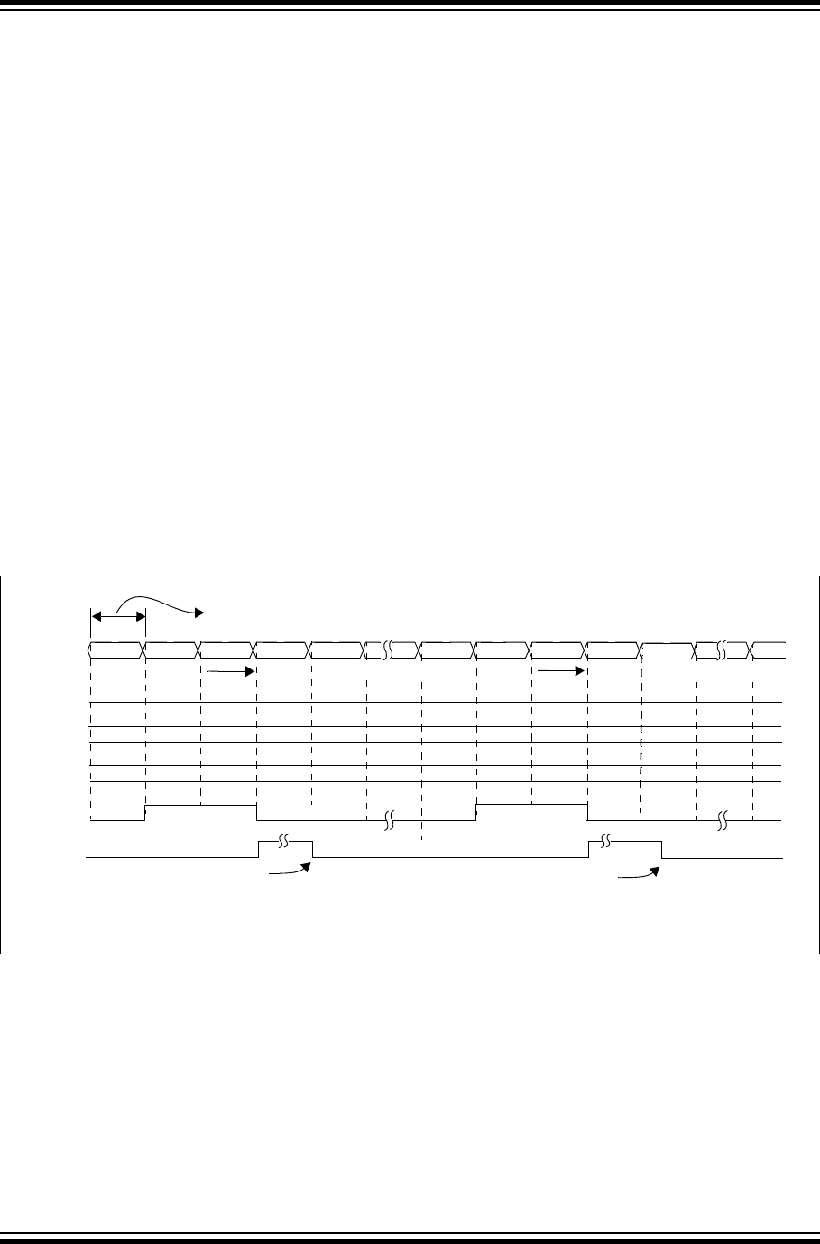
PIC32 Family Reference Manual
DS61111E-page 16-20 © 2011 Microchip Technology Inc.
16.3.2.4 Dual Compare Mode: Continuous Output Pulses
To con fig ure t he Ou tpu t Com pa re mo dul e f or th is mode, set the OCM<2:0> control bits to ‘101’.
In addition, the compare time base must be selected and enabled. Once this mode has been
enabled, the output pin, OCx, will be driven low and remain low until a match occurs between the
compare time base and OCxR register. In Figure 16-14 and Figure 16-16, note the following key
timing events:
•The OCx pin is driven high one PBCLK after the compare match occurs between the
compare time base and OCxR register. The OCx pin will remain high until the next match
event occurs between the time base and the OCxRS register, at which time the pin will be
driven low. This pulse generation sequence of a low-to-high and high-to-low edge will
repeat on the OCx pin without further user intervention.
•Continuous pulses will be generated on the OCx pin until a mode change is made or the
module is disabled
•The compare time base will count up to the value contained in the associated period
register, and then reset to 0x0000 on the next instruction clock
•If the compare time base period register value is less than the OCxRS register value, no
falling edge is generated. The OCx pin will remain high until OCxRS PRy, a mode change
is made, or the device is Reset.
•The respective channel interrupt flag, OCxIF, is asserted when the OCx pin is driven low
(falling edge of single pulse)
General Dual Compare mode generating a continuous output pulse is illustrated in Figure 16-14.
Figure 16-16 depicts another timing example where OCxRS > PRy. In this example, no falling
edge of the pulse is generated, because the time base will reset before counting up to the
contents of OCxRS.
Figure 16-14: Dual Compare Mode: Continuous Output Pulse (PRy = OCxRS, 16-Bit Mode)
Note 1: An ‘x’ represents the output compare channel number. A ‘y’ represents the time base number.
2: OCxR = Compare Register; OCxRS = Secondary Compare Register.
OCxIF
0000
3001 3002 0000 00013000
TMRy 3002
Cleared by User
1 PBCLK Period
3002
3000
PRy
OCxR
3000
OCx pin
3002
OCxRS
3001 3000
0001
TMRy Resets Here due to PRx match TMRy Resets Here ...
Cleared by User

© 2011 Microchip Technology Inc. DS61111E-page 16-21
Section 16. Output Compare
Output Compare
16
Figure 16-15: Dual Compare Mode: Continuous Output Pulse (PRy = OCxRS, 32-Bit Mode)
Figure 16-16: Dual Compare Mode: Continuous Output Pulse (PRy = OCxRS, 16-Bit Mode)
OCxIF
0000:
0003: 0000:
0003:
TMRy 0000:
1 PBCLK Period
0003:
0003:
PRy
OCxR
0003:
OCx pin
TMRy Resets Here
Note: An ‘x’ represents the output compare channel number. A ‘y’ represents the time base number.
0000
0000 0001 0000
0001
0001 0001 0002
Cleared by User
0000:
0001
0003:
OCxRS
0001
0000:
0000
0003:
0000
TMRy Resets Here
Cleared by User
OCxIF
3003
3001 3002 3003 00003000
TMRy 3002
1 PBCLK Period
3003
3000
PRy
OCxR
3000
OCx pin
3003
OCxRS
3001 3000
0000
TMRy Resets Here TMRy Resets Here
Note 1: An ‘x’ represents the output compare channel number. A ‘y’ represents the time base number.
2: OCxR = Compare Register; OCxRS = Secondary Compare Register.
Cleared by User Cleared by User

PIC32 Family Reference Manual
DS61111E-page 16-22 © 2011 Microchip Technology Inc.
16.3.2.5 Setup for Continuous Output Pulse Generation
When the OCM<2:0> control bits are set to ‘101’, the selected output compare channel initializes
the OCx pin to the low state and generates output pulses on each and every compare match
event.
For the user to configure the module for the generation of a continuous stream of output pulses,
the following steps are required (these steps assume the timer source is initially turned off, but
this is not a requirement for the module operation):
1. Determine the peripheral clock cycle time. Take into account the frequency of the external
clock to the timer source (if one is used) and the timer prescaler settings.
2. Calculate the time to the rising edge of the output pulse, relative to the TMRy start value
(0x0000).
3. Calculate the time to the falling edge of the pulse, based on the desired pulse width and
the time to the rising edge of the pulse.
4. Write the values computed in step 2 and 3 above into the compare register, OCxR, and
the secondary compare register, OCxRS, respectively.
5. Set the timer period register, PRy, to a value equal to or greater than the value in OCxRS,
the secondary compare register.
6. Set OCM<2:0> = 101 and the OCTSEL bit (OCxCON<3>) to the desired timer source (for
16-bit mode only). The OCx pin state will now be driven low.
7. Enable the compare time base by setting the TON bit (TyCON<15>) to ‘1’.
8. Upon the first match between TMRy and OCxR, the OCx pin will be driven high.
9. When the compare time base, TMRy, matches the secondary compare register, OCxRS,
the second and trailing edge (high-to-low) of the pulse is driven onto the OCx pin.
10. As a result of the second compare match event, the OCxIF interrupt flag bit is set.
11. When the compare time base and the value in its respective period register match, the
TMRy register resets to 0x0000 and resumes counting.
12. Steps 8 through 11 are repeated, and a continuous stream of pulses is generated,
indefinitely. The OCxIF flag (refer to the IFS0 register for the bit position of each channel’s
interrupt flag) is set on each OCxRS-TMRy compare match event.

© 2011 Microchip Technology Inc. DS61111E-page 16-23
Section 16. Output Compare
Output Compare
16
Example 16-7 shows example code for configuration of the continuous output pulse event.
Example 16-7: Continuous Output Pulse Setup and Interrupt Servicing (16-Bit Mode)
// The following code example will set the Output Compare 1 module
// for interrupts on the continuous pulse event and select Timer2
// as the clock source for the compare time-base.
T2CON = 0x0010; // Configure Timer2 for a prescaler of 2
OC1CON = 0x0000; // Disable OC1 module
OC1CON = 0x0005; // Configure OC1 module for Pulse output
OC1R = 0x3000; // Initialize Compare Register 1
OC1RS = 0x3003; // Initialize Secondary Compare Register 1
PR2 = 0x5000; // Set period
// configure int
IFS0CLR = 0x00000040; // Clear the OC1 interrupt flag
IFS0SET = 0x00000040; // Enable OC1 interrupt
IPC1SET = 0x001C0000; // Set OC1 interrupt priority to 7,
// the highest level
IPC1SET = 0x00030000; // Set Subpriority to 3, maximum
T2CONSET = 0x8000; // Enable Timer2
OC1CONSET = 0x8000; // Enable OC1
// Example code for Output Compare 1 ISR:
void__ISR(_OUTPUT_COMPARE_1_VECTOR, ipl7) OC1_IntHandler (void)
{
// insert user code here
IFS0CLR= 0x0040; // Clear the OC1 interrupt flag
}

PIC32 Family Reference Manual
DS61111E-page 16-24 © 2011 Microchip Technology Inc.
Example 16-8: Continuous Output Pulse Setup and Interrupt Servicing (32-Bit Mode)
// The following code example will set the Output Compare 1 module
// for interrupts on the continuous pulse event and select Timer2
// as the clock source for the compare time-base.
T2CON = 0x0018; // Configure Timer2 for 32-bit operation
// with a prescaler of 2. The Timer2/Timer3
// pair is accessed via registers associated
// with the Timer2 register
OC1CON = 0x0000; // disable OC1 module
OC1CON = 0x0005; // Configure OC1 module for Pulse output
OC1R = 0x3000; // Initialize Compare Register 1
OC1RS = 0x3003; // Initialize Secondary Compare Register 1
PR2 = 0x00500000; // Set period (PR2 is now 32-bits wide)
// configure int
IFS0CLR = 0x00000040; // Clear the OC1 interrupt flag
IFS0SET = 0x00000040; // Enable OC1 interrupt
IPC1SET = 0x001C0000; // Set OC1 interrupt priority to 7,
// the highest level
IPC1SET = 0x00030000; // Set Subpriority to 3, maximum
T2CONSET = 0x8000; // Enable Timer2
OC1CONSET = 0x8000; // Enable OC1
// Example code for Output Compare 1 ISR:
void__ISR(_OUTPUT_COMPARE_1_VECTOR, ipl7) OC1_IntHandler (void)
{
// insert user code here
IFS0CLR = 0x0040; // Clear the OC1 interrupt flag
}

© 2011 Microchip Technology Inc. DS61111E-page 16-25
Section 16. Output Compare
Output Compare
16
16.3.2.6 Special Cases for Dual Compare Mode Generating Continuous Output Pulses
Depending on the relationship of the OCxR, OCxRS and PRy values, the Output Compare
module may not provide the expected results. These special cases are specified in Ta b le 16-3,
along with the resulting behavior of the module.
Table 16-3: Special Cases for Dual Compare Mode Generating Continuous Output Pulses(1)
SFR Logical
Relationship
Special
Conditions Operation Output
at OCx
PRy OCxRS and
OCxRS > OCxR
OCxR = 0
Initialize
TMRy = 0
In the first iteration of the TMRy counting from
0x0000 up to PRy, the OCx pin remains low; no
pulse is generated. After the TMRy resets to zero
(on period match), the OCx pin goes high. Upon the
next TMRy to OCxRS match, the OCx pin goes low.
If OCxR = 0 and PRy = OCxRS, the pin will remain
low for one clock cycle, then be driven high until the
next TMRy to OCxRS match. The OCxIF bit will be
set as a result of the second compare.
There are two alternative initial conditions to
consider:
1. Initialize TMRy = 0 and set OCxR 1.
2. Initialize TMRy = PRy (PRy > 0) and set
OCxR = 0.
Continuous pulses
with the first pulse
delayed by the value
in the PRy register,
depending on setup.
PRy OCxR and
OCxR OCxRS
OCxR 1 and
PRy 1
TMRy counts up to OCxR and on a compare match
event (i.e., TMRy = OCxR), the OCx pin is driven to
a high state. TMRy then continues to count and
eventually resets on period match (i.e., PRy =
TMRy). The timer then restarts from 0x0000 and
counts up to OCxRS. On a compare match event
(i.e., TMRy = OCxR), the OCx pin is driven to a low
state. The OCxIF bit will be set as a result of the
second compare.
Continuous pulses
OCxRS > PRy and
PRy OCxR
None Only one transition will be generated at the OCx pin
until the OCxRS register contents have been
changed to a value less than or equal to the period
register contents (PRy). OCxIF is not set until then.
Rising edge/
transition to high
OCxR > PRy None Unsupported mode; Timer resets prior to match
condition.
Remains low
Legend: OCxR = Compare Register OCxRS = Secondary Compare Register TMRy = Timery Count
PRy = Timery Period Register
Note 1: In all of these cases, the TMRy register is assumed to be initialized to 0x0000.
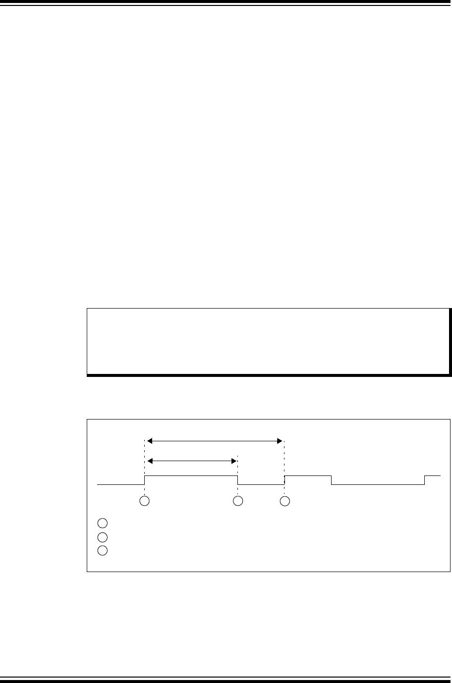
PIC32 Family Reference Manual
DS61111E-page 16-26 © 2011 Microchip Technology Inc.
16.3.3 Pulse Width Modulation Mode
When the OCM<2:0> control bits are set to ‘110’ or ‘111’, the selected output compare channel
is configured for the PWM mode of operation.
The following two PWM modes are available:
•PWM without Fault Protection Input
•PWM with Fault Protection Input
The OCFA or OCFB Fault input pin is utilized for the second PWM mode. In this mode, an
asynchronous logic level ‘0’ on the OCFx pin will cause the selected PWM channel to be shut
down. See 16.3.3.1 “PWM with Fault Protection Input Pin”.
In PWM mode, the OCxR register is a read-only slave duty cycle register and OCxRS is a buffer
register that is written by the user to update the PWM duty cycle. On every timer to period register
match event (end of PWM period), the duty cycle register, OCxR, is loaded with the contents of
OCxRS. The TyIF interrupt flag is asserted at each PWM period boundary.
The following steps should be taken when configuring the Output Compare module for PWM
operation:
1. Set the PWM period by writing to the selected timer period register (PRy).
2. Set the PWM duty cycle by writing to the OCxRS register.
3. Write the OxCR register with the initial duty cycle.
4. Enable interrupts, if required, for the timer and Output Compare modules. The output
compare interrupt is required for PWM Fault pin utilization.
5. Configure the Output Compare module for one of two PWM Operation modes by writing
to the Output Compare mode bits, OCM<2:0> (OCxCON<2:0>).
6. Set the TMRy prescale value and enable the time base by setting TON (TxCON<15>) = 1.
An example PWM output waveform is shown in Figure 16-17.
Figure 16-17: PWM Output Waveform
Note: The OCxR register should be initialized before the Output Compare module is first
enabled. The OCxR register becomes a read-only duty cycle register when the
module is operated in the PWM modes. The value held in OCxR will become the
PWM duty cycle for the first PWM period. The contents of the duty cycle buffer
register, OCxRS, will not be transferred into OCxR until a time base period match
occurs.
Period = (PRy + 1)
Duty Cycle = (OCxRS)
Timery is cleared and the new duty cycle value is loaded from OCxRS into OCxR.
Timer value equals the value in the OCxR register; OCx Pin is driven low.
Timer overflow; value from OCxRS is loaded into OCxR; OCx pin is driven high.
21 3
2
3
1
TyIF interrupt flag is asserted.

© 2011 Microchip Technology Inc. DS61111E-page 16-27
Section 16. Output Compare
Output Compare
16
16.3.3.1 PWM with Fault Protection Input Pin
When the OCM<2:0> control bits are set to ‘111’, the selected output compare channel is
configured for the PWM mode of operation. All functions described in 16.3.3 “Pulse Width
Modulation Mode” apply, with the addition of input Fault protection.
Fault protection is provided via the OCFA and OCFB pins. The OCFA pin is associated with the
output compare channels 1 through 4, while the OCFB pin is associated with the output compare
channel 5.
If a logic ‘0’ is detected on the OCFA/OCFB pin, the selected PWM output pin(s) are placed in
the tri-state. The user may elect to provide a pull-down or pull-up resistor on the PWM pin to
provide for a desired state if a Fault condition occurs. The shutdown of the PWM output is
immediate and is not tied to the device clock source. This state will remain until the following
conditions are met:
•The external Fault condition has been removed
•The PWM mode is re-enabled by writing to the appropriate mode bits, OCM<2:0> bits
(OCxCON<2:0>)
As a result of the Fault condition, the respective interrupt flag, OCxIF bit, is asserted and an
interrupt will be generated, if enabled. Upon detection of the Fault condition, the OCFLT bit
(OCxCON<4>) is asserted high (logic ‘1’). This bit is a read-only bit and will only be cleared once
the external Fault condition has been removed and the PWM mode is re-enabled by writing to
the appropriate mode bits, OCM<2:0> (OCxCON<2:0>).
16.3.3.2 PWM Period
The PWM period is specified by writing to the Timery Period register, PRy. The PWM period can
be calculated using the following formula:
Equation 16-1: Calculating the PWM Period
The PWM period must not exceed the width of the Period Register for the selected mode, 16 bits
for 16-bit mode or 32 bits for 32-bit mode. If the calculated period is too large, select a larger
prescaler to prevent overflow. To maintain maximum PWM resolution, select the smallest
prescaler that does not result in an overflow.
Note: The external Fault pins, if enabled for use, will continue to control the OCx output
pins while the device is in Sleep or Idle mode.
PWM Period = [(PR + 1) • TPB • (TMR Prescale Value)]
PWM Frequency = 1/[PWM Period]
Note: A PRy value of N will produce a PWM period of N + 1 time base count cycles. For
example, a value of 7 written into the PRy register will yield a period consisting of 8
time base cycles.

PIC32 Family Reference Manual
DS61111E-page 16-28 © 2011 Microchip Technology Inc.
16.3.3.3 PWM Duty Cycle
The PWM duty cycle is specified by writing to the OCxRS register. The OCxRS register can be
written to at any time, but the duty cycle value is not latched into OCxR until a match between
PRy and TMRy occurs (i.e., the period is complete). This provides a double buffer for the PWM
duty cycle and is essential for glitchless PWM operation. In the PWM mode, OCxR is a read-only
register.
Some important boundary parameters of the PWM duty cycle include the following:
•If the duty cycle register OCxR is loaded with 0x0000, the OCx pin will remain low
(0% duty cycle)
•If OCxR is greater than PRy (timer period register), the pin will remain high (100% duty cycle)
• If OCxR is equal to PRy, the OCx pin will be low for one time base count value and high for
all other count values
See Figure 16-18 for PWM mode timing details. Tabl e 16-4 through Ta b l e 16-9 show example
PWM frequencies and resolutions for a device with the Peripheral Bus operating at a variety of
frequencies.
Equation 16-2: Calculation for Maximum PWM Resolution
Equation 16-3: PWM Period and Resolution Calculation
( )
Maximum PWM Resolution (bits) =
FPB
FPWM • TMRy • Prescaler bits
log10
log10(2)
Desired PWM frequency is 52.08 kHz
FPB = 10 MHz
Timer2 prescale setting: 1:1
1/52.08 kHz = (PR2 + 1) • TPB • (Timer2 prescale value)
19.20 µs = (PR2 + 1) • 0.1 µs • (1)
PR2 = 191
Find the maximum resolution of the duty cycle that can be used with a 52.08 kHz PWM frequency
and a 10 MHz Peripheral Bus clock rate.
1/52.08 kHz = 2PWM RESOLUTION • 1/10 MHz • 1
19.20 µs = 2PWM RESOLUTION • 100 ns • 1
192 = 2PWM RESOLUTION
log10(192) = (PWM Resolution) • log10(2)
PWM Resolution = 7.6 bits

© 2011 Microchip Technology Inc. DS61111E-page 16-29
Section 16. Output Compare
Output Compare
16
Figure 16-18: PWM Output Timing
Figure 16-19: Dual Compare Mode: Continuous Output Pulse (PR2 = OCxRS, 32-Bit Mode)
0002
0000 0001 0002 00030005
TMR3 0001
1 PBCLK Period
0005
0002
PR3
OCxR
0005
OCx pin
0002
OCxRS
0000 00050003
0004 0004
0001
User Code Writes New Value to OCxRS In ISR
0001
Hardware Loads New Duty Cycle Here
Note 1: An ‘x’ represents the output compare channel number.
2: OCxR = Compare Register; OCxRS = Secondary Compare Register.
T3IF is Set
OCxR = OCxRS T3IF is Set
OCxR = OCxRS
0000:
0000: 0000: 0000:
0000:0005:
TMR2 0000:
1 PBCLK Period
0000:
0000:
PR2
OCxR
0000:
OCx pin
Hardware Loads New Duty Cycle Here
Note: An ‘x’ represents the output compare channel number.
0002
0000 0000 0001 0004
0003
0005
0005 0001 0002
0000:
0002
0000:
OCxRS
0002
0000:
0000
0000:
0001
0000:
0001
User Code Writes New Value to OCxRS in ISR

PIC32 Family Reference Manual
DS61111E-page 16-30 © 2011 Microchip Technology Inc.
Table 16-4: Example PWM Frequencies and Resolutions with a 10 MHz (16-Bit Mode) Peripheral Bus Clock
PWM Frequency 19 Hz 153 Hz 305 Hz 2.44 kHz 9.77 kHz 78.1 kHz 313 kHz
Timer Prescaler Ratio 8 1 1 1 1 1 1
Period Register Value 0xFFFF 0xFFFF 0x7FFF 0x0FFF 0x03FF 0x007F 0x001F
Resolution (bits) 16 16 15 12 10 7 5
Table 16-5: Example PWM Frequencies and Resolutions with a 30 MHz (16-Bit Mode) Peripheral Bus Clock
PWM Frequency 58 Hz 458 Hz 916 Hz 7.32 kHz 29.3 kHz 234 kHz 938 kHz
Timer Prescaler Ratio 8 1 1 1 1 1 1
Period Register Value 0xFC8E 0xFFDD 0x7FEE 0x1001 0x03FE 0x007F 0x001E
Resolution (bits) 16 16 15 12 10 7 5
Table 16-6: Example PWM Frequencies and Resolutions with a 50 MHz (16-Bit Mode) Peripheral Bus Clock
PWM Frequency 57 Hz 458 Hz 916 Hz 7.32 kHz 29.3 kHz 234 kHz 938 kHz
Timer Prescaler Ratio 64 8 1 1 1 1 1
Period Register Value 0x349C 0x354D 0xD538 0x1AAD 0x06A9 0x00D4 0x0034
Resolution (bits) 13.7 13.7 15.7 12.7 10.7 7.7 5.7
Table 16-7: Example PWM Frequencies and Resolutions with a 50 MHz (16-Bit Mode) Peripheral Bus Clock
PWM Frequency 100 Hz 200 Hz 500 Hz 1 kHz 2 kHz 5 kHz 10 kHz
Timer Prescaler
Ratio
8881811
Period Register
Value (hex)
0xF423 0x7A11 0x30D3 0xC34F 0x0C34 0x270F 0x1387
Resolution (bits)
(decimal)
15.9 14.9 13.6 15.6 11.6 13.3 12.3
Table 16-8: Example PWM Frequencies and Resolutions with a 50 MHz (16-Bit Mode) Peripheral Bus Clock
PWM Frequency 100 Hz 200 Hz 500 Hz 1 kHz 2 kHz 5 kHz 10 kHz
Timer Prescaler
Ratio
8421111
Period Register
Value (hex)
0xF423 0xF423 0xC34F 0x0C34F 0x61A7 0x270F 0x1387
Resolution (bits)
(decimal)
15.9 15.9 15.6 15.6 14.6 13.3 12.3
Table 16-9: Example PWM Frequencies and Resolutions with a 50 MHz (32-Bit Mode) Peripheral Bus Clock
PWM
Frequency 100 Hz 200 Hz 500 Hz 1 kHz 2 kHz 5 kHz 10 kHz
Timer Prescaler
Ratio
1 1 1 1 1 8 1
Period Register
Value (hex)
0x0007A11F 0x0003D08F 0x0001869F 0x0000C34F 0x000061A7 0x000004E1 0x00001387
Resolution (bits)
(decimal)
18.9 17.9 16.6 15.6 14.6 10.3 12.3

© 2011 Microchip Technology Inc. DS61111E-page 16-31
Section 16. Output Compare
Output Compare
16
Example 16-9 shows configuration and interrupt service code for the PWM mode of operation.
Example 16-9: PWM Mode Setup and Interrupt Servicing (16-Bit Mode)
// The following code example will set the Output Compare 1 module
// for PWM mode with Fault pin disabled and for 50% duty cycle.
// Timer2 is selected as the clock for the PWM time base, and Timer2
// interrupts are enabled.
#include <plib.h>
int main(void)
{
INTEnableSystemMultiVectoredInt(); // Enable system wide interrupt to
// multivectored mode.
OC1CON = 0x0000; // Turn off the OC1 when performing the setup
OC1R = 0x0064; // Initialize primary Compare register
OC1RS = 0x0064; // Initialize secondary Compare register
OC1CON = 0x0006; // Configure for PWM mode without Fault pin
// enabled
PR2 = 0x00C7; // Set period
// Configure Timer2 interrupt. Note that in PWM mode, the
// corresponding source timer interrupt flag is asserted.
// OC interrupt is not generated in PWM mode.
IFS0CLR = 0x00000100; // Clear the T2 interrupt flag
IEC0SET = 0x00000100; // Enable T2 interrupt
IPC2SET = 0x0000001C; // Set T2 interrupt priority to 7
T2CONSET = 0x8000; // Enable Timer2
OC1CONSET = 0x8000; // Enable OC1
while(1); // Never return
}
// Example code for Timer2 ISR
void __ISR(_TIMER_2_VECTOR, ipl7) T2_IntHandler (void)
{
// Insert user code here
IFS0CLR = 0x0100; // Clearing Timer2 interrupt flag
}

PIC32 Family Reference Manual
DS61111E-page 16-32 © 2011 Microchip Technology Inc.
Example 16-10: PWM Mode Setup and Interrupt Servicing (32-Bit Mode)
// The following code example will set the Output Compare 1 module
// for PWM mode with Fault pin disabled and for 50% duty cycle.
// Timer2 and Timer3 are selected as the clocks for the PWM time base
// in 32-bit mode, and Timer3 interrupts are enabled.
#include <plib.h>
int main(void)
{
INTEnableSystemMultiVectoredInt(); // Enable system wide interrupt to multivectored mode.
OC1CON = 0x0000; // Turn off the OC1 when performing the setup
OC1R = 0x00638000; // Initialize primary Compare register
OC1RS = 0x00638000; // Initialize secondary Compare register
OC1CON = 0x0006; // Configure for PWM mode without Fault pin enabled
T2CONSET = 0x0008; // Enable 32-bit Timer mode
PR2 = 0x00C6FFFF; // Set period
// Configure Timer3 interrupt. Note that in PWM mode, the corresponding source timer
// interrupt flag is asserted. OC interrupt is not generated in PWM mode.
IFS0CLR = 0x00001000; // Clear the T3 interrupt flag
IEC0SET = 0x00001000; // Enable T3 interrupt
IPC3SET = 0x0000001C; // Set T3 interrupt priority to 7
T2CONSET = 0x8000; // Enable Timer2
OC1CONSET = 0x8020; // Enable OC1 in 32-bit mode.
while(1); // Never return
}
// Example code for Timer3 ISR:
void __ISR(_TIMER_3_VECTOR, ipl7) T3_IntHandler (void)
{
// Insert user code here
IFS0CLR = 0x1000; // Clearing Timer3 interrupt flag
}

© 2011 Microchip Technology Inc. DS61111E-page 16-33
Section 16. Output Compare
Output Compare
16
16.4 INTERRUPTS
Each of the available output compare channels has a dedicated interrupt bit, OCxIF, and a
corresponding interrupt enable/mask bit, OCxIE. These bits are used to determine the source of
an interrupt and to enable or disable an individual interrupt source. The priority level of each of
the channels can also be set independently of the other channels.
OCxIF is set when an output compare channel detects a predefined match condition that is
defined as an event generating an interrupt. The OCxIF bit will then be set without regard to the
state of the corresponding OCxIE bit. The OCxIF bit can be polled by software if desired.
The OCxIE bit is used to define the behavior of the Vector Interrupt Controller (VIC) when a
corresponding OCxIF is set. When the OCxIE bit is clear, the VIC module does not generate a
CPU interrupt for the event. If the OCxIE bit is set, the VIC module will generate an interrupt to
the CPU when the corresponding OCxIF bit is set (subject to the priority and subpriority as
outlined below).
It is the responsibility of the routine that services a particular interrupt to clear the appropriate
interrupt flag bit before the service routine is complete.
The priority of each output compare channel can be set independently via the OCxIP<2:0> bits.
This priority defines the priority group that the interrupt source will be assigned to. The priority
groups range from a value of 7, the highest priority, to a value of 0, which does not generate an
interrupt. An interrupt being serviced will be preempted by an interrupt in a higher priority group.
The subpriority bits allow setting the priority of an interrupt source within a priority group. The
values of the subpriority, OCxIS<1:0>, range from 3, the highest priority, to 0, the lowest priority.
An interrupt with the same priority group but having a higher subpriority value will preempt a
lower subpriority interrupt that is in progress.
The priority group and subpriority bits allow more than one interrupt source to share the same
priority and subpriority. If simultaneous interrupts occur in this configuration, the natural order of
the interrupt sources within a priority/subpriority group pair determines the interrupt generated.
The natural priority is based on the vector numbers of the interrupt sources. The lower the vector
number, the higher the natural priority of the interrupt. any interrupts that were overridden by
natural order will then generate their respective interrupts (based on priority, subpriority, and
natural order) after the interrupt flag for the current interrupt is cleared.
After an enabled interrupt is generated, the CPU will jump to the vector assigned to that interrupt.
The vector number for the interrupt is the same as the natural order number. The CPU will then
begin executing code at the vector address. The user’s code at this vector address should
perform any operations required (such as reloading the duty cycle and clearing the interrupt flag),
and then exit. For the vector address table details and for more information on interrupts, refer to
Section 8. “Interrupts” (DS61108).

PIC32 Family Reference Manual
DS61111E-page 16-34 © 2011 Microchip Technology Inc.
16.5 I/O PIN CONTROL
When the Output Compare module is enabled, it controls the I/O pin direction. The Output Com-
pare module returns the I/O pin control back to the appropriate pin LAT and TRIS control bits
when it is disabled.
When the PWM with Fault Protection Input mode is enabled, the OCFx Fault pin must be
configured for an input by setting the respective TRIS SFR bit. The OCFx Fault input pin is not
automatically configured as an input when the PWM fault mode is selected.
Table 16-10: Pins Associated with Output Compare Modules 1-5
Pin
Name
Module
Control
Pin
Type
Buffer
Type Description
OC1 ON O — Output Compare/PWM Channel 1
OC2 ON O — Output Compare/PWM Channel 2
OC3 ON O — Output Compare/PWM Channel 3
OC4 ON O — Output Compare/PWM Channel 4
OC5 ON O — Output Compare/PWM Channel 5
OCFA ON IST PWM Fault Protection A Input (for Channels 1-4)
OCFB ON IST PWM Fault Protection B Input (for Channel 5)
Legend: ST = Schmitt Trigger input with CMOS levels I = Input O = Output

© 2011 Microchip Technology Inc. DS61111E-page 16-35
Section 16. Output Compare
Output Compare
16
16.6 OPERATION IN POWER-SAVING AND DEBUG MODES
16.6.1 Output Compare Operation in Sleep Mode
When the device enters Sleep mode, the system clock is disabled. During Sleep, the Output
Compare module drives the pin to the same active state as driven prior to entering Sleep. The
module will then halt at this state.
For example, if the pin was high and the CPU entered the Sleep state, the pin will stay high.
Likewise, if the pin was low and the CPU entered the Sleep state, the pin will stay low. In both
cases, when the device wakes up, the Output Compare module will resume operation.
When the module is operating in PWM Fault mode, the asynchronous portions of the Fault circuit
remain active. If a Fault is detected, the compare output enable signal is deasserted and the
OCFLT bit (OCxCON<4>) is set. If the corresponding interrupt is enabled, an interrupt is
generated and the device wakes up from Sleep.
16.6.2 Output Compare Operation in Idle Mode
When the device enters Idle mode, the system clock sources remain functional and the CPU
stops executing code. The SIDL bit (OCxCON<13>) selects if the Output Compare module will
stop operation when the device enters Idle mode or whether the module will continue normal
operation in Idle mode.
•If SIDL = 1, the module will discontinue operation in Idle mode. The module will perform the
same procedures when stopped in Idle mode as it does for Sleep mode.
•If SIDL = 0, the module will continue operation in Idle mode only if the selected time base is
set to operate in Idle mode. The output compare channel(s) will operate during Idle mode if
the SIDL bit is a logic ‘0’. Furthermore, the time base must be enabled with the respective
SIDL bit set to a logic ‘0’.
•When the module is operating in PWM Fault mode, the asynchronous portions of the Fault
circuit remain active. If a Fault is detected, the compare output enable signal is deasserted
and the OCFLT bit (OCxCON<4>) is set. If the corresponding interrupt is enabled, an
interrupt is generated and the device wakes up from Idle.
16.6.3 Output Compare Operation in Debug Mode
When the module is operating in PWM Fault mode, the asynchronous portions of the Fault circuit
remain active. If a Fault is detected, the compare output enable signal is deasserted and the
OCFLT bit (OCxCON<4>) is set. If the corresponding interrupt is enabled, an interrupt will be
generated.
16.7 EFFECTS OF VARIOUS RESETS
16.7.1 MCLR Reset
Following a MCLR event, the OCxCON, OCxR, and OCxRS registers for each Output Compare
module are reset to a value of 0x00000000.
16.7.2 Power-on Reset
Following a Power-on (POR) event, the OCxCON, OCxR, and OCxRS registers for each Output
Compare module are reset to a value of 0x00000000.
16.7.3 Watchdog Timer Reset
The status of the Output Compare control registers after a Watchdog Timer (WDT) event
depends on the operational mode of the CPU prior to the WDT event.
If the device is not in Sleep, a WDT event will force the OCxCON, OCxR, and OCxRS registers
to a Reset value of 0x00000000. If the device is in Sleep when a WDT event occurs, the contents
of the OCxCON, OCxR and OCxRS register values are not affected.
Note: The external Fault pins, if enabled for use, will continue to control the associated
OCx output pins while the device is in Sleep or Idle mode.

PIC32 Family Reference Manual
DS61111E-page 16-36 © 2011 Microchip Technology Inc.
16.8 OUTPUT COMPARE APPLICATION
This section provides an example application using the PWM mode of the Output Compare
module to control the speed of a DC motor. The speed of the motor is controlled by changing the
PWM duty cycle.
The circuit consists of the following:
• A PIC32 family device to generate the PWM
•A TC4431 or equivalent MOSFET driver to drive the MOSFET
•A MOSFET to drive the motor
• A pull-up resistor is used to pull the input of the MOSFET driver high when the PIC32 family
is in Reset. This prevents unwanted motor operation during start-up.
•A DC motor
Example 16-11: PWM Mode Example Application (16-Bit Mode)
// The following code example will set the Output Compare 1 module for PWM mode without Fault
// pin disabled and for 50% duty cycle. Timer2 is selected as the clock for the PWM time base
// and Timer2 interrupts are enabled. This example ramps the PWM duty cycle from min to max,
// and then from max to min and repeats. The rate at which the PWM duty cycle is changed can be
// adjusted by the rate at which the Timer2 overflows. The PWM period can be changed by writing
// a different value to the PR2 register. If the PR2 value is adjusted, the maximum PWM value
// will also have to be adjusted so that it is not greater than the PR2 value.
unsigned int Pwm; // Variable to store calculated PWM value
unsigned char Mode = 0; // Variable to determine ramp up or ramp down
OC1CON = 0x0000; // Turn off the OC1 when performing the setup
OC1R = 0x0064; // Initialize primary Compare register
OC1RS = 0x0064; // Initialize secondary Compare register
OC1CON = 0x0006; // Configure for PWM mode without Fault pin enabled
PR2 = 0x00C7; // Set period
IFS0CLR = 0x00000100; // Clear the T2 interrupt flag
IEC0SET = 0x00000100; // Enable T2 interrupt
IPC2SET = 0x0000001C; // Set T2 interrupt priority to 7
T2CONSET = 0x8000; // Enable Timer2
OC1CONSET = 0x8000; // Enable OC1
// Example code for Timer2 ISR:
void __ISR(_TIMER_2_VECTOR, ipl7) T2_IntHandler (void)
{
if ( Mode )
{
if ( Pwm < 0xFFFF ) // Ramp up mode
{
Pwm ++; // If the duty cycle is not at max, increase
OC1RS = Pwm; // Write new duty cycle
}
else
{
Mode = 0; // PWM is at max, change mode to ramp down
}
} // End of ramp up
else
{
if ( !Pwm ) // Ramp Down mode
{
Pwm --; // If the duty cycle is not at min, increase
OC1RS = Pwm; // Write new duty cycle
}
else
{
Mode = 1; // PWM is at min, change mode to ramp up
}
} // End of ramp down
// Insert user code here
IFS0CLR = 0x0100; // Clearing Timer2 interrupt flag
}

© 2011 Microchip Technology Inc. DS61111E-page 16-37
Section 16. Output Compare
Output Compare
16
Figure 16-20: DC Motor Speed Control Application Schematic
VDD
VDD
VDD
VDD
C8
1 µF
VDD
C7
0.1 µF
VDD
C6
0.01 µF
VDD
C5
1 µF
VDD
C4
0.1 µF
VDD
C3
0.01 µF
M
TC4432
12 V
12 V
VDD
1K
92
94
93
91
90
89
88
87
86
85
84
83
82
81
80
79
78
20
2
3
4
5
6
7
8
9
10
11
12
13
14
15
16
65
64
63
62
61
60
59
56
45
44
43
42
41
40
39
28
29
30
31
32
33
34
35
36
37
38
17
18
19
21
22
95
1
76
77
72
71
70
69
68
67
66
75
74
73
58
57
24
23
25
96
98
97
99
27
46
47
48
49
55
54
53
52
51
100
50
26
VDD
VDD
VDD
10K
AVDD
AVSS
VDD 10 µF

PIC32 Family Reference Manual
DS61111E-page 16-38 © 2011 Microchip Technology Inc.
16.9 DESIGN TIPS
Question 1: The Output Compare pin stops functioning even when the SIDL bit is not
set. Why?
Answer: This is most likely to occur when the SIDL bit (TxCON<13>) of the associated
timer source is set. Therefore, it is the timer that actually goes into Idle mode
when the PWRSAV instruction is executed.
Question 2: Can I use the Output Compare modules with the selected time base
configured for 32-bit mode?
Answer: Yes. The timer can be us ed in 32-bit mod e as a time base for the Ou tpu t Com pare
modules by setting the T32 bit (TxCON<3>). For proper operation, the Output
Compare module must be configured for 32-bit Compare mode by setting the
OC32 bit (OCxCON<5>) for all Output Compare modules using the 32-bit timer
as a time base.

© 2011 Microchip Technology Inc. DS61111E-page 16-39
Section 16. Output Compare
Output Compare
16
16.10 RELATED APPLICATION NOTES
This section lists application notes that are related to this section of the manual. These
application notes may not be written specifically for the PIC32 device family, but the concepts are
pertinent and could be used with modification and possible limitations. The current application
notes related to the Output Compare module are:
Title Application Note #
No related application notes at this time. N/A
Note: Please visit the Microchip web site (www.microchip.com) for additional application
notes and code examples for the PIC32 family of devices.

PIC32 Family Reference Manual
DS61111E-page 16-40 © 2011 Microchip Technology Inc.
16.11 REVISION HISTORY
Revision A (October 2007)
This is the initial released version of this document.
Revision B (October 2007)
Updated document to remove Confidential status.
Revision C (April 2008)
Revised status to Preliminary; Revised U-0 to r-x.
Revision D (June 2008)
Revised Registers 16-1, 16-20, 16-32; Revised Examples 16-3, 16-4, 16-5, 16-6, 16-7, 16-8,
16-9, 16-10, 16-11; Added TMR1 and TMR2 to Summary Table; Revised Section 16.3, Notes;
Change Reserved bits from “Maintain as” to “Write”; Added Note to ON bit (0CxCON, T2CON,
T3CON Registers).
Revision E (April 2011)
This revision includes the following updates:
• Changed the document running header from PIC32MX Family Reference Manual to PIC32
Family Reference Manual
• Removed the Preliminary status from the footer
• Removed all references to the FRZ bit throughout the document
•Updated the format of all registers (see Register 16-1 through Register 16-3)
• Changed all occurrences of r-x to U-0 in the register tables
•Removed the corresponding Clear, Set and Invert registers of the SFRs
•Changed the title of Equation 16-3 from PWM Period and Duty Cycle Calculation to PWM
Period and Resolution Calculation
•Updated the code in Example 16-9, Example 16-10 and Example 16-11
•Minor changes to the text and formatting have been incorporated throughout the document

© 2011 Microchip Technology Inc. DS61111E-page 16-41
Information contained in this publication regarding device
applications and the like is provided only for your convenience
and may be superseded by updates. It is your responsibility to
ensure that your application meets with your specifications.
MICROCHIP MAKES NO REPRESENTATIONS OR
WARRANTIES OF ANY KIND WHETHER EXPRESS OR
IMPLIED, WRITTEN OR ORAL, STATUTORY OR
OTHERWISE, RELATED TO THE INFORMATION,
INCLUDING BUT NOT LIMITED TO ITS CONDITION,
QUALITY, PERFORMANCE, MERCHANTABILITY OR
FITNESS FOR PURPOSE. Microchip disclaims all liability
arising from this information and its use. Use of Microchip
devices in life support and/or safety applications is entirely at
the buyer’s risk, and the buyer agrees to defend, indemnify and
hold harmless Microchip from any and all damages, claims,
suits, or expenses resulting from such use. No licenses are
conveyed, implicitly or otherwise, under any Microchip
intellectual property rights.
Trademarks
The Microchip name and logo, the Microchip logo, dsPIC,
KEELOQ, KEELOQ logo, MPLAB, PIC, PICmicro, PICSTART,
PIC32 logo, rfPIC and UNI/O are registered trademarks of
Microchip Technology Incorporated in the U.S.A. and other
countries.
FilterLab, Hampshire, HI-TECH C, Linear Active Thermistor,
MXDEV, MXLAB, SEEVAL and The Embedded Control
Solutions Company are registered trademarks of Microchip
Technology Incorporated in the U.S.A.
Analog-for-the-Digital Age, Application Maestro, CodeGuard,
dsPICDEM, dsPICDEM.net, dsPICworks, dsSPEAK, ECAN,
ECONOMONITOR, FanSense, HI-TIDE, In-Circuit Serial
Programming, ICSP, Mindi, MiWi, MPASM, MPLAB Certified
logo, MPLIB, MPLINK, mTouch, Omniscient Code
Generation, PICC, PICC-18, PICDEM, PICDEM.net, PICkit,
PICtail, REAL ICE, rfLAB, Select Mode, Total Endurance,
TSHARC, UniWinDriver, WiperLock and ZENA are
trademarks of Microchip Technology Incorporated in the
U.S.A. and other countries.
SQTP is a service mark of Microchip Technology Incorporated
in the U.S.A.
All other trademarks mentioned herein are property of their
respective companies.
© 2011, Microchip Technology Incorporated, Printed in the
U.S.A., All Rights Reserved.
Printed on recycled paper.
ISBN: 978-1-61341-098-1
Note the following details of the code protection feature on Microchip devices:
• Microchip products meet the specification contained in their particular Microchip Data Sheet.
• Microchip believes that its family of products is one of the most secure families of its kind on the market today, when used in the
intended manner and under normal conditions.
• There are dishonest and possibly illegal methods used to breach the code protection feature. All of these methods, to our
knowledge, require using the Microchip products in a manner outside the operating specifications contained in Microchip’s Data
Sheets. Most likely, the person doing so is engaged in theft of intellectual property.
• Microchip is willing to work with the customer who is concerned about the integrity of their code.
• Neither Microchip nor any other semiconductor manufacturer can guarantee the security of their code. Code protection does not
mean that we are guaranteeing the product as “unbreakable.”
Code protection is constantly evolving. We at Microchip are committed to continuously improving the code protection features of our
products. Attempts to break Microchip’s code protection feature may be a violation of the Digital Millennium Copyright Act. If such acts
allow unauthorized access to your software or other copyrighted work, you may have a right to sue for relief under that Act.
Microchip received ISO/TS-16949:2002 certification for its worldwide
headquarters, design and wafer fabrication facilities in Chandler and
Tempe, Arizona; Gresham, Oregon and design centers in California
and India. The Company’s quality system processes and procedures
are for its PIC® MCUs and dsPIC® DSCs, KEELOQ® code hopping
devices, Serial EEPROMs, microperipherals, nonvolatile memory and
analog products. In addition, Microchip’s quality system for the design
and manufacture of development systems is ISO 9001:2000 certified.

DS61111E-page 16-42 © 2011 Microchip Technology Inc.
AMERICAS
Corporate Office
2355 West Chandler Blvd.
Chandler, AZ 85224-6199
Tel: 480-792-7200
Fax: 480-792-7277
Technical Support:
http://www.microchip.com/
support
Web Address:
www.microchip.com
Atlanta
Duluth, GA
Tel: 678-957-9614
Fax: 678-957-1455
Boston
Westborough, MA
Tel: 774-760-0087
Fax: 774-760-0088
Chicago
Itasca, IL
Tel: 630-285-0071
Fax: 630-285-0075
Cleveland
Independence, OH
Tel: 216-447-0464
Fax: 216-447-0643
Dallas
Addison, TX
Tel: 972-818-7423
Fax: 972-818-2924
Detroit
Farmington Hills, MI
Tel: 248-538-2250
Fax: 248-538-2260
Indianapolis
Noblesville, IN
Tel: 317-773-8323
Fax: 317-773-5453
Los Angeles
Mission Viejo, CA
Tel: 949-462-9523
Fax: 949-462-9608
Santa Clara
Santa Clara, CA
Tel: 408-961-6444
Fax: 408-961-6445
Toronto
Mississauga, Ontario,
Canada
Tel: 905-673-0699
Fax: 905-673-6509
ASIA/PACIFIC
Asia Pacific Office
Suites 3707-14, 37th Floor
Tower 6, The Gateway
Harbour City, Kowloon
Hong Kong
Tel : 8 52 - 24 0 1- 120 0
Fax: 852-2401-3431
Australia - Sydney
Tel : 6 1-2 -98 68- 6 73 3
Fax: 61-2-9868-6755
China - Beijing
Tel : 8 6-1 0-8 528 - 21 0 0
Fax: 86-10-8528-2104
China - Chengdu
Tel : 8 6-2 8-8 665 - 55 11
Fax: 86-28-8665-7889
China - Chongqing
Tel : 8 6-2 3-8 980 - 95 8 8
Fax: 86-23-8980-9500
China - Hong Kong SAR
Tel : 8 52 - 24 0 1- 120 0
Fax: 852-2401-3431
China - Nanjing
Tel : 8 6-2 5-8 473 - 24 6 0
Fax: 86-25-8473-2470
China - Qingdao
Tel : 8 6-5 32- 8502 -73 55
Fax: 86-532-8502-7205
China - Shanghai
Tel : 8 6-2 1-5 407 - 55 3 3
Fax: 86-21-5407-5066
China - Shenyang
Tel : 8 6-2 4-2 334 - 28 2 9
Fax: 86-24-2334-2393
China - Shenzhen
Tel : 8 6-7 55- 8203 -26 60
Fax: 86-755-8203-1760
China - Wuhan
Tel : 8 6-2 7-5 980 - 53 0 0
Fax: 86-27-5980-5118
China - Xian
Tel : 8 6-2 9-8 833 - 72 5 2
Fax: 86-29-8833-7256
China - Xiamen
Tel: 86-592-2388138
Fax: 86-592-2388130
China - Zhuhai
Tel : 86- 756 -3 210 04 0
Fax: 86-756-3210049
ASIA/PACIFIC
India - Bangalore
Tel : 9 1- 8 0- 309 0-4 444
Fax: 91-80-3090-4123
India - New Delhi
Tel : 9 1- 11 -41 60- 86 31
Fax: 91-11-4160-8632
India - Pune
Tel : 9 1- 2 0- 256 6-1 512
Fax: 91-20-2566-1513
Japan - Yokohama
Tel : 8 1- 4 5- 471 - 6 166
Fax: 81-45-471-6122
Korea - Daegu
Tel : 8 2- 5 3- 744 -43 01
Fax: 82-53-744-4302
Korea - Seoul
Tel : 8 2- 2 -5 54- 720 0
Fax: 82-2-558-5932 or
82-2-558-5934
Malaysia - Kuala Lumpur
Tel : 6 0- 3 -6 201 -98 57
Fax: 60-3-6201-9859
Malaysia - Penang
Tel : 6 0- 4 -2 27- 887 0
Fax: 60-4-227-4068
Philippines - Manila
Tel : 6 3- 2 -6 34- 906 5
Fax: 63-2-634-9069
Singapore
Tel : 6 5- 6 33 4 -8 870
Fax: 65-6334-8850
Taiwan - Hsin Chu
Tel : 8 86 - 3- 657 8-3 00
Fax: 886-3-6578-370
Taiwan - Kaohsiung
Tel : 8 86 - 7- 213 -78 30
Fax: 886-7-330-9305
Taiwan - Taipei
Tel : 8 86 - 2- 250 0-6 610
Fax: 886-2-2508-0102
Thailand - Bangkok
Tel : 6 6- 2 -6 94- 135 1
Fax: 66-2-694-1350
EUROPE
Austria - Wels
Tel : 4 3- 7 24 2 -2 244 -39
Fax: 43-7242-2244-393
Denmark - Copenhagen
Tel : 4 5-4 450 -2 828
Fax: 45-4485-2829
France - Paris
Tel : 3 3-1 -6 9-5 3 -6 3-2 0
Fax: 33-1-69-30-90-79
Germany - Munich
Tel : 4 9- 8 9- 627 -14 4-0
Fax: 49-89-627-144-44
Italy - Milan
Tel : 3 9- 0 33 1 -7 426 11
Fax: 39-0331-466781
Netherlands - Drunen
Tel : 3 1- 4 16 - 690 3 99
Fax: 31-416-690340
Spain - Madrid
Tel : 3 4- 9 1- 708 -08 -90
Fax: 34-91-708-08-91
UK - Wokingham
Tel : 4 4- 11 8-9 21- 58 69
Fax: 44-118-921-5820
Worldwide Sales and Service
02/18/11

© 2007-2011 Microchip Technology Inc. DS61104E-page 17-1
10-bit Analog-to-Digital
Converter (ADC)
17
Section 17. 10-bit Analog-to-Digital Converter (ADC)
HIGHLIGHTS
This section of the manual contains the following major topics:
17.1 Introduction..............................................................................................................17-2
17.2 Control Registers.....................................................................................................17-4
17.3 ADC Operation, Terminology and Conversion Sequence ..................................... 17-12
17.4 ADC Module Configuration.................................................................................... 17-14
17.5 Miscellaneous ADC Functions............................................................................... 17-26
17.6 Initialization............................................................................................................17-51
17.7 Interrupts................................................................................................................17-53
17.8 Operation During Sleep and Idle Modes ............................................................... 17-54
17.9 Effects of Various Resets.......................................................................................17-55
17.10 Related Application Notes ..................................................................................... 17-56
17.11 Revision History.....................................................................................................17-57

PIC32 Family Reference Manual
DS61104E-page 17-2 © 2007-2011 Microchip Technology Inc.
17.1 INTRODUCTION
The PIC32 10-bit Analog-to-Digital Converter (ADC) includes the following features:
• Successive Approximation Register (SAR) conversion
•Up to 16 analog input pins
•External voltage reference input pins
•One unipolar differential Sample-and-Hold Amplifier (SHA)
•Automatic Channel Scan mode
• Selectable conversion trigger source
•16-word conversion result buffer
• Selectable Buffer Fill modes
•Eight conversion result format options
•Operation during CPU Sleep and Idle modes
Figure 17-1 illustrates a block diagram of the 10-bit ADC. The 10-bit ADC can have up to 16
analog input pins, AN0 through AN15. In addition, there are two analog input pins for external
voltage reference connections. These voltage reference inputs may be shared with other analog
input pins and may be common to other analog module references. The actual number of analog
input pins and external voltage reference input configuration will depend on the specific PIC32
device. Refer to the specific device data sheet for more information.
The analog inputs are connected through two multiplexers to one SHA. The analog input
multiplexers can be switched between two sets of analog inputs between conversions. Unipolar
differential conversions are possible on all channels, other than the pin used as the reference,
using a reference input pin (see Figure 17-1).
The Analog Input Scan mode sequentially converts user-specified channels. A control register
specifies which analog input channels will be included in the scanning sequence.
The 10-bit ADC is connected to a 16-word result buffer. Each 10-bit result is converted to one of
eight 32-bit output formats when it is read from the result buffer.
Note: This family reference manual section is meant to serve as a complement to device
data sheets. Depending on the device variant, this manual section may not apply to
all PIC32 devices.
Please consult the note at the beginning of the “10-bit Analog-to-Digital
Converter (ADC)” chapter in the current device data sheet to check whether this
document supports the device you are using.
Device data sheets and family reference manual sections are available for
download from the Microchip Worldwide Web site at: http://www.microchip.com
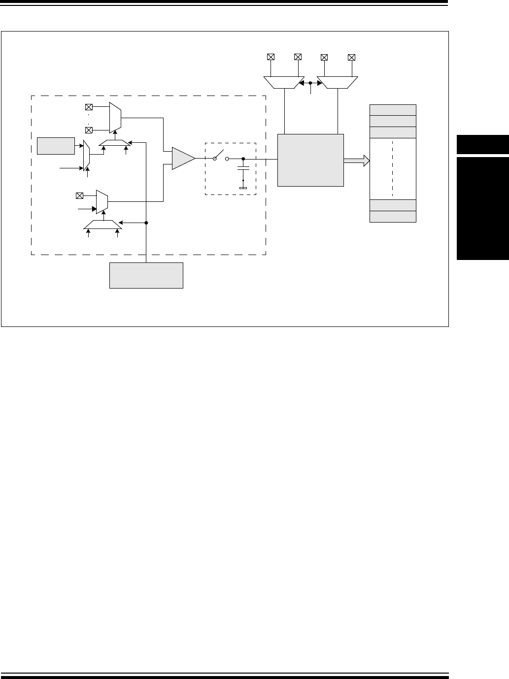
© 2007-2011 Microchip Technology Inc. DS61104E-page 17-3
Section 17. 10-bit Analog-to-Digital Converter (ADC)
10-bit Analog-to-Digital
Converter (ADC)
17
Figure 17-1: 10-bit High-Speed ADC Block Diagram
SAR ADC
SHA
ADC1BUF0
ADC1BUF1
ADC1BUF2
ADC1BUFF
ADC1BUFE
AN0
AN15
AN1
VREFL
CH0SB<3:0>
CH0NA CH0NB
+
-
CH0SA<3:0>
Channel
Scan
CSCNA
Alternate
VREF+(1) AVDD AVSS
VREF-(1)
Input Selection
VREFH VREFL
VCFG<2:0>
Note 1: VREF+ and VREF- inputs can be multiplexed with other analog inputs.

PIC32 Family Reference Manual
DS61104E-page 17-4 © 2007-2011 Microchip Technology Inc.
17.2 CONTROL REGISTERS
The ADC module has the following Special Function Registers (SFRs):
•AD1CON1: ADC Control Register 1
•AD1CON2: ADC Control Register 2
•AD1CON3: ADC Control Register 3
The AD1CON1, AD1CON2 and AD1CON3 registers control the operation of the ADC
module.
•AD1CHS: ADC Input Select Register
The AD1CHS register selects the input pins to be connected to the SHA.
•AD1PCFG: ADC Port Configuration Register(1,2)
The AD1PCFG register configures the analog input pins as analog inputs or as digital I/O.
•AD1CSSL: ADC Input Scan Select Register(1)
The AD1CSSL register selects inputs to be sequentially scanned.
Tabl e 17-1 provides a summary of all ADC-related registers, including their addresses and
formats. Corresponding registers appear after the summary, followed by a detailed description of
each register. All unimplemented registers and/or bits within a register read as zero.
Table 17-1: ADC SFR Summary
Name Bit
31/23/15/7
Bit
30/22/14/6
Bit
29/21/13/5
Bit
28/20/12/4
Bit
27/19/11/3
Bit
26/18/10/2
Bit
25/17/9/1
Bit
24/16/8/0
AD1CON1(1,2,3) 31:24 ————————
23:16 ————————
15:8 ON —SIDL — — FORM<2:0>
7:0 SSRC<2:0> CLRASAM —ASAM SAMP DONE
AD1CON2(1,2,3) 31:24 ————————
23:16 ————————
15:8 VCFG<2:0> OFFCAL —CSCNA — —
7:0 BUFS —SMPI<3:0> BUFM ALTS
AD1CON3(1,2,3) 31:24 ————————
23:16 ————————
15:8 ADRC — — SAMC<4:0>
7:0 ADCS<7:0>
AD1CHS(1,2,3) 31:24 CH0NB ——— CH0SB<3:0>
23:16 CH0NA ——— CH0SA<3:0>
15:8 ————————
7:0 ————————
AD1PCFG(1,2,3) 31:24 ————————
23:16 ————————
15:8 PCFG15 PCFG14 PCFG13 PCFG12 PCFG11 PCFG10 PCFG9 PCFG8
7:0 PCFG7 PCFG6 PCFG5 PCFG4 PCFG3 PCFG2 PCFG1 PCFG0
Legend: — = unimplemented, read as ‘0’.
Note 1: This register has an associated Clear register at an offset of 0x4 bytes. These registers have the same name with CLR appended to the
end of the register name (e.g.,AD1CON1CLR). Writing a ‘1’ to any bit position in the Clear register will clear valid bits in the associated
register. Reads from the Clear register should be ignored.
2: This register has an associated Set register at an offset of 0x8 bytes. These registers have the same name with SET appended to the
end of the register name (e.g.,AD1CON1SET). Writing a ‘1’ to any bit position in the Set register will set valid bits in the associated
register. Reads from the Set register should be ignored.
3: This register has an associated Invert register at an offset of 0xC bytes. These registers have the same name with INV appended to the
end of the register name (e.g., AD1CON1INV). Writing a ‘1’ to any bit position in the Invert register will invert valid bits in the associated
register. Reads from the Invert register should be ignored.

© 2007-2011 Microchip Technology Inc. DS61104E-page 17-5
Section 17. 10-bit Analog-to-Digital Converter (ADC)
10-bit Analog-to-Digital
Converter (ADC)
17
AD1CSSL(1,2,3) 31:24 ————————
23:16 ————————
15:8 CSSL15 CSSL14 CSSL13 CSSL12 CSSL11 CSSL10 CSSL9 CSSL8
7:0 CSSL7 CSSL6 CSSL5 CSSL4 CSSL3 CSSL2 CSSL1 CSSL0
ADC1BUF0 31:0 ADC Result Word 0 (ADC1BUF0<31:0>)
ADC1BUF1 31:0 ADC Result Word 1 (ADC1BUF1<31:0>)
ADC1BUF2 31:0 ADC Result Word 2 (ADC1BUF2<31:0>)
ADC1BUF3 31:0 ADC Result Word 3 (ADC1BUF3<31:0>)
ADC1BUF4 31:0 ADC Result Word 4 (ADC1BUF4<31:0>)
ADC1BUF5 31:0 ADC Result Word 5 (ADC1BUF5<31:0>)
ADC1BUF6 31:0 ADC Result Word 6 (ADC1BUF6<31:0>)
ADC1BUF7 31:0 ADC Result Word 7 (ADC1BUF7<31:0>)
ADC1BUF8 31:0 ADC Result Word 8 (ADC1BUF8<31:0>)
ADC1BUF9 31:0 ADC Result Word 9 (ADC1BUF9<31:0>)
ADC1BUFA 31:0 ADC Result Word A (ADC1BUFA<31:0>)
ADC1BUFB 31:0 ADC Result Word B (ADC1BUFB<31:0>)
ADC1BUFC 31:0 ADC Result Word C (ADC1BUFC<31:0>)
ADC1BUFD 31:0 ADC Result Word D (ADC1BUFD<31:0>)
ADC1BUFE 31:0 ADC Result Word E (ADC1BUFE<31:0>)
ADC1BUFF 31:0 ADC Result Word F (ADC1BUFF<31:0>)
Table 17-1: ADC SFR Summary (Continued)
Name Bit
31/23/15/7
Bit
30/22/14/6
Bit
29/21/13/5
Bit
28/20/12/4
Bit
27/19/11/3
Bit
26/18/10/2
Bit
25/17/9/1
Bit
24/16/8/0
Legend: — = unimplemented, read as ‘0’.
Note 1: This register has an associated Clear register at an offset of 0x4 bytes. These registers have the same name with CLR appended to the
end of the register name (e.g.,AD1CON1CLR). Writing a ‘1’ to any bit position in the Clear register will clear valid bits in the associated
register. Reads from the Clear register should be ignored.
2: This register has an associated Set register at an offset of 0x8 bytes. These registers have the same name with SET appended to the
end of the register name (e.g.,AD1CON1SET). Writing a ‘1’ to any bit position in the Set register will set valid bits in the associated
register. Reads from the Set register should be ignored.
3: This register has an associated Invert register at an offset of 0xC bytes. These registers have the same name with INV appended to the
end of the register name (e.g., AD1CON1INV). Writing a ‘1’ to any bit position in the Invert register will invert valid bits in the associated
register. Reads from the Invert register should be ignored.

PIC32 Family Reference Manual
DS61104E-page 17-6 © 2007-2011 Microchip Technology Inc.
Register 17-1: AD1CON1: ADC Control Register 1
Bit Range Bit
31/23/15/7
Bit
30/22/14/6
Bit
29/21/13/5
Bit
28/20/12/4
Bit
27/19/11/3
Bit
26/18/10/2
Bit
25/17/9/1
Bit
24/16/8/0
31:24 U-0 U-0 U-0 U-0 U-0 U-0 U-0 U-0
— — — — — — — —
23:16 U-0 U-0 U-0 U-0 U-0 U-0 U-0 U-0
— — — — — — — —
15:8 R/W-0 U-0 R/W-0 U-0 U-0 R/W-0 R/W-0 R/W-0
ON(1) —SIDL — — FORM<2:0>
7:0 R/W-0 R/W-0 R/W-0 R/W-0 U-0 R/W-0 R/W-0 R/C-0
SSRC<2:0> CLRASAM —ASAM SAMP DONE(2)
Legend:
R = Readable bit W = Writable bit P = Programmable bit r = Reserved bit
U = Unimplemented bit -n = Bit Value at POR: (‘0’, ‘1’, x = Unknown) C = Clearable bit
bit 31-16 Unimplemented: Read as ‘0’
bit 15 ON: ADC Operating Mode bit(1)
1 = ADC module is operating
0 = ADC is off
bit 14 Unimplemented: Read as ‘0’
bit 13 SIDL: Stop in Idle Mode bit
1 = Discontinue module operation when device enters Idle mode
0 = Continue module operation in Idle mode
bit 12-11 Unimplemented: Read as ‘0’
bit 10-8 FORM<2:0>: Data Output Format bits
011 = Signed Fractional 16-bit (DOUT = 0000 0000 0000 0000 sddd dddd dd00 0000)
010 = Fractional 16-bit (DOUT = 0000 0000 0000 0000 dddd dddd dd00 0000)
001 = Signed Integer 16-bit (DOUT = 0000 0000 0000 0000 ssss sssd dddd dddd)
000 = Integer 16-bit (DOUT = 0000 0000 0000 0000 0000 00dd dddd dddd)
111 = Signed Fractional 32-bit (DOUT = sddd dddd dd00 0000 0000 0000 0000)
110 = Fractional 32-bit (DOUT = dddd dddd dd00 0000 0000 0000 0000 0000)
101 = Signed Integer 32-bit (DOUT = ssss ssss ssss ssss ssss sssd dddd dddd)
100 = Integer 32-bit (DOUT = 0000 0000 0000 0000 0000 00dd dddd dddd)
bit 7-5 SSRC<2:0>: Conversion Trigger Source Select bits
111 = Internal counter ends sampling and starts conversion (auto convert)
110 = Reserved
101 = Reserved
100 = Reserved
011 = Reserved
010 = Timer3 period match ends sampling and starts conversion
001 = Active transition on INT0 pin ends sampling and starts conversion
000 = Clearing SAMP bit ends sampling and starts conversion
bit 4 CLRASAM: Stop Conversion Sequence bit (when the first ADC interrupt is generated)
1 = Stop conversions when the first ADC interrupt is generated. Hardware clears the ASAM bit when the
ADC interrupt is generated.
0 = Normal operation, buffer contents will be overwritten by the next conversion sequence
Note 1: When using the 1:1 Peripheral Bus Clock (PBCLK) divisor, the user software should not read or write the
peripheral’s SFRs in the SYSCLK cycle immediately following the instruction that clears the module’s ON
bit.
2: The DONE bit is not persistent in automatic modes. It is cleared by hardware at the beginning of the next
sample.

© 2007-2011 Microchip Technology Inc. DS61104E-page 17-7
Section 17. 10-bit Analog-to-Digital Converter (ADC)
10-bit Analog-to-Digital
Converter (ADC)
17
bit 3 Unimplemented: Read as ‘0’
bit 2 ASAM: ADC Sample Auto-Start bit
1 = Sampling begins immediately after last conversion completes; SAMP bit is automatically set
0 = Sampling begins when SAMP bit is set
bit 1 SAMP: ADC Sample Enable bit
1 = The ADC SHA is sampling
0 = The ADC sample/hold amplifier is holding
When ASAM = 0, writing ‘1’ to this bit starts sampling.
When SSRC = 000, writing ‘0’ to this bit will end sampling and start conversion.
bit 0 DONE: Analog-to-Digital Conversion Status bit(2)
1 = Analog-to-digital conversion is done
0 = Analog-to-digital conversion is not done or has not started
Clearing this bit will not affect any operation in progress.
Register 17-1: AD1CON1: ADC Control Register 1 (Continued)
Note 1: When using the 1:1 Peripheral Bus Clock (PBCLK) divisor, the user software should not read or write the
peripheral’s SFRs in the SYSCLK cycle immediately following the instruction that clears the module’s ON
bit.
2: The DONE bit is not persistent in automatic modes. It is cleared by hardware at the beginning of the next
sample.
PIC32 Family Reference Manual
DS61104E-page 17-8 © 2007-2011 Microchip Technology Inc.
Register 17-2: AD1CON2: ADC Control Register 2
Bit Range Bit
31/23/15/7
Bit
30/22/14/6
Bit
29/21/13/5
Bit
28/20/12/4
Bit
27/19/11/3
Bit
26/18/10/2
Bit
25/17/9/1
Bit
24/16/8/0
31:24 U-0 U-0 U-0 U-0 U-0 U-0 U-0 U-0
— — — — — — — —
23:16 U-0 U-0 U-0 U-0 U-0 U-0 U-0 U-0
— — — — — — — —
15:8 R/W-0 R/W-0 R/W-0 R/W-0 U-0 R/W-0 U-0 U-0
VCFG<2:0> OFFCAL —CSCNA — —
7:0 R/W-0 U-0 R/W-0 R/W-0 R/W-0 R/W-0 R/W-0 R/W-0
BUFS —SMPI<3:0> BUFM ALTS
Legend:
R = Readable bit W = Writable bit P = Programmable bit r = Reserved bit
U = Unimplemented bit -n = Bit Value at POR: (‘0’, ‘1’, x = Unknown)
bit 31-16 Unimplemented: Read as ‘0’
bit 15-13 VCFG<2:0>: Voltage Reference Configuration bits
ADC VR+ADC VR-
000 AVDD AVSS
001 External VREF+ pin AVSS
010 AVDD External VREF- pin
011 External VREF+ pin External VREF- pin
1xx AVDD AVSS
bit 12 OFFCAL: Input Offset Calibration Mode Select bit
1 = Enable Offset Calibration mode
VINH and VINL of the SHA are connected to VR-
0 = Disable Offset Calibration mode
The inputs to the SHA are controlled by AD1CHS or AD1CSSL
bit 11 Unimplemented: Read as ‘0’
bit 10 CSCNA: Scan Input Selections for CH0+ SHA Input for MUX A Input Multiplexer Setting bit
1 = Scan inputs
0 = Do not scan inputs
bit 9-8 Unimplemented: Read as ‘0’
bit 7 BUFS: Buffer Fill Status bit
Only valid when BUFM = 1 (ADRES split into 2 x 8-word buffers).
1 = ADC is currently filling buffer 0x8-0xF, user should access data in 0x0-0x7
0 = ADC is currently filling buffer 0x0-0x7, user should access data in 0x8-0xF
bit 6 Unimplemented: Read as ‘0’
bit 5-2 SMPI<3:0>: Sample/Convert Sequences Per Interrupt Selection bits
1111 = Interrupts at the completion of conversion for each 16th sample/convert sequence
1110 = Interrupts at the completion of conversion for each 15th sample/convert sequence
•
•
•
0001 = Interrupts at the completion of conversion for each 2nd sample/convert sequence
0000 = Interrupts at the completion of conversion for each sample/convert sequence
bit 1 BUFM: ADC Result Buffer Mode Select bit
1 = Buffer configured as two 8-word buffers, ADC1BUF(7...0), ADC1BUF(15...8)
0 = Buffer configured as one 16-word buffer ADC1BUF(15...0.)
bit 0 ALTS: Alternate Input Sample Mode Select bit
1 = Uses MUX A input multiplexer settings for first sample, then alternates between MUX B and
MUX A input multiplexer settings for all subsequent samples
0 = Always use MUX A input multiplexer settings

© 2007-2011 Microchip Technology Inc. DS61104E-page 17-9
Section 17. 10-bit Analog-to-Digital Converter (ADC)
10-bit Analog-to-Digital
Converter (ADC)
17
Register 17-3: AD1CON3: ADC Control Register 3
Bit Range Bit
31/23/15/7
Bit
30/22/14/6
Bit
29/21/13/5
Bit
28/20/12/4
Bit
27/19/11/3
Bit
26/18/10/2
Bit
25/17/9/1
Bit
24/16/8/0
31:24 U-0 U-0 U-0 U-0 U-0 U-0 U-0 U-0
— — — — — — — —
23:16 U-0 U-0 U-0 U-0 U-0 U-0 U-0 U-0
— — — — — — — —
15:8 R/W-0 U-0 U-0 R/W-0 R/W-0 R/W-0 R/W-0 R/W-0
ADRC — — SAMC<4:0>
7:0 R/W-0 R/W-0 R/W-0 R/W-0 R/W-0 R/W-0 R/W-0 R/W-0
ADCS<7:0>(1)
Legend:
R = Readable bit W = Writable bit P = Programmable bit r = Reserved bit
U = Unimplemented bit -n = Bit Value at POR: (‘0’, ‘1’, x = Unknown)
bit 31-16 Unimplemented: Read as ‘0’
bit 15 ADRC: ADC Conversion Clock Source bit
1 = ADC internal RC clock
0 = Clock derived from Peripheral Bus Clock (PBCLK)
bit 14-13 Unimplemented: Read as ‘0’
bit 12-8 SAMC<4:0>: Auto-sample Time bits
11111 = 31 TAD
•
•
•
00001 = 1 TAD
00000 = 0 TAD (Not allowed)
bit 7-0 ADCS<7:0>: ADC Conversion Clock Select bits(1)
11111111 = TPB • 2 • (ADCS<7:0> + 1) = 512 • TPB = TAD
•
•
•
00000001 = TPB • 2 • (ADCS<7:0> + 1) = 4 • TPB = TAD
00000000 = TPB • 2 • (ADCS<7:0> + 1) = 2 • TPB = TAD
Note 1: TPB is the PIC32 Peripheral Bus clock time period. Refer to Section 6. “Oscillator” (DS61112) for more
information.

PIC32 Family Reference Manual
DS61104E-page 17-10 © 2007-2011 Microchip Technology Inc.
Register 17-4: AD1CHS: ADC Input Select Register
Bit Range Bit
31/23/15/7
Bit
30/22/14/6
Bit
29/21/13/5
Bit
28/20/12/4
Bit
27/19/11/3
Bit
26/18/10/2
Bit
25/17/9/1
Bit
24/16/8/0
31:24 R/W-0 U-0 U-0 U-0 R/W-0 R/W-0 R/W-0 R/W-0
CH0NB — — — CH0SB<3:0>
23:16 R/W-0 U-0 U-0 U-0 R/W-0 R/W-0 R/W-0 R/W-0
CH0NA — — — CH0SA<3:0>
15:8 U-0 U-0 U-0 U-0 U-0 U-0 U-0 U-0
— — — — — — — —
7:0 U-0 U-0 U-0 U-0 U-0 U-0 U-0 U-0
— — — — — — — —
Legend:
R = Readable bit W = Writable bit P = Programmable bit r = Reserved bit
U = Unimplemented bit -n = Bit Value at POR: (‘0’, ‘1’, x = Unknown)
bit 31 CH0NB: Negative Input Select bit for MUX B
1 = Channel 0 negative input is AN1
0 = Channel 0 negative input is VR-
bit 30-28 Unimplemented: Read as ‘0’
bit 27-24 CH0SB<3:0>: Positive Input Select bits for MUX B
1111 = Channel 0 positive input is AN15
1110 = Channel 0 positive input is AN14
1101 = Channel 0 positive input is AN13
•
•
•
0001 = Channel 0 positive input is AN1
0000 = Channel 0 positive input is AN0
bit 23 CH0NA: Negative Input Select bit for MUX A Multiplexer Setting
1 = Channel 0 negative input is AN1
0 = Channel 0 negative input is VR-
bit 22-20 Unimplemented: Read as ‘0’
bit 19-16 CH0SA<3:0>: Positive Input Select bits for MUX A Multiplexer Setting
1111 = Channel 0 positive input is AN15
1110 = Channel 0 positive input is AN14
1101 = Channel 0 positive input is AN13
•
•
•
0001 = Channel 0 positive input is AN1
0000 = Channel 0 positive input is AN0
bit 15-0 Unimplemented: Read as ‘0’
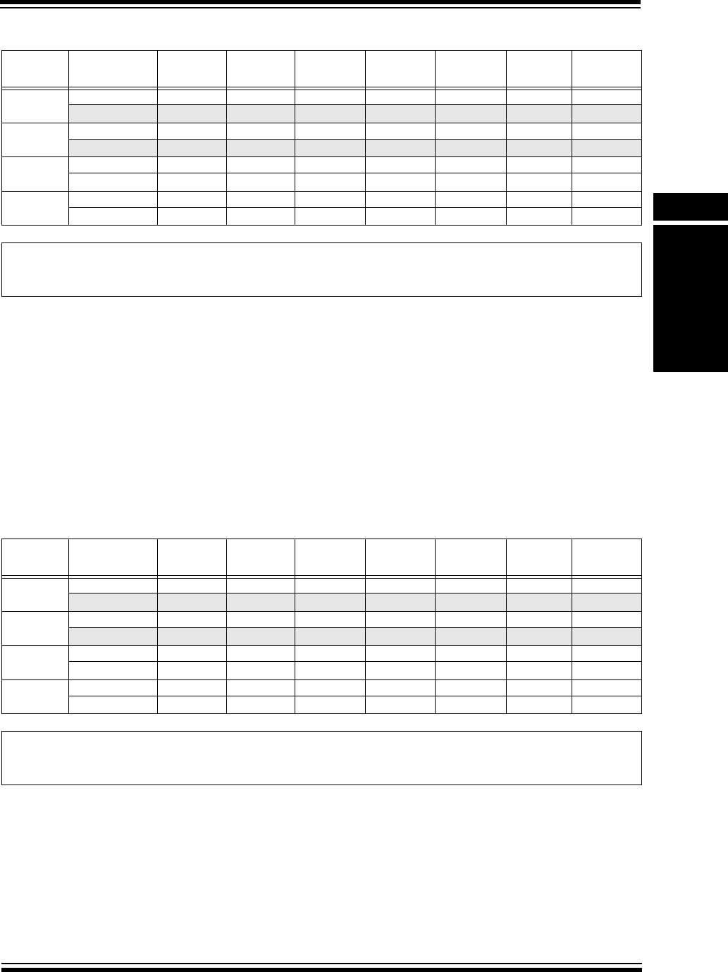
© 2007-2011 Microchip Technology Inc. DS61104E-page 17-11
Section 17. 10-bit Analog-to-Digital Converter (ADC)
10-bit Analog-to-Digital
Converter (ADC)
17
Register 17-5: AD1PCFG: ADC Port Configuration Register(1,2)
Bit Range Bit
31/23/15/7
Bit
30/22/14/6
Bit
29/21/13/5
Bit
28/20/12/4
Bit
27/19/11/3
Bit
26/18/10/2
Bit
25/17/9/1
Bit
24/16/8/0
31:24 U-0 U-0 U-0 U-0 U-0 U-0 U-0 U-0
— — — — — — — —
23:16 U-0 U-0 U-0 U-0 U-0 U-0 U-0 U-0
— — — — — — — —
15:8 R/W-0 R/W-0 R/W-0 R/W-0 R/W-0 R/W-0 R/W-0 R/W-0
PCFG15 PCFG14 PCFG13 PCFG12 PCFG11 PCFG10 PCFG9 PCFG8
7:0 R/W-0 R/W-0 R/W-0 R/W-0 R/W-0 R/W-0 R/W-0 R/W-0
PCFG7 PCFG6 PCFG5 PCFG4 PCFG3 PCFG2 PCFG1 PCFG0
Legend:
R = Readable bit W = Writable bit P = Programmable bit r = Reserved bit
U = Unimplemented bit -n = Bit Value at POR: (‘0’, ‘1’, x = Unknown)
bit 31-16 Unimplemented: Read as ‘0’
bit 15-0 PCFG<15:0>: Analog Input Pin Configuration Control bits
1 = Analog input pin in Digital mode, port read input enabled, ADC input multiplexer input for this analog
input connected to AVss
0 = Analog input pin in Analog mode, digital port read will return as a ‘1’ without regard to the voltage on
the pin, ADC samples pin voltage
Note 1: The AD1PCFG register functionality will vary depending on the number of ADC inputs available on the
selected device. Refer to the specific device data sheet for additional details on this register.
2: The AD1PCFG register is not available on all PIC32 devices. Refer to the specific device data sheet for
availability of this register.
Register 17-6: AD1CSSL: ADC Input Scan Select Register(1)
Bit Range Bit
31/23/15/7
Bit
30/22/14/6
Bit
29/21/13/5
Bit
28/20/12/4
Bit
27/19/11/3
Bit
26/18/10/2
Bit
25/17/9/1
Bit
24/16/8/0
31:24 U-0 U-0 U-0 U-0 U-0 U-0 U-0 U-0
— — — — — — — —
23:16 U-0 U-0 U-0 U-0 U-0 U-0 U-0 U-0
— — — — — — — —
15:8 R/W-0 R/W-0 R/W-0 R/W-0 R/W-0 R/W-0 R/W-0 R/W-0
CSSL15 CSSL14 CSSL13 CSSL12 CSSL11 CSSL10 CSSL9 CSSL8
7:0 R/W-0 R/W-0 R/W-0 R/W-0 R/W-0 R/W-0 R/W-0 R/W-0
CSSL7 CSSL6 CSSL5 CSSL4 CSSL3 CSSL2 CSSL1 CSSL0
Legend:
R = Readable bit W = Writable bit P = Programmable bit r = Reserved bit
U = Unimplemented bit -n = Bit Value at POR: (‘0’, ‘1’, x = Unknown)
bit 31-16 Unimplemented: Read as ‘0’
bit 15-0 CSSL<15:0>: ADC Input Pin Scan Selection bits
1 = Select ANx for input scan
0 = Skip ANx for input scan
Note 1: The AD1CSSL register functionality will vary depending on the number of ADC inputs available on the
selected device. Refer to the specific device data sheet for additional details on this register.

PIC32 Family Reference Manual
DS61104E-page 17-12 © 2007-2011 Microchip Technology Inc.
17.3 ADC OPERATION, TERMINOLOGY AND CONVERSION SEQUENCE
This section describes the operation of the ADC, the steps required to configure the converter,
special features of the module, and provides examples of ADC configuration with timing
diagrams and charts showing the expected output of the converter.
17.3.1 Overview of Operation
Analog sampling consists of two steps: acquisition and conversion (see Figure 17-2). During
acquisition, the analog input pin is connected to the Sample and Hold Amplifier (SHA). After the
pin has been sampled for a sufficient period, and the sample voltage is equivalent to the input,
the pin is disconnected from the SHA to provide a stable input voltage for the conversion process.
The conversion process then converts the analog sample voltage to a binary representation.
An overview of the ADC is presented in Figure 17-1. The 10-bit ADC has a single SHA. The SHA
is connected to the analog input pins through the analog input multiplexers, MUX A and MUX B.
The analog input multiplexers are controlled by the AD1CHS register. There are two sets of MUX
control bits in the AD1CHS register. These two sets of control bits allow the two different analog
input to be independently controlled. The ADC can optionally switch between MUX A and MUX B
configurations between conversions. The ADC can also optionally scan through a series of
analog inputs using a single MUX.
Acquisition time can be controlled manually or automatically. The acquisition time may be started
manually by setting the SAMP bit (AD1CON1<1>), and ended manually by clearing the SAMP
bit in user software. The acquisition time may be started automatically by the ADC hardware and
ended automatically by a conversion trigger source. The acquisition time is set by the SAMC bits
(AD1CON3<12:8>). The SHA has a minimum acquisition period; refer to the specific device data
sheet for acquisition time specifications.
Conversion time is the time required for the ADC to convert the voltage held by the SHA. The
ADC requires one ADC clock cycle (TAD) to convert each bit of the result, plus two additional
clock cycles. Therefore, a total of 12 TAD cycles are required to perform the complete conversion.
When the conversion time is complete, the result is written into one of the 16 ADC result registers
(ADC1BUF0 through ADC1BUFF).
The sum of the acquisition time and the analog-to-digital conversion time provides the total
sample time (refer to Figure 17-2). There are multiple input clock options for the ADC that are
used to create the TAD clock. The user must select an input clock option that does not violate the
minimum TAD specification.
The sampling process can be performed once, periodically, or based on a trigger as defined by
the module configuration.
Figure 17-2: ADC Sample/Conversion Sequence
Acquisition Time Conversion Time
ADC Total Sample Time
SHA is connected to the analog input pin for sampling.
SHA is disconnected from input and holds the signal.
Analog-to-digital conversion is started by the conversion trigger source.
Analog-to-digital conversion complete, result is written
into the ADC result buffer. Optionally generate interrupt.

© 2007-2011 Microchip Technology Inc. DS61104E-page 17-13
Section 17. 10-bit Analog-to-Digital Converter (ADC)
10-bit Analog-to-Digital
Converter (ADC)
17
The start time for sampling can be controlled in software by setting the SAMP bit
(AD1CON1<1>). The start of the sampling time can also be controlled automatically by the hard-
ware. When the ADC operates in Auto-Sample mode, the SHA is reconnected to the analog input
pin at the end of the conversion in the sample/convert sequence. The auto-sample function is
controlled by the ASAM bit (AD1CON1<2>).
The conversion trigger source ends the sampling time and begins an analog-to-digital conversion
or a sample/convert sequence. The conversion trigger source is selected by the SSRC<2:0> bits
(AD1CON1<7:5>). The conversion trigger can be taken from a variety of hardware sources, or
can be controlled manually in software by clearing the SAMP bit. One of the conversion trigger
sources is an auto-conversion. The time between auto-conversions is set by a counter and the
ADC clock. The Auto-Sample mode and auto-conversion trigger can be used together to provide
endless automatic conversions without software intervention.
An interrupt may be generated at the end of each sample sequence or multiple sample
sequences as determined by the value of the SMPI<3:0> bits (AD1CON2<5:2>). The number of
sample sequences between interrupts can vary between 1 and 16. The user should note that the
analog-to-digital conversion buffer holds the results of a single conversion sequence. The next
sequence starts filling the buffer from the top even if the number of samples in the previous
sequence was less than 16. The total number of conversion results between interrupts is the
SMPI value. The total number of conversions between interrupts cannot exceed the physical
buffer length.

PIC32 Family Reference Manual
DS61104E-page 17-14 © 2007-2011 Microchip Technology Inc.
17.4 ADC MODULE CONFIGURATION
Operation of the ADC module is directed through bit settings in the appropriate registers. The
following instructions summarize the actions and the settings. Options and details for each
configuration step are provided in subsequent sections.
To c on fig ure t he ADC m odu le, pe rf orm t he fol lo win g s teps:
1. Configure the analog port pins in AD1PCFG<15:0> (see 17.4.1).
2. Select the analog inputs to the ADC multiplexers in AD1CHS<32:0> (see 17.4.2).
3. Select the format of the ADC result using FORM<2:0> (AD1CON1<10:8>) (see 17.4.3).
4. Select the sample clock source using SSRC<2:0> (AD1CON1<7:5>) (see 17.4.4).
5. Select the voltage reference source using VCFG<2:0> (AD1CON2<15:13>) (see 17.4.7).
6. Select the Scan mode using CSCNA (AD1CON2<10>) (see 17.4.8).
7. Set the number of conversions per interrupt SMP<3:0> (AD1CON2<5:2>), if interrupts are
to be used (see 17.4.9).
8. Set Buffer Fill mode using BUFM (AD1CON2<1>) (see 17.4.10).
9. Select the MUX to be connected to the ADC in ALTS AD1CON2<0> (see 17.4.11).
10. Select the ADC clock source using ADRC (AD1CON3<15>) (see 17.4.12).
11. Select the sample time using SAMC<4:0> (AD1CON3<12:8>), if auto-convert is to be
used (see 17-2).
12. Select the ADC clock prescaler using ADCS<7:0> (AD1CON3<7:0>) (see 17.4.12).
13. Turn the ADC module on using AD1CON1<15> (see 17.4.14).
14. To configure ADC interrupt (if required):
a) Clear the AD1IF bit (IFS1<1>) (see 17.7).
b) Select ADC interrupt priority AD1IP<2:0> (IPC<28:26>) and subpriority AD1IS<1:0>
(IPC<24:24>) if interrupts are to be used (see 17.7).
15. Start the conversion sequence by initiating sampling (see 17.4.15).
Note: Steps 1 through 12, above, can be performed in any order, but Step 13 must be the
final step in every case.

© 2007-2011 Microchip Technology Inc. DS61104E-page 17-15
Section 17. 10-bit Analog-to-Digital Converter (ADC)
10-bit Analog-to-Digital
Converter (ADC)
17
17.4.1 Configuring Analog Port Pins
The AD1PCFG register and the TRISB register control the operation of the ADC port pins.
AD1PCFG specifies the configuration of device pins to be used as analog inputs. A pin is
configured as an analog input when the corresponding PCFGn bit (AD1PCFG<n>) = 0. When
the bit = 1, the pin is set to digital control. When configured for analog input, the associated port
I/O digital input buffer is disabled so it does not consume current. The AD1PCFG register is
cleared at Reset, causing the ADC input pins to be configured for analog input by default at
Reset.
TRIS registers control the digital function of the port pins. The port pins that are desired as analog
inputs must have their corresponding TRIS bit set, specifying the pin as an input. If the I/O pin
associated with an ADC input is configured as output, the TRIS bit is cleared, the ports digital
output level (VOH or VOL) will be converted. After a device Reset, all of the TRIS bits are set.
17.4.2 Selecting the Analog Inputs to the ADC Multiplexers
The AD1CHS register is used to select which analog input pin is connected to MUX A and
MUX B. Each multiplexer has two inputs referred to as the positive and the negative input. The
positive input to MUX A is controlled by the CH0SA<3:0> bits (AD1CHS<19:16>) and the nega-
tive input is controlled by the CH0NA bit (AD1CHS<23>). The positive input for MUX B is con-
trolled by the CH0SB<3:0> bits (AD1CHS<27:24>) and the negative input is controlled by the
CH0NB bit (AD1CHS<31>).
The positive input can be selected from any one of the available analog input pins. The negative
input can be selected as the ADC negative reference or AN1. The use of AN1 as the negative
input allows the ADC to be used in Unipolar Differential mode. Refer to the specific device data
sheet for AN1 input voltage restrictions when used as a negative reference.
17.4.3 Selecting the Format of the ADC Result
The data in the ADC result register can be read as one of eight formats. The format is controlled
by the FORM<2:0> bits (AD1CON1<10:8>). The user can select from integer, signed integer,
fractional, or signed fractional as a 16-bit or 32-bit result. Figure 17-3 and Figure 17-4 illustrate
how a result is formatted. Ta b l e 17-2 and Ta ble 17-3 provide examples of results for the select
results in each of the four formats with 32-bit and 16-bit results.
Note 1: When reading a PORT register that shares pins with the ADC, any pin configured
as an analog input reads as a ‘0’ when the PORT latch is read. Analog levels on
any pin that is defined as a digital input (including the AN15:AN0 pins), but is not
configured as an analog input, may cause the input buffer to consume current that
is out of the device’s specification.
2: The AD1PCFG register is not available in all the PIC32 devices. Refer to the
specific device data sheet for availability.
Note: When using Scan mode, the CH0SA<3:0> bits may be overridden. Refer to
17.4.8 “Selecting the Scan Mode” for more information.
Note: There is no numeric difference between 32-bit and 16-bit modes. In 32-bit mode,
the sign extension is applied to all 32-bits. In 16-bit mode, the sign extension is
applied only to the lower 16-bits of the result.
PIC32 Family Reference Manual
DS61104E-page 17-16 © 2007-2011 Microchip Technology Inc.
Figure 17-3: ADC Output Data Formats, 32-bit Mode
RAM Contents:
d09 d08 d07 d06 d05 d04 d03 d02 d01 d00
Read to Bus:
Integer
0000000000000000000000d09d08d07d06d05d04d03d02d01d00
Signed Integer
d09 d09 d09 d09 d09 d09 d09 d09 d09 d09 d09 d09 d09 d09 d09 d09 d09 d09 d09 d09 d09 d09 d09 d08 d07 d06 d05 d04 d03 d02 d01 d00
Fractional (1.15)
d09 d08 d07 d06 d05 d04 d03 d02 d01 d00 0 0 0 0 0 0 0 0 0 0 0 0 0 0 0 0 0 0 0 0 0 0
Signed Fractional (1.15)
d09 d08 d07 d06 d05 d04 d03 d02 d01 d00 0 0 0 0 0 0 0 0 0 0 0 0 0 0 0 0 0 0 0 0 0 0

© 2007-2011 Microchip Technology Inc. DS61104E-page 17-17
Section 17. 10-bit Analog-to-Digital Converter (ADC)
10-bit Analog-to-Digital
Converter (ADC)
17
Figure 17-4: ADC Output Data Formats, 16-bit Mode
RAM Contents:
d09 d08 d07 d06 d05 d04 d03 d02 d01 d00
Read to Bus:
Integer
0000000000000000000000d09d08d07d06d05d04d03d02d01d00
Signed Integer
0000000000000000d09
d09 d09 d09 d09 d09 d09 d08 d07 d06 d05 d04 d03 d02 d01 d00
Fractional (1.15)
0000000000000000d09d08d07d06d05d04d03d02d01d00000000
Signed Fractional (1.15)
0000000000000000d09
d08 d07 d06 d05 d04 d03 d02 d01 d00 d09 0 0 0 0 0

PIC32 Family Reference Manual
DS61104E-page 17-18 © 2007-2011 Microchip Technology Inc.
Table 17-2: Numerical Equivalents of Select Result Codes for FORM<2> (AD1CON1<10>) = 1, 32-bit Result
VIN/VR10-bit
Output Code 32-bit Integer Format 32-bit Signed
Integer Format
32-bit Fractional
Format
32-bit Signed
Fractional Format
1023/1024 11 1111 1111 0000 0000 0000 0000
0000 0011 1111 1111
= 1023
0000 0000 0000 0000
0000 0001 1111 1111
= 511
1111 1111 1100 0000
0000 0000 0000 0000
= 0.999
0111 1111 1100 0000
0000 0000 0000 0000
= 0.499
1022/1024 11 1111 1110 0000 0000 0000 0000
0000 0011 1111 1110
= 1022
0000 0000 0000 0000
0000 0001 1111 1110
= 510
1111 1111 1000 0000
0000 0000 0000 0000
= 0.998
0111 1111 1000 0000
0000 0000 0000 0000
= 0.498
•••
513/1024 10 0000 0001 0000 0000 0000 0000
0000 0010 0000 0001
= 513
0000 0000 0000 0000
0000 0000 0000 0001
= 1
1000 0000 0100 0000
0000 0000 0000 0000
= 0.501
0 000 0000 0100
0000
0000 0000 0000 0000
= 0.001
512/1024 10 0000 0000 0000 0000 0000 0000
0000 0010 0000 0000
= 512
0000 0000 0000 0000
0000 0000 0000 0000
= 0
1000 0000 0000 0000
0000 0000 0000 0000
= 0.500
0000 0000 0000 0000
0000 0000 0000 0000
= 0.000
511/1024 01 1111 1111 0000 0000 0000 0000
0000 0001 1111 1111
= 511
1111 1111 1111 1111
1111 1111 1111 1111
= -1
0111 1111 1100 0000
0000 0000 0000 0000
= .499
1111 1111 1100 0000
0000 0000 0000 0000
= -0.001
•••
1/1024 00 0000 0001 0000 0000 0000 0000
0000 0000 0000 0001
= 1
1111 1111 1111 1111
1111 1110 0000 0001
= -511
0000 0000 0100 0000
0000 0000 0000 0000
= 0.001
1000 0000 0100 0000
0000 0000 0000 0000
= -0.499
0/1024 00 0000 0000 0000 0000 0000 0000
0000 0000 0000 0000
= 0
1111 1111 1111 1111
1111 1110 0000 0000
= -512
0000 0000 0000 0000
0000 0000 0000 0000
= 0.000
1000 0000 0000 0000
0000 0000 0000 0000
= -0.500
Table 17-3: Numerical Equivalents of Select Result Codes for FORM<2> (AD1CON1<10>) = 0, 16-bit Result
VIN/VR10-bit
Output Code 16-bit Integer Format 16-bit Signed
Integer Format
16-bit Fractional
Format
16-bit Signed
Fractional Format
1023/1024 11 1111 1111 0000 0011 1111 1111
= 1023
0000 0001 1111 1111
= 511
1111 1111 1100 0000
= 0.999
0111 1111 1100 0000
= 0.499
1022/1024 11 1111 1110 0000 0011 1111 1110
= 1022
0000 0001 1111 1110
= 510
1111 1111 1000 0000
= 0.998
0111 1111 1000 0000
= 0.498
•••
513/1024 10 0000 0001 0000 0010 0000 0001
= 513
0000 0000 0000 0001
= 1
1000 0000 0100 0000
= 0.501
0 000 0000 0100
0000
= 0.001
512/1024 10 0000 0000 0000 0010 0000 0000
= 512
0000 0000 0000 0000
= 0
1000 0000 0000 0000
= 0.500
0000 0000 0000 0000
= 0.000
511/1024 01 1111 1111 0000 0001 1111 1111
= 511
1111 1111 1111 1111
= -1
0111 1111 1100 0000
= .499
1111 1111 1100 0000
= -0.001
•••
1/1024 00 0000 0001 0000 0000 0000 0001
= 1
1111 1110 0000 0001
= -511
0000 0000 0100 0000
= 0.001
1000 0000 0100 0000
= -0.499
0/1024 00 0000 0000 0000 0000 0000 0000
= 0
1111 1110 0000 0000
= -512
0000 0000 0000 0000
= 0.000
1000 0000 0000 0000
= -0.500

© 2007-2011 Microchip Technology Inc. DS61104E-page 17-19
Section 17. 10-bit Analog-to-Digital Converter (ADC)
10-bit Analog-to-Digital
Converter (ADC)
17
17.4.4 Selecting the Sample Clock Source
It is often desirable to synchronize the end of sampling and the start of conversion with some
other time event. The ADC module may use one of four sources as a conversion trigger. The
selection of the conversion trigger source is controlled by the SSRC<2:0> bits (AD1CON1<7:5>).
17.4.4.1 MANUAL CONVERSION
To configure the ADC to end sampling and start a conversion when the SAMP bit
(AD1CON1<1>) is cleared (= 0), set the SSRC<2:0> bits to ‘000’.
17.4.4.2 TIMER COMPARE TRIGGER
The ADC is configured for this trigger mode by setting the SSRC<2:0> = 010. When a period
match occurs for the 32-bit timer, TMR3/TMR2, or the 16-bit Timer3, a special ADC trigger event
signal is generated by Timer3. This feature does not exist for the TMR5/TMR4 timer pair or for
16-bit timers other than Timer3. Refer to Section 14. “Timers” (DS61105) for more details.
17.4.4.2.1 External INT0 Pin Trigger
To co nfig ur e t he A DC to b egin a c onv ers io n on an active transition on the INT0 pin, the
SSRC<2:0> bits are set to ‘001’. The INT0 pin may be programmed for either a rising edge input
or a falling edge input to trigger the conversion process.
17.4.4.2.2 Auto-Convert
The ADC can be configured to automatically perform conversions at the rate selected by the
SAMC<4:0> bits (AD1CON3<12:8>). The ADC is configured for this Trigger mode by setting the
SSRC<2:0> bits to ‘111’. In this mode, the ADC will perform continuous conversions on the
selected channels.
17.4.5 Synchronizing ADC Operations to Internal or External Events
The modes where an external event trigger pulse ends sampling and starts conversion
(SSRC<2:0> bits = 001, 010 or 011) may be used in combination with auto-sampling (ASAM bit
(AD1CON1<2>) = 1) to cause the ADC to synchronize the sample conversion events to the
trigger pulse source. For example, in Figure 17-13 where SSRC<2:0> = 010 and ASAM = 1,
ADC will always end sampling and start conversions synchronously with the timer compare
trigger event. The ADC will have a sample conversion rate that corresponds to the timer
comparison event rate. See Example 17-5 for a code example.
17.4.6 Selecting Automatic or Manual Sampling
Sampling can be started manually or automatically when the previous conversion is complete.
17.4.6.1 MANUAL SAMPLING
Clearing the ASAM bit (AD1CON1<2>) disables the Auto-Sample mode. Acquisition will begin
when the SAMP bit (AD1CON1<1>) is set by software. Acquisition will not resume until the
SAMP bit is once again set. Figure 17-8 illustrates an example.
17.4.6.2 AUTOMATIC SAMPLING
Setting the ASAM bit (AD1CON1<2>) enables Auto-Sample mode. In this mode, the sampling
will start automatically after the pervious sample has been converted. Figure 17-9 illustrates an
example.

PIC32 Family Reference Manual
DS61104E-page 17-20 © 2007-2011 Microchip Technology Inc.
17.4.7 Selecting the Voltage Reference Source
The user can select the voltage reference for the ADC module. The reference can be internal or
external.
The VCFG<2:0> bits (AD1CON2<15:13>) select the voltage reference for analog-to-digital
conversions. The upper voltage reference (VR+) and the lower voltage reference (VR-) may be
the internal AVDD and AVSS voltage rails, or the VREF+ and VREF- input pins. The external ADC
voltage reference may be used to reduce noise in the converter.
The external voltage reference pins may be shared with the AN0 and AN1 inputs on low pin count
devices. The ADC can still perform conversions on these pins when they are shared with the
VREF+ and VREF- input pins.
The voltages applied to the external reference pins must meet certain specifications. Refer to the
“Electrical Characteristics” section in the specific device data sheet for more information.
17.4.8 Selecting the Scan Mode
The ADC module has the ability to scan through a selected vector of inputs. The CSCNA bit
(AD1CON2<10>) enables the MUX A input to be scanned across a selected number of analog
inputs.
17.4.8.1 SCAN MODE ENABLE
Scan mode is enabled by setting the CSCNA bit (AD1CON2<10>). When Scan mode is enabled,
the positive input of MUX A is controlled by the contents of the AD1CSSL register. Each bit in the
AD1CSSL register corresponds to an analog input. Bit 0 corresponds to AN0, bit 1 corresponds
to AN1, and so on. If a particular bit in the AD1CSSL register is ‘1’, the corresponding input is
part of the scan sequence. The input is always scanned from lower-numbered input to
higher-numbered input, starting at the first selected channel after each interrupt occurs. When
Scan mode is enabled, the CH0SA<3:0> bits (AD1CHS<19:16>) are ignored.
17.4.8.2 SCAN MODE DISABLE
When the CSCNA bit = 0, Scan mode is disabled and the positive input to MUX A is controlled
by the CH0SA<3:0> bits.
Note: External references, VREF+ and VREF-, must be selected for high conversion. Refer
to the specific device data sheet for more information. The external VREF+ and
VREF- pins may be shared with other analog peripherals. Refer to the specific device
data sheet for more information.
Note: If the number of scanned input selected is greater than the number of samples taken
per interrupt, the higher numbered inputs will not be sampled. The AD1CSSL
register specifies only the input of the positive input of the channel. The CH0NA bit
(AD1CHS<23>) selects the input of the negative input of the channel during
scanning.

© 2007-2011 Microchip Technology Inc. DS61104E-page 17-21
Section 17. 10-bit Analog-to-Digital Converter (ADC)
10-bit Analog-to-Digital
Converter (ADC)
17
17.4.8.3 USING SCAN AND ALTERNATE MODES TOGETHER
The Scan and Alternate modes may be combined to allow a vector of inputs to be scanned and
a single input to be converted every other sample.
This mode is enabled by setting the CSCNA bit (AD1CON2<10>) = 1, and setting the ALTS bit
(AD1CON2<0>) = 1. The CSCNA bit enables the scan for MUX A, and the CH0SB<3:0> bits
(AD1CHS<27:24>) and the CH0NB bit (AD1CHS<31>) are used to configure the inputs to
MUX B. Scanning only applies to the MUX A input selection. The MUX B input selection, as
specified by the CH0SB<3:0> bits, will still select a single input.
The following sequence is an example of three scanned channels (MUX A) and a single fixed
channel (MUX B):
1. The first input in the scan list is sampled.
2. The input selected by CH0SB<3:0> and CH0NB is sampled.
3. The second input in the scan list is sampled.
4. The input selected by CH0SB<3:0> and CH0NB is sampled.
5. The third input in the scan list is sampled.
6. The input selected by CH0SB<3:0> and CH0NB is sampled.
The process is repeated.
17.4.9 Setting the Number of Conversions per Interrupt
The SMPI<3:0> bits (AD1CON2<5:2>) select how many analog-to-digital conversions will take
place before a CPU interrupt is generated. This also defines the number of locations that will be
written in the result buffer starting with ADC1BUF0 (ADC1BUF0 or ADC1BUF8 for Dual Buffer
mode). This can vary from one sample to 16 samples (one to eight samples for Dual Buffer
mode). After the interrupt is generated, the sampling sequence restarts, with the result of the first
sample being written to the first buffer location.
For example, if the SMPI<3:0> bits = 0000, the conversion results will always be written to
ADC1BUF0. In this example, no other buffer locations would be used.
For example, if the SMPI<3:0> bits = 1110, 15 samples would be converted and stored in buffer
locations, ADC1BUF0 through ADC1BUFE. An interrupt would be generated after ADC1BUFE
is written. The next sample would be written to ADC1BUF0. In this example, ADC1BUFF would
not be used.
The data in the result registers will be overwritten by the next sampling sequence. The data in
the result buffer must be read before the completion of the first sample after the interrupt is
generated. The Buffer Fill mode can be used to increase the time between interrupt generation
and the overwriting of data. Refer to 17.4.10 “Buffer Fill Mode”.
The user cannot program a combination of samples and SMPI bits that results in more than 16
conversions per interrupt when the BUFM bit (AD1CON2<1>) is ‘1’, or more than eight
conversions per interrupt when the BUFM bit (AD1CON2<1>) is ‘0’. Attempting to create a
conversion list with the number of samples greater than 16 will result in the sampling sequence
being truncated to 16 samples.

PIC32 Family Reference Manual
DS61104E-page 17-22 © 2007-2011 Microchip Technology Inc.
17.4.10 Buffer Fill Mode
The Buffer Fill mode allows the output buffer to be used as a single 16-word buffer or two 8-word
buffers.
When the Dual Buffer Mode bit, BUFM (AD1CON2<1>), is ‘0’, the complete 16-word buffer is
used for all conversion sequences. Conversion results will be written sequentially in the buffer
starting at ADC1BUF0 until the number of samples as defined by the SMPI<3:0> bits
(AD1CON2<5:2>) is reached. The next conversion result will be written to ADC1BUF0 and the
process repeats. If the ADC interrupt is enabled an interrupt will be generated when the number
of samples in the buffer equals SMPI<3:0>.
When the BUFM bit is ‘1’, the 16-word results buffer (ADRES) will be split into two 8-word groups.
Conversion results will be written sequentially into the first buffer starting at ADC1BUF0, the
BUFS bit (AD1CON2<7>) will be cleared, until the number of samples as defined by the
SMPI<3:0> bits is reached. The ADC interrupt flag will then be set.
After the ADC interrupt flag is set, the following result will be written sequentially to the second
buffer starting at ADC1BUF8. The next conversion result will be written to the second buffer
starting at ADC1BUF8, the BUFS bit will be set, until the number of samples as defined by the
SMPI<3:0> bits is reached. The ADC interrupt flag will then be set.
The process then restarts with BUFS = 0 and results being written to the first buffer.
The decision of which buffer fill mode to use will depend upon how much time is available to move
the buffer contents after the analog-to-digital interrupt and the interrupt latency, as determined by
the application. If the processor can unload a full buffer within the time it takes to sample and
convert one channel, the BUFM bit can be ‘0’ and up to 16 conversions may be done per
interrupt. The processor will have one acquisition-and-conversion period before the first buffer
location is overwritten.
If the processor cannot unload the buffer within the sample-and-conversion time, set the BUFM
bit = 1, to prevent overwriting result data. For example, if the SMPI<3:0> bits = 0111, eight
conversions will be written loaded into the first buffer, following which an interrupt will occur. The
next eight conversions will be written to the second buffer. Therefore, the processor will have the
entire time between interrupts to read the eight conversions out of the buffer.
17.4.11 Selecting the MUX to be Connected to the ADC (Alternating
Sample Mode)
The ADC has two input multiplexers that connect to the SHA. These multiplexers are used to
select which analog input is to be sampled. Each of the multiplexers have a positive and a
negative input (see Figure 17-5 and Figure 17-6).
17.4.11.1 SINGLE INPUT SELECTION
The user may select one of up to 16 analog inputs, as determined by the number of analog
channels on the device, as the positive input of the SHA. The CH0SA<3:0> bits
(AD1CHS<19:16>) select the positive analog input.
The user may select either VR- or AN1 as the negative input. The CH0NA bit (AD1CHS<23>)
selects the analog input for the negative input of channel 0. Using AN1 as the negative input
allows unipolar differential measurements. The ALTS bit (AD1CON2<0>) must be clear for this
mode of operation.
Note: The number of analog inputs will vary among different devices. Consult the specific
device data sheet to verify the analog input availability.

© 2007-2011 Microchip Technology Inc. DS61104E-page 17-23
Section 17. 10-bit Analog-to-Digital Converter (ADC)
10-bit Analog-to-Digital
Converter (ADC)
17
17.4.11.2 ALTERNATING INPUT SELECTIONS
The ALTS bit (AD1CON2<0>) is used by the ADC module to alternate between the two input
multiplexers.
The inputs specified by the CH0SA<3:0> bits (AD1CHS<19:16>) and the CH0NA bit
(AD1CHS<23>) are called the MUX A inputs. The inputs specified by the CH0SB<3:0> bits
(AD1CHS<27:24>) and the CH0NB bit (AD1CHS<31>) are called the MUX B inputs.
When the ALTS bit is ‘1’, the ADC module will alternate between the MUX A inputs on one sample
and the MUX B inputs on the subsequent sample. When the ALTS bit is ‘0’, only the inputs specified
by the CH0SA<3:0> and CH0NA bits are selected for sampling.
For example, if the ALTS bit is ‘1’ on the first sample/convert sequence, the inputs specified by
the CH0SA<3:0> and CH0NA bits are selected for sampling. On the next sample, the inputs
specified by the CH0SB<3:0> and CH0NB bits are selected for sampling. The pattern then
repeats.
17.4.12 Selecting the ADC Conversion Clock Source and Prescaler
The ADC module can use the internal RC oscillator or the Peripheral Bus Clock (PBCLK) as the
conversion clock source.
When the internal RC oscillator is used as the clock source (ADRC bit (AD1CON3<15>) = 1), the
TAD is the period of the oscillator, and no prescaler is used. When using the internal oscillator the
ADC can continue to function in Sleep mode and in Idle mode.
When the PBCLK is used as the conversion clock source, the ADRC bit = 0, the TAD is the period
of the PBCLK after the prescaler ADCS<7:0> bits (AD1CON3<7:0>) are applied.
The ADC has a maximum rate at which conversions may be completed. An Analog module clock,
TAD, controls the conversion timing. The analog-to-digital conversion requires 12 clock
periods (12 TAD).
The period of the ADC conversion clock is software selected using an 8-bit counter. There are
256 possible options for TAD, which are specified by the ADCS<7:0> bits (AD1CON3<7:0>).
Equation 17-1 gives the TAD value as a function of the ADCS bits and the device instruction cycle
clock period, TCY.
Equation 17-1: ADC Conversion Clock Period
For correct analog-to-digital conversions, the ADC conversion clock (TAD) must be selected to
ensure a minimum TAD time of 83.33 ns (see 17.10 “Related Application Notes”).
Equation 17-2: Available Sampling Time, Sequential Sampling
Note: The internal RC oscillator is intended for ADC operation in Sleep mode, and
therefore, it is not calibrated. Applications requiring precise timing of ADC
acquisitions should use a stable calibrated clock source for the ADC.
TAD 2TPB ADCS 1+()•()•=
ADCS TAD
2TPB
•
------------------
⎝⎠
⎛⎞
1–=
TSMP TriggerPulseInterval TSEQ
()ConversionTime TCONV
()–=
TSMP TSEQ TCONV
–=
Note: TSEQ is the trigger pulse interval time.

PIC32 Family Reference Manual
DS61104E-page 17-24 © 2007-2011 Microchip Technology Inc.
17.4.12.1 CONFIGURING THE ADC FOR 1000 KSPS OPERATION
Calculate the parameters for 1 Msps for a system clock of 60 MHz and Peripheral Clock Divider = 2.
The calculation is performed as follows:
1. Calculate the Peripheral Bus clock time period (TPB) and the sample plus convert period.
Equation 17-3: TPB and Sample Plus Convert Period
2. Calculate the ideal TAD. The ADC requires one or more TAD (sample time) and 12 TAD
(convert time) to perform a sample/conversion.
a) Calculate the ADC sample plus convert time with a minimum sample time (1 TAD), as
shown in Equation 17-4. The ADC minimum requirements for TAD is met, but not the
sample time.
Equation 17-4: ADC Sample Plus Convert Time with a Minimum Sample Time
b) Increase the sample period to 2 TAD.
c) Repeat the ADC clock calculation with a sample time equal to 2 TAD. This meets the
ADC minimum requirements for TAD and sample time.
Equation 17-5: ADC Clock Calculation
3. Calculate the ADC clock divisor value using the values from the previous steps.
The closest available higher integer divisor value is 4 (ADCS = 1).
The closest available lower integer divisor value is 2 (ADCS = 0).
Equation 17-6: ADC Clock Divisor
TPB
1
60MHz
------------------ 2×33.3ns==
1
1000ksps
----------------------- 1µsconverttime+=
1µs
12 1+
---------------76.9ns TAD
==
Desired ADC clock period
1µs
12 2+
---------------71.4ns TAD
==
TAD 2 sample periods•71.4ns 2•142.8ns sample time===
71.4ns
1
30MHz
------------------
⎝⎠
⎛⎞
------------------------2.31=Desired ADC clock divisor

© 2007-2011 Microchip Technology Inc. DS61104E-page 17-25
Section 17. 10-bit Analog-to-Digital Converter (ADC)
10-bit Analog-to-Digital
Converter (ADC)
17
4. Calculate the sample rate using the available ADCS divisors. Calculate using an ADC
clock divisor value of 4.
Equation 17-7: Sample Rate Calculation
5. Calculate the sample time by increase the sampling time to reduce the sample rate to an
acceptable value. Recalculate using the divisor value of 2 and a sample time of 3 TAD.
Equation 17-8: Sample Time Calculation
6. Verify the calculations of the actual TAD using the PB period and the actual ADC clock
divisor. The desired sample rate and values that meet the device specification are
calculated.
Equation 17-9:
17.4.13 Acquisition Time Considerations
Different acquisition/conversion sequences provide different times for the sample-and-hold
channel to acquire the analog signal. The user must ensure the acquisition time meets the
sampling requirements, as outlined in 17.5.20 “ADC Sampling Requirements”.
When SSRC<2:0> (AD1CON1<7:5>) = 111, the conversion trigger is under ADC clock control.
The SAMC<4:0> bits (AD1CON3<12:8>) select the number of TAD clock cycles between the start
of acquisition and the start of conversion. This trigger option provides the fastest conversion rates
on multiple channels. After the start of acquisition, the module will count a number of TAD clocks
specified by the SAMC bits.
1
4 12 2+()•33.3ns)•
-------------------------------------------------------535.7ksps=
The resulting actual sample rate is too low. Calculate using a ADC clock divisor value of 2.
1
2 12 2+()•33.3ns)•
-------------------------------------------------------1071ksps=
The actual sample rate achieved is very close to the desired value, but it exceeds the 1 Msps
specification.
1
2123+()•33.3ns)•
-------------------------------------------------------1000ksps=
1
30MHz
------------------ 33.3ns TPB==
33.3ns 266.6ns=•TAD
=
TAD 3•66.6ns 3•200ns sampletime===
Summary:
ADCS = 2: ADC clock is PB divided by 2
SAMPC = 3: Sample time is 3 T
AD periods

PIC32 Family Reference Manual
DS61104E-page 17-26 © 2007-2011 Microchip Technology Inc.
17.4.14 Turning ON the ADC
When the ON bit (AD1CON1<15>) is ‘1’, the ADC module is in Active mode and is fully powered
and functional.
When ON is ‘0’, the ADC module is disabled. The digital and analog portions of the circuit are
turned off for maximum current savings.
In order to return to the Active mode from the OFF mode, the user software must wait for the
analog stages to stabilize. Refer to the “Electrical Characteristics” section in the specific
device data sheet for the stabilization time.
17.4.15 Initiating Sampling
17.4.15.1 MANUAL MODE
In manual sampling, an acquisition is started by writing a ‘1’ to the SAMP bit (AD1CON1<1>).
Software must manually manage the start and end of the acquisition period by setting and then
clearing the SAMP bit after the desired acquisition period has elapsed.
17.4.15.2 AUTO-SAMPLE MODE
In Auto-sample mode, the sampling process is started by writing a ‘1’ to the ASAM bit
(AD1CON1<2>). In Auto-Sample mode, the acquisition period is defined by the ADCS<7:0> bits
(AD1CON3<7:0>). Acquisition is automatically started after a conversion is completed.
Auto-Sample mode can be used with any trigger source other than manual.
17.5 MISCELLANEOUS ADC FUNCTIONS
17.5.1 Aborting Sampling
Clearing the SAMP bit (AD1CON1<1>) while in Manual Sample mode will terminate sampling,
but may also start a conversion, if the SSRC<2:0> bits (AD1CON1<7:5>) = 000.
Clearing the ASAM bit (AD1CON1<2>) while in Auto-sample mode will not terminate an ongoing
acquire/convert sequence. However, sampling will not automatically resume after the current
sample is converted.
17.5.2 Aborting a Conversion
Clearing the ON bit (AD1CON1<15>) during a conversion will abort the current conversion. The
ADC Result register will not be updated with the partially completed analog-to-digital conversion
sample. That is, the corresponding result buffer location will continue to contain the value of the
last completed conversion (or the last value written to the buffer).
17.5.3 Buffer Fill Status
When the conversion result buffer is split using the BUFM bit (AD1CON2<1>), the BUFS bit
(AD1CON2<7>) indicates which half of the buffer the ADC is currently filling. If the BUFS bit = 0,
the ADC is filling ADC1BUF0 to ADC1BUF7 and the user software should read conversion
values from ADC1BUF8 to ADC1BUFF. If the BUFS bit = 1, the situation is reversed and the user
software should read conversion values from ADC1BUF0 to ADC1BUF7.
Note: Writing to any ADC control bits other than the ON (AD1CON1<15>), SAMP
(AD1CON1<1>), and DONE (AD1CON1<0>) bits is not recommended while the
ADC module is running.

© 2007-2011 Microchip Technology Inc. DS61104E-page 17-27
Section 17. 10-bit Analog-to-Digital Converter (ADC)
10-bit Analog-to-Digital
Converter (ADC)
17
17.5.4 Offset Calibration
The ADC module provides a method of measuring the internal offset error. After this offset error
is measured, it can be subtracted, in software, from the result of a analog-to-digital conversion.
Use the following steps to perform an offset measurement:
1. Configure the ADC in the same manner as it will be used in the application.
2. Set the OFFCAL bit (AD1CON2<12>). This overrides the input selections and connects
the sample-and-hold inputs to AVss.
3. If auto-sample is used, set the CLRASAM bit (AD1CON1<4>) to stop conversions when
the number of samples stated by SMPI is reached.
4. Enable the ADC and perform a conversion. The value that is written to the ADC result
buffer is the internal offset error.
5. Clear the OFFCAL bit (AD2CON<12>) to return the ADC to normal operation.
17.5.5 Terminate Conversion Sequence after an Interrupt
The CLRASAM bit provides a method to terminate auto-sample after the first sequence is
completed. Setting the CLRASAM bit and starting an auto-sample sequence will cause the ADC
to complete one auto-sample sequence (the number of samples as defined by the SMPI<3:0>
bits (AD1CON2<5:2>)). Hardware will the clear the ASAM bit (AD1CON1<2>) and set the inter-
rupt flag. This will stop the sampling process to allow inspection of the result buffer without results
being overwritten by the next automatic conversion sequence. The CLRASAM bit must be
cleared by software to disable this mode.
17.5.6 DONE Bit Operation
The DONE bit (AD1CON1<0>) is set when a conversion sequence is complete. In Manual mode,
the DONE bit is persistent. It remains set until it is cleared by software. The DONE bit can be
polled to determine when the conversion has completed.
In all automatic sample modes (ASAM bit = 1), the DONE bit is not persistent. It is set at the end
of a conversion sequence and cleared by hardware when the next acquisition is started. Polling
the DONE bit is not recommended when operating the ADC in automatic modes. The AD1IF flag
bit (IFS1<1>) is latched after a conversion sequence is completed and can therefore be polled.
Figure 17-5 shows the ADC configuring for Alternate Sampling mode. Figure 17-6 shows the
ADC configuration for Scan mode. Figure 17-7 shows the ADC configuration for a combination
of Alternate Sampling mode and Scan mode.
Note: Only positive ADC offsets can be measured with this method.
Note: Disabling Interrupts or masking the ADC interrupt has no effect on the operation of
the CLRASAM bit.
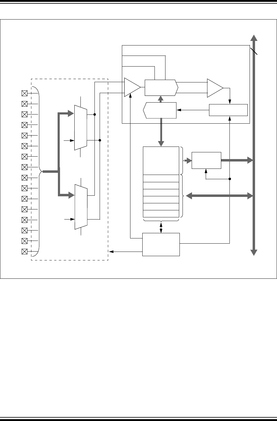
PIC32 Family Reference Manual
DS61104E-page 17-28 © 2007-2011 Microchip Technology Inc.
Figure 17-5: Simplified 10-bit High-Speed ADC Block Diagram for Alternate Sample Mode
AD1CON1
AD1CON2
AD1CON3
AD1CHS
AD1PCFG
AD1CSSL
Comparator
10-bit SAR Conversion Logic
DAC
AN12
AN13
AN14
AN15
AN8
AN9
AN10
AN11
AN4
AN5
AN6
AN7
AN0
AN1
AN2
AN3
Sample Control
SHA
ADC1BUF0:
ADC1BUFF
Control Logic
Data
Input MUX Control
Conversion Control
Pin Config Control
Internal Data Bus
32
VR+
VR-
MUX A
MUX B
VINH
VINL
VINH
VINH
VINL
VINL
Formatting
CH0SA<3:0>
CH0SB<3:0>
CH0NB
CHONA
VR-
VR-
VR+

© 2007-2011 Microchip Technology Inc. DS61104E-page 17-29
Section 17. 10-bit Analog-to-Digital Converter (ADC)
10-bit Analog-to-Digital
Converter (ADC)
17
Figure 17-6: Simplified 10-bit High-Speed ADC Block Diagram for Scan Mode
AD1CON1
AD1CON2
AD1CON3
AD1CHS
AD1PCFG
AD1CSSL
Comparator
10-bit SAR Conversion Logic
DAC
AN12
AN13
AN14
AN15
AN8
AN9
AN10
AN11
AN4
AN5
AN6
AN7
AN0
AN1
AN2
AN3
Sample Control
SHA
ADC1BUF0:
ADC1BUFF
Control Logic
Data
Input MUX Control
Conversion Control
Pin Config Control
Internal Data Bus
32
VR+
VR-
MUX A
VINH
VINL
VINH
VINL
Formatting
AD1CSSL
CH0NA
VR-
VR+
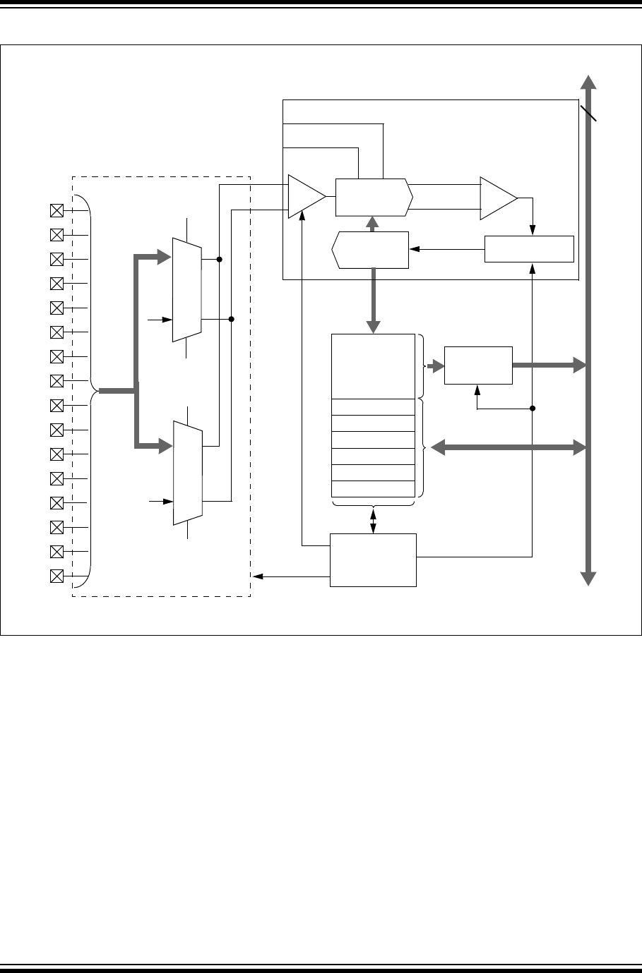
PIC32 Family Reference Manual
DS61104E-page 17-30 © 2007-2011 Microchip Technology Inc.
Figure 17-7: Simplified 10-bit High-Speed ADC Block Diagram for Alternate Sample and Scan Mode
AD1CON1
AD1CON2
AD1CON3
AD1CHS
AD1PCFG
AD1CSSL
Comparator
10-bit SAR Conversion Logic
DAC
AN12
AN13
AN14
AN15
AN8
AN9
AN10
AN11
AN4
AN5
AN6
AN7
AN0
AN1
AN2
AN3
Sample Control
SHA
ADC1BUF0:
ADC1BUFF
Control Logic
Data
Input MUX Control
Conversion Control
Pin Config Control
Internal Data Bus
32
VR+
VR-
MUX A
MUX B
VINH
VINL
VINH
VINH
VINL
VINL
Formatting
AD1CSSL
CH0SB<3:0>
CH0NB
CH0NA
VR-
VR-
VR+

© 2007-2011 Microchip Technology Inc. DS61104E-page 17-31
Section 17. 10-bit Analog-to-Digital Converter (ADC)
10-bit Analog-to-Digital
Converter (ADC)
17
17.5.7 Conversion Sequence Examples
The following configuration examples show the ADC operation in different sampling and buffering
configurations. In each example, setting the ASAM bit (AD1CON2<1>) starts automatic
sampling. A conversion trigger ends sampling and starts conversion.
17.5.8 Manual Conversion Control
When the SSRC<2:0> bits (AD1CON1<7:5>) = 000, the conversion trigger is under software
control. Clearing the SAMP bit (AD1CON1<1>) starts the conversion sequence.
Figure 17-8 is an example where setting the SAMP bit initiates sampling and clearing the SAMP
bit terminates sampling and starts conversion. The user software must time the setting and
clearing of the SAMP bit to ensure adequate acquisition time of the input signal. See
Example 17-1 for a code example.
Figure 17-8: Converting 1 Analog Input, Manual Sample Start, Manual Conversion Start
Example 17-1: Converting 1 Channel, Manual Sample Start, Manual Conversion Start Code
ADCLK
SAMP
ADC1BUF0
TACQ TCONV
set SAMP = 0set SAMP = 1
Instruction Execution
DONE
AD1PCFG = 0xFFFB; // PORTB = Digital; RB2 = analog
AD1CON1 = 0x0000; // SAMP bit = 0 ends sampling
// and starts converting
AD1CHS = 0x00020000; // Connect RB2/AN2 as CH0 input
// in this example RB2/AN2 is the input
AD1CSSL = 0;
AD1CON3 = 0x0002; // Manual Sample, TAD = internal 6 TPB
AD1CON2 = 0;
AD1CON1SET = 0x8000; // turn on the ADC
while (1) // repeat continuously
{
AD1CON1SET = 0x0002; // start sampling ...
DelayNmSec(100); // for 100 ms
AD1CON1CLR = 0x0002; // start Converting
while (!(AD1CON1 & 0x0001));// conversion done?
ADCValue = ADC1BUF0; // yes then get ADC value
} // repeat
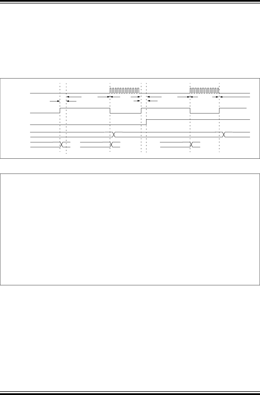
PIC32 Family Reference Manual
DS61104E-page 17-32 © 2007-2011 Microchip Technology Inc.
17.5.9 Automatic Acquisition
Figure 17-9 is an example in which setting the ASAM bit (AD1CON1<2>) initiates automatic
acquisition, and clearing the SAMP bit (AD1CON1<1>) terminates sampling and starts
conversion. After the conversion completes, the module will automatically return to a acquisition
state. The SAMP bit is automatically set at the start of the acquisition interval. The user software
must time the clearing of the SAMP bit to ensure adequate acquisition time of the input signal,
understanding that the time between clearing of the SAMP bit includes the conversion time as
well as the acquisition time. See Example 17-2 for a code example.
Figure 17-9: Converting 1 Channel, Automatic Sample Start, Manual Conversion Start
Example 17-2: Converting 1 Channel, Automatic Sample Start, Manual Conversion Start Code
ADCLK
SAMP
ADC1BUF0
TACQ TCONV
Set = 0 Instruction Execution
TCONV
set ASAM = 1 Set = 0
TACQ
TAD0 TAD0
DONE
AD1PCFG = 0xFF7F; // all PORTB = Digital but RB7 = analog
AD1CON1 = 0x0004; // ASAM bit = 1 implies acquisition
// starts immediately after last
// conversion is done
AD1CHS = 0x00070000; // Connect RB7/AN7 as CH0 input
// in this example RB7/AN7 is the input
AD1CSSL = 0;
AD1CON3 = 0x0002; // Sample time manual, TAD = internal 6 TPB
AD1CON2 = 0;
AD1CON1SET = 0x8000; // turn ON the ADC
while (1) // repeat continuously
{
DelayNmSec(100); // sample for 100 mS
AD1CON1SET = 0x0002; // start Converting
while (!(AD1CON1 & 0x0001));// conversion done?
ADCValue = ADC1BUF0; // yes then get ADC value
} // repeat

© 2007-2011 Microchip Technology Inc. DS61104E-page 17-33
Section 17. 10-bit Analog-to-Digital Converter (ADC)
10-bit Analog-to-Digital
Converter (ADC)
17
17.5.10 Clocked Conversion Trigger
When the SSRC<2:0> bits (AD1CON1<7:5>) = 111, the conversion trigger is under ADC clock
control. The SAMC<4:0> bits (AD1CON3<4:0>) select the number of TAD clock cycles between
the start of acquisition and the start of conversion. This trigger option provides the fastest
conversion rates on multiple channels. After the start of acquisition, the module will count a
number of TAD clocks specified by the SAMC<4:0> bits.
Equation 17-10: Clocked Conversion Trigger Time
SAMC must always be programmed for at least one clock cycle. See Example 17-3 for a code
example.
Figure 17-10: Converting 1 Channel, Manual Sample Start, TAD Based Conversion Start
Example 17-3: Converting 1 Channel, Manual Sample Start, TAD Based Conversion Start Code
TSMP = SAMC<4:0>* TAD
ADCLK
SAMP
ADC1BUF0
TSAMP TCONV
set SAMP = 1
Instruction Execution
DONE
= 31 TAD
AD1PCFG = 0xEFFF; // all PORTB = Digital; RB12 = analog
AD1CON1 = 0x00E0; // SSRC bit = 111 implies internal
// counter ends sampling and starts converting
AD1CHS = 0x000C0000; // Connect RB12/AN12 as CH0 input
// in this example RB12/AN12 is the input
AD1CSSL = 0;
AD1CON3 = 0x1F02; // Sample time = 31 TAD
AD1CON2 = 0;
AD1CON1SET = 0x8000; // turn ON the ADC
while (1) // repeat continuously
{
AD1CON1CLR = 0x0002; // start sampling then...
// after 31Tad go to conversion
while (!(AD1CON1 & 0x0001)); // conversion done?
ADCValue = ADC1BUF0; // yes then get ADC value
} // repeat
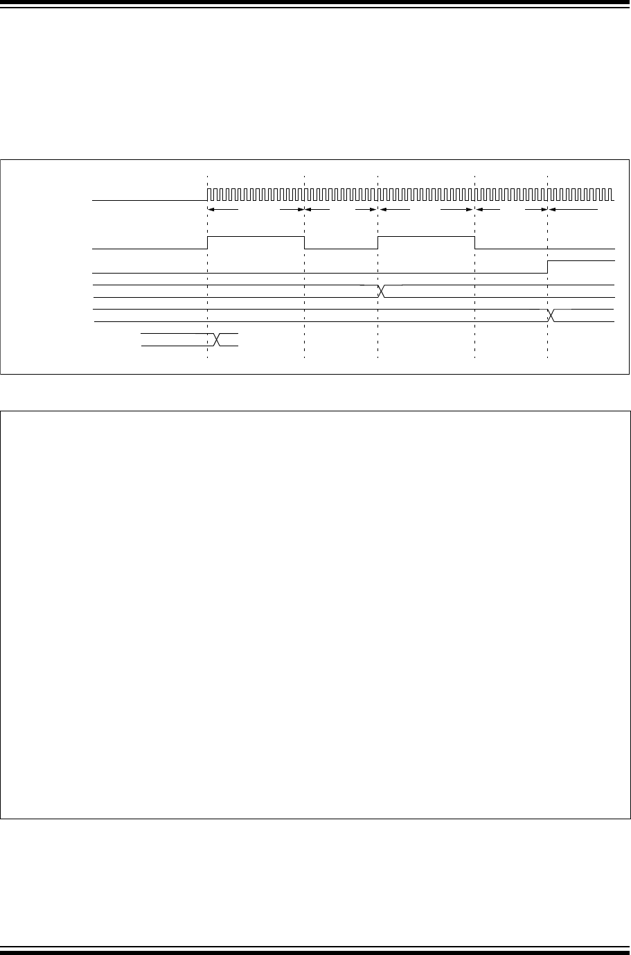
PIC32 Family Reference Manual
DS61104E-page 17-34 © 2007-2011 Microchip Technology Inc.
17.5.11 Free Running Sample Conversion Sequence
As shown in Figure 17-11, using the Auto-Convert Conversion Trigger mode
(SSRC<2:0> = 111) in combination with the Automatic Sampling Start mode (ASAM = 1), allows
the ADC module to schedule acquisition/conversion sequences with no intervention by the user
or other device resources. This “Clocked” mode allows continuous data collection after module
initialization. See Example 17-4 for a code example.
Figure 17-11: Converting 1 Channel, Two Times, Auto-Sample Start, TAD Based Conversion Start
Example 17-4: Converting 1 Channel, Auto-Sample Start, TAD Based Conversion Start Code
ADCLK
SAMP
ADC1BUF1
TSAMP TCONV
DONE
= 15 TAD
TSAMP TCONV
= 15 TAD
ADC1BUF0
set ASAM = 1
Instruction Execution
AD1PCFG = 0xFFFB; // all PORTB = Digital; RB2 = analog
AD1CON1 = 0x00E0; // SSRC bit = 111 implies internal
// counter ends sampling and starts
// converting
AD1CHS = 0x00020000; // Connect RB2/AN2 as CH0 input
// in this example RB2/AN2 is the input
AD1CSSL = 0;
AD1CON3 = 0x0F00; // Sample time = 15 TAD
AD1CON2 = 0x0004; // Interrupt after every 2 samples
AD1CON1SET = 0x8000; // turn ON the ADC
while (1) // repeat continuously
{
ADCValue = 0; // clear value
ADC16Ptr = &ADC1BUF0; // initialize ADC1BUF0 pointer
IFS1CLR = 0x0002; // clear ADC interrupt flag
AD1CON1SET = 0x0004; // auto start sampling
// for 31 TAD, and then go to conversion
while (!IFS1 & 0x0002); // conversion done?
AD1CON1CLR = 0x0004; // yes, stop sample/convert
for (count = 0; count < 2; count++)// average the two ADC values
{
ADCValue = ADCValue + *(ADC16Ptr++);
ADCValue = ADCValue >> 1;
} // repeat
}

© 2007-2011 Microchip Technology Inc. DS61104E-page 17-35
Section 17. 10-bit Analog-to-Digital Converter (ADC)
10-bit Analog-to-Digital
Converter (ADC)
17
17.5.12 Acquisition Time Considerations Using Clocked Conversion
Trigger and Automatic Sampling
Different acquisition/conversion sequences provide different available acquisition times for the
sample-and-hold channel to acquire the analog signal. The user must ensure the acquisition time
exceeds the acquisition requirements, as outlined in 17.5.20 “ADC Sampling Requirements”.
Assuming that the module is set for automatic sampling and using a clocked conversion trigger,
the acquisition interval is determined by the SAMC<4:0> bits (AD1CON3<12:8>).
Equation 17-11 shows the available sampling time. Example 17-5 provides the Converting 1
Channel, Auto-Sample Start and Conversion Trigger Based Conversion Start code.
Equation 17-11: Available Sampling Time
Figure 17-12: Converting 1 Channel, Manual Sample Start, Conversion Trigger Based Conversion Start
Figure 17-13: Converting 1 Channel, Auto-Sample Start, Conversion Trigger Based Conversion Start
TSMP = SAMC<4:0> * TAD
Conversion
ADCLK
SAMP
ADC1BUF0
TSAMP TCONV
Instruction Execution
Trigger
set SAMP = 1
ADCLK
SAMP
ADC1BUF0
TSAMP TCONV
set ASAM = 1 Instruction Execution
TCONV
TSAMP
ADC1BUF1
DONE
Conversion
Trigger

PIC32 Family Reference Manual
DS61104E-page 17-36 © 2007-2011 Microchip Technology Inc.
Example 17-5: Converting 1 Channel, Auto-Sample Start, Conversion Trigger Based Conversion Start Code
AD1PCFG = 0xFFFB; // all PORTB = Digital; RB2 analog
AD1CON1 = 0x0040; // SSRC bit = 010 implies GP TMR3
// compare ends sampling and starts
// converting.
AD1CHS = 0x00020000; // Connect RB2/AN2 as CH0 input
// in this example RB2/AN2 is the input
AD1CSSL = 0;
AD1CON3 = 0x0000; // Sample time is TMR3, TAD = internal TPB * 2
AD1CON2 = 0x0004; // Interrupt after 2 conversions
// set TMR3 to time out every 125 ms
TMR3= 0x0000;
PR3= 0x3FFF;
T3CON = 0x8010;
AD1CON1SET = 0x8000; // turn ON the ADC
AD1CON1SET = 0x0004; // start auto sampling every 125 mSecs
while (1) // repeat continuously
{
while (!IFS1 & 0x0002){}; // conversion done?
ADCValue = ADC1BUF0; // yes then get first ADC value
IFS1CLR = 0x0002; // clear ADIF
} // repeat

© 2007-2011 Microchip Technology Inc. DS61104E-page 17-37
Section 17. 10-bit Analog-to-Digital Converter (ADC)
10-bit Analog-to-Digital
Converter (ADC)
17
17.5.13 Sampling a Single Channel Multiple Times
Figure 17-14 and Ta b le 17-4 illustrate a basic configuration of the ADC module. In this case, one
ADC input, AN0, will be acquired and converted. The results are stored in the ADC1BUF buffer.
This process repeats 15 times until the buffer is full, and then the module generates an interrupt.
The entire process repeats.
With the ALTS bit (AD1CON2<0>) clear, only the MUX A inputs are active. The CH0SA<3:0> bits
(AD1CHS<19:16>) and CH0NA bit (AD1CHS<23>) are specified (AN0-VREF-) as the input to the
sample/hold channel. Other input selection bits are not used.
Figure 17-14: Converting One Channel 15 Times 15 Samples Per Interrupt
ADCLK
SAMP
ADC1BUF0
TSAMP
TCONV
set ASAM = 1 Instruction Execution
ADC1BUF1
DONE
ADC1BUFE
ADC1BUFF
Input to MUX A AN0
TSAMP
TCONV
AN0
TSAMP
TCONV
AN0
TSAMP
TCONV
AN0
ADIF
ASAM
Conversion
Trigger

PIC32 Family Reference Manual
DS61104E-page 17-38 © 2007-2011 Microchip Technology Inc.
Table 17-4: Converting One Channel 15 Times/Interrupt
CONTROL BITS
Sequence Select
SMPI<2:0> = 1111
Interrupt on 15th sample
—
—
BUFM = 0
Single 16-word result buffer
ALTS = 0
Always use MUX A input select
MUX A Input Select
CH0SA<3:0> = 0000
Select AN0 for CH0+ input
CH0NA = 0
Select VR- for CH0- input
CSCNA = 0
No input scan
CSSL<15:0> = n/a
Scan input select unused
—
—
MUX B Input Select
CH0SB<3:0> = n/a
Mux B positive input unused
CH0NB = n/a
Mux B negative input unused
—
—
OPERATION SEQUENCE
Sample MUX A Inputs: AN0
Convert, Write Buffer 0x0
Sample MUX A Inputs: AN0
Convert, Write Buffer 0x1
Sample MUX A Inputs: AN0
Convert, Write Buffer 0x2
Sample MUX A Inputs: AN0
Convert, Write Buffer 0x3
Sample MUX A Inputs: AN0
Convert, Write Buffer 0x4
Sample MUX A Inputs: AN0
Convert, Write Buffer 0x5
Sample MUX A Inputs: AN0
Convert, Write Buffer 0x6
Sample MUX A Inputs: AN0
Convert, Write Buffer 0x7
Sample MUX A Inputs: AN0
Convert, Write Buffer 0x8
Sample MUX A Inputs: AN0
Convert, Write Buffer 0x9
Sample MUX A Inputs: AN0
Convert, Write Buffer 0xA
Sample MUX A Inputs: AN0
Convert, Write Buffer 0xB
Sample MUX A Inputs: AN0
Convert, Write Buffer 0xC
Sample MUX A Inputs: AN0
Convert, Write Buffer 0xD
Sample MUX A Inputs: AN0
Convert, Write Buffer 0xE
Interrupt
Repeat
Buffer
Address
Buffer @
1st Interrupt
Buffer @
2nd Interrupt
ADC1BUF0 AN0 sample 1 AN0 sample 16
ADC1BUF1 AN0 sample 2 AN0 sample 17
ADC1BUF2 AN0 sample 3 AN0 sample 18
ADC1BUF3 AN0 sample 4 AN0 sample 19
ADC1BUF4 AN0 sample 5 AN0 sample 20
ADC1BUF5 AN0 sample 6 AN0 sample 21
ADC1BUF6 AN0 sample 7 AN0 sample 22
ADC1BUF7 AN0 sample 8 AN0 sample 23 •••
ADC1BUF8 AN0 sample 9 AN0 sample 24
ADC1BUF9 AN0 sample 10 AN0 sample 25
ADC1BUFA AN0 sample 11 AN0 sample 26
ADC1BUFB AN0 sample 12 AN0 sample 27
ADC1BUFC AN0 sample 13 AN0 sample 28
ADC1BUFD AN0 sample 14 AN0 sample 29
ADC1BUFE AN0 sample 15 AN0 sample 30
ADC1BUFF

© 2007-2011 Microchip Technology Inc. DS61104E-page 17-39
Section 17. 10-bit Analog-to-Digital Converter (ADC)
10-bit Analog-to-Digital
Converter (ADC)
17
17.5.14 Example: Analog-to-Digital Conversions While Scanning
Through Analog Inputs
Figure 17-15 and Tab le 17-5 illustrate a typical setup where all available analog input channels
are sampled and converted. Setting the CSCNA bit (AD1CON2<10>) specifies scanning of the
ADC inputs. Other conditions are similar to the previous example, (see 17.5.13 “Sampling a
Single Channel Multiple Times”).
Initially, the AN0 input is acquired and converted. The result is stored in the ADC1BUF buffer.
Then the AN1 input is acquired and converted. This process of scanning the inputs repeats 16
times until the buffer is full and then the module generates an interrupt. Then, the entire process
repeats.
Figure 17-15: Scanning Through 16 Inputs 16 Samples Per Interrupt
ADCLK
SAMP
ADC1BUF0
TSAMP
TCONV
set ASAM = 1 Instruction Execution
ADC1BUF1
DONE
ADC1BUFE
ADC1BUFF
Input MUX A AN0
TSAMP
TCONV
AN1
TSAMP
TCONV
AN14
TSAMP
TCONV
AN15
ADIF
ASAM
Conversion
Trigger

PIC32 Family Reference Manual
DS61104E-page 17-40 © 2007-2011 Microchip Technology Inc.
Table 17-5: Scanning Through 16 Inputs/Interrupt
CONTROL BITS
Sequence Select
SMPI<2:0> = 1111
Interrupt on 16th sample
—
—
BUFM = 0
Single 16-word result buffer
ALTS = 0
Always use MUX A input select
MUX A Input Select
CH0SA<3:0> = n/a
Overridden by CSCNA
CH0NA = 0
Select VR- for MUX A negative input
CSCNA = 1
Scan inputs
CSSL<15:0> = 1111 1111 1111 1111
Scan input select
—
—
MUX B Input Select
SB<3:0> = n/a
MUX B positive input unused
CH0NB = n/a
MUX B negative input unused
—
—
OPERATION SEQUENCE
Sample MUX A Inputs: AN0
Convert, Write Buffer 0x0
Sample MUX A Inputs: AN1
Convert, Write Buffer 0x1
Sample MUX A Inputs: AN2
Convert, Write Buffer 0x2
Sample MUX A Inputs: AN3
Convert, Write Buffer 0x3
Sample MUX A Inputs: AN4
Convert, Write Buffer 0x4
Sample MUX A Inputs: AN5
Convert, Write Buffer 0x5
Sample MUX A Inputs: AN6
Convert, Write Buffer 0x6
Sample MUX A Inputs: AN7
Convert, Write Buffer 0x7
Sample MUX A Inputs: AN8
Convert, Write Buffer 0x8
Sample MUX A Inputs: AN9
Convert, Write Buffer 0x9
Sample MUX A Inputs: AN10
Convert, Write Buffer 0xA
Sample MUX A Inputs: AN11
Convert, Write Buffer 0xB
Sample MUX A Inputs: AN12
Convert, Write Buffer 0xC
Sample MUX A Inputs: AN13
Convert, Write Buffer 0xD
Sample MUX A Inputs: AN14
Convert, Write Buffer 0xE
Sample MUX A Inputs: AN15
Convert, Write Buffer 0xF
Interrupt
Repeat
Buffer
Address
Buffer @
1st Interrupt
Buffer @
2nd Interrupt
ADC1BUF0 AN0 sample 1 AN0 sample 17
ADC1BUF1 AN1 sample 2 AN1 sample 18
ADC1BUF2 AN2 sample 3 AN2 sample 19
ADC1BUF3 AN3 sample 4 AN3 sample 20
ADC1BUF4 AN4 sample 5 AN4 sample 21
ADC1BUF5 AN5 sample 6 AN5 sample 22
ADC1BUF6 AN6 sample 7 AN6 sample 23
ADC1BUF7 AN7 sample 8 AN7 sample 24 •••
ADC1BUF8 AN8 sample 9 AN8 sample 25
ADC1BUF9 AN9 sample 10 AN9 sample 26
ADC1BUFA AN10 sample 11 AN10 sample 27
ADC1BUFB AN11 sample 12 AN11 sample 28
ADC1BUFC AN12 sample 13 AN12 sample 29
ADC1BUFD AN13 sample 14 AN13 sample 30
ADC1BUFE AN14 sample 15 AN14 sample 31
ADC1BUFF AN15 sample 16 AN15 sample 32
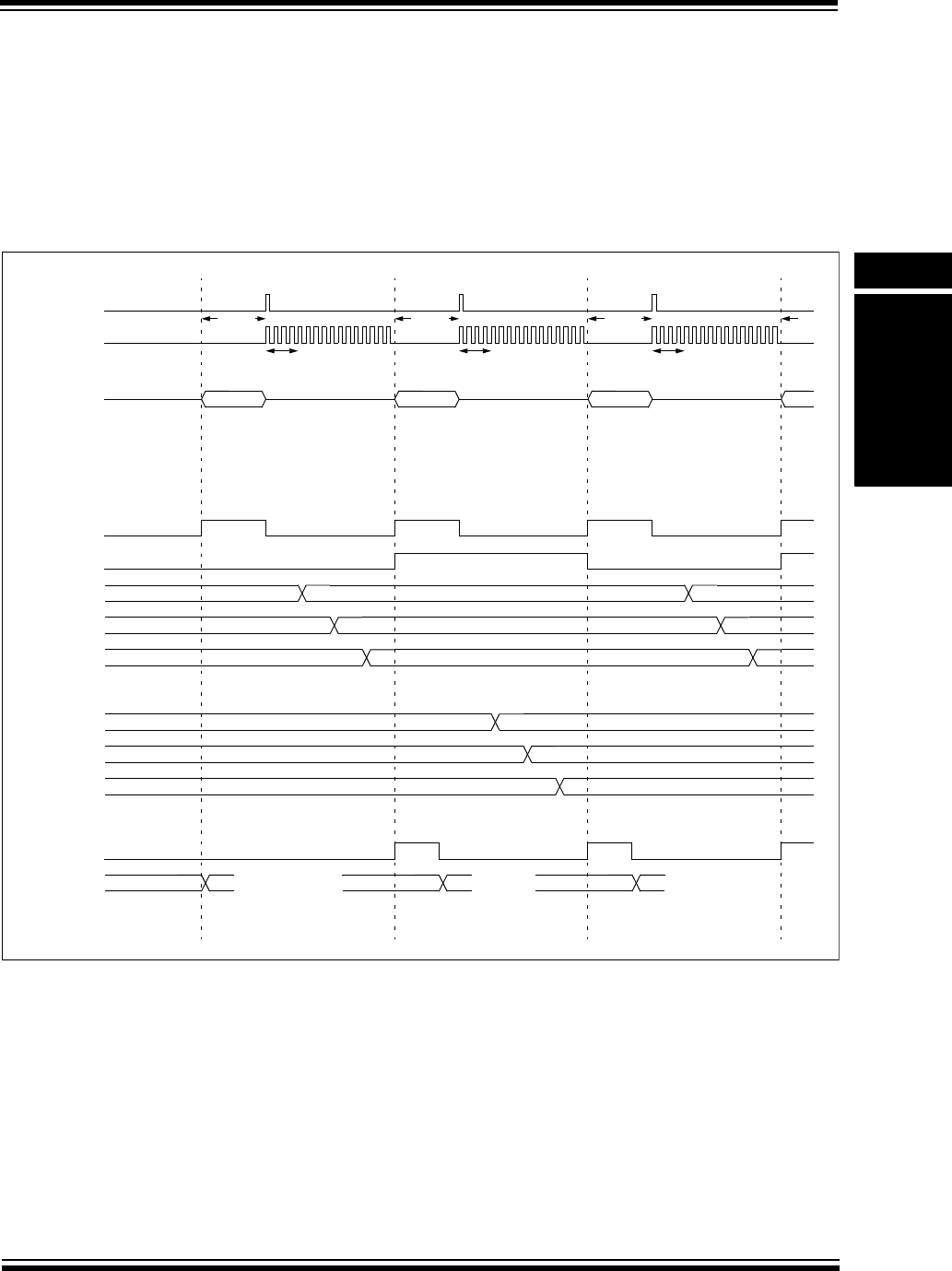
© 2007-2011 Microchip Technology Inc. DS61104E-page 17-41
Section 17. 10-bit Analog-to-Digital Converter (ADC)
10-bit Analog-to-Digital
Converter (ADC)
17
17.5.15 Example: Using Dual 8-Word Buffers
Figure 17-16 and Tabl e 17-6 demonstrate using dual 8-word buffers and alternating the buffer fill.
Setting the BUFM bit (AD1CON2<1>) enables dual 8-word buffers. The BUFM bit setting does
not affect other operational parameters. First, the conversion sequence starts filling the buffer at
ADC1BUF0 (buffer location 0 x 0). After the first interrupt occurs, the buffer begins to fill at
ADC1BUF8 (buffer location 0 x 8). The BUFS Status bit (AD1CON2<7>) is alternately set and
cleared after each interrupt to show which buffer is being filled. In this example, three analog
inputs are sampled and an interrupt occurs after every third sample.
Figure 17-16: Converting Three Inputs, Three Samples Per Interrupt Using Dual 8-Word Buffers
ADCLK
SAMP
ADC1BUF0
set ASAM = 1 Instruction Execution
ADC1BUF1
ADC1BUF2
Input to MUX A AN0
TSAMP
ADIF
ADC1BUF8
ADC1BUF9
ADC1BUFA
AN1
TSAMP
AN2
TSAMP
clear IFS0,#ADIF clear IFS0,#ADIF
BUFS
Conversion
Trigger
TCONV TCONV TCONV

PIC32 Family Reference Manual
DS61104E-page 17-42 © 2007-2011 Microchip Technology Inc.
Table 17-6: Converting Three Inputs, Three Samples/Interrupt Using Dual 8-Word Buffers
CONTROL BITS
Sequence Select
SMPI<2:0> = 0010
Interrupt after every third sample
—
—
BUFM = 1
Dual 8-word result buffers
ALTS = 0
Always use MUX A
MUX A Input Select
CH0SA<3:0> = n/a
MUX A positive input select is not used
CH0NA = 0
Select VR- for MUX A negative input
CSCNA = 1
Enable input scan
CSSL<15:0> = 0x0007
Scan input select scan list consisting of AN0, AN1,
and AN2
AD1PCFG = 0X0007
Select Analog Input mode for AN0, AN1, and AN2
—
MUX B Input Select
CH0SB<3:0> = n/a
MUX B positive input unused
CH0NB = n/a
MUX B negative input unused
—
—
OPERATION SEQUENCE
Sample MUX A Inputs: AN0
Convert AN0, Write Buffer 0x0
Sample MUX A Inputs: AN1
Convert AN1, Write Buffer 0x1
Sample MUX A Inputs: AN2
Convert AN2, Write Buffer 0x2
Interrupt; Change Buffer
Sample MUX A Inputs: AN0
Convert AN0, Write Buffer 0x8
Sample MUX A Inputs: AN1
Convert AN1, Write Buffer 0x9
Sample MUX A Inputs: AN2
Convert AN2, Write Buffer 0xA
Interrupt; Change Buffer
Repeat
Buffer
Address
Buffer @
1st Interrupt
Buffer @
2nd Interrupt
ADC1BUF0 AN0 sample 1
ADC1BUF1 AN1 sample 1
ADC1BUF2 AN2 sample 1
ADC1BUF3
ADC1BUF4
ADC1BUF5
ADC1BUF6
ADC1BUF7 •••
ADC1BUF8 AN0 sample 2
ADC1BUF9 AN1 sample 2
ADC1BUFA AN2 sample 2
ADC1BUFB
ADC1BUFC
ADC1BUFD
ADC1BUFE
ADC1BUFF

© 2007-2011 Microchip Technology Inc. DS61104E-page 17-43
Section 17. 10-bit Analog-to-Digital Converter (ADC)
10-bit Analog-to-Digital
Converter (ADC)
17
17.5.16 Example: Using Alternating MUX A and MUX B Input Selections
Figure 17-17 and Ta ble 17-7 demonstrate alternating sampling of the inputs assigned to MUX A
and MUX B. Setting the ALTS (AD1CON2<0>) bit enables alternating input selections. The first
sample uses the MUX A inputs specified by the CH0SA (AD1CHS<19:16>) and CH0NA
(AD1CHS<23>) bits. The next sample uses the MUX B inputs specified by the CH0SB
(AD1CHS<27:24>) and CH0NB (AD1CHS<31>) bits.
In the following example, one of the MUX B input specifications uses two analog inputs as a
differential source to the sample/hold.
This example also demonstrates use of the dual 8-word buffers. An interrupt occurs after every
fourth sample, which results in filling 4 words into the buffer on each interrupt.
Figure 17-17: Converting Two Analog Inputs by Alternating with Four Samples Per Interrupt
ADCLK
SAMP
ADC1BUF0
TSAMP
T
CONV
set ASAM = 1 Instruction Execution
ADC1BUF1
DONE
ADC1BUFE
ADC1BUFF
Input to MUX A AN0
T
SAMP
TCONV
TSAMP
TCONV
AN0
TSAMP
TCONV
ADIF
ASAM
Conversion
Trigger
Input to MUX B AN1 AN1

PIC32 Family Reference Manual
DS61104E-page 17-44 © 2007-2011 Microchip Technology Inc.
Table 17-7: Converting Two Sets of Inputs Using Alternating Input Selections
CONTROL BITS
Sequence Select
SMPI<2:0> = 0011
Interrupt on 4th sample
—
—
BUFM = 1
Dual 8-word result buffers
ALTS = 1
Alternate MUX A/B input select
MUX A Input Select
CH0SA<3:0> = 0000
Select AN0 for MUX A positive input
CH0NA = 0
Select VR- for MUX A negative input
CSCNA = 0
No input scan
CSSL<15:0> = n/a
Scan input select unused
—
—
MUX B Input Select
CH0SB<3:0> = 0001
Select AN1 for MUX B positive input
CH0NB = 0
Select VR- for MUX B negative input
—
—
OPERATION SEQUENCE
Sample MUX A Inputs: AN0
Convert, Write Buffer 0x0
Sample MUX B Inputs: AN1
Convert, Write Buffer 0x1
Sample MUX A Inputs: AN0
Convert, Write Buffer 0x2
Sample MUX B Inputs: AN1
Convert, Write Buffer 0x3
Interrupt; Change Buffer
Sample MUX A Inputs: AN0
Convert, Write Buffer 0x8
Sample MUX B Inputs: AN1
Convert, Write Buffer 0x9
Sample MUX A Inputs: AN0
Convert, Write Buffer 0xA
Sample MUX B Inputs: AN1
Convert, Write Buffer 0xB
Interrupt; Change Buffer
Repeat
Buffer
Address
Buffer @
1st Interrupt
Buffer @
2nd Interrupt
ADC1BUF0 AN0 sample 1
ADC1BUF1 AN1 sample 1
ADC1BUF2 AN0 sample 2
ADC1BUF3 AN1 sample 2
ADC1BUF4
ADC1BUF5
ADC1BUF6
ADC1BUF7 •••
ADC1BUF8 AN0 sample 3
ADC1BUF9 AN1 sample 3
ADC1BUFA AN0 sample 4
ADC1BUFB AN1 sample 4
ADC1BUFC
ADC1BUFD
ADC1BUFE
ADC1BUFF

© 2007-2011 Microchip Technology Inc. DS61104E-page 17-45
Section 17. 10-bit Analog-to-Digital Converter (ADC)
10-bit Analog-to-Digital
Converter (ADC)
17
17.5.17 Example: Converting Three Analog Inputs Using Alternating
Sample Mode and a Scan List
Figure 17-18, Figure 17-19, and Tabl e 17-8 demonstrate sampling by scanning through inputs
and alternating between MUX A and MUX B. When the Alternating Sample mode is selected, the
first input to be sampled will be the input selected for MUX A, the second sample will be the input
selected for MUX B. Then the process repeats. When scanning is combined with Alternating
Input mode, the positive input to MUX A is selected by the contents of the AD1CSSL register, not
the CH0SA<3:0> bits (AD1CHS<19:16>). For each sample that MUX A is selected the next item
in the scan list is sampled. The positive input to MUX B is selected by the CH0SB<3:0> bits
(AD1CHS<27:24>).
When the ASAM bit (AD1CON1<2>) is clear, sampling will not resume after conversion
completion, but will occur when setting the SAMP bit (AD1CON1<1>).
Figure 17-18: Converting Three Analog Inputs Using Alternating Sample Mode and a Scan List
ADCLK
SAMP
ADC1BUF0
TSAMP
TCONV
set ASAM = 1 Instruction Execution
ADC1BUF1
DONE
ADC1BUFE
ADC1BUFF
Input to MUX A AN0
TSAMP
TCONV
TSAMP
TCONV
AN1
TSAMP
TCONV
ADIF
ASAM
Conversion
Trigger
Input to Max B AN2 AN2
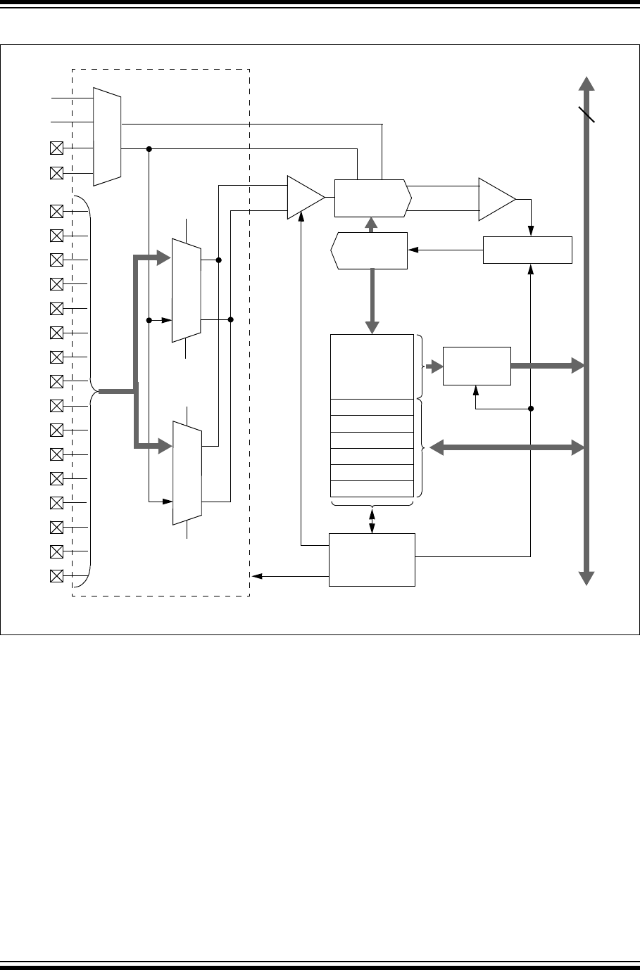
PIC32 Family Reference Manual
DS61104E-page 17-46 © 2007-2011 Microchip Technology Inc.
Figure 17-19: 10-bit High-Speed ADC Block Diagram for Alternating Sample and Scan
AD1CON1
AD1CON2
AD1CON3
AD1CHS
AD1PCFG
AD1CSSL
Comparator
10-bit SAR Conversion Logic
VREF+
DAC
AN12
AN13
AN14
AN15
AN8
AN9
AN10
AN11
AN4
AN5
AN6
AN7
AN0
AN1
AN2
AN3
VREF-
Sample Control
SHA
AVSS
AVDD
ADC1BUF0:
ADC1BUFF
Control Logic
Data
Input MUX Control
Conversion Control
Pin Config Control
Internal Data Bus
32
VR+VR-
MUX A
MUX B
VINH
VINL
VINH
VINH
VINL
VINL
VR+
VR-
VR Select
Formatting
AD1CSSL
CHOSB<3:0>
CHONB
CHONA

© 2007-2011 Microchip Technology Inc. DS61104E-page 17-47
Section 17. 10-bit Analog-to-Digital Converter (ADC)
10-bit Analog-to-Digital
Converter (ADC)
17
Table 17-8: Sampling Eight Inputs Using Sequential Sampling
CONTROL BITS
Sequence Select
SMPI<2:0> = 0011
Interrupt on 4th sample
—
—
BUFM = 0
Single 16-word result buffer
ALTS = 1
Alternate MUX A/B input select
MUX A Input Select
CH0SA<3:0> = n/a
Not used
CH0NA = 0
Select VR- for CH0- input
CSCNA = 1
Enable input scan
CSSL<15:0> = n/a
Scan input select scan list consisting of AN0 and AN1
—
—
MUX B Input Select
CH0SB<3:0> = 0010
Select AN7 for CH0+ input
CH0NB = 0
Select VR- for CH0- input
—
—
OPERATION SEQUENCE
Sample: AN0
Convert, Write Buffer 0x0
Sample: AN2
Convert, Write Buffer 0x1
Sample: AN1
Convert, Write Buffer 0x2
Sample: AN2
Convert, Write Buffer 0x3
Interrupt
Repeat
Buffer
Address
Buffer @
1st Interrupt
Buffer @
2nd Interrupt
ADC1BUF0 AN0 sample 1 AN0 sample 5
ADC1BUF1 AN2 sample 2 AN2 sample 6
ADC1BUF2 AN1 sample 3 AN1 sample 7
ADC1BUF3 AN2 sample 4 AN2 sample 8
ADC1BUF4
ADC1BUF5
ADC1BUF6
ADC1BUF7 •••
ADC1BUF8
ADC1BUF9
ADC1BUFA
ADC1BUFB
ADC1BUFC
ADC1BUFD
ADC1BUFE
ADC1BUFF
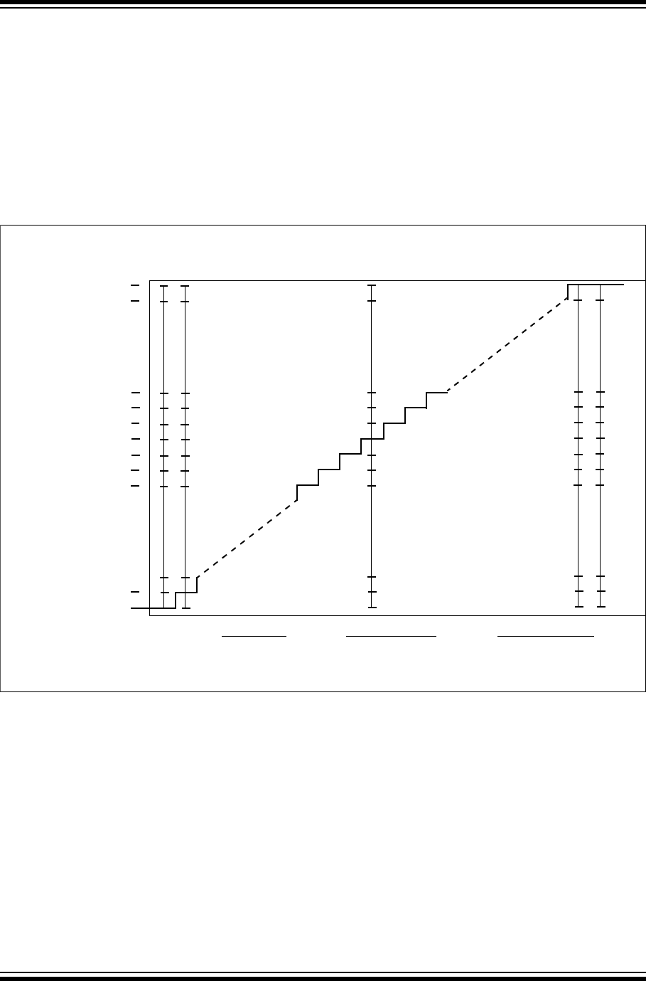
PIC32 Family Reference Manual
DS61104E-page 17-48 © 2007-2011 Microchip Technology Inc.
17.5.18 Transfer Function
The ideal transfer function of the ADC is shown in Figure 17-20. The difference of the input
voltages, (VINH – VINL), is compared to the reference, (VR+ – VR-).
• The first code transition occurs when the input voltage is (VR+ – VR-L/2048) or 0.5 LSb
•The 00 0000 0001 code is centered at (VR+ – VR-/1024) or 1.0 LSb
•The 10 0000 0000 code is centered at (512 * (VR+ – VR-)/1024)
•An input voltage less than (1 * (VR+ – VR-L)/2048) converts as 00 0000 0000
•An input greater than (2045 * (VR+ – VR-)/2048) converts as 11 1111 1111
Figure 17-20: ADC Transfer Function
10 0000 0010 (= 514)
10 0000 0011 (= 515)
01 1111 1101 (= 509)
01 1111 1110 (= 510)
01 1111 1111 (= 511)
11 1111 1110 (= 1022)
11 1111 1111 (= 1023)
00 0000 0000 (= 0)
00 0000 0001 (= 1)
Output
Code
10 0000 0000 (= 512)
(VINH – VINL)
VR-VR+ – VR-
1024
VR+
VR- +
10 0000 0001 (= 513)
512*(VR+ – VR-)
1024
VR- + 1023*(VR+ – VR-)
1024
VR- +

© 2007-2011 Microchip Technology Inc. DS61104E-page 17-49
Section 17. 10-bit Analog-to-Digital Converter (ADC)
10-bit Analog-to-Digital
Converter (ADC)
17
17.5.19 ADC Accuracy/Error
Refer to 17.10 “Related Application Notes” for a list of documents that discuss ADC accuracy.
The following figure depicts the recommended circuit for the conversion rates above 400 ksps.
A 100-pin PIC32 device package is shown as an example in Figure 17-21.
Figure 17-21: ADC Voltage Reference Schematic
VDD
AVDD
AVDD
VDD
R2
10
C2
0.1 µF
C1
0.01 µFR1
10
C8
1 µF
VDD
C7
0.1 µF
VDD
C6
0.01 µF
VDD
C5
1 µF
VDD
C4
0.1 µF
VDD
C3
0.01 µF
VDD
VDD
92
94
93
91
90
89
88
87
86
85
84
83
82
81
80
79
78
20
2
3
4
5
6
7
8
9
10
11
12
13
14
15
16
65
64
63
62
61
60
59
56
45
44
43
42
41
40
39
28
29
30
31
32
33
34
35
36
37
38
17
18
19
21
22
95
1
76
77
72
71
70
69
68
67
66
75
74
73
58
57
24
23
25
96
98
97
99
27
46
47
48
49
55
54
53
52
51
100
50
26
VDD
AVSS
AVSS
AVSS
VDD
VDD
10K
VDD
10 µF
AVSS
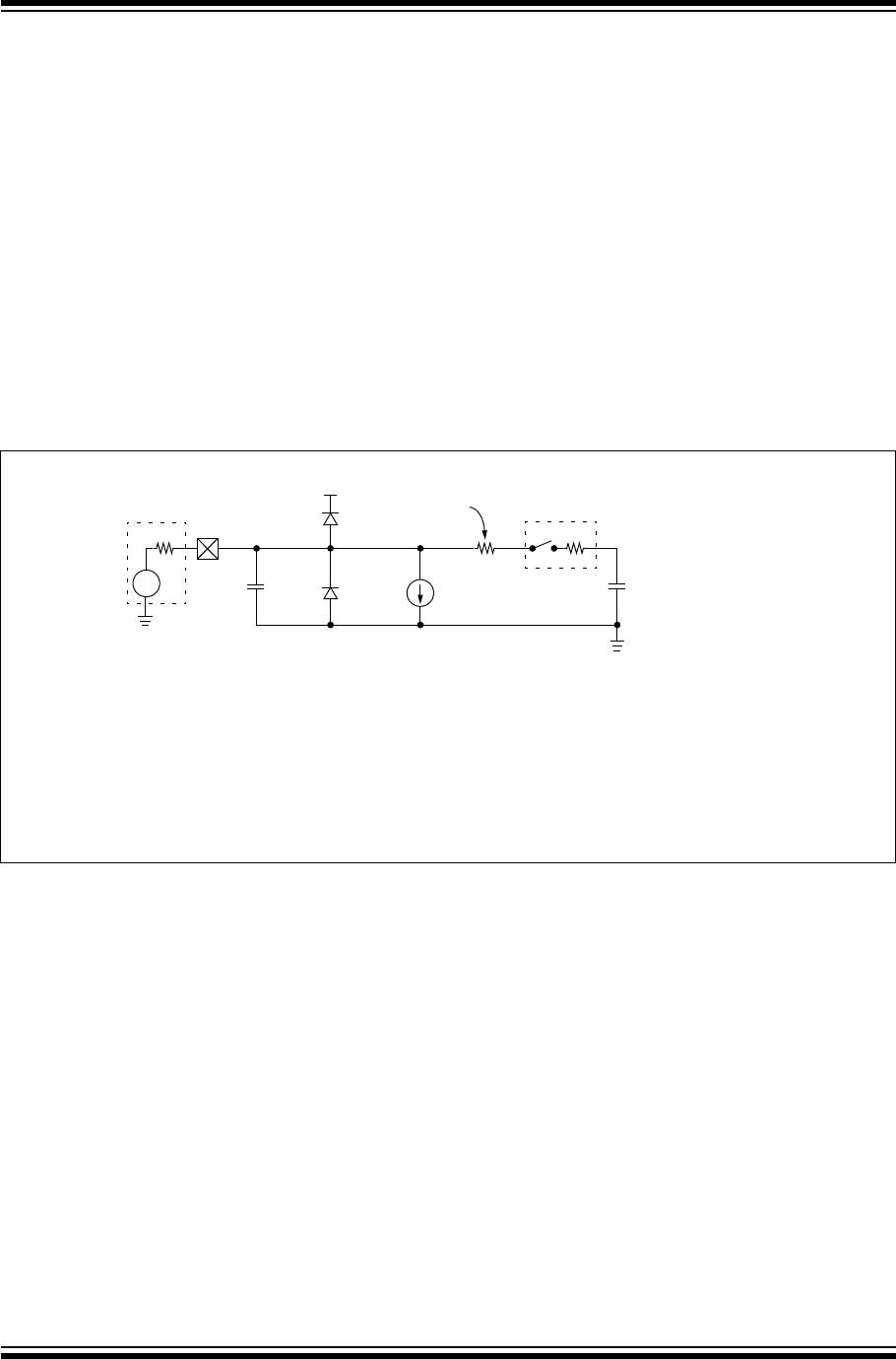
PIC32 Family Reference Manual
DS61104E-page 17-50 © 2007-2011 Microchip Technology Inc.
17.5.20 ADC Sampling Requirements
The analog input model of the 10-bit ADC module is shown in Figure 17-22. The total acquisition
time for the analog-to-digital conversion is a function of the internal amplifier settling time and the
holding capacitor charge time.
For the ADC module to meet its specified accuracy, the charge holding capacitor (CHOLD) must
be allowed to fully charge to the voltage level on the analog input pin. The analog output source
impedance (RS), the interconnect impedance (RIC), and the internal sampling switch (RSS)
impedance combine to directly affect the time required to charge the C
HOLD. The combined
impedance of the analog sources must therefore be small enough to fully charge the holding
capacitor within the chosen sample time. After the analog input channel is selected (changed),
this acquisition function must be completed prior to starting the conversion. The internal holding
capacitor will be in a discharged state prior to each sample operation.
A time period of at least 1 TAD should be allowed between conversions for the acquisition time.
Refer to the “Electrical Characteristics” section in the specific device data sheet for more
information.
Figure 17-22: 10-bit ADC Analog Input Model
17.5.21 Connection Considerations
Since the analog inputs employ Electrostatic Discharge (ESD) protection, they have diodes to
VDD and VSS. This requires that the analog input must be between VDD and VSS. If the input
voltage exceeds this range by greater than 0.3V (in either direction), one of the diodes becomes
forward-biased and it may damage the device if the input current specification is exceeded.
An external RC filter is sometimes added for anti-aliasing of the input signal. The R component
should be selected to ensure that the acquisition time requirements are satisfied. Any external
components connected (through high-impedance) to an analog input pin (capacitor, Zener diode,
etc.) should have very little leakage current at the pin.
CPIN
VA
Rs ANx VT = 0.6V
VT = 0.6V ILEAKAGE
RIC ≤ 250ΩSampling
Switch
RSS
CHOLD
= DAC capacitance
VSS
VDD
= 4.4 pF
± 500 nA
Note: The CPIN value depends on the device package and is not tested. The effect of the CPIN is negligible if Rs ≤ 5 kΩ.
RSS ≤ 3 kΩ
Legend:
CPIN = input capacitance VT = threshold voltage
RSS = sampling switch resistance RIC = interconnect resistance
RS = source resistance CHOLD = sample/hold capacitance
ILEAKAGE = leakage current at the pin due to various junctions

© 2007-2011 Microchip Technology Inc. DS61104E-page 17-51
Section 17. 10-bit Analog-to-Digital Converter (ADC)
10-bit Analog-to-Digital
Converter (ADC)
17
17.6 INITIALIZATION
A simple initialization code example for the ADC module is provided in Example 17-6.
Example 17-7 shows the Converting 1 Channel at 400 ksps, Auto-Sample Start and 2 TAD
Sampling Time code example.
In this particular configuration, all 16 analog input pins, AN0-AN15, are set up as analog inputs.
Operation in Idle mode is disabled, output data is in unsigned fractional format, and AVDD and
AVSS are used for VR+ and VR-. The start of acquisition, as well as start of
conversion (conversion trigger), are performed manually in software. The Channel 0 (CH0) SHA
is used for conversions. Scanning of inputs is disabled, and an interrupt occurs after every
acquisition/convert sequence (1 conversion result). The ADC conversion clock is TPB/2.
Since acquisition is started manually by setting the SAMP bit (AD1CON1<1>) after each
conversion is complete, the auto-sample time bits, SAMC<4:0> (AD1CON3<12:8>), are ignored.
Moreover, since the start of conversion (i.e., end of acquisition) is also triggered manually, the
SAMP bit needs to be cleared each time a new sample needs to be converted.
Example 17-6: ADC Initialization Code Example
AD1PCFG = 0x0000; /* Configure ADC port
all input pins are analog */
AD1CON1 = 0x2208; /* Configure sample clock source and Conversion Trigger mode.
Unsigned Fractional format, Manual conversion trigger,
Manual start of sampling, Simultaneous sampling,
No operation in IDLE mode. */
AD1CON2 = 0x0000; /* Configure ADC voltage reference
and buffer fill modes.
VREF from AVDD and AVSS,
Inputs are not scanned,
Interrupt every sample */
AD1CON3 = 0x0000; /* Configure ADC conversion clock */
AD1CHS = 0x0000; /* Configure input channels,
CH0+ input is AN0.
CHO- input is VREFL (AVss)
AD1CSSL = 0x0000; /* No inputs are scanned.
Note: Contents of AD1CSSL are ignored when CSCNA = 0 */
IFS1CLR = 2; /*Clear ADC conversion interrupt*/
// Configure ADC interrupt priority bits (AD1IP<2:0>) here, if
// required. (default priority level is 4)
IEC1SET = 2; /* Enable ADC conversion interrupt*/
AD1CON1SET = 0x8000; /* Turn on the ADC module */
AD1CON1SET = 0x0002; /* Start sampling the input */
DelayNmSec(100); /* Ensure the correct sampling time has elapsed before
starting a conversion.*/
AD1CON1CLR = 0x0002; /* End Sampling and start Conversion*/
: /* The DONE bit is set by hardware when the convert sequence
is finished. */
: /* The ADIF bit will be set. */

PIC32 Family Reference Manual
DS61104E-page 17-52 © 2007-2011 Microchip Technology Inc.
Example 17-7: Converting 1 Channel at 400 ksps, Auto-Sample Start, 2 TAD Sampling Time Code Example
AD1PCFG = 0xFFFB; // all PORTB = Digital; RB2 = analog
AD1CON1 = 0x00E0; // SSRC bit = 111 implies internal
// counter ends sampling and starts
// converting.
AD1CHS = 0x00020000; // Connect RB2/AN2 as CH0 input
// in this example RB2/AN2 is the input
AD1CSSL = 0;
AD1CON3 = 0x0203; // Sample time = 2 TAD
AD1CON2 = 0x6004; // Select external VREF+ and VREF- pins
// Interrupt after every 2 samples
AD1CON1bits.ADON = 1; // turn ON the ADC
while (1) // repeat continuously
{
ADCValue = 0; // clear value
ADC16Ptr = &ADC1BUF0; // initialize ADC1BUF0 pointer
IF1bits.AD1IF = 0; // clear ADC interrupt flag
AD1CON1bits.ASAM = 1; // auto start sampling
// for 31 TAD, and then go to conversion
while (!IFS0bits.ADIF); // conversion done?
AD1CON1bits.ASAM = 0; // yes, stop sample/convert
for (count = 0; count <2; count++)
{ // average the two
ADCValue = ADCValue + *ADC16Ptr++;
ADCValue = ADCValue >> 1;
}
}//repeat

© 2007-2011 Microchip Technology Inc. DS61104E-page 17-53
Section 17. 10-bit Analog-to-Digital Converter (ADC)
10-bit Analog-to-Digital
Converter (ADC)
17
17.7 INTERRUPTS
The ADC module has a dedicated interrupt bit, AD1IF bit (IFS1<1>), and a corresponding
interrupt enable/mask bit, AD1IE bit (IEC<1>). These bits are used to determine the source of an
interrupt and to enable or disable an individual interrupt source. The priority level of each of the
channels can also be set independently of the other channels.
The AD1IF bit (IFS1<1>) is set when the condition set by the Samples Per Interrupt bit,
SMPI<3:0> bits (AD1CON2<5:2>), is met. The AD1IF bit (IFS1<1>) will then be set without
regard to the state of the corresponding AD1IE bit (IEC<1>). The AD1IF bit (IFS1<1>) can be
polled by software if desired.
The AD1IE bit (IEC<1>) controls the interrupt generation. If the AD1xIE bit is set, the CPU will be
interrupted whenever an event defined by SMPI<3:0> occurs and the corresponding AD1IF bit
(IFS1<1>) will be set (subject to the priority and sub priority as outlined below).
It is the responsibility of the routine that services a particular interrupt to clear the appropriate
Interrupt Flag bit before the service routine is complete.
The priority of the ADC interrupt can be set independently through the AD1IP<2:0> bits
(IPC6<28:26>). This priority defines the priority group that interrupt source will be assigned to.
The priority groups range from a value of 7, the highest priority, to a value of 0, which does not
generate an interrupt. An interrupt being serviced will be preempted by an interrupt in a higher
priority group.
The subpriority bits allow setting the priority of a interrupt source within a priority group. The
values of the subpriority, AD1IS<1:0> bits (IPC6<25:24>), range from 3, the highest priority, to 0
the lowest priority. An interrupt with the same priority group but having a higher subpriority value
will preempt a lower subpriority interrupt that is in progress.
The priority group and subpriority bits allow more than one interrupt source to share the same
priority and subpriority. If simultaneous interrupts occur in this configuration the natural order of
the interrupt sources within a priority/subgroup pair determine the interrupt generated. The
natural priority is based on the vector numbers of the interrupt sources. The lower the vector
number the higher the natural priority of the interrupt. Any interrupts that were overridden by
natural order will then generate their respective interrupts based on priority, subpriority, and
natural order after the interrupt flag for the current interrupt is cleared.
After an enabled interrupt is generated, the CPU will jump to the vector assigned to that interrupt.
The vector number for the interrupt is the same as the natural order number. The IRQ number is
not always the same as the vector number due to some interrupts sharing a single vector. The
CPU will then begin executing code at the vector address. The users code at this vector address
should perform an operations required, such as reloading the duty cycle, clear the interrupt flag,
and then exit. Refer to Section 8. “Interrupts” (DS61108) for vector address table details and
for more information on interrupts. Example 17-8 shows a code example of the ADC interrupt
configuration.
Example 17-8: ADC Interrupt Configuration Code Example
Note: Some PIC32 devices feature persistent interrupts. On such devices, clearing the
AD1IF flag bit will not have any effect unless ADC1BUFx register is read. Refer to
the specific device data sheet and Section 8. “Interrupts” (DS61108) for more
information.
IPS6SET = 0x0014; // Set Priority to 5
IPS6SET = 0x0003; // Set Sub Priority to 3
//
IFS1CLR = 0x0002; // Ensure the interrupt flag is clear
IEC1SET = 0x0002; // Enable ADC interrupts

PIC32 Family Reference Manual
DS61104E-page 17-54 © 2007-2011 Microchip Technology Inc.
17.8 OPERATION DURING SLEEP AND IDLE MODES
Sleep and Idle modes are useful for minimizing conversion noise because the digital activity of
the CPU, buses and other peripherals is minimized.
17.8.1 CPU Sleep Mode Without RC ADC Clock
When the device enters Sleep mode, all clock sources to the module are shut down and stay at
logic ‘0’.
If Sleep occurs in the middle of a conversion, the conversion is aborted unless the ADC module
is clocked from its internal RC clock generator. The converter will not resume a partially
completed conversion on exiting from Sleep mode.
ADC register contents are not affected by the device entering or leaving Sleep mode.
17.8.2 CPU Sleep Mode With RC ADC Clock
The ADC module can operate during Sleep mode if the ADC clock source is set to the internal
RC oscillator (ADRC bit (AD1CON3<15>) = 1). This reduces the digital switching noise from the
conversion. When the conversion is completed, the DONE bit (AD1CON1<0>) will be set and the
result loaded into the ADC result buffer, ADC1BUFx.
If the ADC interrupt is enabled (AD1IE bit (IEC<1>) = 1), the device will wake up from Sleep when
the ADC interrupt occurs. Program execution will resume at the ADC Interrupt Service Routine
(ISR), if the ADC interrupt is greater than the current CPU priority. Otherwise, execution will
continue from the instruction after the WAIT instruction that placed the device in Sleep mode.
If the ADC interrupt is not enabled, the ADC module will then be disabled, although the ON bit
(AD1CON1<15>) will remain set.
To minimize the effects of digital noise on the ADC module operation, the user should select a
conversion trigger source that ensures the analog-to-digital conversion will take place in Sleep
mode. The automatic conversion trigger option can be used for sampling and conversion in Sleep
(SSRC<2:0> bits (AD1CON1<7:5>) = 111). To use the automatic conversion option, the ADC
ON bit should be set in the instruction prior to the WAIT instruction.
17.8.3 ADC Operation During CPU IDLE Mode
For the ADC, the SIDL bit (AD1CON1<13>) specifies whether the module will stop on Idle or
continue on Idle. If the SIDL bit = 0, the ADC module will continue normal operation when the
device enters Idle mode. If the ADC interrupt is enabled (AD1IE bit = 1), the device will wake up
from Idle mode when the ADC interrupt occurs. Program execution will resume at the ADC ISR,
if the ADC interrupt is greater than the current CPU priority. Otherwise, execution will continue
from the instruction after the WAIT instruction that placed the device in Idle mode.
If the SIDL bit = 1, the ADC module will stop in Idle mode. If the device enters Idle mode in the
middle of a conversion, the conversion is aborted. The converter will not resume a partially
completed conversion on exiting from Idle mode.
Note: For the ADC module to operate in Sleep mode, the ADC clock source must be set
to the internal RC oscillator (ADRC = 1).

© 2007-2011 Microchip Technology Inc. DS61104E-page 17-55
Section 17. 10-bit Analog-to-Digital Converter (ADC)
10-bit Analog-to-Digital
Converter (ADC)
17
17.9 EFFECTS OF VARIOUS RESETS
17.9.1 Master Clear Reset
Following a Master Clear (MCLR) reset, all of the ADC control registers (AD1CON1, AD1CON2,
AD1CON3, AD1CHS, AD1PCFG, and AD1CSSL) are reset to a value of 0x00000000. This
disables the ADC module and sets the analog input pins to Analog Input mode. Any conversion
that was in progress will terminate and the result will not be written to the result buffer.
The values in the ADC1BUFx registers are initialized during a MCLR Reset. ADC1BUF0 through
ADC1BUFF will contain 0x00000000.
17.9.2 Power-on Reset
Following a Power-on Reset (POR) event, all of the ADC control registers (AD1CON1,
AD1CON2, AD1CON3, AD1CHS, AD1PCFG and AD1CSSL) are reset to a value of
0x00000000. This disables the ADC module and sets the analog input pins to Analog Input
mode.
The values in the ADC1BUFx registers are initialized during a POR. ADC1BUF0 through
ADC1BUFF will contain 0x00000000.
17.9.3 Watchdog Timer Reset
Following a Watchdog Timer (WDT) reset, all of the ADC control registers (AD1CON1,
AD1CON2, AD1CON3, AD1CHS, AD1PCFG and AD1CSSL) are reset to a value of
0x00000000. This disables the ADC module and sets the analog input pins to Analog Input
mode. Any conversion that was in progress will terminate and the result will not be written to the
result buffer.
The values in the ADC1BUFx registers are initialized after a WDT reset. ADC1BUF0 through
ADC1BUFF will contain 0x00000000.

PIC32 Family Reference Manual
DS61104E-page 17-56 © 2007-2011 Microchip Technology Inc.
17.10 RELATED APPLICATION NOTES
This section lists application notes that are related to this section of the manual. These
application notes may not be written specifically for the PIC32 device family, but the concepts are
pertinent and could be used with modification and possible limitations. The current application
notes related to the 10-bit Analog-to-Digital Converter (ADC) module are:
Title Application Note #
Using the Analog-to-Digital (A/D) Converter AN546
Four Channel Digital Voltmeter with Display and Keyboard AN557
Understanding ADC Performance Specifications AN693
Note: Please visit the Microchip web site (www.microchip.com) for additional Application
Notes and code examples for the PIC32 family of devices.

© 2007-2011 Microchip Technology Inc. DS61104E-page 17-57
Section 17. 10-bit Analog-to-Digital Converter (ADC)
10-bit Analog-to-Digital
Converter (ADC)
17
17.11 REVISION HISTORY
Revision A (October 2007)
This is the initial released version of this document.
Revision B (October 2007)
Updated document to remove Confidential status.
Revision C (April 2008)
Revised status to Preliminary; Revised U-0 to r-x.
Revision D (June 2008)
Revised Register 17-1 note; Revised Registers 17-13, 17-17, 17-21, 17-25, 17-26; Revised
Equation 17-1; Added Section 17.5.6; Revised Tables 17-4, 17-5, 17-6, 17-7, 17-8; Delete
Section 17.11.5 (500 KSPS Configuration Guideline); Change Reserved bits from “Maintain as”
to “Write”; Added Note to ON bit (AD1CON1 Register).
Revision E (August 2011)
This revision includes the following updates:
•Equations:
- Added Equation 17-3 through Equation 17-9 in 17.4.12.1 “Configuring the ADC for
1000 ksps Operation”
•Figures:
- Replaced Figure 17-1
• Registers:
-Removed all Interrupt registers
•Notes:
-Removed Note 1 in Register 17-1
- Added a note about TPB in Register 17-3
- Added Note 2 in 17.4.1 “Configuring Analog Port Pins”
- Added a note about the AD1IF flag bit in 17.7 “Interrupts”
•Sections:
- Added 17.4.12.1 “Configuring the ADC for 1000 ksps Operation”
-Removed 17.8 I/O PIN CONTROL
-Removed all the Motor Control application notes reference in 17.10 “Related
Application Notes”
-Removed 17.11 DESIGN TIPS
•Tables:
-Removed the Clear, Set and Invert registers associated with the AD1CONx, AD1CHS,
AD1PCFG, AD1CSSL registers and added notes about the Set, Invert and Clear
register in Ta bl e 17-1
-Removed Table 17-9: ADC Interrupt Vectors for Various Offsets with
EBASE = 0x8000:0000
• Changed all occurrences of PIC32MX to PIC32
•Updates to register formatting and minor text updates have been incorporated throughout
the document

PIC32 Family Reference Manual
DS61104E-page 17-58 © 2007-2011 Microchip Technology Inc.
NOTES:

© 2007-2011 Microchip Technology Inc. DS61104E-page 17- 59
Information contained in this publication regarding device
applications and the like is provided only for your convenience
and may be superseded by updates. It is your responsibility to
ensure that your application meets with your specifications.
MICROCHIP MAKES NO REPRESENTATIONS OR
WARRANTIES OF ANY KIND WHETHER EXPRESS OR
IMPLIED, WRITTEN OR ORAL, STATUTORY OR
OTHERWISE, RELATED TO THE INFORMATION,
INCLUDING BUT NOT LIMITED TO ITS CONDITION,
QUALITY, PERFORMANCE, MERCHANTABILITY OR
FITNESS FOR PURPOSE. Microchip disclaims all liability
arising from this information and its use. Use of Microchip
devices in life support and/or safety applications is entirely at
the buyer’s risk, and the buyer agrees to defend, indemnify and
hold harmless Microchip from any and all damages, claims,
suits, or expenses resulting from such use. No licenses are
conveyed, implicitly or otherwise, under any Microchip
intellectual property rights.
Trademarks
The Microchip name and logo, the Microchip logo, dsPIC,
KEELOQ, KEELOQ logo, MPLAB, PIC, PICmicro, PICSTART,
PIC32 logo, rfPIC and UNI/O are registered trademarks of
Microchip Technology Incorporated in the U.S.A. and other
countries.
FilterLab, Hampshire, HI-TECH C, Linear Active Thermistor,
MXDEV, MXLAB, SEEVAL and The Embedded Control
Solutions Company are registered trademarks of Microchip
Technology Incorporated in the U.S.A.
Analog-for-the-Digital Age, Application Maestro, chipKIT,
chipKIT logo, CodeGuard, dsPICDEM, dsPICDEM.net,
dsPICworks, dsSPEAK, ECAN, ECONOMONITOR,
FanSense, HI-TIDE, In-Circuit Serial Programming, ICSP,
Mindi, MiWi, MPASM, MPLAB Certified logo, MPLIB,
MPLINK, mTouch, Omniscient Code Generation, PICC,
PICC-18, PICDEM, PICDEM.net, PICkit, PICtail, REAL ICE,
rfLAB, Select Mode, Total Endurance, TSHARC,
UniWinDriver, WiperLock and ZENA are trademarks of
Microchip Technology Incorporated in the U.S.A. and other
countries.
SQTP is a service mark of Microchip Technology Incorporated
in the U.S.A.
All other trademarks mentioned herein are property of their
respective companies.
© 2007-2011, Microchip Technology Incorporated, Printed in
the U.S.A., All Rights Reserved.
Printed on recycled paper.
ISBN: 978-1-61341-575-7
Note the following details of the code protection feature on Microchip devices:
• Microchip products meet the specification contained in their particular Microchip Data Sheet.
• Microchip believes that its family of products is one of the most secure families of its kind on the market today, when used in the
intended manner and under normal conditions.
• There are dishonest and possibly illegal methods used to breach the code protection feature. All of these methods, to our
knowledge, require using the Microchip products in a manner outside the operating specifications contained in Microchip’s Data
Sheets. Most likely, the person doing so is engaged in theft of intellectual property.
• Microchip is willing to work with the customer who is concerned about the integrity of their code.
• Neither Microchip nor any other semiconductor manufacturer can guarantee the security of their code. Code protection does not
mean that we are guaranteeing the product as “unbreakable.”
Code protection is constantly evolving. We at Microchip are committed to continuously improving the code protection features of our
products. Attempts to break Microchip’s code protection feature may be a violation of the Digital Millennium Copyright Act. If such acts
allow unauthorized access to your software or other copyrighted work, you may have a right to sue for relief under that Act.
Microchip received ISO/TS-16949:2009 certification for its worldwide
headquarters, design and wafer fabrication facilities in Chandler and
Tempe, Arizona; Gresham, Oregon and design centers in California
and India. The Company’s quality system processes and procedures
are for its PIC® MCUs and dsPIC® DSCs, KEELOQ® code hopping
devices, Serial EEPROMs, microperipherals, nonvolatile memory and
analog products. In addition, Microchip’s quality system for the design
and manufacture of development systems is ISO 9001:2000 certified.

DS61104E-page 17- 60 © 2007-2011 Microchip Technology Inc.
AMERICAS
Corporate Office
2355 West Chandler Blvd.
Chandler, AZ 85224-6199
Tel: 480-792-7200
Fax: 480-792-7277
Technical Support:
http://www.microchip.com/
support
Web Address:
www.microchip.com
Atlanta
Duluth, GA
Tel: 678-957-9614
Fax: 678-957-1455
Boston
Westborough, MA
Tel: 774-760-0087
Fax: 774-760-0088
Chicago
Itasca, IL
Tel: 630-285-0071
Fax: 630-285-0075
Cleveland
Independence, OH
Tel: 216-447-0464
Fax: 216-447-0643
Dallas
Addison, TX
Tel: 972-818-7423
Fax: 972-818-2924
Detroit
Farmington Hills, MI
Tel: 248-538-2250
Fax: 248-538-2260
Indianapolis
Noblesville, IN
Tel: 317-773-8323
Fax: 317-773-5453
Los Angeles
Mission Viejo, CA
Tel: 949-462-9523
Fax: 949-462-9608
Santa Clara
Santa Clara, CA
Tel: 408-961-6444
Fax: 408-961-6445
Toronto
Mississauga, Ontario,
Canada
Tel: 905-673-0699
Fax: 905-673-6509
ASIA/PACIFIC
Asia Pacific Office
Suites 3707-14, 37th Floor
Tower 6, The Gateway
Harbour City, Kowloon
Hong Kong
Tel : 8 52 - 24 0 1- 120 0
Fax: 852-2401-3431
Australia - Sydney
Tel : 6 1-2 -98 68- 6 73 3
Fax: 61-2-9868-6755
China - Beijing
Tel : 8 6-1 0-8 569 - 70 0 0
Fax: 86-10-8528-2104
China - Chengdu
Tel : 8 6-2 8-8 665 - 55 11
Fax: 86-28-8665-7889
China - Chongqing
Tel : 8 6-2 3-8 980 - 95 8 8
Fax: 86-23-8980-9500
China - Hangzhou
Tel : 8 6-5 71- 2819 -31 87
Fax: 86-571-2819-3189
China - Hong Kong SAR
Tel : 8 52 - 24 0 1- 120 0
Fax: 852-2401-3431
China - Nanjing
Tel : 8 6-2 5-8 473 - 24 6 0
Fax: 86-25-8473-2470
China - Qingdao
Tel : 8 6-5 32- 8502 -73 55
Fax: 86-532-8502-7205
China - Shanghai
Tel : 8 6-2 1-5 407 - 55 3 3
Fax: 86-21-5407-5066
China - Shenyang
Tel : 8 6-2 4-2 334 - 28 2 9
Fax: 86-24-2334-2393
China - Shenzhen
Tel : 8 6-7 55- 8203 -26 60
Fax: 86-755-8203-1760
China - Wuhan
Tel : 8 6-2 7-5 980 - 53 0 0
Fax: 86-27-5980-5118
China - Xian
Tel : 8 6-2 9-8 833 - 72 5 2
Fax: 86-29-8833-7256
China - Xiamen
Tel: 86-592-2388138
Fax: 86-592-2388130
China - Zhuhai
Tel : 86- 756 -3 210 04 0
Fax: 86-756-3210049
ASIA/PACIFIC
India - Bangalore
Tel : 9 1- 8 0- 309 0-4 444
Fax: 91-80-3090-4123
India - New Delhi
Tel : 9 1- 11 -41 60- 86 31
Fax: 91-11-4160-8632
India - Pune
Tel : 9 1- 2 0- 256 6-1 512
Fax: 91-20-2566-1513
Japan - Yokohama
Tel : 8 1- 4 5- 471 - 6 166
Fax: 81-45-471-6122
Korea - Daegu
Tel : 8 2- 5 3- 744 -43 01
Fax: 82-53-744-4302
Korea - Seoul
Tel : 8 2- 2 -5 54- 720 0
Fax: 82-2-558-5932 or
82-2-558-5934
Malaysia - Kuala Lumpur
Tel : 6 0- 3 -6 201 -98 57
Fax: 60-3-6201-9859
Malaysia - Penang
Tel : 6 0- 4 -2 27- 887 0
Fax: 60-4-227-4068
Philippines - Manila
Tel : 6 3- 2 -6 34- 906 5
Fax: 63-2-634-9069
Singapore
Tel : 6 5- 6 33 4 -8 870
Fax: 65-6334-8850
Taiwan - Hsin Chu
Tel : 8 86 - 3- 577 8-3 66
Fax: 886-3-5770-955
Taiwan - Kaohsiung
Tel : 8 86 - 7- 536 -48 18
Fax: 886-7-330-9305
Taiwan - Taipei
Tel : 8 86 - 2- 250 0-6 610
Fax: 886-2-2508-0102
Thailand - Bangkok
Tel : 6 6- 2 -6 94- 135 1
Fax: 66-2-694-1350
EUROPE
Austria - Wels
Tel : 4 3- 7 24 2 -2 244 -39
Fax: 43-7242-2244-393
Denmark - Copenhagen
Tel : 4 5-4 450 -2 828
Fax: 45-4485-2829
France - Paris
Tel : 3 3-1 -6 9-5 3 -6 3-2 0
Fax: 33-1-69-30-90-79
Germany - Munich
Tel : 4 9- 8 9- 627 -14 4-0
Fax: 49-89-627-144-44
Italy - Milan
Tel : 3 9- 0 33 1 -7 426 11
Fax: 39-0331-466781
Netherlands - Drunen
Tel : 3 1- 4 16 - 690 3 99
Fax: 31-416-690340
Spain - Madrid
Tel : 3 4- 9 1- 708 -08 -90
Fax: 34-91-708-08-91
UK - Wokingham
Tel : 4 4- 11 8-9 21- 58 69
Fax: 44-118-921-5820
Worldwide Sales and Service
08/02/11

© 2013 Microchip Technology Inc. DS60001194B-page 18-1
12-bit Pipelined
Analog-to-Digital
Converter (ADC)
18
Section 18. 12-bit Pipelined Analog-to-Digital Converter (ADC)
HIGHLIGHTS
This section of the manual contains the following major topics:
18.1 Introduction .................................................................................................................. 18-2
18.2 Control Registers ......................................................................................................... 18-5
18.3 ADC Operation, Terminology and Conversion Sequence.......................................... 18-30
18.4 ADC Module Configuration ........................................................................................ 18-39
18.5 Additional ADC Functions .......................................................................................... 18-53
18.6 Interrupts.................................................................................................................... 18-63
18.7 Operation During Power-Saving Modes .................................................................... 18-65
18.8 Effects of Reset.......................................................................................................... 18-66
18.9 Transfer Function....................................................................................................... 18-66
18.10 ADC Sampling Requirements .................................................................................... 18-67
18.11 Connection Considerations........................................................................................ 18-67
18.12 Related Application Notes.......................................................................................... 18-68
18.13 Revision History ......................................................................................................... 18-69

PIC32 Family Reference Manual
DS60001194B-page 18-2 © 2013 Microchip Technology Inc.
18.1 INTRODUCTION
The PIC32 12-bit pipelined Analog-to-Digital Converter (ADC) includes the following features:
•12-bit resolution
•Six-stage conversion and four-stage processing pipeline
• 357 ns minimum conversion latency:
- Up to 28 Msps total conversion rate
•External voltage reference input pins
•Six Sample and Hold (S&H) circuits, SH0 through SH5:
- Five dedicated S&H circuits with individual input selection and individual conversion
trigger selection for high-speed conversions
-One shared S&H circuit with automatic Input Scan mode and common conversion
trigger selection
•Up to 48 analog input sources, in addition to the internal voltage reference and an internal
band gap temperature sensor
•Separate 32-bit conversion result register for each analog input
-Conversion result can be formatted as unsigned or signed data
•Six digital comparators:
- Multiple comparison options
- Assignable to specific analog input
•Six oversampling filters:
- Provides increased resolution
-Assignable to specific analog input
•Operation during CPU Sleep and Idle modes
A simplified block diagram of the ADC1 module is illustrated in Figure 18-1. Diagrams of the
related S&H circuits are provided in Figure 18-2 and Figure 18-3.
In each of the five dedicated S&H circuits, the analog inputs are connected through multiplexers
and switches to the S&H capacitor. These multiplexers allow for input and configuration selection
in the S&H circuit. The configuration settings SHxALT<1:0> and SHxMOD<1:0> configure the
multiplexers and are passed to the six stage pipeline converter along with the analog sample at
the start of conversion. The converter uses the digital configuration information to process the
analog sample, which allows it to know the number format, the measurement mode, and which
ANx input the sample was collected from. When conversion is complete, the final result is stored
in the result buffer for the specific analog input and passed to the digital filter and digital
comparator if configured to use data from this particular sample.
The single shared S&H incorporates a large multiplexer on the input. While the dedicated S&H
uses a single input (or its alternate) and is intending for high-speed and precise sampling of time
sensitive or transient signals, the shared S&H is connected to all remaining inputs and provides
flexibility and automated scanning of large groups of inputs using the input scan logic.
Details regarding the dedicated and shared S&H circuits are described in 18.3.2 “Dedicated
Sample and Hold” and 18.3.3 “Shared Sample and Hold”. The analog inputs and their
association with the dedicated and shared S&H circuits form three classes of inputs. Inputs to
dedicated S&H are Class 1 while inputs to the shared S&H are Class 2 or Class 3. These input
types are explained in 18.3.1 “Analog Inputs”. The Pipeline converter is described in
18.3.4 “Six-Stage Pipeline Converter”.
Note: This family reference manual section is meant to serve as a complement to device
data sheets. Depending on the device variant, this manual section may not apply to
all PIC32 devices.
Please refer to the note at the beginning of the “12-bit Analog-to-Digital
Converter (ADC)” chapter in the current device data sheet to check whether this
document supports the device you are using.
Device data sheets and family reference manual sections are available for
download from the Microchip Worldwide Web site at: http://www.microchip.com
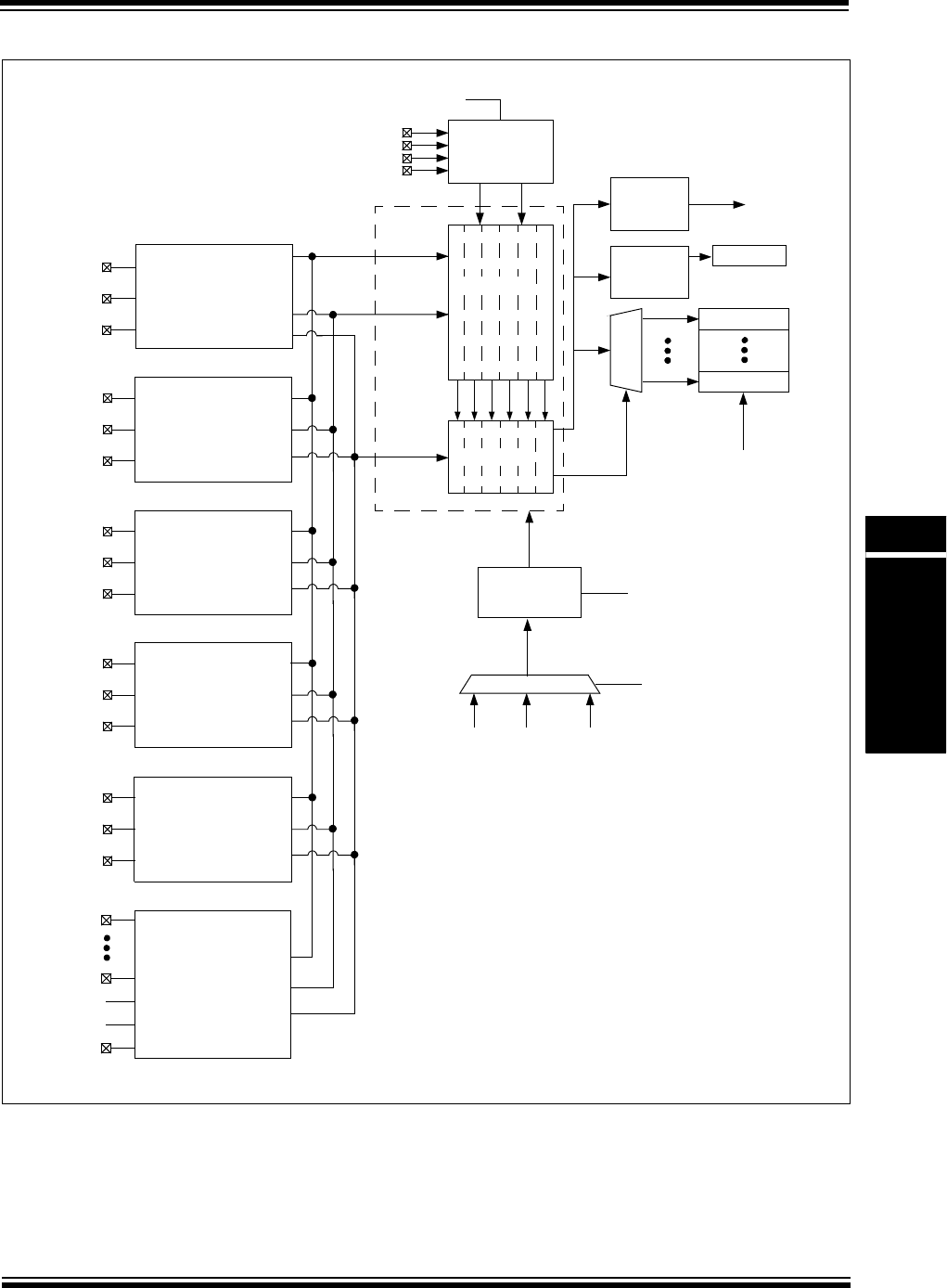
© 2013 Microchip Technology Inc. DS60001194B-page 18-3
Section 18. 12-bit Pipelined Analog-to-Digital Converter (ADC)
12-bit Pipelined
Analog-to-Digital
Converter (ADC)
18
Figure 18-1: ADC1 Module Block Diagram
AN5
AN42
IVREF
IVTEMP
Six-Stage
Conversion
Pipeline
Six Digital
Comparators
Six Digital
Result
Registers
Reference
Selection
VREFH VREFL
AVDD
Sample and Hold 1
(Dedicated)
AN1
AN46
AN6
Sample and Hold 4
(Dedicated)
AN4
AN49
AN9
ADC1DATA0
ADC1DATA44
VREFSEL<2:0>
Voltage
AVSS
VREF+
VREF-
FLTRDATA
Interrupt
Digital Stages
Analog Stages
SH4ALT<1:0>
SH4MOD<1:0>
SH1ALT<1:0>
SH1MOD<1:0>
Sample and Hold 0
(Dedicated)
SH0ALT<1:0>
SH0MOD<1:0>
AN0
AN45
AN5
Sample and Hold 5
(Shared)
SH5MOD<1:0>
(see Figure 18-2)
(see Figure 18-2)
(see Figure 18-2)
(see Figure 18-3)
Sample and Hold 3
(Dedicated)
AN3
AN48
AN8
SH3ALT<1:0>
SH3MOD<1:0>
(see Figure 18-2)
Sample and Hold 2
(Dedicated)
AN2
AN47
AN7
SH2ALT<1:0>
SH2MOD<1:0>
(see Figure 18-2)
AN10
Filters
Divider
1, 2, 4, 6, ...254
FRC SYSCLK REFCLKO3
Clock Selection
PBCLK3
ADCDIV<6:0>
ADCSEL<6:0>
TQ
TAD
PIC32 Family Reference Manual
DS60001194B-page 18-4 © 2013 Microchip Technology Inc.
Figure 18-2: Dedicated S&H 0-4 Block Diagram
Figure 18-3: Shared S&H 5 Block Diagram
0
1
0
1
SHxALT<1:0>
Channel Input ID and Result Format
SHxMOD<1:0>
Positive Input
Alternate
Negative Input
S&H
SHxMOD<1>
VREFL
Single-Ended
Differential
SHxALT<0>
To Ana l o g St a g e s
To Analog Stages
To Di gi ta l St a g es
(Class 1)
Positive Input
Configuration
Note: Refer to the “12-bit Pipelined Analog-to-Digital Converter” chapter in the specific device data sheet for the analog input
assignments for the dedicated and shared S&H circuits.
0
1
Input ID Input Mode Data Format
AN5
S&H
SH5MOD<1>
Single-Ended
Differential
AN11
AN12
AN42
IVREF
IVTEMP
AN10
Channel
SH5MOD<1:0>
To Analog
To Analog
To Di gi ta l
Positive Input
(Class 2)
Positive Input
(Class 3)
Stages
Stages
Stages
Channel Scan Logic
(Negative Input)
VREFL
Configuration
Note: Refer to the “12-bit Pipelined Analog-to-Digital Converter” chapter in the specific device data sheet for the analog input
assignments for the dedicated and shared S&H circuits.
AN43
AN44

© 2013 Microchip Technology Inc. DS60001194B-page 18-5
Section 18. 12-bit Pipelined Analog-to-Digital Converter (ADC)
12-bit Pipelined
Analog-to-Digital
Converter (ADC)
18
18.2 CONTROL REGISTERS
The PIC32 12-bit Pipelined ADC module has the following Special Function Registers (SFRs):
•AD1CON1: ADC1 Control Register 1
This register controls the basic operation of the ADC module, including behavior in Sleep
and Idle modes, and data formatting. This register specifies the vector shift amounts for the
interrupt controller. Additional AD1CON1 functions include early interrupt generation and the
trigger selection for the scanned analog inputs.
•AD1CON2: ADC1 Control Register 2
This register controls the clock source for the ADC module, the clock divider and the auto
sampling time for the shared S&H circuits. This register controls and optimizes the
performance of the ADC core circuitry, and also contains a control bit for putting the ADC
module into a special low-power state.
•AD1CON3: ADC1 Control Register 3
This register enables the user software to explicitly request the conversion of a specific
analog input. The CAL bit can be used for manually starting an ADC calibration process.
•AD1IMOD: ADC1 Input Mode Control Register
These registers enable the user to select an alternate analog input for each of the five ded-
icated S&H circuits (SH0 to SH4). Also, the AD1IMOD register enables the user to select
between single-ended and differential operation as well as select between signed and
unsigned data format.
•AD1GIRQEN1: ADC1 Global Interrupt Enable Register 1 and
AD1GIRQEN2: ADC1 Interrupt Enable Register 2
These registers specify which of the individual input conversion interrupts can generate the
global ADC1 interrupt.
•AD1CSS1: ADC1 Input Scan Select Register 1 and
AD1CSS2: ADC1 Input Scan Select Register 2
These registers specify the analog inputs to be scanned by the common scan trigger.
•AD1DSTAT1: ADC1 Data Ready Status Register 1 and
AD1DSTAT2: ADC1 Data Ready Status Register 2
These registers contain the interrupt status of the individual analog input conversions. Each
bit represents the data-ready status for its associated conversion result.
•AD1CMPCONn: ADC1 Digital Comparator Control Register ‘n’ (‘n’ = 1, 2, 3, 4, 5, or 6)
These registers control the operation of the digital comparator, including the generation of
interrupts and the comparison criteria to be used. This register also provides status when a
comparator event occurs.
•AD1CMPENn: ADC1 Digital Comparator Enable Register ‘n’ (‘n’ = 1, 2, 3, 4, 5, or 6)
These registers select which analog input conversion results will be processed by the digital
comparator.
•AD1CMPn: ADC1 Digital Comparator Register ‘n’ (‘n’ = 1, 2, 3, 4, 5 or 6)
These registers contain the high and low digital comparison values for use by the digital
comparator.
•AD1FLTRn: ADC1 Filter Register ‘n’ (‘n’ = 1, 2, 3, 4, 5, or 6)
These registers provide control and status bits for the oversampling filter accumulator, and
also includes the 16-bit filter output data.
•AD1TRGR1: ADC1 Input Convert Control Register 1
This register controls the trigger source selection for the analog inputs, AN0 through AN3.
•AD1TRGR2: ADC1 Input Convert Control Register 2
This register controls the trigger source selection for the analog inputs, AN4 through AN7.

PIC32 Family Reference Manual
DS60001194B-page 18-6 © 2013 Microchip Technology Inc.
•AD1TRGR3: ADC1 Input Convert Control Register 3
This register controls the trigger source selection for the analog inputs, AN8 through AN11.
•AD1DATAn: ADC1 Data Output Register (‘n’ = 0 to 44)
These registers are the analog-to-digital conversion output data registers. AD1DATAn
register is associated with each analog input ‘n’.
•AD1CALx: ADC1 Calibration Register (‘x’ = 1-5)
These registers contains the ADC calibration value.
The ADC module also has the following associated bits for interrupt control (for more information
on the location of these bits, refer to the “Interrupt Controller” chapter in the specific device
data sheet:
• Interrupt Request Flag Status bits (AD1IF)
• Interrupt Enable Control bits (AD1IE)
•Interrupt Priority Control bits (AD1IP<2:0>) and (AD1IS<1:0>)

© 2013 Microchip Technology Inc. DS60001194B-page 18-7
Section 18. 12-bit Pipelined Analog-to-Digital Converter (ADC)
12-bit Pipelined
Analog-to-Digital
Converter (ADC)
18
Tabl e 18- 1 provides a summary of all ADC Special Function Registers (SFRs). Corresponding registers appear after the summaries, which
include a detailed description of each bit.
Table 18-1: ADC SFR Summary
Register Name Bit
Range Bit 31/15 Bit 30/14 Bit 29/13 Bit 28/12 Bit 27/11 Bit 26/10 Bit 25/9 Bit 24/8 Bit 23/7 Bit 22/6 Bit 21/5 Bit 20/4 Bit 19/3 Bit 18/2 Bit 17/1 Bit 16/0
AD1CON1 31:16 FILTRDLY<4:0> STRGSRC<4:0> — — —EIE<2:0>
15:0 ADCEN —ADSIDL— FRACT — — — — — — — — — — —
AD1CON2 31:16 ADCRDY — — — — — — —SAMC<7:0>
15:0 — BOOST LOWPWR — — —ADCSEL<1:0>—ADCDIV<6:0>
AD1CON3 31:16 CAL GSWTRG RQCONVRT — — — — — — — — — — — — —
15:0 — — — VREFSEL<2:0> ——— —ADINSEL<5:0>
AD1IMOD 31:16 — — — — — —SH4ALT<1:0> SH3ALT<1:0> SH2ALT<1:0> SH1ALT<1:0> SH0ALT<1:0>
15:0 — — — —SH5MOD<1:0>SH4MOD<1:0> SH3MOD<1:0> SH2MOD<1:0> SH1MOD<1:0> SH0MOD<1:0>
AD1GIRQEN1 31:16 AGIEN31 AGIEN30 AGIEN29 AGIEN28 AGIEN27 AGIEN26 AGIEN25 AGIEN24 AGIEN23 AGIEN22 AGIEN21 AGIEN20 AGIEN19 AGIEN18 AGIEN17 AGIEN16
15:0 AGIEN15 AGIEN14 AGIEN13 AGIEN12 AGIEN11 AGIEN10 AGIEN9 AGIEN8 AGIEN7 AGIEN6 AGIEN5 AGIEN4 AGIEN3 AGIEN2 AGIEN1 AGIEN0
AD1GIRQEN2 31:16 — — — — — — — — — — — — — — — —
15:0 — — — AGIEN44 AGIEN43 AGIEN42 AGIEN41 AGIEN40 AGIEN39 AGIEN38 AGIEN37 AGIEN36 AGIEN35 AGIEN34 AGIEN33 AGIEN32
AD1CSS1 31:16 CSS31 CSS30 CSS29 CSS28 CSS27 CSS26 CSS25 CSS24 CSS23 CSS22 CSS21 CSS20 CSS19 CSS18 CSS17 CSS16
15:0 CSS15 CSS14 CSS13 CSS12 CSS11 CSS10 CSS9 CSS8 CSS7 CSS6 CSS5 CSS4 CSS3 CSS2 CSS1 CSS0
AD1CSS2 31:16 — — — — — — — — — — — — — — — —
15:0 — — — CSS44 CSS43 CSS42 CSS41 CSS40 CSS39 CSS38 CSS37 CSS36 CSS35 CSS34 CSS33 CSS32
AD1DSTAT1 31:16 ARDY31 ARDY30 ARDY29 ARDY28 ARDY27 ARDY26 ARDY25 ARDY24 ARDY23 ARDY22 ARDY21 ARDY20 ARDY19 ARDY18 ARDY17 ARDY16
15:0 ARDY15 ARDY14 ARDY13 ARDY12 ARDY11 ARDY10 ARDY9 ARDY8 ARDY7 ARDY6 ARDY5 ARDY4 ARDY3 ARDY2 ARDY1 ARDY0
AD1DSTAT2 31:16 — — — — — — — — — — — — — — — —
15:0 — — —ARDY44ARDY43ARDY42ARDY41ARDY40ARDY39ARDY38ARDY37ARDY36ARDY35ARDY34ARDY33ARDY32
AD1CMPCON1 31:16 — — — — — — — — — — — — — — — —
15:0 — — — AINID<4:0> ENDCMP DCMPGIEN DCMPED IEBTWN IEHIHI IEHILO IELOHI IELOLO
AD1CMPCON2 31:16 — — — — — — — — — — — — — — — —
15:0 — — — AINID<4:0> ENDCMP DCMPGIEN DCMPED IEBTWN IEHIHI IEHILO IELOHI IELOLO
AD1CMPCON3 31:16 — — — — — — — — — — — — — — — —
15:0 — — — AINID<4:0> ENDCMP DCMPGIEN DCMPED IEBTWN IEHIHI IEHILO IELOHI IELOLO
AD1CMPCON4 31:16 — — — — — — — — — — — — — — — —
15:0 — — — AINID<4:0> ENDCMP DCMPGIEN DCMPED IEBTWN IEHIHI IEHILO IELOHI IELOLO
AD1CMPCON5 31:16 — — — — — — — — — — — — — — — —
15:0 — — — AINID<4:0> ENDCMP DCMPGIEN DCMPED IEBTWN IEHIHI IEHILO IELOHI IELOLO
AD1CMPCON6 31:16 — — — — — — — — — — — — — — — —
15:0 — — — AINID<4:0> ENDCMP DCMPGIEN DCMPED IEBTWN IEHIHI IEHILO IELOHI IELOLO
AD1CMPEN1 31:16 CMPE31 CMPE30 CMPE29 CMPE28 CMPE27 CMPE26 CMPE25 CMPE24 CMPE23 CMPE22 CMPE21 CMPE20 CMPE19 CMPE18 CMPE17 CMPE16
15:0 CMPE15 CMPE14 CMPE13 CMPE12 CMPE11 CMPE10 CMPE9 CMPE8 CMPE7 CMPE6 CMPE5 CMPE4 CMPE3 CMPE2 CMPE1 CMPE0
Legend: — = unimplemented, read as ‘0’.

PIC32 Family Reference Manual
DS60001194B-page 18-8 © 2013 Microchip Technology Inc.
AD1CMPEN2 31:16 CMPE31 CMPE30 CMPE29 CMPE28 CMPE27 CMPE26 CMPE25 CMPE24 CMPE23 CMPE22 CMPE21 CMPE20 CMPE19 CMPE18 CMPE17 CMPE16
15:0 CMPE15 CMPE14 CMPE13 CMPE12 CMPE11 CMPE10 CMPE9 CMPE8 CMPE7 CMPE6 CMPE5 CMPE4 CMPE3 CMPE2 CMPE1 CMPE0
AD1CMPEN3 31:16 CMPE31 CMPE30 CMPE29 CMPE28 CMPE27 CMPE26 CMPE25 CMPE24 CMPE23 CMPE22 CMPE21 CMPE20 CMPE19 CMPE18 CMPE17 CMPE16
15:0 CMPE15 CMPE14 CMPE13 CMPE12 CMPE11 CMPE10 CMPE9 CMPE8 CMPE7 CMPE6 CMPE5 CMPE4 CMPE3 CMPE2 CMPE1 CMPE0
AD1CMPEN4 31:16 CMPE31 CMPE30 CMPE29 CMPE28 CMPE27 CMPE26 CMPE25 CMPE24 CMPE23 CMPE22 CMPE21 CMPE20 CMPE19 CMPE18 CMPE17 CMPE16
15:0 CMPE15 CMPE14 CMPE13 CMPE12 CMPE11 CMPE10 CMPE9 CMPE8 CMPE7 CMPE6 CMPE5 CMPE4 CMPE3 CMPE2 CMPE1 CMPE0
AD1CMPEN5 31:16 CMPE31 CMPE30 CMPE29 CMPE28 CMPE27 CMPE26 CMPE25 CMPE24 CMPE23 CMPE22 CMPE21 CMPE20 CMPE19 CMPE18 CMPE17 CMPE16
15:0 CMPE15 CMPE14 CMPE13 CMPE12 CMPE11 CMPE10 CMPE9 CMPE8 CMPE7 CMPE6 CMPE5 CMPE4 CMPE3 CMPE2 CMPE1 CMPE0
AD1CMPEN6 31:16 CMPE31 CMPE30 CMPE29 CMPE28 CMPE27 CMPE26 CMPE25 CMPE24 CMPE23 CMPE22 CMPE21 CMPE20 CMPE19 CMPE18 CMPE17 CMPE16
15:0 CMPE15 CMPE14 CMPE13 CMPE12 CMPE11 CMPE10 CMPE9 CMPE8 CMPE7 CMPE6 CMPE5 CMPE4 CMPE3 CMPE2 CMPE1 CMPE0
AD1CMP1 31:16 ADCCMPHI<15:0>
15:0 ADCCMPLO<15:0>
AD1CMP2 31:16 ADCCMPHI<15:0>
15:0 ADCCMPLO<15:0>
AD1CMP3 31:16 ADCCMPHI<15:0>
15:0 ADCCMPLO<15:0>
AD1CMP4 31:16 ADCCMPHI<15:0>
15:0 ADCCMPLO<15:0>
AD1CMP5 31:16 ADCCMPHI<15:0>
15:0 ADCCMPLO<15:0>
AD1CMP6 31:16 ADCCMPHI<15:0>
15:0 ADCCMPLO<15:0>
AD1FLTR1 31:16 AFEN —— OVRSAM<2:0> AFGIEN AFRDY — — CHNLID<5:0>
15:0 FLTRDATA<15:0>
AD1FLTR2 31:16 AFEN —— OVRSAM<2:0> AFGIEN AFRDY — — CHNLID<5:0>
15:0 FLTRDATA<15:0>
AD1FLTR3 31:16 AFEN —— OVRSAM<2:0> AFGIEN AFRDY — — CHNLID<5:0>
15:0 FLTRDATA<15:0>
AD1FLTR4 31:16 AFEN —— OVRSAM<2:0> AFGIEN AFRDY — — CHNLID<5:0>
15:0 FLTRDATA<15:0>
AD1FLTR5 31:16 AFEN —— OVRSAM<2:0> AFGIEN AFRDY — — CHNLID<5:0>
15:0 FLTRDATA<15:0>
AD1FLTR6 31:16 AFEN —— OVRSAM<2:0> AFGIEN AFRDY — — CHNLID<5:0>
15:0 FLTRDATA<15:0>
AD1TRG1 31:16 — — —TRGSRC3<4:0>— — —TRGSRC2<4:0>
15:0 — — —TRGSRC1<4:0>— — —TRGSRC0<4:0>
Table 18-1: ADC SFR Summary (Continued)
Register Name Bit
Range Bit 31/15 Bit 30/14 Bit 29/13 Bit 28/12 Bit 27/11 Bit 26/10 Bit 25/9 Bit 24/8 Bit 23/7 Bit 22/6 Bit 21/5 Bit 20/4 Bit 19/3 Bit 18/2 Bit 17/1 Bit 16/0
Legend: — = unimplemented, read as ‘0’.

© 2013 Microchip Technology Inc. DS60001194B-page 18-9
Section 18. 12-bit Pipelined Analog-to-Digital Converter (ADC)
12-bit Pipelined
Analog-to-Digital
Converter (ADC)
18
AD1TRG2 31:16 — — —TRGSRC7<4:0>— — —TRGSRC6<4:0>
15:0 — — —TRGSRC5<4:0>— — —TRGSRC4<4:0>
AD1TRG3 31:16 — — —TRGSRC11<4:0>— — —TRGSRC10<4:0>
15:0 — — —TRGSRC9<4:0>— — —TRGSRC8<4:0>
AD1DATAn 31:16 DATA<31:16>
15:0 DATA<15:0>
AD1CAL1 31:16 ADCAL<31:16>
15:0 ADCAL<15:0>
AD1CAL2 31:16 ADCAL<31:16>
15:0 ADCAL<15:0>
AD1CAL3 31:16 ADCAL<31:16>
15:0 ADCAL<15:0>
AD1CAL4 31:16 ADCAL<31:16>
15:0 ADCAL<15:0>
AD1CAL5 31:16 ADCAL<31:16>
15:0 ADCAL<15:0>
Table 18-1: ADC SFR Summary (Continued)
Register Name Bit
Range Bit 31/15 Bit 30/14 Bit 29/13 Bit 28/12 Bit 27/11 Bit 26/10 Bit 25/9 Bit 24/8 Bit 23/7 Bit 22/6 Bit 21/5 Bit 20/4 Bit 19/3 Bit 18/2 Bit 17/1 Bit 16/0
Legend: — = unimplemented, read as ‘0’.

PIC32 Family Reference Manual
DS60001194B-page 18-10 © 2013 Microchip Technology Inc.
Register 18-1: AD1CON1: ADC1 Control Register 1
Bit Range Bit
31/23/15/7
Bit
30/22/14/6
Bit
29/21/13/5
Bit
28/20/12/4
Bit
27/19/11/3
Bit
26/18/10/2
Bit
25/17/9/1
Bit
24/16/8/0
31:24 R/W-0 R/W-0 R/W-0 R/W-0 R/W-0 R/W-0 R/W-0 R/W-0
FILTRDLY<4:0> STRGSRC<4:2>(1,4)
23:16 R/W-0 R/W-0 U-0 U-0 U-0 R/W-0 R/W-0 R/W-0
STRGSRC<1:0> — — — EIE<2:0>(2)
15:8 R/W-0 U-0 R/W-0 U-0 R/W-0 U-0 U-0 U-0
ADCEN(3) —ADSIDL—FRACT— — —
7:0 U-0 U-0 U-0 U-0 U-0 U-0 U-0 U-0
— — — — — — — —
Legend:
R = Readable bit W = Writable bit U = Unimplemented bit, read as ‘0’
-n = Value at POR ‘1’ = Bit is set ‘0’ = Bit is cleared x = Bit is unknown
bit 31-27 FILTRDLY<4:0>: Oversampling Digital Filter Delay bits
Specifies the sampling time for subsequent automatic triggers when using the Oversampling Digital Filter.
Sample time is 1.5 + FILTRDLY<4:0> TAD.
11111 = Sample time is 32.5 TAD
11110 = Sample time is 31.5 TAD
•
•
•
00001 = Sample time is 2.5 TAD
00000 = Sample time is 1.5 TAD
bit 26-22 STRGSRC<4:0>: Scan Trigger Source Select bits(1,4)
11111 = Reserved
•
•
•
01101 = Reserved
01100 = Comparator 2 COUT
01011 = Comparator 1 COUT
01010 = OCMP5
01001 = OCMP3
01000 = OCMP1
00111 = TMR5 match
00110 = TMR3 match
00101 = TMR1 match
00100 = INT0
00011 = Reserved
00010 = Reserved
00001 = Global software trigger (GSWTRG)
00000 = No trigger
Note 1: Selections vary by device. Refer to the “12-bit Pipelined Analog-to-Digital Converter (ADC)” chapter in
the specific device data sheet to determine which selections are available
2: The early interrupt feature should not be used if polling any of the ARDYx bits to determine if the conver-
sion is complete. Early interrupts should be used only when all results from the ADC module are retrieved
using an individual interrupt routine to fetch ADC results.
3: The ADCEN bit should be set only after the ADC module has been configured. Changing ADC
Configuration bits such as ADCSEL<1:0> and ADCDIV<6:0>, when ADCEN = 1, will result in unpredict-
able behavior. When ADCEN = 0, the ADC clocks are disabled, the internal control logic is reset, and all
status flags used by the module are cleared. However, the SFRs are available for reading and writing.
4: Use of the scan trigger requires set up of specific channels in the AD1TRGR1, AD1TRGR2, and/or
AD1TRGR3 register.
Note: The ADC module is not available for normal operations until the ADCRDY bit (AD1CON2<31>) is set.

© 2013 Microchip Technology Inc. DS60001194B-page 18-11
Section 18. 12-bit Pipelined Analog-to-Digital Converter (ADC)
12-bit Pipelined
Analog-to-Digital
Converter (ADC)
18
bit 21-19 Unimplemented: Read as ‘0’
bit 18-16 EIE<2:0>: Early Interrupt Enable bits(2)
These bits select the number of clocks prior to the actual arrival of valid data when the associated
ARDYx bit is set. Since the ARDYx bit triggers an interrupt, these bits allow for early interrupt generation
when an individual interrupt routine is used to fetch each ADC result.
111 = The associated data ready bit, ARDYx, is set 7 TAD clocks prior to when the data is ready
110 = The associated data ready bit, ARDYx, is set 6 TAD clocks prior to when the data is ready
101 = The associated data ready bit, ARDYx, is set 5 TAD clocks prior to when the data is ready
100 = The associated data ready bit, ARDYx, is set 4 TAD clocks prior to when the data is ready
011 = The associated data ready bit, ARDYx, is set 3 TAD clocks prior to when the data is ready
010 = The associated data ready bit, ARDYx, is set 2 TAD clocks prior to when the data is ready
001 = The associated data ready bit, ARDYx, is set 1 TAD clock prior to when the data is ready
000 = The associated data ready bit, ARDYx, is set when the data is ready
bit 15 ADCEN: ADC Operating Mode bit(3)
1 = Enable the ADC module
0 = Disable the ADC module
bit 14 Unimplemented: Read as ‘0’
bit 13 ADSIDL: Stop in Idle Mode bit
1 = Discontinue module operation when device enters Idle mode
0 = Continue module operation in Idle mode
bit 12 Unimplemented: Read as ‘0’
bit 11 FRACT: Fractional Data Output Format bit
Refer to 18.4.5 “Selecting the Format of the ADC Result” for specific format information.
1 = Fractional
0 = Integer
bit 10-0 Unimplemented: Read as ‘0’
Register 18-1: AD1CON1: ADC1 Control Register 1 (Continued)
Note 1: Selections vary by device. Refer to the “12-bit Pipelined Analog-to-Digital Converter (ADC)” chapter in
the specific device data sheet to determine which selections are available
2: The early interrupt feature should not be used if polling any of the ARDYx bits to determine if the conver-
sion is complete. Early interrupts should be used only when all results from the ADC module are retrieved
using an individual interrupt routine to fetch ADC results.
3: The ADCEN bit should be set only after the ADC module has been configured. Changing ADC
Configuration bits such as ADCSEL<1:0> and ADCDIV<6:0>, when ADCEN = 1, will result in unpredict-
able behavior. When ADCEN = 0, the ADC clocks are disabled, the internal control logic is reset, and all
status flags used by the module are cleared. However, the SFRs are available for reading and writing.
4: Use of the scan trigger requires set up of specific channels in the AD1TRGR1, AD1TRGR2, and/or
AD1TRGR3 register.
Note: The ADC module is not available for normal operations until the ADCRDY bit (AD1CON2<31>) is set.

PIC32 Family Reference Manual
DS60001194B-page 18-12 © 2013 Microchip Technology Inc.
Register 18-2: AD1CON2: ADC1 Control Register 2
Bit Range Bit
31/23/15/7
Bit
30/22/14/6
Bit
29/21/13/5
Bit
28/20/12/4
Bit
27/19/11/3
Bit
26/18/10/2
Bit
25/17/9/1
Bit
24/16/8/0
31:24 HS, HC, R-x U-0 U-0 U-0 U-0 U-0 U-0 U-0
ADCRDY(1) — — — — — — —
23:16 R/W-0 R/W-0 R/W-0 R/W-0 R/W-0 R/W-0 R/W-0 R/W-0
SAMC<7:0>
15:8 U-0 R/W-0 R/W-0 U-0 U-0 r-0 R/W-0 R/W-0
—BOOSTLOWPWR— — —ADCSEL<1:0>
(2,3)
7:0 U-0 R/W-0 R/W-0 R/W-0 R/W-0 R/W-0 R/W-0 R/W-0
—ADCDIV<6:0>
(2)
Legend: HS = Set by Hardware HC = Cleared by Hardware r = Reserved
R = Readable bit W = Writable bit U = Unimplemented bit, read as ‘0’
-n = Value at POR ‘1’ = Bit is set ‘0’ = Bit is cleared x = Bit is unknown
bit 31 ADCRDY: ADC Ready bit(1)
1 = ADC module is ready for normal operation
0 = ADC is not ready for use
bit 30-24 Unimplemented: Read as ‘0’
bit 23-16 SAMC<7:0>: Sample Time for Shared S&H bits
11111111 = 256 TAD
•
•
•
00000001 = 2 TAD
00000000 = 1 TAD
This field specifies the number of ADC clock cycles allocated to the ADC sample time for the shared S&H
circuit.
bit 15 Unimplemented: Read as ‘0’
bit 14 BOOST: Boost Voltage Reference bit
1 = Boost VREF
0 = Do not boost VREF
Refer to the “Electrical Characteristics” chapter in the specific device data sheet for the VREF
specification.
Setting this bit maximizes the Signal-to-Noise Ratio (SNR) when the reference voltage, VREF (VREFH -
VREFL), is less than 0.65 * (AVDD - AVSS). See 18.4.7 “Selecting the Voltage Reference Source” for
more information. Changing the state of this bit requires that the ADC module be recalibrated by setting
the CAL bit (AD1CON3<31>).
bit 13 LOWPWR: ADC Low-power bit
1 = Force the ADC module into a low-power state. This low-power state allows nearly immediate operation
after clearing this bit without requiring a calibration cycle.
0 = Exit ADC low-power state
bit 12-11 Unimplemented: Read as ‘0’
bit 10 Reserved: Always write ‘0’ to this location
Note 1: This bit is set to ‘0’ when ADCEN (AD1CON1<15>) = 0.
2: These bits should be configured prior to enabling the ADC by setting the ADCEN bit (AD1CON1<15>) = 1.
3: Selections vary by device. Refer to the “12-bit Pipelined Analog-to-Digital Converter (ADC)” chapter in
the specific device data sheet to determine which selections are available.

© 2013 Microchip Technology Inc. DS60001194B-page 18-13
Section 18. 12-bit Pipelined Analog-to-Digital Converter (ADC)
12-bit Pipelined
Analog-to-Digital
Converter (ADC)
18
bit 9-8 ADCSEL<1:0>: ADC Clock Source (TQ) bits(2,3)
11 = FRC Oscillator output
10 = REFCLK3
01 = System clock (TCY)
00 = Reserved
bit 7 Unimplemented: Read as ‘0’
bit 6-0 ADCDIV<6:0>: ADC Input Clock Divider bits(2)
These bits divide the selected clock source to derive the desired ADC clock rate (TAD).
1111111 = 2 TQ * (ADCDIV<6:0>) = 254 * TQ = TAD
•
•
•
0000011 = 2 TQ * (ADCDIV<6:0>) = 6 * TQ = TAD
0000010 = 2 TQ * (ADCDIV<6:0>) = 4 * TQ = TAD
0000001 = 2 TQ * (ADCDIV<6:0>) = 2 * TQ = TAD
0000000 = TQ = TAD
Register 18-2: AD1CON2: ADC1 Control Register 2 (Continued)
Note 1: This bit is set to ‘0’ when ADCEN (AD1CON1<15>) = 0.
2: These bits should be configured prior to enabling the ADC by setting the ADCEN bit (AD1CON1<15>) = 1.
3: Selections vary by device. Refer to the “12-bit Pipelined Analog-to-Digital Converter (ADC)” chapter in
the specific device data sheet to determine which selections are available.

PIC32 Family Reference Manual
DS60001194B-page 18-14 © 2013 Microchip Technology Inc.
Register 18-3: AD1CON3: ADC1 Control Register 3
Bit
Range
Bit
31/23/15/7
Bit
30/22/14/6
Bit
29/21/13/5
Bit
28/20/12/4
Bit
27/19/11/3
Bit
26/18/10/2
Bit
25/17/9/1
Bit
24/16/8/0
31:24 R/W-0, HC R/W-0, HC R/W-0, HC U-0 U-0 U-0 U-0 U-0
CAL GSWTRG RQCONVRT — — — — —
23:16 U-0 U-0 U-0 U-0 U-0 U-0 U-0 U-0
— — — — — — — —
15:8 U-0 U-0 U-0 R/W-0 R/W-0 R/W-0 U-0 U-0
— — —VREFSEL<2:0>
(2) — —
7:0 U-0 U-0 R/W-0 R/W-0 R/W-0 R/W-0 R/W-0 R/W-0
——ADINSEL<5:0>
(1)
Legend: HC = Cleared by Hardware
R = Readable bit W = Writable bit U = Unimplemented bit, read as ‘0’
-n = Value at POR ‘1’ = Bit is set ‘0’ = Bit is cleared x = Bit is unknown
bit 31 CAL: Calibration bit
During the calibration process, the ADCRDY status bit in the AD1CON2 register is cleared. When
calibration is complete, the CAL bit is cleared and the ADCRDY status bit is set.
1 = ADC module is performing a calibration cycle (calibration requires approximately 160 TAD clock cycles)
0 = Calibration cycle is not in progress
bit 30 GSWTRG: Global Software Trigger bit
1 = Trigger analog-to-digital conversion for ADC inputs that have selected the GSWTRG bit as the trigger
signal, either through the associated TRGSRC<4:0> bits in the AD1TRGn registers or through the
STRGSRC<4:0> bits in the AD1CON1 register.
0 = This bit is automatically cleared within 2 PBCLK3 clock cycles
bit 29 RQCONVRT: Individual ADC Input Conversion Request bit
This bit and its associated ADINSEL<5:0> bits enable the user to individually request an analog-to-digital
conversion of an analog input without having to reprogram the TRGSRC<4:0> bits or the STRGSRC<4:0>
bits. This is very useful during debugging or error handling situations where the user software needs to
obtain an immediate ADC result of a specific input.
1 = Trigger the conversion of the selected ADC input as specified by the ADINSEL<5:0> bits
0 = Do not trigger the conversion; this bit is automatically cleared
bit 28-13 Unimplemented: Read as ‘0’
bit 12-10 VREFSEL<2:0>: VREF Input Selection bits(2)
bit 9-6 Unimplemented: Read as ‘0’
Note 1: Refer to the “12-bit Analog-to-Digital Converter (ADC)” chapter in the specific device data sheet to
determine which analog inputs are available.
2: These bits should be configured prior to enabling the ADC module by setting the ADCEN bit
(AD1CON1<15>) = 1.
VREFSEL<2:0> VREFH VREFL
111 Reserved Reserved
110 Reserved Reserved
101 Reserved Reserved
100 Reserved Reserved
011 VREF+VREF-
010 AVDD VREF-
001 VREF+ AVss
000 AVDD AVss

© 2013 Microchip Technology Inc. DS60001194B-page 18-15
Section 18. 12-bit Pipelined Analog-to-Digital Converter (ADC)
12-bit Pipelined
Analog-to-Digital
Converter (ADC)
18
bit 5-0 ADINSEL<5:0>: ADC Input Select bits(1)
This binary encoded bit-field selects the ADC module input to be converted when the RQCONVRT bit is set.
111111 = Reserved
•
•
•
101101 = Reserved
101100 = IVTEMP (internal temperature reference voltage)
101011 = IVREF (internal voltage reference)
101010 = AN42
•
•
•
000010 = AN2
000001 = AN1
000000 = AN0
Register 18-3: AD1CON3: ADC1 Control Register 3 (Continued)
Note 1: Refer to the “12-bit Analog-to-Digital Converter (ADC)” chapter in the specific device data sheet to
determine which analog inputs are available.
2: These bits should be configured prior to enabling the ADC module by setting the ADCEN bit
(AD1CON1<15>) = 1.

PIC32 Family Reference Manual
DS60001194B-page 18-16 © 2013 Microchip Technology Inc.
Register 18-4: AD1IMOD: ADC1 Input Mode Control Register
Bit Range Bit
31/23/15/7
Bit
30/22/14/6
Bit
29/21/13/5
Bit
28/20/12/4
Bit
27/19/11/3
Bit
26/18/10/2
Bit
25/17/9/1
Bit
24/16/8/0
31:24 U-0 U-0 U-0 U-0 U-0 U-0 R/W-0 R/W-0
— — — — — —SH4ALT<1:0>
23:16 R/W-0 R/W-0 R/W-0 R/W-0 R/W-0 R/W-0 R/W-0 R/W-0
SH3ALT<1:0> SH2ALT<1:0> SH1ALT<1:0> SH0ALT<1:0>
15:8 U-0 U-0 U-0 U-0 R/W-0 R/W-0 R/W-0 R/W-0
— — — — SH5MOD<1:0> SH4MOD<1:0>
7:0 R/W-0 R/W-0 R/W-0 R/W-0 R/W-0 R/W-0 R/W-0 R/W-0
SH3MOD<1:0> SH2MOD<1:0> SH1MOD<1:0> SH0MOD<1:0>
Legend:
R = Readable bit W = Writable bit U = Unimplemented bit, read as ‘0’
-n = Value at POR ‘1’ = Bit is set ‘0’ = Bit is cleared x = Bit is unknown
bit 31-26 Unimplemented: Read as ‘0’
bit 25-24 SH4ALT<1:0>: Analog Input to Dedicated S&H 4 (SH4) Select bits
11 = Reserved; do not use
10 = Reserved; do not use
01 = Alternate input
00 = Default Class 1 input AN4
bit 23-22 SH3ALT<1:0>: Analog Input to Dedicated S&H 3 (SH3) Select bits
11 = Reserved; do not use
10 = Reserved; do not use
01 = Alternate input
00 = Default Class 1 input AN3
bit 21-20 SH2ALT<1:0>: Analog Input to Dedicated S&H 2 (SH2) Select bits
11 = Reserved; do not use
10 = Reserved; do not use
01 = Alternate input
00 = Default Class 1 input AN2
bit 19-18 SH1ALT<1:0>: Analog Input to Dedicated S&H 1 (SH1) Select bits
11 = Reserved; do not use
10 = Reserved; do not use
01 = Alternate input
00 = Default Class 1 input AN1
bit 17-16 SH0ALT<1:0>: Analog Input to Dedicated S&H 0 (SH0) Select bits
11 = Reserved; do not use
10 = Reserved; do not use
01 = Alternate input
00 = Default Class 1 input AN0
Note 1: Alternate inputs are only available for Class 1 Inputs. Refer to the “12-bit Analog-to-Digital Converter
(ADC)” chapter in the specific device data sheet to determine the available Class 1 inputs and alternates
for those inputs.
2: When an alternate input is selected (SHxALT<1:0> ≠ 0) the data, status and control registers for the
default Class 1 input are still used. Selecting an alternate input changes the physical input source only.
3: SHxMOD<1:0> selects both the data output format and input selection for the negative input. Refer to the
“12-bit Analog-to-Digital Converter (ADC)” chapter in the specific device data sheet to determine the
available ANx input options for the negative input.
4: Some bits may not be present on all devices. Refer to the “12-bit Analog-to-Digital Converter (ADC)”
chapter in the specific device data sheet for availability.

© 2013 Microchip Technology Inc. DS60001194B-page 18-17
Section 18. 12-bit Pipelined Analog-to-Digital Converter (ADC)
12-bit Pipelined
Analog-to-Digital
Converter (ADC)
18
bit 15-12 Unimplemented: Read as ‘0’
bit 11-10 SH5MOD<1:0>: Input Configuration for S&H 5 (SH5) Select bits
11 = Differential inputs, two’s complement (signed) data output
10 = Differential inputs, unipolar encoded (unsigned) data output
01 = Single ended inputs, two’s complement (signed) data output
00 = Single ended inputs, unipolar encoded (unsigned) data output
bit 9-8 SH4MOD<1:0>: Input Configuration for S&H 4 (SH4) Select bits
11 = Differential inputs, two’s complement (signed) data output
10 = Differential inputs, unipolar encoded (unsigned) data output
01 = Single ended inputs, two’s complement (signed) data output
00 = Single ended inputs, unipolar encoded (unsigned) data output
bit 7-6 SH3MOD<1:0>: Input Configuration for S&H 3 (SH3) Select bits
11 = Differential inputs, two’s complement (signed) data output
10 = Differential inputs, unipolar encoded (unsigned) data output
01 = Single ended inputs, two’s complement (signed) data output
00 = Single ended inputs, unipolar encoded (unsigned) data output
bit 5-4 SH2MOD<1:0>: Input Configuration for S&H 2 (SH2) Select bits
11 = Differential inputs, two’s complement (signed) data output
10 = Differential inputs, unipolar encoded (unsigned) data output
01 = Single ended inputs, two’s complement (signed) data output
00 = Single ended inputs, unipolar encoded (unsigned) data output
bit 3-2 SH1MOD<1:0>: Input Configuration for S&H 1 (SH1) Select bits
11 = Differential inputs, two’s complement (signed) data output
10 = Differential inputs, unipolar encoded (unsigned) data output
01 = Single ended inputs, two’s complement (signed) data output
00 = Single ended inputs, unipolar encoded (unsigned) data output
bit 1-0 SH0MOD<1:0>: Input Configuration for S&H 0 (SH0) Select bits
11 = Differential inputs, two’s complement (signed) data output
10 = Differential inputs, unipolar encoded (unsigned) data output
01 = Single ended inputs, two’s complement (signed) data output
00 = Single ended inputs, unipolar encoded (unsigned) data output
Register 18-4: AD1IMOD: ADC1 Input Mode Control Register (Continued)
Note 1: Alternate inputs are only available for Class 1 Inputs. Refer to the “12-bit Analog-to-Digital Converter
(ADC)” chapter in the specific device data sheet to determine the available Class 1 inputs and alternates
for those inputs.
2: When an alternate input is selected (SHxALT<1:0> ≠ 0) the data, status and control registers for the
default Class 1 input are still used. Selecting an alternate input changes the physical input source only.
3: SHxMOD<1:0> selects both the data output format and input selection for the negative input. Refer to the
“12-bit Analog-to-Digital Converter (ADC)” chapter in the specific device data sheet to determine the
available ANx input options for the negative input.
4: Some bits may not be present on all devices. Refer to the “12-bit Analog-to-Digital Converter (ADC)”
chapter in the specific device data sheet for availability.

PIC32 Family Reference Manual
DS60001194B-page 18-18 © 2013 Microchip Technology Inc.
Register 18-5: AD1GIRQEN1: ADC1 Global Interrupt Enable Register 1
Bit Range Bit
31/23/15/7
Bit
30/22/14/6
Bit
29/21/13/5
Bit
28/20/12/4
Bit
27/19/11/3
Bit
26/18/10/2
Bit
25/17/9/1
Bit
24/16/8/0
31:24 R/W-0 R/W-0 R/W-0 R/W-0 R/W-0 R/W-0 R/W-0 R/W-0
AGIEN31 AGIEN30 AGIEN29 AGIEN28 AGIEN27 AGIEN26 AGIEN25 AGIEN24
23:16 R/W-0 R/W-0 R/W-0 R/W-0 R/W-0 R/W-0 R/W-0 R/W-0
AGIEN23 AGIEN22 AGIEN21 AGIEN20 AGIEN19 AGIEN18 AGIEN17 AGIEN16
15:8 R/W-0 R/W-0 R/W-0 R/W-0 R/W-0 R/W-0 R/W-0 R/W-0
AGIEN15 AGIEN14 AGIEN13 AGIEN12 AGIEN11 AGIEN10 AGIEN9 AGIEN8
7:0 R/W-0 R/W-0 R/W-0 R/W-0 R/W-0 R/W-0 R/W-0 R/W-0
AGIEN7 AGIEN6 AGIEN5 AGIEN4 AGIEN3 AGIEN2 AGIEN1 AGIEN0
Legend:
R = Readable bit W = Writable bit U = Unimplemented bit, read as ‘0’
-n = Value at POR ‘1’ = Bit is set ‘0’ = Bit is cleared x = Bit is unknown
bit 31-0 AGIENx: Global ADC Interrupt Enable bits(1,2,3)
1 = A data ready event (transition from 0 to 1 of the ARDYx bit) will generate a Global ADC interrupt
0 = No global interrupt is generated on a data ready event for this input
Note 1: These bits control the propagation of the ready events of one or more analog inputs to the single Global
(group) interrupt. They do not affect the assertion of the individual interrupts for the data ready events.
Both the individual and single global interrupt are enabled by setting the appropriate bits in the IECx
register. Refer to the “Interrupt Controller” chapter in the specific device data sheet for details.
2: AGIENx = ANx, where ‘x’ = 0-31.
3: Selections vary by device. Refer to the “12-bit Pipelined Analog-to-Digital Converter (ADC)” chapter in
the specific device data sheet to determine which selections are available.

© 2013 Microchip Technology Inc. DS60001194B-page 18-19
Section 18. 12-bit Pipelined Analog-to-Digital Converter (ADC)
12-bit Pipelined
Analog-to-Digital
Converter (ADC)
18
Register 18-6: AD1GIRQEN2: ADC1 Interrupt Enable Register 2
Bit Range Bit
31/23/15/7
Bit
30/22/14/6
Bit
29/21/13/5
Bit
28/20/12/4
Bit
27/19/11/3
Bit
26/18/10/2
Bit
25/17/9/1
Bit
24/16/8/0
31:24 U-0 U-0 U-0 U-0 U-0 U-0 U-0 U-0
— — — — — — — —
23:16 U-0 U-0 U-0 U-0 U-0 U-0 U-0 U-0
— — — — — — — —
15:8 U-0 U-0 U-0 R/W-0 R/W-0 R/W-0 R/W-0 R/W-0
— — — AGIEN44 AGIEN43 AGIEN42 AGIEN41 AGIEN40
7:0 R/W-0 R/W-0 R/W-0 R/W-0 R/W-0 R/W-0 R/W-0 R/W-0
AGIEN39 AGIEN38 AGIEN37 AGIEN36 AGIEN35 AGIEN34 AGIEN33 AGIEN32
Legend:
R = Readable bit W = Writable bit U = Unimplemented bit, read as ‘0’
-n = Value at POR ‘1’ = Bit is set ‘0’ = Bit is cleared x = Bit is unknown
bit 31-13 Unimplemented: Read as ‘0’
bit 12-0 AGIENx: Global ADC Interrupt Enable bits(1,2,3)
1 = A data ready event (transition from 0 to 1 of the ARDYx bit) will generate a Global ADC interrupt
0 = No global interrupt is generated on a data ready event
The Global ADC Interrupt is enabled by setting a bit in the IECx registers (refer to the “Interrupt
Controller” chapter in the specific device data sheet for details).
Note 1: These bits control the propagation of the ready events of one or more analog inputs to the single Global
(group) interrupt. They do not affect the assertion of the individual interrupts for the data ready events.
Both the individual and single global interrupt are enabled by setting the appropriate bits in the IECx
register. Refer to the “Interrupt Controller” chapter in the specific device data sheet for details.
2: AGIENx = ANx, where ‘x’ = 32-44.
3: Selections vary by device. Refer to the “12-bit Pipelined Analog-to-Digital Converter (ADC)” chapter in
the specific device data sheet to determine which selections are available.
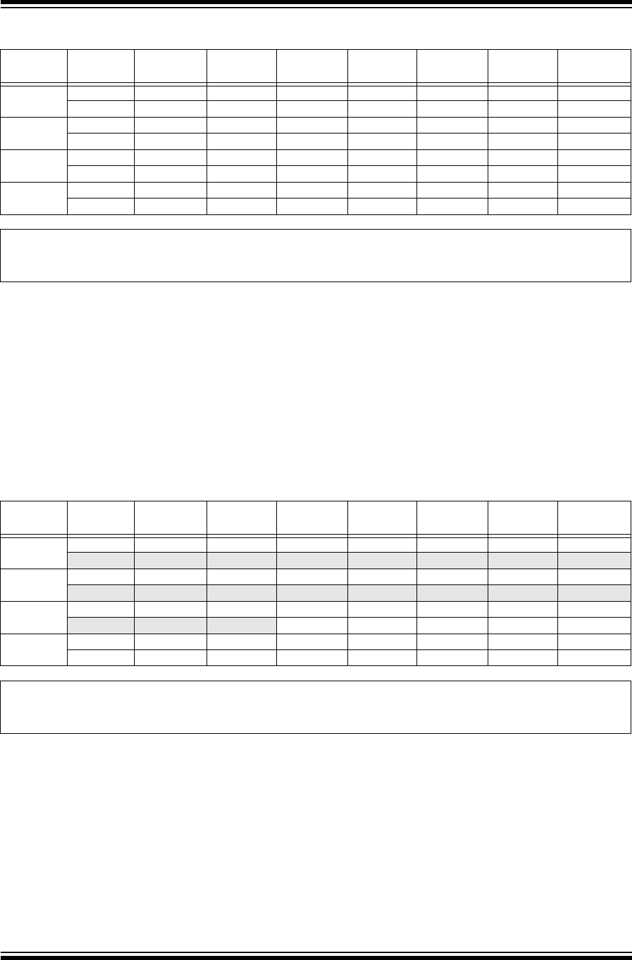
PIC32 Family Reference Manual
DS60001194B-page 18-20 © 2013 Microchip Technology Inc.
Register 18-7: AD1CSS1: ADC1 Input Scan Select Register 1
Bit Range Bit
31/23/15/7
Bit
30/22/14/6
Bit
29/21/13/5
Bit
28/20/12/4
Bit
27/19/11/3
Bit
26/18/10/2
Bit
25/17/9/1
Bit
24/16/8/0
31:24 R/W-0 R/W-0 R/W-0 R/W-0 R/W-0 R/W-0 R/W-0 R/W-0
CSS31 CSS30 CSS29 CSS28 CSS27 CSS26 CSS25 CSS24
23:16 R/W-0 R/W-0 R/W-0 R/W-0 R/W-0 R/W-0 R/W-0 R/W-0
CSS23 CSS22 CSS21 CSS20 CSS19 CSS18 CSS17 CSS16
15:8 R/W-0 R/W-0 R/W-0 R/W-0 R/W-0 R/W-0 R/W-0 R/W-0
CSS15 CSS14 CSS13 CSS12 CSS11 CSS10 CSS9 CSS8
7:0 R/W-0 R/W-0 R/W-0 R/W-0 R/W-0 R/W-0 R/W-0 R/W-0
CSS7 CSS6 CSS5 CSS4 CSS3 CSS2 CSS1 CSS0
Legend:
R = Readable bit W = Writable bit U = Unimplemented bit, read as ‘0’
-n = Value at POR ‘1’ = Bit is set ‘0’ = Bit is cleared x = Bit is unknown
bit 31-0 CSSx: ADC Input Scan Select bits(1,2,3)
1 = Select ANx for input scan
0 = Skip ANx for input scan
Note 1: CSSx = ANx, where ‘x’ = 0-31.
2: In addition to setting the appropriate bits in this register, Class 1 and Class 2 analog inputs must select the
STRIG input as the trigger source if they are to be scanned through the CSSx bits. Refer to the bit
descriptions in the AD1TRGn register (Register 18-15) for selecting the STRIG option.
3: Selections vary by device. Refer to the “12-bit Pipelined Analog-to-Digital Converter (ADC)” chapter in
the specific device data sheet to determine which selections are available.
Register 18-8: AD1CSS2: ADC1 Input Scan Select Register 2
Bit Range Bit
31/23/15/7
Bit
30/22/14/6
Bit
29/21/13/5
Bit
28/20/12/4
Bit
27/19/11/3
Bit
26/18/10/2
Bit
25/17/9/1
Bit
24/16/8/0
31:24 U-0 U-0 U-0 U-0 U-0 U-0 U-0 U-0
— — — — — — — —
23:16 U-0 U-0 U-0 U-0 U-0 U-0 U-0 U-0
— — — — — — — —
15:8 U-0 U-0 U-0 R/W-0 R/W-0 R/W-0 R/W-0 R/W-0
— — — CSS44 CSS43 CSS42 CSS41 CSS40
7:0 R/W-0 R/W-0 R/W-0 R/W-0 R/W-0 R/W-0 R/W-0 R/W-0
CSS39 CSS38 CSS37 CSS36 CSS35 CSS34 CSS33 CSS32
Legend:
R = Readable bit W = Writable bit U = Unimplemented bit, read as ‘0’
-n = Value at POR ‘1’ = Bit is set ‘0’ = Bit is cleared x = Bit is unknown
bit 31-13 Unimplemented: Read as ‘0’
bit 12-0 CSSx: ADC Input Scan Select bits(1,2,3)
1 = Select ANx for input scan
0 = Skip ANx for input scan
Note 1: CSSx = ANx, where ‘x’ = 32-44.
2: In addition to setting the appropriate bits in this register, Class 1 and Class 2 analog inputs must select the
STRIG input as the trigger source if they are to be scanned through the CSSx bits. Refer to the bit
descriptions in the AD1TRGn register (Register 18-15) for selecting the STRIG option.
3: Selections vary by device. Refer to the “12-bit Pipelined Analog-to-Digital Converter (ADC)” chapter in
the specific device data sheet to determine which selections are available.
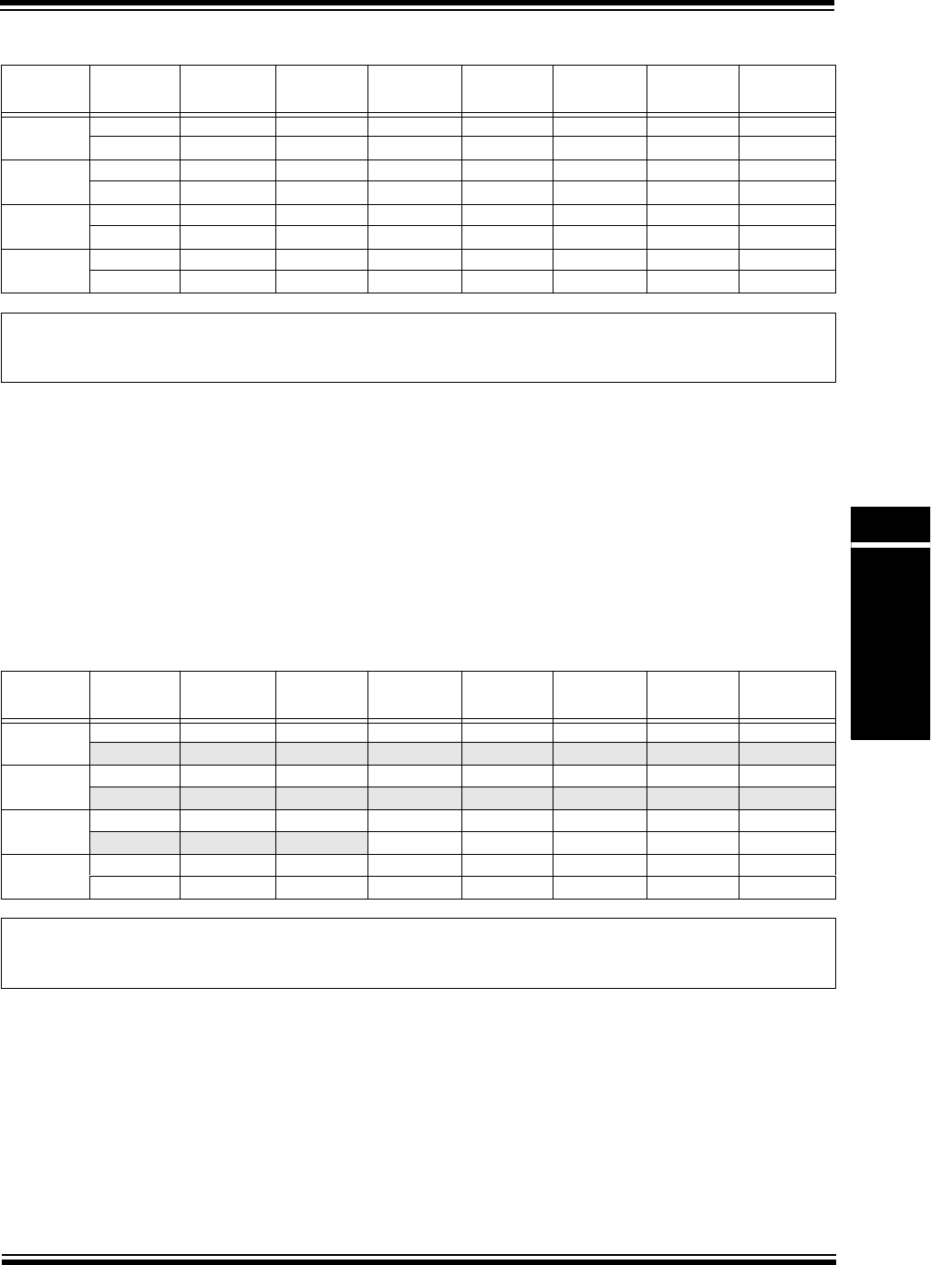
© 2013 Microchip Technology Inc. DS60001194B-page 18-21
Section 18. 12-bit Pipelined Analog-to-Digital Converter (ADC)
12-bit Pipelined
Analog-to-Digital
Converter (ADC)
18
Register 18-9: AD1DSTAT1: ADC1 Data Ready Status Register 1
Bit Range Bit
31/23/15/7
Bit
30/22/14/6
Bit
29/21/13/5
Bit
28/20/12/4
Bit
27/19/11/3
Bit
26/18/10/2
Bit
25/17/9/1
Bit
24/16/8/0
31:24 HS, HC, R-0 HS, HC, R-0 HS, HC, R-0 HS, HC, R-0 HS, HC, R-0 HS, HC, R-0 HS, HC, R-0 HS, HC, R-0
ARDY31 ARDY30 ARDY29 ARDY28 ARDY27 ARDY26 ARDY25 ARDY24
23:16 HS, HC, R-0 HS, HC, R-0 HS, HC, R-0 HS, HC, R-0 HS, HC, R-0 HS, HC, R-0 HS, HC, R-0 HS, HC, R-0
ARDY23 ARDY22 ARDY21 ARDY20 ARDY19 ARDY18 ARDY17 ARDY16
15:8 HS, HC, R-0 HS, HC, R-0 HS, HC, R-0 HS, HC, R-0 HS, HC, R-0 HS, HC, R-0 HS, HC, R-0 HS, HC, R-0
ARDY15 ARDY14 ARDY13 ARDY12 ARDY11 ARDY10 ARDY9 ARDY8
7:0 HS, HC, R-0 HS, HC, R-0 HS, HC, R-0 HS, HC, R-0 HS, HC, R-0 HS, HC, R-0 HS, HC, R-0 HS, HC, R-0
ARDY7 ARDY6 ARDY5 ARDY4 ARDY3 ARDY2 ARDY1 ARDY0
Legend: HS = Set by Hardware HC = Cleared by Hardware
R = Readable bit W = Writable bit U = Unimplemented bit, read as ‘0’
-n = Value at POR ‘1’ = Bit is set ‘0’ = Bit is cleared x = Bit is unknown
bit 31-0 ARDYx: Conversion Data Ready for Corresponding Analog Input Ready bits(1,2,3)
1 = This bit is set when data is ready in the buffer. An interrupt will be generated if the appropriate bit in
the IECx register is set or if enabled for the ADC Global interrupt in the AD1GIRQEN register.
0 = This bit is cleared when the associated data register is read
Note 1: ARDYx = ANx, where ‘x’ = 0-31.
2: When the alternate inputs are used for the Class 1 inputs, the ready bit for the primary input will indicate
the data ready status.
3: Selections vary by device. Refer to the “12-bit Pipelined Analog-to-Digital Converter (ADC)” chapter in
the specific device data sheet to determine which selections are available.
Register 18-10: AD1DSTAT2: ADC1 Data Ready Status Register 2
Bit Range Bit
31/23/15/7
Bit
30/22/14/6
Bit
29/21/13/5
Bit
28/20/12/4
Bit
27/19/11/3
Bit
26/18/10/2
Bit
25/17/9/1
Bit
24/16/8/0
31:24 U-0 U-0 U-0 U-0 U-0 U-0 U-0 U-0
— — — — — — — —
23:16 U-0 U-0 U-0 U-0 U-0 U-0 U-0 U-0
— — — — — — — —
15:8 U-0 U-0 U-0 HS, HC, R-0 HS, HC, R-0 HS, HC, R-0 HS, HC, R-0 HS, HC, R-0
— — —ARDY44ARDY43ARDY42ARDY41ARDY40
7:0 HS, HC, R-0 HS, HC, R-0 HS, HC, R-0 HS, HC, R-0 HS, HC, R-0 HS, HC, R-0 HS, HC, R-0 HS, HC, R-0
ARDY39 ARDY38 ARDY37 ARDY36 ARDY35 ARDY34 ARDY33 ARDY32
Legend: HS = Set by Hardware HC = Cleared by Hardware
R = Readable bit W = Writable bit U = Unimplemented bit, read as ‘0’
-n = Value at POR ‘1’ = Bit is set ‘0’ = Bit is cleared x = Bit is unknown
bit 31-13 Unimplemented: Read as ‘0’
bit 12-0 ARDYx: Conversion Data Ready for Corresponding Analog Input Ready bits(1,2)
1 = This bit is set when data is ready in the buffer. An interrupt will be generated if the appropriate bit in
the IECx register is set or if enabled for the ADC Global interrupt in the AD1GIRQEN register.
0 = This bit is cleared when the associated data register is read
Note 1: ARDYx = ANx, where ‘x’ = 32-44.
2: Selections vary by device. Refer to the “12-bit Pipelined Analog-to-Digital Converter (ADC)” chapter in
the specific device data sheet to determine which selections are available.

PIC32 Family Reference Manual
DS60001194B-page 18-22 © 2013 Microchip Technology Inc.
Register 18-11: AD1CMPCONn: ADC1 Digital Comparator Control Register ‘n’ (‘n’ = 1, 2, 3, 4, 5, or 6)
Bit Range Bit
31/23/15/7
Bit
30/22/14/6
Bit
29/21/13/5
Bit
28/20/12/4
Bit
27/19/11/3
Bit
26/18/10/2
Bit
25/17/9/1
Bit
24/16/8/0
31:24 U-0 U-0 U-0 U-0 U-0 U-0 U-0 U-0
— — — — — — — —
23:16 U-0 U-0 U-0 U-0 U-0 U-0 U-0 U-0
— — — — — — — —
15:8 U-0 U-0 U-0 HS, HC, R-0 HS, HC, R-0 HS, HC, R-0 HS, HC, R-0 HS, HC, R-0
— — —AINID<4:0>
(1)
7:0 R/W-0 R/W-0 HS, HC, R-0 R/W-0 R/W-0 R/W-0 R/W-0 R/W-0
ENDCMP DCMPGIEN(2) DCMPED IEBTWN IEHIHI IEHILO IELOHI IELOLO
Legend: HS = Set by Hardware HC = Cleared by Hardware
R = Readable bit W = Writable bit U = Unimplemented bit, read as ‘0’
-n = Value at POR ‘1’ = Bit is set ‘0’ = Bit is cleared x = Bit is unknown
bit 31-13 Unimplemented: Read as ‘0’
bit 12-8 AINID<4:0>: Analog Input Identification (ID) bits(1)
When a digital comparator event occurs (DCMPED = 1), these bits identify the analog input which
generated the event. In addition, these bits identify the last analog input to generate an event if multiple
inputs are enabled and more than one event has occurred since the last reading.
bit 7 ENDCMP: Digital Comparator Enable bit
1 = Digital Comparator is enabled
0 = Digital Comparator is not enabled, and the DCMPED status bit is cleared
bit 6 DCMPGIEN: Digital Comparator Global ADC Interrupt Enable bit(2)
1 = A Digital Comparator Event (DCMPED transitions from ‘0’ to ‘1’) will generate a Global ADC interrupt.
0 = A Digital Comparator Event will not generate a Global ADC interrupt.
The Global ADC Interrupt is enabled by setting a bit in the IECx registers (refer to the “Interrupt
Controller” chapter in the specific device data sheet for details).
bit 5 DCMPED: Digital Comparator Event Detected Status bit
1 = This bit is set by the digital comparator hardware when a comparison event is detected. An interrupt will
be generated if the appropriate bit in the IECx register is set or if enabled for the ADC Global interrupt
in the DCMPGIEN bit.
0 = This bit is cleared by reading the AINID<4:0> bits or when the ADC module is disabled
bit 4 IEBTWN: Between Low/High Digital Comparator Event bit(2)
1 = Generate a digital comparator event when ADCMPLO<15:0> ≤ DATA<31:0> <ADCMPHI<15:0>
0 = Do not generate a digital comparator event
bit 3 IEHIHI: High/High Digital Comparator Event bit(2)
1 = Generate a Digital Comparator Event when ADCMPHI<15:0> ≤ DATA<31:0>
0 = Do not generate a digital comparator event
bit 2 IEHILO: High/Low Digital Comparator Event bit(2)
1 = Generate a Digital Comparator Event when DATA<31:0> <ADCMPHI<15:0>
0 = Do not generate a digital comparator event
bit 1 IELOHI: Low/High Digital Comparator Event bit(2)
1 = Generate a Digital Comparator Event when ADCMPLO<15:0> ≤ DATA<31:0>
0 = Do not generate a digital comparator event
bit 0 IELOLO: Low/Low Digital Comparator Event bit(2)
1 = Generate a Digital Comparator Event when DATA<31:0> <ADCMPLO<15:0>
0 = Do not generate a digital comparator event
Note 1: A Digital Comparator Event occurred on ANx, where ‘x’ = AINID<4:0>, and ‘x’ has a range of 0-31.
2: Changing these bits while the Digital Comparator is enabled (ENDCMP = 1) can result in unpredictable
behavior.

© 2013 Microchip Technology Inc. DS60001194B-page 18-23
Section 18. 12-bit Pipelined Analog-to-Digital Converter (ADC)
12-bit Pipelined
Analog-to-Digital
Converter (ADC)
18
Register 18-12: AD1CMPENn: ADC1 Digital Comparator Enable Register ‘n’ (‘n’ = 1, 2, 3, 4, 5, or 6)
Bit Range Bit
31/23/15/7
Bit
30/22/14/6
Bit
29/21/13/5
Bit
28/20/12/4
Bit
27/19/11/3
Bit
26/18/10/2
Bit
25/17/9/1
Bit
24/16/8/0
31:24 R/W-0 R/W-0 R/W-0 R/W-0 R/W-0 R/W-0 R/W-0 R/W-0
CMPE31 CMPE30 CMPE29 CMPE28 CMPE27 CMPE26 CMPE25 CMPE24
23:16 R/W-0 R/W-0 R/W-0 R/W-0 R/W-0 R/W-0 R/W-0 R/W-0
CMPE23 CMPE22 CMPE21 CMPE20 CMPE19 CMPE18 CMPE17 CMPE16
15:8 R/W-0 R/W-0 R/W-0 R/W-0 R/W-0 R/W-0 R/W-0 R/W-0
CMPE15 CMPE14 CMPE13 CMPE12 CMPE11 CMPE10 CMPE9 CMPE8
7:0 R/W-0 R/W-0 R/W-0 R/W-0 R/W-0 R/W-0 R/W-0 R/W-0
CMPE7 CMPE6 CMPE5 CMPE4 CMPE3 CMPE2 CMPE1 CMPE0
Legend:
R = Readable bit W = Writable bit U = Unimplemented bit, read as ‘0’
-n = Value at POR ‘1’ = Bit is set ‘0’ = Bit is cleared x = Bit is unknown
bit 31-0 CMPE31:CMPE0: ADC1 Digital Comparator Enable bits(1,2)
These bits enable conversion results corresponding to the Analog Input to be processed by the Digital
Comparator. CMPE0 enables AN0, CMPE1 enables AN1, and so on.
Note 1: CMPEx = ANx, where ‘x’ = 0-31 (Digital Comparator inputs are limited to AN0 through AN31).
2: Changing the bits in this register while the Digital Comparator is enabled (ENDCMP = 1) can result in
unpredictable behavior.

PIC32 Family Reference Manual
DS60001194B-page 18-24 © 2013 Microchip Technology Inc.
Register 18-13: AD1CMPn: ADC1 Digital Comparator Register ‘n’ (‘n’ = 1, 2, 3, 4, 5 or 6)
Bit Range Bit
31/23/15/7
Bit
30/22/14/6
Bit
29/21/13/5
Bit
28/20/12/4
Bit
27/19/11/3
Bit
26/18/10/2
Bit
25/17/9/1
Bit
24/16/8/0
31:24 R/W-0 R/W-0 R/W-0 R/W-0 R/W-0 R/W-0 R/W-0 R/W-0
ADCMPHI<15:8>
23:16 R/W-0 R/W-0 R/W-0 R/W-0 R/W-0 R/W-0 R/W-0 R/W-0
ADCMPHI<7:0>
15:8 R/W-0 R/W-0 R/W-0 R/W-0 R/W-0 R/W-0 R/W-0 R/W-0
ADCMPLO<15:8>
7:0 R/W-0 R/W-0 R/W-0 R/W-0 R/W-0 R/W-0 R/W-0 R/W-0
ADCMPLO<7:0>
Legend:
R = Readable bit W = Writable bit U = Unimplemented bit, read as ‘0’
-n = Value at POR ‘1’ = Bit is set ‘0’ = Bit is cleared x = Bit is unknown
bit 31-16 ADCMPHI<15:0>: Digital Analog Comparator High Limit Value bits
These bits store the high limit value, which is used for comparisons with the analog-to-digital conversion
data. The user is responsible for formatting the high limit value to match the format as specified by the
SHxMOD<1:0> bits for the associated S&H and the global FRACT bit. These bits are located in the
ADxMOD and ADxCON1 registers, respectively.
bit 15-0 ADCMPLO<15:0>: Digital Analog Comparator Low Limit Value bits
These bits store the low limit value, which is used for comparisons with the analog-to-digital conversion
data. The user is responsible for formatting the low limit value to match the format as specified by the
SHxMOD<1:0> bits for the associated S&H and the global FRACT bit. These bits are located in the
ADxMOD and ADxCON1 registers, respectively.
Note: Changing the bits in this register while the Digital Comparator is enabled (ENDCMP = 1) can result in unpre-
dictable behavior.

© 2013 Microchip Technology Inc. DS60001194B-page 18-25
Section 18. 12-bit Pipelined Analog-to-Digital Converter (ADC)
12-bit Pipelined
Analog-to-Digital
Converter (ADC)
18
Register 18-14: AD1FLTRn: ADC1 Filter Register ‘n’ (‘n’ = 1, 2, 3, 4, 5, or 6)
Bit
Range
Bit
31/23/15/7
Bit
30/22/14/6
Bit
29/21/13/5
Bit
28/20/12/4
Bit
27/19/11/3
Bit
26/18/10/2
Bit
25/17/9/1
Bit
24/16/8/0
31:24 R/W-0 U-0 U-0 R/W-0 R/W-0 R/W-0 R/W-0 R/W-0
AFEN — — OVRSAM<2:0> AFGIEN AFRDY
23:16 U-0 U-0 R/W-0 R/W-0 R/W-0 R/W-0 R/W-0 R/W-0
——CHNLID<5:0>
15:8 HS, HC, R-0 HS, HC, R-0 HS, HC, R-0 HS, HC, R-0 HS, HC, R-0 HS, HC, R-0 HS, HC, R-0 HS, HC, R-0
FLTRDATA<15:8>
7:0 HS, HC, R-0 HS, HC, R-0 HS, HC, R-0 HS, HC, R-0 HS, HC, R-0 HS, HC, R-0 HS, HC, R-0 HS, HC, R-0
FLTRDATA<7:0>
Legend: HS = Set by Hardware HC = Cleared by Hardware
R = Readable bit W = Writable bit U = Unimplemented bit, read as ‘0’
-n = Value at POR ‘1’ = Bit is set ‘0’ = Bit is cleared x = Bit is unknown
bit 31 AFEN: Oversampling Filter Enable bit
1 = Oversampling filter is enabled
0 = Oversampling filter is disabled and the AFRDY bit is cleared
bit 30-29 Unimplemented: Read as ‘0’
bit 28-26 OVRSAM<2:0>: Oversampling Filter Ratio bits
111 = 128x (shift sum 3 bits to right, output data is in 15.1 format)
110 = 32x (shift sum 2 bits to right, output data is in 14.1 format)
101 = 8x (shift sum 1 bit to right, output data is in 13.1 format)
100 = 2x (shift sum 0 bits to right, output data is in 12.1 format)
011 = 256x (shift sum 4 bits to right, output data is 16 bits)
010 = 64x (shift sum 3 bits to right, output data is 15 bits)
001 = 16x (shift sum 2 bits to right, output data is 14 bits)
000 = 4x (shift sum 1 bit to right, output data is 13 bits)
bit 25 AFGIEN: Oversampling Filter Global ADC Interrupt Enable bit
1 = An Oversampling Filter Data Ready event (AFRDY transitions from ‘0’ to ‘1’) will generate an ADC
Global Interrupt
0 = An Oversampling Filter Data Ready event will not generate an ADC Global Interrupt
bit 24 AFRDY: Oversampling Filter Data Ready Flag bit
1 = This bit is set when data is ready in the FLTRDATA<15:0> bits
0 = This bit is cleared when FLTRDATA<15:0> is read, or if the module is disabled
bit 23-22 Unimplemented: Read as ‘0’
bit 21-16 CHNLID<5:0>: Channel ID Selection bits(1)
These bits specify the analog input to be used as the oversampling filter data source.
111111 = Reserved
•
•
•
101101 = Reserved
101100 = IVTEMP
101011 = IVREF
101010 = AN42
•
•
•
000010 = AN2
000001 = AN1
000000 = AN0
bit 15-0 FLTRDATA<15:0>: Oversampling Filter Data Output Value bits
These bits contain the oversampling filter result.
Note 1: Selections vary by device. Refer to the “12-bit Pipelined Analog-to-Digital Converter (ADC)” chapter
in the specific device data sheet to determine which selections are available

PIC32 Family Reference Manual
DS60001194B-page 18-26 © 2013 Microchip Technology Inc.
Register 18-15: AD1TRGR1: ADC1 Input Convert Control Register 1
Bit
Range
Bit
31/23/15/7
Bit
30/22/14/6
Bit
29/21/13/5
Bit
28/20/12/4
Bit
27/19/11/3
Bit
26/18/10/2
Bit
25/17/9/1
Bit
24/16/8/0
31:24 U-0 U-0 U-0 R/W-0 R/W-0 R/W-0 R/W-0 R/W-0
— — —TRGSRC3<4:0>
23:16 U-0 U-0 U-0 R/W-0 R/W-0 R/W-0 R/W-0 R/W-0
— — —TRGSRC2<4:0>
15:8 U-0 U-0 U-0 R/W-0 R/W-0 R/W-0 R/W-0 R/W-0
— — —TRGSRC1<4:0>
7:0 U-0 U-0 U-0 R/W-0 R/W-0 R/W-0 R/W-0 R/W-0
— — —TRGSRC0<4:0>
Legend:
R = Readable bit W = Writable bit U = Unimplemented bit, read as ‘0’
-n = Value at POR ‘1’ = Bit is set ‘0’ = Bit is cleared x = Bit is unknown
bit 31-29 Unimplemented: Read as ‘0’
bit 28-24 TRGSRC3<4:0>: Trigger Source for Conversion of Analog Channels AN3 Select bits
11111 = Reserved
•
•
•
01101 = Reserved
01100 = Comparator 2 COUT
01011 = Comparator 1 COUT
01010 = OCMP5
01001 = OCMP3
01000 = OCMP1
00111 = TMR5 match
00110 = TMR3 match
00101 = TMR1 match
00100 = INT0
00011 = STRIG(1)
00010 = Reserved
00001 = Global software trigger (GSWTRG)
00000 = No trigger
bit 23-21 Unimplemented: Read as ‘0’
bit 20-16 TRGSRC2<4:0>: Trigger Source for Conversion of Analog Channels AN2 Select bits
See bits 28-24 for bit value definitions.
bit 15-13 Unimplemented: Read as ‘0’
bit 12-8 TRGSRC1<4:0>: Trigger Source for Conversion of Analog Channels AN1 Select bits
See bits 28-24 for bit value definitions.
bit 7-5 Unimplemented: Read as ‘0’
bit 4-0 TRGSRC0<4:0>: Trigger Source for Conversion of Analog Channels AN0 Select bits
See bits 28-24 for bit value definitions.
Note 1: Using STRIG as the trigger source specifies this input to use the Scan Trigger source for its trigger. The
STRGSRC<4:0> bits (AD1CON1<26:22>), as well as the appropriate CSSx bit(s) in the AD1CSS1 and
AD1CSS2 registers must be set for proper scan operation.

© 2013 Microchip Technology Inc. DS60001194B-page 18-27
Section 18. 12-bit Pipelined Analog-to-Digital Converter (ADC)
12-bit Pipelined
Analog-to-Digital
Converter (ADC)
18
Register 18-16: AD1TRGR2: ADC1 Input Convert Control Register 2
Bit
Range
Bit
31/23/15/7
Bit
30/22/14/6
Bit
29/21/13/5
Bit
28/20/12/4
Bit
27/19/11/3
Bit
26/18/10/2
Bit
25/17/9/1
Bit
24/16/8/0
31:24 U-0 U-0 U-0 R/W-0 R/W-0 R/W-0 R/W-0 R/W-0
— — —TRGSRC7<4:0>
23:16 U-0 U-0 U-0 R/W-0 R/W-0 R/W-0 R/W-0 R/W-0
— — —TRGSRC6<4:0>
15:8 U-0 U-0 U-0 R/W-0 R/W-0 R/W-0 R/W-0 R/W-0
— — —TRGSRC5<4:0>
7:0 U-0 U-0 U-0 R/W-0 R/W-0 R/W-0 R/W-0 R/W-0
— — —TRGSRC4<4:0>
Legend:
R = Readable bit W = Writable bit U = Unimplemented bit, read as ‘0’
-n = Value at POR ‘1’ = Bit is set ‘0’ = Bit is cleared x = Bit is unknown
bit 31-29 Unimplemented: Read as ‘0’
bit 28-24 TRGSRC7<4:0>: Trigger Source for Conversion of Analog Channels AN7 Select bits
11111 = Reserved
•
•
•
01101 = Reserved
01100 = C2OUT
01011 = C1OUT
01010 = OCMP5
01001 = OCMP3
01000 = OCMP1
00111 = TMR5 match
00110 = TMR3 match
00101 = TMR1 match
00100 = INT0
00011 = STRIG(1)
00010 = Reserved
00001 = Global software trigger (GSWTRG)
00000 = No trigger
bit 23-21 Unimplemented: Read as ‘0’
bit 20-16 TRGSRC6<4:0>: Trigger Source for Conversion of Analog Channels AN6 Select bits
See bits 28-24 for bit value definitions.
bit 15-13 Unimplemented: Read as ‘0’
bit 12-8 TRGSRC5<4:0>: Trigger Source for Conversion of Analog Channels AN5 Select bits
See bits 28-24 for bit value definitions.
bit 7-5 Unimplemented: Read as ‘0’
bit 4-0 TRGSRC4<4:0>: Trigger Source for Conversion of Analog Channels AN4 Select bits
See bits 28-24 for bit value definitions.
Note 1: Using STRIG as the trigger source specifies this input to use the Scan Trigger source for its trigger. The
STRGSRC<4:0> bits (AD1CON1<26:22>), as well as the appropriate CSSx bit(s) in the AD1CSS1 and
AD1CSS2 registers must be set for proper scan operation.

PIC32 Family Reference Manual
DS60001194B-page 18-28 © 2013 Microchip Technology Inc.
Register 18-17: AD1TRGR3: ADC1 Input Convert Control Register 3
Bit
Range
Bit
31/23/15/7
Bit
30/22/14/6
Bit
29/21/13/5
Bit
28/20/12/4
Bit
27/19/11/3
Bit
26/18/10/2
Bit
25/17/9/1
Bit
24/16/8/0
31:24 U-0 U-0 U-0 R/W-0 R/W-0 R/W-0 R/W-0 R/W-0
— — —TRGSRC11<4:0>
23:16 U-0 U-0 U-0 R/W-0 R/W-0 R/W-0 R/W-0 R/W-0
— — —TRGSRC10<4:0>
15:8 U-0 U-0 U-0 R/W-0 R/W-0 R/W-0 R/W-0 R/W-0
— — —TRGSRC9<4:0>
7:0 U-0 U-0 U-0 R/W-0 R/W-0 R/W-0 R/W-0 R/W-0
— — —TRGSRC8<4:0>
Legend:
R = Readable bit W = Writable bit U = Unimplemented bit, read as ‘0’
-n = Value at POR ‘1’ = Bit is set ‘0’ = Bit is cleared x = Bit is unknown
bit 31-29 Unimplemented: Read as ‘0’
bit 28-24 TRGSRC11<4:0>: Trigger Source for Conversion of Analog Channels AN11 Select bits
11111 = Reserved
•
•
•
01101 = Reserved
01100 = C2OUT
01011 = C1OUT
01010 = OCMP5
01001 = OCMP3
01000 = OCMP1
00111 = TMR5 match
00110 = TMR3 match
00101 = TMR1 match
00100 = INT0
00011 = STRIG(1)
00010 = Reserved
00001 = Global software trigger (GSWTRG)
00000 = No trigger
bit 23-21 Unimplemented: Read as ‘0’
bit 20-16 TRGSRC10<4:0>: Trigger Source for Conversion of Analog Channels AN10 Select bits
See bits 28-24 for bit value definitions.
bit 15-13 Unimplemented: Read as ‘0’
bit 12-8 TRGSRC9<4:0>: Trigger Source for Conversion of Analog Channels AN9 Select bits
See bits 28-24 for bit value definitions.
bit 7-5 Unimplemented: Read as ‘0’
bit 4-0 TRGSRC8<4:0>: Trigger Source for Conversion of Analog Channels AN8 Select bits
See bits 28-24 for bit value definitions.
Note 1: Using STRIG as the trigger source specifies this input to use the Scan Trigger source for its trigger. The
STRGSRC<4:0> bits (AD1CON1<26:22>), as well as the appropriate CSSx bit(s) in the AD1CSS1 and
AD1CSS2 registers must be set for proper scan operation.

© 2013 Microchip Technology Inc. DS60001194B-page 18-29
Section 18. 12-bit Pipelined Analog-to-Digital Converter (ADC)
12-bit Pipelined
Analog-to-Digital
Converter (ADC)
18
Register 18-18: AD1DATAn: ADC1 Data Output Register (‘n’ = 0 to 44)
Bit Range Bit
31/23/15/7
Bit
30/22/14/6
Bit
29/21/13/5
Bit
28/20/12/4
Bit
27/19/11/3
Bit
26/18/10/2
Bit
25/17/9/1
Bit
24/16/8/0
31:24 R-0 R-0 R-0 R-0 R-0 R-0 R-0 R-0
DATA<31:24>
23:16 R-0 R-0 R-0 R-0 R-0 R-0 R-0 R-0
DATA<23:16>
15:8 R-0 R-0 R-0 R-0 R-0 R-0 R-0 R-0
DATA<15:8>
7:0 R-0 R-0 R-0 R-0 R-0 R-0 R-0 R-0
DATA<7:0>
Legend:
R = Readable bit W = Writable bit U = Unimplemented bit, read as ‘0’
-n = Value at POR ‘1’ = Bit is set ‘0’ = Bit is cleared x = Bit is unknown
bit 31-0 DATA<31:0>: Data Output Value bits
These bits are formatted as specified by the SHxMOD<1:0> bits for the FRACT bit and the associated
S&H circuit.
Note: When an alternate input is used as the input source for a Class 1 input, the data output is still read from the
Primary input Data Output Register.
Register 18-19: AD1CALx: ADC1 Calibration Register (‘x’ = 1-5)
Bit Range Bit
31/23/15/7
Bit
30/22/14/6
Bit
29/21/13/5
Bit
28/20/12/4
Bit
27/19/11/3
Bit
26/18/10/2
Bit
25/17/9/1
Bit
24/16/8/0
31:24 R/W-0 R/W-0 R/W-0 R/W-0 R/W-0 R/W-0 R/W-0 R/W-0
ADCAL<31:24>
23:16 R/W-0 R/W-0 R/W-0 R/W-0 R/W-0 R/W-0 R/W-0 R/W-0
ADCAL<23:16>
15:8 R/W-0 R/W-0 R/W-0 R/W-0 R/W-0 R/W-0 R/W-0 R/W-0
ADCAL<15:8>
7:0 R/W-0 R/W-0 R/W-0 R/W-0 R/W-0 R/W-0 R/W-0 R/W-0
ADCAL<7:0>
Legend:
R = Readable bit W = Writable bit U = Unimplemented bit, read as ‘0’
-n = Value at POR ‘1’ = Bit is set ‘0’ = Bit is cleared x = Bit is unknown
bit 31-0 ADCAL<31:0>: Calibration Data for the ADC module bits

PIC32 Family Reference Manual
DS60001194B-page 18-30 © 2013 Microchip Technology Inc.
18.3 ADC OPERATION, TERMINOLOGY AND CONVERSION SEQUENCE
Analog-to-Digital conversion using the 12-bit ADC involves the following three steps:
1. Sampling of the input signal.
2. Capture of the input signal (holding) and transfer to the converter.
3. Conversion of the analog signal to its digital representation.
Sampling of the input signal involves charging of the capacitor in the S&H circuit. The sampling
time must be adequate so that the capacitor charges to a value equal to the input voltage (see
18.10 “ADC Sampling Requirements”). At the appropriate time, the input is disconnected from
the capacitor and subsequently, the analog voltage is transferred to the converter. The converter
then digitizes the analog signal and provides the result.
The converter requires a clock source and a reference voltage. The clock is referred to as the
ADC clock and has a period of TAD. The clock and reference voltage sources are selectable, as
well as the clock prescaling.
The 12-bit ADC uses two types of S&H circuits: dedicated and shared. Each ADC
implementation includes up to five dedicated S&H circuits and a single shared S&H. Inputs
connected to the S&H circuits are categorized into three types: Class 1, Class 2, and Class 3.
18.3.1 Analog Inputs
The analog input pins that are available on a device are classified into three categories: Class 1,
Class 2, and Class 3. Each analog input, regardless of Class category, has its own unique data
output register where the conversion result is stored.
Table 18-2: Analog Input Types
Class 1 inputs are associated with a dedicated S&H circuit. Each dedicated S&H has a single
Class 1 input associated with it. Each Class 1 input has a unique trigger selection register.
Class 1 inputs can be part of a channel scan list, triggered by the common scan trigger source.
Class 2 inputs are used on the shared S&H, either individually triggered or as part of a channel
scan list. When used individually they are triggered by their unique trigger register.
Class 3 inputs are used for channel scan exclusively. They share a common trigger source.
When using channel scan it is possible to combine Class 1, Class 2, and Class 3 inputs in the
scan list.
Type S&H/Input Type Trigger Trigger Action
Class 1 Dedicated S&H input Individual trigger source
or channel scan trigger
Ends sampling and starts
conversion
Class 2 Shared S&H input Individual trigger source
or channel scan trigger
Starts sampling/conversion
sequence or begins channel
scan sequence
Class 3 Shared S&H channel
scan input
Channel scan trigger Starts channel scan sequence
Note: Each Class 1 input also has an alternate selection. This alternate input is unique
from Class 1, 2, and 3 inputs. When an alternate input is used for a Class 1 input,
the trigger is still selected by the Class 1 trigger register, the result data is stored in
the Class 1 output register and the priority for conversion remains that of the Class
1 input.
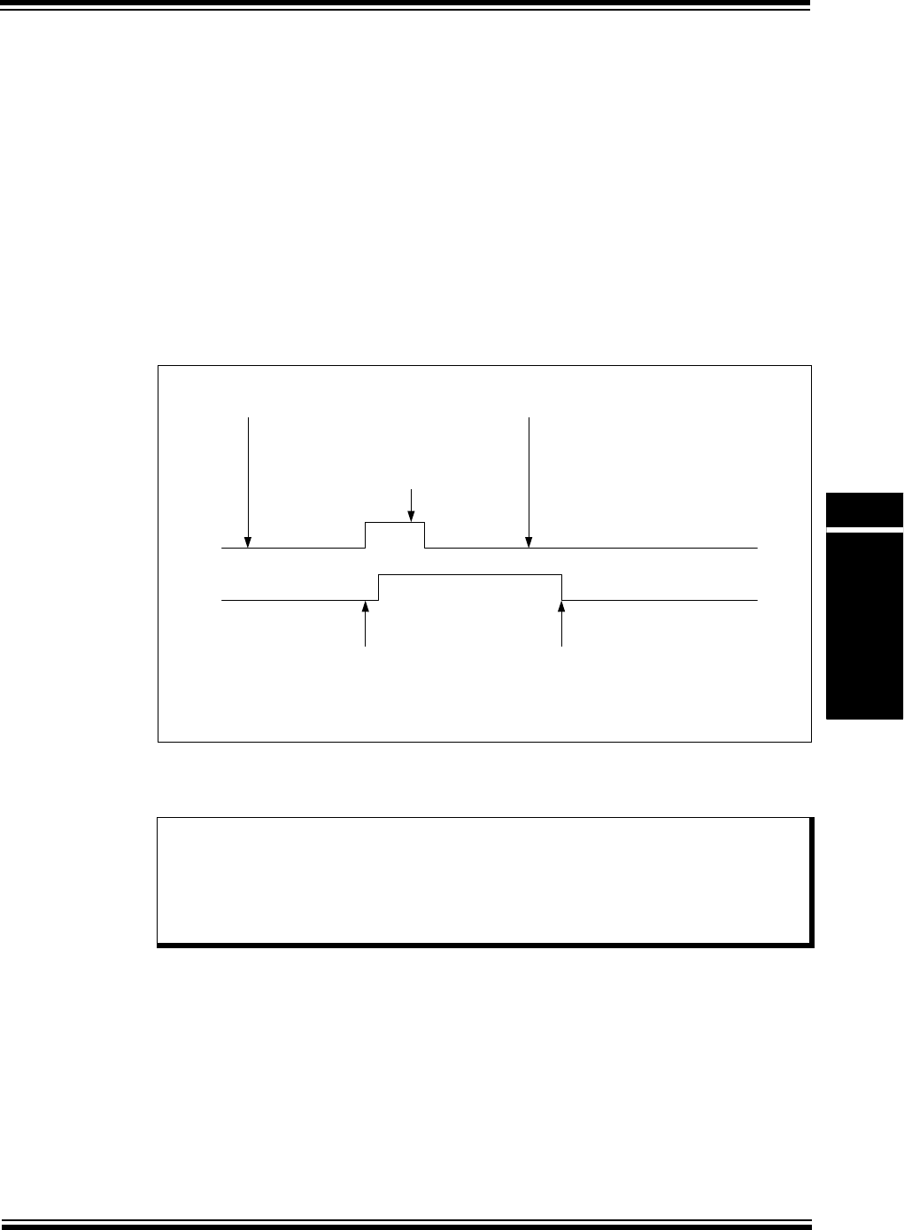
© 2013 Microchip Technology Inc. DS60001194B-page 18-31
Section 18. 12-bit Pipelined Analog-to-Digital Converter (ADC)
12-bit Pipelined
Analog-to-Digital
Converter (ADC)
18
18.3.2 Dedicated Sample and Hold
Dedicated S&H circuits, as the name implies, are dedicated to a Class 1 analog input, and enable
high-speed, high-precision sampling and conversion, and are especially useful for capturing time
sensitive or transient signals. They can be configured for Single-ended or Differential modes.
Each dedicated S&H continuously tracks the input signal in Sample mode until the asynchronous
trigger event occurs. The trigger event causes the S&H to immediately stop sampling and enter
the holding state. It is important to note that the trigger event, which ends sampling, occurs asyn-
chronously to the ADC clock. While the S&H circuits enter the Hold state immediately, the asyn-
chronous trigger must be synchronized to the ADC clock consuming two ADC clock edges before
the conversion request is issued to the pipeline converter. If no higher priority conversion
requests exits, the conversion will commence immediately; otherwise, the conversions take
place by priority. The S&H remains in the holding state during the initial stage of the conversion
process. When the conversion is complete, data is transferred to the result buffer and an interrupt
is generated.
Figure 18-4: Dedicated S&H Conversion Sequence
If using a periodic trigger source with a dedicated S&H, the total sampling time is determined by
the trigger rate. The trigger rate must not violate the necessary sampling time. See 18.10 “ADC
Sampling Requirements” for more information.
Note 1: There is no mechanism in the dedicated S&H to ensure the minimum sampling time
has been met. The system designer must ensure that the S&H has had adequate
sampling time before triggering.
2: The alternate input provided on dedicated S&H circuits provides an alternate
physical connection; however, the dedicated S&H always uses the trigger
configuration and data result registers for its primary Class 1 input.
Sample Hold Sample
Convert
S&H circuit is connected to the analog input for sampling.
S&H circuit is disconnected from
the analog input during Hold
Trigger asynchronously switches the
S&H circuit to a Hold state and the
conversion request is issued
synchronously to the ADC clock.
ADC conversion is complete and the
result is written to the ADC result
buffer. If interrupts are enabled an
interrupt is generated.

PIC32 Family Reference Manual
DS60001194B-page 18-32 © 2013 Microchip Technology Inc.
18.3.3 Shared Sample and Hold
The shared S&H circuit provides the greatest flexibility for handling a large number of Class 2
and Class 3 inputs where timing is not critical. Shared S&H circuits can also be configured for
Single-ended or Differential modes; however, in Differential mode the single negative input is
common to all positive input selections.
The shared S&H is shared among the majority of inputs using a multiplexer on the positive input.
Unlike the dedicated S&H, the trigger event of a shared S&H starts the sampling process using
a specified sample time. Once the signal has been sampled the specified number of ADC clocks,
the S&H enters the hold state and the conversion request is issued. The S&H remains in the hold
state during the initial stage of the conversion process.
Figure 18-5: Shared S&H Conversion Sequence
When using the shared S&H, the SAMC<7:0> bits in the ADC1 Control Register 2
(AD1CON2<23:16>) determine the sample time. When periodically triggering a single input on
the shared S&H, the trigger rate should not be less than the sample time plus 2 TAD, which is the
time to transfer to the pipeline converter.
There are two operation modes for the shared S&H: Independent Class 2 Triggering and
Channel Scanning. The shared S&H accommodate either or both of these modes
simultaneously. There is no assurance that a Class 2 or Class 3 conversion request will be
serviced immediately. Conversion requests to the pipeline converter are serviced in order or
priority.
18.3.3.1 CLASS 2 TRIGGERING
When Class 2 inputs are defined with independent triggers, they are sampled and converted by
the shared S&H using the sequence illustrated in Figure 18-5. When multiple Class 2 inputs with
independent triggers are used it is important to understand the consequences of trigger timing.
If a conversion is underway and another Class 2 trigger occurs then the sample-hold-conversion
for the new trigger will be stalled until the in-process sample-hold cycle is complete, as shown in
Figure 18-6.
Figure 18-6: Multiple Independent Class 2 Trigger Conversion Sequence
Sample Hold
Convert
S&H circuit is disconnected from the analog input.
Trigger causes S&H circuit to begin sampling for the
specified number of ADC clocks, and then switches to the
Hold state.
Conversion request
occurs when the S&H
circuit enters the Hold
state.
Ananlog-to-Digital conversion is
complete and the result is written to
the ADC result buffer. If interrupts are
enabled an interrupt is generated.
Convert AN5
Sample AN5 Hold
Trigger for AN5
Hold
Convert AN6
Sample AN6
Trigger for AN6 S&H cycle for AN6 delayed until AN5
S&H cycle is complete.
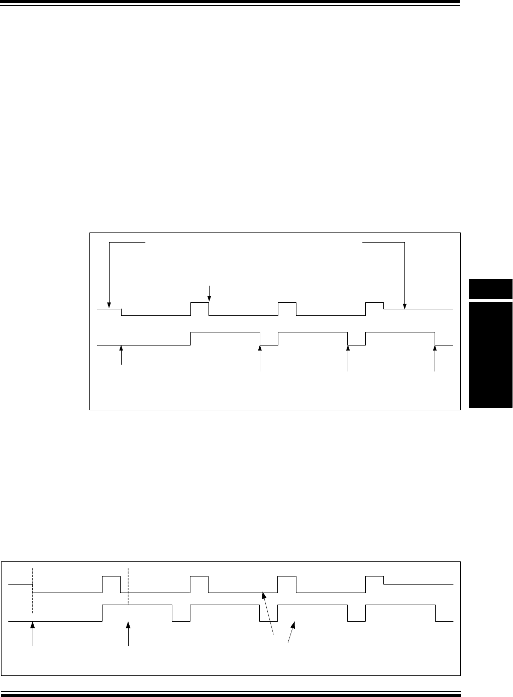
© 2013 Microchip Technology Inc. DS60001194B-page 18-33
Section 18. 12-bit Pipelined Analog-to-Digital Converter (ADC)
12-bit Pipelined
Analog-to-Digital
Converter (ADC)
18
When multiple inputs to the shared S&H are triggered simultaneously, the processing order is
determined by their natural priority (the lowest numbered input has the highest priority). As an
example, if AN5, AN6, and AN7 are triggered using the same source, AN5 will be sampled and
converted first, followed by AN6 and finally, AN7.
When using the independent Class 2 triggering on the shared S&H, the SAMC<7:0> bits
(AD1CON2<23:16>) determine the sample time for all inputs while the appropriate TRGSRC<4:0>
bits in the ADC1 Input Convert Control Register (see Register 18-15) determine the trigger source
for each input.
18.3.3.2 CHANNEL SCAN
Channel scanning is a feature that allows an automated scanning sequence of multiple Class 1,
Class 2 or Class 3 inputs. All Class 2 and Class 3 inputs are scanned using the single shared
S&H. Class 1 inputs are scanned using their dedicated S&H. A single trigger source initiates a
channel scan. Individual triggers, if available, are not used. When a trigger occurs, all Class 1
inputs are captured simultaneously and conversions are started based on natural priority. The
trigger will also initiate sampling of the first Class 2 or 3 input in the scan list and once sampling
is complete, pass it to the converter after all of the Class 1 conversions have begun. The natural
input order is used; lower number inputs are sampled before higher number inputs.
Figure 18-7: Channel Scan Conversion Sequence for Three Class 2 Inputs
When using the shared S&H in scan mode, the SAMC<7:0> bits in the ADC1 Control Register 2
(AD1CON2<23:16>) determine the sample time for all inputs while the Scan Trigger Source
Selection bits (STRGSRC<4:0>) in the ADC1 Control Register 1 (AD1CON1<26:22>), determine
the trigger source.
To en su re p red ica ble r esu lt s, a s can s hou ld no t be r etr ig g er ed un til s amp li n g of a ll ch ann els h as
completed. Care should be taken in the system design to preclude retriggering a channel scan
while a scan is in progress.
Individual Class 2 triggers that occur during a channel scan will pre-empt the channel scan
sequence if they are a higher priority than the sample currently being processed. In Figure 18-8,
a channel scan of AN6, AN7, and AN8 is underway when an independent trigger of Class 2 input
AN5 takes place. The channel scan is interrupted for the sampling and conversion of AN5.
Figure 18-8: Channel Scan Conversion Pre-empted by Class 2 Input Trigger
Sample AN5 Hold
Convert AN5
Shared S&H circuit is disconnected from the analog input.
Trigger causes the S&H circuit to begin
sampling the first input in the scan list for the
specified number of ADC clocks, and then
switches to the Hold state.
When each Analog-to-Digital conversion is complete, the
result is written to the ADC result buffer and an interrupt is
generated.
Convert AN6
Sample AN6 Sample AN7Hold Hold
Convert AN7
Once the first sample has begun conversion,
sampling begins for the next input in the scan list.
Convert AN6
Sample AN6 Hold
Scan trigger starts the
scan process of inputs
AN6, AN7, and AN8
Convert AN7
Sample AN7 Sample AN5Hold Hold
Convert AN5
Sample AN8 Hold
Convert AN8
Independent trigger of
Class 2 input AN5
occurs here
Sampling and conversion of AN5 pre-empts the
scan process. AN5 is sampled and converted
between AN7 and AN8
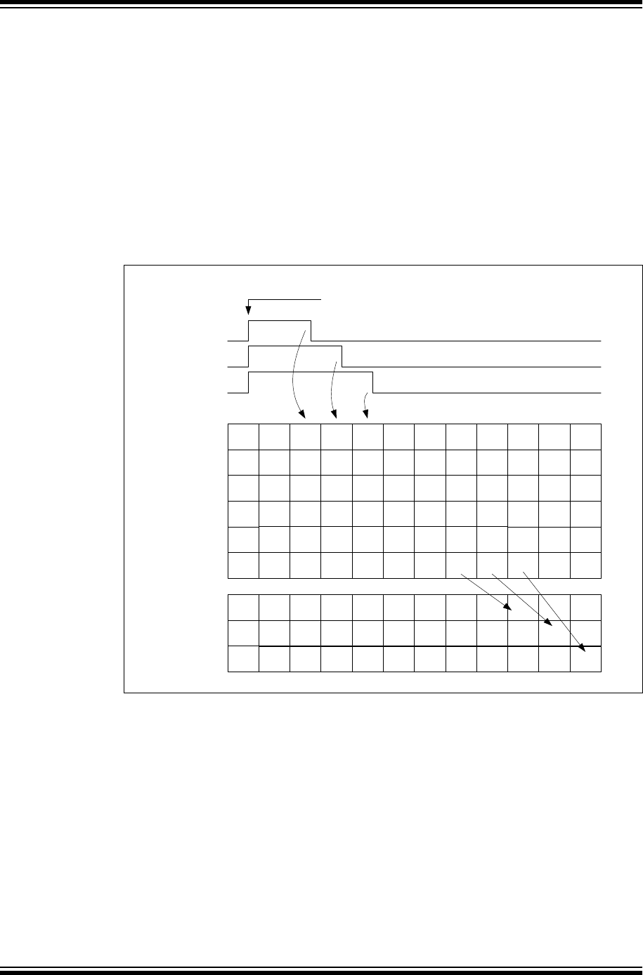
PIC32 Family Reference Manual
DS60001194B-page 18-34 © 2013 Microchip Technology Inc.
18.3.4 Six-Stage Pipeline Converter
The 12-bit ADC incorporates a six-stage pipeline converter architecture. This allows for simulta-
neous conversion of up to six samples, resulting in lower latencies when multiple samples need
conversion. The conversion time for a sample is determined by the ADC clock rate.
When multiple inputs are ready to be converted at the same time, as would be the case when
simultaneously sampling, the converter accepts the signals based on their natural priority. Lower
priority inputs are blocked for pending higher priority inputs.
As shown in Figure 18-9, AN0 is used with S&H0, AN1 with S&H1, and AN2 with S&H2. All three
inputs are configured to use the same trigger for simultaneous sampling. Since the natural prior-
ity is used, AN0 is transferred to the six-stage converter first, followed by AN1, and finally AN2.
The S&H is held in the hold state until its sample has been passed to the converter, and then
automatically resumes sampling.
Figure 18-9: Pipeline Converter (Conversion Process)
-
-
-
A0
T1
-
-
-
-
A0 A0
T1
A0
-
-
-
A1 A0
T1
A1
A0
-
-
A2
A0
T1
A1
A0
A2
A0
T1
A1
A0
A2
A0
T1
A1
A2
A2 -
-
- -
- -
- - - -
-
-
-
-
-
-
-
-
-
-
-
-
-
-
-
-
-
-
-
-
-
-
-
A0
A1
-
A0
A1
A2
A0
-
-
-
-
-
-
-
-
AN0 (SH0)
AN1 (SH1)
AN2 (SH2)
Six-Stage
Pipeline
Converter
Result
Registers
When trigger occurs all three inputs
switch from S&H state and the conversion
process begins.
-
-
-
-
-
-
-
-
-
-
-
-
-
- - - A0 A1 A0
T1
A2 - -
- - -
-
-
-
-
-
-
-
-
-
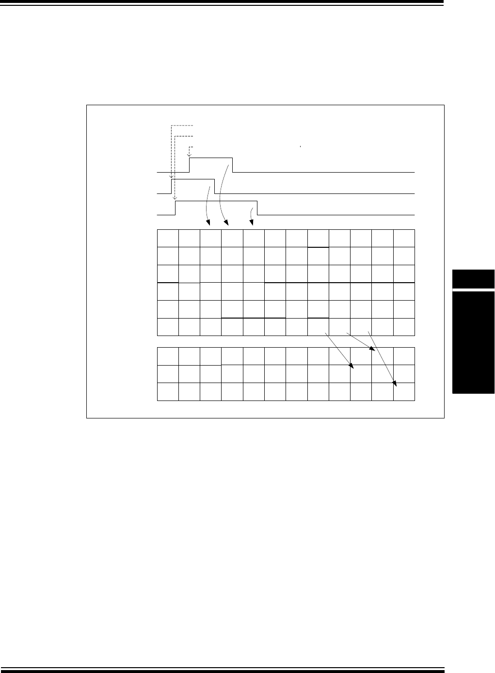
© 2013 Microchip Technology Inc. DS60001194B-page 18-35
Section 18. 12-bit Pipelined Analog-to-Digital Converter (ADC)
12-bit Pipelined
Analog-to-Digital
Converter (ADC)
18
The natural priority for input conversion is illustrated in Figure 18-10. Again, AN0 is used with
S&H0, AN1 with S&H1, and AN2 with S&H2; however, each input is triggered individually. AN1
is triggered first followed by AN2, and finally AN0. The triggers for AN2 and AN0 occur while AN1
is being transferred into the converter pipeline. When the transfer for AN1 is complete, AN0 is
moved into the converter pipeline even though the trigger for AN2 occurred before AN0. This is
because AN0 has a higher natural priority than AN2.
Figure 18-10: Pipeline Converter (Effects of Natural Priority on the Conversion Process)
18.3.5 Sample and Conversion Sequences
The combination of S&H and the pipeline converter establish a sample and conversion sequence
and a resulting sample and conversion time. These sequences vary based on the type of S&H
(dedicated or shared) and the operation mode. Basic operation is described in subsequent
sections.
18.3.5.1 PIPELINE CONVERSION TIME
Conversion time is the time from the S&H entering the hold state until the availability of data in
the result register. During this time, the sample is transferred from the S&H circuit to the pipeline
converter. If there are no other samples pending conversion, this time is determinate. Since there
is only a single pipeline converter and multiple S&H circuits, if S&H circuits are pending transfer
to the converter, the sample must wait for availability of the first converter stage. As previously
described, natural priority determines the order in which pending samples are transferred to the
initial pipeline converter stage.
18.3.5.2 DEDICATED S&H CONVERSION TIME (CLASS 1 INPUTS)
As previously described, triggering a Class 1 input causes the dedicated S&H to enter the hold
state. The conversion starts two clock periods following the ADC clock period in which the
asynchronous trigger occurred. The time required from trigger until data is ready and interrupt
occurs, is defined in Equation 18-1.
-
-
-
-
A0
A0
-
-
-
A1 A0 T1
A1
A0
-
-
A2
A0 T1
A1
A0
A2
A0 T1
A1
A0
A2
A0 T1
A1
A2
A2 -
-
--
--
- - - -
-
-
-
-
-
-
-
-
-
-
-
-
-
-
-
-
-
-
-
-
-
A1
-
-
A1
-
A0
A1
A2
A0
-
-
-
-
-
-
-
-
AN0 (SH0)
AN1 (SH1)
AN2 (SH2)
Six-Stage
Pipeline
Converter
Result
Registers
AN1 Trigger occurs first
AN2 Trigger occurs second
AN0 Trigger occurs last
- - - A0
A1 A0 T1A2 - --
-
-
-
-
-
-
-
-
-
-
-
-
-
-
-
-
-
-
-
-
-
-
-
-
-
-
-
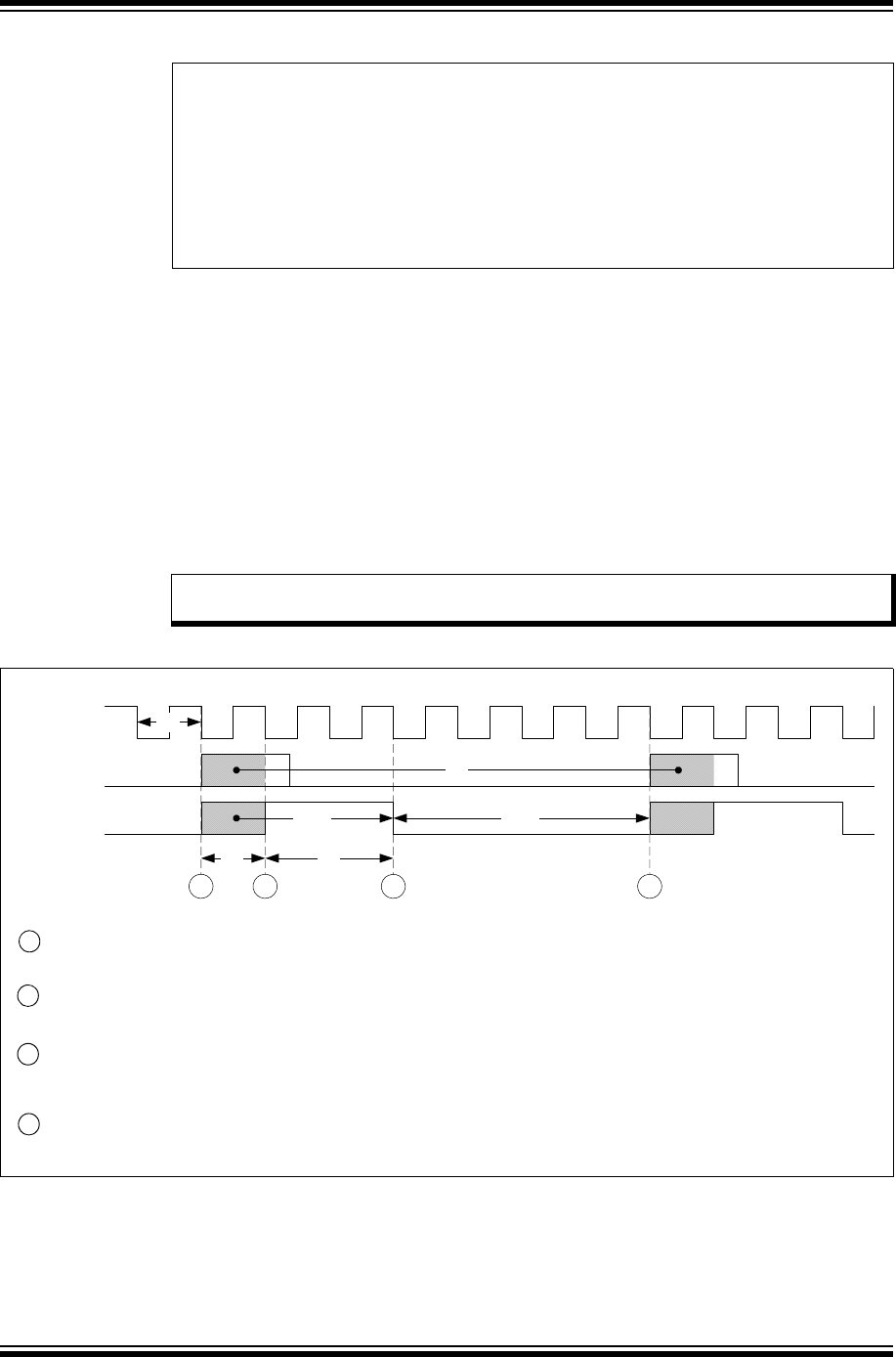
PIC32 Family Reference Manual
DS60001194B-page 18-36 © 2013 Microchip Technology Inc.
Equation 18-1: Dedicated S&H Conversion Time
18.3.5.3 DEDICATED S&H SAMPLE TIME (CLASS 1 INPUTS)
The Dedicated S&H circuits track their inputs until triggered, which starts a conversion sequence.
The trigger rate establishes the sampling time. This is different from the shared S&H circuit where
the trigger connects the input to the S&H, and then starts a sample period followed by a
conversion sequence.
Figure 18-11 shows a simple example for a single Class 1 input that is being triggered by a
periodic source.
The sampling time is the difference between the trigger rate, TTR, and the hold time, THOLD. The
input can be immediately retriggered once the S&H leaves the hold state, as indicated by number
three in Figure 18-11, making it possible to trigger at a rate that violates that minimum sampling
time requirements. There is no mechanism built into the control logic to ensure that the minimum
sampling requirements for dedicated S&H Class 1 inputs are met.
Figure 18-11: Dedicated Sample and Hold Timing
Note: When triggering Class 1 inputs, the trigger rate must allow for minimum sample time
requirements to be met.
TDCONV 10 TAD
⋅=
Where:
TAD = Analog-to-digital conversion clock period
Note: This equation assumes there are no pending conversions. Each pending higher
priority conversion will add one TAD to the conversion time.
At the time of the trigger, the dedicated S&H circuit disconnects from the input pin and switches to a hold state.
The switch to the hold state occurs asynchronously from the ADC clock. The hold state persists for up to one
clock cycle, while the ADC control logic synchronizes to the ADC clock.
Two clock cycles are required to transfer to the converter, and then the S&H switches back to Sample mode
and waits for the next trigger
The S&H tracks the input signal, sampling it until the next trigger occurs where the process repeats.
1
2
3
4
ADC
Clock
Trigger
S&Hx
TAD
TSAMP
1 2 3 4
THOLD
TTR
TH1 TH2
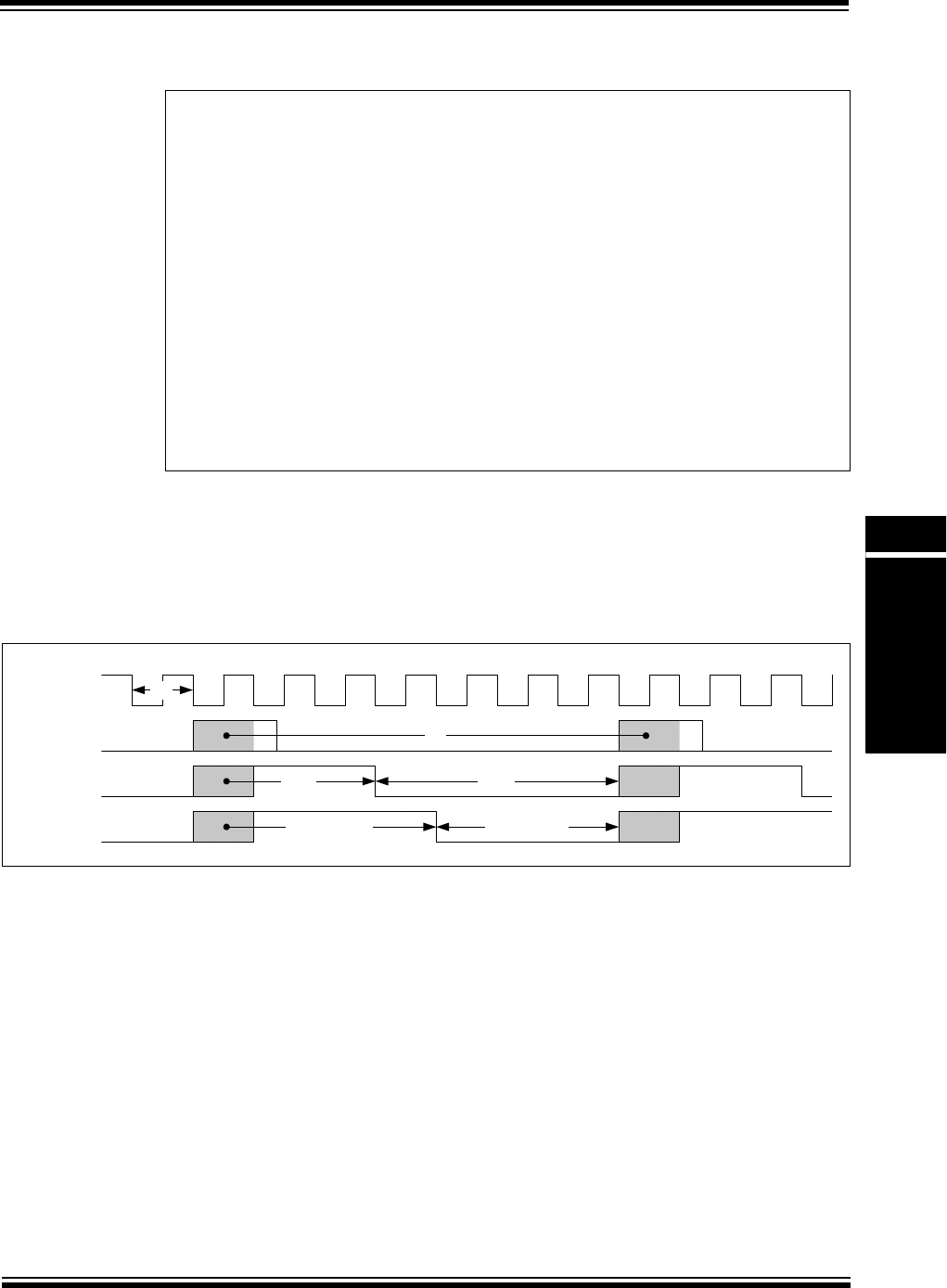
© 2013 Microchip Technology Inc. DS60001194B-page 18-37
Section 18. 12-bit Pipelined Analog-to-Digital Converter (ADC)
12-bit Pipelined
Analog-to-Digital
Converter (ADC)
18
Equation 18-2 can be used to determine the sample time for Class 1 inputs.
Equation 18-2: Dedicated S&H Sample Time
As noted in Equation 18-2, TH2 is increased by 1 TAD for each pending higher priority conversion.
Simultaneously triggering multiple Class 1 Inputs will always create a pending higher priority
conversion. Figure 18-12 shows the effect of an added pending conversion where the sample
time for S&H 1 is shorter than S&H 0 by one TAD period. In these situations, it may become
necessary to increase the trigger interval, TTR, so that the lowest priority input has adequate
sample time.
Figure 18-12: Effects of Simultaneous Sampling Multiple Class 1 Inputs
TSAMP TTR THOLD
–=
Where:
TTR = Trigger rate time interval (as determined by the system design)
Note: The system design must ensure that the trigger rate for Class 1 inputs does not
violate the minimum sampling time requirements. Dedicated S&H Class 1 Inputs
have no mechanism to establish sampling time. It is determined strictly by the
trigger rate. TH1, the time allotted for clock synchronization, can be less than
1TAD depending on the relationship of the asynchronous trigger to the ADC
clock. It is strongly recommended that 1 TAD be allocated for TH1 in the Trigger
period, TTR, to ensure that the required sampling time is met regardless of the
phase relationship of the trigger to ADC clock.
THOLD = TH1 + TH2
TH2 = 2 TAD (add 1 TAD for each pending higher priority conversion)
TH1 = 1 TAD (clock synchronization)
ADC
Clock
Trigger
S&H0
TAD
TSAMP
TSAMP – 1TAD
S&H1
THOLD
THOLD + 1 TAD
TTR

PIC32 Family Reference Manual
DS60001194B-page 18-38 © 2013 Microchip Technology Inc.
18.3.5.4 SHARED S&H CONVERSION TIMES (CLASS 2 INPUTS)
As previously described, triggering a Class 2 input on a shared S&H circuit starts the sampling
process. On completion of the sampling process the S&H will enter the hold state and the con-
version will commence. The SAMC value determines the sample time. The time required from
trigger until data is ready and interrupt occurs is defined in Equation 18-3.
Equation 18-3: Shared Sample and Hold Conversion Time
18.3.5.5 CHANNEL SCAN CONVERSION TIME (CLASS 2 AND CLASS 3 INPUTS)
As previously described, the scan trigger starts the sequential sampling and conversion process
of the Class 1, Class 2, or Class 3 inputs configured for channel scan. The total time to complete
the channel scan is based on the ADC clock rate, the number of inputs being scanned, and the
sampling time. For a scan list consisting of Class 2 and Class 3 inputs, the time required from
trigger until the last scanned input’s data is ready and interrupt occurs is defined in
Equation 18-4.
Equation 18-4: Channel Scan Sample and Conversion Time
TSCONV TSSAM TCONV
+=
Where:
TAD = Analog-to-digital conversion clock period
Note: This equation assumes there are no pending conversions. Each pending higher
priority Class 2 conversion will add one T
AD to the conversion time plus the sample
time (SAMC + 1) * T
AD.
If there are higher priority Class 1 conversions pending at the completion of a
shared S&H sampling period, each higher priority dedicated conversion will delay
conversion of the shared S&H by one TAD.
TSCONV SAMC 1+()TAD 10 TAD
⋅+⋅=
TSCONV SAMC 11+()TAD
⋅=
SAMC = SAMC<7:0> bits (AD1CON2<23:16>)
Where:
Note: This equation assumes there are no pending conversions. Each pending higher
priority Class 1 conversion will add one TAD to the conversion time. Each pending
higher priority Class 2 conversion will add one TAD conversion time plus
(SAMC + 1) * T
AD sample time.
TAD = Analog-to-digital conversion clock period
N = Number of scanned channels
SAMC = SAMC<7:0> bits (AD1CON2<23:16>)
TSCAN NSAMC4+()6+⋅()TAD
⋅=

© 2013 Microchip Technology Inc. DS60001194B-page 18-39
Section 18. 12-bit Pipelined Analog-to-Digital Converter (ADC)
12-bit Pipelined
Analog-to-Digital
Converter (ADC)
18
18.4 ADC MODULE CONFIGURATION
Operation of the ADC module is directed through bit settings in the specific registers. The
following instructions summarize the actions and the settings. The options and details for each
configuration step are provided in the subsequent sections.
To c onf ig u re th e A DC mod ule , perf orm t he fol low in g st eps :
1. Configure the analog port pins, as described in 18.4.1 “Configuring the Analog Port
Pins”.
2. Select the analog inputs to the ADC MUXs, as described in 18.4.2 “Selecting the ADC
Multiplexer Analog Inputs”.
3. Select the format of the ADC result, as described in 18.4.5 “Selecting the Format of the
ADC Result”.
4. Select the conversion trigger source, as described in 18.4.6 “Selecting the Conversion
Trigger Source”.
5. Select the voltage reference source, as described in 18.4.7 “Selecting the Voltage Ref-
erence Source”.
6. Select the scanned inputs, as described in 18.4.8 “Selecting the Scanned Inputs”.
7. Select the analog-to-digital conversion clock source and prescaler, as described in
18.4.9 “Selecting the Analog-to-Digital Conversion Clock Source and Prescaler”.
8. Specify any additional acquisition time, if required, as described in 18.10 “ADC Sampling
Requirements”.
9. Turn on the ADC module, as described in 18.4.10 “Turning ON the ADC”.
10. Perform ADC calibration, as described in 18.4.12 “ADC Calibration”.
11. Configure the ADC interrupts (if required), as described in 18.6 “Interrupts”.
18.4.1 Configuring the Analog Port Pins
The ANSELx registers for the I/O ports associated with the analog inputs are used to configure
the corresponding pin as a digital pin. A pin is configured as analog input when the corresponding
ANSELx bit = 1. When the ANSELx bit = 0, the pin is set to digital control. When configured for
analog input, the associated port I/O digital input buffer is disabled so that it does not consume
current. The ANSELx registers are set when the device comes out of Reset, causing the ADC
input pins to be configured as analog inputs by default.
The TRISx registers control the digital function of the port pins. The port pins that are required
as analog inputs must have their corresponding bit set in the specific TRISx register, configuring
the pin as an input. If the I/O pin associated with an ADC input is configured as an output by
clearing the TRISx bit, the port’s digital output level (VOH or VOL) will be converted. After a device
Reset, all of the TRISx bits are set. For more information on port pin configuration, refer to the
“I/O Ports” chapter of the specific device data sheet.
Note: Steps 1 through 8 can be performed in any order. Steps 9 through 11 must be the
final steps in every case, and must be performed in the sequence specified above.
Note: When reading a PORT register that shares pins with the ADC, any pin configured
as an analog input reads as a ‘0’ when the PORT latch is read. Analog levels on any
pin that is defined as a digital input but not configured as an analog input, may cause
the input buffer to consume current that exceeds the device specification.

PIC32 Family Reference Manual
DS60001194B-page 18-40 © 2013 Microchip Technology Inc.
Example 18-1: ADC Initialize
int main(int argc, char** argv) {
int result[3];
/* Set up the CAL registers */
AD1CAL1 = DEVADC1; // Copy the configuration data to the AD1CAL2 = DEVADC2;
// AD1CALx special function registers.
AD1CAL3 = DEVADC3;
AD1CAL4 = DEVADC4;
AD1CAL5 = DEVADC5;
/* Configure AD1CON1 */
AD1CON1 = 0; // No AD1CON1 features are enabled including: Stop-in-Idle, early
// interrupt, filter delay Fractional mode and scan trigger source.
/* Configure AD1CON2 */
AD1CON2 = 0; // Boost, Low-power mode off, SAMC set to min, set up the ADC Clock
AD1CON2bits.ADCSEL = 1; // 1 = SYSCLK, 2 REFCLK03, 3 FRC
AD1CON2bits.ADCDIV = 4; // TQ = 1/200 MHz; Tad = 4* (TQ * 2) = 40 ns; 25 MHz ADC clock
/* Configure AD1CON3 */
AD1CON3 = 0; // ADINSEL is not configured for this example. VREFSEL of ‘0’
// selects AVDD and AVSS as the voltage reference.
/* Configure AD1MOD */
AD1MOD = 0; // All channels configured for default input and single-ended
// with unsigned output results.
/* Configure AD1GIRGENx */
AD1GIRQEN1 = 0; // No global interrupts are used.
AD1GIRQEN2 = 0;
/* Configure AD1CSSx */
AD1CSS1 = 0; // No channel scanning is used.
AD1CSS2 = 0;
/* Configure AD1CMPCONx */
AD1CMPCON1 = 0; // No digital comparators are used. Setting the AD1CMPCONx
AD1CMPCON2 = 0; // register to ‘0’ ensures that the comparator is disabled. Other
AD1CMPCON3 = 0; // registers are “don’t care”.
AD1CMPCON4 = 0;
AD1CMPCON5 = 0;
AD1CMPCON6 = 0;
/* Configure AD1FLTRx */
AD1FLTR1 = 0; // No oversampling filters are used.
AD1FLTR2 = 0;
AD1FLTR3 = 0;
AD1FLTR4 = 0;
AD1FLTR5 = 0;
AD1FLTR6 = 0;
/* Set up the trigger sources */
AD1TRG1 = 0; // Initialize all sources to no trigger.
AD1TRG2 = 0;
AD1TRG3 = 0;
AD1TRG1bits.TRGSRC0 = 1; // Set AN0 to trigger from software.
AD1TRG1bits.TRGSRC1 = 1; // Set AN1 to trigger from software.
AD1TRG1bits.TRGSRC2 = 1; // Set AN2 to trigger from software.
/* Turn the ADC on, start calibration */
AD1CON1bits.ADCEN = 1;
/* Wait for calibration to complete */
while (AD1CON2bits.ADCRDY == 0);

© 2013 Microchip Technology Inc. DS60001194B-page 18-41
Section 18. 12-bit Pipelined Analog-to-Digital Converter (ADC)
12-bit Pipelined
Analog-to-Digital
Converter (ADC)
18
Example 18-1: ADC Initialize (Continued)
/* Wait for calibration to complete */
while (AD1CON2bits.ADCRDY == 0);
while (1) {
/* Trigger a conversion */
AD1CON3bits.GSWTRG = 1;
/* Wait the conversions to complete */
while (AD1DSTAT1bits.ARDY0 == 0);
/* fetch the result */
result[0] = AD1DATA0;
while (AD1DSTAT1bits.ARDY1 == 0);
/* fetch the result */
result[1] = AD1DATA1;
while (AD1DSTAT1bits.ARDY2 == 0);
/* fetch the result */
result[2] = AD1DATA2;
/*
* Process results here
*
* Note 1: Loop time determines the sampling time since all inputs are Class 1.
* A delay may be needed to meet sample time requirements.
* Note 2: The first 5 samples may have reduced accuracy.
*
*/
}
return (1);
}

PIC32 Family Reference Manual
DS60001194B-page 18-42 © 2013 Microchip Technology Inc.
18.4.2 Selecting the ADC Multiplexer Analog Inputs
Each S&H has two inputs referred to as the positive and negative inputs. Input selection options
vary for the dedicated and shared S&H are described in the following sections.
Each dedicated S&H is dedicated to a single Class 1 positive input. This means that all control,
status and data for that S&H are accessed through the registers associated with its dedicated
analog (ANx) input. For example, if the S&H1 for ADC1 uses AN0 as its dedicated input, readings
obtained from S&H1 will always be read from AD1DATA0, the global interrupt is enabled with
AGIEN0, interrupt status is read using ARDY0, the digital comparator is enabled with CMPE0,
and the trigger source is set by TRGSC0. This is true of all dedicated Class 1 S&H circuits,
regardless of the following settings.
To p ro vi de gr ea te r fl exi bil ity to the dedicated S&H circuits, a single alternate input is provided for
each one. This alternate input can be chosen using the SHxALT<1:0> bits in the ADC1 Input
Mode Control Registers AD1IMOD as follows:
•SH0ALT<1:0> (AD1IMOD<17:16>)
•SH1ALT<1:0> (AD1IMOD<19:18>)
•SH2ALT<1:0> (AD1IMOD<21:20>)
•SH3ALT<1:0>(AD1IMOD<23:22>)
•SH4ALT<1:0> (AD1IMOD<25:24>)
An example (for a device with five S&H circuits) is shown in Ta b l e 1 8 - 3 :
Table 18-3: Positive Input Selections
18.4.3 Positive Input Selection for the Shared Sample and Hold
For the shared S&H circuit, the positive input is shared among all Class 2 and Class 3 inputs.
Input connection of the analog input ANx to the S&H circuit is automatic for either Class 2 input
trigger or during a channel scan of Class 2 and or Class3 inputs. Selecting inputs for Channel
scanning is discussed separately in 18.4.8 “Selecting the Scanned Inputs”.
Module Default Selections
(SHxALT<0> = 0)
Alternate Selections
(SHxALT<0> = 1)
ADC1 SH0 = AN0
SH1 = AN1
SH2 = AN2
SH3 = AN3
SH4 = AN4
SH0 = AN45
SH1 = AN46
SH2 = AN47
SH3 = AN48
SH4 = AN49
Note: The selections shown in Ta bl e 18- 3 are for illustration purposes only. Refer to the
“12-bit Analog-to-Digital Converter (ADC)” chapter in the specific device data
sheet for actual channel assignments on a device.

© 2013 Microchip Technology Inc. DS60001194B-page 18-43
Section 18. 12-bit Pipelined Analog-to-Digital Converter (ADC)
12-bit Pipelined
Analog-to-Digital
Converter (ADC)
18
18.4.4 Negative Input Single-ended and Differential Options (Shared
and Dedicated Sample and Hold)
Negative input selection is determined by the setting of the SHxMOD<1:0> bits of the AD1IMOD
register. The SHxMOD<1:0> bits allow the inputs to be rail-to-rail, and either single-ended or
differential. These bits also scale the internal ADC analog inputs and reference voltages and
configure the digital result to line up with the expected full-scale output range.
Table 18-4: Input Configuration
The SHxMOD<1:0> bits are defined in the AD1IMOD register as follows:
•SH0MOD<1:0> (AD1IMOD<1:0>)
•SH1MOD<1:0> (AD1IMOD<3:2>)
•SH2MOD<1:0> (AD1IMOD<5:4>)
•SH3MOD<1:0> (AD1IMOD<7:6>)
•SH4MOD<1:0> (AD1IMOD<9:8>)
•SH5MOD<1:0> (AD1IMOD<11:10>)
SHxMOD<1:0>
Setting
Input
Configuration
Input Voltage
(see Note 1) Output
11 Differential 2’s
Complement
Minimum Input VINP – VINN = -VREF -2048
Maximum Input VINP – VINN = VREF +2047
10 Differential
Unipolar
Minimum Input VINP – VINN = -VREF 0
Maximum Input VINP – VINN = VREF +4095
01 Single-ended 2’s
Complement
Minimum Input VINP = VINN -2048
Maximum Input VINP – VINN = VREF +2047
00 Single-ended
Unipolar
Minimum Input VINP = VINN 0
Maximum Input VINP – VINN = VREF +4095
Legend: VINP = Positive S&H input; VINN = Negative S&H input;
VREF = VREFH – VREFL
Note 1: For proper operation and to prevent device damage, input voltage levels should not
exceed the limits listed in the “Electrical Characteristics” chapter of the specific
device data sheet.
PIC32 Family Reference Manual
DS60001194B-page 18-44 © 2013 Microchip Technology Inc.
18.4.5 Selecting the Format of the ADC Result
The data in the ADC Result register can be read in any of the four supported data formats. The user can select from unsigned integer,
signed integer, unsigned fractional, or signed fractional. Integer data is right-justified and fractional data is left-justified.
• The integer/fractional data format selection is specified globally for all ADC inputs using the Fractional Data Output Format bit,
FRACT (AD1CON1<11>)
•The signed/unsigned data format selection can be independently specified for each individual S&H circuit using the SHxMOD<1:0>
bits, as shown in 18.4.4 “Negative Input Single-ended and Differential Options (Shared and Dedicated Sample and Hold)”
Figure 18-13 illustrates how a result is formatted.
Figure 18-13: ADC Output Data Formats
Analog-to-Digital Conversion Result
d11 d10 d09 d08 d07 d06 d05 d04 d03 d02 d01 d00
Unsigned Integer
00000000000000000000d11d10d09d08d07d06d05d04d03d02d01d00
Signed Integer
SSSSSSSSSSSSSSSSSSSSSd10d09d08d07d06d05d04d03d02d01d00
Fractional
d11 d10 d09 d08 d07 d06 d05 d04 d03 d02 d01 d00 0 0 0 0 0 0 0 0 0 0 0 0 0 0 0 0 0 0 0 0
Signed Fractional
Sd10d09d08d07d06d05d04d03d02d01d000 0 0 0 0 0 0 0 0 0 0 0 0 0 0 0 0 0 0 0

© 2013 Microchip Technology Inc. DS60001194B-page 18-45
Section 18. 12-bit Pipelined Analog-to-Digital Converter (ADC)
12-bit Pipelined
Analog-to-Digital
Converter (ADC)
18
Example 18-2: ADC Class 2 Configuration and Fractional Format
int main(int argc, char** argv) {
int result[3];
/* Set up the CAL registers */
AD1CAL1 = DEVADC1; // Copy the configuration data to the
AD1CAL2 = DEVADC2; // AD1CALx special function registers.
AD1CAL3 = DEVADC3;
AD1CAL4 = DEVADC4;
AD1CAL5 = DEVADC5;
/* Configure AD1CON1 */
AD1CON1 = 0; // No AD1CON1 features are enabled including:
// Stop-in-Idle, early interrupt, filter delay
// and scan trigger source
AD1CON1bits.FRACT = 1; // use Fractional output format
/* Configure AD1CON2 */
AD1CON2 = 0; // Boost, Low-power mode off
// Set up the ADC Clock
AD1CON2bits.ADCSEL = 1; // 1 = SYSCLK, 2 REFCLK03, 3 FRC
AD1CON2bits.ADCDIV = 4; // TQ = 1/200 MHz; TAD = 4 * (TQ * 2) = 40 ns;
// 25 MHz ADC clock
AD1CON2bits.SAMC = 9; // Sample time set to 10 * TAD = 400 ns for
// Class 2 and 3 inputs.
/* Configure AD1CON3 */
AD1CON3 = 0; // ADINSEL is not configured for this example.
// VREFSEL of 0 selects AVDD and AVSS as the
// voltage reference.
/* Configure AD1MOD */
AD1MOD = 0; // All channels configured for default input
// and single-ended with unsigned output results
/* Configure AD1GIRGENx */
AD1GIRQEN1 = 0; // No global interrupts are used.
AD1GIRQEN2 = 0;
/* Configure AD1CSSx */
AD1CSS1 = 0; // No channel scanning is used.
AD1CSS2 = 0;
/* Configure AD1CMPCONx */
AD1CMPCON1 = 0; // No digital comparators are used.
AD1CMPCON2 = 0; // Setting the AD1CMPCONx register to ‘0’ ensures that
AD1CMPCON3 = 0; // the comparator is disabled. Other registers
AD1CMPCON4 = 0; // are “don't care”.
AD1CMPCON5 = 0;
AD1CMPCON6 = 0;
/* Configure AD1FLTRx */
AD1FLTR1 = 0; // No oversampling filters are used.
AD1FLTR2 = 0;
AD1FLTR3 = 0;
AD1FLTR4 = 0;
AD1FLTR5 = 0;
AD1FLTR6 = 0;
/* Set up the trigger sources */
AD1TRG1 = 0; // Initialize all to no trigger.
AD1TRG2 = 0;
AD1TRG3 = 0;
AD1TRG2bits.TRGSRC5 = 1; // Set AN5 to trigger from software.
AD1TRG2bits.TRGSRC6 = 1; // Set AN6 to trigger from software.
AD1TRG2bits.TRGSRC7 = 1; // Set AN7 to trigger from software.

PIC32 Family Reference Manual
DS60001194B-page 18-46 © 2013 Microchip Technology Inc.
Example 18-2: ADC Class 2 Configuration and Fractional Format (Continued)
/* Turn the ADC on, start calibration */
AD1CON1bits.ADCEN = 1;
/* Wait for calibration to complete */
while (AD1CON2bits.ADCRDY == 0);
while (1) {
/* Trigger a conversion */
AD1CON3bits.GSWTRG = 1;
/* Wait the conversions to complete */
while (AD1DSTAT1bits.ARDY5 == 0);
/* fetch the result */
result[0] = AD1DATA5;
while (AD1DSTAT1bits.ARDY6 == 0);
/* fetch the result */
result[1] = AD1DATA6;
while (AD1DSTAT1bits.ARDY7 == 0);
/* fetch the result */
result[2] = AD1DATA7;
/*
* Process results here
*
* Note 1: The first 5 samples may have reduced accuracy
* Note 2. The output format is fractional as described in
* 18.4.5 “Selecting the Format of the ADC Result”
*/
}
return (1);
}

© 2013 Microchip Technology Inc. DS60001194B-page 18-47
Section 18. 12-bit Pipelined Analog-to-Digital Converter (ADC)
12-bit Pipelined
Analog-to-Digital
Converter (ADC)
18
18.4.6 Selecting the Conversion Trigger Source
Class 1 and Class 2 inputs to the ADC module can be triggered for conversion either individually,
or as part of a channel scan sequence. Class 3 inputs can only be triggered as part of a channel
scan sequence. Individual or channel scan triggers can originate from an on-board timer or
output compare peripheral event, from external digital circuits connected to INT0, from external
analog circuits connected to an analog comparator, or through software by setting a trigger bit in
a SFR.
18.4.6.1 TRIGGER SELECTION FOR CLASS 1 AND CLASS 2 INPUTS
For each one of the Class 1 and Class 2 inputs, the user application can independently specify
a conversion trigger source. The individual trigger source for an analog input ‘n’ is specified by
the TRGSRCn<4:0> bits located in registers AD1TRG1 through AD1TRG3. Refer to the “12-bit
Analog-to-Digital Converter (ADC)” chapter of the specific device data sheet for more
information on the available conversion trigger options. For example, these trigger sources may
include:
•General Purpose (GP) Timers: When a period match occurs for the 32-bit timer, Timer3/2 or
Timer5/4, or the 16-bit Timer1, Timer3 or Timer5, a special ADC trigger event signal is
generated by the timer. This feature does not exist for other timers. For more information,
refer to Section 14. “Timers” (DS61105) and the specific device data sheet.
•Output Compare: The Output Compare peripherals, OC1, OC3, and OC5, can be used to
generate an ADC trigger then the output transitions from a low to high state. For more
information, refer to Section 16. “Output Compare” (DS61111), and the specific device data
sheet.
•Comparators: The analog Comparators can be used to generate an ADC trigger when the
output transitions from a low state to a high state. For more information, refer to Section 19.
“Comparator” (DS61110), and the “Comparator” chapter in the specific device data sheet.
•External INT0 Pin Trigger: In this mode, the ADC module starts a conversion on an active
transition on the INT0 pin. The INT0 pin may be programmed for either a rising edge input or
a falling edge input to trigger the conversion process.
•Global Software Trigger: The ADC module can be configured for manually triggering a
conversion for all inputs that have selected this trigger option. The user can manually trigger a
conversion by setting the Global Software Trigger bit, GSWTRG (AD1CON3<30>).
18.4.6.2 SCANNED TRIGGER SELECTION FOR CLASS 1, CLASS 2 AND
CLASS 3 INPUTS (SH3 ONLY)
All available analog inputs can be configured for automatic channel scanning. Class 1 inputs are
sampled using their dedicated S&H circuit. Class 2 and Class 3 inputs are sampled using the
shared S&H circuit. A single conversion trigger source is selected for all the inputs selected for
scanning using the STRGSRC<4:0> bits (AD1CON1<26:22>). On each conversion trigger, the
ADC module starts converting in the natural priority, all inputs specified in the user-specified
channel scan list. For Class 1 inputs, sampling ends at the time of the trigger. For Class 2 and
Class 3 inputs, the trigger initiates a sequential sample/conversion process in the natural priority
order.
The trigger options available for channel scan are identical to those available for independent
triggering of Class 1 and Class 2 inputs. Any Class 1 or Class 2 inputs that are part of the channel
scan must have the STRIG option selected as their trigger source in the TRGSRCn<4:0> bits.
Note 1: When conversion triggers for multiple Class 1 or Class 2 analog inputs occur simul-
taneously, they are prioritized according to a natural order priority scheme based
on the analog input used. AN0 has the highest priority, AN1 has the next highest
priority, etc. Therefore, time sensitive or transient analog signals should be sampled
and converted using Class 1 S&H circuits, with higher natural priority.
2: When selecting trigger sources for Class 1 inputs, ensure that sampling times are
not violated.

PIC32 Family Reference Manual
DS60001194B-page 18-48 © 2013 Microchip Technology Inc.
18.4.6.3 USER-REQUESTED INDIVIDUAL CONVERSION TRIGGER
The user can explicitly request a single conversion of any selected analog input at any time
during program execution, without changing the trigger source configuration of the ADC. The
input to be converted is specified by the ADC Input Select bits, ADINSEL<5:0>
(AD1CON3<5:0>). The Individual ADC Input Conversion Request bit, RQCONVRT
(AD1CON3<29>) is used to trigger the conversion. This bit is automatically cleared after two
peripheral clock cycles, thereby allowing the user software to trigger another conversion if
needed.
18.4.7 Selecting the Voltage Reference Source
The user application can select the voltage reference for the ADC module and the voltage
reference can be internal or external. The VREF Input Selection bits, VREFSEL<2:0>
(AD1CON3<12:10>), select the voltage reference for analog-to-digital conversions. The upper
voltage reference (VREFH) and the lower voltage reference (VREFL) may be the internal AVDD and
AVSS voltage rails or the VREF+ and VREF- input pins. The external ADC voltage reference may
be used to reduce noise in the converter.
The voltages applied to the external reference pins must comply with certain specifications. Refer
to the “Electrical Characteristics” chapter in the specific device data sheet for the electrical
specifications.
The Voltage Reference Boost bit, BOOST (AD1CON2<14>), should be set when the difference
between the selected reference voltages (VREFH - VREFL) is less than 0.65 * (AVDD - AVSS).
Setting this bit maximizes the SNR for analog-to-digital conversions using small reference
voltage rails.
18.4.8 Selecting the Scanned Inputs
To i ncl ude an a nal og i npu t i n th e s can lis t, i ts specified bit in the Input Scan Select register
(AD1CSS1 or AD1CSS2) must be set to ‘1’. Each bit in the AD1CSS1 and AD1CSS2 registers
corresponds to a different analog input. If the input is a Class 1 or Class 2 input, the trigger source
for that input, specified by the TRGSRCn<4:0> bits located in the AD1TRG1 through AD1TRG3
registers, must be set to the STRIG option, indicating that they are triggered as part of the scan
process.
Every scan conversion trigger, as specified by the STRGSRC<4:0> bits (AD1CON1<26:22>),
starts a scan conversion sequence. As described in 18.3 “ADC Operation, Terminology and
Conversion Sequence”, the scan sequence samples and converts each scanned input in their
natural priority.
Note: The external VREF+ and VREF- pins can be shared with other analog peripherals.
Refer to the “Pinout Diagrams” section of the specific device data sheet for more
information. In addition, the ANSELx bits for the VREF+ and VREF- pins must be set
to Analog mode.
Note: The AD1CSS1 and AD1CSS2 bits specify only the positive input to the S&H circuits.
The negative input of the channel does not change during the scanning sequence.

© 2013 Microchip Technology Inc. DS60001194B-page 18-49
Section 18. 12-bit Pipelined Analog-to-Digital Converter (ADC)
12-bit Pipelined
Analog-to-Digital
Converter (ADC)
18
Example 18-3: ADC Channel Scan
int main(int argc, char** argv) {
int result[3];
/* Set up the CAL registers */
AD1CAL1 = DEVADC1; // Copy the configuration data to the
AD1CAL2 = DEVADC2; // AD1CALx special function registers.
AD1CAL3 = DEVADC3;
AD1CAL4 = DEVADC4;
AD1CAL5 = DEVADC5;
/* Configure AD1CON1 */
AD1CON1 = 0; // No AD1CON1 features are enabled including:
// Stop-in-Idle, early interrupt, filter delay
// and Fractional mode.
AD1CON1bits.STRGSRC = 1; // Software trigger initiates scan.
/* Configure AD1CON2 */
AD1CON2 = 0; // Boost, low power mode off.
// Set up the ADC Clock
AD1CON2bits.ADCSEL = 1; // 1 = SYSCLK, 2 REFCLK03, 3 FRC
AD1CON2bits.ADCDIV = 4; // TQ = 1/200 MHz; TAD = 4 * (TQ * 2) = 40 ns;
// 25 MHz ADC clock.
AD1CON2bits.SAMC = 9; // Sample time set to 10 * TAD = 400 ns for
// Class 2 and 3 Inputs.
/* Configure AD1CON3 */
AD1CON3 = 0; // ADINSEL is not configured for this example.
// VREFSEL of ‘0’ selects AVDD and AVSS as the
// voltage reference.
/* Configure AD1MOD */
AD1MOD = 0; // All channels configured for default input
// and single-ended with unsigned output results
/* Configure AD1GIRGENx */
AD1GIRQEN1 = 0; // No global interrupts are used.
AD1GIRQEN2 = 0;
/* Configure AD1CSSx */
AD1CSS1 = 0; // Clear all bits
AD1CSS2 = 0;
AD1CSS1bits.CSS0 = 1; // AN0 (Class 1) set for scan
AD1CSS1bits.CSS5 = 1; // AN5 (Class 2) set for scan
AD1CSS2bits.CSS43 = 1; // AN43 (Class 3) set for scan
/* Configure AD1CMPCONx */
AD1CMPCON1 = 0; // No digital comparators are used.
AD1CMPCON2 = 0; // Setting the AD1CMPCONx register to ‘0’ ensures that
AD1CMPCON3 = 0; // the comparator is disabled. Other comparator
AD1CMPCON4 = 0; // registers are “don't care”.
AD1CMPCON5 = 0;
AD1CMPCON6 = 0;
/* Configure AD1FLTRx */
AD1FLTR1 = 0; // No oversampling filters are used.
AD1FLTR2 = 0;
AD1FLTR3 = 0;
AD1FLTR4 = 0;
AD1FLTR5 = 0;
AD1FLTR6 = 0;
/* Set up the trigger sources */
AD1TRG1 = 0; // Initialize all sources to no trigger.
AD1TRG2 = 0;
AD1TRG3 = 0;

PIC32 Family Reference Manual
DS60001194B-page 18-50 © 2013 Microchip Technology Inc.
Example 18-3: ADC Channel Scan (Continued)
18.4.9 Selecting the Analog-to-Digital Conversion Clock Source and
Prescaler
The ADC module can use the internal Fast RC (FRC) oscillator output or the System
Clock (SYSCLK) as the conversion clock source (TQ). On some devices, the reference clock can
be used as the conversion clock source. Refer to the “12-bit Analog-to-Digital Converter
(ADC)” chapter in the specific device data sheet to determine which reference clock output
source may be available.
When the ADCSEL<1:0> bits (AD1CON2<9:8>) = 11, the internal FRC oscillator is used as the
ADC clock source. When using the internal FRC oscillator, the ADC module can continue to
function in Sleep and Idle modes.
When the Analog-to-Digital Conversion Clock Source (TQ) bits, ADCSEL<1:0>
(AD1CON2<9:8>) = 01, SYSCLK is used as the conversion clock source. When the
ADCSEL<1:0> bits = 00, the ADC clock is disabled.
The analog-to-digital conversion clock period (T
AD
) is the period of the selected clock source after
the prescaler ADC Input Clock Divider bits, ADCDIV<6:0> (AD1CON2<6:0>), are applied. The
resultant value of T
AD
can range from 1 *
TQ
to 254 *
TQ
.
For correct analog-to-digital conversions, the TAD limits must not be exceeded. ADC clock
frequencies from 1 MHz to 28 MHz are supported by the ADC module.
AD1TRG1bits.TRGSRC0 = 3; // Set AN0 (Class 1) to trigger from scan source
AD1TRG2bits.TRGSRC5 = 3; // Set AN5 (Class 2) to trigger from scan source
// AN43 (class 3) always uses scan trigger source
/* Turn the ADC on, start calibration */
AD1CON1bits.ADCEN = 1;
/* Wait for calibration to complete */
while (AD1CON2bits.ADCRDY == 0);
while (1) {
/* Trigger a conversion */
AD1CON3bits.GSWTRG = 1;
/* Wait the conversions to complete */
while (AD1DSTAT1bits.ARDY0 == 0);
/* fetch the result */
result[0] = AD1DATA0;
while (AD1DSTAT1bits.ARDY5 == 0);
/* fetch the result */
result[1] = AD1DATA5;
while (AD1DSTAT2bits.ARDY43 == 0);
/* fetch the result */
result[2] = AD1DATA43;
/*
* Process results here
*
* Note: The first 5 samples may have reduced accuracy.
*
*/
}
return (1);
}
Note: It is recommended that applications that require precise timing of ADC acquisitions
use SYSCLK as the clock source for the ADC.

© 2013 Microchip Technology Inc. DS60001194B-page 18-51
Section 18. 12-bit Pipelined Analog-to-Digital Converter (ADC)
12-bit Pipelined
Analog-to-Digital
Converter (ADC)
18
The maximum rate at which
analog-to-digital
conversions may be completed by the ADC module
(effective conversion throughput) is 28 Msps. However, the maximum rate at which a single input
channel can be converted is dependent on the sampling time requirements. The fastest possible
conversion rates can be achieved by sampling and converting an analog signal through multiple
Class 1 inputs.
Equation 18-5 provides the T
AD
value as a function of the ADCDIV<6:0> control bits
(AD1CON2<6:0>) and the device instruction cycle clock period, TCY.
Equation 18-5: A/D Conversion Clock Period
For the shared S&H circuits, the SAMC<7:0> bits (AD1CON2<23:16>) specify the number of TAD
clock cycles for which an analog input should be sampled between the conversion trigger and
the start of conversion.
18.4.10 Turning ON the ADC
When the ADC Operating Mode bit, ADCEN (AD1CON1<15>), is set to ‘1’, the module is in
Active mode and is fully powered and functional.
When the ADCEN bit is ‘0’, the module is disabled. The digital and analog portions of the circuit
are turned off for maximum current savings.
In order to return to Active mode from a disabled state, the user must wait for the analog stages
to stabilize. Refer to the “Electrical Characteristics” chapter in the specific device data sheet
for more information on the stabilization time.
18.4.11 ADC Status Bits
The ADC module includes the ADRDY status bit (AD1CON2<31>), which indicates its current
state. This bit indicates that the ADC module is ready to begin a conversion. The ADCRDY bit is
only set after the ADC module has been enabled and calibrated. The user application should not
perform any ADC operations until the ADCRDY bit is set.
Note: The minimum conversion latency, (time from trigger to availability of result) is
10 * TAD. Actual latency could be as much as 11 * TAD since the trigger is
asynchronous to the ADC clock.
Note: Writing to ADC control bits that control the ADC clock, channel assignments,
channel scanning, voltage reference selection, S&H circuit operating modes, and
interrupt configuration is not recommended while the ADC module is enabled.
For ADCDIV = 0
TAD = TQ
For ADCDIV > 0
TAD = 2 TQ * ADCDIV
35.71 ns ≤ TAD ≤ 1.0 µs
For either case:

PIC32 Family Reference Manual
DS60001194B-page 18-52 © 2013 Microchip Technology Inc.
18.4.12 ADC Calibration
Prior to enabling the ADC module, the user must read the ADC calibration data from the
Configuration memory (refer to the “Special Features” chapter in the specific device data sheet
for more information), and then write this data into the calibration registers AD1CAL1 through
AD1CAL5.
When performing a self-calibration, the input mode for SH0 must be set to one of the differential
input modes. Use either the differential unipolar encoded format by setting the SH0MOD<1:0>
bits (AD1MOD<1:0>) = 10 or the differential two’s compliment encoded format by setting the
SH0MOD<1:0> bits = 11. Self-calibration occurs each time the ADC is enabled or by initiating a
calibration cycle after the ADC is enabled. The ADC is enabled by setting the ADCEN bit
(AD1CON1<15>) = 1. A calibration cycle is initiated after the ADC is enabled by setting the CAL
bit (AD1CON3<31>) = 1. After calibration the input mode for SH0 may be changed based on the
application need.
The following conditions require recalibration to be performed:
•A change in reference voltage after enabling the ADC module
•Changing the BOOST bit setting after enabling the ADC module

© 2013 Microchip Technology Inc. DS60001194B-page 18-53
Section 18. 12-bit Pipelined Analog-to-Digital Converter (ADC)
12-bit Pipelined
Analog-to-Digital
Converter (ADC)
18
18.5 ADDITIONAL ADC FUNCTIONS
This section describes some additional features of the ADC module such as a digital comparator
and an oversampling filter.
18.5.1 Digital Comparator
The ADC module features digital comparators that can be used to monitor selected analog input
conversion results and generate interrupts when a conversion result is not within the
user-specified limits. Conversion triggers are still required to initiate conversions. The
comparison occurs automatically once the conversion is complete. This optional feature is
enabled by setting the Digital Comparator Module Enable bit, ENDCMP (AD1CMPCON<7>).
The user application makes use of an interrupt that is generated when the analog-to-digital
conversion result is higher or lower than the specified high and low limit values in the AD1CMP
register. The high and low limit values are specified in the ADCMPHI<15:0> bits
(AD1CMP<31:16>) and the ADCMPLO<15:0> bits (AD1CMP<15:0>).
The CMPEx bits (‘x’ = 0 through 31) in the AD1CMPENx registers are used to specify which
analog inputs are monitored by the digital comparator (for the first 32 analog inputs, ANx, where
‘x’ = 0 through 31). The AD1CMPCON register specifies the comparison conditions that will
generate an interrupt, as follows:
•When IEBTWN = 1, interrupt is generated when AD1CMPLO AD1DATAn < AD1CMPHI
•When IEHIHI = 1, interrupt is generated when AD1CMPHI AD1DATAn
•When IEHILO = 1, interrupt is generated when AD1DATAn < AD1CMPHI
•When IELOHI = 1, interrupt is generated when AD1CMPLO AD1DATAn
•When IELOLO = 1, interrupt is generated when AD1DATAn < AD1CMPLO
The comparator event generation is illustrated in Figure 18-14. When the ADC module generates
a conversion result, the conversion result is provided to the comparator and is formatted based
on the selected data format stored in the specific result register. The comparator uses the
SH0MOD<1:0> (AD1IMOD<1:0>), SH1MOD<1:0> (AD1IMOD<3:2>), SH2MOD<1:0>
(AD1IMOD<5:4>), SH3MOD<1:0> (AD1IMOD<7:6>), SH4MOD<1:0> (AD1IMOD<9:8>), or
SH5MOD<1:0> (AD1IMOD<11:10>) bits (depending on the S&H circuit used) to determine the
data format used and appropriately select whether the comparison should be signed or unsigned.
The global ADC setting, which is specified by the FRACT bit (AD1CON1<11>), is also used to
set the fractional or integer format. The digital magnitude comparator compares the ADC result
with the high and low limit values (depending on the selected comparison criteria) in the
AD1CMP register.
Depending on the comparator results, a digital comparator interrupt event may be generated. If
a comparator event occurs, the Digital Comparator Interrupt Event Detected status bit,
DCMPIF(AD1CMPCON<15>), is set, and the Analog Input Identification (ID) bits, AINID<4:0>
(AD1CMPCON<12:8>), are automatically updated so that the user application knows which
analog input generated the interrupt event.
Note 1: The Digital Comparator module supports only the first 32 analog inputs (AN0
through AN31).
2: The user software must format the values contained in the ADxCMPn registers to
match converted data format as either signed or unsigned, and fractional or integer.
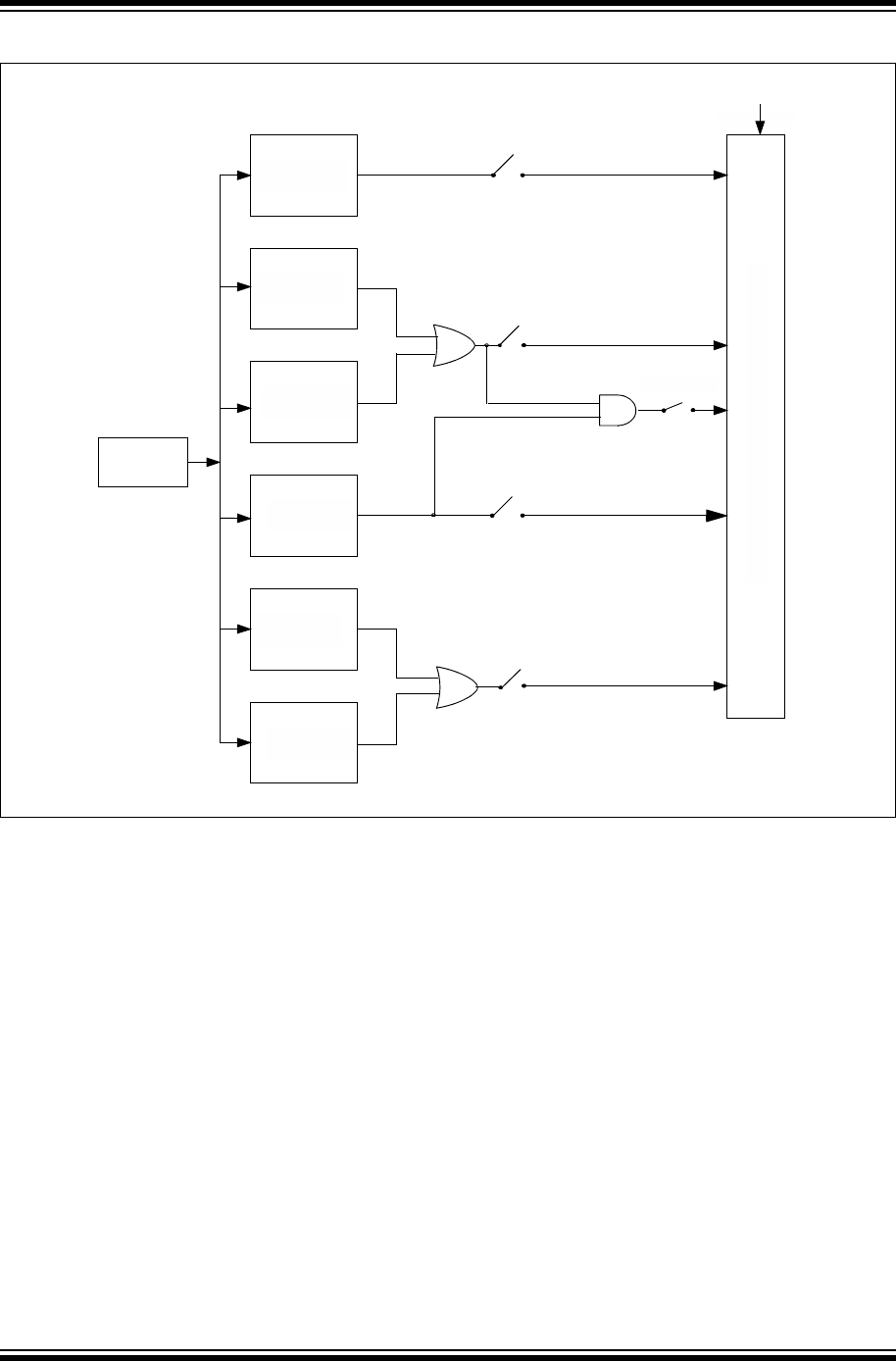
PIC32 Family Reference Manual
DS60001194B-page 18-54 © 2013 Microchip Technology Inc.
Figure 18-14: Digital Comparator
AD1DATAn
<
AD1CMPLO
AD1DATAn
=
AD1CMPLO
AD1DATAn
>
AD1CMPLO
AD1DATAn
<
AD1CMPHI
AD1DATAn
=
AD1CMPHI
AD1DATAn
>
AD1CMPHI
IELOLO
IELOHI
IEHILO
IEHIHI
IEBTWN
ENDCMP
Interrupt Generation Logic For Digital Comparator
AD1DATAn

© 2013 Microchip Technology Inc. DS60001194B-page 18-55
Section 18. 12-bit Pipelined Analog-to-Digital Converter (ADC)
12-bit Pipelined
Analog-to-Digital
Converter (ADC)
18
Example 18-4: ADC Digital Comparator
int main(int argc, char** argv) {
int eventFlag, result;
/* Set up the CAL registers */
AD1CAL1 = DEVADC1; // Copy the configuration data to the
AD1CAL2 = DEVADC2; // AD1CALx special function registers.
AD1CAL3 = DEVADC3;
AD1CAL4 = DEVADC4;
AD1CAL5 = DEVADC5;
/* Configure AD1CON1 */
AD1CON1 = 0; // No AD1CON1 features are enabled including:
// Stop-in-Idle, early interrupt, filter delay
// fractional mode and scan trigger source
/* Configure AD1CON2 */
AD1CON2 = 0; // Boost, low power mode off
// Setup the ADC Clock
AD1CON2bits.ADCSEL = 1; // 1 = SYSCLK, 2 REFCLK03, 3 FRC
AD1CON2bits.ADCDIV = 4; // TQ = 1/200 MHz; TAD = 4* (TQ * 2) = 40 ns;
// 25 MHz ADC clock
AD1CON2bits.SAMC = 9; // Sample time set to 10 * TAD = 400 ns for
// Class 2 and 3 inputs.
/* Configure AD1CON3 */
AD1CON3 = 0; // ADINSEL is not configured for this example.
// VREFSEL of ‘0’ selects AVDD and AVSS as the
// voltage reference.
/* Configure AD1MOD */
AD1MOD = 0; // All channels configured for default input
// and single-ended with unsigned output results.
/* Configure AD1GIRGENx */
AD1GIRQEN1 = 0; // No global interrupts are used.
AD1GIRQEN2 = 0;
/* Configure AD1CSSx */
AD1CSS1 = 0; // No channel scanning is used.
AD1CSS2 = 0;
/* Configure AD1CMPCONx */
AD1CMPCON1 = 0; // Set up Comparator 1, clear all AD1CMPCON1 bits.
AD1CMP1bits.ADCMPHI = 0xC00; // High limit is a 3072 result.
AD1CMP1bits.ADCMPLO = 0x500; // Low limit is a 1280 result.
AD1CMPCON1bits.IEBTWN = 1; // Create an event when the measured result is
// >= low limits and < high limit.
AD1CMPEN1 = 0; // Clear all enable bits
AD1CMPEN1bits.CMPE5 = 1; // set the bit corresponding to AN5
AD1CMPCON1bits.ENDCMP = 1; // enable comparator
AD1CMPCON2 = 0; // Digital comparators 2 through 6 are not used.
AD1CMPCON3 = 0; // Setting the AD1CMPCONx to ‘0’ ensures that
AD1CMPCON4 = 0; // the comparator is disabled. Other registers
AD1CMPCON5 = 0; // are “don't care”.
AD1CMPCON6 = 0;
/* Configure AD1FLTRx */
AD1FLTR1 = 0; // No oversampling filters are used.
AD1FLTR2 = 0;
AD1FLTR3 = 0;
AD1FLTR4 = 0;
AD1FLTR5 = 0;
AD1FLTR6 = 0;

PIC32 Family Reference Manual
DS60001194B-page 18-56 © 2013 Microchip Technology Inc.
Example 18-4: ADC Digital Comparator (Continued)
/* Set up the trigger sources */
AD1TRG1 = 0; // Initialize all sources to no trigger.
AD1TRG2 = 0;
AD1TRG3 = 0;
AD1TRG2bits.TRGSRC5 = 1; // Set AN5 to trigger from software.
/* Turn the ADC on, start calibration */
AD1CON1bits.ADCEN = 1;
/* Wait for calibration to complete */
while (AD1CON2bits.ADCRDY == 0);
while (1) {
/* Trigger a conversion */
AD1CON3bits.GSWTRG = 1;
/* Wait the conversions to complete */
while (AD1DSTAT1bits.ARDY5 == 0);
result = AD1DATA5;
/* Note: It is not necessary to fetch the result for the digital
* comparator to work. In this example we are triggering from
* software so we are using the ARDY5 to gate our loop. Reading the
* data clears the ARDY bit.
*/
/* See if we have a comparator event*/
if (AD1CMPCON1bits.DCMPED == 1) {
eventFlag = 1;
/*
* Process results Here
*
* Note: The first 5 samples may have reduced accuracy.
*
*/
}
}
return (1);
}

© 2013 Microchip Technology Inc. DS60001194B-page 18-57
Section 18. 12-bit Pipelined Analog-to-Digital Converter (ADC)
12-bit Pipelined
Analog-to-Digital
Converter (ADC)
18
18.5.2 Oversampling Digital Filter
The ADC module supports up to six oversampling digital filters. The oversampling digital filter
consists of an accumulator and a decimator (down-sampler), which function together as a
low-pass filter. By sampling an analog input at a higher-than-required sample rate, and then
processing the data through the oversampling digital filter, the effective resolution of the ADC
module can be increased at the expense of decreased conversion throughput. Using 4x
oversampling yields one extra bit of resolution, 16x oversampling yields two extra bits of
resolution, 64x oversampling provides three extra bits of resolution, and 256x oversampling
provides four extra bits of resolution.
The user application should configure the following bits to perform an oversampling conversion:
• Select the amount of oversampling through the Oversampling Filter Oversampling Ratio
(OVRSAM<2:0>) bits in the ADC1 Filter register (AD1FLTRn<28:26>)
•Set the sample time for subsequent samples:
- If using Class 1 inputs, select the sample time of the recurring conversions using the
(FILTRDLY<4:0>) bits in the AD1CON1 registers (AD1CON1<31:27>)
- If using Class 2 or Class 3 inputs, select the sample time using the (SAMC<7:0>) bits in the
ADC1 Control register 2 (AD1CON2<23:16>)
• Select the specific analog input to be oversampled by configuring the Channel ID Selection
(CHNLID<5:0>) bits (AD1FLTRn<21:16>)
•If needed, include the oversampling filter interrupt event in the global ADC interrupt, by
setting the Accumulator Filter Global Interrupt Enable (AFGIEN) bit (AD1FLTRn<25>)
•Enable the oversampling filter by setting the Oversampling Filter Accumulator Enable (AFEN)
bit (AD1FLTRn<31>)
Once the oversampling digital filter is configured, it waits for an external conversion trigger to
initiate the oversampling process. The trigger signal for the channel to be oversampled causes
the accumulator to be cleared and initiates the first conversion. When each conversion request
is in the process of being converted in the conversion pipeline, the filter begins a new sample.
Once each conversion request has been passed to the pipeline converter, a new sample is
initiated based on the values of the FILTDLY<4:0> or SAMC<7:0> bits for Class 1, Class 2, and
Class 3 inputs, respectively. This process continues until the required number of samples (4, 8,
16, 32, 64, 128, or 256) has been converted. When the converted samples have been summed,
the output is transferred to the Oversampling Filter Data output bits, FLTRDATA<15:0>
(AD1FLTRn<15:0>) and the Accumulator Filter Data Ready Interrupt Flag bit, AFRDY
(AD1FLTRn<24>), is set.
Figure 18-15 illustrates 4x oversampling on a Class 1 input. Prior to the trigger, the Class 1 input
S&H is tracking the input signal. The trigger starts the first conversion. Once the sample has been
transferred to the converter, the S&H resumes tracking and starts a filter delay timer
(FILTRDLY<4:0>). When the filter delay timer expires a new conversion sequence occurs. After
each sample is converted it is added to the accumulator. The sequence repeats until the number
of samples specified by the OVRSAM<2:0> bits have been accumulated. When the last sample
has been converted, its value is added to the accumulator. The result is left shifted and then
stored in the FLTRDATA<15:0> bits.
Figure 18-15: 4x Oversampling of a Class 1 Input
Convert
Input tracking Hold
Initial trigger starts the
conversion process
Hold Hold Hold
S&H reverts to tracking (sampling) the
input after the sample is passed to the
converter.
4x oversampling process of a Class 1 input resulting in one additional bit of ADC resolution
Convert Convert Convert
Conversion results are added to accumulator
Prior to trigger the
S&H tracks the input
When last sample has been
passed to the converter the
S&H resumes tracking input
(FLTRDLY +1.5) TAD (FLTRDLY +1.5) TAD
(FLTRDLY +1.5) TAD Input tracking
After a delay of (FLTRDLY + 1.5) TAD , an
oversample trigger occurs.
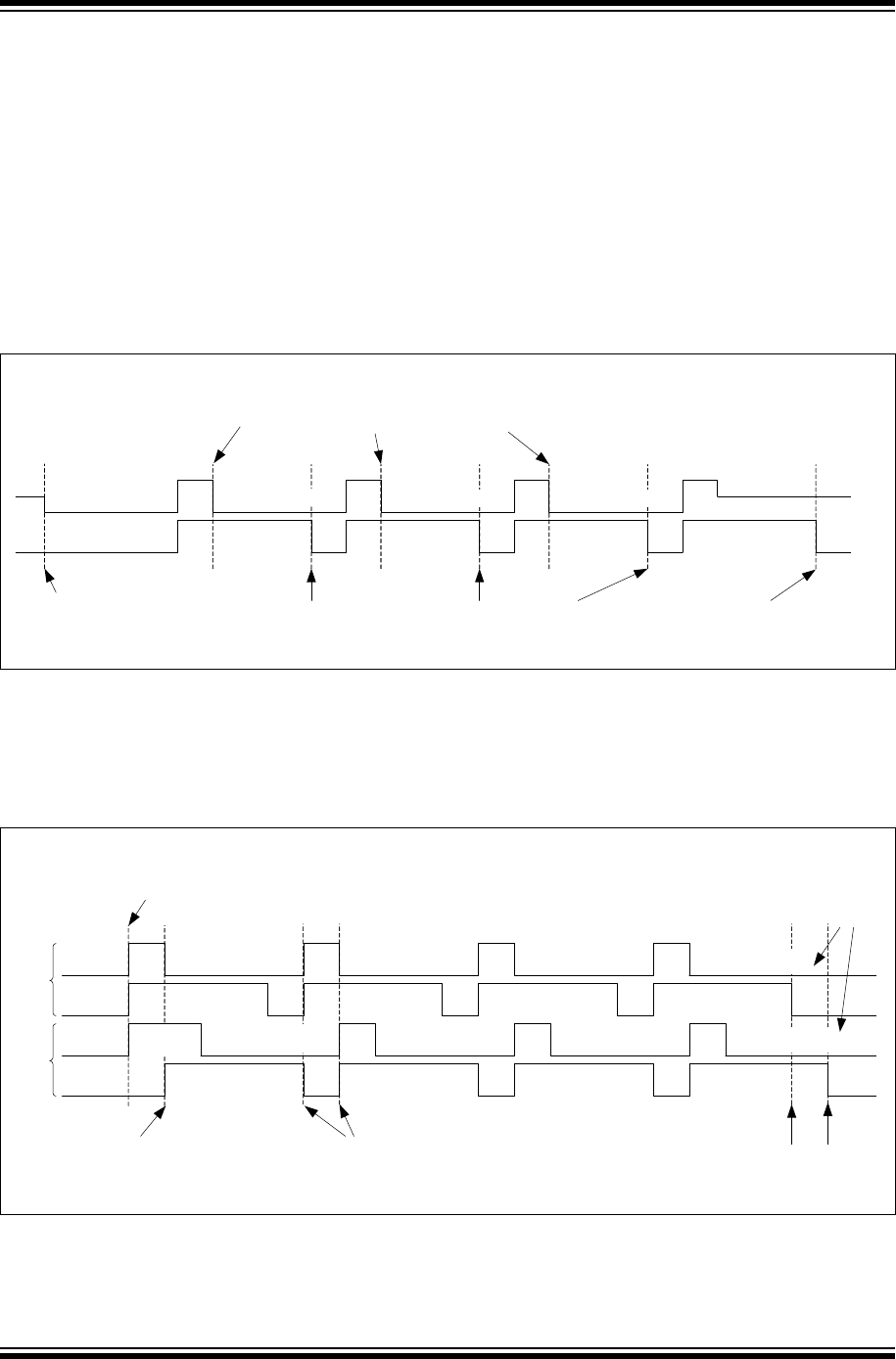
PIC32 Family Reference Manual
DS60001194B-page 18-58 © 2013 Microchip Technology Inc.
When input is being sampled, lower priority inputs can be transferred to the converter without
disrupting oversampling timing. Higher priority conversion requests can disrupt the oversampling
timing and can produce unexpected results. The user application should arrange the initiation
trigger for the oversampling filters to occur while there are no expected interruptions from higher
priority ADC conversion requests.
Figure 18-16 illustrates 4x Oversampling using a Class 2 or Class 3 input. Triggering a Class 2
or Class 3 input initiates sampling for the length of time defined by SAMC. Retriggers generated
by the oversampling logic use the SAMC<4:0> bits, not the FLTRDLY<4:0> bits, to set the
sample time.
Since Class 2 and Class 3 inputs all use the shared S&H, oversampling blocks lower priority
Class 2 and Class 3 triggers. Higher priority Class 2 and Class 3 triggers will completely disrupt
the oversampling process, and therefore, should be avoided completely.
Figure 18-16: 4x Oversampling of a Class 2 Input
Figure 18-17 illustrates 4x oversampling of two Class 1 inputs simultaneously (common trigger).
At the initial trigger, both S&H circuits enter the hold state simultaneously. The higher priority AN0
is transferred to the converter first, followed immediately by the AN1 input. For the remainder of
the oversampling process the conversions are skewed by 1 TAD. Each analog input creates a
unique interrupt when the oversampling process is complete.
Figure 18-17: Oversampling Two Class 1 Inputs
Convert
Hold
Trigger initiates sampling
Hold Hold Hold
4x oversampling process of a Class 2 input resulting in one additional bit of ADC resolution
Convert Convert Convert
Conversion results are added to accumulator Last conversion results in a 14-bit sum,
the sum is right shifted by 1 producing
a 13-bit result in FLTRDATA
Once sample is passed to the converter, an oversample trigger is issued
(SAMC) TAD (SAMC) TAD (SAMC) TAD
(SAMC) TAD
Input tracking
Convert
Input
tracking Hold
Initial trigger starts the conversion process .
AN0 is transferred to converter first.
Hold Hold Hold
4x oversampling of two Class 1 inputs using a common trigger
Convert Convert Convert
When the last sample has been passed to
the converter, the S&H circuit resumes
tracking input
(FLTRDLY +1.5) TAD (FLTRDLY +1.5) TAD
(FLTRDLY +1.5) TAD
Convert
Input
tracking
Convert Convert Convert
Hold Hold Hold
(FLTRDLY +1.5) TAD (FLTRDLY +1.5) TAD
AN1 is transferred to the converter
after the higher priority AN0 transfer is
complete
Hold (FLTRDLY +1.5) TAD
Subsequent retriggers occur after the sample
has been transferred to the converter and the
FLTRDLY time has expired
Input tracking
When the last conversion is complete,
the result is transferred into the
appropriate FLTRDATA register
AN0
AN1
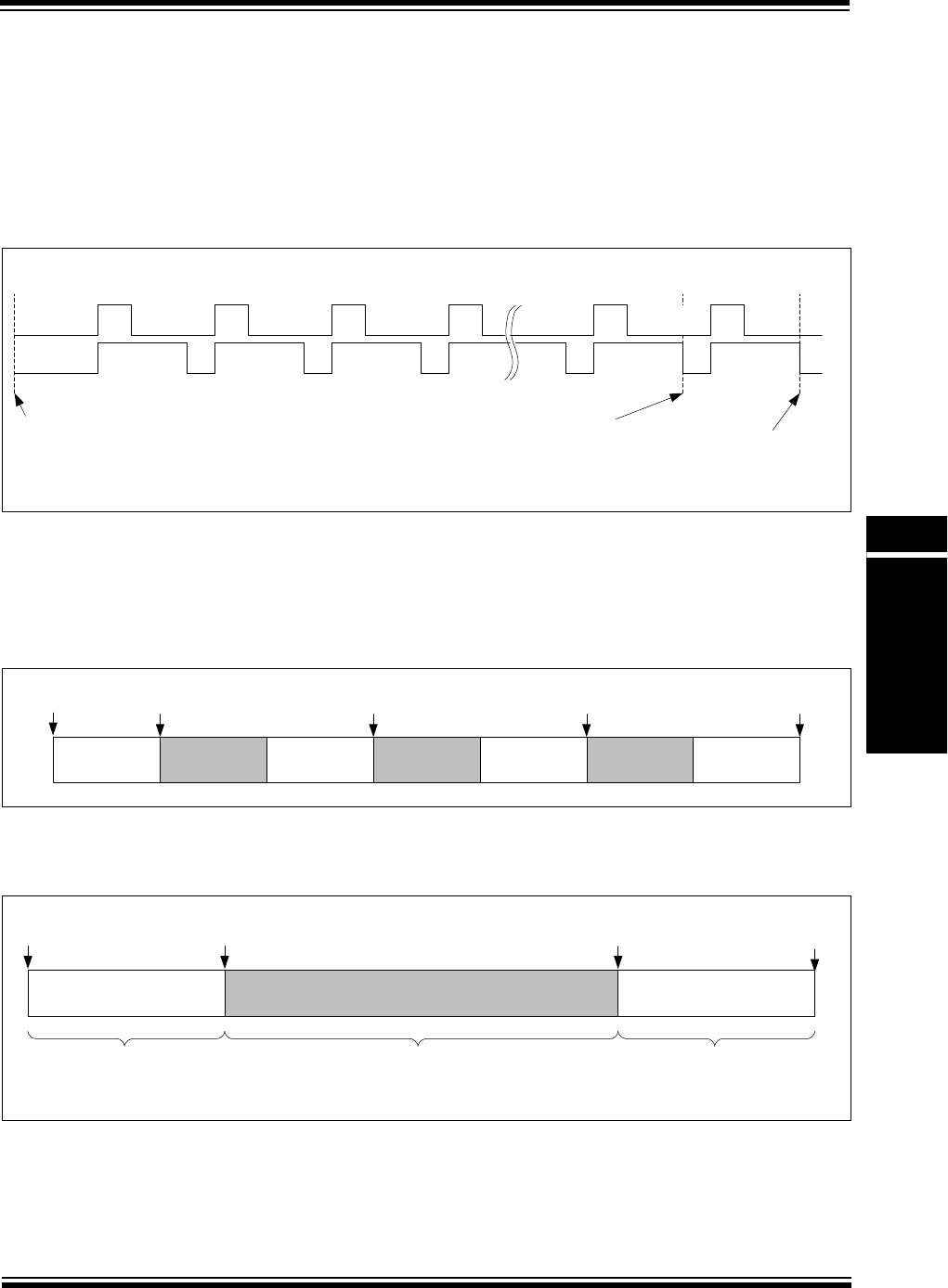
© 2013 Microchip Technology Inc. DS60001194B-page 18-59
Section 18. 12-bit Pipelined Analog-to-Digital Converter (ADC)
12-bit Pipelined
Analog-to-Digital
Converter (ADC)
18
When using the oversampling feature on the analog inputs connected to the shared S&H, the
system will interleave sampling, alternating the highest priority oversampled input with one other
channel. Figure 18-18 illustrates this configuration using AN10 and AN11. In this case, the same
results are obtained if the two inputs, AN10 and AN11, are configured with a common
independent trigger, or if they are set up as a two-input scan list.
Since a single shared S&H is used, sampling must alternate between the two inputs, which
reduces the sample rate by 50 percent in comparison with oversampling a single channel with
the same settings.
Figure 18-18: Oversampling Two Class 2 Inputs
An oversampled input on the shared S&H will alternate with one other lower priority channel.
Therefore, a maximum of two Class 2 or Class 3 inputs can be oversampled at one time.
This interleaving also applies when lower priority non-oversampled Class 2 inputs are triggered
during oversampling of a Class 2 input, as shown in Figure 18-19. Here, the oversampling of AN9
is interleaved with two AN10 samples and a single AN11 sample.
Figure 18-19: Class 2 Oversampling Interrupted by Non-oversampled Trigger
If oversampling a single Class 2 input during the oversampling process, a lower priority,
oversampled input is triggered, the following effect will take place, as shown in Figure 18-20.
Figure 18-20: Oversampling Two Class 2 Inputs with Independent Triggers
It is important to gate the triggers of inputs on the shared S&H when using oversampling to
ensure that the oversampling is not disrupted, otherwise unexpected results could occur.
Last conversion for AN10; Result is
put in FLTRDATA register assigned
to the oversampling filter for AN10
Sample 1
(AN10) Hold Hold Hold Hold Hold Hold
Sample 1
(AN11)
Sample 2
(AN10)
Sample 2
(AN11)
Sample 4
(AN10)
Sample 4
(AN11)
Convert
(AN10)
Convert
(AN11)
Convert
(AN10)
Convert
(AN11)
Convert
(AN10)
Convert
(AN11)
Trigger initiates sampling of the
highest priority input, AN10 Last conversion for AN11; Result is
put in FLTRDATA register assigned
to the oversampling filter for AN11
4x oversampling process of two Class 2 inputs triggered from the same source
AN9
Oversample AN10 Sample
AN9 Trigger AN10 Trigger AN9 Completes
AN9
Oversample AN11 Sample AN10 Sample AN9
Oversample
AN11 Trigger AN10 Trigger
AN9
Oversample
AN10 Oversampling AN10 and AN11 Interleaved Oversampling AN11 Oversampling
First half of AN10
oversampling
AN10 Trigger AN11 Trigger AN10 Completes AN11 Completes
Last half of AN10 and first half of
AN11 oversampling
Last half of AN11
oversampling

PIC32 Family Reference Manual
DS60001194B-page 18-60 © 2013 Microchip Technology Inc.
Example 18-5: ADC Digital Oversampling Filter
int main(int argc, char** argv) {
int result;
/* Set up the CAL registers */
AD1CAL1 = DEVADC1; // Copy the configuration data to the
AD1CAL2 = DEVADC2; // AD1CALx special function registers.
AD1CAL3 = DEVADC3;
AD1CAL4 = DEVADC4;
AD1CAL5 = DEVADC5;
/* Configure AD1CON1 */
AD1CON1 = 0; // No AD1CON1 features are enabled including:
// Stop-in-Idle, early interrupt,
// Fractional mode and scan trigger source
AD1CON1bits.FILTRDLY = 5; // sample time between oversampling triggers
// is 6.5 * TAD = 260 ns.
/* Configure AD1CON2 */
AD1CON2 = 0; // Boost, Low-power mode off, SAMC set to min,
// Set up the ADC Clock
AD1CON2bits.ADCSEL = 1; // 1 = SYSCLK, 2 REFCLK03, 3 FRC
AD1CON2bits.ADCDIV = 4; // TQ = 1/200 MHz; TAD = 4 * (TQ * 2) = 40 ns;
// 25 MHz ADC clock
/* Configure AD1CON3 */
AD1CON3 = 0; // ADINSEL is not configured for this example.
// VREFSEL of ‘0’ selects AVDD and AVSS as the
// voltage reference.
/* Configure AD1MOD */
AD1MOD = 0; // All channels configured for default input
// and single-ended with unsigned output results.
/* Configure AD1GIRGENx */
AD1GIRQEN1 = 0; // No global interrupts are used.
AD1GIRQEN2 = 0;
/* Configure AD1CSSx */
AD1CSS1 = 0; // No channel scanning is used.
AD1CSS2 = 0;
/* Configure AD1CMPCONx */
AD1CMPCON1 = 0; // No digital comparators are used.
AD1CMPCON2 = 0; // Setting the AD1CMPCONx register to ‘0’ ensures that
AD1CMPCON3 = 0; // the comparator is disabled. Other registers
AD1CMPCON4 = 0; // are “don't care”.
AD1CMPCON5 = 0;
AD1CMPCON6 = 0;
/* Configure AD1FLTRx */
AD1FLTR1 = 0; // Clear all bits for Filter 1
AD1FLTR1bits.CHNLID = 0; // Use AN0 as the source
AD1FLTR1bits.OVRSAM = 1; // 16x oversampling
AD1FLTR1bits.AFEN = 1; // Enable filter 1
AD1FLTR2 = 0; // Filters 2 through 6 are not used.
AD1FLTR3 = 0;
AD1FLTR4 = 0;
AD1FLTR5 = 0;
AD1FLTR6 = 0;
/* Set up the trigger sources */
AD1TRG1 = 0; // Initialize all sources to no trigger.
AD1TRG2 = 0;
AD1TRG3 = 0;
AD1TRG1bits.TRGSRC0 = 1; // Set AN0 to trigger from software

© 2013 Microchip Technology Inc. DS60001194B-page 18-61
Section 18. 12-bit Pipelined Analog-to-Digital Converter (ADC)
12-bit Pipelined
Analog-to-Digital
Converter (ADC)
18
Example 18-5: ADC Digital Oversampling Filter (Continued)
18.5.3 Oversampling Conversion Times
Equation 18-6 and Equation 18-7 describe the timing for oversampling using Class 1 and Class 2
inputs. They represent the time from trigger to the conversion result availability.
Equation 18-6: Oversampling Time for Class 1 Input
/* Turn the ADC on, start calibration */
AD1CON1bits.ADCEN = 1;
/* Wait for calibration to complete */
while (AD1CON2bits.ADCRDY == 0);
while (1) {
/* Trigger a conversion */
AD1CON3bits.GSWTRG = 1;
/* Wait for the oversampling process to complete */
while (AD1FLTR1bits.AFRDY == 0);
/* fetch the result */
result = AD1FLTR1bits.FLTRDATA;
/*
* Process result Here
*
* Note 1: Loop time determines the sampling time for the first sample.
* remaining samples sample time is determined by FLTRDLY in AD1CON1.
* Note 2: The first 5 samples may have reduced accuracy.
*
*/
}
return (1);
}
TC1OVS_SAMP FILTDLY 1.5+()TAD
=
Where:
Note 1: This equation assumes that no triggers of any higher priority Class 1 inputs
occur during the oversample conversion sequence. Each higher priority Class 1
conversion which takes place will add one TAD to the equation.
2: The sample time for the initial sample is determined by the trigger rate, as is the
case for all Class 1 inputs. This equation describes the sample time for
subsequent oversampling retriggers.
TAD = Analog-to-digital conversion clock period
N = Total number of samples determined by the OVRSAM<2:0> bits (AD1FLTR<28:26>)
FILTDLY = FILTDLY<4:0> bits (AD1CON1<31:27>)
TC1OVS_CONV N FILTDLY 4+()⋅8+()TAD
=
Total Con ve rsio n Ti me fo r a sin gle tr ig ger of an ov ers am p le d i n pu t:
Sample Time used during retriggering (see Note 2):
TC1OVS_TRG_MIN N FILTDLY 4+()⋅()TAD
=
Minimum time between triggers of an oversampled input:
(see Note 1)
(see Note 1)

PIC32 Family Reference Manual
DS60001194B-page 18-62 © 2013 Microchip Technology Inc.
Equation 18-7: Oversampling Time for Class 2 Input
TC2OVS_SAMP SAMC 1+()TAD
=
Where:
Note: This equation assumes there are no pending conversions from higher priority
Class 1 analog channels.
TAD = Analog-to-digital conversion clock period
N = Total number of samples determined by the OVRSAM<2:0> bits (AD1FLTR<28:26>)
SAMC = SAMC<7:0> bits (AD1CON2<23:16>)
TC2OVS_CONV NSAMC4+()7+⋅()TAD
=
Total Con ve rsi on Time :
Sample Time:

© 2013 Microchip Technology Inc. DS60001194B-page 18-63
Section 18. 12-bit Pipelined Analog-to-Digital Converter (ADC)
12-bit Pipelined
Analog-to-Digital
Converter (ADC)
18
18.6 INTERRUPTS
Each ADC module supports interrupts triggered from a variety of sources, which can be
processed individually or globally. An early interrupt feature is also available to compensate for
interrupt servicing latency.
After an enabled interrupt is generated, the CPU will jump to the vector assigned to that interrupt.
The CPU will then begin executing code at the vector address. The user software at this vector
address should perform the required operations, such as processing the data results, clearing
the interrupt flag, and then exit. For more information on interrupts and the vector address table
details, refer to the Section 8. “Interrupts” (DS61108) in the “PIC32 Family Reference Manual”
and the “Interrupt Controller” chapter in the specific device data sheet.
18.6.1 Interrupt Sources
Each ADC is capable of generating interrupts from the following events:
•ANx Data Ready Event – Upon a completion of a conversion from an analog input source
(ANx) the ARDYx bit associated with that input will be set in the AD1STATn register. Each of
the ARDYx bits is capable of generating a unique interrupt when set.
•Digital Comparator Event – When a conversion's comparison criteria are met by a configured
and enabled digital comparator, the DCMPED bit will be set in the AD1CMPCONn register.
Each of the digital comparators is capable of generating a unique interrupt when its DCMPED
bit is set.
•Oversampling Filter Data Ready Event – When an oversampling filter has completed the
accumulation/decimation process and has stored the result, the AFRDY bit will be set in the
AD1FLTRn register. Each of the Oversampling Filters is capable of generating a unique
interrupt when its AFRDY bit is set.
18.6.2 Interrupt Enabling, Priority and Vectoring
Each of the ADC events previously mentioned will generate an interrupt when its associate
Interrupt Enable bit, IE, is set. An Interrupt Flag bit, IF, priority bits, IP<2:0>, and sub-priority bits
IS<1:0> are also associated with each of the events. For more information on how to enable and
prioritize interrupts, refer to Section 8. “Interrupts” (DS61108) in the “PIC32 Family Reference
Manual”. Each of the ADC events previously listed also has an associated interrupt vector. Refer
to the “Interrupt Controller” chapter in the specific device data sheet for more information on
the vector location and control/status bits associated with each individual interrupt.
18.6.3 Individual and Global Interrupts
The use of the individual interrupts previously listed can significantly optimize the servicing of
multiple ADC events, by keeping each Interrupt Service Routine (ISR) focused on efficiently
handling a specific event. In addition, different ISRs can be easily segregated according to the
tasks performed, thereby making user software easier to implement and maintain.
There may be cases where it is desirable to have a single ISR service multiple interrupt events.
To fac ili ta te thi s, ea c h A DC eve nt ca n b e l og i ca lly “ORed” to create a single global ADC interrupt.
When an ADC event is enabled for a global interrupt, it will vector to a single interrupt routine. It
will be the responsibility of this single global ISR to determine the source of the interrupt through
polling and process it accordingly.
For the ADC Events:
•Each ANx Data Ready interrupt event is included in the Global ADC Interrupt only if the
corresponding AGIENx bit (located in the AD1GIRQEN1 or AD1GIRQEN2 register) is set
•The Digital Comparator interrupt event is included in the Global ADC Interrupt only if the
DCMPGIEN bit (AD1CMPCON<6>) is set
•The Oversampling Filter interrupt event is included in the Global ADC Interrupt only if the
AFGIEN bit (AD1FLTRn<25>) is set
Use of the Global Interrupt requires configuration of its own unique IE, IF, IP and IS bits as well
as configuration of its interrupt vector as described in 18.6.2 “Interrupt Enabling, Priority and
Vectoring”.

PIC32 Family Reference Manual
DS60001194B-page 18-64 © 2013 Microchip Technology Inc.
Interrupts for the ADC can be configured as individual or global, or utilize both where some are
processed individually and others in the global ISR.
18.6.4 Early Interrupts
The EIE<2:0> bits in the AD1CON1 register enable the generation of the interrupts prior to
completion of the conversion. Even though the input is still in the conversion process, the
processor application software can use the “head-start” to begin execution of the entry into the
ISR. The early interrupt can improve the throughput of a system by overlapping the completion
of the ADC conversion with the processor overhead associated with an interrupt. The use of the
EIE<2:0> bits can reduce the latency from the moment the analog signal was sampled until the
point in time when the user application software can use the data.
Use of the EIE<2:0> bits will cause the ARDYx bits in the AD1STATx register to be set prior to
the data actually being available in the AD1DATAx register. The value stored in the EIE<2:0> bits
determines the number of TAD clocks cycles that the bit will be set prior to the completion of the
conversion. The EIE<2:0> bits setting applies to all ARDYx bits of the ADC. Early interrupts
should not be used if the application uses polling to determine if a conversion is complete. This
includes polling inside a Global ISR. In addition, note that the EIE<2:0> bits setting does not
apply to the Oversampling Filter Data Ready signal, AFRDY.
Note: The early interrupt feature should only be used when the data is retrieved using an
individual interrupt routine and not when polling the ARDYx bits, even in the Global
interrupt service routine.

© 2013 Microchip Technology Inc. DS60001194B-page 18-65
Section 18. 12-bit Pipelined Analog-to-Digital Converter (ADC)
12-bit Pipelined
Analog-to-Digital
Converter (ADC)
18
18.7 OPERATION DURING POWER-SAVING MODES
The power-saving modes, Sleep and Idle, are useful for reducing the conversion noise by
minimizing the digital activity of the CPU, buses and other peripherals.
18.7.1 Sleep Mode
When a device enters Sleep mode, the SYSCLK and all peripherals that operate from the
SYSCLK source are halted. This includes the ADC when the SYSCLK is selected for the clock
source or when REFCLK3 is selected for the ADC clock source, and SYSCLK is used as the
REFCLK3 source.
When the SYSCLK is the source, (directly or indirectly) and Sleep mode occurs during a
conversion, the conversion is aborted. The converter will not resume a partially completed
conversion on exiting from Sleep mode. The ADC register contents are not affected by the device
entering or leaving Sleep mode.
The ADC module can operate during Sleep mode if the ADC clock source is derived from a
source other than SYCLK that is active during sleep mode. The FRC clock source is a logical
choice for operation during sleep, however the REFCLK3 clock source can also be used
provided it has an input clock that is operational during sleep mode.
ADC operation during Sleep mode reduces the digital switching noise from the conversion. When
the conversion is completed, the ARDYx status bit for that analog input will be set and the result
will be loaded into the corresponding ADC Result register (AD1DATAn).
If any of the ADC interrupts is enabled (AD1IE = 1), the device will wake-up from Sleep mode
when the ADC interrupt occurs. The program execution will resume at the ADC ISR, if the ADC
interrupt is greater than the current CPU priority. Otherwise, execution will continue from the
instruction after the WAIT instruction that placed the device in Sleep mode.
To m ini mi ze t he e ff ects o f di gital noi se o n t he ADC module operation, the user must select a
conversion trigger source that ensures that the A/D conversion will take place in Sleep mode. For
example, the external interrupt pin (INT0) conversion trigger option (TRGSRCn<4:0> = 00100)
can be used for performing sampling and conversion while the device is in Sleep mode.
18.7.2 ADC Operation during Idle Mode
For the ADC, the Stop in Idle Mode bit, ADSIDL (AD1CON1<13>), specifies whether the ADC
module will stop on Idle or continue on Idle. If ADSIDL = 0, the ADC module will continue normal
operation when the device enters Idle mode. If any of the ADC interrupts are enabled, the device
will wake-up from Idle mode when the ADC interrupt occurs. The program execution will resume
at the ADC ISR if the ADC interrupt is greater than the current CPU priority. Otherwise, execution
will continue from the instruction after the WAIT instruction that placed the device in Idle mode.
If ADSIDL = 1, the ADC module will stop in Idle mode. If the device enters Idle mode during a
conversion, the conversion is aborted. The converter will not resume a partially completed
conversion on exiting from Idle mode.
18.7.3 ADC Low-power Mode
The ADC module can be placed in a low-power state by setting the ADC Low-power bit,
LOWPWR (AD1CON2<13>). Using this low-power mode provides a significantly faster module
restart compared to disabling and re-enabling the ADC module using the ADCEN bit
(AD1CON1<15>). This is because disabling and re-enabling the ADC module using the ADCEN
bit (AD1CON1<15>) requires a long ADC calibration sequence to be performed. Whereas,
restarting the ADC module after clearing the LOWPWR bit (AD1CON2<13>) only requires 2 *
TAD cycles as the ADC bias generators are not turned off in ADC Low-power mode.
Note: For the ADC module to operate in Sleep mode, the ADC clock source must be set
to Internal FRC (ADCSEL<1:0> bits (AD1CON2<9:8>) = 11). Alternately, the REF-
CLK3 source can be used; however, the clock source used for REFCLK3 must
operate during Sleep. Any changes to the ADC clock configuration require that the
ADC be disabled.
Note: The first five conversions following the exit from ADC Low-power mode may be
subject to lower accuracy than specified in the device data sheet.
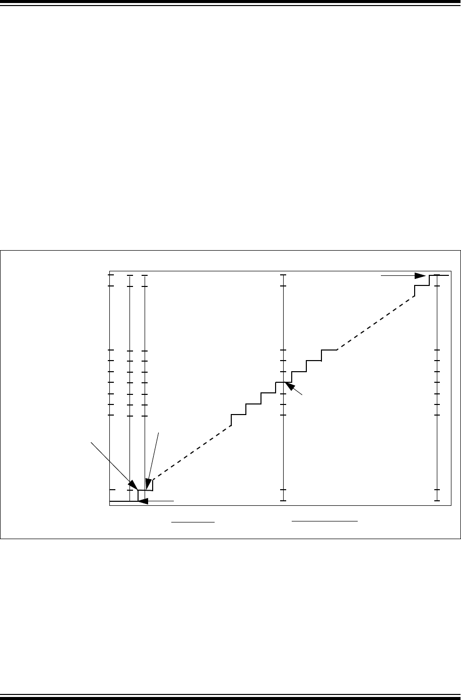
PIC32 Family Reference Manual
DS60001194B-page 18-66 © 2013 Microchip Technology Inc.
18.8 EFFECTS OF RESET
Following any Reset event, all the ADC control and status registers are reset to their default
values with control bits in a non-active state. This disables the ADC module and sets the analog
input pins to Analog Input mode. Any conversion that was in progress will terminate and the result
will not be written to the result buffer. The values in the AD1DATAn registers are initialized to
0x00000000 during a device Reset.
18.9 TRANSFER FUNCTION
A typical transfer function of the 12-bit ADC is illustrated in Figure 18-21. The difference of the
input voltages (VINH - VINL) is compared with the reference (VREFH - VREFL).
•The first code transition (A) occurs when the input voltage is (V
REFH - VREFL/8192) or
0.5 LSb
•The 00 0000 0001 code is centered at (VREFH - VREFL/4096) or 1.0 LSb (B)
•The 10 0000 0000 code is centered at (2048 * (VREFH - VREFL)/4096) (C)
•An input voltage less than (1 * (V
REFH - VREFL)/8192) converts as 00 0000 0000 (D)
•An input greater than (8192 * (VREFH - VREFL)/8192) converts as 11 1111 1111 (E)
Figure 18-21: Analog-to-Digital Transfer Function
1000 0000 0001 (= 2049)
1000 0000 0010 (= 2050)
1000 0000 0011 (= 2051)
0111 1111 1101 (= 2045)
0111 1111 1110 (= 2046)
0111 1111 1111 (= 2047)
1111 1111 1110 (= 4094)
1111 1111 1111 (= 4095)
0000 0000 0000 (= 0)
0000 0000 0001 (= 1)
Output Code
1000 0000 0000 (= 2048)
(VINH – VINL)
VREFL VREFH – VREFL
4096
2048 * (VREFH – VREFL)
4096
VREFH
VREFL + VREFL +
(A)
(B)
(C)
(D)
(E)
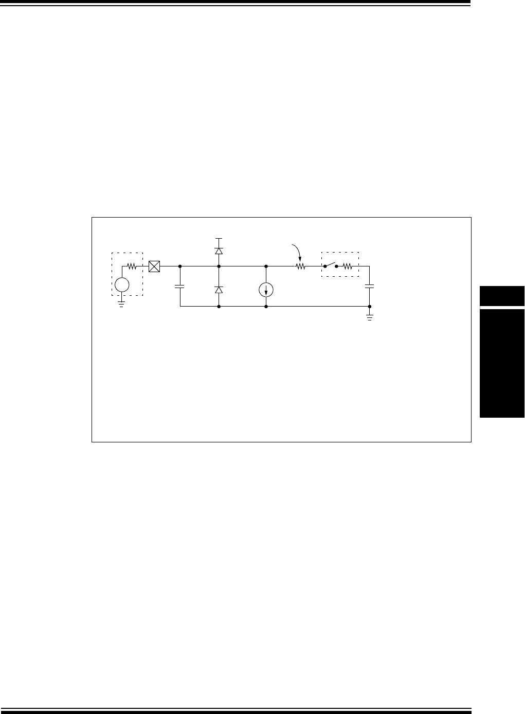
© 2013 Microchip Technology Inc. DS60001194B-page 18-67
Section 18. 12-bit Pipelined Analog-to-Digital Converter (ADC)
12-bit Pipelined
Analog-to-Digital
Converter (ADC)
18
18.10 ADC SAMPLING REQUIREMENTS
The analog input model of the 12-bit ADC is illustrated in Figure 18-22. The total acquisition time
for the analog-to-digital conversion is a function of the internal circuit settling time and the holding
capacitor charge time.
For the ADC module to meet its specified accuracy, the charge holding capacitor (CHOLD) must
be allowed to fully charge to the voltage level on the analog input pin. The analog output source
impedance (RS), the interconnect impedance (RIC), and the internal sampling switch (RSS)
impedance combine to directly affect the time required to charge the CHOLD. The combined
impedance of the analog sources must therefore be small enough to fully charge the holding
capacitor within the selected sample time. The internal holding capacitor will be in the discharged
state prior to each sample operation.
At least 1 TAD time period should be allowed between conversions for the acquisition time. Refer
to the “Electrical Characteristics” chapter in the specific device data sheet for more
information.
Figure 18-22: 12-bit ADC Analog Input Model
18.11 CONNECTION CONSIDERATIONS
Because the analog inputs employ Electrostatic Discharge (ESD) protection, they have diodes
to VDD and VSS; therefore, the analog input must be between VDD and VSS. If the input voltage
exceeds this range by greater than 0.3V (either direction), one of the diodes becomes forward
biased and it may damage the device if the input current specification exceeds.
An external RC filter is sometimes added for anti-aliasing of the input signal. The R (resistive)
component should be selected to ensure that the acquisition time is met. Any external
components connected (through high-impedance) to an analog input pin (capacitor, Zener diode,
and so on) should have very little leakage current at the pin.
CPIN
VA
Rs ANx VT = 0.6V
VT = 0.6V ILEAKAGE
RIC = 300ΩSampling
Switch
RSS
CHOLD
= DAC capacitance
VSS
VDD
= 1.2 pF
± 500 nA
Note: The CPIN value depends on the device package and is not tested. The effect of the CPIN is
negligible if Rs ≤ 5 kΩ.
RSS = 44 Ω
Legend:
CPIN = Input capacitance VT = Threshold voltage
RSS = Sampling switch resistance RIC = Interconnect resistance
RS = Source resistance CHOLD = Sample/hold capacitance
ILEAKAGE = Leakage current at the pin due to various junctions

PIC32 Family Reference Manual
DS60001194B-page 18-68 © 2013 Microchip Technology Inc.
18.12 RELATED APPLICATION NOTES
This section lists application notes that are related to this section of the manual. These
application notes may not be written specifically for the PIC32 device family, but the concepts are
pertinent and could be used with modification and possible limitations. The current application
notes related to the 12-bit Pipelined Analog-to-Digital Converter (ADC) module are:
Title Application Note #
Understanding A/D Converter Performance Specifications AN693
Achieving Higher ADC Resolution Using Oversampling AN1152
Note: Please visit the Microchip Web site (www.microchip.com) for additional Application
Notes and code examples for the PIC32 family of devices.

© 2013 Microchip Technology Inc. DS60001194B-page 18-69
Section 18. 12-bit Pipelined Analog-to-Digital Converter (ADC)
12-bit Pipelined
Analog-to-Digital
Converter (ADC)
18
18.13 REVISION HISTORY
Revision A (May 2013)
This is the initial released version of the document.
Revision B (November 2013)
This revision includes the following updates:
•The Shared S&H 5 Block Diagram was updated (see Figure 18-3)
• Note 4 was added to the STRGSRC<4:0> bits in the ADC1 Control Register 1 (AD1CON1)
(see Register 18-1)
• The SHxALT bits in the ADC1 Input Mode Control Register (AD1MOD) were updated (see
Tabl e 18- 1 and Register 18-4)
•Added example code (see Example 18-1 through Example 18-5)
•Minor updates to text and formatting were incorporated throughout the document

PIC32 Family Reference Manual
DS60001194B-page 18-70 © 2013 Microchip Technology Inc.
NOTES:

2013 Microchip Technology Inc. DS60001194B-page 18-71
Information contained in this publication regarding device
applications and the like is provided only for your convenience
and may be superseded by updates. It is your responsibility to
ensure that your application meets with your specifications.
MICROCHIP MAKES NO REPRESENTATIONS OR
WARRANTIES OF ANY KIND WHETHER EXPRESS OR
IMPLIED, WRITTEN OR ORAL, STATUTORY OR
OTHERWISE, RELATED TO THE INFORMATION,
INCLUDING BUT NOT LIMITED TO ITS CONDITION,
QUALITY, PERFORMANCE, MERCHANTABILITY OR
FITNESS FOR PURPOSE. Microchip disclaims all liability
arising from this information and its use. Use of Microchip
devices in life support and/or safety applications is entirely at
the buyer’s risk, and the buyer agrees to defend, indemnify and
hold harmless Microchip from any and all damages, claims,
suits, or expenses resulting from such use. No licenses are
conveyed, implicitly or otherwise, under any Microchip
intellectual property rights.
Trademarks
The Microchip name and logo, the Microchip logo, dsPIC,
FlashFlex, KEELOQ, KEELOQ logo, MPLAB, PIC, PICmicro,
PICSTART, PIC32 logo, rfPIC, SST, SST Logo, SuperFlash
and UNI/O are registered trademarks of Microchip Technology
Incorporated in the U.S.A. and other countries.
FilterLab, Hampshire, HI-TECH C, Linear Active Thermistor,
MTP, SEEVAL and The Embedded Control Solutions
Company are registered trademarks of Microchip Technology
Incorporated in the U.S.A.
Silicon Storage Technology is a registered trademark of
Microchip Technology Inc. in other countries.
Analog-for-the-Digital Age, Application Maestro, BodyCom,
chipKIT, chipKIT logo, CodeGuard, dsPICDEM,
dsPICDEM.net, dsPICworks, dsSPEAK, ECAN,
ECONOMONITOR, FanSense, HI-TIDE, In-Circuit Serial
Programming, ICSP, Mindi, MiWi, MPASM, MPF, MPLAB
Certified logo, MPLIB, MPLINK, mTouch, Omniscient Code
Generation, PICC, PICC-18, PICDEM, PICDEM.net, PICkit,
PICtail, REAL ICE, rfLAB, Select Mode, SQI, Serial Quad I/O,
Tota l E ndu ra nce , T SHA RC , U n iW inD riv er, Wi per Lo c k, ZE NA
and Z-Scale are trademarks of Microchip Technology
Incorporated in the U.S.A. and other countries.
SQTP is a service mark of Microchip Technology Incorporated
in the U.S.A.
GestIC and ULPP are registered trademarks of Microchip
Technology Germany II GmbH & Co. KG, a subsidiary of
Microchip Technology Inc., in other countries.
All other trademarks mentioned herein are property of their
respective companies.
© 2013, Microchip Technology Incorporated, Printed in the
U.S.A., All Rights Reserved.
Printed on recycled paper.
ISBN: 978-1-62077-653-7
Note the following details of the code protection feature on Microchip devices:
• Microchip products meet the specification contained in their particular Microchip Data Sheet.
• Microchip believes that its family of products is one of the most secure families of its kind on the market today, when used in the
intended manner and under normal conditions.
• There are dishonest and possibly illegal methods used to breach the code protection feature. All of these methods, to our
knowledge, require using the Microchip products in a manner outside the operating specifications contained in Microchip’s Data
Sheets. Most likely, the person doing so is engaged in theft of intellectual property.
• Microchip is willing to work with the customer who is concerned about the integrity of their code.
• Neither Microchip nor any other semiconductor manufacturer can guarantee the security of their code. Code protection does not
mean that we are guaranteeing the product as “unbreakable.”
Code protection is constantly evolving. We at Microchip are committed to continuously improving the code protection features of our
products. Attempts to break Microchip’s code protection feature may be a violation of the Digital Millennium Copyright Act. If such acts
allow unauthorized access to your software or other copyrighted work, you may have a right to sue for relief under that Act.
Microchip received ISO/TS-16949:2009 certification for its worldwide
headquarters, design and wafer fabrication facilities in Chandler and
Tempe, Arizona; Gresham, Oregon and design centers in California
and India. The Company’s quality system processes and procedures
are for its PIC® MCUs and dsPIC® DSCs, KEELOQ® code hopping
devices, Serial EEPROMs, microperipherals, nonvolatile memory and
analog products. In addition, Microchip’s quality system for the design
and manufacture of development systems is ISO 9001:2000 certified.
QUALITY MANAGEMENT S
YSTEM
CERTIFIED BY DNV
== ISO/TS 16949 ==

DS60001194B-page 18-72 2013 Microchip Technology Inc.
AMERICAS
Corporate Office
2355 West Chandler Blvd.
Chandler, AZ 85224-6199
Tel: 480-792-7200
Fax: 480-792-7277
Technical Support:
http://www.microchip.com/
support
Web Address:
www.microchip.com
Atlanta
Duluth, GA
Tel: 678-957-9614
Fax: 678-957-1455
Austin, TX
Tel: 512-257-3370
Boston
Westborough, MA
Tel: 774-760-0087
Fax: 774-760-0088
Chicago
Itasca, IL
Tel: 630-285-0071
Fax: 630-285-0075
Cleveland
Independence, OH
Tel: 216-447-0464
Fax: 216-447-0643
Dallas
Addison, TX
Tel: 972-818-7423
Fax: 972-818-2924
Detroit
Novi, MI
Tel: 248-848-4000
Houston, TX
Tel: 281-894-5983
Indianapolis
Noblesville, IN
Tel: 317-773-8323
Fax: 317-773-5453
Los Angeles
Mission Viejo, CA
Tel: 949-462-9523
Fax: 949-462-9608
New York, NY
Tel: 631-435-6000
San Jose, CA
Tel: 408-735-9110
Canada - Toronto
Tel: 905-673-0699
Fax: 905-673-6509
ASIA/PACIFIC
Asia Pacific Office
Suites 3707-14, 37th Floor
Tower 6, The Gateway
Harbour City, Kowloon
Hong Kong
Tel : 8 52 -24 01- 120 0
Fax: 852-2401-3431
Australia - Sydney
Tel : 6 1- 2-9 868 -67 33
Fax: 61-2-9868-6755
China - Beijing
Tel : 8 6- 10- 856 9-7 00 0
Fax: 86-10-8528-2104
China - Chengdu
Tel : 8 6- 28- 866 5-5 511
Fax: 86-28-8665-7889
China - Chongqing
Tel : 8 6- 23- 898 0-9 58 8
Fax: 86-23-8980-9500
China - Hangzhou
Tel : 8 6- 571 -28 19- 318 7
Fax: 86-571-2819-3189
China - Hong Kong SAR
Tel : 8 52 -29 43- 510 0
Fax: 852-2401-3431
China - Nanjing
Tel : 8 6- 25- 847 3-2 46 0
Fax: 86-25-8473-2470
China - Qingdao
Tel : 8 6- 532 -85 02- 735 5
Fax: 86-532-8502-7205
China - Shanghai
Tel : 8 6- 21- 540 7-5 53 3
Fax: 86-21-5407-5066
China - Shenyang
Tel : 8 6- 24- 233 4-2 82 9
Fax: 86-24-2334-2393
China - Shenzhen
Tel : 8 6- 755 -88 64- 220 0
Fax: 86-755-8203-1760
China - Wuhan
Tel : 8 6- 27- 598 0-5 30 0
Fax: 86-27-5980-5118
China - Xian
Tel : 8 6- 29- 883 3-7 25 2
Fax: 86-29-8833-7256
China - Xiamen
Tel: 86-592-2388138
Fax: 86-592-2388130
China - Zhuhai
Tel : 86- 75 6-3 21 004 0
Fax: 86-756-3210049
ASIA/PACIFIC
India - Bangalore
Tel : 9 1- 80- 309 0-4 44 4
Fax: 91-80-3090-4123
India - New Delhi
Tel : 9 1- 11- 416 0 -8 631
Fax: 91-11-4160-8632
India - Pune
Tel : 9 1- 20- 301 9-1 50 0
Japan - Osaka
Tel : 8 1- 6-6 152 -7 1 60
Fax: 81-6-6152-9310
Japan - Tokyo
Tel : 8 1- 3-6 880 - 377 0
Fax: 81-3-6880-3771
Korea - Daegu
Tel : 8 2- 53- 744 -43 01
Fax: 82-53-744-4302
Korea - Seoul
Tel : 8 2- 2-5 54- 72 0 0
Fax: 82-2-558-5932 or
82-2-558-5934
Malaysia - Kuala Lumpur
Tel : 6 0- 3-6 201 -9 8 57
Fax: 60-3-6201-9859
Malaysia - Penang
Tel : 6 0- 4-2 27- 88 7 0
Fax: 60-4-227-4068
Philippines - Manila
Tel : 6 3- 2-6 34- 90 6 5
Fax: 63-2-634-9069
Singapore
Tel : 6 5- 633 4-8 870
Fax: 65-6334-8850
Taiwan - Hsin Chu
Tel : 8 86 -3- 577 8-3 66
Fax: 886-3-5770-955
Taiwan - Kaohsiung
Tel : 8 86 -7- 213 -78 30
Taiwan - Taipei
Tel : 8 86 -2- 250 8-8 60 0
Fax: 886-2-2508-0102
Thailand - Bangkok
Tel : 6 6- 2-6 94- 13 5 1
Fax: 66-2-694-1350
EUROPE
Austria - Wels
Tel : 4 3- 72 42 -2 244 -3 9
Fax: 43-7242-2244-393
Denmark - Copenhagen
Tel : 4 5- 445 0-2 828
Fax: 45-4485-2829
France - Paris
Tel : 3 3- 1-6 9-5 3-6 3-2 0
Fax: 33-1-69-30-90-79
Germany - Dusseldorf
Tel : 4 9- 21 29 -3 766 400
Germany - Munich
Tel : 4 9- 89 -62 7-1 44- 0
Fax: 49-89-627-144-44
Germany - Pforzheim
Tel : 4 9- 72 31 -4 247 50
Italy - Milan
Tel : 3 9- 03 31 -7 426 11
Fax: 39-0331-466781
Italy - Venice
Tel : 3 9- 04 9- 762 528 6
Netherlands - Drunen
Tel : 3 1- 41 6- 690 399
Fax: 31-416-690340
Poland - Warsaw
Tel : 4 8- 22 -33 257 37
Spain - Madrid
Tel : 3 4- 91 -70 8-0 8-9 0
Fax: 34-91-708-08-91
Sweden - Stockholm
Tel : 4 6- 8-5 090 -46 54
UK - Wokingham
Tel : 4 4- 118 -92 1- 5 800
Fax: 44-118-921-5820
Worldwide Sales and Service
10/28/13

© 2010 Microchip Technology Inc. DS61110E-page 19-1
Comparator
19
Section 19. Comparator
HIGHLIGHTS
This section of the manual contains the following major topics:
19.1 Introduction .............................................................................................................. 19-2
19.2 Comparator Control Registers................................................................................. 19-3
19.3 Comparator Operation............................................................................................. 19-7
19.4 Interrupts................................................................................................................ 19-11
19.5 Operation in Power-Saving and Debug Modes ..................................................... 19-13
19.6 Effects of a Reset .................................................................................................. 19-13
19.7 Related Application Notes ..................................................................................... 19-14
19.8 Revision History..................................................................................................... 19-15
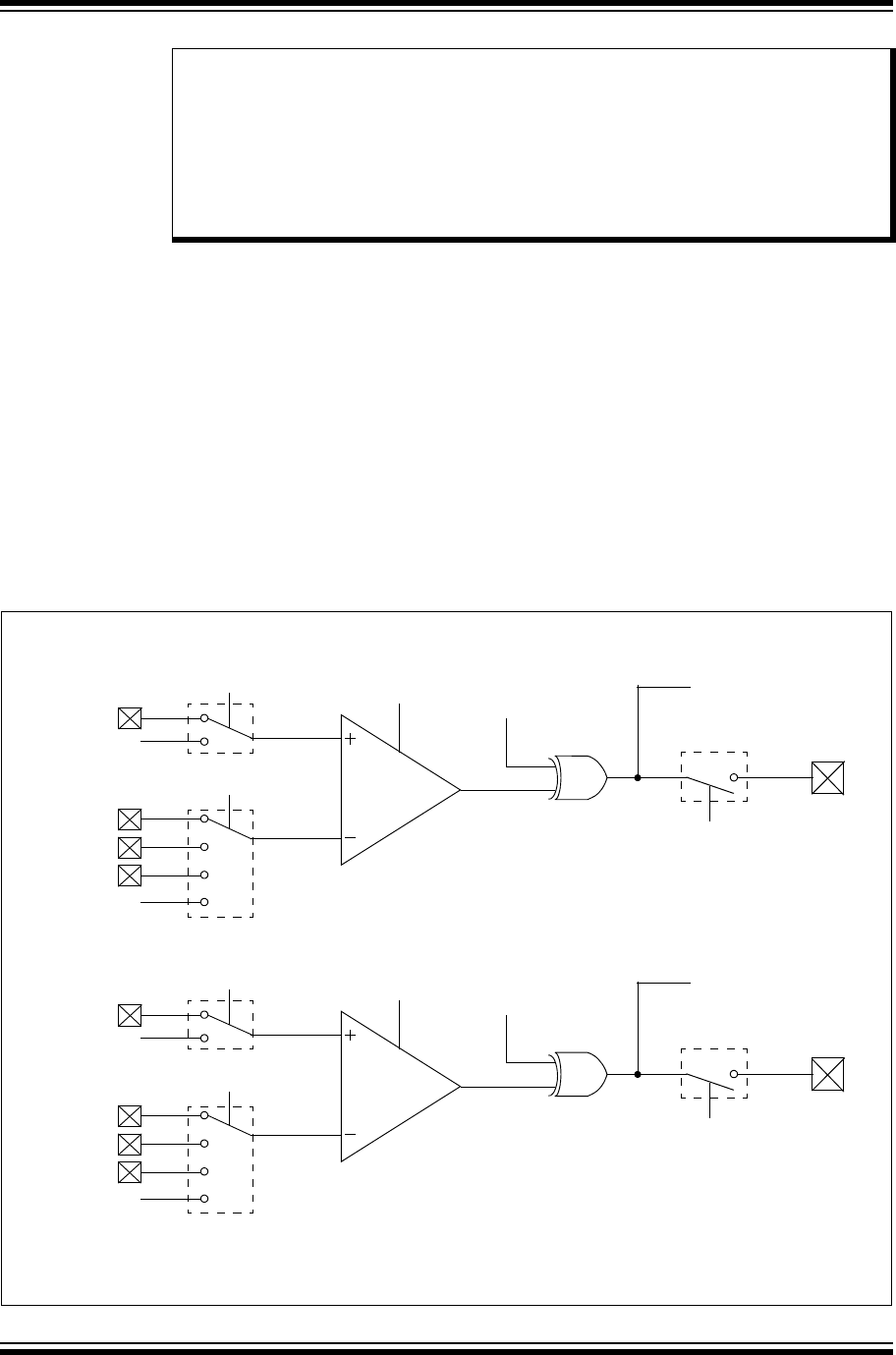
PIC32MX Family Reference Manual
DS61110E-page 19-2 © 2010 Microchip Technology Inc.
19.1 INTRODUCTION
The PIC32MX family Analog Comparator module contains one or more comparator(s) that can
be configured in a variety of ways.
Following are some of the key features of this module:
• Selectable inputs available include:
- Analog inputs multiplexed with I/O pins
- On-Chip Internal Absolute Voltage Reference (IVREF)
-Comparator Voltage Reference (CVREF)
• Outputs can be inverted
• Selectable interrupt generation
A block diagram of the comparator module is illustrated in Figure 19-1.
Figure 19-1: Comparator Block Diagram
Note: This family reference manual section is meant to serve as a complement to device
data sheets. Depending on the device variant, this manual section may not apply to
all PIC32MX devices.
Please consult the note at the beginning of the “Comparator” chapter in the current
device data sheet to check whether this document supports the device you are
using.
Device data sheets and family reference manual sections are available for
download from the Microchip Worldwide Web site at: http://www.microchip.com
C1
CVREF(2)
C1IN+(1)
C1IN+
C1IN-
C1OUT
COUT (CM1CON)
CREF
CCH<1:0>
CPOL
COE
ON
C2IN+
IVREF(2)
C1OUT (CMSTAT)
C2
CVREF(2)
C2IN+
C2IN+
C2IN-
C2OUT
COUT (CM2CON)
CREF
CPOL
COE
ON
C1IN+
IVREF(2)
C2OUT (CMSTAT)
Comparator 2
Comparator 1
CCH<1:0>
Note 1: On devices with a USB module, and when the module is enabled, this pin is controlled by the USB module,
and therefore, is not available as a comparator input.
2: Internally connected.

© 2010 Microchip Technology Inc. DS61110E-page 19-3
Section 19. Comparator
Comparator
19
19.2 COMPARATOR CONTROL REGISTERS
A Comparator module consists of the following Special Function Registers (SFRs):
•CMxCON: Comparator Control Register(1,2,3)
•CMSTAT: Comparator Status Register(1,2,3)
The following table provides a brief summary of all Comparator-related registers. Corresponding
registers appear after the summary, followed by a detailed description of each register.
Note: Each PIC32MX device variant may have one or more Comparator modules. An ‘x’
used in the names of pins, control/status bits and registers denotes the particular
module. Refer to the specific device data sheet for more information.
Table 19-1: Comparator SFRs Summary
Name Bit
31/23/15/7
Bit
30/22/14/6
Bit
29/21/13/5
Bit
28/20/12/4
Bit
27/19/11/3
Bit
26/18/10/2
Bit
25/17/9/1
Bit
24/16/8/0
CMxCON(1,2,3) 31:24 ————————
23:16 ————————
15:8 ON COE CPOL ————COUT
7:0 EVPOL<1:0> — CREF ——CCH<1:0>
CMSTAT(1,2,3) 31:24 ————————
23:16 ————————
15:8 —FRZSIDL—————
7:0 — — — — — — C2OUT C1OUT
Legend: — = unimplemented, read as ‘0’.
Note 1: This register has an associated Clear register at an offset of 0x4 bytes. These registers have the same name with CLR
appended to the end of the register name (e.g., CMxCONCLR). Writing a ‘1’ to any bit position in the Clear register will
clear valid bits in the associated register. Reads from the Clear register should be ignored.
2: This register has an associated Set register at an offset of 0x8 bytes. These registers have the same name with SET
appended to the end of the register name (e.g., CMxCONSET). Writing a ‘1’ to any bit position in the Set register will set
valid bits in the associated register. Reads from the Set register should be ignored.
3: This register has an associated Invert register at an offset of 0xC bytes. These registers have the same name with INV
appended to the end of the register name (e.g., CMxCONINV). Writing a ‘1’ to any bit position in the Invert register will
invert valid bits in the associated register. Reads from the Invert register should be ignored.

PIC32MX Family Reference Manual
DS61110E-page 19-4 © 2010 Microchip Technology Inc.
Register 19-1: CMxCON: Comparator Control Register(1,2,3)
U-0 U-0 U-0 U-0 U-0 U-0 U-0 U-0
— — — — — — — —
bit 31 bit 24
U-0 U-0 U-0 U-0 U-0 U-0 U-0 U-0
— — — — — — — —
bit 23 bit 16
R/W-0 R/W-0 R/W-0 U-0 U-0 U-0 U-0 R-0
ON COE CPOL — — — —COUT
bit 15 bit 8
R/W-1 R/W-1 U-0 R/W-0 U-0 U-0 R/W-1 R/W-1
EVPOL<1:0> — CREF — —CCH<1:0>
bit 7 bit 0
Legend:
R=Readable bit W=Writable bit P=Programmable bit r=Reserved bit
U=Unimplemented bit -n=Bit Value at POR: (‘0’, ‘1’, x=Unknown)
bit 31-16 Unimplemented: Read as ‘0’
bit 15 ON: Comparator ON bit
1 = Module is enabled. Setting this bit does not affect the other bits in this register
0 = Module is disabled and does not consume current. Clearing this bit does not affect the other bits
in this register
Note: When using the 1:1 PBCLK divisor, the user’s software should not read/write the
peripheral’s SFRs in the SYSCLK cycle immediately following the instruction that clears the
module’s ON bit.
bit 14 COE: Comparator Output Enable bit
1 = Comparator output is driven on the output CxOUT pin
0 = Comparator output is not driven on the output CxOUT pin
bit 13 CPOL: Comparator Output Inversion bit
1 = Output is inverted
0 = Output is not inverted
Note: Setting this bit will invert the signal to the comparator interrupt generator as well. This will
result in an interrupt being generated on the opposite edge from the one selected by
EVPOL<1:0>.
bit 12-9 Unimplemented: Read as ‘0’
Note 1: This register has an associated Clear register (CMxCONCLR) at an offset of 0x4 bytes. Writing a ‘1’ to any
bit position in the Clear register will clear valid bits in the associated register. Reads from the Clear register
should be ignored.
2: This register has an associated Set register (CMxCONSET) at an offset of 0x8 bytes. Writing a ‘1’ to any
bit position in the Set register will set valid bits in the associated register. Reads from the Set register
should be ignored.
3: This register has an associated Invert register (CMxCONINV) at an offset of 0xC bytes. Writing a ‘1’ to any
bit position in the Invert register will invert valid bits in the associated register. Reads from the Invert
register should be ignored.
4: For x=1/y=2 or x=2/y=1.

© 2010 Microchip Technology Inc. DS61110E-page 19-5
Section 19. Comparator
Comparator
19
bit 8 COUT: Comparator Output bit
1 = Output of the Comparator is a ‘1’
0 = Output of the Comparator is a ‘0’
bit 7-6 EVPOL<1:0>: Interrupt Event Polarity Select bits
11 = Comparator interrupt is generated on a low-to-high or high-to-low transition of the comparator
output
10 = Comparator interrupt is generated on a high-to-low transition of the comparator output
01 = Comparator interrupt is generated on a low-to-high transition of the comparator output
00 = Comparator interrupt generation is disabled
bit 5 Unimplemented: Read as ‘0’
bit 4 CREF: Comparator Positive Input Configure bit
1 = Comparator non-inverting input is connected to the internal CVREF
0 = Comparator non-inverting input is connected to the CXIN+ pin
bit 3-2 Unimplemented: Read as ‘0’
bit 1-0 CCH<1:0>: Comparator Negative Input Select bits for Comparator
11 = Comparator inverting input is connected to the IVREF
10 = Comparator inverting input is connected to the CyIN+ pin(4)
01 = Comparator inverting input is connected to the CxIN+ pin(4)
00 = Comparator inverting input is connected to the CxIN- pin(4)
Register 19-1: CMxCON: Comparator Control Register(1,2,3) (Continued)
Note 1: This register has an associated Clear register (CMxCONCLR) at an offset of 0x4 bytes. Writing a ‘1’ to any
bit position in the Clear register will clear valid bits in the associated register. Reads from the Clear register
should be ignored.
2: This register has an associated Set register (CMxCONSET) at an offset of 0x8 bytes. Writing a ‘1’ to any
bit position in the Set register will set valid bits in the associated register. Reads from the Set register
should be ignored.
3: This register has an associated Invert register (CMxCONINV) at an offset of 0xC bytes. Writing a ‘1’ to any
bit position in the Invert register will invert valid bits in the associated register. Reads from the Invert
register should be ignored.
4: For x=1/y=2 or x=2/y=1.

PIC32MX Family Reference Manual
DS61110E-page 19-6 © 2010 Microchip Technology Inc.
Register 19-2: CMSTAT: Comparator Status Register(1,2,3)
U-0 U-0 U-0 U-0 U-0 U-0 U-0 U-0
— — — — — — — —
bit 31 bit 24
U-0 U-0 U-0 U-0 U-0 U-0 U-0 U-0
— — — — — — — —
bit 23 bit 16
U-0 R/W-0 R/W-0 U-0 U-0 U-0 U-0 U-0
—FRZSIDL— — — — —
bit 15 bit 8
U-0 U-0 U-0 U-0 U-0 U-0 R-0 R-0
— — — — — —C2OUTC1OUT
bit 7 bit 0
Legend:
R=Readable bit W=Writable bit P=Programmable bit r=Reserved bit
U=Unimplemented bit -n=Bit Value at POR: (‘0’, ‘1’, x=Unknown)
bit 31-15 Unimplemented: Read as ‘0’
bit 14 FRZ: Freeze Control bit
1 = Freeze operation when CPU enters Debug Exception mode
0 = Continue operation when CPU enters Debug Exception mode
Note: FRZ is writable in Debug Exception mode only. It always reads ‘0’ in Normal mode.
bit 13 SIDL: Stop in IDLE Control bit
1 = All Comparator modules are disabled in IDLE mode
0 = All Comparator modules continue to operate in the IDLE mode
bit 12-2 Unimplemented: Read as ‘0’
bit 1 C2OUT: Comparator Output bit
1 = Output of Comparator 2 is a ‘1’
0 = Output of Comparator 2 is a ‘0’
bit 0 C1OUT: Comparator Output bit
1 = Output of Comparator 1 is a ‘1’
0 = Output of Comparator 1 is a ‘0’
Note 1: This register has an associated Clear register (CMSTATCLR) at an offset of 0x4 bytes. Writing a ‘1’ to any
bit position in the Clear register will clear valid bits in the associated register. Reads from the Clear register
should be ignored.
2: This register has an associated Set register (CMSTATSET) at an offset of 0x8 bytes. Writing a ‘1’ to any bit
position in the Set register will set valid bits in the associated register. Reads from the Set register should
be ignored.
3: This register has an associated Invert register (CMSTATINV) at an offset of 0xC bytes. Writing a ‘1’ to any
bit position in the Invert register will invert valid bits in the associated register. Reads from the Invert
register should be ignored.

© 2010 Microchip Technology Inc. DS61110E-page 19-7
Section 19. Comparator
Comparator
19
19.3 COMPARATOR OPERATION
19.3.1 Comparator Configuration
The Comparator module has a flexible input and output configuration to allow the module to be
tailored to the needs of the application. The PIC32MX family Comparator module has individual
control over the enable, output inversion, output on I/O pin and input selections. The VIN+ pin of
each comparator can select from an input pin or the CVREF. The VIN- input of the Comparator
module can select from one of three input pins or the IVREF. In addition, the Comparator module
has two individual comparator event generation control bits. These control bits can be used for
detecting when the output of an individual comparator changes to a desired state or changes
states.
If the comparator mode is changed, the comparator output level may not be valid for the specified
mode change delay (refer to the specific device data sheet for more information).
A single comparator is illustrated in the upper portion of Figure 19-2. The lower portion repre-
sents the relationship between the analog input levels and the digital output. When the analog
input at VIN+ is less than the analog input at VIN-, the output of the comparator is a digital low
level. When the analog input at VIN+ is greater than the analog input VIN-, the output of the com-
parator is a digital high level. The shaded areas of the output of the comparator in the lower por-
tion of Figure 19-2 illustrates the uncertainty that is due to input offsets and the response time of
the comparator.
19.3.2 Comparator Inputs
Depending on the comparator operating mode, the inputs to the comparators may be from two
input pins or a combination of an input pin and one of two internal voltage references. The analog
signal present at VIN- is compared to the signal at VIN+ and the digital output of the comparator
is set or cleared according to the result of the comparison, as illustrated in Figure 19-2.
Figure 19-2: Single Comparator
19.3.2.1 EXTERNAL REFERENCE SIGNAL
An external voltage reference may be used with the comparator by using the output of the reference
as an input to the comparator. Refer to the specific device data sheet for input voltage limits.
Note: Comparator interrupts should be disabled during a comparator mode change;
otherwise, a false interrupt may be generated.
–
+
VIN+
VIN-
Output
Output
VIN-
VIN+

PIC32MX Family Reference Manual
DS61110E-page 19-8 © 2010 Microchip Technology Inc.
19.3.2.2 INTERNAL REFERENCE SIGNALS
The CVREF module and the IVREF can be used as inputs to the comparator, as illustrated in
Figure 19-1. The CVREF provides a user-selectable voltage for use as a comparator reference.
For more information on this module, refer to Section 20. “Comparator Voltage Reference”
(DS61109) in the “PIC32MX Family Reference Manual”. The IVREF has a fixed 1.2V output that
does not change with the device supply voltage. Refer to the specific device data sheet for details
and accuracy of this reference.
19.3.3 Comparator Response Time
Response time is the minimum amount of time that elapses from the moment a change is made
in the input voltage of a comparator to the moment the output reflects the new level. If the internal
reference is changed, the maximum delay of the internal voltage reference must be considered,
when using the comparator outputs. Otherwise, the maximum delay of the comparators should
be used. For more information, refer to the specific device data sheet.
19.3.4 Comparator Outputs
The comparator output is read through the CMSTAT register and the COUT bit (CM2CON<8> or
CM1CON<8>). This bit is read-only. The comparator output may also be directed to an I/O pin
via the CxOUT bit; however, the COUT bit is still valid when the signal is routed to a pin. For the
comparator output to be available on the CxOUT pin, the associated TRIS bit for the output pin
must be configured as an output. When the COUT signal is routed to a pin the signal is the
unsynchronized output of the comparator.
The output of the comparator has a degree of uncertainty. The uncertainty of each of the
comparators is related to the input offset voltage and the response time, as stated in the
specifications. The lower portion of Figure 19-2 provides a graphical representation of this
uncertainty.
The comparator output bit, COUT, provides the latched sampled value of the comparator’s output
when the register was read. There are two common methods used to detect a change in the
comparator output:
•Software polling
•Interrupt generation
19.3.4.1 SOFTWARE POLLING METHOD OF COMPARATOR EVENT
DETECTION
Software polling of COUT is performed by periodically reading the COUT bit. This allows the
output to be read at uniform time intervals. A change in the comparator output is not detected
until the next read of the COUT bit. If the input signal changes at a rate faster than the polling, a
brief change in output may not be detected.
19.3.4.2 INTERRUPT GENERATION METHOD OF COMPARATOR EVENT
DETECTION
Interrupt generation is the other method for detecting a change in the comparator output. The
Comparator module can be configured to generate an interrupt when the COUT bit changes.
An interrupt will be generated when the comparator’s output changes (subject to the interrupt
priorities). This method responds more rapidly to changes than the software polling method;
however, rapidly changing signals will cause an equally large number of interrupts. This can
cause interrupt loading and potentially undetected interrupts due to new interrupts being
generated while the previous interrupt is still being serviced or even before the interrupt can be
serviced. If the input signal changes rapidly, reading the COUT bit in the Interrupt Service
Routine (ISR) may yield a different result than the one that generated the Interrupt. This is due
to the COUT bit representing the value of the comparator output when the bit was read and not
the value that caused the interrupt.
Comparator output and interrupt generation is illustrated in Figure 19-4.
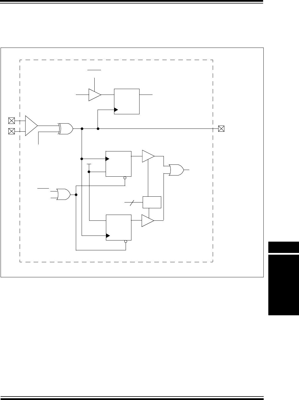
© 2010 Microchip Technology Inc. DS61110E-page 19-9
Section 19. Comparator
Comparator
19
19.3.4.3 CHANGING THE POLARITY OF COMPARATOR OUTPUTS
The polarity of the comparator outputs can be changed using the CPOL bit (CMxCON<13>).
CPOL appears below the comparator Cx on the left side of Figure 19-3.
Figure 19-3: Comparator Output Block Diagram
D
Q
CL
To Cx OU T p in
To Interrupt
CPOL
DQ
CL CL
–
+
D
Q
CL
Freeze
PBCLK CxOUT (CMSTAT)
COUT (CMxCON)
EVPOL
2
Decoder
Reset
Interrupt ACK
CL
C
X
Controller
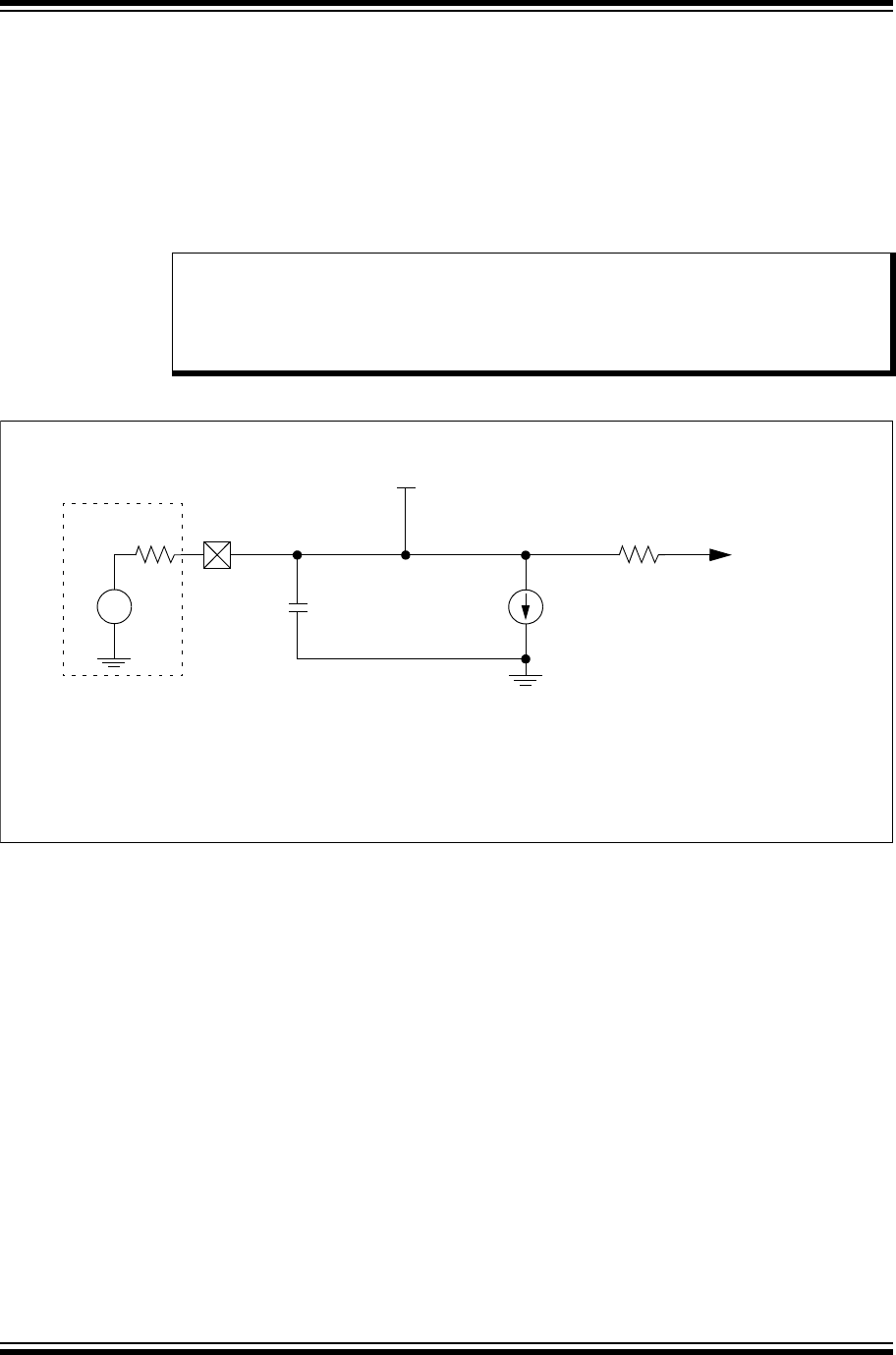
PIC32MX Family Reference Manual
DS61110E-page 19-10 © 2010 Microchip Technology Inc.
19.3.5 Analog Input Connection Considerations
A simplified circuit for an analog input is illustrated in Figure 19-4. A maximum source imped-
ance of 10 kΩ is recommended for the analog sources. Any external component connected to
an analog input pin, such as a capacitor or a Zener diode, should have very little leakage cur-
rent. Refer to the specific device data sheet for input voltage limits. If a pin is to be shared by
two or more analog inputs that are to be used simultaneously, the loading effects of all the mod-
ules involved must be taken into consideration. This loading may reduce the accuracy of one
or more of the modules connected to the common pin. This may also require a lower source
impedance than is stated for a single module with exclusive use of a pin in Analog mode.
Figure 19-4: Comparator Analog Input Model
Note: When reading the PORT register, all pins configured as analog inputs will read as a
‘0’. Pins configured as digital inputs will convert an analog input according to the
Schmitt Trigger input specification.
Analog levels on any pin defined as a digital input may cause the input buffer to
consume more current than is specified.
VA
RS < 10k
AIN
CPIN
5 pF
VDD
RIC
ILEAKAGE
±500 nA
VSS
Comparator
Input
Legend: CPIN = Input Capacitance
ILEAKAGE = Leakage Current at the pin due to various junctions
RIC = Interconnect Resistance
RS = Source Impedance
VA = Analog Voltage

© 2010 Microchip Technology Inc. DS61110E-page 19-11
Section 19. Comparator
Comparator
19
19.4 INTERRUPTS
Each of the available comparators has a dedicated interrupt bit, CMPxIF (IFS1<3> or IFS1<4>),
and a corresponding interrupt enable/mask bit, CMPxIE (IEC1<3> or IEC1<4>). These bits are
used to determine the source of an interrupt and to enable or disable an individual interrupt
source. The priority level of each of the channels can also be set independently of the other
channels.
The CMPxIF bit is set when the CMPx channel detects a predefined match condition that is
defined as an event generating an interrupt. The CMPxIF bit will then be set without regard to the
state of the corresponding CMPxIE bit. The CMPxIF bit can be polled by software if desired.
The CMPxIE bit controls the interrupt generation. If the CMPxIE bit is set, the CPU will be
interrupted whenever a comparator interrupt event occurs and the corresponding CMPxIF bit will
be set (subject to the priority and subpriority as outlined below).
It is the responsibility of the user’s software routine that services a particular interrupt, to clear
the appropriate interrupt flag bit before the service routine is complete.
The priority of each comparator channel can be set independently through the CMPxIP<2:0>
bits. This priority defines the priority group to which the interrupt source will be assigned. The
priority groups range from a value of 7 (the highest priority), to a value of 0 (which does not
generate an interrupt). An interrupt being serviced will be preempted by an interrupt in a higher
priority group.
The subpriority bits allow setting the priority of an interrupt source within a priority group. The
values of the subpriority bit OCxIS<1:0> range from 3 (the highest priority), to 0 (the lowest
priority). An interrupt within the same priority group but having a higher subpriority value will
preempt a lower subpriority interrupt that is in progress.
The priority group and subpriority bits allow more than one interrupt source to share the same
priority and subpriority. If simultaneous interrupts occur in this configuration, the natural order of
the interrupt sources within a priority/subgroup pair determine the interrupt generated. The
natural priority is based on the vector numbers of the interrupt sources. The lower the vector
number, the higher the natural priority of the interrupt. Any interrupts that were overridden by
natural order will then generate their respective interrupts based on priority, subpriority, and
natural order, after the interrupt flag for the current interrupt is cleared.
After an enabled interrupt is generated, the CPU will jump to the vector assigned to that interrupt.
The vector number for the interrupt is the same as the natural order number. The CPU will then
begin executing code at the vector address. The user’s code at this vector address should per-
form any application-specific operations required, such as reloading the duty cycle, clear the
interrupt flag CMPxIF, and then exit. For more information on interrupts, refer to the vector
address table details in Section 8. “Interrupts” (DS61108).

PIC32MX Family Reference Manual
DS61110E-page 19-12 © 2010 Microchip Technology Inc.
Example 19-1: Comparator Initialization with Interrupts Enabled Code Example
Example 19-2: Comparator ISR Code Example
// Configure both comparators to generate an interrupt on any
// output transition
CM1CON = 0xC0D0; // Initialize Comparator 1
// Comparator enabled, output enabled, interrupt on any output
// change, inputs: CVref, C1IN-
CM2CON = 0xA0C2; // Initialize Comparator 2
// Comparator enabled, output enabled, interrupt on any output
// change, inputs: C2IN+, C1IN+
// Enable interrupts for Comparator modules and set priorities
// Set priority to 7 and subpriority to 3
IPC7SET = 0x00000700; // Set CMP1 interrupt subpriority
IFS1CLR = 0x00000008; // Clear the CMP1 interrupt flag
IEC1SET = 0x00000008; // Enable CMP1 interrupt
IPC7SET = 0x00070000; // Set CMP2 interrupt sub priority
IFS1CLR = 0x000000010; // Clear the CMP2 interrupt flag
IEC1SET = 0x000000010; // Enable CMP2 interrupt
// Insert user code here
void__ISR(_COMPARATOR_2_VECTOR, ipl4)Cmp2_IntHandler(void)
{
// Insert user code here
IFS1CLR = 0x00000010; // Clear the CMP2 interrupt flag
}
void__ISR(_COMPARATOR_1_VECTOR, ipl4)Cmp1_IntHandler(void)
{
// Insert code user here
IFS1CLR = 0x00000008; // Clear the CMP1 interrupt flag
}

© 2010 Microchip Technology Inc. DS61110E-page 19-13
Section 19. Comparator
Comparator
19
19.5 OPERATION IN POWER-SAVING AND DEBUG MODES
19.5.1 Comparator Operation During Idle Mode
When a comparator is active and the device is placed in Idle mode, the comparator remains
active and interrupts are generated (if enabled); if SIDL = 1 (CMSTAT<13>), the comparators are
disabled in Idle mode.
19.5.2 Comparator Operation During Sleep Mode
When a comparator is active and the device is placed in Sleep mode, the comparator remains
active and the interrupt is functional (if enabled). This interrupt will wake up the device from Sleep
mode (when enabled). Each operational comparator will consume additional current, as shown
in the comparator specifications. To minimize power consumption while in Sleep mode, turn off
the comparators: ON = 0 (CMxCON<15>), prior to entering Sleep mode. If the device wakes up
from Sleep mode, the contents of the CMxCON register are not affected. For additional
information on Sleep mode, refer to Section 10. “Power-Saving Modes” (DS61130).
19.5.3 Comparator Operation in Debug Mode
The FRZ bit (CMSTAT<14>) determines whether the Comparator module will run or stop while
the CPU is executing debug exception code (i.e., application is halted) in Debug mode. When
FRZ = 0, the Comparator module continues to run even when application is halted in Debug
mode. When FRZ = 1 and application is halted in Debug mode, the module will freeze its
operations and make no changes to the state of the Comparator module. The module will resume
its operation after the CPU resumes execution.
19.6 EFFECTS OF A RESET
All Resets force the CMxCON registers to its Reset state, causing the comparator modules to be
turned off (CMxCON<15> = 0). However, the input pins multiplexed with analog input sources
are configured as analog inputs by default on device Reset. The I/O configuration for these pins
is determined by the setting the AD1PCFG register.
Note: The FRZ bit is readable and writable only when the CPU is executing in Debug
Exception mode. In all other modes, the FRZ bit reads as ‘0’. If the FRZ bit is
changed during Debug mode, the new value does not take effect until the current
Debug Exception mode is exited and re-entered. During the Debug Exception
mode, the FRZ bit reads the state of the peripheral when entering Debug mode.

PIC32MX Family Reference Manual
DS61110E-page 19-14 © 2010 Microchip Technology Inc.
19.7 RELATED APPLICATION NOTES
This section lists application notes that are related to this section of the manual. These
application notes may not be written specifically for the PIC32MX device family, but the concepts
are pertinent and could be used with modification and possible limitations. The current
application notes related to the Comparator module are:
Title Application Note #
No related application notes at this time N/A
Note: Please visit the Microchip web site (www.microchip.com) for additional application
notes and code examples for the PIC32MX family of devices.

© 2010 Microchip Technology Inc. DS61110E-page 19-15
Section 19. Comparator
Comparator
19
19.8 REVISION HISTORY
Revision A (October 2007)
This is the initial released version of this document.
Revision B (October 2007)
Updated document to remove Confidential status.
Revision C (April 2008)
Revised status to Preliminary; Revised U-0 to r-x.
Revision D (May 2008)
Revised Figure 19-1; Revised Registers 19-1, 19-5, 19-13, 19-14, 19-15; Revised Example 19-2;
Revised Section 19.5, pin names; Change Reserved bits from “Maintain as” to “Write”; Added
Note to ON bit (CM1CON/CM2CON Registers).
Revision E (November 2010)
This revision includes the following updates:
•Notes:
- Added a note at the beginning of the section, which provides information on
complementary documentation.
• Updated all Reserved bits as Unimplemented bits in Register 19-1 and Register 19-2.
•Changed Figure 19-1.
•Removed CMxCON and CMSTAT registers along with their corresponding CLR, SET and
INV registers and added the following Note in Ta b le 1 9-1
- All registers in this table have corresponding CLR, SET and INV registers at their
virtual addresses, plus offset of 0X04, 0X08 and 0X0C respectively.
•Removed IFS1, IEC1, IPC1 registers and their corresponding CLR, SET and INV registers.
•Removed Table 19-2 from 19.4 “Interrupts”.
•Removed section 19.5 “I/O Pin Control”.
•Minor changes to the text and formatting have been incorporated throughout the document.

PIC32MX Family Reference Manual
DS61110E-page 19-16 © 2010 Microchip Technology Inc.
NOTES:

© 2010 Microchip Technology Inc. DS61110E-page 19-17
Information contained in this publication regarding device
applications and the like is provided only for your convenience
and may be superseded by updates. It is your responsibility to
ensure that your application meets with your specifications.
MICROCHIP MAKES NO REPRESENTATIONS OR
WARRANTIES OF ANY KIND WHETHER EXPRESS OR
IMPLIED, WRITTEN OR ORAL, STATUTORY OR
OTHERWISE, RELATED TO THE INFORMATION,
INCLUDING BUT NOT LIMITED TO ITS CONDITION,
QUALITY, PERFORMANCE, MERCHANTABILITY OR
FITNESS FOR PURPOSE. Microchip disclaims all liability
arising from this information and its use. Use of Microchip
devices in life support and/or safety applications is entirely at
the buyer’s risk, and the buyer agrees to defend, indemnify and
hold harmless Microchip from any and all damages, claims,
suits, or expenses resulting from such use. No licenses are
conveyed, implicitly or otherwise, under any Microchip
intellectual property rights.
Trademarks
The Microchip name and logo, the Microchip logo, dsPIC,
KEELOQ, KEELOQ logo, MPLAB, PIC, PICmicro, PICSTART,
PIC32 logo, rfPIC and UNI/O are registered trademarks of
Microchip Technology Incorporated in the U.S.A. and other
countries.
FilterLab, Hampshire, HI-TECH C, Linear Active Thermistor,
MXDEV, MXLAB, SEEVAL and The Embedded Control
Solutions Company are registered trademarks of Microchip
Technology Incorporated in the U.S.A.
Analog-for-the-Digital Age, Application Maestro, CodeGuard,
dsPICDEM, dsPICDEM.net, dsPICworks, dsSPEAK, ECAN,
ECONOMONITOR, FanSense, HI-TIDE, In-Circuit Serial
Programming, ICSP, Mindi, MiWi, MPASM, MPLAB Certified
logo, MPLIB, MPLINK, mTouch, Omniscient Code
Generation, PICC, PICC-18, PICDEM, PICDEM.net, PICkit,
PICtail, REAL ICE, rfLAB, Select Mode, Total Endurance,
TSHARC, UniWinDriver, WiperLock and ZENA are
trademarks of Microchip Technology Incorporated in the
U.S.A. and other countries.
SQTP is a service mark of Microchip Technology Incorporated
in the U.S.A.
All other trademarks mentioned herein are property of their
respective companies.
© 2010, Microchip Technology Incorporated, Printed in the
U.S.A., All Rights Reserved.
Printed on recycled paper.
ISBN: 978-1-60932-654-8
Note the following details of the code protection feature on Microchip devices:
• Microchip products meet the specification contained in their particular Microchip Data Sheet.
• Microchip believes that its family of products is one of the most secure families of its kind on the market today, when used in the
intended manner and under normal conditions.
• There are dishonest and possibly illegal methods used to breach the code protection feature. All of these methods, to our
knowledge, require using the Microchip products in a manner outside the operating specifications contained in Microchip’s Data
Sheets. Most likely, the person doing so is engaged in theft of intellectual property.
• Microchip is willing to work with the customer who is concerned about the integrity of their code.
• Neither Microchip nor any other semiconductor manufacturer can guarantee the security of their code. Code protection does not
mean that we are guaranteeing the product as “unbreakable.”
Code protection is constantly evolving. We at Microchip are committed to continuously improving the code protection features of our
products. Attempts to break Microchip’s code protection feature may be a violation of the Digital Millennium Copyright Act. If such acts
allow unauthorized access to your software or other copyrighted work, you may have a right to sue for relief under that Act.
Microchip received ISO/TS-16949:2002 certification for its worldwide
headquarters, design and wafer fabrication facilities in Chandler and
Tempe, Arizona; Gresham, Oregon and design centers in California
and India. The Company’s quality system processes and procedures
are for its PIC® MCUs and dsPIC® DSCs, KEELOQ® code hopping
devices, Serial EEPROMs, microperipherals, nonvolatile memory and
analog products. In addition, Microchip’s quality system for the design
and manufacture of development systems is ISO 9001:2000 certified.

DS61110E-page 19-18 © 2010 Microchip Technology Inc.
AMERICAS
Corporate Office
2355 West Chandler Blvd.
Chandler, AZ 85224-6199
Tel: 480-792-7200
Fax: 480-792-7277
Technical Support:
http://support.microchip.com
Web Address:
www.microchip.com
Atlanta
Duluth, GA
Tel: 678-957-9614
Fax: 678-957-1455
Boston
Westborough, MA
Tel: 774-760-0087
Fax: 774-760-0088
Chicago
Itasca, IL
Tel: 630-285-0071
Fax: 630-285-0075
Cleveland
Independence, OH
Tel: 216-447-0464
Fax: 216-447-0643
Dallas
Addison, TX
Tel: 972-818-7423
Fax: 972-818-2924
Detroit
Farmington Hills, MI
Tel: 248-538-2250
Fax: 248-538-2260
Kokomo
Kokomo, IN
Tel: 765-864-8360
Fax: 765-864-8387
Los Angeles
Mission Viejo, CA
Tel: 949-462-9523
Fax: 949-462-9608
Santa Clara
Santa Clara, CA
Tel: 408-961-6444
Fax: 408-961-6445
Toronto
Mississauga, Ontario,
Canada
Tel: 905-673-0699
Fax: 905-673-6509
ASIA/PACIFIC
Asia Pacific Office
Suites 3707-14, 37th Floor
Tower 6, The Gateway
Harbour City, Kowloon
Hong Kong
Tel : 8 52 - 24 0 1- 120 0
Fax: 852-2401-3431
Australia - Sydney
Tel : 6 1-2 -98 68- 6 73 3
Fax: 61-2-9868-6755
China - Beijing
Tel : 8 6-1 0-8 528 - 21 0 0
Fax: 86-10-8528-2104
China - Chengdu
Tel : 8 6-2 8-8 665 - 55 11
Fax: 86-28-8665-7889
China - Chongqing
Tel : 8 6-2 3-8 980 - 95 8 8
Fax: 86-23-8980-9500
China - Hong Kong SAR
Tel : 8 52 - 24 0 1- 120 0
Fax: 852-2401-3431
China - Nanjing
Tel : 8 6-2 5-8 473 - 24 6 0
Fax: 86-25-8473-2470
China - Qingdao
Tel : 8 6-5 32- 8502 -73 55
Fax: 86-532-8502-7205
China - Shanghai
Tel : 8 6-2 1-5 407 - 55 3 3
Fax: 86-21-5407-5066
China - Shenyang
Tel : 8 6-2 4-2 334 - 28 2 9
Fax: 86-24-2334-2393
China - Shenzhen
Tel : 8 6-7 55- 8203 -26 60
Fax: 86-755-8203-1760
China - Wuhan
Tel : 8 6-2 7-5 980 - 53 0 0
Fax: 86-27-5980-5118
China - Xian
Tel : 8 6-2 9-8 833 - 72 5 2
Fax: 86-29-8833-7256
China - Xiamen
Tel: 86-592-2388138
Fax: 86-592-2388130
China - Zhuhai
Tel : 86- 756 -3 210 04 0
Fax: 86-756-3210049
ASIA/PACIFIC
India - Bangalore
Tel : 9 1- 8 0- 309 0-4 444
Fax: 91-80-3090-4123
India - New Delhi
Tel : 9 1- 11 -41 60- 86 31
Fax: 91-11-4160-8632
India - Pune
Tel : 9 1- 2 0- 256 6-1 512
Fax: 91-20-2566-1513
Japan - Yokohama
Tel : 8 1- 4 5- 471 - 6 166
Fax: 81-45-471-6122
Korea - Daegu
Tel : 8 2- 5 3- 744 -43 01
Fax: 82-53-744-4302
Korea - Seoul
Tel : 8 2- 2 -5 54- 720 0
Fax: 82-2-558-5932 or
82-2-558-5934
Malaysia - Kuala Lumpur
Tel : 6 0- 3 -6 201 -98 57
Fax: 60-3-6201-9859
Malaysia - Penang
Tel : 6 0- 4 -2 27- 887 0
Fax: 60-4-227-4068
Philippines - Manila
Tel : 6 3- 2 -6 34- 906 5
Fax: 63-2-634-9069
Singapore
Tel : 6 5- 6 33 4 -8 870
Fax: 65-6334-8850
Taiwan - Hsin Chu
Tel : 8 86 - 3- 657 8-3 00
Fax: 886-3-6578-370
Taiwan - Kaohsiung
Tel : 8 86 - 7- 213 -78 30
Fax: 886-7-330-9305
Taiwan - Taipei
Tel : 8 86 - 2- 250 0-6 610
Fax: 886-2-2508-0102
Thailand - Bangkok
Tel : 6 6- 2 -6 94- 135 1
Fax: 66-2-694-1350
EUROPE
Austria - Wels
Tel : 4 3- 7 24 2 -2 244 -39
Fax: 43-7242-2244-393
Denmark - Copenhagen
Tel : 4 5-4 450 -2 828
Fax: 45-4485-2829
France - Paris
Tel : 3 3-1 -6 9-5 3 -6 3-2 0
Fax: 33-1-69-30-90-79
Germany - Munich
Tel : 4 9- 8 9- 627 -14 4-0
Fax: 49-89-627-144-44
Italy - Milan
Tel : 3 9- 0 33 1 -7 426 11
Fax: 39-0331-466781
Netherlands - Drunen
Tel : 3 1- 4 16 - 690 3 99
Fax: 31-416-690340
Spain - Madrid
Tel : 3 4- 9 1- 708 -08 -90
Fax: 34-91-708-08-91
UK - Wokingham
Tel : 4 4- 11 8-9 21- 58 69
Fax: 44-118-921-5820
Worldwide Sales and Service
08/04/10

© 2007-2012 Microchip Technology Inc. DS61109G-page 20-1
Comparator
Voltage Reference
20
Section 20. Comparator Voltage Reference
HIGHLIGHTS
This section of the manual contains the following major topics:
20.1 Introduction .................................................................................................................. 20-2
20.2 Comparator Voltage Reference Control Register......................................................... 20-3
20.3 Operation ..................................................................................................................... 20-4
20.4 Interrupts...................................................................................................................... 20-6
20.5 I/O Pin Control .............................................................................................................20-6
20.6 Operation in Power-Saving and Debug Modes............................................................ 20-7
20.7 Effects of Resets .......................................................................................................... 20-7
20.8 Related Application Notes............................................................................................20-8
20.9 Revision History ...........................................................................................................20-9
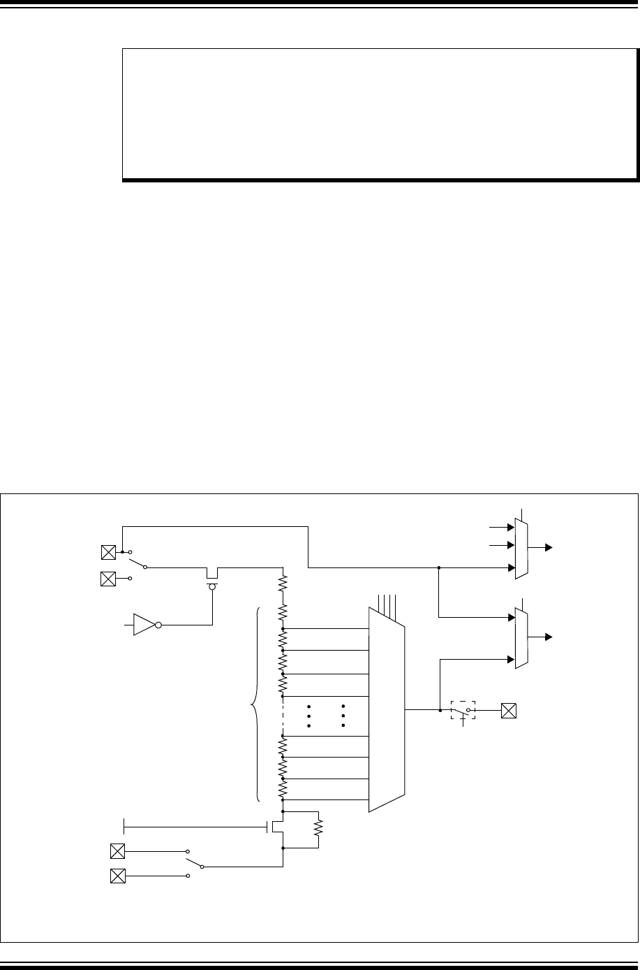
PIC32 Family Reference Manual
DS61109G-page 20-2 © 2007-2012 Microchip Technology Inc.
20.1 INTRODUCTION
The Comparator Voltage Reference module is a 16-tap, resistor ladder network that provides a
selectable reference voltage. Although its primary purpose is to provide a reference for the
analog comparators, it also may be used independently of them.
A block diagram of the module is illustrated in Figure 20-1. The resistor ladder is segmented to
provide two ranges of voltage reference values and has a power-down function to conserve power
when the reference is not used. The module’s supply reference can be provided from either device
AVDD/AVSS or an external voltage reference. The module output is available for the comparators
and typically available for pin output. For more information, refer to the “Comparator Voltage
Reference” chapter in the specific device data sheet.
The Comparator Voltage Reference module has the following features:
•High-range and low-range selection
•Sixteen output levels available for each range
• Internally connected to comparators to conserve device pins
•Output can be connected to a pin
Figure 20-1: Comparator Voltage Reference Block Diagram
Note: This family reference manual section is meant to serve as a complement to device
data sheets. Depending on the device variant, this manual section may not apply to
all PIC32 devices.
Please consult the note at the beginning of the “Comparator Voltage Reference”
chapter in the current device data sheet to check whether this document supports
the device you are using.
Device data sheets and family reference manual sections are available for
download from the Microchip Worldwide Web site at: http://www.microchip.com
16-to-1 MUX
CVR<3:0>
8R
R
CVREN
CVRSS = 0
AVDD
VREF+CVRSS = 1
8R
CVRSS = 0
VREF-CVRSS = 1
R
R
R
R
R
R
16 Steps
CVRR
CVREFOUT
AVSS
CVRCON<CVROE>
CVREFOUT
IVREF
VREFSEL(1)
CVRSRC
BGSEL<1:0>(1)
1.2V
0.6V
Note 1: These bits are not available on all devices. On such devices, CVREF is generated by the resistor network and IVREF
is connected to 1.2V. Refer to the “Comparator Voltage Reference” chapter in the specific device data sheet for
availability.

© 2007-2012 Microchip Technology Inc. DS61109G-page 20-3
Section 20. Comparator Voltage Reference
Comparator
Voltage Reference
20
20.2 COMPARATOR VOLTAGE REFERENCE CONTROL REGISTER
Register 20-1: CVRCON: Comparator Voltage Reference Control Register
Bit
Range
Bit
31/23/15/7
Bit
30/22/14/6
Bit
29/21/13/5
Bit
28/20/12/4
Bit
27/19/11/3
Bit
26/18/10/2
Bit
25/17/9/1
Bit
24/16/8/0
31:24 U-0 U-0 U-0 U-0 U-0 U-0 U-0 U-0
— — — — — — — —
23:16 U-0 U-0 U-0 U-0 U-0 U-0 U-0 U-0
— — — — — — — —
15:8 R/W-0 U-0 U-0 U-0 U-0 R/W-0 R/W-0 R/W-1
ON(1) — — — — VREFSEL(2) BGSEL<1:0>(2)
7:0 U-0 R/W-0 R/W-0 R/W-0 R/W-0 R/W-0 R/W-0 R/W-0
—CVROE CVRR CVRSS CVR<3:0>
Legend:
R = Readable bit W = Writable bit U = Unimplemented bit, read as ‘0’
-n = Value at POR ‘1’ = Bit is set ‘0’ = Bit is cleared x = Bit is unknown
bit 31-16 Unimplemented: Read as ‘0’
bit 15 ON: Comparator Voltage Reference On bit(1)
1 = Module is enabled, setting this bit does not affect other bits in the register.
0 = Module is disabled and does not consume current. Clearing this bit does not affect the other bits in the
register
bit 14-11 Un imp le mn ted: Read as ‘0’
bit 10 VREFSEL: Voltage Reference Select bit(2)
1 = CVREF = VREF+
0 = CVREF is generated by the resistor network
bit 9-8 BGSEL<1:0>: Band Gap Reference Source bits(2)
11 = IVREF = VREF+
10 = Reserved
01 = IVREF = 0.6V (nominal, default)
00 = IVREF = 1.2V (nominal)
bit 7 Unimplemented: Read as ‘0’
bit 6 CVROE: CVREFOUT Enable bit
1 = Voltage level is output on CVREFOUT pin
0 = Voltage level is disconnected from CVREFOUT pin
bit 5 CVRR: CVREF Range Selection bit
1 = 0 to 0.67 CVRSRC, with CVRSRC/24 step size
0 = 0.25 CVRSRC to 0.75 CVRSRC, with CVRSRC/32 step size
bit 4 CVRSS: CVREF Source Selection bit
1 = Comparator voltage reference source, CVRSRC = (VREF+) – (VREF-)
0 = Comparator voltage reference source, CVRSRC = AVDD – AVSS
bit 3-0 CVR<3:0>: CVREF Value Selection 0 CVR<3:0> 15 bits
When CVRR = 1:
CVREF = (CVR<3:0>/24) (CVRSRC)
When CVRR = 0:
CVREF = 1/4 (CVRSRC) + (CVR<3:0>/32) (CVRSRC)
Note 1: When using 1:1 PBCLK divisor, the user software should not read or write the peripheral’s SFRs in the
SYSCLK cycle immediately following the instruction that clears the module’s ON bit.
2: These bits are not available on all devices and the reset value is ‘0’ for devices without these bits. Refer to
the “Comparator Voltage Reference” chapter in the specific device data sheet for availability.

PIC32 Family Reference Manual
DS61109G-page 20-4 © 2007-2012 Microchip Technology Inc.
20.3 OPERATION
20.3.1 CVREF Output
The Comparator Voltage Reference module is controlled through the CVRCON register
(Register 20-1). This module provides two ranges of output voltage, each with 16 distinct levels.
The range to be used is selected by the CVRR bit (CVRCON<5>). The primary difference
between the ranges is the size of the steps selected by the CV
REF value selection bits,
CVR<3:0>, with one range offering finer resolution and the other offering a wider range of output
voltage. The typical output voltages are listed in Ta ble 20-1.
The equations used to calculate the CVREF output are as follows:
If CVRR = 1:Voltage Reference = ((CVR<3:0>)/24) x (CVRSRC)
If CVRR = 0: Voltage Reference = (CVRSRC/4) + ((CVR<3:0>)/32) x (CVRSRC)
The CVREF Source Voltage (CVRSRC) can come from either AVDD and AVSS, or the external
VREF+ and VREF- pins that are multiplexed with I/O pins. The voltage source is selected by the
CVRSS bit (CVRCON<4>). The voltage reference is output to the CVREFOUT pin by setting the
CVROE bit (CVRCON<6>), which overrides the corresponding TRIS bit setting.
The settling time of the Comparator Voltage Reference module must be considered when
changing the CVREF output. For more information, refer to the “Comparator Voltage
Reference” chapter in the specific device data sheet.
Table 20-1: Typical Voltage Reference in Volts (CVRSRC = 3.3)
CVR<3:0>
Voltage Reference
CVRR = 0 (CVRCON<5>) CVRR = 1 (CVRCON<5>)
00.83V 0.00V
10.93V 0.14V
21.03V 0.28V
31.13V 0.41V
41.24V 0.55V
51.34V 0.69V
61.44V 0.83V
71.55V 0.96V
81.65V 1.10V
91.75V 1.24V
10 1.86V 1.38V
11 1.96V 1.51V
12 2.06V 1.65V
13 2.17V 1.79V
14 2.27V 1.93V
15 2.37V 2.06V

© 2007-2012 Microchip Technology Inc. DS61109G-page 20-5
Section 20. Comparator Voltage Reference
Comparator
Voltage Reference
20
20.3.2 CVREF Output Considerations
The full range of voltage reference cannot be realized due to the construction of the module. The
transistors on the top and bottom of the resistor ladder network (see Figure 20-1) keep the volt-
age reference from approaching the reference source rails. The voltage reference is derived from
the reference source. Therefore, the voltage reference output changes with fluctuations in that
source. Refer to the “Electrical Characteristics” chapter in the specific device data sheet for
the electrical specifications. Tabl e 20-2 lists the typical output impedances for the Comparator
Voltage Reference module.
20.3.3 IVREF Output
The Comparator Voltage Reference module provides selection for the internal voltage reference.
The Band Gap Reference Source Select bits (BGSEL<1:0>) allow voltage selection of 1.2V or
0.6V, which is generated internally. Refer to the “Electrical Characteristics” chapter in the
specific device data sheet for the IVREF specifications.
Table 20-2: Typical CVREF Output Impedance in kilohms
CVR<3:0>
Voltage Reference
CVRR = 0 (CVRCON<5>) CVRR = 1 (CVRCON<5>)
012k 0.5k
113k 1.9k
213.8k 3.7k
314.4k 5.3k
415k 6.7k
515.4k 7.9k
615.8k 9k
715.9k 9.9k
816k 10.7k
915.9k 11.3k
10 15.8k 11.7k
11 15.4k 11.9k
12 15k 12k
13 14.4k 11.9k
14 13.8k 11.7k
15 12.9k 11.3k
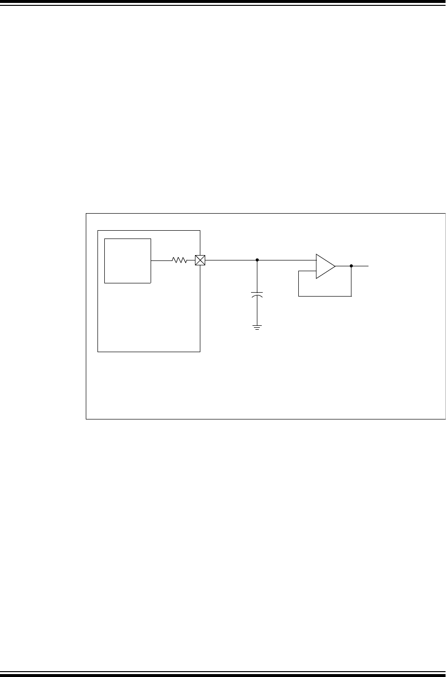
PIC32 Family Reference Manual
DS61109G-page 20-6 © 2007-2012 Microchip Technology Inc.
20.4 INTERRUPTS
There are no Interrupt Configuration registers or bits for the Comparator Voltage Reference
module. The Comparator Voltage Reference module does not generate interrupts.
20.5 I/O PIN CONTROL
The Comparator Voltage Reference module can output to a pin. When the module is enabled and
the CVROE bit (CVRCON<6>) is ‘1’, the output driver for the CVREFOUT pin is disabled and the
CVREF voltage is available at the pin.
For operation, the TRISx bit corresponding to the CVREFOUT pin must be a ‘1’. This disables the
digital input mode for the pin and prevents undesired current draw resulting from applying an
analog voltage to a digital input pin. The output buffer has very limited drive capability. An external
buffer amplifier is recommended for any application that uses the CVREF voltage externally. An
output capacitor may be used to reduce output noise. Use of an output capacitor will increase
settling time (see Figure 20-2).
Figure 20-2: Comparator Voltage Reference Output Buffer Example
Buffered Voltage
Reference Output
Comparator
Voltage
Reference
Module Voltage
Reference
Output
Impedance
R(1)
CVREF
Note 1: R is dependent on the Comparator Voltage Reference Control bits CVRR (CVRCON<5>)
and CVR<3:0> (CVRCON<3:0>). For more information, see Ta ble 20 -2 .
2: Use of an output capacitor will increase settling time. Capacitor value selection is dependent
on the CVR<3:0> and CVRR settings, and the frequency to be attenuated.
+
–
C
(2)

© 2007-2012 Microchip Technology Inc. DS61109G-page 20-7
Section 20. Comparator Voltage Reference
Comparator
Voltage Reference
20
20.6 OPERATION IN POWER-SAVING AND DEBUG MODES
20.6.1 Operation in Sleep Mode
The Comparator Voltage Reference module continues to operate in Sleep mode. The CVRCON
register is not affected when the device enters or wakes from Sleep mode. If the CVREF voltage
is not used in Sleep mode, the module can be disabled by clearing the ON bit (CVRCON<15>)
prior to entering Sleep mode to conserve power.
20.6.2 Operation in Idle Mode
The Comparator Voltage Reference module continues to operate in Idle mode. The CVRCON
register is not affected when the device enters or exits Idle mode. There is no provision to auto-
matically disable the module in Idle mode. If the CVREF voltage is not used in Idle mode, the
module can be disabled by clearing the ON bit (CVRCON<15>) prior to entering Idle mode to
conserve power.
20.6.3 Operation in Debug Mode
The Comparator Voltage Reference module continues to operate while the device is in Debug
mode. The module does not support Freeze mode.
20.7 EFFECTS OF RESETS
All resets disable the voltage reference by forcing all bits in the CVRCON register to ‘0’.

PIC32 Family Reference Manual
DS61109G-page 20-8 © 2007-2012 Microchip Technology Inc.
20.8 RELATED APPLICATION NOTES
This section lists application notes that are related to this section of the manual. These
application notes may not be written specifically for the PIC32 family device family, but the
concepts are pertinent and could be used with modification and possible limitations. The current
application notes related to the Comparator Voltage Reference module are:
Title Application Note #
Related application notes are not available. N/A
Note: Please visit the Microchip web site (www.microchip.com) for additional application
notes and code examples for the PIC32 family of devices.

© 2007-2012 Microchip Technology Inc. DS61109G-page 20-9
Section 20. Comparator Voltage Reference
Comparator
Voltage Reference
20
20.9 REVISION HISTORY
Revision A (October 2007)
This is the initial released version of this document.
Revision B (October 2007)
Updated document to remove Confidential status.
Revision C (April 2008)
Revised status to Preliminary; Revised U-0 to r-x.
Revision D (June 2008)
Revised Figure 20-1; Change Reserved bits from “Maintain as” to “Write”; Added Note to ON bit
(CVRCON Register).
Revision E (August 2010)
This revision includes the following updates:
•Updated the Comparator Voltage Reference Block Diagram (see Figure 20-1)
•Added notes regarding the INV, SET, and CLR registers to the Oscillators SFR Summary
(see Table 20-1)
•Updated the Comparator Voltage Reference Control Register (see Register 20-1)
•Removed the CVRCONINV, CVRCONSET, and CVRCONCLR registers
•Removed 20.3.3 “Initialization”
•Added new section 20.3.3 “IVREF Output”
• Removed Table 20-4: Pins Associated with a Comparator
•Removed 20.8 “Design Tips”
• Minor corrections to formatting and text were incorporated throughout the document
Revision F (May 2011)
This revision includes the following updates:
•Updated the Comparator Voltage Reference Block Diagram (see Figure 20-1)
• Removed the Comparator Voltage Reference SFR Summary (Table 20-1) and related text
•Updated the BGSEL<1:0> bit value for ‘10’ to Reserved and modified the Notes in the
CVRCON register (see Register 20-1)
• Updated the allowable voltage reference selections in 20.3.3 “IVREF Output”
•Minor updates to text and formatting were incorporated throughout the document
Revision G (May 2012)
This revision includes the following updates:
•Changed references to VSS and VDD to: AVSS and AVDD, respectively, in
20.1 “Introduction” and 20.3.1 “CVREF Output”
•Minor updates to text and formatting were incorporated throughout the document

PIC32 Family Reference Manual
DS61109G-page 20-10 © 2007-2012 Microchip Technology Inc.
NOTES:

2007-2012 Microchip Technology Inc. DS61109G-page 20 -11
Information contained in this publication regarding device
applications and the like is provided only for your convenience
and may be superseded by updates. It is your responsibility to
ensure that your application meets with your specifications.
MICROCHIP MAKES NO REPRESENTATIONS OR
WARRANTIES OF ANY KIND WHETHER EXPRESS OR
IMPLIED, WRITTEN OR ORAL, STATUTORY OR
OTHERWISE, RELATED TO THE INFORMATION,
INCLUDING BUT NOT LIMITED TO ITS CONDITION,
QUALITY, PERFORMANCE, MERCHANTABILITY OR
FITNESS FOR PURPOSE. Microchip disclaims all liability
arising from this information and its use. Use of Microchip
devices in life support and/or safety applications is entirely at
the buyer’s risk, and the buyer agrees to defend, indemnify and
hold harmless Microchip from any and all damages, claims,
suits, or expenses resulting from such use. No licenses are
conveyed, implicitly or otherwise, under any Microchip
intellectual property rights.
Trademarks
The Microchip name and logo, the Microchip logo, dsPIC,
KEELOQ, KEELOQ logo, MPLAB, PIC, PICmicro, PICSTART,
PIC32 logo, rfPIC and UNI/O are registered trademarks of
Microchip Technology Incorporated in the U.S.A. and other
countries.
FilterLab, Hampshire, HI-TECH C, Linear Active Thermistor,
MXDEV, MXLAB, SEEVAL and The Embedded Control
Solutions Company are registered trademarks of Microchip
Technology Incorporated in the U.S.A.
Analog-for-the-Digital Age, Application Maestro, chipKIT,
chipKIT logo, CodeGuard, dsPICDEM, dsPICDEM.net,
dsPICworks, dsSPEAK, ECAN, ECONOMONITOR,
FanSense, HI-TIDE, In-Circuit Serial Programming, ICSP,
Mindi, MiWi, MPASM, MPLAB Certified logo, MPLIB,
MPLINK, mTouch, Omniscient Code Generation, PICC,
PICC-18, PICDEM, PICDEM.net, PICkit, PICtail, REAL ICE,
rfLAB, Select Mode, Total Endurance, TSHARC,
UniWinDriver, WiperLock and ZENA are trademarks of
Microchip Technology Incorporated in the U.S.A. and other
countries.
SQTP is a service mark of Microchip Technology Incorporated
in the U.S.A.
All other trademarks mentioned herein are property of their
respective companies.
© 2007-2012, Microchip Technology Incorporated, Printed in
the U.S.A., All Rights Reserved.
Printed on recycled paper.
ISBN: 978-1-62076-303-2
Note the following details of the code protection feature on Microchip devices:
• Microchip products meet the specification contained in their particular Microchip Data Sheet.
• Microchip believes that its family of products is one of the most secure families of its kind on the market today, when used in the
intended manner and under normal conditions.
• There are dishonest and possibly illegal methods used to breach the code protection feature. All of these methods, to our
knowledge, require using the Microchip products in a manner outside the operating specifications contained in Microchip’s Data
Sheets. Most likely, the person doing so is engaged in theft of intellectual property.
• Microchip is willing to work with the customer who is concerned about the integrity of their code.
• Neither Microchip nor any other semiconductor manufacturer can guarantee the security of their code. Code protection does not
mean that we are guaranteeing the product as “unbreakable.”
Code protection is constantly evolving. We at Microchip are committed to continuously improving the code protection features of our
products. Attempts to break Microchip’s code protection feature may be a violation of the Digital Millennium Copyright Act. If such acts
allow unauthorized access to your software or other copyrighted work, you may have a right to sue for relief under that Act.
Microchip received ISO/TS-16949:2009 certification for its worldwide
headquarters, design and wafer fabrication facilities in Chandler and
Tempe, Arizona; Gresham, Oregon and design centers in California
and India. The Company’s quality system processes and procedures
are for its PIC® MCUs and dsPIC® DSCs, KEELOQ® code hopping
devices, Serial EEPROMs, microperipherals, nonvolatile memory and
analog products. In addition, Microchip’s quality system for the design
and manufacture of development systems is ISO 9001:2000 certified.
QUALITYMANAGEMENT
S
YSTEM
CERTIFIEDBYDNV
== ISO/TS16949==

DS61109G-page 20 -12 2007-2012 Microchip Technology Inc.
AMERICAS
Corporate Office
2355 West Chandler Blvd.
Chandler, AZ 85224-6199
Tel: 480-792-7200
Fax: 480-792-7277
Technical Support:
http://www.microchip.com/
support
Web Address:
www.microchip.com
Atlanta
Duluth, GA
Tel: 678-957-9614
Fax: 678-957-1455
Boston
Westborough, MA
Tel: 774-760-0087
Fax: 774-760-0088
Chicago
Itasca, IL
Tel: 630-285-0071
Fax: 630-285-0075
Cleveland
Independence, OH
Tel: 216-447-0464
Fax: 216-447-0643
Dallas
Addison, TX
Tel: 972-818-7423
Fax: 972-818-2924
Detroit
Farmington Hills, MI
Tel: 248-538-2250
Fax: 248-538-2260
Indianapolis
Noblesville, IN
Tel: 317-773-8323
Fax: 317-773-5453
Los Angeles
Mission Viejo, CA
Tel: 949-462-9523
Fax: 949-462-9608
Santa Clara
Santa Clara, CA
Tel: 408-961-6444
Fax: 408-961-6445
Toronto
Mississauga, Ontario,
Canada
Tel: 905-673-0699
Fax: 905-673-6509
ASIA/PACIFIC
Asia Pacific Office
Suites 3707-14, 37th Floor
Tower 6, The Gateway
Harbour City, Kowloon
Hong Kong
Tel : 8 52 -24 01- 120 0
Fax: 852-2401-3431
Australia - Sydney
Tel : 6 1- 2-9 868 -67 33
Fax: 61-2-9868-6755
China - Beijing
Tel : 8 6- 10- 856 9-7 00 0
Fax: 86-10-8528-2104
China - Chengdu
Tel : 8 6- 28- 866 5-5 511
Fax: 86-28-8665-7889
China - Chongqing
Tel : 8 6- 23- 898 0-9 58 8
Fax: 86-23-8980-9500
China - Hangzhou
Tel : 8 6- 571 -28 19- 318 7
Fax: 86-571-2819-3189
China - Hong Kong SAR
Tel : 8 52 -24 01- 120 0
Fax: 852-2401-3431
China - Nanjing
Tel : 8 6- 25- 847 3-2 46 0
Fax: 86-25-8473-2470
China - Qingdao
Tel : 8 6- 532 -85 02- 735 5
Fax: 86-532-8502-7205
China - Shanghai
Tel : 8 6- 21- 540 7-5 53 3
Fax: 86-21-5407-5066
China - Shenyang
Tel : 8 6- 24- 233 4-2 82 9
Fax: 86-24-2334-2393
China - Shenzhen
Tel : 8 6- 755 -82 03- 266 0
Fax: 86-755-8203-1760
China - Wuhan
Tel : 8 6- 27- 598 0-5 30 0
Fax: 86-27-5980-5118
China - Xian
Tel : 8 6- 29- 883 3-7 25 2
Fax: 86-29-8833-7256
China - Xiamen
Tel: 86-592-2388138
Fax: 86-592-2388130
China - Zhuhai
Tel : 86- 75 6-3 21 004 0
Fax: 86-756-3210049
ASIA/PACIFIC
India - Bangalore
Tel : 9 1- 80- 309 0-4 44 4
Fax: 91-80-3090-4123
India - New Delhi
Tel : 9 1- 11- 416 0 -8 631
Fax: 91-11-4160-8632
India - Pune
Tel : 9 1- 20- 256 6-1 51 2
Fax: 91-20-2566-1513
Japan - Osaka
Tel : 8 1- 66- 152 -71 60
Fax: 81-66-152-9310
Japan - Yokohama
Tel : 8 1- 45- 471 - 6 16 6
Fax: 81-45-471-6122
Korea - Daegu
Tel : 8 2- 53- 744 -43 01
Fax: 82-53-744-4302
Korea - Seoul
Tel : 8 2- 2-5 54- 72 0 0
Fax: 82-2-558-5932 or
82-2-558-5934
Malaysia - Kuala Lumpur
Tel : 6 0- 3-6 201 -9 8 57
Fax: 60-3-6201-9859
Malaysia - Penang
Tel : 6 0- 4-2 27- 88 7 0
Fax: 60-4-227-4068
Philippines - Manila
Tel : 6 3- 2-6 34- 90 6 5
Fax: 63-2-634-9069
Singapore
Tel : 6 5- 633 4-8 870
Fax: 65-6334-8850
Taiwan - Hsin Chu
Tel : 8 86 -3- 577 8-3 66
Fax: 886-3-5770-955
Taiwan - Kaohsiung
Tel : 8 86 -7- 536 -48 18
Fax: 886-7-330-9305
Taiwan - Taipei
Tel : 8 86 -2- 250 0-6 61 0
Fax: 886-2-2508-0102
Thailand - Bangkok
Tel : 6 6- 2-6 94- 13 5 1
Fax: 66-2-694-1350
EUROPE
Austria - Wels
Tel : 4 3- 72 42 -2 244 -3 9
Fax: 43-7242-2244-393
Denmark - Copenhagen
Tel : 4 5- 445 0-2 828
Fax: 45-4485-2829
France - Paris
Tel : 3 3- 1-6 9-5 3-6 3-2 0
Fax: 33-1-69-30-90-79
Germany - Munich
Tel : 4 9- 89 -62 7-1 44- 0
Fax: 49-89-627-144-44
Italy - Milan
Tel : 3 9- 03 31 -7 426 11
Fax: 39-0331-466781
Netherlands - Drunen
Tel : 3 1- 41 6- 690 399
Fax: 31-416-690340
Spain - Madrid
Tel : 3 4- 91 -70 8-0 8-9 0
Fax: 34-91-708-08-91
UK - Wokingham
Tel : 4 4- 118 -92 1- 5 869
Fax: 44-118-921-5820
Worldwide Sales and Service
11/29/11

© 2007-2012 Microchip Technology Inc. DS61107G-page 21-1
UART
21
Section 21. UART
HIGHLIGHTS
This section of the manual contains the following major topics:
21.1 Introduction .................................................................................................................. 21-2
21.2 Control Registers ......................................................................................................... 21-4
21.3 UART Baud Rate Generator ...................................................................................... 21-12
21.4 UART Configuration................................................................................................... 21-16
21.5 UART Transmitter ...................................................................................................... 21-17
21.6 Data Bit Detection ...................................................................................................... 21-20
21.7 UART Receiver .......................................................................................................... 21-21
21.8 Using the UART for 9-bit Communication.................................................................. 21-24
21.9 Receiving Break Sequence........................................................................................ 21-26
21.10 Initialization ................................................................................................................ 21-26
21.11 Other UART Features ................................................................................................ 21-27
21.12 Operation of UxCTS and UxRTS Control Pins .......................................................... 21-30
21.13 Infrared Support ......................................................................................................... 21-32
21.14 Interrupts.................................................................................................................... 21-34
21.15 I/O Pin Control ...........................................................................................................21-34
21.16 UART Operation in Power-Saving Modes ................................................................. 21-35
21.17 Effects of Various Resets ........................................................................................... 21-36
21.18 Related Application Notes.......................................................................................... 21-37
21.19 Revision History ......................................................................................................... 21-38

PIC32 Family Reference Manual
DS61107G-page 21-2 © 2007-2012 Microchip Technology Inc.
21.1 INTRODUCTION
The Universal Asynchronous Receiver Transmitter (UART) module is one of the serial I/O
modules available in the PIC32 family of devices. The UART is a full-duplex, asynchronous
communication channel that communicates with peripheral devices and personal computers
through protocols, such as RS-232, RS-485, LIN 1.2 and IrDA®.
Depending on the device variant, the UART module supports the hardware flow control option,
with UxCTS and UxRTS pins, and it may also include the IrDA encoder and decoder. For more
information, refer to the “UART” chapter in the specific device data sheet.
The primary features of the UART module are:
•Full-duplex, 8-bit or 9-bit data transmission
• Even, Odd or No Parity options (for 8-bit data)
•One or two Stop bits
•Hardware auto-baud feature
•Fully integrated Baud Rate Generator (BRG) with 16-bit prescaler
• Baud rates ranging from 76 bps to 20 Mbps at 80 MHz
• Separate receive and transmit First-In First-Out (FIFO) data buffers
• Parity, framing and buffer overrun error detection
•Support for interrupt only on address detect (9th bit = 1)
• Separate transmit and receive interrupts
•Loopback mode for diagnostic support
•LIN 1.2 protocol support
A simplified block diagram of the UART is illustrated in Figure 21-1. The UART module consists
of these important hardware elements:
•Baud Rate Generator
•Asynchronous transmitter
•Asynchronous receiver and IrDA encoder/decoder
Note: This family reference manual section is meant to serve as a complement to device
data sheets. Depending on the device variant, this manual section may not apply to
all PIC32 devices.
Please consult the note at the beginning of the “UART” chapter in the current
device data sheet to check whether this document supports the device you are
using.
Device data sheets and family reference manual sections are available for
download from the Microchip Worldwide Web site at: http://www.microchip.com

© 2007-2012 Microchip Technology Inc. DS61107G-page 21-3
Section 21. UART
UART
21
Figure 21-1: UART Simplified Block Diagram
Baud Rate Generator
UxRX
Hardware Flow Control
UARTx Receiver
UARTx Transmitter UxTX
UxCTS(1)
UxRTS/BCLKx(1)
IrDA®
Note 1: These pins are not available on some of the UART modules. Refer to the “UART” chapter
in the specific device data sheet for more information on availability of these pins in different
UART modules.

PIC32 Family Reference Manual
DS61107G-page 21-4 © 2007-2012 Microchip Technology Inc.
21.2 CONTROL REGISTERS
Each UART module consists of the following Special Function Registers (SFRs):
•UxMODE: UARTx Mode Register
This register does the following:
- Enables or disables the UART module
- Enables or disables the IrDA encoder and decoder
- Enables or disables the WAKE, ABAUD and Loopback features
-Enables or disables the UxRTS
and UxCTS pins
-Configures the UxRTS pin for the desired mode of operation
- Configures the polarity of the UxRX pin
- Selects the type of baud rate
- Selects the number of data bits, parity and stop bits
•UxSTA: UARTx Status and Control Register
This register does the following:
- Selects the Transmission Interrupt mode
- Selects the Receive Interrupt mode
- Enables or disables the UART transmission
-Controls the Address Detect mode
- Indicates various status conditions, such as transmit and receive buffer state, parity
error, framing error and overflow error
•UxTXREG: UARTx Transmit Register
This register provides the data to be transmitted.
•UxRXREG: UARTx Receive Register
This register stores the received data.
•UxBRG: UARTx Baud Rate Register
This register stores the baud rate value of the transmitted or received data.
Each UART module also has associated bits for interrupt control:
•Transmit Interrupt Enable Control bit (UxTXIE)
•Transmit Interrupt Flag Status bit (UXTXIF)
• Receive Interrupt Enable Control bit (UxRXIE)
•Receive Interrupt Flag Status bit (UxRXIF)
•Error Interrupt Enable Control bit (UxEIE)
•Error Interrupt Flag Status bit (UxEIF)
•Interrupt Priority Control bits (UxIP<2:0>)
• Interrupt Subpriority Control bits (UxIS<1:0>)
Tabl e 21- 1 summarizes all UART-related registers. Corresponding registers appear after the
summary, followed by a detailed description of each register bit.
Note: Each PIC32 family device variant may have one or more UART modules. An ‘x’
used in the names of pins, Control/Status bits and registers denotes the particular
module. Refer to the “UART” chapter in the specific device data sheet for more
details.
Note: The UxRTS and UxCTS pins are not available on all devices. Refer to the “Pin
Diagrams” section in the specific device data sheet to determine availability.
Note: Refer to the “Interrupts Controller” chapter in the specific device data sheet for
availability and descriptions of these bits, and Section 8. “Interrupts” (DS61108)
for additional information.

© 2007-2012 Microchip Technology Inc. DS61107G-page 21-5
Section 21. UART
UART
21
Table 21-1: UART SFRs Summary
Name Bit
31/23/15/7
Bit
30/22/14/6
Bit
29/21/13/5
Bit
28/20/12/4
Bit
27/19/11/3
Bit
26/18/10/2
Bit
25/17/9/1
Bit
24/16/8/0
UxMODE(1) 31:24 ————————
23:16 ————————
15:8 ON —SIDLIRENRTSMD
(2) —UEN<1:0>
(2)
7:0 WAKE LPBACK ABAUD RXINV BRGH PDSEL<1:0> STSEL
UxSTA(1) 31:24 ———————ADM_EN
23:16 ADDR<7:0>
15:8 UTXISEL<1:0> UTXINV URXEN UTXBRK UTXEN UTXBF TRMT
7:0 URXISEL<1:0> ADDEN RIDLE PERR FERR OERR URXDA
UxTXREG 31:24 ————————
23:16 ————————
15:8 — — — — — — — TX<8>
7:0 TX<7:0>
UxRXREG 31:24 ————————
23:16 ————————
15:8 ———————RX<8>
7:0 RX<7:0>
UxBRG(1) 31:24 ————————
23:16 ————————
15:8 BRG<15:8>
7:0 BRG<7:0>
Note 1: These registers have an associated Clear register at an offset of 0x4, 0x8, and 0xC bytes, respectively. The Clear, Set,
and Invert register shave the same name with CLR, SET, or INV appended to the register name (e.g., UxMODECLR).
Writing a ‘1’ to any bit position in these registers will clear, set, or invert valid bits in the associated register. Reads from
these registers should be ignored.
2: These bits are not available in some UART modules. Refer to the “UART” chapter in the specific device data sheet for
more information on availability of these bits in different UART modules.

PIC32 Family Reference Manual
DS61107G-page 21-6 © 2007-2012 Microchip Technology Inc.
Register 21-1: UxMODE: UARTx Mode Register
Bit
Range
Bit
31/23/15/7
Bit
30/22/14/6
Bit
29/21/13/5
Bit
28/20/12/4
Bit
27/19/11/3
Bit
26/18/10/2
Bit
25/17/9/1
Bit
24/16/8/0
31:24 U-0 U-0 U-0 U-0 U-0 U-0 U-0 U-0
— — — — — — — —
23:16 U-0 U-0 U-0 U-0 U-0 U-0 U-0 U-0
— — — — — — — —
15:8 R/W-0 U-0 R/W-0 R/W-0 R/W-0 U-0 R/W-0 R/W-0
ON(1) —SIDLIRENRTSMD
(2) —UEN<1:0>
(2)
7:0 R/W-0 R/W-0 R/W-0 R/W-0 R/W-0 R/W-0 R/W-0 R/W-0
WAKE LPBACK ABAUD RXINV BRGH PDSEL<1:0> STSEL
Legend:
R = Readable bit W = Writable bit U = Unimplemented bit, read as ‘0’
-n = Value at POR ‘1’ = Bit is set ‘0’ = Bit is cleared x = Bit is unknown
bit 31-16 Unimplemented: Read as ‘0’
bit 15 ON: UARTx Enable bit(1)
1 = UARTx is enabled. UARTx pins are controlled by UARTx as defined by UEN<1:0> and UTXEN
control bits
0 = UARTx is disabled. All UARTx pins are controlled by corresponding bits in the PORTx, TRISx and LATx
registers; UARTx power consumption is minimal
bit 14 Unimplemented: Read as ‘0’
bit 13 SIDL: Stop in Idle Mode bit
1 = Discontinue operation when device enters Idle mode
0 = Continue operation in Idle mode
bit 12 IREN: IrDA® Encoder and Decoder Enable bit
1 = IrDA is enabled
0 = IrDA is disabled
bit 11 RTSMD: Mode Selection for UxRTS Pin bit(2)
1 = UxRTS pin is in Simplex mode
0 = UxRTS pin is in Flow Control mode
bit 10 Unimplemented: Read as ‘0’
bit 9-8 UEN<1:0>: UARTx Enable bits(2)
11 = UxTX, UxRX and UxBCLK pins are enabled and used; UxCTS pin is controlled by corresponding bits
in the PORTx register
10 = UxTX, UxRX, UxCTS and UxRTS pins are enabled and used
01 = UxTX, UxRX and UxRTS pins are enabled and used; UxCTS pin is controlled by corresponding bits in
the PORTx register
00 = UxTX and UxRX pins are enabled and used; UxCTS and UxRTS/UxBCLK pins are controlled by
corresponding bits in the PORTx register
bit 7 WAKE: Enable Wake-up on Start bit Detect During Sleep Mode bit
1 = Wake-up enabled
0 = Wake-up disabled
bit 6 LPBACK: UARTx Loopback Mode Select bit
1 = Loopback mode is enabled
0 = Loopback mode is disabled
Note 1: When using the 1:1 PBCLK divisor, the user software should not read/write the peripheral SFRs in the
SYSCLK cycle immediately following the instruction that clears the module’s ON bit.
2: These bits are not available in some UART modules. Refer to the “UART” chapter in the specific device
data sheet for more information on availability of these bits in different UART modules.

© 2007-2012 Microchip Technology Inc. DS61107G-page 21-7
Section 21. UART
UART
21
bit 5 ABAUD: Auto-Baud Enable bit
1 = Enable baud rate measurement on the next character – requires reception of Sync character (0x55);
cleared by hardware upon completion
0 = Baud rate measurement disabled or completed
bit 4 RXINV: Receive Polarity Inversion bit
1 = UxRX Idle state is ‘0’
0 = UxRX Idle state is ‘1’
bit 3 BRGH: High Baud Rate Enable bit
1 = High-Speed mode – 4x baud clock enabled
0 = Standard Speed mode – 16x baud clock enabled
bit 2-1 PDSEL<1:0>: Parity and Data Selection bits
11 = 9-bit data, no parity
10 = 8-bit data, odd parity
01 = 8-bit data, even parity
00 = 8-bit data, no parity
bit 0 STSEL: Stop Selection bit
1 = 2 Stop bits
0 = 1 Stop bit
Register 21-1: UxMODE: UARTx Mode Register (Continued)
Note 1: When using the 1:1 PBCLK divisor, the user software should not read/write the peripheral SFRs in the
SYSCLK cycle immediately following the instruction that clears the module’s ON bit.
2: These bits are not available in some UART modules. Refer to the “UART” chapter in the specific device
data sheet for more information on availability of these bits in different UART modules.

PIC32 Family Reference Manual
DS61107G-page 21-8 © 2007-2012 Microchip Technology Inc.
Register 21-2: UxSTA: UARTx Status and Control Register
Bit
Range
Bit
31/23/15/7
Bit
30/22/14/6
Bit
29/21/13/5
Bit
28/20/12/4
Bit
27/19/11/3
Bit
26/18/10/2
Bit
25/17/9/1
Bit
24/16/8/0
31:24 U-0 U-0 U-0 U-0 U-0 U-0 U-0 R/W-0
— — — — — — —ADM_EN
23:16 R/W-0 R/W-0 R/W-0 R/W-0 R/W-0 R/W-0 R/W-0 R/W-0
ADDR<7:0>
15:8 R/W-0 R/W-0 R/W-0 R/W-0 R/W-0 R/W-0 R-0 R-1
UTXISEL<1:0>(1) UTXINV URXEN UTXBRK UTXEN UTXBF TRMT
7:0 R/W-0 R/W-0 R/W-0 R-1 R-0 R-0 R/W-0 R-0
URXISEL<1:0>(1) ADDEN RIDLE PERR FERR OERR URXDA
Legend:
R = Readable bit W = Writable bit U = Unimplemented bit, read as ‘0’
-n = Value at POR ‘1’ = Bit is set ‘0’ = Bit is cleared x = Bit is unknown
bit 31-25 Unimplemented: Read as ‘0’
bit 24 ADM_EN: Automatic Address Detect Mode Enable bit
1 = Automatic Address Detect mode is enabled
0 = Automatic Address Detect mode is disabled
bit 23-16 ADDR<7:0>: Automatic Address Mask bits
When the ADM_EN bit is ‘1’, this value defines the address character to use for automatic address
detection.
bit 15-14 UTXISEL<1:0>: TX Interrupt Mode Selection bits(1)
For 4-level deep FIFO UART modules:
11 = Reserved, do not use
10 = Interrupt is generated when the transmit buffer becomes empty
01 = Interrupt is generated when all characters have been transmitted
00 = Interrupt is generated when the transmit buffer contains at least one empty space
For 8-level deep FIFO UART modules:
11 = Reserved, do not use
10 = Interrupt is generated and asserted while the transmit buffer is empty
01 = Interrupt is generated and asserted when all characters have been transmitted
00 = Interrupt is generated and asserted while the transmit buffer contains at least one empty space
bit 13 UTXINV: Transmit Polarity Inversion bit
If IrDA mode is disabled (i.e., IREN (UxMODE<12>) is ‘0’):
1 = UxTX Idle state is ‘0’
0 = UxTX Idle state is ‘1’
If IrDA mode is enabled (i.e., IREN (UxMODE<12>) is ‘1’):
1 = IrDA encoded UxTX Idle state is ‘1’
0 = IrDA encoded UxTX Idle state is ‘0’
bit 12 URXEN: Receiver Enable bit
1 = UARTx receiver is enabled. UxRX pin is controlled by UARTx (if ON = 1)
0 = UARTx receiver is disabled. UxRX pin is ignored by the UARTx module. UxRX pin is controlled by port.
bit 11 UTXBRK: Transmit Break bit
1 = Send Break on next transmission. Start bit followed by twelve ‘0’ bits, followed by Stop bit; cleared by
hardware upon completion
0 = Break transmission is disabled or completed
Note 1: These bits have different functions based depending on the available UART module. Refer to the “UART”
chapter in the specific device data sheet for availability and interrupt implementation.

© 2007-2012 Microchip Technology Inc. DS61107G-page 21-9
Section 21. UART
UART
21
bit 10 UTXEN: Transmit Enable bit
1 = UARTx transmitter is enabled. UxTX pin is controlled by UARTx (if ON = 1)
0 = UARTx transmitter is disabled. Any pending transmission is aborted and buffer is reset. UxTX pin is
controlled by port.
bit 9 UTXBF: Transmit Buffer Full Status bit (read-only)
1 = Transmit buffer is full
0 = Transmit buffer is not full, at least one more character can be written
bit 8 TRMT: Transmit Shift Register is Empty bit (read-only)
1 = Transmit shift register is empty and transmit buffer is empty (the last transmission has completed)
0 = Transmit shift register is not empty, a transmission is in progress or queued in the transmit buffer
bit 7-6 URXISEL<1:0>: Receive Interrupt Mode Selection bit(1)
For 4-level deep FIFO UART modules:
11 = Interrupt flag bit is set when receive buffer becomes full (i.e., has 4 data characters)
10 = Interrupt flag bit is set when receive buffer becomes 3/4 full (i.e., has 3 data characters)
0x = Interrupt flag bit is set when a character is received
For 8-level deep FIFO UART modules:
11 = Reserved; do not use
10 = Interrupt flag bit is asserted while receive buffer is 3/4 or more full (i.e., has 6 or more data characters)
01 = Interrupt flag bit is asserted while receive buffer is 1/2 or more full (i.e., has 4 or more data characters)
00 = Interrupt flag bit is asserted while receive buffer is not empty (i.e., has at least 1 data character)
bit 5 ADDEN: Address Character Detect bit (bit 8 of received data = 1)
1 = Address Detect mode is enabled. If 9-bit mode is not selected, this control bit has no effect.
0 = Address Detect mode is disabled
bit 4 RIDLE: Receiver Idle bit (read-only)
1 = Receiver is Idle
0 = Data is being received
bit 3 PERR: Parity Error Status bit (read-only)
1 = Parity error has been detected for the current character
0 = Parity error has not been detected
bit 2 FERR: Framing Error Status bit (read-only)
1 = Framing error has been detected for the current character
0 = Framing error has not been detected
bit 1 OERR: Receive Buffer Overrun Error Status bit.
This bit is set in hardware and can only be cleared (= 0) in software. Clearing a previously set OERR bit
resets the receiver buffer and RSR to empty state.
1 = Receive buffer has overflowed
0 = Receive buffer has not overflowed
bit 0 URXDA: Receive Buffer Data Available bit (read-only)
1 = Receive buffer has data, at least one more character can be read
0 = Receive buffer is empty
Register 21-2: UxSTA: UARTx Status and Control Register (Continued)
Note 1: These bits have different functions based depending on the available UART module. Refer to the “UART”
chapter in the specific device data sheet for availability and interrupt implementation.

PIC32 Family Reference Manual
DS61107G-page 21-10 © 2007-2012 Microchip Technology Inc.
Register 21-3: UxTXREG: UARTx Transmit Register
Bit
Range
Bit
31/23/15/7
Bit
30/22/14/6
Bit
29/21/13/5
Bit
28/20/12/4
Bit
27/19/11/3
Bit
26/18/10/2
Bit
25/17/9/1
Bit
24/16/8/0
31:24 U-0 U-0 U-0 U-0 U-0 U-0 U-0 U-0
— — — — — — — —
23:16 U-0 U-0 U-0 U-0 U-0 U-0 U-0 U-0
— — — — — — — —
15:8 U-0 U-0 U-0 U-0 U-0 U-0 U-0 R/W-0
— — — — — — —TX<8>
7:0 R/W-0 R/W-0 R/W-0 R/W-0 R/W-0 R/W-0 R/W-0 R/W-0
TX<7:0>
Legend:
R = Readable bit W = Writable bit U = Unimplemented bit, read as ‘0’
-n = Value at POR ‘1’ = Bit is set ‘0’ = Bit is cleared x = Bit is unknown
bit 31-9 Unimplemented: Read as ‘0’
bit 8-0 TX<8:0>: Data bits 8-0 of the character to be transmitted
Register 21-4: UxRXREG: UARTx Receive Register
Bit
Range
Bit
31/23/15/7
Bit
30/22/14/6
Bit
29/21/13/5
Bit
28/20/12/4
Bit
27/19/11/3
Bit
26/18/10/2
Bit
25/17/9/1
Bit
24/16/8/0
31:24 U-0 U-0 U-0 U-0 U-0 U-0 U-0 U-0
— — — — — — — —
23:16 U-0 U-0 U-0 U-0 U-0 U-0 U-0 U-0
— — — — — — — —
15:8 U-0 U-0 U-0 U-0 U-0 U-0 U-0 R-0
— — — — — — — RX<8>
7:0 R-0 R-0 R-0 R-0 R-0 R-0 R-0 R-0
RX<7:0>
Legend:
R = Readable bit W = Writable bit U = Unimplemented bit, read as ‘0’
-n = Value at POR ‘1’ = Bit is set ‘0’ = Bit is cleared x = Bit is unknown
bit 31-9 Unimplemented: Read as ‘0’
bit 8-0 RX<8:0>: Data bits 8-0 of the received character

© 2007-2012 Microchip Technology Inc. DS61107G-page 21-11
Section 21. UART
UART
21
Register 21-5: UxBRG: UARTx Baud Rate Register
Bit
Range
Bit
31/23/15/7
Bit
30/22/14/6
Bit
29/21/13/5
Bit
28/20/12/4
Bit
27/19/11/3
Bit
26/18/10/2
Bit
25/17/9/1
Bit
24/16/8/0
31:24 U-0 U-0 U-0 U-0 U-0 U-0 U-0 U-0
— — — — — — — —
23:16 U-0 U-0 U-0 U-0 U-0 U-0 U-0 U-0
— — — — — — — —
15:8 R/W-0 R/W-0 R/W-0 R/W-0 R/W-0 R/W-0 R/W-0 R/W-0
BRG<15:8>
7:0 R/W-0 R/W-0 R/W-0 R/W-0 R/W-0 R/W-0 R/W-0 R/W-0
BRG<7:0>
Legend:
R = Readable bit W = Writable bit U = Unimplemented bit, read as ‘0’
-n = Value at POR ‘1’ = Bit is set ‘0’ = Bit is cleared x = Bit is unknown
bit 31-16 Unimplemented: Read as ‘0’
bit 15-0 BRG<15:0>: Baud Rate Divisor bits

PIC32 Family Reference Manual
DS61107G-page 21-12 © 2007-2012 Microchip Technology Inc.
21.3 UART BAUD RATE GENERATOR
The UART module has a dedicated 16-bit Baud Rate Generator (BRG). The UxBRG register
controls the period of a free-running 16-bit timer. Equation 21-1 shows the formula for
computation of the baud rate with BRGH = 0.
Equation 21-1: UART Baud Rate with BRGH = 0
Example 21-1 shows the calculation of the baud rate error for the following conditions:
•F
PB = 4 MHz
•Desired Baud Rate = 9600
Example 21-1: Baud Rate Error Calculation (BRGH = 0)
The maximum possible baud rate (BRGH = 0) is FPB/16 (for UxBRG = 0), and the minimum
possible baud rate is FPB /(16 * 65536).
Equation 21-2 shows the formula for computation of the baud rate with BRGH = 1.
Equation 21-2: UART Baud Rate with BRGH = 1
The maximum possible baud rate (BRGH = 1) is FPB/4 (for UxBRG = 0), and the minimum
possible baud rate is FPB/(4 * 65536).
Writing a new value to the UxBRG register causes the baud rate counter to reset (clear). This
ensures that the BRG does not wait for a timer overflow before it generates the new baud rate.
21.3.1 Baud Rate Tables
UART baud rates are listed in Tabl e 21 - 2 for common Peripheral Bus Clock (PBCLK) frequencies
(FPB). The minimum and maximum baud rates for each frequency are also provided.
Note: FPB denotes the PBCLK frequency.
UxBRG
FPB
16 Baud Rate⋅
--------------------------------------1–=
Baud Rate
FPB
16 UxBRG 1+()⋅
----------------------------------------------=
Desired Baud Rate = FPB/(16 (UxBRG + 1))
Solving for UxBRG value:
UxBRG = ((FPB/Desired Baud Rate)/16) – 1
UxBRG = ((4000000/9600)/16) – 1
UxBRG = [25.042] = 25
Calculated Baud Rate = 4000000/(16 (25 + 1))
= 9615
Error = (Calculated Baud Rate – Desired Baud Rate)
Desired Baud Rate = (9615 – 9600)/9600
= 0.16%
Note: FPB denotes the PBCLK frequency.
UxBRG
FPB
4Baud Rate⋅
-----------------------------------1–=
Baud Rate
FPB
4UxBRG 1+()⋅
-------------------------------------------=

© 2007-2012 Microchip Technology Inc. DS61107G-page 21-13
Section 21. UART
UART
21
Table 21-2: UART Baud Rates (UxMODE.BRGH = ‘0’)
Target
Baud Rate
Peripheral Bus Clock:
40 MHz
Peripheral Bus Clock:
33 MHz
Peripheral Bus Clock:
30 MHz
Actual
Baud Rate % Error BRG Value
(decimal)
Actual
Baud Rate % Error BRG Value
(decimal)
Actual
Baud Rate % Error BRG Value
(decimal)
110 110.0 0.00 22726.0 110.0 0.0 18749.0 110.0 0.0 17044.0
300 300.0 0.00 8332.0 300.0 0.0 6874.0 300.0 0.0 6249.0
1200 1200.2 0.02 2082.0 1199.8 0.0 1718.0 1199.6 0.0 1562.0
2400 2399.2 -0.03 1041.0 2401.0 0.0 858.0 2400.8 0.0 780.0
9600 9615.4 0.16 259.0 9593.0 -0.1 214.0 9615.4 0.2 194.0
19.2 K 19230.8 0.16 129.0 19275.7 0.4 106.0 19132.7 -0.4 97.0
38.4 K 38461.5 0.16 64.0 38194.4 -0.5 53.0 38265.3 -0.4 48.0
56 K 55555.6 -0.79 44.0 55743.2 -0.5 36.0 56818.2 1.5 32.0
115 K 113636.4 -1.19 21.0 114583.3 -0.4 17.0 117187.5 1.9 15.0
250 K 250000.0 0.00 9.0 257812.5 3.1 7.0
300 K 294642.9 -1.8 6.0
500 K 500000.0 0.00 4.0 515625.0 3.1 3.0
Min. Rate 38.1 0.0 65535 31.5 0.0 65535 28.6 0.0 65535
Max. Rate 2500000 0.0 0 2062500 0.0 0 1875000 0.0 0
Target
Baud Rate
Peripheral Bus Clock:
25 MHz
Peripheral Bus Clock:
20 MHz
Peripheral Bus Clock:
18.432 MHz
Actual
Baud Rate % Error BRG Value
(decimal)
Actual
Baud Rate
%
Error
BRG Value
(decimal)
Actual
Baud Rate % Error BRG Value
(decimal)
110 110.0 0.00 14204.0 110.0 0.0 11363.0 110.0 0.0 10472.0
300 300.0 0.01 5207.0 300.0 0.0 4166.0 300.0 0.0 3839.0
1200 1200.1 0.01 1301.0 1199.6 0.0 1041.0 1200.0 0.0 959.0
2400 2400.2 0.01 650.0 2399.2 0.0 520.0 2400.0 0.0 479.0
9600 9585.9 -0.15 162.0 9615.4 0.2 129.0 9600.0 0.0 119.0
19.2 K 19290.1 0.47 80.0 19230.8 0.2 64.0 19200.0 0.0 59.0
38.4 K 38109.8 -0.76 40.0 37878.8 -1.4 32.0 38400.0 0.0 29.0
56 K 55803.6 -0.35 27.0 56818.2 1.5 21.0 54857.1 -2.0 20.0
115 K 111607.1 -2.95 13.0 113636.4 -1.2 10.0 115200.0 0.2 9.0
250 K 250000.0 0.0 4.0
300 K
500 K
Min. Rate 23.8 0.0 65535 19 0.0 65535 18 0.0 65535
Max. Rate 1562500 0.0 0 1250000 0.0 0 1152000 0.0 0
Target
Baud Rate
Peripheral Bus Clock:
16 MHz
Peripheral Bus Clock:
12 MHz
Peripheral Bus Clock:
10 MHz
Actual
Baud Rate % Error BRG Value
(decimal)
Actual
Baud Rate % Error BRG Value
(decimal)
Actual
Baud Rate % Error BRG Value
(decimal)
110 110.0 0.00 9090.0 110.0 0.0 6817.0 110.0 0.0 5681.0
300 300.0 0.01 3332.0 300.0 0.0 2499.0 300.0 0.0 2082.0
1200 1200.5 0.04 832.0 1200.0 0.0 624.0 1199.6 0.0 520.0
2400 2398.1 -0.08 416.0 2396.2 -0.2 312.0 2403.8 0.2 259.0
9600 9615.4 0.16 103.0 9615.4 0.2 77.0 9615.4 0.2 64.0
19.2 K 19230.8 0.16 51.0 19230.8 0.2 38.0 18939.4 -1.4 32.0
38.4 K 38461.5 0.16 25.0 37500.0 -2.3 19.0 39062.5 1.7 15.0
56 K 55555.6 -0.79 17.0 57692.3 3.0 12.0 56818.2 1.5 10.0
115 K 111111.1 -3.38 8.0 6.0
250 K 250000.0 0.00 3.0 250000.0 0.0 2.0
300 K
500 K 500000.0 0.00 1.0
Min. Rate 15 0.0 65535 11 0.0 65535 10 0.0 65535
Max. Rate 1000000 0.0 0 750000 0.0 0 625000 0.0 0

PIC32 Family Reference Manual
DS61107G-page 21-14 © 2007-2012 Microchip Technology Inc.
Table 21-2: UART Baud Rates (UxMODE.BRGH = ‘0’)(Continued)
Target
Baud Rate
Peripheral Bus Clock:
8 MHz
Peripheral Bus Clock:
5 MHz
Peripheral Bus Clock:
4 MHz
Actual
Baud Rate
%
Error
BRG Value
(decimal)
Actual
Baud Rate % Error BRG Value
(decimal)
Actual
Baud Rate % Error BRG Value
(decimal)
110 110.0 0.01 4544.0 110.0 0.0 2840.0 110.0 0.0 2272.0
300 299.9 -0.02 1666.0 299.9 0.0 1041.0 300.1 0.0 832.0
1200 1199.0 -0.08 416.0 1201.9 0.2 259.0 1201.9 0.2 207.0
2400 2403.8 0.16 207.0 2403.8 0.2 129.0 2403.8 0.2 103.0
9600 9615.4 0.16 51.0 9469.7 -1.4 32.0 9615.4 0.2 25.0
19.2 K 19230.8 0.16 25.0 19531.3 1.7 15.0 19230.8 0.2 12.0
38.4 K 38461.5 0.16 12.0 39062.5 1.7 7.0
56 K 55555.6 -0.79 8.0
115 K
250 K 250000.0 0.00 1.0
300 K
500 K 500000.0 0.00 0.0
Min. Rate 8 0.0 65535 5 0.0 65535 4 0.0 65535
Max. Rate 500000 0.0 0 312500 0.0 0 250000 0.0 0
Target
Baud Rate
Peripheral Bus Clock:
7.68 MHz
Peripheral Bus Clock:
7.15909 MHz
Peripheral Bus Clock:
5.0688 MHz
Actual
Baud Rate % Error BRG Value
(decimal)
Actual
Baud Rate % Error BRG Value
(decimal)
Actual
Baud Rate % Error BRG Value
(decimal)
110 110.0 -0.01 4363.0 110.0 0.0 4067.0 110.0 0.0 2879.0
300 300.0 0.00 1599.0 300.1 0.0 1490.0 300.0 0.0 1055.0
1200 1200.0 0.00 399.0 1199.6 0.0 372.0 1200.0 0.0 263.0
2400 2400.0 0.00 199.0 2405.6 0.2 185.0 2400.0 0.0 131.0
9600 9600.0 0.00 49.0 9520.1 -0.8 46.0 9600.0 0.0 32.0
19.2 K 19200.0 0.00 24.0 19454.0 1.3 22.0 18635.3 -2.9 16.0
38.4 K 36923.1 -3.85 12.0 37286.9 -2.9 11.0 39600.0 3.1 7.0
56 K 53333.3 -4.76 8.0 55930.4 -0.1 7.0
115 K 120000.0 4.35 3.0 111860.8 -2.7 3.0
250 K 240000.0 -4.00 1.0
300 K
500 K
Min. Rate 7 0.0 65535 7 0.0 65535 5 0.0 65535
Max. Rate 480000 0.0 0 447443 0.0 0 316800 0.0 0
Target
Baud Rate
Peripheral Bus Clock:
3.579545 MHz
Peripheral Bus Clock:
3.072 MHz
Peripheral Bus Clock:
1.8432 MHz
Actual
Baud Rate % Error BRG Value
(decimal)
Actual
Baud Rate % Error BRG Value
(decimal)
Actual
Baud Rate % Error BRG Value
(decimal)
110 110.0 -0.01 2033.0 110.0 0.0 1744.0 110.0 0.0 1046.0
300 299.9 -0.04 745.0 300.0 0.0 639.0 300.0 0.0 383.0
1200 1202.8 0.23 185.0 1200.0 0.0 159.0 1200.0 0.0 95.0
2400 2405.6 0.23 92.0 2400.0 0.0 79.0 2400.0 0.0 47.0
9600 9727.0 1.32 22.0 9600.0 0.0 19.0 9600.0 0.0 11.0
19.2 K 18643.5 -2.90 11.0 19200.0 0.0 9.0 19200.0 0.0 5.0
38.4 K 37286.9 -2.90 5.0 38400.0 0.0 4.0 38400.0 0.0 2.0
56 K 55930.4 -0.12 3.0
115 K 111860.8 -2.73 1.0
250 K
300 K
500 K
Min. Rate 3 0.0 65535 3 0.0 65535 2 0.0 65535
Max. Rate 223722 0.0 0 192000 0.0 0 115200 0.0 0

© 2007-2012 Microchip Technology Inc. DS61107G-page 21-15
Section 21. UART
UART
21
21.3.2 BCLKx Output
The BCLKx pin outputs the 16x baud clock if the UART and BCLKx output are enabled, that is,
UEN<1:0> bits (UxMODE<9:8>) = 11. This feature is used for external IrDA encoder/decoder
support (see Figure 21-2). BCLKx output stays low during Sleep mode. BCLKx is forced as an
output as long as UART is kept in this mode (that is, UEN<1:0> bits (UxMODE<9:8>) = 11),
regardless of the PORTx and TRISx latch bits.
Figure 21-2: BCLKx Output vs. UxBRG Programming
Note: Some of the UART modules do not support the BCLKx pin. Refer to the “UART”
chapter in the specific device data sheet for more information on availability of this
pin in different UART modules.
(n + 1) / FPB
PBCLK
BCLK (BRG = 0)
BCLK (BRG = 1)
BCLK (BRG = 2)
BCLK (BRG = 3)
BCLK (BRG = 4)
BCLK (BRG = n)

PIC32 Family Reference Manual
DS61107G-page 21-16 © 2007-2012 Microchip Technology Inc.
21.4 UART CONFIGURATION
The UART uses standard non-return-to-zero (NRZ) format (one Start bit, eight or nine data bits,
and one or two Stop bits). Hardware supports the parity, and the user can configure it as even,
odd or no parity. The most common data format is 8 bits, no parity, and one Stop bit (denoted as
8, N, 1), which is the default Power-on Reset (POR) setting. The number of data bits and Stop
bits, and the parity, are specified in the PDSEL<1:0> (UxMODE<2:1>) and STSEL
(UxMODE<0>) bits. The UART transmits and receives the Least Significant bit (LSb) first. The
UART’s transmitter and receiver are functionally independent, but use the same data format and
baud rate.
21.4.1 Enabling the UART
The UART module is enabled by setting the ON bit (UxMODE<15>). In addition, the UART
transmitter and receiver are enabled by setting the UTXEN bit (UxSTA<10>) and the URXEN bit
(UxSTA<12>), respectively. After setting these bits, the UxTX and UxRX pins are configured as
an output and an input, respectively, overriding the bit settings of TRISx and PORTx registers for
the corresponding I/O port pins.
21.4.2 Disabling the UART
The UART module is disabled by clearing the ON bit. This is the default state after any Reset. If
the UART is disabled, all UART pins operate as port pins controlled by their corresponding bits
in the PORTx and TRISx registers.
Disabling the UART module resets the buffers to empty states. Any data in the buffers is lost
when the module is disabled.
All error and status flags associated with the UART module are reset when the module is
disabled. In UxSTA register, the URXDA, OERR, FERR, PERR, UTXEN, URXEN, UTXBRK and
UTXBF bits are cleared, whereas the RIDLE and TRMT bits are set. Other control bits (including
ADDEN, URXISEL<1:0> and UTXISEL<1:0>) and the UxMODE and UxBRG registers are not
affected.
Clearing the ON bit, while the UART module is active, aborts all pending transmissions and
receptions, and resets the module as defined above. Re-enabling the UART module restarts the
module with the same configuration.
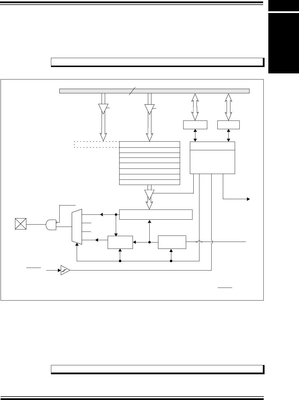
© 2007-2012 Microchip Technology Inc. DS61107G-page 21-17
Section 21. UART
UART
21
21.5 UART TRANSMITTER
Figure 21-3 illustrates the UART transmitter block diagram. The heart of the transmitter is Trans-
mit Shift register (UxTSR). The UxTSR obtains its data from the transmit FIFO buffer, UxTXREG.
The UxTXREG register is loaded with data in software. The UxTSR register is not loaded until
the Stop bit is transmitted from the previous load. As soon as the Stop bit is transmitted, the
UxTSR is loaded with new data from the UxTXREG register (if available).
Figure 21-3: UART Transmitter Block Diagram(1)
Transmission is enabled by setting the UTXEN bit (UxSTA<10>). The actual transmission does
not occur until the UxTXREG register is loaded with data and the BRG, UxBRG has produced a
shift clock (see Figure 21-3). The transmission can be started by loading the UxTXREG register,
and then setting the UTXEN bit. Usually, when transmission is started, the UxTSR register is
empty, so a transfer to the UxTXREG register results in an immediate transfer to the UxTSR.
Clearing the UTXEN bit during a transmission causes the transmission to be aborted and resets
the transmitter. As a result, the UxTX pin reverts to a state defined by the UTXINV bit
(UxSTA<13>).
To select 9-bit transmission, the PDSEL<1:0> bits (UxMODE<2:1>) should be set to ‘11’.
Note: The UxTSR register is not mapped in memory, so it is not available to the user.
Write
TX8 FIFO Slot(1)
Load UxTSR
Transmit Control
– Control UxTSR
– Control Buffer
– Generate Flags
– Generate Interrupt
UxTXIF
Data
(Start)
(Stop)
Parity Parity
Generator
Transmit Shift Register(UxTSR)
Divider
Control
Signals
Baud Clock
from Baud Rate
Generator
Internal Data Bus
UTXBRK
UxTX
UxTX
UxMODE UxSTA
32
Write
Transmit FIFO
32 9 8 0
UxCTS(2)
Note 1: Refer to the “UART” chapter in the specific device data sheet for availability of the 8-level-deep FIFO.
2: Refer to the “Pin Diagrams” section in the specific device data sheet for availability of the UxCTS pin.
(up to 8 levels deep) TX4 FIFO Slot
Note: No parity in 9-bit data transmission.

PIC32 Family Reference Manual
DS61107G-page 21-18 © 2007-2012 Microchip Technology Inc.
21.5.1 Transmit Buffer (UxTXREG)
The transmit buffer is 9 bits wide and up to 8 levels deep. Together with the Transmit Shift
registers (UxTSR), the user can have up to a 9-level-deep buffer. When the UxTXREG contents
are transferred to the UxTSR register, the current buffer location will be available for new data to
be written. The UTXBF status bit (UxSTA<9>) is set whenever the buffer is full. If a user attempts
to write to a full buffer, the new data will not be accepted into the FIFO.
The FIFO is reset during any device Reset, but is not affected when the device enters a
power-saving mode or wakes up from a power-saving mode.
21.5.2 Transmit Interrupt
The Transmit Interrupt Flag Status bit (UxTXIF) is located in the corresponding Interrupt Flag
Status register (IFS). The UTXISEL control bits (UxSTA<15:14>) determine when the UART will
generate a transmit interrupt. The UxTXIF bit is set when the module is enabled. Switching
between the interrupt modes during operation is possible, but it is not recommended unless the
buffer is empty.
While the UxTXIF flag bit indicates the status of the UxTXREG register, the TRMT bit
(UxSTA<8>) indicates the status of the UxTSR register. The TRMT status bit is a read-only bit
and it is set when the UxTSR register is empty. No interrupt logic is tied to this bit, so the user
has to poll this bit to determine if the UxTSR register is empty.
To cle ar an int er rup t for U ART mod ule s hav ing 4 -l e ve l-d eep F IFO , the c orr es pon din g UxT XIF
flag bit must be cleared in the associated IFSx register.
For UART modules having 8-level-deep FIFO, an interrupt is generated and asserted when the
interrupt condition specified by the UTXISEL control bits is true. This means, to clear an interrupt
for these modules, before clearing the corresponding UxTXIF flag bit, the user application must
ensure that the interrupt condition specified by the UTXISEL control bits is no longer true.
21.5.3 Setup for UART Transmit
Follow these steps to set up a UART transmission:
1. Initialize the UxBRG register for the appropriate baud rate (refer to 21.3 “UART Baud
Rate Generator”).
2. Set the number of data and Stop bits, and parity selection by writing to the PDSEL<1:0>
bits (UxMODE<2:1>) and STSEL bit (UxMODE<0>).
3. If transmit interrupts are desired, set the UxTXIE control bit in the corresponding Interrupt
Enable Control register (IEC). Specify the interrupt priority and subpriority for the transmit
interrupt using the UxIP<2:0> and UxIS<1:0> control bits in the corresponding Interrupt
Priority Control register (IPC). Also, select the Transmit Interrupt mode by writing to the
UTXISEL bits (UxSTA<15:14>).
4. Enable the transmission by setting the UTXEN bit (UxSTA<10>), which also sets the
UxTXIF bit. The UxTXIF bit should be cleared in the software routine that services the
UART transmit interrupt. The operation of the UxTXIF bit is controlled by the UTXISEL
control bits.
5. Enable the UART module by setting the ON bit (UxMODE<15>).
6. Load data to the UxTXREG register (starts transmission).
Note: Refer to the “UART” chapter in the specific device data sheet for availability of
8-level-deep and 4-level-deep FIFO.

© 2007-2012 Microchip Technology Inc. DS61107G-page 21-19
Section 21. UART
UART
21
21.5.4 Transmission of Break Characters
A Break character transmit consists of a Start bit, followed by twelve bits of ‘0’, and a Stop bit. A
Frame Break character is sent whenever the UART module is enabled, and the UTXBRK
(UxSTA<11>) and UTXEN (UxSTA<10>) bits are set while the UxTXREG register is loaded with
data. A dummy write to the UxTXREG register is necessary to initiate the Break character
transmission. The data value written to the UxTXREG for the Break character is ignored. The
write merely initiates the proper sequence, so that all zeroes are transmitted.
The UTXBRK bit is automatically reset by hardware after the corresponding break transmission
is complete. This enables the user to preload the write FIFO with the next transmit byte while the
break is being transmitted (typically, the Sync character in the LIN specification).
The TRMT bit (UxSTA<8>) indicates whether the Transmit Shift register is empty or full, like it
does during normal transmission. See Figure 21-4 for the timing of the Break character
sequence.
Figure 21-4: Send Break Sequence
21.5.5 Break and Sync Transmit Sequence
The following sequence is performed to send a message frame header that is composed of a
Break character, followed by an auto-baud Sync byte. This sequence is typical of a LIN
bus master.
1. Configure the UART for the desired mode, refer to 21.5.3 “Setup for UART Transmit”
for setup information.
2. If data is currently being sent, poll the TRMT bit (UxSTA<8>) to determine when the
transmission ends.
3. Set UTXEN (UxSTA<10>) and UTXBRK (UxSTA<11>) to set up the Break character.
4. Load the UxTXREG with a dummy character to initiate transmission (value is ignored).
5. Write 0x55 to UxTXREG to load the Sync character into the transmit FIFO.
After the Break is sent, the UTXBRK bit is reset by hardware. The Sync character now transmits.
Note: The user should wait for the transmitter to be Idle (TRMT = 1) before setting the
UTXBRK bit (UxSTA<11>). The UTXBRK bit overrides any other transmitter activity.
If FIFO contains transmit data when the UTXBRK bit is set, a break character will
be sent when data is transferred to the UxTSR register, instead of the actual trans-
mit data that was transferred into the UxTSR register. If the user application clears
the UTXBRK bit prior to sequence completion, unexpected module behavior can
result.
Write to UxTXREG
Start bit bit 0 bit 1 bit 11 Stop bit
Break
UxTX
TRMT bit
UTXBRK Sampled Here Auto-Cleared
UTXBRK bit
UxTXIF
BCLKx/16
(shift clock)
Dummy Write

PIC32 Family Reference Manual
DS61107G-page 21-20 © 2007-2012 Microchip Technology Inc.
21.6 DATA BIT DETECTION
21.6.1 16X Clock Mode (BRGH = 0)
In 16x Clock mode, each bit of the received data is 16 clock pulses wide. To d e te ct t he val ue of
an incoming data bit, the bit is sampled at 7th, 8th and 9th rising edges of the clock. These rising
edges are called Majority Detection Edges. This mode is more robust than 4x Clock mode.
Figure 21-5: 16x Clock Mode with Majority Detection
21.6.2 4X Clock Mode (BRGH = 1)
In 4x Clock mode, each bit of the received data is four clock pulses wide. The 4x Clock mode
does not provide enough edges to support the Majority Detection Method. Therefore, the
received data is sampled at the one-half bit width.
Figure 21-6: 4x Clock Mode without Majority Detection
Note: In 16x Clock mode, each bit is sampled at 7th, 8th and 9th rising edges of the clock.
Idle Start bit bit 0
MD2
MD3
MD1
Start bit detected
16x Clock
Bit Clock
Internal Bit Counter
(Received Data)
Start bit bit 0 bit 1
Sample point
4x Clock
Bit Clock
Internal Bit Counter
RX
Note: In 4x Clock mode, the sampling occurs only at the one-half bit width.

© 2007-2012 Microchip Technology Inc. DS61107G-page 21-21
Section 21. UART
UART
21
21.7 UART RECEIVER
The heart of the receiver is the Receive (Serial) Shift register (UxRSR). The data is received on
the UxRX pin and is sent to the majority detect block. In BRGH = 0 mode, the majority detect
block operates at 16 times the baud rate, and a majority detect circuit is implemented to
determine whether a high-level or a low-level is present at the UxRX pin. In BRGH = 1 mode, the
majority detect block operates at 4 times the baud rate, and a single sample is used to determine
whether a high-level or a low-level is present.
After sampling the UxRX pin for the Stop bit, the received data in UxRSR is transferred to the
receive FIFO, if it is not full. Figure 21-7 illustrates a UART receiver block diagram. Reception is
enabled by setting the URXEN bit (UxSTA<12>).
21.7.1 Receive Buffer (UxRXREG)
The UART receiver has a 9-bit-wide FIFO receive data buffer that is up to 8 levels deep. The
UxRXREG is a memory mapped register that provides access to the output of the FIFO. It is
possible for the FIFO to be full and the next word to begin shifting to the UxRSR register before
a buffer overrun occurs.
21.7.2 Receiver Error Handling
If the FIFO is full and a new character is fully received into the UxRSR register, the overrun error
bit, OERR (UxSTA<1>), is set. The word in UxRSR register is not kept, and further transfers to
the receive FIFO are inhibited as long as the OERR bit is set. The user must clear the OERR bit
in software to allow further data to be received.
To k eep t he d ata t hat w as r ece iv ed p rior t o t he overrun, the user should read all received
characters and then clear the OERR bit. If the received characters can be discarded, the user
can simply clear the OERR bit. This effectively resets the receive FIFO, and all data previously
received is lost.
The Framing Error Status bit, FERR (UxSTA<2>) is set when the received state of the Stop bit is
incorrect.
The Parity Error Status bit, PERR (UxSTA<3>) is set if a parity error exists in the data word at the
top of the buffer (that is, the current word). For example, a parity error occurs if the parity is set
as even, but the total number of ones in the data has been detected as odd. The PERR bit is
irrelevant in 9-bit mode. The FERR and PERR bits are buffered along with the corresponding
word and should be read before reading the data word.
21.7.3 Receive Interrupt
The UART Receive Interrupt Flag Status bit (UxRXIF) is located in the corresponding Interrupt
Flag Status register (IFSx). The URXISEL<1:0> control bits (UxSTA<7:6>) determine when the
UART receiver generates an interrupt.
To cl e ar a n int err up t fo r UART m odu le s hav ing 4 -l eve l-d ee p FIF O, t he c o rr esp ond in g UxR XI F
flag must be cleared in the associated IFSx register.
For UART modules having 8-level-deep FIFO, an interrupt is generated when the interrupt
condition specified by the URXISEL control bits is true. This means, to clear an interrupt for these
modules before clearing the corresponding UxRXIF flag bit, the user application must ensure that
the interrupt condition specified by the URXISEL control bits is no longer true.
Note: The Receive Shift register (UxRSR) is not mapped in memory; therefore, it is not
available to the user.
Note: The data in the receive FIFO should be read prior to clearing the OERR bit. The
FIFO is reset when the OERR bit is cleared, which causes all data in the buffer to
be lost.
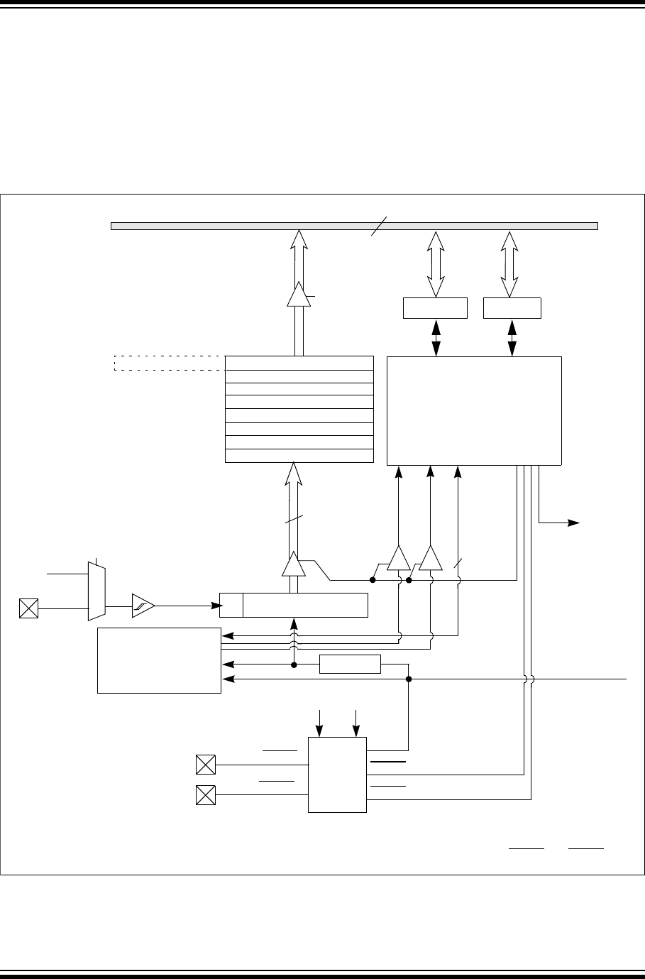
PIC32 Family Reference Manual
DS61107G-page 21-22 © 2007-2012 Microchip Technology Inc.
While the URXDA and UxRXIF bits indicate the status of the UxRXREG register, the RIDLE bit
(UxSTA<4>) indicates the status of the UxRSR register. The RIDLE bit is a read-only bit, which
is set when the receiver is Idle (that is, the UxRSR register is empty). No interrupt is tied to this
bit, so the user must poll this bit to determine whether the UxRSR is Idle.
The URXDA bit (UxSTA<0>) is a read-only bit which indicates whether the receive buffer has
data or it is empty. This bit is set as long as there is one character to be read from the receive
buffer.
A block diagram of the UART receiver is illustrated in Figure 21-7.
Figure 21-7: UART Receiver Block Diagram(1)
RX8 FIFO Slot(1)
Load UxRSR
UxMODE
Receive Buffer Control
– Generate Flags
– Generate Interrupt
UxRXIF
UxRX Receive Shift Register
Control
Signals
Baud Clock
from Baud Rate
Generator
UxSTA
– Shift Data Characters
to Buffer
9
(UxRSR)
PERR
FERR
32
Internal Data Bus
1
0
LPBACK
From UxTX
32 9 8 0
Read
BCLKx/UxRTS(2)
UxCTS(2) Selection
UEN
BCLKx
UEN1 UEN0
Divider
UxRTS
UxCTS
Note 1: Refer to the “UART” chapter in the specific device data sheet for availability of the 8-level-deep FIFO.
2: Refer to the “Pin Diagrams” section of the specific device data sheet for availability of the UxRTS and UxCTS pins.
RX4 FIFO Slot
•Start bit Detect
•Parity Check
•Stop bit Detect
• Shift Clock Generation
• Wake Logic

© 2007-2012 Microchip Technology Inc. DS61107G-page 21-23
Section 21. UART
UART
21
21.7.4 Setup for UART Reception
The following steps are performed to set up a UART reception:
1. Initialize the UxBRG register for the appropriate baud rate (see 21.3 “UART Baud Rate
Generator”).
2. Set the number of data and Stop bits, and parity selection by writing to the PDSEL<1:0>
(UxMODE<2:1>) and STSEL (UxMODE<0>) bits.
3. If interrupts are desired, set the UxRXIE bit in the corresponding Interrupt Enable Control
register (IEC). Specify the priority and subpriority for the interrupt using the UxIP<2:0> and
UxIS<1:0> control bits in the corresponding Interrupt Priority Control register (IPC). Also,
select the Receive Interrupt mode by writing to the URXISEL<1:0> bits (UxSTA<7:6>).
4. Enable the UART receiver by setting the URXEN bit (UxSTA<12>).
5. Enable the UART module by setting the ON bit (UxMODE<15>).
6. Receive interrupts are dependent on the URXISEL<1:0> bit settings. If receive interrupts
are not enabled, the user can poll the URXDA bit (UxSTA<0>). The UxRXIF bit should be
cleared in the software routine that services the UART receive interrupt.
7. Read data from the receive buffer. If 9-bit transmission is selected, read a word; otherwise,
read a byte. The URXDA bit is set whenever data is available in the buffer.

PIC32 Family Reference Manual
DS61107G-page 21-24 © 2007-2012 Microchip Technology Inc.
21.8 USING THE UART FOR 9-BIT COMMUNICATION
The UART receiver in 9-bit Data mode is used for communication in a multiprocessor
environment. With the ADDEN bit (UxSTA<5>) set in 9-bit Data mode, the receiver can ignore
the data when the 9th bit of the data is ‘0’.
21.8.1 Multi-processor Communications
A typical multi-processor communication protocol differentiates between data bytes and
address/control bytes. A common scheme is to use a 9th data bit to identify whether a data byte
is address or data information. If the 9th bit is set, the data is processed as address or control
information. If the 9th bit is cleared, the received data word is processed as data associated with
the previous address/control byte.
The protocol operates in the following sequence:
•The master device transmits a data word with the 9th bit set. The data word contains the
address of a slave device and is considered the address word.
• All slave devices in the communication chain receive the address word and check the slave
address value
• The slave device that is specified by the address word receives and processes subsequent
data bytes sent by the master device. All other slave devices discard subsequent data
bytes until a new address word is received.
21.8.1.1 ADDEN CONTROL BIT
The UART receiver has an Address Detect mode, which allows it to ignore data words with the
9th bit cleared. This reduces the interrupt overhead because the data words with the 9th bit
cleared are not buffered. This feature is enabled by setting the ADDEN bit (UxSTA<5>).
The UART must be configured for 9-bit data to use the Address Detect mode. The ADDEN bit
has no effect when the receiver is configured in 8-bit Data mode.
21.8.1.2 SETUP FOR 9-BIT TRANSMIT MODE
The setup procedure for 9-bit transmission is identical to the 8-bit transmit modes, except that
the PDSEL<1:0> bits (UxMODE<2:1) should be set to ‘11’. Word writes should be performed to
the UxTXREG register (starts transmission). Refer to 21.5.3 “Setup for UART Transmit” for
more information on setting up for UART transmission.
21.8.1.3 SETUP FOR 9-BIT RECEPTION USING ADDRESS DETECT MODE
The setup procedure for 9-bit reception is identical to the 8-bit Receive modes, except that the
PDSEL<1:0> bits (UxMODE<2:1) should be set to ‘11’. Refer to 21.7.4 “Setup for UART
Reception” for more information on setting up for UART reception.
Receive Interrupt mode should be configured by writing to the URXISEL<1:0> bits
(UxSTA<7:6>).
Perform the following steps to use the Address Detect mode:
1. Set PDSEL<1:0> bits (UxMODE<2:1) to ‘11’ to choose 9-bit mode.
2. Set the ADDEN bit (UxSTA<5>) to enable address detect.
3. Set ADDR bits (UxSTA<23:16>) to the desired device address character.
4. Set the ADM_EN bit (UxSTA<24>) to enable Address Detect mode.
5. If this device has been addressed, the UxRXREG is discarded. All subsequent characters
received with UxRXREG<8> = 0 are transferred to the UART receive buffer, and interrupts
are generated according to URXISEL<1:0> bits (UxSTA<7:6>).
Note: A receive interrupt is generated when an Address character is detected and the
Address Detect mode is enabled (ADDEN = 1), regardless of how the
URXISEL<1:0> bits are set.

© 2007-2012 Microchip Technology Inc. DS61107G-page 21-25
Section 21. UART
UART
21
Figure 21-8: Reception with Address Detect (ADDEN = 1)
Start
bit bit 1
bit 0 bit 8 bit 0
Stop
bit
Start
bit bit 8 Stop
bit
UxRX (pin)
Read Rcv
Buffer Reg.
UxRXREG
UxRXIF
(Interrupt Flag)
Word 1
UxRXREG
bit 8 = 0, Data Byte bit 8 = 1, Address Byte
Transfer
to Receive FIFO
Note: This timing diagram illustrates a data byte followed by an address byte. The data byte is not read in the
UxRXREG (receive buffer) because ADDEN = 1 and bit 8 = 0.

PIC32 Family Reference Manual
DS61107G-page 21-26 © 2007-2012 Microchip Technology Inc.
21.9 RECEIVING BREAK SEQUENCE
The wake-up feature is enabled by setting the WAKE bit (UxMODE <7>) = 1. In this mode, the
module receives the Start bit, data and invalid Stop bit (which sets FERR bit); however, the
receiver waits for a valid Stop bit before looking for the next Start bit. It will not assume that the
Break condition on the line is the next Start bit. A Break is regarded as a character containing all
zeros with the FERR bit set. The Break character is loaded into the buffer. No further reception
can occur until a Stop bit is received. The WAKE bit is cleared when the Stop bit is received after
the 13-bit Break character. RIDLE goes high when the Stop bit is received.
The receiver counts and expects a certain number of bit times based on the values programmed
in the PDSEL<1:0> (UxMODE<2:1>) and STSEL (UxMODE<0>) bits.
If the Break is longer than 13 bit times, the reception is considered complete after the number of
bit times specified by the PDSEL and STSEL bits elapses. The URXDA and FERR bits are set,
zeros are loaded into the receive FIFO, and interrupts are generated.
If the wake-up feature is not set, WAKE (UxMODE <7>) = 0, Break reception is not special. The
Break is counted as one character loaded into the buffer (all ‘0’ bits) with FERR bit set.
21.10 INITIALIZATION
An initialization routine for the Transmitter/Receiver in 8-bit mode is shown in Example 21-2. An
initialization routine of the Addressable UART in 9-bit Address Detect mode is shown in
Example 21-3. In both the examples, the value to load into the UxBRG register is dependent on
the desired baud rate and the device frequency.
Example 21-2: 8-bit Transmit/Receive (UART1)
Example 21-3: 8-bit Transmit/Receive (UART1), Address Detect Enabled
U1BRG = BaudRate; // Set Baud rate
U1STA = 0;
U1MODE = 0x8000; // Enable UART for 8-bit data
// No Parity, 1 Stop bit
U1STASET = 0x1400; // Enable Transmit and Receive
U1BRG = BaudRate; // Set Baud rate
U1MODE = 0x8006; // Enable UART for 9-bit data
// No Parity, 1 Stop bit
U1STA = 0x1211420; // Address detect enabled
// Device Address = 0x21
// Enable Automatic Address Detect mode
// Enable Transmit and Receive

© 2007-2012 Microchip Technology Inc. DS61107G-page 21-27
Section 21. UART
UART
21
21.11 OTHER UART FEATURES
21.11.1 UART in Loopback Mode
Setting the LPBACK bit (UxMODE<6>) enables Loopback mode in which the UxTX output is
internally connected to the UxRX input. When configured for the Loopback mode, the UxRX pin
is disconnected from the internal UART receive logic; however, the UxTX pin still
functions normally.
Perform the following steps to select Loopback mode:
1. Configure the UART for the desired mode of operation (see 21.5.3 “Setup for UART
Transmit”).
2. Enable transmission as defined in 21.5 “UART Transmitter”.
3. Set LPBACK (UxMODE<6>) = 1 to enable Loopback mode.
Tabl e 21- 3 shows how the Loopback mode is dependent on the UEN<1:0> bits settings.
Table 21-3: Loopback Mode Pin Function
UEN<1:0> Pin Function, LPBACK = 1(1)
00 UxRX input connected to UxTX
UxTX pin functions
UxRX pin ignored
UxCTS/UxRTS unused(2)
01 UxRX input connected to UxTX
UxTX pin functions
UxRX pin ignored
UxRTS pin functions(2)
UxCTS unused(2)
10 UxRX input connected to UxTX
UxTX pin functions
UxRX pin ignored
UxRTS pin functions(2)
UxCTS input connected to UxRTS(2)
UxCTS pin ignored(2)
11 UxRX input connected to UxTX
UxTX pin functions
UxRX pin ignored
BCLKx pin functions
UxCTS/UxRTS unused(2)
Note 1: LPBACK = 1 should be set only after enabling the other bits associated with the
UART module.
2: Refer to the “Pin Diagrams” section in the specific device data sheet to determine
availability of the UxCTS and UxRTS pins.
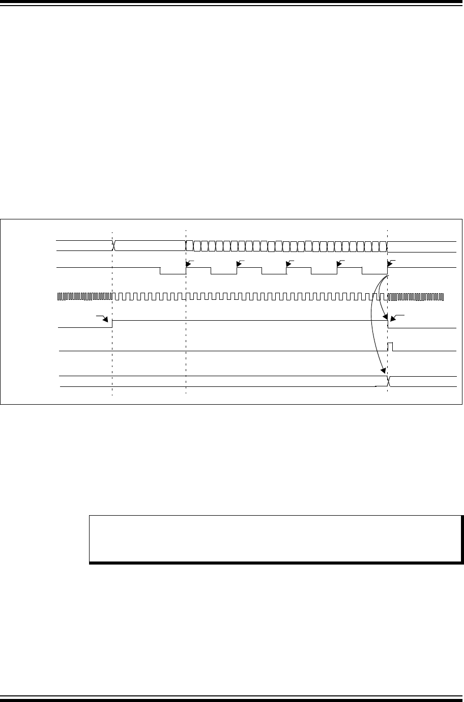
PIC32 Family Reference Manual
DS61107G-page 21-28 © 2007-2012 Microchip Technology Inc.
21.11.2 Auto-Baud Support
The ABAUD bit (UxMODE<5>) is enabled to allow the system to determine the baud rates of the
received characters. The UART begins an automatic baud rate measurement sequence
whenever a Start bit is received, and when the Auto-Baud Rate Detect is enabled (ABAUD = 1).
The calculation is self-averaging. This feature is active only while the auto-wake-up is disabled
(WAKE = 0). In addition, LPBACK (UxMODE<6>) must be ‘0’ for the auto-baud operation. When
the ABAUD bit is set, the BRG counter value clears and looks for a Start bit. In this case, Start
bit is defined as a high-to-low transition followed by a low-to-high transition.
Following the Start bit, the auto-baud expects to receive an ASCII ‘U’ (0x55) to calculate the bit
rate. The measurement is taken over both the low and the high bit time to minimize any effects
caused by asymmetry of the incoming signal. At the end of the Start bit (rising edge), the BRG
counter begins counting up using a FPB/8 clock. On the 5th UxRX pin rising edge, an
accumulated BRG counter value totaling the proper BRG period is transferred to the UxBRG
register. The ABAUD bit automatically clears. If the user clears the ABAUD bit prior to sequence
completion, unexpected module behavior can result. See Figure 21-1 for the ABD sequence.
Figure 21-9: Automatic Baud Rate Calculation
While the auto-baud sequence is in progress, the UART state machine is held in Idle mode. The
UxRXIF interrupt is set on the 5th UxRX rising edge, independent of the URXISEL<1:0> bits
settings. The receiver FIFO is not updated.
21.11.3 Break Detect Sequence
The user can configure the auto-baud to occur immediately following the Break detect. This is
done by setting the ABAUD bit (UxMODE<5>) with the WAKE bit (UxMODE<7>) set.
Figure 21-10 illustrates a Break detect followed by an auto-baud sequence. The WAKE bit takes
priority over the ABAUD bit setting.
The UART transmitter cannot be used during an auto-baud sequence. In addition to that, the user
should ensure that the ABAUD bit is not set while a transmit sequence is already in progress.
Otherwise, the UART module may exhibit unpredictable behavior.
BRG Counter
UxRX
ABAUD bit
bit 0 bit 1
BRG Clock
Start
Auto-Cleared
Set by User
XXXXh 0000h
Edge 1
bit 2 bit 3
Edge 2
bit 4 bit 5
Edge 3
bit 6 bit 7
Edge 4
Stop bit
Edge 5
001Ch
BRG Register XXXXh 001Ch
UxRXIF
Note: If the WAKE bit is set with the ABAUD bit, auto-baud rate detection occurs on the
byte following the Break character. The user must ensure that the baud rate of the
incoming character is within the range of the selected UxBRG clock source,
considering the baud rate possible with the given clock.

© 2007-2012 Microchip Technology Inc. DS61107G-page 21-29
Section 21. UART
UART
21
Figure 21-10: Break Detect Followed by Auto-Baud Sequence
Start bit 0 bit 7 Stop
Idle Break Detect Auto-Baud Rate Detect Idle
SynchronizationSynchronization
Auto-Cleared
Auto-ClearedSet by User
Set by User
Q1
UxRX
WAKE bit
ABAUD bit
UxRXIF
UART Mode
PIC32 Family Reference Manual
DS61107G-page 21-30 © 2007-2012 Microchip Technology Inc.
21.12 OPERATION OF UxCTS AND UxRTS CONTROL PINS
The UxCTS (Clear to Send) and UxRTS (Request to Send) pins are two hardware controlled pins
associated with the UART module. These two pins allow the UART to operate in Flow Control
and Simplex modes, which are explained in 21.12.2 “UxRTS Function in Flow Control Mode”
and 21.12.3 “UxRTS Function in Simplex Mode”. They are implemented to control the
transmission and reception among the Data Terminal Equipment (DTE).
21.12.1 UxCTS Function
In the UART operation, the UxCTS acts as an input pin that can control the transmission. This
pin is controlled by another device (typically a PC). The UxCTS pin is configured using the
UEN<1:0> bits (UxMODE<9:8>). When UEN<1:0> = 10, UxCTS is configured as an input pin. If
UxCTS = 1, the transmitter loads data in the Transmit Shift register, but will not initiate a
transmission. This allows the DTE to control and receive the data accordingly from the controller,
based on its requirement.
The UxCTS pin is sampled simultaneously with a transmit data change (that is, at the beginning
of the 16 baud clocks). Transmission begins only when the UxCTS pin is sampled low. The
UxCTS pin is sampled internally with a Peripheral Bus Clock (PBCLK), which means there is a
minimum pulse width on UxCTS of one peripheral clock. However, this cannot be a specification
as the FPB can vary depending on the clock used.
The user can also read the status of the UxCTS pin by reading the associated port pin.
21.12.2 UxRTS Function in Flow Control Mode
In the Flow Control mode, the UxRTS pin of one DTE is connected to the UxCTS pin of the PIC32
and the UxCTS pin of the DTE is connected to the UxRTS pin of the PIC32, as illustrated in
Figure 21-11.
The UxRTS signal indicates that the device is ready to receive the data. The UxRTS is driven as
an output pin whenever UEN<1:0> = 01 or 10. The UxRTS pin is asserted (driven low) whenever
the receiver is ready to receive data. When the device is in Flow Control mode and RTSMD
(UxMODE<11>) = 0, the UxRTS pin is driven low whenever the receive buffer is not full or the
OERR bit (UxSTA<1>) is not set. When the RTSMD bit = 0, the UxRTS pin is driven high
whenever the device is not ready to receive (that is, when the receiver buffer is either full or in
the process of shifting). The UxRTS pin is asserted (driven low) when the receiver has space for
at least 2 characters in the FIFO.
As the UxRTS pin of the DTE is connected to the UxCTS pin of the PIC32, the UxRTS pin drives
the UxCTS pin low whenever it is ready to receive the data. Transmission of the data begins
when the UxCTS pin goes low, as explained in 21.12.1 “UxCTS Function”.
Figure 21-11: UxRTS/UxCTS Flow Control for DTE-DTE (RTSMD = 0, Flow Control Mode)
Note: Refer to the “Pin Diagrams” section in the specific device data sheet to determine
availability of the UxCTS and UxRTS pins.
UxRTS UxRTS
UxCTS UxCTS
DTE
Typically a PC
DTE
Typically Another System or Microcontroller
I am ready to receive
I will transmit if OK
I am ready to receive
I will transmit if OK
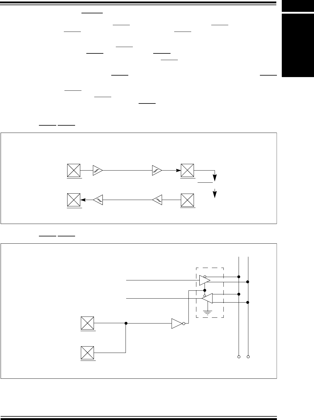
© 2007-2012 Microchip Technology Inc. DS61107G-page 21-31
Section 21. UART
UART
21
21.12.3 UxRTS Function in Simplex Mode
In the Simplex mode, the UxRTS pin of the DCE is connected to the UxRTS pin of the PIC32 and
the UxCTS pin of the DCE is connected to the UxCTS pin of the PIC32, as illustrated in
Figure 21-12.
In the Simplex mode, the UxRTS signal indicates that the DTE is ready to transmit. The DCE
replies to the UxRTS signal with the valid UxCTS signal when the DCE is ready to receive the
transmission. When the DTE receives a valid UxCTS signal, it begins transmission.
Figure 21-13 illustrates that Simplex mode is also used in IEEE-485 systems to enable
transmitters. When the UxRTS signal indicates that the DTE is ready to transmit, the UxRTS
signal enables the driver.
The UxRTS pin is configured as an output and is driven whenever UEN<1:0> = 01 or 10. When
RTSMD = 1, the UxRTS pin is asserted (driven low) whenever the data is available to transmit
(TRMT = 0). When RTSMD = 1, the UxRTS pin is deasserted (driven high) when the transmitter
is empty (TRMT = 1).
Figure 21-12: UxRTS/UxCTS Handshake for DTE-DCE (RTSMD = 1, Simplex Mode)
Figure 21-13: UxRTS/UxCTS Bus Enable for IEEE-485 Systems (RTSMD = 1)
UxRTS UxRTS
UxCTS UxCTS
DTE
(Typically a Microcontroller)
DCE
(Typically a Modem)
May I send something?
UxRTS active and receiver ready.
I will transmit if okay. OK, go ahead and send.
UxRTS
UxCTS
DTE
(Typically a Microcontroller)
May I transmit something?
I will transmit if okay.
UxTX
UxRX
D
R
BA
TTL to RS-485
Transceiver
Integrated CKT
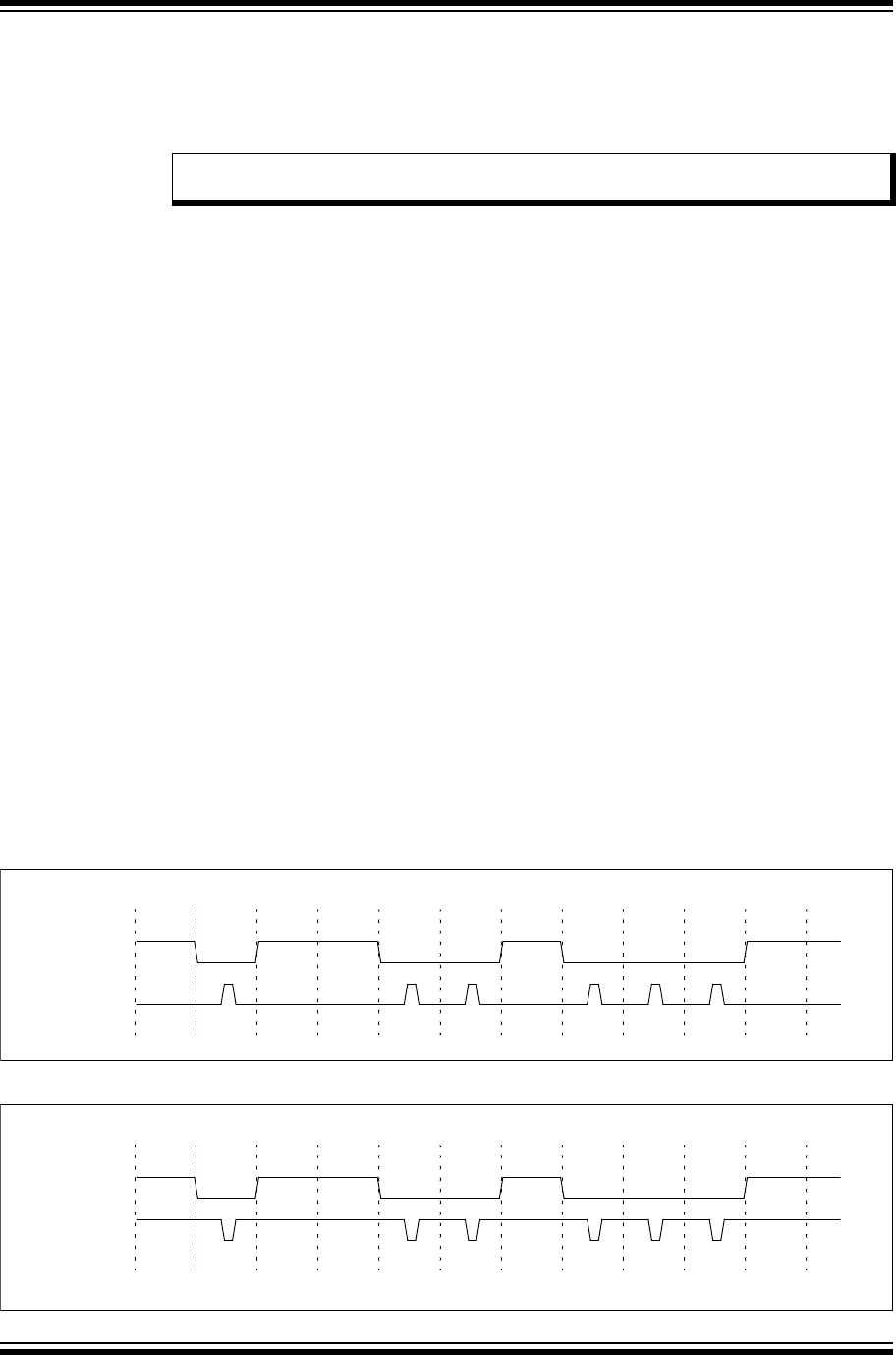
PIC32 Family Reference Manual
DS61107G-page 21-32 © 2007-2012 Microchip Technology Inc.
21.13 INFRARED SUPPORT
The UART module provides the following two infrared UART support features:
• IrDA clock output to support external IrDA encoder and decoder devices (legacy
module support)
•Full implementation of the IrDA encoder and decoder
21.13.1 External IrDA Support – IrDA Clock Output
To sup po rt ext ern al I r DA e nco der a nd d ecod er devices, the BCLKx pin can be configured to
generate the 16x baud clock. When UEN<1:0> = 11, the BCLKx pin will output the 16x baud
clock if the UART module is enabled; it can be used to support the IrDA codec chip.
21.13.2 Built-In IrDA Encoder and Decoder
The UART has full implementation of the IrDA encoder and decoder as part of the UART module.
The built-in IrDA encoder and decoder functionality is enabled using the IREN bit
(UxMODE<12>). When enabled (IREN = 1), the receive pin UxRX acts as the input from the
infrared receiver. The transmit pin UxTX acts as the output to the infrared transmitter.
21.13.2.1 IrDA ENCODER FUNCTION
The encoder works by taking the serial data from the UART and replacing it as follows:
•Transmit bit data of ‘1’ gets encoded as ‘0’ for the entire 16 periods of the 16x baud clock.
•Transmit bit data of ‘0’ gets encoded as ‘0’ for the first 7 periods of the 16x baud clock, as
‘1’ for the next 3 periods and as ‘0’ for the remaining 6 periods.
For more information, see Figure 21-14 and Figure 21-16.
21.13.2.2 IrDA TRANSMIT POLARITY
The IrDA transmit polarity is selected using the UTXINV bit (UxSTA<13>). This bit only affects the
module when the IrDA encoder and decoder are enabled (IREN = 1). The UTXINV bit does not
affect the receiver or the module operation for normal transmission and reception. When
UTXINV = 0, the Idle state of the UxTX line is ‘0’ (see Figure 21-14). When UTXINV = 1, the Idle
state of the UxTX line is ‘1’ (see Figure 21-15).
Figure 21-14: IrDA® Encode Scheme
Figure 21-15: IrDA® Encode Scheme for ‘0’ bit Data
Note: Refer to the “UART” chapter in the specific device data sheet to determine
availability of this feature.
UxTX Data
UxTX
UxTX Data
UxTX

© 2007-2012 Microchip Technology Inc. DS61107G-page 21-33
Section 21. UART
UART
21
Figure 21-16: IrDA® Encode Scheme for ‘0’ bit Data with Respect to 16x Baud Clock
21.13.2.3 IrDA DECODER FUNCTION
The decoder works by taking the serial data from the UxRX pin and replacing it with the
decoded data stream. The stream is decoded based on falling edge detection of the
UxRX input.
Each falling edge of UxRX causes the decoded data to be driven low for 16 periods of the
16x baud clock. If, by the time the 16 periods expire, another falling edge is detected, the
decoded data remains low for another 16 periods. If no falling edge is detected, the decoded
data is driven high.
The data stream into the device is shifted anywhere from 7 to 8 periods of the 16x baud clock
from the actual message source. The one clock uncertainty is due to the clock edge resolution
(see Figure 21-17 for details).
Figure 21-17: Macro View of IrDA® Decoding Scheme
21.13.2.4 IrDA RECEIVE POLARITY
The input of the IrDA signal can have an inverted polarity. The same logic is able to decode the
signal train, but in this case, the decoded data stream is shifted from 10 to 11 periods of the
16x baud clock from the original message source. Again, the one clock uncertainty is due to the
clock edge resolution (see Figure 21-18 for details).
Figure 21-18: Inverted Polarity Decoding Results
Start ofStart of
‘0’ Transmit bit
16x Baud Clock
UxTX Data
UxTX
8th Period 11th Period
16
Start BRG TIRDEL
Before IrDA® Encoder
UxRX
Decoded Data
(Transmitting Device)
Periods
16
Periods
16
Periods
16
Periods
16
Periods
Start BRG TIRDELI
Before IrDA® Encoder
UxRX
Decoded Data
(Transmitting Device)
16
Periods
16
Periods
16
Periods
16
Periods
16
Periods
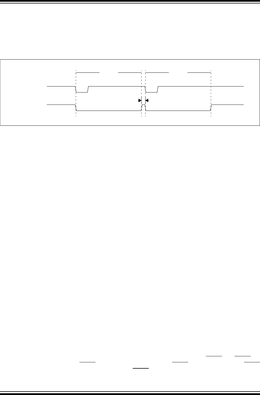
PIC32 Family Reference Manual
DS61107G-page 21-34 © 2007-2012 Microchip Technology Inc.
21.13.2.5 CLOCK JITTER
Due to jitter, or slight frequency differences between devices, it is possible for the next falling bit
edge to be missed for one of the 16x periods. In that case, a one clock-wide-pulse appears on
the decoded data stream. Because, the UART performs a majority detect around the bit center,
this does not cause erroneous data (see Figure 21-19 for details).
Figure 21-19: Clock Jitter Causing a Pulse Between Consecutive Zeros
21.14 INTERRUPTS
The UART module can generate interrupts reflecting the events that occur during the data
communication. The following interrupts can be generated:
•Receiver-data-available interrupt, signalled by UxRXIF. This event occurs based on the
URXISEL<1:0> control bits (UxSTA<7:6>). Refer to 21.7.3 “Receive Interrupt” for details.
•Transmitter buffer-empty interrupt, signalled by UxTXIF. This event occurs based on the
UTXISEL<1:0> control bits (UxSTA<15:14>). Refer to 21.5.2 “Transmit Interrupt” for
details.
• UART-error interrupt, signalled by UxEIF. This event occurs when any of the following error
conditions take place:
- Parity error PERR (UxSTA<3>) is detected
- Framing Error FERR (UxSTA<2>) is detected
-Overflow condition for the receive buffer OERR (UxSTA<1>) occurs
All these interrupt flags must be cleared in software. Refer to 21.5.2 “Transmit Interrupt” and
21.7.3 “Receive Interrupt” for more information.
A UART device is enabled as a source of interrupts through the following respective UART
interrupt enable bits:
•UxRXIE
•UxTXIE
• UxEIE
The interrupt priority-level bits and interrupt subpriority-level bits must be configured:
•UxIP (IPC6<4:2>) and UxIS (IPC6<1:0>)
Refer to Section 8. “Interrupts” (DS61108) for details about priority and subpriority bits.
21.15 I/O PIN CONTROL
When enabling the UART module by setting the ON bit (UxMODE<15>), the UTXEN bit
(UxSTA<10>), and the URXEN bit (UxSTA<12>), the UART module will control the I/O pins as
defined by the UEN<1:0> bits (UxMODE<9:8>), overriding the port TRIS and LATCH register bit
settings.
UxTX is forced as an output and UxRX as an input. Additionally, if UxCTS and UxRTS are
enabled, the UxCTS pin is forced as an input and the UxRTS/BLCKx pin functions as UxRTS
output. If BLCKx is enabled, then the UxRTS/BLCKx output drives the 16x baud clock output.
Extra Pulse will be Ignored
UxRX (rx_in)
Decoded Data
16
Periods
16
Periods

© 2007-2012 Microchip Technology Inc. DS61107G-page 21-35
Section 21. UART
UART
21
21.16 UART OPERATION IN POWER-SAVING MODES
21.16.1 Operation in Sleep Mode
When the device enters Sleep mode, the system clock is disabled. The UART module does not
function in Sleep mode. If entry into Sleep mode occurs while a transmission is in progress, the
transmission is aborted and the UxTX pin is driven to logic ‘1’. Similarly, if entry into Sleep mode
occurs while a reception is in progress, the reception is aborted. The RTS and BCLK pins are
driven to ‘0’.
Optionally, the UART module can be used to wake the PIC32 device from Sleep mode on the
detection of a Start bit. If the WAKE bit (UxMODE<7>) is set before the device enters Sleep mode
and the UART receive interrupt is enabled (UxRXIE = 1), a falling edge on the UxRX pin
generates a receive interrupt and the device wakes up. The Receive Interrupt Mode Selection bit
(RXISEL) has no effect on this function. The ON bit (UxMODE<15>) must be set to generate a
wake-up interrupt.
21.16.2 Operation in Idle Mode
When the device enters Idle mode, the system clock sources remain functional and the CPU
stops executing code. The SIDL bit (UxMODE<13>) selects whether the UART module stops
operation or continues normal operation when the device enters Idle mode.
•If SIDL = 1, the module stops operation in Idle mode. The module performs the same
procedures when stopped in Idle mode (SIDL = 1) as it does for Sleep mode.
•If SIDL = 0, the module continues operation in Idle mode
21.16.3 Auto-Wake-up on Sync Break Character
The auto-wake-up feature is enabled using the WAKE bit (UxMODE<7>). When WAKE is active,
the typical receive sequence on UxRX is disabled. Following the wake-up event, the module
generates the UxRXIF interrupt. The LPBACK bit (UxMODE<6>) must be equal to ‘0’ for
wake-up to operate.
A wake-up event consists of a high-to-low transition on the UxRX line. This coincides with the
start of a Sync Break or a Wake-up Signal character for the LIN protocol. When WAKE is active,
the UxRX line is monitored independently from the CPU mode. The UxRXIF interrupt is
generated synchronously to the PBCLK in Normal User mode, and asynchronously, if the module
is disabled due to Sleep or Sleep mode. To ensure that no actual data is lost, the WAKE bit should
be set prior to entering the Sleep mode and while the UART module is in Idle mode.
The WAKE bit is automatically cleared after a low-to-high transition is observed on the UxRX line
following the wake-up event. At this point, the UART module is in Idle mode and is returned to
normal operation. This signals to the user that the Sync Break event is over. If the user
application clears the WAKE bit prior to sequence completion, unexpected module behavior may
result.
The wake-up event causes a receive interrupt by setting the UxRXIF bit. The Receive Interrupt
Select mode bits, URXISEL<1:0> (UxSTA<7:6>), are ignored for this function. If the UxRXIF
interrupt is enabled, it wakes up the device.
Note: In Sleep mode, a falling edge on the UART receive pin generates a UART receive
interrupt resulting the device wake from the Sleep mode. The transmission right
after waking up from the Sleep mode will not be properly received. User should
ignore the dummy byte in the first UART receive interrupt.
Note: The Sync Break (or Wake-up Signal) character must be of sufficient length to allow
time for the selected oscillator to start and provide proper initialization of the UART.
To ens ur e tha t t he par t wok e up in t ime , the user should read the value of the WAKE
bit. If it is clear, it is possible that the UART was not ready in time to receive the next
character and the module might need to be resynchronized to the bus.

PIC32 Family Reference Manual
DS61107G-page 21-36 © 2007-2012 Microchip Technology Inc.
Figure 21-20: Auto-Wake-up bit (WAKE) Timings During Normal Operation
Figure 21-21: Auto-Wake-up bit (WAKE) Timings During Sleep
21.17 EFFECTS OF VARIOUS RESETS
21.17.1 Device Reset
All UART module registers are forced to their reset states on a device Reset.
21.17.2 Power-on Reset
All UART module registers are forced to their reset states on a Power-on Reset (POR).
21.17.3 Watchdog Reset
All UART module registers are unchanged on a Watchdog Reset.
OSC1
WAKE bit(1)
UxRX
UxRXIF
Bit Set by User Auto-Cleared
Note 1: UART state machine is held in Idle while WAKE bit is active.
OSC1
WAKE bit(2)
UxRX
UxRXIF
Sleep
(1)
Bit Set by User Auto-Cleared
Note 1: If the wake-up event requires long oscillator warm-up time, the auto-clear of the WAKE bit can occur while the
system clocks are still active. This sequence should not depend on the presence of a PBCLK.
2: UART state machine is held in Idle while the WAKE bit is active.

© 2007-2012 Microchip Technology Inc. DS61107G-page 21-37
Section 21. UART
UART
21
21.18 RELATED APPLICATION NOTES
This section lists application notes that are related to this section of the manual. These
application notes may not be written specifically for the PIC32 device family, but the concepts are
pertinent and could be used with modification and possible limitations. The current application
notes related to the UART module are:
Title Application Note #
No related application notes are available. N/A
Note: Please visit the Microchip web site (http://www.microchip.com) for additional Appli-
cation Notes and code examples for the PIC32 family of devices.

PIC32 Family Reference Manual
DS61107G-page 21-38 © 2007-2012 Microchip Technology Inc.
21.19 REVISION HISTORY
Revision A (August 2007)
This is the initial released version of the document.
Revision B (October 2007)
Updated document to remove Confidential status.
Revision C (April 2008)
Revised status to Preliminary; Revised U-0 to r-x; Revised Register 21-1 bit 10; Revised Table
21-1, IEC1; Revised Register 21-16, bit 25; Revised Register 21-18, bit 25; Revised bit names.
Revision D (June 2008)
Revised Section 21.1; Added Footnote number to Registers 21-15-21-20; Change Reserved bits
from “Maintain as” to “Write”; Added Note to ON bit (UxMODE Register).
Revision E (November 2009)
This revision includes the following changes:
•Updated the UART module features in 21.1 “Introduction” to clarify which UART modules
are available for a specific feature
•Updated Note 1 in Figure 21-1
•Updated register introductions in 21.2 “Control Registers”
• Changed all occurrences of UTXISEL0 to UTXISEL
•UART Register Summary (Tabl e 21- 1)
-Removed references to the IFS0, IFS1, IEC0, IEC1, IPC6 and IPC8 registers
- Added the Address Offset column
- Added Notes 1, 2 and 3, which describe the Clear, Set and Invert registers
- Added Note 4 regarding bit availability
•Added Notes describing the Clear, Set, and Invert registers associated with the following
registers:
-UxMODE
- UxSTA
- UxBRG
•Updated Note 4 in the UxMODE: UART ‘x” Mode Register (Register 21-1)
•Updated Note 4 and the UTXISEL<1:0> and URXISEL<1:0> bit definitions in the UxSTA:
UARTx Status and Control Register (Register 21-2)
•Updated the shaded note in 21.3.2 “BCLKx Output”
•Updated the paragraph in 21.4.1 “Enabling the UART”
•Updated the second paragraph in 21.4.2 “Disabling the UART”
•Updated the UART Transmitter Block Diagram (Figure 21-3)
•Updated the third paragraph in 21.5 “UART Transmitter”
•Updated the first paragraph and the shaded note in 21.5.1 “Transmit Buffer (UxTXREG)”
•Removed the three step process and shaded note and added two new paragraphs in
21.5.2 “Transmit Interrupt”
•Swapped steps 4 and 5, updated step 6, and removed the shaded note from 21.5.3 “Setup
for UART Transmit”
•Updated 21.5.4 “Transmission of Break Characters”
•Added a new step 2 in 21.5.5 “Break and Sync Transmit Sequence”
•Removed Figure21-4 and Figure 21-5
•Updated the first paragraph in 21.7 “UART Receiver” and removed the second paragraph
•Updated the third and fourth paragraphs in 21.7.2 “Receiver Error Handling”
•Added two new paragraphs after the first paragraph in 21.7.3 “Receive Interrupt”
•Updated the UART Receiver Block Diagram (Figure 21-7)

© 2007-2012 Microchip Technology Inc. DS61107G-page 21-39
Section 21. UART
UART
21
Revision E (November 2009) (Continued)
•Changed the title of 21.9 “Receiving Break Sequence”, which was formerly “Received
Break Characters”
•Updated Note 2 in the Loopback Mode Pin Function table (Ta b l e 2 1 - 3 )
•Updated the shaded note in 21.12 “Operation of UxCTS and UxRTS Control Pins” and
21.13 “Infrared Support”
•Removed Figure 21-8 and Figure 21-9
•Updated 21.14 “Interrupts”
•Removed 21.13.1 “Interrupt Configuration”
•Changed the title of 21.16.2 “Operation in Idle Mode”, which was formerly “Operation in
Sleep Mode” and corrected the erroneous references to Sleep mode, changing them to Idle
mode
•Removed Table 21-5
Revision F (November 2010)
This revision includes the following changes:
•Updated Note 1 in Figure 21-1
•Updated Note 4 in Ta bl e 21- 1
•Updated Note 4 in UxMODE: UARTx Mode Register (Register 21-1)
•Updated the UTXISEL<1:0> and URXISEL<1:0> bits definitions in the UxSTA: UARTx
Status and Control Register (Register 21-2)
•Updated Note 4 in Register 21-2
•Updated the shaded note in 21.3.2 “BCLKx Output”
•Updated Notes in Figure 21-3
•Updated shaded notes in 21.5.1 “Transmit Buffer (UxTXREG)”
•Updated the third and fourth paragraphs in 21.5.2 “Transmit Interrupt”
•Updated the second and third paragraphs in 21.7.3 “Receive Interrupt”
•Updated Notes in Figure 21-7
•Updated Note 2 in Ta bl e 21- 3
•Updated shaded notes in 21.12 “Operation of UxCTS and UxRTS Control Pins” and
21.13 “Infrared Support”
•Added a shaded note in 21.16.2 “Operation in Idle Mode”
•Changes to the text and formatting have been incorporated throughout the document
Revision G (May 2012)
This revision includes the following changes:
• All references to PIC32MX were changed to: PIC32
•Removed the FRZ bit from the UxMODE register (see Register 21-1)
•Added 21.6 “Data Bit Detection”
•Removed 21.16.3“Operation in Debug Mode”
• Removed 21.18 “Design Tips”
•Minor updates to text and formatting were incorporated throughout the document

PIC32 Family Reference Manual
DS61107G-page 21-40 © 2007-2012 Microchip Technology Inc.
NOTES:

© 2007-2012 Microchip Technology Inc. DS61107G-page 21-41
Information contained in this publication regarding device
applications and the like is provided only for your convenience
and may be superseded by updates. It is your responsibility to
ensure that your application meets with your specifications.
MICROCHIP MAKES NO REPRESENTATIONS OR
WARRANTIES OF ANY KIND WHETHER EXPRESS OR
IMPLIED, WRITTEN OR ORAL, STATUTORY OR
OTHERWISE, RELATED TO THE INFORMATION,
INCLUDING BUT NOT LIMITED TO ITS CONDITION,
QUALITY, PERFORMANCE, MERCHANTABILITY OR
FITNESS FOR PURPOSE. Microchip disclaims all liability
arising from this information and its use. Use of Microchip
devices in life support and/or safety applications is entirely at
the buyer’s risk, and the buyer agrees to defend, indemnify and
hold harmless Microchip from any and all damages, claims,
suits, or expenses resulting from such use. No licenses are
conveyed, implicitly or otherwise, under any Microchip
intellectual property rights.
Trademarks
The Microchip name and logo, the Microchip logo, dsPIC,
KEELOQ, KEELOQ logo, MPLAB, PIC, PICmicro, PICSTART,
PIC32 logo, rfPIC and UNI/O are registered trademarks of
Microchip Technology Incorporated in the U.S.A. and other
countries.
FilterLab, Hampshire, HI-TECH C, Linear Active Thermistor,
MXDEV, MXLAB, SEEVAL and The Embedded Control
Solutions Company are registered trademarks of Microchip
Technology Incorporated in the U.S.A.
Analog-for-the-Digital Age, Application Maestro, chipKIT,
chipKIT logo, CodeGuard, dsPICDEM, dsPICDEM.net,
dsPICworks, dsSPEAK, ECAN, ECONOMONITOR,
FanSense, HI-TIDE, In-Circuit Serial Programming, ICSP,
Mindi, MiWi, MPASM, MPLAB Certified logo, MPLIB,
MPLINK, mTouch, Omniscient Code Generation, PICC,
PICC-18, PICDEM, PICDEM.net, PICkit, PICtail, REAL ICE,
rfLAB, Select Mode, Total Endurance, TSHARC,
UniWinDriver, WiperLock and ZENA are trademarks of
Microchip Technology Incorporated in the U.S.A. and other
countries.
SQTP is a service mark of Microchip Technology Incorporated
in the U.S.A.
All other trademarks mentioned herein are property of their
respective companies.
© 2007-2012, Microchip Technology Incorporated, Printed in
the U.S.A., All Rights Reserved.
Printed on recycled paper.
ISBN: 978-1-62076-301-8
Note the following details of the code protection feature on Microchip devices:
• Microchip products meet the specification contained in their particular Microchip Data Sheet.
• Microchip believes that its family of products is one of the most secure families of its kind on the market today, when used in the
intended manner and under normal conditions.
• There are dishonest and possibly illegal methods used to breach the code protection feature. All of these methods, to our
knowledge, require using the Microchip products in a manner outside the operating specifications contained in Microchip’s Data
Sheets. Most likely, the person doing so is engaged in theft of intellectual property.
• Microchip is willing to work with the customer who is concerned about the integrity of their code.
• Neither Microchip nor any other semiconductor manufacturer can guarantee the security of their code. Code protection does not
mean that we are guaranteeing the product as “unbreakable.”
Code protection is constantly evolving. We at Microchip are committed to continuously improving the code protection features of our
products. Attempts to break Microchip’s code protection feature may be a violation of the Digital Millennium Copyright Act. If such acts
allow unauthorized access to your software or other copyrighted work, you may have a right to sue for relief under that Act.
Microchip received ISO/TS-16949:2009 certification for its worldwide
headquarters, design and wafer fabrication facilities in Chandler and
Tempe, Arizona; Gresham, Oregon and design centers in California
and India. The Company’s quality system processes and procedures
are for its PIC® MCUs and dsPIC® DSCs, KEELOQ® code hopping
devices, Serial EEPROMs, microperipherals, nonvolatile memory and
analog products. In addition, Microchip’s quality system for the design
and manufacture of development systems is ISO 9001:2000 certified.
QUALITYMANAGEMENT
S
YSTEM
CERTIFIEDBYDNV
== ISO/TS16949==

DS61107G-page 21-42 © 2007-2012 Microchip Technology Inc.
AMERICAS
Corporate Office
2355 West Chandler Blvd.
Chandler, AZ 85224-6199
Tel: 480-792-7200
Fax: 480-792-7277
Technical Support:
http://www.microchip.com/
support
Web Address:
www.microchip.com
Atlanta
Duluth, GA
Tel: 678-957-9614
Fax: 678-957-1455
Boston
Westborough, MA
Tel: 774-760-0087
Fax: 774-760-0088
Chicago
Itasca, IL
Tel: 630-285-0071
Fax: 630-285-0075
Cleveland
Independence, OH
Tel: 216-447-0464
Fax: 216-447-0643
Dallas
Addison, TX
Tel: 972-818-7423
Fax: 972-818-2924
Detroit
Farmington Hills, MI
Tel: 248-538-2250
Fax: 248-538-2260
Indianapolis
Noblesville, IN
Tel: 317-773-8323
Fax: 317-773-5453
Los Angeles
Mission Viejo, CA
Tel: 949-462-9523
Fax: 949-462-9608
Santa Clara
Santa Clara, CA
Tel: 408-961-6444
Fax: 408-961-6445
Toronto
Mississauga, Ontario,
Canada
Tel: 905-673-0699
Fax: 905-673-6509
ASIA/PACIFIC
Asia Pacific Office
Suites 3707-14, 37th Floor
Tower 6, The Gateway
Harbour City, Kowloon
Hong Kong
Tel : 8 52 - 24 0 1- 120 0
Fax: 852-2401-3431
Australia - Sydney
Tel : 6 1-2 -98 68- 6 73 3
Fax: 61-2-9868-6755
China - Beijing
Tel : 8 6-1 0-8 569 - 70 0 0
Fax: 86-10-8528-2104
China - Chengdu
Tel : 8 6-2 8-8 665 - 55 11
Fax: 86-28-8665-7889
China - Chongqing
Tel : 8 6-2 3-8 980 - 95 8 8
Fax: 86-23-8980-9500
China - Hangzhou
Tel : 8 6-5 71- 2819 -31 87
Fax: 86-571-2819-3189
China - Hong Kong SAR
Tel : 8 52 - 24 0 1- 120 0
Fax: 852-2401-3431
China - Nanjing
Tel : 8 6-2 5-8 473 - 24 6 0
Fax: 86-25-8473-2470
China - Qingdao
Tel : 8 6-5 32- 8502 -73 55
Fax: 86-532-8502-7205
China - Shanghai
Tel : 8 6-2 1-5 407 - 55 3 3
Fax: 86-21-5407-5066
China - Shenyang
Tel : 8 6-2 4-2 334 - 28 2 9
Fax: 86-24-2334-2393
China - Shenzhen
Tel : 8 6-7 55- 8203 -26 60
Fax: 86-755-8203-1760
China - Wuhan
Tel : 8 6-2 7-5 980 - 53 0 0
Fax: 86-27-5980-5118
China - Xian
Tel : 8 6-2 9-8 833 - 72 5 2
Fax: 86-29-8833-7256
China - Xiamen
Tel: 86-592-2388138
Fax: 86-592-2388130
China - Zhuhai
Tel : 86- 756 -3 210 04 0
Fax: 86-756-3210049
ASIA/PACIFIC
India - Bangalore
Tel : 9 1- 8 0- 309 0-4 444
Fax: 91-80-3090-4123
India - New Delhi
Tel : 9 1- 11 -41 60- 86 31
Fax: 91-11-4160-8632
India - Pune
Tel : 9 1- 2 0- 256 6-1 512
Fax: 91-20-2566-1513
Japan - Osaka
Tel : 8 1- 6 6- 152 -71 60
Fax: 81-66-152-9310
Japan - Yokohama
Tel : 8 1- 4 5- 471 - 6 166
Fax: 81-45-471-6122
Korea - Daegu
Tel : 8 2- 5 3- 744 -43 01
Fax: 82-53-744-4302
Korea - Seoul
Tel : 8 2- 2 -5 54- 720 0
Fax: 82-2-558-5932 or
82-2-558-5934
Malaysia - Kuala Lumpur
Tel : 6 0- 3 -6 201 -98 57
Fax: 60-3-6201-9859
Malaysia - Penang
Tel : 6 0- 4 -2 27- 887 0
Fax: 60-4-227-4068
Philippines - Manila
Tel : 6 3- 2 -6 34- 906 5
Fax: 63-2-634-9069
Singapore
Tel : 6 5- 6 33 4 -8 870
Fax: 65-6334-8850
Taiwan - Hsin Chu
Tel : 8 86 - 3- 577 8-3 66
Fax: 886-3-5770-955
Taiwan - Kaohsiung
Tel : 8 86 - 7- 536 -48 18
Fax: 886-7-330-9305
Taiwan - Taipei
Tel : 8 86 - 2- 250 0-6 610
Fax: 886-2-2508-0102
Thailand - Bangkok
Tel : 6 6- 2 -6 94- 135 1
Fax: 66-2-694-1350
EUROPE
Austria - Wels
Tel : 4 3- 7 24 2 -2 244 -39
Fax: 43-7242-2244-393
Denmark - Copenhagen
Tel : 4 5-4 450 -2 828
Fax: 45-4485-2829
France - Paris
Tel : 3 3-1 -6 9-5 3 -6 3-2 0
Fax: 33-1-69-30-90-79
Germany - Munich
Tel : 4 9- 8 9- 627 -14 4-0
Fax: 49-89-627-144-44
Italy - Milan
Tel : 3 9- 0 33 1 -7 426 11
Fax: 39-0331-466781
Netherlands - Drunen
Tel : 3 1- 4 16 - 690 3 99
Fax: 31-416-690340
Spain - Madrid
Tel : 3 4- 9 1- 708 -08 -90
Fax: 34-91-708-08-91
UK - Wokingham
Tel : 4 4- 11 8-9 21- 58 69
Fax: 44-118-921-5820
Worldwide Sales and Service
11/29/11

© 2007-2011 Microchip Technology Inc. DS61106G-page 23-1
Serial Peripheral
Interface (SPI)
23
Section 23. Serial Peripheral Interface (SPI)
HIGHLIGHTS
This section of the manual contains the following topics:
23.1 Introduction..............................................................................................................23-2
23.2 Status and Control Registers...................................................................................23-7
23.3 Modes of Operation ...............................................................................................23-16
23.4 Audio Protocol Interface Mode ..............................................................................23-30
23.5 Interrupts................................................................................................................23-50
23.6 Operation in Power-Saving and Debug Modes ..................................................... 23-53
23.7 Effects of Various Resets.......................................................................................23-54
23.8 Peripherals Using SPI Modules............................................................................. 23-54
23.9 Related Application Notes ..................................................................................... 23-55
23.10 Revision History.....................................................................................................23-56

PIC32 Family Reference Manual
DS61106G-page 23-2 © 2007-2011 Microchip Technology Inc.
23.1 INTRODUCTION
The Serial Peripheral Interface (SPI) module is a synchronous serial interface useful for
communicating with external peripherals and other microcontroller devices. These peripheral
devices may be a serial EEPROM, shift register, display driver, Analog-to-Digital Converter
(ADC), or an audio codec. The PIC32 family SPI module is compatible with Motorola® SPI and
SIOP interfaces. Figure 23-1 shows a block diagram of the SPI module.
Some of the key features of this module are:
•Master and Slave modes support
•Four different clock formats
•Framed SPI protocol support
•Standard and Enhanced Buffering modes (Enhanced buffering mode is not available on all
devices)
•User-configurable 8-bit, 16-bit, and 32-bit data width
•SPI receive and transmit buffers are FIFO buffers, which are 4/8/16 deep in Enhanced
Buffering mode
•Programmable interrupt event on every 8-bit, 16-bit, and 32-bit data transfer
•Audio Protocol Interface mode
Some PIC32 devices support audio codec serial protocols such as Inter-IC Sound (I2S),
Left-Justified, Right-Justified, and PCM/DSP modes for 16, 24, and 32-bit audio data. Refer to
the specific device data sheet for availability of these features.
The SPIx serial interface consists of four pins:
•SDIx: Serial Data Input
•SDOx: Serial Data Output
•SCKx: Shift Clock Input or Output
•SSx: Active-Low Slave Select or Frame Synchronization I/O Pulse
Note: This family reference manual section is meant to serve as a complement to device
data sheets. Depending on the device variant, this manual section may not apply to
all PIC32 devices.
Please consult the note at the beginning of the “Serial Peripheral Interface (SPI)”
chapter in the current device data sheet to check whether this document supports
the device you are using.
Device data sheets and family reference manual sections are available for
download from the Microchip Worldwide Web site at: http://www.microchip.com
Table 23-1: SPI Features
Available
SPI Modes
SPI
Master
SPI
Slave
Frame
Master
Frame
Slave
8-bit,
16-bit, and
32-bit
Modes
Selectable
Clock
Pulses
and Edges
Selectable
Frame Sync
Pulses and
Edges
Slave
Select
Pulse
Normal Yes Yes — — Yes Yes — Yes
Framed Yes Yes Yes Yes Yes Yes Yes No
Table 23-2: SPI Features in Audio Protocol Interface Mode
Audio Protocol
Support
SPI
Master
SPI
Slave
16/24/32-bit
Data Format
32/64-bit
Frame
Overflow/
Underflow
Detection
Mono/
Stereo
Mode
Master Clock
(MCLK)
Support
I2S,
Left-Justified,
Right-Justified,
PCM/DSP
Yes Yes Yes Yes Yes Yes Yes
Note 1: This feature is not available in all devices. Refer to the specific device data sheet for availability.
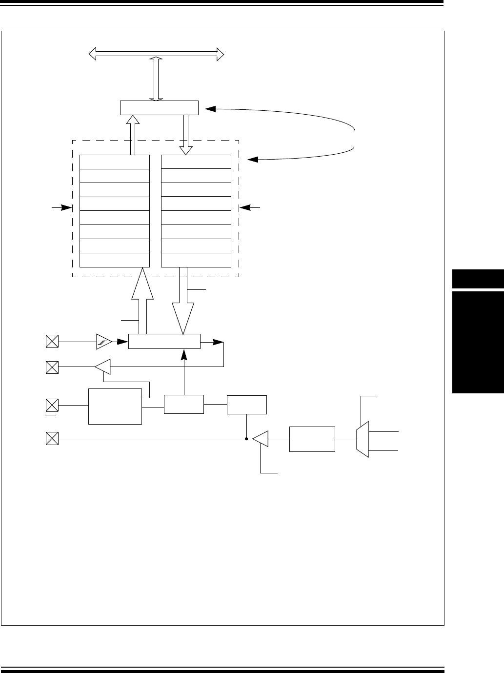
© 2007-2011 Microchip Technology Inc. DS61106G-page 23-3
Section 23. Serial Peripheral Interface (SPI)
Serial Peripheral
Interface (SPI)
23
Figure 23-1: SPI Module Block Diagram
Internal
Data Bus
SDIx
SDOx
SSx
SCKx
SPIxSR(2)
bit 0
Shift
Control
Edge
Select
Enable Master Clock
Baud Rate
Slave Select
Sync Control
Clock
Control
Transmit
SPIxRXB(1)
Receive
and Frame
Note 1: The SPIx Receive Buffer (SPIxRXB) and SPIx Transmit Buffer (SPIxTXB) registers are accessed via the
SPIxBUF register and are multi-element FIFO buffers in Enhanced Buffer mode (pointer arithmetic is circular
for these buffers). Enhanced Buffer mode is not available on all devices. Refer to the specific device data
sheet for availability.
2: The SPIx Shift Register (SPIxSR) is not directly accessible by application software.
3: When the CPU Read Pointer (CRPTR) is less than or equal to the SPI Write Pointer (SWPTR). The CRPTR
is incremented when the application reads a data element from the SPIxRXB register, and the SWPTR is
incremented when a data element is moved from the SPIxSR register to the SPIxRXB register.
4: The SPI Read Pointer (SRPTR) is less than or equal to the CPU Write Pointer (CWPTR). The CWPTR is
incremented when the application writes a new data element to the SPIxBUF register, and the SRPTR is
incremented when data is moved from the SPIxTXB register to the SPIxSR register.
Registers share address SPIxBUF
SPIxBUF
Generator
Write
Read
SPIxTXB(1)
PBCLK
MCLK
MCLKSEL
CWPTR(4)
SRPTR
SWPTR(3)
CRPTR
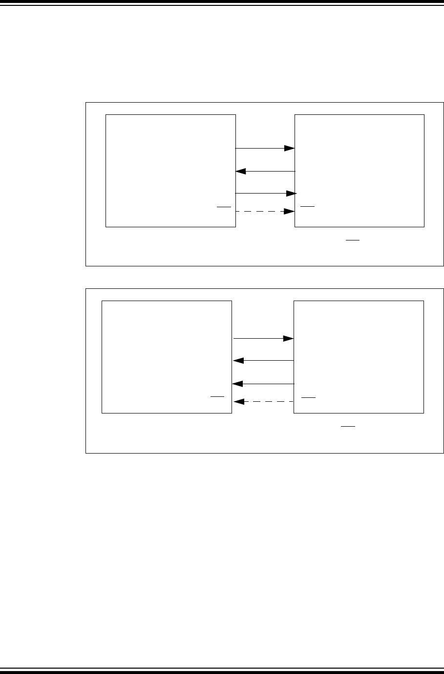
PIC32 Family Reference Manual
DS61106G-page 23-4 © 2007-2011 Microchip Technology Inc.
23.1.1 Normal Mode SPI Operation
In Normal mode operation, the SPI Master controls the generation of the serial clock. The
number of output clock pulses corresponds to the transfer data width: 8, 16, or 32 bits.
Figure 23-2 and Figure 23-3 illustrate SPI Master-to-Slave and Slave-to-Master device
connections.
Figure 23-2: Typical SPI Master-to-Slave Device Connection Diagram
Figure 23-3: Typical SPI Slave-to-Master Device Connection Diagram
SDOx
SDIx
PIC32
Serial Clock
Note 1: In Normal mode, the usage of the Slave Select pin (SSx) is optional.
2: Control of the SDOx pin can be disabled for Receive-Only modes.
GPIO/SSx
SCKx
Slave Select(1)
SDIx
SDOx(2)
PROCESSOR 2
SSx
SCKx
[SPI Master] [Slave]
SDOx(2)
SDIx
PIC32
Serial Clock
Note 1: In Normal mode, the usage of the Slave Select pin (SSx) is optional.
2: The control of the SDOx pin can be disabled for Receive-Only modes.
SSx
SCKx
Slave Select(1)
SDIx
SDOx
PROCESSOR 2
SSx/GPIO
SCKx
[SPI Slave] [Master]
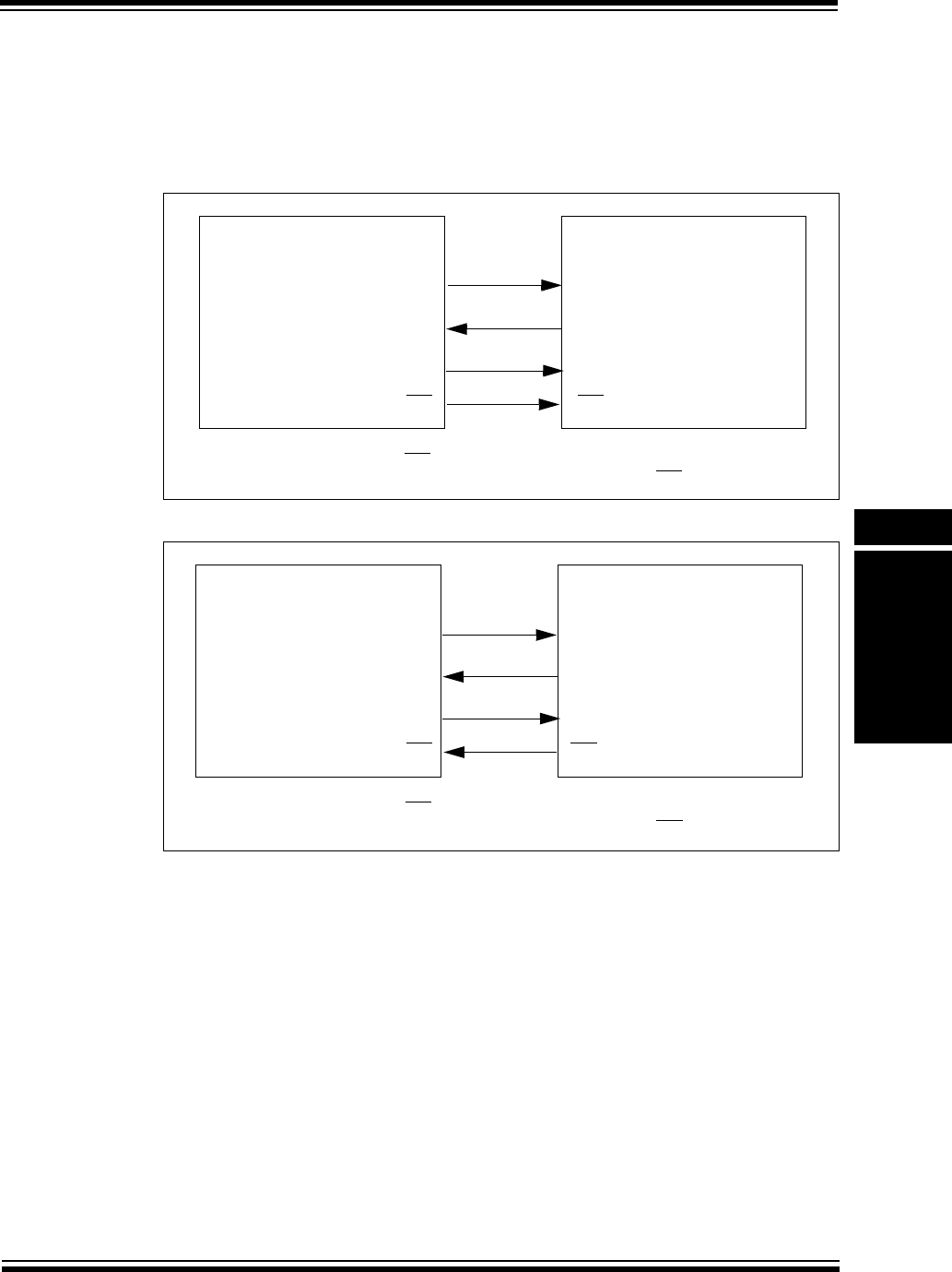
© 2007-2011 Microchip Technology Inc. DS61106G-page 23-5
Section 23. Serial Peripheral Interface (SPI)
Serial Peripheral
Interface (SPI)
23
23.1.2 Framed Mode SPI Operation
In Framed mode operation, the Frame Master controls the generation of the frame
synchronization pulse. The SPI clock is still generated by the SPI Master and is continuously
running. Figure 23-4 and Figure 23-5 illustrate SPI Frame Master and Frame Slave device
connections.
Figure 23-4: Typical SPI Master, Frame Master Connection Diagram
Figure 23-5: Typical SPI Master, Frame Slave Connection Diagram
SDOx
SDIx
PIC32
Serial Clock
Note 1: In Framed SPI mode, the SSx pin is used to transmit/receive the frame synchronization pulse.
2: Framed SPI mode requires the use of all four pins (i.e., using the SSx pin is not optional).
SSx
SCKx
Frame Sync.
Pulse(1,2)
SDIx
SDOx
PROCESSOR 2
SSx
SCKx
[SPI Master, Frame Master] [SPI Slave, Frame Slave]
SDOx
SDIx
Serial Clock
Note 1: In Framed SPI mode, the SSx pin is used to transmit/receive the frame synchronization pulse.
2: Framed SPI mode requires the use of all four pins (i.e., using the SSx pin is not optional).
SSx
SCKx
Frame Sync.
SDIx
SDOx
SSx
SCKx
PIC32
[SPI Master, Frame Slave]
PROCESSOR 2
[SPI Slave, Frame Master]
Pulse(1,2)
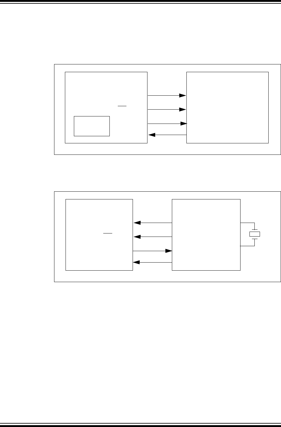
PIC32 Family Reference Manual
DS61106G-page 23-6 © 2007-2011 Microchip Technology Inc.
23.1.3 Audio Protocol Interface Mode
23.1.3.1 SPI IN AUDIO MASTER MODE CONNECTED TO A CODEC SLAVE
Figure 23-6 shows the Bit Clock (BCLK) and Left/Right Channel Clock (LRCK) as generated by
the PIC32 SPI module.
Figure 23-6: Master Generating its Own Clock – Output BCLK and LRCK
23.1.3.2 SPI IN AUDIO SLAVE MODE CONNECTED TO A CODEC MASTER
Figure 23-7 shows the BCLK and LRCK as generated by the codec master.
Figure 23-7: Codec Device as Master Generates Required Clock via External Crystal
SCKx (BCLK)
SSx (LRCK)
SDIx
SDOx
BCLK
LRCK
ADCDAT
DACDAT
PIC32
[SPI Master]
Codec
[Slave]
Internal
Clock
SCK (BCLK)
SSx (LRCK)
SDIx
SDOx
BCLK
LRCK
ADCDAT
DACDAT
PIC32
[SPI Slave]
Codec
[Master]
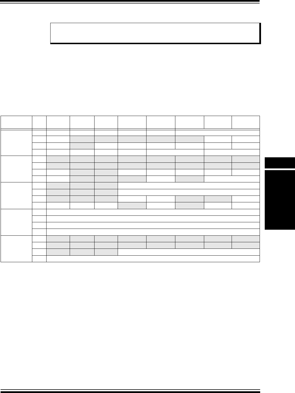
© 2007-2011 Microchip Technology Inc. DS61106G-page 23-7
Section 23. Serial Peripheral Interface (SPI)
Serial Peripheral
Interface (SPI)
23
23.2 STATUS AND CONTROL REGISTERS
The SPI module consists of the following Special Function Registers (SFRs):
•SPIxCON: SPI Control Register
•SPIxCON2: SPI Control Register 2
•SPIxSTAT: SPI Status Register
•SPIxBUF: SPI Buffer Register
•SPIxBRG: SPI Baud Rate Register
Tabl e 23-3 summarizes all SPI-related registers. Corresponding registers appear after the
summary, followed by a detailed description of each register.
Note: Each PIC32 family device variant may have one or more SPI modules. An ‘x’ used
in the names of pins, control/Status bits, and registers denotes the particular
module. Refer to the specific device data sheets for more details.
Table 23-3: SPI SFR Summary
Name Bit
Range
Bit
31/23/15/7
Bit
30/22/14/6
Bit
29/21/13/5
Bit
28/20/12/4
Bit
27/19/11/3
Bit
26/18/10/2
Bit
25/17/9/1
Bit
24/16/8/0
SPIxCON(1,2,3) 31:24 FRMEN FRMSYNC FRMPOL MSSEN(4) FRMSYPW(4) FRMCNT<2:0>(4)
23:16 MCLKSEL(4) — — — — — SPIFE ENHBUF
(4)
15:8 ON — SIDL DISSDO MODE32 MODE16 SMP CKE
7:0 SSEN CKP MSTEN DISSDI(4) STXISEL<1:0>(4) SRXISEL<1:0>(4)
SPIxCON2(1,2,3,5) 31:24 — — — — — — — —
23:16 — — — — — — — —
15:8 SPISGNEXT ——FRMERRENSPIROVENSPITURENIGNROVIGNTUR
7:0 AUDEN — — —AUDMONO— AUDMOD<1:0>
SPIxSTAT(1,2,3) 31:24 — — — RXBUFELM<4:0>
(4)
23:16 — — — TXBUFELM<4:0>
(4)
15:8 — — —FRMERR
(4) SPIBUSY ——SPITUR
7:0 SRMT(4) SPIROV SPIRBE(4) —SPITBE— SPITBF
(4) SPIRBF
SPIxBUF 31:24 DATA<31:24>
23:16 DATA<23:16>
15:8 DATA<15:8>
7:0 DATA<7:0>
SPIxBRG(1,2,3) 31:24 — — — — — — — —
23:16 — — — — — — — —
15:8 — — —BRG<12:8>
(6)
7:0 BRG<7:0>(6)
Legend: — = unimplemented, read as ‘0’. Address offset values are shown in hexadecimal.
Note 1: This register has an associated Clear register at an offset of 0x4 bytes. These registers have the same name with CLR appended to the
end of the register name (e.g., SPIxCONCLR). Writing a ‘1’ to any bit position in the Clear register will clear valid bits in the associated
register. Reads from the Clear register should be ignored.
2: This register has an associated Set register at an offset of 0x8 bytes. These registers have the same name with SET appended to the end
of the register name (e.g., SPIxCONSET). Writing a ‘1’ to any bit position in the Set register will set valid bits in the associated register.
Reads from the Set register should be ignored.
3: This register has an associated Invert register at an offset of 0xC bytes. These registers have the same name with INV appended to the
end of the register name (e.g., SPIxCONINV). Writing a ‘1’ to any bit position in the Invert register will invert valid bits in the associated
register. Reads from the Invert register should be ignored.
4: This bit is not available on all devices. Refer to the specific device data sheet for details.
5: This register is not available on all devices. Refer to the specific data sheet for details.
6: Depending on the device, BRG can have up to 13 bits. Refer to the specific device data sheet for details.

PIC32 Family Reference Manual
DS61106G-page 23-8 © 2007-2011 Microchip Technology Inc.
Register 23-1: SPIxCON: SPI Control Register
Bit
Range
Bit
31/23/15/7
Bit
30/22/14/6
Bit
29/21/13/5
Bit
28/20/12/4
Bit
27/19/11/3
Bit
26/18/10/2
Bit
25/17/9/1
Bit
24/16/8/0
31:24 R/W-0 R/W-0 R/W-0 R/W-0 R/W-0 R/W-0 R/W-0 R/W-0
FRMEN FRMSYNC FRMPOL MSSEN(1,2) FRMSYPW(1) FRMCNT<2:0>(1)
23:16 R/W-0 U-0 U-0 U-0 U-0 U-0 R/W-0 R/W-0
MCLKSEL — — — — —SPIFEENHBUF
(1)
15:8 R/W-0 U-0 R/W-0 R/W-0 R/W-0 R/W-0 R/W-0 R/W-0
ON —SIDLDISSDOMODE32MODE16SMPCKE
7:0 R/W-0 R/W-0 R/W-0 R/W-0 R/W-0 R/W-0 R/W-0 R/W-0
SSEN CKP MSTEN DISSDI STXISEL<1:0>(1,3) SRXISEL<1:0>(1,3)
Legend:
R = Readable bit W = Writable bit U = Unimplemented bit, read as ‘0’
-n = Value at POR ‘1’ = Bit is set ‘0’ = Bit is cleared x = Bit is unknown
bit 31 FRMEN: Framed SPI Support bit
1 = Framed SPI support is enabled (SSx pin used as FSYNC input/output)
0 = Framed SPI support is disabled
bit 30 FRMSYNC: Frame Sync Pulse Direction Control on SSx pin bit (Framed SPI mode only)
1 = Frame sync pulse input (Slave mode)
0 = Frame sync pulse output (Master mode)
bit 29 FRMPOL: Frame Sync Polarity bit (Framed SPI mode only)
1 = Frame pulse is active-high
0 = Frame pulse is active-low
bit 28 MSSEN: Master Mode Slave Select Enable bit(1,2)
1 = Slave select SPI support enabled. The SS pin is automatically driven during transmission in Master
mode. Polarity is determined by the FRMPOL bit
0 = Slave select SPI support is disabled
bit 27 FRMSYPW: Frame Sync Pulse Width bit(1)
1 = Frame sync pulse is one word length wide, as defined by MODE<32,16> bits (SPIxCON<11:10>)
0 = Frame sync pulse is one clock wide
bit 26-24 FRMCNT<2:0>: Frame Sync Pulse Counter bits
This bit controls the number of data characters transmitted per pulse(1).
111 = Reserved; do not use
110 = Reserved; do not use
101 = Generate a frame sync pulse on every 32 data characters
100 = Generate a frame sync pulse on every 16 data characters
011 = Generate a frame sync pulse on every 8 data characters
010 = Generate a frame sync pulse on every 4 data characters
001 = Generate a frame sync pulse on every 2 data characters
000 = Generate a frame sync pulse on every data character
This bit is only valid in Framed SPI mode (FRMEN = 1).
bit 23 MCLKSEL: Master Clock Select bit(2)
1 = MCLK is used by the Baud Rate Generator
0 = PBCLK is used by the Baud Rate Generator
bit 22-18 Unimplemented: Write ‘0’; ignore read
Note 1: These bits are not available on all devices. Refer to the specific device data sheet for availability.
2: When FRMEN = 1, the MSSEN bit is not used.
3: Valid only when enhanced buffers are enabled (ENHBUF = 1).

© 2007-2011 Microchip Technology Inc. DS61106G-page 23-9
Section 23. Serial Peripheral Interface (SPI)
Serial Peripheral
Interface (SPI)
23
bit 17 SPIFE: Frame Sync Pulse Edge Select bit (Framed SPI mode only)
1 = Frame synchronization pulse coincides with the first bit clock
0 = Frame synchronization pulse precedes the first bit clock
bit 16 ENHBUF: Enhanced Buffer Enable bit(1)
1 = Enhanced Buffer mode is enabled
0 = Enhanced Buffer mode is disabled
bit 15 ON: SPI Peripheral On bit
1 = SPI Peripheral is enabled
0 = SPI Peripheral is disabled
When ON = 1, DISSDO and DISSDI are the only other bits that can be modified. When using the 1:1 PBCLK
divisor, the user’s software should not read or write the peripheral’s SFRs in the SYSCLK cycle immediately
following the instruction that clears the module’s ON bit.
bit 14 Unimplemented: Write ‘0’; ignore read
bit 13 SIDL: Stop in Idle Mode bit
1 = Discontinue operation when CPU enters in Idle mode
0 = Continue operation in Idle mode
bit 12 DISSDO: Disable SDOx pin bit
1 = SDOx pin is not used by the module (pin is controlled by associated PORT register)
0 = SDOx pin is controlled by the module
bit 11-10 MODE<32,16>: 32/16-bit Communication Select bits
When AUDEN = 1:
MODE32 MODE16 Communication
1124-bit Data, 32-bit FIFO, 32-bit Channel/64-bit Frame
1032-bit Data, 32-bit FIFO, 32-bit Channel/64-bit Frame
0116-bit Data, 16-bit FIFO, 32-bit Channel/64-bit Frame
0016-bit Data, 16-bit FIFO, 16-bit Channel/32-bit Frame
When AUDEN = 0:
MODE32 MODE16 Communication
1x32-bit
0116-bit
008-bit
bit 9 SMP: SPI Data Input Sample Phase bit
Master mode (MSTEN = 1):
1 = Input data sampled at end of data output time
0 = Input data sampled at middle of data output time
Slave mode (MSTEN = 0):
SMP value is ignored when SPI is used in Slave mode. The module always uses SMP = 0.
bit 8 CKE: SPI Clock Edge Select bit
1 = Serial output data changes on transition from active clock state to idle clock state (see CKP bit)
0 = Serial output data changes on transition from idle clock state to active clock state (see CKP bit)
The CKE bit is not used in the Framed SPI mode. The user should program this bit to ‘0’ for the Framed
SPI mode (FRMEN = 1).
bit 7 SSEN: Slave Select Enable (Slave mode) bit
1 = SSx pin used for Slave mode
0 = SSx pin not used for Slave mode, pin controlled by port function.
bit 6 CKP: Clock Polarity Select bit
1 = Idle state for clock is a high level; active state is a low level
0 = Idle state for clock is a low level; active state is a high level
Register 23-1: SPIxCON: SPI Control Register (Continued)
Note 1: These bits are not available on all devices. Refer to the specific device data sheet for availability.
2: When FRMEN = 1, the MSSEN bit is not used.
3: Valid only when enhanced buffers are enabled (ENHBUF = 1).

PIC32 Family Reference Manual
DS61106G-page 23-10 © 2007-2011 Microchip Technology Inc.
bit 5 MSTEN: Master Mode Enable bit
1 = Master mode
0 = Slave mode
bit 4 DISSDI: Disable SDI bit
1 = SDIx pin is not used by the SPI module (pin is controlled by PORT function)
0 = SDIx pin is controlled by the SPI module
bit 3-2 STXISEL<1:0>: SPI Transmit Buffer Empty Interrupt Mode bits(1,3)
11 = SPIxTXIF is set when the buffer is not full (has one or more empty elements)
10 = SPIxTXIF is set when the buffer is empty by one-half or more
01 = SPIxTXIF is set when the buffer is completely empty
00 = SPIxTXIF is set when the last transfer is shifted out of SPISR and transmit operations are
complete
bit 1-0 SRXISEL<1:0>: SPI Receive Buffer Full Interrupt Mode bits(1,3)
11 = SPIxRXIF is set when the buffer is full
10 = SPIxRXIF is set when the buffer is full by one-half or more
01 = SPIxRXIF is set when the buffer is not empty
00 = SPIxRXIF is set when the last word in the receive buffer is read (i.e., buffer is empty)
Register 23-1: SPIxCON: SPI Control Register (Continued)
Note 1: These bits are not available on all devices. Refer to the specific device data sheet for availability.
2: When FRMEN = 1, the MSSEN bit is not used.
3: Valid only when enhanced buffers are enabled (ENHBUF = 1).

© 2007-2011 Microchip Technology Inc. DS61106G-page 23-11
Section 23. Serial Peripheral Interface (SPI)
Serial Peripheral
Interface (SPI)
23
Register 23-2: SPIxCON2: SPI Control Register 2
Bit
Range
Bit
31/23/15/7
Bit
30/22/14/6
Bit
29/21/13/5
Bit
28/20/12/4
Bit
27/19/11/3
Bit
26/18/10/2
Bit
25/17/9/1
Bit
24/16/8/0
31:24 U-0 U-0 U-0 U-0 U-0 U-0 U-0 U-0
— — — — — — — —
23:16 U-0 U-0 U-0 U-0 U-0 U-0 U-0 U-0
— — — — — — — —
15:8 R/W-0 R/W-0 R/W-0 R/W-0 R/W-1 R/W-1 R/W-0 R/W-0
SPISGNEXT ——FRMERRENSPIROVENSPITURENIGNROVIGNTUR
7:0 R/W-0 R/W-0 R/W-0 R/W-0 R/W-0 R/W-0 R/W-0 R/W-0
AUDEN(1,3) — — —AUDMONO
(2) —AUDMOD<1:0>
(2,4)
Legend:
R = Readable bit W = Writable bit U = Unimplemented bit, read as ‘0’
-n = Value at POR ‘1’ = Bit is set ‘0’ = Bit is cleared x = Bit is unknown
bit 31-16 Unimplemented: Write ‘0’; ignore read
bit 15 SPISGNEXT: Sign Extend Read Data from the RX FIFO bit
1 = Data from RX FIFO is sign extended
0 = Data from RX FIFO is not sign extened
bit 14-13 Unimplemented: Write ‘0’; ignore read
bit 12 FRMERREN: Enable Interrupt Events via FRMERR bit
1 = Frame Error overflow generates error interrupts
0 = Frame Error does not generate error interrupts
bit 11 SPIROVEN: Enable Interrupt Events via SPIROV bit
1 = Receive overflow generates error interrupts
0 = Receive overflow does not generate error interrupts
bit 10 SPITUREN: Enable Interrupt Events via SPITUR bit
1 = Transmit Underrun generates error interrupts
0 = Transmit Underrun does not generate error interrupts
bit 9 IGNROV: Ignore Receive Overflow bit (for Audio Data Transmissions)
1 = A ROV is not a critical error; during ROV data in the FIFO is not overwritten by receive data
0 = A ROV is a critical error which stop SPI operation
bit 8 IGNTUR: Ignore Transmit Underrun bit (for Audio Data Transmissions)
1 = A TUR is not a critical error and zeros are transmitted until the SPIxTXB is not empty
0 = A TUR is a critical error which stop SPI operation
bit 7 AUDEN: Enable Audio CODEC Support bit(1,3)
1 = Audio protocol enabled
0 = Audio protocol disabled
bit 6-5 Unimplemented: Write ‘0’; ignore read
Note 1: This bit can only be written when the ON bit = 0.
2: This bit can only be written when the ON bit = 0, and is only valid for AUDEN = 1.
3: When Audio mode is enabled (i.e., AUDEN = 1), the following bits in the SPIxCON register are configured
by the module internally:
•The direction of the Bit Clock (BCLK) and Left/Right Channel Clock (LRCK) are selected based on the
MSTEN bit
•FRMEN = 1, FRMCNT = 1, SMP = 0
•In Slave mode (MSTN = 0, FRMSYNC = 1) and in Master mode MSTN = 1, FRMSYNC = 0
4: In I2S mode, SPIFE = 0, in Right or Left-Justified mode, SPIFE = 1, except in DSP/PCM mode when
FRMSYPW = 0.
5: This feature is not available on all devices. Refer to the specific device data sheet for availability.

PIC32 Family Reference Manual
DS61106G-page 23-12 © 2007-2011 Microchip Technology Inc.
bit 3 AUDMONO: Transmit Audio Data Format bit(2)
1 = Audio data is mono (Each data word is transmitted on both left and right channels)
0 = Audio data is stereo
bit 2 Unimplemented: Write ‘0’; ignore read
bit 1-0 AUDMOD<1:0>: Audio Protocol Mode bit(2,4)
11 = PCM/DSP mode
10 = Right-Justified mode
01 = Left-Justified mode
00 = I2S mode(5)
Register 23-2: SPIxCON2: SPI Control Register 2 (Continued)
Note 1: This bit can only be written when the ON bit = 0.
2: This bit can only be written when the ON bit = 0, and is only valid for AUDEN = 1.
3: When Audio mode is enabled (i.e., AUDEN = 1), the following bits in the SPIxCON register are configured
by the module internally:
•The direction of the Bit Clock (BCLK) and Left/Right Channel Clock (LRCK) are selected based on the
MSTEN bit
•FRMEN = 1, FRMCNT = 1, SMP = 0
•In Slave mode (MSTN = 0, FRMSYNC = 1) and in Master mode MSTN = 1, FRMSYNC = 0
4: In I2S mode, SPIFE = 0, in Right or Left-Justified mode, SPIFE = 1, except in DSP/PCM mode when
FRMSYPW = 0.
5: This feature is not available on all devices. Refer to the specific device data sheet for availability.

© 2007-2011 Microchip Technology Inc. DS61106G-page 23-13
Section 23. Serial Peripheral Interface (SPI)
Serial Peripheral
Interface (SPI)
23
Register 23-3: SPIxSTAT: SPI Status Register
Bit
Range
Bit
31/23/15/7
Bit
30/22/14/6
Bit
29/21/13/5
Bit
28/20/12/4
Bit
27/19/11/3
Bit
26/18/10/2
Bit
25/17/9/1
Bit
24/16/8/0
31:24 U-0 U-0 U-0 R-0 R-0 R-0 R-0 R-0
— — — RXBUFELM<4:0>(1)
23:16 U-0 U-0 U-0 R-0 R-0 R-0 R-0 R-0
— — — TXBUFELM<4:0>(1)
15:8 U-0 U-0 U-0 R/C-0, HS R-0 U-0 U-0 R/C-0,HS
— — —FRMERRSPIBUSY——SPITUR
(1)
7:0 R-0 R/C-0,HS R-0 U-0 R-1 U-0 R-0 R-0
SRMT(12) SPIROV SPIRBE(1) —SPITBE—SPITBF
(1) SPIRBF
Legend: C = Clearable bit HS = Set in Hardware
R = Readable bit W = Writable bit U = Unimplemented bit, read as ‘0’
-n = Value at POR ‘1’ = Bit is set ‘0’ = Bit is cleared x = Bit is unknown
bit 31-29 Unimplemented: Write ‘0’; ignore read
bit 28-24 RXBUFELM<4:0>: Receive Buffer Element Count bits (valid only when ENHBUF = 1)(1)
Number of receive samples contained in the FIFO.
bit 23-21 Unimplemented: Write ‘0’; ignore read
bit 20-16 TXBUFELM<4:0>: Transmit Buffer Element Count bits (valid only when ENHBUF = 1)(1)
Number of transmit samples remaining in the FIFO.
bit 15-13 Unimplemented: Write ‘0’; ignore read
bit 12 FRMERR: SPI Frame Error status bit
1 = Frame error detected
0 = No Frame error detected
FRMERR is only valid when FRMEN = 1. This bit is only set by hardware. It can be cleared by writing a zero,
preferably with the command SPIxSTATCLR = 1<<12. It can also be cleared by disabling and re-enabling
the module using the SPIxCON.ON bit.
bit 11 SPIBUSY: SPI Activity Status bit
1 = SPI peripheral is currently busy with some transactions
0 = SPI peripheral is currently idle
bit 10-9 Unimplemented: Write ‘0’; ignore read
bit 8 SPITUR: Transmit Under Run bit(1)
1 = Transmit buffer has encountered an underrun condition
0 = Transmit buffer has no underrun condition
This bit is only valid in Framed Sync mode. This bit is only set by hardware. It can be cleared by writing a
zero, preferably with the command SPIxSTATCLR = 1<<8. It can also be cleared by disabling and
re-enabling the module using the SPIxCON.ON bit.
bit 7 SRMT: Shift Register Empty bit (valid only when ENHBUF = 1)(1)
1 = When SPI module shift register is empty
0 = When SPI module shift register is not empty
bit 6 SPIROV: Receive Overflow Flag bit
1 = A new data is completely received and discarded. The user software has not read the previous data in
the SPIxBUF register.
0 = No overflow has occurred
This bit is only set by hardware. It can be cleared by writing a zero, preferably with the command
SPIxSTATCLR = 1<<6. It can also be cleared by disabling and re-enabling the module using the
SPIxCON.ON bit.
Note 1: These bits are not available on all devices. Refer to the specific device data sheet for availability.

PIC32 Family Reference Manual
DS61106G-page 23-14 © 2007-2011 Microchip Technology Inc.
bit 5 SPIRBE: RX FIFO Empty bit (valid only when ENHBUF = 1)
1 = RX FIFO is empty (CRPTR = SWPTR)
0 = RX FIFO is not empty (CRPTR < SWPTR)
bit 4 Unimplemented: Write ‘0’; ignore read
bit 3 SPITBE: SPI Transmit Buffer Empty Status bit(1)
1 = Transmit buffer, SPIxTXB is empty
0 = Transmit buffer, SPIxTXB is not empty
Automatically set in hardware when SPI transfers data from SPIxTXB to SPIxSR.
Automatically cleared in hardware when SPIxBUF is written to, loading SPIxTXB.
bit 2 Unimplemented: Write ‘0’; ignore read
bit 1 SPITBF: SPI Transmit Buffer Full Status bit(1)
1 = Transmit not yet started, SPITXB is full
0 = Transmit buffer is not full
Standard Buffer Mode:
Automatically set in hardware when the core writes to the SPIBUF location, loading SPITXB.
Automatically cleared in hardware when the SPI module transfers data from SPITXB to SPISR.
Enhanced Buffer Mode:
Set when there is no available space in the FIFO.
bit 0 SPIRBF: SPI Receive Buffer Full Status bit
1 = Receive buffer, SPIxRXB is full
0 = Receive buffer, SPIxRXB is not full
Standard Buffer Mode:
Automatically set in hardware when the SPI module transfers data from SPIxSR to SPIxRXB.
Automatically cleared in hardware when SPIxBUF is read from, reading SPIxRXB.
Enhanced Buffer Mode:
Set when there is no available space in the FIFO.
Register 23-3: SPIxSTAT: SPI Status Register (Continued)
Note 1: These bits are not available on all devices. Refer to the specific device data sheet for availability.
© 2007-2011 Microchip Technology Inc. DS61106G-page 23-15
Section 23. Serial Peripheral Interface (SPI)
Serial Peripheral
Interface (SPI)
23
Register 23-4: SPIxBUF: SPI Buffer Register
Bit
Range
Bit
31/23/15/7
Bit
30/22/14/6
Bit
29/21/13/5
Bit
28/20/12/4
Bit
27/19/11/3
Bit
26/18/10/2
Bit
25/17/9/1
Bit
24/16/8/0
31:24 R/W-0 R/W-0 R/W-0 R/W-0 R/W-0 R/W-0 R/W-0 R/W-0
DATA<31:24>
23:16 R/W-0 R/W-0 R/W-0 R/W-0 R/W-0 R/W-0 R/W-0 R/W-0
DATA<23:16>
15:8 R/W-0 R/W-0 R/W-0 R/W-0 R/W-0 R/W-0 R/W-0 R/W-0
DATA<15:8>
7:0 R/W-0 R/W-0 R/W-0 R/W-0 R/W-0 R/W-0 R/W-0 R/W-0
DATA<7:0>
Legend:
R = Readable bit W = Writable bit U = Unimplemented bit, read as ‘0’
-n = Value at POR ‘1’ = Bit is set ‘0’ = Bit is cleared x = Bit is unknown
bit 31-0 DATA<31:0>: SPI Transmit/Receive Buffer register
Serves as a memory-mapped value of Transmit (SPIxTXB) and Receive (SPIxRXB) registers.
When 32-bit Data mode is enabled (MODE<32,16> (SPIxCON<11:10>) = 1x):
All 32 bits (SPIxBUF<31:0>) of this register are used to form a 32-bit character.
When 16-bit Data mode is enabled (MODE<32,16> (SPIxCON<11:10>) = 01):
Only the lower 16 bits (SPIxBUF<15:0>) of this register are used to form the 16-bit character.
When 8-bit Data mode is enabled (MODE<32,16> (SPIxCON<11:10>) = 00):
Only the lower 8 bits (SPIxBUF<7:0>) of this register are used to form the 8-bit character.
Register 23-5: SPIXBRG: SPI Baud Rate Register
Bit
Range
Bit
31/23/15/7
Bit
30/22/14/6
Bit
29/21/13/5
Bit
28/20/12/4
Bit
27/19/11/3
Bit
26/18/10/2
Bit
25/17/9/1
Bit
24/16/8/0
31:24 U-0 U-0 U-0 U-0 U-0 U-0 U-0 U-0
— — — — — — — —
23:16 U-0 U-0 U-0 U-0 U-0 U-0 U-0 U-0
— — — — — — — —
15:8 U-0 U-0 U-0 R/W-0 R/W-0 R/W-0 R/W-0 R/W-0
— — — BRG<12:8>
7:0 R/W-0 R/W-0 R/W-0 R/W-0 R/W-0 R/W-0 R/W-0 R/W-0
BRG<7:0>
Legend:
R = Readable bit W = Writable bit U = Unimplemented bit, read as ‘0’
-n = Value at POR ‘1’ = Bit is set ‘0’ = Bit is cleared x = Bit is unknown
bit 31-13 Unimplemented: Write ‘0’; ignore read
bit 12-0 BRG<12:0>: Baud Rate Divisor bits

PIC32 Family Reference Manual
DS61106G-page 23-16 © 2007-2011 Microchip Technology Inc.
23.3 MODES OF OPERATION
The SPI module offers the following operating modes:
•8-bit, 16-bit, and 32-bit data transmission modes
•8-bit, 16-bit, and 32-bit data reception modes
•Master and Slave modes
•Framed SPI modes
•Audio Protocol Interface mode
23.3.1 8-bit, 16-bit, and 32-bit Operation
The SPI module allows three types of data widths when transmitting and receiving data over an
SPI bus. The selection of data width determines the minimum length of SPI data. For example,
when the selected data width is 32, all transmission and receptions are performed in 32-bit
values. All reads and writes from the CPU are also performed in 32-bit values. Accordingly, the
application software should select the appropriate data width to maximize its data throughput.
Two control bits, MODE32 and MODE16 (SPIxCON<11:10>), which are referred to as
MODE<32,16>, define the mode of operation. To change the mode of operation on the fly, the
SPI module must be idle (i.e., not performing any transactions). If the SPI module is switched off
(SPIxCON<15> = 0), the new mode will be available when the module is again switched on.
Additionally, the following items should be noted in this context:
• The MODE<32,16> bits should not be changed when a transaction is in progress
•The first bit to be shifted out from SPIxSR varies with the selected mode of operation:
-8-bit mode, bit 7
-16-bit mode, bit 15
-32-bit mode, bit 31
•In each mode, data is shifted into bit 0 of the SPIxSR
•The number of clock pulses at the SCKx pin are also dependent on the selected mode of
operation:
-8-bit mode, 8 clocks
-16-bit mode, 16 clocks
-32-bit mode, 32 clocks
23.3.2 Buffer Modes
There are two SPI buffering modes: Standard and Enhanced.
23.3.2.1 STANDARD BUFFER MODE
The SPI Data Receive/Transmit Buffer (SPIxBUF) register is actually two separate internal
registers: the Transmit Buffer (SPIxTXB) and the Receive Buffer (SPIxRXB). These two
unidirectional registers share the SFR address of SPIxBUF.
When a complete byte/word is received, it is transferred from SPIxSR to SPIxRXB and the
SPIxRBF flag is set. If the software reads the SPIxBUF buffer, the SPIRBF bit is cleared.
As the software writes to SPIxBUF, the data is loaded into the SPIxTXB bit and the SPIxTBF bit
is set by hardware. As the data is transmitted out of SPIxSR, the SPIxTBF flag is cleared.
The SPI module double-buffers transmit/receive operations and allow continuous data transfers
in the background. Transmission and reception occur simultaneously in SPIxSR.
Note 1: In Framed SPI mode, these four pins are used: SDIx, SDOx, SCKx, and SSx.
2: If the Slave Select feature is used, all four pins listed in Note 1 are used.
3: If Standard SPI is used, but CKE = 1, enabling/using the Slave Select feature is
mandatory, and therefore, all four pins listed in Note 1 are used.
4: If Standard SPI is used, but DISSDO = 1, only two pins are used: SDIx and SCKx;
unless Slave Select is also enabled.
5: In all other cases, three pins are used: SDIx, SDOx, and SCKx.
Note: Enhanced Buffer mode is not available on all devices. Refer to the specific device
data sheet for details.
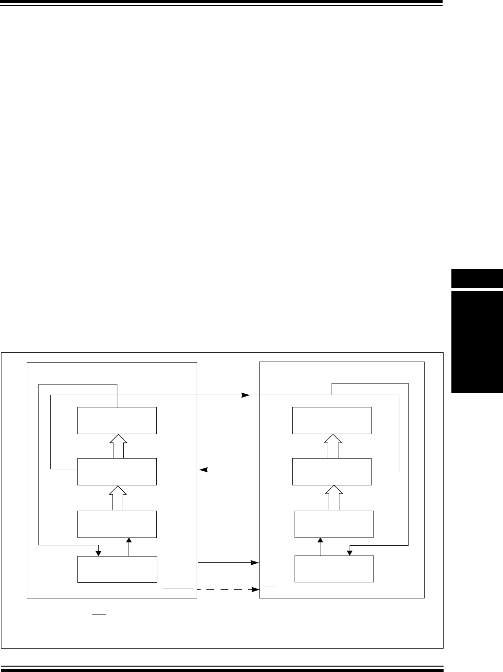
© 2007-2011 Microchip Technology Inc. DS61106G-page 23-17
Section 23. Serial Peripheral Interface (SPI)
Serial Peripheral
Interface (SPI)
23
23.3.2.2 ENHANCED BUFFER MODE
The Enhanced Buffer Enable (ENHBUF) bit in the SPI Control (SPIxCON<16>) register can be
set to enable the Enhanced Buffer mode.
In Enhanced Buffer mode, two 128-bit FIFO buffers are used for the transmit buffer (SPIxTXB)
and the receive buffer (SPIxRXB). SPIxBUF provides access to both the receive and transmit
FIFOs and the data transmission and reception in the SPISR buffer in this mode is identical to
that in Standard Buffer mode. The FIFO depth depends on the data width chosen by the
Word/Half-Word Byte Communication Select (MODE<32,16>) bits in the SPI Control
(SPIxCON<11:10>) register. If the MODE field selects 32-bit data lengths, the FIFO is 4 deep, if
MODE selects 16-bit data lengths, the FIFO is 8 deep, or if MODE selects 8-bit data lengths the
FIFO is 16 deep.
The SPITBF status bit is set when all of the elements in the transmit FIFO buffer are full and is
cleared if one or more of those elements are empty. The SPIRBF status bit is set when all of the
elements in the receive FIFO buffer are full and is cleared if the SPIxBUF buffer is read by the
software.
The SPITBE status bit is set if all the elements in the transmit FIFO buffer are empty and is
cleared otherwise. The SPIRBE bit is set if all of the elements in the receive FIFO buffer are
empty and is cleared otherwise. The Shift Register Empty (SRMT) bit is valid only in Enhanced
Buffer mode and is set when the shift register is empty and cleared otherwise.
There is no underrun or overflow protection against reading an empty receive FIFO element or
writing a full transmit FIFO element. However, the SPIxSTAT register provides the Transmit
Underrun Status bit (SPITUR) and Receive Overflow Status bit (SPIROV), which can be
monitored along with the other status bits.
The Receive Buffer Element Count bits (RXBUFELM<4:0>) in the SPI Status
(SPIxSTAT<28:24>) register indicate the number of unread elements in the receive FIFO. The
Transmit Buffer Element Count bits (TXBUFELM<4:0>) in the SPI Status (SPIxSTAT<20:16>)
register indicate the number of elements not transmitted in the transmit FIFO.
23.3.3 Master and Slave Modes
Figure 23-8: SPI Master/Slave Connection Diagram
Serial Receive Buffer
(SPIxRXB)
Shift Register
(SPIxSR)
LSb
MSb
SDIx
SDOx
PROCESSOR 2
SCKx
SSx(1)
Serial Transmit Buffer
(SPIxTXB)
Serial Receive Buffer
(SPIxRXB)(2)
Shift Register
(SPIxSR)
MSb LSb
SDOx
SDIx
PIC32
Serial Clock
SSEN (SPIxCON<7>) =1 and
MSTEN (SPIxCON<5>) =0
Note 1: Using the SSx pin in Slave mode of operation is optional.
2: User must write transmit data to SPIxBUF and read received data from SPIxBUF. The SPIxTXB and SPIxRXB
registers are memory mapped to SPIxBUF.
GPIO/SSx
SCKx
Serial Transmit Buffer
(SPIxTXB)(2)
MSTEN (SPIxCON<5>)=1
SPI Buffer
(SPIxBUF)
SPI Buffer
(SPIxBUF)
[SPI Master] [SPI Slave]

PIC32 Family Reference Manual
DS61106G-page 23-18 © 2007-2011 Microchip Technology Inc.
23.3.3.1 MASTER MODE OPERATION
Perform the following steps to set up the SPI module for the Master mode operation:
1. Disable the SPI interrupts in the respective IECx register.
2. Stop and reset the SPI module by clearing the ON bit.
3. Clear the receive buffer.
4. Clear the ENHBUF bit (SPIxCON<16>) if using Standard Buffer mode or set the bit if using
Enhanced Buffer mode.
5. If SPI interrupts are not going to be used, skip this step and continue to step 5. Otherwise
the following additional steps are performed:
a) Clear the SPIx interrupt flags/events in the respective IFSx register.
b) Write the SPIx interrupt priority and subpriority bits in the respective IPCx register.
c) Set the SPIx interrupt enable bits in the respective IECx register.
6. Write the Baud Rate register, SPIxBRG.
7. Clear the SPIROV bit (SPIxSTAT<6>).
8. Write the desired settings to the SPIxCON register with MSTEN (SPIxCON<5>) = 1.
9. Enable SPI operation by setting the ON bit (SPIxCON<15>).
10. Write the data to be transmitted to the SPIxBUF register. Transmission (and reception) will
start as soon as data is written to the SPIxBUF register.
In Master mode, the PBCLK is divided and then used as the serial clock. The division is based
on the settings in the SPIxBRG register. The serial clock is output via the SCKx pin to slave
devices. Clock pulses are only generated when there is data to be transmitted; except when in
Framed mode, when clock is generated continuously. For further information, refer to 23.3.7 “SPI
Master Mode Clock Frequency”.
The Master Mode Slave Select Enable (MSSEN) bit in the SPI Control register (SPIxCON<28>)
can be set to automatically drive the slave select signal (SS) in Master mode. Clearing this bit
disables the slave select signal support in Master mode. The FRMPOL bit (SPIxCON<29>)
determines the polarity for the slave select signal in Master mode.
In devices that do not feature the MSSEN bit, the Slave Select signal (in non-Framed SPI mode)
must be generated by using the SSx pin or another general purpose I/O pin under software
control.
The CKP (SPIxCON<6>) and CKE (SPIxCON<8>) bits determine on which edge of the clock
data transmission occurs.
Both data to be transmitted and data that is received are written to, or read from, the SPIxBUF
register, respectively.
The following progression describes the SPI module operation in Master mode:
1. Once the module is set up for Master mode operation and enabled, data to be transmitted
is written to SPIxBUF register. The SPITBE bit (SPIxSTAT<3>) is cleared.
2. The contents of SPIxTXB are moved to the shift register, SPIxSR (see Figure 23-8), and
the SPITBE bit is set by the module.
3. A series of 8/16/32 clock pulses shifts 8/16/32 bits of transmit data from SPIxSR to the
SDOx pin and simultaneously shifts the data at the SDIx pin into SPIxSR.
Note: The SPI device must be turned off prior to changing the mode from Slave to Master.
(When using the Slave Select mode, the SSx or another GPIO pin is used to control
the slave’s SSx input. The pin must be controlled in software.)
Note: The MSSEN bit is not available on all devices. Refer to the specific device data
sheet for details. This bit should not be set the SPI Framed mode is enabled (i.e.,
FRMEN = 1).
Note: The user must turn off the SPI device prior to changing the CKE or CKP bits.
Otherwise, the behavior of the device is not guaranteed.

© 2007-2011 Microchip Technology Inc. DS61106G-page 23-19
Section 23. Serial Peripheral Interface (SPI)
Serial Peripheral
Interface (SPI)
23
4. When the transfer is complete, the following events will occur:
a) The SPIxRXIF interrupt flag bit is set. SPI interrupts can be enabled by setting the
SPIxRXIE interrupt enable bit. The SPIxRXIF flag is not cleared automatically by the
hardware.
b) Also, when the ongoing transmit and receive operation is completed, the contents of
SPIxSR are moved to SPIxRXB.
c) The SPIRBF bit (SPIxSTAT<0>) is set by the module, indicating that the receive
buffer is full. Once SPIxBUF is read by the user code, the hardware clears the
SPIRBF bit. In Enhanced Buffer mode the SPIRBE bit (SPIxSTAT<5>) is set when
the SPIxRXB FIFO buffer is completely empty and cleared when not empty.
5. If the SPIRBF bit is set (the receive buffer is full) when the SPI module needs to transfer
data from SPIxSR to SPIxRXB, the module will set the SPIROV bit (SPIxSTAT<6>)
indicating an overflow condition.
6. Data to be transmitted can be written to SPIxBUF by the user software at any time, if the
SPITBE bit (SPIxSTAT<3>) is set. The write can occur while SPIxSR is shifting out the
previously written data, allowing continuous transmission. In Enhanced Buffer mode the
SPITBF bit (SPIxSTAT<1>) is set when the SPIxTXB FIFO buffer is completely full and
clear when it is not full.
Example 23-1: Initialization Code for 16-bit SPI Master Mode
Note: The SPIxSR register cannot be written to directly by the user. All writes to the
SPIxSR register are performed through the SPIxBUF register.
/*
The following code example will initialize the SPI1 in Master mode.
It assumes that none of the SPI1 input pins are shared with an analog input. If so, the
AD1PCFG and corresponding TRIS registers have to be properly configured.
*/
int rData;
IEC0CLR=0x03800000; // disable all interrupts
SPI1CON = 0; // Stops and resets the SPI1.
rData=SPI1BUF; // clears the receive buffer
IFS0CLR=0x03800000; // clear any existing event
IPC5CLR=0x1f000000; // clear the priority
IPC5SET=0x0d000000; // Set IPL=3, Subpriority 1
IEC0SET=0x03800000; // Enable RX, TX and Error interrupts
SPI1BRG=0x1; // use FPB/4 clock frequency
SPI1STATCLR=0x40; // clear the Overflow
SPI1CON=0x8220; // SPI ON, 8 bits transfer, SMP=1, Master mode
// from now on, the device is ready to transmit and receive data
SPI1BUF=’A’; // transmit an A character
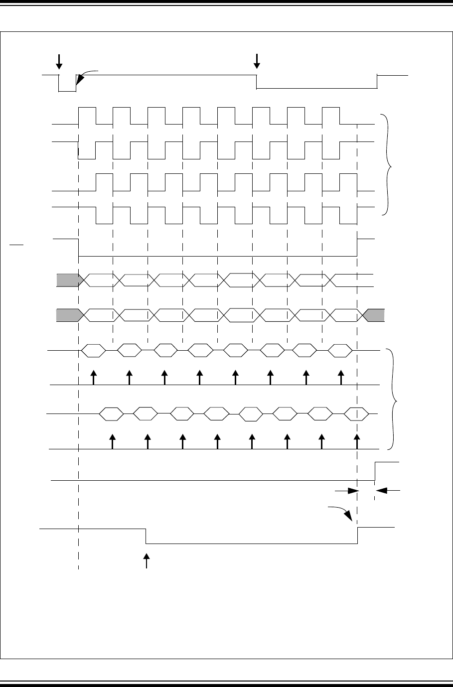
PIC32 Family Reference Manual
DS61106G-page 23-20 © 2007-2011 Microchip Technology Inc.
Figure 23-9: SPI Master Mode Operation in 8-bit Mode (MODE32 = 0, MODE16 = 0)
SCKx
(CKP = 0
SCKx
(CKP = 1
SCKx
(CKP = 0
SCKx
(CKP = 1
4 Clock modes
Input
Sample(2)
Input
Sample
SDIx(2)
bit 7 bit 0
SDOx bit 7 bit 6 bit 5 bit 4 bit 3 bit 2 bit 1 bit 0
bit 7 bit 0
SDIx
SPIxRXIF
(SMP = 1)
(SMP = 0)
(SMP = 1)
CKE = 1)
CKE = 0)
CKE = 1)
CKE = 0)
(SMP = 0)
User writes
to SPIxBUF
SDOx bit 7 bit 6 bit 5 bit 4 bit 3 bit 2 bit 1 bit 0
(CKE = 0)
(CKE = 1)
approximately 2 sysclk latency to set
SPIxRXIF flag bit
Note 1: Four SPI Clock modes are shown here to demonstrate the functionality of bits CKP (SPIxCON<6>) and CKE
(SPIxCON<8>). Only one of the four modes can be chosen for operation.
2: The SDI and input samples shown here for two different values of the SMP bit (SPIxCON<9>) are strictly for
demonstration purposes. Only one of the two configurations of the SMP bit can be chosen during operation.
3: If there are no pending transmissions, SPIxTXB is transferred to SPIxSR as soon as the user writes to SPIxBUF.
4: Operation for 8-bit mode shown. 16-bit and 32-bit modes are similar.
SPIxSR moved
into SPIxRXB
user reads
SPIxBUF
(clock output
at the SCKx
pin in Master
mode)(1)
(SPIxSTAT<0>)
SPITBE
SPIxTXB to SPIxSR(3)
User writes new data
during transmission
SPIRBF
Two modes
available for
SMP control
bit(4)
SSx

© 2007-2011 Microchip Technology Inc. DS61106G-page 23-21
Section 23. Serial Peripheral Interface (SPI)
Serial Peripheral
Interface (SPI)
23
23.3.3.2 SLAVE MODE OPERATION
The following steps are used to set up the SPI module for the Slave mode of operation:
1. If using interrupts, disable the SPI interrupts in the respective IECx register.
2. Stop and reset the SPI module by clearing the ON bit.
3. Clear the receive buffer.
4. Clear the ENHBUF bit (SPIxCON<16>) if using Standard Buffer mode or set the bit if using
Enhanced Buffer mode.
5. If using interrupts, the following additional steps are performed:
a) Clear the SPIx interrupt flags/events in the respective IFSx register.
b) Write the SPIx interrupt priority and subpriority bits in the respective IPCx register.
c) Set the SPIx interrupt enable bits in the respective IECx register.
6. Clear the SPIROV bit (SPIxSTAT<6>).
7. Write the desired settings to the SPIxCON register with MSTEN (SPIxCON<5>) = 0.
8. Enable SPI operation by setting the ON bit (SPIxCON<15>).
9. Transmission (and reception) will start as soon as the master provides the serial clock.
In Slave mode, data is transmitted and received as the external clock pulses appear on the SCKx
pin. The CKP bit (SPIxCON<6>) and the CKE bit (SPIxCON<8>) determine on which edge of the
clock data transmission occurs.
Both data to be transmitted and data that is received are respectively written into or read from
the SPIxBUF register.
The rest of the operation of the module is identical to that in the Master mode including Enhanced
Buffer mode.
23.3.3.2.1 Slave Mode Additional Features
The following additional features are provided in the Slave mode:
•Slave Select Synchronization
The SSx pin allows a Synchronous Slave mode. If the SSEN bit (SPIxCON<7>) is set, trans-
mission and reception is enabled in Slave mode only if the SSx pin is driven to a low state.
The port output or other peripheral outputs must not be driven in order to allow the SSx pin
to function as an input. If the SSEN bit is set and the SSx pin is driven high, the SDOx pin is
no longer driven and will tri-state even if the module is in the middle of a transmission. An
aborted transmission will be retried the next time the SSx pin is driven low using the data
held in the SPIxTXB register. If the SSEN bit is not set, the SSx pin does not affect the
module operation in Slave mode.
•SPITBE Status Flag Operation
The SPITBE bit (SPIxSTAT<3>) has a different function in the Slave mode of operation. The
following describes the function of SPITBE for various settings of the Slave mode of
operation:
-If SSEN (SPIxCON<7>) is cleared, the SPITBE is cleared when SPIxBUF is loaded by
the user code. It is set when the module transfers SPIxTXB to SPIxSR. This is similar
to the SPITBE bit function in Master mode.
-If SSEN is set, SPITBE is cleared when SPIxBUF is loaded by the user code. How-
ever, it is set only when the SPIx module completes data transmission. A transmission
will be aborted when the SSx pin goes high and may be retried at a later time. So,
each data Word is held in SPIxTXB until all bits are transmitted to the receiver.
Note: The SPI module must be turned off prior to changing the mode from Master to
Slave.
Note: Slave Select cannot be used when operating in Frame mode.
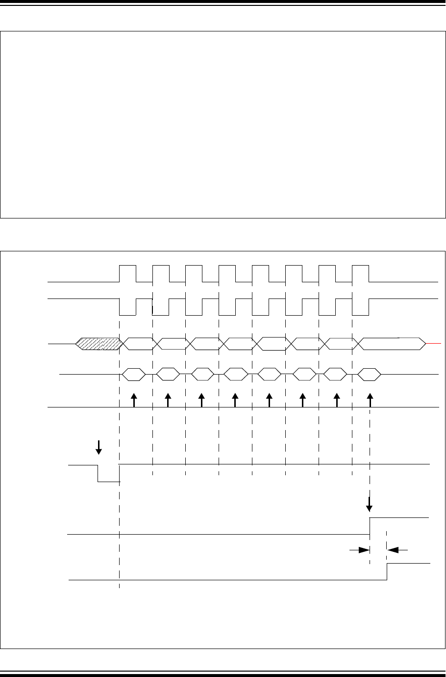
PIC32 Family Reference Manual
DS61106G-page 23-22 © 2007-2011 Microchip Technology Inc.
Example 23-2: Initialization Code for 16-bit SPI Slave Mode
Figure 23-10: SPI Slave Mode Operation in 8-bit Mode with Slave Select Pin Disabled (MODE32 = 0,
MODE16 = 0, SSEN = 0)
/*
The following code example will initialize the SPI1 in Slave mode.
It assumes that none of the SPI1 input pins are shared with an analog input. If so, the
AD1PCFG and corresponding TRIS registers have to be properly configured.
*/
int rData;
IEC0CLR=0x03800000; // disable all interrupts
SPI1CON = 0; // Stops and resets the SPI1.
rData=SPI1BUF; // clears the receive buffer
IFS0CLR=0x03800000; // clear any existing event
IPC5CLR=0x1f000000; // clear the priority
IPC5SET=0x0d000000; // Set IPL=3, Subpriority 1
IEC0SET=0x03800000; // Enable RX, TX and Error interrupts
SPI1STATCLR=0x40; // clear the Overflow
SPI1CON=0x8000; // SPI ON, 8 bits transfer, Slave mode
// from now on, the device is ready to receive and transmit data
SCKx Input(1)
(CKP = 1
SCKx Input(1)
(CKP = 0
Input
Sample
SDIx Input
bit 7 bit 0
SDOx bit 7 bit 6 bit 5 bit 4 bit 3 bit 2 bit 1 bit 0
SPIxRXIF
(SMP = 0)
CKE = 0)
CKE = 0)
(SMP = 0)
User writes to
SPIxBUF(2)
SPIxSR to
SPIxRXB
SPITBE
SPIRBF
Output
Note 1: Two SPI Clock modes are shown here only to demonstrate the functionality of bits CKP (SPIxCON<6>) and CKE
(SPIxCON<8>). Any combination of CKP and CKE bits can be chosen for module operation.
2: If there are no pending transmissions or a transmission is in progress, SPIxBUF is transferred to SPIxSR as soon
as the user writes to SPIxBUF.
3: Operation for 8-bit mode is shown. 16-bit and 32-bit modes are similar.
Approximately 2 SYSCLK latency to set
SPIxRXIF flag bit
(3)
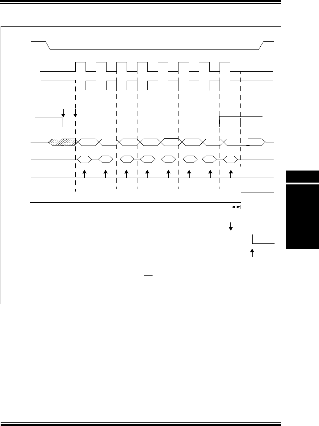
© 2007-2011 Microchip Technology Inc. DS61106G-page 23-23
Section 23. Serial Peripheral Interface (SPI)
Serial Peripheral
Interface (SPI)
23
Figure 23-11: SPI Slave Mode Operation in 8-bit Mode with Slave Select Pin Enabled (MODE32 = 0,
MODE16 = 0, SSEN = 1)
SCKx
(CKP = 1
SCKx
(CKP = 0
Input
Sample
SDIx
bit 7 bit 0
SDOx bit 7 bit 6 bit 5 bit 4 bit 3 bit 2 bit 1 bit 0
SPIxRXIF
(SMP = 0)
CKE = 0)
CKE = 0)
(SMP = 0)
User Writes
SPIxBUF
SPIxSR to
SPIxBUF
SSx(1)
Note 1: When the SSEN (SPIxCON<7>) bit is set to ‘1’, the SSx pin must be driven low so as to enable transmission and
reception in Slave mode.
2: Transmit data is held in SPIxTXB and SPITBE (SPIxSTAT<3>) remains clear until all bits are transmitted.
3: Operation for 8-bit mode is shown. 16-bit and 32-bit modes are similar.
SPIRBF
~2 SYSCLK
latency
SPITBE(2)
SPIxBUF
to
SPIxSR
to
(3)
L
SPIxBUF
User Reads

PIC32 Family Reference Manual
DS61106G-page 23-24 © 2007-2011 Microchip Technology Inc.
23.3.4 SPI Error Handling
When a new data word has been shifted into shift register SPIxSR and the previous contents of
receive register SPIxRXB have not been read by the user software, the SPIROV bit
(SPIxSTAT<6>) will be set. The module will not transfer the received data from SPIxSR to the
SPIxRXB. Further data reception is disabled until the SPIROV bit is cleared. The SPIROV bit is
not cleared automatically by the module and must be cleared by the user software.
23.3.5 SPI Receive-Only Operation
Setting the DISSDO control bit (SPIxCON<12>) disables transmission at the SDOx pin. This
allows the SPIx module to be configured for a Receive-Only mode of operation. The SDOx pin
will be controlled by the respective port function if the DISSDO bit is set.
The DISSDO function is applicable to all SPI operating modes.
23.3.6 Framed SPI Modes
The module supports a very basic framed SPI protocol while operating in either Master or Slave
modes. The following features are provided in the SPI module to support Framed SPI modes:
•The FRMEN control bit (SPIxCON<31>) enables Framed SPI mode and causes the SSx
pin to be used as a frame synchronization pulse input or output pin. The state of SSEN
(SPIxCON<7>) is ignored.
•The FRMSYNC control bit (SPIxCON<30>) determines whether the SSx pin is an input or
an output (i.e., whether the module receives or generates the frame synchronization pulse)
•The FRMPOL control bit (SPIxCON<29>) determines the frame synchronization pulse
polarity for a single SPI clock cycle.
•The FRMSYPW control bit (SPIxCON<27>) can be set to configure the width of the frame
synchronization pulse to one character wide
• The FRMCNT<2:0> control bits (SPIxCON<26:24>) can be set to configure the number of
data characters transmitted per frame synchronization pulse
The following Framed SPI modes are supported by the SPI module:
•Frame Master mode
The SPI module generates the frame synchronization pulse and provides this pulse to other
devices at the SSx pin
• Frame Slave mode
The SPI module uses a frame synchronization pulse received at the SSx pin.
The Framed SPI modes are supported in conjunction with the Master and Slave modes.
Therefore, the following Framed SPI Configurations are available:
•SPI Master mode and Frame Master mode
•SPI Master mode and Frame Slave mode
•SPI Slave mode and Frame Master mode
•SPI Slave mode and Frame Slave mode
These four modes determine whether or not the SPIx module generates the serial clock and the
frame synchronization pulse.
The ENHBUF bit (SPIxCON<16>) can be configured to use the Standard Buffering mode or
Enhanced Buffering mode in Framed SPI mode.
In addition, the SPI module can be used to interface to external audio DAC/ADC and codec
devices in Framed SPI mode.
Note: The FRMSYPW bit is not available on all devices. Refer to the specific device data
sheet for details.
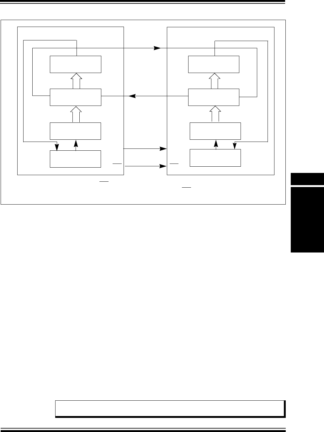
© 2007-2011 Microchip Technology Inc. DS61106G-page 23-25
Section 23. Serial Peripheral Interface (SPI)
Serial Peripheral
Interface (SPI)
23
Figure 23-12: SPI Master, Frame Master Connection Diagram
23.3.6.1 SCKx IN FRAMED SPI MODES
When FRMEN (SPIxCON<31>) = 1 and MSTEN (SPIxCON<5>) = 1, the SCKx pin becomes an
output and the SPI clock at SCKx becomes a free-running clock.
When FRMEN = 1 and MSTEN = 0, the SCKx pin becomes an input. The source clock provided
to the SCKx pin is assumed to be a free-running clock.
The polarity of the clock is selected by the CKP bit (SPIxCON<6>). The CKE bit (SPIxCON<8>)
is not used for the Framed SPI modes.
When CKP xor CKE = 0, the frame sync pulse output and the SDOx data output change on the
rising edge of the clock pulses at the SCKx pin. Input data is sampled at the SDIx input pin on
the falling edge of the serial clock.
When CKP xor CKE = 1, the frame sync pulse output and the SDOx data output change on the
falling edge of the clock pulses at the SCKx pin. Input data is sampled at the SDIx input pin on
the rising edge of the serial clock.
23.3.6.2 SPI BUFFERS IN FRAMED SPI MODES
When FRMSYNC (SPIxCON<30>) = 0, the SPIx module is in the Frame Master mode of
operation. In this mode, the frame sync pulse is initiated by the module when the user software
writes the transmit data to SPIxBUF location (thus writing the SPIxTXB register with transmit
data). At the end of the frame sync pulse, SPIxTXB is transferred to SPIxSR and data
transmission/reception begins.
When FRMSYNC = 1, the module is in Frame Slave mode. In this mode, the frame sync pulse
is generated by an external source. When the module samples the frame sync pulse, it will
transfer the contents of the SPIxTXB register to SPIxSR, and data transmission/reception
begins. The user must make sure that the correct data is loaded into the SPIxBUF for
transmission before the frame sync pulse is received.
Serial Receive Buffer
(SPIxRXB)(3)
Shift Register
(SPIxSR)
MSb LSb
SDOx
SDIx
PIC32
Serial Receive Buffer
(SPIxRXB)
Shift Register
(SPIxSR)
LSb
MSb
SDIx
SDOx
PROCESSOR 2
Serial Clock
Note 1: In Framed SPI modes, the SSx pin is used to transmit/receive the frame synchronization pulse.
2: Framed SPI modes require the use of all four pins (i.e., using the SSx pin is not optional).
3: The SPIxTXB and SPIxRXB registers are memory mapped to the SPIxBUF register.
SCKx
SSx
SSx
SCKx
Serial Transmit Buffer
(SPIxTXB)(3) Serial Transmit Buffer
(SPIxTXB)
Frame Sync
Pulse(1,2)
SPI Buffer
(SPIxBUF)
SPI Buffer
(SPIxBUF)
[SPI Master, Frame Master] [SPI Slave, Frame Slave]
Note: Receiving a frame sync pulse will start a transmission, regardless of whether or not
data was written to SPIxBUF. If a write was not performed, zeros will be transmitted.
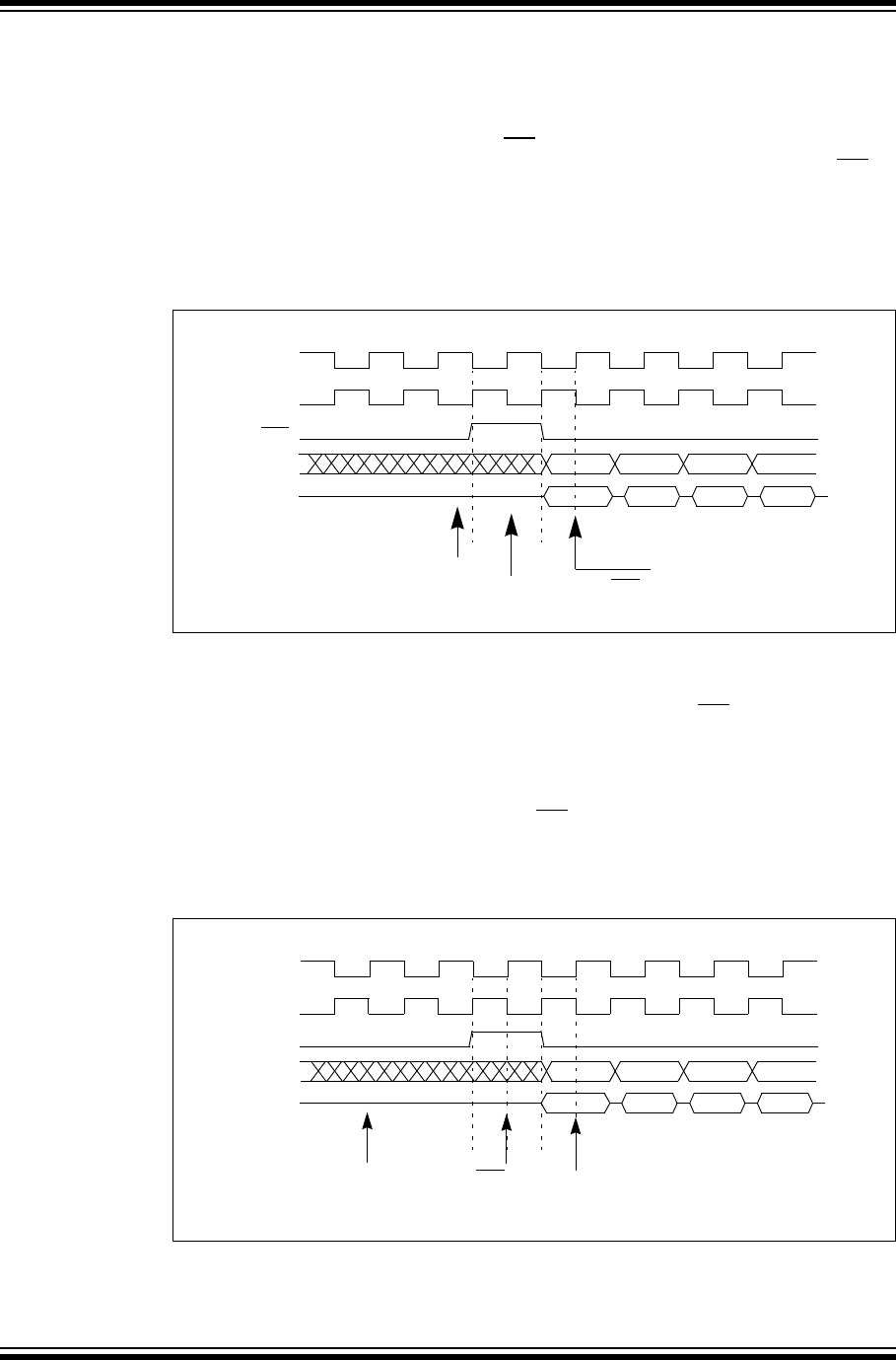
PIC32 Family Reference Manual
DS61106G-page 23-26 © 2007-2011 Microchip Technology Inc.
23.3.6.3 SPI MASTER MODE AND FRAME MASTER MODE
This Framed SPI mode is enabled by setting the MSTEN bit (SPIxCON<5>) and the FRMEN bit
(SPIxCON<31>) to ‘1’, and the FRMSYNC bit (SPIxCON<30>) to ‘0’. In this mode, the serial
clock will be output continuously at the SCKx pin, regardless of whether the module is
transmitting. When SPIxBUF is written, the SSx pin will be driven active, high or low depending
on the FRMPOL bit (SPIxCON<29>), on the next transmit edge of the SCKx clock. The SSx pin
will be high for one SCKx clock cycle. The module will start transmitting data on the next transmit
edge of the SCKx, as shown in Figure 23-13. A connection diagram indicating signal directions
for this operating mode is shown in Figure 23-13.
Figure 23-13: SPI Master, Frame Master (MODE32 = 0, MODE16 = 1, SPIFE = 0,
FRMPOL = 1)
23.3.6.4 SPI MASTER MODE AND FRAME SLAVE MODE
This Framed SPI mode is enabled by setting the MSTEN bit (SPIxCON<5>), the FRMEN bit
(SPIxCON<31>), and the FRMSYNC bit (SPIxCON<30>) to ‘1’. The SSx pin is an input, and it
is sampled on the sample edge of the SPI clock. When it is sampled active, high or low depending
on the FRMPOL bit (SPIxCON<29>), data will be transmitted on the subsequent transmit edge
of the SPI clock, as shown in Figure 23-14. The interrupt flag SPIxIF is set when the transmission
is complete. The user must make sure that the correct data is loaded into SPIxBUF for
transmission before the signal is received at the SSx pin. A connection diagram indicating signal
directions for this operating mode is shown in Figure 23-15.
Figure 23-14: SPI Master, Frame Slave (MODE32 = 0, MODE16 = 1, SPIFE = 0,
FRMPOL = 1)
SCKx
SSx
SDOx
(CKP = 0)
bit 15 bit 14 bit 13 bit 12
SDIx
bit 15 bit 14 bit 13 bit 12
Write to SPIxBUF Receive Samples at SDIx
Pulse Generated at SSx
SCKx
(CKP = 1)
Receive Samples at SDIx
SCK
FSYNC
SDO
(CKP = 0)
bit 15 bit 14 bit 13 bit 12
SDI
Sample SSx Pin
for Frame Sync Pulse
bit 15 bit 14 bit 13 bit 12
Write to
SPIxBUF
SCKx
(CKP = 1)
© 2007-2011 Microchip Technology Inc. DS61106G-page 23-27
Section 23. Serial Peripheral Interface (SPI)
Serial Peripheral
Interface (SPI)
23
Figure 23-15: SPI Master, Frame Slave Connection Diagram
23.3.6.5 SPI SLAVE MODE AND FRAME MASTER MODE
This Framed SPI mode is enabled by setting the MSTEN bit (SPIxCON<5>) to ‘0’, the FRMEN
bit (SPIxCON<31>) to ‘1’, and the FRMSYNC bit (SPIxCON<30>) to ‘0’. The input SPI clock will
be continuous in Slave mode. The SSx pin will be an output when bit FRMSYNC is low. There-
fore, when SPIBUF is written, the module will drive the SSx pin active, high or low depending on
the FRMPOL bit (SPIxCON<29>), on the next transmit edge of the SPI clock. The SSx pin will
be driven high for one SPI clock cycle. Data transmission will start on the next SPI clock transmit
edge. A connection diagram indicating signal directions for this operating mode is shown in
Figure 23-16.
Figure 23-16: SPI Slave, Frame Master Connection Diagram
SDOx
SDIx
Serial Clock
Note 1: In Framed SPI modes, the SSx pin is used to transmit/receive the frame synchronization pulse.
2: Framed SPI modes require the use of all four pins (i.e., using the SSx pin is not optional).
SSx
SCKx
Frame Sync
SDIx
SDOx
SSx
SCKx
PIC32
[SPI Master, Frame Slave]
PROCESSOR 2
[SPI Slave, Frame Master]
Pulse(1,2)
Serial Clock
Note 1: In Framed SPI modes, the SSx pin is used to transmit/receive the frame sync pulse.
2: Framed SPI modes require the use of all four pins (i.e., using the SSx pin is not optional).
SDOx
SDIx
SSx
SCKx
PIC32
[SPI Slave, Frame Master]
SDIx
SDOx
SSx
SCKx
PROCESSOR 2
[SPI Master, Frame Slave]
Frame Sync
Pulse(1,2)
PIC32 Family Reference Manual
DS61106G-page 23-28 © 2007-2011 Microchip Technology Inc.
23.3.6.6 SPI SLAVE MODE AND FRAME SLAVE MODE
This Framed SPI mode is enabled by setting the MSTEN bit (SPIxCON<5>) to ‘0’, the FRMEN
bit (SPIxCON<31>) to ‘1’, and the FRMSYNC bit (SPIxCON<30>) to ‘1’. Therefore, both the
SCKx and SSx pins will be inputs. The SSx pin will be sampled on the sample edge of the SPI
clock. When SSx is sampled active, high or low depending on the FRMPOL bit (SPIxCON<29>),
data will be transmitted on the next transmit edge of SCKx. A connection diagram indicating
signal directions for this operating mode is shown in Figure 23-17.
Figure 23-17: SPI Slave, Frame Slave Connection Diagram
Serial Clock
Note 1: In Framed SPI modes, the SSx pin is used to transmit/receive the frame sync pulse.
2: Framed SPI modes require the use of all four pins (i.e., using the SSx pin is not optional).
3: Slave Select is not available when using Frame mode as a Slave device.
SDOx
SDIx
SSx
SCKx
PIC32
[SPI Slave, Frame Slave]
SDIx
SDOx
SSx
SCKx
PROCESSOR 2
[SPI Master, Frame Master]
Frame Sync
Pulse((1,2,3)

© 2007-2011 Microchip Technology Inc. DS61106G-page 23-29
Section 23. Serial Peripheral Interface (SPI)
Serial Peripheral
Interface (SPI)
23
23.3.7 SPI Master Mode Clock Frequency
The SPI module allows flexibility in baud rate generation through the 9-bit SPIxBRG register.
SPIxBRG is readable and writable, and determines the baud rate. The peripheral clock PBCLK
provided to the SPI module is a divider function of the CPU core clock. This clock is divided based
on the value loaded into SPIxBRG. The SCKx clock obtained by dividing PBCLK is of 50% duty
cycle and it is provided to the external devices via the SCKx pin.
Equation 23-1 defines the SCKx clock frequency as a function of SPIxBRG settings.
Equation 23-1:
Therefore, the maximum baud rate possible is FPB/2 (SPIxBRG = 0), and the minimum baud rate
possible is FPB/1024.
Some sample SPI clock frequencies (in kHz) are shown in Ta b l e 23-4.
Note: The SCKx clock is not free running for non-framed SPI modes. It will only run for 8,
16, or 32 pulses when SPIxBUF is loaded with data. It will however, be continuous
for Framed modes.
Table 23-4: Sample SCKx Frequencies
SPIxBRG
Setting 015 31 63 85 127 255 511
FPB = 80 MHz 40.00
MHz
2.5
MHz
1.25
kHz
625
kHz
465.11
kHz
312.5
kHz
156.25
kHz
78.13
kHz
FPB = 72 MHz 36.00
MHz
2.25
MHz
1.13
kHz
562.5
kHz
418.60
kHz
281.25
kHz
140.63
kHz
70.31
kHz
FPB = 60 MHz 30.00
MHz
1.88
MHz
937.5
kHz
468.75
kHz
348.83
kHz
234.38
kHz
117.19
kHz
58.59
kHz
FPB = 50 MHz 25.00
MHz
1.56
MHz
781.25
kHz
390.63
kHz
290.7
kHz
195.31
kHz
97.66
kHz
48.83
kHz
FPB = 40 MHz 20.00
MHz
1.25
MHz
625.00
kHz
312.50
kHz
232.56
kHz
156.25
kHz
78.13
kHz
39.06
kHz
FPB = 25 MHz 12.50
MHz
781.25
kHz
390.63
kHz
195.31
kHz
145.35
kHz
97.66
kHz
48.83
kHz
24.41
kHz
FPB = 20 MHz 10.00
MHz
625.00
kHz
312.50
kHz
156.25
kHz
116.28
kHz
78.13
kHz
39.06
kHz
19.53
kHz
FPB = 10 MHz 5.00
MHz
312.50
kHz
156.25
kHz
78.13
kHz
58.14
kHz
39.06
kHz
19.53
kHz
9.77
kHz
Note: Not all clock rates are supported. For further information, refer to the SPI timing
specifications in the “Electrical Characteristics” chapter of the specific device
data sheet.
FSCK
FPB
2SPIxBRG 1+()⋅
-------------------------------------------------=

PIC32 Family Reference Manual
DS61106G-page 23-30 © 2007-2011 Microchip Technology Inc.
23.4 AUDIO PROTOCOL INTERFACE MODE
The SPI module can be interfaced to most codec devices available today to provide PIC32
microcontroller-based audio solutions. The SPI module provides support to the audio protocol
functionality via four standard I/O pins. The four pins that make up the audio protocol interface
modes are:
•SDIx: Serial Data Input for receiving sample digital audio data (ADCDAT)
• SDOx: Serial Data Output for transmitting digital audio data (DACDAT)
•SCKx: Serial Clock, also known as bit clock (BCLK)
•SSx: Left/Right Channel Clock (LRCK)
BCLK provides the clock required to drive the data out or into the module, while LRCK provides
the synchronization of the frame based on the protocol mode selected.
In some codecs, Serial Clock (SCK) refers to the Baud/Bit Clock (BCLK). Throughout this
section, the signal SSx is to referred to as LRCK to be consistent with codec naming conventions.
The SPI module has the ability to function in Audio Protocol Master and Audio Protocol Slave
modes. In Master mode, the module generates both the BCLK on the SCKx pin and the LRCK
on the SSx pin. In certain devices, while in Slave mode, the module receives these two clocks
from its I2S partner, which is operating in Master mode.
While in Master mode, the SPI module has the ability to generate its own clock internally via the
Master Clock (MCLK) from various internal sources such as primary clock, PBCLK, USB clock,
FRC and other internal sources. In addition, the SPI module has the ability to provide the MCLK
to the codec device, which is a common requirement.
To st ar t the A ud io Pr oto co l m ode , fir st d isa ble t he p eri ph era l by s ett in g the O N bi t
(SPIxCON<15>) = 0. Next, set the AUDEN bit (SPIxCON2<7>) = 1, and then re-enable the
peripheral by setting the ON bit = 1.
When configured in Master mode, the leading edge of SCK and the LRCK are driven out within
one SCK period of starting the audio protocol. Serial data is shifted in or out with timings
determined by the protocol mode set by the AUDMOD<1:0> bits (SPIxCON2<1:0>). If the
transmit FIFO is empty, zeros are transmitted.
In Slave mode, the peripheral drives zeros out SDO, but does not transmit the contents of the
transmit FIFO until it sees the leading edge of the LRCK, after which time starts receiving data
(provided SDI has not been disabled). It will continue to transmit zeros as long as the transmit
FIFO is empty.
While in Slave or Master mode, the SPI module does not generate an underrun on the TX FIFO
after start-up. This allows software to set up the SPI, set up the DMA, turn on the SPI’s audio
protocol, and then turn on the DMA without getting an error.
After the first write to the TX FIFO (SPIxBUF), the SPI enables underrun detection and
generation. To keep the RX FIFO empty until the DMA is enabled, set DISSDI = 1
(SPIxCON<4>). After enabling the DMA, set DISSDI = 0 to start receiving.
23.4.1 Master Mode
To con fig ur e t he PI C32 dev ice i n Aud io P rotocol Master mode, set both the MSTEN bit
(SPIxCON<5>) and the AUDEN bit (SPIxCON2<7>) to ‘1’.
A few characteristics in Master mode are:
•This mode enables the device to generate SCK and LRCK pulses as long as the ON bit
(SPIxCON<15>) = 1
•The SPI module generates LRCK and SCK continuously in all the cases, regardless of the
transmit data while in Master mode
•The SPI module drives the leading edge of LRCK and SCK within 1 SCK period and the
serial data shifts in and out continuously even when the TX FIFO is empty
Figure 23-18 shows a typical interface between master and slave while in Master mode.
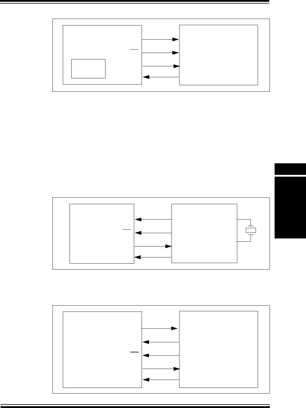
© 2007-2011 Microchip Technology Inc. DS61106G-page 23-31
Section 23. Serial Peripheral Interface (SPI)
Serial Peripheral
Interface (SPI)
23
Figure 23-18: Master Generating its Own Clock – Output BCLK and LRCK
23.4.2 Slave Mode
The SPI module can be configured in audio protocol slave mode by setting the MSTEN bit = 0
(SPIxCON<5>) and the AUDEN bit = 1 (SPIxCON2<7>)
A few characteristics in Slave mode are:
•This mode enables the device to receive SCK and LRCK pulses as long as the ON bit = 1
(SPIxCON<15>)
•The SPI module drives zeros out of SDO, but does not shift data out or in (SDI) until the
module receives the LRCK (i.e., the edge that precedes the left channel)
• Once the module receives the leading edge of LRCK, it starts receiving data if DISSDI = 0
(SPIxCON<4>) and the serial data shifts out continuously even when the TX FIFO is empty
Figure 23-19 shows the interface between a SPI module in Audio Slave Interface mode to a
codec master device.
Figure 23-19: Codec Device as Master Generates Required Clock via External Crystal
Figure 23-20 shows the interface between a SPI module in Audio Slave Interface mode to a
codec master device, in this the master clock is being derived from SPI reference clock out
function.
Figure 23-20: Codec Device as Master Derives MCLK from PIC32 Reference Clock Out
SCKx
SSx
SDIx
SDOx
BCLK
LRCK
ADCDAT
DACDAT
PIC32
[SPI Master]
Codec
[Slave]
Internal
Clock
SCKx
SSx
SDIx
SDOx
BCLK
LRCK
ADCDAT
DACDAT
PIC32
[SPI Slave]
Codec
[Master]
SCKx
SSx
SDIx
SDOx
BCLK
LRCK
ADCDAT
DACDAT
PIC32
[SPI Slave]
Codec
[Slave]
REFCLKO MCLKIN

PIC32 Family Reference Manual
DS61106G-page 23-32 © 2007-2011 Microchip Technology Inc.
23.4.3 Audio Data Length and Frame Length
While codec devices may generate audio data samples of various word lengths of 8/16/20/24/32,
the PIC32 SPI module supports transmit/receive audio data lengths of 16, 24, and 32.
Tabl e 23-5 illustrates how the MODE<32,16> bits (SPIxCON<11:10>) control the maximum
allowable sample length and frame length (LRCK period on SSx).
Table 23-5: Audio Data Length versus LRCK Period
The parameters of the MODE<32,16> bits (SPIxCON<11:10>) have the following behavior:
•Controls Left/Right channel data length, frame length
•In 16-bit Sample mode, 32/64-bit frame length is supported
•In 24/32-bit Sample mode, 64-bit frame length is supported
• Defines FIFO width and depth (e.g., 24-bit data has a 32 bit wide and 4 location deep FIFO)
• If the written data is greater than the data selected, the upper bytes are ignored
• If the written data is less than the data selected, the FIFO pointers change on the write to
the Most Significant Byte (MSB) of the selected length
If this data is written to the transmit FIFO in more than one write, the write order must be from
least significant to most significant.
For example, assuming that audio data is 24 bits per sample with 8 bits available at a time.
According to Tabl e 23-5, the FIFO width is 32 bits per sample. Therefore, the 8 Most Significant
bits (MSbs), bits 31:24, in each FIFO sample are ignored.
Bits 15:8 and 7:0 can be written to the SPIxBUF register in any order; however, bits 23:16 must
be written last, as writing the Most Significant bit (MSb), bit 24, triggers a change in the pointers
of the transmit buffer.
Data written to unused bytes is ignored. Also, transactions that are only to unused bytes are also
ignored. Therefore, a byte write to address offset 0x0023 is completely ignored and does not
cause a FIFO push if the data is less than 32 bits wide.
23.4.4 Frame Error/LRCK Errors
The SPI module provides detection of frame/LRCK errors for debugging. The frame/LRCK error
occurs when the LRCK edge that is defining a channel start happens before the correct number
of bits (as defined by MODE<32,16>).
The SPI module immediately sets the FRMERR bit (SPIxSTAT<12>), pushes data in from
SPIxSR register into the SPIxRXB register, and pops data from the SPIxTXB register into the
SPIxSR register. The module can be configured to detect frame/LRCK-related errors by setting
the FRMERREN bit (SPIxCON2<12>).
Note: Actual sample data can be any length, with a maximum of 32 bits, and the data must
be packed in one of three (16/24/32) formats.
SPIxCON<11:10>
Data
Length
(bits)
FIFO Width
(bits)
Left/Right
Channel
Sample
Length
(bits)
Enhanced
Buffer
FIFO
Depth
(samples)
LRCK
Period
Frame
Length
(bits)
MODE32 MODE16
0 0 16 16 ≤ 16 832
0 1 16 16 ≤ 32 864
1 1 24 32 ≤ 32 464
1 0 32 32 ≤ 32 464
Note: In Audio Protocol mode, both the BCLK (on the SCKx pin) and the LRCK (on the
SSx pin) are free running, meaning they are continuous. Normally, the LRCK is a
fixed number of BCLKs long. In all cases, the SPI module will realign to the new
frame edge and will set the FRMERR bit. If operating in a non-PCM mode, the SPI
module will also push the abbreviated data onto the FIFO when the frame is too
short.

© 2007-2011 Microchip Technology Inc. DS61106G-page 23-33
Section 23. Serial Peripheral Interface (SPI)
Serial Peripheral
Interface (SPI)
23
23.4.5 Audio Protocol Modes
The SPI module supports four audio protocol modes and can be operated in any one of these
modes:
•I
2S mode (not available on all devices; refer to the specific device data sheet for availability)
•Left-Justified mode
•Right-Justified mode
•PCM/DSP mode
These audio protocol modes can be enabled by configuring the AUDMOD<1:0> bits
(SPIxCON2<1:0>). These modes enable communication to different types of codecs and control
the edge relationships of LRCK and SDI/SDO with respect to SCK.
With respect to data transmit, in all of the protocol modes, the MSB is first transmitted followed
by MSB-1, and so on, until the Least Significant Byte (LSB) transmits. The length of the data is
discussed in 23.4.3 “Audio Data Length and Frame Length”. If there are SCK periods left over
after the LSb is transmitted, zeros are sent to fill up the frame.
When in Slave mode, the relationship between the BCLK (on the SCKx pin) and the period (or
frame length) of the LRCK (on the SSx pin) is far less constrained than that of Master mode. In
Master mode, the frame length equals 32 or 64 BCLKs depending on the MODE<32,16> bit
(SPIxCON<11:10>) settings. However, in Slave mode, the frame length can be greater than or
equal to 32 or 64 BCLKs, but the FRMERR bit (SPIxSTAT<12>) will be set if the frame LRCK
edge arrives early.
Figure 23-21 illustrates the general interface between the codec device and the SPI module in
audio mode.
Figure 23-21: SPI Module in Audio Slave Mode – BCLK and WS or LRCK Generated by
Master
SCKx
SSx
SDIx
SDOx
BCLK
LRCK
ADCDAT
DACDAT
PIC32
[SPI Slave]
Codec
[Master]
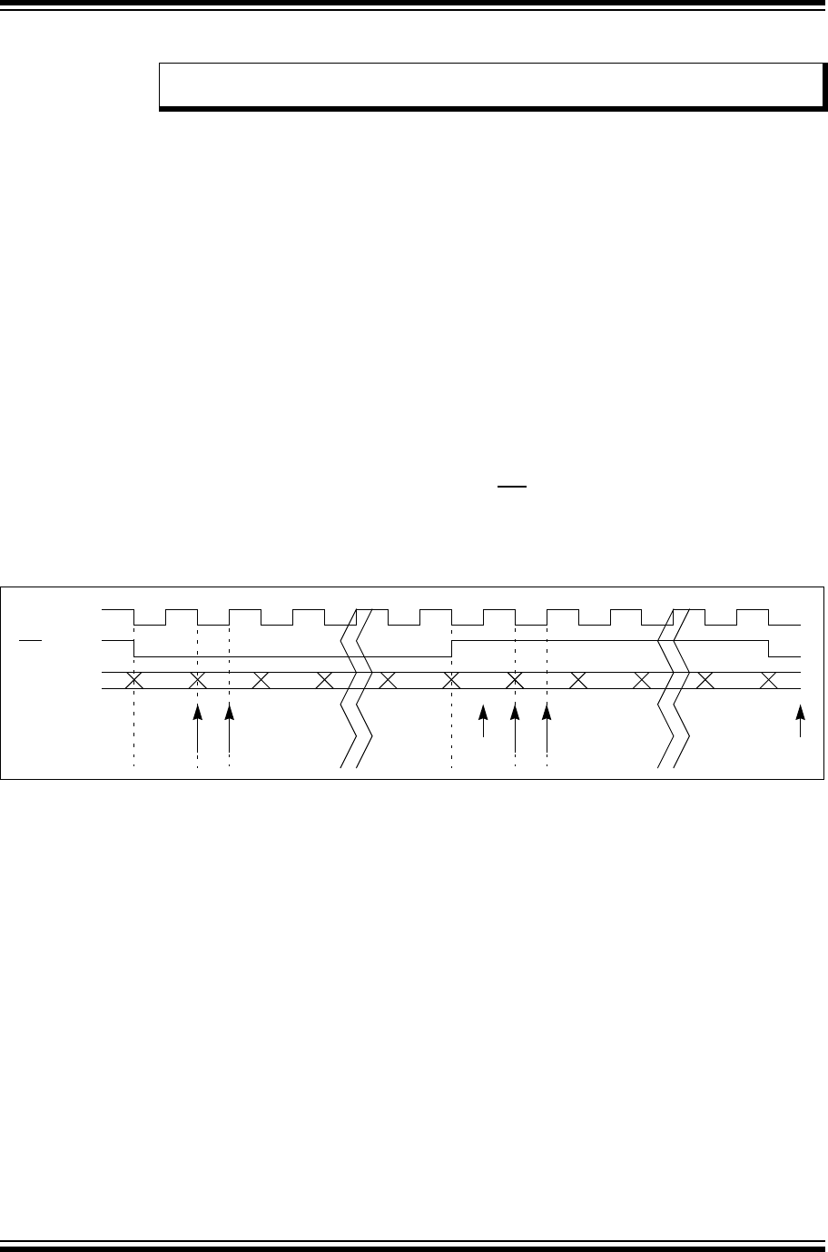
PIC32 Family Reference Manual
DS61106G-page 23-34 © 2007-2011 Microchip Technology Inc.
23.4.5.1 I2S MODE
The Inter-IC Sound (I2S) protocol enables transmission of two channels of digital audio data over
a single serial interface. The I2S protocol defines a 3-wire interface that handles the stereo data
using the WS/LRCK line. The I2S specification defines a half-duplex interface that supports
transmit or receive, but not both at the same time. With both SDO and SDI available, full-duplex
operation is supported by this peripheral, as shown in Figure 23-22.
•Data Transmit and Clocking:
- The transmitter shifts the audio sample data’s MSb on the first falling edge of SCK
after an LRCK transition
-The receiver samples the MSB on the second rising edge of SCK
- The left channel data shifts out while LRCK is low and right channel data is shifted out
while LRCK is high
- The data in the left and right channel consists of a single frame
•Required Configuration Settings:
To s et th e modu le to I2S mode, the following bits must be set:
- AUDMOD<1:0> = 00 (SPIxCON2<1:0>)
- FRMPOL = 0 (SPIxCON<29>)
-CKP = 1 (SPIxCON<6>)
Setting these bits enables the SDO and LRCK (SSx) transitions to occur on the falling edge of
SCK (BCLK) and sampling of SDI to occur on the rising edge of SCK. Refer to the diagrams
shown in Figure 23-22.
Figure 23-22: I2S with 16-bit Data/Channel or 32-bit Data/Channel
Note: This feature is not available on all devices. Refer to the specific device data sheet
for availability.
SSx (LRCK)
SCKx (BCLK)
SDOx/SDIx MSb MSb-1 LSb
LSb+1 MSb MSb-1 LSb+1 LSb
LEFT CHANNEL RIGHT CHANNEL
Transmit Sample
Left Channel LSb
SampleTransmit
Right Channel LSb

© 2007-2011 Microchip Technology Inc. DS61106G-page 23-35
Section 23. Serial Peripheral Interface (SPI)
Serial Peripheral
Interface (SPI)
23
23.4.5.1.1 I2S Audio Slave Mode of Operation
Use the following steps to set up the SPI module for the I2S Audio Slave mode of operation:
1. If using interrupts, disable the SPI interrupts in the respective IECx register.
2. Stop and reset the SPI module by clearing the ON bit (SPIxCON<15>).
3. Reset the SPI audio configuration register, SPIxCON2.
4. Clear the receive buffer.
5. Clear the ENHBUF bit (SPIxCON<16>) if using Standard Buffer mode or set the bit if using
Enhanced Buffer mode.
6. If using interrupts, the following additional steps are performed:
a) Clear the SPIx interrupt flags/events in the respective IFSx register.
b) Write the SPIx interrupt priority and subpriority bits in the respective IPCx register.
c) Set the SPIx interrupt enable bits in the respective IECx register.
7. Clear the SPIROV bit (SPIxSTAT<6>).
8. Write the desired settings to the SPIxCON2 register.
a) AUDMOD<1:0> bits (SPIxCON2<1:0>) = 00
b) AUDEN bit (SPIxCON2<7>) = 1
9. Write the desired settings to the SPIxCON register:
a) MSTEN (SPIxCON<5>) = 0
b) CKP (SPIxCON<6>) = 1
c) MODE<32,16> (SPIxCON<11:10>) = 0 for 16-bit audio channel data.
d) Enable SPI operation by setting the ON bit (SPIxCON<15>).
10. Transmission (and reception) will start as soon as the master provides the BCLK and
LRCK.
Example 23-3: I2S Slave Mode, 16-bit Channel Data, 32-bit Frame
/* The following code example will initialize the SPI1 Module in I2S Slave mode. */
/* It assumes that none of the SPI1 input pins are shared with an analog input. */
unsigned int rData;
IEC0CLR=0x03800000; // disable all interrupts
SPI1CON = 0; // Stops and resets the SPI1.
SPI1CON2 = 0; // Reset audio settings
rData=SPI1BUF; // clears the receive buffer
IFS0CLR=0x03800000; // clear any existing event
IPC5CLR=0x1f000000; // clear the priority
IPC5SET=0x0d000000; // Set IPL = 3, Subpriority 1
IEC0SET=0x03800000; // Enable RX, TX and Error interrupts
SPI1STATCLR=0x40; // clear the Overflow
SPI1CON2=0x00000080; // I2S Mode, AUDEN = 1, AUDMON = 0
SPI1CON =0x00008040; // Slave mode, SPI ON, CKP = 1, 16-bit audio data, 32 bits per frame
// from here, the device is ready to receive and transmit data
/* Note: A few of bits related to frame settings are not required to be set in the SPI1CON */
/* register during audio mode operation. Please refer to the notes in the SPIxCON2 register.*/

PIC32 Family Reference Manual
DS61106G-page 23-36 © 2007-2011 Microchip Technology Inc.
23.4.5.1.2 I2S Audio Master Mode of Operation
A typical application could be to play PCM data (8 kHz sample frequency, 16-bit data, 32-bit
frame size) when interfaced to a codec slave device. In this case, the SPI module is initialized to
generate BCLK @ 256 kbps. Assuming a 40 MHz peripheral bus clock, FPB = 40e6, the baud
rate would be determined using Equation 23-2.
Equation 23-2:
Solving for the value of SPIxBRG is shown in Equation 23-3.
Equation 23-3:
The Baud Rate is now equal to 256e3. Equation 23-4 shows the resulting calculation.
Equation 23-4:
If the result of Equation 23-4 is rounded to the nearest integer, SPIxBRG is now equal to 77;
therefore, the effective Baud Rate is that of Equation 23-5.
Equation 23-5:
The result is 0.16% too fast; however, this is well within most system tolerances (0.16% is exactly
1/625). On certain devices, this error can be removed using the REFOTRIM register to provide
a master clock output at the exact frequency needed.
The following steps can be used to set up the SPI module for operation in I2S Audio Master
mode:
1. If using interrupts, disable the SPI interrupts in the respective IECx register.
2. Stop and reset the SPI module by clearing the ON bit (SPIxCON<15>).
3. Reset the SPI audio configuration register, SPIxCON2.
4. Reset the baud rate register, SPIxBRG.
5. Clear the receive buffer.
6. Clear the ENHBUF bit (SPIxCON<16>) if using Standard Buffer mode or set the bit if using
Enhanced Buffer mode.
7. If using interrupts, perform these additional steps:
a) Clear the SPIx interrupt flags/events in the respective IFSx register.
b) Write the SPIx interrupt priority and subpriority bits in the respective IPCx register.
c) Set the SPIx interrupt enable bits in the respective IECx register.
8. Clear the SPIROV bit (SPIxSTAT<6>).
9. Write the desired settings to the SPIxCON2 register. The AUDMOD<1:0> bits
(SPIxCON2<1:0>) must be set to ‘00’ for I2S mode and the AUDEN bit (SPIxCON2<7>)
must be set to ‘1’ to enable the audio protocol.
10. Set the SPIxBRG baud rate register to 0x4D (to generate approximately 256 kbps sample
rate, with PBCLK @ 40 MHz).
Baud Rate FPB
2SPIxBRG 1+()⋅
-------------------------------------------------=
SPIxBRG FPB
2Baud Rate()
---------------------------------1–=
SPIxBRG 40e6
2 256e3()
----------------------- 177.125=–=
40e6
2 77 1+()⋅
------------------------------ 40e6
156
------------256410.25 bits per second==

© 2007-2011 Microchip Technology Inc. DS61106G-page 23-37
Section 23. Serial Peripheral Interface (SPI)
Serial Peripheral
Interface (SPI)
23
11. Write the desired settings to the SPIxCON register:
a) MSTEN (SPIxCON<5>) = 1.
b) CKP (SPIxCON<6>) = 1.
c) MODE<32,16> (SPIxCON<11:10>) = 0 for 16-bit audio channel data.
d) Enable SPI operation by setting the ON bit (SPIxCON<15>).
12. Transmission (and reception) will start immediately after the ON bit is set.
Example 23-4: I2S Master Mode, 256 kbps BCLK, 16-bit Channel Data, 32-bit Frame
/* The following code example will initialize the SPI1 Module in I2S Master mode. */
/* It assumes that none of the SPI1 input pins are shared with an analog input. */
unsigned int rData;
IEC0CLR=0x03800000; // disable all interrupts
SPI1CON = 0; // Stops and resets the SPI1.
SPI1CON2 = 0; // Reset audio settings
SPI1BRG=0; // Reset Baud rate register
rData=SPI1BUF; // clears the receive buffer
IFS0CLR=0x03800000; // clear any existing event
IPC5CLR=0x1f000000; // clear the priority
IPC5SET=0x0d000000; // Set IPL = 3, Subpriority 1
IEC0SET=0x03800000; // Enable RX, TX and Error interrupts
SPI1STATCLR=0x40; // clear the Overflow
SPI1CON2=0x00000080; // I2S Mode, AUDEN = 1, AUDMON = 0
SPI1BRG =0x4D; //(to generate 256 kbps sample rate, PBCLK @ 40 MHz)
SPI1CON =0x00008060; // Master mode, SPI ON, CKP = 1, 16-bit audio channel
// data, 32 bits per frame
// from here, the device is ready to receive and transmit data
/* Note: A few of bits related to frame settings are not required to be set in the SPI1CON */
/* register during audio mode operation. Please refer to the notes in the SPIxCON2 register.*/
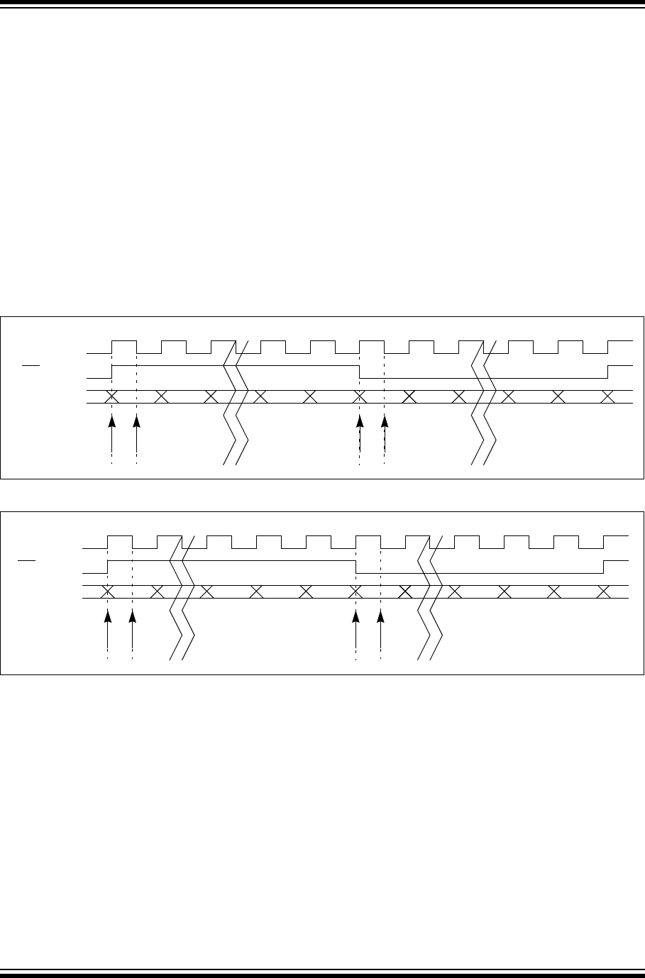
PIC32 Family Reference Manual
DS61106G-page 23-38 © 2007-2011 Microchip Technology Inc.
23.4.5.2 LEFT-JUSTIFIED MODE
The Left-Justified mode is similar to I2S mode; however, in this mode, the SPI shifts the audio
data’s MSb on the first SCK edge that is coincident with an LRCK transition. On the receiver side,
the SPI module samples the MSb on the next SCK edge.
In general, a codec using justified protocols defaults to transmitting data on the rising edge of
SCK and receiving data on the falling edge of SCK.
•Required configuration settings
To s et th e m odu le to L ef t- Jus ti f ie d mode, the following bits must to be set
- AUDMOD<1:0> = 01 (SPIxCON2<1:0>)
- FRMPOL = 1 (SPIxCON<29>)
-CKP = 0 (SPIxCON<6>)
This enables the SDO and LRCK transitions to occur on the rising edge of SCK. Refer to the
sample waveform diagrams shown in Figure 23-23 and Figure 23-24 for 16, 24, 32-bit audio data
transfers.
Figure 23-23: Left-Justified with 16-bit Data/Channel or 32-bit Data/Channel
Figure 23-24: Left-Justified with 16/24-bit Data and 32-bit Channel
SSx (LRCK)
SCKx (BCLK)
SDOx/SDIx MSb MSb-1 LSb
LSb+1 MSb MSb-1 LSb+1 LSb
LEFT CHANNEL RIGHT CHANNEL
Transmit Sample SampleTransmit
SSx (LRCK)
SCKx (BCLK)
SDOx/SDIx MSb LSb MSb LSb
LEFT CHANNEL RIGHT CHANNEL
Transmit Sample SampleTransmit
0000

© 2007-2011 Microchip Technology Inc. DS61106G-page 23-39
Section 23. Serial Peripheral Interface (SPI)
Serial Peripheral
Interface (SPI)
23
23.4.5.2.1 Left-Justified Audio Slave Mode Operation
Use the following steps to set up the SPI module for the Left-Justified Audio Slave mode of
operation:
1. If using interrupts, disable the SPI interrupts in the respective IECx register.
2. Stop and reset the SPI module by clearing the ON bit (SPIxCON<15>).
3. Reset the SPI audio configuration register, SPIxCON2.
4. Clear the receive buffer.
5. Clear the ENHBUF bit (SPIxCON<16>) if using Standard Buffer mode or set the bit if using
Enhanced Buffer mode.
6. If using interrupts, the following additional steps are performed:
a) Clear the SPIx interrupt flags/events in the respective IFSx register.
b) Write the SPIx interrupt priority and subpriority bits in the respective IPCx register.
c) Set the SPIx interrupt enable bits in the respective IECx register.
7. Clear the SPIROV bit (SPIxSTAT<6>).
8. Write the desired settings in the SPIxCON2 register. The AUDMOD<1:0> bits
(SPIxCON2<1:0>) must be set to ‘01’ for Left-Justified mode and the AUDEN bit
(SPIxCON2<7>) must be set to ‘1’ to enable the audio protocol.
9. Write the desired settings to the SPIxCON register:
a) Set to Slave mode, MSTEN (SPIxCON<5>) = 0.
b) Set clock polarity, CKP (SPIxCON<6>) = 0.
c) Set frame polarity, FRMPOL (SPIxCON<29>) = 1.
d) Set MODE<32,16> (SPIxCON<11:10>) = 0 for 16-bit audio channel data
e) Enable SPI operation by setting the ON bit (SPIxCON<15>).
10. Transmission (and reception) will start as soon as the master provides the BCLK and
LRCK.
Example 23-5: Left-Justified Slave Mode, 16-bit Channel Data, 32-bit Frame
/* The following code example will initialize the SPI1 Module in Left-Justified Slave mode. */
/* It assumes that none of the SPI1 input pins are shared with an analog input. */
unsigned int rData;
IEC0CLR=0x03800000; // disable all interrupts
SPI1CON = 0; // Stops and resets the SPI1.
SPI1CON2 = 0; // Reset audio settings
rData=SPI1BUF; // clears the receive buffer
IFS0CLR=0x03800000; // clear any existing event
IPC5CLR=0x1f000000; // clear the priority
IPC5SET=0x0d000000; // Set IPL = 3, Subpriority 1
IEC0SET=0x03800000; // Enable RX, TX and Error interrupts
SPI1STATCLR=0x40; // clear the Overflow
SPI1CON2=0x00000081; // Left-Justified Mode, AUDEN = 1, AUDMON = 0
SPI1CON =0x20008000; // Slave mode, SPI ON, CKP = 0, FRMPOL = 1,
// 16-bit audio data, 32 bits per frame
// from here, the device is ready to receive and transmit data
/* Note: A few of bits related to frame settings are not required to be set in the SPI1CON */
/* register during audio mode operation. Please refer to the notes in the SPIxCON2 register.*/

PIC32 Family Reference Manual
DS61106G-page 23-40 © 2007-2011 Microchip Technology Inc.
23.4.5.2.2 Left-Justified Audio Master Mode Operation
Use the following steps to set up the SPI module for the Left-Justified Audio Master mode of
operation:
1. If using interrupts, disable the SPI interrupts in the respective IECx register.
2. Stop and reset the SPI module by clearing the ON bit (SPIxCON<15>).
3. Reset the SPI audio configuration register, SPIxCON2.
4. Reset the baud rate register, SPIxBRG.
5. Clear the receive buffer.
6. Clear the ENHBUF bit (SPIxCON<16>) if using Standard Buffer mode or set the bit if using
Enhanced Buffer mode.
7. If using interrupts, the following additional steps are performed:
a) Clear the SPIx interrupt flags/events in the respective IFSx register.
b) Write the SPIx interrupt priority and subpriority bits in the respective IPCx register.
c) Set the SPIx interrupt enable bits in the respective IECx register.
8. Clear the SPIROV bit (SPIxSTAT<6>).
9. Write the desired settings in the SPIxCON2 register. The AUDMOD<1:0> bits
(SPIxCON2<1:0>) must be set to ‘01’ for Left-Justified and the AUDEN bit
(SPIxCON2<7>) must be set to ‘1’ to enable the audio protocol.
10. Set the SPIxBRG baud rate register to 0x4D (to generate approximately 256 kbps sample
rate, with PBCLK @ 40 MHz)
11. Write the desired settings to the SPIxCON register:
a) Set to Master mode, MSTEN (SPIxCON<5>) = 1.
b) Set clock polarity, CKP (SPIxCON<6>) = 0.
c) Set frame polarity, FRMPOL (SPIxCON<29>) = 1.
d) Set MODE<32,16> (SPIxCON<11:10>) = 0 for 16-bit audio channel data.
e) Enable SPI operation by setting the ON bit (SPIxCON<15>).
12. Transmission (and reception) will start immediately after the ON bit is set.
Example 23-6: Left-Justified Master Mode, 16-bit Channel Data, 32-bit Frame
/* The following code example will initialize the SPI1 Module in Left-Justified Master mode. */
/* It assumes that none of the SPI1 input pins are shared with an analog input. */
unsigned int rData;
IEC0CLR=0x03800000; // disable all interrupts
SPI1CON = 0; // Stops and resets the SPI1
SPI1CON2 = 0; // Reset audio settings
SPI1BRG = 0;
rData=SPI1BUF; // clears the receive buffer
IFS0CLR=0x03800000; // clear any existing event
IPC5CLR=0x1f000000; // clear the priority
IPC5SET=0x0d000000; // Set IPL = 3, Subpriority 1
IEC0SET=0x03800000; // Enable RX, TX and Error interrupts
SPI1STATCLR=0x40; // clear the Overflow
SPI1CON2=0x00000081; // Left-Justified Mode, AUDEN = 1, AUDMON = 0
SPI1BRG =0x4D; // (to generate 256 kbps sample rate, PBCLK @ 40 MHz)
SPI1CON =0x20008040; // Master mode, SPI ON, CKP = 0, FRMPOL = 1, MSTEN = 1
// 16-bit audio data, 32 bits per frame
// from here, the device is ready to receive and transmit data
/* Note: A few of bits related to frame settings are not required to be set in the SPI1CON */
/* register during audio mode operation. Please refer to the notes in the SPIxCON2 register.*/
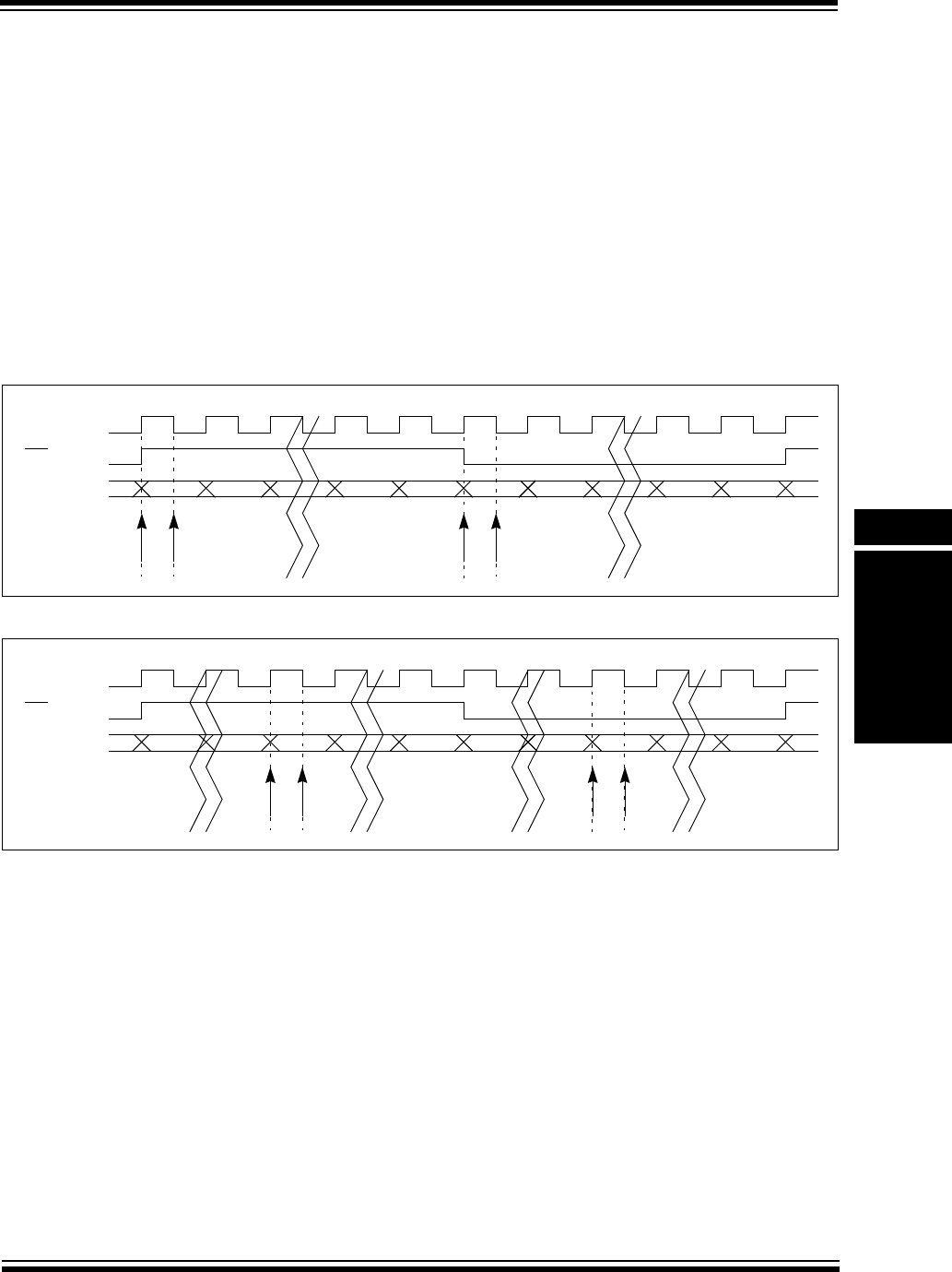
© 2007-2011 Microchip Technology Inc. DS61106G-page 23-41
Section 23. Serial Peripheral Interface (SPI)
Serial Peripheral
Interface (SPI)
23
23.4.5.3 RIGHT-JUSTIFIED MODE
In Right-Justified mode, the SPI module shifts the audio sample data’s MSb after aligning the
data to the last clock cycle. The bits preceding the audio sample data can be driven to logic level
0 by setting the DISSDO bit (SPIxCON<12>) to ‘0’. When DISSDO = 0, the module ignores the
unused bit slot.
•Required configuration:
To set the module to Right-Justified mode, the following bits must to be set:
- AUDMOD<1:0> (SPIxCON2<1:0>) = 10
-FRMPOL (SPIxCON<29>) = 1
- CKP (SPIxCON<6>) = 0
This enables the SDO and LRCK transitions to occur on the rising edge of SCK after the LSb
being aligned to the last clock cycle. Refer to the sample waveform diagrams shown in
Figure 23-25 and Figure 23-26 for 16, 24, 32-bit audio data transfers.
Figure 23-25: Right-Justified with 16-bit Data/Channel or 32-bit Data/Channel
Figure 23-26: Right-Justified with 16/24-bit Data and 32-bit Channel
SSx (LRCK)
SCKx (BCLK)
SDOx/SDIx MSb MSb-1 LSb
LSb+1 MSb MSb-1 LSb+1 LSb
LEFT CHANNEL RIGHT CHANNEL
Transmit Sample SampleTransmit
SSx (LRCK)
SCKx (BCLK)
SDOx/SDIx MSb LSb MSb LSb
LEFT CHANNEL RIGHT CHANNEL
Transmit Sample SampleTransmit
0000

PIC32 Family Reference Manual
DS61106G-page 23-42 © 2007-2011 Microchip Technology Inc.
23.4.5.3.1 Right-Justified Audio Slave Mode Operation
Use the following steps to set up the SPI module for the Right-Justified Audio Slave mode of
operation:
1. If using interrupts, disable the SPI interrupts in the respective IECx register.
2. Stop and reset the SPI module by clearing the ON bit (SPIxCON<15>).
3. Reset the SPI audio configuration register, SPIxCON2.
4. Clear the receive buffer.
5. Clear the ENHBUF bit (SPIxCON<16>) if using Standard Buffer mode or set the bit if using
Enhanced Buffer mode.
6. If using interrupts, perform the following steps:
a) Clear the SPIx interrupt flags/events in the respective IFSx register.
b) Write the SPIx interrupt priority and subpriority bits in the respective IPCx register.
c) Set the SPIx interrupt enable bits in the respective IECx register.
7. Clear the SPIROV bit (SPIxSTAT<6>).
8. Write the desired settings in the SPIxCON2 register. The AUDMOD<1:0> bits
(SPIxCON2<1:0>) must be set to ‘10’ for Right-Justified mode and the AUDEN bit
(SPIxCON2<7>) must be set to ‘1’ to enable the audio protocol.
9. Write the desired settings to the SPIxCON register:
a) Set to slave mode, MSTEN (SPIxCON<5>) = 0.
b) Set clock polarity, CKP (SPIxCON<6>) = 0.
c) Set frame polarity, FRMPOL (SPIxCON<29> = 1.
d) Set MODE<32,16> (SPIxCON<11:10>) = 0 for 16-bit audio channel data.
e) Enable SPI operation by setting the ON bit (SPIxCON<15>).
10. Transmission (and reception) will start as soon as the master provides the BCLK and
LRCK.
Example 23-7: Right-Justified Slave Mode, 16-bit Channel Data, 32-bit Frame
/* The following code example will initialize the SPI1 Module in Right-Justified Slave mode. */
/* It assumes that none of the SPI1 input pins are shared with an analog input. */
unsigned int rData;
IEC0CLR=0x03800000; // disable all interrupts
SPI1CON=0; // Stops and resets the SPI1.
SPI1CON2=0; // Reset audio settings
rData=SPI1BUF; // clears the receive buffer
IFS0CLR=0x03800000; // clear any existing event
IPC5CLR=0x1f000000; // clear the priority
IPC5SET=0x0d000000; // Set IPL = 3, Subpriority 1
IEC0SET=0x03800000; // Enable RX, TX and Error interrupts
SPI1STATCLR=0x40; // clear the Overflow
SPI1CON2=0x00000082; // Right-Justified Mode, AUDEN = 1, AUDMON = 0
SPI1CON=0x20008000; // Slave mode, SPI ON, CKP = 0, FRMPOL = 1,
// 16-bit audio data, 32 bits per frame
// DISSDO = 0, transmit unused bit slots with logic level 0
// DISSDI = 0, receiver to ignore the unused bit slots
// from here, the device is ready to receive and transmit data
/* Note: A few of bits related to frame settings are not required to be set in the SPI1CON */
/* register during audio mode operation. Please refer to the notes in the SPIxCON2 register.*/

© 2007-2011 Microchip Technology Inc. DS61106G-page 23-43
Section 23. Serial Peripheral Interface (SPI)
Serial Peripheral
Interface (SPI)
23
23.4.5.3.2 Right-Justified Audio Master Mode Operation
Use the following steps to set up the SPI module for the Right-Justified Audio Master mode of
operation:
1. If using interrupts, disable the SPI interrupts in the respective IECx register.
2. Stop and reset the SPI module by clearing the ON bit (SPIxCON<15>).
3. Reset the SPI audio configuration register, SPIxCON2.
4. Reset the baud rate register, SPIxBRG.
5. Clear the receive buffer.
6. Clear the ENHBUF bit (SPIxCON<16>) if using Standard Buffer mode or set the bit if using
Enhanced Buffer mode.
7. If using interrupts, the following additional steps are performed:
a) Clear the SPIx interrupt flags/events in the respective IFSx register.
b) Write the SPIx interrupt priority and subpriority bits in the respective IPCx register.
c) Set the SPIx interrupt enable bits in the respective IECx register.
8. Clear the SPIROV bit (SPIxSTAT<6>).
9. Write the desired settings in the SPIxCON2 register. The AUDMOD<1:0> bits
(SPIxCON2<1:0>) must be set to ‘10’ for Right-Justified mode and the AUDEN bit
(SPIxCON2<7>) must be set to ‘1’ to enable the audio protocol.
10. Set the SPIxBRG baud rate register to 0x4D (to generate approximately 256 kbps sample
rate, with PBCLK @ 40 MHz).
11. Write the desired settings to the SPIxCON register:
a) Set to master mode, MSTEN (SPIxCON<5>) = 1.
b) Set clock polarity, CKP (SPIxCON<6>) = 0.
c) Set frame polarity, FRMPOL (SPIxCON<29>) = 1.
d) Set MODE<32,16> (SPIxCON<11:10>) = 0 for 16-bit audio channel data.
e) Enable SPI operation by setting the ON bit (SPIxCON<15>).
12. Transmission (and reception) will start immediately after the ON bit is set.
Example 23-8: Right-Justified Master Mode, 16-bit Channel Data, 32-bit Frame
/* The following code example will initialize the SPI1 Module in Right-Justified Master mode. */
/* It assumes that none of the SPI1 input pins are shared with an analog input. */
unsigned int rData;
IEC0CLR=0x03800000; // disable all interrupts
SPI1CON = 0; // Stops and resets the SPI1.
SPI1CON2 = 0; // Reset audio settings
SPI1BRG=0;
rData=SPI1BUF; // clears the receive buffer
IFS0CLR=0x03800000; // clear any existing event
IPC5CLR=0x1f000000; // clear the priority
IPC5SET=0x0d000000; // Set IPL=3, Subpriority 1
IEC0SET=0x03800000; // Enable RX, TX and Error interrupts
SPI1STATCLR=0x40; // clear the Overflow
SPI1CON2=0x00000082; // Right-Justified Mode, AUDEN =1, AUDMON=0
SPI1BRG =0x4D; // (to generate 256 kbps sample rate, PBCLK @ 40 MHz)
SPI1CON =0x20008020; // Master mode, SPI ON, CKP = 0, FRMPOL = 1, MSTN = 1
// 16-bit audio data, 32 bits per frame
// DISSDO = 0, transmit unused bit slots with logic level 0
// DISSDI = 0, receiver to ignore the unused bit slots
// from here, the device is ready to receive and transmit data
/* Note: A few of bits related to frame settings are not required to be set in the SPI1CON */
/* register during audio mode operation. Please refer to the notes in the SPIxCON2 register.*/
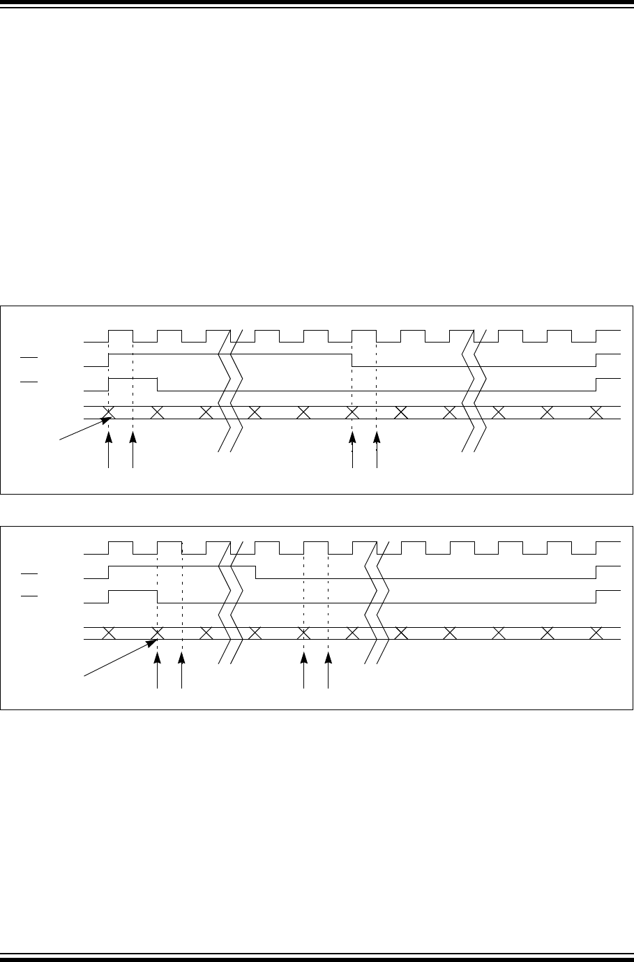
PIC32 Family Reference Manual
DS61106G-page 23-44 © 2007-2011 Microchip Technology Inc.
23.4.5.4 PCM/DSP MODE
The PCM/DSP protocol mode is available for communication with some codecs and certain DSP
devices. This mode modifies the behavior of LRCK and audio data spacing. In PCM/DSP mode,
the LRCK can be a single bit wide (i.e., 1 SCK) or as wide as the audio data (16, 24, 32 bits). The
audio data is packed in the frame with the left channel data immediately followed by the right
channel data. The frame length is still either 32 or 64 clocks when this device is the master.
In PCM/DSP mode, the transmitter drives the audio data’s (left channel) MSb on the first or
second transmit edge (see the SPIFE bit (SPIxCON<17>)) of SCK (after an LRCK transition).
Immediately after the (left channel) LSb, the transmitter drives the (right channel) MSb.
• Required configuration settings:
To s et th e m odu le to L ef t- Jus ti f ie d mode, the following bit must to be set:
- AUDMOD<1:0> bits (SPIxCON2<1:0>) = 11
Refer to the sample waveform diagrams shown in Figure 23-27 and Figure 23-28 for 16, 24,
32-bit audio data transfers.
Figure 23-27: PCM/DSP with 16-bit Data/Channel or 32-bit Data/Channel
Figure 23-28: PCM/DSP with 16/24-bit Data and 32-bit Channel
(FRMSYPW = 1)
SCKx (BCLK)
SDOx/SDIx MSb MSb-1 LSb
LSb+1 MSb MSb-1 LSb+1 LSb
LEFT CHANNEL RIGHT CHANNEL
Transmit Sample SampleTransmit
SSx (LRCK)
(FRMSYPW = 0)LEFT CHANNEL RIGHT CHANNEL
SSx (LRCK)
(SPIFE = 1)
SSx (LRCK)
SCKx (BCLK)
SDOx/SDIx MSb LSb MSb LSb
LEFT CHANNEL RIGHT CHANNEL
Transmit Sample SampleTransmit
000
SSx (LRCK) LEFT CHANNEL RIGHT CHANNEL
(FRMSYPW = 1)
(FRMSYPW = 0)
0
(SPIFE = 0)

© 2007-2011 Microchip Technology Inc. DS61106G-page 23-45
Section 23. Serial Peripheral Interface (SPI)
Serial Peripheral
Interface (SPI)
23
23.4.5.4.1 PCM/DSP Audio Slave Mode of Operation
Use following steps to set up the SPI module for the PCM/DSP Audio Slave mode of operation:
1. If using interrupts, disable the SPI interrupts in the respective IECx register.
2. Stop and reset the SPI module by clearing the ON bit (SPIxCON<15>).
3. Reset the SPI audio configuration register, SPIxCON2.
4. Clear the receive buffer.
5. Clear the ENHBUF bit (SPIxCON<16>) if using Standard Buffer mode or set the bit if using
Enhanced Buffer mode.
6. If using interrupts, the following additional steps are performed:
a) Clear the SPIx interrupt flags/events in the respective IFSx register.
b) Write the SPIx interrupt priority and subpriority bits in the respective IPCx register.
c) Set the SPIx interrupt enable bits in the respective IECx register.
7. Clear the SPIROV bit (SPIxSTAT<6>).
8. Write the desired setting in the SPIxCON2 register. The AUDMOD<1:0> bits
(SPIxCON2<1:0>) must be set to ‘11’ for DSP/PCM mode and the AUDEN bit
(SPIxCON2<7>) must be set to ‘1’ to enable Audio protocol
9. Write the desired settings to the SPIxCON register:
a) Set to slave mode, MSTEN (SPIxCON<5>) = 0.
b) Set MODE<32,16> (SPIxCON<11:10>) = 0 for 16-bit audio channel data.
c) Enable SPI operation by setting the ON bit (SPIxCON<15>).
10. Transmission (and reception) will start as soon as the master provides the BCLK and
LRCK.
Example 23-9: PCM/DSP Slave Mode, 16-bit Channel Data, 32-bit Frame
/* The following code example will initialize the SPI1 Module in PCM/DSP Slave Mode. */
/* It assumes that none of the SPI1 input pins are shared with an analog input. */
unsigned int rData;
IEC0CLR=0x03800000; // disable all interrupts
SPI1CON = 0; // Stops and resets the SPI1.
SPI1CON2 = 0; // Reset audio settings
rData=SPI1BUF; // clears the receive buffer
IFS0CLR=0x03800000; // clear any existing event
IPC5CLR=0x1f000000; // clear the priority
IPC5SET=0x0d000000; // Set IPL = 3, Subpriority 1
IEC0SET=0x03800000; // Enable RX, TX and Error interrupts
SPI1STATCLR=0x40; // clear the Overflow
SPI1CON2=0x00000083; // PCM/DSP Slave Mode, AUDEN = 1, AUDMON = 0
SPI1CON =0x00008000; // Slave mode, SPI ON, FRMSYPW = 0
// 16-bit audio data, 32 bits per frame
// from here, the device is ready to receive and transmit data
/* Note: A few of bits related to frame settings are not required to be set in the SPI1CON */
/* register during audio mode operation. Please refer to the notes in the SPIxCON2 register.*/

PIC32 Family Reference Manual
DS61106G-page 23-46 © 2007-2011 Microchip Technology Inc.
23.4.5.4.2 PCM/DSP Audio Master Mode of Operation
Use the following steps to set up the SPI module for the PCM/DSP Audio Master mode of
operation:
1. If using interrupts, disable the SPI interrupts in the respective IECx register.
2. Stop and reset the SPI module by clearing the ON bit (SPIxCON<15>).
3. Reset the SPI audio configuration register SPI, CON2.
4. Reset the baud rate register, SPIxBRG.
5. Clear the receive buffer.
6. Clear the ENHBUF bit (SPIxCON<16>) if using Standard Buffer mode or set the bit if using
Enhanced Buffer mode.
7. If using interrupts, perform the following steps:
a) Clear the SPIx interrupt flags/events in the respective IFSx register.
b) Write the SPIx interrupt priority and subpriority bits in the respective IPCx register.
c) Set the SPIx interrupt enable bits in the respective IECx register.
8. Clear the SPIROV bit (SPIxSTAT<6>).
9. Write the desired settings in the SPIxCON2 register. The AUDMOD<1:0> bits
(SPIxCON2<1:0>) must be set to ‘11’ for DSP/PCM mode and the AUDEN bit
(SPIxCON<7>) must be set to ‘1’ to enable the audio protocol.
10. Set the SPIxBRG baud rate register to 0x4D (to generate approximately 256 kbps sample
rate, with PBCLK @ 40 MHz).
11. Write the desired settings to the SPIxCON register:
a) Set to Master mode, MSTEN (SPIxCON<5>) = 1.
b) Set MODE<32,16> (SPIxCON<11:10>) = 0 for 16-bit audio channel data.
c) Enable SPI operation by setting the ON bit (SPIxCON<15>).
12. Transmission (and reception) will start immediately after the ON bit is set.
Example 23-10: PCM/DSP Master Mode, 16-bit Channel Data, 32-bit Frame
/* The following code example will initialize the SPI1 Module in PCM/DSP Master Mode. */
/* It assumes that none of the SPI1 input pins are shared with an analog input. */
unsigned int rData;
IEC0CLR=0x03800000; // disable all interrupts
SPI1CON = 0; // Stops and resets the SPI1.
SPI1CON2 = 0; // Reset audio settings
rData=SPI1BUF; // clears the receive buffer
IFS0CLR=0x03800000; // clear any existing event
IPC5CLR=0x1f000000; // clear the priority
IPC5SET=0x0d000000; // Set IPL=3, Subpriority 1
IEC0SET=0x03800000; // Enable RX, TX and Error interrupts
SPI1STATCLR=0x40; // clear the Overflow
SPI1CON2=0x00000083; // PCM/DSP Master Mode, AUDEN =1, AUDMON=0
SPI1BRG =0x4D; // (to generate 256 kbps sample rate, PBCLK @ 40 MHz)
SPI1CON =0x00008020; // Master mode, SPI ON, FRMSYPW = 0
// 16-bit audio data, 32 bits per frame
// from here, the device is ready to receive and transmit data
/* Note: A few of bits related to frame settings are not required to be set in the SPI1CON */
/* register during audio mode operation. Please refer to the notes in the SPIxCON2 register.*/
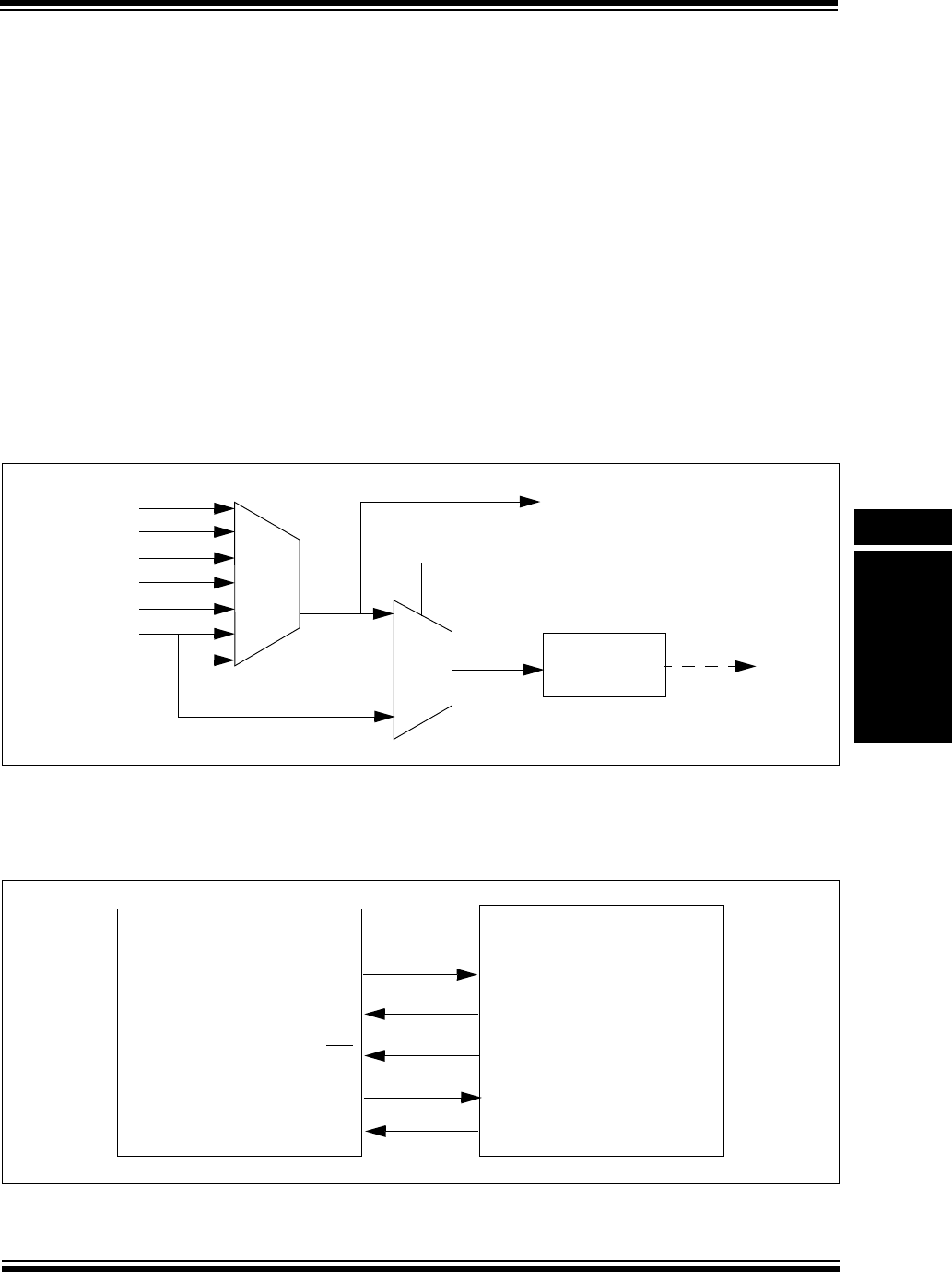
© 2007-2011 Microchip Technology Inc. DS61106G-page 23-47
Section 23. Serial Peripheral Interface (SPI)
Serial Peripheral
Interface (SPI)
23
23.4.6 Audio Protocol Mode Features
23.4.6.1 BCLK/SCK AND LRCK GENERATION
BCLK and LRCK generation is a key requirement in Master mode. The frame frequency of SCK
and LRCK is defined by the MODE<32,16> bits (SPIxCON<11:10>). When the frame is 64 bits,
SCK is 64 times the frequency of LRCK. Similarly, when the frame is 32 bits, SCK is 32 times the
frequency of LRCK. The frequency of SCK must be derived from the toggling rate of LRCK and
the frame size.
For example, to sample a 16-bit channel data at 8 kHz with PBCLK = 36.864 MHz, set the
SPIxBRG register to ‘0x47’ to generate an 8 kHz LRCK.
23.4.6.2 MASTER MODE CLOCKING AND MCLK
The SPI module as a master has the ability to generate BCLK and LRCK by internally generating
using PBCLK (MCLKSEL = 0). The SPI module can generate the clock for external codec
devices using the reference output REFCLKO function (see Figure 23-29), although some
codecs may have the ability to generate their own MCLK from a crystal to provide accurate audio
sample rates. Figure 23-30 shows that the REFCLKO clock can be used as MCLKIN by the
codec.
Figure 23-29: SPI Master Clock Generation
For more information on reference clock output interface refer to the specific device data sheet.
Figure 23-30 shows the interface between a SPI slave and a codec master, deriving the clock
from the MCLK input interface.
Figure 23-30: SPI Slave and Codec Master – Clock Derived from MCLK
Baud Rate
Generator BCLK
USB-PLL
SOSC
LPRC
FRC
POSC
PBCLK
System Clock
MCLK
MCLKSEL
Reference
Clock Output
REFCLKO
SCKx
SSx
SDIx
SDOx
BCLK
LRCK
ADCDAT
DACDAT
PIC32
[SPI Slave]
Codec
[Master]
REFCLKO MCLKIN

PIC32 Family Reference Manual
DS61106G-page 23-48 © 2007-2011 Microchip Technology Inc.
23.4.6.2.1 I2S Audio Master Mode of Operation Using REFCLKO
The following steps can be used to set up the SPI module for the I2S Audio Master mode of
operation with MCLK enabled. The SPI module is initialized to generate BCLK @ 256 kbps and
MCLK is derived from PBCLK using the reference oscillator output configuration register. A
typical application could be to play PCM data (8 kHz sample frequency, 16-bit data, 32-bit frame)
when interfaced to a codec slave device.
1. If using interrupts, disable the SPI interrupts in the respective IECx register.
2. Stop and reset the SPI module by clearing the ON bit (SPIxCON<15>).
3. Reset the SPI audio configuration register, SPIxCON2.
4. Reset the reference oscillator controller register, REFOCON.
5. Reset the baud rate register, SPIxBRG.
6. Clear the receive buffer.
7. Clear the ENHBUF bit (SPIxCON<16>) if using Standard Buffer mode or set the bit if using
Enhanced Buffer mode.
8. If using interrupts, the following additional steps are performed:
a) Clear the SPIx interrupt flags/events in the respective IFSx register.
b) Write the SPIx interrupt priority and subpriority bits in the respective IPCx register.
c) Set the SPIx interrupt enable bits in the respective IECx register.
d) Clear the SPIROV bit (SPIxSTAT<6>).
9. Write the desired settings in the SPIxCON2 register. The AUDMOD<1:0> bits
(SPIxCON2<1:0>) must be set to ‘00’ for I2S mode and the AUDEN bit (SPIxCON2<7>)
must be set to ‘1’ to enable the audio protocol.
10. Set the reference oscillator controller register, REFOCON:
a) RODIV<14:0> (REFOCON<30:16>) = 0.
b) ON (REFOCON<15>) = 1, reference oscillator enabled.
c) OE (REFOCON<4>) = 1, output enabled.
11. Set the SPIxBRG baud rate register to 0x4D (to generate approximately 256 kbps sample
rate, with PBCLK @ 40 MHz).
12. Write the desired settings to the SPIxCON register with
a) MSTEN (SPIxCON<5>) = 1.
b) CKP (SPIxCON<6>) = 1.
c) MODE<32,16> (SPIxCON<11:10>) = 0 for 16-bit audio channel data.
d) MCLKSEL (SPIxCON<23>) = 1, master mode.
e) Enable SPI operation by setting the ON bit (SPIxCON<15>).
13. Transmission (and reception) will start as soon as the master provides the BCLK and
LRCK.

© 2007-2011 Microchip Technology Inc. DS61106G-page 23-49
Section 23. Serial Peripheral Interface (SPI)
Serial Peripheral
Interface (SPI)
23
Example 23-11: I2S Master Mode, 256 kbps BCLK, 16-bit Channel Data, 32-bit Frame
23.4.7 Mono Mode versus Stereo Mode
The SPI module enables the audio data transmission in Mono or Stereo mode by setting the
AUDMONO bit (SPIxCON2<3>). When the AUDMONO bit is set to ‘0’ (Stereo mode), the shift
register uses each FIFO location once, which gives each channel a unique stream of data for
stereo data. When the AUDMONO bit is set to ‘1’ (Mono mode), the shift register uses each FIFO
location twice, to give each channel the same mono stream of audio data.
23.4.8 Streaming Data Support and Error Handling
Most of audio streaming applications transmit or receive data continuously. This is required to
keep the channel active during the period of operation, and guarantees best possible accuracy.
Due to streaming audio, the data feeds could be bursty or packet loss can occur causing the
module to encounter situations like underrun. The software needs to be involved to recover from
an underrun.
The Ignore Transmit Underrun (IGNTUR) bit (SPIxCON2<8>), when set to a ‘1’, ignores an
underrun condition. This is helpful for cases when software does not care or does not need to
know about underrun conditions. When an underrun is encountered, the SPI module sets the
SPITUR bit (SPIxSTAT<8>) when SPITUREN = 1 (SPIxCON2<10>), and remains in an error
state until the software clears the state or the ON bit = 0 (SPIxCON<15>).
During the underrun condition, the SPI module loads the SPIxSR register with zeros instead of
data from the SPIxTXB register, and the module continues to transmit zeros. When the error
condition is cleared (i.e., when the SPIxTXB register is not empty), the SPI module loads the
audio data from the transmit buffer into the SPIxSR register on the next LRCK frame boundary
and software must make sure that the left and right audio data is always transferred to the FIFO
in pairs.
The Ignore Receive Overflow (IGNROV) bit (SPIxCON2<9>), when set to a ‘1’, ignores a receive
overflow condition. This is useful when there is a general performance problem in the system that
software must handle properly. An alternate method to handle the receive overflow is by setting
the DISSDI bit = 1 (SPIxCON<4>) when the system does not need to receive audio data.
Changing the DISSDI bit on-the-fly and the receive shift register starts a receive on the leading
LRCK edge.
/* The following code example will initialize the SPI1 Module in I2S Slave mode.
/* It assumes that none of the SPI1 input pins are shared with an analog input. */
unsigned int rData;
IEC0CLR=0x03800000; // disable all interrupts
SPI1CON = 0; // Stops and resets the SPI1.
SPI1CON2 = 0; // Reset audio settings
REFOCON = 0x0; // Reset reference oscillator register
SPI1BRG=0; // Reset Baud rate register
rData=SPI1BUF; // clears the receive buffer
IFS0CLR=0x03800000; // clear any existing event
IPC5CLR=0x1f000000; // clear the priority
IPC5SET=0x0d000000; // Set IPL = 3, Subpriority 1
IEC0SET=0x03800000; // Enable RX, TX and Error interrupts
SPI1STATCLR=0x40; // clear the Overflow
SPI1CON2=0x00000080; // I2S Mode, AUDEN =1, AUDMON=0
SPI1BRG =0x4D; // (to generate 256 kbps sample rate, PBCLK @ 40 MHz)
REFOCON = 0x8001; // ON = 1, ROSEL = 1 for PBCLK
SPI1CON =0x00808060; // MCLKSEL = 1, MSTEN = 1, ON = 1, CKP = 1, 16-bit audio channel
// data, 32-bits per frame
// from here, the device is ready to receive and transmit data
/* Note: A few of bits related to frame settings are not required to be set in the SPI1CON */
/* register during audio mode operation. Please refer to the notes in the SPIxCON2 register.*/
Note: The use of a reference clock output to generate MCLK for the codec may not be a
perfect choice. Driving a clock out to an I/O pad induces jitter that may degrade
audio fidelity of the codec. The best solution is for the codec to use a crystal and be
the master I2S/Audio device.
Note: Receive data is not affected by AUDMONO bit settings.

PIC32 Family Reference Manual
DS61106G-page 23-50 © 2007-2011 Microchip Technology Inc.
23.5 INTERRUPTS
The SPI module has the ability to generate interrupts reflecting the events that occur during the
data communication. The following types of interrupts can be generated:
• Receive data available interrupts are signalled by SPI1RXIF and SPI2RXIF. This event
occurs when there is new data assembled in the SPIxBUF receive buffer.
•Transmit buffer empty interrupts are signalled by SPI1TXIF and SPI2TXIF. This event occurs
when there is space available in the SPIxBUF transmit buffer and new data can be written.
•Error interrupts are signalled by SPI1EIF and SPI2EIF. This event occurs when there is an
overflow condition for the SPIxBUF receive buffer (i.e., new receive data assembled but the
previous one not read), when there is an underrun of the transmit buffer, or when a FRMERR
event occurs.
All of these interrupt flags, which must be cleared in software, are located in the IFSx registers.
Refer to the specific device data sheet for more information.
To ena ble th e SPI i nte rr upts, u se the r esp ect iv e SPI interrupt enable bits, SPIxRXIE, SPIxTXIE,
and SPIxFIE, in the corresponding IECx registers.
The interrupt priority level bits and interrupt subpriority level bits must be also be configured using
the SPIxIP and SPIxIS bits in the corresponding IPCx registers.
When using Enhanced Buffer mode, the SPI Transmit Buffer Empty Interrupt Mode bits
(STXISEL<1:0>) in the SPI Control (SPIxCON<3:2>) register can be used to configure the
operation of the transmit buffer empty interrupts when the buffer is not full, empty by one-half or
more, completely empty, or when the last transfer is shifted out.
Similarly, when using Enhanced Buffer mode, the SPI Receive Buffer Full Interrupt Mode bits
(SRXISEL<1:0>) in the SPI Control (SPIxCON<1:0>) register can be used to configure the
generation of receive buffer full interrupts when the buffer is full, full by one-half or more, is not
empty, or when the last word is read.
Refer to Section 8. “Interrupts” (DS61108) for further details.
23.5.1 Interrupt Configuration
Each SPI module has three dedicated interrupt flag bits: SPIxEIF, SPIxRXIF, and SPIxTXIF, and
corresponding interrupt enable/mask bits SPIxEIE, SPIxRXIE, and SPIxTXIE. These bits are
used to determine the source of an interrupt, and to enable or disable an individual interrupt
source. Note that all the interrupt sources for a specific SPI module share one interrupt vector.
Each SPI module can have its own priority level independent of other SPI modules.
SPIxTXIF is set when the SPI transmit buffer is empty and another character can be written to
the SPIxBUF register. SPIxRXIF is set when there is a received character available in SPIxBUF.
SPIxEIF is set when a Receive Overflow condition occurs.
Note that the SPIxTXIF, SPIxRXIF, and SPIxEIF bits will be set without regard to the state of the
corresponding enable bit. The interrupt flag bits can be polled by software if desired.
The SPIxEIE, SPIxTXIE, SPIxRXIE bits are used to define the behavior of the Interrupt Controller
when a corresponding SPIxEIF, SPIxTXIF, or SPIxRXIF bit is set. When the corresponding
interrupt enable bit is clear, the Interrupt Controller does not generate a CPU interrupt for the
event. If the interrupt enable bit is set, the Interrupt Controller will generate an interrupt to the
CPU when the corresponding interrupt flag bit is set (subject to the priority and subpriority as
outlined below).
It is the responsibility of the user’s software routine that services a particular interrupt to clear the
appropriate interrupt flag bit before the service routine is complete.
The priority of each SPI module can be set independently with the SPIxIP<2:0> bits. This priority
defines the priority group to which the interrupt source will be assigned. The priority groups range
from a value of 7 (the highest priority), to a value of 0 (which does not generate an interrupt). An
interrupt being serviced will be preempted by an interrupt in a higher priority group. The individual
sources of error interrupts are controlled by the FRMERREN, SPIROVEN, and SPITUREN bits
in the SPIxCON2 register.
Note: Enhanced Buffer mode is not available on all devices. Refer to the specific device
data sheet for details.

© 2007-2011 Microchip Technology Inc. DS61106G-page 23-51
Section 23. Serial Peripheral Interface (SPI)
Serial Peripheral
Interface (SPI)
23
The subpriority bits allow setting the priority of an interrupt source within a priority group. The
values of the subpriority SPIxIS<1:0> range from 3 (the highest priority) to 0, the lowest priority.
An interrupt within the same priority group but having a higher subpriority value will not preempt
a lower subpriority interrupt that is in progress.
The priority group and subpriority bits allow more than one interrupt source to share the same
priority and subpriority. If simultaneous interrupts occur in this configuration the natural order of
the interrupt sources within a Priority/subpriority group pair determine the interrupt generated.
The natural priority is based on the vector numbers of the interrupt sources. The lower the vector
number the higher the natural priority of the interrupt. Any interrupts that were overridden by
natural order will then generate their respective interrupts based on Priority, subpriority, and
natural order, after the interrupt flag for the current interrupt is cleared.
After an enabled interrupt is generated, the CPU will jump to the vector assigned to that interrupt.
The vector number for the interrupt is the same as the natural order number. The CPU will then
begin executing code at the vector address. The user’s code at this vector address should
perform any application-specific operations required, and clear interrupt flags SPIxEIF,
SPIxTXIF, or SPIxRXIF, and then exit. Refer to the vector address table details in the Section 8.
“Interrupts” (DS61108) for more information on interrupts.
Example 23-12: SPI Initialization with Interrupts Enabled Code Example
Example 23-13: SPI1 ISR Code Example
For devices with Enhanced Buffering mode, the user application should clear the interrupt
request flag after servicing the interrupt condition.
If an SPI interrupt has occurred, the ISR should read the SPI Data Buffer (SPIxBUF) register, and
then clear the SPI interrupt flag, as shown in Example 23-14.
/*
The following code example illustrates an SPI1 interrupt configuration.
When the SPI1 interrupt is generated, the cpu will jump to the vector assigned to SPI1
interrupt.
It assumes that none of the SPI1 input pins are shared with an analog input. If so, the
AD1PCFG and corresponding TRIS registers have to be properly configured.
*/
int rData;
IEC0CLR=0x03800000; // disable all SPI interrupts
SPI1CON = 0; // Stops and resets the SPI1.
rData=SPI1BUF; // clears the receive buffer
IFS0CLR=0x03800000; // clear any existing event
IPC5CLR=0x1f000000; // clear the priority
IPC5SET=0x0d000000; // Set IPL=3, Subpriority 1
IEC0SET=0x03800000; // Enable RX, TX and Error interrupts
SPI1BRG=0x1; // use FPB/4 clock frequency
SPI1STATCLR=0x40; // clear the Overflow
SPI1CON=0x8220; // SPI ON, 8 bits transfer, SMP=1, Master mode
/*
The following code example demonstrates a simple interrupt service routine for SPI1
interrupts. The user’s code at this vector should perform any application specific operations
and must clear the SPI1 interrupt flags before exiting.
*/
void __ISR(_SPI_1_VECTOR, ipl3)__SPI1Interrupt(void)
{
// ... perform application specific operations in response to the
// interrupt
IFS0CLR = 0x03800000; // Be sure to clear the SPI1 interrupt flags
// before exiting the service routine.
}

PIC32 Family Reference Manual
DS61106G-page 23-52 © 2007-2011 Microchip Technology Inc.
Example 23-14: SPI1 ISR Code Example for Devices with Enhanced Buffering Mode
/*
The following code example demonstrates a simple interrupt service routine for SPI1
interrupts. The user’s code at this vector should perform any application specific operations
and must clear the SPI1 interrupt flags before exiting.
*/
void __ISR(_SPI_1_VECTOR, ipl3)__SPI1Interrupt(void)
{
int Data; // Read SPI data buffer
Data = SPI1BUF;
// ... perform application specific operations in response to the
// interrupt
IFS0CLR = 0x03800000; // Be sure to clear the SPI1 interrupt flags
// before exiting the service routine.
}
Note: The SPI1 ISR code examples show MPLAB® C32 C compiler specific syntax. Refer
to your compiler manual regarding support for ISRs.

© 2007-2011 Microchip Technology Inc. DS61106G-page 23-53
Section 23. Serial Peripheral Interface (SPI)
Serial Peripheral
Interface (SPI)
23
23.6 OPERATION IN POWER-SAVING AND DEBUG MODES
23.6.1 Sleep Mode
When the device enters Sleep mode, the system clock is disabled. The exact SPI module
operation during Sleep mode depends on the current mode of operation. The following
subsections describe mode-specific behavior.
23.6.1.1 MASTER MODE IN SLEEP MODE
The following items should be noted in Sleep mode:
•The Baud Rate Generator is stopped and may be reset (check the device data sheet).
•On-going transmission and reception sequences are aborted. The module may not resume
aborted sequences when Sleep mode is exited. (Again, check the device data sheet.)
• Once in Sleep mode, the module will not transmit or receive any new data
23.6.1.2 SLAVE MODE IN SLEEP MODE
In the Slave mode, the SPI module operates from the SCK provided by an external SPI Master.
Since the clock pulses at SCKx are externally provided for Slave mode, the module will continue
to function in Sleep mode. It will complete any transactions during the transition into Sleep. On
completion of a transaction, the SPIRBF flag is set. Consequently, bit SPIxRXIF will be set. If SPI
interrupts are enabled (SPIxRXIE = 1) and the SPI interrupt priority level is greater than the
present CPU priority level, the device will wake from Sleep mode and the code execution will
resume at the SPIx interrupt vector location. If the SPI interrupt priority level is lower than or equal
to the present CPU priority level, the CPU will remain in Idle mode.
The module is not reset on entering Sleep mode if it is operating as a slave device. Register
contents are not affected when the SPIx module is going into or coming out of Sleep mode.
23.6.2 Idle Mode
When the device enters Idle mode, the system clock sources remain functional.
23.6.2.1 MASTER MODE IN IDLE MODE
Bit SIDL (SPIxCON<13>) selects whether the module will stop or continue functioning in Idle
mode.
•If SIDL = 1, the module will discontinue operation in Idle mode. The module will perform the
same procedures when stopped in Idle mode that it does for Sleep mode.
•If SIDL = 0, the module will continue operation in Idle mode
23.6.2.2 SLAVE MODE IN IDLE MODE
The module will continue operation in Idle mode irrespective of the SIDL setting. The behavior is
identical to the one in Sleep mode.
23.6.3 Debug Mode
23.6.3.1 OPERATION OF SPIxBUF
23.6.3.1.1 Reads During Debug Mode
During Debug mode, SPIxBUF can be read; but the read operation does not affect any Status
bits. For example, if the SPIRBF bit (SPIxSTAT<0>) is set when Debug mode is entered, it will
remain set on EXIT From Debug mode, even though the SPIxBUF register was read in Debug
mode.
Note: To pr eve nt u n in ten ti ona l ab ort of transmit and receive sequences, you may need to
wait for the current transmission to be completed before activating Sleep mode.

PIC32 Family Reference Manual
DS61106G-page 23-54 © 2007-2011 Microchip Technology Inc.
23.7 EFFECTS OF VARIOUS RESETS
23.7.1 Device Reset
All SPI registers are forced to their Reset states upon a device Reset. When the asynchronous
Reset input goes active, the SPI logic:
• Resets all bits in SPIxCON and SPIxSTAT
•Resets the transmit and receive buffers (SPIxBUF) to the empty state
•Resets the Baud Rate Generator
23.7.2 Power-on Reset
All SPI registers are forced to their reset states when a Power-on Reset occurs.
23.7.3 Watchdog Timer Reset
All SPI registers are forced to their reset states when a Watchdog Timer Reset occurs.
23.8 PERIPHERALS USING SPI MODULES
There are no other peripherals using the SPI module.

© 2007-2011 Microchip Technology Inc. DS61106G-page 23-55
Section 23. Serial Peripheral Interface (SPI)
Serial Peripheral
Interface (SPI)
23
23.9 RELATED APPLICATION NOTES
This section lists application notes that are related to this section of the manual. These
application notes may not be written specifically for the PIC32 device family, but the concepts are
pertinent and could be used with modification and possible limitations. The current application
notes related to the SPI module are:
Title Application Note #
Interfacing Microchip’s MCP41XXX/MCP42XXX Digital Potentiometers
to a PIC® Microcontroller AN746
Interfacing Microchip’s MCP3201 Analog-to-Digital Converter
to the PIC® Microcontroller
AN719
Note: Please visit the Microchip web site (www.microchip.com) for additional application
notes and code examples for the PIC32 family of devices.

PIC32 Family Reference Manual
DS61106G-page 23-56 © 2007-2011 Microchip Technology Inc.
23.10 REVISION HISTORY
Revision A (July 2007)
This is the initial released version of this document.
Revision B (October 2007)
Revised Examples 23-1, 23-2, 23-3; Table 23-5.
Revision C (October 2007)
Updated document to remove Confidential status.
Revision D (April 2008)
Revised status to Preliminary; Revised U-0 to r-x.
Revision E (June 2008)
Added Footnote number to Registers 12-17; Revised Example 23-4; Revised Figure 23-8;
Change Reserved bits from “Maintain as” to “Write”; Added Note to ON bit (SPIxCON Register).
Revision F (August 2009)
This revision includes the following changes:
•Minor changes to the text and formatting have been incorporated through the document
•Updated register introductions in 23.2 “Status and Control Registers”
•Register Summary (Table 23-2)
- Removed references to the Clear, Set, Invert, IFS0, IFS1, IEC0, IEC1, IPC5, and IPC7
registers
- Added the Address Offset column
- Added Notes 1, 2, and 3, which describe the Clear, Set, and Invert registers
-Added these bits: MSSEN, FRMSYPW, FRMCNT<2:0>, ENHBUF, STXISEL<1:0>,
SRXISEL<1:0>, RXBUFELM<4:0>, SPITUR, SRMT, SPIRBE, AND SPITBF
•Removed the IFS0, IFS1, IEC0, IEC1, IPC5, and IPC7 registers
•Added Notes describing the Clear, Set, and Invert registers to the following registers:
- SPIxCON
-SPIxSTAT
-SPIxBRG
•Added SPIxBRG settings for 60, 72, and 80 MHz in the Sample SCKx Frequencies table
(see Table 23-3)
•Removed SPI Interrupt Vectors for Various Offsets table (Table 23-4)
•Added 23.3.2 “Buffer Modes”
•Added a paragraph that provides details on the MSSEN bit in 23.3.3.1 “Master Mode
Operation”
• Added two bullets that provide details on the FRMSYPW and FRMCNT bits in 23.3.6
“Framed SPI Modes”
• Added two paragraphs that provide details on the STXISEL<1:0> and SRXISEL<1:0> bits
in 23.4 “Interrupts”
•Added a paragraph on SPI1 ISR for devices with Enhanced Buffering mode after
Example 23-4 in 23.4.1 “Interrupt Configuration”
•Added SPI1 ISR Code Example for Devices With Enhanced Buffering mode (see
Example 23-5).
•Removed 23.8 “I/O Pin Control”

© 2007-2011 Microchip Technology Inc. DS61106G-page 23-57
Section 23. Serial Peripheral Interface (SPI)
Serial Peripheral
Interface (SPI)
23
Revision G (October 2011)
This revision includes the following updates:
•Added a note box that references companion documentation and updated the SPI module
feature list (see 23.1 “Introduction”)
•Added SPI Features in Audio Protocol Interface Mode (see Tabl e 23-2)
•Updated the SPI Module Block Diagram (see Figure 23-1)
•The following updates were made to the SPI Control register (see Register 23-1)
- Added Note 5
- Updated the Note for bits 26-24 (FRMCNT<2:0>)
-Updated the definitions for bits 3-2 (STXISEL<2:0>)
- Replaced all occurrences of SPI_TBE_EVENT and SPI_RBF_EVENT with SPIxTXIF
and SPIxRXIF, respectively
- Updated the bit values for the MODE32 and MODE16 bits (SPIxCON<11:10>)
•Added the SPIxCON2 register and the MCLKSEL, DISSDI and FRMERR bits (see
Tabl e 23-3, Register 23-1, and Register 23-2)
•Added note references to the CLR, SET, and INV registers to the SPI Status register (see
Tabl e 23-3 and Register 23-3)
•Updated the bit value definitions for the SRMT bit in the SPI Status register (see bit 7 in
Register 23-3)
•Added a note box referencing pin usage to 23.3 “Modes of Operation”
•Updated the Sample SCKx Frequencies (see Tabl e 23-4)
•Swapped sub-steps b) and c) in the Master mode operation sequence (see
23.3.3.1 “Master Mode Operation”)
•Added a new paragraph on the MSSEN bit after the second note box in 23.3.3.1 “Master
Mode Operation”. In addition, the text in the second note box was updated.
•Added a new paragraph on the MSSEN bit
•Added the SSx pin to the SPI Master Mode Operation in 8-bit Mode timing diagram (see
Figure 23-7)
•Swapped sub-steps b) and c) in the Slave mode operation sequence (see 23.3.3.2 “Slave
Mode Operation”)
•Added a new paragraph that references additional interface options just before
Figure 23-12 (see 23.3.6 “Framed SPI Modes”)
•Added section 23.4 “Audio Protocol Interface Mode”
•Updated the bit name and register references in the bulleted items of 23.5 “Interrupts”
•All sections, with the exception of 23.6.3.1 “Operation of SPIxBUF” were removed in
23.6.3 “Debug Mode”
• The section 23.9 “Design Tips” was removed
•References to LRC were updated to LRCK throughout the document
• All Untested Code watermarks were removed from the code examples
•Formatting updates and minor typographical changes have been made throughout the
document

PIC32 Family Reference Manual
DS61106G-page 23-58 © 2007-2011 Microchip Technology Inc.
NOTES:

© 2007-2011 Microchip Technology Inc. DS61106G-page 23 -59
Information contained in this publication regarding device
applications and the like is provided only for your convenience
and may be superseded by updates. It is your responsibility to
ensure that your application meets with your specifications.
MICROCHIP MAKES NO REPRESENTATIONS OR
WARRANTIES OF ANY KIND WHETHER EXPRESS OR
IMPLIED, WRITTEN OR ORAL, STATUTORY OR
OTHERWISE, RELATED TO THE INFORMATION,
INCLUDING BUT NOT LIMITED TO ITS CONDITION,
QUALITY, PERFORMANCE, MERCHANTABILITY OR
FITNESS FOR PURPOSE. Microchip disclaims all liability
arising from this information and its use. Use of Microchip
devices in life support and/or safety applications is entirely at
the buyer’s risk, and the buyer agrees to defend, indemnify and
hold harmless Microchip from any and all damages, claims,
suits, or expenses resulting from such use. No licenses are
conveyed, implicitly or otherwise, under any Microchip
intellectual property rights.
Trademarks
The Microchip name and logo, the Microchip logo, dsPIC,
KEELOQ, KEELOQ logo, MPLAB, PIC, PICmicro, PICSTART,
PIC32 logo, rfPIC and UNI/O are registered trademarks of
Microchip Technology Incorporated in the U.S.A. and other
countries.
FilterLab, Hampshire, HI-TECH C, Linear Active Thermistor,
MXDEV, MXLAB, SEEVAL and The Embedded Control
Solutions Company are registered trademarks of Microchip
Technology Incorporated in the U.S.A.
Analog-for-the-Digital Age, Application Maestro, chipKIT,
chipKIT logo, CodeGuard, dsPICDEM, dsPICDEM.net,
dsPICworks, dsSPEAK, ECAN, ECONOMONITOR,
FanSense, HI-TIDE, In-Circuit Serial Programming, ICSP,
Mindi, MiWi, MPASM, MPLAB Certified logo, MPLIB,
MPLINK, mTouch, Omniscient Code Generation, PICC,
PICC-18, PICDEM, PICDEM.net, PICkit, PICtail, REAL ICE,
rfLAB, Select Mode, Total Endurance, TSHARC,
UniWinDriver, WiperLock and ZENA are trademarks of
Microchip Technology Incorporated in the U.S.A. and other
countries.
SQTP is a service mark of Microchip Technology Incorporated
in the U.S.A.
All other trademarks mentioned herein are property of their
respective companies.
© 2007-2011, Microchip Technology Incorporated, Printed in
the U.S.A., All Rights Reserved.
Printed on recycled paper.
ISBN: 978-1-61341-689-1
Note the following details of the code protection feature on Microchip devices:
• Microchip products meet the specification contained in their particular Microchip Data Sheet.
• Microchip believes that its family of products is one of the most secure families of its kind on the market today, when used in the
intended manner and under normal conditions.
• There are dishonest and possibly illegal methods used to breach the code protection feature. All of these methods, to our
knowledge, require using the Microchip products in a manner outside the operating specifications contained in Microchip’s Data
Sheets. Most likely, the person doing so is engaged in theft of intellectual property.
• Microchip is willing to work with the customer who is concerned about the integrity of their code.
• Neither Microchip nor any other semiconductor manufacturer can guarantee the security of their code. Code protection does not
mean that we are guaranteeing the product as “unbreakable.”
Code protection is constantly evolving. We at Microchip are committed to continuously improving the code protection features of our
products. Attempts to break Microchip’s code protection feature may be a violation of the Digital Millennium Copyright Act. If such acts
allow unauthorized access to your software or other copyrighted work, you may have a right to sue for relief under that Act.
Microchip received ISO/TS-16949:2009 certification for its worldwide
headquarters, design and wafer fabrication facilities in Chandler and
Tempe, Arizona; Gresham, Oregon and design centers in California
and India. The Company’s quality system processes and procedures
are for its PIC® MCUs and dsPIC® DSCs, KEELOQ® code hopping
devices, Serial EEPROMs, microperipherals, nonvolatile memory and
analog products. In addition, Microchip’s quality system for the design
and manufacture of development systems is ISO 9001:2000 certified.

DS61106G-page 23 -60 © 2007-2011 Microchip Technology Inc.
AMERICAS
Corporate Office
2355 West Chandler Blvd.
Chandler, AZ 85224-6199
Tel: 480-792-7200
Fax: 480-792-7277
Technical Support:
http://www.microchip.com/
support
Web Address:
www.microchip.com
Atlanta
Duluth, GA
Tel: 678-957-9614
Fax: 678-957-1455
Boston
Westborough, MA
Tel: 774-760-0087
Fax: 774-760-0088
Chicago
Itasca, IL
Tel: 630-285-0071
Fax: 630-285-0075
Cleveland
Independence, OH
Tel: 216-447-0464
Fax: 216-447-0643
Dallas
Addison, TX
Tel: 972-818-7423
Fax: 972-818-2924
Detroit
Farmington Hills, MI
Tel: 248-538-2250
Fax: 248-538-2260
Indianapolis
Noblesville, IN
Tel: 317-773-8323
Fax: 317-773-5453
Los Angeles
Mission Viejo, CA
Tel: 949-462-9523
Fax: 949-462-9608
Santa Clara
Santa Clara, CA
Tel: 408-961-6444
Fax: 408-961-6445
Toronto
Mississauga, Ontario,
Canada
Tel: 905-673-0699
Fax: 905-673-6509
ASIA/PACIFIC
Asia Pacific Office
Suites 3707-14, 37th Floor
Tower 6, The Gateway
Harbour City, Kowloon
Hong Kong
Tel : 8 52 - 24 0 1- 120 0
Fax: 852-2401-3431
Australia - Sydney
Tel : 6 1-2 -98 68- 6 73 3
Fax: 61-2-9868-6755
China - Beijing
Tel : 8 6-1 0-8 569 - 70 0 0
Fax: 86-10-8528-2104
China - Chengdu
Tel : 8 6-2 8-8 665 - 55 11
Fax: 86-28-8665-7889
China - Chongqing
Tel : 8 6-2 3-8 980 - 95 8 8
Fax: 86-23-8980-9500
China - Hangzhou
Tel : 8 6-5 71- 2819 -31 87
Fax: 86-571-2819-3189
China - Hong Kong SAR
Tel : 8 52 - 24 0 1- 120 0
Fax: 852-2401-3431
China - Nanjing
Tel : 8 6-2 5-8 473 - 24 6 0
Fax: 86-25-8473-2470
China - Qingdao
Tel : 8 6-5 32- 8502 -73 55
Fax: 86-532-8502-7205
China - Shanghai
Tel : 8 6-2 1-5 407 - 55 3 3
Fax: 86-21-5407-5066
China - Shenyang
Tel : 8 6-2 4-2 334 - 28 2 9
Fax: 86-24-2334-2393
China - Shenzhen
Tel : 8 6-7 55- 8203 -26 60
Fax: 86-755-8203-1760
China - Wuhan
Tel : 8 6-2 7-5 980 - 53 0 0
Fax: 86-27-5980-5118
China - Xian
Tel : 8 6-2 9-8 833 - 72 5 2
Fax: 86-29-8833-7256
China - Xiamen
Tel: 86-592-2388138
Fax: 86-592-2388130
China - Zhuhai
Tel : 86- 756 -3 210 04 0
Fax: 86-756-3210049
ASIA/PACIFIC
India - Bangalore
Tel : 9 1- 8 0- 309 0-4 444
Fax: 91-80-3090-4123
India - New Delhi
Tel : 9 1- 11 -41 60- 86 31
Fax: 91-11-4160-8632
India - Pune
Tel : 9 1- 2 0- 256 6-1 512
Fax: 91-20-2566-1513
Japan - Yokohama
Tel : 8 1- 4 5- 471 - 6 166
Fax: 81-45-471-6122
Korea - Daegu
Tel : 8 2- 5 3- 744 -43 01
Fax: 82-53-744-4302
Korea - Seoul
Tel : 8 2- 2 -5 54- 720 0
Fax: 82-2-558-5932 or
82-2-558-5934
Malaysia - Kuala Lumpur
Tel : 6 0- 3 -6 201 -98 57
Fax: 60-3-6201-9859
Malaysia - Penang
Tel : 6 0- 4 -2 27- 887 0
Fax: 60-4-227-4068
Philippines - Manila
Tel : 6 3- 2 -6 34- 906 5
Fax: 63-2-634-9069
Singapore
Tel : 6 5- 6 33 4 -8 870
Fax: 65-6334-8850
Taiwan - Hsin Chu
Tel : 8 86 - 3- 577 8-3 66
Fax: 886-3-5770-955
Taiwan - Kaohsiung
Tel : 8 86 - 7- 536 -48 18
Fax: 886-7-330-9305
Taiwan - Taipei
Tel : 8 86 - 2- 250 0-6 610
Fax: 886-2-2508-0102
Thailand - Bangkok
Tel : 6 6- 2 -6 94- 135 1
Fax: 66-2-694-1350
EUROPE
Austria - Wels
Tel : 4 3- 7 24 2 -2 244 -39
Fax: 43-7242-2244-393
Denmark - Copenhagen
Tel : 4 5-4 450 -2 828
Fax: 45-4485-2829
France - Paris
Tel : 3 3-1 -6 9-5 3 -6 3-2 0
Fax: 33-1-69-30-90-79
Germany - Munich
Tel : 4 9- 8 9- 627 -14 4-0
Fax: 49-89-627-144-44
Italy - Milan
Tel : 3 9- 0 33 1 -7 426 11
Fax: 39-0331-466781
Netherlands - Drunen
Tel : 3 1- 4 16 - 690 3 99
Fax: 31-416-690340
Spain - Madrid
Tel : 3 4- 9 1- 708 -08 -90
Fax: 34-91-708-08-91
UK - Wokingham
Tel : 4 4- 11 8-9 21- 58 69
Fax: 44-118-921-5820
Worldwide Sales and Service
08/02/11

© 2007-2013 Microchip Technology Inc. DS61116F-page 24-1
Inter-Integrated
Circuit™ (I2C™)
24
Section 24. Inter-Integrated Circuit™ (I2C™)
HIGHLIGHTS
This section of the manual contains the following topics:
24.1 Overview.................................................................................................................. 24-2
24.2 Control and Status Registers...................................................................................24-4
24.3 I2C Bus Characteristics .........................................................................................24-14
24.4 Enabling I2C Operation.......................................................................................... 24-17
24.5 Communicating as a Master in a Single Master Environment ...............................24-20
24.6 Communicating as a Master in a Multi-Master Environment ................................. 24-33
24.7 Communicating as a Slave.................................................................................... 24-36
24.8 I2C Bus Connection Considerations ...................................................................... 24-53
24.9 I2C Operation in Power-Saving Modes.................................................................. 24-55
24.10 Effects of a Reset .................................................................................................. 24-56
24.11 Pin Configuration In I2C Mode............................................................................... 24-56
24.12 Using An External Buffer With The I2C Module ..................................................... 24-56
24.13 Related Application Notes ..................................................................................... 24-57
24.14 Revision History.....................................................................................................24-58

PIC32 Family Reference Manual
DS61116F-page 24-2 © 2007-2013 Microchip Technology Inc.
24.1 OVERVIEW
The Inter-Integrated Circuit™ (I2C™) module is a serial interface useful for communicating with
other peripheral or microcontroller devices. These peripheral devices may be serial EEPROMs,
display drivers, analog-to-digital converters, etc.
The I2C module can operate in any of the following I2C systems:
• As a slave device
• As a master device in a single master system (slave may also be active)
•As a master or slave device in a multi-master system (bus collision detection and arbitration
available)
The I2C module contains independent I2C master logic and I2C slave logic, each generating
interrupts based on their events. In multi-master systems, the software is simply partitioned into
a master controller and a slave controller.
When the I2C master logic is active, the slave logic also remains active, detecting the state of the
bus and potentially receiving messages from itself in a single master system or from other
masters in a multi-master system. No messages are lost during multi-master bus arbitration.
In a multi-master system, bus collision conflicts with other masters in the system are detected
and reported to the application (BCOL interrupt). The software can terminate, and then restart
the message transmission.
The I2C module contains a Baud Rate Generator (BRG). The I2C BRG does not consume other
timer resources in the device.
Key features of the I2C module include the following:
•Independent master and slave logic
• Multi-master support, which prevents message losses in arbitration
• Detects 7-bit and 10-bit device addresses with configurable address masking in Slave
mode
• Detects general call addresses as defined in the I2C protocol
• Automatic SCLx clock stretching provides delays for the processor to respond to a slave
data request
• Supports 100 kHz and 400 kHz bus specifications
• Supports strict I2C reserved address rule
Figure 24-1 shows the I2C module block diagram.
Note: This family reference manual section is meant to serve as a complement to device
data sheets. Depending on the device variant, this manual section may not apply to
all PIC32 devices.
Please consult the note at the beginning of the “Inter-Integrated Circuit™ (I2C™)”
chapter in the current device data sheet to check whether this document supports
the device you are using.
Device data sheets and family reference manual sections are available for
download from the Microchip Worldwide Web site at: http://www.microchip.com
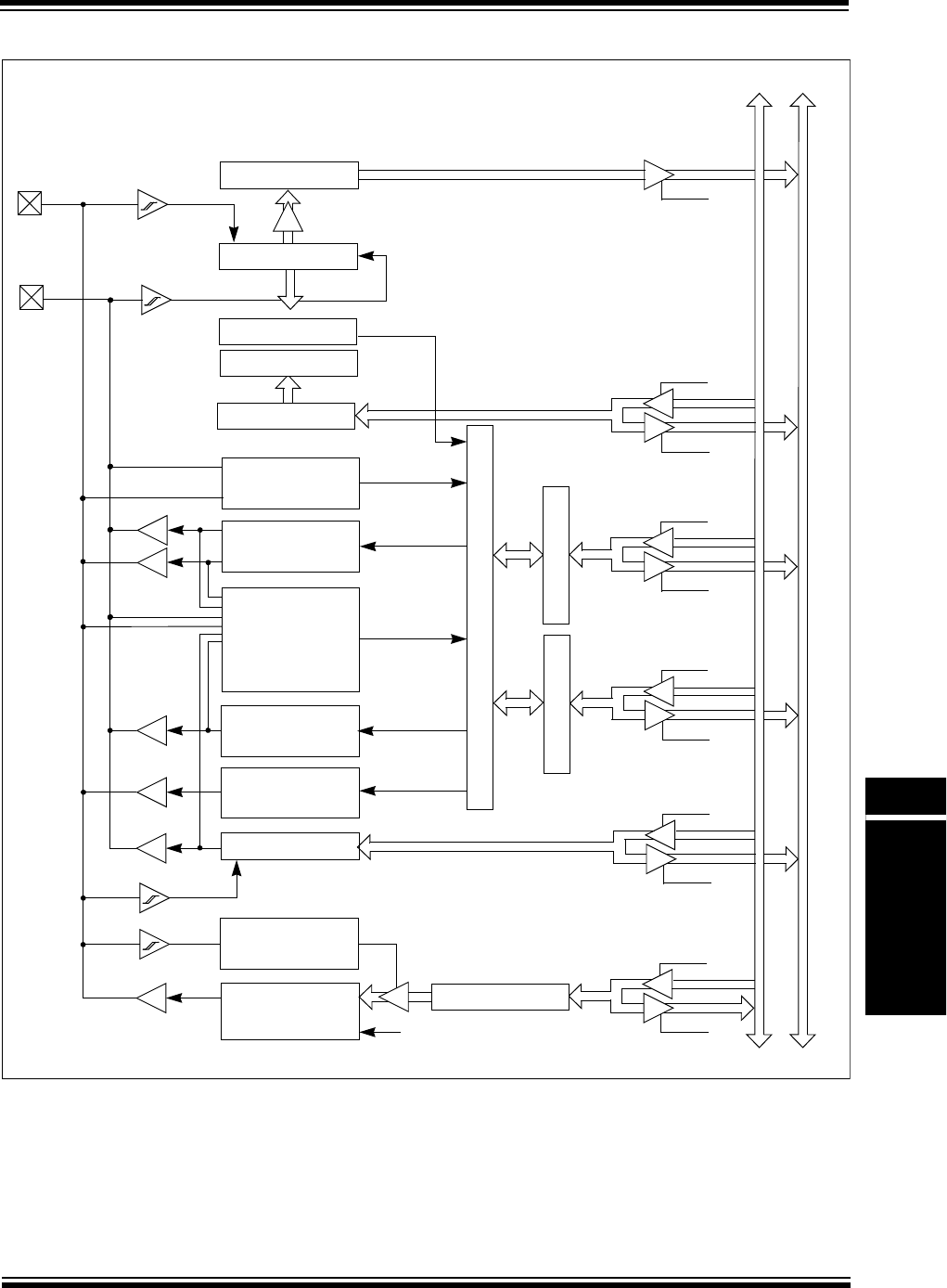
© 2007-2013 Microchip Technology Inc. DS61116F-page 24-3
Section 24. Inter-Integrated Circuit™ (I2C™)
Inter-Integrated
Circuit™ (I2C™)
24
Figure 24-1: I2C™ Block Diagram
I2CxRSR
I2CxRCV
Internal
Data Bus
SCKx
SDAx
Shift
Match Detect
I2CxADD
Start and
Stop bit Detect
Clock
Addr_Match
Clock
Stretching
I2CxTRN
LSb
Shift
Clock
Write
Read
BRG Down Counter I2CxBRG
Reload
Control
Peripheral Bus Clock (PBCLK)
Start, Restart,
Stop bit Generate
Write
Read
Acknowledge
Generation
Collision
Detect
Write
Read
Write
Read
I2CxCON
Write
Read
I2CxSTAT
control logic
Read
LSb
I2CxMSK

PIC32 Family Reference Manual
DS61116F-page 24-4 © 2007-2013 Microchip Technology Inc.
24.2 CONTROL AND STATUS REGISTERS
The I2C module consists of the following Special Function Registers (SFRs):
•I2CxCON: I2C™ Control Register
This register enables operational control of the I2C module.
•I2CxSTAT: I2C™ Status Register
This register contains status flags indicating the state of the I2C module during operation.
•I2CxADD: I2C™ Slave Address Register
This register holds the slave device address.
•I2CxMSK: I2C™ Address Mask Register
This register designates the bit positions in the I2CxADD register that can be ignored, which
allows for multiple address support.
•I2CxBRG: I2C™ Baud Rate Generator Register
This register holds the Baud Rate Generator (BRG) reload value for the I2C module Baud
Rate Generator.
•I2CxTRN: I2C™ Transmit Data Register
This read-only register is the transmit register. Bytes are written to this register during a
transmit operation.
•I2CxRCV: I2C™ Receive Data Register
This read-only register is the buffer register from which data bytes can be read.
Tabl e 24-1 summarizes all registers related to the I2C module. Corresponding registers appear
after the summary, which include detailed bit descriptions for each register.
Note: PIC32 family devices may have one or more I2C modules. An ‘x’ used in the names
of pins, Control/Status bits, and registers denotes the particular module. Refer to the
“Inter-Integrated Circuit (I2C)” chapter in the specific device data sheet for more
details.
© 2007-2013 Microchip Technology Inc. DS61116F-page 24-5
Section 24. Inter-Integrated Circuit™ (I2C™)
Inter-Integrated
Circuit™ (I2C™)
24
Table 24-1: I2C™ SFR Summary
Register Name(1) Bit
31/23/15/7
Bit
30/22/14/6
Bit
29/21/13/5
Bit
28/20/12/4
Bit
27/19/11/3
Bit
26/18/10/2
Bit
25/17/9/1
Bit
24/16/8/0
I2CxCON 31:24 ————————
23:16 —PCIE SCIE BOEN SDAHT SBCDE AHEN DHEN
15:8 ON —SIDL SCLREL STRICT A10M DISSLW SMEN
7:0 GCEN STREN ACKDT ACKEN RCEN PEN RSEN SEN
I2CxSTAT 31:24 ————————
23:16 ————————
15:8 ACKSTAT TRSTAT ACKTIM — — BCL GCSTAT ADD10
7:0 IWCOL I2COV D/A P S R/WRBF TBF
I2CxADD 31:24 ————————
23:16 ————————
15:8 —————— ADD<9:8>
7:0 ADD<7:0>
I2CxMSK 31:24 ————————
23:16 ————————
15:8 —————— MSK<9:8>
7:0 MSK<7:0>
I2CxBRG 31:24 ————————
23:16 ————————
15:8 I2CxBRG<15:8>
7:0 I2CxBRG<7:0>
I2CxTRN 31:24 ————————
23:16 ————————
15:8 ————————
7:0 I2CxTXDATA<7:0>
I2CxRCV 31:24 ————————
23:16 ————————
15:8 ————————
7:0 I2CxRXDATA<7:0>
Note 1: With the exception of the I2CxRCV register, all registers have an associated Clear, Set, and Invert register at an offset
of 0x4, 0x8, and 0xCbytes, respectively. These registers have the same name with CLR, SET, or INV appended to the
end of the register name (e.g., I2CxCONCLR). Writing a ‘1’ to any bit position in these registers will clear valid bits in the
associated register. Reads from these registers should be ignored.

PIC32 Family Reference Manual
DS61116F-page 24-6 © 2007-2013 Microchip Technology Inc.
Register 24-1: I2CXCON: I2C™ Control Register
Bit
Range
Bit
31/23/15/7
Bit
30/22/14/6
Bit
29/21/13/5
Bit
28/20/12/4
Bit
27/19/11/3
Bit
26/18/10/2
Bit
25/17/9/1
Bit
24/16/8/0
31:24 U-0 U-0 U-0 U-0 U-0 U-0 U-0 U-0
— — — — — — — —
23:16 U-0 R/W-0 R/W-0 R/W-0 R/W-0 R/W-0 R/W-0 R/W-0
—PCIE(1) SCIE(1) BOEN(1) SDAHT(1) SBCDE(1) AHEN(1) DHEN(1)
15:8 R/W-0 U-0 R/W-0 R/W-1 R/W-0 R/W-0 R/W-0 R/W-0
ON(2) —SIDL SCLREL STRICT A10M DISSLW SMEN
7:0 R/W-0 R/W-0 R/W-0 R/W-0 R/W-0 R/W-0 R/W-0 R/W-0
GCEN STREN ACKDT ACKEN RCEN PEN RSEN SEN
Legend:
R = Readable bit W = Writable bit U = Unimplemented bit, read as ‘0’
-n = Value at POR ‘1’ = Bit is set ‘0’ = Bit is cleared x = Bit is unknown
bit 31-23 Unimplemented: Read as ‘0’
bit 22 PCIE: Stop Condition Interrupt Enable bit (I2C Slave mode only)(1)
1 = Enable interrupt on detection of Stop condition
0 = Stop detection interrupts are disabled
bit 21 SCIE: Start Condition Interrupt Enable bit (I2C Slave mode only)(1)
1 = Enable interrupt on detection of Start or Restart conditions
0 = Start detection interrupts are disabled
bit 20 BOEN: Buffer Overwrite Enable bit (I2C Slave mode only)(1)
1 = I2CxRCV is updated and ACK is generated for a received address/data byte, ignoring the state of the
I2COV only if the RBF bit = 0
0 = I2CxRCV is only updated when I2COV is clear
bit 19 SDAHT: SDAx Hold Time Selection bit (1)
1 = Minimum of 300 ns hold time on SDAx after the falling edge of SCLx
0 = Minimum of 100 ns hold time on SDAx after the falling edge of SCLx
bit 18 SBCDE: Slave Mode Bus Collision Detect Enable bit (I2C Slave mode only)(1)
If on the rising edge of SCLx, SDAx is sampled low when the module is outputting a high state, the BCL bit
is set, and the bus goes idle. This detection mode is only valid during data and ACK transmit sequences.
1 = Enable slave bus collision interrupts
0 = Slave bus collision interrupts are disabled
bit 17 AHEN: Address Hold Enable bit (I2C Slave mode only)(1)
1 = Following the 8th falling edge of SCLx for a matching received address byte; I2CxCON.SCKREL bit
will be cleared and the SCLx will be held low.
0 = Address holding is disabled
bit 16 DHEN: Data Hold Enable bit (I2C Slave mode only)(1)
1 = Following the 8th falling edge of SCLx for a received data byte; slave hardware clears the
I2CxCON.SCKREL bit and SCLx is held low.
0 = Data holding is disabled
bit 15 ON: I2C Enable bit(2)
1 = Enables the I2C module and configures the SDAx and SCLx pins as serial port pins
0 = Disables I2C module; all I2C pins are controlled by PORT functions
bit 14 Unimplemented: Read as ‘0’
Note 1: This bit is not available on all devices, refer to the “Inter-Integrated Circuit (I2C)” chapter in the specific
device data sheet for availability.
2: When using the 1:1 PBCLK divisor, the user’s software should not read or write the peripheral’s SFRs in
the SYSCLK cycle immediately following the instruction that clears the module’s ON bit.

© 2007-2013 Microchip Technology Inc. DS61116F-page 24-7
Section 24. Inter-Integrated Circuit™ (I2C™)
Inter-Integrated
Circuit™ (I2C™)
24
bit 13 SIDL: Stop in Idle Mode bit
1 = Discontinue module operation when the device enters Idle mode
0 = Continue module operation when the device enters Idle mode
bit 12 SCLREL: SCLx Release Control bit
In I2C Slave mode only; module Reset and (ON = 0) sets SCLREL = 1.
If STREN = 0:
1 = Release clock
0 = Force clock low (clock stretch)
Bit is automatically cleared to ‘0’ at beginning of slave transmission.
If STREN = 1:
1 = Release clock
0 = Holds clock low (clock stretch). User may program this bit to ‘0’ to force a clock stretch at the next
SCLx low.
Bit is automatically cleared to ‘0’ at beginning of slave transmission; automatically cleared to ‘0’ at end of
slave reception.
bit 11 STRICT: Strict I2C Reserved Address Rule Enable bit
1 = Strict reserved addressing is enforced. Device does not respond to reserved address space or generate
addresses in reserved address space.
0 = Strict I2C Reserved Address Rule not enabled
bit 10 A10M: 10-bit Slave Address Flag bit
1 = I2CxADD register is a 10-bit slave address
0 = I2CxADD register is a 7-bit slave address
bit 9 DISSLW: Slew Rate Control Disable bit
1 = Slew rate control disabled for Standard Speed mode (100 kHz); also disabled for 1 MHz mode
0 = Slew rate control enabled for High Speed mode (400 kHz)
bit 8 SMEN: SMBus Input Levels Disable bit
1 = Enable input logic so that thresholds are compliant with the SMBus specification
0 = Disable SMBus specific inputs
bit 7 GCEN: General Call Enable bit
In I2C Slave mode only.
1 = Enable interrupt when a general call address is received in I2CSR. Module is enabled for
reception
0 = General call address disabled
bit 6 STREN: SCLx Clock Stretch Enable bit
In I2C Slave mode only; used in conjunction with SCLREL bit.
1 = Enable clock stretching
0 = Disable clock stretching
bit 5 ACKDT: Acknowledge Data bit
In I2C Master mode only; applicable during master receive. Value that will be transmitted when the user
initiates an Acknowledge sequence at the end of a receive.
1 = A NACK is sent
0 = ACK is sent
bit 4 ACKEN: Acknowledge Sequence Enable bit
In I2C Master mode only; applicable during master receive.
1 = Initiate Acknowledge sequence on SDAx and SCLx pins, and transmit ACKDT data bit; cleared by
module
0 = Acknowledge sequence idle
Register 24-1: I2CXCON: I2C™ Control Register (Continued)
Note 1: This bit is not available on all devices, refer to the “Inter-Integrated Circuit (I2C)” chapter in the specific
device data sheet for availability.
2: When using the 1:1 PBCLK divisor, the user’s software should not read or write the peripheral’s SFRs in
the SYSCLK cycle immediately following the instruction that clears the module’s ON bit.

PIC32 Family Reference Manual
DS61116F-page 24-8 © 2007-2013 Microchip Technology Inc.
bit 3 RCEN: Receive Enable bit
In I2C Master mode only
1 = Enables Receive mode for I2C, automatically cleared by module at end of 8-bit receive data byte
0 = Receive sequence not in progress
bit 2 PEN: Stop Condition Enable bit
In I2C Master mode only.
1 = Initiate Stop condition on SDAx and SCLx pins; cleared by module
0 = Stop condition idle
bit 1 RSEN: Restart Condition Enable bit
In I2C Master mode only.
1 = Initiate Restart condition on SDAx and SCLx pins; cleared by module
0 = Restart condition idle
bit 0 SEN: Start Condition Enable bit
In I2C Master mode only.
1 = Initiate Start condition on SDAx and SCLx pins; cleared by module
0 = Start condition idle
Register 24-1: I2CXCON: I2C™ Control Register (Continued)
Note 1: This bit is not available on all devices, refer to the “Inter-Integrated Circuit (I2C)” chapter in the specific
device data sheet for availability.
2: When using the 1:1 PBCLK divisor, the user’s software should not read or write the peripheral’s SFRs in
the SYSCLK cycle immediately following the instruction that clears the module’s ON bit.

© 2007-2013 Microchip Technology Inc. DS61116F-page 24-9
Section 24. Inter-Integrated Circuit™ (I2C™)
Inter-Integrated
Circuit™ (I2C™)
24
Register 24-2: I2CXSTAT: I2C™ Status Register
Bit
Range
Bit
31/23/15/7
Bit
30/22/14/6
Bit
29/21/13/5
Bit
28/20/12/4
Bit
27/19/11/3
Bit
26/18/10/2
Bit
25/17/9/1
Bit
24/16/8/0
31:24 U-0 U-0 U-0 U-0 U-0 U-0 U-0 U-0
— — — — — — — —
23:16 U-0 U-0 U-0 U-0 U-0 U-0 U-0 U-0
— — — — — — — —
15:8 R-0 R-0 R-0, HS, HC U-0 U-0 R/W-0 R-0 R-0
ACKSTAT TRSTAT ACKTIM(1) — — BCL GCSTAT ADD10
7:0 R/W-0 R/W-0 R-0 R/W-0 R/W-0 R-0 R-0 R-0
IWCOL I2COV D/A P S R/WRBF TBF
Legend: HS = Set by hardware HC = Cleared by hardware
R = Readable bit W = Writable bit U = Unimplemented bit, read as ‘0’
-n = Value at POR ‘1’ = Bit is set ‘0’ = Bit is cleared x = Bit is unknown
bit 31-16 Unimplemented: Read as ‘0’
bit 15 ACKSTAT: Acknowledge Status bit
In both I2C Master and Slave modes; applicable to both transmit and receive.
1 = Acknowledge was not received
0 = Acknowledge was received
bit 14 TRSTAT: Transmit Status bit
In I2C Master mode only; applicable to Master Transmit mode.
1 = Master transmit is in progress (8 bits + ACK)
0 = Master transmit is not in progress
bit 13 ACKTIM: Acknowledge Time Status bit (Valid in I2C Slave mode only)(1)
1 = Indicates I2C bus is in an Acknowledge sequence, set on the eighth falling edge of SCLx clock
0 = Not an Acknowledge sequence, cleared on the ninth rising edge of SCLx clock
bit 12-11 Unimplemented: Read as ‘0’
bit 10 BCL: Master Bus Collision Detect bit
Cleared when the I2C module is disabled (ON = 0).
1 = A bus collision has been detected during a master operation
0 = No collision has been detected
bit 9 GCSTAT: General Call Status bit
Cleared after Stop detection.
1 = General call address was received
0 = General call address was not received
bit 8 ADD10: 10-bit Address Status bit
Cleared after Stop detection.
1 = 10-bit address was matched
0 = 10-bit address was not matched
bit 7 IWCOL: Write Collision Detect bit
1 = An attempt to write the I2CxTRN register collided because the I2C module is busy.
This bit must be cleared in software.
0 = No collision
bit 6 I2COV: I2C Receive Overflow Status bit
1 = A byte is received while the I2CxRCV register is still holding the previous byte.
I2COV is a “don’t care” in Transmit mode. This bit must be cleared in software.
0 = No overflow
Note 1: This bit is not available on all devices, refer to the “Inter-Integrated Circuit (I2C)” chapter in the specific
device data sheet for availability.

PIC32 Family Reference Manual
DS61116F-page 24-10 © 2007-2013 Microchip Technology Inc.
bit 5 D/A: Data/Address bit
Valid only for Slave mode operation.
1 = Indicates that the last byte received or transmitted was data
0 = Indicates that the last byte received or transmitted was address
bit 4 P: Stop bit
Updated when Start, Reset or Stop detected; cleared when the I2C module is disabled (ON = 0).
1 = Indicates that a Stop bit has been detected last
0 = Stop bit was not detected last
bit 3 S: Start bit
Updated when Start, Reset or Stop detected; cleared when the I2C module is disabled (ON = 0).
1 = Indicates that a start (or restart) bit has been detected last
0 = Start bit was not detected last
bit 2 R/W: Read/Write Information bit
Valid only for Slave mode operation.
1 = Read – indicates data transfer is output from slave
0 = Write – indicates data transfer is input to slave
bit 1 RBF: Receive Buffer Full Status bit
1 = Receive complete; I2CxRCV register is full
0 = Receive not complete; I2CxRCV register is empty
bit 0 TBF: Transmit Buffer Full Status bit
1 = Transmit in progress; I2CxTRN register is full (8-bits of data)
0 = Transmit complete; I2CxTRN register is empty
Register 24-2: I2CXSTAT: I2C™ Status Register (Continued)
Note 1: This bit is not available on all devices, refer to the “Inter-Integrated Circuit (I2C)” chapter in the specific
device data sheet for availability.

© 2007-2013 Microchip Technology Inc. DS61116F-page 24-11
Section 24. Inter-Integrated Circuit™ (I2C™)
Inter-Integrated
Circuit™ (I2C™)
24
Register 24-3: I2CXADD: I2C™ Slave Address Register
Bit
Range
Bit
31/23/15/7
Bit
30/22/14/6
Bit
29/21/13/5
Bit
28/20/12/4
Bit
27/19/11/3
Bit
26/18/10/2
Bit
25/17/9/1
Bit
24/16/8/0
31:24 U-0 U-0 U-0 U-0 U-0 U-0 U-0 U-0
— — — — — — — —
23:16 U-0 U-0 U-0 U-0 U-0 U-0 U-0 U-0
— — — — — — — —
15:8 U-0 U-0 U-0 U-0 U-0 U-0 R/W-0 R/W-0
— — — — — — ADD<9:8>
7:0 R/W-0 R/W-0 R/W-0 R/W-0 R/W-0 R/W-0 R/W-0 R/W-0
ADD<7:0>
Legend:
R = Readable bit W = Writable bit U = Unimplemented bit, read as ‘0’
-n = Value at POR ‘1’ = Bit is set ‘0’ = Bit is cleared x = Bit is unknown
bit 31-10 Unimplemented: Read as ‘0’
bit 9-0 ADD<9:0>: I2C Slave Device Address bits
Either Master or Slave mode.
Register 24-4: I2CXMSK: I2C™ Address Mask Register
Bit
Range
Bit
31/23/15/7
Bit
30/22/14/6
Bit
29/21/13/5
Bit
28/20/12/4
Bit
27/19/11/3
Bit
26/18/10/2
Bit
25/17/9/1
Bit
24/16/8/0
31:24 U-0 U-0 U-0 U-0 U-0 U-0 U-0 U-0
— — — — — — — —
23:16 U-0 U-0 U-0 U-0 U-0 U-0 U-0 U-0
— — — — — — — —
15:8 U-0 U-0 U-0 U-0 U-0 U-0 R/W-0 R/W-0
— — — — — — MSK<9:8>(1)
7:0 R/W-0 R/W-0 R/W-0 R/W-0 R/W-0 R/W-0 R/W-0 R/W-0
MSK<7:0>(1)
Legend:
R = Readable bit W = Writable bit U = Unimplemented bit, read as ‘0’
-n = Value at POR ‘1’ = Bit is set ‘0’ = Bit is cleared x = Bit is unknown
bit 31-10 Unimplemented: Read as ‘0’
bit 9-0 MSK<9:0>: I2C Address Mask bits(1)
1 = Forces a “don’t care” in the particular bit position on the incoming address match sequence.
0 = Address bit position must match the incoming I2C address match sequence.
Note 1: MSK<9:8> and MSK<0> are only used in I2C 10-bit mode.
PIC32 Family Reference Manual
DS61116F-page 24-12 © 2007-2013 Microchip Technology Inc.
Register 24-5: I2CXBRG: I2C™ Baud Rate Generator Register
Bit
Range
Bit
31/23/15/7
Bit
30/22/14/6
Bit
29/21/13/5
Bit
28/20/12/4
Bit
27/19/11/3
Bit
26/18/10/2
Bit
25/17/9/1
Bit
24/16/8/0
31:24 U-0 U-0 U-0 U-0 U-0 U-0 U-0 U-0
— — — — — — — —
23:16 U-0 U-0 U-0 U-0 U-0 U-0 U-0 U-0
— — — — — — — —
15:8 R/W-0 R/W-0 R/W-0 R/W-0 R/W-0 R/W-0 R/W-0 R/W-0
I2CxBRG<15:8>(1)
7:0 R/W-0 R/W-0 R/W-0 R/W-0 R/W-0 R/W-0 R/W-0 R/W-0
I2CxBRG<7:0>
Legend:
R = Readable bit W = Writable bit U = Unimplemented bit, read as ‘0’
-n = Value at POR ‘1’ = Bit is set ‘0’ = Bit is cleared x = Bit is unknown
bit 31-16 Unimplemented: Read as ‘0’
bit 15-0 I2CxBRG<15:0>: I2C Baud Rate Generator Value bits(1)
These bits control the divider function of the Peripheral Clock.
Note 1: I2CxBRG<15:12> are not available on all devices, refer to the “Inter-Integrated Circuit (I2C)” chapter in
the specific device data sheet for availability.
Register 24-6: I2CXTRN: I2C™ Transmit Data Register
Bit
Range
Bit
31/23/15/7
Bit
30/22/14/6
Bit
29/21/13/5
Bit
28/20/12/4
Bit
27/19/11/3
Bit
26/18/10/2
Bit
25/17/9/1
Bit
24/16/8/0
31:24 U-0 U-0 U-0 U-0 U-0 U-0 U-0 U-0
— — — — — — — —
23:16 U-0 U-0 U-0 U-0 U-0 U-0 U-0 U-0
— — — — — — — —
15:8 U-0 U-0 U-0 U-0 U-0 U-0 U-0 U-0
— — — — — — — —
7:0 R/W-0 R/W-0 R/W-0 R/W-0 R/W-0 R/W-0 R/W-0 R/W-0
I2CxTXDATA<7:0>
Legend:
R = Readable bit W = Writable bit U = Unimplemented bit, read as ‘0’
-n = Value at POR ‘1’ = Bit is set ‘0’ = Bit is cleared x = Bit is unknown
bit 31-8 Unimplemented: Read as ‘0’
bit 7-0 I2CxTXDATA<7:0>: I2C Transmit Data Buffer bits

© 2007-2013 Microchip Technology Inc. DS61116F-page 24-13
Section 24. Inter-Integrated Circuit™ (I2C™)
Inter-Integrated
Circuit™ (I2C™)
24
Register 24-7: I2CxRCV: I2C™ Receive Data Register
Bit
Range
Bit
31/23/15/7
Bit
30/22/14/6
Bit
29/21/13/5
Bit
28/20/12/4
Bit
27/19/11/3
Bit
26/18/10/2
Bit
25/17/9/1
Bit
24/16/8/0
31:24 U-0 U-0 U-0 U-0 U-0 U-0 U-0 U-0
— — — — — — — —
23:16 U-0 U-0 U-0 U-0 U-0 U-0 U-0 U-0
— — — — — — — —
15:8 U-0 U-0 U-0 U-0 U-0 U-0 U-0 U-0
— — — — — — — —
7:0 R-0 R-0 R-0 R-0 R-0 R-0 R-0 R-0
I2CxRXDATA<7:0>
Legend:
R = Readable bit W = Writable bit U = Unimplemented bit, read as ‘0’
-n = Value at POR ‘1’ = Bit is set ‘0’ = Bit is cleared x = Bit is unknown
bit 31-8 Unimplemented: Read as ‘0’
bit 7-0 I2CxRXDATA<7:0>: I2C Receive Data Buffer bits
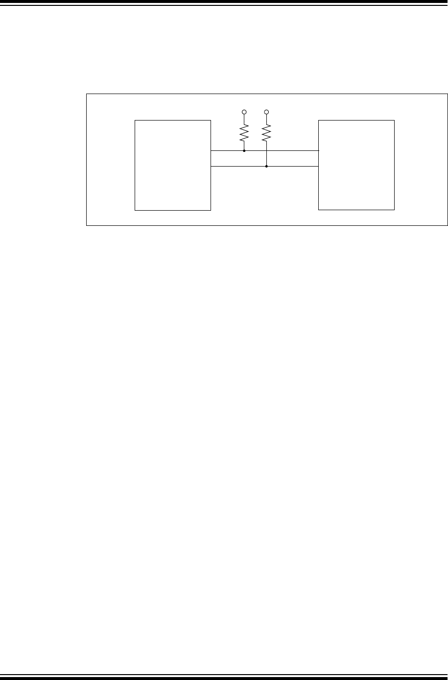
PIC32 Family Reference Manual
DS61116F-page 24-14 © 2007-2013 Microchip Technology Inc.
24.3 I2C BUS CHARACTERISTICS
The I2C bus is a two-wire serial interface. Figure 24-2 shows a schematic of an I2C connection
between a PIC32 device and a 24LC256 I2C serial EEPROM, which is a typical example for any
I2C interface.
Figure 24-2: Typical I2C™ Interconnection Block Diagram
The interface employs a comprehensive protocol to ensure reliable transmission and reception
of data. When communicating, one device is the “master” which initiates transfer on the bus and
generates the clock signals to permit that transfer, while the other device(s) acts as the “slave”
responding to the transfer. The clock line, SCLx, is output from the master and input to the slave,
although occasionally the slave drives the SCLx line. The data line, SDAx, may be output and
input from both the master and the slave.
Because the SDAx and SCLx lines are bidirectional, the output stages of the devices driving the
SDAx and SCLx lines must have an open drain in order to perform the wired AND function of the
bus. External pull-up resistors are used to ensure a high level when no device is pulling the line
down.
In the I2C interface protocol, each device has an address. When a master wishes to initiate a
data transfer, it first transmits the address of the device that it wants to “talk” to. All devices “listen”
to see if this is their address. Within this address, bit 0 specifies if the master wants to read from
or write to the slave device. The master and slave are always in opposite modes of operation
(transmitter/receiver) during a data transfer. That is, they can be thought of as operating in either
of the following two relations:
•Master-transmitter and slave-receiver
•Slave-transmitter and master-receiver
In both cases, the master originates the SCLx clock signal.
The following modes and features specified in the V2.1 I2C specifications are not supported:
•HS mode and switching between F/S modes and HS mode
• Start byte
•CBUS compatibility
• Second byte of the general call address
SCLX
SDAX
PIC32
SDAX
SCLX
VDD VDD
2.4 k24LC256
(typical)
I2C™ Slave
Device

© 2007-2013 Microchip Technology Inc. DS61116F-page 24-15
Section 24. Inter-Integrated Circuit™ (I2C™)
Inter-Integrated
Circuit™ (I2C™)
24
24.3.1 Bus Protocol
The following I2C bus protocol has been defined:
•Data transfer may be initiated only when the bus is not busy
• During data transfer, the data line must remain stable whenever the SCLx clock line is high.
Changes in the data line while the SCLx clock line is high will be interpreted as a Start or
Stop condition.
Accordingly, the following bus conditions have been defined and are shown in Figure 24-3.
Figure 24-3: I2C™ Bus Protocol States
24.3.1.1 START DATA TRANSFER (S)
After a bus Idle state, a high-to-low transition of the SDAx line while the clock (SCLx) is high
determines a Start condition. All data transfers must be preceded by a Start condition.
24.3.1.2 STOP DATA TRANSFER (P)
A low-to-high transition of the SDAx line while the clock (SCLx) is high determines a Stop
condition. All data transfers must end with a Stop condition.
24.3.1.3 REPEATED START (R)
After a wait state, a high-to-low transition of the SDAx line while the clock (SCLx) is high deter-
mines a Repeated Start condition. Repeated Starts allow a master to change bus direction of
addressed slave device without relinquishing control of the bus.
24.3.1.4 DATA VALID (D)
The state of the SDAx line represents valid data when, after a Start condition, the SDAx line is
stable for the duration of the high period of the clock signal. There is one bit of data per SCLx
clock.
24.3.1.5 ACKNOWLEDGE (A) OR NOT ACKNOWLEDGE (N)
All data byte transmissions must be Acknowledged (ACK) or Not Acknowledged (NACK) by the
receiver. The receiver will pull the SDAx line low for an ACK or release the SDAx line for a NACK.
The Acknowledge is a one-bit period using one SCLx clock.
24.3.1.6 WAIT/DATA INVALID (Q)
The data on the line must be changed during the low period of the clock signal. Devices may also
stretch the clock low time by asserting a low on the SCLx line, causing a wait on the bus.
24.3.1.7 BUS IDLE (I)
Both data and clock lines remain high at those times after a Stop condition and before a Start
condition.
Address
Valid
Data
Allowed
to Change
Stop
Condition
Start
Condition
SCLx
SDAx
(I) (S) (D) (A) or (N) (P) (I)
Data or
(Q)
ACK/NACK
Valid
NACK
ACK

PIC32 Family Reference Manual
DS61116F-page 24-16 © 2007-2013 Microchip Technology Inc.
24.3.2 Message Protocol
A typical I2C message is shown in Figure 24-4. In this example, the message will read a specified
byte from a 24LC256 I2C serial EEPROM. The PIC32 device will act as the master and the
24LC256 device will act as the slave.
Figure 24-4 indicates the data as driven by the master device and the data as driven by the slave
device, considering the combined SDAx line is a wired AND of the master and slave data. The
master device controls and sequences the protocol. The slave device will only drive the bus at
specifically determined times.
Figure 24-4: A Typical I2C™ Message: Read of Serial EEPROM (Random Address Mode)
24.3.2.1 START MESSAGE
Each message is initiated with a Start condition and terminated with a Stop condition. The num-
ber of data bytes transferred between the Start and Stop conditions is determined by the master
device. As defined by the system protocol, the bytes of the message may have special meaning,
such as device address byte or data byte.
24.3.2.2 ADDRESS SLAVE
In Figure 24-4, the first byte is the device address byte, that must be the first part of any I2C
message. It contains a device address and a R/W bit (IC2xSTAT<2>). Note that R/W = 0 for this
first address byte, indicating that the master will be a transmitter and the slave will be a receiver.
24.3.2.3 SLAVE ACKNOWLEDGE
The receiving device is obliged to generate an Acknowledge signal, ACK, after the reception of
each byte. The master device must generate an extra SCLx clock which is associated with this
Acknowledge bit.
24.3.2.4 MASTER TRANSMIT
The next two bytes, sent by the master to the slave, are data bytes containing the location of the
requested EEPROM data byte. The slave must Acknowledge each of the data bytes.
24.3.2.5 REPEATED START
The slave EEPROM now has the address information necessary to return the requested data
byte to the master. However, the R/W bit from the first device address byte specified master
transmission and slave reception. The bus must be turned in the other direction for the slave to
send data to the master.
To perf orm th is fun ct ion wit hou t e ndi ng the me ssage, the master sends a Repeated Start. The
Repeated Start is followed with a device address byte containing the same device address as
before and with the R/W = 1 to indicate slave transmission and master reception.
24.3.2.6 SLAVE REPLY
Now, the slave transmits the data byte by driving the SDAx line, while the master continues to
originate clocks but releases its SDAx drive.
24.3.2.7 MASTER ACKNOWLEDGE
During reads, a master must terminate data requests to the slave by Not Acknowledging (gener-
ating a “NACK”) on the last byte of the message. Data is “Acked” for each byte, except for the
last byte.
24.3.2.8 STOP MESSAGE
The master sends a Stop to terminate the message and return the bus to an Idle state.
X
Bus
Master
SDAx
Start
Address
Byte
EEPROM Address
High Byte
EEPROM Address
Low Byte
Address
Byte
Data
Byte
S1010AAA0
210 R1010AAA1
210 P
Slave
SDAx
Activity
N
AAAA
Output
Output
Idle
R/W
ACK
ACK
ACK
Restart
R/W
ACK
NACK
Stop
Idle

© 2007-2013 Microchip Technology Inc. DS61116F-page 24-17
Section 24. Inter-Integrated Circuit™ (I2C™)
Inter-Integrated
Circuit™ (I2C™)
24
24.4 ENABLING I2C OPERATION
The I2C module fully implements all master and slave functions and is enabled by setting the
ON bit (I2CxCON<15>). When the module is enabled, the master and slave functions are active
simultaneously and will respond according to the software or bus events.
When initially enabled, the module will release the SDAx and SCLx pins, putting the bus into the
Idle state. The master functions will remain in the Idle state unless software sets a control bit to
initiate a master event. The slave functions will begin to monitor the bus. If the slave logic detects
a Start event and a valid address on the bus, the slave logic will begin a slave transaction.
24.4.1 Enabling I2C I/O
Two pins are used for bus operation: the SCLx pin, which is the clock, and the SDAx pin, which
is the data. When the I2C module is enabled, assuming no other module with higher priority has
control, the module will assume control of the SDAx and SCLx pins. The module software need
not be concerned with the state of the port I/O of the pins, the module overrides, the port state,
and direction. At initialization, the pins are tri-state (released).
24.4.2 I2C Interrupts
The I2C module generates three interrupt signals:
•Master interrupt
•Slave interrupt
•Bus collision interrupt
These three signals are pulsed high for at least one Peripheral Bus Clock (PBCLK) on the falling
edge of the ninth clock pulse of the SCLx clock. These interrupts will set the corresponding
interrupt flag bit and will interrupt the CPU if the corresponding interrupt enable bit is set and the
corresponding interrupt priority is high enough.
24.4.2.1 MASTER INTERRUPTS
Master mode operations that generate a master interrupt are:
•Start Condition – 1 BRG time after falling edge of SDAx
•Repeated Start Sequence – 1 BRG time after falling edge of SDAx
•Stop Condition – 1 BRG time after the rising edge of SDAx
• Data transfer byte received – 8th falling edge of SCLx (after receiving eight bits of data from
slave)
•During send ACK sequence – 9th falling edge of SCLx (after sending ACK or NACK to slave)
•Data transfer byte transmitted – 9th falling edge of SCLx (regardless of receiving ACK from
slave)
• During a slave-detected Stop – When slave sets the P bit (I2CxSTAT<4>)
24.4.2.2 SLAVE INTERRUPTS
Slave mode operations that generate a slave interrupt are:
•Detection of a valid device address (including general call) – Ninth falling edge of SCLx
(after sending ACK to master. Address must match unless the STRICT bit = 1
(I2CxCON<11>) or the GCEN bit = 1 (I2CxCON<7>)
•Reception of data – Ninth falling edge of SCLx (after sending the ACK to master)
• Request to transmit data – Ninth falling edge of SCLx (regardless of receiving an ACK from
the master)
For devices with the PCIE (I2CxCON<22>), SCIE (I2CxCON<21>), AHEN (I2CxCON<17>), and
DHEN (I2CxCON<16>) bits, the following Slave mode operations generate a slave interrupt:
•During Start sequence (if SCIE = 1) – 1 BRG time after falling edge of SDAx
•During Restart sequence (if SCIE = 1) – 1 BRG time after falling edge of SDAx
•During Stop sequence (if PCIE = 1) – 1 BRG time after the Rising edge of SDAx
•During Receive Address sequence (AHEN = 1) – 8th falling edge of SCLx (address must
match unless STRICT = 1 or GCEN = 1)
•During Receive Data sequence (DHEN = 1) – 8th falling edge of SCLx

PIC32 Family Reference Manual
DS61116F-page 24-18 © 2007-2013 Microchip Technology Inc.
24.4.2.3 BUS COLLISION INTERRUPTS
Bus Collision events that generate an interrupt are:
•During a Start sequence – SDAx sampled before Start condition
• During a Start sequence – SCLx = 0 before SDAx = 0
•During a Start sequence – SDAx = 0 before BRG time out
•During a Repeated Start sequence – If SDAx is sampled 0 when SCLx goes high
•During a Repeated Start sequence – If SCLx goes low before SDAx goes low
•During a Stop sequence – If SDAx is sampled low after allowing it to float
•During a Stop sequence – If SCLx goes low before SDAx goes high
24.4.3 I2C Transmit and Receive Registers
I2CxTRN is the register to which transmit data is written. This register is used when the I2C
module operates as a master transmitting data to the slave, or as a slave sending reply data to
the master. As the message progresses, the I2CxTRN register shifts out the individual bits. As a
result, the I2CxTRN register may not be written to unless the bus is idle.
Data being received by either the master or the slave is shifted into a non-accessible shift
register, I2CxRSR. When a complete byte is received, the byte transfers to the I2CxRCV register.
In receive operations, the I2CxRSR and I2CxRCV registers create a double-buffered receiver.
This allows reception of the next byte to begin before the current byte of received data is read.
If the I2C module receives another complete byte before the software reads the previous byte
from the I2CxRCV register, a receiver overflow occurs and sets the I2COV bit (I2CxSTAT<6>).
For devices with the BOEN bit (I2CxCON<20>), when the receiver overflow occurs, the byte in
the I2CxRSR register is lost if the BOEN bit is clear. When the BOEN bit is clear, the receive buf-
fer, I2CxRCV, is updated only when the I2COV bit is cleared manually. If the BOEN bit is set, the
state of the I2COV bit is ignored and the I2CxRCV buffer is updated. Then, the acknowledge ACK
is generated for the received data/address if the RBF bit is ‘0’ indicating the I2CxRCV buffer is
empty.
The I2CxADD register holds the slave device address. In 10-bit Addressing mode, all bits are
relevant. In 7-bit Addressing mode, only the I2CxADD<6:0> bits are relevant. The A10M bit
(I2CxCON<10>) specifies the expected mode of the slave address. By using the I2CxMSK
register with the I2CxADD register in either Slave Addressing mode, one or more bit positions
can be removed from exact address matching, allowing the module in Slave mode to respond to
multiple addresses.
24.4.4 I2C Baud Rate Generator
The Baud Rate Generator (BRG) used for I2C Master mode operation is used to set the SCLx
clock frequency for 100 kHz, 400 kHz, and 1 MHz. The BRG reload value is contained in the
I2CxBRG register. The BRG will automatically begin counting on a write to the I2CxTRN register.
After the given operation is complete (i.e., transmission of the last data bit is followed by an ACK)
the internal clock will automatically stop counting and the SCLx pin will remain in its last state.
24.4.5 Baud Rate Generator in I2C Master Mode
In I2C Master mode, the reload value for the BRG is located in the I2CxBRG register. When the
BRG is loaded with this value, the BRG counts down to zero and stops until another reload has
taken place. In I2C Master mode, the BRG is not reloaded automatically. If clock arbitration is tak-
ing place, for instance, the BRG will be reloaded when the SCLx pin is sampled high (see
Figure 24-6). Tabl e 24-2 shows device frequency versus the I2CxBRG setting for standard baud
rates.
Note: I2CxBRG values of 0x0 and 0x1 are expressly prohibited. Do not program the
I2CxBRG register with a value of 0x0 or 0x1, as indeterminate results may occur.

© 2007-2013 Microchip Technology Inc. DS61116F-page 24-19
Section 24. Inter-Integrated Circuit™ (I2C™)
Inter-Integrated
Circuit™ (I2C™)
24
To c omp ut e t he BRG re loa d v al u e, us e t he fo rmu la in Equation 24-1:
Equation 24-1: Baud Rate Generator Reload Value Calculation
Figure 24-5: Baud Rate Generator Block Diagram
Figure 24-6: Baud Rate Generator Timing with Clock Arbitration
Table 24-2: I2C™ Clock Rate with BRG
PBCLK I2CxBRG PGD(1) Approximate FSCK (two rollovers of BRG)
50 MHz 0x037 104 ns 400 kHz
50 MHz 0x0F3 104 ns 100 kHz
40 MHz 0x02C 104 ns 400 kHz
40 MHz 0x0C2 104 ns 100 kHz
30 MHz 0x020 104 ns 400 kHz
30 MHz 0x091 104 ns 100 kHz
20 MHz 0x015 104 ns 400 kHz
20 MHz 0x060 104 ns 100 kHz
10 MHz 0x009 104 ns 400 kHz
10 MHz 0x02F 104 ns 100 kHz
Note 1: The typical value of the Pulse Gobbler Delay (PGD) is 104 ns. Refer to the I2Cx
Bus Data Timing Requirements in the “Electrical Characteristics” chapter in the
specific device data sheet for more information.
Note: Equation 24-1 and Ta bl e 24-2 are provided as design guidelines. Due to
system-dependant parameters, the actual baud rate may differ slightly. Testing is
required to confirm that the actual baud rate meets the system requirements.
Otherwise, the value of the I2CxBRG register may need to be adjusted.
I2CxBRG 1
2FSCK
------------------------- TPGD–
PBCLK2–=
BRG Down Counter
SCL_OUT
I2CxBRG<15:0>
SCLx
Reload
Control
Reload
PBCLK
SDAx
SCLx
SCLx de-asserted but slave holds
DX-1DX
BRG
SCLx is sampled high, reload takes
place, and BRG starts its count.
03 02 01 00 (hold off) 03 02
Reload
BRG
Value
SCLx low (clock arbitration)
SCLx allowed to transition high
BRG counts
down
BRG counts
down
BRG counts
down
TOSC/2
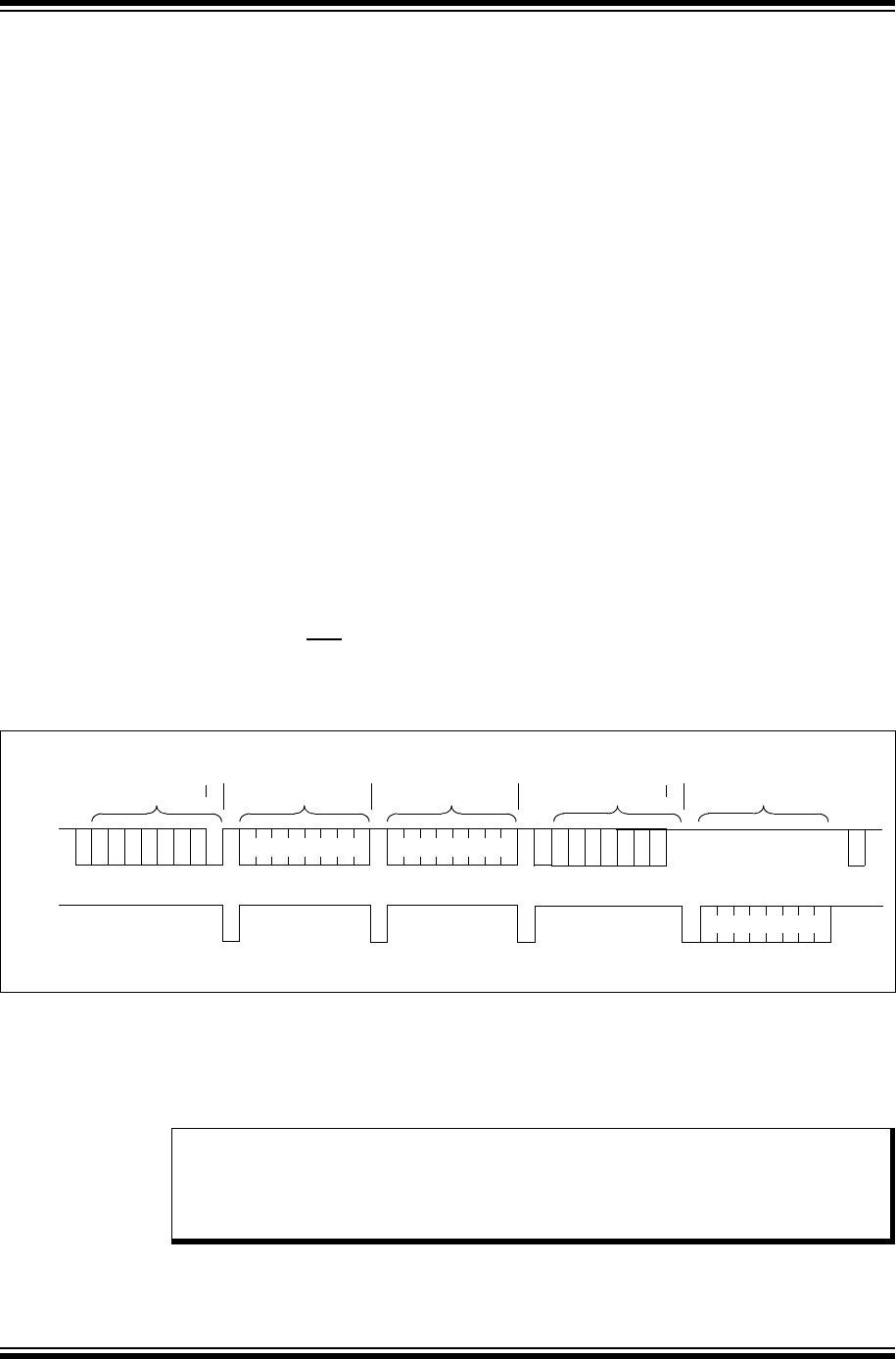
PIC32 Family Reference Manual
DS61116F-page 24-20 © 2007-2013 Microchip Technology Inc.
24.5 COMMUNICATING AS A MASTER IN A SINGLE MASTER ENVIRONMENT
Typical operation of an I2C module in a system is using the module to communicate with an I2C
peripheral, such as an I2C serial memory. In an I2C system, the master controls the sequence of
all data communication on the bus. In this example, the PIC32 device and its I2C module have
the role of the single master in the system. As the single master, it is responsible for generating
the SCLx clock and controlling the message protocol.
In the I2C module, the module controls individual portions of the I2C message protocol; however,
sequencing of the components of the protocol to construct a complete message is a software
task.
For example, a typical operation in a single master environment may be to read a byte from an
I2C serial EEPROM is shown in Figure 24-7.
To accomplish this message, the software will sequence through the following steps:
1. Turn on the I2C module by setting the ON bit (I2CxCON<15>) to ‘1’.
2. Assert a Start condition on SDAx and SCLx.
3. Send the I2C device address byte to the slave with a write indication.
4. Wait for and verify an Acknowledge from the slave.
5. Send the serial memory address high byte to the slave.
6. Wait for and verify an Acknowledge from the slave.
7. Send the serial memory address low byte to the slave.
8. Wait for and verify an Acknowledge from the slave.
9. Assert a Repeated Start condition on SDAx and SCLx.
10. Send the device address byte to the slave with a read indication.
11. Wait for and verify an Acknowledge from the slave.
12. Enable master reception to receive serial memory data.
13. Generate an ACK or NACK condition at the end of a received byte of data.
14. Generate a Stop condition on SDAx and SCLx.
Figure 24-7: Typical I2C™ Message: Read of Serial EEPROM (Random Address Mode)
The I2C module supports Master mode communication with the inclusion of Start and Stop
generators, data byte transmission, data byte reception, an Acknowledge generator and a BRG.
Generally, the software will write to a control register to start a particular step, and then wait for
an interrupt or poll status to wait for completion. Subsequent sections detail each of these
operations.
Bus
Master
SDAx
Start
Address
Byte
EEPROM Address
High Byte
EEPROM Address
Low Byte
Address
Byte
Data
Byte
SAAA0
210 R1P
Slave
SDAx
Activity
N
AAAA
Output
Output
Idle
R/W
ACK
ACK
ACK
Restart
R/W
ACK
NACK
Stop
Idle
A
3
A
4
A
5
A
6
AAA
210
A
3
A
4
A
5
A
6
Note: The I2C module does not allow queueing of events. For instance, the software is not
allowed to initiate a Start condition and then immediately write the I2CxTRN register
to initiate transmission before the Start condition is complete. In this case, the
I2CxTRN register will not be written to and the IWCOL bit (I2CxSTAT<7>) will be
set, indicating that this write to the I2CxTRN register did not occur.
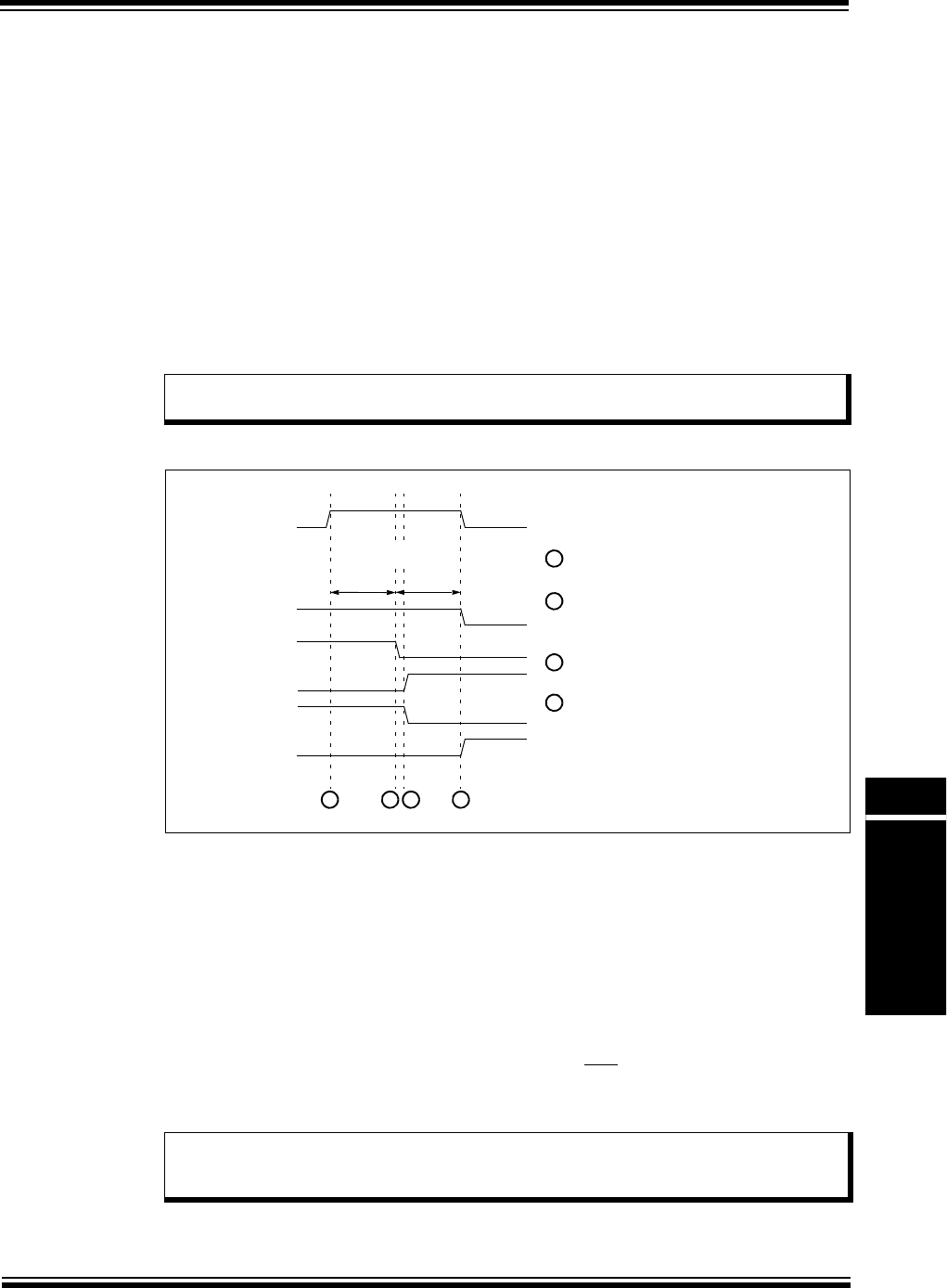
© 2007-2013 Microchip Technology Inc. DS61116F-page 24-21
Section 24. Inter-Integrated Circuit™ (I2C™)
Inter-Integrated
Circuit™ (I2C™)
24
24.5.1 Generating a Start Bus Event
To initiate a Start event, the software sets the Start Enable bit, SEN (I2CxCON<0>). Prior to
setting the Start (S) bit (I2CxSTAT<3>), the software can check the Stop (P) bit (I2CxSTAT<4>)
to ensure that the bus is in an Idle state.
Figure 24-8 shows the timing of the Start condition.
• Slave logic detects the Start condition, sets the S bit and clears the P bit
•The SEN bit is automatically cleared at completion of the Start condition
•A master interrupt is generated at completion of the Start condition
•After the Start condition, the SDAx line and SCLx line are left low (Q state)
24.5.1.1 IWCOL STATUS FLAG
If the software writes to the I2CxTRN register when a Start sequence is in progress, the IWCOL
bit (I2CxSTAT<7>) is set and the contents of the transmit buffer are unchanged (the write does
not occur).
Figure 24-8: Master Start Timing Diagram
24.5.2 Sending Data to a Slave Device
Figure 24-9 shows the timing diagram of master to slave transmission. Transmission of a data
byte, a 7-bit device address byte or the second byte of a 10-bit address is accomplished by
writing the appropriate value to the I2CxTRN register. Loading this register will start the following
process:
1. The software loads the I2CxTRN register with the data byte to transmit.
2. Writing the I2CxTRN register sets the buffer full flag bit, TBF (I2CxSTAT<0>).
3. The data byte is shifted out the SDAx pin until all eight bits are transmitted. Each bit of
address/data will be shifted out onto the SDAx pin after the falling edge of SCLx.
4. On the ninth SCLx clock, the I2C master shifts in the ACK bit from the slave device and
writes its value into the ACKSTAT bit (I2CxSTAT<15>).
5. The I2C master generates the master interrupt at the end of the ninth SCLx clock cycle.
Note: Because queueing of events is not allowed, writing to the five Least Significant bits
of the I2CxCON register is disabled until the Start condition is complete.
Note: The I2C master does not generate or validate the data bytes. The contents and
usage of the bytes are dependent on the state of the message protocol maintained
by the software.
SCLx (Master)
SDAx (Master)
S
SEN
Master Interrupt
TBRG
1 2 3 4
1
TBRG
2
3
4
I2C™ Bus State (I) (Q)
P
(S) Writing SEN = 1 initiates a master Start
event. Baud Rate Generator starts.
Baud Rate Generator times out. Master
module drives SDAx low. Baud Rate
Generator restarts.
Slave module detects Start and sets S = 1
and P = 0.
Baud Rate Generator times out. Master
module drives SCLx low, generates
interrupt and clears SEN.

PIC32 Family Reference Manual
DS61116F-page 24-22 © 2007-2013 Microchip Technology Inc.
24.5.2.1 SENDING A 7-BIT ADDRESS TO THE SLAVE
Sending a 7-bit device address involves sending one byte to the slave. A 7-bit address byte must
contain the 7 bits of the I2C device address and a R/W bit (IC2xSTAT<2>) that defines if the
message will be a write to the slave (master transmission and slave reception) or a read from the
slave (slave transmission and master reception).
24.5.2.2 SENDING A 10-BIT ADDRESS TO THE SLAVE
Sending a 10-bit device address involves sending two bytes to the slave. The first byte contains
five bits of the I2C device address reserved for 10-bit Addressing modes and two bits of the 10-bit
address. Because the next byte, which contains the remaining eight bits of the 10-bit address,
must be received by the slave, the R/W bit in the first byte must be ‘0’, indicating master
transmission and slave reception. If the message data is also directed toward the slave, the
master can continue sending the data. However, if the master expects a reply from the slave, a
Repeated Start sequence with the R/W bit at ‘1’ will change the R/W state of the message to a
read of the slave.
24.5.2.3 RECEIVING ACKNOWLEDGE FROM THE SLAVE
On the falling edge of the eighth SCLx clock, the TBF bit (I2CxSTAT<0>) is cleared and the mas-
ter will deassert the SDAx pin, allowing the slave to respond with an Acknowledge. The master
will then generate a ninth SCLx clock.
This allows the slave device being addressed to respond with an ACK during the ninth bit time if
an address match occurs or data was received properly. A slave sends an Acknowledge when it
has recognized its device address (including a general call) or when the slave has properly
received its data.
The status of ACK is written into the Acknowledge Status bit, ACKSTAT (I2CxSTAT<15>), on the
falling edge of the ninth SCLx clock. After the ninth SCLx clock, the I2C master generates the
master interrupt and enters an Idle state until the next data byte is loaded into the I2CxTRN
register.
24.5.2.4 ACKSTAT STATUS FLAG
The ACKSTAT bit (I2CxSTAT<15>) is updated in both Master and Slave modes on the ninth
SCLx clock irrespective of Transmit or Receive modes. ACKSTAT is cleared when acknowledged
(ACK = 0; i.e., SDAx is ‘0’ on the ninth clock pulse), and is set when not acknowledged (ACK = 1,
i.e., SDAx is ‘1’ on the ninth clock pulse) by the peer.
24.5.2.5 TBF STATUS FLAG
When transmitting, the TBF bit is set when the CPU writes to the I2CxTRN register, and is cleared
when all eight bits are shifted out.
24.5.2.6 IWCOL STATUS FLAG
If the software writes to the I2CxTRN register when a transmit is already in progress (i.e., the I2C
module is still shifting out a data byte), the IWCOL bit (I2CxSTAT<7>) is set and the contents of
the buffer are unchanged (the write does not occur). The IWCOL bit must be cleared in software.
Note 1: In 7-bit Addressing mode, each node using the I2C protocol should be configured
with a unique address that is stored in the I2CxADD register.
2: While transmitting the address byte, the master must shift the address bits <7:0>
left by one bit, and configure bit 0 as the R/W bit.
Note 1: In 10-bit Addressing mode, each node using the I2C protocol should be configured
with a unique address that is stored in the I2CxADD register.
2: While transmitting the address byte, the master must shift the address bits <9:8>
left by one bit, and configure bit 0 as the R/W bit.
Note: Because queueing of events is not allowed, writing to the five Least Significant bits
of the I2CxCON register is disabled until the transmit condition is complete.

© 2007-2013 Microchip Technology Inc. DS61116F-page 24-23
Section 24. Inter-Integrated Circuit™ (I2C™)
Inter-Integrated
Circuit™ (I2C™)
24
Figure 24-9: Master Transmission Timing Diagram
24.5.3 Receiving Data from a Slave Device
Figure 24-10 shows the timing diagram of master reception. The master can receive data from a
slave device after the master has transmitted the slave address with an R/W bit (IC2xSTAT<2>)
value of ‘1’. This is enabled by setting the Receive Enable bit, RCEN (I2CxCON<3>). The master
logic begins to generate clocks, and before each falling edge of the SCLx, the SDAx line is
sampled and data is shifted into the I2CxRSR register.
After the falling edge of the eighth SCLx clock, the following events occur:
• The RCEN bit is automatically cleared
•The contents of the I2CxRSR register transfer into the I2CxRCV register
•The RBF flag bit (I2CxSTAT<1>) is set
•The I
2C master generates the master interrupt
When the CPU reads the buffer, the RBF flag bit is automatically cleared. The software can then
process the data and perform an Acknowledge sequence.
D7 D6 D5 D4 D3 D2 D1 D0
SCLx (Master)
SCLx (Slave)
SDAx (Master)
SDAx (Slave)
TBF
I2CxTRN
Master Interrupt
TBRG TBRG
5 6 7 81 2 3 4
Writing the I2CxTRN register will start a master transmission event. TBF bit is set.
1
Baud Rate Generator starts. The MSb of the I2CxTRN drives SDAx. SCLx remains low. TRSTAT bit is set.
2
Baud Rate Generator times out. SCLx released. Baud Rate Generator restarts.
3
Baud Rate Generator times out. SCLx driven low. After SCLx detected low, the next bit of I2CxTRN drives SDAx.
4
While SCLx is low, the slave can also pull SCLx low to initiate a wait (clock stretch).
5
Master has already released SCLx and slave can release to end wait. Baud Rate Generator restarts.
6
At falling edge of eighth SCLx clock, master releases SDAx. TBF bit is cleared. Slave drives ACK/NACK.
7
At falling edge of ninth SCLx clock, master generates interrupt. SCLx remains low until next event.
8
Slave releases SDAx. TRSTAT bit is clear.
I2C™ Bus State (Q) (D) (Q) (A) (Q)(D) (Q)
TRSTAT
ACKSTAT ACK = 0ACK = 0
Note: The five Least Significant bits of I2CxCON must be ‘0’ before attempting to set the
RCEN bit. This ensures the master logic is inactive.
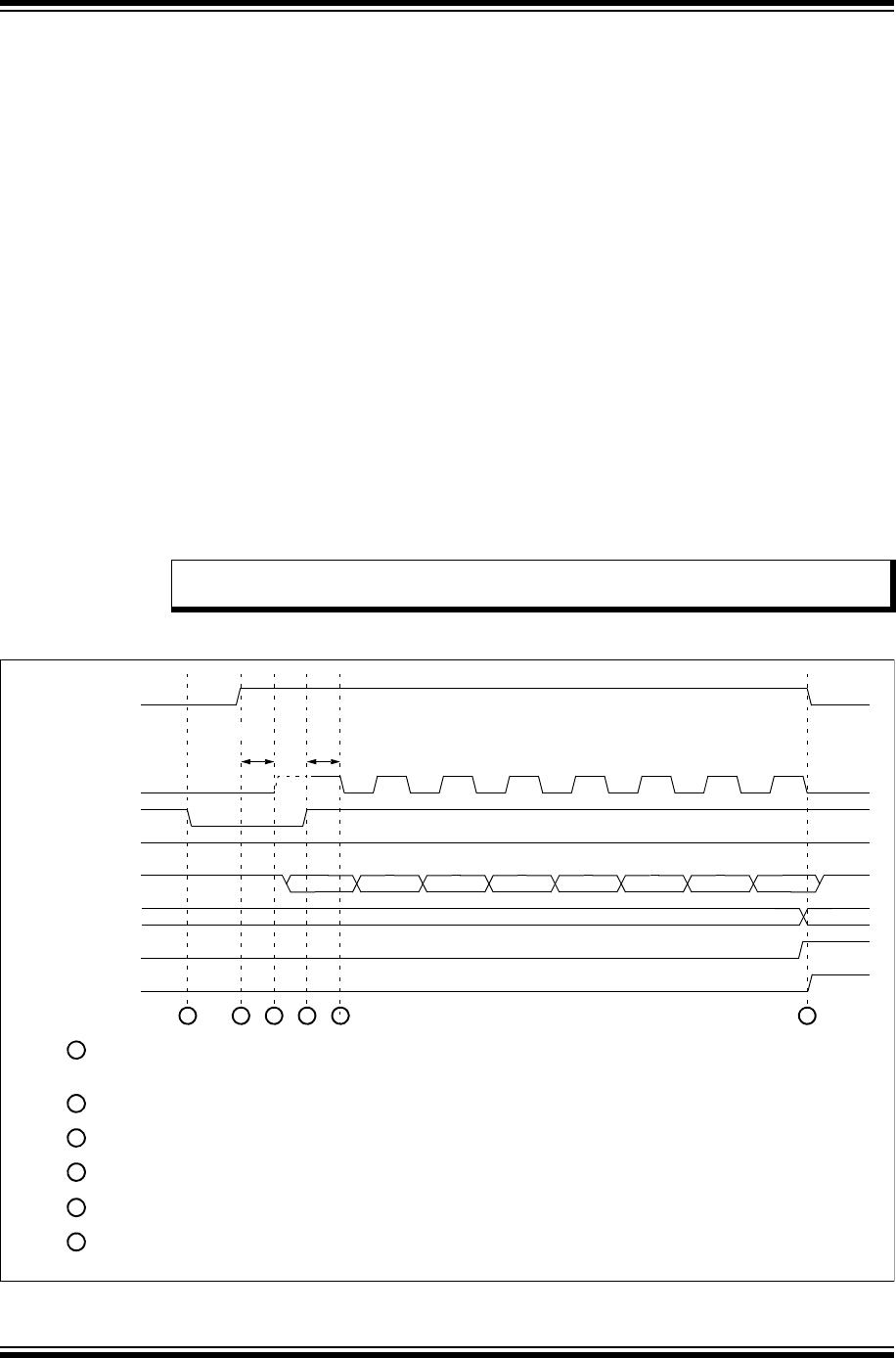
PIC32 Family Reference Manual
DS61116F-page 24-24 © 2007-2013 Microchip Technology Inc.
24.5.3.1 RBF STATUS FLAG
When receiving data, the RBF bit (I2CxSTAT<1>) is set when a device address or data byte is
loaded into I2CxRCV register from the I2CxRSR register. It is cleared when software reads the
I2CxRCV register.
24.5.3.2 I2COV STATUS FLAG
If another byte is received in the I2CxRSR register while the RBF bit remains set and the previous
byte remains in the I2CxRCV register, the I2COV bit (I2CxSTAT<6>) is set and the data in the
I2CxRSR register is lost.
Leaving the I2COV bit set does not inhibit further reception. If the RBF bit is cleared by reading
the I2CxRCV register and the I2CxRSR register receives another byte, that byte will be
transferred to the I2CxRCV register.
For devices with the BOEN bit (I2CxCON<20>), when the receiver overflow occurs, the byte in
the I2CxRCV register is lost if the BOEN bit is cleared. The receive buffer I2CxRCV is updated
only when the I2COV bit is cleared manually. If the BOEN bit is set, the state of the I2COV bit is
ignored and I2CxRCV buffer is updated and the acknowledge is generated for the received
data/address if the RBF bit is ‘0’, indicating the I2CxRCV register is empty.
24.5.3.3 IWCOL STATUS FLAG
If the software writes the I2CxTRN register when a receive is already in progress (i.e., the
I2CxRSR register is still shifting in a data byte), the IWCOL bit (I2CxSTAT<7>) is set and the
contents of the buffer are unchanged (the write does not occur).
Figure 24-10: Master Reception Timing Diagram
Note: Since queueing of events is not allowed, writing to the five Least Significant bits of
the I2CxCON register is disabled until the data reception condition is complete.
D7 D6 D5 D4 D3 D2 D1 D0
SCLx (Master)
SCLx (Slave)
SDAx (Slave)
SDAx (Master)
RBF
I2C™ Bus State
Master Interrupt
TBRG
5 62 3 4
Writing the RCEN bit will start a master reception event. The Baud Rate Generator starts. SCLx remains low.
2
Baud Rate Generator times out. Master attempts to release SCLx.
3
When slave releases SCLx, Baud Rate Generator restarts.
4
Baud Rate Generator times out. MSb of response shifted to I2CxRSR. SCLx driven low for next baud interval.
5
At falling edge of eighth SCLx clock, I2CxRSR transferred to I2CxRCV. I2C master clears RCEN bit.
6
TBRG
RCEN
(D) (Q) (Q)(D)(Q)
I2CxRCV
RBF bit is set. Master generates interrupt.
(Q)
1
Typically, the slave can pull SCLx low (clock stretch) to request a wait to prepare data response.
1
The slave will drive the MSb of the data response on SDAx when ready.
(Q)

© 2007-2013 Microchip Technology Inc. DS61116F-page 24-25
Section 24. Inter-Integrated Circuit™ (I2C™)
Inter-Integrated
Circuit™ (I2C™)
24
24.5.4 Acknowledge Generation
Setting the Acknowledge Enable bit, ACKEN (I2CxCON<4>), enables generation of a master
Acknowledge sequence.
Figure 24-11 shows an ACK sequence and Figure 24-12 shows a NACK sequence. The
Acknowledge Data bit, ACKDT (I2CxCON<5>), specifies ACK or NACK.
After two baud periods, the ACKEN bit is automatically cleared and the I2C master generates the
master interrupt.
24.5.4.1 IWCOL STATUS FLAG
If the software writes to the I2CxTRN register when an Acknowledge sequence is in progress,
the IWCOL bit (I2CxSTAT<7>) is set and the contents of the buffer are unchanged (the write does
not occur).
Figure 24-11: Master Acknowledge (ACK) Timing Diagram
Figure 24-12: Master Not Acknowledge (NACK) Timing Diagram
Note: The five Least Significant bits of I2CxCON must be ‘0’ (master logic inactive) before
attempting to set the ACKEN bit.
Note: Because queueing of events is not allowed, writing to the five Least Significant bits
of the I2CxCON register is disabled until the Acknowledge condition is complete.
SCLx (Master)
SDAx (Master)
ACKEN
Master Interrupt
TBRG
1 2 3
Writing ACKEN = 1 initiates a master Acknowledge event.
1
TBRG
Writing ACKDT = 0 specifies sending an ACK.
When SCLx detected low, I2C master drives SDAx low.
2
Baud Rate Generator times out. I2C master releases SCLx.
3
Baud Rate Generator times out.
4
I2C™ Bus State (A) (Q)
(Q)
4
Baud Rate Generator restarts.
Baud Rate Generator starts. SCLx remains low.
I2C master drives SCLx low, then releases SDAx.
I2C master clears ACKEN. Master generates interrupt.
(Q)
ACKDT = 0
SCLx (Master)
SDAx (Master)
ACKEN
Master Interrupt
TBRG
1 2 3
Writing ACKEN = 1 initiates a master Acknowledge event.
1
TBRG
Writing ACKDT = 1 specifies sending a NACK.
When SCLx detected low, I2C master releases SDAx.
2
Baud Rate Generator times out. I2C master releases SCLx.
3
Baud Rate Generator times out.
4
I2C™ Bus State (A) (I)
(Q)
4
Baud Rate Generator restarts.
Baud Rate Generator starts.
I2C master drives SCLx low, then releases SDAx.
I2C master clears ACKEN. Master generates interrupt.
ACKDT = 1
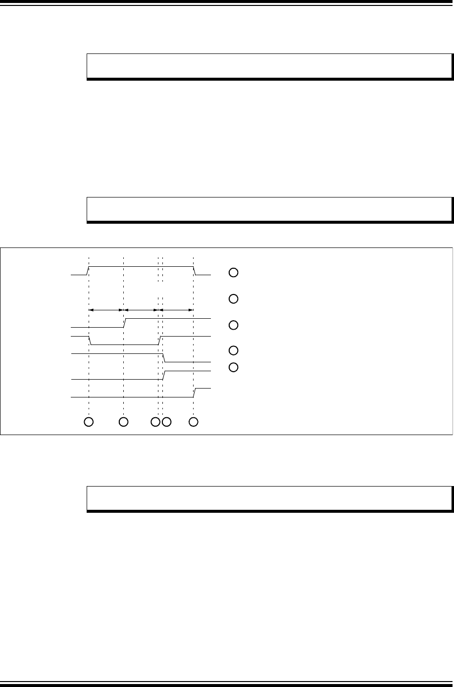
PIC32 Family Reference Manual
DS61116F-page 24-26 © 2007-2013 Microchip Technology Inc.
24.5.5 Generating Stop Bus Event
Setting the Stop Enable bit, PEN (I2CxCON<2>), enables generation of a master Stop sequence.
When the PEN bit is set, the master generates the Stop sequence as shown in Figure 24-13.
• The slave detects the Stop condition, sets the Stop (P) bit (I2CxSTAT<4>) and clears the
Start (S) bit (I2CxSTAT<3>)
•The PEN bit is automatically cleared
•The I
2C master generates the master interrupt
24.5.5.1 IWCOL STATUS FLAG
If the software writes to the I2CxTRN register when a Stop sequence is in progress, the IWCOL
bit (I2CxSTAT<7>) is set and the contents of the buffer are unchanged (the write does not occur).
Figure 24-13: Master Stop Timing Diagram
24.5.6 Generating a Repeated Start Bus Event
Setting the Repeated Start Enable bit, RSEN (I2CxCON<1>), enables generation of a master
Repeated Start sequence (see Figure 24-14).
To generate a Repeated Start condition, software sets the RSEN bit (I2CxCON<1>). The I2C
master asserts the SCLx pin low. When the I2C master samples the SCLx pin low, the module
releases the SDAx pin for one BRG count (TBRG). When the BRG times out and the I2C master
samples SDAx high, the I2C master deasserts the SCLx pin. When the I2C master samples the
SCLx pin high, the BRG reloads and begins counting. SDAx and SCLx must be sampled high for
one TBRG. This action is then followed by assertion of the SDAx pin low for one TBRG while the
SCLx pin is high.
The following is the Repeated Start sequence:
1. The slave detects the Start condition, sets the S bit (I2CxSTAT<3>) and clears the P bit
(I2CxSTAT<4>).
2. The RSEN bit is automatically cleared.
3. The I2C master generates the master interrupt.
Note: The five Least Significant bits of the I2CxCON register must be ‘0’ (master logic
inactive) before attempting to set the PEN bit.
Note: Because queueing of events is not allowed, writing to the five Least Significant bits
of the I2CxCON register is disabled until the Stop condition is complete.
SCLx (Master)
SDAx (Master)
S
PEN
Master Interrupt
TBRG
1 2 3 5
Writing PEN = 1 initiates a master Stop event. Baud Rate
1
TBRG
Generator starts. I2C master drives SDAx low.
Baud Rate Generator times out. I2C master releases SCLx.
2
Baud Rate Generator restarts.
Baud Rate Generator times out. I2C master releases SDAx.
3
Slave logic detects Stop. I2C master sets P = 1, S = 0.
4
I2C™ Bus State (I)
P
TBRG
(Q)
4
Baud Rate Generator restarts.
The Baud Rate Generator times out. I2C master clears PEN.
5
Master generates interrupt.
(Q) (P)
Note: The five Least Significant bits of I2CxCON must be ‘0’ (master logic inactive) before
attempting to set the RSEN bit.

© 2007-2013 Microchip Technology Inc. DS61116F-page 24-27
Section 24. Inter-Integrated Circuit™ (I2C™)
Inter-Integrated
Circuit™ (I2C™)
24
24.5.6.1 IWCOL STATUS FLAG
If the software writes to the I2CxTRN register when a Repeated Start sequence is in progress,
the IWCOL bit (I2CxSTAT<7>) is set and the contents of the buffer are unchanged (the write does
not occur).
Figure 24-14: Master Repeated Start Timing Diagram
24.5.7 Building Complete Master Messages
As described in the 24.5 “Communicating as a Master in a Single Master Environment”,
the software is responsible for constructing messages with the correct message protocol. The
I2C master controls individual portions of the I2C message protocol; however, sequencing of the
components of the protocol to construct a complete message is a software task.
The software can use polling or interrupt methods while using the I2C master. The examples
shown use interrupts.
The software can use the SEN, RSEN, PEN, RCEN and ACKEN bits (five Least Significant bits
of the I2CxCON register) and the TRSTAT bit as “state” flags when progressing through a
message. For example, Ta b le 24-3 shows some example state numbers associated with bus
states.
The software will begin a message by issuing a Start command. The software will record the state
number corresponding to the Start.
Note: Because queueing of events is not allowed, writing of the five Least Significant bits
of the I2CxCON register is disabled until the Repeated Start condition is complete.
SCLx (Master)
SDAx (Master)
S
RSEN
Master Interrupt
TBRG
1 2 3 5
Writing RSEN = 1 initiates a master Repeated Start event.
1
TBRG
Baud Rate Generator starts. I2C master drives SCLx low and
Baud Rate Generator times out. I2C master releases SCLx.
2
Baud Rate Generator restarts.
Baud Rate Generator times out. I2C master drives SDAx low.
3
Slave logic detects Start. I2C master sets S = 1 and P = 0.
4
I2C™ Bus State (Q)
P
TBRG
(Q)
4
Baud Rate Generator restarts.
The Baud Rate Generator times out. I2C master drives SCLx low.
5
I2C master clears RSEN. Master generates interrupt.
(Q) releases SDAx.
(S)
Table 24-3: Master Message Protocol States
Example
State Number I2CxCON<4:0> TRSTAT
(I2CxSTAT<14>) State
000000 0Bus Idle or Wait
100001 N/A Sending Start Event
200000 1Master Transmitting
300010 N/A Sending Repeated Start Event
400100 N/A Sending Stop Event
501000 N/A Master Reception
610000 N/A Master Acknowledgement
Note: Example state numbers are for reference only. User software may assign state
numbers as desired.

PIC32 Family Reference Manual
DS61116F-page 24-28 © 2007-2013 Microchip Technology Inc.
As each event completes and generates an interrupt, the interrupt handler may check the state
number. Therefore, for a Start state, the interrupt handler will confirm execution of the Start
sequence and then start a master transmission event to send the I2C device address, changing
the state number to correspond to the master transmission.
On the next interrupt, the interrupt handler will again check the state, determining that a master
transmission just completed. The interrupt handler will confirm successful transmission of the
data, then move on to the next event, depending on the contents of the message. In this manner,
on each interrupt, the interrupt handler will progress through the message protocol until the
complete message is sent.
Figure 24-15 provides a more detailed examination of the same message sequence shown in
Figure 24-7.
Figure 24-16 shows some simple examples of messages using 7-bit addressing format.
Figure 24-17 shows an example of a 10-bit addressing format message sending data to a
slave.
Figure 24-18 shows an example of a 10-bit addressing format message receiving data from a
slave.

© 2007-2013 Microchip Technology Inc. DS61116F-page 24-29
Section 24. Inter-Integrated Circuit™ (I2C™)
Inter-Integrated
Circuit™ (I2C™)
24
Figure 24-15: Master Message (Typical I2C™ Message: Read of Serial EEPROM)
1Setting the SEN bit starts a Start event.
ACKDT
ACKEN
SEN
SCLx
SDAx
SCLx
SDAx
I2CxTRN
TBF
I2CxRCV
RBF
Master
ACKSTAT
12345678
A1 A0
9
A
PEN
RCEN
12345678
A11
A10
A9
A8
123456789
W1 1
RSEN
123456789
1 32
9
A
12345678
D3 D2 D1 D0D7 D6 D5 D4
9
N
AA
4 5 7 8 9
2Writing the I2CxTRN register starts a master transmission. The data is the serial
3Writing the I2CxTRN register starts a master transmission. The data is the first
4-
5
Writing the I2CxTRN register starts a master transmission. The data is a resend of
6
Setting the RCEN bit starts a master reception. On interrupt, the software reads
7
9
Setting the ACKEN bit starts an Acknowledge event. ACKDT = 0 to send NACK.
Setting the PEN bit starts a master Stop event.
EEPROM device address byte, with R/W clear, indicating a write.
byte of the EEPROM data address.
the serial EEPROM device address byte, but with R/W bit set, indicating a read.
the I2CxRCV register, which clears the RBF flag.
0 0 A2 A7 A6 A5 A4 A2 A1 A0 A1 A0 R1 10 0 A20000
6
Writing the I2CxTRN register starts a master transmission. The data is the second
byte of the EEPROM data address.
8
Setting the RSEN bit starts a Repeated Start event.
(Master)
(Master)
(Slave)
(Slave)
A3
Master interrupt cleared
Interrupt
by user software.
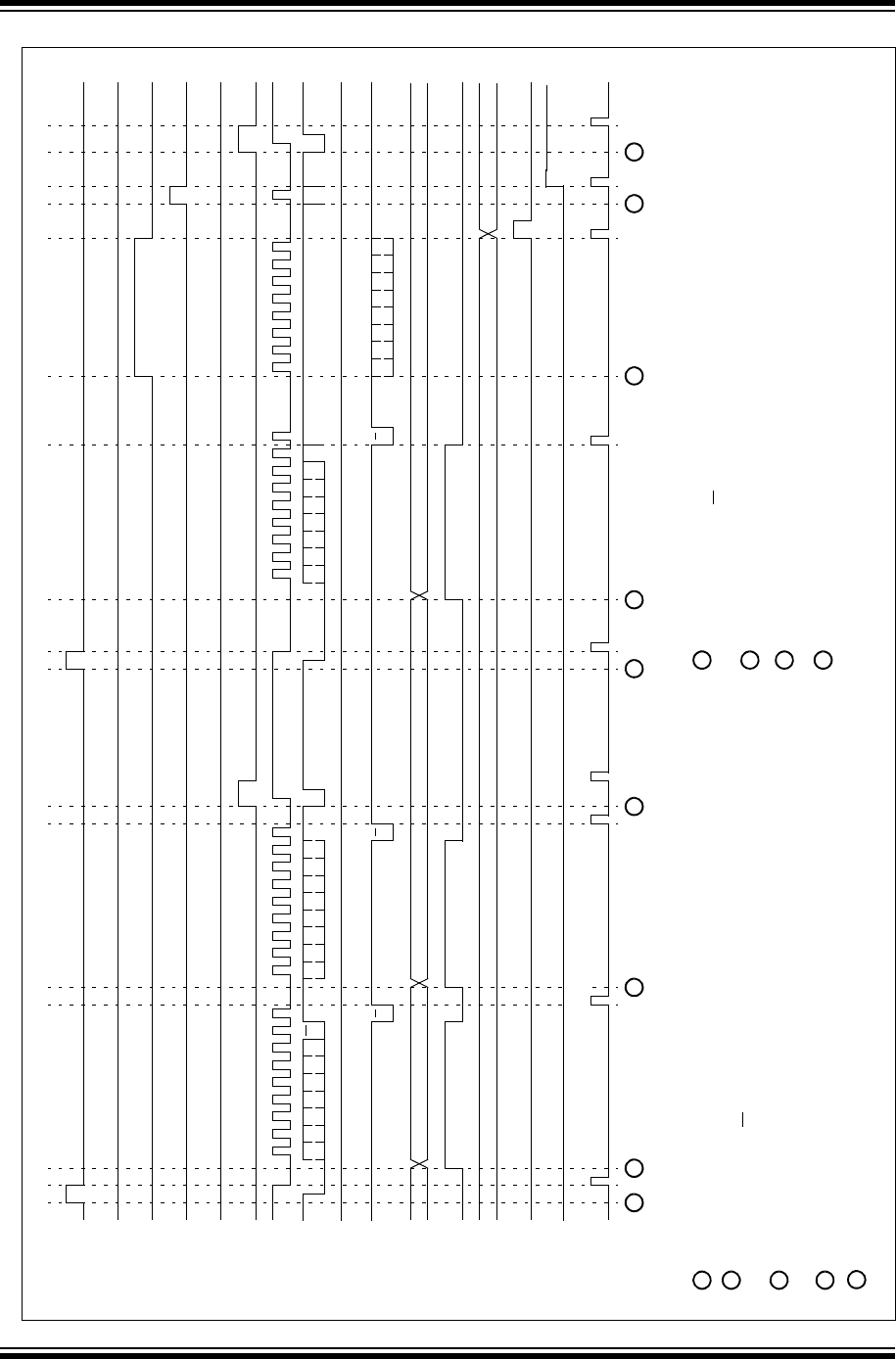
PIC32 Family Reference Manual
DS61116F-page 24-30 © 2007-2013 Microchip Technology Inc.
Figure 24-16: Master Message (7-bit Address: Transmission and Reception)
1Setting the SEN bit starts a Start event.
ACKDT
ACKEN
SEN
SCLx
SDAx
SCLx
SDAx
I2CxTRN
TBF
I2CxRCV
RBF
Master
ACKSTAT
12345678
A2 A1
9
A
PEN
RCEN
12345678
D7 D6 D5 D4 D3 D2 D1 D0
123456789
W
RSEN
1 32
9 12345678
D3 D2 D1 D0D7 D6 D5 D4
9
N
A
4 5 6 97 8
2Writing the I2CxTRN register starts a master transmission. The data is the
3Writing the I2CxTRN register starts a master transmission. The data is the
4Setting the PEN bit starts a master Stop event.
5Setting the SEN bit starts a Start event.
6Writing the I2CxTRN register starts a master transmission. The data is the
7Setting the RCEN bit starts a master reception.
8Setting the ACKEN bit starts an Acknowledge event. ACKDT = 0 to send NACK.
Setting the PEN bit starts a master Stop event.
address byte with R/W bit clear.
message byte.
A7 A6 A5 A4 A3
A
A2 A1
R
A7 A6 A5 A4 A3
address byte with R/W bit set.
9
(Master)
(Master)
(Slave)
(Slave)
Master interrupt cleared
Interrupt
by user software.

© 2007-2013 Microchip Technology Inc. DS61116F-page 24-31
Section 24. Inter-Integrated Circuit™ (I2C™)
Inter-Integrated
Circuit™ (I2C™)
24
Figure 24-17: Master Message (10-bit Transmission)
1Setting the SEN bit starts a Start event.
ACKDT
ACKEN
SEN
SCLx
SDAx
SCLx
SDAx
I2CxTRN
TBF
I2CxRCV
RBF
Master
ACKSTAT
12345678
A9 A8
9
A
PEN
RCEN
12345678
D3 D2 D1 D0D7 D6 D5 D4A7 A6 A5 A4 A3 A2 A1 A0
123456789
W01111
RSEN
123456789
1 32
9
A
123456789
AA
456 7
2Writing the I2CxTRN register starts a master transmission. The data is the first
3Writing the I2CxTRN register starts a master transmission. The data is the second
4Writing the I2CxTRN register starts a master transmission. The data is the first
Setting the PEN bit starts a master Stop event.
byte of the address.
byte of the address.
byte of the message data.
D3 D2 D1 D0D7 D6 D5 D4D3 D2 D1 D0D7 D6 D5 D4
A
5Writing the I2CxTRN register starts a master transmission. The data is the second
byte of the message data.
6Writing the I2CxTRN register starts a master transmission. The data is the third
byte of the message data.
7
(Master)
(Master)
(Slave)
(Slave)
Master interrupt cleared
Interrupt
by user software.
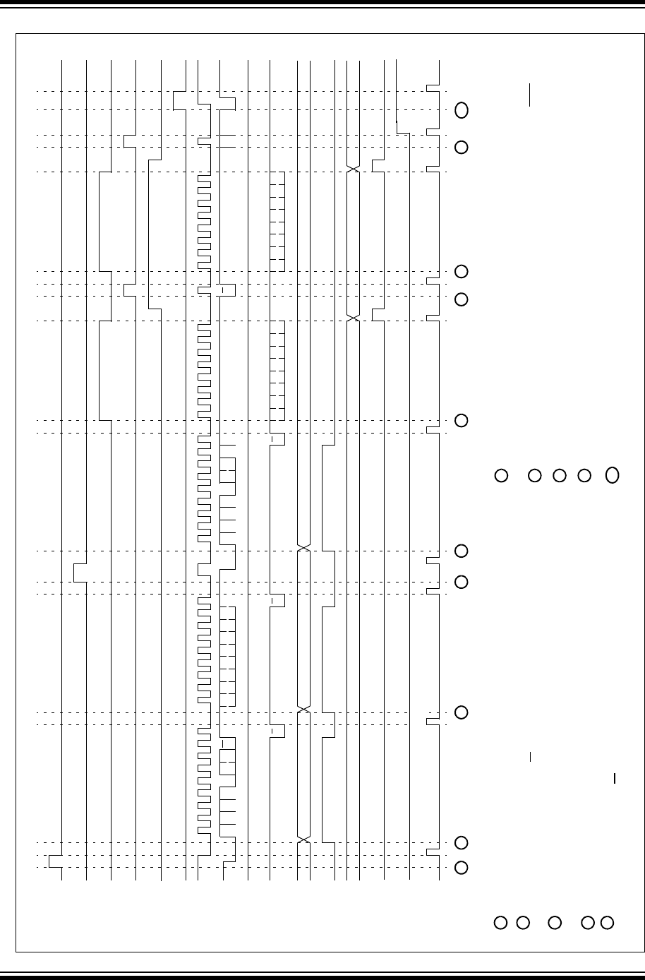
PIC32 Family Reference Manual
DS61116F-page 24-32 © 2007-2013 Microchip Technology Inc.
Figure 24-18: Master Message (10-bit Reception)
1Setting the SEN bit starts a Start event.
ACKDT
ACKEN
SEN
SCLx
SDAx
SCLx
SDAx
I2CxTRN
TBF
I2CxRCV
RBF
Master
ACKSTAT
12345678
A9 A8
9
A
PEN
RCEN
12345678
D3 D2 D1 D0D7 D6 D5 D4
A7 A6 A5 A4 A3 A2 A1 A0
123456789
W01111
RSEN
A9 A8
01111 R
123456789
1 32
9
A
12345678
D3 D2 D1 D0D7 D6 D5 D4
9
N
AA
4 5 6 7 8 9
10
2Writing the I2CxTRN register starts a master transmission. The data is the first
3Writing the I2CxTRN register starts a master transmission. The data is the second
4Setting the RSEN bit starts a master Restart event.
5Writing the I2CxTRN register starts a master transmission. The data is a resend
6Setting the RCEN bit starts a master reception. On interrupt, the software reads
7Setting the ACKEN bit starts an Acknowledge event. ACKDT = 1 to send ACK.
8Setting the RCEN bit starts a master reception.
9Setting the ACKEN bit starts an Acknowledge event. ACKDT = 0 to send NACK.
Setting the PEN bit starts a master Stop event.
byte of the address with the R/W bit cleared.
byte of the address.
of the first byte with the R/W bit set.
the I2CxRCV register, which clears the RBF flag.
(Slave)
(Slave)
(Master)
(Master)
Master interrupt cleared
10
Interrupt
by user software.

© 2007-2013 Microchip Technology Inc. DS61116F-page 24-33
Section 24. Inter-Integrated Circuit™ (I2C™)
Inter-Integrated
Circuit™ (I2C™)
24
24.6 COMMUNICATING AS A MASTER IN A MULTI-MASTER ENVIRONMENT
The I2C protocol allows for more than one master to be attached to a system bus. Considering
that a master can initiate message transactions and generate clocks for the bus, the protocol
has methods to account for situations where more than one master is attempting to control the
bus. Clock synchronization ensures that multiple nodes can synchronize their SCLx clocks to
result in one common clock on the SCLx line. Bus arbitration ensures that if more than one
node attempts a message transaction, one node, and only one node, will be successful in
completing the message. The other nodes will lose bus arbitration and will be left with a bus
collision.
24.6.1 Multi-Master Operation
The Master module has no special settings to enable multi-master operation. The module
performs clock synchronization and bus arbitration at all times. If the module is used in a single
master environment, clock synchronization will only occur between the master and slaves, and
bus arbitration will not occur.
24.6.2 Master Clock Synchronization
In a multi-master system, different masters may have different baud rates. Clock synchronization
will ensure that when these masters are attempting to arbitrate the bus, their clocks will be
coordinated.
Clock synchronization occurs when the master deasserts the SCLx pin (SCLx intended to float
high). When the SCLx pin is released, the BRG is suspended from counting until the SCLx pin is
actually sampled high. When the SCLx pin is sampled high, the BRG is reloaded with the
contents of I2CxBRG<15:0> and begins counting. This ensures that the SCLx high time will
always be at least one BRG rollover count in the event that the clock is held low by an external
device, as shown in Figure 24-19.
Figure 24-19: Baud Rate Generator Timing with Clock Synchronization
SCLx (Slave)
The baud counter decrements twice per TCY. On rollover, the master SCLx will transition.
1
1
000 003001002003
SCLx (Master)
001002003000
Baud Counter
SDAx (Master)
3 4 6
The slave has pulled SCLx low to initiate a wait.
2
At what would be the master baud counter rollover, detecting SCLx low holds counter.
3
Logic samples SCLx once per T
CY. Logic detects SCLx high.
4
2
The baud counter rollover occurs on next cycle.
5
5
On next rollover, the master SCLx will transition.
6
TBRG TBRG
TCY
000

PIC32 Family Reference Manual
DS61116F-page 24-34 © 2007-2013 Microchip Technology Inc.
24.6.3 Bus Arbitration and Bus Collision
Bus arbitration supports multi-master system operation.
The wired AND nature of the SDAx line permits arbitration. Arbitration takes place when the first
master outputs a ‘1’ on SDAx by letting SDAx float high and simultaneously, the second master
outputs a ‘0’ on SDAx by pulling SDAx low. The SDAx signal will go low. In this case, the second
master has won bus arbitration. The first master has lost bus arbitration, and therefore, has a bus
collision.
For the first master, the expected data on SDAx is a ‘1’, but the data sampled on SDAx is a ‘0’.
This is the definition of a bus collision.
The first master will set the Bus Collision bit, BCL (I2CxSTAT<10>), and generate a bus collision
interrupt. The Master module will reset the I2C port to its Idle state.
In multi-master operation, the SDAx line must be monitored for arbitration to see if the signal level
is the expected output level. This check is performed by the Master module, with the result placed
in the BCL bit.
The states where arbitration can be lost are:
•A Start condition
•A Repeated Start condition
•An Address, Data or Acknowledge bit
•A Stop condition
24.6.4 Detecting Bus Collisions and Resending Messages
When a bus collision occurs, the I2C master sets the BCL bit and generates a bus collision inter-
rupt. If bus collision occurs during a byte transmission, the transmission is halted, the TBF bit
(I2CxSTAT<0>) is cleared and the SDAx and SCLx pins are deasserted. If bus collision occurs
during a Start, Repeated Start, Stop or Acknowledge condition, the condition is aborted, the
respective control bits in the I2CxCON register are cleared and the SDAx and SCLx lines are
deasserted.
The software is expecting an interrupt at the completion of the master event. The software can
check the BCL bit to determine if the master event completed successfully or a collision occurred.
If a collision occurs, the software must abort sending the rest of the pending message and
prepare to resend the entire message sequence, beginning with the Start condition, after the bus
returns to an Idle state. The software can monitor the S (I2CxSTAT<3>) and P bits
(I2CxSTAT<4>) to wait for an Idle bus. When the software services the bus collision Interrupt
Service Routine and the I2C bus is free, the software can resume communication by asserting a
Start condition.
24.6.5 Bus Collision During a Start Condition
Before issuing a Start command, the software should verify an Idle state of the bus using the S
and P Status bits. Two masters may attempt to initiate a message at a similar point in time. Typ-
ically, the masters will synchronize clocks and continue arbitration into the message until one
loses arbitration. However, certain conditions can cause a bus collision to occur during a Start.
In this case, the master that loses arbitration during the Start (S) bit generates a bus collision
interrupt.
24.6.6 Bus Collision During a Repeated Start Condition
Should two masters not collide throughout an address byte, a bus collision may occur when one
master attempts to assert a Repeated Start while another transmits data. In this case, the master
generating the Repeated Start will lose arbitration and generate a bus collision interrupt.
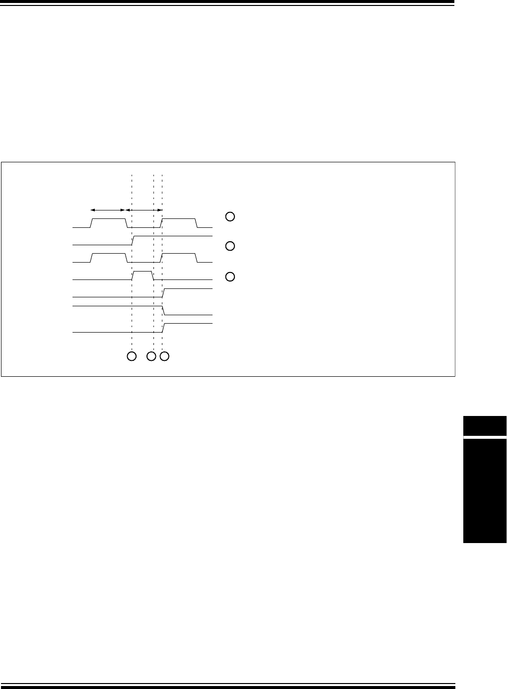
© 2007-2013 Microchip Technology Inc. DS61116F-page 24-35
Section 24. Inter-Integrated Circuit™ (I2C™)
Inter-Integrated
Circuit™ (I2C™)
24
24.6.7 Bus Collision During Message Bit Transmission
The most typical case of data collision occurs while the master is attempting to transmit the
device address byte, a data byte, or an Acknowledge bit.
If the software is checking the bus state, it is unlikely that a bus collision will occur on a Start
condition. However, because another master can, at a very similar time, check the bus and
initiate its own Start condition, it is likely that SDAx arbitration will occur and synchronize the Start
of two masters. In this condition, both masters will begin and continue to transmit their messages
until one master loses arbitration on a message bit. Remember that the SCLx clock
synchronization will keep the two masters synchronized until one loses arbitration. Figure 24-20
shows an example of message bit arbitration.
Figure 24-20: Bus Collision During Message Bit Transmission
24.6.8 Bus Collision During a Stop Condition
If the master software loses track of the state of the I2C bus, there are conditions that cause a
bus collision during a Stop condition. In this case, the master generating the Stop condition will
lose arbitration and generate a bus collision interrupt.
SCLx (Master)
SDAx (Master)
TBF
TBRG
1 2 3
Master transmits bit value of ‘1’ in next SCLx clock.
1
TBRG
I2C master releases SDAx.
Another master on bus transmits bit value of ‘0’
2
in next SCLx clock. Another master pulls SDAx low.
Baud Rate Generator times out. I2C master attempts to verify
3
I2C™ Bus State
BCL
(D)
SCLx (Bus)
SDAx (Bus)
SDAx high. Bus collision detected.
I2C master releases SDAx, SCLx. I2C master sets BCL bit
and clears TBF bit. Master generates interrupt.
(D)(Q)
(Q) (Q)
Master Interrupt
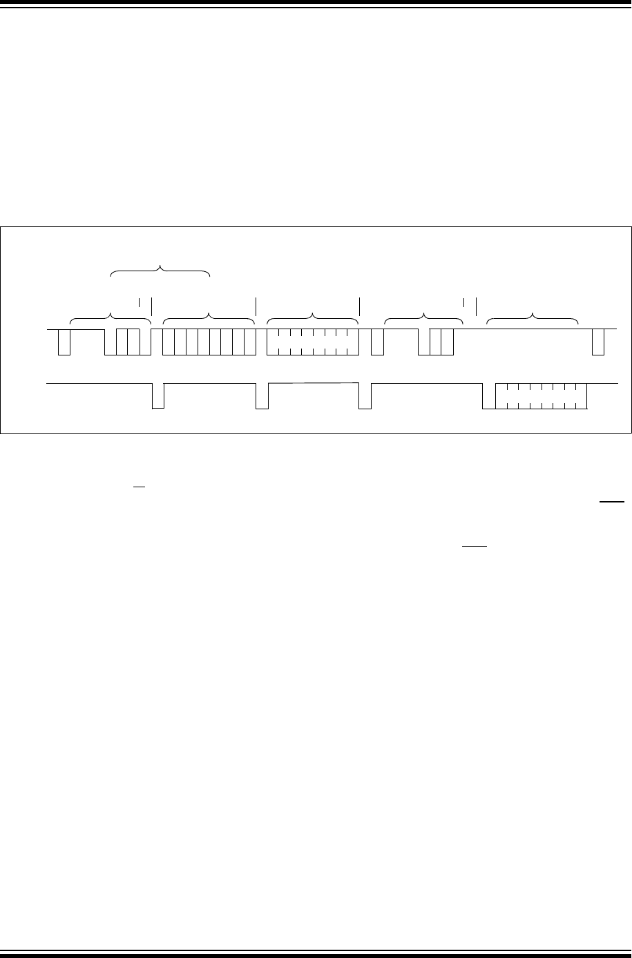
PIC32 Family Reference Manual
DS61116F-page 24-36 © 2007-2013 Microchip Technology Inc.
24.7 COMMUNICATING AS A SLAVE
In some systems, particularly where multiple processors communicate with each other, the
PIC32 device may communicate as a slave, see Figure 24-21. When the I2C slave is enabled,
the Slave module is active. The slave may not initiate a message, it can only respond to a
message sequence initiated by a master. The master requests a response from a particular slave
as defined by the device address byte in the I2C protocol. The Slave module replies to the master
at the appropriate times as defined by the protocol.
As with the Master module, sequencing the components of the protocol for the reply is a software
task. However, the Slave module detects when the device address matches the address
specified by the software for that slave.
Figure 24-21: A Typical Slave I2C™ Message: Multiprocessor Command/Status
After a Start condition, the Slave module will receive and check the device address. The slave
may specify either a 7-bit address or a 10-bit address. When a device address is matched, the
I2C slave will generate an interrupt to notify the software that its device is selected. Based on the
R/W bit (IC2xSTAT<2>) sent by the master, the slave will either receive or transmit data. If the
slave is to receive data, the Slave module automatically generates the Acknowledge (ACK),
loads the I2CxRCV register with the received value currently in the I2CxRSR register, and then
notifies the software through an interrupt. For devices with address hold enable option the AHEN
bit (I2CxCON<17>) should be clear for automatic generation of ACK.
Refer to 24.7.4.1 “Acknowledge Generation” for more information on the acknowledge
sequence when the I2C module is a slave and on the AHEN and DHEN bits. If the slave is to
transmit data, user software must load the I2CxTRN register.
24.7.1 Sampling Receive Data
All incoming bits are sampled with the rising edge of the clock (SCLx) line.
24.7.2 Detecting Start and Stop Conditions
The Slave module will detect Start and Stop conditions on the bus and indicate that status on the
S bit (I2CxSTAT<3>) and P bit (I2CxSTAT<4>). The Start (S) and Stop (P) bits are cleared when
a Reset occurs or when the I2C slave is disabled. After detection of a Start or Repeated Start
event, the S bit is set and the P bit is cleared. After detection of a Stop event, the P bit is set and
the S bit is cleared.
The Slave module can also generate interrupts to notify the Start and Stop conditions. These
Start and Stop detection interrupts can be enabled using the SCIE bit (I2CxCON<21>) and the
PCIE bit (I2CxCON<22>).
Bus
Master
SDAx
Start
First
Address Address
Byte
S111 0 AA0
98 RP
Slave
SDAx
Activity
N
AAAA
Output
Output
R/W
ACK
ACK
ACK
Restart
R/W
ACK
NACK
Stop
1
Byte
Second
Address
Byte
AA
76
AA
54
AA
32
AA
10
Command
Data
Byte
111 0 AA1
98
1
Status
Data
Byte
10-bit
Address
R

© 2007-2013 Microchip Technology Inc. DS61116F-page 24-37
Section 24. Inter-Integrated Circuit™ (I2C™)
Inter-Integrated
Circuit™ (I2C™)
24
24.7.3 Detecting the Address
After the I2C slave has been enabled, the Slave module waits for a Start condition to occur. After
a Start, depending on the A10M bit (I2CxCON<10>), the slave will attempt to detect a 7-bit or
10-bit address. The Slave module will compare one received byte for a 7-bit address or two
received bytes for a 10-bit address. A 7-bit address also contains a R/W bit that specifies the
direction of data transfer after the address. If R/W = 0, a write is specified and the slave will
receive data from the master. If R/W = 1, a read is specified and the slave will send data to the
master. The 10-bit address contains an R/W bit; however, by definition, it is always R/W = 0
because the slave must receive the second byte of the 10-bit address.
24.7.3.1 SLAVE ADDRESS MASKING
The I2CxMSK register masks address bit positions, designating them as “don’t care” bits for both
10-bit and 7-bit Addressing modes. When a bit in the I2CxMSK register is set (= 1), it means
“don’t care”. The Slave module will respond when the bit in the corresponding location of the
address is a ‘0’ or ‘1’. For example, in 7-bit Slave mode with the I2CxMSK register = 0110000,
the I2C slave will Acknowledge addresses ‘0010000’ and ‘0100000’ as valid.
24.7.3.2 LIMITATIONS OF ADDRESS MASK
By default, the device will respond or generate addresses in the reserved address space with
the address mask enabled (see Tabl e 24-4 for the reserved address spaces). When using the
address mask and the STRICT bit (I2CxCON<11>) is cleared, reserved addresses may be
acknowledged. If the user wants to enforce the reserved address space, the STRICT bit must
be set to a ‘1’. Once the bit is set, the device will not acknowledge reserved addresses
regardless of the address mask settings.
24.7.3.3 7-BIT ADDRESS AND SLAVE WRITE
Following the Start condition, the I2C slave shifts eight bits into the I2CxRSR register (see
Figure 24-22). The value of the I2CxRSR<7:1> bits are evaluated against that of the
I2CxADD<6:0> and I2CxMSK<6:0> bits on the falling edge of the eighth clock (SCLx). If the
address is valid (i.e., an exact match between unmasked bit positions), the following events
occur:
1. An ACK is generated (for devices with the AHEN bit (I2CxCON<17>), an ACK is
generated if the AHEN bit is clear).
2. The D/A (IC2xSTAT<5>) bit and the R/W bit (IC2xSTAT<2>) are cleared.
3. The I2C slave generates the slave interrupt on the falling edge of the ninth SCLx clock.
4. The I2C slave will wait for the master to send data.
Figure 24-22: Slave Write 7-bit Address Detection Timing Diagram
SCLx (Master)
SDAx (Master)
SDAx (Slave)
Slave Interrupt
3 41 2
Detecting Start bit enables
1
I2C™ Bus State (D) (D) (A)(D)
A5A6A7 A4 A3 A2 A1
D/A
ADD10
SCLREL
R/W
address detection.
R/W = 0 indicates that slave
2
receives data bytes.
Valid address of first byte clears
3
D/A bit. Slave generates ACK.
R/W bit cleared. Slave generates
4
interrupt.
5
Bus waiting. Slave ready to
5
receive data.
R/W = 0
(S) (Q)
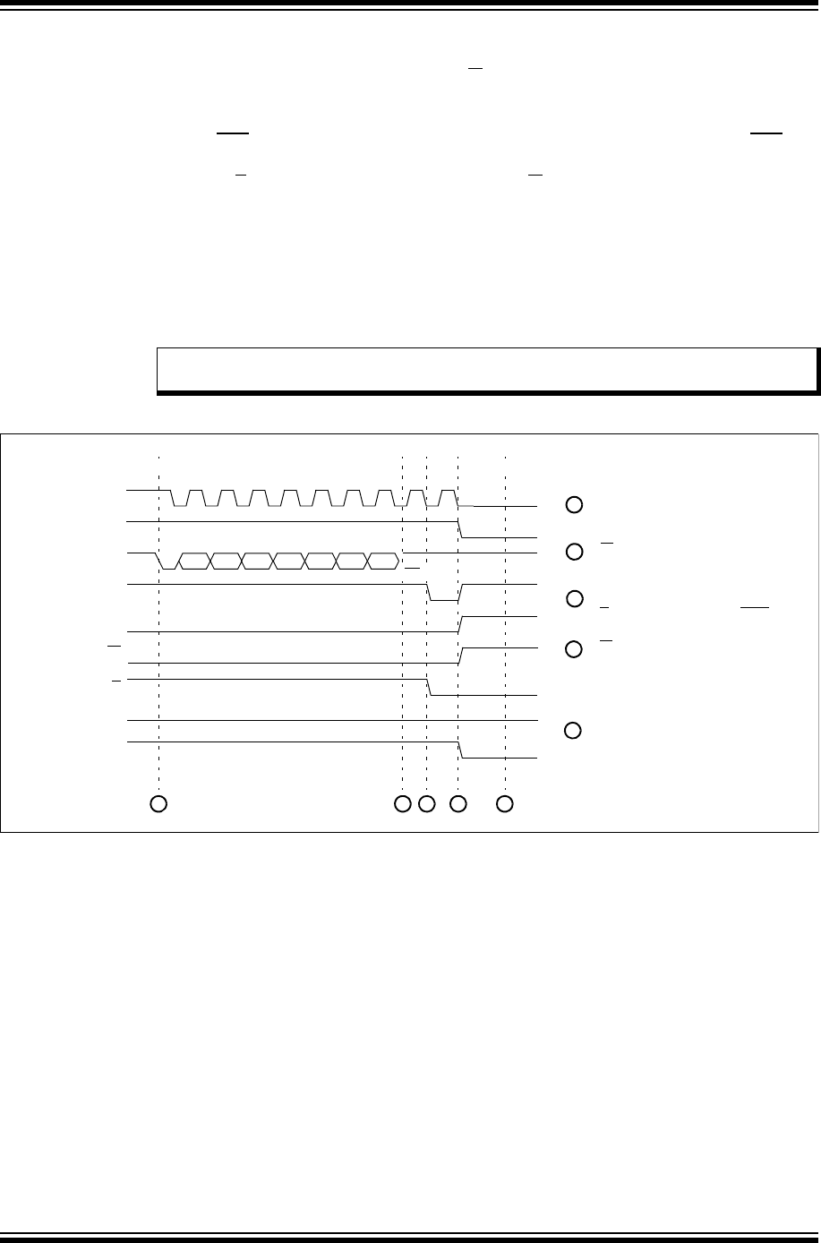
PIC32 Family Reference Manual
DS61116F-page 24-38 © 2007-2013 Microchip Technology Inc.
24.7.3.4 7-BIT ADDRESS AND SLAVE READ
When a slave read is specified by having R/W (IC2xSTAT<2>) = 1 in a 7-bit address byte, the
process of detecting the device address is similar to that for a slave write (see Figure 24-23). If
the addresses match, the following events occur:
1. An ACK is generated (for devices with the AHEN bit (I2CxCON<17>), an ACK is
generated if the AHEN bit is clear).
2. The D/A bit (I2CxSTAT<5>) is cleared and the R/W bit is set.
3. The I2C slave generates the slave interrupt on the falling edge of the ninth SCLx clock.
Since the Slave module is now expected to reply with data, it is necessary to suspend the
operation of the I2C bus to allow the software to prepare a response. This is done automatically
when the I2C slave clears the SCLREL bit (I2CxCON<12>). With SCLREL low, the Slave module
will pull down the SCLx clock line, causing a wait on the I2C bus. The Slave module and the I2C
bus will remain in this state until the software writes the I2CxTRN register with the response data
and sets the SCLREL bit.
Figure 24-23: Slave Read 7-bit Address Detection Timing Diagram
When the slave read occurs with the AHEN and DHEN bits set, after the eighth falling edge of
SCLx, the clock is stretched by hardware until a matching address byte is received. Following
the eighth falling edge, the SCKREL bit is cleared and the clock is asserted low. The slave
software will then set or clear the ACKDT bit to control the acknowledge response. Then, the
slave software sets the SCKREL bit, releasing SCLx. This sequence is shown in Figure 24-24.
Note: SCLREL will automatically clear after detection of a slave read address, regardless
of the state of the STREN bit.
SCLx (Master)
SDAx (Master)
SDAx (Slave)
Slave Interrupt
3 41 2
Detecting Start bit enables
1
I2C™ Bus State (D) (D) (A)(D)
A5A6A7 A4 A3 A2 A1
D/A
ADD10
SCLREL
R/W
address detection.
R/W = 1 indicates that slave
2
sends data bytes.
Valid address of first byte clears
3
D/A bit. Slave generates ACK.
R/W bit set. Slave generates
4
interrupt. SCLREL cleared.
5
Bus waiting. Slave prepares to
5
send data.
SCLx (Slave)
Slave pulls SCLx low while
SCLREL = 0.
(S) (Q)
R/W = 1

© 2007-2013 Microchip Technology Inc. DS61116F-page 24-39
Section 24. Inter-Integrated Circuit™ (I2C™)
Inter-Integrated
Circuit™ (I2C™)
24
Figure 24-24: Slave Read with AHEN = 1 AND DHEN = 1
Receiving Address Receiving Data Received Data
(P)
A7 A6 A5 A4 A3 A2 A1 D7 D6 D5 D4 D3 D2 D1 D0 D7 D6 D5 D4 D3 D2 D1 D0
SDAx
SCxL
RBF
SCKREL
12 3 4 56 7 8 912345 67 8 912345678
Master sends
stop condition
(S)
9
ACK
Master Releases SDAx
to slave for ACK sequence
ACK=1
ACK
ACKDT
ACKTIM
Slave Interrupt
If AHEN = 1, slave interrupt is set, SCKREL is cleared by hardware and SCLx is
1
RBF address is read from I2CxRCV.
2
Slave software clears ACKDT to ACK the received byte.
3
ACKTIM cleared by hardware on the ninth rising edge of SCLx. SCKREL is set by software
4
Slave interrupt is set on ninth falling edge of SCLx, after ACK.
5
When DHEN = 1, SCKREL is cleared by hardware on the eighth falling edge of SCLx.
6
RBF data is read from I2CxRCV.
7
SCKREL is set by software and SCLx is released.
8
Slave interrupt is cleared by software.
9
ACKTIM is set by hardware on the eigth falling edge of SCLx.
10
Slave software sets ACKDT to not ACK.
11
No interrupt afer not ACK from Slave.
12
3 41 2 5 8 96 7 10 11 12
and SCLx is released.
stretched. ACKTIM is set by hardware on the eighth falling edge of SCLx.

PIC32 Family Reference Manual
DS61116F-page 24-40 © 2007-2013 Microchip Technology Inc.
24.7.3.5 10-BIT ADDRESSING MODE
Figure 24-25 shows the sequence of address bytes on the bus in 10-bit Address mode. In this
mode, the slave must receive two device address bytes (see Figure 24-26). The five Most
Significant bits of the first address byte specify a 10-bit address. The R/W bit of the address must
specify a write, causing the slave device to receive the second address byte. For a 10-bit
address, the first byte would equal ‘11110 A9 A8 0’, where ‘A9’ and ‘A8’ are the two Most
Significant bits of the address.
The I2CxMSK register can mask any bit position in a 10-bit address. The two Most Significant
bits of the I2CxMSK register are used to mask the Most Significant bits of the incoming address
received in the first byte. The remaining byte of the register is then used to mask the lower byte
of the address received in the second byte.
Following the Start condition, the I2C slave shifts eight bits into the I2CxRSR register. The value
of the I2CxRSR<2:1> bits are evaluated against the value of the I2CxADD<9:8> and
I2CxMSK<9:8> bits, while the value of the I2CxRSR<7:3> bits are compared to ‘11110’.
Address evaluation occurs on the falling edge of the eighth clock (SCLx). For the address to be
valid, the I2CxRSR<7:3> bits must equal ‘11110’, while the I2CxRSR<2:1> bits must exactly
match any unmasked bits in the I2CxADD<9:8> bits. (If both bits are masked, a match is not
needed.) If the address is valid, the following events occur:
1. An ACK is generated (for devices with the AHEN bit (I2CxCON<17>), an ACK is
generated if the AHEN bit is clear).
2. The D/A (I2CxSTAT<5>) bit and the R/W bit (IC2xSTAT<2>) are cleared.
3. The I2C slave generates the slave interrupt on the falling edge of the ninth SCLx clock.
The I2C slave does generate an interrupt after the reception of the first byte of a 10-bit address;
however, this interrupt is of little use.
The I2C slave will continue to receive the second byte into the I2CxRSR register. This time, the
I2CxRSR<7:0> bits are evaluated against the I2CADD<7:0> and I2CxMSK<7:0> bits. If the lower
byte of the address is valid as previously described, the following events occur:
1. An ACK is generated (for devices with the AHEN bit (I2CxCON<17>), an ACK is
generated if the AHEN bit is clear).
2. The ADD10 bit (I2CxSTAT<8>) is set.
3. The I2C slave generates the slave interrupt on the falling edge of the ninth SCLx clock.
4. The I2C slave will wait for the master to send data or initiate a Repeated Start condition.
Figure 24-25: 10-bit Address Sequence
Note: Following a Repeated Start condition in 10-bit Addressing mode, the Slave module
only matches the first 7-bit address, ‘11110 A9 A8 0’.
s11110A9 A8 R/W ACK A7 A6 A5 A4 A3 A2 A1 A0 ACK
= 0 for write
sent by slave
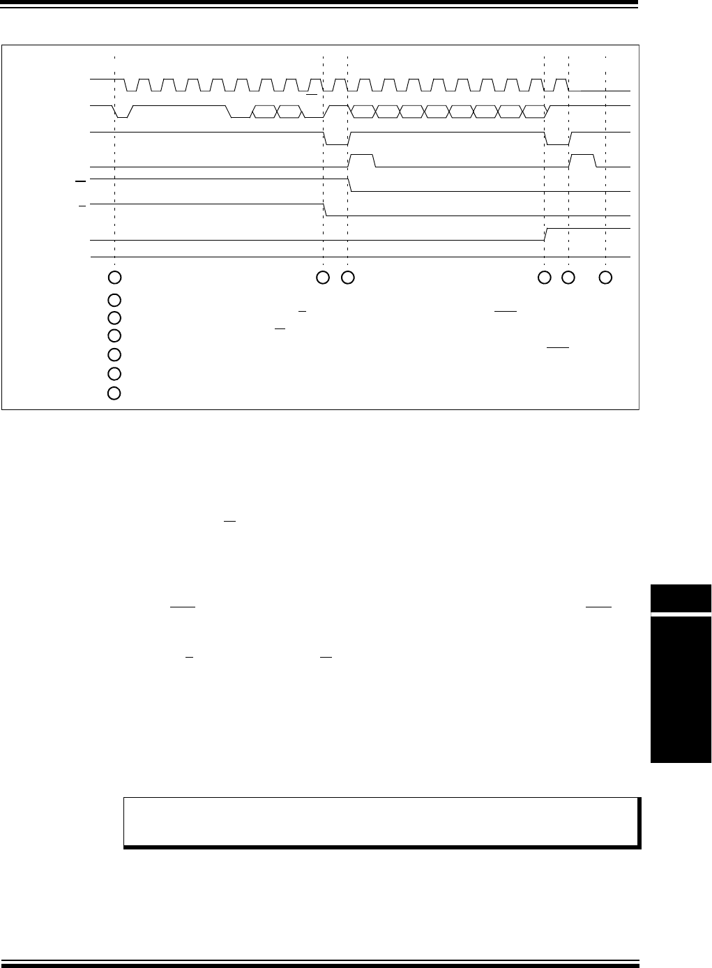
© 2007-2013 Microchip Technology Inc. DS61116F-page 24-41
Section 24. Inter-Integrated Circuit™ (I2C™)
Inter-Integrated
Circuit™ (I2C™)
24
Figure 24-26: 10-bit Address Detection Timing Diagram
24.7.3.6 GENERAL CALL OPERATION
The addressing procedure for the I2C bus is such that the first byte (or first two bytes in case of
10-bit Addressing mode) after a Start condition usually determines which slave device the master
is addressing. The exception is the general call address, which can address all devices. When
this address is used, all enabled devices should respond with an Acknowledge. The general call
address is one of eight addresses reserved for specific purposes by the I2C protocol. It consists
of all zeros with R/W (IC2xSTAT<2>) = 0. The general call is always a slave write operation.
The general call address is recognized when the General Call Enable bit, GCEN (I2CxCON<7>),
is set, see Figure 24-27. Following a Start (S) bit (I2CxSTAT<3>) detect, eight bits are shifted into
the I2CxRSR register and the address is compared against the I2CxADD register and the
general call address. If the general call address matches, the following events occur:
1. An ACK is generated (for devices with the AHEN bit (I2CxCON<17>), an ACK is
generated if the AHEN bit is clear).
2. The Slave module will set the GCSTAT bit (I2CxSTAT<9>).
3. The D/A (IC2xSTAT<5>) and R/W bits are cleared.
4. The I2C slave generates the slave interrupt on the falling edge of the ninth SCLx clock.
5. The I2CxRSR register is transferred to the I2CxRCV register and the RBF flag bit
(I2CxSTAT<1>) is set (during the eighth bit).
6. The I2C slave will wait for the master to send data.
When the interrupt is serviced, the cause for the interrupt can be checked by reading the contents
of the GCSTAT bit to determine if the device address was device specific or a general call
address.
SCLx (Master)
SDAx (Master)
SDAx (Slave)
Slave Interrupt
2 4 51 3
Detecting Start bit enables address detection.
1
Address match of first byte clears D/A bit and causes slave logic to generate ACK.
2
Reception of first byte clears R/W bit. Slave logic generates interrupt.
3
Address match of first and second byte sets ADD10 and causes slave logic to generate ACK.
4
Reception of second byte completes 10-bit address. Slave logic generates interrupt.
5
I2C™ Bus State (D) (D) (A)(D)
11110
A9 A8
R/W = 0
D/A
ADD10
SCLREL
A5A6A7 A4 A3 A2 A1 A0
R/W
(D) (D) (A)(D)
6
Bus waiting. Slave ready to receive data.
5
(S) (Q)
Note: General call addresses are 7-bit addresses. If configuring the Slave module for
10-bit addresses and the A10M bit (I2CxCON<10>) and the GCEN bit are set, the
Slave module will continue to detect the 7-bit general call address.
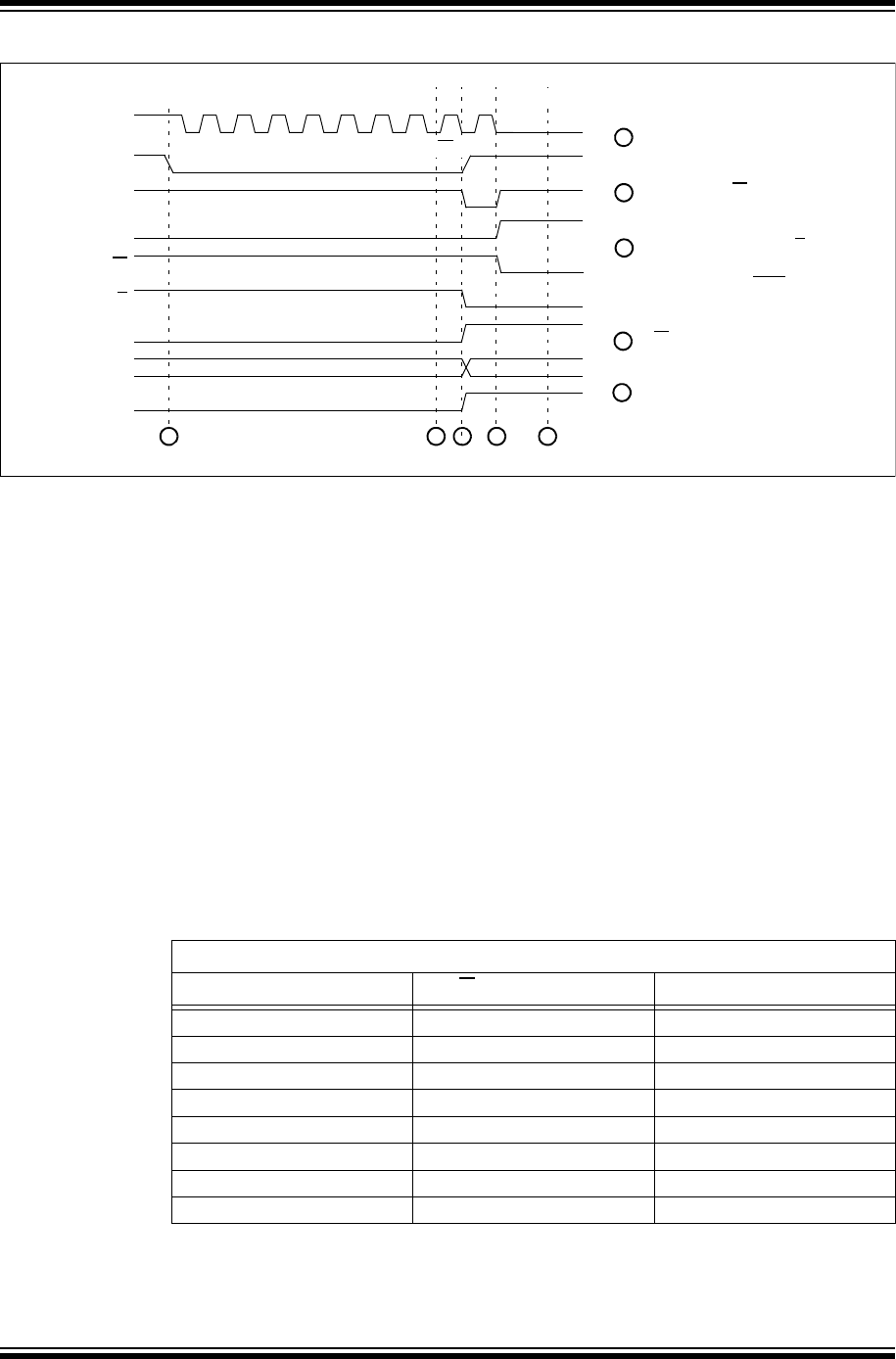
PIC32 Family Reference Manual
DS61116F-page 24-42 © 2007-2013 Microchip Technology Inc.
Figure 24-27: General Call Address Detection Timing Diagram (GCEN = 1)
24.7.3.7 STRICT ADDRESS SUPPORT
When the STRICT bit (I2CxCON<11>) is set, it enables the I2C slave to enforce all reserved
addressing and will not acknowledge any addresses if they fall within the reserved address table.
24.7.3.8 WHEN AN ADDRESS IS INVALID
If a 7-bit address does not match the contents of the I2CxADD<6:0> bits, the Slave module will
return to an Idle state and ignore all bus activity until after the Stop condition.
If the first byte of a 10-bit address does not match the contents of the I2CxADD<9:8> bits, the
Slave module will return to an Idle state and ignore all bus activity until after the Stop condition.
If the first byte of a 10-bit address matches the contents of the I2CxADD<9:8> bits, but the sec-
ond byte of the 10-bit address does not match the I2CxADD<7:0> bits, the Slave module will
return to an Idle state and ignore all bus activity until after the Stop condition.
24.7.3.9 ADDRESSES RESERVED FROM MASKING
Even when enabled, several addresses are excluded in hardware from masking. For these
addresses, an Acknowledge will not be issued independent of the mask setting. These
addresses are listed in Ta b le 24-4.
SCLx (Master)
SDAx (Master)
SDAx (Slave)
Slave Interrupt
3 41 2
Detecting Start bit enables
1
I2C™ Bus State (D) (D) (A)(D)
000 0000
D/A
I2CRCV
RBF
R/W
address detection.
All ‘0’s and R/W = 0 indicates
2
general call.
Valid address clears D/A bit
3
and sets GCSTAT.
R/W bit cleared. Slave generates
4
interrupt.
5
Bus waiting. Slave ready to
5
receive data.
GCSTAT
Slave generates ACK.
Address loaded into I2CxRCV.
R/W = 0
(S) (Q)
Table 24-4: Reserved I2C™ Bus Addresses(1)
7-bit Address Mode:
Slave Address R/W bit (IC2xSTAT<2>) Description
0000 000 0General Call Address(1)
0000 000 1Start Byte
0000 001 xCBUS Address
0000 010 xReserved
0000 011 xReserved
0000 1xx xHS Mode Master Code
1111 1xx xReserved
1111 0xx x10-bit Slave Upper Byte(2)
Note 1: Address will be Acknowledged only if GCEN (I2CxCON<7>) = 1.
2: Match on this address can only occur as the upper byte in the 10-bit Addressing mode.

© 2007-2013 Microchip Technology Inc. DS61116F-page 24-43
Section 24. Inter-Integrated Circuit™ (I2C™)
Inter-Integrated
Circuit™ (I2C™)
24
24.7.4 Receiving Data from a Master Device
When the R/W bit of the device address byte is zero and an address match occurs, the R/W bit
is cleared. The Slave module enters a state waiting for data to be sent by the master. After the
device address byte, the contents of the data byte are defined by the system protocol and are
only received by the Slave module.
The Slave module shifts eight bits into the I2CxRSR register. On the falling edge of the eighth
clock (SCLx), the following events occur:
1. The I2C slave begins to generate an ACK or NACK.
2. The RBF bit (I2CxSTAT<1>) is set to indicate received data.
3. The I2CxRSR register byte is transferred to the I2CxRCV register for access by the
software.
4. The D/A bit (I2CxSTAT<5>) is set.
5. A slave interrupt is generated. Software may check the status of the I2CxSTAT register to
determine the cause of the event, and then clear the slave interrupt flag.
6. The I2C slave will wait for the next data byte.
24.7.4.1 ACKNOWLEDGE GENERATION
Normally, the Slave module will Acknowledge all received bytes by sending an ACK on the ninth
SCLx clock.
For devices with the BOEN bit (I2CxCON<20>), if this bit is set, the state of the I2COV bit
(I2CxSTAT<6>) is ignored and the I2CxRCV buffer is updated. Then, the acknowledge is
generated for the received data/address if the RBF bit is clear. When the BOEN bit is clear, and
if the receive buffer is overrun, the Slave module does not generate this ACK. Overrun is
indicated if either (or both):
•The buffer full bit, RBF (I2CxSTAT<1>), was set before the transfer was received
•The overflow bit, I2COV (I2CxSTAT<6>), was set before the transfer was received
Tabl e 24-5 shows what happens when a data transfer byte is received, given the status of the
RBF and I2COV bits. If the RBF bit is already set when the Slave module attempts to transfer to
the I2CxRCV register, the transfer does not occur but the interrupt is generated and the I2COV
bit is set. If both the RBF and I2COV bits are set, the Slave module acts similarly. The shaded
cells show the condition where software did not clear the overflow condition.
Reading the I2CxRCV register clears the RBF bit. The I2COV bit is cleared by writing to a ‘0’
through software.
Some devices have the Acknowledge Sequence Status bit, ACKTIM. During an acknowledge
sequence of a Slave I2C device, the ACKTIM bit is set. The Acknowledge sequence for I2C
communication is from the eighth falling edge to the ninth falling edge of SCLx. This Status bit
will allow the user software to determine the source of an I2C interrupt, and how far the
communication has progressed.
Table 24-5: Data Transfer Received Byte Actions
Status Bits as Data
Byte Received Transfer
I2CxRSR to
I2CxRCV
Generate
ACK
Generate
Slave
Interrupt
(interrupt
occurs if
enabled)
Set
RBF
Set
I2COV
RBF I2COV
0 0 Yes Yes Yes Ye s No change
1 0 No No Yes No change Yes
1 1 No No Yes No change Yes
0 1 Yes No Yes Yes No change
Legend: Shaded cells show state where the software did not properly clear the overflow
condition.

PIC32 Family Reference Manual
DS61116F-page 24-44 © 2007-2013 Microchip Technology Inc.
24.7.4.2 ADDRESS AND DATA HOLD
In some devices, the AHEN bit (I2CxCON<17>) and the DHEN bit (I2CxCON<16>) are available
to allow the I2C Slave module to NACK byte transmissions.
When the AHEN and DHEN bits are set, slave software allows the user to set the ACK value,
which is sent back to the transmitter. When AHEN is set, after the eighth falling edge of SCLx,
the clock is stretched by hardware until a matching address byte is received. Following the eighth
falling edge, the SCKREL bit is cleared and the clock is asserted low until the user sets the
SCKREL bit, releasing SCLx. This will allow the user software to choose which incoming
addresses to ACK or NACK. When the DHEN bit is set, after the eighth falling edge of SCLx, the
clock is stretched by hardware for a received data byte. The received data must be preceded by
a matching address byte that was acknowledged. For both data and address holding, the slave
software can set or clear the ACKDT bit (I2CxCON<5>). To control the ACK value, the master
will clock in once SCLx is released by the slave. If a NACK is sent from the slave, the slave will
release the bus and wait for the next matching address.
When the AHEN and DHEN bits are clear, the Slave module will automatically generate an ACK
response.
24.7.4.3 WAIT STATES DURING SLAVE RECEPTIONS
When the Slave module receives a data byte, the master can potentially begin sending the next
byte immediately. This allows the software controlling the Slave module nine SCLx clock periods
to process the previously received byte. If this is not enough time, the slave software may want
to generate a bus wait period.
The STREN bit (I2CxCON<6>) enables a bus wait to occur on slave receptions. When STREN = 1
at the falling edge of the ninth SCLx clock of a received byte, the Slave module clears the SCLREL
bit (I2CxCON<12>). Clearing the SCLREL bit causes the Slave module to pull the SCLx line low,
initiating a wait. The SCLx clock of the master and slave will synchronize, as shown in
24.6.2 “Master Clock Synchronization”.
When the software is ready to resume reception, the software sets the SCLREL bit. This causes
the Slave module to release the SCLx line, and the master resumes clocking.
24.7.4.4 EXAMPLE MESSAGES OF SLAVE RECEPTION
Receiving a slave message is a rather automatic process. The software handling the slave
protocol uses the slave interrupt to synchronize to the events.
When the slave detects the valid address, the associated interrupt will notify the software to
expect a message. On receive data, as each byte transfers to the I2CxRCV register, an interrupt
notifies the software to unload the buffer.
Figure 24-28 shows a receive message. Because it is a 7-bit address message, only one inter-
rupt occurs for the address bytes. Then, interrupts occur for each of four data bytes. At an inter-
rupt, the software may monitor the RBF, D/A (IC2xSTAT<5>) and R/W (IC2xSTAT<2>) bits to
determine the condition of the byte received.
Figure 24-29 shows a similar message using a 10-bit address. In this case, two bytes are
required for the address.
Figure 24-30 shows a message where the software does not respond to the received byte and
the buffer overruns. On receipt of the second byte, the I2C slave will automatically NACK the
master transmission. Generally, this causes the master to resend the previous byte. The I2COV
bit (I2CxSTAT<6>) indicates that the buffer has overrun. The I2CxRCV register buffer retains the
contents of the first byte. On receipt of the third byte, the buffer is still full, and again, the I2C slave
will NACK the master. After this, the software finally reads the buffer. Reading the buffer will clear
the RBF bit (I2CxSTAT<1>); however, the I2COV bit remains set. The software must clear the
I2COV bit. The next received byte will be moved to the I2CxRCV register buffer and the I2C slave
will respond with an ACK.

© 2007-2013 Microchip Technology Inc. DS61116F-page 24-45
Section 24. Inter-Integrated Circuit™ (I2C™)
Inter-Integrated
Circuit™ (I2C™)
24
Figure 24-31 highlights clock stretching while receiving data. In the previous examples, the
STREN bit (I2CxCON<6>) = 0, which disables clock stretching on receive messages. In this
example, the software sets the STREN bit to enable clock stretching. When STREN = 1, the I2C
slave will automatically clock stretch after each received data byte, allowing the software more
time to move the data from the buffer. if the RBF bit = 1 at the falling edge of the ninth clock, the
I2C slave will automatically clear the SCLREL bit (I2CxCON<12>) and pull the SCLx bus line low.
As shown with the second received data byte, if the software can read the buffer and clear the
RBF bit before the falling edge of the ninth clock, the clock stretching will not occur. The software
can also suspend the bus at any time. By clearing the SCLREL bit, the I2C slave will pull the SCLx
line low after it detects the bus SCLx low. The SCLx line will remain low, suspending transactions
on the bus until the SCLREL bit is set.
24.7.5 Slave Bus Collision Detect
For devices with the SBCDE bit (I2CxCON<18>), this bit when enabled, will set the BCL bit
(I2CxSTAT<10>) interrupt flag any time the SDAx pin is sampled low when the slave is driving a
high. This allows the slave module to detect a bus collision. The two scenarios when a bus
collision can occur for a slave are during an acknowledge sequence and a read request to the
master. This may be a useful feature to be used when a slave is responding to a General Call
address.

PIC32 Family Reference Manual
DS61116F-page 24-46 © 2007-2013 Microchip Technology Inc.
Figure 24-28: Slave Message (Write Data to Slave: 7-bit Address; Address Matches; A10M = 0; GCEN = 0; STRICT = 0)
1Slave recognizes Start event; S and P bits set/clear accordingly.
SCLx (Master)
SDAx (Master)
SCLx (Slave)
SDAx (Slave)
I2CxRCV
RBF
Slave Interrupt
STREN
12345678
A2 A1
9
A
D7 D6 D5 D4 D3 D2 D1
123456789
1 32
A
4 3 3 3 5
2Slave receives address byte. Address matches. Slave Acknowledges
3Next received byte is message data. Byte moved to I2CxRCV register sets RBF.
4Software reads I2CxRCV register. RBF bit clears.
5Slave recognizes Stop event; S and P bits set/clear accordingly.
Slave generates interrupt. Slave Acknowledges reception.
A7 A6 A5 A4 A3
S
P
I2COV
R/W
D/A
D7 D6 D5 D4 D3 D2 D1
123456789
A
D7 D6 D5 D4 D3 D2 D1
123456789
A
D7 D6 D5 D4 D3 D2 D1
123456789
A
SCLREL
4 4 4
and generates interrupt. Address byte is moved to I2CxRCV register and must be read by user software to prevent buffer overflow.
D0D0D0
D0
W
Slave interrupt cleared
ACKSTAT
by user software.

© 2007-2013 Microchip Technology Inc. DS61116F-page 24-47
Section 24. Inter-Integrated Circuit™ (I2C™)
Inter-Integrated
Circuit™ (I2C™)
24
Figure 24-29: Slave Message (Write Data to Slave: 10-bit Address; Address Matches; A10M = 1; GCEN = 0; STRICT = 0)
1Slave recognizes Start event; S and P bits set/clear accordingly.
SCLx (Master)
SDAx (Master)
SCLx (Slave)
SDAx (Slave)
I2CxRCV
RBF
Slave
STREN
12345678
A9 A8
9
A
A7 A6 A5 A4 A3 A2 A1
123456789
1 32
A
4 4 4 6
2Slave receives address byte. High-order address matches.
3Slave receives address byte. Low-order address matches.
4Next received byte is message data. Byte moved to I2CxRCV register sets RBF.
5Software reads I2CxRCV register. RBF bit clears.
6Slave recognizes Stop event; S and P bits set/clear accordingly.
Slave Acknowledges and generates interrupt. Address byte not
Slave Acknowledges and generates interrupt.
S
P
I2COV
R/W
D/A
D7 D6 D5 D4 D3 D2 D1
123456789
A
D7 D6 D5 D4 D3 D2 D1
123456789
A
D7 D6 D5 D4 D3 D2 D1
123456789
A
SCLREL
5 5 5
11110
Slave Acknowledges and generates interrupt. Address byte not
moved to I2CxRCV register.
moved to I2CxRCV register.
A0 D0
WD0 D0
Slave interrupt cleared
ACKSTAT
Interrupt
by user software.
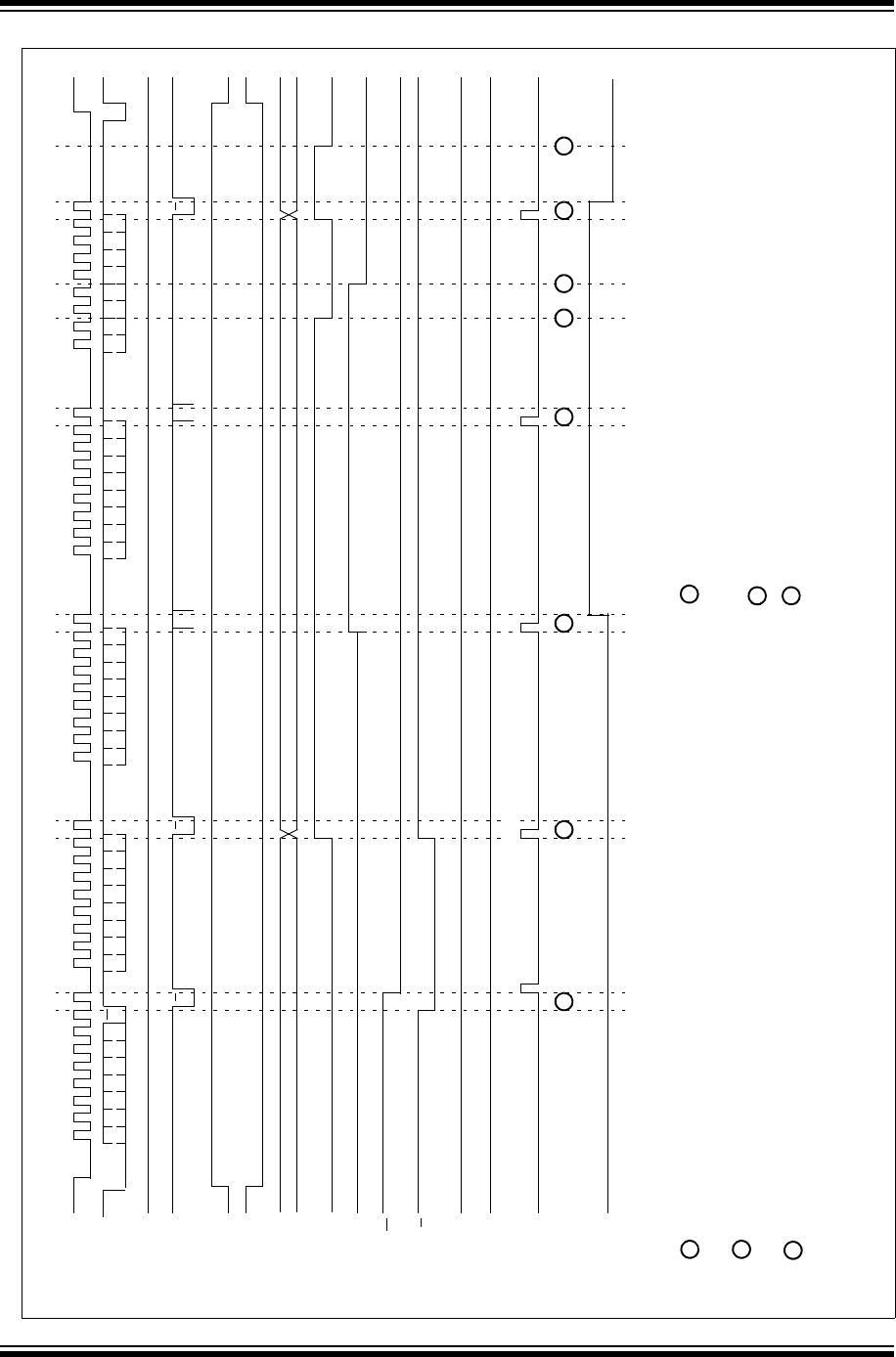
PIC32 Family Reference Manual
DS61116F-page 24-48 © 2007-2013 Microchip Technology Inc.
Figure 24-30: Slave Message (Write Data to Slave: 7-bit Address; Buffer Overrun; A10M = 0; GCEN = 0; STRICT = 0)
SCLx (Master)
SDAx (Master)
SCLx (Slave)
SDAx (Slave)
I2CxRCV
RBF
Slave
STREN
12345678
A2 A1
9
A
D7 D6 D5 D4 D3 D2 D1
123456789
21
A
342
1Slave receives address byte. Address matches. Slave generates interrupt.
2Next received byte is message data. Byte moved to I2CxRCV register sets RBF. 6Software reads I2CxRCV register. RBF bit clears.
7Software clears I2COV bit.
Address byte not moved to I2CxRCV register.
Slave generates interrupt. Slave Acknowledges reception.
A7 A6 A5 A4 A3
S
P
I2COV
R/W
D/A
D7 D6 D5 D4 D3 D2 D1
123456789
N
D7 D6 D5 D4 D3 D2 D1
123456789
D7 D6 D5 D4 D3 D2 D1
123456789
SCLREL
5 5
3Next byte received before I2CxRCV read by software. I2CxRCV register unchanged.
I2COV overflow bit set. Slave generates interrupt. Slave sends NACK for reception.
NA
6
4Next byte also received before I2CxRCV read by software.
Slave sends NACK for reception.
I2CxRCV register unchanged. Slave generates interrupt.
D0 D0
WD0 D0
Slave interrupt cleared
ACKSTAT
Interrupt
by user software.

© 2007-2013 Microchip Technology Inc. DS61116F-page 24-49
Section 24. Inter-Integrated Circuit™ (I2C™)
Inter-Integrated
Circuit™ (I2C™)
24
Figure 24-31: Slave Message (Write Data to Slave: 7-bit Address; Clock Stretching Enabled; A10M = 0; GCEN = 0; STRICT = 0)
1Software sets the STREN bit to enable clock stretching.
SCLx (Master)
SDAx (Master)
SCLx (Slave)
SDAx (Slave)
I2CxTRN
TBF
I2CRCV
RBF
Slave
STREN
12345678
A2 A1
9
A
D7 D6 D5 D4 D3 D2 D1
12345678 9
32
A
5 3 8 3
2Slave receives address byte.
3Next received byte is message data. Byte moved to I2CxRCV register sets RBF.
6Software sets SCLREL bit to release clock.
7Slave does not clear SCLREL because RBF = 0 at this time.
A7 A6 A5 A4 A3
S
P
I2COV
R/W
D/A
D7 D6 D5 D4 D3 D2 D1
12345678 9
A
D7 D6 D5 D3 D2 D1
1234 56789
A
SCLREL
5 9 5
D4
4 6 71
4Because RBF = 1 at ninth clock, automatic clock stretch begins.
Slave clears SCLREL bit. Slave pulls SCLx line low to stretch clock.
5Software reads I2CxRCV register. RBF bit clears.
8Software may clear SCLREL to cause a clock hold. I2C slave must detect SCLx low
9Software may set SCLREL to release a clock hold.
before asserting SCLx low.
D0
WD0 D0
ACKSTAT
Interrupt

PIC32 Family Reference Manual
DS61116F-page 24-50 © 2007-2013 Microchip Technology Inc.
24.7.6 Sending Data to a Master Device
When the R/W bit of the incoming device address byte is ‘1’ and an address match occurs, the
R/W bit (I2CxSTAT<2>) is set. Now, the master device is expecting the slave to respond by
sending a byte of data. The contents of the byte are defined by the system protocol and are only
transmitted by the Slave module.
When the interrupt from the address detection occurs, the software can write a byte to the
I2CxTRN register to start the data transmission.
The Slave module sets the TBF bit (I2CxSTAT<0>). The eight data bits are shifted out on the fall-
ing edge of the SCLx input. This ensures that the SDAx signal is valid during the SCLx high time.
When all eight bits have been shifted out, the TBF bit will be cleared.
The Slave module detects the Acknowledge from the master-receiver on the rising edge of the
ninth SCLx clock.
If the SDAx line is low, indicating an Acknowledge (ACK), the master is expecting more data and
the message is not complete. The I2C slave generates a slave interrupt to signal more data is
requested.
A slave interrupt is generated on the falling edge of the ninth SCLx clock. Software must check
the status of the I2CxSTAT register and clear the slave interrupt flag.
If the SDAx line is high, indicating a Not Acknowledge (NACK), then the data transfer is complete.
The Slave module resets and does not generate an interrupt. The Slave module will wait for
detection of the next Start (S) bit (I2CxSTAT<3>).
24.7.6.1 WAIT STATES DURING SLAVE TRANSMISSIONS
During a slave transmission message, the master expects return data immediately after
detection of the valid address with R/W = 1. Because of this, the Slave module will automatically
generate a bus wait whenever the slave returns data.
The automatic wait occurs at the falling edge of the ninth SCLx clock of a valid device address
byte or transmitted byte Acknowledged by the master, indicating expectation of more transmit
data.
The Slave module clears the SCLREL bit (I2CxCON<12>). Clearing the SCLREL bit causes the
Slave module to pull the SCLx line low, initiating a wait. The SCLx clock of the master and slave
will synchronize as shown in 24.6.2 “Master Clock Synchronization”.
When the software loads the I2CxTRN register and is ready to resume transmission, the software
sets the SCLREL bit. This causes the Slave module to release the SCLx line and the master
resumes clocking.
24.7.6.2 EXAMPLE MESSAGES OF SLAVE TRANSMISSION
Slave transmissions for 7-bit address messages are shown in Figure 24-32. When the address
matches and the R/W bit of the address indicates a slave transmission, the I
2C slave will
automatically initiate clock stretching by clearing the SCLREL bit and generates an interrupt to
indicate a response byte is required. The software will write the response byte into the I2CxTRN
register. As the transmission completes, the master will respond with an Acknowledge. If the
master replies with an ACK, the master expects more data and the I2C slave will again clear the
SCLREL bit and generate another interrupt. If the master responds with a NACK, no more data
is required and the I2C slave will not stretch the clock nor generate an interrupt.
Slave transmissions for 10-bit address messages require the slave to first recognize a 10-bit
address. Because the master must send two bytes for the address, the R/W bit in the first byte
of the address specifies a write. To change the message to a read, the master will send a
Repeated Start and repeat the first byte of the address with the R/W bit specifying a read. The
slave transmission begins as shown in Figure 24-33.
Note: The user software must provide a delay between writing to the Transmit buffer and
setting the SCLREL bit. This delay must be greater than the minimum set up time
for slave transmissions, as specified in the “Electrical Characteristics” section of
the specific device data sheet.

© 2007-2013 Microchip Technology Inc. DS61116F-page 24-51
Section 24. Inter-Integrated Circuit™ (I2C™)
Inter-Integrated
Circuit™ (I2C™)
24
Figure 24-32: Slave Message (Read Data from Slave: 7-bit Address)
1Slave recognizes Start event; S and P bits set/clear accordingly.
SCLx (Master)
SDAx (Master)
SCLx (Slave)
SDAx (Slave)
I2CxTRN
TBF
I2CxRCV
RBF
Slave
STREN
12345678
A2 A1
9
A
D7 D6 D5 D4 D3 D2 D1
123456789
R
1 42
A
5 3 5 3 8
2Slave receives address byte. Address matches. Slave generates interrupt.
3Software writes I2CxTRN with response data. TBF = 1 indicates that buffer is full.
6At end of ninth clock, if master sent ACK, I2C slave clears SCLREL to suspend clock.
8Slave recognizes Stop event; S and P bits set/clear accordingly.
Address byte not moved to I2CxRCV register. R/W = 1 to indicate read from slave.
Writing I2CxTRN sets D/A, indicating data byte.
A7 A6 A5 A4 A3
S
P
I2COV
R/W
D/A
SCLREL
4 4
D7 D6 D5 D4 D3 D2 D1
123456789
A
D7 D6 D5 D4 D3 D2 D1
123456789
N
3 6 6 5 7
SCLREL = 0 to suspend master clock.
4Software sets SCLREL to release clock hold. Master resumes clocking and
slave transmits data byte.
5After last bit, I2C slave clears TBF bit, indicating buffer is available for next byte.
Slave generates interrupt.
7At end of ninth clock, if master sent NACK, no more data expected. I2C slave does not
suspend clock and will generate an interrupt.
D0 D0 D0
ACKSTAT
Interrupt
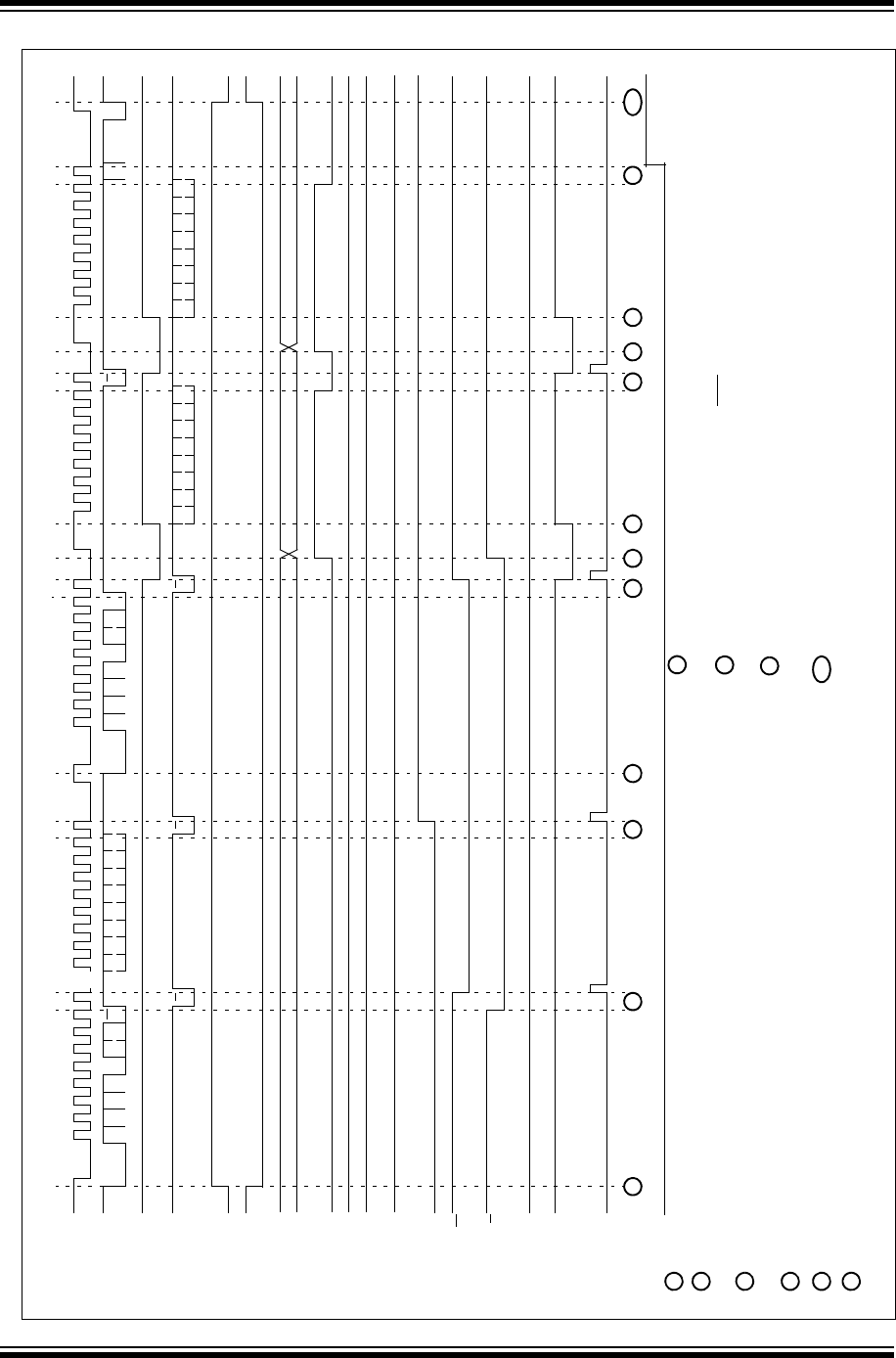
PIC32 Family Reference Manual
DS61116F-page 24-52 © 2007-2013 Microchip Technology Inc.
Figure 24-33: Slave Message (Read Data from Slave: 10-bit Address)
1Slave recognizes Start event; S and P bits set/clear accordingly.
SCLx (Master)
SDAx (Master)
SCLx (Slave)
SDAx (Slave)
I2CxTRN
TBF
I2CxRCV
RBF
Slave
STREN
123456789
A
1 42 7 8
2Slave receives first address byte. Write indicated. Slave Acknowledges and
6Software writes I2CxTRN with response data.
8At end of ninth clock, if master sent ACK, I2C slave clears SCLREL to suspend clock.
Slave recognizes Stop event; S and P bits set/clear accordingly.
S
P
ADD10
R/W
D/A
SCLREL
5 6
D7 D6 D5 D4 D3 D2 D1
123456789
N
3 6 97
7Software sets SCLREL to release clock hold. Master resumes clocking and
slave transmits data byte.
Slave generates interrupt.
9At end of ninth clock, if master sent NACK, no more data expected. I2C slave does not
suspend clock or generate interrupt.
A7 A6 A5 A4 A3 A2 A1
123456789
A
A9 A8
11110
123456789
A
A9 A8
11110
D7 D6 D5 D4 D3 D2 D1
123456789
A
3Slave receives address byte. Address matches. Slave Acknowledges and
10
10
4Master sends a Repeated Start to redirect the message.
5Slave receives resend of first address byte. Read indicated. Slave suspends clock.
R
generates interrupt.
generates interrupt.
A0
W
D0D0
ACKSTAT
Interrupt

© 2007-2013 Microchip Technology Inc. DS61116F-page 24-53
Section 24. Inter-Integrated Circuit™ (I2C™)
Inter-Integrated
Circuit™ (I2C™)
24
24.8 I2C BUS CONNECTION CONSIDERATIONS
Because the I2C bus is a wired Boolean AND bus connection, pull-up resistors on the bus are
required, shown as RP in Figure 24-34. Series resistors, shown as RS, are optional and are used to
improve Electrostatic Discharge (ESD) susceptibility. The values of the RP and RS resistors depend
on the following parameters:
•Supply voltage
•Bus capacitance
•Number of connected devices (input current + leakage current)
•Input level selection (I
2C or SMBus)
To g et an acc ura te S CK x c lo ck, th e ris e t ime should be as small as possible. The limitation factor
is the maximum current sink available on the SCKx pad. Equation 24-2 calculates the minimum
value for RP, which is based on a 3.3V supply and a 6.6 mA sink current at VOLMAX = 0.4V.
Equation 24-2: RPMIN Calculation
The maximum value for RS is determined by the desired noise margin for the low level. RS cannot
drop enough voltage to make the device VOL plus the voltage across RS more than the maximum
VIL. This is expressed mathematically in Equation 24-2.
Equation 24-3: RSMAX Calculation
The SCLx clock input must have a minimum high and low time for proper operation. The high and
low times of the I2C specification, and the requirements of the I2C module, are provided in the
“Electrical Characteristics” chapter in the specific device data sheet.
Figure 24-34: Sample Device Configuration for I2C™ Bus
RPMIN
VDDMAX VOLMAX–
IOL
------------------------------------------------------ 3.3V0.4V–
6.6mA
--------------------------------- 439===
RSMAX
VILMAX VOLMAX–
IOLMAX
--------------------------------------------------- 0.3 VDD 0.4V–
6.6mA
----------------------------------------- 89===
RPRP
VDD + 10%
SDAx
SCLx
Device
CB = 10-400 pF
RSRS
Note: I2C™ devices with input levels related to VDD must have one common supply line to which the
pull-up resistor is also connected.

PIC32 Family Reference Manual
DS61116F-page 24-54 © 2007-2013 Microchip Technology Inc.
24.8.1 Integrated Signal Conditioning and Slope Control
The SCLx and SDAx pins have an input glitch filter. The I2C bus requires this filter in both the
100 kHz and 400 kHz systems.
When operating on a 400 kHz bus, the I2C specification requires a slew rate control of the device
pin output. This slew rate control is integrated into the device. If the DISSLW bit (I2CxCON<9>)
is cleared, the slew rate control is active. For other bus speeds, the I2C specification does not
require slew rate control and the DISSLW bit should be set.
Some system implementations of I2C busses require different input levels for VILMAX and VIHMIN.
In a normal I2C system, VILMAX is 0.3 VDD; VIHMIN is 0.7 VDD. By contrast, in a System
Management Bus (SMBus) system, VILMAX is set at 0.8V, while VIHMIN is set at 2.1V.
The SMEN bit (I2CxCON<8>) controls the input levels. Setting the SMEN bit (= 1) changes the
input levels to SMBus specifications.
24.8.2 SDAx Hold Time Selection
For devices with the SDAHT bit (I2CxCON<19>), the user can configure the hold time on the
SDAx pin after the falling edge of SCLx pin using the SDAHT bit. When the SDAHT bit is set, the
hold time on the SDAx pin after the falling edge of SCLx will be set to a minimum of 300 ns. The
hold time will be set to a minimum of 100 ns if the SDAHT bit is clear.

© 2007-2013 Microchip Technology Inc. DS61116F-page 24-55
Section 24. Inter-Integrated Circuit™ (I2C™)
Inter-Integrated
Circuit™ (I2C™)
24
24.9 I2C OPERATION IN POWER-SAVING MODES
Two power-saving modes are available to the I2C module in PIC32 devices:
•Idle – when the device is in Idle mode, the core and selected peripherals are shut down
•Sleep – when the device is in Sleep mode, the entire device is shut down
24.9.1 Sleep in Master Mode Operation
When the device enters Sleep mode, all clock sources to the I2C master are shut down. The
BRG stops because the clocks stop. It may have to be reset to prevent partial clock detection.
If Sleep occurs in the middle of a transmission, and the master state machine is partially into a
transmission as the clocks stop, the Master mode transmission is aborted.
There is no automatic way to prevent entry into Sleep mode if a transmission or reception is
pending. The user software must synchronize Sleep mode entry with I2C operation to avoid
aborted transmissions.
Register contents are not affected by going into Sleep mode or coming out of Sleep mode.
24.9.2 Sleep in Slave Mode Operation
The I2C module can still function in Slave mode operation while the device is in Sleep mode.
When operating in Slave mode and the device is put into Sleep mode, the master-generated
clock will run the slave state machine. This feature provides an interrupt to the device upon
reception of the address match to wake-up the device.
Register contents are not affected by entering into Sleep mode or coming out of Sleep mode.
It is an error condition to set Sleep mode in the middle of a slave data transmit operation, as
indeterminate results may occur.
24.9.3 Idle Mode
When the device enters Idle mode, all PBCLK clock sources remain functional. If the I2C
module intends to power down, it disables its own clocks.
For the I2C module, the I2CxSIDL bit (I2CxCON<13>) selects whether the module will stop on
Idle mode or continue on Idle. If I2CxSIDL = 0, the module will continue operation in Idle mode.
If I2CxSIDL = 1, the module will stop on Idle.
The I2C module will perform the same procedures for stop on Idle mode as for Sleep mode. The
module state machines must be reset.
Note: As per the slave I2C behavior, a slave interrupt is generated only on an address
match. Therefore, when an I2C slave is in Sleep mode and it receives a message
from the master, the clock required to match the received address is derived from
the master. Only on an address match will the interrupt be generated and the device
can wake up, provided the interrupt has been enabled and an Interrupt Service
Request (ISR) has been defined.

PIC32 Family Reference Manual
DS61116F-page 24-56 © 2007-2013 Microchip Technology Inc.
24.10 EFFECTS OF A RESET
A Reset (Power-on Reset, Watchdog Timer, etc.) disables the I2C module and terminates any
active or pending message activity. See the I2CxCON (Register 24-1) and I2CxSTAT
(Register 24-2) register definitions for the Reset conditions of those registers.
24.11 PIN CONFIGURATION IN I2C MODE
In I2C mode, the SCLx pin is the clock and the SDAx pin is data. The I2C module will override
the data direction bits (TRISx bits) for these pins. The pins that are used for I2C modes are
configured as open drain. Tab le 24-6 lists the pin usage in different modes.
Table 24-6: Required I/O Pin Resources
24.12 USING AN EXTERNAL BUFFER WITH THE I2C MODULE
It is not recommended to use external buffers on the I2C pins. However, if the external buffer must
be used, the application firmware must adhere to the following software flow:
On the slave ACK clock cycle, issue a dummy write using the I2CxTRN register buffer,
ensuring that the MSB of the data is set. This will cause a collision (IWCOL bit = 1), which
must be cleared within the ACK clock cycle.
This can be done using one of the following methods:
• Enable an available timer immediately when the data is written to the I2CxTRN register
buffer. On a timer interrupt designed to coincide with the slave ACK clock cycle, perform a
dummy write to the I2CxTRN register buffer, ensuring that the MSB of the data is set. Clear
the collision status bit, IWCOL, before leaving the timer Interrupt Service Routine. Because
the I2C rate is known, the user application can calculate the timer period required to
intersect the slave ACK/NAK cycle near the rising edge of the ninth SCLx clock cycle after
data is written to the I2CxTRN register buffer.
•Alternately, the user software can poll for the TBF status bit, and then perform the dummy
write to the I2CxTRN register with the MSB of the data set, followed by clearing IWCOL bit.
Note: Idle refers to the CPU power-saving mode. The word idle in all lowercase letters
refers to the time when the I2C module is not transferring data on the bus.
I/O Pin Name Master Mode Slave Mode
SDAx Yes Yes
SCLx Yes Yes

© 2007-2013 Microchip Technology Inc. DS61116F-page 24-57
Section 24. Inter-Integrated Circuit™ (I2C™)
Inter-Integrated
Circuit™ (I2C™)
24
24.13 RELATED APPLICATION NOTES
This section lists application notes that are related to this section of the manual. These
application notes may not be written specifically for the PIC32 device family, but the concepts are
pertinent and could be used with modification and possible limitations. The current application
notes related to the Inter-Integrated Circuit™ (I2C™) module include the following:
Title Application Note #
Use of the SSP Module in the I
2C™ Multi-Master Environment AN578
Using the PIC® Microcontroller SSP for Slave I2C™ Communication AN734
Using the PIC® Microcontroller MSSP Module for Master I2C™ Communications AN735
An I2C™ Network Protocol for Environmental Monitoring AN736
Note: Please visit the Microchip web site (www.microchip.com) for additional application
notes and code examples for the PIC32 family of devices.

PIC32 Family Reference Manual
DS61116F-page 24-58 © 2007-2013 Microchip Technology Inc.
24.14 REVISION HISTORY
Revision A (October 2007)
This is the initial released version of this document.
Revision B (October 2007)
Updated document to remove Confidential status.
Revision C (April 2008)
Revised status to Preliminary; Revised U-0 to r-x.
Revision D (July 2008)
Revised Figure 24-1; Section 24.2; Register 24-1; Revised Register 24-26-24-29; Revised Table
24-1, I2CxCON; Change Reserved bits from “Maintain as” to “Write”; Added Note to ON bit
(I2CXCON Register); Deleted Section 24.12 (Electrical Characteristics).
Revision E (October 2011)
This revision includes the following updates:
•Updated the I
2C Block Diagram (see Figure 24-1)
•I
2C Special Function Register Summary (see Table 24-1):
- Removed the Clear, Set, and Invert registers and their references
- Updated the name for bits <7:0> in the I2CxTRN and I2CxRCV registers to
I2CxTXDATA and I2CxRXDATA, respectively
-Removed the interrupt registers (IFS0, IEC0, IPC6, and IPC8) and their references
- Added Notes 3, 4, and 5, which describe the Clear, Set, and Invert registers
• Changed all occurrences of r-x to U-0 in all registers
• Updated the name for bits <7:0> in the I2CxTRN and I2CxRCV registers to I2CxTXDATA
and I2CxRXDATA, respectively (see Register 24-6 and Register 24-7)
•Updated the Baud Rate Generator Reload Value Calculation (see Equation 24-1)
•Updated all I2CxBRG values and added the PTG column and Note 1 to I
2C Clock Rate with
BRG (see Table 24-2)
•Added a note (or notes) to the following sections:
-24.5.2.1 “Sending a 7-bit Address to the Slave”
-24.5.2.2 “Sending a 10-bit Address to the Slave”
-24.7.6.1 “Wait States During Slave Transmissions”
-24.9.2 “Sleep in Slave Mode Operation”
•Updated Master Message (7-bit Address: Transmission and Reception) (see Figure 24-16)
• Removed 24.12 “Design Tips”
•The Preliminary document status was removed
•Additional updates to text and formatting were incorporated throughout the document
Revision F (March 2013)
This revision includes the following updates:
• Added new bits to the I2CxCON, I2CxSTAT, and I2CxBRG registers and updated the
footnotes in the SFR Summary (see Ta b l e 24-1)
• Updated the following registers: I2CxCON (Register 24-1), I2CxSTAT (Register 24-2), and
I2CxBRG (Register 24-5)
•Updated 24.4.2 “I2C Interrupts”
•Updated the third paragraph in 24.4.3 “I2C Transmit and Receive Registers”
•Updated 24.5.3.2 “I2COV Status Flag”
•Updated the third paragraph in 24.7 “Communicating as a Slave”
•Updated 24.7.2 “Detecting Start and Stop Conditions”

© 2007-2013 Microchip Technology Inc. DS61116F-page 24-59
Section 24. Inter-Integrated Circuit™ (I2C™)
Inter-Integrated
Circuit™ (I2C™)
24
Revision F (March 2013) (Continued)
•Updated Step 1 in 24.7.3.3 “7-bit Address and Slave Write”
•Updated Step 1 in 24.7.3.4 “7-bit Address and Slave Read”
•Added the I
2C Slave, 7-Bit Address, Reception (STREN = 0, AHEN = 1, DHEN = 1) timing
diagram (see Figure 24-24)
•Updated Step 1 in both processes shown in 24.7.3.5 “10-bit Addressing Mode”
•Updated Step 1 in 24.7.3.6 “General Call Operation”
•Updated 24.7.4.1 “Acknowledge Generation”
•Added 24.7.4.2 “Address and Data Hold”
•Updated 24.7.4.3 “Wait States During Slave Receptions”
•Added 24.7.5 “Slave Bus Collision Detect”
•Added 24.8.2 “SDAx Hold Time Selection”
•Added 24.12 “Using An External Buffer With The I2C Module”
• All instances of “lower 5 bits” and “lower five bits” were changed to: five Least Significant bits
•Minor updates to text and formatting were incorporated throughout the document

PIC32 Family Reference Manual
DS61116F-page 24-60 © 2007-2013 Microchip Technology Inc.
NOTES:

2007-2013 Microchip Technology Inc. DS61116F-page 24 -61
Information contained in this publication regarding device
applications and the like is provided only for your convenience
and may be superseded by updates. It is your responsibility to
ensure that your application meets with your specifications.
MICROCHIP MAKES NO REPRESENTATIONS OR
WARRANTIES OF ANY KIND WHETHER EXPRESS OR
IMPLIED, WRITTEN OR ORAL, STATUTORY OR
OTHERWISE, RELATED TO THE INFORMATION,
INCLUDING BUT NOT LIMITED TO ITS CONDITION,
QUALITY, PERFORMANCE, MERCHANTABILITY OR
FITNESS FOR PURPOSE. Microchip disclaims all liability
arising from this information and its use. Use of Microchip
devices in life support and/or safety applications is entirely at
the buyer’s risk, and the buyer agrees to defend, indemnify and
hold harmless Microchip from any and all damages, claims,
suits, or expenses resulting from such use. No licenses are
conveyed, implicitly or otherwise, under any Microchip
intellectual property rights.
Trademarks
The Microchip name and logo, the Microchip logo, dsPIC,
FlashFlex, KEELOQ, KEELOQ logo, MPLAB, PIC, PICmicro,
PICSTART, PIC32 logo, rfPIC, SST, SST Logo, SuperFlash
and UNI/O are registered trademarks of Microchip Technology
Incorporated in the U.S.A. and other countries.
FilterLab, Hampshire, HI-TECH C, Linear Active Thermistor,
MTP, SEEVAL and The Embedded Control Solutions
Company are registered trademarks of Microchip Technology
Incorporated in the U.S.A.
Silicon Storage Technology is a registered trademark of
Microchip Technology Inc. in other countries.
Analog-for-the-Digital Age, Application Maestro, BodyCom,
chipKIT, chipKIT logo, CodeGuard, dsPICDEM,
dsPICDEM.net, dsPICworks, dsSPEAK, ECAN,
ECONOMONITOR, FanSense, HI-TIDE, In-Circuit Serial
Programming, ICSP, Mindi, MiWi, MPASM, MPF, MPLAB
Certified logo, MPLIB, MPLINK, mTouch, Omniscient Code
Generation, PICC, PICC-18, PICDEM, PICDEM.net, PICkit,
PICtail, REAL ICE, rfLAB, Select Mode, SQI, Serial Quad I/O,
Tota l E ndu ra nce , T SHA RC , U n iW inD riv er, Wi per Lo c k, ZE NA
and Z-Scale are trademarks of Microchip Technology
Incorporated in the U.S.A. and other countries.
SQTP is a service mark of Microchip Technology Incorporated
in the U.S.A.
GestIC and ULPP are registered trademarks of Microchip
Technology Germany II GmbH & Co. & KG, a subsidiary of
Microchip Technology Inc., in other countries.
All other trademarks mentioned herein are property of their
respective companies.
© 2007-2013, Microchip Technology Incorporated, Printed in
the U.S.A., All Rights Reserved.
Printed on recycled paper.
ISBN: 978-1-62077-073-3
Note the following details of the code protection feature on Microchip devices:
• Microchip products meet the specification contained in their particular Microchip Data Sheet.
• Microchip believes that its family of products is one of the most secure families of its kind on the market today, when used in the
intended manner and under normal conditions.
• There are dishonest and possibly illegal methods used to breach the code protection feature. All of these methods, to our
knowledge, require using the Microchip products in a manner outside the operating specifications contained in Microchip’s Data
Sheets. Most likely, the person doing so is engaged in theft of intellectual property.
• Microchip is willing to work with the customer who is concerned about the integrity of their code.
• Neither Microchip nor any other semiconductor manufacturer can guarantee the security of their code. Code protection does not
mean that we are guaranteeing the product as “unbreakable.”
Code protection is constantly evolving. We at Microchip are committed to continuously improving the code protection features of our
products. Attempts to break Microchip’s code protection feature may be a violation of the Digital Millennium Copyright Act. If such acts
allow unauthorized access to your software or other copyrighted work, you may have a right to sue for relief under that Act.
Microchip received ISO/TS-16949:2009 certification for its worldwide
headquarters, design and wafer fabrication facilities in Chandler and
Tempe, Arizona; Gresham, Oregon and design centers in California
and India. The Company’s quality system processes and procedures
are for its PIC® MCUs and dsPIC® DSCs, KEELOQ® code hopping
devices, Serial EEPROMs, microperipherals, nonvolatile memory and
analog products. In addition, Microchip’s quality system for the design
and manufacture of development systems is ISO 9001:2000 certified.
QUALITYMANAGEMENT
S
YSTEM
CERTIFIEDBYDNV
== ISO/TS16949==

DS61116F-page 24 -62 2007-2013 Microchip Technology Inc.
AMERICAS
Corporate Office
2355 West Chandler Blvd.
Chandler, AZ 85224-6199
Tel: 480-792-7200
Fax: 480-792-7277
Technical Support:
http://www.microchip.com/
support
Web Address:
www.microchip.com
Atlanta
Duluth, GA
Tel: 678-957-9614
Fax: 678-957-1455
Boston
Westborough, MA
Tel: 774-760-0087
Fax: 774-760-0088
Chicago
Itasca, IL
Tel: 630-285-0071
Fax: 630-285-0075
Cleveland
Independence, OH
Tel: 216-447-0464
Fax: 216-447-0643
Dallas
Addison, TX
Tel: 972-818-7423
Fax: 972-818-2924
Detroit
Farmington Hills, MI
Tel: 248-538-2250
Fax: 248-538-2260
Indianapolis
Noblesville, IN
Tel: 317-773-8323
Fax: 317-773-5453
Los Angeles
Mission Viejo, CA
Tel: 949-462-9523
Fax: 949-462-9608
Santa Clara
Santa Clara, CA
Tel: 408-961-6444
Fax: 408-961-6445
Toronto
Mississauga, Ontario,
Canada
Tel: 905-673-0699
Fax: 905-673-6509
ASIA/PACIFIC
Asia Pacific Office
Suites 3707-14, 37th Floor
Tower 6, The Gateway
Harbour City, Kowloon
Hong Kong
Tel : 8 52 -24 01- 120 0
Fax: 852-2401-3431
Australia - Sydney
Tel : 6 1- 2-9 868 -67 33
Fax: 61-2-9868-6755
China - Beijing
Tel : 8 6- 10- 856 9-7 00 0
Fax: 86-10-8528-2104
China - Chengdu
Tel : 8 6- 28- 866 5-5 511
Fax: 86-28-8665-7889
China - Chongqing
Tel : 8 6- 23- 898 0-9 58 8
Fax: 86-23-8980-9500
China - Hangzhou
Tel : 8 6- 571 -28 19- 318 7
Fax: 86-571-2819-3189
China - Hong Kong SAR
Tel : 8 52 -29 43- 510 0
Fax: 852-2401-3431
China - Nanjing
Tel : 8 6- 25- 847 3-2 46 0
Fax: 86-25-8473-2470
China - Qingdao
Tel : 8 6- 532 -85 02- 735 5
Fax: 86-532-8502-7205
China - Shanghai
Tel : 8 6- 21- 540 7-5 53 3
Fax: 86-21-5407-5066
China - Shenyang
Tel : 8 6- 24- 233 4-2 82 9
Fax: 86-24-2334-2393
China - Shenzhen
Tel : 8 6- 755 -88 64- 220 0
Fax: 86-755-8203-1760
China - Wuhan
Tel : 8 6- 27- 598 0-5 30 0
Fax: 86-27-5980-5118
China - Xian
Tel : 8 6- 29- 883 3-7 25 2
Fax: 86-29-8833-7256
China - Xiamen
Tel: 86-592-2388138
Fax: 86-592-2388130
China - Zhuhai
Tel : 86- 75 6-3 21 004 0
Fax: 86-756-3210049
ASIA/PACIFIC
India - Bangalore
Tel : 9 1- 80- 309 0-4 44 4
Fax: 91-80-3090-4123
India - New Delhi
Tel : 9 1- 11- 416 0 -8 631
Fax: 91-11-4160-8632
India - Pune
Tel : 9 1- 20- 256 6-1 51 2
Fax: 91-20-2566-1513
Japan - Osaka
Tel : 8 1- 6-6 152 -7 1 60
Fax: 81-6-6152-9310
Japan - Tokyo
Tel : 8 1- 3-6 880 - 377 0
Fax: 81-3-6880-3771
Korea - Daegu
Tel : 8 2- 53- 744 -43 01
Fax: 82-53-744-4302
Korea - Seoul
Tel : 8 2- 2-5 54- 72 0 0
Fax: 82-2-558-5932 or
82-2-558-5934
Malaysia - Kuala Lumpur
Tel : 6 0- 3-6 201 -9 8 57
Fax: 60-3-6201-9859
Malaysia - Penang
Tel : 6 0- 4-2 27- 88 7 0
Fax: 60-4-227-4068
Philippines - Manila
Tel : 6 3- 2-6 34- 90 6 5
Fax: 63-2-634-9069
Singapore
Tel : 6 5- 633 4-8 870
Fax: 65-6334-8850
Taiwan - Hsin Chu
Tel : 8 86 -3- 577 8-3 66
Fax: 886-3-5770-955
Taiwan - Kaohsiung
Tel : 8 86 -7- 213 -78 28
Fax: 886-7-330-9305
Taiwan - Taipei
Tel : 8 86 -2- 250 8-8 60 0
Fax: 886-2-2508-0102
Thailand - Bangkok
Tel : 6 6- 2-6 94- 13 5 1
Fax: 66-2-694-1350
EUROPE
Austria - Wels
Tel : 4 3- 72 42 -2 244 -3 9
Fax: 43-7242-2244-393
Denmark - Copenhagen
Tel : 4 5- 445 0-2 828
Fax: 45-4485-2829
France - Paris
Tel : 3 3- 1-6 9-5 3-6 3-2 0
Fax: 33-1-69-30-90-79
Germany - Munich
Tel : 4 9- 89 -62 7-1 44- 0
Fax: 49-89-627-144-44
Italy - Milan
Tel : 3 9- 03 31 -7 426 11
Fax: 39-0331-466781
Netherlands - Drunen
Tel : 3 1- 41 6- 690 399
Fax: 31-416-690340
Spain - Madrid
Tel : 3 4- 91 -70 8-0 8-9 0
Fax: 34-91-708-08-91
UK - Wokingham
Tel : 4 4- 118 -92 1- 5 869
Fax: 44-118-921-5820
Worldwide Sales and Service
11/29/12

© 2011 Microchip Technology Inc. DS61126F-page 27-1
USB On-The-Go
(OTG)
27
Section 27. USB On-The-Go (OTG)
HIGHLIGHTS
This section of the manual contains the following major topics:
27.1 Introduction .................................................................................................................. 27-2
27.2 Control Registers ......................................................................................................... 27-4
27.3 Operation ...................................................................................................................27-36
27.4 Host Mode Operation................................................................................................. 27-51
27.5 Interrupts.................................................................................................................... 27-59
27.6 I/O Pins ...................................................................................................................... 27-62
27.7 Operation in Debug and Power-Saving Modes.......................................................... 27-64
27.8 Effects of a Reset....................................................................................................... 27-66
27.9 Related Application Notes.......................................................................................... 27-67

PIC32 Family Reference Manual
DS61126F-page 27-2 © 2011 Microchip Technology Inc.
27.1 INTRODUCTION
The PIC32 USB OTG module includes the following features:
•USB Full-Speed Support for Host and Device
•Low-Speed Host Support
•USB On-The-Go (OTG) Support
•Integrated Signaling Resistors
•Integrated Analog Comparators for V
BUS Monitoring
•Integrated USB Transceiver
•Transaction Handshaking Performed by Hardware
•Endpoint Buffering Anywhere in System RAM
•Integrated Bus Master to Access System RAM and Flash
•USB OTG module does not require the PIC32 DMA module for its operation
The USB OTG module contains analog and digital components to provide a USB 2.0 full-speed
and low-speed embedded host, full-speed device, or OTG implementation with a minimum of
external components. This module in Host mode is intended for use as an embedded host and
therefore does not implement a UHCI or OHCI controller.
The USB OTG module consists of the clock generator, the USB voltage comparators, the trans-
ceiver, the Serial Interface Engine (SIE), a dedicated USB Bus Master, pull-up and pull-down
resistors and the register interface. A block diagram of the USB OTG module is presented in
Figure 27-1.
The clock generator provides the 48 MHz clock, which is required for USB full-speed and
low-speed communication. The voltage comparators monitor the voltage on the VBUS pin to
determine the state of the bus. The transceiver provides the analog translation between the USB
bus and the digital logic. The SIE is a state machine that transfers data to and from the endpoint
buffers, and generates the hardware protocol for data transfers. The USB Bus Master transfers
data between the data buffers in RAM and the SIE. The integrated pull-up and pull-down resistors
eliminate the need for external signaling components. The register interface allows the CPU to
configure and communicate with the module.
Note: This family reference manual section is meant to serve as a complement to device
data sheets. Depending on the device variant, this manual section may not apply to
all PIC32 devices.
Please consult the note at the beginning of the “USB On-The-Go (OTG)” chapter
in the current device data sheet to check whether this document supports the device
you are using.
Device data sheets and family reference manual sections are available for
download from the Microchip Worldwide Web site at: http://www.microchip.com
IMPORTANT: The implementation and use of the USB specifications, as well as other
third-party specifications or technologies, may require licensing; including,
but not limited to, USB Implementers Forum, Inc. (also referred to as
USB-IF). The user is fully responsible for investigating and satisfying any
applicable licensing obligations.

© 2011 Microchip Technology Inc. DS61126F-page 27-3
Section 27. USB On-The-Go (OTG)
USB On-The-Go
(OTG)
27
Figure 27-1: PIC32 USB OTG Interface Diagram
Note 1: PB clock is only available on this pin for select EC modes.
2: Pins can be used as digital inputs when USB is not enabled.
3: This bit field is contained in the OSCCON register.
4: This bit field is contained in the OSCTRM register.
5: USB PLL UFIN requirements: 4 MHz ≤ UFIN ≤ 5 MHz.
6: This bit field is contained in the DEVCFG2 register.
7: A 48 MHz clock is required for proper USB operation.
8: Pins can be used as GPIO when the USB OTG module is disabled.
9: Pin is pulled high internally when USB OTG module is enabled.
OSC1
OSC2
Primary Oscillator
8 MHz Typical
FRC
Oscillator
TUN<5:0>(4)
PLL
48 MHz USB Clock(7)
Div x
UPLLEN(6)
(PBOUT)(1)
UFRCEN(3)
(POSC)
FUPLLIDIV(6)
UFIN(5)
Div 2
VUSB
D+(2)
D-(2)
ID(8,9)
VBUS
Transceiver
SIE
VBUSON(8)
Comparators
USB
SRP Charge
SRP Discharge
Registers
and
Control
Interface
Transceiver Power 3.3V
To Clock Generator for Core and Peripherals
Sleep or Idle
Sleep
USBEN
USB Suspend
CPU Clock Not POSC
USB OTG Module
Voltage
System
RAM
USB Suspend
Full-Speed Pull-up
Host Pull-down
Low-Speed Pull-up
Host Pull-down
ID Pull-up
Bus
Master
24xPLL

PIC32 Family Reference Manual
DS61126F-page 27-4 © 2011 Microchip Technology Inc.
27.2 CONTROL REGISTERS
The USB OTG module includes the following Special Function Registers (SFRs):
•U1OTGIR: USB OTG Interrupt Status Register
This register records changes on the ID, data and VBUS pins, enabling software to determine
which event caused an interrupt. The interrupt bits are cleared by writing a ‘1’ to the corresponding
interrupt.
•U1OTGIE: USB OTG Interrupt Enable Register
This register enables the corresponding interrupt status bits defined in the U1OTGIR register
to generate an interrupt.
•U1OTGSTAT: USB OTG Status Register
This register provides access to the status of the VBUS voltage comparators and the
debounced status of the ID pin.
•U1OTGCON: USB OTG Control Register
This register controls the operation of the VBUS pin, and the pull-up and pull-down resistors.
•U1PWRC: USB Power Control Register
This register controls the power-saving modes, as well as the module enable/disable
control.
•U1IR: USB Interrupt Register
This register contains information on pending interrupts. Once an interrupt bit is set, it can
be cleared by writing a ‘1’ to the corresponding bit.
•U1IE: USB Interrupt Enable Register(1)
The values in this register provide gating of the various interrupt signals onto the USB inter-
rupt signal. These values do not interact with the USB OTG module. Setting any of these
bits enables the corresponding interrupt source in the U1IR register.
•U1EIR: USB Error Interrupt Status Register
This register contains information on pending error interrupt values. Once an interrupt bit is
set, it can be cleared by writing a ‘1’ to the corresponding bit.
•U1EIE: USB Error Interrupt Enable Register(1)
The values in this register provide gating of the various interrupt signals onto the USB
interrupt signal. These values do not interact with the USB OTG module. Setting any of
these bits enables the respective interrupt source in the U1EIR register, if the UERRIE bit
(U1IE<1>) is also set.
•U1STAT: USB Status Register(1)
U1STAT is a 16-deep First In, First Out register (FIFO). It is read-only by the CPU and
read/write by the USB OTG module. U1STAT is only valid when the TRNIF bit (U1IR<3>) is
set.
•U1CON: USB Control Register
This register provides miscellaneous control and information about the module.
•U1ADDR: USB Address Register
U1ADDR is a read/write register from the CPU side and read-only from the USB OTG mod-
ule side. Although the register values affect the settings of the USB OTG module, the
content of the registers does not change during access.
In Device mode, this address defines the USB device address as assigned by the host dur-
ing the SETUP phase. The firmware writes the address in response to the SETUP request.
The address is automatically reset when a USB bus Reset is detected. In Host mode, the
module transmits the address provided in this register with the corresponding token packet.
This allows the USB OTG module to uniquely address the connected device.

© 2011 Microchip Technology Inc. DS61126F-page 27-5
Section 27. USB On-The-Go (OTG)
USB On-The-Go
(OTG)
27
•U1FRML: USB Frame Number Low Register and U1FRMH: USB Frame Number High
Register
U1FRML and U1FRMH are read-only registers. The frame number is formed by concatenat-
ing the two 8-bit registers. The high-order byte is in the U1FRMH register, and the low-order
byte is in U1FRML.
•U1TOK: USB Token Register
U1TOK is a read/write register required when the module operates as a host. It is used to
specify the token type, PID<3:0> (Packet ID), and the endpoint, EP<3:0>, being addressed
by the host processor. Writing to this register triggers a host transaction.
•U1SOF: USB SOF Threshold Register
U1SOF is a read/write register that contains the count bits of the Start of Frame (SOF)
threshold value, and are used in Host mode only.
To prevent colliding a packet data with the SOF token that is sent every 1 ms, the USB OTG
module will not send any new transactions within the last U1SOF byte times. The USB OTG
module will complete any transactions that are in progress. In Host mode, the SOF interrupt
occurs when this threshold is reached, not when the SOF occurs. In Device mode, the inter-
rupt occurs when a SOF is received. Transactions started within the SOF threshold are held
by the USB OTG module until after the SOF token is sent.
•U1BDTP1: USB BDT Register, U1BDTP2: USB BDT PAGE 2 Register, and U1BDTP3:
USB BDT PAGE 3 Register
These registers are read/write registers that define the upper 23 bits of the 32-bit base
address of the Buffer Descriptor Table (BDT) in the system memory. The BDT is forced to
be 512 byte-aligned. This register allows relocation of the BDT in real time.
•U1CNFG1: USB Configuration 1 Register
U1CNFG1 is a read/write register that controls the Debug and Idle behavior of the module.
The register must be preprogrammed prior to enabling the module.
•U1EP0-U1EP15: USB Endpoint Control Registers
These registers control the behavior of the corresponding endpoint.
27.2.1 Associated Registers
Refer to Section 6. “Oscillators” (DS61112) for information on the register bits used to enable
the USB PLL and/or USB FRC clock sources.
Refer to Section 8. “Interrupts” (DS61108) for information on the register bits used to enable
and identify the USB OTG module interrupts.
Refer to Section 32. “Configuration” (DS61124) for information on the configuration bits used
to enable the USB PLL and set the appropriate divisor. This section also describes the bits that
can be used to reclaim the USBID and VBUSON pins if the USB OTG module will only be operated
in a mode that does not require them.
27.2.2 Clearing USB OTG Interrupts
Unlike other device-level interrupts, the USB OTG interrupt status flags are not freely writable in
software. All USB OTG flag bits are implemented as hardware-set-only bits. These bits can only
be cleared in software by writing a ‘1’ to their locations. Writing a ‘0’ to a flag bit has no effect.
Note: Throughout this section, a bit that can only be cleared by writing a ‘1’ to its location
is referred to as “Write ‘1’ to clear bit”. In register descriptions, this function is
indicated by the descriptor ‘K’.

PIC32 Family Reference Manual
DS61126F-page 27-6 © 2011 Microchip Technology Inc.
27.2.3 Register Summary
All USB OTG registers are summarized in Ta bl e 27- 1.
Table 27-1: USB OTG Register Summary(1)
Register
Name
Bit
Range
Bit
31/23/15/7
Bit
30/22/14/6
Bit
29/21/13/5
Bit
28/20/12/4
Bit
27/19/11/3
Bit
26/18/10/2
Bit
25/17/9/1
Bit
24/16/8/0
U1OTGIR 31:24 — — — — — — — —
23:16 — — — — — — — —
15:8 — — — — — — — —
7:0 IDIF T1MSECIF LSTATEIF ACTVIF SESVDIF SESENDIF — VBUSVDIF
U1OTGIE 31:24 — — — — — — — —
23:16 — — — — — — — —
15:8 — — — — — — — —
7:0 IDIE T1MSECIE LSTATEIE ACTVIE SESVDIE SESENDIE —VBUSVDIE
U1OTGSTAT 31:24 — — — — — — — —
23:16 — — — — — — — —
15:8 — — — — — — — —
7:0 ID — LSTATE — SESVD SESEND —VBUSVD
U1OTGCON 31:24 — — — — — — — —
23:16 — — — — — — — —
15:8 — — — — — — — —
7:0 DPPULUP DMPULUP DPPULDWN DMPULDWN VBUSON OTGEN VBUSCHG VBUSDIS
U1PWRC 31:24 — — — — — — — —
23:16 — — — — — — — —
15:8 — — — — — — — —
7:0 UACTPND —— USLPGRD USBBUSY
(2) —USUS-
PEND
USBPWR
U1IR 31:24 — — — — — — — —
23:16 — — — — — — — —
15:8 — — — — — — — —
7:0 STALLIF ATTACHIF RESUMEIF IDLEIF TRNIF SOFIF UERRIF URSTIF
DETACHIF
U1IE 31:24 — — — — — — — —
23:16 — — — — — — — —
15:8 — — — — — — — —
7:0 STALLIE ATTACHIE RESUMEIE IDLEIE TRNIE SOFIE UERRIE URSTIE
DETACHIE
U1EIR 31:24 — — — — — — — —
23:16 — — — — — — — —
15:8 — — — — — — — —
7:0 BTSEF BMXEF DMAEF BTOEF DFN8EF CRC16EF CRC5EF PIDEF
EOFEF
U1EIE 31:24 — — — — — — — —
23:16 — — — — — — — —
15:8 — — — — — — — —
7:0 BTSEE BMXEE DMAEE BTOEE DFN8EE CRC16EE CRC5EE PIDEE
EOFEE
U1STAT 31:24 — — — — — — — —
23:16 — — — — — — — —
15:8 — — — — — — — —
7:0 ENDPT<3:0> DIR PPBI — —
Legend: — = unimplemented, read as ‘0’. Address offset values are shown in hexadecimal.
Note 1: Not all registers may have associated SET, CLR, INV registers. Refer to the specific device data sheet for details.
2: This bit is not available on all devices. Refer to the specific device data sheet for details.

© 2011 Microchip Technology Inc. DS61126F-page 27-7
Section 27. USB On-The-Go (OTG)
USB On-The-Go
(OTG)
27
U1CON 31:24 — — — — — — — —
23:16 — — — — — — — —
15:8 — — — — — — — —
7:0 JSTATE SE0 PKTDIS USBRST HOSTEN RESUME PPBRST USBEN
TOKBUSY SOFEN
U1ADDR 31:24 — — — — — — — —
23:16 — — — — — — — —
15:8 — — — — — — — —
7:0 LSPDEN DEVADDR<6:0>
U1BDTP1 31:24 — — — — — — — —
23:16 — — — — — — — —
15:8 — — — — — — — —
7:0 BDTPTRL<15:9> —
U1FRML 31:24 — — — — — — — —
23:16 — — — — — — — —
15:8 — — — — — — — —
7:0 FRML<7:0>
U1FRMH 31:24 — — — — — — — —
23:16 — — — — — — — —
15:8 — — — — — — — —
7:0 — — — — —FRMH<2:0>
U1TOK 31:24 — — — — — — — —
23:16 — — — — — — — —
15:8 — — — — — — — —
7:0 PID<3:0> EP<3:0>
U1SOF 31:24 — — — — — — — —
23:16 — — — — — — — —
15:8 — — — — — — — —
7:0 CNT<7:0>
U1BDTP2 31:24 — — — — — — — —
23:16 — — — — — — — —
15:8 — — — — — — — —
7:0 BDTPTRH<23:16>
U1BDTP3 31:24 — — — — — — — —
23:16 — — — — — — — —
15:8 — — — — — — — —
7:0 BDTPTRU<31:24>
U1CNFG1 31:24 — — — — — — — —
23:16 — — — — — — — —
15:8 — — — — — — — —
7:0 UTEYE UOEMON USBFRZ USBSIDL — — —UASUSPND
(2)
U1EP0 31:24 — — — — — — — —
23:16 — — — — — — — —
15:8 — — — — — — — —
7:0 LSPD RETRYDIS — EPCONDIS EPRXEN EPTXEN EPSTALL EPHSHK
U1EP1 31:24 — — — — — — — —
23:16 — — — — — — — —
15:8 — — — — — — — —
7:0 — — — EPCONDIS EPRXEN EPTXEN EPSTALL EPHSHK
Table 27-1: USB OTG Register Summary(1) (Continued)
Register
Name
Bit
Range
Bit
31/23/15/7
Bit
30/22/14/6
Bit
29/21/13/5
Bit
28/20/12/4
Bit
27/19/11/3
Bit
26/18/10/2
Bit
25/17/9/1
Bit
24/16/8/0
Legend: — = unimplemented, read as ‘0’. Address offset values are shown in hexadecimal.
Note 1: Not all registers may have associated SET, CLR, INV registers. Refer to the specific device data sheet for details.
2: This bit is not available on all devices. Refer to the specific device data sheet for details.

PIC32 Family Reference Manual
DS61126F-page 27-8 © 2011 Microchip Technology Inc.
U1EP2 31:24 — — — — — — — —
23:16 — — — — — — — —
15:8 — — — — — — — —
7:0 — — — EPCONDIS EPRXEN EPTXEN EPSTALL EPHSHK
U1EP3 31:24 — — — — — — — —
23:16 — — — — — — — —
15:8 — — — — — — — —
7:0 — — — EPCONDIS EPRXEN EPTXEN EPSTALL EPHSHK
U1EP4 31:24 — — — — — — — —
23:16 — — — — — — — —
15:8 — — — — — — — —
7:0 — — — EPCONDIS EPRXEN EPTXEN EPSTALL EPHSHK
U1EP5 31:24 — — — — — — — —
23:16 — — — — — — — —
15:8 — — — — — — — —
7:0 — — — EPCONDIS EPRXEN EPTXEN EPSTALL EPHSHK
U1EP6 31:24 — — — — — — — —
23:16 — — — — — — — —
15:8 — — — — — — — —
7:0 — — — EPCONDIS EPRXEN EPTXEN EPSTALL EPHSHK
U1EP7 31:24 — — — — — — — —
23:16 — — — — — — — —
15:8 — — — — — — — —
7:0 — — — EPCONDIS EPRXEN EPTXEN EPSTALL EPHSHK
U1EP8 31:24 — — — — — — — —
23:16 — — — — — — — —
15:8 — — — — — — — —
7:0 — — — EPCONDIS EPRXEN EPTXEN EPSTALL EPHSHK
U1EP9 31:24 — — — — — — — —
23:16 — — — — — — — —
15:8 — — — — — — — —
7:0 — — — EPCONDIS EPRXEN EPTXEN EPSTALL EPHSHK
U1EP10 31:24 — — — — — — — —
23:16 — — — — — — — —
15:8 — — — — — — — —
7:0 — — — EPCONDIS EPRXEN EPTXEN EPSTALL EPHSHK
U1EP11 31:24 — — — — — — — —
23:16 — — — — — — — —
15:8 — — — — — — — —
7:0 — — — EPCONDIS EPRXEN EPTXEN EPSTALL EPHSHK
U1EP12 31:24 — — — — — — — —
23:16 — — — — — — — —
15:8 — — — — — — — —
7:0 — — — EPCONDIS EPRXEN EPTXEN EPSTALL EPHSHK
U1EP13 31:24 — — — — — — — —
23:16 — — — — — — — —
15:8 — — — — — — — —
7:0 — — — EPCONDIS EPRXEN EPTXEN EPSTALL EPHSHK
Table 27-1: USB OTG Register Summary(1) (Continued)
Register
Name
Bit
Range
Bit
31/23/15/7
Bit
30/22/14/6
Bit
29/21/13/5
Bit
28/20/12/4
Bit
27/19/11/3
Bit
26/18/10/2
Bit
25/17/9/1
Bit
24/16/8/0
Legend: — = unimplemented, read as ‘0’. Address offset values are shown in hexadecimal.
Note 1: Not all registers may have associated SET, CLR, INV registers. Refer to the specific device data sheet for details.
2: This bit is not available on all devices. Refer to the specific device data sheet for details.

© 2011 Microchip Technology Inc. DS61126F-page 27-9
Section 27. USB On-The-Go (OTG)
USB On-The-Go
(OTG)
27
U1EP14 31:24 — — — — — — — —
23:16 — — — — — — — —
15:8 — — — — — — — —
7:0 — — — EPCONDIS EPRXEN EPTXEN EPSTALL EPHSHK
U1EP15 31:24 — — — — — — — —
23:16 — — — — — — — —
15:8 — — — — — — — —
7:0 — — — EPCONDIS EPRXEN EPTXEN EPSTALL EPHSHK
Table 27-1: USB OTG Register Summary(1) (Continued)
Register
Name
Bit
Range
Bit
31/23/15/7
Bit
30/22/14/6
Bit
29/21/13/5
Bit
28/20/12/4
Bit
27/19/11/3
Bit
26/18/10/2
Bit
25/17/9/1
Bit
24/16/8/0
Legend: — = unimplemented, read as ‘0’. Address offset values are shown in hexadecimal.
Note 1: Not all registers may have associated SET, CLR, INV registers. Refer to the specific device data sheet for details.
2: This bit is not available on all devices. Refer to the specific device data sheet for details.

PIC32 Family Reference Manual
DS61126F-page 27-10 © 2011 Microchip Technology Inc.
27.2.4 Register Definitions
This section provides a detailed description of each USB OTG register.
Register 27-1: U1OTGIR: USB OTG Interrupt Status Register
U-0 U-0 U-0 U-0 U-0 U-0 U-0 U-0
————————
bit 31 bit 24
U-0 U-0 U-0 U-0 U-0 U-0 U-0 U-0
————————
bit 23 bit 16
U-0 U-0 U-0 U-0 U-0 U-0 U-0 U-0
————————
bit 15 bit 8
R/K-0 R/K-0 R/K-0 R/K-0 R/K-0 R/K-0 U-0 R/K-0
IDIF T1MSECIF LSTATEIF ACTVIF SESVDIF SESENDIF — VBUSVDIF
bit 7 bit 0
Legend:
R=Readable bit W=Writable bit P=Programmable bit r=Reserved bit
U=Unimplemented bit K=Write ‘1’ to clear -n=Bit Value at POR: (‘0’, ‘1’, x=unknown)
bit 31-8 Unimplemented: Read as ‘0’
bit 7 IDIF: ID State Change Indicator bit
Write a ‘1’ to this bit to clear the interrupt.
1 = Change in ID state detected
0 = No change in ID state detected
bit 6 T1MSECIF: 1 Millisecond Timer bit
Write a ‘1’ to this bit to clear the interrupt.
1 = 1 millisecond timer has expired
0 = 1 millisecond timer has not expired
bit 5 LSTATEIF: Line State Stable Indicator bit
Write a ‘1’ to this bit to clear the interrupt.
1 = USB line state has been stable for 1 ms, but different from last time
0 = USB line state has not been stable for 1 ms
bit 4 ACTVIF: Bus Activity Indicator bit
Write a ‘1’ to this bit to clear the interrupt.
1 = Activity on the D+, D-, ID or VBUS pins has caused the device to wake-up
0 = Activity has not been detected
bit 3 SESVDIF: Session Valid Change Indicator bit
Write a ‘1’ to this bit to clear the interrupt.
1 = VBUS voltage has dropped below the session end level
0 = VBUS voltage has not dropped below the session end level
bit 2 SESENDIF: B-Device VBUS Change Indicator bit
Write a ‘1’ to this bit to clear the interrupt.
1 = A change on the session end input was detected
0 = No change on the session end input was detected
bit 1 Unimplemented: Read as ‘0’
bit 0 VBUSVDIF: A-Device VBUS Change Indicator bit
Write a ‘1’ to this bit to clear the interrupt.
1 = Change on the session valid input detected
0 = No change on the session valid input detected

© 2011 Microchip Technology Inc. DS61126F-page 27-11
Section 27. USB On-The-Go (OTG)
USB On-The-Go
(OTG)
27
Register 27-2: U1OTGIE: USB OTG Interrupt Enable Register
U-0 U-0 U-0 U-0 U-0 U-0 U-0 U-0
————————
bit 31 bit 24
U-0 U-0 U-0 U-0 U-0 U-0 U-0 U-0
————————
bit 23 bit 16
U-0 U-0 U-0 U-0 U-0 U-0 U-0 U-0
————————
bit 15 bit 8
R/W-0 R/W-0 R/W-0 R/W-0 R/W-0 R/W-0 U-0 R/W-0
IDIE T1MSECIE LSTATEIE ACTVIE SESVDIE SESENDIE —VBUSVDIE
bit 7 bit 0
Legend:
R=Readable bit W=Writable bit P=Programmable bit r=Reserved bit
U=Unimplemented bit -n=Bit Value at POR: (‘0’, ‘1’, x=Unknown)
bit 31-8 Unimplemented: Read as ‘0’
bit 7 IDIE: ID Interrupt Enable bit
1 = ID interrupt enabled
0 = ID interrupt disabled
bit 6 T1MSECIE: 1 Millisecond Timer Interrupt Enable bit
1 = 1 millisecond timer interrupt enabled
0 = 1 millisecond timer interrupt disabled
bit 5 LSTATEIE: Line State Interrupt Enable bit
1 = Line state interrupt enabled
0 = Line state interrupt disabled
bit 4 ACTVIE: Bus Activity Interrupt Enable bit
1 = ACTIVITY interrupt enabled
0 = ACTIVITY interrupt disabled
bit 3 SESVDIE: Session Valid Interrupt Enable bit
1 = Session valid interrupt enabled
0 = Session valid interrupt disabled
bit 2 SESENDIE: B-Session End Interrupt Enable bit
1 = B-session end interrupt enabled
0 = B-session end interrupt disabled
bit 1 Unimplemented: Read as ‘0’
bit 0 VBUSVDIE: A-VBUS Valid Interrupt Enable bit
1 = A-VBUS valid interrupt enabled
0 = A-VBUS valid interrupt disabled

PIC32 Family Reference Manual
DS61126F-page 27-12 © 2011 Microchip Technology Inc.
Register 27-3: U1OTGSTAT: USB OTG Status Register
U-0 U-0 U-0 U-0 U-0 U-0 U-0 U-0
————————
bit 31 bit 24
U-0 U-0 U-0 U-0 U-0 U-0 U-0 U-0
————————
bit 23 bit 16
U-0 U-0 U-0 U-0 U-0 U-0 U-0 U-0
————————
bit 15 bit 8
R-0 U-0 R-0 U-0 R-0 R-0 U-0 R-0
ID —LSTATE—SESVDSESEND—VBUSVD
bit 7 bit 0
Legend:
R=Readable bit W=Writable bit P=Programmable bit r=Reserved bit
U=Unimplemented bit -n=Bit Value at POR: (‘0’, ‘1’, x=Unknown)
bit 31-8 Unimplemented: Read as ‘0’
bit 7 ID: ID Pin State Indicator bit
1 = No cable is attached or a type B cable has been plugged into the USB receptacle
0 = A “type A” OTG cable has been plugged into the USB receptacle
bit 6 Unimplemented: Read as ‘0’
bit 5 LSTATE: Line State Stable Indicator bit
1 = USB line state (U1CON<SE0> and U1CON<JSTATE>) has been stable for the previous 1 ms
0 = USB line state (U1CON<SE0> and U1CON<JSTATE>) has not been stable for the previous 1 ms
bit 4 Unimplemented: Read as ‘0’
bit 3 SESVD: Session Valid Indicator bit
1 = VBUS voltage is above Session Valid on the A or B device
0 = VBUS voltage is below Session Valid on the A or B device
bit 2 SESEND: B-Session End Indicator bit
1 = VBUS voltage is below Session Valid on the B device
0 = VBUS voltage is above Session Valid on the B device
bit 1 Unimplemented: Read as ‘0’
bit 0 VBUSVD: A-VBUS Valid Indicator bit
1 = VBUS voltage is above Session Valid on the A device
0 = VBUS voltage is below Session Valid on the A device

© 2011 Microchip Technology Inc. DS61126F-page 27-13
Section 27. USB On-The-Go (OTG)
USB On-The-Go
(OTG)
27
Register 27-4: U1OTGCON: USB OTG Control Register
U-0 U-0 U-0 U-0 U-0 U-0 U-0 U-0
— — — — — — — —
bit 31 bit 24
U-0 U-0 U-0 U-0 U-0 U-0 U-0 U-0
— — — — — — — —
bit 23 bit 16
U-0 U-0 U-0 U-0 U-0 U-0 U-0 U-0
— — — — — — — —
bit 15 bit 8
R/W-0 R/W-0 R/W-0 R/W-0 R/W-0 R/W-0 R/W-0 R/W-0
DPPULUP DMPULUP DPPULDWN DMPULDWN VBUSON OTGEN VBUSCHG VBUSDIS
bit 7 bit 0
Legend:
R=Readable bit W=Writable bit P=Programmable bit r=Reserved bit
U=Unimplemented bit -n=Bit Value at POR: (‘0’, ‘1’, x=Unknown)
bit 31-8 Unimplemented: Read as ‘0’
bit 7 DPPULUP: D+ Pull-Up Enable bit
1 = D+ data line pull-up resistor is enabled
0 = D+ data line pull-up resistor is disabled
bit 6 DMPULUP: D- Pull-Up Enable bit
1 = D- data line pull-up resistor is enabled
0 = D- data line pull-up resistor is disabled
bit 5 DPPULDWN: D+ Pull-Down Enable bit
1 = D+ data line pull-down resistor is enabled
0 = D+ data line pull-down resistor is disabled
bit 4 DMPULDWN: D- Pull-Down Enable bit
1 = D- data line pull-down resistor is enabled
0 = D- data line pull-down resistor is disabled
bit 3 VBUSON: VBUS Power-on bit
1 = VBUS line is powered
0 = VBUS line is not powered
bit 2 OTGEN: OTG Functionality Enable bit
1 = DPPULUP, DMPULUP, DPPULDWN and DMPULDWN bits are under software control
0 = DPPULUP, DMPULUP, DPPULDWN and DMPULDWN bits are under USB hardware control
bit 1 VBUSCHG: VBUS Charge Enable bit
1 = VBUS line is charged through a pull-up resistor
0 = VBUS line is not charged through a resistor
bit 0 VBUSDIS: VBUS Discharge Enable bit
1 = VBUS line is discharged through a pull-down resistor
0 = VBUS line is not discharged through a resistor

PIC32 Family Reference Manual
DS61126F-page 27-14 © 2011 Microchip Technology Inc.
Register 27-5: U1PWRC: USB Power Control Register
U-0 U-0 U-0 U-0 U-0 U-0 U-0 U-0
————————
bit 31 bit 24
U-0 U-0 U-0 U-0 U-0 U-0 U-0 U-0
————————
bit 23 bit 16
U-0 U-0 U-0 U-0 U-0 U-0 U-0 U-0
————————
bit 15 bit 8
HS, HC-x U-0 U-0 R/W-0 R/W-0 U-0 R/W-0 R/W-0
UACTPND ——USLPGRDUSBBUSY
(1) — USUSPEND USBPWR
bit 7 bit 0
Legend:
HC = Cleared by hardware HS = Set by hardware
R=Readable bit W=Writable bit P=Programmable bit r=Reserved bit
U=Unimplemented bit -n=Bit Value at POR: (‘0’, ‘1’, x=Unknown)
bit 31-8 Unimplemented: Read as ‘0’
bit 7 UACTPND: USB Activity Pending bit
1 = USB bus activity has been detected; but an interrupt is pending, it has not been generated yet
0 = An interrupt is not pending
bit 6-5 Unimplemented: Read as ‘0’
bit 4 USLPGRD: USB Sleep Entry Guard bit
1 = Sleep entry is blocked if USB bus activity is detected or if a notification is pending
0 = USB OTG module does not block Sleep entry
bit 3 USBBUSY: USB OTG module Busy bit(1)
1 = USB OTG module is active or disabled, but not ready to be enabled
0 = USB OTG module is not active and is ready to be enabled
Note : When USBPWR = 0 and USBBUSY = 1, status from all other registers is invalid and writes
to all USB OTG module registers produce undefined results.
bit 2 Unimplemented: Read as ‘0’
bit 1 USUSPEND: USB Suspend Mode bit
1 = USB OTG module is placed in Suspend mode
(The 48 MHz USB clock will be gated off. The transceiver is placed in a low-power state.)
0 = USB OTG module operates normally
bit 0 USBPWR: USB Operation Enable bit
1 = USB OTG module is turned on
0 = USB OTG module is disabled
(Outputs held inactive, device pins not used by USB, analog features are shut down to reduce
power consumption.)
Note 1: This bit is not available on all devices. Refer to the specific device data sheet for details.

© 2011 Microchip Technology Inc. DS61126F-page 27-15
Section 27. USB On-The-Go (OTG)
USB On-The-Go
(OTG)
27
Register 27-6: U1IR: USB Interrupt Register
U-0 U-0 U-0 U-0 U-0 U-0 U-0 U-0
— — — — — — — —
bit 31 bit 24
U-0 U-0 U-0 U-0 U-0 U-0 U-0 U-0
— — — — — — — —
bit 23 bit 16
U-0 U-0 U-0 U-0 U-0 U-0 U-0 U-0
— — — — — — — —
bit 15 bit 8
R/K-0 R/K-0 R/K-0 R/K-0 R/K-0 R/K-0 R/K-0 R/K-0
STALLIF ATTACHIF(1) RESUMEIF(2) IDLEIF TRNIF(3) SOFIF UERRIF(4) URSTIF(5)
DETACHIF(6)
bit 7 bit 0
Legend:
R=Readable bit W=Writable bit P=Programmable bit r=Reserved bit
U=Unimplemented bit K=Write ‘1’ to clear -n=Bit Value at POR: (0, 1, x=unknown)
bit 31-8 Unimplemented: Read as ‘0’
bit 7 STALLIF: STALL Handshake Interrupt bit
Write a ‘1’ to this bit to clear the interrupt.
1 = In Host mode a STALL handshake was received during the handshake phase of the transaction
In Device mode a STALL handshake was transmitted during the handshake phase of the transaction.
0 = STALL handshake has not been sent
bit 6 ATTACHIF: Peripheral Attach Interrupt bit(1)
Write a ‘1’ to this bit to clear the interrupt.
1 = Peripheral attachment was detected by the USB OTG module
0 = Peripheral attachment was not detected
bit 5 RESUMEIF: Resume Interrupt bit(2)
Write a ‘1’ to this bit to clear the interrupt.
1 = K-State is observed on the D+ or D- pin for 2.5 µs
0 = K-State is not observed
bit 4 IDLEIF: Idle Detect Interrupt bit
Write a ‘1’ to this bit to clear the interrupt.
1 = Idle condition detected (constant Idle state of 3 ms or more)
0 = No Idle condition detected
Note 1: This bit is valid only if the HOSTEN bit is set (see Register 27-11), there is no activity on the USB for
2.5 µs, and the current bus state is not SE0.
2: When not in Suspend mode, this interrupt should be disabled.
3: Clearing this bit will cause the STAT FIFO to advance.
4: Only error conditions enabled through the U1EIE register will set this bit.
5: Device mode.
6: Host mode.

PIC32 Family Reference Manual
DS61126F-page 27-16 © 2011 Microchip Technology Inc.
bit 3 TRNIF: Token Processing Complete Interrupt bit(3)
Write a ‘1’ to this bit to clear the interrupt.
1 = Processing of current token is complete; a read of the U1STAT register will provide endpoint
information
0 = Processing of current token not complete
bit 2 SOFIF: SOF Token Interrupt bit
Write a ‘1’ to this bit to clear the interrupt.
1 = SOF token received by the peripheral or the SOF threshold reached by the host
0 = SOF token was not received nor threshold reached
bit 1 UERRIF: USB Error Condition Interrupt bit(4)
Write a ‘1’ to this bit to clear the interrupt.
1 = Unmasked error condition has occurred
0 = Unmasked error condition has not occurred
bit 0 URSTIF: USB Reset Interrupt bit (Device mode)(5)
1 = Valid USB Reset has occurred
0 = No USB Reset has occurred
DETACHIF: USB Detach Interrupt bit (Host mode)(6)
1 = Peripheral detachment was detected by the USB OTG module
0 = Peripheral detachment was not detected
Register 27-6: U1IR: USB Interrupt Register (Continued)
Note 1: This bit is valid only if the HOSTEN bit is set (see Register 27-11), there is no activity on the USB for
2.5 µs, and the current bus state is not SE0.
2: When not in Suspend mode, this interrupt should be disabled.
3: Clearing this bit will cause the STAT FIFO to advance.
4: Only error conditions enabled through the U1EIE register will set this bit.
5: Device mode.
6: Host mode.

© 2011 Microchip Technology Inc. DS61126F-page 27-17
Section 27. USB On-The-Go (OTG)
USB On-The-Go
(OTG)
27
Register 27-7: U1IE: USB Interrupt Enable Register(1)
U-0 U-0 U-0 U-0 U-0 U-0 U-0 U-0
— — — — — — — —
bit 31 bit 24
U-0 U-0 U-0 U-0 U-0 U-0 U-0 U-0
— — — — — — — —
bit 23 bit 16
U-0 U-0 U-0 U-0 U-0 U-0 U-0 U-0
— — — — — — — —
bit 15 bit 8
R/W-0 R/W-0 R/W-0 R/W-0 R/W-0 R/W-0 R/W-0 R/W-0
STALLIE ATTACHIE RESUMEIE IDLEIE TRNIE SOFIE UERRIE URSTIE(2)
DETACHIE(3)
bit 7 bit 0
Legend:
R=Readable bit W=Writable bit P=Programmable bit r=Reserved bit
U=Unimplemented bit -n=Bit Value at POR: (‘0’, ‘1’, x=Unknown)
bit 31-8 Unimplemented: Read as ‘0’
bit 7 STALLIE: STALL Handshake Interrupt Enable bit
1 = STALL interrupt enabled
0 = STALL interrupt disabled
bit 6 ATTACHIE: ATTACH Interrupt Enable bit
1 = ATTACH interrupt enabled
0 = ATTACH interrupt disabled
bit 5 RESUMEIE: RESUME Interrupt Enable bit
1 = RESUME interrupt enabled
0 = RESUME interrupt disabled
bit 4 IDLEIE: Idle Detect Interrupt Enable bit
1 = Idle interrupt enabled
0 = Idle interrupt disabled
bit 3 TRNIE: Token Processing Complete Interrupt Enable bit
1 = TRNIF interrupt enabled
0 = TRNIF interrupt disabled
bit 2 SOFIE: SOF Token Interrupt Enable bit
1 = SOFIF interrupt enabled
0 = SOFIF interrupt disabled
bit 1 UERRIE: USB Error Interrupt Enable bit
1 = USB Error interrupt enabled
0 = USB Error interrupt disabled
Note 1: For an interrupt to propagate to the USBIF bit (IFS1<25>), the UERRIE bit (U1IE<1>) must be set.
2: Device mode.
3: Host mode.

PIC32 Family Reference Manual
DS61126F-page 27-18 © 2011 Microchip Technology Inc.
bit 0 URSTIE: USB Reset Interrupt Enable bit(2)
1 = URSTIF interrupt enabled
0 = URSTIF interrupt disabled
DETACHIE: USB Detach Interrupt Enable bit(3)
1 = DATTCHIF interrupt enabled
0 = DATTCHIF interrupt disabled
Register 27-7: U1IE: USB Interrupt Enable Register(1) (Continued)
Note 1: For an interrupt to propagate to the USBIF bit (IFS1<25>), the UERRIE bit (U1IE<1>) must be set.
2: Device mode.
3: Host mode.

© 2011 Microchip Technology Inc. DS61126F-page 27-19
Section 27. USB On-The-Go (OTG)
USB On-The-Go
(OTG)
27
Register 27-8: U1EIR: USB Error Interrupt Status Register
U-0 U-0 U-0 U-0 U-0 U-0 U-0 U-0
————————
bit 31 bit 24
U-0 U-0 U-0 U-0 U-0 U-0 U-0 U-0
————————
bit 23 bit 16
U-0 U-0 U-0 U-0 U-0 U-0 U-0 U-0
————————
bit 15 bit 8
R/K-0 R/K-0 R/K-0 R/K-0 R/K-0 R/K-0 R/K-0 R/K-0
BTSEF BMXEF DMAEF(1) BTOEF(2) DFN8EF CRC16EF
CRC5EF(3,4)
PIDEF
EOFEF(5)
bit 7 bit 0
Legend:
R=Readable bit W=Writable bit P=Programmable bit r=Reserved bit
U=Unimplemented bit K=Write ‘1’ to clear -n=Bit Value at POR: (‘0’, ‘1’, x=unknown)
bit 31-8 Unimplemented: Read as ‘0’
bit 7 BTSEF: Bit Stuff Error Flag bit
Write a ‘1’ to this bit to clear the interrupt.
1 = Packet rejected due to bit stuff error
0 = Packet accepted
bit 6 BMXEF: Bus Matrix Error Flag bit
Write a ‘1’ to this bit to clear the interrupt.
1 = The base address, of the BDT, or the address of an individual buffer pointed to by a BDT entry,
is invalid.
0 = No address error
bit 5 DMAEF: DMA Error Flag bit(1)
Write a ‘1’ to this bit to clear the interrupt.
1 = USB DMA error condition detected
0 = No DMA error
Note 1: This type of error occurs when the module’s request for the DMA bus is not granted in time to service the
module’s demand for memory, resulting in an overflow or underflow condition, and/or the allocated buffer
size is not sufficient to store the received data packet causing it to be truncated.
2: This type of error occurs when more than 16-bit-times of Idle from the previous End-of-Packet (EOP)
has elapsed.
3: This type of error occurs when the module is transmitting or receiving data and the SOF counter has
reached zero.
4: Device mode.
5: Host mode.

PIC32 Family Reference Manual
DS61126F-page 27-20 © 2011 Microchip Technology Inc.
bit 4 BTOEF: Bus Turnaround Time-Out Error Flag bit(2)
Write a ‘1’ to this bit to clear the interrupt.
1 = Bus turnaround time-out has occurred
0 = No bus turnaround time-out
bit 3 DFN8EF: Data Field Size Error Flag bit
Write a ‘1’ to this bit to clear the interrupt.
1 = Data field received is not an integral number of bytes
0 = Data field received is an integral number of bytes
bit 2 CRC16EF: CRC16 Failure Flag bit
Write a ‘1’ to this bit to clear the interrupt.
1 = Data packet rejected due to CRC16 error
0 = Data packet accepted
bit 1 CRC5EF: CRC5 Host Error Flag bit(3,4)
Write a ‘1’ to this bit to clear the interrupt.
1 = Token packet rejected due to CRC5 error
0 = Token packet accepted
EOFEF: EOF Error Flag bit(5)
1 = EOF error condition detected
0 = No EOF error condition
bit 0 PIDEF: PID Check Failure Flag bit
1 = PID check failed
0 = PID check passed
Register 27-8: U1EIR: USB Error Interrupt Status Register (Continued)
Note 1: This type of error occurs when the module’s request for the DMA bus is not granted in time to service the
module’s demand for memory, resulting in an overflow or underflow condition, and/or the allocated buffer
size is not sufficient to store the received data packet causing it to be truncated.
2: This type of error occurs when more than 16-bit-times of Idle from the previous End-of-Packet (EOP)
has elapsed.
3: This type of error occurs when the module is transmitting or receiving data and the SOF counter has
reached zero.
4: Device mode.
5: Host mode.

© 2011 Microchip Technology Inc. DS61126F-page 27-21
Section 27. USB On-The-Go (OTG)
USB On-The-Go
(OTG)
27
Register 27-9: U1EIE: USB Error Interrupt Enable Register(1)
U-0 U-0 U-0 U-0 U-0 U-0 U-0 U-0
————————
bit 31 bit 24
U-0 U-0 U-0 U-0 U-0 U-0 U-0 U-0
————————
bit 23 bit 16
U-0 U-0 U-0 U-0 U-0 U-0 U-0 U-0
————————
bit 15 bit 8
R/W-0 R/W-0 R/W-0 R/W-0 R/W-0 R/W-0 R/W-0 R/W-0
BTSEE BMXEE DMAEE BTOEE DFN8EE CRC16EE
CRC5EE(2)
PIDEE
EOFEE(3)
bit 7 bit 0
Legend:
R=Readable bit W=Writable bit P=Programmable bit r=Reserved bit
U=Unimplemented bit -n=Bit Value at POR: (‘0’, ‘1’, x=Unknown)
bit 31-8 Unimplemented: Read as ‘0’
bit 7 BTSEE: Bit Stuff Error Interrupt Enable bit
1 = BTSEF interrupt enabled
0 = BTSEF interrupt disabled
bit 6 BMXEE: Bus Matrix Error Interrupt Enable bit
1 = BMXEF interrupt enabled
0 = BMXEF interrupt disabled
bit 5 DMAEE: DMA Error Interrupt Enable bit
1 = DMAEF interrupt enabled
0 = DMAEF interrupt disabled
bit 4 BTOEE: Bus Turnaround Time-out Error Interrupt Enable bit
1 = BTOEF interrupt enabled
0 = BTOEF interrupt disabled
bit 3 DFN8EE: Data Field Size Error Interrupt Enable bit
1 = DFN8EF interrupt enabled
0 = DFN8EF interrupt disabled
bit 2 CRC16EE: CRC16 Failure Interrupt Enable bit
1 = CRC16EF interrupt enabled
0 = CRC16EF interrupt disabled
Note 1: For an interrupt to propagate USBIF bit (IFS1<25>), the UERRIE bit (U1IE<1>) must be set.
2: Device mode.
3: Host mode.

PIC32 Family Reference Manual
DS61126F-page 27-22 © 2011 Microchip Technology Inc.
bit 1 CRC5EE: CRC5 Host Error Interrupt Enable bit(2)
1 = CRC5EF interrupt enabled
0 = CRC5EF interrupt disabled
EOFEE: EOF Error Interrupt Enable bit(3)
1 = EOF interrupt enabled
0 = EOF interrupt disabled
bit 0 PIDEE: PID Check Failure Interrupt Enable bit
1 = PIDEF interrupt enabled
0 = PIDEF interrupt disabled
Register 27-9: U1EIE: USB Error Interrupt Enable Register(1) (Continued)
Note 1: For an interrupt to propagate USBIF bit (IFS1<25>), the UERRIE bit (U1IE<1>) must be set.
2: Device mode.
3: Host mode.

© 2011 Microchip Technology Inc. DS61126F-page 27-23
Section 27. USB On-The-Go (OTG)
USB On-The-Go
(OTG)
27
Register 27-10: U1STAT: USB Status Register(1)
U-0 U-0 U-0 U-0 U-0 U-0 U-0 U-0
————————
bit 31 bit 24
U-0 U-0 U-0 U-0 U-0 U-0 U-0 U-0
————————
bit 23 bit 16
U-0 U-0 U-0 U-0 U-0 U-0 U-0 U-0
————————
bit 15 bit 8
R-x R-x R-x R-x R-x R-x U-0 U-0
ENDPT<3:0> DIR PPBI — —
bit 7 bit 0
Legend:
R=Readable bit W=Writable bit P=Programmable bit r=Reserved bit
U=Unimplemented bit -n=Bit Value at POR: (‘0’, ‘1’, x=Unknown)
bit 31-8 Unimplemented: Read as ‘0’
bit 7-4 ENDPT<3:0>: Encoded Number of Last Endpoint Activity bits
(Represents the number of the BDT, updated by the last USB transfer.)
1111 = Endpoint 15
1110 = Endpoint 14
•
•
•
0001 = Endpoint 1
0000 = Endpoint 0
bit 3 DIR: Last BD Direction Indicator bit
1 = Last transaction was a transmit transfer (TX)
0 = Last transaction was a receive transfer (RX)
bit 2 PPBI: Ping-Pong BD Pointer Indicator bit
1 = The last transaction was to the ODD BD bank
0 = The last transaction was to the EVEN BD bank
bit 1-0 Unimplemented: Read as ‘0’
Note 1: The U1STAT register is a window into a 4 byte FIFO maintained by the USB OTG module. U1STAT value
is only valid when the TRNIF bit (U1IR<3>) is active. Clearing the TRNIF bit (U1IR<3>) advances the
FIFO. Data in register is invalid when the TRNIF bit (U1IR<3>) = 0.

PIC32 Family Reference Manual
DS61126F-page 27-24 © 2011 Microchip Technology Inc.
Register 27-11: U1CON: USB Control Register
U-0 U-0 U-0 U-0 U-0 U-0 U-0 U-0
— — — — — — — —
bit 31 bit 24
U-0 U-0 U-0 U-0 U-0 U-0 U-0 U-0
— — — — — — — —
bit 23 bit 16
U-0 U-0 U-0 U-0 U-0 U-0 U-0 U-0
— — — — — — — —
bit 15 bit 8
R-x R-x R/W-0 R/W-0 R/W-0 R/W-0 R/W-0 R/W-0
JSTATE SE0 PKTDIS(4)
USBRST HOSTEN(2) RESUME(3) PPBRST USBEN(4)
TOKBUSY(1,5) SOFEN(5)
bit 7 bit 0
Legend:
R=Readable bit W=Writable bit P=Programmable bit r=Reserved bit
U=Unimplemented bit -n=Bit Value at POR: (‘0’, ‘1’, x=Unknown)
bit 31-8 Unimplemented: Read as ‘0’
bit 7 JSTATE: Live Differential Receiver JSTATE flag bit
1 = JSTATE detected on the USB
0 = No JSTATE detected
bit 6 SE0: Live Single-Ended Zero flag bit
1 = Single Ended Zero detected on the USB
0 = No Single Ended Zero detected
bit 5 PKTDIS: Packet Transfer Disable bit(4)
1 = Token and packet processing disabled (set upon SETUP token received)
0 = Token and packet processing enabled
TOKBUSY: Token Busy Indicator bit(1,5)
1 = Token being executed by the USB OTG module
0 = No token being executed
bit 4 USBRST: Module Reset bit(5)
1 = USB reset generated
0 = USB reset terminated
Note 1: Software is required to check this bit before issuing another token command to the U1TOK register, see
Register 27-15.
2: All host control logic is reset any time that the value of this bit is toggled.
3: Software must set RESUME for 10 ms if the part is a function, or for 25 ms if the part is a host, and then
clear it to enable remote wake-up. In Host mode, the USB OTG module will append a low-speed EOP to
the RESUME signaling when this bit is cleared.
4: Device mode.
5: Host mode.

© 2011 Microchip Technology Inc. DS61126F-page 27-25
Section 27. USB On-The-Go (OTG)
USB On-The-Go
(OTG)
27
bit 3 HOSTEN: Host Mode Enable bit(2)
1 = USB host capability enabled
0 = USB host capability disabled
bit 2 RESUME: RESUME Signaling Enable bit(3)
1 = RESUME signaling activated
0 = RESUME signaling disabled
bit 1 PPBRST: Ping-Pong Buffers Reset bit
1 = Reset all Even/Odd buffer pointers to the EVEN BD banks
0 = Even/Odd buffer pointers not being Reset
bit 0 USBEN: USB OTG Module Enable bit(4)
1 = USB OTG module and supporting circuitry enabled
0 = USB OTG module and supporting circuitry disabled
SOFEN: SOF Enable bit(5)
1 = SOF token sent every 1 ms
0 = SOF token disabled
Register 27-11: U1CON: USB Control Register (Continued)
Note 1: Software is required to check this bit before issuing another token command to the U1TOK register, see
Register 27-15.
2: All host control logic is reset any time that the value of this bit is toggled.
3: Software must set RESUME for 10 ms if the part is a function, or for 25 ms if the part is a host, and then
clear it to enable remote wake-up. In Host mode, the USB OTG module will append a low-speed EOP to
the RESUME signaling when this bit is cleared.
4: Device mode.
5: Host mode.

PIC32 Family Reference Manual
DS61126F-page 27-26 © 2011 Microchip Technology Inc.
Register 27-12: U1ADDR: USB Address Register
U-0 U-0 U-0 U-0 U-0 U-0 U-0 U-0
————————
bit 31 bit 24
U-0 U-0 U-0 U-0 U-0 U-0 U-0 U-0
————————
bit 23 bit 16
U-0 U-0 U-0 U-0 U-0 U-0 U-0 U-0
————————
bit 15 bit 8
R/W-0 R/W-0 R/W-0 R/W-0 R/W-0 R/W-0 R/W-0 R/W-0
LSPDEN DEVADDR<6:0>
bit 7 bit 0
Legend:
R=Readable bit W=Writable bit P=Programmable bit r=Reserved bit
U=Unimplemented bit -n=Bit Value at POR: (‘0’, ‘1’, x=Unknown)
bit 31-8 Unimplemented: Read as ‘0’
bit 7 LSPDEN: Low-Speed Enable Indicator bit
1 = Next token command to be executed at low-speed
0 = Next token command to be executed at full-speed
bit 6-0 DEVADDR<6:0>: 7-bit USB Device Address bits

© 2011 Microchip Technology Inc. DS61126F-page 27-27
Section 27. USB On-The-Go (OTG)
USB On-The-Go
(OTG)
27
Register 27-13: U1FRML: USB Frame Number Low Register
U-0 U-0 U-0 U-0 U-0 U-0 U-0 U-0
————————
bit 31 bit 24
U-0 U-0 U-0 U-0 U-0 U-0 U-0 U-0
————————
bit 23 bit 16
U-0 U-0 U-0 U-0 U-0 U-0 U-0 U-0
————————
bit 15 bit 8
R-0 R-0 R-0 R-0 R-0 R-0 R-0 R-0
FRML<7:0>
bit 7 bit 0
Legend:
R=Readable bit W=Writable bit P=Programmable bit r=Reserved bit
U=Unimplemented bit -n=Bit Value at POR: (‘0’, ‘1’, x=Unknown)
bit 31-8 Unimplemented: Read as ‘0’
bit 7-0 FRML<7:0>: The 11-bit Frame Number Lower bits
The register bits are updated with the current frame number whenever a SOF TOKEN is received.

PIC32 Family Reference Manual
DS61126F-page 27-28 © 2011 Microchip Technology Inc.
Register 27-14: U1FRMH: USB Frame Number High Register
U-0 U-0 U-0 U-0 U-0 U-0 U-0 U-0
————————
bit 31 bit 24
U-0 U-0 U-0 U-0 U-0 U-0 U-0 U-0
————————
bit 23 bit 16
U-0 U-0 U-0 U-0 U-0 U-0 U-0 U-0
————————
bit 15 bit 8
U-0 U-0 U-0 U-0 U-0 R-0 R-0 R-0
—————FRMH<2:0>
bit 7 bit 0
Legend:
R=Readable bit W=Writable bit P=Programmable bit r=Reserved bit
U=Unimplemented bit -n=Bit Value at POR: (‘0’, ‘1’, x=Unknown)
bit 31-3 Unimplemented: Read as ‘0’
bit 2-0 FRMH<2:0>: The Upper 3 bits of the Frame Number bits
The register bits are updated with the current frame number whenever a SOF TOKEN is received.

© 2011 Microchip Technology Inc. DS61126F-page 27-29
Section 27. USB On-The-Go (OTG)
USB On-The-Go
(OTG)
27
Register 27-15: U1TOK: USB Token Register
U-0 U-0 U-0 U-0 U-0 U-0 U-0 U-0
————————
bit 31 bit 24
U-0 U-0 U-0 U-0 U-0 U-0 U-0 U-0
————————
bit 23 bit 16
U-0 U-0 U-0 U-0 U-0 U-0 U-0 U-0
————————
bit 15 bit 8
R/W-0 R/W-0 R/W-0 R/W-0 R/W-0 R/W-0 R/W-0 R/W-0
PID<3:0>(1) EP<3:0>
bit 7 bit 0
Legend:
R=Readable bit W=Writable bit P=Programmable bit r=Reserved bit
U=Unimplemented bit -n=Bit Value at POR: (‘0’, ‘1’, x=Unknown)
bit 31-8 Unimplemented: Read as ‘0’
bit 7-4 PID<3:0>: Toke n Type I nd i cat or bits(1)
0001 = OUT (TX) token type transaction
1001 =IN (RX) token type transaction
1101 =SETUP (TX) token type transaction
Note: All other values are reserved and must not be used.
bit 3-0 EP<3:0>: Token Command Endpoint Address bits
The four bit value must specify a valid endpoint.
Note 1: All other values are reserved and must not be used.

PIC32 Family Reference Manual
DS61126F-page 27-30 © 2011 Microchip Technology Inc.
Register 27-16: U1SOF: USB SOF Threshold Register
U-0 U-0 U-0 U-0 U-0 U-0 U-0 U-0
————————
bit 31 bit 24
U-0 U-0 U-0 U-0 U-0 U-0 U-0 U-0
————————
bit 23 bit 16
U-0 U-0 U-0 U-0 U-0 U-0 U-0 U-0
————————
bit 15 bit 8
R/W-0 R/W-0 R/W-0 R/W-0 R/W-0 R/W-0 R/W-0 R/W-0
CNT<7:0>
bit 7 bit 0
Legend:
R=Readable bit W=Writable bit P=Programmable bit r=Reserved bit
U=Unimplemented bit -n=Bit Value at POR: (‘0’, ‘1’, x=Unknown)
bit 31-8 Unimplemented: Read as ‘0’
bit 7-0 CNT<7:0>: SOF Threshold Value bits
Typical values of the threshold are:
0100 1010 = 64-byte packet
0010 1010 = 32-byte packet
0001 1010 = 16-byte packet
0001 0010 = 8-byte packet

© 2011 Microchip Technology Inc. DS61126F-page 27-31
Section 27. USB On-The-Go (OTG)
USB On-The-Go
(OTG)
27
Register 27-17: U1BDTP1: USB BDT Register
U-0 U-0 U-0 U-0 U-0 U-0 U-0 U-0
————————
bit 31 bit 24
U-0 U-0 U-0 U-0 U-0 U-0 U-0 U-0
————————
bit 23 bit 16
U-0 U-0 U-0 U-0 U-0 U-0 U-0 U-0
————————
bit 15 bit 8
R/W-0 R/W-0 R/W-0 R/W-0 R/W-0 R/W-0 R/W-0 U-0
BDTPTRL<15:9> —
bit 7 bit 0
Legend:
R=Readable bit W=Writable bit P=Programmable bit r=Reserved bit
U=Unimplemented bit -n=Bit Value at POR: (‘0’, ‘1’, x=Unknown)
bit 31-8 Unimplemented: Read as ‘0’
bit 7-1 BDTPTRL<15:9>: BDT Base Address Low bits
This 7-bit value provides address bits 15 through 9 of the BDT base address, which defines the BDT’s
starting location in the system memory.
The 32-bit BDT base address is 512 byte aligned.
bit 0 Unimplemented: Read as ‘0’

PIC32 Family Reference Manual
DS61126F-page 27-32 © 2011 Microchip Technology Inc.
Register 27-18: U1BDTP2: USB BDT PAGE 2 Register
U-0 U-0 U-0 U-0 U-0 U-0 U-0 U-0
————————
bit 31 bit 24
U-0 U-0 U-0 U-0 U-0 U-0 U-0 U-0
————————
bit 23 bit 16
U-0 U-0 U-0 U-0 U-0 U-0 U-0 U-0
————————
bit 15 bit 8
R/W-0 R/W-0 R/W-0 R/W-0 R/W-0 R/W-0 R/W-0 R/W-0
BDTPTRH<23:16>
bit 7 bit 0
Legend:
R=Readable bit W=Writable bit P=Programmable bit r=Reserved bit
U=Unimplemented bit -n=Bit Value at POR: (‘0’, ‘1’, x=Unknown)
bit 31-8 Unimplemented: Read as ‘0’
bit 7-0 BDTPTRH<23:16>: BDT Base Address High bits
This 8-bit value provides address bits 23 through 16 of the BDT base address, which defines the BDT’s
starting location in the system memory.
The 32-bit BDT base address is 512 byte aligned.

© 2011 Microchip Technology Inc. DS61126F-page 27-33
Section 27. USB On-The-Go (OTG)
USB On-The-Go
(OTG)
27
Register 27-19: U1BDTP3: USB BDT PAGE 3 Register
U-0 U-0 U-0 U-0 U-0 U-0 U-0 U-0
————————
bit 31 bit 24
U-0 U-0 U-0 U-0 U-0 U-0 U-0 U-0
————————
bit 23 bit 16
U-0 U-0 U-0 U-0 U-0 U-0 U-0 U-0
————————
bit 15 bit 8
R/W-0 R/W-0 R/W-0 R/W-0 R/W-0 R/W-0 R/W-0 R/W-0
BDTPTRU<31:24>
bit 7 bit 0
Legend:
R=Readable bit W=Writable bit P=Programmable bit r=Reserved bit
U=Unimplemented bit -n=Bit Value at POR: (‘0’, ‘1’, x=Unknown)
bit 31-8 Unimplemented: Read as ‘0’
bit 7-0 BDTPTRU<31:24>: BDT Base Address Upper bits
This 8-bit value provides address bits 31 through 24 of the BDT base address, which defines the BDT’s
starting location in the system memory.
The 32-bit BDT base address is 512 byte aligned.

PIC32 Family Reference Manual
DS61126F-page 27-34 © 2011 Microchip Technology Inc.
Register 27-20: U1CNFG1: USB Configuration 1 Register
U-0 U-0 U-0 U-0 U-0 U-0 U-0 U-0
——————— —
bit 31 bit 24
U-0 U-0 U-0 U-0 U-0 U-0 U-0 U-0
——————— —
bit 23 bit 16
U-0 U-0 U-0 U-0 U-0 U-0 U-0 U-0
——————— —
bit 15 bit 8
R/W-0 R/W-0 R/W-0 R/W-0 U-0 U-0 U-0 R/W-0
UTEYE UOEMON USBFRZ USBSIDL ———UASUSPND
(1)
bit 7 bit 0
Legend:
R=Readable bit W=Writable bit P=Programmable bit r=Reserved bit
U=Unimplemented bit -n=Bit Value at POR: (‘0’, ‘1’, x=Unknown)
bit 31-8 Unimplemented: Read as ‘0’
bit 7 UTEYE: USB Eye-Pattern Test Enable bit
1 = Eye-Pattern Test enabled
0 = Eye-Pattern Test disabled
bit 6 UOEMON: USB OE Monitor Enable bit
1 = OE signal active; it indicates intervals during which the D+/D- lines are driving
0 = OE signal inactive
bit 5 USBFRZ: Freeze in Debug Mode bit
1 = When emulator is in Debug mode, module freezes operation
0 = When emulator is in Debug mode, module continues operation
bit 4 USBSIDL: Stop in Idle Mode bit
1 = Discontinue module operation when device enters Idle mode
0 = Continue module operation in Idle mode
bit 3-1 Unimplemented: Read as ‘0’
bit 0 UASUSPND: Automatic Suspend Enable bit(1)
1 = USB OTG module automatically suspends upon entry to Sleep mode. See the USUSPEND bit
(U1PWRC<1>) in Register 27-5.
0 = USB OTG module does not automatically suspend upon entry to Sleep mode. Software must use
the USUSPEND bit (U1PWRC<1>) to suspend the module, including the USB 48 MHz clock
Note 1: This bit is not available on all devices. Refer to the specific device data sheet for details.

© 2011 Microchip Technology Inc. DS61126F-page 27-35
Section 27. USB On-The-Go (OTG)
USB On-The-Go
(OTG)
27
Register 27-21: U1EP0-U1EP15: USB Endpoint Control Registers
U-0 U-0 U-0 U-0 U-0 U-0 U-0 U-0
————————
bit 31 bit 24
U-0 U-0 U-0 U-0 U-0 U-0 U-0 U-0
————————
bit 23 bit 16
U-0 U-0 U-0 U-0 U-0 U-0 U-0 U-0
————————
bit 15 bit 8
R/W-0 R/W-0 U-0 R/W-0 R/W-0 R/W-0 R/W-0 R/W-0
LSPD RETRYDIS —EPCONDISEPRXENEPTXENEPSTALLEPHSHK
bit 7 bit 0
Legend:
R=Readable bit W=Writable bit P=Programmable bit r=Reserved bit
U=Unimplemented bit -n=Bit Value at POR: (‘0’, ‘1’, x=Unknown)
bit 31-8 Unimplemented: Read as ‘0’
bit 7 LSPD: Low-Speed Direct Connection Enable bit (Host mode and U1EP0 only)
1 = Direct connection to a low-speed device enabled
0 = Direct connection to a low-speed device disabled; hub required with PRE_PID
bit 6 RETRYDIS: Retry Disable bit (Host mode and U1EP0 only)
1 = Retry NAK’d transactions disabled
0 = Retry NAK’d transactions enabled; retry done in hardware
bit 5 Unimplemented: Read as ‘0’
bit 4 EPCONDIS: Bidirectional Endpoint Control bit
If EPTXEN = 1 and EPRXEN = 1:
1 = Disable Endpoint n from Control transfers; only TX and RX transfers allowed
0 = Enable Endpoint n for Control (SETUP) transfers; TX and RX transfers also allowed
Otherwise, this bit is ignored.
bit 3 EPRXEN: Endpoint Receive Enable bit
1 = Endpoint n receive enabled
0 = Endpoint n receive disabled
bit 2 EPTXEN: Endpoint Transmit Enable bit
1 = Endpoint n transmit enabled
0 = Endpoint n transmit disabled
bit 1 EPSTALL: Endpoint Stall Status bit
1 = Endpoint n was stalled
0 = Endpoint n was not stalled
bit 0 EPHSHK: Endpoint Handshake Enable bit
1 = Endpoint Handshake enabled
0 = Endpoint Handshake disabled (typically used for isochronous endpoints)

PIC32 Family Reference Manual
DS61126F-page 27-36 © 2011 Microchip Technology Inc.
27.3 OPERATION
This section contains a brief overview of USB operation, followed by USB OTG module
implementation specifics, and module initialization requirements.
27.3.1 USB 2.0 Operation Overview
USB is an asynchronous serial interface with a tiered star configuration. USB is implemented as
a master/slave configuration. On a given bus, there can be multiple (up to 127) slaves (devices),
but there is only one master (host).
27.3.2 Modes of Operation
The following USB implementation modes are described in this overview:
•Host mode
- USB Standard Host mode: The USB implementation that is typically used for a
personal computer
- Embedded Host mode: The USB implementation that is typically used for a
microcontroller
•Device mode – the USB implementation that is typically used for a peripheral such as a
thumb drive, keyboard or mouse
• OTG Dual Role mode – the USB implementation in which an application may dynamically
switch its role as either host or device
27.3.2.1 HOST MODE
The host is the master in a USB system and is responsible for identifying all devices connected
to it (enumeration), initiating all transfers, allocating bus bandwidth and supplying power to any
bus-powered USB devices connected directly to it.
27.3.2.1.1 USB Standard Host
In USB Standard Host mode, the following features and requirements are relevant:
• Large variety of devices are supported
•Supports all USB transfer types
• USB hubs are supported (allows connection of multiple devices simultaneously)
• Device drivers can be updated to support new devices
• Type ‘A’ receptacle is used for each port
•Each port must be able to deliver a minimum of 100 mA for a configured or unconfigured
device, and optionally, up to 500 mA for a configured device
•Full-speed and low-speed protocols must be supported (high-speed can be supported)
27.3.2.1.2 Embedded Host
In Embedded Host mode, the following features and requirements are relevant:
• Only supports a specific list of devices, referred to as a Targeted Peripheral List (TPL)
•Only required to support those transfer types that are required by devices in the TPL
•USB hub support is optional
• Device drivers are not required to be updatable
• Type ‘A’ receptacle is used for each port
• Only those speeds required by devices in the TPL must be supported
•Each port must be able to deliver a minimum of 100 mA for a configured or unconfigured
device, and optionally, up to 500 mA for a configured device
Note: A good understanding of USB can be gained from documents that are available on
the USB implementers web site. In particular, refer to “Universal Serial Bus
Specification, Revision 2.0” (http://www.usb.org/developers/docs).
Note: High-speed mode is not supported by the USB OTG module.

© 2011 Microchip Technology Inc. DS61126F-page 27-37
Section 27. USB On-The-Go (OTG)
USB On-The-Go
(OTG)
27
27.3.2.2 DEVICE MODE
USB devices accept commands and data from the host and respond to requests for data. USB
devices perform peripheral functions, e.g., a mouse or other I/O, or data storage.
The following characteristics generally describe a USB device:
•Functionality may be class-specific or vendor-specific
•Draws 100 mA or less from the bus before configuration
•Can draw up to 500 mA from the bus after successful negotiation with the host
•Can support low-speed, full-speed, or high-speed protocol (high-speed support requires
implementation of full-speed protocol to enumerate)
• Supports control and data transfers as required for implementation
•Optionally supports Session Request Protocol (SRP)
•Can be bus-powered or self-powered
27.3.2.3 OTG DUAL ROLE MODE
An OTG dual role device supports both USB host and device functionality. OTG dual role devices
use a micro-AB receptacle. This allows a micro-A or a micro-B plug to be attached. Both the
micro-A and micro-B plugs have an additional pin, the ID pin, to signify which plug type was con-
nected. The plug type connected to the receptacle determines the default role of the host or
device. An OTG device will perform the role of a host when a micro-A plug is detected. When a
micro-B plug is detected, the role of a USB device is performed.
When an OTG device is directly connected to another OTG device using an OTG cable (micro-A
to micro-B), Host Negotiation Protocol (HNP) can be used to swap the roles of host and device
between the two without disconnecting and reconnecting the cable. To differentiate between the
two OTG devices, the term “A-device” refers to the device connected to the micro-A plug and
“B-device” refers to the device connected to the micro-B plug.
27.3.2.3.1 A-Device, the Default Host
In OTG dual role, operating as a host, the following features and requirements describe an
A-device:
• Supports the devices on the TPL (class support is not allowed)
•Required to support those transaction types that are required by devices in the TPL
•USB hub support is optional
• Device drivers are not required to be updatable
• A single micro-AB receptacle is used
•Full-speed protocol must be supported (high-speed and/or low-speed protocol can be
supported)
•USB port must be able to deliver a minimum of 8 mA for a configured or unconfigured
device, and optionally, up to 500 mA for a configured device
• Supports HNP; the host can switch roles to become a device
• Supports at least one form of SRP
•A-device supplies V
BUS power when the bus is powered, even if the roles are swapped
using HNP

PIC32 Family Reference Manual
DS61126F-page 27-38 © 2011 Microchip Technology Inc.
27.3.2.3.2 B-Device, the Default Device
In OTG dual role, operating as a USB device, the following features and requirements describe
a B-Device:
• Class- or vendor-specific functionality
•Draws 8 mA or less before configuration
•Is typically self-powered, due to low-current requirements, but can draw up to 500 mA after
successful negotiation with the host
•A single micro-AB receptacle is used
• Must support full-speed protocol (support of low-speed and/or high-speed protocol is
optional
• Supports control transfers, and supports data transfers as they are required for
implementation
• Supports both forms of SRP – VBUS pulsing and data-line pulsing
• Supports HNP
•B-device does not supply V
BUS power, even if the roles are swapped using HNP
27.3.3 Protocol
USB communication requires the use of specific protocols. The following subsections provide an
overview of communication via USB.
27.3.3.1 BUS TRANSFERS
Communication on the USB bus occurs through transfers between a host and a device. Each
transfer type has unique features. An embedded or OTG host can implement only the control and
the data transfer(s) it will use.
The following four transfer types are possible on the bus:
•Control
Control transfer is used to identify a device during enumeration and to control it during oper-
ation. A percentage of the USB bandwidth is ensured to be available to control transfers. The
data is verified by a cyclic redundancy check (CRC) and reception by the target is verified.
•Interrupt
Interrupt transfer is a scheduled transfer of data in which the host allocates time slots for the
transfers as required by the device’s configuration. This time slot allocation results in the
device being polled in a periodic manner. The data is verified by a CRC and reception by the
target is acknowledged.
•Isochronous
Isochronous transfer is a scheduled transfer of data in which the host allocates time slots for
the transactions as required by the device’s configuration. Reception of the data is not
acknowledged, but the data integrity is verified by the device using a CRC. This transfer type
is typically used for audio and video.
•Bulk
Bulk transfer is used to move large amounts of data where the time of the transaction is not
ensured. Time for this type of transfer is allocated from time that has not been allocated to
the other three transfer types. The data is verified by a CRC and reception is acknowledged.
The following transfer speeds are defined in “Universal Serial Bus Specification, Revision 2.0”:
• 480 Mbps – high-speed
• 12 Mbps – full-speed
• 1.5 Mbps – low-speed
Note: Dual-role devices that do not support full OTG functionality are possible using
multiple USB receptacles; however, there may be special requirements if these
devices are to be made USB-compliant. Refer to the USB IF (implementers forum)
for details.

© 2011 Microchip Technology Inc. DS61126F-page 27-39
Section 27. USB On-The-Go (OTG)
USB On-The-Go
(OTG)
27
The USB OTG module supports full-speed operation in Host and Device modes, and supports
low-speed operation in Host mode.
Information contrasting the timeliness, data integrity, data size and speed of each transfer, or
transaction, type is shown in Tabl e 27 -2.
27.3.3.2 BANDWIDTH ALLOCATION
Control transfers, or transactions, are guaranteed to be at least 10% of the available bandwidth
within a given frame. The remainder is available for allocation to Interrupt and Isochronous trans-
fers. Bulk transfers are allocated from any bandwidth not allocated to control, interrupt or isochro-
nous transfers. Bulk transfers are not assured bandwidth. However, in practice, they have the
greatest bandwidth since frames are rarely completely allocated.
27.3.3.3 ENDPOINTS AND USB DESCRIPTORS
All data transferred on the bus is sent or received through endpoints. USB supports devices with
up to 16 endpoints. Each endpoint can have transmit (TX) and/or receive (RX) functionality. Each
endpoint uses one transaction type. Endpoint 0 is the default control transfer endpoint.
27.3.4 Physical Bus Interface
27.3.4.1 BUS SPEED SELECTION
The USB specification defines full-speed operation as 12 Mbps and low-speed operation as 1.5
Mbps. A data line pull-up resistor is used to identify a device as full-speed or low-speed. For
full-speed operation, the D+ line is pulled up; for low-speed operation, the D- line is pulled up.
27.3.4.2 VBUS CONTROL
VBUS is the 5V USB power supplied by the host, or a hub, to operate bus-powered devices. The
need for VBUS control depends on the role of the application. If VBUS power must be enabled and
disabled, the control must be managed by firmware.
The following list describes the VBUS operation:
•Standard host typically supplies power to the bus at all times
•Host may switch off V
BUS to save power
•USB device never powers the bus – VBUS pulsing may be supported as part of the SRP
• OTG A-device supplies power to the bus, and typically turns off VBUS to conserve power
• OTG B-device can pulse VBUS for SRP
Table 27-2: Transaction Types (Full-Speed Operation)
Transaction Type Timeliness Ensured Data Integrity Ensured Maximum Packet
Size
Maximum
Throughput(1)
Control Yes Yes 64 0.83 MB/s
Interrupt Yes Yes 64 1.22 MB/s
Isochronous Yes No 1023 1.28 MB/s
Bulk No Yes 64 1.22 MB/s
Note 1: These numbers reflect the theoretical maximum data throughput, including protocol overhead, on an other-
wise empty bus. The bit stuffing overhead required by the Non-Return to Zero Inverted (NRZI) encoding is
not included in the calculations.
Note: The PIC32 device does not supply the VBUS power. Refer to the specific device data
sheet for VBUS electrical parameters.

PIC32 Family Reference Manual
DS61126F-page 27-40 © 2011 Microchip Technology Inc.
27.3.5 PIC32 USB OTG Implementation Specifics
This section details how the USB specification requirements are implemented in the PIC32 USB
OTG module.
27.3.5.1 BUS SPEED
The PIC32 USB OTG module supports the following speeds:
•Full-speed operation as a host and a device
•Low-speed operation as a host
27.3.5.2 ENDPOINTS AND DESCRIPTORS
All USB endpoints are implemented as buffers in RAM. The CPU and USB OTG module have
access to the buffers. To arbitrate access to these buffers between the USB OTG module and
CPU, a semaphore flag system is used. Each endpoint can be configured for TX and/or RX, and
each has an ODD and an EVEN buffer, resulting in up to four buffers per endpoint.
Use of the Buffer Descriptor Table (BDT) allows the buffers to be located anywhere in RAM, and
provides status flags and control bits. The BDT contains the address of each endpoint data buf-
fer, as well as information about each buffer (see Figure 27-2, Figure 27-3 and Figure 27-4).
Each BDT entry is called a Buffer Descriptor (BD) and is 8 bytes long. Four descriptor entries are
used for each endpoint. All endpoints, ranging from endpoint 0 to the highest endpoint in use,
must have four descriptor entries. Even if all of the buffers for an endpoint are not used, four
descriptor entries are required for each endpoint.
The USB OTG module calculates a buffer’s location in memory using the BDT Pointer registers.
The base of the BDT is held in registers U1BDTP1 through U1BDTP3. The address of the
desired buffer is found by using the endpoint number, the type (RX/TX) and the ODD/EVEN bit
to index into the BDT. The address held by this entry is the address of the desired data buffer.
See 27.3.5.3 “Buffer Management”.
Each of the 16 endpoints owns two descriptor pairs: two for packets to transmit, and two for pack-
ets received. Each pair manages two buffers, an EVEN and an ODD, requiring a maximum of 64
descriptors (16*2*2).
Having EVEN and ODD buffers for each direction allows the CPU to access data in one buffer
while the USB OTG module transfers data to or from the other buffer. The USB OTG module
alternates between buffers, clearing the UOWN bit in the buffer descriptor automatically when
the transaction for that buffer is complete. The use of alternating buffers maximizes data through-
put by allowing CPU data access in parallel with data transfer. This technique is referred to as
ping-pong buffering. Figure 27-5 illustrates how the endpoints are mapped in the BDT.
27.3.5.2.1 Endpoint Control
Each endpoint is controlled by an Endpoint Control register, U1EPn, that configures the transfer
direction, the handshake, and the stalling properties of the endpoint. The Endpoint Control
register also allows support of control transfers.
27.3.5.2.2 Host Endpoints
The host performs all transactions through a single endpoint (Endpoint 0). All other endpoints
should be disabled and other endpoint buffers are not be used.
27.3.5.2.3 Device Endpoints
Endpoint 0 must be implemented for a USB device to be enumerated and controlled. Devices
typically implement additional endpoints to transfer data.
Note: The contents of the U1BDTP1-U1BDTP3 registers provide the upper 23 bits of the
32-bit address; therefore, the BDT must be aligned to a 512 byte boundary (see
Figure 27-2). This address must be the physical (not virtual) memory address.
Note: In Host mode, Endpoint 0 has additional bits for auto-retry and hub support.

© 2011 Microchip Technology Inc. DS61126F-page 27-41
Section 27. USB On-The-Go (OTG)
USB On-The-Go
(OTG)
27
27.3.5.3 BUFFER MANAGEMENT
The buffers are shared between the CPU and the USB OTG module, and are implemented in
system memory. So, a simple semaphore mechanism is used to distinguish current ownership of
the BD, and associated buffers, in memory. This semaphore mechanism is implemented by the
UOWN bit in each BD.
The USB OTG module clears the UOWN bit automatically when the transaction for that buffer is
complete. When the UOWN bit is clear, the descriptor is owned by the CPU – which may modify
the descriptor and buffer as necessary.
Software must configure the BDT entry for the next transaction, then set the UOWN bit to return
control to the USB OTG module.
A BD is only valid if the corresponding endpoint has been enabled in the U1EPn register. The
BDT is implemented in data memory, and the BDs are not modified when the USB OTG module
is reset. Initialize the BDs prior to enabling them through the U1EPn. At a minimum, the UOWN
bits must be cleared prior to being enabled.
In Host mode, BDT initialization is required before the U1TOK register is written, which triggers
a transfer.
Figure 27-2: BDT Address Generation
BDTBA<22:0> ENDPOINT<3:0> DIR PPBI FIELD
31:9 8:5 4 3 2:0
bit 31-9 BDTBA<22:0>: BDT Base Address bits
The 23-bit value is made up of the contents of the U1BDTP3, U1BDTP2 and U1BDTP1 registers.
bit 8-5 ENDPOINT<3:0>: Transfer Endpoint Number bits
1111 = Endpoint 15
1110 = Endpoint 14
•
•
•
0001 = Endpoint 1
0000 = Endpoint 0
bit 4 DIR: Transfer Direction bit
1 = Transmit: SETUP/OUT for host, IN for function
0 = Receive: IN for host, SETUP/OUT for function
bit 3 PPBI: Ping-Pong Pointer bit
1 = ODD buffer
0 = EVEN buffer
bit 2-0 Manipulated by the USB OTG module
Used to access fields within the BD.

PIC32 Family Reference Manual
DS61126F-page 27-42 © 2011 Microchip Technology Inc.
27.3.5.3.4 Buffer Descriptor Format
The buffer descriptor is used in the following formats:
•Control
•Status
Buffer descriptor control format, in which software writes the descriptor and hands it to hardware,
is shown in Figure 27-3.
Figure 27-3: USB Buffer Descriptor Control Format: Software to Hardware
Address Offset +0
31 26 25 16 15 8 7 6 5 4 3 2 1 0
—BYTE_COUNT<9:0> —
UOWN
DATA0/1
KEEP
NINC
DTS
BSTALL
—
Address Offset +4
31 0
BUFFER_ADDRESS<31:0>(1)
Address Offset +0
bit 31-26 Reserved
bit 25-16 BYTE_COUNT<9:0>: Byte Count bits
Byte count represents the number of bytes to be transmitted or the maximum number of bytes to be
received during a transfer.
bit 15-8 Reserved
bit 7 UOWN: USB Own bit
1 = USB OTG module owns the BD and its corresponding buffer
CPU must not modify the BD or the buffer.
0 = CPU owns the BD and its corresponding buffer
USB OTG module ignores all other fields in the BD.
USBFRZ is writable in Debug Exception mode only, it is forced to ‘0’ in normal mode.
Note: This bit can be programmed by either the CPU or the USB OTG module, and it must be initialized
by the user to the desired value prior to enabling the USB endpoint.
bit 6 DATA0/1: Data Toggle Packet bit
1 = Transmit a Data 1 packet or Check received PID = DATA1, if DTS = 1
0 = Transmit a Data 0 packet or Check received PID = DATA0, if DTS = 1
bit 5 KEEP: BD Keep Enable bit
1 = USB will keep the BD indefinitely once UOWN is set
U1STAT FIFO will not be updated and TRNIF bit will not be set at the end of each transaction.
0 = USB will hand back the BD once a token has been processed
bit 4 NINC: DMA Address Increment Disable bit
1 = DMA address increment disabled
0 = DMA address increment enabled
bit 3 DTS: Data Toggle Synchronization Enable bit
1 = Data Toggle Synchronization is enabled – data packets with incorrect sync value will be ignored
0 = No Data Toggle Synchronization is performed
Note: Expected value of DATA PID (DATA0/DATA1) specified in the DATA0/1 field.

© 2011 Microchip Technology Inc. DS61126F-page 27-43
Section 27. USB On-The-Go (OTG)
USB On-The-Go
(OTG)
27
bit 2 BSTALL: Buffer Stall Enable bit
1 = Buffer STALL enabled
STALL handshake issued if a token is received that would use the BD in the given location (UOWN bit
remains set, BD value is unchanged).
Corresponding EPSTALL bit will get set on any STALL handshake.
0 = Buffer STALL disabled
bit 1-0 Reserved
Address Offset +4
bit 31-0 BUFFER_ADDRESS<31:0>: Buffer Address bits(1)
Starting point address of the endpoint packet data buffer.
Note 1: The individual buffer addresses in the BDT must be physical memory addresses.

PIC32 Family Reference Manual
DS61126F-page 27-44 © 2011 Microchip Technology Inc.
Buffer descriptor status format, in which hardware writes the descriptor and hands it back to
software, is shown in Figure 27-4.
Figure 27-4: USB Buffer Descriptor Status Format: Hardware to Software
Address Offset +0
31 26 25 16 15 8 7 6 5 4 3 2 1 0
—BYTE_COUNT<9:0> —
UOWN
DATA0/1
PID<3:0> —
Address Offset +4
31 0
BUFFER_ADDRESS<31:0>
Address Offset +0
bit 31-26 Reserved
bit 25-16 BYTE_COUNT<9:0>: Byte Count bits
Byte count reflects the actual number of bytes received or transmitted.
bit 15-8 Reserved
bit 7 UOWN: USB Own bit
1 = USB OTG module owns the BD and its corresponding buffer
CPU must not modify the BD or the buffer.
0 = CPU owns the BD and its corresponding buffer
Note: This bit can be programmed by either the CPU or the USB OTG module, and it must be initialized
by the user to the desired value prior to enabling the USB endpoint.
bit 6 DATA0/1: Data Toggle Packet bit
1 = Data 1 packet received
0 = Data 0 packet received
Note: This bit is unchanged when a packet is transmitted.
bit 5-2 PID<3:0>: Packet Identifier bits
The current token PID when a transfer completes.
The values written back are the token PID values from the USB specification: 0x1 for an OUT token, 0x9 for
an IN token or 0xd for a SETUP token.
In Host mode, this field is used to report the last returned PID or a transfer status indication.
The possible values returned are: 0x3 DATA0, 0xb DATA1, 0x2 ACK, 0xe STALL, 0xa NAK, 0x0 Bus
Time-out and 0xf Data Error.
bit 1-0 Reserved
Address Offset +4
bit 31-0 BUFFER_ADDRESS<31:0>: Buffer Address bits
Starting point address of the endpoint packet data buffer.

© 2011 Microchip Technology Inc. DS61126F-page 27-45
Section 27. USB On-The-Go (OTG)
USB On-The-Go
(OTG)
27
Figure 27-5: Buffer Management Overview
27.3.5.4 BUFFER DESCRIPTOR CONFIGURATION
The UOWN, DTS and BSTALL bits in each BDT entry control the data transfer for the associated
buffer and endpoint.
Setting the DTS bit enables the USB OTG module to perform data toggle synchronization. When
DTS is enabled: if a packet arrives with an incorrect DTS, it will be ignored, the buffer remains
unchanged, and the packet will be NAK’d (Negatively Acknowledged).
Setting the BSTALL bit causes the USB to issue a STALL handshake if a token is received by the
SIE that would use the BD in this location – the corresponding EPSTALL bit is set and a STALLIF
interrupt is generated. When the BSTALL bit is set, the BD is not consumed by the USB OTG
module (the UOWN bit remains set and the rest of the BD values are unchanged). If a SETUP
token is sent to the stalled endpoint, the module automatically clears the corresponding BSTALL
bit.
The byte count represents the total number of bytes that are transmitted or received. Valid byte
counts range from 0 to 1023. For all endpoint transfers, the byte count is updated by the USB
OTG module, with the actual number of bytes transmitted or received, after the transfer is com-
pleted. If number of bytes received exceeds the corresponding byte count value written by the
firmware, the overflow bit is set and the data is truncated to fit the size of the buffer (as given in
the BDT).
U1BDTP<1:3>
Pointer
BDT
located in RAM(1)
EP0 RX EVEN Descriptor
EP0 RX ODD Descriptor
EP0 TX EVEN Descriptor
EP0 TX ODD Descriptor
EP1 RX EVEN Descriptor
EP1 RX ODD Descriptor
EP1 TX EVEN Descriptor
EP1 TX ODD Descriptor
EP2 RX EVEN Descriptor
EP2 RX ODD Descriptor
EP2 TX EVEN Descriptor
EP2 TX ODD Descriptor
...
EP15 TX ODD Descriptor
Transfer Buffers
Located in
RAM or Flash(2)
EP0 RX EVEN Buffer
EP0 RX ODD Buffer
EP0 TX EVEN Buffer
EP0 TX ODD Buffer
EP1 RX EVEN Buffer
EP1 RX ODD Buffer
EP1 TX EVEN Buffer
EP1 TX ODD Buffer
EP2 RX EVEN Buffer
EP2 RX ODD Buffer
EP2 TX EVEN Buffer
EP2 TX ODD Buffer
...
EP15 TX ODD Buffer
Note 1: 512-byte aligned.
2: Data to be transmitted may be located in Flash memory.
Buffers receiving data must be located in RAM.
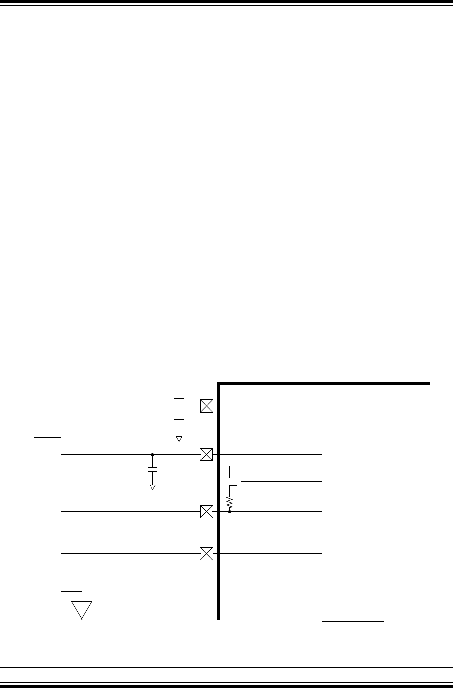
PIC32 Family Reference Manual
DS61126F-page 27-46 © 2011 Microchip Technology Inc.
27.3.6 Hardware Interface
27.3.6.1 POWER SUPPLY REQUIREMENTS
Power supply requirements for USB implementation vary with the type of application, and are
outlined below.
• Device:
Operation as a device requires a power supply for the PIC32 and the USB transceiver, see
Figure 27-6 for an overview of USB implementation as a device.
•Embedded Host:
Operation as a host requires a power supply for the PIC32, the USB transceiver, and a 5V
nominal supply for the USB VBUS. The power supply must be able to deliver 100 mA, or up
to 500 mA, depending on the requirements of the devices in the TPL. The application dic-
tates whether the VBUS power supply can be disabled or disconnected from the bus by the
PIC32 application. Figure 27-7 illustrates an overview of USB implementation as a host.
•OTG Dual Role:
Operation as an OTG dual role requires a power supply for the PIC32, the USB transceiver,
and a switchable 5V nominal supply for the USB VBUS. An overview of USB implementation
as OTG is presented in Figure 27-8.
When acting as an A-device, power must be supplied to VBUS. The power supply must be
able to deliver 8 mA, 100 mA or up to 500 mA, depending on the requirements of the
devices in the TPL.
When acting as a B-device, power must not be supplied to VBUS. VBUS pulsing can be
performed by the USB OTG module or by a capable power supply.
27.3.6.2 VBUS REGULATOR INTERFACE
The VBUSON output can be used to control an off-chip 5V VBUS regulator. The VBUSON pin is
controlled by the VBUSON bit (U1OTGCON<3>). VBUSON appears in Figure 27-7 and
Figure 27-8.
Figure 27-6: Overview of USB Implementation as a Device
VUSB
D+
D-
VBUS
USB OTG
USB Type ‘B’
Connector
2
3
1
4
3.3V
0.1 µF
(1)
Note 1: See Section 7.3 “Physical Layer” in “Universal Serial Bus Specification, Revision 2.0” for the VBUS capacitance value in
a device implementation.
Module

© 2011 Microchip Technology Inc. DS61126F-page 27-47
Section 27. USB On-The-Go (OTG)
USB On-The-Go
(OTG)
27
Figure 27-7: Overview of USB Implementation as a Host
VUSB
D+
D-
VBUS
USB OTG
External Power
USB Type ‘A’
Connector
2
3
1
4
VBUSON
5V
3.3V
0.1 µF
(1)
Note 1: See Section 7.3 “Physical Layer” in “Universal Serial Bus Specification, Revision 2.0” for the VBUS capacitance value in
a host implementation.
Module
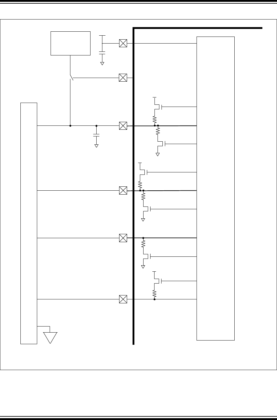
PIC32 Family Reference Manual
DS61126F-page 27-48 © 2011 Microchip Technology Inc.
Figure 27-8: Overview of USB Implementation for OTG (Dual Role)
VUSB
D+
D-
VBUS
USB OTG
External Power
2
3
1
5
VBUSON
5V
SRP Source
SRP Discharge
4
ID
3.3V
USB Type
Micro ‘AB’
Connector
0.1 µF
(1)
Note 1: See Section 7.3 “Physical Layer” and Section 5. “Electrical Requirements” in “Universal Serial Bus Specification,
Revision 2.0” for the VBUS capacitance value in an OTG implementation.
Module

© 2011 Microchip Technology Inc. DS61126F-page 27-49
Section 27. USB On-The-Go (OTG)
USB On-The-Go
(OTG)
27
27.3.7 Module Initialization
This section describes the steps that must be taken to properly initialize the USB OTG module.
27.3.7.1 ENABLING THE USB HARDWARE
In order to use the USB peripheral, software must set the USBPWR bit (U1PWRC<0>) to ‘1’. This
may be done in start-up boot sequence.
USBPWR is used to initiate the following actions:
•Start the USB clock
•Allow the USB interrupt to be activated
• Select USB as the owner of the necessary I/O pins
•Enable the USB transceiver
•Enable the USB comparators
The USB OTG module and internal registers are reset when USBPWR is cleared. Consequently,
the appropriate initialization process must be performed whenever the USB OTG module is
enabled, as described in the following subsections. Otherwise, any configuration packet sent to
the USB OTG module will be NAK’d, by hardware, until the module is configured.
27.3.7.2 INITIALIZING THE BDT
All descriptors for a given endpoint and direction must be initialized prior to enabling the endpoint
(for that direction). After a reset, all endpoints are disabled and start with the EVEN buffer for
transmit and receive directions.
Transmit descriptors must be written with the UOWN bit cleared to ‘0’ (owned by software). All
other transmit descriptor setup may be performed anytime prior to setting the UOWN bit to ‘1’.
Receive descriptors must be fully initialized to receive data. This means that memory must be
reserved for received packet data. The pointer to that memory (Physical Address), and the size
reserved in bytes, must be written to the descriptor. The receive descriptor UOWN bit should be
initialized to ‘1’ (owned by Hardware). The DTS and STALL bits should also be configured
appropriately.
If a transaction is received and the descriptor’s UOWN bit is ‘0’ (owned by software), the USB
OTG module returns a NAK handshake to the host. Usually, this causes the host to retry the
transaction.
27.3.7.3 USB ENABLE/MODE BITS
USB mode of operation is controlled by the following enable bits: OTGEN (U1OTGCON<2>),
HOSTEN (U1CON<3>) and USBEN/SOFEN (U1CON<0>).
•OTGEN: Selects whether the PIC32 is to act as an OTG part (OTGEN = 1) or not. OTG
devices support SRP and HNP in hardware with Firmware management and have direct
control over the data-line pull-up and pull-down resistors.
•HOSTEN: Controls whether the part is acting in the role of USB Host (HOSTEN = 1) or
USB Device (HOSTEN = 0). Note that this role may change dynamically in an OTG
application.
•USBEN/SOFEN: Controls the connection to USB by enabling the D+ pull-up resistor when
the USB OTG module is not configured as a host.
If the USB OTG module is configured as a host, SOFEN controls whether the host is active
on the USB link and sends SOF tokens every 1 ms.
Note: If the USB OTG module was previously active and was quickly disabled and
re-enabled, there is a chance that the module may still be finishing the previous bus
activity. In this situation, the firmware should wait for the USBBUSY bit
(U1PWRC<3>) to become cleared before attempting to configure and enable the
module. Please note that this feature is not available in all devices. Refer to the
specific device data sheet for details.
Note: The other USB OTG module control registers should be properly initialized before
enabling USB via these bits.

PIC32 Family Reference Manual
DS61126F-page 27-50 © 2011 Microchip Technology Inc.
27.3.8 Device Operation
All communication on the USB is initiated by the host. Therefore, in device mode, when USB is
enabled USBEN = 1 (U1CON<0>), endpoint 0 must be ready to receive control transfers. Initial-
ization of the remaining endpoints, descriptors and buffers can be delayed until the host selects
a configuration for the device. Refer to Chapter 9 of “Universal Serial Bus Specification,
Revision 2.0” for more information on this subject.
The following steps are performed to respond to a USB transaction:
1. Software pre-initializes the appropriate BDs, and sets the UOWN bits to ‘1’ to be ready for
a transaction.
2. Hardware receives a TOKEN PID (IN, OUT, SETUP) from the USB host, and checks the
appropriate BD.
3. If the transaction will be transmitted (IN), the module reads packet data from data memory.
4. Hardware receives a DATA PID (DATA0/1), and sends or receives the packet data.
5. If a transaction is received (SETUP, OUT), the module writes packet data to data memory.
6. The module issues, or waits for, a handshake PID (ACK, NAK, STALL), unless the endpoint
is setup as an isochronous endpoint (EPHSHK bit UEPMx<0> is cleared).
7. The module updates the BD, and writes the UOWN bit to ‘0’ (SW owned).
8. The module updates the U1STAT register, and sets the TRNIF interrupt.
9. Software reads the U1STAT register, and determines the endpoint and direction for the
transaction.
10. Software reads the appropriate BD, completes all necessary processing, and clears the
TRNIF interrupt.
27.3.8.1 RECEIVING AN IN TOKEN IN DEVICE MODE
Perform the following steps when an IN token is received in Device mode:
1. Attach to a USB host and enumerate as described in Chapter 9 of “Universal Serial Bus
Specification, Revision 2.0”.
2. Populate the data buffer with the data to send to the host.
3. In the appropriate (EVEN or ODD) transmit buffer descriptor for the desired endpoint:
a) Set up the control bit fields with the correct data toggle (DATA0/1) value and the byte
count of the data buffer.
b) Set up the address bit field with the starting address of the data buffer.
c) Set the UOWN bit field to ‘1’.
4. When the USB OTG module receives an IN token, it automatically transmits the data in
the buffer. Upon completion, the module updates the status bit fields, and sets the transfer
complete interrupt bit, TRNIF(U1IR<3>).
27.3.8.2 RECEIVING AN OUT TOKEN IN DEVICE MODE
Perform the following steps when an OUT token is received in Device mode:
1. Attach to a USB host and enumerate as described in Chapter 9 of “Universal Serial Bus
Specification, Revision 2.0”.
2. Create a data buffer with the amount of data you are expecting from the host.
3. In the appropriate (EVEN or ODD) transmit buffer descriptor for the desired endpoint:
a) Set up the control bit fields with the correct data toggle (DATA0/1) value and the byte
count of the data buffer.
b) Set up the address bit field with the starting address of the data buffer.
c) Set the UOWN bit of the control bit field to ‘1’.
4. When the USB OTG module receives an OUT token, it will automatically transfer the data
the host sent into the buffer. Upon completion, the module updates the status bit fields,
and sets the transfer complete interrupt bit, TRNIF(U1IR<3>).
Note: For transmitted (IN) transactions (host reading data from the device), the read data
must be ready when the Host begins USB signaling. Otherwise, the USB OTG
module will send a NAK handshake if UOWN is ‘0’.

© 2011 Microchip Technology Inc. DS61126F-page 27-51
Section 27. USB On-The-Go (OTG)
USB On-The-Go
(OTG)
27
27.4 HOST MODE OPERATION
In Host mode, only endpoint 0 is used (all other endpoints should be disabled). Since the host
initiates all transfers, the BD does not require immediate initialization. However, the BDs must be
configured before a transfer is initiated – which is done by writing to the U1TOK register.
The following sections describe how to perform common Host mode tasks. In Host mode, USB
transfers are invoked explicitly by the host software. The host software is responsible for initiating
the setup, data, and status stages of all control transfers. The acknowledge (ACK or NAK) is gen-
erated automatically by the hardware, based on the CRC. Host software is also responsible for
scheduling packets so that they do not violate USB protocol. All transfers are performed using
the Endpoint 0 Control register (U1EP0) and BDs.
27.4.1 Configuring the SOF Threshold
The module counts down the number of bits that could be transmitted within the current USB
full-speed frame. Since 12,000 bits can be transmitted during the 1 ms frame time, a counter (not
visible to software) is loaded with the value ‘12,000’ at the start of each frame. The counter
decrements once for each bit time in the frame. When the counter reaches zero, the next frame’s
SOF packet is transmitted, see Figure 27-9.
The SOF threshold register (U1SOF) is used to ensure that no new tokens are started too close
to the end of a frame. This prevents a conflict with the next frame’s SOF packet. When the coun-
ter reaches the threshold value of the U1SOF register (the value in the U1SOF register is in terms
of bytes), no new tokens are started until after the SOF has been transmitted. Thus, the USB
OTG module attempts to ensure that the USB link is idle when the SOF token needs to be
transmitted.
This implies that the value programmed into the U1SOF register must reserve enough time to
ensure the completion of the worst-case transaction. Typically, the worst-case transaction is an
IN token followed by a maximum-sized data packet from the target, followed by the response
from the host. If the host is targeting a low-speed device that is bridging through a full-speed hub,
the transaction will also include the special PRE token packets.
Figure 27-9: Allocation of Bits for a Full-Speed Frame
Tabl e 27- 3 and Ta bl e 27- 4 show examples of calculating worst-case bit times.
SOF SOF
U1SOF * 8
bit times
0 ms 1 ms (12,000 bit times)
Note: Drawing is not to scale.
SOF Threshold
1 Full-Speed Frame
Note 1: While the U1SOF register value is described in terms of bytes, these examples
show the result in terms of bits.
2: In Ta ble 2 7-4 , the IN, DATA and HANDSHAKE packets are transmitted at
low-speed (8 times slower than full-speed).
3: These calculations do not take the possibility that the packet data needs to be
bit-stuffed for NRZI encoding into account.

PIC32 Family Reference Manual
DS61126F-page 27-52 © 2011 Microchip Technology Inc.
.
Table 27-3: Example of SOF Threshold Calculation: Full-Speed
Packet Fields Bits
IN SYNC, PID, ADDR, ENDP, CRC5, EOP 35
Turnaround(1) —8
DATA SYNC, PID, DATA(2), CRC16, EOP 547
Turnaround — 2
HANDSHAKE SYNC, PID, EOP 19
Inter-packet — 2
Total 613
Note 1: Inter-packet delay of 2. An additional 5.5 bit times of latency is added to represent a worst-case
propagation delay through 5 hubs.
2: Using 64 bytes maximum packet size for this example calculation.
Table 27-4: Example of SOF Threshold Calculation: Low-Speed Via Hub
Packet Fields Bits FS Bits
PRE SYNC, PID 16 16
Hub setup — 4 4
IN SYNC, PID, ADDR, ENDP, CRC5, EOP 35 280
Turnaround(1) —88
DATA SYNC, PID, DATA(2), CRC16, EOP 99 792
Turnaround — 2 2
PRE SYNC, PID 16 16
HANDSHAKE SYNC, PID, EOP 19 152
Inter-packet — 2 2
Total 1272
Note 1: Inter-packet delay of 2. An additional 5.5 bit times of latency is added to represent a worst-case
propagation delay through 5 hubs.
2: Packets limited to 8 bytes maximum in Low-Speed mode.
Note: Refer to Section 5.11.3 “Calculating Bus Transaction Times” in “Universal Serial Bus Specification,
Revision 2.0” for details on calculating bus transaction time.

© 2011 Microchip Technology Inc. DS61126F-page 27-53
Section 27. USB On-The-Go (OTG)
USB On-The-Go
(OTG)
27
27.4.2 Enabling Host Mode and Discovering a Connected Device
To e na ble Hos t m od e, per fo rm th e f oll owi ng st ep s:
1. Enable Host mode, the HOSTEN bit (U1CON<3>) = 1.
This enables the D+ and D- pull-down resistors, and disables the D+ and D- pull-up
resistors. To reduce noise on the bus, disable the SOF packet generation by writing the
SOF enable bit to ‘0’, the SOFEN bit (U1CON<0>) = 0.
2. Enable the device attach interrupt, the ATTACHIE bit (U1IE<6> = 1).
3. Wait for the device attach interrupt, the ATTACHIF bit (U1IR<6>).
This is signaled by the USB device changing the state of D+ or D- from ‘0’ to ‘1’ (SE0 to
JSTATE). After it occurs, wait for the device power to stabilize (10 ms is minimum, 100 ms
is recommended).
4. Check the state of the JSTATE and SE0 bits in the control register U1CON.
If the JSTATE bit (U1CON<7>) is ‘0’, the connecting device is low-speed; otherwise, the
device is full-speed.
5. If the connecting device is low-speed, set the low-speed enable bit in the address register,
the LSPDEN bit (U1ADDR<7>= 1), and the low-speed bit in the Endpoint 0 Control
register, the LSPD bit (U1EP0<7> = 1). But, if the device is full-speed, clear these bits.
6. Reset the USB device by sending the Reset signaling for at least 50 ms (USBRST bit
(U1CON<4>) = 1). After 50 ms, terminate the Reset (USBRST bit (U1CON<4>) = 0).
7. Enable SOF packet generation to keep the connected device from going into Suspend
(SOFEN bit (U1CON<0>) = 1).
8. Wait 10 ms for the device to recover from Reset.
9. Perform enumeration as described in Chapter 9 of “Universal Serial Bus Specification,
Revision 2.0”.
27.4.2.1 HOST TRANSACTIONS
When acting as a host, a transaction consists of the following:
1. Software configures the appropriate BD, and sets the UOWN bit to ‘1’ (HW owned).
2. Software checks the state of the TOKBUSY bit (U1CON<5>) to verify that any previous
transaction has completed.
3. Software writes the address of the target device in the U1ADDR register.
4. Software writes the endpoint number and the desired TOKEN PID (IN, OUT or SETUP) to
the U1TOK register.
5. Hardware reads the BD to determine the appropriate action, and to obtain the pointer to
data memory.
6. Hardware issues the correct TOKEN PID (IN, OUT, SETUP) on the USB link.
7. If the transaction is a transmit transaction (OUT, SETUP), the USB OTG module reads the
packet data out of data memory. Then the module follows with the desired DATA PID
(DATA0/DATA1) and packet data.
8. If the transaction is a receive transaction (IN), the USB OTG module waits to receive the
DATA PID and packet data. Hardware writes the packet data to memory.
9. Hardware issues or waits for a Handshake PID (ACK, NAK or STALL), unless the endpoint
is set up as an Isochronous Endpoint (EPHSHK bit (U1EPx<0>) is cleared).
10. Hardware updates the BD, and writes the UOWN bit to ‘0’ (SW owned).
11. Hardware updates the U1STAT register, and sets the TRNIF bit (U1IR<3>) interrupt.
12. Hardware reads the next BD (EVEN or ODD) to see whether it is owned by the USB OTG
module. If it is, hardware begins the next transaction.
13. Software should read the U1STAT register, and then clear the TRNIF interrupt.
If Software does not set the UOWN bit to ‘1’ in the appropriate BD prior to writing the U1TOK
register, the module will read the descriptor and do nothing.

PIC32 Family Reference Manual
DS61126F-page 27-54 © 2011 Microchip Technology Inc.
27.4.3 Completing a Control Transaction to a Connected Device
Complete all of the following steps to discover a connected device:
1. Set up the Endpoint Control register for bidirectional control transfers,
U1EP0<4:0> = 0x0D.
2. Place an 8-byte device setup packet in the appropriate memory buffer. See Chapter 9 of
“Universal Serial Bus Specification, Revision 2.0” for information on the device framework
command set.
3. Initialize the current (EVEN or ODD) TX EP0 BD to transfer the 8-byte device framework
command (for example, a GET DEVICE DESCRIPTOR command).
a) Set the BD control offset 0 to 0x8008 (UOWN bit set, byte count of 8).
b) Set the BD data buffer address (BD0ADR) to the starting address of the 8-byte
memory buffer containing the command, if it is not already initialized.
4. Set the USB address of the target device in the address register U1ADDR<6:0>. After a
USB bus Reset, the device USB address will be zero. After enumeration, it must be set to
another value, between 1 and 127, by the host software.
5. Write the token register with a SETUP command to Endpoint 0, the target device’s default
control pipe (U1TOK = 0xD0). This will initiate a SETUP token on the bus followed by a
data packet. The device handshake will be returned in the PID field of BD status after the
packets complete. When the module updates BD status, a transfer done interrupt will be
asserted (U1IR<TRNIF>). This completes the setup stage of the setup transfer as
described in Chapter 9 of the USB specification.
6. To initiate the data stage of the setup transaction (for example, get the data for the GET
DEVICE DESCRIPTOR command), set up a buffer in memory to store the received data.
7. Initialize the current (EVEN or ODD) RX or TX (RX for IN, TX for OUT) EP0 BD to transfer
the data.
a) Set the BD control UOWN bit to ‘1’, data toggle (DTS) to DATA1 and byte count to the
length of the data buffer.
b) Set the BD data buffer address (BD0ADR) to the starting address of the data buffer
if it is not already initialized.
8. Write the Token register with the appropriate IN or OUT token to Endpoint 0 (the target
device’s default control pipe), for example, an IN token for a GET DEVICE DESCRIPTOR
command (U1TOK = 0x90). This will initiate an IN token on the bus followed by a data
packet from the device to the host. When the data packet completes, the BD status is written
and a transfer done interrupt will be asserted (TRNIF bit (U1IR<3>)). For control transfers
with a single packet data phase, this completes the data phase of the setup transaction. If
more data needs to be transferred, return to step 6.
9. To initiate the status stage of the setup transaction, set up a buffer in memory to receive
or send the zero length status phase data packet.
10. Initialize the current (EVEN or ODD) TX EP0 BD to transfer the status data.
a) Set the BD control to 0x8000 (UOWN bit to ‘1’, data toggle (DTS) to DATA0 and byte
count to ‘0’).
b) Set the BDT buffer address field to the start address of the data buffer.
11. Write the Token register with the appropriate IN or OUT token to Endpoint 0, (the target
device’s default control pipe) for example, an OUT token for a GET DEVICE DESCRIPTOR
command (U1TOK = 0x10). This will initiate a token on the bus, followed by a zero length
data packet from the host to the device. When the data packet completes, the BD is
updated with the handshake from the device, and a transfer done interrupt (TRNIF bit
(U1IR<3>)) will be asserted . This completes the status phase of the setup transaction.
Note: Some devices can only effectively respond to one transaction per frame.

© 2011 Microchip Technology Inc. DS61126F-page 27-55
Section 27. USB On-The-Go (OTG)
USB On-The-Go
(OTG)
27
27.4.4 Data Transfer with a Target Device
Complete all of the following steps to discover and configure a connected device.
1. Write the EP0 Control register (U1EPn) to enable transmit and receive transfers as appro-
priate with handshaking enabled (unless isochronous transfers are to be used). If the tar-
get device is a low-speed device, also set the Low-Speed Enable bit, the LSPD bit
(U1EPn<7>). If you want the hardware to automatically retry indefinitely if the target
device asserts a NAK on the transfer, clear the Retry Disable bit, RETRYDIS (U1EPn<6>).
2. Set up the current Buffer Descriptor (EVEN or ODD) in the appropriate direction to transfer
the desired number of bytes.
3. Set the address of the target device in the address register (U1ADDR<6:0>).
4. Write the Token register (U1TOK) with an IN or OUT token as appropriate for the desired
endpoint. This triggers the module’s transmit state machines to begin transmitting the
token and the data.
5. Wait for the transfer done interrupt (TRNIF bit (U1IR<3>)). This will indicate that the BD
has been released back to the microprocessor and the transfer has completed. If the retry
disable bit is set, the handshake (ACK, NAK, STALL or ERROR (0xf)) will be returned in
the BD PID field. If a stall interrupt occurs, then the pending packet must be dequeued and
the error condition in the target device cleared. If a detach interrupt occurs (SE0 for more
than 2.5 µs), then the target has detached (DETACHIF bit (U1IR<0>)).
6. Once the transfer done interrupt (TRNIF bit (U1IR<3>)) occurs, the BD can be examined
and the next data packet queued by returning to step 2.
27.4.4.1 USB LINK STATES
Three possible link states are described in the following subsections:
•Reset
•Idle and Suspend
•Resume Signaling
27.4.4.1.1 Reset
As a host, software is required to drive Reset signaling. It may do this by setting the USBRST bit
(U1CON<4>). As per the USB specification, the host must drive the Reset for at least 50 ms. (This
does not have to be continuous Reset signaling. Refer to “Universal Serial Bus Specification, Revi-
sion 2.0” for more information.) Following Reset, the host must not initiate any downstream traffic
for another 10 ms.
As a device, the USB OTG module will assert the URSTIF bit (U1IR<0>) interrupt when it has
detected Reset signaling for 2.5 µs. Software must perform any Reset initialization processing at
this time. This includes setting the Address register to 0x00 and enabling Endpoint 0. The
URSTIF interrupt will not be set again until the Reset signaling has gone away and then has been
detected again for 2.5 µs.
Note: Use of automatic indefinite retries can lead to a deadlock condition if the device
never responds.
Note: USB speed, transceiver and pull-ups should only be configured during the module
setup phase. It is not recommended to change these settings while the module is
enabled.

PIC32 Family Reference Manual
DS61126F-page 27-56 © 2011 Microchip Technology Inc.
27.4.4.1.2 Idle and Suspend
The Idle state of the USB is a constant J state. When the USB has been Idle for 3 ms, a device
should go into Suspend state. During active operation, the USB host will send a SOF token every
1 ms, preventing a device from going into Suspend state.
Once the USB link is in the Suspend state, a USB host or device must drive resume signaling
prior to initiating any bus activity. (The USB link may also be disconnected).
As a USB host, software should consider the link in Suspend state as soon as software clears
the SOFEN bit (U1CON<0>).
As a USB device, hardware will set the IDLEIF bit (U1IR<4>) interrupt when it detects a constant
Idle on the bus for 3 ms. Software should consider the link in Suspend state when the IDLEIF
interrupt is set.
When a Suspend condition has been detected, the software may wish to place the USB hard-
ware in a Suspend mode by setting the USUSPEND bit (U1PWRC<1>). The hardware Suspend
mode gates the USB OTG module’s 48 MHz clock and places the USB transceiver in a
Low-Power mode.
Additionally, the user may put the PIC32 into Sleep mode while the link is suspended.
27.4.4.1.3 Driving Resume Signaling
If software wants to wake the USB from Suspend state, it may do so by setting the RESUME bit
(U1CON<2>). This will cause the hardware to generate the proper resume signaling (including
finishing with a low-speed EOP if in host mode).
A USB device should not drive resume signaling unless the Idle state has persisted for at least
5ms. The USB host also must have enabled the function for remote wake-up.
Software must set RESUME for 1-15 ms if a USB device, or greater than 20 ms if a USB host,
then clear it to enable remote wake-up. For more information on RESUME signaling, see
Section 7.1.7.7, 11.9, and 11.4.4 in “Universal Serial Bus Specification, Revision 2.0”.
Writing RESUME will automatically clear the special hardware Suspend (low-power) state.
If the part is acting as a USB host, software should, at minimum, set the SOFEN bit (U1CON<0>)
after driving its resume signaling. Otherwise, the USB link would return right back to the Suspend
state after 3 ms of inactivity. Also, software must not initiate any downstream traffic for 10 ms
following the end of resume signaling.
27.4.4.1.4 Receiving Resume Signaling
When the USB logic detects resume signaling on the USB bus for 2.5 µs, hardware will set the
resume interrupt bit, RESUMEIF (U1IR<5>).
A device receiving resume signaling must prepare itself to receive normal USB activity. A host
receiving resume signaling must immediately start driving resume signaling of its own. The
special hardware Suspend (low-power) state is automatically cleared upon receiving any activity
on the USB link.
Reception of any activity on the USB link (this may be due to resume signaling or a link discon-
nect) while the PIC32 is in Sleep mode will cause the ACTVIF bit (U1OTGIR<4>) interrupt to be
set. This will cause wake-up from Sleep.
27.4.4.2 SRP SUPPORT
SRP support is not required by non-OTG applications. SRP may only be initiated at full-speed.
Refer to the On-The-Go Supplement specification for more information regarding SRP.
An OTG A-device or embedded host may decide to power-down the VBUS supply when it is not
using the USB link. Software may do this by clearing the VBUSON bit (U1OTGCON<3>). When
the VBUS supply is powered down, the A-device is said to have ended a USB session.
Note: When the A-device powers down the VBUS supply, the B-device must disconnect its
pull-up resistor.

© 2011 Microchip Technology Inc. DS61126F-page 27-57
Section 27. USB On-The-Go (OTG)
USB On-The-Go
(OTG)
27
An OTG A-device or embedded host may repower the VBUS supply at any time to initiate a new
session. An OTG B-device may also request that the OTG A-device repower the VBUS supply to
initiate a new session. This is the purpose of the SRP.
Prior to requesting a new session, the B-device must first check that the previous session has
definitely ended. To do this, the B-device must check that:
1. VBUS supply is below the session end voltage.
2. Both D+ and D- have been low for at least 2 ms.
The B-device will be notified of condition 1 by the SESENDIF bit (U1OTGIR<2>) interrupt.
Software can use the LSTATEIF bit (U1OTGIR<5>) and the 1 ms timer to identify condition 2.
The B-device may aid in achieving condition 1 by discharging the VBUS supply through a resistor.
Software may do this by setting the VBUSDIS bit (U1OTGCON<0>).
After these initial conditions are met, the B-device may begin requesting the new session. The
B-device then proceeds by pulsing the D+ data line. Software should do this by setting the DPPULUP
bit (U1OTGCON<7>). The data line should be held high for 5-10 ms.
After data line pulsing, the B-device should complete SRP signaling by pulsing the VBUS supply.
This should be done in software by setting the VBUSCHG bit (U1OTGCON<1>).
When an A-device detects SRP signaling (either via the ATTACHIF bit (U1IR<6>) interrupt or via
the SESVDIF bit (U1OTGIR<3>) interrupt), the A-device must restore the VBUS supply by setting
the VBUSON bit (U1OTGCON<3>).
The B-device should not monitor the state of the VBUS supply while performing VBUS supply
pulsing. Afterwards, if the B-device does detect that the VBUS supply has been restored (via the
SESVDIF bit (U1OTGIR<3>) interrupt), it must reconnect to the USB link by pulling up D+. The
A-device must complete the SRP by enabling VBUS and driving Reset signaling.
Refer to the On-The-Go supplement in “Universal Serial Bus Specification, Revision 2.0” for
additional details.
27.4.4.3 HNP
An OTG application with a micro-AB receptacle must support HNP. The HNP allows an OTG
B-device to temporarily become the USB host. The A-device must first enable HNP in the
B-device. The HNP may only be initiated at full-speed.
After being enabled for HNP by the A-device, the B-device can request to become the host any
time that the USB link is in Suspend state by simply indicating a disconnect. Software may
accomplish this by clearing the DPPULUP bit (U1OTGCON<7>).
When the A-device detects the disconnect condition (via the URSTIF (U1IR<0>) interrupt), the
A-device may allow the B-device to take over as host. The A-device does this by signaling
connect as a full-speed device. Software may accomplish this by disabling host operation,
HOSTEN = 0 (U1CON<3>), and connecting as a device (USB_EN = 1). If the A-device instead
responds with resume signaling, the A-device will remain as host.
When the B-device detects the connect condition (via the ATTACHIF bit (U1IR<6>)), the
B-device becomes host. The B-device drives Reset signaling prior to using the bus.
When the B-device has finished in its role as host, it stops all bus activity and turns on its D+
pull-up resistor by disabling host operations (HOSTEN = 0) and reconnecting as a device
(USB_EN = 1).

PIC32 Family Reference Manual
DS61126F-page 27-58 © 2011 Microchip Technology Inc.
Then the A-device detects a Suspend condition (Idle for 3 ms), the A-device turns off its D+
pull-up. Alternatively the A-device may also power-down the VBUS supply to end the session.
Otherwise, the A-device continues to provide the VBUS throughout this process.
When the A-device detects the connect condition (via ATTACHIF), the A-device resumes host
operation, and drives Reset signaling.
Refer to the On-The-Go supplement for more information regarding HNP.
27.4.4.4 CLOCK REQUIREMENTS
For proper USB operation, the USB OTG module must be clocked with a 48 MHz clock. This
clock source is used to generate the timing for USB transfers; it is the clock source for the SIE.
The control registers are clocked at the same speed as the CPU (refer to Figure 27-1).
The USB OTG module clock is derived from the Primary Oscillator (POSC) for USB operation. A
USB PLL and input prescalers are provided to allow 48 MHz clock generation from a wide variety
of input frequencies. The USB PLL allows the CPU and the USB OTG module to operate at dif-
ferent frequencies while both use the POSC as a clock source. To prevent buffer overruns and
timing issues, the CPU core must be clocked at a minimum of 16 MHz.
The USB OTG module can also use the on-board Fast RC oscillator (FRC) as a clock source.
When using this clock source, the USB OTG module will not meet the USB timing requirements.
The FRC clock source is intended to allow the USB OTG module to detect a USB wake-up and
report it to the interrupt controller when operating in low-power modes. The USB OTG module
must be running from the Primary oscillator before beginning USB transmissions.

© 2011 Microchip Technology Inc. DS61126F-page 27-59
Section 27. USB On-The-Go (OTG)
USB On-The-Go
(OTG)
27
27.5 INTERRUPTS
The USB OTG module uses interrupts to signal USB events such as a change in status, data
received and buffer empty events, to the CPU. Software must be able to respond to these interrupts
in a timely manner.
27.5.1 Interrupt Control
Each interrupt source in the USB OTG module has an interrupt flag bit and a corresponding
enable bit. In addition, the UERRIF bit (U1IR<1>) is a logical OR of all the enabled error flags
and is read-only. The UERRIF bit can be used to check the USB OTG module for events while
in an Interrupt Service Routine (ISR).
27.5.2 USB OTG module Interrupt Request Generation
The USB OTG module can generate interrupt requests from a variety of events. To interface
these interrupts to the CPU, the USB interrupts are combined such that any enabled USB inter-
rupt will cause a generic USB interrupt (if the USB interrupt is enabled) to the interrupt controller,
see Figure 27-11. The USB ISR must then determine which USB event(s) caused the CPU inter-
rupt and service them appropriately. There are two layers of interrupt registers in the USB OTG
module. The top level of bits consists of overall USB status interrupts in the U1OTGIR and U1IR
registers. The U1OTGIR and U1IR bits are individually enabled through the corresponding bits
in the U1OTGIE and U1IE registers. In addition, the USB Error Condition bit (UERRIF) passes
through any interrupt conditions in the U1EIR register enabled via the U1EIE register bits.
27.5.3 Interrupt Timing
Interrupts for transfers are generated at the end of the transfer. Figure 27-10 illustrates some typ-
ical event sequences that can generate a USB interrupt and when that interrupt is generated.
There is no mechanism by which software can manually set an interrupt bit.
The values in the Interrupt Enable registers (U1IE, U1EIE, U1OTGIE) only affect the propagation
of an interrupt condition to the CPU’s interrupt controller. Even though an interrupt is not enabled,
interrupt flag bits can still be polled and serviced.
27.5.4 Interrupt Servicing
Once an interrupt bit has been set by the USB OTG module (in U1IR, U1EIR or U1OTGIR), it
must be cleared by software by writing a ‘1’ to the appropriate bit position to clear the interrupt.
The USB Interrupt bit, USBIF (IFS1<25>), must be cleared before the end of the ISR.
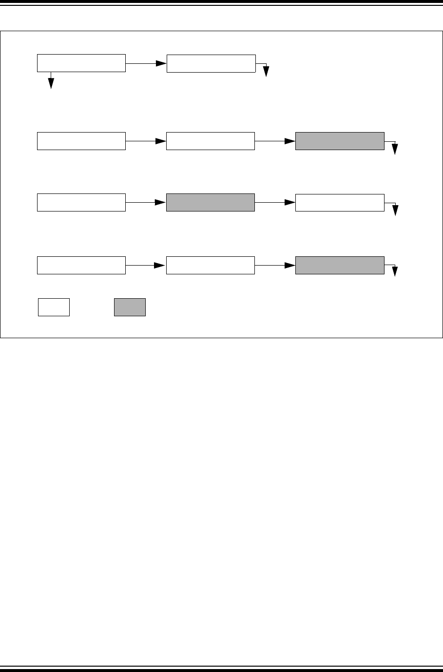
PIC32 Family Reference Manual
DS61126F-page 27-60 © 2011 Microchip Technology Inc.
Figure 27-10: Typical Events for USB Interrupts
USB <USBRST>
ACKSETUP TOKEN DATA
URSTIF
Interrupt Generated
TRNIF
Interrupt Generated
IN TOKEN DATA
ACKOUT TOKEN DATA
TRNIF
Interrupt Generated
TRNIF
Interrupt Generated
Control
ACK
=Host =Function
SOF
SOFIF
Interrupt Generated
© 2011 Microchip Technology Inc. DS61126F-page 27-61
Section 27. USB On-The-Go (OTG)
USB On-The-Go
(OTG)
27
Figure 27-11: USB Interrupt Logic
DMAEF
DMAEE
BTOEF
BTOEE
DFN8EF
DFN8EE
CRC16EF
CRC16EE
CRC5EF/EOFEF
CRC5EE/EOFEE
PIDEF
PIDEE
ATTACHIF
ATTACHIE
RESUMEIF
RESUMEIE
IDLEIF
IDLEIE
TRNIF
TRNIE
SOFIF
SOFIE
DETACHIF/URSTIF
DETACHIE/URSTIE USB Interrupt
STALLIF
STALLIE
BTSEF
BTSEE
T1MSECIF
T1MSECIE
LSTATEIF
LSTATEIE
ACTVIF
ACTVIE
SESVDIF
SESVDIE
SESENDIF
SESENDIE
VBUSVDIF
VBUSVDIE
IDIF
IDIE
UERRIF
UERRIE
BMXEF
BMXEE

PIC32 Family Reference Manual
DS61126F-page 27-62 © 2011 Microchip Technology Inc.
27.6 I/O PINS
Tabl e 27- 5 summarizes the use of pins relating to the USB OTG module.
Table 27-5: Pins Associated with the USB OTG Module
Mode Pin Name Module
Control
Controlling Bit
Field(1)
Required
TRIS Bit
Setting
Pin
Type Description
Embedded Host(4)
D+ USBEN — — U Data line +
D- USBEN — — U Data line -
VBUS USBEN — — A, I USB bus power monitor
VBUSON USBEN VBUSON — D, O Output to control supply for VBUS
VBUSON USBEN FVBUSONIO(2,3) 1D, I General purpose digital input
VBUSON USBEN FVBUSONIO(2,3) 0D, O General purpose digital output
VUSB ———PPower in for USB transceiver
ID USBEN — — R Reserved; do not connect
ID USBEN FUSBIDIO(2,3) 1D, I General purpose digital input
ID USBEN FUSBIDIO(2,3) 0D, O General purpose digital output
Device
D+ USBEN — — U Data line +
D- USBEN — — U Data line -
VBUS USBEN — — A, I USB bus power monitor
VBUSON — — — R Reserved
VBUSON USBEN FVBUSONIO(2,3) 1D, I General purpose digital input
VBUSON USBEN FVBUSONIO(2,3) 0D, O General purpose digital output
VUSB ———PUSB internal transceiver supply
ID — — — R Reserved
ID USBEN FUSBIDIO(2,3) 1D, I General purpose digital input
ID USBEN FUSBIDIO(2,3) 0D, O General purpose digital output
Legend: I = Input O = Output A = Analog D = Digital
U = USB P = Power R = Reserved
Note 1: All pins are subject to the device pin priority control. See the specific device data sheet for further details.
2: Refer to Section 32. “Configuration” (DS61124) for information on these bits.
3: These bits are not available on all devices. Refer to the specific device data sheet for details.
4: The VBUSON pin cannot be reclaimed for I/O usage when operating in Host mode or OTG mode, as it is
required for USB operation.
5: The ID pin cannot be reclaimed for I/O usage when operating in OTG mode, as it is required for USB
operation.

© 2011 Microchip Technology Inc. DS61126F-page 27-63
Section 27. USB On-The-Go (OTG)
USB On-The-Go
(OTG)
27
OTG(4,5)
D+ USBEN — — U Data line +
D- USBEN — — U Data line -
VBUS USBEN VBUSCHG,
VBUSDIS
— A, I/O USB bus power monitor
VBUSON USBEN VBUSCHG,
VBUSDIS,
VBUSON
—D, OUSB Host and OTG bus power
control output
VBUSON USBEN FVBUSONIO(2,3) 1D, I General purpose digital input
VBUSON USBEN FVBUSONIO(2,3) 0D, O General purpose digital output
VUSB ———PPower in for USB transceiver
ID USBEN — — D, I OTG mode host/device select input
ID USBEN FUSBIDIO(2,3) 1D, I General purpose digital input
ID USBEN FUSBIDIO(2,3) 0D, O General purpose digital output
USB Disabled
D+ USBEN — 1D, I General purpose digital input
D- USBEN — 1D, I General purpose digital input
VBUS USBEN — — R Reserved
VBUSON USBEN — 0D, O General purpose digital input
VBUSON USBEN — 1D, I General purpose digital output
VUSB USBEN — — R Reserved
ID USBEN — 1D, I General purpose digital input
ID USBEN — 0D, O General purpose digital output
Table 27-5: Pins Associated with the USB OTG Module (Continued)
Mode Pin Name Module
Control
Controlling Bit
Field(1)
Required
TRIS Bit
Setting
Pin
Type Description
Legend: I = Input O = Output A = Analog D = Digital
U = USB P = Power R = Reserved
Note 1: All pins are subject to the device pin priority control. See the specific device data sheet for further details.
2: Refer to Section 32. “Configuration” (DS61124) for information on these bits.
3: These bits are not available on all devices. Refer to the specific device data sheet for details.
4: The VBUSON pin cannot be reclaimed for I/O usage when operating in Host mode or OTG mode, as it is
required for USB operation.
5: The ID pin cannot be reclaimed for I/O usage when operating in OTG mode, as it is required for USB
operation.

PIC32 Family Reference Manual
DS61126F-page 27-64 © 2011 Microchip Technology Inc.
27.7 OPERATION IN DEBUG AND POWER-SAVING MODES
27.7.1 Operation in Sleep
Use of Sleep mode is only recommended in two cases:
•USB OTG module is disabled
•USB OTG module is in a Suspend state
Placing the USB OTG module in Sleep mode while the bus is active can result in violating
USB protocol.
When the device enters Sleep mode, the clock to the USB OTG module is maintained. The effect
on the CPU clock source is dependent on the USB and CPU clock configuration.
•If the CPU and USB were using the Primary Oscillator (P
OSC) source, the CPU is discon-
nected from the clock source when entering Sleep and the oscillator is left in Enabled state
for the USB OTG module.
• If the CPU was using a different clock source, that clock source is disabled on entering
Sleep, and the USB clock source is left Enabled.
To fu rth er re du ce pow er co ns ump ti o n, th e USB OTG module can be placed in Suspend mode.
This can be done prior to placing the CPU in Sleep using the USUSPEND bit (U1PWRC<1>) or
it can be done automatically when the CPU enters Sleep using the UASUSPND bit
(U1CNFG1<0>).
•If the CPU and USB were using the Primary Oscillator (P
OSC) source, the oscillator is
disabled when the CPU enters Sleep.
•If the CPU was not sharing P
OSC with the USB OTG module, POSC will be disabled when
the USB OTG module enters Suspend. The CPU clock source will be disabled when the
CPU enters Sleep.
27.7.1.1 BUS ACTIVITY COINCIDENT WITH ENTERING SLEEP MODE
Software is unable to predict bus activity therefore even when software has determined that the
USB link is in a state safe for entering Sleep, bus activity can still occur, potentially placing USB in
a non-safe link state. The bits, USLPGRD (U1PWRC<4>) and UACTPND (U1PWRC<7>) can be
used to prevent this. Before entering the sensitive code region, software can set the GUARD bit so
that hardware will prevent the device from entering Sleep mode (by generating a wake-up event)
if activity is detected or if there is a notification pending. UACTPND should be polled to ensure no
interrupt is pending before attempting to enter Sleep.
27.7.2 Operation in Idle Mode
When the device enters Idle mode, the behavior of the USB OTG module is determined by the
PSIDL bit.
27.7.2.1 IDLE OPERATION WITH PSIDL CLEARED
When the bit is clear, the clock to the CPU is gated off but the clock to the USB OTG module is
maintained when in Idle mode. The USB OTG module can therefore continue operation while the
CPU is Idle. When enabled USB interrupts are generated they will bring the CPU out of Idle.
27.7.2.2 IDLE OPERATION WITH PSIDL SET
When the PSIDL bit is set, the clock to the CPU and the clock to the USB OTG module are both
gated off. In this mode the USB OTG module does not continue normal operation and has lower
power consumption. Any USB activity can be used to generate an interrupt to bring the CPU out
of Idle.
To f urt her in cre ase pow er s avi ng s, t he C PU clock source and USB clock sources can be
switched to FRC before entering Idle mode. This will cause the POSC module to power down.
When the POSC module is re-enabled, start-up delays will apply. This mode of operation should
only be used when the bus is idle.
Note: The UASUSPND feature is not available on all devices. Refer to the specific device
data sheet for details.
© 2011 Microchip Technology Inc. DS61126F-page 27-65
Section 27. USB On-The-Go (OTG)
USB On-The-Go
(OTG)
27
27.7.3 Operation in Debug Modes
27.7.3.1 EYE PATTERN
To as sis t wit h US B ha rdw are deb ugg ing a nd t es t ing, an eye pattern test generator is incorpo-
rated into the module. This pattern is generated by the module when the UTEYE bit
(U1CNFG1<7>) is set. The USB OTG module must be enabled, USBPWR bit (PWRC<0> = 1),
the USB 48 MHz clock must be enabled, SUSPEND bit (U1PWRC<1>) = 0, and the module is
not in Freeze mode.
Once the UTEYE bit is set, the module will start transmitting a J-K-J-K bit sequence. The bit
sequence will be repeated indefinitely while the Eye Pattern Test mode is enabled, as shown in
Figure 27-12.
Figure 27-12: Eye Pattern Generation Timing
Note: The UTEYE bit should never be set while the module is connected to an actual USB
system. The Eye Pattern Test mode is intended for board verification to aid with
USB certification tests.
VUSB Value VUSB Value
usb_clk
UTEYE Bit
Output Enabled
D-
D+
Resampled UTEYE
UTEYE Resampled by Two USB Clock Edges
Every 4th USB Clock
Every 4th USB Clock

PIC32 Family Reference Manual
DS61126F-page 27-66 © 2011 Microchip Technology Inc.
27.8 EFFECTS OF A RESET
All forms of Reset force the USB OTG module registers to the default state.
27.8.1 Device Reset (MCLR)
A device Reset forces all USB OTG module registers to their Reset state. This turns the USB
OTG module off.
27.8.2 Power-on Reset (POR)
A POR forces all USB OTG module registers to their Reset state. This turns the USB OTG
module off.
27.8.3 Watchdog Timer Reset (WDT)
A WDT Reset forces all USB OTG module registers to their Reset state. This turns the USB OTG
module off.
Note: The USB OTG module cannot ensure the state of the BDT, nor that of the packet
data buffers contained in RAM, following a Reset.

© 2011 Microchip Technology Inc. DS61126F-page 27-67
Section 27. USB On-The-Go (OTG)
USB On-The-Go
(OTG)
27
27.9 RELATED APPLICATION NOTES
This section lists application notes that are related to this section of the manual. These
application notes may not be written specifically for the PIC32 device family, but the concepts are
pertinent and could be used with modification and possible limitations. The current application
notes related to the USB On-The-Go (OTG) module are:
Title Application Note #
USB Embedded Host Stack AN1140
USB Embedded Host Stack Programmer’s Guide AN1141
USB Mass Storage Class on an Embedded Host AN1142
Using a USB Flash Drive with an Embedded Host AN1145
USB HID Class on an Embedded Device AN1163
USB CDC Class on an Embedded Device AN1164
USB Generic Function on an Embedded Device AN1166
USB Mass Storage Class on an Embedded Device AN1169
USB Device Stack for PIC32 Programmer’s Guide AN1176
Note: Please visit the Microchip web site (www.microchip.com) for additional application
notes and code examples for the PIC32 family of devices.

PIC32 Family Reference Manual
DS61126F-page 27-68 © 2011 Microchip Technology Inc.
27.10 REVISION HISTORY
Revision A (February 2008)
This is the initial released version of this document.
Revision B (April 2008)
Revised status to Preliminary; Revised U-0 to r-x; Revised Figure 27-1; Revised Table 27-5.
Revision C (July 2008)
Revised Registers 27-23 (IFS1) and 27-24 (IEC1); Revised Figures 27-3 and 27-4; Change
Reserved bits from “Maintain as” to “Write”.
Revision D (July 2009)
This revision includes the following changes:
•Changed all references to DMA Controller to Bus Master
•Updated Section 27.2.19 “Associated Registers”
•USB Register Summary (Ta ble 2 7-1 ):
- Removed all references to the Clear, Set and Invert registers
-Removed references to the OSCON, IFS1, IEC1 and DEVCFG2 registers
- Added the USBBUSY and UASUSPND bits
- Added the Address Offset column
- Added Notes 1, 2 and 3, which describe the Clear, Set and Invert registers
•Added Notes describing the Clear, Set and Invert registers to the following registers:
-U1OTGIR
-U1OTGIE
-U1OTGCON
- U1PWRC
-U1IR
-U1IE
- U1EIR
- U1EIE
- U1STAT
-U1CON
- U1ADDR
- U1FRML
- U1FRMH
-U1TOK
- U1SOF
- U1BDTP1, U1BDTP2 and U1BDTP3
-U1CNFG1
-U1EPn (where n = 0 through 15)
•Added the USBBUSY bit definition to the U1PWRC: USB Power Control Register
(Register 27-5)
•Added the UASUSPND bit definition to the U1CNFG1: USB Configuration 1 Register
(Register 27-20)
• Removed these registers: OSCCON, IFS1, IEC1 and DEVCFG2
•Updated the last column of BDT Address Generation (Figure 27-2) from FSOTG to FIELD
•Added Note 1 and Note 2 to Buffer Management Overview (Figure 27-5)
•Added a note after the last paragraph in 27.3.7 “Module Initialization”
•Added the FVBUSONIO and FUSBIDIO controlling bit fields to Table 27-5: Pins Associated
with the USB Module
•Changed references to the USBSIDL bit to PSIDL in 27.7.2 “Operation in Idle Mode”

© 2011 Microchip Technology Inc. DS61126F-page 27-69
Section 27. USB On-The-Go (OTG)
USB On-The-Go
(OTG)
27
Revision D (July 2009) (Continued)
•Removed Section 27.7.3.2 “USB OE Monitor”
•Added Note 4 and Note 5 to Ta b l e 2 7 - 5
• Added applications note AN1140, AN1142 and AN1145 to 27.9 “Related Application
Notes”
Revision E (August 2009)
This revision includes the following changes:
•USB Register Summary (Ta ble 2 7-1 ):
- Removed Notes 1, 2 and 3, which described the Clear, Set and Invert registers
•Removed Notes describing the Clear, Set and Invert registers from the following registers:
-U1OTGIR
-U1OTGIE
-U1OTGCON
- U1PWRC
-U1IR
-U1IE
- U1EIR
- U1EIE
- U1STAT
-U1CON
- U1ADDR
- U1FRML
- U1FRMH
-U1TOK
- U1SOF
- U1BDTP1, U1BDTP2 and U1BDTP3
-U1CNFG1
-U1EPn (where n = 0 through 15)
Revision F (April 2011)
This revision includes the following changes:
• Changed the document running header from PIC32MX Family Reference Manual to PIC32
Family Reference Manual
• Changed all occurrences of PIC32MX to PIC32
• Updated all r-0 and r-x bits as U-0 bits in Register 27-1 through Register 27-21
•Updated UACTPND bit as HS, HC-x in Register 27-5
•Added a note in Figure 27-1 indicating that the ID pin is pulled high internally when the USB
OTG module is enabled
•Reorganized the Control Register section (see 27.2 “Control Registers”)
•Added a note to the Ta ble 2 7- 1 about the Set, Clear and Invert registers and removed the
Address column
•Minor updates to text and formatting have been incorporated throughout the document

PIC32 Family Reference Manual
DS61126F-page 27-70 © 2011 Microchip Technology Inc.
NOTES:

© 2011 Microchip Technology Inc DS61126F-page 27-71
Information contained in this publication regarding device
applications and the like is provided only for your convenience
and may be superseded by updates. It is your responsibility to
ensure that your application meets with your specifications.
MICROCHIP MAKES NO REPRESENTATIONS OR
WARRANTIES OF ANY KIND WHETHER EXPRESS OR
IMPLIED, WRITTEN OR ORAL, STATUTORY OR
OTHERWISE, RELATED TO THE INFORMATION,
INCLUDING BUT NOT LIMITED TO ITS CONDITION,
QUALITY, PERFORMANCE, MERCHANTABILITY OR
FITNESS FOR PURPOSE. Microchip disclaims all liability
arising from this information and its use. Use of Microchip
devices in life support and/or safety applications is entirely at
the buyer’s risk, and the buyer agrees to defend, indemnify and
hold harmless Microchip from any and all damages, claims,
suits, or expenses resulting from such use. No licenses are
conveyed, implicitly or otherwise, under any Microchip
intellectual property rights.
Trademarks
The Microchip name and logo, the Microchip logo, dsPIC,
KEELOQ, KEELOQ logo, MPLAB, PIC, PICmicro, PICSTART,
PIC32 logo, rfPIC and UNI/O are registered trademarks of
Microchip Technology Incorporated in the U.S.A. and other
countries.
FilterLab, Hampshire, HI-TECH C, Linear Active Thermistor,
MXDEV, MXLAB, SEEVAL and The Embedded Control
Solutions Company are registered trademarks of Microchip
Technology Incorporated in the U.S.A.
Analog-for-the-Digital Age, Application Maestro, CodeGuard,
dsPICDEM, dsPICDEM.net, dsPICworks, dsSPEAK, ECAN,
ECONOMONITOR, FanSense, HI-TIDE, In-Circuit Serial
Programming, ICSP, Mindi, MiWi, MPASM, MPLAB Certified
logo, MPLIB, MPLINK, mTouch, Omniscient Code
Generation, PICC, PICC-18, PICDEM, PICDEM.net, PICkit,
PICtail, REAL ICE, rfLAB, Select Mode, Total Endurance,
TSHARC, UniWinDriver, WiperLock and ZENA are
trademarks of Microchip Technology Incorporated in the
U.S.A. and other countries.
SQTP is a service mark of Microchip Technology Incorporated
in the U.S.A.
All other trademarks mentioned herein are property of their
respective companies.
© 2011, Microchip Technology Incorporated, Printed in the
U.S.A., All Rights Reserved.
Printed on recycled paper.
ISBN: 978-1-61341-090-5
Note the following details of the code protection feature on Microchip devices:
• Microchip products meet the specification contained in their particular Microchip Data Sheet.
• Microchip believes that its family of products is one of the most secure families of its kind on the market today, when used in the
intended manner and under normal conditions.
• There are dishonest and possibly illegal methods used to breach the code protection feature. All of these methods, to our
knowledge, require using the Microchip products in a manner outside the operating specifications contained in Microchip’s Data
Sheets. Most likely, the person doing so is engaged in theft of intellectual property.
• Microchip is willing to work with the customer who is concerned about the integrity of their code.
• Neither Microchip nor any other semiconductor manufacturer can guarantee the security of their code. Code protection does not
mean that we are guaranteeing the product as “unbreakable.”
Code protection is constantly evolving. We at Microchip are committed to continuously improving the code protection features of our
products. Attempts to break Microchip’s code protection feature may be a violation of the Digital Millennium Copyright Act. If such acts
allow unauthorized access to your software or other copyrighted work, you may have a right to sue for relief under that Act.
Microchip received ISO/TS-16949:2002 certification for its worldwide
headquarters, design and wafer fabrication facilities in Chandler and
Tempe, Arizona; Gresham, Oregon and design centers in California
and India. The Company’s quality system processes and procedures
are for its PIC® MCUs and dsPIC® DSCs, KEELOQ® code hopping
devices, Serial EEPROMs, microperipherals, nonvolatile memory and
analog products. In addition, Microchip’s quality system for the design
and manufacture of development systems is ISO 9001:2000 certified.

DS61126F-page 27-72 © 2011 Microchip Technology Inc.
AMERICAS
Corporate Office
2355 West Chandler Blvd.
Chandler, AZ 85224-6199
Tel: 480-792-7200
Fax: 480-792-7277
Technical Support:
http://www.microchip.com/
support
Web Address:
www.microchip.com
Atlanta
Duluth, GA
Tel: 678-957-9614
Fax: 678-957-1455
Boston
Westborough, MA
Tel: 774-760-0087
Fax: 774-760-0088
Chicago
Itasca, IL
Tel: 630-285-0071
Fax: 630-285-0075
Cleveland
Independence, OH
Tel: 216-447-0464
Fax: 216-447-0643
Dallas
Addison, TX
Tel: 972-818-7423
Fax: 972-818-2924
Detroit
Farmington Hills, MI
Tel: 248-538-2250
Fax: 248-538-2260
Indianapolis
Noblesville, IN
Tel: 317-773-8323
Fax: 317-773-5453
Los Angeles
Mission Viejo, CA
Tel: 949-462-9523
Fax: 949-462-9608
Santa Clara
Santa Clara, CA
Tel: 408-961-6444
Fax: 408-961-6445
Toronto
Mississauga, Ontario,
Canada
Tel: 905-673-0699
Fax: 905-673-6509
ASIA/PACIFIC
Asia Pacific Office
Suites 3707-14, 37th Floor
Tower 6, The Gateway
Harbour City, Kowloon
Hong Kong
Tel : 8 52 - 24 0 1- 120 0
Fax: 852-2401-3431
Australia - Sydney
Tel : 6 1-2 -98 68- 6 73 3
Fax: 61-2-9868-6755
China - Beijing
Tel : 8 6-1 0-8 528 - 21 0 0
Fax: 86-10-8528-2104
China - Chengdu
Tel : 8 6-2 8-8 665 - 55 11
Fax: 86-28-8665-7889
China - Chongqing
Tel : 8 6-2 3-8 980 - 95 8 8
Fax: 86-23-8980-9500
China - Hong Kong SAR
Tel : 8 52 - 24 0 1- 120 0
Fax: 852-2401-3431
China - Nanjing
Tel : 8 6-2 5-8 473 - 24 6 0
Fax: 86-25-8473-2470
China - Qingdao
Tel : 8 6-5 32- 8502 -73 55
Fax: 86-532-8502-7205
China - Shanghai
Tel : 8 6-2 1-5 407 - 55 3 3
Fax: 86-21-5407-5066
China - Shenyang
Tel : 8 6-2 4-2 334 - 28 2 9
Fax: 86-24-2334-2393
China - Shenzhen
Tel : 8 6-7 55- 8203 -26 60
Fax: 86-755-8203-1760
China - Wuhan
Tel : 8 6-2 7-5 980 - 53 0 0
Fax: 86-27-5980-5118
China - Xian
Tel : 8 6-2 9-8 833 - 72 5 2
Fax: 86-29-8833-7256
China - Xiamen
Tel: 86-592-2388138
Fax: 86-592-2388130
China - Zhuhai
Tel : 86- 756 -3 210 04 0
Fax: 86-756-3210049
ASIA/PACIFIC
India - Bangalore
Tel : 9 1- 8 0- 309 0-4 444
Fax: 91-80-3090-4123
India - New Delhi
Tel : 9 1- 11 -41 60- 86 31
Fax: 91-11-4160-8632
India - Pune
Tel : 9 1- 2 0- 256 6-1 512
Fax: 91-20-2566-1513
Japan - Yokohama
Tel : 8 1- 4 5- 471 - 6 166
Fax: 81-45-471-6122
Korea - Daegu
Tel : 8 2- 5 3- 744 -43 01
Fax: 82-53-744-4302
Korea - Seoul
Tel : 8 2- 2 -5 54- 720 0
Fax: 82-2-558-5932 or
82-2-558-5934
Malaysia - Kuala Lumpur
Tel : 6 0- 3 -6 201 -98 57
Fax: 60-3-6201-9859
Malaysia - Penang
Tel : 6 0- 4 -2 27- 887 0
Fax: 60-4-227-4068
Philippines - Manila
Tel : 6 3- 2 -6 34- 906 5
Fax: 63-2-634-9069
Singapore
Tel : 6 5- 6 33 4 -8 870
Fax: 65-6334-8850
Taiwan - Hsin Chu
Tel : 8 86 - 3- 657 8-3 00
Fax: 886-3-6578-370
Taiwan - Kaohsiung
Tel : 8 86 - 7- 213 -78 30
Fax: 886-7-330-9305
Taiwan - Taipei
Tel : 8 86 - 2- 250 0-6 610
Fax: 886-2-2508-0102
Thailand - Bangkok
Tel : 6 6- 2 -6 94- 135 1
Fax: 66-2-694-1350
EUROPE
Austria - Wels
Tel : 4 3- 7 24 2 -2 244 -39
Fax: 43-7242-2244-393
Denmark - Copenhagen
Tel : 4 5-4 450 -2 828
Fax: 45-4485-2829
France - Paris
Tel : 3 3-1 -6 9-5 3 -6 3-2 0
Fax: 33-1-69-30-90-79
Germany - Munich
Tel : 4 9- 8 9- 627 -14 4-0
Fax: 49-89-627-144-44
Italy - Milan
Tel : 3 9- 0 33 1 -7 426 11
Fax: 39-0331-466781
Netherlands - Drunen
Tel : 3 1- 4 16 - 690 3 99
Fax: 31-416-690340
Spain - Madrid
Tel : 3 4- 9 1- 708 -08 -90
Fax: 34-91-708-08-91
UK - Wokingham
Tel : 4 4- 11 8-9 21- 58 69
Fax: 44-118-921-5820
Worldwide Sales and Service
02/18/11

© 2007-2012 Microchip Technology Inc. DS61125F-page 29-1
Real-Time Clock and
Calendar (RTCC)
29
Section 29. Real-Time Clock and Calendar (RTCC)
HIGHLIGHTS
This section of the manual contains the following topics:
29.1 Introduction.............................................................................................................. 29-2
29.2 Status and Control Registers................................................................................... 29-3
29.3 Modes of Operation ............................................................................................... 29-13
29.4 Alarm ..................................................................................................................... 29-21
29.5 Interrupts................................................................................................................ 29-25
29.6 Operation in Power-Saving modes........................................................................ 29-27
29.7 Effects of Various Resets....................................................................................... 29-28
29.8 Related Application Notes ..................................................................................... 29-29
29.9 Revision History..................................................................................................... 29-30

PIC32 Family Reference Manual
DS61125F-page 29-2 © 2007-2012 Microchip Technology Inc.
29.1 INTRODUCTION
This section discusses the Real-Time Clock and Calendar (RTCC) hardware module, available
on PIC32 devices, and its operation. Listed below are some of the key features of this module:
•Time in hours, minutes and seconds
•24-hour format (military time)
•Visibility of one-half second period
•Provides calendar for weekday, date, month and year
•Alarm configurable for half a second, one second, 10 seconds, one minute, 10 minutes,
one hour, one day, one week, one month, one year
•Alarm repeat with decrementing counter
•Alarm with indefinite repeat
•Year range from 2000 to 2099
•Leap year correction
•Binary Coded Decimal (BCD) format for smaller firmware overhead
• Optimized for long term battery operation
• Fractional second synchronization
•User calibration of the clock crystal frequency with auto-adjust
•Calibration range of 0.66 seconds error per month
•Calibrates up to 260 ppm of crystal error
•Uses external 32.768 kHz clock crystal or internal 32 kHz internal oscillator
•Alarm pulse, seconds clock, or RTCC clock output on the RTCC pin
This module provides real-time clock and calendar functions. The RTCC is intended for
applications where accurate time must be maintained for extended periods with minimum to no
intervention from the CPU. The module is optimized for low-power usage in order to provide
extended battery life while keeping track of time.
The RTCC module is a 100-year clock and calendar with automatic leap year detection. The range
of the clock is from 00:00:00 (midnight) on January 1, 2000 to 23:59:59 on December 31, 2099.
The hours are available in 24-hour (military time) format. The clock provides a granularity of one
second with half-second visibility to the user.
Figure 29-1 illustrates the block diagram of the RTCC module.
Note: This family reference manual section is meant to serve as a complement to device
data sheets. Depending on the device variant, this manual section may not apply to
all PIC32 devices.
Please consult the note at the beginning of the “Real-Time Clock and Calendar
(RTCC)” chapter in the current device data sheet to check whether this document
supports the device you are using.
Device data sheets and family reference manual sections are available for
download from the Microchip Worldwide Web site at: http://www.microchip.com

© 2007-2012 Microchip Technology Inc. DS61125F-page 29-3
Section 29. Real-Time Clock and Calendar (RTCC)
Real-Time Clock and
Calendar (RTCC)
29
Figure 29-1: RTCC Block Diagram
29.2 STATUS AND CONTROL REGISTERS
The RTCC module includes the following Special Function Registers (SFRs):
•RTCCON: RTC Control Register
The RTCCON register controls the operation of the RTCC module.
•RTCALRM: RTC ALARM Control Register(1)
The RTCALRM register controls the alarm functions of the RTCC module.
•RTCTIME: RTC Time Value Register
The RTCC Time register sets the Hour, Minutes and Seconds fields.
•RTCDATE: RTC Date Value Register
The RTCC Date register sets the Year, Month, Day and Weekday fields.
•ALRMTIME: Alarm Time Value Register
The RTCC Alarm Time register sets the Alarm Hour, Minutes and Seconds fields.
•ALRMDATE: Alarm Date Value Register
The RTCC Alarm Date register sets the Alarm Month, Day and Weekday fields.
Seconds Pulse
RTCC Prescalers
RTCC Timer
Comparator
Compare Registers
Repeat Counter
YEAR, MTH, DAY
WKDAY
HR, MIN, SEC
MTH, DAY
WKDAY
HR, MIN, SEC
with Masks
RTCC Interrupt Logic
Alarm
Event
32.768 kHz Input from
Secondary Oscillator (SOSC)
0.5 seconds
Alarm Pulse
RTCC Interrupt
RTCVAL
ALRMVAL
RTCC Pin
RTCOE
32.768 kHz Input from
Internal Oscillator (INTOSC)
or

PIC32 Family Reference Manual
DS61125F-page 29-4 © 2007-2012 Microchip Technology Inc.
The following table summarizes all related RTCC registers. Corresponding registers appear after
the summary, followed by a detailed description of each register.
.
Table 29-1: RTCC SFR Summary
Name Bit
31/23/15/7
Bit
30/22/14/6
Bit
29/21/13/5
Bit
28/20/12/4
Bit
27/19/11/3
Bit
26/18/10/2
Bit
25/17/9/1
Bit
24/16/8/0
RTCCON(1) 31:24 — — — — — — CAL<9:8>
23:16 CAL<7:0>
15:8 ON —SIDL— — — — —
RTCCLKSEL<1:0>(2) RTCOUTSEL<1>(2)
7:0 RTSECSEL(2)
RTCCLKON ——RTCWRENRTCSYNCHALFSEC RTCOE
RTCOUTSEL<0>(2)
RTCALRM(1) 31:24 — — — — — — — —
23:16 — — — — — — — —
15:8 ALRMEN CHIME PIV ALRMSYNC AMASK<3:0>
7:0 ARPT<7:0>
RTCTIME(1) 31:24 —— HR10<1:0> HR01<3:0>
23:16 — MIN10<2:0> MIN01<3:0>
15:8 — SEC10<2:0> SEC01<3:0>
7:0 — — — — — — — —
RTCDATE(1) 31:24 YEAR10<3:0> YEAR01<3:0>
23:16 — — —MONTH10 MONTH01<3:0>
15:8 ——DAY10<1:0> DAY01<3:0>
7:0 — — — — —WDAY01<2:0>
ALRMTIME(1) 31:24 —— HR10<1:0> HR01<3:0>
23:16 — MIN10<2:0> MIN01<3:0>
15:8 — SEC10<2:0> SEC01<3:0>
7:0 — — — — — — — —
ALRMDATE(1) 31:24 — — — — — — — —
23:16 — — —MONTH10 MONTH01<3:0>
15:8 ——DAY10<1:0> DAY01<3:0>
7:0 — — — — —WDAY01<2:0>
Legend: — = unimplemented, read as ‘0’. Address offset values are shown in hexadecimal.
Note 1: This register has an associated Clear, Set, and Invert register at an offset of 0x4, 0x8, and 0xC bytes, respectively. These registers have
the same name with CLR, SET, or INV appended to the end of the register name (e.g., RTCCONCLR). Writing a ‘1’ to any bit position in
these registers will clear valid bits in the associated register. Reads from these registers should be ignored.
2: These bits are not available on all devices. If the bit is not available, the field is unimplemented and is read as ‘0’. Refer to the “RTCC”
chapter in the specific device data sheet for availability.

© 2007-2012 Microchip Technology Inc. DS61125F-page 29-5
Section 29. Real-Time Clock and Calendar (RTCC)
Real-Time Clock and
Calendar (RTCC)
29
Register 29-1: RTCCON: RTC Control Register
Bit
Range
Bit
31/23/15/7
Bit
30/22/14/6
Bit
29/21/13/5
Bit
28/20/12/4
Bit
27/19/11/3
Bit
26/18/10/2
Bit
25/17/9/1
Bit
24/16/8/0
31:24 U-0 U-0 U-0 U-0 U-0 U-0 R/W-0 R/W-0
— — — — — — CAL<9:8>
23:16 R/W-0 R/W-0 R/W-0 R/W-0 R/W-0 R/W-0 R/W-0 R/W-0
CAL<7:0>
15:8
R/W-0 U-0 R/W-0 U-0 U-0 R/W-0 R/W-0 R/W-0
ON(1,2) —SIDL— —
— — —
RTC
CLKSEL<1:0>(7)
RTC
OUTSEL<1>(7)
7:0
R/W-0 R-0 U-0 U-0 R/W-0 R-0 R-0 R/W-0
RTSECSEL(3.7)
RTCCLKON — — RTC
WREN(4) RTCSYNC HALF
SEC(5) RTCOE(6)
RTC
OUTSEL<0>(7)
Legend:
R = Readable bit W = Writable bit U = Unimplemented bit, read as ‘0’
-n = Value at POR ‘1’ = Bit is set ‘0’ = Bit is cleared x = Bit is unknown
bit 31-26 Unimplemented: Read as ‘0’
bit 25-16 CAL<9:0>: RTC Drift Calibration bits, which contain a signed 10-bit integer value
0111111111 = Maximum positive adjustment, adds 511 RTC clock pulses every one minute
•
•
•
0000000001 = Minimum positive adjustment, adds 1 RTC clock pulse every one minute
0000000000 = No adjustment
1111111111 = Minimum negative adjustment, subtracts 1 RTC clock pulse every one minute
•
•
•
1000000000 = Minimum negative adjustment, subtracts 512 clock pulses every one minute
bit 15 ON: RTCC On bit(1,2)
1 = RTCC module is enabled
0 = RTCC module is disabled
bit 14 Unimplemented: Read as ‘0’
Note 1: The ON bit is only writable when RTCWREN = 1.
2: When using the 1:1 PBCLK divisor, the user’s software should not read/write the peripheral’s SFRs in the
SYSCLK cycle immediately following the instruction that clears the module’s ON bit.
3: Requires RTCOE == 1 (RTCCON<0>) for the output to be active.
4: The RTCWREN bit can be set only when the write sequence is enabled.
5: This bit is read-only. It is cleared to ‘0’ on a write to the seconds bit fields (RTCTIME<14:8>).
6: This bit is ANDed with the ON bit (RTCCON<15>) to produce the effective RTCC output enable.
7: This bit is not available on all devices. If the bit is not available, the field is Unimplemented and is read as
‘0’. Refer to the “RTCC” chapter in the specific device data sheet for availability.
Note: This register is reset only on a Power-on Reset (POR).

PIC32 Family Reference Manual
DS61125F-page 29-6 © 2007-2012 Microchip Technology Inc.
bit 13 SIDL: Stop in Idle Mode bit
1 = Disables the PBCLK to the RTCC when CPU enters in Idle mode
0 = Continue normal operation in Idle mode
bit 12-11 Unimplemented: Read as ‘0’(7)
bit 10-9 RTCCLKSEL<1:0>: RTCC Clock Select bits(7)
11 = Reserved; do not use
10 = Reserved, do not use
01 = RTCC uses the external 32.768 kHz Secondary Oscillator (SOSC)
00 = RTCC uses the internal 32 kHz oscillator (INTOSC)
When a new value is written to these bits, the Seconds Value register should also be written to properly reset
the clock prescalers in the RTCC.
bit 8-7 RTCOUTSEL<1:0>: RTCC Output Data Select bits(7)
11 = Reserved, do not use
10 = RTCC Clock is presented on the RTCC pin
01 = Seconds Clock is presented on the RTCC pin
00 = Alarm Pulse is presented on the RTCC pin when the alarm interrupt is triggered
bit 7 RTSECSEL: RTCC Seconds Clock Output Select bit(3,7)
1 = RTCC Seconds Clock is selected for the RTCC pin
0 = RTCC Alarm Pulse is selected for the RTCC pin
bit 6 RTCCLKON: RTCC Clock Enable Status bit
1 = RTCC Clock is actively running
0 = RTCC Clock is not running
bit 5-4 Unimplemented: Read as ‘0’
bit 3 RTCWREN: RTC Value Registers Write Enable bit(4)
1 = RTC Value registers can be written to by the user
0 = RTC Value registers are locked out from being written to by the user
bit 2 RTCSYNC: RTCC Value Registers Read Synchronization bit
1 = RTC Value registers can change while reading, due to a rollover ripple that results in an invalid data read
If the register is read twice and results in the same data, the data can be assumed to be valid
0 = RTC Value registers can be read without concern about a rollover ripple
bit 1 HALFSEC: Half-Second Status bit(5)
1 = Second half period of a second
0 = First half period of a second
bit 0 RTCOE: RTCC Output Enable bit(6)
1 = RTCC clock output enabled – clock presented onto an I/O
0 = RTCC clock output disabled
Register 29-1: RTCCON: RTC Control Register (Continued)
Note 1: The ON bit is only writable when RTCWREN = 1.
2: When using the 1:1 PBCLK divisor, the user’s software should not read/write the peripheral’s SFRs in the
SYSCLK cycle immediately following the instruction that clears the module’s ON bit.
3: Requires RTCOE == 1 (RTCCON<0>) for the output to be active.
4: The RTCWREN bit can be set only when the write sequence is enabled.
5: This bit is read-only. It is cleared to ‘0’ on a write to the seconds bit fields (RTCTIME<14:8>).
6: This bit is ANDed with the ON bit (RTCCON<15>) to produce the effective RTCC output enable.
7: This bit is not available on all devices. If the bit is not available, the field is Unimplemented and is read as
‘0’. Refer to the “RTCC” chapter in the specific device data sheet for availability.
Note: This register is reset only on a Power-on Reset (POR).

© 2007-2012 Microchip Technology Inc. DS61125F-page 29-7
Section 29. Real-Time Clock and Calendar (RTCC)
Real-Time Clock and
Calendar (RTCC)
29
Register 29-2: RTCALRM: RTC ALARM Control Register(1)
Bit
Range
Bit
31/23/15/7
Bit
30/22/14/6
Bit
29/21/13/5
Bit
28/20/12/4
Bit
27/19/11/3
Bit
26/18/10/2
Bit
25/17/9/1
Bit
24/16/8/0
31:24 U-0 U-0 U-0 U-0 U-0 U-0 U-0 U-0
— — — — — — — —
23:16 U-0 U-0 U-0 U-0 U-0 U-0 U-0 U-0
— — — — — — — —
15:8 R/W-0 R/W-0 R/W-0 R-0 R/W-0 R/W-0 R/W-0 R/W-0
ALRMEN(1,2) CHIME(2) PIV(2) ALRMSYNC(3) AMASK<3:0>(2)
7:0 R/W-0 R/W-0 R/W-0 R/W-0 R/W-0 R/W-0 R/W-0 R/W-0
ARPT<7:0>(2)
Legend:
R = Readable bit W = Writable bit U = Unimplemented bit, read as ‘0’
-n = Value at POR ‘1’ = Bit is set ‘0’ = Bit is cleared x = Bit is unknown
bit 31-16 Unimplemented: Read as ‘0’
bit 15 ALRMEN: Alarm Enable bit(2,3)
1 = Alarm is enabled
0 = Alarm is disabled
bit 14 CHIME: Chime Enable bit(3)
1 = Chime is enabled – ARPT<7:0> is allowed to rollover from 0x00 to 0xFF
0 = Chime is disabled – ARPT<7:0> stops once it reaches 0x00
bit 13 PIV: Alarm Pulse Initial Value bit(3)
When ALRMEN = 0, PIV is writable and determines the initial value of the Alarm Pulse.
When ALRMEN = 1, PIV is read-only and returns the state of the Alarm Pulse.
bit 12 ALRMSYNC: Alarm Sync bit(4)
1 = ARPT<7:0> and ALRMEN may change as a result of a half second rollover during a read.
The ARPT must be read repeatedly until the same value is read twice. This must be done since multiple
bits may be changing, which are then synchronized to the PB clock domain
0 = ARPT<7:0> and ALRMEN can be read without concerns of rollover because the prescaler is > 32 RTC
clocks away from a half-second rollover
bit 11-8 AMASK<3:0>: Alarm Mask Configuration bits(3)
0000 = Every half-second
0001 = Every second
0010 = Every 10 seconds
0011 = Every minute
0100 = Every 10 minutes
0101 = Every hour
0110 = Once a day
0111 = Once a week
1000 = Once a month
1001 = Once a year (except when configured for February 29, once every four years)
1010 = Reserved; do not use
1011 = Reserved; do not use
11xx = Reserved; do not use
Note 1: Hardware clears the ALRMEN bit anytime the alarm event occurs, when ARPT<7:0> = 00 and
CHIME = 0.
2: This field should not be written when the RTCC ON bit = ‘1’ (RTCCON<15>) and ALRMSYNC = 1.
3: This assumes a CPU read will execute in less than 32 PBCLKs.
Note: This register is reset only on a Power-on Reset (POR).

PIC32 Family Reference Manual
DS61125F-page 29-8 © 2007-2012 Microchip Technology Inc.
bit 7-0 ARPT<7:0>: Alarm Repeat Counter Value bits(3)
11111111 = Alarm will trigger 256 times
•
•
•
00000000 = Alarm will trigger one time
The counter decrements on any alarm event. The counter only rolls over from 0x00 to 0xFF if CHIME = 1.
Register 29-2: RTCALRM: RTC ALARM Control Register(1) (Continued)
Note 1: Hardware clears the ALRMEN bit anytime the alarm event occurs, when ARPT<7:0> = 00 and
CHIME = 0.
2: This field should not be written when the RTCC ON bit = ‘1’ (RTCCON<15>) and ALRMSYNC = 1.
3: This assumes a CPU read will execute in less than 32 PBCLKs.
Note: This register is reset only on a Power-on Reset (POR).

© 2007-2012 Microchip Technology Inc. DS61125F-page 29-9
Section 29. Real-Time Clock and Calendar (RTCC)
Real-Time Clock and
Calendar (RTCC)
29
Register 29-3: RTCTIME: RTC Time Value Register
Bit
Range
Bit
31/23/15/7
Bit
30/22/14/6
Bit
29/21/13/5
Bit
28/20/12/4
Bit
27/19/11/3
Bit
26/18/10/2
Bit
25/17/9/1
Bit
24/16/8/0
31:24 U-0 U-0 R/W-x R/W-x R/W-x R/W-x R/W-x R/W-x
——HR10<1:0> HR01<3:0>
23:16 U-0 R/W-x R/W-x R/W-x R/W-x R/W-x R/W-x R/W-x
— MIN10<2:0> MIN01<3:0>
15:8 U-0 R/W-x R/W-x R/W-x R/W-x R/W-x R/W-x R/W-x
—SEC10<2:0> SEC01<3:0>
7:0 U-0 U-0 U-0 U-0 U-0 U-0 U-0 U-0
— — — — — — — —
Legend:
R = Readable bit W = Writable bit U = Unimplemented bit, read as ‘0’
-n = Value at POR ‘1’ = Bit is set ‘0’ = Bit is cleared x = Bit is unknown
bit 31-30 Unimplemented: Read as ‘0’
bit 29-28 HR10<1:0>: Binary-Coded Decimal Value of Hours bits, 10 digits; contains a value from 0 to 2
bit 27-24 HR01<3:0>: Binary-Coded Decimal Value of Hours bits, 1 digit; contains a value from 0 to 9
bit 23 Unimplemented: Read as ‘0’
bit 22-20 MIN10<2:0>: Binary-Coded Decimal Value of Minutes bits, 10 digits; contains a value from 0 to 5
bit 19-16 MIN01<3:0>: Binary-Coded Decimal Value of Minutes bits, 1 digit; contains a value from 0 to 9
bit 15 Unimplemented: Read as ‘0’
bit 14-12 SEC10<2:0>: Binary-Coded Decimal Value of Seconds bits, 10 digits; contains a value from 0 to 5
bit 11-8 SEC01<3:0>: Binary-Coded Decimal Value of Seconds bits, 1 digit; contains a value from 0 to 9
bit 7-0 Unimplemented: Read as ‘0’
Note: This register is only writable when RTCWREN = 1 (RTCCON<3>).

PIC32 Family Reference Manual
DS61125F-page 29-10 © 2007-2012 Microchip Technology Inc.
Register 29-4: RTCDATE: RTC Date Value Register
Bit
Range
Bit
31/23/15/7
Bit
30/22/14/6
Bit
29/21/13/5
Bit
28/20/12/4
Bit
27/19/11/3
Bit
26/18/10/2
Bit
25/17/9/1
Bit
24/16/8/0
31:24 R/W-x R/W-x R/W-x R/W-x R/W-x R/W-x R/W-x R/W-x
YEAR10<3:0> YEAR01<3:0>
23:16 U-0 U-0 U-0 R/W-x R/W-x R/W-x R/W-x R/W-x
— — —MONTH10 MONTH01<3:0>
15:8 U-0 U-0 R/W-x R/W-x R/W-x R/W-x R/W-x R/W-x
— — DAY10<1:0> DAY01<3:0>
7:0 U-0 U-0 U-0 U-0 U-0 R/W-x R/W-x R/W-x
— — — — —WDAY01<2:0>
Legend:
R = Readable bit W = Writable bit U = Unimplemented bit, read as ‘0’
-n = Value at POR ‘1’ = Bit is set ‘0’ = Bit is cleared x = Bit is unknown
bit 31-28 YEAR10<3:0>: Binary-Coded Decimal Value of Years bits, 10 digits
bit 27-24 YEAR01<3:0>: Binary-Coded Decimal Value of Years bits, 1 digit
bit 23-21 Unimplemented: Read as ‘0’
bit 20 MONTH10: Binary-Coded Decimal Value of Months bits, 10 digits; contains a value from 0 to 1
bit 19-16 MONTH01<3:0>: Binary-Coded Decimal Value of Months bits, 1 digit; contains a value from 0 to 9
bit 15-14 Unimplemented: Read as ‘0’
bit 13-12 DAY10<1:0>: Binary-Coded Decimal Value of Days bits, 10 digits; contains a value from 0 to 3
bit 11-8 DAY01<3:0>: Binary-Coded Decimal Value of Days bits, 1 digit; contains a value from 0 to 9
bit 7-3 Unimplemented: Read as ‘0’
bit 2-0 WDAY01<2:0>: Binary-Coded Decimal Value of Weekdays bits,1 digit; contains a value from 0 to 6
Note: This register is only writable when RTCWREN = 1 (RTCCON<3>).

© 2007-2012 Microchip Technology Inc. DS61125F-page 29-11
Section 29. Real-Time Clock and Calendar (RTCC)
Real-Time Clock and
Calendar (RTCC)
29
Register 29-5: ALRMTIME: Alarm Time Value Register
Bit
Range
Bit
31/23/15/7
Bit
30/22/14/6
Bit
29/21/13/5
Bit
28/20/12/4
Bit
27/19/11/3
Bit
26/18/10/2
Bit
25/17/9/1
Bit
24/16/8/0
31:24 U-0 U-0 R/W-x R/W-x R/W-x R/W-x R/W-x R/W-x
——HR10<1:0> HR01<3:0>
23:16 U-0 R/W-x R/W-x R/W-x R/W-x R/W-x R/W-x R/W-x
— MIN10<2:0> MIN01<3:0>
15:8 U-0 R/W-x R/W-x R/W-x R/W-x R/W-x R/W-x R/W-x
—SEC10<2:0> SEC01<3:0>
7:0 U-0 U-0 U-0 U-0 U-0 U-0 U-0 U-0
— — — — — — — —
Legend:
R = Readable bit W = Writable bit U = Unimplemented bit, read as ‘0’
-n = Value at POR ‘1’ = Bit is set ‘0’ = Bit is cleared x = Bit is unknown
bit 31-30 Unimplemented: Read as ‘0’
bit 29-28 HR10<1:0>: Binary Coded Decimal value of hours bits, 10 digits; contains a value from 0 to 2
bit 27-24 HR01<3:0>: Binary Coded Decimal value of hours bits, 1 digit; contains a value from 0 to 9
bit 23 Unimplemented: Read as ‘0’
bit 22-20 MIN10<2:0>: Binary Coded Decimal value of minutes bits, 10 digits; contains a value from 0 to 5
bit 19-16 MIN01<3:0>: Binary Coded Decimal value of minutes bits, 1 digit; contains a value from 0 to 9
bit 15 Unimplemented: Read as ‘0’
bit 14-12 SEC10<2:0>: Binary Coded Decimal value of seconds bits, 10 digits; contains a value from 0 to 5
bit 11-8 SEC01<3:0>: Binary Coded Decimal value of seconds bits, 1 digit; contains a value from 0 to 9
bit 7-0 Unimplemented: Read as ‘0’

PIC32 Family Reference Manual
DS61125F-page 29-12 © 2007-2012 Microchip Technology Inc.
Register 29-6: ALRMDATE: Alarm Date Value Register
Bit
Range
Bit
31/23/15/7
Bit
30/22/14/6
Bit
29/21/13/5
Bit
28/20/12/4
Bit
27/19/11/3
Bit
26/18/10/2
Bit
25/17/9/1
Bit
24/16/8/0
31:24 U-0 U-0 U-0 U-0 U-0 U-0 U-0 U-0
— — — — — — — —
23:16 U-0 U-0 U-0 R/W-x R/W-x R/W-x R/W-x R/W-x
— — — MONTH10 MONTH01<3:0>
15:8 U-0 U-0 R/W-x R/W-x R/W-x R/W-x R/W-x R/W-x
— — DAY10<1:0> DAY01<3:0>
7:0 U-0 U-0 U-0 U-0 U-0 R/W-x R/W-x R/W-x
— — — — —WDAY01<2:0>
Legend:
R = Readable bit W = Writable bit U = Unimplemented bit, read as ‘0’
-n = Value at POR ‘1’ = Bit is set ‘0’ = Bit is cleared x = Bit is unknown
bit 31-21 Unimplemented: Read as ‘0’
bit 20 MONTH10: Binary Coded Decimal value of months bits, 10 digits; contains a value from 0 to 1
bit 19-16 MONTH01<3:0>: Binary Coded Decimal value of months bits, 1 digit; contains a value from 0 to 9
bit 15-14 Unimplemented: Read as ‘0’
bit 13-12 DAY10<1:0>: Binary Coded Decimal value of days bits, 10 digits; contains a value from 0 to 3
bit 11-8 DAY01<3:0>: Binary Coded Decimal value of days bits, 1 digit; contains a value from 0 to 9
bit 7-3 Unimplemented: Read as ‘0’
bit 2-0 WDAY01<2:0>: Binary Coded Decimal value of weekdays bits, 1 digit; contains a value from 0 to 6

© 2007-2012 Microchip Technology Inc. DS61125F-page 29-13
Section 29. Real-Time Clock and Calendar (RTCC)
Real-Time Clock and
Calendar (RTCC)
29
29.3 MODES OF OPERATION
The RTCC module offers the following operating modes:
•Real-Time Clock and Calendar (RTCC)
•Alarm
29.3.1 RTCC Mode of Operation
The RTCC is a 100-year clock and calendar with automatic leap year detection. The range of the
clock is from 00:00:00 (midnight) on January 1, 2000, to 23:59:59 on December 31, 2099. The
hours use the 24-hour time format (military time) with no hardware provisions for regular time
format (AM/PM).
The RTCC provides a programming granularity of one second, but has visibility of the
half-second field.
The register interface for the RTCC values (RTCTIME and RTCDATE) is implemented using the
BCD format. This simplifies the firmware when using the module, as each of the digit values is
contained within its own 4-bit value, as illustrated in Figure 29-2.
Figure 29-2: Timer Digit Format
0-60-9 0-9 0-3 0-9
0-9 0-9 0-90-2 0-5 0-5 0/1
DAY OF WEEKYEAR DAY
HOURS
(24-hr format)
MINUTES SECONDS 1/2 SECOND BIT
TIME BCD
0-1 0-9
MONTH
(binary format)

PIC32 Family Reference Manual
DS61125F-page 29-14 © 2007-2012 Microchip Technology Inc.
29.3.2 Alarm Mode of Operation
The RTCC module provides an alarm function configurable anywhere from a half-second to one
year. However, only the half-second alarm has half-second resolution. After the alarm is enabled,
the module can be configured to repeat the alarm at preconfigured intervals.The indefinite
repetition of the alarm is provided through the Chime feature.
The module provides an interrupt at every alarm pulse event. In addition to the alarm interrupt,
an alarm pulse output is provided that operates at half the frequency of the alarm (the alarm pulse
toggles at every alarm match). This output is completely synchronous with the RTCC clock and
can be used to provide a trigger clock to other devices. The initial value of this output pin is
controlled by the PIV bit (RTCALRM<13>). For more information on the RTC Alarm control
register, RTCALRM, see Register 29-2.
The register interface for the Alarm values (ALRMTIME and ALRMDATE) is implemented using
the BCD format. This simplifies the firmware when using the module, as each of the digit values
is contained within its own 4-bit value, as illustrated in Figure 29-3.
Figure 29-3: Timer and Alarm Digit Format
ALARM BCD
0-60-3 0-9
0-9 0-9 0-90-2 0-5 0-5
DAY OF WEEKDAY
HOURS
(24-hr format)
MINUTES SECONDS
0-1 0-9
MONTH

© 2007-2012 Microchip Technology Inc. DS61125F-page 29-15
Section 29. Real-Time Clock and Calendar (RTCC)
Real-Time Clock and
Calendar (RTCC)
29
29.3.3 Clock Source
Depending on the device, the RTCC module can be clocked from two different clock sources: an
external real-time clock crystal (SOSC) that is oscillating at 32.768 kHz or through an internal 32
kHz clock source (INTOSC) from the clock module. The internal oscillator, INTOSC, does not use
the external crystal, and does not operate during Deep Sleep modes. Calibration of the external
crystal (SOSC) can be accomplished through the RTCC module, yielding an accuracy of ±0.66
seconds per month. For more information, see 29.3.10 “Calibration”. When using the LPRC as
the oscillator source for the RTCC, the accuracy can vary. Refer to the “Oscillators” chapter of
the specific device data sheet for details on the accuracy of the LPRC.
For devices with an external and internal oscillator, to decide which source the RTCC module will
use for clocking, the RTCCLKSEL<1:0> bits (RTCCON<10:9>) must be configured. Setting
these bits to ‘00’ selects the internal 32 kHz oscillator (INTOSC). Setting the bits to ‘01’ selects
the external Secondary Oscillator (SOSC). The settings ‘11’ and ‘10’ are reserved and should not
be used.
When selecting the external oscillator, the SOSCEN bit (OSCCON<1>) must also be set (refer
to the “Oscillators” chapter in the specific device data sheet for details). This is the only bit
outside of the RTCC module with which the user must be concerned for enabling the RTCC. The
status bit, SOSCRDY (OSCCON<22>), can be used to check that the Secondary Oscillator
(SOSC) is running.
Figure 29-4: Clock Source and Counting
Note: Not all devices have an external and internal oscillator. Refer to the “Oscillators”
chapter in the specific device data sheet for availability.
1:16384
Tick
INC
Prescaler
Seconds Minutes Hours
INC INC INC
INC INC INC INC
Tick Tick Tick
Tick Tick
Day Month Year Week Day
32.768 kHz External Oscillator
Note 1: This oscillator is not available on all devices. Refer to the “Oscillators” chapter in the specific
device data sheet for availability.
or
32 kHz Internal Oscillator(1)

PIC32 Family Reference Manual
DS61125F-page 29-16 © 2007-2012 Microchip Technology Inc.
29.3.4 Digit Carry Rules
This section explains which timer values are affected when there is a rollover.
•Time of Day – from 23:59:59 to 00:00:00, with a carry to the Day field
•Day – the carry from the day field to the month field is dependent on the current month (see
Tabl e 29- 3 for the day to month rollover schedule).
•Month – from 12/31 to 01/01, with a carry to the Year field
• Day of Week – from 6 to 0, without a carry (see Tabl e 29- 2)
• Year – from 99 to 00, without a carry (this surpasses the intended use of the RTCC)
Considering that the following values are in BCD format, the carry to the upper BCD digit will occur at
a count of 10, and not a count of 16 (SECONDS, MINUTES, HOURS, WEEKDAY, DAYS, MONTHS).
29.3.5 Leap Year
The year range on the RTCC module is from 2000 to 2099; therefore, the leap year calculation is
determined by any year divisible by 4 in the above range. The only month to be affected in a leap
year is February, which has 29 days, but only 28 days in all other years.
29.3.6 RTCC General Functionality
All timer registers containing a time value of seconds or greater are writable. The user can
configure the current time by simply writing to these registers the desired year, month, day, hour,
minutes and seconds. The timer will then use the newly written values to proceed with the count
from the desired starting point.
Note that if the RTCC is enabled by setting the ON bit = 1 (RTCCON<15>), the timer will continue
incrementing even while the registers are being adjusted. However, any time the seconds bit fields
(RTCTIME<14:8>) are written, the prescaler is reset to ‘0’. This provides a known prescaler value
after timer adjustments.
Table 29-2: Day of Week Schedule
Day of Week
Sunday 0
Monday 1
Tuesday 2
Wednesday 3
Thursday 4
Friday 5
Saturday 6
Table 29-3: Day to Month Rollover Schedule(1)
Month Maximum Day Field
01 (January) 31
02 (February) 28 or 29(1)
03 (March) 31
04 (April) 30
05 (May) 31
06 (June) 30
07 (July) 31
08 (August) 31
09 (September) 30
10 (October) 31
11 (November) 30
12 (December) 31
Note 1: See 29.3.5 “Leap Year”.

© 2007-2012 Microchip Technology Inc. DS61125F-page 29-17
Section 29. Real-Time Clock and Calendar (RTCC)
Real-Time Clock and
Calendar (RTCC)
29
If an update (CPU write) of the timer register occurs, it is the user’s responsibility to ensure that
when ON = 1 (RTCCON<15>), a timer increment will not occur to the registers that are being
updated. This can be done by observing the value of the RTCSYNC bit (RTCCON<2>), or the
preceding digits from which a carry can occur, or by only updating the registers immediately
following the seconds pulse (or alarm interrupt). Note that the corresponding counters are clocked
based on their defined intervals (i.e., the days bit fields (RTCDATE<13:8>) are clocked once a
day, the months bit fields (RTCDATE<20:16>) are only clocked once a month, etc). This leaves
large windows of time in which registers can be safely updated.
The timer also provides visibility into the half-second field of the counter. However, this value is
read-only and can only be reset by writing to the seconds bit fields (RTCTIME<14:8>).
29.3.7 Safety Window for Register Reads and Writes
The RTCSYNC bit (RTCCON<2>) indicates a time window during which an update to the RTCC
time registers (RTCTIME and RTCDATE) is not imminent, and the registers can be safely read
and written. When RTCSYNC = 0, the registers can be safely accessed by the CPU. When
RTCSYNC = 1, the user must employ a firmware solution to assure that the data read did not fall
on an update boundary, resulting in an invalid or partial read.
The RTCSYNC bit is set 32 RTCC clock edges before an update is about to occur. It is cleared
one clock later, after the update occurs (thus, RTCSYNC is asserted for a total of 33 clocks).
Note that, independent of the RTCSYNC value the user can, by reading and comparing a timer
register value twice, ensure in code that the register read did not span an RTCC clock update.
Writes to the ALRMTIME and ALRMDATE registers should not be performed when
RTCSYNC = 1. This restriction exists for two reasons:
1. A write could cause a timing violation in the alarm match logic, leading to an invalid alarm
event and a corruption of the ARPT register. This event can occur during the low time of
an RTCC clock, following a rollover event.
2. A write during a rollover event, when the RTCC clock is high, will be ignored by hardware.
Example 29-1: Updating the RTCC Time and Date
Example 29-2: Updating the RTCC Time Using the RTCSYNC Window
/* The following code example will update the RTCC time and date. */
/*assume the secondary oscillator is enabled and ready, i.e. OSCCON<1>=1, OSCCON<22>=1,
and RTCC write is enabled i.e. RTCWREN (RTCCON<3>) =1;*/
unsigned long time=0x04153300;// set time to 04 hr, 15 min, 33 sec
unsigned long date=0x06102705;// set date to Friday 27 Oct 2006
RTCCONCLR=0x8000; // turn off the RTCC
while(RTCCON&0x40); // wait for clock to be turned off
RTCTIME=time; // safe to update the time
RTCDATE=date; // update the date
RTCCONSET=0x8000; // turn on the RTCC
while(!(RTCCON&0x40)); // wait for clock to be turned on
// can disable the RTCC write
/* The following code example will update the RTCC time and date. */
/*assume RTCC write is enabled i.e. RTCWREN (RTCCON<3>) =1; */
unsigned long time=0x04153300;// set time to 04 hr, 15 min, 33 sec
unsigned long date=0x06102705;// set date to Friday 27 Oct 2006
asm volatile (“di”); // disable interrupts, critical section follows
while((RTCCON&0x4)!=0); // wait for not RTCSYNC
RTCTIME=time; // safe to update the time
RTCDATE=date; // update the date
asm volatile (“ei”); // restore interrupts, critical section ended
// can disable the RTCC write
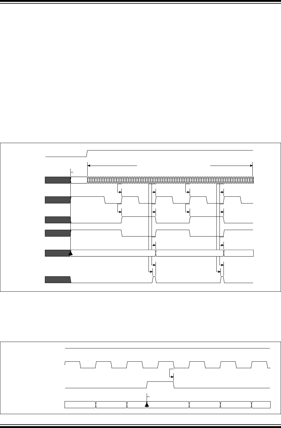
PIC32 Family Reference Manual
DS61125F-page 29-18 © 2007-2012 Microchip Technology Inc.
29.3.8 Synchronization
The RTCC module provides a single RTCSYNC bit (RTCCON<2>) that the user must use to
determine when it is safe to read and update the time and date registers. In addition, the RTCC
module provides synchronization for reset conditions (i.e., a write to the seconds bit fields
(RTCTIME<14:8>)), and for the ON bit (RTCCON<15>).
29.3.8.1 RTCSYNC BIT GENERATION
The RTCSYNC bit is a read-only bit that is set when ON = 1 and the RTCC Prescaler counter
equals 0x7FE0 (32 clocks away from a one-second rollover). Logic clears the RTCSYNC bit for
any of the following conditions:
•On a Power-on Reset (POR)
•Whenever the ON bit=0
• On a write to the seconds bit fields (RTCTIME<14:8>)
•On the rising edge of the RTCC clock, when the prescaler is 0x0000
The RTCSYNC bit timings are illustrated in Figure 29-5.
Figure 29-5: RTCSYNC Timing
29.3.8.2 PRESCALER RESET SYNCHRONIZATION
A write to the seconds bit fields (RTCTIME<14:8>) asynchronously resets the RTCC Prescaler
(including the HALFSEC bit (RTCCON<1>)). The Reset remains active until a falling edge of the
RTCC clock is detected, as illustrated in Figure 29-6.
Figure 29-6: Prescaler Synchronization to SECONDS Register Write
0x000
BCD: 00 BCD: 01 BCD: 02
Write to SECONDS register
Prescaler<13:0> = 0x3FE0
RolloverRolloverRolloverRollover
Increments on rising edge of RTCCLK
ON bit
RTCC Prescaler
Half-second Clock
HALFSEC bit
Seconds Clock
Seconds bit fields
RTCSYNC
Prescaler<13:0> = 0x3FE0
(RTCCON<1>)
(RTCCON<15>)
(RTCTIME<14:8>)
(RTCCON<2>)
0x0000
Write to seconds bit fields (RTCTIME<14:8>)
Reset resynchronized to falling edge
ON bit
RTCC Clock
Internal Prescaler Reset
RTCC Prescaler
(RTCCON<15>)
of the RTCC clock

© 2007-2012 Microchip Technology Inc. DS61125F-page 29-19
Section 29. Real-Time Clock and Calendar (RTCC)
Real-Time Clock and
Calendar (RTCC)
29
29.3.8.3 MASKING OFF THE RTCC CLOCK
To m as k o ff th e RTC C c lo ck, set t he O N b it (RTCC ON< 15> ) t o ‘ 0’. Stopping the RTCC clock
does not affect reading and writing registers from the peripheral bus interface.
29.3.9 Write Lock
In order to perform a write to any of the RTCC timer registers, the RTCWREN bit (RTCCON<3>)
must be set. Setting of the RTCWREN bit is only allowed once the device level unlocking
sequence has been executed. The unlocking sequence is as follows:
1. Load 0xAA996655 to CPU register X.
2. Load 0x556699AA to CPU register Y.
3. Load 0x00000008 to CPU register Z (the RTCWREN bit number).
4. Suspend or disable all Initiators that can access the Peripheral Bus and interrupt the
unlock sequence. (i.e., DMA and Interrupts).
5. Store CPU register X to SYSKEY.
6. Store CPU register Y to SYSKEY.
7. Store CPU register Z to RTCCONSET.
8. Re-enable DMA and interrupts.
See Example 29-3 for an assembly language implementation of the Write Unlock operation.
Example 29-3: Write Unlock Sequence
Note: Steps 5 through 7 must be followed exactly to unlock RTCC write operations. If the
sequence is not followed exactly, the RTCWREN bit will not be set.
Note: To avoid accidental writes to the RTCC time values, it is recommended that the
RTCWREN bit (RTCCON<3>) is kept clear at any other time. For RTCWREN bit to
be set, there is only one instruction cycle time window allowed between the key1,
key2 sequence and the setting of RTCWREN bit. Therefore, it is recommended to
follow the code in Example 29-3.
# assume interrupts are disabled
# assume the DMA controller is suspended
# assume the device is locked
#starting critical sequence
SYSKEY = 0xaa996655; // write first unlock key to SYSKEY
SYSKEY = 0x556699aa; // write second unlock key to SYSKEY
RTCCONSET = 0x8; // set RTCWREN in RTCCONSET
#end critical sequence
# re-enable interrupts
# re-enable the DMA controller

PIC32 Family Reference Manual
DS61125F-page 29-20 © 2007-2012 Microchip Technology Inc.
29.3.10 Calibration
The real-time crystal input can be calibrated using the periodic auto-adjust feature. When
properly calibrated, the RTCC can provide an error of less than 0.66 seconds per month.
Calibration has the ability to eliminate an error of up to 260 ppm.
The calibration is accomplished by finding the number of error clock pulses and writing this value
into the calibration bit fields (RTCCON<9:0>). This 10-bit signed value will be either added or
subtracted from the RTCC timer once every minute. Use the following procedure for RTCC
calibration:
1. Using another timer resource on the device, the user must find the error of the 32.768 kHz
crystal.
2. Once the error is known, it must be converted to the number of error clock pulses per
minute, as shown in Equation 29-1.
Equation 29-1: Calculating Error Clocks Per Minute
3. Based on the result from step 2, the following options are available:
a) If the oscillator is faster than ideal (negative result from step 2), the calibration bit
fields (RTCCON<9:0>) value needs to be negative. This causes the specified number
of clock pulses to be subtracted from the timer counter once every minute.
b) If the oscillator is slower than ideal (positive result from step 2), the calibration bit
fields (RTCCON<9:0>) value needs to be positive. This causes the specified number
of clock pulses to be added to the timer counter once every minute.
4. Load the calibration bit fields (RTCCON<9:0>) with the correct value.
Writes to the calibration bit fields (RTCCON<9:0>) should only occur when the timer is turned off,
or immediately after the rising edge of the seconds pulse (except when the seconds bit fields
(RTCTIME<14:8>) are 0x00, due to the possibility of the auto-adjust event).
Example 29-4: Updating the RTCC Calibration Value
Notes: It is up to the user to include in the error value the initial error of the crystal, drift due
to temperature, and drift due to crystal aging.
A write to the SECONDS register resets the state of calibration (not its value). If an
adjustment just occurred, it will occur again because of the minute rollover.
(Ideal Frequency (32,758) – Measured Frequency) * 60 = Error Clocks per Minute
/* The following code example will update the RTCC calibration. */
int cal=0x3FD; // 10 bits adjustment, -3 in value
if(RTCCON&0x8000)
{ // RTCC is ON
unsigned intt0, t1;
do
{
t0=RTCTIME;
t1=RTCTIME;
}while(t0!=t1); // read valid time value
if((t0&0xFF)==00)
{ // we're at second 00, wait auto-adjust to be performed
while(!(RTCCON&0x2)); // wait until second half...
}
}
RTCCONCLR=0x03FF0000; // clear the calibration
RTCCONSET=cal;

© 2007-2012 Microchip Technology Inc. DS61125F-page 29-21
Section 29. Real-Time Clock and Calendar (RTCC)
Real-Time Clock and
Calendar (RTCC)
29
29.4 ALARM
The RTCC module provides an alarm function with the following features:
•Configurable from a half-second to one year
•Enabled using the ALRMEN bit (RTCALRM<15>)
•One-time alarm, repeat alarms, and indefinite repetition of the alarm
29.4.1 Configuring the Alarm
The alarm feature is enabled using the ALRMEN bit.
The interval selection is made based on the settings of the Alarm Mask bits, AMASK<3:0> (RTC-
ALRM<11:8>). The AMASK<3:0> bits determine which and how many digits of the alarm must
match the clock value for the alarm to occur, as illustrated in Figure 29-7.
29.4.1.1 CONFIGURING THE ONE-TIME ALARM
When the alarm is issued, with the ARPT bit = 0 (RTCALRM<7:0>) and the CHIME bit = 0 (RTC-
ALRM<14>), the ALRMEN bit automatically clears.
Example 29-5: Configuring the RTCC for a One-Time One-Per-Day Alarm
29.4.1.2 CONFIGURING THE REPEAT ALARM
In addition to providing a one-time alarm, the RTCC module can be configured to repeat the alarm
at a preconfigured interval. The ARPT<7:0> bits (RTCALRM<7:0>) contain the number of times
the alarm repeats after the alarm is enabled. When ARPT<7:0> = 0 and CHIME = 0, the repeat
function is disabled and only a single alarm pulse will be produced. The alarm can be generated
up to 256 times by setting ARPT<7:0> = 0xFF.
Each time, after the alarm is issued, the ARPT<7:0> bits are decremented by one. Once they
reaches ‘0’, the alarm will be generated one last time; after which point, ALRMEN bit is cleared
automatically and the alarm will turn off.
Note: Once the timer value reaches the alarm setting, one RTCC clock period will elapse
prior to setting the alarm interrupt. The result is that, for a short period, the user will
see the timer value at the alarm setting without the interrupt having occurred.
/*
The following code example will update the RTCC one-time alarm.
Assumes the interrupts are disabled.
*/
unsigned long alTime=0x16153300;// set time to 04 hr, 15 min, 33 sec
unsigned long alDate=0x06102705;// set date to Friday 27 Oct 2006
// turn off the alarm, chime and alarm repeats; clear
// the alarm mask
while(RTCALRM&0x1000); // wait ALRMSYNC to be off
RTCALRMCLR=0xCFFF; // clear ALRMEN, CHIME, AMASK and ARPT;
ALRMTIME=alTime;
ALRMDATE=alDate; // update the alarm time and date
RTCALRMSET=0x8000|0x00000600; // re-enable the alarm, set alarm mask at once per day

PIC32 Family Reference Manual
DS61125F-page 29-22 © 2007-2012 Microchip Technology Inc.
Example 29-6: Configuring the RTCC for a Ten-Times One-Per-Hour Alarm
29.4.1.3 CONFIGURING THE INDEFINITE ALARM
To p rov id e an ind ef ini te rep et it io n of the a larm, the Chime feature can be enabled using the
CHIME bit (RTCALRM<14>). When CHIME = 1, rather than disabling the alarm when the last
repeat has been performed, the ARPT<7:0> bits (RTCALRM<7:0>) rollover from 0x00 to 0xFF
and continue counting indefinitely.
Example 29-7: Configuring the RTCC for Indefinite One-Per-Day Alarm
/*
The following code example will update the RTCC repeat alarm.
Assumes the interrupts are disabled.
*/
unsigned long alTime=0x23352300; // set time to 23hr, 35 min, 23 sec
unsigned long alDate=0x06111301; // set date to Monday 13 Nov 2006
// turn off the alarm, chime and alarm repeats; clear
// the alarm mask
while(RTCALRM&0x1000); // wait ALRMSYNC to be off
RTCALRMCLR=0xCFFF; // clear the ALRMEN, CHIME, AMASK and ARPT;
ALRMTIME=alTime;
ALRMDATE=alDate; // update the alarm time and date
RTCALRMSET=0x8000|0x0509; // re-enable the alarm, set alarm mask at once per hour
// for 10 times repeat
/*
The following code example will update the RTCC indefinite alarm.
Assumes the interrupts are disabled.
*/
unsigned long alTime=0x23352300; // set time to 23hr, 35 min, 23 sec
unsigned long alDate=0x06111301; // set date to Monday 13 Nov 2006
// turn off the alarm, chime and alarm repeats; clear
// the alarm mask
while(RTCALRM&0x1000); // wait ALRMSYNC to be off
RTCALRMCLR=0xCFFF; // clear ALRMEN, CHIME, AMASK, ARPT;
ALRMTIME=alTime;
ALRMDATE=alDate; // update the alarm time and date
RTCALRMSET=0xC600; // re-enable the alarm, set alarm mask at once per
// hour, enable CHIME
© 2007-2012 Microchip Technology Inc. DS61125F-page 29-23
Section 29. Real-Time Clock and Calendar (RTCC)
Real-Time Clock and
Calendar (RTCC)
29
Figure 29-7: Alarm Mask Settings
Note 1: Annually, except when configured for February 29 (leap year).
s
ss
mss
mm s s
hh mm ss
dhhmmss
dd hh mm ss
mm d d h h mm s s
Day of the
Week Month Day Hours Minutes Seconds
Alarm Mask Setting
AMASK<3:0>
0000 – Every half second
0001 – Every second
0010 – Every 10 seconds
0011 – Every minute
0100 – Every 10 minutes
0101 – Every hour
0110 – Every day
0111 – Every week
1000 – Every month
1001 – Every year(1)

PIC32 Family Reference Manual
DS61125F-page 29-24 © 2007-2012 Microchip Technology Inc.
29.4.2 Alarm Interrupt
The alarm event is generated when the RTCC timer matches the alarm registers. The match
must only occur on the unmasked portion of the time/date registers, according to the settings of
the AMASK<3:0> bits (RTCALRM<11:8>), as illustrated in Figure 29-7.
At every alarm event, an interrupt is generated. In addition, an alarm pulse output is provided that
operates at half the frequency of the alarm. This output is completely synchronous to the RTCC
clock and can be used as a trigger clock to other peripherals. This output is available on the
RTCC pin. The output pulse is a clock with a 50% duty cycle and a frequency half that of the
alarm event, as illustrated in Figure 29-8. The alarm must be enabled for the pulse to be active,
by setting the ALRMEN bit (RTCALRM<15>) = 1. The initial value of the alarm pulse at the RTCC
output pin is programmable using the PIV bit (RTCALRM<13>).
The RTCC pin is also capable of outputting the seconds clock. The user can select between the
alarm pulse, which is generated by the RTCC module, or the seconds clock output. The
RTSECSEL bit (RTCCON<7>) selects between these two outputs. When RTSECSEL = 0, the
alarm pulse is selected. When RTSECSEL = 1, the seconds clock is selected, as illustrated in
Figure 29-9. Depending on the device, the RTCC pin can also output the RTCC clock, showing
the exact clock the RTCC is using going into the prescaler.
Figure 29-8: Alarm Event Generation
Figure 29-9: Alarm Pulse Generation
Note: Changing any of the alarm time, date and alarm registers, other than the RTCOE
bit (RTCCON<0>) while the alarm is enabled (ALRMEN = 1), can result in a false
alarm event leading to a false alarm interrupt. To avoid a false alarm event and to
perform a safe write to the alarm registers, the timer and alarm values should only
be changed while the RTCC is disabled (RTCCON<15> = 0), or when the
ALRMSYNC bit (RTCALRM<12>) = 0.
0x7FFE 0x7FFF 0x0000 0x0001 0x0002
10:14:59 10:15:00
0b0110 (once a day)
10:15:00
RTCC Clock
Half-second Clock
Seconds Clock
RTCC Prescaler
RTCC Time
AMASK<3:0>
Alarm Time
RTCC Alarm Event
ON bit
ALRMEN bit
RTCC Alarm Event
RTCC Pin
(RTCCON<15>)
(RTCALRM<15>)

© 2007-2012 Microchip Technology Inc. DS61125F-page 29-25
Section 29. Real-Time Clock and Calendar (RTCC)
Real-Time Clock and
Calendar (RTCC)
29
29.5 INTERRUPTS
The RTCC module has the ability to generate interrupts reflecting the alarm event that occurs
when the RTCC timer matches the alarm registers. The match occurs on the unmasked portion
of the time/date registers according to the settings of the AMASK<3:0> bits.
At every alarm event, an interrupt can be generated. The alarm interrupt is signalled by the
RTCCIF bit. This interrupt flag must be cleared in software. To enable the RTCC interrupts, use
the respective RTCC interrupt enable bit, RTCCIE. The interrupt priority level bits, RTCCIP<2:0>,
and the interrupt subpriority level bits, RTCCIS<1:0>, must also be configured.
For more information, refer to the “Interrupts” chapter in the specific device data sheet and
Section 8. “Interrupts” (DS61108) in the “PIC32 Family Reference Manual” for details on these
bits and their actual register locations.
29.5.1 Interrupt Configuration
The RTCC module has one dedicated interrupt flag bit, RTCCIF, and a corresponding interrupt
enable/mask bit, RTCCIE. RTCCIE is used to enable or disable the RTCC interrupt source.
There is one specific RTCC interrupt vector.
The RTCCIF bit is set when the RTCC alarm registers match the RTCC time registers. The
RTCCIF bit will be set without regard to the state of the corresponding enable bit. The RTCCIF
bit can be polled by software if desired.
The RTCCIE bit is used to define the behavior of the Interrupts module when the corresponding
RTCCIF bit is set. When the RTCCIE bit is clear, the Interrupts module does not generate a CPU
interrupt for the event. If the RTCCIE bit is set, the Interrupts module will generate an interrupt to
the CPU when the RTCCIF bit is set (subject to the priority and subpriority as outlined in the
following paragraphs).
It is the responsibility of the user’s software routine that services a particular interrupt to clear the
appropriate interrupt flag bit before the service routine is complete.
The priority of the RTCC peripheral can be set with the RTCCIP<2:0> bits (IPC8<28:26>). This
priority defines the priority group to which the interrupt source will be assigned. The priority
groups range from a value of 7 (the highest priority) to a value of 0 (which does not generate an
interrupt). An interrupt being serviced will be preempted by an interrupt in a higher priority group.
The subpriority bits allow setting the priority of an interrupt source within a priority group. The
values of the subpriority RTCCIS<1:0> bits, which range from 3 (the highest priority) to 0 (the
lowest priority). An interrupt within the same priority group, but having a higher subpriority value,
will not preempt a lower subpriority interrupt that is in progress.
The priority group and subpriority bits allow more than one interrupt source to share the same
priority and subpriority. If simultaneous interrupts occur in this configuration, the natural order of
the interrupt sources within a priority/subpriority group pair determine the interrupt generated.
The natural priority is based on the vector numbers of the interrupt sources. The lower the vector
number the higher the natural priority of the interrupt. Any interrupts that were overridden by
natural order will then generate their respective interrupts based on priority, subpriority, and
natural order after the interrupt flag for the current interrupt is cleared.
After an enabled interrupt is generated, the CPU will jump to the vector assigned to that interrupt.
The vector number for the interrupt is the same as the natural order number. The CPU will then
begin executing code at the vector address. The user’s code at this vector address should
perform any application specific operations and clear the RTCCIF interrupt flag, and then exit.
Refer to the vector address table details in Section 8. “Interrupts” (DS61108) for more
information on interrupts.

PIC32 Family Reference Manual
DS61125F-page 29-26 © 2007-2012 Microchip Technology Inc.
Example 29-8: RTCC Initialization with Interrupts Enabled Code Example
Example 29-9: RTCC ISR Code Example
/*
The following code example illustrates an RTCC initialization with interrupts enabled.
When the RTCC alarm interrupt is generated, the cpu will jump to the vector assigned to
RTCC interrupt.
*/
/*// assume RTCC write is enabled i.e. RTCWREN (RTCCON<3>) =1;*/
IEC1CLR=0x00008000; // disable RTCC interrupts
RTCCONCLR=0x8000; // turn off the RTCC
while(RTCCON&0x40); // wait for clock to be turned off
IFS1CLR=0x00008000; // clear RTCC existing event
IPC8CLR=0x1f000000; // clear the priority
IPC8SET=0x0d000000; // Set IPL=3, subpriority 1
IEC1SET=0x00008000; // Enable RTCC interrupts
RTCTIME=0x16153300; // safe to update time to 16 hr, 15 min, 33 sec
RTCDATE=0x06102705; // update the date to Friday 27 Oct 2006
RTCALRMCLR=0xCFFF; // clear ALRMEN, CHIME, AMASK and ARPT;
ALRMTIME=0x16154300; // set alarm time to 16 hr, 15 min, 43 sec
ALRMDATE=0x06102705; // set alarm date to Friday 27 Oct 2006
RTCALRMSET=0x8000|0x00000600; // re-enable the alarm, set alarm mask at once per day
RTCCONSET=0x8000; // turn on the RTCC
while(!(RTCCON&0x40)); // wait for clock to be turned on
/*
The following code example demonstrates a simple interrupt service routine for RTCC
interrupts. The user’s code at this vector should perform any application specific
operations and must clear the RTCC interrupt flag before exiting.
*/
void__ISR(_RTCC_VECTOR, ipl3) __RTCCInterrupt(void)
{
// ... perform application specific operations
// in response to the interrupt
IFS1CLR=0x00008000; // be sure to clear RTCC interrupt flag
// before exiting the service routine.
}
Note: The RTCC ISR code example shows MPLAB® C32 C compiler specific syntax.
Refer to your compiler manual regarding support for ISRs.

© 2007-2012 Microchip Technology Inc. DS61125F-page 29-27
Section 29. Real-Time Clock and Calendar (RTCC)
Real-Time Clock and
Calendar (RTCC)
29
29.6 OPERATION IN POWER-SAVING MODES
29.6.1 RTCC Operation in Sleep Mode
When the device enters Sleep mode, the system clock is disabled. The RTCC and alarm
continue to operate while in Sleep mode. The operation of the alarm is not affected by Sleep. An
alarm event can wake-up the CPU if the alarm interrupt has a higher priority than the current
CPU IPL.
29.6.2 RTCC Operation in Deep Sleep Mode
When the device enters Deep Sleep mode, the system clock is disabled. The RTCC and alarm
continue to operate while in Deep Sleep. An alarm event can wake the CPU.
The alarm interrupt cannot be masked in Deep Sleep mode; therefore, it will wake the CPU when
it triggers.
29.6.3 RTCC Operation in VBAT Mode
In PIC32 devices with VBAT power-saving features, the RTCC module is capable of continued
operation during VBAT mode. While the alarm still functions, it will not wake the device. While in
VBAT mode, the RTCC clock source selected by the RTCCLKSEL<1:0> bits (RTCCON<10:9>)
remains active.
Power must be applied to the VBAT pin for the RTCC module to continue operation. Refer to the
“Power-Saving Features” chapter in the specific device data sheet and Section 10.
“Power-Saving Modes” (DS61130) in the “PIC32 Family Reference Manual” for details.
29.6.4 RTCC Operation in Idle Mode
When the device enters Idle mode, the system clock sources remain functional. The RTCC and
alarm continue to operate while in Idle mode. The operation of the alarm is not affected by Idle.
An alarm event can wake-up the CPU if the alarm interrupt has a higher priority than the current
CPU IPL.
The SIDL bit (RTCCON<13>) selects Idle mode behavior:
•If SIDL = 1, the PBCLK to the RTCC will be disabled
The PBCLK is the clock source for the AMASK bits (RTCALRM<11:8>), CHIME bit
(RTCALRM<14>), ALRMTIME, ALRMDATE and all of the synchronizers that provide the
read data for RTCTIME, and some other bits such as, ALRMSYNC (RTCALRM<12>),
ALRMEN (RTCALRM<15>) and RTCSYNC (RTCCON<2>). Therefore, the SIDL functional-
ity can be used to reduce the RTCC power consumption without affecting the functionality
of the RTCC module.
•If SIDL = 0, the module will continue normal operation in Idle mode
Note: Not all power-saving modes are available on all devices. Refer to the
“Power-Saving Features” chapter in the specific device data sheet for availability.

PIC32 Family Reference Manual
DS61125F-page 29-28 © 2007-2012 Microchip Technology Inc.
29.7 EFFECTS OF VARIOUS RESETS
29.7.1 Device Reset
When a device Reset occurs, the RTCALRM register is forced to its reset state, causing the
alarm to be disabled (if enabled prior to the reset). However, note that if the RTCC is enabled, it
will continue to operate when a device Reset occurs.
29.7.2 Power-on Reset
The RTCTIME and RTCDATE registers are not affected by a Power-on Reset (POR). A POR
forces the device to its inactive state. Once the device exits the POR state, the clock registers
should be reloaded with the desired values.
The timer prescaler values can only be reset by writing to the seconds bit fields
(RTCTIME<14:8>). No device Reset can affect the prescalers.
29.7.3 Watchdog Timer Reset
The Watchdog Timer Reset is equivalent to the device Reset.
29.7.4 Effects of the ON Bit
When the ON bit = 0 (RTCCON<15>), the RTCSYNC (RTCCON<2>), HALFSEC
(RTCCON<1>) and ALRMSYNC bits (RTCALRM<4>) are asynchronously reset and held in
reset. Also, the RTCC pin output is determined by the RTCOE bit (RTCCON<0>), which is
masked by the ON bit.
29.7.5 MCLR Reset
The RTCC module and the Secondary Oscillator (SOSC) will continue to function when the device
is held under reset by pulling the MCLR pin low.

© 2007-2012 Microchip Technology Inc. DS61125F-page 29-29
Section 29. Real-Time Clock and Calendar (RTCC)
Real-Time Clock and
Calendar (RTCC)
29
29.8 RELATED APPLICATION NOTES
This section lists application notes that are related to this section of the manual. These
application notes may not be written specifically for the PIC32 device family, but the concepts are
pertinent and could be used with modification and possible limitations. The current application
notes related to the Real-Time Clock and Calendar (RTCC) module are:
Title Application Note #
No related application notes at this time N/A
Note: Visit the Microchip web site (www.microchip.com) for additional application notes
and code examples for the PIC32 family of devices.

PIC32 Family Reference Manual
DS61125F-page 29-30 © 2007-2012 Microchip Technology Inc.
29.9 REVISION HISTORY
Revision A (October 2007)
This is the initial released version of the document.
Revision B (October 2007)
Updated document to remove Confidential status.
Revision C (April 2008)
Revised status to Preliminary; Revised U-0 to r-x.
Revision D (June 2008)
Revised Registers 29-1, bit 14; Revised Registers 29-26, 29-27, Footnote; Revised Examples
29-1 and 29-9; Change Reserved bits from “Maintain as” to “Write”; Added Note to ON bit
(RTCCON Register).
Revision E (December 2010)
This revision includes the following changes:
•Sections:
- Updated 29.7 “Effects of Various Resets” with the following point:
The RTCC and the Secondary Oscillator (SOSC) will continue to function when the
device is held under reset by pulling the MCLR pin low.
-Removed 29.9 “I/O Pin Control”.
•Notes:
- Added a Note at the beginning of the section, which provides information on
complementary documentation.
• Registers:
- Revised Register 29-1 through Register 29-6
- All SET, CLR, and INV registers were removed
-The IFS1, IEC1, and IPC8 registers were removed
•Minor changes to the text and formatting have been incorporated throughout the document
Revision F (August 2012)
This revision includes the following updates:
•The list of features were updated (see 29.1 “Introduction”)
•The RTCC block diagram was updated (see Figure 29-1)
•The RTCOUTSEL<1:0> and RTCCLKSEL<1:0> bits were added and the FRZ bit was
removed (see Tab le 29 -1 and Register 29-1)
•29.3.3 “Clock Source”was updated
•29.4.2 “Alarm Interrupt”was updated
•29.5 “Interrupts” was updated
•29.6.2 “RTCC Operation in Deep Sleep Mode” was added
•29.6.3 “RTCC Operation in VBAT Mode” was added
•29.6.3 “RTCC Operation in Debug Mode” was removed
•29.8 “Peripherals Using the RTCC Module” was removed
• 29.9 “Design Tips” was removed
•Minor updates to text and formatting were incorporated throughout the document

2007-2012 Microchip Technology Inc. DS61125F-page 29-31
Information contained in this publication regarding device
applications and the like is provided only for your convenience
and may be superseded by updates. It is your responsibility to
ensure that your application meets with your specifications.
MICROCHIP MAKES NO REPRESENTATIONS OR
WARRANTIES OF ANY KIND WHETHER EXPRESS OR
IMPLIED, WRITTEN OR ORAL, STATUTORY OR
OTHERWISE, RELATED TO THE INFORMATION,
INCLUDING BUT NOT LIMITED TO ITS CONDITION,
QUALITY, PERFORMANCE, MERCHANTABILITY OR
FITNESS FOR PURPOSE. Microchip disclaims all liability
arising from this information and its use. Use of Microchip
devices in life support and/or safety applications is entirely at
the buyer’s risk, and the buyer agrees to defend, indemnify and
hold harmless Microchip from any and all damages, claims,
suits, or expenses resulting from such use. No licenses are
conveyed, implicitly or otherwise, under any Microchip
intellectual property rights.
Trademarks
The Microchip name and logo, the Microchip logo, dsPIC,
KEELOQ, KEELOQ logo, MPLAB, PIC, PICmicro, PICSTART,
PIC32 logo, rfPIC and UNI/O are registered trademarks of
Microchip Technology Incorporated in the U.S.A. and other
countries.
FilterLab, Hampshire, HI-TECH C, Linear Active Thermistor,
MXDEV, MXLAB, SEEVAL and The Embedded Control
Solutions Company are registered trademarks of Microchip
Technology Incorporated in the U.S.A.
Analog-for-the-Digital Age, Application Maestro, chipKIT,
chipKIT logo, CodeGuard, dsPICDEM, dsPICDEM.net,
dsPICworks, dsSPEAK, ECAN, ECONOMONITOR,
FanSense, HI-TIDE, In-Circuit Serial Programming, ICSP,
Mindi, MiWi, MPASM, MPLAB Certified logo, MPLIB,
MPLINK, mTouch, Omniscient Code Generation, PICC,
PICC-18, PICDEM, PICDEM.net, PICkit, PICtail, REAL ICE,
rfLAB, Select Mode, Total Endurance, TSHARC,
UniWinDriver, WiperLock and ZENA are trademarks of
Microchip Technology Incorporated in the U.S.A. and other
countries.
SQTP is a service mark of Microchip Technology Incorporated
in the U.S.A.
All other trademarks mentioned herein are property of their
respective companies.
© 2007-2012, Microchip Technology Incorporated, Printed in
the U.S.A., All Rights Reserved.
Printed on recycled paper.
ISBN: 978-1-62076-469-5
Note the following details of the code protection feature on Microchip devices:
• Microchip products meet the specification contained in their particular Microchip Data Sheet.
• Microchip believes that its family of products is one of the most secure families of its kind on the market today, when used in the
intended manner and under normal conditions.
• There are dishonest and possibly illegal methods used to breach the code protection feature. All of these methods, to our
knowledge, require using the Microchip products in a manner outside the operating specifications contained in Microchip’s Data
Sheets. Most likely, the person doing so is engaged in theft of intellectual property.
• Microchip is willing to work with the customer who is concerned about the integrity of their code.
• Neither Microchip nor any other semiconductor manufacturer can guarantee the security of their code. Code protection does not
mean that we are guaranteeing the product as “unbreakable.”
Code protection is constantly evolving. We at Microchip are committed to continuously improving the code protection features of our
products. Attempts to break Microchip’s code protection feature may be a violation of the Digital Millennium Copyright Act. If such acts
allow unauthorized access to your software or other copyrighted work, you may have a right to sue for relief under that Act.
Microchip received ISO/TS-16949:2009 certification for its worldwide
headquarters, design and wafer fabrication facilities in Chandler and
Tempe, Arizona; Gresham, Oregon and design centers in California
and India. The Company’s quality system processes and procedures
are for its PIC® MCUs and dsPIC® DSCs, KEELOQ® code hopping
devices, Serial EEPROMs, microperipherals, nonvolatile memory and
analog products. In addition, Microchip’s quality system for the design
and manufacture of development systems is ISO 9001:2000 certified.
QUALITYMANAGEMENT
S
YSTEM
CERTIFIEDBYDNV
== ISO/TS16949==

DS61125F-page 29-32 2007-2012 Microchip Technology Inc.
AMERICAS
Corporate Office
2355 West Chandler Blvd.
Chandler, AZ 85224-6199
Tel: 480-792-7200
Fax: 480-792-7277
Technical Support:
http://www.microchip.com/
support
Web Address:
www.microchip.com
Atlanta
Duluth, GA
Tel: 678-957-9614
Fax: 678-957-1455
Boston
Westborough, MA
Tel: 774-760-0087
Fax: 774-760-0088
Chicago
Itasca, IL
Tel: 630-285-0071
Fax: 630-285-0075
Cleveland
Independence, OH
Tel: 216-447-0464
Fax: 216-447-0643
Dallas
Addison, TX
Tel: 972-818-7423
Fax: 972-818-2924
Detroit
Farmington Hills, MI
Tel: 248-538-2250
Fax: 248-538-2260
Indianapolis
Noblesville, IN
Tel: 317-773-8323
Fax: 317-773-5453
Los Angeles
Mission Viejo, CA
Tel: 949-462-9523
Fax: 949-462-9608
Santa Clara
Santa Clara, CA
Tel: 408-961-6444
Fax: 408-961-6445
Toronto
Mississauga, Ontario,
Canada
Tel: 905-673-0699
Fax: 905-673-6509
ASIA/PACIFIC
Asia Pacific Office
Suites 3707-14, 37th Floor
Tower 6, The Gateway
Harbour City, Kowloon
Hong Kong
Tel : 8 52 -24 01- 120 0
Fax: 852-2401-3431
Australia - Sydney
Tel : 6 1- 2-9 868 -67 33
Fax: 61-2-9868-6755
China - Beijing
Tel : 8 6- 10- 856 9-7 00 0
Fax: 86-10-8528-2104
China - Chengdu
Tel : 8 6- 28- 866 5-5 511
Fax: 86-28-8665-7889
China - Chongqing
Tel : 8 6- 23- 898 0-9 58 8
Fax: 86-23-8980-9500
China - Hangzhou
Tel : 8 6- 571 -28 19- 318 7
Fax: 86-571-2819-3189
China - Hong Kong SAR
Tel : 8 52 -24 01- 120 0
Fax: 852-2401-3431
China - Nanjing
Tel : 8 6- 25- 847 3-2 46 0
Fax: 86-25-8473-2470
China - Qingdao
Tel : 8 6- 532 -85 02- 735 5
Fax: 86-532-8502-7205
China - Shanghai
Tel : 8 6- 21- 540 7-5 53 3
Fax: 86-21-5407-5066
China - Shenyang
Tel : 8 6- 24- 233 4-2 82 9
Fax: 86-24-2334-2393
China - Shenzhen
Tel : 8 6- 755 -82 03- 266 0
Fax: 86-755-8203-1760
China - Wuhan
Tel : 8 6- 27- 598 0-5 30 0
Fax: 86-27-5980-5118
China - Xian
Tel : 8 6- 29- 883 3-7 25 2
Fax: 86-29-8833-7256
China - Xiamen
Tel: 86-592-2388138
Fax: 86-592-2388130
China - Zhuhai
Tel : 86- 75 6-3 21 004 0
Fax: 86-756-3210049
ASIA/PACIFIC
India - Bangalore
Tel : 9 1- 80- 309 0-4 44 4
Fax: 91-80-3090-4123
India - New Delhi
Tel : 9 1- 11- 416 0 -8 631
Fax: 91-11-4160-8632
India - Pune
Tel : 9 1- 20- 256 6-1 51 2
Fax: 91-20-2566-1513
Japan - Osaka
Tel : 8 1- 66- 152 -71 60
Fax: 81-66-152-9310
Japan - Yokohama
Tel : 8 1- 45- 471 - 6 16 6
Fax: 81-45-471-6122
Korea - Daegu
Tel : 8 2- 53- 744 -43 01
Fax: 82-53-744-4302
Korea - Seoul
Tel : 8 2- 2-5 54- 72 0 0
Fax: 82-2-558-5932 or
82-2-558-5934
Malaysia - Kuala Lumpur
Tel : 6 0- 3-6 201 -9 8 57
Fax: 60-3-6201-9859
Malaysia - Penang
Tel : 6 0- 4-2 27- 88 7 0
Fax: 60-4-227-4068
Philippines - Manila
Tel : 6 3- 2-6 34- 90 6 5
Fax: 63-2-634-9069
Singapore
Tel : 6 5- 633 4-8 870
Fax: 65-6334-8850
Taiwan - Hsin Chu
Tel : 8 86 -3- 577 8-3 66
Fax: 886-3-5770-955
Taiwan - Kaohsiung
Tel : 8 86 -7- 536 -48 18
Fax: 886-7-330-9305
Taiwan - Taipei
Tel : 8 86 -2- 250 0-6 61 0
Fax: 886-2-2508-0102
Thailand - Bangkok
Tel : 6 6- 2-6 94- 13 5 1
Fax: 66-2-694-1350
EUROPE
Austria - Wels
Tel : 4 3- 72 42 -2 244 -3 9
Fax: 43-7242-2244-393
Denmark - Copenhagen
Tel : 4 5- 445 0-2 828
Fax: 45-4485-2829
France - Paris
Tel : 3 3- 1-6 9-5 3-6 3-2 0
Fax: 33-1-69-30-90-79
Germany - Munich
Tel : 4 9- 89 -62 7-1 44- 0
Fax: 49-89-627-144-44
Italy - Milan
Tel : 3 9- 03 31 -7 426 11
Fax: 39-0331-466781
Netherlands - Drunen
Tel : 3 1- 41 6- 690 399
Fax: 31-416-690340
Spain - Madrid
Tel : 3 4- 91 -70 8-0 8-9 0
Fax: 34-91-708-08-91
UK - Wokingham
Tel : 4 4- 118 -92 1- 5 869
Fax: 44-118-921-5820
Worldwide Sales and Service
11/29/11

© 2007-2013 Microchip Technology Inc. DS60001117H-page 31-1
DMA Controller
31
Section 31. DMA Controller
HIGHLIGHTS
This section of the manual contains the following major topics:
31.1 Introduction.............................................................................................................. 31-2
31.2 Status and Control Registers................................................................................... 31-6
31.3 Modes of Operation ............................................................................................... 31-29
31.4 Channel Control..................................................................................................... 31-40
31.5 Interrupts................................................................................................................ 31-44
31.6 Operation in Power-Saving and Debug Modes ..................................................... 31-46
31.7 Effects of Various Resets....................................................................................... 31-46
31.8 Related Application Notes ..................................................................................... 31-47
31.9 Revision History..................................................................................................... 31-48

PIC32 Family Reference Manual
DS60001117H-page 31-2 © 2007-2013 Microchip Technology Inc.
31.1 INTRODUCTION
The Direct Memory Access (DMA) controller is a bus master module that is useful for data
transfers between different peripherals without intervention from the CPU. The source and
destination of a DMA transfer can be any of the memory-mapped modules included in the PIC32
family of devices. For example, memory, or one of the Peripheral Bus (PB) devices such as the
SPI or UART, among others.
Key features of the DMA module include:
•Depending on the device, up to eight identical channels are available, including:
- Auto-Increment Source and Destination Address registers
- Source and Destination Pointers
•Depending on the device, uninterrupted data transfers of up to 64 Kbytes are supported
•Flexible data transfer, featuring the following:
-Transfer granularity down to byte level
- Bytes need not be word-aligned at source and destination
• Fixed priority channel arbitration
•Flexible DMA channel operating modes, including:
- Manual (software) or automatic (interrupt) DMA requests
- One-Shot or Auto-Repeat Block Transfer modes
-Channel-to-channel chaining
•Flexible DMA requests, featuring:
- A DMA request can be selected from any of the peripheral interrupt sources
- Each channel can select any interrupt as its DMA request source
- A DMA transfer abort can be selected from any of the peripheral interrupt sources
- Automatic transfer termination upon a data pattern match
•Multiple DMA channel status interrupts, supplying:
- DMA channel block transfer complete
- Source empty or half-empty
-Destination full or half-full
-DMA transfer aborted due to an external event
-Invalid DMA address generated
•DMA debug support features, including:
-Most recent address accessed by a DMA channel
- Most recent DMA channel to transfer data
•CRC Generation module, featuring:
- CRC module can be assigned to any of the available channels
- Data read from the source can be reordered on some devices
-CRC module is highly configurable
-CRC calculation
Note: This family reference manual section is meant to serve as a complement to device
data sheets. Depending on the device, this manual section may not apply to all
PIC32 devices.
Please consult the note at the beginning of the “Direct Memory Access (DMA)
Controller” chapter in the current device data sheet to check whether this
document supports the device you are using.
Device data sheets and family reference manual sections are available for
download from the Microchip Worldwide Web site at: http://www.microchip.com

© 2007-2013 Microchip Technology Inc. DS60001117H-page 31-3
Section 31. DMA Controller
DMA Controller
31
These features are also available in the DMA controller:
•Different source and destination sizes
•Memory-to-memory transfers
•Memory-to-peripheral transfers
•Channel auto-enable
•Events start/stop
•Pattern match detection
•Channel chaining
31.1.1 DMA Operation
A DMA channel transfers data from a source to a destination without CPU intervention. The
source and destination start addresses define the start address of the source and destination,
respectively.
Both the source and destination have independently configurable sizes and the number of the
transferred bytes is independent of the source and destination sizes.
A transfer is initiated either by software or by an interrupt request. The user can select any
interrupt on the device to start a DMA transfer.
Upon transfer initiation, the DMA controller will perform a cell transfer (defined by the cell size
register) and the channel remains enabled until all bytes of a block (the larger of source size or
destination size) transfer is complete. When a channel is disabled, further transfers will be
prohibited until the channel is re-enabled.
The DMA channel uses separate pointers to keep track of the current word locations at the
source and destination.
Interrupts can be generated when the source/destination pointer is half of the source/destination
size, or when the source/destination counter reaches the end of the source/destination.
A DMA transfer can be aborted by the software, by a pattern match or by an interrupt event. The
transfer will also stop when an address error is detected.
Figure 31-1 shows a typical DMA transfer. The block transfer size is set by setting the Source
size (DCHxSSIZ) and Destination size (DCHxDSIZ) to 4 and 2 bytes (block size is 4). The source
(DCHxSSA) and destination (DCHxDSA) registers are then given starting address locations. The
source address is the physical SRAM location of an array named buffer. The destination address
is the physical PMDIN (PMP output buffer) memory location. The cell size (DCHxCSIZ) is also
set to 2. This means the 4 byte block transfer will take two 2 byte cell transfers to be completed.
The transfer event for the DMA is set to be a PMP write, which means when a PMP write occurs,
a cell transfer will be initiated. Notice the DMA channel can be auto-enabled by setting the
CHAEN bit to ‘1’ in the DCHxCON register. A DMA transfer can also be forced by writing a ‘1’ to
the CFORCE bit in the DCHXECON register. If the channel is auto-enabled, at the end of a block
transfer all channel registers reset to their initial set state before the initial cell transfer. If not, the
DMA channel becomes disabled.
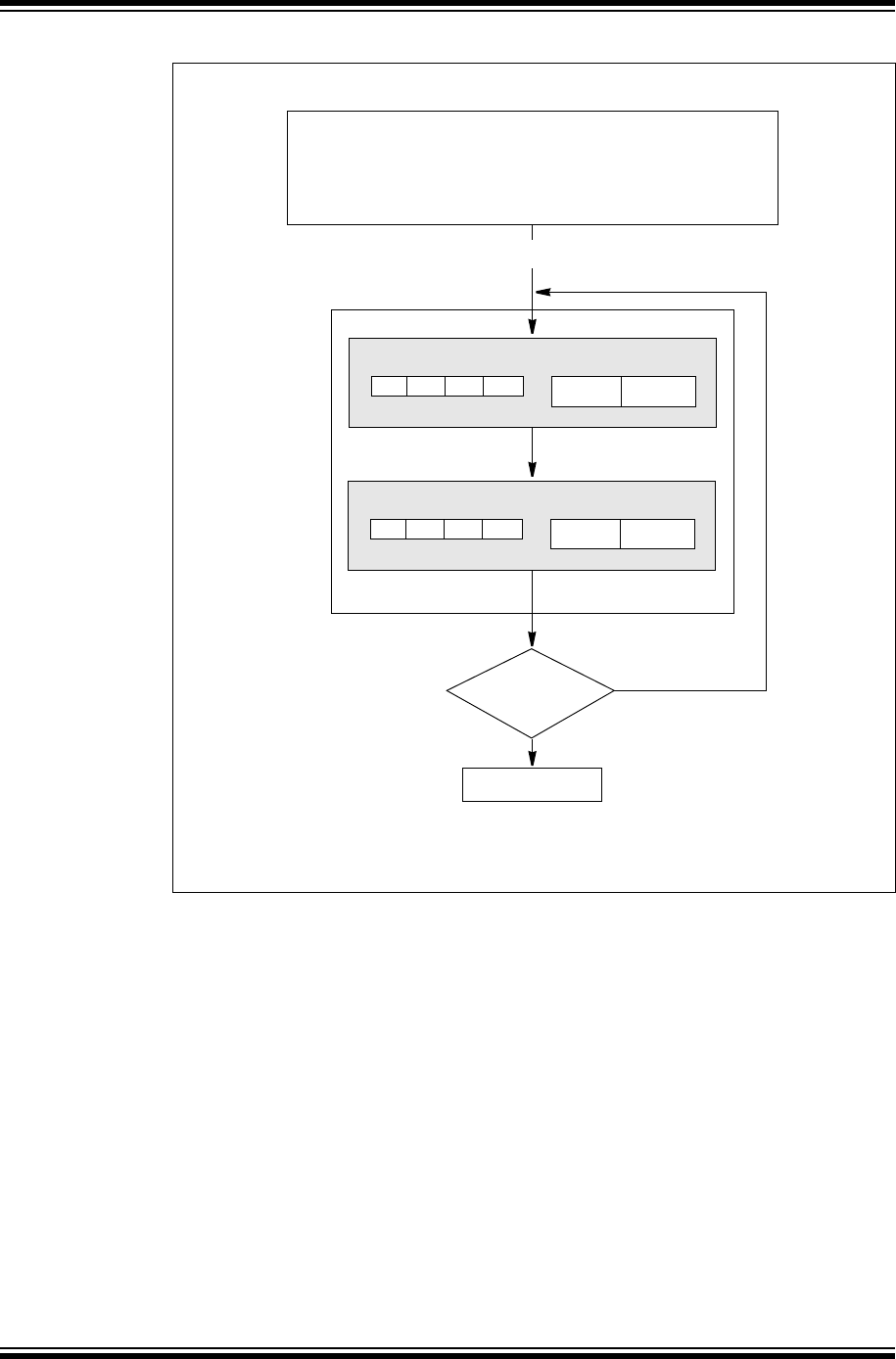
PIC32 Family Reference Manual
DS60001117H-page 31-4 © 2007-2013 Microchip Technology Inc.
Figure 31-1: Typical DMA Source to Destination Transfer Diagram
Source Size (DCHxSSIZ) = 4 bytes
Source Address (DCHxSSA) = _VirtToPhys(&Buffer[0])
Destination Size (DCHxDSIZ) = 2 bytes
Destination Address (DCHxDSA) = _VirtToPhys(&PMDIN)
Cell Size (DCHxCSIZ) = 2 bytes
Transfer Event (DCHxECON<15:8> bits (CHSIRQ<7:0>)) = PMP Write
Cell Transfer 1
PMP Write Event
PMP Write Event
Yes
No
DMA Disabled
Block Transfer
PMP
1234 12
Cell Transfer 2
PMP
SRAM
1234 34
Auto-enable
(CHAEN bit = 1)
Force (set CFORCE = 1) Transfer Event (PMP Inactive)
Note: The _VirtToPhys function is only used as an example.
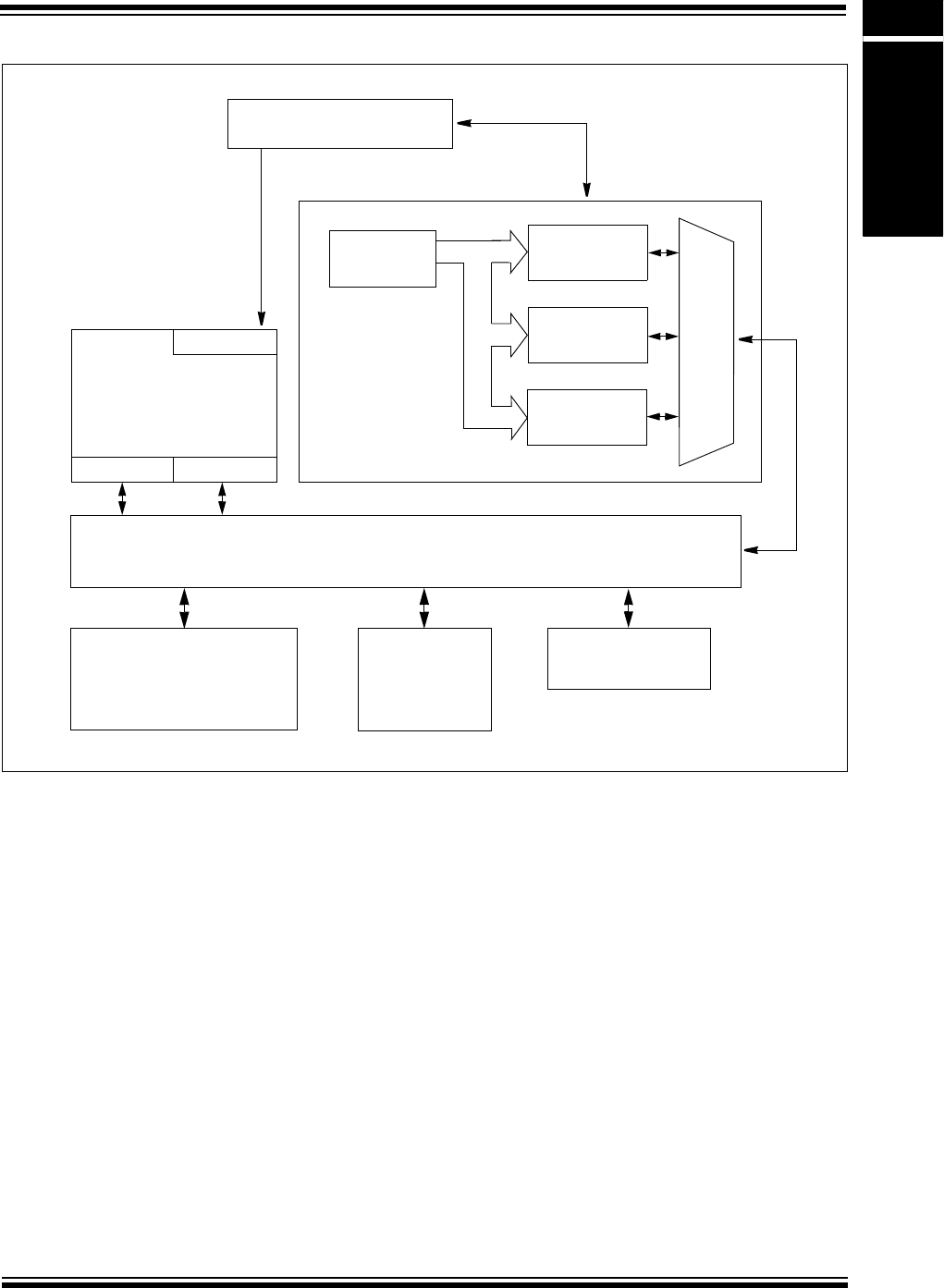
© 2007-2013 Microchip Technology Inc. DS60001117H-page 31-5
Section 31. DMA Controller
DMA Controller
31
Figure 31-2: DMA Module Block Diagram
Channel 0 Control
Channel 1 Control
Channel ‘x’ Control
SEL
SEL
Y
I0
I1
I2
In
INT
PIC32 CPU
IS DS DMA
Global Control
(DMACON)
Priority Interrupt Controller
System Bus
Flash Memory Data Ram
Peripheral
Priority Arbitration

PIC32 Family Reference Manual
DS60001117H-page 31-6 © 2007-2013 Microchip Technology Inc.
31.2 STATUS AND CONTROL REGISTERS
The DMA module consists of the following Special Function Registers (SFRs):
•DMACON: DMA Controller Control Register
This register configures the corresponding DMA channel.
•DMASTAT: DMA Status Register
This register contains the status of the last read or write transfer that occurred.
•DMAADDR: DMA Address Register
This register contains the address of the most recent DMA transfer.
•DCRCCON: DMA CRC Control Register
This register controls the CRC of the DMA and how it will function.
•DCRCDATA: DMA CRC Data Register
This register sets the initial value of the CRC generator. Writing to this register will seed the
CRC generator. Reading from this register will return the current value of the CRC.
•DCRCXOR: DMA CRCXOR Enable Register
This register provides a description of the generator polynomial for CRC calculation.
•DCHxCON: DMA Channel ‘x’ Control Register
This register controls the configuration of a specific DMA channel.
•DCHxECON: DMA Channel ‘x’ Event Control Register
This register controls the event for a specific DMA channel.
•DCHxINT: DMA Channel ‘x’ Interrupt Control Register
This register controls the DMA interrupt for a specific DMA channel.
•DCHxSSA: DMA Channel ‘x’ Source Start Address Register
This register configures the source start address for a specific DMA channel.
•DCHxDSA: DMA Channel ‘x’ Destination Start Address Register
This register configures the destination start address for a specific DMA channel.
•DCHxSSIZ: DMA Channel ‘x’ Source Size Register
This register configures the source size for a specific DMA channel.
•DCHxDSIZ: DMA Channel ‘x’ Destination Size Register
This register configures the destination size for a specific DMA channel.
•DCHxSPTR: DMA Channel ‘x’ Source Pointer Register
This register contains the address of the current location of the source for a specific DMA
channel.
•DCHxDPTR: DMA Channel ‘x’ Destination Pointer Register
This register contains the address of the current location of the destination for a specific
DMA channel.
•DCHxCSIZ: DMA Channel ‘x’ Cell Size Register
This register configures how many transfers can occur per event for a specific DMA channel.
•DCHxCPTR: DMA Channel ‘x’ Cell Pointer Register
This register counts how many transfers have occurred since the last event for a specific
DMA channel.
•DCHxDAT: DMA Channel ‘x’ Pattern Data Register
This register contains data to be matched to allow a terminate on match for a specific DMA
channel.
Note: A PIC32 device may have one or more DMA channels. An ‘x’ used in the names of
Control/Status bits and registers denotes the particular channel. Refer to the
“Direct Memory Access Controller” chapter of the specific device data sheet for
more details.

© 2007-2013 Microchip Technology Inc. DS60001117H-page 31-7
Section 31. DMA Controller
DMA Controller
31
Tabl e 31- 1 provides a brief summary of the related DMA module registers. Corresponding register tables appear after the summary, that include a detailed description of
each bit.
Table 31-1: DMA Register Summary
Name Bit
Range Bit 31/15 Bit 30/14 Bit 29/13 Bit 28/12 Bit 27/11 Bit 26/10 Bit 25/9 Bit 24/8 Bit 23/7 Bit 22/6 Bit 21/5 Bit 20/4 Bit 19/3 Bit 118/2 Bit 17/1 Bit 16/0
DMACON(1) 31:15 — — — — — — — — — — — — — — — —
15:0 — — — — — — — —ON—— SUSPEND DMABUSY
(2) — — —
DMASTAT 31:16 RDWR(2) — — — — — — — — — — — — — — —
15:0 — — — — — — — — — — — — RDWR
(2) DMACH<2:0>(2)
DMAADDR 31:16 DMAADDR<31:16>
15:0 DMAADDR<15:0>
DCRCCON(1) 31:16 ——BYTO<1:0>
(2) WBO(2) ——BITO
(2) — — — — — — — —
15:0 — — —PLEN<4:0>
(2) CRCEN CRCAPP CRCTYP(2) —— CRCCH<2:0>
(2)
DCRCDATA(1) 31:16 DCRCDATA<31:16>(2)
15:0 DCRCDATA<15:0>(2)
DCRCXOR(1) 31:16 DCRCXOR<31:16>(2)
15:0 DCRCXOR<15:0>(2)
DCHxCON(1) 31:16 CHPIGN<7:0> — — — — — — — —
15:0 CHBUSY(2) — CHPIGNEN
(2) —CHPATLEN
(2) — — CHCHNS CHEN CHAED CHCHN CHAEN — CHEDET CHPRI<1:0>
DCHxECON(1) 31:16 — — — — — — — — CHAIRQ<7:0>
15:0 CHSIRQ<7:0> CFORCE CABORT PATEN SIRQEN AIRQEN — — —
DCHxINT(1) 31:16 — — — — — — — — CHSDIE CHSHIE CHDDIE CHDHIE CHBCIE CHCCIE CHTAIE CHERIE
15:0 — — — — — — — — CHSDIF CHSHIF CHDDIF CHDHIF CHBCIF CHCCIF CHTAIF CHERIF
DCHxSSA(1) 31:16 CHSSA<31:16>
15:0 CHSSA<15:0>
DCHxDSA 31:16 CHDSA<31:16>
15:0 CHDSA<15:0>
DCHxSSIZ(1) 31:16 — — — — — — — — — — — — — — — —
15:0 CHSSIZ<15:0>(2)
DCHxDSIZ(1) 31:16 — — — — — — — — — — — — — — — —
15:0 CHDSIZ<15:0>(2)
DCHxSPTR 31:16 — — — — — — — — — — — — — — — —
15:0 CHSPTR<15:0>
Legend: — = unimplemented, read as ‘0’. Address offset values are shown in hexadecimal.
Note 1: This register has an associated Clear, Set, and Invert register at an offset of 0x4, 0x8, and 0xC bytes, respectively. These registers have the same name with CLR, SET, and INV appended to the end of
the register name (e.g., DMACONCLR). Writing a ‘1’ to any bit position in the Clear, Set, or Invert register will clear valid bits in the associated register. Reads from these registers should be ignored.
2: This bit is not available on all devices. Refer to the “Direct Memory Access (DMA) Controller” chapter in the specific device data sheet for availability.

PIC32 Family Reference Manual
DS60001117H-page 31-8 © 2007-2013 Microchip Technology Inc.
DCHxDPTR 31:16 — — — — — — — — — — — — — — — —
15:0 CHDPTR<15:0>(2)
DCHxCSIZ(1) 31:16 — — — — — — — — — — — — — — — —
15:0 CHCSIZ<15:0>(2)
DCHxCPTR 31:16 — — — — — — — — — — — — — — — —
15:0 CHCPTR<15:0>(2)
DCHxDAT(1) 31:16 — — — — — — — — — — — — — — — —
15:0 CHPDAT<15:8>(2) CHPDAT<7:0>
Table 31-1: DMA Register Summary (Continued)
Name Bit
Range Bit 31/15 Bit 30/14 Bit 29/13 Bit 28/12 Bit 27/11 Bit 26/10 Bit 25/9 Bit 24/8 Bit 23/7 Bit 22/6 Bit 21/5 Bit 20/4 Bit 19/3 Bit 118/2 Bit 17/1 Bit 16/0
Legend: — = unimplemented, read as ‘0’. Address offset values are shown in hexadecimal.
Note 1: This register has an associated Clear, Set, and Invert register at an offset of 0x4, 0x8, and 0xC bytes, respectively. These registers have the same name with CLR, SET, and INV appended to the end of
the register name (e.g., DMACONCLR). Writing a ‘1’ to any bit position in the Clear, Set, or Invert register will clear valid bits in the associated register. Reads from these registers should be ignored.
2: This bit is not available on all devices. Refer to the “Direct Memory Access (DMA) Controller” chapter in the specific device data sheet for availability.

© 2007-2013 Microchip Technology Inc. DS60001117H-page 31-9
Section 31. DMA Controller
DMA Controller
31
Register 31-1: DMACON: DMA Controller Control Register
Bit
Range
Bit
31/23/15/7
Bit
30/22/14/6
Bit
29/21/13/5
Bit
28/20/12/4
Bit
27/19/11/3
Bit
26/18/10/2
Bit
25/17/9/1
Bit
24/16/8/0
31:24 U-0 U-0 U-0 U-0 U-0 U-0 U-0 U-0
— — — — — — — —
23:16 U-0 U-0 U-0 U-0 U-0 U-0 U-0 U-0
— — — — — — — —
15:8 R/W-0 U-0 U-0 R/W-0 R/W-0 U-0 U-0 U-0
ON — — SUSPEND DMABUSY(1) — — —
7:0 U-0 U-0 U-0 U-0 U-0 U-0 U-0 U-0
— — — — — — — —
Legend:
R = Readable bit W = Writable bit U = Unimplemented bit, read as ‘0’
-n = Value at POR ‘1’ = Bit is set ‘0’ = Bit is cleared x = Bit is unknown
bit 31-16 Unimplemented: Read as ‘0’
bit 15 ON: DMA On bit
1 = DMA module is enabled
0 = DMA module is disabled
When using the 1:1 PBCLK divisor, the user’s software should not read/write the peripheral’s SFRs in the
SYSCLK cycle immediately following the instruction that clears the module’s ON bit.
bit 14-13 Unimplemented: Read as ‘0’
bit 12 SUSPEND: DMA Suspend bit
1 = DMA transfers are suspended to allow CPU uninterrupted access to data bus
0 = DMA operates normally
bit 11 DMABUSY: DMA Module Busy bit(1)
1 = DMA module is active
0 = DMA module is disabled and not actively transferring data
bit 10-0 Unimplemented: Read as ‘0’
Note 1: This bit is not available on all devices. Refer to the “Direct Memory Access (DMA) Controller” chapter
in the specific device data sheet for availability.

PIC32 Family Reference Manual
DS60001117H-page 31-10 © 2007-2013 Microchip Technology Inc.
Register 31-2: DMASTAT: DMA Status Register
Bit
Range
Bit
31/23/15/7
Bit
30/22/14/6
Bit
29/21/13/5
Bit
28/20/12/4
Bit
27/19/11/3
Bit
26/18/10/2
Bit
25/17/9/1
Bit
24/16/8/0
31:24 R-0 U-0 U-0 U-0 U-0 U-0 U-0 U-0
RDWR — — — — — — —
23:16 U-0 U-0 U-0 U-0 U-0 U-0 U-0 U-0
— — — — — — — —
15:8 U-0 U-0 U-0 U-0 U-0 U-0 U-0 U-0
— — — — — — — —
7:0 U-0 U-0 U-0 U-0 R-0 R-0 R-0 R-0
— — — —RDWR DMACH<2:0>
Legend:
R = Readable bit W = Writable bit U = Unimplemented bit, read as ‘0’
-n = Value at POR ‘1’ = Bit is set ‘0’ = Bit is cleared x = Bit is unknown
bit 31 RDWR: Read/Write Status bit
1 = Last DMA bus access when an error that was detected was a read
0 = Last DMA bus access when an error that was detected was a write
bit 30-4 Unimplemented: Read as ‘0’
bit 3 RDWR: Read/Write Status bit
1 = Last DMA bus access when an error that was detected was a read
0 = Last DMA bus access when an error that was detected was a write
bit 2-0 DMACH<2:0>: DMA Channel bits
These bits contain the value of the most recent active DMA channel when an error was detected.
Note: Not all bits in register are available on all devices. Refer to the “Direct Memory Access (DMA)
Controller” chapter in the specific device data sheet for availability.

© 2007-2013 Microchip Technology Inc. DS60001117H-page 31-11
Section 31. DMA Controller
DMA Controller
31
Register 31-3: DMAADDR: DMA Address Register
Bit
Range
Bit
31/23/15/7
Bit
30/22/14/6
Bit
29/21/13/5
Bit
28/20/12/4
Bit
27/19/11/3
Bit
26/18/10/2
Bit
25/17/9/1
Bit
24/16/8/0
31:24 R-0 R-0 R-0 R-0 R-0 R-0 R-0 R-0
DMAADDR<31:24>
23:16 R-0 R-0 R-0 R-0 R-0 R-0 R-0 R-0
DMAADDR<23:16>
15:8 R-0 R-0 R-0 R-0 R-0 R-0 R-0 R-0
DMAADDR<15:8>
7:0 R-0 R-0 R-0 R-0 R-0 R-0 R-0 R-0
DMAADDR<7:0>
Legend:
R = Readable bit W = Writable bit U = Unimplemented bit, read as ‘0’
-n = Value at POR ‘1’ = Bit is set ‘0’ = Bit is cleared x = Bit is unknown
bit 31-0 DMAADDR<31:0>: DMA Module Address bits
Note: This register contains the address of the most recent DMA access.

PIC32 Family Reference Manual
DS60001117H-page 31-12 © 2007-2013 Microchip Technology Inc.
Register 31-4: DCRCCON: DMA CRC Control Register
Bit
Range
Bit
31/23/15/7
Bit
30/22/14/6
Bit
29/21/13/5
Bit
28/20/12/4
Bit
27/19/11/3
Bit
26/18/10/2
Bit
25/17/9/1
Bit
24/16/8/0
31:24 U-0 U-0 R/W-0 R/W-0 R/W-0 U-0 U-0 R/W-0
——BYTO<1:0>
(1) WBO(1,2) ——BITO
(1)
23:16 U-0 U-0 U-0 U-0 U-0 U-0 U-0 U-0
— — — — — — — —
15:8 U-0 U-0 U-0 R/W-0 R/W-0 R/W-0 R/W-0 R/W-0
— — — PLEN<4:0>(2)
7:0 R/W-0 R/W-0 R/W-0 U-0 U-0 R/W-0 R/W-0 R/W-0
CRCEN CRCAPP(2) CRCTYP(1) ——CRCCH<2:0>
(1)
Legend:
R = Readable bit W = Writable bit U = Unimplemented bit, read as ‘0’
-n = Value at POR ‘1’ = Bit is set ‘0’ = Bit is cleared x = Bit is unknown
bit 31-30 Unimplemented: Read as ‘0’
bit 29-28 BYTO<1:0>: CRC Byte Order Selection bits(1)
11 = Endian byte swap on half-word boundaries (i.e., source half-word order with reverse source byte order
per half-word)
10 = Swap half-words on word boundaries (i.e., reverse source half-word order with source byte order per
half-word)
01 = Endian byte swap on word boundaries (i.e., reverse source byte order)
00 = No swapping (i.e., source byte order)
bit 27 WBO: CRC Write Byte Order Selection bit(1,2)
1 = Source data is written to the destination re-ordered as defined by BYTO<1:0>
0 = Source data is written to the destination unaltered
bit 26-25 Unimplemented: Read as ‘0’
bit 24 BITO: CRC Bit Order Selection bit(2)
1 = The checksum/CRC is calculated Least Significant bit (LSb) first (i.e., reflected)
0 = The checksum/CRC is calculated Most Significant bit (MSb) first (i.e., not reflected)
bit 23-13 Unimplemented: Read as ‘0’
bit 12-8 PLEN<4:0>: Polynomial Length bits(2)
When CRCTYP (DCRCCON<15>) = 1 (CRC module is in IP Header mode):
These bits are unused.
When CRCTYP (DCRCCON<15>) = 0 (CRC module is in LFSR mode):
Denotes the length of the polynomial – 1.
bit 7 CRCEN: CRC Enable bit
1 = CRC module is enabled and channel transfers are routed through the CRC module
0 = CRC module is disabled and channel transfers proceed normally
bit 6 CRCAPP: CRC Append Mode bit(2)
1 = The DMA transfers data from the source into the CRC but NOT to the destination. When a block transfer
completes the DMA writes the calculated CRC value to the location given by CHxDSA
0 = The DMA transfers data from the source through the CRC obeying WBO as it writes the data to the
destination
Note 1: Not all bits are available on all devices. Refer to the “Direct Memory Access (DMA) Controller” chapter
in the specific device data sheet for availability.
2: When WBO = 1, unaligned transfers are not supported and the CRCAPP bit cannot be set.

© 2007-2013 Microchip Technology Inc. DS60001117H-page 31-13
Section 31. DMA Controller
DMA Controller
31
bit 5 CRCTYP: CRC Type Selection bit(1)
1 = The CRC module will calculate an IP header checksum
0 = The CRC module will calculate a LFSR CRC
bit 4-3 Unimplemented: Read as ‘0’
bit 2-0 CRCCH<2:0>: CRC Channel Select bits(1)
111 = CRC is assigned to Channel 7
110 = CRC is assigned to Channel 6
101 = CRC is assigned to Channel 5
100 = CRC is assigned to Channel 4
011 = CRC is assigned to Channel 3
010 = CRC is assigned to Channel 2
001 = CRC is assigned to Channel 1
000 = CRC is assigned to Channel 0
Register 31-4: DCRCCON: DMA CRC Control Register (Continued)
Note 1: Not all bits are available on all devices. Refer to the “Direct Memory Access (DMA) Controller” chapter
in the specific device data sheet for availability.
2: When WBO = 1, unaligned transfers are not supported and the CRCAPP bit cannot be set.

PIC32 Family Reference Manual
DS60001117H-page 31-14 © 2007-2013 Microchip Technology Inc.
Register 31-5: DCRCDATA: DMA CRC Data Register
Bit
Range
Bit
31/23/15/7
Bit
30/22/14/6
Bit
29/21/13/5
Bit
28/20/12/4
Bit
27/19/11/3
Bit
26/18/10/2
Bit
25/17/9/1
Bit
24/16/8/0
31:24 R/W-0 R/W-0 R/W-0 R/W-0 R/W-0 R/W-0 R/W-0 R/W-0
DCRCDATA<31:24>
23:16 R/W-0 R/W-0 R/W-0 R/W-0 R/W-0 R/W-0 R/W-0 R/W-0
DCRCDATA<23:16>
15:8 R/W-0 R/W-0 R/W-0 R/W-0 R/W-0 R/W-0 R/W-0 R/W-0
DCRCDATA<15:8>
7:0 R/W-0 R/W-0 R/W-0 R/W-0 R/W-0 R/W-0 R/W-0 R/W-0
DCRCDATA<7:0>
Legend:
R = Readable bit W = Writable bit U = Unimplemented bit, read as ‘0’
-n = Value at POR ‘1’ = Bit is set ‘0’ = Bit is cleared x = Bit is unknown
bit 31-0 DCRCDATA<31:0>: CRC Data Register bits
Writing to this register will seed the CRC generator. Reading from this register will return the current value
of the CRC. Bits greater than the PLEN<4:0> bits (DCRCCON<12:8>) will return ‘0’ on any read.
When CRCTYP (DCRCCON<15>) = 1 (CRC module is in IP Header mode):
Only the lower 16 bits contain IP header checksum information. The upper 16 bits are always ‘0’. Data
written to this register is converted and read back in 1’s complement form (i.e., current IP header checksum
value).
When CRCTYP (DCRCCON<15>) = 0 (CRC module is in LFSR mode):
Bits greater than the PLEN<4:0> bits (DCRCCON<12:8>) will return ‘0’ on any read.
Note: Not all bits in this register are available on all devices. Refer to the “Direct Memory Access (DMA)
Controller” chapter in the specific device data sheet for availability.

© 2007-2013 Microchip Technology Inc. DS60001117H-page 31-15
Section 31. DMA Controller
DMA Controller
31
Register 31-6: DCRCXOR: DMA CRCXOR Enable Register
Bit
Range
Bit
31/23/15/7
Bit
30/22/14/6
Bit
29/21/13/5
Bit
28/20/12/4
Bit
27/19/11/3
Bit
26/18/10/2
Bit
25/17/9/1
Bit
24/16/8/0
31:24 R/W-0 R/W-0 R/W-0 R/W-0 R/W-0 R/W-0 R/W-0 R/W-0
DCRCXOR<31:24>
23:16 R/W-0 R/W-0 R/W-0 R/W-0 R/W-0 R/W-0 R/W-0 R/W-0
DCRCXOR<23:16>
15:8 R/W-0 R/W-0 R/W-0 R/W-0 R/W-0 R/W-0 R/W-0 R/W-0
DCRCXOR<15:8>
7:0 R/W-0 R/W-0 R/W-0 R/W-0 R/W-0 R/W-0 R/W-0 R/W-0
DCRCXOR<7:0>
Legend:
R = Readable bit W = Writable bit U = Unimplemented bit, read as ‘0’
-n = Value at POR ‘1’ = Bit is set ‘0’ = Bit is cleared x = Bit is unknown
bit 31-0 DCRCXOR<31:0>: CRC XOR Register bits
When CRCTYP (DCRCCON<15>) = 1 (CRC module is in IP Header mode):
This register is unused.
When CRCTYP (DCRCCON<15>) = 0 (CRC module is in LFSR mode):
1 = Enable the XOR input to the Shift register
0 = Disable the XOR input to the Shift register; data is shifted in directly from the previous stage in
the register
Note: Not all bits in this register are available on all devices. Refer to the “Direct Memory Access (DMA)
Controller” chapter in the specific device data sheet for availability.

PIC32 Family Reference Manual
DS60001117H-page 31-16 © 2007-2013 Microchip Technology Inc.
Register 31-7: DCHxCON: DMA Channel ‘x’ Control Register
Bit
Range
Bit
31/23/15/7
Bit
30/22/14/6
Bit
29/21/13/5
Bit
28/20/12/4
Bit
27/19/11/3
Bit
26/18/10/2
Bit
25/17/9/1
Bit
24/16/8/0
31:24 R/W-x R/W-x R/W-x R/W-x R/W-x R/W-x R/W-x R/W-x
CHPIGN<7:0>(1)
23:16 U-0 U-0 U-0 U-0 U-0 U-0 U-0 U-0
— — — — — — — —
15:8 R/W-0 U-0 R/W-0 U-0 R/W-0 U-0 U-0 R/W-0
CHBUSY(1) —CHPIGNEN
(1) —CHPATLEN
(1) — —CHCHNS
(2)
7:0 R/W-0 R/W-0 R/W-0 R/W-0 U-0 R-0 R/W-0 R/W-0
CHEN(3) CHAED CHCHN CHAEN —CHEDETCHPRI<1:0>
Legend:
R = Readable bit W = Writable bit U = Unimplemented bit, read as ‘0’
-n = Value at POR ‘1’ = Bit is set ‘0’ = Bit is cleared x = Bit is unknown
bit 31-24 CHPIGN<7:0>: Channel Register Data bits(1)
Pattern Terminate mode:
Any byte matching these bits during a pattern match may be ignored during the pattern match determina-
tion when the CHPIGNEN bit is set. If a byte is read that is identical to this data byte, the pattern match
logic will treat it as a “don’t care” when the pattern matching logic is enabled and the CHPIGEN bit is set.
bit 23-16 Unimplemented: Read as ‘0’
bit 15 CHBUSY: Channel Busy bit(1)
1 = Channel is active or has been enabled
0 = Channel is inactive or has been disabled
bit 14 Unimplemented: Read as ‘0’
bit 13 CHPIGNEN: Enable Pattern Ignore Byte bit(1)
1 = Treat any byte that matches the CHPIGN<7:0> bits as a “don’t care” when pattern matching is enabled
0 = Disable this feature
bit 12 Unimplemented: Read as ‘0’
bit 11 CHPATLEN: Pattern Length bit(1)
1 = 2 byte length
0 = 1 byte length
bit 8 CHCHNS: Chain Channel Selection bit(2)
1 = Chain to channel lower in natural priority (CH1 will be enabled by CH2 transfer complete)
0 = Chain to channel higher in natural priority (CH1 will be enabled by CH0 transfer complete)
bit 7 CHEN: Channel Enable bit(3)
1 = Channel is enabled
0 = Channel is disabled
bit 6 CHAED: Channel Allow Events If Disabled bit
1 = Channel start/abort events will be registered, even if the channel is disabled
0 = Channel start/abort events will be ignored if the channel is disabled
bit 5 CHCHN: Channel Chain Enable bit
1 = Allow channel to be chained
0 = Do not allow channel to be chained
Note 1: This bit is not available on all devices. Refer to the “Direct Memory Access (DMA) Controller” chapter
in the specific device data sheet for availability.
2: The chain selection bit takes effect when chaining is enabled (i.e., CHCHN = 1).
3: When the channel is suspended by clearing this bit, the user application should poll the CHBUSY bit (if
available on the device) to see when the channel is suspended, as it may take some clock cycles to
complete a current transaction before the channel is suspended.

© 2007-2013 Microchip Technology Inc. DS60001117H-page 31-17
Section 31. DMA Controller
DMA Controller
31
bit 4 CHAEN: Channel Automatic Enable bit
1 = Channel is continuously enabled, and not automatically disabled after a block transfer is complete
0 = Channel is disabled on block transfer complete
bit 3 Unimplemented: Read as ‘0’
bit 2 CHEDET: Channel Event Detected bit
1 = An event has been detected
0 = No events have been detected
bit 1-0 CHPRI<1:0>: Channel Priority bits
11 = Channel has priority 3 (highest)
10 = Channel has priority 2
01 = Channel has priority 1
00 = Channel has priority 0
Register 31-7: DCHxCON: DMA Channel ‘x’ Control Register (Continued)
Note 1: This bit is not available on all devices. Refer to the “Direct Memory Access (DMA) Controller” chapter
in the specific device data sheet for availability.
2: The chain selection bit takes effect when chaining is enabled (i.e., CHCHN = 1).
3: When the channel is suspended by clearing this bit, the user application should poll the CHBUSY bit (if
available on the device) to see when the channel is suspended, as it may take some clock cycles to
complete a current transaction before the channel is suspended.

PIC32 Family Reference Manual
DS60001117H-page 31-18 © 2007-2013 Microchip Technology Inc.
Register 31-8: DCHxECON: DMA Channel ‘x’ Event Control Register
Bit
Range
Bit
31/23/15/7
Bit
30/22/14/6
Bit
29/21/13/5
Bit
28/20/12/4
Bit
27/19/11/3
Bit
26/18/10/2
Bit
25/17/9/1
Bit
24/16/8/0
31:24 U-0 U-0 U-0 U-0 U-0 U-0 U-0 U-0
— — — — — — — —
23:16 R/W-1 R/W-1 R/W-1 R/W-1 R/W-1 R/W-1 R/W-1 R/W-1
CHAIRQ<7:0>
15:8 R/W-1 R/W-1 R/W-1 R/W-1 R/W-1 R/W-1 R/W-1 R/W-1
CHSIRQ<7:0>
7:0 S-0 S-0 R/W-0 R/W-0 R/W-0 U-0 U-0 U-0
CFORCE CABORT PATEN SIRQEN AIRQEN — — —
Legend: S = Settable bit
R = Readable bit W = Writable bit U = Unimplemented bit, read as ‘0’
-n = Value at POR ‘1’ = Bit is set ‘0’ = Bit is cleared x = Bit is unknown
bit 31-24 Unimplemented: Read as ‘0’
bit 23-16 CHAIRQ<7:0>: Channel Transfer Abort IRQ bits
11111111 = Interrupt 255 will abort any transfers in progress and set CHAIF flag
•
•
•
00000001 = Interrupt 1 will abort any transfers in progress and set CHAIF flag
00000000 = Interrupt 0 will abort any transfers in progress and set CHAIF flag
bit 15-8 CHSIRQ<7:0>: Channel Transfer Start IRQ bits
11111111 = Interrupt 255 will initiate a DMA transfer
•
•
•
00000001 = Interrupt 1 will initiate a DMA transfer
00000000 = Interrupt 0 will initiate a DMA transfer
bit 7 CFORCE: DMA Forced Transfer bit
1 = A DMA transfer is forced to begin when this bit is written to a ‘1’
0 = This bit always reads ‘0’
bit 6 CABORT: DMA Abort Transfer bit
1 = A DMA transfer is aborted when this bit is written to a ‘1’
0 = This bit always reads ‘0’
bit 5 PATEN: Channel Pattern Match Abort Enable bit
1 = Abort transfer and clear CHEN on pattern match
0 = Pattern match is disabled
bit 4 SIRQEN: Channel Start IRQ Enable bit
1 = Start channel cell transfer if an interrupt matching CHSIRQ occurs
0 = Interrupt number CHSIRQ is ignored and does not start a transfer
bit 3 AIRQEN: Channel Abort IRQ Enable bit
1 = Channel transfer is aborted if an interrupt matching CHAIRQ occurs
0 = Interrupt number CHAIRQ is ignored and does not terminate a transfer
bit 2-0 Unimplemented: Read as ‘0’

© 2007-2013 Microchip Technology Inc. DS60001117H-page 31-19
Section 31. DMA Controller
DMA Controller
31
Register 31-9: DCHxINT: DMA Channel ‘x’ Interrupt Control Register
Bit
Range
Bit
31/23/15/7
Bit
30/22/14/6
Bit
29/21/13/5
Bit
28/20/12/4
Bit
27/19/11/3
Bit
26/18/10/2
Bit
25/17/9/1
Bit
24/16/8/0
31:24 U-0 U-0 U-0 U-0 U-0 U-0 U-0 U-0
— — — — — — — —
23:16 R/W-0 R/W-0 R/W-0 R/W-0 R/W-0 R/W-0 R/W-0 R/W-0
CHSDIE CHSHIE CHDDIE CHDHIE CHBCIE CHCCIE CHTAIE CHERIE
15:8 U-0 U-0 U-0 U-0 U-0 U-0 U-0 U-0
— — — — — — — —
7:0 R/W-0 R/W-0 R/W-0 R/W-0 R/W-0 R/W-0 R/W-0 R/W-0
CHSDIF CHSHIF CHDDIF CHDHIF CHBCIF CHCCIF CHTAIF CHERIF
Legend:
R = Readable bit W = Writable bit U = Unimplemented bit, read as ‘0’
-n = Value at POR ‘1’ = Bit is set ‘0’ = Bit is cleared x = Bit is unknown
bit 31-24 Unimplemented: Read as ‘0’
bit 23 CHSDIE: Channel Source Done Interrupt Enable bit
1 = Interrupt is enabled
0 = Interrupt is disabled
bit 22 CHSHIE: Channel Source Half Empty Interrupt Enable bit
1 = Interrupt is enabled
0 = Interrupt is disabled
bit 21 CHDDIE: Channel Destination Done Interrupt Enable bit
1 = Interrupt is enabled
0 = Interrupt is disabled
bit 20 CHDHIE: Channel Destination Half Full Interrupt Enable bit
1 = Interrupt is enabled
0 = Interrupt is disabled
bit 19 CHBCIE: Channel Block Transfer Complete Interrupt Enable bit
1 = Interrupt is enabled
0 = Interrupt is disabled
bit 18 CHCCIE: Channel Cell Transfer Complete Interrupt Enable bit
1 = Interrupt is enabled
0 = Interrupt is disabled
bit 17 CHTAIE: Channel Transfer Abort Interrupt Enable bit
1 = Interrupt is enabled
0 = Interrupt is disabled
bit 16 CHERIE: Channel Address Error Interrupt Enable bit
1 = Interrupt is enabled
0 = Interrupt is disabled
bit 15-8 Unimplemented: Read as ‘0’
bit 7 CHSDIF: Channel Source Done Interrupt Flag bit
1 = Channel Source Pointer has reached end of source (CHSPTR = CHSSIZ)
0 = No interrupt is pending
bit 6 CHSHIF: Channel Source Half Empty Interrupt Flag bit
1 = Channel Source Pointer has reached midpoint of source (CHSPTR = CHSSIZ/2)
0 = No interrupt is pending
bit 5 CHDDIF: Channel Destination Done Interrupt Flag bit
1 = Channel Destination Pointer has reached end of destination (CHDPTR = CHDSIZ)
0 = No interrupt is pending

PIC32 Family Reference Manual
DS60001117H-page 31-20 © 2007-2013 Microchip Technology Inc.
bit 4 CHDHIF: Channel Destination Half Full Interrupt Flag bit
1 = Channel Destination Pointer has reached midpoint of destination (CHDPTR = CHDSIZ/2)
0 = No interrupt is pending
bit 3 CHBCIF: Channel Block Transfer Complete Interrupt Flag bit
1 = A block transfer has been completed (the larger of CHSSIZ/CHDSIZ bytes has been transferred), or a
pattern match event occurs
0 = No interrupt is pending
bit 2 CHCCIF: Channel Cell Transfer Complete Interrupt Flag bit
1 = A cell transfer has been completed (CHCSIZ bytes have been transferred)
0 = No interrupt is pending
bit 1 CHTAIF: Channel Transfer Abort Interrupt Flag bit
1 = An interrupt matching CHAIRQ has been detected and the DMA transfer has been aborted
0 = No interrupt is pending
bit 0 CHERIF: Channel Address Error Interrupt Flag bit
1 = A channel address error has been detected
Either the source or the destination address is invalid.
0 = No interrupt is pending
Register 31-9: DCHxINT: DMA Channel ‘x’ Interrupt Control Register (Continued)

© 2007-2013 Microchip Technology Inc. DS60001117H-page 31-21
Section 31. DMA Controller
DMA Controller
31
Register 31-10: DCHxSSA: DMA Channel ‘x’ Source Start Address Register
Bit
Range
Bit
31/23/15/7
Bit
30/22/14/6
Bit
29/21/13/5
Bit
28/20/12/4
Bit
27/19/11/3
Bit
26/18/10/2
Bit
25/17/9/1
Bit
24/16/8/0
31:24 R/W-0 R/W-0 R/W-0 R/W-0 R/W-0 R/W-0 R/W-0 R/W-0
CHSSA<31:24>
23:16 R/W-0 R/W-0 R/W-0 R/W-0 R/W-0 R/W-0 R/W-0 R/W-0
CHSSA<23:16>
15:8 R/W-0 R/W-0 R/W-0 R/W-0 R/W-0 R/W-0 R/W-0 R/W-0
CHSSA<15:8>
7:0 R/W-0 R/W-0 R/W-0 R/W-0 R/W-0 R/W-0 R/W-0 R/W-0
CHSSA<7:0>
Legend:
R = Readable bit W = Writable bit U = Unimplemented bit, read as ‘0’
-n = Value at POR ‘1’ = Bit is set ‘0’ = Bit is cleared x = Bit is unknown
bit 31-0 CHSSA<31:0> Channel Source Start Address bits
These bits define the channel source start address.
Note: The value of this register must be the physical address of the source.
Register 31-11: DCHxDSA: DMA Channel ‘x’ Destination Start Address Register
Bit
Range
Bit
31/23/15/7
Bit
30/22/14/6
Bit
29/21/13/5
Bit
28/20/12/4
Bit
27/19/11/3
Bit
26/18/10/2
Bit
25/17/9/1
Bit
24/16/8/0
31:24 R/W-0 R/W-0 R/W-0 R/W-0 R/W-0 R/W-0 R/W-0 R/W-0
CHDSA<31:24>(1)
23:16 R/W-0 R/W-0 R/W-0 R/W-0 R/W-0 R/W-0 R/W-0 R/W-0
CHDSA<23:16>(1)
15:8 R/W-0 R/W-0 R/W-0 R/W-0 R/W-0 R/W-0 R/W-0 R/W-0
CHDSA<15:8>(1)
7:0 R/W-0 R/W-0 R/W-0 R/W-0 R/W-0 R/W-0 R/W-0 R/W-0
CHDSA<7:0>(1)
Legend:
R = Readable bit W = Writable bit U = Unimplemented bit, read as ‘0’
-n = Value at POR ‘1’ = Bit is set ‘0’ = Bit is cleared x = Bit is unknown
bit 31-0 CHDSA<31:0>: Channel Destination Start Address bits
These bits define the channel destination start address.
Note: The value of this register must be the physical address of the destination.

PIC32 Family Reference Manual
DS60001117H-page 31-22 © 2007-2013 Microchip Technology Inc.
Register 31-12: DCHxSSIZ: DMA Channel ‘x’ Source Size Register
Bit
Range
Bit
31/23/15/7
Bit
30/22/14/6
Bit
29/21/13/5
Bit
28/20/12/4
Bit
27/19/11/3
Bit
26/18/10/2
Bit
25/17/9/1
Bit
24/16/8/0
31:24 U-0 U-0 U-0 U-0 U-0 U-0 U-0 U-0
— — — — — — — —
23:16 U-0 U-0 U-0 U-0 U-0 U-0 U-0 U-0
— — — — — — — —
15:8 R/W-0 R/W-0 R/W-0 R/W-0 R/W-0 R/W-0 R/W-0 R/W-0
CHSSIZ<15:8>
7:0 R/W-0 R/W-0 R/W-0 R/W-0 R/W-0 R/W-0 R/W-0 R/W-0
CHSSIZ<7:0>
Legend:
R = Readable bit W = Writable bit U = Unimplemented bit, read as ‘0’
-n = Value at POR ‘1’ = Bit is set ‘0’ = Bit is cleared x = Bit is unknown
bit 31-16 Unimplemented: Read as ‘0’
bit 15-0 CHSSIZ<15:0>: Channel Source Size bits
1111111111111111 = 65,535 byte source size
•
•
•
0000000000000010 = 2 byte source size
0000000000000001 = 1 byte source size
0000000000000000 = 65,536 byte source size
Note: Not all bits in this register are available on all devices. Refer to the “Direct Memory Access (DMA)
Controller” chapter in the specific device data sheet for availability.

© 2007-2013 Microchip Technology Inc. DS60001117H-page 31-23
Section 31. DMA Controller
DMA Controller
31
Register 31-13: DCHxDSIZ: DMA Channel ‘x’ Destination Size Register
Bit
Range
Bit
31/23/15/7
Bit
30/22/14/6
Bit
29/21/13/5
Bit
28/20/12/4
Bit
27/19/11/3
Bit
26/18/10/2
Bit
25/17/9/1
Bit
24/16/8/0
31:24 U-0 U-0 U-0 U-0 U-0 U-0 U-0 U-0
— — — — — — — —
23:16 U-0 U-0 U-0 U-0 U-0 U-0 U-0 U-0
— — — — — — — —
15:8 R/W-0 R/W-0 R/W-0 R/W-0 R/W-0 R/W-0 R/W-0 R/W-0
CHDSIZ<15:8>
7:0 R/W-0 R/W-0 R/W-0 R/W-0 R/W-0 R/W-0 R/W-0 R/W-0
CHDSIZ<7:0>
Legend:
R = Readable bit W = Writable bit U = Unimplemented bit, read as ‘0’
-n = Value at POR ‘1’ = Bit is set ‘0’ = Bit is cleared x = Bit is unknown
bit 31-16 Unimplemented: Read as ‘0’
bit 15-0 CHDSIZ<15:0>: Channel Destination Size bits
1111111111111111 = 65,535 byte destination size
•
•
•
0000000000000010 = 2 byte destination size
0000000000000001 = 1 byte destination size
0000000000000000 = 65,536 byte destination size
Note: Not all bits in this register are available on all devices. Refer to the “Direct Memory Access (DMA)
Controller” chapter in the specific device data sheet for availability.

PIC32 Family Reference Manual
DS60001117H-page 31-24 © 2007-2013 Microchip Technology Inc.
Register 31-14: DCHxSPTR: DMA Channel ‘x’ Source Pointer Register
Bit
Range
Bit
31/23/15/7
Bit
30/22/14/6
Bit
29/21/13/5
Bit
28/20/12/4
Bit
27/19/11/3
Bit
26/18/10/2
Bit
25/17/9/1
Bit
24/16/8/0
31:24 U-0 U-0 U-0 U-0 U-0 U-0 U-0 U-0
— — — — — — — —
23:16 U-0 U-0 U-0 U-0 U-0 U-0 U-0 U-0
— — — — — — — —
15:8 R-0 R-0 R-0 R-0 R-0 R-0 R-0 R-0
CHSPTR<15:8>
7:0 R-0 R-0 R-0 R-0 R-0 R-0 R-0 R-0
CHSPTR<7:0>
Legend:
R = Readable bit W = Writable bit U = Unimplemented bit, read as ‘0’
-n = Value at POR ‘1’ = Bit is set ‘0’ = Bit is cleared x = Bit is unknown
bit 31-16 Unimplemented: Read as ‘0’
bit 15-0 CHSPTR<15:0>: Channel Source Pointer bits(1)
1111111111111111 = Points to byte 65,535 of the source
•
•
•
0000000000000001 = Points to byte 1 of the source
0000000000000000 = Points to byte 0 of the source
Note 1: When in Pattern Detect mode, this register is Reset on a pattern detect.

© 2007-2013 Microchip Technology Inc. DS60001117H-page 31-25
Section 31. DMA Controller
DMA Controller
31
Register 31-15: DCHxDPTR: DMA Channel ‘x’ Destination Pointer Register
Bit
Range
Bit
31/23/15/7
Bit
30/22/14/6
Bit
29/21/13/5
Bit
28/20/12/4
Bit
27/19/11/3
Bit
26/18/10/2
Bit
25/17/9/1
Bit
24/16/8/0
31:24 U-0 U-0 U-0 U-0 U-0 U-0 U-0 U-0
— — — — — — — —
23:16 U-0 U-0 U-0 U-0 U-0 U-0 U-0 U-0
— — — — — — — —
15:8 R-0 R-0 R-0 R-0 R-0 R-0 R-0 R-0
CHDPTR<15:8>
7:0 R-0 R-0 R-0 R-0 R-0 R-0 R-0 R-0
CHDPTR<7:0>
Legend:
R = Readable bit W = Writable bit U = Unimplemented bit, read as ‘0’
-n = Value at POR ‘1’ = Bit is set ‘0’ = Bit is cleared x = Bit is unknown
bit 31-16 Unimplemented: Read as ‘0’
bit 15-0 CHDPTR<15:0>: Channel Destination Pointer bits
1111111111111111 = Points to byte 65,535 of the destination
•
•
•
0000000000000001 = Points to byte 1 of the destination
0000000000000000 = Points to byte 0 of the destination
Note: Not all bits in this register are available on all devices. Refer to the “Direct Memory Access (DMA) Con-
troller” chapter in the specific device data sheet for availability.

PIC32 Family Reference Manual
DS60001117H-page 31-26 © 2007-2013 Microchip Technology Inc.
Register 31-16: DCHxCSIZ: DMA Channel ‘x’ Cell Size Register
Bit
Range
Bit
31/23/15/7
Bit
30/22/14/6
Bit
29/21/13/5
Bit
28/20/12/4
Bit
27/19/11/3
Bit
26/18/10/2
Bit
25/17/9/1
Bit
24/16/8/0
31:24 U-0 U-0 U-0 U-0 U-0 U-0 U-0 U-0
— — — — — — — —
23:16 U-0 U-0 U-0 U-0 U-0 U-0 U-0 U-0
— — — — — — — —
15:8 R/W-0 R/W-0 R/W-0 R/W-0 R/W-0 R/W-0 R/W-0 R/W-0
CHCSIZ<15:8>
7:0 R/W-0 R/W-0 R/W-0 R/W-0 R/W-0 R/W-0 R/W-0 R/W-0
CHCSIZ<7:0>
Legend:
R = Readable bit W = Writable bit U = Unimplemented bit, read as ‘0’
-n = Value at POR ‘1’ = Bit is set ‘0’ = Bit is cleared x = Bit is unknown
bit 31-16 Unimplemented: Read as ‘0’
bit 15-0 CHCSIZ<15:0>: Channel Cell-Size bits
1111111111111111 = 65,535 bytes transferred on an event
•
•
•
0000000000000010 = 2 bytes transferred on an event
0000000000000001= 1 byte transferred on an event
0000000000000000 = 65,536 bytes transferred on an event
Note: Not all bits in this register are available on all devices. Refer to the “Direct Memory Access (DMA) Con-
troller” chapter in the specific device data sheet for availability.

© 2007-2013 Microchip Technology Inc. DS60001117H-page 31-27
Section 31. DMA Controller
DMA Controller
31
Register 31-17: DCHxCPTR: DMA Channel ‘x’ Cell Pointer Register
Bit
Range
Bit
31/23/15/7
Bit
30/22/14/6
Bit
29/21/13/5
Bit
28/20/12/4
Bit
27/19/11/3
Bit
26/18/10/2
Bit
25/17/9/1
Bit
24/16/8/0
31:24 U-0 U-0 U-0 U-0 U-0 U-0 U-0 U-0
— — — — — — — —
23:16 U-0 U-0 U-0 U-0 U-0 U-0 U-0 U-0
— — — — — — — —
15:8 R-0 R-0 R-0 R-0 R-0 R-0 R-0 R-0
CHCPTR<15:8>
7:0 R-0 R-0 R-0 R-0 R-0 R-0 R-0 R-0
CHCPTR<7:0>
Legend:
R = Readable bit W = Writable bit U = Unimplemented bit, read as ‘0’
-n = Value at POR ‘1’ = Bit is set ‘0’ = Bit is cleared x = Bit is unknown
bit 31-16 Unimplemented: Read as ‘0’
bit 15-0 CHCPTR<15:0>: Channel Cell Progress Pointer bits
1111111111111111 = 65,535 bytes have been transferred since the last event
•
•
•
0000000000000001 = 1 byte has been transferred since the last event
0000000000000000 = 0 bytes have been transferred since the last event
Note 1: Not all bits in this register are available on all devices. Refer to the “Direct Memory Access (DMA)
Controller” chapter in the specific device data sheet for availability.
2: When in Pattern Detect mode, this register is Reset on a pattern detect.

PIC32 Family Reference Manual
DS60001117H-page 31-28 © 2007-2013 Microchip Technology Inc.
Register 31-18: DCHxDAT: DMA Channel ‘x’ Pattern Data Register
Bit
Range
Bit
31/23/15/7
Bit
30/22/14/6
Bit
29/21/13/5
Bit
28/20/12/4
Bit
27/19/11/3
Bit
26/18/10/2
Bit
25/17/9/1
Bit
24/16/8/0
31:24 U-0 U-0 U-0 U-0 U-0 U-0 U-0 U-0
— — — — — — — —
23:16 U-0 U-0 U-0 U-0 U-0 U-0 U-0 U-0
— — — — — — — —
15:8 R/W-0 R/W-0 R/W-0 R/W-0 R/W-0 R/W-0 R/W-0 R/W-0
CHPDAT<15:8>(1)
7:0 R/W-0 R/W-0 R/W-0 R/W-0 R/W-0 R/W-0 R/W-0 R/W-0
CHPDAT<7:0>(1)
Legend:
R = Readable bit W = Writable bit U = Unimplemented bit, read as ‘0’
-n = Value at POR ‘1’ = Bit is set ‘0’ = Bit is cleared x = Bit is unknown
bit 31-16 Unimplemented: Read as ‘0’
bit 15-0 CHPDAT<15:0>: Channel Data Register bits(1)
Pattern Terminate mode:
Data to be matched must be stored in this register to allow terminate on match.
All other modes:
Unused.
Note 1: These bits are not available on all devices. Refer to specific device data sheet for availability.

© 2007-2013 Microchip Technology Inc. DS60001117H-page 31-29
Section 31. DMA Controller
DMA Controller
31
31.3 MODES OF OPERATION
The DMA module offers the following operating modes:
•Basic Transfer mode
•Pattern Match mode
•Channel Chaining mode
•Channel Auto-Enable mode
•Special Function Module (SFM) mode: LFSR CRC, IP header checksum
These operation modes are not mutually exclusive, but can be simultaneously operational. For
example, the DMA controller can perform CRC calculation using chained channels and terminat-
ing the transfer upon a pattern match.
The following terminology is used while describing the various operational modes of the DMA
Controller:
•Event: Any system event that can initiate or abort a DMA transfer
•Transaction: A single word transfer (up to 4 bytes), consisting of read and write operations
•Cell Transfer: The number of bytes transferred when a DMA channel has a transfer
initiated before waiting for another event (given by the DCHxCSIZ register). A cell transfer
is comprised of one or more transactions.
•Block Transfer: Defined as the number of bytes transferred when a channel is enabled.
The number of bytes is the larger of either DCHxSSIZ or DCHxDSIZ. A block transfer is
comprised of one or more cell transfers.
31.3.1 Basic Transfer Mode
A DMA channel will transfer data from a source to a destination without CPU intervention. The
Channel Source Start Address register (DCHxSSA) defines the physical start address of the
source. The Channel Destination Start Address register (DCHxDSA) defines the physical start
address of the destination. Both the source and destination are independently configurable
using the DCHxSSIZ and DCHxDSIZ registers.
A cell transfer is initiated in one of two ways:
•Software can initiate a transfer by setting the channel CFORCE bit (DCHxECON<7>)
•Interrupt event occurs on the device that matches the CHSIRQ interrupt and SIRQEN = 1
(DCHxECON<4>). The user can select any interrupt on the device to start a DMA transfer.
A DMA transfer will transfer DCHxCSIZ (cell transfer) bytes when a transfer is initiated (an
event occurs). The channel remains enabled until the DMA channel has transferred the larger of
DCHxSSIZ and DCHxDSIZ (i.e., block transfer is complete). If DCHxCSIZ is greater than the
larger of DCHxSSIZ and DCHxDSIZ, then the larger of DCHxSSIZ and DCHxDSIZ bytes will be
transferred. When the channel is disabled, further transfers will be prohibited until the channel is
re-enabled (CHEN is set to ‘1’).
Each channel keeps track of the number of words transferred from the source and destination
using the pointers DCHxSPTR and DCHxDPTR. Interrupts are generated when the source or
Destination Pointer is half of the size (DCHxSSIZ/2 or DCHxDSIZ/2), or when the source or
destination counter reaches the end. These interrupts are CHSHIF (DCHxINT<6>), CHDHIF
(DCHxINT<4>), CHSDIF (DCHxINT<7>) or CHDDIF (DCHxINT<5>), respectively.
A DMA transfer request can be reset by the following:
•Writing the CABORT (DCHxECON<6>) bit, as described in 31.4.6 “Resetting the Channel”
•Pattern match occurs if pattern match is enabled as described in 31.3.2 “Pattern Match
Termination Mode”, provided that Channel Auto-Enable mode bit, CHAEN
(DCHxCON<4>), is not set
•Interrupt event occurs on the device that matches the CHAIRQ <7:0> (DCHxECON<23:16>) bits
interrupt if enabled by the AIRQEN (DCHxECON<3>) bit
•Detection of an address error
Note: To av oid cac he c oh eren cy i ss ues on d evi ces with L1 cache, all buffers that are
accessed by the DMA module must be allocated in KSEG1 and/or KSEG3
(uncached) segments.

PIC32 Family Reference Manual
DS60001117H-page 31-30 © 2007-2013 Microchip Technology Inc.
•Completion of a cell transfer
•A block transfer completes and the Channel Auto-Enable mode (CHAEN) is not set
When a channel abort interrupt occurs, the Channel Transfer Abort Interrupt Flag bit, CHTAIF
(DCHxINT<1>), is set. This allows the user to detect and recover from an aborted DMA transfer.
When a transfer is aborted, any transaction currently underway will be completed.
The Source and Destination Pointers are updated as a transfer progresses. These pointers are
read-only. The pointers are reset under the following conditions:
•If the channel source address (DCHxSSA) is updated, the Source Pointer (DCHxSPTR)
will be reset
•Similar updates to the destination address (DCHxDSA) will cause the Destination Pointer
(DCHxDPTR) to be reset
•A channel transfer is aborted by writing the CABORT (DCHxECON<6>) bit
Example 31-1: DMA Channel Initialization for Basic Transfer Mode Code Example
Note: Refer to Tab le 31 -2 for more detailed information about the channel event behavior.
/* This code example illustrates the DMA channel 0 configuration for a data transfer. */
IEC1CLR=0x00010000; // disable DMA channel 0 interrupts
IFS1CLR=0x00010000; // clear existing DMA channel 0 interrupt flag
DMACONSET=0x00008000; // enable the DMA controller
DCH0CON=0x3; // channel off, priority 3, no chaining
DCH0ECON=0; // no start or stop IRQs, no pattern match
// program the transfer
DCH0SSA=VirtToPhys(flashBuff); // transfer source physical address
DCH0DSA=VirtToPhys(ramBuff); // transfer destination physical address
DCH0SSIZ=200; // source size 200 bytes
DCH0DSIZ=200; // destination size 200 bytes
DCH0CSIZ=200; // 200 bytes transferred per event
DCH0INTCLR=0x00ff00ff; // clear existing events, disable all interrupts
DCH0CONSET=0x80; // turn channel on
// initiate a transfer
DCH0ECONSET=0x00000080; // set CFORCE to 1
// do something else
// poll to see that the transfer was done
while(TRUE)
{
register int pollCnt; // use a poll counter.
// continuously polling the DMA controller in a tight
// loop would affect the performance of the DMA transfer
int dmaFlags=DCH0INT;
if( (dmaFlags&0xb)
{ // one of CHERIF (DCHxINT<0>), CHTAIF (DCHxINT<1>)
// or CHBCIF (DCHxINT<3>) flags set
break; // transfer completed
}
pollCnt=100; // use an adjusted value here
while(pollCnt--); // wait before reading again the DMA controller
}
// check the transfer completion result

© 2007-2013 Microchip Technology Inc. DS60001117H-page 31-31
Section 31. DMA Controller
DMA Controller
31
31.3.1.1 Interrupt and Pointer Updates
The Source and Destination Pointers are updated after every transaction. Interrupts will also be
set or cleared at this time. If a pointer passes the halfway point during a transaction, the
interrupt will be updated accordingly.
Pointers are reset when any of the following occurs:
•On any device Reset
• When the DMA is turned off (ON (DMACON<15>) bit is ‘0’)
•A block transfer completes, regardless of the state of CHAEN (DCHxCON<4>) bit
•A pattern match terminates a transfer, regardless of the state of CHAEN (DCHxCON<4>) bit
• The CABORT (DCHxECON<6>) bit flag is written
•Source or destination start addresses are updated
31.3.2 Pattern Match Termination Mode
Pattern Match Termination mode allows the user to end a transfer if data written during a trans-
action matches a specific pattern, as defined by the DCHxDAT register. A pattern match is
treated the same way as a block transfer complete, where the CHBCIF bit (DCHxINT<3>) is set
and the CHEN bit (DCHxCON<7>) is cleared.
This feature is useful in applications where a variable data size is required and eases the setup
of the DMA channel. The UART module is a good example of where this feature can be
effectively used.
Assuming a system has a series of messages that are routinely transmitted to an external host
and it has a maximum message size of 86 characters, the user would set the following
parameters on the channel:
•DCHxSSIZ to 87bytes – If something unexpected occurs, the CPU program will be
interrupted when the buffer overflows and can take the appropriate action
•DCHxDSIZ set to 1 byte
•The destination address is set to the UART TXREG
• The DCHxDAT is set to 0x00, which will stop the transfer on a NULL character in any byte
lane
• The CHSIRQ<7:0> bits (DCHxECON<15:8>) are set to the UART “transmit buffer empty” IRQ
• The SIRQEN bit (DCHxECON<4>) is set to enable the channel to respond to the start
interrupt event
•The start address is set to the start address of the message to be transferred
•The channel is enabled, CHEN (DCHxCON<7>) =1
•The user will then force a cell transfer through CFORCE bit (DCHxECON<7>) and the first
byte transmission by the UART
• Each time a byte is transmitted by the UART, the transmit buffer empty interrupt will initiate
the following byte transfer from the source to the UART
• When the DMA channel detects a NULL character in any of the byte lanes of the channel, the
transaction will be completed and the channel disabled
Pattern matching is independent of the byte lane of the source data. If ANY byte in the source
buffer matches DCHxDAT, a pattern match is detected. The transaction will be completed and
the data read from the source will be written to the destination.
31.3.2.1 PATTERN MATCH IGNORE MODE
In devices with a CHPATLEN bit, a pattern can either be 8 bits or 16 bits wide. This pattern
length is defined by the CHPATLEN bit in the DCHxCON register. If the CHPATLEN bit is set to
a ‘1’, the Pattern Match Ignore mode can be used. If the Enable Pattern Ignore Byte bit
(CHPIGNEN) is set, and when the value in the Channel Register Data bits, CHPIGN<7:0>, is
met, the data being transferred is treated as a “don’t care” when trying to find a termination pat-
tern during a cell transfer. An example of this condition is when there are space characters
found between the end of a line and a carriage return. If an end of line is known as an ‘X’ and a
carriage return is known as a ‘Y’ and the CHPIGN<7:0> bits are set to ‘_’, when ‘X_Y’ is trans-
ferred during a DMA cell transfer, a pattern match termination would be detected since the
zeroes in between would be ignored by the SFM when detecting a Pattern Match.

PIC32 Family Reference Manual
DS60001117H-page 31-32 © 2007-2013 Microchip Technology Inc.
Example 31-2: DMA Channel Initialization in Pattern Match Transfer Mode Code Example
31.3.3 Channel Chaining Mode
Channel chaining is an enhancement to the DMA channel operation. A channel (slave channel)
can be chained to an adjacent channel (master channel). The slave channel will be enabled
when a block transfer of the master channel completes (i.e., CHBCIF (DCHxINT<3>) bit is set).
At this point, any event on the slave channel will initiate a cell transfer. If the channel has an
event pending, a cell transfer will begin immediately.
The master channel will set its interrupt flags normally, CHBCIF bit (DCHxINT<3>) and has no
knowledge of the “chain” status of the slave channel. The master channel is still able to cause
interrupts at the end of a DMA transfer if one of the CHSDIE/CHDDIE/CHBCIE
(DCHxINT<23/21/19>) bits is set.
In the channels natural priority order, channel 0 has the highest priority. The channel higher or
lower in natural priority, that can enable a specific channel, is selected by CHCHNS bit
(DCHxCON<8>), provided that channel chaining is enabled, CHCHN (DCHxCON<5>) = 1.
A feature of the DMA module is the ability to allow events while the channel is disabled using
the CHAED bit (DCHxCON<6>). This bit is particularly useful in Chained mode, in which the
slave channel needs to be ready to start a transfer as soon as the channel is enabled by the
master channel.
The following examples demonstrate situations in which chaining may be useful:
1. Transferring data in one peripheral (e.g., from UART1, DMA channel 0, at 9600 baud, to
SRAM) to another peripheral (e.g., from SRAM to UART2, DMA channel 1, at
19200 baud).
In this example, CHAED will be set in both channels; with UART2 setting the event detect,
CHEDET bit (DCHxCON<2>), on channel 1 when the last byte has been transmitted. As
soon as channel 0 completes a transfer, channel 1 is enabled and the data is
transferred immediately.
2. ADC module transfers data to one buffer (connected to channel 0).
When the destination buffer 0 is full (block transfer completes), channel 1 is enabled and
further conversions are transferred to buffer 1. In this case, CHAED will not be enabled. If
it were, the last word transferred by channel 0 would be transferred a second time by
channel 1 (because the ADC interrupt event would have set the event detect flag
CHEDET in both channels).
/* This code example illustrates the DMA channel 0 configuration for data transfer with pattern
match enabled. Transfer from the UART1 a <CR> ended string, at most 200 characters long */
IEC1CLR=0x00010000; // disable DMA channel 0 interrupts
IFS1CLR=0x00010000; // clear any existing DMA channel 0 interrupt flag
DMACONSET=0x00008000; // enable the DMA controller
DCH0CON=0x03; // channel off, priority 3, no chaining
DCH0ECON=(27 <<8)| 0x30; // start irq is UART1 RX, pattern match enabled
DCH0DAT=’\r’; // pattern value, carriage return
// program the transfer
DCH0SSA=VirtToPhys(&U1RXREG); // transfer source physical address
DCH0DSA=VirtToPhys(ramBuff); // transfer destination physical address
DCH0SSIZ=1; // source size is 1 byte
DCH0DSIZ=200; // destination size at most 200 bytes
DCH0CSIZ=1; // one byte per UART transfer request
DCH0INTCLR=0x00ff00ff; // clear existing events, disable all interrupts
DCH0INTSET=0x00090000; // enable Block Complete and error interrupts
IPC9CLR=0x0000001f; // clear the DMA channel 0 priority and sub-priority
IPC9SET=0x00000016; // set IPL 5, sub-priority 2
IEC1SET=0x00010000; // enable DMA channel 0 interrupt
DCH0CONSET=0x80; // turn channel on

© 2007-2013 Microchip Technology Inc. DS60001117H-page 31-33
Section 31. DMA Controller
DMA Controller
31
Example 31-3: DMA Channel Initialization in Chaining Mode Code Example
/* This code example illustrates the DMA channel 0 configuration for data transfer with pattern
match enabled. DMA channel 0 transfer from the UART1 to a RAM buffer while DMA channel 1
transfers data from the RAM buffer to UART2. Transferred strings are at most 200 characters
long. Transfer on UART2 starts as soon as the UART1 transfer is completed. */
unsigned char myBuff<200>; // transfer buffer
IEC1CLR=0x00010000; // disable DMA channel 0 interrupts
IFS1CLR=0x00010000; // clear any existing DMA channel 0 interrupt flag
DMACONSET=0x00008000; // enable the DMA controller
DCH0CON=0x3; // channel 0 off, priority 3, no chaining
DCH1CON=0x62; // channel 1 off, priority 2
// chain to higher priority
// (channel 0), enable events detection while disabled
DCH0ECON=(27 <<8)| 0x30; // start IRQ is UART1 RX, pattern enabled
DCH1ECON=(42 <<8)| 0x30; // start IRQ is UART1 TX, pattern enabled
DCH0DAT=DCH1DAT=’\r’; // pattern value, carriage return
// program channel 0 transfer
DCH0SSA=VirtToPhys(&U1RXREG); // transfer source physical address
DCH0DSA=VirtToPhys(myBuff); // transfer destination physical address
DCH0SSIZ=1; // source size is 1 byte
DCH0DSIZ=200; // dst size at most 200 bytes
DCH0CSIZ=1; // one byte per UART transfer request
// program channel 1 transfer
DCH1SSA=VirtToPhys(myBuff); // transfer source physical address
DCH1DSA=VirtToPhys(&U2TXREG); // transfer destination physical address
DCH1SSIZ=200; // source size at most 200 bytes
DCH1DSIZ=0; // dst size is 1 byte
DCH1CSIZ=1; // one byte per UART transfer request
DCH0INTCLR=0x00ff00ff; // DMA0: clear events, disable interrupts
DCH1INTCLR=0x00ff00ff; // DMA1: clear events, disable interrupts
DCH1INTSET=0x00090000; // DMA1: enable Block Complete and error interrupts
IPC9CLR=0x00001f1f; // clear the DMA channels 0 and 1 priority and
// sub-priority
IPC9SET=0x00000b16; // set IPL 5, sub-priority 2 for DMA channel 0
// set IPL 2, sub-priority 3 for DMA channel 1
IEC1SET=0x00020000; // enable DMA channel 1 interrupt
DCH0CONSET=0x80; // turn channel on
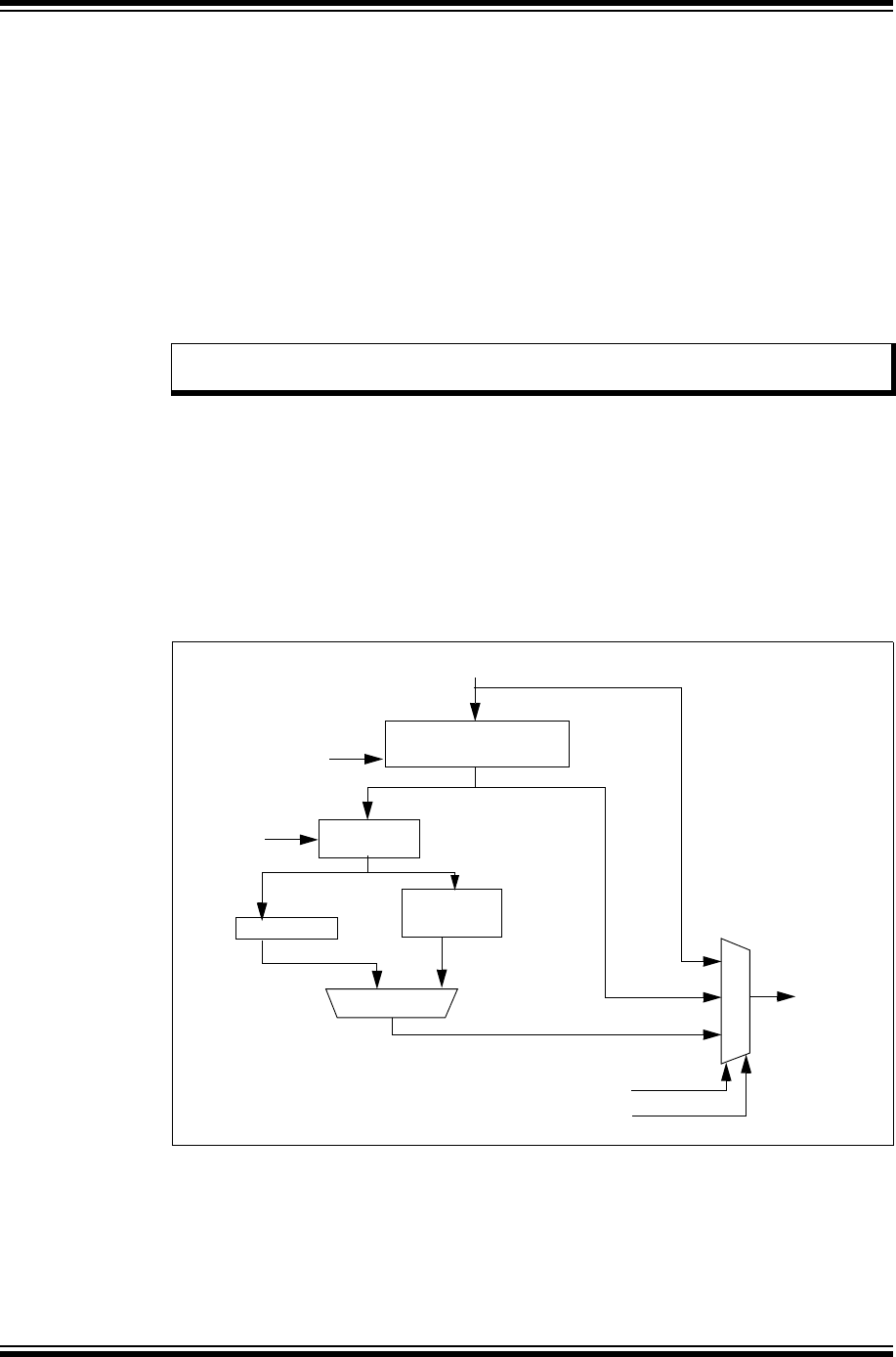
PIC32 Family Reference Manual
DS60001117H-page 31-34 © 2007-2013 Microchip Technology Inc.
31.3.4 Channel Auto-Enable Mode
The channel auto-enable can be used to keep a channel active, even if a block transfer
completes or pattern match occurs. This prevents the user from having to re-enable the channel
each time a block transfer completes. To use this mode the user will configure the channel,
setting the CHAEN bit (DCHxCON<4>) before enabling the channel (i.e., setting the CHEN bit
(DCHxCON<7>)). The channel will behave as normal except that normal termination of a
transfer will not result in the channel being disabled.
Normal block transfer completion is defined as:
•Block transfer complete
•Pattern match detect
As before, the Channel Pointers will be reset. This mode is useful for applications that do
repeated pattern matching.
31.3.5 Special Function Module (SFM) Mode
The DMA module has one integrated Special Function Module (SFM) shared by all channels.
As illustrated in Figure 31-3, the SFM has the following blocks:
•Linear Feedback Shift Register (LFSR) CRC
•IP header checksum
•Byte reordering
•Bit reordering
Figure 31-3: Special Function Module (SFM)
Depending on the device, the SFM is a highly configurable, 16-bit or 32-bit CRC generator. The
SFM can be assigned to any available DMA channel by setting the CRCCH<2:0> bit
(DCRCCON<2:0>). The SFM is enabled by setting the CRCEN bit (DCRCCON<7>).
The data from the source can be optionally subjected to byte reordering using the WBO bit. The
data is then optionally passed to the LFSR CRC or IP header checksum blocks based on the
setting of the CRCTYP bit (DCRCCON<15>), as illustrated in Figure 31-3.
Note: The CHAEN bit prevents the channel from being automatically disabled once it has
been enabled. The channel will still have to be enabled by the software.
Data In
Byte
Reordering
LFSR CRC
BYTO
CRCDATA
CRCAPP
WBO
Data Out
Bit
Reordering
BITO
Note: CRCAPP = 1; WBO = 1 is invalid.
00
01
10
IP Header
Checksum

© 2007-2013 Microchip Technology Inc. DS60001117H-page 31-35
Section 31. DMA Controller
DMA Controller
31
Further, the SFM modifies the behavior of the DMA channel associated with the SFM. The
behavior of the channel is selected by the CRCAPP bit (DCRCCON<6>), resulting in the
following two modes:
•Background mode: CRC is calculated in the background, with normal DMA behavior
maintained (see 31.3.5.1 “CRC Background Mode (CRCAPP = 0)”).
•Append mode: Data read from the source is not written to the destination, but the CRC data
is accumulated in the CRC data register. The accumulated CRC is written to the location
given by the DCHxDSA register when a block transfer completes (see 31.3.5.2 “CRC
Append Mode (CRCAPP = 1)”).
The order in which data is written to the destination can be selected using the WBO bit
(DCRCCON<27>). If the WBO bit is cleared, the writes to the destination are unaltered. If the
WBO bit is set, the writes to the destination are reordered as defined by the CRC Byte Order
Selection bits, BYTO<1:0> (DCRCCON<29:28>).
The SFM generator can be seeded by writing to the DCRCDATA register before enabling the
channel.
When in IP Header Checksum mode (CRCTYP (DCRCCON<15>) = 1), data written reads back
as the 1’s complement form as this is the current value of the checksum.
The CRC value in DCRCDATA can be read at any time during the CRC generation, but is only
valid once the transfer completes.
31.3.5.1 CRC BACKGROUND MODE (CRCAPP = 0)
In this mode, the behavior of the DMA channel is maintained. The DMA reads the data from the
source, passes it through the CRC module and writes it to the destination. Writes to the
destination obey the WBO selection. In this mode, the calculated CRC is left in the DCRCDATA
register at the end of the block transfer.
This mode can be used to calculate a CRC as data is moved from a source address to a
destination address. The data source can be either a memory buffer or a FIFO in a peripheral.
Likewise, the destination can be either a memory buffer or a FIFO. When the data transfer
completes, the user can read the calculated CRC value and either append it to the transmitted
data or verify the received CRC data.
Background mode potentially ties up the CRC module for extended periods of time. For instance,
when assigned to a UART data stream, the SFM cannot be used by another channel until the
UART data stream completes.
Note: This feature is not available on all devices. Refer to the “Direct Memory Access
(DMA) Controller” chapter in the specific device data sheet for availability.
Note 1: If a DMA Transfer is aborted while a CRC calculation is in progress, the DMA chan-
nel should be reset before the next CRC calculation is started. Alternatively, the
same channel or another unused channel can be configured to transfer two or more
bytes. The transfer should then be initiated and allowed to complete. The CRC
module is then ready for the next CRC calculation.
2: If a DMA channel is disabled (CHEN (DCHxCON<7>) = 0) when a CRC calculation
is in progress, the value in the DCRCDATA register is not updated. The same chan-
nel or another unused channel can be configured to transfer two or more bytes. The
transfer should then be initiated and allowed to complete. When the transfer is com-
plete, the DCRCDATA value will be correct for the number of byte processed prior
to the stop being issued. The DMA address register can be inspected to determine
the address range of the current CRC value.

PIC32 Family Reference Manual
DS60001117H-page 31-36 © 2007-2013 Microchip Technology Inc.
Example 31-4: DMA LFSR CRC Calculation in Background Mode Code Example
/* This code example illustrates a DMA calculation using the CRC background mode. Data is
transferred from a 200 bytes Flash buffer to a RAM buffer and the CRC is calculated while the
transfer takes place. */
unsigned int blockCrc; // CRC of the Flash block
IEC1CLR=0x00010000; // disable DMA channel 0 interrupts
IFS1CLR=0x00010000; // clear any existing DMA channel 0 interrupt flag
DMACONSET=0x00008000; // enable the DMA controller
DCRCDATA=0xffff; // seed the CRC generator
DCRCXOR=0x1021; // Use the standard CCITT CRC 16 polynomial: X^16+X^12+X^5+1
DCRCCON=0x0f80; // CRC enabled, polynomial length 16, background mode
// CRC attached to the DMA channel 0.
DCH0CON=0x03; // channel off, priority 3, no chaining
DCH0ECON=0; // no start irqs, no match enabled
// program channel transfer
DCH0SSA=VirtToPhys(flashBuff); // transfer source physical address
DCH0DSA=VirtToPhys(ramBuff); // transfer destination physical address
DCH0SSIZ=200; // source size
DCH0DSIZ=200; // destination size
DCHOCSIZ=200; // 200 bytes per event
DCH0INTCLR=0x00ff00ff; // DMA0: clear events, disable interrupts
DCH0CONSET=0x80; // channel 0 on
// initiate a transfer
DCH0ECONSET=0x00000080; // set CFORCE to 1
// do something else while the transfer takes place
// poll to see that the transfer was done
BOOL error=FALSE;
while(TRUE)
{
register int pollCnt; // don’t poll in a tight loop
int dmaFlags=DCH0INT;
if( (dmaFlags& 0x3)
{ // CHERIF (DCHxINT<0>) or CHTAIF (DCHxINT<1> set
error=TRUE; // error or aborted...
break;
}
else if (dmaFlags&0x8)
{ // CHBCIF (DCHxINT<3>) set
break; // transfer completed normally
}
pollCnt=100; // use an adjusted value here
while(pollCnt--); // wait before polling again
}
if(!error)
{
blockCrc=DCRDATA; // read the CRC of the transferred Flash block
}
else
{
// process error
}

© 2007-2013 Microchip Technology Inc. DS60001117H-page 31-37
Section 31. DMA Controller
DMA Controller
31
31.3.5.2 CRC APPEND MODE (CRCAPP = 1)
In this mode, the DMA only feeds source data to the CRC module; it does not write source data
to the destination address. However, when the block transfer completes or a pattern match
occurs, the DMA writes the CRC value to the destination address.
The following usage information applies to CRC Append mode:
• Only the source buffer is viewed when considering whether a block transfer is complete,
the destination address (DCHxDSA) is only used as the location to write the generated
CRC value.
•The destination size (DCHxDSIZ) can be a maximum of 4.
-If DCHxDSIZ is greater than four, only 4 bytes are written
-If DCHxDSIZ is less than four, only DCHxDSIZ bytes of the CRC are written
- PLEN<4:0> bits have no effect on the number of CRC bytes or bits written
•After the write, the channel is disabled.
•Any abort (i.e., abort IRQ asserts) prevents the CRC value from being written
•Reordering is not supported in Append mode if the WBO bit is set to ‘0’.
Example 31-5: CRC Calculation in Append Mode Code Example
/* This code example illustrates a DMA calculation using the CRC append mode. The CRC of a 256
bytes Flash buffer is calculated without performing any data transfer. As soon as the CRC
calculation is completed the CRC value of the Flash buffer is available in a local variable for
further use. */
unsigned int blockCrc; // CRC of the Flash block
IEC1CLR=0x00010000; // disable DMA channel 0 interrupts
IFS1CLR=0x00010000; // clear any existing DMA channel 0 interrupt flag
DMACONSET=0x00008000; // enable the DMA controller
DCRCDATA=0xffff; // seed the CRC generator
DCRCXOR=0x1021; // Use the standard CCITT CRC 16 polynomial: X^16+X^12+X^5+1
DCRCCON=0x0fc0; // CRC enabled, polynomial length 16, append mode
// CRC attached to the DMA channel 0.
DCH0CON=0x03; // channel off, priority 3, no chaining
DCH0ECON=0; // no start irqs, no match enabled
// program channel transfer
DCH0SSA=VirtToPhys(flashBuff); // transfer source physical address
DCH0DSA=VirtToPhys(&blockCrc); // transfer destination physical address
DCH0SSIZ=200; // source size
DCH0DSIZ=200; // dst size
DCHOCSIZ=200; // 200 bytes transferred per event
DCH0INTCLR=0x00ff00ff; // DMA0: clear events, disable interrupts
DCH1INTCLR=0x00ff00ff; // DMA1: clear events, disable interrupts
DCH0CONSET=0x80; // channel 0 on
// initiate a transfer
DCH0ECONSET=0x00000080; // set CFORCE to 1
// do something else while the CRC calculation takes place
// poll to see that the transfer was done
BOOL error=FALSE;
while(TRUE)
{register int pollCnt; // don’t poll in a tight loop
int dmaFlags=DCH0INT;
if( (dmaFlags& 0x3)
{ // CHERIF (DCHxINT<0>) or CHTAIF (DCHxINT<1> set
error=TRUE; // error or aborted...
break;
}else if (dmaFlags&0x8)
{ // CHBCIF (DCHxINT<3>) set
break; // transfer completed normally
}
pollCnt=100; // use an adjusted value here
while(pollCnt--); // wait before polling again
}
if(error)
{// process error
}
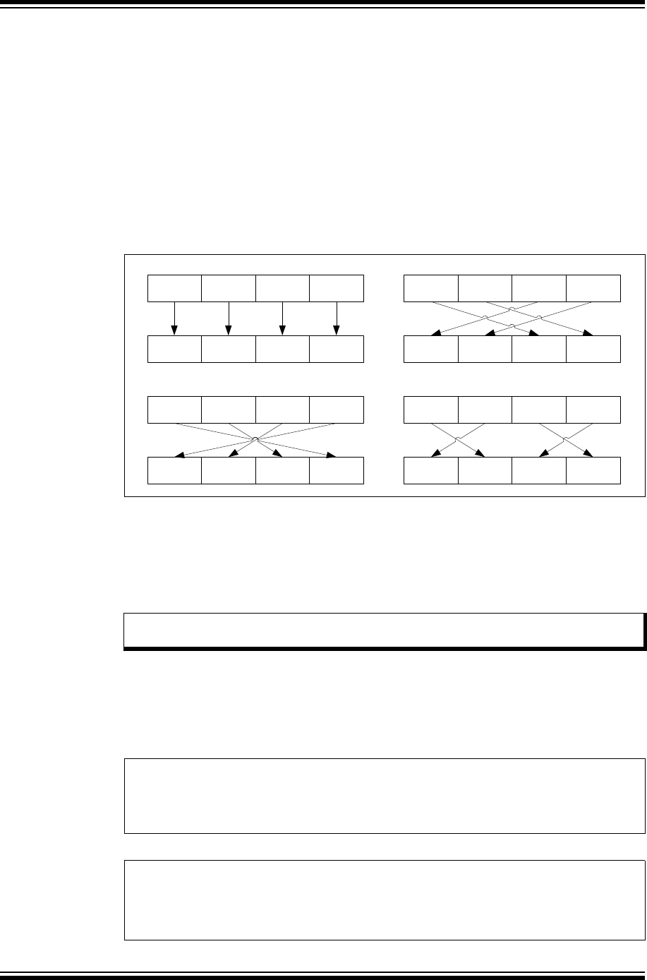
PIC32 Family Reference Manual
DS60001117H-page 31-38 © 2007-2013 Microchip Technology Inc.
31.3.5.3 DATA ORDER
Data read from the source can be reordered to allow for variations in the byte order of the source
data, such as endianness. The reordered source data is written to the channel destination when
WBO = 1. The unaltered source data is written to the destination when WBO = 0.
The BYTO<1:0> bits control the byte order of the data being processed by the module.
Figure 31-4 shows the different byte order settings and the effect on data reads. A BYTO<1:0>
value of ‘01’ is useful for reordering bytes within words. BYTO<1:0> values of ‘10’ and ‘11’ are
useful for reordering bytes within half-words.
It is important to note that the data is reordered as it is read. This means that data that is not
word-aligned may not be reordered correctly.
When using the LFSR CRC mode or IP Header Checksum mode of the SFM, the bit order (either
MSB or LSB) can be changed by using the BITO (DCRCCON<24>) bit.
Figure 31-4: Byte Order for BYTO Values
31.3.5.4 LFSR CRC
The CRC generator will take one system clock to process each byte of data read from the
source. This implies that if 32 bits of data are read from the source, the CRC generation will take
four system clocks to process the data.
When the CRYTYP bit is cleared, the SFM is set to LFSR CRC mode and calculates the LFSR
CRC.
The implementation of the CRC module is software configurable. The terms of the polynomial
and its length can be programmed using the DCRCXOR<31:0> bits and the PLEN<4:0> bits
(DCRCCON<12:8>), respectively.
Example 31-6 and Example 31-7 show th polynomials for the 16-bit and 32-bit CRC. The bit val-
ues that include an ‘x’ are considered a “don’t care” as they are always XORed.
Example 31-6: 16-bit CRC Polynomial
Example 31-7: 32-bit CRC Polynomial
Note: This feature is not available on all devices. Refer to the “Direct Memory Access
(DMA) Controller” chapter in the specific device data sheet for availability.
Byte3 Byte2 Byte1 Byte0
Byte3 Byte2 Byte1 Byte0
Byte3 Byte2 Byte1 Byte0
Byte3Byte2Byte1Byte0
Byte3 Byte2 Byte1 Byte0
Byte3 Byte2Byte1 Byte0
Byte3 Byte2 Byte1 Byte0
Byte3Byte2 Byte1Byte0
BYTO=00
BYTO=01 BYTO=11
BYTO=10
x16 x12 x51+++
PLEN<4:0> = ‘b01111
DCRCXOR<15:0> = ‘bx001 0000 0010 000x
x32 x26 x23 x22 x16 x12 x11 x10 x8x7x5x4x2x1++++++++++++++
PLEN<4:0> = ‘b11111
DCRCXOR<31:0> = ‘bx000 0100 1100 0001 0001 1101 1011 011x

© 2007-2013 Microchip Technology Inc. DS60001117H-page 31-39
Section 31. DMA Controller
DMA Controller
31
The PLEN<4:0> bits (DCRCCON<12:8>) in the CRC generator are used to select which bit is
used as the feedback point of the CRC. For a 16-bit CRC example, if PLEN<4:0> = 00110, bit 6
of the Shift register is fed into the XOR gates of all bits set in the CRCXOR register.
The CRCXOR feedback points are specified using the DCRCXOR register. Setting the Nth bit in
the DCRCXOR register will enable the input to the Nth bit of the CRC Shift register to be XORed
with the (PLEN + 1)th bit of the CRC Shift register. Bit 0 and bit 15 of the CRC generator is
always XORed.
31.3.5.5 CALCULATING THE IP HEADER CHECKSUM
When the CRCTYP bit (DCRCCON<15>) bit is set, the SFM calculates the IP header checksum.
Use the following procedure to calculate the IP header checksum:
1. Configure a channel to point to the IP header.
2. Configure CRCCON to enable the SFM and select the channel being used.
3. Set the CRCTYP bit, which selects IP Header checksum.
4. Set DCRCDATA to ‘0000’.
5. Start the transfer.
6. When the transfer completes, read the data out of the DCRCDATA register.
Note: This feature is not available on all devices. Refer to the “Direct Memory Access
(DMA) Controller” chapter in the specific device data sheet for availability.

PIC32 Family Reference Manual
DS60001117H-page 31-40 © 2007-2013 Microchip Technology Inc.
31.4 CHANNEL CONTROL
31.4.1 Channel Enable
Each channel has an enable bit, CHEN (DCHxCON<7>), which can be used to enable or
disable the channel in question. When this bit is set, the channel transfer requests are serviced
by the DMA controller.
When the CHEN bit is clear, the state of the channel is preserved (this allows the channel to be
suspended once a transfer has begun).
The CHEN bit will be cleared by hardware under the following conditions:
•A block transfer is complete, the pointer to the larger of the source or destination matches
the size (only if the CHAEN (DCHxCON<4>) bit is clear)
•A pattern match occurs in Pattern Match mode (only if the CHAEN bit is clear)
•An abort interrupt occurs
•The user writes the CABORT (DCHxECON<6>) bit
31.4.2 Channel Transfer Behavior
Once a channel has been enabled, CHEN = 1, any event that starts a cell transfer will transfer
the CHCSIZ<15:0> (DCHxCSIZ<15:0>) bytes of data. This will require one or more
transactions. Once the cell transfer is complete the channel will return to an inactive state, and
will wait for another channel start event to occur before starting another cell transfer.
When the larger of CHSSIZ<15:0> (DCHxSSIZ<15:0>) or CHDSIZ<15:0> (DCHxDSIZ<15:0>)
bytes are transferred, a block transfer completes, the channel transfer will be halted and the
channel will be disabled (i.e., CHEN set to ‘0’ by hardware, and pointers are reset).
31.4.2.1 CHANNEL EVENT TRANSFER INITIATION
A given channel transfer can be initiated by:
•Writing the CFORCE bit (DCHxECON<7>)
• An interrupt occurs that matches the value of CHSIRQ<7:0> (DCHxECON<15:8>) if it is
enabled by SIRQEN bit (DCHxECON<4>)
Channel events are registered if the channel is enabled (CHEN = 1), or if “Allow Event If
Disabled” is set (i.e., CHAED (DCHxCON<6>) = 1)
31.4.2.2 CHANNEL EVENT TRANSFER TERMINATION
Channel transfer is terminated in any of the following cases:
•A transfer is aborted as described in 31.4.6 “Resetting the Channel”
•A cell transfer (CHCSIZ<15:0> bytes (DCHxCSIZ<15:0> transferred)) completes
•The DMA has transferred the larger of CHSSIZ<15:0> or CHDSIZ<15:0> bytes (block
transfer complete), the channel is disabled in hardware and must be re-enabled by user
software before the channel will respond to channel events
•A pattern match occurs if enabled
•An abort interrupt, CHAIRQ<7:0> (DCHxECON<23:16>), occurs if abort interrupts are
enabled by AIRQEN bit (DCHxECON<3>)
•An address error occurs
An example of how to use the abort interrupt would be a transfer from a UART channel to the
memory. While the UART Receive Data Available interrupt can be used to start the transfer, the
UART Error interrupt can abort the transfer. This way, whenever an error occurs on the commu-
nication channel (a framing/parity error or even an overrun), the transfer is stopped and the user
code gets control in an ISR (if the abort interrupt is enabled for the DMA controller).
A summary of the status flags affected by channel transfer initiation or termination is provided in
Tabl e 31- 2. Channel abort events are allowed if the channel is enabled, CHEN = 1, or if the user
elects to allow events while the channel is disabled, CHAED = 1.

© 2007-2013 Microchip Technology Inc. DS60001117H-page 31-41
Section 31. DMA Controller
DMA Controller
31
Table 31-2: Channel Event Behavior
31.4.3 Channel IRQ Detection
The DMA Controller maintains its own flags for detecting the start and abort IRQ in the system
and is completely independent of the INT Controller and IESx/IFSx flags. The corresponding IRQ
does not have to be enabled before a transfer can take place, nor cleared at the end of a DMA
transfer.
After the start or abort IRQ system events are triggered, they will be detected automatically by
the DMA controller internal logic, without the need for user intervention.
Event Description and Function Registers Affected
Events Initiating Transfers
System Interrupt Matching
CHSIRQ<7:0>(1,2)
The channel event detect will be set. CHEDET = 1
Channel Chain Event This will enable the channel if not already set. If an event detect
is pending, a channel transfer will begin immediately.
CHEN = 1
User Writes the CFORCE bit(1) The channel event detect will be set. CHEDET = 1
Events Terminating Transfers
System Interrupt Matching
CHAIRQ<7:0>(1,2)
The channel event detect will be reset and the channel turned
off. The abort interrupt flag is set.
CHEDET = 0
CHEN = 0
CHAIF = 1
Pattern Match Terminate(1) This occurs when any byte of data written in a transaction
matches the data in CHPDAT.
The channel event detect is reset.
The channel is turned off if CHAEN = 0. This event is treated
as a completed block transfer.
Pointers are reset.
CHEDET = 0
CHEN = 0
CHBCIF = 1
CHSPTR = 0
CHDPTR = 0
CHCPTR = 0
Cell Transfer is Complete This occurs when CHCSIZ bytes have been transferred. The
transfer event detect is reset and the channel remains enabled
pending the next event.
CHEDET = 0
CHCCIF = 1
Block Transfer is Complete The channel event detect is reset.
The channel is turned off if CHAEN = 0. This event is treated
as a completed transfer.
Pointers are reset.
CHEDET = 0
CHEN = 0
CHBCIF = 1
CHSPTR = 0
CHDPTR = 0
CHCPTR = 0
User Writes the CABORT bit The channel is turned off and the channel event detect is reset.
The pointers are reset.
CHEDET = 0
CHEN = 0
CHSPTR = 0
CHDPTR = 0
CHCPTR = 0
Address Error is Detected The channel is turned off and the event detect is reset. The
address error interrupt flag is set.
CHEDET = 0
CHEN = 0
CHERIF = 1
Note 1: Events are allowed only when the channel is enabled, or the user allows events while disabled (CHEN = 1
or CHAED = 1).
2: The DMA Controller maintains its own flags for detecting start and abort interrupt requests (IRQs) in the sys-
tem, and is completely independent of the INT Controller IES/IFS flags. Once the start or abort IRQ system
events are triggered, they will be detected automatically by the DMA controller internal logic, without the
need for user intervention.

PIC32 Family Reference Manual
DS60001117H-page 31-42 © 2007-2013 Microchip Technology Inc.
31.4.4 Channel Abort Interrupt
A channel can elect to abort a cell transfer if an interrupt event occurs. The interrupt is selected
by the channel’s abort IRQ, CHAIRQ<7:0> (DCHxECON<23:16>). Any one of the device
interrupt events can cause a channel abort. An abort only occurs if enabled by the AIRQEN bit
(DCHxECON<3>).
If this occurs (often a timer time-out or a module error flag), the channel’s status flags will
indicate the external abort event on the channel in question by setting its CHTAIF bit
(DCHxINT<1>).The Source and Destination Pointers are not reset, allowing the user to recover
from the error.
31.4.5 DMA Suspend
DMA transactions are suspended immediately if the SUSPEND bit (DMACON<12>) is set. The
current read or write will be completed. If the suspend comes during the read portion of the
transaction, the transaction will be suspended and the write will be put on hold. If the suspend
comes during the write portion of the transaction, the write will complete and the pointers
updated as normal. Any transactions that were in process will continue where they left off when
the SUSPEND bit is cleared.
Depending on the device, when the DMA module is suspended by setting the SUSPEND bit,
the user application should poll the DMABUSY bit (DMACON<11>) to determine when the
module is completely suspended following the completion of the current transaction.
Example 31-8: DMA Controller Suspension
Individual channels may be suspended using the CHEN bit (DCHxCON<7>). If a DMA transfer
is in progress and the CHEN bit is cleared, the current transaction will be completed and further
transactions on the channel will be suspended.
Depending on the device, when the channel is suspended by clearing the CHEN bit, the user
application should poll the CHBUSY bit (DCHxCON<15>) to determine when the channel is
completely suspended following completion of the current transaction.
Clearing the enable bit, CHEN, will not affect the Channel Pointers or the transaction counters.
While a channel is suspended, the user can elect to continue to receive events (abort interrupts,
etc.) by setting the CHAED bit (DCHxCON<6>).
31.4.6 Resetting the Channel
The channel logic will be reset on any device Reset. The channel is also reset when the channel
bit, CABORT (DCHxECON<6>), is set. This will turn off the channel bit, CHEN = 0, clear the
Source and Destination Pointers, and reset the event detector. When the CABORT bit is set, the
current transaction in progress (if any) will complete before the channel is reset, but any remaining
transactions will be aborted.
The user should modify the channel registers only while the channel is disabled (CHEN = 0).
Modifying the Source and Destination registers will reset the corresponding pointer registers
(DCHxSPTR or DCHxDPTR).
Note: The DMABUSY bit is not available on all device. Refer to the “Direct Memory
Access (DMA) Controller” chapter in the specific device data sheet for availability.
Note: The channel size must be changed while the channel is disabled.
/* This code example will suspend the DMA Controller. */
DMACONSET=0x00001000; // suspend the DMA controller
while(!(DMACONbits.busy)); // wait for the transfer to be suspended
// let the CPU have complete control of the bus
DMACONCLR=0x00001000; // clear the suspend mode and let the DMA
// operate normally. From now on, the CPU and
// DMA controller share the bus access

© 2007-2013 Microchip Technology Inc. DS60001117H-page 31-43
Section 31. DMA Controller
DMA Controller
31
31.4.7 Channel Priority and Selection
The DMA controller has a natural priority associated with each of the channels. Channel 0 has
the highest natural priority. A channel priority can be changed by the CHPRI<1:0> bits
(DCHxCON<1:0>). These bits identify the channel’s priority where a value of zero is the lowest.
If no priority is set, the DMA controller will use the natural priority associated with each channel.
When multiple channels have transfers pending, the next channel to transmit data will be
selected as follows:
•Channels with the highest priority will complete all cell transfers before moving onto
channels with a lower priority (see PRI3 transfers, in Figure 31-5).
•If multiple channels have the same priority (identical CHPRI), the controller will cycle
through all channels at that priority. Each channel with a cell transfer in progress at the
highest priority will be allowed a single transaction of the active cell transfer before the
controller allows a single transaction by the next channel at that priority level (see PRI2
transfers between markers C and B, in Figure 31-5).
•If a channel with a higher priority requests a transfer while another channel of lower priority
has a transaction in process, the transaction will complete before moving to the channel
with the higher priority (see events at marker A in Figure 31-5).
Figure 31-5: Channel Priority Behavior
31.4.8 Byte Alignment
The byte alignment feature of the DMA controller relieves the user from aligning the source and
destination addresses.The read portion of a transaction will read the maximum number of bytes
that are available to be read in a given word. For example, if the Source Pointer is N > 4 bytes
from the source size, 4 bytes will be read if the Source Pointer points to byte 0, 3 bytes if the
Source Pointer points to byte 1, etc. If the number of bytes remaining in the source is N < 4, only
the first N bytes are read. This is important when the read includes registers that are updated on
a read.
The Source Pointer and Destination Pointers are updated after every write, with the number of
bytes that have been written. The user should note that in cases where a transfer is aborted,
before a transaction is complete, the Source Pointer will not necessarily reflect the reads that
have taken place.
31.4.9 Address Error
If the address (either source or destination) occurring during a transfer is an illegal address, the
channel’s address error interrupt flag CHERIF bit (DCHxINT<0>) will be set. The channel will be
disabled (i.e., the CHEN bit will be reset by hardware).
The channel status is unaffected to aid in the debug of the problem.
REQ: CH0, PRI0
REQ: CH1, PRI2
REQ: CH2, PRI3
REQ: CH3, PRI2
DMA Active Channel none 0 3 2 2 2 3 3 3110none
PRI0
transfers
PRI2
transfers
PRI0
transfers PRI3 transfers PRI2 transfers
Cycle through
CH1 and CH3
AA B C B
Transition Legend:
A – Higher priority transfer request; suspend current and transfer next.
B – All highest priority transfers complete; drop to channels at lower priority.
C – Cycle through all channels at the current priority.

PIC32 Family Reference Manual
DS60001117H-page 31-44 © 2007-2013 Microchip Technology Inc.
31.5 INTERRUPTS
The DMA device has the ability to generate interrupts reflecting the events that occur during the
channel’s data transfer:
•Error interrupts, signaled by each channel’s CHERIF bit (DCHxINT<0>) and enabled using
the CHERIE bit (DCHxINT<16>). This event occurs when there is an address error
occurred during the channel transfer operation.
• Abort interrupts, signaled by each channel’s CHTAIF bit (DCHxINT<1>) and enabled using
the CHTAIE bit (DCHxINT<17>). This event occurs when a DMA channel transfer gets
aborted because of a system event (interrupt) matching the CHAIRQ<7:0> bits
(DCHxECON<23:16>) when the abort interrupt request is enabled, AIRQEN
(DCHxECON<3>) = 1.
• Block complete interrupts, signaled by each channel’s CHBCIF bit (DCHxINT<3>) and
enabled using the CHBCIE bit (DCHxINT<19>). This event occurs when a DMA channel
block transfer is completed.
• Cell complete interrupts, signaled by each channel’s CHCCIF bit (DCHxINT<2>) and
enabled using the CHCCIE bit (DCHxINT<18>). This event occurs when a DMA channel
cell transfer is completed.
• Source Address Pointer activity interrupts: either when the Channel Source Pointer
reached the end of the source, signaled by the CHSDIF bit (DCHxINT<7>) and enabled by
CHSDIE bit (DCHxINT<23>), or when the Channel Source Pointer reached midpoint of the
source, signaled by the CHSHIF bit (DCHxINT<6>) and enabled by the CHSHIE bit
(DCHxINT<22>).
•Destination Address Pointer activity interrupts: either when the Channel Destination Pointer
reached the end of the destination, signaled by the CHDDIF bit (DCHxINT<5>) and
enabled by the CHDDIE bit (DCHxINT<21>), or when the Channel Destination Pointer
reached midpoint of the destination, signaled by the CHDHIF bit (DCHxINT<4>) and
enabled by the CHDHIE bit (DCHxINT<20>).
All the interrupts belonging to a DMA channel map to the corresponding channel interrupt vector.
31.5.1 Interrupt Configuration
Each DMA channel internally has multiple interrupt flags (CHSDIF, CHSHIF, CHDDIF, CHDHIF,
CHBCIF, CHCCIF, CHTAIF, CHERIF) and corresponding enable interrupt control bits (CHSDIE,
CHSHIE, CHDDIE, CHDHIE, CHBCIE, CHCCIE, CHTAIE, CHERIE).
However, for the interrupt controller, there is just one dedicated interrupt flag bit per channel,
DMAxIF, and the corresponding interrupt enable/mask bits, DMAxIE.
Therefore, note that all of the interrupt conditions for a specific DMA channel share just one
interrupt vector. Each DMA channel can have its own priority level independent of other DMA
channels.
Note: Not all DMA channels are available on all devices. Refer to the “Interrupts” chapter
in the specific device data sheet for availability.
Note: Depending on the device, up to eight (i.e., 0 through 7) interrupt flags and interrupt
enable/mask bits are available. Refer to the “Interrupts” chapter in the specific
device data sheet for availability.

© 2007-2013 Microchip Technology Inc. DS60001117H-page 31-45
Section 31. DMA Controller
DMA Controller
31
Example 31-9: DMA Channel Initialization with Interrupts Enabled Code Example
Example 31-10: DMA Channel 0 ISR Code Example
/* This code example illustrates a DMA channel 0 interrupt configuration. When the DMA channel
0 interrupt is generated, the CPU will jump to the vector assigned to DMA0 interrupt. */
IEC1CLR=0x00010000; // disable DMA channel 0 interrupts
IFS1CLR=0x00010000; // clear any existing DMA channel 0 interrupt flag
DMACONSET=0x00008000; // enable the DMA controller
DCH0CON=0x03; // channel off, priority 3, no chaining
DCH0ECON=0; // no start or stop irq’s, no pattern match
// program the transfer
DCH0SSA=VirtToPhys(flashBuff); // transfer source physical address
DCH0DSA=VirtToPhys(ramBuff); // transfer destination physical address
DCH0SSIZ=200; // source size 200 bytes
DCH0DSIZ=200; // destination size 200 bytes
DCH0CSIZ=200; // 200 bytes transferred per event
DCH0INTCLR=0x00ff00ff; // clear existing events, disable all interrupts
DCH0INTSET=0x00090000; // enable Block Complete and error interrupts
IPC9CLR=0x0000001f; // clear the DMA channel 0 priority and sub-priority
IPC9SET=0x00000016; // set IPL 5, sub-priority 2
IEC1SET=0x00010000; // enable DMA channel 0 interrupt
DCH0CONSET=0x80; // turn channel on
// initiate a transfer
DCH0ECONSET=0x00000080; // set CFORCE to 1
/*This code example demonstrates a simple Interrupt Service Routine for DMA channel 0
interrupts. The user’s code at this vector should perform any application specific operations
and must clear the DMA0 interrupt flags before exiting. */
void __ISR(_DMA_0_VECTOR, ipl5) __DMA0Interrupt(void)
{
int dmaFlags=DCH0INT&0xff; // read the interrupt flags
/*
perform application specific operations in response to any interrupt flag set
*/
DCH0INTCLR=0x000000ff; // clear the DMA channel interrupt flags
IFS1CLR = 0x00010000; // Be sure to clear the DMA0 interrupt flags
// before exiting the service routine.
}
Note: The DMA ISR code example shows MPLAB® C32 C compiler specific syntax. Refer to your compiler
manual regarding support for ISRs.

PIC32 Family Reference Manual
DS60001117H-page 31-46 © 2007-2013 Microchip Technology Inc.
31.6 OPERATION IN POWER-SAVING AND DEBUG MODES
31.6.1 DMA Operation in Sleep Mode
When the device enters Sleep mode, the system clock is disabled. No DMA activity can occur in
this mode.
31.7 EFFECTS OF VARIOUS RESETS
31.7.1 Device Reset
All DMA registers are forced to their reset states upon a device Reset. When the asynchronous
Reset input goes active, the DMA logic:
• Resets all fields in DMACON, DMASTAT, DMAADDR, DCRCCON, DCRCDATA and
DCRCXOR
• Sets the appropriate values in each channel’s register fields: DCHxCON, DCHxECON,
DCHxINT, DCHxSSIZ, DCHxDSIZ, DCHxSPTR, DCHxDPTR, DCHxCSIZ, DCHxCPTR
and DCHxDAT
•Registers DCHxSSA and DCHxDSA have random values after a reset
• Aborts any ongoing data transfers
31.7.2 Power-on Reset
All DMA registers are forced to their reset states upon a Power-on Reset.
31.7.3 Watchdog Timer Reset
All DMA registers are forced to their reset states upon a Watchdog Timer Reset.

© 2007-2013 Microchip Technology Inc. DS60001117H-page 31-47
Section 31. DMA Controller
DMA Controller
31
31.8 RELATED APPLICATION NOTES
This section lists application notes that are related to this section of the manual. These
application notes may not be written specifically for the PIC32 device family, but the concepts are
pertinent and could be used DMA Controller with modification and possible limitations. The
current application notes related to the Direct Memory Access (DMA) module are:
Title Application Note #
No related application notes at this time N/A
Note: Visit the Microchip web site (www.microchip.com) for additional application notes
and code examples for the PIC32 family of devices.

PIC32 Family Reference Manual
DS60001117H-page 31-48 © 2007-2013 Microchip Technology Inc.
31.9 REVISION HISTORY
Revision A (October 2007)
This is the initial released version of the document.
Revision B (October 2007)
Updated document to remove Confidential status.
Revision C (April 2008)
Revised status to Preliminary; Revised U-0 to r-x; Revised Table 31-1; Revised Table 31-2
(DCHxCON, bit 3), deleted Note 1; Revised Registers 31-19, 31-39, 31-43, 31-47, 31-48, 31-49,
31-53; Revise Sections 31.3, 31.3.2; Revised Examples 31-1, 31-3, 31-4, 31-6, 31-7, 31-8;
Delete Example 31-2 and renumber examples; Delete Section 31.3.3 and renumber sections;
Revised Section 31.3.20.7.
Revision D (June 2008)
Revised Registers 31-58 to 31-60, Footnote; Revised Example 31-8; Change Reserved bits
“Maintain as” to “Write”; Added Note to ON bit (DMACON Register).
Revision E (August 2009)
This revision introduces new bits and functionality that are only available on certain devices. The
following details the resulting changes:
•DMA Register Summary (Table31-1)
- Added the BUSY, BYTO1, BYTO0, WBO, BITO, CRCTYP and CHBUSY bits
-Removed references to the IEC1, IPC9 and IFS1 registers
-Added the Address Offset column to the DMA Register Summary
-Added Notes 1, 2 and 3, which describe the Clear, Set and Invert registers
- Added Notes 4 and 5 regarding the availability of certain bits and ranges of bits
depending on the device
•Added Notes describing the Clear, Set and Invert registers to the following registers:
-DMACON (Register31-1)
-DMASTAT (Register31-2)
-DMAADDR (Register31-3)
- DCRCCON (Register 31-4)
-DCRCDATA (Register31-5)
-DCRCXOR (Register31-6)
-DCHxCON (Register31-7)
-DCHxECON (Register31-8)
-DCHxINT (Register31-9)
-DCHxSSA (Register31-10)
-DCHxDSA (Register31-11)
-DCHxSSIZ (Register31-12)
-DCHxDSIZ (Register31-13)
-DCHSPTR (Register31-14)
-DCHxDPTR (Register31-15)
-DCHxCSIZ (Register31-16)
-DCHxCPTR (Register31-17)
-DCHxDAT (Register31-18)
• Removed these registers: IFS1, IEC1 and IPC9
•Added the BUSY bit (DMACON<11>) and Note 1 regarding availability of the SIDL and
BUSY bits to Register 31-1

© 2007-2013 Microchip Technology Inc. DS60001117H-page 31-49
Section 31. DMA Controller
DMA Controller
31
Revision E (August 2009) (Continued)
•Updated the DMACH bit (DMASTAT<2:0>) and added Note 2 regarding the availability of
all bits in Register 31-2
• Added the BYTO1, BYTO0, WBO, BITO and CRCTYP bits, updated bits PLEN<4:0> and
CRCCH<2:0>, and added Notes 1 and 2 to Register 31-4
• Updated DCRCDATA bits and added Note 1 to Register 31-5
• Updated DCRCXOR bits and added Note 1 to Register 31-6
•Added CHBUSY bit (DCHxCON<15>) and added Note 1 to Register31-7
• Updated DCHxSSIZ bits and added Note 1 to Register 31-12
• Updated DCHxDSIZ bits and added Note 1 to Register 31-13
• Updated DCHxSPTR bits and added Note 2 to Register 31-14
•Updated DCHxDPTR bits and added Note 1 to Register31-15
• Updated DCHxCSIZ bits and added Note 1 to Register 31-16
•Updated DCHxCPTR bits and added Note 2 to Register31-17
•Updated the lowest priority channel number and added a related note to the fourth
paragraph in 31.3.4 “Channel Chaining Mode”
•Added information on suspending the DMA module and a related Note to
31.3.7 “Suspending Transfers” and 31.3.19 “DMA Suspend”
•Updated 31.3.6 “Special Function Module (SFM) Mode” to differentiate between the
16-bit and 32-bit CRC
•Added 31.3.6.5 “Calculating the IP Header Checksum”
• Added DMA channel interrupt flags, enable bits and priority-level bits to 31.4 “Interrupts”
•Added DMA interrupt vectors (DMA4-DMA7) to Table31-6
•Updated 31.5.1 “DMA Operation in Idle Mode”
Revision F (October 2010)
This revision includes the following updates:
•Added a note at the beginning of this section, which provides information on complementary
documentation
• Changed all occurrences of “Reserved: Write ‘0’; ignore read” to “Unimplemented: Read
as ‘0’, and updated the default POR definitions in all registers
• Added Notes 1, 2 and 3, which describe the Clear, Set and Invert registers to the following:
-Table31-1: DMA Register Summary
-Register31-1: DMACON: DMA Controller Control Register
-Register31-4: DCRCCON: DMA CRC Control Register
- Register 31-5: DCRCDATA: DMA CRC Data Register
-Register31-6: DCRCXOR: DMA CRCXOR Enable Register
-Register31-7: DCHxCON: DMA Channel ‘x’ Control Register
-Register31-8: DCHxECON: DMA Channel ‘x’ Event Control Register
-Register31-9: DCHxINT: DMA Channel ‘x’ Interrupt Control Register
- Register 31-10: DCHxSSA: DMA Channel ‘x’ Source Start Address Register
-Register31-12: DCHxSSIZ: DMA Channel ‘x’ Source Size Register
- Register 31-13: DCHxDSIZ: DMA Channel ‘x’ Destination Size Register
- Register 31-16: DCHxCSIZ: DMA Channel ‘x’ Cell Size Register
-Register31-18: DCHxECON: DMA Channel ‘x’ Event Control Register
•Removed all Clear, Set and Invert registers
•Removed all Interrupt registers
•Changed the name of the BUSY bit to DMABUSY in Register31-1 and in Table31-1
•Added a note box just after the last paragraph of 31.3.6 “Special Function Module (SFM)
Mode”
•Minor formatting and text updates have been incorporated throughout the document

PIC32 Family Reference Manual
DS60001117H-page 31-50 © 2007-2013 Microchip Technology Inc.
Revision G (April 2012)
This revision includes the following updates:
• Updated the Typical DMA Source to Destination Transfer Diagram (see Figure 31-1)
•Updated the DMA Module Block Diagram (see Figure31-2)
• Removed the CRC Implementation Details (Figure 31-3)
•Updated the register definitions in 31.2 “Status and Control Registers”
•Removed the FRZ bit from the DMACON register (see Register 31-1)
• Added the CMAWCH<2:0> bits in the DMASTAT register (see Register 31-2)
• Added the CHPIGN<7:0>, CHPIGNEN, and CHPATLEN bits to the DCHxCON register
(see Register 31-7)
• Added the CHPDAT<15:8> bits to the DCHxDAT register (see Register 31-18)
•Added 31.3.2.1“Pattern Match Ignore Mode”
•Created the new section, 31.4“Channel Control”, from existing content
•Removed Source and Destination Point Updates Examples 1 and 2 (Table 31-3 and Table
31-4)
•Removed 31.3.17 “Channel Abort”
•Removed 31.5.3“DMA Operation in Debug Mode”
•Removed 31.6.1 “DMA Operation in Idle Mode”
•Formatting updates to all registers and minor text updates have been incorporated
throughout the document
Revision H (November 2013)
This revision includes the following updates:
• All references to BMX and Bus Matrix were updated to: System Bus
•Note 3 was removed and the Note 2 references were updated in the DMA Register
Summary (see Tabl e 31 - 1)
•An additional RDWR bit was added, and the DMAWCH<2:0> and DMARCH<2:0> bits were
removed in the DMASTAT register (see Ta b l e 3 1 - 1 and Register 31-2)
•Minor updates to text and formatting were incorporated throughout the document

2007-2013 Microchip Technology Inc. DS60001117H-page 31-51
Information contained in this publication regarding device
applications and the like is provided only for your convenience
and may be superseded by updates. It is your responsibility to
ensure that your application meets with your specifications.
MICROCHIP MAKES NO REPRESENTATIONS OR
WARRANTIES OF ANY KIND WHETHER EXPRESS OR
IMPLIED, WRITTEN OR ORAL, STATUTORY OR
OTHERWISE, RELATED TO THE INFORMATION,
INCLUDING BUT NOT LIMITED TO ITS CONDITION,
QUALITY, PERFORMANCE, MERCHANTABILITY OR
FITNESS FOR PURPOSE. Microchip disclaims all liability
arising from this information and its use. Use of Microchip
devices in life support and/or safety applications is entirely at
the buyer’s risk, and the buyer agrees to defend, indemnify and
hold harmless Microchip from any and all damages, claims,
suits, or expenses resulting from such use. No licenses are
conveyed, implicitly or otherwise, under any Microchip
intellectual property rights.
Trademarks
The Microchip name and logo, the Microchip logo, dsPIC,
FlashFlex, KEELOQ, KEELOQ logo, MPLAB, PIC, PICmicro,
PICSTART, PIC32 logo, rfPIC, SST, SST Logo, SuperFlash
and UNI/O are registered trademarks of Microchip Technology
Incorporated in the U.S.A. and other countries.
FilterLab, Hampshire, HI-TECH C, Linear Active Thermistor,
MTP, SEEVAL and The Embedded Control Solutions
Company are registered trademarks of Microchip Technology
Incorporated in the U.S.A.
Silicon Storage Technology is a registered trademark of
Microchip Technology Inc. in other countries.
Analog-for-the-Digital Age, Application Maestro, BodyCom,
chipKIT, chipKIT logo, CodeGuard, dsPICDEM,
dsPICDEM.net, dsPICworks, dsSPEAK, ECAN,
ECONOMONITOR, FanSense, HI-TIDE, In-Circuit Serial
Programming, ICSP, Mindi, MiWi, MPASM, MPF, MPLAB
Certified logo, MPLIB, MPLINK, mTouch, Omniscient Code
Generation, PICC, PICC-18, PICDEM, PICDEM.net, PICkit,
PICtail, REAL ICE, rfLAB, Select Mode, SQI, Serial Quad I/O,
Tota l E ndu ra nce , T SHA RC , U n iW inD riv er, Wi per Lo c k, ZE NA
and Z-Scale are trademarks of Microchip Technology
Incorporated in the U.S.A. and other countries.
SQTP is a service mark of Microchip Technology Incorporated
in the U.S.A.
GestIC and ULPP are registered trademarks of Microchip
Technology Germany II GmbH & Co. KG, a subsidiary of
Microchip Technology Inc., in other countries.
All other trademarks mentioned herein are property of their
respective companies.
© 2007-2013, Microchip Technology Incorporated, Printed in
the U.S.A., All Rights Reserved.
Printed on recycled paper.
ISBN: 978-1-62077-642-1
Note the following details of the code protection feature on Microchip devices:
• Microchip products meet the specification contained in their particular Microchip Data Sheet.
• Microchip believes that its family of products is one of the most secure families of its kind on the market today, when used in the
intended manner and under normal conditions.
• There are dishonest and possibly illegal methods used to breach the code protection feature. All of these methods, to our
knowledge, require using the Microchip products in a manner outside the operating specifications contained in Microchip’s Data
Sheets. Most likely, the person doing so is engaged in theft of intellectual property.
• Microchip is willing to work with the customer who is concerned about the integrity of their code.
• Neither Microchip nor any other semiconductor manufacturer can guarantee the security of their code. Code protection does not
mean that we are guaranteeing the product as “unbreakable.”
Code protection is constantly evolving. We at Microchip are committed to continuously improving the code protection features of our
products. Attempts to break Microchip’s code protection feature may be a violation of the Digital Millennium Copyright Act. If such acts
allow unauthorized access to your software or other copyrighted work, you may have a right to sue for relief under that Act.
Microchip received ISO/TS-16949:2009 certification for its worldwide
headquarters, design and wafer fabrication facilities in Chandler and
Tempe, Arizona; Gresham, Oregon and design centers in California
and India. The Company’s quality system processes and procedures
are for its PIC® MCUs and dsPIC® DSCs, KEELOQ® code hopping
devices, Serial EEPROMs, microperipherals, nonvolatile memory and
analog products. In addition, Microchip’s quality system for the design
and manufacture of development systems is ISO 9001:2000 certified.
QUALITY MANAGEMENT S
YSTEM
CERTIFIED BY DNV
== ISO/TS 16949 ==

DS60001117H-page 31-52 2007-2013 Microchip Technology Inc.
AMERICAS
Corporate Office
2355 West Chandler Blvd.
Chandler, AZ 85224-6199
Tel: 480-792-7200
Fax: 480-792-7277
Technical Support:
http://www.microchip.com/
support
Web Address:
www.microchip.com
Atlanta
Duluth, GA
Tel: 678-957-9614
Fax: 678-957-1455
Austin, TX
Tel: 512-257-3370
Boston
Westborough, MA
Tel: 774-760-0087
Fax: 774-760-0088
Chicago
Itasca, IL
Tel: 630-285-0071
Fax: 630-285-0075
Cleveland
Independence, OH
Tel: 216-447-0464
Fax: 216-447-0643
Dallas
Addison, TX
Tel: 972-818-7423
Fax: 972-818-2924
Detroit
Novi, MI
Tel: 248-848-4000
Houston, TX
Tel: 281-894-5983
Indianapolis
Noblesville, IN
Tel: 317-773-8323
Fax: 317-773-5453
Los Angeles
Mission Viejo, CA
Tel: 949-462-9523
Fax: 949-462-9608
New York, NY
Tel: 631-435-6000
San Jose, CA
Tel: 408-735-9110
Canada - Toronto
Tel: 905-673-0699
Fax: 905-673-6509
ASIA/PACIFIC
Asia Pacific Office
Suites 3707-14, 37th Floor
Tower 6, The Gateway
Harbour City, Kowloon
Hong Kong
Tel : 8 52 -24 01- 120 0
Fax: 852-2401-3431
Australia - Sydney
Tel : 6 1- 2-9 868 -67 33
Fax: 61-2-9868-6755
China - Beijing
Tel : 8 6- 10- 856 9-7 00 0
Fax: 86-10-8528-2104
China - Chengdu
Tel : 8 6- 28- 866 5-5 511
Fax: 86-28-8665-7889
China - Chongqing
Tel : 8 6- 23- 898 0-9 58 8
Fax: 86-23-8980-9500
China - Hangzhou
Tel : 8 6- 571 -28 19- 318 7
Fax: 86-571-2819-3189
China - Hong Kong SAR
Tel : 8 52 -29 43- 510 0
Fax: 852-2401-3431
China - Nanjing
Tel : 8 6- 25- 847 3-2 46 0
Fax: 86-25-8473-2470
China - Qingdao
Tel : 8 6- 532 -85 02- 735 5
Fax: 86-532-8502-7205
China - Shanghai
Tel : 8 6- 21- 540 7-5 53 3
Fax: 86-21-5407-5066
China - Shenyang
Tel : 8 6- 24- 233 4-2 82 9
Fax: 86-24-2334-2393
China - Shenzhen
Tel : 8 6- 755 -88 64- 220 0
Fax: 86-755-8203-1760
China - Wuhan
Tel : 8 6- 27- 598 0-5 30 0
Fax: 86-27-5980-5118
China - Xian
Tel : 8 6- 29- 883 3-7 25 2
Fax: 86-29-8833-7256
China - Xiamen
Tel: 86-592-2388138
Fax: 86-592-2388130
China - Zhuhai
Tel : 86- 75 6-3 21 004 0
Fax: 86-756-3210049
ASIA/PACIFIC
India - Bangalore
Tel : 9 1- 80- 309 0-4 44 4
Fax: 91-80-3090-4123
India - New Delhi
Tel : 9 1- 11- 416 0 -8 631
Fax: 91-11-4160-8632
India - Pune
Tel : 9 1- 20- 301 9-1 50 0
Japan - Osaka
Tel : 8 1- 6-6 152 -7 1 60
Fax: 81-6-6152-9310
Japan - Tokyo
Tel : 8 1- 3-6 880 - 377 0
Fax: 81-3-6880-3771
Korea - Daegu
Tel : 8 2- 53- 744 -43 01
Fax: 82-53-744-4302
Korea - Seoul
Tel : 8 2- 2-5 54- 72 0 0
Fax: 82-2-558-5932 or
82-2-558-5934
Malaysia - Kuala Lumpur
Tel : 6 0- 3-6 201 -9 8 57
Fax: 60-3-6201-9859
Malaysia - Penang
Tel : 6 0- 4-2 27- 88 7 0
Fax: 60-4-227-4068
Philippines - Manila
Tel : 6 3- 2-6 34- 90 6 5
Fax: 63-2-634-9069
Singapore
Tel : 6 5- 633 4-8 870
Fax: 65-6334-8850
Taiwan - Hsin Chu
Tel : 8 86 -3- 577 8-3 66
Fax: 886-3-5770-955
Taiwan - Kaohsiung
Tel : 8 86 -7- 213 -78 30
Taiwan - Taipei
Tel : 8 86 -2- 250 8-8 60 0
Fax: 886-2-2508-0102
Thailand - Bangkok
Tel : 6 6- 2-6 94- 13 5 1
Fax: 66-2-694-1350
EUROPE
Austria - Wels
Tel : 4 3- 72 42 -2 244 -3 9
Fax: 43-7242-2244-393
Denmark - Copenhagen
Tel : 4 5- 445 0-2 828
Fax: 45-4485-2829
France - Paris
Tel : 3 3- 1-6 9-5 3-6 3-2 0
Fax: 33-1-69-30-90-79
Germany - Dusseldorf
Tel : 4 9- 21 29 -3 766 400
Germany - Munich
Tel : 4 9- 89 -62 7-1 44- 0
Fax: 49-89-627-144-44
Germany - Pforzheim
Tel : 4 9- 72 31 -4 247 50
Italy - Milan
Tel : 3 9- 03 31 -7 426 11
Fax: 39-0331-466781
Italy - Venice
Tel : 3 9- 04 9- 762 528 6
Netherlands - Drunen
Tel : 3 1- 41 6- 690 399
Fax: 31-416-690340
Poland - Warsaw
Tel : 4 8- 22 -33 257 37
Spain - Madrid
Tel : 3 4- 91 -70 8-0 8-9 0
Fax: 34-91-708-08-91
Sweden - Stockholm
Tel : 4 6- 8-5 090 -46 54
UK - Wokingham
Tel : 4 4- 118 -92 1- 5 800
Fax: 44-118-921-5820
Worldwide Sales and Service
10/28/13

© 2007-2013 Microchip Technology Inc. DS60001124G-page 32-1
Configuration
32
Section 32. Configuration
HIGHLIGHTS
This section of the manual contains the following major topics:
32.1 Introduction .................................................................................................................. 32-2
32.2 Modes of Operation ..................................................................................................... 32-3
32.3 Effects of Various Resets ............................................................................................. 32-4
32.4 Related Application Notes............................................................................................ 32-5
32.5 Revision History ...........................................................................................................32-6

PIC32 Family Reference Manual
DS60001124G-page 32-2 © 2007-2013 Microchip Technology Inc.
32.1 INTRODUCTION
A PIC32 family device includes several nonvolatile (programmable) Configuration Words that
define device behavior.
The device configuration features may vary according to PIC32 family variants; however, the
following features are common to all PIC32 devices:
• System Clock Oscillator mode and Phase-Locked Loop (PLL)
•Secondary Oscillator (S
OSC) enable/disable
•Watchdog Timer (WDT) enable/disable and postscaler
• Boot Flash and Program Flash write-protect regions
• User ID
•Debug mode
The PIC32 Configuration Words are located in Boot Flash memory and are programmed when
the PIC32 Boot Flash region is programmed.
System clock oscillator and PLL bits provide a large selection of flexible clock source options and
PLL prescalers/postscalers.
The SOSC bit enables or disables a low-power SOSC that can serve as a clock source for several
peripherals, such as RTCC, Timer1 and CPU.
The WDT and postscaler bits allow the user to permanently disable or enable the WDT. When
enabled, a postscaler can be selected to provide a wide range of WDT periods. A Windowed
mode Watchdog feature is also available.
The Boot Flash and Program Flash write-protected bits provide write protection to all of Boot
Flash memory and selected regions of Program Flash memory.
User ID bits are available for programming application-specific or product-specific identification
information, such as product ID or serial numbers. Debug mode bits provide a selection of
debugging modes and channels.
Note: This family reference manual section is meant to serve as a complement to device
data sheets. Depending on the device variant, this manual section may not apply to
all PIC32 devices.
Please consult the note at the beginning of the “Special Features” chapter in the
current device data sheet to check whether this document supports the device you
are using.
Device data sheets and family reference manual sections are available for
download from the Microchip Worldwide Web site at: http://www.microchip.com
Note: For more information on the available device Configuration Words, refer to the
specific device data sheet.

© 2007-2013 Microchip Technology Inc. DS60001124G-page 32-3
Section 32. Configuration
Configuration
32
32.2 MODES OF OPERATION
32.2.1 PIC32MX Configuration Words
In the PIC32MX family of devices, the Configuration Words select various device configurations,
and are located in the last four Words (32-bit x 4 Words) of Boot Flash memory, DEVCFG0 to
DEVCFG3.
During programming, a Configuration Word can be programmed a maximum of two times before
a page erase must be performed. For example, during device programming, a user can program
the Configuration Word, DEVCFG1, with desired data, and then perform a verification or other
integrity check. DEVCFG1 can then be programmed again, this time setting any remaining
unprogrammed bits to ‘0’.
After programming the Configuration Words, the user should reset the device to ensure the
Configuration data is reloaded with the new programmed values.
32.2.1.1 CONFIGURATION REGISTER PROTECTION
To en sur e th e 128 -bi t data int eg rit y of e ach C onfiguration Word, a comparison is continuously
made between each Configuration bit and its stored complement. If a mismatch is detected, a
Configuration Mismatch Reset is generated causing a device Reset.
32.2.2 PIC32MZ Configuration and Alternate Configuration Words
In the PIC32MZ family of devices, the Configuration Words select various device configurations,
and are located at physical addresses 0x1FC0FFC0 (DEVCFG3) through 0x1FC0FFCC
(DEVCFG0).
If an unrecoverable ECC error occurs when reading the Configuration Words, the Alternate
Configuration Words are used to configure the device and Boot Flash memory. This configuration
can be identical to the primary Configuration Words, or different to operate in another condition.
The Alternate Configuration Words are located at physical addresses 0x1FC0FF40
(ADEVCFG3) through 0x1FC0FF4C (ADEVCFG0). To flag that an ECC error has occurred, the
BCFGERR (RCON<27>) bit is set.
If uncorrectable ECC errors are found in both primary and alternate words, the BCFGFAIL
(RCON<26>) bit is set and the default configuration is used.
During programming, all four Configuration Words should be programmed at the same time to
ensure ECC operation. The Configuration Words can only be programmed once before a
quad-word erase must be performed. All unprogrammed bits should be set to '0'.
After programming the Configuration Words, the user application should reset the device to
ensure the configuration data is reloaded with the new programmed values.
32.2.2.1 SEQUENCE NUMBER AND BOOT FLASH MEMORY
In the PIC32MZ family of devices, there are two regions of Boot Flash memory. Each can contain
its own version of Configuration and Alternate Configuration Words, and its own bootloader. At
boot the device reads two memory locations from each panel, which are called the sequence
numbers. If the value programmed into the TSEQ<15:0> bits of the Boot Flash 1 Sequence Word
0 (BF1SEQ0) is equal to or greater than the value programmed into the TSEQ<15:0> bits of the
Boot Flash 2 Sequence Word 0 (BF2SEQ0), Boot Flash 1 is aliased to the lower boot alias
region. If the value of the TSEQ<15:0> bits of BF2SEQ0 is greater than the TSEQ<15:0> bits of
BF1SEQ0, Boot Flash 2 is aliased to the lower boot alias region.
The CSEQ<15:0> bits must contain the complement value of the TSEQ<15:0> bits; otherwise,
the value of the TSEQ<15:0> bits is considered invalid, and an alternate sequence is used.
Once Boot Flash memories are aliased, configuration space located in the lower boot alias region
is used as the basis for the configuration words DEVSIGN0, DEVCP0, and DEVCFGx.
Note: The Configuration Word, DEVCFG0, can only be programmed once before a page
erase must be performed. Each time the Boot Flash memory region is erased, the
DEVCFG0<31> bit is automatically set to ‘0’, leaving only one additional
programming operation available, DEVCFG0.

PIC32 Family Reference Manual
DS60001124G-page 32-4 © 2007-2013 Microchip Technology Inc.
32.3 EFFECTS OF VARIOUS RESETS
The Configuration data is reloaded from the corresponding Boot Flash memory Configuration
Words on the following types of reset:
•Power-on Reset (POR)
•Brown-out Reset (BOR)
•External Reset (MCLR
)
•Configuration Mismatch Reset (CM)
•Watchdog Timer Reset (WDTR)
•Software Reset (SWR)
•NMI Time-out Reset (NMITR)

© 2007-2013 Microchip Technology Inc. DS60001124G-page 32-5
Section 32. Configuration
Configuration
32
32.4 RELATED APPLICATION NOTES
This section lists application notes that are related to this section of the manual. These
application notes may not be written specifically for the PIC32 device family, but the concepts are
pertinent and could be used with modification and possible limitations. The current application
notes related to Configuration are:
Title Application Note #
No related application notes at this time. N/A
Note: Please visit the Microchip web site (www.microchip.com) for additional application
notes and code examples for the PIC32 device families.

PIC32 Family Reference Manual
DS60001124G-page 32-6 © 2007-2013 Microchip Technology Inc.
32.5 REVISION HISTORY
Revision A (August 2007)
This is the initial released version of this document.
Revision B (October 2007)
Updated document to remove Confidential status.
Revision C (April 2008)
Revised status to Preliminary; Revised U-0 to r-x; Revised Section 32.3.2; Revised Table 32-1;
Revised Configuration Word DEVID Register; Revised Configuration Word DEVCFG2 Register.
Revision D (June 2008)
Revised Register 31-1 (DEVCFG0); Change Reserved bits from “Maintain as” to “Write”.
Revision E (July 2009)
This revision includes the following updates:
•Minor updates to the text and formatting have been incorporated throughout the document.
•Added a note regarding Configuration Word availability in PIC32MX devices to “Section
32. Configuration Words”.
• Added the following bits to Table 32-1: Configuration Word Summary and to the related
registers:
- SIGN (see Register 32-1)
-WINDIS (Register32-2)
-FVBUSIO (Register32-4)
-FUSBIDIO (Register32-4)
-FSCM1IO (Register32-4)
-FCANIO (Register32-4)
-FETHIO (Register32-4)
-FMIIEN (Register32-4)
-FSRSSEL (Register32-4)
Revision F (June 2011)
This revision includes the following updates:
•Added a note with information to customers for utilizing family reference manual sections
and data sheets as a joint reference (see note above 32.1 “Introduction”)
•Removed Register 32-1 through Register 32-5
•Removed 32.2 CONFIGURATION WORDS
•Updated 32.2.1 “Configuration Words”
•Removed 32.3.2 Device Code Protection
•Removed 32.3.3 Program Write Protection (PWP)
•Removed Table 32-1 through Table 32-3
•Updated all PIC32MX references to PIC32
•Updates to formatting and minor text changes were incorporated throughout the document
Revision G (November 2013)
This revision includes the following updates:
•Added 32.2.2 “PIC32MZ Configuration and Alternate Configuration Words”
•Minor updates to text and formatting were incorporated throughout the document

2007-2013 Microchip Technology Inc. DS60001124G-page 32-7
Information contained in this publication regarding device
applications and the like is provided only for your convenience
and may be superseded by updates. It is your responsibility to
ensure that your application meets with your specifications.
MICROCHIP MAKES NO REPRESENTATIONS OR
WARRANTIES OF ANY KIND WHETHER EXPRESS OR
IMPLIED, WRITTEN OR ORAL, STATUTORY OR
OTHERWISE, RELATED TO THE INFORMATION,
INCLUDING BUT NOT LIMITED TO ITS CONDITION,
QUALITY, PERFORMANCE, MERCHANTABILITY OR
FITNESS FOR PURPOSE. Microchip disclaims all liability
arising from this information and its use. Use of Microchip
devices in life support and/or safety applications is entirely at
the buyer’s risk, and the buyer agrees to defend, indemnify and
hold harmless Microchip from any and all damages, claims,
suits, or expenses resulting from such use. No licenses are
conveyed, implicitly or otherwise, under any Microchip
intellectual property rights.
Trademarks
The Microchip name and logo, the Microchip logo, dsPIC,
FlashFlex, KEELOQ, KEELOQ logo, MPLAB, PIC, PICmicro,
PICSTART, PIC32 logo, rfPIC, SST, SST Logo, SuperFlash
and UNI/O are registered trademarks of Microchip Technology
Incorporated in the U.S.A. and other countries.
FilterLab, Hampshire, HI-TECH C, Linear Active Thermistor,
MTP, SEEVAL and The Embedded Control Solutions
Company are registered trademarks of Microchip Technology
Incorporated in the U.S.A.
Silicon Storage Technology is a registered trademark of
Microchip Technology Inc. in other countries.
Analog-for-the-Digital Age, Application Maestro, BodyCom,
chipKIT, chipKIT logo, CodeGuard, dsPICDEM,
dsPICDEM.net, dsPICworks, dsSPEAK, ECAN,
ECONOMONITOR, FanSense, HI-TIDE, In-Circuit Serial
Programming, ICSP, Mindi, MiWi, MPASM, MPF, MPLAB
Certified logo, MPLIB, MPLINK, mTouch, Omniscient Code
Generation, PICC, PICC-18, PICDEM, PICDEM.net, PICkit,
PICtail, REAL ICE, rfLAB, Select Mode, SQI, Serial Quad I/O,
Tota l E ndu ra nce , T SHA RC , U n iW inD riv er, Wi per Lo c k, ZE NA
and Z-Scale are trademarks of Microchip Technology
Incorporated in the U.S.A. and other countries.
SQTP is a service mark of Microchip Technology Incorporated
in the U.S.A.
GestIC and ULPP are registered trademarks of Microchip
Technology Germany II GmbH & Co. KG, a subsidiary of
Microchip Technology Inc., in other countries.
All other trademarks mentioned herein are property of their
respective companies.
© 2007-2013, Microchip Technology Incorporated, Printed in
the U.S.A., All Rights Reserved.
Printed on recycled paper.
ISBN: 978-1-62077-640-7
Note the following details of the code protection feature on Microchip devices:
• Microchip products meet the specification contained in their particular Microchip Data Sheet.
• Microchip believes that its family of products is one of the most secure families of its kind on the market today, when used in the
intended manner and under normal conditions.
• There are dishonest and possibly illegal methods used to breach the code protection feature. All of these methods, to our
knowledge, require using the Microchip products in a manner outside the operating specifications contained in Microchip’s Data
Sheets. Most likely, the person doing so is engaged in theft of intellectual property.
• Microchip is willing to work with the customer who is concerned about the integrity of their code.
• Neither Microchip nor any other semiconductor manufacturer can guarantee the security of their code. Code protection does not
mean that we are guaranteeing the product as “unbreakable.”
Code protection is constantly evolving. We at Microchip are committed to continuously improving the code protection features of our
products. Attempts to break Microchip’s code protection feature may be a violation of the Digital Millennium Copyright Act. If such acts
allow unauthorized access to your software or other copyrighted work, you may have a right to sue for relief under that Act.
Microchip received ISO/TS-16949:2009 certification for its worldwide
headquarters, design and wafer fabrication facilities in Chandler and
Tempe, Arizona; Gresham, Oregon and design centers in California
and India. The Company’s quality system processes and procedures
are for its PIC® MCUs and dsPIC® DSCs, KEELOQ® code hopping
devices, Serial EEPROMs, microperipherals, nonvolatile memory and
analog products. In addition, Microchip’s quality system for the design
and manufacture of development systems is ISO 9001:2000 certified.
QUALITY MANAGEMENT S
YSTEM
CERTIFIED BY DNV
== ISO/TS 16949 ==

DS60001124G-page 32-8 2007-2013 Microchip Technology Inc.
AMERICAS
Corporate Office
2355 West Chandler Blvd.
Chandler, AZ 85224-6199
Tel: 480-792-7200
Fax: 480-792-7277
Technical Support:
http://www.microchip.com/
support
Web Address:
www.microchip.com
Atlanta
Duluth, GA
Tel: 678-957-9614
Fax: 678-957-1455
Austin, TX
Tel: 512-257-3370
Boston
Westborough, MA
Tel: 774-760-0087
Fax: 774-760-0088
Chicago
Itasca, IL
Tel: 630-285-0071
Fax: 630-285-0075
Cleveland
Independence, OH
Tel: 216-447-0464
Fax: 216-447-0643
Dallas
Addison, TX
Tel: 972-818-7423
Fax: 972-818-2924
Detroit
Novi, MI
Tel: 248-848-4000
Houston, TX
Tel: 281-894-5983
Indianapolis
Noblesville, IN
Tel: 317-773-8323
Fax: 317-773-5453
Los Angeles
Mission Viejo, CA
Tel: 949-462-9523
Fax: 949-462-9608
New York, NY
Tel: 631-435-6000
San Jose, CA
Tel: 408-735-9110
Canada - Toronto
Tel: 905-673-0699
Fax: 905-673-6509
ASIA/PACIFIC
Asia Pacific Office
Suites 3707-14, 37th Floor
Tower 6, The Gateway
Harbour City, Kowloon
Hong Kong
Tel : 8 52 -24 01- 120 0
Fax: 852-2401-3431
Australia - Sydney
Tel : 6 1- 2-9 868 -67 33
Fax: 61-2-9868-6755
China - Beijing
Tel : 8 6- 10- 856 9-7 00 0
Fax: 86-10-8528-2104
China - Chengdu
Tel : 8 6- 28- 866 5-5 511
Fax: 86-28-8665-7889
China - Chongqing
Tel : 8 6- 23- 898 0-9 58 8
Fax: 86-23-8980-9500
China - Hangzhou
Tel : 8 6- 571 -28 19- 318 7
Fax: 86-571-2819-3189
China - Hong Kong SAR
Tel : 8 52 -29 43- 510 0
Fax: 852-2401-3431
China - Nanjing
Tel : 8 6- 25- 847 3-2 46 0
Fax: 86-25-8473-2470
China - Qingdao
Tel : 8 6- 532 -85 02- 735 5
Fax: 86-532-8502-7205
China - Shanghai
Tel : 8 6- 21- 540 7-5 53 3
Fax: 86-21-5407-5066
China - Shenyang
Tel : 8 6- 24- 233 4-2 82 9
Fax: 86-24-2334-2393
China - Shenzhen
Tel : 8 6- 755 -88 64- 220 0
Fax: 86-755-8203-1760
China - Wuhan
Tel : 8 6- 27- 598 0-5 30 0
Fax: 86-27-5980-5118
China - Xian
Tel : 8 6- 29- 883 3-7 25 2
Fax: 86-29-8833-7256
China - Xiamen
Tel: 86-592-2388138
Fax: 86-592-2388130
China - Zhuhai
Tel : 86- 75 6-3 21 004 0
Fax: 86-756-3210049
ASIA/PACIFIC
India - Bangalore
Tel : 9 1- 80- 309 0-4 44 4
Fax: 91-80-3090-4123
India - New Delhi
Tel : 9 1- 11- 416 0 -8 631
Fax: 91-11-4160-8632
India - Pune
Tel : 9 1- 20- 301 9-1 50 0
Japan - Osaka
Tel : 8 1- 6-6 152 -7 1 60
Fax: 81-6-6152-9310
Japan - Tokyo
Tel : 8 1- 3-6 880 - 377 0
Fax: 81-3-6880-3771
Korea - Daegu
Tel : 8 2- 53- 744 -43 01
Fax: 82-53-744-4302
Korea - Seoul
Tel : 8 2- 2-5 54- 72 0 0
Fax: 82-2-558-5932 or
82-2-558-5934
Malaysia - Kuala Lumpur
Tel : 6 0- 3-6 201 -9 8 57
Fax: 60-3-6201-9859
Malaysia - Penang
Tel : 6 0- 4-2 27- 88 7 0
Fax: 60-4-227-4068
Philippines - Manila
Tel : 6 3- 2-6 34- 90 6 5
Fax: 63-2-634-9069
Singapore
Tel : 6 5- 633 4-8 870
Fax: 65-6334-8850
Taiwan - Hsin Chu
Tel : 8 86 -3- 577 8-3 66
Fax: 886-3-5770-955
Taiwan - Kaohsiung
Tel : 8 86 -7- 213 -78 30
Taiwan - Taipei
Tel : 8 86 -2- 250 8-8 60 0
Fax: 886-2-2508-0102
Thailand - Bangkok
Tel : 6 6- 2-6 94- 13 5 1
Fax: 66-2-694-1350
EUROPE
Austria - Wels
Tel : 4 3- 72 42 -2 244 -3 9
Fax: 43-7242-2244-393
Denmark - Copenhagen
Tel : 4 5- 445 0-2 828
Fax: 45-4485-2829
France - Paris
Tel : 3 3- 1-6 9-5 3-6 3-2 0
Fax: 33-1-69-30-90-79
Germany - Dusseldorf
Tel : 4 9- 21 29 -3 766 400
Germany - Munich
Tel : 4 9- 89 -62 7-1 44- 0
Fax: 49-89-627-144-44
Germany - Pforzheim
Tel : 4 9- 72 31 -4 247 50
Italy - Milan
Tel : 3 9- 03 31 -7 426 11
Fax: 39-0331-466781
Italy - Venice
Tel : 3 9- 04 9- 762 528 6
Netherlands - Drunen
Tel : 3 1- 41 6- 690 399
Fax: 31-416-690340
Poland - Warsaw
Tel : 4 8- 22 -33 257 37
Spain - Madrid
Tel : 3 4- 91 -70 8-0 8-9 0
Fax: 34-91-708-08-91
Sweden - Stockholm
Tel : 4 6- 8-5 090 -46 54
UK - Wokingham
Tel : 4 4- 118 -92 1- 5 800
Fax: 44-118-921-5820
Worldwide Sales and Service
10/28/13

© 2007-2012 Microchip Technology Inc. DS61129F-page 33-1
Programming and
Diagnostics
33
Section 33. Programming and Diagnostics
HIGHLIGHTS
This section of the manual contains the following topics:
33.1 Introduction .............................................................................................................. 33-2
33.2 Operation ................................................................................................................. 33-3
33.3 Interrupts................................................................................................................ 33-13
33.4 Operation in Power-Saving Modes........................................................................ 33-13
33.5 Effects of Resets.................................................................................................... 33-13
33.6 Related Application Notes ..................................................................................... 33-14
33.7 Revision History..................................................................................................... 33-15
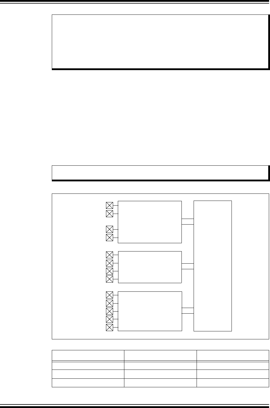
PIC32 Family Reference Manual
DS61129F-page 33-2 © 2007-2012 Microchip Technology Inc.
33.1 INTRODUCTION
The PIC32 family of devices provides a complete range of programming and diagnostic features
that can increase the flexibility of any application using them. These features allow system
designers to include:
•Simplified field programming using 2-wire In-Circuit Serial Programming™ (ICSP™) interfaces
•Debugging using standard ICSP and Enhanced ICSP
•Programming and debugging capabilities using the Enhanced Joint Test Action Group
(Enhanced JTAG) extension of Joint Test Action Group (JTAG) interfaces
• JTAG Boundary scan testing for device and board diagnostics
The PIC32 family of devices incorporates two programming and diagnostic modules, and a trace
controller, which provide a range of functions to the application developer (see Figure 33-1).
They are summarized in Ta ble 3 3- 1 .
Figure 33-1: Block Diagram of Programming, Debugging and Trace Ports
Note: This family reference manual section is meant to serve as a complement to device
data sheets. Depending on the device variant, this manual section may not apply to
all PIC32 devices.
Please consult the note at the beginning of the “Special Features” chapter in the
current device data sheet to check whether this document supports the device you
are using.
Device data sheets and family reference manual sections are available for
download from the Microchip Worldwide Web site at: http://www.microchip.com
Note: Not all programming and diagnostic features are available on all devices. Refer to
the specific device data sheet for availability.
Table 33-1: Comparison of PIC32 Programming and Diagnostic Features
Functions Pins Used Interface
Boundary Scan TDI, TDO, TMS and TCK pins JTAG
Programming and Debugging TDI, TDO, TMS and TCK pins Enhanced JTAG
Programming and Debugging PGECx and PGEDx pins ICSP™
TDI
TDO
TCK
TMS
JTAG
Controller
ICSP™
Controller
Core
Instruction Trace
Controller
PGEC1
PGED1
PGECx
PGEDx
TRCLK
TRD0
TRD1
TRD2
TRD3

© 2007-2012 Microchip Technology Inc. DS61129F-page 33-3
Section 33. Programming and Diagnostics
Programming and
Diagnostics
33
33.2 OPERATION
This section provides a brief overview of operation for each programming option. For detailed
information, refer to the “PIC32MX Flash Programming Specification” (DS61145). Also, for all
device programming options, a minimum VDD requirement for Flash erase and programming
operations is required. Refer to the specific device data sheet for further details.
33.2.1 Device Programming Options
33.2.1.1 IN-CIRCUIT SERIAL PROGRAMMING™ (ICSP™)
ICSP is Microchip’s proprietary solution to providing microcontroller programming in the target
application. ICSP is also the most direct method to program the device, whether the controller is
embedded in a system or loaded into a device programmer.
33.2.1.1.1 ICSP Interface
ICSP uses two pins as the core of its interface. The programming data line (PGD) functions as
both an input and an output, allowing programming data to be read in and device information to
be read out on command. The programming clock line (PGC) is used to clock in data and control
the overall process.
Most PIC32 devices have more than one pair of PGECx and PGEDx pins, which are multiplexed
with other I/O or peripheral functions. Individual ICSP pin pairs are indicated by number, such as
PGEC1/PGED1, and so on. The multiple PGECx/PGEDx pin pairs provide additional flexibility in
system design by allowing users to incorporate ICSP on the pair of pins that is least constrained
by the circuit design. All PGECx and PGEDx pins are functionally tied together and behave iden-
tically, and any one pair can be used for successful device programming. The only limitation is
that both pins from the same pair must be used.
In addition to the PGECx and PGEDx pins, ICSP requires that all voltage supply (including the
voltage regulator pin, ENVREG) and ground pins on the device must be connected. The MCLR
pin, which is used with the PGECx pin to enter and control the programming process, must also
be connected to the programmer.
A typical ICSP connection is shown in Figure 33-2.
Figure 33-2: Typical ICSP™ Connection
ICSP™
PIC32
VSS
VDD
MCLR
PGECx
PGEDx
VSS
VDD
MCLR
CLK
Data I/O

PIC32 Family Reference Manual
DS61129F-page 33-4 © 2007-2012 Microchip Technology Inc.
33.2.1.1.2 ICSP Operation
ICSP uses a combination of internal hardware and external control to program the target device.
Programming data and instructions are provided on the PGD. ICSP uses a special set of
commands to control the overall process, combined with standard PIC32 instructions to execute
the actual writing of the program memory. The PGD also returns data to the external programmer
when responding to queries.
Control of the programming process is achieved by manipulating the PGC and MCLR. Entry into
and exit from Programming mode involves applying (or removing) voltage to MCLR while
supplying a code sequence to the PGD and a clock to the PGC. Any one of the PGECx/PGEDx
pin pairs can be used to enter programming.
The internal process is regulated by a state machine built into the core logic of PIC32 devices;
however, overall control of the process must be provided by the external programming device.
Microchip programming devices, such as the MPLAB®PM 3 (used with MPLAB IDE software),
include the necessary hardware and algorithms to manage the programming process for PIC32
devices. Users who are interested in a detailed description, or who are considering designing
their own programming interface for PIC32 devices, should refer to the “PIC32MX Flash
Programming Specification” (DS61145).
33.2.1.2 ENHANCED ICSP
The Enhanced ICSP protocol is an extension of the standard version of ICSP. It uses the same
physical interface as the original, but changes the location and execution of programming control
to a software application written to a PIC32 device. Use of Enhanced ICSP results in a significant
decrease in overall programming time.
Standard ICSP uses a simple state machine to control each step of the programming process;
however, that state machine is controlled by an external programmer. In contrast, Enhanced
ICSP uses an on-board bootloader, known as the program executive, to manage the
programming process. While overall device programming is still controlled by an external
programmer, the program executive manages most of the tasks that must be directly controlled
by the programmer in standard ICSP.
The program executive implements its own command set, wider in range than standard ICSP,
that can directly erase, program and verify the device program memory. This avoids the need to
repeatedly run ICSP command sequences to perform simple tasks. As a result, Enhanced ICSP
is capable of programming or reprogramming a device faster than standard ICSP.
The program executive is not preprogrammed into a PIC32 device. If Enhanced ICSP is needed,
the user must use standard ICSP to program the executive to the executive memory space in
RAM. This can be done directly by the user, or automatically, using a compatible Microchip
programming system. After the programming executive is written the device can be programmed
using Enhanced ICSP.
For additional information on Enhanced ICSP and the program executive, refer to the “PIC32MX
Flash Programming Specification” (DS61145).
33.2.1.3 DEVICE PROGRAMMING USING THE JTAG INTERFACE
The JTAG interface can also be used to program PIC32 devices in their target applications. The
JTAG interface allows application designers to include a dedicated test and programming port
into their applications, with a single 4-pin interface, without imposing the circuit constraints that
the ICSP interface may require.
33.2.1.4 DEVICE PROGRAMMING USING THE ENHANCED JTAG INTERFACE
Enhanced JTAG programming uses the standard JTAG interface but utilizes a programming
executive written to RAM. Use of the programming executive with the JTAG interface provides a
significant improvement in programming speed.

© 2007-2012 Microchip Technology Inc. DS61129F-page 33-5
Section 33. Programming and Diagnostics
Programming and
Diagnostics
33
33.2.2 Debugging
33.2.2.1 ICSP AND IN-CIRCUIT DEBUGGING
ICSP also provides a hardware channel for the In-Circuit Debugger (ICD), which allows
externally controlled debugging of software. Using the appropriate hardware interface and
software environment, users can force the device to single-step through its code, track the actual
content of multiple registers, and set software breakpoints.
To use ICD, an external system that supports ICD must load a debugger executive program into
the microcontroller. This is automatically handled by many debugger tools, such as the MPLAB
IDE. For PIC32 devices, the program is loaded into the last page of the boot Flash memory
space. When not debugging, the application is free to use the last page of boot Flash memory.
ICSP for PIC32 devices supports standard debugging functions including memory and register
viewing and modification. Breakpoints can be set and the program execution may be stopped or
started. In addition to these functions, registers or memory contents can be viewed and modified
while the CPU is running.
In contrast with programming, only one of the ICSP ports may be used for ICD. If more than one
ICSP port is implemented, a Configuration bit determines which port is available. Depending on
the particular PIC32 device, there may be two or more ICSP ports that can be selected for this
function. The active ICSP debugger port is selected by the ICESEL Configuration bit(s). For
information on a particular device, refer to the specific device data sheet.
33.2.2.2 ENHANCED JTAG DEBUGGING
The industry standard Enhanced JTAG interface allows third-party Enhanced JTAG tools to be
used for debugging. Using the Enhanced JTAG interface, memory and registers can be viewed
and modified. Breakpoints can be set and the program execution may be stopped, started or
single-stepped.
33.2.3 JTAG Boundary Scan
As the complexity and density of board designs increases, testing electrical connections between
the components on fully assembled circuit boards poses many challenges. To address these
challenges, a method for boundary scan testing was developed by the Joint Test Action Group
that was later standardized as IEEE 1149.1-2001, “IEEE Standard Test Access Port and
Boundary Scan Architecture”. Since its adoption, many microcontroller manufacturers have
added device programming to the capabilities of the test port.
The JTAG boundary scan method is the process of adding a shift register stage adjacent to each
of the component’s I/O pins. This permits signals at the component boundaries to be controlled
and observed, using a defined set of scan test principles. An external tester or controller provides
instructions and reads the results in a serial fashion. The external device also provides common
clock and control signals. Depending on the implementation, access to all test signals is provided
through a standardized 4-pin interface.
In system-level applications, individual JTAG-enabled components are connected through their
individual testing interfaces (in addition to their more standard application-specific connections).
Devices are connected in a series or daisy-chained fashion, with the test output of one device
connected exclusively to the test input of the next device in the chain. Instructions in the JTAG
boundary scan protocol allow the testing of any one device in the chain, or any combination of
devices, without testing the entire chain. In this method, connections between components, as
well as connections at the boundary of the application, may be tested.
A typical application incorporating the JTAG boundary scan interface is shown in Figure 33-3. In
this example, a PIC32 family microcontroller is daisy-chained to a second JTAG-compliant
device. Note that the TDI line from the external tester supplies data to the TDI pin of the first
device in the chain (in this case, the microcontroller). The resulting test data for this two-device
chain is provided from the TDO pin of the second device to the TDO line of the tester.
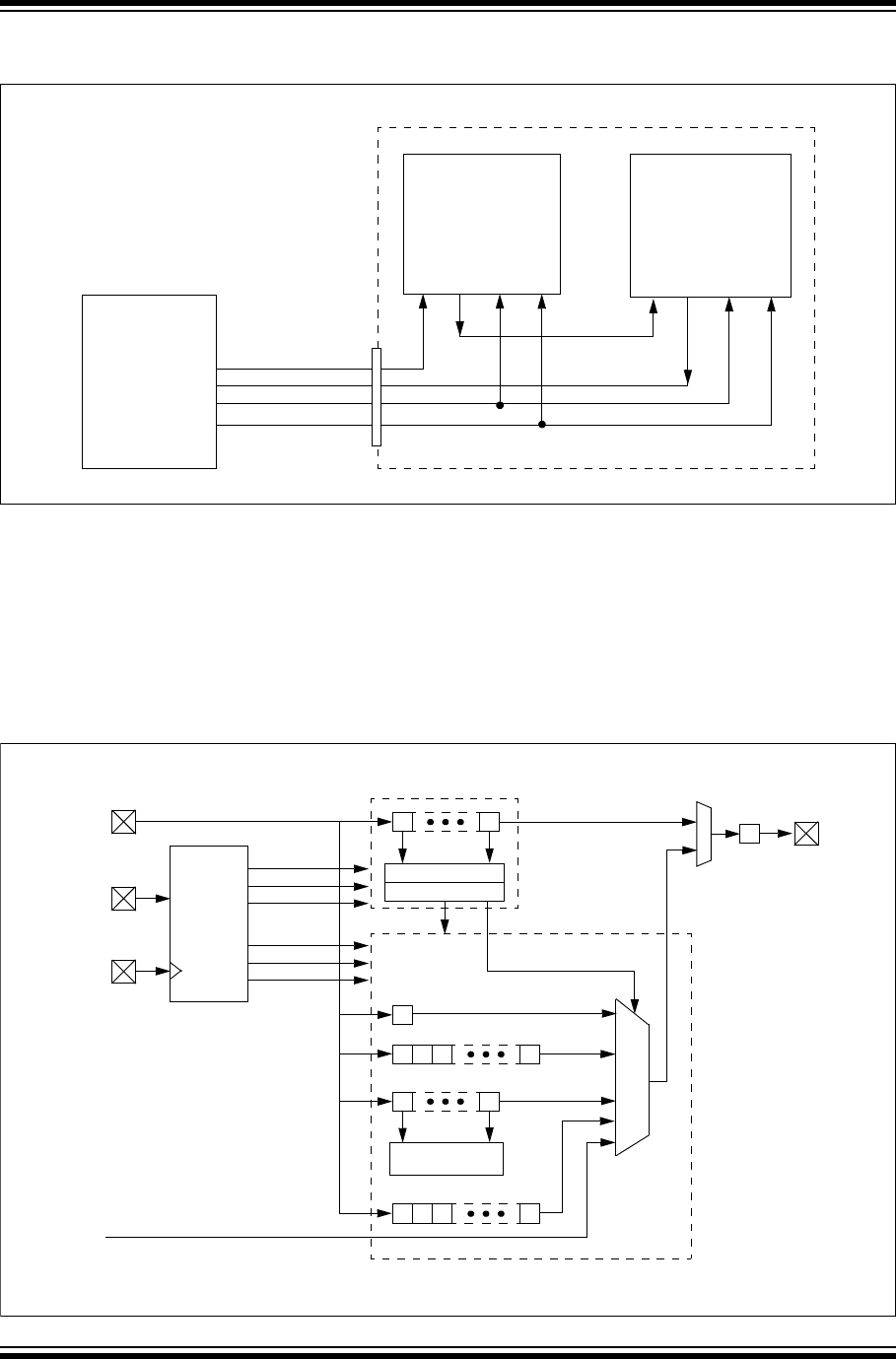
PIC32 Family Reference Manual
DS61129F-page 33-6 © 2007-2012 Microchip Technology Inc.
Figure 33-3: Overview of PIC32 Family-based JTAG-compliant Application Showing Daisy-chaining of
Components
In PIC32 devices, the hardware for the JTAG boundary scan is implemented as a peripheral
module (i.e., outside of the CPU core) with additional integrated logic in all I/O ports. A logical
block diagram of the JTAG module is shown in Figure 33-4. It consists of the following key
elements:
•Test Access Port (TAP) Interface Pins (TDI, TMS, TCK and TDO)
•TAP Controller
• Instruction Shift Register and Instruction Register (IR)
•Data Registers (DR)
Figure 33-4: JTAG Logical Block Diagram
TDI
TDO
TCK
TMS
TDI TDO TCK TMS
JTAG
Controller
PIC32
(or other
JTAG-compliant device)
PIC32-based Application
JTAG Connector
PIC32
TDI TDO TCK TMS
TMS(1)
Capture_IR
TAP
TCK(1)
TDI
Controller
Shift_IR
Update_IR
Capture_DR
Shift_DR
Update_DR
Instruction Shift Register
Instruction Register
Instruction Decode
Data Registers
MCHP Command
Register
MCHP Command Shift Register
Boundary Scan Cell Registers
Device ID Register
Bypass Register
MCHP Scan Data
Data Selector
(MUX)
TDO
TDO Selector
(MUX)
Output Data
Sampling
Register
Note 1: These pins have internal weak pull-ups when JTAG is enabled.
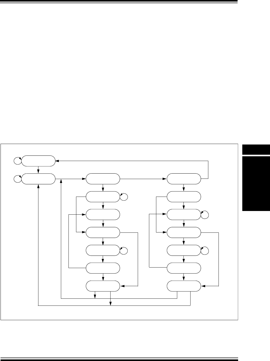
© 2007-2012 Microchip Technology Inc. DS61129F-page 33-7
Section 33. Programming and Diagnostics
Programming and
Diagnostics
33
33.2.3.1 TEST ACCESS PORT (TAP) AND TAP CONTROLLER
The Test Access Port (TAP) on the PIC32 family of devices is a general purpose port that
provides test access to many built-in support functions and test logic defined in the IEEE
Standard 1149.1.
The PIC32 family of devices implements a 4-pin JTAG interface with these pins:
•TCK (Test Clock Input): Provides the clock for test logic
•TMS (Test Mode Select Input): Used by the TAP to control test operations
•TDI (Test Data Input): Serial input for test instructions and data
•TDO (Test Data Output): Serial output for test instructions and data
To minimize I/O loss due to JTAG, the optional TAP reset input pin, specified in the standard, is
not implemented on the PIC32 family of devices. For convenience, a “soft” TAP reset has been
included in the TAP controller, using the TMS and TCK pins. To force a port reset, apply a logic
high to the TMS pin for at least five rising edges of TCK. Note that device Resets (including POR)
do not automatically result in a TAP reset; this must be done by the external JTAG controller
using the soft TAP reset.
The TAP controller on the PIC32 family of devices is a synchronous finite state machine that
implements the standard 16 states for JTAG. Figure 33-5 shows all of the module states of the
TAP controller. All Boundary Scan Testing (BST) instructions and test results are communicated
through the TAP via the TDI pin in a serial format, Least Significant bit (LSb) first.
Figure 33-5: TAP Controller Module State Diagram
Test-Logic
Reset
Run-Test/Idle Select-DR-Scan
Capture-DR
Shift-DR
Exit 1-DR
Pause-DR
Exit 2-DR
Update-DR
Select-IR-Scan
Capture-IR
Shift-IR
Exit 1-IR
Pause-IR
Exit 2-IR
Update-IR
TMS = 0TMS = 1
TMS = 0
TMS = 0
TMS = 1
TMS = 1
TMS = 0
TMS = 0
TMS = 1
TMS = 0
TMS = 1
TMS = 1
TMS = 0TMS = 1
TMS = 0
TMS = 0
TMS = 1
TMS = 0
TMS = 0
TMS = 1
TMS = 0
TMS = 1
TMS = 1
TMS = 1TMS = 1
TMS = 0
TMS = 0
TMS = 0
TMS = 1
TMS = 1
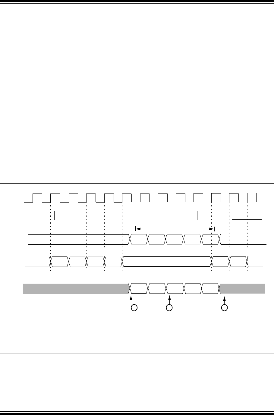
PIC32 Family Reference Manual
DS61129F-page 33-8 © 2007-2012 Microchip Technology Inc.
By manipulating the state of TMS and the clock pulses on TCK, the TAP controller can be moved
through all of the defined module states to capture, shift, and update various instruction and/or
data registers. Figure 33-5 shows the state changes on TMS as the controller cycles through its
state machine. Figure 33-6 shows the timing of TMS and TCK while transitioning the controller
through the appropriate module states for shifting in an instruction. In this example, the sequence
shown demonstrates how an instruction is read by the TAP controller.
All TAP controller states are entered on the rising edge of the TCK pin. In this example, the TAP
controller starts in the Test_Logic Reset state. Since the state of the TAP controller is dependent
on the previous instruction, and therefore could be unknown, it is good programing practice to
begin in the Test_Logic Reset state.
When TMS is asserted low on the next rising edge of TCK, the TAP controller will move into the
Run_Test/Idle state. On the next two rising edges of TCK, TMS is high, which moves the TAP
controller to the Select_IR_Scan state.
On the next two rising edges of TCK, TMS is held low, which moves the TAP controller into the
Shift_IR state. An instruction is shifted into the instruction register (IR) via the TDI on the next
four rising edges of TCK. After the TAP controller enters this state, the TDO pin goes from a
high-impedance state to active. The controller shifts out the initial state of the IR on the TDO pin,
on the falling edges of TCK, and continues to shift out the contents of the instruction register while
in the Shift_IR state. The TDO returns to the high-impedance state on the first falling edge of TCK
upon exiting the shift state.
On the next three rising edges of TCK, the TAP controller exits the Shift_IR state, updates the
Instruction Register and then moves back to the Run_Test/Idle state. Data, or another instruction,
can now be shifted into the appropriate data or instruction register.
Figure 33-6: TAP State Transitions for Shifting in an Instruction
TCK
TMS
TDI
TDO
TAP
State
Instruction Data (LSB)
Shift_IR
Test_L og i c
Reset
Run_Test
Idle
Exit_IR Run_Test
Idle
123
Note 1: The TDO pin is always in a high-impedance state until the first falling edge of TCK in either the Shift_IR or Shift_DR
states.
2: The TDO pin is no longer high-impedance; the initial state of the Instruction Register (IR) is shifted out on the falling
edge of TCK.
3: The TDO pin returns to high-impedance on the first falling edge of TCK in the Exit_IR state.
Select_DR_Scan Capture_IR
Update_IRSelect_IR_Scan

© 2007-2012 Microchip Technology Inc. DS61129F-page 33-9
Section 33. Programming and Diagnostics
Programming and
Diagnostics
33
33.2.3.2 JTAG REGISTERS
The JTAG module uses a number of registers of various sizes as part of its operation. In terms
of bit count, most of the JTAG registers are single-bit register cells, integrated into the I/O ports.
Regardless of their location within the module, none of the JTAG registers are located within the
device data memory space, and cannot be directly accessed by the user in normal operating
modes.
33.2.3.2.1 Instruction Register
The instruction register is a 5-bit shift register used for selecting the actions to be performed
and/or what data registers to be accessed. Instructions are shifted in, Least Significant bit first,
and then decoded.
A list and description of implemented instructions are provided in 33.2.3.4 “JTAG Instructions”.
33.2.3.2.2 Data Registers
Once an instruction is shifted in and updated into the instruction register, the TAP controller
places certain data registers between the TDI and TDO pins. Additional data values can then be
shifted into these data registers as needed.
The PIC32 family of devices supports three data registers:
•BYPASS Register: A single-bit register which allows the boundary scan test data to pass
through the selected device to adjacent devices. The BYPASS register is placed between
the TDI and TDO pins when the BYPASS instruction is active.
•Device ID Register: A 32-bit part identifier. It consists of an 11-bit manufacturer ID assigned
by the IEEE (0x29 for Microchip Technology), device part number and device revision
identifier. When the IDCODE instruction is active, the device ID register is placed between
the TDI and TDO pins. The device data ID is then shifted out on to the TDO pin, on the next
32 falling edges of TCK, after the TAP controller is in the Shift_DR.
•MCHP Command Shift Register: An 8-bit shift register that is placed between the TDI and
TDO pins when the MCHP_CMD instruction is active. This shift register is used to shift in
Microchip commands.
33.2.3.3 BOUNDARY SCAN REGISTER (BSR)
The BSR is a large shift register that is comprised of all the I/O Boundary Scan Cells (BSCs),
daisy-chained together (Figure 33-7). Each I/O pin has one BSC, each containing three BSC
registers: an input cell, an output cell, and a control cell. When the SAMPLE/PRELOAD or EXTEST
instructions are active, the BSR is placed between the TDI and TDO pins, with the TDI pin as the
input and the TDO pin as the output.
The size of the BSR depends on the number of I/O pins on the device. For example, the 100-pin
PIC32 general purpose devices have 82 I/O pins. With three BSC registers for each of the
82 I/Os, this yields a Boundary Scan register length of 244 bits. This is due to the MCLR pin being
an input-only BSR cell. Information on the I/O port pin count of other PIC32 devices can be found
in their specific device data sheets.
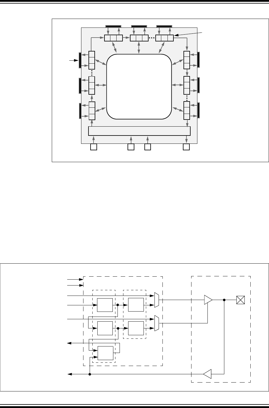
PIC32 Family Reference Manual
DS61129F-page 33-10 © 2007-2012 Microchip Technology Inc.
Figure 33-7: Daisy-chained Boundary Scan Cell Registers on a PIC32 Microcontroller
33.2.3.3.1 Boundary Scan Cell (BSC)
The function of the BSC is to capture and override I/O data values when JTAG is active. The BSC
consists of three single-bit capture register cells and two single-bit holding register cells. The
capture cells are daisy-chained to capture the port’s input, output, and control (output-enable)
data, as well as pass JTAG data along the Boundary Scan register. Command signals from the
TAP controller determine if the port of JTAG data is captured, and how and when it is clocked out
of the BSC.
The first register either captures internal data destined to the output driver, or provides serially
scanned in data for the output driver. The second register captures internal output-enable control
from the output driver and also provides serially scanned in output-enable values. The third
register captures the input data from the I/O’s input buffer.
Figure 33-8 shows a typical BSC and its relationship to the I/O port’s structure.
Figure 33-8: Boundary Scan Cell and Its Relationship to the I/O Port
ICO
ICO
ICO
O
C
I
O
C
I
O
C
I
I
C
O
I
C
O
I
C
O
TAP Controller
Internal
Logic
I/O Pin
TDI TMS TCK TDO
BSC with Three Register Cells:
•Input Cell (I)
•Control Cell (C)
•Output Cell (O)
PIC32
I/O Pin
Input Buffer
OutputBuffer
Data Out
Port
JTAG SDI
from Previous BSC
Port Output Enable
from Output Multiplexer
JTAG SDO
to Next BSC
Port Output
Capture Update
Boundary Scan Cell
Port Input
JTAG Enable
JTAG Clocks
Enable
Output Data
Port I/O Cell
I
O
C

© 2007-2012 Microchip Technology Inc. DS61129F-page 33-11
Section 33. Programming and Diagnostics
Programming and
Diagnostics
33
33.2.3.4 JTAG INSTRUCTIONS
The PIC32 family of devices supports the mandatory instruction set specified by IEEE 1149.1, as
well as several optional public instructions defined in the specification. These devices also
implement instructions that are specific to Microchip devices.
The mandatory JTAG instructions are:
•BYPASS (0x1F): Used for bypassing a device in a test chain, which allows the testing of
off-chip circuitry and board-level interconnections
•SAMPLE/PRELOAD (0x02): Captures the I/O states of the component, providing a snapshot
of its operation
•EXTEST (0x06): Allows the external circuitry and interconnections to be tested, by either
forcing various test patterns on the output pins, or capturing test results from the input pins
Microchip has implemented optional JTAG instructions and manufacturer-specific JTAG
commands in the PIC32 family of devices. For more information, refer to Tab le 3 3 -2 , Table 3 3-3 ,
Tabl e 33- 4, and Ta b le 3 3-5 .
Table 33-2: JTAG Commands
Table 33-3: Microchip TAP IR Commands
Table 33-4: Microchip TAP 8-bit DR Commands
OPCODE Name Device Integration
0x1F Bypass Bypasses device in test chain.
0x00 HIGHZ Places device in a high-impedance state, all pins are
forced to inputs.
0x01 ID Code Shifts out the device’s ID code.
0x02 Sample/Preload Samples all pins or loads a specific value into output
latch.
0x06 EXTEST Boundary Scan.
OPCODE Name Device Integration
0x01 MTAP_IDCODE Shifts out the device’s ID code.
0x07 MTAP_COMMAND Configure Microchip TAP controller for DR commands.
0x04 MTAP_SW_MTAP Select Microchip TAP controller.
0x05 MTAP_SW_ETAP Select Enhanced JTAG TAP controller.
OPCODE Name Device Integration
0x00 MCHP_STATUS Perform NOP and return status.
0xD1 MCHP_ASERT_RST Request assert device Reset.
0xD0 MCHP_DE_ASSERT_RST Request deassert device Reset.
0xFC MCHP_ERASE Perform a Chip Erase.
0xFE MCHP_FLASH_ENABLE Enables fetches and loads to the Flash from the CPU.
0xFD MCHP_FLASH_DISABLE Disables fetches and loads to the Flash from the CPU.
0xFF MCHP_READ_CONFIG Forces device to reread the configuration settings and
initialize accordingly.

PIC32 Family Reference Manual
DS61129F-page 33-12 © 2007-2012 Microchip Technology Inc.
Table 33-5: Enhanced JTAG Commands
33.2.4 Boundary Scan Testing (BST)
BST is the method of controlling and observing the boundary pins of the JTAG-compliant device,
such as PIC32 devices, utilizing software control. BST can be used to test connectivity between
devices by daisy-chaining JTAG compliant devices to form a single scan chain. Several scan
chains can exist on a PCB to form multiple scan chains. These multiple scan chains can then be
driven simultaneously to test many components in parallel. Scan chains can contain both
JTAG-compliant devices and non-JTAG-compliant devices.
A key advantage of BST is that it can be implemented without physical test probes; all that is
needed is a 4-wire interface and an appropriate test platform. Since JTAG boundary scan has
been available for many years, many software tools exist for testing scan chains without the need
for extensive physical probing. The main drawback to BST is that it can only evaluate digital
signals and circuit continuity; it cannot measure input or output voltage levels or currents.
33.2.4.1 RELATED JTAG FILES
To i mp le men t BS T, all J TA G te st to ols w il l req uir e a Bo unda ry Sc an D esc rip ti on La ngu age
(BSDL) file. BSDL is a subset of VHDL (VHSIC Hardware Description Language), and is
described as part of IEEE Std. 1149.1. The device-specific BSDL file describes how the standard
is implemented on a particular device and how it operates.
The BSDL file for a particular device includes the following:
•The pinout and package configuration for the particular device
•The physical location of the TAP pins
• The Device ID register and the device ID
•The length of the Instruction Register
•The supported BST instructions and their binary codes
•The length and structure of the Boundary Scan register
•The boundary scan cell definition
OPCODE Name Device Integration
Data Length
for the
Following DR
0x00 — Not used. —
0x01 IDCODE Selects the device’s ID code register. 32 bits
0x02 — Not used. —
0x03 IMPCODE Selects the implementation register. —
0x04(2) MTAP_SW_MTAP Selects the Microchip TAP controller. —
0x05(2) MTAP_SW_ETAP Selects the Enhanced JTAG TAP controller. —
0x06-0x07 — Not used. —
0x08 ADDRESS Selects the address register. 32 bits
0x09 DATA Selects the data register. 32 bits
0x0A CONTROL Selects the Enhanced JTAG control register 32 bits
0x0B ALL Selects the address, data, and Enhanced
JTAG control registers.
96 bits
0x0C EJTAGBOOT Forces the CPU to take a debug exception
after a boot.
1-bit
0x0D NORMALBOOT Makes the CPU execute the reset handler
after a boot.
1-bit
0x0E FASTDATA Selects the data and fast data registers. 1-bit
0x0F-0x1B — Reserved. —
0x1C-0xFE — Not used. —
0xFF — Selects the BYPASS register. —
Note 1: Refer to the Enhanced JTAG Specification for information about this protocol and
its commands, which is available from MIPS Technologies (www.mips.com).
2: This opcode is not an Enhanced JTAG command, but is recognized by the
Microchip implementation.

© 2007-2012 Microchip Technology Inc. DS61129F-page 33-13
Section 33. Programming and Diagnostics
Programming and
Diagnostics
33
33.3 INTERRUPTS
Programming and debugging operations are not performed during code execution and are
therefore not affected by interrupts. Trace operations will report the change in code execution
when an interrupt occurs but the trace controller is not affected by interrupts.
33.4 OPERATION IN POWER-SAVING MODES
PIC32 devices must be awake for all programming and debugging operations.
33.5 EFFECTS OF RESETS
33.5.1 Device Reset
A device Reset by asserting MCLR while in ICSP mode will force the ICSP to exit. Asserting
MCLR will force an exit from Enhanced JTAG mode.
33.5.2 Watchdog Timer Reset
A Watchdog Timer (WDT) Reset during erase will not abort the erase cycle. The WDT event flag
will be set to show that a WDT Reset has occurred.
A WDT Reset during an Enhanced JTAG session will reset the TAP controller to the Microchip
TAP controller.
A WDT Reset during programming will abort the programming sequence.

PIC32 Family Reference Manual
DS61129F-page 33-14 © 2007-2012 Microchip Technology Inc.
33.6 RELATED APPLICATION NOTES
This section lists application notes that are related to this section of the manual. These
application notes may not be written specifically for the PIC32 family of devices, but the concepts
are pertinent and could be used with modification and possible limitations. The current
application notes related to Programming and Diagnostics are:
Title Application Note #
No related application notes at this time. N/A
Note: Please visit the Microchip web site (www.microchip.com) for additional application
notes and code examples for the PIC32 family of devices.

© 2007-2012 Microchip Technology Inc. DS61129F-page 33-15
Section 33. Programming and Diagnostics
Programming and
Diagnostics
33
33.7 REVISION HISTORY
Revision A (September 2007)
This is the initial released version of this document.
Revision B (October 2007)
Updated document to remove Confidential status.
Revision C (April 2008)
Revised document status to Preliminary; Revised U-0 to r-x.
Revision D (June 2008)
This revision includes the following updates:
•Added a Note to 33.3.1 “Device Programming Options”
• Revised 33.3.2.1 “ICSP and In-Circuit Debugging”
•Revised Table33-7
• Change Reserved bits from “Maintain as” to “Write” in all registers
Revision E (August 2009)
This revision includes the following updates:
•Minor updates to text and formatting have been incorporated throughout the document
• Added the FJTAGEN bit and removed bits DDPU1, DDPU2 and DDPSPI1 from Table 33-2:
Programming and Diagnostics SFR Summary
• Added FJTAGEN bit and removed bits DDPUSB, DDPU1, DDPU2 and DDPSPI1 from
Register 33-1: DDPCON: Debug Data Port Control Register
Revision F (February 2012)
This revision includes the following updates:
• Updated the Programming, Debugging, and Trace Ports Block Diagram (see Figure 33-1)
•Added Note 1 to the JTAG Logical Block Diagram (see Figure 33-4)
•Removed the Programming and Diagnostics SFR Summary (Table33-2)
•Removed the DDPCON and DEVCFG0 registers (Register 33-1 and Register 33-2)
•Removed 33.3.3 “Special Debug Modes for Select Communication Peripherals”
•Updated the first paragraph of 33.2.3.1 “Test Access Port (TAP) and TAP Controller”
•Updated 33.2.4.1 “Related JTAG Files”
•Removed 33.2 “Control Registers”
•Removed 33.5 “I/O Pins”
•Removed 33.8 “Application Ideas”
• All references to the PGC and PGD pins have been updated to: PGECx and PGEDx
• All references to EJTAG were updated to: Enhanced JTAG
• All references to EICSP were updated to: Enhanced ICSP
• All occurrences of PIC32MX have been replaced with PIC32, with the exception of
references to the “PIC32MX Flash Programming Specification” (DS61145)
•Formatting modifications and text updates were incorporated throughout the document

PIC32 Family Reference Manual
DS61129F-page 33-16 © 2007-2012 Microchip Technology Inc.
NOTES:

© 2007-2012 Microchip Technology Inc. DS61129F-page 33-17
Information contained in this publication regarding device
applications and the like is provided only for your convenience
and may be superseded by updates. It is your responsibility to
ensure that your application meets with your specifications.
MICROCHIP MAKES NO REPRESENTATIONS OR
WARRANTIES OF ANY KIND WHETHER EXPRESS OR
IMPLIED, WRITTEN OR ORAL, STATUTORY OR
OTHERWISE, RELATED TO THE INFORMATION,
INCLUDING BUT NOT LIMITED TO ITS CONDITION,
QUALITY, PERFORMANCE, MERCHANTABILITY OR
FITNESS FOR PURPOSE. Microchip disclaims all liability
arising from this information and its use. Use of Microchip
devices in life support and/or safety applications is entirely at
the buyer’s risk, and the buyer agrees to defend, indemnify and
hold harmless Microchip from any and all damages, claims,
suits, or expenses resulting from such use. No licenses are
conveyed, implicitly or otherwise, under any Microchip
intellectual property rights.
Trademarks
The Microchip name and logo, the Microchip logo, dsPIC,
KEELOQ, KEELOQ logo, MPLAB, PIC, PICmicro, PICSTART,
PIC32 logo, rfPIC and UNI/O are registered trademarks of
Microchip Technology Incorporated in the U.S.A. and other
countries.
FilterLab, Hampshire, HI-TECH C, Linear Active Thermistor,
MXDEV, MXLAB, SEEVAL and The Embedded Control
Solutions Company are registered trademarks of Microchip
Technology Incorporated in the U.S.A.
Analog-for-the-Digital Age, Application Maestro, chipKIT,
chipKIT logo, CodeGuard, dsPICDEM, dsPICDEM.net,
dsPICworks, dsSPEAK, ECAN, ECONOMONITOR,
FanSense, HI-TIDE, In-Circuit Serial Programming, ICSP,
Mindi, MiWi, MPASM, MPLAB Certified logo, MPLIB,
MPLINK, mTouch, Omniscient Code Generation, PICC,
PICC-18, PICDEM, PICDEM.net, PICkit, PICtail, REAL ICE,
rfLAB, Select Mode, Total Endurance, TSHARC,
UniWinDriver, WiperLock and ZENA are trademarks of
Microchip Technology Incorporated in the U.S.A. and other
countries.
SQTP is a service mark of Microchip Technology Incorporated
in the U.S.A.
All other trademarks mentioned herein are property of their
respective companies.
© 2007-2012, Microchip Technology Incorporated, Printed in
the U.S.A., All Rights Reserved.
Printed on recycled paper.
ISBN: 978-1-62076-034-5
Note the following details of the code protection feature on Microchip devices:
• Microchip products meet the specification contained in their particular Microchip Data Sheet.
• Microchip believes that its family of products is one of the most secure families of its kind on the market today, when used in the
intended manner and under normal conditions.
• There are dishonest and possibly illegal methods used to breach the code protection feature. All of these methods, to our
knowledge, require using the Microchip products in a manner outside the operating specifications contained in Microchip’s Data
Sheets. Most likely, the person doing so is engaged in theft of intellectual property.
• Microchip is willing to work with the customer who is concerned about the integrity of their code.
• Neither Microchip nor any other semiconductor manufacturer can guarantee the security of their code. Code protection does not
mean that we are guaranteeing the product as “unbreakable.”
Code protection is constantly evolving. We at Microchip are committed to continuously improving the code protection features of our
products. Attempts to break Microchip’s code protection feature may be a violation of the Digital Millennium Copyright Act. If such acts
allow unauthorized access to your software or other copyrighted work, you may have a right to sue for relief under that Act.
Microchip received ISO/TS-16949:2009 certification for its worldwide
headquarters, design and wafer fabrication facilities in Chandler and
Tempe, Arizona; Gresham, Oregon and design centers in California
and India. The Company’s quality system processes and procedures
are for its PIC® MCUs and dsPIC® DSCs, KEELOQ® code hopping
devices, Serial EEPROMs, microperipherals, nonvolatile memory and
analog products. In addition, Microchip’s quality system for the design
and manufacture of development systems is ISO 9001:2000 certified.

DS61129F-page 33-18 © 2007-2012 Microchip Technology Inc.
AMERICAS
Corporate Office
2355 West Chandler Blvd.
Chandler, AZ 85224-6199
Tel: 480-792-7200
Fax: 480-792-7277
Technical Support:
http://www.microchip.com/
support
Web Address:
www.microchip.com
Atlanta
Duluth, GA
Tel: 678-957-9614
Fax: 678-957-1455
Boston
Westborough, MA
Tel: 774-760-0087
Fax: 774-760-0088
Chicago
Itasca, IL
Tel: 630-285-0071
Fax: 630-285-0075
Cleveland
Independence, OH
Tel: 216-447-0464
Fax: 216-447-0643
Dallas
Addison, TX
Tel: 972-818-7423
Fax: 972-818-2924
Detroit
Farmington Hills, MI
Tel: 248-538-2250
Fax: 248-538-2260
Indianapolis
Noblesville, IN
Tel: 317-773-8323
Fax: 317-773-5453
Los Angeles
Mission Viejo, CA
Tel: 949-462-9523
Fax: 949-462-9608
Santa Clara
Santa Clara, CA
Tel: 408-961-6444
Fax: 408-961-6445
Toronto
Mississauga, Ontario,
Canada
Tel: 905-673-0699
Fax: 905-673-6509
ASIA/PACIFIC
Asia Pacific Office
Suites 3707-14, 37th Floor
Tower 6, The Gateway
Harbour City, Kowloon
Hong Kong
Tel : 8 52 - 24 0 1- 120 0
Fax: 852-2401-3431
Australia - Sydney
Tel : 6 1-2 -98 68- 6 73 3
Fax: 61-2-9868-6755
China - Beijing
Tel : 8 6-1 0-8 569 - 70 0 0
Fax: 86-10-8528-2104
China - Chengdu
Tel : 8 6-2 8-8 665 - 55 11
Fax: 86-28-8665-7889
China - Chongqing
Tel : 8 6-2 3-8 980 - 95 8 8
Fax: 86-23-8980-9500
China - Hangzhou
Tel : 8 6-5 71- 2819 -31 87
Fax: 86-571-2819-3189
China - Hong Kong SAR
Tel : 8 52 - 24 0 1- 120 0
Fax: 852-2401-3431
China - Nanjing
Tel : 8 6-2 5-8 473 - 24 6 0
Fax: 86-25-8473-2470
China - Qingdao
Tel : 8 6-5 32- 8502 -73 55
Fax: 86-532-8502-7205
China - Shanghai
Tel : 8 6-2 1-5 407 - 55 3 3
Fax: 86-21-5407-5066
China - Shenyang
Tel : 8 6-2 4-2 334 - 28 2 9
Fax: 86-24-2334-2393
China - Shenzhen
Tel : 8 6-7 55- 8203 -26 60
Fax: 86-755-8203-1760
China - Wuhan
Tel : 8 6-2 7-5 980 - 53 0 0
Fax: 86-27-5980-5118
China - Xian
Tel : 8 6-2 9-8 833 - 72 5 2
Fax: 86-29-8833-7256
China - Xiamen
Tel: 86-592-2388138
Fax: 86-592-2388130
China - Zhuhai
Tel : 86- 756 -3 210 04 0
Fax: 86-756-3210049
ASIA/PACIFIC
India - Bangalore
Tel : 9 1- 8 0- 309 0-4 444
Fax: 91-80-3090-4123
India - New Delhi
Tel : 9 1- 11 -41 60- 86 31
Fax: 91-11-4160-8632
India - Pune
Tel : 9 1- 2 0- 256 6-1 512
Fax: 91-20-2566-1513
Japan - Osaka
Tel : 8 1- 6 6- 152 -71 60
Fax: 81-66-152-9310
Japan - Yokohama
Tel : 8 1- 4 5- 471 - 6 166
Fax: 81-45-471-6122
Korea - Daegu
Tel : 8 2- 5 3- 744 -43 01
Fax: 82-53-744-4302
Korea - Seoul
Tel : 8 2- 2 -5 54- 720 0
Fax: 82-2-558-5932 or
82-2-558-5934
Malaysia - Kuala Lumpur
Tel : 6 0- 3 -6 201 -98 57
Fax: 60-3-6201-9859
Malaysia - Penang
Tel : 6 0- 4 -2 27- 887 0
Fax: 60-4-227-4068
Philippines - Manila
Tel : 6 3- 2 -6 34- 906 5
Fax: 63-2-634-9069
Singapore
Tel : 6 5- 6 33 4 -8 870
Fax: 65-6334-8850
Taiwan - Hsin Chu
Tel : 8 86 - 3- 577 8-3 66
Fax: 886-3-5770-955
Taiwan - Kaohsiung
Tel : 8 86 - 7- 536 -48 18
Fax: 886-7-330-9305
Taiwan - Taipei
Tel : 8 86 - 2- 250 0-6 610
Fax: 886-2-2508-0102
Thailand - Bangkok
Tel : 6 6- 2 -6 94- 135 1
Fax: 66-2-694-1350
EUROPE
Austria - Wels
Tel : 4 3- 7 24 2 -2 244 -39
Fax: 43-7242-2244-393
Denmark - Copenhagen
Tel : 4 5-4 450 -2 828
Fax: 45-4485-2829
France - Paris
Tel : 3 3-1 -6 9-5 3 -6 3-2 0
Fax: 33-1-69-30-90-79
Germany - Munich
Tel : 4 9- 8 9- 627 -14 4-0
Fax: 49-89-627-144-44
Italy - Milan
Tel : 3 9- 0 33 1 -7 426 11
Fax: 39-0331-466781
Netherlands - Drunen
Tel : 3 1- 4 16 - 690 3 99
Fax: 31-416-690340
Spain - Madrid
Tel : 3 4- 9 1- 708 -08 -90
Fax: 34-91-708-08-91
UK - Wokingham
Tel : 4 4- 11 8-9 21- 58 69
Fax: 44-118-921-5820
Worldwide Sales and Service
11/29/11

© 2009-2012 Microchip Technology Inc. DS61154C-page 34-1
Controller Area
Network (CAN)
34
Section 34. Controller Area Network (CAN)
HIGHLIGHT
This section of the manual contains the following topics:
34.1 Introduction..............................................................................................................34-2
34.2 CAN Message Formats ........................................................................................... 34-4
34.3 CAN Registers.........................................................................................................34-9
34.4 Enabling and Disabling the CAN Module .............................................................. 34-47
34.5 CAN Module Operating Modes.............................................................................. 34-47
34.6 CAN Message Handling ....................................................................................... 34-49
34.7 Transmitting a CAN Message................................................................................34-56
34.8 CAN Message Filtering.......................................................................................... 34-68
34.9 Receiving a CAN Message.................................................................................... 34-75
34.10 Bit Timing...............................................................................................................34-83
34.11 CAN Error Management ........................................................................................ 34-87
34.12 CAN Interrupts....................................................................................................... 34-90
34.13 CAN Received Message Time Stamping............................................................... 34-94
34.14 Power-Saving Modes ............................................................................................ 34-95
34.15 Related Application Notes ..................................................................................... 34-96
34.16 Revision History.....................................................................................................34-97
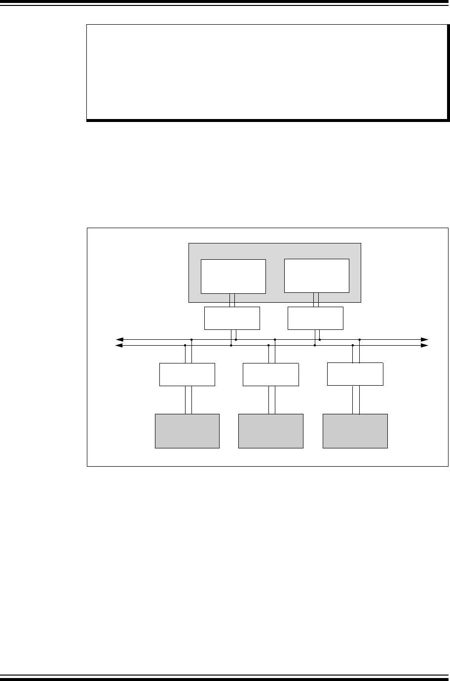
PIC32 Family Reference Manual
DS61154C-page 34-2 © 2009-2012 Microchip Technology Inc.
34.1 INTRODUCTION
The PIC32 Controller Area Network (CAN) module implements the CAN Specification 2.0B,
which is used primarily in industrial and automotive applications. This asynchronous serial data
communication protocol provides reliable communication in an electrically noisy environment.
The PIC32 device family integrates up to two CAN modules. Figure 34-1 illustrates a typical CAN
bus topology.
Figure 34-1: Typical CAN Bus Network
The CAN module supports the following key features:
•Standards Compliance:
-Full CAN Specification 2.0B compliance
- Programmable bit rate up to 1 Mbps
•Message Reception and Transmission:
-32 message FIFOs
- Each FIFO can have up to 32 messages for a total of 1024 messages
-FIFO can be a transmit message FIFO or a receive message FIFO
-User-defined priority levels for message FIFOs used for transmission
-32 acceptance filters for message filtering
-Four acceptance filter mask registers for message filtering
- Automatic response to Remote Transmit Request (RTR)
-DeviceNet™ addressing support
Note: This family reference manual section is meant to serve as a complement to device
data sheets. Depending on the device variant, this manual section may not apply to
all PIC32 devices.
Please consult the note at the beginning of the “Controller Area Network (CAN)”
chapter in the current device data sheet to check whether this document supports
the device you are using.
Device data sheets and family reference manual sections are available for
download from the Microchip Worldwide Web site at: http://www.microchip.com
CAN
bus
CAN1
PIC®
with Integrated
ECAN
CAN
Transceiver
dsPIC33F
with Integrated
ECAN™
dsPIC30F
with Integrated
CAN
Transceiver
CAN Transceiver
CAN
Transceiver
CAN
CAN2
CAN
Transceiver
PIC32
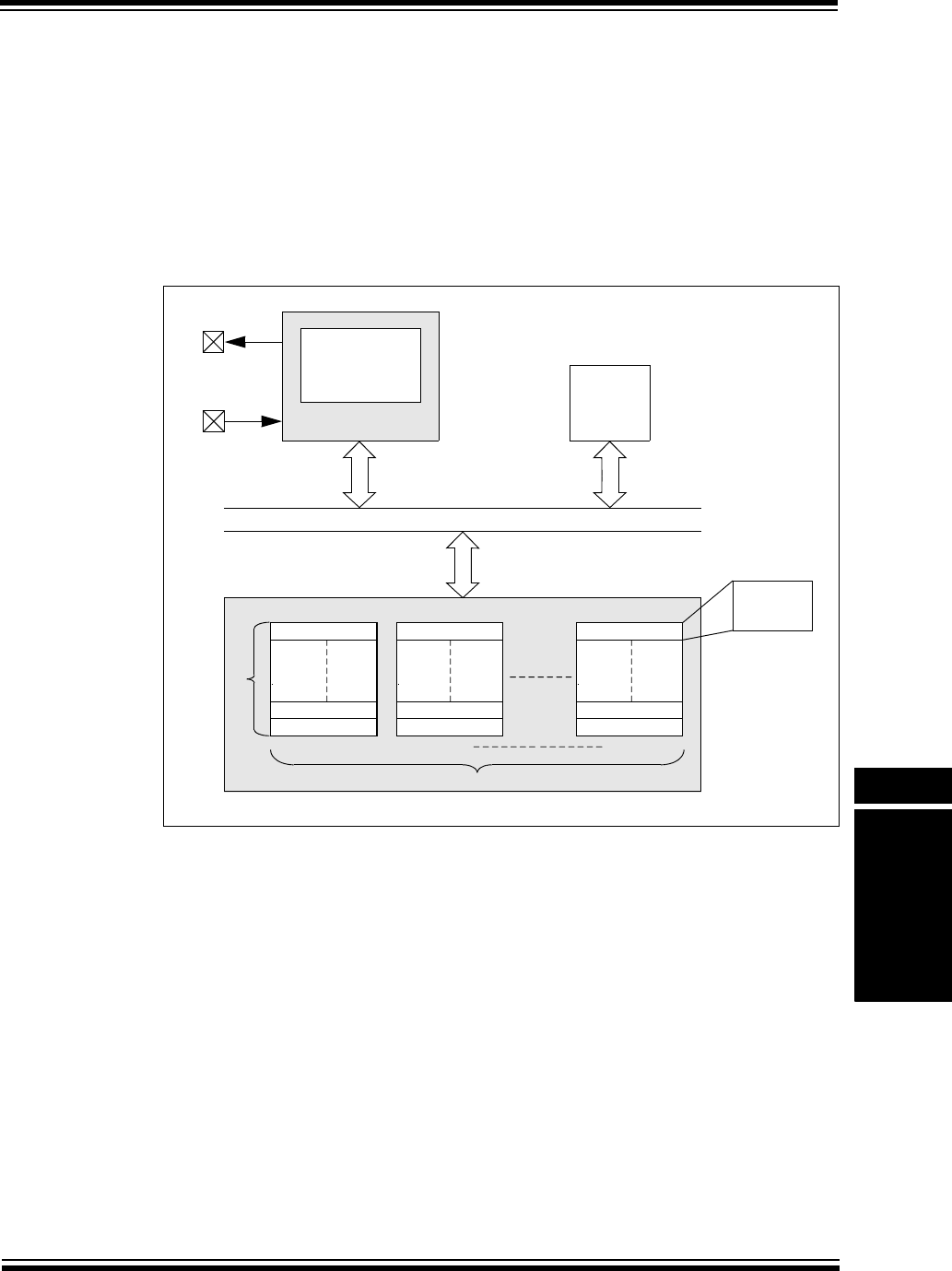
© 2009-2012 Microchip Technology Inc. DS61154C-page 34-3
Section 34. Controller Area Network (CAN)
Controller Area
Network (CAN)
34
•Additional Features:
- Loopback, Listen All Messages and Listen-Only modes for self-test, system diagnostics
and bus monitoring
-Low-power operating modes
-CAN module is a bus master on the PIC32 system bus
-Does not require Direct Memory Access (DMA) channels for operation
-Dedicated time stamp timer
-Data-only Message Reception mode
Figure 34-2 illustrates the general structure of the CAN module.
Figure 34-2: PIC32 CAN Module Block Diagram
The CAN module consists of a protocol engine, message acceptance filters and Message
Assembly Buffers (MABs). The protocol engine transmits and receives messages to and from the
CAN bus (as per CAN Specification 2.0B). Received messages are assembled in the receive
message assembly buffer. The received message is then filtered by the message acceptance
filters. The transmit message assembly buffer holds the message to be transmitted as it is
processed by the protocol engine.
The CAN message buffers reside in device RAM. There are no CAN message buffers in the CAN
module. Therefore, all messages are stored in device RAM. The CAN module is a bus master on
the PIC32 system bus, and will read and write data to device RAM as required. The CAN module
does not use DMA for its operation and fetches messages from the device RAM without DMA or
CPU intervention.
Message Buffer 31
Message Buffer 1
Message Buffer 0
Message Buffer 31
Message Buffer 1
Message Buffer 0
Message Buffer 31
Message Buffer 1
Message Buffer 0
FIFO0 FIFO1 FIFO31
Device RAM
Up to 32 Message Buffers
CAN Message FIFO (up to 32 FIFOs)
Message
Buffer Size
2 or 4 Words
System Bus
CPU
CAN Module
32 Filters
4 Masks
CxTX
CxRX

PIC32 Family Reference Manual
DS61154C-page 34-4 © 2009-2012 Microchip Technology Inc.
34.2 CAN MESSAGE FORMATS
The CAN bus protocol uses asynchronous communication. Information is passed from the
transmitters to receivers in data frames, which are composed of byte fields that define the
contents of the data frame as illustrated in Figure 34-3.
Each frame begins with a Start of Frame (SOF) bit field and terminates with an End of Frame
(EOF) bit field. The SOF is followed by the Arbitration and Control fields, which identify the
message type, format, length and priority. This information allows each node on the CAN bus to
respond appropriately to the message. The Data field conveys the message content and is of
variable length, ranging from 0 bytes to 8 bytes. Error protection is provided by the Cyclic
Redundancy Check (CRC) and Acknowledgement (ACK) fields.
Figure 34-3: CAN Bus Message Frame
The CAN bus protocol supports four frame types:
•Data Frame – carries data from transmitter to the receivers
•Remote Frame – transmitted by a node on the bus, to request transmission of a data
frame with the same identifier from another node
•Error Frame – transmitted by any node when it detects an error
•Overload Frame – provides an extra delay between successive Data or remote frames
•Interframe Space – provides a separation between successive frames
The CAN Specification 2.0B defines two additional data formats:
•Standard Data Frame – intended for standard messages that use 11 identifier bits
•Extended Data Frame – intended for extended messages that use 29 identifier bits
There are three CAN Specification versions:
•2.0A – considers 29-bit identifier as error
•2.0B Passive – ignores 29-bit identifier messages
•2.0B Active – handles both 11-bit and 29-bit identifiers
The PIC32 CAN module is compliant with the CAN Specification 2.0B, while providing enhanced
message filtering capabilities.
Note: For detailed information on the CAN protocol, refer to the Bosch CAN Bus
Specification 2.0B, which is available for download at:
http://www.semiconductors.bosch.de
S
O
F
E
O
F
ARBITRATION CONTROL DATA ACKCRC
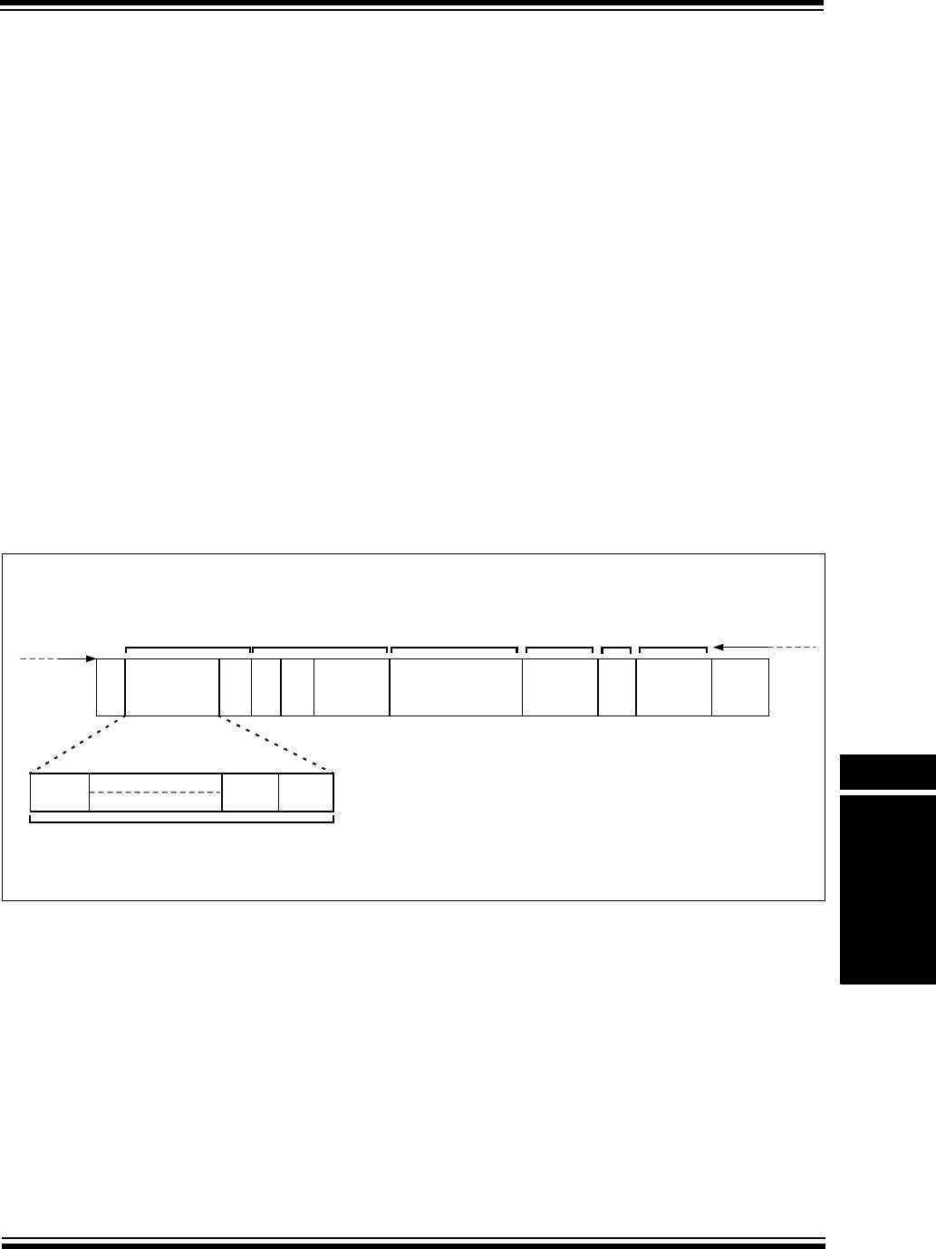
© 2009-2012 Microchip Technology Inc. DS61154C-page 34-5
Section 34. Controller Area Network (CAN)
Controller Area
Network (CAN)
34
34.2.1 Standard Data Frame
The standard data frame message begins with an SOF bit followed by a 12-bit Arbitration field
as illustrated in Figure 34-4. The Arbitration field contains an 11-bit identifier and RTR bit. The
identifier defines the type of information contained in the message, and is used by each receiving
node to determine if the message is of interest to it. The RTR bit distinguishes a data frame from
a remote frame. For a standard data frame, the RTR bit is clear.
Following the Arbitration field is a 6-bit Control field, which provides more information about the
contents of the message. The first bit in the Control field is an Identifier Extension (IDE) bit, which
distinguishes the message as either a standard or extended data frame. A standard data frame
is indicated by a dominant state (logic level ‘0’) during transmission of the IDE bit. The second
bit in the Control field is a reserved (RB0) bit, which is in the dominant state (logic level ‘0’). The
last four bits in the Control field represent the Data Length Code (DLC), which specifies the
number of data bytes present in the message.
The Data field follows the Control field. This field carries the message data – the actual payload
of the data frame. This field is of variable length, ranging from 0 bytes to eight bytes. The number
of bytes is user-selectable.
The Data field is followed by the CRC field, which is a 15-bit CRC sequence with one delimiter bit.
The Acknowledgement (ACK) field is sent as a recessive bit (logic level ‘1’), and is overwritten
as a dominant bit by any receiver that has received the data correctly. The message is
acknowledged by the receiver regardless of the result of the acceptance filter comparison.
The last field is the EOF field, which consists of seven recessive bits that indicate the end of
message.
Figure 34-4: Format of the Standard Data Frame
SID10 SID1
S
O
F
IDENTIFIER
11 Bits
R
T
R
I
D
E
RB0 DLC
4 Bits
DATA
8 Bytes
CRC
16 Bits
ACK
2 Bits
EOF
7 Bits
IFS
3 Bits
SID0
9/19/2006 - 9/26/2006
11-bit Identifier
Interframe Space
9/19/2006 - 9/26/2006 9/19/2006 - 9/26/2006
Data
9/19/2006 - 9/26/2006
9/19/2006 - 9/26/2006
9-9/26/2006
Frame Interframe Space
9/19/2006 - 9/26/2006
IDE is Dominant (Logical ‘0’)
RTR is Dominant (Logical ‘0’)
RB0 is Dominant (Logical ‘0’)
/19/
Arbitration
Field
Control
Field
Field
CRC
Field
ACK
Field
End-of-
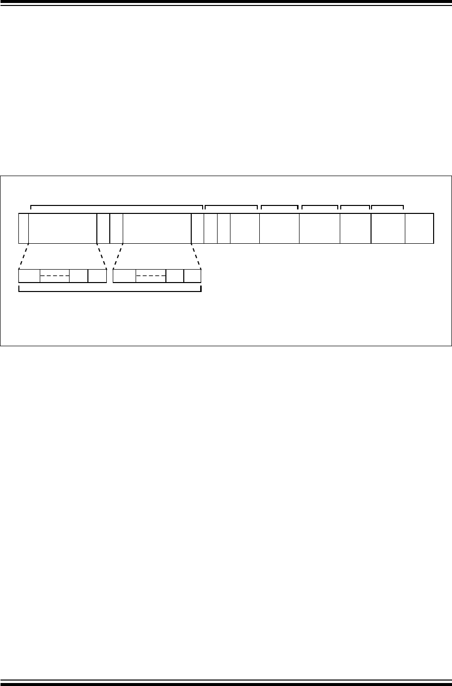
PIC32 Family Reference Manual
DS61154C-page 34-6 © 2009-2012 Microchip Technology Inc.
34.2.2 Extended Data Frame
The extended data frame begins with an SOF bit followed by a 31-bit Arbitration field as
illustrated in Figure 34-5. The Arbitration field for the extended data frame contains 29 identifier
bits in two fields separated by a Substitute Remote Request (SRR) bit and an IDE bit. The SRR
bit determines if the message is a remote frame. SRR = 1 for extended data frames. The IDE bit
indicates the data frame type. For the extended data frame, IDE = 1.
The extended data frame Control field consists of seven bits. The first bit is the RTR. For the
extended data frame, RTR = 0. The next two bits, RB1 and RB0, are reserved bits that are in the
dominant state (logic level ‘0’). The last four bits in the Control field are the DLC, which specifies
the number of data bytes present in the message.
The remaining fields in an extended data frame are identical to a standard data frame.
Figure 34-5: Format of the Extended Data Frame
SID10 SID1
S
O
F
IDENTIFIER
11 Bits
S
R
R
I
D
E
R
T
R
DLC
4 BITS
CRC
16 BITS
ACK
2 BITS
EOF
7 BITS
IFS
3 BITS
SID0
Field
29-bit Identifier
9/19/2006 - 9/26/2006
Control
9/19/2006 - 9/26/2006
CRC
9/19/2006 - 9/26/2006
IDENTIFIER
18 BITS
EID17 EID1 EID0
R
B
1
R
B
0
IDE is Recessive (Logical ‘1’)
SRR is Recessive (Logical ‘1’)
RTR is Dominant (Logical ‘0’)
RB0 is Dominant (Logical ‘0’)
RB1 is Dominant (Logical ‘0’)
9/19/2006 - 9/26/2006
ACK End of
Frame
9/19/2006 - 9/26/20069/19/2006 - 9/26/2006
Data
DATA
8 Bytes
Arbitration
Field Field Field Field
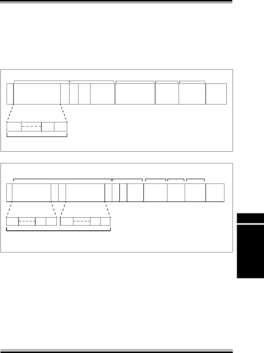
© 2009-2012 Microchip Technology Inc. DS61154C-page 34-7
Section 34. Controller Area Network (CAN)
Controller Area
Network (CAN)
34
34.2.3 Remote Frame
A node expecting to receive data from another node can initiate transmission of the respective
data by the source node, by sending a remote frame. A remote frame can be in standard format
(Figure 34-6) or the extended format (Figure 34-7).
A Remote frame is similar to a data frame, with the following exceptions:
•The RTR bit is recessive (RTR = 1)
•There is no Data field (DLC = 0)
Figure 34-6: Format of the Standard Remote Frame
Figure 34-7: Format of the Extended Remote Frame
SID10 SID1
S
O
F
IDENTIFIER
11 Bits
R
T
R
I
D
E
DLC
4 Bits
CRC
16 Bits
ACK
2 Bits
EOF
7 Bits
IFS
3 Bits
SID0
11-bit Identifier
RB0
IDE is Dominant (Logical ‘0’)
RTR is Recessive (Logical ‘1’)
RB0 is Dominant (Logical ‘0’)
Arbitration Field Control Field CRC Field ACK Field End of Frame
SID10 SID0
S
O
F
IDENTIFIER
11 Bits
S
R
R
I
D
E
R
T
R
DLC
4 Bits
CRC
16 Bits
ACK
2 Bits
EOF
7 Bits
IFS
3 Bits
SID1
Arbitration Field
29-bit Identifier
Control Field CRC Field
IDENTIFIER
18 Bits
EID17 EID1 EID0
R
B
1
R
B
0
IDE is Recessive (Logical ‘1’)
SRR is Recessive (Logical ‘1’)
RTR is Recessive (Logical ‘1’)
RB0 is Dominant (Logical ‘0’)
RB1 is Dominant (Logical ‘0’)
ACK Field
End of
Frame

PIC32 Family Reference Manual
DS61154C-page 34-8 © 2009-2012 Microchip Technology Inc.
34.2.4 Error Frame
An error frame is generated by any node that detects a bus error. An error frame consists of an
Error Flag field followed by an Error Delimiter field. The Error Delimiter consists of eight recessive
bits and allows the bus nodes to restart communication cleanly after an error has occurred. There
are two types of error flag fields, depending on the error status of the node that detects the error:
•Error Active Flag – contains six consecutive dominant bits, which forces all other nodes
on the network to generate Error Echo Fags, thereby resulting in a series of 6 to 12
dominant bits on the bus
•Error Passive Flag – contains six consecutive recessive bits, with the result that unless
the bus error is detected by the transmitting node, the transmission of an Error Passive
Flag will not affect the communication of any other node on the network
34.2.5 Overload Frame
An Overload Frame can be generated by a node either when a dominant bit is detected during
Interframe Space or when a node is not ready to receive the next message (for example, if it is
still reading the previous received message). An Overload Frame has the same format as an
Error Frame with an Active Error Flag, but can only be generated during Interframe Space. It
consists of an Overload Fag field with six dominant bits followed by an Overload Delimiter field
with eight recessive bits. A node can generate a maximum of two sequential overload frames to
delay the start of the next message.
34.2.6 Interframe Space
Interframe Space separates successive frames being transmitted on the CAN bus. It consists of
at least three recessive bits, referred to as intermission. The Interframe Space allows nodes time
to internally process the previously received message before the start of the next frame. If the
transmitting node is in the Error Passive state, an additional eight recessive bits will be inserted
in the Interframe Space before any other message is transmitted by the node. This period is
called a Suspend Transmit field and allows time for other transmitting nodes to take control of the
bus.

© 2009-2012 Microchip Technology Inc. DS61154C-page 34-9
Section 34. Controller Area Network (CAN)
Controller Area
Network (CAN)
34
34.3 CAN REGISTERS
The CAN module registers can be classified by their function into the following groups:
•Module and CAN bit rate Configuration registers
•Interrupt and Status registers
•Mask and Filter Configuration registers
•FIFO Control registers
34.3.1 Module and CAN Bit Rate Configuration Registers
•CiCON: CAN Module Control Register
This register is used to set up the CAN module operational mode and DeviceNet addressing.
•CiCFG: CAN Baud Rate Configuration Register
This register contains control bits to set the period of each time quantum, using the baud rate
prescaler, and specifies Synchronization Jump Width (SJW) in terms of time quanta. It is
also used to program the number of time quanta in each CAN bit segment, including the
propagation and phase segments 1 and 2.
34.3.2 Interrupt and Status Registers
•CiINT: CAN Interrupt Register
This register allows various CAN module interrupt sources to be enabled and disabled. It
also contains interrupt status flags.
•CiVEC: CAN Interrupt Code Register
This register provides status bits which provide information on CAN module interrupt source
and message filter hits. These values can be used to implement a jump table for handling
different cases.
•CiTREC: CAN Transmit/Receive Error Count Register
This register provides information on Transmit and Receive Error Counter values. It also has
bits which indicate various warning states.
•CiFSTAT: CAN FIFO Status Register
This register contains interrupt status flag for all the FIFOs.
•CiRXOVF: CAN Receive FIFO Overflow Status Register
This register contains overflow interrupt status flag for all the FIFOs.
•CiTMR: CAN TImer Register
This register contains CAN Message Timestamp timer and a Prescaler.
34.3.3 Mask and Filter Configuration Registers
•CiRXMn: CAN Acceptance Filter Mask n Register (n = 0, 1, 2 or 3)
These registers allow the configuration of the filter masks. A total of four masks are
available.
•CiFLTCON0: CAN Filter Control Register 0 through CiFLTCON7: CAN Filter Control
Register 7
These registers allow the association of FIFO and Masks with a filter. A Filter can be
associated with any one mask. It also contains a filter enable/disable bit.
•CiRXFn: CAN Acceptance Filter n Register 7 (n = 0 through 31)
These registers specify the filter to be applied to the received message. A total of 32 filters
are available.
Note: The ‘i’ shown in the register identifier denotes CAN1 or CAN2.

PIC32 Family Reference Manual
DS61154C-page 34-10 © 2009-2012 Microchip Technology Inc.
34.3.4 CAN Module Control Registers
•CiFIFOBA: CAN Message Buffer Base Address Register
This register holds the base (start) address of the CAN message buffer area. This is a
physical address.
•CiFIFOCONn: CAN FIFO Control Register (n = 0 through 31)
These registers allow the control and configuration of CAN Message FIFOs.
•CiFIFOINTn: CAN FIFO Interrupt Register (n = 0 through 31)
These registers allow the individual FIFO interrupt sources to be enabled or disabled. They
also contain interrupt status bits.
•CiFIFOUAn: CAN FIFO User Address Register (n = 0 through 31)
These registers provide the address of the memory location in the CAN message FIFO from
where the next message can be read or where the next message should be written to.
•CiFIFOCIn: CAN Module Message Index Register (n = 0 through 31)
These registers provide the message buffer index (in the message FIFO) of the next
message that the CAN module will transmit or where the next received message will be
saved.
Tabl e 34-1 provides a summary of all CAN-related registers. Corresponding registers appear
after the summary, followed by a detailed description of each register. All unimplemented
registers and/or bits within a register read as zeros.
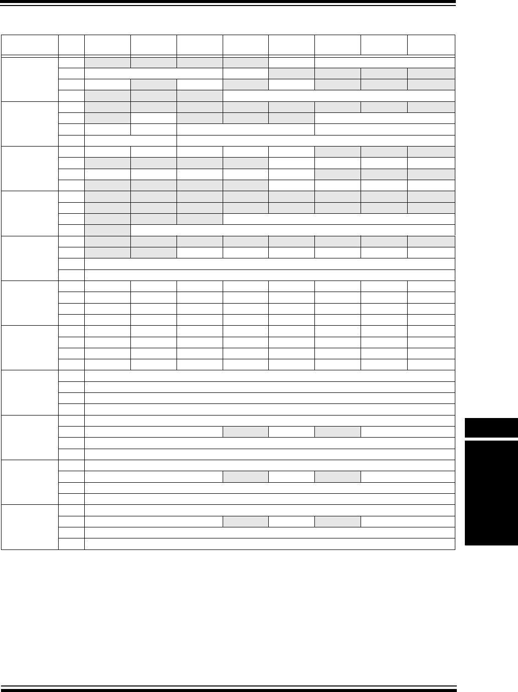
© 2009-2012 Microchip Technology Inc. DS61154C-page 34-11
Section 34. Controller Area Network (CAN)
Controller Area
Network (CAN)
34
Table 34-1: CAN Controller Register Summary
Name Bit
Range
Bit
31/2315/7
Bit
30/22/14/6
Bit
29/21/13/5
Bit
28/20/12/4
Bit
27/19/11/3
Bit
26/18/10/2
Bit
25/17/9/1
Bit
24/16/8/0
CiCON(1) 31:24 — — — — ABAT REQOP<2:0>
23:16 OPMOD<2:0> CANCAP — — — —
15:8 ON —SIDLE —CANBUSY — — —
7:0 — — — DNCNT<4:0>
CiCFG(1) 31:24 — — — — — — — —
23:16 —WAKFIL — — — SEG2PH<2:0>
15:8 SEG2PHTS SAM SEG1PH<2:0> PRSEG<2:0>
7:0 SJW<1:0> BRP<5:0>
CiINT(1) 31:24 IVRIE WAKIE CERRIE SERRIE RBOVIE — — —
23:16 — — — — MODIE CTMRIE RBIE TBIE
15:8 IVRIF WAKIF CERRIF SERRIF RBOVIF — — —
7:0 — — — — MODIF CTMRIF RBIF TBIF
CiVEC(1) 31:24 — — — — — — — —
23:16 — — — — — — — —
15:8 — — — FILHIT<4:0>
7:0 —ICODE<6:0>
CiTREC(1) 31:24 — — — — — — — —
23:16 — — TXBO TXBP RXBP TXWARN RXWARN EWARN
15:8 TERRCNT<7:0>
7:0 RERRCNT<7:0>
CiFSTAT(1) 31:24 FIFOIP31 FIFOIP30 FIFOIP29 FIFOIP28 FIFOIP27 FIFOIP26 FIFOIP25 FIFOIP24
23:16 FIFOIP23 FIFOIP22 FIFOIP21 FIFOIP20 FIFOIP19 FIFOIP18 FIFOIP17 FIFOIP16
15:8 FIFOIP15 FIFOIP14 FIFOIP13 FIFOIP12 FIFOIP11 FIFOIP10 FIFOIP9 FIFOIP8
7:0 FIFOIP7 FIFOIP6 FIFOIP5 FIFOIP4 FIFOIP3 FIFOIP2 FIFOIP1 FIFOIP0
CiRXOVF(1) 31:24 RXOVF31 RXOVF30 RXOVF29 RXOVF28 RXOVF27 RXOVF26 RXOVF25 RXOVF24
23:16 RXOVF23 RXOVF22 RXOVF21 RXOVF20 RXOVF19 RXOVF18 RXOVF17 RXOVF16
15:8 RXOVF15 RXOVF14 RXOVF13 RXOVF12 RXOVF11 RXOVF10 RXOVF9 RXOVF8
7:0 RXOVF7 RXOVF6 RXOVF5 RXOVF4 RXOVF3 RXOVF2 RXOVF1 RXOVF0
CiTMR(1) 31:24 CANTS<15:8>
23:16 CANTS<7:0>
15:8 CANTSPRE<15:8>
7:0 CANTSPRE<7:0>
CiRXM0(1) 31:24 SID<10:3>
23:16 SID<2:0> -— MIDE —EID<17:16>
15:8 EID<15:8>
7:0 EID<7:0>
CiRXM1(1) 31:24 SID<10:3>
23:16 SID<2:0> -— MIDE —EID<17:16>
15:8 EID<15:8>
7:0 EID<7:0>
CiRXM2(1) 31:24 SID<10:3>
23:16 SID<2:0> -— MIDE —EID<17:16>
15:8 EID<15:8>
7:0 EID<7:0>
Legend: ‘—’ = unimplemented; read as ‘0’.
Note 1: This register has an associated Clear, Set, and Invert register at an offset of 0x4, 0x8, or 0xC bytes, respectively. These registers have
the same name with CLR, SET, or INV appended to the end of the register name (For example, CiCONCLR). Writing a ‘1’ to any bit
position in these registers will clear, set, or invert valid bits in the associated register. Reads from these registers should be ignored.

PIC32 Family Reference Manual
DS61154C-page 34-12 © 2009-2012 Microchip Technology Inc.
CiRXM3(1) 31:24 SID<10:3>
23:16 SID<2:0> -— MIDE —EID<17:16>
15:8 EID<15:8>
7:0 EID<7:0>
CiFLTCON0(1) 31:24 FLTEN3 MSEL3<1:0> FSEL3<4:0>
23:16 FLTEN2 MSEL2<1:0> FSEL2<4:0>
15:8 FLTEN1 MSEL1<1:0> FSEL1<4:0>
7:0 FLTEN0 MSEL0<1:0> FSEL0<4:0>
CiFLTCON1(1) 31:24 FLTEN7 MSEL7<1:0> FSEL7<4:0>
23:16 FLTEN6 MSEL6<1:0> FSEL6<4:0>
15:8 FLTEN5 MSEL5<1:0> FSEL5<4:0>
7:0 FLTEN4 MSEL4<1:0> FSEL4<4:0>
CiFLTCON2(1) 31:24 FLTEN11 MSEL11<1:0> FSEL11<4:0>
23:16 FLTEN10 MSEL10<1:0> FSEL10<4:0>
15:8 FLTEN9 MSEL9<1:0> FSEL9<4:0>
7:0 FLTEN8 MSEL8<1:0> FSEL8<4:0>
CiFLTCON3(1) 31:24 FLTEN15 MSEL15<1:0> FSEL15<4:0>
23:16 FLTEN14 MSEL14<1:0> FSEL14<4:0>
15:8 FLTEN13 MSEL13<1:0> FSEL13<4:0>
7:0 FLTEN12 MSEL12<1:0> FSEL12<4:0>
CiFLTCON4(1) 31:24 FLTEN19 MSEL19<1:0> FSEL19<4:0>
23:16 FLTEN18 MSEL18<1:0> FSEL18<4:0>
15:8 FLTEN17 MSEL17<1:0> FSEL17<4:0>
7:0 FLTEN16 MSEL16<1:0> FSEL16<4:0:
CiFLTCON5(1) 31:24 FLTEN23 MSEL23<1:0> FSEL23<4:0>
23:16 FLTEN22 MSEL22<1:0> FSEL22<4:0>
15:8 FLTEN21 MSEL21<1:0> FSEL21<4:0>
7:0 FLTEN20 MSEL20<1:0> FSEL20<4:0>
CiFLTCON6(1) 31:24 FLTEN27 MSEL27<1:0> FSEL27<4:0>
23:16 FLTEN26 MSEL26<1:0> FSEL26<4:0>
15:8 FLTEN25 MSEL25<1:0> FSEL25<4:0>
7:0 FLTEN24 MSEL24<1:0> FSEL24<4:0>
CiFLTCON7(1) 31:24 FLTEN31 MSEL31<1:0> FSEL31<4:0>
23:16 FLTEN30 MSEL30<1:0> FSEL30<4:0>
15:8 FLTEN29 MSEL29<1:0> FSEL29<4:0>
7:0 FLTEN28 MSEL28<1:0> FSEL28<4:0>
CiRXFn(1)
(n = 0 through 31)
31:24 SID<10:3>
23:16 SID<2:0> -— EXID —EID<17:16>
15:8 EID<15:8>
7:0 EID<7:0>
CiFIFOBA(1) 31:24 CiFIFOBA<31:24>
23:16 CiFIFOBA<23:16>
15:8 CiFIFOBA<15:8>
7:0 CiFIFOBA<7:0>
CiFIFOCONn(1)
(n = 0 through 31)
31:24 — — — — — — — —
23:16 — — — FSIZE<4:0>
15:8 —FRESET UINC DONLY — — — —
7:0 TXEN TXABAT TXLARB TXERR TXREQ RTREN TXPR<1:0>
Table 34-1: CAN Controller Register Summary (Continued)
Name Bit
Range
Bit
31/2315/7
Bit
30/22/14/6
Bit
29/21/13/5
Bit
28/20/12/4
Bit
27/19/11/3
Bit
26/18/10/2
Bit
25/17/9/1
Bit
24/16/8/0
Legend: ‘—’ = unimplemented; read as ‘0’.
Note 1: This register has an associated Clear, Set, and Invert register at an offset of 0x4, 0x8, or 0xC bytes, respectively. These registers have
the same name with CLR, SET, or INV appended to the end of the register name (For example, CiCONCLR). Writing a ‘1’ to any bit
position in these registers will clear, set, or invert valid bits in the associated register. Reads from these registers should be ignored.

© 2009-2012 Microchip Technology Inc. DS61154C-page 34-13
Section 34. Controller Area Network (CAN)
Controller Area
Network (CAN)
34
CiFIFOINTn(1)
(n = 0 through 31)
31:24 — — — — — TXNFULLIE TXHALFIE TXEMPTYIE
23:16 — — — — RXOVFLIE RXFULLIE RXHALFIE RXNEMPTYIE
15:8 — — — — — TXNFULLIF TXHALFIF TXEMPTYIF
7:0 — — — — RXOVFLIF RXFULLIF RXHALFIF RXNEMPTYIF
CiFIFOUAn(1)
(n = 0 through 31)
31:24 CiFIFOUA<31:24>
23:16 CiFIFOUA<23:16>
15:8 CiFIFOUA<15:8>
7:0 CiFIFOUA<7:0>
CiFIFOCIn(1)
(n = 0 through 31)
31:24 — — — — — — — —
23:16 — — — — — — — —
15:8 — — — — — — — —
7:0 — — — CiFIFOCI<4:0>
Table 34-1: CAN Controller Register Summary (Continued)
Name Bit
Range
Bit
31/2315/7
Bit
30/22/14/6
Bit
29/21/13/5
Bit
28/20/12/4
Bit
27/19/11/3
Bit
26/18/10/2
Bit
25/17/9/1
Bit
24/16/8/0
Legend: ‘—’ = unimplemented; read as ‘0’.
Note 1: This register has an associated Clear, Set, and Invert register at an offset of 0x4, 0x8, or 0xC bytes, respectively. These registers have
the same name with CLR, SET, or INV appended to the end of the register name (For example, CiCONCLR). Writing a ‘1’ to any bit
position in these registers will clear, set, or invert valid bits in the associated register. Reads from these registers should be ignored.

PIC32 Family Reference Manual
DS61154C-page 34-14 © 2009-2012 Microchip Technology Inc.
Register 34-1: CiCON: CAN Module Control Register
Bit
Range
Bit
31/23/15/7
Bit
30/22/14/6
Bit
29/21/13/5
Bit
28/20/12/4
Bit
27/19/11/3
Bit
26/18/10/2
Bit
25/17/9/1
Bit
24/16/8/0
31:24 U-0 U-0 U-0 U-0 S/HC-0 R/W-1 R/W-0 R/W-0
— — — — ABAT REQOP<2:0>
23:16 R-1 R-0 R-0 R/W-0 U-0 U-0 U-0 U-0
OPMOD<2:0> CANCAP — — — —
15:8 R/W-0 U-0 R/W-0 U-0 R-0 U-0 U-0 U-0
ON(1) —SIDLE —CANBUSY — — —
7:0 U-0 U-0 U-0 R/W-0 R/W-0 R/W-0 R/W-0 R/W-0
— — — DNCNT<4:0>
Legend:
R = Readable bit W = Writable bit U = Unimplemented bit, read as ‘0’
-n = Value at POR ‘1’ = Bit is set ‘0’ = Bit is cleared x = Bit is unknown
bit 31-28 Unimplemented: Read as ‘0’
bit 27 ABAT: Abort All Pending Transmissions bit
1 = Signal all transmit buffers to abort transmission
0 = Module will clear this bit when all transmissions aborted
bit 26-24 REQOP<2:0>: Request Operation Mode bits
111 = Set Listen All Messages mode
110 = Reserved; do not use
101 = Reserved; do not use
100 = Set Configuration mode
011 = Set Listen-Only mode
010 = Set Loopback mode
001 = Set Disable mode
000 = Set Normal Operation mode
bit 23-21 OPMOD<2:0>: Operation Mode Status bits
111 = Module is in Listen All Messages mode
110 = Reserved
101 = Reserved
100 = Module is in Configuration mode
011 = Module is in Listen-Only mode
010 = Module is in Loopback mode
001 = Module is in Disable mode
000 = Module is in Normal Operation mode
bit 20 CANCAP: CAN Message Receive Time Stamp Timer Capture Enable bit
1 = CANTMR value is stored on valid message reception and is stored with the message
0 = Disable CAN message receive time stamp timer capture and stop CANTMR to conserve power
bit 19-16 Unimplemented: Read as ‘0’
bit 15 ON: CAN On bit(1)
1 = CAN module is enabled
0 = CAN module is disabled
bit 14 Unimplemented: Read as ‘0’
Note 1: If the user application clears this bit, it may take a number of cycles before the CAN module completes the
current transaction and responds to this request. The user application should poll the CANBUSY bit to
verify that the request has been honored.

© 2009-2012 Microchip Technology Inc. DS61154C-page 34-15
Section 34. Controller Area Network (CAN)
Controller Area
Network (CAN)
34
bit 13 SIDLE: CAN Stop in Idle bit
1 = CAN Stops operation when system enters Idle mode
0 = CAN continues operation when system enters Idle mode
bit 12 Unimplemented: Read as ‘0’
bit 11 CANBUSY: CAN Module is Busy bit
1 = The CAN module is active
0 = The CAN module is completely disabled
bit 10-5 Unimplemented: Read as ‘0’
bit 4-0 DNCNT<4:0>: Device Net Filter Bit Number bits
11111 = Invalid Selection (compare up to 18-bits of data with EID)
•
•
•
10011 = Invalid Selection (compare up to 18-bits of data with EID)
10010 = Compare up to data byte 2 bit 6 with EID17 (CiRXFn<17>)
•
•
•
00001 = Compare up to data byte 0 bit 7 with EID0 (CiRXFn<0>)
00000 = Do not compare data bytes
Register 34-1: CiCON: CAN Module Control Register (Continued)
Note 1: If the user application clears this bit, it may take a number of cycles before the CAN module completes the
current transaction and responds to this request. The user application should poll the CANBUSY bit to
verify that the request has been honored.

PIC32 Family Reference Manual
DS61154C-page 34-16 © 2009-2012 Microchip Technology Inc.
Register 34-2: CiCFG: CAN Baud Rate Configuration Register
Bit
Range
Bit
31/23/15/7
Bit
30/22/14/6
Bit
29/21/13/5
Bit
28/20/12/4
Bit
27/19/11/3
Bit
26/18/10/2
Bit
25/17/9/1
Bit
24/16/8/0
31:24 U-0 U-0 U-0 U-0 U-0 U-0 U-0 U-0
— — — — — — — —
23:16 U-0 R/W-0 U-0 U-0 U-0 R/W-0 R/W-0 R/W-0
—WAKFIL — — — SEG2PH<2:0>(1,4)
15:8 R/W-0 R/W-0 R/W-0 R/W-0 R/W-0 R/W-0 R/W-0 R/W-0
SEG2PHTS(1) SAM(2) SEG1PH<2:0> PRSEG<2:0>
7:0 R/W-0 R/W-0 R/W-0 R/W-0 R/W-0 R/W-0 R/W-0 R/W-0
SJW<1:0>(3) BRP<5:0>
Legend:
R = Readable bit W = Writable bit U = Unimplemented bit, read as ‘0’
-n = Value at POR ‘1’ = Bit is set ‘0’ = Bit is cleared x = Bit is unknown
bit 31-23 Unimplemented: Read as ‘0’
bit 22 WAKFIL: CAN Bus Line Filter Enable bit
1 = Use CAN bus line filter for wake-up
0 = CAN bus line filter is not used for wake-up
bit 21-19 Unimplemented: Read as ‘0’
bit 18-16 SEG2PH<2:0>: Phase Buffer Segment 2 bits(1,5)
111 = Length is 8 x TQ
•
•
•
000 = Length is 1 x TQ
bit 15 SEG2PHTS: Phase Segment 2 Time Select bit(1)
1 = Freely programmable
0 = Maximum of SEG1PH or Information Processing Time, whichever is greater
bit 14 SAM: Sample of the CAN Bus Line bit(2)
1 = Bus line is sampled three times at the sample point
0 = Bus line is sampled once at the sample point
bit 13-11 SEG1PH<2:0>: Phase Buffer Segment 1 bits(4)
111 = Length is 8 x TQ
•
•
•
000 = Length is 1 x TQ
Note 1: SEG2PH ≤ SEG1PH. If SEG2PHTS is clear, SEG2PH will be set automatically.
2: 3 Time bit sampling is not allowed for BRP < 2.
3: SJW ≤ SEG2PH.
4: The Time Quanta per bit must be greater than 7 (that is, TQBIT > 7).
Note: This register can only be modified when the CAN module is in Configuration mode (OPMOD<2:0>
(CiCON<23:21>) = 100).

© 2009-2012 Microchip Technology Inc. DS61154C-page 34-17
Section 34. Controller Area Network (CAN)
Controller Area
Network (CAN)
34
bit 10-8 PRSEG<2:0>: Propagation Time Segment bits(4)
111 = Length is 8 x TQ
•
•
•
000 = Length is 1 x TQ
bit 7-6 SJW<1:0>: Synchronization Jump Width bits(3)
11 = Length is 4 x TQ
10 = Length is 3 x TQ
01 = Length is 2 x TQ
00 = Length is 1 x TQ
bit 5-0 BRP<5:0>: Baud Rate Prescaler bits
111111 = TQ = (2 x 64)/FSYS
111110 = TQ = (2 x 63)/FSYS
•
•
•
000001 = TQ = (2 x 2)/FSYS
000000 = TQ = (2 x 1)/FSYS
Register 34-2: CiCFG: CAN Baud Rate Configuration Register (Continued)
Note 1: SEG2PH ≤ SEG1PH. If SEG2PHTS is clear, SEG2PH will be set automatically.
2: 3 Time bit sampling is not allowed for BRP < 2.
3: SJW ≤ SEG2PH.
4: The Time Quanta per bit must be greater than 7 (that is, TQBIT > 7).
Note: This register can only be modified when the CAN module is in Configuration mode (OPMOD<2:0>
(CiCON<23:21>) = 100).

PIC32 Family Reference Manual
DS61154C-page 34-18 © 2009-2012 Microchip Technology Inc.
Register 34-3: CiINT: CAN Interrupt Register
Bit
Range
Bit
31/23/15/7
Bit
30/22/14/6
Bit
29/21/13/5
Bit
28/20/12/4
Bit
27/19/11/3
Bit
26/18/10/2
Bit
25/17/9/1
Bit
24/16/8/0
31:24 R/W-0 R/W-0 R/W-0 R/W-0 R/W-0 U-0 U-0 U-0
IVRIE WAKIE CERRIE SERRIE RBOVIE — — —
23:16 U-0 U-0 U-0 U-0 R/W-0 R/W-0 R/W-0 R/W-0
— — — — MODIE CTMRIE RBIE TBIE
15:8 R/W-0 R/W-0 R/W-0 R/W-0 R/W-0 U-0 U-0 U-0
IVRIF WAKIF CERRIF SERRIF(1) RBOVIF — — —
7:0 U-0 U-0 U-0 U-0 R/W-0 R/W-0 R/W-0 R/W-0
— — — — MODIF CTMRIF RBIF TBIF
Legend:
R = Readable bit W = Writable bit U = Unimplemented bit, read as ‘0’
-n = Value at POR ‘1’ = Bit is set ‘0’ = Bit is cleared x = Bit is unknown
bit 31 IVRIE: Invalid Message Received Interrupt Enable bit
1 = Interrupt request enabled
0 = Interrupt request not enabled
bit 30 WAKIE: CAN Bus Activity Wake-up Interrupt Enable bit
1 = Interrupt request enabled
0 = Interrupt request not enabled
bit 29 CERRIE: CAN Bus Error Interrupt Enable bit
1 = Interrupt request enabled
0 = Interrupt request not enabled
bit 28 SERRIE: System Error Interrupt Enable bit
1 = Interrupt request enabled
0 = Interrupt request not enabled
bit 27 RBOVIE: Receive Buffer Overflow Interrupt Enable bit
1 = Interrupt request enabled
0 = Interrupt request not enabled
bit 26-20 Unimplemented: Read as ‘0’
bit 19 MODIE: Mode Change Interrupt Enable bit
1 = Interrupt request enabled
0 = Interrupt request not enabled
bit 18 CTMRIE: CAN Timestamp Timer Interrupt Enable bit
1 = Interrupt request enabled
0 = Interrupt request not enabled
bit 17 RBIE: Receive Buffer Interrupt Enable bit
1 = Interrupt request enabled
0 = Interrupt request not enabled
bit 16 TBIE: Transmit Buffer Interrupt Enable bit
1 = Interrupt request enabled
0 = Interrupt request not enabled
bit 15 IVRIF: Invalid Message Received Interrupt Flag bit
1 = An invalid messages interrupt has occurred
0 = An invalid message interrupt has not occurred
bit 14 WAKIF: CAN Bus Activity Wake-up Interrupt Flag bit
1 = A bus wake-up activity interrupt has occurred
0 = A bus wake-up activity interrupt has not occurred
Note 1: This bit can only be cleared by turning the CAN module OFF and ON by clearing or setting the ON bit
(CiCON<15>).

© 2009-2012 Microchip Technology Inc. DS61154C-page 34-19
Section 34. Controller Area Network (CAN)
Controller Area
Network (CAN)
34
bit 13 CERRIF: CAN Bus Error Interrupt Flag bit
1 = A CAN bus error has occurred
0 = A CAN bus error has not occurred
bit 12 SERRIF: System Error Interrupt Flag bit
1 = A system error occurred (typically an illegal address was presented to the system bus)
0 = A system error has not occurred
bit 11 RBOVIF: Receive Buffer Overflow Interrupt Flag bit
1 = A receive buffer overflow has occurred
0 = A receive buffer overflow has not occurred
bit 10-4 Unimplemented: Read as ‘0’
bit 3 MODIF: CAN Mode Change Interrupt Flag bit
1 = A CAN module mode change has occurred (OPMOD<2:0> has changed to reflect REQOP)
0 = A CAN module mode change has not occurred
bit 2 CTMRIF: CAN Timer Overflow Interrupt Flag bit
1 = A CAN timer (CANTMR) overflow has occurred
0 = A CAN timer (CANTMR) overflow has not occurred
bit 1 RBIF: Receive Buffer Interrupt Flag bit
1 = A receive buffer interrupt is pending
0 = A receive buffer interrupt is not pending
bit 0 TBIF: Transmit Buffer Interrupt Flag bit
1 = A transmit buffer interrupt is pending
0 = A transmit buffer interrupt is not pending
Register 34-3: CiINT: CAN Interrupt Register (Continued)
Note 1: This bit can only be cleared by turning the CAN module OFF and ON by clearing or setting the ON bit
(CiCON<15>).

PIC32 Family Reference Manual
DS61154C-page 34-20 © 2009-2012 Microchip Technology Inc.
Register 34-4: CiVEC: CAN Interrupt Code Register
Bit
Range
Bit
31/23/15/7
Bit
30/22/14/6
Bit
29/21/13/5
Bit
28/20/12/4
Bit
27/19/11/3
Bit
26/18/10/2
Bit
25/17/9/1
Bit
24/16/8/0
31:24 U-0 U-0 U-0 U-0 U-0 U-0 U-0 U-0
— — — — — — — —
23:16 U-0 U-0 U-0 U-0 U-0 U-0 U-0 U-0
— — — — — — — —
15:8 U-0 U-0 U-0 R-0 R-0 R-0 R-0 R-0
— — — FILHIT<4:0>
7:0 U-0 R-1 R-0 R-0 R-0 R-0 R-0 R-0
—ICODE<6:0>(1)
Legend:
R = Readable bit W = Writable bit U = Unimplemented bit, read as ‘0’
-n = Value at POR ‘1’ = Bit is set ‘0’ = Bit is cleared x = Bit is unknown
bit 31-13 Unimplemented: Read as ‘0’
bit 12-8 FILHIT<4:0>: Filter Hit Number bit
11111 = Filter 31
11110 = Filter 30
•
•
•
00001 = Filter 1
00000 = Filter 0
bit 7 Unimplemented: Read as ‘0’
bit 6-0 ICODE<6:0>: Interrupt Flag Code bits(1)
1111111 = Reserved
•
•
•
1001000 = Reserved
1001000 = Invalid message received (IVRIF)
1000111 = CAN module mode change (MODIF)
1000110 = CAN timestamp timer (CTMRIF)
1000101 = Bus bandwidth error (SERRIF)
1000100 = Address error interrupt (SERRIF)
1000011 = Receive FIFO overflow interrupt (RBOVIF)
1000010 = Wake-up interrupt (WAKIF)
1000001 = Error Interrupt (CERRIF)
1000000 = No interrupt
0111111 = Reserved
•
•
•
0100000 = Reserved
0011111 = FIFO31 Interrupt (CiFSTAT<31> set)
0011110 = FIFO30 Interrupt (CiFSTAT<30> set)
•
•
•
0000001 = FIFO1 Interrupt (CiFSTAT<1> set)
0000000 = FIFO0 Interrupt (CiFSTAT<0> set)
Note 1: These bits are only updated for enabled interrupts.

© 2009-2012 Microchip Technology Inc. DS61154C-page 34-21
Section 34. Controller Area Network (CAN)
Controller Area
Network (CAN)
34
Register 34-5: CiTREC: CAN Transmit/Receive Error Count Register
Bit
Range
Bit
31/23/15/7
Bit
30/22/14/6
Bit
29/21/13/5
Bit
28/20/12/4
Bit
27/19/11/3
Bit
26/18/10/2
Bit
25/17/9/1
Bit
24/16/8/0
31:24 U-0 U-0 U-0 U-0 U-0 U-0 U-0 U-0
— — — — — — — —
23:16 U-0 U-0 R-0 R-0 R-0 R-0 R-0 R-0
— — TXBO TXBP RXBP TXWARN RXWARN EWARN
15:8 R-0 R-0 R-0 R-0 R-0 R-0 R-0 R-0
TERRCNT<7:0>
7:0 R-0 R-0 R-0 R-0 R-0 R-0 R-0 R-0
RERRCNT<7:0>
Legend:
R = Readable bit W = Writable bit U = Unimplemented bit, read as ‘0’
-n = Value at POR ‘1’ = Bit is set ‘0’ = Bit is cleared x = Bit is unknown
bit 31-22 Unimplemented: Read as ‘0’
bit 21 TXBO: Transmitter in Error State Bus OFF (TERRCNT ≥ 256)
bit 20 TXBP: Transmitter in Error State Bus Passive (TERRCNT ≥ 128)
bit 19 RXBP: Receiver in Error State Bus Passive (RERRCNT ≥ 128)
bit 18 TXWARN: Transmitter in Error State Warning (128 > TERRCNT ≥ 96)
bit 17 RXWARN: Receiver in Error State Warning (128 > RERRCNT ≥ 96)
bit 16 EWARN: Transmitter or Receiver is in Error State Warning
bit 15-8 TERRCNT<7:0>: Transmit Error Counter
bit 7-0 RERRCNT<7:0>: Receive Error Counter
Register 34-6: CiFSTAT: CAN FIFO Status Register
Bit
Range
Bit
31/23/15/7
Bit
30/22/14/6
Bit
29/21/13/5
Bit
28/20/12/4
Bit
27/19/11/3
Bit
26/18/10/2
Bit
25/17/9/1
Bit
24/16/8/0
31:24 R-0 R-0 R-0 R-0 R-0 R-0 R-0 R-0
FIFOIP31 FIFOIP30 FIFOIP29 FIFOIP28 FIFOIP27 FIFOIP26 FIFOIP25 FIFOIP24
23:16 R-0 R-0 R-0 R-0 R-0 R-0 R-0 R-0
FIFOIP23 FIFOIP22 FIFOIP21 FIFOIP20 FIFOIP19 FIFOIP18 FIFOIP17 FIFOIP16
15:8 R-0 R-0 R-0 R-0 R-0 R-0 R-0 R-0
FIFOIP15 FIFOIP14 FIFOIP13 FIFOIP12 FIFOIP11 FIFOIP10 FIFOIP9 FIFOIP8
7:0 R-0 R-0 R-0 R-0 R-0 R-0 R-0 R-0
FIFOIP7 FIFOIP6 FIFOIP5 FIFOIP4 FIFOIP3 FIFOIP2 FIFOIP1 FIFOIP0
Legend:
R = Readable bit W = Writable bit U = Unimplemented bit, read as ‘0’
-n = Value at POR ‘1’ = Bit is set ‘0’ = Bit is cleared x = Bit is unknown
bit 31-0 FIFOIP<31:0>: FIFOn Interrupt Pending bits
1 = One or more enabled FIFO interrupts are pending
0 = No FIFO interrupts are pending
PIC32 Family Reference Manual
DS61154C-page 34-22 © 2009-2012 Microchip Technology Inc.
Register 34-7: CiRXOVF: CAN Receive FIFO Overflow Status Register
Bit
Range
Bit
31/23/15/7
Bit
30/22/14/6
Bit
29/21/13/5
Bit
28/20/12/4
Bit
27/19/11/3
Bit
26/18/10/2
Bit
25/17/9/1
Bit
24/16/8/0
31:24 R-0 R-0 R-0 R-0 R-0 R-0 R-0 R-0
RXOVF31 RXOVF30 RXOVF29 RXOVF28 RXOVF27 RXOVF26 RXOVF25 RXOVF24
23:16 R-0 R-0 R-0 R-0 R-0 R-0 R-0 R-0
RXOVF23 RXOVF22 RXOVF21 RXOVF20 RXOVF19 RXOVF18 RXOVF17 RXOVF16
15:8 R-0 R-0 R-0 R-0 R-0 R-0 R-0 R-0
RXOVF15 RXOVF14 RXOVF13 RXOVF12 RXOVF11 RXOVF10 RXOVF9 RXOVF8
7:0 R-0 R-0 R-0 R-0 R-0 R-0 R-0 R-0
RXOVF7 RXOVF6 RXOVF5 RXOVF4 RXOVF3 RXOVF2 RXOVF1 RXOVF0
Legend:
R = Readable bit W = Writable bit U = Unimplemented bit, read as ‘0’
-n = Value at POR ‘1’ = Bit is set ‘0’ = Bit is cleared x = Bit is unknown
bit 31-0 RXOVF<31:0>: FIFOn Receive Overflow Interrupt Pending bit
1 = FIFO has overflowed
0 = FIFO has not overflowed
Register 34-8: CiTMR: CAN TImer Register
Bit
Range
Bit
31/23/15/7
Bit
30/22/14/6
Bit
29/21/13/5
Bit
28/20/12/4
Bit
27/19/11/3
Bit
26/18/10/2
Bit
25/17/9/1
Bit
24/16/8/0
31:24 R/W-0 R/W-0 R/W-0 R/W-0 R/W-0 R/W-0 R/W-0 R/W-0
CANTS<15:8>
23:16 R/W-0 R/W-0 R/W-0 R/W-0 R/W-0 R/W-0 R/W-0 R/W-0
CANTS<7:0>
15:8 R/W-0 R/W-0 R/W-0 R/W-0 R/W-0 R/W-0 R/W-0 R/W-0
CANTSPRE<15:8>
7:0 R/W-0 R/W-0 R/W-0 R/W-0 R/W-0 R/W-0 R/W-0 R/W-0
CANTSPRE<7:0>
Legend:
R = Readable bit W = Writable bit U = Unimplemented bit, read as ‘0’
-n = Value at POR ‘1’ = Bit is set ‘0’ = Bit is cleared x = Bit is unknown
bit 31-0 CANTS<15:0>: CAN Time Stamp Timer bits
This is a free-running timer that increments every CANTSPRE system clocks when the CANCAP bit
(CiCON<20>) is set.
bit 15-0 CANTSPRE<15:0>: CAN Time Stamp Timer Prescaler bits
65535 = CAN time stamp timer (CANTS) increments every 65,535 system clocks
•
•
•
0 = CAN time stamp timer (CANTS) increments every system clock
Note 1: CiTMR will be frozen when CANCAP = 0.
2: The CiTMR prescaler count will be reset on any write to CiTMR (CANTSPRE will be unaffected).

© 2009-2012 Microchip Technology Inc. DS61154C-page 34-23
Section 34. Controller Area Network (CAN)
Controller Area
Network (CAN)
34
Register 34-9: CiRXMn: CAN Acceptance Filter Mask n Register (n = 0, 1, 2 or 3)
Bit
Range
Bit
31/23/15/7
Bit
30/22/14/6
Bit
29/21/13/5
Bit
28/20/12/4
Bit
27/19/11/3
Bit
26/18/10/2
Bit
25/17/9/1
Bit
24/16/8/0
31:24 R/W-0 R/W-0 R/W-0 R/W-0 R/W-0 R/W-0 R/W-0 R/W-0
SID<10:3>
23:16 R/W-0 R/W-0 R/W-0 U-0 R/W-0 U-0 R/W-0 R/W-0
SID<2:0> —MIDE —EID<17:16>
15:8 R/W-0 R/W-0 R/W-0 R/W-0 R/W-0 R/W-0 R/W-0 R/W-0
EID<15:8>
7:0 R/W-0 R/W-0 R/W-0 R/W-0 R/W-0 R/W-0 R/W-0 R/W-0
EID<7:0>
Legend:
R = Readable bit W = Writable bit U = Unimplemented bit, read as ‘0’
-n = Value at POR ‘1’ = Bit is set ‘0’ = Bit is cleared x = Bit is unknown
bit 31-21 SID<10:0>: Standard Identifier bits
1 = Include bit, SIDx, in filter comparison
0 = Bit SIDx is ‘don’t care’ in filter operation
bit 20 Unimplemented: Read as ‘0’
bit 19 MIDE: Identifier Receive Mode bit
1 = Match only message types (standard/extended address) that correspond to the EXID bit in filter
0 = Match either standard or extended address message if filters match (that is, if (Filter SID) = (Message
SID) or if (FILTER SID/EID) = (Message SID/EID))
bit 18 Unimplemented: Read as ‘0’
bit 17-0 EID<17:0>: Extended Identifier bits
1 = Include bit, EIDx, in filter comparison
0 = Bit EIDx is ‘don’t care’ in filter operation
Note: This register can only be modified when the CAN module is in Configuration mode (OPMOD<2:0>
(CiCON<23:21>) = 100).

PIC32 Family Reference Manual
DS61154C-page 34-24 © 2009-2012 Microchip Technology Inc.
Register 34-10: CiFLTCON0: CAN Filter Control Register 0
Bit Range Bit
31/23/15/7
Bit
30/22/14/6
Bit
29/21/13/5
Bit
28/20/12/4
Bit
27/19/11/3
Bit
26/18/10/2
Bit
25/17/9/1
Bit
24/16/8/0
31:24 R/W-0 R/W-0 R/W-0 R/W-0 R/W-0 R/W-0 R/W-0 R/W-0
FLTEN3 MSEL3<1:0> FSEL3<4:0>
23:16 R/W-0 R/W-0 R/W-0 R/W-0 R/W-0 R/W-0 R/W-0 R/W-0
FLTEN2 MSEL2<1:0> FSEL2<4:0>
15:8 R/W-0 R/W-0 R/W-0 R/W-0 R/W-0 R/W-0 R/W-0 R/W-0
FLTEN1 MSEL1<1:0> FSEL1<4:0>
7:0 R/W-0 R/W-0 R/W-0 R/W-0 R/W-0 R/W-0 R/W-0 R/W-0
FLTEN0 MSEL0<1:0> FSEL0<4:0>
Legend:
R = Readable bit W = Writable bit U = Unimplemented bit, read as ‘0’
-n = Value at POR ‘1’ = Bit is set ‘0’ = Bit is cleared x = Bit is unknown
bit 31 FLTEN3: Filter 3 Enable bit
1 = Filter is enabled
0 = Filter is disabled
bit 30-29 MSEL3<1:0>: Filter 3 Mask Select bits
11 = Acceptance Mask 3 selected
10 = Acceptance Mask 2 selected
01 = Acceptance Mask 1 selected
00 = Acceptance Mask 0 selected
bit 28-24 FSEL3<4:0>: FIFO Selection bits
11111 = Message matching filter is stored in FIFO buffer 31
11110 = Message matching filter is stored in FIFO buffer 30
•
•
•
00001 = Message matching filter is stored in FIFO buffer 1
00000 = Message matching filter is stored in FIFO buffer 0
bit 23 FLTEN2: Filter 2 Enable bit
1 = Filter is enabled
0 = Filter is disabled
bit 22-21 MSEL2<1:0>: Filter 2 Mask Select bits
11 = Acceptance Mask 3 selected
10 = Acceptance Mask 2 selected
01 = Acceptance Mask 1 selected
00 = Acceptance Mask 0 selected
bit 20-16 FSEL2<4:0>: FIFO Selection bits
11111 = Message matching filter is stored in FIFO buffer 31
11110 = Message matching filter is stored in FIFO buffer 30
•
•
•
00001 = Message matching filter is stored in FIFO buffer 1
00000 = Message matching filter is stored in FIFO buffer 0
Note: The bits in this register can only be modified if the corresponding filter enable (FLTENn) bit is ‘0’.

© 2009-2012 Microchip Technology Inc. DS61154C-page 34-25
Section 34. Controller Area Network (CAN)
Controller Area
Network (CAN)
34
bit 15 FLTEN1: Filter 1 Enable bit
1 = Filter is enabled
0 = Filter is disabled
bit 14-13 MSEL1<1:0>: Filter 1 Mask Select bits
11 = Acceptance Mask 3 selected
10 = Acceptance Mask 2 selected
01 = Acceptance Mask 1 selected
00 = Acceptance Mask 0 selected
bit 12-8 FSEL1<4:0>: FIFO Selection bits
11111 = Message matching filter is stored in FIFO buffer 31
11110 = Message matching filter is stored in FIFO buffer 30
•
•
•
00001 = Message matching filter is stored in FIFO buffer 1
00000 = Message matching filter is stored in FIFO buffer 0
bit 7 FLTEN0: Filter 0 Enable bit
1 = Filter is enabled
0 = Filter is disabled
bit 6-5 MSEL0<1:0>: Filter 0 Mask Select bits
11 = Acceptance Mask 3 selected
10 = Acceptance Mask 2 selected
01 = Acceptance Mask 1 selected
00 = Acceptance Mask 0 selected
bit 4-0 FSEL0<4:0>: FIFO Selection bits
11111 = Message matching filter is stored in FIFO buffer 31
11110 = Message matching filter is stored in FIFO buffer 30
•
•
•
00001 = Message matching filter is stored in FIFO buffer 1
00000 = Message matching filter is stored in FIFO buffer 0
Register 34-10: CiFLTCON0: CAN Filter Control Register 0 (Continued)
Note: The bits in this register can only be modified if the corresponding filter enable (FLTENn) bit is ‘0’.

PIC32 Family Reference Manual
DS61154C-page 34-26 © 2009-2012 Microchip Technology Inc.
Register 34-11: CiFLTCON1: CAN Filter Control Register 1
Bit
Range
Bit
31/23/15/7
Bit
30/22/14/6
Bit
29/21/13/5
Bit
28/20/12/4
Bit
27/19/11/3
Bit
26/18/10/2
Bit
25/17/9/1
Bit
24/16/8/0
31:24 R/W-0 R/W-0 R/W-0 R/W-0 R/W-0 R/W-0 R/W-0 R/W-0
FLTEN7 MSEL7<1:0> FSEL7<4:0>
23:16 R/W-0 R/W-0 R/W-0 R/W-0 R/W-0 R/W-0 R/W-0 R/W-0
FLTEN6 MSEL6<1:0> FSEL6<4:0>
15:8 R/W-0 R/W-0 R/W-0 R/W-0 R/W-0 R/W-0 R/W-0 R/W-0
FLTEN5 MSEL5<1:0> FSEL5<4:0>
7:0 R/W-0 R/W-0 R/W-0 R/W-0 R/W-0 R/W-0 R/W-0 R/W-0
FLTEN4 MSEL4<1:0> FSEL4<4:0>
Legend:
R = Readable bit W = Writable bit U = Unimplemented bit, read as ‘0’
-n = Value at POR ‘1’ = Bit is set ‘0’ = Bit is cleared x = Bit is unknown
bit 31 FLTEN7: Filter 7 Enable bit
1 = Filter is enabled
0 = Filter is disabled
bit 30-29 MSEL7<1:0>: Filter 7 Mask Select bits
11 = Acceptance Mask 3 selected
10 = Acceptance Mask 2 selected
01 = Acceptance Mask 1 selected
00 = Acceptance Mask 0 selected
bit 28-24 FSEL7<4:0>: FIFO Selection bits
11111 = Message matching filter is stored in FIFO buffer 31
11110 = Message matching filter is stored in FIFO buffer 30
•
•
•
00001 = Message matching filter is stored in FIFO buffer 1
00000 = Message matching filter is stored in FIFO buffer 0
bit 23 FLTEN6: Filter 6 Enable bit
1 = Filter is enabled
0 = Filter is disabled
bit 22-21 MSEL6<1:0>: Filter 6 Mask Select bits
11 = Acceptance Mask 3 selected
10 = Acceptance Mask 2 selected
01 = Acceptance Mask 1 selected
00 = Acceptance Mask 0 selected
bit 20-16 FSEL6<4:0>: FIFO Selection bits
11111 = Message matching filter is stored in FIFO buffer 31
11110 = Message matching filter is stored in FIFO buffer 30
•
•
•
00001 = Message matching filter is stored in FIFO buffer 1
00000 = Message matching filter is stored in FIFO buffer 0
Note: The bits in this register can only be modified if the corresponding filter enable (FLTENn) bit is ‘0’.

© 2009-2012 Microchip Technology Inc. DS61154C-page 34-27
Section 34. Controller Area Network (CAN)
Controller Area
Network (CAN)
34
bit 15 FLTEN5: Filter 5 Enable bit
1 = Filter is enabled
0 = Filter is disabled
bit 14-13 MSEL5<1:0>: Filter 5 Mask Select bits
11 = Acceptance Mask 3 selected
10 = Acceptance Mask 2 selected
01 = Acceptance Mask 1 selected
00 = Acceptance Mask 0 selected
bit 12-8 FSEL5<4:0>: FIFO Selection bits
11111 = Message matching filter is stored in FIFO buffer 31
11110 = Message matching filter is stored in FIFO buffer 30
•
•
•
00001 = Message matching filter is stored in FIFO buffer 1
00000 = Message matching filter is stored in FIFO buffer 0
bit 7 FLTEN4: Filter 4 Enable bit
1 = Filter is enabled
0 = Filter is disabled
bit 6-5 MSEL4<1:0>: Filter 4 Mask Select bits
11 = Acceptance Mask 3 selected
10 = Acceptance Mask 2 selected
01 = Acceptance Mask 1 selected
00 = Acceptance Mask 0 selected
bit 4-0 FSEL4<4:0>: FIFO Selection bits
11111 = Message matching filter is stored in FIFO buffer 31
11110 = Message matching filter is stored in FIFO buffer 30
•
•
•
00001 = Message matching filter is stored in FIFO buffer 1
00000 = Message matching filter is stored in FIFO buffer 0
Register 34-11: CiFLTCON1: CAN Filter Control Register 1 (Continued)
Note: The bits in this register can only be modified if the corresponding filter enable (FLTENn) bit is ‘0’.

PIC32 Family Reference Manual
DS61154C-page 34-28 © 2009-2012 Microchip Technology Inc.
Register 34-12: CiFLTCON2: CAN Filter Control Register 2
Bit
Range
Bit
31/23/15/7
Bit
30/22/14/6
Bit
29/21/13/5
Bit
28/20/12/4
Bit
27/19/11/3
Bit
26/18/10/2
Bit
25/17/9/1
Bit
24/16/8/0
31:24 R/W-0 R/W-0 R/W-0 R/W-0 R/W-0 R/W-0 R/W-0 R/W-0
FLTEN11 MSEL11<1:0> FSEL11<4:0>
23:16 R/W-0 R/W-0 R/W-0 R/W-0 R/W-0 R/W-0 R/W-0 R/W-0
FLTEN10 MSEL10<1:0> FSEL10<4:0>
15:8 R/W-0 R/W-0 R/W-0 R/W-0 R/W-0 R/W-0 R/W-0 R/W-0
FLTEN9 MSEL9<1:0> FSEL9<4:0>
7:0 R/W-0 R/W-0 R/W-0 R/W-0 R/W-0 R/W-0 R/W-0 R/W-0
FLTEN8 MSEL8<1:0> FSEL8<4:0>
Legend:
R = Readable bit W = Writable bit U = Unimplemented bit, read as ‘0’
-n = Value at POR ‘1’ = Bit is set ‘0’ = Bit is cleared x = Bit is unknown
bit 31 FLTEN11: Filter 11 Enable bit
1 = Filter is enabled
0 = Filter is disabled
bit 30-29 MSEL11<1:0>: Filter 11 Mask Select bits
11 = Acceptance Mask 3 selected
10 = Acceptance Mask 2 selected
01 = Acceptance Mask 1 selected
00 = Acceptance Mask 0 selected
bit 28-24 FSEL11<4:0>: FIFO Selection bits
11111 = Message matching filter is stored in FIFO buffer 31
11110 = Message matching filter is stored in FIFO buffer 30
•
•
•
00001 = Message matching filter is stored in FIFO buffer 1
00000 = Message matching filter is stored in FIFO buffer 0
bit 23 FLTEN10: Filter 10 Enable bit
1 = Filter is enabled
0 = Filter is disabled
bit 22-21 MSEL10<1:0>: Filter 10 Mask Select bits
11 = Acceptance Mask 3 selected
10 = Acceptance Mask 2 selected
01 = Acceptance Mask 1 selected
00 = Acceptance Mask 0 selected
bit 20-16 FSEL10<4:0>: FIFO Selection bits
11111 = Message matching filter is stored in FIFO buffer 31
11110 = Message matching filter is stored in FIFO buffer 30
•
•
•
00001 = Message matching filter is stored in FIFO buffer 1
00000 = Message matching filter is stored in FIFO buffer 0
Note: The bits in this register can only be modified if the corresponding filter enable (FLTENn) bit is ‘0’.

© 2009-2012 Microchip Technology Inc. DS61154C-page 34-29
Section 34. Controller Area Network (CAN)
Controller Area
Network (CAN)
34
bit 15 FLTEN9: Filter 9 Enable bit
1 = Filter is enabled
0 = Filter is disabled
bit 14-13 MSEL9<1:0>: Filter 9 Mask Select bits
11 = Acceptance Mask 3 selected
10 = Acceptance Mask 2 selected
01 = Acceptance Mask 1 selected
00 = Acceptance Mask 0 selected
bit 12-8 FSEL9<4:0>: FIFO Selection bits
11111 = Message matching filter is stored in FIFO buffer 31
11110 = Message matching filter is stored in FIFO buffer 30
•
•
•
00001 = Message matching filter is stored in FIFO buffer 1
00000 = Message matching filter is stored in FIFO buffer 0
bit 7 FLTEN8: Filter 8 Enable bit
1 = Filter is enabled
0 = Filter is disabled
bit 6-5 MSEL8<1:0>: Filter 8 Mask Select bits
11 = Acceptance Mask 3 selected
10 = Acceptance Mask 2 selected
01 = Acceptance Mask 1 selected
00 = Acceptance Mask 0 selected
bit 4-0 FSEL8<4:0>: FIFO Selection bits
11111 = Message matching filter is stored in FIFO buffer 31
11110 = Message matching filter is stored in FIFO buffer 30
•
•
•
00001 = Message matching filter is stored in FIFO buffer 1
00000 = Message matching filter is stored in FIFO buffer 0
Register 34-12: CiFLTCON2: CAN Filter Control Register 2 (Continued)
Note: The bits in this register can only be modified if the corresponding filter enable (FLTENn) bit is ‘0’.

PIC32 Family Reference Manual
DS61154C-page 34-30 © 2009-2012 Microchip Technology Inc.
Register 34-13: CiFLTCON3: CAN Filter Control Register 3
Bit
Range
Bit
31/23/15/7
Bit
30/22/14/6
Bit
29/21/13/5
Bit
28/20/12/4
Bit
27/19/11/3
Bit
26/18/10/2
Bit
25/17/9/1
Bit
24/16/8/0
31:24 R/W-0 R/W-0 R/W-0 R/W-0 R/W-0 R/W-0 R/W-0 R/W-0
FLTEN15 MSEL15<1:0> FSEL15<4:0>
23:16 R/W-0 R/W-0 R/W-0 R/W-0 R/W-0 R/W-0 R/W-0 R/W-0
FLTEN14 MSEL14<1:0> FSEL14<4:0>
15:8 R/W-0 R/W-0 R/W-0 R/W-0 R/W-0 R/W-0 R/W-0 R/W-0
FLTEN13 MSEL13<1:0> FSEL13<4:0>
7:0 R/W-0 R/W-0 R/W-0 R/W-0 R/W-0 R/W-0 R/W-0 R/W-0
FLTEN12 MSEL12<1:0> FSEL12<4:0>
Legend:
R = Readable bit W = Writable bit U = Unimplemented bit, read as ‘0’
-n = Value at POR ‘1’ = Bit is set ‘0’ = Bit is cleared x = Bit is unknown
bit 31 FLTEN15: Filter 15 Enable bit
1 = Filter is enabled
0 = Filter is disabled
bit 30-29 MSEL15<1:0>: Filter 15 Mask Select bits
11 = Acceptance Mask 3 selected
10 = Acceptance Mask 2 selected
01 = Acceptance Mask 1 selected
00 = Acceptance Mask 0 selected
bit 28-24 FSEL15<4:0>: FIFO Selection bits
11111 = Message matching filter is stored in FIFO buffer 31
11110 = Message matching filter is stored in FIFO buffer 30
•
•
•
00001 = Message matching filter is stored in FIFO buffer 1
00000 = Message matching filter is stored in FIFO buffer 0
bit 23 FLTEN14: Filter 14 Enable bit
1 = Filter is enabled
0 = Filter is disabled
bit 22-21 MSEL14<1:0>: Filter 14 Mask Select bits
11 = Acceptance Mask 3 selected
10 = Acceptance Mask 2 selected
01 = Acceptance Mask 1 selected
00 = Acceptance Mask 0 selected
bit 20-16 FSEL14<4:0>: FIFO Selection bits
11111 = Message matching filter is stored in FIFO buffer 31
11110 = Message matching filter is stored in FIFO buffer 30
•
•
•
00001 = Message matching filter is stored in FIFO buffer 1
00000 = Message matching filter is stored in FIFO buffer 0
Note: The bits in this register can only be modified if the corresponding filter enable (FLTENn) bit is ‘0’.

© 2009-2012 Microchip Technology Inc. DS61154C-page 34-31
Section 34. Controller Area Network (CAN)
Controller Area
Network (CAN)
34
bit 15 FLTEN13: Filter 13 Enable bit
1 = Filter is enabled
0 = Filter is disabled
bit 14-13 MSEL13<1:0>: Filter 13 Mask Select bits
11 = Acceptance Mask 3 selected
10 = Acceptance Mask 2 selected
01 = Acceptance Mask 1 selected
00 = Acceptance Mask 0 selected
bit 12-8 FSEL13<4:0>: FIFO Selection bits
11111 = Message matching filter is stored in FIFO buffer 31
11110 = Message matching filter is stored in FIFO buffer 30
•
•
•
00001 = Message matching filter is stored in FIFO buffer 1
00000 = Message matching filter is stored in FIFO buffer 0
bit 7 FLTEN12: Filter 12 Enable bit
1 = Filter is enabled
0 = Filter is disabled
bit 6-5 MSEL12<1:0>: Filter 12 Mask Select bits
11 = Acceptance Mask 3 selected
10 = Acceptance Mask 2 selected
01 = Acceptance Mask 1 selected
00 = Acceptance Mask 0 selected
bit 4-0 FSEL12<4:0>: FIFO Selection bits
11111 = Message matching filter is stored in FIFO buffer 31
11110 = Message matching filter is stored in FIFO buffer 30
•
•
•
00001 = Message matching filter is stored in FIFO buffer 1
00000 = Message matching filter is stored in FIFO buffer 0
Register 34-13: CiFLTCON3: CAN Filter Control Register 3 (Continued)
Note: The bits in this register can only be modified if the corresponding filter enable (FLTENn) bit is ‘0’.

PIC32 Family Reference Manual
DS61154C-page 34-32 © 2009-2012 Microchip Technology Inc.
,4
Register 34-14: CiFLTCON4: CAN Filter Control Register 4
Bit
Range
Bit
31/23/15/7
Bit
30/22/14/6
Bit
29/21/13/5
Bit
28/20/12/4
Bit
27/19/11/3
Bit
26/18/10/2
Bit
25/17/9/1
Bit
24/16/8/0
31:24 R/W-0 R/W-0 R/W-0 R/W-0 R/W-0 R/W-0 R/W-0 R/W-0
FLTEN19 MSEL19<1:0> FSEL19<4:0>
23:16 R/W-0 R/W-0 R/W-0 R/W-0 R/W-0 R/W-0 R/W-0 R/W-0
FLTEN18 MSEL18<1:0> FSEL18<4:0>
15:8 R/W-0 R/W-0 R/W-0 R/W-0 R/W-0 R/W-0 R/W-0 R/W-0
FLTEN17 MSEL17<1:0> FSEL17<4:0>
7:0 R/W-0 R/W-0 R/W-0 R/W-0 R/W-0 R/W-0 R/W-0 R/W-0
FLTEN16 MSEL16<1:0> FSEL16<4:0>
Legend:
R = Readable bit W = Writable bit U = Unimplemented bit, read as ‘0’
-n = Value at POR ‘1’ = Bit is set ‘0’ = Bit is cleared x = Bit is unknown
bit 31 FLTEN19: Filter 19 Enable bit
1 = Filter is enabled
0 = Filter is disabled
bit 30-29 MSEL19<1:0>: Filter 19 Mask Select bits
11 = Acceptance Mask 3 selected
10 = Acceptance Mask 2 selected
01 = Acceptance Mask 1 selected
00 = Acceptance Mask 0 selected
bit 28-24 FSEL19<4:0>: FIFO Selection bits
11111 = Message matching filter is stored in FIFO buffer 31
11110 = Message matching filter is stored in FIFO buffer 30
•
•
•
00001 = Message matching filter is stored in FIFO buffer 1
00000 = Message matching filter is stored in FIFO buffer 0
bit 23 FLTEN18: Filter 18 Enable bit
1 = Filter is enabled
0 = Filter is disabled
bit 22-21 MSEL18<1:0>: Filter 18 Mask Select bits
11 = Acceptance Mask 3 selected
10 = Acceptance Mask 2 selected
01 = Acceptance Mask 1 selected
00 = Acceptance Mask 0 selected
bit 20-16 FSEL18<4:0>: FIFO Selection bits
11111 = Message matching filter is stored in FIFO buffer 31
11110 = Message matching filter is stored in FIFO buffer 30
•
•
•
00001 = Message matching filter is stored in FIFO buffer 1
00000 = Message matching filter is stored in FIFO buffer 0
Note: The bits in this register can only be modified if the corresponding filter enable (FLTENn) bit is ‘0’.

© 2009-2012 Microchip Technology Inc. DS61154C-page 34-33
Section 34. Controller Area Network (CAN)
Controller Area
Network (CAN)
34
bit 15 FLTEN17: Filter 17 Enable bit
1 = Filter is enabled
0 = Filter is disabled
bit 14-13 MSEL17<1:0>: Filter 17 Mask Select bits
11 = Acceptance Mask 3 selected
10 = Acceptance Mask 2 selected
01 = Acceptance Mask 1 selected
00 = Acceptance Mask 0 selected
bit 12-8 FSEL17<4:0>: FIFO Selection bits
11111 = Message matching filter is stored in FIFO buffer 31
11110 = Message matching filter is stored in FIFO buffer 30
•
•
•
00001 = Message matching filter is stored in FIFO buffer 1
00000 = Message matching filter is stored in FIFO buffer 0
bit 7 FLTEN16: Filter 16 Enable bit
1 = Filter is enabled
0 = Filter is disabled
bit 6-5 MSEL16<1:0>: Filter 16 Mask Select bits
11 = Acceptance Mask 3 selected
10 = Acceptance Mask 2 selected
01 = Acceptance Mask 1 selected
00 = Acceptance Mask 0 selected
bit 4-0 FSEL16<4:0>: FIFO Selection bits
11111 = Message matching filter is stored in FIFO buffer 31
11110 = Message matching filter is stored in FIFO buffer 30
•
•
•
00001 = Message matching filter is stored in FIFO buffer 1
00000 = Message matching filter is stored in FIFO buffer 0
Register 34-14: CiFLTCON4: CAN Filter Control Register 4 (Continued)
Note: The bits in this register can only be modified if the corresponding filter enable (FLTENn) bit is ‘0’.
PIC32 Family Reference Manual
DS61154C-page 34-34 © 2009-2012 Microchip Technology Inc.
Register 34-15: CiFLTCON5: CAN Filter Control Register 5
Bit
Range
Bit
31/23/15/7
Bit
30/22/14/6
Bit
29/21/13/5
Bit
28/20/12/4
Bit
27/19/11/3
Bit
26/18/10/2
Bit
25/17/9/1
Bit
24/16/8/0
31:24 R/W-0 R/W-0 R/W-0 R/W-0 R/W-0 R/W-0 R/W-0 R/W-0
FLTEN23 MSEL23<1:0> FSEL23<4:0>
23:16 R/W-0 R/W-0 R/W-0 R/W-0 R/W-0 R/W-0 R/W-0 R/W-0
FLTEN22 MSEL22<1:0> FSEL22<4:0>
15:8 R/W-0 R/W-0 R/W-0 R/W-0 R/W-0 R/W-0 R/W-0 R/W-0
FLTEN21 MSEL21<1:0> FSEL21<4:0>
7:0 R/W-0 R/W-0 R/W-0 R/W-0 R/W-0 R/W-0 R/W-0 R/W-0
FLTEN20 MSEL20<1:0> FSEL20<4:0>
Legend:
R = Readable bit W = Writable bit U = Unimplemented bit, read as ‘0’
-n = Value at POR ‘1’ = Bit is set ‘0’ = Bit is cleared x = Bit is unknown
bit 31 FLTEN23: Filter 23 Enable bit
1 = Filter is enabled
0 = Filter is disabled
bit 30-29 MSEL23<1:0>: Filter 23 Mask Select bits
11 = Acceptance Mask 3 selected
10 = Acceptance Mask 2 selected
01 = Acceptance Mask 1 selected
00 = Acceptance Mask 0 selected
bit 28-24 FSEL23<4:0>: FIFO Selection bits
11111 = Message matching filter is stored in FIFO buffer 31
11110 = Message matching filter is stored in FIFO buffer 30
•
•
•
00001 = Message matching filter is stored in FIFO buffer 1
00000 = Message matching filter is stored in FIFO buffer 0
bit 23 FLTEN22: Filter 22 Enable bit
1 = Filter is enabled
0 = Filter is disabled
bit 22-21 MSEL22<1:0>: Filter 22 Mask Select bits
11 = Acceptance Mask 3 selected
10 = Acceptance Mask 2 selected
01 = Acceptance Mask 1 selected
00 = Acceptance Mask 0 selected
bit 20-16 FSEL22<4:0>: FIFO Selection bits
11111 = Message matching filter is stored in FIFO buffer 31
11110 = Message matching filter is stored in FIFO buffer 30
•
•
•
00001 = Message matching filter is stored in FIFO buffer 1
00000 = Message matching filter is stored in FIFO buffer 0
Note: The bits in this register can only be modified if the corresponding filter enable (FLTENn) bit is ‘0’.

© 2009-2012 Microchip Technology Inc. DS61154C-page 34-35
Section 34. Controller Area Network (CAN)
Controller Area
Network (CAN)
34
bit 15 FLTEN21: Filter 21 Enable bit
1 = Filter is enabled
0 = Filter is disabled
bit 14-13 MSEL21<1:0>: Filter 21 Mask Select bits
11 = Acceptance Mask 3 selected
10 = Acceptance Mask 2 selected
01 = Acceptance Mask 1 selected
00 = Acceptance Mask 0 selected
bit 12-8 FSEL21<4:0>: FIFO Selection bits
11111 = Message matching filter is stored in FIFO buffer 31
11110 = Message matching filter is stored in FIFO buffer 30
•
•
•
00001 = Message matching filter is stored in FIFO buffer 1
00000 = Message matching filter is stored in FIFO buffer 0
bit 7 FLTEN20: Filter 20 Enable bit
1 = Filter is enabled
0 = Filter is disabled
bit 6-5 MSEL20<1:0>: Filter 20 Mask Select bits
11 = Acceptance Mask 3 selected
10 = Acceptance Mask 2 selected
01 = Acceptance Mask 1 selected
00 = Acceptance Mask 0 selected
bit 4-0 FSEL20<4:0>: FIFO Selection bits
11111 = Message matching filter is stored in FIFO buffer 31
11110 = Message matching filter is stored in FIFO buffer 30
•
•
•
00001 = Message matching filter is stored in FIFO buffer 1
00000 = Message matching filter is stored in FIFO buffer 0
Register 34-15: CiFLTCON5: CAN Filter Control Register 5 (Continued)
Note: The bits in this register can only be modified if the corresponding filter enable (FLTENn) bit is ‘0’.

PIC32 Family Reference Manual
DS61154C-page 34-36 © 2009-2012 Microchip Technology Inc.
Register 34-16: CiFLTCON6: CAN Filter Control Register 6
Bit
Range
Bit
31/23/15/7
Bit
30/22/14/6
Bit
29/21/13/5
Bit
28/20/12/4
Bit
27/19/11/3
Bit
26/18/10/2
Bit
25/17/9/1
Bit
24/16/8/0
31:24 R/W-0 R/W-0 R/W-0 R/W-0 R/W-0 R/W-0 R/W-0 R/W-0
FLTEN27 MSEL27<1:0> FSEL27<4:0>
23:16 R/W-0 R/W-0 R/W-0 R/W-0 R/W-0 R/W-0 R/W-0 R/W-0
FLTEN26 MSEL26<1:0> FSEL26<4:0>
15:8 R/W-0 R/W-0 R/W-0 R/W-0 R/W-0 R/W-0 R/W-0 R/W-0
FLTEN25 MSEL25<1:0> FSEL25<4:0>
7:0 R/W-0 R/W-0 R/W-0 R/W-0 R/W-0 R/W-0 R/W-0 R/W-0
FLTEN24 MSEL24<1:0> FSEL24<4:0>
Legend:
R = Readable bit W = Writable bit U = Unimplemented bit, read as ‘0’
-n = Value at POR ‘1’ = Bit is set ‘0’ = Bit is cleared x = Bit is unknown
bit 31 FLTEN27: Filter 27 Enable bit
1 = Filter is enabled
0 = Filter is disabled
bit 30-29 MSEL27<1:0>: Filter 27 Mask Select bits
11 = Acceptance Mask 3 selected
10 = Acceptance Mask 2 selected
01 = Acceptance Mask 1 selected
00 = Acceptance Mask 0 selected
bit 28-24 FSEL27<4:0>: FIFO Selection bits
11111 = Message matching filter is stored in FIFO buffer 31
11110 = Message matching filter is stored in FIFO buffer 30
•
•
•
00001 = Message matching filter is stored in FIFO buffer 1
00000 = Message matching filter is stored in FIFO buffer 0
bit 23 FLTEN26: Filter 26 Enable bit
1 = Filter is enabled
0 = Filter is disabled
bit 22-21 MSEL26<1:0>: Filter 26 Mask Select bits
11 = Acceptance Mask 3 selected
10 = Acceptance Mask 2 selected
01 = Acceptance Mask 1 selected
00 = Acceptance Mask 0 selected
bit 20-16 FSEL26<4:0>: FIFO Selection bits
11111 = Message matching filter is stored in FIFO buffer 31
11110 = Message matching filter is stored in FIFO buffer 30
•
•
•
00001 = Message matching filter is stored in FIFO buffer 1
00000 = Message matching filter is stored in FIFO buffer 0
Note: The bits in this register can only be modified if the corresponding filter enable (FLTENn) bit is ‘0’.

© 2009-2012 Microchip Technology Inc. DS61154C-page 34-37
Section 34. Controller Area Network (CAN)
Controller Area
Network (CAN)
34
bit 15 FLTEN25: Filter 25 Enable bit
1 = Filter is enabled
0 = Filter is disabled
bit 14-13 MSEL25<1:0>: Filter 25 Mask Select bits
11 = Acceptance Mask 3 selected
10 = Acceptance Mask 2 selected
01 = Acceptance Mask 1 selected
00 = Acceptance Mask 0 selected
bit 12-8 FSEL25<4:0>: FIFO Selection bits
11111 = Message matching filter is stored in FIFO buffer 31
11110 = Message matching filter is stored in FIFO buffer 30
•
•
•
00001 = Message matching filter is stored in FIFO buffer 1
00000 = Message matching filter is stored in FIFO buffer 0
bit 7 FLTEN24: Filter 24 Enable bit
1 = Filter is enabled
0 = Filter is disabled
bit 6-5 MSEL24<1:0>: Filter 24 Mask Select bits
11 = Acceptance Mask 3 selected
10 = Acceptance Mask 2 selected
01 = Acceptance Mask 1 selected
00 = Acceptance Mask 0 selected
bit 4-0 FSEL24<4:0>: FIFO Selection bits
11111 = Message matching filter is stored in FIFO buffer 31
11110 = Message matching filter is stored in FIFO buffer 30
•
•
•
00001 = Message matching filter is stored in FIFO buffer 1
00000 = Message matching filter is stored in FIFO buffer 0
Register 34-16: CiFLTCON6: CAN Filter Control Register 6 (Continued)
Note: The bits in this register can only be modified if the corresponding filter enable (FLTENn) bit is ‘0’.

PIC32 Family Reference Manual
DS61154C-page 34-38 © 2009-2012 Microchip Technology Inc.
Register 34-17: CiFLTCON7: CAN Filter Control Register 7
Bit
Range
Bit
31/23/15/7
Bit
30/22/14/6
Bit
29/21/13/5
Bit
28/20/12/4
Bit
27/19/11/3
Bit
26/18/10/2
Bit
25/17/9/1
Bit
24/16/8/0
31:24 R/W-0 R/W-0 R/W-0 R/W-0 R/W-0 R/W-0 R/W-0 R/W-0
FLTEN31 MSEL31<1:0> FSEL31<4:0>
23:16 R/W-0 R/W-0 R/W-0 R/W-0 R/W-0 R/W-0 R/W-0 R/W-0
FLTEN30 MSEL30<1:0> FSEL30<4:0>
15:8 R/W-0 R/W-0 R/W-0 R/W-0 R/W-0 R/W-0 R/W-0 R/W-0
FLTEN29 MSEL29<1:0> FSEL29<4:0>
7:0 R/W-0 R/W-0 R/W-0 R/W-0 R/W-0 R/W-0 R/W-0 R/W-0
FLTEN28 MSEL28<1:0> FSEL28<4:0>
Legend:
R = Readable bit W = Writable bit U = Unimplemented bit, read as ‘0’
-n = Value at POR ‘1’ = Bit is set ‘0’ = Bit is cleared x = Bit is unknown
bit 31 FLTEN31: Filter 31 Enable bit
1 = Filter is enabled
0 = Filter is disabled
bit 30-29 MSEL31<1:0>: Filter 31 Mask Select bits
11 = Acceptance Mask 3 selected
10 = Acceptance Mask 2 selected
01 = Acceptance Mask 1 selected
00 = Acceptance Mask 0 selected
bit 28-24 FSEL31<4:0>: FIFO Selection bits
11111 = Message matching filter is stored in FIFO buffer 31
11110 = Message matching filter is stored in FIFO buffer 30
•
•
•
00001 = Message matching filter is stored in FIFO buffer 1
00000 = Message matching filter is stored in FIFO buffer 0
bit 23 FLTEN30: Filter 30 Enable bit
1 = Filter is enabled
0 = Filter is disabled
bit 22-21 MSEL30<1:0>: Filter 30 Mask Select bits
11 = Acceptance Mask 3 selected
10 = Acceptance Mask 2 selected
01 = Acceptance Mask 1 selected
00 = Acceptance Mask 0 selected
bit 20-16 FSEL30<4:0>: FIFO Selection bits
11111 = Message matching filter is stored in FIFO buffer 31
11110 = Message matching filter is stored in FIFO buffer 30
•
•
•
00001 = Message matching filter is stored in FIFO buffer 1
00000 = Message matching filter is stored in FIFO buffer 0
Note: The bits in this register can only be modified if the corresponding filter enable (FLTENn) bit is ‘0’.

© 2009-2012 Microchip Technology Inc. DS61154C-page 34-39
Section 34. Controller Area Network (CAN)
Controller Area
Network (CAN)
34
bit 15 FLTEN29: Filter 29 Enable bit
1 = Filter is enabled
0 = Filter is disabled
bit 14-13 MSEL29<1:0>: Filter 29 Mask Select bits
11 = Acceptance Mask 3 selected
10 = Acceptance Mask 2 selected
01 = Acceptance Mask 1 selected
00 = Acceptance Mask 0 selected
bit 12-8 FSEL29<4:0>: FIFO Selection bits
11111 = Message matching filter is stored in FIFO buffer 31
11110 = Message matching filter is stored in FIFO buffer 30
•
•
•
00001 = Message matching filter is stored in FIFO buffer 1
00000 = Message matching filter is stored in FIFO buffer 0
bit 7 FLTEN28: Filter 28 Enable bit
1 = Filter is enabled
0 = Filter is disabled
bit 6-5 MSEL28<1:0>: Filter 28 Mask Select bits
11 = Acceptance Mask 3 selected
10 = Acceptance Mask 2 selected
01 = Acceptance Mask 1 selected
00 = Acceptance Mask 0 selected
bit 4-0 FSEL28<4:0>: FIFO Selection bits
11111 = Message matching filter is stored in FIFO buffer 31
11110 = Message matching filter is stored in FIFO buffer 30
•
•
•
00001 = Message matching filter is stored in FIFO buffer 1
00000 = Message matching filter is stored in FIFO buffer 0
Register 34-17: CiFLTCON7: CAN Filter Control Register 7 (Continued)
Note: The bits in this register can only be modified if the corresponding filter enable (FLTENn) bit is ‘0’.

PIC32 Family Reference Manual
DS61154C-page 34-40 © 2009-2012 Microchip Technology Inc.
Register 34-18: CiRXFn: CAN Acceptance Filter n Register 7 (n = 0 through 31)
Bit
Range
Bit
31/23/15/7
Bit
30/22/14/6
Bit
29/21/13/5
Bit
28/20/12/4
Bit
27/19/11/3
Bit
26/18/10/2
Bit
25/17/9/1
Bit
24/16/8/0
31:24 R/W-x R/W-x R/W-x R/W-x R/W-x R/W-x R/W-x R/W-x
SID<10:3>
23:16 R/W-x R/W-x R/W-x U-0 R/W-0 U-0 R/W-x R/W-x
SID<2:0> —EXID —EID<17:16>
15:8 R/W-x R/W-x R/W-x R/W-x R/W-x R/W-x R/W-x R/W-x
EID<15:8>
7:0 R/W-x R/W-x R/W-x R/W-x R/W-x R/W-x R/W-x R/W-x
EID<7:0>
Legend:
R = Readable bit W = Writable bit U = Unimplemented bit, read as ‘0’
-n = Value at POR ‘1’ = Bit is set ‘0’ = Bit is cleared x = Bit is unknown
bit 31-21 SID<10:0>: Standard Identifier bits
1 = Message address bit SIDx must be ‘1’ to match filter
0 = Message address bit SIDx must be ‘0’ to match filter
bit 20 Unimplemented: Read as ‘0’
bit 19 EXID: Extended Identifier Enable bits
1 = Match only messages with extended identifier addresses
0 = Match only messages with standard identifier addresses
bit 18 Unimplemented: Read as ‘0’
bit 17-0 EID<17:0>: Extended Identifier bits
1 = Message address bit EIDx must be ‘1’ to match filter
0 = Message address bit EIDx must be ‘0’ to match filter
Note: This register can only be modified when the filter is disabled (FLTENn = 0).

© 2009-2012 Microchip Technology Inc. DS61154C-page 34-41
Section 34. Controller Area Network (CAN)
Controller Area
Network (CAN)
34
Register 34-19: CiFIFOBA: CAN Message Buffer Base Address Register
Bit
Range
Bit
31/23/15/7
Bit
30/22/14/6
Bit
29/21/13/5
Bit
28/20/12/4
Bit
27/19/11/3
Bit
26/18/10/2
Bit
25/17/9/1
Bit
24/16/8/0
31:24 R/W-0 R/W-0 R/W-0 R/W-0 R/W-0 R/W-0 R/W-0 R/W-0
CiFIFOBA<31:24>
23:16 R/W-0 R/W-0 R/W-0 R/W-0 R/W-0 R/W-0 R/W-0 R/W-0
CiFIFOBA<23:16>
15:8 R/W-0 R/W-0 R/W-0 R/W-0 R/W-0 R/W-0 R/W-0 R/W-0
CiFIFOBA<15:8>
7:0 R/W-0 R/W-0 R/W-0 R/W-0 R/W-0 R/W-0 R-0(1) R-0(1)
CiFIFOBA<7:0>
Legend:
R = Readable bit W = Writable bit U = Unimplemented bit, read as ‘0’
-n = Value at POR ‘1’ = Bit is set ‘0’ = Bit is cleared x = Bit is unknown
bit 31-0 CiFIFOBA<31:0>: CAN FIFO Base Address bits
Defines the base address of all message buffers. Individual message buffers are located based on the size
of the previous message buffers. This address is a physical address. Note that bits <1:0> are read-only and
read ‘0’, forcing the messages to be 32-bit word-aligned in device RAM.
Note 1: This bit is unimplemented and will always read ‘0’, which forces word-alignment of messages.
Note: This register can only be modified when the CAN module is in Configuration mode (OPMOD<2:0>
(CiCON<23:21>) = 100).

PIC32 Family Reference Manual
DS61154C-page 34-42 © 2009-2012 Microchip Technology Inc.
Register 34-20: CiFIFOCONn: CAN FIFO Control Register (n = 0 through 31)
Bit
Range
Bit
31/23/15/7
Bit
30/22/14/6
Bit
29/21/13/5
Bit
28/20/12/4
Bit
27/19/11/3
Bit
26/18/10/2
Bit
25/17/9/1
Bit
24/16/8/0
31:24 U-0 U-0 U-0 U-0 U-0 U-0 U-0 U-0
————————
23:16 U-0 U-0 U-0 R/W-0 R/W-0 R/W-0 R/W-0 R/W-0
——— FSIZE<4:0>(1)
15:8 U-0 S/HC-0 S/HC-0 R/W-0 U-0 U-0 U-0 U-0
—FRESET UINC DONLY(1) — — — —
7:0 R/W-0 R-0 R-0 R-0 R/W-0 R/W-0 R/W-0 R/W-0
TXEN TXABAT(2) TXLARB(3) TXERR(3) TXREQ RTREN TXPR<1:0>
Legend: S = Settable bit HC = Hardware clearable bit
R = Readable bit W = Writable bit U = Unimplemented bit, read as ‘0’
-n = Value at POR ‘1’ = Bit is set ‘0’ = Bit is cleared x = Bit is unknown
bit 31-21 Unimplemented: Read as ‘0’
bit 20-16 FSIZE<4:0>: FIFO Size bits(1)
11111 = FIFO is 32 messages deep
•
•
•
00010 = FIFO is 3 messages deep
00001 = FIFO is 2 messages deep
00000 = FIFO is 1 message deep
bit 15 Unimplemented: Read as ‘0’
bit 14 FRESET: FIFO Reset bits
1 = FIFO will be reset when bit is set, cleared by hardware when FIFO is reset. After setting, the user should
poll if this bit is clear before taking any action
0 = No effect
bit 13 UINC: Increment Head/Tail bit
TXEN = 1: (FIFO configured as a Transmit FIFO)
When this bit is set the FIFO head will increment by a single message
TXEN = 0: (FIFO configured as a Receive FIFO)
When this bit is set the FIFO tail will increment by a single message
bit 12 DONLY: Store Message Data Only bit(1)
TXEN = 1: (FIFO configured as a Transmit FIFO)
This bit is not used and has no effect.
TXEN = 0: (FIFO configured as a Receive FIFO)
1 = Only data bytes will be stored in the FIFO
0 = Full message is stored, including identifier
bit 11-8 Unimplemented: Read as ‘0’
bit 7 TXEN: TX/RX Buffer Selection bit
1 = FIFO is a Transmit FIFO
0 = FIFO is a Receive FIFO
Note 1: These bits can only be modified when the CAN module is in Configuration mode (OPMOD<2:0> bits
(CiCON<23:21>) = 100).
2: This bit is updated when a message completes (or aborts) or when the FIFO is reset.
3: This bit is reset on any read of this register or when the FIFO is reset.

© 2009-2012 Microchip Technology Inc. DS61154C-page 34-43
Section 34. Controller Area Network (CAN)
Controller Area
Network (CAN)
34
bit 6 TXABAT: Message Aborted bit(2)
1 = Message was aborted
0 = Message completed successfully
bit 5 TXLARB: Message Lost Arbitration bit(3)
1 = Message lost arbitration while being sent
0 = Message did not loose arbitration while being sent
bit 4 TXERR: Error Detected During Transmission bit(3)
1 = A bus error occured while the message was being sent
0 = A bus error did not occur while the message was being sent
bit 3 TXREQ: Message Send Request
TXEN = 1: (FIFO configured as a Transmit FIFO)
Setting this bit to ‘1’ requests sending a message.
The bit will automatically clear when all the messages queued in the FIFO are successfully sent
Clearing the bit to ‘0’ while set (‘1’) will request a message abort.
TXEN = 0: (FIFO configured as a Receive FIFO)
This bit has no effect.
bit 2 RTREN: Auto RTR Enable bit
1 = When a remote transmit is received, TXREQ will be set
0 = When a remote transmit is received, TXREQ will be unaffected
bit 1-0 TXPR<1:0>: Message Transmit Priority bits
11 = Highest Message Priority
10 = High Intermediate Message Priority
01 = Low Intermediate Message Priority
00 = Lowest Message Priority
Register 34-20: CiFIFOCONn: CAN FIFO Control Register (n = 0 through 31) (Continued)
Note 1: These bits can only be modified when the CAN module is in Configuration mode (OPMOD<2:0> bits
(CiCON<23:21>) = 100).
2: This bit is updated when a message completes (or aborts) or when the FIFO is reset.
3: This bit is reset on any read of this register or when the FIFO is reset.

PIC32 Family Reference Manual
DS61154C-page 34-44 © 2009-2012 Microchip Technology Inc.
Register 34-21: CiFIFOINTn: CAN FIFO Interrupt Register (n = 0 through 31)
Bit
Range
Bit
31/23/15/7
Bit
30/22/14/6
Bit
29/21/13/5
Bit
28/20/12/4
Bit
27/19/11/3
Bit
26/18/10/2
Bit
25/17/9/1
Bit
24/16/8/0
31:24 U-0 U-0 U-0 U-0 U-0 R/W-0 R/W-0 R/W-0
— — — — — TXNFULLIE TXHALFIE TXEMPTYIE
23:16 U-0 U-0 U-0 U-0 R/W-0 R/W-0 R/W-0 R/W-0
— — — — RXOVFLIE RXFULLIE RXHALFIE RXNEMPTYIE
15:8 U-0 U-0 U-0 U-0 U-0 R-0 R-0 R-0
— — — — — TXNFULLIF(1) TXHALFIF TXEMPTYIF(1)
7:0 U-0 U-0 U-0 U-0 R/W-0 R-0 R-0 R-0
— — — — RXOVFLIF RXFULLIF(1) RXHALFIF(1) RXNEMPTYIF(1)
Legend:
R = Readable bit W = Writable bit U = Unimplemented bit, read as ‘0’
-n = Value at POR ‘1’ = Bit is set ‘0’ = Bit is cleared x = Bit is unknown
bit 31-27 Unimplemented: Read as ‘0’
bit 26 TXNFULLIE: Transmit FIFO Not Full Interrupt Enable bit
1 = Interrupt enabled for FIFO not full
0 = Interrupt disabled for FIFO not full
bit 25 TXHALFIE: Transmit FIFO Half Full Interrupt Enable bit
1 = Interrupt enabled for FIFO half full
0 = Interrupt disabled for FIFO half full
bit 24 TXEMPTYIE: Transmit FIFO Empty Interrupt Enable bit
1 = Interrupt enabled for FIFO empty
0 = Interrupt disabled for FIFO empty
bit 23-20 Unimplemented: Read as ‘0’
bit 19 RXOVFLIE: Overflow Interrupt Enable bit
1 = Interrupt enabled for overflow event
0 = Interrupt disabled for overflow event
bit 18 RXFULLIE: Full Interrupt Enable bit
1 = Interrupt enabled for FIFO full
0 = Interrupt disabled for FIFO full
bit 17 RXHALFIE: FIFO Half Full Interrupt Enable bit
1 = Interrupt enabled for FIFO half full
0 = Interrupt disabled for FIFO half full
bit 16 RXNEMPTYIE: Empty Interrupt Enable bit
1 = Interrupt enabled for FIFO not empty
0 = Interrupt disabled for FIFO not empty
bit 15-11 Unimplemented: Read as ‘0’
bit 10 TXNFULLIF: Transmit FIFO Not Full Interrupt Flag bit(1)
TXEN = 1: (FIFO configured as a Transmit Buffer)
1 = FIFO is not full
0 = FIFO is full
TXEN = 0: (FIFO configured as a Receive Buffer)
Unused, reads ‘0’
Note 1: This bit is read-only and reflects the status of the FIFO.

© 2009-2012 Microchip Technology Inc. DS61154C-page 34-45
Section 34. Controller Area Network (CAN)
Controller Area
Network (CAN)
34
bit 9 TXHALFIF: FIFO Transmit FIFO Half Empty Interrupt Flag bit(1)
TXEN = 1: (FIFO configured as a Transmit Buffer)
1 = FIFO is ≤ half full
0 = FIFO is > half full
TXEN = 0: (FIFO configured as a Receive Buffer)
Unused, reads ‘0’
bit 8 TXEMPTYIF: Transmit FIFO Empty Interrupt Flag bit(1)
TXEN = 1: (FIFO configured as a Transmit Buffer)
1 = FIFO is empty
0 = FIFO is not empty, at least 1 message queued to be transmitted
TXEN = 0: (FIFO configured as a Receive Buffer)
Unused, reads ‘0’
bit 7-4 Unimplemented: Read as ‘0’
bit 3 RXOVFLIF: Receive FIFO Overflow Interrupt Flag bit
TXEN = 1: (FIFO configured as a Transmit Buffer)
Unused, reads ‘0’
TXEN = 0: (FIFO configured as a Receive Buffer)
1 = Overflow event has occurred
0 = No overflow event occured
bit 2 RXFULLIF: Receive FIFO Full Interrupt Flag bit(1)
TXEN = 1: (FIFO configured as a Transmit Buffer)
Unused, reads ‘0’
TXEN = 0: (FIFO configured as a Receive Buffer)
1 = FIFO is full
0 = FIFO is not full
bit 1 RXHALFIF: Receive FIFO Half Full Interrupt Flag bit(1)
TXEN = 1: (FIFO configured as a Transmit Buffer)
Unused, reads ‘0’
TXEN = 0: (FIFO configured as a Receive Buffer)
1 = FIFO is ≥ half full
0 = FIFO is < half full
bit 0 RXNEMPTYIF: Receive Buffer Not Empty Interrupt Flag bit(1)
TXEN = 1: (FIFO configured as a Transmit Buffer)
Unused, reads ‘0’
TXEN = 0: (FIFO configured as a Receive Buffer)
1 = FIFO is not empty, has at least 1 message
0 = FIFO is empty
Register 34-21: CiFIFOINTn: CAN FIFO Interrupt Register (n = 0 through 31) (Continued)
Note 1: This bit is read-only and reflects the status of the FIFO.
PIC32 Family Reference Manual
DS61154C-page 34-46 © 2009-2012 Microchip Technology Inc.
Register 34-22: CiFIFOUAn: CAN FIFO User Address Register (n = 0 through 31)
Bit
Range
Bit
31/23/15/7
Bit
30/22/14/6
Bit
29/21/13/5
Bit
28/20/12/4
Bit
27/19/11/3
Bit
26/18/10/2
Bit
25/17/9/1
Bit
24/16/8/0
31:24 R-x R-x R-x R-x R-x R-x R-x R-x
CiFIFOUAn<31:24>
23:16 R-x R-x R-x R-x R-x R-x R-x R-x
CiFIFOUAn<23:16>
15:8 R-x R-x R-x R-x R-x R-x R-x R-x
CiFIFOUAn<15:8>
7:0 R-x R-x R-x R-x R-x R-x R-0(2) R-0(2)
CiFIFOUAn<7:0>
Legend:
R = Readable bit W = Writable bit U = Unimplemented bit, read as ‘0’
-n = Value at POR ‘1’ = Bit is set ‘0’ = Bit is cleared x = Bit is unknown
bit 31-0 CiFIFOUAn<31:0>: CAN FIFO User Address bits
TXEN = 1: (FIFO configured as a Transmit Buffer)
A read of this register will return the address where the next message is to be written (FIFO head).
TXEN = 0: (FIFO configured as a Receive Buffer)
A read of this register will return the address where the next message is to be read (FIFO tail).
Note 1: This bit will always read ‘0’, which forces byte-alignment of messages.
Note: This register is not guaranteed to read correctly in Configuration mode, and should only be accessed when
the module is not in Configuration mode.
Register 34-23: CiFIFOCIn: CAN Module Message Index Register (n = 0 through 31)
Bit
Range
Bit
31/23/15/7
Bit
30/22/14/6
Bit
29/21/13/5
Bit
28/20/12/4
Bit
27/19/11/3
Bit
26/18/10/2
Bit
25/17/9/1
Bit
24/16/8/0
31:24 U-0 U-0 U-0 U-0 U-0 U-0 U-0 U-0
— — — — — — — —
23:16 U-0 U-0 U-0 U-0 U-0 U-0 U-0 U-0
— — — — — — — —
15:8 U-0 U-0 U-0 U-0 U-0 U-0 U-0 U-0
— — — — — — — —
7:0 U-0 U-0 U-0 R-0 R-0 R-0 R-0 R-0
— — — CiFIFOCI<4:0>
Legend:
R = Readable bit W = Writable bit U = Unimplemented bit, read as ‘0’
-n = Value at POR ‘1’ = Bit is set ‘0’ = Bit is cleared x = Bit is unknown
bit 31-5 Unimplemented: Read as ‘0’
bit 4-0 CiFIFOCIn<4:0>: CAN Side FIFO Message Index bits
TXEN = 1: (FIFO configured as a Transmit Buffer)
A read of this register will return an index to the message that the FIFO will next attempt to transmit.
TXEN = 0: (FIFO configured as a Receive Buffer)
A read of this register will return an index to the message that the FIFO will use to save the next message.

© 2009-2012 Microchip Technology Inc. DS61154C-page 34-47
Section 34. Controller Area Network (CAN)
Controller Area
Network (CAN)
34
34.4 ENABLING AND DISABLING THE CAN MODULE
When the CAN module is OFF, the entire CAN module is held in reset, with only the CAN module
Special Function Registers (SFRs) being user-accessible. The CAN module can be enabled by
setting the ON bit in the CAN Control register (CiCON<15>). When the ON bit (CiCON<15>) is
set, the CAN module is active and the CAN module will request priority on the CAN TX (CiTX)
and RX (CiRX) pins.
Turning the CAN module OFF will place the CAN module into reset and release device control
of the CiTX and CiRX pins. All message FIFOs are reset when the CAN module is turned OFF.
It may take a number of clocks for the CAN module to fully turn OFF. The CAN Module is Busy
(CANBUSY) bit in the CAN Module Control register (CiCON<11>) gives a status of the CAN
module. The user should poll the CANBUSY bit (CiCON<11>) to ensure that the CAN module
has been turned OFF. In addition, it is important to ensure that the CAN module is in
Configuration mode (see 34.5 “CAN Module Operating Modes”) before turning the CAN
module OFF. This prevents bus errors caused by the CAN module being turned OFF during the
transmitting of message. Example 34-1 demonstrates the necessary steps to switch the CAN1
module OFF.
Example 34-1: Disabling the CAN1 Module
34.5 CAN MODULE OPERATING MODES
The CAN module can operate in one of the following modes selected by the user application:
•Configuration mode
•Normal Operation mode
•Listen-Only mode
•Listen All Messages mode
•Loopback mode
•Disable mode
The operating modes are requested by the user application that is writing to the Request
Operation Mode bits (REQOP<2:0>) in the CAN Control register (CiCON<26:24>). The CAN
module acknowledges entry into the requested mode by the Operation Mode bits
(OPMOD<2:0>) in the CAN Control register (CiCON<23:21>). Mode transition is performed in
synchronization with the CAN network.
The user application can choose to be interrupted when a requested mode change has occurred
by enabling the Mode Change Interrupt (MODIE) bit in the CAN Interrupt register (CiINT<19>).
When the new mode has been successfully applied, a CAN interrupt will be generated.
Alternatively, the user can elect to poll the OPMOD<2:0> bits (CiCON<23:21>) to determine
when the CAN module has successfully switched modes (current operation mode matches the
requested operation mode).
/* Place the CAN module in Configuration mode. */
C1CONbits.REQOP = 4;
while(C1CONbits.OPMOD != 4);
/* Switch the CAN module off. */
C1CONCLR = 0x00008000; /*Clear the ON bit */
while(C1CONbits.CANBUSY == 1);

PIC32 Family Reference Manual
DS61154C-page 34-48 © 2009-2012 Microchip Technology Inc.
34.5.1 Configuration Mode
After a device reset, the CAN module is in Configuration mode (OPMOD<2:0> bits
(CiCON<23:21>) = 100). The error counters are cleared and all registers contain the reset
values. The CAN module can be configured or initialized only in Configuration mode.
Configuration mode is requested by programming the REQOP<2:0> bits (CiCON<26:24>)
to ‘100’. The user application should wait until the CAN module is actually in Configuration mode.
This is done by polling the OPMOD<2:0> bits (CiCON<23:21>) for a value of ‘100’. The following
registers and bits can be modified in Configuration mode only:
•CAN Configuration register (CiCFG)
•CAN FIFO Base Address register (CiFIFOBA)
•CAN Acceptance Filter Mask register (CiRXMn)
• FIFO Size (FSIZE<4:0>) bits in the CAN FIFO Control register (CiFIFOCONn<20:16>) and
the Store Message Data Only (DONLY) bit (CiFIFOCONn<12>)
This protects the user from accidentally violating the CAN protocol through programming errors.
34.5.2 Normal Operation Mode
In Normal Operation mode, the CAN module will be on the CAN bus, and can transmit and
receive CAN messages. Normal Operation mode is requested after initialization by programming
the REQOP<2:0> bits (CiCON<26:24>) to ‘000’. When OPMOD<2:0> = 000, the CAN module
proceeds with normal operation. The CAN module will check for bus idle condition before
entering the Normal Operation mode.
34.5.3 Listen-Only Mode
The Listen-only mode is a variant of Normal Operation mode. If Listen-Only mode is activated,
the CAN module is present on the CAN bus but is passive. It will receive messages but not
transmit. The CAN module will not generate error flags and will not acknowledge signals. The
error counters are deactivated in this state. Listen-Only mode can be used for detecting the baud
rate on the CAN bus. For this to occur, it is necessary that at least two other nodes are present
that communicate with each other. The baud rate can be detected empirically by testing different
values. This mode is also useful as a bus monitor, as the CAN bus does not influence the data
traffic.
34.5.4 Listen All Messages Mode
The Listen All Messages mode is a variant of Normal Operation mode. If Listen All Messages
mode is activated, transmission and reception operate the same as normal operation mode with
the exception that if a message is received with an error, it will be transferred to the receive buffer
as if there was no error. The receive buffer will contain data that was received up to the error. The
filters still need to be enabled and configured.
34.5.5 Loopback Mode
Loopback mode is used for self-test to allow the CAN module to receive its own message. In this
mode, the CAN module transmit path is connected internally to the receive path. A “dummy”
acknowledge is provided, thereby eliminating the need for another node to provide the
Acknowledge bit. The CAN message is not actually transmitted on the CAN bus.
34.5.6 Disable Mode
Disable mode is similar to Configuration mode, except that the CAN module error counters are
not reset. The CAN module is placed in Disable mode by setting the REQOP<2:0> bits
(CiCON<26:24>) to ‘001’. In Disable mode, the CAN module’s internal clock will stop unless the
CAN module is receiving or transmitting a message. The CAN module will not be allowed to enter
Disable mode while a transmission or reception is taking place to prevent the CAN module from
causing errors on the system bus. The CAN module will enter Disable mode when the current
message completes. The OPMOD<2:0> bits (CiCON<23:21>) indicate whether the CAN module
successfully went into Disable mode. The CAN module Transmit (CiTX) pin will stay in the
recessive state while the CAN module is in Disable mode to prevent inadvertent CAN bus errors.
Note: If the CAN module is not connected to the bus or a transceiver, the CAN module will
not enter Normal Operation mode. This is because, the CAN module will always
detect a dominant state at its receive pin.
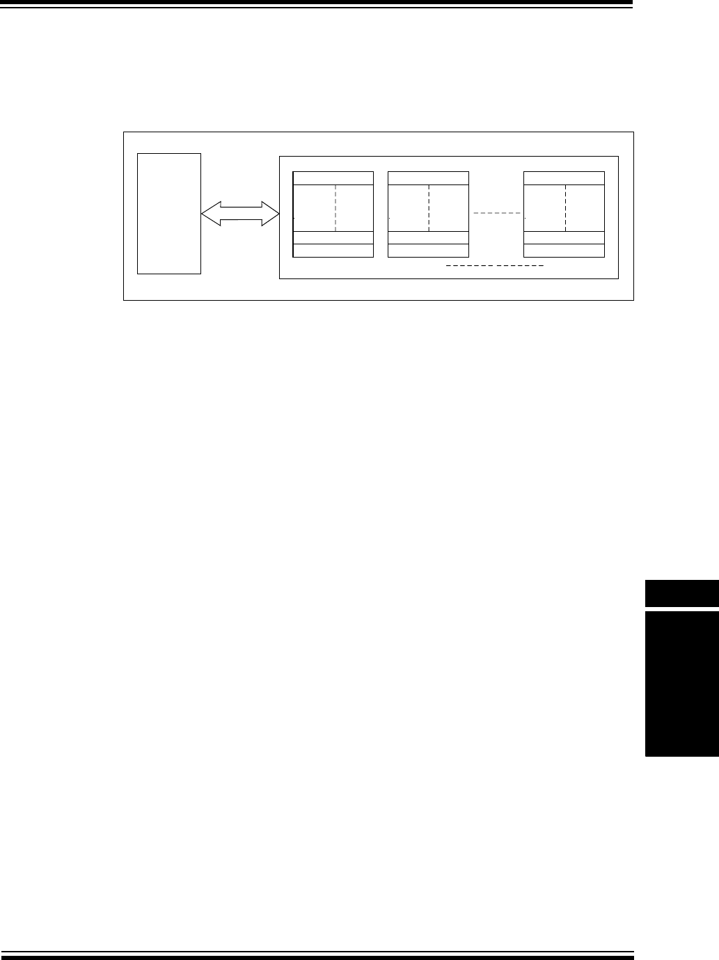
© 2009-2012 Microchip Technology Inc. DS61154C-page 34-49
Section 34. Controller Area Network (CAN)
Controller Area
Network (CAN)
34
34.6 CAN MESSAGE HANDLING
The CAN module uses device RAM for storing CAN messages that need to be transmitted or
received. The CAN module by itself does not have user-accessible message buffers. Figure 34-8
illustrates the organization of the CAN module buffer memory in device RAM.
Figure 34-8: CAN Message Buffers and Device RAM Organization
As illustrated in Figure 34-8, the CAN module organizes message buffers as FIFOs. A total of 32
distinct FIFOs are available, which have the following characteristics:
•Minimum size of one CAN message buffer and a maximum size of 32 CAN message
buffers
•Independent configurable size
•Configurable to be a transmit message or a receive message FIFO
•User-readable head and tail pointer
•Independently configurable interrupts
• Status bits to provide the status of the FIFO as messages are transmitted or received
•Can be a transmit FIFO or receive FIFO, but not both (therefore, if a FIFO is configured for
transmit operation, all messages in the FIFO are considered for transmission)
•Can be configured to be a transmit FIFO or receive FIFO, independent of each other and
can be configured in any order
Each of the 32 message FIFOs has the following associated registers:
•CAN FIFO Control register (CiFIFOCONn) (Register 34-20)
•CAN FIFO Interrupt register (CiFIFOINTn) (Register 34-21)
•CAN FIFO User Address register (CiFIFOUAn) (Register 34-22)
•CAN FIFO Message Index register (CiFIFOCIn) (Register 34-23)
The CAN module requires only the start address of the first message buffer in the FIFO. The CAN
FIFO Base Address register (CiFIFOBA) should point to the start address of this message buffer.
The CAN module automatically calculates the address of message buffers in each of the FIFO
based on the configuration of the individual FIFOs. The individual FIFOs will be arranged
contiguously, with all the message buffers being packed. This produces a CAN message buffer
memory without any gaps. While the CiFIFOUAn register provides the address of the next
read/write CAN Message Buffer that the user application must use, the CiFIFOCIn register
provides the corresponding CAN Message Buffer Index of the next message buffer to be
transmitted or written to by the CAN module.
For more information on FIFO related interrupts along with other CAN module interrupts, refer to
34.12 “CAN Interrupts”.
Message Buffer 31
Message Buffer 1
Message Buffer 0
Message Buffer 31
Message Buffer 1
Message Buffer 0
Message Buffer 31
Message Buffer 1
Message Buffer 0
CAN
Module
FIFO0 FIFO1 FIFO31
Device RAM
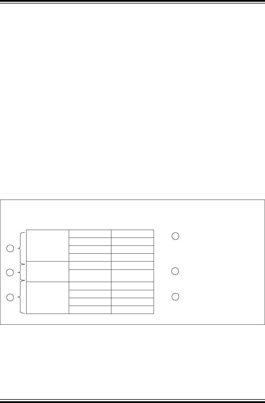
PIC32 Family Reference Manual
DS61154C-page 34-50 © 2009-2012 Microchip Technology Inc.
34.6.1 Message FIFO Configuration
The user application must allocate device RAM space for CAN message buffering. The
requirements of each type of message buffer are as follows:
• A CAN transmit message buffer requires 4 words (16 bytes) of memory
•A CAN receive message buffer will require 4 words (16 bytes) of memory, if the entire
message (time stamp plus data plus message ID) is stored - (full receive message)
•A CAN receive message buffer will require 2 words (8 bytes) of memory only if the data is
stored - (data-only receive message)
The user application must design the size of each message FIFO. The FIFO size is controlled
through the FIFO size (FSIZE<4:0>) bits in the corresponding CAN FIFO Control register
(CiFIFOCONn<20:16>). All FIFOs have a default size of at least one message buffer. The total
memory to be allocated is obtained by counting the total number of buffers across FIFOs while
accounting for the memory size of each buffer.
For optimal use of the CAN FIFO message buffering model, the user application should configure
the required number of FIFOs in the order starting from FIFO0, and then configuring FIFO1,
FIFO2, FIFO3, and so on.
For example, a user application requires 29 FIFOs and configures FIFO0, FIFO1 and FIFO5
through FIFO31. FIFO2, FIFO3 and FIFO4 are not configured. FIFO2, FIFO3 and FIFO4,
although not configured, still occupy 4 words of RAM each. The CAN module will not use these
FIFOs, but takes these into account while computing the address of FIFO5. In this example, the
user application must allocate memory for all of the 32 FIFOs. The memory occupied by FIFO2,
FIFO3 and FIFO4 could be used by the user application.
An optimal way to accomplish this is to configure FIFO0 through FIFO28, and not configure
FIFO29, FIFO30 and FIFO31. Therefore, the user application must allocate space only for 29
FIFOs. Figure 34-9 illustrates an example.
Figure 34-9: Example of CAN Message Buffer FIFO Configuration (Including Data-only RX Message Buffers)
FIFO Number Message Buffer
Start Address Message Buffer
FIFO
(Transmit FIFO)
0x00001000 MB0
0x00001010 MB1
0x00001020 MB2
0x00001030 MB3
FIFO1
(Data-only RX
Message)
0x00001040 MB0
0x00001048 MB1
FIFO3
(Full Receive
Message)
0x00001050 MB0
0x00001060 MB1
0x00001070 MB2
0x00001080 MB3
A
B
C
A
B
C
C1FIFOCON0.TXEN = 1
C1FIFOCON0.FSIZE = 3
C1FIFOCON1. TXEN = 0
C1FIFOCON1.DONLY = 1
C1FIFOCON1.FSIZE = 1
C1FIFOONC3.TXEN = 0
C1FIFOCON3.DONLY = 0
C1FIFOCON3.FSIZE = 3
CAN1FIFO Configuration
C1FIFOBA = 0x00001000
(Start address of MB0 in FIFO0)

© 2009-2012 Microchip Technology Inc. DS61154C-page 34-51
Section 34. Controller Area Network (CAN)
Controller Area
Network (CAN)
34
For the CAN1 message buffer FIFO configuration illustrated in Figure 34-9, FIFO0 has four
transmit buffers, which would require a total of 16 (4 buffers x 4 words per buffer) words. FIFO1
has two data-only receive buffers, which would require a total of four (2 buffers x 2 words per
buffer) words. FIFO3 has four full receive buffers, which would require a total of 16 (4 buffers x 4
words per buffer) words. Therefore, a total of 36 (16 + 4 + 16) words of memory needs to be
allocated.
Consider another example of a user application illustrated in Figure 34-10, which requires a total
of four FIFOs.
Figure 34-10: Example of CAN FIFO Configuration
FIFO0 and FIFO1 have two message buffers each and are configured to be CAN message
transmit FIFOs. FIFO2 and FIFO3 have three message buffers each and are configured to be
CAN message receive FIFOs. FIFO0 and FIFO1 will require a total of 16 (2 FIFOs x 2 message
buffers per FIFO x 4 words per message buffer) words of memory. FIFO2 and FIFO3 will require
a total of 24 (2 FIFOs x 3 message buffers per FIFO x 4 words per message buffer) words of
memory. Therefore, a total of 40 (16 + 24) words of memory needs to be allocated.
The following steps can be used to configure the CAN module FIFOs:
1. Allocate memory for the CAN message buffer FIFOs.
2. Place the CAN module into Configuration mode (OPMOD<2:0> = 100).
3. Update the CAN FIFO Base Address register (CiFIFOBA) with the base address of the
FIFO. This should be the physical start address of Message Buffer 0 of FIFO0.
4. Update the FSIZE<4:0> bits (CiFIFOCONn<20:16>).
5. Select whether the FIFO is to be a transmit or receive FIFO (TXEN bit
(CiFIFOCONn<7:0>)).
6. Place the CAN module into Normal Operation mode (OPMOD<2:0> = 000).
Example 34-2 illustrates how the above coding steps can be used to configure the CAN message
FIFO as shown in Example 34-10.
FIFO Number Message Buffer
Start Address Message Buffer
FIFO0 0x00002000 MB0
0x00002010 MB1
FIFO1 0x00002020 MB0
0x00002030 MB1
FIFO2
0x00002040 MB0
0x00002050 MB1
0x00002060 MB2
FIFO3
0x00002070 MB0
0x00002080 MB1
0x00002090 MB2
A
B
C
D
C1FIFOCON0.TXEN = 1
C1FIFOCON0.SIZE = 1
C1FIFOCON1.TXEN = 1
C1FIFOCON1.SIZE = 1
C1FIFOCON2.TXEN = 0
C1FIFOCON2.SIZE = 2
C1FIFOCON3.TXEN = 0
C1FIFOCON3.SIZE = 2
CAN1FIFO Configuration
C1FIFOBA = 0x00002000
A
B
C
D

PIC32 Family Reference Manual
DS61154C-page 34-52 © 2009-2012 Microchip Technology Inc.
Example 34-2: Setting Up the CAN Message FIFO
/* This code snippet illustrates the steps required to configure the */
/* PIC32 CAN Message FIFOs. The FIFO configuration example shown in */
/* Figure 34-5 will be used in this example. */
/* FIFO0 - Transmit - 2 MESSAGE BUFFERS */
/* FIFO1 - Transmit - 2 MESSAGE BUFFERS */
/* FIF02 - Receive - 3 MESSAGE BUFFERS */
/* FIF03 - Receive - 3 MESSAGE BUFFERS */
/* FIFO4 - FIFO31 - Not used */
/* Allocate a total of 40 words.
unsigned int CanFifoMessageBuffers[40];
/* Request CAN to switch to configuration mode and wait until it has switched */
C1CONbits.REQOP = 100
while(C1CONbits.OPMOD != 100);
/* Initialize C1FIFOBA register with physical address of CAN message Buffer */
C1FIFOBA = KVA_TO_PA(CanFifoMessageBuffers); ;
/* Configure FIFO0 */
C1FIFOCON0bits.FSIZE = 1;
C1FIFOCON0SET = 0x80; /* Set the TXEN bit */
/* Configure FIFO1 */
C1FIFOCON1bits.FSIZE = 1;
C1FIFOCON1SET = 0x80; /* Set the TXEN bit */
/* Configure FIFO2 */
C1FIFOCON2bits.FSIZE = 2;
C1FIFOCON2CLR = 0x80; /* Clear the TXEN bit */
/* Configure FIFO3 */
C1FIFOCON3bits.FSIZE = 2;
C1FIFOCON3CLR = 0x80; /* Clear the TXEN bit */
/* The CAN module can now be placed into normal mode if no further */
/* configuration is required. */
C1CONbits.REQOP = 0;
while(C1CONbits.OPMOD != 0);

© 2009-2012 Microchip Technology Inc. DS61154C-page 34-53
Section 34. Controller Area Network (CAN)
Controller Area
Network (CAN)
34
34.6.2 Loading Messages to be Transmitted into the FIFO
In order to use a FIFO to transmit data, the FIFO must be configured as a transmit FIFO. This is
done by setting the TX/RX Buffer Selection (TXEN) bit in the CAN FIFO Control register
(CiFIFOCONn<7>).
The CAN FIFO User Address register (CiFIFOUAn) provides the physical address of the next
message buffer in FIFO where the user application should store the message (also referred to
as the FIFO head location). The CAN message should be loaded, starting at the location
provided by the CiFIFOUAn register.
The user application should set the Increment Head/Tail (UINC) bit in the CAN FIFO Control
register (CiFIFOCONn<13>) after loading one message buffer in the FIFO. This will cause the
CAN module to increment the address contained in the CiFIFOUAn register by 16 (thereby
pointing to the next message buffer). The message is then ready to be transmitted. The
CiFIFOUAn register rolls over to the start of the FIFO when it has reached the end of FIFO.
As a result, the user application need not track the FIFO head location, and can use the
CiFIFOUAn register for this purpose. The following coding steps can be followed to load a
message for transmission into a transmit FIFO:
1. Read the CiFIFOUAn register and store one message (16 bytes) at this address.
2. Set the UINC bit (CiFIFOCONn<13>) to update the CiFIFOUAn register.
3. Set the Message Send Request (TXREQ) bit in the CAN FIFO Control register
(CiFIFOCONn<3>) to transmit the message.
4. Perform steps 2 and 3 for the number of messages to be queued and the size of the FIFO.
Example 34-3 illustrates the above coding steps. In this example, four messages are loaded into
FIFO0 of the CAN1 module.
Example 34-3: Loading a Transmit Message FIFO
/* This code snippet illustrates the steps to load a transmit message FIFO. */
/* This example uses the CAN1 module. */
/* Four messages to be transmitted using transmit FIFO0 */
int message; /* Tracks the message buffer */
unsigned int * currentMessageBuffer; /* Points to message buffer to be written */
message = 0;
for(message = 0; message <= 3; message ++)
{
/* Get the address of the message buffer to write to from the C1FIFOUA0 */
/* register. Convert this physical address to virtual address. */
currentMessageBuffer = PA_TO_KVA1(C1FIF0UA0);
/* This procedure will load the message
* buffer with the message to be transmitted. */
LoadMessageBuffer(currentMessageBuffer);
C1FIFOCON0SET = 0x2008; /* Set the UINC and TXREQ bit */
}
/* At this point the messages are loaded in FIFO0 */

PIC32 Family Reference Manual
DS61154C-page 34-54 © 2009-2012 Microchip Technology Inc.
34.6.3 Accessing Received Messages In the FIFO
To us e the FIFO to rec eiv e dat a, the FIFO must be configured as a receive FIFO. This is done
by clearing the TXEN bit (CiFIFOCONn<7>). After a message is received, the user application
should obtain the physical start address of the first message buffer to read (also called the FIFO
tail pointer) from the CiFIFOUAn register. The message can then be read from this address
onward.
After processing the message from the FIFO, the user application should signal the CAN module
that the message has been processed and can be overwritten by setting the UINC bit
(CiFIFOCONn<13>). This will increment the tail pointer and increase the address pointed to by
the CiFIFOUAn register by 4 words or 2 words, depending on the value of the DONLY bit
(CiFIFOCONn<12>). The CiFIFOUAn register rolls over to the start of the FIFO when it has
reached the end of the FIFO.
As a result, the user application need not track the FIFO tail location, and can use the CiFIFOUAn
register for this purpose. The following coding steps can be followed to process a message in a
receive FIFO:
1. Use any of the available interrupts to determine if there is a message in the FIFO.
2. Read the CiFIFOUAn register and process one message (16 bytes) from this address.
3. Set the UINC bit (CiFIFOCONn<13>) to update the CiFIFOUAn register.
4. Perform steps 1 and 2 until the interrupt condition gets cleared.
Example 34-4 illustrates the code using the above steps. In this code example, FIFO1 of the CAN
1 module is configured for receive operation. The code example reads the FIFO until it is empty.
Example 34-4: Reading Received Messages from the FIFO
/* This code snippet illustrates the steps to read messages from receive */
/* message FIFO. This example uses the CAN1 module.*/
/* FIFO1 size is 4 messages and each message is 4 words long. */
unsigned int * currentMessageBuffer; /* Points to message buffer to be read */
while(1)
{
/* Keep reading until the FIFO is empty. */
while(C1FIFOINT1bits.RXNEMPTYIF == 1)
{
/* Get the address of the message buffer to read from the C1FIFOUA1 */
/* register. Convert this physical address to virtual address. */
currentMessageBuffer = PA_TO_KVA1(C1FIF0UA1);
ProcessReceivedMessage(currentMessageBuffer);
/* Set the UINC bit to tell the CAN module that
* a message has been read. */
C1FIFOCON0SET = 0x2000;
}
}

© 2009-2012 Microchip Technology Inc. DS61154C-page 34-55
Section 34. Controller Area Network (CAN)
Controller Area
Network (CAN)
34
34.6.4 Resetting the FIFO
The FIFO can be reset by any of the following methods:
•Setting the FIFO Reset (FRESET) bit in the CAN FIFO Control register
(CiFIFOCONn<14>)
•Placing the CAN module into Configuration mode (OPMOD<2:0> bits (CiCON<23:21>) = 100)
•Turning the CAN module OFF (CiCON<15> = 0)
Resetting the FIFO will reset the head and tail pointers, the interrupt flags, and the following
status bits in the CAN FIFO Control register (CiFIFOCONn): the Message Aborted (TXABAT) bit
(CiFIFOCONn<6>), the Message Lost Arbitration (TXLARB) bit (CiFIFOCONn<5>) and the Error
Detected During Transmission (TXERR) bit (CiFIFOCONn<4>).
The following should be considered before resetting a FIFO using the FRESET bit
(CiFIFOCONn<14>):
•If the FIFO is a transmit FIFO, no transmissions should be pending
•If the FIFO is a receive FIFO, it should not be pointed to by any active filters
A user application may typically reset the FIFO after coming out of Disable mode. While resetting
the FIFO using the FRESET bit (CiFIFOCONn<14>), the user application must poll the bit to
ensure that the reset operation has completed. This is shown in Example 34-5.
Example 34-5: Resetting a Message FIFO
/* This code snippet shows how to reset a message FIFO. This example */
/* uses FIFO0 of the CAN1 module. */
C1FIFOCON0SET = 0x00004000; /* Set the FRESET bit */
while(C1FIFOCON0bits.FRESET == 1);
PIC32 Family Reference Manual
DS61154C-page 34-56 © 2009-2012 Microchip Technology Inc.
34.7 TRANSMITTING A CAN MESSAGE
The CAN module will transmit messages that are loaded in a transmit FIFO. For detailed
descriptions on configuring a message FIFO for transmit operation, refer to 34.6.1 “Message
FIFO Configuration” and 34.6.2 “Loading Messages to be Transmitted into the FIFO”.
34.7.1 Format of Transmit Message Buffer
The transmit message FIFO can hold up to 32 CAN transmit message buffers. A transmit
message buffer is 4 words (16 bytes) long and has a fixed format as described in Ta bl e 34-2. It
contains four words: CMSGSID, CMSGEID, CMSGDATA0 and CMSGDATA1. The bits in these
registers have a one-to-one correspondence to bit fields in the CAN message, as defined by the
CAN Specification 2.0B. The user application must ensure that every message buffer in the
transmit FIFO conforms to the formats illustrated in Figure 34-11 through Figure 34-14.
Figure 34-11: Format of CMSGSID
Table 34-2: Transmit Message Buffer Format as Stored in System Memory
Name Bit
31/2315/7
Bit
30/22/14/6
Bit
29/21/13/5
Bit
28/20/12/4
Bit
27/19/11/3
Bit
26/18/10/2
Bit
25/17/9/1
Bit
24/16/8/0
CMSGSID 31:24 -— -— -— -— -— -— -— -—
23:16 -— -— -— -— -— -— -— -—
15:8 -— -— -— -— -— SID<10:8>
7:0 SID<7:0>
CMSGEID 31:24 -— -— SRR IDE EID<17:14>
23:16 EID<13:6>
15:8 EID<5:0> RTR RB1
7:0 -— -— --—RB0 DLC<3:0>
CMSGDATA0 31:24 Transmit Buffer Data Byte 3
23:16 Transmit Buffer Data Byte 2
15:8 Transmit Buffer Data Byte 1
7:0 Transmit Buffer Data Byte 0
CMSGDATA1 31:24 Transmit Buffer Data Byte 7
23:16 Transmit Buffer Data Byte 6
15:8 Transmit Buffer Data Byte 5
7:0 Transmit Buffer Data Byte 4
Legend: Shaded bits should be set to ‘0’.
Note: The CAN transmit message is stored in device RAM and has no associated SET/CLR/INV registers.
SID<10:0>
bit 10-0 SID<10:0>: Standard Identifier

© 2009-2012 Microchip Technology Inc. DS61154C-page 34-57
Section 34. Controller Area Network (CAN)
Controller Area
Network (CAN)
34
Figure 34-12: Format of CMSGEID
Figure 34-13: Format of CMSGDATA0
Figure 34-14: Format of CMSGDATA1
—SRRIDEEID<17:0>RTRRB1—RB0DLC<3:0>
bit 31-30 Unimplemented: Read as ‘0’
bit 29 SRR: Substitute Remote Request bit
In case of a standard message format (IDE = 0), this bit is don’t care.
In case of an extended message format (IDE = 1), this bit should always be set.
bit 28 IDE: Extended Identifier bit
1 = Message will transmit extended identifier
0 = Message will transmit standard identifier
bit 27-10 EID<17:0>: Extended Identifier bits
bit 9 RTR: Remote Transmission Request bit
1 = Message is a remote transmission request
0 = Message is not a remote transmission request
bit 8 RB1: Reserved bit 1
The user application must set this bit to ‘0’ per the CAN Specification 2.0B.
bit 7-5 Unimplemented: Read as ‘0’
bit 4 RB0: Reserved bit 0
The user application must set this bit to ‘0’ per the CAN Specification 2.0B.
bit 3-0 DLC<3:0>: Data Length Code bits
1xxx = Module will transmit 8 bytes
0111 = 7 bytes of data will be transmitted
•
•
•
0001 = 1 byte of data will be transmitted
0000 = 0 bytes of data will be transmitted
Note: This register is in system memory outside the CAN module.
DATA3<7:0> DATA2<7:0> DATA1<7:0> DATA0<7:0>
bit 31-24 DATA3<7:0>: Data Byte 3
bit 23-16 DATA2<7:0>: Data Byte 2
bit 15-8 DATA1<7:0>: Data Byte 1
bit 7-0 DATA0<7:0>: Data Byte 0
Note: This register is in system memory outside the CAN module.
DATA7<7:0> DATA6<7:0> DATA5<7:0> DATA4<7:0>
bit 31-24 DATA7<7:0>: Data Byte 7
bit 23-16 DATA6<7:0>: Data Byte 6
bit 15-8 DATA5<7:0>: Data Byte 5
bit 7-0 DATA4<7:0>: Data Byte 4
Note: This register is in system memory outside the CAN module.

PIC32 Family Reference Manual
DS61154C-page 34-58 © 2009-2012 Microchip Technology Inc.
Example 34-6 shows a code example data structure for implementing a CAN message buffer in
memory. An example of using this structure is provided in Example 34-7.
Example 34-6: Implementing a CAN Message Buffer in Memory
/* This code snippet shows an example of data structure to implement a CAN */
/* message buffer. */
/* Define the sub-components of the data structure as specified in Table 34-2 */
/* Create a CMSGSID data type. */
typedefstruct
{
unsigned SID:11;
unsigned :21;
}txcmsgsid;
/* Create a CMSGEID data type. */
typedef struct
{
unsigned DLC:4;
unsigned RB0:1;
unsigned :3;
unsigned RB1:1;
unsigned RTR:1;
unsigned EID:18;
unsigned IDE:1;
unsigned SRR:1;
unsigned :2;
}txcmsgeid;
/* Create a CMSGDATA0 data type. */
typedef struct
{
unsigned Byte0:8;
unsigned Byte1:8;
unsigned Byte2:8;
unsigned Byte3:8;
}txcmsgdata0;
/* Create a CMSGDATA1 data type. */
typedefstruct
{
unsigned Byte4:8;
unsigned Byte5:8;
unsigned Byte6:8;
unsigned Byte7:8;
}txcmsgdata1;
/* This is the main data structure. */
typedef union uCANTxMessageBuffer {
struct
{
txcmsgsid CMSGSID;
txcmsgeid CMSGEID;
txcmsgdata0 CMSGDATA0;
txcmsgdata0 CMSGDATA1;
};
int messageWord[4];
}CANTxMessageBuffer;
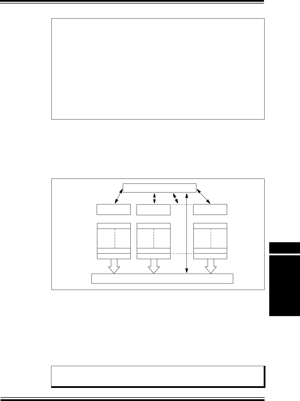
© 2009-2012 Microchip Technology Inc. DS61154C-page 34-59
Section 34. Controller Area Network (CAN)
Controller Area
Network (CAN)
34
Example 34-7: Example Usage of the Data Structure
34.7.2 Requesting Transmit of a Message
Tabl e 34-15 shows the CAN module transmission process. The user application must configure
the FIFO for transmit operation. Message transmission and priority is controlled by the
CiFIFOCONn register (see Register 34-20). The CAN module will then select the next message
to be transmitted based on readiness and priority, and will process this message for
transmission.
Figure 34-15: CAN Message Transmission
Once a message has been loaded into the FIFO and is ready to be transmitted, the user
application can initiate a transmission by setting the TXREQ bit (CiFIFOCONn<3>). When this
bit is set, the contents of the FIFO will be queued for transmission according to the message
priority, and the CAN module will transmit all the messages in the FIFO. When all messages have
been transmitted, the TXREQ bit (CiFIFOCONn<3>) will be cleared. A user application can load
all of the transmit FIFOs and set the TXREQ bit (CiFIFOCONn<3>) for all of these FIFOs.
Alternately, the user application can load one transmit FIFO, set the associated TXREQ bit
(CiFIFOCONn<3>), and then load the next FIFO while the previous FIFO is being processed.
Messages can be appended to the FIFO while a message is being transmitted. The user
application should use the CiFIFOUAn register to get the FIFO head pointer and should store the
message at this address. Appended messages will be queued for transmission.
Note: It is recommended that the user application set the TXREQ bit (CiFIFOCONn<3>)
after every message is loaded into the FIFO (after the UINC bit (CiFIFOCONn<13>)
is set).
/* Example usage of data structure shown in Example 34-6. This example sets */
/* up a message buffer in FIFO1 */
CANTxMessageBuffer * buffer;
buffer = (CANTxMessageBuffer *)(PA_TO_KVA1(C1FIFOUA1));
/* Clear the message buffer. */
buffer->messageWord[0] = 0;
buffer->messageWord[1] = 0;
buffer->messageWord[2] = 0;
buffer->messageWord[3] = 0;
buffer->CMSGSID.SID = 0x100;/* Message SID */
buffer->CMSGEID.DLC = 0x2;/* Data Length is 2 */
buffer->CMSGDATA0.Byte0 = 0xAA;/* Byte 0 Data */
buffer->CMSGDATA0.Byte1 = 0xbb;/* Byte 1 Data */
Message Buffer 31
Message Buffer 1
Message Buffer 0
Message Buffer 31
Message Buffer 1
Message Buffer 0
Message Buffer 31
Message Buffer 1
Message Buffer 0
FIFO0 FIFO1 FIFO31
Message Queue and Priority Control
Message Assembly Buffer
CiFOFOCON0 CiFOFOCON1 CiFOFOCON31

PIC32 Family Reference Manual
DS61154C-page 34-60 © 2009-2012 Microchip Technology Inc.
The user application should check that the transmit FIFO can accommodate messages (that is,
the transmit FIFO is not full) before writing messages to the FIFO. This can be done by checking
the TxNFULLIF bit in the CAN FIFO Interrupt register (CiFIFOINTn<10>). Writing a message to
a FIFO which is full could cause an untransmitted message to be overwritten.
The following coding steps can be used to transmit CAN messages:
1. Configure the desired number of FIFOs for transmit operation.
2. If desired, set the priority of the individual FIFOs.
3. Create a transmit message using the format shown in Tabl e 34-2.
4. If the TxNFULLIF bit (CiFIFOINTn <10>) is clear, this means the FIFO is full. In this case,
skip to Step 7.
5. Read the CiFIFOUAn register and store the message at the provided address.
6. Set the UINC bit (CiFIFOCONn<13>).
7. Set the TXREQ bit (CiFIFOCONn<3>).
8. Repeat steps 3 through 6 for the number of messages to be transmitted across the
desired number of FIFOs.
9. The transmit FIFO interrupts can be used to monitor the FIFO status.
Example 34-8 shows a code example that provides the steps required to transmit a CAN
message using the CAN1 module to transmit four messages. Message 0 and 1 are Standard
Identifier (SID) CAN messages. Message 2 and 3 are EID messages. FIFO1 is used and its
length is 3.
Example 34-8: Transmitting Standard and Extended ID Messages
/* This code example illustrates how to transmit standard and extended */
/* ID messages with the PIC32 CAN module. */
/* The code example uses CAN1, FIFO0. FIFO0 size is 4 */
/* Four CAN message have to be transmitted. */
/* Msg 0: SID - 0x100 Data - 0x12BC1245 */
/* Msg 1: SID - 0x102 Data - 0x12BC124512BC1245 */
/* Msg 2: SID - 0x100 EID - 0xC000 Data - 0x12BC1245 */
/* Msg 3: SID - 0x102 EID - 0xC000 Data - 0x12BC124512BC1245 */
/* Pointer to CAN Message Buffer */
CANTxMessageBuffer * transmitMessage;
/* This array is the CAN FIFO and message buffers. FIF0 has 4 message */
/* buffers. All other buffers are default size. */
unsigned int CANFIFO[16];
/* Place CAN module in configuration mode */
C1CONbits.REQOP = 4;
while(C1CONbits.OPMOD != 4);
/* Initialize the C1FIFOBA with the start address of the CAN FIFO message */
/* buffer area. */
C1FIFOBA = KVA_TO_PA(CANFIFO);
/* Set FIFO0 size to 3 messages. All other FIFOs at default size. */
/* Configure FIFO0 for transmit.*/
C1FIFOCON0bits.FSIZE = 2
C1FIFOCON0SET = 0x00000080; /* Set the TXEN bit - Transmit FIFO */

© 2009-2012 Microchip Technology Inc. DS61154C-page 34-61
Section 34. Controller Area Network (CAN)
Controller Area
Network (CAN)
34
Example 34-8: Transmitting Standard and Extended ID Messages (Continued)
/* Place the CAN module in Normal mode. */
C1CONbits.REQOP = 0;
while(C1CONbits.OPMOD != 0);
/* Get the address of the message buffer to write to. Load the buffer and */
/* then set the UINC bit. Set the TXREQ bit next to send the message. */
/* Message 0 SID - 0x100 Data - 0x12BC1245*/
transmitMessage = (CANTxMessageBuffer *)(PA_TO_KVA1(C1FIFOUA1));
transmitMessage->CMSGSID.SID = 0x100; /* CMSGSID */
transmitMessage->CMSGEID.IDE = 0;
transmitMessage->CMSGEID.DLC = 0x4;
transmitMessage->messageWord[2] = 0x12BC1245; /* CMSGDAT0 */
C1FIFOCON1SET = 0x00002000; /* Set the UINC bit */
C1FIFOCON1SET = 0x00000008; /* Set the TXREQ bit */
/* Message 1 SID - 0x102 Data - 0x12BC124512BC1245 */
transmitMessage = (CANTxMessageBuffer *)(PA_TO_KVA1(C1FIFOUA1));
transmitMessage->CMSGSID.SID = 0x102; /* CMSGSID */
transmitMessage->CMSGEID.IDE = 0;
transmitMessage->CMSGEID.DLC = 0x8;
transmitMessage->messageWord[2] = 0x12BC1245; /* CMSGDAT0 */
transmitMessage->messageWord[3] = 0x12BC1245; /* CMSGDAT1 */
C1FIFOCON1SET = 0x00002000; /* Set the UINC bit */
C1FIFOCON1SET = 0x00000008; /* Set the TXREQ bit */
/* Message 2 SID - 0x100 EID - 0xC000 Data - 0x12BC1245*/
transmitMessage = (CANTxMessageBuffer *)(PA_TO_KVA1(C1FIFOUA1));
transmitMessage->CMSGSID.SID = 0x100; /* CMSGSID */
transmitMessage->CMSGEID.SID = 0xC000; /* CMSGEID */
transmitMessage->CMSGEID.IDE = 1;
transmitMessage->CMSGEID.DLC = 0x4;
transmitMessage->messageWord[2] = 0x12BC1245; /* CMSGDAT0 */
C1FIFOCON1SET = 0x00002000; /* Set the UINC bit */
C1FIFOCON1SET = 0x00000008; /* Set the TXREQ bit */
/* Message 3 SID - 0x102 EID - 0xC000 Data - 0x12BC124512BC1245*/
transmitMessage = (CANTxMessageBuffer *)(PA_TO_KVA1(C1FIFOUA1));
transmitMessage->CMSGSID.SID = 0x102; /* CMSGSID */
transmitMessage->CMSGEID.SID = 0xC000; /* CMSGEID */
transmitMessage->CMSGEID.IDE = 1;
transmitMessage->CMSGEID.DLC = 0x8;
transmitMessage->messageWord[2] = 0x12BC1245; /* CMSGDAT0 */
transmitMessage->messageWord[3] = 0x12BC1245; /* CMSGDAT1 */
C1FIFOCON1SET = 0x00002000; /* Set the UINC bit */
C1FIFOCON1SET = 0x00000008; /* Set the TXREQ bit */
}

PIC32 Family Reference Manual
DS61154C-page 34-62 © 2009-2012 Microchip Technology Inc.
34.7.3 Transmit Message Priority
The CAN module allows the user application to control the priority of transmit message buffers.
Prior to sending a message SOF, the CAN module compares the priority of all buffers that are
ready for transmission. The transmit message buffer with the highest priority will be sent first. For
example, if transmit FIFO0 has a higher priority setting than transmit FIFO1, all messages in
FIFO0 will be sent first. In a case where the priority of a FIFO is changed while another FIFO is
being processed, the CAN module will reassess the priority of all FIFOs after it has completed
transmitting the current message. This allows the change in FIFO priority to take effect at the
earliest opportunity.
The priority levels are controlled by the Message Transmit Priority (TXPR<1:0>) bits in the CAN
FIFO Control register (CiFIFOCONn<1:0>). There are four levels of transmit priority as defined
by the (TXPR<1:0>) bits (CiFIFOCONn<1:0>). The selections are as follows:
•11 = This FIFO has the highest priority
•10 = This FIFO has an intermediate high priority
•01 = This FIFO has an intermediate low priority
•00 = This FIFO has the lowest priority
If two FIFOs have the same priority setting, the FIFO with the highest natural order is sent. The
natural order of transmission if all FIFOs have the same priority is as follows:
•FIFO0 = lowest natural priority
•FIFO1 = higher natural priority
•
•
•
•FIFO31 = highest natural priority
34.7.4 Aborting Transmission of a Queued Message
A message that has been queued to be transmitted can be aborted by clearing the TXREQ bit
(CiFIFOCONn<3>). If the TXREQ bit (CiFIFOCONn<3>) is cleared, the CAN module will attempt
to abort the transmission.
If the message aborts successfully, the TXABAT bit (CiFIFOCONn<6>) will be set by hardware.
TXREQ will remain set until the message either aborts or is successfully transmitted.
If the message is successfully transmitted, the FIFO pointers will be updated as normal. If the
message is successfully aborted, the FIFO pointers will not change. The user can then use the
internal index (CFIFOCI) to determine which messages have already been transmitted if
required.
To reset the FIFO pointers and erase all pending messages, the user application can set the
FRESET bit (CiFIFOCONn<14>). The FIFO can then be re-enabled and loaded with new
messages to be transmitted.

© 2009-2012 Microchip Technology Inc. DS61154C-page 34-63
Section 34. Controller Area Network (CAN)
Controller Area
Network (CAN)
34
34.7.5 Remote Transmit Request
As discussed in 34.7.2 “Requesting Transmit of a Message”, the CAN bus system has a
method for allowing a node to request data from another node. The requesting node sends a
message with the RTR bit set. The message contains no data, only an address to trigger a filter
match.
The filter that is configured to respond to an RTR will point to a FIFO that is configured for
transmission. The FIFO must also be enabled to reply to the remote transmission requests by
setting the RTREN = 1.
RTRs can be handled without CPU intervention. If a transmit FIFO is configured correctly, when
a filter matches and that filter points to the FIFO, the buffer will be queued for transmission. The
FIFO must be configured as follows:
1. Set FIFO to Transmit mode by setting the TXEN bit (CiFIFOCONn<7>) to ‘1’.
2. A filter must be enabled and loaded with a matching message identifier.
3. The buffer pointer register for that filter must point to the transmit buffer (note that although
a filter normally points to a receive FIFO, in this case it must point to the transmit FIFO).
4. The RTREN bit (CiFIFOCONn<2>) must be set to ‘1’ to enable RTR.
5. The FIFO must be preloaded with at least one message to be sent.
When a RTR message is received, and it matches a filter pointing to the properly configured
transmit buffer, the TXREQ bit (CiFIFOCONn<3>) is automatically set. The message buffers in
the FIFO are then transmitted in priority order. If no messages are available in the transmit buffer
when a request for a remote transmission occurs, the event will be treated as a FIFO overflow,
and the Receive FIFO Overflow Interrupt Flag (RXOVFLIF) bit in the CAN FIFO Interrupt register
(CiFIFOINTn<3>) will be set. Example 34-9 shows a code example of how a node can request
data from remote node. Example 34-10 shows a code example of how a node can be configured
to respond to a RTR.
Example 34-9: Remote Transmit Request
/* This code snippet shows an example of a Remote Transmit Request. The */
/* node in this case will request a transmission from an application (or */
/* node) with an SID of 0x100. */
CANMessageBuffer * rtrMessage;
rtrMessage = (CANMessageBuffer *)(PA_TO_KVA1(C1FIFOUA1));
/* Clear the message. */
rtrMessage->messageWord[0] = 0x0;
rtrMessage->messageWord[1] = 0x0;
rtrMessage->messageWord[2] = 0x0;
rtrMessage->messageWord[3] = 0x0;
rtrMessage->CMSGSID.SID = 0x100;
rtrMessage->CMSGEID.IDE = 0;
rtrMessage->CMSGEID.RTR = 1;
rtrMessage->CMSGEID.DLC = 0;
C1FIFOCON1SET = 0x00002000; /* Set the UINC bit */
/* The Remote Transmit Request message (rtrMessage) is now ready to be sent.*/

PIC32 Family Reference Manual
DS61154C-page 34-64 © 2009-2012 Microchip Technology Inc.
Example 34-10: Responding to a Remote Transmit Request
/* This code example shows how to configure the CAN1 module to respond */
/* to a remote transmit request. */
/* In this case, FIFO1 is configured to respond to the a remote request */
/* on SID = 0x100. */
/* Allocate CAN FIFO memory. */
unsigned int CANFIFO[140];
/* This is the pointer to the reply message. */
CANMessageBuffer * rtrReply;
/* Place CAN Module in configuration mode.*/
C1CONbits.REQOP = 4;
while(C1CONbits.OPMOD != 4);
/* Configure FIFO1 for transmit operation, 4 message buffers and enable */
/* Auto Remote Transmit. */
C1FIFOCON1SET = 0x00000080; /* Set the TXEN bit */
C1FIFOCON1SET = 0x00000004; /* Enable RTR */
C1FIFOCON1bits.FSIZE = 4;
/* Configure a filter to accept a message with SID = 0x100. Refer to */
/* 34.8 “CAN Message Filtering” for more details on configuring */
/* filters. In this case, Filter 0 and Mask0 are used. */
C1FLTCON0bits.FSEL0 = 1; /* Point to FIF01 */
C1FLTCON0bits.MSEL0 = 0; /* Select Mask 0 */
C1RXF0bits.SID = 0x100; /* Configure Filter 0. */
C1RXF0bits.EXID = 0;
C1RXM0bits.SID = 0x1FF; /* Configure Mask 0. */
C1RXM0bits.MIDE = 1;
C1FLTCON0SET = 0x00000080; /* Enable the filter. */
/* Assign FIFO memory to CAN module */
C1FIFOBA = KVA_TO_PA(CANFIFO);
/* Place CAN Module in normal mode.*/
C1CONbits.REQOP = 0;
while(C1CONbits.OPMOD != 0);
/* Form the remote reply message. */
rtrReply = (CANMessageBuffer *)(PA_TO_KVA1(C1FIFOUA1));
rtrReply->messageWord[0] = 0;
rtrReply->messageWord[1] = 0;
rtrReply->messageWord[2] = 0;
rtrReply->messageWord[3] = 0;
rtrReply->CMSGSID.SID = 0x100; /* CMSGSID */
rtrReply->CMSGEID.IDE = 0;
rtrReply->CMSGEID.DLC = 0x4;
rtrReply->messageWord[2] = 0x12BC1245; /* CMSGDAT0 */
C1FIFOCON1bits.UINC = 1;
/* FIFO is now ready to respond to RTR. */
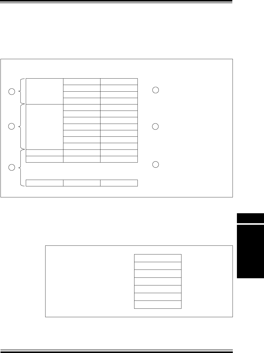
© 2009-2012 Microchip Technology Inc. DS61154C-page 34-65
Section 34. Controller Area Network (CAN)
Controller Area
Network (CAN)
34
34.7.6 Example Message Transmission FIFO Behavior
Consider an example user application that uses two FIFOs, FIFO0 and FIFO1, of the CAN1
module. FIFO0 has four message buffers configured for CAN message reception. FIFO1 has
seven message buffers and is configured for message transmission. FIFO2 through FIFO31 are
left in a default state. The CAN message buffer starts at physical address 0x00000100. This
value is loaded in the C1FIFOBA register. Figure 34-16 shows this application configuration.
Figure 34-16: FIFO Configuration for Example FIFO Behavior
The start address of FIFO1 can be calculated from the base address of the CAN message buffer
(0x00000100) and the byte size of FIFO0 (4 message buffers * 16 = 0x40). The physical start
address of FIFO1 is 0x00000140. The below section focuses on the transmit FIFO1.
Figure 34-17 illustrates the case where FIFO1 of CAN1 module is empty and no messages have
been written. The FIFO Transmit Not Full Interrupt Flag (TXNFULLIF), FIFO Transmit Half Empty
interrupt flag (TXHALFIF) and the FIFO Transmit Empty Interrupt Flag (TXEMPTYIF) are set.
Figure 34-17: FIFO1 at Start
FIFO Number Message Buffer
Start Address Message Buffer
FIFO0
(Full Receive Mes-
sage)
0x00000100 MB0
0x00000110 MB1
0x00000120 MB2
0x00000130 MB3
FIFO1
(Transmit FIFO)
0x00000140 MB0
0x00000150 MB1
0x00000160 MB2
0x00000170 MB3
0x00000180 MB4
0x00000190 MB5
0x000001A0 MB6
FIFO2 0x000001B0 MB0
FIFO4 0x000001C0 MB0
•
•
•
•
•
•
•
•
•
FIFO31 0x00000380 MB0
A
B
C
C1FIFOCON0.TXEN = 1
C1FIFOCON0.FSIZE = 3
C1FIFOCON1.TXEN = 1
C1FIFOCON1.SIZE = 6
FIFO2 - FIFO31 are not configured
CAN1FIFO Configuration
C1FIFOBA = 0x00000100
A
B
C
MB2
MB1
MB0
MB6
MB5
MB4
MB3
C1FIFOBA = 0x00000100
C1FIFOUA1 = 0x00000140
TXNFULLIF - 1
TXHALFIF - 1
TXEMPTYIF - 1
TXREQ - 0
C1FIFOCI1 = 0x00000000

PIC32 Family Reference Manual
DS61154C-page 34-66 © 2009-2012 Microchip Technology Inc.
Figure 34-18 illustrates FIFO1 after the first message has been loaded to the FIFO. Note that the
first message buffer (MB) in FIFO1, MB0, contains data. The user application sets the UINC bit
(C1FIFOCON1<13>), which causes the FIFO head (C1FIFOUA1) to advance and point to the
next empty message buffer, MB1. The TXEMPTYIF flag is cleared since the FIFO is not empty.
The user application at this point has requested a transmission by setting the TXREQ bit
(C1FIFOCON1<3>).
Figure 34-18: FIFO1 - First Write
Figure 34-19 illustrates FIFO1 after the first message has been transmitted from MB0. TXREQ
has been cleared and TXEMPTYIF is set once again. Note that the CAN module Message Index
register, C1FIFOCI1, now points to the second message buffer, MB1 at address 0x00000150.
Figure 34-19: FIFO1 - First Message Transmitted
Figure 34-20 illustrates the FIFO after six more messages have been loaded into MB1 through
MB6. The user application will have read C1FIFOUA1 when loading the messages to get the
address location of the next message buffer to write to. The TXHALFIF flag is cleared and the
user application has not requested the data be transmitted (TXREQ = 0).
Figure 34-20: FIFO1 - Seventh Write About to Fill
MB2
MB1
MB0/MSG0
MB6
MB5
MB4
MB3
C1FIFOBA = 0x00000100
C1FIFOUA1 = 0x00000150
TXNFULLIF - 1
TXHALFIF - 1
TXEMPTYIF - 0
TXREQ - 1
C1FIFOCI1 = 0x00000000
MB2
MB1
MB0
MB6
MB5
MB4
MB3
C1FIFOBA = 0x00000100
C1FIFOUA1 = 0x00000150
TXNFULLIF - 1
TXHALFIF - 1
TXEMPTYIF - 1
TXREQ - 0
C1FIFOCI1 = 0x00000001
MB2/MSG2
MB1/MSG1
MB0
MB6/MSG6
MB5/MSG5
MB4/MSG4
MB3/MSG3
C1FIFOBA = 0x00000100
C1FIFOUA1 = 0x00000140
TXNFULLIF - 1
TXHALFIF - 0
TXEMPTYIF - 0
TXREQ - 0
C1FIFOCI1 = 0x00000001
© 2009-2012 Microchip Technology Inc. DS61154C-page 34-67
Section 34. Controller Area Network (CAN)
Controller Area
Network (CAN)
34
Figure 34-21 illustrates the FIFO after an eighth message has been loaded, this time into MB0.
The TXNFULLIF and TXHALFIF flags are both clear. The FIFO head now points to MB1. The
FIFO at this stage is full. The user application has also requested that the message be
transmitted (TXREQ = 1).
Figure 34-21: FIFO1 - Eighth Write Buffer Full
Figure 34-22 illustrates the FIFO empty once again. The CAN module has transmitted all of the
seven messages in the FIFO. TXEMPTYIF is set once again, and TXREQ has been cleared by
hardware. At this stage, the C1FOCI1 has wrapped completely around and once again points at
MB1.
Figure 34-22: FIFO1 - Fully Transmitted
MB2/MSG2
MB1/MSG1
MB0/MSG7
MB6/MSG6
MB5/MSG5
MB4/MSG4
MB3/MSG3
C1FIFOBA = 0x00000100
C1FIFOUA1 = 0x00000150
TXNFULLIF - 0
TXHALFIF - 0
TXEMPTYIF - 0
TXREQ - 1
C1FIFOCI1 = 0x00000001
MB2
MB1
MB0
MB6
MB5
MB4
MB3
C1FIFOBA = 0x00000100
C1FIFOUA1 = 0x00000150
TXNFULLIF - 1
TXHALFIF - 1
TXEMPTYIF - 1
TXREQ - 0
C1FIFOCI1 = 0x00000001
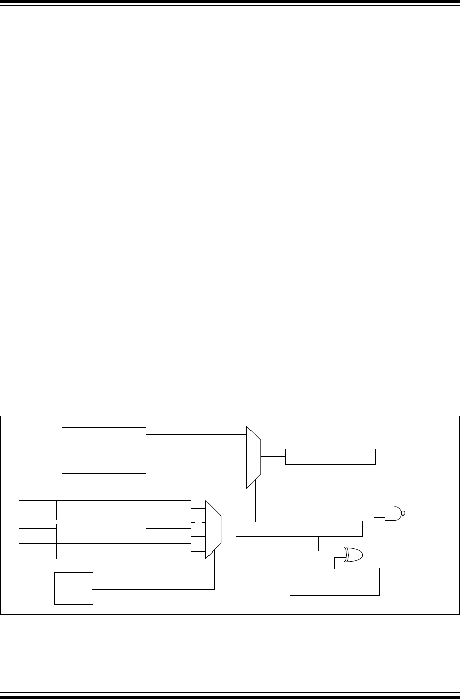
PIC32 Family Reference Manual
DS61154C-page 34-68 © 2009-2012 Microchip Technology Inc.
34.8 CAN MESSAGE FILTERING
The CAN network is a broadcast type of network. A message transmitted by one node is received
by all nodes in the network. Individual CAN nodes require a filtering mechanism to receive
messages of interest. This filtering mechanism is provided by the CAN message acceptance
filters and mask registers. Filtering is performed on the ID field of the CAN message.
The PIC32 CAN module has a total of 32 acceptance filters and four mask registers. The user
application configures the specific filter to receive a message with a given identifier by setting a
filter to match the identifier of the message to be received.
Each filter is controlled by its own CAN Filter Control register (CiFLTCONn). This register has the
following bits for each filter:
•FLTENn (n = 0 through 31) - Filter Enable bit enables/disable the filter
• MSELn<1:0> (n = 0 through 31) - Mask Select defines which mask is applied in the filter
comparison
•FSELn<4:0> (n = 0 thorough 31) - Buffer Pointer defines the destination FIFO of a
message whose ID matches the filter
As messages are received by the CAN module, the message identifier is compared with the
corresponding bits in the filters. If the identifier matches the filter configured by the user, the
message will be stored into the FIFO pointed to by the FIFO Selection (FSELn<4:0>) bits in the
CAN Filter Control registers (CiFLTCONn).
The acceptance masks can be used to ignore the selected bits of the identifier as they are
received. These bits will not be compared with the bits in the filter as the message is received.
For example, if the user would like to receive all of the messages with identifiers 0, 1, 2 and 3,
the user would mask out the lower two bits of the identifier. There are four mask registers
available. A filter can have any one of the four masks associated with it.
Figure 34-23 illustrates a schematic representation of the CAN message filtering. After a
message is received, the CAN module loops through all of the filters. As each filter is selected,
the appropriate mask is also selected using the MSELn<1:0> bits. The message in the Message
Assembly Buffer (MAB) is compared to the filter (XOR). Any bits that should be excluded from
the filtering is excluded using the selected mask. If all the conditions match, an ID match occurs
and the CAN module will move the contents of the MAB into the appropriate FIFO, pointed to by
the FSELn<4:0> bits (CiFLTCONn<4:0>).
Figure 34-23: CAN Message Filtering
In the example illustrated in Figure 34-23, the received message has an ID of 01234567 and the
closest match is Filter 1, which has an ID of 01234566. Note that these two match completely
except for the Least Significant bit (LSb). A match still occurs because the selected mask
(Mask 2) is set to ignore the LSb of the message. Since Filter 2 has its FSELn bits set to 2, the
CAN module will then store the message in FIFO2.
RXF31 Filter = 2A2B3FD
RXF1 Filter = 01234566
RXF0 Filter = 01234565
MASK3 = 00000000
MASK2 = FFFFFFFE
MASK1 = FFFF0FFF
MASK0 = FFFFFFFF
MSEL=1
MSEL=2
MSEL=0
Current Filter = 01234566MSEL
Message Assembly Buffer
Current Mask = FFFFFFFE
ID Match = 1
CAN
FSM
Filter Select = 1 (MAB) = 01234567
FSEL31 = 9
FSEL1 = 2
FSEL0 = 10

© 2009-2012 Microchip Technology Inc. DS61154C-page 34-69
Section 34. Controller Area Network (CAN)
Controller Area
Network (CAN)
34
34.8.1 Enabling and Modifying Filters
Filters can be turned ON or OFF using the Filter Enable (FLTENn) bit in the CiFLTCONn register.
Clearing the bit turns the appropriate filter Off and setting it turns the filter on. Filters can be
modified when the CAN module is in Configuration mode (OPMOD<2:0> = 100), Normal
Operation mode (OPMOD<2:0> = 000) or Disable mode (OPMOD<2:0> = 001).
The CAN module will hold off disabling a filter when a received message is being processed. The
FLTENn bit will remain set until the filtering is complete. If a message hits this filter during filtering,
the message received will be written to the buffer pointed to by the filter. The filter is disabled after
the message has been processed.
The user application should poll the FLTENn bit to ensure that the filter has been disabled before
modifying the filter. Writes to the filter registers are blocked when the filter is enabled.
34.8.2 Extended and Standard Identifiers
A CAN message can have an 11-bit SID or 29-bit EID. The SID<10:0> bits and the EID<17:0>
bits in the CAN Acceptance Filter Mask n registers (CiRXFn) should be configured to match the
SID, or SID and EID of the desired message. Setting the Extended Identifier Enable (EXID) bit
(CiRXFn<19>) will enable the filter to match messages with EIDs. Clearing the EXID bit
(CiRXFn<19>) will enable the filter to match messages with SIDs. If the mask Identifier Receive
Mode (MIDE) bit (CiRXMn<19>) is clear, this type of message will be ignored and all message
types that match the filter will be accepted.
34.8.3 Acceptance Mask
There are four dedicated mask registers in the CAN module, Mask Register 0, 1, 2 and 3. Any
filter can select one of four mask options:
•Mask Register 0
•Mask Register 1
•Mask Register 2
•Mask Register 3
Selection of the mask for an acceptance filter is controlled by the MSELm<1:0> bits
corresponding to the filter in the appropriate CiFLTCONn register. The mask register cannot be
modified when the filter using the mask is enabled. The filter should be disabled before modifying
the mask. If no masking is desired on a given filter, then corresponding mask bits should be set
to one. This will cause the filtering logic to consider all filter bits while performing the filtering
operation. Table 34-3 shows a truth table for various combinations of IDE bit in the CAN
Message, EXID bit (CiRXFn<19>) and the MIDE bit (CiRXMn<19>).
Note: The CiRXMn register can only be modified when the CAN module is in
Configuration mode.

PIC32 Family Reference Manual
DS61154C-page 34-70 © 2009-2012 Microchip Technology Inc.
34.8.4 Buffer Pointer
Associated with the acceptance filter’s control register are the FSELn<4:0> bits
(CiFLTCONn<4:0>). This serves as an address pointer for the corresponding filter. As the
identifier comes in and if a match occurs, the FSELn output corresponding to that filter is enabled
and latched into an address pointer for the receive FIFO memory. After the message has been
assembled in the MAB, it is written into the selected FIFO. The address of the filter that matched
the message is loaded into the Filter Hit Number (FILHIT<4:0>) bits (CiVEC<12:8>) within the
receive buffer.
The use of a buffer pointer means that any filter can be made to point to any FIFO, and any FIFO
can have multiple filters pointed to it. An example of how this can be used in a system would be
to have all receive messages with a low priority be placed in one large FIFO, which is serviced
infrequently by the CPU, and high priority messages placed into a second FIFO, which is
serviced as the messages arrive.
34.8.5 Handling Messages with the Same ID
With the message filtering and masking options available in the CAN module, it is possible that
one message may match more than one filter. When two or more filters match a message
received and point to different receive buffer registers, only one receive buffer register will be
loaded. The receive buffer register to be loaded will be determined by the filter number and buffer
availability. The lower number filter will always have priority over a higher number filter. For
example, Filter 0 will always take precedence over Filter 1. If the receive buffer register that Filter
0 points to is full, then the message will be loaded into the next available FIFO associated to a
matching filter.
Figure 34-24 illustrates an example of the prioritization of multiple filter hits. The message in the
MAB matches Filters 1, 2, 4 and 7. Filter 1 has the highest natural priority, but the associated
FIFO is full, as is Filter 2. Filter 4 has the next highest priority and has room. The message is
stored in FIFO4.
Table 34-3: Standard/Extended Message Reception Truth Table
Message
IDE bit
Filter
EXID
bit
Mask
MIDE
bit
Comment Message
Accepted
0 0 1 Standard message, filter specifies standard only, SID matches Yes
Standard message, filter specifies standard only, SID does not match No
1 1 1 Extended message, filter specifies extended only, SID and EID match Ye s
Extended message, filter specifies extended only, either SID or EID do not match No
1 0 1 Extended message, filter specifies standard only No
0 1 1 Standard message, filter specifies extended only No
0 x 0 Standard message, filter specifies ignoring type, SID matches Yes
Standard message, filter specifies ignoring type, SID does not match No
1 x 0 Extended message, filter specifies ignoring type, SID and EID match Yes
Extended message, filter specifies ignoring type, either SID or EID do not match No
Legend: x = don’t care

© 2009-2012 Microchip Technology Inc. DS61154C-page 34-71
Section 34. Controller Area Network (CAN)
Controller Area
Network (CAN)
34
Figure 34-24: Prioritizing Multiple Filter Hits
34.8.6 Configuring a Filter
The following steps should be followed for configuring a filter for SID CAN messages:
1. Update the SID<10:0> bits (CiRXFn<0:0>) (n is the desired filter) with the SID of the
required CAN message.
2. Clear the EXID bit (CiRXFn<19>). This will cause the filter to match SID messages only.
3. Create a mask for the filter. Load the appropriate value in the CiRXMn register. Set the
MIDE bit (CiRXMn<19>) to match only SID messages
4. Identify the CiFLTCONn register which controls the selected filter. Set the value of the
FSELn<4:0> bits (CiFLTCONn<4:0>) to point to the receive FIFO. Set the MSELn bits to
use the mask configured in step 3.
5. Enable the filter by setting the FLTENn bit in the CiFLTCONn register.
Example 34-11 shows a code example for configuring the CAN module message acceptance
filter for SIDs.
Example 34-11: Configuring a Filter to Match a SID CAN Message
Message = 3A8E924
MAB
Filter 7 ID = 3AxE924 FSEL = 7
Filter 6 ID = 9902B37 FSEL = 6
Filter 5 ID = 62C74E9 FSEL = 5
Filter 4 ID = 3A8Ex24 FSEL = 4
Filter 3 ID = 05092B3 FSEL = 3
Filter 2 ID = 3A8E9x4 FSEL = 2
Filter 1 ID = 3A8E92x FSEL = 1
Filter 0 ID = 23D34A8 FSEL = 0
MATCH = 1
MATCH = 0
MATCH = 0
MATCH = 1(1)
MATCH = 0
MATCH = 1
MATCH = 1
MATCH = 0
FULL = 0
FULL = 0
FULL = 0
FULL = 0(1)
FULL = 0
FULL = 1
FULL = 1
FULL = 0
FIFO7
FIFO6
FIFO5
FIFO4
FIFO3
FIFO2
FIFO1
FIFO0
SELECTED FSEL = 4
X(2)
X(2)
Note 1: The match that is considered by the CAN module.
2: Filter values that are masked out.
3A8Ex24
/* This code example shows how to configure a filter to match a Standard */
/* Identifier (SID) CAN message. */
/* In this example, Filter 3 is set up to accept messages with a SID range */
/* of 0x100 to 103. Accepted messages will be stored in FIFO5. Mask 1 is */
/* used to implement the filter address range. */
C1FLTCON0bits.FSEL3 = 5; /* Store messages in FIFO5 */
C1FLTCON0bits.MSEL3 = 1; /* Use Mask 1 */
C1RXF3bits.SID = 0x100; /* Filter 3 SID */
C1RXF3bits.EXID = 0; /* Filter only SID messages */
C1RXM1bits.SID = 0x7FC; /* Ignore last 2 bits in comparison */
C1RXM1bits.MIDE = 1; /* Match only message types. */
C1FLTCON0bits.FLTEN3 = 1; /* Enable the filter */
/* Filter is now configured. */

PIC32 Family Reference Manual
DS61154C-page 34-72 © 2009-2012 Microchip Technology Inc.
The following steps should be followed for configuring a filter for EID CAN messages:
1. Update the SID<10:0> bits (CiRXFn<31:21>) (where n is the desired filter) with the SID of
the required CAN message. Update the EID<17:0> bits (CiRXFn <17:0>) with the EID of
the required CAN message
2. Set the EXID bit (CiRXFn<19>) register. This will cause the filter to match EID messages
only.
3. Create a mask for the filter. Load the appropriate value in the CiRXMn register. Set the
MIDE bit (CiRXMn<19>) to match only EID messages.
4. Identify the CiFLTCONn register which controls the selected filter. Set the value of the
FSELn<4:0> bits (CiFLTCONn<4:0>) to point to the receive FIFO. Set the MSELn bits to
use the mask configured in step 3.
5. Enable the filter by setting the FLTENn bit in the CiFLTCONn register.
Example 34-12 shows a code example for configuring the CAN module message acceptance
filter for EIDs.
Example 34-12: Configuring a Filter to Match an EID CAN Message
/* This code example shows how to configure a filter to match an */
/* Extended Identifier CAN message. */
/* In this example, Filter 3 is set up to accept messages with SID = 0x53 */
/* and EID = 0x1C498. Accepted message will be stored in FIFO5. Mask 1 is */
/* used. */
C1FLTCON0bits.FSEL3 = 5; /* Store messages in FIFO5 */
C1FLTCON0bits.MSEL3 = 1; /* Use Mask 1 */
C1RXF3bits.SID = 0x100; /* Filter 3 SID */
C1RXF3bits.EID = 0x1C498; /* Filter 3 EID */
C1RXF3bits.EXID = 1; /* Filter only SID messages */
C1RXM1bits.SID = 0x7FF; /* Consider all bits in */
C1RXM1bits.EID = 0x3FFFF; /* in the filter comparison. */
C1RXM1bits.MIDE = 1; /* Match only message types. */
C1FLTCON0bits.FLTEN3 = 1; /* Enable the filter */
/* Filter is now configured. */

© 2009-2012 Microchip Technology Inc. DS61154C-page 34-73
Section 34. Controller Area Network (CAN)
Controller Area
Network (CAN)
34
34.8.7 DeviceNet™ Filtering
The DeviceNet filtering feature is based on the CAN Specification 2.0A, in which up to 18 bits of
the data field can be compared with the EID of the message acceptance filter in addition to the
SID.
The DeviceNet feature is enabled or disabled by the DeviceNet Filter Bit Number (DNCNT<4:0>)
control bits in the CAN Control register (CiCON<4:0>). The value specified in the DNCNT field
determines the number of data bits to be used for comparison with the EID bits of the message
acceptance filter. If the DNCNT<4:0> bits (CiCON<4:0>) are cleared, the DeviceNet feature is
disabled.
For a message to be accepted, the 11-bit SID must match the SID<10:0> bits in the message
acceptance filter and the first ‘n’ data bits in the message should match the EID<17:0> bits in the
message acceptance filter. For example, as shown in Figure 34-25, the first 18 data bits of the
received message data payload are compared with the corresponding EID bits of the message
acceptance filter (CiRXFn<17:0>). The IDE bit of the received message must be ‘0’.
Figure 34-25: CAN Operation with DeviceNet™ Filtering
SID10 SID9
S
O
F
IDENTIFIER
11 Bits
EOF
7 Bits 3 Bits
SID0
Accept/Reject Message
IFS
DATA BYTE 0 DATA BYTE 1 DATA BYTE 2
7654321 0 76543210 76543210
Data Byte 0 Data Byte 1 Data Byte 2MESSAGE SID<10:0>
SID10 SID9 SID0
EID0 EID1 EID7
EID8 EID9 EID15 EID1
6
EID17
STANDARD MESSAGE DATA FRAME
MESSAGE ACCEPTANCE FILTER
SID<10:0>
MESSAGE ACCEPTANCE FILTER
EID<0:17>
Note: The DeviceNet™ filtering configuration shown for EID bits is DNCNT<4:0> = 10010.

PIC32 Family Reference Manual
DS61154C-page 34-74 © 2009-2012 Microchip Technology Inc.
34.8.7.1 FILTER COMPARISONS
Tabl e 34-4 shows the filter comparisons configured by the DNCNT<4:0> control bits
(CiCON<4:0>). For example, if DNCNT<4:0> = 00011, only a message in which the 11-bit SID
matches the SID acceptance filter (SID<10:0>) and bits 7, 6 and 5 of Data Byte 0 match the EID
filter (EID<0:2>) is accepted.
34.8.7.2 SPECIAL CASES
There may be special cases when the message contains fewer data bits than are called for by
the DeviceNet filter configuration.
•Case 1 – If DNCNT<4:0> is greater than 18, indicating that the user application selected a
number of bits greater than the total number of EID bits, the filter comparison terminates
with the eighteenth bit of the data (bit 6 of data byte 2). If the SID and all 18 data bits match,
the message is accepted.
•Case 2 – If DNCNT<4:0> is greater than 16, and the received message Data Length Code
(DLC) is 2 (indicating a payload of two data bytes), the filter comparison terminates with the
sixteenth bit of data (bit 0 of data byte 1). If the SID and all 16 bits match, the message is
accepted.
•Case 3 – If DNCNT<4:0> is greater than 8, and the received message has DLC = 1
(indicating a payload of one data byte), the filter comparison terminates with the eighth bit
of data (bit 0 of data byte 0). If the SID and all 8 bits match, the message is accepted.
•Case 4 – If DNCNT<4:0> is greater than 0, and the received message has DLC = 0,
indicating no data payload, the filter comparison terminates with the SID. If the SID
matches, the message is accepted.
Table 34-4: DeviceNet™ Filter Bit Configurations
DeviceNet™ Filter
Configuration
(DNCNT<4:0>)
Received Message Data Bits to be Compared
(Byte #<bits>)
EID Bits Used for
Acceptance
Filter
00000 No comparison No comparison
00001 Data Byte 0<7> EID<0>
00010 Data Byte 0<7:6> EID<1:0>
00011 Data Byte 0<7:5> EID<2:0>
00100 Data Byte 0<7:4> EID<3:0>
00101 Data Byte 0<7:3> EID<4:0>
00110 Data Byte 0<7:2> EID<5:0>
00111 Data Byte 0<7:1> EID<6:0>
01000 Data Byte 0<7:0> EID<7:0>
01001 Data Byte 0<7:0> and Data Byte 1<7> EID<8:0>
01010 Data Byte 0<7:0> and Data Byte 1<7:6> EID<9:0>
01011 Data Byte 0<7:0> and Data Byte 1<7:5> EID<10:0>
01100 Data Byte 0<7:0> and Data Byte 1<7:4> EID<11:0>
01101 Data Byte 0<7:0> and Data Byte 1<7:3> EID<12:0>
01110 Data Byte 0<7:0> and Data Byte 1<7:2> EID<13:0>
01111 Data Byte 0<7:0> and Data Byte 1<7:1> EID<14:0>
10000 Data Byte 0<7:0> and Data Byte 1<7:0> EID<15:0>
10001 Byte 0<7:0> and Byte 1<7:0> and Byte 2<7> EID<16:0>
10010 Byte 0<7:0> and Byte 1<7:0> and Byte 2<7:6> EID<17:0>
10011 to 11111 Invalid Selection Invalid Selection

© 2009-2012 Microchip Technology Inc. DS61154C-page 34-75
Section 34. Controller Area Network (CAN)
Controller Area
Network (CAN)
34
34.9 RECEIVING A CAN MESSAGE
The CAN module continually monitors messages on the CAN bus. As messages are received by
the CAN module, the message identifier is compared to the filter/mask combinations that are
currently configured. If a match occurs, the CAN module will store the message in the FIFO
pointed to by the FSELn<4:0> bits (CiFLTCONn<4:0>). Once the message has been received
and stored in the FIFO, the following bits will be updated:
• The CFIFOCI<4:0> bits in the CAN Module Message Index register (CiFIFOCIn<4:0>) will
be updated
•The Receive FIFO Overflow interrupt flag (RXOVFLIF), Receive FIFO Full interrupt flag
(RXFULLIF), Receive FIFO Not Empty interrupt flag (RXNEMPTYIF), and the Receive
FIFO Half Full interrupt flag (RXHALFIF) in the CiFIFOINTn register will be updated
•The FIFO Interrupt Pending Flag (FIFOIPn<31:0>) bits in the CAN FIFO Status register
(CiFSTAT<31:0>) will be updated
•An interrupt will be generated, if the interrupts are enabled
The ICODE<6:0> bits (CiVEC<6:0>) and the FILHIT<4:0> bits (CiVEC<12:8>) will also be
updated.
The accepted CAN message is stored in the message buffer using the format shown in
Tabl e 34-5. The CAN module uses the formatting as illustrated in Figure 34-26 through
Figure 34-29.
Note: The user application must enable at least one message acceptance filter and one
mask register in order to receive messages.
Table 34-5: Receive Message Format as Stored in RAM - CiCON.CANCAP = 1,
CFIFOCON.DONLY = 0
Name Bit
31/2315/7
Bit
30/22/14/6
Bit
29/21/13/5
Bit
28/20/12/4
Bit
27/19/11/3
Bit
26/18/10/2
Bit
25/17/9/1
Bit
24/16/8/0
CMSGSID 31:24 CMSGTS<15:8>
23:16 CMSGTS<7:0>
15:8 FILHIT<4:0> SID<10:8>
7:0 SID<7:0>
CMSGEID 31:24 -— -— SRR IDE EID<17:14>
23:16 EID<13:6>
15:8 EID<5:0> RTR RB1
7:0 -— -— --—RB0 DLC<3:0>
CMSGDATA0 31:24 Receive Buffer Data Byte 3
23:16 Receive Buffer Data Byte 2
15:8 Receive Buffer Data Byte 1
7:0 Receive Buffer Data Byte 0
CMSGDATA1 31:24 Receive Buffer Data Byte 7
23:16 Receive Buffer Data Byte 6
15:8 Receive Buffer Data Byte 5
7:0 Receive Buffer Data Byte 4
Legend: Shaded bits read as ‘0’.
Note: The CAN receive message is stored in device RAM and has no associated SET/CLR/INV registers.
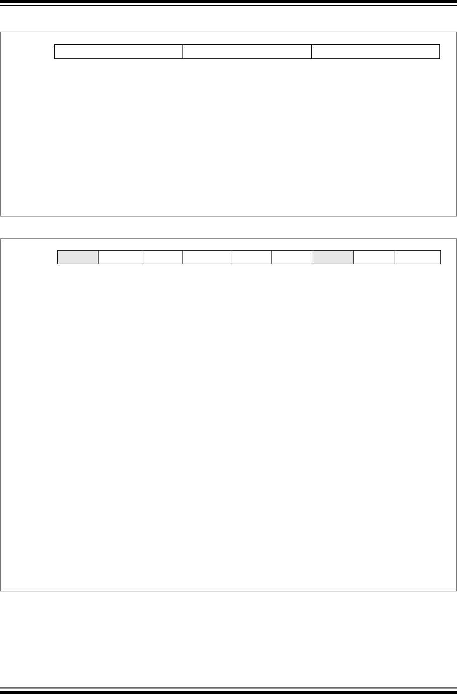
PIC32 Family Reference Manual
DS61154C-page 34-76 © 2009-2012 Microchip Technology Inc.
Figure 34-26: Format of CMSGSID
Figure 34-27: Format of CMSGEID
CMSGTS<15:0> FILHIT<4:0> SID<10:0>
bit 31-16 CMSGTS<15:0>: CAN Message Timestamp bits
Value of the CANTMR when the message is successfully received. If CANCAP = 0, these bits will
read as ‘0’.
bit 15-11 FILHIT<4:0>: Filter Hit Code bits
Encodes the number of the filter that resulted in writing this buffer.
11111 = Message was accepted by Filter 31
•
•
•
00000 = Message was accepted by Filter 0
bit 10-0 SID<10:0>: Standard Identifier of Received Message
— SRR IDE EID<17:0> RTR RB1 —RB0DLC<3:0>
bit 31-30 Unimplemented: Read as ‘0’
bit 29 SRR: Substitute Remote Request bit
In case of a standard message frame (IDE = 0), this bit is don’t care.
In case of an extended message frame (IDE = 1), this bit is always ‘1’.
bit 28 IDE: Extended Identifier bit
1 = Message received has extended identifier
0 = Message received has standard identifier
bit 27-10 EID<17:0>: Extended Identifier bits
bit 9 RTR: Remote Transmission Request bit
1 = Message sender requested a remote transmission
0 = Normal message received
bit 8 RB1: Reserved bit 1
The user application must set this bit to ‘0’ per the CAN Specification 2.0B
bit 7-5 Unimplemented: Read as ‘0’
bit 4 RB0: Reserved bit 0
The user application must set this bit to ‘0’ per the CAN Specification 2.0B
bit 3-0 DLC<3:0>: Data Length Code bits
1xxx = Message received contains 8 bytes of data
0111 = Message received contains 7 bytes of data
•
•
•
0001 = Message received contains 1 byte of data
0000 = Message received contains 0 bytes of data
Note: This register is in system memory outside the CAN module.

© 2009-2012 Microchip Technology Inc. DS61154C-page 34-77
Section 34. Controller Area Network (CAN)
Controller Area
Network (CAN)
34
Figure 34-28: Format of CMSGDATA0
Figure 34-29: Format of CMSGDATA1
DATA3<7:0> DATA2<7:0> DATA1<7:0> DATA0<7:0>
bit 31-24 DATA3<7:0>: Data Byte 3
bit 23-16 DATA2<7:0>: Data Byte 2
bit 15-8 DATA1<7:0>: Data Byte 1
bit 7-0 DATA0<7:0>: Data Byte 0
Note: This register is in system memory outside the CAN module.
DATA7<7:0> DATA6<7:0> DATA5<7:0> DATA4<7:0>
bit 31-24 DATA7<7:0>: Data Byte 7
bit 23-16 DATA6<7:0>: Data Byte 6
bit 15-8 DATA5<7:0>: Data Byte 5
bit 7-0 DATA4<7:0>: Data Byte 4
Note: This register is in system memory outside the CAN module.

PIC32 Family Reference Manual
DS61154C-page 34-78 © 2009-2012 Microchip Technology Inc.
The code in Example 34-13 shows an example data structure for implementing a CAN full
receive message buffer. An example of using this structure is provided in Example 34-14.
Example 34-13: Implementing a CAN Full Receive Message Buffer in Memory
Example 34-14: Example Usage of the Data Structure
/* This code snippet shows an example of data structure to implement a CAN */
/* full receive message buffer.*/
/* Define the sub-components of the data structure as specified in Table 34-5 */
/* Create a CMSGSID data type. */
typedef struct
{
unsigned SID:11;
unsigned FILHIT:5;
unsigned CMSGTS:16;
}rxcmsgsid;
/* Create a CMSGEID data type. */
typedef struct
{
unsigned DLC:4;
unsigned RB0:1;
unsigned :3;
unsigned RB1:1;
unsigned RTR:1;
unsigned EID:18;
unsigned IDE:1;
unsigned SRR:1;
unsigned :2;
}rxcmsgeid;
/* Create a CMSGDATA0 data type. */
typedef struct
{
unsigned Byte0:8;
unsigned Byte1:8;
unsigned Byte2:8;
unsigned Byte3:8;
}rxcmsgdata0;
/* Create a CMSGDATA1 data type. */
typedef struct
{
unsigned Byte4:8;
unsigned Byte5:8;
unsigned Byte6:8;
unsigned Byte7:8;
}rxcmsgdata1;
/* This is the main data structure. */
typedef union uCANRxMessageBuffer {
struct
{
rxcmsgsid CMSGSID;
rxcmsgeid CMSGEID;
rxcmsgdata0 CMSGDATA0;
rxcmsgdata0 CMSGDATA1;
};
int messageWord[4];
}CANRxMessageBuffer;
/* Example usage of code provided in Example 34-13. */
CANRxMessageBuffer * buffer;
/* When a message have been received and read, the individual fields of */
/* the received message can be queried as such. */
buffer = (CANRxMessageBuffer *)(PA_TO_KVA1(C1FIFOUA1));
if(buffer->CMSGEID.DLC == 4)
{
/* If the length of the received message is 4 then do something. */
}

© 2009-2012 Microchip Technology Inc. DS61154C-page 34-79
Section 34. Controller Area Network (CAN)
Controller Area
Network (CAN)
34
34.9.1 Data-Only Receive Messages
The PIC32 CAN module provides a special receive mode where only the data payload section of
the received message is stored in the message buffer. The CAN module will discard the identifier,
the reserved bits and the DLC bits. The time stamp value is not stored even if time stamping is
enabled. This mode can be enabled by setting the DONLY bit (CiFIFOCONn<12>).
Note that eight bytes of data are stored, regardless of the value of the DLC field in the CAN
message. The unused bytes are filled with 0x00. One possible use of this mode is to concatenate
messages whose data spans multiple messages. For example, transmitting a string across the
CAN bus.
34.9.2 Processing a Received Message
The user application can either use the polling methods or use the CAN module interrupt to track
message reception. The CAN module provides notification about different Receive FIFO events.
The user application can be notified when the Receive FIFO is not empty, is half-full or is full. The
user applications should read the Receive FIFO frequently to ensure that there is no FIFO
overflow. Regardless of the technique used (polling or interrupts), the following steps can be
used to read the message from the FIFO:
1. Read the value of the CiFIFOUAn register. This provides a 32-bit physical address pointer
to the receive message buffer that the user application should read.
2. In case of the Data-only receive message type, process two words from the message buffer.
3. In case of Full receive message type, process four words from the message buffer.
4. After processing the message buffer, set the UINC bit (CiFIFOCONn<13>).
Example 34-15 shows a code example of copying a CAN message.
Example 34-15: Copying a Message from a Receive FIFO
Table 34-6: Data-Only Receive Message Format as Stored in RAM
Name Bit
31/2315/7
Bit
30/22/14/6
Bit
29/21/13/5
Bit
28/20/12/4
Bit
27/19/11/3
Bit
26/18/10/2
Bit
25/17/9/1
Bit
24/16/8/0
CMSG0DATA0 31:24 Receive Buffer Data Byte 3
23:16 Receive Buffer Data Byte 2
15:8 Receive Buffer Data Byte 1
7:0 Receive Buffer Data Byte 0
CMSG0DATA1 31:24 Receive Buffer Data Byte 7
23:16 Receive Buffer Data Byte 6
15:8 Receive Buffer Data Byte 5
7:0 Receive Buffer Data Byte 4
Note: The transmit message is stored in device RAM and has no associated SET/CLR/INV registers.
/* This code example shows how to process a message from a receive FIFO. */
/* In this example CAN1 and FIF01 are used. */
CANRxMessageBuffer rxMessage;
unsigned int * bufferToRead;
/* Check if there is a message available to read. */
if(C1FIFOINT1bits.RXNEMPTYIF == 1)
{
/* Get the address of the buffer to read */
bufferToRead = PA_TO_KVA1(C1FIFOUA1);
/* This is an example process (Copying the buffer). The application */
/* could process this buffer in place. */
bufferToRead[0] = rxMessage->messageWord[0];
bufferToRead[1] = rxMessage->messageWord[1];
bufferToRead[2] = rxMessage->messageWord[2];
bufferToRead[3] = rxMessage->messageWord[3];
/* Update the message buffer pointer. */
C1FIFOCON1bits.UINC = 1;
}

PIC32 Family Reference Manual
DS61154C-page 34-80 © 2009-2012 Microchip Technology Inc.
34.9.3 Example Receive FIFO Behavior
Consider a user application where FIFO0 of the CAN1 module is configured as a receive
message FIFO. Figure 34-30 illustrates the FIFO before the first message arrives and is placed
in the FIFO. The CAN FIFO Base Address register (C1FIFOBA) is set to 0x00000100. The
received messages will be placed in device RAM (physical address 0x00000100). Note that the
CiFIFOUA0 initially points to the start of the FIFO. The example tracks the Receive FIFO
Overflow Interrupt Flag (RXOVFLIF), Receive FIFO Full Interrupt Flag (RXFULLIF), Receive
FIFO Half Full Interrupt Flag (RXHALFIF) and Receive FIFO Not Empty Interrupt Flag
(RXNEMPTYIF). This configuration is illustrated in Figure 34-30.
Figure 34-30: FIFO - At Start
Figure 34-31 illustrates the FIFO after the first message has been received and written to the
FIFO. Note that while the first message buffer in the FIFO (MB0) contains data, the CFIFOUA0
still points to the base address of the FIFO because the user has not read this location. Note that
the CAN module message index register (C1FIFOCI0) has incremented showing that the next
received message will be placed in MB1. The RXNEMPTYIF flag is set indicating that the FIFO
is not empty.
Figure 34-31: FIFO - First Write
Figure 34-32 illustrates the FIFO after another five messages have been received as the
CFIFOUA0 has not been modified earlier. The Buffer Half Full flag (RXHALFIF) was set after the
reception of the fourth message.
Figure 34-32: FIFO - Sixth Write
MB2
MB1
MB0
MB6
MB5
MB4
MB3
C1FIFOBA = 0x00000100
C1FIFOUA0 = 0x00000100
RXOVFLIF - 0
RXFULLIF - 0
RXHALFIF - 0
RXNEMPTYIF - 0
C1FIFOCI0 = 0x00000000
MB2
MB1
MB0/MSG0
MB6
MB5
MB4
MB3
C1FIFOBA = 0x00000100
C1FIFOUA0 = 0x00000100
RXOVFLIF - 0
RXFULLIF - 0
RXHALFIF - 0
RXNEMPTYIF - 1
C1FIFOCI0 = 0x00000001
MB2/MSG2
MB1/MSG1
MB0/MSG0
MB6
MB5/MSG5
MB4/MGG4
MB3/MSG3
C1FIFOBA = 0x00000100
C1FIFOUA0 = 0x00000100
RXOVFLIF - 0
RXFULLIF - 0
RXHALFIF - 1
RXNEMPTYIF - 1
C1FIFOCI0 = 0x00000006

© 2009-2012 Microchip Technology Inc. DS61154C-page 34-81
Section 34. Controller Area Network (CAN)
Controller Area
Network (CAN)
34
Figure 34-33 illustrates the FIFO after the first message has been read from MB0. Once the user
application has read this message, it should set the UINC bit (CiFIFOCONn<13>). This will cause
the CFIFOUA0 register to change to 0x0000110 (which is the address of the next message buffer
the user application must read).
Figure 34-33: FIFO - First Read
Figure 34-34 illustrates the FIFO after receiving a seventh message.
Figure 34-34: FIFO - Seventh Write About to Fill
Figure 34-35 illustrates the FIFO in a full state. Note that the RXFULLIF flag is set.
Figure 34-35: FIFO - Eighth Write FIFO Full
MB2/MSG2
MB1/MSG1
MB0
MB6
MB5/MSG5
MB4/MSG4
MB3/MSG3
C1FIFOBA = 0x00000100
C1FIFOUA0 = 0x00000110
RXOVFLIF - 0
RXFULLIF - 0
RXHALFIF - 1
RXNEMPTYIF - 1
C1FIFOCI0 = 0x00000006
MB2/MSG2
MB1/MSG1
MB0
MB6/MSG6
MB5/MSG5
MB4/MSG4
MB3/MSG3
C1FIFOBA = 0x00000100
C1FIFOUA0 = 0x00000110
RXOVFLIF - 0
RXFULLIF - 0
RXHALFIF - 1
RXNEMPTYIF - 1
C1FIFOCI0 = 0x00000000
MB2/MSG2
MB1/MSG1
MB0/MSG7
MB6/MSG6
MB5/MSG5
MB4/MSG4
MB3/MSG3
C1FIFOBA = 0x00000100
C1FIFOUA0 = 0x00000110
RXOVFLIF - 0
RXFULLIF - 1
RXHALFIF - 1
RXNEMPTYIF - 1
C1FIFOCI0 = 0x00000001

PIC32 Family Reference Manual
DS61154C-page 34-82 © 2009-2012 Microchip Technology Inc.
Figure 34-36 illustrates the FIFO receiving an additional message with the FIFO full, which
overflows the FIFO. Note that the RXOVFLIF flag is set, the CAN index (CiCIFOCI) has not
moved, and the message (MSG8) has been lost.
Figure 34-36: FIFO - Ninth Write FIFO Overflow
MB2/MSG2
MB1/MSG1
MB0/MSG7
MB6/MSG6
MB5/MSG5
MB4/MSG4
MB3/MSG3
C1FIFOBA = 0x00000100
C1FIFOUA0 = 0x00000110
RXOVFLIF - 1
RXFULLIF - 1
RXHALFIF - 1
RXNEMPTYIF - 1
C1FIFOCI0 = 0x00000001

© 2009-2012 Microchip Technology Inc. DS61154C-page 34-83
Section 34. Controller Area Network (CAN)
Controller Area
Network (CAN)
34
34.10 BIT TIMING
The nominal bit rate is the number of bits per second transmitted on the CAN bus, as shown in
Equation 34-1.
Equation 34-1: Nominal Bit Rate Calculation
There are four time segments in a bit time to compensate for any phase shifts due to oscillator
drifts or propagation delays. These time segments do not overlap each other and are represented
in terms of Time Quantum (TQ). One TQ is a fixed unit of time derived from the oscillator clock.
The total number of time quanta in a nominal bit time must be programmed between 8 TQ and
25 TQ.
Figure 34-37 illustrates how the CAN Bit Time Quantum Frequency (FTQ) is obtained from the
system clock and also how the different time segments are programmed.
Figure 34-37: CAN Bit Timing
Nominal Bit Time 1Nominal Bit Rate÷=
CAN Nominal Bit Time
Time Quanta
Time Segments Propagation Segment Phase Segment 1 Phase Segment 2
Sync
Seg
1 TQ1 TQ - 8 T Q1 TQ - 8 TQ
Sample Point
BAUD RATE
PRESCALER
FSYS 2
Prop Seg
Phase Seg1
Phase Seg2
Sync Seg
FTQ
Time Quanta
CiCFG<BRP>
CiCFG<PRSEG>
CiCFG<SEG1PH>
CiCFG<SEG2PH>
CiCFG<SJW>
1 TQ - 8 TQ
1:1
1:2
1:64
(TQ)
1 TQ - 8 TQ
1 TQ - 8 TQ
1 TQ
8 TQ - 25 TQ
1 TQ - 8 TQ

PIC32 Family Reference Manual
DS61154C-page 34-84 © 2009-2012 Microchip Technology Inc.
34.10.1 Bit Segments
Each bit transmission time consists of four time segments:
•Synchronization Segment – This time segment synchronizes the different nodes
connected on the CAN bus. A bit edge is expected to be within this segment. Based on
CAN protocol, the Synchronization Segment is assumed to be 1 TQ.
•Propagation Segment – This time segment compensates for any time delay that may
occur due to the bus line or due to the various transceivers connected on that bus.
•Phase Segment 1 – This time segment compensates for errors that may occur due to
phase shift in the edges. The time segment may be lengthened during resynchronization to
compensate for the phase shift.
•Phase Segment 2 – This time segment compensates for errors that may occur due to
phase shift in the edges. The time segment may be shortened during resynchronization to
compensate for the phase shift. The Phase Segment 2 time can be configured to be either
programmable or specified by the Phase Segment 1 time.
34.10.2 Sample Point
The sample point is the point in a CAN bit time interval where the sample is taken and the bus
state is read and interpreted. It is situated between Phase Segment 1 and Phase Segment 2.
The CAN bus can be sampled once or thrice at the sample point, as configured by the Sample
CAN Bus Line (SAM) bit in the CAN Baud Rate Configuration register (CiCFG<14>).
•If CiCFG<14> = 1, the CAN bus is sampled three times at the sample point (the most
common of the three samples determines the bit value)
•If CiCFG<14> = 0, the CAN bus is sampled only once at the sample point
34.10.3 Synchronization
Two types of synchronization are used: Hard Synchronization and Resynchronization. A Hard
Synchronization occurs once at the SOF. Resynchronization occurs inside a frame.
•Hard Synchronization – takes place on the recessive-to-dominant transition of the start
bit. The bit time is restarted from that edge
•Resynchronization – takes place when a bit edge does not occur within the
Synchronization Segment in a message. One of the Phase Segments is shortened or
lengthened by an amount that depends on the phase error in the signal. The maximum
amount that can be used is determined by the SJW parameter (CiCFG<7:6>).
The length of Phase Segment 1 and Phase Segment 2 can be changed depending on oscillator
tolerances of the transmitting node and receiving node. Resynchronization compensates for any
phase shifts that may occur due to the different oscillators used by the transmitting and receiving
nodes.
•Bit Lengthening – If the transmitting node in CAN has a slower oscillator than the
receiving node, the next falling edge, and therefore, the sample point can be delayed by
lengthening Phase Segment 1 in the bit time
•Bit Shortening – If the transmitting node in CAN has a faster oscillator than the receiving
node, the next falling edge, and therefore, the sample point of the next bit can be reduced
by shortening the Phase Segment 2 in the bit time
•Synchronization Jump Width (SJW) – The SJW<1:0> bits in CAN Baud Rate
Configuration register (CiCFG<7:6>) determine the SJW by limiting the amount of
lengthening or shortening that can be applied to the Phase Segment 1 and Phase Segment
2 time intervals. This segment should not be longer than Phase Segment 2 time. The width
can be 1 TQ - 4 TQ.

© 2009-2012 Microchip Technology Inc. DS61154C-page 34-85
Section 34. Controller Area Network (CAN)
Controller Area
Network (CAN)
34
34.10.4 CAN Bit Time Calculations
The steps that must be performed by the user application to configure the bit timing for the CAN
module are described below along with examples.
34.10.4.1 STEP 1: CALCULATE THE CAN BIT TIME QUANTUM FREQUENCY (FTQ)
• Select the Baud Rate (FBAUD) for the CAN Bus.
• Select the number of time quanta in a bit time, based on your system requirements.
Equation 34-2 shows the formula for computing FTQ.
Equation 34-2: CAN Bit Time Quantum Frequency (FTQ)
34.10.4.2 STEP 2: CALCULATE THE BAUD RATE PRESCALER (BRP<5:0>
(CiCFG<5:0>))
Equation 34-3 shows the formula for computing the baud rate prescaler.
Equation 34-3: Baud Rate Prescaler
34.10.4.3 STEP 3: SELECT THE INDIVIDUAL BIT TIME SEGMENTS
The Individual Bit Time Segments are selected using the CiCFG register:
Bit Time = Sync Segment + Propagation Segment + Phase Segment 1 + Phase
Segment 2
Example 34-16 shows the procedure to calculate the FTQ.
Example 34-16: CAN Bit Timing Calculation Example
Note 1: The total number of time quanta in a nominal bit time must be programmed between
8 TQ and 25 TQ. Therefore, the FTQ is between 8 to 25 times the baud rate (FBAUD).
2: Make sure that FTQ is an integer multiple of FBAUD to get the precise bit time.
Otherwise, the oscillator input frequency or the FBAUD may need to be changed.
Note 1: (Propagation Segment + Phase Segment 1) must be greater than or equal to the
length of Phase Segment 2.
2: Phase Segment 2 must be greater than SJW.
FTQ NF
BAUD
×=
CiCFG<BRP> = (FSYS/(2 * FTQ)) – 1
Step 1: Calculate the FTQ.
If FBAUD = 1 Mbps, and the number of time quanta ‘N’ = 10, then FTQ = 10 MHz
Step 2: Calculate the baud rate prescaler (assuming that the PIC32 device is running at
80 MHz, that is FSYS = 80000000).
CiCFG<BRP> = ( 80000000/(2 * FTQ) ) - 1 = 3
Step 3: Select the individual bit time segments.
Synchronization Segment = 1 TQ (constant)
Based on system characteristics, if Propagation Delay = 3 TQ, if the sample point is to be at
70% of Nominal Bit Time, then:
Phase Segment 2 = 30% of Nominal Bit Time = 3 TQ
Phase Segment 1 = 10 TQ - (1 TQ + 3 TQ + 3 TQ) = 3 TQ

PIC32 Family Reference Manual
DS61154C-page 34-86 © 2009-2012 Microchip Technology Inc.
Example 34-17 illustrates a code example for configuring the CAN bit timing code.
Example 34-17: Configuring the CAN Module to Obtain a Specific Bit Rate
/* This code example shows how to configure the CAN module to obtain a */
/* specific bit rate implementing the configuration shown in Example 34-16. */
/* Fsys = System Clock Frequency = 80000000; */
/* Fbaud = CAN bit rate = 1000000; */
/* N = Time Quanta (Tq) per bit = 10; */
/* Prop Segment = 3 Tq */
/* Phase Seg 1 = 3 Tq */
/* Phase Seg 2 = 3 Tq */
/* Sync Jump Width = 2 Tq */
/* Ensure the CAN module is in configuration mode.*/
C1CONbits.REQOP = 4
while(C1CONbits.OPMOD != 4);
C1CFGbits.SEG2PHTS = 1; /* Phase seg 2 is freely programmable */
C1CFGbits.SEG2PH = 2; /* Phase seg 2 is 3 Tq. */
C1CFGbits.SEG1PH = 2; /* Phase seg 1 is 3 Tq. */
C1CFGbits.PRSEG = 2; /* Propagation seg 2 is 3 Tq. */
C1CFGbits.SAM = 1; /* Sample bit 3 times. */
C1CFGbits.SJW = 2; /* Sync jump width is 2 Tq */
C1CFGbits.BRP = 3; /* BRP value as calculated in Example 34-11 */
/* CAN bit rate configuration complete. */

© 2009-2012 Microchip Technology Inc. DS61154C-page 34-87
Section 34. Controller Area Network (CAN)
Controller Area
Network (CAN)
34
34.11 CAN ERROR MANAGEMENT
34.11.1 CAN Bus Errors
The CAN Specification 2.0B defines five different ways of detecting errors:
•Bit Error
•Acknowledge Error
•Form Error
•Stuffing Error
•CRC Error
The bit error and the acknowledge error occur at the bit level; the other three errors occur at the
message level.
34.11.1.1 BIT ERROR
A node that is sending a bit on the bus also monitors the bus. A bit error is detected when the bit
value that is monitored is different from the bit value that is sent. An exception is when a
recessive bit is sent during the stuffed bit stream of the Arbitration field or during the ACK slot. In
this case, no bit error occurs when a dominant bit is monitored. A transmitter sending a passive
error frame and detecting a dominant bit does not interpret this as a bit error.
34.11.1.2 ACKNOWLEDGE ERROR
In the Acknowledge field of a message, the transmitter checks if the Acknowledge Slot (which it
has sent out as a recessive bit) contains a dominant bit. If not, this implies that no other node has
received the frame correctly. An acknowledge error has occurred, and as a result, the message
must be repeated. No error frame is generated in this case.
34.11.1.3 FORM ERROR
A form error is detected when a fixed-form bit field (EOF, Inter-frame Space, Acknowledge
Delimiter or CRC Delimiter) contains one or more illegal bits. For a receiver, a dominant bit during
the last bit of EOF is not treated as a form error.
34.11.1.4 STUFFING ERROR
A stuffing error is detected at the bit time of the sixth consecutive equal bit level in a message
field that should be coded by the method of bit stuffing.
34.11.1.5 CRC ERROR
The node transmitting a message computes and transmits the CRC corresponding to the trans-
mitted message. Every receiver on the bus performs the same CRC calculation as the transmit-
ter. A CRC error is detected, if the calculated result is not the same as the CRC value obtained
from the received message.
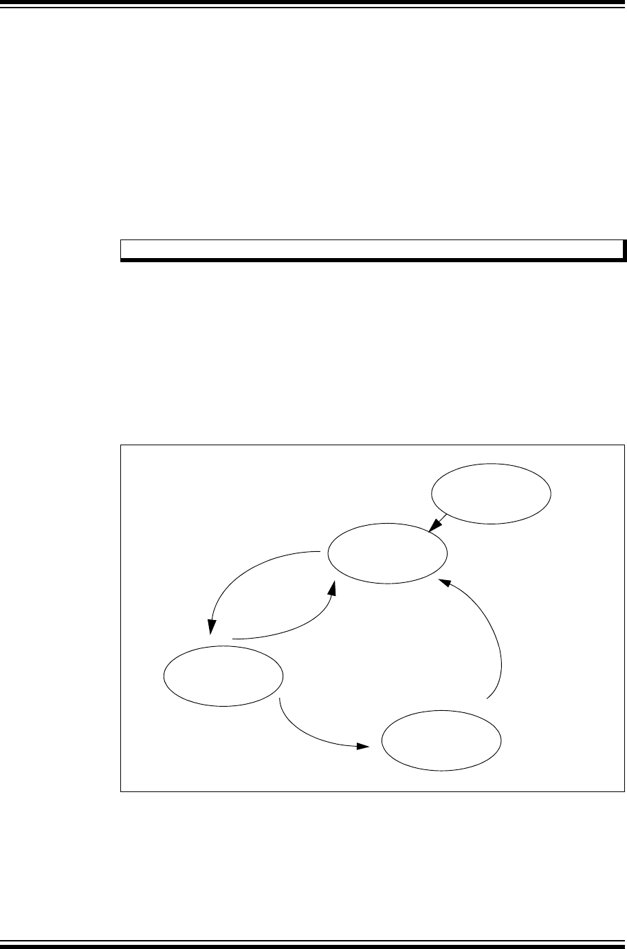
PIC32 Family Reference Manual
DS61154C-page 34-88 © 2009-2012 Microchip Technology Inc.
34.11.2 Fault Confinement
Every CAN controller on a bus tries to detect the errors outlined above within each message. If
an error is found, the discovering node transmits an error frame, thus destroying the bus traffic.
The other nodes detect the error caused by the error frame (if they have not already detected the
original error) and take appropriate action (that is, discard the current message).
The CAN module maintains two error counters:
•Transmit Error Counter (TERRCNT) – CiTREC<15:8>
•Receive Error Counter (RERRCNT) – CiTREC<7:0>
There are several rules governing how these counters are incremented and/or decremented.
That is, a transmitter detecting a fault increments its transmit error counter faster than the
listening nodes will increment their receive error counter. This is because there is a good chance
that it is the transmitter that is at fault.
A node starts out in Error Active mode. When any one of the two Error Counters equals or
exceeds a value of 127, the node enters a state known as Error Passive. When the Transmit
Error Counter exceeds a value of 255, the node enters the Bus OFF state.
•An Error Active node transmits an Active Error Frame when it detects errors
• An Error Passive node transmits a Passive Error Frame when it detects errors
•A node that is in the Bus OFF state transmits nothing on the bus
In addition, the CAN module employs an error warning feature that warns the user application
(when the Transmit Error Counter equals or exceeds 96) before the node enters Error Passive
state as illustrated in Figure 34-38.
Figure 34-38: Error Modes
34.11.2.1 TRANSMITTER IN ERROR PASSIVE STATE
The Transmitter Error Passive (TXBP) bit (CiTREC<20>) is set when the Transmit Error Counter
equals or exceeds 128 and generates an error interrupt, CERRIF bit (CiINT<12>), upon entry into
the Error Passive state. The Transmit Error Passive flag is cleared automatically by the
hardware, if the Transmit Error Counter becomes less than 128.
Note: The error counters are modified according to the CAN Specification 2.0B.
Bus
Off
Error
Active
Error
Passive
RERRCNT > 127 or
TERRCNT > 127
RERRCNT < 127 or
RERRCNT < 127
TERRCNT > 255
128 occurrences of
11 consecutive
“recessive” bits
Reset

© 2009-2012 Microchip Technology Inc. DS61154C-page 34-89
Section 34. Controller Area Network (CAN)
Controller Area
Network (CAN)
34
34.11.2.2 RECEIVER IN ERROR PASSIVE STATE
The Receiver Error Passive (RXBP) bit (CiTREC<19>) is set when the Receive Error Counter
equals or exceeds 128 and generates an error interrupt, CERRIF bit (CiINT<12>), upon entry into
Error Passive state. The Receive Error Passive flag is cleared automatically by the hardware, if
the Receive Error Counter becomes less than 128.
34.11.2.3 TRANSMITTER IN BUS OFF STATE
The Transmitter Bus OFF (TXBO) bit (CiTREC<21>) is set when the Transmit Error Counter
equals or exceeds 256 and generates an error interrupt, CERRIF bit (CiINT<12>).
34.11.2.4 TRANSMITTER IN ERROR WARNING STATE
The Transmitter Error Warn (TXWARN) bit (CiTREC<18>) is set when the Transmit Error
Counter equals or exceeds 96 and generates an error interrupt, CERRIF bit (CiINT<12>), upon
entry into the Error Warn state. The Transmit Error Warn flag is cleared automatically by the
hardware, if the Transmit Error Counter becomes less than 96.
34.11.2.5 RECEIVER IN ERROR WARNING STATE
The Receiver Error Warn (RXWARN) bit (CiTREC<17>) is set when the Receive Error Counter
equals or exceeds 96 and generates an error interrupt, CERRIF bit (CiINT<12>), upon entry into
the Error Warn state. The Receive Error Warn flag is cleared automatically by the hardware, if
the Receive Error Counter becomes less than 96.
Additionally, there is an Error State Warning Flag (EWARN) bit (CiTREC<16>), which is set if at
least one of the error counters equals or exceeds the error warning limit of 96. EWARN is reset
if both error counters are less than the error warning limit.
PIC32 Family Reference Manual
DS61154C-page 34-90 © 2009-2012 Microchip Technology Inc.
34.12 CAN INTERRUPTS
Interrupts in the PIC32 CAN module can be classified into three layers. Lower layer interrupts
propagate to higher layers where they are multiplexed into single interrupts. Therefore, the
layer 1 interrupt is multiplex of a multiple interrupts in layer 2. Some of the interrupts in layer 2
are a multiplex of interrupts in layer 3 (see Figure 34-39).
Figure 34-39: Multiple Interrupt Multiplex
At layer 1, the CAN module generates one interrupt to the CPU called the CANx interrupt. The
interrupt is caused by any of the layer 2 interrupts. The CANx Interrupts can be enabled or
disabled through the PIC32 Interrupt Controller. For more details on enabling and configuring
CPU interrupts on the PIC32 device, refer to Section 8. “Interrupts” (DS61108).
Each of the layer 2 and layer 3 interrupts has an Interrupt Enable bit (IE) bit and Interrupt Status
Flag (IF) bit associated with it. The CAN module will set an IF bit when an interrupt event occurs.
If the user application has set the IE bit, then the event will be propagated to the next Interrupt
layer. User applications can either poll the IF bits or enable interrupts to become aware of the
CAN module events.
The ICODE<6:0> bits (CiVEC<6:0>) will contain the code for the latest interrupts. These bits can
be used in combination with a jump table for efficient handling of interrupts.
34.12.1 Layer 2 Interrupts
The CAN module has nine interrupts at layer 2:
•Transmit FIFO Interrupt (TBIF)
•Receive FIFO Interrupt (RBIF)
•CAN Timestamp Timer Rollover Interrupt (CTMRIF)
•CAN Operation Mode Change Interrupt (MODIF)
•Receive FIFO Overflow Interrupt (RBOVIF)
•CAN System Error Interrupt (SERRIF)
•CAN Bus Error Interrupt (CERRIF)
•CAN Wake-up Interrupt (WAKIF)
•Invalid CAN Message Interrupt (IVRIF)
Of the above interrupts, the Invalid Message Received (IVRIF), the Wake-up (WAKIF), the CAN
Timer (CTMRIF) and the CAN Mode Change (MODIF) interrupts have a single source. The FIFO
(TBIF/RBIF), FIFO overflow (RBOVIF), CAN Bus Error (CERRIF) and System Error (SERRIF)
interrupts have multiple sources.
RXEMPTYIF
RXHALFIF
RXFULLIF
FIFO0
FIFO1
FIFO31
FIFO0
FIFO1
FIFO31
TXEMPTYIF
TXHALFIF
TXNFULLIF
RBIF
RBOVIF
TBIF
WAKIF
CTMRIF
IVRIF
SERRIF
CERRIF
MODIF
Third Layer Interrupts Second Layer Interrupts First Layer Interrupt
CAN Interrupt to
CPU
RXEMPTYIE
RXHALFIE
RXFULLIE
TXEMPTYIE
TXHALFIE
TXNFULLIE
RXOVLIE
RXOVLIF
FIFO31
RXOVF
FIFO1
FIFO0
CiFSTAT Register
CiRXOVF Register
All of these Interrupts sources
have corresponding enable bits
(not shown here for clarity)

© 2009-2012 Microchip Technology Inc. DS61154C-page 34-91
Section 34. Controller Area Network (CAN)
Controller Area
Network (CAN)
34
34.12.1.1 INVALID MESSAGE RECEIVED INTERRUPT (IVRIF)
The Invalid Message Received Interrupt (IVRIF) occurs when an error has occurred in the last
transmitted message or received message. The specific error that occurred is not available to
the user application. To clear the interrupt, the flag bit must be cleared.
34.12.1.2 WAKE-UP INTERRUPT (WAKIF)
The Wake-up Interrupt (WAKIF) occurs when CAN bus-activity is detected while the CAN module
is in Seep mode. To clear the interrupt, the flag must be cleared.
34.12.1.3 CAN BUS ERROR INTERRUPT (CERRIF)
The CAN Bus Error Interrupt (CERRIF) occurs when there is an error on the CAN bus. The bit is
set every time there is change in the current error state of the CAN module with respect to the
CAN network. The error states are tracked by the CiTREC register. To clear the interrupt, the flag
bit must be cleared. The CERRIF bit will be set once each time the Transmit Error Counter
(TERRCNT<7:0>) bits or the Receive Error Counter bits (RERRCNT<7:0>) in the CAB
Transmit/Receive Error Counter register (CiTREC) cross a threshold. For example, if the
TERRCNT bit (CiTREC<7:0>) goes from 95 to 96, then CERRIF will be set. If this bit is cleared,
it will remain clear even if the TERRCNT bit (CiTREC<7:0>) remains above 96. It will be set again
if the TERRCNT bit (CiTREC<7:0>) drops below 96 and rises above 95 again, or if the TERRCNT
bit (CiTREC<7:0>) goes above 127.
34.12.1.4 SYSTEM ERROR INTERRUPT (SERRIF)
A System Error Interrupt (SERRIF) can occur due to two types of system errors, addressing
errors and bandwidth errors. Both of these errors are fatal and the CAN module will be stopped.
Once the error occurs, the user should wait until the CAN module stops, by polling the CANBUSY
bit (CiCON<11>). Once the CAN module has stopped, SERRIF can be cleared by clearing the
ON bit (CiCON<15>).
34.12.1.5 ADDRESSING ERRORS
There are two sources of Addressing errors. Both of these have the same ICODE values
(ICODE = 100 0100).
•An addressing error will occur, if a FIFO is configured with an invalid base address. This
error will most commonly occur when the FIFO points to an unimplemented address.
•An addressing error will occur if the message destination is illegal, such as attempting to
write a received message to program Flash, which is not directly writable
34.12.1.6 BUS BANDWIDTH ERROR
A Bus Bandwidth error will occur when the CAN module is unable to write a received CAN
message to the location in system memory before the next CAN message arrives. This condition
is represented by ICODE = 100 0101. This may occur if some other PIC32 system bus initiator
with a higher priority than the CAN module uses the system bus for an extended period of time,
thereby preventing the CAN module from storing the received CAN message. The overflow bit in
the corresponding FIFO Interrupt register will be set.
Note: A error condition which caused the System Error Interrupt (SERRIF) can only be
resolved by turning the CAN module OFF (by clearing the ON bit (CiCON<15>)).
Clearing the System Error Interrupt Flag (SERRIF) bit in the CAN Interrupt register
(CiINT<12>) will not clear this error condition.

PIC32 Family Reference Manual
DS61154C-page 34-92 © 2009-2012 Microchip Technology Inc.
34.12.1.7 RECEIVE FIFO OVERRUN INTERRUPT (RBOVIF)
The Receive FIFO Overrun Interrupt occurs when the CAN module has received a message but
the designated Receive FIFO is full. The CAN module will set the RXOVFLIF flag in the
CiFIFOINTn register corresponding to the affected Receive FIFO. This is also reflected in CAN
Receive FIFO Overflow Status register (CiRXOVF), if the Receive FIFO Overflow Interrupt
Enable (RXOVFLIE) bit is set in the CAN FIFO Interrupt register (CiFIFOINTn<19>).
The RBOVIF bit in the CAN Interrupt register (CiINT<11>) is the OR reduction of all the bits in
the CiRXOVF register. The RBOVIF bit (CiINT<11>) and the RXOVIFn bits in the CAN Receive
FIFO Overflow Status register (CiRXOVF<31:0>) are not directly clearable. These need to be
cleared by clearing the appropriate RXOVFLIF bit (CiFIFOINTn<3:0>).
34.12.1.8 CAN MODE CHANGE INTERRUPT (MODIF)
The CAN Mode Change Interrupt (MODIF) occurs when the OPMOD<2:0> bits (CiCON<23:21>)
change indicating a change in the operating mode of the CAN module. The ICODE<6:0> bits
(CiVEC<6:0>) will indicate a mode change condition. To clear the interrupt, the flag bit must be
cleared.
34.12.1.9 CAN TIMESTAMP TIMER INTERRUPT (CTMRIF)
The CAN Timestamp Timer Interrupt (CMTRIF) occurs when CAN Timestamp timer overflows.
The ICODE<6:0> bits (CiVEC<6:0>) will indicate a timestamp timer overflow. To clear the
interrupt, the flag bit must be cleared.
34.12.1.10 CAN TRANSMIT FIFO INTERRUPT (TBIF)
The CAN Transmit FIFO interrupt (TBIF) occurs when there is a change in the status of the
Transmit FIFO. This interrupt has multiple layer 3 interrupt sources:
•Transmit FIFO Not Full Interrupt (TXNFULLIF)
•Transmit FIFO Half Full Interrupt (TXHALFIF)
•Transmit FIFO Empty Interrupt (TXEMPTYIF)
The TBIF interrupt cannot be cleared by the application. The interrupt will be cleared when all of
the source interrupt conditions terminate.
34.12.1.11CAN RECEIVE FIFO INTERRUPT (RBIF)
The CAN Receive FIFO interrupt (RBIF) occurs when there is change in the status of the Receive
FIFO. This interrupt has multiple layer 3 interrupt sources:
•Receive FIFO Full Interrupt (RXFULLIF)
•Receive FIFO Half Full Interrupt (RXHALFIF)
•Receive FIFO Not Empty Interrupt (RXNEMPTYIF)
The RBIF interrupt cannot be cleared by the user application. The interrupt will be cleared when
all of the source interrupt conditions terminate.
34.12.2 Layer 3 Interrupts
The CAN module has the following layer 3 interrupts:
•Transmit FIFO Not Full Interrupt (TXNFULLIF)
•Transmit FIFO Not Half Full Interrupt (TXNHALFIF)
•Transmit FIFO Not Empty Interrupt (TXNEMPTYIF)
•Receive FIFO Full Interrupt (RXFULLIF)
•Receive FIFO Half Full Interrupt (RXHALFIF)
•Receive FIFO Empty Interrupt (RXEMPTYIF)
•Receive FIFO Overflow Interrupt (RXOVLIF)
These interrupts reflect the current status of the Transmit and Receive FIFOs.

© 2009-2012 Microchip Technology Inc. DS61154C-page 34-93
Section 34. Controller Area Network (CAN)
Controller Area
Network (CAN)
34
34.12.3 Interrupt Persistency
The CAN module provides interrupts which indicate the operational status of message FIFOs.
These interrupts are persistent, in that they are present until the interrupt causing condition has
cleared. The interrupts flags themselves cannot be cleared directly by the user application. For
example, the Receive FIFO Not Empty Interrupt (RXNEMPTYIF) will remain set as long as there
is at least one message in the Receive FIFO. The following CAN interrupts are persistent:
•Transmit FIFO (TBIF) Interrupt (CiINT<0>)
•Receive FIFO (RBIF) Interrupt (CiINT<1>)
•FIFO Status (FIFOIPx) Interrupt (CiFSTAT<31:0>)
•Transmit FIFO Not Full (TXNFULLIF) Interrupt (CiFIFOINTn<10>)
•Transmit FIFO Half Full (TXHALFIF) Interrupt (CiFIFOINTn<9>)
•Transmit FIFO Empty (TXNEMPTYIF) Interrupt (CiFIFOINTn<8>)
•Receive FIFO Full (RXFULLIF) Interrupt (CiFIFOINTn<10>)
•Receive FIFO Half Full (RXHALFIF) Interrupt (CiFIFOINTn<9>)
•Receive FIFO Not Empty (RXNEMPTYIF) Interrupt (CiFIFOINTn<8>)
Note that the Receive FIFO Overflow (RXOVFLIF) Interrupt (CiFIFOINTn<11>) is sticky and is
user-clearable.
34.12.4 CAN FIFO Status Register (CiFSTAT)
The CAN FIFO Status register (CiFSTAT) is an indication register. The FIFOIPn bits in the CAN
FIFO Status register (CiFSTAT<31:0>) get set when interrupts are enabled in the corresponding
CiFIFOINTn registers, and when any of the following interrupt conditions occur:
•Transmit FIFO Not Full (TXNFULLIF) Interrupt (CiFIFOINTn<10>)
•Transmit FIFO Half Full (TXHALFIF) Interrupt (CiFIFOINTn<9>)
•Transmit FIFO Empty (TXNEMPTYIF) Interrupt (CiFIFOINTn<8>)
•Receive FIFO Full (RXFULLIF) Interrupt (CiFIFOINTn<10>)
•Receive FIFO Half Full (RXHALFIF) Interrupt (CiFIFOINTn<9>)
•Receive FIFO Not Empty (RXNEMPTYIF) Interrupt (CiFIFOINTn<8>)
The FIFOIPn bits by themselves are not interrupt sources. The ICODE<6:0> bits (CiVEC<6:0>)
will reflect value of the FIFOIPn bits which are set.
34.12.5 CAN Receive FIFO Overflow Register (CiRXOVF)
The RXOVFn bits in the CAN Receive FIFO Overflow register (CiRXOVF<31:0>) gets set when
a Receive FIFO overflow occurs and when the Receive FIFO Overflow Interrupt Enable
(RXOVFLIE) bit (CiFIFOINTn<19>) is set. The RXOVFn bits are source interrupts to the RBOVIF
(CiINT<11>) Interrupt. The bits in the CiRXOVF register are not directly clearable, and can be
cleared by clearing the RXOVFLIF bit (CiFIFOINTn<3>).
34.12.6 Interrupt Code (ICODE) bits
The ICODE<6:0> bits (CiVEC<6:0>) will reflect the highest interrupt that is still pending in the
CAN module. The higher the ICODE value, the higher the natural priority of the pending interrupt.
The ICODE events are persistent. If an interrupt with a higher natural priority occurs, masking the
lower priority in the ICODE register, the lower priority will be shown as soon as the higher priority
interrupt is cleared.
For example, consider the following application case:
• FIFO0 causes an interrupt - ICODE<6:0> = 000 0000
•Buffer 5 also has an event that causes an interrupt, causing ICODE to be set to ‘000 0101’
•The user enters the CAN interrupt handler, services buffer 5 and clears the interrupt
•ICODE<6:0> will now read ‘000 0000’, indicating that buffer 0 still has an interrupt pending,
which can then be serviced before returning from the Interrupt Service Routine (ISR)
34.12.7 CAN Filter Hit (FILHIT) Bits
The CAN Filter Hit (FILHIT<4:0>) bits in the CAN Interrupt Code register (CiVEC<12:8>) contain
the value of the filter that last matched a receiving message. Unlike the ICODE<6:0> bits
(CiVEC<6:0>), the FILHIT<4:0> bits (CiVEC<12:8>) have no history, and are only updated when
a message is received.

PIC32 Family Reference Manual
DS61154C-page 34-94 © 2009-2012 Microchip Technology Inc.
34.13 CAN RECEIVED MESSAGE TIME STAMPING
The CAN module can provide a time value of when a message is received. This time stamp will
be stored with the received message, if the CAN Receive Message Timer Stamp Time Capture
Event Enable (CANCAP) bit in the CAN Control register (CiCON<20>) is set. The CAN module
will write a time stamp to the CMSGTS bits of the CMSGSID field (CMSGSID<31:16>) in the
Receive Message Buffer. The CAN module obtains the timestamp by capturing the value of CAN
Time Stamp Timer (CANTS<15:0>) bits in the CAN Timer register (CiTMR<31:16>) whenever a
valid frame has been received. Because the CAN Specification 2.0B defines a frame to be valid,
if no errors occurred before the EOF field has been transmitted successfully, the value of
CANTS<15:0> bits (CiTMR<31:16>) will be captured right after the EOF.
All received messages will be time stamped, even messages that the CAN module transmits and
receives itself. The user application can configure the CAN Time Stamp time interval in terms of
system clocks through the CAN Time Stamp Timer Prescaler (CANSTPRE<15:0>) bits in the
CAN Timer register (CiTMR<15:0>).

© 2009-2012 Microchip Technology Inc. DS61154C-page 34-95
Section 34. Controller Area Network (CAN)
Controller Area
Network (CAN)
34
34.14 POWER-SAVING MODES
34.14.1 Sleep Mode
The user application must ensure that the CAN module is not active when the CPU goes into
Sleep mode. To protect the CAN bus system from fatal consequences due to violations of the
above rule, the CAN module drives the TXCAN pin into the recessive state while in Sleep mode.
The recommended procedure is to bring the CAN module into Disable mode before the CPU is
put into Sleep mode.
34.14.2 Idle Mode
When the CPU is in Idle mode, the CAN module powers down if the Stop in Idle Mode (SIDLE)
bit in the CAN Control register (CiCON<13>) is ‘1’. The user application must ensure that the
CAN module is not active when the CPU goes into Idle mode and the SIDLE bit (CiCON<13>) is
set. To protect the CAN bus system from fatal consequences due to violations of the above rule,
the CAN module drives the CiTX pin into the recessive state while the CPU is in Idle mode and
the SIDLE bit (CiCON<13>) is set.
34.14.3 Wake-up Functions
The CAN module will monitor the CAN receive (CiRX) pin for activity while the CAN module is in
Sleep mode. The CAN module will be sleeping when:
•The device is in Sleep mode
•The device is in Idle mode and the SIDLE bit (CiCON<13>) is set
While in this mode, the CAN module will generate an interrupt, if the Bus Wake-Up Activity
Interrupt Enable (WAKIE) bit in the CAN Interrupt register (CiINT<30>) is set and the bus activity
is detected.
The CAN module can be programmed to apply a low-pass filter function to the CiRX line while in
Disable mode or Sleep/Idle. This feature can be used to protect the CAN module from wake-up
due to short glitches on the CAN bus lines. The CAN Bus Line Filter Enable (WAKFIL) bit in the
CAN Configuration register (CICFG<22>) enables or disables the filter while the CAN module is
in Sleep mode.
Note that while the CAN module generates the interrupt, the state of the CAN module itself will
be not affected by the interrupt.
The following steps describe the recommended procedure for using the wake-up interrupt
feature with the PIC32 device Sleep mode:
1. The WAKIE bit (CiINT<30>) should be set in order to enable the wake-up on bus activity
feature.
2. Before placing the device into Sleep mode, switch the CAN operation mode to Disable and
wait until the CAN module has entered Disable mode.
3. Put the PIC32 device into Sleep mode.
4. During Sleep, if there is CAN bus activity, the PIC32 device will wake-up from Sleep mode.
If the CAN CPU interrupt is enabled, the CPU will execute the CAN ISR.
In the ISR, check whether the CAN Bus Activity Wake-up Interrupt Flag (WAKIF) bit in the CAN
Interrupt register (CiINT<14>) is set, and switch the CAN operation mode to Normal. When the
switch is complete, the CAN module will be able to receive messages (clear the WAKIF bit
(CiINT<14>)). Note that the CAN message that woke the device will be lost.

PIC32 Family Reference Manual
DS61154C-page 34-96 © 2009-2012 Microchip Technology Inc.
34.15 RELATED APPLICATION NOTES
This section lists application notes that are related to this section of the manual. These
application notes may not be written specifically for the PIC32 device family, but the concepts are
pertinent and could be used with modification and possible limitations. The current application
notes related to Controller Area Network (CAN) module are:
Title Application Note #
Ethernet Theory of Operation AN1120
Note: Please visit the Microchip web site (www.microchip.com) for additional application
notes and code examples for the PIC32 family of devices.

© 2009-2012 Microchip Technology Inc. DS61154C-page 34-97
Section 34. Controller Area Network (CAN)
Controller Area
Network (CAN)
34
34.16 REVISION HISTORY
Revision A (July 2009)
This is the initial released version of the document.
Revision B (September 2011)
This revision includes the following updates:
•Examples:
-Updated CiCFG1 to CiCFG in Example 34-16
-Updated Example 34-17
•Figures:
-Updated the following labels in Figure 34-17 through Figure 34-22:
•CFIFOBA is updated to C1FIFOBA
•CFIFOUA is updated to C1FIFOUA1
•CFIFOCI is updated to C1FIFOCI1
-Updated the following labels in Figure 34-30 through Figure 34-36:
•CFIFOBA is updated to C1FIFOBA
•CFIFOUA is updated to C1FIFOUA0
•CFIFOCI is updated to C1FIFOCI1
•Notes:
- Added a Note above 34.1 “Introduction”, which provides information on the
complementary documentation
- Added a note in 34.5.2 “Normal Operation Mode”
• Registers:
-Updated the register title to CiCON: CAN Module Control Register in Register 34-1
-Updated Register 34-11 to show correct bit numbers
-Updated the bit condition of FRESET and UINC bits as S/HC-0 and TXABAT,
TXLARB, TXERR bits as R-0 in Register 34-20
•Sections:
- Added a new paragraph about checking whether the Transmit FIFO can accommodate
the incoming messages, in 34.7.2 “Requesting Transmit of a Message”
- Updated any references of TXABT to TXABAT in 34.7.4 “Aborting Transmission of a
Queued Message”
- Any references of CiFIFOUA is updated to CiFIFOUA0 in 34.9.3 “Example Receive
FIFO Behavior”
•Tables:
- Updated the EID bits in Tab le 34-4
•Updated the following in the entire document:
- Updated any references of PIC32MX to PIC32
- Updated any references of system RAM to device RAM
- Updated any references of TXPRI to TXPR
- Updated any references of CMSG0SID to CMSGSID
• Additional minor corrections such as text and formatting updates were incorporated
throughout the document
Revision C (May 2012)
This revision includes the following updates:
•Updated the Notes and removed the Address Offset column in the CAN Controller Register
Summary (see Tabl e 34-1)
•Updated the Notes in all applicable register tables (see Register 34-1 through Register 34-23)
•Minor updates to text and formatting were incorporated throughout the document

PIC32 Family Reference Manual
DS61154C-page 34-98 © 2009-2012 Microchip Technology Inc.
NOTES:

© 2009-2012 Microchip Technology Inc. DS61154C-page 34 -99
Information contained in this publication regarding device
applications and the like is provided only for your convenience
and may be superseded by updates. It is your responsibility to
ensure that your application meets with your specifications.
MICROCHIP MAKES NO REPRESENTATIONS OR
WARRANTIES OF ANY KIND WHETHER EXPRESS OR
IMPLIED, WRITTEN OR ORAL, STATUTORY OR
OTHERWISE, RELATED TO THE INFORMATION,
INCLUDING BUT NOT LIMITED TO ITS CONDITION,
QUALITY, PERFORMANCE, MERCHANTABILITY OR
FITNESS FOR PURPOSE. Microchip disclaims all liability
arising from this information and its use. Use of Microchip
devices in life support and/or safety applications is entirely at
the buyer’s risk, and the buyer agrees to defend, indemnify and
hold harmless Microchip from any and all damages, claims,
suits, or expenses resulting from such use. No licenses are
conveyed, implicitly or otherwise, under any Microchip
intellectual property rights.
Trademarks
The Microchip name and logo, the Microchip logo, dsPIC,
KEELOQ, KEELOQ logo, MPLAB, PIC, PICmicro, PICSTART,
PIC32 logo, rfPIC and UNI/O are registered trademarks of
Microchip Technology Incorporated in the U.S.A. and other
countries.
FilterLab, Hampshire, HI-TECH C, Linear Active Thermistor,
MXDEV, MXLAB, SEEVAL and The Embedded Control
Solutions Company are registered trademarks of Microchip
Technology Incorporated in the U.S.A.
Analog-for-the-Digital Age, Application Maestro, chipKIT,
chipKIT logo, CodeGuard, dsPICDEM, dsPICDEM.net,
dsPICworks, dsSPEAK, ECAN, ECONOMONITOR,
FanSense, HI-TIDE, In-Circuit Serial Programming, ICSP,
Mindi, MiWi, MPASM, MPLAB Certified logo, MPLIB,
MPLINK, mTouch, Omniscient Code Generation, PICC,
PICC-18, PICDEM, PICDEM.net, PICkit, PICtail, REAL ICE,
rfLAB, Select Mode, Total Endurance, TSHARC,
UniWinDriver, WiperLock and ZENA are trademarks of
Microchip Technology Incorporated in the U.S.A. and other
countries.
SQTP is a service mark of Microchip Technology Incorporated
in the U.S.A.
All other trademarks mentioned herein are property of their
respective companies.
© 2009-2012, Microchip Technology Incorporated, Printed in
the U.S.A., All Rights Reserved.
Printed on recycled paper.
ISBN: 978-1-62076-302-5
Note the following details of the code protection feature on Microchip devices:
• Microchip products meet the specification contained in their particular Microchip Data Sheet.
• Microchip believes that its family of products is one of the most secure families of its kind on the market today, when used in the
intended manner and under normal conditions.
• There are dishonest and possibly illegal methods used to breach the code protection feature. All of these methods, to our
knowledge, require using the Microchip products in a manner outside the operating specifications contained in Microchip’s Data
Sheets. Most likely, the person doing so is engaged in theft of intellectual property.
• Microchip is willing to work with the customer who is concerned about the integrity of their code.
• Neither Microchip nor any other semiconductor manufacturer can guarantee the security of their code. Code protection does not
mean that we are guaranteeing the product as “unbreakable.”
Code protection is constantly evolving. We at Microchip are committed to continuously improving the code protection features of our
products. Attempts to break Microchip’s code protection feature may be a violation of the Digital Millennium Copyright Act. If such acts
allow unauthorized access to your software or other copyrighted work, you may have a right to sue for relief under that Act.
Microchip received ISO/TS-16949:2009 certification for its worldwide
headquarters, design and wafer fabrication facilities in Chandler and
Tempe, Arizona; Gresham, Oregon and design centers in California
and India. The Company’s quality system processes and procedures
are for its PIC® MCUs and dsPIC® DSCs, KEELOQ® code hopping
devices, Serial EEPROMs, microperipherals, nonvolatile memory and
analog products. In addition, Microchip’s quality system for the design
and manufacture of development systems is ISO 9001:2000 certified.
QUALITYMANAGEMENT
S
YSTEM
CERTIFIEDBYDNV
== ISO/TS16949==

DS61154C-page 34-100 © 2009-2012 Microchip Technology Inc.
AMERICAS
Corporate Office
2355 West Chandler Blvd.
Chandler, AZ 85224-6199
Tel: 480-792-7200
Fax: 480-792-7277
Technical Support:
http://www.microchip.com/
support
Web Address:
www.microchip.com
Atlanta
Duluth, GA
Tel: 678-957-9614
Fax: 678-957-1455
Boston
Westborough, MA
Tel: 774-760-0087
Fax: 774-760-0088
Chicago
Itasca, IL
Tel: 630-285-0071
Fax: 630-285-0075
Cleveland
Independence, OH
Tel: 216-447-0464
Fax: 216-447-0643
Dallas
Addison, TX
Tel: 972-818-7423
Fax: 972-818-2924
Detroit
Farmington Hills, MI
Tel: 248-538-2250
Fax: 248-538-2260
Indianapolis
Noblesville, IN
Tel: 317-773-8323
Fax: 317-773-5453
Los Angeles
Mission Viejo, CA
Tel: 949-462-9523
Fax: 949-462-9608
Santa Clara
Santa Clara, CA
Tel: 408-961-6444
Fax: 408-961-6445
Toronto
Mississauga, Ontario,
Canada
Tel: 905-673-0699
Fax: 905-673-6509
ASIA/PACIFIC
Asia Pacific Office
Suites 3707-14, 37th Floor
Tower 6, The Gateway
Harbour City, Kowloon
Hong Kong
Tel : 8 52 - 24 0 1- 120 0
Fax: 852-2401-3431
Australia - Sydney
Tel : 6 1-2 -98 68- 6 73 3
Fax: 61-2-9868-6755
China - Beijing
Tel : 8 6-1 0-8 569 - 70 0 0
Fax: 86-10-8528-2104
China - Chengdu
Tel : 8 6-2 8-8 665 - 55 11
Fax: 86-28-8665-7889
China - Chongqing
Tel : 8 6-2 3-8 980 - 95 8 8
Fax: 86-23-8980-9500
China - Hangzhou
Tel : 8 6-5 71- 2819 -31 87
Fax: 86-571-2819-3189
China - Hong Kong SAR
Tel : 8 52 - 24 0 1- 120 0
Fax: 852-2401-3431
China - Nanjing
Tel : 8 6-2 5-8 473 - 24 6 0
Fax: 86-25-8473-2470
China - Qingdao
Tel : 8 6-5 32- 8502 -73 55
Fax: 86-532-8502-7205
China - Shanghai
Tel : 8 6-2 1-5 407 - 55 3 3
Fax: 86-21-5407-5066
China - Shenyang
Tel : 8 6-2 4-2 334 - 28 2 9
Fax: 86-24-2334-2393
China - Shenzhen
Tel : 8 6-7 55- 8203 -26 60
Fax: 86-755-8203-1760
China - Wuhan
Tel : 8 6-2 7-5 980 - 53 0 0
Fax: 86-27-5980-5118
China - Xian
Tel : 8 6-2 9-8 833 - 72 5 2
Fax: 86-29-8833-7256
China - Xiamen
Tel: 86-592-2388138
Fax: 86-592-2388130
China - Zhuhai
Tel : 86- 756 -3 210 04 0
Fax: 86-756-3210049
ASIA/PACIFIC
India - Bangalore
Tel : 9 1- 8 0- 309 0-4 444
Fax: 91-80-3090-4123
India - New Delhi
Tel : 9 1- 11 -41 60- 86 31
Fax: 91-11-4160-8632
India - Pune
Tel : 9 1- 2 0- 256 6-1 512
Fax: 91-20-2566-1513
Japan - Osaka
Tel : 8 1- 6 6- 152 -71 60
Fax: 81-66-152-9310
Japan - Yokohama
Tel : 8 1- 4 5- 471 - 6 166
Fax: 81-45-471-6122
Korea - Daegu
Tel : 8 2- 5 3- 744 -43 01
Fax: 82-53-744-4302
Korea - Seoul
Tel : 8 2- 2 -5 54- 720 0
Fax: 82-2-558-5932 or
82-2-558-5934
Malaysia - Kuala Lumpur
Tel : 6 0- 3 -6 201 -98 57
Fax: 60-3-6201-9859
Malaysia - Penang
Tel : 6 0- 4 -2 27- 887 0
Fax: 60-4-227-4068
Philippines - Manila
Tel : 6 3- 2 -6 34- 906 5
Fax: 63-2-634-9069
Singapore
Tel : 6 5- 6 33 4 -8 870
Fax: 65-6334-8850
Taiwan - Hsin Chu
Tel : 8 86 - 3- 577 8-3 66
Fax: 886-3-5770-955
Taiwan - Kaohsiung
Tel : 8 86 - 7- 536 -48 18
Fax: 886-7-330-9305
Taiwan - Taipei
Tel : 8 86 - 2- 250 0-6 610
Fax: 886-2-2508-0102
Thailand - Bangkok
Tel : 6 6- 2 -6 94- 135 1
Fax: 66-2-694-1350
EUROPE
Austria - Wels
Tel : 4 3- 7 24 2 -2 244 -39
Fax: 43-7242-2244-393
Denmark - Copenhagen
Tel : 4 5-4 450 -2 828
Fax: 45-4485-2829
France - Paris
Tel : 3 3-1 -6 9-5 3 -6 3-2 0
Fax: 33-1-69-30-90-79
Germany - Munich
Tel : 4 9- 8 9- 627 -14 4-0
Fax: 49-89-627-144-44
Italy - Milan
Tel : 3 9- 0 33 1 -7 426 11
Fax: 39-0331-466781
Netherlands - Drunen
Tel : 3 1- 4 16 - 690 3 99
Fax: 31-416-690340
Spain - Madrid
Tel : 3 4- 9 1- 708 -08 -90
Fax: 34-91-708-08-91
UK - Wokingham
Tel : 4 4- 11 8-9 21- 58 69
Fax: 44-118-921-5820
Worldwide Sales and Service
11/29/11

© 2009-2013 Microchip Technology Inc. DS60001155C-page 35-1
Ethernet Controller
35
Section 35. Ethernet Controller
HIGHLIGHTS
This section of the manual contains the following major topics:
35.1 Introduction..............................................................................................................35-2
35.2 Ethernet Controller Overview ..................................................................................35-3
35.3 Status and Control Registers ...................................................................................35-4
35.4 Operation...............................................................................................................35-43
35.5 Ethernet Interrupts .................................................................................................35-81
35.6 Operation in Power-Saving and Debug Modes ..................................................... 35-86
35.7 Effects of Various Resets....................................................................................... 35-89
35.8 I/O Pin Control .......................................................................................................35-90
35.9 Related Application Notes .....................................................................................35-91
35.10 Revision History.....................................................................................................35-92

PIC32 Family Reference Manual
DS60001155C-page 35-2 © 2009-2013 Microchip Technology Inc.
35.1 INTRODUCTION
The Ethernet Controller is a bus master module that interfaces with an off-chip PHY in order to
implement a complete Ethernet node in an embedded system.
The following are key features of the Ethernet Controller module:
• Supports 10/100 Mbps data transfer rates
• Supports the full-duplex and half-duplex operation
• Supports the Reduced Media Independent Interface (RMII) and Media Independent
Interface (MII) PHY interface
• Supports the MII Management (MIIM) PHY Management interface
• Supports manual and automatic Flow Control
• Supports Auto-MDIX and enabled PHYs
•RAM descriptor based Direct Memory Access (DMA) operation for receive and transmit
path
•Fully configurable interrupts
•Configurable receive packet filtering
-Cyclic Redundancy Check (CRC)
-64-byte pattern match
- Broadcast, multicast, and unicast packets
- Magic Packet™
- 64-bit Hash table
-Runt packet
• Supports Packet Payload Checksum calculation
• Supports various hardware statistics counters
Note: This family reference manual section is meant to serve as a complement to device
data sheets. Depending on the device variant, this manual section may not apply to
all PIC32 devices.
Please consult the note at the beginning of the “Ethernet Controller” chapter in
the current device data sheet to check whether this document supports the device
you are using.
Device data sheets and family reference manual sections are available for
download from the Microchip Worldwide Web site at: http://www.microchip.com
Note: To a voi d c ach e c oh e re ncy pr obl ems o n d evi ces with L1 cache, Ethernet buffers
must only be accessed from the KSEG1 segment.
© 2009-2013 Microchip Technology Inc. DS60001155C-page 35-3
Section 35. Ethernet Controller
Ethernet Controller
35
35.2 ETHERNET CONTROLLER OVERVIEW
The Ethernet Controller provides the modules needed to implement a 10/100 Mbps Ethernet
node using an external PHY chip. To offload the CPU from a moving packet data to and from the
module, the internal descriptor based DMA engines are included in the controller.
The Ethernet Controller consists of the following modules:
•Media Access Control (MAC) block: This module implements the MAC functions of the
IEEE 802.3 Specification
•Flow Control block: This module controls the transmission of PAUSE frames. Reception of
PAUSE frames is handled within the MAC
•RX Filter (RXF) block: This module performs filtering on every receive packet to determine
whether each packet to be accepted or rejected
•TX DMA/TX Buffer Management (BM) Engine: The TX DMA and TX BM engines perform
data transfers from the system memory (using descriptor tables) to the MAC transmit
interface
•RX DMA/RX BM Engine: The RX DMA and RX BM engines transfer receive packets from
the MAC to the system memory (using descriptor tables)
Figure 35-1 illustrates the block d iagram of the Ethernet Controller.
Figure 35-1: Ethernet Controller Block Diagram
Note: Refer to the “Ethernet Theory of Operation” (DS01120) for more information on the
Ethernet operation and the IEEE 802.3 Specification (www.ieee.org).
TX Bus
Master
System BUS
RX Bus
Master
TX DMA
TX Flow Control
Host I/F
RX DMA
RX Filter
Checksum
MAC External
PHY
MII/RMII
I/F
MIIM
IF
MAC Control
and
Configuration
Registers
TX Function
RX Function
DMA
Control
Registers
Fast Peripheral Bus
Ethernet Controller
RX Flow
Control
Ethernet DMA
RX BM
TX BM
TX
FIFO
RX
FIFO

PIC32 Family Reference Manual
DS60001155C-page 35-4 © 2009-2013 Microchip Technology Inc.
35.3 STATUS AND CONTROL REGISTERS
The Ethernet Controller module consists of the following Special Function Registers (SFRs):
Controller and DMA Engine Configuration/Status Registers:
•ETHCON1: Ethernet Controller Control 1 Register
•ETHCON2: Ethernet Controller Control 2 Register
•ETHTXST: Ethernet Controller TX Packet Descriptor Start Address Register
•ETHRXST: Ethernet Controller RX Packet Descriptor Start Address Register
•ETHIEN: Ethernet Controller Interrupt Enable Register
•ETHIRQ: Ethernet Controller Interrupt Request Register
•ETHSTAT: Ethernet Controller Status Register
RX Filtering Configuration Registers:
•ETHRXFC: Ethernet Controller Receive Filter Configuration Register
•ETHHT0: Ethernet Controller Hash Table 0 Register
•ETHHT1: Ethernet Controller Hash Table 1 Register
•ETHPMM0: Ethernet Controller Pattern Match Mask 0 Register
•ETHPMM1: Ethernet Controller Pattern Match Mask 1 Register
•ETHPMCS: Ethernet Controller Pattern Match Checksum Register
•ETHPMO: Ethernet Controller Pattern Match Offset Register
Flow Control Configuring Register:
•ETHRXWM: Ethernet Controller Receive Watermarks Register
Ethernet Statistics Registers:
•ETHRXOVFLOW: Ethernet Controller Receive Overflow Statistics Register
•ETHFRMTXOK: Ethernet Controller Frames Transmitted Okay Statistics Register
•ETHSCOLFRM: Ethernet Controller Single Collision Frames Statistics Register
•ETHMCOLFRM: Ethernet Controller Multiple Collision Frames Statistics Register
•ETHFRMRXOK: Ethernet Controller Frames Received Okay Statistics Register
•ETHFCSERR: Ethernet Controller Frame Check Sequence Error Statistics Register
•ETHALGNERR: Ethernet Controller Alignment Errors Statistics Register
MAC Configuration Registers:
•EMAC1CFG1: Ethernet Controller MAC Configuration 1 Register
•EMAC1CFG2: Ethernet Controller MAC Configuration 2 Register
•EMAC1IPGT: Ethernet Controller MAC Back-to-Back Interpacket Gap Register
•EMAC1IPGR: Ethernet Controller MAC Non-Back-to-Back Interpacket Gap Register
•EMAC1CLRT: Ethernet Controller MAC Collision Window/Retry Limit Register
•EMAC1MAXF: Ethernet Controller MAC Maximum Frame Length Register
•EMAC1SUPP: Ethernet Controller MAC PHY Support Register
•EMAC1TEST: Ethernet Controller MAC Test Register
•EMAC1SA0: Ethernet Controller MAC Address 0 Register
•EMAC1SA1: Ethernet Controller MAC Address 1 Register
•EMAC1SA2: Ethernet Controller MAC Address 2 Register
MII Management Registers:
•EMAC1MCFG: Ethernet Controller MAC MII Management Configuration Register
•EMAC1MCMD: Ethernet Controller MAC MII Management Command Register
•EMAC1MADR: Ethernet Controller MAC MII Management Address Register
•EMAC1MWTD: Ethernet Controller MAC MII Management Write Data Register
•EMAC1MRDD: Ethernet Controller MAC MII Management Read Data Register
•EMAC1MIND: Ethernet Controller MAC MII Management Indicators Register
© 2009-2013 Microchip Technology Inc. DS60001155C-page 35-5
Section 35. Ethernet Controller
Ethernet Controller
35
Tabl e 35-1 provides a summary of the Ethernet Controller registers. Corresponding registers appear after the summary, followed by a
detailed description of each register.
Table 35-1: Ethernet Controller Register Summary
Register
Name(1) Bit
Range Bit 31/15 Bit 30/14 Bit 29/13 Bit 28/12 Bit 27/11 Bit 26/10 Bit 25/9 Bit 24/8 Bit 23/7 Bit 22/6 Bit 21/5 Bit 20/4 Bit 19/3 Bit 18/2 Bit 17/1 Bit 16/0
ETHCON1 31:16 PTV<15:8> PTV<7:0>
15:0 ON —SIDL — — — TXRTS RXEN AUTOFC — — MANFC — — — BUFCDEC
ETHCON2 31:16 — — — — — — — — — — — — — — — —
15:0 — — — — — RXBUFSZ<6:4> RXBUFSZ<3:0> — — — —
ETHTXST 31:16 TXSTADDR<31:24> TXSTADDR<23:16>
15:0 TXSTADDR<15:8> TXSTADDR<7:2> — —
ETHRXST 31:16 RXSTADDR<31:24> RXSTADDR<23:16>
15:0 RXSTADDR<15:8> RXSTADDR<7:2> — —
ETHHT0 31:16 HT<31:24> HT<23:16>
15:0 HT<15:8> HT<7:0>
ETHHT1 31:16 HT<63:56> HT<55:48>
15:0 HT<47:40> HT<39:32>
ETHPMM0 31:16 PMM<31: 24> PMM<23:16>
15:0 PMM<15:8> PMM<7:0>
ETHPMM1 31:16 PMM<63:56> PMM<55:48>
15:0 PMM<47:40> PMM<39:32>
ETHPMCS 31:16 — — — — — — — — — — — — — — — —
15:0 PMCS<15:8> PMCS<7:0>
ETHPMO 31:16 — — — — — — — — — — — — — — — —
15:0 PMO<15:8> PMO<7:0>
ETHRXFC
31:16 — — — — — — — — — — — — — — — —
15:0 HTEN MPEN —NOTPM PMMODE<3:0> CRC
ERREN CRCOKEN RUNT
ERREN RUNTEN UCEN NOTMEEN MCEN BCEN
ETHRXWM 31:16 — — — — — — — — RXFWM<7:0>
15:0 — — — — — — — — RXEWM<7:0>
ETHIEN
31:16 — — — — — — — — — — — — — — — —
15:0 —TXBUSEIE RXBUSEIE — — — EW
MARKIE
FW
MARKIE
RX
DONEIE
PKT
PENDIE RXACTIE —TX
DONEIE
TX
ABORTIE
RX
BUFNAIE
RX
OVFLWIE
ETHIRQ
31:16 — — — — — — — — — — — — — — — —
15:0 —TXBUSE RXBUSE — — — EWMARK FWMARK RXDONE PKTPEND RXACT —TXDONE TX
ABORT
RX
BUFNA
RX
OVFLW
ETHSTAT 31:16 — — — — — — — — BUFCNT<7:0>
15:0 — — — — — — — — ETHBUSY TXBUSY RXBUSY — — — — —
ETH
RXOVFLOW
31:16 — — — — — — —
15:0 RXOVFLWCNT<15:8> RXOVFLWCNT<7:0>
Legend: — = unimplemented, read as ‘0’.
Note 1: With the exception of the ETHSTAT register, all registers have an associated Clear, Set, and Invert register at an offset of 0x4, 0x8, and 0xC bytes, respectively. These registers have the same name with
CLR, SET, or INV appended to the end of the register name (e.g., ETHCON1CLR). Writing a ‘1’ to any bit position in these registers will clear, set, or invert valid bits in the associated register. Reads from
these registers should be ignored.

PIC32 Family Reference Manual
DS60001155C-page 35-6 © 2009-2013 Microchip Technology Inc.
ETH
FRMTXOK
31:16 — — — — — — — — — — — — — — — —
15:0 FRMTXOKCNT<15:0>
ETH
SCOLFRM
31:16 — — — — — — — — — — — — — — — —
15:0 SCOLFRMCNT<15:0>
ETH
MCOLFRM
31:16 — — — — — — — — — — — — — — — —
15:0 MCOLFRMCNT<15:0>
ETH
FRMRXOK
31:16 — — — — — — — — — — — — — — — —
15:0 FRMRXOKCNT<15:0>
ETH
FCSERR
31:16 — — — — — — — — — — — — — — — —
15:0 FCSERRCNT<15:0>
ETH
ALGNERR
31:16 — — — — — — — — — — — — — — — —
15:0 ALGNERRCNT<15:0>
EMAC1CFG1
31:16 — — — — — — — — — — — — — — — —
15:0 SOFT
RESET
SIM
RESET — — RESET
RMCS
RESET
RFUN
RESET
TMCS
RESET
TFUN — — — LOOP
BACK TXPAUSE RXPAUSE PASSALL RX
ENABLE
EMAC1CFG2
31:16 — — — — — — — — — — — — — — — —
15:0 —EXCESS
DFR
BPNO
BKOFF
NO
BKOFF — — LONGPRE PUREPRE AUTOPAD VLANPAD PAD
ENABLE
CRC
ENABLE
DELAY-
CRC HUGEFRM LENGTH
CK
FULL
DPLX
EMAC1IPGT 31:16 — — — — — — — — — — — — — — — —
15:0 — — — — — — — — — B2BIPKTGP<6:0>
EMAC1IPGR 31:16 — — — — — — — — — — — — — — — —
15:0 —NB2BIPKTGP1<6:0> —NB2BIPKTGP2<6:0>
EMAC1CLRT 31:16 — — — — — — — — — — — — — — — —
15:0 — — CWINDOW<5:0> — — — — RETX<3:0>
EMAC1MAXF 31:16 — — — — — — — — — — — — — — — —
15:0 MACMAXF<15:0>
EMAC1SUPP
31:16 — — — — — — — — — — — — — — — —
15:0 — — — — RESETRMII — — SPEED
RMII — — — — — — — —
EMAC1TEST
31:16 — — — — — — — — — — — — — — — —
15:0 — — — — — — — — — — — — — TESTBP TEST
PAUSE
SHRT
QNTA
EMAC1MCFG
31:16 — — — — — — — — — — — — — — — —
15:0 RESET
MGMT — — — — — — — — — CLKSEL<3:0> NOPRE SCANINC
EMAC1MCMD 31:16 — — — — — — — — — — — — — — — —
15:0 — — — — — — — — — — — — — — SCAN READ
EMAC1MADR 31:16 — — — — — — — — — — — — — — — —
15:0 — — — PHYADDR<4:0> — — — REGADDR<4:0>
Table 35-1: Ethernet Controller Register Summary (Continued)
Register
Name(1) Bit
Range Bit 31/15 Bit 30/14 Bit 29/13 Bit 28/12 Bit 27/11 Bit 26/10 Bit 25/9 Bit 24/8 Bit 23/7 Bit 22/6 Bit 21/5 Bit 20/4 Bit 19/3 Bit 18/2 Bit 17/1 Bit 16/0
Legend: — = unimplemented, read as ‘0’.
Note 1: With the exception of the ETHSTAT register, all registers have an associated Clear, Set, and Invert register at an offset of 0x4, 0x8, and 0xC bytes, respectively. These registers have the same name with
CLR, SET, or INV appended to the end of the register name (e.g., ETHCON1CLR). Writing a ‘1’ to any bit position in these registers will clear, set, or invert valid bits in the associated register. Reads from
these registers should be ignored.

© 2009-2013 Microchip Technology Inc. DS60001155C-page 35-7
Section 35. Ethernet Controller
Ethernet Controller
35
EMAC1MWTD 31:16 — — — — — — — — — — — — — — — —
15:0 MWTD<15:0>
EMAC1MRDD 31:16 — — — — — — — — — — — — — — — —
15:0 MRDD<15:0>
EMAC1MIND 31:16 — — — — — — — — — — — — — — — —
15:0 — — — — — — — — — — — — LINKFAIL NOTVALID SCAN MIIMBUSY
EMAC1SA0 31:16 — — — — — — — — — — — — — — — —
15:0 STNADDR6<7:0> STNADDR5<7:0>
EMAC1SA1 31:16 — — — — — — — — — — — — — — — —
15:0 STNADDR4<7:0> STNADDR3<7:0>
EMAC1SA2 31:16 — — — — — — — — — — — — — — — —
15:0 STNADDR2<7:0> STNADDR1<7:0>
Table 35-1: Ethernet Controller Register Summary (Continued)
Register
Name(1) Bit
Range Bit 31/15 Bit 30/14 Bit 29/13 Bit 28/12 Bit 27/11 Bit 26/10 Bit 25/9 Bit 24/8 Bit 23/7 Bit 22/6 Bit 21/5 Bit 20/4 Bit 19/3 Bit 18/2 Bit 17/1 Bit 16/0
Legend: — = unimplemented, read as ‘0’.
Note 1: With the exception of the ETHSTAT register, all registers have an associated Clear, Set, and Invert register at an offset of 0x4, 0x8, and 0xC bytes, respectively. These registers have the same name with
CLR, SET, or INV appended to the end of the register name (e.g., ETHCON1CLR). Writing a ‘1’ to any bit position in these registers will clear, set, or invert valid bits in the associated register. Reads from
these registers should be ignored.

PIC32 Family Reference Manual
DS60001155C-page 35-8 © 2009-2013 Microchip Technology Inc.
Register 35-1: ETHCON1: Ethernet Controller Control 1 Register
Bit
Range
Bit
31/23/15/7
Bit
30/22/14/6
Bit
29/21/13/5
Bit
28/20/12/4
Bit
27/19/11/3
Bit
26/18/10/2
Bit
25/17/9/1
Bit
24/16/8/0
31:24 R/W-0 R/W-0 R/W-0 R/W-0 R/W-0 R/W-0 R/W-0 R/W-0
PTV<15:8>
23:16 R/W-0 R/W-0 R/W-0 R/W-0 R/W-0 R/W-0 R/W-0 R/W-0
PTV<7:0>
15:8 R/W-0 U-0 R/W-0 U-0 U-0 U-0 R/W-0 R/W-0
ON —SIDL— — — TXRTS RXEN(1)
7:0 R/W-0 U-0 U-0 R/W-0 U-0 U-0 U-0 R/W-0
AUTOFC — — MANFC — — —BUFCDEC
Legend:
R = Readable bit W = Writable bit U = Unimplemented bit, read as ‘0’
-n = Value at POR ‘1’ = Bit is set ‘0’ = Bit is cleared x = Bit is unknown
bit 31-16 PTV<15:0>: PAUSE Timer Value bits
This register should be written only when the RXEN bit (ETHCON1<8>) is not set. These bits are only used
for Flow Control operations.
bit 15 ON: Ethernet ON bit
1 = Ethernet module is enabled
0 = Ethernet module is disabled
bit 14 Unimplemented: Read as ‘0’
bit 13 SIDL: Ethernet Stop in Idle Mode bit
1 = Ethernet module transfers are suspended during Idle mode
0 = Ethernet module transfers continue during Idle mode
bit 12-10 Unimplemented: Read as ‘0’
bit 9 TXRTS: Transmit Request to Send bit
1 = Activate the transmit logic and send the packet(s) defined in the TX Ethernet Descriptor Table (EDT)
0 = Stop transmit (when cleared by software) or transmit done (when cleared by hardware)
After the bit is written with a ‘1’, it will clear to ‘0’ whenever the transmit logic has finished transmitting the
requested packets in the EDT. If ‘0’ is written by the CPU, the transmit logic finishes the current packet’s
transmission, and then stops any further transmission.
This bit only affects TX operations.
bit 8 RXEN: Receive Enable bit(1)
1 = Enable RX logic, packets are received and stored in the RX buffer as controlled by the filter configuration
0 = Disable RX logic, no packets are received in the RX buffer
This bit only affects RX operations.
bit 7 AUTOFC: Automatic Flow Control bit
1 = Automatic Flow Control is enabled
0 = Automatic Flow Control is disabled
Setting this bit will enable the automatic Flow Control. If set, the full and empty watermarks are used to
automatically enable and disable the Flow Control. When the number of received buffers BUFCNT<7:0> bits
(ETHSTAT<23:16>) rises to the full watermark, Flow Control is automatically enabled. When the BUFCNT
falls to the empty watermark, Flow Control is automatically disabled.
This bit is only used for Flow Control operations, and affects both TX and RX operations.
bit 6-5 Unimplemented: Read as ‘0’
Note 1: It is not recommended to clear the RXEN bit, and then make changes to any RX related field/register. The
Ethernet Controller must be reinitialized (ON cleared to ‘0’), and then the RX changes applied.

© 2009-2013 Microchip Technology Inc. DS60001155C-page 35-9
Section 35. Ethernet Controller
Ethernet Controller
35
bit 4 MANFC: Manual Flow Control bit
1 = Manual Flow Control is enabled
0 = Manual Flow Control is disabled
Setting this bit will enable the manual Flow Control. If set, the Flow Control logic will send a PAUSE frame
using the PTV<15:0> bits (ETHCON1<31:16>). It will then resend a PAUSE frame every 128 * PTV<15:0>/2
TX clock cycles until the bit is cleared.
For 10 Mbps operation, the TX clock runs at 2.5 MHz. For 100 Mbps operation, the TX clock runs at
25 MHz.
When this bit is cleared, the Flow Control logic will automatically send a PAUSE frame with a 0x0000 PAUSE
timer value to disable Flow Control.
This bit is only used for Flow Control operations, and affects both TX and RX operations.
bit 3-1 Unimplemented: Read as ‘0’
bit 0 BUFCDEC: Descriptor Buffer Count Decrement bit
The BUFCDEC bit is a write-1 bit that reads out ‘0’. When written with ‘1’, the Descriptor Buffer Counter,
BUFCNT, will decrement by one. If the BUFCNT counter is incremented by the RX logic at the same time
that this bit is written, the BUFCNT value will remain unchanged. Writing ‘0’ will have no effect.
This bit is only used for RX operations.
Register 35-1: ETHCON1: Ethernet Controller Control 1 Register (Continued)
Note 1: It is not recommended to clear the RXEN bit, and then make changes to any RX related field/register. The
Ethernet Controller must be reinitialized (ON cleared to ‘0’), and then the RX changes applied.

PIC32 Family Reference Manual
DS60001155C-page 35-10 © 2009-2013 Microchip Technology Inc.
Register 35-2: ETHCON2: Ethernet Controller Control 2 Register
Bit
Range
Bit
31/23/15/7
Bit
30/22/14/6
Bit
29/21/13/5
Bit
28/20/12/4
Bit
27/19/11/3
Bit
26/18/10/2
Bit
25/17/9/1
Bit
24/16/8/0
31:24 U-0 U-0 U-0 U-0 U-0 U-0 U-0 U-0
— — — — — — — —
23:16 U-0 U-0 U-0 U-0 U-0 U-0 U-0 U-0
— — — — — — — —
15:8 U-0 U-0 U-0 U-0 U-0 R/W-0 R/W-0 R/W-0
— — — — —RXBUFSZ<6:4>
7:0 R/W-0 R/W-0 R/W-0 R/W-0 U-0 U-0 U-0 U-0
RXBUFSZ<3:0> — — — —
Legend:
R = Readable bit W = Writable bit U = Unimplemented bit, read as ‘0’
-n = Value at POR ‘1’ = Bit is set ‘0’ = Bit is cleared x = Bit is unknown
bit 31-11 Unimplemented: Read as ‘0’
bit 10-4 RXBUFSZ<6:0>: RX Data Buffer Size for all RX Descriptors (in 16-byte increments) bits
0x7F = RX data Buffer size for descriptors is 2032 bytes
•
•
•
0x60 = RX data Buffer size for descriptors is 1536 bytes
•
•
•
0x03 = RX data Buffer size for descriptors is 48 bytes
0x02 = RX data Buffer size for descriptors is 32 bytes
0x01 = RX data Buffer size for descriptors is 16 bytes
0x00 = Reserved
bit 3-0 Unimplemented: Read as ‘0’
Note 1: This register is only used for RX operations.
2: The bits in this register may be changed only when the RXEN bit (ETHCON1<8>) = 0.

© 2009-2013 Microchip Technology Inc. DS60001155C-page 35-11
Section 35. Ethernet Controller
Ethernet Controller
35
Register 35-3: ETHTXST: Ethernet Controller TX Packet Descriptor Start Address Register
Bit
Range
Bit
31/23/15/7
Bit
30/22/14/6
Bit
29/21/13/5
Bit
28/20/12/4
Bit
27/19/11/3
Bit
26/18/10/2
Bit
25/17/9/1
Bit
24/16/8/0
31:24 R/W-0 R/W-0 R/W-0 R/W-0 R/W-0 R/W-0 R/W-0 R/W-0
TXSTADDR<31:24>
23:16 R/W-0 R/W-0 R/W-0 R/W-0 R/W-0 R/W-0 R/W-0 R/W-0
TXSTADDR<23:16>
15:8 R/W-0 R/W-0 R/W-0 R/W-0 R/W-0 R/W-0 R/W-0 R/W-0
TXSTADDR<15:8>
7:0 R/W-0 R/W-0 R/W-0 R/W-0 R/W-0 R/W-0 U-0 U-0
TXSTADDR<7:2> — —
Legend:
R = Readable bit W = Writable bit U = Unimplemented bit, read as ‘0’
-n = Value at POR ‘1’ = Bit is set ‘0’ = Bit is cleared x = Bit is unknown
bit 31-2 TXSTADDR<31:2>: Starting Address of First Transmit Descriptor bits
This register should not be written while any transmit, receive or DMA operations are in progress.
This address must be 4-byte aligned (i.e., bits 1-0 must be ‘00’).
bit 1-0 Unimplemented: Read as ‘0’
Note 1: This register is only used for TX operations.
2: This register will be updated by hardware with the last descriptor used by the last successfully transmitted
packet.
Register 35-4: ETHRXST: Ethernet Controller RX Packet Descriptor Start Address Register
Bit
Range
Bit
31/23/15/7
Bit
30/22/14/6
Bit
29/21/13/5
Bit
28/20/12/4
Bit
27/19/11/3
Bit
26/18/10/2
Bit
25/17/9/1
Bit
24/16/8/0
31:24 R/W-0 R/W-0 R/W-0 R/W-0 R/W-0 R/W-0 R/W-0 R/W-0
RXSTADDR<31:24>
23:16 R/W-0 R/W-0 R/W-0 R/W-0 R/W-0 R/W-0 R/W-0 R/W-0
RXSTADDR<23:16>
15:8 R/W-0 R/W-0 R/W-0 R/W-0 R/W-0 R/W-0 R/W-0 R/W-0
RXSTADDR<15:8>
7:0 R/W-0 R/W-0 R/W-0 R/W-0 R/W-0 R/W-0 U-0 U-0
RXSTADDR<7:2> — —
Legend:
R = Readable bit W = Writable bit U = Unimplemented bit, read as ‘0’
-n = Value at POR ‘1’ = Bit is set ‘0’ = Bit is cleared x = Bit is unknown
bit 31-2 RXSTADDR<31:2>: Starting Address of First Receive Descriptor bits
This register should not be written while any transmit, receive or DMA operations are in progress.
This address must be 4-byte aligned (i.e., bits 1-0 must be ‘00’).
bit 1-0 Unimplemented: Read as ‘0’
Note 1: This register is only used for RX operations.
2: This register will be updated by hardware with the last descriptor used by the last successfully transmitted
packet.

PIC32 Family Reference Manual
DS60001155C-page 35-12 © 2009-2013 Microchip Technology Inc.
Register 35-5: ETHHT0: Ethernet Controller Hash Table 0 Register
Bit
Range
Bit
31/23/15/7
Bit
30/22/14/6
Bit
29/21/13/5
Bit
28/20/12/4
Bit
27/19/11/3
Bit
26/18/10/2
Bit
25/17/9/1
Bit
24/16/8/0
31:24 R/W-0 R/W-0 R/W-0 R/W-0 R/W-0 R/W-0 R/W-0 R/W-0
HT<31:24>
23:16 R/W-0 R/W-0 R/W-0 R/W-0 R/W-0 R/W-0 R/W-0 R/W-0
HT<23:16>
15:8 R/W-0 R/W-0 R/W-0 R/W-0 R/W-0 R/W-0 R/W-0 R/W-0
HT<15:8>
7:0 R/W-0 R/W-0 R/W-0 R/W-0 R/W-0 R/W-0 R/W-0 R/W-0
HT<7:0>
Legend:
R = Readable bit W = Writable bit U = Unimplemented bit, read as ‘0’
-n = Value at POR ‘1’ = Bit is set ‘0’ = Bit is cleared x = Bit is unknown
bit 31-0 HT<31:0>: Hash Table Bytes 0-3 bits
Note 1: This register is only used for RX operations.
2: The bits in this register may be changed only when the RXEN bit (ETHCON1<8>) = 0, or the HTEN bit
(ETHRXFC<15>) = 0.
Register 35-6: ETHHT1: Ethernet Controller Hash Table 1 Register
Bit
Range
Bit
31/23/15/7
Bit
30/22/14/6
Bit
29/21/13/5
Bit
28/20/12/4
Bit
27/19/11/3
Bit
26/18/10/2
Bit
25/17/9/1
Bit
24/16/8/0
31:24 R/W-0 R/W-0 R/W-0 R/W-0 R/W-0 R/W-0 R/W-0 R/W-0
HT<63:56>
23:16 R/W-0 R/W-0 R/W-0 R/W-0 R/W-0 R/W-0 R/W-0 R/W-0
HT<55:48>
15:8 R/W-0 R/W-0 R/W-0 R/W-0 R/W-0 R/W-0 R/W-0 R/W-0
HT<47:40>
7:0 R/W-0 R/W-0 R/W-0 R/W-0 R/W-0 R/W-0 R/W-0 R/W-0
HT<39:32>
Legend:
R = Readable bit W = Writable bit U = Unimplemented bit, read as ‘0’
-n = Value at POR ‘1’ = Bit is set ‘0’ = Bit is cleared x = Bit is unknown
bit 31-0 HT<63:32>: Hash Table Bytes 4-7 bits
Note 1: This register is only used for RX operations.
2: The bits in this register may be changed only when the RXEN bit (ETHCON1<8>) = 0, or the HTEN bit
(ETHRXFC<15>) = 0.

© 2009-2013 Microchip Technology Inc. DS60001155C-page 35-13
Section 35. Ethernet Controller
Ethernet Controller
35
Register 35-7: ETHPMM0: Ethernet Controller Pattern Match Mask 0 Register
Bit
Range
Bit
31/23/15/7
Bit
30/22/14/6
Bit
29/21/13/5
Bit
28/20/12/4
Bit
27/19/11/3
Bit
26/18/10/2
Bit
25/17/9/1
Bit
24/16/8/0
31:24 R/W-0 R/W-0 R/W-0 R/W-0 R/W-0 R/W-0 R/W-0 R/W-0
PMM<31:24>
23:16 R/W-0 R/W-0 R/W-0 R/W-0 R/W-0 R/W-0 R/W-0 R/W-0
PMM<23:16>
15:8 R/W-0 R/W-0 R/W-0 R/W-0 R/W-0 R/W-0 R/W-0 R/W-0
PMM<15:8>
7:0 R/W-0 R/W-0 R/W-0 R/W-0 R/W-0 R/W-0 R/W-0 R/W-0
PMM<7:0>
Legend:
R = Readable bit W = Writable bit U = Unimplemented bit, read as ‘0’
-n = Value at POR ‘1’ = Bit is set ‘0’ = Bit is cleared x = Bit is unknown
bit 31-24 PMM<31:24>: Pattern Match Mask 3 bits
bit 23-16 PMM<23:16>: Pattern Match Mask 2 bits
bit 15-8 PMM<15:8>: Pattern Match Mask 1 bits
bit 7-0 PMM<7:0>: Pattern Match Mask 0 bits
Note 1: This register is only used for RX operations.
2: The bits in this register may be changed only when the RXEN bit (ETHCON1<8>) = 0, or the PMMODE
<3:0>bits (ETHRXFC<11:8>) = 0.
Register 35-8: ETHPMM1: Ethernet Controller Pattern Match Mask 1 Register
Bit
Range
Bit
31/23/15/7
Bit
30/22/14/6
Bit
29/21/13/5
Bit
28/20/12/4
Bit
27/19/11/3
Bit
26/18/10/2
Bit
25/17/9/1
Bit
24/16/8/0
31:24 R/W-0 R/W-0 R/W-0 R/W-0 R/W-0 R/W-0 R/W-0 R/W-0
PMM<63:56>
23:16 R/W-0 R/W-0 R/W-0 R/W-0 R/W-0 R/W-0 R/W-0 R/W-0
PMM<55:48>
15:8 R/W-0 R/W-0 R/W-0 R/W-0 R/W-0 R/W-0 R/W-0 R/W-0
PMM<47:40>
7:0 R/W-0 R/W-0 R/W-0 R/W-0 R/W-0 R/W-0 R/W-0 R/W-0
PMM<39:32>
Legend:
R = Readable bit W = Writable bit U = Unimplemented bit, read as ‘0’
-n = Value at POR ‘1’ = Bit is set ‘0’ = Bit is cleared x = Bit is unknown
bit 31-24 PMM<63:56>: Pattern Match Mask 7 bits
bit 23-16 PMM<55:48>: Pattern Match Mask 6 bits
bit 15-8 PMM<47:40>: Pattern Match Mask 5 bits
bit 7-0 PMM<39:32>: Pattern Match Mask 4 bits
Note 1: This register is only used for RX operations.
2: The bits in this register may be changed only when the RXEN bit (ETHCON1<8>) = 0, or the
PMMODE<3:0> bits (ETHRXFC<11:8>) = 0.
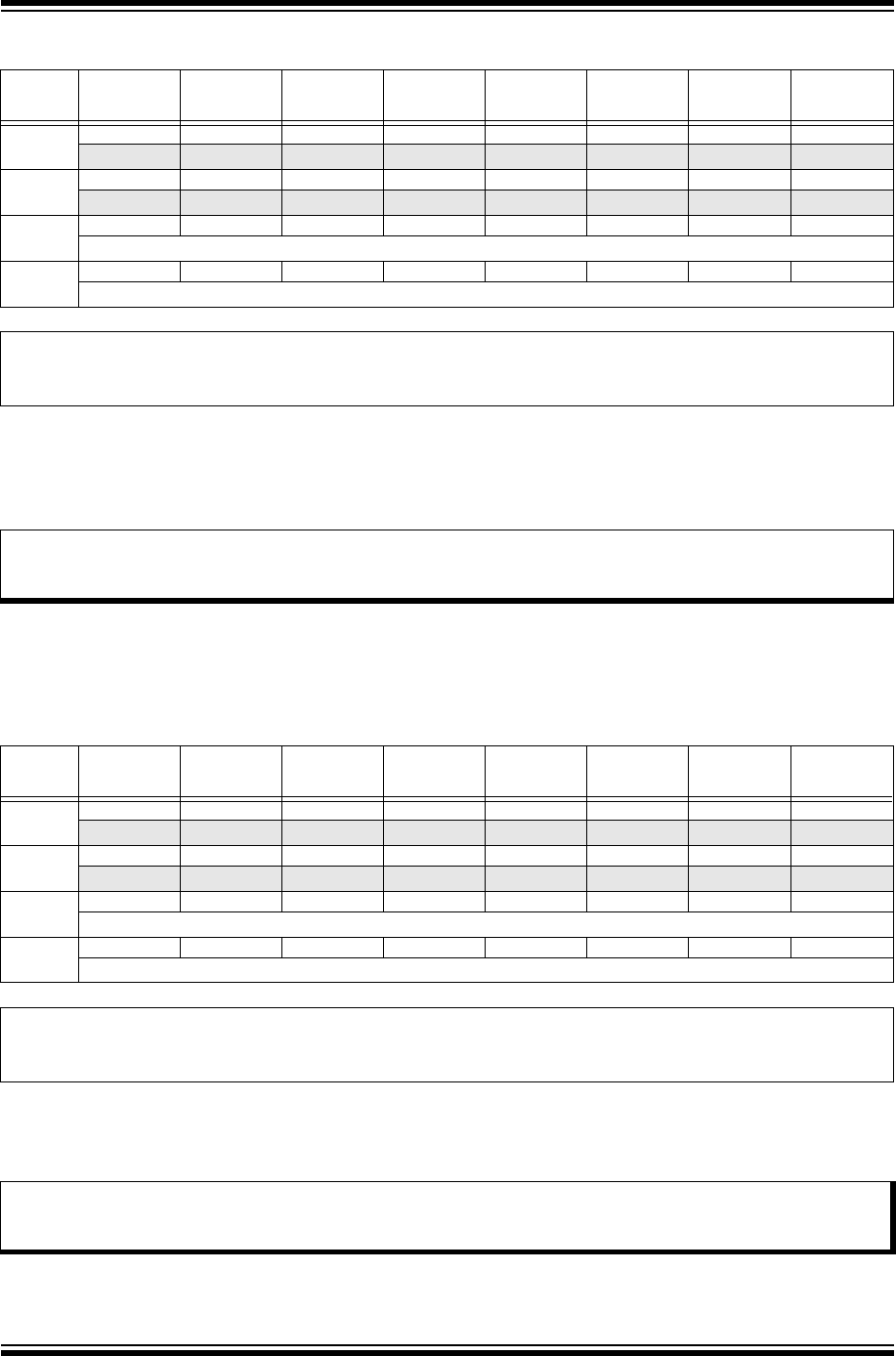
PIC32 Family Reference Manual
DS60001155C-page 35-14 © 2009-2013 Microchip Technology Inc.
Register 35-9: ETHPMCS: Ethernet Controller Pattern Match Checksum Register
Bit
Range
Bit
31/23/15/7
Bit
30/22/14/6
Bit
29/21/13/5
Bit
28/20/12/4
Bit
27/19/11/3
Bit
26/18/10/2
Bit
25/17/9/1
Bit
24/16/8/0
31:24 U-0 U-0 U-0 U-0 U-0 U-0 U-0 U-0
— — — — — — — —
23:16 U-0 U-0 U-0 U-0 U-0 U-0 U-0 U-0
— — — — — — — —
15:8 R/W-0 R/W-0 R/W-0 R/W-0 R/W-0 R/W-0 R/W-0 R/W-0
PMCS<15:8>
7:0 R/W-0 R/W-0 R/W-0 R/W-0 R/W-0 R/W-0 R/W-0 R/W-0
PMCS<7:0>
Legend:
R = Readable bit W = Writable bit U = Unimplemented bit, read as ‘0’
-n = Value at POR ‘1’ = Bit is set ‘0’ = Bit is cleared x = Bit is unknown
bit 31-16 Unimplemented: Read as ‘0’
bit 15-8 PMCS<15:8>: Pattern Match Checksum 1 bits
bit 7-0 PMCS<7:0>: Pattern Match Checksum 0 bits
Note 1: This register is only used for RX operations.
2: The bits in this register may be changed only when the RXEN bit (ETHCON1<8>) = 0, or the PMMODE
<3:0>bits (ETHRXFC<11:8>) = 0.
Register 35-10: ETHPMO: Ethernet Controller Pattern Match Offset Register
Bit
Range
Bit
31/23/15/7
Bit
30/22/14/6
Bit
29/21/13/5
Bit
28/20/12/4
Bit
27/19/11/3
Bit
26/18/10/2
Bit
25/17/9/1
Bit
24/16/8/0
31:24 U-0 U-0 U-0 U-0 U-0 U-0 U-0 U-0
— — — — — — — —
23:16 U-0 U-0 U-0 U-0 U-0 U-0 U-0 U-0
— — — — — — — —
15:8 R/W-0 R/W-0 R/W-0 R/W-0 R/W-0 R/W-0 R/W-0 R/W-0
PMO<15:8>
7:0 R/W-0 R/W-0 R/W-0 R/W-0 R/W-0 R/W-0 R/W-0 R/W-0
PMO<7:0>
Legend:
R = Readable bit W = Writable bit U = Unimplemented bit, read as ‘0’
-n = Value at POR ‘1’ = Bit is set ‘0’ = Bit is cleared x = Bit is unknown
bit 31-16 Unimplemented: Read as ‘0’
bit 15-0 PMO<15:0>: Pattern Match Offset 1 bits
Note 1: This register is only used for RX operations.
2: The bits in this register may be changed only when the RXEN bit (ETHCON1<8>) = 0, or the PMMODE
<3:0>bits (ETHRXFC<11:8>) = 0.

© 2009-2013 Microchip Technology Inc. DS60001155C-page 35-15
Section 35. Ethernet Controller
Ethernet Controller
35
Register 35-11: ETHRXFC: Ethernet Controller Receive Filter Configuration Register
Bit
Range
Bit
31/23/15/7
Bit
30/22/14/6
Bit
29/21/13/5
Bit
28/20/12/4
Bit
27/19/11/3
Bit
26/18/10/2
Bit
25/17/9/1
Bit
24/16/8/0
31:24 U-0 U-0 U-0 U-0 U-0 U-0 U-0 U-0
— — — — — — — —
23:16 U-0 U-0 U-0 U-0 U-0 U-0 U-0 U-0
— — — — — — — —
15:8 R/W-0 R/W-0 U-0 R/W-0 R/W-0 R/W-0 R/W-0 R/W-0
HTEN MPEN —NOTPM PMMODE<3:0>
7:0 R/W-0 R/W-0 R/W-0 R/W-0 R/W-0 R/W-0 R/W-0 R/W-0
CRCERREN CRCOKEN RUNTERREN RUNTEN UCEN NOTMEEN MCEN BCEN
Legend:
R = Readable bit W = Writable bit U = Unimplemented bit, read as ‘0’
-n = Value at POR ‘1’ = Bit is set ‘0’ = Bit is cleared x = Bit is unknown
bit 31-16 Unimplemented: Read as ‘0’
bit 15 HTEN: Enable Hash Table Filtering bit
1 = Enable Hash table filtering
0 = Disable Hash table filtering
bit 14 MPEN: Magic Packet™ Enable bit
1 = Enable Magic Packet filtering
0 = Disable Magic Packet filtering
bit 13 Unimplemented: Read as ‘0’
bit 12 NOTPM: Pattern Match Inversion bit
1 = The pattern match checksum must not match for a successful pattern match to occur
0 = The pattern match checksum must match for a successful pattern match to occur
This bit determines whether Pattern Match Checksum must match for a successful pattern match to occur.
bit 11-8 PMMODE<3:0>: Pattern Match Mode bits
1001 = Pattern match is successful if (NOTPM = 1 XOR Pattern Match Checksum matches) AND
(Packet = Magic Packet)(1,3)
1000 = Pattern match is successful if (NOTPM = 1 XOR Pattern Match Checksum matches) AND
(Hash Table Filter match)(1,2)
0111 = Pattern match is successful if (NOTPM = 1 XOR Pattern Match Checksum matches) AND
(Destination Address = Broadcast Address)(1)
0110 = Pattern match is successful if (NOTPM = 1 XOR Pattern Match Checksum matches) AND
(Destination Address = Broadcast Address)(1)
0101 = Pattern match is successful if (NOTPM = 1 XOR Pattern Match Checksum matches) AND
(Destination Address = Unicast Address)(1)
0100 = Pattern match is successful if (NOTPM = 1 XOR Pattern Match Checksum matches) AND
(Destination Address = Unicast Address)(1)
0011 = Pattern match is successful if (NOTPM = 1 XOR Pattern Match Checksum matches) AND
(Destination Address = Station Address)(1)
0010 = Pattern match is successful if (NOTPM = 1 XOR Pattern Match Checksum matches) AND
(Destination Address = Station Address)(1)
0001 = Pattern match is successful if (NOTPM = 1 XOR Pattern Match Checksum matches)(3)
0000 = Pattern Match is disabled; pattern match is always unsuccessful
Note 1: XOR = True when either one or the other conditions are true, but not both.
2: This Hash Table Filter match is active regardless of the value of the HTEN bit.
3: This Magic Packet Filter match is active regardless of the value of the MPEN bit.
Note 1: This register is only used for RX operations.
2: The bits in this register may be changed only when the RXEN bit (ETHCON1<8>) = 0.

PIC32 Family Reference Manual
DS60001155C-page 35-16 © 2009-2013 Microchip Technology Inc.
bit 7 CRCERREN: CRC Error Collection Enable bit
1 = The received packet CRC must be invalid for the packet to be accepted
0 = Disable CRC Error Collection filtering
This bit allows the user to collect all packets that have an invalid CRC.
bit 6 CRCOKEN: CRC Okay Enable bit
1 = The received packet CRC must be valid for the packet to be accepted
0 = Disable CRC filtering
This bit allows the user to reject all packets that have an invalid CRC.
bit 5 RUNTERREN: Runt Error Collection Enable bit
1 = The received packet must be a runt packet for the packet to be accepted
0 = Disable Runt Error Collection filtering
This bit allows the user to collect all packets that are runt packets. For this filter, a runt packet is defined as
any packet with a size of less than 64 bytes (when CRCOKEN = 0) or any packet with a size of less than
64 bytes that has a valid CRC (when CRCOKEN = 1).
bit 4 RUNTEN: Runt Enable bit
1 = The received packet must not be a runt packet for the packet to be accepted
0 = Disable runt filtering
This bit allows the user to reject all runt packets. For this filter, a runt packet is defined as any packet with a
size of less than 64 bytes.
bit 3 UCEN: Unicast Enable bit
1 = Enable unicast filtering
0 = Disable unicast filtering
This bit allows the user to accept all unicast packets whose Destination Address matches the Station
Address.
bit 2 NOTMEEN: Not Me Unicast Enable bit
1 = Enable not-me unicast filtering
0 = Disable not-me unicast filtering
This bit allows the user to accept all unicast packets whose Destination Address does not match the
Station Address.
bit 1 MCEN: Multicast Enable bit
1 = Enable multicast filtering
0 = Disable multicast filtering
This bit allows the user to accept all Multicast Address packets.
bit 0 BCEN: Broadcast Enable bit
1 = Enable broadcast filtering
0 = Disable broadcast filtering
This bit allows the user to accept all Broadcast Address packets.
Register 35-11: ETHRXFC: Ethernet Controller Receive Filter Configuration Register (Continued)
Note 1: XOR = True when either one or the other conditions are true, but not both.
2: This Hash Table Filter match is active regardless of the value of the HTEN bit.
3: This Magic Packet Filter match is active regardless of the value of the MPEN bit.
Note 1: This register is only used for RX operations.
2: The bits in this register may be changed only when the RXEN bit (ETHCON1<8>) = 0.

© 2009-2013 Microchip Technology Inc. DS60001155C-page 35-17
Section 35. Ethernet Controller
Ethernet Controller
35
Register 35-12: ETHRXWM: Ethernet Controller Receive Watermarks Register
Bit
Range
Bit
31/23/15/7
Bit
30/22/14/6
Bit
29/21/13/5
Bit
28/20/12/4
Bit
27/19/11/3
Bit
26/18/10/2
Bit
25/17/9/1
Bit
24/16/8/0
31:24 U-0 U-0 U-0 U-0 U-0 U-0 U-0 U-0
— — — — — — — —
23:16 R/W-0 R/W-0 R/W-0 R/W-0 R/W-0 R/W-0 R/W-0 R/W-0
RXFWM<7:0>
15:8 U-0 U-0 U-0 U-0 U-0 U-0 U-0 U-0
— — — — — — — —
7:0 R/W-0 R/W-0 R/W-0 R/W-0 R/W-0 R/W-0 R/W-0 R/W-0
RXEWM<7:0>
Legend:
R = Readable bit W = Writable bit U = Unimplemented bit, read as ‘0’
-n = Value at POR ‘1’ = Bit is set ‘0’ = Bit is cleared x = Bit is unknown
bit 31-24 Unimplemented: Read as ‘0’
bit 23-16 RXFWM<7:0>: Receive Full Watermark bits
The software controlled RX Buffer Full Watermark Pointer is compared against the RX BUFCNT to deter-
mine the full watermark condition for the FWMARK interrupt and for enabling Flow Control when automatic
Flow Control is enabled. The Full Watermark Pointer should be greater than the Empty Watermark Pointer.
bit 15-8 Unimplemented: Read as ‘0’
bit 7-0 RXEWM<7:0>: Receive Empty Watermark bits
The software controlled RX Buffer Empty Watermark Pointer is compared against the RX BUFCNT to
determine the empty watermark condition for the EWMARK interrupt and for disabling Flow Control when
automatic Flow Control is enabled. The Empty Watermark Pointer should be less than the Full Watermark
Pointer.
Note: This register is only used for RX operations .

PIC32 Family Reference Manual
DS60001155C-page 35-18 © 2009-2013 Microchip Technology Inc.
Register 35-13: ETHIEN: Ethernet Controller Interrupt Enable Register
Bit
Range
Bit
31/23/15/7
Bit
30/22/14/6
Bit
29/21/13/5
Bit
28/20/12/4
Bit
27/19/11/3
Bit
26/18/10/2
Bit
25/17/9/1
Bit
24/16/8/0
31:24 U-0 U-0 U-0 U-0 U-0 U-0 U-0 U-0
— — — — — — — —
23:16 U-0 U-0 U-0 U-0 U-0 U-0 U-0 U-0
— — — — — — — —
15:8 U-0 R/W-0 R/W-0 U-0 U-0 U-0 R/W-0 R/W-0
—TXBUSEIE
(1) RXBUSEIE(2) — — —EWMARKIE
(2) FWMARKIE(2)
7:0 R/W-0 R/W-0 R/W-0 U-0 R/W-0 R/W-0 R/W-0 R/W-0
RXDONEIE(2) PKTPENDIE(2) RXACTIE —TXDONEIE
(1) TXABORTIE(1) RXBUFNAIE(2) RXOVFLWIE(2)
Legend:
R = Readable bit W = Writable bit U = Unimplemented bit, read as ‘0’
-n = Value at POR ‘1’ = Bit is set ‘0’ = Bit is cleared x = Bit is unknown
bit 31-15 Unimplemented: Read as ‘0’
bit 14 TXBUSEIE: Transmit BVCI Bus Error Interrupt Enable bit(1)
1 = Enable TXBUS error interrupt
0 = Disable TXBUS error interrupt
bit 13 RXBUSEIE: Receive BVCI Bus Error Interrupt Enable bit(2)
1 = Enable RXBUS error interrupt
0 = Disable RXBUS error interrupt
bit 12-10 Unimplemented: Read as ‘0’
bit 9 EWMARKIE: Empty Watermark Interrupt Enable bit(2)
1 = Enable EWMARK interrupt
0 = Disable EWMARK interrupt
bit 8 FWMARKIE: Full Watermark Interrupt Enable bit(2)
1 = Enable FWMARK interrupt
0 = Disable FWMARK interrupt
bit 7 RXDONEIE: Receiver Done Interrupt Enable bit(2)
1 = Enable RXDONE interrupt
0 = Disable RXDONE interrupt
bit 6 PKTPENDIE: Packet Pending Interrupt Enable bit(2)
1 = Enable PKTPEND interrupt
0 = Disable PKTPEND interrupt
bit 5 RXACTIE: RX Activity Interrupt Enable bit
1 = Enable RXACT interrupt
0 = Disable RXACT interrupt
bit 4 Unimplemented: Read as ‘0’
bit 3 TXDONEIE: Transmitter Done Interrupt Enable bit(1)
1 = Enable TXDONE interrupt
0 = Disable TXDONE interrupt
bit 2 TXABORTIE: Transmitter Abort Interrupt Enable bit(1)
1 = Enable TXABORT interrupt
0 = Disable TXABORT interrupt
bit 1 RXBUFNAIE: Receive Buffer Not Available Interrupt Enable bit(2)
1 = Enable RXBUFNA interrupt
0 = Disable RXBUFNA interrupt
bit 0 RXOVFLWIE: Receive FIFO Overflow Interrupt Enable bit(2)
1 = Enable RXOVFLW interrupt
0 = Disable RXOVFLW interrupt
Note 1: This bit is only used for TX operations.
2: This bit is only used for RX operations.

© 2009-2013 Microchip Technology Inc. DS60001155C-page 35-19
Section 35. Ethernet Controller
Ethernet Controller
35
Register 35-14: ETHIRQ: Ethernet Controller Interrupt Request Register
Bit
Range
Bit
31/23/15/7
Bit
30/22/14/6
Bit
29/21/13/5
Bit
28/20/12/4
Bit
27/19/11/3
Bit
26/18/10/2
Bit
25/17/9/1
Bit
24/16/8/0
31:24 U-0 U-0 U-0 U-0 U-0 U-0 U-0 U-0
— — — — — — — —
23:16 U-0 U-0 U-0 U-0 U-0 U-0 U-0 U-0
— — — — — — — —
15:8 U-0 R/W-0 R/W-0 U-0 U-0 U-0 R/W-0 R/W-0
—TXBUSE
(1) RXBUSE(2) — — — EWMARK(2) FWMARK(2)
7:0 R/W-0 R/W-0 R/W-0 U-0 R/W-0 R/W-0 R/W-0 R/W-0
RXDONE(2) PKTPEND(2) RXACT(2) —TXDONE
(1) TXABORT(1) RXBUFNA(2) RXOVFLW(2)
Legend:
R = Readable bit W = Writable bit U = Unimplemented bit, read as ‘0’
-n = Value at POR ‘1’ = Bit is set ‘0’ = Bit is cleared x = Bit is unknown
bit 31-15 Unimplemented: Read as ‘0’
bit 14 TXBUSE: Transmit BVCI Bus Error Interrupt bit(1)
1 = BVCI bus error occurred
0 = No BVCI error occurred
This bit is set when the TX DMA encounters a BVCI bus error during a system memory access. It is cleared
by either a Reset or CPU write of a ‘1’ to the CLR register.
bit 13 RXBUSE: Receive BVCI Bus Error Interrupt bit(2)
1 = BVCI bus error occurred
0 = No BVC error occurred
This bit is set when the RX DMA encounters a BVCI bus error during a system memory access. It is cleared
by either a Reset or CPU write of a ‘1’ to the CLR register.
bit 12-10 Unimplemented: Read as ‘0’
bit 9 EWMARK: Empty Watermark Interrupt bit(2)
1 = Empty Watermark pointer reached
0 = No interrupt pending
This bit is set when the RX Descriptor Buffer Count is less than or equal to the value in the RXEWM
<7:0>bits (ETHRXWM<7:0>). It is cleared by the BUFCNT<7:0> bits (ETHSTAT<23:16>) being
incremented by hardware. Writing a ‘0’ or a ‘1’ has no effect.
bit 8 FWMARK: Full Watermark Interrupt bit(2)
1 = Full Watermark pointer reached
0 = No interrupt pending
This bit is set when the RX Descriptor Buffer Count is greater than or equal to the value in the
RXFWM<7:0> bits (ETHRXWM<23:16>). It is cleared by writing the BUFCDEC bit (ETHCON1<0>) to dec-
rement the BUFCNT counter. Writing a ‘0’ or a ‘1’ has no effect.
bit 7 RXDONE: Receive Done Interrupt bit(2)
1 = RX packet was successfully received
0 = No interrupt pending
This bit is set whenever a RX packet is successfully received. It is cleared by either a Reset or CPU write of
a ‘1’ to the CLR register.
Note 1: This bit is only used for TX operations.
2: This bit is only used for RX operations.
Note: It is recommended to use the SET, CLR, or INV registers to set or clear any bit in this register. Setting or
clearing any bits in this register should be done only for debug/test purposes.

PIC32 Family Reference Manual
DS60001155C-page 35-20 © 2009-2013 Microchip Technology Inc.
bit 6 PKTPEND: Packet Pending Interrupt bit(2)
1 = Received packet pending in memory
0 = No receive packet is pending in memory
This bit is set when the BUFCNT counter has a value other than ‘0’. It is cleared by either a Reset or by
writing the BUFCDEC bit (ETHCON1<0>) to decrement the BUFCNT counter. Writing a ‘0’ or a ‘1’ has no
effect.
bit 5 RXACT: Receive Activity Interrupt bit(2)
1 = RX packet data was successfully received
0 = No interrupt pending
This bit is set whenever RX packet data is stored in the RX BM FIFO. It is cleared by either a Reset or CPU
write of a ‘1’ to the CLR register.
bit 4 Unimplemented: Read as ‘0’
bit 3 TXDONE: Transmit Done Interrupt bit(1)
1 = TX packet successfully sent
0 = No interrupt pending
This bit is set when the currently transmitted TX packet completes transmission, and the Transmit Status
Vector is loaded into the first descriptor used for the packet. It is cleared by either a Reset or CPU write of a
‘1’ to the CLR register.
bit 2 TXABORT: Transmit Abort Condition Interrupt bit(1)
1 = TX abort condition occurred on the last TX packet
0 = No interrupt pending
This bit is set when the MAC aborts the transmission of a TX packet for one of the following reasons:
• Jumbo TX packet abort
•Underrun abort
•Excessive defer abort
•Late collision abort
•Excessive collisions abort
This bit is cleared by a Reset or a CPU write of a ‘1’ to the CLR register.
bit 1 RXBUFNA: Receive Buffer Not Available Interrupt bit(2)
1 = RX Buffer Descriptor Not Available condition occurred
0 = No interrupt pending
This bit is set by a RX Buffer Descriptor Overrun condition. It is cleared by a Reset or a CPU write of a ‘1’ to
the CLR register.
bit 0 RXOVFLW: Receive FIFO Over Flow Error bit(2)
1 = RX FIFO Overflow Error condition occurred
0 = No interrupt pending
RXOVFLW is set by the RX BM Logic for an RX FIFO Overflow condition. It is cleared by a Reset or a CPU
write of a ‘1’ to the CLR register.
Register 35-14: ETHIRQ: Ethernet Controller Interrupt Request Register (Continued)
Note 1: This bit is only used for TX operations.
2: This bit is only used for RX operations.
Note: It is recommended to use the SET, CLR, or INV registers to set or clear any bit in this register. Setting or
clearing any bits in this register should be done only for debug/test purposes.

© 2009-2013 Microchip Technology Inc. DS60001155C-page 35-21
Section 35. Ethernet Controller
Ethernet Controller
35
Register 35-15: ETHSTAT: Ethernet Controller Status Register
Bit
Range
Bit
31/23/15/7
Bit
30/22/14/6
Bit
29/21/13/5
Bit
28/20/12/4
Bit
27/19/11/3
Bit
26/18/10/2
Bit
25/17/9/1
Bit
24/16/8/0
31:24 U-0 U-0 U-0 U-0 U-0 U-0 U-0 U-0
— — — — — — — —
23:16 R/W-0 R/W-0 R/W-0 R/W-0 R/W-0 R/W-0 R/W-0 R/W-0
BUFCNT<7:0>(1)
15:8 U-0 U-0 U-0 U-0 U-0 U-0 U-0 U-0
— — — — — — — —
7:0 R/W-0 R/W-0 R/W-0 U-0 U-0 U-0 U-0 U-0
ETHBUSY(4) TXBUSY(2,5) RXBUSY(3,5) — — — — —
Legend:
R = Readable bit W = Writable bit U = Unimplemented bit, read as ‘0’
-n = Value at POR ‘1’ = Bit is set ‘0’ = Bit is cleared x = Bit is unknown
bit 31-24 Unimplemented: Read as ‘0’
bit 23-16 BUFCNT<7:0>: Packet Buffer Count bits(1)
Number of packet buffers received in memory. Once a packet has been successfully received, this register
is incremented by hardware based on the number of descriptors used by the packet. Software decrements
the counter (by writing to the BUFCDEC bit (ETHCON1<0>) for each descriptor used) after a packet has
been read out of the buffer. The register does not roll over (0xFF to 0x00) when hardware tries to increment
the register and the register is already at 0xFF. Conversely, the register does not roll under (0x00 to 0xFF)
when software tries to decrement the register and the register is already at 0x0000. When software attempts
to decrement the counter at the same time that the hardware attempts to increment the counter, the counter
value will remain unchanged.
When this register value reaches 0xFF, the RX logic will halt (only if automatic Flow Control is enabled)
awaiting software to write the BUFCDEC bit to decrement the register below 0xFF.
If Auto Flow Control is disabled, the RXDMA will continue processing and the BUFCNT will saturate at a
value of 0xFF.
When this register is non-zero, the PKTPEND status bit will be set and an interrupt may be generated,
depending on the value of the PKTPENDIE bit (ETHIEN<6>).
When the ETHRXST register is written, the BUFCNT counter is automatically cleared to 0x00.
Note: BUFCNT will NOT be cleared when ON is set to ‘0’. This enables software to continue to utilize
and decrement this count.
bit 15-8 Unimplemented: Read as ‘0’
bit 7 ETHBUSY: Ethernet Module busy bit(4)
1 = Ethernet logic has been turned on (ON (ETHCON1<15>) = 1) or is completing a transaction
0 = Ethernet logic is idle
This bit indicates that the Ethernet module has been turned on or is completing a transaction after being
turned off.
Note 1: These bits are only used for RX operations.
2: This bit is only affected by TX operations.
3: This bit is only affected by RX operations.
4: This bit will be set when the ON bit (ETHCON1<15>) = 1.
5: This bit will be cleared when the ON bit (ETHCON1<15>) = 0.

PIC32 Family Reference Manual
DS60001155C-page 35-22 © 2009-2013 Microchip Technology Inc.
bit 6 TXBUSY: Transmit Busy bit(2, 5)
1 = TX logic is receiving data
0 = TX logic is idle
This bit indicates that a packet is currently being transmitted. A change in this status bit is not necessarily
reflected by the TXDONE interrupt, as TX packets may be aborted or rejected by the MAC.
bit 5 RXBUSY: Receive Busy bit(3, 5)
1 = RX logic is receiving data
0 = RX logic is idle
This bit indicates that a packet is currently being received. A change in this status bit is not necessarily
reflected by the RXDONE interrupt, as RX packets may be aborted or rejected by the RX filter.
bit 4-0 Unimplemented: Read as ‘0’
Register 35-15: ETHSTAT: Ethernet Controller Status Register (Continued)
Note 1: These bits are only used for RX operations.
2: This bit is only affected by TX operations.
3: This bit is only affected by RX operations.
4: This bit will be set when the ON bit (ETHCON1<15>) = 1.
5: This bit will be cleared when the ON bit (ETHCON1<15>) = 0.

© 2009-2013 Microchip Technology Inc. DS60001155C-page 35-23
Section 35. Ethernet Controller
Ethernet Controller
35
Register 35-16: ETHRXOVFLOW: Ethernet Controller Receive Overflow Statistics Register
Bit
Range
Bit
31/23/15/7
Bit
30/22/14/6
Bit
29/21/13/5
Bit
28/20/12/4
Bit
27/19/11/3
Bit
26/18/10/2
Bit
25/17/9/1
Bit
24/16/8/0
31:24 U-0 U-0 U-0 U-0 U-0 U-0 U-0 U-0
— — — — — — — —
23:16 U-0 U-0 U-0 U-0 U-0 U-0 U-0 U-0
— — — — — — — —
15:8 R/W-0 R/W-0 R/W-0 R/W-0 R/W-0 R/W-0 R/W-0 R/W-0
RXOVFLWCNT<15:8>
7:0 R/W-0 R/W-0 R/W-0 R/W-0 R/W-0 R/W-0 R/W-0 R/W-0
RXOVFLWCNT<7:0>
Legend:
R = Readable bit W = Writable bit U = Unimplemented bit, read as ‘0’
-n = Value at POR ‘1’ = Bit is set ‘0’ = Bit is cleared x = Bit is unknown
bit 31-16 Unimplemented: Read as ‘0’
bit 15-0 RXOVFLWCNT<15:0>: Dropped Receive Frames Count bits
Increment counter for frames accepted by the RX filter and subsequently dropped due to internal receive
error (RXFIFO overrun). This event also sets the RXOVFLW bit (ETHIRQ<0>) interrupt flag.
Note 1: This register is only used for RX operations.
2: This register is automatically cleared by hardware after a read operation, unless the byte enables for
bytes 0/1 are ‘0’.
3: It is recommended to use the SET, CLR, or INV registers to set or clear any bit in this register. Setting or
clearing any bits in this register should only be done for debug/test purposes.
Register 35-17: ETHFRMTXOK: Ethernet Controller Frames Transmitted Okay Statistics Register
Bit
Range
Bit
31/23/15/7
Bit
30/22/14/6
Bit
29/21/13/5
Bit
28/20/12/4
Bit
27/19/11/3
Bit
26/18/10/2
Bit
25/17/9/1
Bit
24/16/8/0
31:24 U-0 U-0 U-0 U-0 U-0 U-0 U-0 U-0
— — — — — — — —
23:16 U-0 U-0 U-0 U-0 U-0 U-0 U-0 U-0
— — — — — — — —
15:8 R/W-0 R/W-0 R/W-0 R/W-0 R/W-0 R/W-0 R/W-0 R/W-0
FRMTXOKCNT<15:8>
7:0 R/W-0 R/W-0 R/W-0 R/W-0 R/W-0 R/W-0 R/W-0 R/W-0
FRMTXOKCNT<7:0>
Legend:
R = Readable bit W = Writable bit U = Unimplemented bit, read as ‘0’
-n = Value at POR ‘1’ = Bit is set ‘0’ = Bit is cleared x = Bit is unknown
bit 31-16 Unimplemented: Read as ‘0’
bit 15-0 FRMTXOKCNT<15:0>: Frame Transmitted Okay Count bits
Increment counter for frames successfully transmitted.
Note 1: This register is only used for TX operations.
2: This register is automatically cleared by hardware after a read operation, unless the byte enables for
bytes 0/1 are ‘0’.
3: It is recommended to use the SET, CLR, or INV registers to set or clear any bit in this register. Setting or
clearing any bits in this register should only be done for debug/test purposes.
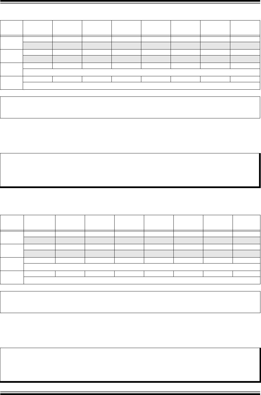
PIC32 Family Reference Manual
DS60001155C-page 35-24 © 2009-2013 Microchip Technology Inc.
Register 35-18: ETHSCOLFRM: Ethernet Controller Single Collision Frames Statistics Register
Bit
Range
Bit
31/23/15/7
Bit
30/22/14/6
Bit
29/21/13/5
Bit
28/20/12/4
Bit
27/19/11/3
Bit
26/18/10/2
Bit
25/17/9/1
Bit
24/16/8/0
31:24 U-0 U-0 U-0 U-0 U-0 U-0 U-0 U-0
— — — — — — — —
23:16 U-0 U-0 U-0 U-0 U-0 U-0 U-0 U-0
— — — — — — — —
15:8 R/W-0 R/W-0 R/W-0 R/W-0 R/W-0 R/W-0 R/W-0 R/W-0
SCOLFRMCNT<15:8>
7:0 R/W-0 R/W-0 R/W-0 R/W-0 R/W-0 R/W-0 R/W-0 R/W-0
SCOLFRMCNT<7:0>
Legend:
R = Readable bit W = Writable bit U = Unimplemented bit, read as ‘0’
-n = Value at POR ‘1’ = Bit is set ‘0’ = Bit is cleared x = Bit is unknown
bit 31-16 Unimplemented: Read as ‘0’
bit 15-0 SCOLFRMCNT<15:0>: Single Collision Frame Count bits
Increment count for frames that were successfully transmitted on the second try.
Note 1: This register is only used for TX operations.
2: This register is automatically cleared by hardware after a read operation, unless the byte enables for
bytes 0/1 are ‘0’.
3: It is recommended to use the SET, CLR, or INV registers to set or clear any bit in this register. Setting or
clearing any bits in this register should only be done for debug/test purposes.
Register 35-19: ETHMCOLFRM: Ethernet Controller Multiple Collision Frames Statistics Register
Bit
Range
Bit
31/23/15/7
Bit
30/22/14/6
Bit
29/21/13/5
Bit
28/20/12/4
Bit
27/19/11/3
Bit
26/18/10/2
Bit
25/17/9/1
Bit
24/16/8/0
31:24 U-0 U-0 U-0 U-0 U-0 U-0 U-0 U-0
— ———————
23:16 U-0 U-0 U-0 U-0 U-0 U-0 U-0 U-0
— ———————
15:8 R/W-0 R/W-0 R/W-0 R/W-0 R/W-0 R/W-0 R/W-0 R/W-0
MCOLFRMCNT<15:8>
7:0 R/W-0 R/W-0 R/W-0 R/W-0 R/W-0 R/W-0 R/W-0 R/W-0
MCOLFRMCNT<7:0>
Legend:
R = Readable bit W = Writable bit U = Unimplemented bit, read as ‘0’
-n = Value at POR ‘1’ = Bit is set ‘0’ = Bit is cleared x = Bit is unknown
bit 31-16 Unimplemented: Read as ‘0’
bit 15-0 MCOLFRMCNT<15:0>: Multiple Collision Frame Count bits
Increment count for frames that were successfully transmitted after there was more than one collision.
Note 1: This register is only used for TX operations.
2: This register is automatically cleared by hardware after a read operation, unless the byte enables for
bytes 0/1 are ‘0’.
3: It is recommended to use the SET, CLR, or INV registers to set or clear any bit in this register. Setting or
clearing any bits in this register should only be done for debug/test purposes.

© 2009-2013 Microchip Technology Inc. DS60001155C-page 35-25
Section 35. Ethernet Controller
Ethernet Controller
35
Register 35-20: ETHFRMRXOK: Ethernet Controller Frames Received Okay Statistics Register
Bit
Range
Bit
31/23/15/7
Bit
30/22/14/6
Bit
29/21/13/5
Bit
28/20/12/4
Bit
27/19/11/3
Bit
26/18/10/2
Bit
25/17/9/1
Bit
24/16/8/0
31:24 U-0 U-0 U-0 U-0 U-0 U-0 U-0 U-0
————————
23:16 U-0 U-0 U-0 U-0 U-0 U-0 U-0 U-0
————————
15:8 R/W-0 R/W-0 R/W-0 R/W-0 R/W-0 R/W-0 R/W-0 R/W-0
FRMRXOKCNT<15:8>
7:0 R/W-0 R/W-0 R/W-0 R/W-0 R/W-0 R/W-0 R/W-0 R/W-0
FRMRXOKCNT<7:0>
Legend:
R = Readable bit W = Writable bit U = Unimplemented bit, read as ‘0’
-n = Value at POR ‘1’ = Bit is set ‘0’ = Bit is cleared x = Bit is unknown
bit 31-16 Unimplemented: Read as ‘0’
bit 15-0 FRMRXOKCNT<15:0>: Frames Received Okay Count bits
Increment count for frames received successfully by the RX Filter. This count will not be incremented if
there is a Frame Check Sequence (FCS) or Alignment error.
Note 1: This register is only used for RX operations.
2: This register is automatically cleared by hardware after a read operation, unless the byte enables for
bytes 0/1 are ‘0’.
3: It is recommended to use the SET, CLR, or INV registers to set or clear any bit in this register. Setting or
clearing any bits in this register should only be done for debug/test purposes.
Register 35-21: ETHFCSERR: Ethernet Controller Frame Check Sequence Error Statistics Register
Bit
Range
Bit
31/23/15/7
Bit
30/22/14/6
Bit
29/21/13/5
Bit
28/20/12/4
Bit
27/19/11/3
Bit
26/18/10/2
Bit
25/17/9/1
Bit
24/16/8/0
31:24 U-0 U-0 U-0 U-0 U-0 U-0 U-0 U-0
— — — — — — — —
23:16 U-0 U-0 U-0 U-0 U-0 U-0 U-0 U-0
— — — — — — — —
15:8 R/W-0 R/W-0 R/W-0 R/W-0 R/W-0 R/W-0 R/W-0 R/W-0
FCSERRCNT<15:8>
7:0 R/W-0 R/W-0 R/W-0 R/W-0 R/W-0 R/W-0 R/W-0 R/W-0
FCSERRCNT<7:0>
Legend:
R = Readable bit W = Writable bit U = Unimplemented bit, read as ‘0’
-n = Value at POR ‘1’ = Bit is set ‘0’ = Bit is cleared x = Bit is unknown
bit 31-16 Unimplemented: Read as ‘0’
bit 15-0 FCSERRCNT<15:0>: FCS Error Count bits
Increment count for frames received with FCS error and the frame length in bits is an integral multiple of
eight bits.
Note 1: This register is only used for RX operations.
2: This register is automatically cleared by hardware after a read operation, unless the byte enables for
bytes 0/1 are ‘0’.
3: It is recommended to use the SET, CLR, or INV registers to set or clear any bit in this register. Setting or
clearing any bits in this register should only be done for debug/test purposes.

PIC32 Family Reference Manual
DS60001155C-page 35-26 © 2009-2013 Microchip Technology Inc.
Register 35-22: ETHALGNERR: Ethernet Controller Alignment Errors Statistics Register
Bit
Range
Bit
31/23/15/7
Bit
30/22/14/6
Bit
29/21/13/5
Bit
28/20/12/4
Bit
27/19/11/3
Bit
26/18/10/2
Bit
25/17/9/1
Bit
24/16/8/0
31:24 U-0 U-0 U-0 U-0 U-0 U-0 U-0 U-0
— — — — — — — —
23:16 U-0 U-0 U-0 U-0 U-0 U-0 U-0 U-0
— — — — — — — —
15:8 R/W-0 R/W-0 R/W-0 R/W-0 R/W-0 R/W-0 R/W-0 R/W-0
ALGNERRCNT<15:8>
7:0 R/W-0 R/W-0 R/W-0 R/W-0 R/W-0 R/W-0 R/W-0 R/W-0
ALGNERRCNT<7:0>
Legend:
R = Readable bit W = Writable bit U = Unimplemented bit, read as ‘0’
-n = Value at POR ‘1’ = Bit is set ‘0’ = Bit is cleared x = Bit is unknown
bit 31-16 Unimplemented: Read as ‘0’
bit 15-0 ALGNERRCNT<15:0>: Alignment Error Count bits
Increment count for frames with alignment errors. Note that an alignment error is a frame that has an FCS
error and the frame length in bits is not an integral multiple of eight bits (also known as, dribble nibble).
Note 1: This register is only used for RX operations.
2: This register is automatically cleared by hardware after a read operation, unless the byte enables for
bytes 0/1 are ‘0’.
3: It is recommended to use the SET, CLR, or INV registers to set or clear any bit in this register. Setting or
clearing any bits in this register should only be done for debug/test purposes.

© 2009-2013 Microchip Technology Inc. DS60001155C-page 35-27
Section 35. Ethernet Controller
Ethernet Controller
35
Register 35-23: EMAC1CFG1: Ethernet Controller MAC Configuration 1 Register
Bit
Range
Bit
31/23/15/7
Bit
30/22/14/6
Bit
29/21/13/5
Bit
28/20/12/4
Bit
27/19/11/3
Bit
26/18/10/2
Bit
25/17/9/1
Bit
24/16/8/0
31:24 U-0 U-0 U-0 U-0 U-0 U-0 U-0 U-0
— — — — — — — —
23:16 U-0 U-0 U-0 U-0 U-0 U-0 U-0 U-0
— — — — — — — —
15:8 R/W-1 R/W-0 U-0 U-0 R/W-0 R/W-0 R/W-0 R/W-0
SOFTRESET SIMRESET ——RESETRMCSRESETRFUNRESETTMCS RESETTFUN
7:0 U-0 U-0 U-0 R/W-0 R/W-1 R/W-1 R/W-0 R/W-1
— — —LOOPBACKTXPAUSERXPAUSEPASSALLRXENABLE
Legend:
R = Readable bit W = Writable bit U = Unimplemented bit, read as ‘0’
-n = Value at POR ‘1’ = Bit is set ‘0’ = Bit is cleared x = Bit is unknown
bit 31-16 Unimplemented: Read as ‘0’
bit 15 SOFTRESET: Soft Reset bit
Setting this bit will put the MACMII in Reset. Its default value is ‘1’.
bit 14 SIMRESET: Simulation Reset bit
Setting this bit will cause a Reset to the random number generator within the Transmit Function.
bit 13-12 Unimplemented: Read as ‘0’
bit 11 RESETRMCS: Reset MCS/RX bit
Setting this bit will put the MAC Control Sub-layer/Receive domain logic in Reset.
bit 10 RESETRFUN: Reset RX Function bit
Setting this bit will put the MAC Receive function logic in Reset.
bit 9 RESETTMCS: Reset MCS/TX bit
Setting this bit will put the MAC Control Sub-layer/TX domain logic in Reset.
bit 8 RESETTFUN: Reset TX Function bit
Setting this bit will put the MAC Transmit function logic in Reset.
bit 7-5 Unimplemented: Read as ‘0’
bit 4 LOOPBACK: MAC Loopback mode bit
1 = MAC Transmit interface is loop backed to the MAC Receive interface
0 = MAC normal operation
bit 3 TXPAUSE: MAC TX Flow Control bit
1 = PAUSE Flow Control frames are allowed to be transmitted
0 = PAUSE Flow Control frames are blocked
bit 2 RXPAUSE: MAC RX Flow Control bit
1 = The MAC acts upon received PAUSE Flow Control frames
0 = Received PAUSE Flow Control frames are ignored
bit 1 PASSALL: MAC Pass all Receive Frames bit
1 = The MAC will accept all frames regardless of type (Normal vs. Control)
0 = The received Control frames are ignored
bit 0 RXENABLE: MAC Receive Enable bit
1 = Enable the MAC receiving of frames
0 = Disable the MAC receiving of frames
Note: 16-bit and 32-bit accesses to this register (including the Set, Clear and Invert registers) are allowed. 8-bit
accesses are not allowed and are ignored by hardware.

PIC32 Family Reference Manual
DS60001155C-page 35-28 © 2009-2013 Microchip Technology Inc.
Register 35-24: EMAC1CFG2: Ethernet Controller MAC Configuration 2 Register
Bit
Range
Bit
31/23/15/7
Bit
30/22/14/6
Bit
29/21/13/5
Bit
28/20/12/4
Bit
27/19/11/3
Bit
26/18/10/2
Bit
25/17/9/1
Bit
25/16/8/0
31:24 U-0 U-0 U-0 U-0 U-0 U-0 U-0 U-0
— — — — — — — —
23:16 U-0 U-0 U-0 U-0 U-0 U-0 U-0 U-0
— — — — — — — —
15:8 U-0 R/W-1 R/W-0 R/W-0 U-0 U-0 R/W-0 R/W-0
—EXCESSDFRBPNOBKOFFNOBKOFF——LONGPREPUREPRE
7:0 R/W-1 R/W-0 R/W-1 R/W-1 R/W-0 R/W-0 R/W-1 R/W-0
AUTOPAD(1,2) VLANPAD(1,2) PADENABLE(1,3) CRCENABLE DELAYCRC HUGEFRM LENGTHCK FULLDPLX
Legend:
R = Readable bit W = Writable bit U = Unimplemented bit, read as ‘0’
-n = Value at POR ‘1’ = Bit is set ‘0’ = Bit is cleared x = Bit is unknown
bit 31-15 Unimplemented: Read as ‘0’
bit 14 EXCESSDFR: Excess Defer bit
1 = The MAC will defer to carrier indefinitely as per the IEEE 802.3 Specification standard
0 = The MAC will abort when the excessive deferral limit is reached
bit 13 BPNOBKOFF: Back-pressure/No Back-off bit
1 = The MAC after incidentally causing a collision during back-pressure will immediately retransmit without
back-off reducing the chance of further collisions and ensuring transmit packets get sent
0 = The MAC will not remove the back-off
bit 12 NOBKOFF: No Back-off bit
1 = Following a collision, the MAC will immediately retransmit rather than using the Binary Exponential
Back-off algorithm as specified in the IEEE 802.3 Specification standard
0 = Following a collision, the MAC will use the Binary Exponential Back-off algorithm
bit 11-10 Unimplemented: Read as ‘0’
bit 9 LONGPRE: Long Preamble Enforcement bit
1 = The MAC only allows receive packets that contain preamble fields less than 12 bytes in length
0 = The MAC allows any length preamble as per the IEEE 802.3 Specification standard
bit 8 PUREPRE: Pure Preamble Enforcement bit
1 = The MAC will verify the content of the preamble to ensure it contains 0x55 and is error-free. A packet with
errors in its preamble is discarded
0 = The MAC does not perform any preamble checking
bit 7 AUTOPAD: Auto Detect Pad Enable bit(1,2)
1 = The MAC will automatically detect the type of frame, either tagged or untagged, by comparing the two
bytes following the source address with 0x8100 (VLAN Protocol ID) and pad accordingly
0 = The MAC does not perform auto detection
bit 6 VLANPAD: VLAN Pad Enable bit(1,2)
1 = The MAC will pad all short frames to 64 bytes and append a valid CRC
0 = The MAC does not perform padding of short frames
Note 1: This bit is ignored, if the PADENABLE bit is cleared.
2: This bit is used in conjunction with the AUTOPAD and VLANPAD bits.
3: Tabl e 3 5-2 provides a description of the pad function based on the configuration of this register.
Note: 16-bit and 32-bit accesses to this register (including the Set, Clear and Invert registers) are allowed. 8-bit
accesses are not allowed and are ignored by hardware.
© 2009-2013 Microchip Technology Inc. DS60001155C-page 35-29
Section 35. Ethernet Controller
Ethernet Controller
35
Table 35-2: Pad Operation
bit 5 PADENABLE: Pad/CRC Enable bit(1,3)
1 = The MAC will pad all short frames
0 = The frames presented to the MAC have a valid length
bit 4 CRCENABLE: CRC Enable1 bit
1 = The MAC will append a CRC to every frame whether padding was required or not. Must be set if the
PADENABLE bit is set
0 = The frames presented to the MAC have a valid CRC
bit 3 DELAYCRC: Delayed CRC bit
This bit determines the number of bytes, if any, of proprietary header information that exist on the front of the
IEEE 802.3 frames.
1 = Four bytes of header (ignored by the CRC function)
0 = No proprietary header
bit 2 HUGEFRM: Huge Frame enable bit
1 = Frames of any length are transmitted and received
0 = Huge frames are not allowed for receive or transmit
bit 1 LENGTHCK: Frame Length checking bit
1 = Both transmit and receive frame lengths are compared to the Length/Type field. If the Length/Type field
represents a length then the check is performed. Mismatches are reported on the Transmit/Receive
Statistics Vector
0 = Length/Type field check is not performed
bit 0 FULLDPLX: Full-Duplex Operation bit
1 = The MAC operates in Full-Duplex mode
0 = The MAC operates in Half-Duplex mode
Type AUTOPAD VLANPAD PADENABLE Action
Any x x 0 No pad, check CRC
Any 0 0 1 Pad to 60 Bytes, append CRC
Any x 1 1 Pad to 64 Bytes, append CRC
Any 1 0 1 If untagged: Pad to 60 Bytes, append CRC
If VLAN tagged: Pad to 64 Bytes, append CRC
Register 35-24: EMAC1CFG2: Ethernet Controller MAC Configuration 2 Register (Continued)
Note 1: This bit is ignored, if the PADENABLE bit is cleared.
2: This bit is used in conjunction with the AUTOPAD and VLANPAD bits.
3: Tabl e 3 5-2 provides a description of the pad function based on the configuration of this register.
Note: 16-bit and 32-bit accesses to this register (including the Set, Clear and Invert registers) are allowed. 8-bit
accesses are not allowed and are ignored by hardware.

PIC32 Family Reference Manual
DS60001155C-page 35-30 © 2009-2013 Microchip Technology Inc.
Register 35-25: EMAC1IPGT: Ethernet Controller MAC Back-to-Back Interpacket Gap Register
Bit
Range
Bit
31/23/15/7
Bit
30/22/14/6
Bit
29/21/13/5
Bit
28/20/12/4
Bit
27/19/11/3
Bit
26/18/10/2
Bit
25/17/9/1
Bit
24/16/8/0
31:24 U-0 U-0 U-0 U-0 U-0 U-0 U-0 U-0
— — — — — — — —
23:16 U-0 U-0 U-0 U-0 U-0 U-0 U-0 U-0
— — — — — — — —
15:8 U-0 U-0 U-0 U-0 U-0 U-0 U-0 U-0
— — — — — — — —
7:0 U-0 R/W-0 R/W-0 R/W-1 R/W-0 R/W-0 R/W-1 R/W-0
— B2BIPKTGP<6:0>
Legend:
R = Readable bit W = Writable bit U = Unimplemented bit, read as ‘0’
-n = Value at POR ‘1’ = Bit is set ‘0’ = Bit is cleared x = Bit is unknown
bit 31-7 Unimplemented: Read as ‘0’
bit 6-0 B2BIPKTGP<6:0>: Back-to-Back Interpacket Gap bits
This is a programmable field representing the nibble time offset of the minimum possible period between
the end of any transmitted packet to the beginning of the next.
In Full-Duplex mode, the register value should be the desired period in nibble times minus 3.
In Half-Duplex mode, the register value should be the desired period in nibble times minus 6.
In Full-Duplex mode, the recommended setting is 0x15 (21d), which represents the minimum IPG of
0.96 µs (in 100 Mbps) or 9.6 µs (in 10 Mbps).
In Half-Duplex mode, the recommended setting is 0x12 (18d), which represents the minimum IPG of 0.96
µs (in 100 Mbps) or 9.6 µs (in 10 Mbps).
Note: 16-bit and 32-bit accesses to this register (including the Set, Clear and Invert registers) are allowed. 8-bit
accesses are not allowed and are ignored by hardware.

© 2009-2013 Microchip Technology Inc. DS60001155C-page 35-31
Section 35. Ethernet Controller
Ethernet Controller
35
Register 35-26: EMAC1IPGR: Ethernet Controller MAC Non-Back-to-Back Interpacket Gap Register
Bit
Range
Bit
31/23/15/7
Bit
30/22/14/6
Bit
29/21/13/5
Bit
28/20/12/4
Bit
27/19/11/3
Bit
26/18/10/2
Bit
25/17/9/1
Bit
24/16/8/0
31:24 U-0 U-0 U-0 U-0 U-0 U-0 U-0 U-0
— — — — — — — —
23:16 U-0 U-0 U-0 U-0 U-0 U-0 U-0 U-0
— — — — — — — —
15:8 U-0 R/W-0 R/W-0 R/W-0 R/W-1 R/W-1 R/W-0 R/W-0
— NB2BIPKTGP1<6:0>
7:0 U-0 R/W-0 R/W-0 R/W-1 R/W-0 R/W-0 R/W-1 R/W-0
— NB2BIPKTGP2<6:0>
Legend:
R = Readable bit W = Writable bit U = Unimplemented bit, read as ‘0’
-n = Value at POR ‘1’ = Bit is set ‘0’ = Bit is cleared x = Bit is unknown
bit 31-15 Unimplemented: Read as ‘0’
bit 14-8 NB2BIPKTGP1<6:0>: Non-Back-to-Back Interpacket Gap Part 1 bits
This is a programmable field representing the optional Carrier Sense window referenced in
Section 4.2.3.2.1 “Deference” of the IEEE 802.3 Specification.
If Carrier is detected during the timing of IPGR1, the MAC defers to Carrier. If, however, Carrier becomes
after IPGR1, the MAC continues timing IPGR2 and transmits, knowingly causing a collision, thus ensuring
fair access to medium. Its range of values is 0x0 to IPGR2. Its recommend value is 0xC (12d).
bit 7 Unimplemented: Read as ‘0’
bit 6-0 NB2BIPKTGP2<6:0>: Non-Back-to-Back Interpacket Gap Part 2 bits
This is a programmable field representing the non-back-to-back Inter-Packet-Gap. Its recommended value
is 0x12 (18d), which represents the minimum IPG of 0.96 µs (in 100 Mbps) or 9.6 µs (in 10 Mbps).
Note: 16-bit and 32-bit accesses to this register (including the Set, Clear and Invert registers) are allowed. 8-bit
accesses are not allowed and are ignored by hardware.

PIC32 Family Reference Manual
DS60001155C-page 35-32 © 2009-2013 Microchip Technology Inc.
Register 35-27: EMAC1CLRT: Ethernet Controller MAC Collision Window/Retry Limit Register
Bit
Range
Bit
31/23/15/7
Bit
30/22/14/6
Bit
29/21/13/5
Bit
28/20/12/4
Bit
27/19/11/3
Bit
26/18/10/2
Bit
25/17/9/1
Bit
24/16/8/0
31:24 U-0 U-0 U-0 U-0 U-0 U-0 U-0 U-0
— — — — — — — —
23:16 U-0 U-0 U-0 U-0 U-0 U-0 U-0 U-0
— — — — — — — —
15:8 U-0 U-0 R/W-1 R/W-1 R/W-0 R/W-1 R/W-1 R/W-1
——CWINDOW<5:0>
7:0 U-0 U-0 U-0 U-0 R/W-1 R/W-1 R/W-1 R/W-1
— — — —RETX<3:0>
Legend:
R = Readable bit W = Writable bit U = Unimplemented bit, read as ‘0’
-n = Value at POR ‘1’ = Bit is set ‘0’ = Bit is cleared x = Bit is unknown
bit 31-14 Unimplemented: Read as ‘0’
bit 13-8 CWINDOW<5:0>: Collision Window bits
This is a programmable field representing the slot time or collision window during which collisions occur in
properly configured networks. Since the collision window starts at the beginning of transmission, the
preamble and SFD is included. Its default of 0x37 (55d) corresponds to the count of frame bytes at the end
of the window.
bit 7-4 Unimplemented: Read as ‘0’
bit 3-0 RETX<3:0>: Retransmission Maximum bits
This is a programmable field specifying the number of retransmission attempts following a collision before
aborting the packet due to excessive collisions. The IEEE 802.3 Specification standard specifies the
maximum number of attempts (attemptLimit) to be 0xF (15d). Its default is ‘0xF’.
Note: 16-bit and 32-bit accesses to this register (including the Set, Clear and Invert registers) are allowed. 8-bit
accesses are not allowed and are ignored by hardware.

© 2009-2013 Microchip Technology Inc. DS60001155C-page 35-33
Section 35. Ethernet Controller
Ethernet Controller
35
Register 35-28: EMAC1MAXF: Ethernet Controller MAC Maximum Frame Length Register
Bit
Range
Bit
31/23/15/7
Bit
30/22/14/6
Bit
29/21/13/5
Bit
28/20/12/4
Bit
27/19/11/3
Bit
26/18/10/2
Bit
25/17/9/1
Bit
24/16/8/0
31:24 U-0 U-0 U-0 U-0 U-0 U-0 U-0 U-0
— — — — — — — —
23:16 U-0 U-0 U-0 U-0 U-0 U-0 U-0 U-0
— — — — — — — —
15:8 R/W-0 R/W-0 R/W-0 R/W-0 R/W-0 R/W-1 R/W-0 R/W-1
MACMAXF<15:8>
7:0 R/W-1 R/W-1 R/W-1 R/W-0 R/W-1 R/W-1 R/W-1 R/W-0
MACMAXF<7:0>(1)
Legend:
R = Readable bit W = Writable bit U = Unimplemented bit, read as ‘0’
-n = Value at POR ‘1’ = Bit is set ‘0’ = Bit is cleared x = Bit is unknown
bit 31-16 Unimplemented: Read as ‘0’
bit 15-0 MACMAXF<15:0>: Maximum Frame Length bits(1)
This field resets to 0x05EE, which represents a maximum receive frame of 1518 bytes. An untagged
maximum size Ethernet frame is 1518 bytes. A tagged frame adds four bytes for a total of 1522 bytes. If a
shorter/longer maximum length restriction is desired, program this 16-bit field.
Note 1: If a proprietary header is allowed, this field should be adjusted accordingly. For example, if 4-byte headers
are prepended to frames, MACMAXF could be set to 1527 bytes. This would allow the maximum VLAN
tagged frame plus the 4-byte header.
Note: 16-bit and 32-bit accesses to this register (including the Set, Clear and Invert registers) are allowed. 8-bit
accesses are not allowed and are ignored by hardware.

PIC32 Family Reference Manual
DS60001155C-page 35-34 © 2009-2013 Microchip Technology Inc.
Register 35-29: EMAC1SUPP: Ethernet Controller MAC PHY Support Register
Bit
Range
Bit
31/23/15/7
Bit
30/22/14/6
Bit
29/21/13/5
Bit
28/20/12/4
Bit
27/19/11/3
Bit
26/18/10/2
Bit
25/17/9/1
Bit
24/16/8/0
31:24 U-0 U-0 U-0 U-0 U-0 U-0 U-0 U-0
— — — — — — — —
23:16 U-0 U-0 U-0 U-0 U-0 U-0 U-0 U-0
— — — — — — — —
15:8 U-0 U-0 U-0 U-0 R/W-0 U-0 U-0 R/W-0
— — — — RESETRMII ——SPEEDRMII
7:0 U-0 U-0 U-0 U-0 U-0 U-0 U-0 U-0
— — — — — — — —
Legend:
R = Readable bit W = Writable bit U = Unimplemented bit, read as ‘0’
-n = Value at POR ‘1’ = Bit is set ‘0’ = Bit is cleared x = Bit is unknown
bit 31-12 Unimplemented: Read as ‘0’
bit 11 RESETRMII: Reset RMII Logic bit
1 = Reset the MAC RMII module
0 = Normal Operation.
bit 10-9 Unimplemented: Read as ‘0’
bit 8 SPEEDRMII: RMII Speed bit
This bit configures the Reduced MII logic for the current operating speed.
1 = RMII running in 100 Mbps
0 = RMII running in 10 Mbps
bit 7-0 Unimplemented: Read as ‘0’
Note 1: Both 16-bit and 32-bit accesses to this register (including the Set, Clear and Invert registers) are allowed.
8-bit accesses are not allowed and are ignored by hardware.
2: The bits in this register are only used for the RMII module.

© 2009-2013 Microchip Technology Inc. DS60001155C-page 35-35
Section 35. Ethernet Controller
Ethernet Controller
35
Register 35-30: EMAC1TEST: Ethernet Controller MAC Test Register
Bit
Range
Bit
31/23/15/7
Bit
30/22/14/6
Bit
29/21/13/5
Bit
28/20/12/4
Bit
27/19/11/3
Bit
26/18/10/2
Bit
25/17/9/1
Bit
24/16/8/0
31:24 U-0 U-0 U-0 U-0 U-0 U-0 U-0 U-0
— — — — — — — —
23:16 U-0 U-0 U-0 U-0 U-0 U-0 U-0 U-0
— — — — — — — —
15:8 U-0 U-0 U-0 U-0 U-0 U-0 U-0 U-0
— — — — — — — —
7:0 U-0 U-0 U-0 U-0 U-0 R/W-0 R/W-0 R/W-0
— — — — —TESTBPTESTPAUSESHRTQNTA
Legend:
R = Readable bit W = Writable bit U = Unimplemented bit, read as ‘0’
-n = Value at POR ‘1’ = Bit is set ‘0’ = Bit is cleared x = Bit is unknown
bit 31-3 Unimplemented: Read as ‘0’
bit 2 TESTBP: Test Back-pressure bit
1 = The MAC will assert back-pressure on the link. Back-pressure causes preamble to be transmitted, raising
Carrier Sense. A transmit packet from the system will be sent during back-pressure.
0 = Normal Operation
bit 1 TESTPAUSE: Test PAUSE bit
1 = The MAC Control sub-layer will inhibit transmissions, just as if a PAUSE Receive Control frame with a
non-zero pause time parameter was received
0 = Normal Operation
bit 0 SHRTQNTA: Shortcut PAUSE Quanta bit
1 = The MAC reduces the effective PAUSE Quanta from 64 byte-times to 1 byte-time
0 = Normal Operation
Note 1: 16-bit and 32-bit accesses to this register (including the Set, Clear and Invert registers) are allowed. 8-bit
accesses are not allowed and are ignored by hardware.
2: The bits in this register are only used for testing.

PIC32 Family Reference Manual
DS60001155C-page 35-36 © 2009-2013 Microchip Technology Inc.
Table 35-3: MIIM Clock Selection
Register 35-31: EMAC1MCFG: Ethernet Controller MAC MII Management Configuration Register
Bit
Range
Bit
31/23/15/7
Bit
30/22/14/6
Bit
29/21/13/5
Bit
28/20/12/4
Bit
27/19/11/3
Bit
26/18/10/2
Bit
25/17/9/1
Bit
24/16/8/0
31:24 U-0 U-0 U-0 U-0 U-0 U-0 U-0 U-0
— — — — — — — —
23:16 U-0 U-0 U-0 U-0 U-0 U-0 U-0 U-0
— — — — — — — —
15:8 R/W-0 U-0 U-0 U-0 U-0 U-0 U-0 U-0
RESETMGMT — — — — — — —
7:0 U-0 U-0 R/W-1 R/W-0 R/W-0 R/W-0 R/W-0 R/W-0
——CLKSEL<3:0>NOPRESCANINC
Legend:
R = Readable bit W = Writable bit U = Unimplemented bit, read as ‘0’
-n = Value at POR ‘1’ = Bit is set ‘0’ = Bit is cleared x = Bit is unknown
bit 31-16 Unimplemented: Read as ‘0’
bit 15 RESETMGMT: Test Reset MII Management bit
1 = Reset the MII Management module
0 = Normal Operation
bit 14-6 Unimplemented: Read as ‘0’
bit 5-2 CLKSEL<3:0>: MII Management Clock Select 1 bits(2)
This field is used by the clock divide logic in creating the MII Management Clock (MDC), which the
IEEE 802.3 Specification defines to be no faster than 2.5 MHz. Some PHYs support clock rates up to
12.5 MHz.
bit 1 NOPRE: Suppress Preamble bit
1 = The MII Management will perform read/write cycles without the 32-bit preamble field. Some PHYs
support suppressed preamble
0 = Normal read/write cycles are performed
bit 0 SCANINC: Scan Increment bit
1 = The MII Management module will perform read cycles across a range of PHYs. The read cycles will start
from address 1 through the value set in EMAC1MADR<PHYADDR>
0 = Continuous reads of the same PHY
Note 1: 16-bit and 32-bit accesses to this register (including the Set, Clear and Invert registers) are allowed. 8-bit
accesses are not allowed and are ignored by hardware.
2: Tabl e 3 5-3 provides a description of the clock divider encoding.
MIIM Clock Select EMAC1MCFG<5:2>
SYSCLK divided by 4 000x
SYSCLK divided by 6 0010
SYSCLK divided by 8 0011
SYSCLK divided by 10 0100
SYSCLK divided by 14 0101
SYSCLK divided by 20 0110
SYSCLK divided by 28 0111
SYSCLK divided by 40 1000
Undefined Any other combination
Note: SYSCLK is the CPU clock.

© 2009-2013 Microchip Technology Inc. DS60001155C-page 35-37
Section 35. Ethernet Controller
Ethernet Controller
35
Register 35-32: EMAC1MCMD: Ethernet Controller MAC MII Management Command Register
Bit
Range
Bit
31/23/15/7
Bit
30/22/14/6
Bit
29/21/13/5
Bit
28/20/12/4
Bit
27/19/11/3
Bit
26/18/10/2
Bit
25/17/9/1
Bit
24/16/8/0
31:24 U-0 U-0 U-0 U-0 U-0 U-0 U-0 U-0
————————
23:16 U-0 U-0 U-0 U-0 U-0 U-0 U-0 U-0
————————
15:8 U-0 U-0 U-0 U-0 U-0 U-0 U-0 U-0
————————
7:0 U-0 U-0 U-0 U-0 U-0 U-0 R/W-0 R/W-0
— — — — — — SCAN READ
Legend:
R = Readable bit W = Writable bit U = Unimplemented bit, read as ‘0’
-n = Value at POR ‘1’ = Bit is set ‘0’ = Bit is cleared x = Bit is unknown
bit 31-2 Unimplemented: Read as ‘0’
bit 1 SCAN: MII Management Scan Mode bit
1 = The MII Management module will perform read cycles continuously (for example, useful for monitoring
the Link Fail)
0 = Normal Operation
bit 0 READ: MII Management Read Command bit
1 = The MII Management module will perform a single read cycle. The read data is returned in the
EMAC1MRDD register
0 = The MII Management module will perform a write cycle. The write data is taken from the EMAC1MWTD
register
Note: 16-bit and 32-bit accesses to this register (including the Set, Clear and Invert registers) are allowed. 8-bit
accesses are not allowed and are ignored by hardware.

PIC32 Family Reference Manual
DS60001155C-page 35-38 © 2009-2013 Microchip Technology Inc.
Register 35-33: EMAC1MADR: Ethernet Controller MAC MII Management Address Register
Bit
Range
Bit
31/23/15/7
Bit
30/22/14/6
Bit
29/21/13/5
Bit
28/20/12/4
Bit
27/19/11/3
Bit
26/18/10/2
Bit
25/17/9/1
Bit
24/16/8/0
31:24 U-0 U-0 U-0 U-0 U-0 U-0 U-0 U-0
— — — — — — — —
23:16 U-0 U-0 U-0 U-0 U-0 U-0 U-0 U-0
— — — — — — — —
15:8 U-0 U-0 U-0 R/W-0 R/W-0 R/W-0 R/W-0 R/W-1
— — —PHYADDR<4:0>
7:0 U-0 U-0 U-0 R/W-0 R/W-0 R/W-0 R/W-0 R/W-0
— — —REGADDR<4:0>
Legend:
R = Readable bit W = Writable bit U = Unimplemented bit, read as ‘0’
-n = Value at POR ‘1’ = Bit is set ‘0’ = Bit is cleared x = Bit is unknown
bit 31-13 Unimplemented: Read as ‘0’
bit 12-8 PHYADDR<4:0>: MII Management PHY Address bits
This field represents the 5-bit PHY Address field of Management cycles. Up to 31 PHYs can be addressed
(0 is reserved).
bit 7-5 Unimplemented: Read as ‘0’
bit 4-0 REGADDR<4:0>: MII Management Register Address bits
This field represents the 5-bit Register Address field of Management cycles. Up to 32 registers can be
accessed.
Note: 16-bit and 32-bit accesses to this register (including the Set, Clear and Invert registers) are allowed. 8-bit
accesses are not allowed and are ignored by hardware.

© 2009-2013 Microchip Technology Inc. DS60001155C-page 35-39
Section 35. Ethernet Controller
Ethernet Controller
35
Register 35-34: EMAC1MWTD: Ethernet Controller MAC MII Management Write Data Register
Bit
Range
Bit
31/23/15/7
Bit
30/22/14/6
Bit
29/21/13/5
Bit
28/20/12/4
Bit
27/19/11/3
Bit
26/18/10/2
Bit
25/17/9/1
Bit
24/16/8/0
31:24 U-0 U-0 U-0 U-0 U-0 U-0 U-0 U-0
————————
23:16 U-0 U-0 U-0 U-0 U-0 U-0 U-0 U-0
————————
15:8 R/W-0 R/W-0 R/W-0 R/W-0 R/W-0 R/W-0 R/W-0 R/W-0
MWTD<15:8>
7:0 R/W-0 R/W-0 R/W-0 R/W-0 R/W-0 R/W-0 R/W-0 R/W-0
MWTD<7:0>
Legend:
R = Readable bit W = Writable bit P = Programmable bit r = Reserved bit
U = Unimplemented bit -n = Bit Value at POR: (‘0’, ‘1’, x = Unknown)
bit 31-16 Unimplemented: Read as’0’
bit 15-0 MWTD<15:0>: MII Management Write Data bits
When written, a MII Management write cycle is performed using the 16-bit data and the preconfigured
PHY and Register addresses from the EMAC1MADR register.
Note: 16-bit and 32-bit accesses to this register (including the Set, Clear and Invert registers) are allowed. 8-bit
accesses are not allowed and are ignored by hardware.
Register 35-35: EMAC1MRDD: Ethernet Controller MAC MII Management Read Data Register
Bit
Range
Bit
31/23/15/7
Bit
30/22/14/6
Bit
29/21/13/5
Bit
28/20/12/4
Bit
27/19/11/3
Bit
26/18/10/2
Bit
25/17/9/1
Bit
24/16/8/0
31:24 U-0 U-0 U-0 U-0 U-0 U-0 U-0 U-0
— — — — — — — —
23:16 U-0 U-0 U-0 U-0 U-0 U-0 U-0 U-0
— — — — — — — —
15:8 R/W-0 R/W-0 R/W-0 R/W-0 R/W-0 R/W-0 R/W-0 R/W-0
MRDD<15:8>
7:0 R/W-0 R/W-0 R/W-0 R/W-0 R/W-0 R/W-0 R/W-0 R/W-0
MRDD<7:0>
Legend:
R = Readable bit W = Writable bit U = Unimplemented bit, read as ‘0’
-n = Value at POR ‘1’ = Bit is set ‘0’ = Bit is cleared x = Bit is unknown
bit 31-16 Unimplemented: Read as ‘0’
bit 15-0 MRDD<15:0>: MII Management Read Data bits
Following a MII Management Read Cycle, the 16-bit data can be read from this location.
Note: 16-bit and 32-bit accesses to this register (including the Set, Clear and Invert registers) are allowed. 8-bit
accesses are not allowed and are ignored by hardware.

PIC32 Family Reference Manual
DS60001155C-page 35-40 © 2009-2013 Microchip Technology Inc.
Register 35-36: EMAC1MIND: Ethernet Controller MAC MII Management Indicators Register
Bit
Range
Bit
31/23/15/7
Bit
30/22/14/6
Bit
29/21/13/5
Bit
28/20/12/4
Bit
27/19/11/3
Bit
26/18/10/2
Bit
25/17/9/1
Bit
24/16/8/0
31:24 U-0 U-0 U-0 U-0 U-0 U-0 U-0 U-0
— — — — — — — —
23:16 U-0 U-0 U-0 U-0 U-0 U-0 U-0 U-0
— — — — — — — —
15:8 U-0 U-0 U-0 U-0 U-0 U-0 U-0 U-0
— — — — — — — —
7:0 U-0 U-0 U-0 U-0 R/W-0 R/W-0 R/W-0 R/W-0
— — — — LINKFAIL NOTVALID SCAN MIIMBUSY
Legend:
R = Readable bit W = Writable bit U = Unimplemented bit, read as ‘0’
-n = Value at POR ‘1’ = Bit is set ‘0’ = Bit is cleared x = Bit is unknown
bit 31-4 Unimplemented: Read as ‘0’
bit 3 LINKFAIL: Link Fail bit
When ‘1’ is returned - indicates link fail has occurred. This bit reflects the value last read from the PHY
status register.
bit 2 NOTVALID: MII Management Read Data Not Valid bit
When ‘1’ is returned - indicates an MII management read cycle has not completed and the Read Data is not
yet valid.
bit 1 SCAN: MII Management Scanning bit
When ‘1’ is returned - indicates a scan operation (continuous MII Management Read cycles) is in progress.
bit 0 MIIMBUSY: MII Management Busy bit
When ‘1’ is returned - indicates MII Management module is currently performing an MII Management Read
or Write cycle.
Note: 16-bit and 32-bit accesses to this register (including the Set, Clear and Invert registers) are allowed. 8-bit
accesses are not allowed and are ignored by hardware.
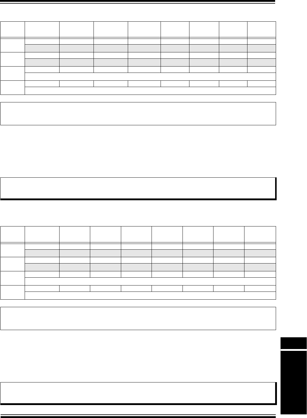
© 2009-2013 Microchip Technology Inc. DS60001155C-page 35-41
Section 35. Ethernet Controller
Ethernet Controller
35
Register 35-37: EMAC1SA0: Ethernet Controller MAC Address 0 Register
Bit
Range
Bit
31/23/15/7
Bit
30/22/14/6
Bit
29/21/13/5
Bit
28/20/12/4
Bit
27/19/11/3
Bit
26/18/10/2
Bit
25/17/9/1
Bit
24/16/8/0
31:24 U-0 U-0 U-0 U-0 U-0 U-0 U-0 U-0
— — — — — — — —
23:16 U-0 U-0 U-0 U-0 U-0 U-0 U-0 U-0
— — — — — — — —
15:8 R/W-P R/W-P R/W-P R/W-P R/W-P R/W-P R/W-P R/W-P
STNADDR6<7:0>
7:0 R/W-P R/W-P R/W-P R/W-P R/W-P R/W-P R/W-P R/W-P
STNADDR5<7:0>
Legend: P = Programmable bit
R = Readable bit W = Writable bit U = Unimplemented bit, read as ‘0’
-n = Value at POR ‘1’ = Bit is set ‘0’ = Bit is cleared x = Bit is unknown
bit 31-16 Unimplemented: Read as ‘0’
bit 15-8 STNADDR6<7:0>: Station Address Sixth Byte bits
This field holds the sixth transmitted byte of the station address.
bit 7-0 STNADDR5<7:0>: Station Address Fifth Byte bits
This field holds the fifth transmitted byte of the station address.
Note 1: 16-bit and 32-bit accesses to this register (including the Set, Clear and Invert registers) are allowed. 8-bit
accesses are not allowed and are ignored by hardware.
2: This register is loaded at reset from the factory preprogrammed station address.
Register 35-38: EMAC1SA1: Ethernet Controller MAC Address 1 Register
Bit
Range
Bit
31/23/15/7
Bit
30/22/14/6
Bit
29/21/13/5
Bit
28/20/12/4
Bit
27/19/11/3
Bit
26/18/10/2
Bit
25/17/9/1
Bit
24/16/8/0
31:24 U-0 U-0 U-0 U-0 U-0 U-0 U-0 U-0
— — — — — — — —
23:16 U-0 U-0 U-0 U-0 U-0 U-0 U-0 U-0
— — — — — — — —
15:8 R/W-P R/W-P R/W-P R/W-P R/W-P R/W-P R/W-P R/W-P
STNADDR4<7:0>
7:0 R/W-P R/W-P R/W-P R/W-P R/W-P R/W-P R/W-P R/W-P
STNADDR3<7:0>
Legend: P = Programmable bit
R = Readable bit W = Writable bit U = Unimplemented bit, read as ‘0’
-n = Value at POR ‘1’ = Bit is set ‘0’ = Bit is cleared x = Bit is unknown
bit 31-16 Unimplemented: Read as ‘0’
bit 15-8 STNADDR4<7:0>: Station Address Fourth Byte bits
This field holds the fourth transmitted byte of the station address.
bit 7-0 STNADDR3<7:0>: Station Address Third Byte bits
This field holds the third transmitted byte of the station address.
Note 1: Both 16-bit and 32-bit accesses to this register (including the Set, Clear and Invert registers) are allowed.
8-bit accesses are not allowed and are ignored by hardware.
2: This register is loaded at reset from the factory preprogrammed station address.

PIC32 Family Reference Manual
DS60001155C-page 35-42 © 2009-2013 Microchip Technology Inc.
Register 35-39: EMAC1SA2: Ethernet Controller MAC Address 2 Register
Bit
Range
Bit
31/23/15/7
Bit
30/22/14/6
Bit
29/21/13/5
Bit
28/20/12/4
Bit
27/19/11/3
Bit
26/18/10/2
Bit
25/17/9/1
Bit
24/16/8/0
31:24 U-0 U-0 U-0 U-0 U-0 U-0 U-0 U-0
— — — — — — — —
23:16 U-0 U-0 U-0 U-0 U-0 U-0 U-0 U-0
— — — — — — — —
15:8 R/W-P R/W-P R/W-P R/W-P R/W-P R/W-P R/W-P R/W-P
STNADDR2<7:0>
7:0 R/W-P R/W-P R/W-P R/W-P R/W-P R/W-P R/W-P R/W-P
STNADDR1<7:0>
Legend: P = Programmable bit
R = Readable bit W = Writable bit U = Unimplemented bit, read as ‘0’
-n = Value at POR ‘1’ = Bit is set ‘0’ = Bit is cleared x = Bit is unknown
bit 31-16 Reserved: Maintain as ‘0’; ignore read
bit 15-8 STNADDR2<7:0>: Station Address Second Byte bits
This field holds the second transmitted byte of the station address.
bit 7-0 STNADDR1<7:0>: Station Address First Byte bits
This field holds the most significant (first transmitted) byte of the station address.
Note 1: 16-bit and 32-bit accesses to this register (including the Set, Clear and Invert registers) are allowed. 8-bit
accesses are not allowed and are ignored by hardware.
2: This register is loaded at reset from the factory preprogrammed station address.

© 2009-2013 Microchip Technology Inc. DS60001155C-page 35-43
Section 35. Ethernet Controller
Ethernet Controller
35
35.4 OPERATION
The Ethernet Controller provides the system modules needed to implement a 10/100 Mbps
Ethernet node using an external PHY chip. To offload the CPU from moving packet data to and
from the module, two internal descriptor-based DMA engines are included in the
Ethernet Controller.
The Ethernet Controller module consists of the following sub-modules:
•10/100 Megabit Media Access Controller (MAC):
This controller implements the MAC sub-layer of the Data Link Layer, and performs the
CSMA/CD function contained in the ISO/IEC 8802-3 and the IEEE 802.3 specifications,
which includes:
- MII to connect to an external PHY
- RMII to connect to an external PHY
- MII Management block that provides control/status connection to the external PHY
- Performs the receive path Flow Control functions contained in Annex 31B of the IEEE
802.3 Specification
- Implements the MAC Transmit and MAC Receive interfaces that connect with the TX
and RX DMA engines.
•Flow Control:
Responsible for control of the transmission of PAUSE frames, as defined in Annex 31B of
the IEEE 802.3 Specification
•RX Filter (RXF):
This block performs multiple filters on every receive packet to determine whether each
packet should be accepted or rejected.
•TX DMA/TX BM Engine:
The TX DMA engine and TX BM engine perform data transfers from the packet buffers to
the MAC Transmit Interface, and also transfers the Transmit Status Vector (TSV) from the
MAC to the packet buffers once the transmission is complete. It operates using the TX
Descriptor tables.
•RX DMA/RX BM Engine:
The RX DMA engine and RX BM engine transfer receive packets and the Receive Status
Vector (RSV) from the MAC to the packet buffers using the RX Descriptor tables.
35.4.1 Ethernet Frame Overview
IEEE 802.3-compliant Ethernet frames (packets) are between 64 bytes and 1518 bytes long
(Preamble and Start-of-Frame (SOF) Delimiter not included). Frames containing less
than 64 bytes are known as Runt frames, while frames containing more than 1518 bytes are
known as Huge frames.
An Ethernet frame is made up of the following fields:
•Start-of-Stream/Preamble
•Start-of-Frame Delimiter (SFD)
•Destination MAC address (DA)
•Source MAC address (SA)
•Type/Length field
•Data Payload
•Optional Padding field
•Frame Check Sequence (FCS)
Figure 35-2 illustrates the traffic on the actual physical cable. Refer to the IEEE 802.3
Specification for detailed information about the Ethernet protocol.
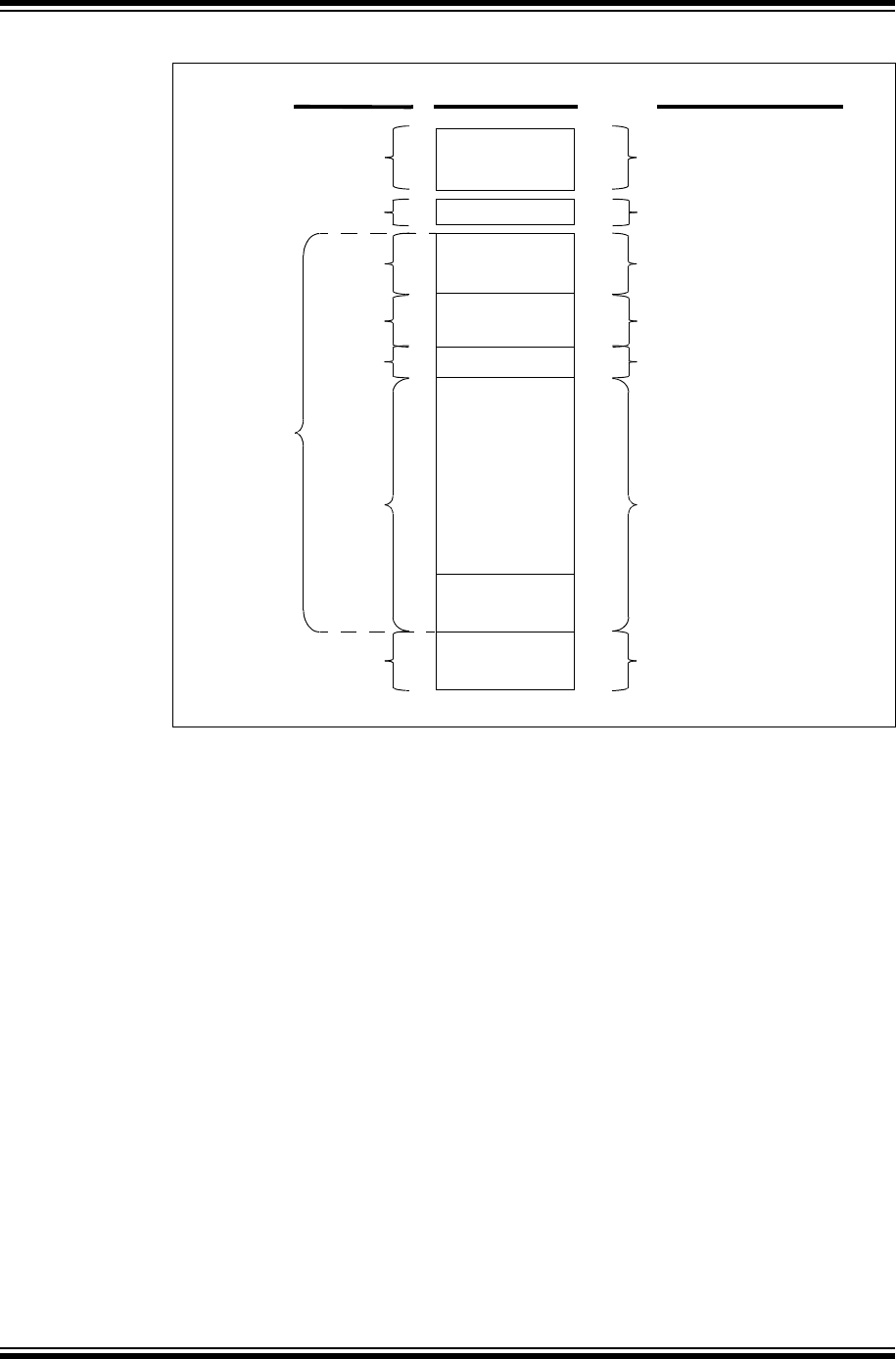
PIC32 Family Reference Manual
DS60001155C-page 35-44 © 2009-2013 Microchip Technology Inc.
Figure 35-2: Ethernet Frame Format
35.4.1.1 START OF STREAM/PREAMBLE AND START-OF-FRAME DELIMITER
When transmitted on the Ethernet medium, the Start-of-Stream/Preamble and the SFD fields are
appended to the beginning of an Ethernet frame automatically by the MAC.
When receiving, these fields are automatically stripped from the received frames so that these
fields are not written into the RX data buffers. The software does not need to process/generate
these fields.
35.4.1.2 DESTINATION MAC ADDRESS
A MAC address is a 6-byte number representing the physical address of the node(s) on an
Ethernet network. The destination address contains the MAC address of the device for which the
frame is intended. There are different types of addresses in the Ethernet space.
For example,
• Unicast Address: Designated for usage by the addressed node only. A Unicast address is
an address where the Least Significant bit (LSb) in the first byte of the address is zero (i.e.,
the first byte of the address is even). For example, 00 04 a3 00 00 01 is a Unicast address,
but 01 04 a3 00 00 01 is not a Unicast address.
•Multicast Address: Designated for use by a selected group of Ethernet nodes. A Multicast
address is an address where the LSb in the first byte of this address is set (i.e., the byte is
odd). For example, 01 04 a3 00 00 01 is a Multicast address. The Multicast address,
FF-FF-FF-FF-FF-FF, is reserved (Broadcast address) and is directed to all nodes on the
network.
The Ethernet Controller incorporates the Receive Filter module that can be configured to accept
or discard Unicast, Multicast and Broadcast frames. For more information on the receive filters,
refer to 35.4.8 “Receive Filtering Overview”.
Filtered out by the module
Start of-Frame Delimiter
(filtered out by the module)
Destination address such as:
Multicast, Broadcast, or Unicast
Source Address
Type of packet or the length
Packet Payload
(with optional padding)
Frame Check Sequence – CRC
Start-of-Stream/
Preamble
SFD
DA
SA
Type/Length
Data
Padding
FCS
7
1
6
6
2
46-1500
4
Used in the
calculation of
FCS
Number of Bytes Field Comments
of the packet

© 2009-2013 Microchip Technology Inc. DS60001155C-page 35-45
Section 35. Ethernet Controller
Ethernet Controller
35
35.4.1.3 SOURCE MAC ADDRESS
The source address is the 6-byte field MAC address of the node that transmitted the Ethernet
frame. Every Ethernet device must have a globally unique MAC address. Each PIC32 including
an Ethernet Controller has a unique address, which is loaded into the MAC registers on
power-up. This value can be used as is, or the registers may be reconfigured with a different
address at run time by modifying the EMAC1SA0, EMAC1SA1, and EMAC1SA2 registers.
35.4.1.4 TYPE/LENGTH
This is a 2-byte field indicating the protocol to which the frame belongs. Applications using
standards such as Internet Protocol (IP) or Address Resolution Protocol (ARP), should use the
type code specified in the specific standards document. Alternately, this field can be used as a
length field when the user is implementing proprietary network protocols. Typically, any value of
1500 (0x05DC) or smaller, is considered to be a length field and specifies the amount of
non-padding data, which follows in the data field.
35.4.1.5 DATA
The data field typically consists of between 0 byte and 1500 bytes of payload data for each frame.
PIC32 devices are capable of transmitting and receiving frames larger than this when the Huge
Frame Enable bit (HUGEFRM) in the Ethernet Controller MAC Configuration 2 Register
(EMAC1CFG2<2>) is set. However, these larger frames that do not meet the IEEE 802.3
Specification will likely be dropped by most Ethernet nodes.
35.4.1.6 PADDING
The padding field is a variable length field appended to meet the IEEE 802.3 Specification
requirements when transmitting small data payloads. The minimum payload for an Ethernet
frame is 46 bytes. Smaller frames must be padded to fill this space. For transmitted frames, the
software can instruct the Ethernet Controller to automatically generate the required padding by
using the Pad/CRC Enable bit, PADENABLE (EMAC1CFG2<5>), the VLAN Pad Enable bit,
VLANPAD (EMAC1CFG2<6>), and the Auto Detect Pad Enable bit,
AUTOPAD (EMAC1CFG2<7>). However, if the auto-padding is not enabled and the application
does not provide appropriate padding, the PIC32 device will not prevent the transmission of
these “runt” frames. When receiving frames, PIC32 devices accept and write all padding to the
receive buffer. Frames shorter than the required 64 bytes can optionally be filtered by the Runt
Error Reject filter, as described in 35.4.8.4 “Runt Rejection Filter”.
35.4.1.7 FRAME CHECK SEQUENCE
The Frame Check Sequence (FCS) is a 4-byte field containing a standard 32-bit CRC calculated
over the Destination, Source, Type/Length, Data, and Padding fields. It allows for the detection
of transmission errors.
For transmitted frames, PIC32 devices can automatically generate and append a valid Flow
Control by using the CRC Enable1 bit, CRCENABLE (EMAC1CFG2<4>). Otherwise, the
software must calculate the CRC for the frame to be transmitted and append it properly.
For received frames, the FCS field is stored to the receive buffer. Frames with invalid CRC values
can either be discarded or accepted using the CRC Error and CRC Check Acceptance filters
described in 35.4.8.1 “CRC Error Acceptance Filter” and 35.4.8.3 “CRC Check Acceptance
Filter”.
Note: The polynomial for generating the FCS is:
G(x) = x32 + x26 + x23 + x22 + x16 + x12 + x11 + x10 + x8 + x7 + x5 +x4 + x2 + x + 1.
The FCS is transmitted starting with bit 31 and ending with bit 0.

PIC32 Family Reference Manual
DS60001155C-page 35-46 © 2009-2013 Microchip Technology Inc.
35.4.2 Basic Ethernet Controller Operation
The Ethernet Controller is enabled by setting the Ethernet ON bit in the Ethernet Controller
Control 1 Register (ETHCON1<15>), and is disabled by resetting the same bit. This is the default
state after any Reset. If the Ethernet Controller is disabled, all of the I/O pins used for the
MII/RMII and MIIM interfaces operate as port pins, and are under the control of the respective
PORT latch bit and TRIS bit.
Disabling the controller resets the internal DMA state machines, and all transmit and receive
operations are aborted. The SFRs are still accessible and their values preserved.
Clearing the ON bit while the Ethernet Controller is active will abort all pending operations and
reset the peripheral, as defined above.
Re-enabling the ON bit will restart the Ethernet Controller in its clean reset state while preserving
the SFRs values.
35.4.3 MAC Overview
The MAC sub-layer is part of the functionality described in the Open Systems
Interconnection (OSI) model for the Data Link Layer. It defines a medium independent facility,
built on the medium dependent physical facility provided by the Physical Layer, and under the
access-layer-independent LLC sub-layer or other MAC client. It is applicable to a general class
of local area broadcast media suitable for use with the Carrier Sense Multiple Access with
Collision Detection (CSMA/CD).
The CSMA/CD MAC sub-layer provides services to the MAC client required for the transmission
and reception of frames. The CSMA/CD MAC sub-layer makes best effort to acquire the medium,
and transfer a serial stream of bits to the Physical Layer. Although, certain errors are reported to
the client, error recovery is not provided by the MAC.
The following is a summary of the functional capabilities of the CSMA/CD MAC sub-layer, see
Figure 35-3:
• For Frame transmission:
- Accepts data from the MAC client and constructs a frame
- Presents a bit-serial data stream to the Physical Layer for transmission on the medium
-In Half-Duplex mode, defers transmission of a bit-serial stream whenever the physical
medium is busy
-It can append proper FCS value to outgoing frames and verifies full byte boundary
alignment
- Delays transmission of frame bit-stream for specified Interframe Gap (IFG) period
-In Half-Duplex mode, halts transmission when collision is detected
- In Half-Duplex mode, schedules retransmission after a collision until a specified retry
limit is reached
-In Half-Duplex mode, enforces collision to ensure propagation throughout network by
sending jam message
- Adds preamble and Start-of-Frame Delimiter and appends FCS to all frame
- Appends PAD field for frames whose data length is less than the minimum value
Note 1: If the ON bit is cleared during an active internal bus transaction, the controller will
complete the current bus transaction before entering the disabled state. Once the
controller is disabled, the Transmit Busy bit (TXBUSY) in the Ethernet Controller
Status Register (ETHSTAT<6>) and the Receive Busy bit, RXBUSY
(ETHSTAT<5>), will reflect an inactive status.
2: Whenever the Ethernet Controller is reset through the ON bit, the software should
also reset the external PHY using the MIIM interface. This ensures the PHY is in a
known initialized state. In addition, the MAC should also be soft reset through the
Ethernet Controller MAC Configuration 1 Register (EMAC1CFG1).
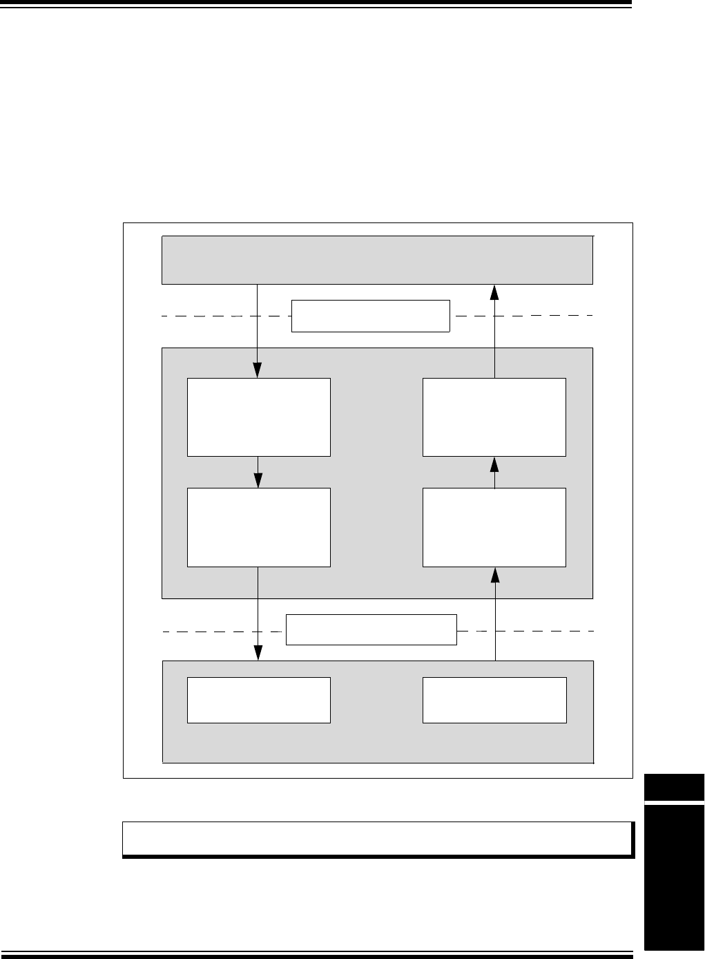
© 2009-2013 Microchip Technology Inc. DS60001155C-page 35-47
Section 35. Ethernet Controller
Ethernet Controller
35
•For Frame reception:
-Receives a bit-serial data stream from the Physical Layer
- Presents the received frames to the MAC client (broadcast, multicast, unicast frames,
and so on)
-Checks incoming frames for transmission errors by way of FCS, and verifies byte
boundary alignment
-Removes preamble, Start-of-Frame Delimiter and PAD field (if necessary) from the
received frames
-Implements the MII Management block that provides control/status connection to the
external PHY
Figure 35-3: CSMA/CD Media Access Control Functions
The MAC is accessed using Register 35-23 through Register 35-30 and Register 35-37 through
Register 35-39 SFRs.
Note: Refer to Clause 2, Clause 3, and Clause 4 of the IEEE 802.3 Specification for a
detailed explanation of the MAC sub-layer functions and operation.
Physical Layer Signaling
Receive
Data Decoding
Transmit
Data Encoding
Access to Physical Interface
Receive Media
Access Management
Transmit Media
Access Management
Transmit
Data Encapsulation
Receive
Data Decapsulation
Access to MAC Client
MAC Client Sub-Layer

PIC32 Family Reference Manual
DS60001155C-page 35-48 © 2009-2013 Microchip Technology Inc.
35.4.4 Media Independent Interface
The Media Independent Interface (MII) is a standard interconnection between the MAC and the
PHY for communicating TX and RX frame data.
The MII has the following important characteristics:
• Capable of supporting 10/100 Mbps rates for data transfer, and offers support for
management functions
•Provides independent four bit wide transmit and receive data paths
•Uses Transistor-Transistor Logic (TTL) signal levels, compatible with common digital
Complementary Metal-oxide Semiconductor (CMOS) processes
• Provides Full-Duplex operation
In 10 Mbps mode, the MII runs at 2.5 MHz; in 100 Mbps mode, it runs at 25 MHz. PHYs that
provide MII are not required to support both data rates, and may support either one or both.
Tabl e 35-4 provides a list of the 18 MII signals.
Table 35-4: MII Signals
Signal
Name
IEEE
802.3 MII
Signals
Width Type Description
ETXCLK TX_CLK 1Input The transmit clock signal is a continuous clock that provides the timing
reference for the transfer of the ETXEN, ETXD and ETXERR signals from
the MAC to the PHY. The ETXCLK frequency is a quarter of the nominal
transmit data rate. A PHY operating at 100 Mbps must provide a ETXCLK
frequency of 25 MHz, and a PHY operating at 10 Mbps must provide a
ETXCLK frequency of 2.5 MHz.
ERXCLK RX_CLK 1Input The receive clock signal is a continuous clock that provides the timing
reference for the transfer of the ERXDV, RXD and ERXERR signals from
the PHY to the MAC. ERXCLK has a frequency equal to a quarter of the
data rate of the received signal.
ETXEN TX_EN 1Output The transmit enable signal indicates that the MAC is presenting nibbles on
the MII for transmission. ETXEN transitions synchronously with respect to
ETXCLK.
ETXD<3:0> TXD<3:0> 4Output The transmit data signals transition synchronously with respect to the
ETXCLK.
ETXERR TX_ER 1Output The transmit coding error signal is synchronous with respect to the
ETXCLK. When ETXERR is asserted for one or more ETXCLK periods
while ETXEN is also asserted, the PHY will emit one or more symbols that
are not part of the valid data or delimiter set somewhere in the frame being
transmitted. This signal only affects 100 Mbps data transmission.
ERXDV RX_DV 1Input The receive data valid signal indicates that the PHY is presenting
recovered and decoded nibbles on the RXD data lines. ERXDV is
synchronous with ERXCLK. ERXDV remains asserted for the entire frame.
ERXD<3:0> RXD<3:0> 4Input The receive data signals represents the four data signals synchronous
with respect to ERXCLK. For each ERXCLK period in which ERXDV is
asserted, RXD<3:0> transfers four bits of recovered data from the PHY to
the MAC.
ERXERR RX_ER 1Input The receive error signal is asserted to indicate to the MAC that a cod ing
error (or any error that the PHY is capable of detecting) has occurred in
the frame being transferred from the PHY to the MAC. ERXERR is
synchronous with ERXCLK.
ECRS CRS 1Input The Carrier Sense signal is asserted by the PHY when either the transmit
or receive medium is non idle. Carrier Sense (CRS) will be deasserted by
the PHY when both the transmit and receive media are idle. The CRS
remains asserted throughout the d uration of a collision condition. It does
not have to be synchronous with either the ETXCLK or the ERXCLK.

© 2009-2013 Microchip Technology Inc. DS60001155C-page 35-49
Section 35. Ethernet Controller
Ethernet Controller
35
Refer to Clause 22 of the IEEE 802.3 Specification for detailed MII specifications.
Figure 35-4 illustrates a typical MII connection between the PIC32 and the external PHY.
Figure 35-4: PIC32 to External PHY Typical MII Connection
ECOL COL 1Input The collision detected signal is asserted by the PHY upon detection of a
collision on the medium, and remains asserted while the collision condition
persists. It does not have to be synchronous with respect to either
ETXCLK or ERXCLK.
EMDC MDC 1Output The management data clock signal is part of the MII Management
interface, and is explained in 35.4.6 “Media Independent Interface
Management (MIIM)”.
EMDIO MDIO 1Input/
Output
The management data input/output signal is part of the MII Management
interface, and is explained in 35.4.6 “Media Independent Interface
Management (MIIM)”.
Table 35-4: MII Signals (Continued)
Signal
Name
IEEE
802.3 MII
Signals
Width Type Description
PIC32 with
Ethernet Controller
MII
External PHY
EMDC
EMDIO
MII
Management
Interface
ETXCLK
ERXCLK
ETXEN
ETXD<3:0>
ETXERR
ERXDV
ERXD<3:0>
ERXERR
ECRS
ECOL
Media
Independent
Interface

PIC32 Family Reference Manual
DS60001155C-page 35-50 © 2009-2013 Microchip Technology Inc.
35.4.5 Reduced Media Independent Interface (RMII)
The management interface (MDIO/MDC) is assumed to be identical to that defined in MII.
The RMII has the following characteristics:
• Capable of supporting 10 Mbps and 100 Mbps data rates
•Single clock reference for both MAC and the PHY (can be sourced from the MAC or from
an external source)
•Provides independent two bit wide transmit and receive data paths
• Uses TTL signal levels, compatible with common digital CMOS processes
• Provides Full-Duplex operation
The interface runs at 50 MHz. Tab l e 35-5 provides a list of the 10 Reduced Media Independent
Interface (RMII) signals.
Table 35-5: RMII Signals
Signal
Name
IEEE 802.3
RMII Signals Width Type Description
EREFCLK REF_CLK 1Input The reference clock signal is a continuous clock that provides the
timing reference for ECRSDV, RXD<1:0>, ETXEN, ETXD<1:0> and
ERXERR. EREFCLK is a 50 MHz clock signal sourced by the MAC or
an external source. For PIC32 devices, the EREFCLK is an external
supplied clock signal.
ECRSDV CRS_DV 1Input The Carrier Sense/Receive Data Valid signal is asserted by the PHY
when the receive medium is non idle. ECRSDV is asserted
asynchronously on detection of carrier. Loss of carrier results in the
deassertion of ECRSDV synchronous to the REF_CLK (only on nibble
boundaries). The data on RXD<1:0> is considered valid once
ECRSDV is asserted. Using the ECRSDV the MAC can accurately
recover ERXDV and CRS. If ERXERR is asserted while ECRSDV is
asserted, the frame will be rejected. If the ECRSDV is not asserted,
the ERXERR is ignored.
ERXD<1:0> RXD<1:0> 2Input The receive data signals transition synchronously to EREFCLK. For
each clock period in which ECRSDV is asserted, ERXD transfers two
bits of recovered data from the PHY.
•ERXD is ‘00’ to indicate the idle condition when ECRSDV is
deasserted. Since the use of the PHY signal ERXERR is optional,
in order to ensure the propagation of errors for the received
signal, the ERXD replaces the data in the decoded stream with
‘01’ so that the MAC CRC mechanism will reject the frame.
• In 100 Mbps ERXD is synchronous to the EREFCLK
• In 10 Mbps the ERXD is sampled every tenth cycle
ETXEN TX_EN 1Output The transmit enable signal indicates that the MAC is presenting di-bits
on ETXD<1:0> for transmission. ETXEN is asserted with the first
nibble of the preamble and remains asserted while all di-bits are
transmitted. ETXEN is synchronous with respect to EREFCLK.
ETXD<1:0> TXD<1:0> 2Output The transmit data signal is transmits data to the PHY when ETXEN is
asserted. The ETXD data lines transition synchronously with respect
to EREFCLK. ETXD uses the value of ‘00’ to signal idle when the
ETXEN is deasserted.
• In 100 Mbps mode, ETXD provides valid data for each EREFCLK
period while ETXEN is asserted
• In 10 Mbps mode since the EREFCLK frequency is 10 times the
data rate the value on ETXD is sampled every tenth cycle

© 2009-2013 Microchip Technology Inc. DS60001155C-page 35-51
Section 35. Ethernet Controller
Ethernet Controller
35
Figure 35-5 illustrates a typical RMII connection between the PIC32 and the external PHY.
Figure 35-5: PIC32 to External PHY Typical RMII Connection
ERXERR RX_ER 1Input The receive error signal is asserted for one or more EREFCLK periods
to indicate that an error was detected somewhere in the frame
presently being transferred from the PHY. The ERXERR is
synchronous with respect to EREFCLK.
EMDC MDC 1Output The management data clock signal is part of the MII Management
interface and is explained in 35.4.6 “Media Independent Interface
Management (MIIM)”.
EMDIO MDIO 1Input/
Output
The management data input/output signal is part of the MII
Management interface and is explained in 35.4.6 “Media
Independent Interface Management (MIIM)”.
Table 35-5: RMII Signals (Continued)
Signal
Name
IEEE 802.3
RMII Signals Width Type Description
PIC32 with
Ethernet Controller
RMII
External PHY
EMDC
EMDIO
RMII
Management
Interface
EREFCLK
ETXEN
ETXD<1:0>
ERXD<1:0>
ERXERR
ECRSDV
Reduced
Media
Independent
Interface
External ClockSource

PIC32 Family Reference Manual
DS60001155C-page 35-52 © 2009-2013 Microchip Technology Inc.
35.4.6 Media Independent Interface Management (MIIM)
The Media Independent Interface Management (MIIM) module provides a serial communication
link between the PIC32 host and an external MII PHY device. The external serial
communications link operates in accordance with Clause 22 of the IEEE 802.3 Specification.
The MIIM input/output signals are:
•Management Data Clock (MDC) – MDC is sourced by the MAC to the PHY as the timing
reference for transfer of information on the MDIO signal.
•Management Data Input/Output (MDIO) – MDIO is a bidirectional signal between the PHY
and the MAC. It is used to transfer control information and status between the PHY and the
MAC. Control information is driven by the MAC synchronously with respect to MDC and is
sampled synchronously by the PHY. Status information is driven by the PHY synchronously
with respect to MDC and is sampled synchronously by the MAC.
The communication over the MIIM interface takes place in frames. Frames transmitted on the
MIIM have the following structure (see Ta ble 35-6):
• Preamble: At the beginning of each transaction, the MAC sends a sequence of 32 logic one
bits on MDIO to provide the PHY with a synchronization pattern.
• SOF: The SOF is indicated by a <01> pattern
•Operation Code: <10> for a read transaction, <01> for a write transaction
• PHY Address: Five bits, allowing 32 unique PHY addresses. A PHY will always respond to
transactions with address zero.
• Register Address: Five bits, allowing 32 individual registers to be addressed within each PHY
• Turnaround: A 2-bit-time spacing between the Register Address field and the Data field of a
management frame to avoid contention during a read transaction.
•Data: This 16-bit field carries the data to/from the addressed PHY register
Table 35-6: MIIM Frame Format
As indicated previously, the size of an MIIM frame is 64 bits. However, the MIIM module may be
configured to suppress the preamble portion of the MII Management serial stream using the
Suppress Preamble bit (NOPRE) in the Ethernet Controller MAC MII Management Configuration
Register (EMAC1MCFG<1>), when the PHY supports a suppressed preamble operation.
Refer to Clause 22 in the IEEE 802.3 Specification for more information on MIIM.
35.4.6.1 EXTERNAL PHY REGISTER ACCESS
The PHY registers provide configuration and control of the PHY module, and status information
about its operation. Unlike the on-chip SFRs, the PHY registers are not directly accessible
through the SFR control interface. Instead, access is accomplished through a special set of MAC
control registers that implement the Media Independent Interface Management. These control
registers are referred to as the MIIM registers. The PHY registers are accessed through the MIIM
interface of the MAC. To do this, the MII Management Command, Address, and Data registers in
the MAC must be used.
The registers that control access to the PHY registers are listed in Ta b l e 35-1, and include
Register 35-31 through Register 35-36.
Note: The Idle condition on MDIO is a high-impedance state.
Operation
Management Frame Fields
PRE ST OPCODE PHYAD REGAD TA DATA IDLE
READ 1….1 01 10 a0…a4 r0…r4 Z0 d0….d15 Z
WRITE 1….1 01 01 a0…a4 r0…r4 10 d0….d15 Z

© 2009-2013 Microchip Technology Inc. DS60001155C-page 35-53
Section 35. Ethernet Controller
Ethernet Controller
35
35.4.6.2 INITIALIZING THE MII MANAGEMENT MODULE
For the MAC MIIM module to create the interface clock (MDC) frequency, t he clock speed must
be configured. The MIIM module uses the SYSCLK as an input clock.
Use the MII Management Clock Select 1 bits, CLKSEL<3:0> (EMAC1MCFG<5:2>) to select the
divider for creating the MDC clock signal, which the IEEE 802.3 Specification defines to be no
faster than 2.5 MHz. However, some PHYs support clock rates up to 12.5 MHz.
35.4.6.3 READING A PHY REGISTER
When a PHY register is read through the MAC, the entire 16 bits are obtained.
To r ead fr om a PHY re gis ter, f ol low the se ste ps :
1. Write the address of the PHY and of the PHY register to read from into the Ethernet
Controller MAC MII Management Address Register (EMAC1MADR).
2. Set the MII Management Read Command bit (READ) in the Ethernet Controller MAC MII
Management Command Register (EMAC1MCMD<0>). The read operation begins and
the MII Management Busy bit (MIIMBUSY) in the Ethernet Controller MAC MII
Management Indicators Register (EMAC1MIND<0>), will be set after three SYSCLK
periods (this is due to the internal pipeline of the MIIM interface).
3. Poll the MIIMBUSY bit to be certain that the operation is complete (the operation time is
the one needed to transfer a full MIIM frame). While MIIM is busy, the software should not
start any MII scan operations or write to the Ethernet Controller MAC MII Management
Write Data Register (EMAC1MWTD). When the MAC has obtained the register contents,
the MIIMBUSY bit will clear itself.
4. Clear the READ bit (EMAC1MCMD<0>).
5. Read the desired data from the Ethernet Controller MAC MII Management Write Data
Register (EMAC1MRDD).
35.4.6.4 WRITING A PHY REGISTER
When a PHY register is written to, all of the 16 bits are written at once; selective bit writes are not
implemented. If it is necessary to only reprogram select bits in the register, the software must first
read the PHY register, modify the resulting data, and then write the data back to the PHY register.
To w rit e to a PH Y r egi ste r, fo llo w t hes e s teps:
1. Write the address of the PHY and of the PHY register to read from into the EMAC1MADR
register.
2. Write the 16 bits of data to be written into the EMAC1MWTD register. Writing to this
register automatically begins the MIIM transaction, which causes the MIIMBUSY bit to be
set after three SYSCLK periods, this is due to the internal pipeline of the MIIM interface.
3. Poll the MIIMBUSY bit until it is cleared, which indicates the write has completed.
4. The PHY register will be written after the MIIM operation completes, which takes a MIIM
frame time. When the write operation has completed, the MIIMBUSY bit will clear itself.
The software should not start any MII scan or read operations while busy.
Note: All PHY chip registers are treated as 16 bits in width. Writes to unimplemented
locations are ignored, and any attempts to read these locations will return ‘0’. All
reserved locations should be written as ‘0’; their contents should be ignored when
read. Refer to the vendor-specific PHY data sheet for register access information.

PIC32 Family Reference Manual
DS60001155C-page 35-54 © 2009-2013 Microchip Technology Inc.
35.4.6.5 SCANNING A PHY REGISTER
The MAC can be configured to perform automatic back-to-back read operations on a PHY
register. This can significantly red uce the software complexity when periodic status information
updates are desired.
To perform the scan operation, follow these steps:
1. Write the address of the PHY, and of the PHY register to be read from, into the
EMAC1MADR register.
2. Set the MII Management Scan Mode bit, SCAN (EMAC1MCMD<1>). The scan operation
begins and the MIIMBUSY bit is set.
3. The first read operation will complete after the first MIIM frame is transferred. Subsequent
reads will be done at the same interval until the operation is canceled. The MII
Management Read Data Not Valid bit, NOTVALID (EMAC1MIND<2>), may be polled to
determine when the first read operation is complete. Read the scanned register data from
the EMAC1MRDD register.
4. After setting the SCAN bit, the EMAC1MRDD register will be updated automatically every
MIIM frame interval. There is no status information, which can be used to determine when
the EMAC1MRDD register is updated.
5. When the MIIM scan operation is in progress, the software must not attempt to write to the
EMAC1MWTD register or start a read operation.
6. The MIIM scan operation can be cancelled by clearing the SCAN bit, and then polling the
MIIMBUSY bit. New operations may be started after the MIIMBUSY bit is cleared.
Example 35-1 provides example code for a MIIM initialization and PHY register read, write, and
scan.
Example 35-1: MIIM Initialization and PHY Access
// Assume we're running at 80 MHz and we're working with a PHY that supports a maximum
// 2.5 MHz MIIM frequency
#include <p32xxxx.h>
#define PHY_ADDRESS 0x1f // the address of the PHY
EMAC1MCFG=0x00008000; // issue reset
EMAC1MCFG=0; // clear reset
EMAC1MCFG=(0x8)<<2; // program the MIIM clock, divide by 40
// read the basic status PHY register: 1
unsigned int phyRegVal;
while(EMAC1MIND&0x1); // wait not busy
EMAC1MADR=0x1|((PHY_ADDRESS)<<8); // set the PHY and register address
EMAC1MCMD=1; // issue the read order
__asm__ __volatile__ (“nop; nop; nop;”); // wait busy to be set
while(EMAC1MIND&0x1); // wait op complete
EMAC1MCMD=0; // clear command register
phyRegVal=EMAC1MRDD; // read the selected register
// write the basic control PHY register: 0
while(EMAC1MIND&0x1); // wait in case of some previous operation
EMAC1MADR=0x0|((PHY_ADDRESS)<<8); // set the PHY and register address
EMAC1MWT=0x8000; // issue the write order (PHY reset)
__asm__ __volatile__ (“nop; nop; nop;”); // wait busy to be set
while(EMAC1MIND&0x1); // wait write complete
// Make sure data has been written
// Perform a scan of the status PHY register: 1
// Start the scan
while(EMAC1MIND&0x1); // wait in case of some previous operation
EMAC1MADR=0x1|((PHY_ADDRESS)<<8); // set the PHY and register address
EMAC1MCMD=0x2; // issue the scan order
// Read the status register
// Note that the read can occur now at any time
// without previously selecting the read operation and the register
while(EMAC1MIND&0x4); // wait data valid
phyRegVal=EMAC1MRDD; // read the scanned register
// After some time we decide to stop the scan operation
EMAC1MCMD=0; // cancel scan

© 2009-2013 Microchip Technology Inc. DS60001155C-page 35-55
Section 35. Ethernet Controller
Ethernet Controller
35
35.4.7 Flow Control Overview
Ethernet Flow Control can send and receive PAUSE frames, which cause the receiving node to
stop transmitting for a specific time.
On the transmit side, the Flow Control block handles the hardware handshaking between the
MAC and the CPU when the transmit Flow Control is enabled. Flow Control for the received
packets is part of the MAC functionality.
The PIC32 MAC supports Symmetric PAUSE and Asymmetric PAUSE, as described in Clause
28, Table 28B-2, and Clause 31 and Annex 31B of the IEEE 802.3 Specification.
The Flow Control block supports two modes of operation: manual and automatic. In addition, the
mode of transmission (Full-Duplex or Half-Duplex) programmed into the MAC registers, is used
by the Flow Control block.
Before software can throttle-down incoming packets, it must enable Flow Control. The Flow
Control mechanism operates d ifferently between Full-Duplex and Half-Duplex mode.
35.4.7.1 FULL-DUPLEX
On the transmit side, the MAC will send a PAUSE control frame with a PAUSE timer value. The
receiving MAC decodes the control frame, extracts the PAUSE timer value and stalls
transmission for the designated time. This does not imply the transmitting device will pause
immediately. There is latency in the activation of the pause mechanism. If Flow Control is to be
deactivated before the PAUSE timer value expires, another PAUSE frame can be sent that
encodes a value of 0x0000 for the PAUSE timer value.
At the receiving node, if the MAC receives a PAUSE frame transmitted by another device, the
receiving node's transmit operation is inhibited until the PAUSE timer expires or the other device
cancels the request for PAUSE frames.
35.4.7.2 HALF-DUPLEX
When the software enables the Flow Control, the Flow Control block requests the MAC to apply
back-pressure. The MAC will continue sending a preamble pattern on the transmit line to prevent
any other device from gaining control of the bus. This will continue until Flow Control is disabled.
35.4.7.3 MANUAL FLOW CONTROL
The manual Flow Control is enabled through the Manual Flow Control bit, MANFC
(ETHCON1<4>). When manual Flow Control is enabled, the MAC sends PAUSE control frames
using the value of the PAUSE Timer Value bits, PTV<15:0> (ETHCON1<31:16>). When transmit
Flow Control is disabled, the MAC will send another PAUSE frame that encodes a value of
0x0000 for the PAUSE timer value to disable the Flow Control.
Note: The software should not change the Full-Duplex or Half-Duplex mode of operation,
while the transmit logic is in the middle of transmitting a package.
Note: A PAUSE frame includes the period of pause time being requested, in the range of
0 through 65535. The pause time is measured in units of pause “quanta”, where
each unit is equal to 512 bit times.

PIC32 Family Reference Manual
DS60001155C-page 35-56 © 2009-2013 Microchip Technology Inc.
35.4.7.4 AUTOMATIC FLOW CONTROL
The automatic Flow Control is enabled through the Automatic Flow Control bit, AUTOFC
(ETHCON1<7>). When automatic Flow Control is enabled, the PAUSE control frames are sent
by hardware based on the current value of the Packet Buffer Count bits, BUFCNT<7:0>
(ETHSTAT<23:16>).
The PAUSE control frames are framed based on the value in the Receive Watermark bits:
•When the BUFCNT value reaches the value specified by the Receive Full Watermark bits
(RXFWM<7:0>) in the Ethernet Controller Receive Watermarks Register
(ETHRXWM<23:16>), a PAUSE frame is automatically sent every 512/2 * PTV<15:0>
(ETHCON1<31:16>) bit transmit clock cycles.
•When the BUFCNT value reaches the value specified by the Receive Empty Watermark
bits, RXEWM<7:0> (ETHRXWM<7:0>), a PAUSE frame with the MAC with the PTV set to
0x0000.
The BUFCNT value is only updated on a packet boundary; therefore, all automatic Flow Control
changes occur on packet boundaries. When automatic Flow Control is enabled, it has the highest
priority for setting and clearing Flow Control operations. Therefore, it is not recommended to mix
automatic and manual Flow Control.
To m anu all y t ra n sm i t a PA USE fr am e, fol low t hes e s teps:
1. In the initialization sequence, software sets the PAUSE value by writing the PTV<15:0>
bits (ETHCON1<31:16>).
2. Software writes the MANFC bit (ETHCON1<4>) to manually start the transmission of a
PAUSE frame.
3. The Flow Control block will request the MAC to send a PAUSE frame.
4. The MAC will assemble the complete Flow Control frame as follows:
•Preamble
•Start-of-Frame Delimiter (SFD)
•Destination Address = 01-80-c2-00-00-01 (Special PAUSE multicast address)
• Source Address = Station Address from EMAC1SA0-EMAC1SA3 registers
•Length = 0x8088 (Control Frame)
• Payload: Opcode (2 bytes) = 0x0001, PAUSE Value (2 bytes) = PTV
•Pad
•FCS
Note 1: The transmit clock cycle is 10 MHz or 100 MHz depending on the current MAC
speed selection: 10 Mbps or 100 Mbps.
2: Software must ensure that the Flow Control watermark values allow the PAUSE
frames to be sent when the amount of free space allocated by the free RX
descriptors drops below two times maximum Ethernet frame size (i.e., 1536 * 2).
This will ensure there is no receive overflow conditions.
3: The PTV value may only be changed when the operation is not enabled
ETHCON1<15> = 0.

© 2009-2013 Microchip Technology Inc. DS60001155C-page 35-57
Section 35. Ethernet Controller
Ethernet Controller
35
Example 35-2 shows example code for using manual Flow Control.
Example 35-2: Using Manual Flow Control Code
35.4.8 Receive Filtering Overview
The Receive Filter (RXF) block examines all incoming receive packets and accepts or rejects the
packet based on the user selectable filters. The following RX filters are supported:
•CRC Error Acceptance Filter controlled by the CRC Error Collection Enable (CRCERREN) bit
in the Ethernet Controller Receive Filter Configuration Register (ETHRXFC<7>)
•Runt Error Acceptance Filter controlled by the Runt Error Collection Enable bit, RUNTERREN
(ETHRXFC<5>)
• CRC Check Rejection Filter controlled by the CRC Okay Enable bit, CRCOKEN
(ETHRXFC<6>)
• Runt Rejection Filter controlled by the Runt Enable bit, RUNTEN (ETHRXFC<4>)
•Unicast Acceptance Filter controlled by the Unicast Enable bit, UCEN (ETHRXFC<3>)
• Not Me Unicast Acceptance Filter controlled by the Not Me Unicast Enable bit, NOTMEEN
(ETHRXFC<2>)
•Multicast Acceptance Filter controlled by the Multicast Enable bit, MCEN (ETHRXFC<1>)
•Broadcast Acceptance Filter controlled by the Broadcast Enable bit, BCEN (ETHRXFC<0>)
•Hash Table Acceptance Filter controlled by the Enable Hash Table Filtering bit, HTEN
(ETHRXFC<15>)
•Magic Packet Acceptance Filter controlled by the Magic Packet™ Enable bit, MPEN
(ETHRXFC<14>)
•Pattern Match Acceptance Filter with logical inversion controlled by the Pattern Match Mode
bits, PMMODE<3:0> (ETHRXFC<11:8>), and the Pattern Match Inversion bit, NOTPM
(ETHRXFC<12>)
The order of the filters listed above specifies the priority of the filter from highest-to-lowest, such
that if a filter is enabled and accepts or rejects a packet, all lower priority filters will have no effect.
For example, if the Runt Error Acceptance Filter is enabled and a packet of less than 64 bytes is
received, it will always be accepted even if the CRC check fails.
If a received packet is not explicitly accepted or discarded by an enabled filter, the packet will be
discarded by default. Due to the internal design of the RX Filter, the final accept versus abort
decision for an Ethernet frame is made at the end of the frame.
When a packet is received, the RSV for each receive packet contains information about which
filters matched the corresponding RX packet, regardless of whether these filters were active at
the time. This provides extra “status” information about the packet that may be used to filter
packets in software. For example, in Promiscuous mode, the Magic Packet Filter RSV bit (see
Offset 8, RXF_RSV<3> in Tabl e 35-8) may be used to quickly identify a magic packet without the
need to examine the frame contents. Figure 35-9 illustrates information about the RSV.
Note: Each filter is either an Acceptance filter or a Rejection filter. Acceptance filters force
the acceptance of a packet, while Rejection filters force the rejection of a packet.
// NOTE: Setting the new PTV value should be done only when the peripheral
// is not enabled
#include <p32xxxx.h>
ETHCON1CLR=0xffff0000; // clear PTV
ETHCON1SET=(ptvVal)<<16; // set the new PTV value
/*....*/
ETHCON1SET=0x10; // turn on the Manual Flow Control at this moment PAUSE
// Frames are being sent or back-pressure is applied
// do some other things
// manage/retrieve all the received packets so far
// ...
// ...
ETHCON1CLR=0x10; // disable the Manual Flow Control

PIC32 Family Reference Manual
DS60001155C-page 35-58 © 2009-2013 Microchip Technology Inc.
All filter settings are done using the ETHRXFC register. Due to synchronization in the RXF block,
Register 35-5 through Register 35-10 and Register 35-37 through Register 35-39 should not be
changed while the ON bit (ETHCON1<15>) is set. To change one or more of these registers or
their bits, you must first clear the ON bit.
The following sub-sections provide summary of each receive filter.
35.4.8.1 CRC ERROR ACCEPTANCE FILTER
This filter is used to explicitly accept packets that fail the CRC check. If enabled, all packets that
fail the CRC check are accepted, regardless of whether the CRC Check Filter is enabled or not.
35.4.8.2 RUNT ERROR ACCEPTANCE FILTER
This filter is used to explicitly accept packets that fail the Runt check. If enabled, all packets that
fail the Runt check are accepted, regardless of whether or not the Runt Filter is enabled.
35.4.8.3 CRC CHECK ACCEPTANCE FILTER
If enabled, results of the MAC CRC check will be examined and used to filter the packet. If this
filter is enabled and fails, the packet will be aborted. Conversely, if CRC checking is not enabled,
the received packet’s CRC is ignored and is not used as an acceptance requirement for the
packet.
35.4.8.4 RUNT REJECTION FILTER
The Runt Filter allows filtering on the size of the received packet (Destination Address, Source
Address, Length/Type, Payload, and FCS). When the Runt Rejection Filter is enabled, packets
smaller than 64 bytes will be rejected.
35.4.8.5 CAST ACCEPTANCE FILTER
The packet is filtered by its cast and supports the following:
• Unicast: Accepts any packet that is of type Unicast and whose Destination Address
matches the Station MAC Address
•Not-Me Unicast: Accepts any packet that is of type Unicast and whose Destination Address
does not match the Station MAC Address
•Broadcast: Accepts any packet that is of type Broadcast
•Multicast: Accepts any packet that is of type Multicast
A receive packet may be accepted (depending on the other filters), if any of the active cast filters
accept the packet. Enabling both the Unicast and Broadcast filters, for example, would allow
either type of the packet to be received. To accept all incoming packets (Promiscuous mode),
enable the UCEN, NOTMEEN, MCEN and BCEN filters, and disable all other filters.
35.4.8.6 HASH TABLE ACCEPTANCE FILTER
When enabled, the Hash Table filter accepts received packets based on their destination
address, with up to 64 different addresses allowed. This is done by using the Destination Address
CRC output from the MAC as a lookup key in a user-defined Hash table.
The CRC value is calculated on the received packet Destination Address field. Bits <28:23> of
this value are then used as an index into a 64-bit user programmable table (ETHHT0, ETHHT1)
containing single-bit accept ‘1’ or ignore ‘0’ values. For example, if the calculated CRC has a
value of 0x05, the value in bit 5 of the 64-bit HT register table is examined. If that entry is a logical
‘1’, the packet is accepted; otherwise, the filter results are not considered when deciding whether
to accept the packet or not.
The Destination Address CRC output used by this filter corresponds to bits <28:23> of the
uncomplemented 32-bit CRC over the Destination Address of the RX packet.

© 2009-2013 Microchip Technology Inc. DS60001155C-page 35-59
Section 35. Ethernet Controller
Ethernet Controller
35
35.4.8.7 MAGIC PACKET™ ACCEPTANCE FILTER
The Magic Packet filter scans the received packet for a predetermined pattern to accept the
packet. A Magic Packet is defined by the Data field. The Data field contains a synchronization
pattern of six 0xFF bytes followed by the Destination Station Address repeated sixteen times.
The data packet may contain additional payload besides the Magic Packet pattern.
Figure 35-6 illustrates the sample Magic Packet format.
Figure 35-6: Sample Magic Packet™ Format
SA
FCS
DA
Type/Length
Data
11 22 33 44 55 66
00 FE
09 0A 0B 0C 0D 0E
Received
Data Field
77 88 99 AA BB CC
EF 54 32 10
FF FF FF FF FF 00
FF FF FF FF FF FF
11 22 33 44 55 66
11 22 33 44 55 66
11 22 33 44 55 66
11 22 33 44 55 66
11 22 33 44 55 66
11 22 33 44 55 66
11 22 33 44 55 66
11 22 33 44 55 66
11 22 33 44 55 66
11 22 33 44 55 66
11 22 33 44 55 66
11 22 33 44 55 66
11 22 33 44 55 66
11 22 33 44 55 66
11 22 33 44 55 66
11 22 33 44 55 66
19 1A 1B 1C 1D 1E
Data
Sync Pattern
Sixteen repeats of
the Station Address

PIC32 Family Reference Manual
DS60001155C-page 35-60 © 2009-2013 Microchip Technology Inc.
35.4.8.8 PATTERN MATCH ACCEPTANCE FILTER
When enabled, the Pattern Match Acceptance filter accepts packets that match a certain pattern.
The match is accomplished by generating a Checksum of the selected bytes in a 64-byte window.
If the calculated checksum is equal or not equal to the ETHPMCS register, as specified by the
NOTPM bit (ETXRXFC<12>), and all conditions associated with the PMMODE<3:0> bits
(ETHRXFC<11:8>) are met, the packet is accepted. Otherwise, the packet is aborted.
The 64-byte window is programmed using the Pattern Match Offset 1 bits (PMO<15:0>) in the
Ethernet Controller Pattern Match Offset Register (ETHPMO<15:0>), so the start of the window
can be anywhere from 0 to 65536 bytes. However, if the 64-byte window extends past the end
of the packet, the pattern match filter aborts the packet.
The Pattern Match Mask bits, PMM<63:0> (ETHPMM0<31:0> and ETHPMM1<31:0>) are used
to select whether or not the given byte in the 64-byte window is used in the computation of the
Checksum. If the Pattern Match Mask bit (PMM<n>) in the Ethernet Pattern Match Mask
registers (ETHPMM0, ETHPMM1) is set, the respective byte is used in the Checksum
computation (where n = 0, 1, 2,..., 62, 63 and n = 0 points to the first byte after the offset value).
The Checksum algorithm is same as the TCP/IP Checksum calculation. Note that the algorithm
requires that the calculation uses a 16-bit word length. This means that the data series used for
the calculation will have a zero byte of padding for the last byte, if odd number of bytes are to be
matched. Also, the Checksum value is initialized to 0x00000000 before the calculation is started.
Figure 35-7 illustrates an example of the Checksum calculation.
Figure 35-7: Checksum Calculation
12 00 AC 23 92 55 00 00 FE AA FF FF 34 12 CD AB <-- Data Packet (hex)
0 1 2 3 4 5 6 7 8 9 10 11 12 13 14 15 <-- Byte Number
Step 1: Add words of data packet:
1200h + AC23h + 9255h + 0000h + FEAAh + FFFFh + 3412h + CDABh = 450DEh
Step 2a: Add high word with low word of checksum_reg:
50DEh + 0004h = 50E2h
checksum_reg[31:0] = 0x0004_50DE
checksum_reg[31:0] = 0000_50E2h
Step 3: NOT(000050E2h) = FFFFAF1Dh
checksum_reg[31:0] = 0000_50E2h
output dma_checksum_val[15:0] = AF1Dh
Note 1: The above calculation assumes an initial seed of 0x0000.
2: If dma_length[DMA_ADDR_MSB:0] = 0, the final checksum value must be the 1’s complement of the checksum seed. For
an initial checksum seed of 0x0000, this will result in 0xFFFF. For a user-specified seed, this will result in the same
seed value, as user-specified seed values are already 1’s complemented before being brought into the DMA.
Step 2b: If the high order word from Step 2a > 0x0000, add the high word with the low word of checksum_reg
(i.e., repeat step 2a).

© 2009-2013 Microchip Technology Inc. DS60001155C-page 35-61
Section 35. Ethernet Controller
Ethernet Controller
35
Figure 35-8 illustrates a sample pattern match format.
Figure 35-8: Sample Pattern Match Format
Example 35-3 shows setting the pattern match RX filter.
Example 35-3: Setting the Pattern Match RX Filter
SA
Pattern Match Offset = 0x6
FCSDA Type/Length Data
Bytes used for
Checksum
Pattern Match Mask bits (PMM<63:0>) = 0x0000000000001F0A
11 22 33 44 55 66 77 88 99 AA BB CC 00 5A 09 0A 0B 0C 0D . . . 40 . . . FE 45 23 01
Received
Data
Field
0 1 2 3 4 5 6 7 8 9 10 11 12 13 14 15 16 17 18 . . . 70 . . .Byte #
Computation
64-byte Window used
for Pattern Matching
Input configuration:
Received data is shown in hexadecimal; Byte number shown in decimal format
Values used for Checksum computation = {0x88, 0xAA, 0x09, 0x0A, 0x0B, 0x0C, 0x0D, 0x00}
Note: 00h hardware padded
Chec ksum Value Output = 0x563F
// Note: Setting the Pattern Match filter should be done only when receive
// is not enabled
/* Input parameters:
- int matchMode: a value between 0 and 9 describing the Pattern Match Mode
(see PMMODE (ETHRXFC<8:11>) in the ETHRXFC: Ethernet Controller Receive
Filter Configuration Register (Register 35-4)
- long long matchMask: the match mask in the 64 Byte packet window
- int matchOffs: the offset applied to the incoming packet data to obtain
the window
- int matchChecksum: the 16 bit checksum to be used for comparison
- int matchInvert: Boolean to for the Pattern Match Inversion bit NOTPM
(ETHRXFC<12>)
*/
#include <p32xxxx.h>
ETHRXFCCLR = 0x00000F00; // disable Pattern Match mode
ETHPMM0 = (unsigned int)matchMask;
ETHPMM1 = (unsigned int)(matchMask>>32);
ETHPMO = matchOffs;
ETHPMCS = matchChecksum;
if(matchInvert)
{
ETHRXFCSET = 0x00001000; // set NOTPM
}
else
{
ETHRXFCCLR = 0x00001000; // clear NOTPM
}
ETHRXFCSET=(matchMode)<<0x00000008; // enable Pattern Match mode
PIC32 Family Reference Manual
DS60001155C-page 35-62 © 2009-2013 Microchip Technology Inc.
35.4.9 Ethernet DMA and Buffer Management Engines
In order to reduce the overhead on the CPU to move the packet data between data memory and
the Ethernet Controller, internal RX and TX DMA engines are integrated into the Ethernet
module. The DMA engines are responsible for transferring data from system memory to the MAC
for transmit packets and for transferring data from the MAC to system memory for receive
packets. The DMA engines each have access to the system memory by acting as two different
bus masters, one bus master for transmit and one for receive.
The DMA engines use separate Ethernet Descriptor Tables (EDTs) for TX and RX operations to
determine where the TX/RX packet buffer resides in the system memory.
Both transmit and receive descriptors, called Ethernet Descriptors (EDs), used by the DMA
engines have a similar format, with only the status word formats being different. The format of
the descriptors is shown in Tabl e 35-7 and Ta ble 35-8. It is the software’s responsibility to set up
the RX and TX descriptor tables before enabling an Ethernet transfer.
Table 35-7: Ethernet Controller TX Buffer Descriptor Format
Offset 31 30 29 28 27 26 25 24 23 22 21 20 19 18 17 16 15 14 13 12 11 10 9 8 7 6 5 4 3 2 1 0
Addr+0
S
O
P
E
O
P
UU U BYTE_COUNT<10:0> UU U UUU U
N
P
V
E
O
W
N
— — — — — — —
Addr+4 DATA_BUFFER_ADDRESS<31:0>
Addr+8 UUUUUUUU— — — — TSV<51:32>
Addr+12 TSV<31:0>
Addr+16 NEXT_ED<31:0>
Note: The address of the Ethernet Descriptor must be 4-byte aligned.
Offset 0
bit 31 SOP: Start-of-Packet Enable bit
1 = Transmit a Start-of-Packet delimiter with this data buffer
0 = No Start-of-Packet delimiter present
bit 30 EOP: End-of-Packet Enable bit
1 = Transmit an End-of-Packet delimiter with this data buffer
0 = No End-of-Packet delimiter present
bit 29-27 User-defined bits; not used by the Ethernet Controller
bit 26-16 BYTE_COUNT<10:0>: Byte Count bits
The Byte Count represents the number of bytes to be transmitted for this descriptor. Valid
byte counts are 1-2047 per descriptor entry.
Note: Programming a BYTE_COUNT = 0 can result in undefined behavior.
bit 15-9 User-defined bits; not used by the Ethernet Controller
bit 8 NPV: NEXT ED Pointer Valid Enable bit
1 = Next Descriptor is pointed to by the Next_ED field in this descriptor
0 = Next Descriptor follows this descriptor in system data memory
bit 7 EOWN: Ethernet Controller Own bit
1 = The Ethernet Controller owns the ED and its corresponding data buffer. The software
must not modify the ED or the data buffer.
0 = The software owns the ED and its corresponding data buffer. The Ethernet Controller
ignores all other fields in the ED.
Note: This bit can be written by either the software or the Ethernet Controller and it
must be initialized by the user application to the desired value prior to enabling
the Ethernet Controller.
bit 6-0 Reserved: Maintain as ‘0’; ignore Read
Offset 4
bit 31-0 DATA_BUFFER_ADDRESS<31:0>: Data Buffer Address bits
The starting point address of the Descriptor data buffer.

© 2009-2013 Microchip Technology Inc. DS60001155C-page 35-63
Section 35. Ethernet Controller
Ethernet Controller
35
Offset 8
bit 31-24 User-defined bits; not used by the Ethernet Controller
bit 23-20 Reserved: Maintain as ‘0’; ignore Read
bit 19-0 TSV<51:32>: Transmit Status Vector bits
Status for the transmitted packet:
TSV<51> = Transmit VLAN Tagged Frame
Frame’s length/type field contained 0x8100 which is the VLAN Protocol Identifier.
TSV<50> = Transmit Back-pressure Applied
Carrier Sense method back-pressure was previously applied.
TSV<49> = Transmit PAUSE Control Frame
The frame transmitted was a Control frame with a valid PAUSE Op code.
TSV<48> = Transmit Control Frame
The frame transmitted was a Control frame.
TSV<47-32> = Total Bytes Transmitted on Wire
Total b yt es t ran smi tt e d o n th e w ire fo r th e c urrent packet, including all bytes from col-
lided attempts.
Offset 12
bit 31-0 TSV<31:0>: Transmit Status vector
Status for the transmitted packet:
TSV<31> = Transmit Under-run
The system failed to transfer complete packet to the transmit MAC module.
TSV<30> = Transmit Giant
Byte count for frame was greater than MACMAXF (EMAC1MAXF<0:15>).
TSV<29> = Transmit Late Collision
Collision occurred beyond the collision window (512 bit times).
TSV<28> = Transmit Maximum Collision
Packet was aborted due after number of collision exceeded RETX (EMAC1CLRT<0:3>).
TSV<27> = Transmit Excessive Defer
Packet was deferred in excess of 6071 nibble times in 100 Mbps mode or 24,287 bit times
in 10 Mbps mode.
TSV<26> = Transmit Packet Defer
Packet was deferred for at least one attempt, but less than an excessive defer.
TSV<25> = Transmit Broadcast
Packet’s destination address was a broadcast address.
TSV<24> = Transmit Multicast
Packet’s destination address was a multicast address.
TSV<23> = Transmit Done
Transmission of the packet was completed.
TSV<22> = Transmit Length Out Of Range
Indicates that frame Type/Length field was larger than 1500 bytes (Type Field).
TSV<21> = Transmit Length Check Error
Indicates that frame length field value in the packet does not match the actual data byte
length and is not a Type field.
TSV<20> = Transmit CRC Error
The attached CRC in the packet did not match the internal generated CRC.
TSV<19:16> = Transmit Collision Count
Number of collisions current packet incurred during transmission attempts.
TSV<15:0> = Transmit Byte Count
Total byt es in fr ame no t c oun tin g c ol l id ed b yt es.
Offset 16
bit 31-0 NEXT_ED<31:0>: Next Ethernet Descriptor Address bits
When NPV = 1: This field contains the starting point address of the next Ethernet Descriptor.
When NPV = 0: This field is not present in the descriptor.
Table 35-7: Ethernet Controller TX Buffer Descriptor Format (Continued)

PIC32 Family Reference Manual
DS60001155C-page 35-64 © 2009-2013 Microchip Technology Inc.
Table 35-8: Ethernet Controller RX Buffer Descriptor Format
Offset 31 30 29 28 27 26 25 24 23 22 21 20 19 18 17 16 15 14 13 12 11 10 9 8 7 6 5 4 3 2 1 0
Addr+0
S
O
P
E
O
P
——— BYTE_COUNT<10:0> UUUUUUU
N
P
V
E
O
W
N
— — — — — — —
Addr+4 DATA_BUFFER_ADDRESS<31:0>
Addr+8 RXF_RSV<7:0> U U U U U U U U PKT_CHECKSUM<15:0>
Addr+12 RSV<31:0>
Addr+16 NEXT_ED<31:0>
Note: The address of the Ethernet Descriptor must be 4-byte aligned.
Offset 0
bit 31 SOP: Start-of-Packet Enable bit
1 = Received a Start-of-Packet delimiter with this data buffer
0 = No Start-of-Packet delimiter present
bit 30 EOP: End-of-Packet Enable bit
1 = Transmit an End-of-Packet delimiter with this data buffer
0 = No End-of-Packet delimiter present
bit 29-27 Reserved: Maintain as ‘0’; ignore Read
bit 26-16 BYTE_COUNT<10:0>: Byte Count bits
The Byte Count represents the number of bytes to be transmitted for this descriptor. Valid
byte counts are 1-2047 per descriptor entry.
bit 15-9 User-defined bits; not used by the Ethernet Controller
bit 8 NPV: NEXT ED Pointer Valid Enable bit
1 = Next Descriptor is pointed to by the Next_ED field in this descriptor
0 = Next Descriptor follows this descriptor in system data memory
bit 7 EOWN: Ethernet Controller Own bit(1)
1 = The Ethernet Controller owns the ED and its corresponding data buffer. The software
must not modify the ED or the data buffer.
0 = The software owns the ED and its corresponding data buffer. The Ethernet Controller
ignores all other fields in the ED.
Note: This bit can be written by either the software or the Ethernet Controller and it
must be initialized by the user application to the desired value prior to enabling
the Ethernet Controller.
bit 6-0 Reserved: Maintain as ‘0’; ignore Read
Offset 4
bit 31-0 DATA_BUFFER_ADDRESS<31:0>: Data Buffer Address bits
The starting point address of the Descriptor data buffer.
Offset 8
bit 31-24 RXF_RSV<7:0>: Receive Filter Status Vector bits
This field carries extra information about filtering of the received packet:
RXF_RSV<7> = Multicast match
RXF_RSV<6> = Broadcast match
RXF_RSV<5> = Unicast match
RXF_RSV<4> = Pattern Match match
RXF_RSV<3> = Magic Packet match
RXF_RSV<2> = Hash Table match
RXF_RSV<1> = NOT (Unicast match) AND NOT (Multicast Match)
RXF_RSV<0> = Runt packet
bit 23-16 User-defined bits; not used by the Ethernet Controller
bit 15-0 PKT_CHECKSUM<15:0>: The RX Packet Payload Checksum of this descriptor’s packet.
The calculated 1’s complement of the 16-bit packet checksum value.

© 2009-2013 Microchip Technology Inc. DS60001155C-page 35-65
Section 35. Ethernet Controller
Ethernet Controller
35
Offset 12
bit 31-0 RSV<31:0>: Receive Status Vector bits
Status for the received packet:
RSV<31> = Reserved
RSV<30> = Receive VLAN Type Detected
Current frame was recognized as a VLAN tagged frame.
RSV<29> = Receive Unknown Op code
Current Frame was recognized as a Control Frame but it contained an Unknown Op-code.
Packet does not have a CRC error and has a valid length (64-1518).
RSV<28> = Receive PAUSE Control Frame
Current Frame was recognized as a Control Frame containing a valid PAUSE Frame
Op-code and a valid address. Packet does not have a CRC error and has a valid length
(64-1518).
RSV<27> = Receive Control Frame
Current Frame was recognized as a Control Frame for having a valid Type-Length
designating it as a Control Frame. Packet does not have a CRC error and has a valid length
(64-1518).
RSV<26> = Dribble Nibble
Indicates that after the end of this packet an additional 1 to 7 bits were received. A single
nibble, called the dribble nibble, is formed but not sent out.
RSV<25> = Receive Broadcast Packet
Indicates packet received had a valid broadcast address.
RSV<24> = Receive Multicast Packet
Indicates packet received had a valid multicast address.
RSV<23> = Received Okay
Indicates that at the packet had a valid CRC and no symbol errors.
RSV<22> = Length Out of Range
Indicates that frame type/length field was larger than 1500 bytes (Type field).
RSV<21> = Length Check Error
Indicates that frame length field value in the packet does not match the actual data
byte-length and specifies a valid length.
RSV<20> = CRC Error
Indicates that frame CRC field value does not match the CRC calculated by the receiver
MAC.
RSV<19> = Receive Code Violation
Indicates that the MII data does not represent a valid receive code when MRXER asserts
during the data phase of a frame.
RSV<18> = Carrier Event Previously Seen
Indicates that at some time since the last receive statistics, a carrier event was detected,
noted and reported with the next receive statistics. The carrier event is not associated with
this packet. A carrier event is activity on the receive channel that does not result in a packet
receive attempt being made.
RSV<17> = RXDV Event Previously Seen
Indicates that the last receive event seen was not long enough to be a valid packet.
RSV<16> = Long Event/Drop Event
Indicates a packet over 50,000 bit times occurred, or that a packet since the last RSV was
dropped.
RSV<15:0> = Received Byte Count
Indicates length of received frame.
Offset 16
bit 31-0 NEXT_ED<31:0>: Next Ethernet Descriptor Address bits
When NPV = 1: This field contains the starting point address of the next Ethernet Descriptor.
When NPV = 0: This field is not present in the descriptor.
Table 35-8: Ethernet Controller RX Buffer Descriptor Format (Continued)
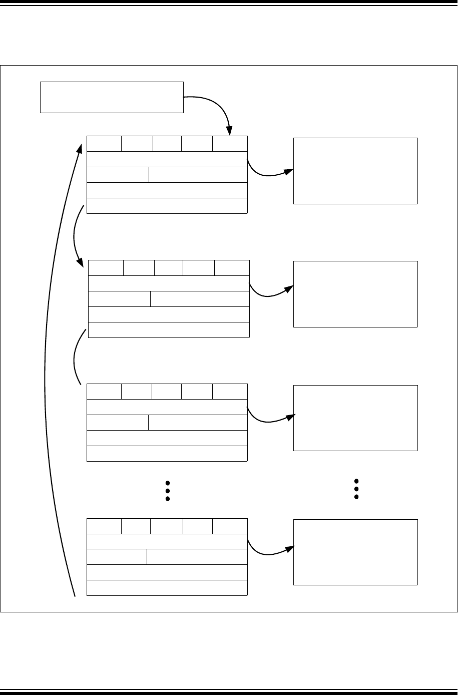
PIC32 Family Reference Manual
DS60001155C-page 35-66 © 2009-2013 Microchip Technology Inc.
The descriptor tables can contain a linked list or linear list of descriptors that point to packet
buffers as illustrated in Figure 35-9 and Figure 35-10.
Figure 35-9: Ethernet Descriptor Table (EDT) Format (Linked List, NPV = 1)
Packet Buffer
TX/RX Start ADDR
(SFR)
Packet Buffer
Packet Buffer
Packet Buffer
STATUS
NEXT_ED
STATUS CHECKSUM/STATUS
DATA_BUFF_ADDR
EOWN BC SOP EOP
NPV = 1
STATUS
NEXT_ED
STATUS CHECKSUM/STATUS
DATA_BUFF_ADDR
EOWN BC SOP EOP
NPV = 1
STATUS
NEXT_ED
STATUS CHECKSUM/STATUS
DATA_BUFF_ADDR
EOWN BC SOP EOP
NPV = 1
STATUS
NEXT_ED
STATUS CHECKSUM/STATUS
DATA_BUFF_ADDR
EOWN BC SOP EOP
NPV = 1
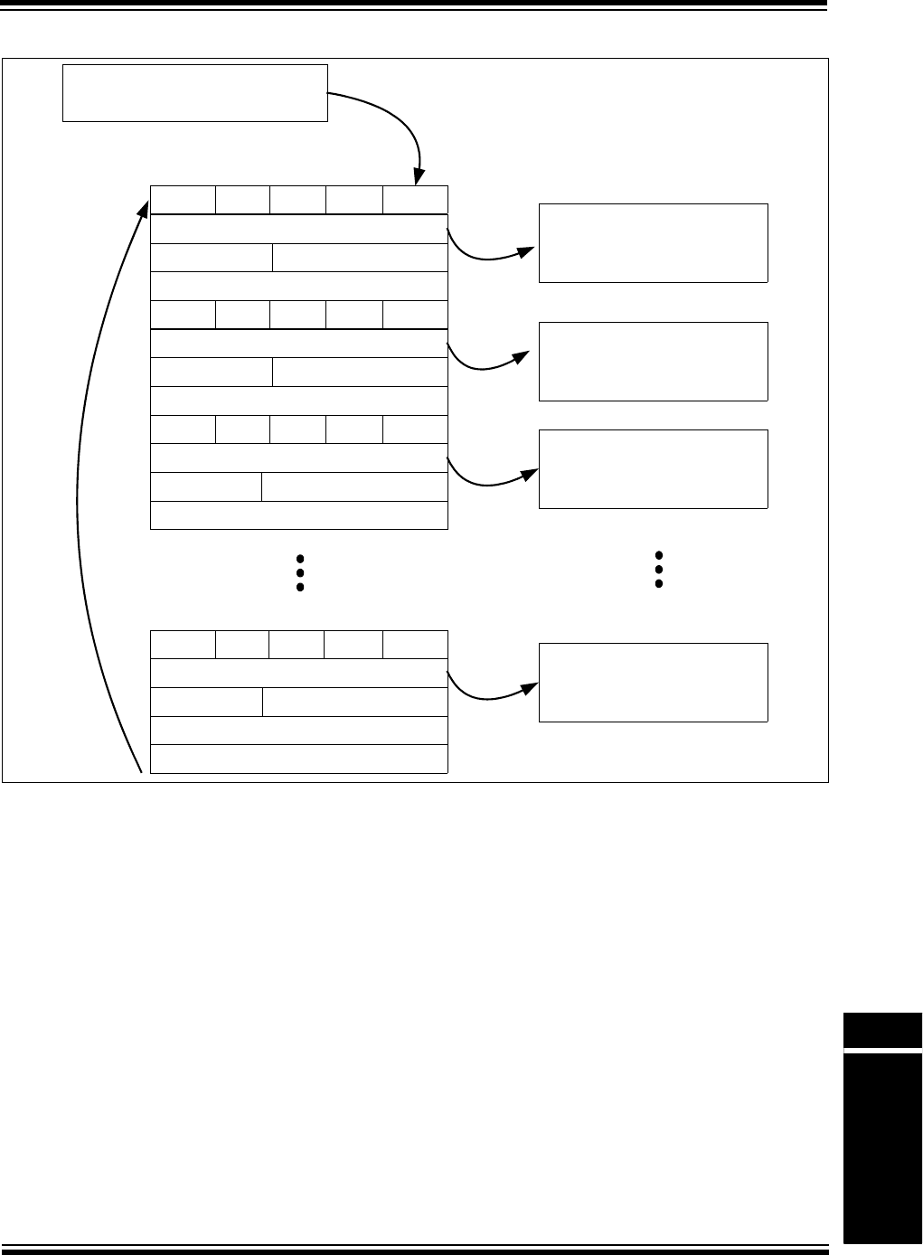
© 2009-2013 Microchip Technology Inc. DS60001155C-page 35-67
Section 35. Ethernet Controller
Ethernet Controller
35
Figure 35-10: Ethernet Descriptor Table (EDT) Format (Linear List, NPV = 0)
35.4.9.1 ETHERNET DESCRIPTOR BUFFER MANAGEMENT
The descriptor tables and packet data buffers used by the receive and transmit paths reside in
the system data memory. The descriptor tables are a linked list of descriptors that reference
blocks of packet data buffers in the system’s data memory. They are physically and logically
partitioned into separate Transmit and a Receive Descriptors and Buffers. Note that the start
address of both the RX and TX Descriptor tables must be 4-byte-aligned (i.e., bit 1 and
bit 0 = 00).
35.4.9.2 ETHERNET DESCRIPTOR OWNERSHIP
Because the descriptors and buffers are shared between the CPU and the Ethernet Controller,
a simple semaphore mechanism is used to distinguish either CPU or Ethernet Controller is
allowed to update the descriptor and associated buffers in the data memory. This semaphore
mechanism is implemented by the EOWN bit in each Buffer Descriptor. When the EOWN bit is
clear, the descriptor is owned by the CPU. When the buffers and descriptors are owned by the
CPU, the CPU may modify the descriptor at its discretion. When the EOWN bit is set, the
descriptor (and the buffer memory pointed to by the descriptor) is owned by the Ethernet
Controller hardware. The software may not modify the descriptor or its corresponding data buffer.
The Ethernet Controller will write the Buffer Descriptor and corresponding data buffer at its
discretion.
TX/RX Start ADDR
(SFR)
Packet Buffer
STATUS
STATUS CHECKSUM/STATUS
DATA_BUFF_ADDR
STATUS
STATUS CHECKSUM/STATUS
DATA_BUFF_ADDR
STATUS
STATUS CHECKSUM/STATUS
DATA_BUFF_ADDR
EOWN BC SOP EOP
NPV = 0
STATUS
STATUS CHECKSUM/STATUS
DATA_BUFF_ADDR
EOWN BC SOP EOP
NPV = 1
Packet Buffer
Packet Buffer
NEXT_ED
Packet Buffer
EOWN BC SOP EOP
NPV = 0
EOWN BC SOP EOP
NPV = 0
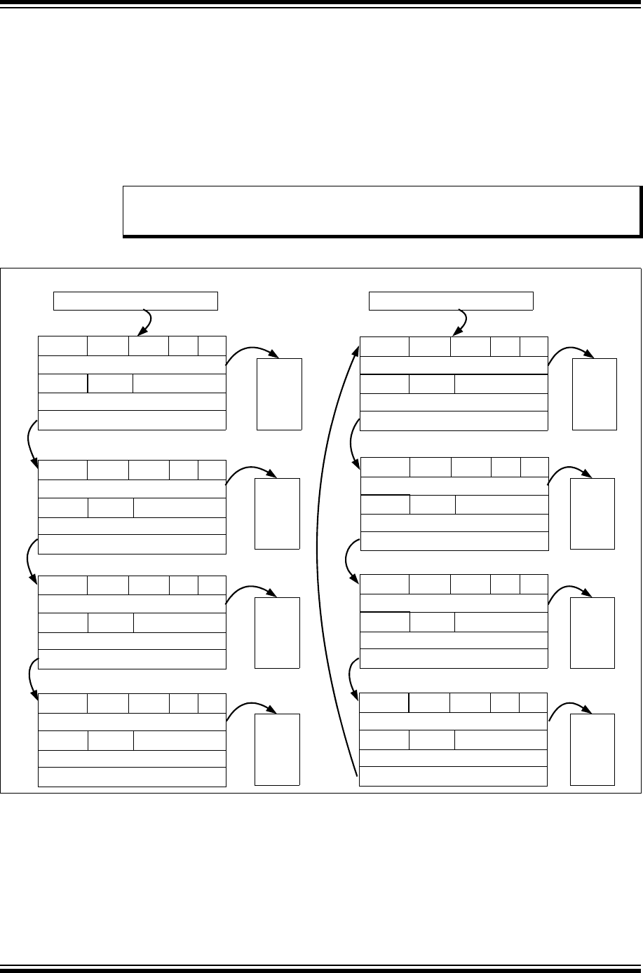
PIC32 Family Reference Manual
DS60001155C-page 35-68 © 2009-2013 Microchip Technology Inc.
35.4.9.3 ETHERNET DESCRIPTOR TABLE (EDT) CONFIGURATION
Before enabling the transfers for the Ethernet Controller, the software must set up both the TX
and RX descriptor tables and also allocate the packet data buffer areas pointed to by the
descriptors. The number of descriptor entries in each table is determined by the software and the
amount of memory available in the system.
The software can set up two EDT configurations: a descriptor ring and a descriptor list.The only
difference is whether the last descriptor in the list is an “empty” descriptor with the EOWN bit =
0, or the last descriptor has a reference back to the top of the ring. Either of these can be handled
by the Ethernet DMA engines. An example of these two types is illustrated in Figure 35-11.
Figure 35-11: Ethernet Descriptor Table (EDT) List and Ring Format
Note: It is the responsibility of the software to initialize all the fields for each descriptor in
the EDT, which includes initializing the status field to 0’s. See Ta ble 35-7 and
Tabl e 35-8, for detailed descriptions of the Ethernet Descriptor format.
Packet
Buffer
TX/RX Start ADDR (SFR)
STATUS (TSV/RSV)
NEXT_ED
DATA_BUFF_ADDR
NPV =
1
EOWN =
1
Byte Cnt EOP
SOP
CHKSUM/STATUS
STATUS
Descriptor List Configuration Descriptor Ring Configuration
Packet
Buffer
Packet
Buffer
Packet
Buffer
Packet
Buffer
TX/RX Start ADDR (SFR)
Packet
Buffer
Packet
Buffer
Packet
Buffer
STATUS (TSV/RSV)
NEXT_ED
DATA_BUFF_ADDR
NPV = 1
EOWN = 1Byte Cnt EOP
SOP
CHKSUM/STATUS
STATUS
STATUS (TSV/RSV)
NEXT_ED
DATA_BUFF_ADDR
NPV = 1
EOWN = 1Byte Cnt EOP
SOP
CHKSUM/STATUS
STATUS
STATUS (TSV/RSV)
xxxxxxxxxxxxxxxxxxxxxxx
DATA_BUFF_ADDR
NPV = 1
EOWN = 0Byte Cnt EOP
SOP
CHKSUM/STATUS
STATUS
STATUS (TSV/RSV)
NEXT_ED
DATA_BUFF_ADDR
NPV = 1
EOWN = 1Byte Cnt EOP
SOP
CHKSUM/STATUS
STATUS
STATUS (TSV/RSV)
NEXT_ED
DATA_BUFF_ADDR
NPV = 1
EOWN = 1Byte Cnt EOP
SOP
CHKSUM/STATUS
STATUS
STATUS (TSV/RSV)
NEXT_ED
DATA_BUFF_ADDR
NPV = 1
EOWN = 1Byte Cnt EOP
SOP
CHKSUM/STATUS
STATUS
STATUS (TSV/RSV)
NEXT_ED
DATA_BUFF_ADDR
NPV = 1
EOWN = 1Byte Cnt EOP
SOP
CHKSUM/STATUS
STATUS

© 2009-2013 Microchip Technology Inc. DS60001155C-page 35-69
Section 35. Ethernet Controller
Ethernet Controller
35
35.4.9.4 ETHERNET TRANSMIT BUFFER MANAGEMENT
The Transmit Buffer Management (TXBM) block along with the TX DMA manages the flow of
transmit packets from the system memory to the MAC using the Transmit Buffer descriptors.
Transmit operation is enabled by setting the Transmit Request to Send bit, TXRTS
(ETHCON1<9>). In response to the TXRTS bit being set, the TX DMA will fetch an ED from the
EDT pointed to by the Ethernet Controller TX Packet Descriptor Start Address Register
(ETHTXST). After it has read the location of the data buffer and the control word for the data
buffer, the DMA will begin reading the data buffer data and writing it to the transmit port of the
MAC. If more than one descriptor is needed, the DMA will move to the next descriptor and will
continue sending data.
When a packet has to be transmitted from the system memory to the MAC, the packet data is
read from the memory pointed by the descriptor DATA_BUFFER_ADDRESS, see Figure 35-9.
The format of the transmitted packets is the same as the one for the received packets. Each
transmit packet buffer contains the standard Ethernet frame fields to be transmitted (DA, SA,
Type/Length, and Payload).
An example of a TX packet using three descriptors is illustrated in Figure 35-12. Once the
descriptor table entries and packet data buffers are programmed by the software, the transmit
operation is initiated by setting the TXRTS bit.
Note: Software must ensure that the TX descriptor list and the ETHTXST register are
initialized before setting the TXRTS bit.
Note: The EOWN bits in the transmitted descriptors should be set by the software starting
with the last descriptor of the packet to be transmitted and ending with the first. This
prevents any race condition between software and the Ethernet Controller
hardware.
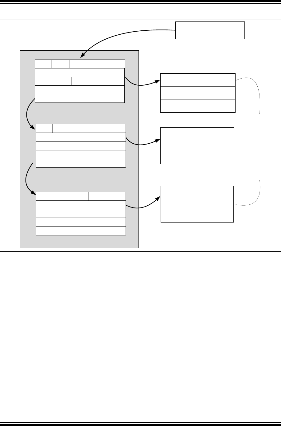
PIC32 Family Reference Manual
DS60001155C-page 35-70 © 2009-2013 Microchip Technology Inc.
Figure 35-12: Ethernet Descriptor Table (EDT) with Multiple Descriptors Per Packet
Once a complete packet has been transmitted, the Ethernet Controller will update the Transmit
Status Vector (TSV) in the first descriptor entry used for that packet. The EOWN field is updated
for all descriptors used by the transmitted packet. Also, the hardware will update the ETHTXST
register to reflect the next TX descriptor to be used for the next transmitted packet.
As long as there are valid transmit descriptors for packets (the next descriptor is valid,
EOWN = 1), the TX DMA will continue to traverse the descriptor table and send packet data to
the MAC for transmission. When all the transmit operations are complete, the transmit logic will
clear the TXRTS bit and set the Transmit Done Interrupt bit (TXDONE) in the Ethernet Controller
Interrupt Request Register (ETHIRQ<3>). The TXDONE bit will generate an interrupt if the
Transmitter Done Interrupt Enable bit (TXDONEIE) in the Ethernet Controller Interrupt Enable
Register (ETHIEN<3>) is set. Thus the completion of the transmit operation can be monitored by
either polling the TXRTS bit or by using the TXDONE bit interrupt.
The transmit operation can be stopped by clearing the TXRTS bit at any time during the
transmission of the packet. When the TXRTS bit is cleared during a packet transmission, the
current packet will complete its transmission after which the TXBUSY Status bit (ETHSTAT<6>)
will be cleared, indicating the transmit engine has stopped.
TX/RX Start ADDR
(SFR)
Data bytes 1-50
Data bytes 51-75
Type/Length (2 bytes)
Source Address (6 bytes)
Destination Address (6 bytes)
STATUS
NEXT_ED
STATUS CHECKSUM/STATUS
DATA_BUFF_ADDR
EOWN BC = 25 SOP = 0EOP = 1NPV = 1
STATUS
NEXT_ED
STATUS CHECKSUM/STATUS
DATA_BUFF_ADDR
STATUS
NEXT_ED
STATUS CHECKSUM/STATUS
DATA_BUFF_ADDR
EDT
Packet to Transmit
EOWN BC = 50 SOP = 0EOP = 0NPV = 1
EOWN BC = 14 SOP = 1EOP = 0NPV = 1

© 2009-2013 Microchip Technology Inc. DS60001155C-page 35-71
Section 35. Ethernet Controller
Ethernet Controller
35
Software should not write any of the TX related SFR registers while the TXRTS bit is set. To
change these registers, the TXRTS must be cleared, then the software must wait for TXBUSY to
deassert, after which the registers can be written and the TXRTS bit is set again.
35.4.9.5 ETHERNET TRANSMIT OPERATION DETAILS
The packet transmit process is as follows:
1. Software writes the packet data to a packet buffer in data memory and programs a
descriptor entry to point to the packet data buffer. It also programs the SOP, EOP,
BYTE_COUNT, and EOWN bits to show that a valid packet is available, and also if there
are other descriptors needed to send the complete packet. See Figure 35-12 for an
example of a TX packet using multiple descriptor entries. The descriptor is used to define
the Transmission Packet data buffer location and length.
2. Software sets the TXRTS bit (ETHCON1<9>) to start the transmission, which starts the
TX DMA and TXBM logic.
3. The TX DMA engine will read the next available descriptor entry from the descriptor table
which is pointed to by the ETHTXST register.
4. After the TX DMA engine reads the DATA_BUFFER_ADDRESS value, the engine will
begin reading the packet data from the location read from the descriptor.
5. The TXBM indicates the SOF to the MAC and transmits the entire frame data from the
transmit buffer, until the end address is reached. The TXBM simply transmits from the start
address until the specified number of bytes has been transmitted to the MAC transmit
interface.
6. The MAC can retry a transmission due to an early collision.
7. The MAC can abort a transmission due to a late collision, excessive collisions or
excessive defers. This condition is signaled by the Transmit Abort Condition Interrupt bit,
TXABORT (ETHIRQ<2>).
8. Once the transmission has completed, the TX DMA engine stores the relevant bits of the
TSV into the first descriptor entry of the packet.
9. After the packet has been transmitted, all the descriptors used for the transmission are
released to the software through the EOWN bits being cleared.
10. If more valid TX descriptors are available (EOWN = 1), the DMA engine will go back to
step 3 to begin the next packet’s transmission. Otherwise, if the next descriptor is still
owned by hardware (EOWN = 0), transmission will halt and wait for the software to set the
TXRTS bit again.
Any collision that occurs within the Collision Window bits (CWINDOW<5:0>) in the Ethernet
Controller MAC Collision Window/Retry Limit Register (EMAC1CLRT<13:8>), boundary is an
early collision and results in a Retry operation. A collision that happens beyond the CWINDOW
boundary will be treated as a late collision and will cause an abort. The CWINDOW<5:0> bits is
typically set to 64 bytes. An abort condition can also result from reaching the maximum collision
count Retransmission Maximum bits, RETX<3:0> (EMAC1CLRT<3:0>), for a packet to be sent.
Note: The ETHTXST transmit configuration register (starting address of TX Descriptor
Table) is used by the TX DMA, and should be changed only when the TX DMA is
not operating (i.e., TXRTS bit = 0 and TXBUSY bit = 0), because continual
synchronization to the DMA clock domain is not provided.
Software must ensure the ETHTXST configuration register does not change when
the TX DMA is active.

PIC32 Family Reference Manual
DS60001155C-page 35-72 © 2009-2013 Microchip Technology Inc.
The TXBM engine has little information about the content of data it sends to the MAC. However,
the following two kinds of transmit packets can be sent:
•A complete packet, which includes the following:
- Addresses (DA, SA), Type/Length and Payload
- Pad (if required)
-FCS
In this case, the PADENABLE bit (EMAC1CFG2<5>) is ‘0’. The MAC will not pad the frame,
but will perform a CRC check on the frame, and set TSV<20> in the TX status vector if the
CRC check match fails.
•An incomplete packet that includes: Addresses (DA, SA), Type/Length and Payload
In this case, PADENABLE = 1. The MAC will pad the frame (in accordance with the settings
of the AUTOPAD bit (EMAC1CFG2<7>) and the VLANPAD bit (EMAC1CFG2<6>)), and will
insert the calculated CRC (FCS) for the frame.
See Ta bl e 35-2 for a description of the pad and CRC options based on the settings of the
EMAC1CFG2 register. Example 35-4 shows the Ethernet transmit packet code.
Example 35-4: Ethernet Transmit Packet Code
/* The following assumptions were made for this example:
- the packet that has to be sent consists of multiple buffers in memory.
- the number of available TX descriptors greater than the number of buffers composing the
packet (there's at least an extra descriptor ending the chain of descriptors)
- this is the first transmission of a packet, the example enables the transmission process.
Input parameters:
- sEthTxDcpt* pArrDcpt: pointer to an array that holds free descriptors that we can use for
the TX operation (see below the definition for sEthTxDcpt).
- char* pArrBuff: pointer to an array that holds buffers to be transmitted
- int* pArrSize: pointer to an array that holds the sizes of buffers to be transmitted
- int nArrayItems: how many buffers to be transmitted are stored in the array. */
#include <p32xxxx.h>
// definition used (see Table 35-7: Ethernet Controller TX Buffer Descriptor Format)
typedef struct
{
volatile union
{
struct
{
unsigned: 7;
unsigned EOWN: 1;
unsigned NPV: 1;
unsigned: 7;
unsigned bCount: 11;
unsigned: 3;
unsigned EOP: 1;
unsigned SOP: 1;
};
unsigned intw;
}hdr; // descriptor header
unsigned char* pEDBuff; // data buffer address
volatile unsigned long longstat; // TX packet status
unsigned int next_ed; // next descriptor (hdr.NPV==1);
}__attribute__ ((__packed__)) sEthTxDcpt; // hardware TX descriptor (linked).
extern void* VA_TO_PA(char* pBuff); // extern function that returns the physical
// address of the virtual address input parameter
int ix; // loop index
sEthTxDcpt* pEDcpt; // current Ethernet descriptor
sEthTxDcpt* tailDcpt; // last Ethernet descriptor
char* pBuff; // current data buffer to be transmitted
int* pSize; // current data buffer size

© 2009-2013 Microchip Technology Inc. DS60001155C-page 35-73
Section 35. Ethernet Controller
Ethernet Controller
35
Example 35-4: Ethernet Transmit Packet Code (Continued)
pEDcpt=pArrDcpt;
pBuff=pArrBuff;
pSize=pArrSize;
tailDcpt=0;
for(ix=0; ix< nArrayItems; ix++, pEDcpt++, pBuff++, pSize++)
{
// pass the descriptor to hw, use linked descriptors, set proper size
pEDcpt->pEDBuff=(unsigned char*)VA_TO_PA(pBuff); // set buffer
pEDcpt->hdr.w=0; // clear all the fields
pEDcpt-> hdr.NPV=1; // set next pointer valid
pEDcpt-> hdr.EOWN=1; // set hardware ownership
pEDcpt->hdr.bCount=* pSize; // set proper size
if(tailDcpt)
{
tailDcpt->next_ed=VA_TO_PA(&pEDcpt);
}
tailDcpt=pEDcpt;
}
// at this moment pEDcpt is an extra descriptor we use to end the descriptors list
pEDcpt->hdr.w=0; // software ownership
tailDcpt->next_ed= VA_TO_PA(&pEDcpt);
pArrDcpt[0].hdr.SOP=1; // Start-of-Packet
pArrDcpt[nArrayItems-1].hdr.EOP=1; // End-of-Packet
ETHTXST=VA_TO_PA(pArrDcpt); // set the transmit address
ETHCON1SET= 0x00008200; // set the ON and the TXRTS
// the ETHC will transmit the buffers we just programmed
/* do something else in between */
while(!(ETHCON1&0x00000200)); // wait transmission to be done
// check the ETHSTAT register to see the transfer result
Note: Example 35-4 uses the syntax specific to the MPLAB® C Compiler for PIC32 MCUs.
Refer to your compiler manual regarding support for packed data structures.

PIC32 Family Reference Manual
DS60001155C-page 35-74 © 2009-2013 Microchip Technology Inc.
35.4.9.6 ETHERNET RECEIVE BUFFER MANAGEMENT (RX BM)
The Receive Buffer Management (RX BM) block along with the RX DMA manages the flow of
receive packets from the MAC to the system memory using the Receive Buffer descriptors.
The receive operation is enabled by setting the RXEN bit (ETHCON1<8>). Once the RXEN bit
is set, the RX DMA will respond to the incoming packets by reading the next available descriptor
entry in the table and writing the packet data into the packet buffer pointed to by the descriptor,
and writing the receive packet status into the descriptor entry itself. If the incoming packet
requires more space than is allocated by a single buffer, the packet may span multiple
descriptors. If the RX DMA reads the next packet descriptor in the table and does not own it, this
may be an overflow condition and will be reported through the status registers.
When a packet is successfully received (the packet is not aborted by the filter or an overrun
error), the packet data is stored in the memory pointed to by the descriptor
DATA_BUFFER_ADDRESS (see Figure 35-9). The RSV, the receive filter status vector
(RXF_RSV), the packet checksum (PKT_CHECKSUM), and the control word (SOP and EOP)
are updated in the first descriptor entry used for that packet. The EOWN field is updated for all
descriptors used by the received packet. Additionally, for improved packet management, the
BUFCNT<7:0> bits (ETHSTAT<23:16>) keeps a running count of the number of received packet
buffers stored in data memory.
The ETHRXST register is updated to reflect the next RX descriptor to be used for the next
received packet. Once hardware has stored the packet in memory, software is responsible for
checking the packet’s RSV for errors before the packet is processed.
Once software processes a received packet, it should write the Descriptor Buffer Count
Decrement bit, BUFCDEC (ETHCON1<0>), once for each descriptor used for that packet in
order to decrement the packet buffer count, BUFCNT. This provides an accurate count of
unprocessed packet buffers pending in data memory that is used in automatic flow control (see
35.4.7 “Flow Control Overview”). Software should also update the descriptors and clear the
EOWN field in the descriptors used for that packet to free them up for another received packet.
When automatic flow control is enabled, an overrun condition occurs if the RX logic receives
more packets than the maximum number that the BUFCNT<7:0> bits (ETHSTAT<23:16>) can
reflect. If an attempt is made to increment the BUFCNT field (by RX BM having received a
packet), and the register has reached its maximum value (0xFF), the register will not rollover; an
overrun error condition will be generated and the RX logic will halt. The proper way to handle this
situation is to read out packets and decrement the BUFCNT counter.
If automatic flow control is disabled, the RX DMA will continue processing, and BUFCNT will
saturate at a value of 0xFF.
If the RX engine stops due to a lack of available descriptors, it will not start again until it detects
a write to the BUFCDEC bit (ETHCON1<0>). This signals that the software has made available
additional RX descriptor buffers.
Note: When the RXEN bit is enabled, the RX DMA engine will initially fetch an RX
descriptor from the system data memory in preparation of receiving packet data.
Software must ensure the descriptor list is initialized prior to setting the RXEN bit.
Note 1: The ETHRXST receive configuration register (starting address of the RX Descriptor
table) is used by the RX DMA, and should be changed only when the RX DMA is
not operating (i.e., RXEN = 0 and RXBUSY = 0), since continual synchronization
to the DMA clock domain is not provided. Ensuring the ETHRXST configuration
register does not change when the RX DMA is active is the responsibility of
software.
2: When using the receive EDT (RX EDT), the software must ensure that the RX EDT
contains (at a minimum) sufficient entries that are required to buffer the largest
Ethernet Frame. This is needed because the RX DMA engine does not detect the
wrap-around condition.

© 2009-2013 Microchip Technology Inc. DS60001155C-page 35-75
Section 35. Ethernet Controller
Ethernet Controller
35
35.4.9.7 ETHERNET RECEIVE OPERATION DETAILS
A received packet is stored in the packet buffer along with a status vector, which is stored in the
descriptor. The status vector has two components:
•The RSV, which is driven by the MAC at the end of a received packet and contains
information about the packet received
• The RXF_RSV, which driven out by the RXF block
This combined status is stored in the first descriptor used to store the packet data buffer.
The following of steps are involved in the packet receiving process:
1. Software sets up the RX descriptor table with RX descriptor entries and the associated
packet data buffers pointed to by each descriptor entry.
2. Software writes to the ETHRXST register (pointing to the start of the RX descriptor table)
and enables the RX port by setting the RXEN bit (ETHCON1<8>).
3. The RX DMA engine reads a valid descriptor from the table, and determines start of the
packet data buffer.
4. When a packet is received, the MAC indicates the start of a new frame and presents the
data.
5. The RX BM receives the data and stores it in an RX FIFO. Writes to the system memory
are postponed until 32 bits of data have been received. The RX DMA takes the data from
the RX FIFO and stores it in the Packet data buffer pointed to by the descriptor it just read.
Once all the bytes are written that have been allocated by the descriptor, the RX DMA
reads another descriptor in order to write more packet data.
6. If the RX DMA fetches a descriptor with EOWN = 0 when needed to store more packet
data, the Receive Buffer Not Available Interrupt bit, RXBUFNA (ETHIRQ<1>), interrupt
occurs.
7. If any one of the following events occur during a packet reception, the packet is aborted
and the descriptor is not updated with the packet status, which leaves it available for the
next packet:
•The RXF aborts the packet
• RXFIFO overrun, which can be caused by:
- Excessive system level latency
- The BUFCNT<7:0> bits (ETHSTAT<23:16>) reaching maximum value
- No descriptors are available for hardware processing
8. Once the frame completes, the MAC presents the RSV and the RXF presents the
RXF_RSV.
9. The RX DMA will traverse the descriptors a second time:
a) The first descriptor used for the current packet will be updated with the RSV,
RXF_RSV, PKT_CHECKSUM and BYTE_COUNT values.
b) All the descriptors that belong to the current packet get their SOP and EOP updated.
Also, the EOWN bit is updated to indicate to the software that it can read the received
packet data.
10. Once the RSV is passed to the RX DMA, the RX BM is ready to receive another packet.

PIC32 Family Reference Manual
DS60001155C-page 35-76 © 2009-2013 Microchip Technology Inc.
Example 35-5 shows code example for the Ethernet receive packet.
Example 35-5: Ethernet Receive Packet Code
/* The following assumptions were made for this example:
- the packet that has to be received might consist of multiple Ethernet frames.
- the number of available RX descriptors is greater than the number of receive buffers that
have to be made available for the incoming frames (there’s at least an extra descriptor
ending the chain of descriptors)
- all the RX filtering is already programmed
- this is the first receive operation to take place, the example enables the receive
process.
Input parameters:
- sEthRxDcpt* pArrDcpt: pointer to an array that holds free descriptors that we can use for
the RX operation (see below the definition for sEthRxDcpt).
- char* pArrBuff: pointer to an array that holds buffers to receive the incoming data
traffic
- int rxBuffSize: size of the receive buffers
- int nArrayItems: how many receive buffers are stored in the array. */
#include <p32xxxx.h>
// definition used for this example (see Table 35-7)
typedef struct
{
volatile union
{
struct
{
unsigned: 7;
unsigned EOWN: 1;
unsigned NPV: 1;
unsigned: 7;
unsigned bCount: 11;
unsigned: 3;
unsigned EOP: 1;
unsigned SOP: 1;
};
unsigned int w;
}hdr; // descriptor header
unsigned char* pEDBuff; // data buffer address
volatile unsigned long long stat; // TX packet status
unsigned int next_ed; // next descriptor (hdr.NPV==1);
}__attribute__ ((__packed__)) sEthRxDcpt; // hardware RX descriptor (linked).
extern void* VA_TO_PA(char* pBuff); // extern function that returns the physical
// address of the input virtual address parameter
int ix; // index
sEthRxDcpt* pEDcpt; // current Ethernet descriptor
sEthRxDcpt* tailDcpt; // last Ethernet descriptor
char* pBuff; // current data buffer to be transmitted
pEDcpt=pArrDcpt;
pBuff=pArrBuff;
tailDcpt=0;
ETHCON2=(rxBuffSize/16)<<4; // set the RX data buffer size
for(ix=0; ix< nArrayItems; ix++, pEDcpt++, pBuff++)
{
// pass the descriptor to hardware, use linked descriptors, set proper size
pEDcpt->pEDBuff=(unsigned char*)VA_TO_PA(pBuff); // set buffer
pEDcpt->hdr.w=0; // clear all the fields
pEDcpt-> hdr.NPV= 1; // set next pointer valid
pEDcpt-> hdr.EOWN= 1; // set hardware ownership
if(tailDcpt)
{
tailDcpt->next_ed=VA_TO_PA(&pEDcpt);
}

© 2009-2013 Microchip Technology Inc. DS60001155C-page 35-77
Section 35. Ethernet Controller
Ethernet Controller
35
Example 35-5: Ethernet Receive Packet Code (Continued)
35.4.10 Ethernet Initialization Sequence
To in i ti ali ze t he Eth ern et C ont rol ler to rec eive and transmit Ethernet messages, perform these
steps:
1. Ethernet Controller Initialization:
a) Disable Ethernet interrupts in the EVIC register by clearing the Ethernet Controller IE
bit, ETHIE (IEC1<28>).
b) Turn the Ethernet Controller off, and then clear the ON bit (ETHCON1<15>), the
RXEN bit (ETHCON1<8>), and the TXRTS bit (ETHCON1<9>).
c) Abort the Wait activity by polling the ETHBUSY bit (ETHSTAT<7>).
d) Clear the Ethernet Interrupt Flag bit (ETHIF) in the Interrupts module (IFS1<28>).
e) Disable any Ethernet Controller interrupt generation by clearing the ETHIRQIE
register.
f) Clear the TX and RX start addresses from the ETHTXST and ETHRXST registers.
2. MAC Initialization:
a) Reset the MAC using the SOFTRESET bit (EMAC1CFG1<15>), or individually reset
the modules by setting the Reset MCS/RX bit, RESETRMCS (EMAC1CFG1<11), the
Reset RX Function bit, RESETRFUN (EMAC1CFG1<10>), the Reset MCS/TX bit,
RESETTMCS (EMAC1CFG1<9>), and the Reset TX Function bit, RESETTFUN
(EMAC1CFG1<8>).
b) Use the Configuration bit setting, FETHIO (DEVCFG3<25>), to detect the alternate
or default I/O configuration. Refer to Section 32. “Configuration” (DS60001124) for
more information.
c) Use the Configuration bit setting, FMIIEN (DEVCFG3<24>), to detect MII/RMII
operation mode.
d) Initialize as digital, all of the pins used by the MAC PHY interface (generally, only
those pins that have shared analog functionality need to be configured).
e) Initialize the MIIM interface:
i. If the RMII operation is selected, Reset the RMII module by using the
RESETRMII bit (EMAC1SUPP<11>) and set proper speed in the SPEEDRMII bit
(EMAC1SUPP<8>).
ii. Issue an MIIM block reset, by setting and then clearing the Test Reset MII
Management bit, RESETMGMT (EMAC1MCFG<15>).
iii. Select a proper divider in the CLKSEL<3:0> bits (EMAC1MCFG<5:2>) for the
MIIM PHY communication based on the system running clock frequency and the
external PHY supported clock.
tailDcpt=pEDcpt;
}
// at this moment pEDcpt is an extra descriptor we use to end the descriptors list
pEDcpt->hdr.w=0; // software ownership
tailDcpt->next_ed= VA_TO_PA(&pEDcpt);
ETHRXST=VA_TO_PA(pArrDcpt); // set the address of the first RX descriptor
ETHCON1SET= 0x00008100; // set the ON and the RXEN
// the Ethernet Controller will receive frames and place them in the receive buffers
// we just programmed
/* do something else in between */
// can check the BUFCNT (ETHSTAT<16:23>) or RXDONE (ETHIRQ<7>)
// to see if there are packets received
Note: Example 35-5 uses the syntax specific to the MPLAB C Compiler for PIC32 MCUs.
Refer to your compiler manual regarding support for packed data structures.

PIC32 Family Reference Manual
DS60001155C-page 35-78 © 2009-2013 Microchip Technology Inc.
3. PHY Initialization:
This depends on the actual external PHY used. All PHYs should implement the basic
register set as specified in Table 22-6 of the “MII Management Register Set” in Clause 22
of the IEEE 802.3 Specification.
In addition to the basic register set, PHYs may provide an extended set of nine registers
and capabilities that may be accessed and controlled through the MIIM interface. They
provide a PHY specific identifier, control and monitoring for the auto-negotiation process,
and so on. The IEEE 802.3 Specification provides room for 16 extended registers which
implement vendor-specific capabilities.
Following are the common steps for PHY initialization. Adjust these steps according to the
vendor specific PHY data sheet:
a) Reset the PHY (use Control Register 0).
b) Set the MII/RMII operation mode. This requires access to a vendor-specific control
register.
c) Set the normal, swapped, or automatic (preferred) MDIX. This requires access to a
vendor-specific control register.
d) Check the PHY capabilities by investigating the Status Register 1.
e) The automatic negotiation should be enabled (preferably), if the PHY supports it.
Advertise the supported capabilities using the PHY Register 4 “Auto-negotiation
Advertisement Register”. Start the negotiation (Control Register 0) and wait for the
negotiation to complete. Once the negotiation is complete, get the link partner
capabilities from the PHY Register 5 “Auto-negotiation Link Partner Ability Register”
and negotiation result from the vendor-specific register.
f) If automatic negotiation is not supported or selected, update the PHY Duplex and
Speed settings directly (use Control Register 0 and possibly some vendor-specific
registers).
4. MAC Configuration:
When the Duplex and Speed settings are available, configure the MAC using these steps:
a) Enable the MAC Receive Enable bit, RXENABLE (EMAC1CFG1<0>), selecting both
the MAC TX Flow Control bit, TXPAUSE (EMAC1CFG1<3>), and the MAC RX Flow
Control bit, RXPAUSE (EMAC1CFG1<2>) (the PIC32 MAC supports both).
b) Select the desired automatic padding and CRC capabilities, enabling of the Huge
frames, and the Duplex type in the EMAC1CFG2 register.
c) Program the EMAC1IPGT register with the back-to-back inter-packet gap.
d) Use the Ethernet Controller EMAC1IPGR register, for setting the non-back-to-back
inter-packet gap.
e) Set the collision window and the maximum number of retransmissions in the
EMAC1CLRT register.
f) Set the maximum frame length in the EMAC1MAXF register.
g) Optionally, set the station MAC address in the EMAC1SA0, EMAC1SA1, and
EMAC1SA2 registers (these registers are loaded at Reset from the factory
preprogrammed station address).
5. Continue the Ethernet Controller initialization:
a) If you want to turn on the Flow Control, update the value of the PTV<15:0> bits
(ETHCON1<31:16>).
b) If you want to use automatic Flow Control, set the full and empty watermarks:
RXFWM<7:0> bits (ETHRXWM<23:16>) and the RXEWM<7:0> bits
(ETHRXWM<7:0>).
c) If needed, enable the automatic Flow Control by setting the AUTOFC bit
(ETHCON1<7>).
d) Set the RXFs by updating the ETHHT0, ETHHT1, ETHPMM0, ETHPMM1,
ETHPMCS, and ETHRXFC registers.
e) Set the size of the RX buffers in the RXBUFSZ<6:0> bits (ETHCON2<10:4>) (all
receive descriptors use the same buffer size). Note that using packets that are too
small will lead to packet fragmentation, and has a noticeable impact on the
performance.

© 2009-2013 Microchip Technology Inc. DS60001155C-page 35-79
Section 35. Ethernet Controller
Ethernet Controller
35
f) Prepare a list/ring of TX descriptors for messages to be transmitted. Update all of the
fields in the TX descriptor (NPV, EOWN = 1, NEXT_ED) (see Ta ble 35 -7 ). If using a
list, end it with a software own descriptor (EOWN = 0).
The SOP, EOP, DATA_BUFFER_ADDRESS and BYTE_COUNT will be updated
when a specific message has to be transmitted. The DATA_BUFFER_ADDRESS will
contain the physical address of the message, and the BYTE_COUNT contains the
message size. SOP and EOP are set depending on how many packets are needed
to transmit the message.
g) Prepare a list of the RX descriptors populated with valid buffers for messages to be
received. Update the NEXT ED Pointer Valid (NPV) Enable bit, EOWN = 1 and
DATA_BUFFER_ADDRESS fields in the RX descriptors (see Ta b le 35 -8). The
DATA_BUFFER_ADDRESS should contain the physical address of the
corresponding RX buffer.
h) The actual number of RX/TX descriptors and the previously allocated RX buffers
depends on the available system memory, and the anticipated Ethernet traffic.
i) Update the ETHTXST register with the physical address of the Head of the TX
descriptors list.
j) Update the ETHRXST register with the physical address of the Head of the RX
descriptors list.
k) Enable the Ethernet Controller by setting the ON bit (ETHCON1<15>).
l) Enable the receiving of messages by setting the RXEN bit (ETHCON1<8>).
m) Check the list of RX descriptors to determine whether the EOWN bit is clear. If the
EOWN bit is clear, this descriptor is under software control and an Ethernet message
is received. Use SOP and EOP to extract the Ethernet message, and use the
BYTE_COUNT, RXF_RSV, RSV and PKT_CHECKSUM to get the Ethernet message
characteristics.
n) To transmit an Ethernet message:
i. Ensure that the message has the proper format according the Ethernet Frame
specifications.
ii. Update the necessary number of TX descriptors, starting with the Head of the
list, by setting the DATA_BUFFER_ADDRESS as the physical address of the
corresponding buffer in the message to be transmitted.
iii. Note that large packet fragmentation has an impact on the performance.
iv. Update the BYTE_COUNT value for each descriptor with the number of bytes
contained in each buffer.
v. Set EOWN = 1 for each descriptor that belongs to the packet.
vi. Use SOP and EOP to specify that the message uses one or more TX descriptors.
o) To enable the transmission of the message, set the TXRTS bit (ETHCON1<9>).
p) Inspect the list of TX descriptors to check if the EOWN bit is cleared. If it is cleared,
this descriptor is under software control and the message is transmitted. Use TSV to
check the transmission result.

PIC32 Family Reference Manual
DS60001155C-page 35-80 © 2009-2013 Microchip Technology Inc.
35.4.11 Ethernet Statistics Registers
To co mpl y wi th th e 802 .3 La ye r Ma n ag e me n t Sp ec ification, the Ethernet Controller implements
various statistics registers in hardware. These registers are incremented by hardware when
various conditions are detected in a transmitted/received packet. Once a register reaches its
maximum value, it will roll over to all zeros the next time it is incremented. Therefore, it is the
responsibility of software to read these in a timely manner to avoid losing any data.
A read by software will automatically cause the corresponding register to be cleared. Statistics
counters can be written by software using the SET, CLR, and INV registers. Writes to the normal
registers are also supported. In normal operation, the statistics registers should just be read on
a periodic basis to collect data on the Ethernet link traffic.
35.4.11.1 PAYLOAD CHECKSUM CALCULATION
The Ethernet Controller automatically calculates a 16-bit packet checksum for all received
packets and stores the 16-bit value along with the received packets status vector in the packet
descriptor, PKT_CHECKSUM (RX_DCPT<96:111>) field. This checksum can be useful for the
TCP/IP software implementations.
The payload checksum is calculated over the complete received packet except for the
first 14 bytes (destination address, source address and length/type fields). If the software needs
to exclude more bytes from the calculated checksum, it must subtract the values accordingly.
A payload checksum is a simple checksum used to provide basic protection against the bit
corruption during transmission of Ethernet frames. It is typically used in TCP and UDP packets
of the TCP/IP protocols. The checksum is calculated by dividing the byte stream into 16-bit words
and adding them together. Any overflow is also added back into the checksum. The checksum
calculation begins after the first 14 bytes of the frame are received and includes the FCS bytes.
The result is the 1’s complement of the calculated sum.
Figure 35-7 illustrates an example of the payload checksum calculation.
Note 1: The SET, CLR, and INV Statistics registers are only meant for supporting software
debugging and testing.
2: When the device is put in Sleep mode, updates to the Statistics registers are
suspended as the system clock is not running. The only exception to this is an
overflow case, which will increment the overflow counter and set the overflow flag
Receive FIFO Over Flow Error bit, RXOVFLW (ETHIRQ<0>). This is done to signal
to software upon a wake-up that some packets have been lost.
3: Some statistical counters may immediately increment when exiting Sleep due to
pending events.

© 2009-2013 Microchip Technology Inc. DS60001155C-page 35-81
Section 35. Ethernet Controller
Ethernet Controller
35
35.5 ETHERNET INTERRUPTS
The PIC32 device can generate interrupts reflecting the events that occur during the Ethernet
Controller’s transfer of frames. Each of the Ethernet Controller interrupt events has a
corresponding Interrupt Enable bit (IE) in the ETHIEN register, which must be set for an interrupt
to be generated. However, regardless of the value of the ETHIEN register, the status of all
interrupt events is directly readable through the ETHIRQ register. Therefore, the software has
visibility of an event generating a potential interrupt by polling the register, and not having an
interrupt propagate out of the Ethernet module.
Ethernet interrupts are persistent. This means that as long as the event that generated the
interrupt is pending, the interrupt signal from the Ethernet Controller module will remain asserted.
Following is a description of the interrupt events generated by the transmission and receive of
Ethernet frames.
Transmit path related interrupt events:
• TX DMA engine transfer error interrupt, signaled by the TXBUSE bit (ETHIRQ<14>) and
enabled using the TXBUSEIE bit (ETHIEN<14>). This event occurs when the TX DMA
encounters a bus error during a memory access, and is caused by an addressing error
(usually because of a bad pointer).
•Transmission done interrupt, signaled by the TXDONE bit (ETHIRQ<3>) and enabled using
the TXDONEIE bit (ETHIEN<3>). This event occurs when the currently transmitted TX
packet completes transmission and the TSV is loaded into the first descriptor of the packet.
•Transmission aborted interrupt, signaled by the TXABORT bit (ETHIRQ<2>) and enabled
using the TXABORTIE bit (ETHIEN<2>). This event occurs when the MAC aborts the
transmission due to one of these reasons:
- Jumbo TX packet abort (packet size is greater than the maximum size MACMAXF bit
(EMAC1MAXF<15:0>))
-Underrun abort (Transmit engine cannot keep up with the requested data flow. This
happens when the system bus is overloaded.)
- Excessive defer abort (Packet was deferred in excess of 6071 nibble times in
100 Mbps mode or 24,287 bit times in 10 Mbps mode)
-Late collision abort (Collision occurred beyond the collision window)
- Excessive collisions abort (Packet was aborted because the number of collisions
exceeded the RETX bit (EMAC1CLRT<3:0>)
Receive path related interrupt events:
•RX DMA engine transfer error interrupt, signaled by the RXBUSE bit (ETHIRQ<13>) and
enabled using the RXBUSEIE bit (ETHIEN<13>). This event occurs when the RX DMA
encounters a bus error during a memory access and is caused by an addressing error
(usually because of a bad pointer).
•Receive done interrupt, signaled by the RXDONE bit (ETHIRQ<7>) and enabled using the
RXDONEIE bit (ETHIEN<7>). This event occurs whenever a packet is successfully
received.
•Packet pending interrupt, signaled by the PKTPEND bit (ETHIRQ<6>) and enabled using the
PKTPENDIE bit (ETHIEN<6>). This event occurs whenever the buffer counter
BUFCNT<7:0> bits (ETHSTAT<23:16>) has a value greater than ‘0’.
•Receive activity interrupt, signaled by the RXACT bit (ETHIRQ<5>) and enabled using the
RXACTIE bit (ETHIEN<5>). This event occurs whenever data is stored in the RX BM FIFO.
• Receive buffer not available interrupt, signaled by the RXBUFNA bit (ETHIRQ<1>) and
enabled using the RXBUFNAIE bit (ETHIEN<1>). This event occurs whenever the RX
DMA runs out of descriptors by fetching a descriptor not owned by hardware (EOWN = 0).
Note: An early collision will cause the MAC to assert the Retry, but not the Abort. This
condition will therefore not cause an interrupt.

PIC32 Family Reference Manual
DS60001155C-page 35-82 © 2009-2013 Microchip Technology Inc.
• Receive FIFO overflow error interrupt, signaled by the RXOVFLW bit (ETHIRQ<0>) and
enabled using the RXOVFLIE bit (ETHIEN<0>). This event occurs whenever the RX BM is
unable to transfer data out of the receive FIFO to the system memory and the internal FIFO
overflows because of one of the following reasons:
- Excessive system level latency
- The BUFCNT<7:0> bits (ETHSTAT<23:16>) reaching maximal value
- No descriptors are available for hardware processing
•Empty Watermark interrupt, signaled by the EWMARK bit (ETHIRQ<9>) and enabled using
the EWMARKIE bit (ETHIEN<9>). This event occurs whenever the RX descriptor buffer
count BUFCNT<7:0> bits (ETHSTAT<23:16>) is less than or equal to the RXEWM bit
ETHRXWM<7:0>) value.
•Full Watermark interrupt, signaled by the FWMARK bit (ETHIRQ<8>) and enabled using the
FWMARKIE bit (ETHIEN<8>). This event occurs whenever the RX descriptor buffer count
BUFCNT<7:0> bits (ETHSTAT<23:16>) is greater than or equal to the RXFWM bit
(ETHRXWM<23:16>) value.
Interrupts in the Ethernet peripheral can be divided into two types depending on how and where
the interrupt is cleared: software cleared interrupt events and hardware cleared interrupt events.
Both interrupt events are cleared by a device Reset.
Software cleared interrupt events are cleared by writing the corresponding bit in the ETHIRQCLR
or ETHIRQ register directly, and include the following bits: TXBUSE, RXBUSE, RXDONE,
RXACT, TXDONE, TXABORT, RXBUFNA, and RXOVFLW.
Hardware cleared interrupt events are cleared by removing the condition that caused the
interrupt, and include the following bits:
•EWMARK: This interrupt can be cleared when an RX packet is successfully received and
the BUFCNT value is greater than the value of the RXEWM bits (ETHRXWM<7:0>).
•FWMARK: This interrupt can be cleared by writing to the BUFCDEC bit (ETHCON1<0>),
thereby decrementing the buffer descriptor count (BUFCNT) below the value of the
RXFWM<7:0> bits (ETHRXWM<23:16>).
• PKTPEND: This interrupt can be cleared by writing the BUFCDEC bit (ETHCON1<0>) until
the value of the BUFCNT<7:0> bits (ETHSTAT<23:16>) reaches ‘0’.
All the interrupts belonging to the Ethernet Controller map to the Ethernet interrupt vector. The
corresponding Ethernet Controller interrupt flag is the ETHIF bit (IFS1<28>). This interrupt flag
must be cleared in software once the cause generating the interrupt is processed.
The Ethernet Controller is enabled as a source of interrupts through the respective ETHIE bit
(IEC1<28>). The interrupt priority level bits, ETHIP<2:0> (IPC12<4:2>), and interrupt sub-priority
level bits, ETHIS<1:0> (IPC12<1:0>), must also be configured.
Note: Refer to Section 8. “Interrupts” (DS60001108) for detailed description of the IFSx,
IECx, and IPCx interrupt bits.

© 2009-2013 Microchip Technology Inc. DS60001155C-page 35-83
Section 35. Ethernet Controller
Ethernet Controller
35
35.5.1 Interrupt Configuration
The Ethernet Controller module has multiple internal interrupt flags (TXBUSE, RXBUSE,
EWMARK, FWMARK, RXDONE, PKTPEND, RXACT, TXDONE, TXABORT, RXBUFNA and
RXOVFLW) and corresponding enable interrupt control bits (TXBUSEIE, RXBUSEIE,
EWMARKIE, FWMARKIE, RXDONEIE, PKTPENDIE, RXACTIE, TXDONEIE, TXABORTIE,
RXBUFNAIE and RXOVFLIE). However, for the interrupt controller, there is one dedicated
interrupt flag bit for the Ethernet Controller, ETHIF (IFS1<28>), and the corresponding interrupt
enable/mask bit, ETHIE (IEC1<28>).
The Ethernet Controller module has its own priority and sub-priority levels independent of other
peripherals. The ETHIF bit (IFS1<28>) will be set without regard to the state of the corresponding
enable bit, ETHIE (IEC1<28>). The ETHIF can be polled by software, if required.
The ETHIE bit (IEC1<28>) is used to define the behavior of the Vector Interrupt Controller (INT)
module when the corresponding ETHIF bit is set. When the corresponding ETHIE bit is clear, the
Interrupts module does not generate a CPU interrupt for the event. If the ETHIE bit is set, the
Interrupts module will generate an interrupt to the CPU when the ETHIF bit is set (subject to the
priority and sub-priority as follows). It is the responsibility of the user software routine that
services a particular interrupt to clear the interrupt flag bit before the service routine is complete.
The priority of the Ethernet Controller module interrupt can be set using the IPC12 register of the
INT controller. This priority defines the priority group to which the interrupt source will be
assigned. The priority groups range from a value of 7 (the highest priority) to a value of 0, which
does not generate an interrupt. An interrupt being serviced will be preempted by an interrupt in
a higher priority group.
The sub-priority bits allow setting the priority of an interrupt source within a priority group. The
values for the sub-priority range from 3 (highest priority) to 0 (lowest priority). An interrupt with
the same priority group but having a higher sub-priority value will not preempt a lower sub-priority
interrupt that is in progress.
The priority group and sub-priority bits allow more than one interrupt source to share the same
priority and sub-priority. If simultaneous interrupts occur in this configuration, the natural order
of the interrupt sources within a priority/sub-priority group pair determine the interrupt
generated.
The natural priority is based on the vector numbers of the interrupt sources. The lower the vector
number, the higher the natural priority of the interrupt. Any interrupts that were overridden by
natural order will then generate their respective interrupts based on priority, sub-priority and
natural order after the interrupt flag for the current interrupt is cleared.
After an enabled interrupt is generated, the CPU will jump to the vector assigned to that interrupt.
The vector number for the interrupt is the same as the natural order number. The CPU will then
begin executing code at the vector address. The user’s code at this vector address should
perform any application specific operations and clear the ETHIF interrupt flags (as well as the
corresponding event in the ETHIRQ register, if a software clearable interrupt) and then exit. Refer
to the vector address table in Section 8. “Interrupts” (DS60001108) for more information.
Tabl e 35-9 provides the Ethernet interrupt vectors for various offsets with Ebase = 0x8000:0000.
Example 35-6 shows the Ethernet initialization with interrupts enabled code.
Table 35-9: Ethernet Interrupt Vectors for Various Offsets with EBASE = 0x8000:0000
Note: All of the interrupt conditions for the Ethernet Controller module share one interrupt
vector.
Interrupt
Vector/
Natural
Order
IRQ
Number
Vector
Address
IntCtl.VS
= 0x01
Vector
Address
IntCtl.VS
= 0x02
Vector
Address
IntCtl.VS
= 0x04
Vector
Address
IntCtl.VS
= 0x08
Vector
Address
IntCtl.VS
= 0x10
ETH 48 60 8000 0800 8000 0e00 8000 1a00 8000 3200 8000 6200

PIC32 Family Reference Manual
DS60001155C-page 35-84 © 2009-2013 Microchip Technology Inc.
Example 35-6: Ethernet Initialization with Interrupts Enabled Code
Example 35-7: Ethernet Controller Interrupt Service Routine (ISR) Code
// this code example assumes that the system vectored interrupts are properly configured
#include <p32xxxx.h>
IEC1CLR =0x10000000; // disable Ethernet interrupts
ETHCON1CLR=0x00008300; // reset: disable ON, clear TXRTS, RXEN
while(ETHSTAT&0x80); // wait everything down
IFS1CLR=0x10000000; // clear the interrupt controller flag
ETHIENCLR=0x000063ef; // disable all events
ETHIRQCLR=0x000063ef; // clear any existing interrupt event
ETHCON1SET=0x00008000; // turn device ON
/*
Initialize the MAC
Initialize the PHY
Initialize RX Filtering
Initialize Flow Control
*/
ETHIENSET=0x0000400c; // enable the TXBUSE, TXDONE
// and TXABORT interrupt events
IPC12CLR = 0x0000001f; // clear the Ethernet Controller priority and sub-priority
IPC12SET = 0x00000016; // set IPL 5, sub-priority 2
IEC1SET=0x10000000; // enable the Ethernet Controller interrupt
// start transmit packets
// whenever a packet completes transmission or an transmission error occurs
// an interrupt will be generated
/*
The following code example demonstrates a simple Interrupt Service Routine for Ethernet
Controller interrupts. The user’s code at this vector should perform any application specific
operations and must clear the Ethernet Controller interrupt flags before exiting.
*/
#include <p32xxxx.h>
void __ISR(_ETH_VECTOR, IPL5) __EthInterrupt(void)
{
int ethFlags=ETHIRQ; // read the interrupt flags (requests)
// the sooner we acknowledge, the smaller the chance to miss another event of the
// same type because of a lengthy ISR
ETHIRQCLR= ethFlags; // acknowledge the interrupt flags
/*
perform application specific operations in response
to any interrupt flag set in ethFlags
*/
IFS1CLR= 0x10000000; // Be sure to clear the Ethernet Controller Interrupt
// Controller flag before exiting the service routine.
}
Note: Example 35-6 and Example 35-7 show the syntax specific to the MPLAB C
Compiler for PIC32 MCUs. Refer to your compiler manual regarding support for the
Interrupt Service Routines (ISRs).

© 2009-2013 Microchip Technology Inc. DS60001155C-page 35-85
Section 35. Ethernet Controller
Ethernet Controller
35
35.5.2 External PHY Interrupt
Some PHYs have the option of generating an interrupt signal when a specific event occurs. A
PHY interrupt is usually asserted for the following types of events/conditions:
•Energy detect
•Power-down mode exited
•Automatic negotiation complete
•Remote fault detected
•Link down
•Automatic negotiation Link Partner (LP) acknowledge
•Parallel detection fault
•Automatic negotiation page received
Refer to the vendor-specific PHY data sheet for more information about the events that generate
interrupts.
If the PIC32 device must be made aware and respond to this interrupt, the PHY interrupt signal
should be tied to a PIC32 external interrupt pin. This interrupt does not go through the Ethernet
Controller module. The software must clear the PHY generated interrupt event by writing a
register in the PHY through the MAC MIIM registers. Also, in this case, the PHY interrupt is the
only software clearable interrupt that is not directly clearable in the ETHIRQ register.

PIC32 Family Reference Manual
DS60001155C-page 35-86 © 2009-2013 Microchip Technology Inc.
35.6 OPERATION IN POWER-SAVING AND DEBUG MODES
35.6.1 Ethernet Operation in Sleep Mode
When the PIC32 device enters Sleep mode, the system clock is disabled. No Ethernet transfers
can occur in this mode. For the Ethernet Controller module, all clocks are stopped except for the
external MII RX_CLK and TX_CLK signals or REF_CLK, if operating in RMII mode. The Ethernet
Controller module is in Sleep mode with asynchronous wake-up events allowed.
If the user application enters Sleep mode while the Ethernet Controller is operating on an active
transfer, it will be suspended in its current state until clock execution resumes. The software
should avoid this situation as it might result in unexpected pin timings.
Software is responsible for determining when the link is in a state that is safe for the Ethernet
Controller to enter Sleep mode. Execution of the WAIT instruction by the CPU to place the device
in Sleep mode is only recommended in two cases:
•The Ethernet Controller is disabled
•The Ethernet Controller has no pending TX packets and all the incoming RX packets are
processed
Placing the Ethernet Controller in Sleep mode while transmit transactions on the bus are active,
may result in improper Ethernet device behavior, which may cause dropped packets or a broken
link connection. Once the device has safely entered Sleep Mode, the Ethernet Controller will
generate a wake-up interrupt when an asynchronous enabled event occurs.
35.6.2 Ethernet Operation in Idle Mode
When the device enters Idle mode, the system clock sources remain functional. The SIDL bit
(ETHCON1<13>) selects whether the Ethernet Controller will stop or continue functioning in Idle
mode:
•If SIDL = 0, the Ethernet Controller will continue normal operation in Idle mode and will
have the clocks turned on
•If SIDL = 1, the Ethernet Controller will discontinue operation in Idle mode. The Ethernet
controller will turn off the clocks (except RX_CLK, TX_CLK or REF_CLK) so that power
consumption is more efficient. When the Ethernet Controller is stopped in Idle mode, it
behaves the same as when in Sleep mode.
35.6.3 Wake-on-LAN Operation
There is no specific Wake-on-LAN (WOL) functionality implemented in the Ethernet Controller.
Instead, WOL functionality is implemented by setting the appropriate RX filters and enabling the
RXDONE bit (ETHIRQ<7>) interrupt to wake this system when a receive packet is accepted.
Generally, a Magic Packet filter is used for this purpose.
If the system is in Sleep mode or in Slow-clock mode, the software can enable the RXACT bit
(ETHIRQ<5>) interrupt. This prevents the receive buffer from overflowing while the device is in
Low-power mode. Special care must be ensured when using the RXACT bit to wake-up the
system from Sleep or Idle mode while the SIDL bit is set.
Note: The Ethernet Controller treats Idle mode with SIDL = 1 (i.e., same as Sleep mode).
Therefore, the same restrictions apply.

© 2009-2013 Microchip Technology Inc. DS60001155C-page 35-87
Section 35. Ethernet Controller
Ethernet Controller
35
Example 35-8 provides a sequence of instructions to put the system into Sleep or Idle mode.
Example 35-8: Using the Ethernet Controller to Wake-up the System
Under these circumstances, the wake-up ISR must be as shown in Example 35-9.
Example 35-9: Ethernet Controller Wake-up on RXACT ISR
/*
The following code example illustrates a simple sequence of instructions to put the system into
Sleep or Idle state so that the incoming Ethernet activity, signaled by RXACT, is used to
wake-up the system. It assumes that either the Sleep state is enabled or, if the Idle state is
enabled, the Ethernet Controller SIDL bit is set.
*/
#include <p32xxxx.h>
if(want_to_sleep)
{
ETHIRQCLR = 0x20; // clear RXACT flag
ETHIENSET = 0x20; // enable RXACT interrupt
asm(“wait”); // go to Sleep/Idle
}
/*
The following code example demonstrates a simple Interrupt Service Routine for Ethernet
Controller interrupts. The user’s code at this vector should perform any application specific
operations and must clear the Ethernet Controller interrupt flags before exiting.
*/
#include <p32xxxx.h>
void __ISR(_ETH_VECTOR, IPL5) __EthInterrupt(void)
{
int ethFlags=ETHIRQ; // read the interrupt flags (requests)
ethFlags =ETHIRQ;
if(ethFlags &0x20)
{ // RXACT interrupt
ETHIENCLR = 0x20; // disable further RXACT interrupts
ETHCON1CLR= 0x2000; // disable SIDL
// suspend any activity in your system that could interfere
// with the critical system unlock sequence such as:
// disable higher priority interrupts, DMA transfers, etc.
// now unlock the system
SYSKEY = 0, SYSKEY = 0xAA996655, SYSKEY = 0x556699AA;
OSCCONCLR = 0x10; // disable SLEEP mode, enable IDLE
SYSKEY = 0x33333333; // relock the system
// resume the activity previously stopped: re-enable interrupts,
// DMA, etc.
}
/*
perform other application specific operations in response
to other interrupt flag set in ethFlags
*/
ETHIRQCLR= ethFlags; // acknowledge the interrupt flags
IFS1CLR= 0x10000000; // clear the Ethernet Controller Interrupt Controller
// flag before exiting the service routine.
}
Note: The Ethernet Controller ISR code example shows syntax specific to the MPLAB C
Compiler for PIC32 MCUs. Refer to your compiler manual regarding support for
ISRs.

PIC32 Family Reference Manual
DS60001155C-page 35-88 © 2009-2013 Microchip Technology Inc.
The disabling of further RXACT interrupts in this ISR is required because of the way the Ethernet
Controller generates this Interrupt Request (IRQ), which is active as long as there is data in the
RX FIFO. Otherwise, the control will continuously get back to the ISR and execution will be
locked up.
However, instead of disabling the RXACT interrupt, further action is needed: disable Sleep mode
and enable Idle mode, and ensure that the Ethernet Controller is enabled (SIDL = 0). This is
needed to prevent the situation where a RXACT interrupt was taken exactly after the enabling of
the RXACT bit, but before the execution of the WAIT instruction in the main loop of Example 35-9.
If activity was received right before the WAIT instruction call, the ISR will disable the RX activity
interrupt and when the ISR returns the main loop will execute the WAIT instruction. At this point,
the Ethernet Controller will never be able to wake the device.
The avoid this condition, have the ISR disable Sleep mode and clear the Ethernet SIDL bits so
that the Ethernet Controller will not go to sleep. Another Ethernet interrupt needs to be enabled
after the RXACT interrupt is disabled. Preferably, the RXDONE bit (ETHIRQ<7>) should be used.

© 2009-2013 Microchip Technology Inc. DS60001155C-page 35-89
Section 35. Ethernet Controller
Ethernet Controller
35
35.7 EFFECTS OF VARIOUS RESETS
35.7.1 Device Reset
All Ethernet registers are forced to their Reset states upon a device Reset.
When the asynchronous Reset input goes active, the Ethernet logic performs the following:
• Resets all fields in the SFRs (ETHCON1, ETHCON2, ETHSTAT, and so on)
•Loads the EMAC1SA0, EMAC1SA1 and EMAC1SA2 registers containing the station
address from the factory preprogrammed station address
• Resets the TX and RX DMA engines, and puts the corresponding FIFOs in the empty state
• Aborts any on going data transfers
35.7.2 Power-on Reset (POR)
All Ethernet Controller registers are forced to their Reset states upon a POR.
35.7.3 Watchdog Timer (WDT) Reset
All Ethernet Controller registers are forced to their Reset states upon a WDT Reset.

PIC32 Family Reference Manual
DS60001155C-page 35-90 © 2009-2013 Microchip Technology Inc.
35.8 I/O PIN CONTROL
Enabling the Ethernet Controller will configure the I/O pin direction, as defined by the Ethernet
Controller control bits (see Table 35-10). The port TRIS and LATCH registers will be overridden.
Table 35-10: I/O Pin Configuration for use with the Ethernet Controller(1)
I/O Pin
Name
MII
Required
RMII
Required
Module
Control TRIS Pin Type Description
EMDC Yes Yes ON
See
Note 2
OEthernet MII Management Clock
EMDIO Yes Yes ON I/O Ethernet MII Management IO
ETXCLK Yes No ON IEthernet MII TX Clock
ETXEN Yes Yes ON OEthernet Transmit Enable
ETXD0 Yes Yes ON OEthernet Data Transmit 0
ETXD1 Yes Yes ON OEthernet Data Transmit 1
ETXD2 Yes No ON OEthernet Data Transmit 2
ETXD3 Yes No ON OEthernet Data Transmit 3
ETXERR Yes No ON OEthernet Transmit Error
ERXCLK Yes No ON IEthernet MII RX Clock
EREF_CLK No Yes ON I Ethernet RMII Ref Clock
ERXDV Yes No ON IEthernet MII Receive Data Valid
ECRS_DV No Yes ON IEthernet RMII Carrier Sense/Receive Data Valid
ERXD0 Yes Yes ON IEthernet Data Receive 0
ERXD1 Yes Yes ON IEthernet Data Receive 1
ERXD2 Yes No ON IEthernet Data Receive 2
ERXD3 Yes No ON IEthernet Data Receive 3
ERXERR Yes Yes ON IEthernet Receive Error
ECRS Yes No ON IEthernet Carrier Sense
ECOL Yes No ON IEthernet Collision Detected
Note 1: Ethernet controller pins that are not used by selected interface but can be used by other peripherals.
2: The setting of the TRIS bit is irrelevant; however, if the pin is shared with an analog input, the AD1PCFG
and corresponding TRIS register must be properly set to configure this pin as digital.

© 2009-2013 Microchip Technology Inc. DS60001155C-page 35-91
Section 35. Ethernet Controller
Ethernet Controller
35
35.9 RELATED APPLICATION NOTES
This section lists application notes that are related to this section of the manual. These
application notes may not be written specifically for the PIC32 device family, but the concepts are
pertinent and could be used with modification and possible limitations. The current application
notes related to Ethernet Controller module are:
Title Application Note #
Ethernet Theory of Operation AN1120
Note: Please visit the Microchip web site (www.microchip.com) for additional application
notes and code examples for the PIC32 family of devices.

PIC32 Family Reference Manual
DS60001155C-page 35-92 © 2009-2013 Microchip Technology Inc.
35.10 REVISION HISTORY
Revision A (August 2009)
This is the initial released version of the document
Revision B (October 2011)
This revision includes the following updates:
•Added a Note at the beginning of the section, which provides information on the
complementary documentation
• Changed the document running header from PIC32MX Family Reference Manual to PIC32
Family Reference Manual
• Changed all occurrences of PIC32MX to PIC32
•Updated all occurrences of MACx as MAC1
• Changed all occurrences of SCLK to SYSCLK
•Updated the Signal Name column and added new column for IEEE 802.3 signals in
Tabl e 35-4 and Ta ble 35-5
•Updated signal names in Figure 35-4 and Figure 35-5
•Added a note in Tabl e 35-10 indicating that the Ethernet controller pins that are not used by
selected interface but can be used by other peripherals
•Removed the following Clear, Set and Invert registers:
-RCONCLR: Reset Control Clear Register
-RCONSET: Reset Control Set Register
-RONINV: Reset Control Invert Register
- RSWRSTCLR: Software Reset Clear Register
-RSWRSTSET: Software Reset Set Register
-RSWRSTINV: Software Reset Invert Register
• Updated all r-x bits as U-0 bits in Register 35-1 and Register 35-39
•Modifications to register formatting and minor text updates have been made throughout the
document
Revision C (November 2013)
This revision includes the following updates:
•Notes:
- Added a note in Tabl e 35-3
-Updated incorrect note references in Register 35-14
-Removed Note 4 in Register 35-15
• Registers:
-Changed the term “octets” to “bytes” in Register 35-24 (bit 7 description),
Register 35-28 and Register 35-37 through Register 35-39
-Updated the register title in Register 35-37 through Register 35-39
•Sections:
- Updated 6-octet number to 6-byte number in 35.4.1.2 “Destination MAC Address”
-Updated the last sentence in 35.4.1.3 “Source MAC Address”
-Updated the term Open Systems Incorrect (OSI) to Open Systems Interconnection
(OSI) in 35.4.3 “MAC Overview”
-Updated 35.4.9.2 “Ethernet Descriptor Ownership”
•Tables:
-Updated Tabl e 35-1 to the new table format
-Updated the ECRSDV pin description in Ta ble 35-5
•Minor changes to text and formatting were incorporated throughout the document

2009-2013 Microchip Technology Inc. DS60001155C-page 35 -93
Information contained in this publication regarding device
applications and the like is provided only for your convenience
and may be superseded by updates. It is your responsibility to
ensure that your application meets with your specifications.
MICROCHIP MAKES NO REPRESENTATIONS OR
WARRANTIES OF ANY KIND WHETHER EXPRESS OR
IMPLIED, WRITTEN OR ORAL, STATUTORY OR
OTHERWISE, RELATED TO THE INFORMATION,
INCLUDING BUT NOT LIMITED TO ITS CONDITION,
QUALITY, PERFORMANCE, MERCHANTABILITY OR
FITNESS FOR PURPOSE. Microchip disclaims all liability
arising from this information and its use. Use of Microchip
devices in life support and/or safety applications is entirely at
the buyer’s risk, and the buyer agrees to defend, indemnify and
hold harmless Microchip from any and all damages, claims,
suits, or expenses resulting from such use. No licenses are
conveyed, implicitly or otherwise, under any Microchip
intellectual property rights.
Trademarks
The Microchip name and logo, the Microchip logo, dsPIC,
FlashFlex, KEELOQ, KEELOQ logo, MPLAB, PIC, PICmicro,
PICSTART, PIC32 logo, rfPIC, SST, SST Logo, SuperFlash
and UNI/O are registered trademarks of Microchip Technology
Incorporated in the U.S.A. and other countries.
FilterLab, Hampshire, HI-TECH C, Linear Active Thermistor,
MTP, SEEVAL and The Embedded Control Solutions
Company are registered trademarks of Microchip Technology
Incorporated in the U.S.A.
Silicon Storage Technology is a registered trademark of
Microchip Technology Inc. in other countries.
Analog-for-the-Digital Age, Application Maestro, BodyCom,
chipKIT, chipKIT logo, CodeGuard, dsPICDEM,
dsPICDEM.net, dsPICworks, dsSPEAK, ECAN,
ECONOMONITOR, FanSense, HI-TIDE, In-Circuit Serial
Programming, ICSP, Mindi, MiWi, MPASM, MPF, MPLAB
Certified logo, MPLIB, MPLINK, mTouch, Omniscient Code
Generation, PICC, PICC-18, PICDEM, PICDEM.net, PICkit,
PICtail, REAL ICE, rfLAB, Select Mode, SQI, Serial Quad I/O,
Tota l E ndu ra nce , T SHA RC , U n iW inD riv er, Wi per Lo c k, ZE NA
and Z-Scale are trademarks of Microchip Technology
Incorporated in the U.S.A. and other countries.
SQTP is a service mark of Microchip Technology Incorporated
in the U.S.A.
GestIC and ULPP are registered trademarks of Microchip
Technology Germany II GmbH & Co. KG, a subsidiary of
Microchip Technology Inc., in other countries.
All other trademarks mentioned herein are property of their
respective companies.
© 2009-2013, Microchip Technology Incorporated, Printed in
the U.S.A., All Rights Reserved.
Printed on recycled paper.
ISBN: 978-1-62077-636-0
Note the following details of the code protection feature on Microchip devices:
• Microchip products meet the specification contained in their particular Microchip Data Sheet.
• Microchip believes that its family of products is one of the most secure families of its kind on the market today, when used in the
intended manner and under normal conditions.
• There are dishonest and possibly illegal methods used to breach the code protection feature. All of these methods, to our
knowledge, require using the Microchip products in a manner outside the operating specifications contained in Microchip’s Data
Sheets. Most likely, the person doing so is engaged in theft of intellectual property.
• Microchip is willing to work with the customer who is concerned about the integrity of their code.
• Neither Microchip nor any other semiconductor manufacturer can guarantee the security of their code. Code protection does not
mean that we are guaranteeing the product as “unbreakable.”
Code protection is constantly evolving. We at Microchip are committed to continuously improving the code protection features of our
products. Attempts to break Microchip’s code protection feature may be a violation of the Digital Millennium Copyright Act. If such acts
allow unauthorized access to your software or other copyrighted work, you may have a right to sue for relief under that Act.
Microchip received ISO/TS-16949:2009 certification for its worldwide
headquarters, design and wafer fabrication facilities in Chandler and
Tempe, Arizona; Gresham, Oregon and design centers in California
and India. The Company’s quality system processes and procedures
are for its PIC® MCUs and dsPIC® DSCs, KEELOQ® code hopping
devices, Serial EEPROMs, microperipherals, nonvolatile memory and
analog products. In addition, Microchip’s quality system for the design
and manufacture of development systems is ISO 9001:2000 certified.
QUALITY MANAGEMENT S
YSTEM
CERTIFIED BY DNV
== ISO/TS 16949 ==

DS60001155C-page 47 -94 2013 Microchip Technology Inc.
AMERICAS
Corporate Office
2355 West Chandler Blvd.
Chandler, AZ 85224-6199
Tel: 480-792-7200
Fax: 480-792-7277
Technical Support:
http://www.microchip.com/
support
Web Address:
www.microchip.com
Atlanta
Duluth, GA
Tel: 678-957-9614
Fax: 678-957-1455
Austin, TX
Tel: 512-257-3370
Boston
Westborough, MA
Tel: 774-760-0087
Fax: 774-760-0088
Chicago
Itasca, IL
Tel: 630-285-0071
Fax: 630-285-0075
Cleveland
Independence, OH
Tel: 216-447-0464
Fax: 216-447-0643
Dallas
Addison, TX
Tel: 972-818-7423
Fax: 972-818-2924
Detroit
Novi, MI
Tel: 248-848-4000
Houston, TX
Tel: 281-894-5983
Indianapolis
Noblesville, IN
Tel: 317-773-8323
Fax: 317-773-5453
Los Angeles
Mission Viejo, CA
Tel: 949-462-9523
Fax: 949-462-9608
New York, NY
Tel: 631-435-6000
San Jose, CA
Tel: 408-735-9110
Canada - Toronto
Tel: 905-673-0699
Fax: 905-673-6509
ASIA/PACIFIC
Asia Pacific Office
Suites 3707-14, 37th Floor
Tower 6, The Gateway
Harbour City, Kowloon
Hong Kong
Tel : 8 52 -24 01- 120 0
Fax: 852-2401-3431
Australia - Sydney
Tel : 6 1- 2-9 868 -67 33
Fax: 61-2-9868-6755
China - Beijing
Tel : 8 6- 10- 856 9-7 00 0
Fax: 86-10-8528-2104
China - Chengdu
Tel : 8 6- 28- 866 5-5 511
Fax: 86-28-8665-7889
China - Chongqing
Tel : 8 6- 23- 898 0-9 58 8
Fax: 86-23-8980-9500
China - Hangzhou
Tel : 8 6- 571 -28 19- 318 7
Fax: 86-571-2819-3189
China - Hong Kong SAR
Tel : 8 52 -29 43- 510 0
Fax: 852-2401-3431
China - Nanjing
Tel : 8 6- 25- 847 3-2 46 0
Fax: 86-25-8473-2470
China - Qingdao
Tel : 8 6- 532 -85 02- 735 5
Fax: 86-532-8502-7205
China - Shanghai
Tel : 8 6- 21- 540 7-5 53 3
Fax: 86-21-5407-5066
China - Shenyang
Tel : 8 6- 24- 233 4-2 82 9
Fax: 86-24-2334-2393
China - Shenzhen
Tel : 8 6- 755 -88 64- 220 0
Fax: 86-755-8203-1760
China - Wuhan
Tel : 8 6- 27- 598 0-5 30 0
Fax: 86-27-5980-5118
China - Xian
Tel : 8 6- 29- 883 3-7 25 2
Fax: 86-29-8833-7256
China - Xiamen
Tel: 86-592-2388138
Fax: 86-592-2388130
China - Zhuhai
Tel : 86- 75 6-3 21 004 0
Fax: 86-756-3210049
ASIA/PACIFIC
India - Bangalore
Tel : 9 1- 80- 309 0-4 44 4
Fax: 91-80-3090-4123
India - New Delhi
Tel : 9 1- 11- 416 0 -8 631
Fax: 91-11-4160-8632
India - Pune
Tel : 9 1- 20- 301 9-1 50 0
Japan - Osaka
Tel : 8 1- 6-6 152 -7 1 60
Fax: 81-6-6152-9310
Japan - Tokyo
Tel : 8 1- 3-6 880 - 377 0
Fax: 81-3-6880-3771
Korea - Daegu
Tel : 8 2- 53- 744 -43 01
Fax: 82-53-744-4302
Korea - Seoul
Tel : 8 2- 2-5 54- 72 0 0
Fax: 82-2-558-5932 or
82-2-558-5934
Malaysia - Kuala Lumpur
Tel : 6 0- 3-6 201 -9 8 57
Fax: 60-3-6201-9859
Malaysia - Penang
Tel : 6 0- 4-2 27- 88 7 0
Fax: 60-4-227-4068
Philippines - Manila
Tel : 6 3- 2-6 34- 90 6 5
Fax: 63-2-634-9069
Singapore
Tel : 6 5- 633 4-8 870
Fax: 65-6334-8850
Taiwan - Hsin Chu
Tel : 8 86 -3- 577 8-3 66
Fax: 886-3-5770-955
Taiwan - Kaohsiung
Tel : 8 86 -7- 213 -78 30
Taiwan - Taipei
Tel : 8 86 -2- 250 8-8 60 0
Fax: 886-2-2508-0102
Thailand - Bangkok
Tel : 6 6- 2-6 94- 13 5 1
Fax: 66-2-694-1350
EUROPE
Austria - Wels
Tel : 4 3- 72 42 -2 244 -3 9
Fax: 43-7242-2244-393
Denmark - Copenhagen
Tel : 4 5- 445 0-2 828
Fax: 45-4485-2829
France - Paris
Tel : 3 3- 1-6 9-5 3-6 3-2 0
Fax: 33-1-69-30-90-79
Germany - Dusseldorf
Tel : 4 9- 21 29 -3 766 400
Germany - Munich
Tel : 4 9- 89 -62 7-1 44- 0
Fax: 49-89-627-144-44
Germany - Pforzheim
Tel : 4 9- 72 31 -4 247 50
Italy - Milan
Tel : 3 9- 03 31 -7 426 11
Fax: 39-0331-466781
Italy - Venice
Tel : 3 9- 04 9- 762 528 6
Netherlands - Drunen
Tel : 3 1- 41 6- 690 399
Fax: 31-416-690340
Poland - Warsaw
Tel : 4 8- 22 -33 257 37
Spain - Madrid
Tel : 3 4- 91 -70 8-0 8-9 0
Fax: 34-91-708-08-91
Sweden - Stockholm
Tel : 4 6- 8-5 090 -46 54
UK - Wokingham
Tel : 4 4- 118 -92 1- 5 800
Fax: 44-118-921-5820
Worldwide Sales and Service
10/28/13

© 2011-2012 Microchip Technology Inc. DS61167B-page 37-1
Charge Time
Measurement Unit
(CTMU)
37
Section 37. Charge Time Measurement Unit (CTMU)
HIGHLIGHTS
This section of the manual contains the following major topics:
37.1 Introduction .................................................................................................................. 37-2
37.2 Registers...................................................................................................................... 37-3
37.3 CTMU Operation.......................................................................................................... 37-6
37.4 CTMU Module Initialization .......................................................................................... 37-8
37.5 Calibrating the CTMU Module...................................................................................... 37-9
37.6 Measuring Capacitance with the CTMU..................................................................... 37-15
37.7 Measuring Time with the CTMU Module.................................................................... 37-18
37.8 Creating a Delay with the CTMU Module................................................................... 37-18
37.9 Measuring On-Chip Temperature with the CTMU...................................................... 37-19
37.10 Operation During Sleep/Idle Modes........................................................................... 37-20
37.11 Effects of a Reset on CTMU ...................................................................................... 37-20
37.12 Related Application Notes.......................................................................................... 37-21
37.13 Revision History ......................................................................................................... 37-22
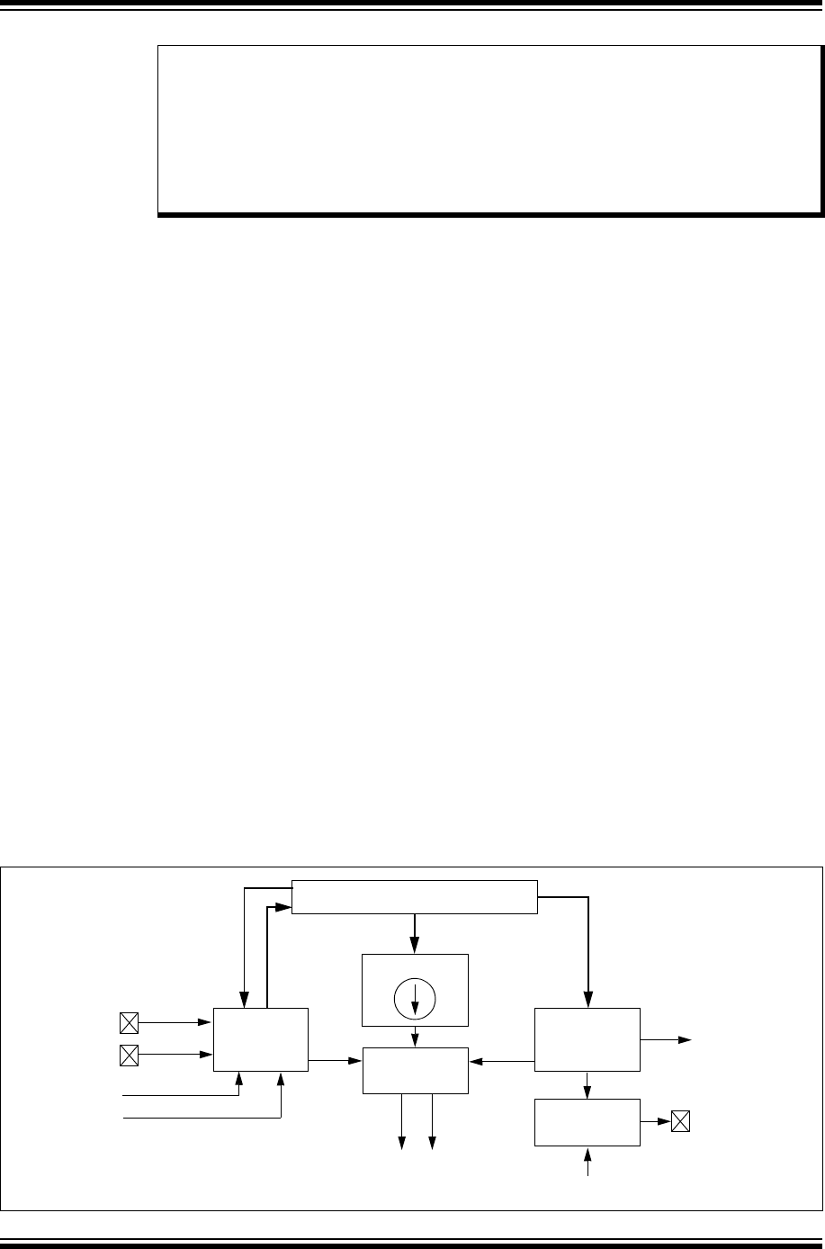
PIC32 Family Reference Manual
DS61167B-page 37-2 © 2011-2012 Microchip Technology Inc.
37.1 INTRODUCTION
The Charge Time Measurement Unit (CTMU) is a flexible analog module that has a configurable
current source with a digital configuration circuit built around it. The CTMU can be used for
differential time measurement between pulse sources and can be used for generating an asyn-
chronous pulse. By working with other on-chip analog modules, the CTMU can be used for high
resolution time measurement, measure capacitance, measure relative changes in capacitance
or generate output pulses with a specific time delay. The CTMU is ideal for interfacing with
capacitive-based sensors.
The module includes the following key features:
•Up to 32 channels available for capacitive or time measurement input
•On-chip precision current source
•16-edge input trigger sources
• Selection of edge or level-sensitive inputs
•Polarity control for each edge source
•Control of edge sequence
•Control of response to edges
•High precision time measurement
•Time delay of external or internal signal asynchronous to system clock
• Integrated temperature sensing diode
•Control of current source during auto-sampling
•Four current source ranges
•Time measurement resolution of one nanosecond
The CTMU works in conjunction with the Analog-to-Digital Converter (ADC) to provide up to 32
channels for time or charge measurement, depending on the specific device and the number of
ADC channels available. When configured for time delay, the CTMU is connected to one of the
analog comparators. The level-sensitive input edge sources can be selected from four sources:
two external inputs, Timer1 or Output Compare Module 1. For information on available input
sources, refer to the specific device data sheet.
A block diagram of the CTMU is shown in Figure 37-1.
Figure 37-1: CTMU Block Diagram
Note: This family reference manual section is meant to serve as a complement to device
data sheets. Depending on the device variant, this manual section may not apply to
all PIC32 devices.
Please consult the note at the beginning of the “Charge Time Measurement Unit
(CTMU)” chapter in the current device data sheet to check whether this document
supports the device you are using.
Device data sheets and family reference manual sections are available for
download from the Microchip Worldwide Web site at: http://www.microchip.com
CTED16
CTED1
Current Source
Edge
Control
Logic
Pulse
Generator
ADC Comparator 2
Input
OC1
Current
Control
ITRIM<5:0>
IRNG<1:0>
CTMUCON
CTMU
Control
Logic
EDGEN
EDGSEQEN
EDG1SELx
EDG1POL
EDG2SELx
EDG2POL EDG1STAT
EDG2STAT
TGEN
IDISSEN
CTTRIG
ADC Trigger
CTPLS
Comparator 2 Output
EDG1MOD
EDG2MOD
.
.
.
Timer1

© 2011-2012 Microchip Technology Inc. DS61167B-page 37-3
Section 37. Charge Time Measurement Unit (CTMU)
Charge Time
Measurement Unit
(CTMU)
37
37.2 REGISTERS
The CTMUCON register contains control bits for configuring the CTMU module edge source
selection, edge source polarity selection, edge sequencing, ADC trigger, analog circuit capacitor
discharge and enables. In addition, this register has bits for selecting the current source range
and current source trim.
Tabl e 37- 1 summarizes the CTMU-related register. A detailed description of the register follows
the summary.
Table 37-1: CTMU SFR Summary(1)
Name Bit
Range
Bit
31/23/15/7
Bit
30/22/14/6
Bit
29/21/13/5
Bit
28/20/12/4
Bit
27/19/11/3
Bit
26/18/10/2
Bit
25/17/9/1
Bit
24/16/8/0
CTMUCON 31:24 EDG1MOD EDG1POL EDG1SEL<3:0> EDG2STAT EDG1STAT
23:16 EDG2MOD EDG2POL EDG2SEL<3:0> — —
15:8 ON — CTMUSIDL TGEN EDGEN EDGSEQEN IDISSEN CTTRIG
7:0 ITRIM<5:0> IRNG<1:0>
Legend: — = unimplemented, read as ‘0’. Address offset values are shown in hexadecimal.
Note 1: Not all registers have associated SET, CLR, and INV registers. Refer to the specific device data sheet for details.

PIC32 Family Reference Manual
DS61167B-page 37-4 © 2011-2012 Microchip Technology Inc.
Register 37-1: CTMUCON: CTMU Control Register
Bit
Range
Bit
31/23/15/7
Bit
30/22/14/6
Bit
29/21/13/5
Bit
28/20/12/4
Bit
27/19/11/3
Bit
26/18/10/2
Bit
25/17/9/1
Bit
24/16/8/0
31:24 R/W-0 R/W-0 R/W-0 R/W-0 R/W-0 R/W-0 R/W-0 R/W-0
EDG1MOD EDG1POL EDG1SEL<3:0>(1) EDG2STAT EDG1STAT
23:16 R/W-0 R/W-0 R/W-0 R/W-0 R/W-0 R/W-0 U-0 U-0
EDG2MOD EDG2POL EDG2SEL<3:0>(1) — —
15:8 R/W-0 U-0 R/W-0 R/W-0 R/W-0 R/W-0 R/W-0 R/W-0
ON —CTMUSIDLTGENEDGENEDGSEQENIDISSENCTTRIG
7:0 R/W-0 R/W-0 R/W-0 R/W-0 R/W-0 R/W-0 R/W-0 R/W-0
ITRIM<5:0> IRNG<1:0>
Legend:
R = Readable bit W = Writable bit U = Unimplemented bit, read as ‘0’
-n = Value at POR ‘1’ = Bit is set ‘0’ = Bit is cleared x = Bit is unknown
bit 31 EDG1MOD: Edge1 Edge Sampling Select bit
1 = Input is edge-sensitive
0 = Input is level-sensitive
bit 30 EDG1POL: Edge 1 Polarity Select bit
1 = Edge1 programmed for a positive edge response
0 = Edge1 programmed for a negative edge response
bit 29-26 EDG1SEL<3:0>: Edge 1 Source Select bits(1)
1111 = CTED16 selected
•
•
•
0000 = CTED1 selected
bit 25 EDG2STAT: Edge2 Status bit
Indicates the status of Edge2 and can be written to control edge source
1 = Edge2 has occurred
0 = Edge2 has not occurred
bit 24 EDG1STAT: Edge1 Status bit
Indicates the status of Edge1 and can be written to control edge source
1 = Edge1 has occurred
0 = Edge1 has not occurred
bit 23 EDG2MOD: Edge2 Edge Sampling Select bit
1 = Input is edge-sensitive
0 = Input is level-sensitive
bit 22 EDG2POL: Edge 2 Polarity Select bit
1 = Edge2 programmed for a positive edge response
0 = Edge2 programmed for a negative edge response
bit 21-18 EDG2SEL<3:0>: Edge 2 Source Select bits(1)
1111 = CTED16 selected
•
•
•
0000 = CTED1 selected
bit 17-16 Unimplemented: Read as ‘0’
bit 15 ON: ON Enable bit
1 = Module is enabled
0 = Module is disabled
Note 1: Refer to the “CTMU” chapter in the specific device data sheet for the list of available trigger sources.

© 2011-2012 Microchip Technology Inc. DS61167B-page 37-5
Section 37. Charge Time Measurement Unit (CTMU)
Charge Time
Measurement Unit
(CTMU)
37
bit 14 Unimplemented: Read as ‘0’
bit 13 CTMUSIDL: Stop in Idle Mode bit
1 = Discontinue module operation when device enters Idle mode
0 = Continue module operation in Idle mode
bit 12 TGEN: Time Generation Enable bit
1 = Enables edge delay generation
0 = Disables edge delay generation
bit 11 EDGEN: Edge Enable bit
1 = Edges are not blocked
0 = Edges are blocked
bit 10 EDGSEQEN: Edge Sequence Enable bit
1 = Edge1 must occur before Edge2 can occur
0 = No edge sequence is needed
bit 9 IDISSEN: Current Discharge Enable bit
1 = Analog current source output is grounded
0 = Analog current source output is not grounded
bit 8 CTTRIG: Trigger Control bit
1 = Trigger output is enabled
0 = Trigger output is disabled
bit 7-2 ITRIM<5:0>: Current Source Trim bits
111111 = Minimum negative change from nominal current
•
•
•
100010
100001 = Maximum negative change from nominal current
011111 = Maximum positive change from nominal current
011110
•
•
•
000001 = Minimum positive change from nominal current
000000 = Nominal current output specified by IRNG<1:0>
bit 1-0 IRNG<1:0>: Current Range Select bits
11 = 100 times base current
10 = 10 times base current
01 = Base current level (0.55 A nominal)
00 = 1000 times base current
Register 37-1: CTMUCON: CTMU Control Register (Continued)
Note 1: Refer to the “CTMU” chapter in the specific device data sheet for the list of available trigger sources.

PIC32 Family Reference Manual
DS61167B-page 37-6 © 2011-2012 Microchip Technology Inc.
37.3 CTMU OPERATION
The CTMU works by using a constant current source to charge a circuit. The type of circuit
depends on the type of measurement being made. In the case of capacitance measurement, the
current is fixed and the amount of time the current is applied to the circuit is fixed. The amount
of voltage read by the ADC is then a measurement of the capacitance of the circuit. In the case
of time measurement, the current, as well as the capacitance of the circuit, is fixed and charge
time varies. In this case, the voltage read by the ADC is then representative of the amount of time
elapsed from the time the current source starts and stops charging the circuit.
If the CTMU is being used as a time delay, both capacitance and current source are fixed, as well
as the voltage supplied to the comparator circuit. The delay of a signal is determined by the
amount of time taken for the voltage to charge to the comparator threshold voltage.
37.3.1 Theory of Operation
The operation of the CTMU is based on the equation for charge, as shown in Equation 37-1.
Equation 37-1:
More simply, the amount of charge measured in coulombs in a circuit is defined as current in
amperes (I) multiplied by the amount of time in seconds that the current flows (t). Charge is also
defined as the capacitance in farads (C) multiplied by the voltage of the circuit (V), as shown in
Equation 37-2.
Equation 37-2:
The CTMU module provides a constant, known current source. The ADC is used to measure (V)
in the equation, leaving two unknowns: capacitance (C) and time (t). Equation 37-2 can be used
to calculate capacitance or time, by either the relationship shown in Equation 37-3 and using the
known fixed capacitance of the circuit, or by Equation 37-4 using a fixed time that the current
source is applied to the circuit.
Equation 37-3:
Equation 37-4:
IC
dV
dt
-------=
ItCV=
tCV
I
-----------------=
CIt
V
-------------=

© 2011-2012 Microchip Technology Inc. DS61167B-page 37-7
Section 37. Charge Time Measurement Unit (CTMU)
Charge Time
Measurement Unit
(CTMU)
37
37.3.2 Current Source
At the heart of the CTMU is a precision current source, designed to provide a constant reference
for measurements. The level of current is user-selectable across four ranges, or a total of two
orders of magnitude, with the ability to trim the output in ±2% increments (nominal). The current
range is selected by the IRNG<1:0> bits (CTMUCON<1:0>) with a value of ‘01’ representing the
lowest range.
Current trim is provided by the ITRIM<5:0> bits (CTMUCON<7:2>). These six bits allow trimming
of the current source in steps of approximately 2% per step. Note that half of the range adjusts
the current source positively and the other half reduces the current source. A value of ‘000000’
is the neutral position (no change). A value of ‘100001’ (see Note 1) is the maximum negative
adjustment (approximately -62%) and ‘011111’ (see Note 2) is the maximum positive
adjustment (approximately +62%).
37.3.3 Edge Selection and Control
CTMU measurements are controlled by edge events occurring on the module’s two input
channels. Each channel, referred as Edge 1 and Edge 2, can be configured to receive input
pulses from one of the sixteen edge input pins. The inputs are selected using the
EDG1SEL<3:0> and EDG2SEL<3:0> bit pairs (CTMUCON<29:26> and CTMUCON<21:18>).
In addition to source, each channel can be configured for event polarity using the EDG1POL and
EDG2POL bits (CTMUCON<30>and CTMUCON<22>). The input channels can also be filtered
for an edge event sequence (Edge 1 occurring before Edge 2) by setting the EDGSEQEN bit
(CTMUCON<10>).
37.3.4 Edge Status
The CTMUCON register also contains two status bits: EDG1STAT (CTMUCON<24>) and
EDG2STAT (CTMUCON<25>). Their primary function is to show if an edge response has
occurred on the corresponding channel. The CTMU automatically sets a particular bit when an
edge response is detected on its channel. The level-sensitive or edge-sensitive nature of the
input channels means that the status bits are set immediately if the channel’s configuration
changes and remains in the new state.
The CTMU module uses the edge status bits to control the current source output to external ana-
log modules (such as the ADC). Current is supplied to external modules only when one (but not
both) of the status bits is set and shuts current off when both bits are either set or cleared. This
allows the CTMU to measure current only during the interval between edges. After both the
status bits are set, it is necessary to clear them before another measurement is taken. Both the
bits should be cleared simultaneously, if possible, to avoid re-enabling the CTMU current source.
In addition to being set by the CTMU hardware, the edge status bits can also be set by software.
This allows the user’s application to manually enable or disable the current source. Setting either
one (but not both) of the bits enables the current source. Setting or clearing both bits at once
disables the source.
37.3.5 Interrupts
The CTMU sets its interrupt flag (CTMUIF) whenever the current source is enabled and then
disabled. If edge sequencing is not enabled (i.e., Edge 1 must occur before Edge 2), it is
necessary to monitor the edge status bits and determine which edge occurred last and caused
the interrupt.
Note 1: The value '100001' = -31 & 0x3F iTRIM = -31 * Delta I, approximately -62% of
nominal.
2: The value '011111' = +31 & 0x3F iTRIM = +31 * Delta I, approximately +62% of
nominal.

PIC32 Family Reference Manual
DS61167B-page 37-8 © 2011-2012 Microchip Technology Inc.
37.4 CTMU MODULE INITIALIZATION
The following sequence is a general guideline used to initialize the CTMU module:
1. Select the current source range using the IRNG<1:0> bits (CTMUCON<1:0>).
2. Adjust the current source trim using the ITRIM<5:0> bits (CTMUCON<7:2>).
3. Configure the edge input sources for Edge 1 and Edge 2 by setting the EDG1SEL and
EDG2SEL bits (CTMUCON<29:26> and CTMUCON<21:18>).
4. Configure the input polarities for the edge inputs using the EDG1POL bit
(CTMUCON<30>) and EDG2POL bit (CTMUCON<22>). The default configuration is for
negative edge polarity (high-to-low transitions).
5. Enable edge sequencing using the EDGSEQEN bit (CTMUCON<10>). By default, edge
sequencing is disabled.
6. Select the operating mode (Measurement or Time Delay) with the TGEN bit
(CTMUCON<12>). By default, the time delay mode is disabled.
7. Configure the module to automatically trigger an analog-to-digital conversion when the
second edge event has occurred using the CTTRIG bit (CTMUCON<8>). The conversion
trigger is disabled by default.
8. Discharge the connected circuit by setting the IDISSEN bit (CTMUCON<9>). After waiting
a sufficient time for the circuit to discharge, clear the IDISSEN bit.
9. Disable the module by clearing the ON bit (CTMUCON<15>).
10. Clear the Edge Status bits, EDG2STAT<3:0> and EDG1STAT<3:0> (CTMUCON<29:26>
and CTMUCON<21:18>).
11. Enable both edge inputs by setting the EDGEN bit (CTMUCON<11>).
12. Enable the module by setting the ON bit (CTMUCON<15>).
Depending on the type of measurement or pulse generation being performed, one or more
additional modules may also need to be initialized and configured with the CTMU module:
•Edge Source Generation: In addition to the external edge input pins, other modules, such
as ICx, OCx, and Timer1 can be used as edge sources for the CTMU. Refer to the specific
device data sheet for available sources.
•Capacitance or Time Measurement: The CTMU module uses the ADC to measure the
voltage across a capacitor that is connected to one of the analog input channels.
•Pulse Generation: When generating system clock independent output pulses, the CTMU
module uses Comparator 2 and the associated comparator voltage reference.
For specific information on initializing these modules, refer to the applicable section in the “PIC32
Family Reference Manual” for the appropriate module.

© 2011-2012 Microchip Technology Inc. DS61167B-page 37-9
Section 37. Charge Time Measurement Unit (CTMU)
Charge Time
Measurement Unit
(CTMU)
37
37.5 CALIBRATING THE CTMU MODULE
The CTMU requires calibration for precise measurements of capacitance and time, as well as for
accurate time delay. If the application requires only measurement of a relative change in capac-
itance or time, calibration is usually not necessary. An example of this type of application would
include a capacitive touch switch, in which the touch circuit has a baseline capacitance and the
added capacitance of the human body changes the overall capacitance of a circuit.
If actual capacitance or time measurement is required, two hardware calibrations must take
place: the current source needs calibration to set it to a precise current, and the circuit being
measured needs calibration to measure and/or nullify all other capacitance other than that to be
measured.
37.5.1 Current Source Calibration
The current source on-board the CTMU module has a range of ±62% nominal for each of four
current ranges. Therefore, for precise measurements, it is possible to measure and adjust this
current source by placing a high precision resistor, RCAL, onto a special analog channel. An
example circuit is shown in Figure 37-2. The current source measurement is performed using the
following steps:
1. Initialize the ADC.
2. Initialize the CTMU by configuring the module for Pulse Generation (TGEN = 1) mode.
3. Enable the current source by setting the EDG1STAT bit (CTMUCON<24>).
4. Issue settling time delay.
5. Perform analog-to-digital conversion.
6. Calculate the current source current using I = V/RCAL, where RCAL is a high precision
resistance and V is measured by performing an analog-to-digital conversion.
The CTMU current source may be trimmed with the trim bits in the CTMUCON register using an
iterative process to get an exact desired current. Alternatively, the nominal value without adjust-
ment may be used. It may be stored by the software for use in all subsequent capacitive or time
measurements.
Figure 37-2 shows the external connections for current source calibration, as well as the relationship
of the different analog modules required.
CTMU charge pump calibration should be done only on the special pin that connects to the Com-
parator module associated with the CTMU. Use of any other ANx pin will add around 2.5 k of series
resistance to the measurement from the analog multiplexer in front of the ADC. This effect can be
ignored only for the smallest current settings. For larger current settings, the uncertainty in the extra
series resistance overwhelms the overall resistance accuracy from the calibration resistor.
To c a lc u la te th e v a lu e for RCAL, the nominal current must be chosen and then the resistance can
be calculated. For example, if the ADC reference voltage is 3.3V, use 70% of full scale, or 2.31V
as the desired approximate voltage to be read by the ADC. If the range of the CTMU current
source is selected to be 0.55 A, the required resistor value is calculated as
RCAL =2.31V/0.55 µA, for a value of 4.2 M. Similarly, if the current source is chosen to be
5.5 µA, RCAL would be 420,000 and 42,000 if the current source is set to 55 µA.
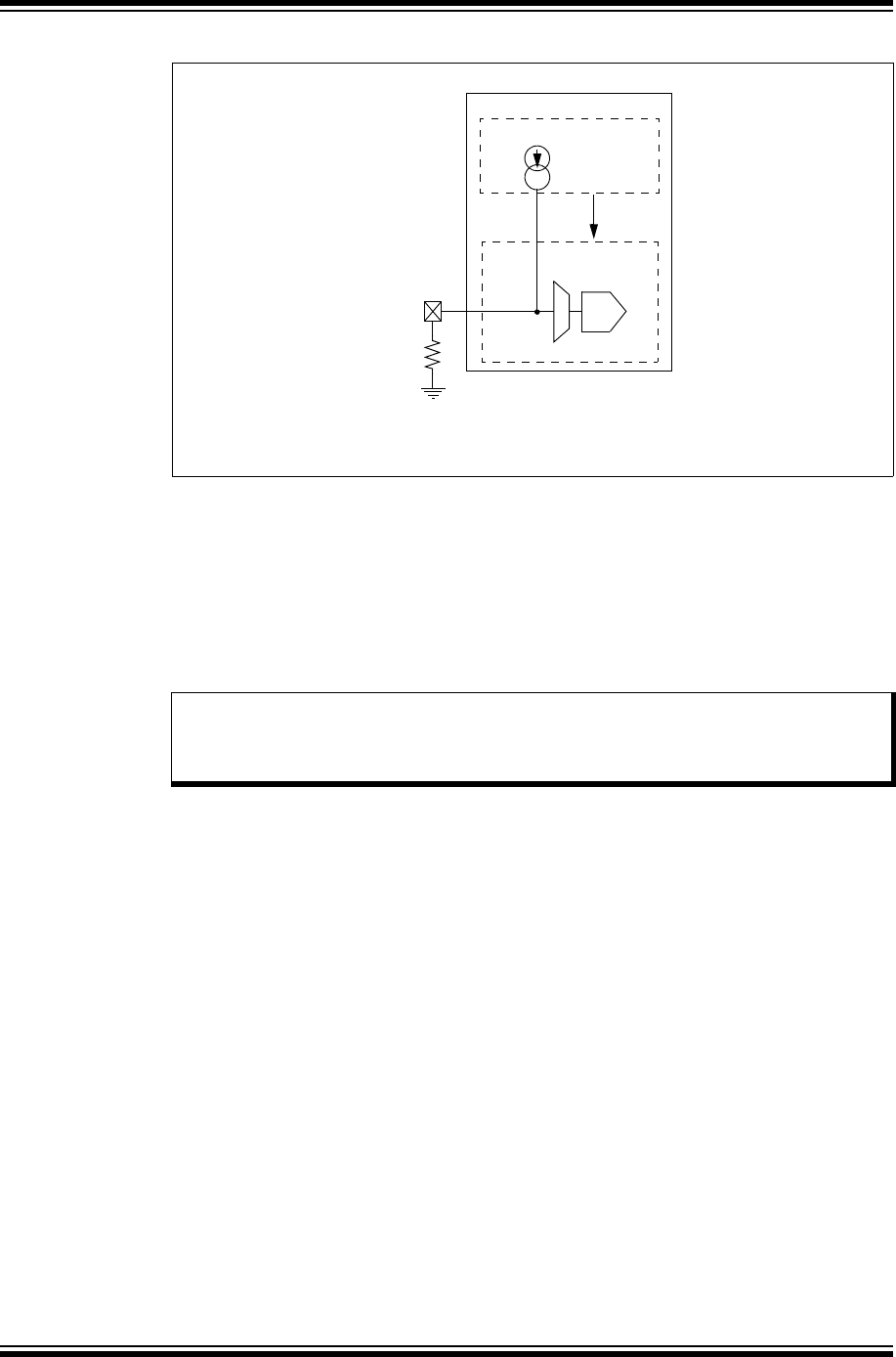
PIC32 Family Reference Manual
DS61167B-page 37-10 © 2011-2012 Microchip Technology Inc.
Figure 37-2: CTMU Current Source Calibration Circuit
Choose a value of 70% full-scale voltage to ensure that the ADC is in a range that is above the
noise floor. If exact current is chosen to incorporate the trimming bits from the CTMUCON
register, the resistor value of RCAL must be adjusted accordingly. RCAL may be adjusted to allow
for available resistor values. RCAL should be of the highest precision available, the amount of
precision required for the circuit that the CTMU will be used to measure. A recommended
minimum precision would be 0.1% tolerance.
Example 37-1 shows a typical method for performing a CTMU current calibration. This method
manually triggers the ADC and it is performed to demonstrate the process. It is also possible to
automatically trigger the conversion by setting the CTTRIG bit (CTMUCON<8>).
Note: A complete MPLAB project based on this calibration routine is available on the
Microchip website at: http://www.microchip.com/CodeExamplesByFunc.aspx.
From the landing page, scroll down and select Touch Sense (mTouch) as the
application.
PIC32 Device
ADC
CTMU
Comparator Input(1)
RCAL
Current Source
ADC
Trigger
ADC
MUX
Note 1: Refer to the “Comparator” and “CTMU” chapters in the specific device data sheet to
determine which comparator and comparator input pin is used by the CTMU module.

© 2011-2012 Microchip Technology Inc. DS61167B-page 37-11
Section 37. Charge Time Measurement Unit (CTMU)
Charge Time
Measurement Unit
(CTMU)
37
Example 37-1: Current Calibration Routine
// Device setup - TO DO: Set up device with #pragma's
int main(void)
{
unsigned long int ADC_Sum; // For averaging multiple ADC measurements
unsigned short int iAvg, // Averaging index
Naverages = 1024, // Number of averages < 2^22 (22=32-10 bits of ADC)
Log2Naverages = 10; // Right shift equal to 1/Naverages
short int iTrim; // Current trim index
unsigned short int VmeasADC, VavgADC; // Measured Voltages, 65536 = Full Scale
// TO DO: Disable JTAG and enable multivector interrupt table
// Set up UART2 for transmission of button data
// TO DO: Set up pins
// CTMU Setup
CTMUCONbits.TGEN = 1; // Enable direct output to C2INB/AN2 pin
CTMUCONbits.IRNG = 0x3; // Current Range
// Turn on CTMU after setting current trim below
// ADC Setup
AD1CON2 = 0x0; // VR+ = AVDD, V- = AVSS, Don't scan, MUX A only
// ADC clock derived from peripheral buss clock
// Tadc = 4 * Tpbus = 4 * 25 ns = 100 ns > 65 ns required
// Tadc = 2*(1+1)*Tpbus
// Tadc = 2*(AD1CON3<7:0>+1)*Tpbus
AD1CON3 = 1;
AD1CSSL = 0x0; // No channels scanned
AD1CHSbits.CH0SA = 2; // Select channel AN2 (PG1D/AN2/C2INB)
ANSELA = 0x0000; // No ADC pins
ANSELB = 1<<0; // RB0: for AN2/C2INB, which is connected to Rcal
ANSELC = 0x0000; // No ADC pins
IEC0bits.AD1IE = 0; // Disable ADC interrupts
AD1CON1bits.ON = 1; // Turn on ADC
// Sweep over all possible current trim values
for ( iTrim = -31; iTrim < 32; iTrim++ )
{
CTMUCONbits.ITRIM = iTrim & 0x3F; // Set current trim value
CTMUCONbits.ON = 1; // Turn on CTMU
// TO DO: Add delay of 1 ms
ADC_Sum = 0;
for ( iAvg = 0; iAvg < Naverages; iAvg++ )
{
CTMUCONCLR = 0x03000000; // Clear Status bits at same time
AD1CON1bits.SAMP = 1; // Manual sampling start
CTMUCONbits.IDISSEN = 1; // Ground charge pump
// TO DO: Add delay of 500 us;
CTMUCONbits.IDISSEN = 0; // End drain of circuit
LATASET = 1<<8; // Turn on RA8
CTMUCONbits.EDG1STAT = 1; // Begin charging the circuit
LATASET = 1<<7; // Turn on RA7
// TO DO: Wait 25 us
AD1CON1bits.SAMP = 0; // Begin analog-to-digital conversion
CTMUCONbits.EDG2STAT = 1; // Stop charging circuit
while (!AD1CON1bits.DONE) // Wait for ADC conversion
{
// Do Nothing
}
AD1CON1bits.DONE = 0; // ADC conversion done, clear flag
VmeasADC = ADC1BUF0; // Get the value from the ADC
ADC_Sum += VmeasADC; // Update averaging sum
}//end for ( iAvg = 0; iAvg < Naverages; iAvg++ )
CTMUCONbits.ON = 0; // Turn off CTMU
VavgADC = ADC_Sum >> (Log2Naverages-6); // Full scale = 2^10<<6 = 65536
// TO DO: Transmit iTrim and VavgADC using UART
}// end for ( iTrim = -31; iTrim < 32; iTrim++ )
}// end main()

PIC32 Family Reference Manual
DS61167B-page 37-12 © 2011-2012 Microchip Technology Inc.
37.5.2 Capacitance Calibration
A small amount of capacitance from the internal ADC sample capacitor as well as stray capaci-
tance from the circuit board traces and pads that affect the precision of capacitance measure-
ments. The measurement of the stray capacitance can be taken by making sure the desired
capacitance to be measured has been removed. The measurement is then performed using the
following steps:
1. Initialize the ADC and the CTMU.
2. Set the EDG1STAT bit (= 1).
3. Wait for a fixed delay of time, t.
4. Clear the EDG1STAT bit.
5. Perform an analog-to-digital conversion.
6. Calculate the stray and analog-to-digital sample capacitances using Equation 37-5.
Equation 37-5:
This measured value is then stored and used for calculations of time measurement or subtracted
for capacitance measurement. For calibration, it is expected that the capacitance of CSTRAY +CAD
is approximately known. CAD is approximately 4 pF.
An iterative process may need to be used to adjust the time, t, that the circuit is charged to obtain
a reasonable voltage reading from the ADC. The value of t may be determined by setting COFFSET
to a theoretical value, and then solving for t. For example, if CSTRAY is theoretically calculated to
be 11 pF, and V is expected to be 70% of VDD or 2.31V, t would be equal to Equation 37-6 or
63 µs.
Equation 37-6:
A charge delay of 63 µs represents 2520 instructions when the system is operating at 40 MHz
(2520 = 40 MHz * 63 µs). If the CTMU charge pump is set to 100 x base current (55 µA), the
charge time is cut by a factor of 100, or 25.2 instructions. This can easily be implemented by 25
NOP instructions in the code.
Example 37-2 shows a typical method for measuring capacitance after the CTMU's charge pump
has been calibrated.
Note: A complete MPLAB project based on this calibration routine is available on the
Microchip website at: http://www.microchip.com/CodeExamplesByFunc.aspx.
From the landing page, scroll down and select Touch Sense (mTouch) as the
application.
COFFSET CSTRAY CAD
It
V
-------------=+=
Where:
I is known from the current source measurement step
t is a fixed delay
V is measured by performing an analog-to-digital conversion.
t4pF 11pF+
2.31V
0.55A
------------------63s==

© 2011-2012 Microchip Technology Inc. DS61167B-page 37-13
Section 37. Charge Time Measurement Unit (CTMU)
Charge Time
Measurement Unit
(CTMU)
37
Example 37-2: Capacitance Calibration Routine
// Device setup - TO DO: Set up device with #pragma's
int main(void)
{
unsigned long int ADC_Sum; // For averaging multiple ADC measurements
unsigned short int iAvg, // Averaging index
Naverages = 1024, // Number of averages < 2^22 (22=32-10 bits of ADC)
Log2Naverages = 10; // Right shift equal to 1/Naverages
short int iTrim; // Current trim index
unsigned short int VmeasADC, VavgADC; // Measured Voltages, 65536 = Full Scale
// TO DO: Disable JTAG and enable multivector interrupt table
// Set up UART2 for transmission of button data.
// TO DO: Set up pins
// CTMU Setup
CTMUCONbits.TGEN = 1; // Enable direct output to C2INB/AN2 pin
CTMUCONbits.IRNG = PLIB_CTMU_CurrentRange_100xBase; //Current Range: 100 x 0.55 = 55 uA
// ADC Setup
AD1CON2 = 0x0; // VR+ = AVDD, V- = AVSS, Don't scan, MUX A only
// ADC clock derived from peripheral buss clock
// Tadc = 4 * Tpbus = 4 * 25 ns = 100 ns > 65 ns required
// Tadc = 2*(1 +1)*Tpbus
// Tadc = 2*(AD1CON3<7:0>+1)*Tpbus
AD1CON3 = 1;
AD1CSSL = 0x0; // No channels scanned
AD1CHSbits.CH0SA = 2; // Select channel AN2
ANSELA = 0x0000; // No ADC pins
ANSELB = 1<<0; // RB0: for AN2/C2INB, which is connected to Rcal
ANSELC = 0x0000; // No ADC pins
IEC0bits.AD1IE = 0; // Disable ADC interrupts
AD1CON1bits.ON = 1; // Turn on ADC
// Sweep over all possible current trim values
for ( iTrim = -31; iTrim < 32; iTrim++ )
{
CTMUCONbits.ITRIM = iTrim & 0x3F; // Set current trim value
CTMUCONbits.ON = 1; // Turn on CTMU
// TO DO: Wait 1 ms for CTMU start-up
ADC_Sum = 0;
for ( iAvg = 0; iAvg < Naverages; iAvg++ )
{
AD1CON1bits.SAMP = 1; // Manual sampling start
CTMUCONbits.IDISSEN = 1; // Ground charge pump
// TO DO: Wait 1 ms for grounding
CTMUCONbits.IDISSEN = 0; // End drain of circuit
CTMUCONbits.EDG1STAT = 1; // Begin charging the circuit
// Use Equation 37-6 to solve for charge time with current = 55 uA
// Charge time = 0.63 us, or 25.2 NOPs at 40 MHz system clock
// TO DO: Wait 25 NOPs
AD1CON1bits.SAMP = 0; // Begin analog-to-digital conversion
CTMUCONbits.EDG1STAT = 0; // Stop charging circuit
while (!AD1CON1bits.DONE) // Wait for ADC conversion
{
// Do Nothing
}
AD1CON1bits.DONE = 0; // ADC conversion done, clear flag
VmeasADC = ADC1BUF0; // Get the value from the ADC
ADC_Sum += VmeasADC; // Update averaging sum
}// end for ( iAvg = 0; iAvg < Naverages; iAvg++ )

PIC32 Family Reference Manual
DS61167B-page 37-14 © 2011-2012 Microchip Technology Inc.
Example 37-2: Capacitance Calibration Routine (Continued)
CTMUCONbits.ON = 0; // Turn off CTMU
VavgADC = ADC_Sum >> (Log2Naverages-6); //Full scale = 2^10<<6 = 65536
// TO DO: Transmit iTrim and VavgADC using UART
if ( VavgADC > 50000 ) // Stop, ADC voltage too high
{
break;
}
}// end for ( iTrim = -31; iTrim < 32; iTrim++ )
return 0;
}// end main()

© 2011-2012 Microchip Technology Inc. DS61167B-page 37-15
Section 37. Charge Time Measurement Unit (CTMU)
Charge Time
Measurement Unit
(CTMU)
37
37.6 MEASURING CAPACITANCE WITH THE CTMU
There are two separate methods of measuring capacitance with the CTMU. The first is the
absolute method, in which the actual capacitance value is required. The second is the relative
method, in which the actual capacitance is not required, rather an indication of a change in
capacitance is required.
37.6.1 Absolute Capacitance Measurement
For absolute capacitance measurements, both the current and capacitance calibration steps
found in 37.5 “Calibrating the CTMU Module” should be followed. Capacitance measurements
are performed using the following steps:
1. Initialize the ADC.
2. Initialize the CTMU.
3. Set the EDG1STAT bit.
4. Wait for a fixed delay, T.
5. Clear the EDG1STAT bit.
6. Perform an analog-to-digital conversion.
7. Calculate the total capacitance, CTOTAL = (I * T)/V, where I is known from the current
source measurement step (37.5.1 “Current Source Calibration”), T is a fixed delay and
V is measured by performing an analog-to-digital conversion.
8. Subtract the stray and analog-to-digital capacitance (COFFSET from 37.5.2 “Capacitance
Calibration”) from CTOTAL to determine the measured capacitance.
37.6.2 Relative Charge Measurement
An application may not require precise capacitance measurements. For example, when detect-
ing a valid press of a capacitance-based switch, detecting a relative change of capacitance is of
interest. In this type of application, when the switch is open (or not touched), the total capacitance
is the capacitance of the combination of the board traces, the ADC, etc. A larger voltage will be
measured by the ADC. When the switch is closed (or is touched), the total capacitance is larger
due to the addition of the capacitance of the human body to the above listed capacitances and a
smaller voltage will be measured by the ADC.
Detecting capacitance changes can be accomplished with the CTMU using these steps:
1. Initialize the ADC and the CTMU.
2. Set the EDG1STAT bit.
3. Wait for a fixed delay.
4. Clear the EDG1STAT bit.
5. Perform an analog-to-digital conversion.
The voltage measured by performing the analog-to-digital conversion is an indication of the
relative capacitance. In this case, no calibration of the current source or circuit capacitance mea-
surement is needed.
A sample software routine for a capacitive touch switch is shown in Example 37-3. In this exam-
ple, the prior calibration of the 8-Key Direct Sensor Daughter Board can be used to equalize the
measured voltages by adjusting charge time for variations in each button circuit's capacitance.
Alternatively, a fixed charge time can be used if the software supports separate trigger levels for
each button. For simplicity, the routine only checks the second button (9) on the 8-Key Direct
Sensor Daughter Board.
Note: The ADC must be configured correctly for proper CTMU functionality. If necessary,
ensure that the ADC is pointing to an unused pin.
Note: The ADC must be configured correctly for proper CTMU functionality. If necessary,
ensure that the ADC is pointing to an unused pin.
Note: A more advanced version that measures all eight buttons is available on the
Microchip website at: http://www.microchip.com/CodeExamplesByFunc.aspx.
From the landing page, scroll down and select Touch Sense (mTouch) as the
application.

PIC32 Family Reference Manual
DS61167B-page 37-16 © 2011-2012 Microchip Technology Inc.
Example 37-3: Routine for Capacitive Touch Switch
// Taken from HardwareProfile.h
#define NUM_DIRECT_KEYS 8
static unsigned short int ButtonADCChannels[NUM_DIRECT_KEYS] = {0,1,4,5,6,7,8,9};
// Device setup
//TO DO: Setup up device with #pragma's
int main(void)
{
unsigned long int ADC_Sum; // For averaging multiple ADC measurements
unsigned short int iAvg, // Averaging index
Naverages = 32, // Number of averages < 2^22
Log2Naverages = 5; // Right shift equal to 1/Naverages
short int iButton, // Button Index
iChan, // ADC channel index
CurrentButtonStatus; // Bit field of buttons that are pressed
unsigned short int VmeasADC, VavgADC; // Measured Voltages, 65536 = Full Scale
unsigned short int ButtonVmeasADC[NUM_DIRECT_KEYS]; // Report out all voltages at once
// TO DO: Disable JTAG and enable multivector interrupt table
// Set up UART2 for transmission of button data.
// TO DO: Set up pins
// CTMU Setup
CTMUCONbits.IRNG = 0x3; // Current Range
CTMUCONbits.ON = 1; // Turn on CTMU
// TO DO: Wait 1 ms for CTMU to warm-up
// ADC Setup
AD1CON2 = 0x0; // VR+ = AVDD, V- = AVSS, Don't scan, MUX A only
// ADC clock derived from peripheral buss clock
// Tadc = 4 * Tpbus = 4 * 25 ns = 100 ns > 65 ns required
// Tadc = 2*(1+1)*Tpbus
// Tadc = 2*(AD1CON3<7:0>+1)*Tpbus
AD1CON3 = 1;
AD1CSSL = 0x0; // No channels scanned
// Taken from mTouchCapADC.c
ANSELA = (1<<0) | (1<<1); //RA0,1
ANSELB = (1<<2) | (1<<3) | (1<<13) | (1<<14) | (1<<15); //RB2,3,13,14,15
ANSELC = (1<<0) | (1<<1) | (1<<2) | (1<<3); //RC0,1,2,3
IEC0bits.AD1IE = 0; // Disable ADC interrupts
AD1CON1bits.ON = 1; // Turn on ADC
while ( 1 )
{
CurrentButtonStatus = 0;
for ( iButton = 0; iButton < NUM_DIRECT_KEYS; iButton++ )
{
iChan = ButtonADCChannels[iButton];
AD1CHSbits.CH0SA = iChan;
ADC_Sum = 0;
iButton = 2;
AD1CON1bits.SAMP = 1; // Manual sampling start
CTMUCONbits.IDISSEN = 1; // Ground charge pump
DelayMs(1); // Wait 1 ms for grounding
CTMUCONbits.IDISSEN = 0; // End drain of circuit

© 2011-2012 Microchip Technology Inc. DS61167B-page 37-17
Section 37. Charge Time Measurement Unit (CTMU)
Charge Time
Measurement Unit
(CTMU)
37
Example 37-3: Routine for Capacitive Touch Switch (Continued)
switch (iButton)
CTMUCONbits.EDG1STAT = 1; // Begin charging the circuit
// TO DO: Wait 33 NOPs for Button 2 charge
AD1CON1bits.SAMP = 0; // Begin analog-to-digital conversion
CTMUCONbits.EDG1STAT = 0; // Stop charging circuit
while (!AD1CON1bits.DONE) // Wait for ADC conversion
{
// Do Nothing
}
AD1CON1bits.DONE = 0; // ADC conversion done, clear flag
VmeasADC = ADC1BUF0; // Get the value from the ADC
ADC_Sum += VmeasADC; // Update averaging sum
}// end for ( iAvg = 0; iAvg < Naverages; iAvg++ )
if ( Log2Naverages-6 > 0 )
{
VavgADC = ADC_Sum >> (Log2Naverages-6); // Full scale = 2^10<<6 = 65536
}
else
{
VavgADC = ADC_Sum << (6-Log2Naverages); // Full scale = 2^10<<6 = 65536
}
if ( VavgADC < 32768 ) // Button is being pressed
{
CurrentButtonStatus += 1<<iButton;
}
ButtonVmeasADC[iButton] = VavgADC;
}//end while ( 1 )
}//end main()

PIC32 Family Reference Manual
DS61167B-page 37-18 © 2011-2012 Microchip Technology Inc.
37.7 MEASURING TIME WITH THE CTMU MODULE
Time can be precisely measured after the ratio (C/I) is measured from the current and
capacitance calibration step by following these steps:
1. Initialize the ADC and the CTMU.
2. Set the EDG1STAT bit.
3. Set the EDG2STAT bit.
4. Perform an analog-to-digital conversion.
5. Calculate the time between edges as T = (C/I) * V, where I is calculated in the current
calibration step (37.5.1 “Current Source Calibration”), C is calculated in the
capacitance calibration step (37.5.2 “Capacitance Calibration”) and V is measured by
performing the analog-to-digital conversion.
It is assumed that the time measured is small enough that the capacitance, COFFSET, provides a
valid voltage to the ADC. For the smallest time measurement, always set the ADC Channel
Select register (AD1CHS) to the ADC input channel named Open. This minimizes any stray
capacitance, keeping the total circuit capacitance close to that of the ADC itself (4-5 pF). To mea-
sure longer time intervals, an external capacitor may be connected to an ADC channel and this
channel is selected when making a time measurement.
37.8 CREATING A DELAY WITH THE CTMU MODULE
A unique feature on board the CTMU module is its ability to generate system clock independent
output pulses based on an external capacitor value. This is accomplished using the internal
comparator voltage reference module, Comparator 2 input pin and an external capacitor. The
pulse is output onto the CTPLS pin. To enable this mode, set the TGEN bit.
An example circuit is shown in Figure 37-3. CDELAY is chosen by the user to determine the output
pulse width on CTPLS. The pulse width is calculated by T = (CDELAY/I)*V, where I is known from
the current source measurement step (37.5.1 “Current Source Calibration”) and V is the
internal reference voltage (CVREF).
An example use of this feature is for interfacing with variable capacitive-based sensors, such as
a humidity sensor. As the humidity varies, the pulse-width output on CTPLS will vary. The CTPLS
output pin can be connected to an input capture pin and the varying pulse width is measured to
determine the humidity in the application.
Follow these steps to use this feature:
1. Initialize Comparator 2.
2. Initialize the comparator voltage reference.
3. Initialize the CTMU and enable time delay generation by setting the TGEN bit.
4. Set the EDG1STAT bit.
5. When CDELAY charges to the value of the voltage reference trip point, an output pulse is
generated on CTPLS.
Figure 37-3: Typical Connections and Internal Configuration for Pulse Delay Generation
Cx
CVREF
CTPLS
PIC32 Device
Current Source
Comparator
CTMU
CTED1
Comparator Input(1)
CDELAY
EDG1STAT
Note 1: Please refer to the specific device data sheet for information related to the comparator input used in this mode.

© 2011-2012 Microchip Technology Inc. DS61167B-page 37-19
Section 37. Charge Time Measurement Unit (CTMU)
Charge Time
Measurement Unit
(CTMU)
37
37.9 MEASURING ON-CHIP TEMPERATURE WITH THE CTMU
The CTMU module can be used to measure the internal temperature of the device through an
internal diode that is available. When EDG1STAT is not equal to EDG2STAT and TGEN = 0, the
current is steered into the temperature sensing diode. The voltage across the diode is available
as an input to the ADC module.
Figure 37-4 shows how this module can be used for temperature measurement. As the temper-
ature rises, the voltage across the diode will drop by about 300 mV over a 150ºC range. Selecting
a higher current drive strength will raise the voltage value by a few 100 mV.
37.9.1 Basic Principle
The forward voltage (Vf) of a P-N junction, such as a diode, is an extension of the equation for
the junction’s thermal voltage, as shown in Equation 37-7:
Equation 37-7:
Since k and q are physical constants, and Is is a constant for the device, this only leaves T and If
as independent variables. If If is held constant, it follows from the equation that Vf will vary as a
function of T. As the natural log term of the equation will always be negative, the temperature will
be negatively proportional to Vf.
In other words, as temperature increases, Vf decreases.
Figure 37-4: CTMU Temperature Measurement Circuit
Where:
k is the Boltzmann constant (1.38 x 10⁻²³ J K-1)
T is the absolute junction temperature in kelvin
q is the electron charge (1.6 x 10⁻¹⁹ C)
Vf = ( kT/q ) ln ( 1- If / Is )
If is the forward current applied to the diode
Is is the diode’s characteristic saturation current
PIC32 Device
ADC
CTMU
Current Source
ADC
Trigger
A/D
MUX
Diode
ANx

PIC32 Family Reference Manual
DS61167B-page 37-20 © 2011-2012 Microchip Technology Inc.
37.10 OPERATION DURING SLEEP/IDLE MODES
37.10.1 Sleep Mode
When the device enters any Sleep mode, the CTMU module’s current source is always disabled.
If the CTMU is performing an operation that depends on the current source when Sleep mode is
invoked, the operation may not terminate correctly. Capacitance and time measurements may
return erroneous values.
37.10.2 Idle Mode
The behavior of the CTMU in Idle mode is determined by the CTMUSIDL bit (CTMUCON<13>).
If the CTMUSIDL bit is cleared, the module will continue to operate in Idle mode. If the
CTMUSIDL bit is set, the module’s current source is disabled when the device enters Idle mode.
If the module is performing an operation when Idle mode is invoked, in this case, the results will
be similar to those with Sleep mode.
37.11 EFFECTS OF A RESET ON CTMU
Upon Reset, all registers of the CTMU are cleared. This leaves the CTMU module disabled, its
current source is turned off and all configuration options return to their default settings. The
module needs to be re-initialized following any Reset.
If the CTMU is in the process of taking a measurement at the time of Reset, the measurement will
be lost. A partial charge may exist on the circuit that was being measured and should be properly
discharged before the CTMU makes subsequent attempts to make a measurement. The circuit is
discharged by setting, and then clearing, the IDISSEN bit (CTMUCON<9>) while the ADC is
connected to the appropriate channel.

© 2011-2012 Microchip Technology Inc. DS61167B-page 37-21
Section 37. Charge Time Measurement Unit (CTMU)
Charge Time
Measurement Unit
(CTMU)
37
37.12 RELATED APPLICATION NOTES
This section lists application notes that are related to this section of the manual. These
application notes may not be written specifically for the PIC32 device family, but the concepts are
pertinent and could be used with modification and possible limitations. The current application
notes related to the Charge Time Measurement Unit (CTMU) module are:
Title Application Note #
No related application notes at this time. N/A
Note: Please visit the Microchip web site (www.microchip.com) for additional application
notes and code examples for the PIC32 family of devices.

PIC32 Family Reference Manual
DS61167B-page 37-22 © 2011-2012 Microchip Technology Inc.
37.13 REVISION HISTORY
Revision A (March 2011)
This is the initial released revision of this document.
Revision B (February 2012)
This revision includes the following updates:
•Added Note 1 and Note 2 to 37.3.2 “Current Source”
•Updated the last sentence of the first paragraph in 37.3.4 “Edge Status”
•Added Note 1 to the CTMU Current Source Calibration Circuit (see Figure 37-2)
•Removed Setup for CTMU Calibration Routines (formerly Example 37-1)
•Updated the code in the Current Calibration Routine (see Example 37-1)
•Updated the code in the Capacitance Calibration Routine (see Example 37-2)
• Updated the code in the Routine for Capacitive Touch Switch Routine (see Example 37-3)
•Minor updates to text and formatting were incorporated throughout the document
2011-2012 Microchip Technology Inc. DS61167B-page 37-23
Information contained in this publication regarding device
applications and the like is provided only for your convenience
and may be superseded by updates. It is your responsibility to
ensure that your application meets with your specifications.
MICROCHIP MAKES NO REPRESENTATIONS OR
WARRANTIES OF ANY KIND WHETHER EXPRESS OR
IMPLIED, WRITTEN OR ORAL, STATUTORY OR
OTHERWISE, RELATED TO THE INFORMATION,
INCLUDING BUT NOT LIMITED TO ITS CONDITION,
QUALITY, PERFORMANCE, MERCHANTABILITY OR
FITNESS FOR PURPOSE. Microchip disclaims all liability
arising from this information and its use. Use of Microchip
devices in life support and/or safety applications is entirely at
the buyer’s risk, and the buyer agrees to defend, indemnify and
hold harmless Microchip from any and all damages, claims,
suits, or expenses resulting from such use. No licenses are
conveyed, implicitly or otherwise, under any Microchip
intellectual property rights.
Trademarks
The Microchip name and logo, the Microchip logo, dsPIC,
KEELOQ, KEELOQ logo, MPLAB, PIC, PICmicro, PICSTART,
PIC32 logo, rfPIC and UNI/O are registered trademarks of
Microchip Technology Incorporated in the U.S.A. and other
countries.
FilterLab, Hampshire, HI-TECH C, Linear Active Thermistor,
MXDEV, MXLAB, SEEVAL and The Embedded Control
Solutions Company are registered trademarks of Microchip
Technology Incorporated in the U.S.A.
Analog-for-the-Digital Age, Application Maestro, chipKIT,
chipKIT logo, CodeGuard, dsPICDEM, dsPICDEM.net,
dsPICworks, dsSPEAK, ECAN, ECONOMONITOR,
FanSense, HI-TIDE, In-Circuit Serial Programming, ICSP,
Mindi, MiWi, MPASM, MPLAB Certified logo, MPLIB,
MPLINK, mTouch, Omniscient Code Generation, PICC,
PICC-18, PICDEM, PICDEM.net, PICkit, PICtail, REAL ICE,
rfLAB, Select Mode, Total Endurance, TSHARC,
UniWinDriver, WiperLock and ZENA are trademarks of
Microchip Technology Incorporated in the U.S.A. and other
countries.
SQTP is a service mark of Microchip Technology Incorporated
in the U.S.A.
All other trademarks mentioned herein are property of their
respective companies.
© 2011-2012, Microchip Technology Incorporated, Printed in
the U.S.A., All Rights Reserved.
Printed on recycled paper.
ISBN: 978-1-62076-043-7
Note the following details of the code protection feature on Microchip devices:
• Microchip products meet the specification contained in their particular Microchip Data Sheet.
• Microchip believes that its family of products is one of the most secure families of its kind on the market today, when used in the
intended manner and under normal conditions.
• There are dishonest and possibly illegal methods used to breach the code protection feature. All of these methods, to our
knowledge, require using the Microchip products in a manner outside the operating specifications contained in Microchip’s Data
Sheets. Most likely, the person doing so is engaged in theft of intellectual property.
• Microchip is willing to work with the customer who is concerned about the integrity of their code.
• Neither Microchip nor any other semiconductor manufacturer can guarantee the security of their code. Code protection does not
mean that we are guaranteeing the product as “unbreakable.”
Code protection is constantly evolving. We at Microchip are committed to continuously improving the code protection features of our
products. Attempts to break Microchip’s code protection feature may be a violation of the Digital Millennium Copyright Act. If such acts
allow unauthorized access to your software or other copyrighted work, you may have a right to sue for relief under that Act.
Microchip received ISO/TS-16949:2009 certification for its worldwide
headquarters, design and wafer fabrication facilities in Chandler and
Tempe, Arizona; Gresham, Oregon and design centers in California
and India. The Company’s quality system processes and procedures
are for its PIC® MCUs and dsPIC® DSCs, KEELOQ® code hopping
devices, Serial EEPROMs, microperipherals, nonvolatile memory and
analog products. In addition, Microchip’s quality system for the design
and manufacture of development systems is ISO 9001:2000 certified.

DS61167B-page 37-24 2011-2012 Microchip Technology Inc.
AMERICAS
Corporate Office
2355 West Chandler Blvd.
Chandler, AZ 85224-6199
Tel: 480-792-7200
Fax: 480-792-7277
Technical Support:
http://www.microchip.com/
support
Web Address:
www.microchip.com
Atlanta
Duluth, GA
Tel: 678-957-9614
Fax: 678-957-1455
Boston
Westborough, MA
Tel: 774-760-0087
Fax: 774-760-0088
Chicago
Itasca, IL
Tel: 630-285-0071
Fax: 630-285-0075
Cleveland
Independence, OH
Tel: 216-447-0464
Fax: 216-447-0643
Dallas
Addison, TX
Tel: 972-818-7423
Fax: 972-818-2924
Detroit
Farmington Hills, MI
Tel: 248-538-2250
Fax: 248-538-2260
Indianapolis
Noblesville, IN
Tel: 317-773-8323
Fax: 317-773-5453
Los Angeles
Mission Viejo, CA
Tel: 949-462-9523
Fax: 949-462-9608
Santa Clara
Santa Clara, CA
Tel: 408-961-6444
Fax: 408-961-6445
Toronto
Mississauga, Ontario,
Canada
Tel: 905-673-0699
Fax: 905-673-6509
ASIA/PACIFIC
Asia Pacific Office
Suites 3707-14, 37th Floor
Tower 6, The Gateway
Harbour City, Kowloon
Hong Kong
Tel : 8 52 -24 01- 120 0
Fax: 852-2401-3431
Australia - Sydney
Tel : 6 1- 2-9 868 -67 33
Fax: 61-2-9868-6755
China - Beijing
Tel : 8 6- 10- 856 9-7 00 0
Fax: 86-10-8528-2104
China - Chengdu
Tel : 8 6- 28- 866 5-5 511
Fax: 86-28-8665-7889
China - Chongqing
Tel : 8 6- 23- 898 0-9 58 8
Fax: 86-23-8980-9500
China - Hangzhou
Tel : 8 6- 571 -28 19- 318 7
Fax: 86-571-2819-3189
China - Hong Kong SAR
Tel : 8 52 -24 01- 120 0
Fax: 852-2401-3431
China - Nanjing
Tel : 8 6- 25- 847 3-2 46 0
Fax: 86-25-8473-2470
China - Qingdao
Tel : 8 6- 532 -85 02- 735 5
Fax: 86-532-8502-7205
China - Shanghai
Tel : 8 6- 21- 540 7-5 53 3
Fax: 86-21-5407-5066
China - Shenyang
Tel : 8 6- 24- 233 4-2 82 9
Fax: 86-24-2334-2393
China - Shenzhen
Tel : 8 6- 755 -82 03- 266 0
Fax: 86-755-8203-1760
China - Wuhan
Tel : 8 6- 27- 598 0-5 30 0
Fax: 86-27-5980-5118
China - Xian
Tel : 8 6- 29- 883 3-7 25 2
Fax: 86-29-8833-7256
China - Xiamen
Tel: 86-592-2388138
Fax: 86-592-2388130
China - Zhuhai
Tel : 86- 75 6-3 21 004 0
Fax: 86-756-3210049
ASIA/PACIFIC
India - Bangalore
Tel : 9 1- 80- 309 0-4 44 4
Fax: 91-80-3090-4123
India - New Delhi
Tel : 9 1- 11- 416 0 -8 631
Fax: 91-11-4160-8632
India - Pune
Tel : 9 1- 20- 256 6-1 51 2
Fax: 91-20-2566-1513
Japan - Osaka
Tel : 8 1- 66- 152 -71 60
Fax: 81-66-152-9310
Japan - Yokohama
Tel : 8 1- 45- 471 - 6 16 6
Fax: 81-45-471-6122
Korea - Daegu
Tel : 8 2- 53- 744 -43 01
Fax: 82-53-744-4302
Korea - Seoul
Tel : 8 2- 2-5 54- 72 0 0
Fax: 82-2-558-5932 or
82-2-558-5934
Malaysia - Kuala Lumpur
Tel : 6 0- 3-6 201 -9 8 57
Fax: 60-3-6201-9859
Malaysia - Penang
Tel : 6 0- 4-2 27- 88 7 0
Fax: 60-4-227-4068
Philippines - Manila
Tel : 6 3- 2-6 34- 90 6 5
Fax: 63-2-634-9069
Singapore
Tel : 6 5- 633 4-8 870
Fax: 65-6334-8850
Taiwan - Hsin Chu
Tel : 8 86 -3- 577 8-3 66
Fax: 886-3-5770-955
Taiwan - Kaohsiung
Tel : 8 86 -7- 536 -48 18
Fax: 886-7-330-9305
Taiwan - Taipei
Tel : 8 86 -2- 250 0-6 61 0
Fax: 886-2-2508-0102
Thailand - Bangkok
Tel : 6 6- 2-6 94- 13 5 1
Fax: 66-2-694-1350
EUROPE
Austria - Wels
Tel : 4 3- 72 42 -2 244 -3 9
Fax: 43-7242-2244-393
Denmark - Copenhagen
Tel : 4 5- 445 0-2 828
Fax: 45-4485-2829
France - Paris
Tel : 3 3- 1-6 9-5 3-6 3-2 0
Fax: 33-1-69-30-90-79
Germany - Munich
Tel : 4 9- 89 -62 7-1 44- 0
Fax: 49-89-627-144-44
Italy - Milan
Tel : 3 9- 03 31 -7 426 11
Fax: 39-0331-466781
Netherlands - Drunen
Tel : 3 1- 41 6- 690 399
Fax: 31-416-690340
Spain - Madrid
Tel : 3 4- 91 -70 8-0 8-9 0
Fax: 34-91-708-08-91
UK - Wokingham
Tel : 4 4- 118 -92 1- 5 869
Fax: 44-118-921-5820
Worldwide Sales and Service
11/29/11

© 2012-2013 Microchip Technology Inc. DS60001183B-page 41-1
Prefetch Module
for Devices with
L1 CPU Cache
41
Section 41. Prefetch Module for Devices with L1 CPU Cache
HIGHLIGHTS
This section of the manual contains the following major topics:
41.1 Introduction .................................................................................................................. 41-2
41.2 Prefetch Module Overview........................................................................................... 41-3
41.3 Control Registers .........................................................................................................41-5
41.4 Prefetch Module Operation ..........................................................................................41-8
41.5 Prefetch Module Configurations................................................................................... 41-8
41.6 Prefetch Module Predictive Prefetch Behavior ............................................................ 41-8
41.7 Coherency Support ......................................................................................................41-9
41.8 Effects of Reset............................................................................................................41-9
41.9 Error Conditions ......................................................................................................... 41-10
41.10 Operation in Power-Saving Modes ............................................................................ 41-11
41.11 Related Application Notes.......................................................................................... 41-12
41.12 Revision History ......................................................................................................... 41-13

PIC32 Family Reference Manual
DS60001183B-page 41-2 © 2012-2013 Microchip Technology Inc.
41.1 INTRODUCTION
This section describes the features and operation of the Prefetch module for PIC32 devices with
L1 CPU Cache. Prefetch module features increase system performance for most applications.
41.1.1 Prefetch Module Features
The Prefetch module includes the following features:
•4 x 16 byte fully associative lines
•One line for CPU instructions
•One line for CPU data
•Two lines for peripheral data
•16 byte parallel memory fetch
• Configurable predictive prefetch
• Error detection and correction
Note: This family reference manual section is meant to serve as a complement to device
data sheets. Depending on the device variant, this manual section may not apply to
all PIC32 devices.
Please consult the note at the beginning of the “Prefetch Module” chapter in the
current device data sheet to check whether this document supports the device you
are using.
Device data sheets and family reference manual sections are available for
download from the Microchip Worldwide Web site at: http://www.microchip.com

© 2012-2013 Microchip Technology Inc. DS60001183B-page 41-3
Section 41. Prefetch Module for Devices with L1 CPU Cache
Prefetch Module
for Devices with
L1 CPU Cache
41
41.2 PREFETCH MODULE OVERVIEW
The Prefetch module is a performance enhancing module included in PIC32 devices with L1
CPU caches. When running at high-clock rates, Wait states must be inserted into Program Flash
Memory (PFM) read transactions to meet the access time of the PFM. Wait states can be hidden
to the core by prefetching and storing instructions in a temporary holding area that the CPU can
access quickly. Although the data path to the CPU is 32 bits wide, the data path to the PFM is
128 bits wide. This wide data path provides the same bandwidth to the CPU as a 32-bit path
running at four times the frequency.
The Prefetch module holds a subset of PFM in temporary holding spaces known as lines. Each
line contains a tag and data field. Normally, the lines hold a copy of what is currently in memory
to make instructions or data available to the CPU without Wait states.
Data located in the PFM may be requested by the CPU or by a peripheral. If the requested data
is not currently stored in a Prefetch module line, a read is performed to the PFM at the correct
address, and the data is supplied to the Prefetch module and to the CPU or peripheral. If the
requested data is stored in the Prefetch module and is valid, the data is supplied to the CPU or
peripheral without Wait states.
Figure 41-1 shows a block diagram of the Prefetch module. Logically, the Prefetch module fits
between the System Bus module and the PFM.
Figure 41-1: Prefetch Module Block Diagram
Bus Control
Prefetch Buffer
Line Control
Tag Data
Program Flash Memory (PFM)
System Bus/CPU
System Bus/CPU
PIC32 Family Reference Manual
DS60001183B-page 41-4 © 2012-2013 Microchip Technology Inc.
41.2.1 Prefetch Module Line Organization
The Prefetch module consists of two arrays, data and tag, each of which hold four lines. A data
array consists of program instructions, program data, or peripheral data. Address matches are
based on the physical address, not the virtual address.
Each line in the tag array contains the following information:
•Tag – Physical address of the data held in the data line
•Valid bit
•Type – CPU instruction, CPU data, or peripheral data
•Double-bit Error Detected (DED) bit
Each line in the data array contains 16 bytes of data. Depending on the line, the data can be
CPU instructions, CPU data, or peripheral data.
Figure 41-2 and Figure 41-3 illustrate the organization of a line.
Figure 41-2: Tag Line
Figure 41-3: Data Line
Figure 41-4: Prefetch Module Arrays
31 43 2 1 0
LTAG<31:4>
LVALID
DED
LTYPE<1:0>
31 0
WORD 3
31 0
WORD 2
31 0
WORD 1
31 0
WORD 0
Line # Tag Array(1) Data Array(1)
0TAGValid0CPU-I WORD 3WORD 2WORD 1WORD 0
1TAGValid0 CPU-DWORD 3WORD 2WORD 1WORD 0
2TAGValid0P-DataWORD 3WORD 2WORD 1WORD 0
3TAGValid0P-DataWORD 3WORD 2WORD 1WORD 0
Note 1: These arrays cannot be read or written by the user application.

© 2012-2013 Microchip Technology Inc. DS60001183B-page 41-5
Section 41. Prefetch Module for Devices with L1 CPU Cache
Prefetch Module
for Devices with
L1 CPU Cache
41
41.3 CONTROL REGISTERS
The Prefetch module for PIC32 devices with L1 CPU cache contains the following Special Function Registers (SFRs):
•PRECON: Prefetch Module Control Register
This register manages configuration of the Prefetch module and controls Wait states.
•PRESTAT: Prefetch Module Status Register
This register contains status information for error correction and detection.
Tabl e 41-1 provides a brief summary of the related Prefetch module registers. Corresponding registers appear after the summary, followed
by a detailed description of each bit.
Table 41-1: Prefetch Module SFR Summary
Name Bit 31/15 Bit 30/14 Bit 29/13 Bit 28/12 Bit 27/11 Bit 26/10 Bit 25/9 Bit 24/8 Bit 23/7 Bit 22/6 Bit 21/5 Bit 20/4 Bit 19/3 Bit 118/2 Bit 17/1 Bit 16/0
PRECON(1) 31:16 — — — — — PFMSECEN ——————— — ——
15:0 — — — — — — — — — — PREFEN<1:0> —PFMWS<2:0>
PRESTAT(1) 31:16 — — — — PFMDED PFMSEC ——————— — ——
15:0 — — — — — — — — PFMSECCNT<7:0>
Legend: — = unimplemented, read as ‘0’.
Note 1: These registers have associated Clear, Set and Invert registers at offsets of 0x4, 0x8, and 0xC bytes, respectively. The Clear, Set and Invert registers have the same name with
CLR, SET, or INV appended to the register name (e.g., PRECONCLR). Writing a ‘1’ to any bit position in these registers will clear, set or invert valid bits in the associated
register. Reads from these registers should be ignored.

PIC32 Family Reference Manual
DS60001183B-page 41-6 © 2012-2013 Microchip Technology Inc.
Register 41-1: PRECON: Prefetch Module Control Register
Bit Range Bit
31/23/15/7
Bit
30/22/14/6
Bit
29/21/13/5
Bit
28/20/12/4
Bit
27/19/11/3
Bit
26/18/10/2
Bit
25/17/9/1
Bit
24/16/8/0
31:24 U-0 U-0 U-0 U-0 U-0 R/W-0 U-0 U-0
— — — — — PFMSECEN — —
23:16 U-0 U-0 U-0 U-0 U-0 U-0 U-0 U-0
— — — — — — — —
15:8 U-0 U-0 U-0 U-0 U-0 U-0 U-0 U-0
— — — — — — — —
7:0 U-0 U-0 R/W-0 R/W-0 U-0 R/W-1 R/W-1 R/W-1
— — PREFEN<1:0> —PFMWS<2:0>
Legend:
R = Readable bit W = Writable bit U = Unimplemented bit, read as ‘0’
-n = Value at POR ‘1’ = Bit is set ‘0’ = Bit is cleared x = Bit is unknown
bit 31-27 Unimplemented: Write ‘0’; ignore read
bit 26 PFMSECEN: Flash SEC Interrupt Enable bit
1 = Generate an interrupt when the PFMSEC bit (PRESTAT<26>) is set
0 = Do not generate an interrupt when the PFMSEC bit is set
bit 25-6 Unimplemented: Write ‘0’; ignore read
bit 5-4 PREFEN<1:0>: Predictive Prefetch Enable bits
11 = Enable predictive prefetch for any address
10 = Enable predictive prefetch for CPU instructions and CPU data
01 = Enable predictive prefetch for CPU instructions only
00 = Disable predictive prefetch
bit 3 Unimplemented: Write ‘0’; ignore read
bit 2-0 PFMWS<2:0>: PFM Access Time Defined in Terms of SYSCLK Wait States bits
111 = Seven Wait states
110 = Six Wait states
101 = Five Wait states
100 = Four Wait states
011 = Three Wait states
010 = Two Wait states
001 = One Wait state
000 = Zero Wait state

© 2012-2013 Microchip Technology Inc. DS60001183B-page 41-7
Section 41. Prefetch Module for Devices with L1 CPU Cache
Prefetch Module
for Devices with
L1 CPU Cache
41
Register 41-2: PRESTAT: Prefetch Module Status Register
Bit
Range
Bit
31/23/15/7
Bit
30/22/14/6
Bit
29/21/13/5
Bit
28/20/12/4
Bit
27/19/11/3
Bit
26/18/10/2
Bit
25/17/9/1
Bit
24/16/8/0
31:24 U-0 U-0 U-0 U-0 HS, R/C-0 HS, R/W-0 U-0 U-0
— — — — PFMDED PFMSEC — —
23:16 U-0 U-0 U-0 U-0 U-0 U-0 U-0 U-0
— — — — — — — —
15:8 U-0 U-0 U-0 U-0 U-0 U-0 U-0 U-0
— — — — — — — —
7:0
HS, HC,
R/W-0
HS, HC,
R/W-0
HS, HC,
R/W-0
HS, HC,
R/W-0
HS, HC,
R/W-0
HS, HC,
R/W-0
HS, HC,
R/W-0
HS, HC,
R/W-0
PFMSECCNT<7:0>
Legend: HS = Set by hardware HC = Cleared by hardware C = Clearable bit
R = Readable bit W = Writable bit U = Unimplemented bit, read as ‘0’
-n = Value at POR ‘1’ = Bit is set ‘0’ = Bit is cleared x = Bit is unknown
bit 31-28 Unimplemented: Write ‘0’; ignore read
bit 27 PFMDED: Flash Double-bit Error Detected (DED) Status bit
This bit is set in hardware and can only be cleared (i.e., set to ‘0’) in software.
1 = A DED error has occurred
0 = A DED error has not occurred
bit 26 PFMSEC: Flash Single-bit Error Corrected (SEC) Status bit
1 = A SEC error occurred when PFMSECCNT<7:0> was equal to zero
0 = A SEC error has not occurred
bit 25-8 Unimplemented: Write ‘0’; ignore read
bit 7-0 PFMSECCNT<7:0>: Flash SEC Count bits
Decrements by 1 its count value each time an SEC error occurs. Holds at zero. When an SEC error occurs
when PFMSECCNT<7:0> is zero, the PFMSEC status bit is set. If PFMSECEN is also set, a Prefetch
module interrupt event is generated.

PIC32 Family Reference Manual
DS60001183B-page 41-8 © 2012-2013 Microchip Technology Inc.
41.4 PREFETCH MODULE OPERATION
The Prefetch module is designed to complement an L1 CPU cache rather than replace it. A sin-
gle 128-bit (16-byte) line holds instructions or data from the PFM. The Prefetch module uses the
Wait states value from the PFMWS<2:0> bits (PRECON<2:0>) to determine how long it must
wait for a Flash access when it reads instructions or data from the PFM. If the instructions or
data already reside in a Prefetch module line, the Prefetch module returns the instruction or
data in zero Wait states. For CPU instructions, if prefetch is enabled and the code is 100% lin-
ear, the Prefetch module will provide instructions back to the CPU with Wait states only on the
first instruction of the Prefetch module line.
One Prefetch module line is allocated to CPU data and two lines are allocated to peripheral
data. Which of these lines are enabled is determined by the PREFEN<1:0> bits
(PRECON<5:4>). Although the lines are enabled by type, the type is not used for matching.
Therefore, the line allocated to CPU data and filled by CPU data can be read by a CPU instruc-
tion read or a non-CPU peripheral data read. A non-CPU peripheral could be DMA or any other
peripheral that has read access to the PFM.
The Prefetch module does not support preloading, address masking, or line locking.
41.5 PREFETCH MODULE CONFIGURATIONS
The PRECON register controls the general configurations available for accelerating instruction
and data accesses to the Flash memory system. The Prefetch module implements the following
general options:
• The PFMWS<2:0> bits (PRECON<2:0>) control the number of system clock cycles
required to access the PFM
• The PREFEN<1:0> bits (PRECON<5:4>) control which types of reads are predictively
prefetched
•The PFMSECEN bit (PRECON<26>) controls whether the Prefetch module generates an
interrupt event on a specific count of single bit errors corrected by the Flash Error
Correction Code (ECC)
41.6 PREFETCH MODULE PREDICTIVE PREFETCH BEHAVIOR
When configured for predictive prefetch, the Prefetch module predicts the next line address,
fetches the data, and then stores it in the prefetch buffer. If the requested instruction or data is
not in a Prefetch module line, and the read address matches the predicted address, the con-
tents of the prefetch buffer are loaded in the Prefetch module line while simultaneously returning
the critical word to the read initiator.
If enabled, the prefetch function starts predicting based on the first address read to the PFM.
When the first line is placed in the Prefetch module, the module simply increments the address
to the next 16-byte aligned address and starts a PFM access.
Predictive prefetches, like all PFM read accesses, are never aborted. If a new address request
does not match the predicted address, a new PFM access occurs after the current access fin-
ishes. The PREFEN <1:0> bits (PRECON<5:4>) control what types of requests can start a pre-
dictive prefetch. They can be CPU instruction only, CPU instruction and data, or CPU and
peripheral reads. The use of CPU and peripheral data read prefetching is beneficial for reading
large data structures in the PFM. One such case would be to verify the entire flash with a Hash
or CRC value using DMA. For all other use models, it is best to only allow prediction on CPU
instructions.
If the selected system clock speed is sufficiently low enough to access the Flash at zero Wait
states, predictive prefetch is detrimental and should be disabled.

© 2012-2013 Microchip Technology Inc. DS60001183B-page 41-9
Section 41. Prefetch Module for Devices with L1 CPU Cache
Prefetch Module
for Devices with
L1 CPU Cache
41
41.7 COHERENCY SUPPORT
When a PFM programming event occurs, the Prefetch module invalidates all lines and the
contents of the prefetch buffer. If a transaction is in progress, the invalidation occurs after
completion. When programming or erasing a Flash page, a read of that Flash page will cause
the transaction to stall until the erase or program event completes.
41.8 EFFECTS OF RESET
41.8.1 On Reset
Upon a device Reset, the following occurs:
•All lines are invalidated
• All tag bits are cleared
41.8.2 After Reset
The module operates as per the values in the PRECON register (Register 41-1).

PIC32 Family Reference Manual
DS60001183B-page 41-10 © 2012-2013 Microchip Technology Inc.
41.9 ERROR CONDITIONS
The Prefetch module handles and reports information about two error types: ECC Double-bit
Error Detected (DED) and ECC Single-bit Error Corrected (SEC). The ECC Error detection logic
is enabled and disabled using the configuration bits, FECCCON<1:0> (DEVCFG0<9:8>). Refer
to the “Special Features” chapter in the specific device data sheet for information on the
DEVCFG0 Configuration register.
The ECC logic increases the read access delay from the PFM. Depending on the frequency of
the system clock, the wait states may be different between ECC enabled and ECC disabled.
Please see the specific device data sheet for flash access timing specifications for a particular
device.
41.9.1 ECC Double-bit Error Detected (DED)
A read from the Flash memory that results in a PFM ECC DED causes the Prefetch module to
return a bus exception error to the initiator. If that initiator is the CPU, it recognizes the bus
exception error, prevents the instruction from executing, or read data from loading, and
generates an exception using the bus exception error vector.
When an ECC DED error occurs, the PFMDED bit (PRESTAT<27>) is set. The exception
handling code can then check this bit to determine whether the exception was caused by a PFM
ECC DED event. This bit must be cleared in software by the exception handler.
41.9.2 ECC Single Error Corrected (SEC)
A PFM ECC SEC event is not a critical error and as such is reported through an interrupt. The
user has the option to enable or disable this interrupt through the PFMSECEN bit
(PRECON<26>). The data in the Prefetch module is correct, and no further ECC events are
generated for addresses that hit the data line as long as that data is in the Prefetch module.
Each read that returns from the PFM with an ECC SEC status causes the PFMSECCNT<7:0>
bits (PRESTAT<7:0>) to decrement by one. If PFMSECCNT<7:0> is zero and a PFM ECC SEC
event occurs, the PFMSEC bit (PRESTAT<26>) is set and an interrupt is generated. Therefore,
the PFMSECCNT<7:0> bits should be set to the number of PFM ECC SEC events desired for
an interrupt minus 1. For example, to generate an interrupt after five PFM ECC SEC events,
PFMSECCNT<7:0> should be set to four (’00000100’). The Prefetch module does not reload
the PFMSECCNT<7:0> bits when it reaches zero. Software must write the desired count each
time it services the PFMSEC interrupt.
Software can generate an ECC SEC interrupt by setting the PFMSECEN bit and then setting the
PFMSEC bit. If the PFMSEC bit is already set when PFMSECEN is set, the Prefetch module will
also generate an ECC SEC interrupt. The ECC SEC interrupt persists as long as the
PFMSECEN and PFMSEC bits remain set.
Note: ECC errors are captured for predictive prefetch reads of the PFM. However, those
errors are not reported until, and unless, that data is used by the system.
Note: CPU instructions or data prefetched from the PFM will always be loaded into the
Prefetch module, even if a DED error is generated. The Prefetch module line
containing the DED data will be tagged as valid until the line is replaced.

© 2012-2013 Microchip Technology Inc. DS60001183B-page 41-11
Section 41. Prefetch Module for Devices with L1 CPU Cache
Prefetch Module
for Devices with
L1 CPU Cache
41
41.10 OPERATION IN POWER-SAVING MODES
41.10.1 Sleep Mode
When the device enters Sleep mode, the Prefetch module is disabled and placed into a
low-power state where no clocking occurs in the module.
41.10.2 Idle Mode
When the device enters Idle mode, the Prefetch module and its clock source remain functional
and the CPU stops executing code. Any outstanding prefetch completes before the Prefetch
module stops its clock through automatic clock gating.
41.10.3 Debug Mode
The behavior of the Prefetch module is unaltered in Debug mode.

PIC32 Family Reference Manual
DS60001183B-page 41-12 © 2012-2013 Microchip Technology Inc.
41.11 RELATED APPLICATION NOTES
This section lists application notes that are related to this section of the manual. These
application notes may not be written specifically for the PIC32 device family, but the concepts are
pertinent and could be used with modification and possible limitations. The current application
notes related to the Prefetch Module for Devices with L1 CPU Cache are:
Title Application Note #
No related application notes at this time. N/A
Note: Please visit the Microchip web site (www.microchip.com) for additional application
notes and code examples for the PIC32 family of devices.

© 2012-2013 Microchip Technology Inc. DS60001183B-page 41-13
Section 41. Prefetch Module for Devices with L1 CPU Cache
Prefetch Module
for Devices with
L1 CPU Cache
41
41.12 REVISION HISTORY
Revision A (August 2012)
This is the initial released version of the document.
Revision B (September 2013)
This revision includes the following updates:
• All references to BMX and Bus Matrix were updated to System Bus
•Minor updates to text and formatting were incorporated throughout the document

PIC32 Family Reference Manual
DS60001183B-page 41-14 © 2012-2013 Microchip Technology Inc.
NOTES:

2012-2013 Microchip Technology Inc. DS60001183B-page 41--15
Information contained in this publication regarding device
applications and the like is provided only for your convenience
and may be superseded by updates. It is your responsibility to
ensure that your application meets with your specifications.
MICROCHIP MAKES NO REPRESENTATIONS OR
WARRANTIES OF ANY KIND WHETHER EXPRESS OR
IMPLIED, WRITTEN OR ORAL, STATUTORY OR
OTHERWISE, RELATED TO THE INFORMATION,
INCLUDING BUT NOT LIMITED TO ITS CONDITION,
QUALITY, PERFORMANCE, MERCHANTABILITY OR
FITNESS FOR PURPOSE. Microchip disclaims all liability
arising from this information and its use. Use of Microchip
devices in life support and/or safety applications is entirely at
the buyer’s risk, and the buyer agrees to defend, indemnify and
hold harmless Microchip from any and all damages, claims,
suits, or expenses resulting from such use. No licenses are
conveyed, implicitly or otherwise, under any Microchip
intellectual property rights.
Trademarks
The Microchip name and logo, the Microchip logo, dsPIC,
FlashFlex, KEELOQ, KEELOQ logo, MPLAB, PIC, PICmicro,
PICSTART, PIC32 logo, rfPIC, SST, SST Logo, SuperFlash
and UNI/O are registered trademarks of Microchip Technology
Incorporated in the U.S.A. and other countries.
FilterLab, Hampshire, HI-TECH C, Linear Active Thermistor,
MTP, SEEVAL and The Embedded Control Solutions
Company are registered trademarks of Microchip Technology
Incorporated in the U.S.A.
Silicon Storage Technology is a registered trademark of
Microchip Technology Inc. in other countries.
Analog-for-the-Digital Age, Application Maestro, BodyCom,
chipKIT, chipKIT logo, CodeGuard, dsPICDEM,
dsPICDEM.net, dsPICworks, dsSPEAK, ECAN,
ECONOMONITOR, FanSense, HI-TIDE, In-Circuit Serial
Programming, ICSP, Mindi, MiWi, MPASM, MPF, MPLAB
Certified logo, MPLIB, MPLINK, mTouch, Omniscient Code
Generation, PICC, PICC-18, PICDEM, PICDEM.net, PICkit,
PICtail, REAL ICE, rfLAB, Select Mode, SQI, Serial Quad I/O,
Tota l E ndu ra nce , T SHA RC , U n iW inD riv er, Wi per Lo c k, ZE NA
and Z-Scale are trademarks of Microchip Technology
Incorporated in the U.S.A. and other countries.
SQTP is a service mark of Microchip Technology Incorporated
in the U.S.A.
GestIC and ULPP are registered trademarks of Microchip
Technology Germany II GmbH & Co. & KG, a subsidiary of
Microchip Technology Inc., in other countries.
All other trademarks mentioned herein are property of their
respective companies.
© 2012-2013, Microchip Technology Incorporated, Printed in
the U.S.A., All Rights Reserved.
Printed on recycled paper.
ISBN: 978-1-62077-445-8
Note the following details of the code protection feature on Microchip devices:
• Microchip products meet the specification contained in their particular Microchip Data Sheet.
• Microchip believes that its family of products is one of the most secure families of its kind on the market today, when used in the
intended manner and under normal conditions.
• There are dishonest and possibly illegal methods used to breach the code protection feature. All of these methods, to our
knowledge, require using the Microchip products in a manner outside the operating specifications contained in Microchip’s Data
Sheets. Most likely, the person doing so is engaged in theft of intellectual property.
• Microchip is willing to work with the customer who is concerned about the integrity of their code.
• Neither Microchip nor any other semiconductor manufacturer can guarantee the security of their code. Code protection does not
mean that we are guaranteeing the product as “unbreakable.”
Code protection is constantly evolving. We at Microchip are committed to continuously improving the code protection features of our
products. Attempts to break Microchip’s code protection feature may be a violation of the Digital Millennium Copyright Act. If such acts
allow unauthorized access to your software or other copyrighted work, you may have a right to sue for relief under that Act.
Microchip received ISO/TS-16949:2009 certification for its worldwide
headquarters, design and wafer fabrication facilities in Chandler and
Tempe, Arizona; Gresham, Oregon and design centers in California
and India. The Company’s quality system processes and procedures
are for its PIC® MCUs and dsPIC® DSCs, KEELOQ® code hopping
devices, Serial EEPROMs, microperipherals, nonvolatile memory and
analog products. In addition, Microchip’s quality system for the design
and manufacture of development systems is ISO 9001:2000 certified.
QUALITYMANAGEMENT
S
YSTEM
CERTIFIEDBYDNV
== ISO/TS16949==

DS60001183B-page 41 -16 2012-2013 Microchip Technology Inc.
AMERICAS
Corporate Office
2355 West Chandler Blvd.
Chandler, AZ 85224-6199
Tel: 480-792-7200
Fax: 480-792-7277
Technical Support:
http://www.microchip.com/
support
Web Address:
www.microchip.com
Atlanta
Duluth, GA
Tel: 678-957-9614
Fax: 678-957-1455
Boston
Westborough, MA
Tel: 774-760-0087
Fax: 774-760-0088
Chicago
Itasca, IL
Tel: 630-285-0071
Fax: 630-285-0075
Cleveland
Independence, OH
Tel: 216-447-0464
Fax: 216-447-0643
Dallas
Addison, TX
Tel: 972-818-7423
Fax: 972-818-2924
Detroit
Farmington Hills, MI
Tel: 248-538-2250
Fax: 248-538-2260
Indianapolis
Noblesville, IN
Tel: 317-773-8323
Fax: 317-773-5453
Los Angeles
Mission Viejo, CA
Tel: 949-462-9523
Fax: 949-462-9608
Santa Clara
Santa Clara, CA
Tel: 408-961-6444
Fax: 408-961-6445
Toronto
Mississauga, Ontario,
Canada
Tel: 905-673-0699
Fax: 905-673-6509
ASIA/PACIFIC
Asia Pacific Office
Suites 3707-14, 37th Floor
Tower 6, The Gateway
Harbour City, Kowloon
Hong Kong
Tel : 8 52 -24 01- 120 0
Fax: 852-2401-3431
Australia - Sydney
Tel : 6 1- 2-9 868 -67 33
Fax: 61-2-9868-6755
China - Beijing
Tel : 8 6- 10- 856 9-7 00 0
Fax: 86-10-8528-2104
China - Chengdu
Tel : 8 6- 28- 866 5-5 511
Fax: 86-28-8665-7889
China - Chongqing
Tel : 8 6- 23- 898 0-9 58 8
Fax: 86-23-8980-9500
China - Hangzhou
Tel : 8 6- 571 -28 19- 318 7
Fax: 86-571-2819-3189
China - Hong Kong SAR
Tel : 8 52 -29 43- 510 0
Fax: 852-2401-3431
China - Nanjing
Tel : 8 6- 25- 847 3-2 46 0
Fax: 86-25-8473-2470
China - Qingdao
Tel : 8 6- 532 -85 02- 735 5
Fax: 86-532-8502-7205
China - Shanghai
Tel : 8 6- 21- 540 7-5 53 3
Fax: 86-21-5407-5066
China - Shenyang
Tel : 8 6- 24- 233 4-2 82 9
Fax: 86-24-2334-2393
China - Shenzhen
Tel : 8 6- 755 -88 64- 220 0
Fax: 86-755-8203-1760
China - Wuhan
Tel : 8 6- 27- 598 0-5 30 0
Fax: 86-27-5980-5118
China - Xian
Tel : 8 6- 29- 883 3-7 25 2
Fax: 86-29-8833-7256
China - Xiamen
Tel: 86-592-2388138
Fax: 86-592-2388130
China - Zhuhai
Tel : 86- 75 6-3 21 004 0
Fax: 86-756-3210049
ASIA/PACIFIC
India - Bangalore
Tel : 9 1- 80- 309 0-4 44 4
Fax: 91-80-3090-4123
India - New Delhi
Tel : 9 1- 11- 416 0 -8 631
Fax: 91-11-4160-8632
India - Pune
Tel : 9 1- 20- 301 9-1 50 0
Japan - Osaka
Tel : 8 1- 6-6 152 -7 1 60
Fax: 81-6-6152-9310
Japan - Tokyo
Tel : 8 1- 3-6 880 - 377 0
Fax: 81-3-6880-3771
Korea - Daegu
Tel : 8 2- 53- 744 -43 01
Fax: 82-53-744-4302
Korea - Seoul
Tel : 8 2- 2-5 54- 72 0 0
Fax: 82-2-558-5932 or
82-2-558-5934
Malaysia - Kuala Lumpur
Tel : 6 0- 3-6 201 -9 8 57
Fax: 60-3-6201-9859
Malaysia - Penang
Tel : 6 0- 4-2 27- 88 7 0
Fax: 60-4-227-4068
Philippines - Manila
Tel : 6 3- 2-6 34- 90 6 5
Fax: 63-2-634-9069
Singapore
Tel : 6 5- 633 4-8 870
Fax: 65-6334-8850
Taiwan - Hsin Chu
Tel : 8 86 -3- 577 8-3 66
Fax: 886-3-5770-955
Taiwan - Kaohsiung
Tel : 8 86 -7- 213 -78 28
Fax: 886-7-330-9305
Taiwan - Taipei
Tel : 8 86 -2- 250 8-8 60 0
Fax: 886-2-2508-0102
Thailand - Bangkok
Tel : 6 6- 2-6 94- 13 5 1
Fax: 66-2-694-1350
EUROPE
Austria - Wels
Tel : 4 3- 72 42 -2 244 -3 9
Fax: 43-7242-2244-393
Denmark - Copenhagen
Tel : 4 5- 445 0-2 828
Fax: 45-4485-2829
France - Paris
Tel : 3 3- 1-6 9-5 3-6 3-2 0
Fax: 33-1-69-30-90-79
Germany - Munich
Tel : 4 9- 89 -62 7-1 44- 0
Fax: 49-89-627-144-44
Italy - Milan
Tel : 3 9- 03 31 -7 426 11
Fax: 39-0331-466781
Netherlands - Drunen
Tel : 3 1- 41 6- 690 399
Fax: 31-416-690340
Spain - Madrid
Tel : 3 4- 91 -70 8-0 8-9 0
Fax: 34-91-708-08-91
UK - Wokingham
Tel : 4 4- 118 -92 1- 5 869
Fax: 44-118-921-5820
Worldwide Sales and Service
08/20/13

© 2013 Microchip Technology Inc. Preliminary DS60001250A-page 42-1
Oscillators with
Enhanced PLL
42
Section 42. Oscillators with Enhanced PLL
HIGHLIGHTS
This section of the manual contains the following major topics:
42.1 Introduction .................................................................................................................. 42-2
42.2 Control Registers ......................................................................................................... 42-4
42.3 Operation: Clock Generation and Clock Sources ...................................................... 42-14
42.4 Interrupts.................................................................................................................... 42-30
42.5 Operation in Power-Saving Modes ............................................................................ 42-30
42.6 Effects of Various Resets ........................................................................................... 42-31
42.7 Clocking Guidelines ................................................................................................... 42-31
42.8 Related Application Notes.......................................................................................... 42-34
42.9 Revision History......................................................................................................... 42-35

PIC32 Family Reference Manual
DS60001250A-page 42-2 Preliminary © 2013 Microchip Technology Inc.
42.1 INTRODUCTION
This section describes the PIC32 oscillator system and its operation. The PIC32 oscillator system
has the following modules and features:
•Five external and internal oscillator options as clock sources
•On-chip Phase-Locked Loop (PLL) with a user-selectable input divider and multiplier, as
well as an output divider, to boost operating frequency on select internal and external
oscillator sources
•On-chip user-selectable divisor postscaler on select oscillator sources
•Software-controllable switching between various clock sources
•Flexible reference clock output
• Multiple clock branches for peripherals, which provides better performance flexibility
•A Fail-Safe Clock Monitor (FSCM) that detects clock failure and permits safe application
recovery or shutdown
•A dedicated Backup Fast RC oscillator (BFRC), which provides an 8 MHz clock when the
FSCM detects a clock failure to support Class B operation (this feature is not available on
all PIC32 devices; refer to the “Oscillator Configuration” chapter in the specific device
data sheet for availability)
A block diagram of the PIC32 oscillator system is shown in Figure 42-1.
Note: This family reference manual section is meant to serve as a complement to device
data sheets. Depending on the device variant, this manual section may not apply to
all PIC32 devices.
Please consult the note at the beginning of the “Oscillator Configuration” chapter
in the current device data sheet to check whether this document supports the device
you are using.
Device data sheets and family reference manual sections are available for
download from the Microchip Worldwide Web site at: http://www.microchip.com

© 2013 Microchip Technology Inc. Preliminary DS60001250A-page 42-3
Section 42. Oscillators with Enhanced PLL
Oscillators with
Enhanced PLL
42
Figure 42-1: PIC32 Family Oscillator System Block Diagram
Note 1: A series resistor, RS, may be required for AT strip cut crystals or to eliminate clipping. Alternatively, to increase
oscillator circuit gain, add a parallel resistor, RP, with a value of 1 M.
2: The internal feedback resistor, RF, is typically in the range of 2 to 10 M
3: See 42.7.3.1 “Determining the Best Values for Oscillator Components”.
4: PBCLK1 divided by 2 is available on the OSC2 pin in certain clock modes.
5: This feature is not available on all PIC32 devices. Refer to the “Oscillator Configuration” Chapter in the specific
device data sheet for more information.
6: Refer to the “Electrical Characteristics” chapter in the specific device data sheet for FSYS frequency limitations.
Legend: Outlined areas with background shading represent multiple
instantiations, which are device-dependent. Refer to the
“Oscillator Configuration” chapter in the specific device
data sheet for availability.
Note: This diagram depicts a general representation of the Oscillator module on a PIC32 device; therefore, depending on
the device, not all features may be available. Refer to the “Oscillator Configuration” chapter in the specific device
data sheet to determine which features are available on your device.
Timer1, RTCC
Clock Control Logic
Fail-Safe
Clock
Monitor
FSCM INT
FSCM Event
COSC<2:0>
NOSC<2:0>
OSWEN
FCKSM<1:0>
Secondary Oscillator (SOSC)
SOSCEN
SOSCO
SOSCI
POSC (HS, EC)
FRCDIV<2:0>
WDT, PWRT, RTCC
8 MHz typical
31.25 kHz typical
FRC
Oscillator
LPRC
Oscillator
SOSC
LPRC
FRCDIV
TUN<5:0>
Postscaler
PLLIDIV<2:0>
PLLICLK
FIN(6)
PLLODIV<2:0>
32.768 kHz
PLLMULT<2:0>
SYSCLK
N
Backup FRC
Oscillator
8 MHz typical
BFRC
N
(N)
(N)
(N)
REFCLKOx
OE
To S PI ,
Reference Clock(5)
RODIV<4:0> (N)
ROTRIM<8:0> (M)
N
SPLL
REFCLKIx
POSC
FRC
LPRC
SOSC
PBCLK1
SYSCLK
ROSEL<3:0>
Peripheral Bus Clock(5)
Peripherals,
PBxDIV<6:0>
Postscaler
PBCLKx
(N)
C1(3)
C2(3)
XTAL
R
S
(1)
Enable
OSC2(4)
OSC1
RF(2)
Primary Oscillator (POSC)
RP(1)
(M)
PLL x M
USB Clock (USBCLK)
USB PLL
UPLLFSELUPLLEN
FSYS(6)
BFRC
PLLRANGE<2:0>
To AD C an d F lash
ADC,
SQI
Fvco(6)
System PLL
From POSC
(12 or 24 MHz only)
CPU
‘x’ = 1-8
FREF(6)
‘x’ = 1-4
REFOxCON REFOxTRIM
SPLL
2N
M
512
----------+

PIC32 Family Reference Manual
DS60001250A-page 42-4 Preliminary © 2013 Microchip Technology Inc.
42.2 CONTROL REGISTERS
The Oscillator module consists of the following Special Function Registers (SFRs):
•OSCCON: Oscillator Control Register
This register controls clock switching and provides status information that allows current
clock source, PLL lock, and clock fail conditions to be monitored.
•OSCTUN: FRC Tuning Register(1)
This register is used to tune the Internal FRC oscillator frequency in software. It allows the
FRC oscillator frequency to be adjusted over a range of ±12%.
•SPLLCON: System PLL Control Register
This register is used to control the system clock PLL. It allows the input frequency to be used
to generate a higher system frequency.
•REFOCON/REFOxCON: Reference Oscillator Control Register
This register controls the reference oscillator output.
•REFOTRIM/REFOxTRIM: Reference Oscillator Trim Register
This register fine tunes the reference oscillator(s).
•PBxDIV: Peripheral Bus ‘x’ Clock Divisor Control Register (‘x’ = 1-8)
This register is used to control the amount by which the system clock is divided to drive the
individual peripheral clocks.
Note: Device Configuration Word registers are also available to provide additional
configuration settings that are related to the Oscillator module. Refer to the
“Special Features” chapter in the specific device data sheet for detailed
information on these registers.

© 2013 Microchip Technology Inc. Preliminary DS60001250A-page 42-5
Section 42. Oscillators with Enhanced PLL
Oscillators with
Enhanced PLL
42
42.2.1 Special Function Register Summary
Tab le 4 2- 1 provides a brief summary of the related Oscillator module registers. The corresponding registers appear after the summary,
which include detailed descriptions.
Table 42-1: Oscillators SFR Summary
Name Bit
Range Bit 31/15 Bit 30/14 Bit 29/13 Bit 28/12 Bit 27/11 Bit 26/10 Bit 25/9 Bit 24/8 Bit 23/7 Bit 22/6 Bit 21/5 Bit 20/4 Bit 19/3 Bit 118/2 Bit 17/1 Bit 16/0
OSCCON 31:16 — — — — —FRCDIV<2:0>DRMENSOSCRDY— — — — — —
15:0 —COSC<2:0> —NOSC<2:0>CLKLOCKULOCKSLOCKSLPENCF—SOSCENOSWEN
OSCTUN 31:16 — — — — — — — — — — — — — — — —
15:0 — — — — — — — — — — TUN<5:0>
(1)
SPLLCON 31:16 — — — — —PLLODIV<2:0>—PLLMULT<6:0>
15:0 — — — — —PLLIDIV<2:0>PLLICLK— — — —PLLRANGE<2:0>
REFOCON/
REFOxCON
31:16 —RODIV<14:0>
15:0 ON —SIDLOERSLP —DIVSWENACTIVE — — — — ROSEL<3:0>
REFOTRIM/
REFOxTRIM
31:16 ROTRIM<8:0> — — — — — — —
15:0 — — — — — — — — — — — — — — — —
PBxDIV 31:16 — — — — — — — — — — — — — — — —
15:0 ON — — —PBDIVRDY— — — —PBDIV<6:0>
Note 1: These bits are not available in all devices. Refer to the “Oscillator Configuration” chapter in the specific device data sheet for availability.

PIC32 Family Reference Manual
DS60001250A-page 42-6 Preliminary © 2013 Microchip Technology Inc.
Register 42-1: OSCCON: Oscillator Control Register
Bit
Range
Bit
31/23/15/7
Bit
30/22/14/6
Bit
29/21/13/5
Bit
28/20/12/4
Bit
27/19/11/3
Bit
26/18/10/2
Bit
25/17/9/1
Bit
24/16/8/0
31:24 U-0 U-0 U-0 U-0 U-0 R/W-0 R/W-0 R/W-1
— — — — —FRCDIV<2:0>
23:16 R/W-0 R-0 U-0 U-0 U-0 U-0 U-0 U-0
DRMEN(1) SOSCRDY — — — — — —
15:8 U-0 R-y R-y R-y U-0 R/W-y R/W-y R/W-y
—COSC<2:0>—NOSC<2:0>
7:0 R/W-0 R-0 R-0 R/W-0 R/W-0, HS U-0 R/W-y R/W-y
CLKLOCK ULOCK(1) SLOCK SLPEN CF(2) —SOSCENOSWEN
(3)
Legend: y = Value set from Configuration bits on POR HS = Set by Hardware
R = Readable bit W = Writable bit U = Unimplemented bit, read as ‘0’
-n = Value at POR ‘1’ = Bit is set ‘0’ = Bit is cleared x = Bit is unknown
bit 31-27 Unimplemented: Read as ‘0’
bit 26-24 FRCDIV<2:0>: Internal Fast RC (FRC) Oscillator Clock Divider bits
111 = FRC divided by 256
110 = FRC divided by 64
101 = FRC divided by 32
100 = FRC divided by 16
011 = FRC divided by 8
010 = FRC divided by 4
001 = FRC divided by 2
000 = FRC divided by 1 (POR default setting)
bit 23 DRMEN: Dream Mode Enable bit(1)
1 = Enable Dream mode. DMA transfers that occur from an interrupt are completed without waking up the
CPU from Sleep mode.
0 = Disable Dream mode. All interrupts from operating peripherals will wake-up the CPU.
bit 22 SOSCRDY: Secondary Oscillator (SOSC) Ready Indicator bit
1 = Indicates that the SOSC is running and is stable
0 = SOSC is still warming up or is turned off
bit 21-15 Unimplemented: Read as ‘0’
bit 14-12 COSC<2:0>: Current Oscillator Selection bits
111 = Fast RC Oscillator (FRC) divided by FRCDIV<2:0> setting
110 = Back-up Fast RC Oscillator (BFRC) switched by hardware FSCM only; not user-selectable(1)
101 = Low-Power RC (LPRC) Oscillator
100 = SOSC
011 = Reserved; do not use
010 = Primary Oscillator (POSC) HS and EC
001 = System PLL (SPLL)
000 = FRC Oscillator divided by FRCDIV<2:0> setting
The definitions and availability of these bits is device-dependent. For details, please refer to the “Oscillator
Configuration” chapter in the specific device data sheet. In addition, upon Reset, these bits are set to the
value of the FNOSC Configuration bits (DEVCFG1<2:0>).
Note 1: This bit or feature is not available on all devices. Refer to the “Oscillator Configuration” chapter in the
specific device data sheet for availability.
2: Writing a ‘1’ to this bit will cause a FSCM clock switchover.
3: The reset value of this bit depends on the value of the IESO bit (DEVCFG1<7>). If the IESO bit is set to ‘1’,
the OSWEN bit will reset to a ‘1’ to trigger the change from the FRC to the options chosen in the
DEVCFG1 and DEVCFG2 registers.
Note: Writes to this register require an unlock sequence. Refer to 42.3.7.2 “Oscillator Switching Sequence”
for details.

© 2013 Microchip Technology Inc. Preliminary DS60001250A-page 42-7
Section 42. Oscillators with Enhanced PLL
Oscillators with
Enhanced PLL
42
bit 11 Unimplemented: Read as ‘0’
bit 10-8 NOSC<2:0>: New Oscillator Selection bits
111 = FRC divided by FRCDIV<2:0> setting
110 = Reserved; do not use
101 = LPRC
100 = SOSC
011 = Reserved; do not use
010 = POSC HS and EC
001 = SPLL
000 = FRC divided by FRCDIV<2:0> setting
The definitions and availability of these bits is device-dependent. For details, please refer to the “Oscillator
Configuration” chapter in the specific device data sheet. In addition, upon Reset, these bits are set to the
value of the FNOSC<2:0> Configuration bits (DEVCFG1<2:0>).
bit 7 CLKLOCK: Clock Selection Lock Enable bit
1 = Clock and PLL configurations are locked
0 = Clock and PLL configurations can be modified
Once CLKLOCK is set, it can only be cleared by a device Reset. When active, this bit prevents writes to the
NOSC<2:0> and OSWEN bits.
bit 6 ULOCK: USB PLL Lock Status bit(1)
1 = Indicates that the USB PLL module is in lock or the USB PLL module start-up timer is satisfied
0 = Indicates that the USB PLL module is out of lock, or the USB PLL module start-up timer is in progress,
or the USB PLL is disabled
bit 5 SLOCK: System PLL Lock Status bit
1 = System PLL module is in lock or module start-up timer is satisfied
0 = System PLL module is out of lock, start-up timer is running or system PLL is disabled
bit 4 SLPEN: Sleep Mode Enable bit
1 = Device will enter Sleep mode when a WAIT instruction is executed
0 = Device will enter Idle mode when a WAIT instruction is executed
bit 3 CF: Clock Fail Detect bit(2)
1 = FSCM has detected a clock failure
0 = No clock failure has been detected
bit 2 Unimplemented: Read as ‘0’
bit 1 SOSCEN: Secondary Oscillator (SOSC) Enable bit
1 = Enable SOSC
0 = Disable SOSC
The POR default is set by the FSOCSEN bit (DEVCFG1<5>).
bit 0 OSWEN: Oscillator Switch Enable bit(3)
1 = Initiate an oscillator switch to selection specified by NOSC<2:0> bits
0 = Oscillator switch is complete
Register 42-1: OSCCON: Oscillator Control Register (Continued)
Note 1: This bit or feature is not available on all devices. Refer to the “Oscillator Configuration” chapter in the
specific device data sheet for availability.
2: Writing a ‘1’ to this bit will cause a FSCM clock switchover.
3: The reset value of this bit depends on the value of the IESO bit (DEVCFG1<7>). If the IESO bit is set to ‘1’,
the OSWEN bit will reset to a ‘1’ to trigger the change from the FRC to the options chosen in the
DEVCFG1 and DEVCFG2 registers.
Note: Writes to this register require an unlock sequence. Refer to 42.3.7.2 “Oscillator Switching Sequence”
for details.

PIC32 Family Reference Manual
DS60001250A-page 42-8 Preliminary © 2013 Microchip Technology Inc.
Register 42-2: OSCTUN: FRC Tuning Register
Bit
Range
Bit
31/23/15/7
Bit
30/22/14/6
Bit
29/21/13/5
Bit
28/20/12/4
Bit
27/19/11/3
Bit
26/18/10/2
Bit
25/17/9/1
Bit
24/16/8/0
31:24 U-0 U-0 U-0 U-0 U-0 U-0 U-0 U-0
— — — — — — — —
23:16 U-0 U-0 U-0 U-0 U-0 U-0 U-0 U-0
— — — — — — — —
15:8 U-0 U-0 U-0 U-0 U-0 U-0 U-0 U-0
— — — — — — — —
7:0 U-0 U-0 R/W-0 R/W-0 R/W-0 R/W-0 R/W-0 R/W-0
——TUN<5:0>
(1)
Legend: y = Value set from Configuration bits on POR
R = Readable bit W = Writable bit U = Unimplemented bit, read as ‘0’
-n = Value at POR ‘1’ = Bit is set ‘0’ = Bit is cleared x = Bit is unknown
bit 31-6 Unimplemented: Read as ‘0’
bit 5-0 TUN<5:0>: FRC Oscillator Tuning bits(1)
100000 = Center frequency -12.5%
100001 =
•
•
•
111111 =
000000 = Center frequency. Oscillator runs at calibrated frequency (8 MHz)
000001 =
•
•
•
011110 =
011111 = Center frequency +12.5%
Note 1: OSCTUN functionality has been provided to assist customers with compensating for temperature effects
on the FRC frequency over a wide range of temperatures. The tuning step size is an approximation, and is
neither characterized nor tested.
Note: Writes to this register require an unlock sequence. Refer to 42.3.7.2 “Oscillator Switching Sequence”
for details.

© 2013 Microchip Technology Inc. Preliminary DS60001250A-page 42-9
Section 42. Oscillators with Enhanced PLL
Oscillators with
Enhanced PLL
42
Register 42-3: SPLLCON: System PLL Control Register
Bit
Range
Bit
31/23/15/7
Bit
30/22/14/6
Bit
29/21/13/5
Bit
28/20/12/4
Bit
27/19/11/3
Bit
26/18/10/2
Bit
25/17/9/1
Bit
24/16/8/0
31:24 U-0 U-0 U-0 U-0 U-0 R/W-y R/W-y R/W-y
—————PLLODIV<2:0>
23:16 U-0 R/W-y R/W-y R/W-y R/W-y R/W-y R/W-y R/W-y
—PLLMULT<6:0>
15:8 U-0 U-0 U-0 U-0 U-0 R/W-y R/W-y R/W-y
—PLLIDIV<2:0>
7:0 R/W-y U-0 U-0 U-0 U-0 R/W-y R/W-y R/W-y
PLLICLK ————PLLRANGE<2:0>
Legend: y = Value set from Configuration bits on POR
R = Readable bit W = Writable bit U = Unimplemented bit, read as ‘0’
-n = Value at POR ‘1’ = Bit is set ‘0’ = Bit is cleared x = Bit is unknown
bit 31-27 Unimplemented: Read as ‘0’
bit 26-24 PLLODIV<2:0>: System PLL (SPLL) Output Clock Divider bits
Refer to the “Oscillator Configuration” chapter in the specific device data sheet for descriptions and
availability of these bits.
The default setting is specified by the FPLLODIV<2:0> Configuration bits in the DEVCFG2 register. Refer
to the “Special Features” chapter in the specific device data sheet for more information.
bit 23 Unimplemented: Read as ‘0’
bit 22-16 PLLMULT<6:0>: System Clock PLL Multiplier bits
Refer to the “Oscillator Configuration” chapter in the specific device data sheet for descriptions and
availability of these bits.
The default setting is specified by the FPLLMUL<6:0> Configuration bits in the DEVCFG2 register. Refer to
the “Special Features” chapter in the specific device data sheet for information. For additional bit values
(if available), refer to the “Oscillator Configuration” chapter in the specific device data sheet.
bit 15-11 Unimplemented: Read as ‘0’
bit 10-8 PLLIDIV<2:0>: SPLL Input Clock Divider bits
Refer to the “Oscillator Configuration” chapter in the specific device data sheet for descriptions and
availability of these bits.
The default setting is specified by the FPLLIDIV<2:0> Configuration bits in the DEVCFG2 register. Refer to
the “Special Features” chapter in the specific device data sheet for details.
bit 7 PLLICLK: SPLL Input Clock Source bit
1 = FRC is selected as the input to the SPLL
0 = POSC is selected as the input to the SPLL
The POR default is specified by the FPLLICLK Configuration bit in the DEVCFG2 register. Refer to the
“Special Features” chapter in the specific device data sheet for details.
bit 6-3 Unimplemented: Read as ‘0’
bit 2-0 PLLRANGE<2:0>: SPLL Frequency Range Selection bits
Refer to the “Oscillator Configuration” chapter in the specific device data sheet for descriptions and avail-
ability of these bits.
The POR default is specified by the FPLLRANGE<2:0> Configuration bits in the DEVCFG2 registers. Refer
to the “Special Features” chapter in the specific device data sheet for details.
Note 1: Writes to this register require an unlock sequence. Refer to 42.3.7.2 “Oscillator Switching Sequence”
for details.
2: In addition, writes to this register are not allowed if the SPLL is selected as the clock source
(COSC<2:0> = 001).

PIC32 Family Reference Manual
DS60001250A-page 42-10 Preliminary © 2013 Microchip Technology Inc.
Register 42-4: REFOCON/REFOxCON: Reference Oscillator Control Register
Bit
Range
Bit
31/23/15/7
Bit
30/22/14/6
Bit
29/21/13/5
Bit
28/20/12/4
Bit
27/19/11/3
Bit
26/18/10/2
Bit
25/17/9/1
Bit
24/16/8/0
31:24
U-0 R/W-0 R/W-0 R/W-0 R/W-0 R/W-0 R/W-0 R/W-0
—RODIV<14:8>(3)
23:16
R/W-0 R/W-0 R/W-0 R/W-0 R/W-0 R/W-0 R/W-0 R/W-0
RODIV<7:0>(3)
15:8
R/W-0 U-0 R/W-0 R/W-0 R/W-0 U-0 R/W-0, HC R-0, HS, HC
ON(5) —SIDLOE
RSLP(2) —DIVSWENACTIVE
7:0
U-0 U-0 U-0 U-0 R/W-0 R/W-0 R/W-0 R/W-0
— — — — ROSEL<3:0>(1,3)
Legend: HC = Hardware Clearable HS = Hardware Settable
R = Readable bit W = Writable bit U = Unimplemented bit, read as ‘0’
-n = Value at POR ‘1’ = Bit is set ‘0’ = Bit is cleared x = Bit is unknown
bit 31 Unimplemented: Read as ‘0’
bit 30-16 RODIV<14:0> Reference Clock Divider bits(1,3)
Output clock frequency is the source clock frequency divided by 2 * [RODIV + (ROTRIM 512)]. This value
selects the reference clock divider bits. See Figure 42-1 for more information.
111111111111111 = Output clock is source clock frequency divided by 65,534
111111111111110 = Output clock is source clock frequency divided by 65,532
•
•
•
000000000000010 = Output clock is source clock frequency divided by 4
000000000000001 = Output clock is source clock frequency divided by 2
000000000000000 = Output clock is same frequency as source clock (no divider)
bit 15 ON: Output Enable bit(1)
1 = Reference Oscillator Module enabled
0 = Reference Oscillator Module disabled
bit 14 Unimplemented: Read as ‘0’
bit 13 SIDL: Peripheral Stop in Idle Mode bit
1 = Discontinue module operation when device enters Idle mode
0 = Continue module operation in Idle mode
bit 12 OE: Reference Clock Output Enable bit
1 = Reference clock is driven out on REFCLKOx pin
0 = Reference clock is not driven out on REFCLKOx pin
bit 11 RSLP: Reference Oscillator Module Run in Sleep bit(2)
1 = Reference Oscillator Module output continues to run in Sleep
0 = Reference Oscillator Module output is disabled in Sleep
Note 1: The ROSEL<3:0> bits and the RODIV<14:0> bits should not be written while the ACTIVE bit is ‘1’, as
undefined behavior may result.
2: This bit is ignored when the ROSEL<3:0> bits = 0000 or 0001.
3: While the ON bit (REFOCON<15>) is ‘1’, writes to these bits do not take effect until the DIVSWEN bit is set
to ‘1’.
4: This bit selection is only available on devices with a BFRC oscillator. Refer to the “Oscillator
Configuration” chapter in the specific device data sheet for availability.
5: Do not write to this register when the ON bit is not equal to the ACTIVE bit.
Note: This register is not available on all devices. Refer to the “Oscillator Configuration” chapter in the specific
device data sheet for availability.

© 2013 Microchip Technology Inc. Preliminary DS60001250A-page 42-11
Section 42. Oscillators with Enhanced PLL
Oscillators with
Enhanced PLL
42
bit 10 Unimplemented: Read as ‘0’
bit 9 DIVSWEN: Divider Switch Enable bit
1 = Divider switch is in progress
0 = Divider switch is complete
bit 8 ACTIVE: Reference Clock Request Status bit
1 = Reference clock request is active
0 = Reference clock request is not active
bit 7-4 Unimplemented: Read as ‘0’
bit 3-0 ROSEL<3:0>: Reference Clock Source Select bits(1)
1111 = Reserved; do not use
•
•
•
1001 = Reserved in devices without a BFRC oscillator; do not use
= BFRC(4)
1000 = REFCLKI
0111 = System PLL
0110 = Reserved; do not use
0101 = SOSC
0100 = LPRC
0011 = FRC
0010 = POSC
0001 = PBCLK/PBCLK1
0000 = SYSCLK
Register 42-4: REFOCON/REFOxCON: Reference Oscillator Control Register (Continued)
Note 1: The ROSEL<3:0> bits and the RODIV<14:0> bits should not be written while the ACTIVE bit is ‘1’, as
undefined behavior may result.
2: This bit is ignored when the ROSEL<3:0> bits = 0000 or 0001.
3: While the ON bit (REFOCON<15>) is ‘1’, writes to these bits do not take effect until the DIVSWEN bit is set
to ‘1’.
4: This bit selection is only available on devices with a BFRC oscillator. Refer to the “Oscillator
Configuration” chapter in the specific device data sheet for availability.
5: Do not write to this register when the ON bit is not equal to the ACTIVE bit.
Note: This register is not available on all devices. Refer to the “Oscillator Configuration” chapter in the specific
device data sheet for availability.

PIC32 Family Reference Manual
DS60001250A-page 42-12 Preliminary © 2013 Microchip Technology Inc.
Register 42-5: REFOTRIM/REFOxTRIM: Reference Oscillator Trim Register
Bit
Range
Bit
31/23/15/7
Bit
30/22/14/6
Bit
29/21/13/5
Bit
28/20/12/4
Bit
27/19/11/3
Bit
26/18/10/2
Bit
25/17/9/1
Bit
24/16/8/0
31:24 R/W-0 R/W-0 R/W-0 R/W-0 R/W-0 R/W-0 R/W-0 R/W-0
ROTRIM<8:1>
23:16 R/W-0 U-0 U-0 U-0 U-0 U-0 U-0 U-0
ROTRIM<0> — — — — — — —
15:8 U-0 U-0 U-0 U-0 U-0 U-0 U-0 U-0
— — — — — — — —
7:0 U-0 U-0 U-0 U-0 U-0 U-0 U-0 U-0
— — — — — — — —
Legend: y = Value set from Configuration bits on POR
R = Readable bit W = Writable bit U = Unimplemented bit, read as ‘0’
-n = Value at POR ‘1’ = Bit is set ‘0’ = Bit is cleared x = Bit is unknown
bit 31-23 ROTRIM<8:0>: Reference Oscillator Trim bits
111111111 = 511/512 divisor added to RODIV value
111111110 = 510/512 divisor added to RODIV value
•
•
•
100000000 = 256/512 divisor added to RODIV value
•
•
•
000000010 = 2/512 divisor added to RODIV value
000000001 = 1/512 divisor added to RODIV value
000000000 = 0/512 divisor added to RODIV value
bit 22-0 Unimplemented: Read as ‘0’
Note 1: While the ON bit (REFOCON<15>) is ‘1’, writes to this register do not take effect until the DIVSWEN bit is
set to ‘1’.
2: Do not write to this register when the ON bit (REFOxCON<15>) is not equal to the ACTIVE bit
(REFOxCON<8>).
3: Specified values in this register do not take effect if RODIV<14:0> (REFOxCON<30:16>) = 0.
4: This register is not available on all devices. Refer to the “Oscillator Configuration” chapter in the
specific device data sheet for availability.

© 2013 Microchip Technology Inc. Preliminary DS60001250A-page 42-13
Section 42. Oscillators with Enhanced PLL
Oscillators with
Enhanced PLL
42
Register 42-6: PBxDIV: Peripheral Bus ‘x’ Clock Divisor Control Register (‘x’ = 1-8)
Bit
Range
Bit
31/23/15/7
Bit
30/22/14/6
Bit
29/21/13/5
Bit
28/20/12/4
Bit
27/19/11/3
Bit
26/18/10/2
Bit
25/17/9/1
Bit
24/16/8/0
31:24 U-0 U-0 U-0 U-0 U-0 U-0 U-0 U-0
— — — — — — — —
23:16 U-0 U-0 U-0 U-0 U-0 U-0 U-0 U-0
— — — — — — — —
15:8 R/W-1 U-0 U-0 U-0 R-1 U-0 U-0 U-0
ON(1) — — —PBDIVRDY— — —
7:0 U-0 R/W-x R/W-x R/W-x R/W-x R/W-x R/W-x R/W-x
— PBDIV<6:0>
Legend:
R = Readable bit W = Writable bit U = Unimplemented bit, read as ‘0’
-n = Value at POR ‘1’ = Bit is set ‘0’ = Bit is cleared x = Bit is unknown
bit 31-16 Unimplemented: Read as ‘0’
bit 15 ON: Peripheral Bus ‘x’ Output Clock Enable bit(1)
1 = Output clock is enabled
0 = Output clock is disabled
bit 14-12 Unimplemented: Read as ‘0’
bit 11 PBDIVRDY: Peripheral Bus ‘x’ Clock Divisor Ready bit
1 = Clock divisor logic is not switching divisors and the PBxDIV<6:0> bits may be written
0 = Clock divisor logic is currently switching values and the PBxDIV<6:0> bits cannot be written
bit 10-7 Unimplemented: Read as ‘0’
bit 6-0 PBDIV<6:0>: Peripheral Bus ‘x’ Clock Divisor Control bits
1111111 = PBCLKx is SYSCLK divided by 128
1111110 = PBCLKx is SYSCLK divided by 127
•
•
•
0000011 = PBCLKx is SYSCLK divided by 4
0000010 = PBCLKx is SYSCLK divided by 3
0000001 = PBCLKx is SYSCLK divided by 2 (default value for x 7)
0000000 = PBCLKx is SYSCLK divided by 1 (default value for x = 7)
For devices with only one PBCLK, the POR default is specified by the FPDIV<6:0> Configuration bits in the
DEVCFG1 register. For devices with multiple PBCLKs, the POR default is device-dependent and is not
configurable. Refer to the “Oscillator Configuration” and “Special Features” chapters in the specific
device data sheet for details.
Note 1: The clock for peripheral bus 1 cannot be turned off. Therefore, the ON bit in the PB1DIV register cannot
be written as a ‘0’.
Note 1: Writes to this register require an unlock sequence. Refer to 42.3.7.2 “Oscillator Switching Sequence”
for details.
2: This register is not available on all devices. Refer to the “Oscillator Configuration” chapter in the specific
device data sheet for availability.

PIC32 Family Reference Manual
DS60001250A-page 42-14 Preliminary © 2013 Microchip Technology Inc.
42.3 OPERATION: CLOCK GENERATION AND CLOCK SOURCES
The PIC32 family of devices has multiple internal clocks that are derived from internal or external
clock sources. Some of these clock sources have Phase-Locked Loops (PLLs), a programmable
output divider, and/or an input divider, to scale the input frequency to suit the application. The
clock source can be changed on-the-fly by software. The oscillator control register is locked by
hardware, it must be unlocked by a series of writes before software can perform a clock switch.
There are three main clocks in a PIC32 device:
•System Clock (SYSCLK)
• One or more Peripheral Bus Clocks (PBCLKx)
•USB Clock (USBCLK)
The PIC32 clocks are derived from one of the following sources:
•Primary Oscillator (P
OSC) on the OSC1 and OSC2 pins
•Secondary Oscillator (SOSC) on the SOSCI and SOSCO pins
•Internal Fast RC (FRC) Oscillator
•Internal Backup FRC (BFRC) Oscillator
•Internal Low-Power RC (LPRC) Oscillator
Each of the clock sources has unique configurable options, such as a PLL, an input divider and/or
output divider, which are detailed in their respective sections.
42.3.1 System Clock (SYSCLK) Generation
The SYSCLK is derived from one of the following four clock sources:
•P
OSC
•SOSC
•Internal FRC Oscillator
•LPRC Oscillator
Some of the clock sources have specific clock multipliers and/or divider options.
No clock scaling is applied, other than the user-specified values.
The SYSCLK source is selected by the device configuration and can be changed by software
during operation. The ability to switch clock sources during operation allows the application to
reduce power consumption by reducing the clock speed.
For a list of SYSCLK sources and how they can be combined with the System PLL to produce
the SYSCLK, refer to Ta b l e 4 2 - 2 .
Note: The BFRC Oscillator is not available on all devices. Refer to the “Oscillator
Configuration” chapter in the specific device data sheet for availability.
Note: Clock sources for peripherals that use external clocks, such as the Real-Time Clock
and Calendar (RTC) and Timer1, are covered in their respective family reference
manual sections. Refer to Section 14. “Timers” (DS60001105) and
Section 29. “Real-Time Clock and Calendar” (DS60001125) for further details.

© 2013 Microchip Technology Inc. Preliminary DS60001250A-page 42-15
Section 42. Oscillators with Enhanced PLL
Oscillators with
Enhanced PLL
42
Table 42-2: Clock Selection Configuration Bit Values
Oscillator Mode Oscillator
Source PLLICLK POSCMOD<1:0>
(see Note 4)
FNOSC<2:0>
(see Note 4)
See
Note
FRC Oscillator with Postscaler (FRCDIV) Internal xxx 1111, 2
LPRC Oscillator Internal xxx 1011
SOSC (Timer1/RTCC) Secondary xxx 1001
POSC in HS mode with PLL Module (HSPLL) Primary 110 0013
POSC in EC mode with PLL Module (ECPLL) Primary 100 0013
POSC in HS mode Primary x10 010—
POSC in EC mode Primary x00 010—
FRC Oscillator with PLL Module (FRCPLL) Internal 010 0011
FRC Oscillator with Postscaler (FRCDIV) Internal xxx 0001
Note 1: OSC2 pin function, as PBCLK1 out or digital I/O, is determined by the OSCIOFNC Configuration bit
(DEVCFG1<10>). When the pin is not required by the oscillator mode, it may be configured for one of
these options.
2: Default oscillator mode for an unprogrammed (erased) device.
3: When using the PLL modes, the input divider must be chosen such that the resulting frequency applied to
the PLL is in the range that is specified in the “Electrical Characteristics” chapter in the specific device
data sheet.
4: See the “Special Features” chapter in the specific device data sheet and Section 32. “Configuration”
(DS60001124) of the “PIC32 Family Reference Manual” for information on the DEVCFG1 and DEVCFG2
Configuration registers.
PIC32 Family Reference Manual
DS60001250A-page 42-16 Preliminary © 2013 Microchip Technology Inc.
42.3.1.1 PRIMARY OSCILLATOR (POSC)
The Primary Oscillator (POSC) has four operating modes, as summarized in Figure 42-2,
Ta b l e 4 2 - 3 , Figure 42-4 show various configurations of the POSC.
Figure 42-2: Crystal or Ceramic Resonator Operation (HS or HSPLL Oscillator Mode)
The POSC is connected to the OSC1 and OSC2 pins in this device family. The POSC can be
configured for an external clock input, or an external crystal or resonator.
The HS and HSPLL modes are external crystal or resonator controller oscillator modes. OSC2
provides crystal/resonator feedback in HS Oscillator mode and is not available for use as an input
or output in this mode. The HSPLL mode has a Phase-Locked Loop (PLL) with a user-selectable
input divider and multiplier, and an output divider, to provide a wide range of output frequencies.
The oscillator circuit will consume more current when the PLL is enabled.
The External Clock modes, EC and ECPLL, allow the SYSCLK to be derived from an external
clock source. The EC/ECPLL modes configure the OSC1 pin as a high-impedance input that can
be driven by a CMOS driver. The external clock can be used to drive the SYSCLK directly (EC)
or the ECPLL module with prescaler and postscaler can be used to change the input clock
frequency (ECPLL). The External Clock mode also disables the internal feedback buffer allowing
the OSC2 pin to be used for other functions. In the External Clock mode, the OSC2 pin can be
used as an additional device I/O pin (see Figure 42-3) or a PBCLK output pin (see Figure 42-4).
Table 42-3: Primary Oscillator Operating Modes
Oscillator Mode Description
HS High-speed crystal
EC External clock input
HSPLL Crystal, PLL enabled
ECPLL External clock input, PLL enabled
Note: The clock applied to the CPU, after applicable prescalers, postscalers, and PLL
multipliers, must not exceed the maximum allowable processor frequency. Refer to
the “Electrical Characteristics” chapter in the specific device data sheet for more
information.
Note 1: A series resistor, Rs, may be required for AT strip cut crystals or to eliminate clip-
ping. Alternatively, to increase oscillator circuit gain, add a parallel resistor, RP,
with a value of 1 M.
2: The internal feedback resistor, RF, is typically in the range of 2 M to 10 M
3: See 42.7.3.1 “Determining the Best Values for Oscillator Components”.
To In te rna l L og i c
PIC32
C1
(3)
C2
(3)
XTAL
R
S
(1)
Enable
OSC2
OSC1
RF
(2)
RP
(1)
Note: When using the PLL modes, the input divider must be chosen such that the
resulting frequency applied to the PLL is in the range that is specified in the
“Electrical Characteristics” chapter in the specific device data sheet.

© 2013 Microchip Technology Inc. Preliminary DS60001250A-page 42-17
Section 42. Oscillators with Enhanced PLL
Oscillators with
Enhanced PLL
42
Figure 42-3: External Clock Input Operation with No Clock-Out (EC, ECPLL Mode)
Figure 42-4: External Clock Input Operation with Clock-Out (EC, ECPLL Mode)
42.3.1.1.1 Primary Oscillator (POSC) Configuration
To co nf i gur e th e POSC, perform the following steps:
1. Select the POSC as the default oscillator in the device Configuration register DEVCFG1 by
setting FNOSC<2:0> = 010 (without PLL) or to ‘001’ (with PLL). If using the PLL, set the
FPLLICLK bit in the DEVCFG2 register so that the SYSCLK is driven by the PLL and the
POSC, instead of the PLL and FRC.
2. Select the desired mode, HS or EC, using the POSCMOD<1:0> bits in DEVCFG1.
3. If the PLL is to be used:
a) Select the appropriate Configuration bits for the PLL input divider to scale the input
frequency using the FPLLIDIV<2:0> in DEVCFG2. The input frequency must be in a
range appropriate for the device. Refer to the “Electrical Characteristics” chapter
in the specific device data sheet for details.
b) Select the range of the frequency going into the multiplier using the FPLLRNG<2:0>
bits (DEVCFG2<6:4>).
c) Select the desired PLL multiplier ratio using FPLLMUL<2:0> in DEVCFG2.
d) Select the desired PLL output divider using FPLLODIV (DEVCFG1<29:27>) to
provide the desired SYSCLK frequency.
4. The values from the DEVCFGx locations are copied to the OSCCON and SPLLCON
registers upon a device Reset. In addition, adjustments may be made during runtime by
modifying these registers.
Note 1: Refer to the “Special Features” chapter in the specific device data sheet and
Section 32. “Configuration” (DS60001124) of the “PIC32 Family Reference
Manual” for information on the DEVCFG1 and DEVCFG2 Configuration registers.
2: An unlock sequence is required before a write to the OSCCON register can occur.
Refer to 42.3.7.2 “Oscillator Switching Sequence” for more information.
OSC1
I/O (OSC2)I/O
Clock from
External System PIC32
OSCIOFNC (DEVCFG1<10>) = 1
OSC1
OSC2 (Clock Out)PBCLK, or PBCLK1 divided by 2
Clock from
External System PIC32
OSCIOFNC (DEVCFG1<10>) = 0

PIC32 Family Reference Manual
DS60001250A-page 42-18 Preliminary © 2013 Microchip Technology Inc.
42.3.1.1.2 Oscillator Start-up Timer (OST)
In order to ensure that a crystal oscillator (or ceramic resonator) has started and stabilized, an
Oscillator Start-up Timer (OST) is provided. The OST is a simple 10-bit counter that counts
1024 TOSC cycles before releasing the oscillator clock to the rest of the system. This time-out
period is designated as TOST. The amplitude of the oscillator signal must reach the VIL and VIH
thresholds for the oscillator pins before the OST can begin to count cycles.
The TOST interval is required every time the oscillator has to restart (i.e., on a Power-on Reset
(POR), Brown-out Reset (BOR) or a wake-up from Sleep mode). The OST is applied to the HS
mode for the POSC, and the SOSC (see 42.3.1.2 “Secondary Oscillator (SOSC)”).
42.3.1.1.3 Primary Oscillator Start-up from Sleep Mode
To e nsu re rel ia bl e wa ke -u p f r om S le ep , c are m ust b e t ak en t o d es ig n the P rima ry O sci ll at or
circuit. This is because the load capacitors have both partially charged to some quiescent value
and phase differential at wake-up is minimal. Therefore, more time is required to achieve stable
oscillation. Also, low voltage, high temperatures, and lower frequency clock modes also impose
limitations on loop gain, which in turn, affects start-up.
Each of the following factors increases the start-up time:
•Low-frequency design (with a Low Gain Clock mode)
•Quiet environment (such as a battery operated device)
•Operating in a shielded box (away from the noisy RF area)
•Low voltage
•High temperature
•Wake-up from Sleep mode
42.3.1.1.4 Primary Oscillator Pin Functionality
The Primary Oscillator pins (OSCI/OSCO) can be used for other functions when the oscillator is
not being used.
The POSCMD Configuration bits in the Oscillator Configuration (FOSC<1:0>) register determine
the oscillator pin function.
The OSCIOFNC bit (DEVCFG1<10>) determines the OSC2 pin function. Refer to the “Special
Features” chapter in the specific device data sheet for OSCIOFNC functionality.
42.3.1.2 SECONDARY OSCILLATOR (SOSC)
The Secondary Oscillator (SOSC) is designed specifically for low-power operation with an
external 32.768 kHz crystal. The oscillator is located on the SOSCO and SOSCI device pins and
serves as a secondary crystal clock source for low-power operation. It can also drive Timer1
and/or the Real-Time Clock and Calendar (RTCC) module for Real-Time Clock (RTC)
applications.
42.3.1.2.1 Enabling the SOSC
The SOSC is hardware enabled by the FSOSCEN Configuration bit (DEVCFG1<5>). Refer to the
“Special Features” chapter of the specific device data sheet and Section 32. “Configuration”
(DS60001124) in the “PIC32 Family Reference Manual” for information on the DEVCFG1
Configuration register. The software can control the SOSC by modifying the SOSCEN bit
(OSCCON<1>). Setting SOSCEN enables the oscillator; the SOSCO and SOSCI pins are
controlled by the oscillator and cannot be used for port I/O or other functions.
The SOSC requires a warm-up period before it can be used as a clock source. When the oscillator
is enabled, a warm-up counter increments to 1024. When the counter expires the SOSCRDY bit
(OSCCON<22>) is set to ‘1’. Refer to 42.3.1.1.2 “Oscillator Start-up Timer (OST)”.
Note: The oscillator start-up timer is disabled when POSC is configured for EC mode or
ECPLL mode.
Note: An unlock sequence is required before a write to OSCCON can occur. Refer to
42.3.7.2 “Oscillator Switching Sequence” for more information.

© 2013 Microchip Technology Inc. Preliminary DS60001250A-page 42-19
Section 42. Oscillators with Enhanced PLL
Oscillators with
Enhanced PLL
42
42.3.1.2.2 SOSC Continuous Operation
The SOSC is always enabled when SOSCEN bit (OSCCON<1>) is set. Leaving the oscillator
running at all times allows a fast switch to the 32 kHz SYSCLK for lower power operation.
Returning to the faster main oscillator will still require an oscillator start-up time if it is a crystal
type source and/or uses the PLL (see 42.3.1.1.2 “Oscillator Start-up Timer (OST)”).
In addition, the oscillator will need to remain running at all times for Real-Time Clock applications
and may be required for Timer1. Refer to Section 14. “Timers” (DS60001105) and
Section 29. “Real-Time Clock and Calendar” (DS60001125) for further details.
Example 42-1: Enabling the SOSC
42.3.1.3 SOSC EXTERNAL CLOCKING
The SOSCI pin can be driven by an external 32.768 kHz clock source instead of using a crystal.
The SOSCEN bit must still be enabled; however, the SOSCO pin will be usable as an I/O pin.
42.3.1.4 INTERNAL FAST RC (FRC) OSCILLATOR
The FRC Oscillator is a fast (8 MHz nominal), user-trimmable, internal RC oscillator with a
user-selectable input divider, PLL multiplier, and output divider. Refer to the “Oscillator
Configuration” chapter in the specific device data sheet for more information about the FRC
Oscillator.
42.3.1.4.1 FRC Postscaler Mode (FRCDIV)
Users are not limited to the nominal 8 MHz FRC output if they want to use the fast internal
oscillator as a clock source. An additional FRC mode, FRCDIV, implements a selectable output
divider that allows the choice of a lower clock frequency from seven different options, plus the
direct 8 MHz output. The output divider is configured using the FRCDIV<2:0> bits
(OSCCON<26:24>). Assuming a nominal 8 MHz output, available lower frequency options range
from 4 MHz (divide-by-2) to 31 kHz (divide-by-256). The range of frequencies allows users the
ability to save power at any time in an application by simply changing the FRCDIV<2:0> bits.
42.3.1.4.2 FRC Oscillator with PLL Mode (FRCPLL)
The output of the FRC may also be combined with a user-selectable PLL multiplier and output
divider to produce a SYSCLK across a wide range of frequencies. The FRC PLL mode is
selected whenever the COSC<2:0> bits (OSCCON<14:12>) are ‘001’. The desired PLL
multiplier and output divider values can be chosen to provide the desired device frequency.
42.3.1.4.3 Oscillator Tune Register (OSCTUN)
The FRC Oscillator Tuning register, OSCTUN, allows the user to fine tune the FRC Oscillator
over a range of approximately ±12% (typical). Each bit increment or decrement changes the
factory calibrated frequency of the FRC Oscillator by a fixed amount.
Note: An unlock sequence is required before a write to OSCTUN register can occur. Refer
to 42.3.7.2 “Oscillator Switching Sequence” for more information.
SYSKEY = 0x0; // Ensure OSCCON is locked
SYSKEY = 0xAA996655; // Write Key1 to SYSKEY
SYSKEY = 0x556699AA; // Write Key2 to SYSKEY
// OSCCON is now unlocked
// Make the desired change
OSCCON |= 2; // Enable Secondary Oscillator
// Relock the SYSKEY
SYSKEY = 0x0; // Write any value other than Key1 or Key2
// OSCCON is relocked

PIC32 Family Reference Manual
DS60001250A-page 42-20 Preliminary © 2013 Microchip Technology Inc.
42.3.1.5 INTERNAL BACKUP FAST RC (BFRC) OSCILLATOR
A dedicated Backup Fast RC oscillator (BFRC) is available on certain devices, which provides
an 8 MHz clock when the FSCM detects a clock failure to support Class B operation. It is
important to know that this oscillator is not user-selectable as the primary SYSCLK. The BFRC
is only intended as a backup clock, and therefore, it is not factory calibrated to the accuracy of
the FRC Oscillator. Refer to the “Oscillator Configuration” chapter in the specific device data
sheet for availability.
42.3.1.6 INTERNAL LOW-POWER RC (LPRC) OSCILLATOR
The LPRC Oscillator is separate from the FRC. It oscillates at a nominal frequency of 31.25 kHz.
The LPRC Oscillator is the clock source for the Power-up Timer (PWRT), Watchdog Timer
(WDT), Fail-Safe Clock Monitor (FSCM) and Phase-Locked Loop (PLL) reference circuits. It may
also be used to provide a low-frequency clock source option for the device in those applications
where power consumption is critical, and timing accuracy is not required.
42.3.1.6.1 Enabling the LPRC Oscillator
Since it serves as the PWRT clock source, the LPRC Oscillator is enabled at a POR whenever
the on-board voltage regulator is enabled. After the PWRT expires, the LPRC Oscillator will
remain ON if any one of the following is true:
•The Fail-Safe Clock Monitor is enabled
•The WDT is enabled
• The LPRC Oscillator is selected as the SYSCLK (COSC<2:0> = 100)
If none of the above is true, the LPRC will shut off after the PWRT expires.
42.3.2 PLL Clock Generator
42.3.2.1 SYSTEM CLOCK PHASE-LOCKED LOOP (PLL)
The system clock PLL provides a user-configurable input divider and multiplier, and output
divider, which can be used with the HS and EC POSC modes and with the Internal FRC Oscillator
mode to create a variety of clock frequencies from a single clock source.
The input divider, multiplier, and output divider control initial value bits are contained in the
DEVCFG2 Device Configuration register. The multiplier and output divider bits are also contained
in the OSCCON register. As part of a device Reset, values from the device configuration register
DEVCFG2 are copied to the OSCCON register. This allows the user to preset the input divider
to provide the appropriate input frequency to the PLL and set an initial PLL multiplier when
programming the device. At runtime, the multiplier and output divider can be changed by
software to scale the clock frequency to suit the application.
To co nf i gur e th e PL L , t h e f ol l owi n g s te ps ar e requ ir ed :
1. Calculate the PLL input divider, range, multiplier, and output divider values.
2. Set the PLL input divider, input clock, range, and the initial multiplier and output divider
values in the DEVCFG2 register when programming the device.
3. At runtime, all four settings can be changed in the SPLLCON register to suit the
application.
Note: Refer to the “Special Features” chapter in the specific device data sheet and
Section 32. “Configuration” (DS60001124) of the “PIC32 Family Reference
Manual” for information on the DEVCFG2 Configuration register.

© 2013 Microchip Technology Inc. Preliminary DS60001250A-page 42-21
Section 42. Oscillators with Enhanced PLL
Oscillators with
Enhanced PLL
42
Example 42-2 shows a sample configuration setup for running the system at 200 MHz.
Example 42-2: Setup Example for 200 MHz Operation
Combinations of the PLL input divider, multiplier, and output divider provide a combined multiplier
of approximately 0.004 to 128 times the input frequency. For reliable operation, the output of the
PLL module must not exceed the maximum clock frequency of the device. The PLL input divider
value should be chosen to limit the input frequency to the PLL to the range that is appropriate for
the device.
42.3.2.2 PLL LOCK STATUS
Due to the time required for the PLL to provide a stable output, the SLOCK Status bit
(OSCCON<5>) is provided. When the clock input to the PLL is changed, this bit is driven low (‘0’).
After the PLL has achieved a lock or the PLL start-up timer has expired, the bit is set. The bit will
be set upon the expiration of the timer even if the PLL has not achieved a lock.
The PLL Lock Status indicates the lock status of the PLL. It is set automatically after a typical
time delay for the PLL to achieve lock, also designated as TLOCK. If the PLL does not stabilize
during start-up, SLOCK may not reflect the status of the PLL lock, nor does it detect when the
PLL loses lock during normal operation. The SLOCK bit is cleared at a POR and on clock
switches when the PLL is selected as a destination clock source. It remains clear when any clock
source not using the PLL is selected. Refer to the “Electrical Characteristics” chapter in the
specific device data sheet for further information on the PLL lock interval.
42.3.3 Peripheral Bus Clocks (PBCLKx) Generation
Certain PIC32 devices include more than one PBCLK, allowing peripherals to run at different bus
speeds, depending on the application. Refer to the “Oscillator Configuration” chapter in the
specific device data sheet for details as to which devices have multiple PBCLKs, and the
peripherals that are available on each peripheral bus.
42.3.3.1 PBCLKx SPEED CONTROL
Each PBCLK is derived from the SYSCLK divided by the PBCLKx Divisor bits PBDIV<6:0>
(PBxDIVx<6:0>). The PBDIV<6:0> bits allow postscalers of 1:1 to 1:128.
The peripheral bus frequency can be changed on the fly by writing a new value to the
PBDIV<6:0> bits in the PBxDIV register. A state machine is used to control the changing of the
PB frequency. This state machine requires up to 60 CPU clocks to perform a switch and be ready
to receive a new PBxDIV value. If a new value is written to the PBDIV<6:0> bits before the state
machine has completed the operation, the new value will be ignored and the PBDIV<6:0> bits
will reflect the previous value.
#include <xc.h>
#pragma config POSCMOD = EC // External Clock Mode
#pragma config FNOSC = SPLL // System Clock is through System PLL
#pragma config FPLLICLK = PLL_POSC // Input to PLL is from Primary Oscillator
#pragma config FPLLIDIV = DIV_3 // Divide input by 3
#pragma config FPLLRNG = RANGE_5_10_MHz // Input to PLL will be in 5-10 MHz range after division
#pragma config FPLLMUL = MUL_50 // Multiply frequency by 50
#pragma config FPLLODIV = DIV_2 // Divide VCO output by 2

PIC32 Family Reference Manual
DS60001250A-page 42-22 Preliminary © 2013 Microchip Technology Inc.
The PBDIVRDY bit (PBxDIV<11>) indicates whether a divisor switch is in progress during which
time the PBDIV<6:0> bits should not be written. Rewriting the current value to the PBDIV<6:0>
bits is ignored and has no effect.
42.3.3.2 PBCLKx LIMITATIONS
Not all Peripheral Bus Clocks can operate at the same speed as the SYSCLK. Ensure that the
PBCLKx does not exceed the maximum speed rating for that peripheral bus. Refer to the
“Electrical Characteristics” chapter in the specific device data sheet to determine the
maximum speed for each peripheral bus in your device.
42.3.3.3 PBCLKx ON/OFF CONTROL
In addition to speed, each Peripheral Bus Clock can also be turned ON and OFF as desired. This
capability permits unused portions of the PIC32 device to be turned off to reduce active power
consumption. Control of the PBCLKx is accomplished by setting or clearing the ON bit
(PBxDIV<15>).
42.3.4 USB Clock (USBCLK) Generation
For PIC32 devices that support High-Speed USB, the 480 MHz USBCLK is generated within the
USB PHY. It is not under software control; however, it is configurable through the DEVCFG2
register.
42.3.4.1 USB PLL LOCK STATUS
The ULOCK bit (OSCCON<6>) is a read-only Status bit that indicates the lock status of the USB
PLL. It is automatically set after the typical time delay for the PLL to achieve lock. If the PLL does
not stabilize properly during start-up, ULOCK may not reflect the actual status of PLL lock, nor
does it detect when the PLL loses lock during normal operation.
42.3.4.2 CLOCK REQUIREMENTS
For the HS USB PLL to operate at the correct 480 MHz frequency, the Primary Oscillator (POSC)
must be used, and the crystal or clock source must be either 12 MHz or 24 MHz.
The USB PHY knows the speed value being provided through the UPLLFSEL bit
(DEVCFG2<30>). The PLL must also be turned on by setting the UPLLEN bit (DEVCFG2<31>).
This is the only available control for the USB PLL.
Refer to the “Special Features” chapter in the specific device data sheet and Section 32.
“Configuration” (DS60001124) of the “PIC32 Family Reference Manual” for information on the
DEVCFG2 Configuration register.
Note: When the PBDIV divisor is set to a ratio of 1:1, the SYSCLK and PBCLK are
equivalent in frequency. The PBCLK frequency is never greater than the processor
clock frequency.
The effect of changing the PBCLK frequency on individual peripherals should be
taken into account when selecting or changing the PBDIV value.
Performing back-to-back operations on PBCLK peripheral registers when the PB
divisor is not set at 1:1 will cause the CPU to stall for a number of cycles. This stall
occurs to prevent an operation from occurring before the previous one has
completed. The length of the stall is determined by the ratio of the CPU and PBCLK
and synchronizing time between the two busses.
Changing the PBCLK frequency has no effect on the operation of peripherals on the
SYSCLK.
Note: PBCLK1 controls certain system functions that must not be disabled by removing
the clock. Therefore, PBCLK1 cannot be disabled and does not have an ON bit to
control.
Note: This feature is not available on all devices. Refer to the “Oscillator Configuration”
chapter in the specific device data sheet for availability.

© 2013 Microchip Technology Inc. Preliminary DS60001250A-page 42-23
Section 42. Oscillators with Enhanced PLL
Oscillators with
Enhanced PLL
42
42.3.5 Two-Speed Start-up
Two-Speed Start-up mode can be used to reduce the device start-up latency when using all
external crystal POSC modes including PLL. Two-Speed Start-up uses the FRC clock as the
SYSCLK source until the Primary Oscillator (POSC) has stabilized. After the user selected
oscillator has stabilized, the clock source will switch to POSC. This allows the CPU to begin
running code, at a lower speed, while the oscillator is stabilizing. When the POSC has met the
start-up criteria, an automatic clock switch occurs to switch to POSC. This mode is enabled by the
IESO Configuration bit (DEVCFG1<7>).
Refer to the “Special Features” chapter in the specific device data sheet and Section 32.
“Configuration” (DS60001124) of the “PIC32 Family Reference Manual” for information on the
DEVCFG1 Configuration register. Two-Speed Start-up operates after a POR or on exit from
Sleep. Software can determine the oscillator source currently in use by reading the COSC<2:0>
bits (OSCCON<14:12>).
42.3.6 Fail-Safe Clock Monitor (FSCM) Operation
The Fail-Safe Clock Monitor (FSCM) is designed to allow continued device operation if the
current oscillator fails. The FSCM automatically switches the SYSCLK to an internal FRC
oscillator if a failure is detected on the original clock source. The switch to an internal FRC
oscillator allows continued device operation and the ability to retry the POSC or to execute code
appropriate for a clock failure.
The FSCM mode is controlled by the FCKSM<1:0> bits in the DEVCFG1 register. Any of the
POSC modes can be used with FSCM. Refer to the “Special Features” chapter in the specific
device data sheet and Section 32. “Configuration” (DS60001124) of the “PIC32 Family
Reference Manual” for information on the DEVCFG1 Configuration register.
When a clock failure is detected by the FSCM, a Non-Maskable Interrupt (NMI) is generated. The
Interrupt Service Routine (ISR) attached to the NMI can read the CF bit in the RMNICON register
to detect that the NMI was generated by the FSCM. Refer to the “Resets” chapter in the specific
device data sheet for details.
The FSCM module takes the following actions when a clock failure is detected:
1. The COSC<2:0> bits (OSCCON<14:12>) are loaded with ‘000’ if no BFRC oscillator is
present; otherwise ‘110’ if a BFRC oscillator is present.
2. The CF bit (OSCCON<3>) is set to indicate the clock failure.
3. The OSWEN control bit (OSCCON<0>) is cleared to cancel any pending clock switches.
To ena bl e t he F SCM , set F CK SM < 1:0 > = 1 (DEVCFG1<15:14>) and set the desired SYSCLK
configuration, as previously described in 42.3.1 “System Clock (SYSCLK) Generation”.
42.3.6.1 FSCM DELAY
On a POR, BOR, or wake from a Sleep mode event, a nominal delay (TFSCM) may be inserted
before the FSCM begins to monitor the SYSCLK source. The purpose of the FSCM delay is to
provide time for the oscillator and/or PLL to stabilize when the Power-up Timer (PWRT) is not
utilized. The FSCM delay will be generated after the internal System Reset signal, SYSRST, has
been released. Refer to Section 7. “Resets” (DS60001118) for FSCM delay timing information.
The TFSCM interval is applied whenever the FSCM is enabled and the HS, HSPLL, or SOSC
modes are selected as the SYSCLK.
Note: The Watchdog Timer (WDT), if enabled, will continue to count at the same rate
regardless of the SYSCLK frequency. Care must be taken to service the WDT
during Two-Speed Start-up, taking into account the change in SYSCLK.
Note: All devices have at least one internal Fast RC oscillator, which is referred to as the
FRC; however, depending on the device, another internal FRC oscillator, the
Backup FRC (BRFC), is available that is dedicated to this fail-safe clock function
Note: Please refer to the “Electrical Characteristics” chapter in the specific device data
sheet for TFSCM specification values.

PIC32 Family Reference Manual
DS60001250A-page 42-24 Preliminary © 2013 Microchip Technology Inc.
42.3.6.2 FSCM AND SLOW OSCILLATOR START-UP
If the chosen device oscillator has a slow start-up time coming out of POR, BOR or Sleep mode,
it is possible that the FSCM delay will expire before the oscillator has started. In this case, the
FSCM will initiate a clock failure trap. As this happens, the COSC<2:0> bits (OSCCON<14:12>)
are loaded with the BFRC Oscillator selection. This will effectively shut off the original oscillator
that was trying to start. Software can detect a clock failure using the NMI ISR or by polling the
CF bit (OSCCON<3>).
42.3.6.3 FSCM AND WDT
The FSCM and the WDT both use the LPRC Oscillator as their time base. In the event of a clock
failure on these devices, the WDT is unaffected and continues to run.
42.3.6.4 SOFTWARE TRIGGER OF FSCM
Triggering a FSCM switchover sequence through software is useful for the purpose of testing
how the PIC32 application handles this event without having to physically remove a clock source.
To trigger a FSCM event in software, execute the following procedure:
1. Unlock the OSCCON register for writing using the unlock sequence, which is described in
42.3.7.2 “Oscillator Switching Sequence”.
2. Write a ‘1’ to the CF bit (OSCCON<3>).
The NMI ISR will then be entered, once the switchover has completed.
It is also possible to trigger the NMI ISR without actually switching the clock to the BFRC. This is
done by writing a ‘1’ to the CF bit in the RNMICON register. Refer to Section 6. “Resets”
(DS60001112) in the “PIC32 Family Reference Manual” for information.
42.3.6.5 CLEARING A FSCM EVENT CONDITION
The NMI handler procedure (_nmi_handler), which is available through the MPLAB® XC32 C
Compiler, can be used to attempt a restart of the main oscillator. To return to the point of
execution where the FSCM event occurred, use an ERET instruction.
42.3.7 Clock Switching Operation
With few limitations, applications are free to switch between any of the four clock sources (POSC,
SOSC, FRC, and LPRC) under software control and at any time. To limit the possible side effects
that could result from this flexibility, PIC32 devices have a safeguard lock built into the switch
process.
42.3.7.1 ENABLING CLOCK SWITCHING
To e nab le c lo ck s wit ch ing, t he FC KSM <0 > C on fig u rat io n b it ( DEVC FG 1< 14 >) mus t be
programmed to ‘1’.
The NOSC<2:0> Control bits (OSCCON<10:8>) do not control the clock selection when clock
switching is disabled. However, the COSC<2:0> bits (OSCCON<14:12>) will reflect the clock
source selected by the FNOSC<2:0> Configuration bits.
The OSWEN Control bit (OSCCON<0>) has no effect when clock switching is disabled. It is held
at ‘0’ at all times.
Note 1: Primary Oscillator mode has two different submodes (HS, and EC) which are deter-
mined by the POSCMOD Configuration bits in DEVCFG1. While an application can
switch to and from Primary Oscillator mode in software, it cannot switch between
the different primary submodes without reprogramming the device. Refer to the
“Special Features” chapter in the specific device data sheet and Section 32.
“Configuration” (DS60001124) of the “PIC32 Family Reference Manual” for
information on the DEVCFG1 Configuration register.
2: The user application should not change the PLL multiplier, prescaler, or postscaler
values when running from the affected PLL source. To perform any of these clock
switching functions, the clock switch should be performed in two steps. The clock
source should first be switched to a non-PLL source, such as FRC, and then
switched to the desired source. This requirement only applies to PLL-based clock
sources.

© 2013 Microchip Technology Inc. Preliminary DS60001250A-page 42-25
Section 42. Oscillators with Enhanced PLL
Oscillators with
Enhanced PLL
42
42.3.7.2 OSCILLATOR SWITCHING SEQUENCE
At a minimum, performing a clock switch requires the following sequence:
1. If desired, read the COSC<2:0> bits (OSCCON<14:12>) to determine the current oscillator
source.
2. Perform the unlock sequence to allow a write to the OSCCON register. The unlock sequence
has critical timing requirements and should be performed with interrupts and DMA disabled.
3. Write the appropriate value to the NOSC<2:0> control bits (OSCCON<10:8>) for the new
oscillator source.
4. Set the OSWEN bit (OSCCON<0>) to initiate the oscillator switch.
5. Optionally, perform the lock sequence to lock the OSCCON register. The lock sequence
must be performed separately from any other operation.
After the basic sequence is completed, the SYSCLK hardware responds automatically as
follows:
1. The clock switching hardware compares the COSC<2:0> Status bits with the new value of
the NOSC<2:0> control bits. If they are the same, then the clock switch is a redundant
operation. In this case, the OSWEN bit is cleared automatically and the clock switch is
aborted.
2. The new oscillator is turned on by the hardware if it is not currently running. If a crystal oscil-
lator must be turned on, the hardware will wait until the Oscillator Start-up timer (OST)
expires. If the new source is using the PLL, then the hardware waits until a PLL lock is
detected (SLOCK = 1).
3. The hardware clears the OSWEN bit to indicate a successful clock transition. In addition, the
NOSC<2:0> bit values are transferred to the COSC<2:0> Status bits.
4. The old clock source is turned off at this time if the clock is not being used by any modules.
The transition timing between the clock sources is shown in Figure 42-5.
Figure 42-5: Clock Transition Timing Diagram
Note: The processor will continue to execute code throughout the clock switching
sequence. Timing-sensitive code should not be executed during this time.
Old Clock Source
New Clock Source
SYSCLK
Both Oscillators Active
OSWEN bit
New Source
Enabled
New Source
Stable
Old Source
Disabled
Note: The SYSCLK can be any selected source (POSC, SOSC, FRC or LPRC).

PIC32 Family Reference Manual
DS60001250A-page 42-26 Preliminary © 2013 Microchip Technology Inc.
The following is a recommended code sequence for a clock switch:
1. Disable interrupts and DMA prior to the system unlock sequence.
2. Execute the system unlock sequence by writing the Key values of 0xAA996655 and
0x556699AA to the SYSKEY register in two back-to-back Assembly or ‘C’ instructions.
3. Write the new oscillator source value to the NOSC<2:0> control bits.
4. Set the OSWEN bit in the OSCCON register to initiate the clock switch.
5. Write a non-key value (such as, 0x33333333) to the SYSKEY register to perform a lock.
Continue to execute code that is not clock-sensitive (optional).
6. Check if the OSWEN bit is ‘0’. If it is, the switch was successful. Loop until the bit is ‘0’.
7. Re-enable interrupts and DMA.
Note: There are no timing requirements for the steps other than the initial back-to-back
writing of the Key values to perform the unlock sequence.
The unlock sequence unlocks all registers that are secured by the lock function. It
is recommended that the amount of time the system is unlocked is kept to a
minimum. For example code for unlocking the OSCCON register, refer to
Example 42-1.

© 2013 Microchip Technology Inc. Preliminary DS60001250A-page 42-27
Section 42. Oscillators with Enhanced PLL
Oscillators with
Enhanced PLL
42
42.3.7.3 CLOCK SWITCHING CONSIDERATIONS
When incorporating clock switching into an application, consider the following issues when
designing their code:
•The SYSLOCK unlock sequence is timing critical. The two key values must be written
back-to-back with no in-between peripheral register access. Prevent unintended peripheral
register accesses by disabling all interrupts and DMA transfers.
•The system will not relock automatically. Perform the relock sequence as soon as possible
after the clock switch
•The unlock sequence unlocks other registers such as the those related to Real-Time Clock
control
•If the destination clock source is a crystal oscillator, the clock switch time is dictated by the
oscillator start-up time
•If the new clock source does not start, or is not present, the OSWEN bit remains set
•A clock switch to a different frequency affects the clocks to peripherals. Peripherals may
require reconfiguration to continue operation at the same rate as they did before the clock
switch occurred
•If the new clock source uses the PLL, a clock switch does not occur until lock has been
achieved
•If the WDT is used, care must be taken to ensure it can be serviced in a timely manner at
the new clock rate
42.3.7.4 ENTERING SLEEP MODE DURING A CLOCK SWITCH
If, during a clock switch operation, the device enters Sleep mode, the clock switch operation is
not aborted. If the clock switch does not complete before the device enters Sleep mode, the
device will perform the switch when it exits Sleep, and then the code after the WAIT instruction
executes normally.
Note 1: When the Fail-Safe Clock Monitor is enabled, the application should not attempt to
switch to a clock that has a frequency lower than 100 kHz. Clock switching in these
instances may generate a false oscillator fail event and result in a switch to the FRC
oscillator or the BFRC oscillator.
2: The user application should not change the PLL multiplier, prescaler, or postscaler
values when running from the affected PLL source. To perform either of the above
clock switching functions, the clock switch should be performed in two steps. The
clock source should first be switched to a non-PLL source, such as FRC; and then,
switched to the desired source. This requirement only applies to PLL-based clock
sources.

PIC32 Family Reference Manual
DS60001250A-page 42-28 Preliminary © 2013 Microchip Technology Inc.
42.3.8 Real-Time Clock Oscillator
To p ro vi d e a ccu ra t e t im eke e pin g, the Rea l- Ti m e Cl oc k a n d C al end a r ( RT CC ) requ ir es a pre ci se
time base. To achieve this, the SOSC is used as the time base for the RTCC. The SOSC uses an
external 32.768 kHz crystal connected to the SOSCI and SOSCO pins.
42.3.8.1 SOSC CONTROL
The SOSC can be used by modules other than the RTCC; therefore, the SOSC is controlled by a
combination of software and hardware. Setting the SOSCEN bit (OSCCON<1>) to ‘1’ enables
the SOSC. The SOSC is disabled when it is not being used by the CPU module and the SOSCEN
bit is ‘0’. If the SOSC is being used as SYSCLK, such as after a clock switch, it cannot be disabled
by writing a ‘0’ to the SOSCEN bit. If the SOSC is enabled by the SOSCEN bit, it will continue to
operate when the device is in Sleep. To prevent inadvertent clock changes, the OSCCON
register is locked. It must be unlocked prior to software enabling or disabling the SOSC.
42.3.8.2 LPRC CONTROL
On certain PIC32 devices, the RTCC module can also be driven by the LPRC oscillator. If this is
done, the timing of the RTCC module will not be accurate for date/time purposes.
42.3.9 Timer1 External Oscillator
Timers can be clocked using an external signal or the TxCK pins (where ‘x’ is the number of the
Timer module). In addition, the Timer1 module has the ability to use the SOSC as a clock source
to increment Timer1. The SOSC is designed to use an external 32.768 kHz crystal connected to
the SOSCI and SOSCO pins.
42.3.9.1 SOSC CONTROL
The SOSC can be used by modules other than Timer1, therefore, the SOSC is controlled by a
combination of software and hardware. Setting the SOSCEN bit (OSCCON<1>) to ‘1’ enables
the SOSC. The SOSC is disabled when it is not being used by the CPU module and the SOSCEN
bit is ‘0’. If the SOSC is being used as SYSCLK, such as after a clock switch, it cannot be disabled
by writing a ‘0’ to the SOSCEN bit. If the SOSC is enabled by the SOSCEN bit, it will continue to
operate when the device is in Sleep. To prevent inadvertent clock changes the OSCCON register
is locked. It must be unlocked prior to software enabling or disabling the SOSC.
Note: If the RTCC is to be used when the CPU clock source is to be switched between
SOSC and another clock source, the SOSCEN bit should be set to ‘1’ in software.
Failure to set the bit will cause the SOSC to be disabled when the CPU is switched
to another clock source.
Due to the start-up time for an external crystal, the user should wait for stable
SOCSC oscillator output before enabling the RTCC. Refer to the data sheet for the
external crystal for information on the crystal’s start-up time. Once the clock is
stable, 256 cycles (approximately 8 ms) must pass before the RTCC module is
turned on. The actual time required will depend on the crystal in use and the
application.
There are numerous system and peripheral registers that are protected from
inadvertent writes by the SYSREG lock. Performing a lock or unlock affects access
to all registers protected by SYSREG including the OSCCON register.
Note: If the Timer1 module is to be used when the CPU clock source is to be switched
between SOSC and another clock source, the SOSCEN bit should be set to ‘1’ in
software.
Due to the start-up time for an external crystal the user should wait for stable SOSC
output before attempting to use Timer1 for accurate measurements. Refer to the
data sheet for the external crystal for information on the crystal’s start-up time. Once
the clock is stable, 256 cycles (approximately 8 ms) must pass before the Timer1
module is turned on. The actual time required will depend on the crystal in use and
the application.
There are numerous system and peripheral registers that are protected from
inadvertent writes by the SYSREG lock. Performing a lock or unlock affects access
to all registers protected by SYSREG including the OSCCON register.

© 2013 Microchip Technology Inc. Preliminary DS60001250A-page 42-29
Section 42. Oscillators with Enhanced PLL
Oscillators with
Enhanced PLL
42
42.3.10 Reference Clock Output
The reference clock output provides a clock signal on the REFCLKOx pin. The reference clock
can be selected from various clock sources.
Depending on the PIC32 device, these sources may include one of the following:
•External REFCLKI pin
•Internal FRC oscillator
•Internal LPRC oscillator
•Sosc
•PBCLK1
•SYSCLK
•BFRC
The ROSEL<3:0> bits (REFOxCON<3:0>) select between these sources.
After the clock source has been selected, it may be further divided by using the RODIV<14:0>)
bits (REFOxCON<30:16>) and the ROTRIM<8:0> bits (REFOxTRIM<31:23>). The formula for
determining the final frequency output is shown in Equation 42-1.
Equation 42-1: Calculating Final Frequency Output
Refer to Figure 42-1 for a block diagram of the reference clock. See the REFOxCON register
(Register 42-4) for the bits associated with the reference clock output.
Note: This feature is not available on all devices. See the “Oscillators” chapter in the
specific device data sheet for availability.
FREFOUT
FREFIN
2NM
512
---------+
--------------------------------=
Where:
N = RODIV<14:0>
M = ROTRIM<8:0>
When N = 0, the initial clock is the same as the input clock
FREFOUT = Output Frequency
FREFIN = Input Frequency
For example, for an input frequency of 100 MHz, an N of 5 and an M of 256, the resulting
frequency would be:
FREFOUT
100MHz
25
256
512
---------+
------------------------------- 9.091MHz=

PIC32 Family Reference Manual
DS60001250A-page 42-30 Preliminary © 2013 Microchip Technology Inc.
42.4 INTERRUPTS
The only interrupt generated by the Oscillator module is a Non-maskable Interrupt (NMI), which
is detectable through a special Clock Fail Detect bit., CF, in the RNMICON register.
42.4.1 FSCM Non-Maskable Interrupt
The ISR attached to the NMI (i.e., _nmi_handler) can read the CF bit (RNMICON<1>) to detect
that the FSCM has generated the NMI. Refer to the “Resets” chapter in the specific device data
sheet for information on the RNMICON register and to determine whether the CF bit is available
on your device.
42.5 OPERATION IN POWER-SAVING MODES
42.5.1 Oscillator Operation in Sleep Mode
Clock sources are disabled in Sleep unless they are being used by a peripheral. The following
sections outline the behavior of each of the clock sources in Sleep mode.
42.5.1.1 PRIMARY OSCILLATOR IN SLEEP MODE
The POSC is always disabled in Sleep. Start-up delays apply when exiting Sleep.
42.5.1.2 SECONDARY OSCILLATOR IN SLEEP MODE
The SOSC is disabled in Sleep unless the SOSCEN bit is set or it is in use by an enabled module
that operates in Sleep. Start-up delays apply when exiting Sleep if the SOSC is not already
running.
42.5.1.3 FAST RC OSCILLATOR IN SLEEP MODE
The FRC oscillator is disabled in Sleep.
42.5.1.4 LOW-POWER OSCILLATOR IN SLEEP MODE
The LPRC Oscillator is disabled in Sleep if the WDT is disabled.
42.5.2 Oscillator Operation in Dream Mode
With Dream mode enabled, DMA interrupts with a priority higher than the priority of the CPU
causes the device to wake up and change to Run mode. After completion of the activating data
transfer, code execution will continue with the next instruction after the instruction that placed the
device into Sleep mode. Therefore, prior to the DMA interrupt, the device is in Sleep Mode and
oscillator behavior is the same as in Sleep Mode (see 42.5.1.1 “Primary Oscillator in Sleep
Mode” for details). After the DMA interrupt the device exits Sleep Mode and enters Run mode.
If the DMA interrupt is lower in priority than the priority of the CPU, the data transfer will cause
the device to wake up into Idle mode. Memory transfers are then made without waking the CPU
and the device will return to Sleep mode. Therefore, prior to the DMA interrupt, the device is in
Sleep Mode and oscillator behavior is the same as in Sleep Mode (see 42.5.1.1 “Primary
Oscillator in Sleep Mode” for details). After the DMA interrupt, the device enters Idle mode.
When the DMA transfer is complete the device re-enters Sleep Mode.
42.5.3 Oscillator Operation in Idle Mode
Clock sources are not disabled in Idle mode. Start-up delays do not apply when exiting Idle mode.
42.5.4 Oscillator Operation in Debug Mode
The Oscillator module continues to operate while the device is in Debug mode.

© 2013 Microchip Technology Inc. Preliminary DS60001250A-page 42-31
Section 42. Oscillators with Enhanced PLL
Oscillators with
Enhanced PLL
42
42.6 EFFECTS OF VARIOUS RESETS
On all forms of device Reset, OSCCON is set to the default value, and the COSC<2:0>,
PLLIDIV<2:0>, PLLMULT<6:0>, PLLODIV<2:0>, PLLICLK, and PLLRANGE<2:0> bit values are
forced to the values defined in the DEVCFG1 and DEVCFG2 registers. The oscillator source is
transferred to the source as defined in the DEVCFG1 register. Oscillator start-up delays will
apply.
42.7 CLOCKING GUIDELINES
42.7.1 Crystal Oscillators and Ceramic Resonators
In HS mode, a crystal or ceramic resonator is connected to the OSC1 and OSC2 pins to establish
oscillation. The PIC32 oscillator design requires the use of a parallel cut crystal. Using a series
cut crystal may give a frequency out of the crystal manufacturer’s specifications.
In general, users should select the oscillator option with the lowest possible gain that still meets
their specifications. This will result in lower dynamic currents (IDD). The frequency range of each
oscillator mode is the recommended frequency cut-off, but the selection of a different gain mode
is acceptable as long as a thorough validation is performed (voltage, temperature and
component variations, such as resistor, capacitor and internal oscillator circuitry).
42.7.2 Oscillator/Resonator Start-up
As the device voltage increases from VSS, the oscillator will start its oscillations. The time
required for the oscillator to start oscillating depends on many factors, including the following:
•Crystal/resonator frequency
•Capacitor values used
•Series resistor, if used, and its value and type
•Device V
DD rise time
•System temperature
•Oscillator mode selection of device (selects the gain of the internal oscillator inverter)
•Crystal quality
•Oscillator circuit layout
•System noise
The course of a typical crystal or resonator start-up is shown in Figure 42-6. Notice that the time
to achieve stable oscillation is not instantaneous. Refer to the “Electrical Characteristics”
chapter in the specific device data sheet for further information regarding frequency range for
each crystal mode.
Figure 42-6: Example of Oscillator/Resonator Start-up Characteristics
Note: Refer to the “Special Features” chapter in the specific device data sheet and
Section 32. “Configuration” (DS60001124) of the “PIC32 Family Reference
Manual” for information on the DEVCFG1 and DEVCFG2 Configuration registers.
Voltage
Crystal Start-up Time
Time
Device VDD
Maximum VDD of System
0V
VIL
VIH

PIC32 Family Reference Manual
DS60001250A-page 42-32 Preliminary © 2013 Microchip Technology Inc.
42.7.3 Tuning the Oscillator Circuit
Since Microchip devices have wide operating ranges (frequency, voltage and temperature;
depending on the part and version ordered) and external components (crystals, capacitors, etc.)
of varying quality and manufacture, validation of operation needs to be performed to ensure that
the component selection will comply with the requirements of the application. There are many
factors that go into the selection and arrangement of these external components. Depending on
the application, these may include one of the following:
•Amplifier gain
•Desired frequency
•Resonant frequency of the crystal
• Temperature of operation
•Supply voltage range
•Start-up time
•Stability
•Crystal life
• Power consumption
•Simplification of the circuit
•Use of standard components
•Component count
42.7.3.1 DETERMINING THE BEST VALUES FOR OSCILLATOR COMPONENTS
The best method for selecting components is to apply a little knowledge and a lot of trial
measurement and testing. Crystals are usually selected by their parallel resonant frequency only;
however, other parameters may be important to your design, such as temperature or frequency
tolerance. The Microchip application note, AN588 “PIC® Microcontroller Oscillator Design Guide”
(DS00000588), is an excellent reference from which to learn more about crystal operation and
ordering information.
The PIC32 internal oscillator circuit is a parallel oscillator circuit which requires that a parallel
resonant crystal be selected. The load capacitance is usually specified in the 22 pF to 33 pF
range. The crystal will oscillate closest to the desired frequency with a load capacitance in this
range. It may be necessary to alter these values, as described later, in order to achieve other
benefits.
C1 and C2 should be initially selected based on the load capacitance, as suggested by the crystal
manufacturer, and the tables supplied in the device data sheet. The values given in the device
data sheet can only be used as a starting point since the crystal manufacturer, supply voltage,
PCB layout and other factors already mentioned may cause your circuit to differ from those used
in the factory characterization process.
Ideally, the capacitance is chosen so that it will oscillate at the highest temperature and the lowest
VDD that the circuit will be expected to perform under. High-temperature and low VDD both have
a limiting effect on the loop gain, such that if the circuit functions at these extremes, the designer
can be more assured of proper operation at other temperatures and supply voltage
combinations. The output sine wave should not be clipped in the highest gain environment
(highest VDD and lowest temperature) and the sine output amplitude should be large enough in
the lowest gain environment (lowest VDD and highest temperature) to cover the logic input
requirements of the clock as listed in the specific device data sheet.
A method for improving start-up is to use a value of C2 that is greater than the value of C1. This
causes a greater phase shift across the crystal at power-up which speeds oscillator start-up.
Besides loading the crystal for proper frequency response, these capacitors can have the effect
of lowering loop gain if their value is increased. C2 can be selected to affect the overall gain of
the circuit. A higher C2 can lower the gain if the crystal is being overdriven (also, see discussion
on Rs). Capacitance values that are too high can store and dump too much current through the
crystal, so C1 and C2 should not become excessively large. Measuring the wattage through a
crystal is difficult, but if you do not stray too far from the suggested values you should not have
to be concerned with this.

© 2013 Microchip Technology Inc. Preliminary DS60001250A-page 42-33
Section 42. Oscillators with Enhanced PLL
Oscillators with
Enhanced PLL
42
A series resistor, Rs, is added to the circuit if, after all other external components are selected to
satisfaction, the crystal is still being overdriven. This can be determined by looking at the OSC2
pin, which is the driven pin, with an oscilloscope. Connecting the probe to the OSC1 pin will load
the pin too much and negatively affect performance. Remember that a scope probe adds its own
capacitance to the circuit, so this may have to be accounted for in your design (i.e., if the circuit
worked best with a C2 of 22 pF and the scope probe was 10 pF, a 33 pF capacitor may actually
be called for). The output signal should not be clipping or flattened. Overdriving the crystal can
also lead to the circuit jumping to a higher harmonic level, or even, crystal damage.
The OSC2 signal should be a clean sine wave that easily spans the input minimum and maximum
of the clock input pin. An easy way to set this is to again test the circuit at the minimum
temperature and maximum VDD that the design will be expected to perform in, then look at the
output. This should be the maximum amplitude of the clock output. If there is clipping, or the sine
wave is distorted near VDD and VSS, increasing load capacitors may cause too much current to
flow through the crystal or push the value too far from the manufacturer’s load specification. To
adjust the crystal current, add a trimmer potentiometer between the crystal inverter output pin
and C2 and adjust it until the sine wave is clean. The crystal will experience the highest drive
currents at the low temperature and high VDD extremes.
The trimmer potentiometer should be adjusted at these limits to prevent overdriving. A series
resistor, Rs, of the closest standard value can now be inserted in place of the trimmer. If Rs is
too high, perhaps more than 20 k, the input will be too isolated from the output, making the clock
more susceptible to noise. If you find a value this high is needed to prevent overdriving the
crystal, try increasing C2 to compensate or changing the Oscillator Operating mode. Try to get a
combination where Rs is around 10 k or less and load capacitance is not too far from the
manufacturer’s specification.

PIC32 Family Reference Manual
DS60001250A-page 42-34 Preliminary © 2013 Microchip Technology Inc.
42.8 RELATED APPLICATION NOTES
This section lists application notes that are related to this section of the manual. These
application notes may not be written specifically for the PIC32 device family, but the concepts are
pertinent and could be used with modification and possible limitations. The current application
notes related to the Oscillators with Enhanced PLL module are:
Title Application Note #
Crystal Oscillator Basics and Crystal Selection for rfPIC® and PIC® MCU Devices AN826
Basic PIC® Microcontroller Oscillator Design AN849
Practical PIC® Microcontroller Oscillator Analysis and Design AN943
Making Your Oscillator Work AN949
Note: Please visit the Microchip web site (www.microchip.com) for additional application
notes and code examples for the PIC32 family of devices.

© 2013 Microchip Technology Inc. Preliminary DS60001250A-page 42-35
Section 42. Oscillators with Enhanced PLL
Oscillators with
Enhanced PLL
42
42.9 REVISION HISTORY
Revision A (November 2013)
This is the initial released version of this document.

PIC32 Family Reference Manual
DS60001250A-page 42-36 Preliminary © 2013 Microchip Technology Inc.
NOTES:

2013 Microchip Technology Inc. Preliminary DS60001250A-page 42-37
Information contained in this publication regarding device
applications and the like is provided only for your convenience
and may be superseded by updates. It is your responsibility to
ensure that your application meets with your specifications.
MICROCHIP MAKES NO REPRESENTATIONS OR
WARRANTIES OF ANY KIND WHETHER EXPRESS OR
IMPLIED, WRITTEN OR ORAL, STATUTORY OR
OTHERWISE, RELATED TO THE INFORMATION,
INCLUDING BUT NOT LIMITED TO ITS CONDITION,
QUALITY, PERFORMANCE, MERCHANTABILITY OR
FITNESS FOR PURPOSE. Microchip disclaims all liability
arising from this information and its use. Use of Microchip
devices in life support and/or safety applications is entirely at
the buyer’s risk, and the buyer agrees to defend, indemnify and
hold harmless Microchip from any and all damages, claims,
suits, or expenses resulting from such use. No licenses are
conveyed, implicitly or otherwise, under any Microchip
intellectual property rights.
Trademarks
The Microchip name and logo, the Microchip logo, dsPIC,
FlashFlex, KEELOQ, KEELOQ logo, MPLAB, PIC, PICmicro,
PICSTART, PIC32 logo, rfPIC, SST, SST Logo, SuperFlash
and UNI/O are registered trademarks of Microchip Technology
Incorporated in the U.S.A. and other countries.
FilterLab, Hampshire, HI-TECH C, Linear Active Thermistor,
MTP, SEEVAL and The Embedded Control Solutions
Company are registered trademarks of Microchip Technology
Incorporated in the U.S.A.
Silicon Storage Technology is a registered trademark of
Microchip Technology Inc. in other countries.
Analog-for-the-Digital Age, Application Maestro, BodyCom,
chipKIT, chipKIT logo, CodeGuard, dsPICDEM,
dsPICDEM.net, dsPICworks, dsSPEAK, ECAN,
ECONOMONITOR, FanSense, HI-TIDE, In-Circuit Serial
Programming, ICSP, Mindi, MiWi, MPASM, MPF, MPLAB
Certified logo, MPLIB, MPLINK, mTouch, Omniscient Code
Generation, PICC, PICC-18, PICDEM, PICDEM.net, PICkit,
PICtail, REAL ICE, rfLAB, Select Mode, SQI, Serial Quad I/O,
Total Endurance, TSHARC, UniWinDriver, WiperLock, ZENA
and Z-Scale are trademarks of Microchip Technology
Incorporated in the U.S.A. and other countries.
SQTP is a service mark of Microchip Technology Incorporated
in the U.S.A.
GestIC and ULPP are registered trademarks of Microchip
Tec hn olo gy Ge rm an y II G mb H & C o. K G, a s ub si d iar y of
Microchip Technology Inc., in other countries.
All other trademarks mentioned herein are property of their
respective companies.
© 2013, Microchip Technology Incorporated, Printed in the
U.S.A., All Rights Reserved.
Printed on recycled paper.
ISBN: 9781620776476
Note the following details of the code protection feature on Microchip devices:
• Microchip products meet the specification contained in their particular Microchip Data Sheet.
• Microchip believes that its family of products is one of the most secure families of its kind on the market today, when used in the
intended manner and under normal conditions.
• There are dishonest and possibly illegal methods used to breach the code protection feature. All of these methods, to our
knowledge, require using the Microchip products in a manner outside the operating specifications contained in Microchip’s Data
Sheets. Most likely, the person doing so is engaged in theft of intellectual property.
• Microchip is willing to work with the customer who is concerned about the integrity of their code.
• Neither Microchip nor any other semiconductor manufacturer can guarantee the security of their code. Code protection does not
mean that we are guaranteeing the product as “unbreakable.”
Code protection is constantly evolving. We at Microchip are committed to continuously improving the code protection features of our
products. Attempts to break Microchip’s code protection feature may be a violation of the Digital Millennium Copyright Act. If such acts
allow unauthorized access to your software or other copyrighted work, you may have a right to sue for relief under that Act.
Microchip received ISO/TS-16949:2009 certification for its worldwide
headquarters, design and wafer fabrication facilities in Chandler and
Tempe, Arizona; Gresham, Oregon and design centers in California
and India. The Company’s quality system processes and procedures
are for its PIC® MCUs and dsPIC® DSCs, KEELOQ® code hopping
devices, Serial EEPROMs, microperipherals, nonvolatile memory and
analog products. In addition, Microchip’s quality system for the design
and manufacture of development systems is ISO 9001:2000 certified.
QUALITY MANAGEMENT S
YSTEM
CERTIFIED BY DNV
== ISO/TS 16949 ==

DS60001250A-page 42-38 Preliminary 2013 Microchip Technology Inc.
AMERICAS
Corporate Office
2355 West Chandler Blvd.
Chandler, AZ 85224-6199
Tel: 480-792-7200
Fax: 480-792-7277
Tec hn ic a l S up po r t:
http://www.microchip.com/
support
Web Address:
www.microchip.com
Atlanta
Duluth, GA
Tel: 678-957-9614
Fax: 678-957-1455
Austin, TX
Tel: 512-257-3370
Boston
Westborough, MA
Tel: 774-760-0087
Fax: 774-760-0088
Chicago
Itasca, IL
Tel: 630-285-0071
Fax: 630-285-0075
Cleveland
Independence, OH
Tel: 216-447-0464
Fax: 216-447-0643
Dallas
Addison, TX
Tel: 972-818-7423
Fax: 972-818-2924
Detroit
Novi, MI
Tel: 248-848-4000
Houston, TX
Tel: 281-894-5983
Indianapolis
Noblesville, IN
Tel: 317-773-8323
Fax: 317-773-5453
Los Angeles
Mission Viejo, CA
Tel: 949-462-9523
Fax: 949-462-9608
New York, NY
Tel: 631-435-6000
San Jose, CA
Tel: 408-735-9110
Canada - Toronto
Tel: 905-673-0699
Fax: 905-673-6509
ASIA/PACIFIC
Asia Pacific Office
Suites 3707-14, 37th Floor
Towe r 6, Th e Gate way
Harbour City, Kowloon
Hong Kong
Tel: 852-2401-1200
Fax: 852-2401-3431
Australia - Sydney
Tel: 61-2-9868-6733
Fax: 61-2-9868-6755
China - Beijing
Tel: 86-10-8569-7000
Fax: 86-10-8528-2104
China - Chengdu
Tel: 86-28-8665-5511
Fax: 86-28-8665-7889
China - Chongqing
Tel: 86-23-8980-9588
Fax: 86-23-8980-9500
China - Hangzhou
Tel: 86-571-2819-3187
Fax: 86-571-2819-3189
China - Hong Kong SAR
Tel: 852-2943-5100
Fax: 852-2401-3431
China - Nanjing
Tel: 86-25-8473-2460
Fax: 86-25-8473-2470
China - Qingdao
Tel: 86-532-8502-7355
Fax: 86-532-8502-7205
China - Shanghai
Tel: 86-21-5407-5533
Fax: 86-21-5407-5066
China - Shenyang
Tel: 86-24-2334-2829
Fax: 86-24-2334-2393
China - Shenzhen
Tel: 86-755-8864-2200
Fax: 86-755-8203-1760
China - Wuhan
Tel: 86-27-5980-5300
Fax: 86-27-5980-5118
China - Xian
Tel: 86-29-8833-7252
Fax: 86-29-8833-7256
China - Xiamen
Tel: 86-592-2388138
Fax: 86-592-2388130
China - Zhuhai
Tel: 86 -75 6 -3 2100 40
Fax: 86-756-3210049
ASIA/PACIFIC
India - Bangalore
Tel: 91-80-3090-4444
Fax: 91-80-3090-4123
India - New Delhi
Tel: 91-11-4160-8631
Fax: 91-11-4160-8632
India - Pune
Tel: 91-20-3019-1500
Japan - Osaka
Tel: 81-6-6152-7160
Fax: 81-6-6152-9310
Japan - Tokyo
Tel: 81-3-6880- 3770
Fax: 81-3-6880-3771
Korea - Daegu
Tel: 82-53-744-4301
Fax: 82-53-744-4302
Korea - Seoul
Tel: 82-2-554-7200
Fax: 82-2-558-5932 or
82-2-558-5934
Malaysia - Kuala Lumpur
Tel: 60-3-6201-9857
Fax: 60-3-6201-9859
Malaysia - Penang
Tel: 60-4-227-8870
Fax: 60-4-227-4068
Philippines - Manila
Tel: 63-2-634-9065
Fax: 63-2-634-9069
Singapore
Tel: 65-6334-8870
Fax: 65-6334-8850
Taiwan - Hsin Chu
Tel: 886-3-5778-366
Fax: 886-3-5770-955
Taiwan - Kaohsiung
Tel: 886-7-213-7830
Taiwan - Taipei
Tel: 886-2-2508-8600
Fax: 886-2-2508-0102
Thailand - Bangkok
Tel: 66-2-694-1351
Fax: 66-2-694-1350
EUROPE
Austria - Wels
Tel: 43-7242-2244-39
Fax: 43-7242-2244-393
Denmark - Copenhagen
Tel: 45-4450-2828
Fax: 45-4485-2829
France - Paris
Tel: 33-1-69-53-63-20
Fax: 33-1-69-30-90-79
Germany - Dusseldorf
Tel: 49-2129-3766400
Germany - Munich
Tel: 49-89-627-144-0
Fax: 49-89-627-144-44
Germany - Pforzheim
Tel: 49-7231-424750
Italy - Milan
Tel: 39-0331-742611
Fax: 39-0331-466781
Italy - Venice
Tel: 39-049-7625286
Netherlands - Drunen
Tel: 31-416-690399
Fax: 31-416-690340
Poland - Warsaw
Tel: 48-22-3325737
Spain - Madrid
Tel: 34-91-708-08-90
Fax: 34-91-708-08-91
Sweden - Stockholm
Tel: 46-8-5090-4654
UK - Wokingham
Tel: 44-118-921-5800
Fax: 44-118-921-5820
Worldwide Sales and Service
10/28/13

© 2013 Microchip Technology Inc. Preliminary DS60001244A-page 46-1
Serial Quad
Interface (SQI)
46
Section 46. Serial Quad Interface (SQI)
HIGHLIGHTS
This section of the manual contains the following major topics:
46.1 Introduction .................................................................................................................. 46-2
46.2 SQI Module Features................................................................................................... 46-2
46.3 Functional Block Description........................................................................................ 46-3
46.4 Control Registers ......................................................................................................... 46-4
46.5 SQI Transfer Modes................................................................................................... 46-30
46.6 SQI Data Flow Modes................................................................................................ 46-38
46.7 Flash Instructions and Sequence Diagrams Quick Reference .................................. 46-39
46.8 Effects Of Reset......................................................................................................... 46-43
46.9 Operation in Power-Saving Modes ............................................................................ 46-43
46.10 Related Application Notes.......................................................................................... 46-44
46.11 Revision History ......................................................................................................... 46-45

PIC32 Family Reference Manual
DS60001244A-page 46-2 Preliminary © 2013 Microchip Technology Inc.
46.1 INTRODUCTION
The SQI module is a synchronous serial interface that provides access to serial Flash memories
and other serial devices. The SQI module supports Single Lane (identical to SPI), Dual Lane, and
Quad Lane interface modes.
46.2 SQI MODULE FEATURES
The Serial Quad Interface (SQI) module offers the following key features:
• Supports Single, Dual, and Quad Lane modes
•Programmable command sequence
•Data transfer modes:
- DMA mode
- Programmed I/O (PIO) mode
•eXecute-In-Place (XIP)
• Supports SPI Mode 0 and Mode 3
•Programmable Clock Polarity (CPOL) and Clock Phase (CPHA) bits
• Supports up to two Chip Selects
• Supports up to four bytes of Flash address
•Programmable interrupt thresholds
• 32-byte transmit data buffer
• 32-byte receive data buffer
•4-word controller buffer
Note: This family reference manual section is meant to serve as a complement to device
data sheets. Depending on the device variant, this manual section may not apply to
all PIC32 devices.
Please consult the note at the beginning of the “Serial Quad Interface (SQI)”
chapter in the current device data sheet to check whether this document supports
the device you are using.
Device data sheets and family reference manual sections are available for
download from the Microchip Worldwide Web site at: http://www.microchip.com

© 2013 Microchip Technology Inc. Preliminary DS60001244A-page 46-3
Section 46. Serial Quad Interface (SQI)
46
Serial Quad
Interface (SQI)
46.3 FUNCTIONAL BLOCK DESCRIPTION
The SQI module has three interfaces, one external to the device (SQI Bus Interface) that
connects to the external Flash memories or other serial devices, and two internal (Bus Slave
interface for control register reads/writes and Bus Master for data transfers), as illustrated in
Figure 46-1.
The SQI bus interface consists of four data lines (SQID3-SQID0), a clock line (SQICLK), and two
select lines (SQICS0 and SQICS1). As mentioned earlier, the SQI module supports Single Lane
(SPI mode), Dual Lane, and Quad Lane modes of operation.
The SQI module, which is an industry standard synchronous serial link, helps communicate with
multiple SPI compatible devices such as serial EEPROMs and serial Flash devices.
The SQI module has configurable transmit and receive buffers, programmable baud rates
through the internal clock divider, clock phase, and clock polarity control for efficient data
operations. Transmit and receive buffers can be accessed through SQI1TXDATA and
SQI1RXDATA registers. Similarly, the control buffer can be accessed through the SQI1CON
register and is mainly used to pipeline the operations. The SQI module operates in three transfer
modes: DMA, PIO, and XIP. All three modes use the control buffer to pipeline the command/data
sequences on the SQI bus.
The SQI module supports two data flow modes: SPI Mode 0 and Mode 3. Each transfer mode
(XIP/PIO/DMA) can use any of the data flow modes as desired by the application.
DMA and PIO modes are typically used to transfer the data to and from external serial Flash
memory, whereas, eXecute In Place (XIP) mode is used to execute the code out of the external
serial Flash memory. DMA mode uses the internal DMA engine and buffer descriptors to transfer
data between source and destination memory spaces off-loading the Host processor. However,
PIO mode engages the Host processor to access the contents of the external serial Flash
memory using a bit-band method through the transmit and receive data registers. Refer to
section 46.5 “SQI Transfer Modes” for a detailed description of each transfer mode.
Figure 46-1 shows a block diagram of the SQI module.
Figure 46-1: SQI Module Block Diagram
Note: The SQI module is a half-duplex, synchronous serial interface when in Master mode
of operation.
Transmit
Buffer
SQI Master
Interface
Control and
Status
Registers
System Bus
Receive
Buffer
DMA
Bus Slave
Bus Master
Control
Buffer
SQID0
SQID1
SQID2
SQID3
SQICLK
SQICS0
SQICS1
Divider
TSQI
Base Clock
(TBC)

PIC32 Family Reference Manual
DS60001244A-page 46-4 Preliminary © 2013 Microchip Technology Inc.
46.4 CONTROL REGISTERS
The SQI module for PIC32 devices contains the following Special Function Registers (SFRs):
•SQI1XCON1: SQI XIP Control Register 1
This register is used to control the SQI operation in XIP mode and the user application
should program this register prior to entering XIP mode.
•SQI1XCON2: SQI XIP Control Register 2
This register is used to control the SQI operation in XIP mode and the user application
should program this register prior to entering XIP mode.
•SQI1CFG: SQI Configuration Register
This register can be read at any time and must be written only when the SQI port is not
actively transmitting and receiving data. This register is used to configure the SQI module in
all modes of operation.
•SQI1CON: SQI Control Register
This register can be read or written at any time and is used to configure the SQI module. The
SQI control buffer can be accessed using this register in the PIO mode of operation. Up to
four commands can be stacked inside the SQI control buffer.
•SQI1CLKCON: SQI Clock Control Register
This read/write register is used to generate SQI clock from the SQI base clock. It can be read
and written at any time. The behavior of the clock is not deterministic if changed in the middle
of a transfer. This register should be configured with desired clock rate before entering any
mode of operation.
•SQI1CMDTHR: SQI Command Threshold Register
This register is used to program the buffer depth thresholds before the designated transmit
or receive command is executed by the SQI module. This register is mostly used when the
SQI module is in PIO mode of operation.
•SQI1INTTHR: SQI Interrupt Threshold Register
This register is used to program the interrupt and buffer depth thresholds. If interrupt enable
is not set for the corresponding bits, the interrupt signal will not be asserted; however, the
status signal reflects the value and it can be polled for appropriate action.
•SQI1INTEN: SQI Interrupt Enable Register
This register is used to set the mask for interrupt generation. The status values will be set
regardless of the interrupt mask value.
•SQI1INTSTAT: SQI Interrupt Status Register
This register provides interrupt status information. Bits that provide information about the
SQI module are read-only; these bits are set and cleared by the hardware. Read/write bits
are set by hardware when an interrupt condition occurs and must be cleared by software.
•SQI1TXDATA: SQI Transmit Data Buffer Register
This register is used to write data to the transmit buffer and to issue commands to the device
that is attached to the SQI.
•SQI1RXDATA: SQI Receive Data Buffer Register
This register contains the read contents from the external serial devices.
•SQI1STAT1: SQI Status Register 1
This register provides the transmit/receive buffer levels.
•SQI1STAT2: SQI Status Register 2
This register is used to monitor buffer overflow/underflow events and for data bus
debugging.
•SQI1BDCON: SQI Buffer Descriptor Control Register
This register controls the Buffer Descriptor and is used in the DMA mode of operation.
•SQI1BDCURADD: SQI Buffer Descriptor Current Address Register
This register provides the current descriptor address being processed by the DMA.

© 2013 Microchip Technology Inc. Preliminary DS60001244A-page 46-5
Section 46. Serial Quad Interface (SQI)
46
Serial Quad
Interface (SQI)
•SQI1BDBASEADD: SQI Buffer Descriptor Base Address Register
This register contains the address of the first buffer descriptor. This register must be updated
only when the Buffer Descriptor DMA is idle.
•SQI1BDSTAT: SQI Buffer Descriptor Status Register
This register contains the current descriptor control word and provides DMA status
information.
•SQI1BDPOLLCON: SQI Buffer Descriptor Poll Control Register
This register determines the number of cycles the DMA would wait before refetching the
descriptor control word if the previous descriptor fetched was disabled.
•SQI1BDTXDSTAT: SQI Buffer Descriptor DMA Transmit Status Register
This register provides the Buffer Descriptor DMA transmit status.
•SQI1BDRXDSTAT: SQI Buffer Descriptor DMA Receive Status Register
This register provides the Buffer Descriptor DMA receive status.
•SQI1THR: SQI Threshold Control Register
This register is used to program the threshold value for the SQI control buffer.
•SQI1INTSEN: SQI Interrupt Signal Enable Register
This register acts as a second level gate for the interrupts. Interrupt bits in both the
SQI1INTEN and SQI1INTSEN registers should be set simultaneously to trigger an interrupt.
Tabl e 46- 1 provides a brief summary of the related SQI module registers. Corresponding
registers appear after the summary, followed by a detailed description of each bit.

PIC32 Family Reference Manual
DS60001244A-page 46-6 Preliminary © 2013 Microchip Technology Inc.
Table 46-1: SQI Module SFR Summary
Name Bit
Range Bit 31/15 Bit 30/14 Bit 29/13 Bit 28/12 Bit 27/11 Bit 26/10 Bit 25/9 Bit 24/8 Bit 23/7 Bit 22/6 Bit 21/5 Bit 20/4 Bit 19/3 Bit 118/2 Bit 17/1 Bit 16/0
SQI1
XCON1
31:16 — — — — — — — — DUMMYBYTES<2:0> ADDRBYTES<2:0> READOPCODE<7:6>
15:0 READOPCODE<5:0> TYPEDATA<1:0> TYPEDUMMY<1:0> TYPEMODE<1:0> TYPEADDR<1:0> TYPECMD<1:0>
SQI1
XCON2
31:16 — — — — — — — — — — — — — — — —
15:0 — — — — DEVSEL<1:0> MODEBYTES<1:0> MODECODE<7:0>
SQI1CFG 31:16 SQIEN — — — — —CSEN<1:0>——DATAEN<1:0>— — —RESET
15:0 — — —BURSTEN — HOLD WP SERMODE RXLATCH —LSBFCPOLCPHA MODE<2:0>
SQI1CON 31:16 — — — — — — — — — DASSERT DEVSEL<1:0> LANEMODE<1:0> CMDINIT<1:0>
15:0 TXRXCOUNT<15:0>
SQI1
CLKCON
31:16 — — — — — — — — — — — — — — — —
15:0 CLKDIV<7:0> — — — — — —STABLEEN
SQI1
CMDTHR
31:16 — — — — — — — — — — — — — — — —
15:0 — — — TXCMDTHR<4:0> — — — RXCMDTHR<4:0>
SQI1
INTTHR
31:16 — — — — — — — — — — — — — — — —
15:0 — — — TXINTTHR<4:0> — — —RXINTTHR<4:0>
SQI1
INTEN
31:16 — — — — — — — — — — — — — — — —
15:0 — — — — —PKT
COMPIE
BD
DONEIE
CON
THRIE
CON
EMPTYIE
CON
FULLIE
RX
THRIE
RX
FULLIE
RX
EMPTYIE
TX
THRIE
TX
FULLIE
TX
EMPTYIE
SQI1
INTSTAT
31:16 — — — — — — — — — — — — — — — —
15:0 — — — — —PKT
COMPIF
BD
DONEIF
CON
THRIF
CON
EMPTYIF
CON
FULLIF
RX
THRIF
RX
FULLIF
RX
EMPTYIF
TX
THRIF
TX
FULLIF
TX
EMPTYIF
SQI1
TXDATA
31:16 TXDATA<31:16>
15:0 TXDATA<15:0>
SQI1
RXDATA
31:16 RXDATA<31:16>
15:0 RXDATA<15:0>
SQI1STAT1 31:16 — — — — — — — — TXBUFFREE<7:0>
15:0 — — — — — — — —RXBUFCNT<7:0>
SQI1STAT2 31:16 — — — — — — — — — — — — — — — —
15:0 — — — — — — — — — SQID3 SQID2 SQID1 SQID0 —RXUNTXOV
SQI1BDCON 31:16 — — — — — — — — — — — — — — — —
15:0 — — — — — — — — — — — — —STARTPOLLENDMAEN
SQI1
BDCURADD
31:16 BDCURRADDR<31:16>
15:0 BDCURRADDR<15:0>
SQI1
BDBASEADD
31:16 BDADDR<31:16>
15:0 BDADDR<15:0>
SQI1
BDSTAT
31:16 — — — — — — — — — —BDSTATE<3:0>DMASTARTDMAACTV
15:0 BDCON<15:0>
SQI1
BDPOLLCON
31:16 — — — — — — — — — — — — — — — —
15:0 POLLCON<15:0>
Legend: — = unimplemented, read as ‘0’.

© 2013 Microchip Technology Inc. Preliminary DS60001244A-page 46-7
Section 46. Serial Quad Interface (SQI)
Serial Quad
Interface (SQI)
46
SQI1
BDTXDSTAT
31:16 — — —TXSTATE<3:0> — — — — TXBUFCNT<4:0>
15:0 TXCURBUFLEN<15:0>
SQI1
BDRXDSTAT
31:16 — — —RXSTATE<3:0> — — — — RXBUFCNT<4:0>
15:0 RXCURBUFLEN<15:0>
SQI1THR 31:16 — — — — — — — — — — — — — — — —
15:0 — — — — — — — — — — — THRES<4:0>
SQI1
INTSEN
31:16 — — — — — — — — — — — — — — — —
15:0 — — — — —PKT
DONEISE
BD
DONEISE
CON
THRISE
CON
EMPTYISE
CON
FULLISE
RX
THRISE
RX
FULLISE
RX
EMPTYISE
TX
THRISE
TX
FULLISE
TX
EMPTYISE
Table 46-1: SQI Module SFR Summary (Continued)
Name Bit
Range Bit 31/15 Bit 30/14 Bit 29/13 Bit 28/12 Bit 27/11 Bit 26/10 Bit 25/9 Bit 24/8 Bit 23/7 Bit 22/6 Bit 21/5 Bit 20/4 Bit 19/3 Bit 118/2 Bit 17/1 Bit 16/0
Legend: — = unimplemented, read as ‘0’.

PIC32 Family Reference Manual
DS60001244A-page 46-8 Preliminary © 2013 Microchip Technology Inc.
Register 46-1: SQI1XCON1: SQI XIP Control Register 1
Bit
Range
Bit
31/23/15/7
Bit
30/22/14/6
Bit
29/21/13/5
Bit
28/20/12/4
Bit
27/19/11/3
Bit
26/18/10/2
Bit
25/17/9/1
Bit
24/16/8/0
31:24 U-0 U-0 U-0 U-0 U-0 U-0 U-0 U-0
— — — — — — — —
23:16 R/W-0 R/W-0 R/W-0 R/W-0 R/W-0 R/W-0 R/W-0 R/W-0
DUMMYBYTES<2:0> ADDRBYTES<2:0> READOPCODE<7:6>
15:8 R/W-0 R/W-0
READOPCODE<5:0> TYPEDATA<1:0>
7:0 R/W-0 R/W-0 R/W-0 R/W-0 R/W-0 R/W-0 R/W-0 R/W-0
TYPEDUMMY<1:0> TYPEMODE<1:0> TYPEADDR<1:0> TYPECMD<1:0>
Legend:
R = Readable bit W = Writable bit U = Unimplemented bit, read as ‘0’
-n = Value at POR ‘1’ = Bit is set ‘0’ = Bit is cleared x = Bit is unknown
bit 31-24 Unimplemented: Read as ‘0’
bit 23-21 DUMMYBYTES<2:0>: Transmit Dummy Bytes bits
111 = Transmit seven dummy bytes after the address bytes
•
•
•
011 = Transmit three dummy bytes after the address bytes
010 = Transmit two dummy bytes after the address bytes
001 = Transmit one dummy bytes after the address bytes
000 = Transmit zero dummy bytes after the address bytes
bit 20-18 ADDRBYTES<2:0>: Address Bytes bits
111 = Reserved; do not use
•
•
•
101 = Reserved; do not use
100 = Four address bytes
011 = Three address bytes
010 = Two address bytes
001 = One address bytes
000 = Zero address bytes
bit 17-10 READOPCODE<7:0>: Op code Value for Read Operation bits
These bits contain the 8-bit op code value for read operation.
bit 9-8 TYPEDATA<1:0>: SQI Type Data Enable bits
The boot controller will receive the data in Single Lane, Dual Lane, or Quad Lane.
11 = Reserved; do not use
10 = Quad Lane mode data is enabled
01 = Dual Lane mode data is enabled
00 = Single Lane mode data is enabled
bit 7-6 TYPEDUMMY<1:0>: SQI Type Dummy Enable bits
The boot controller will send the dummy in Single Lane, Dual Lane, or Quad Lane.
11 = Reserved; do not use
10 = Quad Lane mode dummy is enabled
01 = Dual Lane mode dummy is enabled
00 = Single Lane mode dummy is enabled

© 2013 Microchip Technology Inc. Preliminary DS60001244A-page 46-9
Section 46. Serial Quad Interface (SQI)
46
Serial Quad
Interface (SQI)
bit 5-4 TYPEMODE<1:0>: SQI Type Mode Enable bits
The boot controller will send the mode in Single Lane, Dual Lane, or Quad Lane.
11 = Reserved; do not use
10 = Quad Lane mode is enabled
01 = Dual Lane mode is enabled
00 = Single Lane mode is enabled
bit 3-2 TYPEADDR<1:0>: SQI Type Address Enable bits
The boot controller will send the address in Single Lane, Dual Lane, or Quad Lane.
11 = Reserved; do not use
10 = Quad Lane mode address is enabled
01 = Dual Lane mode address is enabled
00 = Single Lane mode address is enabled
bit 1-0 TYPECMD<1:0>: SQI Type Command Enable bits
The boot controller will send the command in Single Lane, Dual Lane, or Quad Lane.
11 = Reserved; do not use
10 = Quad Lane mode command is enabled
01 = Dual Lane mode command is enabled
00 = Single Lane mode command is enabled
Register 46-1: SQI1XCON1: SQI XIP Control Register 1 (Continued)

PIC32 Family Reference Manual
DS60001244A-page 46-10 Preliminary © 2013 Microchip Technology Inc.
Register 46-2: SQI1XCON2: SQI XIP Control Register 2
Bit
Range
Bit
31/23/15/7
Bit
30/22/14/6
Bit
29/21/13/5
Bit
28/20/12/4
Bit
27/19/11/3
Bit
26/18/10/2
Bit
25/17/9/1
Bit
24/16/8/0
31:24 U-0 U-0 U-0 U-0 U-0 U-0 U-0 U-0
— — — — — — — —
23:16 U-0 U-0 U-0 U-0 U-0 U-0 U-0 U-0
— — — — — — — —
15:8 U-0 U-0 U-0 U-0 R/W-0 R/W-0 R/W-0 R/W-0
— — — —DEVSEL<1:0>MODEBYTES<1:0>
(1)
7:0 R/W-0 R/W-0 R/W-0 R/W-0 R/W-0 R/W-0 R/W-0 R/W-0
MODECODE<7:0>(2)
Legend:
R = Readable bit W = Writable bit U = Unimplemented bit, read as ‘0’
-n = Value at POR ‘1’ = Bit is set ‘0’ = Bit is cleared x = Bit is unknown
bit 31-12 Unimplemented: Read as ‘0’
bit 11-10 DEVSEL<1:0>: Device Select bits
11 = Reserved; do not use
10 = Reserved; do not use
01 = Device 1 is selected
00 = Device 0 is selected
bit 9-8 MODEBYTES<1:0>: Mode Byte Cycle Enable bits(1)
11 = Three cycles
10 = Two cycles
01 = One cycle
00 = Zero cycles
bit 7-0 MODECODE<7:0>: Mode Code Value bits(2)
These bits contain the 8-bit code value for the mode bits.
Note 1: This field provides the programmable number of MODECODE bytes and supports up to three bytes.
Typical MODECODE size is one byte.
2: The MODECODE field is provided for the convenience of the Serial Flash memories that support
MODECODE during the transaction (i.e., Dual or Quad I/O high-performance read execution of a
Spansion Flash).

© 2013 Microchip Technology Inc. Preliminary DS60001244A-page 46-11
Section 46. Serial Quad Interface (SQI)
46
Serial Quad
Interface (SQI)
Register 46-3: SQI1CFG: SQI Configuration Register
Bit
Range
Bit
31/23/15/7
Bit
30/22/14/6
Bit
29/21/13/5
Bit
28/20/12/4
Bit
27/19/11/3
Bit
26/18/10/2
Bit
25/17/9/1
Bit
24/16/8/0
31:24 R/W-0 U-0 U-0 U-0 U-0 U-0 R/W-0 R/W-0
SQIEN — — — — —CSEN<1:0>
23:16 U-0 U-0 R/W-0 R/W-0 U-0 U-0 U-0 R/W-0
——DATAEN<1:0>— — —RESET
15:8 r-0 r-0 r-0 R/W-0 r-0 R/W-0 R/W-0 R/W-0
— — —BURSTEN
(1) —HOLDWPSERMODE
7:0 R/W-0 r-0 R/W-0 R/W-0 R/W-0 R/W-0 R/W-0 R/W-0
RXLATCH —LSBFCPOLCPHA MODE<2:0>
Legend: r = Reserved
R = Readable bit W = Writable bit U = Unimplemented bit, read as ‘0’
-n = Value at POR ‘1’ = Bit is set ‘0’ = Bit is cleared x = Bit is unknown
bit 31 SQIEN: SQI Enable bit
1 = SQI module is enabled
0 = SQI module is disabled
bit 30-26 Unimplemented: Read as ‘0’
bit 25-24 CSEN<1:0>: Chip Select Output Enable bits
11 = Chip Select 0 and Chip Select 1 are used
10 = Chip Select 1 is used (Chip Select 0 is not used)
01 = Chip Select 0 is used (Chip Select 1 is not used)
00 = Chip Select 0 and Chip Select 1 are not used
bit 23-22 Unimplemented: Read as ‘0’
bit 21-20 DATAEN<1:0> Data Output Enable bits
11 = Reserved; do not use
10 = SQID3-SQID0 outputs are enabled
01 = SQID1 and SQID0 data outputs are enabled
00 = SQID0 data output is enabled
bit 19-17 Unimplemented: Read as ‘0’
bit 16 RESET: Software Reset Select bit
This bit is automatically cleared by the SQI module. All of the internal state machines and buffer pointers
are reset by this reset pulse.
1 = A reset pulse is generated
0 = A reset pulse is not generated
bit 15-13 Reserved: Programmed as ‘0’
bit 12 BURSTEN: Burst Configuration bit(1)
1 = Burst is enabled
0 = Burst is not enabled
bit 11 Reserved: Programmed as ‘0’
bit 10 HOLD: Hold bit
In Single Lane or Dual Lane mode, this bit is used to drive the SQID3 signal, which can be used for devices
with a HOLD input pin. The meaning of the values for this bit will depend on the device to which SQID3 is
connected.
Note 1: This bit must be programmed as '1'. These Bursts represent the internal System Bus data transfers
between source memory and the transmit and receive buffers without any interruption. Throughput can be
improved when this bit is set to '1'.

PIC32 Family Reference Manual
DS60001244A-page 46-12 Preliminary © 2013 Microchip Technology Inc.
bit 9 WP: Write Protect bit
In Single Lane or Dual Lane mode, this bit is used to drive the SQID2 signal, which can be used with
devices with a write-protect pin. The meaning of the values for this bit will depend on the device to which
SQID2 is connected.
bit 8 SERMODE: Serial Flash Mode Select bit
1 = CPHA and CPOL are always 1 irrespective of the values set through the configuration register.
0 = Clock phase and polarity are controlled by the CPHA and CPOL bit settings
bit 7 RXLATCH: RX Latch Control During TX Mode bit
1 = RX Data sent to receive buffer when CMDINIT<1:0> (SQI1CON<17:16>) is set to TX
0 = RX Data is discarded when CMDINIT (SQI1CON<17:16>) is set to TX
bit 6 Reserved: Programmed as ‘0’
bit 5 LSBF: Data Format Select bit
1 = LSB is sent or received first
0 = MSB is sent or received first
bit 4 CPOL: Clock Polarity Select bit
1 = Active-low SQICLK (SQICLK high is the Idle state)
0 = Active-high SQICLK (SQICLK low is the Idle state)
bit 3 CPHA: Clock Phase Select bit
1 = SQICLK starts toggling at the start of the first data bit
0 = SQICLK starts toggling at the middle of the first data bit
bit 2-0 MODE<2:0>: Mode Select bits
111 =Reserved; do not use
•
•
•
100 = Reserved; do not use
011 = XIP mode is selected (when this mode is entered, the SQI module behaves as if executing in place
(XIP), and uses the register data to control timing)
010 = DMA mode is selected
001 = PIO mode is selected (the SQI module is controlled by the CPU in PIO mode; SQI enters this mode
when leaving Boot or XIP mode)
000 = Reserved; do not use
Register 46-3: SQI1CFG: SQI Configuration Register (Continued)
Note 1: This bit must be programmed as '1'. These Bursts represent the internal System Bus data transfers
between source memory and the transmit and receive buffers without any interruption. Throughput can be
improved when this bit is set to '1'.

© 2013 Microchip Technology Inc. Preliminary DS60001244A-page 46-13
Section 46. Serial Quad Interface (SQI)
46
Serial Quad
Interface (SQI)
Register 46-4: SQI1CON: SQI Control Register
Bit
Range
Bit
31/23/15/7
Bit
30/22/14/6
Bit
29/21/13/5
Bit
28/20/12/4
Bit
27/19/11/3
Bit
26/18/10/2
Bit
25/17/9/1
Bit
24/16/8/0
31:24 U-0 U-0 U-0 U-0 U-0 U-0 U-0 U-0
— — — — — — — —
23:16 U-0 R/W-0 R/W-0 R/W-0 R/W-0 R/W-0 R/W-0 R/W-0
—DASSERT DEVSEL<1:0> LANEMODE<1:0> CMDINIT<1:0>
15:8 R/W-0 R/W-0 R/W-0 R/W-0 R/W-0 R/W-0 R/W-0 R/W-0
TXRXCOUNT<15:8>
7:0 R/W-0 R/W-0 R/W-0 R/W-0 R/W-0 R/W-0 R/W-0 R/W-0
TXRXCOUNT<7:0>
Legend:
R = Readable bit W = Writable bit U = Unimplemented bit, read as ‘0’
-n = Value at POR ‘1’ = Bit is set ‘0’ = Bit is cleared x = Bit is unknown
bit 31-23 Unimplemented: Read as ‘0’
bit 22 DASSERT: Chip Select Assert bit
1 = Chip Select is deasserted after transmission or reception of the specified number of bytes
0 = Chip Select is not deasserted after transmission or reception of the specified number of bytes
bit 21-20 DEVSEL<1:0>: SQI Device Select bits
11 = Reserved; do not use
10 = Reserved; do not use
01 = Select Device 1
00 = Select Device 0
bit 19-18 LANEMODE<1:0>: SQI Lane Mode Select bits
11 = Reserved; do not use
10 = Quad Lane mode
01 = Dual Lane mode
00 = Single Lane mode
bit 17-16 CMDINIT<1:0>: Command Initiation Mode Select bits
In Transmit mode, commands are initiated based on a write to the transmit data register (SQI1TXDATA). In
Receive mode, commands are initiated based on reads to the read data register (SQI1RXDATA).
11 = Reserved; do not use
10 = Receive
01 = Transmit
00 = Idle
bit 15-0 TXRXCOUNT<15:0>: Transmit/Receive Count bits
These bits specify the total number of bytes to transmit or receive (based on CMDINIT).

PIC32 Family Reference Manual
DS60001244A-page 46-14 Preliminary © 2013 Microchip Technology Inc.
Register 46-5: SQI1CLKCON: SQI Clock Control Register
Bit
Range
Bit
31/23/15/7
Bit
30/22/14/6
Bit
29/21/13/5
Bit
28/20/12/4
Bit
27/19/11/3
Bit
26/18/10/2
Bit
25/17/9/1
Bit
24/16/8/0
31:24 U-0 U-0 U-0 U-0 U-0 U-0 U-0 U-0
— — — — — — — —
23:16 U-0 U-0 U-0 U-0 U-0 U-0 U-0 U-0
— — — — — — — —
15:8 R/W-0 R/W-0 R/W-0 R/W-0 R/W-0 R/W-0 R/W-0 R/W-0
CLKDIV<7:0>(1)
7:0 U-0 U-0 U-0 U-0 U-0 U-0 R-0 R/W-0
— — — — — —STABLEEN
Legend:
R = Readable bit W = Writable bit U = Unimplemented bit, read as ‘0’
-n = Value at POR ‘1’ = Bit is set ‘0’ = Bit is cleared x = Bit is unknown
bit 15-8 CLKDIV<7:0>: SQI Clock T
SQI Frequency Select bit(1)
10000000 = Base clock TBC is divided by 512
01000000 = Base clock TBC is divided by 256
00100000 = Base clock TBC is divided by 128
00010000 = Base clock TBC is divided by 64
00001000 = Base clock TBC is divided by 32
00000100 = Base clock TBC is divided by 16
00000010 = Base clock TBC is divided by 8
00000001 = Base clock TBC is divided by 4
00000000 = Base clock TBC is divided by 2
Setting these bits to ‘00000000’ specifies the highest frequency of the SQI clock.
bit 7-2 Unimplemented: Read as ‘0’
bit 1 STABLE: TSQI Clock Stable Select bit
This bit is set to ‘1’ when the SQI clock, TSQI, is stable after writing a ‘1’ to the EN bit.
1 = TSQI clock is stable
0 = TSQI clock is not stable
bit 0 EN: TSQI Clock Enable Select bit
When clock oscillation is stable, the SQI module will set the STABLE bit to ‘1’.
1 = Enable the SQI clock (TSQI) (when clock oscillation is stable, the SQI module sets the STABLE bit to ‘1’)
0 = Disable the SQI clock (T
SQI) (the SQI module should stop its clock to enter a low power state); SFRs
can still be accessed, as they use PBCLK5
Note 1: Refer to the “Electrical Characteristics” chapter in the specific device data sheet for the maximum clock
frequency specifications.

© 2013 Microchip Technology Inc. Preliminary DS60001244A-page 46-15
Section 46. Serial Quad Interface (SQI)
46
Serial Quad
Interface (SQI)
Register 46-6: SQI1CMDTHR: SQI Command Threshold Register
Bit
Range
Bit
31/23/15/7
Bit
30/22/14/6
Bit
29/21/13/5
Bit
28/20/12/4
Bit
27/19/11/3
Bit
26/18/10/2
Bit
25/17/9/1
Bit
24/16/8/0
31:24 U-0 U-0 U-0 U-0 U-0 U-0 U-0 U-0
— — — — — — — —
23:16 U-0 U-0 U-0 U-0 U-0 U-0 U-0 U-0
— — — — — — — —
15:8 U-0 U-0 U-0 R/W R/W R/W R/W R/W
— — —TXCMDTHR<4:0>
7:0 U-0 U-0 U-0 R/W R/W R/W R/W R/W
— — —RXCMDTHR<4:0>
(1)
Legend:
R = Readable bit W = Writable bit U = Unimplemented bit, read as ‘0’
-n = Value at POR ‘1’ = Bit is set ‘0’ = Bit is cleared x = Bit is unknown
bit 31-13 Unimplemented: Read as ‘0’
bit 12-8 TXCMDTHR<4:0>: Transmit Command Threshold bits
These bits are used to monitor transmits based on the transmit buffer space availability.
In Transmit mode, the SQI module performs a transmit operation only when transmit command threshold
bytes are present in the transmit buffer. These bits are usually be set to ‘1’ for all of the Flash commands.
bit 7-5 Unimplemented: Read as ‘0’
bit 4-0 RXCMDTHR<4:0>: Receive Command Threshold bits(1)
These bits are used to monitor receives based on the receive buffer space availability.
In Receive mode, the SQI module attempts to perform receive operations only when receive command
threshold number of bytes are available in the receive buffer. If the receive buffer has less space than the
receive command threshold, receive operations will be put on hold until the space becomes available
through the SQI1RXDATA register reads.
For XIP mode, the SQI module use the System Bus burst size, instead of the receive command threshold
value.
Note 1: These bits should only be programmed when a receive is not active (i.e., during Idle mode or a transmit).

PIC32 Family Reference Manual
DS60001244A-page 46-16 Preliminary © 2013 Microchip Technology Inc.
Register 46-7: SQI1INTTHR: SQI Interrupt Threshold Register
Bit
Range
Bit
31/23/15/7
Bit
30/22/14/6
Bit
29/21/13/5
Bit
28/20/12/4
Bit
27/19/11/3
Bit
26/18/10/2
Bit
25/17/9/1
Bit
24/16/8/0
31:24 U-0 U-0 U-0 U-0 U-0 U-0 U-0 U-0
— — — — — — — —
23:16 U-0 U-0 U-0 U-0 U-0 U-0 U-0 U-0
— — — — — — — —
15:8 U-0 U-0 U-0 R/W-0 R/W-0 R/W-0 R/W-0 R/W-0
— — —TXINTTHR<4:0>
7:0 U-0 U-0 U-0 R/W-0 R/W-0 R/W-0 R/W-0 R/W-0
— — —RXINTTHR<4:0>
Legend:
R = Readable bit W = Writable bit U = Unimplemented bit, read as ‘0’
-n = Value at POR ‘1’ = Bit is set ‘0’ = Bit is cleared x = Bit is unknown
bit 31-13 Unimplemented: Read as ‘0’
bit 12-8 TXINTTHR<4:0>: Transmit Interrupt Threshold bits
A transmit interrupt is set when the transmit buffer has more space than the transmit interrupt threshold
bytes.
bit 7-5 Unimplemented: Read as ‘0’
bit 4-0 RXINTTHR<4:0>: Receive Interrupt Threshold bits
A receive interrupt is set when the receive buffer count is larger than or equal to the receive interrupt
threshold value. RXINTTHR is the number of bytes in the receive buffer.

© 2013 Microchip Technology Inc. Preliminary DS60001244A-page 46-17
Section 46. Serial Quad Interface (SQI)
46
Serial Quad
Interface (SQI)
Register 46-8: SQI1INTEN: SQI Interrupt Enable Register
Bit
Range
Bit
31/23/15/7
Bit
30/22/14/6
Bit
29/21/13/5
Bit
28/20/12/4
Bit
27/19/11/3
Bit
26/18/10/2
Bit
25/17/9/1
Bit
24/16/8/0
31:24 U-0 U-0 U-0 U-0 U-0 U-0 U-0 U-0
— — — — — — — —
23:16 U-0 U-0 U-0 U-0 U-0 U-0 U-0 U-0
— — — — — — — —
15:8 U-0 U-0 U-0 U-0 U-0 R/W-0 R/W-0 R/W-0
— — — — —
PKTCOMPIE BDDONEIE CONTHRIE
7:0 R/W-0 R/W-0 R/W-0 R/W-0 R/W-0 R/W-0 R/W-0 R/W-0
CONEMPTYIE CONFULLIE RXTHRIE RXFULLIE RXEMPTYIE TXTHRIE TXFULLIE TXEMPTYIE
Legend: HS = set by hardware
R = Readable bit W = Writable bit U = Unimplemented bit, read as ‘0’
-n = Value at POR ‘1’ = Bit is set ‘0’ = Bit is cleared x = Bit is unknown
bit 31-11 Unimplemented: Read as ‘0’
bit 10 PKTCOMPIE: DMA Buffer Descriptor Packet Complete Interrupt Enable bit
1 = Interrupt is enabled
0 = Interrupt is not enabled
bit 9 BDDONEIE: DMA Buffer Descriptor Done Interrupt Enable bit
1 = Interrupt is enabled
0 = Interrupt is disabled
bit 8 CONTHRIE: Control Buffer Threshold Interrupt Enable bit
1 = Interrupt is enabled
0 = Interrupt is disabled
bit 7 CONEMPTYIE: Control Buffer Empty Interrupt bit
1 = Interrupt is enabled
0 = Interrupt is disabled
bit 6 CONFULLIE: Control Buffer Full Interrupt Enable bit
1 = Interrupt is enabled
0 = Interrupt is disabled
bit 5 RXTHRIE: Receive Buffer Threshold Interrupt Enable bit
1 = Interrupt is enabled
0 = Interrupt is disabled
bit 4 RXFULLIE: Receive Buffer Full Interrupt Enable bit
1 = Interrupt is enabled
0 = Interrupt is disabled
bit 3 RXEMPTYIE: Receive Buffer Empty Interrupt Enable bit
1 = Interrupt is enabled
0 = Interrupt is disabled
bit 2 TXTHRIE: Transmit Threshold Interrupt Enable bit
1 = Interrupt is enabled
0 = Interrupt is disabled
bit 1 TXFULLIE: Transmit Buffer Full Interrupt Enable bit
1 = Interrupt is enabled
0 = Interrupt is disabled
bit 0 TXEMPTYIE: Transmit Buffer Empty Interrupt Enable bit
1 = Interrupt is enabled
0 = Interrupt is disabled

PIC32 Family Reference Manual
DS60001244A-page 46-18 Preliminary © 2013 Microchip Technology Inc.
Register 46-9: SQI1INTSTAT: SQI Interrupt Status Register
Bit
Range
Bit
31/23/15/7
Bit
30/22/14/6
Bit
29/21/13/5
Bit
28/20/12/4
Bit
27/19/11/3
Bit
26/18/10/2
Bit
25/17/9/1
Bit
24/16/8/0
31:24 U-0 U-0 U-0 U-0 U-0 U-0 U-0 U-0
— — — — — — — —
23:16 U-0 U-0 U-0 U-0 U-0 U-0 U-0 U-0
— — — — — — — —
15:8
U-0 U-0 U-0 U-0 U-0 HS, R-0 HS, R-0 HS, R-0
— — — — — PKT
COMPIF
BD
DONEIF
CON
THRIF
7:0
HS, R-1 HS, R-0 HS, R-1 HS, R-0 HS, R-1 HS, R-1 HS, R-0 HS, R-1
CON
EMPTYIF
CON
FULLIF RXTHRIF(1) RXFULLIF RX
EMPTYIF TXTHRIF TXFULLIF TX
EMPTYIF
Legend: HS = Set by hardware
R = Readable bit W = Writable bit U = Unimplemented bit, read as ‘0’
-n = Value at POR ‘1’ = Bit is set ‘0’ = Bit is cleared x = Bit is unknown
bit 31-11 Unimplemented: Read as ‘0’
bit 10 PKTCOMPIF: DMA Buffer Descriptor Processor Packet Completion Interrupt Status bit
1 = DMA BD packet is complete
0 = DMA BD packet is in progress
bit 9 BDDONEIF: DMA Buffer Descriptor Done Interrupt Status bit
1 = DMA BD process is done
0 = DMA BD process is in progress
bit 8 CONTHRIF: Control Buffer Threshold Interrupt Status bit
1 = The control buffer has more than THRES words of space available
0 = The control buffer has less than THRES words of space available
bit 7 CONEMPTYIF: Control Buffer Empty Interrupt Status bit
1 = Control buffer is empty
0 = Control buffer is not empty
bit 6 CONFULLIF: Control Buffer Full Interrupt Status bit
1 = Control buffer is full
0 = Control buffer is not full
bit 5 RXTHRIF: Receive Buffer Threshold Interrupt Status bit(1)
1 = Receive buffer has more than RXINTTHR words of space available
0 = Receive buffer has less than RXINTTHR words of space available
bit 4 RXFULLIF: Receive Buffer Full Interrupt Status bit
1 = Receive buffer is full
0 = Receive buffer is not full
bit 3 RXEMPTYIF: Receive Buffer Empty Interrupt Status bit
1 = Receive buffer is empty
0 = Receive buffer is not empty
bit 2 TXTHRIF: Transmit Buffer Interrupt Status bit
1 = Transmit buffer has more than TXINTTHR words of space available
0 = Transmit buffer has less than TXINTTHR words of space available
bit 1 TXFULLIF: Transmit Buffer Full Interrupt Status bit
1 = The transmit buffer is full
0 = The transmit buffer is not full
bit 0 TXEMPTYIF: Transmit Buffer Empty Interrupt Status bit
1 = The transmit buffer is empty
0 = The transmit buffer has content
Note 1: In the case of XIP mode, the POR value of the receive buffer threshold is zero. Therefore, this bit will be
set to a ‘1’, immediately after a POR until a read request on the System Bus bus is received.

© 2013 Microchip Technology Inc. Preliminary DS60001244A-page 46-19
Section 46. Serial Quad Interface (SQI)
46
Serial Quad
Interface (SQI)
Register 46-10: SQI1TXDATA: SQI Transmit Data Buffer Register
Bit
Range
Bit
31/23/15/7
Bit
30/22/14/6
Bit
29/21/13/5
Bit
28/20/12/4
Bit
27/19/11/3
Bit
26/18/10/2
Bit
25/17/9/1
Bit
24/16/8/0
31:24 R/W-0 R/W-0 R/W-0 R/W-0 R/W-0 R/W-0 R/W-0 R/W-0
TXDATA<31:24>
23:16 R/W-0 R/W-0 R/W-0 R/W-0 R/W-0 R/W-0 R/W-0 R/W-0
TXDATA<23:16>
15:8 R/W-0 R/W-0 R/W-0 R/W-0 R/W-0 R/W-0 R/W-0 R/W-0
TXDATA<15:8>
7:0 R/W-0 R/W-0 R/W-0 R/W-0 R/W-0 R/W-0 R/W-0 R/W-0
TXDATA<7:0>
Legend:
R = Readable bit W = Writable bit U = Unimplemented bit, read as ‘0’
-n = Value at POR ‘1’ = Bit is set ‘0’ = Bit is cleared x = Bit is unknown
bit 31-0 TXDATA<31:0>: Transmit Command Data bits
Data is loaded into this register before being transmitted. Just prior to the beginning of a data transfer, the
data in TXDATA is loaded into the shift register.
Multiple writes to TXDATA can occur even while a transfer is already in progress. There can be a maximum
of eight commands that can be queued.
Register 46-11: SQI1RXDATA: SQI Receive Data Buffer Register
Bit
Range
Bit
31/23/15/7
Bit
30/22/14/6
Bit
29/21/13/5
Bit
28/20/12/4
Bit
27/19/11/3
Bit
26/18/10/2
Bit
25/17/9/1
Bit
24/16/8/0
31:24 R-0 R-0 R-0 R-0 R-0 R-0 R-0 R-0
RXDATA<31:24>
23:16 R-0 R-0 R-0 R-0 R-0 R-0 R-0 R-0
RXDATA<23:16>
15:8 R-0 R-0 R-0 R-0 R-0 R-0 R-0 R-0
RXDATA<15:8>
7:0 R-0 R-0 R-0 R-0 R-0 R-0 R-0 R-0
RXDATA<7:0>
Legend:
R = Readable bit W = Writable bit U = Unimplemented bit, read as ‘0’
-n = Value at POR ‘1’ = Bit is set ‘0’ = Bit is cleared x = Bit is unknown
bit 31-0 RXDATA<31:0>: Receive Data Buffer bits
At the end of a data transfer, the data in the shift register is loaded into the RXDATA register. This register
works like a buffer. The depth of the receive buffer is eight words. These bits indicate the starting write block
address for an erase operation.

PIC32 Family Reference Manual
DS60001244A-page 46-20 Preliminary © 2013 Microchip Technology Inc.
Register 46-12: SQI1STAT1: SQI Status Register 1
Bit
Range
Bit
31/23/15/7
Bit
30/22/14/6
Bit
29/21/13/5
Bit
28/20/12/4
Bit
27/19/11/3
Bit
26/18/10/2
Bit
25/17/9/1
Bit
24/16/8/0
31:24 U-0 U-0 U-0 U-0 U-0 U-0 U-0 U-0
— — — — — — — —
23:16 R-0 R-0 R-0 R-0 R-0 R-0 R-0 R-0
TXBUFFREE<7:0>
15:8 U-0 U-0 U-0 U-0 U-0 U-0 U-0 U-0
— — — — — — — —
7:0 R-0 R-0 R-0 R-0 R-0 R-0 R-0 R-0
RXBUFCNT<7:0>
Legend:
R = Readable bit W = Writable bit U = Unimplemented bit, read as ‘0’
-n = Value at POR ‘1’ = Bit is set ‘0’ = Bit is cleared x = Bit is unknown
bit 31-24 Unimplemented: Read as ‘0’
bit 23-16 TXBUFFREE<7:0>: Transmit Buffer Available Word Space bits
bit 15-8 Unimplemented: Read as ‘0’
bit 7-0 RXBUFCNT<7:0>: Number Receive Buffer Read Data Words bits

© 2013 Microchip Technology Inc. Preliminary DS60001244A-page 46-21
Section 46. Serial Quad Interface (SQI)
46
Serial Quad
Interface (SQI)
Register 46-13: SQI1STAT2: SQI Status Register 2
Bit
Range
Bit
31/23/15/7
Bit
30/22/14/6
Bit
29/21/13/5
Bit
28/20/12/4
Bit
27/19/11/3
Bit
26/18/10/2
Bit
25/17/9/1
Bit
24/16/8/0
31:24 U-0 U-0 U-0 U-0 U-0 U-0 U-0 U-0
— — — — — — — —
23:16 U-0 U-0 U-0 U-0 U-0 U-0 U-0 U-0
— — — — — — — —
15:8 U-0 U-0 U-0 U-0 U-0 U-0 U-0 U-0
— — — — — — — —
7:0 U-0 R-0 R-0 R-0 R-0 U-0 R-0 R-0
—SQID3SQID2SQID1SQID0—RXUNTXOV
Legend:
R = Readable bit W = Writable bit U = Unimplemented bit, read as ‘0’
-n = Value at POR ‘1’ = Bit is set ‘0’ = Bit is cleared x = Bit is unknown
bit 31-7 Unimplemented: Read as ‘0’
bit 6 SQID3: SQID3 Status bits
1 = Data is present on SQID3
0 = Data is not present on SQID3
bit 5 SQID2: SQID2 Status bits
1 = Data is present on SQID2
0 = Data is not present on SQID2
bit 4 SQID1: SQID1 Status bits
1 = Data is present on SQID1
0 = Data is not present on SQID1
bit 3 SQID0: SQID0 Status bits
1 = Data is present on SQID0
0 = Data is not present on SQID0
bit 2 Unimplemented: Read as ‘0’
bit 1 RXUN: Receive buffer Underflow Status bit
1 = Receive buffer Underflow has occurred
0 = Receive buffer underflow has not occurred
bit 0 TXOV: Transmit buffer Overflow Status bit
1 = Transmit buffer overflow has occurred
0 = Transmit buffer overflow has not occurred

PIC32 Family Reference Manual
DS60001244A-page 46-22 Preliminary © 2013 Microchip Technology Inc.
Register 46-14: SQI1BDCON: SQI Buffer Descriptor Control Register
Bit
Range
Bit
31/23/15/7
Bit
30/22/14/6
Bit
29/21/13/5
Bit
28/20/12/4
Bit
27/19/11/3
Bit
26/18/10/2
Bit
25/17/9/1
Bit
24/16/8/0
31:24 U-0 U-0 U-0 U-0 U-0 U-0 U-0 U-0
— — — — — — — —
23:16 U-0 U-0 U-0 U-0 U-0 U-0 U-0 U-0
— — — — — — — —
15:8 U-0 U-0 U-0 U-0 U-0 U-0 U-0 U-0
— — — — — — — —
7:0 U-0 U-0 U-0 U-0 U-0 R/W-0 R/W-0 R/W-0
— — — — —START
(1) POLLEN DMAEN
Legend:
R = Readable bit W = Writable bit U = Unimplemented bit, read as ‘0’
-n = Value at POR ‘1’ = Bit is set ‘0’ = Bit is cleared x = Bit is unknown
bit 31-3 Unimplemented: Read as ‘0’
bit 2 START: Buffer Descriptor Fetch Start bit(1)
1 = Start the Buffer Descriptor fetch
0 = Do not start the Buffer Descriptor fetch
bit 1 POLLEN: Buffer Descriptor Poll Enable bit
1 = Buffer Descriptor poll enabled
0 = Buffer Descriptor poll is not enabled
bit 0 DMAEN: DMA Enable bit
1 = DMA is enabled
0 = DMA is disabled
Note 1: Ensure that the previous BD process is finished before setting this bit, as setting this bit before the
previous buffer is processed can corrupt the BD.
Register 46-15: SQI1BDCURADD: SQI Buffer Descriptor Current Address Register
Bit
Range
Bit
31/23/15/7
Bit
30/22/14/6
Bit
29/21/13/5
Bit
28/20/12/4
Bit
27/19/11/3
Bit
26/18/10/2
Bit
25/17/9/1
Bit
24/16/8/0
31:24 R-0 R-0 R-0 R-0 R-0 R-0 R-0 R-0
BDCURRADDR<31:24>
23:16 R-0 R-0 R-0 R-0 R-0 R-0 R-0 R-0
BDCURRADDR<23:16>
15:8 R-0 R-0 R-0 R-0 R-0 R-0 R-0 R-0
BDCURRADDR<15:8>
7:0 R-0 R-0 R-0 R-0 R-0 R-0 R-0 R-0
BDCURRADDR<7:0>
Legend:
R = Readable bit W = Writable bit U = Unimplemented bit, read as ‘0’
-n = Value at POR ‘1’ = Bit is set ‘0’ = Bit is cleared x = Bit is unknown
bit 31-0 BDCURRADDR<31:0>: Current Buffer Descriptor Address bits
These bits contain the address of the current descriptor being processed.

© 2013 Microchip Technology Inc. Preliminary DS60001244A-page 46-23
Section 46. Serial Quad Interface (SQI)
46
Serial Quad
Interface (SQI)
Register 46-16: SQI1BDBASEADD: SQI Buffer Descriptor Base Address Register
Bit
Range
Bit
31/23/15/7
Bit
30/22/14/6
Bit
29/21/13/5
Bit
28/20/12/4
Bit
27/19/11/3
Bit
26/18/10/2
Bit
25/17/9/1
Bit
24/16/8/0
31:24 R/W-0 R/W-0 R/W-0 R/W-0 R/W-0 R/W-0 R/W-0 R/W-0
BDADDR<31:24>
23:16 R/W-0 R/W-0 R/W-0 R/W-0 R/W-0 R/W-0 R/W-0 R/W-0
BDADDR<23:16>
15:8 R/W-0 R/W-0 R/W-0 R/W-0 R/W-0 R/W-0 R/W-0 R/W-0
BDADDR<15:8>
7:0 R/W-0 R/W-0 R/W-0 R/W-0 R/W-0 R/W-0 R/W-0 R/W-0
BDADDR<7:0>
Legend:
R = Readable bit W = Writable bit U = Unimplemented bit, read as ‘0’
-n = Value at POR ‘1’ = Bit is set ‘0’ = Bit is cleared x = Bit is unknown
bit 31-0 BDADDR<31:0>: Buffer Descriptor Base Address bits
These bits contain address of the first Buffer Descriptor. This register should be updated only when the
DMA is idle.

PIC32 Family Reference Manual
DS60001244A-page 46-24 Preliminary © 2013 Microchip Technology Inc.
Register 46-17: SQI1BDSTAT: SQI Buffer Descriptor Status Register
Bit
Range
Bit
31/23/15/7
Bit
30/22/14/6
Bit
29/21/13/5
Bit
28/20/12/4
Bit
27/19/11/3
Bit
26/18/10/2
Bit
25/17/9/1
Bit
24/16/8/0
31:24 U-0 U-0 U-0 U-0 U-0 U-0 U-0 U-0
— — — — — — — —
23:16 U-0 U-0 R-x R-x R-x R-x R-x R-x
— — BDSTATE<3:0> DMASTART DMAACTV
15:8 R-x R-x R-x R-x R-x R-x R-x R-x
BDCON<15:8>
7:0 R-x R-x R-x R-x R-x R-x R-x R-x
BDCON<7:0>
Legend:
R = Readable bit W = Writable bit U = Unimplemented bit, read as ‘0’
-n = Value at POR ‘1’ = Bit is set ‘0’ = Bit is cleared x = Bit is unknown
bit 31-22 Unimplemented: Read as ‘0’
bit 21-18 BDSTATE<3:0>: DMA Buffer Descriptor Processor State Status bits
These bits return the current state of the Buffer Descriptor processor:
5 = Fetched Buffer Descriptor is disabled
4 = Descriptor is done
3 = Data phase
2 = Buffer descriptor is loading
1 = Descriptor fetch request is pending
0 = Idle
bit 17 DMASTART: DMA Buffer Descriptor Processor Start Status bit
1 = DMA has started
0 = DMA has not started
bit 16 DMAACTV: DMA Buffer Descriptor Processor Active Status bit
1 = Buffer Descriptor Processor is active
0 = Buffer Descriptor Processor is idle
bit 15-0 BDCON<7:0>: DMA Buffer Descriptor Control Word bits
These bits contain the current Buffer Descriptor control word.

© 2013 Microchip Technology Inc. Preliminary DS60001244A-page 46-25
Section 46. Serial Quad Interface (SQI)
46
Serial Quad
Interface (SQI)
Register 46-18: SQI1BDPOLLCON: SQI Buffer Descriptor Poll Control Register
Bit
Range
Bit
31/23/15/7
Bit
30/22/14/6
Bit
29/21/13/5
Bit
28/20/12/4
Bit
27/19/11/3
Bit
26/18/10/2
Bit
25/17/9/1
Bit
24/16/8/0
31:24 U-0 U-0 U-0 U-0 U-0 U-0 U-0 U-0
— — — — — — — —
23:16 U-0 U-0 U-0 U-0 U-0 U-0 U-0 U-0
— — — — — — — —
15:8 R/W-0 R/W-0 R/W-0 R/W-0 R/W-0 R/W-0 R/W-0 R/W-0
POLLCON<15:8>
7:0 R/W-0 R/W-0 R/W-0 R/W-0 R/W-0 R/W-0 R/W-0 R/W-0
POLLCON<7:0>
Legend:
R = Readable bit W = Writable bit U = Unimplemented bit, read as ‘0’
-n = Value at POR ‘1’ = Bit is set ‘0’ = Bit is cleared x = Bit is unknown
bit 31-16 Unimplemented: Read as ‘0’
bit 15-0 POLLCON<15:0>: Buffer Descriptor Processor Poll Control bits
These bits indicate the number of cycles the DMA would wait before fetching the next descriptor word if the
current descriptor fetched was disabled (through the DSCEN bit of the Buffer Descriptor control word).
Note: This register is only used when the POLLEN (SQI1BDCON<1>) bit is set to '1'.

PIC32 Family Reference Manual
DS60001244A-page 46-26 Preliminary © 2013 Microchip Technology Inc.
Register 46-19: SQI1BDTXDSTAT: SQI Buffer Descriptor DMA Transmit Status Register
Bit
Range
Bit
31/23/15/7
Bit
30/22/14/6
Bit
29/21/13/5
Bit
28/20/12/4
Bit
27/19/11/3
Bit
26/18/10/2
Bit
25/17/9/1
Bit
24/16/8/0
31:24 U-0 U-0 U-0 R-x R-x R-x R-x U-0
— — — TXSTATE<3:0> —
23:16 U-0 U-0 U-0 R-x R-x R-x R-x R-x
— — —TXBUFCNT<4:0>
15:8 R-x R-x R-x R-x R-x R-x R-x R-x
TXCURBUFLEN<15:8>
7:0 R-x R-x R-x R-x R-x R-x R-x R-x
TXCURBUFLEN<7:0>
Legend:
R = Readable bit W = Writable bit U = Unimplemented bit, read as ‘0’
-n = Value at POR ‘1’ = Bit is set ‘0’ = Bit is cleared x = Bit is unknown
bit 31-29 Unimplemented: Read as ‘0’
bit 28-25 TXSTATE<3:0>: Current DMA Transmit State Status bits
These bits provide information on the current DMA receive states.
111 = Reserved
110 = Reserved
101 = Fetched Buffer Descriptor is disabled
100 = Buffer Descriptor done
011 = Buffer Transfer in progress
010 = Buffer Descriptor fetch in progress
001 = Buffer Descriptor fetch pending
000 = Idle
bit 24-21 Unimplemented: Read as ‘0’
bit 20-16 TXBUFCNT<4:0>: DMA Transmit Buffer Byte Count Status bits
These bits provide information on the internal transmit buffer space.
bit 15-0 TXCURBUFLEN<15:0>: Current DMA Transmit Buffer Length Status bits
These bits provide the length of the current DMA transmit buffer.

© 2013 Microchip Technology Inc. Preliminary DS60001244A-page 46-27
Section 46. Serial Quad Interface (SQI)
46
Serial Quad
Interface (SQI)
Register 46-20: SQI1BDRXDSTAT: SQI Buffer Descriptor DMA Receive Status Register
Bit
Range
Bit
31/23/15/7
Bit
30/22/14/6
Bit
29/21/13/5
Bit
28/20/12/4
Bit
27/19/11/3
Bit
26/18/10/2
Bit
25/17/9/1
Bit
24/16/8/0
31:24 U-0 U-0 U-0 R-x R-x R-x R-x U-0
— — —RXSTATE<3:0>—
23:16 U-0 U-0 U-0 R-x R-x R-x R-x R-x
— — — RXBUFCNT<4:0>
15:8 R-x R-x R-x R-x R-x R-x R-x R-x
RXCURBUFLEN<15:8>
7:0 R-x R-x R-x R-x R-x R-x R-x R-x
RXCURBUFLEN<7:0>
Legend:
R = Readable bit W = Writable bit U = Unimplemented bit, read as ‘0’
-n = Value at POR ‘1’ = Bit is set ‘0’ = Bit is cleared x = Bit is unknown
bit 31-29 Unimplemented: Read as ‘0’
bit 28-25 RXSTATE<3:0>: Current DMA Receive State Status bits
These bits provide information on the current DMA receive states.
111 = Reserved
110 = Reserved
101 = Fetched Buffer Descriptor is disabled
100 = Buffer Descriptor done
011 = Buffer Transfer in progress
010 = Buffer Descriptor fetch in progress
001 = Buffer Descriptor fetch pending
000 = Idle
bit 24-21 Unimplemented: Read as ‘0’
bit 20-16 RXBUFCNT<4:0>: DMA Receive Buffer Byte Count Status bits
These bits provide information on the internal receive buffer space.
bit 15-0 RXCURBUFLEN<15:0>: Current DMA Receive Buffer Length Status bits
These bits provide the length of the current DMA receive buffer.

PIC32 Family Reference Manual
DS60001244A-page 46-28 Preliminary © 2013 Microchip Technology Inc.
Register 46-21: SQI1THR: SQI Threshold Control Register
Bit
Range
Bit
31/23/15/7
Bit
30/22/14/6
Bit
29/21/13/5
Bit
28/20/12/4
Bit
27/19/11/3
Bit
26/18/10/2
Bit
25/17/9/1
Bit
24/16/8/0
31:24 U-0 U-0 U-0 U-0 U-0 U-0 U-0 U-0
— — — — — — — —
23:16 U-0 U-0 U-0 U-0 U-0 U-0 U-0 U-0
— — — — — — — —
15:8 U-0 U-0 U-0 U-0 U-0 U-0 U-0 U-0
— — — — — — — —
7:0 U-0 U-0 U-0 R/W-0 R/W-0 R/W-0 R/W-0 R/W-0
— — —THRES<4:0>
Legend:
R = Readable bit W = Writable bit U = Unimplemented bit, read as ‘0’
-n = Value at POR ‘1’ = Bit is set ‘0’ = Bit is cleared x = Bit is unknown
bit 31-5 Unimplemented: Read as ‘0’
bit 4-0 THRES<4:0>: SQI Control Threshold Value bits
The SQI control threshold interrupt is asserted when the amount of space in indicated by THRES<6:0> is
available in the SQI control buffer.

© 2013 Microchip Technology Inc. Preliminary DS60001244A-page 46-29
Section 46. Serial Quad Interface (SQI)
46
Serial Quad
Interface (SQI)
Register 46-22: SQI1INTSEN: SQI Interrupt Signal Enable Register
Bit
Range
Bit
31/23/15/7
Bit
30/22/14/6
Bit
29/21/13/5
Bit
28/20/12/4
Bit
27/19/11/3
Bit
26/18/10/2
Bit
25/17/9/1
Bit
24/16/8/0
31:24 U-0 U-0 U-0 U-0 U-0 U-0 U-0 U-0
— — — — — — — —
23:16 U-0 U-0 U-0 U-0 U-0 U-0 U-0 U-0
— — — — — — — —
15:8
U-0 U-0 U-0 U-0 U-0 R/W-0 R/W-0 R/W-0
— — — — —PKT
DONEISE
BD
DONEISE
CON
THRISE
7:0
R/W-0 R/W-0 R/W-0 R/W-0 R/W-0 R/W-0 R/W-0 R/W-0
CON
EMPTYISE
CON
FULLISE
RX
THRISE
RX
FULLISE
RX
EMPTYISE
TX
THRISE
TX
FULLISE
TX
EMPTYISE
Legend:
R = Readable bit W = Writable bit U = Unimplemented bit, read as ‘0’
-n = Value at POR ‘1’ = Bit is set ‘0’ = Bit is cleared x = Bit is unknown
bit 31-11 Unimplemented: Read as ‘0’
bit 10 PKTDONEISE: Receive Error Interrupt Signal Enable bit
1 = Interrupt signal is enabled
0 = Interrupt signal is disabled
bit 9 BDDONEISE: Transmit Error Interrupt Signal Enable bit
1 = Interrupt signal is enabled
0 = Interrupt signal is disabled
bit 8 CONTHRISE: Control Buffer Threshold Interrupt Signal Enable bit
1 = Interrupt signal is enabled
0 = Interrupt signal is disabled
bit 7 CONEMPTYISE: Control Buffer Empty Interrupt Signal Enable bit
1 = Interrupt signal is enabled
0 = Interrupt signal is disabled
bit 6 CONFULLISE: Control Buffer Full Interrupt Signal Enable bit
1 = Interrupt signal is enabled
0 = Interrupt signal is disabled
bit 5 RXTHRISE: Receive Buffer Threshold Interrupt Signal Enable bit
1 = Interrupt signal is enabled
0 = Interrupt signal is disabled
bit 4 RXFULLISE: Receive Buffer Full Interrupt Signal Enable bit
1 = Interrupt signal is enabled
0 = Interrupt signal is disabled
bit 3 RXEMPTYISE: Receive Buffer Empty Interrupt Signal Enable bit
1 = Interrupt signal is enabled
0 = Interrupt signal is disabled
bit 2 TXTHRISE: Transmit Buffer Threshold Interrupt Signal Enable bit
1 = Interrupt signal is enabled
0 = Interrupt signal is disabled
bit 1 TXFULLISE: Transmit Buffer Full Interrupt Signal Enable bit
1 = Interrupt signal is enabled
0 = Interrupt signal is disabled
bit 0 TXEMPTYISE: Transmit Buffer Empty Interrupt Signal Enable bit
1 = Interrupt signal is enabled
0 = Interrupt signal is disabled

PIC32 Family Reference Manual
DS60001244A-page 46-30 Preliminary © 2013 Microchip Technology Inc.
46.5 SQI TRANSFER MODES
The SQI module operates in three transfer modes: DMA, PIO, and XIP. As mentioned earlier,
DMA and PIO modes are typically used to transfer data, whereas XIP mode is used to execute
the code out of the attached Serial Flash memory space. DMA mode uses the internal DMA
engine and linked-list type of structures to transfer data between source and destination memory
spaces, making it a little more automated, resulting in less software overhead and CPU
intervention. DMA mode can be considered as a high throughput data transfer mode. In PIO
mode, the CPU can access the contents of the attached serial memory device through the SQI
transmit data and receive data registers with status and interrupt flag assistance.
Each transfer mode can use any of the data flow modes (Mode 0, Mode 3) for transactions. Refer
to section 46.6 “SQI Data Flow Modes” for additional details.
46.5.1 DMA Mode
DMA mode is a higher throughput data transfer mode, where the SQI DMA engine off-loads the
Host processor by using predefined Buffer Descriptors for data transfers. Each Buffer Descriptor
can handle up to 64KB of data and multiple descriptors can be chained to support larger portions
of data transfers. See Figure 46-6 for an example.
46.5.1.1 SQI BUFFER DESCRIPTORS
Buffer Descriptors are part of the SQI DMA mode of operation. In addition to the control registers
described in 46.4 “Control Registers”, the SQI module contains four words, as shown in
Tabl e 46- 2 to handle the data transactions in DMA mode. Four words cumulatively are called a
Buffer Descriptor (BD), and are part of the transmit and receive structure. Individually, a Buffer
Descriptor describes an area within the Host memory where data is waiting to be transmitted
from or received into. Host software creates a single or linked list of Buffer Descriptors based on
the buffer size and places them in the system memory. Host software uses the SQI Buffer
Descriptor Base Address Register (SQI1BDBASEADD) to point to the first BD of the linked list.
From this point forward, each BD points to the next descriptor using the BD_NXTPTR word. The
Buffer Descriptors can be arranged either in chained fashion or in ring fashion, as shown in
Figure 46-6.
• BD_CTRL – Buffer Descriptor Control Word (see Figure 46-2)
This register contains the control bits to process the Buffer Descriptor. The user application
should program this register prior to entering DMA mode.
• BD_STAT – Buffer Descriptor Status Word (see Figure 46-3)
This register is reserved. DMA status can be monitored through the SQI1INTSTAT, SQI1BD-
STAT, SQI1BDTXDSTAT and SQI1BDRXDSTAT registers.
• BD_BUFADDR – Buffer Descriptor Current Buffer Address Word (see Figure 46-4)
This register contains the address pointer to the current buffer location. In the event of a
transmit, this address in this register is interpreted as the source address, while in the event
of a receive address, this register becomes the destination address.
• BD_NXTPTR – Buffer Descriptor Next Buffer Descriptor Address Word (see Figure 46-5)
This register contains address pointer to the next Buffer Descriptor.
Note: To av o id c ach e c ohe ren cy p rob lem s on d evi ce s w i th L 1 c ach e, a ll S QI b u ffer s
described in this section must only be accessed from the KSEG1 segment.
Note: If no Buffer Descriptors are available for transmission or reception, the DMA engine
enters idle mode.

© 2013 Microchip Technology Inc. Preliminary DS60001244A-page 46-31
Section 46. Serial Quad Interface (SQI)
46
Serial Quad
Interface (SQI)
Table 46-2: SQI DMA Buffer Descriptors
Name Bit
31/2315/7
Bit
30/22/14/6
Bit
29/21/13/5
Bit
28/20/12/4
Bit
27/19/11/3
Bit
26/18/10/2
Bit
25/17/9/1
Bit
24/16/8/0
BD_CTRL 31:24 DESCEN — SQICS<1:0> SCHECK —LSBF—
23:16 MODE<1:0> —DIRLASTBDLASTPKTPKTINTEN
BDDONE
INTEN
15:8 — — — — — — — —
7:0 BUFLEN<7:0>
BD_STAT 31:24 — — — — — — — —
23:16 — — — — — — — —
15:8 — — — — — — — —
7:0 — — — — — — — —
BD_BUFADDR 31:24 BUFADDR<31:24>
23:16 BUFADDR<23:16>
15:8 BUFADDR<15:8>
7:0 BUFADDR<7:0>
BD_NXTPTR 31:24 NXTBDADDR<31:24>
23:16 NXTBDADDR<23:16>
15:8 NXTBDADDR<15:8>
7:0 NXTBDADDR<7:0>

PIC32 Family Reference Manual
DS60001244A-page 46-32 Preliminary © 2013 Microchip Technology Inc.
Figure 46-2: Format of BD_CTRL – Buffer Descriptor Control Word
Bit
Range
Bit
31/23/15/7
Bit
30/22/14/6
Bit
29/21/13/5
Bit
28/20/12/4
Bit
27/19/11/3
Bit
26/18/10/2
Bit
25/17/9/1
Bit
24/16/8/0
31-24 DESCEN —SQICS<1:0>SCHECK
(1) — LSBF —
23-16 MODE<1:0> —DIRLASTBD
(2) LASTPKT PKTINTEN(3) BDDONE
INTIEN(3)
15-8 — — — — — — — —
7-0 BUFLEN<7:0>(4)
bit 31 DESCEN: Buffer Descriptor Enable
1 = The descriptor is owned by hardware. After processing the BD, hardware resets this bit to ‘0’.
0 = The descriptor is owned by software
bit 30 Unimplemented: Read as ‘0’
bit 29-28 SQICS<1:0>: SQI Chip Select
11 = Reserved
10 = Reserved
01 = Selects device on SQICS1
00 = Selects device on SQICS0
bit 27 SCHECK: Status Check(1)
This bit is used to check the status after program or erase operations.
1 = Check status
0 = Do not check status
bit 26 Unimplemented: Read as ‘0’
bit 25 LSBF: Data Format
1 = LSB is sent or received first
0 = MSB is sent or received first
bit 24 Unimplemented: Read as ‘0’
bit 23-22 MODE<1:0>: Indicates Lane Mode
11 = Reserved
10 = Quad Lane mode
01 = Dual Lane mode
00 = Single Lane mode
bit 21 Unimplemented: Read as ‘0’
bit 20 DIR: Data Direction
1 = Data is transferred from an internal buffer to memory location specified by the Host
0 = Data is transferred from a memory location specified by the Host to an internal buffer
bit 19 LASTBD: Last Buffer Descriptor(2)
1 = Last descriptor in the Buffer Descriptor chain
0 = Not the last descriptor
bit 18 LASTPKT: Last Packet of the Buffer Descriptor in Progress
This bit is set at the same time as LASTBD and is used to trigger the packet complete interrupt (PKTCOMPIFS)
1 = Indicates the last packet of the data set
0 = Not the last packet
bit 17 PKTINTEN: Packet Interrupt Enable(3)
1 = Packet interrupt is enabled
0 = Packet interrupt is not enabled
bit 16 BDDONEINTIEN: Buffer Descriptor Done Interrupt Enable(3)
1 = Buffer Descriptor process has completed
0 = Buffer Descriptor process is in progress
bit 15-8 Unimplemented: Read as ‘0’
bit 7-0 BD_BUFLEN<7:0>: Length of the Transfer Buffer in Bytes(4)
This field contains the length of the transfer buffer and is updated as the transfer progresses.
Note 1: When this bit is set to '1', hardware automatically issues a status command and waits for the Flash device to be
busy while performing program and erase commands. The hardware issues the pending command only after the
status check phase.
2: When this bit is set to '1', the DMA engine ignores the value in the BD_NXTPTR.
3: For packet complete interrupt (PKTCOMPIF) and Buffer Descriptor done interrupt (BDDONEIF) to flag, PKTIEN and
BDDONEIEN in the BD_CTRL word should be set along with corresponding bits (PKTCOMPIE and BDDONEIE) in
the SQI1INTEN register.
4: The largest amount of data that can be referenced by a single Buffer Descriptor is 256 bytes (2BUFFLEN bytes)

© 2013 Microchip Technology Inc. Preliminary DS60001244A-page 46-33
Section 46. Serial Quad Interface (SQI)
46
Serial Quad
Interface (SQI)
Figure 46-3: Format of BD_STAT – Buffer Descriptor Status Word
Figure 46-4: Format of BD_BUFADDR – Buffer Descriptor Current Buffer Address Word
Figure 46-5: Format of BD_NXTPTR – Buffer Descriptor Next Buffer Descriptor Address Word
Bit
Range
Bit
31/23/15/7
Bit
30/22/14/6
Bit
29/21/13/5
Bit
28/20/12/4
Bit
27/19/11/3
Bit
26/18/10/2
Bit
25/17/9/1
Bit
24/16/8/0
31-24 — — — — — — — —
23-16 — — — — — — — —
15-8 — — — — — — — —
7-0 — — — — — — — —
bit 31 Unimplemented: Read as ‘0’
Bit
Range
Bit
31/23/15/7
Bit
30/22/14/6
Bit
29/21/13/5
Bit
28/20/12/4
Bit
27/19/11/3
Bit
26/18/10/2
Bit
25/17/9/1
Bit
24/16/8/0
31-24 BUFADDR<31:24>
23-16 BUFADDR<23:16>
15-8 BUFADDR<15:8>
7-0 BUFADDR<7:0>
bit 31 BUFADDR<31:0>: Transmit/Receive Buffer Address
This field contains the address of the buffer in system memory. The DIR bit in BD_CTRL indicates whether this is a
transmit/receive buffer.
Bit
Range
Bit
31/23/15/7
Bit
30/22/14/6
Bit
29/21/13/5
Bit
28/20/12/4
Bit
27/19/11/3
Bit
26/18/10/2
Bit
25/17/9/1
Bit
24/16/8/0
31-24 NXTBDADDR<31:24>
23-16 NXTBDADDR<23:16>
15-8 NXTBDADDR<15:8>
7-0 NXTBDADDR<7:0>
bit 31 NXTBDADDR<31:0>: Next Buffer Descriptor Address
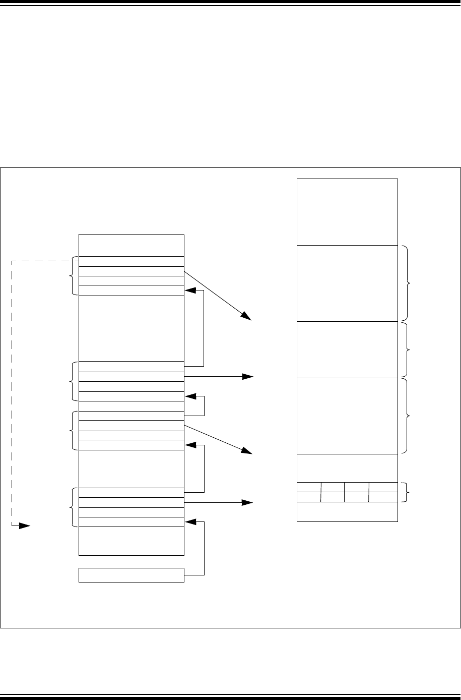
PIC32 Family Reference Manual
DS60001244A-page 46-34 Preliminary © 2013 Microchip Technology Inc.
As shown, in Figure 46-6, the chain of Buffer Descriptors are provided as an example to read
(High-Speed) 384 bytes of data from the Serial Flash device attached to the SQICS0 signal in
Quad Lane mode. In this example, BD0 is configured as the transmit buffer descriptor and
BD1-BD3 as receive buffer descriptors. The buffer space (0x0002000) in memory that BD0
points to should be preloaded with the 5 bytes (0x0B command, 0x001000 address and 0x00
dummy). Refer to 46.7 “Flash Instructions and Sequence Diagrams Quick Reference” for
additional Flash instructions.
Once the DMA process is complete, Buffers 0 through 3 (0x00020100-0x00020280) should
contain the data read from the Serial Flash device. For a better understanding of buffer descriptor
control value of each descriptor, refer to Figure 46-2. Refer to 46.7 “Flash Instructions and
Sequence Diagrams Quick Reference” for additional Flash instructions.
Figure 46-6: Buffer Descriptor Structure Example
DataBuffer3 (256 Bytes)
DataBuffer2 (128 Bytes)
DataBuffer1 (256 Bytes)
XXX0x00
0x00 0x10 0x00 0x0B(2)
0x0(1)
0x00020280
Reserved
0x829F00FF
0x00002040
0x00020200
Reserved
0x829300FF
0x00001078
0x00020100
Reserved
0x8293FFFF
0x00001064 (BD_NXTPTR)
0x00020000 (BD_BUFADDR
)
Reserved (BD_STAT
)
0x82830005 (BD_CTRL)
BD0
BD1
Buffer3
0x00020000
0x00020100
0x00020200
0x00020280
Buffer2
Buffer0
Buffer1
0x00002040
0x00001078
0x00001064
0x00001000
BD2
BD3
0x00001000
SQI1BDBASEADDR
Note 1: The structure becomes a ring if this address points to 0x1000 (address of BD0).
2: The transmit buffer at 0x00020000 should contain the High-Speed read command (0x0B), followed by the address (0x001000) and
the dummy byte (0x00).

© 2013 Microchip Technology Inc. Preliminary DS60001244A-page 46-35
Section 46. Serial Quad Interface (SQI)
46
Serial Quad
Interface (SQI)
Figure 46-7 shows the DMA mode flow diagram.
Figure 46-7: DMA Mode Flowchart
Start
Configure Buffer Descriptors(1)
Configure SQI1INTEN and
SQI1INTSEN
POLLEN == 1?
(SQI1BDCON)
DMA hardware is in control
No
Configure SQI1CFG
DMAEN = 1?
(SQI1BDC=ON)
START == 1?
(SQI1BDCON)
Yes
Configure SQI1CLKCON
(EN and CLKDIV<7:0> bits)
No
Yes
No
Note 1: Each Buffer Descriptor contains four words (BD_CTRL, BD_STAT, BD_BUFADDR, and
BD_NXTPTR) that need to be set up.
2: This register points to the address of BD_CTRL word of the first Buffer Descriptor.
STABLE == 1?
(SQI1CLKCON)
Yes
Configure Yes
No
SQI1BDPOLLCON
Configure SQI1BDBASEADD(2)
Configure SQI1BDCON
and starts fetching the
Buffer Descriptor

PIC32 Family Reference Manual
DS60001244A-page 46-36 Preliminary © 2013 Microchip Technology Inc.
46.5.2 PIO Mode
The SQI module is controlled by the Host processor in PIO mode, indicating Host load during all
PIO transactions. In PIO mode, the Host CPU configures the SQI through the SQI1CFG register
and handles the control of each transaction through the SQI1CON register. The Host processor
should actively monitor all of the status and interrupt bits to dynamically control the transactions.
PIO mode is used for smaller portions of controlled data transfers. Figure 46-8 shows the basic
PIO mode flow diagram.
Figure 46-8: PIO Mode Flowchart
Start
Configure SQI1CFG, SQI1CON,
SQI1CMDTHR and SQI1INTTHR
Configure SQI1CLKCON
(EN and CLKDIV<7:0> bits)
STABLE == 1?
(SQI1CLKCON)
Yes
No
Configure SQI1INTEN
and SQI1INTSEN
CMDINT<1:0> = 10?
(SQI1CLKCON)
No
CMDINT<1:0> = 01?
(SQI1CLKCON)
CMDINIT<1:0> = 10?
(SQI1CON)
No
Write SQI1TXDATA
TXEMPTY == 1?
(SQI1INTSTAT)
No
Write SQI1RXDATA
RXFULL == 1?
(SQI1INTSTAT)
No
Yes
Yes
Idle
Yes

© 2013 Microchip Technology Inc. Preliminary DS60001244A-page 46-37
Section 46. Serial Quad Interface (SQI)
46
Serial Quad
Interface (SQI)
46.5.3 XIP Mode
XIP mode as described in the previous sections is used to execute code out of Serial Flash
devices. This mode uses an optimal timing setup for faster execution. For the SQI module to
function properly in XIP mode, the Host processor should program the SQI1XCON1 and
SQI1XCON2 registers as required, and then set the MODE<2:0> bits in the SQI1CFG register
to switch to XIP mode. Figure 46-9 shows the XIP mode flow diagram.
Figure 46-9: XIP Mode Flowchart
Note: If XIP is done with CACHE enabled, make sure the SQI Flash device is in Burst
mode and any reads are performed through burst read to avoid exceptions.
Start
Configure SQI1CFG(1)
ConfigureSQI1CLKCON
Is STABLE == 1?
(SQI1CLKCON)
Configure SQI1XCON1
Set MODE<1:0>
in SQI1CFG to XIP
Yes
No
Disable Interrupts
(EN and CLKDIV<7:0> bits)
Note 1: This step configures all SQI Configuration fields, with the exception of MODE<1:0>.
2: Configuration of SQI1XCON1 and SQI1XCON2 depends on the features and param-
eters of the attached Serial Flash device. Other bit fields in this register are trivial; set
them as desired by the application.
and SQI1XCON2(2)
End

PIC32 Family Reference Manual
DS60001244A-page 46-38 Preliminary © 2013 Microchip Technology Inc.
46.6 SQI DATA FLOW MODES
The SQI module is a synchronous SPI-compatible serial port, which can operate in typical SPI
modes 0 and 3 (specified by the CPOL bit (SQI1CFG<4>) and the CPHA bit (SQI1CFG<3>)).
46.6.1 Mode 0 and Mode 3
Mode 0 and Mode 3 are typical SPI modes of operation, which are differentiated by the CPOL
and CPHA bit settings. When CPOL and CPHA are set to '0', the SQI module operates in Mode
0. When these two bits are set to '1', the SQI module operates in Mode 3.
As shown in Figure 46-10 and Figure 46-11, the primary difference between Mode 0 and Mode
3 concerns the state of SQI clock when the SQI controller is in Idle mode (i.e., no transfers are
in progress). In Mode 0, the SQI clock stays low during Idle mode and in Mode 3, it stays high
(provides a better clock edge entering active mode). In Mode 0, the SQI clock is held low at the
start and the end of the SQI transfer cycle, whereas in Mode 3, the SQI clock is held high at the
start and end of the transfer cycle. In both modes, the SQI data input in sampled on the rising
edge of the SQI clock, and the SQI data output is clocked on the falling edge of the SQI clock.
Figure 46-10: Mode 0 (CPHA = 0, CPOL = 0)
Figure 46-11: Mode 3 (CPHA = 1, CPOL = 1)
12345678910111213141516
SQICLK (CPOL = 0)
Sample Edge
SQID<3:0>
SQICS<1:0>
12345678910111213141516
SQICLK (CPOL = 1)
Sample Edge
SQID<3:0>
SQICS<1:0>

© 2013 Microchip Technology Inc. Preliminary DS60001244A-page 46-39
Section 46. Serial Quad Interface (SQI)
46
Serial Quad
Interface (SQI)
46.7 FLASH INSTRUCTIONS AND SEQUENCE DIAGRAMS QUICK REFERENCE
This section provides a quick reference to a few general Flash instructions and sequence
diagrams using the Microchip SST26VF016/031 Quad Flash device. See the “Serial Quad I/O
(SQI) Flash Memory SST26VF016 / SST26VF032 Data Sheet” (DS20005017) for additional
details.
Tabl e 46- 3 describes the set of Flash commands implemented by the SST26VF016/032 SQI
Flash device. Some of the commands differ from one Flash memory to the other as noted below.
Table 46-3: Quad Flash Memory Sample Instructions
Instruction Description Command
Byte
Number of
Address
Bytes
Number of
Dummy
Bytes
Number of
Data Bytes
RSTEN Reset Enable 0x66 0 0 0
RST(1) Reset Memory 0x99 0 0 0
EQIO Enable Quad I/O 0x38 0 0 0
RSTEQIO(2) Reset Quad I/O 0xFF 0 0 0
Read(3) Read Memory 0x03 3 0 ≥ 1
High-Speed
Read/Fast
Read(3)
Read Memory at
Higher Speed
0x0B 3 1 ≥ 1
JEDEC-ID(3,4) Read JEDEC ID 0x9F 0 0 3 to infinity
≥ 3
Note 1: The RST command is only executed if the RSTEN command is executed first. Any
intervening command will disable Reset.
2: The Device accepts eight-clock command in SPI mode, or two-clock command in
SQI mode.
3: After a power cycle, Read, High-Speed Read, and JEDEC-ID Read instructions
input and output cycles are SPI bus protocol.
4: The Quad J-ID read wraps the three Quad J-ID Bytes of data until terminated by a
low-to-high transition on the SQICS0/SQICS1 pins.
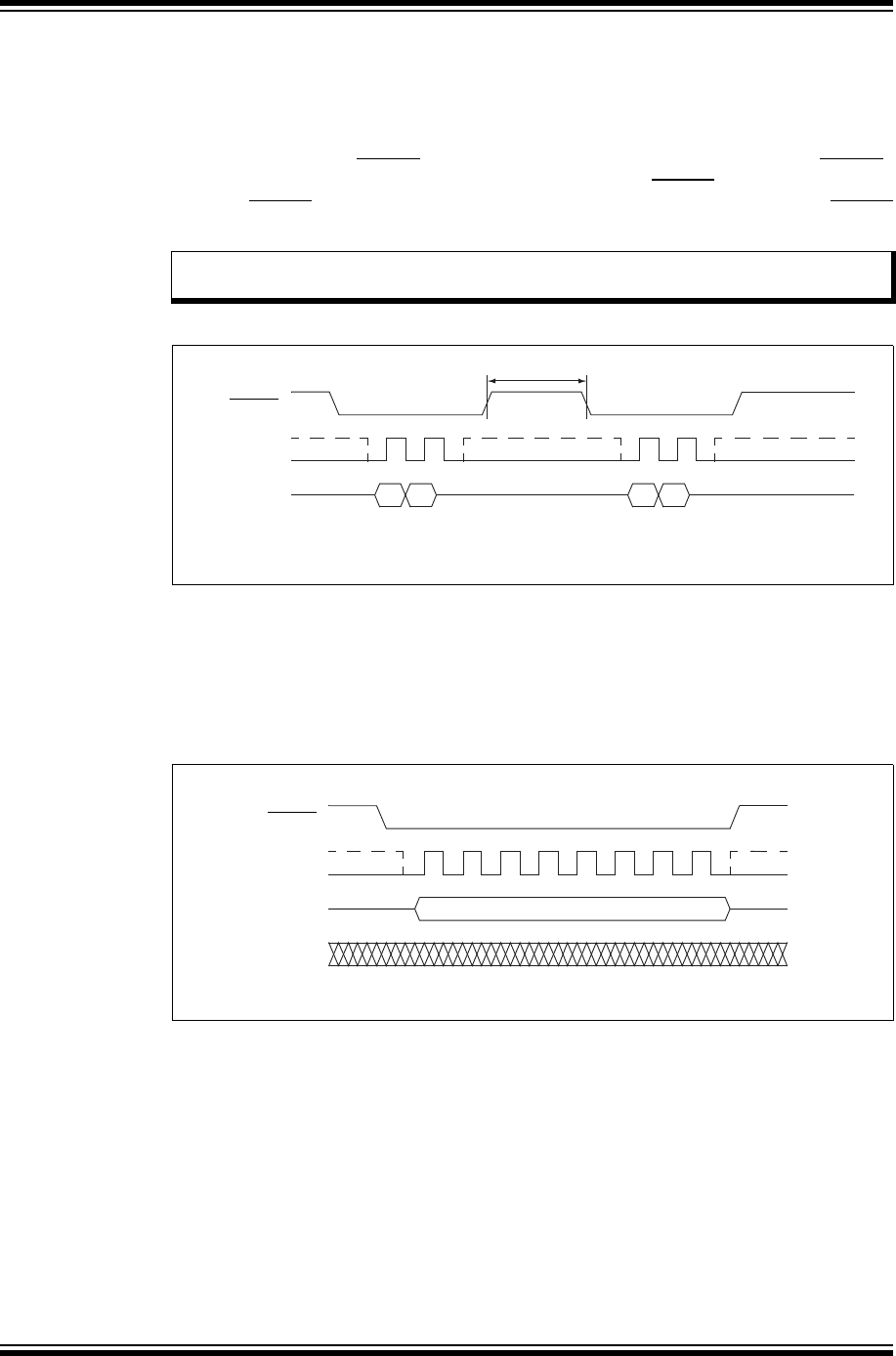
PIC32 Family Reference Manual
DS60001244A-page 46-40 Preliminary © 2013 Microchip Technology Inc.
46.7.1 Instruction Sequence Diagrams
46.7.1.1 RESET-ENABLE (RSTEN) AND RESET (RST)
The Reset operation is used as a system software reset of the Flash device. Reset operation
consists of two commands: Reset Enable and Reset (RST). As an example, to reset the memory,
the SQI first drives the SQICS0 pin low (assuming Flash memory is connected to SQICS0),
sends the Reset Enable command (0x66), and then drives the SQICS0 pin high. Next, the SQI
drives the SQICS0 pin low again, sends the Reset command (0x99), and then drives the SQICS0
pin high, as shown in Figure 46-12.
Figure 46-12: Reset Sequence
46.7.1.2 ENABLE QUAD I/O (EQIO)
The Enable Quad I/O (EQIO) instruction (0x38) enables the Flash Memory for SQI bus operation.
Upon completion of the instruction, all instructions thereafter will be 4-bit multiplexed input/output
until a power cycle or a “Reset Quad I/O instruction” is executed. The Reset Quad I/O instruction
(0xFF) is executed in the same manner as Enable Quad I/O. Refer to Figure 46-13.
Figure 46-13: Enable Quad I/O Sequence
Note: Any command other than the Reset command after the Reset Enable command will
disable the Reset Enable.
MODE3
SQICLK
SQD<3:0>
SQICSx
MODE3
C1 C3 C2C0
MODE0
MODE3
MODE0MODE0
TCPH
Note: C1 and C0 = 0x6; C3 and C2 = 0x9.
MODE3 0 1
SQICLK
SQDIO0
SQICSx
MODE0
2
0x38
SQD<3:1>
34567

© 2013 Microchip Technology Inc. Preliminary DS60001244A-page 46-41
Section 46. Serial Quad Interface (SQI)
46
Serial Quad
Interface (SQI)
46.7.1.3 READ
The Read instruction (0x03) is only supported in SPI bus protocol Modes 0 or 3. This instruction
is not supported in Dual/Quad Lane modes. The memory outputs the data starting from the
specified address location, and then continuously streams the data output through all addresses
until terminated by a low-to-high transition on the SQICS0 or SQICS1 pin. The Read instruction
is initiated by executing an 8-bit command (0x03), followed by a 24-bit address, as shown in
Figure 46-14. Chip Select will remain active-low for the duration of the Read cycle.
Figure 46-14: Read Sequence
46.7.1.4 HIGH-SPEED/FAST QUAD READ
The High-Speed Read (0x0B) instruction is supported in both the SPI bus protocol and the
SQI bus protocol (Dual/Quad Lane mode). Figure 46-15 shows the timing diagram of the Quad
Lane High Speed Read instruction. To execute this instruction with the SST16VF series Quad
Flash, the SQI module would first issue an Enable Quad I/O instruction (refer to 46.7.1.2 “Enable
Quad I/O (EQIO)”) followed by a High Speed Read instruction (0x0B).
Figure 46-15: High-Speed Read Single Lane Sequence
SQICSx
SQID0
SQID1
SQICLK
ADD.
01 2 3 4 5 6 7 8
ADD. ADD.
03
High Impedance
15 16 23 24 31 32 39 40 7047 48 55 56 63 64
N+2 N+3 N+4NN+1
DOUT
MSB MSB
MSB
MODE0
MODE3
DOUT DOUT DOUT DOUT
1432765891028293031323334351432765891014327658910
Mode 3
Mode 0
0
Instruction (0x3B)
SQICLK
SQICS<1:0>
SQID0
SQID1
21 3 1 4 023 22 622
173
5
0
24-bit Address
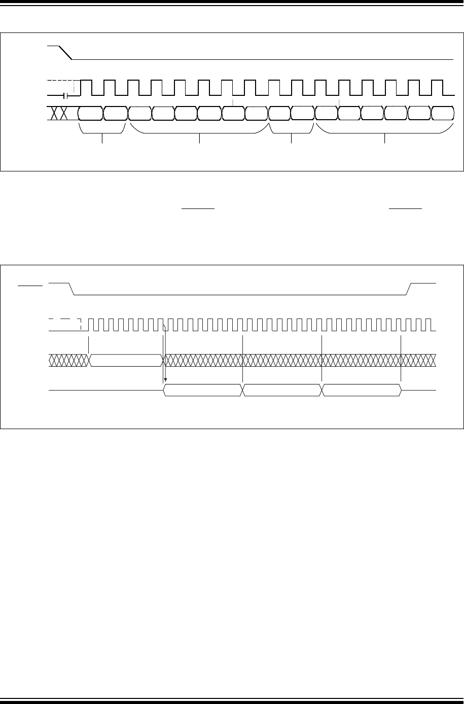
PIC32 Family Reference Manual
DS60001244A-page 46-42 Preliminary © 2013 Microchip Technology Inc.
Figure 46-16: High-Speed Read Quad Lane Sequence
46.7.1.5 JEDEC-ID READ
The JEDEC-ID Read instruction reads the manufacturer and device identifications, and is
executed by driving the SQICS0 pin low (assuming the Flash is connected to SQICS0), and then
sending the JEDEC-ID instruction (0x9F). The memory outputs the device ID (up to 3 bytes),
immediately after the instruction, as shown in Figure 46-17.
Figure 46-17: Device ID Read Sequence – Microchip SST Flash
2
Mode 3
Mode 0
0
SQICLK
SQICS<1:0>
SQID<3:0>
134 56 7 891011121314
0x0 0xB 0x0 0x0 0x4 0x0 0x0 0x0 0xX 0xX H1 H2 H3
L1 L2
Command ADDRESS<A23:A0> Dummy Bytes Data
15
L3
26 Device ID
SQICSx
SQID1
SQID0
SQICLK
0
High Impedance
15 1614 28 29 30 31
BF
MODE3
MODE0
MSBMSB
910111213 1718 32 34
9F
19 20 21 22 23 3324 25 26 27123456 78

© 2013 Microchip Technology Inc. Preliminary DS60001244A-page 46-43
Section 46. Serial Quad Interface (SQI)
46
Serial Quad
Interface (SQI)
46.8 EFFECTS OF RESET
46.8.1 Device Reset (MCLR)
All SQI registers are forced to their reset states upon a device Reset. When the asynchronous
reset input goes active, the SQI module resets:
• All read/write bits in all registers (SQI1XCON1, SQI1XCON2, SQI1CFG, SQI1CON, etc.)
•The transmit, receive, and control buffers to the empty state
•The SQI1TXDATA and SQI1RXDATA registers
•The SQI1CLKCON register, setting T
SQI to TBC/2
46.8.2 Software Reset
A software reset is achieved through the RESET bit of the SQI1CFG register. In this case, the
SQI module behaves as if a device Reset has occurred and performs the same reset actions that
are described in 46.8.1 “Device Reset (MCLR)”.
46.8.3 Power-on Reset
All of the SQI control registers are forced to their reset states when a Power-on Reset occurs.
46.8.4 Watchdog Timer Reset
During a Watchdog Timer reset, the SQI module behaves as if a device Reset has occurred and
performs the same reset actions that are described in 46.8.1 “Device Reset (MCLR)”.
46.9 OPERATION IN POWER-SAVING MODES
46.9.1 Sleep Mode
When the device enters Sleep mode, the SQI module is disabled and placed into a low-power
state where no clocking occurs in the module. Depending on the device, the state of the SQI
module is either preserved or reset when the device exits Sleep mode. Refer to the
“Power-Saving Features” chapter in the specific device data sheet for details.
46.9.2 Idle Mode
When the device enters Idle mode, the SQI module clocks still operate and the peripheral is
functional. However, as the CPU is halted, the SQI module operation is limited to certain
functions. BD DMA transfers should run uninterrupted when the device is in Idle mode.
46.9.3 Debug Mode
The behavior of the SQI module is unaltered in Debug mode.

PIC32 Family Reference Manual
DS60001244A-page 46-44 Preliminary © 2013 Microchip Technology Inc.
46.10 RELATED APPLICATION NOTES
This section lists application notes that are related to this section of the manual. These
application notes may not be written specifically for the PIC32 device family, but the concepts are
pertinent and could be used with modification and possible limitations. The current application
notes related to the Serial Quad Interface (SQI) module are:
Title Application Note #
No related application notes at this time. N/A
Note: Please visit the Microchip web site (www.microchip.com) for additional application
notes and code examples for the PIC32 family of devices.

© 2013 Microchip Technology Inc. Preliminary DS60001244A-page 46-45
Section 46. Serial Quad Interface (SQI)
46
Serial Quad
Interface (SQI)
46.11 REVISION HISTORY
Revision A (November 2013)
This is the initial released version of this document.

PIC32 Family Reference Manual
DS60001244A-page 46-46 Preliminary © 2013 Microchip Technology Inc.
NOTES:

2013 Microchip Technology Inc. Preliminary DS60001244A-page 46-47
Information contained in this publication regarding device
applications and the like is provided only for your convenience
and may be superseded by updates. It is your responsibility to
ensure that your application meets with your specifications.
MICROCHIP MAKES NO REPRESENTATIONS OR
WARRANTIES OF ANY KIND WHETHER EXPRESS OR
IMPLIED, WRITTEN OR ORAL, STATUTORY OR
OTHERWISE, RELATED TO THE INFORMATION,
INCLUDING BUT NOT LIMITED TO ITS CONDITION,
QUALITY, PERFORMANCE, MERCHANTABILITY OR
FITNESS FOR PURPOSE. Microchip disclaims all liability
arising from this information and its use. Use of Microchip
devices in life support and/or safety applications is entirely at
the buyer’s risk, and the buyer agrees to defend, indemnify and
hold harmless Microchip from any and all damages, claims,
suits, or expenses resulting from such use. No licenses are
conveyed, implicitly or otherwise, under any Microchip
intellectual property rights.
Trademarks
The Microchip name and logo, the Microchip logo, dsPIC,
FlashFlex, KEELOQ, KEELOQ logo, MPLAB, PIC, PICmicro,
PICSTART, PIC32 logo, rfPIC, SST, SST Logo, SuperFlash
and UNI/O are registered trademarks of Microchip Technology
Incorporated in the U.S.A. and other countries.
FilterLab, Hampshire, HI-TECH C, Linear Active Thermistor,
MTP, SEEVAL and The Embedded Control Solutions
Company are registered trademarks of Microchip Technology
Incorporated in the U.S.A.
Silicon Storage Technology is a registered trademark of
Microchip Technology Inc. in other countries.
Analog-for-the-Digital Age, Application Maestro, BodyCom,
chipKIT, chipKIT logo, CodeGuard, dsPICDEM,
dsPICDEM.net, dsPICworks, dsSPEAK, ECAN,
ECONOMONITOR, FanSense, HI-TIDE, In-Circuit Serial
Programming, ICSP, Mindi, MiWi, MPASM, MPF, MPLAB
Certified logo, MPLIB, MPLINK, mTouch, Omniscient Code
Generation, PICC, PICC-18, PICDEM, PICDEM.net, PICkit,
PICtail, REAL ICE, rfLAB, Select Mode, SQI, Serial Quad I/O,
Tota l E ndu ra nce , T SHA RC , U n iW inD riv er, Wi per Lo c k, ZE NA
and Z-Scale are trademarks of Microchip Technology
Incorporated in the U.S.A. and other countries.
SQTP is a service mark of Microchip Technology Incorporated
in the U.S.A.
GestIC and ULPP are registered trademarks of Microchip
Technology Germany II GmbH & Co. KG, a subsidiary of
Microchip Technology Inc., in other countries.
All other trademarks mentioned herein are property of their
respective companies.
© 2013, Microchip Technology Incorporated, Printed in the
U.S.A., All Rights Reserved.
Printed on recycled paper.
ISBN: 978-1-62077-654-4
Note the following details of the code protection feature on Microchip devices:
• Microchip products meet the specification contained in their particular Microchip Data Sheet.
• Microchip believes that its family of products is one of the most secure families of its kind on the market today, when used in the
intended manner and under normal conditions.
• There are dishonest and possibly illegal methods used to breach the code protection feature. All of these methods, to our
knowledge, require using the Microchip products in a manner outside the operating specifications contained in Microchip’s Data
Sheets. Most likely, the person doing so is engaged in theft of intellectual property.
• Microchip is willing to work with the customer who is concerned about the integrity of their code.
• Neither Microchip nor any other semiconductor manufacturer can guarantee the security of their code. Code protection does not
mean that we are guaranteeing the product as “unbreakable.”
Code protection is constantly evolving. We at Microchip are committed to continuously improving the code protection features of our
products. Attempts to break Microchip’s code protection feature may be a violation of the Digital Millennium Copyright Act. If such acts
allow unauthorized access to your software or other copyrighted work, you may have a right to sue for relief under that Act.
Microchip received ISO/TS-16949:2009 certification for its worldwide
headquarters, design and wafer fabrication facilities in Chandler and
Tempe, Arizona; Gresham, Oregon and design centers in California
and India. The Company’s quality system processes and procedures
are for its PIC® MCUs and dsPIC® DSCs, KEELOQ® code hopping
devices, Serial EEPROMs, microperipherals, nonvolatile memory and
analog products. In addition, Microchip’s quality system for the design
and manufacture of development systems is ISO 9001:2000 certified.
QUALITY MANAGEMENT S
YSTEM
CERTIFIED BY DNV
== ISO/TS 16949 ==

DS60001244A-page 46-48 Preliminary 2013 Microchip Technology Inc.
AMERICAS
Corporate Office
2355 West Chandler Blvd.
Chandler, AZ 85224-6199
Tel: 480-792-7200
Fax: 480-792-7277
Technical Support:
http://www.microchip.com/
support
Web Address:
www.microchip.com
Atlanta
Duluth, GA
Tel: 678-957-9614
Fax: 678-957-1455
Austin, TX
Tel: 512-257-3370
Boston
Westborough, MA
Tel: 774-760-0087
Fax: 774-760-0088
Chicago
Itasca, IL
Tel: 630-285-0071
Fax: 630-285-0075
Cleveland
Independence, OH
Tel: 216-447-0464
Fax: 216-447-0643
Dallas
Addison, TX
Tel: 972-818-7423
Fax: 972-818-2924
Detroit
Novi, MI
Tel: 248-848-4000
Houston, TX
Tel: 281-894-5983
Indianapolis
Noblesville, IN
Tel: 317-773-8323
Fax: 317-773-5453
Los Angeles
Mission Viejo, CA
Tel: 949-462-9523
Fax: 949-462-9608
New York, NY
Tel: 631-435-6000
San Jose, CA
Tel: 408-735-9110
Canada - Toronto
Tel: 905-673-0699
Fax: 905-673-6509
ASIA/PACIFIC
Asia Pacific Office
Suites 3707-14, 37th Floor
Tower 6, The Gateway
Harbour City, Kowloon
Hong Kong
Tel : 8 52 -24 01- 120 0
Fax: 852-2401-3431
Australia - Sydney
Tel : 6 1- 2-9 868 -67 33
Fax: 61-2-9868-6755
China - Beijing
Tel : 8 6- 10- 856 9-7 00 0
Fax: 86-10-8528-2104
China - Chengdu
Tel : 8 6- 28- 866 5-5 511
Fax: 86-28-8665-7889
China - Chongqing
Tel : 8 6- 23- 898 0-9 58 8
Fax: 86-23-8980-9500
China - Hangzhou
Tel : 8 6- 571 -28 19- 318 7
Fax: 86-571-2819-3189
China - Hong Kong SAR
Tel : 8 52 -29 43- 510 0
Fax: 852-2401-3431
China - Nanjing
Tel : 8 6- 25- 847 3-2 46 0
Fax: 86-25-8473-2470
China - Qingdao
Tel : 8 6- 532 -85 02- 735 5
Fax: 86-532-8502-7205
China - Shanghai
Tel : 8 6- 21- 540 7-5 53 3
Fax: 86-21-5407-5066
China - Shenyang
Tel : 8 6- 24- 233 4-2 82 9
Fax: 86-24-2334-2393
China - Shenzhen
Tel : 8 6- 755 -88 64- 220 0
Fax: 86-755-8203-1760
China - Wuhan
Tel : 8 6- 27- 598 0-5 30 0
Fax: 86-27-5980-5118
China - Xian
Tel : 8 6- 29- 883 3-7 25 2
Fax: 86-29-8833-7256
China - Xiamen
Tel: 86-592-2388138
Fax: 86-592-2388130
China - Zhuhai
Tel : 86- 75 6-3 21 004 0
Fax: 86-756-3210049
ASIA/PACIFIC
India - Bangalore
Tel : 9 1- 80- 309 0-4 44 4
Fax: 91-80-3090-4123
India - New Delhi
Tel : 9 1- 11- 416 0 -8 631
Fax: 91-11-4160-8632
India - Pune
Tel : 9 1- 20- 301 9-1 50 0
Japan - Osaka
Tel : 8 1- 6-6 152 -7 1 60
Fax: 81-6-6152-9310
Japan - Tokyo
Tel : 8 1- 3-6 880 - 377 0
Fax: 81-3-6880-3771
Korea - Daegu
Tel : 8 2- 53- 744 -43 01
Fax: 82-53-744-4302
Korea - Seoul
Tel : 8 2- 2-5 54- 72 0 0
Fax: 82-2-558-5932 or
82-2-558-5934
Malaysia - Kuala Lumpur
Tel : 6 0- 3-6 201 -9 8 57
Fax: 60-3-6201-9859
Malaysia - Penang
Tel : 6 0- 4-2 27- 88 7 0
Fax: 60-4-227-4068
Philippines - Manila
Tel : 6 3- 2-6 34- 90 6 5
Fax: 63-2-634-9069
Singapore
Tel : 6 5- 633 4-8 870
Fax: 65-6334-8850
Taiwan - Hsin Chu
Tel : 8 86 -3- 577 8-3 66
Fax: 886-3-5770-955
Taiwan - Kaohsiung
Tel : 8 86 -7- 213 -78 30
Taiwan - Taipei
Tel : 8 86 -2- 250 8-8 60 0
Fax: 886-2-2508-0102
Thailand - Bangkok
Tel : 6 6- 2-6 94- 13 5 1
Fax: 66-2-694-1350
EUROPE
Austria - Wels
Tel : 4 3- 72 42 -2 244 -3 9
Fax: 43-7242-2244-393
Denmark - Copenhagen
Tel : 4 5- 445 0-2 828
Fax: 45-4485-2829
France - Paris
Tel : 3 3- 1-6 9-5 3-6 3-2 0
Fax: 33-1-69-30-90-79
Germany - Dusseldorf
Tel : 4 9- 21 29 -3 766 400
Germany - Munich
Tel : 4 9- 89 -62 7-1 44- 0
Fax: 49-89-627-144-44
Germany - Pforzheim
Tel : 4 9- 72 31 -4 247 50
Italy - Milan
Tel : 3 9- 03 31 -7 426 11
Fax: 39-0331-466781
Italy - Venice
Tel : 3 9- 04 9- 762 528 6
Netherlands - Drunen
Tel : 3 1- 41 6- 690 399
Fax: 31-416-690340
Poland - Warsaw
Tel : 4 8- 22 -33 257 37
Spain - Madrid
Tel : 3 4- 91 -70 8-0 8-9 0
Fax: 34-91-708-08-91
Sweden - Stockholm
Tel : 4 6- 8-5 090 -46 54
UK - Wokingham
Tel : 4 4- 118 -92 1- 5 800
Fax: 44-118-921-5820
Worldwide Sales and Service
10/28/13

© 2013 Microchip Technology Inc. Preliminary DS60001245A-page 47-1
External Bus
Interface (EBI)
47
Section 47. External Bus Interface (EBI)
HIGHLIGHTS
This section of the manual contains the following major topics:
47.1 Introduction .................................................................................................................. 47-2
47.2 Control Registers ......................................................................................................... 47-4
47.3 Interfacing to Various Devices ................................................................................... 47-14
47.4 Bus Configuration ...................................................................................................... 47-16
47.5 Device Configuration.................................................................................................. 47-17
47.6 Timing Diagrams........................................................................................................ 47-21
47.7 Effects Of Reset......................................................................................................... 47-24
47.8 Operation in Power-Saving Modes ............................................................................ 47-24
47.9 Related Application Notes.......................................................................................... 47-25
47.10 Revision History ......................................................................................................... 47-26
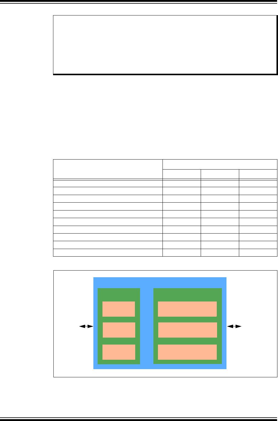
PIC32 Family Reference Manual
DS60001245A-page 47-2 Preliminary © 2013 Microchip Technology Inc.
47.1 INTRODUCTION
The External Bus Interface (EBI) module provides a convenient, high-speed way to interface
external parallel memory devices to the PIC32 family device.
With the EBI module, it is possible to connect asynchronous SRAM and NOR Flash devices, as
well as non-memory devices, such as camera sensors. The EBI module also supports Low-Cost
Controllerless (LCC) Graphics devices.
The features of the EBI module depend on the particular PIC32 device and the pin count, as
shown in Ta b l e 4 7 - 1 .
Table 47-1: EBI Module Features
Figure 47-1: EBI System Block Diagram
Note: This family reference manual section is meant to serve as a complement to device
data sheets. Depending on the device variant, this manual section may not apply to
all PIC32 devices.
Please consult the note at the beginning of the “External Bus Interface (EBI)”
chapter in the current device data sheet to check whether this document supports
the device you are using.
Device data sheets and family reference manual sections are available for
download from the Microchip Worldwide Web site at: http://www.microchip.com
Feature Number of Device Pins
100 124 144
Asynchronous SRAM Y Y Y
Asynchronous NOR Flash Y Y Y
Available address lines 20 20 24
8-bit data bus support Y Y Y
16-bit data bus support Y Y Y
Available Chip Selects 1 1 4
Timing mode sets 3 3 3
8-bit R/W from 16-bit bus N N Y
Performance (MHz) 50 50 50
Non-memory device Y Y Y
Control
Registers
Data
FIFO
Address
FIFO
System
Bus
Static
Interface
Memory
Bus Interface Memory Interface
External Bus Interface
Control Registers
Address Decoder
Static Memory Controller
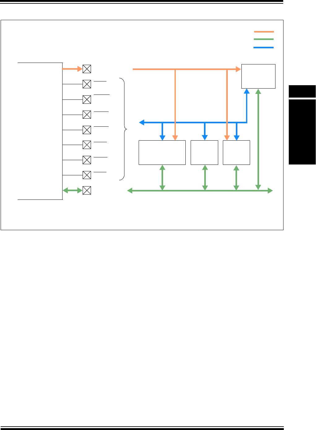
© 2013 Microchip Technology Inc. Preliminary DS60001245A-page 47-3
Section 47. External Bus Interface (EBI)
External Bus
Interface (EBI)
47
Figure 47-2: EBI Module Pinout and Connections to External Devices
EBIBS0
EBICS<3:0>
EBIRDY<3:1>
EBIOE
EBIWE
EBIBS1
EBIA<23:0>(1)
Flash
Address Bus
Data Bus
Control Lines
LCD SRAM
Microcontroller
8-bit/16-bit data
Up to 24-bit address
EBID<15:8>
EBID<7:0>
External Bus
PIC32
Note 1: No EBIA address pins are available on 64-pin devices and the EBIA<23:20> address pins are only available
on 144-pin devices.
Interface
Memory
EBIRP

PIC32 Family Reference Manual
DS60001245A-page 47-4 Preliminary © 2013 Microchip Technology Inc.
47.2 CONTROL REGISTERS
The EBI module for PIC32 devices contains the following Special Function Registers (SFRs):
•EBICSx: External Bus Interface Chip Select Register (x = 0-3)
This register contains the base address in physical memory for the selected external Device.
•EBIMSKx: External Bus Interface Address Mask Register (x = 0-3)
This register enables selection of the timing register set, as well as the Chip Select memory
type and memory size.
•EBISMTx: External Bus Interface Static Memory Timing Register (x = 0-2)
This register can be used to configure the static memory timing.
•EBIFTRPD: External Bus Interface Flash Timing Register
This register defines the number of clock cycles to hold the external Flash memory in reset.
•EBISMCON: External Bus Interface Static Memory Control Register
This register can be used to define the static memory width for register sets 0-2, and to select
Flash Reset/Power-down mode during a device Reset.
•CFGEBIA: External Bus Interface Address Pin Configuration Register
This register can be used to configure the address pins for the EBI module.
•CFGEBIC: External Bus Interface Control Pin Configuration Register
This register can be used to configure the control pins for the EBI module.
© 2013 Microchip Technology Inc. Preliminary DS60001245A-page 47-5
Section 47. External Bus Interface (EBI)
External Bus
Interface (EBI)
47
Tabl e 47- 2 and Ta b l e 4 7 - 3 provide a brief summary of the related EBI registers. Corresponding registers appear after the summary, fol-
lowed by a detailed description of each bit.
Table 47-2: EBI SFR Summary
Register
Name
Bit
Range Bit 31/15 Bit 30/14 Bit 29/13 Bit 28/12 Bit 27/11 Bit 26/10 Bit 25/9 Bit 24/8 Bit 23/7 Bit 22/6 Bit 21/5 Bit 20/4 Bit 19/3 Bit 118/2 Bit 17/1 Bit 16/0
EBICSx 31:16 CSADDR<15:0>
15:0 — — — — — — — — — — — — — — — —
EBIMSKx 31:16 — — — — — — — — — — — — — — — —
15:0 — — — — — REGSEL<2:0> MEMTYPE<2:0> MEMSIZE<4:0>
EBISMTx 31:16 — — — — —RDYMODEPAGESIZE<1:0>PAGEMODE TPRC<3:0> TBTA<2:0>
15:0 TWP<5:0> TWR<1:0> TAS<1:0> TRC<5:0>
EBIFTRPD 31:16 — — — — — — — — — — — — — — — —
15:0 ————TRPD<11:0>
EBISMCON 31:16 — — — — — — — — — — — — — — — —
15:0 SMDWIDTH2<2:0> SMDWIDTH1<2:0> SMDWIDTH0<2:0> — — — — — —SMRP
Legend: — = unimplemented, read as ‘0’.
Table 47-3: EBI Configuration Register Summary
Register
Name
Bit
Range Bit 31/15 Bit 30/14 Bit 29/13 Bit 28/12 Bit 27/11 Bit 26/10 Bit 25/9 Bit 24/8 Bit 23/7 Bit 22/6 Bit 21/5 Bit 20/4 Bit 19/3 Bit 118/2 Bit 17/1 Bit 16/0
CFGEBIA 31:16 EBIPINEN — — — — — — — EBIA23EN EBIA22EN EBIA21EN EBIA20EN EBIA19EN EBIA18EN EBIA17EN EBIA16EN
15:0 EBIA15EN EBIA14EN EBIA13EN EBIA12EN EBIA11EN EBIA10EN EBIA9EN EBIA8EN EBIA7EN EBIA6EN EBIA5EN EBIA4EN EBIA3EN EBIA2EN EBIA1EN EBIA0EN
CFGEBIC 31:16 —EBI
RDYINV3
EBI
RDYINV2
EBI
RDYINV1 —EBI
RDYEN3
EBI
RDYEN2
EBI
RDYEN1 — — — — — — EBI
RDYLVL EBIRPEN
15:0 —— EBIWEEN EBIOEEN —— EBIBSEN1 EBIBSEN0 EBICSEN3 EBICSEN2 EBICSEN1 EBICSEN0 —— EBIDEN1 EBIDEN0
Legend: — = unimplemented, read as ‘0’.

PIC32 Family Reference Manual
DS60001245A-page 47-6 Preliminary © 2013 Microchip Technology Inc.
Register 47-1: EBICSx: External Bus Interface Chip Select Register (x = 0-3)
Bit
Range
Bit
31/23/15/7
Bit
30/22/14/6
Bit
29/21/13/5
Bit
28/20/12/4
Bit
27/19/11/3
Bit
26/18/10/2
Bit
25/17/9/1
Bit
24/16/8/0
31:24 R/W-0 R/W-0 R/W-0 R/W-0 R/W-0 R/W-0 R/W-0 R/W-0
CSADDR<15:8>
23:16 R/W-0 R/W-0 R/W-0 R/W-0 R/W-0 R/W-0 R/W-0 R/W-0
CSADDR<7:0>
15:8 U-0 U-0 U-0 U-0 U-0 U-0 U-0 U-0
————————
7:0 U-0 U-0 U-0 U-0 U-0 U-0 U-0 U-0
————————
Legend:
R = Readable bit W = Writable bit U = Unimplemented bit, read as ‘0’
-n = Value at POR ‘1’ = Bit is set ‘0’ = Bit is cleared x = Bit is unknown
bit 31-16 CSADDR<15:0>: Base Address for Device bits
Address in physical memory, which will select the external device.
bit 15-0 Unimplemented: Read as ‘0’

© 2013 Microchip Technology Inc. Preliminary DS60001245A-page 47-7
Section 47. External Bus Interface (EBI)
External Bus
Interface (EBI)
47
Register 47-2: EBIMSKx: External Bus Interface Address Mask Register (x = 0-3)
Bit
Range
Bit
31/23/15/7
Bit
30/22/14/6
Bit
29/21/13/5
Bit
28/20/12/4
Bit
27/19/11/3
Bit
26/18/10/2
Bit
25/17/9/1
Bit
24/16/8/0
31:24 U-0 U-0 U-0 U-0 U-0 U-0 U-0 U-0
————————
23:16 U-0 U-0 U-0 U-0 U-0 U-0 U-0 U-0
————————
15:8 U-0 U-0 U-0 U-0 U-0 R/W-0 R/W-0 R/W-0
—————REGSEL<2:0>
7:0 R/W-0 R/W-0 R/W-1 R/W-0 R/W-0 R/W-0 R/W-0 R/W-0
MEMTYPE<2:0> MEMSIZE<4:0>
Legend:
R = Readable bit W = Writable bit U = Unimplemented bit, read as ‘0’
-n = Value at POR ‘1’ = Bit is set ‘0’ = Bit is cleared x = Bit is unknown
bit 31-11 Unimplemented: Read as ‘0’
bit 10-8 REGSEL<2:0>: Timing Register Set for Chip Select ‘x’ bits
111 = Reserved
•
•
•
011 = Reserved
010 = Use EBITMGR2
001 = Use EBITMGR1
000 = Use EBITMGR0
bit 7-5 MEMTYPE<2:0>: Select Memory Type for Chip Select ‘x’ bits
111 = Reserved
•
•
•
011 = Reserved
010 = NOR-Flash
001 = SRAM
000 = Reserved
bit 4-0 MEMSIZE<4:0>: Select Memory Size for Chip Select ‘x’ bits
11111 = Reserved
•
•
•
01010 = Reserved
01001 = 16 MB
01000 = 8 MB
00111 = 4 MB
00110 = 2 MB
00101 = 1 MB
00100 = 512 KB
00011 = 256 KB
00010 = 128 KB
00001 = 64 KB (smaller memories alias within this range)
00000 = Chip Select is not used

PIC32 Family Reference Manual
DS60001245A-page 47-8 Preliminary © 2013 Microchip Technology Inc.
Register 47-3: EBISMTx: External Bus Interface Static Memory Timing Register (x = 0-2)
Bit
Range
Bit
31/23/15/7
Bit
30/22/14/6
Bit
29/21/13/5
Bit
28/20/12/4
Bit
27/19/11/3
Bit
26/18/10/2
Bit
25/17/9/1
Bit
24/16/8/0
31:24 U-0 U-0 U-0 U-0 U-0 R/W-0 R/W-0 R/W-0
— — — — — RDYMODE PAGESIZE<1:0>
23:16 R/W-0 R/W-0 R/W-1 R/W-0 R/W-0 R/W-1 R/W-0 R/W-0
PAGEMODE TPRC<3:0> TBTA<2:0>
15:8 R/W-0 R/W-0 R/W-1 R/W-1 R/W-0 R/W-0 R/W-0 R/W-1
TWP<5:0> TWR<1:0>
7:0 R/W-0 R/W-1 R/W-0 R/W-0 R/W-1 R/W-1 R/W-0 R/W-0
TAS<1:0> TRC<5:0>
Legend:
R = Readable bit W = Writable bit U = Unimplemented bit, read as ‘0’
-n = Value at POR ‘1’ = Bit is set ‘0’ = Bit is cleared x = Bit is unknown
bit 31-27 Unimplemented: Read as ‘0’
bit 26 RDYMODE: Data Ready Device Select bit
The device associated with register set ‘x’ is a data-ready device, and will use the READY pin.
1 = Ready input is used
0 = Ready input is not used
bit 25-24 PAGESIZE<1:0>: Page Size for Page Mode Device bits
11 = 32-word page
10 = 16-word page
01 = 8-word page
00 = 4-word page
bit 23 PAGEMODE: Memory Device Page Mode Support bit
1 = Device supports Page mode
0 = Device does not support Page mode
bit 22-19 TPRC<3:0>: Page Mode Read Cycle Time bits
Read cycle time is TPRC + 1 clock cycle.
bit 18-16 TBTA<2:0>: Data Bus Turnaround Time bits
Clock cycles (0-7) for static memory between read-to-write, write-to-read, and read-to-read when Chip
Select changes.
bit 15-10 TWP<5:0>: Write Pulse Width bits
Write pulse width is TWP + 1 clock cycle.
bit 9-8 TWR<1:0>: Write Address/Data Hold Time bits
Number of clock cycles to hold address or data on the bus.
bit 7-6 TAS<1:0>: Write Address Setup Time bits
Clock cycles for address setup time. A value of ‘0’ is only valid in the case of SSRAM.
bit 5-0 TRC<5:0>: Read Cycle Time bits
Read cycle time is TRC + 1 clock cycle.

© 2013 Microchip Technology Inc. Preliminary DS60001245A-page 47-9
Section 47. External Bus Interface (EBI)
External Bus
Interface (EBI)
47
Register 47-4: EBIFTRPD: External Bus Interface Flash Timing Register
Bit
Range
Bit
31/23/15/7
Bit
30/22/14/6
Bit
29/21/13/5
Bit
28/20/12/4
Bit
27/19/11/3
Bit
26/18/10/2
Bit
25/17/9/1
Bit
24/16/8/0
31:24 U-0 U-0 U-0 U-0 U-0 U-0 U-0 U-0
————————
23:16 U-0 U-0 U-0 U-0 U-0 U-0 U-0 U-0
————————
15:8 U-0 U-0 U-0 U-0 R/W-0 R/W-0 R/W-0 R/W-0
————TRPD<11:8>
7:0 R/W-x R/W-x R/W-x R/W-x R/W-x R/W-x R/W-x R/W-x
TRPD<7:0>(1)
Legend:
R = Readable bit W = Writable bit U = Unimplemented bit, read as ‘0’
-n = Value at POR ‘1’ = Bit is set ‘0’ = Bit is cleared x = Bit is unknown
bit 31-12 Unimplemented: Read as ‘0’
bit 11-0 TRPD<11:0>: Flash Timing bits(1)
These bits define the number of clock cycles to wait after resetting the external Flash memory before starting
any read/write accesses.
Note 1: Please refer to the specific device data sheet for the actual reset values for these bits.

PIC32 Family Reference Manual
DS60001245A-page 47-10 Preliminary © 2013 Microchip Technology Inc.
Register 47-5: EBISMCON: External Bus Interface Static Memory Control Register
Bit
Range
Bit
31/23/15/7
Bit
30/22/14/6
Bit
29/21/13/5
Bit
28/20/12/4
Bit
27/19/11/3
Bit
26/18/10/2
Bit
25/17/9/1
Bit
24/16/8/0
31:24 U-0 U-0 U-0 U-0 U-0 U-0 U-0 U-0
— — — — — — — —
23:16 U-0 U-0 U-0 U-0 U-0 U-0 U-0 U-0
— — — — — — — —
15:8 R/W-0 R/W-0 R/W-0 R/W-0 R/W-0 R/W-0 R/W-1 R/W-0
SMDWIDTH2<2:0> SMDWIDTH1<2:0> SMDWIDTH0<2:1>
7:0 R/W-0 U-0 U-0 U-0 U-0 U-0 U-0 R/W-1
SMDWIDTH0<0> ——————SMRP
Legend:
R = Readable bit W = Writable bit U = Unimplemented bit, read as ‘0’
-n = Value at POR ‘1’ = Bit is set ‘0’ = Bit is cleared x = Bit is unknown
bit 31-16 Unimplemented: Read as ‘0’
bit 15-13 SMDWIDTH2<2:0>: Static Memory Width for Register Set 2 bits
111 = Reserved
110 = Reserved
101 = Reserved
100 = 8 bits
011 = Reserved
010 = Reserved
001 = Reserved
000 = 16 bits
bit 12-10 SMDWIDTH1<2:0>: Static Memory Width for Register Set 1 bits
111 = Reserved
110 = Reserved
101 = Reserved
100 = 8 bits
011 = Reserved
010 = Reserved
001 = Reserved
000 = 16 bits
bit 9-7 SMDWIDTH0<2:0>: Static Memory Width for Register Set 0 bits
111 = Reserved
110 = Reserved
101 = Reserved
100 = 8 bits
011 = Reserved
010 = Reserved
001 = Reserved
000 = 16 bits
bit 6-1 Unimplemented: Read as ‘0’
bit 0 SMRP: Flash Reset/Power-down mode Select bit
After a Reset, the controller internally performs a power-down for Flash, and then sets this bit to ‘1’.
1 = Flash is taken out of Power-down mode
0 = Flash is forced into Power-down mode

© 2013 Microchip Technology Inc. Preliminary DS60001245A-page 47-11
Section 47. External Bus Interface (EBI)
External Bus
Interface (EBI)
47
Register 47-6: CFGEBIA: External Bus Interface Address Pin Configuration Register
Bit
Range
Bit
31/23/15/7
Bit
30/22/14/6
Bit
29/21/13/5
Bit
28/20/12/4
Bit
27/19/11/3
Bit
26/18/10/2
Bit
25/17/9/1
Bit
24/16/8/0
31:24 R/W-0 U-0 U-0 U-0 U-0 U-0 U-0 U-0
EBIPINEN ———————
23:16 R/W-0 R/W-0 R/W-0 R/W-0 R/W-0 R/W-0 R/W-0 R/W-0
EBIA23EN EBIA22EN EBIA21EN EBIA20EN EBIA19EN EBIA18EN EBIA17EN EBIA16EN
15:8 R/W-0 R/W-0 R/W-0 R/W-0 R/W-0 R/W-0 R/W-0 R/W-0
EBIA15EN EBIA14EN EBIA13EN EBIA12ENEBIA11ENEBIA10EN EBIA9EN EBIA8EN
7:0 R/W-0 R/W-0 R/W-0 R/W-0 R/W-0 R/W-0 R/W-0 R/W-0
EBIA7EN EBIA6EN EBIA5EN EBIA4EN EBIA3EN EBIA2EN EBIA1EN EBIA0EN
Legend:
R = Readable bit W = Writable bit U = Unimplemented bit, read as ‘0’
-n = Value at POR ‘1’ = Bit is set ‘0’ = Bit is cleared x = Bit is unknown
bit 31 EBIPINEN: EBI Pin Enable bit
1 = EBI controls access of pins shared with PMP
0 = Pins shared with EBI are available for general use
bit 30-24 Unimplemented: Read as ‘0’
bit 23-0 EBIA23EN:EBIA0EN: EBI Address Pin Enable bits
1 = The EBIAx pin is enabled for use by EBI
0 = The EBIAx pin has is available for general use
Note: When EBIMD = 1, the bits in this register are ignored and the pins are available for general use.

PIC32 Family Reference Manual
DS60001245A-page 47-12 Preliminary © 2013 Microchip Technology Inc.
Register 47-7: CFGEBIC: External Bus Interface Control Pin Configuration Register
Bit
Range
Bit
31/23/15/7
Bit
30/22/14/6
Bit
29/21/13/5
Bit
28/20/12/4
Bit
27/19/11/3
Bit
26/18/10/2
Bit
25/17/9/1
Bit
24/16/8/0
31:24
U-0 R/W-0 R/W-0 R/W-0 U-0 R/W-0 R/W-0 R/W-0
— EBI
RDYINV3
EBI
RDYINV2
EBI
RDYINV1
—EBI
RDYEN3
EBI
RDYEN2
EBI
RDYEN1
23:16 U-0 U-0 U-0 U-0 U-0 U-0 R/W-0 R/W-0
— — — — — — EBIRDYLVL EBIRPEN
15:8 U-0 U-0 R/W-0 R/W-0 U-0 U-0 R/W-0 R/W-0
——EBIWEENEBIOEEN——EBIBSEN1EBIBSEN0
7:0 R/W-0 R/W-0 R/W-0 R/W-0 U-0 U-0 R/W-0 R/W-0
EBICSEN3 EBICSEN2 EBICSEN1 EBICSEN0 — — EBIDEN1 EBIDEN0
Legend:
R = Readable bit W = Writable bit U = Unimplemented bit, read as ‘0’
-n = Value at POR ‘1’ = Bit is set ‘0’ = Bit is cleared x = Bit is unknown
bit 31 Unimplemented: Read as ‘0’
bit 30 EBIRDYINV3: EBIRDY3 Inversion Control bit
1 = Invert EBIRDY3 pin before use
0 = Do not invert EBIRDY3 pin before use
bit 29 EBIRDYINV2: EBIRDY2 Inversion Control bit
1 = Invert EBIRDY2 pin before use
0 = Do not invert EBIRDY2 pin before use
bit 28 EBIRDYINV1: EBIRDY1 Inversion Control bit
1 = Invert EBIRDY1 pin before use
0 = Do not invert EBIRDY1 pin before use
bit 27 Unimplemented: Read as ‘0’
bit 26 EBIRDYEN3: EBIRDY3 Pin Enable bit
1 = EBIRDY3 pin is enabled for use by the EBI module
0 = EBIRDY3 pin is available for general use
bit 25 EBIRDYEN2: EBIRDY2 Pin Enable bit
1 = EBIRDY2 pin is enabled for use by the EBI module
0 = EBIRDY2 pin is available for general use
bit 24 EBIRDYEN1: EBIRDY1 Pin Enable bit
1 = EBIRDY1 pin is enabled for use by the EBI module
0 = EBIRDY1 pin is available for general use
bit 23-18 Unimplemented: Read as ‘0’
bit 17 EBIRDYLVL: EBIRDYx Pin Sensitivity Control bit
1 = Use level detect for EBIRDYx pins
0 = Use edge detect for EBIRDYx pins
bit 16 EBIRPEN: EBIRP Pin Sensitivity Control bit
1 = EBIRP pin is enabled for use by the EBI module
0 = EBIRP pin is available for general use
bit 15-14 Unimplemented: Read as ‘0’
bit 13 EBIWEEN: EBIWE Pin Enable bit
1 = EBIWE pin is enabled for use by the EBI module
0 = EBIWE pin is available for general use
Note: When EBIMD = 1, the bits in this register are ignored and the pins are available for general use.

© 2013 Microchip Technology Inc. Preliminary DS60001245A-page 47-13
Section 47. External Bus Interface (EBI)
External Bus
Interface (EBI)
47
bit 12 EBIOEEN: EBIOE Pin Enable bit
1 = EBIOE pin is enabled for use by the EBI module
0 = EBIOE pin is available for general use
bit 11-10 Unimplemented: Read as ‘0’
bit 9 EBIBSEN1: EBIBS1 Pin Enable bit
1 = EBIBS1 pin is enabled for use by the EBI module
0 = EBIBS1 pin is available for general use
bit 8 EBIBSEN0: EBIBS0 Pin Enable bit
1 = EBIBS0 pin is enabled for use by the EBI module
0 = EBIBS0 pin is available for general use
bit 7 EBICSEN3: EBICS3 Pin Enable bit
1 = EBICS3 pin is enabled for use by the EBI module
0 = EBICS3 pin is available for general use
bit 6 EBICSEN2: EBICS2 Pin Enable bit
1 = EBICS2 pin is enabled for use by the EBI module
0 = EBICS2 pin is available for general use
bit 5 EBICSEN1: EBICS1 Pin Enable bit
1 = EBICS1 pin is enabled for use by the EBI module
0 = EBICS1 pin is available for general use
bit 4 EBICSEN0: EBICS0 Pin Enable bit
1 = EBICS0 pin is enabled for use by the EBI module
0 = EBICS0 pin is available for general use
bit 3-2 Unimplemented: Read as ‘0’
bit 1 EBIDEN1: EBI Data Upper Byte Pin Enable bit
1 = EBID<15:8> pins are enabled for use by the EBI module
0 = EBID<15:8> pins have reverted to general use
bit 0 EBIDEN0: EBI Data Upper Byte Pin Enable bit
1 = EBID<7:0> pins are enabled for use by the EBI module
0 = EBID<7:0> pins have reverted to general use
Register 47-7: CFGEBIC: External Bus Interface Control Pin Configuration Register (Continued)
Note: When EBIMD = 1, the bits in this register are ignored and the pins are available for general use.
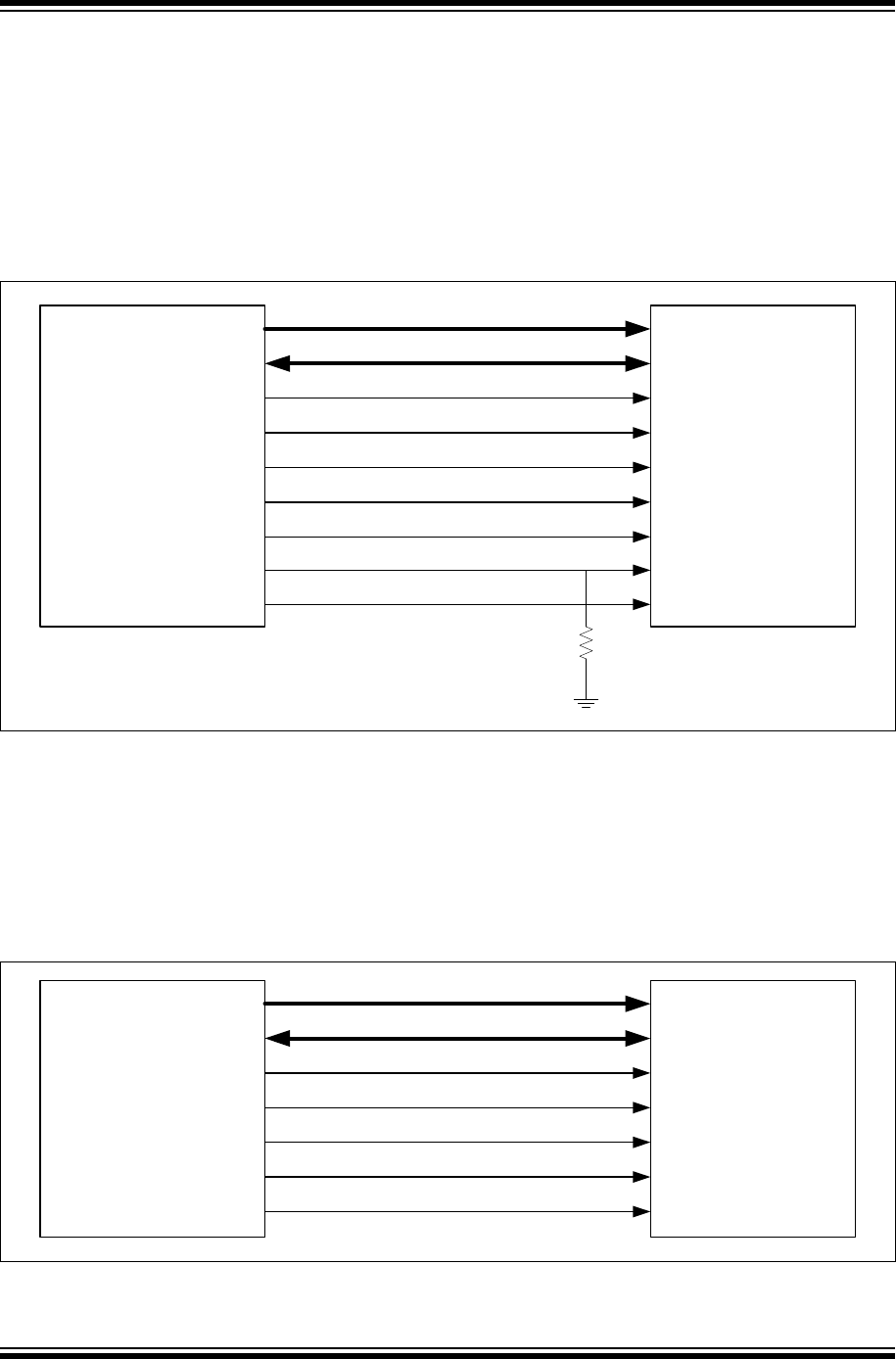
PIC32 Family Reference Manual
DS60001245A-page 47-14 Preliminary © 2013 Microchip Technology Inc.
47.3 INTERFACING TO VARIOUS DEVICES
To pr ovi de s upp ort for a wid e ra nge o f ext er nal devices, the EBI module can be configured to
understand such things as the type, size, and bus width of each attached device. Since this
configuration is determined on a Chip Select basis, when mixing devices on the EBI, similar
devices should be on the same Chip Select line.
47.3.1 Interfacing to NOR Flash Memory
Figure 47-3 shows an example of connecting the EBI bus to an asynchronous NOR Flash device.
Figure 47-3: Interface to an Asynchronous Flash Device
Note that the Write Protect (WP) pin on the Flash device is connected to a General Purpose I/O
pin (RB6). This pin would not be under EBI control, hence it would be up to the user application
to enable Flash writes prior to using the EBI to write the data, and disabling Flash writes when
all writes are complete.
47.3.2 Interfacing to SRAM Memory
Figure 47-2 shows an example connecting the EBI bus to an Asynchronous SRAM memory
device.
Figure 47-4: Interface to an Asynchronous SRAM Device
PIC32MZ
External
Bus Interface
Asynchronous
Flash
EBID<15:0>
EBIA<23:0>
EBIOE
EBIWE
EBICS0
EBIBS0
EBIBS1
D<15:0>
A<23:0>
OE
WE
CS
LB
UB
RB6 WP
10 k
EBIRP RST
PIC32MZ
External
Bus Interface
Asynchronous
SRAM
EBID<15:0>
EBIA<23:0>
EBIOE
EBIWE
EBICS0
EBIBS0
EBIBS1
D<15:0>
A<23:0>
OE
WE
CS
LB
UB

© 2013 Microchip Technology Inc. Preliminary DS60001245A-page 47-15
Section 47. External Bus Interface (EBI)
External Bus
Interface (EBI)
47
In the case of 8-bit memory devices, the Byte-Select (EBIBS) lines are not necessary and only
EBID<7:0> would be connected. Two 8-bit memory devices can share the address and control
lines, and only have separate data lines.
47.3.3 Interfacing to Non-Memory Devices
When non-memory devices are connected to the EBI bus, these devices provide a Ready line to
indicate when valid data is on the data bus. This Ready line is connected to the EBIRDYx pin to
connect to the EBI bus.
Figure 47-5 shows an example of connecting a non-Memory camera device to the EBI bus.
Figure 47-5: Interface to a Non-memory Device
In this case, when the Chip Select line is asserted, the EBI bus would wait to read the data lines
until the camera asserts the EBIRDY1 line.
47.3.4 Combining Devices on the EBI Bus
Figure 47-6 shows an example of sharing some elements of the EBI bus to achieve certain
design purposes.
Figure 47-6: Sharing a Connection Between SRAM and a LCD
In this case, the SRAM serves as a memory buffer for the LCD. As the EBI goes through the data
in the buffer, it is clocked into the LCD, permitting it to display the contents in memory.
PIC32MZ
External
Bus Interface
Camera
EBID<7:0>
EBIRDY1
EBICS0
D<7:0>
RDY
CS
PIC32MZ
External
Bus Interface
Asynchronous
SRAM
EBID<15:0>
EBIA<23:0>
EBIOE
EBIWE
EBICS0
EBIBS0
EBIBS1
D<15:0>
A<23:0>
OE
WE
CS
LB
UB
LCD
RGB<23:0>
PCLK

PIC32 Family Reference Manual
DS60001245A-page 47-16 Preliminary © 2013 Microchip Technology Inc.
47.4 BUS CONFIGURATION
47.4.1 Configuring Address Lines
The CFGEBIA register controls the number of EBIA lines in use and whether, overall, the EBI
controls the address, data, and control lines, or if the lines are available for general use.
Each address line has an enable control in CFGEBIA. By setting the corresponding bit, the EBI
controls that address line. Address bits in use should be contiguous.
The EBIPINEN bit (CFGEBIA<31>) determines control of the overall EBI lines. Setting the bit
allows the EBI to control the corresponding pins. Clearing the bit allows the lines to be used for
other purposes.
47.4.2 Configuring Control and Data Lines
The CFGEBIC register determines the settings for the EBICSx, EBIRDYx, EBIBSx, EBIWE,
EBIOE, EBIRP, and EBIDx lines.
The EBICSEN0, EBICSEN1, EBICSEN2, and EBICSEN3 bits in the CFGEBIC register
determine which EBICS lines are enabled. Setting a bit enables the corresponding EBICSx pin
for EBI use. Clearing a bit disables the pin and allows it for general purpose use.
Three bits control the EBIRDYx lines, EBIRDYEN1, EBIRDYEN2, and EBIRDYEN3. When a of
bit is set, the corresponding EBIRDYx pin is enabled for use by the EBI module. Clearing a bit
allows the EBIRDYx pin to be used for general use.
The EBIRDYINV1, EBIRDYINV2, and EBIRDYINV3 bits control the inversion of the EBIRDYx
line prior to using it. When a bit is set, the EBIRDYx level will be inverted. When cleared, the
signal is not inverted.
The final bit, EBIRDYLVL, determines whether the EBI module uses a level detect or an edge
detect to determine when the EBIRDYx line is being asserted. Devices that have mixed assertion
logic can thus be combined on the EBI bus by having separate EBIRDYx lines.
The EBIBSEN0, EBIBSEN1, EBIWEEN, EBIOEEN, and EBIRPEN bits control whether the
EBIBSx, EBIWE, EBIOE, and EBIRP pins are enabled for use by the EBI module. The pins are
enabled when the corresponding control bit is set, or available for general use when the bit is
cleared.
The EBIDEN0 and EBIDEN1 bits control which 8-bit portion of the EBIDx bus is enabled. Setting
EBIDEN1 enables EBID<15:8> for use by the EBI bus, and setting EBIDEN0 enables the
EBID<7:0> lines. Clearing the bits disables the corresponding side of the bus and allows the pins
to be used for general use. Note that only enabling EBID<15:8> does not guarantee that the bus
will only use 8-bit transfers. If the design requires only 8-bit data transfers, use EBID<7:0>.

© 2013 Microchip Technology Inc. Preliminary DS60001245A-page 47-17
Section 47. External Bus Interface (EBI)
External Bus
Interface (EBI)
47
47.5 DEVICE CONFIGURATION
The basic configuration for each device or group of devices that will be using a particular Chip
Select line includes:
•Configuring the base address of the device
• The type of device
•The size of the device
•The bus timing for the device
47.5.1 Base Address
Configuring the base address of a memory device is done through the EBICSx register. This
register sets the beginning address in the PIC32 physical memory space where the device will
appear. It is a 16-bit value, which allows the minimum device size (64 KB) to have contiguous
locations in memory. In addition, it is not required to have larger memory devices appear lower
in memory than smaller devices. For example, it is possible to have a 64 KB device at the start
of EBI memory (0x20000000), adjacent to a 16 MB device, which would start at 0x20010000.
Example code for configuring the EBICSx registers to handle four memory devices is provided
in Example 47-1. This example maps a 1 MB device, followed by a 64 KB device, followed by
another 1 MB device, and finally a 16 MB device.
Example 47-1:
47.5.2 Device Type
The EBI bus needs to know what type of device is attached to a particular chip select line. This
is done through the MEMTYPE field in the EBIMSKx register of each Chip Select. There are two
options available, NOR Flash (MEMTYPE = 0b010) and SRAM (MEMTYPE = 0b001).
Non-memory devices would not require this to be set.
Example code for configuring the memory types for the devices previously listed in Example 47-1
is shown in Example 47-2.
Example 47-2:
47.5.3 Device Size
In addition to the type of memory device, the EBI bus needs to know the size of the attached
device. The device size is configured by the MEMSIZE<4:0> (EBIMSKx<4:0>) bits.
The smallest memory size that can be accommodated by the EBI in a contiguous manner is
64 KB. Smaller devices would alias to that size, which results in gaps in the memory map.
Example code for configuring the device size for the devices listed in Example 47-2 is shown in
Example 47-3.
/* Device 1: 1 MB Flash going from 0x20000000 to 0x200FFFFF */
EBICS0 = 0x20000000;
/* Device 2: 64 KB SRAM going from 0x20100000 to 0x2010FFFF */
EBICS1 = 0x20100000;
/* Device 3: 1 MB Flash going from 0x20110000 to 0x2020FFFF */
EBICS2 = 0x20110000;
/* Device 4: 16 MB SRAM going from 0x20210000 to 0x2120FFFF */
EBICS3 = 0x20210000;
EBIMSK0bits.MEMTYPE = 0b010; /* Device 1: NOR Flash */
EBIMSK1bits.MEMTYPE = 0b001; /* Device 2: SRAM */
EBIMSK2bits.MEMTYPE = 0b010; /* Device 3: NOR Flash */
EBIMSK3bits.MEMTYPE = 0b001; /* Device 4: SRAM */

PIC32 Family Reference Manual
DS60001245A-page 47-18 Preliminary © 2013 Microchip Technology Inc.
Example 47-3:
47.5.4 Bus Timing
The EBI bus can handle a variety of memory timing requirements. There are three registers that
configure the timing parameters, EBISMT0, EBISMT1, and EBISMT2. Identical memory devices
should use the same EBISMTx register for timing purposes.
The REGSEL<2:0> bits (EBIMSKx<10:8>) are used to set which EBISMTx register will be used
for each Chip Select line. Example code for setting up the bus timing is shown in Example 47-4.
Example 47-4:
EBIMSK0bits.MEMSIZE = 0b00101; /* Device 1: 1 MB */
EBIMSK1bits.MEMSIZE = 0b00001; /* Device 2: 64 KB */
EBIMSK2bits.MEMSIZE = 0b00101; /* Device 3: 1 MB */
EBIMSK3bits.MEMSIZE = 0b01001; /* Device 4: 16 MB */
EBIMSK0bits.REGSEL = 0b000; /* Device 1: EBISMT0 */
EBIMSK1bits.REGSEL = 0b001; /* Device 2: EBISMT1 */
EBIMSK2bits.REGSEL = 0b000; /* Device 3: EBISMT0 */
EBIMSK3bits.REGSEL = 0b010; /* Device 4: EBISMT2 */

© 2013 Microchip Technology Inc. Preliminary DS60001245A-page 47-19
Section 47. External Bus Interface (EBI)
External Bus
Interface (EBI)
47
47.5.5 Configuring Bus Timing
Since devices have different timing considerations, it is necessary to configure the EBI bus to
automatically handle those timing differences. By configuring the EBISMTx register, the bus will
adjust read and write timings as needed.
If a device has a Ready pin, the RDYMODE bit (EBISMTx<26>) is set.
For devices with Page mode, the PAGEMODE bit (EBISMTx<23>) enables support for the
device in the EBI module. Then, the PAGESIZE<1:0> bits (EBISMTx<25:24>) configure the
Page Size so that the EBI knows how many words to write for each page.
The remaining bits in the EBISMTx register control how the EBI bus timing works. Refer to the
diagrams in 47.6 “Timing Diagrams” to see visual representations of the bus cycles, and where
the timing parameters are needed. Tab le 47 -4 lists the individual timing parameters, and what
they affect.
Table 47-4: Timing Parameters
Parameter
EBISMTx
Register Bit
Name
Description Effect
tPRC TPRC<3:0> Page mode read cycle time. Read cycle time is TPRC+1
clock cycles.
tBTA TBTA<2:0> Bus turnaround time. Clock cycles (0-7) for
read-to-write, write-to-read, and
read-to-read (different CS) tran-
sitions.
tWP TWP<5:0> Write Pulse Width. Write pulse width is TWP+1
clock cycles.
tWR TWR<1:0> Write address/data hold time. Number of clock cycles to hold
address or data on the bus.
tAS TAS<1:0> Write address setup time. Clock cycles for address setup
time. A value of ‘0’ is only valid
in case of SRAM.
tRC TRC<5:0> Read cycle time (non-Page
mode memory).
Read cycle time is TRC + 1
clock cycles.
tRPD TRPD<11:0> Flash memory reset time. Clock cycles after Flash reset
before a read/write access.
Note: Clock cycles refers to system clock cycles, and is dependent on the speed of the
SYSCLK when the system is running.

PIC32 Family Reference Manual
DS60001245A-page 47-20 Preliminary © 2013 Microchip Technology Inc.
47.5.6 Reading and Writing to the EBI Module
Example 47-5 shows code that uses both reads and writes to SRAM attached to the EBI module.
This example assumes a 200 MHz System Clock and that the TLB and MMU are set up correctly.
Example 47-5:
// Global Defines
#define SRAM_ADDR_CS0 0xC0000000
#define RAM_SIZE 2*1024*1024
int main(void)
{
uint32_t loop;
uint32_t *addr;
uint32_t val;
// Note: ISSI SRAM (IS64WV102416BLL). All of the parameters of the EBI
// module are set up based on the timing of this RAM.
// Enable address lines [0:17]
//Controls access of pins shared with PMP
CFGEBIA = 0x800FFFFF;
//Enable write enable pin
//Enable output enable pin
//Enable byte select pin 0
//Enable byte select pin 1
//Enable Chip Select 0
//Enable data pins [0:15]
CFGEBIC = 0x00003313;
//Connect CS0 to physical address
EBICS0 = 0x20000000;
// Memory size is set as 2 MB
// Memory type is set as SRAM
// Uses timing numbers in EBISMT0
EBIMSK0 = 0x00000026;
//Configure EBISMT0
// ISSI device has read cycles time of 10 ns
// ISSI device has address setup time of 0ns
// ISSI device has address/data hold time of 2.5 ns
// ISSI device has Write Cycle Time of 10 ns
// Bus turnaround time is 0 ns
// No page mode
// No page size
// No RDY pin
EBISMT0 = 0x000029CA;
//Keep default data width to 16-bits
EBISMCON = 0x00000000;
addr = (uint32_t *)SRAM_ADDR_CS0;
//Write loop
for (loop=0; loop < RAM_SIZE/4; loop++)
{
*addr++ = 0xAA55AA55;
}
//Read and verify loop
addr = (uint32_t *)SRAM_ADDR_CS0; // reset address to beginning
for (loop=0 ; loop < RAM_SIZE/4; loop++)
{
val = *addr++;
if (val != 0xAA55AA55)
{
return (0); //Exit Failure
}
}
return (1); // exit success
}

© 2013 Microchip Technology Inc. Preliminary DS60001245A-page 47-21
Section 47. External Bus Interface (EBI)
External Bus
Interface (EBI)
47
47.6 TIMING DIAGRAMS
47.6.1 Read/Write Access
Figure 47-7 shows the timing diagram of a read access. The EBI module checks the EBIRDYx
pin after the tRC read access time. You need to ensure that the EBIRDYx signal is being driven
with respect to the System Clock (SYSCLK). This avoids a possible race condition if EBIRDYx
is driven by a different clock. When EBIRDYx is high, the EBI module latches the read data at
the next rising clock edge.
Figure 47-7: Read Access of the Device with Ready Signal
Figure 47-8 shows the timing diagram of a write access. The EBI module checks the EBIRDYx
pin after a time equal to tAS(address setup time) + tWP(write period). When EBIRDYx is high,
the write is finished. You need to ensure that the EBIRDYx signal is being driven with respect to
the SYSCLK. This avoids a possible race condition if EBIRDYx is driven by a different clock.
Figure 47-8: Write Access of the Device with Ready Signal
1234567
A0
D0
PBCLK8
EBIA
EBICSx
EBIOE
EBIWE
EBIRDYx
EBID
tRC
123456789
A0
D0
tWP
PBCLK8
EBIA
EBICSx
EBIOE
EBIWE
EBIRDYx
EBID
tWPtAS
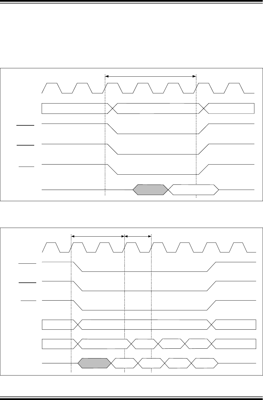
PIC32 Family Reference Manual
DS60001245A-page 47-22 Preliminary © 2013 Microchip Technology Inc.
47.6.2 Static Memory
The static memory timing diagrams assume an internal delay of two System Bus clock cycles,
which is the delay for a cycle to be active on the bus to the clock cycle where the corresponding
memory command is seen on the memory bus.
Figure 47-9 shows the timing for a SRAM and Flash read operation, where tRC is the read cycle
time.
Figure 47-9: SRAM and Flash Memory Read Timing
Figure 47-10 shows the Flash page read operation, where tRC is the read cycle time and tPRC
is the page mode read cycle time.
Figure 47-10: Flash Memory Page Read Timing
Address
Data
tRC
PBCLK8
EBIA
EBICSx
EBIBSx
EBIOE
EBID
Address
D0
tPRC
00 01 11
D1 D2 D3
10
tRC
byte_slct_n
PBCLK8
EBICSx
EBIBSx
EBIOE
EBID
EBIA<1:0>
EBIA<20:2>

© 2013 Microchip Technology Inc. Preliminary DS60001245A-page 47-23
Section 47. External Bus Interface (EBI)
External Bus
Interface (EBI)
47
Figure 47-11 shows the SRAM and Flash timing for a write operation, where tAS is the address
setup time, tWP is the write pulse period, and tWR is the write recovery time.
Figure 47-11: SRAM and Flash Write Timing
Figure 47-12 shows an example of inserting one idle clock for memory data bus turnaround time,
where tBTA is the number of idle clock cycles.
Figure 47-12: External Memory Data Bus Turnaround Timing
Address
Data
tWPtAS tWR
PBCLK8
EBICSx
EBIBSx
EBIWE
EBID
EBIA
PBCLK8
EBICSx
EBIOE
EBIA
EBID
A0 A1
D1
A2
EBIWE
EBIBSx
EBID D0 D2
tBTA tBTA
(Two reads)
(One write)

PIC32 Family Reference Manual
DS60001245A-page 47-24 Preliminary © 2013 Microchip Technology Inc.
47.7 EFFECTS OF RESET
47.7.1 On Reset
All EBI module registers are forced to their reset states on a device Reset. In addition, the
CFGEBIA and CFGEBIC registers are forced to their Reset states.
47.7.2 After Reset
The EBI module is not active, and must be initialized prior to accessing memory in the EBI
address space. In addition, the Translation Lookaside Buffer (TLB) of the CPU must be set up
prior to accessing any external device.
47.8 OPERATION IN POWER-SAVING MODES
47.8.1 Sleep Mode
When the device enters Sleep mode, the EBI module is disabled and placed into a low-power
state where no clocking occurs in the module.
47.8.2 Idle Mode
When the device enters Idle mode, the EBI module continues to operate, and can execute
transfers between internal and external memory.
47.8.3 Debug Mode
The behavior of the EBI module is unaltered in Debug mode.

© 2013 Microchip Technology Inc. Preliminary DS60001245A-page 47-25
Section 47. External Bus Interface (EBI)
External Bus
Interface (EBI)
47
47.9 RELATED APPLICATION NOTES
This section lists application notes that are related to this section of the manual. These
application notes may not be written specifically for the PIC32 device family, but the concepts are
pertinent and could be used with modification and possible limitations. The current application
notes related to the External Bus Interface (EBI) are:
Title Application Note #
No related application notes at this time. N/A
Note: Please visit the Microchip web site (www.microchip.com) for additional application
notes and code examples for the PIC32 family of devices.

PIC32 Family Reference Manual
DS60001245A-page 47-26 Preliminary © 2013 Microchip Technology Inc.
47.10 REVISION HISTORY
Revision A (November 2013)
This is the initial released version of this document.

2013 Microchip Technology Inc. Preliminary DS60001245A-page 47-27
Information contained in this publication regarding device
applications and the like is provided only for your convenience
and may be superseded by updates. It is your responsibility to
ensure that your application meets with your specifications.
MICROCHIP MAKES NO REPRESENTATIONS OR
WARRANTIES OF ANY KIND WHETHER EXPRESS OR
IMPLIED, WRITTEN OR ORAL, STATUTORY OR
OTHERWISE, RELATED TO THE INFORMATION,
INCLUDING BUT NOT LIMITED TO ITS CONDITION,
QUALITY, PERFORMANCE, MERCHANTABILITY OR
FITNESS FOR PURPOSE. Microchip disclaims all liability
arising from this information and its use. Use of Microchip
devices in life support and/or safety applications is entirely at
the buyer’s risk, and the buyer agrees to defend, indemnify and
hold harmless Microchip from any and all damages, claims,
suits, or expenses resulting from such use. No licenses are
conveyed, implicitly or otherwise, under any Microchip
intellectual property rights.
Trademarks
The Microchip name and logo, the Microchip logo, dsPIC,
FlashFlex, KEELOQ, KEELOQ logo, MPLAB, PIC, PICmicro,
PICSTART, PIC32 logo, rfPIC, SST, SST Logo, SuperFlash
and UNI/O are registered trademarks of Microchip Technology
Incorporated in the U.S.A. and other countries.
FilterLab, Hampshire, HI-TECH C, Linear Active Thermistor,
MTP, SEEVAL and The Embedded Control Solutions
Company are registered trademarks of Microchip Technology
Incorporated in the U.S.A.
Silicon Storage Technology is a registered trademark of
Microchip Technology Inc. in other countries.
Analog-for-the-Digital Age, Application Maestro, BodyCom,
chipKIT, chipKIT logo, CodeGuard, dsPICDEM,
dsPICDEM.net, dsPICworks, dsSPEAK, ECAN,
ECONOMONITOR, FanSense, HI-TIDE, In-Circuit Serial
Programming, ICSP, Mindi, MiWi, MPASM, MPF, MPLAB
Certified logo, MPLIB, MPLINK, mTouch, Omniscient Code
Generation, PICC, PICC-18, PICDEM, PICDEM.net, PICkit,
PICtail, REAL ICE, rfLAB, Select Mode, SQI, Serial Quad I/O,
Tota l E ndu ra nce , T SHA RC , U n iW inD riv er, Wi per Lo c k, ZE NA
and Z-Scale are trademarks of Microchip Technology
Incorporated in the U.S.A. and other countries.
SQTP is a service mark of Microchip Technology Incorporated
in the U.S.A.
GestIC and ULPP are registered trademarks of Microchip
Technology Germany II GmbH & Co. KG, a subsidiary of
Microchip Technology Inc., in other countries.
All other trademarks mentioned herein are property of their
respective companies.
© 2013, Microchip Technology Incorporated, Printed in the
U.S.A., All Rights Reserved.
Printed on recycled paper.
ISBN: 978-1-62077-645-2
Note the following details of the code protection feature on Microchip devices:
• Microchip products meet the specification contained in their particular Microchip Data Sheet.
• Microchip believes that its family of products is one of the most secure families of its kind on the market today, when used in the
intended manner and under normal conditions.
• There are dishonest and possibly illegal methods used to breach the code protection feature. All of these methods, to our
knowledge, require using the Microchip products in a manner outside the operating specifications contained in Microchip’s Data
Sheets. Most likely, the person doing so is engaged in theft of intellectual property.
• Microchip is willing to work with the customer who is concerned about the integrity of their code.
• Neither Microchip nor any other semiconductor manufacturer can guarantee the security of their code. Code protection does not
mean that we are guaranteeing the product as “unbreakable.”
Code protection is constantly evolving. We at Microchip are committed to continuously improving the code protection features of our
products. Attempts to break Microchip’s code protection feature may be a violation of the Digital Millennium Copyright Act. If such acts
allow unauthorized access to your software or other copyrighted work, you may have a right to sue for relief under that Act.
Microchip received ISO/TS-16949:2009 certification for its worldwide
headquarters, design and wafer fabrication facilities in Chandler and
Tempe, Arizona; Gresham, Oregon and design centers in California
and India. The Company’s quality system processes and procedures
are for its PIC® MCUs and dsPIC® DSCs, KEELOQ® code hopping
devices, Serial EEPROMs, microperipherals, nonvolatile memory and
analog products. In addition, Microchip’s quality system for the design
and manufacture of development systems is ISO 9001:2000 certified.
QUALITY MANAGEMENT S
YSTEM
CERTIFIED BY DNV
== ISO/TS 16949 ==

DS60001245A-page 47-28 Preliminary 2013 Microchip Technology Inc.
AMERICAS
Corporate Office
2355 West Chandler Blvd.
Chandler, AZ 85224-6199
Tel: 480-792-7200
Fax: 480-792-7277
Technical Support:
http://www.microchip.com/
support
Web Address:
www.microchip.com
Atlanta
Duluth, GA
Tel: 678-957-9614
Fax: 678-957-1455
Austin, TX
Tel: 512-257-3370
Boston
Westborough, MA
Tel: 774-760-0087
Fax: 774-760-0088
Chicago
Itasca, IL
Tel: 630-285-0071
Fax: 630-285-0075
Cleveland
Independence, OH
Tel: 216-447-0464
Fax: 216-447-0643
Dallas
Addison, TX
Tel: 972-818-7423
Fax: 972-818-2924
Detroit
Novi, MI
Tel: 248-848-4000
Houston, TX
Tel: 281-894-5983
Indianapolis
Noblesville, IN
Tel: 317-773-8323
Fax: 317-773-5453
Los Angeles
Mission Viejo, CA
Tel: 949-462-9523
Fax: 949-462-9608
New York, NY
Tel: 631-435-6000
San Jose, CA
Tel: 408-735-9110
Canada - Toronto
Tel: 905-673-0699
Fax: 905-673-6509
ASIA/PACIFIC
Asia Pacific Office
Suites 3707-14, 37th Floor
Tower 6, The Gateway
Harbour City, Kowloon
Hong Kong
Tel : 8 52 -24 01- 120 0
Fax: 852-2401-3431
Australia - Sydney
Tel : 6 1- 2-9 868 -67 33
Fax: 61-2-9868-6755
China - Beijing
Tel : 8 6- 10- 856 9-7 00 0
Fax: 86-10-8528-2104
China - Chengdu
Tel : 8 6- 28- 866 5-5 511
Fax: 86-28-8665-7889
China - Chongqing
Tel : 8 6- 23- 898 0-9 58 8
Fax: 86-23-8980-9500
China - Hangzhou
Tel : 8 6- 571 -28 19- 318 7
Fax: 86-571-2819-3189
China - Hong Kong SAR
Tel : 8 52 -29 43- 510 0
Fax: 852-2401-3431
China - Nanjing
Tel : 8 6- 25- 847 3-2 46 0
Fax: 86-25-8473-2470
China - Qingdao
Tel : 8 6- 532 -85 02- 735 5
Fax: 86-532-8502-7205
China - Shanghai
Tel : 8 6- 21- 540 7-5 53 3
Fax: 86-21-5407-5066
China - Shenyang
Tel : 8 6- 24- 233 4-2 82 9
Fax: 86-24-2334-2393
China - Shenzhen
Tel : 8 6- 755 -88 64- 220 0
Fax: 86-755-8203-1760
China - Wuhan
Tel : 8 6- 27- 598 0-5 30 0
Fax: 86-27-5980-5118
China - Xian
Tel : 8 6- 29- 883 3-7 25 2
Fax: 86-29-8833-7256
China - Xiamen
Tel: 86-592-2388138
Fax: 86-592-2388130
China - Zhuhai
Tel : 86- 75 6-3 21 004 0
Fax: 86-756-3210049
ASIA/PACIFIC
India - Bangalore
Tel : 9 1- 80- 309 0-4 44 4
Fax: 91-80-3090-4123
India - New Delhi
Tel : 9 1- 11- 416 0 -8 631
Fax: 91-11-4160-8632
India - Pune
Tel : 9 1- 20- 301 9-1 50 0
Japan - Osaka
Tel : 8 1- 6-6 152 -7 1 60
Fax: 81-6-6152-9310
Japan - Tokyo
Tel : 8 1- 3-6 880 - 377 0
Fax: 81-3-6880-3771
Korea - Daegu
Tel : 8 2- 53- 744 -43 01
Fax: 82-53-744-4302
Korea - Seoul
Tel : 8 2- 2-5 54- 72 0 0
Fax: 82-2-558-5932 or
82-2-558-5934
Malaysia - Kuala Lumpur
Tel : 6 0- 3-6 201 -9 8 57
Fax: 60-3-6201-9859
Malaysia - Penang
Tel : 6 0- 4-2 27- 88 7 0
Fax: 60-4-227-4068
Philippines - Manila
Tel : 6 3- 2-6 34- 90 6 5
Fax: 63-2-634-9069
Singapore
Tel : 6 5- 633 4-8 870
Fax: 65-6334-8850
Taiwan - Hsin Chu
Tel : 8 86 -3- 577 8-3 66
Fax: 886-3-5770-955
Taiwan - Kaohsiung
Tel : 8 86 -7- 213 -78 30
Taiwan - Taipei
Tel : 8 86 -2- 250 8-8 60 0
Fax: 886-2-2508-0102
Thailand - Bangkok
Tel : 6 6- 2-6 94- 13 5 1
Fax: 66-2-694-1350
EUROPE
Austria - Wels
Tel : 4 3- 72 42 -2 244 -3 9
Fax: 43-7242-2244-393
Denmark - Copenhagen
Tel : 4 5- 445 0-2 828
Fax: 45-4485-2829
France - Paris
Tel : 3 3- 1-6 9-5 3-6 3-2 0
Fax: 33-1-69-30-90-79
Germany - Dusseldorf
Tel : 4 9- 21 29 -3 766 400
Germany - Munich
Tel : 4 9- 89 -62 7-1 44- 0
Fax: 49-89-627-144-44
Germany - Pforzheim
Tel : 4 9- 72 31 -4 247 50
Italy - Milan
Tel : 3 9- 03 31 -7 426 11
Fax: 39-0331-466781
Italy - Venice
Tel : 3 9- 04 9- 762 528 6
Netherlands - Drunen
Tel : 3 1- 41 6- 690 399
Fax: 31-416-690340
Poland - Warsaw
Tel : 4 8- 22 -33 257 37
Spain - Madrid
Tel : 3 4- 91 -70 8-0 8-9 0
Fax: 34-91-708-08-91
Sweden - Stockholm
Tel : 4 6- 8-5 090 -46 54
UK - Wokingham
Tel : 4 4- 118 -92 1- 5 800
Fax: 44-118-921-5820
Worldwide Sales and Service
10/28/13

© 2013 Microchip Technology Inc. DS60001214A-page 48-1
Memory
Organization and
Permissions
48
Section 48. Memory Organization and Permissions
HIGHLIGHTS
This section of the manual contains the following major topics:
48.1 Introduction .................................................................................................................. 48-2
48.2 Control Registers ......................................................................................................... 48-3
48.3 Memory Layout .......................................................................................................... 48-13
48.4 The System Bus......................................................................................................... 48-16
48.5 System Bus Arbitration .............................................................................................. 48-18
48.6 Access Permissions................................................................................................... 48-19
48.7 Effects of Reset.......................................................................................................... 48-21
48.8 Operation in Power-Saving Modes ............................................................................ 48-21
48.9 Debug Mode .............................................................................................................. 48-21
48.10 Code Examples.......................................................................................................... 48-22
48.11 Related Application Notes.......................................................................................... 48-25
48.12 Revision History ......................................................................................................... 48-26

PIC32 Family Reference Manual
DS60001214A-page 48-2 © 2013 Microchip Technology Inc.
48.1 INTRODUCTION
The PIC32MZ family of microcontrollers provides 4 GB of unified virtual memory address space.
All memory regions, including program memory, data memory, external memory, SFRs, and
Configuration registers, reside in this address space at their respective unique addresses.
PIC32MZ devices can execute from boot Flash, program Flash, data memory, or external
memory. A highly configurable protection scheme can prevent access by user software or DMA
to selected memory regions while the secure kernel or boot code retains full access.
The PIC32MZ System Bus, which is implemented as a multi-layer fabric (crossbar), allows
concurrent transactions by connecting a multitude of initiators to a multitude of targets. Bus
initiators consist of the CPU, general purpose DMA, and peripherals with dedicated DMA, while
bus targets include program memory, data memory, and peripherals.
Key features of PIC32MZ memory organization include the following:
•32-bit native data width
•Integrated Memory Management Unit (MMU) with fixed mapping allows for securely
configurable memory and peripheral access control permissions
•Bus arbitration scheme is implemented using a least recently serviced (LRS) priority to
provide a Quality of Service (QOS) for the CPU, general purpose DMA, and peripherals
with dedicated DMA
•Dual Flash panels allow for live updates of program memory
•Separate dual boot Flash memory allows updates of boot code
•Dual RAM banks can be used to avoid bus arbitration when using DMA
•External serial and or parallel memory can be mapped into virtual memory space for data
access or code execution using the Serial Quad Interface (SQI) or External Bus Interface
(EBI)
•Cacheable and non-cacheable address regions
Note: This family reference manual section is meant to serve as a complement to device
data sheets. Depending on the device variant, this manual section may not apply to
all PIC32 devices.
Please consult the note at the beginning of the “Memory Organization” chapter in
the current device data sheet to check whether this document supports the device
you are using.
Device data sheets and family reference manual sections are available for
download from the Microchip Worldwide Web site at: http://www.microchip.com

© 2013 Microchip Technology Inc. DS60001214A-page 48-3
Section 48. Memory Organization and Permissions
Memory
Organization and
Permissions
48
48.2 CONTROL REGISTERS
The PIC32 MMU has the following SFRs:
•SBFLAG: System Bus Status Flag Register
This bit encoded register indicates which, if any, Bus targets are reporting a permission
group violation errors.
•SBTxELOG1: System Bus Target ‘x’ Error Log Register 1 (‘x’ = 0-13)
This register provides details regarding a permission group violation error, if one exists.
•SBTxELOG2: System Bus Target ‘x’ Error Log Register 2 (‘x’ = 0-13)
This register provides details regarding a permission group violation error, if one exists.
•SBTxECON: System Bus Target ‘x’ Error Control Register (‘x’ = 0-13)
This register provides control over permission group violation error reporting.
•SBTxECLRS: System Bus Target ‘x’ Single Error Clear Register (‘x’ = 0-13)
This register provides a mechanism for clearing reports of single permission group violation
errors.
•SBTxECLRM: System Bus Target ‘x’ Multiple Error Clear Register (‘x’ = 0-13)
This register provides a mechanism for clearing reports of multiple permission group
violation errors.
•SBTxREGy: System Bus Target ‘x’ Region ‘y’ Register (‘x’ = 0-13; ‘y’ = 0-8)
This register is used to configure the base address, priority and size for a target’s memory
region. A target has multiple memory regions.
•SBTxRDy: System Bus Target ‘x’ Region ‘y’ Read Permissions Register (‘x’ = 0-13; ‘y’
= 0-8)
This register is used to configure read permissions for each of the groups of a target’s
memory regions.
•SBTxWRy: System Bus Target ‘x’ Region ‘y’ Write Permissions Register (‘x’ = 0-13;
‘y’ = 0-8)
This register is used to configure write permissions for each of the groups of a target’s
memory regions.

PIC32 Family Reference Manual
DS60001214A-page 48-4 © 2013 Microchip Technology Inc.
Tabl e 48- 1 provides a brief summary of the related Memory Organization and Permissions registers. Corresponding registers appear after the summary, followed by a
detailed description of each bit.
Table 48-1: System Bus SFR Summary
Name Bit 31/15 Bit 30/14 Bit 29/13 Bit 28/12 Bit 27/11 Bit 26/10 Bit 25/9 Bit 24/8 Bit 23/7 Bit 22/6 Bit 21/5 Bit 20/4 Bit 19/3 Bit 118/2 Bit 17/1 Bit 16/0
SBFLAG(1) 31:16 ————————————————
15:0 ——T13PGVT12PGVT11PGVT10PGVT9PGVT8PGVT7PGVT6PGVT5PGVT4PGVT3PGVT2PGVT1PGVT0PGV
SBTxELOG1(1) 31:16 MULTI ———CODE<3:0>————————
15:0 INITID<7:0> REGION<3:0> —CMD<2:0>
SBTxELOG2(1) 31:16 ————————————————
15:0 —————————————— GROUP<1:0>
SBTxECON(1) 31:16 ————————————————
15:0 ———————————————ERRP
SBTxECLRS(1) 31:16 ————————————————
15:0 ———————————————CLEAR
SBTxECLRM(1) 31:16 ————————————————
15:0 ———————————————CLEAR
SBTxREGy(1,2) 31:16 BASE<21:6>
15:0 BASE<5:0> PRI —SIZE<4:0>———
SBTxRDy(1,2) 31:16 ————————————————
15:0 ———————————— GROUP3 GROUP2 GROUP1 GROUP0
SBTxWRy(1,2) 31:16 ————————————————
15:0 ———————————— GROUP3 GROUP2 GROUP1 GROUP0
Legend: — = unimplemented, read as ‘0’.
Note 1: Refer to the “Memory Organization” chapter in the specific device data sheet for the list of available targets and their descriptions.
2: For some target regions, certain bits in this register are read-only with preset values. Refer to the “Memory Organization” chapter in the specific device data sheet for more information.
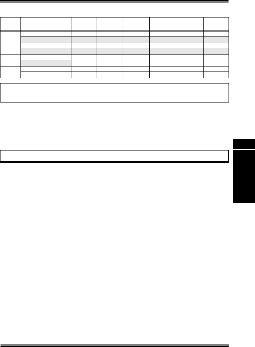
© 2013 Microchip Technology Inc. DS60001214A-page 48-5
Section 48. Memory Organization and Permissions
Memory
Organization and
Permissions
48
Register 48-1: SBFLAG: System Bus Status Flag Register
Bit
Range
Bit
31/23/15/7
Bit
30/22/14/6
Bit
29/21/13/5
Bit
28/20/12/4
Bit
27/19/11/3
Bit
26/18/10/2
Bit
25/17/9/1
Bit
24/16/8/0
31:24 U-0 U-0 U-0 U-0 U-0 U-0 U-0 U-0
— — — — — — — —
23:16 U-0 U-0 U-0 U-0 U-0 U-0 U-0 U-0
— — — — — — — —
15:8 U-0 U-0 R-0 R-0 R-0 R-0 R-0 R-0
——T13PGVT12PGVT11PGVT10PGV T9PGV T8PGV
7:0 R-0 R-0 R-0 R-0 R-0 R-0 R-0 R-0
T7PGV T6PGV T5PGV T4PGV T3PGV T2PGV T1PGV T0PGV
Legend:
R = Readable bit W = Writable bit U = Unimplemented bit, read as ‘0’
-n = Value at POR ‘1’ = Bit is set ‘0’ = Bit is cleared
bit 31-14 Unimplemented: Read as ‘0’
bit 13-0 TxPGV: Target ‘x’ Permission Group Violation Status bits (‘x’ = 0-13)
Refer to the “Memory Organization” chapter in the specific device data sheet for the list of available
targets and their descriptions.
1 = Target is reporting a permission group violation
0 = Target is not reporting a permission group violation
Note: All errors are cleared at the source (i.e., SBTxELOG1, SBTxELOG2, SBTxECLRS, or SBTxECLRM
registers).

PIC32 Family Reference Manual
DS60001214A-page 48-6 © 2013 Microchip Technology Inc.
Register 48-2: SBTxELOG1: System Bus Target ‘x’ Error Log Register 1 (‘x’ = 0-13)
Bit
Range
Bit
31/23/15/7
Bit
30/22/14/6
Bit
29/21/13/5
Bit
28/20/12/4
Bit
27/19/11/3
Bit
26/18/10/2
Bit
25/17/9/1
Bit
24/16/8/0
31:24 R/W-0 U-0 U-0 U-0 R/W-0 R/W-0 R/W-0 R/W-0
MULTI — — —CODE<3:0>
23:16 U-0 U-0 U-0 U-0 U-0 U-0 U-0 U-0
— — — — — — — —
15:8 R-0 R-0 R-0 R-0 R-0 R-0 R-0 R-0
INITID<7:0>(1)
7:0 R-0 R-0 R-0 R-0 U-0 R-x R-x R-x
REGION<3:0> —CMD<2:0>
Legend:
R = Readable bit W = Writable bit U = Unimplemented bit, read as ‘0’
-n = Value at POR ‘1’ = Bit is set ‘0’ = Bit is cleared
bit 31 MULTI: Multiple Permission Violations Status bit
1 = Multiple errors have been detected
0 = No multiple errors have been detected
bit 30-28 Unimplemented: Read as ‘0’
bit 27-24 CODE<3:0>: Error Code bits
Indicates the type of error reported.
1111 = Reserved
•
•
•
0100 = Reserved
0011 = Permission violation
0010 = Reserved
0001 = Reserved
0000 = No error
bit 23-16 Unimplemented: Read as ‘0’
Note 1: Selections vary by device. Refer to the “Memory Organization” chapter in the specific device data sheet
to determine which selections are available.
Note: Refer to the “Memory Organization” chapter in the specific device data sheet for the list of available
System Bus targets and their descriptions.

© 2013 Microchip Technology Inc. DS60001214A-page 48-7
Section 48. Memory Organization and Permissions
Memory
Organization and
Permissions
48
bit 15-8 INITID<7:0>: Initiator ID of Requestor bits
11111111 = Reserved
•
•
•
00001111 = Reserved
00001110 = Crypto Engine
00001101 = Flash Controller
00001100 = SQI1
00001011 = CAN2
00001010 = CAN1
00001001 = Ethernet Write
00001000 = Ethernet Read
00000111 = USB
00000110 = DMA Write (DMAPRI (CFGCON<25>) = 1)
00000101 = DMA Write (DMAPRI (CFGCON<25>) = 0)
00000100 = DMA Read (DMAPRI (CFGCON<25>) = 1)
00000011 = DMA Read (DMAPRI (CFGCON<25>) = 0)
00000010 = CPU (CPUPRI (CFGCON<24>) = 1)
00000001 = CPU (CPUPRI (CFGCON<25>) = 0)
00000000 = Reserved
bit 7-4 REGION<3:0>: Requested Region Number bits
1111 - 0000 = Target’s region that reported a permission group violation (this number corresponds to the
‘y’ of the SBTxREGy region definition register name)
bit 3 Unimplemented: Read as ‘0’
bit 2-0 CMD<2:0>: Transaction Command of the Requestor bits
111 = Reserved
110 = Reserved
101 = Write (a non-posted write)
100 = Reserved
011 = Read (a locked read caused by a Read-Modify-Write transaction)
010 = Read
001 = Write
000 = Idle
Register 48-2: SBTxELOG1: System Bus Target ‘x’ Error Log Register 1 (‘x’ = 0-13) (Continued)
Note 1: Selections vary by device. Refer to the “Memory Organization” chapter in the specific device data sheet
to determine which selections are available.
Note: Refer to the “Memory Organization” chapter in the specific device data sheet for the list of available
System Bus targets and their descriptions.
PIC32 Family Reference Manual
DS60001214A-page 48-8 © 2013 Microchip Technology Inc.
Register 48-3: SBTxELOG2: System Bus Target ‘x’ Error Log Register 2 (‘x’ = 0-13)
Bit
Range
Bit
31/23/15/7
Bit
30/22/14/6
Bit
29/21/13/5
Bit
28/20/12/4
Bit
27/19/11/3
Bit
26/18/10/2
Bit
25/17/9/1
Bit
24/16/8/0
31:24 U-0 U-0 U-0 U-0 U-0 U-0 U-0 U-0
— — — — — — — —
23:16 U-0 U-0 U-0 U-0 U-0 U-0 U-0 U-0
— — — — — — — —
15:8 U-0 U-0 U-0 U-0 U-0 U-0 U-0 U-0
— — — — — — — —
7:0 U-0 U-0 U-0 U-0 U-0 U-0 R-0 R-0
— — — — — —GROUP<1:0>
Legend:
R = Readable bit W = Writable bit U = Unimplemented bit, read as ‘0’
-n = Value at POR ‘1’ = Bit is set ‘0’ = Bit is cleared
bit 31-3 Unimplemented: Read as ‘0’
bit 1-0 GROUP<1:0>: Requested Permissions Group bits
11 = Group 3
10 = Group 2
01 = Group 1
00 = Group 0
Note: Refer to the “Memory Organization” chapter in the specific device data sheet for the list of available
System Bus targets and their descriptions.
Register 48-4: SBTxECON: System Bus Target ‘x’ Error Control Register (‘x’ = 0-13)
Bit
Range
Bit
31/23/15/7
Bit
30/22/14/6
Bit
29/21/13/5
Bit
28/20/12/4
Bit
27/19/11/3
Bit
26/18/10/2
Bit
25/17/9/1
Bit
24/16/8/0
31:24 U-0 U-0 U-0 U-0 U-0 U-0 U-0 U-0
— — — — — — — —
23:16 U-0 U-0 U-0 U-0 U-0 U-0 U-0 R/W-0
— — — — — — — ERRP
15:8 U-0 U-0 U-0 U-0 U-0 U-0 U-0 U-0
— — — — — — — —
7:0 U-0 U-0 U-0 U-0 U-0 U-0 U-0 U-0
— — — — — — — —
Legend:
R = Readable bit W = Writable bit U = Unimplemented bit, read as ‘0’
-n = Value at POR ‘1’ = Bit is set ‘0’ = Bit is cleared
bit 31-25 Unimplemented: Read as ‘0’
bit 24 ERRP: Error Control bit
1 = Report protection group violation errors
0 = Do not report protection group violation errors
bit 23-0 Unimplemented: Read as ‘0’
Note: Refer to the “Memory Organization” chapter in the specific device data sheet for the list of available
System Bus targets and their descriptions.
© 2013 Microchip Technology Inc. DS60001214A-page 48-9
Section 48. Memory Organization and Permissions
Memory
Organization and
Permissions
48
Register 48-5: SBTxECLRS: System Bus Target ‘x’ Single Error Clear Register (‘x’ = 0-13)
Bit
Range
Bit
31/23/15/7
Bit
30/22/14/6
Bit
29/21/13/5
Bit
28/20/12/4
Bit
27/19/11/3
Bit
26/18/10/2
Bit
25/17/9/1
Bit
24/16/8/0
31:24 U-0 U-0 U-0 U-0 U-0 U-0 U-0 U-0
— — — — — — — —
23:16 U-0 U-0 U-0 U-0 U-0 U-0 U-0 U-0
— — — — — — — —
15:8 U-0 U-0 U-0 U-0 U-0 U-0 U-0 U-0
— — — — — — — —
7:0 U-0 U-0 U-0 U-0 U-0 U-0 U-0 R-0
— — — — — — —CLEAR
Legend:
R = Readable bit W = Writable bit U = Unimplemented bit, read as ‘0’
-n = Value at POR ‘1’ = Bit is set ‘0’ = Bit is cleared
bit 31-1 Unimplemented: Read as ‘0’
bit 0 CLEAR: Clear Single Error on Read bit
A single error as reported via SBTxELOG1 and SBTxELOG2 is cleared by a read of this register. If the
error log has been cleared, a value of ‘1’ will be returned in the CLEAR field.
Note: Refer to the “Memory Organization” chapter in the specific device data sheet for the list of available
System Bus targets and their descriptions.
Register 48-6: SBTxECLRM: System Bus Target ‘x’ Multiple Error Clear Register (‘x’ = 0-13)
Bit
Range
Bit
31/23/15/7
Bit
30/22/14/6
Bit
29/21/13/5
Bit
28/20/12/4
Bit
27/19/11/3
Bit
26/18/10/2
Bit
25/17/9/1
Bit
24/16/8/0
31:24 U-0 U-0 U-0 U-0 U-0 U-0 U-0 U-0
— — — — — — — —
23:16 U-0 U-0 U-0 U-0 U-0 U-0 U-0 U-0
— — — — — — — —
15:8 U-0 U-0 U-0 U-0 U-0 U-0 U-0 U-0
— — — — — — — —
7:0 U-0 U-0 U-0 U-0 U-0 U-0 U-0 R-0
— — — — — — —CLEAR
Legend:
R = Readable bit W = Writable bit U = Unimplemented bit, read as ‘0’
-n = Value at POR ‘1’ = Bit is set ‘0’ = Bit is cleared
bit 31-1 Unimplemented: Read as ‘0’
bit 0 CLEAR: Clear Multiple Errors on Read bit
Multiple errors as reported via SBTxELOG1 and SBTxELOG2 is cleared by a read of this register. If the
error log has been cleared, a value of ‘1’ will be returned in the CLEAR field.
Note: Refer to the “Memory Organization” chapter in the specific device data sheet for the list of available
System Bus targets and their descriptions.

PIC32 Family Reference Manual
DS60001214A-page 48-10 © 2013 Microchip Technology Inc.
Register 48-7: SBTxREGy: System Bus Target ‘x’ Region ‘y’ Register (‘x’ = 0-13; ‘y’ = 0-8)
Bit
Range
Bit
31/23/15/7
Bit
30/22/14/6
Bit
29/21/13/5
Bit
28/20/12/4
Bit
27/19/11/3
Bit
26/18/10/2
Bit
25/17/9/1
Bit
24/16/8/0
31:24 R/W0 R/W-0 R/W0 R/W-0 R/W0 R/W-0 R/W0 R/W-0
BASE<21:14>
23:16 R/W-0 R/W-0 R/W-0 R/W-0 R/W-0 R/W-0 R/W-0 R/W-0
BASE<13:6>
15:8 R/W-0 R/W-0 R/W-0 R/W-0 R/W-0 R/W-0 R/W-x U-0
BASE<5:0> PRI —
7:0 R/W-0 R/W-0 R/W-0 R/W-0 R/W-0 U-0 U-0 U-0
SIZE<4:0> — — —
Legend:
R = Readable bit W = Writable bit U = Unimplemented bit, read as ‘0’
-n = Value at POR ‘1’ = Bit is set ‘0’ = Bit is cleared x = Bit is unknown
bit 31-10 BASE<21:0>: Region Base Address bits
Bits 31:10 of the base address bits of this permission region as defined in physical memory space. These
bits must define an address that is aligned to the size specified by the SIZE<4:0> bits.
bit 9 PRI: Region Priority Level bit
1 = Level 2
0 = Level 1
bit 8 Unimplemented: Read as ‘0’
bit 7-3 SIZE<4:0>: Region Size bits
Permissions for a region are only active is the SIZE is non-zero. Region size = 2(SIZE – 1) x 1024 (bytes)
11111 = Reserved
•
•
•
11000 = Reserved
10111 = 4,294,967,296
10110 = 2,147,483,648
10101 = 1,073,741,824
10100 = 536,870,912
10011 = 268,435,456
10010 = 134,217,728
10001 = 67,108,864
10000 = 33,554,432
01111 = 16,777,216
01110 = 8,388,608
01101 = 4,194,304
01100 = 2,097,152
01011 = 1,048,576
01010 = 524,288
01001 = 262,144
01000 = 131,072
00111 = 65,536
00110 = 32,768
00101 = 16,384
00100 = 8,192
00011 = 4,096
00010 = 2,048
00001 = 1,024
00000 = Region not present
bit 2-0 Unimplemented: Read as ‘0’
Note 1: Refer to the “Memory Organization” chapter in the specific device data sheet for the list of available
System Bus targets and their descriptions.
2: For some target regions, certain bits in this register are read-only with preset values. Refer to the
“Memory Organization” chapter in the specific device data sheet for more information.

© 2013 Microchip Technology Inc. DS60001214A-page 48-11
Section 48. Memory Organization and Permissions
Memory
Organization and
Permissions
48
Register 48-8: SBTxRDy: System Bus Target ‘x’ Region ‘y’ Read Permissions Register (‘x’ = 0-13; ‘y’ = 0-8)
Bit
Range
Bit
31/23/15/7
Bit
30/22/14/6
Bit
29/21/13/5
Bit
28/20/12/4
Bit
27/19/11/3
Bit
26/18/10/2
Bit
25/17/9/1
Bit
24/16/8/0
31:24 U-0 U-0 U-0 U-0 U-0 U-0 U-0 U-0
— — — — — — — —
23:16 U-0 U-0 U-0 U-0 U-0 U-0 U-0 U-0
— — — — — — — —
15:8 U-0 U-0 U-0 U-0 U-0 U-0 U-0 U-0
— — — — — — — —
7:0 U-0 U-0 U-0 U-0 R/W-1 R/W-1 R/W-1 R/W-1
— — — —GROUP3GROUP2GROUP1GROUP0
Legend:
R = Readable bit W = Writable bit U = Unimplemented bit, read as ‘0’
-n = Value at POR ‘1’ = Bit is set ‘0’ = Bit is cleared
bit 31-4 Unimplemented: Read as ‘0’
bit 3 GROUP3: Group 3 Read Permissions bits
1 = Privilege Group 3 has read permission
0 = Privilege Group 3 does not have read permission
bit 2 GROUP2: Group 2 Read Permissions bits
1 = Privilege Group 2 has read permission
0 = Privilege Group 2 does not have read permission
bit 1 GROUP1: Group 1 Read Permissions bits
1 = Privilege Group 1 has read permission
0 = Privilege Group 1 does not have read permission
bit 0 GROUP0: Group 0 Read Permissions bits
1 = Privilege Group 0 has read permission
0 = Privilege Group 0 does not have read permission
Note 1: Refer to the “Memory Organization” chapter in the specific device data sheet for the list of available
System Bus targets and their descriptions.
2: For some target regions, certain bits in this register are read-only with preset values. Refer to the
“Memory Organization” chapter in the specific device data sheet for more information.

PIC32 Family Reference Manual
DS60001214A-page 48-12 © 2013 Microchip Technology Inc.
Register 48-9: SBTxWRy: System Bus Target ‘x’ Region ‘y’ Write Permissions Register (‘x’ = 0-13; ‘y’ = 0-8)
Bit
Range
Bit
31/23/15/7
Bit
30/22/14/6
Bit
29/21/13/5
Bit
28/20/12/4
Bit
27/19/11/3
Bit
26/18/10/2
Bit
25/17/9/1
Bit
24/16/8/0
31:24 U-0 U-0 U-0 U-0 U-0 U-0 U-0 U-0
— — — — — — — —
23:16 U-0 U-0 U-0 U-0 U-0 U-0 U-0 U-0
— — — — — — — —
15:8 U-0 U-0 U-0 U-0 U-0 U-0 U-0 U-0
— — — — — — — —
7:0 U-0 U-0 U-0 U-0 R/W-1 R/W-1 R/W-1 R/W-1
— — — —GROUP3GROUP2GROUP1GROUP0
Legend:
R = Readable bit W = Writable bit U = Unimplemented bit, read as ‘0’
-n = Value at POR ‘1’ = Bit is set ‘0’ = Bit is cleared
bit 31-4 Unimplemented: Read as ‘0’
bit 3 GROUP3: Group 3 Write Permissions bits
1 = Privilege Group 3 has write permission
0 = Privilege Group 3 does not have write permission
bit 2 GROUP2: Group 2 Write Permissions bits
1 = Privilege Group 2 has write permission
0 = Privilege Group 2 does not have write permission
bit 1 GROUP1: Group 1 Write Permissions bits
1 = Privilege Group 1 has write permission
0 = Privilege Group 1 does not have write permission
bit 0 GROUP0: Group 0 Write Permissions bits
1 = Privilege Group 0 has write permission
0 = Privilege Group 0 does not have write permission
Note 1: Refer to the “Memory Organization” chapter in the specific device data sheet for the list of available
System Bus targets and their descriptions.
2: For some target regions, certain bits in this register are read-only with preset values. Refer to the
“Memory Organization” chapter in the specific device data sheet for more information.
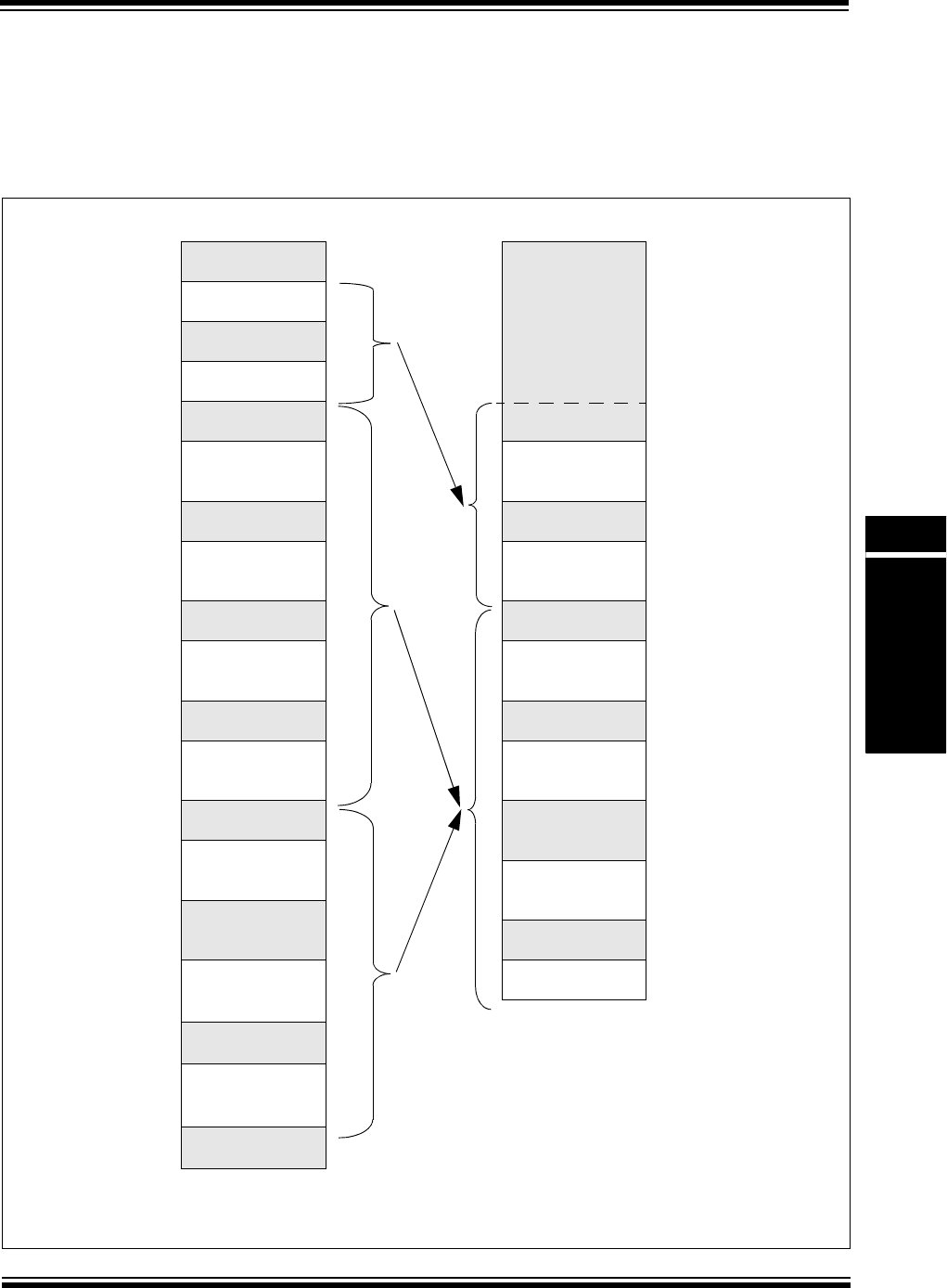
© 2013 Microchip Technology Inc. DS60001214A-page 48-13
Section 48. Memory Organization and Permissions
Memory
Organization and
Permissions
48
48.3 MEMORY LAYOUT
Figure 48-1 shows an example of the memory map for a device with 2048 KB of program
memory for a typical application running in Kernel mode. Physical addresses, shown on the right,
are used by DMA, the Flash controller (when programming Flash memory), and when defining
protected memory regions. Virtual addresses are used by the CPU for fetching and reading or
writing data or peripheral SFRs.
Figure 48-1: Memory Map for Devices with 2048 KB of Program Memory
Virtual
Memory Map(1) Physical
Memory Map(1)
0xFFFFFFFF Reserved
Reserved
0xFFFFFFFF
0xD4000000
0xD3FFFFFF External Memory via
SQI
0xD0000000
Reserved
0xC4000000
0xC3FFFFFF External Memory via
EBI
0xC0000000
0xBFFFFFFF Reserved
0xBFC74000 0x34000000
0xBFC73FFF
Boot Flash External Memory via
SQI
0x33FFFFFF
0xBFC00000 0x30000000
Reserved Reserved
0xBF900000 0x24000000
0xBF8FFFFF
SFRs External Memory via
EBI
0x23FFFFFF
0xBF800000 0x20000000
Reserved Reserved
0xBD200000 0x1FC74000
0xBD1FFFFF
Program Flash Boot Flash
0x1FC73FFF
0xBD000000 0x1FC00000
Reserved Reserved
0xA0080000 0x1F900000
0xA007FFFF
RAM(2) SFRs
0x1F8FFFFF
0xA0000000 0x1F800000
Reserved Reserved0x9FC74000
0x9FC73FFF
Boot Flash
0x1D200000
Program Flash
0x1D1FFFFF
0x9FC00000
Reserved
0x1D000000
Reserved
0x9D200000 0x00080000
0x9D1FFFFF
Program Flash RAM(2) 0x0007FFFF
0x00000000
0x9D000000
Reserved
0x80080000
0x8007FFFF
RAM(2)
0x80000000
Reserved
0x00000000
Note 1: Memory areas are not shown to scale.
2: On certain devices, RAM memory is divided into two banks: RAM Bank 1 and RAM Bank 2.
3: The MMU must be enabled and the TLB must be set up to access this segment.
KSEG1
KSEG0 KSEG2
(3)
(cacheable)
(not cacheable)
(cacheable)

PIC32 Family Reference Manual
DS60001214A-page 48-14 © 2013 Microchip Technology Inc.
For a typical application running in Kernel mode, virtual memory is divided into three segments
named KSEG0, KSEG1, and KSEG2. The segments, KSEG0 and KSEG1, both translate to
physical address 0x0 and include all of program Flash and data memory; however, KSEG0 is
cacheable and KSEG1 is not. This arrangement allows the CPU to access identical physical
address space from the virtual segment of KSEG0 and KSEG1 so that the application can
choose to execute any or all code as either cached or uncached by branching or calling the
function in the cached or uncached region. The uncached region, KSEG1, provides virtual
address space translation to the Special Function Registers for PIC32MZ family devices. KSEG2
maps to external memory, which is connected to the device through the SQI and EBI modules
using the Translation Lookaside Buffer (TLB).
There are two additional virtual memory segments: a user segment, KUSEG, which occupies the
lower 2 GB of virtual memory, and KSEG3, which occupies the upper most 512 MB block of
memory. For information regarding the use of these segments and their configuration using the
TLB, please refer to Section 50. “CPU for Devices with microAptiv™ Core” (DS60001192).
48.3.1 Virtual to Physical Address Calculation (and Vice-Versa)
To tran sla te t he vir tu a l a ddr ess in KS E G0 or KSEG1 to a physical address, perform a “Bitwise
AND” operation of the virtual address with 0x1FFFFFFF:
•Physical Address = Virtual Address & 0x1FFFFFFF
For physical address to KSEG0 virtual address translation, perform a “Bitwise OR” operation of
the physical address with 0x80000000:
•KSEG0 Virtual Address = Physical Address | 0x80000000
For physical address to KSEG1 virtual address translation, perform a “Bitwise OR” operation of
the physical address with 0xA0000000:
•KSEG1 Virtual Address = Physical Address | 0xA0000000
To translate from KSEG0 to KSEG1 virtual address, perform a “Bitwise OR” operation of the
KSEG0 virtual address with 0x20000000:
•KSEG1 Virtual Address = KSEG0 Virtual Address | 0x20000000 (since KSEG2 is mapped
using the TLB, virtual to physical calculations depend on the specific configuration)
48.3.2 Boot Flash Memory
The Boot Flash Memory (BFM) region has special features which facilitate a Dual Boot
implementation. Two identical Boot Flash regions are implemented where one is active (used at
startup) and the other is available for field upgrades. Each BFM region exists in a fixed address
space, either Boot Flash 1 or Boot Flash 2 and in either the Lower or Upper Boot Aliased address
space as shown in Figure 48-2.
At Power-on Reset (POR), the sequence words are read and the Boot Flash 1 or Boot Flash 2
region with the larger sequence number is mapped to the Lower Boot Aliased region while the
smaller sequence number is mapped to the Upper Boot Aliased region. Configuration data is
then read from the Lower Boot Aliased region and finally code execution begins at the reset
vector located at the beginning of the Lower Boot Alias (0x1FC00000 in the example in
Figure 48-2). See Section 52. “Flash Memory with Support for Live Update” (DS60001193)
for more information.
The sequence number is stored in the lower 16 bits of the sequence word. The upper 16 bits are
set to the complement of the lower sixteen bits. This allows the system to know that the sequence
word has been programmed with a sequence number. In systems where Dual Boot is not used
and it is desired to use both boot regions for the applications boot code, it is recommended that
the Sequence Word be reserved and not used for code or data storage to insure proper aliasing
at start-up.
© 2013 Microchip Technology Inc. DS60001214A-page 48-15
Section 48. Memory Organization and Permissions
Memory
Organization and
Permissions
48
Figure 48-2: Boot and Alias Memory Map
48.3.3 Dual Ram Banks
On certain devices, RAM Memory is divided into two banks, each with their own target bus
interface. Two bus interfaces allow two different bus initiators to access RAM simultaneously
without arbitration. This allows for a system design where RAM memory dedicated to CPU-only
use (stack and general purpose data storage) is allocated in one RAM bank, while RAM memory
dedicated to DMA use (data buffers) is allocated in another. High-speed peripherals can be
storing or fetching data from RAM buffers during CPU RAM accesses without arbitration
impacting their performance. Please see Chapter 17. “Linking Programs” in the “MPLAB®
XC32 C/C++ Compiler User’s Guide” (DS50001686) documentation for specifying and
configuring RAM usage for your project.
Physical Memory Map(1) 0x1FC74000
Sequence/Configuration Space(4) 0x1FC6FF40
Boot Flash 2
0x1FC60000
Reserved 0x1FC54000
Serial Number(5) 0x1FC54020
ADC Calibration Space(3) 0x1FC54000
Sequence/Configuration Space(4) 0x1FC4FF40
Boot Flash 1
0x1FC40000
Reserved
0x1FC34000
Upper Boot Alias
0x1FC20000
Reserved
0x1FC14000
Configuration Space(2,4) 0x1FC0FF40
Lower Boot Alias
0x1FC00000
Note 1: Memory areas are not shown to scale.
2: Memory locations 0x1FC0FF40 through 0x1FC0FFFC are used to initialize
Configuration registers (see the “Special Features” chapter in the specific
device data sheet).
3: Memory locations 0x1FC54000 through 0x1FC5410 are used to initialize
the ADC Calibration registers (see the “Special Features” chapter in the
specific device data sheet).
4: Refer to the “Memory Organization” chapter in the specific device data
sheet for more information.
5: Memory locations 0x1FC54020 and 0x1FC54024 contain a unique device
serial number (see the “Special Features” chapter in the specific device
data sheet).

PIC32 Family Reference Manual
DS60001214A-page 48-16 © 2013 Microchip Technology Inc.
48.4 THE SYSTEM BUS
The PIC32MZ family of devices incorporates a System Bus, which is implemented as a
multi-layer fabric that allows concurrent transactions by multiple initiators (bus masters) to
multiple targets (bus slaves). There are no arbitration delays unless two initiators attempt access
to the same target at the same time. Initiators include the CPU, general purpose DMA, and bus
master peripherals with dedicated DMA access.
The following is a list of Initiators for a typical device:
•CPU
•General Purpose DMA
•Crypto Engine
•SQI
•High-Speed USB
•CAN
•Ethernet
•Flash Controller (for Run-Time Self-Programming (RTSP))
Targ et s i ncl ude Fl ash a nd R AM m emo ry a s w ell as all peripherals of the device, such as the
UART, SPI, I2C, etc. Some peripherals are grouped together as a single target to form a
Peripheral Bus, which in addition to sharing a target interface, also shares a common peripheral
bus clock source (PBCLK). See the “Device Overview” and “Oscillator Configuration”
chapters of the specific device data sheet for more information.
All bus master peripherals with integrated DMA, in addition to being initiators, are also targets.
This is necessary to access their Configuration SFRs. Figure 48-3 provides a diagram of the
PIC32MZ System Bus. All data buses are 32 bits wide. Initiators can only access targets as
indicated in the diagram.
SRAM is the only target accessible by every initiator. In most applications, SRAM will be a
frequent target for CPU operations, as well as DMA transfers between communication
peripherals and data buffers. To avoid arbitration in these situations, many PIC32MZ
implementations provide two SRAM banks. It is recommended that access to DMA serviced
buffers should be through non-cached memory regions (KSEG1) or cache coherency issues will
result.
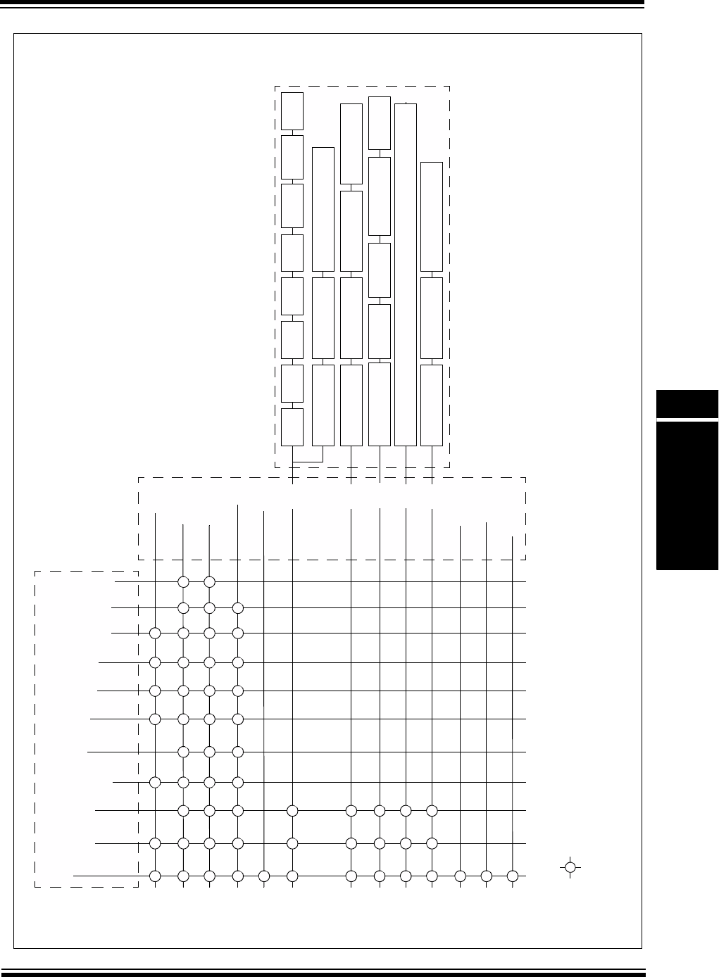
© 2013 Microchip Technology Inc. DS60001214A-page 48-17
Section 48. Memory Organization and Permissions
Memory
Organization and
Permissions
48
Figure 48-3: System Bus Diagram
Flash
CPU
DMA RD
DMA WR
CRYPTO (M)
SQI (M)
USB (M)
CAN1 (M)
CAN2 (M)
Ethernet RD
SRAM1
SRAM2
EBI
RNG
PB1
PB2
PB3
Ethernet WR
PB4
PB5
CFG PPS ICD WDT DMT RTCC DAC4 CRU
SPI 1-6 I2C1-5 UART1-6 PMP
Timer1-9 OC1-9 IC1-9 Comparator ADC
PORTA-PORTK
CAN1 (S) CAN2 (S) Ethernet (S)
EVIC DMA Flash Control
USB (S)
SQI (S)
Crypto (S)
Flash Control
Initiators (Bus Masters)
Targets
(Bus Slaves)
Peripheral Sets
Legend
= Master or Slave Connection
(M) = Master Interface
(S) = Slave Interface
PBn = Peripheral Bus

PIC32 Family Reference Manual
DS60001214A-page 48-18 © 2013 Microchip Technology Inc.
48.5 SYSTEM BUS ARBITRATION
Two initiators cannot access the same target at the same time. If this occurs, arbitration takes
place, which prioritizes the access of the two or more initiators, granting access to one while
holding off any others. Arbitration can be minimized or avoided in system design by partitioning
SRAM allocation for the CPU and DMA initiators into the two SRAM banks. This also applies to
devices where identical peripherals are available on different peripheral buses.
When arbitration is necessary, it is handled using a least recently serviced (LRS) priority to
provide Quality of Service (QOS) for most initiators. The Flash controller initiator, which is a very
low bandwidth initiator, always uses a fixed high priority to guarantee data for Flash row
programming operations.
The CPU can be assigned a fixed high priority to SRAM access for interrupt processing using the
CPUPRI (CFGCON<24>) Configuration bit. The general purpose DMA can be assigned a fixed
high priority to SRAM access using the DMAPRI (CFGCON<25>) Configuration bit. Refer to the
“Special Features” chapter of the specific device data sheet for information on the CFGCON
register.
Improper use of fixed priority arbitration can have serious negative effects on other initiators.
Fixed high priority settings are not recommended for an initiator that uses significant bandwidth.
It is intended for low bandwidth applications that need low latency. Initiators set to fixed priority
share arbitration with other initiators with fixed high priority. The dual RAM banks, however, can
be utilized to allow for a DMA initiator to maintain low latency with a fixed high priority while still
maintaining an adequate quality of service for a high bandwidth bus master DMA initiator. An
example of this would be using DMA to implement low-cost controllerless (LCC) graphics (a low
latency requirement) in a system with Ethernet or High-Speed USB. DMA buffers for graphics
would be placed in one RAM bank while the Ethernet or USB buffers are in placed in the other
RAM bank.
Tabl e 48- 2 provides an example of a typical initiator list for a device with the initiator identifiers
(ID) and quality of service priority options (QOS). The IDs are used to identify permission access
violations, as discussed in 48.6 “Access Permissions”. Note that the initiators with selectable
QOS have unique IDs for both the HIGH and LRS priority levels.
Table 48-2: Initiator ID and QOS
Note: DMA must always be disabled when changing the DMAPRI bit setting.
Name ID QOS
CPU 1 LRS
CPU 2 HIGH
DMA Read 3 LRS
DMA Read 4 HIGH
DMA Write 5 LRS
DMA Write 6 HIGH
USB 7 LRS
Ethernet Read 8 LRS
Ethernet Write 9 LRS
CAN1 10 LRS
CAN2 11 LRS
SQI1 12 LRS
Flash Controller 13 HIGH
Crypto Engine 14 LRS

© 2013 Microchip Technology Inc. DS60001214A-page 48-19
Section 48. Memory Organization and Permissions
Memory
Organization and
Permissions
48
48.6 ACCESS PERMISSIONS
The PIC32MZ family of devices provides configurable memory protection features that can be
used to restrict access by bus initiators to bus targets or bus target regions. Access violations are
logged and can optionally generate interrupts. These features are typically used by operating
systems and boot loaders to prevent one task or application from interfering with the execution
of another task or application and can also be used to help prevent an untrusted application from
accessing protected memory regions for the purpose of intellectual property infringement.
Each bus initiator can be assigned to one of four permission groups. Each bus target contains
one or more memory regions that can be configured to deny or allow access to each of the
permission groups. See Figure 48-3 for a diagram of typical bus targets and bus initiators.
Targ et p e rm iss ion v io l at ion s ca n be c o nf igu red to generate an interrupt allowing the operating
system to intercept and handle these events. This is accomplished by setting the ERRP bit of a
target’s system bus error control register, SBTxECON, resulting in that target’s bit being set in
the SBFLAG register when a permission violation occurs. Setting of the target’s bit in the
SBFLAG register will result in a System Bus protection violation interrupt being generated,
assuming that the interrupt is configured and enabled in the Interrupt Controller. Refer to the
“CPU Exceptions and Interrupt Controller” chapter in the specific device data sheet for more
information.
The service routine for this interrupt can query the SBFLAG of the System Bus to determine
which target generated the violation. In addition, it can query the System Bus target registers,
SBTxELOG1 and SBTxELOG2, for specific details about the violation including the target region
where the error occurred. Finally, errors can be cleared using the System Bus target registers
SBTxECLRS and SBTxECLRM.
If an initiator attempts to access a protected region, the write does not occur regardless of the
interrupt enable or reporting status. Offending read instructions will return values of 0x0.
Permission groups for each initiator are assigned using the CFGPG register (see the “Special
Features” chapter of the specific device data sheet for information on this register). On reset, all
initiators are assigned to Permission Group 0.
Access permissions by initiators to the System Bus targets are configured using the SBTxREGy,
SBTxRDy, and SBTxWRy registers. These three registers define a memory region and the read
and write permissions for that region. Each target contains a set of these registers for the default
memory space region, which is the size of the entire target address space. In addition, most
targets have at least one definable (base address and size) permission memory region. The
upper 22 bits of the base address are specified by the BASE<21:0> bits (SBTxREGy<31:10>)
with the lower 10 bits fixed at 0. The base address must be aligned to the size specified by the
SIZE<4:0> bits (SBTxREGy<7:3>). For example, a base address of 9216 (0x2400) would only
allow for a size of 1024 (0x400), whereas a base address of 8192 (0x2000) would allow for sizes
of 1024 (0x400), 2048 (0x800), 4096 (0x1000), and 8192 (0x2000). The memory space
containing the CFGPG, SBTxREGy, SBTxRDy, and SBTxWRy registers is itself one of the target
regions (Target 0 - System Bus) with definable permissions.
When an initiator attempts access to a region of memory that is defined in two target regions, the
priority level determines which permission level is required. Level 0 is the lowest priority and
Level 3 is the highest. Permissions for the highest level of the defined address space are always
used. For any target, region 0 (the default space the size of the entire target) is always Level 0
while region 1 is always Level 3. If a target has regions beyond 0 and 1, the level for the region
is defined in the read-only bit, LEVEL, in the SBTxREGy register. In these cases, a LEVEL bit
value of ‘0’ indicates a priority of 1 while a LEVEL bit value of ‘1’ indicates priority 2. Never
configure overlapping regions with the same priority level.
Configuration of permissions occurs in boot software at initialization where each initiator is
assigned a permission group and the permission regions for all targets are configured. It is
assumed that the boot software is trusted code. At reset, the CPU is set to Group 0 permissions.
When the configurations are complete, the boot code will set the CPU privilege to the appropriate
group (disabling access to the secure regions) prior to branching to the application.
Note: The boot code must reside in a page that has permissions of Group 0 and the Group
being set when the setting of the CPUPG<1:0> (CFGPG<1:0>) Configuration bits
is changed.

PIC32 Family Reference Manual
DS60001214A-page 48-20 © 2013 Microchip Technology Inc.
Permission Group 0 is intended to be the Secure permission group, configured to be the only
group with permissions to the Target 0 System Bus region, which allows changing of the initiator
permission groups and target permissions as well as any memory regions that the application
wants to protect. The reason for this is that after the CPU permissions have been changed,
blocking access to the secure target regions, the only run-time mechanism that can be used to
change the CPU permission is the Non-Maskable Interrupt (NMI). When the NMI occurs, the
CPU privilege is changed to Group 0 prior to vectoring to the Interrupt Service Routine (ISR). It
is required that the NMI service routine will reside in memory where Group 0 privileges are
allowed. After the NMI, the CPU has access to secure memory regions. Once the secure
operations are complete, software must change the CPU privilege to the appropriate group
blocking access to the secure regions in the same manner that it did at start-up in the boot code.
Permission Group 3 is a special case permission group for use when the processor is in Debug
mode. Debug mode is the state of the processor when an external debugger has control over it
so that memory or SFRs can be inspected or altered. The DBGPER<2:0> (DEVCFG0<14:12>)
bits allow selection of permissions in Debug mode for Groups 0, 1, and 2. When the processor
is in Debug mode and the CPU permission, defined by the CPU1PG<1:0> (CFGPG<1:0>) bits
is set to one of the denied permission groups specified the DBGPER<2:0> bits, the transaction
request is assigned Group 3 permissions. The System Bus target region permission registers,
SBTxRDy and SBTxWRy, reset to permission settings that allow access for Groups 0 through 2
and deny access to Group 3. By using the DBGPER<2:0> bits, it is possible to prevent access
by the debugger until protected boot code defines permissions specifying which memory regions
are accessible by the debugger. These features require debug tools that are designed to support
them. In addition, the EJTAGBEN (DEVCFG0<30>) bit should be set to ‘0’ and code protection
should be enabled.
48.6.1 Interrupts Vectors and Service Routines
The PIC32MZ family of devices allows placement of the ISRs and exception handlers anywhere
in system memory. Care must be taken to insure that the read privileges for the target region that
contains the ISR and exception handling code include any permissions that software may use for
the CPU. The NMI interrupt is a special case, which always vectors to the fixed reset or NMI
location that would typically be used for boot code.
48.6.2 Peripheral Permissions
Peripheral registers, when used in conjunction with interrupts, must also be assigned read and
write permissions that allow access by any permission group that the CPU might be set to in the
target application. If it is desired that access to peripherals be protected from access by the CPU,
the DMA (either general purpose or DMA associated with a bus master) must be used. In this
case, the DMA and the target peripheral can be assigned a permission group without regard to
the permission group (or groups) used by the CPU.
48.6.3 Cache
Permissions are checked when the target memory is accessed by an initiator. If the target
memory is SRAM or Flash and a cache is in use, the access to the target occurs when the
instructions or data is moved between the target and the cache. The permissions of the CPU are
not checked when the contents are accessed from cache. If the cache contains a high privilege
permission group data and the CPU permission is changed to a lower privilege group, the cache
must be flushed to prevent access by the lower privilege CPU setting. Flushing the cache should
be done just prior to changing the CPU privilege setting.
48.6.4 Aliased and Bank Swapped Memory
On devices where memory is aliased and a fixed and aliased region of the same memory exists,
both regions must be protected. It may also be necessary to protect the SWAP (NVMCON<7>)
bit of the Flash Controller, only allowing access to the secure permission group.

© 2013 Microchip Technology Inc. DS60001214A-page 48-21
Section 48. Memory Organization and Permissions
Memory
Organization and
Permissions
48
48.7 EFFECTS OF RESET
48.7.1 On Reset
The contents of RAM are unchanged and the CPU is set to Permission Group 0. All target regions
are set to allow access by all four permission groups. Programmable target regions and sizes are
set to their reset values.
48.7.2 On Power-up or Brown-out Reset
The contents of RAM are undefined and the CPU is set to Permission Group 0. All target regions
are set to allow access by all four permission groups. Programmable target regions and sizes are
set to their reset values.
48.8 OPERATION IN POWER-SAVING MODES
48.8.1 Sleep Mode
When the device wakes from Sleep mode, the contents of RAM are unchanged and the CPU
permission group is unchanged. Settings for target regions remain unchanged.
48.8.2 Idle Mode
When the device exits Idle mode, the CPU permission group is unchanged. Settings for target
regions remain unchanged. Exiting Idle mode does not cause changes to RAM contents;
however, DMA peripherals that can be enabled to run in Idle mode can modify RAM contents
while the CPU is in Idle mode.
48.9 DEBUG MODE
To p rev ent a cce ss to p ro tec ted re gio ns by the deb ugg er pri or to b oo t c o de set ti ng u p t he
protection schemes, limit EJTAG functionality by setting the EJTAGBEN (DEVCFG0<30>) bit to
‘0’, preventing the probe from being able to boot from EJTAG.
In addition, the Device Configuration Word, DEVCFG0, contains the DBGPER<2:0>
(DEVCFG0<6:4>) bits, which are used in conjunction with the device debugging tools to control
access during Debug mode. Refer to “Special Features” chapter in the specific device data
sheets and the related development tools documentation for more information. In addition, refer
to 48.6 “Access Permissions” regarding use of Permission Group 3 when debugging.
Note: Permission groups do not prevent Debug code from setting up a trace into a pro-
tected region. If the trace is not disabled by clearing the TRCEN (DEVCFG0<5>)
bit, EJTAG Serial Execution must be disabled if protection is desired.

PIC32 Family Reference Manual
DS60001214A-page 48-22 © 2013 Microchip Technology Inc.
48.10 CODE EXAMPLES
Example 48-1 shows how to set up Flash memory permissions for a device that supports two
application code spaces. Application 1, which includes the boot loading software, is trusted code.
Application 2 is not trusted code and is prevented from accessing Application 1 Flash regions.
This device in this example includes dual boot banks with fixed and aliased regions. The
application uses only the lower aliased boot region. The lower aliased boot Flash consists of five
16 KB memory pages for a total of 80 KB. Pages 0 through 3 have been selected as space for
the boot code of Application 1 (64 KB). Page 0 must be used as it contains the reset and NMU
vectors. Boot Flash page 4 (16 KB) is designated as dual privilege space needed for the Interrupt
Vector Table (IVT) and for the code that changes the CPU privilege from Application 1 to
Application 2. In both situations, this code must be able to execute while the CPU is in the
permission group of either Application 1 or Application 2.
This device in this example includes 2 MB of program Flash memory, which is divided equally
between the two applications with the upper half allocated to Application 2 and the lower half
allocated to Application 1.
At reset, the CPU is set to Group 0 permissions, which will be used as the Group Permission for
Application 1. Application 1 initialization occurs, which includes setting target regions and
permissions as defined in the example code. When Application 1 is ready to relinquish control to
Application 2, it will change the CPU permission group from 0 to the permission group of
Application 2, which is Permission Group 1 that used in this example. The CPU permission group
change occurs in code executing from the transitory region, and then jumps to the start-up
location in Application 2.
Application 1 can cooperatively relinquish control back to Application 2 by generating an NMI in
software, or the Watchdog Timer (WDT) can be used to pre-empt execution of Application 2 and
return control back to Application 1.
Note: Because of the dual boot, aliased and fixed regions, both regions must be protected
with identical schemes.

© 2013 Microchip Technology Inc. DS60001214A-page 48-23
Section 48. Memory Organization and Permissions
Memory
Organization and
Permissions
48
Example 48-1: Flash Memory Permissions for Two Application Code Spaces
To acco mpl ish the pe r mi ssi on r equ ir e me nts pre vi ously described, the regions must be defined
and the permissions set for the IVT/transitory region and the Application 2 code space. The Flash
default region that encompasses all of Flash will then be set to only allow only access by Group
0, which is the permission group for Application 1. Finally, the System Bus target permissions are
defined allowing access only by Application 1.
The permissions for the IVT/transitory and the Application 2 code space will take precedence
over the default permissions as they are defined in registers with higher priority levels.
Example 48-2 provides the code that can be used to set permissions for two application spaces.
Note: The code shown in Example 48-2 only addresses the permission settings for the
Flash memory. It does not cover the other aspects of permission control for DMA
initiators or RAM, external memory, and peripheral targets.
Boot Code
Lower Aliased
Pages 0-3
Boot Segment
Lower Aliased
Page 4
PFM Upper
1 MB
PFM Lower
1 MB
Boot Code
Lower Fixed
Pages 0-3
Boot Segment
Lower Fixed
Page 4
0x1D000000
0x1D100000
0x1D0FFFFF
0x1D1FFFFF
0x1FC00000 Reset Vector
0x1FC10000
0x1FC0FFFF
0x1FC13FFF
0x1FC40000
0x1FC50000
0x1FC4FFFF
0x1FC53FFF
Application 1 Code
Group 0 Read Permissions
Application 2 Code
Group 1 Read Permissions
Boot Code – Application 1
Group 0 Read Permissions
Transitory and IVT Region
Group 0 and 1 Read Permissions
Boot Code – Application 1
Group 0 Read Permissions
Transitory Region
Group 0 and 1 Read Permissions

PIC32 Family Reference Manual
DS60001214A-page 48-24 © 2013 Microchip Technology Inc.
Example 48-2: Code to Set Permissions for Two Application Spaces
// Transitory Region, last page of Lower Aliased Boot Memory
// Must be configured for the aliased and fixed regions
SBT1REG3bits.BASE = 0x1FC10000 >> 10;// Lower aliased region, starting address
SBT1REG3bits.SIZE = 0x5; // Lower aliased size is one 16 KB page
SBT1REG4bits.BASE = 0x1FC50000 >> 10; // Lower fixed region, starting address
SBT1REG4bits.SIZE = 0x5; // Size is identical to alias
// Set permissions for both aliased and fixed regions
SBT1RD3 = 0x3; // Allow access by Group 0 and 1
// permissions and block access to Group 2 and 3 permissions
SBT1RD4 = 0x3; // Duplicate for the fixed region
// Application 2 Region, upper half of PFM
SBT1REG7bits.BASE = 0x1D100000 >> 10; // PFM upper region, starting address
SBT1REG7bits.SIZE = 0xB; // Upper PFM, 1 MB size
SBT1RD7 = 0x2; // Allow access only for Group 1 permissions while blocking
// access by groups 0, 2 and 3
// Set default region to allow access only for Group 0
SBT1RD0 = 0x1;
// Set the System Bus to allow access to only group 0
SBT0RD0 = SBT0WR0 = 0x01;
SBT0RD1 = SBT0WR1 = 0x01;

© 2013 Microchip Technology Inc. DS60001214A-page 48-25
Section 48. Memory Organization and Permissions
Memory
Organization and
Permissions
48
48.11 RELATED APPLICATION NOTES
This section lists application notes that are related to this section of the manual. These
application notes may not be written specifically for the PIC32 device family, but the concepts are
pertinent and could be used with modification and possible limitations. The current application
notes related to the Memory Organization and Permissions are:
Title Application Note #
No related application notes at this time. N/A
Note: Please visit the Microchip Web site (www.microchip.com) for additional application
notes and code examples for the PIC32 family of devices.

PIC32 Family Reference Manual
DS60001214A-page 48-26 © 2013 Microchip Technology Inc.
48.12 REVISION HISTORY
Revision A (November 2013)
This is the initial released version of the document.

2013 Microchip Technology Inc. DS60001214A-page 48-27
Information contained in this publication regarding device
applications and the like is provided only for your convenience
and may be superseded by updates. It is your responsibility to
ensure that your application meets with your specifications.
MICROCHIP MAKES NO REPRESENTATIONS OR
WARRANTIES OF ANY KIND WHETHER EXPRESS OR
IMPLIED, WRITTEN OR ORAL, STATUTORY OR
OTHERWISE, RELATED TO THE INFORMATION,
INCLUDING BUT NOT LIMITED TO ITS CONDITION,
QUALITY, PERFORMANCE, MERCHANTABILITY OR
FITNESS FOR PURPOSE. Microchip disclaims all liability
arising from this information and its use. Use of Microchip
devices in life support and/or safety applications is entirely at
the buyer’s risk, and the buyer agrees to defend, indemnify and
hold harmless Microchip from any and all damages, claims,
suits, or expenses resulting from such use. No licenses are
conveyed, implicitly or otherwise, under any Microchip
intellectual property rights.
Trademarks
The Microchip name and logo, the Microchip logo, dsPIC,
FlashFlex, KEELOQ, KEELOQ logo, MPLAB, PIC, PICmicro,
PICSTART, PIC32 logo, rfPIC, SST, SST Logo, SuperFlash
and UNI/O are registered trademarks of Microchip Technology
Incorporated in the U.S.A. and other countries.
FilterLab, Hampshire, HI-TECH C, Linear Active Thermistor,
MTP, SEEVAL and The Embedded Control Solutions
Company are registered trademarks of Microchip Technology
Incorporated in the U.S.A.
Silicon Storage Technology is a registered trademark of
Microchip Technology Inc. in other countries.
Analog-for-the-Digital Age, Application Maestro, BodyCom,
chipKIT, chipKIT logo, CodeGuard, dsPICDEM,
dsPICDEM.net, dsPICworks, dsSPEAK, ECAN,
ECONOMONITOR, FanSense, HI-TIDE, In-Circuit Serial
Programming, ICSP, Mindi, MiWi, MPASM, MPF, MPLAB
Certified logo, MPLIB, MPLINK, mTouch, Omniscient Code
Generation, PICC, PICC-18, PICDEM, PICDEM.net, PICkit,
PICtail, REAL ICE, rfLAB, Select Mode, SQI, Serial Quad I/O,
Tota l E ndu ra nce , T SHA RC , U n iW inD riv er, Wi per Lo c k, ZE NA
and Z-Scale are trademarks of Microchip Technology
Incorporated in the U.S.A. and other countries.
SQTP is a service mark of Microchip Technology Incorporated
in the U.S.A.
GestIC and ULPP are registered trademarks of Microchip
Technology Germany II GmbH & Co. KG, a subsidiary of
Microchip Technology Inc., in other countries.
All other trademarks mentioned herein are property of their
respective companies.
© 2013, Microchip Technology Incorporated, Printed in the
U.S.A., All Rights Reserved.
Printed on recycled paper.
ISBN: 978-1-62077-637-7
Note the following details of the code protection feature on Microchip devices:
• Microchip products meet the specification contained in their particular Microchip Data Sheet.
• Microchip believes that its family of products is one of the most secure families of its kind on the market today, when used in the
intended manner and under normal conditions.
• There are dishonest and possibly illegal methods used to breach the code protection feature. All of these methods, to our
knowledge, require using the Microchip products in a manner outside the operating specifications contained in Microchip’s Data
Sheets. Most likely, the person doing so is engaged in theft of intellectual property.
• Microchip is willing to work with the customer who is concerned about the integrity of their code.
• Neither Microchip nor any other semiconductor manufacturer can guarantee the security of their code. Code protection does not
mean that we are guaranteeing the product as “unbreakable.”
Code protection is constantly evolving. We at Microchip are committed to continuously improving the code protection features of our
products. Attempts to break Microchip’s code protection feature may be a violation of the Digital Millennium Copyright Act. If such acts
allow unauthorized access to your software or other copyrighted work, you may have a right to sue for relief under that Act.
Microchip received ISO/TS-16949:2009 certification for its worldwide
headquarters, design and wafer fabrication facilities in Chandler and
Tempe, Arizona; Gresham, Oregon and design centers in California
and India. The Company’s quality system processes and procedures
are for its PIC® MCUs and dsPIC® DSCs, KEELOQ® code hopping
devices, Serial EEPROMs, microperipherals, nonvolatile memory and
analog products. In addition, Microchip’s quality system for the design
and manufacture of development systems is ISO 9001:2000 certified.
QUALITY MANAGEMENT S
YSTEM
CERTIFIED BY DNV
== ISO/TS 16949 ==

DS60001214A-page 48-28 2013 Microchip Technology Inc.
AMERICAS
Corporate Office
2355 West Chandler Blvd.
Chandler, AZ 85224-6199
Tel: 480-792-7200
Fax: 480-792-7277
Technical Support:
http://www.microchip.com/
support
Web Address:
www.microchip.com
Atlanta
Duluth, GA
Tel: 678-957-9614
Fax: 678-957-1455
Austin, TX
Tel: 512-257-3370
Boston
Westborough, MA
Tel: 774-760-0087
Fax: 774-760-0088
Chicago
Itasca, IL
Tel: 630-285-0071
Fax: 630-285-0075
Cleveland
Independence, OH
Tel: 216-447-0464
Fax: 216-447-0643
Dallas
Addison, TX
Tel: 972-818-7423
Fax: 972-818-2924
Detroit
Novi, MI
Tel: 248-848-4000
Houston, TX
Tel: 281-894-5983
Indianapolis
Noblesville, IN
Tel: 317-773-8323
Fax: 317-773-5453
Los Angeles
Mission Viejo, CA
Tel: 949-462-9523
Fax: 949-462-9608
New York, NY
Tel: 631-435-6000
San Jose, CA
Tel: 408-735-9110
Canada - Toronto
Tel: 905-673-0699
Fax: 905-673-6509
ASIA/PACIFIC
Asia Pacific Office
Suites 3707-14, 37th Floor
Tower 6, The Gateway
Harbour City, Kowloon
Hong Kong
Tel : 8 52 -24 01- 120 0
Fax: 852-2401-3431
Australia - Sydney
Tel : 6 1- 2-9 868 -67 33
Fax: 61-2-9868-6755
China - Beijing
Tel : 8 6- 10- 856 9-7 00 0
Fax: 86-10-8528-2104
China - Chengdu
Tel : 8 6- 28- 866 5-5 511
Fax: 86-28-8665-7889
China - Chongqing
Tel : 8 6- 23- 898 0-9 58 8
Fax: 86-23-8980-9500
China - Hangzhou
Tel : 8 6- 571 -28 19- 318 7
Fax: 86-571-2819-3189
China - Hong Kong SAR
Tel : 8 52 -29 43- 510 0
Fax: 852-2401-3431
China - Nanjing
Tel : 8 6- 25- 847 3-2 46 0
Fax: 86-25-8473-2470
China - Qingdao
Tel : 8 6- 532 -85 02- 735 5
Fax: 86-532-8502-7205
China - Shanghai
Tel : 8 6- 21- 540 7-5 53 3
Fax: 86-21-5407-5066
China - Shenyang
Tel : 8 6- 24- 233 4-2 82 9
Fax: 86-24-2334-2393
China - Shenzhen
Tel : 8 6- 755 -88 64- 220 0
Fax: 86-755-8203-1760
China - Wuhan
Tel : 8 6- 27- 598 0-5 30 0
Fax: 86-27-5980-5118
China - Xian
Tel : 8 6- 29- 883 3-7 25 2
Fax: 86-29-8833-7256
China - Xiamen
Tel: 86-592-2388138
Fax: 86-592-2388130
China - Zhuhai
Tel : 86- 75 6-3 21 004 0
Fax: 86-756-3210049
ASIA/PACIFIC
India - Bangalore
Tel : 9 1- 80- 309 0-4 44 4
Fax: 91-80-3090-4123
India - New Delhi
Tel : 9 1- 11- 416 0 -8 631
Fax: 91-11-4160-8632
India - Pune
Tel : 9 1- 20- 301 9-1 50 0
Japan - Osaka
Tel : 8 1- 6-6 152 -7 1 60
Fax: 81-6-6152-9310
Japan - Tokyo
Tel : 8 1- 3-6 880 - 377 0
Fax: 81-3-6880-3771
Korea - Daegu
Tel : 8 2- 53- 744 -43 01
Fax: 82-53-744-4302
Korea - Seoul
Tel : 8 2- 2-5 54- 72 0 0
Fax: 82-2-558-5932 or
82-2-558-5934
Malaysia - Kuala Lumpur
Tel : 6 0- 3-6 201 -9 8 57
Fax: 60-3-6201-9859
Malaysia - Penang
Tel : 6 0- 4-2 27- 88 7 0
Fax: 60-4-227-4068
Philippines - Manila
Tel : 6 3- 2-6 34- 90 6 5
Fax: 63-2-634-9069
Singapore
Tel : 6 5- 633 4-8 870
Fax: 65-6334-8850
Taiwan - Hsin Chu
Tel : 8 86 -3- 577 8-3 66
Fax: 886-3-5770-955
Taiwan - Kaohsiung
Tel : 8 86 -7- 213 -78 30
Taiwan - Taipei
Tel : 8 86 -2- 250 8-8 60 0
Fax: 886-2-2508-0102
Thailand - Bangkok
Tel : 6 6- 2-6 94- 13 5 1
Fax: 66-2-694-1350
EUROPE
Austria - Wels
Tel : 4 3- 72 42 -2 244 -3 9
Fax: 43-7242-2244-393
Denmark - Copenhagen
Tel : 4 5- 445 0-2 828
Fax: 45-4485-2829
France - Paris
Tel : 3 3- 1-6 9-5 3-6 3-2 0
Fax: 33-1-69-30-90-79
Germany - Dusseldorf
Tel : 4 9- 21 29 -3 766 400
Germany - Munich
Tel : 4 9- 89 -62 7-1 44- 0
Fax: 49-89-627-144-44
Germany - Pforzheim
Tel : 4 9- 72 31 -4 247 50
Italy - Milan
Tel : 3 9- 03 31 -7 426 11
Fax: 39-0331-466781
Italy - Venice
Tel : 3 9- 04 9- 762 528 6
Netherlands - Drunen
Tel : 3 1- 41 6- 690 399
Fax: 31-416-690340
Poland - Warsaw
Tel : 4 8- 22 -33 257 37
Spain - Madrid
Tel : 3 4- 91 -70 8-0 8-9 0
Fax: 34-91-708-08-91
Sweden - Stockholm
Tel : 4 6- 8-5 090 -46 54
UK - Wokingham
Tel : 4 4- 118 -92 1- 5 800
Fax: 44-118-921-5820
Worldwide Sales and Service
10/28/13

© 2013 Microchip Technology Inc. DS60001246A-page 49-1
Crypto Engine and
Random Number Gen-
erator (RNG)
49
Section 49. Crypto Engine and Random Number
Generator (RNG)
HIGHLIGHTS
This section of the manual contains the following major topics:
49.1 Introduction .................................................................................................................. 49-2
49.2 Control Registers ......................................................................................................... 49-4
49.3 Crypto Engine Buffer Descriptors .............................................................................. 49-23
49.4 Crypto Engine Security Association Structure ........................................................... 49-28
49.5 Crypto Engine Operation ........................................................................................... 49-35
49.6 Crypto Engine Interrupts ............................................................................................ 49-40
49.7 Random Number Generator Operation...................................................................... 49-42
49.8 Random Number Generator Interrupts ...................................................................... 49-43
49.9 Effects of Various Resets ........................................................................................... 49-43
49.10 Operation in Power-Saving Modes ............................................................................ 49-43
49.11 Related Application Notes.......................................................................................... 49-44
49.12 Revision History ......................................................................................................... 49-45
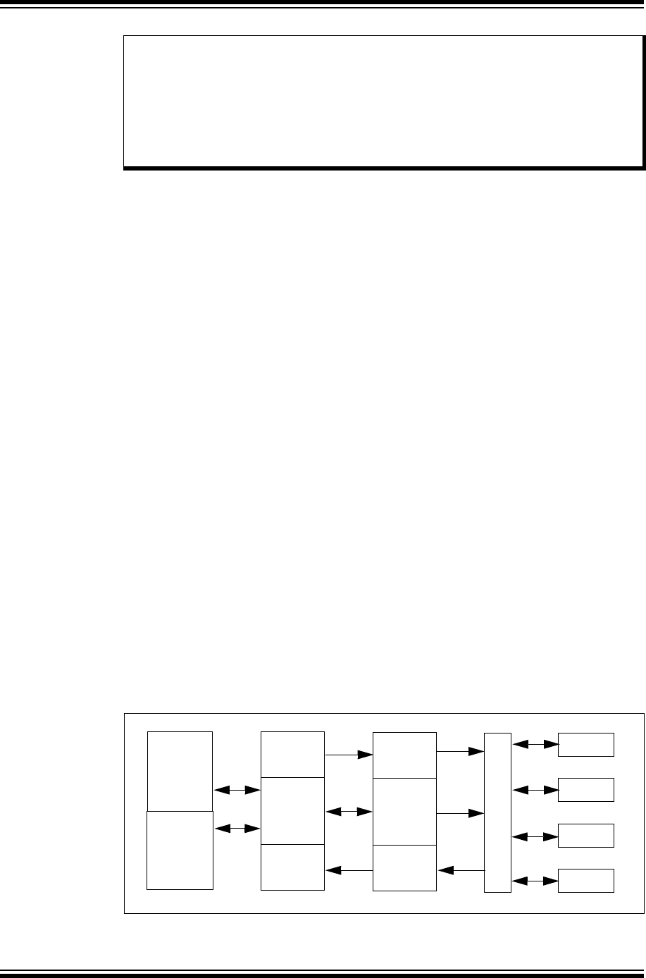
PIC32 Family Reference Manual
DS60001246A-page 49-2 © 2013 Microchip Technology Inc.
49.1 INTRODUCTION
49.1.1 Crypto Engine Features
The Crypto Engine is intended to accelerate applications that need cryptographic functions. By
executing these functions in the hardware module, software overhead is reduced, and actions
such as encryption, decryption, and authentication can execute much more quickly.
The Crypto Engine uses a descriptor-based DMA for efficient programming of the security asso-
ciation data and packet pointers (allowing scatter/gather data fetching). An intelligent state
machine schedules the Crypto engines based on the protocol selection and packet boundaries.
The hardware engines can perform the encryption and authentication in sequence or in parallel.
Key features of the Crypto Engine include:
•Bulk ciphers and hash engines
•Integrated DMA to off-load processing:
- Buffer descriptor-based
- Security Association per Buffer Descriptor
•Some functions can execute in parallel
Bulk ciphers that are handled by the Crypto Engine include:
•AES:
-128-bit, 192-bit, and 256-bit key sizes
-CBC, ECB, CTR, CFB, and OFB modes
•DES/TDES:
-CBC, ECB, CFB, and OFB modes
Authentication engines that are available through the Crypto Engine include:
•SHA-1
•SHA-256
•MD-5
•AES-GCM
•HMAC operation (for all authentication engines)
Figure 49-1: Crypto Engine Block Diagram
Note: This family reference manual section is meant to serve as a complement to device
data sheets. Depending on the device variant, this manual section may not apply to
all PIC32 devices.
Please consult the note at the beginning of the “Crypto Engine and Random
Number Generator (RNG)” chapter in the current device data sheet to check
whether this document supports the device you are using.
Device data sheets and family reference manual sections are available for
download from the Microchip Worldwide Web site at: http://www.microchip.com
DMA
Controller
System
INB
FIFO
OUTB
FIFO
Crypto
FSM
Packet
RD
Packet
WR
AES
TDES
SHA-1/256
MD5
Local Bus
SFR
System
Bus
Bus

© 2013 Microchip Technology Inc. DS60001246A-page 49-3
Section 49. Crypto Engine and Random Number Generator (RNG)
Crypto Engine and
Random Number Gen-
erator (RNG)
49
49.1.2 Random Number Generator (RNG) Features
The Random Number Generator (RNG) core implements a thermal noise-based, True Random
Number Generator (TRNG) and a cryptographically secure Pseudo-Random Number
Generator (PRNG).
The TRNG uses multiple ring oscillators and the inherent thermal noise of integrated circuits to
generate true random numbers that can initialize the PRNG.
The PRNG is a flexible LSFR, which is capable of manifesting a maximal length LFSR of up to
64-bits.
The following are some of the key features of the RNG:
•TRNG:
- Up to 25 Mbps of random bits
- Multi-Ring Oscillator based design
- Built in Bias Corrector
•PRNG:
-LSFR-based
-Up to 64-bit polynomial length
- Programmable polynomial
-TRNG can be seed value
Figure 49-2: Random Number Generator Block Diagram
System Bus Target
PRNG
SFR
Edge Comparator
RingRing
BIAS Corrector
TRNG
Oscillator Oscillator

PIC32 Family Reference Manual
DS60001246A-page 49-4 © 2013 Microchip Technology Inc.
49.2 CONTROL REGISTERS
The Crypto Engine and RNG for PIC32 devices contain the following Special Function Registers
(SFRs):
•CEVER: Crypto Engine Revision, Version, and ID Register
This read-only register contains version information for the Crypto Engine core.
•CECON: Crypto Engine Control Register
This register controls the Crypto Engine, enabling and disabling DMA and the Buffer
Descriptor Processor.
•CEBDADDR: Crypto Engine Buffer Descriptor Register
This read-only register contains the address of the current Buffer Descriptor the Buffer
Descriptor Processor is processing
•CEBDPADDR: Crypto Engine Buffer Descriptor Processor Register
This register controls the address from which the DMA starts fetching Buffer Descriptors.
•CESTAT: Crypto Engine Status Register
This read-only register contains the current status of the Crypto Engine.
•CEINTSRC: Crypto Engine Interrupt Source Register
This register indicates what triggered an interrupt from the Crypto Engine core. Possible
sources include DMA, an empty TX Buffer Descriptor, or a DMA Packet Completion.
•CEINTEN: Crypto Engine Interrupt Enable Register
This register controls which interrupts are enabled/disabled from the Crypto Engine core.
•CEPOLLCON: Crypto Engine Poll Control Register
This register controls how long the Buffer Descriptor Processor will wait before refetching a
descriptor control word if the previous descriptor fetched was disabled.
•CEHDLEN: Crypto Engine Header Length Register
This register controls how much data in a packet should be unchanged before filling the data.
•CETRLLEN: Crypto Engine Trailer Length Register
This register controls how much data should be unchanged at the end of a packet.
•CEDTXSTAT: Crypto Engine DTX Debug Status Register
This read -only register indicates the status of the outgoing FIFO in the Crypto Engine.
•CEDRXSTAT: Crypto Engine DRX Debug Status Register
This read-only register indicates the status of the incoming FIFO in the Crypto Engine.
•RNGVER: Random Number Generator ID, Version, and Revision Register
This register read-only register contains version information for the RNG core.
•RNGCON: Random Number Generator Control Register
This register controls the RNG, enabling and disabling the TRNG and RNG, transferring the
seed value from the TRNG to the PRNG, and enabling continuous pseudo-random number
generation.
•RNGPOLY1: Random Number Generator Polynomial Register 1
This register controls the Least Significant Byte 32-bits of the polynomial, which generates the
pseudo-random bit.
•RNGPOLY2: Random Number Generator Polynomial Register 2
This register controls the Most Significant Byte 32-bits of the polynomial which generates the
pseudo-random bit.

© 2013 Microchip Technology Inc. DS60001246A-page 49-5
Section 49. Crypto Engine and Random Number Generator (RNG)
Crypto Engine and
Random Number Gen-
erator (RNG)
49
•RNGNUMGEN1: Random Number Generator Pseudo-Random Number Generator
Register 1
This register contains the Least Significant Byte 32-bits of the current random number in the
PRNG. It may be written to set an initial seed value for the PRNG.
•RNGNUMGEN2: Random Number Generator Pseudo-Random Number Generator
Register 2
This register contains the Most Significant Byte 32-bits of the current random number in the
PRNG. It may be written to set an initial seed value for the PRNG.
•RNGSEED1: True Random Number Generator Seed Register 1
This read-only register contains the Least Significant Byte 32-bits of the TRNG.
•RNGSEED2: True Random Number Generator Seed Register 2
This read-only register contains the Most Significant Byte 32-bits of the TRNG.
•RNGRCNT: True Random Number Generator Count Register
This read-only register indicates the number of valid bits in the TRNG registers,
RNGSEEDx. To ensure randomness, developers should not use the RNGSEEDx registers
until this register reaches the appropriate value for the number of bits desired.
PIC32 Family Reference Manual
DS60001246A-page 49-6 © 2013 Microchip Technology Inc.
Tabl e 49- 1 and Tab l e 49- 2 provide brief summaries of the related Crypto Engine and RNG registers. Corresponding registers appear after
the summary, followed by a detailed description of each bit.
Table 49-1: Crypto Engine SFR Summary
Name Bit 31/15 Bit 30/14 Bit 29/13 Bit 28/12 Bit 27/11 Bit 26/10 Bit 25/9 Bit 24/8 Bit 23/7 Bit 22/6 Bit 21/5 Bit 20/4 Bit 19/3 Bit 118/2 Bit 17/1 Bit 16/0
CEVER 31:16 REVISION<7:0> VERSION<7:0>
15:0 ID<15:0>
CECON 31:16 — — — — — — — — — — — — — — — —
15:0 — — — — — — — — —SWRSTSWAPEN—— BDPCHST BDPPLEN DMAEN
CEBDADDR 31:16 BDPADDR<31:16>
15:0 BDPADDR<15:0>
CEBDPADDR 31:16 BASEADDR<31:16>
15:0 BASEADDR<15:0>
CESTAT 31:16 ERRMODE<2:0> ERROP<2:0> ERRPHASE<1:0> ——BDSTATE<3:0>STARTACTIVE
15:0 BDCTRL<15:0>
CEINTSRC 31:16 — — — — — — — — — — — — — — — —
15:0 — — — — — — — — — — — — AREIF PKTIF CBDIF PENDIF
CEINTEN 31:16 — — — — — — — — — — — — — — — —
15:0 — — — — — — — — — — — —AREIEPKTIECBDIEPENDIE
CEPOLLCON 31:16 — — — — — — — — — — — — — — — —
15:0 BDPPLCON<15:0>
CEHDLEN 31:16 — — — — — — — — — — — — — — — —
15:0 — — — — — — — — HDRLEN<7:0>
CETRLLEN 31:16 — — — — — — — — — — — — — — — —
15:0 — — — — — — — —TRLRLEN<7:0>
CEDTXSTAT 31:16 — — — — — — — — — — — — DTXBLEN<15:12>
15:0 DTXBLEN<11:0> DTXSTATE<3:0>
CEDRXSTAT 31:16 — — — — — — — — — — — — DRXBLEN<15:12>
15:0 DTXBLEN<11:0> DRXSTATE<3:0>
Legend: — = unimplemented, read as ‘0’.
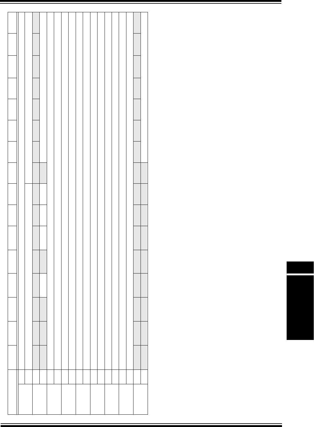
© 2013 Microchip Technology Inc. DS60001246A-page 49-7
Section 49. Crypto Engine and Random Number Generator (RNG)
Crypto Engine and
Random Number Gen-
erator (RNG)
49
Table 49-2: Random Number Generator SFR Summary
Name Bit 31/15 Bit 30/14 Bit 29/13 Bit 28/12 Bit 27/11 Bit 26/10 Bit 25/9 Bit 24/8 Bit 23/7 Bit 22/6 Bit 21/5 Bit 20/4 Bit 19/3 Bit 118/2 Bit 17/1 Bit 16/0
RNGVER 31:16 ID<15:8>
15:0 VERSION<7:0> REVISION<7:0>
RNGCON 31:16 — — — — — — — — — — — — — — — —
15:0 ———LOAD— CONT PRNGEN TRNGEN — PLEN<6:0>
RNGPOLY1 31:16 POLY1<31:16>
15:0 POLY1<15:0>
RNGPOLY2 31:16 POLY2<31:16>
15:0 POLY2<15:0>
RNG1 31:16 RNG1<31:16>
15:0 RNG1<15:0>
RNG2 31:16 RNG2<31:16>
15:0 RNG2<15:0>
RNGSEED1 31:16 RDATA1<31:16>
15:0 RDATA1<15:0>
RNGSEED2 31:16 RDATA2<31:16>
15:0 RDATA2<15:0>
RNGRCNT 31:24 — — — — — — — — — — — — — — — —
7:0 — — — — — — — — — RCNT<6:0>
Legend: — = unimplemented, read as ‘0’.

PIC32 Family Reference Manual
DS60001246A-page 49-8 © 2013 Microchip Technology Inc.
Register 49-1: CEVER: Crypto Engine Revision, Version, and ID Register
Bit
Range
Bit
31/23/15/7
Bit
30/22/14/6
Bit
29/21/13/5
Bit
28/20/12/4
Bit
27/19/11/3
Bit
26/18/10/2
Bit
25/17/9/1
Bit
24/16/8/0
31:24 R-0 R-0 R-0 R-0 R-0 R-0 R-0 R-0
REVISION<7:0>
23:16 R-0 R-0 R-0 R-0 R-0 R-0 R-0 R-0
VERSION<7:0>
15:8 R-0 R-0 R-0 R-0 R-0 R-0 R-0 R-0
ID<15:8>
7:0 R-0 R-0 R-0 R-0 R-0 R-0 R-0 R-0
ID<7:0>
Legend:
R = Readable bit W = Writable bit U = Unimplemented bit, read as ‘0’
-n = Value at POR ‘1’ = Bit is set ‘0’ = Bit is cleared x = Bit is unknown
bit 31-24 REVISION<7:0>: Crypto Engine Revision bits
bit 23-16 VERSION<7:0>: Crypto Engine Version bits
bit 15-0 ID: Crypto Engine Identification bits

© 2013 Microchip Technology Inc. DS60001246A-page 49-9
Section 49. Crypto Engine and Random Number Generator (RNG)
Crypto Engine and
Random Number Gen-
erator (RNG)
49
Register 49-2: CECON: Crypto Engine Control Register
Bit
Range
Bit
31/23/15/7
Bit
30/22/14/6
Bit
29/21/13/5
Bit
28/20/12/4
Bit
27/19/11/3
Bit
26/18/10/2
Bit
25/17/9/1
Bit
24/16/8/0
31:24 U-0 U-0 U-0 U-0 U-0 U-0 U-0 U-0
— — — — — — — —
23:16 U-0 U-0 U-0 U-0 U-0 U-0 U-0 U-0
— — — — — — — —
15:8 U-0 U-0 U-0 U-0 U-0 U-0 U-0 U-0
— — — — — — — —
7:0 U-0 R/W-0 R/W-0 U-0 U-0 R/W-0 R/W-0 R/W-0
— SWRST SWAPEN — —BDPCHSTBDPPLENDMAEN
Legend:
R = Readable bit W = Writable bit U = Unimplemented bit, read as ‘0’
-n = Value at POR ‘1’ = Bit is set ‘0’ = Bit is cleared x = Bit is unknown
bit 31-7 Unimplemented: Read as ‘0’
bit 6 SWRST: Software Reset bit
1 = Initiate a software Reset of the Crypto Engine
0 = Normal operation
bit 5 SWAPEN: I/O Swap Enable bit
1 = Input data is byte swapped when read by dedicated DMA
0 = Input data is not byte swapped when read by dedicated DMA
bit 4-3 Unimplemented: Read as ‘0’
bit 2 BDPCHST: Buffer Descriptor Processor Fetch Enable bit
This bit should be enabled only after all DMA descriptor programming is completed.
1 = Buffer Descriptor Processor descriptor fetch is enabled
0 = Buffer Descriptor Processor descriptor fetch is disabled
bit 1 BDPPLEN: Buffer Descriptor Processor Poll Enable bit
This bit should be enabled only after all DMA descriptor programming is completed.
1 = Poll for descriptor until valid bit is set
0 = Do not poll
bit 0 DMAEN: DMA Enable bit
1 = Crypto Engine DMA is enabled
0 = Crypto Engine DMA is disabled

PIC32 Family Reference Manual
DS60001246A-page 49-10 © 2013 Microchip Technology Inc.
Register 49-3: CEBDADDR: Crypto Engine Buffer Descriptor Register
Bit
Range
Bit
31/23/15/7
Bit
30/22/14/6
Bit
29/21/13/5
Bit
28/20/12/4
Bit
27/19/11/3
Bit
26/18/10/2
Bit
25/17/9/1
Bit
24/16/8/0
31:24 R-0 R-0 R-0 R-0 R-0 R-0 R-0 R-0
BDPADDR<31:24>
23:16 R-0 R-0 R-0 R-0 R-0 R-0 R-0 R-0
BDPADDR<23:16>
15:8 R-0 R-0 R-0 R-0 R-0 R-0 R-0 R-0
BDPADDR<15:8>
7:0 R-0 R-0 R-0 R-0 R-0 R-0 R-0 R-0
BDPADDR<7:0>
Legend:
R = Readable bit W = Writable bit U = Unimplemented bit, read as ‘0’
-n = Value at POR ‘1’ = Bit is set ‘0’ = Bit is cleared x = Bit is unknown
bit 31-0 BDPADDR<31:0>: Current Buffer Descriptor Process Address Status bits
These bits contain the current descriptor address that is being processed by the Buffer Descriptor
Processor.
Register 49-4: CEBDPADDR: Crypto Engine Buffer Descriptor Processor Register
Bit
Range
Bit
31/23/15/7
Bit
30/22/14/6
Bit
29/21/13/5
Bit
28/20/12/4
Bit
27/19/11/3
Bit
26/18/10/2
Bit
25/17/9/1
Bit
24/16/8/0
31:24 R/W-0 R/W-0 R/W-0 R/W-0 R/W-0 R/W-0 R/W-0 R/W-0
BASEADDR<31:24>
23:16 R/W-0 R/W-0 R/W-0 R/W-0 R/W-0 R/W-0 R/W-0 R/W-0
BASEADDR<23:16>
15:8 R/W-0 R/W-0 R/W-0 R/W-0 R/W-0 R/W-0 R/W-0 R/W-0
BASEADDR<15:8>
7:0 R/W-0 R/W-0 R/W-0 R/W-0 R/W-0 R/W-0 R/W-0 R/W-0
BASEADDR<7:0>
Legend:
R = Readable bit W = Writable bit U = Unimplemented bit, read as ‘0’
-n = Value at POR ‘1’ = Bit is set ‘0’ = Bit is cleared x = Bit is unknown
bit 31-0 BASEADDR<31:0>: DMA Base Address Status bits
These bits contain the base address of the DMA controller. After a reset, a fetch starts from this address.

© 2013 Microchip Technology Inc. DS60001246A-page 49-11
Section 49. Crypto Engine and Random Number Generator (RNG)
Crypto Engine and
Random Number Gen-
erator (RNG)
49
Register 49-5: CESTAT: Crypto Engine Status Register
Bit
Range
Bit
31/23/15/7
Bit
30/22/14/6
Bit
29/21/13/5
Bit
28/20/12/4
Bit
27/19/11/3
Bit
26/18/10/2
Bit
25/17/9/1
Bit
24/16/8/0
31:24 R-0 R-0 R-0 R-0 R-0 R-0 R-0 R-0
ERRMODE<2:0> ERROP<2:0> ERRPHASE<1:0>
23:16 U-0 U-0 R-0 R-0 R-0 R-0 R-0 R-0
— — BDSTATE<3:0> START ACTIVE
15:8 R-0 R-0 R-0 R-0 R-0 R-0 R-0 R-0
BDCTRL<15:8>
7:0 R-0 R-0 R-0 R-0 R-0 R-0 R-0 R-0
BDCTRL<7:0>
Legend:
R = Readable bit W = Writable bit U = Unimplemented bit, read as ‘0’
-n = Value at POR ‘1’ = Bit is set ‘0’ = Bit is cleared x = Bit is unknown
bit 31-29 ERRMOD<2:0>: Internal Error Mode Status bits
111 = Reserved
•
•
•
001 = Reserved
000 = Normal operation
bit 28-26 ERROP<2:0>: Internal Error Operation Status bits
111 = Reserved
110 = Reserved
101 = Reserved
100 = Authentication
011 = Reserved
010 = Decryption
001 = Encryption
000 = Reserved
bit 25-24 ERRPHASE<1:0>: Internal Error Phase of DMA Status bits
11 = Destination data
10 = Source data
01 = Security Association access
00 = Buffer Descriptor access
bit 23-22 Unimplemented: Read as ‘0’
bit 21-18 BDSTATE<3:0>: Buffer Descriptor Processor State Status bits
These bits contain a number, which indicates the current state of the Buffer Descriptor Processor:
1111 = Reserved
•
•
•
0111 = Reserved
0110 = Security Association fetch
0101 = Fetch Buffer Descriptor Processor is disabled
0100 = Descriptor is done
0011 = Data phase
0010 = Buffer Descriptor Processor is loading
0001 = Descriptor fetch request is pending
0000 = Buffer Descriptor Processor is idle
bit 17 START: DMA Start Status bit
1 = DMA start has occurred
0 = DMA start has not occurred

PIC32 Family Reference Manual
DS60001246A-page 49-12 © 2013 Microchip Technology Inc.
bit 16 ACTIVE: Buffer Descriptor Processor Status bit
1 = Buffer Descriptor Processor is active
0 = Buffer Descriptor Processor is idle
bit 15-0 BDCTRL<15:0>: Descriptor Control Word Status bits
These bits contain the current descriptor control word.
Register 49-5: CESTAT: Crypto Engine Status Register (Continued)

© 2013 Microchip Technology Inc. DS60001246A-page 49-13
Section 49. Crypto Engine and Random Number Generator (RNG)
Crypto Engine and
Random Number Gen-
erator (RNG)
49
Register 49-6: CEINTSRC: Crypto Engine Interrupt Source Register
Bit
Range
Bit
31/23/15/7
Bit
30/22/14/6
Bit
29/21/13/5
Bit
28/20/12/4
Bit
27/19/11/3
Bit
26/18/10/2
Bit
25/17/9/1
Bit
24/16/8/0
31:24 U-0 U-0 U-0 U-0 U-0 U-0 U-0 U-0
— — — — — — — —
23:16 U-0 U-0 U-0 U-0 U-0 U-0 U-0 U-0
— — — — — — — —
15:8 U-0 U-0 U-0 U-0 U-0 U-0 U-0 U-0
— — — — — — — —
7:0 U-0 U-0 U-0 U-0 R-0, HS R-0, HS R-0, HS R-0, HS
— — — — AREIF(1) PKTIF(1) CBDIF(1) PENDIF(1)
Legend: HS Set by hardware
R = Readable bit W = Writable bit U = Unimplemented bit, read as ‘0’
-n = Value at POR ‘1’ = Bit is set ‘0’ = Bit is cleared x = Bit is unknown
bit 31-4 Unimplemented: Read as ‘0’
bit 3 AREIF: Access Response Error Interrupt bit(1)
1 = The Crypto Engine attempted to access an invalid memory location
0 = No error has occurred
bit 2 PKTIF: DMA Packet Completion Interrupt Status bit(1)
1 = DMA packet was completed
0 = DMA packet was not completed
bit 1 CBDIF: Buffer Descriptor Transmit Status bit(1)
1 = Last Buffer Descriptor transmit was processed
0 = Last Buffer Descriptor transmit has not been processed
bit 0 PENDIF: Crypto Engine Interrupt Pending Status bit(1)
1 = Crypto Engine interrupt is pending (this value is the result of an OR of all interrupts in the Crypto Engine)
0 = Crypto Engine interrupt is not pending
Note 1: Write a '1' to this bit to clear the interrupt.

PIC32 Family Reference Manual
DS60001246A-page 49-14 © 2013 Microchip Technology Inc.
Register 49-7: CEINTEN: Crypto Engine Interrupt Enable Register
Bit
Range
Bit
31/23/15/7
Bit
30/22/14/6
Bit
29/21/13/5
Bit
28/20/12/4
Bit
27/19/11/3
Bit
26/18/10/2
Bit
25/17/9/1
Bit
24/16/8/0
31:24 U-0 U-0 U-0 U-0 U-0 U-0 U-0 U-0
— — — — — — — —
23:16 U-0 U-0 U-0 U-0 U-0 U-0 U-0 U-0
— — — — — — — —
15:8 U-0 U-0 U-0 U-0 U-0 U-0 U-0 U-0
— — — — — — — —
7:0 U-0 U-0 U-0 U-0 R/W-0 R/W-0 R/W-0 R/W-0
— — — — AREIE PKTIE BDPIE PENDIE(1)
Legend:
R = Readable bit W = Writable bit U = Unimplemented bit, read as ‘0’
-n = Value at POR ‘1’ = Bit is set ‘0’ = Bit is cleared x = Bit is unknown
bit 31-4 Unimplemented: Read as ‘0’
bit 3 AREIE: Access Response Error Interrupt Enable bit
1 = Access response error interrupts are enabled
0 = Access response error interrupts are not enabled
bit 2 PKTIE: DMA Packet Completion Interrupt Enable bit
1 = DMA packet completion interrupts are enabled
0 = DMA packet completion interrupts are not enabled
bit 1 BDPIE: DMA Buffer Descriptor Processor Interrupt Enable bit
1 = Buffer Descriptor Processor interrupts are enabled
0 = Buffer Descriptor Processor interrupts are not enabled
bit 0 PENDIE: Master Interrupt Enable bit(1)
1 = Crypto Engine interrupts are enabled
0 = Crypto Engine interrupts are not enabled
Note 1: The PENDIE bit is a Global enable bit and must be enabled together with the other interrupts desired.

© 2013 Microchip Technology Inc. DS60001246A-page 49-15
Section 49. Crypto Engine and Random Number Generator (RNG)
Crypto Engine and
Random Number Gen-
erator (RNG)
49
Register 49-8: CEPOLLCON: Crypto Engine Poll Control Register
Bit
Range
Bit
31/23/15/7
Bit
30/22/14/6
Bit
29/21/13/5
Bit
28/20/12/4
Bit
27/19/11/3
Bit
26/18/10/2
Bit
25/17/9/1
Bit
24/16/8/0
31:24 U-0 U-0 U-0 U-0 U-0 U-0 U-0 U-0
— — — — — — — —
23:16 U-0 U-0 U-0 U-0 U-0 U-0 U-0 U-0
— — — — — — — —
15:8 R/W-0 R/W-0 R/W-0 R/W-0 R/W-0 R/W-0 R/W-0 R/W-0
BDPPLCON<15:8>
7:0 R/W-0 R/W-0 R/W-0 R/W-0 R/W-0 R/W-0 R/W-0 R/W-0
BDPPLCON<7:0>
Legend:
R = Readable bit W = Writable bit U = Unimplemented bit, read as ‘0’
-n = Value at POR ‘1’ = Bit is set ‘0’ = Bit is cleared x = Bit is unknown
bit 31-16 Unimplemented: Read as ‘0’
bit 15 BDPPLCON<15:0>: Buffer Descriptor Processor Poll Control bits
These bits determine the number of cycles that the DMA transmit Buffer Descriptor Processor would wait
before refetching the descriptor control word if the previous descriptor fetched was disabled.
Register 49-9: CEHDLEN: Crypto Engine Header Length Register
Bit
Range
Bit
31/23/15/7
Bit
30/22/14/6
Bit
29/21/13/5
Bit
28/20/12/4
Bit
27/19/11/3
Bit
26/18/10/2
Bit
25/17/9/1
Bit
24/16/8/0
31:24 U-0 U-0 U-0 U-0 U-0 U-0 U-0 U-0
— — — — — — — —
23:16 U-0 U-0 U-0 U-0 U-0 U-0 U-0 U-0
— — — — — — — —
15:8 U-0 U-0 U-0 U-0 U-0 U-0 U-0 U-0
— — — — — — — —
7:0 R/W-0 R/W-0 R/W-0 R/W-0 R/W-0 R/W-0 R/W-0 R/W-0
HDRLEN<7:0>
Legend:
R = Readable bit W = Writable bit U = Unimplemented bit, read as ‘0’
-n = Value at POR ‘1’ = Bit is set ‘0’ = Bit is cleared x = Bit is unknown
bit 31-8 Unimplemented: Read as ‘0’
bit 7-0 HDRLEN<7:0>: DMA Header Length bits
For every packet, leave this length of locations and start filling the data.
PIC32 Family Reference Manual
DS60001246A-page 49-16 © 2013 Microchip Technology Inc.
Register 49-10: CETRLLEN: Crypto Engine Trailer Length Register
Bit
Range
Bit
31/23/15/7
Bit
30/22/14/6
Bit
29/21/13/5
Bit
28/20/12/4
Bit
27/19/11/3
Bit
26/18/10/2
Bit
25/17/9/1
Bit
24/16/8/0
31:24 U-0 U-0 U-0 U-0 U-0 U-0 U-0 U-0
— — — — — — — —
23:16 U-0 U-0 U-0 U-0 U-0 U-0 U-0 U-0
— — — — — — — —
15:8 U-0 U-0 U-0 U-0 U-0 U-0 U-0 U-0
— — — — — — — —
7:0 R/W-0 R/W-0 R/W-0 R/W-0 R/W-0 R/W-0 R/W-0 R/W-0
TRLRLEN<7:0>
Legend:
R = Readable bit W = Writable bit U = Unimplemented bit, read as ‘0’
-n = Value at POR ‘1’ = Bit is set ‘0’ = Bit is cleared x = Bit is unknown
bit 31-8 Unimplemented: Read as ‘0’
bit 7-0 TRLRLEN<7:0>: DMA Trailer Length bits
For every packet, leave this length of locations and start putting the next packet.
Register 49-11: CEDTXSTAT: Crypto Engine DTX Debug Status Register
Bit
Range
Bit
31/23/15/7
Bit
30/22/14/6
Bit
29/21/13/5
Bit
28/20/12/4
Bit
27/19/11/3
Bit
26/18/10/2
Bit
25/17/9/1
Bit
24/16/8/0
31:24 U-0 U-0 U-0 U-0 U-0 U-0 U-0 U-0
— — — — — — — —
23:16 U-0 U-0 U-0 U-0 R-0 R-0 R-0 R-0
— — — —DTXBLEN<15:12>
15:8 R-0 R-0 R-0 R-0 R-0 R-0 R-0 R-0
DTXBLEN<11:4>
7:0 R-0 R-0 R-0 R-0 R-0 R-0 R-0 R-0
DTXBLEN<3:0> DTXSTATE<3:0>
Legend:
R = Readable bit W = Writable bit U = Unimplemented bit, read as ‘0’
-n = Value at POR ‘1’ = Bit is set ‘0’ = Bit is cleared x = Bit is unknown
bit 31-16 Unimplemented: Read as ‘0’
bit 15-4 DTXBLEN<15:0>: Current DMA Transmit Buffer Length Debug Status bits
bit 3-0 DTXSTATE<3:0>: Current DMA Transmit States Debug Status bits
1111 = Reserved
•
•
•
0110 = Reserved
0101 = Transmitting to internal Crypto Engine Memory
0100 = Reserved
0011 = Wait
0010 = Reserved
0001 = Reserved
0000 = Idle

© 2013 Microchip Technology Inc. DS60001246A-page 49-17
Section 49. Crypto Engine and Random Number Generator (RNG)
Crypto Engine and
Random Number Gen-
erator (RNG)
49
Register 49-12: CEDRXSTAT: Crypto Engine DRX Debug Status Register
Bit
Range
Bit
31/23/15/7
Bit
30/22/14/6
Bit
29/21/13/5
Bit
28/20/12/4
Bit
27/19/11/3
Bit
26/18/10/2
Bit
25/17/9/1
Bit
24/16/8/0
31:24 U-0 U-0 U-0 U-0 U-0 U-0 U-0 U-0
— — — — — — — —
23:16 U-0 U-0 U-0 U-0 R-0 R-0 R-0 R-0
— — — —DRXBLEN<15:12>
15:8 R-0 R-0 R-0 R-0 R-0 R-0 R-0 R-0
DTXBLEN<11:4>
7:0 R-0 R-0 R-0 R-0 R-0 R-0 R-0 R-0
DRXBLEN<3:0> DRXSTATE<3:0>
Legend:
R = Readable bit W = Writable bit U = Unimplemented bit, read as ‘0’
-n = Value at POR ‘1’ = Bit is set ‘0’ = Bit is cleared x = Bit is unknown
bit 31-16 Unimplemented: Read as ‘0’
bit 15-4 DTXBLEN<15:0>: Current DMA Receive Buffer Length Debug Status bits
bit 3-0 DTXSTATE<3:0>: Current DMA Receive States Debug Status bits
0000 = Idle
All other values indicate a transaction is in progress.
Register 49-13: RNGVER: Random Number Generator ID, Version, and Revision Register
Bit
Range
Bit
31/23/15/7
Bit
30/22/14/6
Bit
29/21/13/5
Bit
28/20/12/4
Bit
27/19/11/3
Bit
26/18/10/2
Bit
25/17/9/1
Bit
24/16/8/0
31:24 R-0 R-0 R-0 R-0 R-0 R-0 R-0 R-0
ID<15:8>
23:16 R-0 R-0 R-0 R-0 R-0 R-0 R-0 R-0
ID<15:8>
15:8 R-0 R-0 R-0 R-0 R-0 R-0 R-0 R-0
VERSION<7:0>
7:0 R-0 R-0 R-0 R-0 R-0 R-0 R-0 R-0
REVISION<7:0>
Legend:
R = Readable bit W = Writable bit U = Unimplemented bit, read as ‘0’
-n = Value at POR ‘1’ = Bit is set ‘0’ = Bit is cleared x = Bit is unknown
bit 31-16 ID<15:8>: Block Identification bits
bit 15-8 VERSION<7:0>: Block Version bits
bit 7-0 REVISION<7:0>: Block Revision bits

PIC32 Family Reference Manual
DS60001246A-page 49-18 © 2013 Microchip Technology Inc.
Register 49-14: RNGCON: Random Number Generator Control Register
Bit
Range
Bit
31/23/15/7
Bit
30/22/14/6
Bit
29/21/13/5
Bit
28/20/12/4
Bit
27/19/11/3
Bit
26/18/10/2
Bit
25/17/9/1
Bit
24/16/8/0
31:24 U-0 U-0 U-0 U-0 U-0 U-0 U-0 U-0
— — — — — — — —
23:16 U-0 U-0 U-0 U-0 U-0 U-0 U-0 U-0
— — — — — — — —
15:8 U-0 U-0 U-0 R/W-0, HC U-0 R/W-0 R/W-0 R/W-0
— — — LOAD —CONTPRNGENTRNGEN
7:0 U-0 R/W-0 R/W-0 R/W-0 R/W-0 R/W-0 R/W-0 R/W-0
—PLEN<6:0>
Legend: HC = Cleared by hardware
R = Readable bit W = Writable bit U = Unimplemented bit, read as ‘0’
-n = Value at POR ‘1’ = Bit is set ‘0’ = Bit is cleared x = Bit is unknown
bit 31-13 Unimplemented: Read as ‘0’
bit 12 LOAD: Device Select bit
Setting this bit to ‘1’ loads the seed from the TRNG (i.e., the random value) as a seed to the PRNG. It is
cleared automatically by hardware.
bit 11 Unimplemented: Read as ‘0’
bit 10 CONT: PRNG Number Shift Enable bit
1 = The PRNG random number is shifted every cycle
0 = The PRNG random number is shifted when the previous value is removed
bit 9 PRNGEN: PRNG Operation Enable bit
1 = PRNG operation is enabled
0 = PRNG operation is not enabled
bit 8 TRNGEN: TRNG Operation Enable bit
1 = TRNG operation is enabled
0 = TRNG operation is not enabled
bit 7 Unimplemented: Read as ‘0’; must always be written as ‘0’
bit 6-0 PLEN<6:0>: PRNG Polynomial Length bits
These bits contain the length of the polynomial used for the PRNG.
© 2013 Microchip Technology Inc. DS60001246A-page 49-19
Section 49. Crypto Engine and Random Number Generator (RNG)
Crypto Engine and
Random Number Gen-
erator (RNG)
49
Register 49-15: RNGPOLY1: Random Number Generator Polynomial Register 1
Bit
Range
Bit
31/23/15/7
Bit
30/22/14/6
Bit
29/21/13/5
Bit
28/20/12/4
Bit
27/19/11/3
Bit
26/18/10/2
Bit
25/17/9/1
Bit
24/16/8/0
31:24 R/W-0 R/W-0 R/W-0 R/W-0 R/W-0 R/W-0 R/W-0 R/W-0
POLY1<31:24>
23:16 R/W-0 R/W-0 R/W-0 R/W-0 R/W-0 R/W-0 R/W-0 R/W-0
POLY1<23:16>
15:8 R/W-0 R/W-0 R/W-0 R/W-0 R/W-0 R/W-0 R/W-0 R/W-0
POLY1<15:8>
7:0 R/W-0 R/W-0 R/W-0 R/W-0 R/W-0 R/W-0 R/W-0 R/W-0
POLY1<7:0>
Legend:
R = Readable bit W = Writable bit U = Unimplemented bit, read as ‘0’
-n = Value at POR ‘1’ = Bit is set ‘0’ = Bit is cleared x = Bit is unknown
bit 31-0 POLY1<31:0>: PRNG LFSR Polynomial Most Significant Byte bits
These bits are reverse-order for the LSFR. Therefore, these bits actually represent bits 32-63 of the LSFR.
Register 49-16: RNGPOLY2: Random Number Generator Polynomial Register 2
Bit
Range
Bit
31/23/15/7
Bit
30/22/14/6
Bit
29/21/13/5
Bit
28/20/12/4
Bit
27/19/11/3
Bit
26/18/10/2
Bit
25/17/9/1
Bit
24/16/8/0
31:24 R/W-0 R/W-0 R/W-0 R/W-0 R/W-0 R/W-0 R/W-0 R/W-0
POLY2<31:24>
23:16 R/W-0 R/W-0 R/W-0 R/W-0 R/W-0 R/W-0 R/W-0 R/W-0
POLY2<23:16>
15:8 R/W-0 R/W-0 R/W-0 R/W-0 R/W-0 R/W-0 R/W-0 R/W-0
POLY2<15:8>
7:0 R/W-0 R/W-0 R/W-0 R/W-0 R/W-0 R/W-0 R/W-0 R/W-0
POLY2<7:0>
Legend:
R = Readable bit W = Writable bit U = Unimplemented bit, read as ‘0’
-n = Value at POR ‘1’ = Bit is set ‘0’ = Bit is cleared x = Bit is unknown
bit 31-0 POLY2<31:0>: PRNG LFSR Polynomial Least Significant Byte bits
These bits are reverse-order for the LSFR. Therefore, these bits actually represent bits 0-31 of the LSFR.

PIC32 Family Reference Manual
DS60001246A-page 49-20 © 2013 Microchip Technology Inc.
Register 49-17: RNGNUMGEN1: Random Number Generator Pseudo-Random Number Generator Register 1
Bit
Range
Bit
31/23/15/7
Bit
30/22/14/6
Bit
29/21/13/5
Bit
28/20/12/4
Bit
27/19/11/3
Bit
26/18/10/2
Bit
25/17/9/1
Bit
24/16/8/0
31:24 R/W-0 R/W-0 R/W-0 R/W-0 R/W-0 R/W-0 R/W-0 R/W-0
RNG1<31:24>
23:16 R/W-0 R/W-0 R/W-0 R/W-0 R/W-0 R/W-0 R/W-0 R/W-0
RNG1<23:16>
15:8 R/W-0 R/W-0 R/W-0 R/W-0 R/W-0 R/W-0 R/W-0 R/W-0
RNG1<15:8>
7:0 R/W-0 R/W-0 R/W-0 R/W-0 R/W-0 R/W-0 R/W-0 R/W-0
RNG1<7:0>
Legend:
R = Readable bit W = Writable bit U = Unimplemented bit, read as ‘0’
-n = Value at POR ‘1’ = Bit is set ‘0’ = Bit is cleared x = Bit is unknown
bit 31-0 RNG1<31:0>: Current PRNG Least Significant Byte Value bits
Register 49-18: RNGNUMGEN2: Random Number Generator Pseudo-Random Number Generator Register 2
Bit
Range
Bit
31/23/15/7
Bit
30/22/14/6
Bit
29/21/13/5
Bit
28/20/12/4
Bit
27/19/11/3
Bit
26/18/10/2
Bit
25/17/9/1
Bit
24/16/8/0
31:24 R/W-0 R/W-0 R/W-0 R/W-0 R/W-0 R/W-0 R/W-0 R/W-0
RNG2<31:24>
23:16 R/W-0 R/W-0 R/W-0 R/W-0 R/W-0 R/W-0 R/W-0 R/W-0
RNG2<23:16>
15:8 R/W-0 R/W-0 R/W-0 R/W-0 R/W-0 R/W-0 R/W-0 R/W-0
RNG2<15:8>
7:0 R/W-0 R/W-0 R/W-0 R/W-0 R/W-0 R/W-0 R/W-0 R/W-0
RNG2<7:0>
Legend:
R = Readable bit W = Writable bit U = Unimplemented bit, read as ‘0’
-n = Value at POR ‘1’ = Bit is set ‘0’ = Bit is cleared x = Bit is unknown
bit 31-0 RNG2<31:0>: Current PRNG Most Significant Byte Value bits

© 2013 Microchip Technology Inc. DS60001246A-page 49-21
Section 49. Crypto Engine and Random Number Generator (RNG)
Crypto Engine and
Random Number Gen-
erator (RNG)
49
Register 49-19: RNGSEED1: True Random Number Generator Seed Register 1
Bit
Range
Bit
31/23/15/7
Bit
30/22/14/6
Bit
29/21/13/5
Bit
28/20/12/4
Bit
27/19/11/3
Bit
26/18/10/2
Bit
25/17/9/1
Bit
24/16/8/0
31:24 R-0 R-0 R-0 R-0 R-0 R-0 R-0 R-0
RDATA1<31:24>
23:16 R-0 R-0 R-0 R-0 R-0 R-0 R-0 R-0
RDATA1<23:16>
15:8 R-0 R-0 R-0 R-0 R-0 R-0 R-0 R-0
RDATA1<15:8>
7:0 R-0 R-0 R-0 R-0 R-0 R-0 R-0 R-0
RDATA1<7:0>
Legend:
R = Readable bit W = Writable bit U = Unimplemented bit, read as ‘0’
-n = Value at POR ‘1’ = Bit is set ‘0’ = Bit is cleared x = Bit is unknown
bit 31-0 RDATA1<31:0>: TRNG Least Significant Byte 32 Value bits
Register 49-20: RNGSEED2: True Random Number Generator Seed Register 2
Bit
Range
Bit
31/23/15/7
Bit
30/22/14/6
Bit
29/21/13/5
Bit
28/20/12/4
Bit
27/19/11/3
Bit
26/18/10/2
Bit
25/17/9/1
Bit
24/16/8/0
31:24 R-0 R-0 R-0 R-0 R-0 R-0 R-0 R-0
RDATA2<31:24>
23:16 R-0 R-0 R-0 R-0 R-0 R-0 R-0 R-0
RDATA2<23:16>
15:8 R-0 R-0 R-0 R-0 R-0 R-0 R-0 R-0
RDATA2<15:8>
7:0 R-0 R-0 R-0 R-0 R-0 R-0 R-0 R-0
RDATA2<7:0>
Legend:
R = Readable bit W = Writable bit U = Unimplemented bit, read as ‘0’
-n = Value at POR ‘1’ = Bit is set ‘0’ = Bit is cleared x = Bit is unknown
bit 31-0 RDATA2<31:0>: TRNG Most Significant Byte 32 Value bits

PIC32 Family Reference Manual
DS60001246A-page 49-22 © 2013 Microchip Technology Inc.
Register 49-21: RNGRCNT: True Random Number Generator Count Register
Bit
Range
Bit
31/23/15/7
Bit
30/22/14/6
Bit
29/21/13/5
Bit
28/20/12/4
Bit
27/19/11/3
Bit
26/18/10/2
Bit
25/17/9/1
Bit
24/16/8/0
31:24 U-0 U-0 U-0 U-0 U-0 U-0 U-0 U-0
— — — — — — — —
23:16 U-0 U-0 U-0 U-0 U-0 U-0 U-0 U-0
— — — — — — — —
15:8 U-0 U-0 U-0 U-0 U-0 U-0 U-0 U-0
— — — — — — — —
7:0 U-0 R-0 R-0 R-0 R-0 R-0 R-0 R-0
—RCNT<6:0>
Legend:
R = Readable bit W = Writable bit U = Unimplemented bit, read as ‘0’
-n = Value at POR ‘1’ = Bit is set ‘0’ = Bit is cleared x = Bit is unknown
bit 31-7 Unimplemented: Read as ‘0’
bit 6-0 RCNT<6:0>: Number of Valid TRNG Most Significant Byte 32 bits

© 2013 Microchip Technology Inc. DS60001246A-page 49-23
Section 49. Crypto Engine and Random Number Generator (RNG)
Crypto Engine and
Random Number Gen-
erator (RNG)
49
49.3 CRYPTO ENGINE BUFFER DESCRIPTORS
Host software creates a linked list of Buffer Descriptors and the hardware updates them.
Tabl e 49- 3 provides a list of the Crypto Engine Buffer Descriptors, followed by format descrip-
tions (see Figure 49-3 through Figure 49-10).
Table 49-3: Crypto Engine Buffer Descriptors
Name Bit
31/23/15/7
Bit
30/22/14/6
Bit
29/21/13/5
Bit
28/20/12/4
Bit
27/19/11/3
Bit
26/18/10/2
Bit
25/17/9/1
Bit
24/16/8/0
BD_CTRL 31:24 DESC_EN SEC_CODE<7:1>
23:16 SEC_CODE<0> SA_FETCH_EN UPD_RES CRDMA_EN LAST_BD LIFM PKT_INT_EN CBD_INT_EN
15:8 BD_BUFLEN<15:8>
7:0 BD_BUFLEN<7:0>
BD_SA_ADDR 31:24 BD_SAADDR<31:24>
23:16 BD_SAADDR<23:16>
15:8 BD_SAADDR<15:8>
7:0 BD_SAADR<7:0>
BD_SRCADDR 31:24 BD_SRCADDR<31:24>
23:16 BD_SRCADDR<23:16>
15:8 BD_SRCADDR<15:8>
7:0 BD_SRCADDR<7:0>
BD_DSTADDR 31:24 BD_DSTADDR<31:24>
23:16 BD_DSTADDR<23:16>
15:8 BD_DSTADDR<15:8>
7:0 BD_DSTADDR<7:0>
BD_NXTPTR 31:24 BD_NXTADDR<31:24>
23:16 BD_NXTADDR<23:16>
15:8 BD_NXTADDR<15:8>
7:0 BD_NXTADDR<7:0>
BD_UPDPTR 31:24 BD_UPDADDR<31:24>
23:16 BD_UPDADDR<23:16>
15:8 BD_UPDADDR<15:8>
7:0 BD_UPDADDR<7:0>
BD_MSG_LEN 31:24 MSG_LENGTH<31:24>
23:16 MSG_LENGTH<23:16>
15:8 MSG_LENGTH<15:8>
7:0 MSG_LENGTH<7:0>
BD_ENC_OFF 31:24 ENCR_OFFSET<31:24>
23:16 ENCR_OFFSET<23:16>
15:8 ENCR_OFFSET<15:8>
7:0 ENCR_OFFSET<7:0>
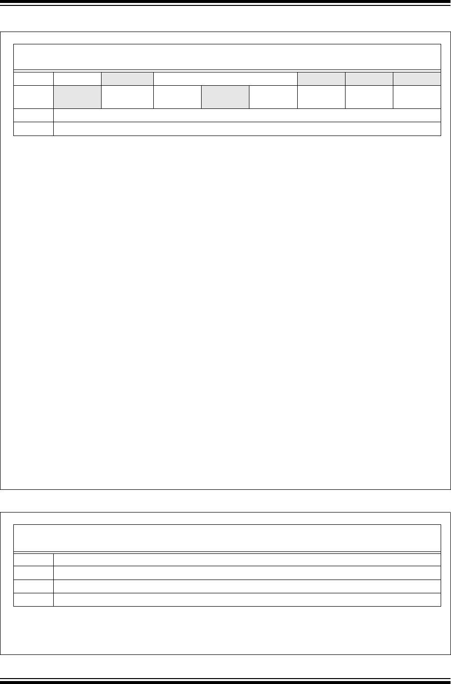
PIC32 Family Reference Manual
DS60001246A-page 49-24 © 2013 Microchip Technology Inc.
Figure 49-3: Format of BD_CTRL
Figure 49-4: Format of BD_SADDR
Bit
Range
Bit
31/23/15/7
Bit
30/22/14/6
Bit
29/21/13/5
Bit
28/20/12/4
Bit
27/19/11/3
Bit
26/18/10/2
Bit
25/17/9/1
Bit
24/16/8/0
31-24 DESC_EN — CRY_MODE<2:0> — — —
23-16 —SA_
FETCH_EN UPD_RES —LAST_BDLIFM PKT_
INT_EN
CBD_
INT_EN
15-8 BD_BUFLEN<15:8>
7-0 BD_BUFLEN<7:0>
bit 31 DESC_EN: Descriptor Enable
1 = The descriptor is owned by hardware. After processing the BD, hardware resets this bit to ‘0’.
0 = The descriptor is owned by software
bit 30 Unimplemented: Must be written as ‘0’
bit 29-27 CRY_MODE<2:0>: Crypto Mode
111 = Reserved
110 = Reserved
101 = Reserved
100 = Reserved
011 = CEK operation
010 = KEK operation
001 = Preboot authentication
000 = Normal operation
bit 22 SA_FETCH_EN: Fetch Security Association From External Memory
1 = Fetch SA from the SA pointer. This bit needs to be set to ‘1’ for every new packet.
0 = User current fetched SA or the internal SA
bit 21-20 Unimplemented: Must be written as ‘0’
bit 19 LAST_BD: Last Buffer Descriptors
After the last BD, the BD_PTR goes to the base address in the CSR.
bit 18 LIFM: Last In Frame
In case of Receive Packets (from H/W-> Host), this field is filled by the Hardware to indicate whether
the packet goes across multiple buffer descriptors. In case of transmit packets (from Host -> H/W),
this field indicates whether this BD is the last in the frame.
bit 17 PKT_INT_EN: Packet Interrupt Enable
Generate an interrupt after processing the current buffer descriptor, if it is the end of the packet.
bit 16 CBD_INT_EN: CBD Interrupt Enable
Generate an interrupt after processing the current buffer descriptor.
bit 15-0 BD_BUFLEN<15:0>: Buffer Descriptor Length
This field contains the length of the buffer and is updated with the actual length filled by the receiver.
Bit
Range
Bit
31/23/15/7
Bit
30/22/14/6
Bit
29/21/13/5
Bit
28/20/12/4
Bit
27/19/11/3
Bit
26/18/10/2
Bit
25/17/9/1
Bit
24/16/8/0
31-24 BD_SAADDR<31:24>
23-16 BD_SAADDR<23:16>
15-8 BD_SAADDR<15:8>
7-0 BD_SAADDR<7:0>
bit 31-0 BD_SAADDR: Security Association IP Session Address
The sessions’ Security Association pointer has the keys and IV values.

© 2013 Microchip Technology Inc. DS60001246A-page 49-25
Section 49. Crypto Engine and Random Number Generator (RNG)
Crypto Engine and
Random Number Gen-
erator (RNG)
49
Figure 49-5: Format of BD_SRCADDR
Figure 49-6: Format of BD_DSTADDR
Figure 49-7: Format of BD_NXTADDR
Bit
Range
Bit
31/23/15/7
Bit
30/22/14/6
Bit
29/21/13/5
Bit
28/20/12/4
Bit
27/19/11/3
Bit
26/18/10/2
Bit
25/17/9/1
Bit
24/16/8/0
31-24 BD_SCRADDR<31:24>
23-16 BD_SCRADDR<23:16>
15-8 BD_SCRADDR<15:8>
7-0 BD_SCRADDR<7:0>
bit 31-0 BD_SCRADDR: Buffer Source Address
The source address of the buffer that needs to be passed through the PE-CRDMA for encryption or
authentication.
Bit
Range
Bit
31/23/15/7
Bit
30/22/14/6
Bit
29/21/13/5
Bit
28/20/12/4
Bit
27/19/11/3
Bit
26/18/10/2
Bit
25/17/9/1
Bit
24/16/8/0
31-24 BD_DSTADDR<31:24>
23-16 BD_DSTADDR<23:16>
15-8 BD_DSTADDR<15:8>
7-0 BD_DSTADDR<7:0>
bit 31-0 BD_DSTADDR: Buffer Destination Address
The destination address of the buffer that needs to be passed through the PE-CRDMA for encryption
or authentication.
Bit
Range
Bit
31/23/15/7
Bit
30/22/14/6
Bit
29/21/13/5
Bit
28/20/12/4
Bit
27/19/11/3
Bit
26/18/10/2
Bit
25/17/9/1
Bit
24/16/8/0
31-24 BD_NXTADDR<31:24>
23-16 BD_NXTADDR<23:16>
15-8 BD_NXTADDR<15:8>
7-0 BD_NXTADDR<7:0>
bit 31-0 BD_NXTADDR: Next Buffer Descriptor Pointer Address Has Next Buffer Descriptor
The next buffer can be a next segment of the previous buffer or a new packet.
PIC32 Family Reference Manual
DS60001246A-page 49-26 © 2013 Microchip Technology Inc.
Figure 49-8: Format of BD_UPDPTR
Figure 49-9: Format of BD_MSG_LEN
Figure 49-10: Format of BD_ENC_OFF
Bit
Range
Bit
31/23/15/7
Bit
30/22/14/6
Bit
29/21/13/5
Bit
28/20/12/4
Bit
27/19/11/3
Bit
26/18/10/2
Bit
25/17/9/1
Bit
24/16/8/0
31-24 BD_UPDADDR<31:24>
23-16 BD_UPDADDR<23:16>
15-8 BD_UPDADDR<15:8>
7-0 BD_UPDADDR<7:0>
bit 31-0 BD_UPDADDR: UPD Address Location
The update address has the location where the CRDMA results are posted. The updated results are
the ICV values, key output values as needed.
Bit
Range
Bit
31/23/15/7
Bit
30/22/14/6
Bit
29/21/13/5
Bit
28/20/12/4
Bit
27/19/11/3
Bit
26/18/10/2
Bit
25/17/9/1
Bit
24/16/8/0
31-24 MSG_LENGTH<31:24>
23-16 MSG_LENGTH<23:16>
15-8 MSG_LENGTH<15:8>
7-0 MSG_LENGTH<7:0>
bit 31-0 MSG_LENGTH: Total Message Length
Total mes sa ge l e ng th fo r th e h ash an d H MA C a lgo rit hms in bytes. Total number of crypto bytes in
case of GCM algorithm (LEN-C).
Bit
Range
Bit
31/23/15/7
Bit
30/22/14/6
Bit
29/21/13/5
Bit
28/20/12/4
Bit
27/19/11/3
Bit
26/18/10/2
Bit
25/17/9/1
Bit
24/16/8/0
31-24 ENCR_OFFSET<31:24>
23-16 ENCR_OFFSET<23:16>
15-8 ENCR_OFFSET<15:8>
7-0 ENCR_OFFSET<7:0>
bit 31-0 ENCR_OFFSET: Encryption Offset
Encryption offset for the multi-task test cases (both encryption and authentication). The number of
AAD bytes in the case of GCM algorithm (LEN-A).

© 2013 Microchip Technology Inc. DS60001246A-page 49-27
Section 49. Crypto Engine and Random Number Generator (RNG)
Crypto Engine and
Random Number Gen-
erator (RNG)
49
Example 49-1: Buffer Descriptor C Structures
typedef struct bdCtrl {
unsigned int BUFLEN : 16;
unsigned int CBD_INT_EN : 1;
unsigned int PKT_INT_EN : 1;
unsigned int LIFM : 1;
unsigned int LAST_BD: 1;
unsigned int : 2;
unsigned int SA_FETCH_EN : 1;
unsigned int : 4;
unsigned int CRY_MODE: 3;
unsigned int : 1;
unsigned int DESC_EN : 1;
} bdCtrl;
typedef struct bufferDescriptor {
bdCtrl BD_CTRL;
unsigned int SA_ADDR;
unsigned int SRCADDR;
unsigned int DSTADDR;
unsigned int NXTPTR;
unsigned int UPDPTR;
unsigned int MSGLEN;
unsigned int ENCOFF;
} bufferDescriptor;

PIC32 Family Reference Manual
DS60001246A-page 49-28 © 2013 Microchip Technology Inc.
49.4 CRYPTO ENGINE SECURITY ASSOCIATION STRUCTURE
Tabl e 49- 4 shows the Security Association structure.
The Crypto Engine uses the Security Association to determine the settings for processing a
Buffer Descriptor Processor. The Security Association contains:
•Which algorithm to use
•Whether to use engines in parallel (for both authentication and encryption/decryption)
•The size of the key
•Authentication key
•Encryption/decryption key
•Authentication Initialization Vector (IV)
•Encryption IV
Table 49-4: Crypto Engine Security Association Structure
Name Bit
31/23/15/7
Bit
30/22/14/6
Bit
29/21/13/5
Bit
28/20/12/4
Bit
27/19/11/3
Bit
26/18/10/2
Bit
25/17/9/1
Bit
24/16/8/0
SA_CTRL 31:24 ——VERIFY— NO_RX OR_EN ICVONLY IRFLAG
23:16 LNC LOADIV FB FLAGS — — —ALGO<6>
15:8 ALGO<5:0> ENCTYPE KEYSIZE<1>
7:0 KEYSIZE<0> MULTITASK<2:0> CRYPTOALGO<3:0>
SA_AUTHKEY1 31:24 AUTHKEY<31:24>
23:16 AUTHKEY<23:16>
15:8 AUTHKEY<15:8>
7:0 AUTHKEY<7:0>
SA_AUTHKEY2 31:24 AUTHKEY<31:24>
23:16 AUTHKEY<23:16>
15:8 AUTHKEY<15:8>
7:0 AUTHKEY<7:0>
SA_AUTHKEY3 31:24 AUTHKEY<31:24>
23:16 AUTHKEY<23:16>
15:8 AUTHKEY<15:8>
7:0 AUTHKEY<7:0>
SA_AUTHKEY4 31:24 AUTHKEY<31:24>
23:16 AUTHKEY<23:16>
15:8 AUTHKEY<15:8>
7:0 AUTHKEY<7:0>
SA_AUTHKEY5 31:24 AUTHKEY<31:24>
23:16 AUTHKEY<23:16>
15:8 AUTHKEY<15:8>
7:0 AUTHKEY<7:0>
SA_AUTHKEY6 31:24 AUTHKEY<31:24>
23:16 AUTHKEY<23:16>
15:8 AUTHKEY<15:8>
7:0 AUTHKEY<7:0>
SA_AUTHKEY7 31:24 AUTHKEY<31:24>
23:16 AUTHKEY<23:16>
15:8 AUTHKEY<15:8>
7:0 AUTHKEY<7:0>
SA_AUTHKEY8 31:24 AUTHKEY<31:24>
23:16 AUTHKEY<23:16>
15:8 AUTHKEY<15:8>
7:0 AUTHKEY<7:0>
SA_ENCKEY1 31:24 ENCKEY<31:24>
23:16 ENCKEY<23:16>
15:8 ENCKEY<15:8>
7:0 ENCKEY<7:0>
SA_ENCKEY2 31:24 ENCKEY<31:24>
23:16 ENCKEY<23:16>
15:8 ENCKEY<15:8>
7:0 ENCKEY<7:0>

© 2013 Microchip Technology Inc. DS60001246A-page 49-29
Section 49. Crypto Engine and Random Number Generator (RNG)
Crypto Engine and
Random Number Gen-
erator (RNG)
49
SA_ENCKEY3 31:24 ENCKEY<31:24>
23:16 ENCKEY<23:16>
15:8 ENCKEY<15:8>
7:0 ENCKEY<7:0>
SA_ENCKEY4 31:24 ENCKEY<31:24>
23:16 ENCKEY<23:16>
15:8 ENCKEY<15:8>
7:0 ENCKEY<7:0>
SA_ENCKEY5 31:24 ENCKEY<31:24>
23:16 ENCKEY<23:16>
15:8 ENCKEY<15:8>
7:0 ENCKEY<7:0>
SA_ENCKEY6 31:24 ENCKEY<31:24>
23:16 ENCKEY<23:16>
15:8 ENCKEY<15:8>
7:0 ENCKEY<7:0>
SA_ENCKEY7 31:24 ENCKEY<31:24>
23:16 ENCKEY<23:16>
15:8 ENCKEY<15:8>
7:0 ENCKEY<7:0>
SA_ENCKEY8 31:24 ENCKEY<31:24>
23:16 ENCKEY<23:16>
15:8 ENCKEY<15:8>
7:0 ENCKEY<7:0>
SA_AUTHIV1 31:24 AUTHIV<31:24>
23:16 AUTHIV<23:16>
15:8 AUTHIV<15:8>
7:0 AUTHIV<7:0>
SA_AUTHIV2 31:24 AUTHIV<31:24>
23:16 AUTHIV<23:16>
15:8 AUTHIV<15:8>
7:0 AUTHIV<7:0>
SA_AUTHIV3 31:24 AUTHIV<31:24>
23:16 AUTHIV<23:16>
15:8 AUTHIV<15:8>
7:0 AUTHIV<7:0>
SA_AUTHIV4 31:24 AUTHIV<31:24>
23:16 AUTHIV<23:16>
15:8 AUTHIV<15:8>
7:0 AUTHIV<7:0>
SA_AUTHIV5 31:24 AUTHIV<31:24>
23:16 AUTHIV<23:16>
15:8 AUTHIV<15:8>
7:0 AUTHIV<7:0>
SA_AUTHIV6 31:24 AUTHIV<31:24>
23:16 AUTHIV<23:16>
15:8 AUTHIV<15:8>
7:0 AUTHIV<7:0>
SA_AUTHIV7 31:24 AUTHIV<31:24>
23:16 AUTHIV<23:16>
15:8 AUTHIV<15:8>
7:0 AUTHIV<7:0>
SA_AUTHIV8 31:24 AUTHIV<31:24>
23:16 AUTHIV<23:16>
15:8 AUTHIV<15:8>
7:0 AUTHIV<7:0>
Table 49-4: Crypto Engine Security Association Structure (Continued)
Name Bit
31/23/15/7
Bit
30/22/14/6
Bit
29/21/13/5
Bit
28/20/12/4
Bit
27/19/11/3
Bit
26/18/10/2
Bit
25/17/9/1
Bit
24/16/8/0

PIC32 Family Reference Manual
DS60001246A-page 49-30 © 2013 Microchip Technology Inc.
SA_ENCIV1 31:24 ENCIV<31:24>
23:16 ENCIV<23:16>
15:8 ENCIV<15:8>
7:0 ENCIV<7:0>
SA_ENCIV2 31:24 ENCIV<31:24>
23:16 ENCIV<23:16>
15:8 ENCIV<15:8>
7:0 ENCIV<7:0>
SA_ENCIV3 31:24 ENCIV<31:24>
23:16 ENCIV<23:16>
15:8 ENCIV<15:8>
7:0 ENCIV<7:0>
SA_ENCIV4 31:24 ENCIV<31:24>
23:16 ENCIV<23:16>
15:8 ENCIV<15:8>
7:0 ENCIV<7:0>
Table 49-4: Crypto Engine Security Association Structure (Continued)
Name Bit
31/23/15/7
Bit
30/22/14/6
Bit
29/21/13/5
Bit
28/20/12/4
Bit
27/19/11/3
Bit
26/18/10/2
Bit
25/17/9/1
Bit
24/16/8/0

© 2013 Microchip Technology Inc. DS60001246A-page 49-31
Section 49. Crypto Engine and Random Number Generator (RNG)
Crypto Engine and
Random Number Gen-
erator (RNG)
49
Figure 49-11: Format of SA_CTRL
Bit
Range
Bit
31/23/15/7
Bit
30/22/14/6
Bit
29/21/13/5
Bit
28/20/12/4
Bit
27/19/11/3
Bit
26/18/10/2
Bit
25/17/9/1
Bit
24/16/8/0
31-24 ——VERIFY—NO_RXOR_ENICVONLYIRFLAG
23-16 LNC LOADIV FB FLAGS — — — ALGO<6>
15-8 ALGO<5:0> ENC KEY
SIZE<1>
7-0 KEY
SIZE<0> MULTITASK<2:0> CRYPTOALGO<3:0>
bit 31-30 Reserved: Do not use
bit 29 VERIFY: NIST Procedure Verification Setting
1 = NIST procedures are to be used
0 = Do not use NIST procedures
bit 28 Reserved: Do not use
bit 27 NO_RX: Receive DMA Control Setting
1 = Only calculate ICV for authentication calculations
0 = Normal processing
bit 26 OR_EN: OR Register Bits Enable Setting
1 = OR the register bits with the internal value of the CSR register
0 = Normal processing
bit 25 ICVONLY: Incomplete Check Value Only Flag
This affects the SHA-1 algorithm only. It has no effect on the AES algorithm.
1 = Only three words of the HMAC result are available
0 = All results from the HMAC result are available
bit 24 IRFLAG: Immediate Result of Hash Setting
This bit is set when the immediate result for hashing is requested.
1 = Save the immediate result for hashing
0 = Do not save the immediate result
bit 23 LNC: Load New Keys Setting
1 = Load a new set of keys for encryption and authentication
0 = Do not load new keys
bit 22 LOADIV: Load IV Setting
1 = Load the IV from this Security Association
0 = Use the next IV
bit 21 FB: First Block Setting
This bit indicates that this is the first block of data to feed the IV value.
1 = Indicates this is the first block of data
0 = Indicates this is not the first block of data
bit 20 FLAGS: Incoming/Outgoing Flow Setting
1 = Security Association is associated with an outgoing flow
0 = Security Association is associated with an incoming flow
bit 19-17 Reserved: Do not use

PIC32 Family Reference Manual
DS60001246A-page 49-32 © 2013 Microchip Technology Inc.
Figure 49-11: Format of SA_CTRL (Continued)
bit 16-10 ALGO<6:0>: Type of Algorithm to Use
1xxxxxx = HMAC 1
x1xxxxx = SHA-256
xx1xxxx = SHA1
xxx1xxx = MD5
xxxx1xx = AES
xxxxx1x = TDES
xxxxxx1 = DES
bit 9 ENC: Type of Encryption Setting
1 = Encryption
0 = Decryption
bit 8-7 KEYSIZE<1:0>: Size of Keys in SA_AUTHKEYx or SA_ENCKEYx
11 = Reserved; do not use
10 = 256 bits
01 = 192 bits
00 = 128 bits(1)
bit 6-4 MULTITASK<2:0>: How to Combine Parallel Operations in the Crypto Engine
111 = Fresh authentication and decryption (parallel pass)
101 = Fresh authentication and encryption (pipe pass)
011 = Reserved
010 = Reserved
001 = Reserved
000 = Encryption or authentication or decryption (no pass)
bit 3-0 CRYPTOALGO<3:0>: Mode of operation for the Crypto Algorithm
1111 = Reserved
1110 = AES_GCM (for AES processing)
1101 = RCTR (for AES processing)
1100 = RCBC_MAC (for AES processing)
1011 = ROFB (for AES processing)
1010 = RCFB (for AES processing)
1001 = RCBC (for AES processing)
1000 = REBC (for AES processing)
0111 = TOFB (for Triple-DES processing)
0110 = TCFB (for Triple-DES processing)
0101 = TCBC (for Triple-DES processing)
0100 = TECB (for Triple-DES processing)
0011 = OFB (for DES processing)
0010 = CFB (for DES processing)
0001 = CBC (for DES processing)
0000 = ECB (for DES processing)
Note 1: This setting does not alter the size of SA_AUTHKEYx or SA_ENCKEYx in the Security Association,
only the number of bits of SA_AUTHKEYx and SA_ENCKEYx that are used.

© 2013 Microchip Technology Inc. DS60001246A-page 49-33
Section 49. Crypto Engine and Random Number Generator (RNG)
Crypto Engine and
Random Number Gen-
erator (RNG)
49
Figure 49-12: Format of SA_AUTHKEYx (x = 1 through 8)
Figure 49-13: Format of SA_ENCKEYx (x = 1 through 8)
Figure 49-14: Format of SA_AUTHIVx (x = 1 through 8)
Figure 49-15: Format of SA_ENCIVx (x = 1 through 4)
Bit
Range
Bit
31/23/15/7
Bit
30/22/14/6
Bit
29/21/13/5
Bit
28/20/12/4
Bit
27/19/11/3
Bit
26/18/10/2
Bit
25/17/9/1
Bit
24/16/8/0
31-24 AUTHKEY<31:24>
23-16 AUTHKEY<23:16>
15-8 AUTHKEY<15:8>
7-0 AUTHKEY<7:0>
bit 31-0 AUTHKEY<31:0>: Key Used in Authentication Engine Processing
These entries should be set to ‘0’ if the Authentication Engine is not being used.
Bit
Range
Bit
31/23/15/7
Bit
30/22/14/6
Bit
29/21/13/5
Bit
28/20/12/4
Bit
27/19/11/3
Bit
26/18/10/2
Bit
25/17/9/1
Bit
24/16/8/0
31-24 ENCKEY<31:24>
23-16 ENCKEY<23:16>
15-8 ENCKEY<15:8>
7-0 ENCKEY<7:0>
bit 31-0 ENCKEY<31:0>: Key Used in Crypto Engine Processing
These entries should be set to ‘0’ if the Crypto Engine is not being used.
Bit
Range
Bit
31/23/15/7
Bit
30/22/14/6
Bit
29/21/13/5
Bit
28/20/12/4
Bit
27/19/11/3
Bit
26/18/10/2
Bit
25/17/9/1
Bit
24/16/8/0
31-24 AUTHIV<31:24>
23-16 AUTHIV<23:16>
15-8 AUTHIV<15:8>
7-0 AUTHIV<7:0>
bit 31-0 AUTHIV<31:0>: IV Used in Authentication Engine Processing
These entries should be set to ‘0’ if the Authentication Engine is not being used.
Bit
Range
Bit
31/23/15/7
Bit
30/22/14/6
Bit
29/21/13/5
Bit
28/20/12/4
Bit
27/19/11/3
Bit
26/18/10/2
Bit
25/17/9/1
Bit
24/16/8/0
31-24 ENCIV<31:24>
23-16 ENCIV<23:16>
15-8 ENCIV<15:8>
7-0 ENCIV<7:0>
bit 31-0 ENCIV<31:0>: IV Used in Crypto Engine Processing
These entries should be set to ‘0’ if the Crypto Engine is not being used.

PIC32 Family Reference Manual
DS60001246A-page 49-34 © 2013 Microchip Technology Inc.
Example 49-2: Security Association C Structures
typedef struct saCtrl {
unsigned int CRYPTOALGO : 4;
unsigned int MULTITASK : 3;
unsigned int KEYSIZE : 2;
unsigned int ENCTYPE : 1;
unsigned int ALGO : 7;
unsigned int : 3;
unsigned int FLAGS : 1;
unsigned int FB : 1;
unsigned int LOADIV : 1;
unsigned int LNC : 1;
unsigned int IRFLAG : 1;
unsigned int ICVONLY : 1;
unsigned int OR_EN : 1;
unsigned int NO_RX : 1;
unsigned int : 1;
unsigned int VERIFY : 1;
unsigned int : 2;
} saCtrl;
typedef struct securityAssociation {
saCtrl SA_CTRL;
unsigned int SA_AUTHKEY[8];
unsigned int SA_ENCKEY[8];
unsigned int SA_AUTHIV[8];
unsigned int SA_ENCIV[4];
} securityAssociation;

© 2013 Microchip Technology Inc. DS60001246A-page 49-35
Section 49. Crypto Engine and Random Number Generator (RNG)
Crypto Engine and
Random Number Gen-
erator (RNG)
49
49.5 CRYPTO ENGINE OPERATION
49.5.1 Cryptographic Security Engines
To reduce the processing requirements of the PIC32 family, the Crypto Engine includes four
different cryptographic security engines. These security engines perform the types of
encryptions, decryptions, and mathematical computations that are most commonly used for a
variety of security applications. They accelerate the computation of public/private key pair
negotiations, message hash authentication, and bulk data encryption/decryption. These engines
may be used in parallel, or daisy-chained to provide additional security.
The four engines implemented are:
•Triple Data Encryption Standard (TDES)
•Advanced Encryption Standard (AES)
•Secure Hash Algorithm (SHA-1 and SHA-256)
•Message Digest 5 (MD5)
49.5.1.1 TRIPLE DATA ENCRYPTION STANDARD (TDES)
The Data Encryption Standard (DES) is an encryption algorithm developed in the early 1970s. It
is a block cipher, encrypting data in 64-bit blocks. For each 64-bit block sent through the engine,
a 64-bit block is returned.
The key length used by DES is 56-bits long. It is usually represented as a 64-bit number;
however, per the DES standard, every eighth bit of the key is used for parity checking of the key,
and then discarded. That is, positions 8, 16, 24, 32, 40, 48, 56, and 64 are removed from the
64-bit key, leaving only the 56-bit key.
Padding must be added to ensure the size of the incoming data to be processed is a multiple of
8 bytes. This padding is exclusive of any header/trailer data that is skipped over and should
consist of zeros.
Triple DES (TDES) uses the algorithm three times on the same block of data, rather than only
once, and can use key lengths of 56, 112, or 168 bits. Like DES, TDES is a symmetric algorithm,
meaning the same algorithm and key are used for both encryption and decryption of data.
49.5.1.2 ADVANCED ENCRYPTION STANDARD (AES)
The Advanced Encryption Standard (AES) engine implements the Advanced Encryption
Standard (originally known as Rijndael), as described in the NIST Federal Information
Processing Standard Publication 197. Like DES, it is a block cipher, and the same key is used to
both encrypt and decrypt data. It operates on 128-bit blocks regardless of the key size.
The key length used by AES can be 128, 192, or 256 bits, and determines the number of
transformation rounds used to convert the input to the output. The key length also determines
the effective bit rate for algorithm execution.
Padding must be added to ensure the size of the incoming data to be processed is a multiple of
16 bytes (128 bits). This padding is exclusive of any header/trailer data that is skipped over and
should consist of zeros.
49.5.1.3 SECURE HASH ALGORITHM (SHA-1 AND SHA-256)
Secure Hash Algorithm (SHA) is a cryptographic hash function designed by the United States
National Security Agency (NSA). It is a one-way message digest function, taking an unlimited
amount of input data, and producing a digest of 160 bits (for SHA-1) or 256 bits (for SHA-256).
Both versions operate on 512-bit blocks. Padding is required to make the input data a multiple of
64 bytes. The most significant bit of the padding must be a ‘1’, followed by as many zeros as
needed to make the length 64 bits short of a multiple of 512 bits (64 bytes). The final 64 bits are
a binary representation of the length of the message before padding. This ensures that different
messages will not look the same after padding.
PIC32 Family Reference Manual
DS60001246A-page 49-36 © 2013 Microchip Technology Inc.
49.5.1.4 MESSAGE DIGEST 5 (MD5)
Message Digest 5 (MD5) is similar to SHA, in that it is a cryptographic hash function. It was
designed by Ron Rivest in 1991 to replace an earlier hash function, MD4. MD5 takes an unlimited
amount of input data, and produces a 128-bit hash value.
MD5 operates on 512-bit blocks. Padding is required to make the input data a multiple of 64
bytes. The most significant bit of the padding must be a 1, followed by as many zeros as needed
to make the length 64 bits short of a multiple of 512 bits (64 bytes). The final 64 bits are a binary
representation of the length of the message before padding. This ensures that different
messages will not look the same after padding.
49.5.1.5 MODES OF OPERATION
The TDES and AES block cipher engines offer up to six modes of operation, which enables the
repeated and secure use of the cipher under a single key. The six modes are:
•Cipher-Block Chaining (CBC)
•Electronic Code Book (ECB)
•Counter (CTR) - AES only
•Cipher Feedback (CFB)
•Output Feedback (OFB)
•Galois/Counter (GCM) - AES only
The modes in use are decided by the Security Association structure when the data is processed.
49.5.2 Running the Crypto Engine
The Crypto Engine is configured via a set of Buffer Descriptors, which tell the engine, for a
particular block of data, how to process it, and which Security Association to use with it. One
Security Association can be associated with multiple Buffer Descriptors, thus saving memory.
Figure 49-1 shows the relationship between one Security Association, multiple Buffer
Descriptors, and the data to be processed.
Figure 49-16: Relationship of Security Association, Buffer Descriptor and Pending Processed Data
Header
Data 1
Trailer
Header
Data 2
Trailer
Header
Data 3
Trailer
Header
Data n
Trailer
SA_CTRL
0x80001000
0x80001100
0x80001188
0x80001F00
BD_CTRL
Buffer Descriptor 1
0x80001300
BD_SA_ADDR
BD_SRCADDR
BD_DSTADDR
BD_NXTPTR
BD_UPDPTR
BD_MSG_LEN
BD_ENC_OFF
0x80001500
Buffer
0x80001340
Buffer
0x80001380
Buffer
0x80001400
SA_AUTHKEY
SA_ENCKEY
SA_AUTHIV
SA_ENCIV
Security Association
0x80001504
0x80001524
0x80001544
0x80001564
Descriptor 2
Descriptor 3
Descriptor n
Header
Data 1
Trailer
Header
Data 2
Trailer
Header
Data 3
Trailer
Header
Data n
Trailer
0x80002000
0x80002100
0x80002188
0x80002F00

© 2013 Microchip Technology Inc. DS60001246A-page 49-37
Section 49. Crypto Engine and Random Number Generator (RNG)
Crypto Engine and
Random Number Gen-
erator (RNG)
49
49.5.2.1 DATA BLOCK HEADER AND TRAILER
For some applications, each data block may have header and/or trailer information that should
not be processed by the Crypto Engine, but should be passed through without alteration. The
CEHDLEN and CETRLLEN registers determine the length of the header and trailer. Setting each
register reserves up to 255 bytes.
49.5.2.2 CREATING THE SECURITY ASSOCIATION
The Security Association describes to the Crypto Engine how to run the engine for the given
block, and what security keys and Initialization Vectors (IV) to use. At a minimum, the Security
Association must contain the following information:
•The algorithm to use (HMAC, SHA256, SHA1, MD5, AES, TDES, DES)
•Whether to load the Initialization Vector (IV)
•The direction of flow (incoming or outgoing)
•Encryption or decryption
•Key size
•Multi-task options
•Mode of operation (only applies to certain algorithms)
An example for creating and setting up a Security Association is shown in Example 49-3.
Example 49-3: Setting Up a Security Association
securityAssociation enc_sa __attribute__((aligned (8)));
securityAssociation dec_sa __attribute__((aligned (8)));
memset((void *)&enc_sa, 0, sizeof(enc_sa));
memset((void *)&dec_sa, 0, sizeof(dec_sa));
/* Set up the Security Association */
enc_sa.SA_CTRL.ALGO = 0b0000010; /* TDES */
enc_sa.SA_CTRL.LNC = 1;
enc_sa.SA_CTRL.LOADIV = 1;
enc_sa.SA_CTRL.FB = 1;
enc_sa.SA_CTRL.ENCTYPE = 1; /* Encryption */
enc_sa.SA_CTRL.CRYPTOALGO = 0b0101; /* TCBC */
dec_sa.SA_CTRL.ALGO = 0b0000010; /* TDES */
dec_sa.SA_CTRL.LNC = 1;
dec_sa.SA_CTRL.LOADIV = 1;
dec_sa.SA_CTRL.FB = 1;
dec_sa.SA_CTRL.ENCTYPE = 0; /* Decryption */
dec_sa.SA_CTRL.CRYPTOALGO = 0b0101; /* TCBC */
/* Load the encryption keys */
enc_sa.SA_ENCKEY[2] = 0x01234567;
enc_sa.SA_ENCKEY[3] = 0x89abcdef;
enc_sa.SA_ENCKEY[4] = 0xfedeba98;
enc_sa.SA_ENCKEY[5] = 0x76543210;
enc_sa.SA_ENCKEY[6] = 0x89abcdef;
enc_sa.SA_ENCKEY[7] = 0x01234567;
dec_sa.SA_ENCKEY[2] = 0x01234567;
dec_sa.SA_ENCKEY[3] = 0x89abcdef;
dec_sa.SA_ENCKEY[4] = 0xfedeba98;
dec_sa.SA_ENCKEY[5] = 0x76543210;
dec_sa.SA_ENCKEY[6] = 0x89abcdef;
dec_sa.SA_ENCKEY[7] = 0x01234567;
/* Load the initialization vector (IV) */
enc_sa.SA_ENCIV[2] = 0x12345678;
enc_sa.SA_ENCIV[3] = 0x90abcdef;
dec_sa.SA_ENCIV[2] = 0x12345678;
dec_sa.SA_ENCIV[3] = 0x90abcdef;

PIC32 Family Reference Manual
DS60001246A-page 49-38 © 2013 Microchip Technology Inc.
49.5.2.3 CREATING THE BUFFER DESCRIPTOR
For each block of data that needs to be processed, the Buffer Descriptor tells the Crypto Engine
how to process the data. At a minimum, the Buffer Descriptor must include the following
information:
• The address of the Security Association (BD_SA_ADDR)
• The address of the source data to process (BD_SRCADDR)
• The address of the destination data after processing (BD_DSTADDR)
• The address of the next Buffer Descriptor (BD_NXTPTR)
• The address of the place to store updates for hash algorithms (BD_UPDADDR)
•The total message length in bytes (MSG_LENGTH)
An example of creating and setting up a series of Buffer Descriptors is shown in Example 49-4.
Example 49-4: Setting Up Buffer Descriptors
49.5.2.4 STARTING THE BUFFER DESCRIPTOR PROCESSOR
When the Security Associations and Buffer Descriptors have been set up, starting the BDP is
done as follows:
1. Tell the engine the address of the first Buffer Descriptor.
2. Selecting the interrupts to enable.
3. Turning on the Crypto DMA engine.
An example of starting the processing is shown in Example 49-5.
Example 49-5: Setting Up the Crypto Engine to Process Buffer Descriptors
/* vector is the source data for the encryption phase.
cipher is the destination for the encryption phase,
and the source data for the decryption phase.
plain is the destination for the decryption phase.
/* Set up the Buffer Descriptor */
enc_bd.BD_CTRL.BUFLEN = sizeof(vector);
enc_bd.BD_CTRL.LIFM = 1;
enc_bd.BD_CTRL.SA_FETCH_EN = 1;
enc_bd.BD_CTRL.LAST_BD = 1;
enc_bd.BD_CTRL.DESC_EN = 1;
dec_bd.BD_CTRL.BUFLEN = sizeof(cipher);
dec_bd.BD_CTRL.LIFM = 1;
dec_bd.BD_CTRL.SA_FETCH_EN = 1;
dec_bd.BD_CTRL.LAST_BD = 1;
dec_bd.BD_CTRL.DESC_EN = 1;
enc_bd.SA_ADDR = KVA_TO_PA(&enc_sa);
enc_bd.SRCADDR = KVA_TO_PA(vector);
enc_bd.DSTADDR = KVA_TO_PA(cipher);
enc_bd.NXTPTR = KVA_TO_PA(&dec_bd);
enc_bd.MSGLEN = sizeof(vector);
dec_bd.SA_ADDR = KVA_TO_PA(&dec_sa);
dec_bd.SRCADDR = KVA_TO_PA(cipher);
dec_bd.DSTADDR = KVA_TO_PA(plain);
dec_bd.MSGLEN = sizeof(cipher);
CEBDPADDR = KVA_TO_PA(&enc_bd);
CEINTEN = 0x07;
CECON = 0x07;

© 2013 Microchip Technology Inc. DS60001246A-page 49-39
Section 49. Crypto Engine and Random Number Generator (RNG)
Crypto Engine and
Random Number Gen-
erator (RNG)
49
49.5.3 Crypto Engine Operation Guidelines
The following guidelines are used to ensure proper configuration and operation of the Crypto
engine.
•Data Alignment
- Security Association structures shall be aligned on a 8-byte boundary. This can be
done with an alignment attribute for the variable, see Example 49-3.
- Buffer Descriptor structures shall be aligned on a 8-byte boundary. This can be done
with an alignment attribute for the variable, see Example 49-4.
- The source and destination addresses used in the Buffer Descriptor shall be aligned
on a 32-bit boundary.
•Data Lengths
- The Buffer Length field of each Buffer Descriptor shall be an integral multiple of the
word size of the Crypto algorithm used. Data blocks should be expanded to meet the
required size and filled with zeros to avoid corruption. The word sizes for each
algorithm are listed in Ta ble 4 9-5 .
Table 49-5: Encryption Algorithm Word Sizes
- The total length of the data across multiple buffer descriptors shall be an integral multi-
ple of the word size of the Crypto algorithm used. The word sizes for each algorithm
are listed in Ta bl e 49- 5 .
- For the hashing algorithms (MD5, SHA1, SHA256) the packet length shall be a
minimum of 64 bytes
-If the input data length does not match the above guidelines, it should be zero-padded
to make it the correct length
•Algorithms, Initialization Vectors (IV)
-IV size is restricted to 96 bits for AES GCM
- The fourth word (LSB 32-bit) of Encryption IV for AES GCM shall be 1
- When encryption is used in parallel with authentication, HMAC shall be used
- HMAC shall be used in combination with one of the authentication engines
(MD5/SHA1/SHA256)
Note: To avoid cache coherency problems on devices with L1 cache, all Buffer
Descriptors and Security Associations must be accessed from KSEG1 or KSEG3
(uncached) segments only.
Algorithm Word Size
AES 16 Bytes
TDES 24 Bytes
DES 8 Bytes

PIC32 Family Reference Manual
DS60001246A-page 49-40 © 2013 Microchip Technology Inc.
49.6 CRYPTO ENGINE INTERRUPTS
The PIC32 device can generate interrupts reflecting the events that occur during the Crypto
Engine's operation. Each of the Crypto Engine interrupt events has a corresponding interrupt
enable bit in the CEINTEN register, which must be set for an interrupt to be generated. However,
regardless of the value of the CEINTEN register, the status of all interrupt events is directly
readable via the CEINTSRC register. Therefore, the software has visibility of an event generating
a potential interrupt by polling the register and not having an interrupt propagate out of the
module.
To c l ea r a n in ter rup t, the softw are mus t w rit e a ' 1' to both the particular interrupt and the PENDIF
bits in CEINTSRC.
Following is a description of the interrupt events generated by the Crypto Engine:
• Access Response error interrupt, signaled by the AREIF bit (CEINTSRC<3>) and enabled
using the AREIE bit (CEINTEN<3>). This event occurs when the Crypto Engine DMA
encounters a bus error during a memory access and is caused by an addressing error. For
example, if the Crypto Engine attempts to access reserved memory, or memory that has
been protected from access by the Crypto Engine, this interrupt will be generated. Recov-
ering from this error requires a soft reset of the Crypto Engine using the SWRST bit
(CECON<6>).
•DMA Packet Completion interrupt, signaled by the PKTIF (CEINTSRC<2>) bit and enabled
using the PKTIE bit (CEINTEN<2>). This event occurs when the Crypto Engine has
completed transferring memory.
• Buffer Descriptor Processing interrupt, signaled by the CBDIF bit (CEINTSRC<1>) and
enabled using the CBDIE bit (CEINTEN<1>). This event occurs when the Crypto Engine
has completed processing a Buffer Descriptor.
• Pending interrupt, signaled by the PENDIF bit (CEINTSRC<0>) and enabled using the
PENDIE bit (CEINTEN<0>). This is a global interrupt, combining the values of the other
interrupt sources. This bit must be enabled in addition to the other interrupt sources in order
to generate interrupts from the Crypto Engine.
All interrupts belonging to the Crypto Engine map to the Crypto Engine interrupt vector.
The corresponding Crypto Engine interrupt flag is CRPTIF (IFS3<11>). This interrupt flag must
be cleared in software once the cause generating the interrupt is processed.
The Crypto Engine is enabled as a source of interrupts via the respective Crypto Engine interrupt
enable bit, CRPTIE (IEC3<11>).
The interrupt priority-level bits and interrupt subpriority-level bits must also be configured:
•CRPTIP<2:0> (IPC26<28:26>)
•CRPTIS<1:0> (IPC26<25:24>)
The interrupt service routine that is to be used when a Crypto Engine interrupt is generated is
configured via the VOFF107<17:1> (OFF107<17:1>) bits.
49.6.1 Interrupt Configuration
The Crypto Engine has multiple internal interrupt flags (AREIF, PKTIF, CBDIF, PENDIF) and
corresponding enable interrupt control bits (AREIE, PKTIE, CBDIE, PENDIE). However, for the
Interrupt Controller, there is just one dedicated interrupt flag bit for the Crypto Engine: CRPTIF
(IFS3<11>) and the corresponding interrupt enable/mask bit, CRPTIE (IEC3<11>).
The Crypto Engine has its own priority and sub-priority levels independent of other peripherals.
Note that the CRPTIF bit will be set without regard to the state of the corresponding enable bit,
CRPTIE. The CRPTIF bit can be polled by software if desired.
Note: Refer to Section 8. “Interrupts” (DS60001108) in the “PIC32 Family Reference
Manual” for detailed descriptions of the IFSx, IECx, IPCx, and OFFx register
interrupt bits.
Note: All of the interrupt conditions for the Crypto Engine share one interrupt vector.

© 2013 Microchip Technology Inc. DS60001246A-page 49-41
Section 49. Crypto Engine and Random Number Generator (RNG)
Crypto Engine and
Random Number Gen-
erator (RNG)
49
The CRPTIE bit is used to define the behavior of the Interrupt Controller when the corresponding
CRPTIF bit is set. When the corresponding CRPTIE bit is clear, the Interrupt Controller does not
generate a CPU interrupt for the event. If the CRPTIE bit is set, the Interrupt Controller will
generate an interrupt to the CPU when the CRPTIF bit is set (subject to the priority and
sub-priority as follows).
It is the responsibility of the user's software routine that services a particular interrupt to clear the
interrupt flag bit before the service routine is complete.
The priority of the Crypto Engine interrupt can be set using the IPC26 register of the Interrupt
Controller. This priority defines the priority group to which the interrupt source will be assigned.
The priority groups range from a value of 7 (the highest priority), to a value of 0, which does not
generate an interrupt. An interrupt being serviced will be preempted by an interrupt in a higher
priority group.
The sub-priority bits allow setting the priority of an interrupt source within a priority group. The
values for the sub-priority range from 3 (the highest priority) to 0 (the lowest priority). An interrupt
with the same priority group, but having a higher sub-priority value, will not pre-empt a lower
sub-priority interrupt that is in progress. Rather, if two interrupts in the same priority group are
pending, the one with the higher sub-priority value will be serviced first.
The priority group and sub-priority bits allow more than one interrupt source to share the same
priority and sub-priority. If simultaneous interrupts occur in this configuration, the natural order of
the interrupt sources within a priority/sub-priority group pair determine the interrupt generated.
The natural priority is based on the vector numbers of the interrupt sources. The lower the vector
number, the higher the natural priority of the interrupt. Any interrupts that were overridden by
natural order will then generate their respective interrupts based on priority, sub-priority and
natural order after the interrupt flag for the current interrupt is cleared.
After an enabled interrupt is generated, the CPU will jump to the vector assigned to that interrupt.
The vector number for the interrupt is the same as the natural order number. The CPU will then
begin executing code at the vector address. The user's code at this vector address should
perform any application-specific operations and clear the CRPTIF interrupt flags (as well as the
corresponding event in the CEINTSRC register if a software clearable interrupt) and then exit.
Refer to the vector address table details in Section 8. “Interrupts” (DS60001108) in the “PIC32
Family Reference Manual” for more information.
Example 49-6: Crypto Engine Initialization with Interrupts Enabled Code
/* Start the engine */
CEBDPADDR = KVA_TO_PA(&enc_bd);
CEINTEN = 0x07;
CECON = 0x07;

PIC32 Family Reference Manual
DS60001246A-page 49-42 © 2013 Microchip Technology Inc.
49.7 RANDOM NUMBER GENERATOR OPERATION
The Random Number Generator (RNG) core implements a thermal noise-based True Random
Number Generator (TRNG) and a cryptographically secure Pseudo-Random Number Generator
(PRNG).
The TRNG uses multiple ring oscillators and the inherent thermal noise of integrated circuits to
generate true random numbers that can initialize the PRNG.
The PRNG is a flexible Linear Shift Feedback Register (LSFR), which is capable of manifesting
a maximal length LFSR of up to 64 bits.
49.7.1 TRNG Usage
Enabling the TRNG for operation is done using the TRNGEN bit (RNGCON<8>). Setting this bit
starts the TRNG generating numbers.
The random numbers are read through the RNGSEED1 and RNGSEED2 registers. This
provides up to a 64-bit wide number for use. The number of valid bits in the registers is indicated
in the RNGCNT register. It is recommended to wait until the value in that register equals or
exceeds the number of bits desired before reading the value.
49.7.2 PRNG Usage
Before starting the PRNG, it is necessary to set up the initial seed value, set the length of the
polynomial, and the polynomial equation itself.
The initial seed value is set by writing to the RNGNUMGEN1 and RNGNUMGEN2 registers,
which are also the registers where the random value are read.
The initial seed value can also be loaded from the TRNG by writing a '1' to the LOAD bit
(RNGCON<12>). This action transfers the current value in the RNGSEEDx registers to the
corresponding RNGNUMGENx registers.
The polynomial length for the LSFR is set by writing the length (in bits) to the PLEN<7:0> bits
(RNGCON<7:0>). Since the polynomial can be a maximum of 64 bits, the maximum value for
this register would be 64. However, the actual length needed will depend on the needs of the
application and the degree of pseudo-randomness needed.
The polynomial equation itself is set via the RNGPOLYx registers. Setting a bit in these registers
turns on the corresponding tap for the generation of the random numbers.
Enabling the PRNG for operation is done by writing a '1' to the PRNGEN bit (RNGCON<9>).
The following example sets the PRNG for a 42-bit maximal-length polynomial with the equation,
x42 + x41 + x20 + x19 + 1, initializes the random number with a set value, and turns on the PRNG.
Example 49-7: PRNG Configuration
Once the PRNG has been turned on, it is necessary to wait PLEN cycles before reading the
RNGNUMGENx registers. Reading the RNGNUMGENx registers will trigger the generation of
the next random number, which will take PLEN clock cycles to complete. Optionally, a new
random number can be generated every PLEN clock cycles by setting the CONT bit
(RNGCON<10>).
RNGPOLY1 = 0x00C00003;
RNGPOLY2 = 0x00000000;
RNGNUMGEN1 = 0x090a0b0c;
RNGNUMGEN2 = 0x0d0e0f10;
RNGCON.PLEN = 42;
RNGCON.CONT = 1;

© 2013 Microchip Technology Inc. DS60001246A-page 49-43
Section 49. Crypto Engine and Random Number Generator (RNG)
Crypto Engine and
Random Number Gen-
erator (RNG)
49
49.8 RANDOM NUMBER GENERATOR INTERRUPTS
The RNG does not generate interrupts in PIC32 devices.
49.9 EFFECTS OF VARIOUS RESETS
49.9.1 Device Reset
All Crypto Engine and RNG registers are forced to their reset states upon a device Reset. For
the Crypto Engine, and any on-going data transfers are aborted. For the RNG, the TRNG and
PRNG halt their operations.
49.9.2 Power-on Reset
All Crypto Engine and RNG registers are forced to their reset states upon a Power-on Reset.
49.9.3 NMI Reset
All Crypto Engine and RNG registers are forced to their reset states if the NMI countdown lapses
and a full reset is issued.
49.10 OPERATION IN POWER-SAVING MODES
49.10.1 Crypto Engine Operation in Sleep Mode
When the PIC32 device enters Sleep mode, the system clock is disabled. No Crypto Engine
transfers can occur in this mode. All clocks are stopped, so no further Crypto Engine activity can
take place. Software is responsible for determining if a Crypto Engine operation is in progress
and whether to prevent going to Sleep mode until such actions are finished.
49.10.2 Crypto Engine Operation in Idle Mode
When the device enters Idle mode, the system and peripheral bus clock sources remain
functional. The Crypto Engine will continue to operate in Idle mode, can continue operations, and
can generate interrupts that will wake the CPU.
49.10.3 Random Number Generator Operation in Sleep Mode
When the PIC32 device enters Sleep mode, the system clock is disabled. The PRNG halts
generating random numbers if the CONT bit was set. The state of the RNG registers is
preserved, so random numbers can continue from their stopping point when Sleep mode was
entered. The TRNG may continue generating random numbers, since it is dependent on ring
oscillators that do not depend on the system clock. However, the random numbers may not be
clocked into the RNGSEEDx registers.
49.10.4 Random Number Generator Operation in Idle Mode
When the device enters Idle mode, the system and peripheral bus clock sources remain
functional. The PRNG will continue to generate random numbers if the CONT bit was set. The
TRNG will continue generating random number. The RNG cannot generate interrupts; therefore,
it cannot wake the CPU.

PIC32 Family Reference Manual
DS60001246A-page 49-44 © 2013 Microchip Technology Inc.
49.11 RELATED APPLICATION NOTES
This section lists application notes that are related to this section of the manual. These
application notes may not be written specifically for the PIC32 device family, but the concepts are
pertinent and could be used with modification and possible limitations. The current application
notes related to the Crypto Engine and Random Number Generator (RNG) are:
Title Application Note #
No related application notes at this time. N/A
Note: Please visit the Microchip web site (www.microchip.com) for additional application
notes and code examples for the PIC32 family of devices.

© 2013 Microchip Technology Inc. DS60001246A-page 49-45
Section 49. Crypto Engine and Random Number Generator (RNG)
Crypto Engine and
Random Number Gen-
erator (RNG)
49
49.12 REVISION HISTORY
Revision A (November 2013)
This is the initial released version of this document.

PIC32 Family Reference Manual
DS60001246A-page 49-46 © 2013 Microchip Technology Inc.
NOTES:

2013 Microchip Technology Inc. DS60001246A-page 49-47
Information contained in this publication regarding device
applications and the like is provided only for your convenience
and may be superseded by updates. It is your responsibility to
ensure that your application meets with your specifications.
MICROCHIP MAKES NO REPRESENTATIONS OR
WARRANTIES OF ANY KIND WHETHER EXPRESS OR
IMPLIED, WRITTEN OR ORAL, STATUTORY OR
OTHERWISE, RELATED TO THE INFORMATION,
INCLUDING BUT NOT LIMITED TO ITS CONDITION,
QUALITY, PERFORMANCE, MERCHANTABILITY OR
FITNESS FOR PURPOSE. Microchip disclaims all liability
arising from this information and its use. Use of Microchip
devices in life support and/or safety applications is entirely at
the buyer’s risk, and the buyer agrees to defend, indemnify and
hold harmless Microchip from any and all damages, claims,
suits, or expenses resulting from such use. No licenses are
conveyed, implicitly or otherwise, under any Microchip
intellectual property rights.
Trademarks
The Microchip name and logo, the Microchip logo, dsPIC,
FlashFlex, KEELOQ, KEELOQ logo, MPLAB, PIC, PICmicro,
PICSTART, PIC32 logo, rfPIC, SST, SST Logo, SuperFlash
and UNI/O are registered trademarks of Microchip Technology
Incorporated in the U.S.A. and other countries.
FilterLab, Hampshire, HI-TECH C, Linear Active Thermistor,
MTP, SEEVAL and The Embedded Control Solutions
Company are registered trademarks of Microchip Technology
Incorporated in the U.S.A.
Silicon Storage Technology is a registered trademark of
Microchip Technology Inc. in other countries.
Analog-for-the-Digital Age, Application Maestro, BodyCom,
chipKIT, chipKIT logo, CodeGuard, dsPICDEM,
dsPICDEM.net, dsPICworks, dsSPEAK, ECAN,
ECONOMONITOR, FanSense, HI-TIDE, In-Circuit Serial
Programming, ICSP, Mindi, MiWi, MPASM, MPF, MPLAB
Certified logo, MPLIB, MPLINK, mTouch, Omniscient Code
Generation, PICC, PICC-18, PICDEM, PICDEM.net, PICkit,
PICtail, REAL ICE, rfLAB, Select Mode, SQI, Serial Quad I/O,
Tota l E ndu ra nce , T SHA RC , U n iW inD riv er, Wi per Lo c k, ZE NA
and Z-Scale are trademarks of Microchip Technology
Incorporated in the U.S.A. and other countries.
SQTP is a service mark of Microchip Technology Incorporated
in the U.S.A.
GestIC and ULPP are registered trademarks of Microchip
Technology Germany II GmbH & Co. KG, a subsidiary of
Microchip Technology Inc., in other countries.
All other trademarks mentioned herein are property of their
respective companies.
© 2013, Microchip Technology Incorporated, Printed in the
U.S.A., All Rights Reserved.
Printed on recycled paper.
ISBN: 978-1-62077-655-1
Note the following details of the code protection feature on Microchip devices:
• Microchip products meet the specification contained in their particular Microchip Data Sheet.
• Microchip believes that its family of products is one of the most secure families of its kind on the market today, when used in the
intended manner and under normal conditions.
• There are dishonest and possibly illegal methods used to breach the code protection feature. All of these methods, to our
knowledge, require using the Microchip products in a manner outside the operating specifications contained in Microchip’s Data
Sheets. Most likely, the person doing so is engaged in theft of intellectual property.
• Microchip is willing to work with the customer who is concerned about the integrity of their code.
• Neither Microchip nor any other semiconductor manufacturer can guarantee the security of their code. Code protection does not
mean that we are guaranteeing the product as “unbreakable.”
Code protection is constantly evolving. We at Microchip are committed to continuously improving the code protection features of our
products. Attempts to break Microchip’s code protection feature may be a violation of the Digital Millennium Copyright Act. If such acts
allow unauthorized access to your software or other copyrighted work, you may have a right to sue for relief under that Act.
Microchip received ISO/TS-16949:2009 certification for its worldwide
headquarters, design and wafer fabrication facilities in Chandler and
Tempe, Arizona; Gresham, Oregon and design centers in California
and India. The Company’s quality system processes and procedures
are for its PIC® MCUs and dsPIC® DSCs, KEELOQ® code hopping
devices, Serial EEPROMs, microperipherals, nonvolatile memory and
analog products. In addition, Microchip’s quality system for the design
and manufacture of development systems is ISO 9001:2000 certified.
QUALITY MANAGEMENT S
YSTEM
CERTIFIED BY DNV
== ISO/TS 16949 ==

DS60001246A-page 49-48 2013 Microchip Technology Inc.
AMERICAS
Corporate Office
2355 West Chandler Blvd.
Chandler, AZ 85224-6199
Tel: 480-792-7200
Fax: 480-792-7277
Technical Support:
http://www.microchip.com/
support
Web Address:
www.microchip.com
Atlanta
Duluth, GA
Tel: 678-957-9614
Fax: 678-957-1455
Austin, TX
Tel: 512-257-3370
Boston
Westborough, MA
Tel: 774-760-0087
Fax: 774-760-0088
Chicago
Itasca, IL
Tel: 630-285-0071
Fax: 630-285-0075
Cleveland
Independence, OH
Tel: 216-447-0464
Fax: 216-447-0643
Dallas
Addison, TX
Tel: 972-818-7423
Fax: 972-818-2924
Detroit
Novi, MI
Tel: 248-848-4000
Houston, TX
Tel: 281-894-5983
Indianapolis
Noblesville, IN
Tel: 317-773-8323
Fax: 317-773-5453
Los Angeles
Mission Viejo, CA
Tel: 949-462-9523
Fax: 949-462-9608
New York, NY
Tel: 631-435-6000
San Jose, CA
Tel: 408-735-9110
Canada - Toronto
Tel: 905-673-0699
Fax: 905-673-6509
ASIA/PACIFIC
Asia Pacific Office
Suites 3707-14, 37th Floor
Tower 6, The Gateway
Harbour City, Kowloon
Hong Kong
Tel : 8 52 -24 01- 120 0
Fax: 852-2401-3431
Australia - Sydney
Tel : 6 1- 2-9 868 -67 33
Fax: 61-2-9868-6755
China - Beijing
Tel : 8 6- 10- 856 9-7 00 0
Fax: 86-10-8528-2104
China - Chengdu
Tel : 8 6- 28- 866 5-5 511
Fax: 86-28-8665-7889
China - Chongqing
Tel : 8 6- 23- 898 0-9 58 8
Fax: 86-23-8980-9500
China - Hangzhou
Tel : 8 6- 571 -28 19- 318 7
Fax: 86-571-2819-3189
China - Hong Kong SAR
Tel : 8 52 -29 43- 510 0
Fax: 852-2401-3431
China - Nanjing
Tel : 8 6- 25- 847 3-2 46 0
Fax: 86-25-8473-2470
China - Qingdao
Tel : 8 6- 532 -85 02- 735 5
Fax: 86-532-8502-7205
China - Shanghai
Tel : 8 6- 21- 540 7-5 53 3
Fax: 86-21-5407-5066
China - Shenyang
Tel : 8 6- 24- 233 4-2 82 9
Fax: 86-24-2334-2393
China - Shenzhen
Tel : 8 6- 755 -88 64- 220 0
Fax: 86-755-8203-1760
China - Wuhan
Tel : 8 6- 27- 598 0-5 30 0
Fax: 86-27-5980-5118
China - Xian
Tel : 8 6- 29- 883 3-7 25 2
Fax: 86-29-8833-7256
China - Xiamen
Tel: 86-592-2388138
Fax: 86-592-2388130
China - Zhuhai
Tel : 86- 75 6-3 21 004 0
Fax: 86-756-3210049
ASIA/PACIFIC
India - Bangalore
Tel : 9 1- 80- 309 0-4 44 4
Fax: 91-80-3090-4123
India - New Delhi
Tel : 9 1- 11- 416 0 -8 631
Fax: 91-11-4160-8632
India - Pune
Tel : 9 1- 20- 301 9-1 50 0
Japan - Osaka
Tel : 8 1- 6-6 152 -7 1 60
Fax: 81-6-6152-9310
Japan - Tokyo
Tel : 8 1- 3-6 880 - 377 0
Fax: 81-3-6880-3771
Korea - Daegu
Tel : 8 2- 53- 744 -43 01
Fax: 82-53-744-4302
Korea - Seoul
Tel : 8 2- 2-5 54- 72 0 0
Fax: 82-2-558-5932 or
82-2-558-5934
Malaysia - Kuala Lumpur
Tel : 6 0- 3-6 201 -9 8 57
Fax: 60-3-6201-9859
Malaysia - Penang
Tel : 6 0- 4-2 27- 88 7 0
Fax: 60-4-227-4068
Philippines - Manila
Tel : 6 3- 2-6 34- 90 6 5
Fax: 63-2-634-9069
Singapore
Tel : 6 5- 633 4-8 870
Fax: 65-6334-8850
Taiwan - Hsin Chu
Tel : 8 86 -3- 577 8-3 66
Fax: 886-3-5770-955
Taiwan - Kaohsiung
Tel : 8 86 -7- 213 -78 30
Taiwan - Taipei
Tel : 8 86 -2- 250 8-8 60 0
Fax: 886-2-2508-0102
Thailand - Bangkok
Tel : 6 6- 2-6 94- 13 5 1
Fax: 66-2-694-1350
EUROPE
Austria - Wels
Tel : 4 3- 72 42 -2 244 -3 9
Fax: 43-7242-2244-393
Denmark - Copenhagen
Tel : 4 5- 445 0-2 828
Fax: 45-4485-2829
France - Paris
Tel : 3 3- 1-6 9-5 3-6 3-2 0
Fax: 33-1-69-30-90-79
Germany - Dusseldorf
Tel : 4 9- 21 29 -3 766 400
Germany - Munich
Tel : 4 9- 89 -62 7-1 44- 0
Fax: 49-89-627-144-44
Germany - Pforzheim
Tel : 4 9- 72 31 -4 247 50
Italy - Milan
Tel : 3 9- 03 31 -7 426 11
Fax: 39-0331-466781
Italy - Venice
Tel : 3 9- 04 9- 762 528 6
Netherlands - Drunen
Tel : 3 1- 41 6- 690 399
Fax: 31-416-690340
Poland - Warsaw
Tel : 4 8- 22 -33 257 37
Spain - Madrid
Tel : 3 4- 91 -70 8-0 8-9 0
Fax: 34-91-708-08-91
Sweden - Stockholm
Tel : 4 6- 8-5 090 -46 54
UK - Wokingham
Tel : 4 4- 118 -92 1- 5 800
Fax: 44-118-921-5820
Worldwide Sales and Service
10/28/13

© 2013 Microchip Technology Inc. Preliminary DS61192A-page 50-1
CPU for Devices with
microAptiv™ Core
50
Section 50. CPU for Devices with microAptiv™ Core
HIGHLIGHTS
This section of the manual contains the following topics:
50.1 Introduction.............................................................................................................. 50-2
50.2 Architecture Overview ............................................................................................. 50-4
50.3 PIC32 CPU Details ..................................................................................................50-7
50.4 Special Considerations When Writing to CP0 Registers ....................................... 50-12
50.5 Architecture Release 2 Details .............................................................................. 50-13
50.6 CPU Bus................................................................................................................ 50-13
50.7 Internal System Busses......................................................................................... 50-14
50.8 Set/Clear/Invert...................................................................................................... 50-14
50.9 ALU Status Bits...................................................................................................... 50-15
50.10 Interrupt and Exception Mechanism ...................................................................... 50-15
50.11 Programming Model .............................................................................................. 50-15
50.12 Coprocessor 0 (CP0) Registers............................................................................. 50-22
50.13 microMIPS™ Execution......................................................................................... 50-95
50.14 MCU™ ASE Extension.......................................................................................... 50-95
50.15 MIPS® DSP ASE Extension .................................................................................. 50-96
50.16 Memory Model (microAptiv™ MCU only) .............................................................. 50-96
50.17 Memory Management (microAptiv™ MPU only) ................................................... 50-98
50.18 L1 Caches (microAptiv™ MPU only) ...................................................................50-104
50.19 CPU Instructions.................................................................................................. 50-108
50.20 MIPS® DSP ASE Instructions.............................................................................. 50-114
50.21 CPU Initialization ................................................................................................. 50-116
50.22 Effects of a Reset ................................................................................................ 50-117
50.23 Related Application Notes ................................................................................... 50-118
50.24 Revision History................................................................................................... 50-119

PIC32 Family Reference Manual
DS61192A-page 50-2 Preliminary © 2013 Microchip Technology Inc.
50.1 INTRODUCTION
The PIC32 device is a complex System-on-Chip (SoC) that is based on the microAptiv™
Microprocessor core from MIPS® Technologies, Inc. This document provides an overview of the
CPU system architecture and features of PIC32 microcontrollers that feature the microAptiv™
Microprocessor core.
The microAptiv™ Microprocessor core is a superset of the MIPS® M14KE™ and M14KEc™
Microprocessor cores. These cores are state of the art, 32-bit, low-power, RISC processor cores
with the enhanced MIPS32® Release 2 Instruction Set Architecture (ISA). Visit the MIPS®
Tech no l og ies , I nc. Web si te ( www.mips.com) to learn more about these microprocessor cores.
Depending on the specific device, the PIC32 device will use one of two microAptiv™ core
configurations (MCU or MPU), as shown in Ta ble 5 0-1 .
Table 50-1: microAptiv™ Microprocessor Core Configurations
The primary difference between the microAptiv™ MCU and microAptiv™ MPU is the presence
of an L1 cache and TLB-based MMU on the microAptiv™ MPU. These features are used to
facilitate PIC32 designs that use operating systems to manage virtual memory.
Note: This family reference manual section is meant to serve as a complement to device
data sheets. Depending on the device variant, this manual section may not apply to
all PIC32 devices.
Please consult the note at the beginning of the “CPU” chapter in the current device
data sheet to check whether this document supports the device you are using.
Device data sheets and family reference manual sections are available for
download from the Microchip Worldwide Web site at: http://www.microchip.com
MCU Features MPU Features
Split-bus architecture Unified bus architecture
Integrated DSP ASE Integrated DSP ASE
Integrated MCU™ ASEIntegrated MCU ASE
microMIPS™ code compression microMIPS code compression
FMT-based MMU TLB-based MMU
Two shadow register sets Eight shadow register sets
EJTAG TAP controller EJTAG TAP controller
Performance counters Performance counters
Hardware Trace (iFlowtrace®)Hardware Trace (iFlowtrace)
Level One (L1) CPU cache

© 2013 Microchip Technology Inc. Preliminary DS61192A-page 50-3
Section 50. CPU for Devices with microAptiv™ Core
CPU for Devices with
microAptiv™ Core
50
50.1.1 Key Features Common to All PIC32 Devices with the
microAptiv™ Microprocessor Core
The following key features are common to all PIC32 devices that are based on the microAptiv™
Microprocessor core:
•microMIPS™ variable-length instruction mode for compact code
•Vectored interrupt controller with up to 256 interrupt sources
•Atomic bit manipulations on peripheral registers (Single cycle)
•High-speed Microchip ICD port with hardware-based non-intrusive data monitoring and
application data streaming functions
•EJTAG debug port allows extensive third party debug, programming and test tools support
•Instruction controlled power management modes
• Five-stage pipelined instruction execution
• Internal code protection to help protect intellectual property
•Arithmetic saturation and overflow handling support
• Zero cycle overhead saturation and rounding operations
•Atomic read-modify-write memory-to-memory instructions
•MAC instructions with up to 4 accumulators
•Native fractional data type (Q15, Q31) with rounding support
• Digital Signal Processing (DSP) Application-Specific Extension (ASE) Revision 2, which adds
DSP capabilities with support for powerful data processing operations
• Multiply/Divide unit with a maximum issue rate of one 32 x 32 multiply per clock
50.1.2 Related MIPS® Documentation
The following related documentation is available for download from the MIPS Technologies, Inc.
Web site (www.mips.com). Please note that a login is required to access these documents.
•MIPS
® Instruction Set – MD00086-2B-MIPS32BIS-AFP
•microMIPS32™ Instruction Set – MD00582-2B-microMIPS-AFP
•MIPS32
® Privileged Resource Architecture – MD00090-2B-MIPS32PRA-AFP
•MCU Application Specific Extension to the MIPS32
® and microMIPS32™ Architectures –
MD00641-1C-MUCON-AFP
•MIPS32
® Architecture for Programmers VolumeIV-e: The MIPS® DSP Application-Specific
Extension to the MIPS32® Architecture – MD00374, Revision 2.34, May 6, 2011
•MIPS
® Architecture for Programmers VolumeIV-e: The MIPS® DSP Application-Specific
Extension to the microMIPS32™ Architecture
Note: For the microAptiv™ Microprocessor core software user manual, please refer
directly to the MIPS® Technologies, Inc. Web site for the latest information.
PIC32 Family Reference Manual
DS61192A-page 50-4 Preliminary © 2013 Microchip Technology Inc.
50.2 ARCHITECTURE OVERVIEW
The PIC32 family of devices are complex systems-on-a-chip that contain many features.
Included in all processors of the PIC32 family is a high-performance RISC CPU, which can be
programmed in 32-bit and 16-bit modes, and even mixed modes. PIC32 devices contain a
high-performance interrupt controller, DMA controller, USB controller, in-circuit debugger,
high-performance switching matrix for high-speed data accesses to the peripherals, and on-chip
data RAM memory that holds data and programs. The optional prefetch cache and prefetch
buffer for the Flash memory, which hides the latency of the Flash, provides zero Wait state
equivalent performance.
Figure 50-1: PIC32 Block Diagram
JTAG/BSCAN Priority Interrupt
Controller LDO VREG
DMAC ICD
PIC32 CPU
System Bus
Prefetch Cache Data RAM
Peripheral
Flash Memory
Flash Controller
Clock Control/
Generation Reset Generation
PMP/PSP
PORTS
ADC
RTCC
Timers
Input Capture
PWM/Output
Compare
Comparators
SSP/SPI
I2C™
UART
128-bit
USB
Bridge
CAN
Motor Control
PWM
DAC
CTMU
ETH
Note: This diagram is provided as a general example. Please refer to the “Device Overview”
chapter in the specific device data sheet to determine availability of the features and
peripherals listed here.

© 2013 Microchip Technology Inc. Preliminary DS61192A-page 50-5
Section 50. CPU for Devices with microAptiv™ Core
CPU for Devices with
microAptiv™ Core
50
The peripherals of a PIC32 device connect to the CPU through a System Bus and a series of
internal busses. The main peripheral bus connects most of the peripheral units to the System Bus
through one or more peripheral bridges.
The PIC32 CPU performs operations under program control. Instructions are fetched by the CPU
and are synchronously decoded and executed. Instructions exist in either Program Flash mem-
ory or Data RAM memory. In addition, PIC32 devices with the microAptiv™ core incorporate the
MIPS DSP Application-Specific Extension Revision 2 that provides digital signal processing
(DSP) capabilities with support for a number of powerful data processing operations.
The PIC32 CPU is based on a load/store architecture and performs most operations on a set of
internal registers. Specific load and store instructions are used to move data between these
internal registers and the outside world.
Figure 50-2: microAptiv™ Microprocessor Core Block Diagram
System
Coprocessor
MDU
(Enhanced MDU with
DSP ASE)
L1 Data
Cache(2)
MMU
(FMT or
TLB(1))
TAP
EJTAG
Power
Management
Off-Chip
Debug I/F
Execution Core
(RF/ALU/Shift, DSP ASE)
On-Chip
Memory
Trace
Off-Chip
Trace I/F
Memory
Interface Dual Memory
I/F
Note 1: TLB is available only on devices with the microAptiv™ MPU Microprocessor core.
2: Level One (L1) caches are available only on devices with the microAptiv™ MPU Microprocessor core.
L1
Instruction
Cache(2)

PIC32 Family Reference Manual
DS61192A-page 50-6 Preliminary © 2013 Microchip Technology Inc.
50.2.1 Busses
All PIC32 devices use a System Bus to connect the CPU and other bus masters to memory and
other target devices. The System Bus controls and arbitrates accesses between different bus
masters and targets. The type of System Bus and the bus architecture in a specific PIC32 device
is dependent on which microAptiv™ CPU core is used.
PIC32 devices based on the microAptiv™ MCU Microprocessor core use a split-bus CPU archi-
tecture. In this architecture, there are separate busses for instruction fetch and data load/store
operations. Both the instruction, or I-side bus, and the data, or D-side bus, are connected to the
System Bus. The System Bus allows simultaneous accesses between different bus masters
accessing different targets, and uses an arbitration algorithm to serialize accesses from different
masters to the same target. Since the CPU has two different data paths to the System Bus, the
CPU is effectively two different bus masters to the system. When running from Flash memory,
load and store operations to SRAM and the internal peripherals will occur in parallel to instruction
fetches from Flash memory.
PIC32 devices based on the microAptiv™ MPU core use a unified bus CPU architecture along
with a multi-layer (crossbar) System Bus. In this architecture, the CPU has a single interface to
the System Bus. The System Bus uses dedicated links to provide multiple independent data
paths between bus initiators and targets. This allows for concurrent data transactions on the bus.
In addition to the CPU, and depending on the device variant, there are other bus masters in
PIC32 devices:
•DMA controller
•In-Circuit Debugger (ICD)
•USB controller
•CAN controller
•Ethernet controller
50.2.2 Core Timer
The PIC32 architecture includes a core timer that is available to application programs. This timer
is implemented in the form of two coprocessor registers: the Count register, and the Compare
register. The Count register is incremented every two system clock (SYSCLK) cycles. The
incrementing of Count can be optionally suspended during Debug mode. The Compare register
is used to cause a timer interrupt if desired. An interrupt is generated when the Compare register
matches the Count register. An interrupt is taken only if it is enabled in the interrupt controller.
For more information on the core timer, see 50.12 “Coprocessor 0 (CP0) Registers” and
Section 8. “Interrupts.” (DS61108) in the “PIC32 Family Reference Manual”.
Note: Please refer to the “Memory Organization” chapter in the specific device data
sheet and Section 3. “Memory Organization” (DS61115) in the “PIC32 Family
Reference Manual” for a description of the System Bus for a specific device.

© 2013 Microchip Technology Inc. Preliminary DS61192A-page 50-7
Section 50. CPU for Devices with microAptiv™ Core
CPU for Devices with
microAptiv™ Core
50
50.3 PIC32 CPU DETAILS
50.3.1 Pipeline Stages
The pipeline consists of five stages:
•Instruction (I) Stage
•Execution (E) Stage
•Memory (M) Stage
•Align (A) Stage
•Writeback (W) Stage
50.3.1.1 I STAGE – INSTRUCTION FETCH
During I stage:
•An instruction is fetched from the instruction SRAM
•microMIPS™ instructions are converted into instructions that are similar to MIPS32®
instructions
50.3.1.2 E STAGE – EXECUTION
During E stage:
•Operands are fetched from the register file
•Operands from the M and A stage are bypassed to this stage
•The Arithmetic Logic Unit (ALU) begins the arithmetic or logical operation for
register-to-register instructions
• The ALU calculates the data virtual address for load and store instructions and the MMU
performs the fixed virtual-to-physical address translation
•The ALU determines whether the branch condition is true and calculates the virtual branch
target address for branch instructions
•Instruction logic selects an instruction address and the MMU performs the fixed
virtual-to-physical address translation
• All multiply divide operations begin in this stage
50.3.1.3 M STAGE – MEMORY FETCH
During M stage:
•The arithmetic or logic ALU operation completes
•The data SRAM access is performed for load and store instructions
• A 16 x 16 or 32 x 16 MUL operation completes in the array and stalls for one clock in the M
stage to complete the carry-propagate-add in the M stage
• A 32 x 32 MUL operation stalls for two clocks in the M stage to complete the second cycle
of the array and the carry-propagate-add in the M stage
• Multiply and divide calculations proceed in the MDU. If the calculation completes before the
IU moves the instruction past the M stage, the MDU holds the result in a temporary register
until the IU moves the instructions to the A stage (and it is consequently known that it will
not be killed).
50.3.1.4 A STAGE – ALIGN
During A stage:
•A separate aligner aligns loaded data with its word boundary
•A MUL operation makes the result available for writeback. The actual register writeback is
performed in the W stage
•From this stage, load data or a result from the MDU are available in the E stage for
bypassing
PIC32 Family Reference Manual
DS61192A-page 50-8 Preliminary © 2013 Microchip Technology Inc.
50.3.1.5 W STAGE – WRITEBACK
During W stage:
For register-to-register or load instructions, the result is written back to the register file.
The microAptiv™ Microprocessor cores implement a “bypass” mechanism that allows the result
of an operation to be sent directly to the instruction that needs it without having to write the result
to the register, and then read it back.
Figure 50-3: Simplified PIC32 CPU Pipeline
The results of using instruction pipelining in the PIC32 core is a fast, single-cycle instruction
execution environment.
Figure 50-4: Single-Cycle Execution Throughput
I Stage E Stage M Stage
A to E Bypass
M to E Bypass
A Stage W Stage
Load Data, HI/LO Data
or CP0 Data
ALU
MStage
ALU
EStage
Bypass
Multiplexers
Rt Read
Rd Write
Reg File
Rt Address
Rs Read
Rs Address
Instruction
EIMAW
EIMAW
EIMAW
EIMAW
EIMAW
One
Cycle
One
Cycle
One
Cycle
One
Cycle
One
Cycle
One
Cycle
One
Cycle
One
Cycle
One
Cycle

© 2013 Microchip Technology Inc. Preliminary DS61192A-page 50-9
Section 50. CPU for Devices with microAptiv™ Core
CPU for Devices with
microAptiv™ Core
50
50.3.2 Execution Unit
The PIC32 Execution Unit is responsible for carrying out the processing of most of the instruc-
tions of the MIPS instruction set. The Execution Unit provides single-cycle throughput for most
instructions by means of pipelined execution. Pipelined execution, sometimes referred to as
“pipelining”, is where complex operations are broken into smaller pieces called stages. Operation
stages are executed over multiple clock cycles.
The Execution Unit contains the following features:
•32-bit adder used for calculating the data address
•Address unit for calculating the next instruction address
•Logic for branch determination and branch target address calculation
•Load aligner
•Bypass multiplexers used to avoid stalls when executing instructions streams where data
producing instructions are followed closely by consumers of their results
•Leading Zero/One detect unit for implementing the CLZ and CLO instructions
•Arithmetic Logic Unit (ALU) for performing bit-wise logical operations
•Shifter and Store Aligner
50.3.3 Multiply/Divide Unit (MDU)
The Multiply/Divide unit (MDU) performs multiply and divide operations. The MDU consists of a
32 x 16 multiplier, result-accumulation registers (HI and LO), multiply and divide state machines,
and all multiplexers and control logic required to perform these functions. The high-performance,
pipelined MDU supports execution of a 16 x 16 or 32 x 16 multiply operation every clock cycle;
32 ×32 multiply operations can be issued every other clock cycle. Appropriate interlocks are
implemented to stall the issue of back-to-back 32 x 32 multiply operations. Divide operations are
implemented with a simple 1 bit per clock iterative algorithm and require 35 clock cycles in the-
worst case to complete. Any attempt to issue a subsequent MDU instruction while a divide is still
active causes a pipeline stall until the divide operation is completed.
The microAptiv™ Microprocessor cores implement an additional multiply instruction, MUL, which
specifies that lower 32-bits of the multiply result be placed in the register file instead of the HI/LO
register pair. By avoiding the explicit move from the LO (MFLO) instruction, which required when
using the LO register, and by supporting multiple destination registers, the throughput of
multiply-intensive operations is increased. Two instructions, multiply-add (MADD/MADDU) and
multiply-subtract (MSUB/MSUBU), are used to perform the multiply-add and multiply-subtract
operations. The MADD instruction multiplies two numbers, and then adds the product to the
current contents of the HI and LO registers. Similarly, the MSUB instruction multiplies two
operands, and then subtracts the product from the HI and LO registers. The MADD/MADDU and
MSUB/MSUBU operations are commonly used in Digital Signal Processor (DSP) algorithms.
The MDU a separate pipeline for integer multiply and divide operations and DSP ASE multiply
instructions. This pipeline operates in parallel with the integer unit (IU) pipeline and does not stall
when the IU pipeline stalls. This allows the long-running MDU operations to be partially masked
by system stalls and/or other integer unit instructions. The MDU supports execution of one 32 x
32 multiply or multiply-accumulate operation every clock cycle. The 32-bit divide operation
executes in 12-38 clock cycles. The MDU also implements various shift instructions operating on
the HI/LO register and multiply instructions as defined in the DSP ASE.
50.3.4 Shadow Register Sets
The PIC32 processor implements one or more copies of the General Purpose Registers (GPR)
for use by high-priority interrupts. The extra banks of registers are known as shadow register
sets. When a high-priority interrupt occurs the processor automatically switches to a shadow
register set without software intervention. This reduces overhead in the interrupt handler and
reduces effective latency.
The shadow register sets are controlled by registers located in the System Coprocessor (CP0)
as well as the interrupt controller hardware located outside of the CPU core.
For more information on shadow register sets, see Section 8. “Interrupts” (DS61108).
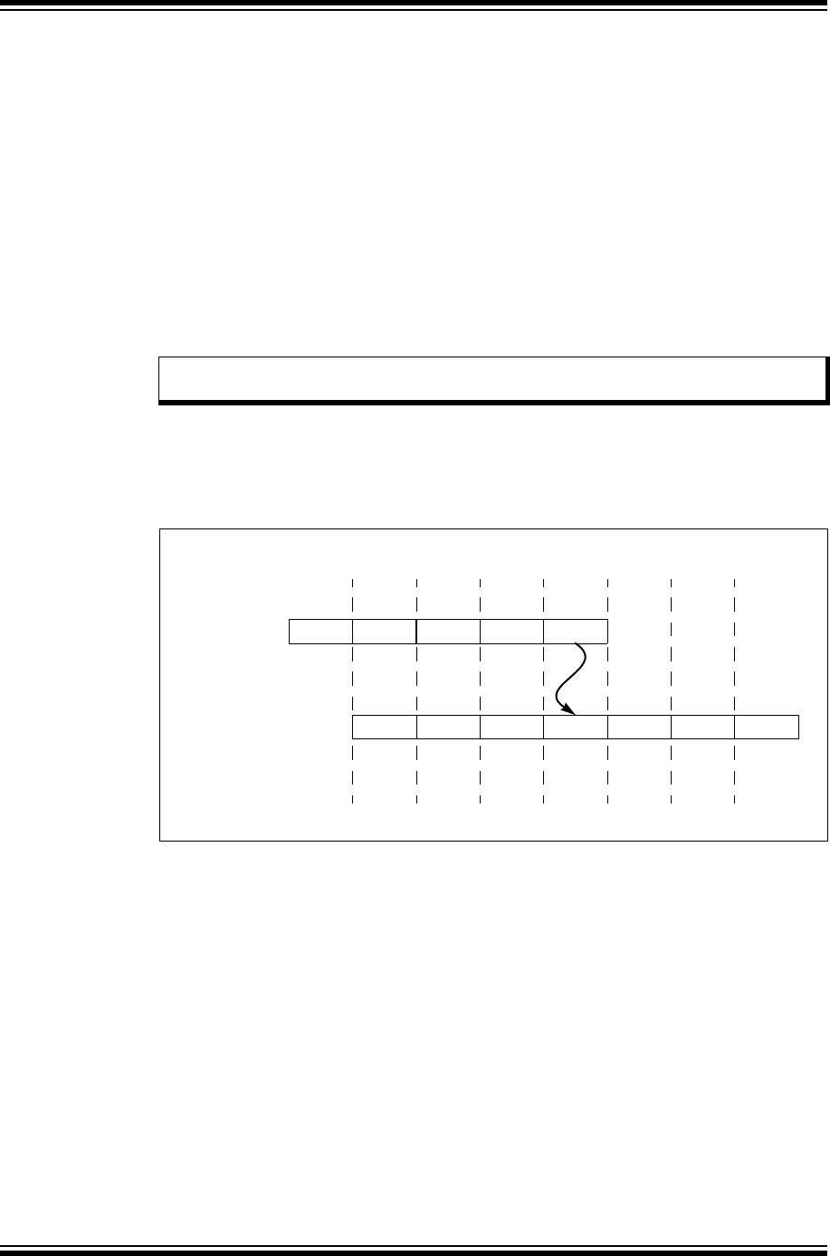
PIC32 Family Reference Manual
DS61192A-page 50-10 Preliminary © 2013 Microchip Technology Inc.
50.3.5 Pipeline Interlock Handling
Smooth pipeline flow is interrupted when an instruction in a pipeline stage cannot advance due
to a data dependency or a similar external condition. Pipeline interruptions are handled entirely
in hardware. These dependencies, are referred to as “interlocks”. At each cycle, interlock
conditions are checked for all active instructions. An instruction that depends on the result of a
previous instruction is an example of an interlock condition.
In general, MIPS processors support two types of hardware interlocks:
•Stalls – These interlocks are resolved by halting the entire pipeline. All instructions currently
executing in each pipeline stage are affected by a stall
•Slips – These interlocks allow one part of the pipeline to advance while another part of the
pipeline is held static
In the PIC32 processor core, all interlocks are handled as slips. These slips are minimized by
grabbing results from other pipeline stages by using a method called register bypassing, which
is described in 50.3.6 “Register Bypassing”.
As shown in Figure 50-5, the sub instruction has a source operand dependency on register r3
with the previous add instruction. The sub instruction slips by two clocks waiting until the result
of the add is written back to register r3. This slipping does not occur on the PIC32 family of
processors.
Figure 50-5: Pipeline Slip (If Bypassing Was Not Implemented)
Note: To il lu str ate th e conce pt o f a pip eli ne sli p, t he exa mp l e in Figure 50-5 shows would
happen if the PIC32 core did not implement register bypassing.
EIMW
ESLIPIMAWE
One
Cycle
One
Cycle
One
Cycle
One
Cycle
One
Cycle
One
Cycle
One
Cycle
One
Cycle
A
ESLIP
Add r3, r2, r1
(r3 r2 + r1
Sub r4, r3, r7
(r4 r3 – r7

© 2013 Microchip Technology Inc. Preliminary DS61192A-page 50-11
Section 50. CPU for Devices with microAptiv™ Core
CPU for Devices with
microAptiv™ Core
50
50.3.6 Register Bypassing
As mentioned previously, the PIC32 processor implements a mechanism called register bypass-
ing that helps reduce pipeline slips during execution. When an instruction is in the E stage of the
pipeline, the operands must be available for that instruction to continue. If an instruction has a
source operand that is computed from another instruction in the execution pipeline, register
bypassing allows a shortcut to get the source operands directly from the pipeline. An instruction
in the E stage can retrieve a source operand from another instruction that is executing in either
the M stage or the A stage of the pipeline. As seen in Figure 50-6, a sequence of three instruc-
tions with interdependencies does not slip at all during execution. This example uses both A to
E, and M to E register bypassing. Figure 50-7 shows the operation of a load instruction utilizing
A to E bypassing. Since the result of load instructions are not available until the A pipeline stage,
M to E bypassing is not needed.
The performance benefit of register bypassing is that instruction throughput is increased to the
rate of one instruction per clock for ALU operations, even in the presence of register
dependencies.
Figure 50-6: IU Pipeline M to E Bypass
Figure 50-7: IU Pipeline A to E Data Bypass
EIMW
EI WA
One
Cycle
One
Cycle
One
Cycle
One
Cycle
One
Cycle
One
Cycle
A
M
Add1
r3 = r2 + r1
Sub2
r4 = r3 – r7
Add3
r5 = r3 + r4EI AM
M to E Bypass A to E Bypass
M to E Bypass
EIMW
EI WA
One
Cycle
One
Cycle
One
Cycle
One
Cycle
One
Cycle
One
Cycle
A
M
Load Instruction
Consumer of Load Data Instruction EI AM
Data Bypass from A to E
One Clock
Load Delay

PIC32 Family Reference Manual
DS61192A-page 50-12 Preliminary © 2013 Microchip Technology Inc.
50.4 SPECIAL CONSIDERATIONS WHEN WRITING TO CP0 REGISTERS
In general, the PIC32 core ensures that instructions are executed following a fully sequential pro-
gram model. Each instruction in the program sees the results of the previous instruction. There
are some deviations to this model. These deviations are referred to as “hazards”.
In privileged software, there are two different types of hazards:
•Execution
• Instruction
50.4.1 Execution Hazards
Execution hazards are those created by the execution of one instruction, and seen by the
execution of another instruction. Tab le 50 -2 lists the execution hazards.
Table 50-2: Execution Hazards
50.4.2 Instruction Hazards
Instruction hazards are those created by the execution of one instruction, and seen by the
instruction fetch of another instruction. Ta ble 5 0-3 lists the instruction hazards.
Table 50-3: Instruction Hazards
Created by Seen by Hazard On Spacing
(Instructions)
LL MFC0 LLAddr 1
MTC0 Coprocessor instruction execution
depends on the new value of the CU0 bit
(Status<28>)
CU0 bit (Status<28>) 1
MTC0 ERET EPC, DEPC, ErrorEPC 1
MTC0, EI, DI Interrupted Instruction IE bit (Status<0>) 1
MTC0 Interrupted Instruction IP1 and IP0 bits (Cause<1> and <0>) 3
MTC0 TLBR, TLBWI, TLBWR EntryHi 1
MTC0 TLBP, Load/Store affected by new state ASID<7:0> bits (EntryHi<7:0>) 1
MTC0 TLBWI, TLBWR Index 1
MTC0 RDPGPR, WRPGPR PSS<3:0> bits (SRSCtl<9:6>) 1
MTC0 Instruction is not seeing a Core Timer
interrupt
Compare update that clears Core
Timer Interrupt
4
MTC0 Instruction affected by change Any other CP0 register 2
Created by Seen by Hazard On Spacing
(Instructions)
TLBWR, TLBWI Instruction fetch using new TLB entry TLB entry 3
MTC0 Instruction fetch seeing the new value
(including a change to ERL followed by
an instruction fetch from the useg
segment)
Status
MTCO Instruction fetch seeing the new value ASID<7:0> bits (Ent-
ryHi<7:0>)
3
MTC0 Instruction fetch seeing the new value WatchHi and
WatchLo
1
MTC0 Interrupted instruction IP1 and IP0 bits
(Cause<1> and <0>)
2
Instruction stream write via CACHE Instruction fetch seeing the new
instruction stream
Cache entries 3
Instruction stream write via store Instruction fetch seeing the new
instruction stream
Cache entries System
dependent

© 2013 Microchip Technology Inc. Preliminary DS61192A-page 50-13
Section 50. CPU for Devices with microAptiv™ Core
CPU for Devices with
microAptiv™ Core
50
50.5 ARCHITECTURE RELEASE 2 DETAILS
The PIC32 CPU utilizes Release 2 of the MIPS® 32-bit processor architecture, and implements
the following Release 2 features:
•Vectored interrupts using and external-to-core interrupt controller
Provide the ability to vector interrupts directly to a handler for that interrupt.
•Programmable exception vector base:
Allows the base address of the exception vectors to be moved for exceptions that occur
when StatusBEV is ‘0’. This allows any system to place the exception vectors in memory that
is appropriate to the system environment.
•Atomic interrupt enable/disable:
Two instructions have been added to atomically enable or disable interrupts, and return the
previous value of the Status register.
•The ability to disable the Count register for highly power-sensitive applications
• GPR shadow registers:
Provides the addition of GPR shadow registers and the ability to bind these registers to a
vectored interrupt or exception.
•Field, Rotate and Shuffle instructions:
Add additional capability in processing bit fields in registers.
•Explicit hazard management:
Provides a set of instructions to explicitly manage hazards, in place of the cycle-based
SSNOP method of dealing with hazards.
50.6 CPU BUS
The PIC32 devices use two different CPU bus architectures, depending on which CPU core is
implemented.
PIC32 devices based on the microAptiv™ MCU Microprocessor core have a split-bus
architecture, with two distinct busses to provide parallel instruction and data operations. Load
and store operations occur at the same time as instruction fetches. The two busses are known
as the I-side bus, which is used for feeding instructions into the CPU, and the D-side bus, which
is used for data transfers.
In the split-bus architecture, the CPU fetches instructions during the I-pipeline stage. A fetch is
issued to the I-side bus and is handled by the System Bus. Depending on the address, the
System Bus will do one of the following:
• Forward the fetch request to the Prefetch Cache unit (if available)
•Forward the fetch request to the DRM unit, or
•Cause an exception
Instruction fetches always use the I-side bus independent of the addresses being fetched.
The D-side bus processes all load and store operations executed by the CPU. When a load or
store instruction is executed the request is routed to the System Bus by the D-side bus. This
operation occurs during the M-pipeline stage and is routed to one of several targets:
•Data RAM
•Prefetch Cache/Flash memory
• Fast Peripheral Bus (Interrupt controller, DMA, Debug unit, USB, Ethernet, GPIO ports)
•General Peripheral Bus (UART, SPI, Flash Controller, EPMP/EPSP, TRCC Timers, Input
Capture, PWM/Output Compare, ADC, Dual Compare, I2C, Clock SIB, and Reset SIB)
PIC32 devices based on the microAptiv™ MPU core have a unified Data/Instruction bus
connected to the System Bus. This architecture uses a multi-layer System Bus to provide
multiple simultaneous data transactions between bus initiators and targets.
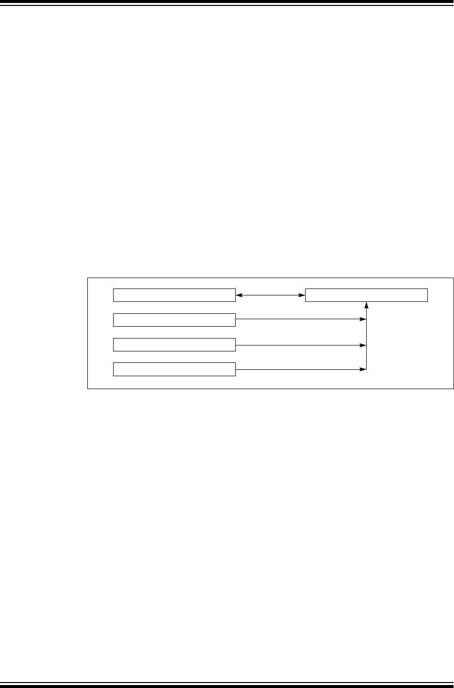
PIC32 Family Reference Manual
DS61192A-page 50-14 Preliminary © 2013 Microchip Technology Inc.
50.7 INTERNAL SYSTEM BUSSES
The internal busses of the PIC32 processor connect the peripherals to the System Bus. The
System Bus routes bus accesses from different initiators to a set of targets utilizing several data
paths throughout the device to help eliminate performance bottlenecks.
Some of the paths that the System Bus uses serve a dedicated purpose, while others are shared
between several targets.
The data RAM and Flash memory read paths are dedicated paths, allowing low-latency access
to the memory resources without being delayed by peripheral bus activity. The high-bandwidth
peripherals are placed on a high-speed bus. These include the Interrupt controller, Debug unit,
DMA engine, the USB Host/Peripheral unit, and other high-bandwidth peripherals (i.e., CAN,
Ethernet engines).
Peripherals that do not require high-bandwidth are located on a separate peripheral bus to save
power.
50.8 SET/CLEAR/INVERT
To provide single-cycle bit operations on peripherals, the registers in the peripheral units can be
accessed in three different ways depending on peripheral addresses. Each register has four dif-
ferent addresses. Although the four different addresses appear as different registers, they are
really just four different methods to address the same physical register.
Figure 50-8: Four Addresses for a Single Physical Register
The base register address provides normal Read/Write access, while the other three provide
special write-only functions.
• Normal access
•Set bit atomic RMW access
•Clear bit atomic RMW access
•Invert bit atomic RMW access
Peripheral reads must occur from the base address of each peripheral register. Reading from a
Set/Clear/Invert address has an undefined meaning, and may be different for each peripheral.
Writing to the base address writes an entire value to the peripheral register. All bits are written.
For example, assume a register contains 0xAAAA5555 before a write of 0x000000FF. After the
write, the register will contain 0x000000FF (assuming that all bits are R/W bits).
Writing to the Set address for any peripheral register causes only the bits written as ‘1’s to be set
in the destination register. For example, assume that a register contains 0xAAAA5555 before a
write of 0x000000FF to the set register address. After the write to the Set register address, the
value of the peripheral register will contain 0xAAAA55FF.
Writing to the Clear address for any peripheral register causes only the bits written as ‘1’s to be
cleared to ‘0’s in the destination register. For example, assume that a register contains
0xAAAA5555 before a write of 0x000000FF to the Clear register address. After the write to the
Clear register address, the value of the peripheral register will contain 0xAAAA5500.
Writing to the Invert address for any peripheral register causes only the bits written as ‘1’s to be
inverted, or toggled, in the destination register. For example, assume that a register contains
0xAAAA5555 before a write of 0x000000FF to the invert register address. After the write to the
Invert register, the value of the peripheral register will contain 0xAAAA55AA.
Peripheral RegisterRegister Address
Register Address + 4
Register Address + 8
Register Address + 12
Clear Bits
Set Bits
Invert Bits

© 2013 Microchip Technology Inc. Preliminary DS61192A-page 50-15
Section 50. CPU for Devices with microAptiv™ Core
CPU for Devices with
microAptiv™ Core
50
50.9 ALU STATUS BITS
Unlike most other PIC® microcontrollers, the PIC32 processor does not use Status register flags.
Condition flags are used on many processors to help perform decision making operations during
program execution. Flags are set based on the results of comparison operations or some arith-
metic operations. Conditional branch instructions on these machines then make decisions based
on the values of the single set of condition codes.
Instead, the PIC32 processor uses instructions that perform a comparison and stores a flag or
value into a General Purpose Register. A conditional branch is then executed with this general
purpose register used as an operand.
50.10 INTERRUPT AND EXCEPTION MECHANISM
The PIC32 family of processors implement an efficient and flexible interrupt and exception han-
dling mechanism. Interrupts and exceptions both behave similarly in that the current instruction
flow is changed temporarily to execute special procedures to handle an interrupt or exception.
The difference between the two is that interrupts are usually a result of normal operation, and
exceptions are a result of error conditions such as bus errors.
When an interrupt or exception occurs, the processor does the following:
1. The PC of the next instruction to execute after the handler returns is saved into a
coprocessor register.
2. The Cause register is updated to reflect the reason for exception or interrupt.
3. The Status register EXL or ERL bit is set to cause Kernel mode execution.
4. Handler PC is calculated from Ebase and OFFSET values.
5. Automated Interrupt Epilogue can save some of the COP0 state in the stack and
automatically update some of the COP0 registers in preparation for interrupt handling.
6. Processor starts execution from new PC.
This is a simplified overview of the interrupt and exception mechanism. Refer to the “CPU
Exceptions and Interrupt Controller” chapter in the specific device data sheet for details.
50.11 PROGRAMMING MODEL
The PIC32 family of processors is designed to be used with a high-level language such as the C
programming language. It supports several data types and uses simple but flexible addressing
modes needed for a high-level language. There are 32 General Purpose Registers and two
special registers for multiplying and dividing.
There are three different formats for the machine language instructions on the PIC32 processor:
•Immediate or I-type CPU instructions
• Jump or J-type CPU instructions, and
•Registered or R-type CPU instructions
Most operations are performed in registers. The register type CPU instructions have three
operands; two source operands and a destination operand.
Having three operands and a large register set allows assembly language programmers and
compilers to use the CPU resources efficiently. This creates faster and smaller programs by
allowing intermediate results to stay in registers rather than constantly moving data to and from
memory.
The immediate format instructions have an immediate operand, a source operand and a desti-
nation operand. The jump instructions have a 26-bit relative instruction offset field that is used to
calculate the jump destination.
Note: In this section, the terms “precise” and “imprecise” are used to describe exceptions.
A precise exception is one in which the EPC (CP0, Register 14, Select 0) can be
used to identify the instruction that caused the exception. For imprecise exceptions,
the instruction that caused the exception cannot be identified. Most exceptions are
precise. Bus error exceptions may be imprecise.

PIC32 Family Reference Manual
DS61192A-page 50-16 Preliminary © 2013 Microchip Technology Inc.
50.11.1 CPU Instruction Formats
A CPU instruction is a single 32-bit aligned word. The CPU instruction formats are:
•Immediate (see Figure 50-9)
• Jump (see Figure 50-10)
• Register (see Figure 50-11)
Tabl e 50- 4 describes the fields used in these instructions.
Table 50-4: CPU Instruction Format Fields
Figure 50-9: Immediate (I-Type) CPU Instruction Format
Figure 50-10: Jump (J-Type) CPU Instruction Format
Figure 50-11: Register (R-Type) CPU Instruction Format
50.11.2 CPU Registers
The PIC32 architecture defines the following CPU registers:
•Thirty-two 32-bit General Purpose Registers (GPRs)
•The standard MIPS32
® architecture defines one pair of HI/LO accumulator registers (AC0).
The microAptiv™ cores in PIC32 devices include the DSP ASE, which provides three addi-
tional pairs of HI/LO accumulator registers (AC1, AC2, and AC3). These registers improve
the parallelization of independent accumulation routines. DSP instructions that target the
accumulators use two instruction bits to specify the destination accumulator.
•A special purpose program counter (PC), which is affected only indirectly by certain
instructions; it is not an architecturally visible register.
Field Description
opcode 6-bit primary operation code.
rd 5-bit specifier for the destination register.
rs 5-bit specifier for the source register.
rt 5-bit specifier for the target (source/destination) register or used to specify
functions within the primary opcode REGIMM.
immediate 16-bit signed immediate used for logical operands, arithmetic signed operands,
load/store address byte offsets, and PC-relative branch signed instruction
displacement.
instr_index 26-bit index shifted left two bits to supply the low-order 28 bits of the jump
target address.
sa 5-bit shift amount.
function 6-bit function field used to specify functions within the primary opcode
SPECIAL.
31 26 25 21 20 16 15 0
opcode rs rt immediate
655 16
31 26 25 21 20 16 15 11 10 6 5 0
opcode instr_index
626
31 26 25 21 20 16 15 11 10 6 5 0
opcode rs rt rd sa function
655556

© 2013 Microchip Technology Inc. Preliminary DS61192A-page 50-17
Section 50. CPU for Devices with microAptiv™ Core
CPU for Devices with
microAptiv™ Core
50
50.11.2.1 CPU GENERAL PURPOSE REGISTERS
Two of the CPU General Purpose Registers have assigned functions:
• r0 – This register is hard-wired to a value of ‘0’, and can be used as the target register for
any instruction the result of which will be discarded. r0 can also be used as a source when
a ‘0’ value is needed.
• r31 – This is the destination register used by JAL, BLTZAL, BLTZALL, BGEZAL, and BGE-
ZALL, without being explicitly specified in the instruction word; otherwise, r31 is used as a
normal register.
The remaining registers are available for general purpose use.
50.11.2.2 REGISTER CONVENTIONS
Although most of the registers in the PIC32 architecture are designated as General Purpose Reg-
isters, as shown in Ta bl e 5 0-5 , there are some recommended uses of the registers for correct soft-
ware operation with high-level languages such as the Microchip MPLAB® XC32 C/C++ compiler.
Table 50-5: Register Conventions
50.11.2.3 CPU SPECIAL PURPOSE REGISTERS
The CPU contains these special purpose registers:
•PC – Program Counter register
•AC0 through AC3 – 64-bit Accumulator register pairs (HI/LO):
-HI/LO – Multiply and divide register pair (high and low result):
•During a multiply operation, the HI and LO registers store the product of integer multiply
•During a multiply-add or multiply-subtract operation, the HI and LO registers store the
result of the integer multiply-add or multiply-subtract
•During a division, the HI and LO registers store the quotient (in LO) and remainder (in
HI) of integer divide
•During a multiply-accumulate, the HI and LO registers store the accumulated result of
the operation
CPU
Register
Symbolic
Register Usage
r0 zero Always ‘0’ (see Note 1)
r1 at Assembler Temporary
r2 - r3 v0-v1 Function Return Values
r4 - r7 a0-a3 Function Arguments
r8 - r15 t0-t7 Temporary – Caller does not need to preserve contents
r16 - r23 s0-s7 Saved Temporary – Caller must preserve contents
r24 - r25 t8-t9 Temporary – Caller does not need to preserve contents
r26 - r27 k0-k1 Kernel temporary – Used for interrupt and exception handling
r28 gp Global Pointer – Used for fast-access common data
r29 sp Stack Pointer – Software stack
r30 s8 or fp Saved Temporary – Caller must preserve contents OR
Frame Pointer – Pointer to procedure frame on stack
r31 ra Return Address (see Note 1)
Note 1: Hardware enforced, not just convention.

PIC32 Family Reference Manual
DS61192A-page 50-18 Preliminary © 2013 Microchip Technology Inc.
Figure 50-12 shows the layout of the CPU registers.
Figure 50-12: CPU Registers
31 0 31 0
r0 (zero) HI (0)
r1 (at) LO (0)
r2 (v0) HI (1)
r3 (v1) LO (1)
r4 (a0) HI (2)
r5 (a1) LO (2)
r6 (a2) HI (3)
r7 (a3) LO (3)
r8 (t0)
r9 (t1)
r10 (t2)
r11 (t3)
r12 (t4)
r13 (t5)
r14 (t6)
r15 (t7)
r16 (s0)
r17 (s1)
r18 (s2)
r19 (s3)
r20 (s4)
r21 (s5)
r22 (s6)
r23 (s7)
r24 (t8)
r25 (t9)
r26 (k0)
r27 (k1)
r28 (gp)
r29 (sp)
r30 (s8 or fp) 31 0
r31 (ra) PC
General Purpose Registers Special Purpose Registers

© 2013 Microchip Technology Inc. Preliminary DS61192A-page 50-19
Section 50. CPU for Devices with microAptiv™ Core
CPU for Devices with
microAptiv™ Core
50
Table 50-6: microMIPS™ 16-bit Instruction Register Usage
Table 50-7: microMIPS™ Special Registers
16-bit
Register
Encoding
32-bit MIPS
Register
Encoding
Symbolic
Name Description
0 16/0 s0/zero General-purpose register
1 17 s1 General-purpose register
2 2 v0 General-purpose register
3 3 v1 General-purpose register
4 4 a0 General-purpose register
5 5 a1 General-purpose register
6 6 a2 General-purpose register
7 7 a3 General-purpose register
N/A 28 gp microMIPS™ implicitly referenced
General- pointer register
N/A 29 sp microMIPS implicitly referenced Stack
pointer register
N/A 31 ra microMIPS implicitly referenced Return
address register
Symbolic
Name Purpose
PC Program counter. The PC-relative instructions can access this register as an
operand.
HI Contains high-order word of multiply or divide result.
LO Contains low-order word of multiply or divide result.
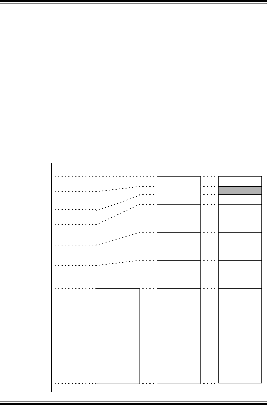
PIC32 Family Reference Manual
DS61192A-page 50-20 Preliminary © 2013 Microchip Technology Inc.
50.11.3 How to Implement Stack/MIPS Calling Conventions
The PIC32 CPU does not have hardware stacks. Instead, the processor relies on software to pro-
vide this functionality. Since the hardware does not perform stack operations itself, a convention
must exist for all software within a system to use the same mechanism. For example, a stack can
grow either toward lower addresses, or grow toward higher addresses. If one piece of software
assumes that the stack grows toward a lower address, and calls a routine that assumes that the
stack grows toward a higher address, the stack would become corrupted.
Using a system-wide calling convention prevents this problem from occurring. The Microchip
MPLAB® XC32 C/C++ compiler assumes the stack grows toward lower addresses.
50.11.4 Processor Modes
There are two operational modes and one special mode of execution in the PIC32 family CPUs:
User mode, Kernel mode and Debug mode. The processor starts execution in Kernel mode, and
if desired, can stay in Kernel mode for normal operation. User mode is an optional mode that
allows a system designer to partition code between privileged and unprivileged software. Debug
mode is normally only used by a debugger or monitor.
One of the main differences between the modes of operation is the memory addresses that soft-
ware is allowed to access. Peripherals are not accessible in User mode. Figure 50-13 shows the
different memory maps for each mode. For more information on the processor’s memory map,
see Section 3. “Memory Organization” (DS61115).
Figure 50-13: CPU Modes
useg kuseg kuseg
kseg0
kseg1
kseg2
kseg3
kseg2
kseg1
kseg0
kseg3
kseg3
dseg
User Mode Kernel Mode Debug ModeVirtual Address
0x7FFF_FFFF
0x8000_0000
0x9FFF_FFFF
0xBFFF_FFFF
0xDFFF_FFFF
0xFF1F_FFFF
0xFF3F_FFFF
0xFFFF_FFFF
0xA000_0000
0xC000_0000
0xE000_0000
0xFF20_0000
0xFF40_0000
0x0000_0000

© 2013 Microchip Technology Inc. Preliminary DS61192A-page 50-21
Section 50. CPU for Devices with microAptiv™ Core
CPU for Devices with
microAptiv™ Core
50
50.11.4.1 KERNEL MODE
To ac ces s ma ny o f t h e ha r dw a re res o ur c es , the processor must be operating in Kernel mode.
Kernel mode gives software access to the entire address space of the processor as well as
access to privileged instructions.
The processor operates in Kernel mode when the DM bit in the Debug register is ‘0’ and the Status
register contains one, or more, of the following values:
•UM = 0
•ERL = 1
•EXL = 1
When a non-debug exception is detected, EXL or ERL will be set and the processor will enter
Kernel mode. At the end of the exception handler routine, an Exception Return (ERET) instruction
is generally executed. The ERET instruction jumps to the Exception PC (EPC or ErrorPC
depending on the exception), clears ERL, and clears EXL if ERL= 0.
If UM = 1 the processor will return to User mode after returning from the exception when ERL
and EXL are cleared back to ‘0’.
50.11.4.2 USER MODE
When executing in User mode, software is restricted to use a subset of the processor’s
resources. In many cases it is desirable to keep application-level code running in User mode
where if an error occurs it can be contained and not be allowed to affect the Kernel mode code.
Applications can access Kernel mode functions through controlled interfaces such as the
SYSCALL mechanism.
As seen in Figure 50-13, User mode software has access to the USEG memory area.
To operate in User mode, the Status register must contain each the following bit values:
•UM = 1
•EXL = 0
•ERL = 0
50.11.4.3 DEBUG MODE
Debug mode is a special mode of the processor normally only used by debuggers and system
monitors. Debug mode is entered through a debug exception and has access to all Kernel mode
resources as well as special hardware resources used to debug applications.
The processor is in Debug mode when the DM bit in the Debug register is ‘1’.
Debug mode is normally exited by executing a DERET instruction from the debug handler.

PIC32 Family Reference Manual
DS61192A-page 50-22 Preliminary © 2013 Microchip Technology Inc.
50.12 COPROCESSOR 0 (CP0) REGISTERS
The PIC32 uses a special register interface to communicate status and control information
between system software and the CPU. This interface is called Coprocessor 0, or CP0. The
features of the CPU that are visible through Coprocessor 0 are:
•Translation Lookaside Buffer (TLB)
•Core timer
•Interrupt and exception control
•Virtual memory configuration
•Shadow register set control
•Processor identification
•Debugger control
• Performance counters
System software accesses the registers in CP0 using coprocessor instructions such as MFC0
and MTC0. Tabl e 50- 8 describes the CP0 registers found on PIC32 devices.
Table 50-8: CP0 Registers
Register
Number Register Name Function
0Index Index into the TLB array (microAptiv™ MPU only).
1Random Randomly generated index into the TLB array (microAptiv™ MPU only).
2EntryLo0 Low-order portion of the TLB entry for even-numbered virtual pages (microAptiv™
MPU only).
3EntryLo1 Low-order portion of the TLB entry for odd-numbered virtual pages (microAptiv™ MPU
only).
4Context/
UserLocal
Pointer to the page table entry in memory (microAptiv™ MPU only).
User information that can be written by privileged software and read via the RDHWR
instruction.
5PageMask/
PageGrain
PageMask controls the variable page sizes in TLB entries. PageGrain enables support
of 1 KB pages in the TLB (microAptiv™ MPU only).
6Wired Controls the number of fixed (i.e., wired) TLB entries (microAptiv™ MPU only).
7HWREna Enables access via the RDHWR instruction to selected hardware registers in
Non-privileged mode.
8BadVAddr Reports the address for the most recent address-related exception.
9 Count Processor cycle count.
10 EntryHi High-order portion of the TLB entry (microAptiv™ MPU only).
11 Compare Core timer interrupt control.
12 Status Processor status and control.
IntCtl Interrupt control of vector spacing.
SRSCtl Shadow register set control.
SRSMap Shadow register mapping control.
View_IPL Allows the Priority Level to be read/written without
extracting or inserting that bit from/to the Status register.
SRSMAP2 Contains two 4-bit fields that provide the mapping from a vector number to the shadow
set number to use when servicing such an interrupt.
13 Cause Describes the cause of the last exception.
NestedExc Contains the error and exception level status bit values that existed prior to the current
exception.
View_RIPL Enables read access to the RIPL bit that is available in the Cause register.
14 EPC Program counter at last exception.
NestedEPC Contains the exception program counter that existed prior to the current exception.

© 2013 Microchip Technology Inc. Preliminary DS61192A-page 50-23
Section 50. CPU for Devices with microAptiv™ Core
CPU for Devices with
microAptiv™ Core
50
15 PRID Processor identification and revision
Ebase Exception base address of exception vectors.
CDMMBase Common device memory map base.
16 Config Configuration register.
Config1 Configuration register 1.
Config2 Configuration register 2.
Config3 Configuration register 3.
Config4 Configuration register 4.
Config5 Configuration register 5.
Config7 Configuration register 7.
17 LLAddr Load link address (microAptiv™ MPU only).
18 WatchLo Low-order watchpoint address (microAptiv™ MPU only).
19 WatchHi High-order watchpoint address (microAptiv™ MPU only).
20-22 Reserved Reserved in the PIC32 core.
23 Debug EJTAG debug register.
TraceControl EJTAG trace control.
TraceControl2 EJTAG trace control 2.
UserTraceData1 EJTAG user trace data 1 register.
TraceBPC EJTAG trace breakpoint register.
Debug2 Debug control/exception status 1.
24 DEPC Program counter at last debug exception.
UserTraceData2 EJTAG user trace data 2 register.
25 PerfCtl0 Performance counter 0 control.
PerfCnt0 Performance counter 0.
PerfCtl1 Performance counter 1 control.
PerfCnt1 Performance counter 1.
26 ErrCtl Software test enable of way-select and data RAM arrays for I-Cache and D-Cache
(microAptiv™ MPU only).
27 Reserved Reserved in the PIC32 core.
28 TagLo/DataLo Low-order portion of cache tag interface (microAptiv™ MPU only).
29 Reserved Reserved in the PIC32 core.
30 ErrorEPC Program counter at last error.
31 DeSAVE Debug handler scratchpad register.
Table 50-8: CP0 Registers (Continued)
Register
Number Register Name Function

PIC32 Family Reference Manual
DS61192A-page 50-24 Preliminary © 2013 Microchip Technology Inc.
50.12.1 Index Register (CP0 Register 0, Select 0)
(microAptiv™ MPU only)
The Index register is a 32-bit read/write register that contains the index used to access the TLB
for TLBP, TLBR, and TLBWI instructions.
Register 50-1: Index; TLB Index Register; CP0 Register 0, Select 0
Bit
Range
Bit
31/23/15/7
Bit
30/22/14/6
Bit
29/21/13/5
Bit
28/20/12/4
Bit
27/19/11/3
Bit
26/18/10/2
Bit
25/17/9/1
Bit
24/16/8/0
31:24 R-x U-0 U-0 U-0 U-0 U-0 U-0 U-0
P — — — — — — —
23:16 U-0 U-0 U-0 U-0 U-0 U-0 U-0 U-0
— — — — — — — —
15:8 U-0 U-0 U-0 U-0 U-0 U-0 U-0 U-0
— — — — — — — —
7:0 U-0 U-0 U-0 R/W-x R/W-x R/W-x R/W-x R/W-x
— — —Index<4:0>
(1)
Legend:
R = Readable bit W = Writable bit U = Unimplemented bit, read as ‘0’
-n = Value at POR ‘1’ = Bit is set ‘0’ = Bit is cleared x = Bit is unknown
bit 31 P: Probe Failure Detect bit
1 = The previous TLBP instruction failed to find a match in the TLB
0 = The previous TLBP instruction found a match in the TLB
bit 30-5 Unimplemented: Read as ‘0’
bit 4-0 Index<4:0>: Index to TLB Entry Affected by the TLBR and TLBW Instructions bits(1)
11111 = TLB Entry 31
•
•
•
00000 = TLB Entry 0
Note 1: Depending on the configuration of the MMU, not all bits may be used. The number of TLB entries
supported by the MMU can be read from the MMU Size<5:0> field of the Config1 CP0 register.
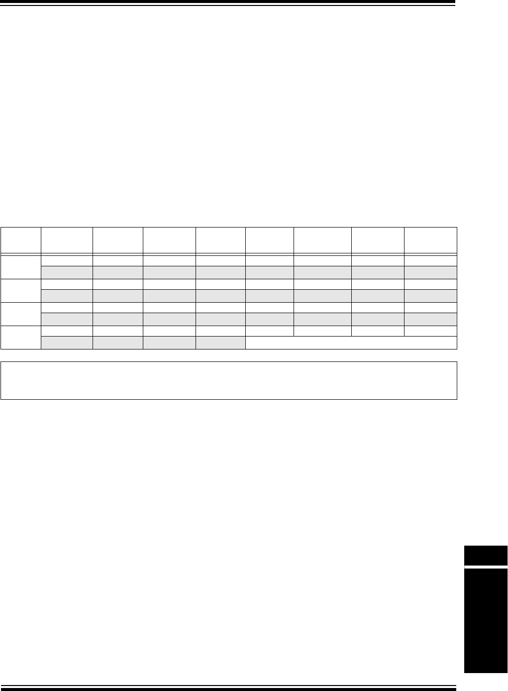
© 2013 Microchip Technology Inc. Preliminary DS61192A-page 50-25
Section 50. CPU for Devices with microAptiv™ Core
CPU for Devices with
microAptiv™ Core
50
50.12.2 Random Register (CP0 Register 1, Select 0)
(microAptiv™ MPU only)
The Random register is a read-only register whose value is used to index the TLB during a
TLBWR instruction.
The value of the register varies between an upper and lower bound as follows:
• A lower bound is set by the number of TLB entries reserved for exclusive use by the oper-
ating system (the contents of the Wired register). The entry indexed by the Wired register is
the first entry available to be written by a TLB Write Random operation.
• An upper bound is set by the total number of TLB entries minus 1
The Random register is decremented by one almost every clock, wrapping after the value in the
Wired register is reached. To enhance the level of randomness and reduce the possibility of a
live lock condition, an LFSR register is used that prevents the decrement pseudo-randomly.
The processor initializes the Random register to the upper bound on a Reset exception and when
the Wired register is written.
Register 50-2: Random; Random Field Register; CP0 Register 1, Select 0
Bit
Range
Bit
31/23/15/7
Bit
30/22/14/6
Bit
29/21/13/5
Bit
28/20/12/4
Bit
27/19/11/3
Bit
26/18/10/2
Bit
25/17/9/1
Bit
24/16/8/0
31:24 U-0 U-0 U-0 U-0 U-0 U-0 U-0 U-0
— — — — — — — —
23:16 U-0 U-0 U-0 U-0 U-0 U-0 U-0 U-0
— — — — — — — —
15:8 U-0 U-0 U-0 U-0 U-0 U-0 U-0 U-0
— — — — — — — —
15:8 U-0 U-0 U-0 U-0 R-1 R-1 R-1 R-1
— — — —Random<3:0>
Legend:
R = Readable bit W = Writable bit U = Unimplemented bit, read as ‘0’
-n = Value at POR ‘1’ = Bit is set ‘0’ = Bit is cleared x = Bit is unknown
bit 31-4 Unimplemented: Read as ‘0’
bit 3-0 Random<3:0>: TLB Random Index bits

PIC32 Family Reference Manual
DS61192A-page 50-26 Preliminary © 2013 Microchip Technology Inc.
50.12.3 EntryLo0 Register (CP0 Register 2, Select 0) and
EntryLo1 Register (CP0 Register 3, Select 0)
(microAptiv™ MPU only)
The pair of EntryLo registers act as the interface between the TLB and the TLBR, TLBWI, and
TLBWR instructions. EntryLo0 holds the entries for even pages and EntryLo1 holds the entries for
odd pages.
The contents of the EntryLo0 and EntryLo1 registers are undefined after an address error, TLB
invalid, TLB modified, or TLB refill exception.
Register 50-3: EntryLo0; Even Page TLB Entries Register; CP0 Register 2, Select 0 and
EntryLo1; Odd Page TLB Entries Register; CP0 Register 3, Select 0
Bit
Range
Bit
31/23/15/7
Bit
30/22/14/6
Bit
29/21/13/5
Bit
28/20/12/4
Bit
27/19/11/3
Bit
26/18/10/2
Bit
25/17/9/1
Bit
24/16/8/0
31:24 R/W-0 R/W-0 U-0 U-0 U-0 U-0 R/W-x R/W-x
RI XI — — — —PFN<19:18>
23:16 R/W-x R/W-x R/W-x R/W-x R/W-x R/W-x R/W-x R/W-x
PFN<17:10>
15:8 R/W-x R/W-x R/W-x R/W-x R/W-x R/W-x R/W-x R/W-x
PFN<9:2>
7:0 R/W-x R/W-x R/W-x R/W-x R/W-x R/W-x R/W-x R/W-x
PFN<1:0> C<2:0> D V G
Legend:
R = Readable bit W = Writable bit U = Unimplemented bit, read as ‘0’
-n = Value at POR ‘1’ = Bit is set ‘0’ = Bit is cleared x = Bit is unknown
bit 31 RI: Read Inhibit bit
If this bit is set, an attempt to read data from the page causes a TLB Invalid exception, even if the V
(Valid) bit is set. The RI bit is enabled only if the RIE bit of the PageGrain register is set. If the RIE bit of
PageGrain is not set, the RI bit of EntryLo0/EntryLo1 is a reserved 0 bit as per the MIPS32® specification.
bit 30 XI: Execute Inhibit bit
If this bit is set, an attempt to fetch from the page causes a TLB Invalid exception, even if the V (Valid) bit is
set. The XI bit is enabled only if the XIE bit of the PageGrain register is set. If the XIE bit of PageGrain is not
set, the XI bit of EntryLo0/EntryLo1 is a reserved 0 bit as per the MIPS32® specification.
bit 29-26 Unimplemented: Read as ‘0’
bit 25-6 PFN<19:0>: Page Frame Number bits
Contributes to the definition of the high-order bits of the physical address.
The PFN<19:0> bits correspond to bits <31:12> of the physical address.
bit 5-3 C<2:0>: Coherency Page Attribute bits
111 = Reserved
110 = Reserved
101 = Reserved
100 = Reserved
011 = Cacheable, non-coherent, write-back, write allocate
010 = Uncached
001 = Cacheable, non-coherent, write-through, write allocate
000 = Cacheable, non-coherent, write-through, no write allocate
bit 2 D: Dirty (write-enable) bit
1 = Stores to the page are permitted
0 = Stores to the page cause a TLB modified exception
bit 1 V: Valid bit
1 = Accesses to the page are permitted
0 = Accesses to the page cause a TLB invalid exception
bit 0 G: Global bit
On a TLB write, the logical AND of the G bits in both the EntryLo0 and EntryLo1 register becomes the G bit
in the TLB entry. If the TLB entry G bit is a ‘1’, the ASID comparisons are ignored during TLB matches. On
a read from a TLB entry, the G bits of both EntryLo0 and EntryLo1 reflect the state of the TLB G bit.

© 2013 Microchip Technology Inc. Preliminary DS61192A-page 50-27
Section 50. CPU for Devices with microAptiv™ Core
CPU for Devices with
microAptiv™ Core
50
50.12.4 Context Register (CP0 Register 4, Select 0)
(microAptiv™ MPU Only)
The Context register is a read/write register containing a pointer to an entry in the page table
entry (PTE) array. This array is an operating system data structure that stores virtual-to-physical
translations. During a TLB miss, the operating system loads the TLB with the missing translation
from the PTE array. The Context register duplicates some of the information provided in the
BadVAddr register but is organized in such a way that the operating system can directly
reference an 8-byte page table entry (PTE) in memory.
Register 50-4: Context: Context Register; CP0 Register 4, Select 0
Bit
Range
Bit
31/23/15/7
Bit
30/22/14/6
Bit
29/21/13/5
Bit
28/20/12/4
Bit
27/19/11/3
Bit
26/18/10/2
Bit
25/17/9/1
Bit
24/16/8/0
31:24 R/W-x R/W-x R/W-x R/W-x R/W-x R/W-x R/W-x R/W-x
PTEBase<8:1>
23:16 R/W-x R-x R-x R-x R-x R-x R-x R-x
PTEBase<0> BadVPN2<19:13>
15:8 R-x R-x R-x R-x R-x R-x R-x R-x
BadVPN2<12:5>
7:0 R-x R-x R-x R-x R-x U-0 U-0 U-0
BadVPN2<4:0> — — —
Legend:
R = Readable bit W = Writable bit U = Unimplemented bit, read as ‘0’
-n = Value at POR ‘1’ = Bit is set ‘0’ = Bit is cleared x = Bit is unknown
bit 31-23 PTEBase<8:0>: Context Register PTE Array Pointer bits
These bits are for use by the operating system and are normally written with a value that allows the
operating system to use the Context register as a pointer into the current PTE array in memory.
bit 22-4 BadVPN2<12:0>: TLB Hardware Miss Status bits
These bits contain the value of bits VA<31:13> of the virtual address that was missed.
bit 3-0 Unimplemented: Read as ‘0’

PIC32 Family Reference Manual
DS61192A-page 50-28 Preliminary © 2013 Microchip Technology Inc.
50.12.5 UserLocal Register (CP0 Register 4, Select 2)
The UserLocal register is a read-write register that is not interpreted by hardware and is
conditionally readable via the RDHWR instruction.
Privileged software may write this register with arbitrary information and make it accessible to
unprivileged software via register 29 (ULR) of the RDHWR instruction. To do so, the URL bit
(HWREna<29>) must be set to a ‘1’ to enable unprivileged access to the register.
In some operating environments, the UserLocal register contains a pointer to a thread-specific
storage block that is obtained via the RDHWR register.
Register 50-5: UserLocal: User Local Register; CP0 Register 4, Select 2
Bit
Range
Bit
31/23/15/7
Bit
30/22/14/6
Bit
29/21/13/5
Bit
28/20/12/4
Bit
27/19/11/3
Bit
26/18/10/2
Bit
25/17/9/1
Bit
24/16/8/0
31:24 R/W-x R/W-x R/W-x R/W-x R/W-x R/W-x R/W-x R/W-x
USERLOCAL<31:24>
23:16 R/W-x R/W-x R/W-x R/W-x R/W-x R/W-x R/W-x R/W-x
USERLOCAL<23:16>
15:8 R/W-x R/W-x R/W-x R/W-x R/W-x R/W-x R/W-x R/W-x
USERLOCAL<15:8>
7:0 R/W-x R/W-x R/W-x R/W-x R/W-x R/W-x R/W-x R/W-x
USERLOCAL<7:0>
Legend:
R = Readable bit W = Writable bit U = Unimplemented bit, read as ‘0’
-n = Value at POR ‘1’ = Bit is set ‘0’ = Bit is cleared x = Bit is unknown
bit 31-0 USERLOCAL<31:0>: User Local bits

© 2013 Microchip Technology Inc. Preliminary DS61192A-page 50-29
Section 50. CPU for Devices with microAptiv™ Core
CPU for Devices with
microAptiv™ Core
50
50.12.6 PageMask Register (CP0 Register 5, Select 0)
(microAptiv™ MPU only)
The PageMask register is a read/write register used for reading from and writing to the TLB. It
holds a comparison mask that sets the variable page size for each TLB entry, as shown in
Tabl e 50- 9.
Table 50-9: Values for the Mask bits of the PageMask Register
Register 50-6: PageMask; TLB Variable Page Size Register; CP0 Register 5, Select 0
Bit
Range
Bit
31/23/15/7
Bit
30/22/14/6
Bit
29/21/13/5
Bit
28/20/12/4
Bit
27/19/11/3
Bit
26/18/10/2
Bit
25/17/9/1
Bit
24/16/8/0
31:24 U-0 U-0 U-0 R/W-x R/W-x R/W-x R/W-x R/W-x
— — — Mask<15:11>
23:16 R/W-x R/W-x R/W-x R/W-x R/W-x R/W-x R/W-x R/W-x
Mask<10:3>
15:8 R/W-x R/W-x R/W-x U-0 U-0 U-0 U-0 U-0
Mask<2:0> — — — — —
7:0 U-0 U-0 U-0 U-0 U-0 U-0 U-0 U-0
— — — — — — — —
Legend:
R = Readable bit W = Writable bit U = Unimplemented bit, read as ‘0’
-n = Value at POR ‘1’ = Bit is set ‘0’ = Bit is cleared x = Bit is unknown
bit 31-29 Unimplemented: Read as ‘0’
bit 28-13 Mask<15:0>: Virtual Address Mask bits
When this bit is a ‘1’, this indicates that the corresponding bit of the virtual address should not participate in
the TLB match.
bit 12-0 Unimplemented: Read as ‘0’
Page
Size
Register Bit Location
28 27 26 25 24 23 22 21 20 19 18 17 16 15 14 13
4 KB 0000000000000000
16 KB 0000000000000011
64 KB 0000000000001111
256 KB 0000000000111111
1 MB 0000000011111111
4 MB 0000001111111111
16 MB 0000111111111111
64 MB 0011111111111111
256 MB 1111111111111111

PIC32 Family Reference Manual
DS61192A-page 50-30 Preliminary © 2013 Microchip Technology Inc.
50.12.7 PageGrain Register (CP0 Register 5, Select 1)
(microAptiv™ MPU only)
The PageGrain register is used on the PIC32 device to enable or disable the read and execute
inhibit bits in the EntryLo0 and EntryLo1 registers.
Register 50-7: PageGrain; TLB Page Grain Enable Register; CP0 Register 5, Select 1
Bit
Range
Bit
31/23/15/7
Bit
30/22/14/6
Bit
29/21/13/5
Bit
28/20/12/4
Bit
27/19/11/3
Bit
26/18/10/2
Bit
25/17/9/1
Bit
24/16/8/0
31:24 R/W-0 R/W-0 U-0 U-0 R/W-0 U-0 U-0 U-0
RIE XIE — — IEC — — —
23:16 U-0 U-0 U-0 U-0 U-0 U-0 U-0 U-0
— — — — — — — —
15:8 U-0 U-0 U-0 U-0 U-0 U-0 U-0 U-0
— — — — — — — —
7:0 U-0 U-0 U-0 U-0 U-0 U-0 U-0 U-0
— — — — — — — —
Legend:
R = Readable bit W = Writable bit U = Unimplemented bit, read as ‘0’
-n = Value at POR ‘1’ = Bit is set ‘0’ = Bit is cleared x = Bit is unknown
bit 31 RIE: Read Inhibit Enable bit
1 = RI bit of EntryLo0 and EntryLo1 registers is enabled
0 = RI bit of EntryLo0 and EntryLo1 registers is disabled and is not writable
bit 30 XIE: Execute Inhibit Enable bit
1 = XI bit of EntryLo0 and EntryLo1 registers is enabled
0 = XI bit of EntryLo0 and EntryLo1 registers is disabled and is not writable
bit 29-28 Unimplemented: Must be written as ‘0’; returns ‘0’ on a read
bit 27 IEC: Enable Read-Inhibit and Execute-Inhibit Exception Codes bit
1 = Read-Inhibit exceptions use the TLBRI exception code. Execute-Inhibit exceptions use the
TLBXI exception code
0 = Read-Inhibit and Execute-Inhibit exceptions both use the TLBL exception code
bit 26-0 Unimplemented: Must be written as ‘0’; returns ‘0’ on a read

© 2013 Microchip Technology Inc. Preliminary DS61192A-page 50-31
Section 50. CPU for Devices with microAptiv™ Core
CPU for Devices with
microAptiv™ Core
50
50.12.8 Wired Register (CP0 Register 6, Select 0)
(microAptiv™ MPU Only)
The Wired register is a read/write register that specifies the boundary between the wired and
random entries in the TLB. The width of the Wired field is calculated in the same manner as that
described for the Index register. Wired entries are fixed, non-replaceable entries that are not
overwritten by a TLBWR instruction. Wired entries can be overwritten by a TLBWI instruction.
The Wired register is reset to zero by a Reset exception. Writing the Wired register causes the
Random register to reset to its upper bound.
Register 50-8: Wired; TLB Boundary Entries Register; CP0 Register 6, Select 0
Bit
Range
Bit
31/23/15/7
Bit
30/22/14/6
Bit
29/21/13/5
Bit
28/20/12/4
Bit
27/19/11/3
Bit
26/18/10/2
Bit
25/17/9/1
Bit
24/16/8/0
31:24 U-0 U-0 U-0 U-0 U-0 U-0 U-0 U-0
— — — — — — — —
23:16 U-0 U-0 U-0 U-0 U-0 U-0 U-0 U-0
— — — — — — — —
15:8 U-0 U-0 U-0 U-0 U-0 U-0 U-0 U-0
— — — — — — — —
7:0 U-0 U-0 U-0 R/W-0 R/W-0 R/W-0 R/W-0 R/W-0
— — — Wired<4:0>(1)
Legend:
R = Readable bit W = Writable bit U = Unimplemented bit, read as ‘0’
-n = Value at POR ‘1’ = Bit is set ‘0’ = Bit is cleared x = Bit is unknown
bit 31-5 Unimplemented: Read as ‘0’
bit 4-0 Wired<4:0>: TLB Wired Boundary bits(1)
11111 = Entry 31 is random, entries 0-30 are wired
•
•
•
01111 = Entry 15 is random, entries 0-14 are wired
•
•
•
00111 = Entries 7 and above are random, below 7 are wired
•
•
•
00000 = All 16 entries are random
Note 1: Depending on the configuration of the MMU, not all bits may be used. The number of TLB entries
supported by the MMU can be read from the MMU Size<5:0> field of the Config1 CP0 register.

PIC32 Family Reference Manual
DS61192A-page 50-32 Preliminary © 2013 Microchip Technology Inc.
50.12.9 HWREna Register (CP0 Register 7, Select 0)
The HWREna register contains a bit mask that determines which hardware registers are
accessible via the RDHWR instruction.
Register 50-9: HWREna: Hardware Accessibility Register; CP0 Register 7, Select 0
Bit
Range
Bit
31/23/15/7
Bit
30/22/14/6
Bit
29/21/13/5
Bit
28/20/12/4
Bit
27/19/11/3
Bit
26/18/10/2
Bit
25/17/9/1
Bit
24/16/8/0
31:24 U-0 U-0 R/W-0 U-0 U-0 U-0 U-0 U-0
——ULR— — — — —
23:16 U-0 U-0 U-0 U-0 U-0 U-0 U-0 U-0
— — — — — — — —
15:8 U-0 U-0 U-0 U-0 U-0 U-0 U-0 U-0
— — — — — — — —
7:0 U-0 U-0 U-0 U-0 R/W-0 R/W-0 R/W-0 R/W-0
— — — —MASK<3:0>
Legend:
R = Readable bit W = Writable bit U = Unimplemented bit, read as ‘0’
-n = Value at POR ‘1’ = Bit is set ‘0’ = Bit is cleared x = Bit is unknown
bit 31-30 Unimplemented: Read as ‘0’
bit 29 ULR: User Local Register bit
1 = Enable unprivileged access to UserLocal register
0 = Disable unprivileged access to UserLocal register
This bit provides read access to the Coprocessor 0 UserLocal register.
bit 28-4 Unimplemented: Read as ‘0’
bit 3-0 MASK<3:0>: Bit Mask bits
1 = Access is enabled to corresponding hardware register
0 = Access is disabled
Each of these bits enables access by the RDHWR instruction to a particular hardware register (which may not
be an actual register). See the RDHWR instruction for a list of valid hardware registers.

© 2013 Microchip Technology Inc. Preliminary DS61192A-page 50-33
Section 50. CPU for Devices with microAptiv™ Core
CPU for Devices with
microAptiv™ Core
50
50.12.10 BadVAddr Register (CP0 Register 8, Select 0)
BadVAddr is a read-only register that captures the most recent virtual address that caused an
address error exception. Address errors are caused by executing load, store, or fetch operations
from unaligned addresses, or by trying to access Kernel mode addresses from User mode.
For devices with the microAptiv™ MPU core, the BadVAddr register will also capture the most
recent virtual address that caused a TLB refill, TLB invalid, or TLB modified exception.
BadVAddr does not capture address information for bus errors, because they are not addressing
errors.
Register 50-10: BadVAddr: Bad Virtual Address Register; CP0 Register 8, Select 0
Bit
Range
Bit
31/23/15/7
Bit
30/22/14/6
Bit
29/21/13/5
Bit
28/20/12/4
Bit
27/19/11/3
Bit
26/18/10/2
Bit
25/17/9/1
Bit
24/16/8/0
31:24 R-x R-x R-x R-x R-x R-x R-x R-x
BadVAddr<31:24>
23:16 R-x R-x R-x R-x R-x R-x R-x R-x
BadVAddr<23:16>
15:8 R-x R-x R-x R-x R-x R-x R-x R-x
BadVAddr<15:8>
7:0 R-x R-x R-x R-x R-x R-x R-x R-x
BadVAddr<7:0>
Legend:
R = Readable bit W = Writable bit U = Unimplemented bit, read as ‘0’
-n = Value at POR ‘1’ = Bit is set ‘0’ = Bit is cleared x = Bit is unknown
bit 31-0 BadVAddr<31:0>: Bad Virtual Address bits
Captures the virtual address that caused the most recent address error exception.

PIC32 Family Reference Manual
DS61192A-page 50-34 Preliminary © 2013 Microchip Technology Inc.
50.12.11 Count Register (CP0 Register 9, Select 0)
The Count register acts as a timer, incrementing at a constant rate, whether or not an instruction
is executed, retired, or any forward progress is made through the pipeline. The counter
increments every other clock, if the DC bit in the Cause register is ‘0’.
Count can be written for functional or diagnostic purposes, including at Reset or to synchronize
processors.
By writing the COUNTDM bit in the Debug register, it is possible to control whether Count
continues to increment while the processor is in Debug mode.
Register 50-11: Count: Interval Counter Register; CP0 Register 9, Select 0
Bit
Range
Bit
31/23/15/7
Bit
30/22/14/6
Bit
29/21/13/5
Bit
28/20/12/4
Bit
27/19/11/3
Bit
26/18/10/2
Bit
25/17/9/1
Bit
24/16/8/0
31:24 R/W-x R/W-x R/W-x R/W-x R/W-x R/W-x R/W-x R/W-x
COUNT<31:24>
23:16 R/W-x R/W-x R/W-x R/W-x R/W-x R/W-x R/W-x R/W-x
COUNT<23:16>
15:8 R/W-x R/W-x R/W-x R/W-x R/W-x R/W-x R/W-x R/W-x
COUNT<15:8>
7:0 R/W-x R/W-x R/W-x R/W-x R/W-x R/W-x R/W-x R/W-x
COUNT<7:0>
Legend:
R = Readable bit W = Writable bit U = Unimplemented bit, read as ‘0’
-n = Value at POR ‘1’ = Bit is set ‘0’ = Bit is cleared x = Bit is unknown
bit 31-0 COUNT<31:0>: Interval Counter bits
This value is incremented every other clock cycle.
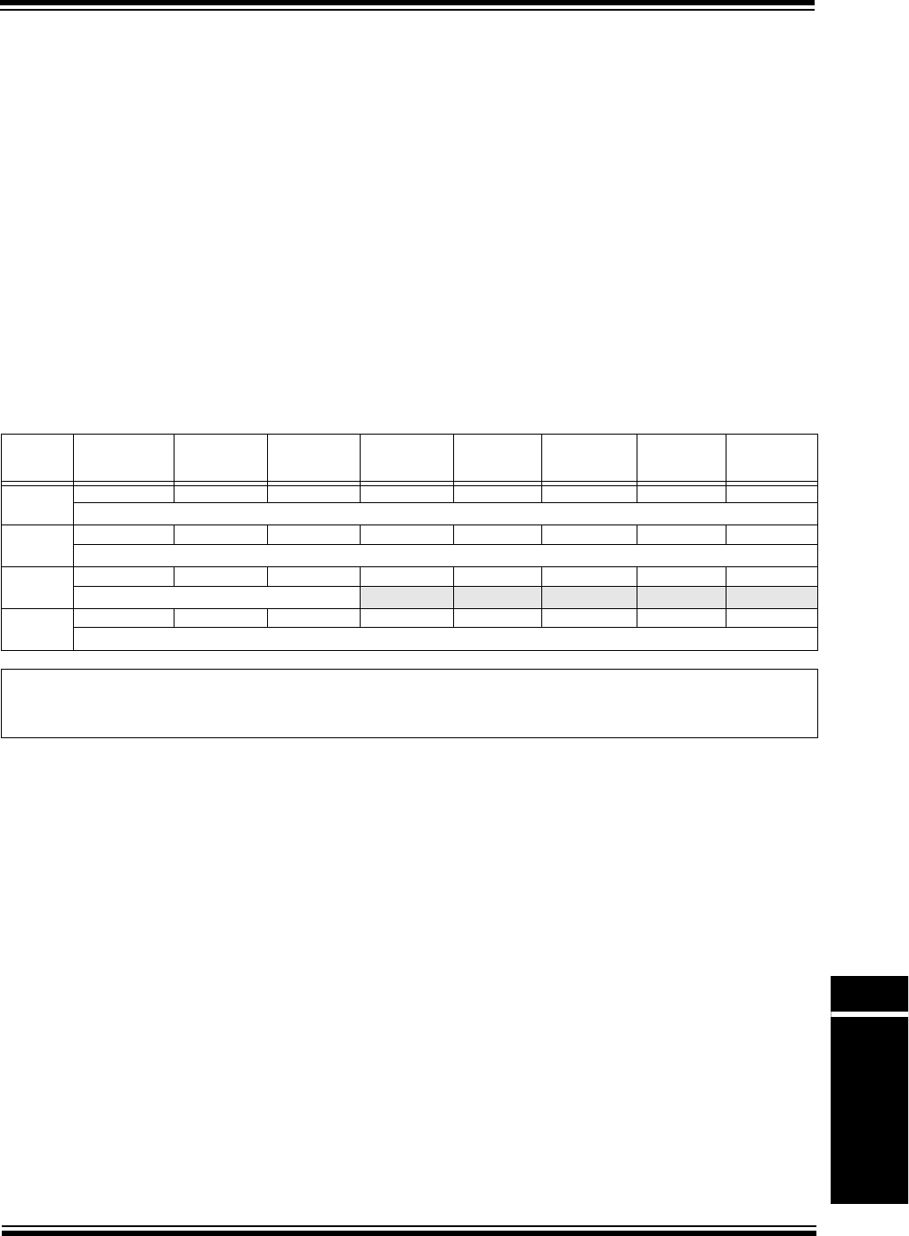
© 2013 Microchip Technology Inc. Preliminary DS61192A-page 50-35
Section 50. CPU for Devices with microAptiv™ Core
CPU for Devices with
microAptiv™ Core
50
50.12.12 EntryHi Register (CP0 Register 10, Select 0)
(microAptiv™ MPU only)
The EntryHi register contains the virtual address match information used for TLB read, write, and
access operations.
A TLB exception (TLB Refill, TLB Invalid, or TLB Modified) causes bits VA31...13 of the virtual
address to be written into the VPN2 field of the EntryHi register. A TLBR instruction writes the
EntryHi register with the corresponding fields from the selected TLB entry. The ASID field is
written by software with the current address space identifier value and is used during the TLB
comparison process to determine TLB match.
Because the ASID field is overwritten by a TLBR instruction, software must save and restore the
value of ASID around use of the TLBR. This is especially important in TLB Invalid and TLB
Modified exceptions, and in other memory management software.
The VPN2 field of the EntryHi register is not defined after an address error exception, and may
be modified by hardware during the address error exception sequence. Software writes of the
EntryHi register (via MTC0) do not cause the implicit write of address-related fields in the
BadVAddr or Context registers.
Register 50-12: EntryHi: TLB Address Match Register; CP0 Register 10, Select 0
Bit
Range
Bit
31/23/15/7
Bit
30/22/14/6
Bit
29/21/13/5
Bit
28/20/12/4
Bit
27/19/11/3
Bit
26/18/10/2
Bit
25/17/9/1
Bit
24/16/8/0
31:24 R/W-x R/W-x R/W-x R/W-x R/W-x R/W-x R/W-x R/W-x
VPN2<18:11>
23:16 R/W-x R/W-x R/W-x R/W-x R/W-x R/W-x R/W-x R/W-x
VPN2<10:3>
15:8 R/W-x R/W-x R/W-x U-0 U-0 U-0 U-0 U-0
VPN2<2:0> — — — — —
7:0 R/W-x R/W-x R/W-x R/W-x R/W-x R/W-x R/W-x R/W-x
ASID<7:0>
Legend:
R = Readable bit W = Writable bit U = Unimplemented bit, read as ‘0’
-n = Value at POR ‘1’ = Bit is set ‘0’ = Bit is cleared x = Bit is unknown
bit 31-13 VPN2: Virtual Page Number bits
These bits are written by hardware on a TLB exception or on a TLB read, and are written by software before
a TLB write.
bit 12-8 Unimplemented: Read as ‘0’
bit 7-0 ASID<7:0>: Address Space Identifier bits
These bits are written by hardware on a TLB read and by software to establish the current ASID value for a
TLB write and against which TLB references match each entry’s TLB ASID field.

PIC32 Family Reference Manual
DS61192A-page 50-36 Preliminary © 2013 Microchip Technology Inc.
50.12.13 Compare Register (CP0 Register 11, Select 0)
The Compare register acts in conjunction with the Count register to implement a timer and timer
interrupt function. Compare maintains a stable value and does not change on its own.
When the value of Count equals the value of Compare, the CPU asserts an interrupt signal to the
system interrupt controller. This signal will remain asserted until Compare is written.
Register 50-13: Compare: Interval Count Compare Register; CP0 Register 11, Select 0
Bit
Range
Bit
31/23/15/7
Bit
30/22/14/6
Bit
29/21/13/5
Bit
28/20/12/4
Bit
27/19/11/3
Bit
26/18/10/2
Bit
25/17/9/1
Bit
24/16/8/0
31:24 R/W-x R/W-x R/W-x R/W-x R/W-x R/W-x R/W-x R/W-x
COMPARE<31:24>
23:16 R/W-x R/W-x R/W-x R/W-x R/W-x R/W-x R/W-x R/W-x
COMPARE<23:16>
15:8 R/W-x R/W-x R/W-x R/W-x R/W-x R/W-x R/W-x R/W-x
COMPARE<15:8>
7:0 R/W-x R/W-x R/W-x R/W-x R/W-x R/W-x R/W-x R/W-x
COMPARE<7:0>
Legend:
R = Readable bit W = Writable bit U = Unimplemented bit, read as ‘0’
-n = Value at POR ‘1’ = Bit is set ‘0’ = Bit is cleared x = Bit is unknown
bit 31-0 COMPARE<31:0>: Interval Count Compare Value bits
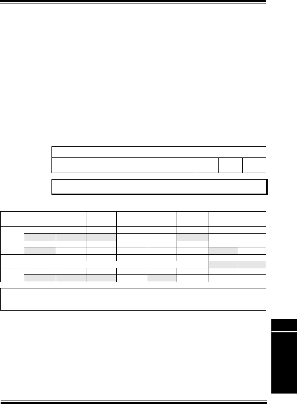
© 2013 Microchip Technology Inc. Preliminary DS61192A-page 50-37
Section 50. CPU for Devices with microAptiv™ Core
CPU for Devices with
microAptiv™ Core
50
50.12.14 Status Register (CP0 Register 12, Select 0)
The read/write Status register contains the operating mode, interrupt enabling, and the diagnostic
states of the processor. The bits of this register combine to create operating modes for the processor.
50.12.14.1 INTERRUPT ENABLE
Interrupts are enabled when all of the following conditions are true:
•IE = 1
•EXL = 0
•ERL = 0
•DM = 0
If these conditions are met, the settings of the IPL bits enable the interrupts.
50.12.14.2 OPERATING MODES
If the DM bit in the Debug register is ‘1’, the processor is in Debug mode; otherwise, the
processor is in either Kernel mode or User mode.
The CPU Status register bit settings shown in Ta b l e 5 0 - 10 determine User or Kernel mode:
Table 50-10: CPU Status Register Bits That Determine Processor Mode
Mode Bit/Setting
User (requires all of the following bits and values) UM = 1EXL = 0ERL = 0
Kernel (requires one or more of the following bit values) UM = 0EXL = 1ERL = 1
Note: The Status register CU0 bit (Status<28>) controls Coprocessor 0 accessibility. If
Coprocessor 0 is unusable, an instruction that accesses it generates an exception.
Register 50-14: Status: Status Register; CP0 Register 12, Select 0
Bit
Range
Bit
31/23/15/7
Bit
30/22/14/6
Bit
29/21/13/5
Bit
28/20/12/4
Bit
27/19/11/3
Bit
26/18/10/2
Bit
25/17/9/1
Bit
24/16/8/0
31:24 U-0 U-0 U-0 R/W-x R/W-0 U-0 R/W-x R/W-0
— — —CU0RP —REMX
23:16 U-0 R/W-1 R/W-0, HS, CS R/W-1 R/W-0 R/W-x U-0 R/W-0
—BEVTS
(1) SR NMI IPL<7> —IPL<6>
15:8 R/W-x R/W-x R/W-x R/W-x R/W-x R/W-x U-0 U-0
IPL<5:0> — —
7:0 U-0 U-0 U-0 R/W-x U-0 R/W-x R/W-x R/W-x
— — —UM— ERL EXL IE
Legend: HS = Set by hardware CS = Cleared by software
R = Readable bit W = Writable bit U = Unimplemented bit, read as ‘0’
-n = Value at POR ‘1’ = Bit is set ‘0’ = Bit is cleared x = Bit is unknown
bit 31-29 Unimplemented: Read as ‘0’
bit 28 CU0: Coprocessor 0 Usable bit
This bit controls access to Coprocessor 0.
1 = Access allowed
0 = Access not allowed
Coprocessor 0 is always usable when the processor is running in Kernel mode, independent of the state of
the CU0 bit.
Note 1: This bit is only available on devices with the microAptiv™ MPU core. Refer to the “CPU” chapter in the
specific device data sheet for availability.

PIC32 Family Reference Manual
DS61192A-page 50-38 Preliminary © 2013 Microchip Technology Inc.
bit 27 RP: Reduced Power bit
1 = Enables Reduced Power mode
0 = Disables Reduced Power mode
bit 26 Unimplemented: Read as ‘0’
bit 25 RE: Reverse-endian Memory Reference Enable bit
Used to enable reverse-endian memory references while the processor is running in User mode
1 = User mode uses reversed endianness
0 = User mode uses configured endianness
Debug, Kernel, or Supervisor mode references are not affected by the state of this bit.
bit 24 MX: MIPS DSP Resource Enable bit
This bit must be set prior to executing any DSP ASE instruction. An attempt to execute a DSP ASE instruction
while this bit is cleared will result in a DSP State Disabled exception.
1 = Access is enabled
0 = Access is disabled
bit 23 Unimplemented: Read as ‘0’
bit 22 BEV: Bootstrap Exception Vector Control bit
Controls the location of exception vectors.
1 = Bootstrap
0 = Normal
bit 21 TS: TLB Shutdown Control bit(1)
Indicates that the TLB has detected a match on multiple entries. This bit is also set if a TLBWI or TLBWR
instruction is issued that would cause a TLB shutdown condition if allowed to complete. A machine check
exception is also issued.
1 = TLB shutdown event
0 = No TLB shutdown event
Software can only write a '0' to this bit to clear it and cannot force a '0' to '1' transition.
bit 20 SR: Soft Reset bit
Indicates that the entry through the Reset exception vector was due to a Soft Reset.
1 = Soft Reset; this bit is always set for any type of reset on the PIC32 core
0 = Not used on PIC32
Software can only write a ‘0’ to this bit to clear it and cannot force a ‘0’ to ‘1’ transition.
bit 19 NMI: Non-Maskable Interrupt bit
Indicates that the entry through the reset exception vector was due to a NMI.
1 = NMI
0 = Not NMI (Soft Reset or Reset)
Software can only write a ‘0’ to this bit to clear it and cannot force a ‘0’ to ‘1’ transition.
bit 18 IPL<7>: Interrupt Priority Level bits
This field is the encoded (0-256) value of the current IPL. An interrupt will be signaled only if the requested
IPL is higher than this value.
bit 17 Unimplemented: Read as ‘0’
bit 16-10 IPL<6:0>: Interrupt Priority Level bits
This field is the encoded (0-256) value of the current IPL. An interrupt will be signaled only if the requested
IPL is higher than this value.
bit 9-5 Unimplemented: Read as ‘0’
bit 4 UM: User Mode bit
This bit denotes the base operating mode of the processor. On the encoding of this bit is:
1 = Base mode is User mode
0 = Base mode in Kernel mode
The processor can also be in Kernel mode if ERL or EXL is set, regardless of the state of the UM bit.
bit 3 Unimplemented: Read as ‘0’
Register 50-14: Status: Status Register; CP0 Register 12, Select 0 (Continued)
Note 1: This bit is only available on devices with the microAptiv™ MPU core. Refer to the “CPU” chapter in the
specific device data sheet for availability.

© 2013 Microchip Technology Inc. Preliminary DS61192A-page 50-39
Section 50. CPU for Devices with microAptiv™ Core
CPU for Devices with
microAptiv™ Core
50
bit 2 ERL: Error Level bit
Set by the processor when a Reset, Soft Reset, NMI or Cache Error exception are taken.
1 = Error level
0 = Normal level
When ERL is set:
•Processor is running in Kernel mode
•Interrupts are disabled
•ERET instruction will use the return address held in the ErrorEPC register instead of the EPC register
•Lower 2
29 bytes of kuseg are treated as an unmapped and uncached region. This allows main mem-
ory to be accessed in the presence of cache errors. The operation of the processor is undefined if the
ERL bit is set while the processor is executing instructions from kuseg.
bit 1 EXL: Exception Level bit
Set by the processor when any exception other than Reset, Soft Reset, or NMI exceptions is taken.
1 = Exception level
0 = Normal level
When EXL is set:
•Processor is running in Kernel mode
•Interrupts are disabled
EPC, BD, and SRSCtl will not be updated if another exception is taken.
bit 0 IE: Interrupt Enable bit
Acts as the master enable for software and hardware interrupts:
1 = Interrupts are enabled
0 = Interrupts are disabled
This bit may be modified separately via the DI and EI instructions
Register 50-14: Status: Status Register; CP0 Register 12, Select 0 (Continued)
Note 1: This bit is only available on devices with the microAptiv™ MPU core. Refer to the “CPU” chapter in the
specific device data sheet for availability.

PIC32 Family Reference Manual
DS61192A-page 50-40 Preliminary © 2013 Microchip Technology Inc.
50.12.15 IntCtl: Interrupt Control Register (CP0 Register 12, Select 1)
The IntCtl register controls the vector spacing of the PIC32 architecture.
Register 50-15: IntCtl: Interrupt Control Register; CP0 Register 12, Select 1
Bit
Range
Bit
31/23/15/7
Bit
30/22/14/6
Bit
29/21/13/5
Bit
28/20/12/4
Bit
27/19/11/3
Bit
26/18/10/2
Bit
25/17/9/1
Bit
24/16/8/0
31:24 U-0 U-0 U-0 U-0 U-0 U-0 U-0 U-0
— — — — — — — —
23:16 U-0 R/W-0 R/W-0 R/W-0 R/W-0 R/W-0 R/W-1 R/W-1
— PF ICE STKDEC<4:0>
15:8 R/W-0 R/W-0 R/W-0 U-0 U-0 U-0 R/W-0 R/W-0
CLREXL APE USESTK — — — VS<4:3>
7:0 R/W-0 R/W-0 R/W-0 U-0 U-0 U-0 U-0 U-0
VS<2:0> — — — — —
Legend:
R = Readable bit W = Writable bit U = Unimplemented bit, read as ‘0’
-n = Value at POR ‘1’ = Bit is set ‘0’ = Bit is cleared x = Bit is unknown
bit 31-23 Unimplemented: Read as ‘0’
bit 22 PF: Vector Prefetching Enable bit
1 = Vector Prefetching Enabled
0 = Vector Prefetching Disabled
bit 21 ICE: Interrupt Chaining Enable bit
1 = Interrupt chaining Enabled
0 = Interrupt chaining Disabled
bit 20-16 STKDEC<4:0>: Stack Pointer Decrement bits
For the Auto-Prologue feature, this is the number of 4-byte words that are decremented from the stack pointer
value.
31-4 = Specifies the number of words to be decremented
3-0 = Decrement 3 words (12 bytes)
bit 15 CLREXL: Clear KSU/ERL/EXL bit
For the Auto-Prologue feature and IRET instruction, this bit, if set, during Auto-Prologue and IRET interrupt
chaining, clears the KSU/ERL/EXL bits.
1 = Bits are cleared by these operations
0 = Bits are not cleared by these operations
bit 14 APE: Auto-Prologue Enable bit
1 = Auto-Prologue enabled
0 = Auto-Prologue disabled
bit 13 USEKSTK: Stack Use bit
Chooses which Stack to use during Interrupt Auto-Prologue.
1 = Use r29 of the Current SRS at the beginning of IAP
Used for environments where there are separate User mode and Kernel mode stacks. In this case, r29 of the
SRS used during IAP must be preinitialized by software to hold the Kernel mode stack pointer.
0 = Copy r29 of the Previous SRS to the Current SRS at the beginning of IAP
Used for Bare-Iron environments with only one stack.
bit 12-10 Unimplemented: Read as ‘0’
bit 9-5 VS<4:0>: Vector Spacing bits
These bits specify the spacing between each interrupt vector.
All other values are reserved. The operation of the processor is undefined if a reserved value is written to these
bits.
bit 4-0 Unimplemented: Read as ‘0’
Encoding Spacing Between Vectors (hex) Spacing Between Vectors (decimal)
0x00 0x000 0
0x01 0x020 32
0x02 0x040 64
0x04 0x080 128
0x08 0x100 256
0x10 0x200 512

© 2013 Microchip Technology Inc. Preliminary DS61192A-page 50-41
Section 50. CPU for Devices with microAptiv™ Core
CPU for Devices with
microAptiv™ Core
50
50.12.16 SRSCtl Register (CP0 Register 12, Select 2)
The SRSCtl register controls the operation of GPR shadow sets in the processor.
Table 50-11: Sources for New CSS on an Exception or Interrupt
Exception Type Bit Source Condition Comment
Exception ESS All —
Non-Vectored Interrupt ESS IV bit = 0 (Cause<23>) Treat as exception
Vectored EIC Interrupt EICSS IV bit = 1 (Cause<23>) and,
VEIC bit = 1 (Config3<6>)
Source is external interrupt controller.
Register 50-16: SRSCtl: Shadow Register Set Register; CP0 Register 12, Select 2
Bit
Range
Bit
31/23/15/7
Bit
30/22/14/6
Bit
29/21/13/5
Bit
28/20/12/4
Bit
27/19/11/3
Bit
26/18/10/2
Bit
25/17/9/1
Bit
24/16/8/0
31:24 U-0 U-0 R-0 R-1 R-1 R-1 U-0 U-0
——HSS<3:0>— —
23:16 U-0 U-0 R-x R-x R-x R-x U-0 U-0
— — EICSS<3:0> — —
15:8 R/W-0 R/W-0 R/W-0 R/W-0 U-0 U-0 R/W-0 R/W-0
ESS<3:0> ——PSS<3:2>
7:0 R/W-0 R/W-0 U-0 U-0 R-0 R-0 R-0 R-0
PSS<1:0> ——CSS<3:0>
Legend:
R = Readable bit W = Writable bit U = Unimplemented bit, read as ‘0’
-n = Value at POR ‘1’ = Bit is set ‘0’ = Bit is cleared x = Bit is unknown
bit 31-30 Unimplemented: Read as ‘0’
bit 29-26 HSS<3:0>: High Shadow Set bits
This bit contains the highest shadow set number that is implemented by this processor. A value of ‘0000’ in
these bits indicates that only the normal GPRs are implemented.
1111 = Reserved
0111 = Eight shadow sets are present
0110 = Reserved
0101 = Reserved
0100 = Reserved
0011 = Four shadow sets are present
0010 = Reserved
0001 = Two shadow sets are present
0000 = One shadow set (normal GPR set) is present
The value in this bit also represents the highest value that can be written to the ESS<3:0>, EICSS<3:0>,
PSS<3:0>, and CSS<3:0> bits of this register, or to any of the bits of the SRSMap register. The operation
of the processor is undefined if a value larger than the one in this bit is written to any of these other bits.
bit 25-22 Unimplemented: Read as ‘0’
bit 21-18 EICSS<3:0>: External Interrupt Controller Shadow Set bits
EIC Interrupt mode shadow set. This bit is loaded from the external interrupt controller for each interrupt
request and is used in place of the SRSMap register to select the current shadow set for the interrupt.
bit 17-16 Unimplemented: Read as ‘0’

PIC32 Family Reference Manual
DS61192A-page 50-42 Preliminary © 2013 Microchip Technology Inc.
bit 15-12 ESS<3:0>: Exception Shadow Set bits
This bit specifies the shadow set to use on entry to Kernel mode caused by any exception other than a vec-
tored interrupt. The operation of the processor is undefined if software writes a value into this bit that is
greater than the value in the HSS<3:0> bits.
bit 11-10 Unimplemented: Read as ‘0’
bit 9-6 PSS<3:0>: Previous Shadow Set bits
Since GPR shadow registers are implemented, this bit is copied from the CSS bit when an exception or
interrupt occurs. An ERET instruction copies this value back into the CSS bit if the BEV bit (Status<22>) = 0.
This bit is not updated on any exception which sets the ERL bit (Status<2>) to ‘1’ (i.e., Reset, Soft Reset,
NMI, cache error), an entry into EJTAG Debug mode, or any exception or interrupt that occurs with the EXL
bit (Status<1>) = 1, or BEV = 1. This bit is not updated on an exception that occurs while ERL = 1.
The operation of the processor is undefined if software writes a value into this bit that is greater than the
value in the HSS<3:0> bits.
bit 5-4 Unimplemented: Read as ‘0’
bit 3-0 CSS<3:0>: Current Shadow Set bits
Since GPR shadow registers are implemented, this bit is the number of the current GPR set. This bit is
updated with a new value on any interrupt or exception, and restored from the PSS bit on an ERET.
Tabl e 50- 11 describes the various sources from which the CSS<3:0> bits are updated on an exception or
interrupt.
This bit is not updated on any exception which sets the ERL bit (Status<2>) to ‘1’ (i.e., Reset, Soft Reset,
NMI, cache error), an entry into EJTAG Debug mode, or any exception or interrupt that occurs with EXL bit
(Status<1>) = 1, or BEV = 1. Neither is it updated on an ERET with ERL = 1 or BEV = 1. This bit is not
updated on an exception that occurs while ERL = 1.
The value of the CSS<3:0> bits can be changed directly by software only by writing the PSS<3:0> bits and
executing an ERET instruction.
Register 50-16: SRSCtl: Shadow Register Set Register; CP0 Register 12, Select 2 (Continued)
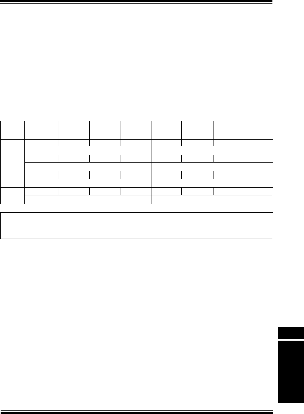
© 2013 Microchip Technology Inc. Preliminary DS61192A-page 50-43
Section 50. CPU for Devices with microAptiv™ Core
CPU for Devices with
microAptiv™ Core
50
50.12.17 SRSMap: Register (CP0 Register 12, Select 3)
The SRSMap register contains eight 4-bit fields that provide the mapping from a vector number
to the shadow set number to use when servicing such an interrupt. The values from this register
are not used for a non-interrupt exception, or a non-vectored interrupt (IV bit = 0, Cause<23> or
VS<4:0> bit = 0, IntCtl<9:5>). In such cases, the shadow set number comes from the ESS<3:0>
bits (SRSCtl<15:12>).
If the HSS<3:0> bits (SRSCTL29:26) are ‘0’, the results of a software read or write of this register
are unpredictable.
The operation of the processor is undefined if a value is written to any bit in this register that is
greater than the value of the HSS<3:0> bits.
The SRSMap register contains the shadow register set numbers for vector numbers 7-0. The
same shadow set number can be established for multiple interrupt vectors, creating a
many-to-one mapping from a vector to a single shadow register set number.
Register 50-17: SRSMap: Shadow Register Set Map Register; CP0 Register 12, Select 3
Bit
Range
Bit
31/23/15/7
Bit
30/22/14/6
Bit
29/21/13/5
Bit
28/20/12/4
Bit
27/19/11/3
Bit
26/18/10/2
Bit
25/17/9/1
Bit
24/16/8/0
31:24 R/W-0 R/W-0 R/W-0 R/W-0 R/W-0 R/W-0 R/W-0 R/W-0
SSV7<3:0> SSV6<3:0>
23:16 R/W-0 R/W-0 R/W-0 R/W-0 R/W-0 R/W-0 R/W-0 R/W-0
SSV5<3:0> SSV4<3:0>
15:8 R/W-0 R/W-0 R/W-0 R/W-0 R/W-0 R/W-0 R/W-0 R/W-0
SSV3<3:0> SSV2<3:0>
7:0 R/W-0 R/W-0 R/W-0 R/W-0 R/W-0 R/W-0 R/W-0 R/W-0
SSV1<3:0> SSV0<3:0>
Legend:
R = Readable bit W = Writable bit U = Unimplemented bit, read as ‘0’
-n = Value at POR ‘1’ = Bit is set ‘0’ = Bit is cleared x = Bit is unknown
bit 31-28 SSV7<3:0>: Shadow Set Vector 7 bits
Shadow register set number for Vector Number 7
bit 27-24 SSV6<3:0>: Shadow Set Vector 6 bits
Shadow register set number for Vector Number 6
bit 23-20 SSV5<3:0>: Shadow Set Vector 5 bits
Shadow register set number for Vector Number 5
bit 19-16 SSV4<3:0>: Shadow Set Vector 4 bits
Shadow register set number for Vector Number 4
bit 15-12 SSV3<3:0>: Shadow Set Vector 3 bits
Shadow register set number for Vector Number 3
bit 11-8 SSV2<3:0>: Shadow Set Vector 2 bits
Shadow register set number for Vector Number 2
bit 7-4 SSV1<3:0>: Shadow Set Vector 1 bits
Shadow register set number for Vector Number 1
bit 3-0 SSV0<3:0>: Shadow Set Vector 0 bit
Shadow register set number for Vector Number 0

PIC32 Family Reference Manual
DS61192A-page 50-44 Preliminary © 2013 Microchip Technology Inc.
50.12.18 View_IPL Register (CP0 Register 12, Select 4)
This register gives read and write access to the IPL<7:0> bits that are also available in the Status
register. The use of this register allows the Priority Level to be read/written without
extracting/inserting that field from/to the Status register.
The IPL field is located in non-contiguous bits within the Status register. All of the IPL bits are
presented as a contiguous field within this register.
Register 50-18: View_IPL: View Interrupt Priority Level Register; CP0 Register 12, Select 4
Bit
Range
Bit
31/23/15/7
Bit
30/22/14/6
Bit
29/21/13/5
Bit
28/20/12/4
Bit
27/19/11/3
Bit
26/18/10/2
Bit
25/17/9/1
Bit
24/16/8/0
31:24 U-0 U-0 U-0 U-0 U-0 U-0 U-0 U-0
— — — — — — — —
23:16 U-0 U-0 U-0 U-0 U-0 U-0 U-0 U-0
— — — — — — — —
15:8 U-0 U-0 U-0 U-0 U-0 U-0 R/W-0 R/W-0
— — — — — —IPL<7:6>
7:0 R/W-0 R/W-0 R/W-0 R/W-0 R/W-0 R/W-0 U-0 U-0
IPL<5:0> — —
Legend:
R = Readable bit W = Writable bit U = Unimplemented bit, read as ‘0’
-n = Value at POR ‘1’ = Bit is set ‘0’ = Bit is cleared x = Bit is unknown
bit 31-10 Unimplemented: Read as ‘0’
bit 9-2 IPL<7:0>: These bits contain the encoded (0...256) value of the current IPL.
bit 1-0 Unimplemented: Read as ‘0’
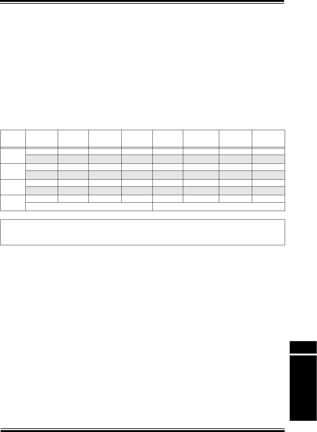
© 2013 Microchip Technology Inc. Preliminary DS61192A-page 50-45
Section 50. CPU for Devices with microAptiv™ Core
CPU for Devices with
microAptiv™ Core
50
50.12.19 SRSMAP2 Register (CP0 Register 12, Select 5)
The SRSMAP2 register contains two 4-bit bits that provide the mapping from an vector number
to the shadow set number to use when servicing such an interrupt. The values from this register
are not used for a non-interrupt exception, or a non-vectored interrupt (IV bit (Cause<23>) = 0
or the VS<4:0> bits (IntCtl<9:5>) = 0). In such cases, the shadow set number comes from the
ESS<3:0> bits (SRSCtl<15:12>).
If the HSS<3:0> bits (SRSCtl<9:6>) are ‘0’, the results of a software read or write of this register
are unpredictable.
The operation of the processor is undefined if a value is written to any bit in this register that is
greater than the value of the HSS<3:0> bits.
The SRSMAP2 register contains the shadow register set numbers for vector numbers 9:8. The
same shadow set number can be established for multiple interrupt vectors, creating a
many-to-one mapping from a vector to a single shadow register set number.
Register 50-19: SRSMAP2: Shadow Register Set Map 2 Register; CP0 Register 12, Select 5
Bit
Range
Bit
31/23/15/7
Bit
30/22/14/6
Bit
29/21/13/5
Bit
28/20/12/4
Bit
27/19/11/3
Bit
26/18/10/2
Bit
25/17/9/1
Bit
24/16/8/0
31:24 U-0 U-0 U-0 U-0 U-0 U-0 U-0 U-0
— — — — — — — —
23:16 U-0 U-0 U-0 U-0 U-0 U-0 U-0 U-0
— — — — — — — —
15:8 U-0 U-0 U-0 U-0 U-0 U-0 U-0 U-0
— — — — — — — —
7:0 R/W-x R/W-x R/W-x R/W-x R/W-x R/W-x R/W-x R/W-x
SSV9<3:0> SSV8<3:0>
Legend:
R = Readable bit W = Writable bit U = Unimplemented bit, read as ‘0’
-n = Value at POR ‘1’ = Bit is set ‘0’ = Bit is cleared x = Bit is unknown
bit 31-8 Unimplemented: Read as ‘0’
bit 7-4 SSV9<3:0>: Shadow Set Vector 9 bits
Shadow register set number for Vector Number 9.
bit 3-0 SSV8<3:0>: Shadow Set Vector 8 bits
Shadow register set number for Vector Number 8.

PIC32 Family Reference Manual
DS61192A-page 50-46 Preliminary © 2013 Microchip Technology Inc.
50.12.20 Cause Register (CP0 Register 13, Select 0)
The Cause register primarily describes the cause of the most recent exception. In addition, bits
also control software interrupt requests and the vector through which interrupts are dispatched.
With the exception of the IP1, IP0, DC, and IV bits, all bits in the Cause register are read-only.
Table 50-12: Cause Register EXCCODE<4:0> Bits
Exception Code Value
Mnemonic Description
Decimal Hex
00x00 IntInterrupt
10x01MOD
(1) TLB modified exception
20x02TLBL
(1) TLB exception (load or instruction fetch)
30x03TLBS
(1) TLB exception (store)
4 0x04 AdEL Address error exception (load or instruction fetch)
50x05AdESAddress error exception (store)
60x06IBEBus error exception (instruction fetch)
70x07DBEBus error exception (data reference: load or store)
80x08SysSyscall exception
90x09 BpBreakpoint exception
10 0x0a RI Reserved instruction exception
11 0x0b CPU Coprocessor Unusable exception
12 0x0c Ov Arithmetic Overflow exception
13 0x0d Tr Trap exception
14-18 0x0e-0x12 —Reserved
19 0x13 TLBRI(1)ITLB read-inhibit
20 0x14 TLBEI(1) TLB execute-inhibit
21-22 0x15-0x16 —Reserved
23 0x17 WATCH(1) Reference to WatchHi/WatchLo address
24 0x18 MCheck(1) Machine check
25 0x19 —Reserved
26 0x1A DSPDis DSP ASE state disabled exception
27-31 0x1B-0x1F —Reserved
Note 1: This feature is only available on PIC32 devices with the microAptiv™ MPU core.
Refer to the “CPU” chapter in the specific device data sheet for availability.

© 2013 Microchip Technology Inc. Preliminary DS61192A-page 50-47
Section 50. CPU for Devices with microAptiv™ Core
CPU for Devices with
microAptiv™ Core
50
Register 50-20: Cause: Exception Cause Register; CP0 Register 13, Select 0
Bit
Range
Bit
31/23/15/7
Bit
30/22/14/6
Bit
29/21/13/5
Bit
28/20/12/4
Bit
27/19/11/3
Bit
26/18/10/2
Bit
25/17/9/1
Bit
24/16/8/0
31:24 R-x R-x R-x R-x R/W-0 R-0 R-x R-x
BD TI CE<1:0> DC PCI IC AP
23:16 R/W-x R/W-x R-x U-0 U-0 U-0 R-x R-x
IV WP(1) FDCI — — —RIPL<7:6>
15:8 R-x R-x R-x R-x R-x R-x R/W-x R/W-x
RIPL<5:0> IP1 IP0
7:0 U-0 R-x R-x R-x R-x R-x U-0 U-0
—EXCCODE<4:0>— —
Legend:
R = Readable bit W = Writable bit U = Unimplemented bit, read as ‘0’
-n = Value at POR ‘1’ = Bit is set ‘0’ = Bit is cleared x = Bit is unknown
bit 31 BD: Branch Delay bit
Indicates whether the last exception taken occurred in a branch delay slot:
1 = In delay slot
0 = Not in delay slot
The processor updates BD only if the EXL bit (Status<1>) was ‘0’ when the exception occurred.
bit 30 TI: Timer Interrupt bit
Timer Interrupt. This bit denotes whether a timer interrupt is pending (analogous to the IP bits for other
interrupt types):
1 = Timer interrupt is pending
0 = No timer interrupt is pending
bit 29-28 CE<1:0>: Coprocessor Exception bits
Coprocessor unit number referenced when a Coprocessor Unusable exception is taken. This bit is loaded
by hardware on every exception, but is unpredictable for all exceptions except for Coprocessor Unusable.
11 = Reserved
10 = Reserved
01 = Reserved
00 = Coprocessor 0
bit 27 DC: Disable Count Register bit
In some power-sensitive applications, the Count register is not used and can be stopped to avoid
unnecessary toggling.
1 = Disable counting of Count register
0 = Enable counting of Count register
bit 26 PCI: Performance Counter Interrupt bit
1 = Performance counter interrupt is pending
0 = No performance counter interrupt is pending
bit 25 IC: Interrupt Chaining bit
Indicates if Interrupt chaining occurred on the last IRET instruction.
1 = Interrupt Chaining occurred during last IRET instruction
0 = Interrupt Chaining did not happen on last IRET instruction
bit 24 AP: Interrupt Auto-Prologue Exception bit
Indicates whether an exception occurred during Interrupt Auto-Prologue.
1 = Exception occurred during Auto-Prologue operation
0 = Exception did not occur during Auto-Prologue operation
Note 1: This bit is only available on PIC32 devices with the microAptiv™ MPU core. Refer to the “CPU” chapter in
the specific device data sheet for availability.

PIC32 Family Reference Manual
DS61192A-page 50-48 Preliminary © 2013 Microchip Technology Inc.
bit 23 IV: Interrupt Vector bit
Indicates whether an interrupt exception uses the general exception vector or a special interrupt vector
1 = Use the special interrupt vector (0x200)
0 = Use the general exception vector (0x180)
If the IV bit (Cause<23>) is ‘1’ and the BEV bit (Status<22>) is ‘0’, the special interrupt vector represents
the base of the vectored interrupt table.
bit 22 WP: Watch Exception Pending bit(1)
This bit indicates that a watch exception was deferred because the status bits EXL or ERL were set at the
time the watch exception was detected.
1 = Watch exception pending
0 = Watch exception not pending
When set, this bit indicates a pending watch exception, and causes the exception to be initiated once the
Status EXL and ERL bits are both zero. The software must clear this bit as part of the watch exception
handler to prevent a watch exception loop.
Note: Software should not write a '1' to this bit when its value is '0', thereby causing a 0-to-1 transition.
If such a transition is caused by software, the results are unpredictable.
bit 21 FDCI: Fast Debug Channel Interrupt bit
This bit indicates that a FDC interrupt is pending
1 = Fast Debug Channel interrupt is pending
0 = Fast Debug Channel interrupt is not pending
bit 20-18 Unimplemented: Read as ‘0’
bit 17-10 RIPL<7:0>: Requested Interrupt Priority Level bits
This bit is the encoded (255-0) value of the requested interrupt. A value of ‘0’ indicates that no interrupt is
requested.
bit 9-8 IP<1:0>: Software Interrupt Request Control bits
Controls the request for software interrupts
1 = Request software interrupt
0 = No interrupt requested
These bits are exported to the system interrupt controller for prioritization in EIC Interrupt mode with other
interrupt sources.
bit 7 Unimplemented: Read as ‘0’
bit 6-2 EXCCODE<4:0>: Exception Code bits
See Tab l e 50 -12 for the list of Exception codes.
bit 1-0 Unimplemented: Read as ‘0’
Register 50-20: Cause: Exception Cause Register; CP0 Register 13, Select 0 (Continued)
Note 1: This bit is only available on PIC32 devices with the microAptiv™ MPU core. Refer to the “CPU” chapter in
the specific device data sheet for availability.
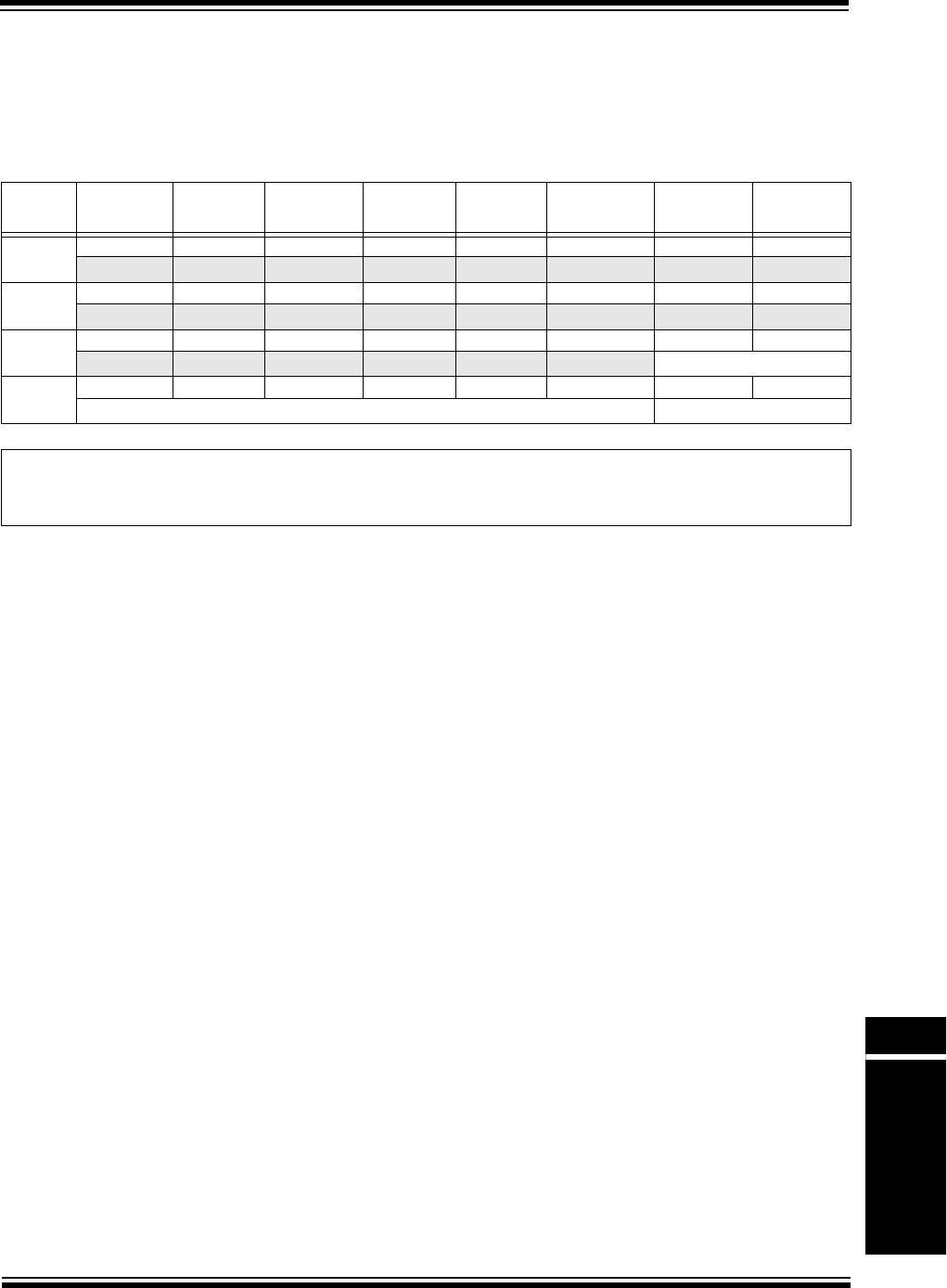
© 2013 Microchip Technology Inc. Preliminary DS61192A-page 50-49
Section 50. CPU for Devices with microAptiv™ Core
CPU for Devices with
microAptiv™ Core
50
50.12.21 View_RIPL Register (CP0 Register 13, Select 4)
This register gives read access to the RIPL bit that is also available in the Cause register. The
use of this register allows the Requested Priority Level to be read without extracting that bit from
the Cause register.
Register 50-21: View_RIPL: View Requested Priority Level Register; CP0 Register 13, Select 4
Bit
Range
Bit
31/23/15/7
Bit
30/22/14/6
Bit
29/21/13/5
Bit
28/20/12/4
Bit
27/19/11/3
Bit
26/18/10/2
Bit
25/17/9/1
Bit
24/16/8/0
31:24 U-0 U-0 U-0 U-0 U-0 U-0 U-0 U-0
— — — — — — — —
23:16 U-0 U-0 U-0 U-0 U-0 U-0 U-0 U-0
— — — — — — — —
15:8 U-0 U-0 U-0 U-0 U-0 U-0 R-0 R-0
— — — — — —RIPL<7:6>
7:0 R-0 R-0 R-0 R-0 R-0 R-0 R/W-0 R/W-0
RIPL<5:0> IP<1:0>
Legend:
R = Readable bit W = Writable bit U = Unimplemented bit, read as ‘0’
-n = Value at POR ‘1’ = Bit is set ‘0’ = Bit is cleared x = Bit is unknown
bit 31-10 Unimplemented: Read as ‘0’
bit 9-2 RIPL<7:0>: Requested Interrupt Priority Level bits
If EIC Interrupt mode is enabled, this bit indicates the encoded (0...255) value of the current Requested Priority
Level of the pending interrupt.
bit 1-0 IP<1:0>: Software Interrupt Pending bits
If EIC Interrupt mode is not enabled, controls which SW interrupts are pending.

PIC32 Family Reference Manual
DS61192A-page 50-50 Preliminary © 2013 Microchip Technology Inc.
50.12.22 NestedExc Register (CP0 Register 13, Select 5)
The NestedExc register is a read-only register that contains the values of Status<1> (EXL) and
Status<2> (ERL) prior to acceptance of the current exception.
Register 50-22: NestedExc: Nested Exception Register; CP0 Register 13, Select 5
Bit
Range
Bit
31/23/15/7
Bit
30/22/14/6
Bit
29/21/13/5
Bit
28/20/12/4
Bit
27/19/11/3
Bit
26/18/10/2
Bit
25/17/9/1
Bit
24/16/8/0
31:24 U-0 U-0 U-0 U-0 U-0 U-0 U-0 U-0
— — — — — — — —
23:16 U-0 U-0 U-0 U-0 U-0 U-0 U-0 U-0
— — — — — — — —
15:8 U-0 U-0 U-0 U-0 U-0 U-0 U-0 U-0
— — — — — — — —
7:0 U-0 U-0 U-0 U-0 U-0 R/W-x R/W-x U-0
— — — — —NERLNEXL—
Legend: r = Reserved bit
R = Readable bit W = Writable bit U = Unimplemented bit, read as ‘0’
-n = Value at POR ‘1’ = Bit is set ‘0’ = Bit is cleared x = Bit is unknown
bit 31-3 Unimplemented: Read as ‘0’
bit 2 NERL: Nested Error Level bit
This bit contains the value of the ERL bit prior to acceptance of the current exception. This bit is updated by
all exceptions that would set either the EXL bit or the ERL bit in the status register. This bit is not updated by
Debug exceptions.
bit 1 NEXL: Nested Exception Level bit
This bit contains the value of the EXL bit prior to acceptance of current exception. This bit is updated by
exceptions that would update the exception program counter if the EXL bit is not set (MCheck, interrupt,
Address Error, all TLB exceptions, Bus Error, CopUnusable, Reserved Instruction, Overflow, Trap, Syscall,
FPU, etc.). For these exception types, this register field is updated regardless of the value of StatusEXL. This
bit is not updated by exception types that update ErrorEPC (Reset, Soft Reset, NMI, and Cache Error). In
addition, this bit is not updated by Debug exceptions.
bit 0 Unimplemented: Read as ‘0’

© 2013 Microchip Technology Inc. Preliminary DS61192A-page 50-51
Section 50. CPU for Devices with microAptiv™ Core
CPU for Devices with
microAptiv™ Core
50
50.12.23 EPC Register (CP0 Register 14, Select 0)
The Exception Program Counter (EPC) is a read/write register that contains the address at which
processing resumes after an exception has been serviced. All bits of the EPC register are
significant and are writable.
For synchronous (precise) exceptions, the EPC contains one of the following:
•The virtual address of the instruction that was the direct cause of the exception
•The virtual address of the immediately preceding BRANCH or JUMP instruction, when the
exception causing instruction is in a branch delay slot and the Branch Delay bit in the
Cause register is set
On new exceptions, the processor does not write to the EPC register when the EXL bit in the
Status register is set; however, the register can still be written via the MTC0 instruction.
Since the PIC32 family implements MIPS16e® or microMIPS™ ASE, a read of the EPC register
(via MFC0) returns the following value in the destination GPR:
GPR[rt] ExceptionPC31..1 || ISAMode0
That is, the upper 31 bits of the exception PC are combined with the lower bit of the ISA<1:0>
bits (Config3<15:14>) and are written to the GPR.
Similarly, a write to the EPC register (via MTC0) takes the value from the GPR and distributes
that value to the exception PC and the ISA<1:0> bits (Config3<15:14>), as follows:
ExceptionPC GPR[rt]31..1 || 0
ISAMode 2#0 || GPR[rt]0
That is, the upper 31 bits of the GPR are written to the upper 31 bits of the exception PC, and the
lower bit of the exception PC is cleared. The upper bit of the ISA<1:0> bits (Config3<15:14>) is
cleared and the lower bit is loaded from the lower bit of the GPR.
Register 50-23: EPC: Exception Program Counter Register; CP0 Register 14, Select 0
Bit
Range
Bit
31/23/15/7
Bit
30/22/14/6
Bit
29/21/13/5
Bit
28/20/12/4
Bit
27/19/11/3
Bit
26/18/10/2
Bit
25/17/9/1
Bit
24/16/8/0
31:24 R/W-x R/W-x R/W-x R/W-x R/W-x R/W-x R/W-x R/W-x
EPC<31:24>
23:16 R/W-x R/W-x R/W-x R/W-x R/W-x R/W-x R/W-x R/W-x
EPC<23:16>
15:8 R/W-x R/W-x R/W-x R/W-x R/W-x R/W-x R/W-x R/W-x
EPC<15:8>
7:0 R/W-x R/W-x R/W-x R/W-x R/W-x R/W-x R/W-x R/W-x
EPC<7:0>
Legend:
R = Readable bit W = Writable bit U = Unimplemented bit, read as ‘0’
-n = Value at POR ‘1’ = Bit is set ‘0’ = Bit is cleared x = Bit is unknown
bit 31-0 EPC<31:0>: Exception Program Counter bits

PIC32 Family Reference Manual
DS61192A-page 50-52 Preliminary © 2013 Microchip Technology Inc.
50.12.24 NestedEPC Register (CP0 Register 14, Select 2)
The NestedEPC register is a read/write register with the same behavior as the EPC register, with
the following exceptions:
•The NestedEPC register ignores the value of Status<1> (EXL) and is therefore updated on
the occurrence of any exception, including nested exceptions
•The NestedEPC register is not used by the ERET/DERET/IERET instructions. To return to
the address stored in NestedEPC, software must copy the value of the NestedEPC register
to the EPC register.
Register 50-24: NestedEPC: Nested Exception Program Counter Register; CP0 Register 14, Select 2
Bit
Range
Bit
31/23/15/7
Bit
30/22/14/6
Bit
29/21/13/5
Bit
28/20/12/4
Bit
27/19/11/3
Bit
26/18/10/2
Bit
25/17/9/1
Bit
24/16/8/0
31:24 R/W-x R/W-x R/W-x R/W-x R/W-x R/W-x R/W-x R/W-x
EPC<31:24>
23:16 R/W-x R/W-x R/W-x R/W-x R/W-x R/W-x R/W-x R/W-x
EPC<23:16>
15:8 R/W-x R/W-x R/W-x R/W-x R/W-x R/W-x R/W-x R/W-x
EPC<15:8>
7:0 R/W-x R/W-x R/W-x R/W-x R/W-x R/W-x R/W-x R/W-x
EPC<7:0>
Legend:
R = Readable bit W = Writable bit U = Unimplemented bit, read as ‘0’
-n = Value at POR ‘1’ = Bit is set ‘0’ = Bit is cleared x = Bit is unknown
bit 31-0 EPC<31:0>: Nested Exception Program Counter bits
These bits are updated by exceptions that would update the exception program counter if the EXL bit is not
set (MCheck, Interrupt, Address Error, all TLB exceptions, Bus Error, CopUnusable, Reserved Instruction,
Overflow, Trap, Syscall, FPU, etc.). For these exception types, this register field is updated regardless of the
value of EXL. These bits are not updated by exception types that update the exception program counter
(Reset, Soft Reset, NMI, and Cache Error). In addition, these bits are not updated by Debug exceptions.

© 2013 Microchip Technology Inc. Preliminary DS61192A-page 50-53
Section 50. CPU for Devices with microAptiv™ Core
CPU for Devices with
microAptiv™ Core
50
50.12.25 PRID Register (CP0 Register 15, Select 0)
The Processor Identification (PRID) register is a 32-bit read-only register that contains informa-
tion identifying the manufacturer, manufacturer options, processor identification, and revision
level of the processor.
Register 50-25: PRID: Processor Identification Register; CP0 Register 15, Select 0
Bit
Range
Bit
31/23/15/7
Bit
30/22/14/6
Bit
29/21/13/5
Bit
28/20/12/4
Bit
27/19/11/3
Bit
26/18/10/2
Bit
25/17/9/1
Bit
24/16/8/0
31:24 U-0 U-0 R-0 U-0 U-0 U-0 U-0 U-0
— — — — — — — —
23:16 R-0 R-0 R-0 R-0 R-0 R-0 R-0 R-1
COMPANYID<23:16>
15:8 R-1 R-0 R-0 R-1 R-1 R-1 R-1 R-0
PROCESSORID<15:8>
7:0 R-x R-x R-x R-x R-x R-x R-x R-x
MAJORREV<2:0> MINORREV<2:0> PATCHREV<1:0>
Legend:
R = Readable bit W = Writable bit U = Unimplemented bit, read as ‘0’
-n = Value at POR ‘1’ = Bit is set ‘0’ = Bit is cleared x = Bit is unknown
bit 31-24 Unimplemented: Read as ‘0’
bit 23-16 COMPANYID<7:0>: Company Identification bits
In PIC32 devices, these bits contain a value of ‘1’ to indicate MIPS Technologies, Inc. as the processor
manufacturer/designer.
bit 15-8 PROCESSORID<7:0>: Processor Identification bits
These bits allow software to distinguish between the various types of MIPS Technologies Inc. processors.
0x9E = microAptiv™ Microprocessor core
bit 7-5 MAJORREV<2:0>: Processor Major Revision Identification bits
These bits allow software to distinguish between one revision and another of the same processor type. This
number is increased on major revisions of the processor core.
bit 4-2 MINORREV<2:0>: Processor Minor Revision Identification bits
This number is increased on each incremental revision of the processor and reset on each new major
revision.
bit 1-0 PATCHREV<1:0>: Processor Patch Level Identification bits
If a patch is made to modify an older revision of the processor, the value of these bits will be incremented.

PIC32 Family Reference Manual
DS61192A-page 50-54 Preliminary © 2013 Microchip Technology Inc.
50.12.26 Ebase Register (CP0 Register 15, Select 1)
The Ebase register is a read/write register containing the base address of the exception vectors
used when the BEV bit (Status<22>) equals ‘0’, and a read-only CPU number value that may be
used by software to distinguish different processors in a multi-processor system.
The Ebase register provides the ability for software to identify the specific processor within a
multi-processor system, and allows the exception vectors for each processor to be different,
especially in systems composed of heterogeneous processors. Bits 31-12 of the Ebase register
are concatenated with zeros to form the base of the exception vectors when the BEV bit is ‘0’.
The exception vector base address comes from the fixed defaults when the BEV bit is ‘1’, or for
any EJTAG Debug exception. The Reset state of bits 31-12 of the Ebase register initialize the
exception base register to 0x80000000.
Bits 31 and 30 of the Ebase Register are fixed with the value 2#10 to force the exception base
address to be in the kseg0 or kseg1 unmapped virtual address segments.
If the value of the exception base register is to be changed, this must be done with the BEV bit
equal to ‘1’. The operation of the processor is undefined if the Ebase<17:0> bits are written with
a different value when the BEV bit (Status<22>) is ‘0’.
Combining bits 31-20 of the Ebase register allows the base address of the exception vectors to
be placed at any 4 KB page boundary.
Register 50-26: Ebase: Exception Base Register; CP0 Register 15, Select 1
Bit
Range
Bit
31/23/15/7
Bit
30/22/14/6
Bit
29/21/13/5
Bit
28/20/12/4
Bit
27/19/11/3
Bit
26/18/10/2
Bit
25/17/9/1
Bit
24/16/8/0
31:24 U-1 U-0 R/W-0 R/W-0 R/W-0 R/W-0 R/W-0 R/W-0
— — EBASE<17:12>
23:16 R/W-0 R/W-0 R/W-0 R/W-0 R/W-0 R/W-0 R/W-0 R/W-0
EBASE<11:4>
15:8 R/W-0 R/W-0 R/W-0 R/W-0 U-0 U-0 R-0 R-0
EBASE<3:0> — —CPUNUM<9:8>
7:0 R-0 R-0 R-0 R-0 R-0 R-0 R-0 R-0
CPUNUM<7:0>
Legend:
R = Readable bit W = Writable bit U = Unimplemented bit, read as ‘0’
-n = Value at POR ‘1’ = Bit is set ‘0’ = Bit is cleared x = Bit is unknown
bit 31 Unimplemented: Read as ‘1’
bit 30 Unimplemented: Read as ‘0’
bit 29-12 EBASE<17:0>: Exception Vector Base Address bits
In conjunction with bits 31-30, these bits specify the base address of the exception vectors when the BEV
bit (Status<22>) is ‘0’.
bit 11-10 Unimplemented: Read as ‘0’
bit 9-0 CPUNUM<9:0>: CPU Number bits
These bits specify the number of CPUs in a multi-processor system and can be used by software to
distinguish a particular processor from others. In a single processor system, this value is set to ‘0’.

© 2013 Microchip Technology Inc. Preliminary DS61192A-page 50-55
Section 50. CPU for Devices with microAptiv™ Core
CPU for Devices with
microAptiv™ Core
50
50.12.27 CDMMBase Register (CP0 Register 15, Select 2)
The 36-bit physical base address for the Common Device Memory Map (CDMM) is defined by
this register. Since the PIC32 is a 32-bit device, the upper four bits of the address are zero. The
CDMM is a region of physical address space that is reserved for mapping I/O device
Configuration registers within a MIPS processor. The CDMM helps aggregate various device
mappings into one area, preventing fragmentation of the memory address space. On PIC32
devices, the CDMM contains the Fast Debug Channel (FDC) control registers.
Register 50-27: CDMMBase: Common Device Memory Map Base Register; CP0 Register 15, Select 2
Bit
Range
Bit
31/23/15/7
Bit
30/22/14/6
Bit
29/21/13/5
Bit
28/20/12/4
Bit
27/19/11/3
Bit
26/18/10/2
Bit
25/17/9/1
Bit
24/16/8/0
31:24 R/W-x R/W-x R/W-x R/W-x R/W-x R/W-x R/W-x R/W-x
CDMMUA<20:13>
23:16 R/W-x R/W-x R/W-x R/W-x R/W-x R/W-x R/W-x R/W-x
CDMMUA<12:5>
15:8 R/W-x R/W-x R/W-x R/W-x R/W-x R/W-0 R-0 R-0
CDMMUA<4:0> EN CI CDMMSize<8>
7:0 R-0 R-0 R-0 R-0 R-0 R-0 R-1 R-0
CDMMSize<7:0>
Legend:
R = Readable bit W = Writable bit U = Unimplemented bit, read as ‘0’
-n = Value at POR ‘1’ = Bit is set ‘0’ = Bit is cleared x = Bit is unknown
bit 31-11 CDMMUA: CDMM Upper Address bits
Bits 35:15 of the base physical address of the memory mapped registers. Unimplemented bits ignore writes
and return ‘0’ on reads.
bit 10 EN: CDMM Enable bit
1 = CDMM region is enabled
0 = CDMM region is disabled
bit 9 CI: Device Register Block Reserved bit
1 = The first 64-byte Device Register Block of the CDMM is reserved for additional registers that manage
CDMM region behavior and are not IO device registers
0 = The first 64-byte Device Register Block of the CDMM is not reserved
bit 8-0 CDMMSize: CDMM Size bits
These bits indicate the number of 64-byte Device Register Blocks instantiated in the CPU core.
111111111 = 512 Device Register Blocks
•
•
•
000000000 = 1 Device Register Block
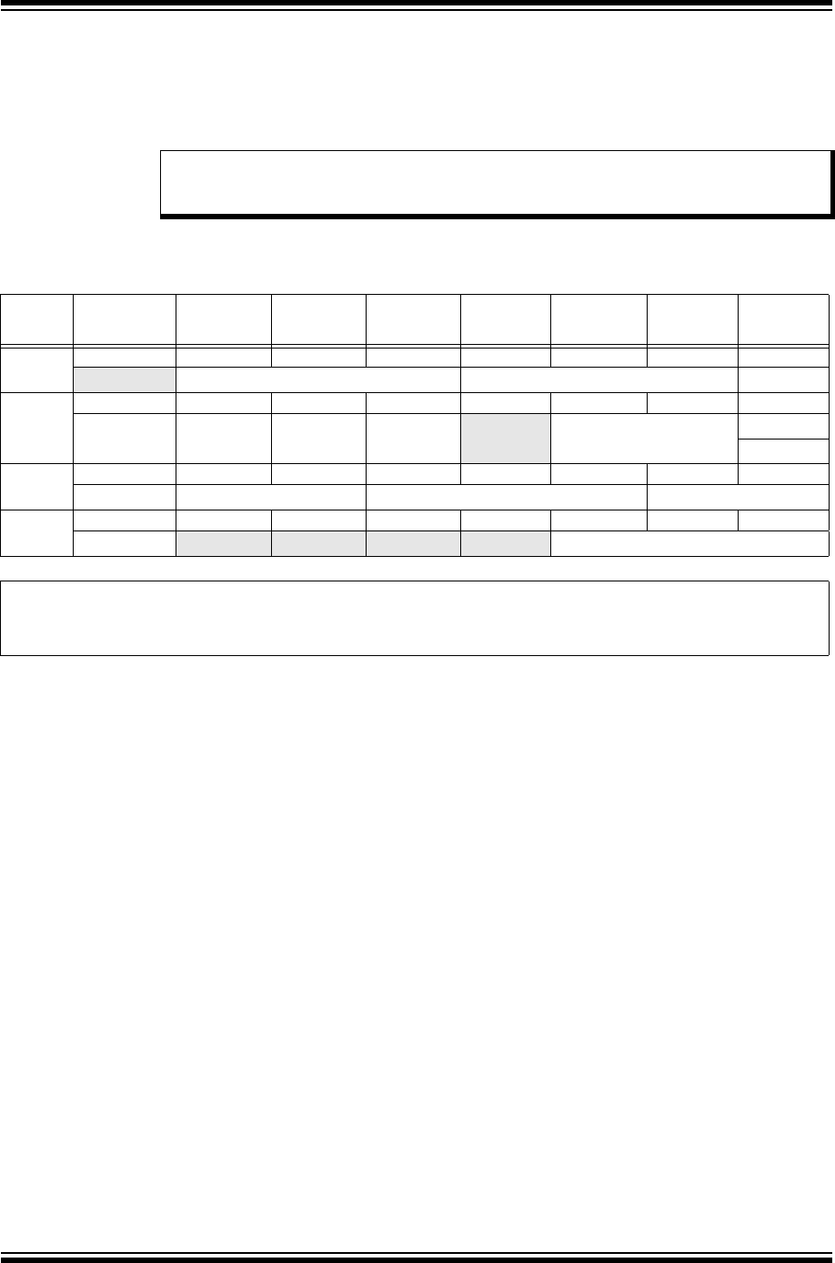
PIC32 Family Reference Manual
DS61192A-page 50-56 Preliminary © 2013 Microchip Technology Inc.
50.12.28 Config Register (CP0 Register 16, Select 0)
The Config register specifies various configuration and capabilities information. Most of the fields
in the Config register are initialized by hardware during the Reset exception process, or are
constant.
Note: The microAptiv Core Configuration register bit fields and default values may vary
between devices. Refer to “microAptiv Core Configuration” chapter in the specific
device data sheet for the core configuration of a specific device.
Register 50-28: Config: Configuration Register; CP0 Register 16, Select 0
Bit
Range
Bit
31/23/15/7
Bit
30/22/14/6
Bit
29/21/13/5
Bit
28/20/12/4
Bit
27/19/11/3
Bit
26/18/10/2
Bit
25/17/9/1
Bit
24/16/8/0
31:24 r-1 R/W-x R/W-x R/W-x R/W-x R/W-x R/W-x R-x
—K23<2:0>
(1) KU<2:0>(1) ISP
23:16
R-x R-x R-x R-x U-0 R-x R-x R-x
DSP UDI SB MDU —MM<1:0>
(2) DS(1)
BM(2)
15:8 R-0 R-0 R-0 R-0 R-0 R-1 R-0 R-x
BE AT<1:0> AR<2:0> MT<2:1>
7:0 R-x U-0 U-0 U-0 U-0 R/W-x R/W-x R/W-x
MT<0> — — — —K0<2:0>
Legend: r = Reserved bit
R = Readable bit W = Writable bit U = Unimplemented bit, read as ‘0’
-n = Value at POR ‘1’ = Bit is set ‘0’ = Bit is cleared x = Bit is unknown
bit 31 Reserved: This bit is hardwired to ‘1’ to indicate the presence of the Config1 register.
bit 30-28 K23<2:0>: kseg2 and kseg3 bits(1)
These bits control the cacheability of the kseg2 and kseg3 address segments.
Refer to Ta b le 5 0 -1 3 for the bit encoding.
bit 27-25 KU<2:0>: kuseg and useg bits(1)
These bits control the cacheability of the kuseg and useg address segments.
Refer to Ta b le 5 0 -1 3 for the bit encoding.
bit 24 ISP: Instruction Scratchpad RAM bit
This bit indicates whether instruction scratchpad RAM is implemented.
1 = Instruction scratchpad RAM is implemented
0 = Instruction scratchpad RAM is not implemented
bit 23 DSP: Data Scratchpad RAM bit
This bit indicates whether data scratchpad RAM is implemented.
1 = Data scratchpad RAM is implemented
0 = Data scratchpad RAM is not implemented
Note 1: This bit is only available on devices with the microAptiv™ MCU Microprocessor core. On devices with the
microAptiv™ MPU Microprocessor core, this bit is reserved, and is always read as ‘0’. Refer to the “CPU”
chapter in the specific device data sheet to determine availability.
2: This bit is only available on devices with the microAptiv™ MPU Microprocessor core. Refer to the “CPU”
chapter in the specific device data sheet to determine availability.

© 2013 Microchip Technology Inc. Preliminary DS61192A-page 50-57
Section 50. CPU for Devices with microAptiv™ Core
CPU for Devices with
microAptiv™ Core
50
bit 22 UDI: User-defined bit
This bit indicates that CorExtend User-Defined Instructions have been implemented.
1 = User-defined instructions are implemented
0 = No user-defined instructions are implemented
bit 21 SB: SimpleBE bit
This bit indicates whether SimpleBE Bus mode is enabled.
1 = Only simple byte enables allowed on internal bus interface
0 = No reserved byte enables on internal bus interface
This bit is hardwired to ‘1’ to indicate only simple byte enables allowed on internal bus interface.
bit 20 MDU: Multiply/Divide Unit bit
1 = Iterative, area-efficient MDU
0 = Fast, high-performance MDU
This bit is hardwired to ‘0’ to indicate the fast, high-performance MDU.
bit 19 Unimplemented: Read as ‘0’
bit 18-17 MM<1:0>: Merge Mode bits(2)
11 = Reserved
10 = Merging is allowed
01 = Reserved
00 = Merging is not allowed
bit 16 DS: Dual SRAM bit(1)
1 = Dual instruction/data SRAM internal bus interfaces
0 = Unified instruction/data SRAM internal bus interface
BM: Burst Mode bit(2)
This bit is hardwired to a ‘0’ to indicate burst order is sequential.
bit 15 BE: Big-Endian bit
Indicates the endian mode in which the processor is running, PIC32 is always little-endian.
1 = Big-endian
0 = Little-endian
bit 14-13 AT<1:0>: Architecture Type bits
Architecture type implemented by the processor. This bit is always ‘00’ to indicate the MIPS32®
architecture.
bit 12-10 AR<2:0>: Architecture Revision Level bits
Architecture revision level. This bit is always ‘001’ to indicate MIPS32® Release 2.
111 = Reserved
110 = Reserved
101 = Reserved
100 = Reserved
011 = Reserved
010 = Reserved
001 = Release 2
000 = Release 1
Register 50-28: Config: Configuration Register; CP0 Register 16, Select 0 (Continued)
Note 1: This bit is only available on devices with the microAptiv™ MCU Microprocessor core. On devices with the
microAptiv™ MPU Microprocessor core, this bit is reserved, and is always read as ‘0’. Refer to the “CPU”
chapter in the specific device data sheet to determine availability.
2: This bit is only available on devices with the microAptiv™ MPU Microprocessor core. Refer to the “CPU”
chapter in the specific device data sheet to determine availability.

PIC32 Family Reference Manual
DS61192A-page 50-58 Preliminary © 2013 Microchip Technology Inc.
bit 9-7 MT<2:0>: MMU Type bits
PIC32 devices with the microAptiv™ MCU Microprocessor core use a fixed-mapping MMU.
PIC32 devices with the microAptiv™ MPU Microprocessor core use a TLB-based MMU.
111 = Reserved
110 = Reserved
101 = Reserved
100 = Reserved
011 = Fixed mapping
010 = Reserved
001 = Standard TLB
000 = Reserved
bit 6-3 Unimplemented: Read as ‘0’
bit 2-0 K0<2:0>: Kseg0 bits
Kseg0 coherency algorithm. Refer to Ta bl e 5 0 - 13 for the bit encoding.
Register 50-28: Config: Configuration Register; CP0 Register 16, Select 0 (Continued)
Note 1: This bit is only available on devices with the microAptiv™ MCU Microprocessor core. On devices with the
microAptiv™ MPU Microprocessor core, this bit is reserved, and is always read as ‘0’. Refer to the “CPU”
chapter in the specific device data sheet to determine availability.
2: This bit is only available on devices with the microAptiv™ MPU Microprocessor core. Refer to the “CPU”
chapter in the specific device data sheet to determine availability.
Table 50-13: Cache Coherency Attributes
K0<2:0> Value Cache Coherency Attribute
011 Cacheable, non-coherent, write-back, write allocate
010 Uncached
001 Cacheable, non-coherent, write-through, write allocate
000 Cacheable, non-coherent, write-through, no write allocate
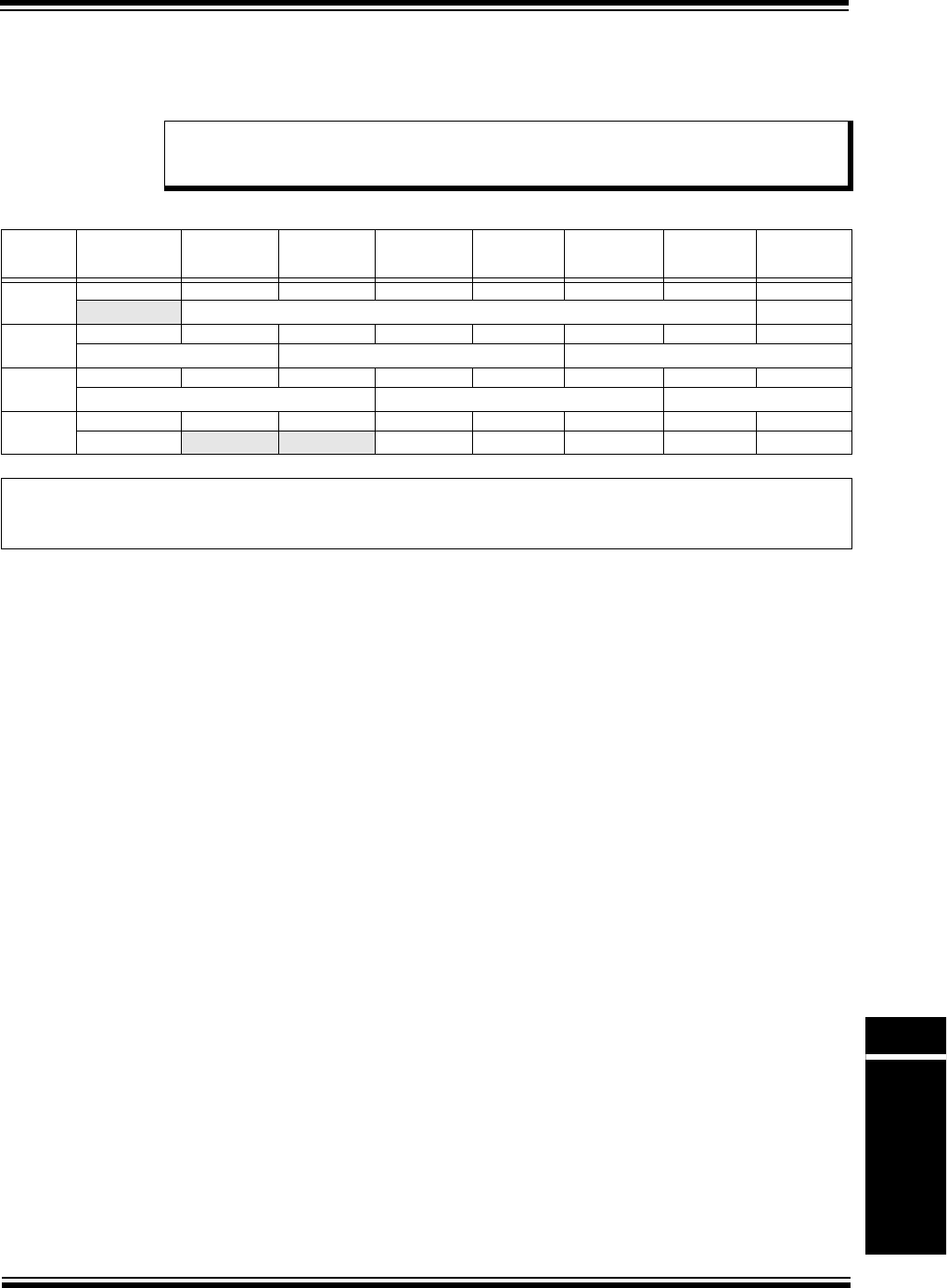
© 2013 Microchip Technology Inc. Preliminary DS61192A-page 50-59
Section 50. CPU for Devices with microAptiv™ Core
CPU for Devices with
microAptiv™ Core
50
50.12.29 Config1 Register (CP0 Register 16, Select 1)
The Config1 register is an adjunct to the Config register and encodes additional information
about capabilities present on the core. All fields in the Config1 register are read-only.
Note: The microAptiv Core Configuration register bit fields and default values may vary
between devices. Refer to “microAptiv Core Configuration” chapter in the specific
device data sheet for the core configuration of a specific device.
Register 50-29: Config1: Configuration Register 1; CP0 Register 16, Select 1
Bit
Range
Bit
31/23/15/7
Bit
30/22/14/6
Bit
29/21/13/5
Bit
28/20/12/4
Bit
27/19/11/3
Bit
26/18/10/2
Bit
25/17/9/1
Bit
24/16/8/0
31:24 r-1 R-x R-x R-x R-x R-x R-x R-x
— MMU Size<5:0>(1) IS<2>
23:16 R-x R-x R-x R-x R-x R-x R-x R-x
IS<1:0>(1) IL<2:0>(1) IA<2:0>(1)
15:8 R-x R-x R-x R-x R-x R-x R-x R-x
DS<2:0>(1) DL<2:0>(1) DA<2:1>(1)
7:0 R-x U-0 U-0 R-x R-x R-x R-x R-x
DA<0> ——PCWRCAEPFP
Legend: r = Reserved bit
R = Readable bit W = Writable bit U = Unimplemented bit, read as ‘0’
-n = Value at POR ‘1’ = Bit is set ‘0’ = Bit is cleared x = Bit is unknown
bit 31 Reserved: This bit is hardwired to a ‘1’ to indicate the presence of the Config2 register.
bit 30-25 MMU Size: Contains the number of TLB entries minus 1(1)
11111 = 32 TLB entries
•
•
•
00000 = No TLB entries
bit 24-22 IS<2:0>: Instruction Cache Sets bits(1)
Contains the number of instruction cache sets per way.
0x0 = 64
0x1 = 128
0x2 = 256
0x3 = 512
0x4 = 1024
0x5 = Reserved
0x6 = Reserved
0x7 = Reserved
bit 21-19 IL<2:0>: Instruction-Cache Line bits(1)
Contains the instruction cache line size.
0x0 = No instruction cache is present
0x3 = 16 bytes
All other values are Reserved.
Note 1: For the PIC32 devices with the microAptiv™ MCU Microprocessor core, these bits are reserved and
always read as ‘0’. Refer to the “CPU” chapter in the specific device data sheet to determine availability.

PIC32 Family Reference Manual
DS61192A-page 50-60 Preliminary © 2013 Microchip Technology Inc.
bit 18-16 IA<2:0: Instruction-Cache Associativity bits(1)
Contains the level of instruction cache associativity.
0x0 = Direct-mapped
0x1 = 2-way
0x2 = 3-way
0x3 = 4-way
0x4 = Reserved
0x5 = Reserved
0x6 = Reserved
0x7 = Reserved
bit 15-13 DS<2:0>: Data-Cache Sets bits(1)
Contains the number of data cache sets per way.
0x0 = 64
0x1 = 128
0x2 = 256
0x3 = 512
0x4 = 1024
0x5 = Reserved
0x6 = Reserved
0x7 = Reserved
bit 12-10 DL<2:0>: Data-Cache Line bits(1)
Contains the data cache line size.
0x0 = No instruction cache is present
0x3 = 16 bytes
All other values are Reserved.
bit 9-7 DA<2:0>: Data-Cache Associativity bits(1)
Contains the type of set associativity for the data cache.
0x0 = Direct-mapped
0x1 = 2-way
0x2 = 3-way
0x3 = 4-way
0x4 = Reserved
0x5 = Reserved
0x6 = Reserved
0x7 = Reserved
bit 6-5 Unimplemented: Read as ‘0’
bit 4 PC: Performance Counter bit
Performance Counter registers implemented.
1 = The processor core contains Performance Counters
0 = The processor core does not contain Performance Counters
bit 3 WR: Watch Register Presence bit
1 = No Watch registers are present
0 = One or more Watch registers is present
bit 2 CA: Code Compression Implemented bit
1 = MIPS16e® is implemented
0 = No MIPS16e® present
bit 1 EP: EJTAG Present bit
1 = EJTAG unit is implemented
0 = EJTAG unit is not implemented
bit 0 FP: Floating Point Unit bit
1 = Floating Point Unit is implemented
0 = Floating Point Unit is not implemented
Register 50-29: Config1: Configuration Register 1; CP0 Register 16, Select 1 (Continued)
Note 1: For the PIC32 devices with the microAptiv™ MCU Microprocessor core, these bits are reserved and
always read as ‘0’. Refer to the “CPU” chapter in the specific device data sheet to determine availability.

© 2013 Microchip Technology Inc. Preliminary DS61192A-page 50-61
Section 50. CPU for Devices with microAptiv™ Core
CPU for Devices with
microAptiv™ Core
50
50.12.30 Config2 (CP0 Register 16, Select 2)
The Config2 register is an adjunct to the Config register and is reserved to encode additional
capabilities information. Config2 is allocated for showing the configuration of level 2/3 caches.
These bits are reset to ‘0’ because L2/L3 caches are not supported by the PIC32 core. All bits in
the Config2 register are read-only.
Note: The microAptiv Core Configuration register bit fields and default values may vary
between devices. Refer to “microAptiv Core Configuration” chapter in the specific
device data sheet for the core configuration of a specific device.
Register 50-30: Config2: Configuration Register 2; CP0 Register 16, Select 2
Bit
Range
Bit
31/23/15/7
Bit
30/22/14/6
Bit
29/21/13/5
Bit
28/20/12/4
Bit
27/19/11/3
Bit
26/18/10/2
Bit
25/17/9/1
Bit
24/16/8/0
31:24 r-1 U-0 U-0 U-0 U-0 U-0 U-0 U-0
— — — — — — — —
23:16 U-0 U-0 U-0 U-0 U-0 U-0 U-0 U-0
— — — — — — — —
15:8 U-0 U-0 U-0 U-0 U-0 U-0 U-0 U-0
— — — — — — — —
7:0 U-0 U-0 U-0 U-0 U-0 U-0 U-0 U-0
— — — — — — — —
Legend: r = Reserved bit
R = Readable bit W = Writable bit U = Unimplemented bit, read as ‘0’
-n = Value at POR ‘1’ = Bit is set ‘0’ = Bit is cleared x = Bit is unknown
bit 31 Reserved: This bit is hardwired to a ‘1’ to indicate the presence of the Config3 register.
bit 30-0 Unimplemented: Read as ‘0’

PIC32 Family Reference Manual
DS61192A-page 50-62 Preliminary © 2013 Microchip Technology Inc.
50.12.31 Config3 Register (CP0 Register 16, Select 3)
The Config3 register encodes additional capabilities. All fields in the Config3 register are
read-only.
Note: The microAptiv Core Configuration register bit fields and default values may vary
between devices. Refer to “microAptiv Core Configuration” chapter in the specific
device data sheet for the core configuration of a specific device.
Register 50-31: Config3: Configuration Register 3; CP0 Register 16, Select 3
Bit
Range
Bit
31/23/15/7
Bit
30/22/14/6
Bit
29/21/13/5
Bit
28/20/12/4
Bit
27/19/11/3
Bit
26/18/10/2
Bit
25/17/9/1
Bit
24/16/8/0
31:24 r-1 U-0 U-0 U-0 U-0 U-0 U-0 U-0
— — — — — — — —
23:16 U-0 R-0 R-x R-0 R-0 R-0 R-x R/W-y
—IPLW<1:0> MMAR<2:0> MCUISAONEXC
15:8 R-y R-y R-x R-x R-x R-x U-0 R-x
ISA<1:0> ULRI RXI(1) DSP2P DSPP —ITL
7:0 U-0 R-x R-x R-x R-x U-0 U-0 R-x
—VEICVINTSP
(1) CDDM ——TL
Legend:
U = Unimplemented bit, read as ‘0’ y = Value set from BOOTISA Configuration bit (CFG0<6>) on a POR
R = Readable bit W = Writable bit U = Unimplemented bit, read as ‘0’
-n = Value at POR ‘1’ = Bit is set ‘0’ = Bit is cleared x = Bit is unknown
bit 31 Reserved: This bit is hardwired to a ‘1’ to indicate the presence of a Config4 register
bit 30-23 Unimplemented: Read as ‘0’
bit 22-21 IPLW<22:21>: Width of the Status IPL and Cause RIPL bits
11 = Reserved
10 = Reserved
01 = IPL and RIPL bits are 8-bits in width
00 = IPL and RIPL bits are 6-bits in width
If the IPL field is 8-bits in width, bits 18 and 16 of the Status register are used as the Most Significant bit and
second Most Significant bit, respectively, of that bit.
If the RIPL field is 8-bits in width, bits 17 and 16 of the Cause register are used as the Most Significant bit
and second Most Significant bit, respectively, of that bit.
Note: PIC32 devices with the microAptiv™ core use 8-bit IPL and RIPL fields, so these bits are set to
‘01’.
bit 20-18 MMAR<2:0>: microMIPS™ Architecture Revision level bits
111 = Reserved
110 = Reserved
101 = Reserved
100 = Reserved
011 = Reserved
010 = Reserved
001 = Reserved
000 = Release 1
bit 17 MCU: MIPS® MCU™ ASE Implemented bit
1 = MCU™ ASE is implemented
0 = MCU™ ASE is not implemented
Note 1: This bit is only available on devices with the microAptiv™ MPU microprocessor core. Refer to the “CPU”
chapter in the specific device data sheet for availability.

© 2013 Microchip Technology Inc. Preliminary DS61192A-page 50-63
Section 50. CPU for Devices with microAptiv™ Core
CPU for Devices with
microAptiv™ Core
50
bit 16 ISAONEXC: ISA on Exception bit
Reflects the ISA used when vectoring to an exception. Affects exceptions whose vectors are offsets from
EBASE. The reset value of this bit is determined by the BOOTISA Configuration bit (CFG0<6>).
1 = microMIPS™ is used on entrance to an exception vector
0 = MIPS32® ISA is used on entrance to an exception vector
bit 15-14 ISA<1:0>: Indicates Instruction Set Availability
The reset value of this bit is determined by the BOOTISA Configuration bit (CFG0<6>).
11 = Both MIPS32® and microMIPS™ are implemented; microMIPS™ is used when coming out of reset
10 = Both MIPS32® and microMIPS™ are implemented; MIPS32® ISA used when coming out of reset
01 = Only microMIPS™ is implemented
00 = Only MIPS32® is implemented
bit 13 ULRI: UserLocal register implemented bit
This bit indicates whether the UserLocal coprocessor 0 register is implemented.
1 = UserLocal register is implemented
0 = UserLocal register is not implemented
bit 12 RXI: RIE and XIE Implemented in PageGrain bit(1)
1 = RIE and XIE bits are implemented
0 = RIE and XIE bits are not implemented
bit 11 DSP2P: MIPS DSP ASE Revision 2 Presence bit
1 = DSP Revision 2 is present
0 = DSP Revision 2 is not present
bit 10 DSPP: MIPS DSP ASE Presence bit
1 = DSP is present
0 = DSP is not present
bit 9 Unimplemented: Read as ‘0’
bit 8 ITL: iFlowtrace® Hardware bit
This bit indicates that iFlowtrace® hardware is present
1 = The iFlowtrace® is implemented in the core
0 = The iFlowtrace® is not implemented in the core
bit 7 Unimplemented: Read as ‘0’
bit 6 VEIC: External Vector Interrupt Controller bit
This bit indicates whether support for an external interrupt controller is implemented.
1 = Support for EIC Interrupt mode is implemented
0 = Support for EIC Interrupt mode is not implemented
PIC32 devices internally implement a MIPS “external interrupt controller”; therefore, this bit reads ‘1’.
bit 5 VINT: Vector Interrupt bit
This bit indicates whether vectored interrupts are implemented.
1 = Vector interrupts are implemented
0 = Vector interrupts are not implemented
On the PIC32 core, this bit is always a ‘1’ since vectored interrupts are implemented.
bit 4 SP: Small Page bit(1)
This bit indicates whether support for small pages (1 KB) is implemented.
1 = Small page support is implemented
0 = Small page support is not implemented
bit 3 CDMM: Common Device Memory Map bit
This bit indicates whether support for the Common Device Memory Map is implemented.
1 = CDMM is implemented
0 = CDMM is not implemented
bit 2-1 Unimplemented: Read as ‘0’
bit 0 TL: Trace Logic bit
This bit indicates whether trace logic is implemented.
1 = Trace logic is implemented
0 = Trace logic is not implemented
Register 50-31: Config3: Configuration Register 3; CP0 Register 16, Select 3 (Continued)
Note 1: This bit is only available on devices with the microAptiv™ MPU microprocessor core. Refer to the “CPU”
chapter in the specific device data sheet for availability.
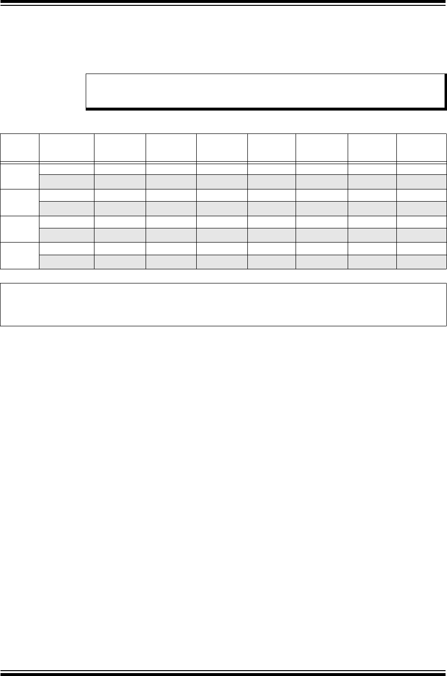
PIC32 Family Reference Manual
DS61192A-page 50-64 Preliminary © 2013 Microchip Technology Inc.
50.12.32 Config4 Register (CP0 Register 16, Select 4)
The Config4 register is an adjunct to the Config register and encodes additional information
about capabilities present on the core. On PIC32 devices, the Config4 register indicates the
presence of the Config5 register. All fields in the Config4 register are read-only.
Note: The microAptiv Core Configuration register bit fields and default values may vary
between devices. Refer to “microAptiv Core Configuration” chapter in the specific
device data sheet for the core configuration of a specific device.
Register 50-32: Config4: Configuration Register 4; CP0 Register 16, Select 4
Bit
Range
Bit
31/23/15/7
Bit
30/22/14/6
Bit
29/21/13/5
Bit
28/20/12/4
Bit
27/19/11/3
Bit
26/18/10/2
Bit
25/17/9/1
Bit
24/16/8/0
31:24 r-1 U-0 U-0 U-0 U-0 U-0 U-0 U-0
— — — — — — — —
23:16 U-0 U-0 U-0 U-0 U-0 U-0 U-0 U-0
— — — — — — — —
15:8 U-0 U-0 U-0 U-0 U-0 U-0 U-0 U-0
— — — — — — — —
7:0 U-0 U-0 U-0 U-0 U-0 U-0 U-0 U-0
— — — — — — — —
Legend: r = Reserved
R = Readable bit W = Writable bit U = Unimplemented bit, read as ‘0’
-n = Value at POR ‘1’ = Bit is set ‘0’ = Bit is cleared x = Bit is unknown
bit 31 Reserved: This bit is hardwired to a '1' to indicate the presence of the Config5 register.
bit 30-0 Unimplemented: Read as ‘0’

© 2013 Microchip Technology Inc. Preliminary DS61192A-page 50-65
Section 50. CPU for Devices with microAptiv™ Core
CPU for Devices with
microAptiv™ Core
50
50.12.33 Config5 Register (CP0 Register 16, Select 5)
The Config5 register is an adjunct to the Config register and encodes additional information
about capabilities present on the core. The Config5 register indicates whether or not the Nested
Fault feature is implemented. All fields in the Config5 register are read-only.
Note: The microAptiv Core Configuration register bit fields and default values may vary
between devices. Refer to “microAptiv Core Configuration” chapter in the specific
device data sheet for the core configuration of a specific device.
Register 50-33: Config5: Configuration Register 5; CP0 Register 16, Select 5
Bit
Range
Bit
31/23/15/7
Bit
30/22/14/6
Bit
29/21/13/5
Bit
28/20/12/4
Bit
27/19/11/3
Bit
26/18/10/2
Bit
25/17/9/1
Bit
24/16/8/0
31:24 U-0 U-0 U-0 U-0 U-0 U-0 U-0 U-0
— — — — — — — —
23:16 U-0 U-0 U-0 U-0 U-0 U-0 U-0 U-0
— — — — — — — —
15:8 U-0 U-0 U-0 U-0 U-0 U-0 U-0 U-0
— — — — — — — —
7:0 U-0 U-0 U-0 U-0 U-0 U-0 U-0 R-1
— — — — — — —NF
Legend: r = Reserved
R = Readable bit W = Writable bit U = Unimplemented bit, read as ‘0’
-n = Value at POR ‘1’ = Bit is set ‘0’ = Bit is cleared x = Bit is unknown
bit 31-1 Unimplemented: Read as ‘0’
bit 0 NF: Nested Fault bit
1 = Nested Fault feature is implemented
0 = Nested Fault feature is not implemented
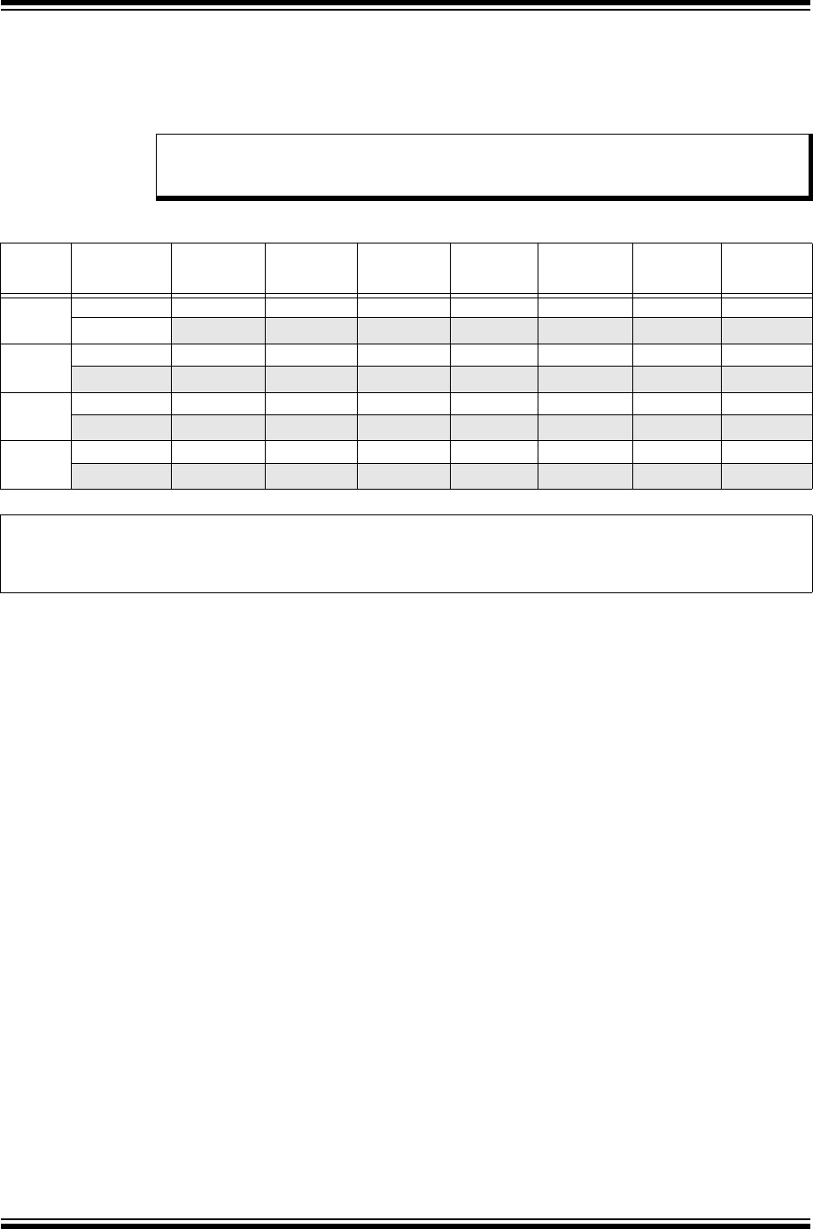
PIC32 Family Reference Manual
DS61192A-page 50-66 Preliminary © 2013 Microchip Technology Inc.
50.12.34 Config7 Register (CP0 Register 16, Select 7)
The Config7 register contains implementation specific configuration information. A number of
these bits are writable to disable certain performance enhancing features within the microAptiv™
Microprocessor core.
Note: The microAptiv Core Configuration register bit fields and default values may vary
between devices. Refer to “microAptiv Core Configuration” chapter in the specific
device data sheet for the core configuration of a specific device.
Register 50-34: Config7: Configuration Register 7; CP0 Register 16, Select 7
Bit
Range
Bit
31/23/15/7
Bit
30/22/14/6
Bit
29/21/13/5
Bit
28/20/12/4
Bit
27/19/11/3
Bit
26/18/10/2
Bit
25/17/9/1
Bit
24/16/8/0
31:24 R-1 U-0 U-0 U-0 U-0 U-0 U-0 U-0
WII — — — — — — —
23:16 U-0 U-0 U-0 U-0 U-0 U-0 U-0 U-0
— — — — — — — —
15:8 U-0 U-0 U-0 U-0 U-0 U-0 U-0 U-0
— — — — — — — —
7:0 U-0 U-0 U-0 U-0 U-0 U-0 U-0 U-0
— — — — — — — —
Legend:
R = Readable bit W = Writable bit U = Unimplemented bit, read as ‘0’
-n = Value at POR ‘1’ = Bit is set ‘0’ = Bit is cleared x = Bit is unknown
bit 31 WII: Wait IE Ignore bit
Indicates that this processor will allow an interrupt to unblock a WAIT instruction, even if IE is preventing
the interrupt from being taken. This avoids problems using the WAIT instruction for ‘bottom half’ interrupt
servicing. This bit always reads ‘1’ for devices with the microAptiv™ Microprocessor core.
bit 30-0 Unimplemented: Read as ‘0’

© 2013 Microchip Technology Inc. Preliminary DS61192A-page 50-67
Section 50. CPU for Devices with microAptiv™ Core
CPU for Devices with
microAptiv™ Core
50
50.12.35 LLAddr Register (CP0 Register 17, Select 0)
(microAptiv™ MPU Only)
The LLAddr register contains the physical address read by the most recent Load Linked (LL)
instruction. This register is for diagnostic purposes only, and serves no function during normal
operation.
Register 50-35: LLAddr: Load Linked Address Register; CP0 Register 17, Select 0
Bit
Range
Bit
31/23/15/7
Bit
30/22/14/6
Bit
29/21/13/5
Bit
28/20/12/4
Bit
27/19/11/3
Bit
26/18/10/2
Bit
25/17/9/1
Bit
24/16/8/0
31:24 U-0 U-0 U-0 U-0 R-x R-x R-x R/x
————PAddr<27:24>
23:16 R-x R-x R-x R-x R-x R-x R-x R-x
PAddr< 23:16>
15:8 R-x R-x R-x R-x R-x R-x R-x R-x
PAddr<15:8>
7:0 R-x R-x R-x R-x R-x R-x R-x R-x
PAddr<7:0>
Legend:
R = Readable bit W = Writable bit U = Unimplemented bit, read as ‘0’
-n = Value at POR ‘1’ = Bit is set ‘0’ = Bit is cleared x = Bit is unknown
bit 31-28 Unimplemented: Read as ‘0’
bit 27-0 PAddr<27:0>: Load Linked Instruction Physical Address Encode bits
These bits encode the physical address read by the most recent Load Linked instruction.

PIC32 Family Reference Manual
DS61192A-page 50-68 Preliminary © 2013 Microchip Technology Inc.
50.12.36 WatchLo Register (CP0 Register 18, Select 0-3)
(microAptiv™ MPU Only)
The WatchLo and WatchHi registers together provide the interface to a watchpoint debug facility
that initiates a watch exception if an instruction or data access matches the address specified in
the registers. As such, they duplicate some functions of the EJTAG debug solution. Watch
exceptions are taken only if the EXL and ERL bits are both ‘0’ in the Status register. If either bit
is a ‘1’, the WP bit is set in the Cause register, and the watch exception is deferred until both the
EXL and ERL bits are ‘0’.
The WatchLo register specifies the base virtual address and the type of reference (instruction
fetch, load, store) to match.
Register 50-36: WatchLo: Watchdog Debug Low Register; CP0 Register 18, Select 0-7
Bit
Range
Bit
31/23/15/7
Bit
30/22/14/6
Bit
29/21/13/5
Bit
28/20/12/4
Bit
27/19/11/3
Bit
26/18/10/2
Bit
25/17/9/1
Bit
24/16/8/0
31:24 R/W-x R/W-x R/W-x R/W-x R/W-x R/W-x R/W-x R/W-x
VAddr<28:21>
23:16 R/W-x R/W-x R/W-x R/W-x R/W-x R/W-x R/W-x R/W-x
VAddr< 20:13>
15:8 R/W-x R/W-x R/W-x R/W-x R/W-x R/W-x R/W-x R/W-x
VAddr<12:5>
7:0 R/W-x R/W-x R/W-x R/W-x R/W-x R/W-0 R/W-0 R/W-0
VAddr<4:0> I R W
Legend:
R = Readable bit W = Writable bit U = Unimplemented bit, read as ‘0’
-n = Value at POR ‘1’ = Bit is set ‘0’ = Bit is cleared x = Bit is unknown
bit 31-3 VAddr<28:0>: Virtual Address Match bits
This field specifies the virtual address to match. This is a double word address, because bits <2:0> are used
to control the type of match.
bit 2 I: Instruction Fetch Watch Address Exception Enable bit
1 = Watch exceptions are enabled for instruction fetches that match the address
0 = Watch exceptions are not enabled
bit 1 R: Instruction Fetch Watch Load Exception Enable bit
1 = Watch exceptions are enabled for loads that match the address
0 = Watch exceptions are not enabled
bit 0 W: Instruction Fetch Watch Stores Exception Enable bit
1 = Watch exceptions are enabled for stores that match the address
0 = Watch exceptions are not enabled
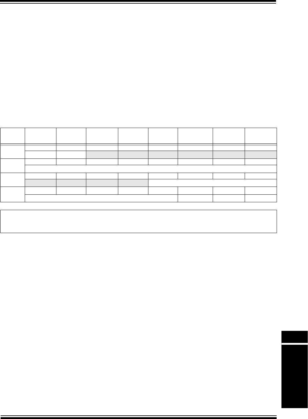
© 2013 Microchip Technology Inc. Preliminary DS61192A-page 50-69
Section 50. CPU for Devices with microAptiv™ Core
CPU for Devices with
microAptiv™ Core
50
50.12.37 WatchHi Register (CP0 Register 19, Select 0-3)
(microAptiv™ MPU Only)
The WatchLo and WatchHi registers together provide the interface to a watchpoint debug facility
that initiates a watch exception if an instruction or data access matches the address specified in
the registers. As such, they duplicate some functions of the EJTAG debug solution. Watch
exceptions are taken only if the EXL and ERL bits are zero in the Status register. If either bit is a
‘1’, the WP bit is set in the Cause register, and the watch exception is deferred until both the EXL
and ERL bits are ‘0’.
The WatchHi register contains information that qualifies the virtual address specified in the
WatchLo register: an ASID, a Global (G) bit, and an optional address mask. If the G bit is ‘1’, any
virtual address reference that matches the specified address will cause a watch exception. If the
G bit is a ‘0’, only those virtual address references for which the ASID value in the WatchHi
register matches the ASID value in the EntryHi register cause a watch exception. The optional
mask field provides address masking to qualify the address specified in WatchLo.
Register 50-37: WatchHi: Watchdog Debug High Register; CP0 Register 19, Select 0-7
Bit
Range
Bit
31/23/15/7
Bit
30/22/14/6
Bit
29/21/13/5
Bit
28/20/12/4
Bit
27/19/11/3
Bit
26/18/10/2
Bit
25/17/9/1
Bit
24/16/8/0
31:24 R-x R/W-x U-0 U-0 U-0 U-0 U-0 U-0
MG— — — — — —
23:16 R/W-x R/W-x R/W-x R/W-x R/W-x R/W-x R/W-x R/W-x
ASID<7:0>
15:8 U-0 U-0 U-0 U-0 R/W-x R/W-x R/W-x R/W-x
————Mask<8:5>
7:0 R/W-x R/W-x R/W-x R/W-x R/W-x W-x, HS, CS W-x, HS, CS W-x, HS, CS
Mask<4:0> I R W
Legend: HS = Set in Hardware CS = Cleared by Software
R = Readable bit W = Writable bit U = Unimplemented bit, read as ‘0’
-n = Value at POR ‘1’ = Bit is set ‘0’ = Bit is cleared x = Bit is unknown
bit 31 M: Watch Register Pairs Detect bit
Indicates whether additional Watch register pairs beyond this one are present or not
bit 30 G: Global bit
1 = Any address that matches that specified in the WatchLo register causes a watch exception
0 = ASID<7:0> must match the ASID bits of the EntryHi register to cause a watch exception
bit 29-24 Unimplemented: Read as ‘0’
bit 23-16 ASID<7:0>: Address Space ID Watch Exception Match bits
ASID value which is required to match that in the EntryHi register if the G bit is zero in the WatchHi register.
bit 15-12 Unimplemented: Read as ‘0’
bit 11-3 Mask<8:0>: Virtual Address Match Mask bits
Bit mask that qualifies the address in the WatchLo register. Any bit in this field that is a set inhibits the correspond-
ing address bit from participating in the address match.
bit 2 I: Instruction Fetch Condition Match bit
This bit is set by hardware when an instruction fetch condition matches the values in this watch register
pair. When set, the bit remains set until cleared by software, which is accomplished by writing a ‘1’.
bit 1 R: Load Condition Match bit
This bit is set by hardware when a load condition matches the values in this watch register pair. When set,
the bit remains set until cleared by software, which is accomplished by writing a ‘1’.
bit 0 W: Store Condition Match bit
This bit is set by hardware when a store condition matches the values in this watch register pair. When set,
the bit remains set until cleared by software, which is accomplished by writing a ‘1’
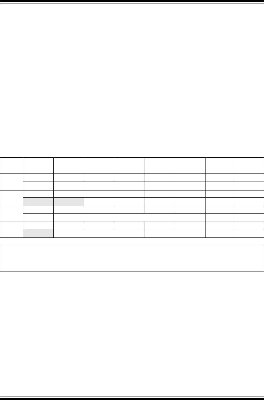
PIC32 Family Reference Manual
DS61192A-page 50-70 Preliminary © 2013 Microchip Technology Inc.
50.12.38 Debug Register (CP0 Register 23, Select 0)
The Debug register is used to control the debug exception and provide information about the
cause of the debug exception and when re-entering at the debug exception vector due to a
normal exception in Debug mode. The read-only information bits are updated every time the
debug exception is taken or when a normal exception is taken when already in Debug mode.
Only the DM bit and the VER<2:0> bits are valid when read from non-Debug mode; the values
of all other bits and fields are unpredictable. Operation of the processor is undefined if the Debug
register is written from non-Debug mode.
Some of the bits and fields are only updated on debug exceptions and/or exceptions in Debug
mode, as follows:
•DSS, DBP, DDBL, DDBS, DIB, DINT are updated on both debug exceptions and on
exceptions in debug modes
•DEXCCODE<4:0> are updated on exceptions in Debug mode, and are undefined after a
debug exception
•HALT and DOZE are updated on a debug exception, and are undefined after an exception
in Debug mode
•DBD is updated on both debug and on exceptions in debug modes
All bits are undefined when read from Normal mode, except VER<2:0> and DM.
Register 50-38: Debug: Debug Exception Register; CP0 Register 23, Select 0
Bit
Range
Bit
31/23/15/7
Bit
30/22/14/6
Bit
29/21/13/5
Bit
28/20/12/4
Bit
27/19/11/3
Bit
26/18/10/2
Bit
25/17/9/1
Bit
24/16/8/0
31:24 R-0 R-0 R-0 R/W-0 R-x R-x R/W-1 R/W-0
DBD DM NODCR LSNM DOZE HALT COUNTDM IBUSEP
23:16 U-0 U-0 R/W-0 R/W-0 R-0 R-0 R-1 R-0
— — DBUSEP IEXI DDBSIMPR DDBLIMPR VER<2:1>
15:8 R-1 R-x R-x R-x R-x R-x R-0 R/W-0
VER<0> DEXCCODE<4:0> NOSST SST
7:0 U-0 R-x R-x R-x R-x R-x R-x R-x
—DIBIMPRDINT DIB DDBSDDBL DBP DSS
Legend:
R = Readable bit W = Writable bit U = Unimplemented bit, read as ‘0’
-n = Value at POR ‘1’ = Bit is set ‘0’ = Bit is cleared x = Bit is unknown
bit 31 DBD: Branch Delay Debug Exception bit
Indicates whether the last debug exception or exception in Debug mode, occurred in a branch delay slot:
1 = In delay slot
0 = Not in delay slot
bit 30 DM: Debug Mode bit
Indicates that the processor is operating in Debug mode:
1 = Processor is operating in Debug mode
0 = Processor is operating in non-Debug mode
bit 29 NODCR: Debug Control Register bit
Indicates whether the dseg memory segment is present and the Debug Control Register is accessible:
1 = No dseg present
0 = dseg is present

© 2013 Microchip Technology Inc. Preliminary DS61192A-page 50-71
Section 50. CPU for Devices with microAptiv™ Core
CPU for Devices with
microAptiv™ Core
50
bit 28 LSNM: Load Store Access Control bit
Controls access of load/store between dseg and main memory:
1 = Load/stores in dseg address range goes to main memory
0 = Load/stores in dseg address range goes to dseg
bit 27 DOZE: Low-Power Mode Debug Exception bit
Indicates that the processor was in any kind of low-power mode when a debug exception occurred.
1 = Processor was in a low-power mode when a debug exception occurred
0 = Processor was not in a low-power mode when a debug exception occurred
bit 26 HALT: System Bus Clock Stop bit
Indicates that the internal system bus clock was stopped when the debug exception occurred.
1 = Internal system bus clock running
0 = Internal system bus clock stopped
bit 25 COUNTDM: Count Register Behavior bit
Indicates the Count register behavior in Debug mode.
1 = Count register is running in Debug mode
0 = Count register stopped in Debug mode
bit 24 IBUSEP: Instruction Fetch Bus Error Exception Pending bit
Set when an instruction fetch bus error event occurs or if a ‘1’ is written to the bit by software. Cleared when
a Bus Error exception on instruction fetch is taken by the processor, and by Reset. If IBUSEP is set when
IEXI is cleared, a Bus Error exception on instruction fetch is taken by the processor, and IBUSEP is cleared.
bit 23-22 Unimplemented: Read as ‘0’
bit 21 DBUSEP: Data Access Bus Error Exception Pending bit
Covers imprecise bus errors on data access, similar to behavior of IBUSEP for imprecise bus errors on an
instruction fetch.
bit 20 IEXI: Imprecise Error Exception Inhibit Control bit
Controls exceptions taken due to imprecise error indications. Set when the processor takes a debug excep-
tion or exception in Debug mode. Cleared by execution of the DERET instruction; otherwise modifiable by
Debug mode software. When IEXI is set, the imprecise error exception from a bus error on an instruction
fetch or data access, cache error, or machine check is inhibited and deferred until the bit is cleared.
bit 19 DDBSIMPR: Debug Data Break Store Exception bit
Indicates that an imprecise Debug Data Break Store exception was taken. All data breaks are precise on
the PIC32 core, so this bit will always read as ‘0’.
bit 18 DDBLIMPR: Debug Data Break Load Exception bit
Indicates that an imprecise Debug Data Break Load exception was taken. All data breaks are precise on the
PIC32 core, so this bit will always read as ‘0’.
bit 17-15 VER<2:0>: EJTAG Version bit
Contains the EJTAG version number.
bit 14-10 DEXCCODE<4:0>: Latest Exception in Debug Mode bit
Indicates the cause of the latest exception in Debug mode. The bit is encoded as the EXCCODE<4:0> bits
in the Cause register for those normal exceptions that may occur in Debug mode. Value is undefined after
a debug exception.
bit 9 NOSST: Singe-step Feature Control bit
Indicates whether the single-step feature controllable by the SST bit is available in this implementation.
1 = No single-step feature available
0 = Single-step feature available
bit 8 SST: Debug Single-step Control bit
Controls if debug single-step exception is enabled.
1 = Debug single step exception enabled
0 = No debug single-step exception enabled
bit 7 Unimplemented: Read as ‘0’
Register 50-38: Debug: Debug Exception Register; CP0 Register 23, Select 0 (Continued)

PIC32 Family Reference Manual
DS61192A-page 50-72 Preliminary © 2013 Microchip Technology Inc.
bit 6 DIBIMPR: Imprecise Debug Instruction Break Exception bit
Indicates that an imprecise debug instruction break exception occurred (due to a complex breakpoint).
Cleared on exception in Debug mode.
bit 5 DINT: Debug Interrupt Exception bit
Indicates that a debug interrupt exception occurred. Cleared on exception in Debug mode.
1 = Debug interrupt exception
0 = No debug interrupt exception
bit 4 DIB: Debug Instruction Break Exception bit
Indicates that a debug instruction break exception occurred. Cleared on exception in Debug mode.
1 = Debug instruction exception
0 = No debug instruction exception
bit 3 DDBS: Debug Data Break Exception on Store bit
Indicates that a debug data break exception occurred on a store. Cleared on exception in Debug mode.
1 = Debug instruction exception on a store
0 = No debug data exception on a store
bit 2 DDBL: Debug Data Break Exception on Load bit
Indicates that a debug data break exception occurred on a load. Cleared on exception in Debug mode.
1 = Debug instruction exception on a load
0 = No debug data exception on a load
bit 1 DBP: Debug Software Breakpoint Exception bit
Indicates that a debug software breakpoint exception occurred. Cleared on exception in Debug mode.
1 = Debug software breakpoint exception
0 = No debug software breakpoint exception
bit 0 DSS: Debug Single-step Exception bit
Indicates that a debug single-step exception occurred. Cleared on exception in Debug mode.
1 = Debug single-step exception
0 = No debug single-step exception
Register 50-38: Debug: Debug Exception Register; CP0 Register 23, Select 0 (Continued)
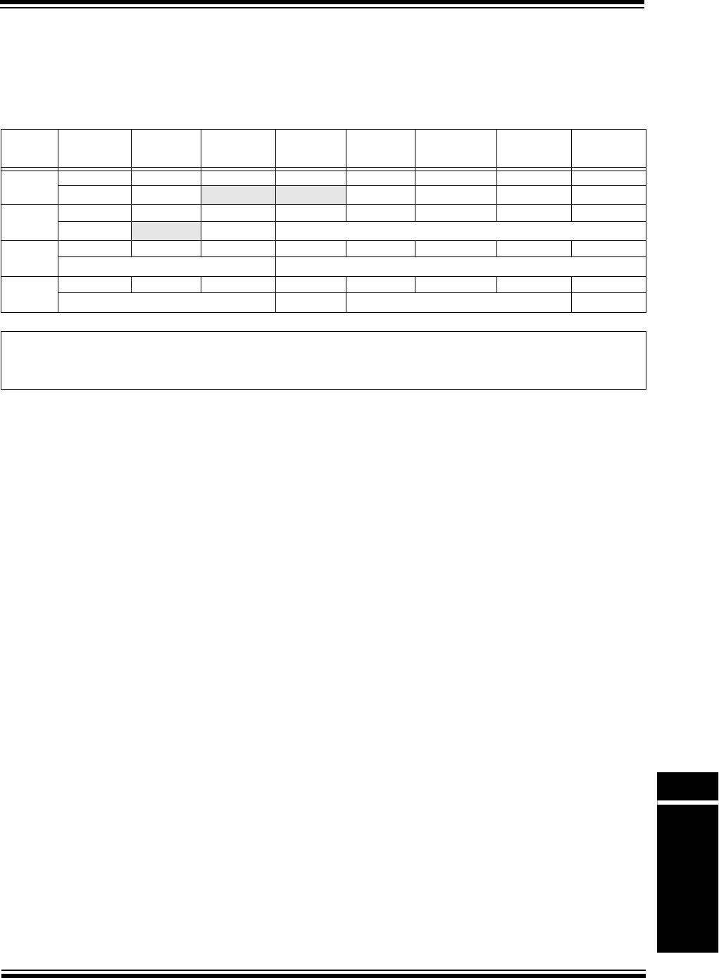
© 2013 Microchip Technology Inc. Preliminary DS61192A-page 50-73
Section 50. CPU for Devices with microAptiv™ Core
CPU for Devices with
microAptiv™ Core
50
50.12.39 TraceControl Register (CP0 Register 23, Select 1)
The TraceControl register enables software trace control and is only implemented on devices
with the EJTAG trace capability.
Register 50-39: TraceControl: Trace Control Register; CP0 Register 23, Select 1
Bit
Range
Bit
31/23/15/7
Bit
30/22/14/6
Bit
29/21/13/5
Bit
28/20/12/4
Bit
27/19/11/3
Bit
26/18/10/2
Bit
25/17/9/1
Bit
24/16/8/0
31:24 R/W-0 R/W-x U-0 U-0 R/W-x R/W-x R/W-x R/W-x
TS UT ——TB IO D
(1) E(1)
23:16 R/W-x U-0 R/W-x R/W-x R/W-x R/W-x R/W-x R/W-x
K(1) —U
(1) ASID_M<7:3>
15:8 R/W-x R/W-x R/W-x R/W-x R/W-x R/W-x R/W-x R/W-x
ASID_M<2:0> ASID<7:3>
7:0 R/W-x R/W-x R/W-x R/W-x R/W-x R/W-x R/W-x R/W-0
ASID<2:0> G MODE<2:0> ON
Legend:
R = Readable bit W = Writable bit U = Unimplemented bit, read as ‘0’
-n = Value at POR ‘1’ = Bit is set ‘0’ = Bit is cleared x = Bit is unknown
bit 31 TS: Trace Select bit
This bit is used to select between the hardware and the software trace control bits.
1 = Selects the trace control bits
0 = Selects the external hardware trace block signals
bit 30 UT: User Type Select bit
This bit is used to indicate the type of user-triggered trace record.
1 = User type 2
0 = User type 1
bit 27 TB: Trace Branch bit
1 = Trace the PC value for all taken branches
0 = Trace the PC value for branch targets with unpredictable static addresses
bit 26 IO: Inhibit Overflow bit
This signal is used to indicate to the core trace logic that slow but complete tracing is desired.
1 = Inhibit FIFO overflow or discard of trace data
0 = Allow FIFO overflow or discard of trace data
bit 25 D: Debug Mode Trace Enable bit(1)
1 = Enable tracing in Debug mode
0 = Disable tracing in Debug mode
bit 24 E: Exception Mode Trace Enable bit(1)
1 = Enable tracing in Exception mode
0 = Disable tracing in Exception mode
bit 23 K: Kernel Mode Trace Enable bit(1)
1 = Enable tracing in Kernel mode
0 = Disable tracing in Kernel mode
bit 22 Unimplemented: Read as ‘0’
bit 21 U: User Mode Trace Enable bit(1)
1 = Enable tracing in User mode
0 = Disable tracing in User mode
Note 1: The ON bit must be set to ‘1’ to enable tracing.

PIC32 Family Reference Manual
DS61192A-page 50-74 Preliminary © 2013 Microchip Technology Inc.
bit 20-13 ASID_M<7:0>: Address Space ID Mask Value bits
A ‘1’ in any bit in this field inhibits the corresponding ASID bit from participating in the match.
A value of ‘0’ in this field compares all bits of ASID.
bit 12-5 ASID<7:0>: Address Space ID Value bits
These bits must match the Address Space ID when the G bit is set to ‘0’.
These bits are ignored when the G bit is set to ‘1’.
bit 4 G: Global bit
1 = Tracing is to be enabled for all processes, provided that other enabling functions are also true
0 = Tracing is not enabled
bit 3-1 MODE<2:0>: Trace Mode Control bits
111 = Trace PC and both load and store address and data
110 = Trace PC and store address and data
101 = Trace PC and load address and data
100 = Trace PC and load data
011 = Trace PC and both load and store addresses
010 = Trace PC and store address
001 = Trace PC and load address
000 = Trace PC
bit 0 ON: Master Trace Enable bit
1 = Tracing is enabled when another trace enable bit is set to ‘1’
0 = Tracing is disabled
Register 50-39: TraceControl: Trace Control Register; CP0 Register 23, Select 1 (Continued)
Note 1: The ON bit must be set to ‘1’ to enable tracing.

© 2013 Microchip Technology Inc. Preliminary DS61192A-page 50-75
Section 50. CPU for Devices with microAptiv™ Core
CPU for Devices with
microAptiv™ Core
50
50.12.40 TraceControl2 Register (CP0 Register 23, Select 2)
The TraceControl2 register provides additional control and status information. Note that some
fields in the TraceControl2 register are read-only, but have a reset state of “Undefined”. This is
because these values are loaded from the Trace Control Block (TCB). As such, these fields in
the TraceControl2 register will not have valid values until the TCB asserts these values.
Register 50-40: TraceControl2: Trace Control Register 2; CP0 Register 23, Select 2
Bit
Range
Bit
31/23/15/7
Bit
30/22/14/6
Bit
29/21/13/5
Bit
28/20/12/4
Bit
27/19/11/3
Bit
26/18/10/2
Bit
25/17/9/1
Bit
24/16/8/0
31:24 U-0 U-0 U-0 U-0 U-0 U-0 U-0 U-0
— — — — — — — —
23:16 U-0 U-0 U-0 U-0 U-0 U-0 U-0 U-0
— — — — — — — —
15:8 U-0 U-0 U-0 U-0 U-0 U-0 U-0 U-0
— — — — — — — —
7:0 U-0 R-1 R-0 R-0 R-1 R-x R-x R-x
—VALIDMODES<1:0>TBITBU SYP<2:0>
Legend:
R = Readable bit W = Writable bit U = Unimplemented bit, read as ‘0’
-n = Value at POR ‘1’ = Bit is set ‘0’ = Bit is cleared x = Bit is unknown
bit 31-7 Unimplemented: Read as ‘0’
bit 6-5 VALIDMODES<1:0>: Valid Trace Mode Select bits
11 = Reserved
10 = PC, load and store address, and load and store data
01 = PC and load and store address tracing only
00 = PC tracing only
bit 4 TBI: Trace Buffers Implemented bit
1 = On-chip and off-chip trace buffers are implemented by the TCB
0 = Only one trace buffer is implemented
bit 3 TBU: Trace Buffers Used bit
1 = Trace data is being sent to an off-chip trace buffer
0 = Trace data is being sent to an on-chip trace buffer
bit 2-0 SYP<2:0>: Synchronization Period bits
The “On-chip” column value is used when the trace data is being written to an on-chip trace buffer (e.g,
TraceControl2TBU = 0). Conversely, the “Off-chip” column is used when the trace data is being written to an
off-chip trace buffer (e.g., TraceControl2TBU = 1).
Bit
Setting On-chip Off-chip
111 = 2227
110 = 2328
101 = 2429
100 = 25210
011 = 26211
010 = 27212
001 = 28213
000 = 29214

PIC32 Family Reference Manual
DS61192A-page 50-76 Preliminary © 2013 Microchip Technology Inc.
50.12.41 UserTraceData1 Register (CP0 Register 23, Select 3)
A software write to any bits in the UserTraceData1 register will trigger a trace record to be written
indicating a type 1 user format. The type is based on the UT bit in the TraceControl register. This
register cannot be written in consecutive cycles. The trace output data is unpredictable if this
register is written in consecutive cycles.
This register is only implemented on devices with the EJTAG trace capability.
Register 50-41: UserTraceData1: User Trace Data Register 1; CP0 Register 23, Select 3
Bit
Range
Bit
31/23/15/7
Bit
30/22/14/6
Bit
29/21/13/5
Bit
28/20/12/4
Bit
27/19/11/3
Bit
26/18/10/2
Bit
25/17/9/1
Bit
24/16/8/0
31:24 R/W-0 R/W-0 R/W-0 R/W-0 R/W-0 R/W-0 R/W-0 R/W-0
DATA<31:24>
23:16 R/W-0 R/W-0 R/W-0 R/W-0 R/W-0 R/W-0 R/W-0 R/W-0
DATA<23:10>
15:8 R/W-0 R/W-0 R/W-0 R/W-0 R/W-0 R/W-0 R/W-0 R/W-0
DATA<15:6>
7:0 R/W-0 R/W-0 R/W-0 R/W-0 R/W-0 R/W-0 R/W-0 R/W-0
DATA<7:0>
Legend:
R = Readable bit W = Writable bit U = Unimplemented bit, read as ‘0’
-n = Value at POR ‘1’ = Bit is set ‘0’ = Bit is cleared x = Bit is unknown
bit 31-0 DATA: Software Readable/Writable Data bits
When written, this register triggers a user format trace record out of the PDtrace interface that transmits the
Data bit to trace memory.

© 2013 Microchip Technology Inc. Preliminary DS61192A-page 50-77
Section 50. CPU for Devices with microAptiv™ Core
CPU for Devices with
microAptiv™ Core
50
50.12.42 TraceBPC Register (CP0 Register 23, Select 4)
This register is used to control start and stop of tracing using an EJTAG Hardware breakpoint.
The Hardware breakpoint would then be set as a trigger source and optionally also as a Debug
exception breakpoint.
This register is only implemented on devices with both Hardware breakpoints and the EJTAG
trace capability.
Register 50-42: TraceBPC: Trace Breakpoint Control Register; CP0 Register 23, Select 4
Bit
Range
Bit
31/23/15/7
Bit
30/22/14/6
Bit
29/21/13/5
Bit
28/20/12/4
Bit
27/19/11/3
Bit
26/18/10/2
Bit
25/17/9/1
Bit
24/16/8/0
31:24 R/W-0 U-0 U-0 U-0 U-0 U-0 U-0 U-0
DE — — — — — — —
23:16 R/W-0 R/W-0 R/W-0 R/W-0 R/W-0 R/W-0 R/W-0 R/W-0
DBPO7(1) DBPO6(1) DBPO5(1) DBPO4(1) DBPO3(1) DBPO2(1) DBPO1 DBPO0
15:8 R/W-0 U-0 U-0 U-0 U-0 U-0 U-0 U-0
IE — — — — — — —
7:0 R/W-0 R/W-0 R/W-0 R/W-0 R/W-0 R/W-0 R/W-0 R/W-0
IBPO7(1) IBPO6(1) IBPO5 IBPO4 IBPO3 IBPO2 IBPO1 IBPO0
Legend:
R = Readable bit W = Writable bit U = Unimplemented bit, read as ‘0’
-n = Value at POR ‘1’ = Bit is set ‘0’ = Bit is cleared x = Bit is unknown
bit 31 DE: EJTAG Data Breakpoint Trigger Select bit
1 = Enable trigger signals from data breakpoints
0 = Disable trigger signals from data breakpoints
bit 30-24 Unimplemented: Read as ‘0’
bit 23 DBPO7: Data Breakpoint 7 bit(1)
1 = Enable corresponding data instruction breakpoint trigger to start tracing
0 = Disable tracing with the trigger signal
bit 22 DBPO6: Data Breakpoint 6 bit(1)
1 = Enable corresponding data instruction breakpoint trigger to start tracing
0 = Disable tracing with the trigger signal
bit 21 DBPO5: Data Breakpoint 5 bit(1)
1 = Enable corresponding data instruction breakpoint trigger to start tracing
0 = Disable tracing with the trigger signal
bit 20 DBPO4: Data Breakpoint 4 bit(1)
1 = Enable corresponding data instruction breakpoint trigger to start tracing
0 = Disable tracing with the trigger signal
bit 19 DBPO3: Data Breakpoint 3 bit(1)
1 = Enable corresponding data instruction breakpoint trigger to start tracing
0 = Disable tracing with the trigger signal
bit 18 DBPO2: Data Breakpoint 2 bit(1)
1 = Enable corresponding data instruction breakpoint trigger to start tracing
0 = Disable tracing with the trigger signal
bit 17 DBPO1: Data Breakpoint 1 bit
1 = Enable corresponding data instruction breakpoint trigger to start tracing
0 = Disable tracing with the trigger signal
Note 1: This bit is only available on PIC32 devices with the microAptiv™ MPU core.

PIC32 Family Reference Manual
DS61192A-page 50-78 Preliminary © 2013 Microchip Technology Inc.
bit 16 DBPO0: Data Breakpoint 0 bit
1 = Enable corresponding data instruction breakpoint trigger to start tracing
0 = Disable tracing with the trigger signal
bit 15 IE: EJTAG Instruction Breakpoint Select bit
1 = Enable trigger signals from instruction breakpoints
0 = Disable trigger signals from instruction breakpoints
bit 14-8 Unimplemented: Read as ‘0’
bit 5 IBPO7: Instruction Breakpoint 7 bit(1)
1 = Enable corresponding instruction breakpoint trigger to start tracing
0 = Disable tracing with the trigger signal
bit 4 IBPO6: Instruction Breakpoint 6 bit(1)
1 = Enable corresponding instruction breakpoint trigger to start tracing
0 = Disable tracing with the trigger signal
bit 5 IBPO5: Instruction Breakpoint 5 bit
1 = Enable corresponding instruction breakpoint trigger to start tracing
0 = Disable tracing with the trigger signal
bit 4 IBPO4: Instruction Breakpoint 4 bit
1 = Enable corresponding instruction breakpoint trigger to start tracing
0 = Disable tracing with the trigger signal
bit 3 IBPO3: Instruction Breakpoint 3 bit
1 = Enable corresponding instruction breakpoint trigger to start tracing
0 = Disable tracing with the trigger signal
bit 2 IBPO2: Instruction Breakpoint 2 bit
1 = Enable corresponding instruction breakpoint trigger to start tracing
0 = Disable tracing with the trigger signal
bit 1 IBPO1: Instruction Breakpoint 1 bit
1 = Enable corresponding instruction breakpoint trigger to start tracing
0 = Disable tracing with the trigger signal
bit 0 IBPO0: Instruction Breakpoint 0 bit
1 = Enable corresponding instruction breakpoint trigger to start tracing
0 = Disable tracing with the trigger signal
Register 50-42: TraceBPC: Trace Breakpoint Control Register; CP0 Register 23, Select 4 (Continued)
Note 1: This bit is only available on PIC32 devices with the microAptiv™ MPU core.
© 2013 Microchip Technology Inc. Preliminary DS61192A-page 50-79
Section 50. CPU for Devices with microAptiv™ Core
CPU for Devices with
microAptiv™ Core
50
50.12.43 Debug2 Register (CP0 Register 23, Select 5)
This register holds additional information about Complex Breakpoint exceptions. This register is
only implemented if complex hardware breakpoints are present.
Register 50-43: Debug2: Debug Breakpoint Exceptions Register; CP0 Register 23, Select 5
Bit
Range
Bit
31/23/15/7
Bit
30/22/14/6
Bit
29/21/13/5
Bit
28/20/12/4
Bit
27/19/11/3
Bit
26/18/10/2
Bit
25/17/9/1
Bit
24/16/8/0
31:24 r-1 U-0 U-0 U-0 U-0 U-0 U-0 U-0
— — — — — — — —
23:16 U-0 U-0 U-0 U-0 U-0 U-0 U-0 U-0
— — — — — — — —
15:8 U-0 U-0 U-0 U-0 U-0 U-0 U-0 U-0
— — — — — — — —
7:0 U-0 U-0 U-0 U-0 R-x R-x R-x R-x
— — — — PRM DQ TUP PACO
Legend: r = Reserved bit
R = Readable bit W = Writable bit U = Unimplemented bit, read as ‘0’
-n = Value at POR ‘1’ = Bit is set ‘0’ = Bit is cleared x = Bit is unknown
bit 31 Reserved: Read as ‘1’
bit 30-4 Unimplemented: Read as ‘0’
bit 3 PRM: Primed bit
Indicates whether a complex breakpoint with an active priming condition was seen on the last debug
exception.
bit 2 DQ: Data Qualified bit
Indicates whether a complex breakpoint with an active data qualifier was seen on the last debug exception.
bit 1 TUP: Tuple Breakpoint bit
Indicates whether a tuple breakpoint was seen on the last debug exception.
bit 0 PACO: Pass Counter bit
Indicates whether a complex breakpoint with an active pass counter was seen on the last debug exception.

PIC32 Family Reference Manual
DS61192A-page 50-80 Preliminary © 2013 Microchip Technology Inc.
50.12.44 DEPC Register (CP0 Register 24, Select 0)
The Debug Exception Program Counter (DEPC) register is a read/write register that contains the
address at which processing resumes after a debug exception or Debug mode exception has
been serviced.
For synchronous (precise) debug and Debug mode exceptions, the DEPC register contains
either:
•The virtual address of the instruction that was the direct cause of the debug exception, or
• The virtual address of the immediately preceding branch or jump instruction, when the
debug exception causing instruction is in a branch delay slot, and the Debug Branch Delay
(DBD) bit in the Debug register is set.
For asynchronous debug exceptions (debug interrupt), the DEPC register contains the virtual
address of the instruction where execution should resume after the debug handler code is exe-
cuted.
Since the PIC32 family implements the MIPS16e® or microMIPS™ ASE, a read of the DEPC
register (via MFC0) returns the following value in the destination GPR:
GPR[rt] = DebugExceptionPC31..1 || ISAMode0
That is, the upper 31 bits of the debug exception PC are combined with the lower bit of the
ISA<1:0> bits (Config3<15:14>)and are written to the GPR.
Similarly, a write to the DEPC register (via MTC0) takes the value from the GPR and distributes
that value to the debug exception PC and the ISA<1:0> bits (Config3<15:14>), as follows:
DebugExceptionPC = GPR[rt]31..1 || 0
ISAMode = 2#0 || GPR[rt]0
That is, the upper 31 bits of the GPR are written to the upper 31 bits of the debug exception PC,
and the lower bit of the debug exception PC is cleared. The upper bit of the ISA<1:0> bits (Con-
fig3<15:14>) is cleared and the lower bit is loaded from the lower bit of the GPR.
Register 50-44: DEPC: Debug Exception Program Counter Register; CP0 Register 24, Select 0
Bit
Range
Bit
31/23/15/7
Bit
30/22/14/6
Bit
29/21/13/5
Bit
28/20/12/4
Bit
27/19/11/3
Bit
26/18/10/2
Bit
25/17/9/1
Bit
24/16/8/0
31:24 R/W-x R/W-x R/W-x R/W-x R/W-x R/W-x R/W-x R/W-x
DEPC<31:24>
23:16 R/W-x R/W-x R/W-x R/W-x R/W-x R/W-x R/W-x R/W-x
DEPC<23:16>
15:8 R/W-x R/W-x R/W-x R/W-x R/W-x R/W-x R/W-x R/W-x
DEPC<15:8>
7:0 R/W-x R/W-x R/W-x R/W-x R/W-x R/W-x R/W-x R/W-x
DEPC<7:0>
Legend:
R = Readable bit W = Writable bit U = Unimplemented bit, read as ‘0’
-n = Value at POR ‘1’ = Bit is set ‘0’ = Bit is cleared x = Bit is unknown
bit 31-0 DEPC<31:0>: Debug Exception Program Counter bits
The DEPC register is updated with the virtual address of the instruction that caused the debug exception. If
the instruction is in the branch delay slot, the virtual address of the immediately preceding branch or jump
instruction is placed in this register.
Execution of the DERET instruction causes a jump to the address in the DEPC register.

© 2013 Microchip Technology Inc. Preliminary DS61192A-page 50-81
Section 50. CPU for Devices with microAptiv™ Core
CPU for Devices with
microAptiv™ Core
50
50.12.45 UserTraceData2(CP0 Register 24, Select 3)
A software write to any bits in the UserTraceData2 register will trigger a trace record to be written
indicating a type 2 user format. The type is based on the UT bit in the TraceControl register. This
register cannot be written in consecutive cycles. The trace output data is unpredictable if this
register is written in consecutive cycles.
This register is only implemented on devices with the EJTAG trace capability.
Register 50-45: UserTraceData2: User Trace Data Register 2; CP0 Register 24, Select 3
Bit
Range
Bit
31/23/15/7
Bit
30/22/14/6
Bit
29/21/13/5
Bit
28/20/12/4
Bit
27/19/11/3
Bit
26/18/10/2
Bit
25/17/9/1
Bit
24/16/8/0
31:24 R/W-0 R/W-0 R/W-0 R/W-0 R/W-0 R/W-0 R/W-0 R/W-0
DATA<31:24>
23:16 R/W-0 R/W-0 R/W-0 R/W-0 R/W-0 R/W-0 R/W-0 R/W-0
DATA<23:16>
15:8 R/W-0 R/W-0 R/W-0 R/W-0 R/W-0 R/W-0 R/W-0 R/W-0
DATA<15:8>
7:0 R/W-0 R/W-0 R/W-0 R/W-0 R/W-0 R/W-0 R/W-0 R/W-0
DATA<7:0>
Legend:
R = Readable bit W = Writable bit U = Unimplemented bit, read as ‘0’
-n = Value at POR ‘1’ = Bit is set ‘0’ = Bit is cleared x = Bit is unknown
bit 31-0 DATA<31:0>: Software Readable/Writable Data bits
When written, this register triggers a user format trace record out of the PDtrace interface that transmits the
DATA bits to trace memory.
PIC32 Family Reference Manual
DS61192A-page 50-82 Preliminary © 2013 Microchip Technology Inc.
50.12.46 PerfCtlx Register (CP0 Register 25, Select 0/3)
The microAptiv™ microprocessor core defines two performance counters, PerfCnt0 and
PerfCnt1 (see Register 50-47), and two associated control registers, PerfCtl0 and PerfCtl1,
which are mapped to CP0 register 25. The select bit of the MTC0/MFC0 instructions are used to
select the specific register accessed by the instruction, as shown in Ta ble 5 0-1 4.
Table 50-14: Performance Counter Register Selects
Each counter is a 32-bit read/write register and is incremented by one each time the countable
event, specified in its associated control register, occurs. Each counter can independently count
one type of event at a time.
Bit 31 of each of the counters are ANDed with an interrupt enable bit, IE, of their respective
control register to determine if a performance counter interrupt should be signaled. The two
values are then ORed together to create the Performance Counter Interrupt output. This signals
an interrupt to the microAptiv™ core. Counting is not affected by the interrupt indication. This
output is cleared when the counter wraps to zero, and may be cleared in software by writing a
value with bit 31 = 0 to the Performance Counter Count registers.
Select<2:0> Register
0Register 0 Control
1Register 0 Count
2Register 1 Control
3Register 1 Count
Note: The performance counter registers are connected to a clock that is stopped when
the processor is in Sleep mode. Most events would not be active during that time,
but others would be, notably the cycle count. This behavior should be considered
when analyzing measurements taken on a system.
Register 50-46: PerfCtlx: Performance Counter Control Register; CP0 Register 25, Select 0/3)
Bit
Range
Bit
31/23/15/7
Bit
30/22/14/6
Bit
29/21/13/5
Bit
28/20/12/4
Bit
27/19/11/3
Bit
26/18/10/2
Bit
25/17/9/1
Bit
24/16/8/0
31:24 r-x U-0 U-0 U-0 U-0 U-0 U-0 U-0
— — — — — — — —
23:16 U-0 U-0 U-0 U-0 U-0 U-0 U-0 U-0
— — — — — — — —
15:8 U-0 U-0 U-0 U-0 R/W-x R/W-x R/W-x R/W-x
— — — —EVENT<6:3>
7:0 R/W-x R/W-x R/W-x R/W-0 R-0 U-0 R/W-x R/W-x
EVENT<2:0> IE U —KEXL
Legend: r = Reserved bit
R = Readable bit W = Writable bit U = Unimplemented bit, read as ‘0’
-n = Value at POR ‘1’ = Bit is set ‘0’ = Bit is cleared x = Bit is unknown
bit 31 Reserved: Read as ‘1’ for PerfCtl0, and ‘0’ for PerfCtl1
bit 30-12 Unimplemented: Read as ‘0’
bit 11-5 EVENT<6:0>:
Counter event enabled for this counter. Possible events are listed in Ta ble 5 0- 1 5.
bit 4 IE: Counter Interrupt Enable bit
This bit masks bit 31 of the associated count register from the interrupt exception request output.

© 2013 Microchip Technology Inc. Preliminary DS61192A-page 50-83
Section 50. CPU for Devices with microAptiv™ Core
CPU for Devices with
microAptiv™ Core
50
Ta b l e 5 0 -1 5 describes the events countable with the two performance counters. The mode
column indicates whether the event counting is influenced by the mode bits (U, K, EXL). The
operation of a counter is unpredictable for events that are specified as Reserved.
Performance counters never count in Debug mode or when ERL = 1.
bit 3 U: Count in User Mode bit
When this bit is set, the specified event is counted in User mode.
bit 2 Unimplemented: Read as ‘0’
bit 1 K: Count in Kernel Mode bit
When this bit is set, count the event in Kernel mode when EXL and ERL are both ‘0’.
bit 0 EXL: Count when EXL bit
When this bit is set, count the event when EXL = 1 and ERL = 0.
Register 50-46: PerfCtlx: Performance Counter Control Register; CP0 Register 25, Select 0/3) (Continued)
Table 50-15: Performance Countable Events
Event
Number Counter 0 Mode Counter 1 Mode
0 Cycles No Cycles No
1 Instructions completed Yes Instructions completed Yes
2 Branch instructions Yes Reserved N/A
3 JR r31 (return) instructions Yes Reserved N/A
4 JR (not r31) instructions Yes Reserved N/A
5 ITLB accesses(1) Yes ITLB mi sse s(1) Yes
6 DTLB accesses(1) Yes DTLB misses(1) Yes
7 JTLB instruction accesses(1) Yes JT LB ins truction misses(1) Yes
8 JTLB data accesses(1) Yes JT LB data misses(1) Yes
9 Instruction cache accesses(1) Yes Instruction cache misses(1) Yes
10 Data cache accesses(1) Yes Da ta cache write-backs (1) Yes
11 Data cache misses(1) Yes Data cache miss es(1) Yes
12 Reserved N/A Reserved N/A
13 Reserved N/A Reserved N/A
14 integer instructions completed Yes Reserved N/A
15 loads completed Yes Stores completed Yes
16 J/JAL completed Yes microMIPS™ instructions completed Yes
17 no-ops completed Yes Integer multiply/divide completed Yes
18 Stall cycles No Reserved N/A
19 SC instructions completed Yes SC instructions failed Yes
20 Prefetch instructions completed Yes Prefetch instructions completed with cache
hit(1)
Yes
21 Reserved N/A Reserved N/A
22 Reserved N/A Reserved N/A
23 Exceptions taken Yes Reserved N/A
24 Reserved N/A Reserved N/A
25 IFU stall cycles(1) No ALU stall cycles No
26 Reserved N/A Reserved N/A
27 Reserved N/A Reserved N/A
28 Reserved N/A Implementation-specific CP2 event Yes
Note 1: This event is only available on devices with the microAptiv™ MPU core. Refer to the “CPU” chapter in the
specific device data sheet for availability.

PIC32 Family Reference Manual
DS61192A-page 50-84 Preliminary © 2013 Microchip Technology Inc.
29 Reserved N/A Reserved N/A
30 Reserved N/A Reserved N/A
31 Reserved N/A Reserved N/A
32 Reserved N/A Reserved N/A
33 Uncached loads N/A Uncached stores N/A
34 Reserved N/A Reserved N/A
35 CP2 arithmetic instructions completed Yes CP2 To/From instructions completed Yes
36 Reserved N/A Reserved N/A
37 I-Cache miss stall cycles(1) Yes D-C ach e miss stall cy cle s(1) Yes
38 Reserved N/A Reserved N/A
39 D-Cache miss cycles(1) No Reserved N/A
40 Uncached stall cycles Yes Reserved N/A
41 MDU stall cycles Yes Reserved N/A
42 CP2 stall cycles Yes Reserved N/A
43 Reserved N/A Reserved N/A
44 CACHE instruction stall cycles(1) No Reserved N/A
45 Load to Use stall cycles Yes Reserved N/A
46 Other interlock stall cycles Yes Reserved N/A
47 Reserved N/A Reserved N/A
48 Reserved N/A Reserved N/A
49 EJTAG Instruction Triggerpoints Yes EJTAG Data Triggerpoints Yes
50 -51 Reserved N/A Reserved N/A
52 LFQ < one-fourth full(1) No LFQ one-fourth to one-half full(1) No
53 LFQ > one-half full(1) No LFQ full pipeline stall cycles(1) No
54 WBB < one-fourth full(1) No WBB one-fourth to one-half full(1) No
55 WBB > one-half full(1) No WBB full pipeline stall cycles(1) No
56-63 Reserved N/A Reserved N/A
Table 50-15: Performance Countable Events (Continued)
Event
Number Counter 0 Mode Counter 1 Mode
Note 1: This event is only available on devices with the microAptiv™ MPU core. Refer to the “CPU” chapter in the
specific device data sheet for availability.

© 2013 Microchip Technology Inc. Preliminary DS61192A-page 50-85
Section 50. CPU for Devices with microAptiv™ Core
CPU for Devices with
microAptiv™ Core
50
Table 50-16: Event Description
Event Name Counter Event
Number Description
Cycles 0/1 0 Total number of cycles. The performance counters are clocked
by the top-level gated clock. If the microAptiv™ core is built
with that clock gate is present, none of the counters will
increment while the clock is stopped (e.g., due to a WAIT
instruction).
Instruction Completion
The following events indicate completion of various types of instructions
Instructions 0/1 1 Total number of instructions completed.
Branch instructions 0 2 Counts all branch instructions that completed.
JR R31 (return) instructions 0 3 Counts all JR R31 instructions that completed.
JR (not R31) 0 4 Counts all JR rxx (not r31) and JALR instructions (indirect
jumps).
Integer instructions 0 14 Non-floating point instructions.
Loads 0 15 Includes both integer and coprocessor loads.
Stores 1 15 Includes both integer and coprocessor stores.
J/JAL 0 16 Direct Jump (And Link) instruction.
microMIPS™ 1 16 All microMIPS™ instructions.
no-ops 0 17 This includes all instructions that normally write to a GPR, but
where the destination register was set to r0.
Integer Multiply/Divide 1 17 Counts all Integer Multiply/Divide instructions (MULxx, DIVx,
MADDx, MSUBx).
SC 0 19 Counts conditional stores regardless of whether they
succeeded.
PREF 0 20 Note that this only counts PREFs that are actually attempted.
PREFs to uncached addresses or ones with translation errors
are not counted
Uncached loads(1) 033
Include both uncached and uncached accelerated CCAs.
Uncached stores(1) 133
Instruction Execution Events
ITLB accesses(1) 0 5 Counts ITLB accesses that are due to fetches showing up in IF
stage of the pipe and do not use fixed mapping or are not in
unmapped space. If an address is fetched twice down the pipe
(as in the case of a cache miss), that instruction will count 2
ITLB accesses. Also, because each fetch returns 2
instructions, there is one access marked per double word.
ITLB misses(1) 1 5 Counts all misses in ITLB except ones that are on the back of
another miss. We cannot process back to back misses and
thus those are ignored for this purpose. Also ignored if there is
some form of address error.
DTLB accesses(1) 0 6 Counts DTLB access including those in unmapped address
spaces.
DTLB misses(1) 1 6 Counts DTLB misses. Back to back misses that result in only
one DTLB entry getting refilled are counted as a single miss.
JTLB instruction accesses(1) 07Instruction JTLB accesses are counted exactly the same as
ITLB misses.
JTLB instruction misses(1) 1 7 Counts instruction JTLB accesses that result in no match or a
match
on an invalid translation.
Note 1: This event is only available on devices with the microAptiv™ MPU core. Refer to the “CPU” chapter in the
specific device data sheet for availability.

PIC32 Family Reference Manual
DS61192A-page 50-86 Preliminary © 2013 Microchip Technology Inc.
JTLB data accesses(1) 08Data JTLB accesses.
JTLB data misses(1) 1 8 Counts data JTLB accesses that result in no match or a match
on an invalid translation.
I-Cache accesses(1) 0 9 Counts every time the instruction cache is accessed. All
replays, wasted fetches etc. are counted. For example, follow-
ing a branch, even the prediction is taken, the fall-through
access is counted.
I-Cache misses(1) 1 9 Counts all instruction cache misses that result in a bus
request.
D-Cache accesses(1) 0 10 Counts cached loads and stores.
D-Cache writebacks(1) 110Counts cache lines written back to memory due to
replacement or cache ops.
D-Cache misses(1) 0/1 11 Counts loads and stores that miss in the cache.
SC instructions failed 1 19 SC instruction that did not update memory.
Note: While this event and the SC instruction count event
can be configured to count in specific operating
modes, the timing of the events is much different, and
the observed operating mode could change between
them, causing some inaccuracy in the measured
ratio.
PREF completed with cache
hit(1)
1 20 Counts PREF instructions that hit in the cache.
Exceptions Taken 0 23 Any type of exception taken.
EJTAG instruction triggers 0 49 Number of times an EJTAG Instruction Trigger Point condition
matched.
EJTAG data triggers 1 49 Number of times an EJTAG Data Trigger Point condition
matched.
Pipeline
Cache fixup(1) 024Counts cycles where the DCC is in a fixup and cannot accept a
new instruction from the ALU. Fixups are replays within the
DCC that occur when a instruction needs to reaccess the
cache or the DTLB.
General Stalls
IFU stall cycles(1) 025Counts the number of cycles in which the fetch unit is not
providing a valid instruction to the ALU.
ALU stall cycles 1 25 Counts the number of cycles in which the ALU pipeline cannot
advance.
Stall cycles 0 18 Counts the total number of cycles in which no instructions are
issued by SRAM to ALU (the RF stage does not advance).
This includes both of the previous two events. However, this is
different from the sum of them, because cycles when both
stalls are active will only be counted once.
Specific Stalls
These events will count the number of cycles lost due to this. This will include bubbles introduced by replays within
the pipe. If multiple stall sources are active simultaneously, the counters for each of the active events will be
incremented.
I-Cache miss stall cycles(1) 037Cycles when ICC stalls because an I-Cache miss caused the
ICC not to have any runnable instructions. Ignores the stalls
due to ITLB misses as well as the 4 cycles following a redirect.
Table 50-16: Event Description (Continued)
Event Name Counter Event
Number Description
Note 1: This event is only available on devices with the microAptiv™ MPU core. Refer to the “CPU” chapter in the
specific device data sheet for availability.

© 2013 Microchip Technology Inc. Preliminary DS61192A-page 50-87
Section 50. CPU for Devices with microAptiv™ Core
CPU for Devices with
microAptiv™ Core
50
D-Cache miss stall cycles(1) 137Counts all cycles in which the integer pipeline waits on a Load
to return data due to a D-Cache miss.
D-Cache miss cycle cycles(1) 0 39 D-Cache miss is outstanding, but not necessarily stalling the
pipeline. The difference between this and D-Cache miss stall
cycles can show the gain from non-blocking cache misses.
Uncached stall cycles 0 40 Cycles in which the processor is stalled on an uncached fetch,
load, or store.
MDU stall cycles 0 41 Counts all cycles in which the integer pipeline waits on MDU
return data.
CACHE instruction stall cycles(1) 044Counts all cycles in which pipeline is stalled due to CACHE
instructions. Includes cycles in which CACHE instructions
themselves are stalled in the ALU, and cycles in which CACHE
instructions cause subsequent instructions to be stalled.
Load to Use stall cycles 0 45 Counts all cycles in which the integer pipeline waits on Load
return data.
Other interlocks stall cycles 0 46 Counts all cycles in which the integer pipeline waits on return
data from MFC0 and RDHWR instructions.
LFB full pipeline stall cycles 1 53 Cycles in which the pipeline is stalled because the Load Fill
Buffer (LFB) in the DCC is full.
Write-through buffer full stall
cycles(1)
1 55 Cycles in which the pipeline is stalled because the
write-through buffer in the BIU is full.
Table 50-16: Event Description (Continued)
Event Name Counter Event
Number Description
Note 1: This event is only available on devices with the microAptiv™ MPU core. Refer to the “CPU” chapter in the
specific device data sheet for availability.

PIC32 Family Reference Manual
DS61192A-page 50-88 Preliminary © 2013 Microchip Technology Inc.
50.12.47 PerfCntx Register (CP0 Register 25, Select 1/3)
The microAptiv™ microprocessor core defines two performance counters, PerfCnt0 and
PerfCnt1, and two associated control registers, PerfCtl0 and PerfCtl1 (see Register 50-46),
which are mapped to CP0 register 25. The select bit of the MTC0/MFC0 instructions are used to
select the specific register accessed by the instruction, as shown in Ta ble 5 0-1 4.
The performance counter resets to a low-power state, in which none of the counters will start
counting events until software has enabled event counting, using an MTC0 instruction to the
Performance Counter Control Registers.
Register 50-47: PerfCntx: Performance Counter Count Register; CP0 Register 25, Select 1/3 (x = 0 or 1)
Bit
Range
Bit
31/23/15/7
Bit
30/22/14/6
Bit
29/21/13/5
Bit
28/20/12/4
Bit
27/19/11/3
Bit
26/18/10/2
Bit
25/17/9/1
Bit
24/16/8/0
31:24 R/W-x R/W-x R/W-x R/W-x R/W-x R/W-x R/W-x R/W-x
COUNTER<31:24>
23:16 R/W-x R/W-x R/W-x R/W-x R/W-x R/W-x R/W-x R/W-x
COUNTER<23:16>
15:8 R/W-x R/W-x R/W-x R/W-x R/W-x R/W-x R/W-x R/W-x
COUNTER<15:8>
7:0 R/W-x R/W-x R/W-x R/W-x R/W-x R/W-x R/W-x R/W-x
COUNTER <7:0>
Legend:
R = Readable bit W = Writable bit U = Unimplemented bit, read as ‘0’
-n = Value at POR ‘1’ = Bit is set ‘0’ = Bit is cleared x = Bit is unknown
bit 31-0 COUNTER<31:0>: Event Counter bits
Counter for events enabled for this counter.

© 2013 Microchip Technology Inc. Preliminary DS61192A-page 50-89
Section 50. CPU for Devices with microAptiv™ Core
CPU for Devices with
microAptiv™ Core
50
50.12.48 ErrCtl Register (CP0 Register 26, Select 0)
(microAptiv™ MPU Only)
The ErrCtl register provides for software testing of the way-selection and RAM.
The way-selection RAM test mode is enabled by setting the WST bit. It modifies the functionality
of the CACHE Index Load Tag and Index Store Tag operations so that they modify the
way-selection RAM and leave the Tag RAMs untouched. When this bit is set, the lower six bits
of the PA field in the TagLo register are used as the source and destination for Index Load Tag
and Index Store Tag CACHE operations.
The WST bit also enables the data RAM test mode. When this bit is set, the Index Store Data
CACHE instruction is enabled. This CACHE operation writes the contents of the DataLo register
to the word in the data array that is indicated by the index and byte address.
Register 50-48: ErrCtl: Parity Protection Control Register; CP0 Register 26, Select 0
Bit
Range
Bit
31/23/15/7
Bit
30/22/14/6
Bit
29/21/13/5
Bit
28/20/12/4
Bit
27/19/11/3
Bit
26/18/10/2
Bit
25/17/9/1
Bit
24/16/8/0
31:24 U-0 U-0 R/W-0 U-0 U-0 U-0 U-0 U-0
——WST— — — — —
23:16 U-0 U-0 U-0 U-0 U-0 U-0 U-0 U-0
— — — — — — — —
15:8 U-0 U-0 U-0 U-0 U-0 U-0 U-0 U-0
— — — — — — — —
7:0 U-0 U-0 U-0 U-0 U-0 U-0 U-0 U-0
— — — — — — — —
Legend:
R = Readable bit W = Writable bit U = Unimplemented bit, read as ‘0’
-n = Value at POR ‘1’ = Bit is set ‘0’ = Bit is cleared x = Bit is unknown
bit 31-28 Unimplemented: Read as ‘0’
bit 29 WST: Way-Select/Tag Array bit
Indicates whether the tag array or the way-select array should be read/written on Index Load/Store Tag
CACHE instructions. This bit also enables the Index Store Data CACHE instruction, which writes the contents
of DataLo to the data array.
1 = Way-select array is read/written on Index Load/Store tag CACHE instruction
0 = Tag array is read/written on Index Load/Store tag CACHE instruction
bit 27-0 Unimplemented: Read as ‘0’

PIC32 Family Reference Manual
DS61192A-page 50-90 Preliminary © 2013 Microchip Technology Inc.
50.12.49 TagLo Register (CP0 Register 28, Select 0) When WST = 0
(ErrCtl<29>) (microAptiv™ MPU Only)
The TagLo register acts as the interface to the cache tag array. The Index Store Tag and Index
Load Tag operations of the CACHE instruction use the TagLo register as the source of tag
information.
When the WST bit of the ErrCtl register is asserted, this register becomes the interface to the
way-selection RAM. In this mode, the fields are redefined to give appropriate access the contents
of the WS array instead of the Tag array.
Note: Register 50-50 describes the fields in the TagLo register when WST = 1.
Register 50-49: TagLo: Cache Tag Array Interface Register; CP0 Register 28, Select 0 (When WST = 0)
Bit
Range
Bit
31/23/15/7
Bit
30/22/14/6
Bit
29/21/13/5
Bit
28/20/12/4
Bit
27/19/11/3
Bit
26/18/10/2
Bit
25/17/9/1
Bit
24/16/8/0
31:24 R/W-x R/W-x R/W-x R/W-x R/W-x R/W-x R/W-x R/W-x
PA<21:14>
23:16 R/W-x R/W-x R/W-x R/W-x R/W-x R/W-x R/W-x R/W-x
PA<13:6>
15:8 R/W-x R/W-x R/W-x R/W-x R/W-x R/W-x U-0 U-0
PA<5:0> — —
7:0 R/W-x R/W-x R/W-x U-0 U-0 U-0 U-0 U-0
VDL— — — — —
Legend:
R = Readable bit W = Writable bit U = Unimplemented bit, read as ‘0’
-n = Value at POR ‘1’ = Bit is set ‘0’ = Bit is cleared x = Bit is unknown
bit 31-10 PA<21:0>: Cache Line Physical Address bits
These bits contain the physical address of the cache line. PA<21> corresponds to bit 31 of the physical
address and PA<0> corresponds to bit 10 of the physical address.
bit 9-8 Unimplemented: Read as ‘0’
bit 7 V: Valid Cache Line Status bit
This bit indicates whether the cache line is valid.
bit 6 D: Dirty Cache Line Status bit
This bit indicates whether the cache line is dirty. This bit is only set if bit 7 (V) is also set.
bit 5 L: Cache Tag Lock Status bit
This bit specifies the lock bit for the cache tag. When this bit is set, and bit 7 (V) is set, the corresponding
cache line will not be replaced by the cache replacement algorithm.
bit 4-0 Unimplemented: Read as ‘0’

© 2013 Microchip Technology Inc. Preliminary DS61192A-page 50-91
Section 50. CPU for Devices with microAptiv™ Core
CPU for Devices with
microAptiv™ Core
50
50.12.50 TagLo Register (CP0 Register 28, Select 0) When WST = 1
(ErrCtl<29>) (microAptiv™ MPU Only)
The TagLo register acts as the interface to the cache tag array. The Index Store Tag and Index
Load Tag operations of the CACHE instruction use the TagLo register as the source of tag
information.
When the WST bit of the ErrCtl register is asserted, this register becomes the interface to the
way-selection RAM. In this mode, the fields are redefined to give appropriate access the contents
of the WS array instead of the Tag array.
Note: Register 50-49 describes the fields in the TagLo register when WST = 0.
Register 50-50: TagLo: Cache Tag Array Interface Register; CP0 Register 28, Select 0 (When WST = 1)
Bit
Range
Bit
31/23/15/7
Bit
30/22/14/6
Bit
29/21/13/5
Bit
28/20/12/4
Bit
27/19/11/3
Bit
26/18/10/2
Bit
25/17/9/1
Bit
24/16/8/0
31:24 U-0 U-0 U-0 U-0 U-0 U-0 U-0 U-0
— — — — — — — —
23:16 U-0 U-0 U-0 U-0 R/W-x R/W-x R/W-x R/W-x
————WSD<3:0>
15:8 R/W-x R/W-x R/W-x R/W-x R/W-x R/W-x U-0 U-0
WSLRU<5:0> — —
7:0 U-0 U-0 U-0 U-0 U-0 U-0 U-0 U-0
— — — — — — — —
Legend:
R = Readable bit W = Writable bit U = Unimplemented bit, read as ‘0’
-n = Value at POR ‘1’ = Bit is set ‘0’ = Bit is cleared x = Bit is unknown
bit 31-20 Unimplemented: Read as ‘0’
bit 19-16 WSD<3:0>: Way-Select Dirty Status bits
These bits contain the value read from the WS array after a CACHE Index Load WS operation. It is used to
store into the WS array during CACHE Index Store WS operations.
bit 15-10 WSLRU<5:0>: Way-Select Least Recently Used bits
These bits contain the value read from or to be stored to the WS array.
bit 9-0 Unimplemented: Read as ‘0’.

PIC32 Family Reference Manual
DS61192A-page 50-92 Preliminary © 2013 Microchip Technology Inc.
50.12.51 DataLo Register (CP0 Register 28, Select 1)
(microAptiv™ MPU Only)
The DataLo register is a register that acts as the interface to the cache data array and is intended
for diagnostic operations only. The Index Load Tag operation of the CACHE instruction reads the
corresponding data values into the DataLo register. If the WST bit in the ErrCtl register is set, the
contents of DataLo can be written to the cache data array by doing an Index Store Data CACHE
instruction.
Register 50-51: DataLo: Cache Data Array Interface Register; CP0 Register 28, Select 1
Bit
Range
Bit
31/23/15/7
Bit
30/22/14/6
Bit
29/21/13/5
Bit
28/20/12/4
Bit
27/19/11/3
Bit
26/18/10/2
Bit
25/17/9/1
Bit
24/16/8/0
31:24 R/W-x R/W-x R/W-x R/W-x R/W-x R/W-x R/W-x R/W-x
DATA<31:24>
23:16 R/W-x R/W-x R/W-x R/W-x R/W-x R/W-x R/W-x R/W-x
DATA<23:16>
15:8 R/W-x R/W-x R/W-x R/W-x R/W-x R/W-x R/W-x R/W-x
DATA<15:8>
7:0 R/W-x R/W-x R/W-x R/W-x R/W-x R/W-x R/W-x R/W-x
DATA<7:0>
Legend:
R = Readable bit W = Writable bit U = Unimplemented bit, read as ‘0’
-n = Value at POR ‘1’ = Bit is set ‘0’ = Bit is cleared x = Bit is unknown
bit 31-0 DATA<31:0>: Low-order Data Read from Cache Data Array bits

© 2013 Microchip Technology Inc. Preliminary DS61192A-page 50-93
Section 50. CPU for Devices with microAptiv™ Core
CPU for Devices with
microAptiv™ Core
50
50.12.52 ErrorEPC (CP0 Register 30, Select 0)
The ErrorEPC register is a read/write register, similar to the EPC register, except that ErrorEPC
is used on error exceptions. All bits of the ErrorEPC register are significant and must be writable.
It is also used to store the program counter on Reset, Soft Reset, and non-maskable interrupt
(NMI) exceptions.
The ErrorEPC register contains the virtual address at which instruction processing can resume
after servicing an error. This address can be:
•The virtual address of the instruction that caused the exception
•The virtual address of the immediately preceding branch or jump instruction when the error
causing instruction is in a branch delay slot
Unlike the EPC register, there is no corresponding branch delay slot indication for the ErrorEPC
register.
Since the PIC32 family implements the MIPS16e® or microMIPS™ ASE, a read of the ErrorEPC
register (via MFC0) returns the following value in the destination GPR:
GPR[rt] = ErrorExceptionPC31..1 || ISAMode0
That is, the upper 31 bits of the error exception PC are combined with the lower bit of the
ISA<1:0> bits (Config3<15:14>) and are written to the GPR.
Similarly, a write to the ErrorEPC register (via MTC0) takes the value from the GPR and
distributes that value to the error exception PC and the ISA<1:0> bits (Config3<15:14>), as
follows:
ErrprExceptionPC = GPR[rt]31..1 || 0
ISAMode = 2#0 || GPR[rt]0
That is, the upper 31 bits of the GPR are written to the upper 31 bits of the error exception PC,
and the lower bit of the error exception PC is cleared. The upper bit of the ISA<1:0> bits (Con-
fig3<15:14>) is cleared and the lower bit is loaded from the lower bit of the GPR.
Register 50-52: ErrorEPC: Error Exception Program Counter Register; CP0 Register 30, Select 0
Bit
Range
Bit
31/23/15/7
Bit
30/22/14/6
Bit
29/21/13/5
Bit
28/20/12/4
Bit
27/19/11/3
Bit
26/18/10/2
Bit
25/17/9/1
Bit
24/16/8/0
31:24 R/W-x R/W-x R/W-x R/W-x R/W-x R/W-x R/W-x R/W-x
ErrorEPC<31:24>
23:16 R/W-x R/W-x R/W-x R/W-x R/W-x R/W-x R/W-x R/W-x
ErrorEPC<23:16>
15:8 R/W-x R/W-x R/W-x R/W-x R/W-x R/W-x R/W-x R/W-x
ErrorEPC<15:8>
7:0 R/W-x R/W-x R/W-x R/W-x R/W-x R/W-x R/W-x R/W-x
ErrorEPC<7:0>
Legend:
R = Readable bit W = Writable bit U = Unimplemented bit, read as ‘0’
-n = Value at POR ‘1’ = Bit is set ‘0’ = Bit is cleared x = Bit is unknown
bit 31-0 ErrorEPC<31:0>: Error Exception Program Counter bits

PIC32 Family Reference Manual
DS61192A-page 50-94 Preliminary © 2013 Microchip Technology Inc.
50.12.53 DeSAVE Register (CP0 Register 31, Select 0)
The DeSAVE register is a read/write register that functions as a simple memory location. This
register is used by the debug exception handler to save one of the GPRs that is then used to
save the rest of the context to a predetermined memory area (such as in the EJTAG Probe). This
register allows the safe debugging of exception handlers and other types of code where the
existence of a valid stack for context saving cannot be assumed.
Register 50-53: DeSAVE: Debug Exception Save Register; CP0 Register 31, Select 0
Bit
Range
Bit
31/23/15/7
Bit
30/22/14/6
Bit
29/21/13/5
Bit
28/20/12/4
Bit
27/19/11/3
Bit
26/18/10/2
Bit
25/17/9/1
Bit
24/16/8/0
31:24 R/W-x R/W-x R/W-x R/W-x R/W-x R/W-x R/W-x R/W-x
DESAVE<31:24>
23:16 R/W-x R/W-x R/W-x R/W-x R/W-x R/W-x R/W-x R/W-x
DESAVE<23:16>
15:8 R/W-x R/W-x R/W-x R/W-x R/W-x R/W-x R/W-x R/W-x
DESAVE<15:8>
7:0 R/W-x R/W-x R/W-x R/W-x R/W-x R/W-x R/W-x R/W-x
DESAVE<7:0>
Legend:
R = Readable bit W = Writable bit U = Unimplemented bit, read as ‘0’
-n = Value at POR ‘1’ = Bit is set ‘0’ = Bit is cleared x = Bit is unknown
bit 31-0 DESAVE<31:0>: Debug Exception Save bits
Scratch Pad register used by Debug Exception code.

© 2013 Microchip Technology Inc. Preliminary DS61192A-page 50-95
Section 50. CPU for Devices with microAptiv™ Core
CPU for Devices with
microAptiv™ Core
50
50.13 microMIPS™ EXECUTION
microMIPS™ minimizes the code footprint of applications and therefore reduces the cost of
memory, which is particularly high for embedded memory. Simultaneously, the high performance
of MIPS cores is maintained. Using this technology, best results can be achieved without the
need to spend time to profile the application. The smaller code footprint typically leads to reduced
power consumption per executed task because of the smaller number of memory accesses.
The MIPS32® Release 3.0 Architecture supports both the MIPS32® instruction set and
microMIPS™, the enhanced MIPS32® instruction set.
50.14 MCU™ ASE EXTENSION
The MCU™ ASE extends the microMIPS™ and MIPS32® Architecture with a set of new features
designed for the microcontroller market.
The MCU™ ASE contains enhancements in several distinct areas: interrupt delivery and
interrupt latency.
50.14.1 Interrupt Delivery
The MCU™ ASE extends the number of interrupt hardware inputs from 63 to 255 (External
Interrupt Controller (EIC) mode), with separate priority and vector generation.
50.14.2 Interrupt Latency Reduction
The MCU™ ASE includes a package of extensions to microMIPS™ and MIPS32® that decrease
the latency of the processor’s response to a signaled interrupt.
50.14.2.1 INTERRUPT VECTOR PREFETCHING
Normally on MIPS architecture processors, when an interrupt or exception is signaled, execution
pipelines must be flushed before the interrupt/exception handler is fetched. This is necessary to
avoid mixing the contexts of the interrupted/faulting program and the exception handler. The
MCU™ ASE introduces a hardware mechanism in which the interrupt exception vector is
prefetched whenever the interrupt input signals change. The prefetch memory transaction occurs
in parallel with the pipeline flush and exception prioritization. This decreases the overall latency
of the execution of the interrupt handler’s first instruction.
50.14.2.2 AUTOMATED INTERRUPT PROLOGUE
The use of Shadow Register Sets avoids the software steps of having to save general-purpose
registers before handling an interrupt.
The MCU™ ASE adds additional hardware logic that automatically saves some of the CP0 state
in the stack and automatically updates some of the CP0 registers in preparation for interrupt
handling.
50.14.2.3 AUTOMATED INTERRUPT EPILOGUE
A mirror to the Automated Prologue, this features automates the restoration of some of the CP0
registers from the stack and the preparation of some of the CP0 registers for returning to
Non-Exception mode. This feature is implemented within the IRET instruction, which is
introduced in this ASE.
50.14.2.4 INTERRUPT CHAINING
An optional feature of the Automated Interrupt Epilogue, this feature allows handling a second
interrupt after a primary interrupt is handled, without returning to Non-Exception mode (and the
related pipeline flushes that would normally be necessary).
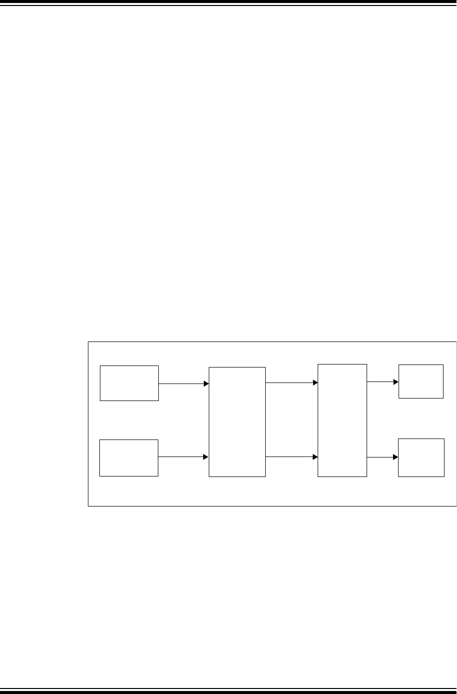
PIC32 Family Reference Manual
DS61192A-page 50-96 Preliminary © 2013 Microchip Technology Inc.
50.15 MIPS® DSP ASE EXTENSION
The MIPS DSP Application-Specific Extension Revision 2 is an extension to the MIPS32®
architecture. This extension comprises new integer instructions and states that include new
HI/LO accumulator register pairs and a DSP control register. This extension is crucial in a wide
range of DSP, multimedia, and DSP-like algorithms covering Audio and Video processing
applications. The extension supports native fractional format data type operations, register
Single Instruction Multiple Data (SIMD) operations, such as add, subtract, multiple, and shift. In
addition, the extension includes the following features that are essential in making DSP
algorithms computationally efficient:
•Support for multiplication of complex operands
•Variable bit insertion and extraction
•Implementation and use of virtual circular buffers
•Arithmetic saturation and overflow handling support
• Zero cycle overhead saturation and rounding operations
Refer to “MIPS32® Architecture for Programmers VolumeIV-e: The MIPS® DSP
Application-Specific Extension to the MIPS32® Architecture” – MD00374, Revision 2.34, May 6,
2011 for information on this extension, which is available from www.mips.com.
50.16 MEMORY MODEL (microAptiv™ MCU ONLY)
Virtual addresses used by software are converted to physical addresses by the memory
management unit (MMU) before being sent to the CPU busses. PIC32 devices based on the
microAptiv™ MCU Microprocessor core use a fixed mapping for this conversion.
For more information regarding the system memory model, see Section3. “Memory
Organization” (DS61115).
Figure 50-14: Address Translation During SRAM Access
50.16.1 Cacheability
The CPU uses the virtual address of an instruction fetch, load or store to determine whether to
access the cache or not. Memory accesses within kseg0, or useg/kuseg can be cached, while
accesses within kseg1 are non-cacheable. The CPU uses the CCA bits in the Config register to
determine the cacheability of a memory segment. A memory access is cacheable if its
corresponding CCA = 0112. For more information on cache operation, see Section 4. “Prefetch
Cache Module” (DS61119).
50.16.1.1 LITTLE ENDIAN BYTE ORDERING
On CPUs that address memory with byte resolution, there is a convention for multi-byte data
items that specify the order of high-order to low-order bytes. Big-endian byte-ordering is where
the lowest address has the MSB. Little-endian ordering is where the lowest address has the LSB
of a multi-byte datum. The PIC32 CPU supports little-endian byte ordering.
SRAM
Interface
Instn
SRAM
Data
SRAM
FMT
Instruction
Address
Calculator
Data
Address
Calculator
Virtual
Address
Virtual
Address
Physical
Address
Physical
Address

© 2013 Microchip Technology Inc. Preliminary DS61192A-page 50-97
Section 50. CPU for Devices with microAptiv™ Core
CPU for Devices with
microAptiv™ Core
50
Figure 50-15: Big-Endian Byte Ordering
Figure 50-16: Little-Endian Byte Ordering
Higher
Address Word
Address
Lower
Address
Bit #
} 1 word = 4 bytes
12
8
4
0
13
9
5
1
14
10
6
2
15
11
7
3
31 24 23 16 15 8 70
12
8
4
0
Higher
Address Word
Address
Lower
Address
Bit #
15
11
7
3
14
10
6
2
13
9
5
1
12
8
4
0
31 24 23 16 15 8 70
12
8
4
0
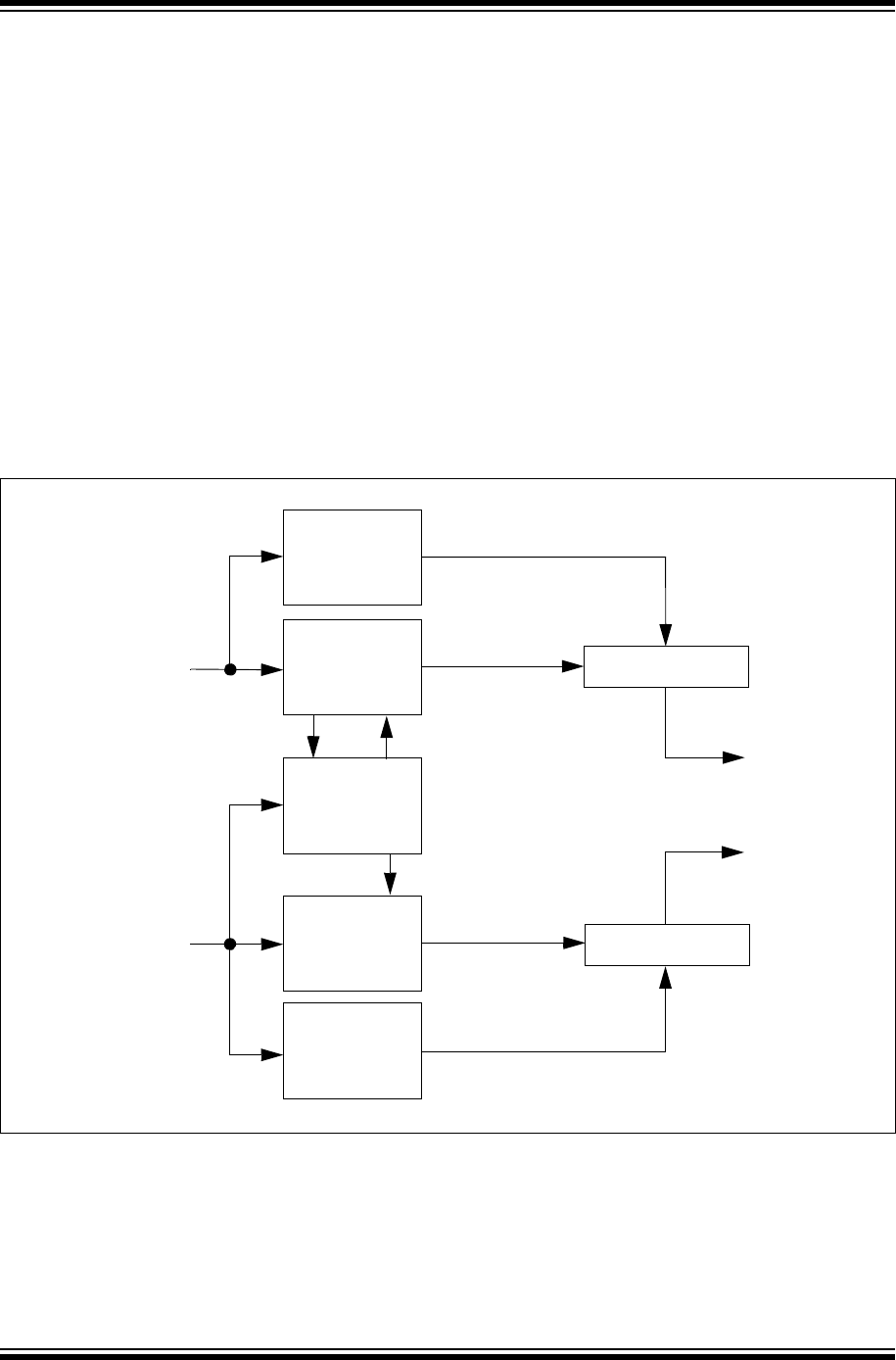
PIC32 Family Reference Manual
DS61192A-page 50-98 Preliminary © 2013 Microchip Technology Inc.
50.17 MEMORY MANAGEMENT (microAptiv™ MPU ONLY)
PIC32 devices with the microAptiv™ MPU core include a Memory Management Unit (MMU) that
uses a Translation Lookaside Buffer (TLB) to translate a virtual page address to a physical page
address. This feature is used by operating systems to manage multiple tasks running in the same
virtual memory, by mapping them into separate physical memory locations. The MMU can also
provide protection of physical memory areas and define the cache protocol. PIC32 devices with
the microAptiv™ MPU core support page sizes from 4 KB to 1 MB.
The core of the MMU is the TLB. The TLB contains three address translation buffers:
•16 dual-entry fully associative Joint TLB (JTLB)
•4-entry Instruction micro-TLB (ITLB)
•4-entry Data micro-TLB (DTLB)
When a page address is translated, the ITLB or DTLB is accessed first. If the translation is not
found in the micro-TLB, the JTLB is accessed. If the translation is not found in the JTLB, an
exception is taken.
Figure 50-17 shows how the TLB interacts with cache accesses in PIC32 devices with the
microAptiv™ MPU core.
Figure 50-17: TLB Address Translation
Instruction
Cache
ITLB
JTLB
DTLB
Data
Cache
Tag (IPA )
Instruction
Physical
Address (IPA)
Comparator
IVA Entry
Entry
Instruction
Virtual
Address (IVA)
Data
Virtual
Address (DVA)
Data
Physical
Address (DPA)
Tag (DPA )
Comparator
Instruction
Hit/Miss
Data
Hit/Miss

© 2013 Microchip Technology Inc. Preliminary DS61192A-page 50-99
Section 50. CPU for Devices with microAptiv™ Core
CPU for Devices with
microAptiv™ Core
50
50.17.1 Virtual Memory and Modes of Operation
All PIC32 devices support three modes of operation:
•User mode
•Kernel mode
•Debug mode
The core enters Kernel mode at reset, and when an exception is recognized. While in Kernel
mode, the software has access to the entire 4 GB address space, as well as the CP0 registers.
User mode access is restricted to the first 2 GB of the address space (0x00000000 through
0x7FFFFFFF), and can be excluded from accessing CP0 functions. Accessing a virtual address
above 0x7FFFFFFF in User mode will cause an exception.
Debug mode is entered on a debug exception. While in Debug mode, the software has access
to all Kernel mode addresses and functions, as well as debug segment dseg, which overlays part
of the kernel segment kseg3.
The virtual memory segments are different depending on the mode of operation. See
Figure 50-13 in 50.11.4 “Processor Modes” for the PIC32 virtual memory map.
50.17.1.1 MAPPED AND UNMAPPED SEGMENTS
Memory segments that use the MMU to translate virtual page address into physical memory
locations are considered to be mapped. Those that do not use the MMU are considered
unmapped. Unmapped segments have a fixed translation from virtual to physical addresses. At
reset, it is important to execute from unmapped memory until the TLB is programmed to perform
address translation.
Except for kseg0, unmapped segments are always uncached. The cacheability of kseg0 is set in
the K0 field of the CP0 register. The cacheability of mapped segments is set in the K23 and KU
fields of the CP0 register. Figure 50-18 shows the mapped and unmapped virtual memory areas
for Kernel mode and User mode. When operating in Debug mode, the dseg area is unmapped.
The mapping for all other areas is the same as Kernel mode.
Figure 50-18: User and Kernel Mode Virtual Mapping
0xFFFFFFFF
0x80000000
0x7FFFFFFF
0x00000000
User Mode Kernel Mode
0xFFFFFFFF
0x80000000
0x7FFFFFFF
0x00000000
0xE0000000
0xDFFFFFFF
0xC0000000
0xBFFFFFFF
0xA0000000
0x7FFFFFFF
Reserved
2 GB Mapped
512 MB Mapped
512 MB Mapped
512 MB Unmapped
512 MB Unmapped
2 GB Mapped
useg kuseg
kseg3
kseg2
kseg1
kseg0
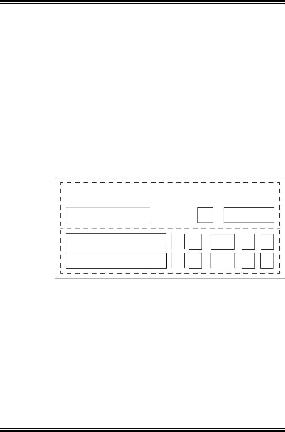
PIC32 Family Reference Manual
DS61192A-page 50-100 Preliminary © 2013 Microchip Technology Inc.
50.17.2 Translation Lookaside Buffer (TLB)
The TLB consists of one joint and two micro address translation buffers:
•16 dual-entry fully associative Joint TLB (JTLB)
•4-entry fully associative Instruction micro-TLB (ITLB)
•4-entry fully associative Data micro-TLB (DTLB)
50.17.2.1 JOINT TLB
The JTLB maps 32 virtual page addresses to their corresponding physical addresses. The
purpose of the TLB is to translate virtual page addresses along with their corresponding Address
Space ID (ASID) into a physical memory address. Operating systems typically assign an ASID
to each user program or process. The TLB helps the operating system separate each user
process into its own physical memory space.
The virtual to physical translation is performed by comparing the upper bits of the virtual address
and the ASID bits against each of the JTLB tag entries. The JTLB is referred to as a “Joint” TLB
because it is used to translate both instruction and data virtual page addresses.
The JTLB is organized as pairs of even and odd entries containing address translations of pages
ranging from 4 KB to 1 MB in size. Each virtual tag entry corresponds to two physical data entries,
an even page entry and an odd page entry. The highest order virtual address bit not participating
in the tag comparison is used to determine which of the two data entries is used. Figure 50-19
shows the contents of one the dual entries in the JTLB.
Figure 50-19: JTLB Entry (Tag and Data)
PageMask<28:11>
VPN2<31:13>
PFN0<31:12>
PFN1<31:12>
GASID<7:0>
RI0
RI1
XI0
XI1
C0<2:0>
C1<2:0>
D0
D1
V0
V1

© 2013 Microchip Technology Inc. Preliminary DS61192A-page 50-101
Section 50. CPU for Devices with microAptiv™ Core
CPU for Devices with
microAptiv™ Core
50
Ta b l e 5 0 -1 7 describes each field of a JTLB entry.
Table 50-17: TLB Tag Entry Fields
A table entry is filled with a TLBWI or TLBWR instruction. Before executing either instruction, the
following CP0 registers must be updated with the information to be written to the TLB entry:
•PageMask is set in the PageMask register (CP0 Register 5, Select 0).
•VPN2, VPN2X, and ASID are set in the EntryHi register (CP0 Register 10, Select 0)
•PFN0, C0, D0, V0, and G are set in the EntryLo0 register (CP0 Register 2, Select 0)
•PFN1, C1, D1, V1, and G are set in the EntryLo1 register (CP0 Register 3, Select 0)
Bit Name Description
PageMask<28:11> Page Mask Value. The Page Mask defines the page size by masking the appropriate VPN2 bits.
It also determines which address bit is used to make the even-odd page (PFN0-PFN1)
determination.
VPN2<31:13> Virtual Page Number divided by two. This field contains the upper bits of the virtual page
number divided by two. Because it represents a pair of TLB pages, it is divided by two. Bits
<31:25> are always included in the TLB lookup comparison. Bits <24:13> are included
depending on the page size, defined by PageMask.
GGlobal Bit. When set, indicates that this entry is global to all address spaces, and therefore
excludes the ASID in the TLB lookup comparison.
ASID<7:0> Address Space Identifier. Identifies which process or thread this TLB entry is associated with.
PFN0<31:12>
PFN1<31:12>
Physical Frame Number. Defines the upper bits of the physical address. For page sizes larger
than 4KB, only a subset of these bits is actually used.
C0<2:0>
C1<2:0>
Cacheability. Indicates the cacheability attributes and determines whether the page should be
placed in the cache or not.
RI0
RI1
Read Inhibit bit. Indicates that the page is read protected. If this bit is set, and the IEC bit of the
PageGrain register is set, any attempt to read from the page will result in a TLB Read Inhibit
exception.
XI0
XI1
Execute Inhibit bit. Indicates that the page is execution protected. If this bit is set, and the IEC
bit of the PageGrain register is set, any attempt to fetch an instruction from the page will result in
a TLB Execute Inhibit exception.
D0
D1
Dirty bit. Indicates that the page has been written and/or is writable. If this bit is set, writes to the
page are allowed. If this bit is not set, writes to the page will result in a TLB Modified exception.
V0
V1
Valid bit. Indicates that the TLB entry is valid. If this bit is set, accesses to the page are
permitted. If the bit is not set, accesses to the page will result in a TLB Invalid exception.
PageMask Page Size Even/Odd Bank Select Bit
00 0000 0000 0000 0011 4 KB VAddr<12>
00 0000 0000 0000 1111 16 KB VAddr<14>
00 0000 0000 0011 1111 64 KB VAddr<16>
00 0000 0000 1111 1111 256 KB VAddr<18>
00 0000 0011 1111 1111 1 MB VAddr<20>
C<2:0> Coherency Attribute
000 Cacheable, non-coherent, write-through, no write-allocate
001 Cacheable, non-coherent, write-through, write-allocate
010 Uncached
011 Cacheable, non-coherent, write-back, write-allocate
100-111 Reserved
Note: The global bit is part of the EntryLo0 and EntryLo1 registers. The value written to
the G bit in the JTLB is the logical AND of the G bits in the EntryLo0 and EntryLo1
registers.
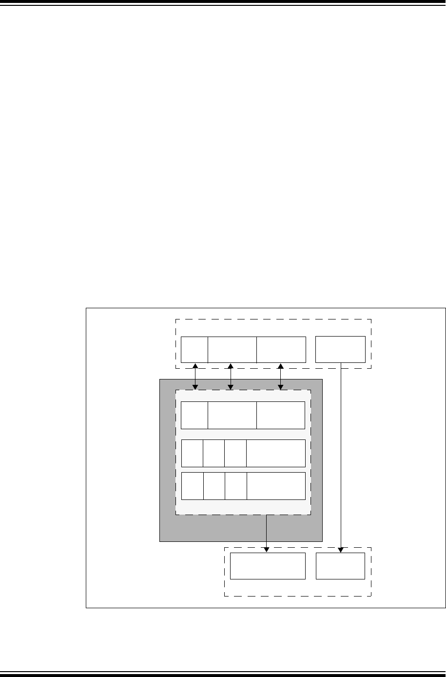
PIC32 Family Reference Manual
DS61192A-page 50-102 Preliminary © 2013 Microchip Technology Inc.
50.17.2.2 micro-TLBs (ITLB AND DTLB)
The ITLB is a small (i.e., micro) TLB dedicated to the instruction stream. The DTLB is a small
TLB that provides a faster translation for Load/Store addresses than is possible with the JTLB.
Both are 4-entry, fully associative, and managed entirely by hardware.
Instruction fetch address translation is handled first by the ITLB. If the fetch misses the ITLB, the
JTLB is accessed in the following clock cycle. If successful, the entry is copied into the ITLB. The
ITLB is then accessed again, and the address is successfully translated.
Data translations access the ITLB and the JTLB in parallel. If there is a DTLB miss and a JTLB
hit, the DTLB can be reloaded in the same clock cycle. The DTLB is then accessed on the next
clock cycle.
50.17.3 Virtual to Physical Address Translation
Essentially, the TLB acts a cache for page table entries. When a virtual address is converted to
a physical address, the Virtual Page Number (VPN) of the address (the upper bits of the address)
is compared with the virtual page numbers stored in the TLB. A TLB hit occurs when the following
conditions are met:
•The VPN of the virtual address matches a VPN stored in the TLB and:
-The Global (G) bit of both the even and odd pages of the TLB entry are set, or
-The ASID field of the virtual address is the same as the ASID field of the TLB entry
If these two conditions are not met, a TLB miss exception is taken by the processor and software
is allowed to refill the TLB from a page table of virtual/physical addresses in memory.
Figure 50-20 shows the translation of a virtual address into a physical address.
Figure 50-20: Virtual to Physical Address Translation
Each JTLB entry contains a tag and two data fields. On a TLB hit, the upper bits of the virtual
address are replaced with the Page Frame Number (PFN) stored in the corresponding data field.
On a TLB miss, an exception is taken and software refills the TLB from a page table stored in
memory.
GASID VPN
C0
C1
D0
D1
V0
V1
PFN0
PFN1
TLB Entry
TLB
GASID VPN Offset
Virtual Address
Physical Address
PFN Offset

© 2013 Microchip Technology Inc. Preliminary DS61192A-page 50-103
Section 50. CPU for Devices with microAptiv™ Core
CPU for Devices with
microAptiv™ Core
50
50.17.4 TLB Entry Replacement
On a normal TLB miss, JTLB entries are replaced by a random replacement algorithm. The CPU
also provides the ability to lock a programmable number of mappings into the TLB via the CP0
Wired register (see Register 50-8 for details).
The JTLB supports pages of different sizes ranging from 4 KB to 1 MB in powers of four. The
page size can be configured on a per-entry basis by loading the CP0 PageMask register with the
desired page size prior to writing a new entry. A common use for this feature is to map a large
memory block (such as a frame buffer) with a single TLB entry.
50.17.5 TLB Instructions
Ta b l e 5 0 -1 8 lists the TLB-related instructions supported by the PIC32. See 50.19.5.5 “TLB
Instructions (microAptiv™ MPU Only)” for details on these instructions.
Table 50-18: TLB Instructions
Instruction Description
TLBP Translation Lookaside Buffer Probe
TLBR Translation Lookaside Buffer Read
TLBWI Translation Lookaside Buffer Write Index
TLBWR Translation Lookaside Buffer Write Random
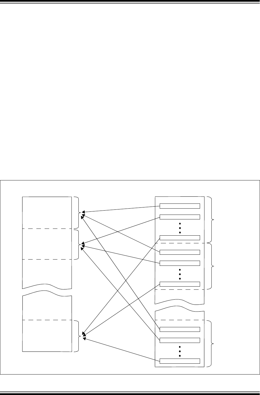
PIC32 Family Reference Manual
DS61192A-page 50-104 Preliminary © 2013 Microchip Technology Inc.
50.18 L1 CACHES (microAptiv™ MPU ONLY)
PIC32 devices with the microAptiv™ MPU microprocessor core have separate instruction and
data caches. The use of separate caches allows instruction and data references to happen
simultaneously. Both caches are Virtually Index, Physically-tagged (VIPT), allowing cache
access to occur in parallel with virtual-to-physical address translation.
50.18.1 Cache Configuration
The instruction and data caches may have different sizes and associativities. For example, the
instruction cache may be 16 KB in size with 4-way set associativity, while the data cache may be
4 KB with 2-way set associativity. A set-associative cache is a compromise between
direct-mapped and fully-associative caches.
In a direct-mapped cache, any location in memory can only be mapped to a single location in the
cache. A direct-mapped cache is simple to implement and address, but can be inflexible and lead
to thrashing when two heavily used memory locations share the same mapping.
A fully-associative cache allows any location in memory to map to any location in cache. This
minimizes collisions, but is expensive to implement.
In a set-associative cache, the cache is divided into groups of lines known as sets. The number
of lines per set is known as the associativity. Each memory location is mapped to a set, and may
be cached in any line within the set. For example, in a 16 KB, 16 bytes per line, 4-way
set-associative cache, the cache is divided into 256 sets of four lines each. As shown, in
Figure 50-21, any cacheable (16-byte) memory location is mapped to a single set, and may be
mapped to any of four lines within the set. In a system with 64 MB of cacheable memory, each
set is shared by 16,384 (256 x 16-bytes) blocks of memory.
Figure 50-21: microAptiv™ MPU 16 Kbyte 4-way Set-Associative Cache
Memory
Memory
Block 16,383
L1 Cache (16 KB) Physical Memory (64 MB)
Block 0
4 KB
(256 x 16 bytes)
Memory
Block 1
4 KB
(256 x 16 bytes)
Set 0
(4 x 16 bytes)
Set 1
(4 x 16 bytes)
0
255
4 KB
(256 x 16 bytes)
1
256
511
257
4,194,048
4,194,303
4,194,049
Set 255
(4 x 16 bytes)
(See Figure 50-22 for
details.)

© 2013 Microchip Technology Inc. Preliminary DS61192A-page 50-105
Section 50. CPU for Devices with microAptiv™ Core
CPU for Devices with
microAptiv™ Core
50
50.18.2 Cache Organization
Each cache line is organized into three arrays:
•Tag
•Data
•Way-select
The tag array holds the physical address of the cached memory location, and the data array
holds the cached (16-byte) instruction or data. The tag and data arrays hold four lines of
information per set, corresponding to the 4-way set associativity of the cache. The way-select
array holds Least Recently Used (LRU) bits that are decoded to select the way to be replaced,
according to a LRU algorithm. In the data cache, this array also holds the dirty bits, which indicate
whether or not the data needs to be written back to memory before being replaced in the cache.
Figure 50-22: Cache Array Formats
Definitions for Figure 50-22 are as follows:
•Physical Address: The upper 22 bits of the physical address (bits <31:10>)
•Lock: This bit is set or cleared using the CACHE instruction. When set, the cache line is
“locked” (i.e., it cannot be selected for replacement on a cache miss).
•Valid: Indicates whether or not the data in the cache line is valid
•Word 0-3: Instruction or data words from memory. Each cache line stores four 32-bit
words.
•Dirty: Present only in the data cache array, there is one dirty bit for each way. The dirty bit
is set when data in the cache line is modified. This lets the CPU know to write the cache
line back to memory before it is replaced on a cache fill.
•LRU: These bits indicate the way to be replaced according to a Least Recently Used (LRU)
algorithm
22 1 1
Physical Address Lock ValidWay 1
22 1 1
Physical Address Lock ValidWay 2
22 1 1
Physical Address Lock ValidWay 3
22 1 1
Physical Address Lock ValidWay 4
Word3 Word2 Word1 Word0
32 32 32 32
Word3 Word2 Word1 Word0
32 32 32 32
Word3 Word2 Word1 Word0
32 32 32 32
Word3 Word2 Word1 Word0
32 32 32 32
Dirty(1) LRU
46
Way-Select
Tag D a t a
Note 1: Data Cache only.

PIC32 Family Reference Manual
DS61192A-page 50-106 Preliminary © 2013 Microchip Technology Inc.
50.18.3 Cacheability Attributes
The cacheability attributes of kseg0 can be set with the CP0 Config1 register. The cacheability
options are:
•Uncached: Addresses in an uncached memory area are read from main memory, and not
from cache. Writes to uncached memory areas are written directly to main memory, without
changing the cache contents.
•Write-back with write allocation: Loads and instruction fetches first search the cache,
reading main memory only if the desired data does not reside in the cache. On data store
operations, the cache is first searched to see if the target address is resident in the cache.
If it is resident, the cache contents are updated, but main memory is not written. If the
cache lookup misses on a store, main memory is read to bring the line into the cache and
merge it with the new store data. Therefore, the allocation policy on a cache miss is read-
or write-allocate. Data stores will update the appropriate dirty bit in the way-select array to
indicate that the line contains modified data. When a line with dirty data is displaced from
the cache, it is written back to memory.
•Write-through with no write allocation: Loads and instruction fetches first search the
cache, reading main memory only if the desired data does not reside in the cache. On data
store operations, the cache is first searched to see if the target address is resident in the
cache. If it is resident, the cache contents are updated, and main memory is also written. If
the cache lookup misses on a store, only main memory is written. Therefore, the allocation
policy on a cache miss is read-allocate only.
•Write-through with write allocation: Loads and instruction fetches first search the cache,
reading main memory only if the desired data does not reside in the cache. On data store
operations, the cache is first searched to see if the target address is resident in the cache.
If it is resident, the cache contents are updated, and main memory is also written. If the
cache lookup misses on a store, main memory is read to bring the line into the cache and
merge it with the new store data. In addition, the store data is also written to main memory.
Therefore, the allocation policy on a cache miss is read- or write-allocate.
50.18.4 Cache Replacement Policy
The cache replacement policy refers to how the cache determines which way within a set to fill
on a cache miss. In a normal cache miss, the lock and LRU tag bits are used to determine the
way that is filled. If all ways are valid, any locked ways will not be replaced. If all ways are locked,
fill data will not fill into the cache, and Write-back stores turn into Write-through, Write-allocate
stores. If the way being replaced is dirty, the 16-byte line will be written back to memory before
the fill takes place.
The LRU field in the way-select array is updated in the following ways:
•On a cache hit, the associated way is updated to be the most recently used
•On a cache fill, the filled way is updated to be the most recently used
•On a CACHE instruction, the update of the LRU bits depends on the operation:
-Index (Writeback) Invalidate: Least recently used
-Index Load Tag: No update
-Index Store Tag (CP0 ErrCtl<WST> = 0): Most recently used if CP0 TagLo<V> = 1
Least recently used if CP0 TagLo<V> = 0
-Index Store Tag (CP0 ErrCtl<WST> = 1): Updated with contents of CP0 TagLo<LRU>
-Index Store Data: No update
-Hit Invalidate: Least recently used if a hit is generated; otherwise, no update
-Fill: Most recently used
-Hit Writeback: No update
-Fetch and Lock: Most recently used

© 2013 Microchip Technology Inc. Preliminary DS61192A-page 50-107
Section 50. CPU for Devices with microAptiv™ Core
CPU for Devices with
microAptiv™ Core
50
50.18.5 Cache Instruction
The contents of the tag, data and way-select arrays can be manipulated by the user with the
CACHE instruction. The user may fill, lock and invalidate individual cache lines by setting or
clearing bits in the tag and data arrays. See 50.19.7 “microAptiv™ MPU Cache Instruction”
for details on how to use the CACHE instruction.
50.18.6 Cache Coherency
Because a cache holds a copy of memory-resident data, it is possible for another bus master to
modify cached memory locations, rendering the cached data stale. Likewise, the CPU may
update the cache contents, rendering the corresponding memory data stale until it is written
back. The PIC32 CPU has no hardware support for maintaining coherency between cache and
memory, so it must be handled by software. Most operating systems manage cache coherency
issues automatically. Programs running without the benefit of a operating system must manage
cache coherency internally.
In Write-through mode, all data writes are written to main memory. In Write-back mode, data
writes only go to the cache; the cache may contain the only valid copy of the data until it is written
to main memory by a line refill or a CACHE instruction.
50.18.7 Cache Initialization
The PIC32 L1 cache tag and data arrays power up to an unknown state and are not affected by
reset. Therefore, the caches must be initialized before use. This is typically done by the boot
code by writing all-zero values to the tag array. Note that the boot code runs from uncached
memory (kseg1).

PIC32 Family Reference Manual
DS61192A-page 50-108 Preliminary © 2013 Microchip Technology Inc.
50.19 CPU INSTRUCTIONS
CPU instructions are organized into the following functional groups:
•Load and store
•Computational
• Jump and branch
•Miscellaneous
•Coprocessor
Each instruction is 32 bits long.
50.19.1 CPU Load and Store Instructions
MIPS processors use a load/store architecture; all operations are performed on operands held
in processor registers and main memory is accessed only through load and store instructions.
50.19.1.1 TYPES OF LOADS AND STORES
There are several different types of load and store instructions, each designed for a different
purpose:
•Transferring variously-sized fields (for example, LB, SW)
•Trading transferred data as signed or unsigned integers (for example, LHU)
•Accessing unaligned fields (for example, LWR, SWL)
•Atomic memory update (read-modify-write: for instance, LL/SC)
50.19.1.2 LIST OF CPU LOAD AND STORE INSTRUCTIONS
The following data sizes (as defined in the AccessLength field) are transferred by CPU load and
store instructions:
•Byte
•Half-word
•Word
Signed and unsigned integers of different sizes are supported by loads that either sign-extend or
zero-extend the data loaded into the register.
Unaligned words and double words can be loaded or stored in just two instructions by using a
pair of special instructions. For loads a LWL instruction is paired with a LWR instruction. The load
instructions read the left-side or right-side bytes (left or right side of register) from an aligned word
and merge them into the correct bytes of the destination register.
50.19.1.3 LOADS AND STORES USED FOR ATOMIC UPDATES
The paired instructions, Load Linked and Store Conditional, can be used to perform an atomic
read-modify-write of word or double word cached memory locations. These instructions are used
in carefully coded sequences to provide one of several synchronization primitives, including
test-and-set, bit-level locks, semaphores, and sequencers and event counts.
50.19.1.4 COPROCESSOR LOADS AND STORES
If a particular coprocessor is not enabled, loads and stores to that processor cannot execute and
the attempted load or store causes a Coprocessor Unusable exception. Enabling a coprocessor
is a privileged operation provided by the System Control Coprocessor, CP0.

© 2013 Microchip Technology Inc. Preliminary DS61192A-page 50-109
Section 50. CPU for Devices with microAptiv™ Core
CPU for Devices with
microAptiv™ Core
50
50.19.2 Computational Instructions
Two’s complement arithmetic is performed on integers represented in 2’s complement notation.
These are signed versions of the following operations:
•Add
•Subtract
•Multiply
•Divide
The add and subtract operations labelled “unsigned” are actually modulo arithmetic without
overflow detection.
There are also unsigned versions of multiply and divide, as well as a full complement of shift and
logical operations. Logical operations are not sensitive to the width of the register.
MIPS32® provides 32-bit integers and 32-bit arithmetic.
50.19.2.1 SHIFT INSTRUCTIONS
The ISA defines two types of shift instructions:
•Those that take a fixed shift amount from a 5-bit field in the instruction word (for instance,
SLL, SRL)
•Those that take a shift amount from the low-order bits of a general register (for instance,
SRAV, SRLV)
50.19.2.2 MULTIPLY AND DIVIDE INSTRUCTIONS
The multiply instruction performs 32-bit by 32-bit multiplication and creates either 64-bit or 32-bit
results. Divide instructions divide a 64-bit value by a 32-bit value and create 32-bit results. With
one exception, they deliver their results into the HI and LO special registers. The MUL instruction
delivers the lower half of the result directly to a GPR.
• Multiply produces a full-width product twice the width of the input operands; the low half is
loaded into LO and the high half is loaded into HI
•Multiply-Add and Multiply-Subtract produce a full-width product twice the width of the input
operations and adds or subtracts the product from the concatenated value of HI and LO.
The low half of the addition is loaded into LO and the high half is loaded into HI.
• Divide produces a quotient that is loaded into LO and a remainder that is loaded into HI
The results are accessed by instructions that transfer data between HI/LO and the general
registers.
50.19.3 Jump and Branch Instructions
50.19.3.1 TYPES OF JUMP AND BRANCH INSTRUCTIONS DEFINED BY THE ISA
The architecture defines the following jump and branch instructions:
•PC-relative conditional branch
•PC-region unconditional jump
•Absolute (register) unconditional jump
•A set of procedure calls that record a return link address in a general register
50.19.3.2 BRANCH DELAYS AND THE BRANCH DELAY SLOT
All branches have an architectural delay of one instruction. The instruction immediately following
a branch is said to be in the “branch delay slot”. If a branch or jump instruction is placed in the
branch delay slot, the operation of both instructions is undefined.
By convention, if an exception or interrupt prevents the completion of an instruction in the branch
delay slot, the instruction stream is continued by re-executing the branch instruction. To permit
this, branches must be restartable; procedure calls may not use the register in which the return
link is stored (usually GPR 31) to determine the branch target address.

PIC32 Family Reference Manual
DS61192A-page 50-110 Preliminary © 2013 Microchip Technology Inc.
50.19.3.3 BRANCH AND BRANCH LIKELY
There are two versions of conditional branches; they differ in the manner in which they handle
the instruction in the delay slot when the branch is not taken and execution falls through.
• Branch instructions execute the instruction in the delay slot
• Branch likely instructions do not execute the instruction in the delay slot if the branch is not
taken (they are said to nullify the instruction in the delay slot)
50.19.4 microMIPS™ Instructions
The microMIPS™ ISA introduces several new instructions, including the ability to load or store
multiple 16-bit or 32-bit words from/to memory. Refer to the “microMIPS32™ Instruction Set –
MD00582-2B-microMIPS-AFP”, which is available from the MIPS Technologies, Inc. Web site
www.mips.com for the full listing and complete description of the microMIPS™ ISA.
50.19.5 Miscellaneous Instructions
50.19.5.1 INSTRUCTION SERIALIZATION (SYNC AND SYNCI)
In normal operation, the order in which load and store memory accesses appear to a viewer out-
side the executing processor (for instance, in a multiprocessor system) is not specified by the
architecture.
The SYNC instruction can be used to create a point in the executing instruction stream at which
the relative order of some loads and stores can be determined: loads and stores executed before
the SYNC are completed before loads and stores after the SYNC can start.
The SYNCI instruction synchronizes the processor caches with previous writes or other
modifications to the instruction stream.
50.19.5.2 EXCEPTION INSTRUCTIONS
Exception instructions transfer control to a software exception handler in the kernel. There are
two types of exceptions, conditional and unconditional. These are caused by the following
instructions: syscall, trap, and break.
Trap instructions cause conditional exceptions based upon the result of a comparison. System
call and breakpoint instructions cause unconditional exceptions.
50.19.5.3 CONDITIONAL MOVE INSTRUCTIONS
MIPS32® includes instructions to conditionally move one CPU general register to another, based
on the value in a third general register.
50.19.5.4 NOP INSTRUCTIONS
The NOP instruction is actually encoded as an all-zero instruction. MIPS processors special-case
this encoding as performing no operation, and optimize execution of the instruction. In addition,
the SSNOP instruction takes up one issue cycle on any processor, including super-scalar
implementations of the architecture.
50.19.5.5 TLB INSTRUCTIONS (microAptiv™ MPU ONLY)
The TLBR, TLBWI and TLBWR instructions can be used to read or write TLB entries. The Index
register is loaded with the VPN of a TLB entry, and the tag contents are read into the EntryLo0,
EntryLo1 and PageMask registers. TLB entries are written in a similar manner using the TLBWI
and TLBWR instructions.
Note: Although the Branch Likely instructions are included in this specification, software
is strongly encouraged to avoid the use of the Branch Likely instructions, as they
will be removed from a future revision of the MIPS® architecture.

© 2013 Microchip Technology Inc. Preliminary DS61192A-page 50-111
Section 50. CPU for Devices with microAptiv™ Core
CPU for Devices with
microAptiv™ Core
50
50.19.6 Coprocessor Instructions
50.19.6.1 WHAT COPROCESSORS DO
Coprocessors are alternate execution units, with register files separate from the CPU. In abstrac-
tion, the MIPS architecture provides for up to four coprocessor units, numbered 0 to 3. Each level
of the ISA defines a number of these coprocessors. Coprocessor 0 is always used for system
control and coprocessor 1 and 3 are used for the floating point unit. Coprocessor 2 is reserved
for implementation-specific use. PIC32 devices only implement Coprocessor 0.
A coprocessor may have two different register sets:
•Coprocessor general registers
•Coprocessor control registers
Each set contains up to 32 registers. Coprocessor computational instructions may use the
registers in either set.
50.19.6.2 SYSTEM CONTROL COPROCESSOR 0 (CP0)
The system controller for all MIPS® processors is implemented as coprocessor 0 (CP0), the
System Control Coprocessor. It provides the processor control, memory management, and
exception handling functions.
50.19.6.3 COPROCESSOR LOAD AND STORE INSTRUCTIONS
Explicit load and store instructions are not defined for CP0; the move to and from coprocessor
instructions must be used to write and read the CP0 registers.
50.19.7 microAptiv™ MPU Cache Instruction
The CACHE instruction can be used to read or write the data, tag or way-select arrays. It takes
two arguments: a 5-bit operation field, and a 16-bit offset field. The format is similar to a load and
store instruction, with the offset field consisting of a base register plus 16-bit signed immediate
offset:
cache OP, offset(base)
The 16-bit offset is sign-extended and added to the contents of the base register to form an effective
address. The effective address can be one of two types:
•Address: The effective address is the virtual memory location of some instruction or data,
and is processed just like a normal cached access.
•Index: The effective address encodes the cache virtual index, the byte location within the
cache line, and the way. The exact size and boundary of each value depends on the cache
size and configuration. In general, an index effective address has the following format, as
shown in Figure 50-23.
Figure 50-23: Cache Effective Address
Where:
b_offset = 4
b_index = log2 (cache_size associativity)
b_way = b_index + 2
For a 32 KB, 4-way associative cache:
b_index = log2(32768 4) = 13
b_way = 15
Reserved Way Index Byte Index
b_way b_index b_offset

PIC32 Family Reference Manual
DS61192A-page 50-112 Preliminary © 2013 Microchip Technology Inc.
The operation field encodes the cache on which to perform the operation and the operation itself,
as shown in Figure 50-24.
Figure 50-24: Cache Operation
The lower two bits of the operation field specify the cache on which to perform the operation, as
shown in Ta b l e 5 0 - 1 9 .
Table 50-19: Cache Instruction OP bits Encoding (Cache)
The remaining bits of the operation field specify the operation to perform, as shown in
Ta b l e 5 0 -2 0 .
Table 50-20: Cache Instruction OP bits Encoding
OP<1:0> bits Cache
‘0b00 Instruction Cache
‘0b01 Data Cache
‘0b10 Reserved
‘0b11 Reserved
Cache
Operation
b2 b0
OP<4:2> bits Cache Name Type Operation
‘0b000
Instruction
Index Invalidate Index
Set the state of the cache block at the specified
address to invalid. Commonly used to initialize the
instruction cache at startup.
Data
Set the state of the cache block at the specified
address to invalid. If invalid and dirty, write back to
memory first. Should NOT be used to initialize the
data cache at startup.
‘0b001 — — — Reserved.
‘0b010 Both Index Store Tag Index
Sets the cache tag using the values from the TagLo
register. Commonly used to initialize the data cache
at startup by setting TagLo to zero.
‘0b011 — — — Reserved.
‘0b100 Both Hit Invalidate Address If the cache block contains the specified address,
set to invalid. Do not write back if dirty.
‘0b101
Instruction
Fill Address
Fill the cache from the specified address. Similar to
a cache miss.
Data
If the cache block contains the specified address,
set to invalid. Write back if dirty. Recommended way
to invalidate a cache line in a running cache.
‘0b110 — — — Reserved.
‘0b111 — — — Reserved.

© 2013 Microchip Technology Inc. Preliminary DS61192A-page 50-113
Section 50. CPU for Devices with microAptiv™ Core
CPU for Devices with
microAptiv™ Core
50
The CACHE Index Load Tag and Index Store Tag instructions can be used to read and write the
LRU bits in the instruction or data cache way-select arrays by setting the WST bit in the ErrCtl
CP0 register. Valid LRU field values are shown in Ta b l e 5 0 - 2 1 .
Table 50-21: LRU bit Way Selection Encoding
The order is indicated by listing the least-recently used way to the left and the most-recently used
way to the right. Note that not all values are valid.
Selection
Order
LRU<5:0>
bits
Selection
Order
LRU<5:0>
bits
Selection
Order
LRU<5:0>
bits
Selection
Order
LRU<5:0>
bits
0123 000000 1023 000100 2013 100010 3012 011001
0132 000001 1032 000101 2031 110010 3021 011011
0213 000010 1203 100100 2103 100110 3102 011101
0231 010010 1230 101100 2130 101110 3120 111101
0312 010001 1302 001101 2301 111010 3201 111011
0321 010011 1320 101101 2310 111110 3210 111111

PIC32 Family Reference Manual
DS61192A-page 50-114 Preliminary © 2013 Microchip Technology Inc.
50.20 MIPS® DSP ASE INSTRUCTIONS
The MIPS® DSP ASE Revision 2 instructions can be classified into the following subclasses:
•Arithmetic
•GPR-based shift
•Multiply
•Bit manipulation
• Compare-Pick
•DSP Control Access
•Indexed-Load
•Branch
The MIPS® DSP ASE adds four new registers. The software is required to recognize the
presence of the MIPS® DSP ASE and to include these additional registers in context save and
restore operations.
Three additional HI/LO registers are available to create a total of four accumulator registers.
Many common DSP computations involve accumulation (e.g., convolution). MIPS® DSP ASE
Revision 2 instructions that target the accumulators use two bits to specify the destination accu-
mulator, with the zero value referring to the original accumulator of the MIPS® architecture.
A new control register, DSPControl, is used to hold extra state bits needed for efficient support
of the new instructions. Register 50-54 illustrates the bits in this register.
50.20.1 DSPControl Register
The DSPControl register is used to hold extra state bits needed for efficient support of the MIPS®
DSP ASE Revision 2 instruction set.
Register 50-54: DSPControl: MIPS® DSP ASE Control Register
Bit
Range
Bit
31/23/15/7
Bit
30/22/14/6
Bit
29/21/13/5
Bit
28/20/12/4
Bit
27/19/11/3
Bit
26/18/10/2
Bit
25/17/9/1
Bit
24/16/8/0
31:24 U-0 U-0 U-0 U-0 R/W-0 R/W-0 R/W-0 R/W-0
— — — —CCOND<3:0>
23:16 R/W-0 R/W-0 R/W-0 R/W-0 R/W-0 R/W-0 R/W-0 R/W-0
OUFLAG<7:0>
15:8 U-0 R/W-0 R/W-0 R/W-0 R/W-0 R/W-0 R/W-0 R/W-0
— EFI C SCOUNT<5:1>
7:0 R/W-0 U-0 R/W-0 R/W-0 R/W-0 R/W-0 R/W-0 R/W-0
SCOUNT<0> — POS<5:0>
Legend:
R = Readable bit W = Writable bit U = Unimplemented bit, read as ‘0’
-n = Value at POR ‘1’ = Bit is set ‘0’ = Bit is cleared x = Bit is unknown
bit 31-28 Unimplemented: Read as ‘0’
bit 27-24 CCOND<3:0>: Condition Code bits
These bits are set by vector comparison instructions and are used as source selectors by the group of
PICK instructions. The vector element size determines the number of bits set by a comparison (1, 2, or 4).
Bits that are not set after the comparison are unpredictable.

© 2013 Microchip Technology Inc. Preliminary DS61192A-page 50-115
Section 50. CPU for Devices with microAptiv™ Core
CPU for Devices with
microAptiv™ Core
50
bit 23-16 OUFLAG<7:0>: Overflow/Underflow Indication bits
The bits of the overflow flag OUFLAG<7:0> are set by the instructions listed in the following table. These
bits are sticky and can be reset only by an explicit write to these bits in the register (using the WRDSP
instruction).
bit 15 Unimplemented: Read as ‘0’
bit 14 EFI: Extract Fail Indicator bit
This bit is set to ‘1’ when one of the extraction instructions (EXTP, EXTPV, EXTPDP, or EXTPDPV) fails. A
failure occurs when there are insufficient bits to extract (i.e., when the value of the POS<5:0> bits is less
than the size argument specified in the instruction.
bit 13 C: Carry bit
This bit is set and used by a special add instruction to implement a 64-bit addition across two GPRs in a
microMIPS32™ implementation. Instruction ADDSC sets the bit and instruction ADDWC uses this bit.
bit 12-7 SCOUNT<6:0>: Size Count bit
This bit is used by the INSV instruction to specify the size of the bit field to be inserted.
bit 6 Unimplemented: Read as ‘0’
bit 5-0 POS<5:0>: Insert/Extract Position bits
These bits are used by the variable insert instruction, INSV, to specify the position to insert bits. It is also
used to indicate the extract position for the EXTP, EXTPV, EXTPDP, or EXTPDPV instructions.
Register 50-54: DSPControl: MIPS® DSP ASE Control Register (Continued)
Bit Number Description
23 This bit is set when the destination is accumulator (HI-LO pair) zero, and an operation
overflow or underflow occurs. These instructions are: DPAQ_S, DPAQ_SA, DPSQ_S,
DPSQ_SA, DPAQX_S, DPAQX_SA, DPSQX_S, DPSQX_SA, MAQ_S, MAQ_SA and MULSAQ_S.
23 Same instructions as above, when the destination is accumulator (HI-LO pair) one.
21 Same instructions as above, when the destination is accumulator (HI-LO pair) two.
20 Same instructions as above, when the destination is accumulator (HI-LO pair) three.
19 Instructions that set this bit on an overflow/underflow: ABSQ_S, ADDQ, ADDQ_S, ADDU,
ADDU_S, ADDWC, SUBQ, SUBQ_S, SUBU and SUBU_S.
18 Instructions that set this bit on an overflow/underflow: MUL, MUL_S, MULEQ_S, MULEU_S,
MULQ_RS, and MULQ_S.
17 Instructions that set this bit on an overflow/underflow: PRECRQ_RS, SHLL, SHLL_S,
SHLLV, and SHLLV_S.
16 Instructions that set this bit on an overflow/underflow: EXTR, EXTR_S, EXTR_RS, EXTRV,
and EXTRV_RS.

PIC32 Family Reference Manual
DS61192A-page 50-116 Preliminary © 2013 Microchip Technology Inc.
50.21 CPU INITIALIZATION
Software is required to initialize the following parts of the device after a Reset event.
50.21.1 General Purpose Registers
The CPU register file powers up in an unknown state with the exception of r0 which is always ‘0’.
Initializing the rest of the register file is not required for proper operation in hardware. However,
depending on the software environment, several registers may need to be initialized. Some of
these are:
• sp – Stack pointer
•gp – Global pointer
•fp – Frame pointer
50.21.2 Coprocessor 0 State
Miscellaneous CP0 states need to be initialized prior to leaving the boot code. There are various
exceptions that are blocked by ERL = 1 or EXL = 1, and which are not cleared by Reset. These
can be cleared to avoid taking spurious exceptions when leaving the boot code.
Table 50-22: CPU Initialization
50.21.3 System Bus
The System Bus should be initialized before switching to User mode or before executing from
DRM. The values written to the System Bus are based on the memory layout of the application
to be run.
50.21.4 Caches (microAptiv™ MPU Only)
The cache tag and data arrays power-up to an unknown state and are not affected by a reset.
Every tag in the cache arrays should be initialized to an invalid state using the CACHE instruction
(Index Invalidate function).
CP0 Register Action
Cause WP (Watch Pending), SW0/1 (Software Interrupts) should be cleared.
Config Typically, the K0, KU and K23 fields should be set to the desired Cache
Coherency Algorithm (CCA) value prior to accessing the corresponding
memory regions.
Count(1) Should be set to a known value if Timer Interrupts are used.
Compare(1) Should be set to a known value if Timer Interrupts are used. The write to
Compare will also clear any pending Timer Interrupts (Thus, Count should
be set before Compare to avoid any unexpected interrupts).
Status Desired state of the device should be set.
Other CP0 state Other registers should be written before they are read. Some registers are
not explicitly writable, and are only updated as a by-product of instruction
execution or a taken exception. Uninitialized bits should be masked off after
reading these registers.
Note 1: When the Count register is equal to the Compare register a timer interrupt is
signaled. There is a mask bit in the interrupt controller to disable passing this
interrupt to the CPU if desired.

© 2013 Microchip Technology Inc. Preliminary DS61192A-page 50-117
Section 50. CPU for Devices with microAptiv™ Core
CPU for Devices with
microAptiv™ Core
50
50.22 EFFECTS OF A RESET
50.22.1 Master Clear Reset
The PIC32 core is not fully initialized by a hardware Reset. Only a minimal subset of the
processor state is cleared. This is enough to bring the core up while running in unmapped and
uncached code space. All other processor state can then be initialized by software. Power-up
Reset brings the device into a known state. A Soft Reset can be forced by asserting the Master
Clear (MCLR) pin. This distinction is made for compatibility with other MIPS® processors. In
practice, both resets are handled identically.
50.22.1.1 COPROCESSOR 0 STATE
Much of the hardware initialization occurs in Coprocessor 0, which are described in Ta bl e 5 0 - 23 .
Table 50-23: Bits Cleared or Set by Reset
50.22.1.2 BUS STATE MACHINES
All pending bus transactions are aborted and the state machines in the SRAM interface unit are
reset when a Reset or Soft Reset exception is taken.
50.22.2 Fetch Address
Upon Reset/Soft Reset, unless the EJTAGBOOT option is used, the fetch is directed to VA 0xB-
FC00000 (PA 0x1FC00000). This address is in kseg1, which is unmapped and uncached.
50.22.3 WDT Reset
The status of the CPU registers after a WDT event depends on the operational mode of the CPU
prior to the WDT event.
If the device was not in Sleep a WDT event will force registers to a Reset value.
Register Name Bit Name Cleared
or Set Value Cleared or Set By
Status BEV Set 1Reset or Soft Reset
TS Cleared 0Reset or Soft Reset
SR Set 1Soft Reset
SR Cleared 0Reset
NMI Cleared 0Reset or Soft Reset
ERL Set 1Reset or Soft Reset
RP Cleared 0Reset or Soft Reset
All Configuration
Registers:
Config
Config1
Config2
Config3
Config4
Config5
Config7
Note: The reset state of the CP0 Configuration registers may vary
between devices. Refer to the “CPU” chapter in the specific
device data sheet for details.
Debug DM Cleared 0Reset or Soft Reset(1)
LSNM Cleared 0Reset or Soft Reset
IBUSEP Cleared 0Reset or Soft Reset
IEXI Cleared 0Reset or Soft Reset
SSt Cleared 0Reset or Soft Reset
Note 1: Unless EJTAGBOOT option is used to boot into Debug mode.

PIC32 Family Reference Manual
DS61192A-page 50-118 Preliminary © 2013 Microchip Technology Inc.
50.23 RELATED APPLICATION NOTES
This section lists application notes that are related to this section of the manual. These
application notes may not be written specifically for the PIC32 device family, but the concepts are
pertinent and could be used with modification and possible limitations. The current application
notes related to the PIC32 CPU for Devices with microAptiv™ Core include the following:
Title Application Note #
No related application notes at this time. N/A
Note: Please visit the Microchip Web site (www.microchip.com) for additional application
notes and code examples for the PIC32 family of devices.

© 2013 Microchip Technology Inc. Preliminary DS61192A-page 50-119
Section 50. CPU for Devices with microAptiv™ Core
CPU for Devices with
microAptiv™ Core
50
50.24 REVISION HISTORY
Revision A (April 2013)
This is the initial released version of the document.

PIC32 Family Reference Manual
DS61192A-page 50-120 Preliminary © 2013 Microchip Technology Inc.
NOTES:

2013 Microchip Technology Inc. Preliminary DS61192A-page 50-121
Information contained in this publication regarding device
applications and the like is provided only for your convenience
and may be superseded by updates. It is your responsibility to
ensure that your application meets with your specifications.
MICROCHIP MAKES NO REPRESENTATIONS OR
WARRANTIES OF ANY KIND WHETHER EXPRESS OR
IMPLIED, WRITTEN OR ORAL, STATUTORY OR
OTHERWISE, RELATED TO THE INFORMATION,
INCLUDING BUT NOT LIMITED TO ITS CONDITION,
QUALITY, PERFORMANCE, MERCHANTABILITY OR
FITNESS FOR PURPOSE. Microchip disclaims all liability
arising from this information and its use. Use of Microchip
devices in life support and/or safety applications is entirely at
the buyer’s risk, and the buyer agrees to defend, indemnify and
hold harmless Microchip from any and all damages, claims,
suits, or expenses resulting from such use. No licenses are
conveyed, implicitly or otherwise, under any Microchip
intellectual property rights.
Trademarks
The Microchip name and logo, the Microchip logo, dsPIC,
FlashFlex, KEELOQ, KEELOQ logo, MPLAB, PIC, PICmicro,
PICSTART, PIC32 logo, rfPIC, SST, SST Logo, SuperFlash
and UNI/O are registered trademarks of Microchip Technology
Incorporated in the U.S.A. and other countries.
FilterLab, Hampshire, HI-TECH C, Linear Active Thermistor,
MTP, SEEVAL and The Embedded Control Solutions
Company are registered trademarks of Microchip Technology
Incorporated in the U.S.A.
Silicon Storage Technology is a registered trademark of
Microchip Technology Inc. in other countries.
Analog-for-the-Digital Age, Application Maestro, BodyCom,
chipKIT, chipKIT logo, CodeGuard, dsPICDEM,
dsPICDEM.net, dsPICworks, dsSPEAK, ECAN,
ECONOMONITOR, FanSense, HI-TIDE, In-Circuit Serial
Programming, ICSP, Mindi, MiWi, MPASM, MPF, MPLAB
Certified logo, MPLIB, MPLINK, mTouch, Omniscient Code
Generation, PICC, PICC-18, PICDEM, PICDEM.net, PICkit,
PICtail, REAL ICE, rfLAB, Select Mode, SQI, Serial Quad I/O,
Tota l E ndu ra nce , T SHA RC , U n iW inD riv er, Wi per Lo c k, ZE NA
and Z-Scale are trademarks of Microchip Technology
Incorporated in the U.S.A. and other countries.
SQTP is a service mark of Microchip Technology Incorporated
in the U.S.A.
GestIC and ULPP are registered trademarks of Microchip
Technology Germany II GmbH & Co. & KG, a subsidiary of
Microchip Technology Inc., in other countries.
All other trademarks mentioned herein are property of their
respective companies.
© 2013, Microchip Technology Incorporated, Printed in the
U.S.A., All Rights Reserved.
Printed on recycled paper.
ISBN: 978-1-62077-169-3
Note the following details of the code protection feature on Microchip devices:
• Microchip products meet the specification contained in their particular Microchip Data Sheet.
• Microchip believes that its family of products is one of the most secure families of its kind on the market today, when used in the
intended manner and under normal conditions.
• There are dishonest and possibly illegal methods used to breach the code protection feature. All of these methods, to our
knowledge, require using the Microchip products in a manner outside the operating specifications contained in Microchip’s Data
Sheets. Most likely, the person doing so is engaged in theft of intellectual property.
• Microchip is willing to work with the customer who is concerned about the integrity of their code.
• Neither Microchip nor any other semiconductor manufacturer can guarantee the security of their code. Code protection does not
mean that we are guaranteeing the product as “unbreakable.”
Code protection is constantly evolving. We at Microchip are committed to continuously improving the code protection features of our
products. Attempts to break Microchip’s code protection feature may be a violation of the Digital Millennium Copyright Act. If such acts
allow unauthorized access to your software or other copyrighted work, you may have a right to sue for relief under that Act.
Microchip received ISO/TS-16949:2009 certification for its worldwide
headquarters, design and wafer fabrication facilities in Chandler and
Tempe, Arizona; Gresham, Oregon and design centers in California
and India. The Company’s quality system processes and procedures
are for its PIC® MCUs and dsPIC® DSCs, KEELOQ® code hopping
devices, Serial EEPROMs, microperipherals, nonvolatile memory and
analog products. In addition, Microchip’s quality system for the design
and manufacture of development systems is ISO 9001:2000 certified.
QUALITY MANAGEMENT S
YSTEM
CERTIFIED BY DNV
== ISO/TS 16949 ==

DS61192A-page 50-122 Preliminary 2013 Microchip Technology Inc.
AMERICAS
Corporate Office
2355 West Chandler Blvd.
Chandler, AZ 85224-6199
Tel: 480-792-7200
Fax: 480-792-7277
Technical Support:
http://www.microchip.com/
support
Web Address:
www.microchip.com
Atlanta
Duluth, GA
Tel: 678-957-9614
Fax: 678-957-1455
Boston
Westborough, MA
Tel: 774-760-0087
Fax: 774-760-0088
Chicago
Itasca, IL
Tel: 630-285-0071
Fax: 630-285-0075
Cleveland
Independence, OH
Tel: 216-447-0464
Fax: 216-447-0643
Dallas
Addison, TX
Tel: 972-818-7423
Fax: 972-818-2924
Detroit
Farmington Hills, MI
Tel: 248-538-2250
Fax: 248-538-2260
Indianapolis
Noblesville, IN
Tel: 317-773-8323
Fax: 317-773-5453
Los Angeles
Mission Viejo, CA
Tel: 949-462-9523
Fax: 949-462-9608
Santa Clara
Santa Clara, CA
Tel: 408-961-6444
Fax: 408-961-6445
Toronto
Mississauga, Ontario,
Canada
Tel: 905-673-0699
Fax: 905-673-6509
ASIA/PACIFIC
Asia Pacific Office
Suites 3707-14, 37th Floor
Tower 6, The Gateway
Harbour City, Kowloon
Hong Kong
Tel : 8 52 -24 01- 120 0
Fax: 852-2401-3431
Australia - Sydney
Tel : 6 1- 2-9 868 -67 33
Fax: 61-2-9868-6755
China - Beijing
Tel : 8 6- 10- 856 9-7 00 0
Fax: 86-10-8528-2104
China - Chengdu
Tel : 8 6- 28- 866 5-5 511
Fax: 86-28-8665-7889
China - Chongqing
Tel : 8 6- 23- 898 0-9 58 8
Fax: 86-23-8980-9500
China - Hangzhou
Tel : 8 6- 571 -28 19- 318 7
Fax: 86-571-2819-3189
China - Hong Kong SAR
Tel : 8 52 -29 43- 510 0
Fax: 852-2401-3431
China - Nanjing
Tel : 8 6- 25- 847 3-2 46 0
Fax: 86-25-8473-2470
China - Qingdao
Tel : 8 6- 532 -85 02- 735 5
Fax: 86-532-8502-7205
China - Shanghai
Tel : 8 6- 21- 540 7-5 53 3
Fax: 86-21-5407-5066
China - Shenyang
Tel : 8 6- 24- 233 4-2 82 9
Fax: 86-24-2334-2393
China - Shenzhen
Tel : 8 6- 755 -88 64- 220 0
Fax: 86-755-8203-1760
China - Wuhan
Tel : 8 6- 27- 598 0-5 30 0
Fax: 86-27-5980-5118
China - Xian
Tel : 8 6- 29- 883 3-7 25 2
Fax: 86-29-8833-7256
China - Xiamen
Tel: 86-592-2388138
Fax: 86-592-2388130
China - Zhuhai
Tel : 86- 75 6-3 21 004 0
Fax: 86-756-3210049
ASIA/PACIFIC
India - Bangalore
Tel : 9 1- 80- 309 0-4 44 4
Fax: 91-80-3090-4123
India - New Delhi
Tel : 9 1- 11- 416 0 -8 631
Fax: 91-11-4160-8632
India - Pune
Tel : 9 1- 20- 256 6-1 51 2
Fax: 91-20-2566-1513
Japan - Osaka
Tel : 8 1- 6-6 152 -7 1 60
Fax: 81-6-6152-9310
Japan - Tokyo
Tel : 8 1- 3-6 880 - 377 0
Fax: 81-3-6880-3771
Korea - Daegu
Tel : 8 2- 53- 744 -43 01
Fax: 82-53-744-4302
Korea - Seoul
Tel : 8 2- 2-5 54- 72 0 0
Fax: 82-2-558-5932 or
82-2-558-5934
Malaysia - Kuala Lumpur
Tel : 6 0- 3-6 201 -9 8 57
Fax: 60-3-6201-9859
Malaysia - Penang
Tel : 6 0- 4-2 27- 88 7 0
Fax: 60-4-227-4068
Philippines - Manila
Tel : 6 3- 2-6 34- 90 6 5
Fax: 63-2-634-9069
Singapore
Tel : 6 5- 633 4-8 870
Fax: 65-6334-8850
Taiwan - Hsin Chu
Tel : 8 86 -3- 577 8-3 66
Fax: 886-3-5770-955
Taiwan - Kaohsiung
Tel : 8 86 -7- 213 -78 28
Fax: 886-7-330-9305
Taiwan - Taipei
Tel : 8 86 -2- 250 8-8 60 0
Fax: 886-2-2508-0102
Thailand - Bangkok
Tel : 6 6- 2-6 94- 13 5 1
Fax: 66-2-694-1350
EUROPE
Austria - Wels
Tel : 4 3- 72 42 -2 244 -3 9
Fax: 43-7242-2244-393
Denmark - Copenhagen
Tel : 4 5- 445 0-2 828
Fax: 45-4485-2829
France - Paris
Tel : 3 3- 1-6 9-5 3-6 3-2 0
Fax: 33-1-69-30-90-79
Germany - Munich
Tel : 4 9- 89 -62 7-1 44- 0
Fax: 49-89-627-144-44
Italy - Milan
Tel : 3 9- 03 31 -7 426 11
Fax: 39-0331-466781
Netherlands - Drunen
Tel : 3 1- 41 6- 690 399
Fax: 31-416-690340
Spain - Madrid
Tel : 3 4- 91 -70 8-0 8-9 0
Fax: 34-91-708-08-91
UK - Wokingham
Tel : 4 4- 118 -92 1- 5 869
Fax: 44-118-921-5820
Worldwide Sales and Service
11/29/12

© 2013 Microchip Technology Inc. Preliminary DS60001232A-page 51-1
Hi-Speed USB with
On-The-Go (OTG)
51
Section 51. Hi-Speed USB with On-The-Go (OTG)
HIGHLIGHTS
This section of the manual contains the following major topics:
51.1 Introduction .................................................................................................................. 51-2
51.2 Modes of Operation ..................................................................................................... 51-4
51.3 Control Registers ......................................................................................................... 51-5
51.4 Effects Of Reset......................................................................................................... 51-52
51.5 Operation in Power-Saving Modes ............................................................................ 51-52
51.6 Related Application Notes.......................................................................................... 51-53
51.7 Revision History ......................................................................................................... 51-54

PIC32 Family Reference Manual
DS60001232A-page 51-2 Preliminary © 2013 Microchip Technology Inc.
51.1 INTRODUCTION
The USB module includes the following features:
•USB Hi-Speed, Full-Speed, and Low-Speed support for host and device
• USB OTG support with one or more Hi-Speed, Full-Speed, or Low-Speed device
•Integrated signaling resistors
•Integrated analog comparators for V
BUS monitoring
•Integrated USB transceiver
•Transaction handshaking performed by hardware
•Integrated 8-channel DMA to access system RAM and Flash
• Seven transmit endpoints and seven receive endpoints, in addition to Endpoint 0
•Session Request Protocol (SRP) and Host Negotiation Protocol (HNP) support
•Suspend and resume signaling support
•Dynamic FIFO sizing
•Integrated RAM for the FIFOs, eliminating the need for system RAM for the FIFOs
•Link power management support
Note: This family reference manual section is meant to serve as a complement to device
data sheets. Depending on the device variant, this manual section may not apply to
all PIC32 devices.
Please consult the note at the beginning of the “Hi-Speed USB with On-The-Go
(OTG)” chapter in the current device data sheet to check whether this document
supports the device you are using.
Device data sheets and family reference manual sections are available for
download from the Microchip Worldwide Web site at: http://www.microchip.com
Note 1: The implementation and use of the USB specifications, as well as other third party
specifications or technologies, may require licensing; including, but not limited to,
USB Implementers Forum, Inc. (also referred to as USB-IF). The user is fully
responsible for investigating and satisfying any applicable licensing obligations.
2: When the USB module is used, the Primary Oscillator (POSC) is limited to either
12 MHz or 24 MHz.
3: To avoid cache coherency problems on devices with L1 cache, USB buffers must
only be allocated or accessed from the KSEG1 segment.

© 2013 Microchip Technology Inc. Preliminary DS60001232A-page 51-3
Section 51. Hi-Speed USB with On-The-Go (OTG)
Hi-Speed USB with
On-The-Go (OTG)
51
Figure 51-1: PIC32 Hi-Speed USB with On-The-Go (OTG) Interface Diagram
Endpoint Control
EP0
Control
Host
EPO
Control
Function
EP1 - EP7
Control
Host
Transaction
Scheduler
Interrupt
Control
EP Reg
Decoder
Common
Regs
Cycle
Control
FIFO
Decoder
RAM
Packet
Encode/Decode
Link Power
Management
Combine Endpoints
Packet Encode
Packet Decode
CRC Gen/Check
Data Sync
Hi-Speed
HNP/SRP
Timers
USB 2.0
Hi-Speed
UTM
Synchronization
DMA
Requests
Interrupts
System Bus
Slave mode
Transmit
Receive
RAM Controller
RX
Buff
TX
Buff
Cycle Control
RX
Buff
TX
Buff
USB PLL
POSC
(12 MHz or 24 MHz only)
UPLLEN UPLLFSEL
USBCLK
D+
D-
USBID
VUSB3V3
VBUS
Negotiation
PHY

PIC32 Family Reference Manual
DS60001232A-page 51-4 Preliminary © 2013 Microchip Technology Inc.
51.2 MODES OF OPERATION
The Hi-Speed USB OTG module has two main modes of operation: Device mode and Host
mode.
In Device mode, the module encodes, decodes, checks, and directs all USB packets sent and
received. IN transactions are handled through the device’s TX FIFOs, OUT transactions are
handled through its RX FIFOs. Control, Bulk, Isochronous and Interrupt transactions are also
supported.
In Host mode, the way in which the Hi-Speed USB OTG module behaves depends on whether it
is linked up for point-to-point communications with another USB function or whether it is attached
to a hub. When attached to another USB function, the module offers the range of capabilities
needed in order to act as the host in point-to-point communications with this USB function. When
attached to a hub, it provides the facilities required to act as the host to a number of devices,
supported simultaneously.
When operating in Host mode and used for point-to-point communications with a single other
USB device (which can be Hi-Speed, Full-Speed, or Low-Speed), the Hi-Speed USB OTG
module can support Control, Bulk, Isochronous or Interrupt transactions. IN transactions are
handled through the RX FIFOs, OUT transactions are handled through the TX FIFOs. As well as
encoding, decoding and checking the USB packets sent and received, the module will also
automatically schedule Isochronous endpoints and Interrupt endpoints to perform one
transaction every ‘n’ frames/microframes (or up to three transactions if the high-bandwidth option
is selected), where ‘n’ represents the polling interval that has been programmed for the endpoint.
The remaining bus bandwidth is shared equally between the Control and Bulk endpoints.
When attached to a hub, the Hi-Speed USB OTG module continues to offer the facilities
previously mentioned, but it needs to be further programmed with these details:
•The function address of the target device
•The operating speed of the target device (so that the appropriate speed conversion can be
carried out)
•If the target device is a Full-Speed or Low-Speed device that is accessed through a
Hi-Speed hub, the endpoint additionally needs to be programmed with the function address
and port number of the hub
The device may be required to power the VBUS3V3 pin to 5V as the ‘A’ device of the connection
(source of power and default host) or, as the ‘B’ device (default peripheral), to be able to wake
the ‘A’ device by charging the VBUS3V3 pin to 2V. Outputs from the Hi-Speed USB OTG module
indicate when these charging options are required.
Whether the Hi-Speed USB OTG module initially operates in Host mode or in Device mode
depends on whether it is being used in an ‘A’ device or a ‘B’ device, which in turn depends on
whether the USBID input pin is low or high. When the module is operating as an ‘A’ device, it is
initially configured to operate in Host mode. When operating as a ‘B’ device, the module is initially
configured to operate in Device mode. However, a HOSTREQ bit is provided in the USBOTG
register through which the CPU can request that the ‘B’ device becomes the Host the next time
there is no activity on the USB bus.
The USBID input pin reflects the state of the ID pin of the device’s mini-AB receptacle, with
USBID being low indicating an ‘A’ plug (i.e., operation as an ‘A’ device), and USBID being high
indicating a ‘B’ plug and operation as a ‘B’ device.
Information on whether the Hi-Speed USB OTG module is acting as an ‘A’ device or as a ‘B’
device and on whether the device it is connected to is Hi-Speed, Full-Speed, or Low-Speed is
also recorded in the USBOTG register, along with information about the level of the VBUS3V3 pin
relative to the high- and low-voltage thresholds used to signal Session Start and Session End.

© 2013 Microchip Technology Inc. Preliminary DS60001232A-page 51-5
Section 51. Hi-Speed USB with On-The-Go (OTG)
Hi-Speed USB with
On-The-Go (OTG)
51
51.3 CONTROL REGISTERS
The Hi-Speed USB with On-The-Go (OTG) module for PIC32 devices contains the following
Special Function Registers (SFRs):
•USBCSR0: USB Control Status Register 0
•USBCSR1: USB Control Status Register 1
•USBCSR2: USB Control Status Register 2
•USBCSR3: USB Control Status Register 3
•USBIE0CSR0: USB Indexed Endpoint Control Status Register 0 (Endpoint 0)
•USBIE0CSR2: USB Indexed Endpoint Control Status Register 2 (Endpoint 0)
•USBIE0CSR3: USB Indexed Endpoint Control Status Register 3 (Endpoint 0)
•USBIENCSR0: USB Indexed Endpoint Control Status Register 0 (Endpoint 1-7)
•USBIENCSR1: USB Indexed Endpoint Control Status Register 1 (Endpoint 1-7)
•USBIENCSR2: USB Indexed Endpoint Control Status Register 2 (Endpoint 1-7)
•USBIENCSR3: USB Indexed Endpoint Control Status Register 3 (Endpoint 1-7)
•USBFIFOx: USB FIFO Data Register ‘x’ (‘x’ = 0-7)
•USBOTG: USB OTG Control/Status Register
•USBFIFOA: USB FIFO Address Register
•USBHWVER: USB Hardware Version Register
•USBINFO: USB Information Register
•USBEOFRST: USB End-of-Frame/Soft Reset Control Register
•USBExTXA: USB Endpoint ‘x’ Transmit Address Register
•USBExRXA: USB Endpoint ‘x’ Receive Address Register
•USBDMAINT: USB DMA Interrupt Register
•USBDMAxC: USB DMA Channel ‘x’ Control Register (‘x’ = 1-8)
•USBDMAxA: USB DMA Channel ‘x’ Memory Address Register (‘x’ = 1-8)
•USBDMAxN: USB DMA Channel ‘x’ Count Register (‘x’ = 1-8)
•USBExRPC: USB Endpoint ‘x’ Request Packet Count Register (Host Mode Only)
(‘x’ = 1-7)
•USBDPBFD: USB Double Packet Buffer Disable Register
•USBTMCON1: USB Timing Control Register 1
•USBTMCON2: USB Timing Control Register 2
•USBLPMR1: USB Link Power Management Control Register 1
•USBLPMR2: USB Link Power Management Control Register 2
PIC32 Family Reference Manual
DS60001232A-page 51-6 Preliminary © 2013 Microchip Technology Inc.
Tabl e 51- 1 provides a brief summary of the related registers. Corresponding register tables appear after the summary, which include a
detailed description of each bit.
Table 51-1: Hi-Speed USB with On-The-Go (OTG) Special Function Register Map
Register
Name
Bit Range
Bits
31/15 30/14 29/13 28/12 27/11 26/10 25/9 24/8 23/7 22/6 21/5 20/4 19/3 18/2 17/1 16/0
USBCSR0
31:16 — — — — — — — — EP7TXIF EP6TXIF EP5TXIF EP4TXIF EP3TXIF EP2TXIF EP1TXIF EP0IF
15:0 ISOUPD(1) SOFT
CONN(1) HSEN HSMODE RESET RESUME SUSP
MODE SUSPEN —FUNC<6:0>(1)
—(2) —(2) —(2) —(2) —(2) —(2) —(2) —(2) —(2)
USBCSR1 31:16 — — — — — — — — EP7TXIE EP6TXIE EP5TXIE EP4TXIE EP3TXIE EP2TXIE EP1TXIE EP0IE
15:0 — — — — — — — —EP7RXIFEP6RXIFEP5RXIFEP4RXIFEP3RXIFEP2RXIFEP1RXIF—
USBCSR2 31:16 VBUSIE SESSRQIE DISCONIE CONNIE SOFIE RESETIE RESUMEIE SUSPIE VBUSIF SESS
REQIF DISCONIF CONNIF SOFIF RESETIF RESUMEIF SUSPIF
15:0 — — — — — — — —EP7RXIEEP6RXIEEP5RXIEEP4RXIEEP3RXIEEP2RXIEEP1RXIE—
USBCSR3 31:16 FORCEHST FIFOACC FORCEFS FORCEHS PACKET TESTK TESTJ NAK — — — —ENDPOINT<3:0>
15:0 — — — — — RFRMNUM<10:0>
USB
IE0CSR0(3)
31:16 — — — —
—(1) —(1) —(1)
FLSHFIFO
SVC
SETEND(1) SVCRPR(1) SEND
STALL(1) SETUP
END(1) DATAEND(1) SENT
STALL(1) TXPKT
RDY
RXPKT
RDY
DISPING(2) DTWREN(2) DATA
TGGL(2) NAK
TMOUT(2) STATPKT(2) REQPKT(2) ERROR(2) SETUP
PKT(2) RXSTALL(2)
15:0 — — — — — — — — — — — — — — — —
USB
IE0CSR2(3)
31:16 — — —NAKLIM<4:0>
(2) SPEED<1:0>(2) — — — — — —
15:0 — — — — — — — — —RXCNT<6:0>
USB
IE0CSR3(3)
31:16 MPRXEN MPTXEN BIGEND HBRXEN HBTXEN DYNFIFOS SOFTCONE UTMIDWID — — — — — — — —
15:0 — — — — — — — — — — — — — — — —
USB
IENCSR0(4)
31:16 AUTOSET
ISO(1)
MODE DMA
REQEN
FRC
DATTG
DMA
REQMD
—(1) —(1) INCOMP
TX(1)
CLRDT
SENT
STALL(1) SEND
STALL(1)
FLUSH
UNDER
RUN(1)
FIFONE TXPKT
RDY
—DTWREN
(2) DATA
TGGL(2) NAK
TMOUT(2) RXSTALL(2) SETUPPKT(2) ERROR(2)
15:0 MULT<4:0> TXMAXP<10:0>
USB
IENCSR1(4)
31:16 AUTOCLR
ISO(1)
DMA
REQEN
DISNYET(1)
DMA
REQMD
—(1) —(1)
INCOM
PRX CLRDT
SENTSTALL(1) SENDSTALL(1)
FLUSH
DATAERR(1) OVERRUN(1)
FIFOFULL RXPKT
RDY
AUTOREQ(2) PIDERR(2) DATA
TWEN(2) DATA
TGGL(2) RXSTALL(2) REQPKT(2) DERR
NAKT(1) ERROR(2)
15:0 MULT<4:0> RXMAXP<10:0>
USB
IENCSR2(4)
31:16 TXINTERV<7:0>(2) SPEED<1:0>(2) PROTOCOL<1:0> TEP<3:0>
15:0 — — RXCNT<13:0>
USB
IENCSR3
(1,3)
31:16 RXFIFOSZ<3:0> TXFIFOSZ<3:0> — — — — — — — —
15:0 RXINTERV<7:0> SPEED<1:0> PROTOCOL<1:0> TEP<3:0>
USB
FIFO0
31:16 DATA<31:16>
15:0 DATA<15:0>
Legend: x = unknown value on Reset; — = unimplemented, read as ‘0’. Reset values are shown in hexadecimal.
Note 1: Device mode.
2: Host mode.
3: Definition for Endpoint 0 (ENDPOINT<3:0> (USBCSR<19:16>) = 0).
4: Definition for Endpoints 1-7 (ENDPOINT<3:0> (USBCSR<19:16>) = 1 through 7).

© 2013 Microchip Technology Inc. Preliminary DS60001232A-page 51-7
Section 51. Hi-Speed USB with On-The-Go (OTG)
Hi-Speed USB with
On-The-Go (OTG)
51
USB
FIFO1
31:16 DATA<31:16>
15:0 DATA<15:0>
USB
FIFO2
31:16 DATA<31:16>
15:0 DATA<15:0>
USB
FIFO3
31:16 DATA<31:16>
15:0 DATA<15:0>
USB
FIFO4
31:16 DATA<31:16>
15:0 DATA<15:0>
USB
FIFO5
31:16 DATA<31:16>
15:0 DATA<15:0>
USB
FIFO6
31:16 DATA<31:16>
15:0 DATA<15:0>
USB
FIFO7
31:16 DATA<31:16>
15:0 DATA<15:0>
USBOTG 31:16 — — — RXDPB RXFIFOSZ<3:0> — — — TXDPB TXFIFOSZ<3:0>
15:0 — — — — — —TXEDMARXEDMABDEV FSDEV LSDEV VBUS<1:0> HOSTMODEHOSTREQSESSION
USB
FIFOA
31:16 — — — RXFIFOAD<12:0>
15:0 — — — TXFIFOAD<12:0>
USB
HWVER
31:16 — — — — — — — — — — — — — — — —
15:0 RC VERMAJOR<4:0> VERMINOR<9:0>
USB
INFO
31:16 VPLEN<7:0> WTCON<3:0> WTID<3:0>
15:0 DMACHANS<3:0> RAMBITS<3:0> RXENDPTS<3:0> TXENDPTS<3:0>
USB
EOFRST
31:16 — — — — — —NRSTXNRST LSEOF<7:0>
15:0 FSEOF<7:0> HSEOF<7:0>
USB
E0TXA
31:16 — TXHUBPRT<6:0> MULTTRAN TXHUBADD<6:0>
15:0 — — — — — — — — —TXFADDR<6:0>
USB
E0RXA
31:16 —RXHUBPRT<6:0>MULTTRANRXHUBADD<6:0>
15:0 — — — — — — — — — — — — — — — —
USB
E1TXA
31:16 — TXHUBPRT<6:0> MULTTRAN TXHUBADD<6:0>
15:0 — — — — — — — — —TXFADDR<6:0>
USB
E1RXA
31:16 —RXHUBPRT<6:0>MULTTRANRXHUBADD<6:0>
15:0 — — — — — — — — —RXFADDR<6:0>
USB
E2TXA
31:16 — TXHUBPRT<6:0> MULTTRAN TXHUBADD<6:0>
15:0 — — — — — — — — —TXFADDR<6:0>
USB
E2RXA
31:16 —RXHUBPRT<6:0>MULTTRANRXHUBADD<6:0>
15:0 — — — — — — — — —RXFADDR<6:0>
USB
E3TXA
31:16 — TXHUBPRT<6:0> MULTTRAN TXHUBADD<6:0>
15:0 — — — — — — — — —TXFADDR<6:0>
Table 51-1: Hi-Speed USB with On-The-Go (OTG) Special Function Register Map (Continued)
Register
Name
Bit Range
Bits
31/15 30/14 29/13 28/12 27/11 26/10 25/9 24/8 23/7 22/6 21/5 20/4 19/3 18/2 17/1 16/0
Legend: x = unknown value on Reset; — = unimplemented, read as ‘0’. Reset values are shown in hexadecimal.
Note 1: Device mode.
2: Host mode.
3: Definition for Endpoint 0 (ENDPOINT<3:0> (USBCSR<19:16>) = 0).
4: Definition for Endpoints 1-7 (ENDPOINT<3:0> (USBCSR<19:16>) = 1 through 7).

PIC32 Family Reference Manual
DS60001232A-page 51-8 Preliminary © 2013 Microchip Technology Inc.
USB
E3RXA
31:16 —RXHUBPRT<6:0>MULTTRANRXHUBADD<6:0>
15:0 — — — — — — — — —RXFADDR<6:0>
US
BE4TXA
31:16 —TXHUBPRT<6:0>MULTTRANTXHUBADD<6:0>
15:0 — — — — — — — — —TXFADDR<6:0>
USB
E4RXA
31:16 —RXHUBPRT<6:0>MULTTRANRXHUBADD<6:0>
15:0 — — — — — — — — —RXFADDR<6:0>
USB
E5TXA
31:16 —TXHUBPRT<6:0>MULTTRANTXHUBADD<6:0>
15:0 — — — — — — — — —TXFADDR<6:0>
USB
E5RXA
31:16 —RXHUBPRT<6:0>MULTTRANRXHUBADD<6:0>
15:0 — — — — — — — — —RXFADDR<6:0>
USB
E6TXA
31:16 —TXHUBPRT<6:0>MULTTRANTXHUBADD<6:0>
15:0 — — — — — — — — —TXFADDR<6:0>
USB
E6RXA
31:16 —RXHUBPRT<6:0>MULTTRANRXHUBADD<6:0>
15:0 — — — — — — — — —RXFADDR<6:0>
USB
E7TXA
31:16 —TXHUBPRT<6:0>MULTTRANTXHUBADD<6:0>
15:0 — — — — — — — — —TXFADDR<6:0>
USB
E7RXA
31:16 —RXHUBPRT<6:0>MULTTRANRXHUBADD<6:0>
15:0 — — — — — — — — —RXFADDR<6:0>
USB
E0CSR0
31:16 Indexed by the same bits in USBIE0CSR0
15:0
USB
E0CSR2
31:16 Indexed by the same bits in USBIE0CSR2
15:0
USB
E0CSR3
31:16 Indexed by the same bits in USBIE0CSR3
15:0
USB
E1CSR0
31:16 Indexed by the same bits in USBIE1CSR0
15:0
USB
E1CSR1
31:16 Indexed by the same bits in USBIE1CSR1
15:0
USB
E1CSR2
31:16 Indexed by the same bits in USBIE1CSR2
15:0
USB
E1CSR3
31:16 Indexed by the same bits in USBIE1CSR3
15:0
USB
E2CSR0
31:16 Indexed by the same bits in USBIE2CSR0
15:0
USB
E2CSR1
31:16 Indexed by the same bits in USBIE2CSR1
15:0
USB
E2CSR2
31:16 Indexed by the same bits in USBIE2CSR2
15:0
Table 51-1: Hi-Speed USB with On-The-Go (OTG) Special Function Register Map (Continued)
Register
Name
Bit Range
Bits
31/15 30/14 29/13 28/12 27/11 26/10 25/9 24/8 23/7 22/6 21/5 20/4 19/3 18/2 17/1 16/0
Legend: x = unknown value on Reset; — = unimplemented, read as ‘0’. Reset values are shown in hexadecimal.
Note 1: Device mode.
2: Host mode.
3: Definition for Endpoint 0 (ENDPOINT<3:0> (USBCSR<19:16>) = 0).
4: Definition for Endpoints 1-7 (ENDPOINT<3:0> (USBCSR<19:16>) = 1 through 7).

© 2013 Microchip Technology Inc. Preliminary DS60001232A-page 51-9
Section 51. Hi-Speed USB with On-The-Go (OTG)
Hi-Speed USB with
On-The-Go (OTG)
51
USB
E2CSR3
31:16 Indexed by the same bits in USBIE2CSR3
15:0
USB
E3CSR0
31:16 Indexed by the same bits in USBIE3CSR0
15:0
USB
E3CSR1
31:16 Indexed by the same bits in USBIE3CSR1
15:0
USB
E3CSR2
31:16 Indexed by the same bits in USBIE3CSR2
15:0
USB
E3CSR3
31:16 Indexed by the same bits in USBIE3CSR3
15:0
USB
E4CSR0
31:16 Indexed by the same bits in USBIE4CSR0
15:0
USB
E4CSR1
31:16 Indexed by the same bits in USBIE4CSR1
15:0
USB
E4CSR2
31:16 Indexed by the same bits in USBIE4CSR2
15:0
USB
E4CSR3
31:16 Indexed by the same bits in USBIE4CSR3
15:0
USB
E5CSR0
31:16 Indexed by the same bits in USBIE5CSR0
15:0
USB
E5CSR1
31:16 Indexed by the same bits in USBIE5CSR1
15:0
USB
E5CSR2
31:16 Indexed by the same bits in USBIE5CSR2
15:0
USB
E5CSR3
31:16 Indexed by the same bits in USBIE5CSR3
15:0
USB
E6CSR0
31:16 Indexed by the same bits in USBIE6CSR0
15:0
USB
E6CSR1
31:16 Indexed by the same bits in USBIE6CSR1
15:0
USB
E6CSR2
31:16 Indexed by the same bits in USBIE6CSR2
15:0
USB
E6CSR3
31:16 Indexed by the same bits in USBIE6CSR3
15:0
USB
E7CSR0
31:16 Indexed by the same bits in USBIE7CSR0
15:0
USB
E7CSR1
31:16 Indexed by the same bits in USBIE7CSR1
15:0
Table 51-1: Hi-Speed USB with On-The-Go (OTG) Special Function Register Map (Continued)
Register
Name
Bit Range
Bits
31/15 30/14 29/13 28/12 27/11 26/10 25/9 24/8 23/7 22/6 21/5 20/4 19/3 18/2 17/1 16/0
Legend: x = unknown value on Reset; — = unimplemented, read as ‘0’. Reset values are shown in hexadecimal.
Note 1: Device mode.
2: Host mode.
3: Definition for Endpoint 0 (ENDPOINT<3:0> (USBCSR<19:16>) = 0).
4: Definition for Endpoints 1-7 (ENDPOINT<3:0> (USBCSR<19:16>) = 1 through 7).

PIC32 Family Reference Manual
DS60001232A-page 51-10 Preliminary © 2013 Microchip Technology Inc.
USB
E7CSR2
31:16 Indexed by the same bits in USBIE7CSR2
15:0
USB
E7CSR3
31:16 Indexed by the same bits in USBIE7CSR3
15:0
USB
DMAINT
31:16 — — — — — — — — — — — — — — — —
15:0 — — — — — — — —DMA8IFDMA7IF DMA6IF DMA5IFDMA4IFDMA3IFDMA2IFDMA1IF
USB
DMA1C
31:16 — — — — — — — — — — — — — — — —
15:0 — — — — —DMABRSTM<1:0>DMAERR DMAEP<3:0> DMAIEDMAMODEDMADIRDMAEN
USB
DMA1A
31:16 DMAADDR<31:16>
15:0 DMAADDR<15:0>
USB
DMA1N
31:16 DMACOUNT<31:16>
15:0 DMACOUNT<15:0>
USB
DMA2C
31:16 — — — — — — — — — — — — — — — —
15:0 — — — — —DMABRSTM<1:0>DMAERR DMAEP<3:0> DMAIEDMAMODEDMADIRDMAEN
USB
DMA2A
31:16 DMAADDR<31:16>
15:0 DMAADDR<15:0>
USB
DMA2N
31:16 DMACOUNT<31:16>
15:0 DMACOUNT<15:0>
USB
DMA3C
31:16 — — — — — — — — — — — — — — — —
15:0 — — — — —DMABRSTM<1:0>DMAERR DMAEP<3:0> DMAIEDMAMODEDMADIRDMAEN
USB
DMA3A
31:16 DMAADDR<31:16>
15:0 DMAADDR<15:0>
USB
DMA3N
31:16 DMACOUNT<31:16>
15:0 DMACOUNT<15:0>
USB
DMA4C
31:16 — — — — — — — — — — — — — — — —
15:0 — — — — —DMABRSTM<1:0>DMAERR DMAEP<3:0> DMAIEDMAMODEDMADIRDMAEN
USB
DMA4A
31:16 DMAADDR<31:16>
15:0 DMAADDR<15:0>
USB
DMA4N
31:16 DMACOUNT<31:16>
15:0 DMACOUNT<15:0>
USB
DMA5C
31:16 — — — — — — — — — — — — — — — —
15:0 — — — — —DMABRSTM<1:0>DMAERR DMAEP<3:0> DMAIEDMAMODEDMADIRDMAEN
USB
DMA5A
31:16 DMAADDR<31:16>
15:0 DMAADDR<15:0>
USB
DMA5N
31:16 DMACOUNT<31:16>
15:0 DMACOUNT<15:0>
USB
DMA6C
31:16 — — — — — — — — — — — — — — — —
15:0 — — — — —DMABRSTM<1:0>DMAERR DMAEP<3:0> DMAIEDMAMODEDMADIRDMAEN
Table 51-1: Hi-Speed USB with On-The-Go (OTG) Special Function Register Map (Continued)
Register
Name
Bit Range
Bits
31/15 30/14 29/13 28/12 27/11 26/10 25/9 24/8 23/7 22/6 21/5 20/4 19/3 18/2 17/1 16/0
Legend: x = unknown value on Reset; — = unimplemented, read as ‘0’. Reset values are shown in hexadecimal.
Note 1: Device mode.
2: Host mode.
3: Definition for Endpoint 0 (ENDPOINT<3:0> (USBCSR<19:16>) = 0).
4: Definition for Endpoints 1-7 (ENDPOINT<3:0> (USBCSR<19:16>) = 1 through 7).

PIC32 Family Reference Manual
DS60001232A-page 51-11 Preliminary © 2013 Microchip Technology Inc.
USB
DMA6A
31:16 DMAADDR<31:16>
15:0 DMAADDR<15:0>
USB
DMA6N
31:16 DMACOUNT<31:16>
15:0 DMACOUNT<15:0>
USB
DMA7C
31:16 — — — — — — — — — — — — — — — —
15:0 — — — — —DMABRSTM<1:0>DMAERR DMAEP<3:0> DMAIEDMAMODEDMADIRDMAEN
USB
DMA7A
31:16 DMAADDR<31:16>
15:0 DMAADDR<15:0>
USB
DMA7N
31:16 DMACOUNT<31:16>
15:0 DMACOUNT<15:0>
USB
DMA8C
31:16 — — — — — — — — — — — — — — — —
15:0 — — — — —DMABRSTM<1:0>DMAERR DMAEP<3:0> DMAIEDMAMODEDMADIRDMAEN
USB
DMA8A
31:16 DMAADDR<31:16>
15:0 DMAADDR<15:0>
USB
DMA8N
31:16 DMACOUNT<31:16>
15:0 DMACOUNT<15:0>
USB
E1RPC
31:16 — — — — — — — — — — — — — — — —
15:0 RQPKTCNT<15:0>
USB
E2RPC
31:16 — — — — — — — — — — — — — — — —
15:0 RQPKTCNT<15:0>
USB
E3RPC
31:16 — — — — — — — — — — — — — — — —
15:0 RQPKTCNT<15:0>
USB
E4RPC
31:16 — — — — — — — — — — — — — — — —
15:0 RQPKTCNT<15:0>
USB
E5RPC
31:16 — — — — — — — — — — — — — — — —
15:0 RQPKTCNT<15:0>
USB
E6RPC
31:16 — — — — — — — — — — — — — — — —
15:0 RQPKTCNT<15:0>
USB
E7RPC
31:16 — — — — — — — — — — — — — — — —
15:0 RQPKTCNT<15:0>
USB
DPBFD
31:16 — — — — — — — —EP7TXDEP6TXDEP5TXDEP4TXDEP3TXDEP2TXDEP1TXD—
15:0 — — — — — — — —EP7RXDEP6RXDEP5RXDEP4RXDEP3RXDEP2RXDEP1RXD—
USB
TMCON1
31:16 THHSRTN<15:0>
15:0 TUCH<15:0>
USB
TMCON2
31:16 — — — — — — — — — — — — — — — —
15:0 — — — — — — — — — — — —THSBT<3:0>
Table 51-1: Hi-Speed USB with On-The-Go (OTG) Special Function Register Map (Continued)
Register
Name
Bit Range
Bits
31/15 30/14 29/13 28/12 27/11 26/10 25/9 24/8 23/7 22/6 21/5 20/4 19/3 18/2 17/1 16/0
Legend: x = unknown value on Reset; — = unimplemented, read as ‘0’. Reset values are shown in hexadecimal.
Note 1: Device mode.
2: Host mode.
3: Definition for Endpoint 0 (ENDPOINT<3:0> (USBCSR<19:16>) = 0).
4: Definition for Endpoints 1-7 (ENDPOINT<3:0> (USBCSR<19:16>) = 1 through 7).

PIC32 Family Reference Manual
DS60001232A-page 51-12 Preliminary © 2013 Microchip Technology Inc.
USB
LPMR1
31:16 — — LPM
ERRIE
LPM
RESIE LPMACKIE LPMNYIE LPMSTIE LPMTOIE — — — LPMNAK(1) LPMEN<1:0> LPMRES LPMXMT
—(2) —(2) —(2)
15:0 ENDPOINT<3:0> — — —RMTWAK HIRD<3:0> LNKSTATE<3:0>
USB
LMPR2
31:16 — — — — — — — — — — — — — — — —
15:0 —LPMFADDR<6:0>— — LPMERR(1)
LPMRES LPMNC LPMACK LPMNY LPMST
—(2)
Table 51-1: Hi-Speed USB with On-The-Go (OTG) Special Function Register Map (Continued)
Register
Name
Bit Range
Bits
31/15 30/14 29/13 28/12 27/11 26/10 25/9 24/8 23/7 22/6 21/5 20/4 19/3 18/2 17/1 16/0
Legend: x = unknown value on Reset; — = unimplemented, read as ‘0’. Reset values are shown in hexadecimal.
Note 1: Device mode.
2: Host mode.
3: Definition for Endpoint 0 (ENDPOINT<3:0> (USBCSR<19:16>) = 0).
4: Definition for Endpoints 1-7 (ENDPOINT<3:0> (USBCSR<19:16>) = 1 through 7).

© 2013 Microchip Technology Inc. Preliminary DS60001232A-page 51-13
Section 51. Hi-Speed USB with On-The-Go (OTG)
Hi-Speed USB with
On-The-Go (OTG)
51
Register 51-1: USBCSR0: USB Control Status Register 0
Bit
Range
Bit
31/23/15/7
Bit
30/22/14/6
Bit
29/21/13/5
Bit
28/20/12/4
Bit
27/19/11/3
Bit
26/18/10/2
Bit
25/17/9/1
Bit
24/16/8/0
31:24 U-0 U-0 U-0 U-0 U-0 U-0 U-0 U-0
— — — — — — — —
23:16 R-0, HS R-0, HS R-0, HS R-0, HS R-0, HS R-0, HS R-0, HS R-0, HS
EP7TXIF EP6TXIF EP5TXIF EP4TXIF EP3TXIF EP2TXIF EP1TXIF EP0IF
15:8
R/W-0 R/W-0 R/W-1 R-0, HS R-0 R/W-0 R-0, HC R/W-0
ISOUPD SOFTCONN HSEN HSMODE RESET RESUME SUSPMODE SUSPEN
— —
7:0
U-0 R/W-0 R/W-0 R/W-0 R/W-0 R/W-0 R/W-0 R/W-0
—FUNC<6:0>
— — — — — — —
Legend: HS = Hardware Settable HC = Hardware Clearable
R = Readable bit W = Writable bit U = Unimplemented bit, read as ‘0’
-n = Value at POR ‘1’ = Bit is set ‘0’ = Bit is cleared x = Bit is unknown
bit 31-24 Unimplemented: Read as ‘0’
bit 23-17 EP7TXIF:EP1TXIF: Endpoint ‘n’ TX Interrupt Flag bit
1 = Endpoint has a transmit interrupt to be serviced
0 = No interrupt event
bit 16 EP0IF: Endpoint 0 Interrupt bit
1 = Endpoint 0 has an interrupt to be serviced
0 = No interrupt event
All EPxTX and EP0 bits are cleared when the byte is read. Therefore, these bits must be read independently
from the remaining bits in this register to avoid accidental clearing.
bit 15 ISOUPD: ISO Update bit (Device mode only; unimplemented in Host mode)
1 = The USB module will wait for a SOF token from the time TXPKTRDY is set before sending the packet
0 = No change in behavior
This bit only affects endpoints performing isochronous transfers when in Device mode. This bit is
unimplemented in Host mode.
bit 14 SOFTCONN: Soft Connect/Disconnect Feature Selection bit
1 = The USB D+/D- lines are enabled and active
0 = The USB D+/D- lines are disabled and are tri-stated
This bit is only available in Device mode.
bit 13 HSEN: Hi-Speed Enable bit
1 = The USB module will negotiate for Hi-Speed mode when the device is reset by the hub
0 = The USB module only operates in Full-Speed mode
bit 12 HSMODE: Hi-Speed Mode Status bit
1 = Hi-Speed mode successfully negotiated during a USB reset
0 = The USB module is not in Hi-Speed mode
In Device mode, this bit becomes valid when a USB reset completes. In Host mode, it becomes valid when
the RESET bit is cleared.
bit 11 RESET: Module Reset Status bit
1 = Reset signaling is present on the bus
0 = Normal module operation
In Device mode, this bit is read-only. In Host mode, this bit is read/write.

PIC32 Family Reference Manual
DS60001232A-page 51-14 Preliminary © 2013 Microchip Technology Inc.
bit 10 RESUME: Resume from Suspend control bit
1 = Generate Resume signaling when the device is in Suspend mode
0 = Stop Resume signaling
In Device mode, the software should clear this bit after 10 ms (a maximum of 15 ms) to end Resume
signaling. In Host mode, the software should clear this bit after 20 ms.
bit 9 SUSPMODE: Suspend Mode status bit
1 = The USB module is in Suspend mode
0 = The USB module is in normal operation
This bit is read-only in Device mode. In Host mode, it can be set by software, and is cleared by hardware.
bit 8 SUSPEN: Suspend Mode Enable bit
1 = Suspend mode is enabled
0 = Suspend mode is not enabled
bit 7 Unimplemented: Read as ‘0’
bit 6-0 FUNC<6:0>: Device Function Address bits
These bits are only available in Device mode. These bits are written with the address received through a
SET_ADDRESS command, which will then be used for decoding the function address in subsequent token
packets.
Register 51-1: USBCSR0: USB Control Status Register 0 (Continued)

© 2013 Microchip Technology Inc. Preliminary DS60001232A-page 51-15
Section 51. Hi-Speed USB with On-The-Go (OTG)
Hi-Speed USB with
On-The-Go (OTG)
51
Register 51-2: USBCSR1: USB Control Status Register 1
Bit
Range
Bit
31/23/15/7
Bit
30/22/14/6
Bit
29/21/13/5
Bit
28/20/12/4
Bit
27/19/11/3
Bit
26/18/10/2
Bit
25/17/9/1
Bit
24/16/8/0
31:24 U-0 U-0 U-0 U-0 U-0 U-0 U-0 U-0
— — — — — — — —
23:16 R/W-1 R/W-1 R/W-1 R/W-1 R/W-1 R/W-1 R/W-1 R/W-0
EP7TXIE EP6TXIE EP5TXIE EP4TXIE EP3TXIE EP2TXIE EP1TXIE EP0IE
15:8 U-0 U-0 U-0 U-0 U-0 U-0 U-0 U-0
— — — — — — — —
7:0 R-0, HS R-0, HS R-0, HS R-0, HS R-0, HS R-0, HS R-0, HS U-0
EP7RXIF EP6RXIF EP5RXIF EP4RXIF EP3RXIF EP2RXIF EP1RXIF —
Legend:
R = Readable bit W = Writable bit U = Unimplemented bit, read as ‘0’
-n = Value at POR ‘1’ = Bit is set ‘0’ = Bit is cleared x = Bit is unknown
bit 31-24 Unimplemented: Read as ‘0’
bit 23-17 EP7TXIE:EP1TXIE: Endpoint ‘n’ Transmit Interrupt Enable bits
1 = Endpoint Transmit interrupt events are enabled
0 = Endpoint Transmit interrupt events are not enabled
bit 16 EP0IE: Endpoint 0 Interrupt Enable bit
1 = Endpoint 0 interrupt events are enabled
0 = Endpoint 0 interrupt events are not enabled
bit 15-8 Unimplemented: Read as ‘0’
bit 7-1 EP7RXIF:EP1RXIF: Endpoint ‘n’ RX Interrupt bit
1 = Endpoint has a receive event to be serviced
0 = No interrupt event
bit 0 Unimplemented: Read as ‘0’

PIC32 Family Reference Manual
DS60001232A-page 51-16 Preliminary © 2013 Microchip Technology Inc.
Register 51-3: USBCSR2: USB Control Status Register 2
Bit
Range
Bit
31/23/15/7
Bit
30/22/14/6
Bit
29/21/13/5
Bit
28/20/12/4
Bit
27/19/11/3
Bit
26/18/10/2
Bit
25/17/9/1
Bit
24/16/8/0
31:24 R/W-0 R/W-0 R/W-0 R/W-0 R/W-0 R/W-1 R/W-1 R/W-0
VBUSIE SESSRQIE DISCONIE CONNIE SOFIE RESETIE RESUMEIE SUSPIE
23:16 R-0, HS R-0, HS R-0, HS R-0, HS R-0, HS R-0, HS R-0, HS R-0, HS
VBUSIF SESSRQIF DISCONIF CONNIF SOFIF RESETIF RESUMEIF SUSPIF
15:8 U-0 U-0 U-0 U-0 U-0 U-0 U-0 U-0
— — — — — — — —
7:0 R/W-1 R/W-1 R/W-1 R/W-1 R/W-1 R/W-1 R/W-1 U-0
EP7RXIE EP6RXIE EP5RXIE EP4RXIE EP3RXIE EP2RXIE EP1RXIE —
Legend: HS = Hardware Settable
R = Readable bit W = Writable bit U = Unimplemented bit, read as ‘0’
-n = Value at POR ‘1’ = Bit is set ‘0’ = Bit is cleared x = Bit is unknown
bit 31 VBUSIE: VBUS Error Interrupt Enable bit
1 = VBUS error interrupt is enabled
0 = VBUS error interrupt is disabled
bit 30 SESSRQIE: Session Request Interrupt Enable bit
1 = Session request interrupt is enabled
0 = Session request interrupt is disabled
bit 29 DISCONIE: Device Disconnect Interrupt Enable bit
1 = Device disconnect interrupt is enabled
0 = Device disconnect interrupt is disabled
bit 28 CONNIE: Device Connection Interrupt Enable bit
1 = Device connection interrupt is enabled
0 = Device connection interrupt is disabled
bit 27 SOFIE: Start of Frame Interrupt Enable bit
1 = Start of Frame event interrupt is enabled
0 = Start of Frame event interrupt is disabled
bit 26 RESETIE: Reset/Babble Interrupt Enable bit
1 = Interrupt when reset (Device mode) or Babble (Host mode) is enabled
0 = Reset/Babble interrupt is disabled
bit 25 RESUMEIE: Resume Interrupt Enable bit
1 = Resume signaling interrupt is enabled
0 = Resume signaling interrupt is disabled
bit 24 SUSPIE: Suspend Interrupt Enable bit
1 = Suspend signaling interrupt is enabled
0 = Suspend signaling interrupt is disabled
bit 23 VBUSIF: VBUS Error Interrupt bit
1 = VBUS has dropped below the VBUS valid threshold during a session
0 = No interrupt
bit 22 SESSRQIF: Session Request Interrupt bit
1 = Session request signaling has been detected
0 = No session request detected
bit 21 DISCONIF: Device Disconnect Interrupt bit
1 = In Host mode, indicates when a device disconnect is detected. In Device mode, indicates when a
session ends.
0 = No device disconnect detected
bit 20 CONNIF: Device Connection Interrupt bit
1 = In Host mode, indicates when a device connection is detected
0 = No device connection detected

© 2013 Microchip Technology Inc. Preliminary DS60001232A-page 51-17
Section 51. Hi-Speed USB with On-The-Go (OTG)
Hi-Speed USB with
On-The-Go (OTG)
51
bit 19 SOFIF: Start of Frame Interrupt bit
1 = A new frame has started
0 = No start of frame detected
bit 18 RESETIF: Reset/Babble Interrupt bit
1 = In Host mode, indicates babble is detected. In Device mode, indicates reset signaling is detected on
the bus.
0 = No reset/babble detected
bit 17 RESUMEIF: Resume Interrupt bit
1 = Resume signaling is detected on the bus while USB module is in Suspend mode
0 = No Resume signaling detected
bit 16 SUSPIF: Suspend Interrupt bit
1 = Suspend signaling is detected on the bus (Device mode)
0 = No suspend signaling detected
bit 15-8 Unimplemented: Read as ‘0’
bit 7-1 EP7RXIE:EP1RXIE: Endpoint ‘n’ Receive Interrupt Enable bit
1 = Receive interrupt is enabled for this endpoint
0 = Receive interrupt is not enabled
bit 0 Unimplemented: Read as ‘0’
Register 51-3: USBCSR2: USB Control Status Register 2 (Continued)

PIC32 Family Reference Manual
DS60001232A-page 51-18 Preliminary © 2013 Microchip Technology Inc.
Register 51-4: USBCSR3: USB Control Status Register 3
Bit
Range
Bit
31/23/15/7
Bit
30/22/14/6
Bit
29/21/13/5
Bit
28/20/12/4
Bit
27/19/11/3
Bit
26/18/10/2
Bit
25/17/9/1
Bit
24/16/8/0
31:24 R/W-0 R/W-0, HC R/W-0 R/W-0 R/W-0 R/W-0 R/W-0 R/W-0
FORCEHST FIFOACC FORCEFS FORCEHS PACKET TESTK TESTJ NAK
23:16 U-0 U-0 U-0 U-0 R/W-0 R/W-0 R/W-0 R/W-0
— — — —ENDPOINT<3:0>
15:8 U-0 U-0 U-0 U-0 U-0 R-0 R-0 R-0
— — — — —RFRMNUM<10:8>
7:0 R-0 R-0 R-0 R-0 R-0 R-0 R-0 R-0
RFRMNUM<7:0>
Legend: HC = Cleared by hardware
R = Readable bit W = Writable bit U = Unimplemented bit, read as ‘0’
-n = Value at POR ‘1’ = Bit is set ‘0’ = Bit is cleared x = Bit is unknown
bit 31 FORCEHST: Test Mode Force Host Select bit
1 = Forces the USB module into Host mode, regardless of whether it is connected to any peripheral
0 = Normal operation
bit 30 FIFOACC: Test Mode Endpoint 0 FIFO Transfer Force bit
1 = Transfers the packet in the Endpoint 0 TX FIFO to the Endpoint 0 RX FIFO
0 = No transfer
bit 29 FORCEFS: Test mode Force Full-Speed Mode Select bit
1 = Forces the USB module into Full-Speed mode. Undefined behavior if FORCEHS = 1.
0 = If FORCEHS = 0, the USB module is placed into Low-Speed mode
This bit is only active if FORCEHST = 1.
bit 28 FORCEHS: Test mode Force Hi-Speed Mode Select bit
1 = Forces USB module into Hi-Speed mode. Undefined behavior if FORCEFS = 1.
0 = If FORCEFS = 0, the USB module is placed into Low-Speed mode
This bit is only active if FORCEHST = 1.
bit 27 PACKET: Test_Packet Test Mode Select bit
1 = The USB module repetitively transmits on the bus a 53-byte test packet. Test packet must be loaded
into the Endpoint 0 FIFO before the test mode is entered.
0 = Normal operation
This bit is only active if the USB module is in Hi-Speed mode.
bit 26 TESTK: Test_K Test Mode Select bit
1 = Enters Test_K test mode. The USB module transmits a continuous K on the bus.
0 = Normal operation
This bit is only active if the USB module is in Hi-Speed mode.
bit 25 TESTJ: Test_J Test Mode Select bit
1 = Enters Test_J test mode. The USB module transmits a continuous J on the bus.
0 = Normal operation
This bit is only active if the USB module is in Hi-Speed mode.
bit 24 NAK: Test_SE0_NAK Test Mode Select bit
1 = Enter Test_SE0_NAK test mode. The USB module remains in Hi-Speed mode but responds to any valid
IN token with a NAK
0 = Normal operation
This mode is only active if the USB module is in Hi-Speed mode.
bit 23-20 Unimplemented: Read as ‘0’

© 2013 Microchip Technology Inc. Preliminary DS60001232A-page 51-19
Section 51. Hi-Speed USB with On-The-Go (OTG)
Hi-Speed USB with
On-The-Go (OTG)
51
bit 19-16 ENDPOINT<3:0>: Endpoint Registers Select bits
1111 = Reserved
•
•
•
1000 = Reserved
0111 = Endpoint 7
•
•
•
0000 = Endpoint 0
These bits select which endpoint registers are accessed through addresses 0x3010-0x301F.
bit 15-11 Unimplemented: Read as ‘0’
bit 10-0 RFRMNUM<10:0>: Last Received Frame Number bits
Register 51-4: USBCSR3: USB Control Status Register 3 (Continued)

PIC32 Family Reference Manual
DS60001232A-page 51-20 Preliminary © 2013 Microchip Technology Inc.
Register 51-5: USBIE0CSR0: USB Indexed Endpoint Control Status Register 0 (Endpoint 0)
Bit
Range
Bit
31/23/15/7
Bit
30/22/14/6
Bit
29/21/13/5
Bit
28/20/12/4
Bit
27/19/11/3
Bit
26/18/10/2
Bit
25/17/9/1
Bit
24/16/8/0
31:24
U-0 U-0 U-0 U-0 R/W-0 R/W-0, HC R/W-0 R/W-0, HC
— — — —
— — — FLSHFIFO
DISPING DTWREN DATATGGL
23:16
R/W-0, HC R/W-0, HC R/W-0, HC R/C-0, HS R/W-0, HS R-0, HS R-0 R-0
SVCSETEND SVCRPR SENDSTALL SETUPEND DATAEND SENTSTALL TXPKTRDY RXPKTRDY
NAKTMOUT STATPKT REQPKT ERROR SETUPPKT RXSTALL
15:8 U-0 U-0 U-0 U-0 U-0 U-0 U-0 U-0
— — — — — — — —
7:0 U-0 U-0 U-0 U-0 U-0 U-0 U-0 U-0
— — — — — — — —
Legend: HC = Cleared by hardware HS Cleared by software
R = Readable bit W = Writable bit U = Unimplemented bit, read as ‘0’
-n = Value at POR ‘1’ = Bit is set ‘0’ = Bit is cleared x = Bit is unknown
bit 31-28 Unimplemented: Read as ‘0’
bit 27 DISPING: Disable Ping tokens control bit (Host mode)
1 = The USB Module will not issue Ping tokens in data and status phases of a Hi-Speed control transfer
0 = Ping tokens are issued
bit 26 DTWREN: Data Toggle Write Enable bit (Host mode)
1 = Enable the current state of the Endpoint 0 data toggle to be written. This bit is automatically cleared.
0 = Disable data toggle write
bit 25 DATATGGL: Data Toggle bit (Host mode)
When read, this bit indicates the current state of the Endpoint 0 data toggle.
If DTWREN = 1, this bit is writable with the desired setting
If DTWREN = 0, this bit is read-only
bit 24 FLSHFIFO: Flush FIFO Control bit
1 = Flush the next packet to be transmitted/read from the Endpoint 0 FIFO. The FIFO pointer is reset and
the TXPKTRDY/RXPKTRDY bit is cleared. Automatically cleared when the operation completes. Should
be used only when TXPKTRDY/RXPKTRDY = 1.
0 = No Flush operation
bit 23 SVCSETEND: Clear SETUPEND Control bit (Device mode)
1 = Clear the SETUPEND bit in this register. This bit is automatically cleared.
0 = Do not clear
NAKTMOUT: NAK Time-out Control bit (Host mode)
1 = Endpoint 0 is halted following the receipt of NAK responses for longer than the time set by the
NAKLIM<4:0> bits (USBICSR<28:24>)
0 = Allow the endpoint to continue
bit 22 SVCRPR: Serviced RXPKTRDY Clear Control bit (Device mode)
1 = Clear the RXPKTRDY bit in this register. This bit is automatically cleared.
0 = Do not clear
STATPKT: Status Stage Transaction Control bit (Host mode)
1 = When set at the same time as the TXPKTRDY or REQPKT bit is set, performs a status stage transaction
0 = Do not perform a status stage transaction

© 2013 Microchip Technology Inc. Preliminary DS60001232A-page 51-21
Section 51. Hi-Speed USB with On-The-Go (OTG)
Hi-Speed USB with
On-The-Go (OTG)
51
bit 21 SENDSTALL: Send Stall Control bit (Device mode)
1 = Terminate the current transaction and transmit a STALL handshake. This bit is automatically cleared.
0 = Do not send STALL handshake.
REQPKT: IN transaction Request Control bit (Host mode)
1 = Request an IN transaction. This bit is cleared when the RXPKTRDY bit is set.
0 = Do not request an IN transaction
bit 20 SETUPEND: Early Control Transaction End Status bit (Device mode)
1 = A control transaction ended before the DATAEND bit has been set. An interrupt will be generated and
the FIFO flushed at this time.
0 = Normal operation
This bit is cleared by writing a ‘1’ to the SVCSETEND bit in this register.
ERROR: No Response Error Status bit (Host mode)
1 = Three attempts have been made to perform a transaction with no response from the peripheral. An
interrupt is generated.
0 = Clear this flag. Software must write a ‘0’ to this bit to clear it.
bit 19 DATAEND: End of Data Control bit (Device mode)
The software sets this bit when:
•Setting TXPKTRDY for the last data packet
•Clearing RXPKTRDY after unloading the last data packet
•Setting TXPKTRDY for a zero length data packet
Hardware clears this bit.
SETUPPKT: Send a SETUP token Control bit (Host mode)
1 = When set at the same time as the TXPKTRDY bit is set, the module sends a SETUP token instead of an
OUT token for the transaction
0 = Normal OUT token operation
Setting this bit also clears the Data Toggle.
bit 18 SENTSTALL: STALL sent status bit (Device mode)
1 = STALL handshake has been transmitted
0 = Software clear of bit
RXSTALL: STALL handshake received Status bit (Host mode)
1 = STALL handshake was received
0 = Software clear of bit
bit 17 TXPKTRDY: TX Packet Ready Control bit
1 = Data packet has been loaded into the FIFO. This bit is cleared automatically.
0 = No data packet is ready for transmit
bit 16 RXPKTRDY: RX Packet Ready Status bit
1 = Data packet has been received. Interrupt is generated (when enabled) when this bit is set.
0 = No data packet has been received
This bit is cleared by setting the SVCRPR bit.
bit 15-0 Unimplemented: Read as ‘0’
Register 51-5: USBIE0CSR0: USB Indexed Endpoint Control Status Register 0 (Endpoint 0) (Continued)

PIC32 Family Reference Manual
DS60001232A-page 51-22 Preliminary © 2013 Microchip Technology Inc.
Register 51-6: USBIE0CSR2: USB Indexed Endpoint Control Status Register 2 (Endpoint 0)
Bit
Range
Bit
31/23/15/7
Bit
30/22/14/6
Bit
29/21/13/5
Bit
28/20/12/4
Bit
27/19/11/3
Bit
26/18/10/2
Bit
25/17/9/1
Bit
24/16/8/0
31:24 U-0 U-0 U-0 R/W-0 R/W-0 R/W-0 R/W-0 R/W-0
— — —NAKLIM<4:0>
23:16 R/W-0 R/W-0 U-0 U-0 U-0 U-0 U-0 U-0
SPEED<1:0> — — — — — —
15:8 U-0 U-0 U-0 U-0 U-0 U-0 U-0 U-0
— — — — — — — —
7:0 U-0 R-0 R-0 R-0 R-0 R-0 R-0 R-0
—RXCNT<6:0>
Legend:
R = Readable bit W = Writable bit U = Unimplemented bit, read as ‘0’
-n = Value at POR ‘1’ = Bit is set ‘0’ = Bit is cleared x = Bit is unknown
bit 31-29 Unimplemented: Read as ‘0’
bit 28-24 NAKLIM<4:0>: Endpoint 0 NAK Limit bits
The number of frames/microframes (Hi-Speed transfers) after which Endpoint 0 should time-out on receiving
a stream of NAK responses.
bit 23-22 SPEED<1:0>: Operating Speed Control bits
11 = Low-Speed
10 = Full-Speed
01 = Hi-Speed
00 = Reserved
bit 21-7 Unimplemented: Read as ‘0’
bit 6-0 RXCNT<6:0>: Receive Count bits
The number of received data bytes in the Endpoint 0 FIFO. The value returned changes as the contents of
the FIFO change and is only valid while RXPKTRDY is set.

© 2013 Microchip Technology Inc. Preliminary DS60001232A-page 51-23
Section 51. Hi-Speed USB with On-The-Go (OTG)
Hi-Speed USB with
On-The-Go (OTG)
51
Register 51-7: USBIE0CSR3: USB Indexed Endpoint Control Status Register 3 (Endpoint 0)
Bit
Range
Bit
31/23/15/7
Bit
30/22/14/6
Bit
29/21/13/5
Bit
28/20/12/4
Bit
27/19/11/3
Bit
26/18/10/2
Bit
25/17/9/1
Bit
24/16/8/0
31:24 R-x R-x R-0 R-x R-x R-x R-1 R-0
MPRXEN MPTXEN BIGEND HBRXEN HBTXEN DYNFIFOS SOFTCONE UTMIDWID
23:16 U-0 U-0 U-0 U-0 U-0 U-0 U-0 U-0
— — — — — — — —
15:8 U-0 U-0 U-0 U-0 U-0 U-0 U-0 U-0
— — — — — — — —
7:0 U-0 U-0 U-0 U-0 U-0 U-0 U-0 U-0
— — — — — — — —
Legend:
R = Readable bit W = Writable bit U = Unimplemented bit, read as ‘0’
-n = Value at POR ‘1’ = Bit is set ‘0’ = Bit is cleared x = Bit is unknown
bit 31 MPRXEN: Automatic Amalgamation Option bit
1 = Automatic amalgamation of bulk packets is done
0 = No automatic amalgamation
bit 30 MPTXEN: Automatic Splitting Option bit
1 = Automatic splitting of bulk packets is done
0 = No automatic splitting
bit 29 BIGEND: Byte Ordering Option bit
1 = Big Endian ordering
0 = Little Endian ordering
bit 28 HBRXEN: High-bandwidth RX ISO Option bit
1 = High-bandwidth RX ISO endpoint support is selected
0 = No High-bandwidth RX ISO endpoint support
bit 27 HBTXEN: High-bandwidth TX ISO Option bit
1 = High-bandwidth TX ISO endpoint support is selected
0 = No High-bandwidth TX ISO endpoint support
bit 26 DYNFIFOS: Dynamic FIFO Sizing Option bit
1 = Dynamic FIFO sizing is supported
0 = No Dynamic FIFO sizing is supported
bit 25 SOFTCONE: Soft Connect/Disconnect Option bit
1 = Soft Connect/Disconnect is supported
0 = Soft Connect/Disconnect is not supported
bit 24 UTMIDWID: UTMI+ Data Width Option bit
This bit is always ‘0’, indicating 8-bit UTMI+ data width.
bit 23-0 Unimplemented: Read as ‘0’

PIC32 Family Reference Manual
DS60001232A-page 51-24 Preliminary © 2013 Microchip Technology Inc.
Register 51-8: USBIENCSR0: USB Indexed Endpoint Control Status Register 0 (Endpoint 1-7)
Bit
Range
Bit
31/23/15/7
Bit
30/22/14/6
Bit
29/21/13/5
Bit
28/20/12/4
Bit
27/19/11/3
Bit
26/18/10/2
Bit
25/17/9/1
Bit
24/16/8/0
31:24
R/W-0 R/W-0 R/W-0 R/W-0 R/W-0 R/W-0 R/W-0 R/W-0
AUTOSET ISO MODE DMAREQEN FRCDATTG DMAREQMD — —
—DATAWENDATATGGL
23:16
R/W-0, HS R/W-0, HC R/W-0, HS R/W-0 R/W-0 R/W-0, HS R/W-0 R/W-0, HC
INCOMPTX CLRDT SENTSTALL SENDSTALL FLUSH UNDERRUN FIFONE TXPKTRDY
NAKTMOUT RXSTALL SETUPPKT ERROR
15:8 R/W-0 R/W-0 R/W-0 R/W-0 R/W-0 R/W-0 R/W-0 R/W-0
MULT<4:0> TXMAXP<10:8>
7:0 R/W-0 R/W-0 R/W-0 R/W-0 R/W-0 R/W-0 R/W-0 R/W-0
TXMAXP<7:0>
Legend:
R = Readable bit W = Writable bit U = Unimplemented bit, read as ‘0’
-n = Value at POR ‘1’ = Bit is set ‘0’ = Bit is cleared x = Bit is unknown
bit 31 AUTOSET: Auto Set Control bit
1 = TXPKTRDY will be automatically set when data of the maximum packet size (value in TXMAXP) is loaded
into the TX FIFO. If a packet of less than the maximum packet size is loaded, then TXPKTRDY will have
to be set manually.
0 = TXPKTRDY must be set manually for all packet sizes
bit 30 ISO: Isochronous TX Endpoint Enable bit (Device mode)
1 = Enables the endpoint for Isochronous transfers
0 = Disables the endpoint for Isochronous transfers and enables it for Bulk or Interrupt transfers.
This bit only has an effect in Device mode. In Host mode, it always returns ‘0’.
bit 29 MODE: Endpoint Direction Control bit
1 = Endpoint is TX
0 = Endpoint is RX
This bit only has any effect where the same endpoint FIFO is used for both TX and RX transactions.
bit 28 DMAREQEN: Endpoint DMA Request Enable bit
1 = DMA requests are enabled for this endpoint
0 = DMA requests are disabled for this endpoint
bit 27 FRCDATTG: Force Endpoint Data Toggle Control bit
1 = Forces the endpoint data toggle to switch and the data packet to be cleared from the FIFO, regardless of
whether an ACK was received.
0 = No forced behavior
bit 26 DMAREQMD: Endpoint DMA Request Mode Control bit
1 = DMA Request Mode 1
0 = DMA Request Mode 0
This bit must not be cleared either before or in the same cycle as the above DMAREQEN bit is cleared.
bit 25 DATAWEN: Data Toggle Write Enable bit (Host mode)
1 = Enable the current state of the TX endpoint data toggle (DATATGGL) to be written
0 = Disables writing the DATATGGL bit
bit 24 DATATGGL: Data Toggle Control bit (Host mode)
When read, this bit indicates the current state of the TX endpoint data toggle.
If DATAWEN = 1, this bit may be written with the required setting of the data toggle.
If DATAWEN = 0, any value written to this bit is ignored.

© 2013 Microchip Technology Inc. Preliminary DS60001232A-page 51-25
Section 51. Hi-Speed USB with On-The-Go (OTG)
Hi-Speed USB with
On-The-Go (OTG)
51
bit 23 INCOMPTX: Incomplete TX Status bit (Device mode)
1 = For high-bandwidth Isochronous endpoint, a large packet has been split into two or three packets for
transmission, but insufficient IN tokens have been received to send all the parts
0 = Normal operation
In anything other than isochronous transfers, this bit will always return ‘0’.
NAKTMOUT: NAK Time-out status bit (Host mode)
1 = TX endpoint is halted following the receipt of NAK responses for longer than the NAKLIM setting
0 = Written by software to clear this bit
bit 22 CLRDT: Clear Data Toggle Control bit
1 = Resets the endpoint data toggle to 0
0 = Do not clear the data toggle
bit 21 SENTSTALL: STALL handshake transmission status bit (Device mode)
1 = STALL handshake is transmitted. The FIFO is flushed and the TXPKTRDY bit is cleared.
0 = Written by software to clear this bit
RXSTALL: STALL receipt bit (Host mode)
1 = STALL handshake is received. Any DMA request in progress is stopped, the FIFO is completely flushed
and the TXPKTRDY bit is cleared.
0 = Written by software to clear this bit
bit 20 SENDSTALL: STALL handshake transmission control bit (Device mode)
1 = Issue a STALL handshake to an IN token
0 = Terminate stall condition
This bit has no effect when the endpoint is being used for Isochronous transfers.
SETUPPKT: Definition bit (Host mode)
1 = When set at the same time as the TXPKTRDY bit is set, send a SETUP token instead of an OUT token
for the transaction. This also clears the Data Toggle.
0 = Normal OUT token for the transaction
bit 19 FLUSH: FIFO Flush control bit
1 = Flush the latest packet from the endpoint TX FIFO. The FIFO pointer is reset, TXPKTRDY is cleared and
an interrupt is generated.
0 = Do not flush the FIFO
bit 18 UNDERRUN: Underrun status bit (Device mode)
1 = An IN token has been received when TXPKTRDY is not set.
0 = Written by software to clear this bit
ERROR: Handshake failure status bit (Host mode)
1 = Three attempts have been made to send a packet and no handshake packet has been received
0 = Written by software to clear this bit
bit 17 FIFONE: FIFO Not Empty status bit
1 = At least 1 packet in the TX FIFO
0 = TX FIFO is empty
bit 16 TXPKTRDY: TX Packet Ready Control bit
The software sets this bit after loading a data packet into the FIFO. It is cleared automatically when a data
packet has been transmitted. This bit is also automatically cleared prior to loading a second packet into a
double-buffered FIFO.
Register 51-8: USBIENCSR0: USB Indexed Endpoint Control Status Register 0 (Endpoint 1-7) (Continued)

PIC32 Family Reference Manual
DS60001232A-page 51-26 Preliminary © 2013 Microchip Technology Inc.
bit 15-11 MULT<4:0>: Multiplier Control bits
For Isochronous/Interrupt endpoints or of packet splitting on Bulk endpoints, multiplies TXMAXP by MULT + 1
for the payload size.
For Bulk endpoints, MULT can be up to 32 and defines the number of “USB” packets of the specified payload
into which a single data packet placed in the FIFO should be split, prior to transfer. The data packet is required
to be an exact multiple of the payload specified by TXMAXP.
For Isochronous/Interrupts endpoints operating in Hi-Speed mode, the value of MULT may be either 2 or 3 and
specifies the maximum number of such transactions that can take place in a single microframe.
bit 10-0 TXMAXP<10:0>: Maximum TX Payload per transaction Control bits
These bits set the maximum payload (in bytes) transmitted in a single transaction. The value is subject to the
constraints placed by the USB Specification on packet sizes for Bulk, Interrupt and Isochronous transfers in
Full-Speed and Hi-Speed operations.
TXMAXP must be set to an even number of bytes for proper interrupt generation in DMA Mode 1.
Register 51-8: USBIENCSR0: USB Indexed Endpoint Control Status Register 0 (Endpoint 1-7) (Continued)

© 2013 Microchip Technology Inc. Preliminary DS60001232A-page 51-27
Section 51. Hi-Speed USB with On-The-Go (OTG)
Hi-Speed USB with
On-The-Go (OTG)
51
Register 51-9: USBIENCSR1: USB Indexed Endpoint Control Status Register 1 (Endpoint 1-7)
Bit
Range
Bit
31/23/15/7
Bit
30/22/14/6
Bit
29/21/13/5
Bit
28/20/12/4
Bit
27/19/11/3
Bit
26/18/10/2
Bit
25/17/9/1
Bit
24/16/8/0
31:24
R/W-0 R/W-0 R/W-0 R/W-0 R/W-0 R/W-0, HC R-0 R/W-0
AUTO-
CLR
ISO DMAREQEN
DISNYE
TDMAREQMD — — INCOMPRX
AUTOREQ PIDERR DATATWEN DATATGGL
23:16
R/W-0, HC R/W-0, HS R/W-0 R/W-0, HC R-0, HS R/W-0, HS R-0, HSC R/W-0, HS
CLRDT SENTSTALL SENDSTALL FLUSH DATAERR OVERRUN FIFOFULL RXPK-
TRDY
RXSTALL REQPKT DERRNAKT ERROR
15:8 R/W-0 R/W-0 R/W-0 R/W-0 R/W-0 R/W-0 R/W-0 R/W-0
MULT<4:0> RXMAXP<10:8>
7:0 R/W-0 R/W-0 R/W-0 R/W-0 R/W-0 R/W-0 R/W-0 R/W-0
RXMAXP<7:0>
Legend: HC = Hardware Clearable HS = Hardware Settable
R = Readable bit W = Writable bit U = Unimplemented bit, read as ‘0’
-n = Value at POR ‘1’ = Bit is set ‘0’ = Bit is cleared x = Bit is unknown
bit 31 AUTOCLR: RXPKTRDY Automatic Clear Control bit
1 = RXPKTRDY will be automatically cleared when a packet of RXMAXP bytes has been unloaded from the
RX FIFO. When packets of less than the maximum packet size are unloaded, RXPKTRDY will have to
be cleared manually. When using a DMA to unload the RX FIFO, data is read from the RX FIFO in 4-byte
chunks regardless of the RXMAXP.
0 = No automatic clearing of RXPKTRDY
This bit should not be set for high-bandwidth Isochronous endpoints.
bit 30 ISO: Isochronous Endpoint Control bit (Device mode)
1 = Enable the RX endpoint for Isochronous transfers
0 = Enable the RX endpoint for Bulk/Interrupt transfers
AUTOREQ: Automatic Packet Request Control bit (Host mode)
1 = REQPKT will be automatically set when the RXPKTRDY bit is cleared
0 = No automatic packet request
This bit is automatically cleared when a short packet is received.
bit 29 DMAREQEN: DMA Request Enable Control bit
1 = Enable DMA requests for the RX endpoint
0 = Disable DMA requests for the RX endpoint
bit 28 DISNYET: Disable NYET Handshakes Control/PID Error Status bit (Device mode)
1 = In Bulk/Interrupt transactions, disables the sending of NYET handshakes. All successfully received RX
packets are ACKed including at the point at which the FIFO becomes full.
0 = Normal operation.
In Bulk/Interrupt transactions, this bit only has any effect in Hi-Speed mode, in which mode it should be set
for all Interrupt endpoints.
PIDERR: PID Error Status bit (Host mode)
1 = In ISO transactions, this indicates a PID error in the received packet
0 = No error
bit 27 DMAREQMD: DMA Request Mode Selection bit
1 = DMA Request Mode 1
0 = DMA Request Mode 0

PIC32 Family Reference Manual
DS60001232A-page 51-28 Preliminary © 2013 Microchip Technology Inc.
bit 26 DATATWEN: Data Toggle Write Enable Control bit (Host mode)
1 = DATATGGL can be written
0 = DATATGGL is not writable
bit 25 DATATGGL: Data Toggle bit (Host mode)
When read, this bit indicates the current state of the endpoint data toggle.
If DATATWEN = 1, this bit may be written with the required setting of the data toggle.
If DATATWEN = 0, any value written to this bit is ignored.
bit 24 INCOMPRX: Incomplete Packet Status bit
1 = The packet in the RX FIFO during a high-bandwidth Isochronous/Interrupt transfer is incomplete
because parts of the data were not received
0 = Written by then software to clear this bit
In anything other than Isochronous transfer, this bit will always return ‘0’.
bit 23 CLRDT: Clear Data Toggle Control bit
1 = Reset the endpoint data toggle to 0
0 = Leave endpoint data toggle alone
bit 22 SENTSTALL: STALL Handshake Status bit (Device mode)
1 = STALL handshake is transmitted
0 = Written by the software to clear this bit
RXSTALL: STALL Handshake Receive Status bit (Host mode)
1 = A STALL handshake has been received. An interrupt is generated.
0 = Written by the software to clear this bit
bit 21 SENDSTALL: STALL Handshake Control bit (Device mode)
1 = Issue a STALL handshake
0 = Terminate stall condition
REQPKT: IN Transaction Request Control bit (Host mode)
1 = Request an IN transaction.
0 = No request
This bit is cleared when RXPKTRDY is set.
bit 20 FLUSH: Flush FIFO Control bit
1 = Flush the next packet to be read from the endpoint RX FIFO. The FIFO pointer is reset and the
RXPKTRDY bit is cleared. This should only be used when RXPKTRDY is set. If the FIFO is
double-buffered, FLUSH may need to be set twice to completely clear the FIFO.
0 = Normal FIFO operation
This bit is automatically cleared.
bit 19 DATAERR: Data Packet Error Status bit (Device mode)
1 = The data packet has a CRC or bit-stuff error.
0 = No data error
This bit is cleared when RXPKTRDY is cleared. This bit is only valid when the endpoint is operating in ISO
mode. In Bulk mode, it always returns ‘0’.
DERRNAKT: Data Error/NAK Time-out Status bit (Host mode)
1 = The data packet has a CRC or bit-stuff error. In Bulk mode, the RX endpoint is halted following the receipt
of NAK responses for longer than the time set as the NAK limit.
0 = No data or NAK time-out error
Register 51-9: USBIENCSR1: USB Indexed Endpoint Control Status Register 1 (Endpoint 1-7) (Continued)

© 2013 Microchip Technology Inc. Preliminary DS60001232A-page 51-29
Section 51. Hi-Speed USB with On-The-Go (OTG)
Hi-Speed USB with
On-The-Go (OTG)
51
bit 18 OVERRUN: Data Overrun Status bit (Device mode)
1 = An OUT packet cannot be loaded into the RX FIFO.
0 = Written by software to clear this bit
This bit is only valid when the endpoint is operating in ISO mode. In Bulk mode, it always returns ‘0’.
ERROR: No Data Packet Received Status bit (Host mode)
1 = Three attempts have been made to receive a packet and no data packet has been received. An interrupt
is generated.
0 = Written by the software to clear this bit.
This bit is only valid when the RX endpoint is operating in Bulk or Interrupt mode. In ISO mode, it always
returns ‘0’.
bit 17 FIFOFULL: FIFO Full Status bit
1 = No more packets can be loaded into the RX FIFO
0 = The RX FIFO has at least one free space
bit 16 RXPKTRDY: Data Packet Reception Status bit
1 = A data packet has been received. An interrupt is generated.
0 = Written by software to clear this bit when the packet has been unloaded from the RX FIFO
bit 15-11 MULT<4:0>: Multiplier Control bits
For Isochronous/Interrupt endpoints or of packet splitting on Bulk endpoints, multiplies TXMAXP by MULT + 1
for the payload size.
For Bulk endpoints, MULT can be up to 32 and defines the number of “USB” packets of the specified payload
into which a single data packet placed in the FIFO should be split, prior to transfer. The data packet is required
to be an exact multiple of the payload specified by TXMAXP.
For Isochronous/Interrupts endpoints operating in Hi-Speed mode, the value of MULT may be either 2 or 3
and specifies the maximum number of such transactions that can take place in a single microframe.
bit 10-0 RXMAXP<10:0>: Maximum RX Payload Per Transaction Control bits
These bits set the maximum payload (in bytes) transmitted in a single transaction. The value is subject to the
constraints placed by the USB Specification on packet sizes for Bulk, Interrupt and Isochronous transfers in
Full-Speed and Hi-Speed operations.
RXMAXP must be set to an even number of bytes for proper interrupt generation in DMA Mode 1.
Register 51-9: USBIENCSR1: USB Indexed Endpoint Control Status Register 1 (Endpoint 1-7) (Continued)

PIC32 Family Reference Manual
DS60001232A-page 51-30 Preliminary © 2013 Microchip Technology Inc.
Register 51-10: USBIENCSR2: USB Indexed Endpoint Control Status Register 2 (Endpoint 1-7)
Bit
Range
Bit
31/23/15/7
Bit
30/22/14/6
Bit
29/21/13/5
Bit
28/20/12/4
Bit
27/19/11/3
Bit
26/18/10/2
Bit
25/17/9/1
Bit
24/16/8/0
31:24 R/W-0 R/W-0 R/W-0 R/W-0 R/W-0 R/W-0 R/W-0 R/W-0
TXINTERV<7:0>
23:16 R/W-0 R/W-0 R/W-0 R/W-0 R/W-0 R/W-0 R/W-0 R/W-0
SPEED<1:0> PROTOCOL<1:0> TEP<3:0>
15:8 U-0 U-0 R-0 R-0 R-0 R-0 R-0 R-0
——RXCNT<13:8>
7:0 R-0 R-0 R-0 R-0 R-0 R-0 R-0 R-0
RXCNT<7:0>
Legend: HC = Hardware Clearable HS = Hardware Settable
R = Readable bit W = Writable bit U = Unimplemented bit, read as ‘0’
-n = Value at POR ‘1’ = Bit is set ‘0’ = Bit is cleared x = Bit is unknown
bit 31-24 TXINTERV<7:0>: Endpoint TX Polling Interval/NAK Limit bits (Host mode)
For Interrupt and Isochronous transfers, these bits define the polling interval for the endpoint. For Bulk
endpoints, these bits set the number of frames/microframes after which the endpoint should time out on
receiving a stream of NAK responses.
The following table describes the valid values and interpretation for these bits:
bit 23-22 SPEED<1:0>: TX Endpoint Operating Speed Control bits (Host mode)
11 = Low-Speed
10 = Full-Speed
01 = Hi-Speed
00 = Reserved
bit 21-20 PROTOCOL<1:0>: TX Endpoint Protocol Control bits
11 = Interrupt
10 = Bulk
01 = Isochronous
00 = Control
bit 19-16 TEP<3:0>: TX Target Endpoint Number bits
This value is the endpoint number contained in the TX endpoint descriptor returned to the USB module during
device enumeration.
bit 15-14 Unimplemented: Read as ‘0’
bit 13-0 RXCNT<13:0>: Receive Count bits
The number of received data bytes in the RX FIFO endpoint. The value returned changes as the contents of
the FIFO change and is only valid while RXPKTRDY is set.
Transfer Type Speed Valid Values (m) Interpretation
Interrupt Low-Speed/
Full-Speed
0x01 to 0xFF Polling interval is ‘m’ frames.
Hi-Speed 0x01 to 0x10 Polling interval is 2(m-1) frames.
Isochronous Full-Speed or
Hi-Speed
0x01 to 0x10 Polling interval is 2(m-1) frames/microframes.
Bulk Full-Speed or
Hi-Speed
0x02 to 0x10 NAK limit is 2(m-1) frames/microframes. A value of ‘0’
or ‘1’ disables the NAK time-out function.

© 2013 Microchip Technology Inc. Preliminary DS60001232A-page 51-31
Section 51. Hi-Speed USB with On-The-Go (OTG)
Hi-Speed USB with
On-The-Go (OTG)
51
Register 51-11: USBIENCSR3: USB Indexed Endpoint Control Status Register 3 (Endpoint 1-7)
Bit
Range
Bit
31/23/15/7
Bit
30/22/14/6
Bit
29/21/13/5
Bit
28/20/12/4
Bit
27/19/11/3
Bit
26/18/10/2
Bit
25/17/9/1
Bit
24/16/8/0
31:24 R-x R-x R-x R-x R-x R-x R-x R-x
RXFIFOSZ<3:0> TXFIFOSZ<3:0>
23:16 U-0 U-0 U-0 U-0 U-0 U-0 U-0 U-0
— — — — — — — —
15:8 R/W-0 R/W-0 R/W-0 R/W-0 R/W-0 R/W-0 R/W-0 R/W-0
RXINTERV<7:0>
7:0 R/W-0 R/W-0 R/W-0 R/W-0 R/W-0 R/W-0 R/W-0 R/W-0
SPEED<1:0> PROTOCOL<1:0> TEP<3:0>
Legend:
R = Readable bit W = Writable bit U = Unimplemented bit, read as ‘0’
-n = Value at POR ‘1’ = Bit is set ‘0’ = Bit is cleared x = Bit is unknown
bit 31-28 RXFIFOSZ<3:0>: Receive FIFO Size bits
1111 = Reserved
1110 = Reserved
1101 = 8192 bytes
1100 = 4096 bytes
•
•
•
0011 = 8 bytes
0010 = Reserved
0001 = Reserved
0000 = Reserved or endpoint has not been configured
This register only has this interpretation when dynamic sizing is not selected. It is not valid where dynamic
FIFO sizing is used.
bit 27-24 TXFIFOSZ<3:0>: Transmit FIFO Size bits
1111 = Reserved
1110 = Reserved
1101 = 8192 bytes
1100 = 4096 bytes
•
•
•
0011 = 8 bytes
0010 = Reserved
0001 = Reserved
0000 = Reserved or endpoint has not been configured
This register only has this interpretation when dynamic sizing is not selected. It is not valid where dynamic
FIFO sizing is used.
bit 23-16 Unimplemented: Read as ‘0’

PIC32 Family Reference Manual
DS60001232A-page 51-32 Preliminary © 2013 Microchip Technology Inc.
bit 15-8 RXINTERV<7:0>: Endpoint RX Polling Interval/NAK Limit bits
For Interrupt and Isochronous transfers, these bits define the polling interval for the endpoint. For Bulk
endpoints, these bits set the number of frames/microframes after which the endpoint should time out on
receiving a stream of NAK responses.
The following table describes the valid values and meaning for these bits:
bit 7-6 SPEED<1:0>: RX Endpoint Operating Speed Control bits
11 = Low-Speed
10 = Full-Speed
01 = Hi-Speed
00 = Reserved
bit 5-4 PROTOCOL<1:0>: RX Endpoint Protocol Control bits
11 = Interrupt
10 = Bulk
01 = Isochronous
00 = Control
bit 3-0 TEP<3:0>: RX Target Endpoint Number bits
This value is the endpoint number contained in the TX endpoint descriptor returned to the USB module
during device enumeration.
Register 51-11: USBIENCSR3: USB Indexed Endpoint Control Status Register 3 (Endpoint 1-7) (Continued)
Transfer Type Speed Valid Values (m) Interpretation
Interrupt Low-Speed/
Full-Speed
0x01 to 0xFF Polling interval is ‘m’ frames.
Hi-Speed 0x01 to 0x10 Polling interval is 2(m-1) frames.
Isochronous Full-Speed or
Hi-Speed
0x01 to 0x10 Polling interval is 2(m-1) frames/microframes.
Bulk Full-Speed or
Hi-Speed
0x02 to 0x10 NAK limit is 2(m-1) frames/microframes. A value of ‘0’
or ‘1’ disables the NAK time-out function.

© 2013 Microchip Technology Inc. Preliminary DS60001232A-page 51-33
Section 51. Hi-Speed USB with On-The-Go (OTG)
Hi-Speed USB with
On-The-Go (OTG)
51
Register 51-12: USBFIFOx: USB FIFO Data Register ‘x’ (‘x’ = 0-7)
Bit
Range
Bit
31/23/15/7
Bit
30/22/14/6
Bit
29/21/13/5
Bit
28/20/12/4
Bit
27/19/11/3
Bit
26/18/10/2
Bit
25/17/9/1
Bit
24/16/8/0
31:24 R/W-0 R/W-0 R/W-0 R/W-0 R/W-0 R/W-0 R/W-0 R/W-0
DATA<31:24>
23:16 R/W-0 R/W-0 R/W-0 R/W-0 R/W-0 R/W-0 R/W-0 R/W-0
DATA<23:16>
15:8 R/W-0 R/W-0 R/W-0 R/W-0 R/W-0 R/W-0 R/W-0 R/W-0
DATA<15:8>
7:0 R/W-0 R/W-0 R/W-0 R/W-0 R/W-0 R/W-0 R/W-0 R/W-0
DATA<7:0>
Legend:
R = Readable bit W = Writable bit U = Unimplemented bit, read as ‘0’
-n = Value at POR ‘1’ = Bit is set ‘0’ = Bit is cleared x = Bit is unknown
bit 31-0 DATA<31:0>: USB Transmit/Receive FIFO Data bits
Writes to this register loads data into the TX FIFO for the corresponding endpoint. Reading from this register
unloads data from the RX FIFO for the corresponding endpoint.
Transfers may be 8-bit, 16-bit or 32-bit as required, and any combination of access is allowed provided the
data accessed is contiguous. However, all transfers associated with one packet must be of the same width
so that data is consistently byte-, word- or double-word aligned. The last transfer may contain fewer bytes
than the previous transfers in order to complete an odd-byte or odd-word transfer.

PIC32 Family Reference Manual
DS60001232A-page 51-34 Preliminary © 2013 Microchip Technology Inc.
Register 51-13: USBOTG: USB OTG Control/Status Register
Bit
Range
Bit
31/23/15/7
Bit
30/22/14/6
Bit
29/21/13/5
Bit
28/20/12/4
Bit
27/19/11/3
Bit
26/18/10/2
Bit
25/17/9/1
Bit
24/16/8/0
31:24 U-0 U-0 U-0 R/W-0 R/W-0 R/W-0 R/W-0 R/W-0
— — —RXDPB RXFIFOSZ<3:0>
23:16 U-0 U-0 U-0 R/W-0 R/W-0 R/W-0 R/W-0 R/W-0
— — —TXDPB TXFIFOSZ<3:0>
15:8 U-0 U-0 U-0 U-0 U-0 U-0 R/W-0 R/W-0
————— —TXEDMARXEDMA
7:0 R-1 R-0 R-0 R-0 R-0 R-0 R/W-0, HC R/W-0
BDEV FSDEV LSDEV VBUS<1:0> HOSTMODE HOSTREQ SESSION
Legend:
R = Readable bit W = Writable bit U = Unimplemented bit, read as ‘0’
-n = Value at POR ‘1’ = Bit is set ‘0’ = Bit is cleared x = Bit is unknown
bit 31-29 Unimplemented: Read as ‘0’
bit 28 RXDPB: RX Endpoint Double-packet Buffering Control bit
1 = Double-packet buffer is supported. This doubles the size set in RXFIFOSZ.
0 = Double-packet buffer is not supported
bit 27-24 RXFIFOSZ<3:0>: RX Endpoint FIFO Packet Size bits
The maximum packet size to allowed for (before any splitting within the FIFO of Bulk/High-Bandwidth
packets prior to transmission)
1111 = Reserved
•
•
•
1010 = Reserved
1001 = 4096 bytes
1000 = 2048 bytes
0111 = 1024 bytes
0110 = 512 bytes
0101 = 256 bytes
0100 = 128 bytes
0011 = 64 bytes
0010 = 32 bytes
0001 = 16 bytes
0000 = 8 bytes
bit 23-21 Unimplemented: Read as ‘0’
bit 20 TXDPB: TX Endpoint Double-packet Buffering Control bit
1 = Double-packet buffer is supported. This doubles the size set in TXFIFOSZ.
0 = Double-packet buffer is not supported

© 2013 Microchip Technology Inc. Preliminary DS60001232A-page 51-35
Section 51. Hi-Speed USB with On-The-Go (OTG)
Hi-Speed USB with
On-The-Go (OTG)
51
bit 19-16 TXFIFOSZ<3:0>: TX Endpoint FIFO packet size bits
The maximum packet size to allowed for (before any splitting within the FIFO of Bulk/High-Bandwidth
packets prior to transmission)
1111 = Reserved
•
•
•
1010 = Reserved
1001 = 4096 bytes
1000 = 2048 bytes
0111 = 1024 bytes
0110 = 512 bytes
0101 = 256 bytes
0100 = 128 bytes
0011 = 64 bytes
0010 = 32 bytes
0001 = 16 bytes
0000 = 8 bytes
bit 15-10 Unimplemented: Read as ‘0’
bit 9 TXEDMA: TX Endpoint DMA Assertion Control bit
1 = DMA_REQ signal for all IN endpoints will be deasserted when MAXP-8 bytes have been written to an
endpoint. This is Early mode.
0 = DMA_REQ signal for all IN endpoints will be deasserted when MAXP bytes have been written to an
endpoint. This is Late mode.
bit 8 RXEDMA: RX Endpoint DMA Assertion Control bit
1 = DMA_REQ signal for all OUT endpoints will be deasserted when MAXP-8 bytes have been written to
an endpoint. This is Early mode.
0 = DMA_REQ signal for all OUT endpoints will be deasserted when MAXP bytes have been written to an
endpoint. This is Late mode.
bit 7 BDEV: USB Device Type bit
1 = USB is operating as a ‘B’ device
0 = USB is operating as an ‘A’ device
bit 6 FSDEV: Full-Speed/Hi-Speed device detection bit (Host mode)
1 = A Full-Speed or Hi-Speed device has been detected being connected to the port
0 = No Full-Speed or Hi-Speed device was detected
bit 5 LSDEV: Low-Speed Device Detection bit (Host mode)
1 = A Low-Speed device has been detected being connected to the port
0 = No Low-Speed device was detected
bit 4-3 VBUS<1:0>: VBUS Level Detection bits
11 = Above VBUS Valid
10 = Above AValid, below VBUS Valid
11 = Above Session End, below AValid
00 = Below Session End
bit 2 HOSTMODE: Host Mode bit
1 = The USB module is acting as a Host
0 = The USB module is not acting as a Host
bit 1 HOSTREQ: Host Request Control bit
‘B’ device only:
1 = USB module initiates the Host Negotiation when Suspend mode is entered. This bit is cleared when
Host Negotiation is completed.
0 = Host Negotiation is not taking place
Register 51-13: USBOTG: USB OTG Control/Status Register (Continued)

PIC32 Family Reference Manual
DS60001232A-page 51-36 Preliminary © 2013 Microchip Technology Inc.
bit 0 SESSION: Active Session Control/Status bit
‘A’ device:
1 = Start a session
0 = End a session
‘B’ device:
1 = (Read) Session has started or is in progress, (Write) Initiate the Session Request Protocol
0 = When USB module is in Suspend mode, clearing this bit will cause a software disconnect
Clearing this bit when the USB module is not suspended will result in undefined behavior.
Register 51-13: USBOTG: USB OTG Control/Status Register (Continued)

© 2013 Microchip Technology Inc. Preliminary DS60001232A-page 51-37
Section 51. Hi-Speed USB with On-The-Go (OTG)
Hi-Speed USB with
On-The-Go (OTG)
51
Register 51-14: USBFIFOA: USB FIFO Address Register
Bit
Range
Bit
31/23/15/7
Bit
30/22/14/6
Bit
29/21/13/5
Bit
28/20/12/4
Bit
27/19/11/3
Bit
26/18/10/2
Bit
25/17/9/1
Bit
24/16/8/0
31:24 U-0 U-0 U-0 R/W-0 R/W-0 R/W-0 R/W-0 R/W-0
— — —RXFIFOAD<12:8>
23:16 R/W-0 R/W-0 R/W-0 R/W-0 R/W-0 R/W-0 R/W-0 R/W-0
RXFIFOAD<7:0>
15:8 U-0 U-0 U-0 R/W-0 R/W-0 R/W-0 R/W-0 R/W-0
— — —TXFIFOAD<12:8>
7:0 R/W-0 R/W-0 R/W-0 R/W-0 R/W-0 R/W-0 R/W-0 R/W-0
TXFIFOAD<7:0>
Legend:
R = Readable bit W = Writable bit U = Unimplemented bit, read as ‘0’
-n = Value at POR ‘1’ = Bit is set ‘0’ = Bit is cleared x = Bit is unknown
bit 31-29 Unimplemented: Read as ‘0’
bit 28-16 RXFIFOAD<12:0>: Receive Endpoint FIFO Address bits
Start address of the endpoint FIFO in units of 8 bytes as follows:
1111111111111 = 0xFFF8
•
•
•
0000000000010 = 0x0010
0000000000001 = 0x0008
0000000000000 = 0x0000
bit 15-13 Unimplemented: Read as ‘0’
bit 12-0 TXFIFOAD<12:0>: Transmit Endpoint FIFO Address bits
Start address of the endpoint FIFO in units of 8 bytes as follows:
1111111111111 = 0xFFF8
•
•
•
0000000000010 = 0x0010
0000000000001 = 0x0008
0000000000000 = 0x0000

PIC32 Family Reference Manual
DS60001232A-page 51-38 Preliminary © 2013 Microchip Technology Inc.
Register 51-15: USBHWVER: USB Hardware Version Register
Bit
Range
Bit
31/23/15/7
Bit
30/22/14/6
Bit
29/21/13/5
Bit
28/20/12/4
Bit
27/19/11/3
Bit
26/18/10/2
Bit
25/17/9/1
Bit
24/16/8/0
31:24 U-0 U-0 U-0 U-0 U-0 U-0 U-0 U-0
— — — — — — — —
23:16 U-0 U-0 U-0 U-0 U-0 U-0 U-0 U-0
— — — — — — — —
15:8 R-0 R-0 R-0 R-0 R-1 R-0 R-0 R-0
RC VERMAJOR<4:0> VERMINOR<9:8>
7:0 R-0 R-0 R-0 R-0 R-0 R-0 R-0 R-0
VERMINOR<7:0>
Legend:
R = Readable bit W = Writable bit U = Unimplemented bit, read as ‘0’
-n = Value at POR ‘1’ = Bit is set ‘0’ = Bit is cleared x = Bit is unknown
bit 31-16 Unimplemented: Read as ‘0’
bit 15 RC: Release Candidate bit
1 = The USB module was created using a release candidate
0 = The USB module was created using a full release
bit 14-10 VERMAJOR<4:0>: USB Module Major Version number bits
This read-only number is the Major version number for the USB module.
bit 9-0 VERMINOR<9:0>: USB Module Minor Version number bits
This read-only number is the Minor version number for the USB module.

© 2013 Microchip Technology Inc. Preliminary DS60001232A-page 51-39
Section 51. Hi-Speed USB with On-The-Go (OTG)
Hi-Speed USB with
On-The-Go (OTG)
51
Register 51-16: USBINFO: USB Information Register
Bit
Range
Bit
31/23/15/7
Bit
30/22/14/6
Bit
29/21/13/5
Bit
28/20/12/4
Bit
27/19/11/3
Bit
26/18/10/2
Bit
25/17/9/1
Bit
24/16/8/0
31:24 R/W-0 R/W-0 R/W-1 R/W-1 R/W-1 R/W-1 R/W-0 R/W-0
VPLEN<7:0>
23:16 R/W-0 R/W-1 R/W-0 R/W-1 R/W-1 R/W-1 R/W-0 R/W-0
WTCON<3:0> WTID<3:0>
15:8 R-1 R-0 R-0 R-0 R-1 R-1 R-0 R-0
DMACHANS<3:0> RAMBITS<3:0>
7:0 R-0 R-1 R-1 R-1 R-0 R-1 R-1 R-1
RXENDPTS<3:0> TXENDPTS<3:0>
Legend:
R = Readable bit W = Writable bit U = Unimplemented bit, read as ‘0’
-n = Value at POR ‘1’ = Bit is set ‘0’ = Bit is cleared x = Bit is unknown
bit 31-24 VPLEN<7:0>: VBUS pulsing charge length bits
Sets the duration of the VBUS pulsing charge in units of 546.1 µs. The default setting corresponds to
32.77 ms.
bit 23-20 WTCON<3:0>: Connect/Disconnect filter control bits
Sets the wait to be applied to allow for the connect/disconnect filter in units of 533.3 ns. The default setting
corresponds to 2.667 µs.
bit 19-6 WTID<3:0>: ID delay valid control bits
Sets the delay to be applied from IDPULLUP being asserted to IDDIG being considered valid in units of
4.369ms. The default setting corresponds to 52.43 ms.
bit 15-12 DMACHANS<3:0>: DMA Channels bits
These read-only bits provide the number of DMA channels in the USB module. For the PIC32MZ EC family,
this number is 8.
bit 11-8 RAMBITS<3:0>: RAM address bus width bits
These read-only bits provide the width of the RAM address bus. For the PIC32MZ EC family, this number
is 12.
bit 7-4 RXENDPTS<3:0>: Included RX Endpoints bits
This read-only register gives the number of RX endpoints in the design. For the PIC32MZ EC family, this
number is 7.
bit 3-0 TXENDPTS<3:0>: Included TX Endpoints bits
These read-only bits provide the number of TX endpoints in the design. For the PIC32MZ EC family, this
number is 7.

PIC32 Family Reference Manual
DS60001232A-page 51-40 Preliminary © 2013 Microchip Technology Inc.
Register 51-17: USBEOFRST: USB End-of-Frame/Soft Reset Control Register
Bit
Range
Bit
31/23/15/7
Bit
30/22/14/6
Bit
29/21/13/5
Bit
28/20/12/4
Bit
27/19/11/3
Bit
26/18/10/2
Bit
25/17/9/1
Bit
24/16/8/0
31:24 U-0 U-0 U-0 U-0 U-0 U-0 R/W-0 R/W-0
——————NRSTXNRST
23:16 R/W-0 R/W-1 R/W-1 R/W-1 R/W-0 R.W-0 R/W-1 R/W-0
LSEOF<7:0>
15:8 R/W-0 R/W-1 R/W-1 R/W-1 R/W-0 R.W-1 R/W-1 R/W-1
FSEOF<7:0>
7:0 R/W-1 R/W-0 R/W-0 R/W-0 R/W-0 R.W-0 R/W-0 R/W-0
HSEOF<7:0>
Legend:
R = Readable bit W = Writable bit U = Unimplemented bit, read as ‘0’
-n = Value at POR ‘1’ = Bit is set ‘0’ = Bit is cleared x = Bit is unknown
bit 31-26 Unimplemented: Read as ‘0’
bit 25 NRSTX: Reset of XCLK Domain bit
1 = Reset the XCLK domain, which is the clock recovered from the received data by the PHY
0 = Normal operation
bit 24 NRST: Reset of CLK Domain bit
1 = Reset the CLK domain, which is the clock recovered from the peripheral bus
0 = Normal operation
bit 23-16 LSEOF<7:0>: Low-Speed EOF bits
These bits set the Low-Speed transaction in units of 1.067 µs (default setting is 121.6 µs) prior to the EOF
to stop new transactions from beginning.
bit 15-8 FSEOF<7:0>: Full-Speed EOF bits
These bits set the Full-Speed transaction in units of 533.3 µs (default setting is 63.46 µs) prior to the EOF
to stop new transactions from beginning.
bit 7-0 HSEOF<7:0>: Hi-Speed EOF bits
These bits set the Hi-Speed transaction in units of 133.3 µs (default setting is 17.07 µs) prior to the EOF to
stop new transactions from beginning.

© 2013 Microchip Technology Inc. Preliminary DS60001232A-page 51-41
Section 51. Hi-Speed USB with On-The-Go (OTG)
Hi-Speed USB with
On-The-Go (OTG)
51
Register 51-18: USBExTXA: USB Endpoint ‘x’ Transmit Address Register
Bit
Range
Bit
31/23/15/7
Bit
30/22/14/6
Bit
29/21/13/5
Bit
28/20/12/4
Bit
27/19/11/3
Bit
26/18/10/2
Bit
25/17/9/1
Bit
24/16/8/0
31:24 U-0 R/W-0 R/W-0 R/W-0 R/W-0 R/W-0 R/W-0 R/W-0
—TXHUBPRT<6:0>
23:16 R/W-0 R/W-0 R/W-0 R/W-0 R/W-0 R/W-0 R/W-0 R/W-0
MULTTRAN TXHUBADD<6:0>
15:8 U-0 U-0 U-0 U-0 U-0 U-0 U-0 U-0
————————
7:0 U-0 R/W-0 R/W-0 R/W-0 R/W-0 R/W-0 R/W-0 R/W-0
—TXFADDR<6:0>
Legend:
R = Readable bit W = Writable bit U = Unimplemented bit, read as ‘0’
-n = Value at POR ‘1’ = Bit is set ‘0’ = Bit is cleared x = Bit is unknown
bit 31 Unimplemented: Read as ‘0’
bit 30-24 TXHUBPRT<6:0>: TX Hub Port bits (Host mode)
When a Low-Speed or Full-Speed device is connected to this endpoint through a Hi-Speed USB 2.0 hub,
these bits record the port number of that USB 2.0 hub.
bit 23 MULTTRAN: TX Hub Multiple Translators bit (Host mode)
1 = The USB 2.0 hub has multiple transaction translators
0 = The USB 2.0 hub has a single transaction translator
bit 22-16 TXHUBADD<6:0>: TX Hub Address bits (Host mode)
When a Low-Speed or Full-Speed device is connected to this endpoint through a Hi-Speed USB 2.0 hub,
these bits record the address of that USB 2.0 hub.
bit 15-7 Unimplemented: Read as ‘0’
bit 6-0 TXFADDR<6:0>: TX Functional Address bits (Host mode)
Specifies the address for the target function that to be accessed through the associated endpoint, which
must be defined for each TX endpoint that is used.

PIC32 Family Reference Manual
DS60001232A-page 51-42 Preliminary © 2013 Microchip Technology Inc.
Register 51-19: USBExRXA: USB Endpoint ‘x’ Receive Address Register
Bit
Range
Bit
31/23/15/7
Bit
30/22/14/6
Bit
29/21/13/5
Bit
28/20/12/4
Bit
27/19/11/3
Bit
26/18/10/2
Bit
25/17/9/1
Bit
24/16/8/0
31:24 U-0 R/W-0 R/W-0 R/W-0 R/W-0 R/W-0 R/W-0 R/W-0
—RXHUBPRT<6:0>
23:16 R/W-0 R/W-0 R/W-0 R/W-0 R/W-0 R/W-0 R/W-0 R/W-0
MULTTRAN RXHUBADD<6:0>
15:8 U-0 U-0 U-0 U-0 U-0 U-0 U-0 U-0
— — — — — — — —
7:0 U-0 R/W-0 R/W-0 R/W-0 R/W-0 R/W-0 R/W-0 R/W-0
—RXFADDR<6:0>
Legend: HC = Hardware Clearable HS = Hardware Settable
R = Readable bit W = Writable bit U = Unimplemented bit, read as ‘0’
-n = Value at POR ‘1’ = Bit is set ‘0’ = Bit is cleared x = Bit is unknown
bit 31 Unimplemented: Read as ‘0’
bit 30-24 RXHUBPRT<6:0>: RX Hub Port bits (Host mode)
When a Low-Speed or Full-Speed device is connected to this endpoint through a Hi-Speed USB 2.0 hub,
these bits record the port number of that USB 2.0 hub.
bit 23 MULTTRAN: RX Hub Multiple Translators bit (Host mode)
1 = The USB 2.0 hub has multiple transaction translators
0 = The USB 2.0 hub has a single transaction translator
bit 22-16 TXHUBADD<6:0>: RX Hub Address bits (Host mode)
When a Low-Speed or Full-Speed device is connected to this endpoint through a Hi-Speed USB 2.0 hub,
these bits record the address of that USB 2.0 hub.
bit 15-7 Unimplemented: Read as ‘0’
bit 6-0 RXFADDR<6:0>: RX Functional Address bits (Host mode)
Specifies the address for the target function that to be accessed through the associated endpoint, which must
be defined for each RX endpoint that is used.

© 2013 Microchip Technology Inc. Preliminary DS60001232A-page 51-43
Section 51. Hi-Speed USB with On-The-Go (OTG)
Hi-Speed USB with
On-The-Go (OTG)
51
Register 51-20: USBDMAINT: USB DMA Interrupt Register
Bit
Range
Bit
31/23/15/7
Bit
30/22/14/6
Bit
29/21/13/5
Bit
28/20/12/4
Bit
27/19/11/3
Bit
26/18/10/2
Bit
25/17/9/1
Bit
24/16/8/0
31:24 U-0 U-0 U-0 U-0 U-0 U-0 U-0 U-0
— — — — — — — —
23:16 U-0 U-0 U-0 U-0 U-0 U-0 U-0 U-0
— — — — — — — —
15:8 U-0 U-0 U-0 U-0 U-0 U-0 U-0 U-0
— — — — — — — —
7:0 R/W-0, HS R/W-0, HS R/W-0, HS R/W-0, HS R/W-0, HS R/W-0, HS R/W-0, HS R/W-0, HS
DMA8IF DMA7IF DMA6IF DMA5IF DMA4IF DMA3IF DMA2IF DMA1IF
Legend:
R = Readable bit W = Writable bit U = Unimplemented bit, read as ‘0’
-n = Value at POR ‘1’ = Bit is set ‘0’ = Bit is cleared x = Bit is unknown
bit 31-8 Unimplemented: Read as ‘0’
bit 7-0 DMA8IF:DMA1IF: DMA Channel ‘x’ Interrupt bit
1 = The DMA channel has an interrupt event
0 = No interrupt event
All bits are cleared on a read of the register.

PIC32 Family Reference Manual
DS60001232A-page 51-44 Preliminary © 2013 Microchip Technology Inc.
Register 51-21: USBDMAxC: USB DMA Channel ‘x’ Control Register (‘x’ = 1-8)
Bit
Range
Bit
31/23/15/7
Bit
30/22/14/6
Bit
29/21/13/5
Bit
28/20/12/4
Bit
27/19/11/3
Bit
26/18/10/2
Bit
25/17/9/1
Bit
24/16/8/0
31:24 U-0 U-0 U-0 U-0 U-0 U-0 U-0 U-0
— — — — — — — —
23:16 U-0 U-0 U-0 U-0 U-0 U-0 U-0 U-0
— — — — — — — —
15:8 U-0 U-0 U-0 U-0 U-0 R/W-0 R/W-0 R/W-0
— — — — —DMABRSTM<1:0>DMAERR
7:0 R/W-0 R/W-0 R/W-0 R/W-0 R/W-0 R/W-0 R/W-0 R/W-0
DMAEP<3:0> DMAIE DMAMODE DMADIR DMAEN
Legend:
R = Readable bit W = Writable bit U = Unimplemented bit, read as ‘0’
-n = Value at POR ‘1’ = Bit is set ‘0’ = Bit is cleared x = Bit is unknown
bit 31-11 Unimplemented: Read as ‘0’
bit 10-9 DMABRSTM<1:0>: DMA Burst Mode Selection bit
11 = Burst Mode 3: INCR16, INCR8, INCR4 or unspecified length
10 = Burst Mode 2: INCR8, INCR4 or unspecified length
01 = Burst Mode 1: INCR4 or unspecified length
00 = Burst Mode 0: Bursts of unspecified length
bit 8 DMAERR: Bus Error bit
1 = A bus error has been observed on the input
0 = The software writes this to clear the error
bit 7-4 DMAEP<3:0>: DMA Endpoint Assignment bits
These bits hold the endpoint that the DMA channel is assigned to. Valid values are 0-7.
bit 3 DMAIE: DMA Interrupt Enable bit
1 = Interrupt is enabled for this channel
0 = Interrupt is disabled for this channel
bit 2 DMAMODE: DMA Transfer Mode bit
1 = DMA Mode 1 Transfers
0 = DMA Mode 0 Transfers
bit 1 DMADIR: DMA Transfer Direction bit
1 = DMA Read (TX endpoint)
0 = DMA Write (RX endpoint)
bit 0 DMAEN: DMA Enable bit
1 = Enable the DMA transfer and start the transfer
0 = Disable the DMA transfer

© 2013 Microchip Technology Inc. Preliminary DS60001232A-page 51-45
Section 51. Hi-Speed USB with On-The-Go (OTG)
Hi-Speed USB with
On-The-Go (OTG)
51
Register 51-22: USBDMAxA: USB DMA Channel ‘x’ Memory Address Register (‘x’ = 1-8)
Bit
Range
Bit
31/23/15/7
Bit
30/22/14/6
Bit
29/21/13/5
Bit
28/20/12/4
Bit
27/19/11/3
Bit
26/18/10/2
Bit
25/17/9/1
Bit
24/16/8/0
31:24 R/W-0 R/W-0 R/W-0 R/W-0 R/W-0 R/W-0 R/W-0 R/W-0
DMAADDR<31:24>
23:16 R/W-0 R/W-0 R/W-0 R/W-0 R/W-0 R/W-0 R/W-0 R/W-0
DMAADDR<23:16>
15:8 R/W-0 R/W-0 R/W-0 R/W-0 R/W-0 R/W-0 R/W-0 R/W-0
DMAADDR<15:8>
7:0 R/W-0 R/W-0 R/W-0 R/W-0 R/W-0 R/W-0 R-0 R-0
DMAADDR<7:0>
Legend:
R = Readable bit W = Writable bit U = Unimplemented bit, read as ‘0’
-n = Value at POR ‘1’ = Bit is set ‘0’ = Bit is cleared x = Bit is unknown
bit 31-0 DMAADDR<31:0>: DMA Memory Address bits
This register identifies the current memory address of the corresponding DMA channel. The initial memory
address written to this register during initialization must have a value such that its Modulo 4 value is equal
to ‘0’. The lower two bits of this register are read only and cannot be set by software. As the DMA transfer
progresses, the memory address will increment as bytes are transferred.
Register 51-23: USBDMAxN: USB DMA Channel ‘x’ Count Register (‘x’ = 1-8)
Bit
Range
Bit
31/23/15/7
Bit
30/22/14/6
Bit
29/21/13/5
Bit
28/20/12/4
Bit
27/19/11/3
Bit
26/18/10/2
Bit
25/17/9/1
Bit
24/16/8/0
31:24 R/W-0 R/W-0 R/W-0 R/W-0 R/W-0 R/W-0 R/W-0 R/W-0
DMACOUNT<31:24>
23:16 R/W-0 R/W-0 R/W-0 R/W-0 R/W-0 R/W-0 R/W-0 R/W-0
DMACOUNT<23:16>
15:8 R/W-0 R/W-0 R/W-0 R/W-0 R/W-0 R/W-0 R/W-0 R/W-0
DMACOUNT<15:8>
7:0 R/W-0 R/W-0 R/W-0 R/W-0 R/W-0 R/W-0 R/W-0 R/W-0
DMACOUNT<7:0>
Legend:
R = Readable bit W = Writable bit U = Unimplemented bit, read as ‘0’
-n = Value at POR ‘1’ = Bit is set ‘0’ = Bit is cleared x = Bit is unknown
bit 31-0 DMACOUNT<31:0>: DMA Transfer Count bits
This register identifies the current DMA count of the transfer. Software will set the initial count of the transfer
which identifies the entire transfer length. As the count progresses this count is decremented as bytes are
transferred.

PIC32 Family Reference Manual
DS60001232A-page 51-46 Preliminary © 2013 Microchip Technology Inc.
Register 51-24: USBExRPC: USB Endpoint ‘x’ Request Packet Count Register (Host Mode Only) (‘x’ = 1-7)
Bit
Range
Bit
31/23/15/7
Bit
30/22/14/6
Bit
29/21/13/5
Bit
28/20/12/4
Bit
27/19/11/3
Bit
26/18/10/2
Bit
25/17/9/1
Bit
24/16/8/0
31:24 U-0 U-0 U-0 U-0 U-0 U-0 U-0 U-0
— — — — — — — —
23:16 U-0 U-0 U-0 U-0 U-0 U-0 U-0 U-0
— — — — — — — —
15:8 R/W-0 R/W-0 R/W-0 R/W-0 R/W-0 R/W-0 R/W-0 R/W-0
RQPKTCNT<15:8>
7:0 R/W-0 R/W-0 R/W-0 R/W-0 R/W-0 R/W-0 R/W-0 R/W-0
RQPKTCNT<7:0>
Legend:
R = Readable bit W = Writable bit U = Unimplemented bit, read as ‘0’
-n = Value at POR ‘1’ = Bit is set ‘0’ = Bit is cleared x = Bit is unknown
bit 31-16 Unimplemented: Read as ‘0’
bit 15-0 RQPKTCNT<15:0>: Request Packet Count bits
Sets the number of packets of size MAXP that are to be transferred in a block transfer. This register is only
available in Host mode when the AUTOREQ bit (USBIENCSR1<14>) is set.
Register 51-25: USBDPBFD: USB Double Packet Buffer Disable Register
Bit
Range
Bit
31/23/15/7
Bit
30/22/14/6
Bit
29/21/13/5
Bit
28/20/12/4
Bit
27/19/11/3
Bit
26/18/10/2
Bit
25/17/9/1
Bit
24/16/8/0
31:24 U-0 U-0 U-0 U-0 U-0 U-0 U-0 U-0
— — — — — — — —
23:16 R/W-0 R/W-0 R/W-0 R/W-0 R/W-0 R/W-0 R/W-0 U-0
EP7TXD EP6TXD EP5TXD EP4TXD EP3TXD EP2TXD EP1TXD —
15:8 U-0 U-0 U-0 U-0 U-0 U-0 U-0 U-0
— — — — — — — —
7:0 R/W-0 R/W-0 R/W-0 R/W-0 R/W-0 R/W-0 R/W-0 U-0
EP7RXD EP6RXD EP5RXD EP4RXD EP3RXD EP2RXD EP1RXD —
Legend:
R = Readable bit W = Writable bit U = Unimplemented bit, read as ‘0’
-n = Value at POR ‘1’ = Bit is set ‘0’ = Bit is cleared x = Bit is unknown
bit 31-24 Unimplemented: Read as ‘0’
bit 23-17 EP7TXD:EP1TXD: TX Endpoint ‘x’ Double Packet Buffer Disable bits
1 = TX double packet buffering is disabled for Endpoint ‘x’
0 = TX double packet buffering is enabled for Endpoint ‘x’
bit 16 Unimplemented: Read as ‘0’
bit 15-1 EP7RXD:EP1RXD: RX Endpoint ‘x’ Double Packet Buffer Disable bits
1 = RX double packet buffering is disabled for Endpoint ‘x’
0 = RX double packet buffering is enabled for Endpoint ‘x’
bit 0 Unimplemented: Read as ‘0’

© 2013 Microchip Technology Inc. Preliminary DS60001232A-page 51-47
Section 51. Hi-Speed USB with On-The-Go (OTG)
Hi-Speed USB with
On-The-Go (OTG)
51
Register 51-26: USBTMCON1: USB Timing Control Register 1
Bit
Range
Bit
31/23/15/7
Bit
30/22/14/6
Bit
29/21/13/5
Bit
28/20/12/4
Bit
27/19/11/3
Bit
26/18/10/2
Bit
25/17/9/1
Bit
24/16/8/0
31:24 R/W-0 R/W-0 R/W-0 R/W-0 R/W-0 R/W-1 R/W-0 R/W-1
THHSRTN<15:8>
23:16 R/W-1 R/W-1 R/W-1 R/W-0 R/W-0 R/W-1 R/W-1 R/W-0
THHSRTN<7:0>
15:8 R/W-0 R/W-1 R/W-0 R/W-0 R/W-0 R/W-0 R/W-0 R/W-0
TUCH<15:8>
7:0 R/W-0 R/W-1 R/W-1 R/W-1 R/W-0 R/W-1 R/W-0 R/W-0
TUCH<7:0>
Legend:
R = Readable bit W = Writable bit U = Unimplemented bit, read as ‘0’
-n = Value at POR ‘1’ = Bit is set ‘0’ = Bit is cleared x = Bit is unknown
bit 31-16 THHSRTN:<15:0>: Hi-Speed Resume Signaling Delay bits
These bits set the delay from the end of Hi-Speed resume signaling (acting as a Host) to enable the UTM
normal operating mode.
bit 15-0 TUCH<15:0>: Chirp Time-out bits
These bits set the chirp time-out. This number, when multiplied by 4, represents the number of USB module
clock cycles before the time-out occurs.
Note: This register will allow the Hi-Speed time-out to be set to values that are greater than the maximum speci-
fied in the USB 2.0 specification, making the USB module non-compliant.
Register 51-27: USBTMCON2: USB Timing Control Register 2
Bit
Range
Bit
31/23/15/7
Bit
30/22/14/6
Bit
29/21/13/5
Bit
28/20/12/4
Bit
27/19/11/3
Bit
26/18/10/2
Bit
25/17/9/1
Bit
24/16/8/0
31:24 U-0 U-0 U-0 U-0 U-0 U-0 U-0 U-0
————————
23:16 U-0 U-0 U-0 U-0 U-0 U-0 U-0 U-0
————————
15:8 U-0 U-0 U-0 U-0 U-0 U-0 U-0 U-0
————————
7:0 U-0 U-0 U-0 U-0 R/W-0 R/W-0 R/W-0 R/W-0
————THBST<3:0>
Legend:
R = Readable bit W = Writable bit U = Unimplemented bit, read as ‘0’
-n = Value at POR ‘1’ = Bit is set ‘0’ = Bit is cleared x = Bit is unknown
bit 31-4 Unimplemented: Read as ‘0’
bit 3-0 THBST<3:0>: High Speed Time-out Adder bits
These bits represent the value to be added to the minimum Hi-Speed time-out period of 736 bit times. The
time-out period can be increased in increments of 64 Hi-Speed bit times (133 ns).
Note: This register will allow the Hi-Speed time-out to be set to values that are greater than the maximum
specified in the USB 2.0 specification, making the USB module non-compliant.

PIC32 Family Reference Manual
DS60001232A-page 51-48 Preliminary © 2013 Microchip Technology Inc.
Register 51-28: USBLPMR1: USB Link Power Management Control Register 1
Bit
Range
Bit
31/23/15/7
Bit
30/22/14/6
Bit
29/21/13/5
Bit
28/20/12/4
Bit
27/19/11/3
Bit
26/18/10/2
Bit
25/17/9/1
Bit
24/16/8/0
31:24 U-0 U-0 R/W-0 R/W-0 R/W-0 R/W-0 R/W-0 R/W-0
——LPMERRIELPMRESIELPMACKIELPMNYIELPMSTIELPMTOIE
23:16 U-0 U-0 U-0 R/W-0 R/W-0 R/W-0 R/W-0, HC R/W-0, HC
— — —LPMNAK LPMEN<1:0> LPMRESLPMXMT
15:8 R-0 R-0 R-0 R-0 U-0 U-0 U-0 R-0
ENDPOINT<3:0> ———RMTWAK
7:0 R-0 R-0 R-0 R-0 R-0 R-0 R-0 R-0
HIRD<3:0> LNKSTATE<3:0>
Legend: Hardware Clearable
R = Readable bit W = Writable bit U = Unimplemented bit, read as ‘0’
-n = Value at POR ‘1’ = Bit is set ‘0’ = Bit is cleared x = Bit is unknown
bit 31-30 Unimplemented: Read as ‘0’
bit 29 LPMERRIE: LPM Error Interrupt Enable bit
1 = LPMERR interrupt is enabled
0 = LPMERR interrupt is disabled
bit 28 LPMRESIE: LPM Resume Interrupt Enable bit
1 = LPMRES interrupt is enabled
0 = LPMRES interrupt is disabled
bit 27 LPMACKIE: LPM Acknowledge Interrupt Enable bit
1 = Enable the LPMACK Interrupt
0 = Disable the LPMACK Interrupt
bit 26 LPMNYIE: LPM NYET Interrupt Enable bit
1 = Enable the LPMNYET Interrupt
0 = Disable the LPMNYET Interrupt
bit 25 LPMSTIE: LPM STALL Interrupt Enable bit
1 = Enable the LPMST Interrupt
0 = Disable the LPMST Interrupt
bit 24 LPMTOIE: LPM Time-out Interrupt Enable bit
1 = Enable the LPMTO Interrupt
0 = Disable the LPMTO Interrupt
bit 23-21 Unimplemented: Read as ‘0’
bit 20 LPMNAK: LPM-only Transaction Setting bit
1 = All endpoints will respond to all transactions other than a LPM transaction with a NAK
0 = Normal transaction operation
Setting this bit to ‘1’ will only take effect after the USB module as been LPM suspended.
bit 19-18 LPMEN<1:0>: LPM Enable bits (Device mode)
11 = LPM extended transactions are supported
10 = LPM and Extended transactions are not supported
01 = LPM mode is not supported but extended transactions are supported
00 = LPM extended transactions are supported
bit 17 LPMRES: LPM Resume bit
1 = Initiate resume (remote wake-up). Resume signaling is asserted for 50 µs.
0 = No resume operation
This bit is self-clearing.

© 2013 Microchip Technology Inc. Preliminary DS60001232A-page 51-49
Section 51. Hi-Speed USB with On-The-Go (OTG)
Hi-Speed USB with
On-The-Go (OTG)
51
bit 16 LPMXMT: LPM Transition to the L1 State bit
When in Device mode:
1 = USB module will transition to the L1 state upon the receipt of the next LPM transaction. LPMEN must
be set to ‘0b11. Both LPMXMT and LPMEN must be set in the same cycle.
0 = Maintain current state
When LPMXMT and LPMEN are set, the USB module can respond in the following ways:
•If no data is pending (all TX FIFOs are empty), the USB module will respond with an ACK. The bit will
self clear and a software interrupt will be generated.
•If data is pending (data resides in at least one TX FIFO), the USB module will respond with a NYET. In
this case, the bit will not self clear however a software interrupt will be generated.
When in Host mode:
1 = USB module will transmit an LPM transaction. This bit is self clearing, and will be immediately cleared
upon receipt of any Token or three time-outs have occurred.
0 = Maintain current state
bit 15-12 ENDPOINT<3:0>: LPM Token Packet Endpoint bits
This is the endpoint in the token packet of the LPM transaction.
bit 11-9 Unimplemented: Read as ‘0’
bit 8 RMTWAK: Remote Wake-up Enable bit
This bit is applied on a temporary basis only and is only applied to the current suspend state.
1 = Remote wake-up is enabled
0 = Remote wake-up is disabled
bit 7-4 HIRD<3:0>: Host Initiated Resume Duration bits
The minimum time the host will drive resume on the bus. The value in this register corresponds to an actual
resume time of:
Resume Time = 50 µs + HIRD * 75 µs. The resulting range is 50 µs to 1200 µs.
bit 3-0 LNKSTATE<3:0>: Link State bits
This value is provided by the host to the peripheral to indicate what state the peripheral must transition to
after the receipt and acceptance of a LPM transaction. The only valid value for this register is ‘1’ for Sleep
State (L1). All other values are reserved.
Register 51-28: USBLPMR1: USB Link Power Management Control Register 1 (Continued)

PIC32 Family Reference Manual
DS60001232A-page 51-50 Preliminary © 2013 Microchip Technology Inc.
Register 51-29: USBLPMR2: USB Link Power Management Control Register 2
Bit
Range
Bit
31/23/15/7
Bit
30/22/14/6
Bit
29/21/13/5
Bit
28/20/12/4
Bit
27/19/11/3
Bit
26/18/10/2
Bit
25/17/9/1
Bit
24/16/8/0
31:24 U-0 U-0 U-0 U-0 U-0 U-0 U-0 U-0
— — — — — — — —
23:16 U-0 U-0 U-0 U-0 U-0 U-0 U-0 U-0
— — — — — — — —
15:8 U-0 R/W-0 R/W-0 R/W-0 R/W-0 R/W-0 R/W-0 R/W-0
—LPMFADDR<6:0>
7:0 U-0 U-0 R-0 R-0, HS R-0, HS R-0, HS R-0, HS R-0, HS
——LPMERRIFLPMRESIFLPMNCIFLPMACKIFLPMNYIFLPMSTIF
Legend: HS = Hardware Settable
R = Readable bit W = Writable bit U = Unimplemented bit, read as ‘0’
-n = Value at POR ‘1’ = Bit is set ‘0’ = Bit is cleared x = Bit is unknown
bit 31-15 Unimplemented: Read as ‘0’
bit 14-8 LPMFADDR<6:0>: LPM Payload Function Address bits
These bits contain the address of the LPM payload function.
bit 7-6 Unimplemented: Read as ‘0’
bit 5 LPMERRIF: LPM Error Interrupt Flag bit (Device mode)
1 = An LPM transaction was received that had a LINKSTATE field that is not supported. The response will
be a STALL.
0 = No error condition
bit 4 LPMRESIF: LPM Resume Interrupt Flag bit
1 = The USB module has resumed (for any reason)
0 = No Resume condition
bit 3 LPMNCIF: LPM NC Interrupt Flag bit
When in Device mode:
1 = The USB module received a LPM transaction and responded with a NYET due to data pending in the
RX FIFOs.
0 = No NC interrupt condition
When in Host mode:
1 = A LPM transaction is transmitted and the device responded with an ACK
0 = No NC interrupt condition
bit 2 LPMACKIF: LPM ACK Interrupt Flag bit
When in Device mode:
1 = A LPM transaction was received and the USB Module responded with an ACK
0 = No ACK interrupt condition
When in Host mode:
1 = The LPM transaction is transmitted and the device responds with an ACK
0 = No ACK interrupt condition
bit 1 LPMNYIF: LPM NYET Interrupt Flag bit
When in Device mode:
1 = A LPM transaction is received and the USB Module responded with a NYET
0 = No NYET interrupt flag
When in Host mode:
1 = A LPM transaction is transmitted and the device responded with an NYET
0 = No NYET interrupt flag

© 2013 Microchip Technology Inc. Preliminary DS60001232A-page 51-51
Section 51. Hi-Speed USB with On-The-Go (OTG)
Hi-Speed USB with
On-The-Go (OTG)
51
bit 0 LPMSTIF: LPM STALL Interrupt Flag bit
When in Device mode:
1 = A LPM transaction was received and the USB Module responded with a STALL
0 = No Stall condition
When in Host mode:
1 = A LPM transaction was transmitted and the device responded with a STALL
0 = No Stall condition
Register 51-29: USBLPMR2: USB Link Power Management Control Register 2 (Continued)

PIC32 Family Reference Manual
DS60001232A-page 51-52 Preliminary © 2013 Microchip Technology Inc.
51.4 EFFECTS OF RESET
All forms of Reset force the Hi-Speed USB OTG module registers to the default state.
51.4.1 Device Reset (MCLR)
A device Reset forces all Hi-Speed USB OTG module registers to their reset state and turns off
the USB module.
51.4.2 Power-on Reset (POR)
A POR forces all Hi-Speed USB OTG module registers to their reset state and turns off the USB
module.
51.4.3 Watchdog Timer Reset (WDT)
A WDT Reset forces all Hi-Speed USB OTG module registers to their reset state and turns off
the USB module.
51.5 OPERATION IN POWER-SAVING MODES
51.5.1 Sleep Mode
Placing the PIC32 device into Sleep mode while the Hi-Speed USB OTG module is active can
result in violating the USB protocol.
When the device enters Sleep mode, the clock to the module is maintained. The effect on the
CPU clock source is dependent on the USB and CPU clock configuration.
•If the CPU and Hi-Speed USB OTG module were using the Primary Oscillator (P
OSC)
source, the CPU is disconnected from the clock source when entering Sleep mode and the
oscillator remains in an enabled state for the module
• If the CPU was using a different clock source, that clock source is disabled on entering
Sleep, and the USB clock source is left enabled
To further reduce power consumption, the Hi-Speed USB OTG module can be placed in Suspend
mode. This can be done prior to placing the CPU in Sleep mode using the SUSPEN bit
(USBCSR0<8>).
51.5.2 Idle Mode
When the device enters Idle mode, the CPU clock is turned off, but the clock to the Hi-Speed
USB OTG module is maintained when in Idle mode. The module can therefore continue
operation while the CPU is in Idle mode. When USB interrupts are generated, the CPU is taken
out of Idle mode.

© 2013 Microchip Technology Inc. Preliminary DS60001232A-page 51-53
Section 51. Hi-Speed USB with On-The-Go (OTG)
Hi-Speed USB with
On-The-Go (OTG)
51
51.6 RELATED APPLICATION NOTES
This section lists application notes that are related to this section of the manual. These
application notes may not be written specifically for the PIC32 device family, but the concepts are
pertinent and could be used with modification and possible limitations. The current application
notes related to the Hi-Speed USB with On-The-Go (OTG) module are:
Title Application Note #
No application notes at this time N/A
Note: Please visit the Microchip web site (www.microchip.com) for additional application
notes and code examples for the PIC32 family of devices.

PIC32 Family Reference Manual
DS60001232A-page 51-54 Preliminary © 2013 Microchip Technology Inc.
51.7 REVISION HISTORY
Revision A (November 2013)
This is the initial released version of this document.

2013 Microchip Technology Inc. Preliminary DS60001232A-page 51-55
Information contained in this publication regarding device
applications and the like is provided only for your convenience
and may be superseded by updates. It is your responsibility to
ensure that your application meets with your specifications.
MICROCHIP MAKES NO REPRESENTATIONS OR
WARRANTIES OF ANY KIND WHETHER EXPRESS OR
IMPLIED, WRITTEN OR ORAL, STATUTORY OR
OTHERWISE, RELATED TO THE INFORMATION,
INCLUDING BUT NOT LIMITED TO ITS CONDITION,
QUALITY, PERFORMANCE, MERCHANTABILITY OR
FITNESS FOR PURPOSE. Microchip disclaims all liability
arising from this information and its use. Use of Microchip
devices in life support and/or safety applications is entirely at
the buyer’s risk, and the buyer agrees to defend, indemnify and
hold harmless Microchip from any and all damages, claims,
suits, or expenses resulting from such use. No licenses are
conveyed, implicitly or otherwise, under any Microchip
intellectual property rights.
Trademarks
The Microchip name and logo, the Microchip logo, dsPIC,
FlashFlex, KEELOQ, KEELOQ logo, MPLAB, PIC, PICmicro,
PICSTART, PIC32 logo, rfPIC, SST, SST Logo, SuperFlash
and UNI/O are registered trademarks of Microchip Technology
Incorporated in the U.S.A. and other countries.
FilterLab, Hampshire, HI-TECH C, Linear Active Thermistor,
MTP, SEEVAL and The Embedded Control Solutions
Company are registered trademarks of Microchip Technology
Incorporated in the U.S.A.
Silicon Storage Technology is a registered trademark of
Microchip Technology Inc. in other countries.
Analog-for-the-Digital Age, Application Maestro, BodyCom,
chipKIT, chipKIT logo, CodeGuard, dsPICDEM,
dsPICDEM.net, dsPICworks, dsSPEAK, ECAN,
ECONOMONITOR, FanSense, HI-TIDE, In-Circuit Serial
Programming, ICSP, Mindi, MiWi, MPASM, MPF, MPLAB
Certified logo, MPLIB, MPLINK, mTouch, Omniscient Code
Generation, PICC, PICC-18, PICDEM, PICDEM.net, PICkit,
PICtail, REAL ICE, rfLAB, Select Mode, SQI, Serial Quad I/O,
Tota l E ndu ra nce , T SHA RC , U n iW inD riv er, Wi per Lo c k, ZE NA
and Z-Scale are trademarks of Microchip Technology
Incorporated in the U.S.A. and other countries.
SQTP is a service mark of Microchip Technology Incorporated
in the U.S.A.
GestIC and ULPP are registered trademarks of Microchip
Technology Germany II GmbH & Co. KG, a subsidiary of
Microchip Technology Inc., in other countries.
All other trademarks mentioned herein are property of their
respective companies.
© 2013, Microchip Technology Incorporated, Printed in the
U.S.A., All Rights Reserved.
Printed on recycled paper.
ISBN: 978-1-62077-618-6
Note the following details of the code protection feature on Microchip devices:
• Microchip products meet the specification contained in their particular Microchip Data Sheet.
• Microchip believes that its family of products is one of the most secure families of its kind on the market today, when used in the
intended manner and under normal conditions.
• There are dishonest and possibly illegal methods used to breach the code protection feature. All of these methods, to our
knowledge, require using the Microchip products in a manner outside the operating specifications contained in Microchip’s Data
Sheets. Most likely, the person doing so is engaged in theft of intellectual property.
• Microchip is willing to work with the customer who is concerned about the integrity of their code.
• Neither Microchip nor any other semiconductor manufacturer can guarantee the security of their code. Code protection does not
mean that we are guaranteeing the product as “unbreakable.”
Code protection is constantly evolving. We at Microchip are committed to continuously improving the code protection features of our
products. Attempts to break Microchip’s code protection feature may be a violation of the Digital Millennium Copyright Act. If such acts
allow unauthorized access to your software or other copyrighted work, you may have a right to sue for relief under that Act.
Microchip received ISO/TS-16949:2009 certification for its worldwide
headquarters, design and wafer fabrication facilities in Chandler and
Tempe, Arizona; Gresham, Oregon and design centers in California
and India. The Company’s quality system processes and procedures
are for its PIC® MCUs and dsPIC® DSCs, KEELOQ® code hopping
devices, Serial EEPROMs, microperipherals, nonvolatile memory and
analog products. In addition, Microchip’s quality system for the design
and manufacture of development systems is ISO 9001:2000 certified.
QUALITYMANAGEMENTS
YSTEM
CERTIFIEDBYDNV
== ISO/TS16949==

DS60001232A-page 51-56 Preliminary 2013 Microchip Technology Inc.
AMERICAS
Corporate Office
2355 West Chandler Blvd.
Chandler, AZ 85224-6199
Tel: 480-792-7200
Fax: 480-792-7277
Technical Support:
http://www.microchip.com/
support
Web Address:
www.microchip.com
Atlanta
Duluth, GA
Tel: 678-957-9614
Fax: 678-957-1455
Austin, TX
Tel: 512-257-3370
Boston
Westborough, MA
Tel: 774-760-0087
Fax: 774-760-0088
Chicago
Itasca, IL
Tel: 630-285-0071
Fax: 630-285-0075
Cleveland
Independence, OH
Tel: 216-447-0464
Fax: 216-447-0643
Dallas
Addison, TX
Tel: 972-818-7423
Fax: 972-818-2924
Detroit
Novi, MI
Tel: 248-848-4000
Houston, TX
Tel: 281-894-5983
Indianapolis
Noblesville, IN
Tel: 317-773-8323
Fax: 317-773-5453
Los Angeles
Mission Viejo, CA
Tel: 949-462-9523
Fax: 949-462-9608
New York, NY
Tel: 631-435-6000
San Jose, CA
Tel: 408-735-9110
Canada - Toronto
Tel: 905-673-0699
Fax: 905-673-6509
ASIA/PACIFIC
Asia Pacific Office
Suites 3707-14, 37th Floor
Tower 6, The Gateway
Harbour City, Kowloon
Hong Kong
Tel : 8 52 -24 01- 120 0
Fax: 852-2401-3431
Australia - Sydney
Tel : 6 1- 2-9 868 -67 33
Fax: 61-2-9868-6755
China - Beijing
Tel : 8 6- 10- 856 9-7 00 0
Fax: 86-10-8528-2104
China - Chengdu
Tel : 8 6- 28- 866 5-5 511
Fax: 86-28-8665-7889
China - Chongqing
Tel : 8 6- 23- 898 0-9 58 8
Fax: 86-23-8980-9500
China - Hangzhou
Tel : 8 6- 571 -28 19- 318 7
Fax: 86-571-2819-3189
China - Hong Kong SAR
Tel : 8 52 -29 43- 510 0
Fax: 852-2401-3431
China - Nanjing
Tel : 8 6- 25- 847 3-2 46 0
Fax: 86-25-8473-2470
China - Qingdao
Tel : 8 6- 532 -85 02- 735 5
Fax: 86-532-8502-7205
China - Shanghai
Tel : 8 6- 21- 540 7-5 53 3
Fax: 86-21-5407-5066
China - Shenyang
Tel : 8 6- 24- 233 4-2 82 9
Fax: 86-24-2334-2393
China - Shenzhen
Tel : 8 6- 755 -88 64- 220 0
Fax: 86-755-8203-1760
China - Wuhan
Tel : 8 6- 27- 598 0-5 30 0
Fax: 86-27-5980-5118
China - Xian
Tel : 8 6- 29- 883 3-7 25 2
Fax: 86-29-8833-7256
China - Xiamen
Tel: 86-592-2388138
Fax: 86-592-2388130
China - Zhuhai
Tel : 86- 75 6-3 21 004 0
Fax: 86-756-3210049
ASIA/PACIFIC
India - Bangalore
Tel : 9 1- 80- 309 0-4 44 4
Fax: 91-80-3090-4123
India - New Delhi
Tel : 9 1- 11- 416 0 -8 631
Fax: 91-11-4160-8632
India - Pune
Tel : 9 1- 20- 301 9-1 50 0
Japan - Osaka
Tel : 8 1- 6-6 152 -7 1 60
Fax: 81-6-6152-9310
Japan - Tokyo
Tel : 8 1- 3-6 880 - 377 0
Fax: 81-3-6880-3771
Korea - Daegu
Tel : 8 2- 53- 744 -43 01
Fax: 82-53-744-4302
Korea - Seoul
Tel : 8 2- 2-5 54- 72 0 0
Fax: 82-2-558-5932 or
82-2-558-5934
Malaysia - Kuala Lumpur
Tel : 6 0- 3-6 201 -9 8 57
Fax: 60-3-6201-9859
Malaysia - Penang
Tel : 6 0- 4-2 27- 88 7 0
Fax: 60-4-227-4068
Philippines - Manila
Tel : 6 3- 2-6 34- 90 6 5
Fax: 63-2-634-9069
Singapore
Tel : 6 5- 633 4-8 870
Fax: 65-6334-8850
Taiwan - Hsin Chu
Tel : 8 86 -3- 577 8-3 66
Fax: 886-3-5770-955
Taiwan - Kaohsiung
Tel : 8 86 -7- 213 -78 30
Taiwan - Taipei
Tel : 8 86 -2- 250 8-8 60 0
Fax: 886-2-2508-0102
Thailand - Bangkok
Tel : 6 6- 2-6 94- 13 5 1
Fax: 66-2-694-1350
EUROPE
Austria - Wels
Tel : 4 3- 72 42 -2 244 -3 9
Fax: 43-7242-2244-393
Denmark - Copenhagen
Tel : 4 5- 445 0-2 828
Fax: 45-4485-2829
France - Paris
Tel : 3 3- 1-6 9-5 3-6 3-2 0
Fax: 33-1-69-30-90-79
Germany - Dusseldorf
Tel : 4 9- 21 29 -3 766 400
Germany - Munich
Tel : 4 9- 89 -62 7-1 44- 0
Fax: 49-89-627-144-44
Germany - Pforzheim
Tel : 4 9- 72 31 -4 247 50
Italy - Milan
Tel : 3 9- 03 31 -7 426 11
Fax: 39-0331-466781
Italy - Venice
Tel : 3 9- 04 9- 762 528 6
Netherlands - Drunen
Tel : 3 1- 41 6- 690 399
Fax: 31-416-690340
Poland - Warsaw
Tel : 4 8- 22 -33 257 37
Spain - Madrid
Tel : 3 4- 91 -70 8-0 8-9 0
Fax: 34-91-708-08-91
Sweden - Stockholm
Tel : 4 6- 8-5 090 -46 54
UK - Wokingham
Tel : 4 4- 118 -92 1- 5 800
Fax: 44-118-921-5820
Worldwide Sales and Service
10/28/13

© 2013 Microchip Technology Inc. Preliminary DS61193A-page 52-1
Flash Memory with
Support for Live
Update
52
Section 52. Flash Memory with Support for Live Update
HIGHLIGHTS
This section of the manual contains the following topics:
52.1 Introduction..............................................................................................................52-2
52.2 Control Registers.....................................................................................................52-4
52.3 Memory Configuration ...........................................................................................52-14
52.4 Boot Flash Memory (BFM) Partitions .................................................................... 52-16
52.5 Program Flash Memory (PFM) Partitions .............................................................. 52-17
52.6 Error Correcting Code (ECC) and Flash Programming .........................................52-18
52.7 Interrupts................................................................................................................52-19
52.8 Error Detection ......................................................................................................52-20
52.9 NVMKEY Register Unlocking Sequence ............................................................... 52-21
52.10 Word Programming................................................................................................ 52-23
52.11 Quad Word Programming......................................................................................52-24
52.12 Row Programming................................................................................................. 52-25
52.13 Page Erase............................................................................................................52-26
52.14 Program Flash Memory Erase...............................................................................52-27
52.15 Operation in Power-Saving Modes........................................................................ 52-28
52.16 Operation in Debug Mode ..................................................................................... 52-28
52.17 Effects of Various Resets....................................................................................... 52-28
52.18 Related Application Notes ..................................................................................... 52-29
52.19 Revision History.....................................................................................................52-30

PIC32 Family Reference Manual
DS61193A-page 52-2 Preliminary © 2013 Microchip Technology Inc.
52.1 INTRODUCTION
This document describes techniques for programming the Flash memory on PIC32 devices with
dual flash memory banks. These devices contain two banks of flash memory each with their own
Boot Flash Memory (BFM) partition and Program Flash Memory (PFM) partition for storing user
code or non-volatile data. The dual memory bank feature allows Flash to be programmed in one
bank while executing from another for live updates of program memory. There are three methods
by which the user can program this memory:
• Run-Time Self-Programming (RTSP) – performed by the user’s software
•In-Circuit Serial Programming™ (ICSP™) – performed using a serial data connection to the
device, which allows much faster programming than RTSP
•Enhanced Joint Test Action Group Programming (EJTAG) – performed by an
EJTAG-capable programmer, using the EJTAG port of the device
RTSP techniques are described in this chapter. The ICSP and EJTAG methods are described in
the “PIC32 Flash Programming Specification” (DS61145), which is available for download from
the Microchip Web site (www.microchip.com).
52.1.1 Run-Time Self-Programming (RTSP)
RTSP is used for applications where field upgradable firmware or non-volatile data storage is
needed. Software that implements field upgradable firmware capability is called a Bootloader.
Non-volatile data storage in flash memory is often implemented using EEPROM simulation
software which incorporates wear leveling that extends the usable life of the memory used for
data storage. Complete example code for both of these techniques is available for download from
the Microchip Web site (www.microchip.com).
52.1.2 Dual Memory Bank
The dual memory bank features supplied on these PIC32 devices lend significant advantages for
Bootloader and EEPROM simulation software. Dual flash memory banks allow code to be
executing in one bank, while another bank is being erased or programmed, thereby avoiding
CPU stalling during programming operations. Flash banks can be aliased or mapped into
memory and selected for execution at start-up, either automatically or manually, allowing for high
reliability field updates to application and Bootloader software. Error-Correcting Code (ECC)
memory has also been incorporated, which extends the usable life of the Flash memory.
52.1.2.1 FLASH PARTITIONS
Each bank of Flash memory is divided into two logical Flash partitions: the PFM and the BFM.
The two BFM partitions are aliased into two regions at start-up. The order of the aliasing is
determined by the Flash Sequence Codes (FSEQs) stored in special Configuration words in
each bank at start-up. This ordering determines which partition of BFM memory is selected to be
used as the start-up code upon a device Reset. The PFM partitions of each bank are mapped
into upper and lower regions of the memory map. Start-up code, executing from BFM, can select
the mapping of the two PFM partitions into the two PFM regions. Refer to the “Memory
Organization” chapter in the specific device data sheet for detailed information on devices
memory maps and the available options for Flash memory.
Note: This family reference manual section is meant to serve as a complement to device
data sheets. Depending on the device variant, this manual section may not apply to
all PIC32 devices.
Please consult the note at the beginning of the “Flash Program Memory” chapter
in the current device data sheet to check whether this document supports the device
you are using.
Device data sheets and family reference manual sections are available for
download from the Microchip Worldwide Web site at: http://www.microchip.com

© 2013 Microchip Technology Inc. Preliminary DS61193A-page 52-3
Section 52. Flash Memory with Support for Live Update
Flash Memory with
Support for Live
Update
52
52.1.3 Addressing
PIC32 devices implement two address schemes: virtual and physical. Virtual addresses are
exclusively used by the CPU to fetch and execute instructions as well as access peripherals.
When programming or erasing Flash memory, the physical addresses is always the address
used for the target operation.
Code protection on BFM is implemented by page, is enabled at reset and must be disabled prior
to programming any BFM. Code protection of PFM is implemented using a watermark register,
is disabled at reset and must be configured in the startup code at initialization to avoid inadvertent
program or erasure of PFM.

PIC32 Family Reference Manual
DS61193A-page 52-4 Preliminary © 2013 Microchip Technology Inc.
52.2 CONTROL REGISTERS
Flash program, erase, and write protection operations are controlled using the following
Non-Volatile Memory (NVM) control registers:
•NVMCON: Programming Control Register
The NVMCON register is the control register for Flash program/erase operations. This reg-
ister is used to select the operation to be performed, initiate the operation, and provide status
of the result when the operation is complete.
•NVMKEY: Programming Unlock Register
NVMKEY is a write-only register that is used to implement an unlock sequence to help pre-
vent accidental writes/erasures of Flash or EEPROM memory or accidental changing the
NVMSWAP and write permission settings.
•NVMADDR: Flash Address Register
This register is used to store the physical target address for row, quad word and word
programming as well as page erasing.
•NVMDATAx: Flash Data Register (‘x’ = 0-3)
These registers hold the data to be programmed during Flash Word program operations.
NVMDATA3 through NVMDATA1 are used for Quad Word (128-bit) programming while only
NVMDATA0 is used for Word (32-bit) Programming.
•NVMSRCADDR: Source Data Address Register
This register is used to point to the physical address of the data to be programmed when
executing a row program operation.
•NVMPWP: Program Flash Write-Protect Register
This register is used to set the boundary of the last write protected page in the Program
Flash partition.
•NVMBWP: Flash Boot (Page) Write-Protect Register
This register is used to configure which Boot Flash partition pages are write-protected.
Tabl e 52-1 provides a brief summary of all of the Flash-programming-related registers.
Corresponding registers appear after the summary, followed by a detailed description.

© 2013 Microchip Technology Inc. Preliminary DS61193A-page 52-5
Section 52. Flash Memory with Support for Live Update
Flash Memory with
Support for Live
Update
52
Table 52-1: Flash Controller SFR Summary
Name Bit
Range Bit 31/15 Bit 30/14 Bit 29/13 Bit 28/12 Bit 27/11 Bit 26/10 Bit 25/9 Bit 24/8 Bit 23/7 Bit 22/6 Bit 21/5 Bit 20/4 Bit 19/3 Bit 118/2 Bit 17/1 Bit 16/0
NVMCON(1) 31:24 — — — — — — — — — — — — — — — —
23:16 WR WREN WRERR LVDERR — — — — SWAP — — — NVMOP<3:0>
NVMKEY 31:24 NVMKEY<31:16>
23:16 NVMKEY<15:0>
NVMADDR(1) 31:24 NVMADDR<31:16>
23:16 NVMADDR<15:0>
NVMDATA3 31:24 NVMDATA<31:16>
23:16 NVMDATA<15:0>
NVMDATA2 31:24 NVMDATA<31:16>
23:16 NVMDATA<15:0>
NVMDATA1 31:24 NVMDATA<31:16>
23:16 NVMDATA<15:0>
NVMDATA0 31:24 NVMDATA<31:16>
23:16 NVMDATA<15:0>
NVMSRCADDR 31:24 NVMSRCADDR<31:16>
23:16 NVMSRCADDR<15:0>
NVMPWP 31:24 PWPULOCK — — — — — — —PWP<23:16>
15:8 PWP<15:0>
NVMBWP(1) 31:24 — — — — — — — — — — — — — — — —
23:16 LBWPULOCK — — LBWP4 LBWP3 LBWP2 LBWP1 LBWP0 UBWPULOCK — — UBWP4 UBWP3 UBWP2 UBWP1 UBWP0
Legend: — = unimplemented, read as ‘0’.
Note 1: This register has an associated Clear, Set, and Invert register at an offset of 0x4, 0x8, and 0xC bytes, respectively. These registers have the same name with CLR, SET, or INV appended to the end of
the register name (e.g., NVMCONCLR). Writing a ‘1’ to any bit position in these registers will clear, set, or invert valid bits in the associated register. Reads from these registers should be ignored.

PIC32 Family Reference Manual
DS61193A-page 52-6 Preliminary © 2013 Microchip Technology Inc.
Register 52-1: NVMCON: Programming Control Register
Bit
Range
Bit
31/23/15/7
Bit
30/22/14/6
Bit
29/21/13/5
Bit
28/20/12/4
Bit
27/19/11/3
Bit
26/18/10/2
Bit
25/17/9/1
Bit
24/16/8/0
31:24 U-0 U-0 U-0 U-0 U-0 U-0 U-0 U-0
— — — — — — — —
23:16 U-0 U-0 U-0 U-0 U-0 U-0 U-0 U-0
— — — — — — — —
15:8 R/W-0, HC R/W-0 R-0, HS, HC R-0, HS, HC U-0 U-0 U-0 U-0
WR(2) WREN(2) WRERR(2) LVDERR(2) — — — —
7:0 R/W-0 U-0 U-0 U-0 R/W-0 R/W-0 R/W-0 R/W-0
SWAP ——— NVMOP<3:0>
Legend: HS = Set by Hardware HC = Cleared by Hardware
R = Readable bit W = Writable bit U = Unimplemented bit, read as ‘0’
-n = Value at POR ‘1’ = Bit is set ‘0’ = Bit is cleared x = Bit is unknown
bit 31-16 Unimplemented: Read as ‘0’
bit 15 WR: Write Control bit(2)
This bit cannot be cleared and can be set only when WREN = 1 and the unlock sequence has been
performed.
1 = Initiate a Flash operation
0 = Flash operation is complete or inactive
bit 14 WREN: Write Enable bit(2)
1 = Enable writes to the WR bit and the SWAP bit and disables writes to the NVMOP<3:0> bits
0 = Disable writes to WR bit and the SWAP bit and enables writes to the NVMOP<3:0> bits
bit 13 WRERR: Write Error bit(2)
This bit can be cleared only by setting the NVMOP<3:0> bits = 0000 (NOP) and initiating a Flash operation.
1 = Program or erase sequence did not complete successfully
0 = Program or erase sequence completed normally
bit 12 LVDERR: Low-Voltage Detect Error bit(2)
This bit can be cleared only by setting the NVMOP<3:0> bits = 0000 (NOP) and initiating a Flash operation.
1 = Low-voltage condition was detected during a program and erase operation (possible data corruption, if
WRERR is set)
0 = No low-voltage condition occurred during a program or erase operation
bit 11-8 Unimplemented: Read as ‘0’
bit 7 SWAP: Program Flash Bank Swap Control bit
1 = Program Flash Bank 2 is mapped to the lower mapped region and program Flash Bank 1 is mapped to
the upper mapped region
0 = Program Flash Bank 1 is mapped to the lower mapped region and program Flash Bank 2 is mapped to
the upper mapped region
bit 6-4 Unimplemented: Read as ‘0’
Note 1: This operation results in a “no operation” (NOP) when the Dynamic Flash ECC Configuration bits = 00
(FECCCTRL<1:0> (DVCFG0<9:8>)), which enables ECC at all times. For all other FECCTRL<1:0> bit
settings, this command will execute, but will not write the ECC bits for the word and can cause DED errors
if dynamic Flash ECC is enabled (FECCTRL<1:0> = 01).
2: This bit is only reset on a Power-on reset (POR) and are unaffected by other reset sources.

© 2013 Microchip Technology Inc. Preliminary DS61193A-page 52-7
Section 52. Flash Memory with Support for Live Update
Flash Memory with
Support for Live
Update
52
bit 3-0 NVMOP<3:0>: NVM Operation bits(2)
These bits are only writable when WREN = 0.
1111 = Reserved
•
•
•
1000 = Reserved
0111 = Program erase operation: erase all of program Flash memory (all pages must be unprotected,
PWP<23:0> = 0x000000)
0110 = Upper program Flash memory erase operation: erases only the upper mapped region of program
Flash (all pages in that region must be unprotected)
0101 = Lower program Flash memory erase operation: erases only the lower mapped region of program
Flash (all pages in that region must be unprotected)
0100 = Page erase operation: erases page selected by NVMADDR, if it is not write-protected
0011 = Row program operation: programs row selected by NVMADDR, if it is not write-protected
0010 = Quad Word (128-bit) program operation: programs the 128-bit Flash word selected by NVMADDR,
if it is not write-protected
0001 = Word program operation: programs word selected by NVMADDR, if it is not write-protected(1)
0000 = No operation
Register 52-1: NVMCON: Programming Control Register (Continued)
Note 1: This operation results in a “no operation” (NOP) when the Dynamic Flash ECC Configuration bits = 00
(FECCCTRL<1:0> (DVCFG0<9:8>)), which enables ECC at all times. For all other FECCTRL<1:0> bit
settings, this command will execute, but will not write the ECC bits for the word and can cause DED errors
if dynamic Flash ECC is enabled (FECCTRL<1:0> = 01).
2: This bit is only reset on a Power-on reset (POR) and are unaffected by other reset sources.

PIC32 Family Reference Manual
DS61193A-page 52-8 Preliminary © 2013 Microchip Technology Inc.
Register 52-2: NVMKEY: Programming Unlock Register
Bit
Range
Bit
31/23/15/7
Bit
30/22/14/6
Bit
29/21/13/5
Bit
28/20/12/4
Bit
27/19/11/3
Bit
26/18/10/2
Bit
25/17/9/1
Bit
24/16/8/0
31:24 W-0 W-0 W-0 W-0 W-0 W-0 W-0 W-0
NVMKEY<31:24>
23:16 W-0 W-0 W-0 W-0 W-0 W-0 W-0 W-0
NVMKEY<23:16>
15:8 W-0 W-0 W-0 W-0 W-0 W-0 W-0 W-0
NVMKEY<15:8>
7:0 W-0 W-0 W-0 W-0 W-0 W-0 W-0 W-0
NVMKEY<7:0>
Legend:
R = Readable bit W = Writable bit U = Unimplemented bit, read as ‘0’
-n = Value at POR ‘1’ = Bit is set ‘0’ = Bit is cleared x = Bit is unknown
bit 31-0 NVMKEY<31:0>: Unlock Register bits
These bits are write-only, and read as ‘0’ on any read.
Note: This register is used as part of the unlock sequence to prevent inadvertent writes to the PFM.

© 2013 Microchip Technology Inc. Preliminary DS61193A-page 52-9
Section 52. Flash Memory with Support for Live Update
Flash Memory with
Support for Live
Update
52
Register 52-3: NVMADDR: Flash Address Register
Bit
Range
Bit
31/23/15/7
Bit
30/22/14/6
Bit
29/21/13/5
Bit
28/20/12/4
Bit
27/19/11/3
Bit
26/18/10/2
Bit
25/17/9/1
Bit
24/16/8/0
31:24 R/W-0 R/W-0 R/W-0 R/W-0 R/W-0 R/W-0 R/W-0 R/W-0
NVMADDR<31:24>
23:16 R/W-0 R/W-0 R/W-0 R/W-0 R/W-0 R/W-0 R/W-0 R/W-0
NVMADDR<23:16>
15:8 R/W-0 R/W-0 R/W-0 R/W-0 R/W-0 R/W-0 R/W-0 R/W-0
NVMADDR<15:8>
7:0 R/W-0 R/W-0 R/W-0 R/W-0 R/W-0 R/W-0 R/W-0 R/W-0
NVMADDR<7:0>
Legend:
R = Readable bit W = Writable bit U = Unimplemented bit, read as ‘0’
-n = Value at POR ‘1’ = Bit is set ‘0’ = Bit is cleared x = Bit is unknown
bit 31-0 NVMADDR<31:0>: Flash Address bits
Note: The bits in this register are only reset on a Power-on reset (POR) and are unaffected by other reset
sources.
NVMOP<3:0>
Selection
(see Note 1)
Flash Address Bits
Page Erase Address identifies the page to erase (lower address bits are ignored based on device
page size)
Row Program Address identifies the row to program (lower address bits are ignored based on
device row size)
Word Program
(32-bit)
Address identifies the word to program (NVMADDR<1:0> are ignored)
Quad Word
Program (128-bit)
Address identifies the quad word (128-bit) to program (NVMADDR<3:0> bits are
ignored).
Note 1: For all other NVMOP<3:0> bit settings, the Flash address is ignored.

PIC32 Family Reference Manual
DS61193A-page 52-10 Preliminary © 2013 Microchip Technology Inc.
Register 52-4: NVMDATAx: Flash Data Register (‘x’ = 0-3)
Bit
Range
Bit
31/23/15/7
Bit
30/22/14/6
Bit
29/21/13/5
Bit
28/20/12/4
Bit
27/19/11/3
Bit
26/18/10/2
Bit
25/17/9/1
Bit
24/16/8/0
31:24 R/W-0 R/W-0 R/W-0 R/W-0 R/W-0 R/W-0 R/W-0 R/W-0
NVMDATA<31:24>
23:16 R/W-0 R/W-0 R/W-0 R/W-0 R/W-0 R/W-0 R/W-0 R/W-0
NVMDATA<23:16>
15:8 R/W-0 R/W-0 R/W-0 R/W-0 R/W-0 R/W-0 R/W-0 R/W-0
NVMDATA<15:8>
7:0 R/W-0 R/W-0 R/W-0 R/W-0 R/W-0 R/W-0 R/W-0 R/W-0
NVMDATA<7:0>
Legend:
R = Readable bit W = Writable bit U = Unimplemented bit, read as ‘0’
-n = Value at POR ‘1’ = Bit is set ‘0’ = Bit is cleared x = Bit is unknown
bit 31-0 NVMDATA<31:0>: Flash Data bits
Word Program: Writes NVMDATA0 to the target Flash address defined in NVMADDR
Quad Word Program: Writes NVMDATA3:NVMDATA2:NVMDATA1:NVMDATA0 to the target Flash address
defined in NVMADDR. NVMDATA0 is the least significant instruction word.
Note: The bits in this register are only reset by a Power-on Reset (POR). Other reset sources do not affect its
contents.
Register 52-5: NVMSRCADDR: Source Data Address Register
Bit
Range
Bit
31/23/15/7
Bit
30/22/14/6
Bit
29/21/13/5
Bit
28/20/12/4
Bit
27/19/11/3
Bit
26/18/10/2
Bit
25/17/9/1
Bit
24/16/8/0
31:24 R/W-0 R/W-0 R/W-0 R/W-0 R/W-0 R/W-0 R/W-0 R/W-0
NVMSRCADDR<31:24>
23:16 R/W-0 R/W-0 R/W-0 R/W-0 R/W-0 R/W-0 R/W-0 R/W-0
NVMSRCADDR<23:16>
15:8 R/W-0 R/W-0 R/W-0 R/W-0 R/W-0 R/W-0 R/W-0 R/W-0
NVMSRCADDR<15:8>
7:0 R/W-0 R/W-0 R/W-0 R/W-0 R/W-0 R/W-0 R/W-0 R/W-0
NVMSRCADDR<7:0>
Legend:
R = Readable bit W = Writable bit U = Unimplemented bit, read as ‘0’
-n = Value at POR ‘1’ = Bit is set ‘0’ = Bit is cleared x = Bit is unknown
bit 31-0 NVMSRCADDR<31:0>: Source Data Address bits
The system physical address of the data to be programmed into the Flash when the NVMOP<3:0> bits
(NVMCON<3:0>) are set to perform row programming.
Note: The bits in this register are only reset by a Power-on Reset (POR). Other reset sources do not affect its
contents.

© 2013 Microchip Technology Inc. Preliminary DS61193A-page 52-11
Section 52. Flash Memory with Support for Live Update
Flash Memory with
Support for Live
Update
52
Register 52-6: NVMPWP: Program Flash Write-Protect Register
Bit
Range
Bit
31/23/15/7
Bit
30/22/14/6
Bit
29/21/13/5
Bit
28/20/12/4
Bit
27/19/11/3
Bit
26/18/10/2
Bit
25/17/9/1
Bit
24/16/8/0
31:24 R/W-1 U-0 U-0 U-0 U-0 U-0 U-0 U-0
PWPULOCK — — — — — — —
23:16 R/W-0 R/W-0 R/W-0 R/W-0 R/W-0 R/W-0 R/W-0 R/W-0
PWP<23:16>
15:8 R/W-0 R/W-0 R-0 R-0 R-0 R-0 R-0 R-0
PWP<15:8>
7:0 R-0 R-0 R-0 R-0 R-0 R-0 R-0 R-0
PWP<7:0>
Legend:
R = Readable bit W = Writable bit U = Unimplemented bit, read as ‘0’
-n = Value at POR ‘1’ = Bit is set ‘0’ = Bit is cleared x = Bit is unknown
bit 31 PWPULOCK: Program Flash Memory Page Write-protect Unlock bit
1 = Register is not locked and can be modified
0 = Register is locked and cannot be modified
This bit is only clearable and cannot be set except by any reset.
bit 30-24 Unimplemented: Read as ‘0’
bit 23-0 PWP<23:0>: Flash Program Write-protect (Page) Address bits
Physical program Flash memory from address 0x1D000000 to address 0x1Dxxxxxx is write protected,
where ‘xxxxxx’ is specified by PWP<23:0>. When PWP<23:0> has a value of ‘0’, write protection is disabled
for the entire program Flash. If the specified address falls within the page, the entire page and all pages
below the current page will be protected.
Note: This register is only writable when the NVMKEY unlock sequence has been followed and the PWPULOCK
bit is set.

PIC32 Family Reference Manual
DS61193A-page 52-12 Preliminary © 2013 Microchip Technology Inc.
Register 52-7: NVMBWP: Flash Boot (Page) Write-Protect Register
Bit
Range
Bit
31/23/15/7
Bit
30/22/14/6
Bit
29/21/13/5
Bit
28/20/12/4
Bit
27/19/11/3
Bit
26/18/10/2
Bit
25/17/9/1
Bit
24/16/8/0
31:24 U-0 U-0 U-0 U-0 U-0 U-0 U-0 U-0
— — — — — — — —
23:16 U-0 U-0 U-0 U-0 U-0 U-0 U-0 U-0
— — — — — — — —
15:8 R/W-1 U-0 U-0 R/W-1 R/W-1 R/W-1 R/W-1 R/W-1
LBWPULOCK — — LBWP4(1) LBWP3(1) LBWP2(1) LBWP1(1) LBWP0(1)
7:0 R/W-1 r-1 U-0 R/W-1 R/W-1 R/W-1 R/W-1 R/W-1
UBWPULOCK — — UBWP4(2) UBWP3(2) UBWP2(2) UBWP1(2) UBWP0(2)
Legend: r = Reserved
R = Readable bit W = Writable bit U = Unimplemented bit, read as ‘0’
-n = Value at POR ‘1’ = Bit is set ‘0’ = Bit is cleared x = Bit is unknown
bit 31-16 Unimplemented: Read as ‘0’
bit 15 LBWPULOCK: Lower Boot Alias Write-protect Unlock bit
1 = LBWPx bits are not locked and can be modified
0 = LBWPx bits are locked and cannot be modified
This bit is only clearable and cannot be set except by any reset.
bit 14-13 Unimplemented: Read as ‘0’
bit 12 LBWP4: Lower Boot Alias Page 4 Write-protect bit(1)
1 = Write protection enabled
0 = Write protection disabled
bit 11 LBWP3: Lower Boot Alias Page 3 Write-protect bit(1)
1 = Write protection enabled
0 = Write protection disabled
bit 10 LBWP2: Lower Boot Alias Page 2 Write-protect bit(1)
1 = Write protection enabled
0 = Write protection disabled
bit 9 LBWP1: Lower Boot Alias Page 1 Write-protect bit(1)
1 = Write protection enabled
0 = Write protection disabled
bit 8 LBWP0: Lower Boot Alias Page 0 Write-protect bit(1)
1 = Write protection enabled
0 = Write protection disabled
bit 7 UBWPULOCK: Upper Boot Alias Write-protect Unlock bit
1 = UBWPx bits are not locked and can be modified
0 = UBWPx bits are locked and cannot be modified
This bit is only user-clearable and cannot be set except by any reset.
bit 6 Reserved: This bit is reserved for use by development tools
bit 5 Unimplemented: Read as ‘0’
bit 4 UBWP4: Upper Boot Alias Page 4 Write-protect bit(2)
1 = Write protection enabled
0 = Write protection disabled
Note 1: These bits are only writable when the NVMKEY unlock sequence has been followed and the
LBWPULOCK bit is set.
2: These bits are only writable when the NVMKEY unlock sequence has been followed and the
UBWPULOCK bit is set.

© 2013 Microchip Technology Inc. Preliminary DS61193A-page 52-13
Section 52. Flash Memory with Support for Live Update
Flash Memory with
Support for Live
Update
52
bit 3 UBWP3: Upper Boot Alias Page 3 Write-protect bit(2)
1 = Write protection enabled
0 = Write protection disabled
bit 2 UBWP2: Upper Boot Alias Page 2 Write-protect bit(2)
1 = Write protection enabled
0 = Write protection disabled
bit 1 UBWP1: Upper Boot Alias Page 1 Write-protect bit(2)
1 = Write protection enabled
0 = Write protection disabled
bit 0 UBWP0: Upper Boot Alias Page 0 Write-protect bit(2)
1 = Write protection enabled
0 = Write protection disabled
Register 52-7: NVMBWP: Flash Boot (Page) Write-Protect Register (Continued)
Note 1: These bits are only writable when the NVMKEY unlock sequence has been followed and the
LBWPULOCK bit is set.
2: These bits are only writable when the NVMKEY unlock sequence has been followed and the
UBWPULOCK bit is set.
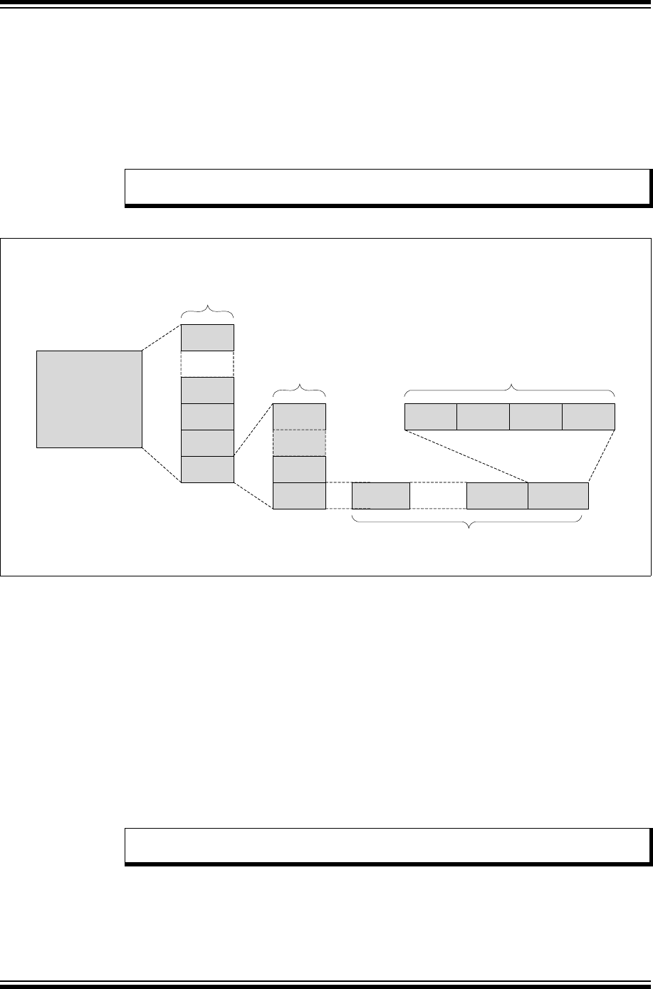
PIC32 Family Reference Manual
DS61193A-page 52-14 Preliminary © 2013 Microchip Technology Inc.
52.3 MEMORY CONFIGURATION
52.3.1 Flash Bank Construction
Each bank of Flash memory is divided into pages. A page is the smallest unit of memory that can
be erased at one time. Each page of memory is segmented into eight rows. A row is the largest
unit of memory that can be programmed at one time. A row consists of 128 Quad (128-bit) words.
Each Quad word consists of four instruction (32-bit) words. Flash memory can be programmed
in rows, Quad word (128-bit) or Word (32-bit) units.
Figure 52-1: Flash Construction
52.3.2 Dual Flash Banks
Flash memory is divided into two equal banks, each with a BFM partition and a PFM partition.
Both the BFM and PFM partitions can be erased in page increments. The PFM partitions can be
erased in their entirety with a single command.
52.3.3 Programming or Erasing Flash in the Same Bank Where Code
is Executing
Code cannot be fetched by the CPU from the same Flash bank that is the target of the
programming operation, which is either BFM or PFM. When this operation is attempted, the CPU
will cease to execute code (stall) while the programming operation is in progress. This includes
Interrupt Service Routines (and their vectors) when they are located in the same bank as the
target Flash operation. If the system software requires execution of code during Flash
operations, the code must reside in system RAM or the Flash bank that is not the target of the
programming operation.
Note: Page size varies by device. Please refer to the “Flash Program Memory” chapter
in the specific device data sheet to determine the Flash page size for your device.
Flash Bank
Page 0
Page 1
Page 2
Page 3
Page n
Row 0
Row 1
Row 7
QW 0QW 1QW 127
word 0word 1word 2word 3
Flash bank
consisting of
‘n’ pages
Each page
consists of 8
rows
Each row consists of 128 quad (128-bit) words
Each quad word consists of 4
instruction (32-bit) words
Note: Instruction code that is already stored in the cache when the programming
operation is initiated will continue to execute.

© 2013 Microchip Technology Inc. Preliminary DS61193A-page 52-15
Section 52. Flash Memory with Support for Live Update
Flash Memory with
Support for Live
Update
52
52.3.4 Programming or Erasing Flash in the Opposite Bank Where
Code is Executing
To avo id C P U stall ing d uri ng pr ogr amm in g o per ati ons , ins ure t ha t all tar g et a ddr ess es fo r
programming operations are location in a Flash bank where no executable code is being fetched.
When this requirement is met, the CPU can fetch and execute code during any of the
programming operations without stalling, including Interrupt Service Routines. To accomplish
this, the application must place all executable code in the BFM and PFM partitions of one bank
and execute programming operations on the BFM or PFM partitions of the other bank.
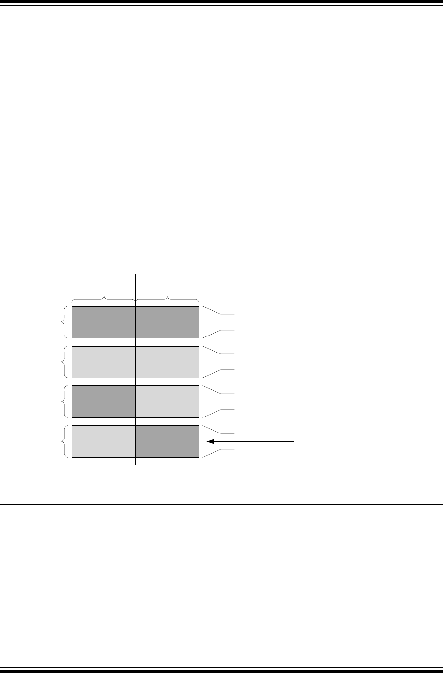
PIC32 Family Reference Manual
DS61193A-page 52-16 Preliminary © 2013 Microchip Technology Inc.
52.4 BOOT FLASH MEMORY (BFM) PARTITIONS
52.4.1 BFM Bank Aliasing – Selecting the Start-up Bank
The BFM partitions of each Flash bank are mapped into fixed and aliased regions. The order of
mapping to the aliased regions is determined by the device Configuration memory words
BFxSEQ0 (BFxSEQ1-BFxSEQ3 are not used). The mapping occurs at reset prior to execution
of any instruction code. Whichever BFM has the larger value in the associated sequence word
register, that bank will be mapped into the lower aliased region. If the values are equal, Bank 1
is mapped into the lower aliased region, Bank 2 and the other BFM is mapped into the upper
aliased region.
When programming the BFxSEQ0 value, the sequence number value is stored in the lower 16
bits and the compliment of this value is stored in the upper 16 bits. As an example, using a
sequence number of three, the BFxSEQ0 value would be 0xFFFC0003.
Figure 52-2 illustrates the effect of the BFxSEQ0 comparison. In either case, Bank 1 and Bank
2 BFM are mapped identically in the fixed regions, with Bank 1 in the lower fixed region, and Bank
2 in the upper fixed region. The mapping to the aliased regions changes based on the BFxSEQ0
values. This example shows a device with 80 KB BFM banks. Refer to the “Memory
Organization” chapter of the specific device data sheet to determine the size and address
mapping for the BFM banks of your particular device.
Figure 52-2: Example of Aliased and Fixed BFM Regions Based on BFxSEQ0 Values
52.4.2 BFM Write Protection
Pages in the upper and lower aliased regions can be protected individually using bits in the
NVMBWP register. Since these bits correspond to pages referenced in the aliased region, they
are affected by the mapping of the aliasing at start-up. At reset, all pages are in a write-protected
state and must be disabled prior to performing any programming operations on the BFM regions.
There are also Upper Region and Lower Region unlock bits, UBWPULOCK (NVMBWP<7>) and
LBWPULOCK (NVMBWP<15>), which are set at reset and can be cleared by user software.
When cleared, changes to write protection for that region can no longer be made. Once cleared,
the UBWPULOCK and LBWPULOCK bits can only be set by a reset.
The NVMBWP write-protect register can only be changed when the unlock sequence is followed.
See 52.9 “NVMKEY Register Unlocking Sequence” for more information.
Note: Refer to the “Special Features” chapter in the specific device data sheet for the Configuration
Word locations and the fixed and aliased region locations.
BFM Bank 2
BFM Bank 1
BFM Lower
Fixed Region
BFM Upper
Fixed Region BFM Bank 2
BFM Bank 1
BFM Bank 1
BFM Bank 2
BFM Upper
Aliased Region
BFM Lower
Aliased Region
BFM Bank 2
BFM Bank 1
0x1FC00000 (Code execution begins here at reset)
0x1FC13FFF
0x1FC20000
0x1FC33FFF
0x1FC40000
0x1FC53FFF
0x1FC60000
0x1FC73FFF
Aliasing when
BF1SEQ0
BF2SEQ0
Aliasing when
BF2SEQ0 >
BF1SEQ0
Device Configuration is fetched from
the BFM Lower Aliased Region at reset.
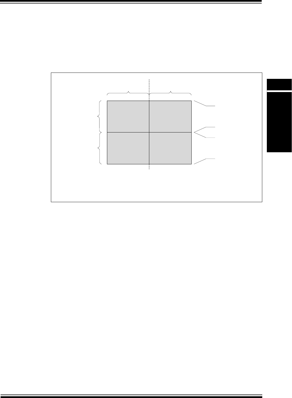
© 2013 Microchip Technology Inc. Preliminary DS61193A-page 52-17
Section 52. Flash Memory with Support for Live Update
Flash Memory with
Support for Live
Update
52
52.5 PROGRAM FLASH MEMORY (PFM) PARTITIONS
52.5.1 PFM Mapping to Address Space
Each Flash bank has an equally sized PFM region. The mapping of the banks of PFM into
address space is determined by the state of the SWAP control bit (NVMCON<7>), as shown in
Figure 52-3. It is recommended that this bit is only changed by the code executing from the BFM
region.
Figure 52-3: Example of PFM Mapping Based on SWAP Setting
The SWAP bit setting can only be changed when the unlock sequence is first completed. See
52.9 “NVMKEY Register Unlocking Sequence” for more information.
52.5.2 PFM Write Protection
Write protection for the PFM region is implemented by pages using a watermark address, defined
by the NVMPWP<23:0> bits (NVMPWP<23:0>). Write protection is always implemented on page
boundaries; therefore, for a device with a 0x4000 (16 KB) page size, address bits 0 through 13
are ignored and will always read ‘0’. When the NVMPWP is equal to ‘0’, no PFM pages are
write-protected. When not equal to ‘0’, the NVMPWP bit will always point to the first address of
the last page that is write-protected. All pages with lesser addresses will be write-protected. At
reset no PFM memory is write-protected.
There is also an unlock bit, PFMULOCK (NVMPWP<31>), which is set at reset and can be
cleared by user software. When cleared, changes to write protection of the PFM can no longer
be made, including the PFMULOCK bit. The NVMPWP write-protect register can only be
changed when the unlock sequence is followed. See 52.9 “NVMKEY Register Unlocking
Sequence” for more information.
PFM Bank 1
PFM Bank 2
0x1D000000
0x1D100000
0x1D0FFFFF
0x1D1FFFFF
PFM Upper
Mapped Region
PFM Lower
Mapped Region
PFM Bank 2
PFM Bank 1
SWAP = 0SWAP = 1
Note: This example shows addresses for a 2 MB device. Refer to the “Memory
Organization” chapter in the specific device data sheet for the actual
addresses.

PIC32 Family Reference Manual
DS61193A-page 52-18 Preliminary © 2013 Microchip Technology Inc.
52.6 ERROR CORRECTING CODE (ECC) AND FLASH PROGRAMMING
Some PIC32 devices incorporate Error Correcting Code (ECC) features, which detect and
correct errors resulting in extended Flash memory life. This feature is explained in detail in
Section 41. “Prefetch Module for Devices with L1 CPU Cache”.
ECC is implemented in 128-bit wide Flash words or four 32-bit instruction word groups. As a
result, when programming Flash memory on a device where ECC is employed, the programming
operation must be at minimum four instructions words or in groups of four instruction words. This
is the reason that the Quad Word programming command exists and why row programming
always programs multiples of four words.
For a given software application, ECC can be enabled at all times, disabled at all times, or
dynamically enabled using the FECCCON Configuration bits. When ECC is enabled at all times,
the Single Word NVMOP programming command does not function, and the quad word is the
smallest unit of memory that can be programmed. When ECC is disabled or enabled dynamically,
both the Word and Quad word programming NVMOP commands are functional and the
programming method used determines how ECC is handled.
In the case of dynamic ECC, if the memory was programmed with the Word command, ECC is
turned off for that word, and when it is read, no error correction is performed. If the memory was
programmed with the Quad Word or Row Programming commands, ECC data is written and
tested for errors (and corrected if needed) when read. Ta bl e 52-2 describes the different ECC
scenarios.
Table 52-2: ECC Programming Summary
FECCCON
Setting
Programming Operation
Data Read
Word Write Quad Word Write Row Write
Disabled Allowed Allowed Allowed ECC is never applied on
a Flash read
Enabled Not allowed Allowed Allowed ECC is applied on every
Flash word read.
Dynamic Allowed, but when used,
the programmed word is
flagged to NOT USE
ECC
Writes ECC data and
flags programmed words
to USE ECC
Writes ECC data and
flags programmed words
to USE ECC
ECC is only applied on
words that are flagged
to USE ECC
Note: When using dynamic ECC, all non-ECC locations must be programmed with the 32-bit Word programming
command, while all ECC enabled locations must be programmed with a 128-bit Quad Word or Row
programming command. Divisions between ECC and non-ECC memory must be on even quad word
boundaries (address bits 0 through 3 are equal to ‘0’).

© 2013 Microchip Technology Inc. Preliminary DS61193A-page 52-19
Section 52. Flash Memory with Support for Live Update
Flash Memory with
Support for Live
Update
52
52.7 INTERRUPTS
An interrupt is generated when the WR bit is cleared by the Flash Controller upon completion of
a Flash program or erase operation. The interrupt event will cause a CPU interrupt if it has been
configured and enabled in the Interrupt Controller. The interrupt occurs regardless of the
outcome of the program or erase operation; successful or unsuccessful. The only exception is
the No Operation (NOP) programming operation (NVMOP = 0), which is used to manually clear
the error flags and does not create an interrupt event on completion, but does clear the WR bit.
Flash Controller interrupts are not persistent, and therefore, no additional steps are required to
clear the cause or source of the interrupt. It is only necessary to clear the appropriate IFSx bit
prior to exiting the interrupt service routine.
Once the Interrupt Controller is configured, the Flash event will cause the CPU to jump to the
vector assigned to the Flash event. The CPU will then begin executing code at the vector
address. The user software at this vector address should perform the required operations, and
then exit. For more information on interrupts, how to configure them, and the vector address table
details, refer to the Section 8. “Interrupts” (DS61108) in the “PIC32 Family Reference Manual”
and the “Interrupt Controller” chapter in the specific device data sheet.
52.7.1 Interrupts and CPU Stalling
Code cannot be fetched by the CPU from the same Flash bank, either BFM or PFM, which is the
target of the programming operation. When this operation is attempted, the CPU will cease to
execute code (stall) while the programming operation is in progress. CPU code execution does
not resume until the programming operation is complete, and when this occurs, any pending
interrupts, including those from the Flash Controller, will be processed in order of priority.
Note that code that is already loaded into the processor cache will continue to execute up to the
point where an attempt is made to fetch code or data from the same Flash panel as the active
programming operation. At this point the CPU will stall.
In situations where all executable code and data constants are located in the bank opposite of
the target of all programming operations, the Flash event interrupt allows the system to initiate a
Flash operation, and then commence code execution and use the interrupt service routine to flag
the completion of the programming operation. Using this technique, it is possible to design a
system with background Flash programming functionality for live updates of Flash memory.
Stalling can also be avoided by placing any needed executable code in SRAM during Flash
programming.

PIC32 Family Reference Manual
DS61193A-page 52-20 Preliminary © 2013 Microchip Technology Inc.
52.8 ERROR DETECTION
The NVMCON register includes two bits for detecting error conditions during a program or erase
operation. They are Low-Voltage detect error, LVDERR (NVMCOM<12>) and Write Error,
WRERR (NVMCON<13>).
The WRERR is set each time the WR bit (NVMCON<15>) is set, initiating a programming
operation. WRERR is cleared on successful completion of the flash operation and at the same
time that WR is cleared and as such should not be polled until the Flash Controller clears WR.
When the WRERR is set, any attempt to initiate programming or erase operation is ignored.
WRERR must be cleared before commencing flash program or erase operations.
LVDERR is set when a Brown out Reset (BOR) occurs during a programming operation. The only
reset which clears LVDERR is a power on reset (POR). Other reset types do not affect LVDERR.
When the LVDERR is set, any attempt to initiate programming or erase operation is ignored.
LVDERR must be cleared before commencing flash program or erase operations.
Both the WRERR and LVDERR can be cleared manually in software by initiating a flash
operation (setting WR) with NVMOP set to NOP (0x00). Note that executing the NVMOP NOP
command clears WRERR, LVDERR and WR but does not generate an interrupt event on
completion.
Table 52-3: Programming Error Cause and Effects
Cause of Error Effect on Programming Erase Operation Indication
A low-voltage event occurred during a
programming sequence.
The last programming or erase operation may
not have completed.
LVDERR = 1,
WRERR = 1
A non-POR reset occurred during
programming.
Programming or erase operation is aborted. WRERR = 1
Attempt to program or erase a page out of the
Flash memory range.
Erase or programming operation is not initiated. WRERR = 1
Attempt to erase or program a write protected
PFM page.
Erase or programming operation is not initiated. WRERR = 1
Attempt to erase or program a write protected
BFM page.
Operation occurs, but the page is not
programmed or erased.
WRERR = 0
Bus master error or row programming data
underrun error during programming.
Programming or erase operation is aborted. WRERR = 1

© 2013 Microchip Technology Inc. Preliminary DS61193A-page 52-21
Section 52. Flash Memory with Support for Live Update
Flash Memory with
Support for Live
Update
52
52.9 NVMKEY REGISTER UNLOCKING SEQUENCE
Important register settings that could compromise the Flash memory if inadvertently changed are
protected by a register unlocking sequence. This feature is implemented using the NVMKEY
register. NVMKEY is a write-only register that is used to implement an unlock sequence to help
prevent accidental writes or erasures of Flash memory or accidental changes to the SWAP bit
(NVMCON<7>) and write permission settings.
In some instances the operation is also dependant on the setting of the WREN bit
(NVMCON<14>), as shown in Ta ble 52-4.
Table 52-4: NVMKEY Register Unlocking and WREN
The following steps must be followed in the exact order as shown to enable writes to registers
that require this unlock sequence:
1. Write 0x00000000 to NVMKEY.
2. Write 0xAA996655 to NVMKEY.
3. Write 0x556699AA to NVMKEY.
4. Write the value to the register requiring the unlock sequence.
To e nsu re a s ucc ess fu l w rit e t o t he reg ist er as shown in Step 4, Steps 2 through 4 must be
executed without any other activity on the peripheral bus that is in use by the Flash Controller.
Interrupts and DMA transfers that access the same peripheral bus as the Flash Controller must
be disabled. Refer to the specific device data sheet to determine which peripherals share the
same peripheral bus as the Flash Controller. In addition, the operation in Step 4 must be atomic.
The Set, Clear, and Invert registers may be used, where applicable, for the target register in
Step 4.
Example 52-1 shows code written in the C language to initiate a NVM Operation (NVMOP)
command. In this particular example, the WR bit is being set in the NVMCON register, and
therefore, must include the unlock sequence. Note the use of the NVMCONSET register, which
sets the WR bit in a single instruction without changing other bits in the register. Using
NVMCONbits.WR = 1 will fail, as this line of code compiles to a read-modify-write sequence.
Operation WREN
Setting
Unlock
Sequence
Required
Changing value of SWAP (NVMCON<7>) 0Yes
Changing value of NVMOP<3:0> (NVMCON<3:0>) 0No
Setting WR (NVMCON<15>) to start a write or erase operation 1Yes
Changing any fields in the NVMPWP register Don’t care Yes
Changing any fields in the NVMBWP register Don’t care Yes

PIC32 Family Reference Manual
DS61193A-page 52-22 Preliminary © 2013 Microchip Technology Inc.
Example 52-1: Initiate NVM Operation (Unlock Sequence Example)
Note: Once the unlock codes have been written to the NVMKEY register, the next activity
on the same peripheral bus as the Flash Controller will reset the lock. As a result,
only atomic operations can be used. Setting register fields using structures compile
into a read-modify-write operation, and will fail.
void NVMInitiateOperation(void)
{
int int_status; // storage for current Interrupt Enable state
int dma_susp; // storage for current DMA state
// Disable Interrupts
asm volatile("di %0" : "=r"(int_status));
// Disable DMA
if(!(dma_susp=DMACONbits.SUSPEND))
{
DMACONSET=_DMACON_SUSPEND_MASK; // suspend
while((DMACONbits.DMABUSY)); // wait to be actually suspended
}
NVMKEY = 0x0;
NVMKEY = 0xAA996655;
NVMKEY = 0x556699AA;
NVMCONSET = NVMCON_WR; // must be an atomic instruction
// Restore DMA
if(!dma_susp)
{
DMACONCLR=_DMACON_SUSPEND_MASK; // resume DMA activity
}
// Restore Interrupts
if(int_status & 0x00000001)
{
asm volatile("ei");
}
}

© 2013 Microchip Technology Inc. Preliminary DS61193A-page 52-23
Section 52. Flash Memory with Support for Live Update
Flash Memory with
Support for Live
Update
52
52.10 WORD PROGRAMMING
The smallest block of data that can be programmed in a single operation is one 32-bit word. The
data to be programmed must be written to the NVMDATA0 register, and the address of the word
must be loaded into the NVMADDR register before the programming sequence is initiated. The
instruction word at the physical location pointed to by the NVMADDR register is then
programmed. Programming occurs on 32-bit word boundaries; therefore, bits 0 and 1 of the
NVMADDR register are ignored.
Once a word is programmed, it must be erased before it can be programmed again, even if
changing a bit from an erased ‘1’ state to a ‘0’ state.
Word programming will only succeed if the target address is in a page that is not write-protected.
Programming to a write-protected PFM page will fail and result in the WRERR bit being set in the
NVMCON register. Programming a write-protected BFM page will fail, but does not set the
WRERR bit.
A programming sequence consists of the following steps:
1. Write 32-bit data to be programmed to the NVMDATA0 register.
2. Load the NVMADDR register with the address to be programmed.
3. Set the WREN bit = 1 and NVMOP bits = 1 in the NVMCON register. This defines and
enables the programming operation.
4. Initiation of the programming operation (see 52.9 “NVMKEY Register Unlocking
Sequence”).
5. Monitor the WR bit of the NVMCON register to flag completion of the operation.
6. Clear the WREN bit in the NVMCON register.
7. Check for errors and process accordingly.
Example 52-2 shows code for Word programming, where a value of 0x12345678 is programmed
into location 0x1D008000.
Example 52-2: Word Programming
…
// Set up Address and Data Registers
NVMADDR = 0x1D008000; // physical address
NVMDATA0 = 0x12345678; // value
// set the operation, assumes WREN = 0
NVMCONbits.NVMOP = 0x1; // NVMOP for Word programming
// Enable Flash for write operation and set the NVMOP
NVMCONSET = NVMCON_WREN;
// Start programming
NVMInitiateOperation(); // see Example 52-1
// Wait for WR bit to clear
while(NVMCON & NVMCON_WR);
// Disable future Flash Write/Erase operations
NVMCONCLR = NVMCON_WREN;
// Check Error Status
if(NVMCON & 0x3000) // mask for WRERR and LVDERR
{
// process errors
}
…

PIC32 Family Reference Manual
DS61193A-page 52-24 Preliminary © 2013 Microchip Technology Inc.
52.11 QUAD WORD PROGRAMMING
The process for Quad Word programming is identical to Word programming except that all four
of the NVMDATAx registers are used. The value of NVMDATA0 is programmed at address
NVMADDR, NVMDATA1 at NVMADDR + 0x4, NVMDATA2 at NVMADDR + 0x8, and
NVMDATA3 at address NVMDATA + 0xC.
Quad Word programming is always performed on a quad word boundary; therefore, bits 3
through 0 are ignored.
Quad Word programming will only succeed if the target address is in a page that is not
write-protected. Once a Quad Word is programmed, it must be erased before any word in it can
be programmed again, even if changing a bit from an erased ‘1’ state to a ‘0’ state.
Example 52-3 shows code for Quad Word Programming where a value of 0x11111111 is
programmed into location 0x1D008000, 0x22222222 into 0x1D008004, 0x33333333 into
0x1D008008, and 0x44444444 into location 0x1D00800C.
Example 52-3: Quad Word Programming
…
// Set up Address and Data Registers
NVMADDR = 0x1D008000; // physical address
NVMDATA0 = 0x11111111; // value written to 0x1D008000
NVMDATA1 = 0x22222222; // value written to 0x1D008004
NVMDATA2 = 0x33333333; // value written to 0x1D008008
NVMDATA3 = 0x44444444; // value written to 0x1D00800C
// set the operation, assumes WREN = 0
NVMCONbits.NVMOP = 0x2; // NVMOP for Quad Word programming
// Enable Flash for write operation and set the NVMOP
NVMCONSET = NVMCON_WREN;
// Start programming
NVMInitiateOperation(); // see Example 52-1
// Wait for WR bit to clear
while(NVMCON & NVMCON_WR);
// Disable future Flash Write/Erase operations
NVMCONCLR = NVMCON_WREN;
// Check Error Status
if(NVMCON & 0x3000) // mask for WRERR and LVDERR bits
{
// process errors
}
…

© 2013 Microchip Technology Inc. Preliminary DS61193A-page 52-25
Section 52. Flash Memory with Support for Live Update
Flash Memory with
Support for Live
Update
52
52.12 ROW PROGRAMMING
The largest block of data that can be programmed is a row, which varies by device. Refer to the
“Flash Program Memory” chapter in the specific device data sheet to determine the row size.
Unlike Word and Quad Word Programming, where the data source is stored in SFR memory,
Row programming source data is stored in SRAM. The NVMSRCADDR register is a pointer to
the physical location of the source data for Row programming.
Like other Non-volatile Memory (NVM) programming commands, the NVMADDR register points
to the target address of the operation. Row programming always occurs on row boundaries;
therefore, for a device with an instruction word row size of 512, bits 0 through 9 of the NVMADDR
register are ignored.
Row Word programming will only succeed if the target address is in a page that is not
write-protected. Once a row is programmed, it must be erased before any word in it can be
programmed again, even if changing a bit from an erased ‘1’ state to a ‘0’ state.
Example 52-4 shows code for Row programming. Array rowbuff is populated with data and
programmed into a row located at physical address 0x1D008000.
Example 52-4: Row Programming
Note: When assigning the value to the NVMSRCADDR register, it must be converted to a
physical address.
…
unsigned int rowbuff[512]; // example is for a 512 word row size.
int x; // loop counter
// put some data in the source buffer
for (x = 0; x < (sizeof(rowbuff) * sizeof (int)); x++)
((char *)rowbuff)[x] = x;
// set destination row address
NVMADDR = 0x1D008000; // row physical address
// set source address. Must be converted to a physical address.
NVMSRCADDR = (unsigned int)((int)rowbuff & 0x1FFFFFFF);
// define flash operation
NVMCONbits.NVMOP = 0x3; // NVMOP for Row programming
// Enable Flash Write
NVMCONSET = NVMCON_WREN;
// commence programming
NVMInitiateOperation(); // see Example 52-1
// Wait for WR bit to clear
while(NVMCON & NVMCON_WR);
// Disable future Flash Write/Erase operations
NVMCONCLR = NVMCON_WREN;
// Check Error Status
if(NVMCON & 0x3000) // mask for WRERR and LVDERR bits
{
// process errors
}
…

PIC32 Family Reference Manual
DS61193A-page 52-26 Preliminary © 2013 Microchip Technology Inc.
52.13 PAGE ERASE
A page erase performs an erase of a single page of either PFM or BFM. Refer to the “Flash
Program Memory” chapter in the specific device data sheet for the page size for your device.
The page to be erased is selected using the NVMADDR register. Pages are always erased on
page boundaries; therefore, for a device with an instruction word page size of 4096, bits 0
through 11 of the NVMADDR register are ignored.
A page erase will only succeed if the target address is a page that is not write-protected. Erasing
a write-protected page will fail and result in the WRERR bit being set in the NVMCON register.
Example 52-5 shows code for a single page erase operation at address 0x1D008000.
Example 52-5: Page Erase
…
// set destination page address
NVMADDR = 0x1D008000; // page physical address
// define flash operation
NVMCONbits.NVMOP = 0x4; // NVMOP for Page Erase
// Enable Flash Write
NVMCONSET = NVMCON_WREN;
// commence programming
NVMInitiateOperation(); // see Example 52-1
// Wait for WR bit to clear
while(NVMCON & NVMCON_WR);
// Disable future Flash Write/Erase operations
NVMCONCLR = NVMCON_WREN;
// Check Error Status
if(NVMCON & 0x3000) // mask for WRERR and LVDERR bits
{
// process errors
}
…

© 2013 Microchip Technology Inc. Preliminary DS61193A-page 52-27
Section 52. Flash Memory with Support for Live Update
Flash Memory with
Support for Live
Update
52
52.14 PROGRAM FLASH MEMORY ERASE
Program Flash memory can be erased in its entirety or by bank. Three discreet NVMOP
commands are implemented to accomplish this:
•Erase the entire PFM area (both PFM banks)
•Erase the upper PFM bank
•Erase the lower PFM bank
When erasing the entire PFM area, code must be executing from BFM. When erasing a single
upper or lower PFM bank, code must either be executing from BFM or from the PFM bank that
is not being erased.
Program Flash memory erase operations will only succeed if no pages are write-protected in the
bank being erased. When erasing the entire PFM area, PFM write protection must be completely
disabled.
Example 52-6 shows code for erasing the upper program Flash bank.
Example 52-6: Program Flash Erase
…
// define flash operation
NVMCONbits.NVMOP = 0x6; // NVMOP for upper bank PFM erase
// Enable Flash Write
NVMCONSET = NVMCON_WREN;
// commence programming
NVMInitiateOperation(); // see Example 52-1
// Wait for WR bit to clear
while(NVMCON & NVMCON_WR);
// Disable future Flash Write/Erase operations
NVMCONCLR = NVMCON_WREN;
// Check Error Status
if(NVMCON & 0x3000) // mask for WRERR and LVDERR bits
{
// process errors
}
…

PIC32 Family Reference Manual
DS61193A-page 52-28 Preliminary © 2013 Microchip Technology Inc.
52.15 OPERATION IN POWER-SAVING MODES
The Flash Controller does not operate in power-saving modes. If a WAIT instruction is
encountered when programming, the CPU will stop execution (stall), wait for the programming
operation to complete, and then enter the power-saving mode.
52.16 OPERATION IN DEBUG MODE
Programming operations will continue to completion if processor execution is halted in Debug
mode.
52.17 EFFECTS OF VARIOUS RESETS
Devices Resets other than a Power-on Reset (POR), reset the SWAP bit in the NVMCON
register and the entire contents of the NVMPWP and NVMBWP registers. All other register
content persists through a non-POR reset.
All Flash Controller registers are forced to their reset states upon a POR.

© 2013 Microchip Technology Inc. Preliminary DS61193A-page 52-29
Section 52. Flash Memory with Support for Live Update
Flash Memory with
Support for Live
Update
52
52.18 RELATED APPLICATION NOTES
This section lists application notes that are related to this section of the manual. These
application notes may not be written specifically for the PIC32 device family, but the concepts are
pertinent and could be used with modification and possible limitations. The current application
notes related to Flash Memory with Support for Live Update include the following:
Title Application Note #
No related application notes at this time. N/A
Note: Please visit the Microchip Web site (www.microchip.com) for additional application
notes and code examples for the PIC32 family of devices.

PIC32 Family Reference Manual
DS61193A-page 52-30 Preliminary © 2013 Microchip Technology Inc.
52.19 REVISION HISTORY
Revision A (May 2013)
This is the initial released version of the document.

2013 Microchip Technology Inc. Preliminary DS61193A-page 52- 31
Information contained in this publication regarding device
applications and the like is provided only for your convenience
and may be superseded by updates. It is your responsibility to
ensure that your application meets with your specifications.
MICROCHIP MAKES NO REPRESENTATIONS OR
WARRANTIES OF ANY KIND WHETHER EXPRESS OR
IMPLIED, WRITTEN OR ORAL, STATUTORY OR
OTHERWISE, RELATED TO THE INFORMATION,
INCLUDING BUT NOT LIMITED TO ITS CONDITION,
QUALITY, PERFORMANCE, MERCHANTABILITY OR
FITNESS FOR PURPOSE. Microchip disclaims all liability
arising from this information and its use. Use of Microchip
devices in life support and/or safety applications is entirely at
the buyer’s risk, and the buyer agrees to defend, indemnify and
hold harmless Microchip from any and all damages, claims,
suits, or expenses resulting from such use. No licenses are
conveyed, implicitly or otherwise, under any Microchip
intellectual property rights.
Trademarks
The Microchip name and logo, the Microchip logo, dsPIC,
FlashFlex, KEELOQ, KEELOQ logo, MPLAB, PIC, PICmicro,
PICSTART, PIC32 logo, rfPIC, SST, SST Logo, SuperFlash
and UNI/O are registered trademarks of Microchip Technology
Incorporated in the U.S.A. and other countries.
FilterLab, Hampshire, HI-TECH C, Linear Active Thermistor,
MTP, SEEVAL and The Embedded Control Solutions
Company are registered trademarks of Microchip Technology
Incorporated in the U.S.A.
Silicon Storage Technology is a registered trademark of
Microchip Technology Inc. in other countries.
Analog-for-the-Digital Age, Application Maestro, BodyCom,
chipKIT, chipKIT logo, CodeGuard, dsPICDEM,
dsPICDEM.net, dsPICworks, dsSPEAK, ECAN,
ECONOMONITOR, FanSense, HI-TIDE, In-Circuit Serial
Programming, ICSP, Mindi, MiWi, MPASM, MPF, MPLAB
Certified logo, MPLIB, MPLINK, mTouch, Omniscient Code
Generation, PICC, PICC-18, PICDEM, PICDEM.net, PICkit,
PICtail, REAL ICE, rfLAB, Select Mode, SQI, Serial Quad I/O,
Tota l E ndu ra nce , T SHA RC , U n iW inD riv er, Wi per Lo c k, ZE NA
and Z-Scale are trademarks of Microchip Technology
Incorporated in the U.S.A. and other countries.
SQTP is a service mark of Microchip Technology Incorporated
in the U.S.A.
GestIC and ULPP are registered trademarks of Microchip
Technology Germany II GmbH & Co. & KG, a subsidiary of
Microchip Technology Inc., in other countries.
All other trademarks mentioned herein are property of their
respective companies.
© 2013, Microchip Technology Incorporated, Printed in the
U.S.A., All Rights Reserved.
Printed on recycled paper.
ISBN: 978-1-62077-183-9
Note the following details of the code protection feature on Microchip devices:
• Microchip products meet the specification contained in their particular Microchip Data Sheet.
• Microchip believes that its family of products is one of the most secure families of its kind on the market today, when used in the
intended manner and under normal conditions.
• There are dishonest and possibly illegal methods used to breach the code protection feature. All of these methods, to our
knowledge, require using the Microchip products in a manner outside the operating specifications contained in Microchip’s Data
Sheets. Most likely, the person doing so is engaged in theft of intellectual property.
• Microchip is willing to work with the customer who is concerned about the integrity of their code.
• Neither Microchip nor any other semiconductor manufacturer can guarantee the security of their code. Code protection does not
mean that we are guaranteeing the product as “unbreakable.”
Code protection is constantly evolving. We at Microchip are committed to continuously improving the code protection features of our
products. Attempts to break Microchip’s code protection feature may be a violation of the Digital Millennium Copyright Act. If such acts
allow unauthorized access to your software or other copyrighted work, you may have a right to sue for relief under that Act.
Microchip received ISO/TS-16949:2009 certification for its worldwide
headquarters, design and wafer fabrication facilities in Chandler and
Tempe, Arizona; Gresham, Oregon and design centers in California
and India. The Company’s quality system processes and procedures
are for its PIC® MCUs and dsPIC® DSCs, KEELOQ® code hopping
devices, Serial EEPROMs, microperipherals, nonvolatile memory and
analog products. In addition, Microchip’s quality system for the design
and manufacture of development systems is ISO 9001:2000 certified.
QUALITY MANAGEMENT S
YSTEM
CERTIFIED BY DNV
== ISO/TS 16949 ==

DS61193A-page 52- 32 Preliminary 2013 Microchip Technology Inc.
AMERICAS
Corporate Office
2355 West Chandler Blvd.
Chandler, AZ 85224-6199
Tel: 480-792-7200
Fax: 480-792-7277
Technical Support:
http://www.microchip.com/
support
Web Address:
www.microchip.com
Atlanta
Duluth, GA
Tel: 678-957-9614
Fax: 678-957-1455
Boston
Westborough, MA
Tel: 774-760-0087
Fax: 774-760-0088
Chicago
Itasca, IL
Tel: 630-285-0071
Fax: 630-285-0075
Cleveland
Independence, OH
Tel: 216-447-0464
Fax: 216-447-0643
Dallas
Addison, TX
Tel: 972-818-7423
Fax: 972-818-2924
Detroit
Farmington Hills, MI
Tel: 248-538-2250
Fax: 248-538-2260
Indianapolis
Noblesville, IN
Tel: 317-773-8323
Fax: 317-773-5453
Los Angeles
Mission Viejo, CA
Tel: 949-462-9523
Fax: 949-462-9608
Santa Clara
Santa Clara, CA
Tel: 408-961-6444
Fax: 408-961-6445
Toronto
Mississauga, Ontario,
Canada
Tel: 905-673-0699
Fax: 905-673-6509
ASIA/PACIFIC
Asia Pacific Office
Suites 3707-14, 37th Floor
Tower 6, The Gateway
Harbour City, Kowloon
Hong Kong
Tel : 8 52 -24 01- 120 0
Fax: 852-2401-3431
Australia - Sydney
Tel : 6 1- 2-9 868 -67 33
Fax: 61-2-9868-6755
China - Beijing
Tel : 8 6- 10- 856 9-7 00 0
Fax: 86-10-8528-2104
China - Chengdu
Tel : 8 6- 28- 866 5-5 511
Fax: 86-28-8665-7889
China - Chongqing
Tel : 8 6- 23- 898 0-9 58 8
Fax: 86-23-8980-9500
China - Hangzhou
Tel : 8 6- 571 -28 19- 318 7
Fax: 86-571-2819-3189
China - Hong Kong SAR
Tel : 8 52 -29 43- 510 0
Fax: 852-2401-3431
China - Nanjing
Tel : 8 6- 25- 847 3-2 46 0
Fax: 86-25-8473-2470
China - Qingdao
Tel : 8 6- 532 -85 02- 735 5
Fax: 86-532-8502-7205
China - Shanghai
Tel : 8 6- 21- 540 7-5 53 3
Fax: 86-21-5407-5066
China - Shenyang
Tel : 8 6- 24- 233 4-2 82 9
Fax: 86-24-2334-2393
China - Shenzhen
Tel : 8 6- 755 -88 64- 220 0
Fax: 86-755-8203-1760
China - Wuhan
Tel : 8 6- 27- 598 0-5 30 0
Fax: 86-27-5980-5118
China - Xian
Tel : 8 6- 29- 883 3-7 25 2
Fax: 86-29-8833-7256
China - Xiamen
Tel: 86-592-2388138
Fax: 86-592-2388130
China - Zhuhai
Tel : 86- 75 6-3 21 004 0
Fax: 86-756-3210049
ASIA/PACIFIC
India - Bangalore
Tel : 9 1- 80- 309 0-4 44 4
Fax: 91-80-3090-4123
India - New Delhi
Tel : 9 1- 11- 416 0 -8 631
Fax: 91-11-4160-8632
India - Pune
Tel : 9 1- 20- 256 6-1 51 2
Fax: 91-20-2566-1513
Japan - Osaka
Tel : 8 1- 6-6 152 -7 1 60
Fax: 81-6-6152-9310
Japan - Tokyo
Tel : 8 1- 3-6 880 - 377 0
Fax: 81-3-6880-3771
Korea - Daegu
Tel : 8 2- 53- 744 -43 01
Fax: 82-53-744-4302
Korea - Seoul
Tel : 8 2- 2-5 54- 72 0 0
Fax: 82-2-558-5932 or
82-2-558-5934
Malaysia - Kuala Lumpur
Tel : 6 0- 3-6 201 -9 8 57
Fax: 60-3-6201-9859
Malaysia - Penang
Tel : 6 0- 4-2 27- 88 7 0
Fax: 60-4-227-4068
Philippines - Manila
Tel : 6 3- 2-6 34- 90 6 5
Fax: 63-2-634-9069
Singapore
Tel : 6 5- 633 4-8 870
Fax: 65-6334-8850
Taiwan - Hsin Chu
Tel : 8 86 -3- 577 8-3 66
Fax: 886-3-5770-955
Taiwan - Kaohsiung
Tel : 8 86 -7- 213 -78 28
Fax: 886-7-330-9305
Taiwan - Taipei
Tel : 8 86 -2- 250 8-8 60 0
Fax: 886-2-2508-0102
Thailand - Bangkok
Tel : 6 6- 2-6 94- 13 5 1
Fax: 66-2-694-1350
EUROPE
Austria - Wels
Tel : 4 3- 72 42 -2 244 -3 9
Fax: 43-7242-2244-393
Denmark - Copenhagen
Tel : 4 5- 445 0-2 828
Fax: 45-4485-2829
France - Paris
Tel : 3 3- 1-6 9-5 3-6 3-2 0
Fax: 33-1-69-30-90-79
Germany - Munich
Tel : 4 9- 89 -62 7-1 44- 0
Fax: 49-89-627-144-44
Italy - Milan
Tel : 3 9- 03 31 -7 426 11
Fax: 39-0331-466781
Netherlands - Drunen
Tel : 3 1- 41 6- 690 399
Fax: 31-416-690340
Spain - Madrid
Tel : 3 4- 91 -70 8-0 8-9 0
Fax: 34-91-708-08-91
UK - Wokingham
Tel : 4 4- 118 -92 1- 5 869
Fax: 44-118-921-5820
Worldwide Sales and Service
11/29/12
