Pioneer DEH P1Y, P8MP, P80MP Service Manual. Www.s Manuals.com. Manual
User Manual: Pioneer DEH-P1Y - Service manuals and Schematics. Free.
Open the PDF directly: View PDF ![]() .
.
Page Count: 91
- SAFETY INFORMATION
- CONTENTS
- 1. SPECIFICATIONS
- 2. EXPLODED VIEWS AND PARTS LIST
- 2.1 PACKING(DEH-P8MP/XN/UC,DEH-P80MP/XN/UC)
- 2.2 PACKING(DEH-P1Y/XN/ES)
- 2.3 EXTERIOR
- 2.4 CD MECHANISM MODULE
- 3. BLOCK DIAGRAM AND SCHEMATIC DIAGRAM
- 3.1 BLOCK DIAGRAM
- 3.2 OVERALL CONNECTION DIAGRAM(GUIDE PAGE)
- 3.3 KEYBOARD UNIT
- 3.4 CD MECHANISM MODULE(GUIDE PAGE)
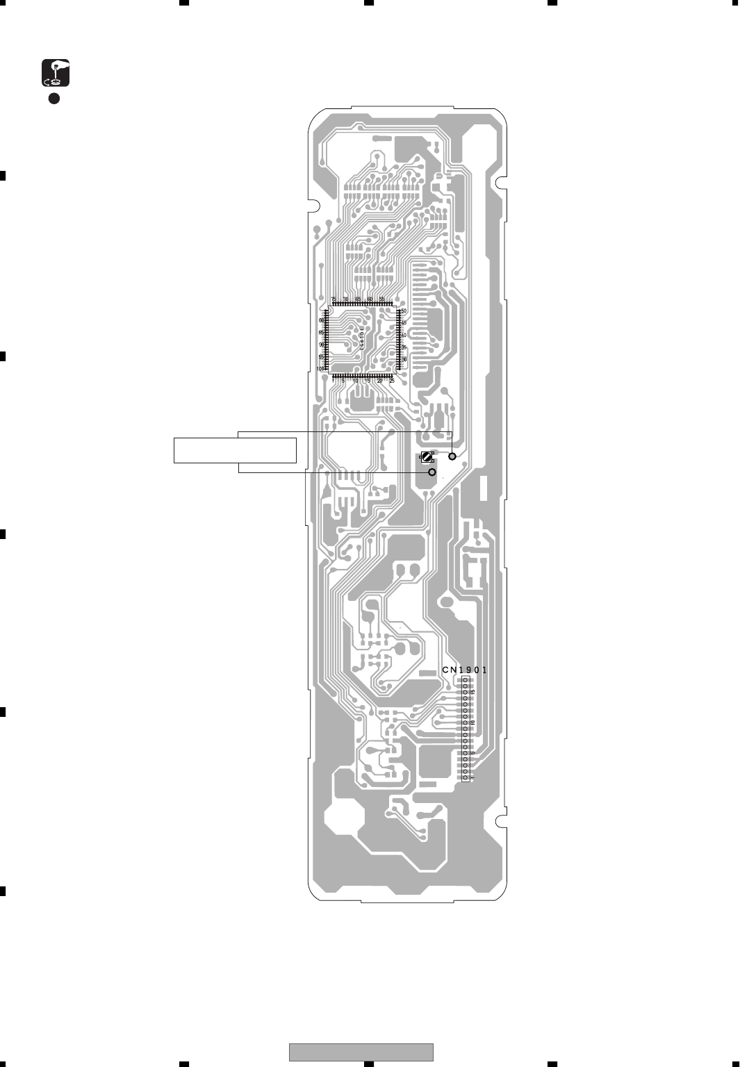
- 4. PCB CONNECTION DIAGRAM
- 4.1 TUNER AMP UNIT
- 4.2 SWITCH UNIT
- 4.3 KEYBOARD UNIT
- 4.4 CD MECHANISM MODULE
- 5. ELECTRICAL PARTS LIST
- 6. ADJUSTMENT
- 6.1 CONNECTION DIAGRAM
- 6.2 OEL UNIT ADJUSTMENT
- 6.3 CD ADJUSTMENT
- 6.4 CHECKING THE GRATING AFTER CHANGING THE PICKUP UNIT
- 6.5 ERROR MODE
- 6.6 OEL SCREENSAVER STUDIO LKA TO LKD APPLICATION
- 6.7 SYSTEM MICROCOMPUTER TEST PROGRAM
- 7. GENERAL INFORMATION
- 7.1 DIAGNOSIS
- 7.1.1 DISASSEMBLY
- 7.1.2 CONNECTOR FUNCTION DESCRIPTION
- 7.2 IC
- 7.3 EXPLANATION
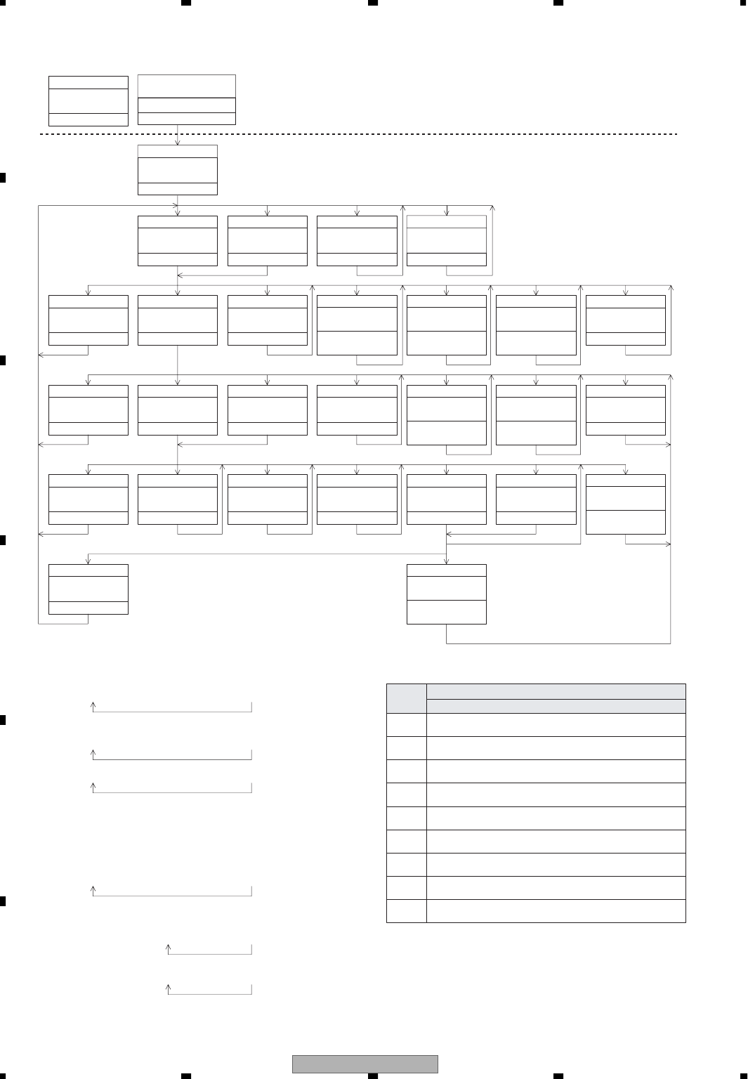
- 7.3.1 OPERATIONAL FLOW CHART
- 7.3.2 CIRCUIT DESCRIPTIONS
- 7.4 CLEANING
- 8. OPERATIONS
ORDER NO.
PIONEER CORPORATION 4-1, Meguro 1-chome, Meguro-ku, Tokyo 153-8654, Japan
PIONEER ELECTRONICS (USA) INC. P.O. Box 1760, Long Beach, CA 90801-1760, U.S.A.
PIONEER EUROPE NV Haven 1087, Keetberglaan 1, 9120 Melsele, Belgium
PIONEER ELECTRONICS ASIACENTRE PTE. LTD. 253 Alexandra Road, #04-01, Singapore 159936
PIONEER CORPORATION 2004
DEH-P8MP/XN/UC
CRT3219
MULTI-CD CONTROL HIGH POWER CD/MP3/WMA PLAYER WITH FM/AM TUNER
DEH-P8MP
/XN/UC
DEH-P80MP
/XN/UC
DEH-P1Y
/XN/ES
This service manual should be used together with the following manual(s):
Model No. Order No. Mech.Module Remarks
CX-3098 CRT3179 S10WMAcode2 CD Mech. Module:Circuit Description, Mech. Description, Disassembly
For details, refer to "Important symbols for good services".
K-ZZD.MAY 2004 printed in Japan
DEH-P8MP/XN/UC
2
1234
1234
C
D
F
A
B
E
SAFETY INFORMATION
CAUTION
This service manual is intended for qualified service technicians; it is not meant for the casual do-it-yourselfer.
Qualified technicians have the necessary test equipment and tools, and have been trained to properly and safely
complex products such as those covered by this manual.
Improperly performed repairs can adversely affect the safety and reliability of the product and may void the
If you are not qualified to perform the repair of this product properly and safely, you should not risk
and refer the repair to a qualified service technician.
WARNING
This product contains lead in solder and certain electrical parts contain chemicals which are known to the
of California to cause cancer, birth defects or other reproductive harm.
Health & Safety Code Section 25249.6 - Proposition 65
repair
warranty.
trying to do so
state
- Service Precaution
1. You should conform to the regulations governing the
product (safety, radio and noise, and other regulations),
and should keep the safety during servicing by following
the safety instructions described in this manual.
2. Before disassembling the unit, be sure to turn off
the power. Unplugging and plugging the connectors
during power-on mode may damage the ICs inside
the unit.
3. To protect the pickup unit from electrostatic discharge
during servicing, take an appropriate treatment
(shorting-solder) by referring to "the DISASSEMBLY"
on page 63.
4. After replacing the pickup unit, be sure to check the
grating. (See page 59.)
[ Important symbols for good services ]
In this manual, the symbols shown-below indicate that adjustments, settings or cleaning should be made securely.
When you find the procedures bearing any of the symbols, be sure to fulfill them:
2. Adjustments
To keep the original performances of the product, optimum adjustments or specification confirmation is indispensable.
In accordance with the procedures or instructions described in this manual, adjustments should be performed.
3. Cleaning
For optical pickups, tape-deck heads, lenses and mirrors used in projection monitors, and other parts requiring cleaning,
proper cleaning should be performed to restore their performances.
5. Lubricants, glues, and replacement parts
Appropriately applying grease or glue can maintain the product performances. But improper lubrication or applying
glue may lead to failures or troubles in the product. By following the instructions in this manual, be sure to apply the
prescribed grease or glue to proper portions by the appropriate amount.For replacement parts or tools, the prescribed
ones should be used.
4. Shipping mode and shipping screws
To protect the product from damages or failures that may be caused during transit, the shipping mode should be set or
the shipping screws should be installed before shipping out in accordance with this manual, if necessary.
1. Product safety
You should conform to the regulations governing the product (safety, radio and noise, and other regulations), and
should keep the safety during servicing by following the safety instructions described in this manual.

DEH-P8MP/XN/UC 3
5678
5678
C
D
F
A
B
E
CONTENTS
SAFETY INFORMATION......................................................................................................................................2
1. SPECIFICATIONS.............................................................................................................................................4
2. EXPLODED VIEWS AND PARTS LIST.............................................................................................................8
2.1 PACKING(DEH-P8MP/XN/UC,DEH-P80MP/XN/UC) .................................................................................8
2.2 PACKING(DEH-P1Y/XN/ES) ....................................................................................................................10
2.3 EXTERIOR ...............................................................................................................................................12
2.4 CD MECHANISM MODULE .....................................................................................................................16
3. BLOCK DIAGRAM AND SCHEMATIC DIAGRAM ..........................................................................................18
3.1 BLOCK DIAGRAM....................................................................................................................................18
3.2 OVERALL CONNECTION DIAGRAM(GUIDE PAGE) ..............................................................................20
3.3 KEYBOARD UNIT ....................................................................................................................................26
3.4 CD MECHANISM MODULE(GUIDE PAGE).............................................................................................28
4. PCB CONNECTION DIAGRAM ......................................................................................................................38
4.1 TUNER AMP UNIT ...................................................................................................................................38
4.2 SWITCH UNIT ..........................................................................................................................................42
4.3 KEYBOARD UNIT ....................................................................................................................................43
4.4 CD MECHANISM MODULE .....................................................................................................................44
5. ELECTRICAL PARTS LIST .............................................................................................................................46
6. ADJUSTMENT ................................................................................................................................................55
6.1 CONNECTION DIAGRAM........................................................................................................................55
6.2 OEL UNIT ADJUSTMENT........................................................................................................................56
6.3 CD ADJUSTMENT ...................................................................................................................................57
6.4 CHECKING THE GRATING AFTER CHANGING THE PICKUP UNIT.....................................................59
6.5 ERROR MODE.........................................................................................................................................61
6.6 OEL SCREENSAVER STUDIO LKA TO LKD APPLICATION ..................................................................62
6.7 SYSTEM MICROCOMPUTER TEST PROGRAM....................................................................................62
7. GENERAL INFORMATION .............................................................................................................................63
7.1 DIAGNOSIS..............................................................................................................................................63
7.1.1 DISASSEMBLY......................................................................................................................................63
7.1.2 CONNECTOR FUNCTION DESCRIPTION ..........................................................................................68
7.2 IC ..............................................................................................................................................................69
7.3 EXPLANATION.........................................................................................................................................81
7.3.1 OPERATIONAL FLOW CHART.............................................................................................................81
7.3.2 CIRCUIT DESCRIPTIONS ....................................................................................................................82
7.4 CLEANING ...............................................................................................................................................84
8. OPERATIONS .................................................................................................................................................85
DEH-P8MP/XN/UC
4
1234
1234
C
D
F
A
B
E
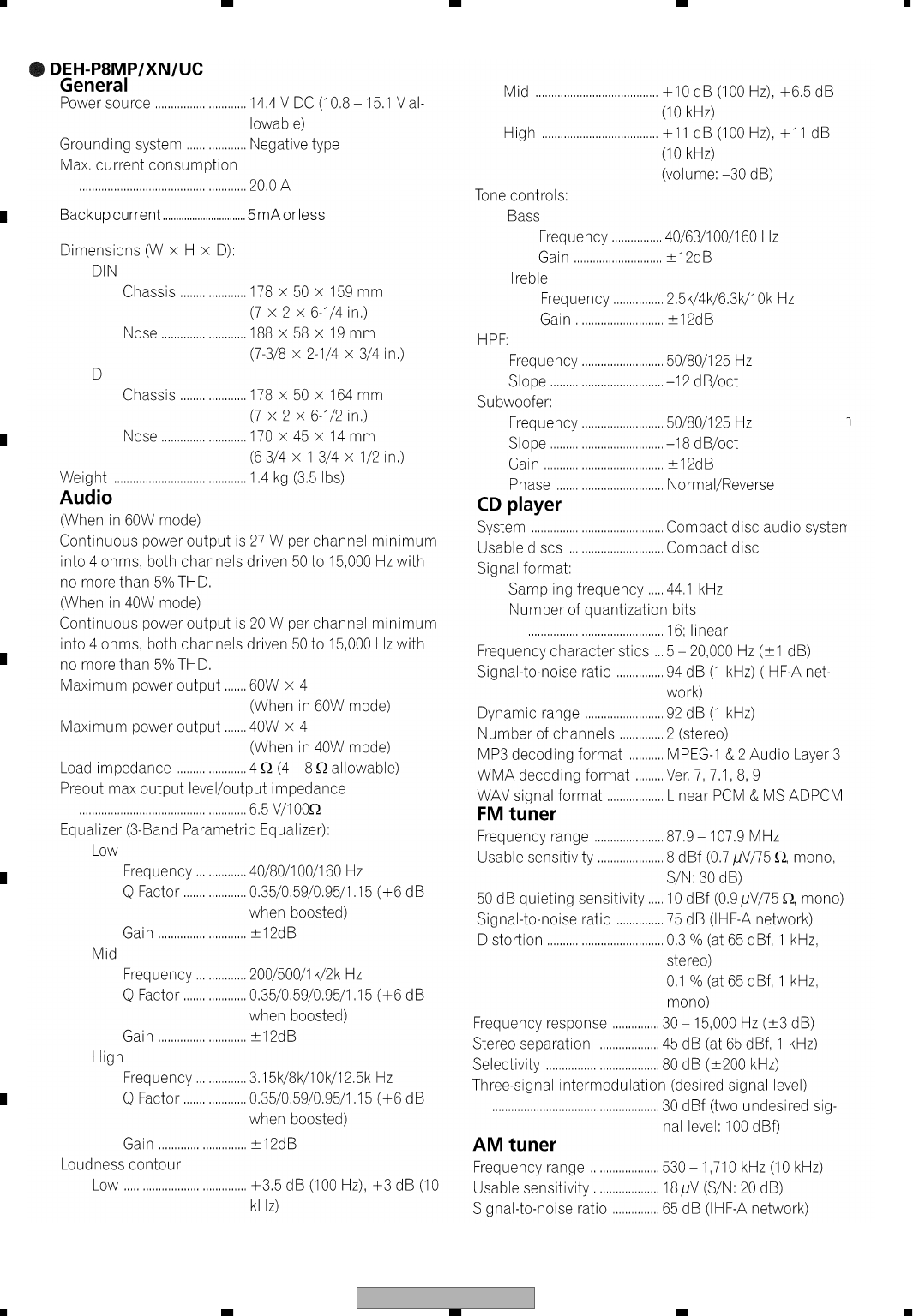
1. SPECIFICATIONS
DEH-P8MP/XN/UC 5
5678
5678
C
D
F
A
B
E
DEH-P8MP/XN/UC
6
1234
1234
C
D
F
A
B
E

DEH-P8MP/XN/UC 7
5678
5678
C
D
F
A
B
E
DEH-P8MP/XN/UC
8
1234
1234
C
D
F
A
B
E
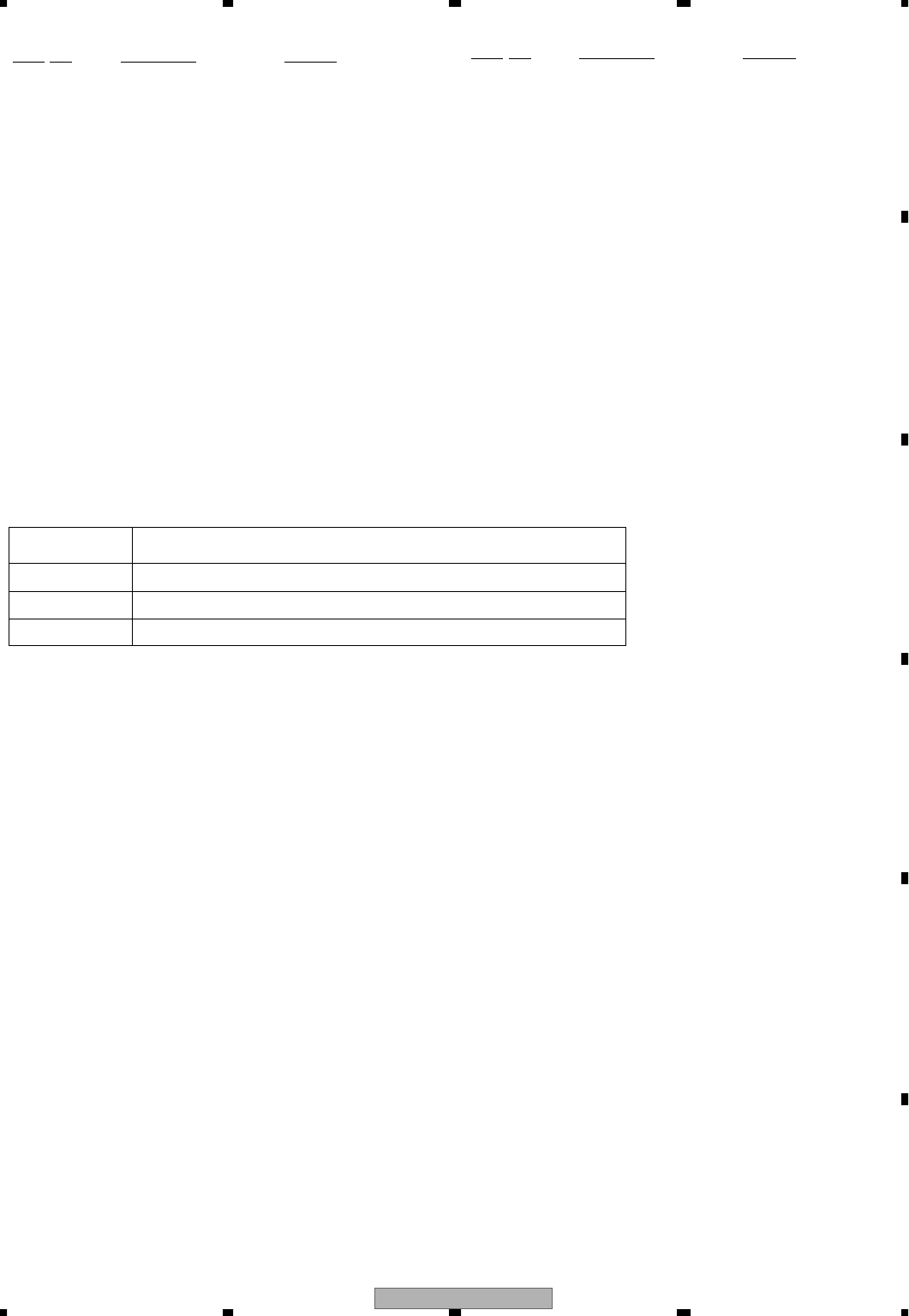
2. EXPLODED VIEWS AND PARTS LIST
2.1 PACKING(DEH-P8MP/XN/UC,DEH-P80MP/XN/UC)
N
OTES : • Parts marked by " * " are generally unavailable because they are not in our Master Spare Parts List.
• Screw adjacent to mark on the product are used for disassembly.
• For the applying amount of lobricants or glue, follow the instructions in this manual.
(In the case of no amount instructions,apply as you think it appropriate.)
"
17
18
21
22
23
24
23
24
20
25
27
2
19
1
3
8
5
9
12
13
14
16
26
15
4
7
6
11
10
28
DEH-P8MP/XN/UC 9
5678
5678
C
D
F
A
B
E
(1) PACKING(DEH-P8MP/XN/UC,DEH-P80MP/XN/UC) SECTION PARTS LIST
(2) CONTRAST TABLE
DEH-P8MP/XN/UC and DEH-P80MP/XN/UC are constructed the same except for the following:
Owner's Manual,Installation Manual
Mark No. Description Part No.
1 Cord Assy CDE7612
2 Cord Assy CDE7482
3 Accessory Assy CEA4302
4 Spring CBH1650
5 Screw Assy CEA4303
6 Screw CBA1650
7 Bolt(M5x16) CBA1783
* 8 Polyethylene Bag CEG-127
9 Screw CRZ50P090FTC
10 Screw JPZ20P060FZK
11 Nut NF50FTC
12 Screw TRZ50P080FTC
* 13 Polyethylene Bag CEG-158
14 Handle CNC5395
15 Strap CNC5402
16 Bush CNV3930
17-1 Polyethylene Bag CEG1116
17-2 Owner's Manual See Contrast table(2)
17-3 Installation Manual See Contrast table(2)
* 17-4 Caution Card CRP1307
17-5 Caution Card CRP1310
* 17-6 Warranty Card See Contrast table(2)
* 17-7 Card See Contrast table(2)
18 Polyethylene Bag CEG1173
19 Carton See Contrast table(2)
20 Sub Carton CHA3258
21 Contain Box See Contrast table(2)
22 Protector CHP2546
23 Protector CHP2539
24 Protector CHP2538
25 Protector CHP2541
26 Remote Control Unit CXC2665
27 Case Assy CXC3572
* 28 Caution Card CRP1311
Mark No. Description Part No.
Mark NO Description DEH-P8MP/XN/UC DEH-P80MP/XN/UC
17-2 Owner's Manual CRD3844 CRD3846
17-3 Installation Manual CRD3845 CRD3847
* 17-6 Warranty Card CRY1070 Not used
* 17-7 Card Not used ARY1048
19 Carton CHG5212 CHG5211
21 Contain Box CHL5212 CHL5211
Part No. Language
CRD3844 English, French
CRD3845 English, French
CRD3846 English, French
CRD3847 English, French
DEH-P8MP/XN/UC
10
1234
1234
C
D
F
A
B
E
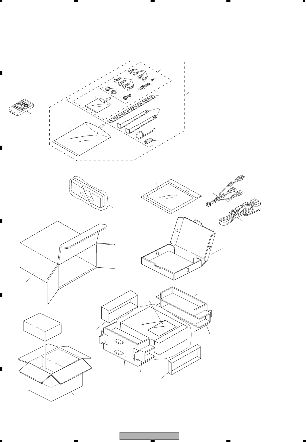
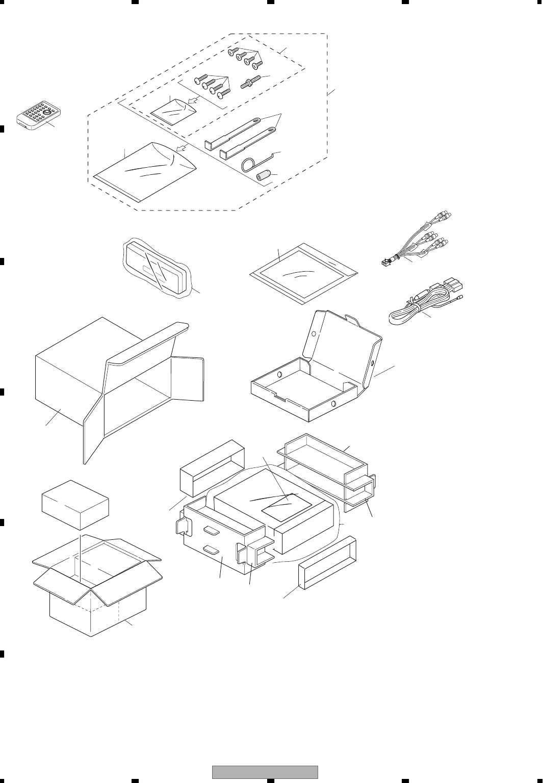
2.2 PACKING(DEH-P1Y/XN/ES)
17
18
21
22
23
24
23
24
20
25
27
2
19
1
3
8
5
9
12
13
14
16
26
4
6
28
DEH-P8MP/XN/UC 11
5678
5678
C
D
F
A
B
E
PACKING(DEH-P1Y/XN/ES) SECTION PARTS LIST
Owner's Manual,Installation Manual
Mark No. Description Part No.
1 Cord Assy CDE7612
2 Cord Assy CDE7482
3 Accessory Assy CEA4301
4 Spring CBH1650
5 Screw Assy CEA3849
6 Screw CBA1650
7 •••••
* 8 Polyethylene Bag CEG-127
9 Screw CRZ50P090FTC
10 •••••
11 •••••
12 Screw TRZ50P080FTC
* 13 Polyethylene Bag CEG-158
14 Handle CNC5395
15 •••••
16 Bush CNV3930
17-1 Polyethylene Bag CEG1116
17-2 Owner's Manual CRD3848
17-3 Owner's Manual CRD3849
17-4 Installation Manual CRD3850
* 17-5 Caution Card CRP1307
17-6 Caution Card CRP1310
18 Polyethylene Bag CEG-162
19 Carton CHG5210
20 Sub Carton CHA3258
21 Contain Box CHL5210
22 Protector CHP2546
23 Protector CHP2539
24 Protector CHP2538
25 Protector CHP2541
26 Remote Control Unit CXC2665
27 Case Assy CXC3572
* 28 Caution Card CRP1311
Mark No. Description Part No.
Part No. Language
CRD3848 English, Spanish, Portuguese(B)
CRD3849 Traditional Chinese, Arabic
CRD3850 English, Spanish, Portuguese(B), Traditional Chinese, Arabic
DEH-P8MP/XN/UC
12
1234
1234
C
D
F
A
B
E
2.3 EXTERIOR

DEH-P8MP/XN/UC 13
5678
5678
C
D
F
A
B
E
(1) EXTERIOR SECTION PARTS LIST
Mark No. Description Part No.
1 Screw BMZ26P200FTC
2 Screw BSZ26P060FTC
3 Screw(M2x2.5) CBA1641
4 Screw(M2.6x4) CBA1769
5 Flat Cable CDE7468
6 Cord Assy CDE7482
7 Fuse(10A) CEK1136
8 •••••
9 Cap CNS1472
10 IC(IC201) PAL008A
11 Resistor RS1/2PMF102J
12 Cord Assy See Contrast table(2)
13 Cord Assy CDE7484
14 Cord Assy CDE7612
15 Cap CNV6727
16 Case CNB2945
17 Holder CNC8659
18 Earth Plate CND2171
19 Insulator CNM8638
20 Insulator CNM8790
21 Cushion CNM9126
22 Panel CNS7772
23 Tuner Amp Unit See Contrast table(2)
24 Screw BMZ26P200FTC
25 Screw BSZ26P080FTC
26 Antenna Cable CDH1336
27 Clamper CEF1033
28 Connector(CN361) CKM1389
29 Plug(CN981) CKM1428
30 Plug(CN871) CKS-786
31 Connector(CN571) See Contrast table(2)
32 Connector(CN704) CKS3125
33 Connector(CN101) CKS3408
34 Connector(CN701) CKS3837
35 Connector(CN801) CKS4811
36 Holder(CN402) CNC5399
37 Case CNC8138
38 Holder CND2029
39 Holder CND2030
40 Heat Sink CND2031
41 Insulator CNM6249
42 Heat Sink CNR1728
43 Holder CND1054
44 Drive Unit See Contrast table(2)
45 Screw BMZ26P040FTC
46 Screw(M2x2) CBA1633
47 Spring CBL1632
48 Cord CDE7392
49 Holder CND1848
50 Holder CND1850
51 Insulator CNM8797
52 Gear CNV7752
53 Gear CNV7753
54 Gear CNV7754
55 Gear CNV7755
56 Switch Unit CWS1389
57 Switch(S1) CSN1051
58 Spring Switch(S2) CSN1052
59 Holder Unit CXC2196
60 Holder Unit CXC2197
61 Arm Unit CXC2198
62 Arm Unit CXC2199
63 Arm Unit CXC2200
64 Arm Unit CXC2201
65 Chassis Unit See Contrast table(2)
66 Motor Unit(M871) CXC2204
67 FM/AM Tuner Unit CWE1646
68 Gear Unit CXC2205
69 Screw JFZ20P025FTC
70 Washer YE15FTC
71 Panel Unit CXC2603
72 Remote Control Unit CXC2665
73 Cover CZN5357
74 Screw(M2x2) CBA1561
75 Screw(M2x2) CBA1633
76 Screw(M2x3.5) CBA1754
77 Spring CBH2530
78 Connector CKS4796
79 Holder CND2172
80 Flexible PCB CNP7698
81 Arm CNV6962
82 Guide CNV6967
83 Guide CNV6968
84 Case Unit CXC2670
85 Detach Grille Assy See Contrast table(2)
86 Screw BPZ20P060FZK
87 Button(OPEN/RESET) CAC8442
88 Button(BAND) CAC8443
89 Button(ENT/EQ/EQ-EX) CAC8444
90 Button(CLOCK/DISP/LIST) CAC8450
91 Button(ATT/OFF/SRC) CAC9003
92 Cover CNS7770
93 Lighting Conductor CNV7966
94 Keyboard Unit CWM9290
95 Connector(CN1901) CKS4795
96 Holder CND2028
97 Double-sided Seal CNM8673
98 Spacer CNM9141
99 Spacer CNM9142
100 Holder CNV7965
101 OEL Unit MXS8202
102 Sub Grille Assy See Contrast table(2)
103 Knob Unit CXC3581
104 CD Mechanism Module(S10CODE2)CXK5666
105 Screw ISS26P055FTC
106 •••••
107 Diode(D241,242) FMG22
108 Diode(D243,244) FMJ-2303
109 Transistor(Q241,242) FKV550N
110 Transistor(Q742,902,921) 2SD2375
Mark No. Description Part No.

DEH-P8MP/XN/UC
14
1234
1234
C
D
F
A
B
E
(2) CONTRAST TABLE
DEH-P8MP/XN/UC, DEH-P80MP/XN/UC and DEH-P1Y/XN/ES are constructed the same except for the following:
Mark NO Description DEH-P8MP/XN/UC DEH-P80MP/XN/UC DEH-P1Y/XN/ES
12 Cord Assy CDE7483 CDE7483 Not used
23 Tuner Amp Unit CWM9287 CWM9288 CWM9289
31 Connector(CN571) CKS3125 CKS3125 Not used
44 Drive Unit CXC2206 CXC2206 CXC3562
65 Chassis Unit CXC2203 CXC2203 CXC3561
85 Detach Grille Assy CXC2695 CXC2696 CXC2697
102 Sub Grille Assy CXC3235 CXC3236 CXC3237

DEH-P8MP/XN/UC 15
5678
5678
C
D
F
A
B
E
DEH-P8MP/XN/UC
16
1234
1234
C
D
F
A
B
E
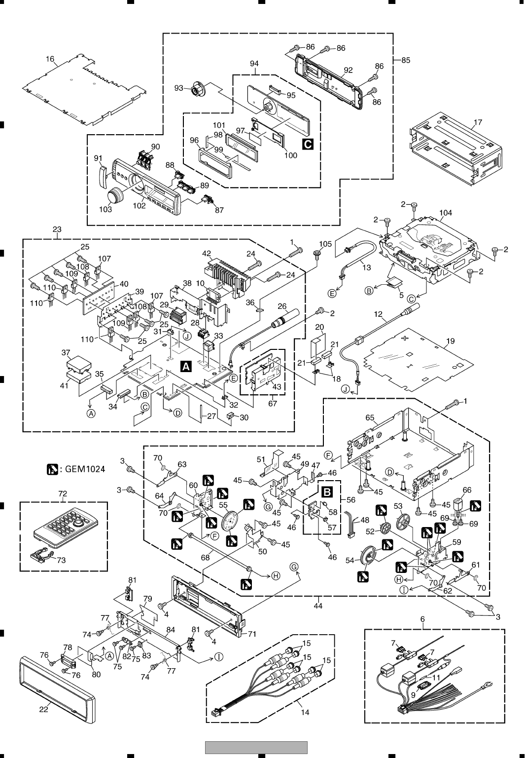
2.4 CD MECHANISM MODULE
A
D
H
L
M
NO
Q
R
A
B
C
D
E
F
GH
I
J
K
L
M
N
O
Q
B
16
25
13 83
42
68
28
82
4
71
23
J
K
38
23
59
87
86
5
13
34
5
5
13
44
5C
52
53
36
4
73
29
51
18
64
76
50
10
72
75
49
77
67
27
78
60
90 48
8
17
46
6
60
11 89
43
70
14
31
65
85
66
85
31
35
14
74
85
1
2
R
94
91
12
33
61
63
21
79
57
58
62
80
13
4
86
I
45
28
7
24
47
P
41
20
40
69
39
30
P
19
56
F
E22
81
15
G
26
4
54
37
55
93
92
10
D
3
1GEM1024
2GEM1045
3GEM1035
1
1
1
1
1
1
1
1
2
2
2
2
1
1
1
1
1
2
2
1
3

DEH-P8MP/XN/UC 17
5678
5678
C
D
F
A
B
E
CD MECHANISM MODULE PARTS LIST
Mark No. Description Part No.
1 CD Core Unit(S10WMACODE2)CWX2952
2 Connector(CN101) CKS4182
3 Connector(CN901) CKS4017
4 Screw BMZ20P035FTC
5 Screw BSZ20P040FTC
6 Screw(M2x4) CBA1362
7 Screw(M2x3) CBA1511
8 Screw(M2x3) CBA1527
9 •••••
10 Washer CBF1038
11 Washer CBF1060
12 Spring CBH2390
13 Spring CBH2606
14 Spring CBH2607
15 Spring CBH2608
16 Spring CBH2609
17 Spring CBH2610
18 Spring CBH2735
19 Spring CBH2612
20 Spring CBH2613
21 Spring CBH2614
22 Spring CBH2615
23 Spring CBH2616
24 Spring CBH2617
25 Spring CBH2620
26 Spring CBH2621
27 Spring CBH2641
28 Spring CBH2642
29 Spring CBH2643
30 Spring CBH2659
31 Spring CBH2688
32 •••••
33 Shaft CLA4441
34 Frame CNC9962
35 Frame CNC9963
36 Bracket CNC9966
37 Bracket CND1895
38 Arm CNC9968
39 Arm CND1909
40 Lever CND2032
41 Lever CNC9984
42 Sheet CNM8134
43 Collar CNV7798
44 Guide CNV7799
45 Arm CNV7800
46 Rack CNV7199
47 Holder CNV7201
48 Holder CNV7202
49 Arm CNV7203
50 Gear CNV7207
51 Gear CNV7208
52 Gear CNV7209
53 Gear CNV7210
54 Gear CNV7211
55 Gear CNV7212
56 Rack CNV7214
57 Arm CNV7215
58 Arm CNV7216
59 Guide CNV7217
60 Roller CNV7218
61 Gear CNV7219
62 Arm CNV7221
63 Arm CNV7220
64 Arm CNV7222
65 Damper CNV7313
66 Damper CNV7314
67 Arm CNV7341
68 Arm CNV7342
69 Guide CNV7360
70 Guide CNV7361
71 Holder CNV7437
72 Arm CNV7805
73 Gear CNV7595
74 Damper CNV7618
75 Motor Unit(M1) CXB6007
76 Chassis Unit CXC2318
77 Screw Unit CXB8729
78 Gear Unit CXC2397
79 Arm Unit CXC2316
80 Arm CND1896
81 Arm CND1894
82 Motor Unit(M2) CXB8933
83 Bracket CNC9985
84 •••••
85 Screw(M2x5) EBA1028
86 Screw JFZ20P020FTC
87 Screw JGZ17P022FTC
88 •••••
89 Washer YE20FTC
90 Pickup Unit(P9.9MP3)(Service) CXX1805
91 Screw IMS26P030FTC
92 Spring CBL1635
93 Clamper CNV7197
94 Connector(CN902) CKS2193
Mark No. Description Part No.
DEH-P8MP/XN/UC
18
1234
1234
C
D
F
A
B
E
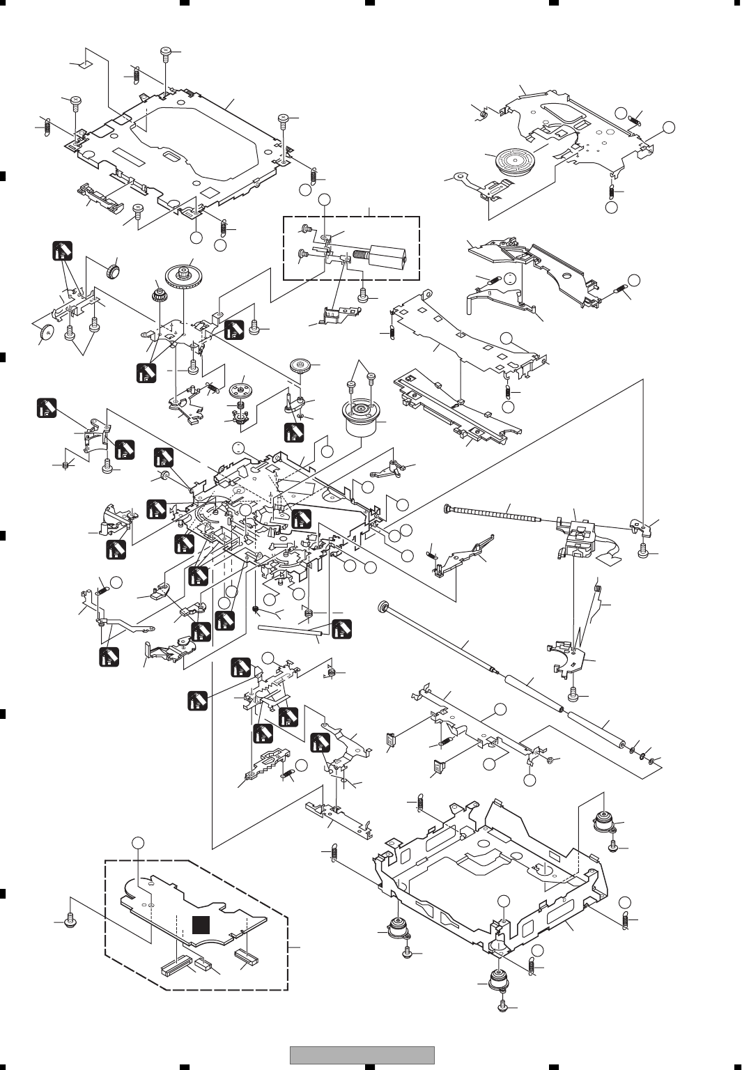
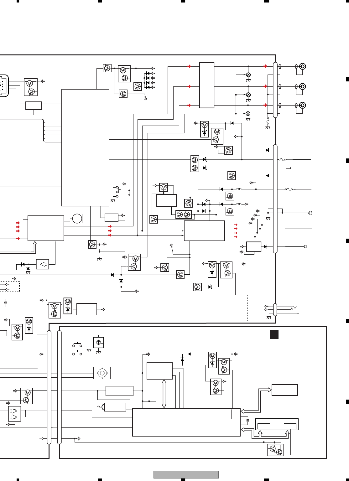
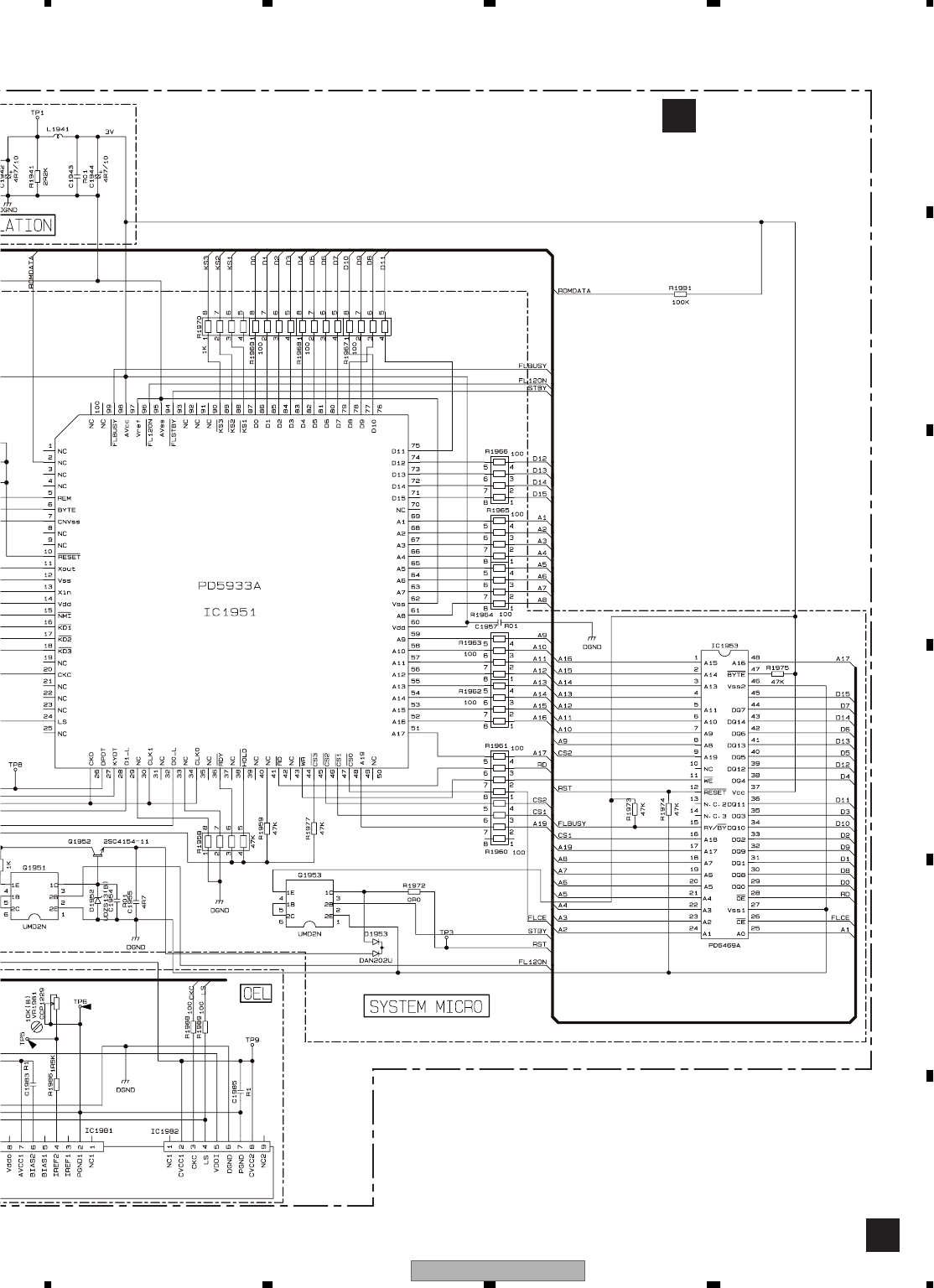
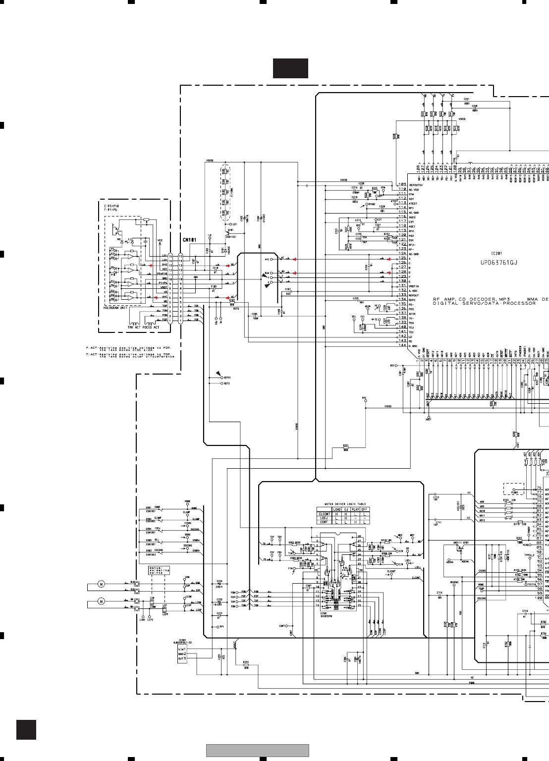
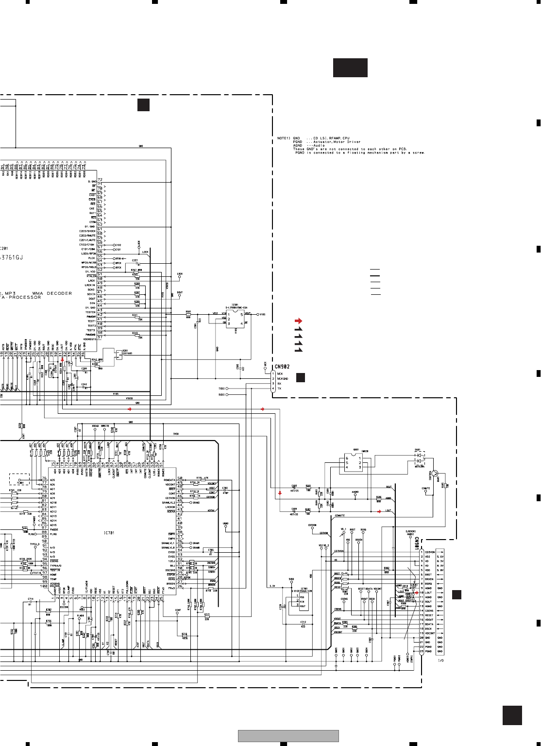
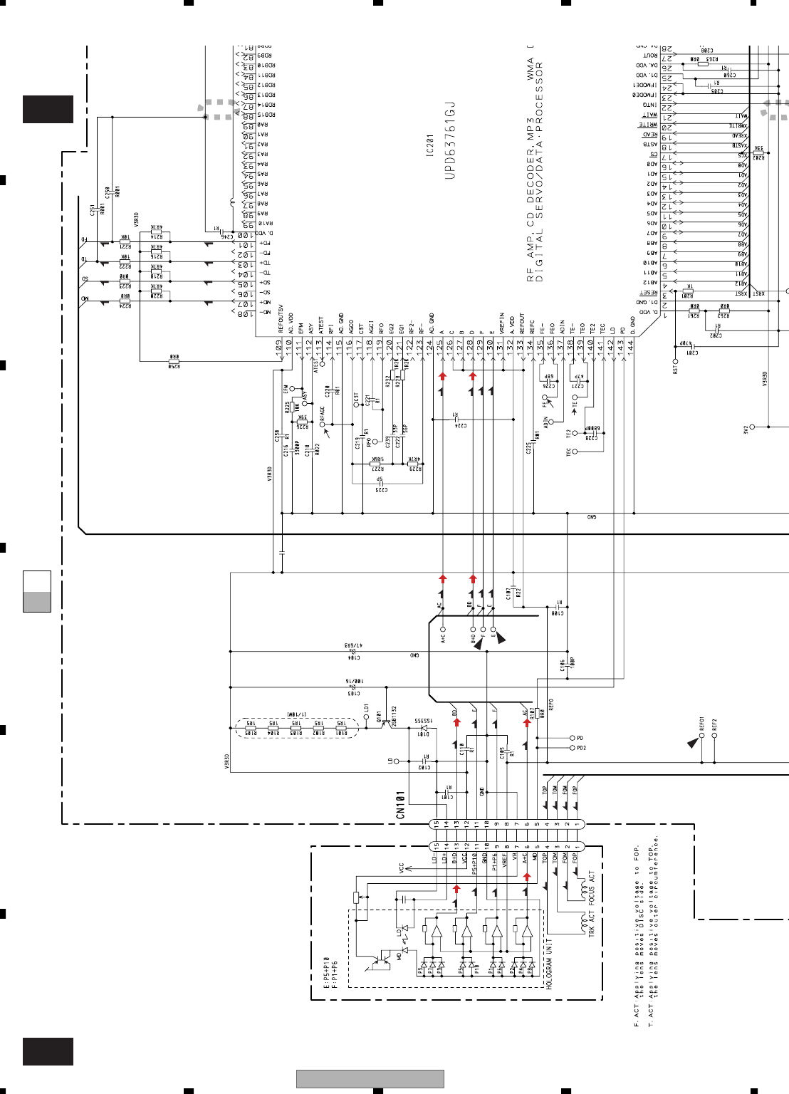
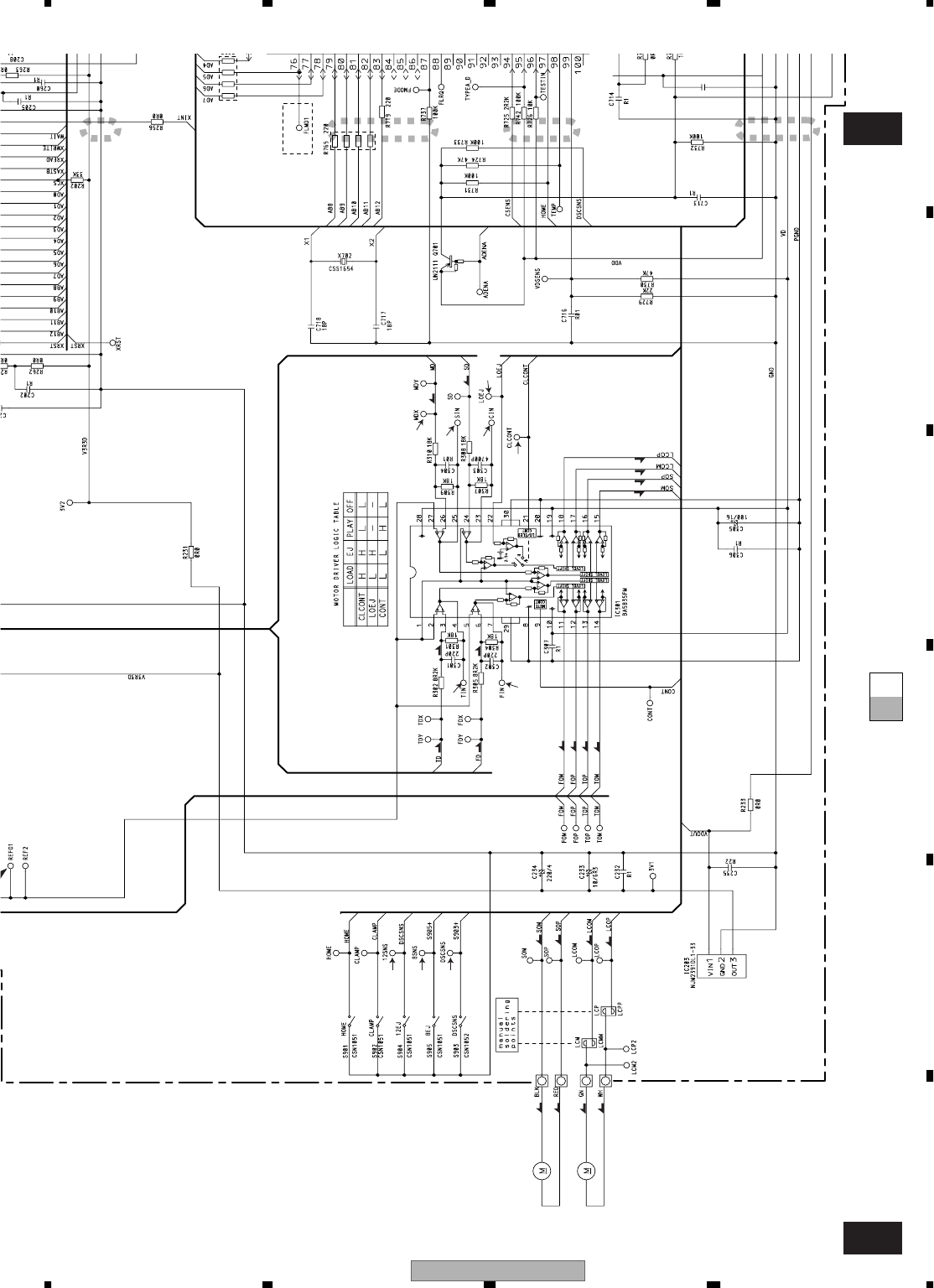
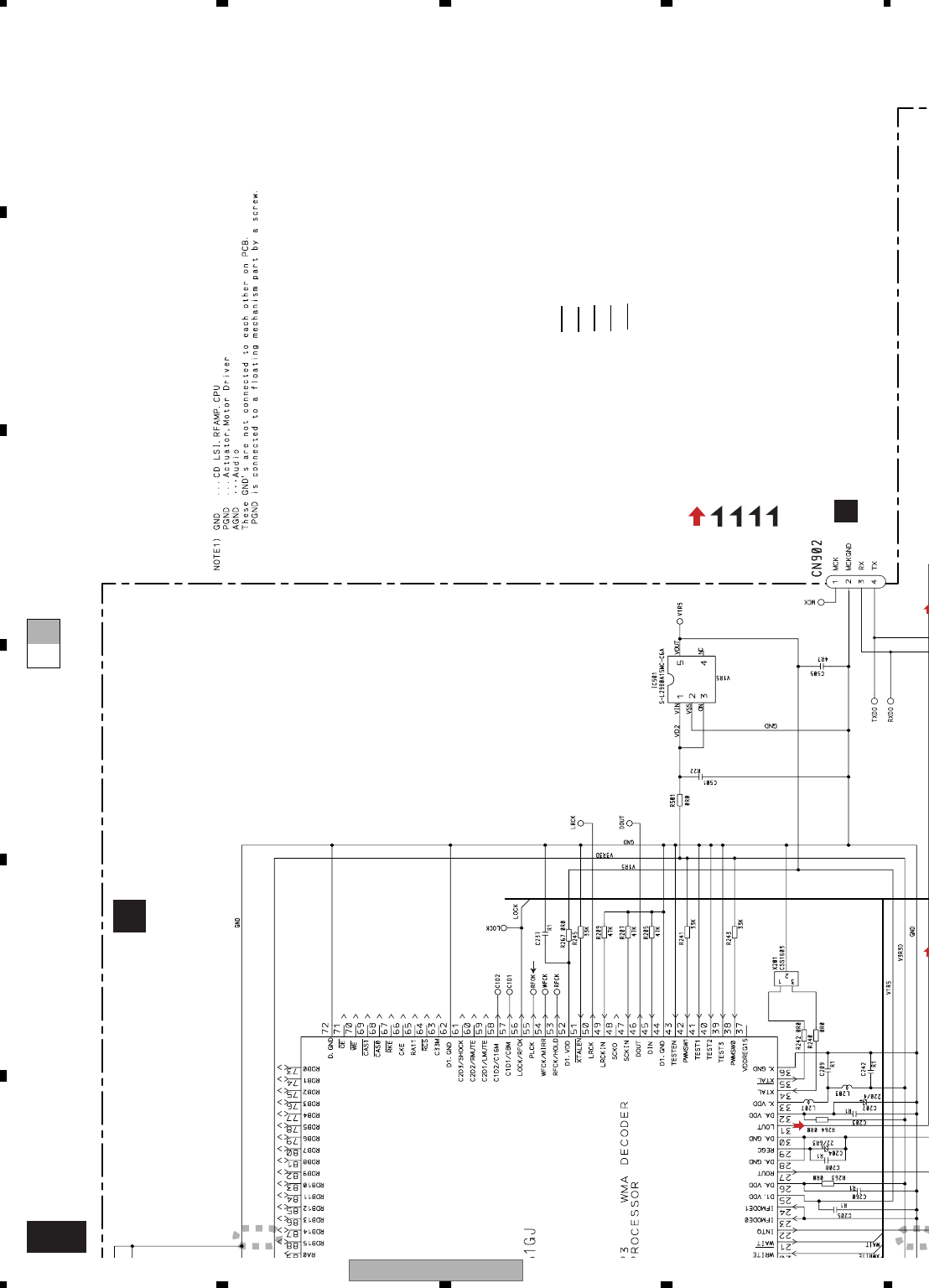
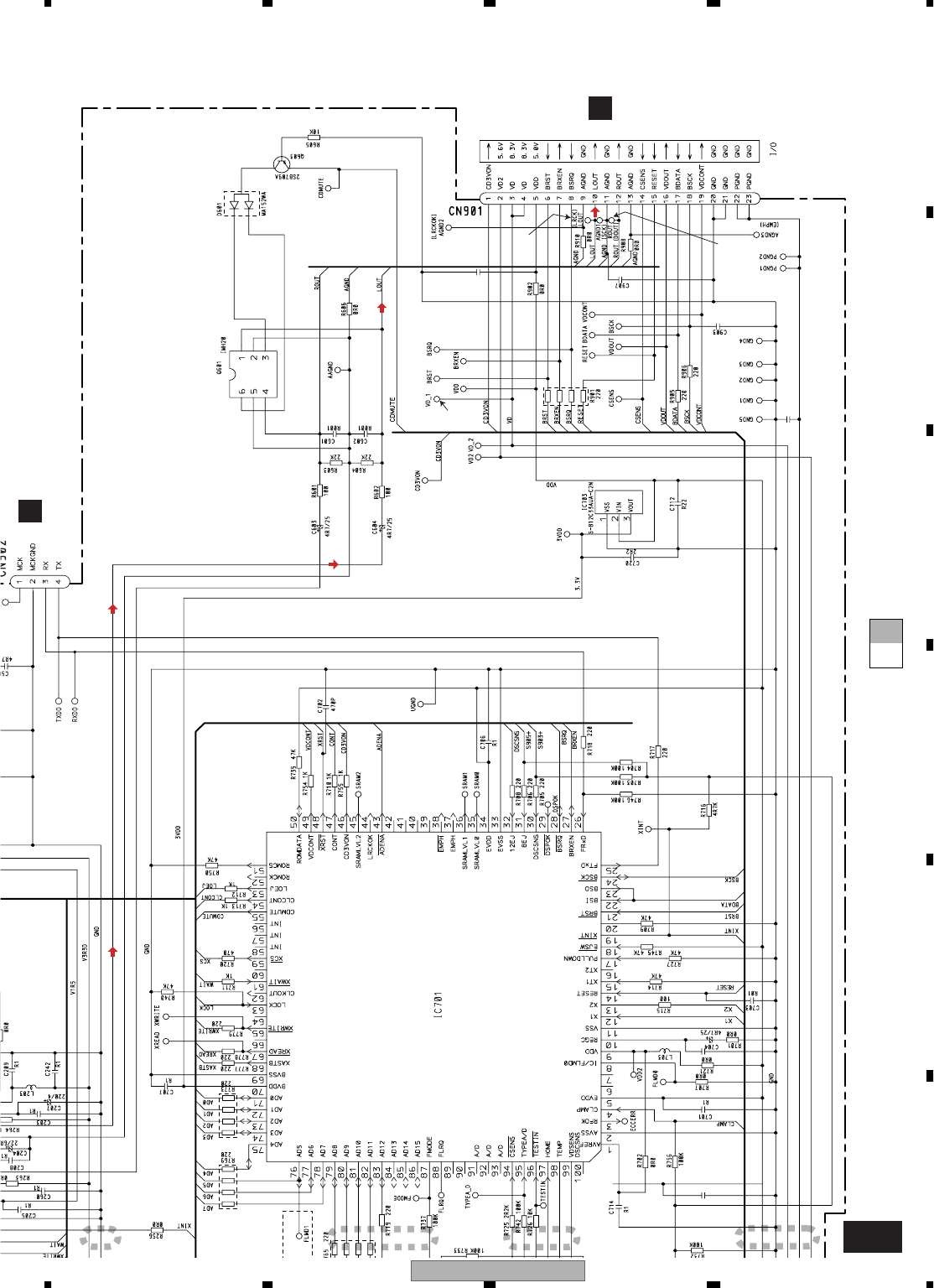
3. BLOCK DIAGRAM AND SCHEMATIC DIAGRAM
3.1 BLOCK DIAGRAM
102
VDD
85
MUTE
XIN
XOUT
IN3-
L
42
PEE
22
38
IN4-
L
44
IN4+
L
43
IN2-
L
41
RESET SYSTEM CONTROLLER
IC 601(2/2)
PD5925A
IC 652 reset
CN401
ELE
C
SO
SWVDD
Q831
TUNER AMP UNIT
13
X601
11
1
EVST,EVCK,EVDT
TUN L
CD L
33
DPDT
34
KYDT
1
SYSPW
41
ILMPW
A
BUZZER
BA033FP
IC 451
13 SYS+B
TUNER 3.3V REGULATOR
TUN 3.3V
SYS+B
VDD
ANTENNA
7
92
LVLINL
LEVEL INDICATO
B.UP
Q821
Q822
20
OELPW
B
SP 601
IC 801(2/2)
1211
35
ROT1
36
ROT0
VDD
BD4835G
15
ASLIN
NOI
S
CN701
14
OE
L
TC74VHCT125AFT
98
IC 801(1/2) 32
65
CDRX
CDTX
GDTC1
GDTC2
1
4
GDTC1
GDTC2
13
10
TC74VHCT125AFT
SYSPW2
84
SYSPW2
47
gdtc@
GDTC2
43
gdtc!
GDTC1
3
2
BUSL+
BUS-
BUS+
BUS+L
BUS-L 5
8
1
7
CN101
11
IC 1
0
HA122
IP-
B
8
6
5
I
Q101
8
BUSL-
9
BA6288FS
IC 871 6
34
11
B.UP
M
FLAP
MOTOR 14
4
5
5
CN871
CLOSE
fclssw
OPEN
fopnsw
OUT1
OUT2
Q872
Q871
2
3FCLSSW
FOPNSW
1
SWITCH UNIT
B
M871
S1
S2
51
50
KEYAD
KYDT
89
KEYAD
34
KYDT
BRST,BRXEN,BSRQ
BDATA,BSCK
21
19
5
20
VDD
22
VD
VD2
VDCONT
23 CD3VON
B.UP
Q741
Q742
Q744
Q743
A
B
A
B
CN704
CDTX
CDRX
C
87
CROSSKEY
Q651
RST1
R
91
DSENS
ejtin 42
1
2
BRST,BRXEN,BSRQ
D
CN901
Q101
M
LASER
DIODE
MONITOR
DIODE
S902
CLAMP S903
DSCSNS
FOCUS ACT.
M1
SPINDLE
MOTOR
M
M2
LOADING/CARRIAGE
MOTOR
TRACKING ACT.
LD-
MD
FO+
TO+
15
5
1
4
PICKUP UNIT
(P9.9MP3)(SERVICE)
HOLOGRAM
UNIT
IC 301
BA5835FM
IC 201
UPD63761GJ
IC 703
3.3V REGULATOR
RF AMP, CD DECODER,
MP3 AND WMA DECODER
DIGITAL SERVO/DATA PROCESSOR
CD
DRIVER
3
VD
VD
3VDD 5
CN101
TOP
FOP
16 SOP
15 SOM
18 LCOP
17 LCOM
22
2
LOEJ
LOUT
9
CONT
12 FOP
TD/FD
AC,BD
F,E
SD/MD
3
13 TOP
S901
HOME
S904
12EJ S905
8EJ
LD+ 14
142 LD
143 PD
CD CORE UNIT(S10WMACODE2)
1312
X702
DSCSNS
CONT
LOEJ
HOME
32
97
53
47
VDD
IC 203
NJM2391DL1-33
3.3V REGULATOR
V3R3D 1
3
VDCONT 49
S-812C33AUA-C2N
MICRO
COMPUTER
IC 701
PE5423A
4
V3R3D
19
BDATA,BSCK
VD2
VDD
2
15
5
1
4
14
CLAMP
4
VD2
VDCONT
30
31 8EJ
12EJ
IC 501
S-L2980A15MC-C6A
1.5V REGULATOR
V1R5 1,3
5V3R3D
X1 X2
CN902
RX
TX
3
4
FRxD
FTxD
26
25
1
CD3VON 46
CD3VON
10
31
FMRF
ANT adj RF adj
FM ANT
T51 CF52
CF51
RFGND
OSCGND
DGND
AUDIOGND
NC
VCC
VDD_3.3
3.3V 2.5V
IC 4
3.3V 2.5V
←
IC 2
2.5V
WC
CE2
ROM_VDD
SL
DI
CK
CE1
NC
DO
7 6 13 5 10 9 8 11 14 18 19 20 21
1
3
212 1522 16 4 17
IC 1
3.3V
AM ANT FMRF
ATT LPF
OSC
IC 3 EEPROM
5.0V
IC 5
5V 3.3V
←
ATT MIXER, IF AMP
DET,
FM MPX
24
23
Rch
Lch
FM/AM TUNER UNIT
NC
NC
NC
NC
DEH-P8
M
DEH-P80
M
DEH-P8MP/XN/UC 19
5678
5678
C
D
F
A
B
E
bsens
asens
B.UP
72
73
10
FL 11
RL
8
5
IL+B
SWDVDD
8
10
4
6
FL-
FL+
RL-
RL+
AC
IN3-L
42
IN4-L
44
IN4+L
43
IN2-L
41
FLIN
12
RLIN
13
27
POWER AMP
IC 601(1/2)
PD5925A
IC 131
PML009A IC 201
PAL008A
VDD
Q902
Q931
SYSPW
ELECTRONIC VOLUME/
SOURCE SELECTOR
MUTE
Q831
1
3
X601
1
1
EVST,EVCK,EVDT
TUN L
CD L
DPDT
KYDT
SYS+B BU
Q922
Q923
1
B.UP
Q201
MUTE
Q363
12
PL
7
8
13
12
4
1
MUTE
S421
60W/40W
4
sel^)w
SYSTEM CONTROLLER
Q951
VDD
TELIN 8
FL-
FL+
RL-
RL+
VDD REGULATOR
BACKUP SENSE
ACC SENSE
TELEPHONE MUTE
SYS +B REGULATOR
9
8
5
2
4
15
14
11
18
CN981
Q364
BU
BACKUP
GND
FUSE
10A
TELMUTE
B.REM
Q921
Q901
DALMON 67
Q501
5
Q362
PL
FL
Q941
isens 81 ILM SENSE
ILM
13
NJM4558MD
IC 171
57
9
2
1
SEL_OUT_L
LEVEL INDICATOR
MIC
13
MICIN
MICROPHONE
1
B.UP
Q821
Q822
2
0
B.UP Q841 Q842
IC 841
NJM2360M
65
11
10
ROT1
ROT0
VDD
MIC 321
15
ASLIN
93
ASLIN
NOISEDET
CN801
Q361
RL
OEL+B
OEL+B
/
2) 32
65
D
TC1
D
TC2
1
4
5AFT
ACC
SYSPW2
8
4
SYS+B
SL
tunpce@
TUNPCE1
TUNPDI
TUNPDO
95
69
70
98
99
TUNPCK
100
ce@
CE1
DO
DI
CK
B
USL+
B.UP
ASENBO
80
28
27
79
BUS-
BUS+
TX
RX
IPPW
5
8
1
01
IC 101
HA12240FP
IP-BUS DRIVER
1
2
8
6
5TX
RX
IPPW
Q101
8
USL-
9
52 FLPCLS
53 FLPOPN
54 FLPPW
FL
SWL 9
CN361 SUB
WOOFER L
REAR L
5
RL
FRONT L
1
10
6
2
FU351
3A
IC 341
PA2028A
17
15
13
8
10
12
Q242
B.UP
VCC1 MG1
27
Q241
ACC
VCC2
21
IC 241
UPC494GS
10 Q243
9
6
Q248
SYS+B
4
5
Q244
VCC1
ddchk
88
VCC2
IC 221
3
NJM2406F
ACC
FUSE
10A
17
1k(1/2W)
Q221
81
1
ACCMON
3
ACC
15
B.REMOTE
IC 561
TPD1018F
B.UP
6
SYSPW2
Q883
FL-
FL+
RL-
RL+
VCC1
FL-
FL+
RL-
RL+
Q881(1/2)
Q885
Q881(2/2)
Q882
2
ICERORR
16
CN571
WIRED REMOTE
CONTROL
KEYAD
KYDT 2
1
3
KEYAD
KYDT
8
9
3
4
VDD
40W
60W
9
CLOSSKEY
16
14
15
RST1
9
1
4
2EJSW
DSENS
Q202
SYS+B
C
C
Q247 Q246
DEH-P8MP/XN/UC
DEH-P80MP/XN/UC
DEH-P8MP/XN/UC
DEH-P80MP/XN/UC
IL+B
SWVDD
OELB
IC 1951
PD5933A
OEL CONTROLLER/
KEY CONTROLLER
7
8
5
KEY DATA
OEL DATA
AVCC
97
CN1901
KEYBOARD UNIT
13
12
DPDT
KYDT
IC 1952
RS-140
REMOTE CONTROL
SENSOR
OPT IN 4
15REM
27
28
DPDT
KTDT
OEL UNIT
8,21 2,8
IC 1941
S-818A33AUC-BGN
3.3V REGULATOR
15
C
11
10 ROT1
ROT0
KEY MATRIX
ILLUMINATION
Q1981
Q1982
IC1970 IC1971
VDD
14
VDD
60
16V
12V
IC 1953
PD6469A
FLASH MEMORY
37 VCC
26
ce
cs!
47
cs@
46
cs)
48
Q1951
Q1952
16
FL12PON
96
16V
16V
12
reset
Q1953
3.3V
flstsy
93
3.3V
XIN
XOUT
13 X1940
11
S1913
SEL/VOL
9JOYST
A18 9
A19
16 OPEN
OPEN
S1902
14 RST1
15 DSENS
RESET
S1901
DEH-P8MP/XN/UC
20
1234
1234
C
D
F
A
B
E
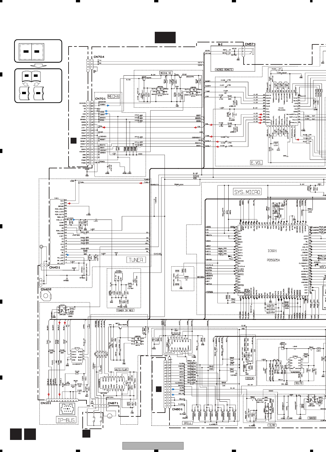
3.2 OVERALL CONNECTION DIAGRAM(GUIDE PAGE)
A-a A-b
A-a A-b
A-b
A-a
Large size
SCH diagram
Guide page
Detailed page
Note: When ordering service parts, be sure to refer to " EXPLODED VIEWS AND PARTS LIST" or
"ELECTRICAL PARTS LIST". A-a
A B
60W/40W
CCN1901
FM/AM TUNER UNIT
D
CN901 CN902
CD CORE UNIT(S10WMACODE2)
111098
65
2143
7
FM/AM ANTENNA
WIRED REMOTE CONTROL
BSWITCH UNIT
S2 OPEN
CSN1052
S1 CLOSE
CSN1051
M
M871
FLAP MOTOR
CXC2204
231
CD:0dBs
FM(100%):-19.5dBs
AM(30%):-30.0dBs
IP-BUS:+2.2dBs
FM:-20.5dBs
AM:-31.0dBs
IP-BUS: +2.2dBs
CD: 0dBs
FM:+2.6dBs
AM: -7.9dBs
IP-BUS:+8.3dBs
CD:+8.1dBs
P
P
P
P
P
P
P
DEH-P8MP/XN/UC 21
5678
5678
C
D
F
A
B
E
A-b
A-a A-b
A-a A-b
A-b
A-a
A
Decimal points for resistor
and capacitor fixed values
are expressed as :
2.2 2R2
0.022 R022
←
←
The > mark found on some component parts indicates
the importance of the safety factor of the part.
Therefore, when replacing, be sure to use parts of
identical designation.
Symbol indicates a resistor.
No differentiation is made between chip resistors and
discrete resistors.
NOTE :
Symbol indicates a capacitor.
No differentiation is made between chip capacitors and
discrete capacitors.
>
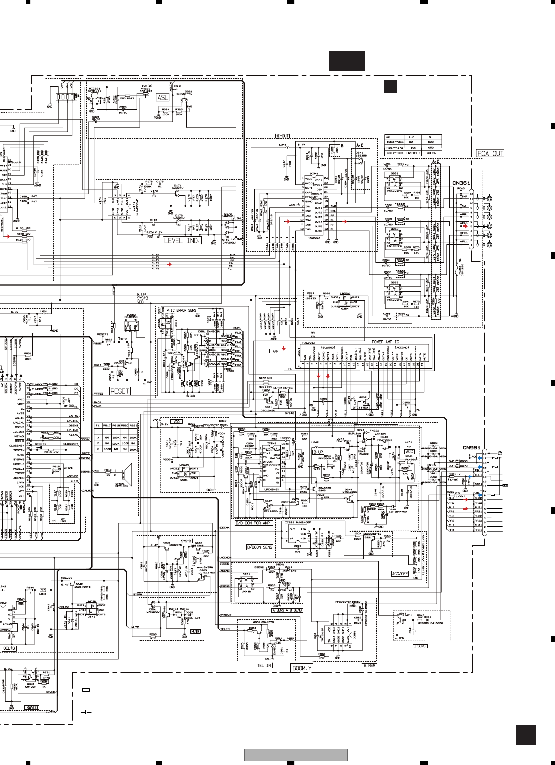
ATUNER AMP UNIT
REAR
R CH
SUB
WOOFER
R CH
SUB
WOOFER
L CH
REAR
L CH
FRONT
R CH
FRONT
L CH
A : DEH-P8MP/XN/UC
B : DEH-P80MP/XN/UC
C : DEH-P1Y/XN/ES
>
GND
TEL MUTE
BACKUP
ACC
CEK1136
10A
1K(1/2W)
CEK1136
10A
>
B.REM
ILL
RL-
FR-
RL+
FR+
FL-
RR-
FL+
RR+
T
ROL
FM:+2.6dBs
AM: -7.9dBs
BUS:+8.3dBs
CD:+8.1dBs
FM:+13.1dBs
AM: +2.6dBs
IP-BUS:+18.8dBs
CD:+18.6dBs
FM:+28.6dBs
AM:+18.1dBs
IP-BUS:+34.3dBs
CD:+34.1dBs
P
P
P
P
DEH-P8MP/XN/UC 25
5678
5678
C
D
F
A
B
E
A-a A-b
A-b
3 4
Decimal points for resistor
and capacitor fixed values
are expressed as :
2.2 2R2
0.022 R022
←
←
The > mark found on some component parts indicates
the importance of the safety factor of the part.
Therefore, when replacing, be sure to use parts of
identical designation.
Symbol indicates a resistor.
No differentiation is made between chip resistors and
discrete resistors.
NOTE :
Symbol indicates a capacitor.
No differentiation is made between chip capacitors and
discrete capacitors.
>
GND
TEL MUTE
BACKUP
ACC
CEK1136
10A
1K(1/2W)
CEK1136
10A
>
B.REM
ILL
RL-
FR-
RL+
FR+
FL-
RR-
FL+
RR+
FM:+28.6dBs
AM:+18.1dBs
IP-BUS:+34.3dBs
CD:+34.1dBs
P
P
P
P
DEH-P8MP/XN/UC 29
5678
5678
C
D
F
A
B
E
D-b
D
470P
R01
C722
1
C906 R22
C910
2R2
16.934MHz
AND
PE5423A
SWITCHES:
CD CORE UNIT(S10WMACODE2)
S901 : HOME SWITCH.........ON-OFF
S902 : CLAMP SWITCH.......ON-OFF
S903 : DSCSNS SWITCH.....ON-OFF
S904 : 12EJ SWITCH............ON-OFF
S905 : 8EJ SWITCH..............ON-OFF
The underlined indicates the switch position.
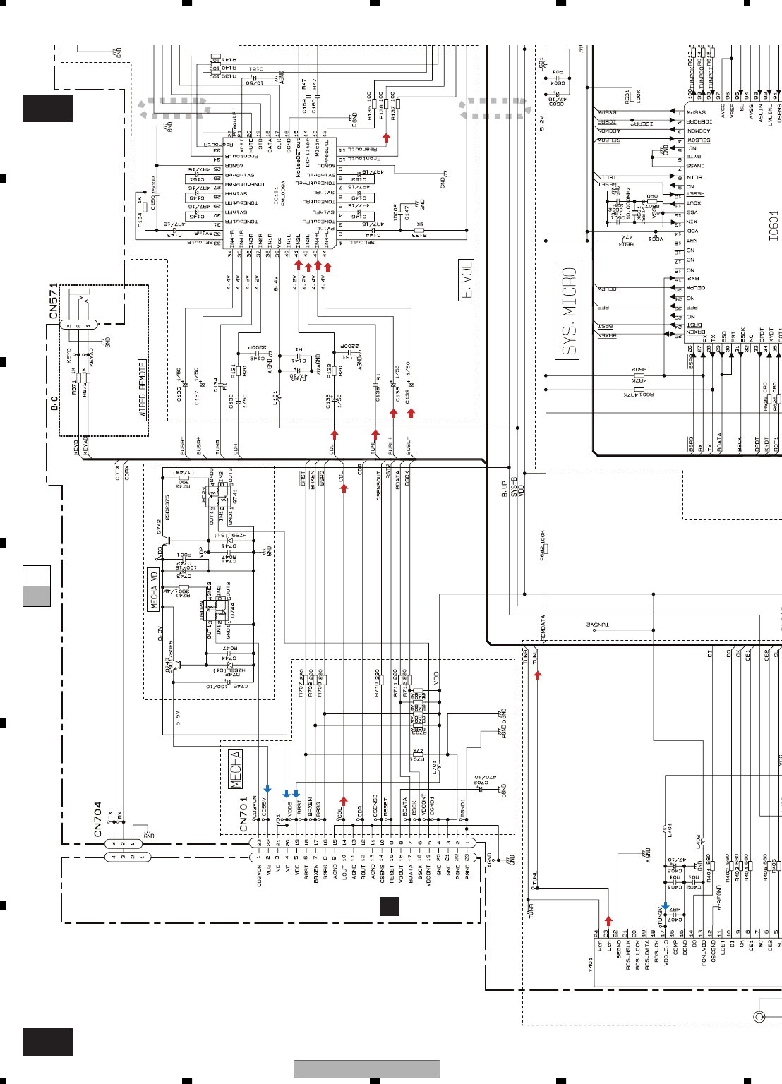
A
D
CN701
CD CORE UNIT(S10WMACODE2)
MICRO COMPUTER
1.5V REGULATOR
3.3V REGULATOR
Pull-down
A
CN704
!
6
^
&
SIGNAL LINE
FOCUS SERVO LINE
TRACKING SERVO LINE
CARRIAGE SERVO LINE
SPINDLE SERVO LINE
F
T
C
S
DEH-P8MP/XN/UC
32
1234
1234
C
D
F
A
B
E
D-a D-b
D-b 12
16.934MHz
AND
SWITCHES:
CD CORE UNIT(S10WMACODE2)
S901 : HOME SWITCH.........ON-OFF
S902 : CLAMP SWITCH.......ON-OFF
S903 : DSCSNS SWITCH.....ON-OFF
S904 : 12EJ SWITCH............ON-OFF
S905 : 8EJ SWITCH..............ON-OFF
The underlined indicates the switch position.
D
CD CORE UNIT(S10WMACODE2)
1.5V REGULATOR
A
CN704
!
SIGNAL LINE
FOCUS SERVO LINE
TRACKING SERVO LINE
CARRIAGE SERVO LINE
SPINDLE SERVO LINE
F
T
C
S
DEH-P8MP/XN/UC
34
1234
1234
C
D
F
A
B
E
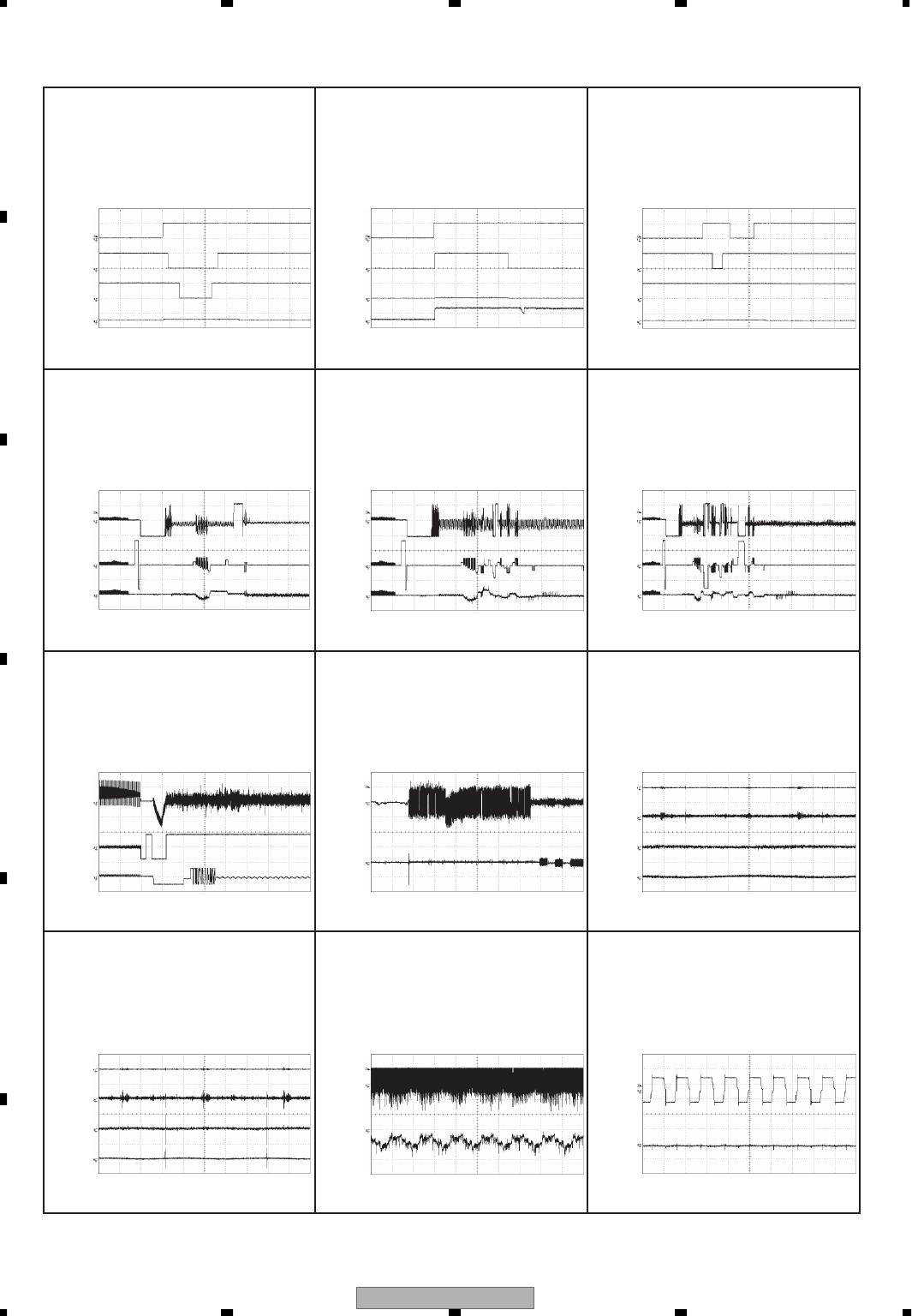
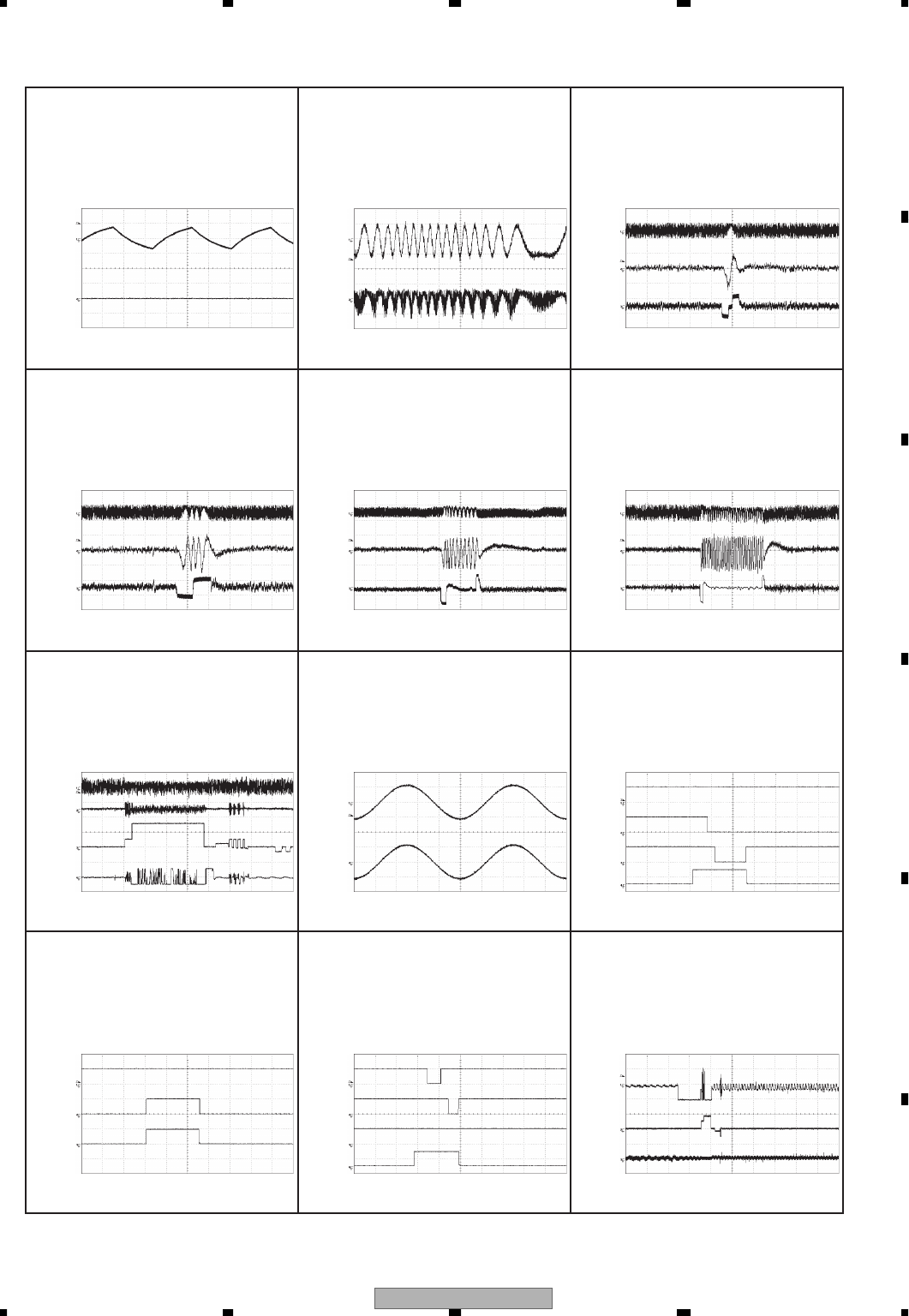
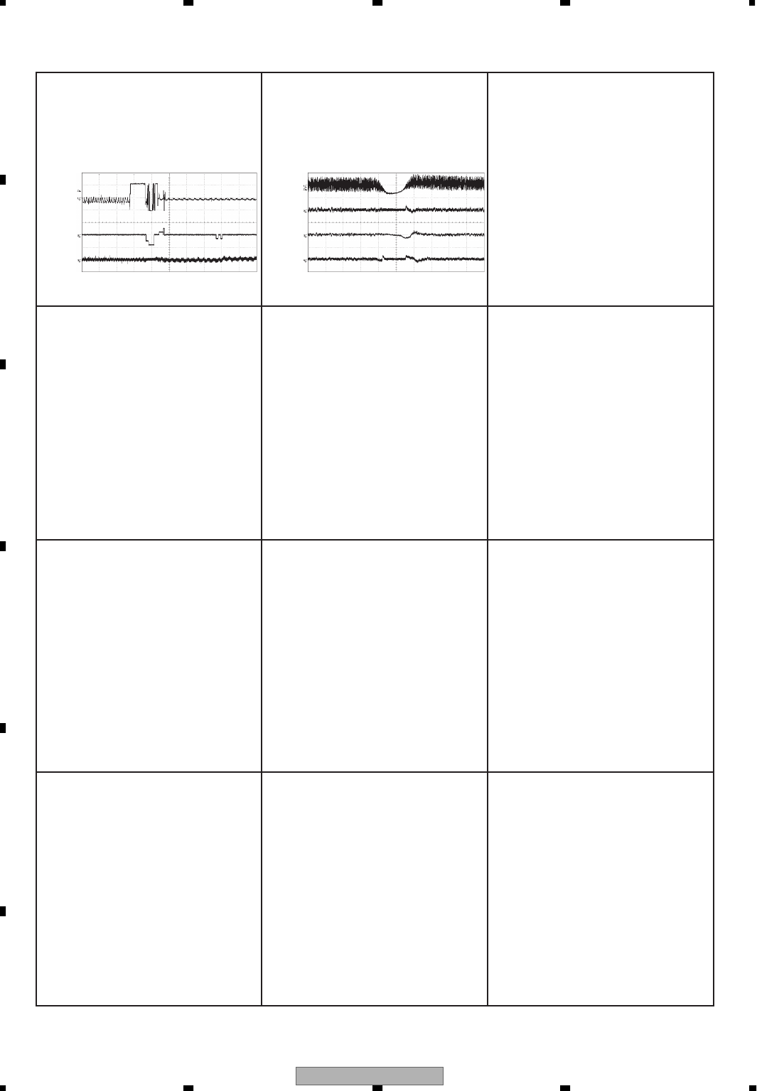
- Waveforms Note : 1. The encircled numbers denote measuring points in the circuit diagram.
2. Reference voltage REFO1(1.65V)
1 DSCSNS
2 8SNS
3 12SNS
4 LOEJ
5V/div
5V/div
5V/div
5V/div
500ms/div
12 cm CD Loading operation
Ref.:
GND
Mode:
Normal
1 DSCSNS
2 8SNS
3 12SNS
4 LOEJ
5V/div
5V/div
5V/div
5V/div
500ms/div
Ref.:
GND
Mode:
Normal
1 DSCSNS
5 CLCONT
4 LOEJ
6 VD
5V/div
5V/div
5V/div
10V/div
500ms/div
12 cm CD Loading operation 8 cm CD Loading operation
Ref.:
GND
Mode:
Normal
0 FIN
! RFOK
7 SIN
200mV/div
2V/div
2V/div
500ms/div
12 cm CD-DA Source On setup operation
Ref.:
REFO
Mode:
Normal
# FE
0 FIN
@ TE
9 TIN
500mV/div
500mV/div
500mV/div
500mV/div
20ms/div
Ref.:
REFO
Mode:
Normal
@ TE
# FE
500mV/div
500mV/div
200ms/div
Source On setup operation CD-DA Play operation
Ref.:
REFO
Mode:
Normal
# FE
0 FIN
@ TE
9 TIN
500mV/div
500mV/div
500mV/div
500mV/div
20ms/div
CD-ROM play operation(Regular track Jump)
Ref.:
REFO
Mode:
Normal
$ MDX
7 SIN
2V/div
1V/div
5µs/div
Ref.:
REFO
Mode:
Normal
$ MDX
7 SIN
1V/div
200mV/div
50ms/div
Spindle waveform during play operation Spindle waveform during play operation
(Wider)
Ref.:
REFO
Mode:
Normal
7 SIN
8 CIN
9 TIN
1V/div
500mV/div
500mV/div
2s/div
12 cm CD-DA setup operation after loading 12 cm CD-ROM(3 sessions) setup operation
after loading
Ref.:
REFO
Mode:
Normal
7 SIN
8 CIN
9 TIN
1V/div
500mV/div
500mV/div
2s/div
Ref.:
REFO
Mode:
Normal
7 SIN
8 CIN
9 TIN
1V/div
500mV/div
500mV/div
1s/div
12 cm CD-ROM(1 session) setup operation
after loading
Ref.:
REFO
Mode:
Normal
DEH-P8MP/XN/UC 35
5678
5678
C
D
F
A
B
E
0 FIN
# FE
500mV/div
500mV/div
200ms/div
Focus Search waveform
Ref.:
REFO
Mode:
TEST
% RFAGC
@ TE
9 TIN
1V/div
500mV/div
500mV/div
500µs/div
Ref.:
REFO
Mode:
TEST
@ TE
% RFAGC
500mV/div
500mV/div
2ms/div
Track Open waveform 1 Track Jump waveform
Ref.:
REFO
Mode:
TEST
% RFAGC
@ TE
8 CIN
7 SIN
1V/div
1V/div
500mV/div
2V/div
200ms/div
Search operation(Outter to Inner)
Ref.:
REFO
Mode:
Normal
1 DSCSNS
2 8SNS
3 12SNS
4 LOEJ
5V/div
5V/div
5V/div
5V/div
500ms/div
Ref.:
GND
Mode:
Normal
^ LOUT
& ROUT
1V/div
1V/div
200µs/div
Analog audio waveform 12 cm CD Eject operation
Ref.:
AGND
Mode:
Normal
1 DSCSNS
5 CLCONT
4 LOEJ
5V/div
5V/div
5V/div
500ms/div
12 cm CD Eject operation
Ref.:
GND
Mode:
Normal
7 SIN
8 CIN
9 TIN
1V/div
500mV/div
500mV/div
500ms/div
Ref.:
REFO
Mode:
Normal
1 DSCSNS
2 8SNS
3 12SNS
4 LOEJ
5V/div
5V/div
5V/div
5V/div
500ms/div
8 cm CD Eject operation CD-DA >> CD-ROM mode change(Band key)
Ref.:
GND
Mode:
Normal
% RFAGC
@ TE
9 TIN
1V/div
500mV/div
500mV/div
500µs/div
4 Tracks Jump waveform 32 Tracks Jump waveform
Ref.:
REFO
Mode:
TEST
% RFAGC
@ TE
9 TIN
1V/div
500mV/div
500mV/div
2ms/div
Ref.:
REFO
Mode:
TEST
% RFAGC
@ TE
9 TIN
1V/div
500mV/div
500mV/div
1ms/div
10 Tracks Jump waveform
Ref.:
REFO
Mode:
TEST
DEH-P8MP/XN/UC
36
1234
1234
C
D
F
A
B
E
7 SIN
8 CIN
9 TIN
1V/div
500mV/div
500mV/div
500ms/div
CD-ROM >> CD-DA mode change(Band key)
Ref.:
REFO
Mode:
Normal
% RFAGC
9 TIN
@ TE
0 FIN
1V/div
1V/div
1V/div
1V/div
500µs/div
Black dot(800µm) during play
Ref.:
REFO
Mode:
Normal

DEH-P8MP/XN/UC 37
5678
5678
C
D
F
A
B
E
DEH-P8MP/XN/UC
38
1234
1234
C
D
F
A
B
E
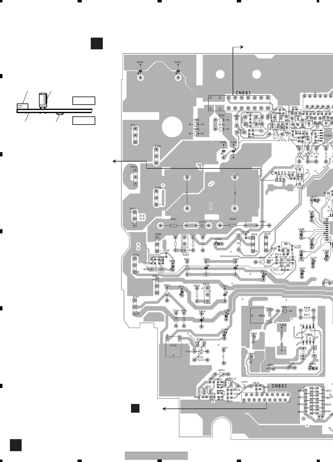
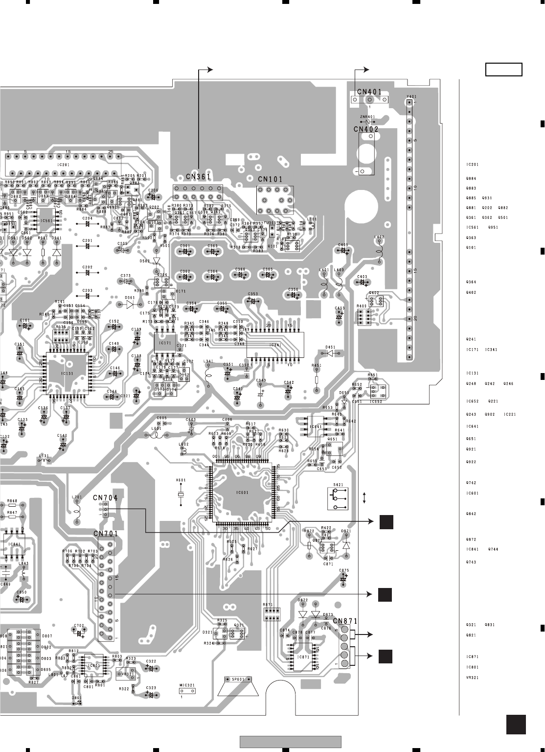
4. PCB CONNECTION DIAGRAM
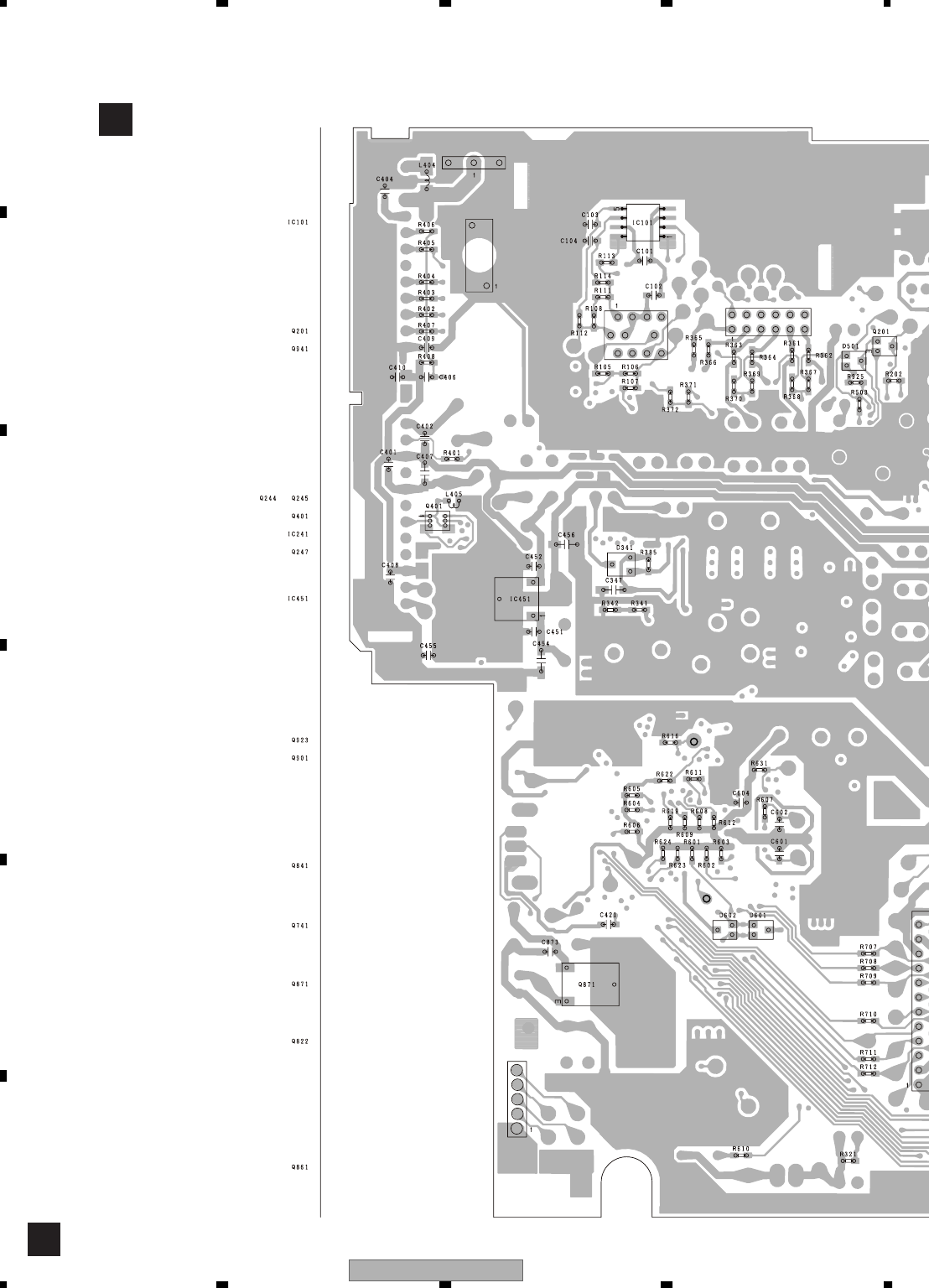
4.1 TUNER AMP UNIT
Capacitor
Connector
P.C.Board Chip Part
A
ATUNER AMP UNIT
SIDE B
SIDE A
NOTE FOR PCB DIAGRAMS
1.The parts mounted on this PCB
include all necessary parts for
several destination.
For further information for
respective destinations, be sure
to check with the schematic dia-
gram.
2.Viewpoint of PCB diagrams
FRONT
CCN1901
WIRED REMOTE
CONTROL
(DEH-P8MP/XN/UC,
DEH-P80MP/XN/UC)
CORD ASSY
(POWER SUPPLY, SPEAKER)
11 1012 913 814 7
15 616 54
32
1
17
18
11
10 12
913
814
715
616
5
4
3
2
117
18
DEH-P8MP/XN/UC
42
1234
1234
C
D
F
A
B
E
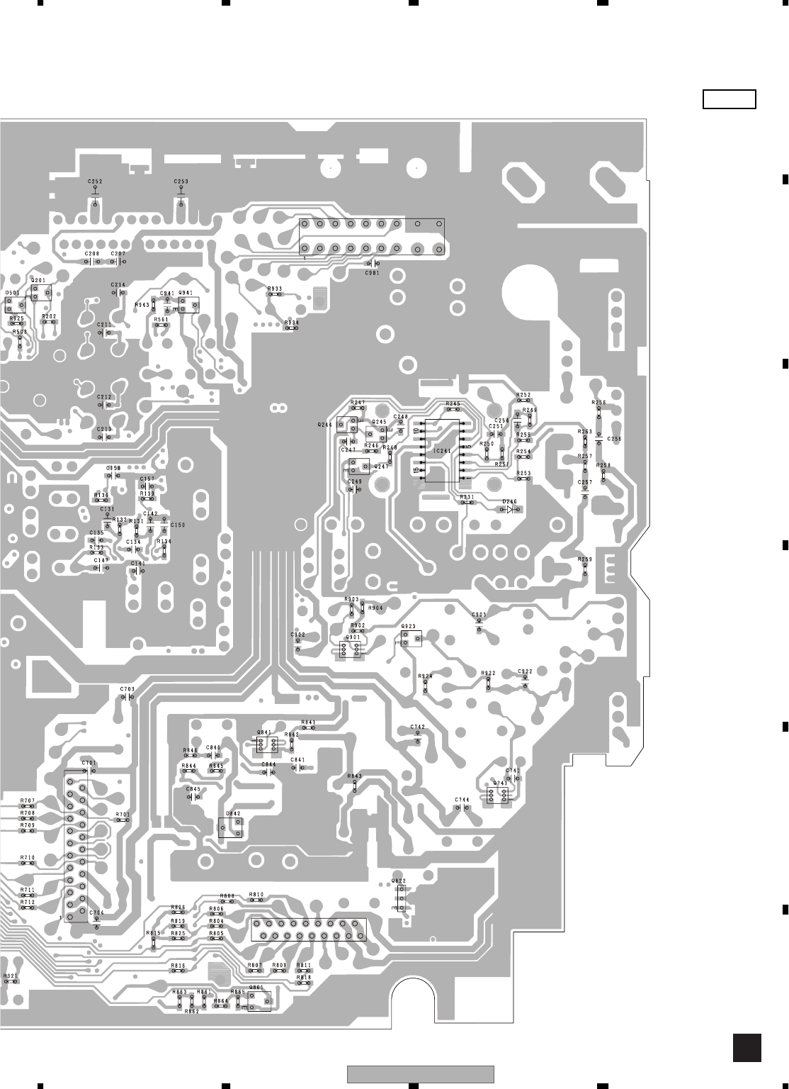
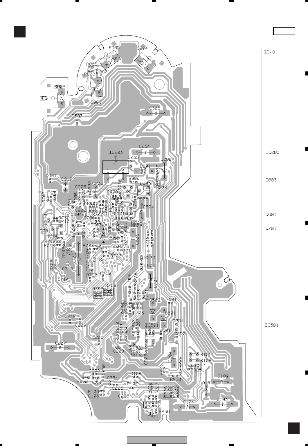
4.2 SWITCH UNIT
B
BSWITCH UNIT
123
CLOSE
OPEN
ACN871
DEH-P8MP/XN/UC 43
5678
5678
C
D
F
A
B
E
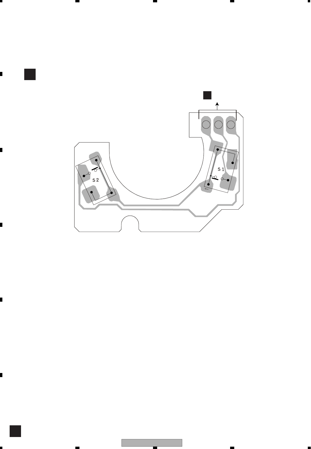
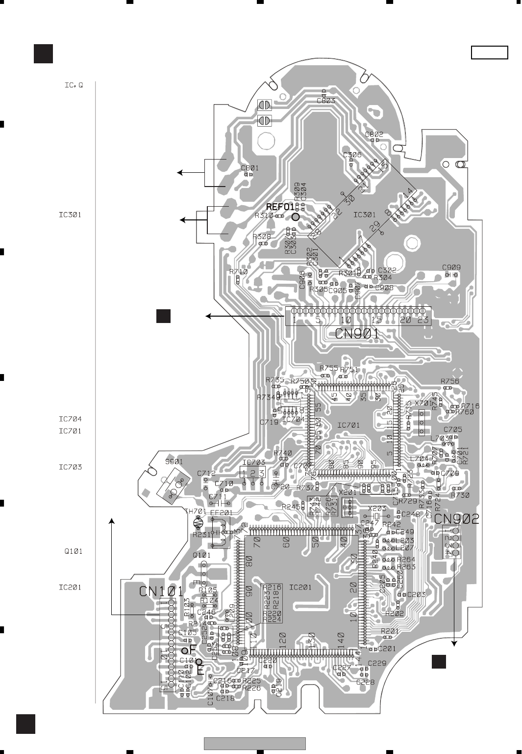
4.3 KEYBOARD UNIT
C
CKEYBOARD UNIT CKEYBOARD UNIT
SIDE A SIDE B
IC,Q IC,Q
ADJ
A
CN801
TP5
TP6
OEL UNIT
1
10
2
9
6
5
8
4
7
3
ATT
RESET
OPEN
LIST
VOL/SEL
EQ-EX
EQ
ENT
BAND
DISP
CLOCK
SRC
DEH-P8MP/XN/UC
44
1234
1234
C
D
F
A
B
E
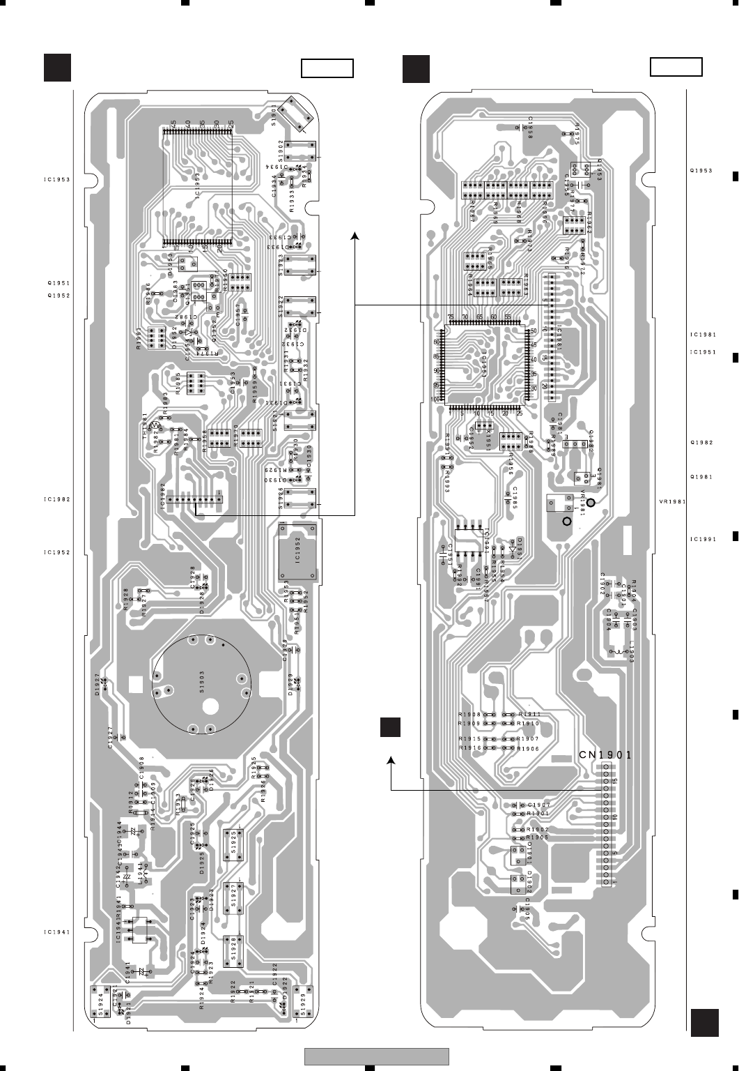
4.4 CD MECHANISM MODULE
D
DCD CORE UNIT(S10WMACODE2) SIDE A
ACN701
ACN704
M1
SPINDLE
MOTOR
M2
LOADING
/CARRIAGE
MOTOR
PICKUP UNIT(P9.9MP3)(SERVICE)
HOME
DEH-P8MP/XN/UC 45
5678
5678
C
D
F
A
B
E
D
DCD CORE UNIT(S10WMACODE2) SIDE B
CLAMP
DSCSNS
8EJ
12EJ
DEH-P8MP/XN/UC
46
1234
1234
C
D
F
A
B
E
5. ELECTRICAL PARTS LIST
Circuit Symbol and No. Part No.
A
Unit Number:CWM9287(P8MP/XN/UC)
Unit Number:CWM9288(P80MP/XN/UC)
Unit Number:CWM9289(P1Y/XN/ES)
Unit Name:Tuner Amp Unit
MISCELLANEOUS
IC 101 IC HA12240FP
IC 131 IC PML009A
IC 171 IC NJM4558MD
IC 201 IC PAL008A
IC 221 IC NJM2406F
IC 241 IC UPC494GS
IC 341 IC PA2028A
IC 451 IC BA033FP
IC 561 IC TPD1018F
IC 601 IC PD5925A
IC 652 IC BD4835G
IC 801 IC TC74VHCT125AFT
IC 841 IC NJM2360M
IC 871 IC BA6288FS
Q 101 Transistor UMF23N
Q 201 Transistor DTC124EU
Q 202 Transistor DTC114EU
Q 221 Transistor 2SC3052-12
Q 241 Transistor FKV550N
Q 242 Transistor FKV550N
Q 243 Transistor 2SA933S
Q 244 Transistor DTC123EU
Q 246 Transistor 2SC1740S
Q 247 Transistor DTC143EU
Q 248 Transistor 2SC1740S
Q 361 Chip Transistor HN1C03FU
(P8MP/XN/UC,P1Y/XN/ES)
Transistor UMH3N
(P80MP/XN/UC)
Q 362 Chip Transistor HN1C03FU
(P8MP/XN/UC,P1Y/XN/ES)
Transistor UMH3N
(P80MP/XN/UC)
Q 363 Chip Transistor HN1C03FU
(P8MP/XN/UC,P1Y/XN/ES)
Transistor UMH3N
(P80MP/XN/UC)
Q 364 Transistor UMD2N
Q 501 Transistor 2SC4081
Q 651 Transistor 2SC3052-12
Q 741 Transistor UMD2N
Q 742 Transistor 2SD2375
Q 743 Transistor 2SD1760F5
Q 744 Transistor UMD2N
Q 821 Transistor UMD2N
Q 822 Transistor 2SD1767
Q 831 Transistor UMF23N
Q 841 Transistor UMD2N
Q 842 Transistor 2SD1760F5
Q 861 Transistor 2SC3052-12
Q 871 Transistor 2SD1760F5
Q 872 Transistor UMD3N
Q 881 Transistor UMH9N
Q 882 Transistor 2SC4081
Q 883 Transistor 2SA1576
Q 884 Transistor 2SC4081
Q 885 Transistor 2SC4081
Q 901 Transistor UMD2N
Q 902 Transistor 2SD2375
Q 921 Transistor 2SD2375
Q 922 Transistor 2SB1243
Q 923 Transistor DTC114EU
Q 931 Transistor UMX1N
Q 941 Transistor DTC114EU
Q 951 Transistor 2SA1576
D 171 Diode Network DA204U
D 172 Diode Network DA204U
D 173 Diode DAN202U
D 174 Diode DAP202U
D 221 Diode UDZS6R2(B)
D 222 Diode UDZS6R8(B)
D 241 Diode FMG22
D 242 Diode FMG22
D 243 Diode FMJ-2303
D 244 Diode FMJ-2303
D 245 Diode 1SR154-400
D 246 Diode 1SS355
D 321 Diode RB706F-40
D 341 Diode(P8MP/XN/UC,P1Y/XN/ES) 1SS396
D 361 Diode 1SS133
D 451 Diode 1SR154-400
Circuit Symbol and No. Part No.

DEH-P8MP/XN/UC 47
5678
5678
C
D
F
A
B
E
D 501 Diode DAN202U
D 502 Diode HZS9L(A2)
D 561 Diode MPG06G-6415G50
D 562 Diode MPG06G-6415G50
D 741 Diode HZS9L(B1)
D 742 Diode HZS6L(C1)
D 801 Diode DAN202U
D 802 Diode DAP202U
D 803 Diode DAP202U
D 804 Diode DAN202U
D 805 Diode DAP202U
D 806 Diode DAN202U
D 807 Diode DAP202U
D 808 Diode DAN202U
D 821 Diode HZS11L(A1)
D 841 Diode HZS11L(A1)
D 842 Diode RB411D
D 861 LED SML311BBT(PQ)
D 871 Diode HZS6L(C3)
D 872 Diode 1SS133
D 873 Diode 1SS133
D 881 Diode DAN202U
D 882 Diode DAN202U
D 883 Diode DAN202U
D 884 Diode DAN202U
D 901 Diode HZS6L(B2)
D 902 Diode MPG06G-6415G50
D 921 Diode HZS9L(B3)
D 931 Diode HZS7L(C3)
D 932 Diode HZS7L(A1)
D 941 Diode MPG06G-6415G50
D 951 Diode DAN202U
D 981 Diode MPG06G-6415G50
D 982 Diode MPG06G-6415G50
D 983 Diode MPG06G-6415G50
D 984 Diode MPG06G-6415G50
ZNR401 Surge Protector RCCA-201Q31UA-PI
L 101 Inductor LCTC2R2K1608
L 131 Inductor LCTA2R2J2520
L 241 Coil CTH1310
L 242 Coil CTH1310
L 243 Ferri-Inductor LAU220K
L 341 Ferri-Inductor LAU220K
L 401 Inductor LAU1R0K
L 402 Inductor LAU2R2K
L 403 Inductor LAU1R0K
L 404 Inductor LCTA4R7J2520
L 601 Ferri-Inductor LAU100K
L 701 Ferri-Inductor LAU100K
L 801 Inductor CTF1379
L 831 Ferri-Inductor LAU100K
L 841 Inductor CTF1489
L 842 Inductor CTF1510
L 843 Chip-Inductor LCTA2R2J3225
L 951 Chip-Inductor LCTA2R2J3225
X 601 Radiator 10.00MHz CSS1475
S 421 Slide Switch(60W/40W) CSH1051
VR321 Semi-fixed 10kΩ(B) CCP1229
FU361 Fuse 3A >CEK1286
MIC321 Microphone CPM1011
Circuit Symbol and No. Part No.
SP601 Buzzer CPV1062
FM/AM Tuner Unit CWE1646
RESISTORS
R 101 RS1/16S102J
R 102 RS1/16S223J
R 103 RS1/16S181J
R 104 RS1/16S222J
R 105 RS1/16S181J
R 106 RS1/16S223J
R 107 RS1/16S102J
R 108 RS1/16S150J
R 109 RS1/16S562J
R 110 RS1/16S332J
R 111 RS1/16S470J
R 112 RS1/16S101J
R 113 RS1/16S102J
R 114 RS1/16S101J
R 131 RS1/16S821J
R 132 RS1/16S821J
R 133 RS1/16S102J
R 134 RS1/16S102J
R 135 RAB4C102J
R 136 RS1/16S101J
R 137 RS1/16S101J
R 138 RS1/16S101J
R 139 RS1/16S101J
R 140 RS1/16S101J
R 141 RS1/16S101J
R 171 RS1/16S104J
R 172 RS1/16S104J
R 173 RS1/16S563J
R 174 RS1/16S563J
R 175 RS1/16S474J
R 176 RS1/16S474J
R 201 RS1/16S681J
R 202 RS1/16S103J
R 203 RS1/16S103J
R 204 RS1/16S331J
R 205 RS1/16S681J
R 221 RS1/16S103J
R 222 RS1/16S103J
R 223 RS1/16S473J
R 224 RS1/16S104J
R 231 RS1/16S473J
R 241 RS1/2PMF3R3J
R 242 RS1/2PMF3R3J
R 243 RD1/4MUF470J
R 244 RD1/4MUF470J
R 245 RS1/16S222J
R 247 RS1/16S104J
R 248 RS1/16S822J
R 249 RS1/16S224J
R 250 RS1/16S472J
R 251 RS1/16S103J
R 252 RS1/16S1002D
R 253 RS1/16S1002D
R 254 RS1/16S3902D
R 255 RS1/16S3902D
Circuit Symbol and No. Part No.

DEH-P8MP/XN/UC
48
1234
1234
C
D
F
A
B
E
R 256 RS1/16S2R2J
R 257 RS1/16S2R2J
R 258 RS1/16S473J
R 259 RS1/16S473J
R 260 RS1/16S103J
R 261 RS1/4SA331J
R 262 RS1/4SA331J
R 263 RS1/16S0R0J
R 264 RS1/4SA151J
R 265 RS1/16S332J
R 266 RS1/16S332J
R 267 RS1/16S152J
R 268 RS1/4SA151J
R 269 RS1/16S152J
R 321 RS1/16S222J
R 323 RS1/16S561J
R 324 RS1/16S104J
R 325 RS1/16S104J
R 341 RS1/16S103J
R 342 RS1/16S103J
R 361 (P8MP/XN/UC,P1Y/XN/ES) RS1/16S820J
(P80MP/XN/UC) RS1/16S821J
R 362 (P8MP/XN/UC,P1Y/XN/ES) RS1/16S820J
(P80MP/XN/UC) RS1/16S821J
R 363 (P8MP/XN/UC,P1Y/XN/ES) RS1/16S820J
(P80MP/XN/UC) RS1/16S821J
R 364 (P8MP/XN/UC,P1Y/XN/ES) RS1/16S820J
(P80MP/XN/UC) RS1/16S821J
R 365 (P8MP/XN/UC,P1Y/XN/ES) RS1/16S820J
(P80MP/XN/UC) RS1/16S821J
R 366 (P8MP/XN/UC,P1Y/XN/ES) RS1/16S820J
(P80MP/XN/UC) RS1/16S821J
R 367 (P8MP/XN/UC,P1Y/XN/ES) RS1/16S103J
(P80MP/XN/UC) RS1/16S0R0J
R 368 (P8MP/XN/UC,P1Y/XN/ES) RS1/16S103J
(P80MP/XN/UC) RS1/16S0R0J
R 369 (P8MP/XN/UC,P1Y/XN/ES) RS1/16S103J
(P80MP/XN/UC) RS1/16S0R0J
R 370 (P8MP/XN/UC,P1Y/XN/ES) RS1/16S103J
(P80MP/XN/UC) RS1/16S0R0J
R 371 (P8MP/XN/UC,P1Y/XN/ES) RS1/16S103J
(P80MP/XN/UC) RS1/16S0R0J
R 372 (P8MP/XN/UC,P1Y/XN/ES) RS1/16S103J
(P80MP/XN/UC) RS1/16S0R0J
R 373 RS1/16S223J
R 374 RS1/16S223J
R 375 RS1/16S223J
R 376 RS1/16S223J
R 377 RS1/16S223J
R 378 RS1/16S223J
R 379 (P8MP/XN/UC,P1Y/XN/ES) RS1/16S471J
R 380 (P8MP/XN/UC,P1Y/XN/ES) RS1/16S471J
R 381 (P8MP/XN/UC,P1Y/XN/ES) RS1/16S471J
R 382 (P8MP/XN/UC,P1Y/XN/ES) RS1/16S471J
R 383 (P8MP/XN/UC,P1Y/XN/ES) RS1/16S471J
R 384 (P8MP/XN/UC,P1Y/XN/ES) RS1/16S471J
R 385 (P80MP/XN/UC) RS1/16S0R0J
R 389 RS1/16S102J
R 401 RS1/16S681J
R 402 RS1/16S681J
R 403 RS1/16S681J
Circuit Symbol and No. Part No.
R 404 RS1/16S681J
R 405 RS1/16S681J
R 406 RS1/16S681J
R 421 RS1/16S104J
R 422 RS1/16S102J
R 451 RD1/4PU2R2J
R 501 RS1/16S103J
R 502 RS1/16S473J
R 503 RS1/16S473J
R 561 RS1/16S103J
R 571 (P8MP/XN/UC,P80MP/XN/UC) RS1/16S102J
R 572 (P8MP/XN/UC,P80MP/XN/UC) RS1/16S102J
R 601 RS1/16S472J
R 602 RS1/16S472J
R 603 RS1/16S473J
R 604 RS1/16S104J
R 605 RS1/16S104J
R 606 RS1/16S103J
R 607 RS1/16S0R0J
R 608 RS1/16S104J
R 609 RS1/16S104J
R 610 RS1/16S102J
R 612 RS1/16S103J
R 613 RS1/16S681J
R 614 RS1/16S681J
R 615 RS1/16S681J
R 616 RS1/16S473J
R 617 (P1Y/XN/ES) RS1/16S104J
R 618 (P8MP/XN/UC,P80MP/XN/UC) RS1/16S104J
R 619 RS1/16S104J
R 620 (P80MP/XN/UC) RS1/16S104J
R 621 (P8MP/XN/UC,P1Y/XN/ES) RS1/16S104J
R 622 RS1/16S104J
R 623 RS1/16S104J
R 624 RS1/16S104J
R 625 RS1/16S0R0J
R 626 RS1/16S0R0J
R 627 RS1/16S0R0J
R 628 RS1/16S0R0J
R 629 RS1/16S0R0J
R 630 RS1/16S0R0J
R 631 RS1/16S104J
R 642 RS1/16S104J
R 651 RS1/16S102J
R 652 RS1/16S102J
R 653 RS1/16S183J
R 654 RS1/16S473J
R 655 RS1/16S222J
R 701 RS1/16S473J
R 703 RS1/16S682J
R 704 RS1/16S682J
R 705 RS1/16S682J
R 706 RS1/16S682J
R 707 RS1/16S221J
R 708 RS1/16S221J
R 709 RS1/16S221J
R 710 RS1/16S221J
R 711 RS1/16S221J
R 712 RS1/16S221J
Circuit Symbol and No. Part No.

DEH-P8MP/XN/UC 49
5678
5678
C
D
F
A
B
E
R 741 RD1/4PU391J
R 743 RD1/4PU391J
R 801 RS1/16S104J
R 802 RS1/16S104J
R 803 RS1/16S102J
R 804 RS1/16S222J
R 805 RS1/16S472J
R 806 RS1/16S222J
R 807 RS1/16S222J
R 808 RS1/16S222J
R 809 RS1/16S222J
R 810 RS1/16S222J
R 811 RS1/16S0R0J
R 812 RS1/16S104J
R 813 RS1/16S102J
R 815 RS1/16S104J
R 816 RS1/16S221J
R 818 RS1/16S103J
R 819 RS1/16S122J
R 821 RS1/16S221J
R 822 RS1/16S221J
R 823 RS1/16S1R0J
R 824 RS1/16S473J
R 825 RS1/16S473J
R 826 RS1/16S473J
R 827 RS1/16S104J
R 831 RS1/16S472J
R 832 RS1/16S102J
R 833 RS1/16S472J
R 841 RS1/16S331J
R 842 RS1/16S331J
R 844 RS1/16S1R0J
R 845 RS1/16S391J
R 846 RS1/16S121J
R 847 RD1/4PU302J
R 848 RD1/4PU302J
R 861 RS1/16S331J
R 862 RS1/16S331J
R 863 RS1/16S331J
R 864 RS1/16S103J
R 865 RS1/16S103J
R 871 RAB4C102J
R 872 RD1/4PU391J
R 881 RS1/16S472J
R 882 RS1/16S2203D
R 883 RS1/16S3303D
R 884 RS1/16S4702D
R 885 RS1/16S223J
R 886 RS1/16S223J
R 887 RS1/16S3303D
R 888 RS1/16S3303D
R 889 RS1/16S1503D
R 890 RS1/16S1503D
R 891 RS1/16S1503D
R 892 RS1/16S1503D
R 893 RS1/16S1503D
R 894 RS1/16S1503D
R 895 RS1/16S1503D
R 896 RS1/16S1503D
R 902 RS1/16S223J
Circuit Symbol and No. Part No.
R 903 RS1/16S332J
R 904 RS1/16S0R0J
R 922 RS1/16S152J
R 923 RD1/4PU152J
R 924 RS1/16S223J
R 925 RS1/16S472J
R 931 RS1/16S104J
R 932 RS1/16S473J
R 933 RS1/16S103J
R 934 RS1/16S473J
R 935 RS1/16S472J
R 943 RS1/16S103J
R 951 RS1/16S102J
R 952 RS1/16S472J
R 953 RS1/16S472J
R 954 RS1/16S153J
R 955 RS1/16S104J
R 981 RD1/4PU102J
R 982 RS1/4SA0R0J
R 987 RS1/16S0R0J
CAPACITORS
C 102 CKSRYB104K16
C 103 CKSRYB102K50
C 104 CKSRYB102K50
C 131 CCSQCH222J50
C 132 CEAL1R0M50
C 133 CEAL1R0M50
C 134 CKSRYB104K16
C 135 CKSRYB104K16
C 136 CEAL1R0M50
C 137 CEAL1R0M50
C 138 CEAL1R0M50
C 139 CEAL1R0M50
C 140 CEJQ470M10
C 141 CKSRYB104K16
C 142 CCSQCH222J50
C 143 CEALNP4R7M16
C 144 CEALNP4R7M16
C 145 CEALNP4R7M16
C 146 CEALNP4R7M16
C 147 CCSQCH152J50
C 148 CEALNP4R7M16
C 149 CEALNP4R7M16
C 150 CCSQCH152J50
C 151 CEALNP4R7M16
C 152 CEALNP4R7M16
C 159 CKSRYB474K10
C 160 CKSRYB474K10
C 161 CEJQ100M50
C 171 CKSRYB103K50
C 172 CKSRYB104K16
C 173 CKSRYB104K16
C 174 CKSRYB104K16
C 175 CKSRYB104K16
C 176 CKSRYB474K10
C 177 CKSRYB474K10
C 178 CCSRCH101J50
Circuit Symbol and No. Part No.

DEH-P8MP/XN/UC
50
1234
1234
C
D
F
A
B
E
C 179 CCSRCH101J50
C 201 CFTNA224J50
C 202 CFTNA224J50
C 203 CFTNA224J50
C 204 CFTNA224J50
C 205 CEAL330M10
C 206 CEHAR100M16
C 207 CKSQYB225K10
C 208 CKSQYB225K10
C 211 CKSRYB472K50
C 212 CKSRYB472K50
C 213 CKSRYB472K50
C 214 CKSRYB472K50
C 221 CKSRYB103K50
C 222 CKSRYB104K25
C 223 CKSRYB104K25
C 241 CQMA332J50
C 242 CQMA332J50
C 243 2200µF/25V CCH1594
C 244 2200µF/25V CCH1594
C 245 CEHAZL102M16
C 246 CEHAZL102M16
C 247 CCSRCH270J50
C 249 CKSRYB222K50
C 250 CQMAQ102J50
C 251 CKSRYB332K50
C 252 CKSYB105K25
C 253 CKSYB105K25
C 254 CCSQCH222J50
C 255 CEJQ101M16
C 256 CKSRYB103K50
C 257 CKSRYB103K50
C 259 CEHAZL100M50
C 321 CEJQ100M50
C 322 CEJQ220M25
C 323 CEJQ100M50
C 341 CEAL4R7M35
C 342 CEJQ101M16
C 343 CASAQ3R3M16
C 344 CKSRYB105K10
C 345 CKSRYB105K10
C 346 CKSRYB105K10
C 347 CKSYB684K16
C 348 CKSRYB105K10
C 349 CKSRYB105K10
C 350 CKSRYB105K10
C 351 CEAL100M16
C 352 CKSQYB225K10
C 353 CEJQ330M25
C 354 CEJQ330M25
C 355 (P8MP/XN/UC,P1Y/XN/ES) CEJQ330M25
C 356 (P8MP/XN/UC,P1Y/XN/ES) CEJQ330M25
C 361 CEJQ100M50
C 362 CEJQ100M50
C 363 CEJQ100M50
C 364 CEJQ100M50
C 365 CEJQ100M50
C 366 CEJQ100M50
C 367 (P8MP/XN/UC,P1Y/XN/ES) CKSRYB222K50
C 368 (P8MP/XN/UC,P1Y/XN/ES) CKSRYB222K50
Circuit Symbol and No. Part No.
C 369 (P8MP/XN/UC,P1Y/XN/ES) CKSRYB222K50
C 370 (P8MP/XN/UC,P1Y/XN/ES) CKSRYB222K50
C 371 (P8MP/XN/UC,P1Y/XN/ES) CKSRYB222K50
C 372 (P8MP/XN/UC,P1Y/XN/ES) CKSRYB222K50
C 373 CEAL220M35
C 401 CKSRYB103K50
C 402 CKSRYB103K50
C 403 CEJQ470M10
C 404 CKSRYB103K50
C 405 CEJQ101M10
C 407 CKSYB475K10
C 451 CKSRYB103K50
C 452 CKSRYB103K50
C 453 CEJQ220M25
C 454 CKSYB475K10
C 455 CKSRYB103K50
C 456 CKSYB475K10
C 561 CKSRYB104K25
C 562 CKSRYB473K25
C 601 CCSRCH180J50
C 602 CCSRCH220J50
C 603 CEAL470M16
C 604 CKSRYB103K50
C 606 CCSRCH470J50
C 652 CKSRYB105K10
C 653 CKSRYB104K16
C 702 470µF/10V CCH1438
C 741 CKSRYB473K16
C 742 CKSRYB102K50
C 743 CEJQ101M16
C 744 CKSRYB473K16
C 745 CEJQ101M10
C 801 CKSRYB473K16
C 821 CKSRYB473K25
C 832 CCSRCH101J50
C 833 CKSRYB473K50
C 834 CKSRYB105K10
C 841 CKSRYB104K16
C 842 CEAL470M16
C 843 CEAL101M10
C 844 CKSRYB104K16
C 845 CCSRCH331J50
C 846 CKSRYB103K50
C 847 CEAL330M25
C 848 CEAL100M25
C 849 4.7µF CCG1111
C 861 CKSRYB104K25
C 873 CKSRYB224K10
C 874 CKSRYB224K10
C 875 CEAT331M10
C 876 CKSRYB102K50
C 877 CCSRCH101J50
C 878 CCSRCH101J50
C 881 CKSRYB103K50
C 882 CKSQYB105K16
C 883 CKSQYB474K25
C 884 CKSQYB474K25
C 885 CKSQYB474K25
C 886 CKSQYB474K25
C 887 CKSQYB474K25
Circuit Symbol and No. Part No.

DEH-P8MP/XN/UC 51
5678
5678
C
D
F
A
B
E
C 888 CKSQYB474K25
C 889 CKSQYB474K25
C 890 CKSQYB474K25
C 901 CEJQ101M10
C 902 CKSRYB103K50
C 903 CKSRYB472K50
C 904 470µF/16V CCH1331
C 905 470µF/16V CCH1331
C 921 CEJQ221M10
C 922 CKSRYB103K50
C 923 CEJQ101M10
C 924 470µF/16V CCH1331
C 931 CKSRYB104K25
C 941 CKSQYB105K16
C 951 CKSRYB104K25
C 981 CKSRYB473K50
B
Unit Number:CWS1389
Unit Name:Switch Unit
S 1 Switch(CLOSE) CSN1051
S 2 Switch(OPEN) CSN1052
C
Unit Number:CWM9290
Unit Name:Keyboard Unit
MISCELLANEOUS
IC 1941 IC S-818A33AUC-BGN
IC 1951 IC PD5933A
IC 1952 IC RS-140
IC 1953 IC PD6469A
Q 1951 Transistor UMD2N
Q 1952 Transistor 2SC4154-11
Q 1953 Transistor UMD2N
Q 1981 Transistor 2SC4617
Q 1982 Transistor 2SD1664
D 1901 Diode DAP202U
D 1902 Diode DAN202U
D 1921 LED SML311BBT(PQ)
D 1922 LED SML311BBT(PQ)
D 1923 LED SML311BBT(PQ)
D 1924 LED SML311BBT(PQ)
D 1925 LED SML311BBT(PQ)
D 1926 LED SML311BBT(PQ)
D 1927 LED SML311BBT(PQ)
D 1928 LED SML311BBT(PQ)
D 1929 LED SML311BBT(PQ)
D 1930 LED SML311BBT(PQ)
D 1931 LED SML311BBT(PQ)
D 1932 LED SML311BBT(PQ)
D 1933 LED SML311BBT(PQ)
D 1934 LED SML311BBT(PQ)
D 1951 Diode 1SS355
D 1952 Diode UDZS13(B)
D 1953 Diode DAN202U
L 1903 Inductor CTF1530
L 1941 Inductor CTF1530
Circuit Symbol and No. Part No.
TH1981 Thermistor CCX1037
X 1951 Ceramic Resonator 16MHz CSS1616
S 1901 Push Switch CSG1155
S 1902 Push Switch CSG1155
S 1903 Switch(SEL/VOL) CSX1065
S 1921 Push Switch CSG1155
S 1922 Push Switch CSG1155
S 1923 Push Switch CSG1155
S 1924 Push Switch CSG1155
S 1925 Push Switch CSG1155
S 1926 Push Switch CSG1155
S 1927 Push Switch CSG1155
S 1928 Push Switch CSG1155
S 1929 Push Switch CSG1155
VR1981 Semi-fixed 10kΩ(B) CCP1229
OEL Unit MXS8202
RESISTORS
R 1901 RS1/16S222J
R 1902 RS1/16S222J
R 1905 RS1/16S822J
R 1906 RS1/16S102J
R 1907 RS1/16S102J
R 1908 RS1/16S222J
R 1909 RS1/16S332J
R 1910 RS1/16S822J
R 1911 RS1/16S473J
R 1912 RS1/16S154J
R 1913 RS1/10S0R0J
R 1914 RS1/10S0R0J
R 1916 RS1/16S103J
R 1921 RS1/16S221J
R 1922 RS1/16S560J
R 1923 RS1/16S221J
R 1924 RS1/16S560J
R 1925 RS1/16S221J
R 1926 RS1/16S560J
R 1927 RS1/16S221J
R 1928 RS1/16S560J
R 1929 RS1/16S221J
R 1930 RS1/16S560J
R 1931 RS1/16S221J
R 1932 RS1/16S560J
R 1933 RS1/16S221J
R 1934 RS1/16S560J
R 1941 RS1/16S222J
R 1951 RS1/16S121J
R 1952 RS1/16S184J
R 1953 RS1/16S2R2J
R 1954 RS1/16S154J
R 1955 RS1/16S473J
R 1956 RAB4C102J
R 1957 RS1/16S103J
R 1958 RAB4C473J
R 1959 RS1/16S473J
R 1960 RAB4C101J
R 1961 RAB4C101J
R 1962 RAB4C101J
Circuit Symbol and No. Part No.

DEH-P8MP/XN/UC
52
1234
1234
C
D
F
A
B
E
R 1963 RAB4C101J
R 1964 RAB4C101J
R 1965 RAB4C101J
R 1966 RAB4C101J
R 1967 RAB4C101J
R 1968 RAB4C101J
R 1969 RAB4C101J
R 1970 RAB4C102J
R 1971 RS1/16S102J
R 1972 RS1/16S0R0J
R 1973 RS1/16S473J
R 1974 RS1/16S473J
R 1975 RS1/16S473J
R 1977 RS1/16S473J
R 1981 RS1/16S333J
R 1982 RS1/16S683J
R 1983 RS1/16S393J
R 1984 RS1/16S392J
R 1985 RAB4C101J
R 1986 RS1/16S152J
R 1988 RS1/16S101J
R 1989 RS1/16S101J
R 1991 RS1/16S104J
CAPACITORS
C 1905 CKSRYB104K25
C 1908 CKSRYB104K25
C 1909 CKSRYB104K25
C 1921 CKSRYB104K25
C 1922 CKSRYB104K25
C 1923 CKSRYB104K25
C 1924 CKSRYB104K25
C 1925 CKSRYB104K25
C 1926 CKSRYB104K25
C 1927 CKSRYB104K25
C 1928 CKSRYB104K25
C 1929 CKSRYB104K25
C 1930 CKSRYB104K25
C 1931 CKSRYB104K25
C 1932 CKSRYB104K25
C 1933 CKSRYB104K25
C 1934 CKSRYB104K25
C 1941 CSZSR4R7M16
C 1942 CSZSR4R7M10
C 1943 CKSQYB103K50
C 1944 CSZSR4R7M10
C 1951 CKSYF106Z10
C 1952 CKSRYB473K50
C 1953 CKSRYB103K25
C 1954 CKSRYB103K25
C 1955 CKSYF475Z16
C 1957 CKSRYB103K25
C 1981 CKSRYB104K25
C 1982 CKSRYB104K25
C 1983 CKSRYB104K25
C 1985 CKSRYB104K25
D
Circuit Symbol and No. Part No.
Unit Number:CWX2952
Unit Name:CD CORE UNIT(S10WMACODE2)
MISCELLANEOUS
IC 201 IC UPD63761GJ
IC 203 IC NJM2391DL1-33
IC 301 IC BA5835FM
IC 501 IC S-L2980A15MC-C6A
IC 701 IC PE5423A
IC 703 IC S-812C33AUA-C2N
Q 101 Transistor 2SB1132
Q 601 Transistor IMH20
Q 603 Transistor 2SB709A
Q 701 Transistor UN2111
D 101 Diode 1SS355
D 601 Diode MA152WA
L 203 Inductor CTF1389
L 207 Inductor CTF1389
L 209 Inductor CTF1389
L 703 Inductor CTF1389
X 201 Ceramic Resonator 16.934MHz CSS1603
X 702 Resonator 4.00MHz CSS1654
S 901 Switch(HOME) CSN1051
S 902 Switch(CLAMP) CSN1051
S 903 Spring Switch(DSCSNS) CSN1052
S 904 Switch(12EJ) CSN1051
S 905 Switch(8EJ) CSN1051
RESISTORS
R 101 RS1/10S1R5J
R 102 RS1/10S1R5J
R 103 RS1/10S1R5J
R 104 RS1/10S1R5J
R 105 RS1/10S1R5J
R 107 RS1/16SS0R0J
R 201 RS1/16SS102J
R 202 RS1/16SS333J
R 205 RS1/16SS473J
R 207 RS1/16SS473J
R 209 RS1/16SS473J
R 214 RS1/16SS472J
R 216 RS1/16SS472J
R 218 RS1/16SS472J
R 220 RS1/16SS472J
R 221 RS1/16SS103J
R 222 RS1/16SS103J
R 223 RS1/16SS0R0J
R 224 RS1/16SS0R0J
R 225 RS1/16SS103J
R 226 RS1/16SS393J
R 227 RS1/16SS562J
R 228 RS1/16SS122J
R 229 RS1/16SS472J
R 231 RS1/16SS0R0J
R 232 RS1/16SS122J
R 233 RS1/16SS0R0J
R 240 RS1/16SS0R0J
R 241 RS1/16SS333J
R 242 RS1/16SS0R0J
Circuit Symbol and No. Part No.

DEH-P8MP/XN/UC 53
5678
5678
C
D
F
A
B
E
R 243 RS1/16SS333J
R 245 RS1/16SS333J
R 250 RS1/16SS0R0J
R 256 RS1/16SS0R0J
R 261 RS1/16S0R0J
R 262 RS1/16S0R0J
R 263 RS1/16S0R0J
R 264 RS1/16S0R0J
R 267 RS1/16S0R0J
R 301 RS1/16SS183J
R 302 RS1/16SS822J
R 304 RS1/16SS183J
R 305 RS1/16SS822J
R 307 RS1/16SS183J
R 308 RS1/16SS183J
R 309 RS1/16SS183J
R 310 RS1/16SS183J
R 501 RS1/16SS0R0J
R 601 RS1/16S101J
R 602 RS1/16S101J
R 603 RS1/16S223J
R 604 RS1/16S223J
R 605 RS1/16SS103J
R 606 RS1/16S0R0J
R 701 RS1/16S0R0J
R 702 RS1/16SS0R0J
R 703 RS1/16SS104J
R 704 RS1/16SS104J
R 705 RS1/16SS221J
R 706 RS1/16SS221J
R 707 RS1/16SS0R0J
R 708 RS1/16SS221J
R 709 RS1/16SS473J
R 710 RS1/16SS102J
R 711 RS1/16SS102J
R 712 RS1/16SS102J
R 713 RS1/16SS102J
R 714 RS1/16SS473J
R 715 RS1/16SS101J
R 716 RS1/16SS472J
R 717 RS1/16SS221J
R 718 RS1/16SS221J
R 719 RS1/16SS221J
R 720 RS1/16SS471J
R 721 RS1/16S0R0J
R 724 RS1/16S473J
R 725 RS1/16SS222J
R 726 RS1/16SS103J
R 727 RS1/16SS473J
R 729 RS1/16SS223J
R 730 RS1/16SS473J
R 731 RS1/16SS104J
R 732 RS1/16SS104J
R 733 RS1/16SS104J
R 735 RS1/16SS473J
R 737 RS1/16SS104J
R 740 RS1/16SS473J
R 742 RS1/16SS104J
R 745 RS1/16SS473J
R 746 RS1/16SS104J
Circuit Symbol and No. Part No.
R 750 RS1/16SS473J
R 754 RS1/16SS102J
R 755 RS1/16SS102J
R 756 RS1/16SS104J
R 765 RAB4CQ221J
R 769 RAB4CQ221J
R 773 RAB4CQ221J
R 777 RS1/16SS221J
R 778 RS1/16SS221J
R 779 RS1/16SS221J
R 901 RAB4CQ221J
R 902 RS1/16S0R0J
R 905 RS1/16SS221J
R 906 RS1/16SS221J
R 908 RS1/16SS0R0J
R 910 RS1/16SS0R0J
CAPACITORS
C 101 CKSSYB104K10
C 102 CKSSYB104K10
C 103 100µF/16V CCH1504
C 104 47µF/6.3V CCH1506
C 105 CKSSYB104K10
C 106 CCSSCH101J50
C 107 CKSRYB224K16
C 108 CKSSYB104K10
C 110 CKSSYB104K10
C 201 CKSSYB471K50
C 202 CKSSYB104K10
C 203 CKSSYB104K10
C 204 22µF/6.3V CCH1507
C 205 CKSSYB104K10
C 207 220µF/4V CCH1590
C 208 CKSSYB104K10
C 209 CKSSYB104K10
C 216 CKSSYB332K50
C 217 CKSSYB104K10
C 218 CKSSYB223K16
C 219 CKSSYB104K10
C 220 CKSSYB103K16
C 221 CKSSYB104K10
C 222 CCSSCH560J50
C 223 CCSSCH5R0C50
C 224 CKSSYB104K10
C 225 CKSSYB103K16
C 226 CCSSCH680J50
C 227 CCSSCH470J50
C 228 CKSSYB682K25
C 230 CKSSYB104K10
C 232 CKSSYB104K10
C 233 10µF/6.3V CCH1470
C 234 220µF/4V CCH1590
C 235 CKSRYB224K16
C 237 CKSSYB104K10
C 239 CCSSCH330J50
C 242 CKSSYB104K10
C 246 CKSSYB104K10
C 250 CKSRYB102K50
Circuit Symbol and No. Part No.

DEH-P8MP/XN/UC
54
1234
1234
C
D
F
A
B
E
C 251 CKSRYB102K50
C 260 CKSSYB104K10
C 301 CKSSYB221K50
C 302 CKSSYB221K50
C 303 CKSSYB472K25
C 304 CKSSYB103K16
C 305 100µF/16V CCH1504
C 306 CKSSYB104K10
C 307 CKSSYB104K10
C 501 CKSRYB224K16
C 505 CKSQYB475K6R3
C 601 CCSRCH102J50
C 602 CCSRCH102J50
C 603 4.7µF/25V CCH1568
C 604 4.7µF/25V CCH1568
C 701 CKSSYB104K10
C 702 CKSSYB471K50
C 703 CKSSYB103K16
C 704 4.7µF/25V CCH1592
C 706 CKSSYB104K10
C 707 CKSSYB104K10
C 712 CKSRYB224K16
C 713 CKSSYB104K10
C 714 CKSSYB104K10
C 716 CKSSYB103K16
C 717 CCSSCH180J50
C 718 CCSSCH180J50
C 720 CKSQYB225K10
C 722 CKSRYB105K10
C 903 CKSSYB471K50
C 906 CKSRYB224K16
C 907 CKSSYB103K16
C 910 CKSQYB225K10
Miscellaneous Parts List
Pickup Unit(P9.9MP3)(Service) CXX1805
M 1 Motor Unit(SPINDLE) CXB6007
M2 Motor Unit(LOADING/CARRIAGE) CXB8933
M 871 Motor Unit(FLAP) CXC2204
Circuit Symbol and No. Part No.
DEH-P8MP/XN/UC 55
5678
5678
C
D
F
A
B
E
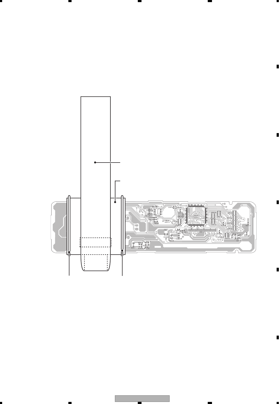
6. ADJUSTMENT
6.1 CONNECTION DIAGRAM
Rubber Band Rubber Band
GGD1160
CN1901
KEYBOARD UNIT
TUNER AMP UNIT CN801
GGD1378
DEH-P8MP/XN/UC
56
1234
1234
C
D
F
A
B
E
6.2 OEL UNIT ADJUSTMENT
TP5
TP6
VR1981
KEYBOARD UNIT (SIDE B)
Adjustment point
Digital Multi-Meter
<When the OEL Unit has been replaced>
1. Use VR1981 to adjust the resistance between TP5 and TP6 to 2.3 kΩ.

DEH-P8MP/XN/UC 57
5678
5678
C
D
F
A
B
E
6.3 CD ADJUSTMENT
1) Cautions on adjustments
• In this product the single voltage (3.3V) is used for the
regulator. The reference voltage is the REFO1 (1.65V)
instead of the GND.
If you should mistakenly short the REFO1 with the GND
during adjustment, accurate voltage will not be obtained,
and the servo’s misoperation will apply excessive shock
to the pickup. To avoid such problems:
a. Do not mix up the REFO1 with the GND when
connecting the (-) probe of measuring instruments.
Especially on an oscilloscope, avoid connecting the (-)
probe for CH1 to the GND.
b. In many cases, measuring instruments have the same
potential as that for the (-) probe. Be sure to set the
measuring instruments to the floating state.
c. If you have mistakenly connected the REFO1 to the GND,
turn off the regulator or the power immediately.
• Before mounting and removing filters or leads for
adjustment, be sure to turn off the regulator.
• For stable circuit operation, keep the mechanism
operating for about one minute or more after the
regulator is turned on.
• In the test mode, any software protections will not
work. Avoid applying any mechanical or electrical
shock to the mechanism during adjustment.
• The RFI and RFO signals with a wide frequency range
are easy to oscillate. When observing the signals,
insert a resistor of 1k ohms in series.
• The load and eject operation is not guarantied with the
mechanism upside down. If the mechanism is blocked
due to mistaken eject operation, reset the product or
turn off and on the ACC to restore it.
2) Test mode
This mode is used to adjust the CD mechanism module.
• To enter the test mode.
While pressing the LIST and EQ keys at the same time,
reset.
• To exit from the test mode.
Turn off the ACC and back up.
Notes:
a. During ejection, do not press any other keys than the
EJECT key until the loaded disc is ejected.
b. If you have pressed the (→) key or (←) key during focus
search, turn off the power immediately to protect the
actuator from damage caused by the lens stuck.
c. For the TR jump modes except 100TR, the track jump
operation will continue even if the key is released.
d. For the CRG move and 100TR jump modes, the tracking
loop will be closed at the same time when the key is
released.
e. When the power is turned off and on, the jump mode
is reset to the single TR (91), the RF amp gain is set to 0dB,
and the auto-adjustment values are reset to the default
settings.
DEH-P8MP/XN/UC
58
1234
1234
C
D
F
A
B
E
[BAND]
[BAND]
[BAND]
[BAND]
[BAND]
Power On
(T.Offset is adjusted)
TRK00
MIN00
SEC
SEC
00
[CD]or[SOURCE]
Source On
TRK MIN
[LIST]+[EQ]+Reset or
[LIST]+[EQ]+BU+ACC
Test Mode In
[3]
[1]
[1]
Power On
(T.Offset is not adjusted)
TRK99
MIN99
SEC99
[2]
[2]
[2]
[2]
Power Off
TRK MIN SEC
Power Off
TRK MIN SEC
Power Off
TRK MIN SEC
Power Off
TRK MIN SEC
Focus Close
S.Curve check
TRK91
MIN91
SEC91
[6] [1]
[3]
[6]
[3]
Focus Mode
switching
*2
TRK0xMIN0xSEC 0x
Tracking Servo
Close
TRK00 MIN00 SEC00
or TRK99
MIN99
SEC99
CRG- *8
TRK00
MIN00
SEC00
or TRK99
MIN99
SEC99
[→][←]
[→][←]
[→][←]
CRG+ *8
*9
TRK00 MIN00 SEC00
or TRK99
MIN99
SEC99
Automatic adjustment
display switching
*3
TRK?? MIN?? SEC??
Applicable servomechanism
TRK
?tr MIN
?min
SEC
?sec
[6]
[3]
T.Close
Applicable servomechanism
TRK MIN SEC
RF AGC /
RF AGC coefficient display
TRK ??
MIN?? SEC ??
CRG+
TRK8x MIN8x SEC8x
or TRK9xMIN9xSEC 9x
CRG-
TRK8xMIN8xSEC8x
or TRK9xMIN9xSEC 9x
T.Balance adjustment /
T.Balance coefficient display
TRK?? MIN?? SEC??
F, T, RF AGC
F.Bias display switching
*7
TRK?? MIN?? SEC??
F, T AGC / F.Bias
RF AGC
TRK MIN SEC
CRG/TR Jump *5
value switching
TRK MIN SEC
CRG/TR Jump +
*4
TRK MIN SEC
CRG/TR Jump -
*4
*6
TRK MIN SEC
Tracking Open
TRK8xMIN8xSEC8x
or TRK 9xMIN 9xSEC 9x
Tracking Open
TRK8x MIN8x SEC8x
or TRK9xMIN9xSEC 9x
[Key]
[BAND]
[→]
[6]
[1]
[2]
[3]
Power On/Off
CRG + / TR Jump +
(Direction of the external surface)
CRG - / TR Jump -
(Direction of the internal surface)
T.CLS and AGC and Applicable servomechanism /
AGC, AGC display switching
RF Gain switching / Offset adjustment display /
T.Balance adjustment / T.Open
F.Close, S.Curve / Rough Servo and RF AGC / F, T, RF AGC
SPDL 1X/2X switching
As for the double speed (2x), audio output cannot be supported.
F. Mode switching / Tracking Close / CRG, TR Jump switching
Test Mode
Operation
[KEY]
Contents
Display
*1) TYP → -6dB → -12dB
TRK MIN SEC TRK 06 MIN 06 SEC 06 TRK 12 MIN 12 SEC 12
*2) Focus Close → S.Curve ckeck setting → F EQ measurement setting
TRK 00 MIN 00 SEC 00 TRK 01 MIN 01 SEC 01 TRK 02 MIN 02 SEC 02
(TRK 99 MIN 99 SEC 99)
*3) F.Offset Display → T.Offset Display → Switch to the order of the original display
*4) 1TR / 32TR / 100TR
*5) Single TR → 32TR → 100TR → CRG Move
9x(8x) : 91(81) 92(82) 93(83) 94(84)
*6) Only at the time of CRG Move, 100TR Jump
*7) TRK/MIN/SEC → F.AGC → T.AGC → F.Bias → RF AGC
*8) CRG motor voltage = 2[V]
[←]
Error Rate measurement 1st-ON : ERR count beginning(30Sec)
2nd-ON : BER display data[%]
[4]
[5]
- Flow Chart
RF AMP
Gain switching
TRKGGMINGGSECGG
[2]
SPINDLE
Speed switching
TRKSP MINSPSECSP
[4]
*1
T.Close and AGC
*9) TYP(1X) → 2X → 1X
TRK MIN SEC TRK 22 MIN 22 SEC 22 TRK 11 MIN 11 SEC 11
As for the double speed (2x), audio output cannot be supported.
TYP(2X) → 1X → 2X
TRK MIN SEC TRK 11 MIN 11 SEC 11 TRK 22 MIN 22 SEC 22
?tr ?min ?sec
?tr ?min ?sec?tr ?min ?sec?tr ?min ?sec?tr ?min ?sec
Key of the head unit
Key of the remote control unit
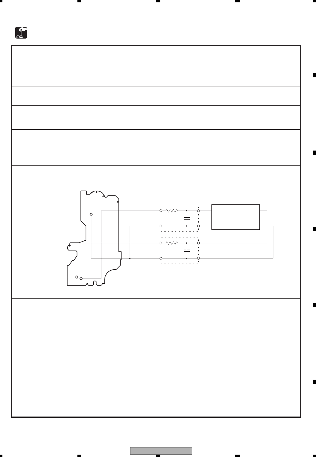
DEH-P8MP/XN/UC 59
5678
5678
C
D
F
A
B
E
6.4 CHECKING THE GRATING AFTER CHANGING THE PICKUP UNIT
• Note :
The grating angle of the PU unit cannot be adjusted after the PU unit is changed. The PU unit in the CD mechanism
module is adjusted on the production line to match the CD mechanism module and is thus the best adjusted PU
unit for the CD mechanism module. Changing the PU unit is thus best considered as a last resort. However, if the
PU unit must be changed, the grating should be checked using the procedure below.
• Purpose :
To check that the grating is within an acceptable range when the PU unit is changed.
• Symptoms of Mal-adjustment :
If the grating is off by a large amount symptoms such as being unable to close tracking, being unable to perform
track search operations, or taking a long time for track searching.
• Method :
• Measuring Equipment
• Measuring Points
• Oscilloscope, Two L.P.F.
• E, F, REFO1
• Disc • TCD-782
• Mode • TEST MODE
• Checking Procedure
1. In test mode, load the disc and switch the 3V regulator on.
2. Using the → and ← buttons, move the PU unit to the innermost track.
3. Press key 3 to close focus, the display should read "91". Press key 2 to implement the tracking balance
adjustment the display should now read "81". Press key 3. The display will change, returning to "81" on the
fourth press.
4. As shown in the diagram above, monitor the LPF outputs using the oscilloscope and check that the phase
difference is within 75° . Refer to the photographs supplied to determine the phase angle.
5. If the phase difference is determined to be greater than 75° try changing the PU unit to see if there is any
improvement. If, after trying this a number of times, the grating angle does not become less than 75° then the
mechanism should be judged to be at fault.
• Note
Because of eccentricity in the disc and a slight misalignment of the clamping center the grating waveform may be
seen to "wobble" ( the phase difference changes as the disc rotates). The angle specified above indicates the
average angle.
• Hint
Reloading the disc changes the clamp position and may decrease the "wobble".
100kΩ
390pF
100kΩ
390pF
E
VREF
F
VREF
Xch Ych
L.P.F.
L.P.F.
REFO1
FE
CD CORE UNIT(S10WMACODE2)
Oscilloscope
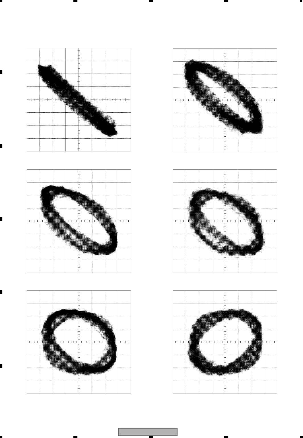
DEH-P8MP/XN/UC
60
1234
1234
C
D
F
A
B
E
Grating waveform
45°
0°
75°
60°
30°
90°
Ech → Xch 20mV/div, AC
Fch → Ych 20mV/div, AC
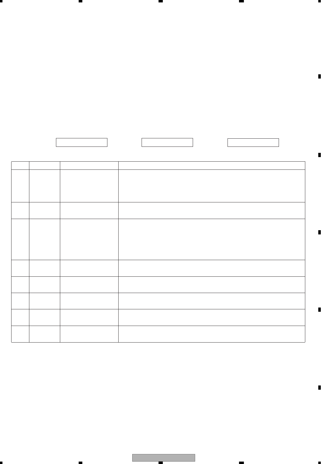
DEH-P8MP/XN/UC 61
5678
5678
C
D
F
A
B
E
6.5 ERROR MODE
- Error Messages
If a CD is not operative or stopped during operation due to an error, the error mode is turned on and cause(s) of
the error is indicated with a corresponding number. This arrangement is intended at reducing nonsense calls from
the users and also for facilitating trouble analysis and repair work in servicing.
(1) Basic Indication Method
1) When SERRORM is selected for the CSMOD (CD mode area for the system), error codes are written to DMIN
(minutes display area) and DSEC (seconds display area). The same data is written to DMIN and DSEC. DTNO
remains in blank as before.
2) Head unit display examples
Depending on display capability of LCD used, display will vary as shown below. xx contains the error number.
8-digit display 6-digit display 4-digit display
ERROR–xx ERR–xx E–xx
(2) Error Code List
Code Class Displayed error code Description of the code and potential cause(s)
10 Electricity Carriage Home NG CRG can't be moved to inner diameter.
SERVO LSI Com- CRG can't be moved from inner diameter.
munication Error → Failure on home switch or CRG move mechanism.
Communication error between microcomputer and SERVO LSI.
11 Electricity Focus Servo NG Focusing not available.
→ Stains on rear side of disc or excessive vibrations on REWRITABLE.
12 Electricity Spindle Lock NG Spindle not locked. Sub-code is strange (not readable).
Subcode NG → Failure on spindle, stains or damages on disc, or excessive vibrations.
A disc not containing CD-R data is found.
Turned over disc are found, though rarely.
CD signal error.
17 Electricity Setup NG AGC protection doesn't work. Focus can be easily lost.
→ Damages or stains on disc, or excessive vibrations on REWRITABLE.
30 Electricity Search Time Out Failed to reach target address.
→ CRG tracking error or damages on disc.
44 Electricity ALL Skip Skip setting for all track.
(CD-R/RW)
50 Mechanism CD On Mech Error Mechanical error during CD ON.
→ Defective loading motor, mechanical lock and mechanical sensor.
A0 System Power Supply NG Power (VD) is ground faulted.
→ Failure on SW transistor or power supply (failure on connector).
Remarks: Mechanical errors are not displayed (because a CD is turned off in these errors).
Unreadable TOC does not constitute an error. An intended operation continues in this case.
Upper digits of an error code are subdivided as shown below:
1x: Setup relevant errors, 3x: Search relevant errors, Ax: Other errors.

DEH-P8MP/XN/UC
62
1234
1234
C
D
F
A
B
E
6.6 OEL SCREENSAVER STUDIO LKA TO LKD APPLICATION
6.7 SYSTEM MICROCOMPUTER TEST PROGRAM
"OEL Screensaver Studio" is an application to create OEL display image file. The customer write the image file on a
CD-R disc and install it to car audio. This function is similar to PC link-kit (CD-PC1).
"OEL Screensaver Studio" is available to the public on the PIONEER Home Page.
This software (GGV1169) is added LKA to LKD file conversion function to original "OEL Screensaver Studio".
- How to check:
1. Set up GGV1169 application.
2. Confirm the LKA file (ent_disp.lka) is converted to LKD file correctly or not.
Please see a Readme.txt in the GGV1169 or help file of "OEL Screensaver Studio" for more
information.
- PCL output
In the normal operation mode (with the detachable panel installed, the ACC switched ON, the standby mode
cancelled), shift the STEST1 (Pin 86) terminal to H.
The clock signal is output from the PCL1 terminal (Pin 37).
The frequency of the clock signal is 312.500kHz that is one 32nd of the fundamental frequency.
The clock signal should be 312.500kHz ± 13Hz.
If the clock signal is out of the range, the X'tal (X601) should be replaced with new one.
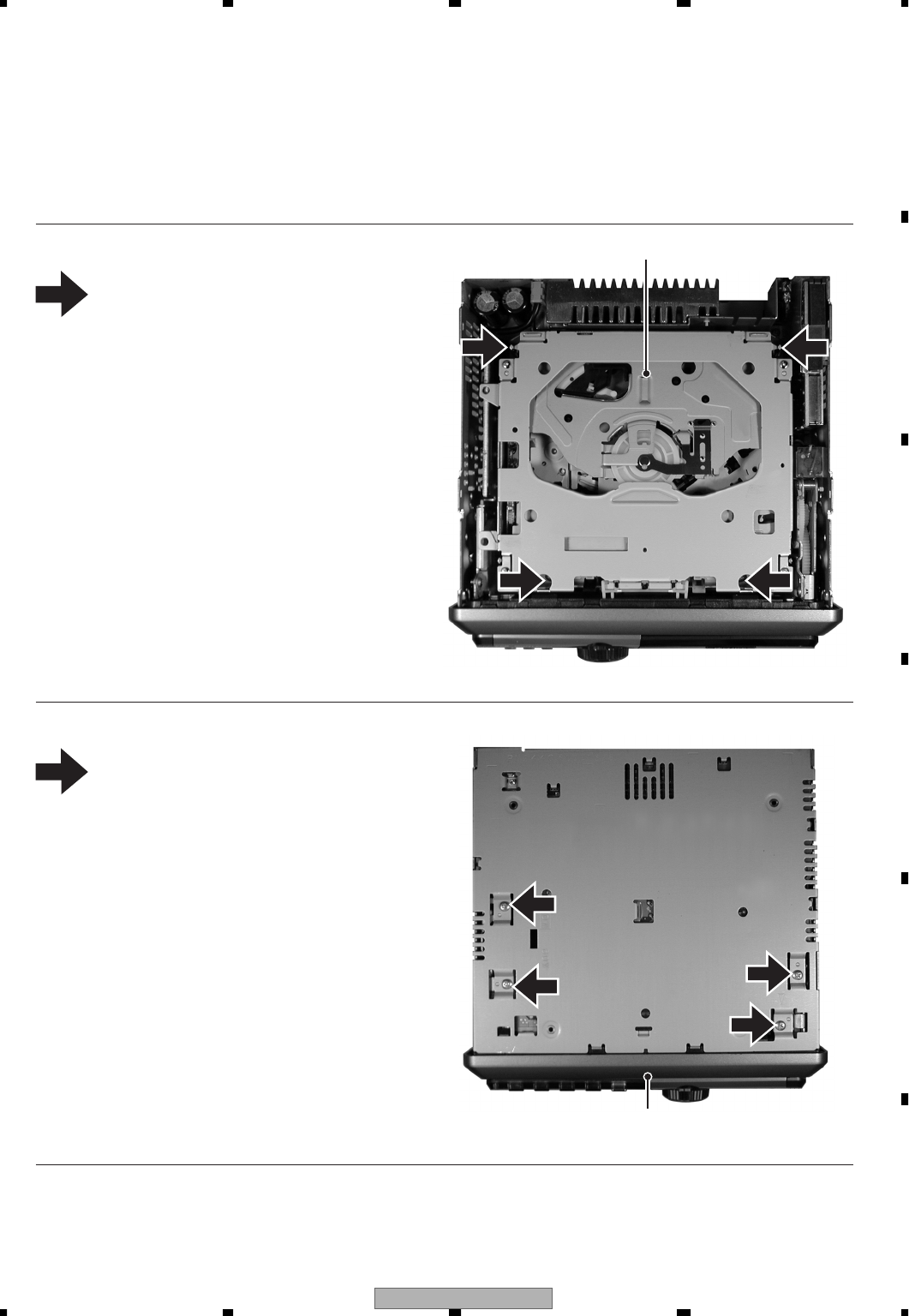
DEH-P8MP/XN/UC 63
5678
5678
C
D
F
A
B
E
7. GENERAL INFORMATION
7.1 DIAGNOSIS
7.1.1 DISASSEMBLY
- Removing the CD Mechanism Module (Fig.1)
1
Fig.1
- Removing the Case (not shown)
Grille Assy
- Removing the Grille Assy (Fig.2)
1. Remove the Case.
CD Mechanism Module
1
1
1
1
Fig.2
Remove the four screws.
Disconnect the connector and then remove the
CD Mechanism Module.
1Remove the four screws.
Disconnect the connector and then remove the
Grille Assy.
1
1
1
1
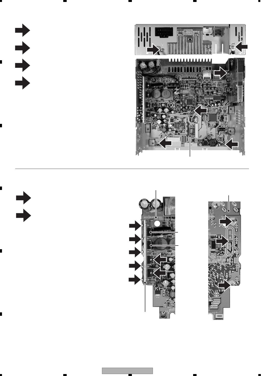
DEH-P8MP/XN/UC
64
1234
1234
C
D
F
A
B
E
Fig.3
Tuner Amp Unit
- Removing the Tuner Amp Unit (Fig.3)
Remove the screw.
1
2
33
3
4
Remove the screw.
2
Straighten the tabs at three locations
indicated.
3
Remove the screw and then remove
the Tuner Amp Unit.
4
1
1
Fig.4
- Removing the D242 and D244 (Fig.4)
Holder
Tuner Amp Unit (SIDE A)
2
2
1
1
Remove the seven screws.
2Remove the solder and then remove
the D242 and D244.
1
1
1
1
1
Tuner Amp Unit (SIDE B)
2
D242
D244
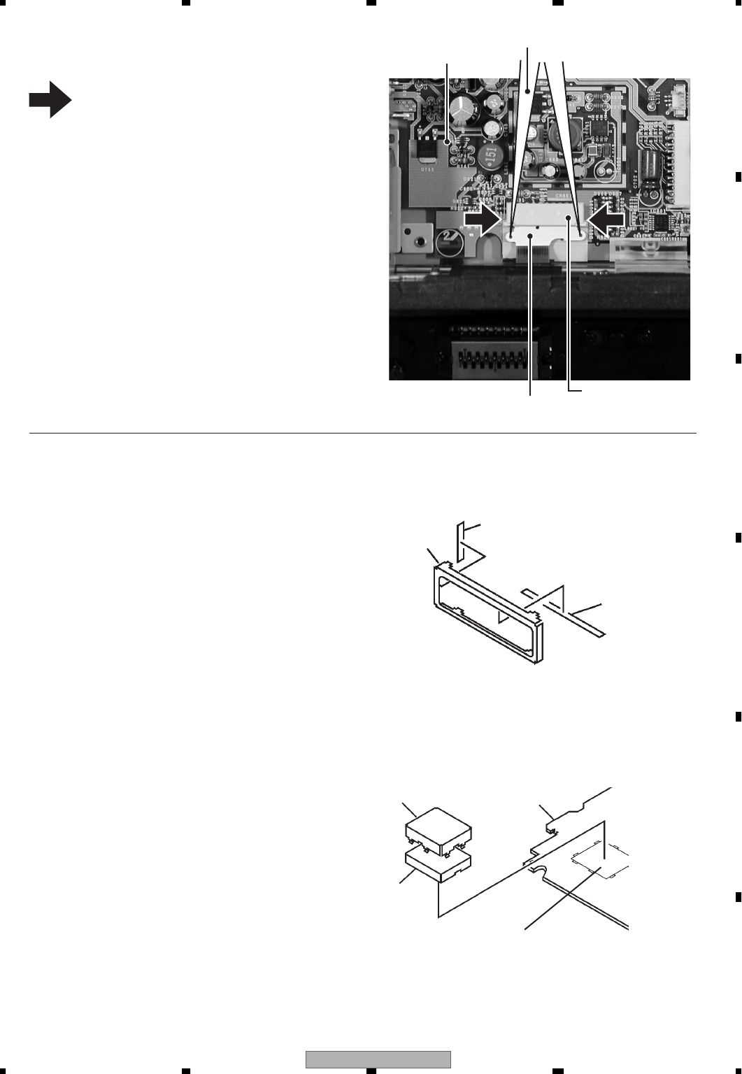
DEH-P8MP/XN/UC 65
5678
5678
C
D
F
A
B
E
- Service Precaution
Fig.5
Flexible PCB
- Disconnecting the Flexible PCB (Fig.5) Tuner Amp Unit
11
Release the two latches.
Tweezers are inserted in the hole of Flexible PCB
and Flexible PCB is removed from CN801.
CN801
When you attach Case(CNC8138) in Tuner Amp
Unit, please attach in Tuner Amp Unit, without
also forgetting Insulator(CNM6249).
If you forget to attach Insulator in Tuner Amp
Unit, there is a possibility that the DC/DC Converter
Section may short-circuit.
Case
(CNC8138)
Insulator
(CNM6249)
Tuner Amp Unit
DC/DC Converter Section
1
On the internal surface of the Holder(CND2028),
2 types of spacers(CNM9141, CNM9142) are
affixed for insulation with the OEL unit. When
ordering parts to replace the Holder, please order
the 2 types of spacers along with the Holder.
Fig.6
Fig.7
Tweezers
Spacer
(CNM9141)
Spacer
(CNM9142)
Holder
(CND2028)
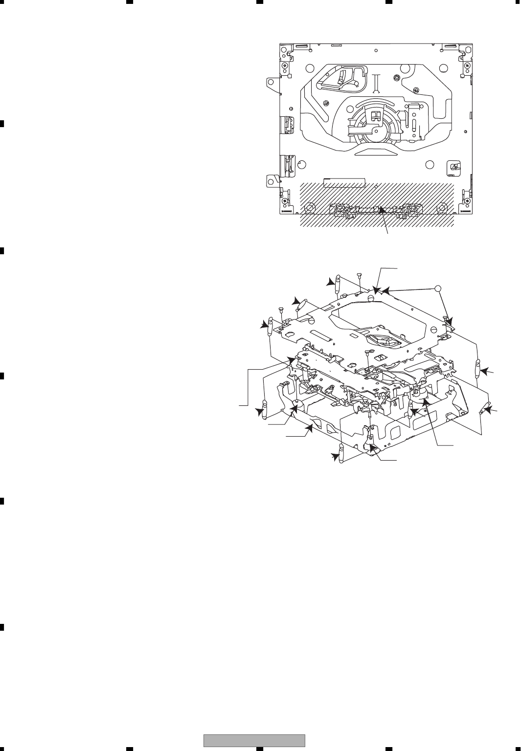
DEH-P8MP/XN/UC
66
1234
1234
C
D
F
A
B
E
- How to hold the Mechanism Unit
1. Hold the top and bottom frame.
2. Do not squeeze top frame's front portion too tight,
because it is fragile.
- Removing the Upper and Lower Frames
1. With a disc clamped, remove the four springs (A),
the two springs (B), the two springs (C), and the
four screws.
2. To remove the upper frame, open it on the fulcrum
A.
3. While lifting the carriage mechanism, remove the
three dampers.
4. With the frames removed, insert the connectors
coming from the main unit and eject the disc.
Caution: Before installing the carriage mechanism in
the frames, be sure to apply some alcohol to the
dampers and set the mechanism to the clamp mode.
Do not squeeze.
Lower Frame
Damper
Carriage Mechanism
A
C
A
B
B
Damper
Damper
C
A
A
A
Upper Frame
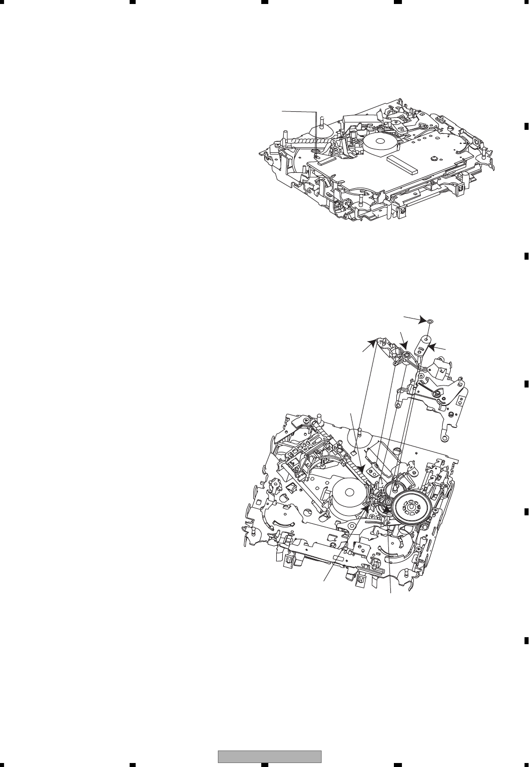
DEH-P8MP/XN/UC 67
5678
5678
C
D
F
A
B
E
- Removing the Pickup Unit
1. Apply shorting solder to the Pickup flexible cable.
Disconnect the cable.
2. Set the mechanism to the clamp mode.
3. Remove the lead wires from the inner holder.
4. Remove the washer, styling holder, change arm,
and pickup lock arm.
5. While releasing from the hook of the inner holder,
lift the end of the feed screw.
Caution: In assembling, move the planet gear to the
load/eject position before setting the feed screw
in the inner holder.
Shorting
Solder
Planet Gear
Change Arm
Inner Holder
Styling Holder
Feed Screw
Washer
Pickup Lock Arm
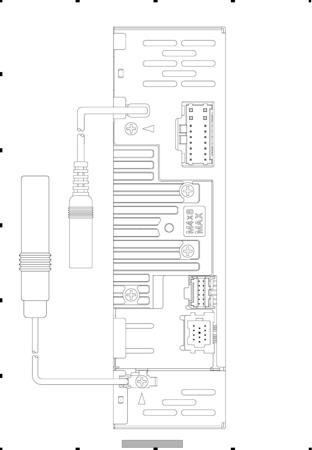
DEH-P8MP/XN/UC
68
1234
1234
C
D
F
A
B
E
7.1.2 CONNECTOR FUNCTION DESCRIPTION
111098
765
4321
10. NC
11. B.REMOTE
12. NC
13. ILL
14. MUTE
15. BACKUP
16. GND
17. ACC
18. GND
1. RR+
2. FL+
3. RR-
4. FL-
5. FR+
6. RL+
7. FR-
8. RL-
9. ACC(SENSE)
1. BUS+
2. GND
3. GND
4. NC
5. BUS-
6. GND
7. BUS L+ INPUT
8. ASENB
9. BUS R+ INPUT
10. BUS R- INPUT
11. BUS L- INPUT
WIRED REMOTE CONTROL
(DEH-P8MP/XN/UC,DEH-P80MP/XN/UC)
1153 5 7 9 11 13
216468101214
FM/AM ANTENNA
1. FL OUTPUT
2. GND
3. FR OUTPUT
4. GND
5. RL OUTPUT
6. GND
7. RR OUTPUT
8. GND
9. SWL OUTPUT
10. GND
11. SWR OUTPUT
12. GND
12246810
1113579 17
18
DEH-P8MP/XN/UC 69
5678
5678
C
D
F
A
B
E
7.2 IC
- Pin Functions(PD5925A)
Pin No. Pin Name I/O Function and Operation
1 SYSPW O System power control output
2 ICERROR I Power IC error sense input
3 ACCMON O ACC monitor output
4 SEL60W I Power amp 60W/40W select input
5 NC Not used
6 BYTE External data bus width change input
7 CNVSS Processor mode change input
8 TELIN I Telephone mute input
9 NC Not used
10 reset I Reset input
11 XOUT O Clock output
12 VSS GND
13 XIN I Clock input
14 VDD Power supply input
15 nmi Not used
16 NC Not used
17 NC Not used
18 NC Not used
19 RX2 I IP-BUS : Data input 2
20 OELPW O OEL power supply output
21 NC Not used
22 PEE O PEE sound output
23 NC Not used
24 brst O P-BUS : Reset output
25 brxen I/O P-BUS : Reception enable input / output
26 bsrq I P-BUS : Service request input
27 RX I IP-BUS : Data input
28 TX O IP-BUS : Data output
29 BSO O P-BUS : Data output
30 BSI I P-BUS : Data input
31 BSCK O P-BUS : Clock output
32 NC Not used
33 DPDT O Display data output
34 KYDT I Key data input
35, 36 ROT1, 0 I Rotary encoder pulse input1, 0
37 PCL O Output for clock adjustment
38 SWVDD O GRILLE : Chip enable output
39 NC Not used
40 FLPILM O Inside of flap illumination output
41 ILMPW O Illumination output
42 ejtin I Eject key input
43 gdtc1 O Picture rewriting output 1
44 NC Not used
45 NC Not used
46 NC Not used
47 gdtc2 O Picture rewriting output 2
48,49 NC Not used
50 fopnsw I Flap open sense input
51 fclssw I Flap close sense input
52 FLPCLS O Flap motor close output
53 FLPOPN O Flap motor open output
54 FLPPW O Flap motor driver power ON/OFF output
55 RECEIVE O Not used
56 CSENSOUT O Flap open/close output
PD5925A
HA12240FP
UPC494GS
PAL008A
PD5933A
PD6469A
PE5423A
UPD63761GJ
S-812C33AUA-C2N
BA5835FM
S-L2980A15MC-C6A
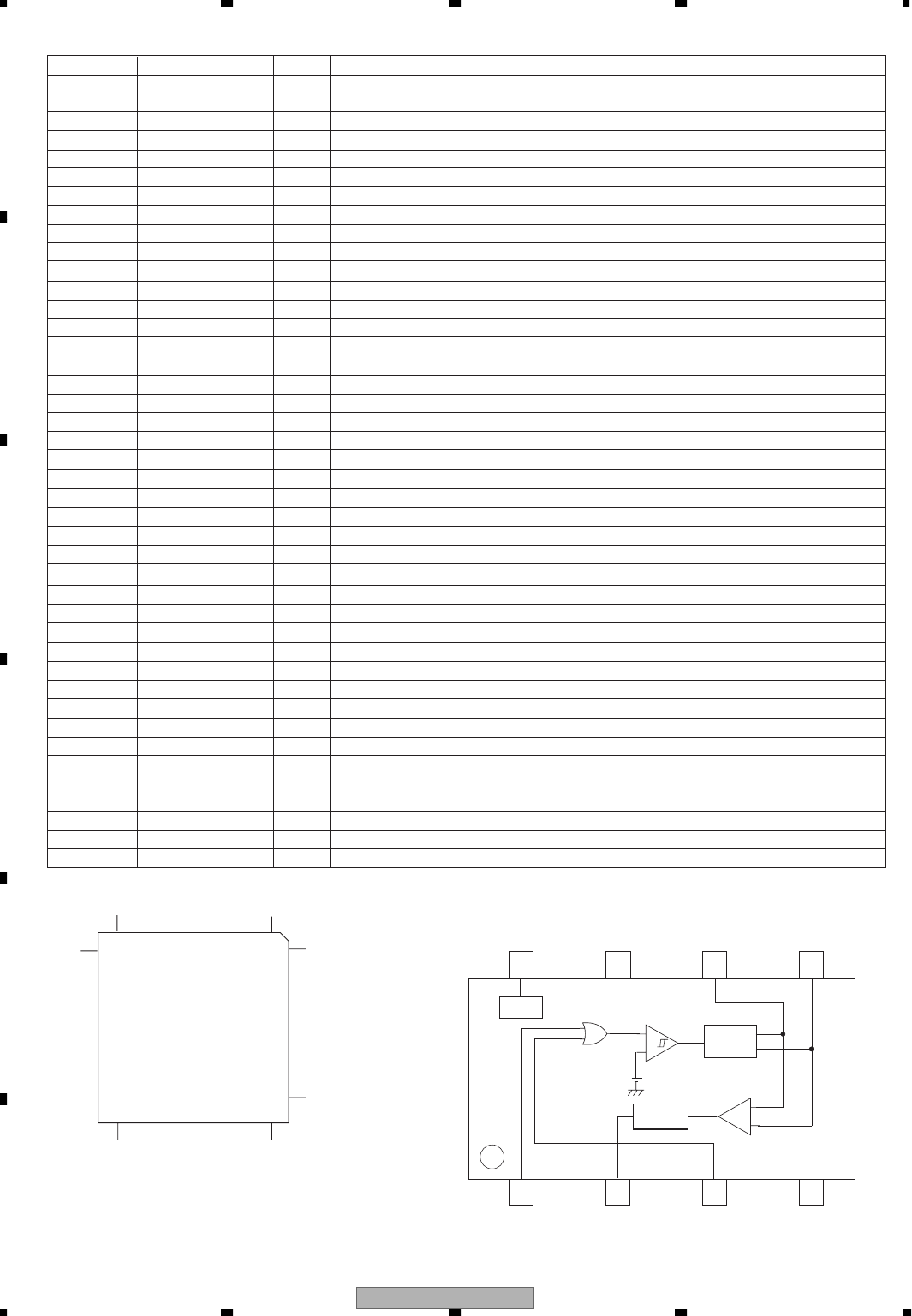
DEH-P8MP/XN/UC
70
1234
1234
C
D
F
A
B
E
Pin No. Pin Name I/O Function and Operation
57 EMUTE O Electronic volume : Mute output
58,59 NC Not used
60 VDD Power supply input
61 NC Not used
62 VSS GND
63 NC Not used
64 KEYD I Wired remote control input
65 PADA I Power amp : Data input
66 PACK I/O Power amp : Clock input / output
67 DALMON O For consumption current reduction output
68 NC Not used
69 tunpce@ O TUNER : Chip enable output(EEPROM)
70 TUNPCE1 O TUNER : Chip enable output(PLL)
71 ROMCS O ROM correction chip select output
72 asens I ACC sense input
73 bsens I Back up sense input
74 ROMCK O ROM correction clock output
75 ROMDATA I/O ROM correction data input/output
76 VST O Electronic volume : Strobe output
77 VDT O Electronic volume : Data output
78 VCK O Electronic volume : Clock output
79 IPPW O IPBUS : Driver power supply control output
80 ASENBO O IPBUS : Slave ACC sense output
81 isens I Illumination sense input
82,83 MODEL1,0 I Model select input
84 SYSPW2 O Power IC power control output
85 MUTE O System mute output
86 TESTIN I Test program input
87 CROSSKEY I Cross key data input
88 ddchk I Temperature sense input for power amp DC/DC converter
89 KEYAD I Wired remote control input
90 LVLINR I Level indicator R channel input
91 DSENS I Flap close sense input
92 LVLINL I Level indicator L channel input
93 ASLIN I ASL input
94 AVSS A/D converter power supply terminal
95 SL I TUNER : Signal level input
96 VREF A/D converter reference voltage
97 AVCC A/D converter power supply input terminal
98 TUNPDI I TUNER : PLL communication data input
99 TUNPDO O TUNER : Data output(PLL)
100 TUNPCK O TUNER : Clock output(PLL)
* PD5925A
25
26
50
51 75
76
100
1
IC's marked by * are MOS type.
Be careful in handling them because they are very
liable to be damaged by electrostatic induction. 132
S1 R S2 GND
BUS-BUS+VCCSTB
4
56
78
BIAS
DRIVER
OUTPUT
+
-
-
+
COM
RECEIVER
OUTPUT
HA12240FP
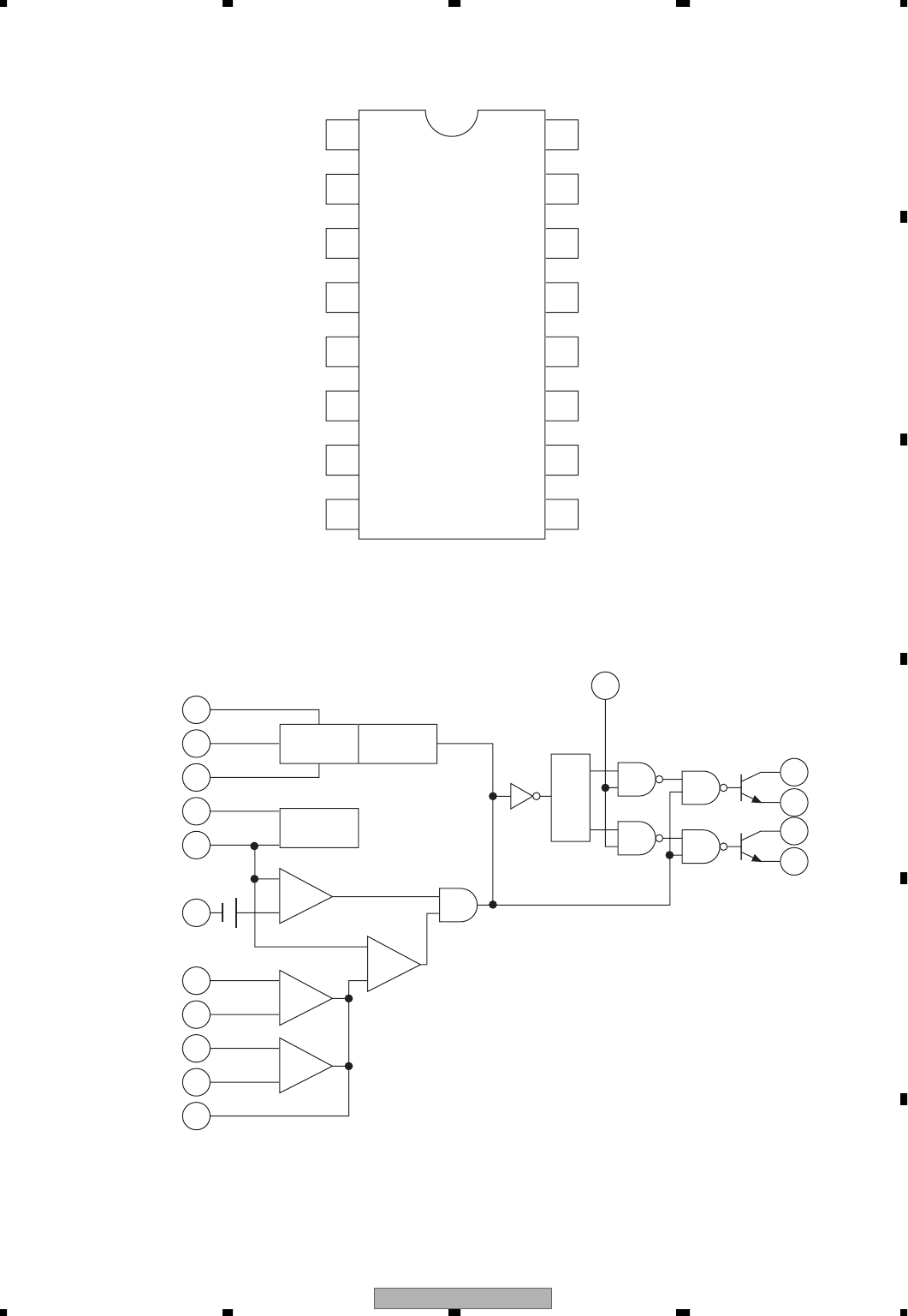
DEH-P8MP/XN/UC 71
5678
5678
C
D
F
A
B
E
3
16
2
1
4
5
8
13 Output Control
9
11
10
C1
E1
C2
E2
6
7
14
12
15
Feed-Back
Non-lnv.Input
lnv.Input
Non-lnv.Input
Dead-Time
Control
CT
RT
GND
Ref Out Reference
Regulator
Oscillator
EA I
PWM
Comparator
TF
/
F
T
EA II
Dead-Time
Comparator
Low Voltage
Step
VCC
lnv.Input -
+
-
+
-
+
-
+
1
2
3
4
5
6
7
8
Non-Inv.Input
Inv.Input
Feed-Back
Dead-Time
Control
CT
RT
GND
C1
Non-Inv.Input
Inv.Input
Ref Out
Output Control
VCC
C2
E2
E1
16
15
14
13
12
11
10
9
- Pin Layout
- Block Diagram
UPC494GS
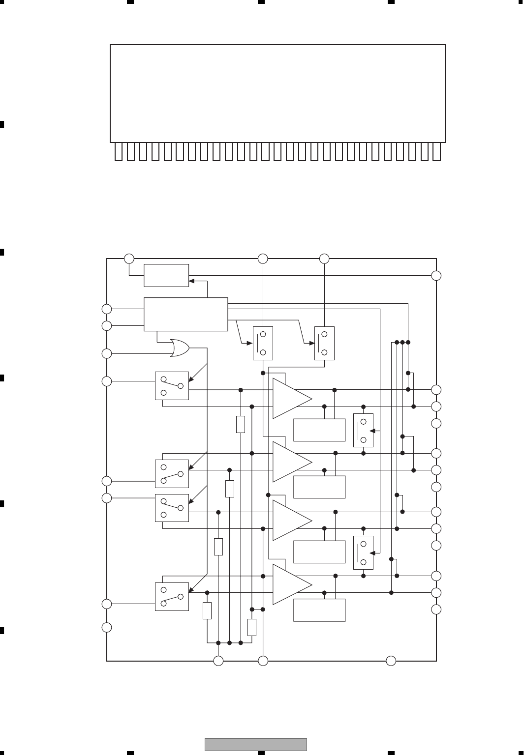
DEH-P8MP/XN/UC
72
1234
1234
C
D
F
A
B
E
+
-
+
-
+
-
+
-
S.GND
IN4
IN3
IN2
IN1
AC-GND
CK
DATA
MG1 VCC1 VCC2
TABAC-GNDSVR
CCGND
OUT1+
OUT1-
PW GND CH1
PW GND CH2
PW GND CH3
OUT3+
OUT3-
PW GND CH4
OUT4+
OUT4-
OUT2+
OUT2-
Vcc2
offset Detection
Vcc1
D/D conv.
contoroller
Short Circuit
Protection
Short Circuit
Protection
Short Circuit
Protection
Short Circuit
Protection
STEP-UP
HE/STD SW
Mute STBY
26
23
17
12
13
15
16
14
11 17 1
19
20
18
25
24
22
3
4
6
9
8
5
2172
10
1
- Pin Layout
- Block Diagram
PAL008A
TAB
MG1
PW GND CH2
OUT2-
CCGND
OUT2+
VCC1
OUT1-
PW GND CH1
OUT1+
SVR
IN1
IN2
S.GND
IN3
IN4
AC-GND
OUT4+
PW GND CH4
OUT4-
VCC2
OUT3+
CK
OUT3-
PW GND CH3
DATA
MUTE
23456789101112131415161718192021222324252627

DEH-P8MP/XN/UC 73
5678
5678
C
D
F
A
B
E
- Pin Functions(PD5933A)
Pin No. Pin Name I/O Function and Operation
1-4 NC O Not used
5 REM I
Remote control reception input
6 BYTE I
GND connection
7 CNVSS I Processor select input
8,9 NC Not used
10 reset I Reset input
11 XOUT O Clock output
12 VSS GND
13 XIN I Clock input
14 VDD Power supply input
15 nmi Not used
16-18 kd!-kd# I Key data input
19 NC Not used
20 CKC O
Cathode driver pulse output
21-23 NC Not used
24 LS O
Line synchronous signal output
25 NC Not used
26 CKD O
Data transfer and driver clock output
27 DPDT I Display data input
28 KYDT O Key data output
29
D1_L O Display data MSB output
30 NC Not used
31
CLK1 I UART1 clock input
32 NC Not used
33
D0_L O Display data LSB output
34 NC Not used
35
CLK0 I UART0 clock input
36 NC Not used
37
rdy O Not used Pull up
38 NC Not used
39 hold I Hold input
40,41 NC Not used
42 rd O
Read strobe output
43 NC Not used
44 wr O
Not used OPEN
45-48 cs#-cs0 O External ROM chip select output
49 A19 O Address bus 19 output
50 NC Not used
51-59 A17-A9 O
Address bus 17-9 output
60 VDD Power supply input
61 A8 O
Address bus 8 output
62 VSS GND connection
63-69 A7-A1 O Address bus 7-1 output
70 NC Not used
71-86 D15-D0 I/O
Data bus 15-0 input / output
87-89 ks!-ks# O Key strobe output
90-92 NC Not used
93
flstby O Not used
94 AVSS
GND connection
95 fl!@on Not used OPEN
96 VREF GND connection
97 AVCC VCC connection
98 flstby O Not used OPEN
99-100 NC Not used
DEH-P8MP/XN/UC
74
1234
1234
C
D
F
A
B
E
* PD5933A
25
26 50
51
75
76
100
1
* PD6469A
2
10
11
12
13
14
15
16
17
18
19
20
21
22
39
38
37
36
35
34
33
32
31
30
29
28
27
43
42
41
40
47
46
45
44
48
A15
A14
A13
A12
A11
A10
A9
A8
A19
NC
we
reset
NC
NC
RY/by
A18
A17
A7
A6
A5
A4
A3
A16
byte
VSS
DQ15/A-1
DQ7
DQ14
DQ6
DQ13
DQ5
DQ12
DQ4
VCC
DQ11
DQ3
DQ10
DQ2
DQ9
DQ1
DQ8
DQ0
oe
VSS
A-1A0-A19
DQ0-DQ15
ce
oe
we
RY/by
byte
AVCC
VSS
8
9
4
5
6
7
3
1
: Address input
: Data input / output
: Chip enable input
: Output enable input
: Write enable input
: Ready/Busy output
: 8 bit / 16 bit select input
: Power supply
: GND
23
21
26
25
A2
A1
ce
A0

DEH-P8MP/XN/UC 75
5678
5678
C
D
F
A
B
E
- Pin Functions(PE5423A)
Pin No. Pin Name I/O Format Function and Operation
1 AVREF A power supply Positive power supply(5V)
2 AVSS A power supply GND
3 RFOK O C Output of state of RFOK
4 CLAMP I CLAMP SW sense input
5 EVDD E power supply Positive power supply
6 PWM For changer(PWM)
7 NC Not used
8 IC/FLMD0 IC : VSS direct connection/FLMOD0 : Pull-down
9 VDD Positive power supply(5V)
10 REGC Connected to the capacity stabilizing output of the regulator
11 VSS GND
12 X1 I Oscillator connection for mainclock
13 X2 Oscillator connection for mainclock
14 reset I System reset input
15 XT1 I Connected to the oscillator for subclock
(connected to VSS via the resistor)
16 XT2 Connected to the oscillator for subclock(Open)
17 PULLDOWN I Connected to EVDD or EVSS via the resistor
18 ejsw I Eject key input
19 xint I CD LSI interruption signal input
20 NC Not used
21 brst I P-Bus reset input
22 BSI I P-Bus serial data input
23 BSO O C P-Bus serial data output
24 bsck I/O /C P-Bus serial clock input/output
25 FTXD O C For flash rewriting(transmitted signal)
26 FRXD I For flash rewriting(received signal)
27 BRXEN I/O /C It is possible to receive P-Bus
28 bsrq I/O /C P-Bus service request demand
29 dspok I DSP microcomputer initialization OK input
30 DSCSNS(S903) I Disc state sense input
31 8EJ(S905) I Input of detection of 8 cm disc ejection
32 12EJ(S904) I Input of detection of 12 cm disc ejection
33 EVSS E power supply GND
34 EVDD E power supply Positive power supply
35, 36 SRAMLEVEL0, 1 O C SRAM level meter output
37 EMPH O C Emphasis information output
38 emph O C Emphasis information output
39-42 NC Not used
43 adena O C A/D reference voltage supply control output
44 LRCKOK O C (DOUT mute output)
45 SRAMLEVEL2 O C SRAM level meter output
46 CD3VON O C CD +3.3V power supply control output
47 CONT O C Servo driver power supply control output
48 xrst O C CD LSI reset control output
49 VDCONT O C VD power supply control output
50 ROMDATA I/O /C E2PROM data input/output
51 ROMCS O C E2PROM chip selection output
52 ROMCK O C E2PROM clock output
53 LOEJ O C The direction change output of LOAD/EJECT
54 CLCONT O C Driver input change output
55 CDMUTE O C CD mute control output
56-58 INT For changer(Interruption at the edge)
59 xcs O C CD LSI chip selection output
60 NC Not used
61 xwait I CD LSI write control signal output
62 CLKOUT O C Internal system clock output(Open)
63 LOCK I Spindle lock input
64 NC Not used
65 xwrite O CD LSI write control signal output
DEH-P8MP/XN/UC
76
1234
1234
C
D
F
A
B
E
Pin No. Pin Name I/O Format Function and Operation
66 NC Not used
67 xread O CD LSI read control signal output
68 XASTB O CD LSI address strobe output
69 BVSS B power supply GND
70 BVDD B power supply Positive power supply
71-86 AD0-15 I/O /C Address/data Bus 0-15
87-90 NC Not used
91-93 A/D For changer(A/D)
94 csens I Flap closing sense input
95 TYPE_A/D I CD-DA analog/digital output change setup
96 testin I Chip check test program starting input
97 HOME I Home SW sense input
98 TEMP Temperature information sense input
99 VDSENS VD power supply short sense input
100 NC Not used
* PE5423A
25
26
50
51
75
76
100
1
Format Meaning
C CMOS

DEH-P8MP/XN/UC 77
5678
5678
C
D
F
A
B
E
- Pin Functions(UPD63761GJ)
Pin No. Pin Name I/O Function and Operation
1 D.VDD Power supply for digital circuits
2 D1.GND GND for 1.6V digital circuits
3 reset I Input of reset
4-8 AB12-8 I Address bus 12-8 from the microcomputer
9-16 AD7-0 I/O Address/data bus 7-0 to the microcomputer
17 cs I Chip selection
18 ASTB I Address strobe
19 read I Control signals(read)
20 write I Control signals(write)
21 wait O Control signals(wait)
22 INTQ O Interruption signals to the external microcomputer
23, 24 IFMODE0, 1 I Switching the microcomputer I/F 0, 1
25 D1.VDD Power supply for 1.6V digital circuits
26 DA.VDD Power supply for DAC
27 ROUT O Output of audio for the right channel
28 DA.GND GND for DAC
29 REGC Connected to the capacitor for band gap
30 DA.GND GND for DAC
31 LOUT O Output of audio for the left channel
32 DA.VDD Power supply for DAC
33 X.VDD Power supply for the crystal oscillator
34 XTAL I Connected to the crystal oscillator(16.9344MHz)
35 xtal O Connected to the crystal oscillator(16.9344MHz)
36 X.GND Ground for the crystal oscillator
37 VDDREG15 Control of 1.6V regulator
38 PWMSW0 I Setup 0 for PWM output(SD, MD)
39-41 TEST3-1 I Connected to GND
42 PWMSW1 I Setup 1 for PWM output(FD, TD)
43 TESTEN I Connected to GND
44 D1.GND GND for 1.6V digital circuits
45 DIN I Input of audio data
46 DOUT O Output of audio data
47 SCKIN I Clock input for audio data
48 SCKO O Clock output for audio data
49 LRCKIN I Input of LRCK for audio data
50 LRCK O Output LRCK for audio data
51 xtalen I Permission to oscillate 16.9344MHz
52 D1.VDD Power supply for 1.6V digital circuits
53 RFCK/HOLD O Output of RFCK/HOLD signal
54 WFCK/MIRR O Output of WFCK/MIRR signal
55 PLCK O Output of PLCK
56 LOCK/RFOK O Output of LRCK/Output of RFOK
57 C1D1/C8M O Information on error correction/C8M : 8MHz
58 C1D2/C16M O Information on error correction/C16M : 16MHz
59 C2D1/RMUTE O Information on error correction/Mute for Rch
60 C2D2/LMUTE O Information on error correction/Mute for Lch
61 C2D3/SHOCK O Information on error correction/Detection of vibration
62 D1.GND GND for 1.6V digital circuits
63 C33M O Output of 33.8688MHz(CLK for SDRAM)
64 (rcs) O DRAM cs
65 RA11 O Output of DRAM address 11
66 (CKE) O Output of DRAM CKE
67 ras O Output of DRAM ras
68 cas)(LDQM) O Output of DRAM lower cas(LDQM)
69 cas!(UDQM) O Output of DRAM upper cas(UDQM)
70 we O Output of DRAM we
71 oe(cas) O Output of DRAM oe(cas)
72 D.GND Ground for digital circuits
73-88 RDB0-15 I/O Input/output of DRAM data0-15
89-99 RA0-10 O Output of DRAM address0-10
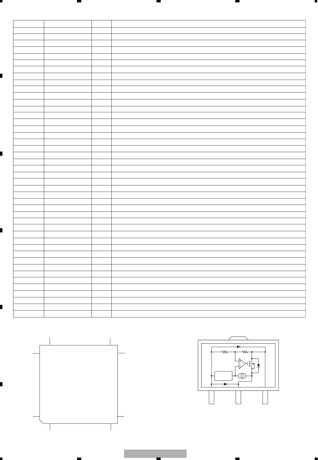
DEH-P8MP/XN/UC
78
1234
1234
C
D
F
A
B
E
Pin No. Pin Name I/O Function and Operation
100 D.VDD Power supply for digital circuits
101 FD+ O Output of focus drive PWM +
102 FD- O Output of focus drive PWM -
103 TD+ O Output of tracking drive PWM +
104 TD- O Output of tracking drive PWM -
105 SD+ O Output of thread drive PWM +
106 SD- O Output of thread drive PWM -
107 MD+ O Output of spindle drive PWM +
108 MD- O Output of spindle drive PWM -
109 REFOUTSV O REFOUT for servo
110 AD.VDD Power supply for ADC
111 EFM O Output of EFM signals
112 ASY I Input of asymmetry
113 ATEST O Analog tests
114 RFI I Input of RF
115 AD.GND Ground for the analog system
116 AGCO O Output of RF
117 C3T O Connection to the capacitor for detecting 3T
118 AGCI I Input of AGC
119 RFO O Output of RF(AGC)
120, 121 EQ2, 1 I Equalizer 2, 1
122 RF2- I Reversal input of RF2
123 RF- I Reversal input of RF
124 A.GND Ground for the analog system
125 A I Input of A
126 C I Input of C
127 B I Input of B
128 D I Input of D
129 F I Input of F
130 E I Input of E
131 VREFIN I Input of reference voltage
132 A.VDD Power supply for the analog system
133 REFOUT O Output of reference voltage
134 REFC I Connected to the capacitor for output of REFOUT
135 FE- I Reversal input of FE
136 FEO O Output of FE
137 ADIN I Input of FE, TE A/D converter
138 TE- I Reversal input of TE
139 TEO O Output of TE
140 TE2 O TE2
141 TEC I TEC
142 LD O Output of LD
143 PD I Input of PD
144 D.GND Ground for digital circuits
* UPD63761GJ
72
73
108
109
36
37
1
144
123
VIN
VOUT
VSS
Reference
Voltage
* S-812C33AUA-C2N
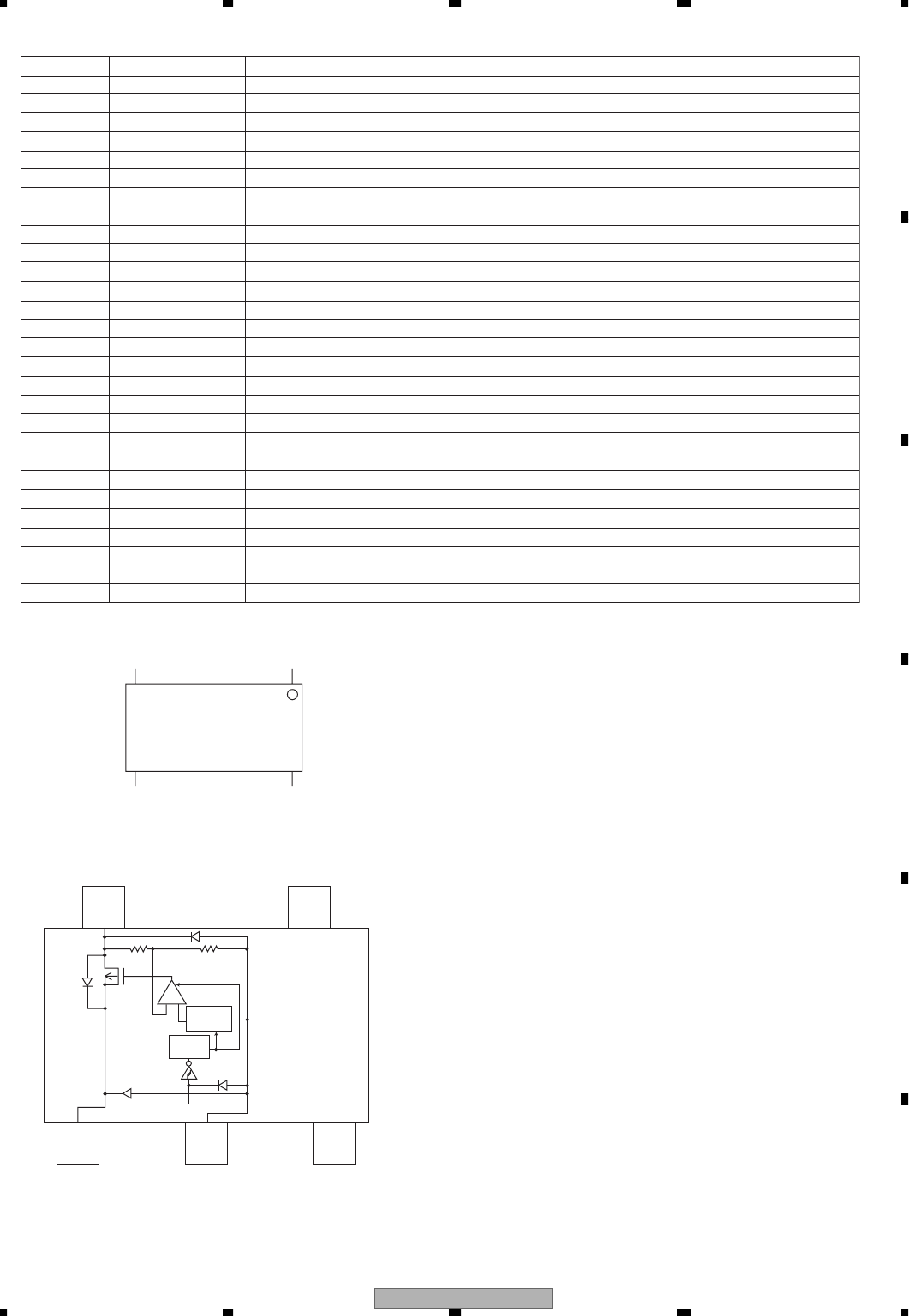
DEH-P8MP/XN/UC 79
5678
5678
C
D
F
A
B
E
- Pin Functions(BA5835FM)
Pin No. Pin Name Function and Operation
1 VR Input pin for reference voltage
2 OPIN2(+) Input pin for non-inverting input for CH2 preamplifier
3 OPIN2(-) Input pin for inverting input for CH2 preamplifier
4 OPOUT2 Output pin for CH2 preamplifier
5 OPIN1(+) Input pin for non-inverting input for CH1 preamplifier
6 OPIN1(-) Input pin for inverting input from CH1 preamplifier
7 OPOUT1 Output pin for CH1 preamplifier
8 GND Ground pin
9 MUTE Mute control pin
10 POWVCC1 Power supply pin for CH1, CH2, and CH3 at "Power" stage
11 VO1(-) Driver CH1 - Negative output
12 VO1(+) Driver CH2 - Positive output
13 VO2(-) Driver CH2 - Negative output
14 VO2(+) Driver CH2 - Positive output
15 VO3(+) Driver CH2 - Positive output
16 VO3(-) Driver CH2 - Negative output
17 VO4(+) Driver CH4 - Positive output
18 VO4(-) Driver CH4 - Negative output
19 POWVCC2 Power supply pin for CH4 at "Power" stage
20 GND Ground pin
21 CNT Control pin
22 LDIN Loading input
23 OPOUTSL Output pin for preamplifier for thread
24 OPINLSL Input pin for preamplifier for thread
25 OPOUT3 CH3 preamplifier output pin
26 OPIN3(-) Input pin for inverting input for CH3 preamplifier
27 OPIN3(+) Input pin for non-inverting input for CH3 preamplifier
28 PREVCC PreVcc
BA5835FM
114
15 28
ON/OFF
VSS
VIN
321
5 4
NC
VOUT
* S-L2980A15MC-C6A
-
+
Reference
voltage
ON/OFF
circuit
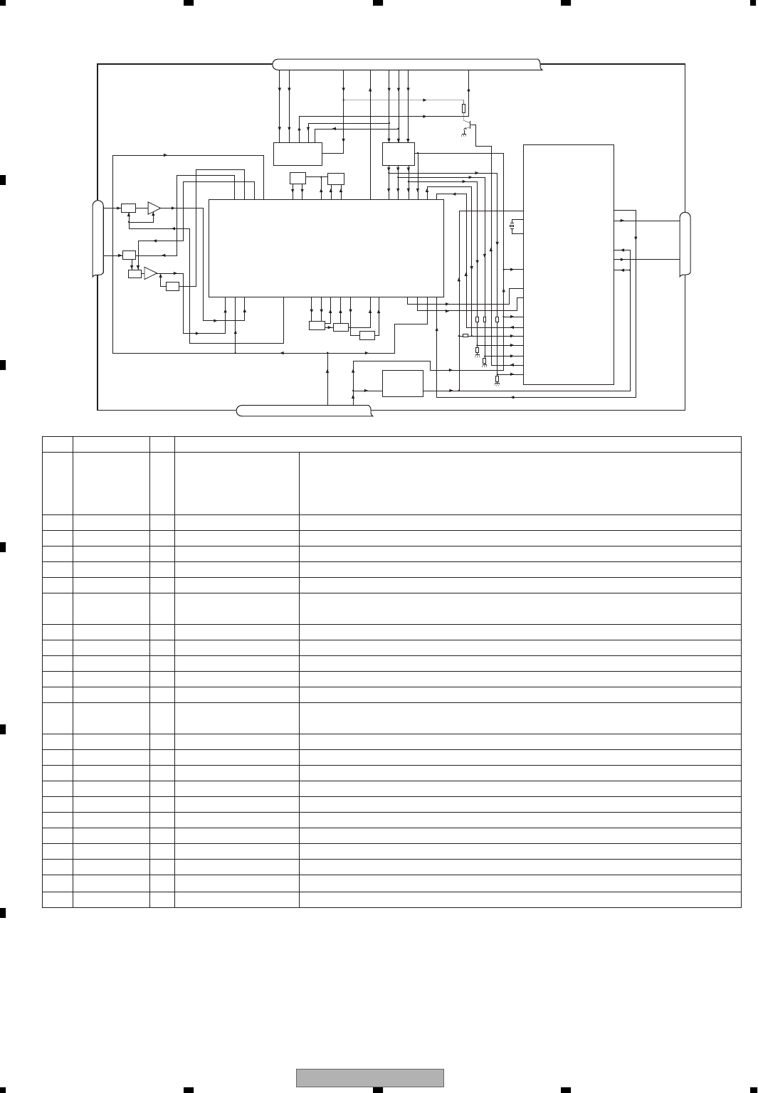
DEH-P8MP/XN/UC
80
1234
1234
C
D
F
A
B
E
No. Symbol I/O Explain
1 AMANT I AM antenna input AM antenna input high impedance AMANT pin is connected with
an all antenna by way of 4.7µH. (LAU type inductor) A series circuit
including an inductor and a resistor is connected with RF ground for
the countermeasure against the hum of power transmission line.
2 RFGND RF ground Ground of antenna block
3 FMANT I FM antenna input Input of FM antenna 75ΩSurge absorber(DSP-201M-S00B) is necessary.
4 VCC power supply The power supply for analog block. D.C 8.4V ±0.3V
5 SL O signal level Output of FM/AM signals level
6 CE2 I chip enable-2 Chip enable for EEPROM ”Low” active
7 WC I write control You can write EEPROM, when EEPROM write control is “Low”.
Ordinary non connection
8 CE1 I chip enable-1 Chip enable for AF•RF ”High” active
9 CK I clock Clock
10 DI I data in Data input
11 NC non connection Not used
12 OSCGND osc ground Ground of oscillator block
13 ROM_VDD power supply Power supply for EEPROM pin 13 is connected with a power supply of
micro computer.
14 DO O data out Data output
15 DGND digital ground Ground of digital block
16 NC non connection Not used
17 VDD_3.3 power supply The power supply for digital block. 3.3V ±0.2V
18 NC non connection Not used
19 NC non connection Not used
20 NC non connection Not used
21 NC non connection Not used
22 AUDIOGND audio ground Ground of audio block
23 L ch O L channel output FM stereo “L-ch” signal output or AM audio output
24 R ch O R channel output FM stereo “R-ch” signal output or AM audio output
FMRF
ANT adj RF adj
FM ANT
T51 CF52
CF51
RFGND
OSCGND
DGND
AUDIOGND
NC
VCC
VDD_3.3
3.3V 2.5V
IC 4
3.3V 2.5V
←
IC 2
2.5V
WC
CE2
ROM_VDD
SL
DI
CK
CE1
NC
DO
NC
NC
NC
NC
76 13 5 1098 11 14 18192021
1
3
212 1522 16 4 17
IC 1
3.3V
AM ANT FMRF
ATT
LPF
OSC
IC 3 EEPROM
5.0V
IC 5
5V 3.3V
←
ATT
MIXER, IF AMP DET, FM MPX
24
23
Rch
Lch
- FM/AM Tuner Unit
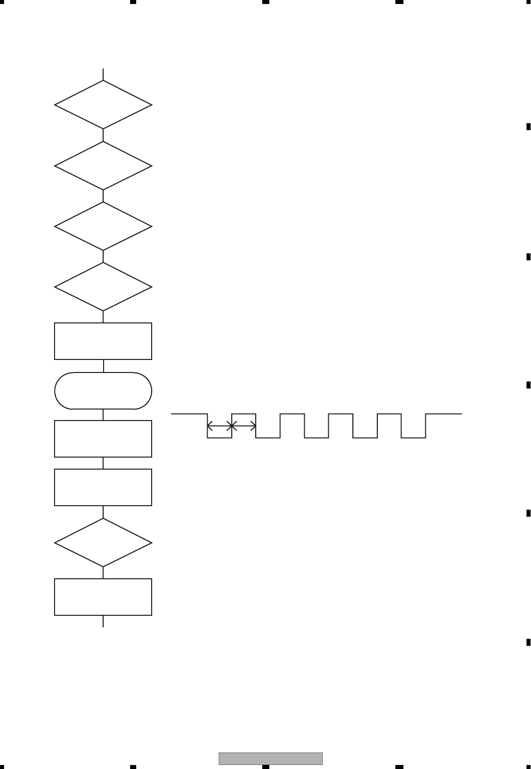
DEH-P8MP/XN/UC 81
5678
5678
C
D
F
A
B
E
7.3 EXPLANATION
7.3.1 OPERATIONAL FLOW CHART
VDD=5V
Pin 14,60
ASENBO←H
Pin 80
Power ON
bsens=L
asens=L
bsens
Pin 73
asens
Pin 72
DSENS
Pin 91
SWVDD←H
Pin 38
Source keys
operative
Completes power-on operation.
(After that, proceed to each source operation)
SYSPW←H
Pin 1
Starts
communication
with Grille
microcomputer.
Source ON
300ms
300ms
In case of the above signal, the communication
with Grille microcomputer may fail.
If the time interval is not 300msec, the oscillator
may be defective.
1.5V < DSENS < 4.5V
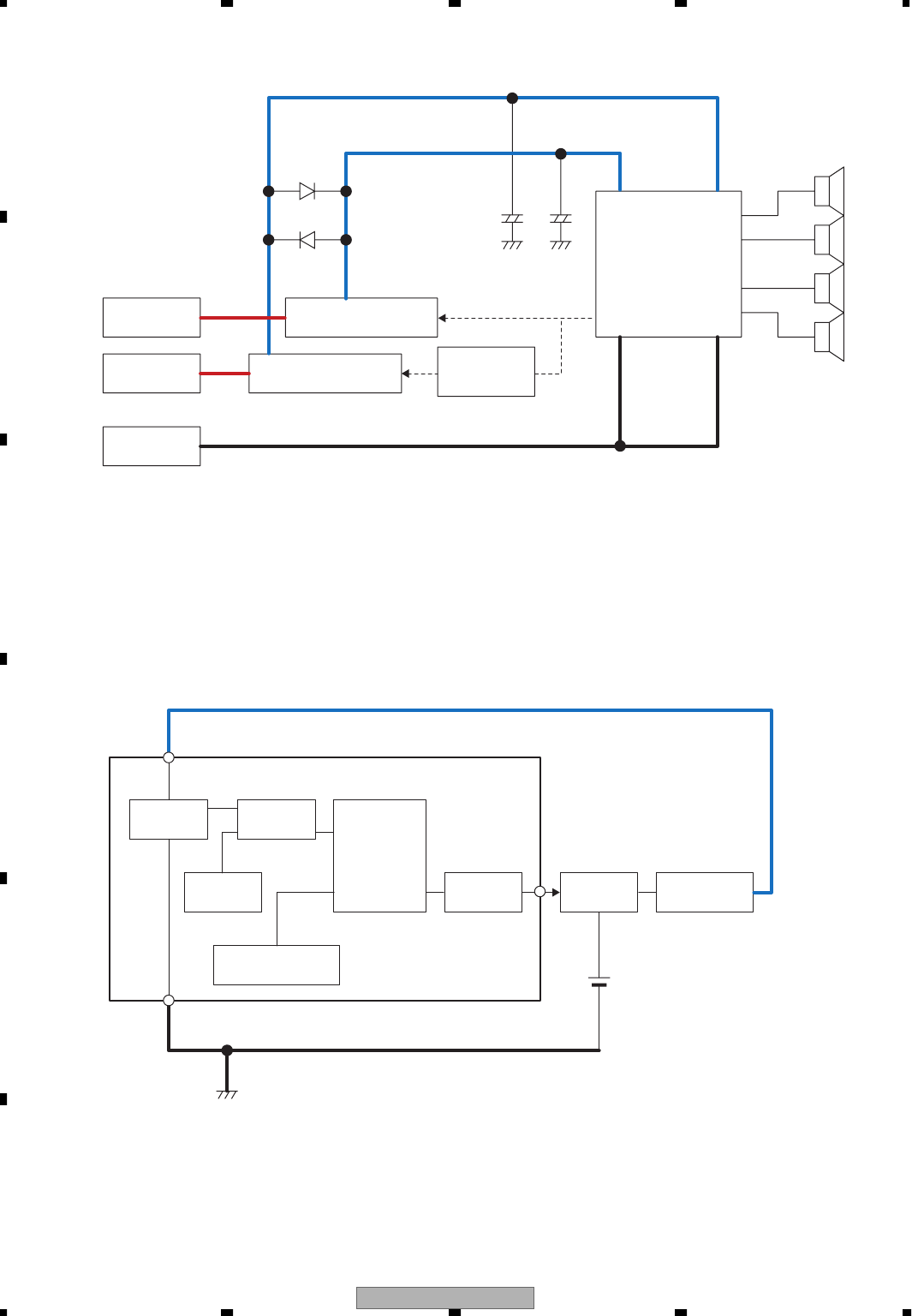
DEH-P8MP/XN/UC
82
1234
1234
C
D
F
A
B
E
7.3.2 CIRCUIT DESCRIPTIONS
BACKUP 10A
14.4V
VCC2(CH3,4) 17.5V
VCC1(CH1,2) 17.5V
14.4V
ACC 10A DRIVER
DC/DC CONVERTER 2
for ACC
MOSFET60
4CH POWER AMP
DC/DC CONVERTER
DRIVER
GND
- Power Amp Secsion
IC201
PAL008A
IC241
UPC494GS
DC/DC CONVERTER 1
for BACKUP
- DC/DC converter 1
VOLTAGE
DIVIDER ERROR AMP
TRIANGULAR
WAVE OSCILLATOR
COMPARATOR
Power AMP
DC/DC
CONVERTOR 1
VCC1
BATTERY
VOLTAGE
REFERENCE
VOLTAGE
PULSE
OUTPUT
VOLTAGE
BOOSTER
RECTIFICATION
CIRCUIT
IC201 PAL008A
IC201 incorporates a 4channel power amplifier and a DC/DC converter driver. Current for channels 1 and 2 is
supplied from the BACKUP power supply and current for channels 3 and 4 from the ACC power supply.
This is because when current is supplied with voltage increase in the BACKUP power supply as it is done
conventionally, 10A which is the limit to the vehicle fuse is exceeded.
Thus ACC power supply was enabled to supply current so that there are two power supplies of BACUP and
ACC and output of 60W x 4channel is expressed. Increased voltage (VCC1, VCC2) is controlled individually by
separate DC/DC converters. Therefore, different voltages occur when there is difference between the outputs
from L channel and R channel. A diode was hence connected between VCC1 and VCC2 so that voltage difference
will not occur.
Only one DC/DC converter driver is incorporated in IC201. Therefore, another DC/DC converter driver was
prepared externally to be synchronized with the DC/DC converter driver for IC201 and eliminate noise.
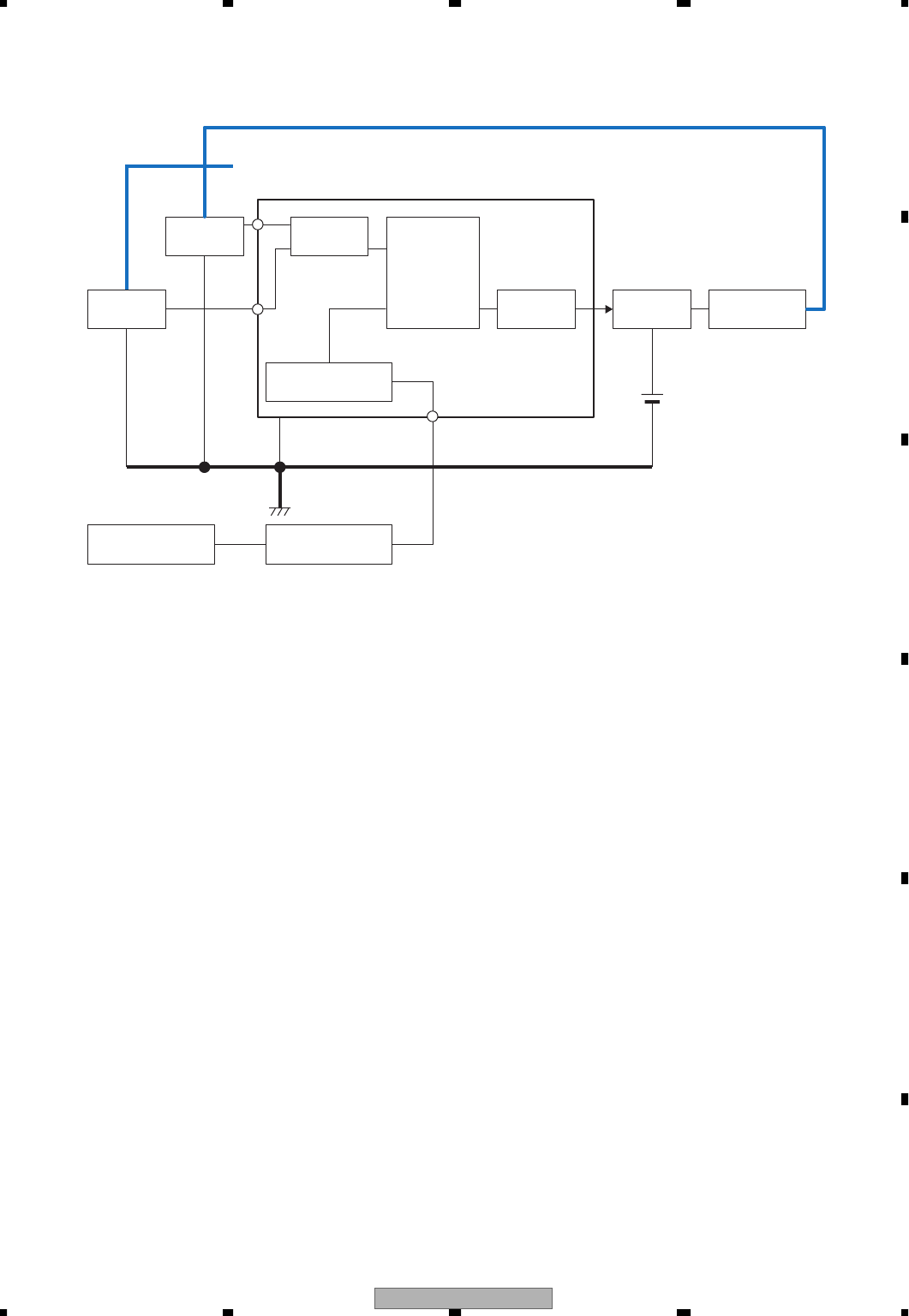
DEH-P8MP/XN/UC 83
5678
5678
C
D
F
A
B
E
VOLTAGE
DIVIDER ERROR AMP
SYNCHRONIZING
CIRCUIT
OUTPUT PULSE
of IC201 PAL008A
TRIANGULAR
WAVE OSCILLATOR
COMPARATOR DC/DC
CONVERTOR 2
VCC2
VCC1
BATTERY
VOLTAGE
VOLTAGE
DIVIDER
PULSE
OUTPUT
VOLTAGE
BOOSTER
RECTIFICATION
CIRCUIT
- DC/DC Converter 2
IC241 UPC494GS
Difference between VCC1 and VCC2 is detected with IC241 error amplifier to adjust the pulse output so that
VCC1 and VCC2 are identical.

DEH-P8MP/XN/UC
84
1234
1234
C
D
F
A
B
E
7.4 CLEANING
Before shipping out the product, be sure to clean the
following portions by using the prescribed cleaning
tools:
Portions to be cleaned Cleaning tools
CD pickup lenses Cleaning liquid : GEM1004
Cleaning paper : GED-008
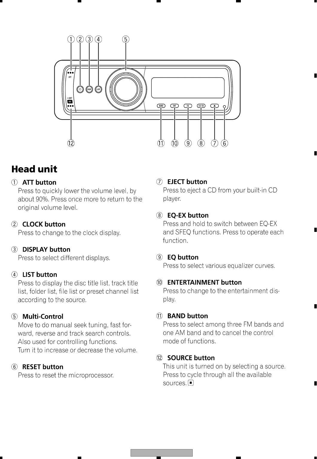
DEH-P8MP/XN/UC 85
5678
5678
C
D
F
A
B
E
8. OPERATIONS
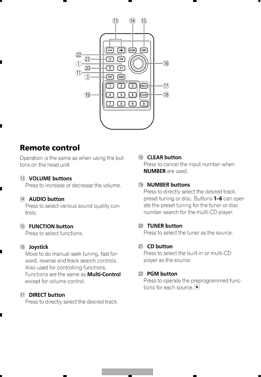
DEH-P8MP/XN/UC
86
1234
1234
C
D
F
A
B
E
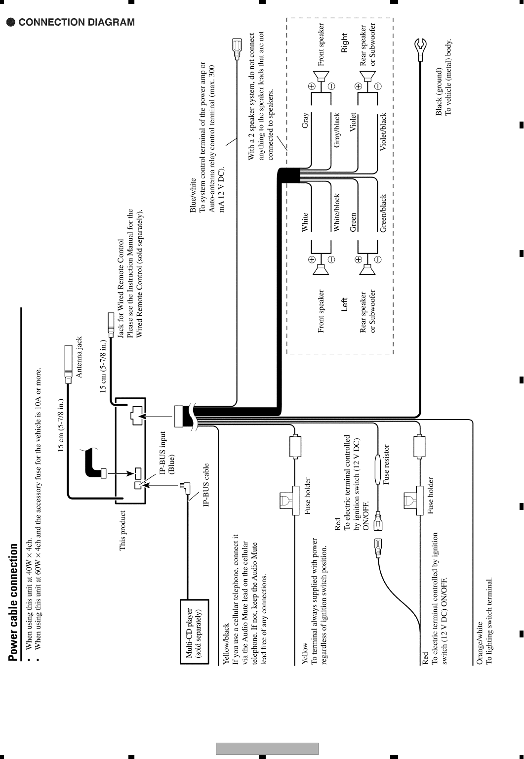
DEH-P8MP/XN/UC 87
5678
5678
C
D
F
A
B
E
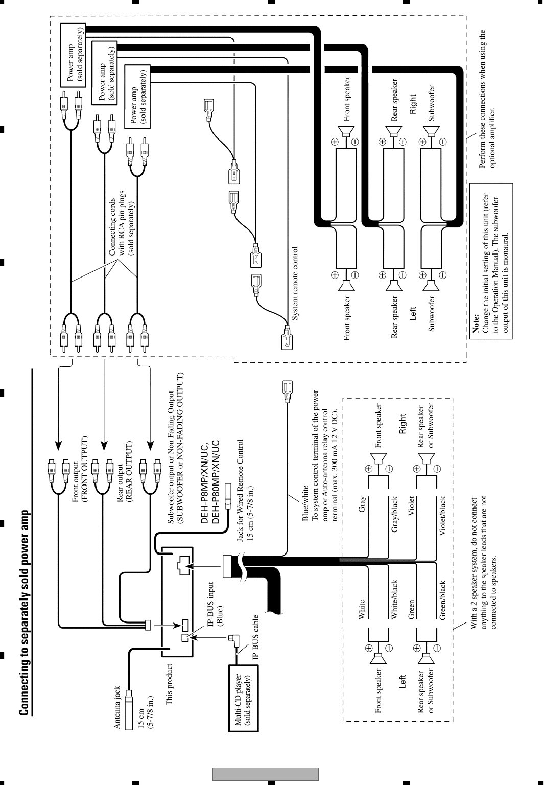
DEH-P8MP/XN/UC
88
1234
1234
C
D
F
A
B
E

DEH-P8MP/XN/UC 89
5678
5678
C
D
F
A
B
E

DEH-P8MP/XN/UC
90
1234
1234
C
D
F
A
B
E
-
J
ig
s L
i
st
T
est Disc
L.P.F.
Extension Cabl
e
Extension P
C
B
C
D-R
O
M
C
leanin
g
liquid
C
leanin
g
paper
TC
D-7
8
2
GG
D11
60
GG
D137
8
GG
V116
9
G
EM1
00
4
G
ED-
008
C
heckin
g
the
g
ratin
g
ggg
C
heckin
g
the
g
ratin
g
ggg
(
Two pieces
)
()
C
heckin
g
the ke
y
board uni
t
gy
C
heckin
g
the ke
y
board uni
t
gy
O
EL screensaver studio lka to lkd application
C
leaning
C
D pickup lenses
C
leaning
C
D pickup lenses
N
ame
Ji
g No
.
R
emarks
S
/
S
/
M
Locat
i
on
P
.5
9
P
.5
9
P.
55
P.
55
P.
6
2
P
.84
P
.84