Pioneer DEH P460MP, P4600MP, P4650MP Service Manual. Www.s Manuals.com. Manual
User Manual: Pioneer DEH-P4600MP - Service manuals and Schematics. Free.
Open the PDF directly: View PDF ![]() .
.
Page Count: 78
- SAFETY INFORMATION
- CONTENTS
- 1. SPECIFICATIONS
- 2. EXPLODED VIEWS AND PARTS LIST
- 2.1 PACKING
- 2.2 EXTERIOR
- 2.3 CD MECHANISM MODULE
- 3. BLOCK DIAGRAM AND SCHEMATIC DIAGRAM
- 3.1 BLOCK DIAGRAM
- 3.2 OVERALL CONNECTION DIAGRAM(GUIDE PAGE)
- 3.3 KEYBOARD UNIT
- 3.4 CD MECHANISM MODULE(GUIDE PAGE)
- 4. PCB CONNECTION DIAGRAM
- 4.1 TUNER AMP UNIT
- 4.2 PANEL UNIT
- 4.3 KEYBOARD UNIT
- 4.4 CD CORE UNIT(S10WMA)
- 5. ELECTRICAL PARTS LIST
- 6. ADJUSTMENT
- 6.1 CD ADJUSTMENT
- 6.2 CHECKING THE GRATING AFTER CHANGING THE PICKUP UNIT
- 6.3 ERROR MODE
- 6.4 SYSTEM MICROCOMPUTER TEST PROGRAM
- 7. GENERAL INFORMATION
- 7.1 DIAGNOSIS
- 7.1.1 DISASSEMBLY
- 7.1.2 CONNECTOR FUNCTION DESCRIPTION
- 7.2 PARTS
- 7.2.1 IC
- 7.2.2 DISPLAY
- 7.3 OPERATIONAL FLOW CHART
- 7.4 CLEANING
- 8. OPERATIONS
ORDER NO.
PIONEER CORPORATION 4-1, Meguro 1-chome, Meguro-ku, Tokyo 153-8654, Japan
PIONEER ELECTRONICS (USA) INC. P.O. Box 1760, Long Beach, CA 90801-1760, U.S.A.
PIONEER EUROPE NV Haven 1087, Keetberglaan 1, 9120 Melsele, Belgium
PIONEER ELECTRONICS ASIACENTRE PTE. LTD. 253 Alexandra Road, #04-01, Singapore 159936
PIONEER CORPORATION 2003
DEH-P460MP/XM/UC
CRT3171
MULTI-CD CONTROL HIGH POWER CD/MP3/WMA PLAYER WITH FM/AM TUNER
DEH-P460MP
/XM/UC
DEH-P4600MP
/XM/UC
DEH-P4650MP
/XM/ES
This service manual should be used together with the following manual(s):
Model No. Order No. Mech.Module Remarks
CX-3098 CRT3179 S10WMAcode2 CD Mech. Module:Circuit Description, Mech. Description, Disassembly
For details, refer to "Important symbols for good services".
K-ZZW. NOV. 2003 printed in Japan

DEH-P460MP/XM/UC
2
1234
1234
C
D
F
A
B
E
SAFETY INFORMATION
CAUTION
This service manual is intended for qualified service technicians; it is not meant for the casual do-it-yourselfer.
Qualified technicians have the necessary test equipment and tools, and have been trained to properly and safely
complex products such as those covered by this manual.
Improperly performed repairs can adversely affect the safety and reliability of the product and may void the
If you are not qualified to perform the repair of this product properly and safely, you should not risk
and refer the repair to a qualified service technician.
WARNING
This product contains lead in solder and certain electrical parts contain chemicals which are known to the
of California to cause cancer, birth defects or other reproductive harm.
Health & Safety Code Section 25249.6 - Proposition 65
repair
warranty.
trying to do so
state
-CD Player Service Precautions
1. Before disassembling the unit, be sure to turn off the
power. Unplugging and plugging the connectors dur-
ing power-on mode may damage the ICs inside the
unit.
2. To protect the pickup unit from electrostatic dis-
charge during serviving, take an appropriate treat-
ment(shorting-solder) by referring to "the DISAS-
SEMBLY" on page 56.
3. After replacing the pickup unit, be sure to check
the grating.(See p.52.)
DEH-P460MP/XM/UC 3
5678
5678
C
D
F
A
B
E
[ Important symbols for good services ]
In this manual, the symbols shown-below indicate that adjustments, settings or cleaning should be made securely.
When you find the procedures bearing any of the symbols, be sure to fulfill them:
2. Adjustments
To keep the original performances of the product, optimum adjustments or specification confirmation is indispensable.
In accordance with the procedures or instructions described in this manual, adjustments should be performed.
3. Cleaning
For optical pickups, tape-deck heads, lenses and mirrors used in projection monitors, and other parts requiring cleaning,
proper cleaning should be performed to restore their performances.
5. Lubricants, glues, and replacement parts
Appropriately applying grease or glue can maintain the product performances. But improper lubrication or applying
glue may lead to failures or troubles in the product. By following the instructions in this manual, be sure to apply the
prescribed grease or glue to proper portions by the appropriate amount.For replacement parts or tools, the prescribed
ones should be used.
4. Shipping mode and shipping screws
To protect the product from damages or failures that may be caused during transit, the shipping mode should be set or
the shipping screws should be installed before shipping out in accordance with this manual, if necessary.
1. Product safety
You should conform to the regulations governing the product (safety, radio and noise, and other regulations), and
should keep the safety during servicing by following the safety instructions described in this manual.

DEH-P460MP/XM/UC
4
1234
1234
C
D
F
A
B
E
CONTENTS
SAFETY INFORMATION..................................................................................................................................... 2
1. SPECIFICATIONS ............................................................................................................................................ 5
2. EXPLODED VIEWS AND PARTS LIST ............................................................................................................ 8
2.1 PACKING ................................................................................................................................................... 8
2.2 EXTERIOR............................................................................................................................................... 10
2.3 CD MECHANISM MODULE..................................................................................................................... 14
3. BLOCK DIAGRAM AND SCHEMATIC DIAGRAM..........................................................................................16
3.1 BLOCK DIAGRAM ................................................................................................................................... 16
3.2 OVERALL CONNECTION DIAGRAM(GUIDE PAGE).............................................................................. 18
3.3 KEYBOARD UNIT.................................................................................................................................... 24
3.4 CD MECHANISM MODULE(GUIDE PAGE) ............................................................................................ 26
4. PCB CONNECTION DIAGRAM ..................................................................................................................... 36
4.1 TUNER AMP UNIT................................................................................................................................... 36
4.2 PANEL UNIT ............................................................................................................................................ 40
4.3 KEYBOARD UNIT.................................................................................................................................... 41
4.4 CD CORE UNIT(S10WMA)...................................................................................................................... 42
5. ELECTRICAL PARTS LIST ............................................................................................................................ 44
6. ADJUSTMENT ............................................................................................................................................... 50
6.1 CD ADJUSTMENT................................................................................................................................... 50
6.2 CHECKING THE GRATING AFTER CHANGING THE PICKUP UNIT .................................................... 52
6.3 ERROR MODE ........................................................................................................................................ 54
6.4 SYSTEM MICROCOMPUTER TEST PROGRAM ................................................................................... 55
7. GENERAL INFORMATION............................................................................................................................. 56
7.1 DIAGNOSIS ............................................................................................................................................. 56
7.1.1 DISASSEMBLY ..................................................................................................................................... 56
7.1.2 CONNECTOR FUNCTION DESCRIPTION.......................................................................................... 59
7.2 PARTS...................................................................................................................................................... 60
7.2.1 IC .......................................................................................................................................................... 60
7.2.2 DISPLAY ............................................................................................................................................... 69
7.3 OPERATIONAL FLOW CHART ............................................................................................................... 71
7.4 CLEANING............................................................................................................................................... 72
8. OPERATIONS ................................................................................................................................................ 73
DEH-P460MP/XM/UC 5
5678
5678
C
D
F
A
B
E
1. SPECIFICATIONS
DEH-P460MP/XM/UC
6
1234
1234
C
D
F
A
B
E
DEH-P460MP/XM/UC 7
5678
5678
C
D
F
A
B
E
DEH-P460MP/XM/UC
8
1234
1234
C
D
F
A
B
E
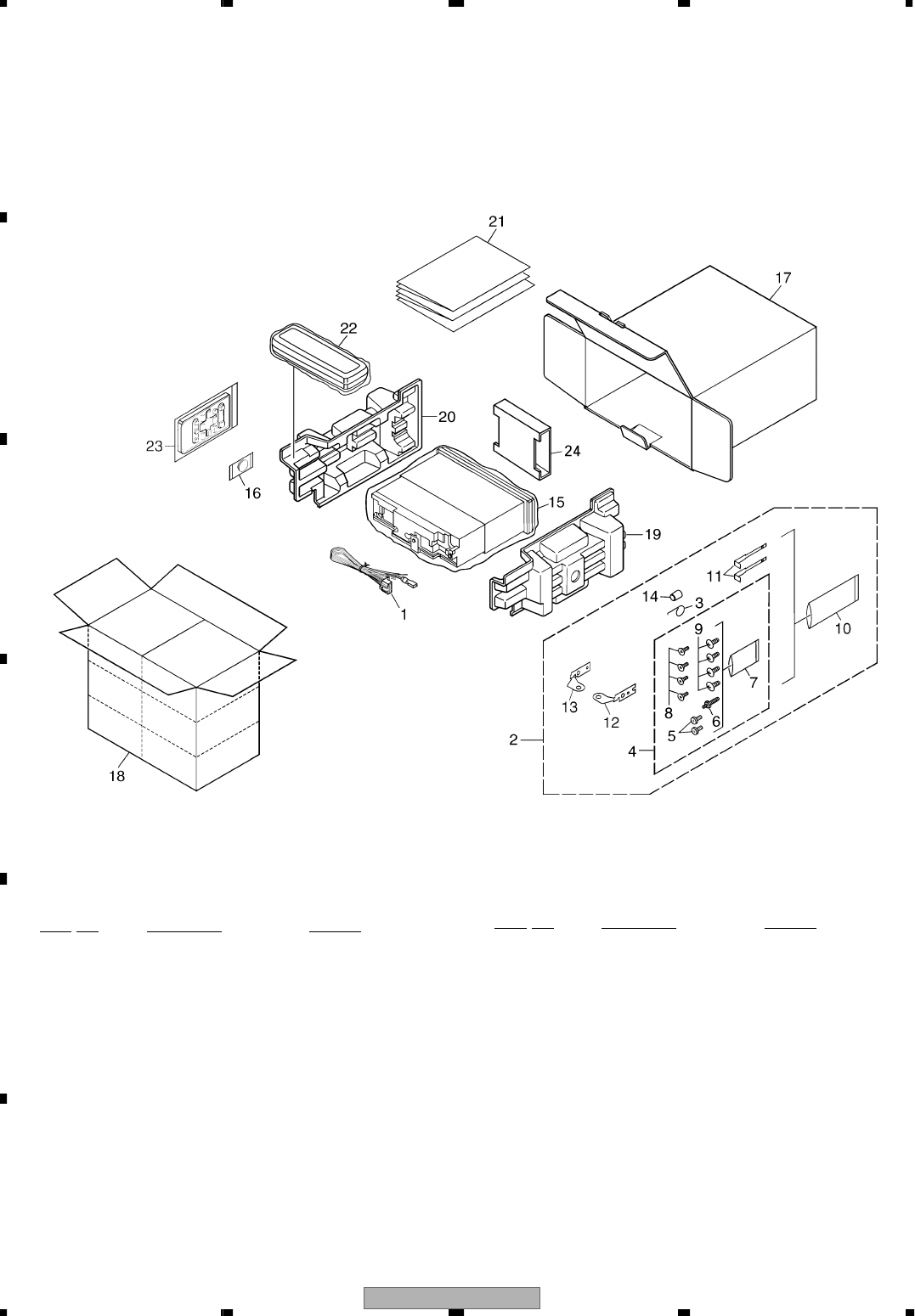
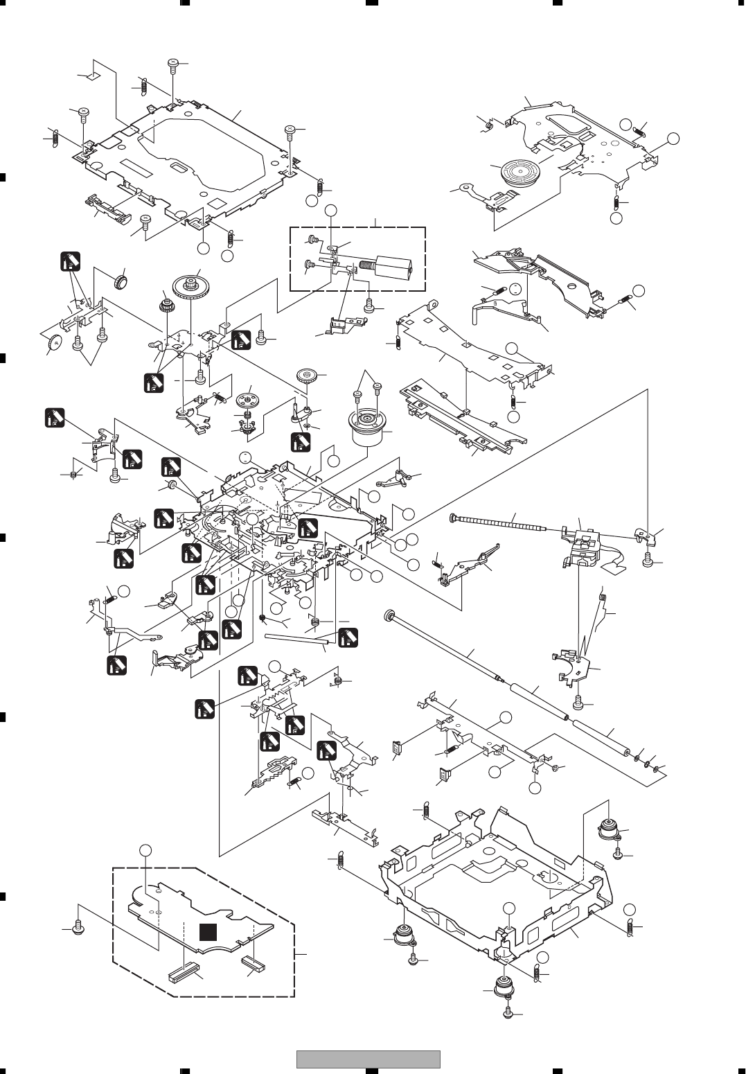
2. EXPLODED VIEWS AND PARTS LIST
2.1 PACKING
(1) PACKING SECTION PARTS LIST
N
OTES : • Parts marked by " * " are generally unavailable because they are not in our Master Spare Parts List.
• Screw adjacent to mark on the product are used for disassembly.
• For the applying amount of lobricants or glue, follow the instructions in this manual.
(In the case of no amount instructions,apply as you think it appropriate.)
"
Mark No. Description Part No.
1 Cord Assy CDE7060
2 Accessory Assy See Contrast table(2)
3 Spring CBH1650
4 Screw Assy See Contrast table(2)
5 Fixing Screw See Contrast table(2)
6 Screw CBA1650
* 7 Polyethylene Bag CEG-127
8 Screw CRZ50P090FTC
9 Screw TRZ50P080FTC
* 10 Polyethylene Bag CEG-158
11 Handle CNC5395
12 Holder See Contrast table(2)
13 Holder See Contrast table(2)
14 Bush CNV3930
15 Polyethylene Bag See Contrast table(2)
* 16 Battery CEX1065
17 Carton See Contrast table(2)
18 Contain Box See Contrast table(2)
19 Protector CHP2663
20 Protector CHP2664
21-1 Owner's Manual See Contrast table(2)
21-2 Owner's Manual See Contrast table(2)
21-3 Installation Manual See Contrast table(2)
* 21-4 Warranty Card See Contrast table(2)
* 21-5 Card See Contrast table(2)
* 21-6 Caution Card See Contrast table(2)
22 Case Assy See Contrast table(2)
23 Remote Control Unit CXC3173
24 Inner Box XHW7001
Mark No. Description Part No.
DEH-P460MP/XM/UC 9
5678
5678
C
D
F
A
B
E
(2) CONTRAST TABLE
DEH-P460MP/XM/UC, DEH-P4600MP/XM/UC and DEH-P4650MP/XM/ES are constructed the same
except for the following:
Mark No. Symbol and Description
2
4
5
12
13
15
17
18
21-1
21-2
21-3
21-4
21-5
21-6
22
Accessory Assy
Screw Assy
Fixing Screw
Holder
Holder
Polyethylene Bag
Carton
Contain Box
Owner's Manual
Owner's Manual
Installation Manual
Warranty Card
Card
Caution Card
Case Assy
DEH-P460MP/XM/UC
CEA3376
CEA3848
BPZ20P060FZK
CND1249
CND1250
CEG1173
XHG7016
XHL7016
XRD7030
Not used
XRD7031
CRY1070
Not used
Not used
Not used
DEH-P4600MP/XM/UC
CEA3376
CEA3848
BPZ20P060FZK
CND1249
CND1250
CEG1173
XHG7013
XHL7013
XRD7028
Not used
XRD7029
Not used
ARY1048
CRP1294
Not used
Parts No.
DEH-P4650MP/XM/ES
CEA3439
CEA3849
Not used
Not used
Not used
CEG-162
XHG7011
XHL7011
XRD7021
XRD7022
XRD7023
Not used
Not used
Not used
CXB3520
*
*
*
- Owner's Manual, Installation Manual
Model
DEH-P460MP/XM/UC
DEH-P4600MP/XM/UC
DEH-P4650MP/XM/ES
Parts No.
XRD7030
XRD7031
XRD7028
XRD7029
XRD7021
XRD7022
XRD7023
Language
English, French, Spanish
English, Spanish, Portuguese(B)
Arabic, Traditional Chinese
English, Spanish, Portuguese(B), Arabic, Traditional Chinese
DEH-P460MP/XM/UC
10
1234
1234
C
D
F
A
B
E
2.2 EXTERIOR

DEH-P460MP/XM/UC 11
5678
5678
C
D
F
A
B
E
(1) EXTERIOR SECTION PARTS LIST
Mark No. Description Part No.
1 Screw BMZ30P040FZK
2 Screw BSZ26P060FTC
3 Screw BSZ30P060FTC
4 Screw BSZ30P200FTC
5 Terminal(CN402) VNF1084
6 Cord Assy CDE7060
7 Button(EJECT) CAC7752
8 Screw(M2x4.5) CBA1647
9 Screw(M2x4) CBA1649
10 Washer CBF1038
11 Spring CBH2650
12 Spring CBH2651
13 Spring CBH2652
14 Spring CBH2653
15 Holder CND1254
16 Gear CNV5997
17 Arm CNV7400
18 Arm CNV7401
19 Arm CNV7402
20 Arm CNV7403
21 Panel Unit CWM8758
22 Socket(CN1950) CKS3550
23 Connector(CN1951) CKS4806
24 Holder Unit CXB9501
25 Holder Unit CXB9502
26 Damper Unit CXB9503
27 Service Panel Unit CXX1691
28 Spring CBL1512
29 Cover CNM6854
30 Panel CNS7245
31 Pin CNV6486
32 Lighting Conductor CNV6487
33 Case CNB2870
34 Earth Plate CNC8915
35 Cushion CNM8890
36 Insulator CNM7682
37 Insulator CNM7935
38 Insulator CNM8174
39 Panel See Contrast table(2)
40 Holder Unit CXB6681
41 Chassis Unit CXB9528
42 Remote Control Unit CXC3173
43 Cover CNS7068
44 CD Mechanism Module(S10CODE2)CXK5665
45 Screw ISS26P055FTC
46 Cable CDE7189
47 Tuner Amp Unit See Contrast table(2)
48 Screw ASZ26P060FTC
49 Screw BPZ26P080FTC
50 Screw BSZ26P160FTC
51 Fuse(10A) CEK1208
52 FM/AM Tuner Unit CWE1646
53 Holder CND1054
54 Pin Jack(CN352) See Contrast table(2)
55 Plug(CN981) CKM1376
56 Connector(CN801) See Contrast table(2)
57 Connector(CN101) CKS3408
58 Plug(CN831) CKS3537
59 Connector(CN721) CKS3837
60 Antenna Jack(CN401) CKX1056
61 Holder See Contrast table(2)
62 Holder CND1352
63 Heat Sink CNR1668
64 Insulator XNM7031
65 Detachable Assy See Contrast table(2)
66 Screw BPZ20P100FZK
67 Spring CBL1470
68 Knob See Contrast table(2)
69 Button(1-6) XAC7005
70 Button(LOUD) XAC7020
71 Button(PAUSE) XAC7019
72 Button(OPEN) See Contrast table(2)
73 Spring XBH7001
74 Cover XNS7013
75 Keyboard Unit See Contrast table(2)
76 LCD(LCD1901) See Contrast table(2)
77 Connector(CN1901) CKS4524
78 Sheet XNM7006
79 Connector XNV7006
80 Holder XNC7002
81 Lighting Conductor XNV7005
82 Button(BAND) XAC7021
83 Button(EQ) XAC7022
84 Sub Grille Assy See Contrast table(2)
85 Sub Button Assy(SELECT) See Contrast table(2)
86 IC(IC301) PAL007A
87 Choke Coil(L981) CTH1280
88 Transistor(Q752,901,911) 2SD2375
89 Screw See Contrast table(2)
90 Holder See Contrast table(2)
91 Sheet See Contrast table(2)
* 92 Lighting Conductor XNV7012
93 Button(CLOCK) See Contrast table(2)
Mark No. Description Part No.

DEH-P460MP/XM/UC
12
1234
1234
C
D
F
A
B
E
(2) CONTRAST TABLE
DEH-P460MP/XM/UC, DEH-P4600MP/XM/UC and DEH-P4650MP/XM/ES are constructed the same
except for the following:
Mark No. Symbol and Description
39
47
54
56
61
65
68
72
75
76
84
85
89
90
91
93
Panel
Tuner Amp Unit
Pin Jack(CN352)
Connector(CN801)
Holder
Detachable Assy
Knob
Button(OPEN)
Keyboard Unit
LCD(LCD1901)
Sub Grille Assy
Sub Button Assy(SELECT)
Screw
Holder
Sheet
Button(CLOCK)
DEH-P460MP/XM/UC
CNS6935
XWM7023
CKB1051
CKS4124
CND1325
XXA7132
XAA7009
XAC7026
XWM7031
XAW7004
XXA7147
XXA7229
Not used
Not used
Not used
XAC7016
DEH-P4600MP/XM/UC
XNS7070
XWM7023
CKB1051
CKS4124
CND1325
XXA7133
XAA7003
XAC7012
XWM7031
XAW7004
XXA7148
XXA7228
BMZ40P140FTC
CNV7619
Not used
XAC7024
Parts No.
DEH-P4650MP/XM/ES
CNS6935
XWM7024
CKB1057(CN351)
Not used
CND1237
XXA7134
XAA7009
XAC7026
XWM7032
XAW7002
XXA7149
XXA7229
Not used
Not used
XNM7008
XAC7016

DEH-P460MP/XM/UC 13
5678
5678
C
D
F
A
B
E
DEH-P460MP/XM/UC
14
1234
1234
C
D
F
A
B
E
2.3 CD MECHANISM MODULE
A
D
H
L
M
NO
Q
R
A
B
C
D
E
F
GH
I
J
K
L
M
N
O
Q
B
16
25
13 83
42
68
28
82
4
71
23
J
K
38
23
59
87
86
5
13
34
5
5
13
44
5C
52
53
36
4
73
29
51
18
64
76
50
10
72
75
49
77
67
27
78
60
90 48
8
17
46
6
60
11 89
43
70
14
31
65
85
66
85
31
35
14
74
85
1
2
3
R
91
12
33
61
63
21
79
57
58
62
80
13
4
86
I
45
28
7
24
47
P
41
20
40
69
39
30
P
19
56
F
E22
81
15
G
26
4
54
37
55
93
92
10
D
1GEM1024
2GEM1045
3GEM1035
1
1
1
1
1
1
1
1
2
2
2
2
1
1
1
1
1
2
2
1
3

DEH-P460MP/XM/UC 15
5678
5678
C
D
F
A
B
E
CD MECHANISM MODULE SECTION PARTS LIST
Mark No. Description Part No.
1 CD Core Unit(S10WMA) CWX2851
2 Connector(CN101) CKS4182
3 Connector(CN901) CKS4017
4 Screw BMZ20P035FTC
5 Screw BSZ20P040FTC
6 Screw(M2x4) CBA1362
7 Screw(M2x3) CBA1511
8 Screw(M2x3) CBA1527
9 •••••
10 Washer CBF1038
11 Washer CBF1060
12 Spring CBH2390
13 Spring CBH2606
14 Spring CBH2607
15 Spring CBH2608
16 Spring CBH2609
17 Spring CBH2610
18 Spring CBH2735
19 Spring CBH2612
20 Spring CBH2613
21 Spring CBH2614
22 Spring CBH2615
23 Spring CBH2616
24 Spring CBH2617
25 Spring CBH2620
26 Spring CBH2621
27 Spring CBH2641
28 Spring CBH2642
29 Spring CBH2643
30 Spring CBH2659
31 Spring CBH2688
32 •••••
33 Shaft CLA4441
34 Frame CNC9962
35 Frame CNC9963
36 Bracket CNC9966
37 Bracket CND1895
38 Arm CNC9968
39 Arm CND1909
40 Lever CND2032
41 Lever CNC9984
42 Sheet CNM8134
43 Collar CNV7798
44 Guide CNV7799
45 Arm CNV7800
46 Rack CNV7199
47 Holder CNV7201
48 Holder CNV7202
49 Arm CNV7203
50 Gear CNV7207
51 Gear CNV7208
52 Gear CNV7209
53 Gear CNV7210
54 Gear CNV7211
55 Gear CNV7212
56 Rack CNV7214
57 Arm CNV7215
58 Arm CNV7216
59 Guide CNV7217
60 Roller CNV7218
61 Gear CNV7219
62 Arm CNV7221
63 Arm CNV7220
64 Arm CNV7222
65 Damper CNV7313
66 Damper CNV7314
67 Arm CNV7341
68 Arm CNV7342
69 Guide CNV7360
70 Guide CNV7361
71 Holder CNV7437
72 Arm CNV7805
73 Gear CNV7595
74 Damper CNV7618
75 Motor Unit(M1) CXB6007
76 Chassis Unit CXC2318
77 Screw Unit CXB8729
78 Gear Unit CXC2397
79 Arm Unit CXC2316
80 Arm CND1896
81 Arm CND1894
82 Motor Unit(M2) CXB8933
83 Bracket CNC9985
84 •••••
85 Screw(M2x5) EBA1028
86 Screw JFZ20P020FTC
87 Screw JGZ17P022FTC
88 •••••
89 Washer YE20FTC
90 Pickup Unit(P10)(Service) CXX1641
91 Screw IMS26P030FTC
92 Spring CBL1635
93 Clamper CNV7197
Mark No. Description Part No.
DEH-P460MP/XM/UC
16
1234
1234
C
D
F
A
B
E
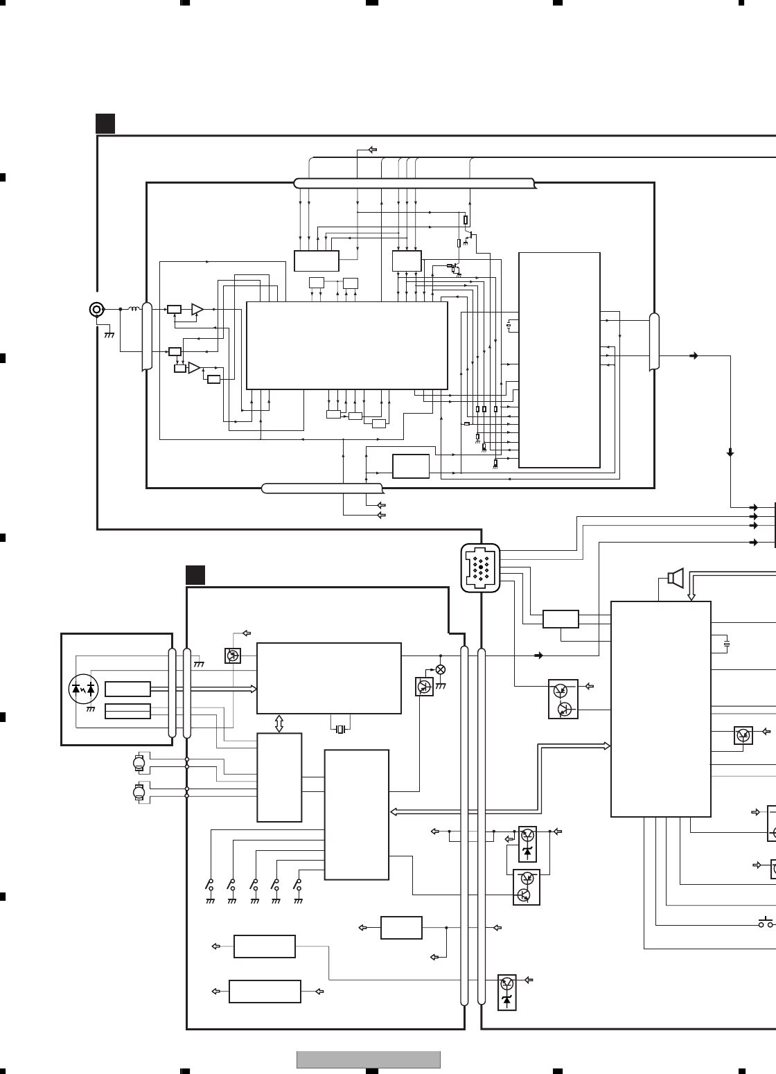
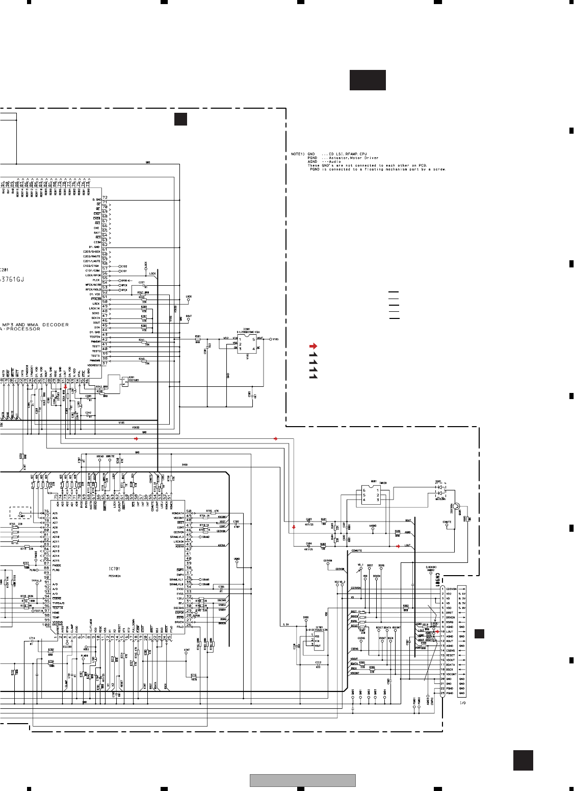
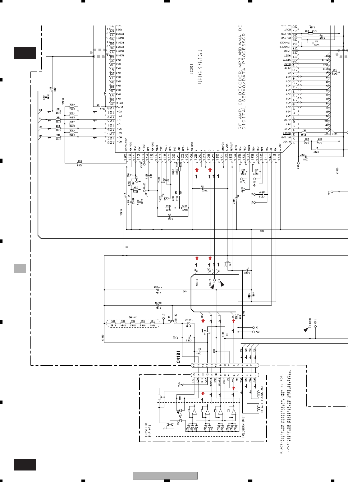
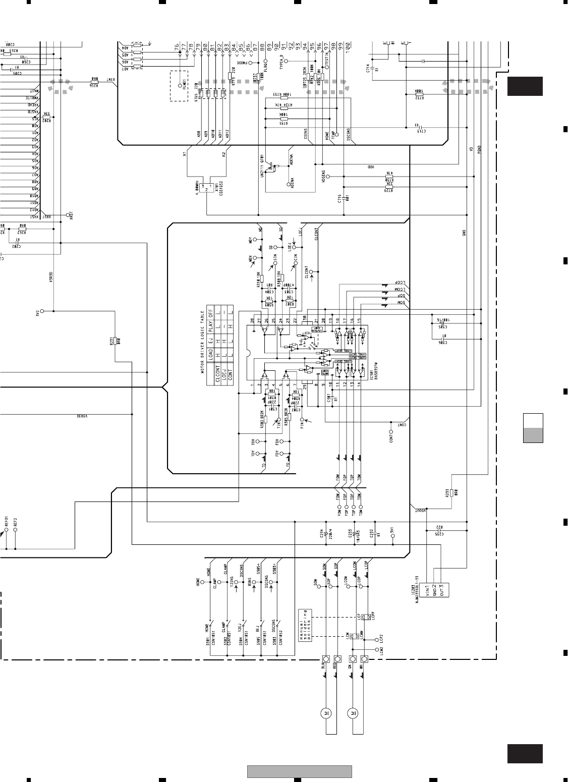
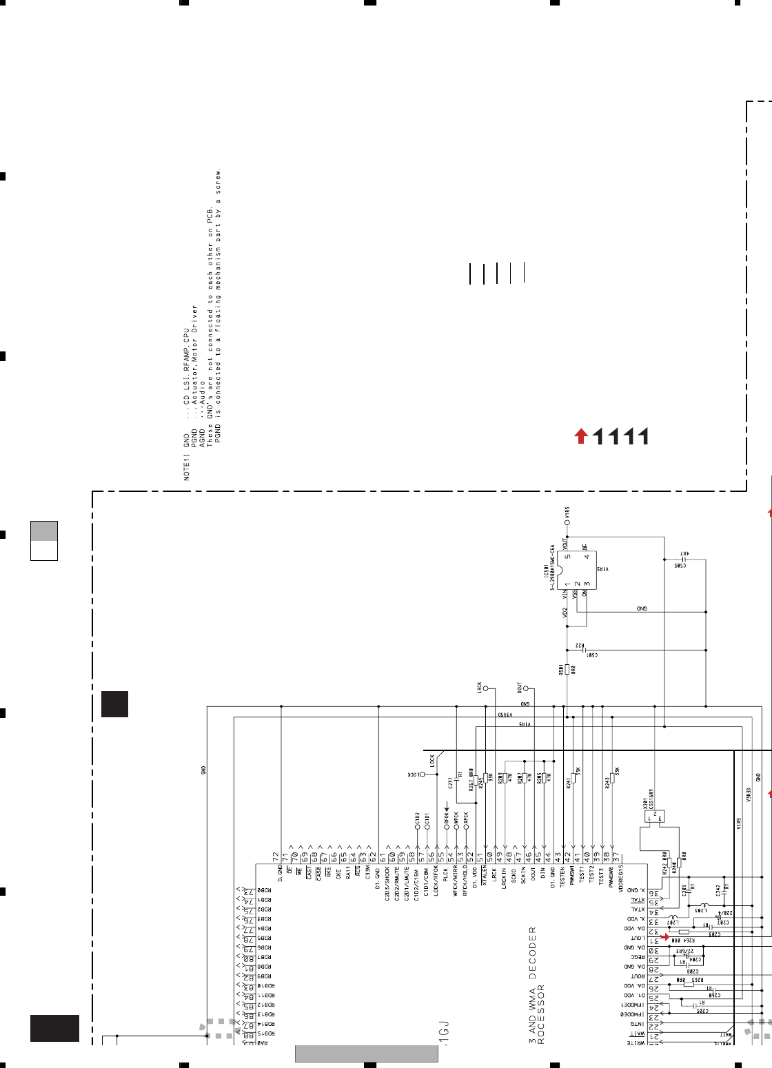
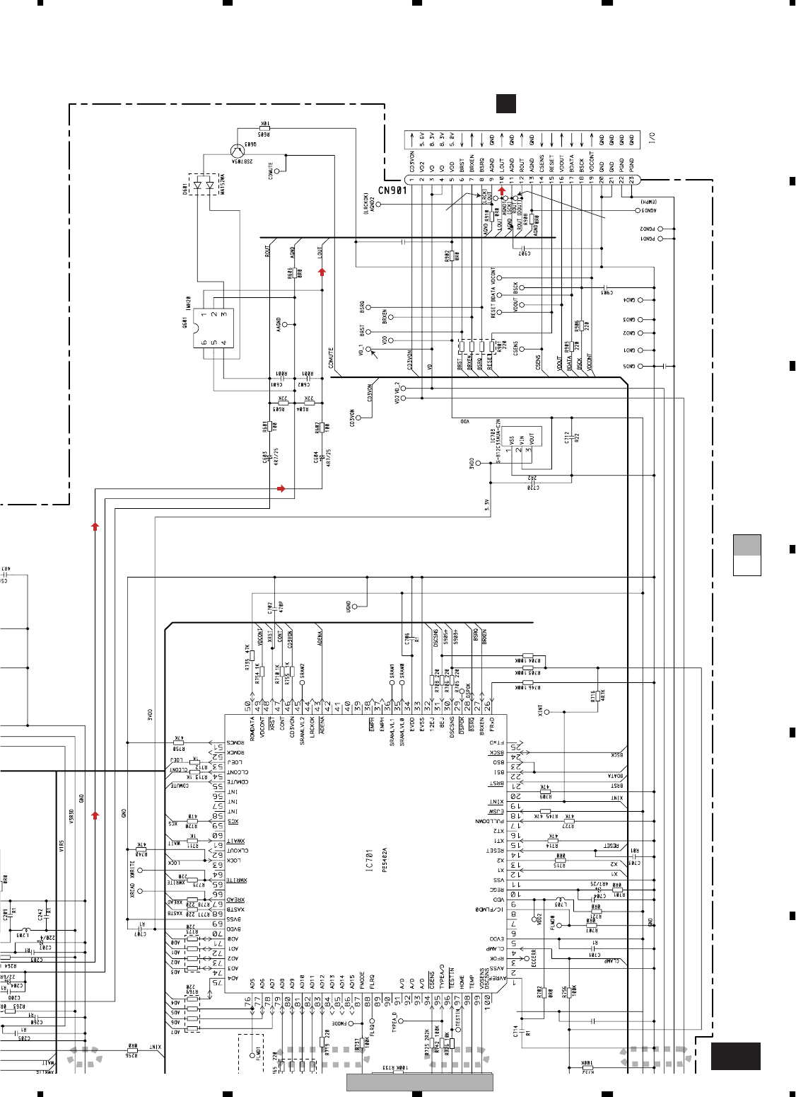
3. BLOCK DIAGRAM AND SCHEMATIC DIAGRAM
3.1 BLOCK DIAGRAM
BRST,BRXEN,BSRQ
Q601
Q603
MUTE
D
CN901
Q101
M
LASER
DIODE
MONITOR
DIODE
CLAMP
SENSE DISC
SENSE
FOCUS ACT.
SPINDLE
MOTOR
M
CARRIAGE
MOTOR
LOAD/
TRACKING ACT.
LD-
MD
FO+
TO+
15
5
1
4
PICKUP UNIT
(P10)(SERVICE)
HOLOGRAM
UNIT
IC 301
BA5835FM
IC 201
UPD63761GJ
IC 703
+3.3V REGULATOR
RF-AMP,CD DECODER,
MP3 and WMA DECODER,
DIGITAL SERVO / DATA PROCESSOR
CD
DRIVER
3
VD
VD
3VDD
10
L-OUT
5
CN101
TOP
FOP
16 SOP
15 SOM
18 LCOP
17 LCOM
22
2
LOEJ
31
LOUT
9
CONT
12 FOP
TD/FD
AC,BD
F,E
SD/MD
3
13 TOP
HOME
12EJ
SENSE 8EJ
SENSE
LD+ 14
142 LD
143 PD
CD CORE UNIT(S10WMA)
3534
X201
DSCSNS
CONT
LOEJ
HOME
32
97
53
47
VDD
IC 203
NJM2391DL1-33
+3.3V REGULATOR
V3R3D 1
3
VDCONT 49
S-812C33AUA-C2N
CD CONTROLLER
IC 701
PE5402A
55
CDMUTE
4
V3R3D
19
1
BDATA,BSCK
VD2 2
15
5
1
4
14
CLAMP
4
VD2
VDCONT
30
31 8EJ
12EJ
IC 501
S-L2980A15MC-C6A
1.5V REGULATOR
V1R5 1,3
5V3R3D
ASENBO
37
mute
X1
X2
3
PEE
100
1
5
6
4
71
86
85
24
SYSTEM CONTROLLER
IC 601(2/2)
PE5407A
CN401
1
2
BUS-
BUS+
BUS+L
BUS-L
TX
RX
IPPW
swvdd
BU
VDD
CN721
Q
Q
Q
TUNER AMP UNIT
16
X601
15
EVST,EVCK,EVDT
TUN L
BUS+L
BUS-L
CD L
96
DPDT
95
KYDT
21
SYSPW
20
ILMPW
S
8
DETACH SEN
S
90
dsens
A
5
8
1
7
CN101
11
BUZZER
14
IC 101
HA12240FP
IP-BUS DRIVER
1
2
8
6
5TX
RX
IPPW
BU
Q101
Q102
TUN 3.3V
SYS 8V
VDD
58
STRKEY2 75
STRKEY1
ANTENNA
FLPILM 9
ejectin 8
BU
Q751
Q752
20
19
5
21
VDD
BRST,BRXEN,BSRQ
BDATA,BSCK
VD
Q754
22
VD
Q601
83
AVREF
22
adpw
V
D
FMRF
ANT adj RF adj
FM ANT
T51 CF52
CF51
RFGND
OSCGND
DGND
AUDIOGND
NC
VCC
VDD_3.3
3.3V 2.5V
IC 4
3.3V 2.5V
←
IC 2
2.5V
WC
CE2
ROM_VDD
SL
DI
CK
CE1
DO
7 6 13 5 10 9 8 14
1
3
212 1522 16 4 17
IC 1
3.3V
AM ANT FMRF
ATT
LPF
OSC
IC 3 EEPROM
5.0V
IC 5
5V 3.3V
←
ATT
MIXER, IF AMP DET, FM MPX
24
23
Rch
Lch
FM/AM TUNER UNIT
DEH-P460MP/XM/UC 17
5678
5678
C
D
F
A
B
E
11
1
bsens
asens
VDD
BU
92
93
10
FL 11
RL
37
u
te
X1
X2
ILB
SWVDD
ILB
SWDVDD
23
21
3
5
FL-
FL+
RL-
RL+
ACC
IN2-L
3
IN4+L
5
IN4-L
6
IN3-L
4
FLIN
14
RLIN
12
22 4
RESET
POWER AMP
IC 601(1/2)
PE5407A
R
IC 131
PML003AM
IC 651
BD4834G
IC 301
PAL007A
reset
VDD
Q901
Q931
SYSPW
ELECTRONIC VOLUME/
SOURCE SELECTOR
BU
VDD
STBYMUTE
IC 1901
PD6340A
LCD DRIVER/
KEY CONTROLLER
KEY MATRIX
9
11
KEY DATA
VDD
55
CN1901
Q961
Q962
Q971
KEYBOARD UNIT
16
X601
15
2
EVST,EVCK,EVDT
TUN L
BUS+L
BUS-L
CD L
DPDT 3
5
DPDT
KYDT
SYS 8V BU
Q912
Q913
21
P
W
BU
Q301
MUTE
Q351
7
2
11
14
7
2
11
14
CN1950
CN1951
KYDT
4
2
10
8
IC 1902
RS-140
REMOTE CONTROL SENSOR
OPT IN 3
1
17
RFM
18
20
DPDT
KTDT LCD
PANEL UNIT
MUTE
S831
DETACH SENSE
SYSTEM CONTROLLER
25
B.REMOTE
FL-
FL+
RL-
RL+
VDD REGULATOR
BACKUP SENSE
ACC SENSE
SYS 8V REGULATOR
3
9
11
12
10
1
6
3
9
11
12
10
1
6
22
BC
CN981
Q502
BU
BACK UP
GND
FUSE
10A
ACC
B.REM
SL
tunpce@
TUNPCE
TUNPDI
TUNPDO
74
32
99
94
98
TUNPCK
97
CE2
CE1
NJM2391DL1-33
IC 921
13 SYS 8V
TUN 3.3V
TUNER 3.3V REGULATOR
Q911
DO
DI
CK
Q902
DALMON 10
BU
20
VLCD
11
810 10 5BL+B
CN801
1
2
3
58
E
Y2 75
E
Y1 KEYD
KEYAD
CN831
88
S1970
EJECT
99
DGND
BU 5
6
5
6
Q831
LM 9
t
in 8
FL
RL
CN352
2
6
Q352
Q601
83
R
EF
22
d
pw
VDD
UC model only
UC model only
RL
CN351
2
ES model only
DEH-P460MP/XM/UC
18
1234
1234
C
D
F
A
B
E
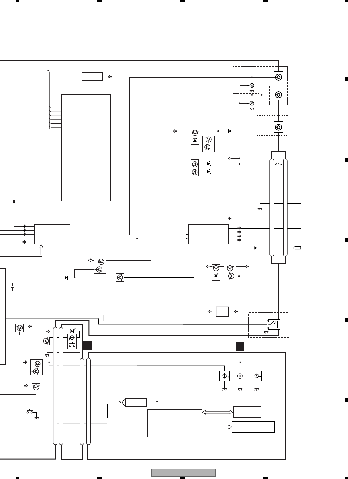
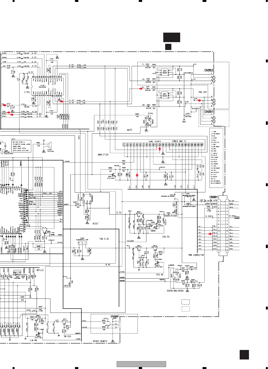
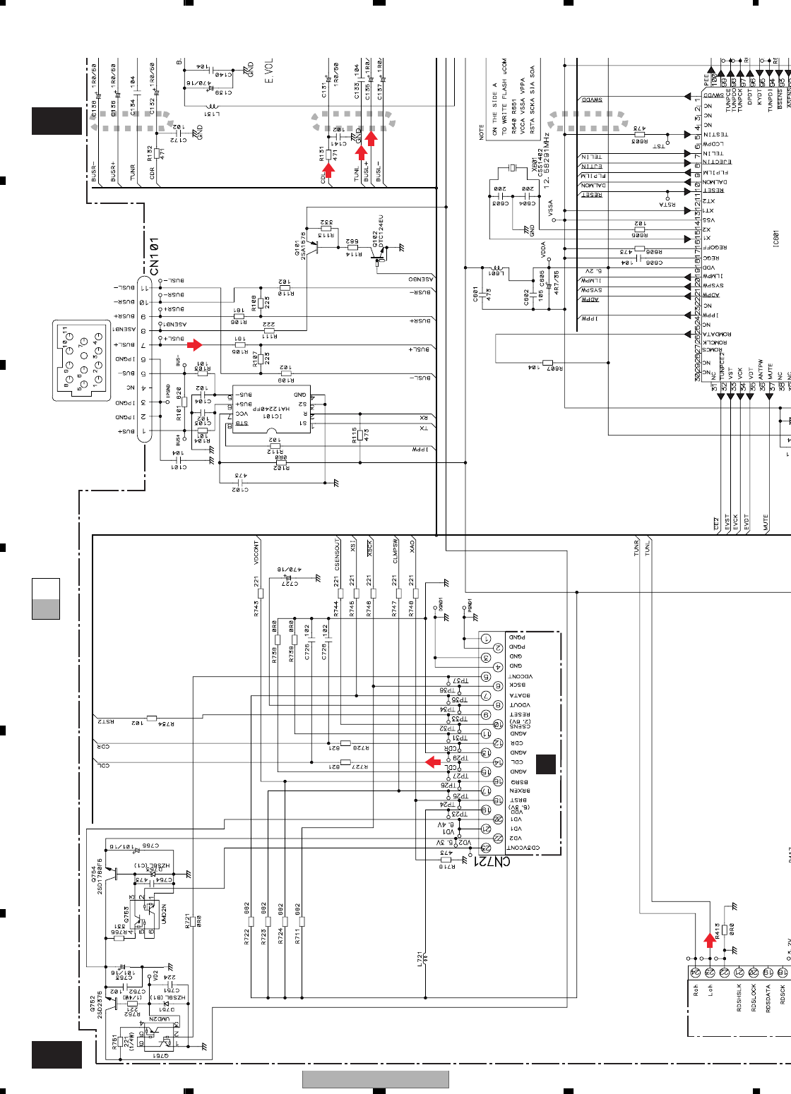
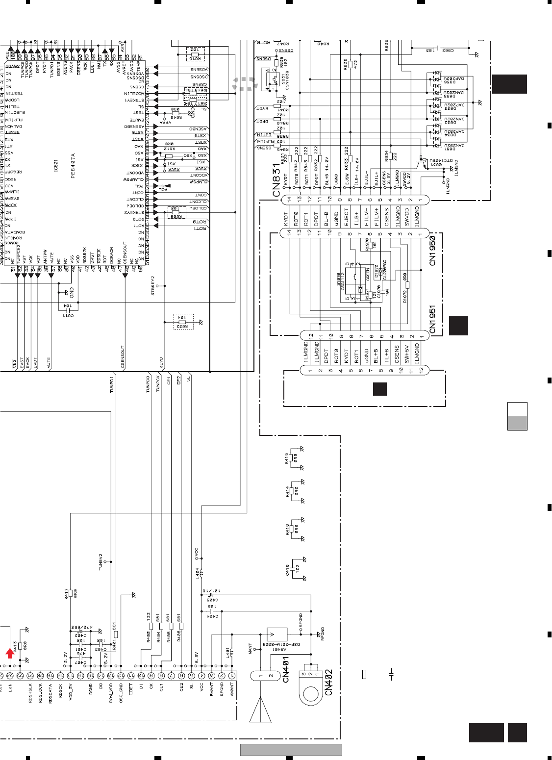
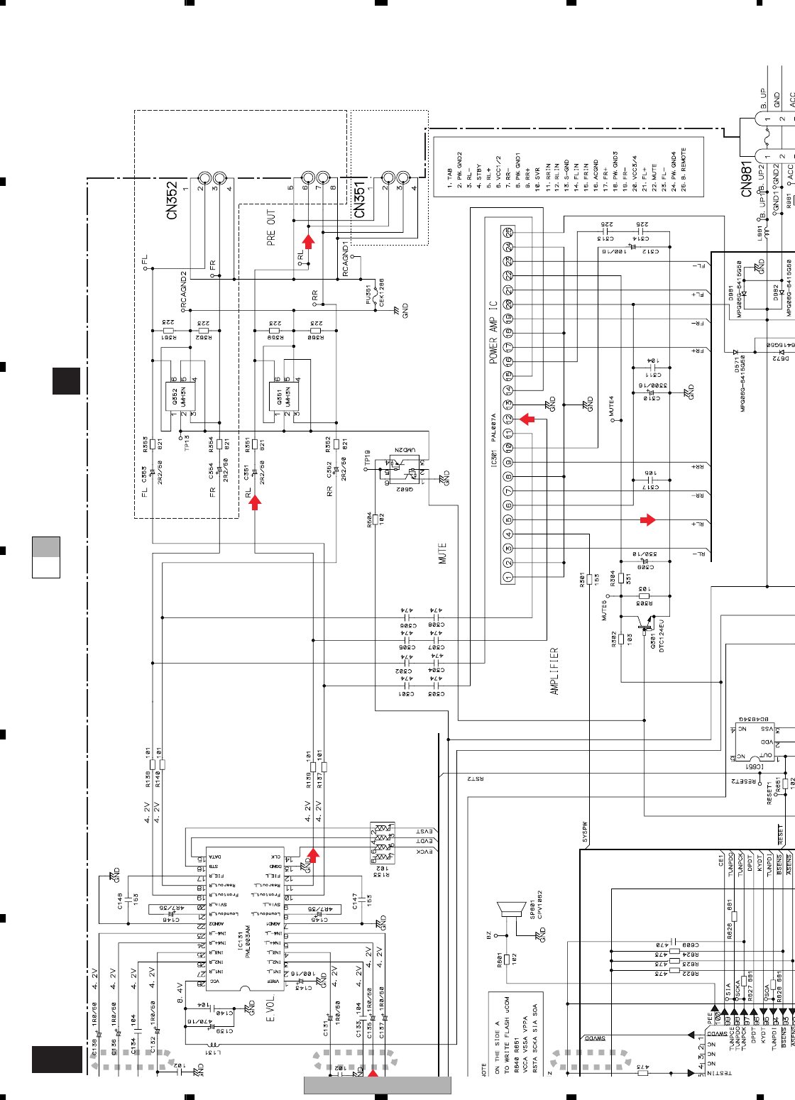
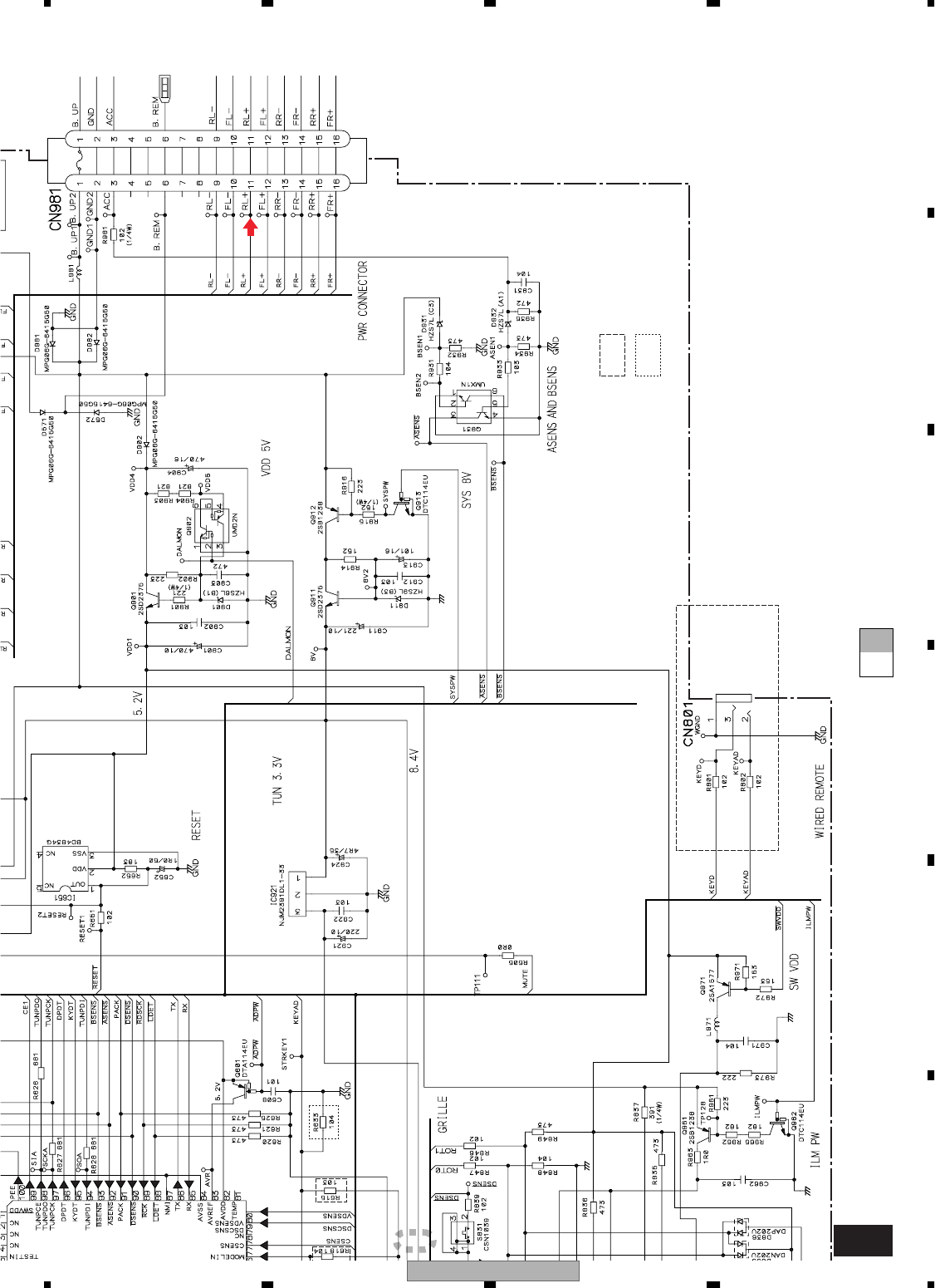
3.2 OVERALL CONNECTION DIAGRAM(GUIDE PAGE)
A-a A-b
A-a A-b
A-b
A-a
Large size
SCH diagram
Guide page
Detailed page
Note: When ordering service parts, be sure to refer to " EXPLODED VIEWS AND PARTS LIST" or
"ELECTRICAL PARTS LIST". A-a
A B
For resistors and capacitors in the circuit diagrams, their resistance values or
capacitance values are expressed in codes:
Ex. *Resistors
Code Practical value
123 12k ohms
103 10k ohms
*Capacitors
Code Practical value
103 0.01uF
101/10 100uF/10V
Symbol indicates a resistor.
No differentiation is made between chip resistors and
discrete resistors.
NOTE :
Symbol indicates a capacitor.
No differentiation is made between chip capacitors and
discrete capacitors.
The > mark found on some component parts indicates
the importance of the safety factor of the part.
Therefore, when replacing, be sure to use parts of
identical designation.
CN1901
BPANEL UNIT
FM/AM TUNER UNIT
DETACH
SENSE
C
CN901
D
SYSTEM CONTROLLER
CD : 0.0dBs
IP-BUS : 2.2dBs
FM(100%) : -19.5dBs
AM(30%) : -30dBs
EJECT
DEH-P460MP/XM/UC 19
5678
5678
C
D
F
A
B
E
A-b
A-a A-b
A-a A-b
A-b
A-a
A
ATUNER AMP UNIT
DETACH
SENSE
600µH
CEK1208
10A
>
>
FRONT
OUTPUT
REAR
OUTPUT
WIRED
REMOTE
CONTROL
L
LER
: UC model only
: ES model only
REAR
OUTPUT
FM : 31.6dBs
AM : 21.1dBs
CD : 36.1dBs
IP-BUS : 36.3dBs
FM : 5.6dBs
AM : -4.9dBs
CD : 10.1dBs
IP-BUS : 10.3dBs
3A
FM : 4.8dBs
AM : -5.7dBs
CD : 9.3dBs
IP-BUS : 9.5dBs
DEH-P460MP/XM/UC 21
5678
5678
C
D
F
A
B
E
A-a A-b
A-a
A-a
A-b
B
4
For resistors and capacitors in the circuit diagrams, their resistance values or
capacitance values are expressed in codes:
Ex. *Resistors
Code Practical value
123 12k ohms
103 10k ohms
*Capacitors
Code Practical value
103 0.01uF
101/10 100uF/10V
Symbol indicates a resistor.
No differentiation is made between chip resistors and
discrete resistors.
NOTE :
Symbol indicates a capacitor.
No differentiation is made between chip capacitors and
discrete capacitors.
The > mark found on some component parts indicates
the importance of the safety factor of the part.
Therefore, when replacing, be sure to use parts of
identical designation.
CN1901
B
PANEL UNIT
FM/AM TUNER UNIT
DETACH
SENSE
C
SYSTEM CONTROLLER
EJECT
DEH-P460MP/XM/UC 27
5678
5678
C
D
F
A
B
E
D-b
D
470P
R01
C722
1
C906 R22
C910
2R2
16.934MHz
SWITCHES:
CD CORE UNIT(S10WMA)
S901 : HOME SWITCH.........ON-OFF
S902 : CLAMP SWITCH.......ON-OFF
S903 : DSCSNS SWITCH.....ON-OFF
S904 : 12EJ SWITCH............ON-OFF
S905 : 8EJ SWITCH..............ON-OFF
The underlined indicates the switch position.
A
D
CN721
CD CORE UNIT(S10WMA)
MICRO COMPUTER
1.5 REGULATOR
3.3 REGULATOR
Pull-down
!
6
^
&
SIGNAL LINE
FOCUS SERVO LINE
TRACKING SERVO LINE
CARRIAGE SERVO LINE
SPINDLE SERVO LINE
F
T
C
S
DEH-P460MP/XM/UC
30
1234
1234
C
D
F
A
B
E
D-a D-b
D-b 12
16.934MHz
SWITCHES:
CD CORE UNIT(S10WMA)
S901 : HOME SWITCH.........ON-OFF
S902 : CLAMP SWITCH.......ON-OFF
S903 : DSCSNS SWITCH.....ON-OFF
S904 : 12EJ SWITCH............ON-OFF
S905 : 8EJ SWITCH..............ON-OFF
The underlined indicates the switch position.
D
CD CORE UNIT(S10WMA)
1.5 REGULATOR
!
SIGNAL LINE
FOCUS SERVO LINE
TRACKING SERVO LINE
CARRIAGE SERVO LINE
SPINDLE SERVO LINE
F
T
C
S
DEH-P460MP/XM/UC
32
1234
1234
C
D
F
A
B
E
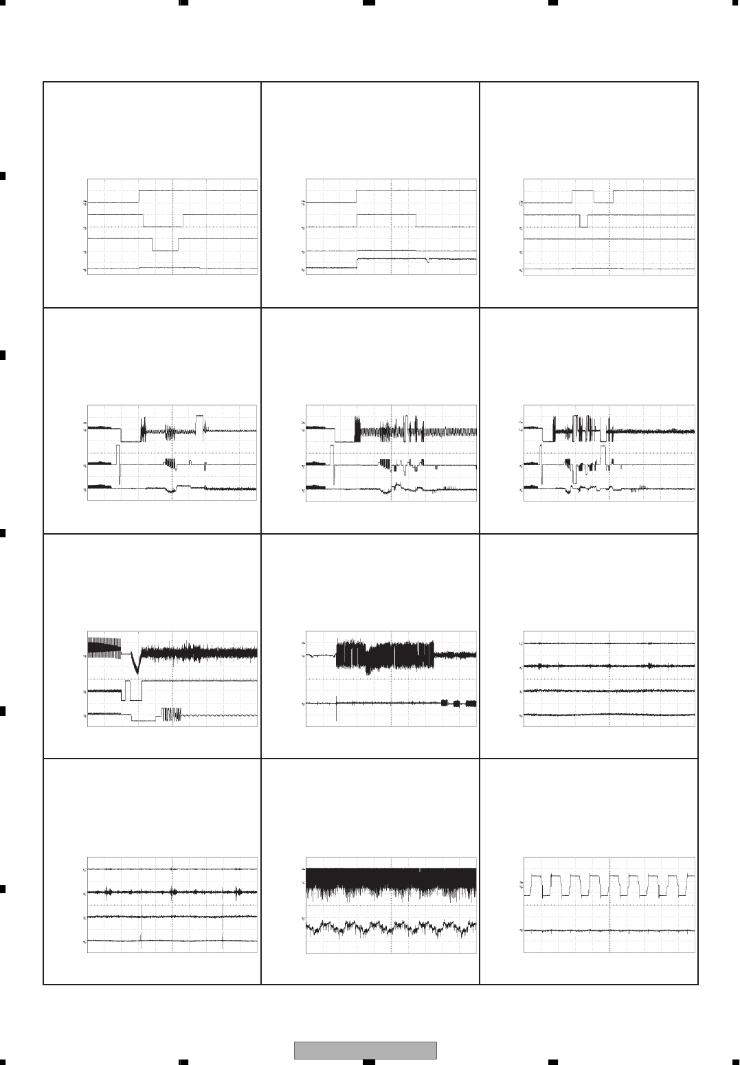
- Waveforms Note : 1. The encircled numbers denote measuring points in the circuit diagram.
2. Reference voltage REFO1(1.65V)
1 DSCSNS
2 8SNS
3 12SNS
4 LOEJ
5V/div
5V/div
5V/div
5V/div
500ms/div
12 cm CD Loading operation
Ref.:
GND
Mode:
Normal
1 DSCSNS
2 8SNS
3 12SNS
4 LOEJ
5V/div
5V/div
5V/div
5V/div
500ms/div
Ref.:
GND
Mode:
Normal
1 DSCSNS
5 CLCONT
4 LOEJ
6 VD
5V/div
5V/div
5V/div
10V/div
500ms/div
12 cm CD Loading operation 8 cm CD Loading operation
Ref.:
GND
Mode:
Normal
0 FIN
! RFOK
7 SIN
200mV/div
2V/div
2V/div
500ms/div
12 cm CD-DA Source On setup operation
Ref.:
REFO
Mode:
Normal
# FE
0 FIN
@ TE
9 TIN
500mV/div
500mV/div
500mV/div
500mV/div
20ms/div
Ref.:
REFO
Mode:
Normal
@ TE
# FE
500mV/div
500mV/div
200ms/div
Source On setup operation CD-DA Play operation
Ref.:
REFO
Mode:
Normal
# FE
0 FIN
@ TE
9 TIN
500mV/div
500mV/div
500mV/div
500mV/div
20ms/div
CD-ROM play operation(Regular track Jump)
Ref.:
REFO
Mode:
Normal
$ MDX
7 SIN
2V/div
1V/div
5µs/div
Ref.:
REFO
Mode:
Normal
$ MDX
7 SIN
1V/div
200mV/div
50ms/div
Spindle waveform during play operation Spindle waveform during play operation
(Wider)
Ref.:
REFO
Mode:
Normal
7 SIN
8 CIN
9 TIN
1V/div
500mV/div
500mV/div
2s/div
12 cm CD-DA setup operation after loading 12 cm CD-ROM(3 sessions) setup operation
after loading
Ref.:
REFO
Mode:
Normal
7 SIN
8 CIN
9 TIN
1V/div
500mV/div
500mV/div
2s/div
Ref.:
REFO
Mode:
Normal
7 SIN
8 CIN
9 TIN
1V/div
500mV/div
500mV/div
1s/div
12 cm CD-ROM(1 session) setup operation
after loading
Ref.:
REFO
Mode:
Normal
DEH-P460MP/XM/UC 33
5678
5678
C
D
F
A
B
E
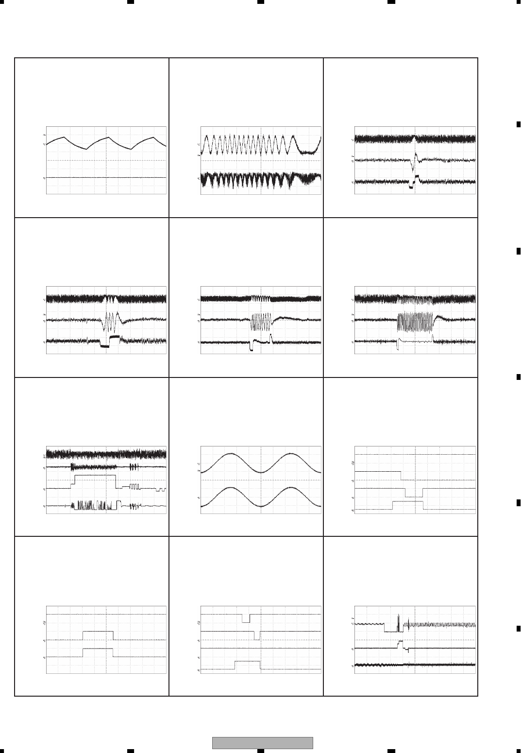
0 FIN
# FE
500mV/div
500mV/div
200ms/div
Focus Search waveform
Ref.:
REFO
Mode:
TEST
% RFAGC
@ TE
9 TIN
1V/div
500mV/div
500mV/div
500µs/div
Ref.:
REFO
Mode:
TEST
@ TE
% RFAGC
500mV/div
500mV/div
2ms/div
Track Open waveform 1 Track Jump waveform
Ref.:
REFO
Mode:
TEST
% RFAGC
@ TE
8 CIN
7 SIN
1V/div
1V/div
500mV/div
2V/div
200ms/div
Search operation(Outter to Inner)
Ref.:
REFO
Mode:
Normal
1 DSCSNS
2 8SNS
3 12SNS
4 LOEJ
5V/div
5V/div
5V/div
5V/div
500ms/div
Ref.:
GND
Mode:
Normal
^ LOUT
& ROUT
1V/div
1V/div
200µs/div
Analog audio waveform 12 cm CD Eject operation
Ref.:
AGND
Mode:
Normal
1 DSCSNS
5 CLCONT
4 LOEJ
5V/div
5V/div
5V/div
500ms/div
12 cm CD Eject operation
Ref.:
GND
Mode:
Normal
7 SIN
8 CIN
9 TIN
1V/div
500mV/div
500mV/div
500ms/div
Ref.:
REFO
Mode:
Normal
1 DSCSNS
2 8SNS
3 12SNS
4 LOEJ
5V/div
5V/div
5V/div
5V/div
500ms/div
8 cm CD Eject operation CD-DA >> CD-ROM mode change(Band key)
Ref.:
GND
Mode:
Normal
% RFAGC
@ TE
9 TIN
1V/div
500mV/div
500mV/div
500µs/div
4 Tracks Jump waveform 32 Tracks Jump waveform
Ref.:
REFO
Mode:
TEST
% RFAGC
@ TE
9 TIN
1V/div
500mV/div
500mV/div
2ms/div
Ref.:
REFO
Mode:
TEST
% RFAGC
@ TE
9 TIN
1V/div
500mV/div
500mV/div
1ms/div
10 Tracks Jump waveform
Ref.:
REFO
Mode:
TEST
DEH-P460MP/XM/UC
34
1234
1234
C
D
F
A
B
E
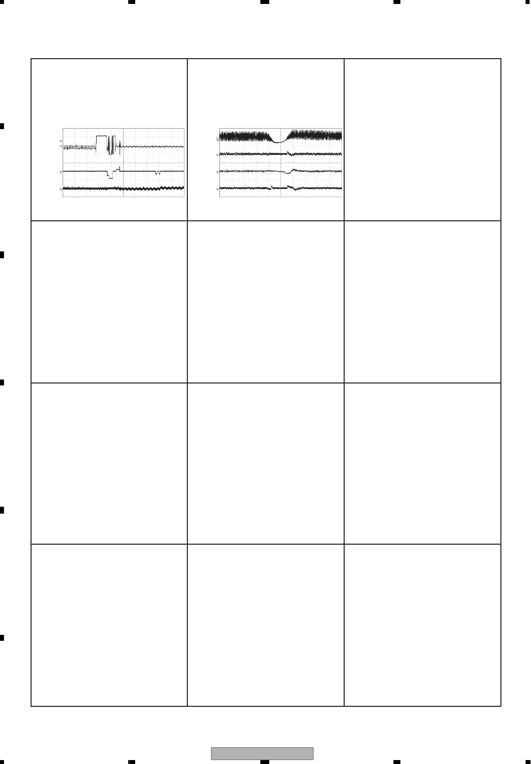
7 SIN
8 CIN
9 TIN
1V/div
500mV/div
500mV/div
500ms/div
CD-ROM >> CD-DA mode change(Band key)
Ref.:
REFO
Mode:
Normal
% RFAGC
9 TIN
@ TE
0 FIN
1V/div
1V/div
1V/div
1V/div
500µs/div
Black dot(800µm) during play
Ref.:
REFO
Mode:
Normal

DEH-P460MP/XM/UC 35
5678
5678
C
D
F
A
B
E
DEH-P460MP/XM/UC
36
1234
1234
C
D
F
A
B
E
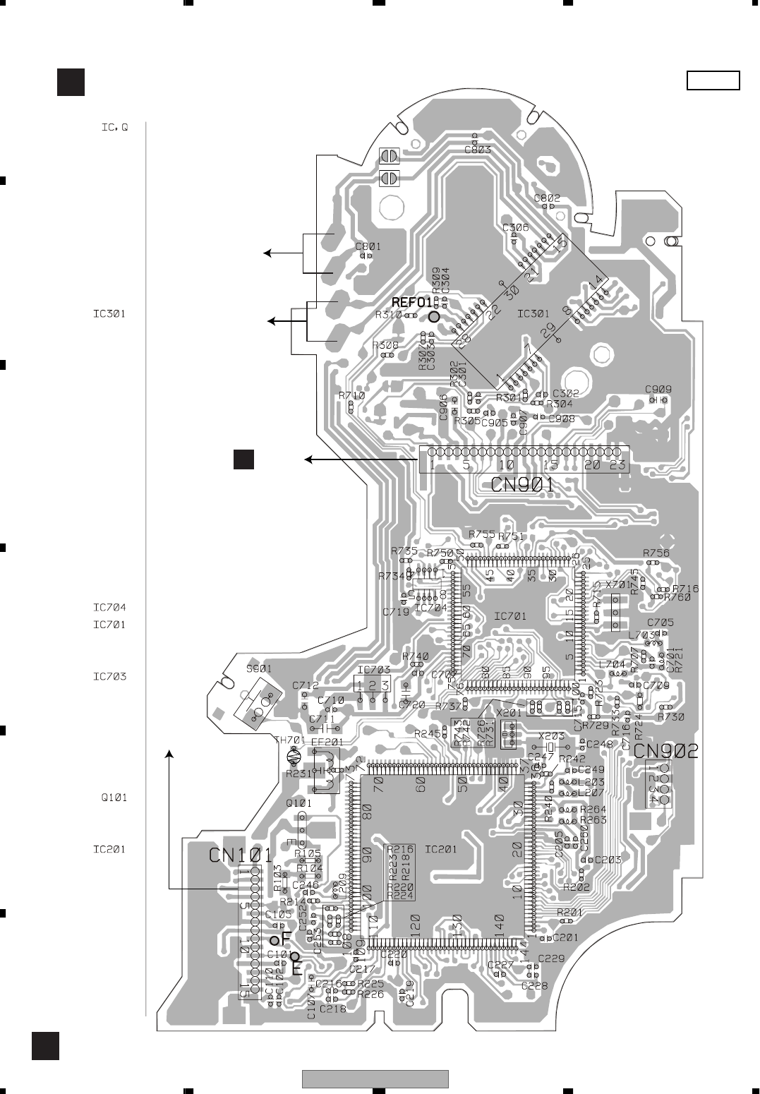
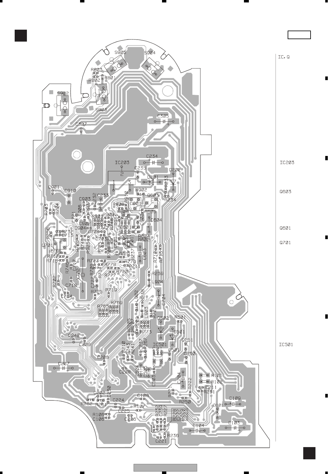
4. PCB CONNECTION DIAGRAM
4.1 TUNER AMP UNIT
Capacitor
Connector
P.C.Board Chip Part
A
ATUNER AMP UNIT
SIDE B
SIDE A
NOTE FOR PCB DIAGRAMS
1.The parts mounted on this PCB
include all necessary parts for
several destination.
For further information for
respective destinations, be sure
to check with the schematic dia-
gram.
2.Viewpoint of PCB diagrams 1
2
3
IP-BUS
DCN901
CORD
A
WIRED
REMOTE
CONTROL
DETACH
SENSE
DEH-P460MP/XM/UC
40
1234
1234
C
D
F
A
B
E
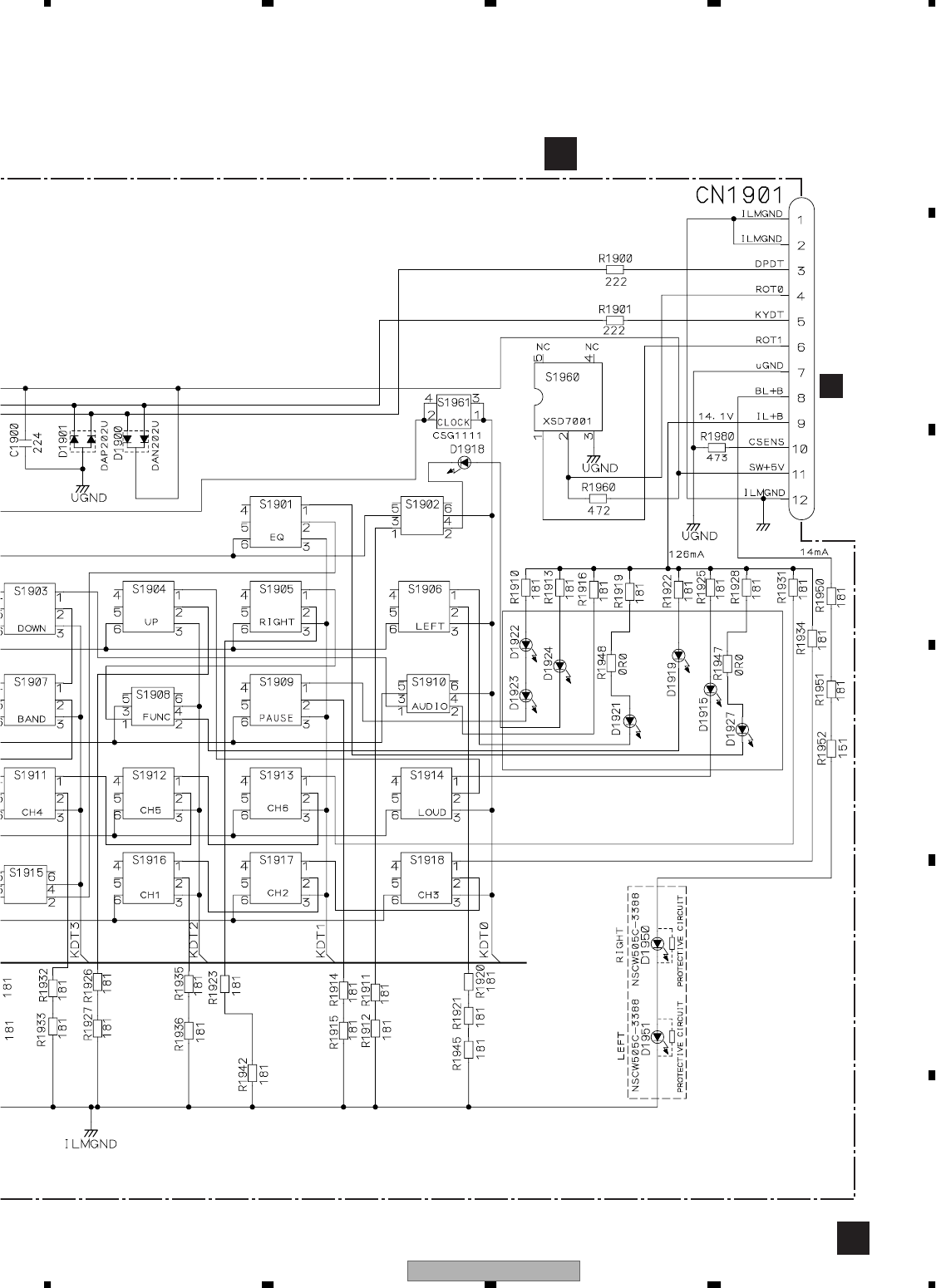
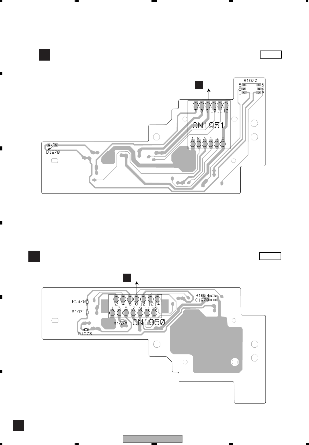
4.2 PANEL UNIT
B
BPANEL UNIT
BPANEL UNIT
SIDE A
SIDE B
CCN1901
ACN831
EJECT
DEH-P460MP/XM/UC 41
5678
5678
C
D
F
A
B
E
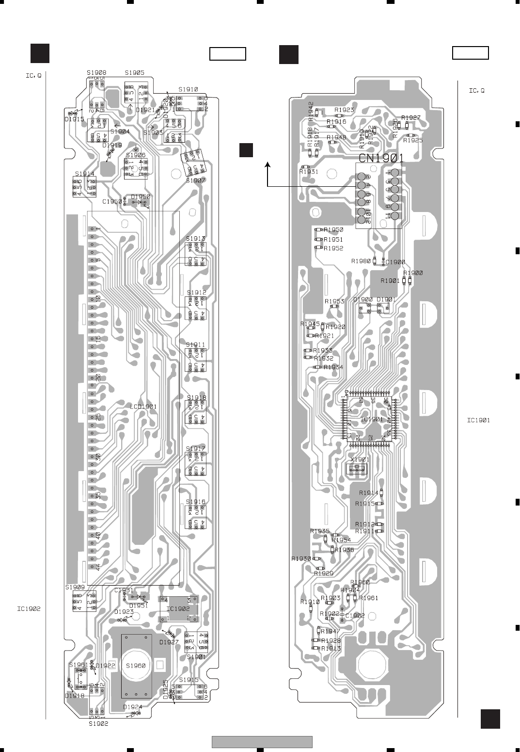
4.3 KEYBOARD UNIT
C
CKEYBOARD UNIT CKEYBOARD UNIT
SIDE A SIDE B
FUNC
AUDIO
LOUD
BAND
6
5
4
3
2
1
PAUSE
EQ
SRC-OFF
SCRL
VOLUME
BCN1951
CLOCK
DEH-P460MP/XM/UC
42
1234
1234
C
D
F
A
B
E
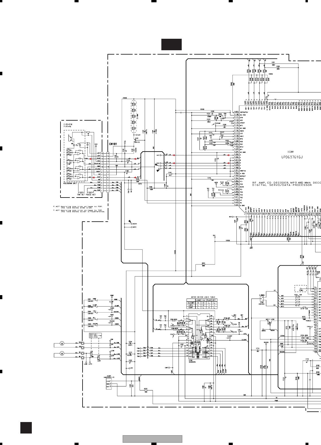
4.4 CD CORE UNIT(S10WMA)
D
DCD CORE UNIT(S10WMA) SIDE A
ACN721
M1
SPINDLE
MOTOR
M2
LOADING
/CARRIAGE
MOTOR
PICKUP UNIT(P10)(SERVICE)
HOME
DEH-P460MP/XM/UC 43
5678
5678
C
D
F
A
B
E
D
DCD CORE UNIT(S10WMA) SIDE B
CLAMP
DSCSNS
8EJ
12EJ

DEH-P460MP/XM/UC
44
1234
1234
C
D
F
A
B
E
5. ELECTRICAL PARTS LIST
NOTE:
• Parts whose parts numbers are omitted are subject to being not supplied.
• The part numbers shown below indicate chip components.
Chip Resistor
RS1/_S___J,RS1/__S___J
Chip Capacitor (except for CQS.....)
CKS....., CCS....., CSZS.....
Circuit Symbol and No. Part No.
A
Unit Number:XWM7023(DEH-P460MP, P4600MP)
:XWM7024(DEH-P4650MP)
Unit Name:Tuner Amp Unit
MISCELLANEOUS
IC 101 IC HA12240FP
IC 131 IC PML003AM
IC 301 IC PAL007A
IC 601 IC PE5407A
IC 651 IC BD4834G
IC 921 IC NJM2391DL1-33
Q 101 Transistor 2SA1576
Q 102 Transistor DTC124EU
Q 301 Transistor DTC124EU
Q 351 Transistor UMH3N
Q 352 Transistor (DEH-P460MP, P4600MP) UMH3N
Q 502 Transistor UMD2N
Q 601 Transistor DTA114EU
Q 751 Transistor UMD2N
Q 752 Transistor 2SD2375
Q 753 Transistor UMD2N
Q 754 Transistor 2SD1760F5
Q 831 Transistor DTC143EU
Q 901 Transistor 2SD2375
Q 902 Transistor UMD2N
Q 911 Transistor 2SD2375
Q 912 Transistor 2SB1238
Q 913 Transistor DTC114EU
Q 931 Transistor UMX1N
Q 961 Transistor 2SB1238
Q 962 Transistor DTC114EU
Q 971 Transistor 2SA1577
D 571 Diode MPG06G-6415G50
D 572 Diode MPG06G-6415G50
D 751 Diode HZS9L(B1)
D 753 Diode HZS6L(C1)
D 831 Diode DAN202U
D 832 Diode DAN202U
D 833 Diode DAP202U
D 834 Diode DAP202U
D 835 Diode DAN202U
D 836 Diode DAP202U
D 901 Diode HZS6L(B1)
D 902 Diode MPG06G-6415G50
D 911 Diode HZS9L(B3)
D 931 Diode HZS7L(C3)
D 932 Diode HZS7L(A1)
D 981 Diode MPG06G-6415G50
D 982 Diode MPG06G-6415G50
L 131 Inductor LACU2R2K
L 401 Inductor LACU4R7K
L 404 Inductor LACU1R0K
L 601 Inductor LACU2R2K
L 721 Inductor LACU2R2K
L 971 Inductor LACU2R2K
L 981 Choke Coil 600µH CTH1280
X 601 Radiator 12.58291MHz CSS1402
S 831 Switch(DETACH SENSE) CSN1039
FU351 Fuse 3A CEK1286
Fuse 10A CEK1208
FM/AM Tuner Unit CWE1646
SP601 Buzzer CPV1062
AR401 Surge Protector DSP-201M-S00B
RESISTORS
R 101 RS1/16S620J
R 102 RS1/16S0R0J
R 103 RS1/16S101J
R 104 RS1/16S101J
R 105 RS1/16S181J
R 106 RS1/16S181J
R 107 RS1/16S223J
R 108 RS1/16S223J
R 109 RS1/16S102J
R 110 RS1/16S102J
R 111 RS1/16S222J
R 112 RS1/16S102J
R 113 RS1/16S332J
R 114 RS1/16S562J
R 115 RS1/16S473J
R 131 RS1/16S471J
R 132 RS1/16S471J
R 133 RAB4C102J
R 137 RS1/16S101J
R 138 RS1/16S101J
R 139 RS1/16S101J
R 140 RS1/16S101J
R 301 RS1/16S153J
R 302 RS1/16S103J
R 303 RS1/16S103J
R 304 RS1/16S331J
R 351 RS1/16S821J
R 352 RS1/16S821J
Circuit Symbol and No. Part No.

DEH-P460MP/XM/UC 45
5678
5678
C
D
F
A
B
E
R 353 (DEH-P460MP, P4600MP) RS1/16S821J
R 354 (DEH-P460MP, P4600MP) RS1/16S821J
R 359 RS1/16S223J
R 360 RS1/16S223J
R 361 (DEH-P460MP, P4600MP) RS1/16S223J
R 362 (DEH-P460MP, P4600MP) RS1/16S223J
R 401 RS1/16S681J
R 403 RS1/16S122J
R 404 RS1/16S681J
R 405 RS1/16S681J
R 406 RS1/16S681J
R 413 RS1/16S0R0J
R 414 RS1/16S0R0J
R 415 RS1/16S0R0J
R 416 RS1/16S0R0J
R 417 RS1/16S0R0J
R 504 RS1/16S102J
R 505 RS1/16S0R0J
R 601 RS1/16S102J
R 603 RS1/16S473J
R 605 RS1/16S102J
R 606 RS1/16S473J
R 607 RS1/16S104J
R 609 (DEH-P460MP, P4600MP) RS1/16S103J
R 612 RS1/16S0R0J
R 615 (DEH-P460MP, P4600MP) RS1/16S103J
R 617 (DEH-P4650MP) RS1/16S104J
R 618 (DEH-P460MP, P4600MP) RS1/16S104J
R 620 RS1/16S473J
R 621 RS1/16S473J
R 622 RS1/16S473J
R 623 RS1/16S473J
R 624 RS1/16S473J
R 625 RS1/16S473J
R 626 RS1/16S681J
R 627 RS1/16S681J
R 628 RS1/16S681J
R 632 (DEH-P4650MP) RS1/16S104J
R 633 (DEH-P4650MP) RS1/16S104J
R 640 RS1/16S0R0J
R 651 RS1/16S102J
R 652 RS1/16S183J
R 711 RS1/16S682J
R 718 RS1/16S473J
R 721 RS1/16S0R0J
R 722 RS1/16S682J
R 723 RS1/16S682J
R 724 RS1/16S682J
R 727 RS1/16S821J
R 728 RS1/16S821J
R 734 RS1/16S102J
R 738 RS1/16S0R0J
R 739 RS1/16S0R0J
R 743 RS1/16S221J
R 744 RS1/16S221J
R 745 RS1/16S221J
R 746 RS1/16S221J
R 747 RS1/16S221J
R 748 RS1/16S221J
R 751 RD1/4PU221J
Circuit Symbol and No. Part No.
R 752 RD1/4PU221J
R 755 RS1/16S331J
R 801 (DEH-P460MP, P4600MP) RS1/16S102J
R 802 (DEH-P460MP, P4600MP) RS1/16S102J
R 831 RS1/16S222J
R 832 RS1/16S222J
R 833 RS1/16S222J
R 834 RS1/16S222J
R 835 RS1/16S473J
R 836 RS1/16S473J
R 837 RD1/4PU391J
R 838 RS1/16S102J
R 839 RS1/16S102J
R 840 RS1/16S102J
R 841 RS1/16S102J
R 842 RS1/16S222J
R 843 RS1/16S222J
R 845 RS1/16S102J
R 846 RS1/16S102J
R 847 RS1/16S102J
R 848 RS1/16S104J
R 849 RS1/16S473J
R 901 RD1/4PU221J
R 902 RS1/16S223J
R 903 RS1/16S821J
R 904 RS1/16S821J
R 914 RS1/16S152J
R 915 RD1/4PU152J
R 916 RS1/16S223J
R 931 RS1/16S104J
R 932 RS1/16S473J
R 933 RS1/16S103J
R 934 RS1/16S473J
R 935 RS1/16S472J
R 961 RS1/16S223J
R 962 RS1/16S182J
R 963 RS1/16S1R0J
R 965 RS1/16S182J
R 971 RS1/16S153J
R 972 RS1/16S153J
R 973 RS1/16S222J
R 981 RD1/4PU102J
CAPACITORS
C 101 CKSRYB104K16
C 102 CKSRYB473K25
C 103 CKSRYB102K50
C 104 CKSRYB102K50
C 131 CEJQ1R0M50
C 132 CEJQ1R0M50
C 133 CKSRYB104K16
C 134 CKSRYB104K16
C 135 CEJQ1R0M50
C 136 CEJQ1R0M50
C 137 CEJQ1R0M50
C 138 CEJQ1R0M50
C 139 CEJQ470M16
C 140 CKSRYB104K16
C 141 CKSRYB102K50
Circuit Symbol and No. Part No.

DEH-P460MP/XM/UC
46
1234
1234
C
D
F
A
B
E
C 143 CEJQ100M16
C 145 CEJQ4R7M35
C 146 CEJQ4R7M35
C 147 CKSRYB153K50
C 148 CKSRYB153K50
C 172 CKSRYB102K50
C 301 CKSRYB474K10
C 302 CKSRYB474K10
C 303 CKSRYB474K10
C 304 CKSRYB474K10
C 305 CKSRYB474K10
C 306 CKSRYB474K10
C 307 CKSRYB474K10
C 308 CKSRYB474K10
C 309 CEJQ330M10
C 310 3300µF/16V CCH1486
C 311 CKSRYB104K25
C 312 CEHAR100M16
C 313 CKSQYB225K10
C 314 CKSQYB225K10
C 317 CKSQYB105K16
C 351 CEJQ2R2M50
C 352 CEJQ2R2M50
C 353 (DEH-P460MP, P4600MP) CEJQ2R2M50
C 354 (DEH-P460MP, P4600MP) CEJQ2R2M50
C 401 CKSRYB103K50
C 402 CEJQ470M6R3
C 403 CKSRYB103K50
C 404 CKSRYB103K50
C 405 CEJQ101M16
C 407 CKSYB475K10
C 410 CKSRYB102K50
C 601 CKSRYB473K25
C 602 CKSRYB105K10
C 603 CCSRCH200J50
C 604 CCSRCH200J50
C 605 CEJQ4R7M35
C 606 CKSRYB104K16
C 608 CCSRCH101J50
C 609 CCSRCH470J50
C 611 CKSRYB104K16
C 652 CEJQ1R0M50
C 725 CKSRYB102K50
C 726 CKSRYB102K50
C 727 470µF/16V CCH1331
C 751 CKSRYB224K10
C 752 CKSRYB102K50
C 753 CEJQ101M16
C 754 CKSRYB473K25
C 755 CEJQ101M16
C 901 CEJQ470M10
C 902 CKSRYB103K50
C 903 CKSRYB472K50
C 904 470µF/16V CCH1331
C 911 CEJQ221M10
C 912 CKSRYB103K50
C 913 CEJQ101M16
C 921 CEJQ220M10
C 922 CKSRYB103K50
C 924 CEJQ4R7M35
Circuit Symbol and No. Part No.
C 931 CKSRYB104K25
C 962 CKSRYB103K50
C 971 CKSRYB104K25
C
Unit Number:XWM7031(DEH-P460MP, P4600MP)
:XWM7032(DEH-P4650MP)
Unit Name:Keyboard Unit
MISCELLANEOUS
IC 1901 IC PD6340A
IC 1902 IC RS-140
D 1900 Diode DAN202U
D 1901 Diode DAP202U
D 1915 LED CL-195PG-CD
D 1918 LED CL-195PG-CD
D 1919 LED CL-195PG-CD
D 1921 LED CL-195PG-CD
D 1922 LED CL-195PG-CD
D 1923 LED CL-195PG-CD
D 1924 LED CL-195PG-CD
D 1927 LED CL-195PG-CD
D 1950 LED NSCW505C-3388
D 1951 LED NSCW505C-3388
X 1901 Ceramic Resonator 4.97MHz CSS1573
S 1901 Switch CSG1107
S 1902 Push Switch CSG1112
S 1903 Switch CSG1107
S 1904 Switch CSG1107
S 1905 Switch CSG1107
S 1906 Switch CSG1107
S 1907 Switch CSG1107
S 1908 Push Switch CSG1112
S 1909 Switch CSG1107
S 1910 Push Switch CSG1112
S 1911 Switch CSG1107
S 1912 Switch CSG1107
S 1913 Switch CSG1107
S 1914 Switch CSG1107
S 1915 Push Switch CSG1112
S 1916 Switch CSG1107
S 1917 Switch CSG1107
S 1918 Switch CSG1107
S 1960 Encoder(VOLUME) XSD7001
S 1961 Push Switch CSG1111
LCD1901 LCD (DEH-P460MP, P4600MP) XAW7004
LCD1901 LCD (DEH-P4650MP) XAW7002
RESISTORS
R 1900 RS1/16S222J
R 1901 RS1/16S222J
R 1902 RS1/16S2R2J
R 1904 RS1/16S121J
R 1910 RS1/16S181J
R 1911 RS1/16S181J
R 1912 RS1/16S181J
R 1913 RS1/16S181J
R 1914 RS1/16S181J
R 1915 RS1/16S181J
Circuit Symbol and No. Part No.

DEH-P460MP/XM/UC 47
5678
5678
C
D
F
A
B
E
R 1916 RS1/16S181J
R 1917 RS1/16S181J
R 1918 RS1/16S181J
R 1919 RS1/16S181J
R 1920 RS1/16S181J
R 1921 RS1/16S181J
R 1922 RS1/16S181J
R 1923 RS1/16S181J
R 1925 RS1/16S181J
R 1926 RS1/16S181J
R 1927 RS1/16S181J
R 1928 RS1/16S181J
R 1929 RS1/16S181J
R 1930 RS1/16S181J
R 1931 RS1/16S181J
R 1932 RS1/16S181J
R 1933 RS1/16S181J
R 1934 RS1/16S181J
R 1935 RS1/16S181J
R 1936 RS1/16S181J
R 1942 RS1/16S181J
R 1945 RS1/16S181J
R 1947 RS1/16S0R0J
R 1948 RS1/16S0R0J
R 1950 RS1/16S181J
R 1951 RS1/16S181J
R 1952 RS1/16S151J
R 1960 RS1/16S472J
R 1980 RS1/16S473J
CAPACITORS
C 1900 CKSRYB224K10
C 1902 CKSYF106Z10
B
Unit Number:CWM8758
Unit Name:Panel Unit
MISCELLANEOUS
D 1970 LED CL220PGC
S 1970 Push Switch(EJECT) CSG1112
RESISTORS
R 1970 RS1/16S101J
R 1971 RS1/16S101J
R 1972 RS1/16S0R0J
CAPACITORS
C 1970 CKSRYB104K16
D
Unit Number:CWX2851
Unit Name:CD CORE UNIT(S10WMA)
MISCELLANEOUS
IC 201 IC UPD63761GJ
Circuit Symbol and No. Part No.
IC 203 IC NJM2391DL1-33
IC 301 IC BA5835FM
IC 501 IC S-L2980A15MC-C6A
IC 701 IC PE5402A
IC 703 IC S-812C33AUA-C2N
Q 101 Transistor 2SB1132
Q 601 Transistor IMH20
Q 603 Transistor 2SB709A
Q 701 Transistor UN2111
D 101 Diode 1SS355
D 601 Diode MA152WA
L 203 Inductor CTF1389
L 207 Inductor CTF1389
L 209 Inductor CTF1389
L 703 Inductor CTF1389
X 201 Ceramic Resonator 16.934MHzCSS1603
X 701 Ceramic Resonator 4.00MHz CSS1652
S 901 Switch(HOME) CSN1051
S 902 Switch(CLAMP) CSN1051
S 903 Spring Switch(DSCSNS) CSN1052
S 904 Switch(12EJ) CSN1051
S 905 Switch(8EJ) CSN1051
RESISTORS
R 101 RS1/10S1R5J
R 102 RS1/10S1R5J
R 103 RS1/10S1R5J
R 104 RS1/10S1R5J
R 105 RS1/10S1R5J
R 107 RS1/16SS0R0J
R 201 RS1/16SS102J
R 202 RS1/16SS333J
R 205 RS1/16SS473J
R 207 RS1/16SS473J
R 209 RS1/16SS473J
R 214 RS1/16SS472J
R 216 RS1/16SS472J
R 218 RS1/16SS472J
R 220 RS1/16SS472J
R 221 RS1/16SS103J
R 222 RS1/16SS103J
R 223 RS1/16SS0R0J
R 224 RS1/16SS0R0J
R 225 RS1/16SS103J
R 226 RS1/16SS393J
R 227 RS1/16SS562J
R 228 RS1/16SS122J
R 229 RS1/16SS472J
R 231 RS1/16SS0R0J
R 232 RS1/16SS122J
R 233 RS1/16SS0R0J
R 240 RS1/16SS0R0J
R 241 RS1/16SS333J
R 242 RS1/16SS0R0J
R 243 RS1/16SS333J
R 245 RS1/16SS333J
R 250 RS1/16SS0R0J
R 256 RS1/16SS0R0J
R 261 RS1/16S0R0J
Circuit Symbol and No. Part No.

DEH-P460MP/XM/UC
48
1234
1234
C
D
F
A
B
E
R 262 RS1/16S0R0J
R 263 RS1/16S0R0J
R 264 RS1/16S0R0J
R 267 RS1/16S0R0J
R 301 RS1/16SS183J
R 302 RS1/16SS822J
R 304 RS1/16SS183J
R 305 RS1/16SS822J
R 307 RS1/16SS183J
R 308 RS1/16SS183J
R 309 RS1/16SS183J
R 310 RS1/16SS183J
R 501 RS1/16SS0R0J
R 601 RS1/16S101J
R 602 RS1/16S101J
R 603 RS1/16S223J
R 604 RS1/16S223J
R 605 RS1/16SS103J
R 606 RS1/16S0R0J
R 701 RS1/16S0R0J
R 702 RS1/16SS0R0J
R 703 RS1/16SS104J
R 704 RS1/16SS104J
R 705 RS1/16SS221J
R 706 RS1/16SS221J
R 707 RS1/16SS0R0J
R 708 RS1/16SS221J
R 709 RS1/16SS473J
R 710 RS1/16SS102J
R 711 RS1/16SS102J
R 712 RS1/16SS102J
R 713 RS1/16SS102J
R 714 RS1/16SS473J
R 715 RS1/16SS0R0J
R 716 RS1/16SS472J
R 719 RS1/16SS221J
R 720 RS1/16SS471J
R 721 RS1/16S0R0J
R 724 RS1/16S473J
R 725 RS1/16SS222J
R 726 RS1/16SS103J
R 727 RS1/16SS473J
R 729 RS1/16SS223J
R 730 RS1/16SS473J
R 731 RS1/16SS104J
R 732 RS1/16SS104J
R 733 RS1/16SS104J
R 735 RS1/16SS473J
R 737 RS1/16SS104J
R 740 RS1/16SS473J
R 742 RS1/16SS104J
R 745 RS1/16SS473J
R 746 RS1/16SS104J
R 750 RS1/16SS473J
R 754 RS1/16SS102J
R 755 RS1/16SS102J
R 756 RS1/16SS104J
R 765 RAB4CQ221J
R 769 RAB4CQ221J
R 773 RAB4CQ221J
Circuit Symbol and No. Part No.
R 777 RS1/16SS221J
R 778 RS1/16SS221J
R 779 RS1/16SS221J
R 901 RAB4CQ221J
R 902 RS1/16S0R0J
R 905 RS1/16SS221J
R 906 RS1/16SS221J
R 908 RS1/16SS0R0J
R 910 RS1/16SS0R0J
CAPACITORS
C 101 CKSSYB104K10
C 102 CKSSYB104K10
C 103 100µF/16V CCH1504
C 104 47µF/6.3V CCH1506
C 105 CKSSYB104K10
C 106 CCSSCH101J50
C 107 CKSRYB224K16
C 108 CKSSYB104K10
C 110 CKSSYB104K10
C 201 CKSSYB471K50
C 202 CKSSYB104K10
C 203 CKSSYB104K10
C 204 22µF/6.3V CCH1507
C 205 CKSSYB104K10
C 207 220µF/4V CCH1590
C 208 CKSSYB104K10
C 209 CKSSYB104K10
C 216 CKSSYB332K50
C 217 CKSSYB104K10
C 218 CKSSYB223K16
C 219 CKSSYB104K10
C 220 CKSSYB103K16
C 221 CKSSYB104K10
C 222 CCSSCH560J50
C 223 CCSSCH5R0C50
C 224 CKSSYB104K10
C 225 CKSSYB103K16
C 226 CCSSCH680J50
C 227 CCSSCH470J50
C 228 CKSSYB682K25
C 230 CKSSYB104K10
C 232 CKSSYB104K10
C 233 10µF/6.3V CCH1470
C 234 220µF/4V CCH1590
C 235 CKSRYB224K16
C 237 CKSSYB104K10
C 239 CCSSCH330J50
C 242 CKSSYB104K10
C 246 CKSSYB104K10
C 250 CKSRYB102K50
C 251 CKSRYB102K50
C 260 CKSSYB104K10
C 301 CKSSYB221K50
C 302 CKSSYB221K50
C 303 CKSSYB472K25
C 304 CKSSYB103K16
C 305 100µF/16V CCH1504
C 306 CKSSYB104K10
C 307 CKSSYB104K10
Circuit Symbol and No. Part No.

DEH-P460MP/XM/UC 49
5678
5678
C
D
F
A
B
E
C 501 CKSRYB224K16
C 505 CKSQYB475K6R3
C 601 CCSRCH102J50
C 602 CCSRCH102J50
C 603 4.7µF/25V CCH1568
C 604 4.7µF/25V CCH1568
C 701 CKSSYB104K10
C 702 CKSSYB471K50
C 703 CKSSYB103K16
C 704 4.7µF/25V CCH1592
C 706 CKSSYB104K10
C 707 CKSSYB104K10
C 712 CKSRYB224K16
C 713 CKSSYB104K10
C 714 CKSSYB104K10
C 716 CKSSYB103K16
C 720 CKSQYB225K10
C 722 CKSRYB105K10
C 903 CKSSYB471K50
C 906 CKSRYB224K16
C 907 CKSSYB103K16
C 910 CKSQYB225K10
Miscellaneous Parts List
Pickup Unit(P10)(Service) CXX1641
M 1 Motor Unit(SPINDLE) CXB6007
M2 Motor Unit(LOADING/CARRIAGE)CXB8933
Circuit Symbol and No. Part No.

DEH-P460MP/XM/UC
50
1234
1234
C
D
F
A
B
E
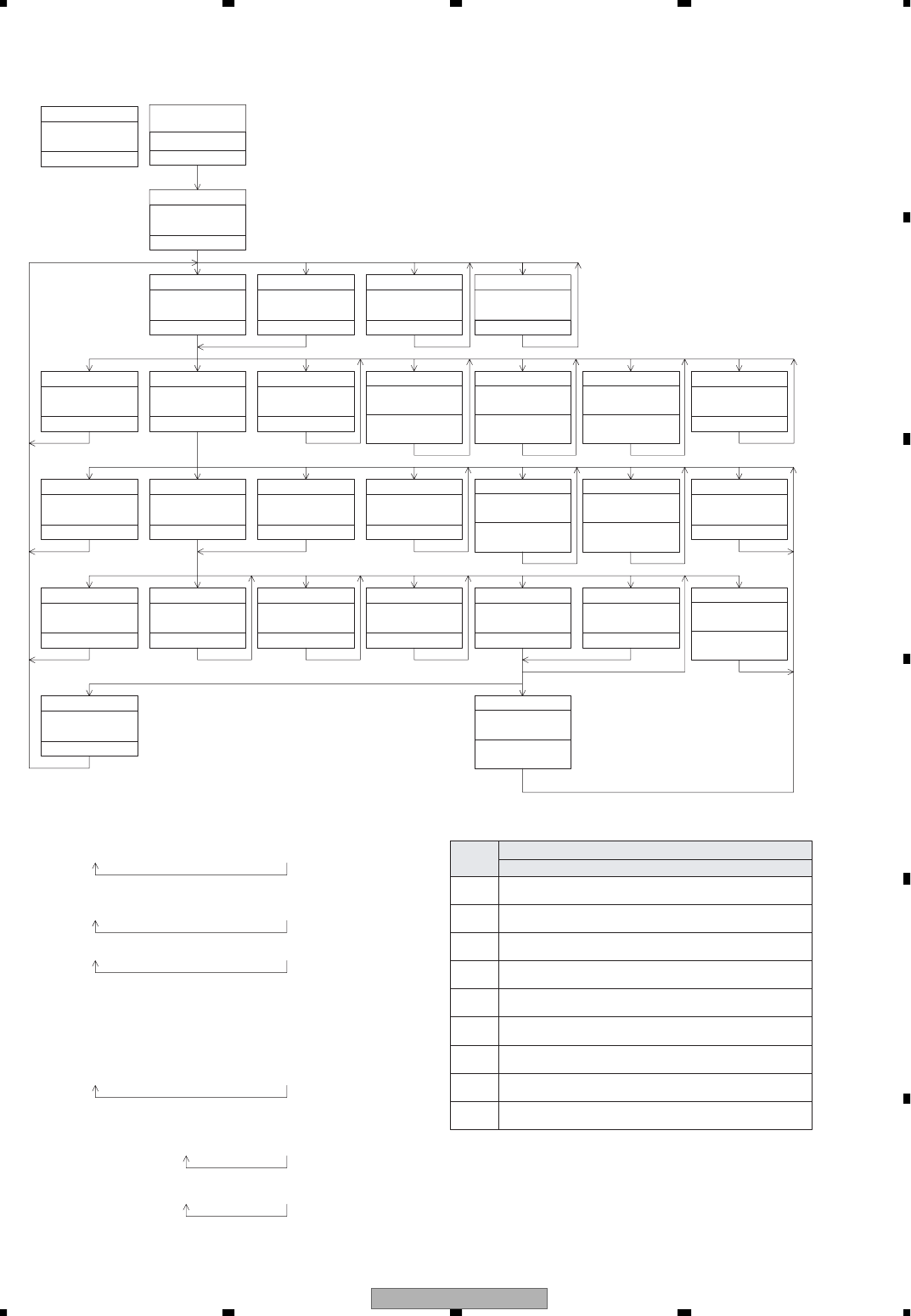
6. ADJUSTMENT
6.1 CD ADJUSTMENT
1) Cautions on adjustments
• In this product the single voltage (3.3V) is used for the
regulator. The reference voltage is the REFO1 (1.65V)
instead of the GND.
If you should mistakenly short the REFO1 with the GND
during adjustment, accurate voltage will not be obtained,
and the servo’s misoperation will apply excessive shock
to the pickup. To avoid such problems:
a. Do not mix up the REFO1 with the GND when
connecting the (-) probe of measuring instruments.
Especially on an oscilloscope, avoid connecting the (-)
probe for CH1 to the GND.
b. In many cases, measuring instruments have the same
potential as that for the (-) probe. Be sure to set the
measuring instruments to the floating state.
c. If you have mistakenly connected the REFO1 to the GND,
turn off the regulator or the power immediately.
• Before mounting and removing filters or leads for
adjustment, be sure to turn off the regulator.
• For stable circuit operation, keep the mechanism
operating for about one minute or more after the
regulator is turned on.
• In the test mode, any software protections will not
work. Avoid applying any mechanical or electrical
shock to the mechanism during adjustment.
• The RFI and RFO signals with a wide frequency range
are easy to oscillate. When observing the signals,
insert a resistor of 1k ohms in series.
• The load and eject operation is not guarantied with the
mechanism upside down. If the mechanism is blocked
due to mistaken eject operation, reset the product or
turn off and on the ACC to restore it.
2) Test mode
This mode is used to adjust the CD mechanism module.
• To enter the test mode.
While pressing the 4 and 6 keys at the same time, reset.
• To exit from the test mode.
Turn off the ACC and back up.
Notes:
a. During ejection, do not press any other keys than the
EJECT key until the loaded disc is ejected.
b. If you have pressed the (→) key or (←) key during focus
search, turn off the power immediately to protect the
actuator from damage caused by the lens stuck.
c. For the TR jump modes except 100TR, the track jump
operation will continue even if the key is released.
d. For the CRG move and 100TR jump modes, the tracking
loop will be closed at the same time when the key is
released.
e. When the power is turned off and on, the jump mode
is reset to the single TR (91), the RF amp gain is set to 0dB,
and the auto-adjustment values are reset to the default
settings.
DEH-P460MP/XM/UC 51
5678
5678
C
D
F
A
B
E
[BAND]
[BAND]
[BAND]
[BAND]
[BAND]
Power On
(T.Offset is adjusted)
TRK00
MIN00
SEC
SEC
00
[CD]or[SOURCE]
Source On
TRK MIN
[4]+[6]+Reset or
[4]+[6]+BU+ACC
Test Mode In
[3]
[1]
[1]
Power On
(T.Offset is not adjusted)
TRK99
MIN99
SEC99
[2]
[2]
[2]
[2]
Power Off
TRK MIN SEC
Power Off
TRK MIN SEC
Power Off
TRK MIN SEC
Power Off
TRK MIN SEC
Focus Close
S.Curve check
TRK91
MIN91
SEC91
[6] [1]
[3]
[6]
[3]
Focus Mode
switching
*2
TRK0xMIN0xSEC0x
Tracking Servo
Close
TRK00 MIN00 SEC00
or TRK99
MIN99
SEC99
CRG- *8
TRK00
MIN00
SEC00
or TRK99
MIN99
SEC99
[→][←]
[→][←]
[→][←]
CRG+ *8
*9
TRK00 MIN00 SEC00
or TRK99
MIN99
SEC99
Automatic adjustment
display switching
*3
TRK?? MIN?? SEC??
Applicable servomechanism
TRK
?tr MIN
?min
SEC
?sec
[6]
[3]
T.Close
Applicable servomechanism
TRK MIN SEC
RF AGC /
RF AGC coefficient display
TRK ??
MIN?? SEC ??
CRG+
TRK8x MIN8x SEC8x
or TRK9xMIN9xSEC9x
CRG-
TRK8xMIN8xSEC8x
or TRK9xMIN9xSEC9x
T.Balance adjustment /
T.Balance coefficient display
TRK?? MIN?? SEC??
F, T, RF AGC
F.Bias display switching
*7
TRK?? MIN?? SEC??
F, T AGC / F.Bias
RF AGC
TRK MIN SEC
CRG/TR Jump *5
value switching
TRK MIN SEC
CRG/TR Jump +
*4
TRK MIN SEC
CRG/TR Jump -
*4
*6
TRK MIN SEC
Tracking Open
TRK8xMIN8xSEC8x
or TRK 9xMIN 9xSEC 9x
Tracking Open
TRK8x MIN8x SEC8x
or TRK9xMIN9xSEC9x
[Key]
[BAND]
[→]
[6]
[1]
[2]
[3]
Power On/Off
CRG + / TR Jump +
(Direction of the external surface)
CRG - / TR Jump -
(Direction of the internal surface)
T.CLS and AGC and Applicable servomechanism /
AGC, AGC display switching
RF Gain switching / Offset adjustment display /
T.Balance adjustment / T.Open
F.Close, S.Curve / Rough Servo and RF AGC / F, T, RF AGC
SPDL 1X/2X switching
As for the double speed (2x), audio output cannot be supported.
F. Mode switching / Tracking Close / CRG, TR Jump switching
Test Mode
Operation
[KEY]
Contents
Display
*1) TYP → -6dB → -12dB
TRK MIN SEC TRK 06 MIN 06 SEC 06 TRK 12 MIN 12 SEC 12
*2) Focus Close → S.Curve ckeck setting → F EQ measurement setting
TRK 00 MIN 00 SEC 00 TRK 01 MIN 01 SEC 01 TRK 02 MIN 02 SEC 02
(TRK 99 MIN 99 SEC 99)
*3) F.Offset Display → T.Offset Display → Switch to the order of the original display
*4) 1TR / 32TR / 100TR
*5) Single TR → 32TR → 100TR → CRG Move
9x(8x) : 91(81) 92(82) 93(83) 94(84)
*6) Only at the time of CRG Move, 100TR Jump
*7) TRK/MIN/SEC → F.AGC → T.AGC → F.Bias → RF AGC
*8) CRG motor voltage = 2[V]
[←]
Error Rate measurement 1st-ON : ERR count beginning(30Sec)
2nd-ON : BER display data[%]
[4]
[5]
- Flow Chart
RF AMP
Gain switching
TRKGGMINGGSECGG
[2]
SPINDLE
Speed switching
TRKSPMINSPSECSP
[4]
*1
T.Close and AGC
*9) TYP(1X) → 2X → 1X
TRK MIN SEC TRK 22 MIN 22 SEC 22 TRK 11 MIN 11 SEC 11
As for the double speed (2x), audio output cannot be supported.
TYP(2X) → 1X → 2X
TRK MIN SEC TRK 11 MIN 11 SEC 11 TRK 22 MIN 22 SEC 22
?tr ?min ?sec
?tr ?min ?sec?tr ?min ?sec?tr ?min ?sec?tr ?min ?sec
DEH-P460MP/XM/UC
52
1234
1234
C
D
F
A
B
E
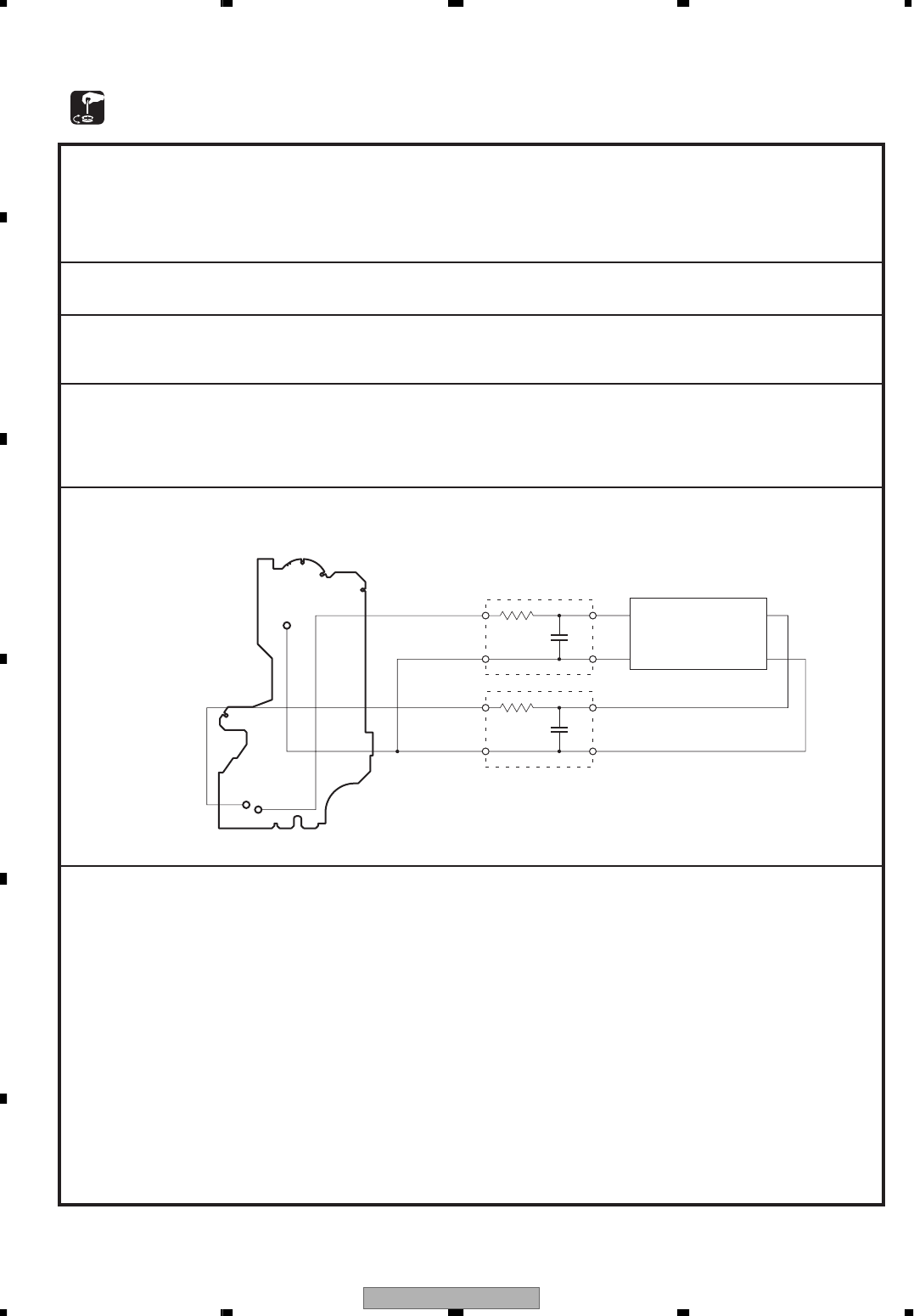
6.2 CHECKING THE GRATING AFTER CHANGING THE PICKUP UNIT
• Note :
The grating angle of the PU unit cannot be adjusted after the PU unit is changed. The PU unit in the CD mechanism
module is adjusted on the production line to match the CD mechanism module and is thus the best adjusted PU
unit for the CD mechanism module. Changing the PU unit is thus best considered as a last resort. However, if the
PU unit must be changed, the grating should be checked using the procedure below.
• Purpose :
To check that the grating is within an acceptable range when the PU unit is changed.
• Symptoms of Mal-adjustment :
If the grating is off by a large amount symptoms such as being unable to close tracking, being unable to perform
track search operations, or taking a long time for track searching.
• Method :
• Measuring Equipment
• Measuring Points
• Oscilloscope, Two L.P.F.
• E, F, REFO1
• Disc • ABEX TCD-782
• Mode • TEST MODE
• Checking Procedure
1. In test mode, load the disc and switch the 3V regulator on.
2. Using the → and ← buttons, move the PU unit to the innermost track.
3. Press key 3 to close focus, the display should read "91". Press key 2 to implement the tracking balance
adjustment the display should now read "81". Press key 3. The display will change, returning to "81" on the
fourth press.
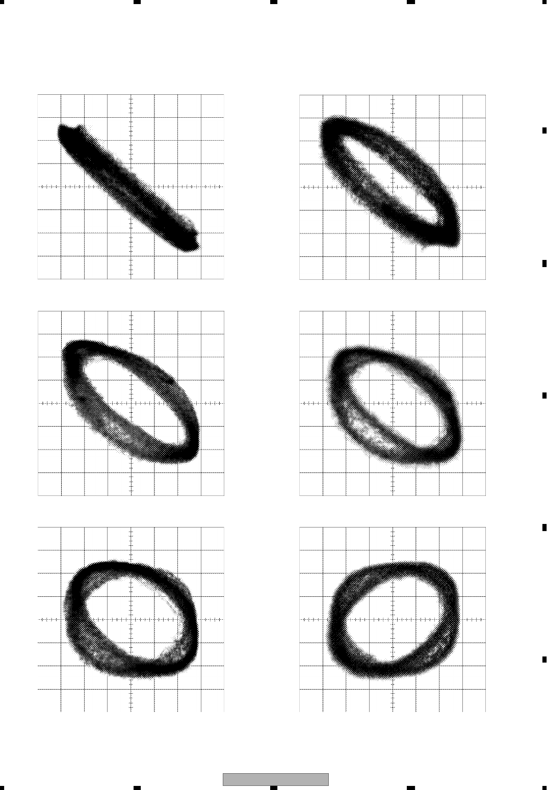
4. As shown in the diagram above, monitor the LPF outputs using the oscilloscope and check that the phase
difference is within 75° . Refer to the photographs supplied to determine the phase angle.
5. If the phase difference is determined to be greater than 75° try changing the PU unit to see if there is any
improvement. If, after trying this a number of times, the grating angle does not become less than 75° then the
mechanism should be judged to be at fault.
• Note
Because of eccentricity in the disc and a slight misalignment of the clamping center the grating waveform may be
seen to "wobble" ( the phase difference changes as the disc rotates). The angle specified above indicates the
average angle.
• Hint
Reloading the disc changes the clamp position and may decrease the "wobble".
100kΩ
390pF
100kΩ
390pF
E
VREF
F
VREF
Xch Ych
L.P.F.
L.P.F.
REFO1
FE
CD CORE UNIT(S10WMA)
Oscilloscope
DEH-P460MP/XM/UC 53
5678
5678
C
D
F
A
B
E
Grating waveform
45°
0°
75°
60°
30°
90°
Ech → Xch 20mV/div, AC
Fch → Ych 20mV/div, AC
DEH-P460MP/XM/UC
54
1234
1234
C
D
F
A
B
E
6.3 ERROR MODE
- Error Messages
If a CD is not operative or stopped during operation due to an error, the error mode is turned on and cause(s) of
the error is indicated with a corresponding number. This arrangement is intended at reducing nonsense calls from
the users and also for facilitating trouble analysis and repair work in servicing.
(1) Basic Indication Method
1) When SERRORM is selected for the CSMOD (CD mode area for the system), error codes are written to DMIN
(minutes display area) and DSEC (seconds display area). The same data is written to DMIN and DSEC. DTNO
remains in blank as before.
2) Head unit display examples
Depending on display capability of LCD used, display will vary as shown below. xx contains the error number.
8-digit display 6-digit display 4-digit display
ERROR–xx ERR–xx E–xx
(2) Error Code List
Code Class Displayed error code Description of the code and potential cause(s)
10 Electricity Carriage Home NG CRG can't be moved to inner diameter.
SERVO LSI Com- CRG can't be moved from inner diameter.
munication Error → Failure on home switch or CRG move mechanism.
Communication error between microcomputer and SERVO LSI.
11 Electricity Focus Servo NG Focusing not available.
→ Stains on rear side of disc or excessive vibrations on REWRITABLE.
12 Electricity Spindle Lock NG Spindle not locked. Sub-code is strange (not readable).
Subcode NG → Failure on spindle, stains or damages on disc, or excessive vibrations.
A disc not containing CD-R data is found.
Turned over disc are found, though rarely.
CD signal error.
17 Electricity Setup NG AGC protection doesn't work. Focus can be easily lost.
→ Damages or stains on disc, or excessive vibrations on REWRITABLE.
30 Electricity Search Time Out Failed to reach target address.
→ CRG tracking error or damages on disc.
44 Electricity ALL Skip Skip setting for all track.
(CD-R/RW)
50 Mechanism CD On Mech Error Mechanical error during CD ON.
→ Defective loading motor, mechanical lock and mechanical sensor.
A0 System Power Supply NG Power (VD) is ground faulted.
→ Failure on SW transistor or power supply (failure on connector).
Remarks: Mechanical errors are not displayed (because a CD is turned off in these errors).
Unreadable TOC does not constitute an error. An intended operation continues in this case.
Upper digits of an error code are subdivided as shown below:
1x: Setup relevant errors, 3x: Search relevant errors, Ax: Other errors.

DEH-P460MP/XM/UC 55
5678
5678
C
D
F
A
B
E
6.4 SYSTEM MICROCOMPUTER TEST PROGRAM
- PCL output
In the normal operation mode (with the detachable panel installed, the ACC switched ON, the standby mode
cancelled), shift the TESTIN (Pin 5) terminal to H.
The clock signal is output from the PCL terminal (Pin 62).
The frequency of the clock signal is 786.432kHz that is one 4th of the fundamental frequency.
The clock signal should be 786.432kHz ± 32Hz.
If the clock signal is out of the range, the X'tal (X601) should be replaced with new one.
DEH-P460MP/XM/UC
56
1234
1234
C
D
F
A
B
E
7. GENERAL INFORMATION
7.1 DIAGNOSIS
7.1.1 DISASSEMBLY
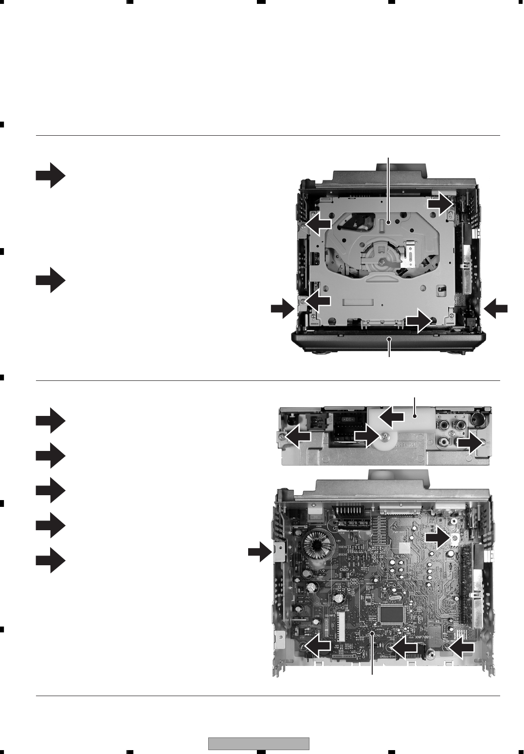
- Removing the CD Mechanism Module (Fig.1)
1
Fig.1
- Removing the Case (not shown)
Grille Assy
- Removing the Grille Assy (Fig.1)
1. Remove the Case.
CD Mechanism Module
1
1
1
1
Fig.2
Tuner Amp Unit
- Removing the Tuner Amp Unit (Fig.2)
Remove the screw and then remove
the Holder.
1
Remove the four screws.
Disconnect the connector and then remove the
CD Mechanism Module.
2Remove the two screws and then remove the
Grille Assy.
22
3
22
2
44
4
5
Remove the three screws.
2
Straighten the tabs at three locations
indicated.
4
Remove the screw and then remove
the Tuner Amp Unit.
5
1
Holder
Remove the screw.
3
DEH-P460MP/XM/UC 57
5678
5678
C
D
F
A
B
E
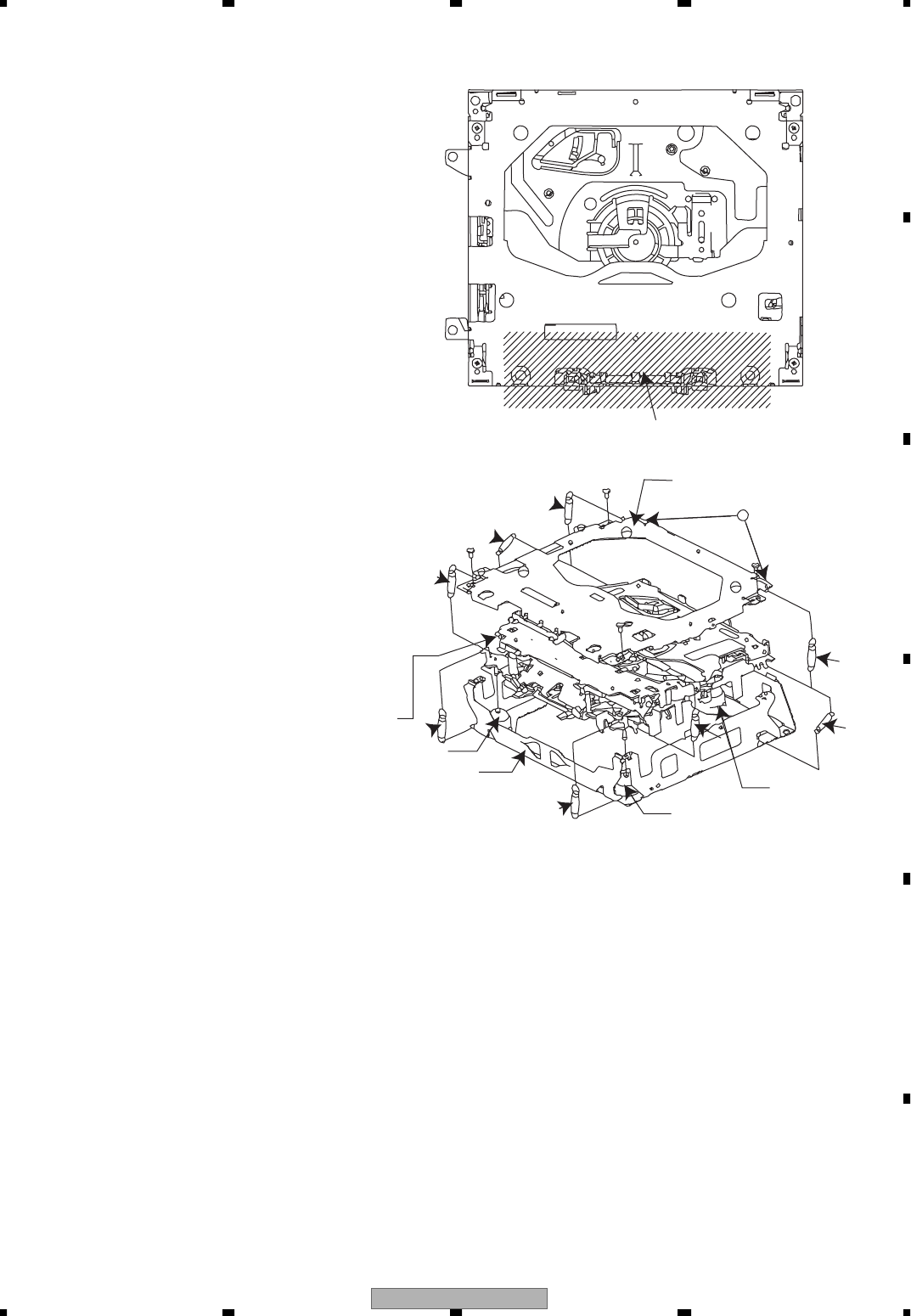
- How to hold the Mechanism Unit
1. Hold the top and bottom frame.
2. Do not squeeze top frame's front portion too tight,
because it is fragile.
- Removing the Upper and Lower Frames
1. With a disc clamped, remove the four springs (A),
the two springs (B), the two springs (C), and the
four screws.
2. To remove the upper frame, open it on the fulcrum
A.
3. While lifting the carriage mechanism, remove the
three dampers.
4. With the frames removed, insert the connectors
coming from the main unit and eject the disc.
Caution: Before installing the carriage mechanism in
the frames, be sure to apply some alcohol to the
dampers and set the mechanism to the clamp mode.
Do not squeeze.
Lower Frame
Damper
Carriage Mechanism
A
C
A
B
B
Damper
Damper
C
A
A
A
Upper Frame
DEH-P460MP/XM/UC
58
1234
1234
C
D
F
A
B
E
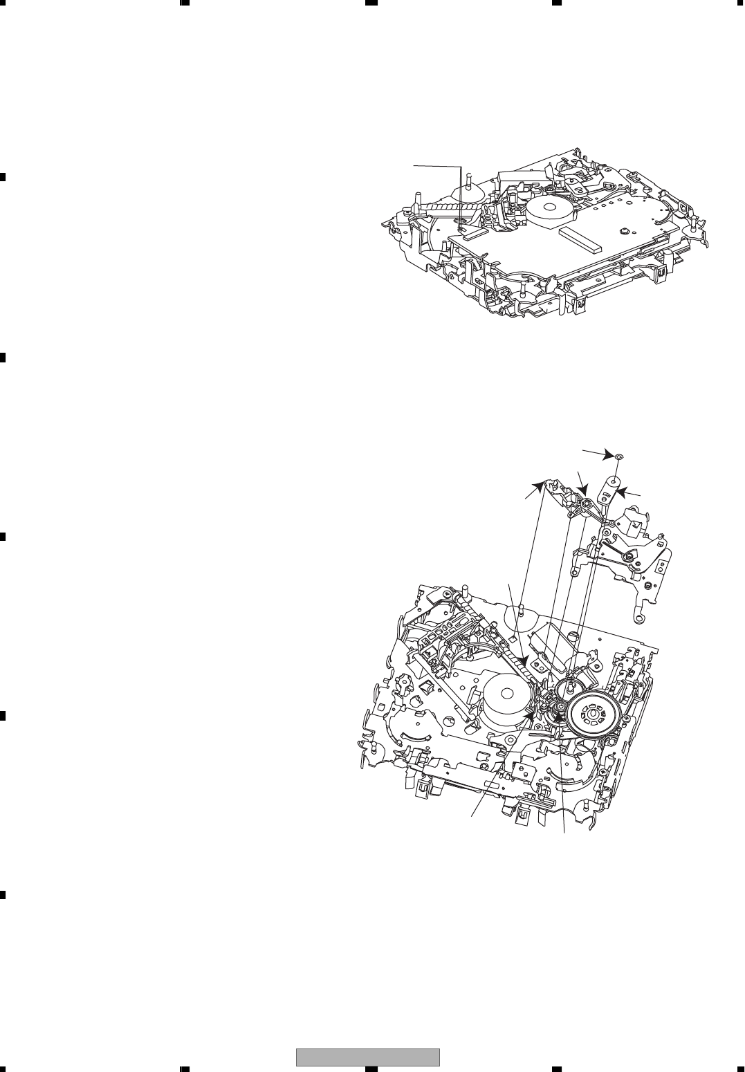
- Removing the Pickup Unit
1. Apply shorting solder to the Pickup flexible cable.
Disconnect the cable.
2. Set the mechanism to the clamp mode.
3. Remove the lead wires from the inner holder.
4. Remove the washer, styling holder, change arm,
and pickup lock arm.
5. While releasing from the hook of the inner holder,
lift the end of the feed screw.
Caution: In assembling, move the planet gear to the
load/eject position before setting the feed screw
in the inner holder.
Shorting
Solder
Planet Gear
Change Arm
Inner Holder
Styling Holder
Feed Screw
Washer
Pickup Lock Arm
DEH-P460MP/XM/UC 59
5678
5678
C
D
F
A
B
E
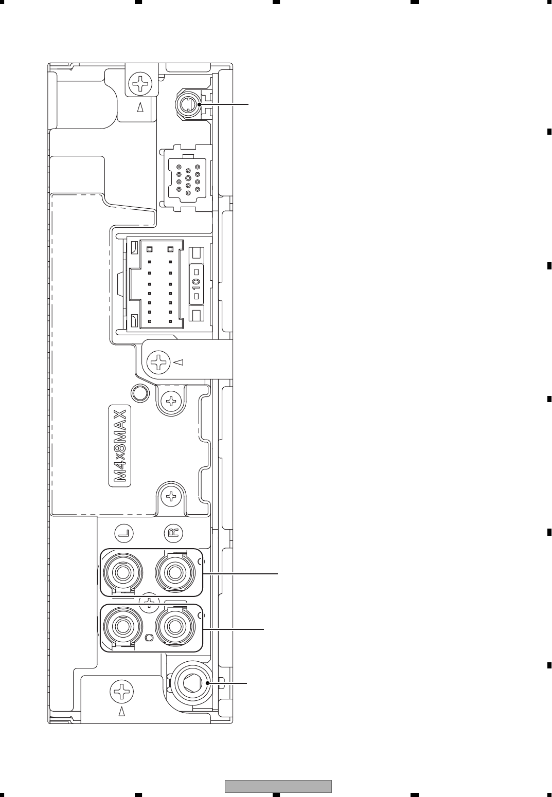
7.1.2 CONNECTOR FUNCTION DESCRIPTION
9. RL-
10. FL-
11. RL+
12. FL+
13. RR-
14. FR-
15. RR+
16. FR+
1. B. UP
2. GND
3. ACC
4. NC
5. NC
6. B.REM
7. NC
8. NC
WIRED
REMOTE
CONTROL
(UC Model only)
1. BUS+
2. IPGND
3. IPGND
4. NC
5. BUS-
6. IPGND
7. BUSL+
8. ASENB1
9. BUSR+
10. BUSR-
11. BUSL-
10A
15 1
13 11 9 753
16 2
14 12 10 8 64
111098
7
65
4321
POWER SUPPLY IP-BUS
ANTENNA JACK
REAR OUTPUT
FRONT OUTPUT
(UC Model only)
DEH-P460MP/XM/UC
60
1234
1234
C
D
F
A
B
E
7.2 PARTS
7.2.1 IC
- Pin Functions(PE5407A)
Pin No. Pin Name I/O Format Function and Operation
1swvdd O C Grille : Chip enable output
2-4 NC Not used
5 TESTIN I Test program mode input
6 LCDPW Not used
7 TELIN I Telephone mute input
8ejectin I Eject sense input
9 FLPILM O C Flap illumination output
10 DALMON O C For consumption low-current output
11 reset I Reset input
12 XT2 Not used
13 XT1 I Clock connection pin
14 VSS GND
15 X2 Crystal oscillator connection pin
16 X1 I Crystal oscillator connection pin
17 REGOFF Regulator operation specification signal
18 REGC Capacitor for regulator connect pin
19 VDD Power supply
20 ILMPW O C Illumination power supply control output
21 SYSPW O C System power control output
22 adpw O C A/D converter power supply control output
23 NC Not used
24 IPPW O C Power supply control output for IP BUS interface IC
25 NC Not used
26 ROMDATA O C ROM correction data output
27 ROMCLK Not used
28 ROMCS Not used
29-31 NC Not used
32 tunpce@ O C PLL chip enable output2
33 VST O C E.VOL : Strobe output
34 VCK O C E.VOL : Clock output
35 VDT O C E.VOL : Data output
36 ANTPW Not used
37 MUTE O C System mute output
38, 39 NC Not used
40 VSS GND
41 VDD Power supply
42 RDS57K Not used
43 drst Not used
44 rdslk Not used
45 RDT Not used
46 DORAON Not used
47 NC Not used
48 CSENSOUT O C CSENS state output
49-55 NC Not used
56,57 ROT1,0 I Rotary encoder pulse input 1,0
58 STRKEY2 O C Steering remote controller output
59 CDLOEJ O C CD : Load Moter Load/Eject output
60 CLCONT O C CD : Driver input switch output
61 CONT O C CD : Servo driver power supply control output
62 PCL O C Clock adjustment output
63 CLAMPSW I Clamp SW input
64 VDCONT O C CD : VD power control output
65 xsck O C CD LSI clock output
66 XSI I CD LSI data input
67 XSO O C CD LSI data output
68 XAO O C CD LSI command/data control output
69 xrst O C CD LSI reset control output
70 xstb O C CD LSI strobe output
DEH-P460MP/XM/UC 61
5678
5678
C
D
F
A
B
E
Pin No. Pin Name I/O Format Function and Operation
71 ASENSBO O C IP-BUS : Slave power supply control output
72 EMUTE Not used
73 TEST I GND
74 SL I TUNER : Signal level input
75 STRKEY1 I Steering remote controller input
76 MODELIN Not used
77 CSENS I Flap close sense input
78 NC Not used
79 DSCSNS I CD : Disc insert sense input
80 VDSENS I CD : VD voltage sense input
81 TEMP I CD : Temperature sense input
82 AVDD A/D converter power supply terminal
83 AVREF A/D converter reference voltage terminal
84 AVSS GND
85 RX I IP-BUS : Data input
86 TX O C IP-BUS : Data output
87 NMI GND
88 ldet I PLL lock sense input
89 rck I RDS : Clock input
90 dsens I Grille detach sense input
91 PACK I PACK input
92 asens I ACC power sense input
93 bsens I Back up power sense input
94 TUNPDI I PLL IC data input
95 KYDT I Grille data input
96 DPDT O C Grille data output
97 TUNPCK O C PLL clock output
98 TUNPDO O C PLL data output
99 TUNPCE O C PLL chip enable output
100 PEE O C Beep tone output
* PE5407A
30
31
50
51 80
81
100
1
Format Meaning
C CMOS
IC's marked by * are MOS type.
Be careful in handling them because they are very
liable to be damaged by electrostatic induction.
123
VDD
GND
54
VOUT
N.C.
N.C.
Vref
BD4834G
DEH-P460MP/XM/UC
62
1234
1234
C
D
F
A
B
E
-Pin Functions (PD6340A)
Pin No. Pin Name I/O Function and Operation
1-5 SEG4-0 O LCD segment output
6-9 COM3-0 O LCD common output
10 VLCD LCD drive power supply
11-14 KST3-0 O Key strobe output
15,16 KDT0,1 I Key data input (analogue input)
17 REM I Remote control reception input
18 DPDT I Display data input
19 NC Not used
20 KYDT O Key data output
21 MODA GND
22 XO Crystal oscillator connection pin
23 XI Crystal oscillator connection pin
24 VSS GND
25,26 KDT2,3 I Key data input
27,28 KST5,4 Key strobe output
29-55 SEG39-13 LCD segment output
56 VDD Power supply
57-64 SEG12-5 O LCD segment output
*PD6340A
49
48 33
32
17
16
1
64
132
S1 RS2 GND
BUS-BUS+VCC
STB
4
56
78
BIAS
DRIVER
OUTPUT
+
-
-
+
COM
RECEIVER
OUTPUT
HA12240FP
O
O

DEH-P460MP/XM/UC 63
5678
5678
C
D
F
A
B
E
- Pin Functions(PE5402A)
Pin No. Pin Name I/O Format Function and Operation
1 AVREF A power supply Positive power supply(5V)
2 AVSS A power supply GND
3 RFOK O C Output of state of RFOK
4 CLAMP I C CLAMP SW sense input
5 EVDD E power supply Positive power supply
6 PWM For changer(PWM)
7 NC Not used
8 IC/FLMD0 IC : VSS direct connection/FLMOD0 : Pull-down
9 VDD Positive power supply(5V)
10 REGC Connected to the capacity stabilizing output of the regulator
11 VSS GND
12 X1 I Oscillator connection for mainclock
13 X2 Oscillator connection for mainclock
14 reset I System reset input
15 XT1 I Connected to the oscillator for subclock
(connected to VSS via the resistor)
16 XT2 Connected to the oscillator for subclock(Open)
17 PULLDOWN I Connected to EVDD or EVSS via the resistor
18 ejsw I C Eject key input
19 xint C CD LSI interruption signal input
20 NC Not used
21 brst I P-Bus reset input
22 BSI I P-Bus serial data input
23 BSO O C P-Bus serial data output
24 bsck I/O /C P-Bus serial clock input/output
25 FTXD O C For flash rewriting(transmitted signal)
26 FRXD I For flash rewriting(received signal)
27 BRXEN I/O /C It is possible to receive P-Bus
28 bsrq I/O /C P-Bus service request demand
29 dspok I DSP microcomputer initialization OK input
30 DSCSNS(S903) I Disc state sense input
31 8EJ(S905) I Input of detection of 8 cm disc ejection
32 12EJ(S904) I Input of detection of 12 cm disc ejection
33 EVSS E power supply GND
34 EVDD E power supply Positive power supply
35, 36 SRAMLEVEL0, 1 O C SRAM level meter output
37 EMPH O C Emphasis information output
38 emph O C Emphasis information output
39-42 NC Not used
43 adena O C A/D reference voltage supply control output
44 LRCKOK O C (DOUT mute output)
45 SRAMLEVEL2 O C SRAM level meter output
46 CD3VON O C CD +3.3V power supply control output
47 CONT O C Servo driver power supply control output
48 xrst O C CD LSI reset control output
49 VDCONT O C VD power supply control output
50 ROMDATA I/O /C E2PROM data input/output
51 ROMCS O C E2PROM chip selection output
52 ROMCK O C E2PROM clock output
53 LOEJ O C The direction change output of LOAD/EJECT
54 CLCONT O C Driver input change output
55 CDMUTE O C CD mute control output
56-58 INT For changer(Interruption at the edge)
59 xcs O C CD LSI chip selection output
60 NC Not used
61 xwait I CD LSI write control signal output
62 CLKOUT O C Internal system clock output(Open)
63 LOCK I Spindle lock input
64 NC Not used
65 xwrite O CD LSI write control signal output
DEH-P460MP/XM/UC
64
1234
1234
C
D
F
A
B
E
Pin No. Pin Name I/O Format Function and Operation
66 NC Not used
67 xread O CD LSI read control signal output
68 XASTB O CD LSI address strobe output
69 BVSS B power supply GND
70 BVDD B power supply Positive power supply
71-86 AD0-15 I/O /C Address/data Bus 0-15
87-90 NC Not used
91-93 A/D For changer(A/D)
94 csens I Flap closing sense input
95 TYPE_A/D I CD-DA analog/digital output change setup
96 testin I Chip check test program starting input
97 HOME I Home SW sense input
98 TEMP Temperature information sense input
99 VDSENS VD power supply short sense input
100 NC Not used
* PE5402A
25
26
50
51
75
76
100
1
Format Meaning
C CMOS
123
VIN
VOUT
VSS
Reference
Voltage
* S-812C33AUA-C2N

DEH-P460MP/XM/UC 65
5678
5678
C
D
F
A
B
E
- Pin Functions(UPD63761GJ)
Pin No. Pin Name I/O Function and Operation
1 D.VDD Power supply for digital circuits
2 D1.GND GND for 1.6V digital circuits
3 reset I Input of reset
4-8 AB12-8 I Address bus 12-8 from the microcomputer
9-16 AD7-0 I/O Address/data bus 7-0 to the microcomputer
17 cs I Chip selection
18 ASTB I Address strobe
19 read I Control signals(read)
20 write I Control signals(write)
21 wait O Control signals(wait)
22 INTQ O Interruption signals to the external microcomputer
23, 24 IFMODE0, 1 I Switching the microcomputer I/F 0, 1
25 D1.VDD Power supply for 1.6V digital circuits
26 DA.VDD Power supply for DAC
27 ROUT O Output of audio for the right channel
28 DA.GND GND for DAC
29 REGC Connected to the capacitor for band gap
30 DA.GND GND for DAC
31 LOUT O Output of audio for the left channel
32 DA.VDD Power supply for DAC
33 X.VDD Power supply for the crystal oscillator
34 XTAL I Connected to the crystal oscillator(16.9344MHz)
35 xtal O Connected to the crystal oscillator(16.9344MHz)
36 X.GND Ground for the crystal oscillator
37 VDDREG15 Control of 1.6V regulator
38 PWMSW0 I Setup 0 for PWM output(SD, MD)
39-41 TEST3-1 I Connected to GND
42 PWMSW1 I Setup 1 for PWM output(FD, TD)
43 TESTEN I Connected to GND
44 D1.GND GND for 1.6V digital circuits
45 DIN I Input of audio data
46 DOUT O Output of audio data
47 SCKIN I Clock input for audio data
48 SCKO O Clock output for audio data
49 LRCKIN I Input of LRCK for audio data
50 LRCK O Output LRCK for audio data
51 xtalen I Permission to oscillate 16.9344MHz
52 D1.VDD Power supply for 1.6V digital circuits
53 RFCK/HOLD O Output of RFCK/HOLD signal
54 WFCK/MIRR O Output of WFCK/MIRR signal
55 PLCK O Output of PLCK
56 LOCK/RFOK O Output of LRCK/Output of RFOK
57 C1D1/C8M O Information on error correction/C8M : 8MHz
58 C1D2/C16M O Information on error correction/C16M : 16MHz
59 C2D1/RMUTE O Information on error correction/Mute for Rch
60 C2D2/LMUTE O Information on error correction/Mute for Lch
61 C2D3/SHOCK O Information on error correction/Detection of vibration
62 D1.GND GND for 1.6V digital circuits
63 C33M O Output of 33.8688MHz(CLK for SDRAM)
64 (rcs) O DRAM cs
65 RA11 O Output of DRAM address 11
66 (CKE) O Output of DRAM CKE
67 ras O Output of DRAM ras
68 cas)(LDQM) O Output of DRAM lower cas(LDQM)
69 cas!(UDQM) O Output of DRAM upper cas(UDQM)
70 we O Output of DRAM we
71 oe(cas) O Output of DRAM oe(cas)
72 D.GND Ground for digital circuits
73-88 RDB0-15 I/O Input/output of DRAM data0-15
89-99 RA0-10 O Output of DRAM address0-10
DEH-P460MP/XM/UC
66
1234
1234
C
D
F
A
B
E
Pin No. Pin Name I/O Function and Operation
100 D.VDD Power supply for digital circuits
101 FD+ O Output of focus drive PWM +
102 FD- O Output of focus drive PWM -
103 TD+ O Output of tracking drive PWM +
104 TD- O Output of tracking drive PWM -
105 SD+ O Output of thread drive PWM +
106 SD- O Output of thread drive PWM -
107 MD+ O Output of spindle drive PWM +
108 MD- O Output of spindle drive PWM -
109 REFOUTSV O REFOUT for servo
110 AD.VDD Power supply for ADC
111 EFM O Output of EFM signals
112 ASY I Input of asymmetry
113 ATEST O Analog tests
114 RFI I Input of RF
115 AD.GND Ground for the analog system
116 AGCO O Output of RF
117 C3T O Connection to the capacitor for detecting 3T
118 AGCI I Input of AGC
119 RFO O Output of RF(AGC)
120, 121 EQ2, 1 I Equalizer 2, 1
122 RF2- I Reversal input of RF2
123 RF- I Reversal input of RF
124 A.GND Ground for the analog system
125 A I Input of A
126 C I Input of C
127 B I Input of B
128 D I Input of D
129 F I Input of F
130 E I Input of E
131 VREFIN I Input of reference voltage
132 A.VDD Power supply for the analog system
133 REFOUT O Output of reference voltage
134 REFC I Connected to the capacitor for output of REFOUT
135 FE- I Reversal input of FE
136 FEO O Output of FE
137 ADIN I Input of FE, TE A/D converter
138 TE- I Reversal input of TE
139 TEO O Output of TE
140 TE2 O TE2
141 TEC I TEC
142 LD O Output of LD
143 PD I Input of PD
144 D.GND Ground for digital circuits
* UPD63761GJ
72
73
108
109
36
37
1
144
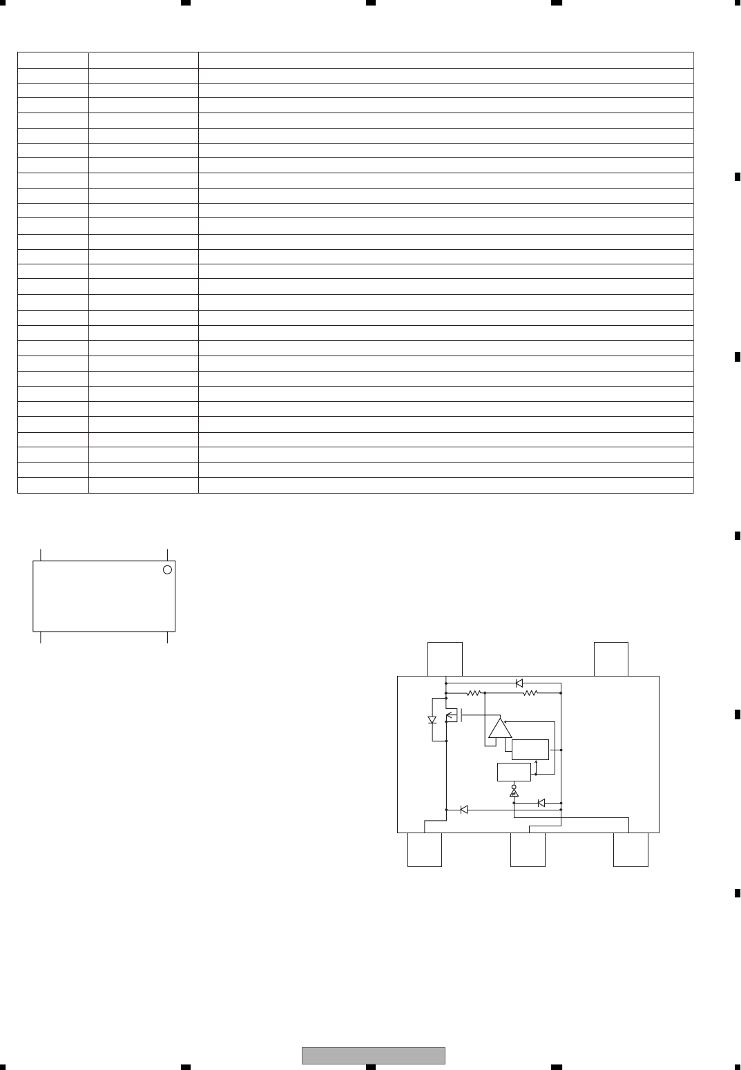
DEH-P460MP/XM/UC 67
5678
5678
C
D
F
A
B
E
- Pin Functions(BA5835FM)
Pin No. Pin Name Function and Operation
1 VR Input pin for reference voltage
2 OPIN2(+) Input pin for non-inverting input for CH2 preamplifier
3 OPIN2(-) Input pin for inverting input for CH2 preamplifier
4 OPOUT2 Output pin for CH2 preamplifier
5 OPIN1(+) Input pin for non-inverting input for CH1 preamplifier
6 OPIN1(-) Input pin for inverting input from CH1 preamplifier
7 OPOUT1 Output pin for CH1 preamplifier
8 GND Ground pin
9 MUTE Mute control pin
10 POWVCC1 Power supply pin for CH1, CH2, and CH3 at "Power" stage
11 VO1(-) Driver CH1 - Negative output
12 VO1(+) Driver CH2 - Positive output
13 VO2(-) Driver CH2 - Negative output
14 VO2(+) Driver CH2 - Positive output
15 VO3(+) Driver CH2 - Positive output
16 VO3(-) Driver CH2 - Negative output
17 VO4(+) Driver CH4 - Positive output
18 VO4(-) Driver CH4 - Negative output
19 POWVCC2 Power supply pin for CH4 at "Power" stage
20 GND Ground pin
21 CNT Control pin
22 LDIN Loading input
23 OPOUTSL Output pin for preamplifier for thread
24 OPINLSL Input pin for preamplifier for thread
25 OPOUT3 CH3 preamplifier output pin
26 OPIN3(-) Input pin for inverting input for CH3 preamplifier
27 OPIN3(+) Input pin for non-inverting input for CH3 preamplifier
28 PREVCC PreVcc
BA5835FM
114
15 28
ON/OFF
VSS
VIN
321
5 4
NC
VOUT
-
+
Reference
voltage
ON/OFF
circuit
* S-L2980A15MC-C6A
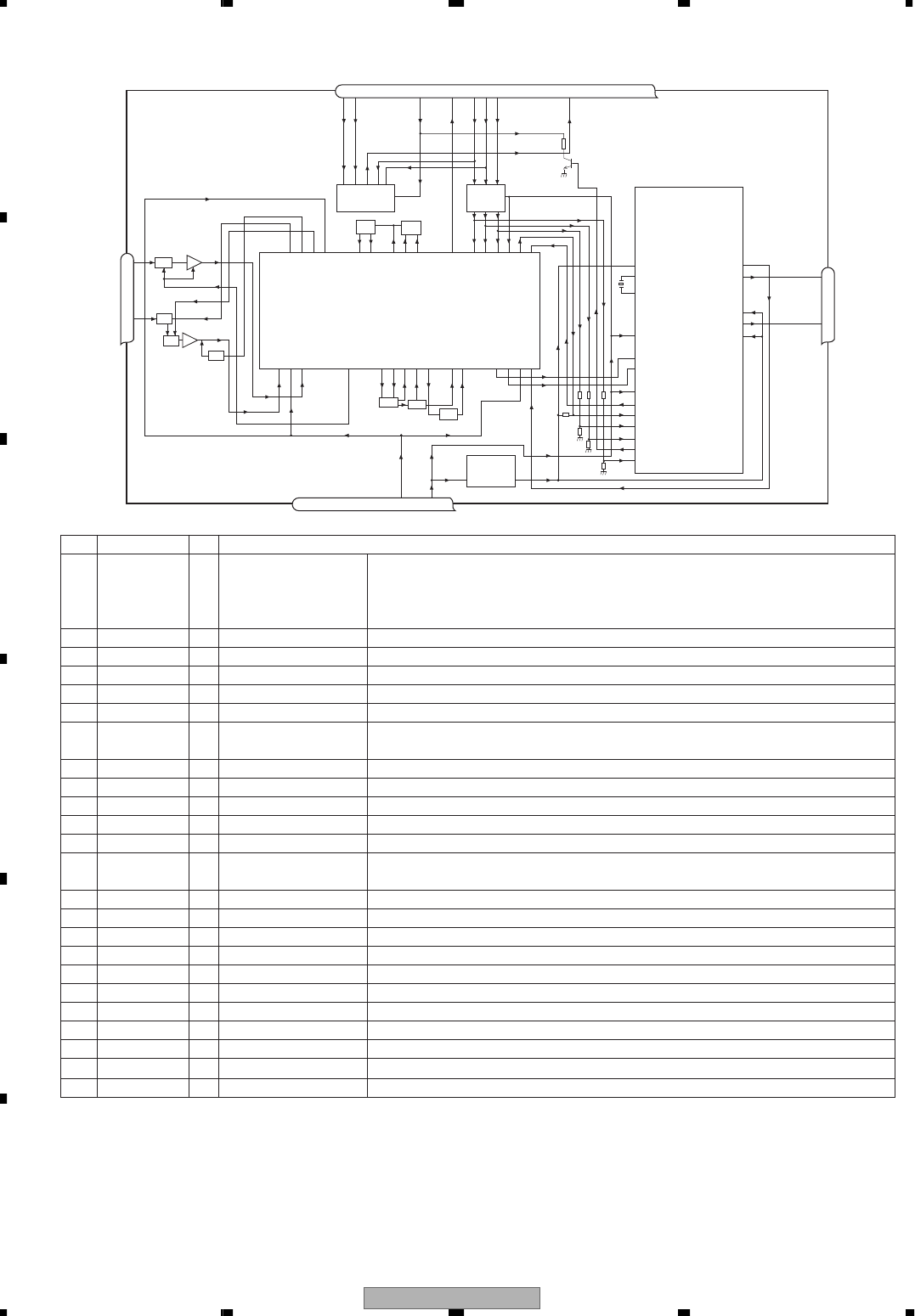
DEH-P460MP/XM/UC
68
1234
1234
C
D
F
A
B
E
No. Symbol I/O Explain
1 AMANT I AM antenna input AM antenna input high impedance AMANT pin is connected with
an all antenna by way of 4.7µH. (LAU type inductor) A series circuit
including an inductor and a resistor is connected with RF ground for
the countermeasure against the hum of power transmission line.
2 RFGND RF ground Ground of antenna block
3 FMANT I FM antenna input Input of FM antenna 75ΩSurge absorber(DSP-201M-S00B) is necessary.
4 VCC power supply The power supply for analog block. D.C 8.4V ±0.3V
5 SL O signal level Output of FM/AM signals level
6 CE2 I chip enable-2 Chip enable for EEPROM ”Low” active
7 WC I write control You can write EEPROM, when EEPROM write control is “Low”.
Ordinary non connection
8 CE1 I chip enable-1 Chip enable for AF•RF ”High” active
9 CK I clock Clock
10 DI I data in Data input
11 NC non connection Not used
12 OSCGND osc ground Ground of oscillator block
13 ROM_VDD power supply Power supply for EEPROM pin 13 is connected with a power supply of
micro computer.
14 DO O data out Data output
15 DGND digital ground Ground of digital block
16 NC non connection Not used
17 VDD_3.3 power supply The power supply for digital block. 3.3V ±0.2V
18 NC non connection Not used
19 NC non connection Not used
20 NC non connection Not used
21 NC non connection Not used
22 AUDIOGND audio ground Ground of audio block
23 L ch O L channel output FM stereo “L-ch” signal output or AM audio output
24 R ch O R channel output FM stereo “R-ch” signal output or AM audio output
FMRF
ANT adj RF adj
FM ANT
T51 CF52
CF51
RFGND
OSCGND
DGND
AUDIOGND
NC
VCC
VDD_3.3
3.3V 2.5V
IC 4
3.3V 2.5V
←
IC 2
2.5V
WC
CE2
ROM_VDD
SL
DI
CK
CE1
NC
DO
NC
NC
NC
NC
76 13 5 1098 11 14 18192021
1
3
212 1522 16 4 17
IC 1
3.3V
AM ANT FMRF
ATT
LPF
OSC
IC 3 EEPROM
5.0V
IC 5
5V 3.3V
←
ATT
MIXER, IF AMP DET, FM MPX
24
23
Rch
Lch
- FM/AM Tuner Unit
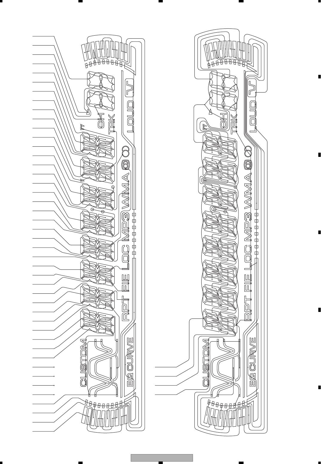
DEH-P460MP/XM/UC 69
5678
5678
C
D
F
A
B
E
7.2.2 DISPLAY
COMMON
SEGMENT
- LCD(XAW7004)(DEH-P460MP/XM/UC, DEH-P4600MP/XM/UC)
SEG39
SEG38
SEG37
SEG36
COM 3
COM 2
COM 1
COM 0
SEG35
SEG34
SEG33
SEG32
SEG31
SEG30
SEG29
SEG28
SEG27
SEG26
SEG25
SEG24
SEG23
SEG22
SEG21
SEG20
SEG19
SEG18
SEG17
SEG16
SEG15
SEG14
SEG13
SEG12
SEG11
SEG10
SEG 9
SEG 8
SEG 7
SEG 6
SEG 5
SEG 4
SEG 3
SEG 2
SEG 1
SEG 0
COM 3
COM 2
COM 1
COM 0
DEH-P460MP/XM/UC
70
1234
1234
C
D
F
A
B
E
COMMON
SEGMENT
- LCD(XAW7002)(DEH-P4650MP/XM/ES)
SEG35
SEG36
SEG37
SEG38
SEG39
SEG32
SEG33
SEG34
COM 3
COM 2
COM 1
COM 0
SEG 0
SEG 1
SEG 2
SEG 3
SEG 4
SEG 5
SEG 6
SEG 7
SEG 8
SEG 9
SEG10
SEG11
SEG12
SEG13
SEG14
SEG15
SEG16
SEG17
SEG18
SEG19
SEG20
SEG21
SEG22
SEG23
SEG24
SEG25
SEG26
SEG27
SEG28
SEG29
SEG30
SEG31
DEH-P460MP/XM/UC 71
5678
5678
C
D
F
A
B
E
7.3 OPERATIONAL FLOW CHART
VDD=5V
Pin 41
ASENSBO←H
Pin 71
Power ON
bsens=L
asens=L
dsens=L
bsens
Pin 93
asens
Pin 92
dsens
Pin 90
swvdd←L
Pin 1
Source keys
operative
Completes power-on operation.
(After that, proceed to each source operation)
SYSPW←H
Pin 21
Starts
communication
with Grille
microcomputer.
Source ON
300ms
300ms
In case of the above signal, the communication
with Grille microcomputer may fail.
If the time interval is not 300msec, the oscillator
may be defective.
CSENS
Pin 77
2V < CSENS < 3V
- CSENS 2V, 3V CSENS
Last source returns.
CD loading functions are available.
Keys except for EJECT key are not available.
<<
==

DEH-P460MP/XM/UC
72
1234
1234
C
D
F
A
B
E
7.4 CLEANING
Before shipping out the product, be sure to clean the
following portions by using the prescribed cleaning
tools:
Portions to be cleaned Cleaning tools
CD pickup lenses Cleaning liquid : GEM1004
Cleaning paper : GED-008
DEH-P460MP/XM/UC 73
5678
5678
C
D
F
A
B
E
8. OPERATIONS
DEH-P460MP/XM/UC
74
1234
1234
C
D
F
A
B
E
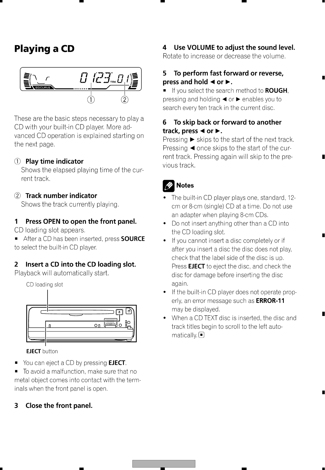
DEH-P460MP/XM/UC 75
5678
5678
C
D
F
A
B
E
DEH-P460MP/XM/UC
76
1234
1234
C
D
F
A
B
E
Fixing the Front Panel
If you do not operate the Detaching and Replacing the Front Panel Function, use the supplied fixing screws
and fix the front panel to this unit.
1. Attach the holders to both sides of the front panel.
2. Replace the front panel to the unit.
3. Flip the holders into upright positions.
4. Fix the front panel to the unit using fixing screws.
Fixing screw
Holder
CND1249(UC)
CXX1644(ES)
Holder
CND1250(UC)
CXX1645(ES)
BPZ20P060FZK(UC)
CXX1646(ES)
DEH-P460MP/XM/UC 77
5678
5678
C
D
F
A
B
E
+
≠
+
≠
+
≠
+
≠
IP-BUS input (Blue)
This product
Blue/white
To system control terminal of the power amp
or Auto-antenna relay control terminal
(max. 300 mA 12 V DC).
Connecting cords
with RCA pin plugs
(sold separately)
System remote control
Rear speakerRear speaker
Right
Front speaker
Rear speaker
White Gray
White/black
Green
Green/black
Gray/black
Violet
Violet/black
Front speaker
Rear speaker
Left
With a 2 speaker system, do not connect
anything to the speaker leads that are not
connected to speakers.
Yellow
To terminal always supplied
with power regardless of
ignition switch position.
Black (ground)
To vehicle (metal) body.
Red
To electric terminal controlled
by ignition switch (12 V DC)
ON/OFF.
Antenna jack
Rear output
(REAR OUTPUT)
Perform these connections when using
the optional amplifier.
Front output
(FRONT OUTPUT)
Power amp
(sold separately)
Front speaker Front speaker
Right
Left
Jack for the Wired Remote Control
Please see the Instruction Manual for the
Wired Remote Control (sold separately).
IP-BUS cable
Multi-CD player
(sold separately)
Fuse
+
≠
+
≠
+
≠
+
≠
Power amp
(sold separately)
- CONNECTION DIAGRAM