PJ5121 Datasheet. Www.s Manuals.com. Noname
User Manual: Marking of electronic components, SMD Codes 51, 51**, 51***, 5103, 51031, 5108, 51117, 51123, 51123A, 51125, 5121*, 51216, 51219, 5121M, 51225, 5160x, 51716, 5173, 5193, 5198NL, 5199NL, 51A, 51AC30B, 51AC33, 51AC33B, 51Y. Datasheets 1.5SMC51AT3, AT5160TP1U, BZV49-C51, CS51031, FX011Z, G5108RDU, G5111T11, G5121TB1U, G5173R41U, G5193R41U, KB4312B-GRE, LP2951ACSDX-3.3, LP2951CSD-3.0, LP2951CSD-3.3, MM5Z2V7, MTP5103N3, PJ5121EMR, PJ5121EQFN, SST5198NL, SST5199NL, TPS51117PW, TPS51117RGY, TPS51123ARGER, TPS51123
Open the PDF directly: View PDF ![]() .
.
Page Count: 8
White LED Step-Up Converter
GENERAL DESCRIPTION
The PJ 5121 is a step-up DC/DC converter designed for driving up to 8 white LEDs in series from a single
cell Lithium Ion battery with constant current. Because it directly regulates output current, the PJ5121 is i deal for
driving light emitting diodes (LEDs) whose light intensity is proportional to the current passing through them, not
the voltage across their terminals. A single external resistor sets LED current between 5mA and 20mA, which can
then be easily adjusted using either a DC voltage or a pulse width modulated (PWM) signal. Its low 225mV
feedback voltage reduces power loss and improves efficiency. The OV pin monitors the output voltage and turns
off the converter if an over-voltage condition is present due to an open circuit condition. The PJ5121 is available
in SOT23-6 and QFN8 packages.
FEATURES
Drives Up to 5 Series White LEDs from 2.5V
Drives Up to 6 Series White LEDs from 3.6V
Up to 87% Efficiency
1.2MHz Fixed Switching Frequency
Low 225mV Feedback Voltage
Open Load Shutdown
Soft Start/PWM Dimming
SOT23-6 and QFN-8 Packages
APPLICATIONS
Cell Phones
Handheld Computers and PDAs
Digital Cameras
Small LCD Displays
TYPICAL APPLICATIONS
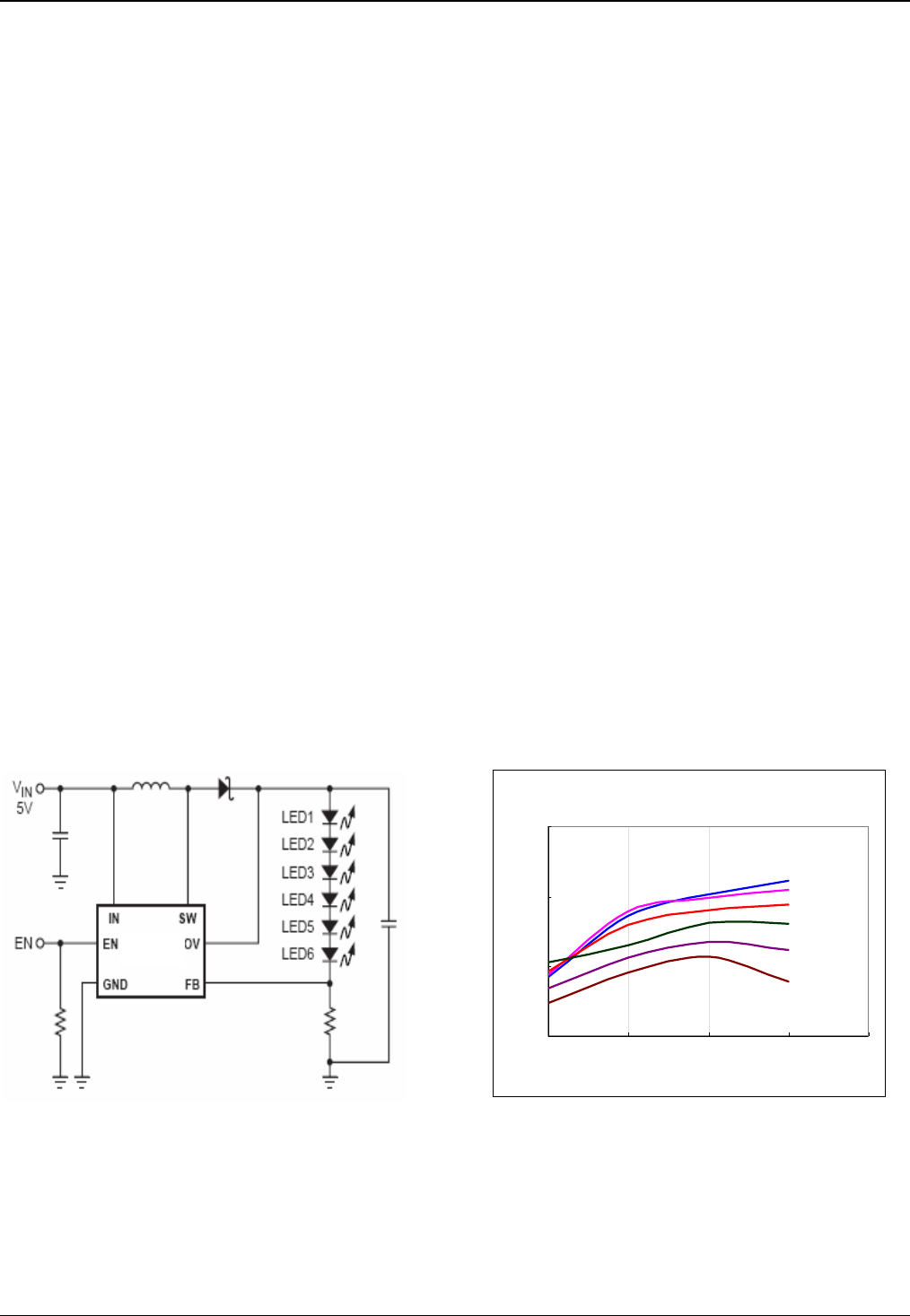
Efficiency vs n(LED)
4LED
5LED
6LED
7LED
3LED
75.00%
80.00%
85.00%
90.00%
510152025
Iout (mA) Vin=3.6V
8LED
Figure 1.
Li-Ion Driver for Six White LEDs Figure 2. Efficiency vs Number of LEDs
Page 1
PJ5121
PJ5121
White LED Step-Up Converter
ORDERING INFORMATION
Package Type
SOT-23-6
QFN: QFN-8 2x2
E: Pb Free Package
PACKAGES
Note: Pin 1 at the bottom-left corner of the digit “4”
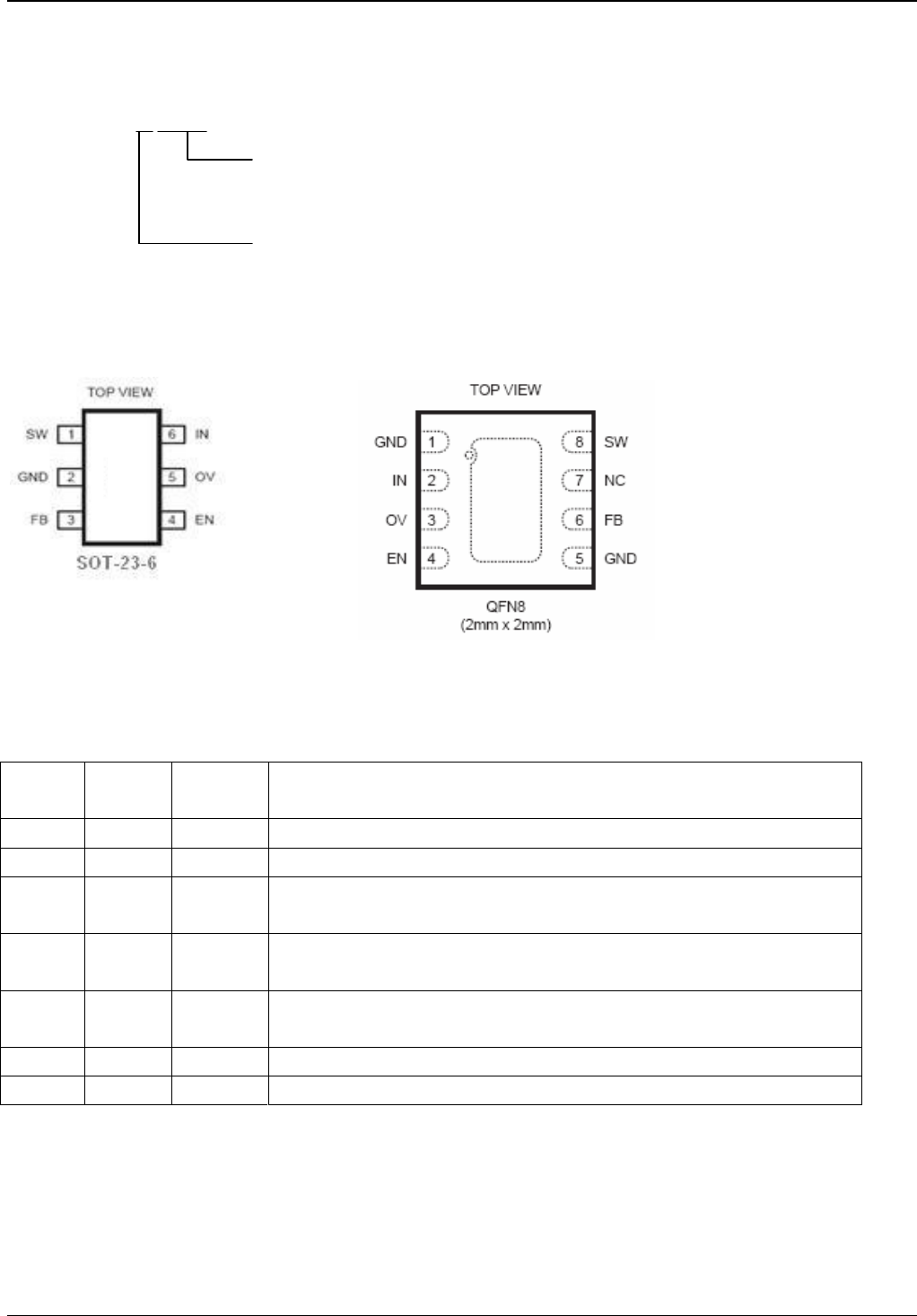
PIN DESCRIPTION
SOT
Pin No.
QFN
Pin No.
Pin
Names
Description
1 8 SW Power Switch Output. Connect the inductor and the blocking Schottky diode to SW.
2 1,5 GND Ground
3 6 FB Feedback input pin. The reference voltage at this pin is 225mV. Connect the cathode of
the lowest LED to FB and a current sense resistor between FB and GND.
4 4 EN Enable pin. A high input at EN enables the device and a low input disables the devices.
When not used, connect EN to the input source for automatic startup.
5 3 OV Over Voltage Input. OV measures the output voltage for open circuit protection. Connect
OV to the output at the top of the LED string.
6 2 IN Input Supply Pin. Must be locally bypassed.
7 NC Not Connected
Page 2
PJ5121
PJ5121APPP
MR:
White LED Step-Up Converter
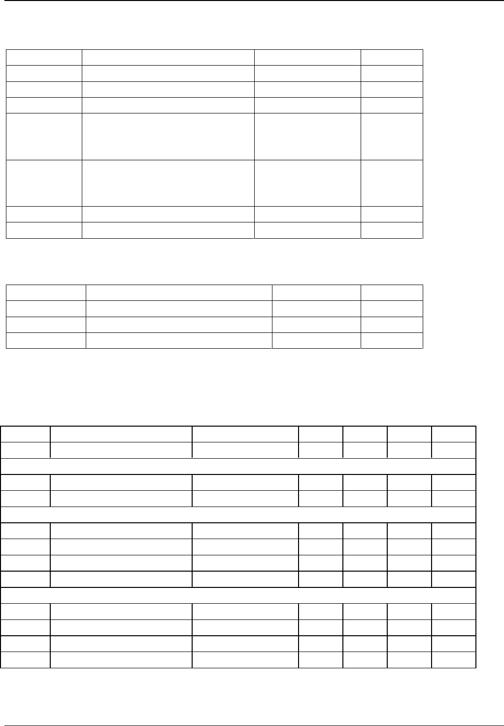
ABSOLUTE MAXIMUM RATINGS (Note 1)
SYMBOL ITEMS VALUE UNIT
VIN Input Voltage -0.3~6 V
VSW Voltage at SW Pin -0.5~25 V
VIO All Other I/O Pins GND-0.3 to VDD+0.3 V
PTR1
Thermal Resistance,SOT-23-6
ΘJA
ΘJC
220
110
℃/W
PTR2
Thermal Resistance,QFN-8 (2mm x 2mm)
ΘJA
ΘJC
80
16
℃/W
Tstg Storage Temperature -55 to 150 ℃
Tsolder Package Lead Soldering Temperature 260℃, 10s
RECOMMANDED OPERATING RANGE (Note 2)
SYMBOL ITEMS VALUE UNIT
VIN VIN Supply Voltage 2.5 to +6 V
VSW Output Voltage VIN to 28 V
TOPT Operating Temperature -40 to +85 ℃
ELECTRICAL CHARACTERISTICS
VIN=VEN=3V, Topt=25℃ unless specified otherwise.
SYMBOL ITEMS CONDITIONS Min. Typ. Max. UNIT
VIN Input Voltage 2.5 6 V
Feedback
VFB FB Pin Voltage Driving 4xLED @15mA 200 225 250 mV
Ibias FB Pin Input Bias Current 0.05 1 µA
Operating Current
Ioff Operating Current(Shutdown) VSW-ON =0V 0.1 1 µA
Isby Operating Current(Quiescent) VFB=0.3V 100 350 µA
Fsw Switching Frequency 1.0 1.25 1.5 MHz
Dmax Maximum Duty Cycle VFB=0V 85 90 %
Chip Enable
VEN_H EN Minimum High Level 1.5 V
VEN_L EN Maximum Low Level 0.4 V
VHYS EN Hysteresis 90 mV
EN Input Bias Current VSW-ON =0V, 5V 1 µA
Page 3
PJ5121
White LED Step-Up Converter
ELECTRICAL CHARACTERISTICS(contd.)
VIN=VEN=3V, Topt=25℃ unless specified otherwise.
SYMBOL ITEMS CONDITIONS Min. Typ. Max. UNIT
Output Switch
RON SW On Resistance (Note 3) 0.5 Ω
ILIMIT SW Current Limit 400 mA
ILEAK SW Leakage Current Vsw=5V 0.01 1 µA
Open Circuit Protection
VOV Open Circuit Shutdown Threshold VOV Rising 30 V
Soft Start
tss Soft Start Time (Note 3) VIN Power On 160 µS
Notes:
1. Exceeding these ratings may damage the device
2. The device is not guaranteed to function outside of its operating rating.
3. Guaranteed by design.
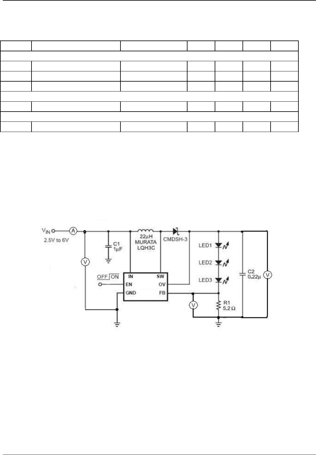
TESTING CIRCUIT
Page 4
5121M
PJ5121
White LED Step-Up Converter
TYPICAL PERFORMANCE CHARACTERISTICS
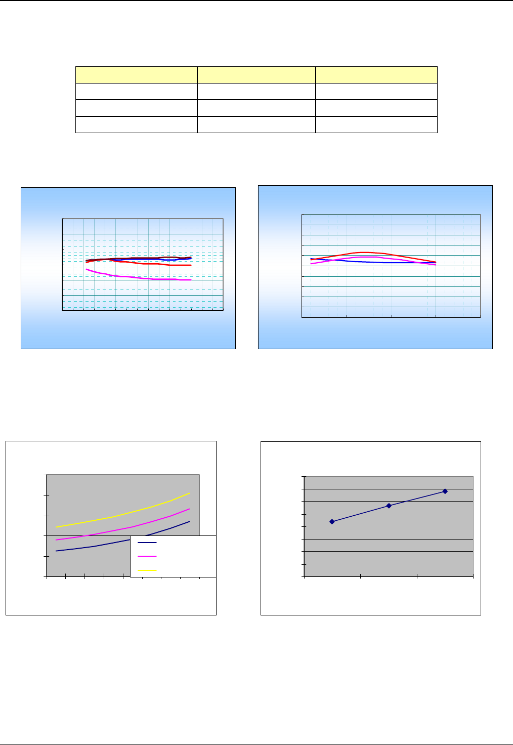
1. Driving Capability
Vin ILED=15mA ILED=20mA
2.5V 5 x LED 4 x LED
3.0V 6 x LED 5 x LED
3.6V 8 x LED 8 x LED
2.Efficiency
Figure 3. Efficiency vs Vin and ILED Figure 4. Efficiency vs Temperature
Efficiency vs. Vin
5mA
10mA
15mA
70.00%
75.00%
80.00%
85.00%
90.00%
95.00%
100.00%
3
3.1
3.2
3.3
3.4
3.5
3.6
3.7
3.8
3.9
4
4.1
4.2
4.3
4.4
4.5
Vin (V)
20mA
Efficiency vs. Temperature
10mA
15mA
20mA
80.00%
81.00%
82.00%
83.00%
84.00%
85.00%
86.00%
87.00%
88.00%
89.00%
90.00%
-50 0 50 100 150
Temp (C)
Efficiency
3. Quiescent Current vs VIN and Temperature
Figure 5. Iq vs. Temperature
Iq VS Temperature
0
50
100
150
200
250
2.5 3 3.5 4 4.5 5 5.5 6
Vin(V)
Iq(uA)
Temp=-40℃
Temp=25℃
Temp=100℃
4.Switching Frequency vs Temperature
Figure 6. Fosc vs. Temperature
Fosc VS Temp.
0
0.2
0.4
0.6
0.8
1
1.2
1.4
1.6
-40 25 100
Temp(℃)
Fosc(MHz)
Page 5
PJ5121
White LED Step-Up Converter
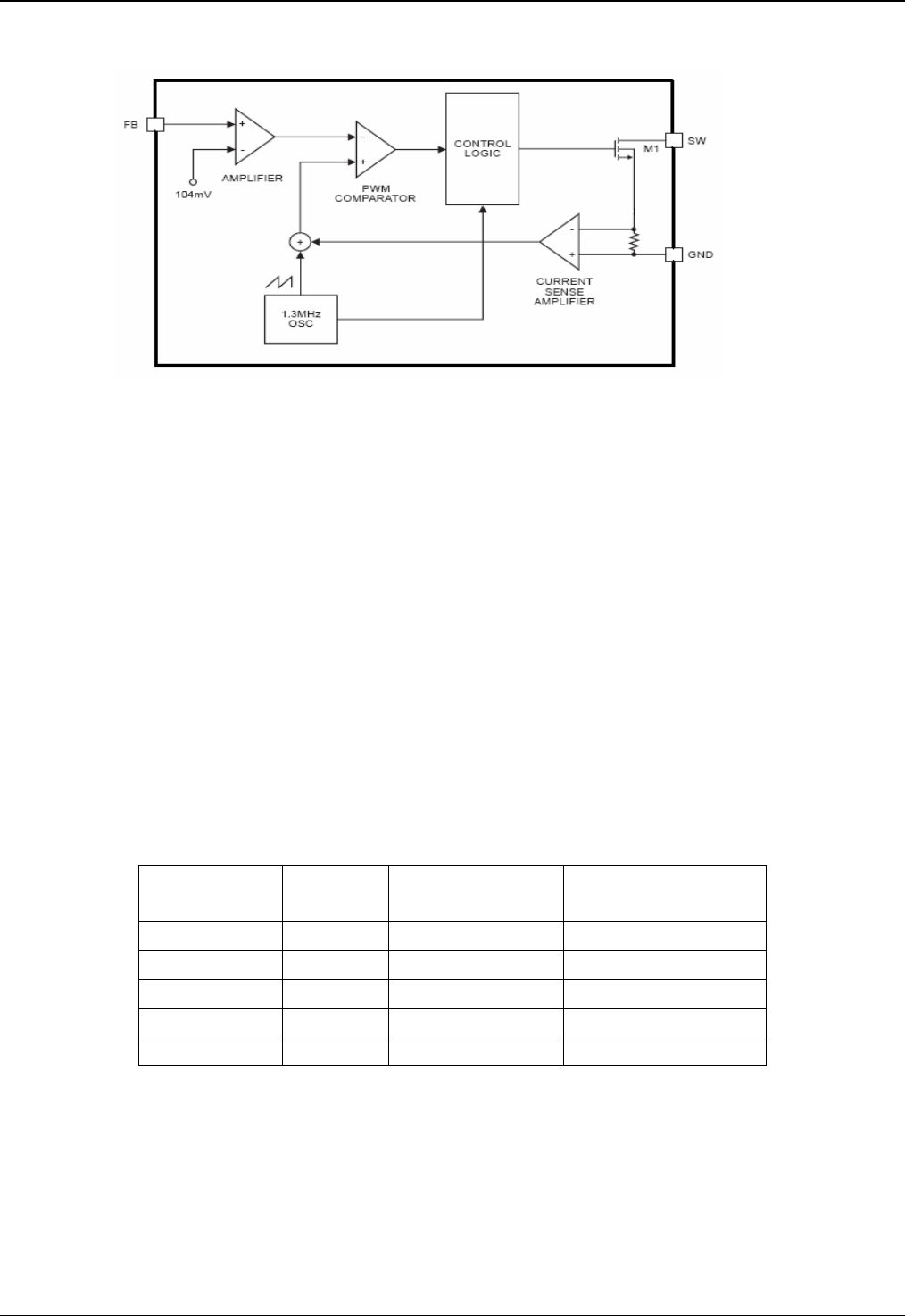
OPERATION
Figure 7. Simplified Block Diagram of the PJ 5121
The PJ5121 uses a constan t frequency, peak current mode boost
regulator architecture to regulate the series string of white LEDs.
The operation of the PJ5121 can be understood by referring to the
simplified block diagram shown above in Figure 7. At the start of
each oscillator cycle, the control logic turns on the power switch
M1. The signal at the non-inverting input of the PWM comparator
is proportional to the switch current, summed together with a
portion of the oscillator ramp. When this signal reaches the level
set by the output of error amplifier, the PWM comparator resets
the latch in the control logic and turns off the power switch. In this
manner, error amplifier sets the correct peak current level to keep
the LED current in regulation. If the feedback voltage starts to
drop, the output of the error amplifier increases. This results in
more current to flow through M1, hence increasing the power
delivered to the output.
APPLICATION INFORMATION
Inductor Selections
For most of the applications of the PJ512 1, it is
recommended to use an inductor of 22uH. Although small
size is one of the major factors in selecting an inductor, the
smaller and thinner inductors give higher core losses at
1.25MHz and DRC, resulting in lower efficiencies. The
following tab le provides a list of recommended inductors:
PART
NUMBER
DCR
(Ω)
CURRENT RATING
(mA)
MANUFACTURER
LQH3C220 0.71 250 MURATA
CDRH3D16-220 0.53 350 SUMIDA
LB2012B220M 1.7 75 TAIYO YUDEN
LEM2520-220 5.5 125 TAIYO YUDEN
EJPC220KF 4.0 160 PANASONIC
Capacitor Selection
The small size of ceramic capacitors makes them ideal for
PJ5 121 pplications. X5R and X7R types are
recommended because they retain their capacitance over
wider voltage and temperature ranges than other types such
as Y5V or Z5U. A 1µF input capacitor and a 0.22 µF output
capacitor are sufficient for most PJ5121 applications.
Page 6
PJ5121
White LED Step-Up Converter
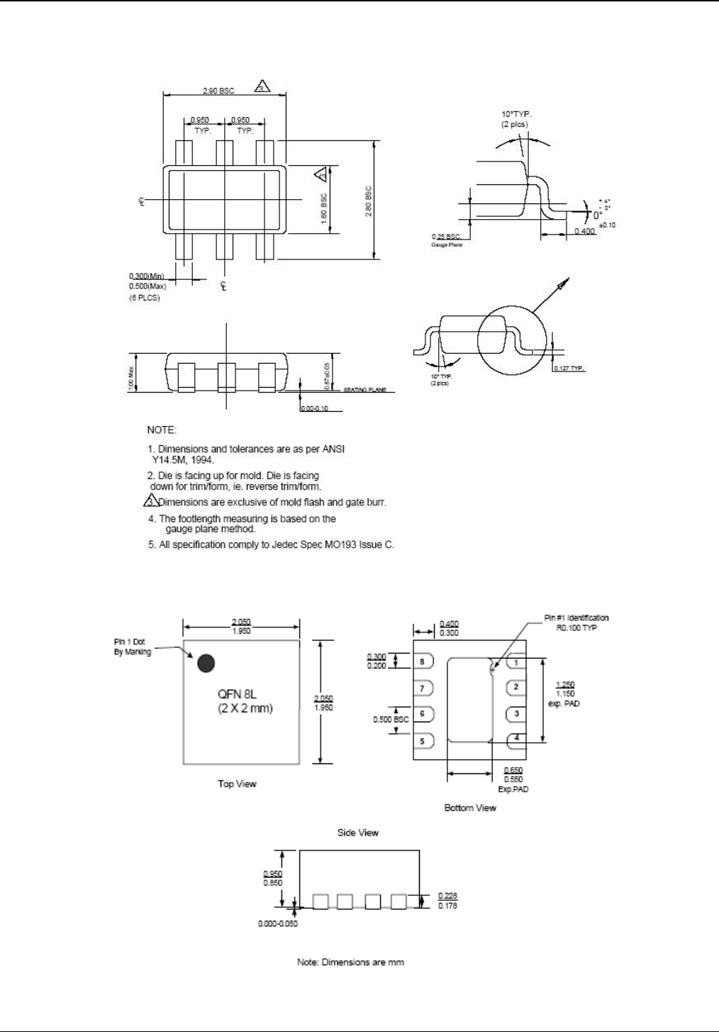
PACKAGE INFORMATION
1. SOT-23-6
2. QFN8 2x2
Page
PJ5121
