PJDLC05C 02 Datasheet. Www.s Manuals.com. Panjit
User Manual: Marking of electronic components, SMD Codes DA, DA*, DA**, DA***, DA-, DA-***, DA5, DAA, DAA**, DAB, DAB**, DACI, DAD**, DADI, DAE**, DAEI, DAF**, DAFI, DAG**, DAH**, DAI**, DAJ**, DAL, DALC, DAP, DAP6, DAP8A, DAQ, DAR, DAU, DAU**, DAV**, Da. Datasheets 2SD1664, AP131-15W, BAR43SFILM, BCW67A, BD49E27G, BD49K27G, BZX384-C11, DALC208SC6, DAP006, DMN5L06DMK, MAX6314US38D2-T, MMBZ4708-V, NCP1203D60R2 (analog), NCP1400ASN19T1, NCP1400ASN25T1, NCP1400ASN27T1, NCP1400ASN30T1, NCP1400ASN33T1, NCP1400ASN50T1, NCP140
Open the PDF directly: View PDF ![]() .
.
Page Count: 6
PAGE . 1
February 16,2010-REV.02
PJDLC05C-02
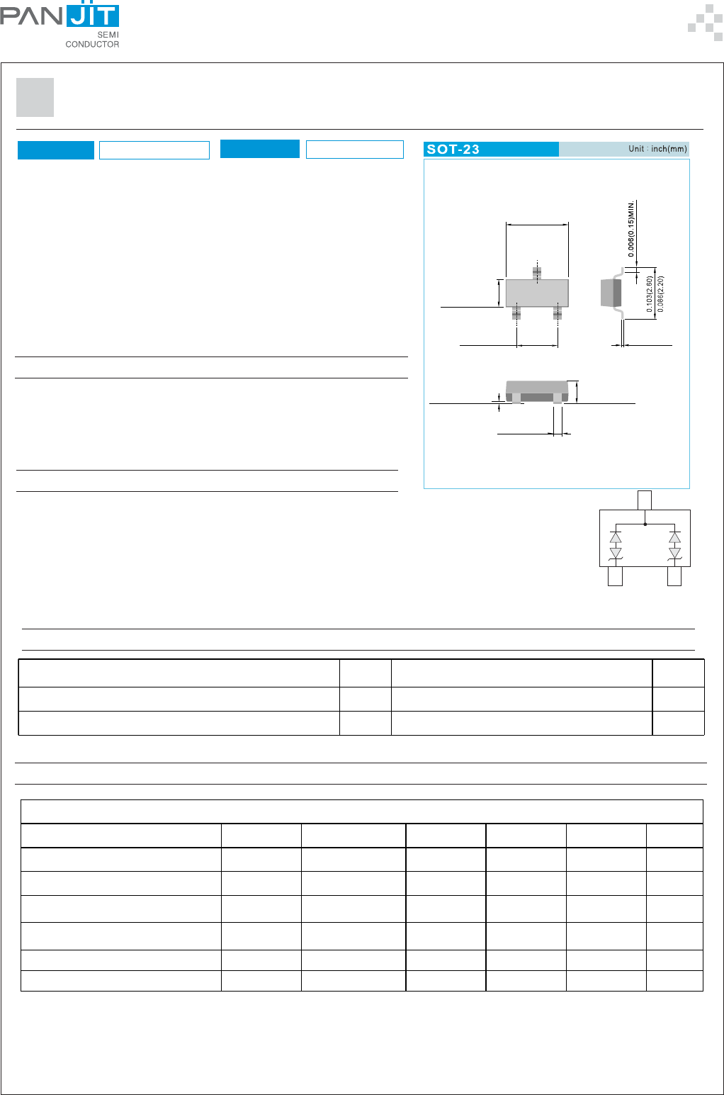
Fig.21
VOLTAGE POWER
5.0 Volts 200 Watts
MECHANICAL
• Case: SOT-23, plastic
• Terminals: solderable per MIL-STD-750, Method 2026
• Approx. Weight: 0.0003 ounce, 0.0084 gram
• Marking : DAA
DATA
ULTRA LOW CAPACITANCE DUAL TRANSIET VOLTAGE
SUPPRESSOR FOR HIGH SPEED DATA LINES
This transient overvoltage suppressor is intended to protect sensitive
equipment against electrostatic discharge events as well to offer a
minimum insertion loss in data transmission lines in communications ports
used in portable consumer, computing and networking applications. This
dual transient voltage suppressor comes in a single SOT-23, offering board
space reduction, where the application requires it.
This device comes with two pairs of high speed switching diodes
connected in series, where both pairs are electrically isolated, offering a
very low capacitance, minimizing the insertion losses in data transmission
lines.
MAXIMUM RATINGS
ELECTRICAL CHARACTERISTICS
PARAMETER SYMBOL VALUE UNITS
Operating Junction T
J
-55 to +150
O
C
Storage Temperature Range T
STG
-55 to +150
O
C
PJDLC05C-02
PARAMETER SYMBOL CONDITIONS Min. Typ. Max. UNITS
Reverse Stand-Off Voltage V
RWM
---5V
Reverse Breakdown Voltage V
BR
I
T
=1mA 6 - - V
Reverse Leakage Current I
R
V
RWM
= 5 V,
T = 25
O
C--20μA
Junction Capacitance C
J
Between pin1.2 to 3
V
R
=0V,f=1MHz --1.0pF
Peak Pulse Current I
PP
t
P
=8/20 μsec - - 10 A
Max Clamping Voltage V
C
t
P
=8/20 μsec - - 20.5 V
PAN JIT RESERVES THE RIGHT TO CHANGE THE SPECIFICATION ANY TIME WITHOUT NOTICE IN ORDER TO IMPROVE THE
DESIGN AND SUPPLY THE BEST POSSIBLE PRODUCT.
FEATURES
• Maximum capacitance @ 0 Vdc Bias of 1.0 pF between terminals 1-3 or
terminals 2-3
• IEC61000-4-2 esd 15kV Air, 8kV contact compliance
• Lead free in comply with EU RoHS 2002/95/EC directives.
• Green molding compound as per IEC61249 Std. . (Halogen Free)
0.120(3.04)
0.110(2.80)
0.056(1.40)
0.047(1.20)
0.079(2.00)
0.070(1.80)
0.020(0.50)
0.013(0.35)
0.044(1.10)
0.035(0.90)
0.008(0.20)
0.003(0.08)
0.004(0.10)
0.000(0.00)
PAGE . 2
February 16,2010-REV.02
PJDLC05C-02
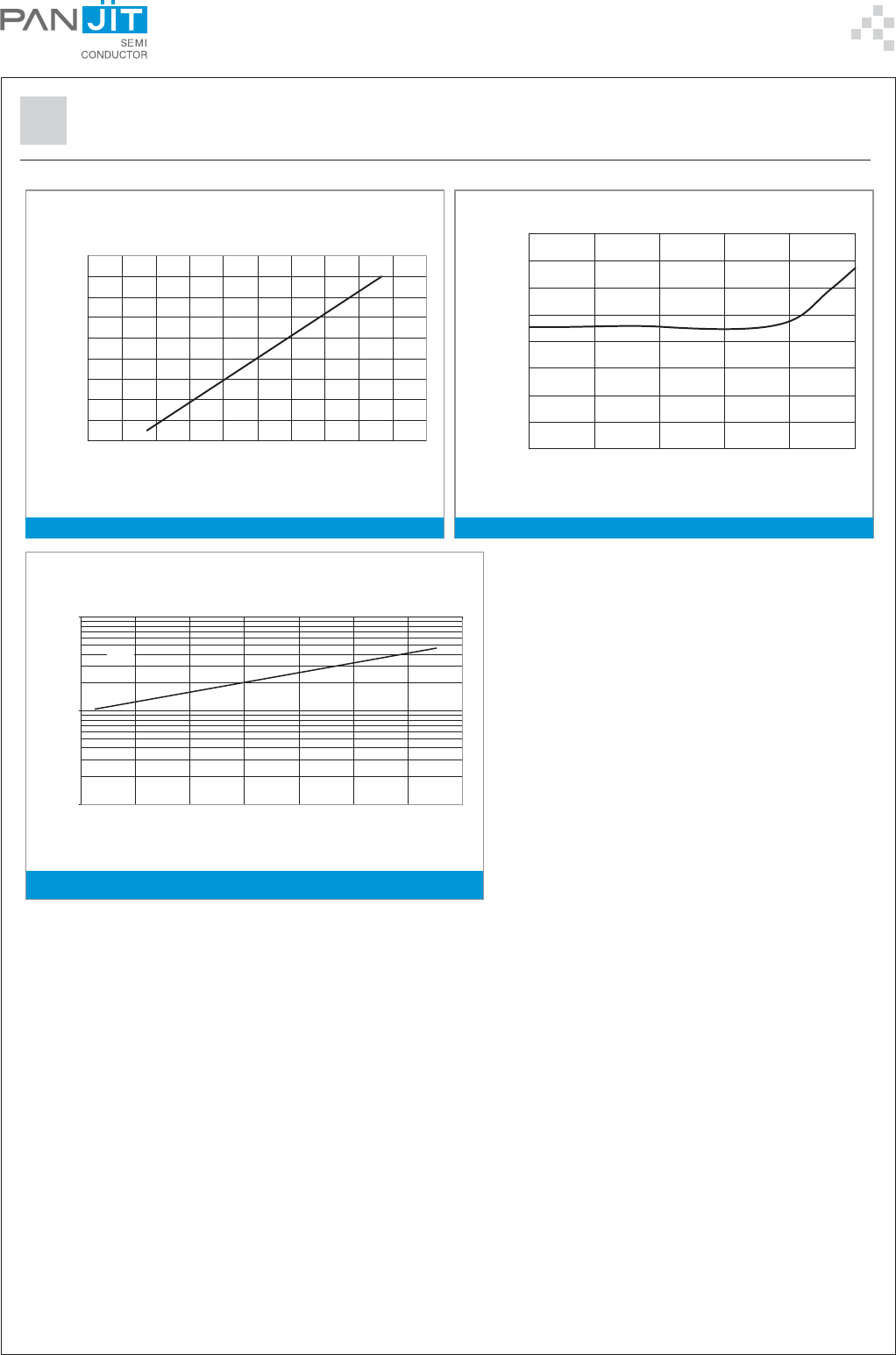
FIG.3- TYPICAL LEAKAGE CURRENT JUNCTION TEMPERATURE
FIG.3- TYPICAL LEAKAGE CURRENT JUNCTION TEMPERATURE
FIG.1- TYPICAL CLAMPING VOLTAGE
FIG.1- TYPICAL CLAMPING VOLTAGE
FIG.2- TYPICAL JUNCTION CAPACITANCE UNDER BIAS
FIG.2- TYPICAL JUNCTION CAPACITANCE UNDER BIAS
Clamping Voltage V , V
C
Peak Pulse Curren t Ip p ,A
0.3
0.35
0.4
0.45
0.5
0.55
0.6
0.65
0.7
012345
Reverse Bias Voltage, V
Capacitance C
J
,pF
0.01
0.1
1
20 40 60 80 100 120 140 160
T
J
, Junction Temperature (°C)
VR =5V
0
2
4
6
8
10
12
14
16
18
5 7 9 1113151719212325
I , Reverse Leakage Current( A)
R
m
PAGE . 3
February 16,2010-REV.02
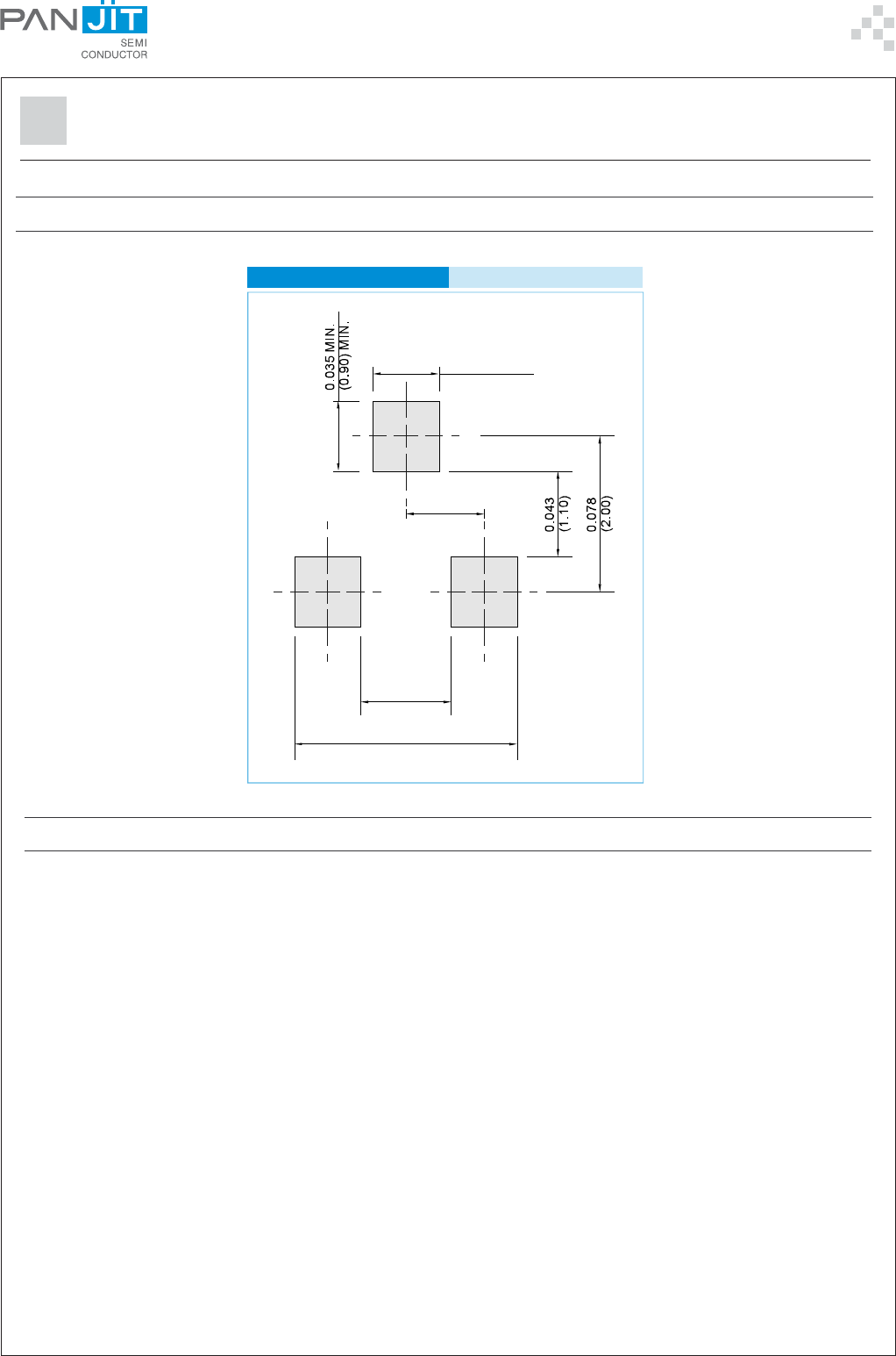
MOUNTING PAD LAYOUT
• Packing information
T/R - 12K per 13" plastic Reel
T/R - 3K per 7” plastic Reel
ORDER INFORMATION
SOT-23
0.031 MIN.
(0.80) MIN.
0.037
(0.95)
0.043
(1.10)
0.106
(2.70)
Unit inch(mm):
PJDLC05C-02
PAGE . 4
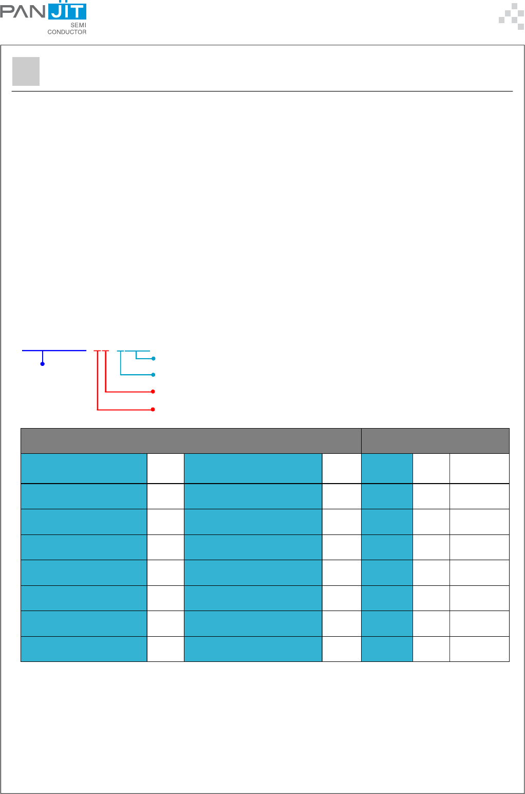
Part No_packing code_Version
PJDLC05C-02_R1_00001
PJDLC05C-02_R2_00001
For example :
RB500V-40_R2_00001
Part No.
Serial number
Version code means HF
Packing size code means 13"
Packing type means T/R
Packing Code XX Version Code XXXXX
Packing type 1st Code Packing size code 2nd Code HF or RoHS 1st Code 2nd~5th Code
Tape and Ammunition Box
(T/B) AN/A 0HF 0 serial number
Tape and Reel
(T/R) R7" 1RoHS 1 serial number
Bulk Packing
(B/P) B13" 2
Tube Packing
(T/P) T26mm X
Tape and Reel (Right Oriented)
(TRR) S52mm Y
Tape and Reel (Left Oriented)
(TRL) LPANASERT T/B CATHODE UP
(PBCU) U
FORMING FPANASERT T/B CATHODE DOWN
(PBCD) D
PJDLC05C-02
February 16,2010-REV.02

Disclaimer
z Reproducing and modifying information of the document is prohibited without
permission from Panjit International Inc..
z Panjit International Inc. reserves the rights to make changes of the content herein the
document anytime without notification. Please refer to our website for the latest
document.
z Panjit International Inc. disclaims any and all liability arising out of the application or
use of any product including damages incidentally and consequentially occurred.
z Panjit International Inc. does not assume any and all implied warranties, including
warranties of fitness for particular purpose, non-infringement and merchantability.
z Applications shown on the herein document are examples of standard use and
operation. Customers are responsible in comprehending the suitable use in particular
applications. Panjit International Inc. makes no representation or warranty that such
applications will be suitable for the specified use without further testing or modification.
z The products shown herein are not designed and authorized for equipments requiring
high level of reliability or relating to human life and for any applications concerning
life-saving or life-sustaining, such as medical instruments, transportation equipment,
aerospace machinery et cetera. Customers using or selling these products for use in
such applications do so at their own risk and agree to fully indemnify Panjit
International Inc. for any damages resulting from such improper use or sale.
PJDLC05C-02
February 16,2010-REV.02
PAGE . 5