PT1301 Datasheet. Www.s Manuals.com. R3.2 Powtech
User Manual: Marking of electronic components, SMD Codes 13, 13 •, 13 **, 13**, 13-, 13003, 1301, 1308A, 1308AI, 1308B, 1308BI, 130P03LS, 132, 133G, 133L, 138, 1392B, 13A, 13N03LA, 13W, 13Y, 13p, 13t. Datasheets 1.5SMC13AT3, 3DD13003, BC847BPN, BSC130P03LS G, BSS138W, BSS84, BZV49-C13, CMSZDA36V, DTA123JUA, DTA123JUB, DTA143EE, DTA143EKA, DTA143EM, DTA143EUA, DTA143EUB, IPD13N03LA, IPU13N03LA, LR9101G-33-AL4-R, LR9101L-33-AL4-R, LT1308ACS8, LT1308AIS8, LT1308BCS8, LT1308BIS8, MMBD1503, MTP3413N3, MTP3415KN3, NCP1392BDR2
Open the PDF directly: View PDF ![]() .
.
Page Count: 9
High Efficiency
Low Voltage Step-up DC/DC Converter
China Resources Powtech (Shanghai) Limited WWW.CRPOWTECH.COM Page 1
PT1301_DS Rev EN_3.2
PT1301
GENERATION DESCRIPTION
The PT1301 is a compact, high efficiency, and low
voltage step-up DC/DC converter with an Adaptive
Current Mode PWM control loop. It comprises of an
error amplifier, a ramp generator, a PWM comparator, a
switch pass element and the driver. It provides stable
and high efficient operation over a wide range of load
currents without external compensation. The below 1V
start-up input voltage makes PT1301 suitable for single
battery cell applications. The built-in power transistor is
able to provide up to 300mA output current while
working under Li-Battery Supply. Besides, it provides
extra pin to drive external power devices (NMOS or
NPN ) in case higher output current is needed. The
output voltage is set with two external resistors. The
500KHz high switching rate reduces the size of external
components. Besides, the 14μA low quiescent current
together with high efficiency maintains long battery
lifetime.
FEATURES
z Low Quiescent (Switch-off) Supply Current: 14μA
z Low Start-up Input Voltage: typical 0.8V
z High Supply Capability: Deliver 3.3V 100mA with
1Alkaline Cell; 5V 300mA with 1 Li-Cell
z Zero Shutdown Mode Supply Current
z High efficiency: 90%
z Fixed switching frequency: 500KHz
z Options for internal or external power switches
z Package type: SOT-26, SOT-89-5
APPLICATIONS
z MP3, PDA, Electronic
z Dictionary, DSC, LCD, RF-Tag,
z Portable Devices, Wireless Devices, etc.
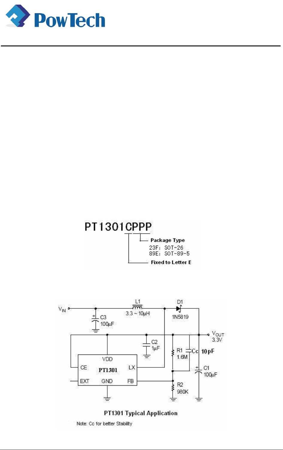
OREER INFORMATION
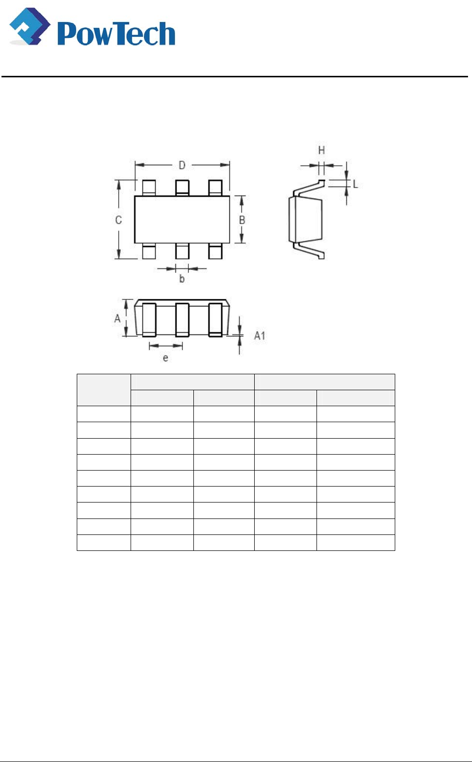
TYPICAL APPLICATION CIRCUITS
(1) Typical Application
1.5Vto 3.3V, 100mA Output Current, typically for MP3 Application.
High Efficiency
Low Voltage Step-up DC/DC Converter
China Resources Powtech (Shanghai) Limited WWW.CRPOWTECH.COM Page 2
PT1301_DS Rev EN_3.2
PT1301
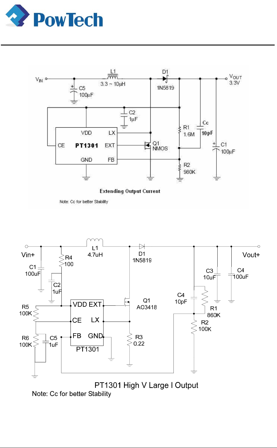
(2) Extending Output Current
1.5V to 3.3V, 250mA Output Current
(3) High Output Voltage, Large Output Current
5V to 12V, 300mA Output Current
High Efficiency
Low Voltage Step-up DC/DC Converter
China Resources Powtech (Shanghai) Limited WWW.CRPOWTECH.COM Page 3
PT1301_DS Rev EN_3.2
PT1301
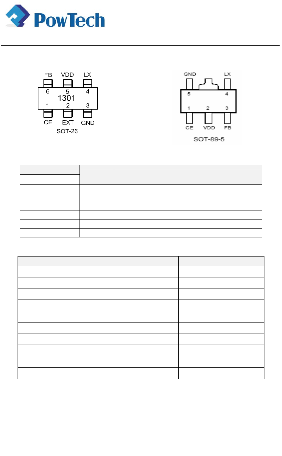
PIN ASSIGNMENT
PIN DESCRIPTION
PIN No
SOT-26 SOT-89-5 SYMBOL DESCRIPTTION
1 1 CE Enable pin. PT1301 Shut-down when CE is low
2 EXT Output pin for driving external power transistor
3 5 GND Ground
4 4 LX Output for internal power switch
5 2 VDD Power Supply
6 3 FB Feed back input
ABSOLUTE MAXIMUM RATINGS (Note 1)
SYMBOL ITEM RATING UNIT
VDD Supply Voltage -0.3~7.0V V
VLX LX pin Switch Voltage -0.3~7.0V V
VIO Voltage on other I/O pins -0.3V to (VDD+0.3V)
IOUT LX pin Output Current 2.5 A
IEXT EXT pin Drive Current 200 mA
PTR1 Package Thermal Resistance SOT-26, ΘJC 145 W/℃
PTR2 Package Thermal Resistance SOT-89-5, ΘJC 45 W/℃
TOPT Operating Temperature Range -40~125 ℃
TSTG Storage Temperature Range -65~150 ℃
TSOLDER Lead Temperature (Soldering) 260℃, 10s
Note1: Absolute Maximum Ratings are threshold limit values that must not be exceeded even for an instant under
any condition. Moreover, such values for any two items must not be reached simultaneously. Operation above these
absolute maximum ratings may cause degradation or permanent damage to the device. These are stress ratings only
and do not necessarily imply functional operation below these limits.
High Efficiency
Low Voltage Step-up DC/DC Converter
China Resources Powtech (Shanghai) Limited WWW.CRPOWTECH.COM Page 4
PT1301_DS Rev EN_3.2
PT1301
ELECTRICAL CHARACTERISTICS (Note 2,3,4)
(VIN=1.5V, VDD=3.3V, load current=0, TA =25℃, unless otherwise specified. )
SYMBOL ITEM TEST CONDITION MIN TYP MAX UNIT
VST Startup Voltage IL = 1mA -- 0.80 1.05 V
VDD Operating VDD Range VDD pin Voltage 2 -- 6 V
IOFF Shutdown Current I (VIN) CE Pin = 0V, VIN = 4.5V -- 0.01 1 μA
ISWITCH OFF Switch-Off Current I(VDD) VIN = 6V -- 14 25 μA
ISWITCH Continuous Switching
Current
VIN = CE= 3.3V, VFB = GND 0.22 0.24 0.7 mA
INO LOAD No Load Current I(VIN) VIN = 1.5V, VOUT = 3.3V -- 56 -- μA
V REF Feedback Reference Voltage Close loop, VDD = 3.3V 1.225 1.25 1.275 V
Fs Switching Frequency VDD = 3.3V 400 500 600 KHz
DMAX Maximum Duty VDD = 3.3V 85 94 -- %
On Resistance, LX to VDD VDD = 3.3V -- 0.3 1.1 Ω
ILIMIT Limit Current VDD = 3.3V 1 1.5 2 A
On Resistance, EXT to VDD VDD = 3.3V -- 4.4 8.5 Ω
On Resistance, EXT to GND VDD = 3.3V -- 2.45 8.5 Ω
△VLINE Line Regulation VIN = 3.5 ~ 6V, IL = 1mA -- 1.25 5 mV/V
△VLOAD Load Regulation VIN = 2.5V, IL = 1 ~ 100mA -- 0.14 -- mV/mA
CE trigger Level VDD = 3.3V 0.4 0.8 1.2 V
TS Vout Temperature Coefficient 50
ppm/℃
△TSD Thermal Shutdown Hysteresis -- 10 -- ℃
Note 2: Electrical Characteristics state DC and AC electrical specifications under particular test conditions which
guarantee specific performance limits. This assumes that the device is within the recommended operating Range.
Specifications are not guaranteed for parameters where no limit is given, however, the typical value is a good
indication of device performance.
Note 3: Typicals are measured at 25˚C and represent the parametric norm.
Note 4: Datasheet min/max specification limits are guaranteed by design, test, or statistical analysis.
High Efficiency
Low Voltage Step-up DC/DC Converter
China Resources Powtech (Shanghai) Limited WWW.CRPOWTECH.COM Page 5
PT1301_DS Rev EN_3.2
PT1301
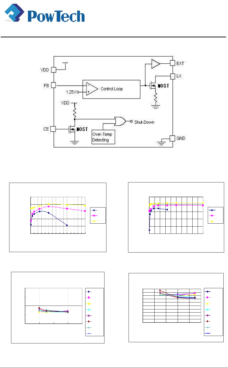
SIMPLIFIED BLOCK DIAGRAM
TYPICAL OPERATING CHARACTERISTICS
(1) Efficiency
(1.1) Vout=3.3V
Efficiency @ Vout=3.3V
50.00%
60.00%
70.00%
80.00%
90.00%
100.00%
0
10
20
30
40
50
60
70
80
90
100
110
120
130
140
150
Iout (mA)
Efficiency
1.0V
1.5V
3.0V
(1.2) Vout=5.0V
Efficiency @ Vout=5.0V
50.00%
60.00%
70.00%
80.00%
90.00%
100.00%
0
30
60
90
120
150
180
210
240
270
300
Iout (mA)
Efficiency
1.5V
3.0V
4.5V
(2) Line Regulation
(2.1) Vout=3.3V
Line Regulation @ Vout=3.3V
3.2
3.25
3.3
3.35
3.4
01234
Vin(V)
Vout(V)
Io=1mA
Io=5mA
Io=10mA
Io=25mA
Io=50mA
Io=100mA
Io=150mA
Io=300mA
(2.2) Vout=5.0V
Line Regulation @ Vout=5.0V
4.9
4.91
4.92
4.93
4.94
4.95
4.96
4.97
4.98
4.99
5
012345
Vin (V)
Vout (V)
Io=1mA
Io=5mA
Io=10mA
Io=25mA
Io=50mA
Io=100mA
Io=150mA
Io=300mA
High Efficiency
Low Voltage Step-up DC/DC Converter
China Resources Powtech (Shanghai) Limited WWW.CRPOWTECH.COM Page 6
PT1301_DS Rev EN_3.2
PT1301
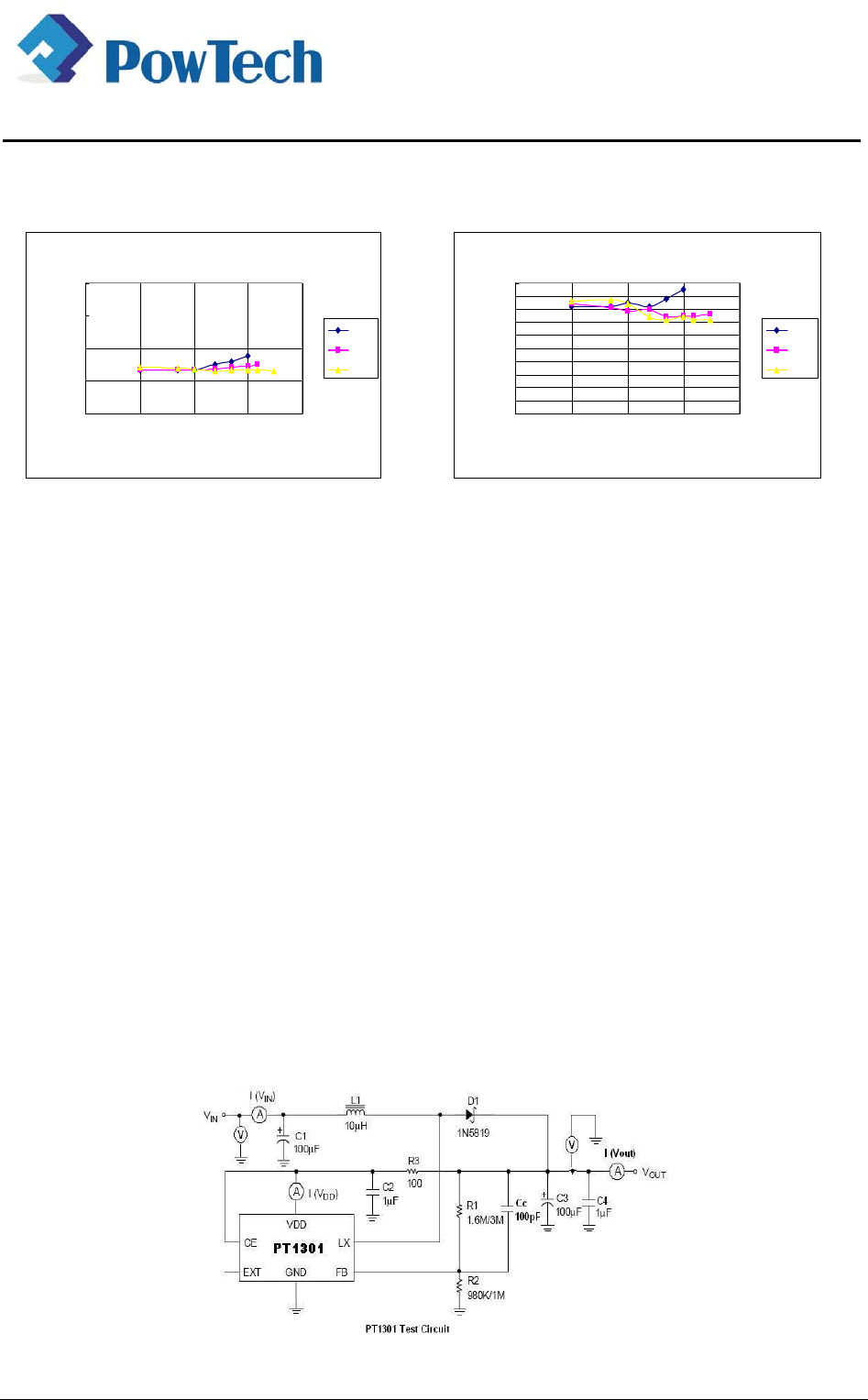
TYPICAL OPERATING CHARACTERISTICS
(3) Load Regulation
(3.1) Vout=3.3V
Load Regulation @ Vout=3.3V
3.2
3.25
3.3
3.35
3.4
0.1 1 10 100 1000
Iout (mA)
Vout (V)
1.0V
1.5V
3.0V
(3.2) Vout=5.0V
Load Regulation @ Vout=5.0V
4.9
4.91
4.92
4.93
4.94
4.95
4.96
4.97
4.98
4.99
5
0.1 1 10 100 1000
Iout (mA)
Vout (V)
1.5V
3.0V
4.5V
APPLICATION INFORMATION
1) Output Voltage Setting
Referring to Typical Application Circuit 1, the
output voltage of switching regulator (Vout) is set
with following equation:
Vout=(1+R1/R2)*Vfb
2) Feedback Loop Design
Referring to Typical Application Circuit 1 again,
the selection of R1 and R2 is a trade-off between
quiescent current consumption and interference
immunity besides abiding by the above equation.
z Higher R reduces quiescent current
( I=1.25V/R2 )
z Lower R gives better interference immunity,
and is less sensitive to interference, layout
parasitic, FB node leakage, and improper
probing to FB pin.
Hence for applications without standby or suspend
modes lower R1 and R2 values are preferred, while
for applications concerning the current
consumption in standby or suspend modes, higher
values of R1 and R2 are needed. Such high
impedance feedback loop is sensitive to any
interference, which requires careful PCB layout
and avoid any interference, especially to FB pin.
To improve the system stability, a proper value
capacitor between FB pin and Vout is suggested.
An empirical suggestion is around 100pF for MΩ
feedback resistors and 10nF~0.1uF for lower R
values.
3) PCB Layout Guide
PCB Layout shall follow these guidelines for better
system stability:
z A full GND plane without any gap break.
z VDD to GND bypass Cap – The 1μF MLCC noise
bypass Cap between pin 5 and pin 3 shall have
short and wide connections.
z Vin to GND bypass Cap – Add a Cap close to the
inductor when Vin is not an idea voltage source.
z Minimize the FB node copper area and keep it far
away from noise sources.
z Minimize the parasitic capacitance connected to
LX and EXT nodes to reduce the switch loss.
TEST CIRCUITS
High Efficiency
Low Voltage Step-up DC/DC Converter
China Resources Powtech (Shanghai) Limited WWW.CRPOWTECH.COM Page 7
PT1301_DS Rev EN_3.2
PT1301
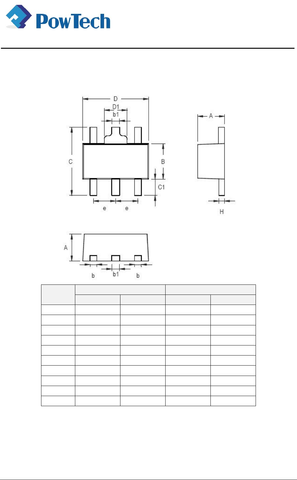
PACKAGE INFORMATION
(1) SOT-26
DIMENSION ( in mm) DIMENSION ( in Inch)
SYMBOL MIN MAX MIN MAX
A 0.787 1.450 0.031 0.057
A1 0.152 0.006
B 1.397 1.803 0.055 0.071
b 0.250 0.559 0.010 0.022
C 2.591 2.997 0.102 0.118
D 2.692 3.099 0.106 0.122
e 0.838 1.041 0.033 0.041
H 0.080 0.254 0.003 0.010
L 0.300 0.610 0.012 0.024
High Efficiency
Low Voltage Step-up DC/DC Converter
China Resources Powtech (Shanghai) Limited WWW.CRPOWTECH.COM Page 8
PT1301_DS Rev EN_3.2
PT1301
PACKAGE INFORMATION
(2) SOT-89-5
DIMENSION ( in mm ) DIMENSION( in Inch )
SYMBOL MIN MAX MIN MAX
A 1.400 1.600 0.055 0.063
b 0.460 0.520 0.014 0.020
B 2.400 2.600 0.094 0.102
b1 0.406 0.533 0.016 0.021
C 4.250 0.167
C1 0.800 0.031
D 4.400 4.600 0.173 0.181
D1 1.700 0.067
e 1.400 1.600 0.055 0.063
H 0.380 0.430 0.014 0.017