2313v1 Pt2313, Pt2313 S Ptc
User Manual: Datasheets PT2313, PT2313-S, PT2313L, PT2313L-D.
Open the PDF directly: View PDF ![]() .
.
Page Count: 16

PTC Princeton Technology Corp. Tel : 886-2-29162151
Fax : 886-2-29174598
4-Channel Audio Processor IC PT2313
PT2313 v 1 Page 1 Written Feb. 1997
Description
PT2313 is an four-channel digital audio processor utilizing CMOS Technology. Volume,
Right/Left Bass and Treble Balance, Front/Rear Fader Processor are incorporated into a single
chip. Loudness Function and Selectable Input Gain are also provided to build a highly effective
electronic audio processor having the highest performance and reliability with the least external
components. All functions are programmable using the Serial Bus. The pin assignments and
application circuit are optimized for easy PCB layout and cost saving advantage for audio
application. PT2313 is housed in a 28-pin DIP/SO Package and is functionally compatible with
TDA7313.
Features
r CMOS Technology
r Least External Components
r Treble and Bass Control
r Loudness Function
r 3 Stereo Inputs with Selectable Input Gain
r Input/Output for External Noise Reduction System/Equalizer
r 4 Independent Speaker Controls for Fader and Balance
r Independent Mute Function
r Volume Control in 1.25 dB/step
r Low Distortion
r Low Noise and DC Stepping
r Controlled by Serial Bus Micro-Processor Interface
Applications
r Car Stereo (Audio)
r Hi-Fi Audio System
PTC Princeton Technology Corp. Tel : 886-2-29162151
Fax : 886-2-29174598
4-Channel Audio Processor IC PT2313
PT2313 v 1 Page 2 Written Feb. 1997
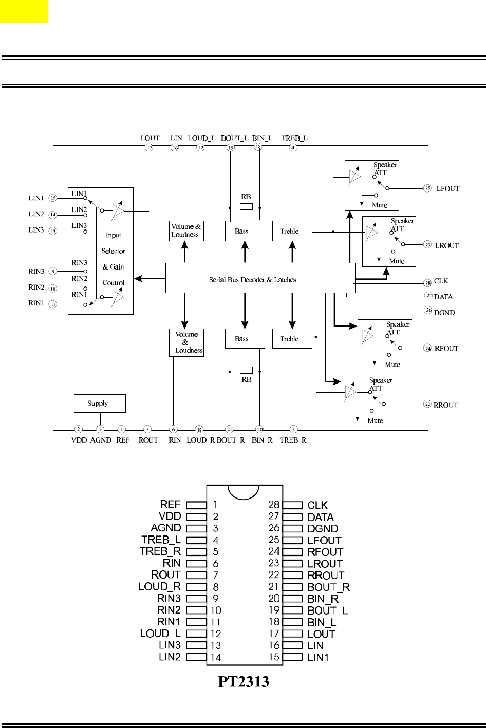
Block Diagram
Pin Configuration
PTC Princeton Technology Corp. Tel : 886-2-29162151
Fax : 886-2-29174598
4-Channel Audio Processor IC PT2313
PT2313 v 1 Page 3 Written Feb. 1997
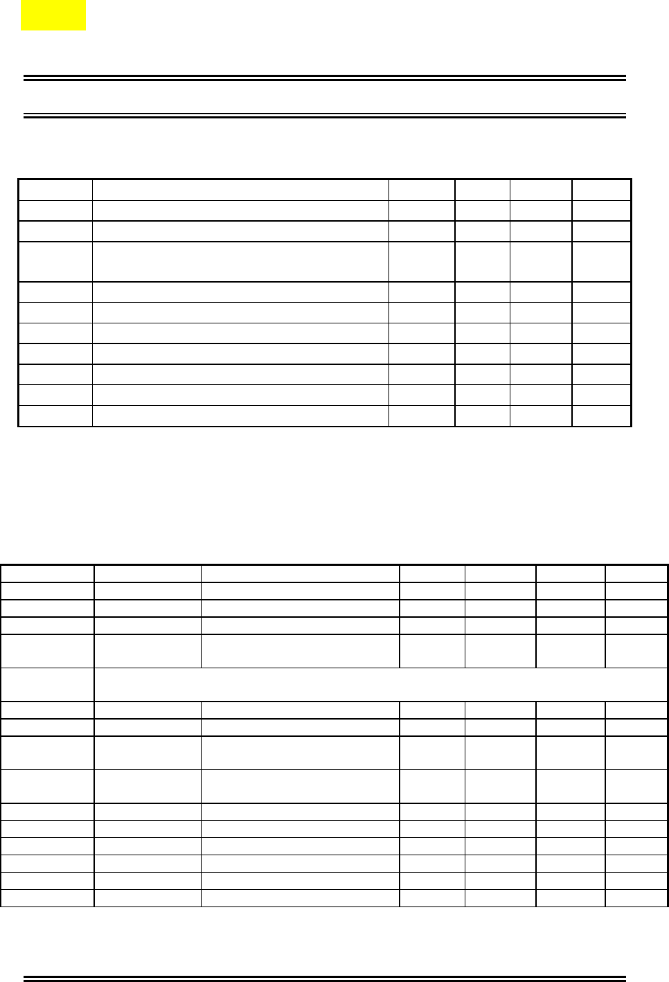
Pin Description
Pin Name I/O Description Pin No.
REF - Analog Reference Voltage (1/2 VDD) 1
VDD - Supply Input Voltage 2
AGND - Analog Ground 3
TREB_L I Left Channel Input for Treble Controller 4
TREB_R I Right Channel Input for Treble Controller 5
RIN I Audio Processor Right Channel Input 6
ROUT OGain Output and Input Selector for Right
Channel7
LOUD_R I Right Channel Loudness Input 8
RIN3 I Right Channel Input 3 9
RIN2 I Right Channel Input 2 10
RIN1 I Right Channel Input 1 11
LOUD_L I Left Channel Loudness Input 12
LIN3 I Left Channel Input 3 13
LIN2 I Left Channel Input 2 14
LIN1 I Left Channel Input 1 15
LIN I Audio Processor Left Channel Input 16
LOUT OGain Output and Input Selector for Left
Channel17
BIN_L I Left Bass Controller Input Channel 18
BOUT_L O Left Bass Controller Output Channel 19
BIN_R I Right Channel Input for Bass Controller 20
BOUT_R O Right Channel Output for Bass Controller 21
RROUT O Right Rear Speaker Output 22
LROUT O Left Rear Speaker Output 23
RFOUT O Right Front Speaker Output 24
LFOUT O Left Front Speaker Output 25
DGND - Digital Ground 26
DATA I Control Data Input 27
CLK I Clock Input for Serial Data Transmission 28
PTC Princeton Technology Corp. Tel : 886-2-29162151
Fax : 886-2-29174598
4-Channel Audio Processor IC PT2313
PT2313 v 1 Page 4 Written Feb. 1997
Functional Description
Bus Interface
Data are transmitted to and from the microprocessor to the PT2313 via the DATA and
CLK. The DATA and CLK make up the BUS Interface. It should be noted that the pull-
up resistors must be connected to the positive supply voltage.
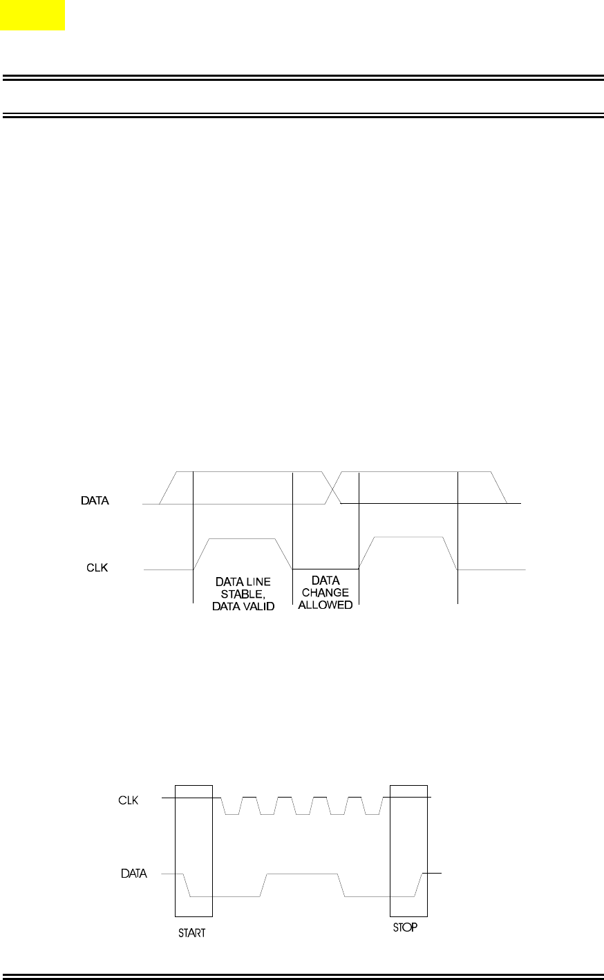
Data Validity
A data on the DATA Line is considered valid and stable only when the CLK Signal is in
HIGH State. The HIGH and LOW State of the DATA Line can only change when the
CLK signal is LOW. Please refer to the figure below.
Start and Stop Conditions
A Start Condition is activated when 1) the CLK is set to HIGH and 2) DATA shifts
from HIGH to LOW State. The Stop Condition is activated when 1) CLK is set to
HIGH and 2) DATA shifts from LOW to HIGH State. Please refer to the timing diagram
below.
PTC Princeton Technology Corp. Tel : 886-2-29162151
Fax : 886-2-29174598
4-Channel Audio Processor IC PT2313
PT2313 v 1 Page 5 Written Feb. 1997
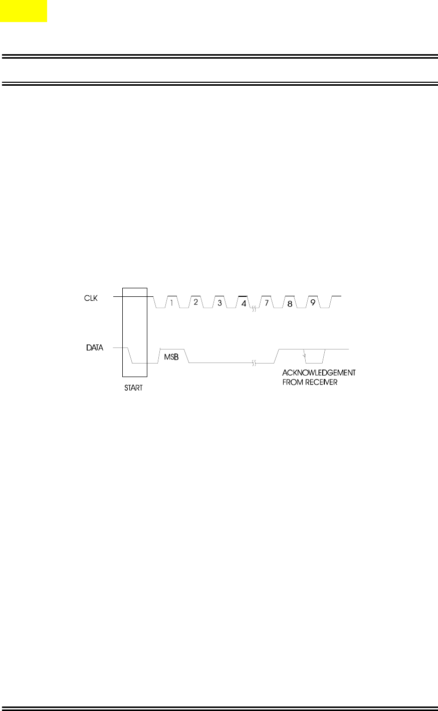
Byte Format
Every byte transmitted to the DATA Line consist of 8 bits. Each byte must be followed
by an Acknowledge Bit. The MSB is transmitted first.
Acknowledge
During the Acknowledge Clock Pulse, the master (µP) puts a resistive HIGH level on the
DATA Line. The peripheral (audio processor) that acknowledges has to pull-down
(LOW) the DATA line during the Acknowledge Clock Pulse so that the DATA Line is in
a Stable Low State during this Clock Pulse. Please refer to the diagram below.
The audio processor that has been addressed has to generate an acknowledge after
receiving each byte, otherwise, the DATA Line will remain at the High Level during the
ninth (9th) Clock Pulse. In this case, the master transmitter can generate the STOP
Information in order to abort the transfer.
Transmission without Acknowledge
If you want to avoid the acknowledge detection of the audio processor, a simpler µP
transmission may be used. Wait one clock and do not check the slave acknowledge of
this same clock then send the new data. If you use this approach, there are greater
chances of faulty operation as well as decrease in noise immunity.
Interface Protocol
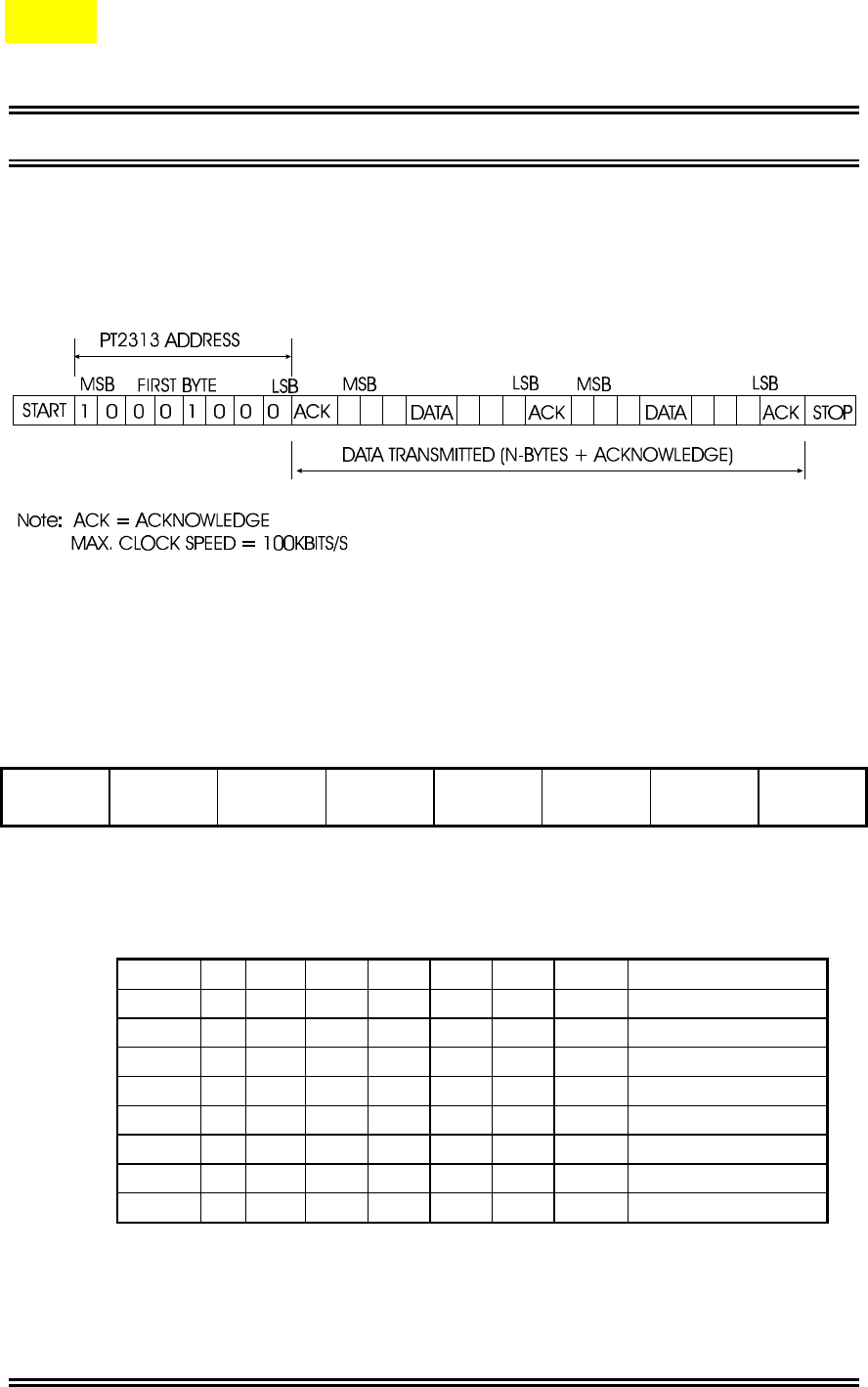
The interface protocol consists of the following:
• A Start Condition
• A Chip Address Byte including the PT2313 address. The 8th Bit of the Byte must be
“0”. PT2313 must always acknowledge the end of each transmitted byte.
PTC Princeton Technology Corp. Tel : 886-2-29162151
Fax : 886-2-29174598
4-Channel Audio Processor IC PT2313
PT2313 v 1 Page 6 Written Feb. 1997
• A Data Sequence (N-Bytes + Acknowledge)
• A Stop Condition
Please refer to the diagram below:
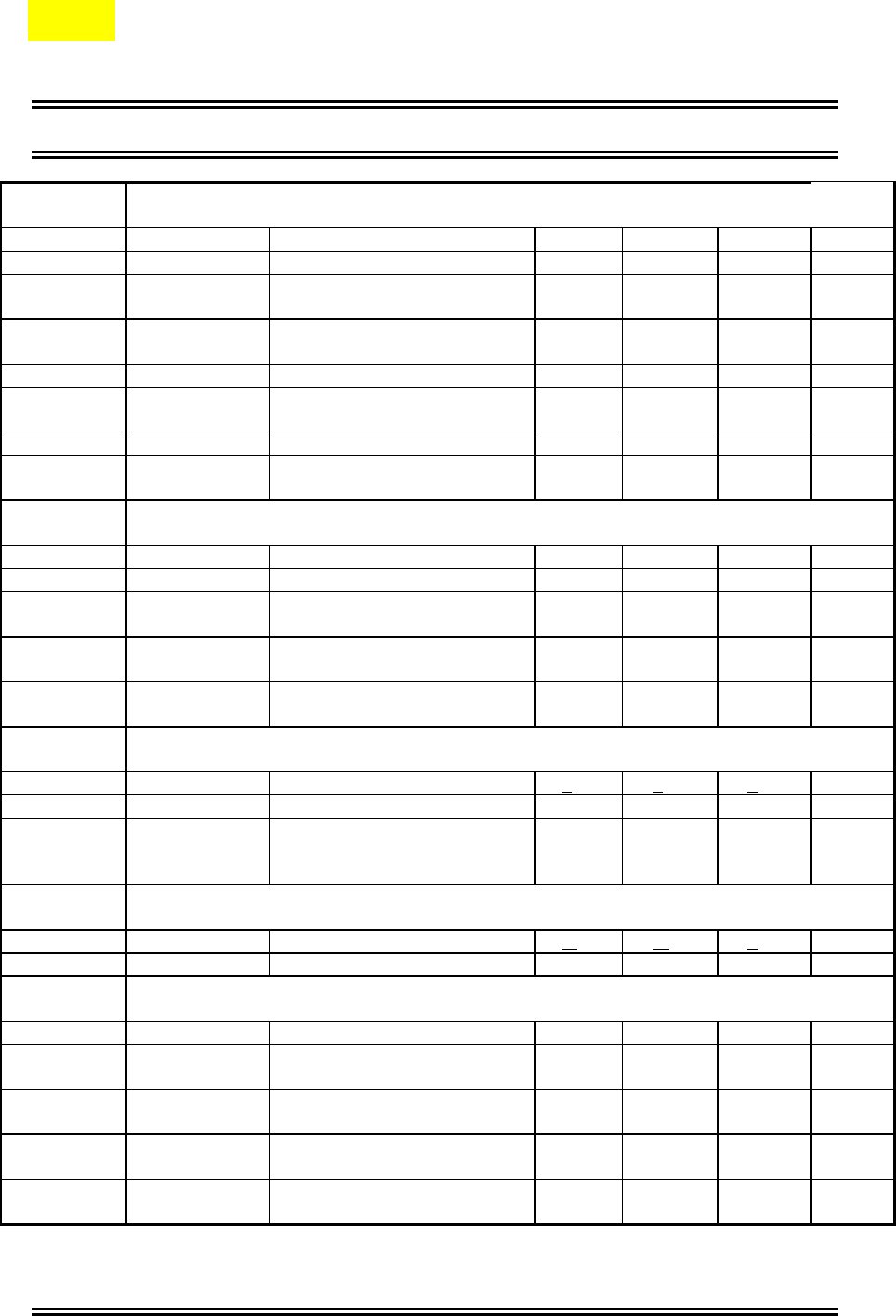
Software Specification
PT2313 Address
PT2313 Address is shown below.
1
MSB 0 0 0 1 0 0 0
LSB
Data Bytes
MSB LSB FUNCTION
0 0 B2 B1 B0 A2 A1 A0 Volume Control
1 1 0 B1 B0 A2 A1 A0 Speaker ATT LR
1 1 1 B1 B0 A2 A1 A0 Speaker ATT RR
1 0 0 B1 B0 A2 A1 A0 Speaker ATT LF
1 0 1 B1 B0 A2 A1 A0 Speaker ATT RF
0 1 0 G1 G0 S2 S1 S0 Audio Switch
0 1 1 0 C3 C2 C1 C0 Bass Control
0 1 1 1 C3 C2 C1 C0 Treble Control
where Ax = 1.25 dB steps; Bx = 10 dB steps; Cx = 2 dB steps; Gx = 3.75 dB/steps
PTC Princeton Technology Corp. Tel : 886-2-29162151
Fax : 886-2-29174598
4-Channel Audio Processor IC PT2313
PT2313 v 1 Page 7 Written Feb. 1997
Volume
The table below gives a detailed description of the Volume Data Bytes. For example, a
volume of -37.5 dB is given by 0 0 0 1 1 1 1 0.
MSB LSB FUNCTION
0 0 B2 B1 B0 A2 A1 A0 Volume 1.25 dB steps
0 0 0 0
0 0 1 -1.25
0 1 0 -2.5
0 1 1 -3.75
1 0 0 -5
1 0 1 -6.25
1 1 0 -7.5
1 1 1 -8.75
0 0 B2 B1 B0 A2 A1 A0 Volume 10dB steps
0 0 0 0
0 0 1 -10
0 1 0 -20
0 1 1 -30
1 0 0 -40
1 0 1 -50
1 1 0 -60
1 1 1 -70
Speaker Attenuators
The table below gives a detailed description of the speaker attenuators data bytes. For
example, an attenuation of 30dB on the Speaker lF (Right Front) is given by: 1 0 0 1 1 0
0 0.
MSB LSB FUNCTION
1 0 0 B1 B0 A2 A1 A0 Speaker LF
1 0 1 B1 B0 A2 A1 A0 Speaker RF
1 1 0 B1 B0 A2 A1 A0 Speaker LR
1 1 1 B1 B0 A2 A1 A0 Speaker RR
0 0 0 0
0 0 1 -1.25
0 1 0 -2.5
0 1 1 -3.75
PTC Princeton Technology Corp. Tel : 886-2-29162151
Fax : 886-2-29174598
4-Channel Audio Processor IC PT2313
PT2313 v 1 Page 8 Written Feb. 1997
1 0 0 -5
1 0 1 -6.25
1 1 0 -7.5
1 1 1 -8.75
0 0 0
0 1 -10
1 0 -20
1 1 -30
1 1 1 1 1 Mute
Audio Switch Data Byte
The following table shows the detailed description of the Audio Switch Data Bytes. For
example, a Stereo 1 Input with Gain of +11.25 dB Loudness ON is given by: 0 1 0 0 0 0
0 0.
MSB LSB FUNCTION
0 1 0 G1 G0 S2 S1 S0 Audio Switch
0 0 Stereo 1
0 1 Stereo 2
1 0 Stereo 3
1 1 Stereo 4 *
0 Loudness ON
1 Loudness OFF
0 0 +11.25dB
0 1 +7.5dB
1 0 3.75dB
1 1 0dB
Note: * = Stereo 4 is internally connected.
Bass and Treble Data Bytes
The following table shows a detailed description of the Bass and Treble Data Byte. For
example a Treble at -12dB is given by : 0 1 1 1 0 0 0 1.
PTC Princeton Technology Corp. Tel : 886-2-29162151
Fax : 886-2-29174598
4-Channel Audio Processor IC PT2313
PT2313 v 1 Page 9 Written Feb. 1997
MSB LSB Function
0 1 1 0 C3 C2 C1 C0 Bass
0 1 1 1 C3 C2 C1 C0 Treble
0 0 0 0 -14
0 0 0 1 -12
0 0 1 0 -10
0 0 1 1 -8
0 1 0 0 -6
0 1 0 1 -4
0 1 1 0 -2
0 1 1 1 0
1 1 1 1 0
1 1 1 0 2
1 1 0 1 4
1 1 0 0 6
1 0 1 1 8
1 0 1 0 10
1 0 0 1 12
1 0 0 0 14
Unit: dB
Thermal Data
Symbol Description SO28 DIP28 Unit
Rth j-pins Thermal
Resistance
Junction-Pins
Max.
85 65 oC/W
Absolute Maximum Ratings
Symbol Parameter Rating Unit
Vs Operating Supply
Voltage 10.2 V
Tamb Operating Ambient
Temperature -40 to 85 oC
Tstg Storage
Temperature Range -55 to +150 oC
PTC Princeton Technology Corp. Tel : 886-2-29162151
Fax : 886-2-29174598
4-Channel Audio Processor IC PT2313
PT2313 v 1 Page 10 Written Feb. 1997
Quick Reference Data
Symbol Parameter Min. Typ. Max. Unit
Vs Supply Voltage 6 9 10 V
VCL Max. Input Signal Handling 2 Vrms
THD Total harmonic Distortion V = 1Vrms,
f = 1KHz 0.01 0.1 %
S/N Signal to Noise ratio 106 dB
Sc Channel Separation f = 1KHz 103 dB
Volume Control 1.25dB step -78.75 0 dB
Bass & Treble Control 2dB step -14 +14 dB
Fader & Balance Control 1.25dB step -38.75 0 dB
Input Gain 3.75 dB step 0 11.25 dB
Mute Attenuation 100 dB
Electrical Characteristics
(Unless specified: Tamb = 25oC, Vc=9V, RL=10KΩ, Rg = 600Ω, all controls flat (G=0),
f=1KHz)
Symbol Parameter Test Condition Min. Typ. Max. Unit
Supply
Vcc Supply Voltage 6 9 10 V
Is Supply Current 8 11 mA
SVRR Ripple
Rejection 60 80 dB
Input
Selectors
RII Input Resistance Input 1,2,3 35 50 70 KOhms
VCL Clipping Level 2 2.5 Vrms
SIN Input Separation
(2) 80 100 dB
RLOutput Load
Resistance Pin 7, 17 2 KOhms
GINmin Min. Input Gain -1 0 1 dB
GINmax Max. Input Gain 11.25 dB
GSTEP Step Resolution 3.75 dB
Ein Input Noise G=11.25dB 2 uV
VDC DC Steps Adjacent Gain Steps 4 20 mV
G=18.75 dB to Mute 4 mV
PTC Princeton Technology Corp. Tel : 886-2-29162151
Fax : 886-2-29174598
4-Channel Audio Processor IC PT2313
PT2313 v 1 Page 11 Written Feb. 1997
Volume
Control
RIV Input Resistance 20 33 50 KOhms
CRANGE Control Range 70 75 80 dB
AVMIN Min.
Attenuation -1 0 1 dB
AVMAX Max.
Attenuation 70 75 80 dB
ASTEP Step Resolution 0.5 1.25 1.75 dB
EAAttenuation Set
Error AV=0 to -20dB
AV=-20 to –60dB -1.25
-3 0 1.25
2dB
dB
ETTracking Error 2 dB
VDC DC Steps Adjacent Attenuation Steps
From 0dB to AV max 0
0.5 3
7.5 mV
mV
Speaker
Attenuators
CRANGE Control Range 35 37.5 40 dB
SSTEP Step Resolution 0.5 1.25 1.75 dB
EAAttenuation Set
Error 1.5 dB
AMUTE Output Mute
Attenuation 80 100 dB
VDC DC Steps Adjacent Att. Steps
From 0 to Mute 0
13
10 mV
mV
Bass Control
(1)
Gb Control Range Max. Boost/Cut + 12 + 14 + 16 dB
BSTEP Step Resolution 1 2 3 dB
RBInternal
Feedback
Resistance
34 44 58 KOhms
Treble
Control (1)
Gt Control Range Max. Boost/Cut + 13 + 14 + 15 dB
TSTEP Step Resolution 1 2 3 dB
Audio
Outputs
VOCL Clipping Level d=0.3% 2 2.5 Vrms
RLOutput Load
Resistance 2 KOhms
CLOutput Load
Capacitance 10 nF
ROUT Output
Resistance 30 75 120 Ohms
VOUT DC Voltage
Level 4.2 4.5 4.8 V
PTC Princeton Technology Corp. Tel : 886-2-29162151
Fax : 886-2-29174598
4-Channel Audio Processor IC PT2313
PT2313 v 1 Page 12 Written Feb. 1997
General
eNO Output Noise BW==20-20KHz, flat
Output Muted
All gains=0dB 2.5
5 15 uV
uV
A Curve All Gains=0dB 3 uV
S/N Signal to Noise
Ratio All Gains=0dB
Vo=1Vrms 106 dB
d Distortion AV=0, VIN=1Vrms
AV=-20dB, VIN=1Vrms
VIN=0.3Vrms
0.01
0.09
0.04
0.1
0.3 %
%
%
Sc Channel
Separation
Left/Right
80 103 dB
Total Tracking
Error AV=0 to -20dB
-20 to -60dB 0
01
2dB
dB
Bus Inputs
VIL Input Low
Voltage 1 V
VIH Input High
Voltage 3 V
IIN Input Current -5 +5 uA
Vo Output Voltage
SDA
Acknowledge
Io=1.6mA 0.4 V
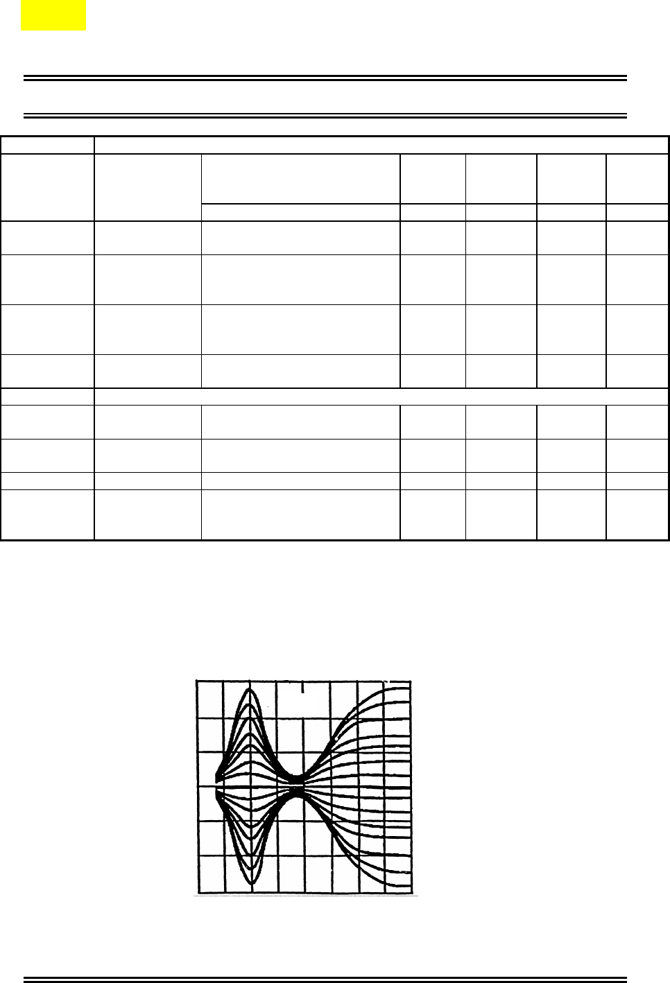
Note: (1) For the Bass and Treble response please, refer to the diagram below. The
center frequency and quality of the resonance behavior can be selected by the external
circuitry. A standard first order bass response can realized by a standard feedback
network.
(2) The selected input is grounded thru the 2.2uF capacitor.
(dB)
10
5
0
5
10
15 10 30 100 300 1K 3K 10K f (Hz)
Typical Tone Response (with the ext. Components indicated in the test circuit)
AV=0
PTC Princeton Technology Corp. Tel : 886-2-29162151
Fax : 886-2-29174598
4-Channel Audio Processor IC PT2313
PT2313 v 1 Page 13 Written Feb. 1997
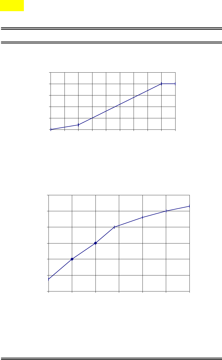
Loudness vs Volume Attenuation
0
5
10
15
20
25
0 5 10 15 20 25 30 35 40 45
Volume Attenuation (dB)
Loudness (dB)
Quiescent Current vs. Supply Voltage
3
4
5
6
7
8
9
4 5 6 7 8 9 10
Supply Voltage (V)
Quiescent Current (mA)
PTC Princeton Technology Corp. Tel : 886-2-29162151
Fax : 886-2-29174598
4-Channel Audio Processor IC PT2313
PT2313 v 1 Page 14 Written Feb. 1997
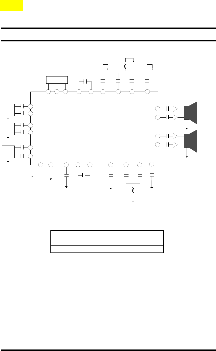
Application Circuit
26272817161219184
MCU
DGND DATA CLK LOUT LIN LOUD_L BOUT_L BIN_L TREB_L
2.2u
100n
100n
2.7n
2.7n
2.7n
100n
100n
100n
100n
C9
2.2u
C9
C11
C10
C17
C16
C7
C14
C13
C15
C12
5.6K
5.6K
R2
R1
LFOUT
RFOUT
LROUT
RROUT
25
23
24
22
Front Speaker
Rear Speaker
10u
C18
10u
C20
10u
C19
10u
C21
458
20
21
8
6
7
32
VDD
C4 2.2u
C3 2.2u
C2 2.2u
C5 2.2u
C1 2.2u
C6 2.2u
RIN1
LIN1
RIN2
LIN2
RIN3
LIN3
Tape
CD
Player
AM/FM
Tuner
VDD AGND REF ROUT RIN LOUD_R BOUT_R BIN_R TREB_R
Amp1
Amp2
Amp4
Amp3
PT2313
Order Information
Valid Part Number Package Type
PT2313 28 Pins, DIP
PT2313-S 28 Pins, SO (300 mil)
PTC Princeton Technology Corp. Tel : 886-2-29162151
Fax : 886-2-29174598
4-Channel Audio Processor IC PT2313
PT2313 v 1 Page 15 Written Feb. 1997
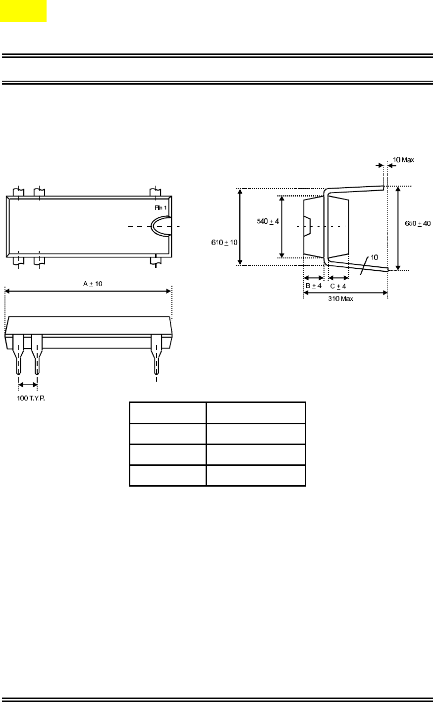
Package Information
28 Pins, DIP Package
Symbol Dimension in Mil
A 1450
B 70
C 70
PTC Princeton Technology Corp. Tel : 886-2-29162151
Fax : 886-2-29174598
4-Channel Audio Processor IC PT2313
PT2313 v 1 Page 16 Written Feb. 1997
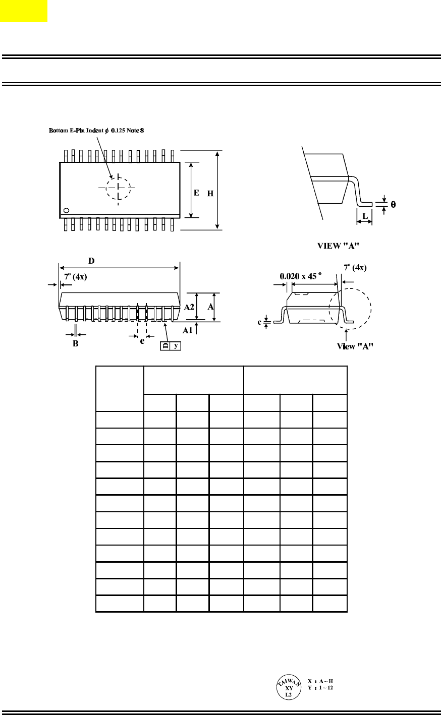
28 Pins, SO Package (300 mil)
Symbol
Dimensions in
Millimeter Dimensions in Inches
Min Nom Max Min Nom Max
A 2.36 2.49 2.64 0.093 0.098 0.104
A1 0.10 - 0.30 0.004 - 0.012
A2 - 2.34 - - 0.092 -
B 0.33 0.41 0.51 0.013 0.016 0.020
C 0.23 0.25 0.30 0.009 0.010 0.012
D 17.70 17.91 18.11 0.697 0.705 0.713
E 7.39 7.49 7.59 0.291 0.295 0.299
e - 1.27 - - 0.050 -
H 10.01 10.31 10.64 0.394 0.406 0.419
L 0.38 0.81 1.27 0.015 0.032 0.050
y - - 0.10 - - 0.004
θ 0O- 8O0O- 8O
Note: 1. Controlling Dimension: Inch
2. Lead Frame Material: Copper 194
3. After solder plating lead thickness will be 0.015” max.
4. Dimension “D” does not include mold flash, protrusions or gate burrs.
5. Dimension “E” does not include interlead or protrusions.
6. Tolerance: ±0.010” unless otherwise specified.
7. Otherwise dimension follow acceptable spec.
8. Bottom E-Pin Indent in marked as below:
