Input Capture HAL Module Guide Application Project R11an0106eu0101 Synergy Mod
User Manual:
Open the PDF directly: View PDF ![]() .
.
Page Count: 16
- 1. Input Capture HAL Module Features
- 2. Input Capture HAL Module APIs Overview
- 3. Input Capture HAL Module Operational Overview
- 4. Including the Input Capture HAL Module in an Application
- 5. Configuring the Input Capture HAL Module
- 6. Using the Input Capture HAL Module in an Application
- 7. The Input Capture HAL Module Application Project
- 8. Customizing the Input Capture HAL Module for a Target Application
- 9. Running the Input Capture HAL Module Application Project
- 10. Input Capture HAL Module Conclusion
- 11. Input Capture HAL Module Next Steps
- 12. Input Capture HAL Module Reference Information
- Revision History
Application Note
R11AN0106EU0101 Rev.1.01 Page 1 of 14
Aug 30, 2017
Renesas Synergy™ Platform
Input Capture HAL Module Guide
Introduction
This module guide will enable you to effectively use a module in your own design. Upon completion of this guide, you
will be able to add this module to your own design, configure it correctly for the target application and write code, using
the included application project code as a reference and an efficient starting point. References to more detailed API
descriptions and suggestions of other application projects that illustrate more advanced uses of the module are included
in this document and should be valuable resources for creating more complex designs.
The Input Capture HAL module is an API used for measuring input pulse-widths and is implemented on
r_gpt_input_capture. The Input Capture HAL module configures the input capture parameters to use with the
GPT peripheral on Synergy MCUs. A user-defined callback can be created to acquire the value each time a new
measurement is complete.
Contents
1. Input Capture HAL Module Features ....................................................................................... 2
2. Input Capture HAL Module APIs Overview .............................................................................. 3
3. Input Capture HAL Module Operational Overview ................................................................... 4
3.1 Input Capture HAL Module Operational Notes ........................................................................................ 4
3.2 Input Capture HAL Module Limitations.................................................................................................... 4
4. Including the Input Capture HAL Module in an Application ....................................................... 5
5. Configuring the Input Capture HAL Module ............................................................................. 6
5.1 Input Capture HAL Module Clock Configuration ..................................................................................... 7
5.2 Input Capture HAL Module Pin Configuration ......................................................................................... 7
6. Using the Input Capture HAL Module in an Application ............................................................ 8
7. The Input Capture HAL Module Application Project ................................................................. 8
8. Customizing the Input Capture HAL Module for a Target Application ..................................... 12
9. Running the Input Capture HAL Module Application Project .................................................. 12
10. Input Capture HAL Module Conclusion .................................................................................. 13
11. Input Capture HAL Module Next Steps .................................................................................. 13
12. Input Capture HAL Module Reference Information ................................................................ 13
R11AN0106EU0101
Rev.1.01
Aug 30, 2017
Renesas Synergy™ Platform Input Capture HAL Module Guide
R11AN0106EU0101 Rev.1.01 Page 2 of 14
Aug 30, 2017
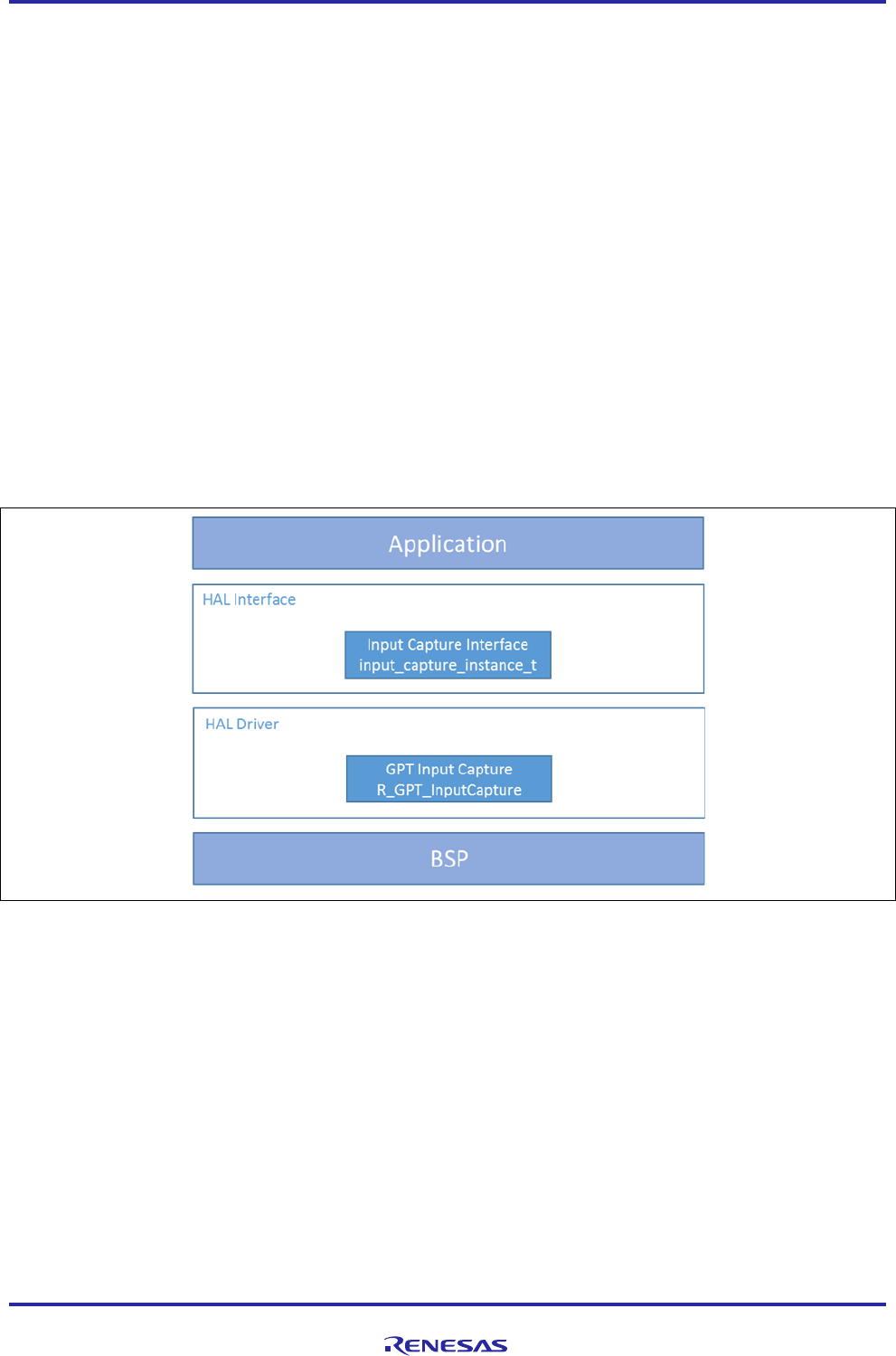
1. Input Capture HAL Module Features
The Input Capture HAL module configures the GPT for an input capture function.
• The Input Capture HAL allows the user to perform the following tasks:
Initialize the module
Enable input capture measurement
Disable input capture measurement
Get the status (running or not) of the measurement counter
Get the last captured timer/overflows counter value
Close the input capture operation
• The Input Capture HAL module supports:
Pulse-width measurement only
Rising-edge or falling-edge measurement start
One-shot or periodic mode
Hardware-enable signals to enable captures (low enable/high enable)
Callback function with the following events:
• Counter overflow
• Input capture occur.
Callback structure (input_capture_callback_args_t) that provides data on the interrupting event,
including which interrupt occurs and the associated counter values.
Figure 1 Input Capture HAL Module Block Diagram
Renesas Synergy™ Platform Input Capture HAL Module Guide
R11AN0106EU0101 Rev.1.01 Page 3 of 14
Aug 30, 2017
2. Input Capture HAL Module APIs Overview
The Input Capture HAL module interface defines APIs for opening, closing, enabling, disabling, accessing status
information and last-capture value accessing using the General PWM Timer (GPT) with input capture. A complete list of
the available APIs, an example API call, and a short description of each can be found in the following table. A table of
status return values follows the API summary table.
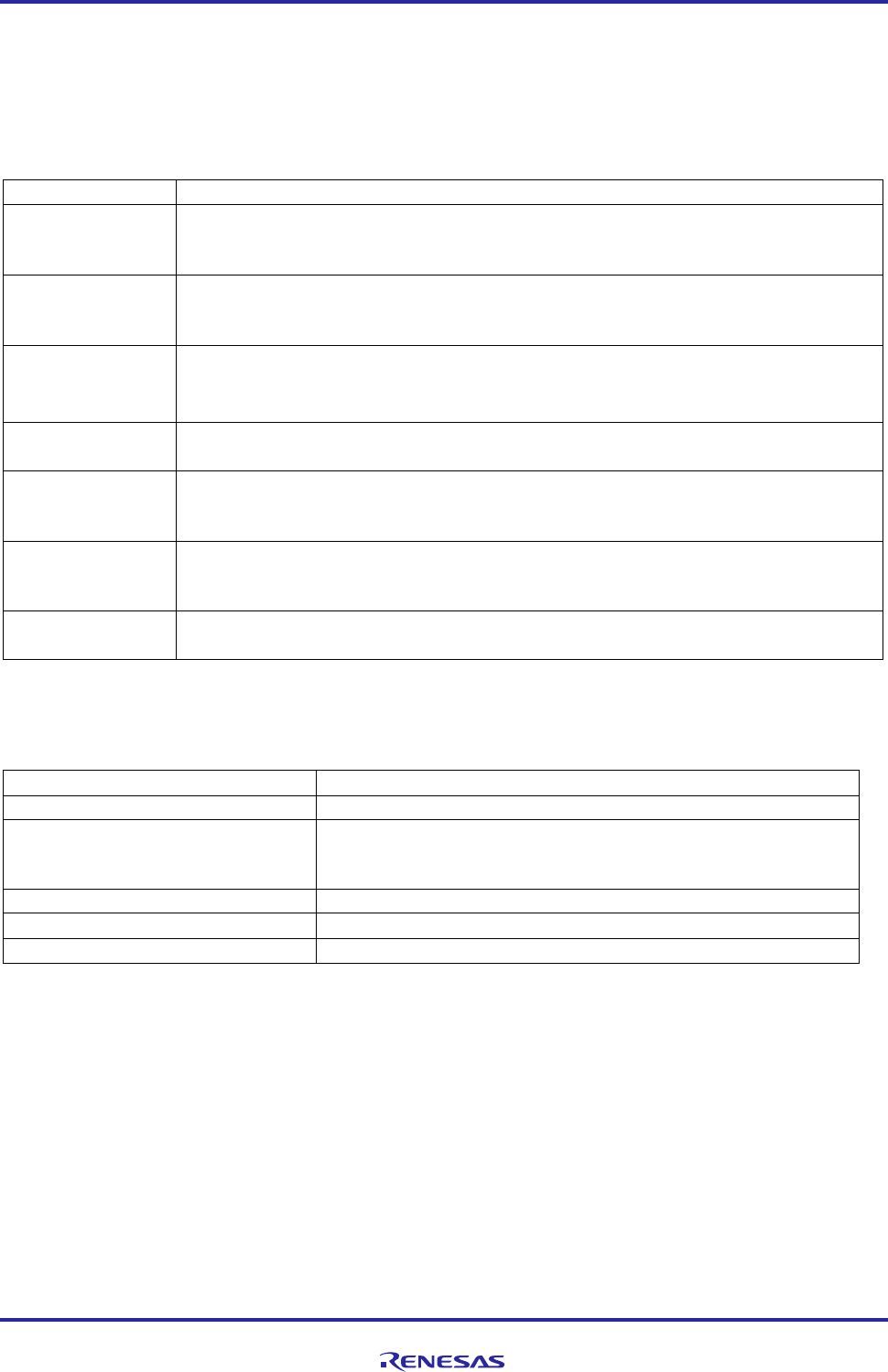
Table 1 Input Capture HAL Module API Summary
Function Name
Example API Call and Description
.open
g_input_capture.p_api->open(g_input_capture.p_ctrl,
g_input_capture.p_cfg);
Opens the Input Capture HAL and initializes configuration.
.close
g_input_capture.p_api->close(g_input_capture.p_ctrl);
Closes the input capture operation. Allow drive to be reconfigured, and may reduce
power consumption.
.enable
g_input_capture.p_api->enable(g_input_capture.p_ctrl);
Enables input capture measurement.
.disable
g_input_capture.p_api->disable(g_input_capture.p_ctrl);
Disables input capture measurement.
.infoGet
g_input_capture.p_api->infoGet(g_input_capture.p_ctrl,
&input_capture_info);
Gets the status (running or not) of the measurement counter.
.lastCaptureGet
g_input_capture.p_api->lastCaptureGet(g_input_capture.p_ctrl,
&input_capture_counter);
Gets the last captured timer/overflows counter value.
.versionGet
g_input_capture.p_api->versionGet(&input_capture_version);
Retrieve the API version with the input_capture_version pointer.
Note: For more complete descriptions of operation and definitions for the function data structures, typedefs,
defines, API data, API structures and function variables, review the Synergy Software Platform (SSP)
User’s Manual API References for the associated module.
Table 2 Status Return Values
Name
Description
SSP_SUCCESS
API Call Successful.
SSP_ERR_ASSERTION
One of the parameters is NULL, or the channel requested in the
p_cfg parameter may not be available on the device selected in
r_bsp_cfg.h, or p_cfg->mode is invalid.
SSP_ERR_INVALID_ARGUMENT
Parameter has invalid value, or ISR is not enabled.
SSP_ERR_IN_USE
Attempted to open an already open device instance.
SSP_ERR_NOT_OPEN
The channel is not opened.
Note: Lower-level drivers may return common error codes. Refer to the SSP User’s Manual API References
for the associated module for a definition of all relevant status return values.

Renesas Synergy™ Platform Input Capture HAL Module Guide
R11AN0106EU0101 Rev.1.01 Page 4 of 14
Aug 30, 2017
3. Input Capture HAL Module Operational Overview
The Input Capture HAL module controls the GPT HAL module units on a Synergy microcontroller (as configured by the
user). It directly accesses the GPT hardware without using any RTOS elements and provides convenient APIs to simplify
development.
When a normal measurement is complete and a callback is available (with interrupts enabled), the Input Capture HAL
module invokes the callback with the argument input_capture_callback_args_t.
The argument input_capture_callback_args_t indicates the channel, the input_capture_event_t
event, the value of the timer captured when the interrupt occurred, and the number of counter overflows that occurred
during this measurement.
If the interrupts are not enabled, the API retrieves the last captured timer/overflows counter value in the main loop.
3.1 Input Capture HAL Module Operational Notes
GPT Input Capture Measurement Mode
The input capture interface provides a selectable mode, a one-shot measurement and a periodic measurement. The GPT
hardware does not natively support one-shot functionality. Software support is in the interrupt service routine (ISR) to
stop and clear the timer. For this reason, ISRs must be enabled for one-shot mode, even when the callback is unused.
GPT Input Capture Signal
The input capture measurement starts when the input capture signal edge (rising or falling) is detected on the input capture
signal pin (GTIOCA/GTIOCB) and the enable condition is met. The enable condition is defined by the enable level and
can be disabled (none), or a specified low or high level on the input capture enable pin (GTIOCA/GTIOCB). The input
capture enable pin is the pin not used as the input capture signal pin.
Converting Measurement Counts to Time
When a measurement completes, the raw-count data and the number of overflows is returned to the user in the callback
function.
If desired, the raw measurement data can be converted to logical time units in the callback or user application. To convert
the raw data, the current PCLKD clock frequency and its pre-scaler value, the number of overflows, the maximum counter
value and the measurement counts should be considered. The measurement counts and the number of overflows are
provided in the callback arguments input_capture_callback_args_t.
The recommended method to obtain the current PCLKD frequency is to use the systemClockFreqGet API. The
input clock frequency is the PCLKD frequency and is divided by the pre-scalar value and is represented as clk_freq_hz
in the following Input Capture Time Calculation table.
The maximum counter value on the S7G2 (all channels), S3A7 (all channels) and S124 (channel 0) is 0xFFFFFFFF. The
maximum counter value for S124 (channels 1-6) is 0xFFFF. This maximum counter value plus one (since the counter
starts at zero) is represented as max_counts in the following table:
Table 3 Input Capture Time Calculation
Desired Time Units
Formula
Nanoseconds (ns)
time_ns = ((overflows * max_counts) + counter) * 1000000000 / clk_freq_hz
Microseconds (us)
time_ns = ((overflows * max_counts) + counter) * 1000000 / clk_freq_hz
Milliseconds (ms)
time_ns = ((overflows * max_counts) + counter) * 1000 / clk_freq_hz
Seconds (s)
time_ns = ((overflows * max_counts) + counter) / clk_freq_hz
3.2 Input Capture HAL Module Limitations
• Currently, the Input Capture HAL module supports only pulse-width measurement.
• Refer to the latest SSP Release Notes for any additional operational limitations for this module.

Renesas Synergy™ Platform Input Capture HAL Module Guide
R11AN0106EU0101 Rev.1.01 Page 5 of 14
Aug 30, 2017
4. Including the Input Capture HAL Module in an Application
This section describes how to include the Input Capture HAL module in an application using the SSP configurator.
Note: It is assumed you are familiar with creating a project, adding threads, adding a stack to a thread and configuring
a block within the stack. If you are unfamiliar with any of these items, refer to the first few chapters of the SSP
User’s Manual to learn how to manage each of these important steps in creating SSP-based applications.
To add the Input Capture Driver to an application, simply add it to a thread using the stacks selection sequence given in
the following table. (The default name for the Input Capture Driver is g_input_capture. This name can be changed
in the associated Properties window.)
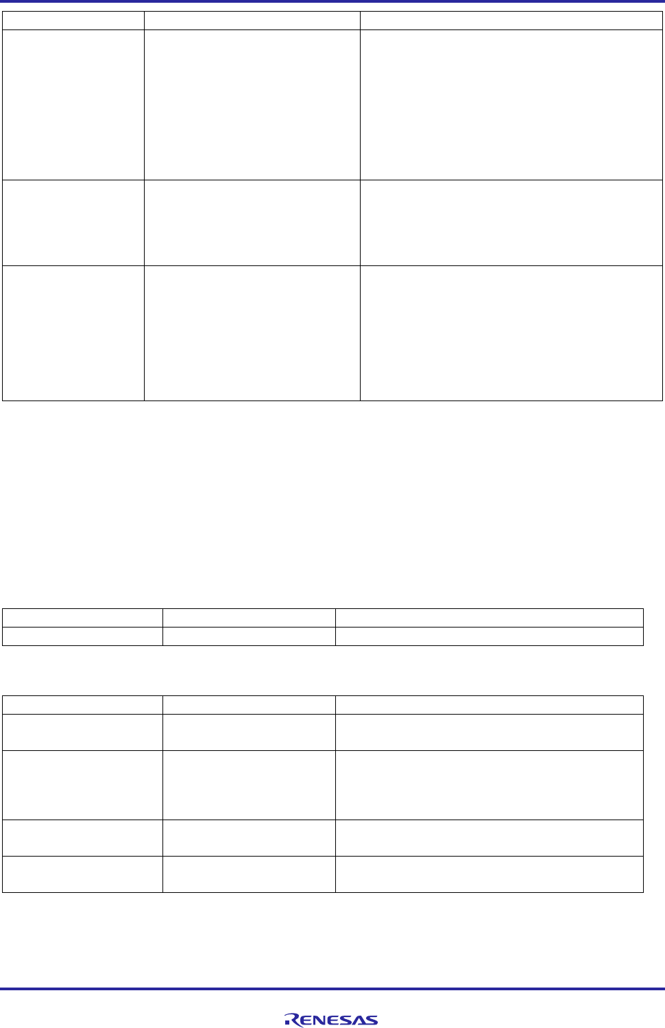
Table 4 Input Capture HAL Module Selection Sequence
Resource
ISDE Tab
Stacks Selection Sequence
g_input_capture Input Capture
Driver on r_gpt_input_capture
Threads->HAL/Common
Stacks
Highlight Threads > HAL/Common Stacks
and select New Stack > Driver > Timers >
Input Capture Driver on r_gpt_input_capture
When the Input Capture HAL module on r_gpt_input_capture is added to the thread stack as shown in the
following figure, the configurator automatically adds any lower-level drivers needed. Any drivers requiring
configuration information are box text highlighted in Red. Modules with a Gray band are standalone modules.
Figure 2 Input Capture HAL Module Stack

Renesas Synergy™ Platform Input Capture HAL Module Guide
R11AN0106EU0101 Rev.1.01 Page 6 of 14
Aug 30, 2017
5. Configuring the Input Capture HAL Module
You can configure the Input Capture HAL module for the desired operation. The SSP configuration window
automatically identifies (by highlighting the block in red) any configuration selections required, such as interrupts or
operating modes, for lower-level modules to achieve successful operation. Only properties that can be changed without
causing a conflict are available for modification. Properties that are ‘locked’ are identified with a lock icon in the
Properties window and cannot be changed in the ISDE. This approach simplifies the configuration process, making it
much less error-prone than previous ‘manual’ approaches to configuration. The Properties tab within the SSP
Configurator shows all available user-accessible properties. The configuration settings and defaults for these properties
are given in the following tables for easy reference.
One of the properties most often identified as requiring a change is the interrupt priority; this configuration setting is
available in the Properties window of the associated module. Simply select the indicated module, then view the
Properties window. Note that the interrupt priorities also indicate the validity of the setting based on the MCU targeted
(CM4 or CM0+).
Note: You may want to open your ISDE, create the Input Capture HAL module and explore the property settings in
parallel with looking over the following configuration table settings. This can help orient you and can also be a
useful ‘hands-on’ approach as you learn the ins and outs of developing with SSP.
Table 5 Configuration Settings for the Input Capture HAL Module on r_gpt_input_capture
ISDE Property
Value
Description
Parameter Checking
BSP, Enabled, Disabled
(Default: BSP)
Selects whether code for parameter checking
is to be included in the build.
Name
(Default: g_input_capture)
Name of the module.
Channel
0-13 for S7G2, 0-9 for S3A7, 0-6
for S124 (Default: 0)
Physical hardware channel.
Mode
Pulse width
Measure inputs from the signal edge until the
opposite edge.
Signal Edge
Rising, Falling
(Default: Rising)
Start measurement on rising or falling edge.
Measurement stops on the opposite edge.
Repetition
One Shot, Periodic
(Default: Periodic)
Capture a signal measurement, then disable
captures (one shot) until the enable API is
called, or capture measurements continuously
(periodic).
Auto Start
True, False
(Default: True)
Set to true to enable measurements after
configuring, or set to false to leave the
measurements disabled until the enable API is
called.
Callback
User-defined, call with
arguments
(Default: NULL)
A user callback function must be registered in
the open API. The callback is called from the
ISR each time the timer period elapses.
Note: Since the callback is called from an ISR,
be careful not to use blocking calls or
lengthy processing. Spending excessive
time in an ISR can affect the
responsiveness of the system.
Input Capture Signal
Pin
GTIOCA, GTIOCB
(Default: GTIOCA)
Select the input pin used to trigger the start of
a measurement.
GTIOCx Signal Filter
None, PCLK/1, PCLK/4,
PCLK/16, PCLK/64
(Default: None)
The noise filter samples the external signal at
intervals of the PCLK divided by one of the
values. When 3 consecutive samples are at the
same level (high or low) that level is passed on
as the observed state of the signal.
Clock Divider
PCLK/1, PCLK/4, PCLK/16,
PCLK/64, PCLK/256,
PCLK/1024
(Default: PCLK/1)
Clock divider used to scale the measurement
counter.
Renesas Synergy™ Platform Input Capture HAL Module Guide
R11AN0106EU0101 Rev.1.01 Page 7 of 14
Aug 30, 2017
ISDE Property
Value
Description
Input Capture
Enable Level
None, Low, High
(Default: None)
Each GPT channel has 2 I/O pins (GPIOCA
and GPIOCB). One of them must be selected
as the Input Capture Signal Pin. The other
GPT I/O pin can be used as a hardware enable
signal to enable captures. Select None and
captures are always enabled. Select low and
captures are enabled only while the enable
input pin is low. Select high and captures are
enabled only while the enable input pin is high.
Input Capture
Enable Filter
None (No filtering), PCLK/1
(Fast sampling), PCLK/4,
PCLK/16, PCLK/64 (Slow
sampling)
(Default: None (No filtering))
The enable filter samples the enable signal at
intervals of the PCLK divided by one of the
values. When 3 consecutive samples are at the
same level (high or low) that level is passed on
as the observed state of the signal.
Capture Interrupt
Priority/Overflow
Interrupt Priority
Priority 0 (Highest), Priority 1-2,
Priority 3 (CM4: valid, CM0+:
lowest – not valid if using
ThreadX), Priority 4-14 (CM4:
valid, CM0+: invalid), Priority 15
(CM4: lowest – not valid if using
ThreadX, CM0+: invalid)
(Default: Priority 2)
Specifies the Priority of the interrupt.
Note: The example values and defaults listed in the table are for a project using the Synergy S7G2 MCUs.
Other MCUs may have different default values and available configuration settings.
5.1 Input Capture HAL Module Clock Configuration
The GPT HAL module uses the PCLKD as its clock source. The PCLKD frequency is set using the SSP configurator
clocks tab prior to a build, or using the CGC Interface at run-time.
5.2 Input Capture HAL Module Pin Configuration
To access a particular channel and pin, the GTIOCx pins must be set in the Pins tab of the ISDE. The following table
has the method for selecting the pins within the SSP configuration window, with the subsequent table listing an example
selection for GTIOCx pins.
Table 6 Pin Selection Sequence for Input Capture HAL Module
Resource
ISDE Tab
Pin selection Sequence
GPT Input Capture
Pins
Select Peripherals > Timer: GPT > GPT0
Note: The selection sequence assumes GPT0 is the desired hardware target for the driver.
Table 7 Pin Configuration Settings for Input Capture HAL Module
Property
Value
Description
Pin Group Selection
Mixed, _A Only, _B Only
(Default: Mixed)
Pin grouping selection
Operation Mode
Disabled, GTIOCA or
GTIOCB, GTIOCA and
GTIOCB
(Default: Disable)
Select GTIOCA or GTIOCB as the operation
mode for Input Capture on GPT
GTIOCA
None, P300, P512
(Default: None)
GTIOCA pin
GTIOCB
None, P108, P511
(Default: None)
GTIOCB pin
Note: The example values are for a project using the Synergy S7G2 MCUs and the SK-S7G2 Kit. Other
Synergy Kits and other Synergy MCUs may have different available pin configuration settings.
Renesas Synergy™ Platform Input Capture HAL Module Guide
R11AN0106EU0101 Rev.1.01 Page 8 of 14
Aug 30, 2017
6. Using the Input Capture HAL Module in an Application
Once the module has been configured and the files generated, the Input Capture HAL module is ready to be used in an
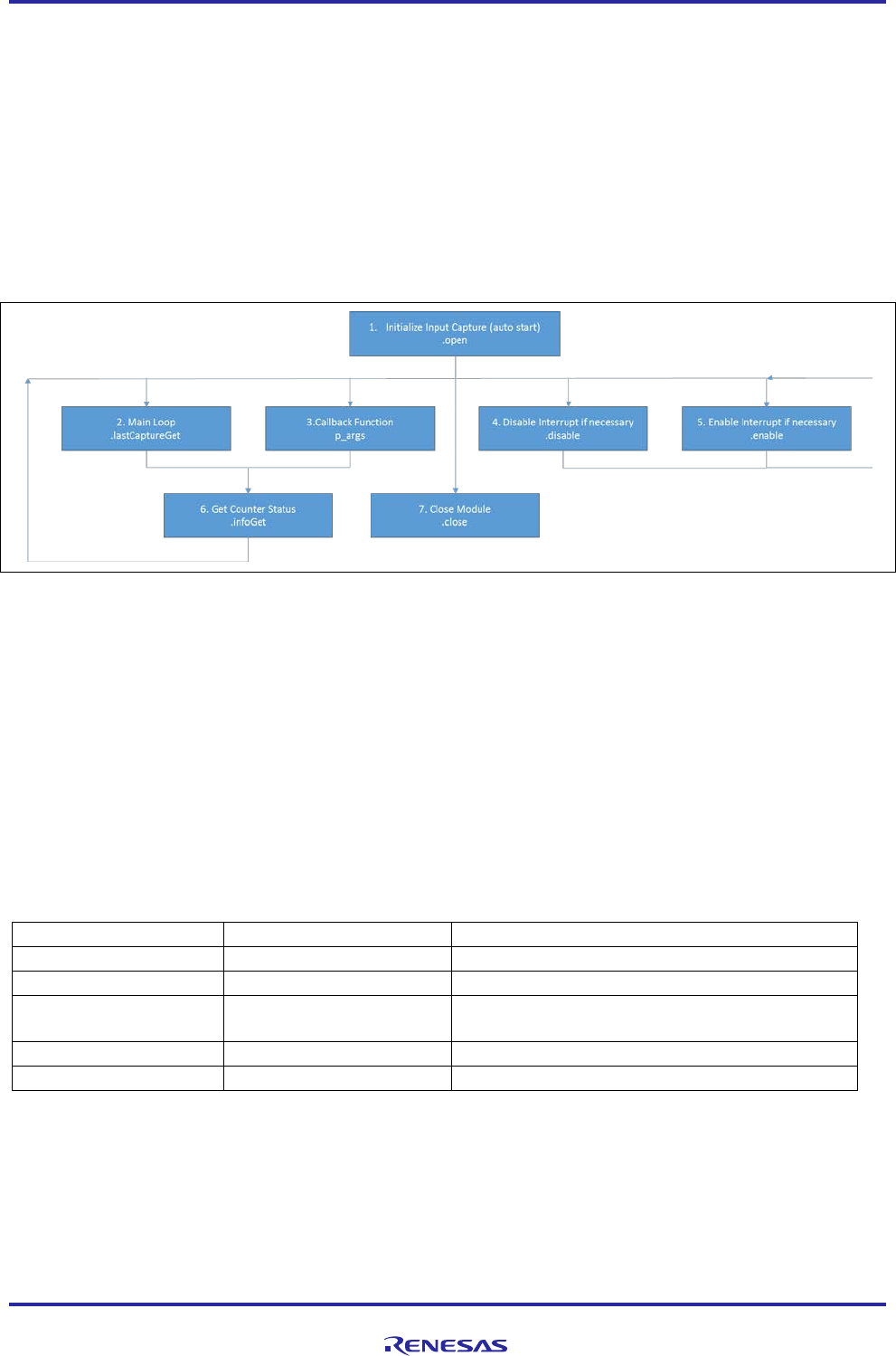
application. The typical steps to using the Input Capture HAL module in an application are:
1. Initialize the module using the open API.
2. The desired value can be found either in the main loop routine using the lastCaptureGet API or in the callback
function using p_args.
3. The capture interrupt can be disabled using the disable API.
4. The capture and overflow interrupt can be enabled using the enable API.
5. The status of the captured counter (running or stopped) can be queried using the infoGet API.
6. The module can be closed using the close API once done.
The following figure illustrates these common steps in a typical operational flow:
Figure 3 Flow Diagram of a Typical Input Capture HAL Module Application
7. The Input Capture HAL Module Application Project
The application project associated with this module guide demonstrates the steps in a callback function design. You may
want to import and open the application project within the ISDE and view the configuration settings for the Input Capture
HAL module. You can also read over the code (see input_capture_hal_mg.c) to see the Input Capture HAL APIs
used in a complete design.
In the application project, the program uses a callback function to read the value. The value is captured periodically and
is displayed on the ISDE debug console using the common semi-hosting technique.
For the application project, a few key properties are configured to support the required operations and physical
properties of the target board and MCU. The following table lists the properties with the values set for this application
project. You can also open the application project and view these settings in the Properties window as a hands-on
exercise.
Table 8 Software and Hardware Resources Used by the Application Project
Resource
Revision
Description
e2 studio
5.3.1 or later
Integrated Solution Development Environment
SSP
1.2.0 or later
Synergy Software Platform
IAR EW for Synergy 7.71.2 or later
IAR Embedded Workbench® for Renesas
Synergy
™
SSC
5.3.1 or later
Synergy Standalone Configurator
SK-S7G2
v3.0 to v3.1
Starter Kit
Renesas Synergy™ Platform Input Capture HAL Module Guide
R11AN0106EU0101 Rev.1.01 Page 9 of 14
Aug 30, 2017
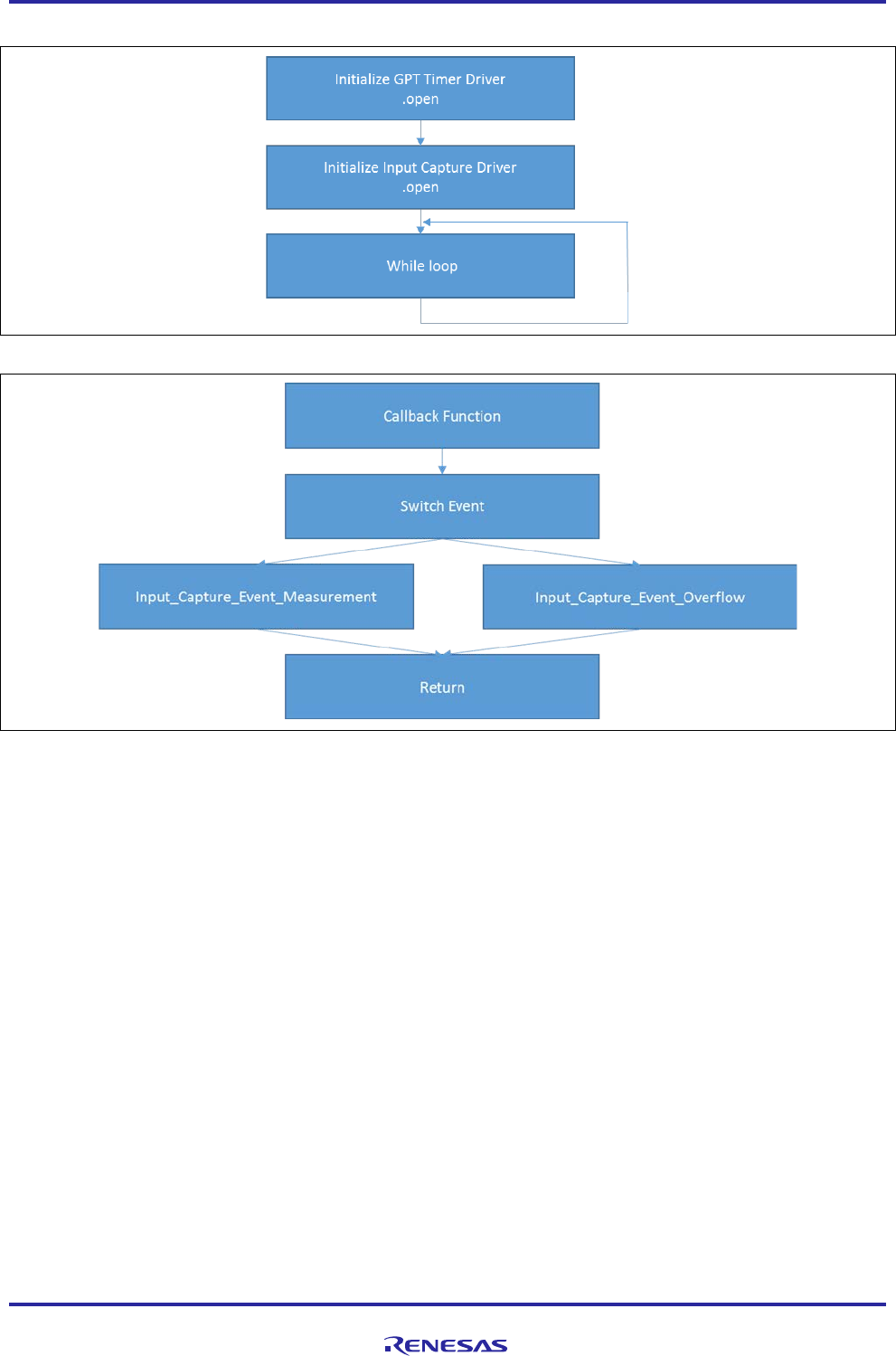
The following figures show some simple application project flow diagrams:
Figure 4 Detailed flow chart of Input Capture HAL Application Project
Figure 5 Detailed flow chart of callback function
The complete application project can be found using the link provided in the References section at the end of this
document. The input_capture_hal_mg.c file is located on the project once the file has been imported into the
ISDE. You can open this file within the ISDE and follow along to help identify key uses of the APIs.
The first section of input_capture_hal_mg.c file has the header files that reference the input capture instance
structure and external function declaration. The hal_entry.c code calls the
input_capture_hal_module_guide_project() function in input_capture_hal_mg.c. In
input_capture_hal_mg.c, the timer driver is initialized for generating measurable pulse, then the Input Capture
HAL module initializes using the open API. All operations, such as getting the value of the captured timer and
overflows counter, are handled in the callback function, once the input capture interrupt or overflow interrupt occur. If
semi-hosting function is enabled, the printf() function outputs all the valuable information at Debug Virtual
Console.
Note: It is assumed that you are familiar using the printf() function with the Debug Console in the SSP. If you are
unfamiliar with this function, refer to the “How do I Use Printf() with the Debug Console in the Synergy
Software Package” given in the References section at the end of this document. Alternatively, the user can see
results using the watch variables in the debug mode.
Renesas Synergy™ Platform Input Capture HAL Module Guide
R11AN0106EU0101 Rev.1.01 Page 10 of 14
Aug 30, 2017
The properties configured in this application project support the required operations, as well as the physical properties
of the target board and the MCU. The following table lists the properties with the values set for this specific project.
You can also open the application project and view these settings in the Properties window as a hands-on exercise.
Table 9 Input Capture HAL Module Configuration Settings for the Application Project
ISDE Property
Value Set
Parameter Checking
Default (BSP)
Name
g_input_capture
Channel
0
Mode
Pulse Width
Signal Edge
Falling
Repetition
Periodic
Auto Start
True
Callback
input_capture_callback
Input Capture Signal Pin
GTIOCA
GTIOCx Signal Filter
None
Clock Divider
PCLK/1
Input Capture Enable Level
None
Input Capture Enable Filter
None (No filtering)
Capture Interrupt Priority
Priority 2
Overflow Interrupt Priority
Priority 2
Because the pulse measured by the input capture function outputs from the GPT channel 2 in this demonstration, the
stack of g_timer0 Timer Driver on r_gpt API is also configured. The following table lists the properties,
with the values set for output pulse:
Table 10 Timer Driver Configuration Settings for the Application Project
ISDE Property
Value Set
Parameter Checking
Default (BSP)
Name
g_timer0
Channel
2
Mode
Periodic
Period Value
40
Period Unit
Seconds
Duty Cycle Value
50
Duty Cycle Unit
Unit Raw Counts
Auto Start
True
GTIOCA Output Enabled
True
GTIOCA Stop Level
Pin Level High
GTIOCB Output Enabled
False
GTIOCB Stop Level
Pin Level Low
Callback
Null
Interrupt Priority
Disabled
To access a particular channel and pin, the GTIOCA pin for input capture and output pulse must be set in the Pins tab of
the ISDE.
The following table lists the method used to select pins within the SSP configuration window and includes an example
that indicates a selection for the GTIOCA input pin and pulse output pin:
Table 11 Pin Selection Sequence for the Input Capture HAL Module
Resource
ISDE Tab
Pin selection Sequence
Input Capture
Pins
Select Peripherals > Timer: GPT > GPT0
Renesas Synergy™ Platform Input Capture HAL Module Guide
R11AN0106EU0101 Rev.1.01 Page 11 of 14
Aug 30, 2017
Table 12 Pin configuration Settings for the Input Capture HAL Module
Pin Configuration Property
Value Set
Pin Group Selection
Mixed
Operation Mode
GTIOCA or GTIOCB
GTIOCA
P512
GTIOCB
None
Table 13 Pin Selection Sequence for the Timer Driver
Resource
ISDE Tab
Pin selection Sequence
GPT Timer
Pins
Select Peripherals > Timer: GPT > GPT2
Table 14 Pin configuration Settings for the Timer Driver
Pin Configuration Property
Value Set
Pin Group Selection
Mixed
Operation Mode
GTIOCA or GTIOCB
GTIOCA
P103
GTIOCB
None
Note: The example values are for a project using the Synergy S7G2 MCUs and the SK-S7G2 Kit. Other
Synergy Kits and other Synergy MCUs may have different available pin configuration settings. In
addition, P103 is set to SSL0 of SPI0 by default. You need to disable SPI0 operation mode, and then
reassign this pin as GTIOCA.
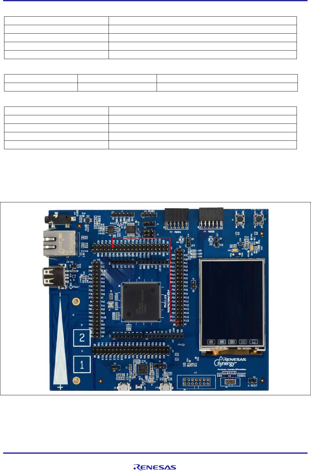
Besides the configuration settings in the tables provided, the GPT timer output pin (P103) and GPT input capture input
pin (P512) must be connected directly on board as the following figure shows.
Figure 6 Hardware connection picture

Renesas Synergy™ Platform Input Capture HAL Module Guide
R11AN0106EU0101 Rev.1.01 Page 12 of 14
Aug 30, 2017
8. Customizing the Input Capture HAL Module for a Target Application
Some configuration settings are normally changed by the developer from those shown in the application project. For
example, the user can easily change the configuration settings for the input capture clock by updating the PCLKD in the
Clocks tab. The user can also change the input capture port pins to select the desired input. This can be done using the
Pins tab in the configurator. The user can also change input capture start condition.
9. Running the Input Capture HAL Module Application Project
To run the Input Capture HAL application project and see it executed on a target kit, you can simply import it into your
ISDE, compile and run debug. Refer to the Importing a Renesas Synergy Project (11an0023eu0116-synergy-ssp-import-
guide.pdf, included in this package) for instructions on importing the project into e2 studio or the IAR EW for Synergy,
and building/running the application.
To implement the Input Capture HAL module application in a new project, follow the steps for defining, configuring,
auto-generating files, adding code, compiling and debugging on the target kit. These steps offer a hands-on approach to
make the development process with SSP more practical, while just reading over this guide tends to be more theoretical.
Note: The following steps are described in sufficient detail for someone experienced with the basic flow through the
Synergy development process. If these steps are unfamiliar, refer to the first few chapters of the SSP User’s
Manual for a description of how to accomplish these steps.
To create and run the Input Capture application project, complete the following steps:
1. Create a new Renesas Synergy project for the SK-S7G2 board (S7G2-BSP) called Input_Capture_HAL_MG_AP.
2. Select the BSP in the project template selection page when creating a project, then finish a new project setup.
3. Select the Threads tab -> HAL/Common.
4. Add the Input Capture HAL module to the HAL/Common stack.
5. Configure the parameters.
6. Click on the Generate Project Content button.
7. Add the code from the supplied project file input_capture_hal_mg.c, input_capture_hal_mg.h, and
hal_entry.c, or copy over the files.
8. Compile the project.
9. Connect to the host PC via a micro USB cable to J19 on SK-S7G2.
10. Start to debug the application.
11. The output can be viewed in the Renesas Debug Virtual Console.
Figure 7 Example Output from the Input Capture HAL Module Application Project
12. The captured timer and overflows counter can also be observed through adding variables into the expressions
window in the debug menu (Window->show view->expressions).
Figure 8 Output Value Observed in the Expressions Window

Renesas Synergy™ Platform Input Capture HAL Module Guide
R11AN0106EU0101 Rev.1.01 Page 13 of 14
Aug 30, 2017
10. Input Capture HAL Module Conclusion
This module guide has provided you with the background information needed to select, add, configure, and use a
component in an example project. Many of these steps were time consuming and error-prone activities in previous
generations of embedded systems. The Renesas SynergyTM Platform makes these steps much less time consuming and
removes common errors, such as conflicting configuration settings or the incorrect selection of lower-level drivers. The
high-level APIs (as demonstrated in the application project) demonstrate the development time savings achieved by
allowing work to begin at a high level and avoiding the time required in older development environments to use or, in
some cases, create, lower-level drivers.
11. Input Capture HAL Module Next Steps
After you have mastered a simple Input Capture HAL module project, you may like to review a more complex example.
In particular, it may be useful to explore the various power-saving options available with the Synergy Platform, as these
are often related to clock-control functions. Explore the Power Profiles and Low Power Mode-related module guides for
additional examples related to clock control.
12. Input Capture HAL Module Reference Information
SSP User Manual: Available in html format in the SSP distribution package and as a pdf from the Synergy Gallery.
Links to all the most up-to-date r_input_capture module reference materials and resources are available on the Synergy
Knowledge Base: https://en-
us.knowledgebase.renesas.com/English_Content/Renesas_Synergy%E2%84%A2_Platform/Renesas_Synergy_Knowle
dge_Base/R_Input_Capture_Module_Guide_References.

Renesas Synergy™ Platform Input Capture HAL Module Guide
R11AN0106EU0101 Rev.1.01 Page 14 of 14
Aug 30, 2017
Website and Support
Support: https://synergygallery.renesas.com/support
Technical Contact Details:
• America: https://renesas.zendesk.com/anonymous_requests/new
• Europe: https://www.renesas.com/en-eu/support/contact.html
• Japan: https://www.renesas.com/ja-jp/support/contact.html
All trademarks and registered trademarks are the property of their respective owners.

Revision History
Rev.
Date
Description
Page
Summary
1.00
May 31, 2017
Initial version
1.01
Aug 30, 2017
Update to Hardware and Software Resources Table
Notice
1. Descriptions of circuits, software and other related information in this document are provided only to illustrate the operation of semiconductor products and application examples. You are fully responsible for
the incorporation or any other use of the circuits, software, and information in the design of your product or system. Renesas Electronics disclaims any and all liability for any losses and damages incurred by
you or third parties arising from the use of these circuits, software, or information.
2. Renesas Electronics hereby expressly disclaims any warranties against and liability for infringement or any other disputes involving patents, copyrights, or other intellectual property rights of third parties, by or
arising from the use of Renesas Electronics products or technical information described in this document, including but not limited to, the product data, drawing, chart, program, algorithm, application
examples.
3. No license, express, implied or otherwise, is granted hereby under any patents, copyrights or other intellectual property rights of Renesas Electronics or others.
4. You shall not alter, modify, copy, or otherwise misappropriate any Renesas Electronics product, whether in whole or in part. Renesas Electronics disclaims any and all liability for any losses or damages
incurred by you or third parties arising from such alteration, modification, copy or otherwise misappropriation of Renesas Electronics products.
5. Renesas Electronics products are classified according to the following two quality grades: "Standard" and "High Quality". The intended applications for each Renesas Electronics product depends on the
product’s quality grade, as indicated below.
"Standard": Computers; office equipment; communications equipment; test and measurement equipment; audio and visual equipment; home electronic appliances; machine tools; personal electronic
equipment; and industrial robots etc.
"High Quality": Transportation equipment (automobiles, trains, ships, etc.); traffic control (traffic lights); large-scale communication equipment; key financial terminal systems; safety control equipment; etc.
Renesas Electronics products are neither intended nor authorized for use in products or systems that may pose adirect threat to human life or bodily injury (artificial life support devices or systems, surgical
implantations etc.), or may cause serious property damages (space and undersea repeaters; nuclear power control systems; aircraft control systems; key plant systems; military equipment; etc.). Renesas
Electronics disclaims any and all liability for any damages or losses incurred by you or third parties arising from the use of any Renesas Electronics product for which the product is not intended by Renesas
Electronics.
6. When using the Renesas Electronics products, refer to the latest product information (data sheets, user’s manuals, application notes, "General Notes for Handling and Using Semiconductor Devices" in the
reliability handbook, etc.), and ensure that usage conditions are within the ranges specified by Renesas Electronics with respect to maximum ratings, operating power supply voltage range, heat radiation
characteristics, installation, etc. Renesas Electronics disclaims any and all liability for any malfunctions or failure or accident arising out of the use of Renesas Electronics products beyond such specified
ranges.
7. Although Renesas Electronics endeavors to improve the quality and reliability of Renesas Electronics products, semiconductor products have specific characteristics such as the occurrence of failure at a
certain rate and malfunctions under certain use conditions. Further, Renesas Electronics products are not subject to radiation resistance design. Please ensure to implement safety measures to guard them
against the possibility of bodily injury, injury or damage caused by fire, and social damage in the event of failure or malfunction of Renesas Electronics products, such as safety design for hardware and
software including but not limited to redundancy, fire control and malfunction prevention, appropriate treatment for aging degradation or any other appropriate measures by your own responsibility as warranty
for your products/system. Because the evaluation of microcomputer software alone is very difficult and not practical, please evaluate the safety of the final products or systems manufactured by you.
8. Please contact aRenesas Electronics sales office for details as to environmental matters such as the environmental compatibility of each Renesas Electronics product. Please investigate applicable laws and
regulations that regulate the inclusion or use of controlled substances, including without limitation, the EU RoHS Directive carefully and sufficiently and use Renesas Electronics products in compliance with all
these applicable laws and regulations. Renesas Electronics disclaims any and all liability for damages or losses occurring as a result of your noncompliance with applicable laws and regulations.
9. Renesas Electronics products and technologies shall not be used for or incorporated into any products or systems whose manufacture, use, or sale is prohibited under any applicable domestic or foreign laws
or regulations. You shall not use Renesas Electronics products or technologies for (1) any purpose relating to the development, design, manufacture, use, stockpiling, etc., of weapons of mass destruction,
such as nuclear weapons, chemical weapons, or biological weapons, or missiles (including unmanned aerial vehicles (UAVs)) for delivering such weapons, (2) any purpose relating to the development,
design, manufacture, or use of conventional weapons, or (3) any other purpose of disturbing international peace and security, and you shall not sell, export, lease, transfer, or release Renesas Electronics
products or technologies to any third party whether directly or indirectly with knowledge or reason to know that the third party or any other party will engage in the activities described above. When exporting,
selling, transferring, etc., Renesas Electronics products or technologies, you shall comply with any applicable export control laws and regulations promulgated and administered by the governments of the
countries asserting jurisdiction over the parties or transactions.
10. Please acknowledge and agree that you shall bear all the losses and damages which are incurred from the misuse or violation of the terms and conditions described in this document, including this notice,
and hold Renesas Electronics harmless, if such misuse or violation results from your resale or making Renesas Electronics products available any third party.
11. This document shall not be reprinted, reproduced or duplicated in any form, in whole or in part, without prior written consent of Renesas Electronics.
12. Please contact a Renesas Electronics sales office if you have any questions regarding the information contained in this document or Renesas Electronics products.
(Note 1) "Renesas Electronics" as used in this document means Renesas Electronics Corporation and also includes its majority-owned subsidiaries.
(Note 2) "Renesas Electronics product(s)" means any product developed or manufactured by or for Renesas Electronics.
http://www.renesas.com
Refer to "http://www.renesas.com/" for the latest and detailed information.
Renesas Electronics America Inc.
2801 Scott Boulevard Santa Clara, CA 95050-2549, U.S.A.
Tel: +1-408-588-6000, Fax: +1-408-588-6130
Renesas Electronics Canada Limited
9251 Yonge Street, Suite 8309 Richmond Hill, Ontario Canada L4C 9T3
Tel: +1-905-237-2004
Renesas Electronics Europe Limited
Dukes Meadow, Millboard Road, Bourne End, Buckinghamshire, SL8 5FH, U.K
Tel: +44-1628-585-100, Fax: +44-1628-585-900
Renesas Electronics Europe GmbH
Arcadiastrasse 10, 40472 Düsseldorf, Germany
Tel: +49-211-6503-0, Fax: +49-211-6503-1327
Renesas Electronics (China) Co., Ltd.
Room 1709, Quantum Plaza, No.27 ZhiChunLu Haidian District, Beijing 100191, P.R.China
Tel: +86-10-8235-1155, Fax: +86-10-8235-7679
Renesas Electronics (Shanghai) Co., Ltd.
Unit 301, Tower A, Central Towers, 555 Langao Road, Putuo District, Shanghai, P. R. China 200333
Tel: +86-21-2226-0888, Fax: +86-21-2226-0999
Renesas Electronics Hong Kong Limited
Unit 1601-1611, 16/F., Tower 2, Grand Century Place, 193 Prince Edward Road West, Mongkok, Kowloon, Hong Kong
Tel: +852-2265-6688, Fax: +852 2886-9022
Renesas Electronics Taiwan Co., Ltd.
13F, No. 363, Fu Shing North Road, Taipei 10543, Taiwan
Tel: +886-2-8175-9600, Fax: +886 2-8175-9670
Renesas Electronics Singapore Pte. Ltd.
80 Bendemeer Road, Unit #06-02 Hyflux Innovation Centre, Singapore 339949
Tel: +65-6213-0200, Fax: +65-6213-0300
Renesas Electronics Malaysia Sdn.Bhd.
Unit 1207, Block B, Menara Amcorp, Amcorp Trade Centre, No. 18, Jln Persiaran Barat, 46050 Petaling Jaya, Selangor Darul Ehsan, Malaysia
Tel: +60-3-7955-9390, Fax: +60-3-7955-9510
Renesas Electronics India Pvt. Ltd.
No.777C, 100 Feet Road, HAL II Stage, Indiranagar, Bangalore, India
Tel: +91-80-67208700, Fax: +91-80-67208777
Renesas Electronics Korea Co., Ltd.
12F., 234 Teheran-ro, Gangnam-Gu, Seoul, 135-080, Korea
Tel: +82-2-558-3737, Fax: +82-2-558-5141
SALES OFFICES
© 2017 Renesas Electronics Corporation. All rights reserved.
Colophon 6.0
(Rev.3.0-1 November 2016)
