R3000 Manual
User Manual:
Open the PDF directly: View PDF ![]() .
.
Page Count: 354 [warning: Documents this large are best viewed by clicking the View PDF Link!]
- IDT R30xx Family Software Reference Manual
- About IDT
- About This Manual
- Table of Contents
- INTRODUCTION CHAPTER 1
- MIPS-1 (R30xx) ARCHITECTURE CHAPTER 2
- SYSTEM CONTROL CO-PROCESSOR ARCHITECTURE CHAPTER 3
- EXCEPTION MANAGEMENT CHAPTER 4
- CACHE MANAGEMENT CHAPTER 5
- MEMORY MANAGEMENT AND THE TLB CHAPTER 6
- RESET INITIALIZATION CHAPTER 7
- FLOATING POINT CO-PROCESSOR CHAPTER 8
- ASSEMBLER LANGUAGE PROGRAMMING CHAPTER 9
- C PROGRAMMING CHAPTER 10
- PORTABILITY CONSIDERATIONS CHAPTER 11
- WRITING POWER-ON DIAGNOSTICS CHAPTER 12
- INSTRUCTION TIMING AND OPTIMIZATION CHAPTER 13
- SOFTWARE TOOLS FOR BOARD BRING-UP CHAPTER 14
- SOFTWARE DESIGN EXAMPLES CHAPTER 15
- ASSEMBLY LANGUAGE PROGRAMMING TIPS CHAPTER 16
- MACHINE INSTRUCTIONS REFERENCE APPENDIX A
- FPA INSTRUCTION REFERENCE APPENDIX B
- CP0 OPERATION REFERENCE APPENDIX C
- ASSEMBLER LANGUAGE SYNTAX APPENDIX D
- OBJECT CODE FORMATS APPENDIX E
- GLOSSARY OF COMMON "MIPS" TERMS APPENDIX F

Table of Contents
i–1
IDT R30xx Family
Software Reference Manual
Revision 1.0
1994 Integrated Device Technology, Inc.
Portions
1994 Algorithmics, Ltd.
Chapter 16 contains some material that is
1988 Prentice-Hall.
Appendices A & B contain material that is
1994 by Mips Technology, Inc.

Table of Contents
i–2
About IDT
Integrated Device Technology, Inc. has been a MIPS semiconductor
partner since 1988, and has led efforts to bring the high-performance
inherent in the MIPS architecture to embedded systems engineers. These
efforts include derivatives of MIPS R3xxx and R4xxx CPUs, development
tools, and applications support.
Additional information about IDT’s RISC family can be obtained from
your local sales representative. Alternately, IDT can be reached directly at:
Corporate Marketing (800) 345-7015
RISC Applications "Hotline" (408) 492-8208
RISC Applications FAX (408) 492-8469
RISC Applications Internet rischelp@idtinc.com
About Algorithmics
Much of this manual was written by Dominic Sweetman and Nigel
Stephens of Algorithmics Ltd in London, England, under contract to IDT.
Algorithmics were early enthusiasts for the MIPS architecture, designing
their first MIPS systems and system software in 1986/87. A small
engineering company, Algorithmics provide enabling technologies for
companies designing in both R30xx family CPUs and the 64-bit R4x00
architecture. This includes training, toolkits, GNU C support, and
evaluation boards. Dominic Sweetman can be reached at the following:.
Dominic Sweetman phone: +44 71 700 3301
Algorithmics Ltd fax: +44 71 700 3400
3 Drayton Park email: dom@algor.co.uk
London N5 1NU
ENGLAND.

Table of Contents
i–3
About This Manual
This manual is targeted to a systems programmer building an R30xx-
based system. It contains the architecture specific operations and
programming conventions relevant to such a programmer.
This manual is not intended to be a tutorial on structured programming,
real-time operating systems, any particular high-level programming
language, or any particular toolchain. Other references are better suited to
those topics.
This manual does contain specific code fragments and the most
common programming conventions that are specific to the IDT R30xx
RISController family. The manual was consciously limited to the R30xx
family; information relevant to the R4xxx family of processors may be
found, but the device specific programs (such as cache management,
exception handling, etc.) shown as examples are specific to the R30xx
family.
This manual contains references to the toolchains most commonly used
by the authors (IDT, Inc., and Algorithmics, Ltd.). Code fragments shown
are typically from software used by and/or provided by these companies,
includeing development tools such as IDT/c and software utilities (such as
IDT/kit, IDT/sim, and Micromonitor). A wide variety of other, 3rd party
products, are also available to support R30xx development, under the
Advantage-IDT program. The reader of this manual is encouraged to look
at all the available tools to determine which toolchains and utilities best fit
the system development requirements.
Additional information on the IDT family of RISC processors, and their
support tools, is available from your local IDT salesman.

Table of Contents
i–4
Integrated Device Technology, Inc. reserves the right to make changes to its products or specifications at
any time, without notice, in order to improve design or performance and to supply the best possible product.
IDT does not assume any responsibility for use of any circuitry described other than the circuitry embodied
in an IDT product. The Company makes no representations that circuitry described herein is free from patent
infringement or other rights of third parties which may result from its use. No license is granted by impli-
cation or otherwise under any patent, patent rights or other rights, of Integrated Device Technology, Inc.
LIFE SUPPORT POLICY
Integrated Device Technology's products are not authorized for use as critical components in life
support devices or systems unless a specific written agreement pertaining to such intended use is
executed between the manufacturer and an officer of IDT.
1. Life support devices or systems are devices or systems which (a) are intended for surgical implant
into the body or (b) support or sustain life and whose failure to perform, when properly used in
accordance with instructions for use provided in the labeling, can be reasonably expected to result in
a significant injury to the user.
2. A critical component is any components of a life support device or system whose failure to
perform can be reasonably expected to cause the failure of the life support device or system, or to
affect its safety or effectiveness.
The IDT logo is a registered trademark and BiCameral, BurstRAM, BUSMUX, CacheRAM, DECnet,
Double-Density, FASTX, Four-Port, FLEXI-CACHE, Flexi-PAK, Flow-thruEDC, IDT/c, IDTenvY, IDT/sae,
IDT/sim, IDT/ux, MacStation, MICROSLICE, Orion, PalatteDAC, REAL8, R3041, R3051, R3052, R3081,
R3721, R4600, RISCompiler, RISController, RISCore, RISC Subsystem, RISC Windows, SARAM, SmartLogic,
SyncFIFO, SyncBiFIFO, SPC, TargetSystem and WideBus are trademarks of Integrated Device Technology,
Inc.
MIPS is a registered trademark of MIPS Computer Systems, Inc
All others are trademarks of their respective companies..

Table of Contents
i–5
IDT R30xx Family
Software Reference Manual
Table of Contents
Introduction........................................................................................................................1
What is a RISC?......................................................................................................... 1-1
PIPELINES................................................................................................................ 1-2
The IDT R3xxx Family CPUs ................................................................................... 1-3
MIPS Architecture Levels.......................................................................................... 1-4
MIPS-1 Compared with CISC Archtectures.............................................................. 1-4
Unusual Instruction Encoding Features............................................................... 1-5
Addressing and Memory Accesses...................................................................... 1-5
Operations not Directly Supported ...................................................................... 1-6
Multiply and Divide Operations ................................................................................ 1-7
Programmer-visible Pipeline Effects......................................................................... 1-7
A Note on Machine and Assembler Language .......................................................... 1-8
MIPs-1 (R30xx) Architecture............................................................................................2
Programmer’s View of the Processor Archtecture.....................................................2-1
Registers..................................................................................................................... 2-1
Conventional Names and Uses of General-Purpose Registers .................................. 2-2
Notes on Conventional Register Names ............................................................. 2-2
Integer Multiply Unit and Registers .......................................................................... 2-3
Instruction Types ....................................................................................................... 2-4
Loading and Storing: Addressing Modes .................................................................. 2-5
Data types in Memory and Registers......................................................................... 2-6
Integer Data Types .............................................................................................. 2-6
Unaligned Loads and Stores ............................................................................... 2-6
Floating Point Data in Memory .......................................................................... 2-7
Basic Address Space.................................................................................................. 2-8
Summary of System Addressing................................................................................ 2-9
Kernel vs. User Mode .......................................................................................... 2-9
Memory map for CPUs without MMU Hardware............................................. 2-10
Subsegments in the R3041 – Memory Width Configuration ...................... 2-10
System Control Coprocessor Architecture......................................................................3
CPU Control Summary.............................................................................................. 3-1
CPU Control and ‘‘CO-PROCESSOR 0’’................................................................. 3-2
CPU Control Instructions..................................................................................... 3-2
Standard CPU control registers............................................................................ 3-3
PRId Register ................................................................................................ 3-4
SR Register .................................................................................................... 3-4
Cause Register ............................................................................................... 3-7
EPC Register ................................................................................................. 3-8
BadVaddr Register ........................................................................................ 3-8
R3041, R3071, and R3081 Specific Registers..................................................... 3-8

Table of Contents
i–6
Count and Compare Registers (R3041 only) .................................................3-8
Config Register (R3071 and R3081) .............................................................3-8
Config Register (R3041) ...............................................................................3-9
BusCtrl Register (R3041 only) ....................................................................3-10
PortSize Register (R3041 only) ...................................................................3-11
What registers are relevant when?......................................................................3-11
Exception Management.....................................................................................................4
Exceptions ..................................................................................................................4-1
Precise Exceptions................................................................................................4-1
When Exceptions Happen ....................................................................................4-2
Exception vectors .................................................................................................4-2
Exception Handling – Basics................................................................................4-3
Nesting Exceptions...............................................................................................4-4
An Exception Routine ..........................................................................................4-4
Interrupts...................................................................................................................4-12
Conventions and Examples ................................................................................4-14
Cache Management...........................................................................................................5
Caches and Cache Management.................................................................................5-1
Cache Isolation and Swapping .............................................................................5-3
Initializing and Sizing the Caches ........................................................................5-4
Invalidation...........................................................................................................5-6
Testing and Probing..............................................................................................5-8
Configuration (R3041/71/81 only).......................................................................5-8
Write Buffer................................................................................................................5-9
Implementing
wbflush()......................................................................................5-10
Memory Management and the TLB ................................................................................6
Memory Management and the TLB ...........................................................................6-1
MMU Registers Described...................................................................................6-3
EntryHi, EntryLo ...........................................................................................6-3
Index ..............................................................................................................6-4
Random ..........................................................................................................6-4
Context ...........................................................................................................6-4
MMU Control Instructions ...................................................................................6-5
Programming Interface to the TLB.......................................................................6-5
How Refill Happens ......................................................................................6-5
Using ASIDs ..................................................................................................6-6
The Random Register and Wired Entries ......................................................6-6
Memory Translation – Setup................................................................................6-6
TLB Exception Sample Code...............................................................................6-7
Basic Exception Handler ...............................................................................6-7
Fast kuseg Refill from Page Table ................................................................6-7
Simulating Dirty Bits............................................................................................6-8
Use of TLB in Debugging ..........................................................................................6-8
TLB Management Utilities.........................................................................................6-9
Reset Initialization.............................................................................................................7
Starting Up..................................................................................................................7-1
Probing and Recognizing the CPU .......................................................................7-4
Bootstrap Sequences.............................................................................................7-5
Starting Up an Application ...................................................................................7-5

Table of Contents
i–7
Floating Point Coprocessor...............................................................................................8
The IEEE754 Standard and its Background .............................................................. 8-1
What is Floating Point?.............................................................................................. 8-2
IEEE exponent field and bias............................................................................... 8-3
IEEE mantissa and normalization........................................................................ 8-3
Strange values use reserved exponent values ...................................................... 8-3
MIPS FP Data formats......................................................................................... 8-4
MIPS Implementation of IEEE754............................................................................ 8-5
Floating Point Registers............................................................................................. 8-6
Floating Point Eeceptions/Interrupts.......................................................................... 8-6
The Floating Point Control/Status Register............................................................... 8-6
Floating Point Implementation/Revision Register..................................................... 8-8
Guide to FP Instructions ............................................................................................ 8-8
Load/Store............................................................................................................ 8-8
Move Between Registers ..................................................................................... 8-9
3-Operand Arithmetic Operations........................................................................ 8-9
Unary (sign-changing) Operations..................................................................... 8-10
Conversion Operations....................................................................................... 8-10
Conditional Branch and Test Instructions.......................................................... 8-10
Instruction Timing Requirements ............................................................................ 8-12
Instruction Timing for Speed................................................................................... 8-12
Initialization and Enable On Demand...................................................................... 8-12
Floating Point Emulation......................................................................................... 8-13
Assembler Language Programming.................................................................................9
Syntax Overview........................................................................................................ 9-1
Key Points to Note............................................................................................... 9-1
Register-to-Register Instructions ............................................................................... 9-2
Immediate (Constant) Operands ................................................................................ 9-3
Multiply/Divide.......................................................................................................... 9-4
Load/Store Instructions.............................................................................................. 9-5
Unaligned Loads and Store.................................................................................. 9-5
Addressing Modes ..................................................................................................... 9-6
Gp-Relative Addressing....................................................................................... 9-6
Jumps, Subroutine Calls and Branches...................................................................... 9-8
Conditional Branches................................................................................................. 9-8
Co-processor Conditional Branches .................................................................... 9-9
Compare and Set........................................................................................................ 9-9
Coprocessor Transfers ............................................................................................... 9-9
Coprocessor Hazards ......................................................................................... 9-10
Assembler Directives............................................................................................... 9-10
Sections.............................................................................................................. 9-10
.text, .rdata, .data ......................................................................................... 9-10
.lit4, .lit8 ...................................................................................................... 9-10
Program Segments in Memory ................................................................... 9-11
.bss .............................................................................................................. 9-12
.sdata, .sbss .................................................................................................. 9-12
Stack and Heap ........................................................................................... 9-12
Special Symbols .......................................................................................... 9-12
Data Definition and Alignment.......................................................................... 9-12

Table of Contents
i–8
.byte, .half, .word ........................................................................................ 9-13
.float, .double .............................................................................................. 9-13
.ascii, .asciiz ................................................................................................ 9-13
.align ............................................................................................................ 9-13
.comm, .lcomm ........................................................................................... 9-13
.space ........................................................................................................... 9-14
Symbol Binding Attributes ................................................................................ 9-14
.globl ........................................................................................................... 9-14
.extern .......................................................................................................... 9-15
.weakext ...................................................................................................... 9-15
Function Directives............................................................................................ 9-15
.ent, .end ...................................................................................................... 9-15
.aent ............................................................................................................. 9-16
.frame, .mask, .fmask .................................................................................. 9-16
Assembler Control (.set).................................................................................... 9-17
.set noreorder/reorder .................................................................................. 9-17
.set volatile/novolatile ................................................................................. 9-17
.set noat/at ................................................................................................... 9-18
.set nomacro/macro ..................................................................................... 9-18
.set nobopt/bopt ........................................................................................... 9-18
The Complete Guide to Assembler Instructions...................................................... 9-18
Alphabetic List of Assembler Instructions .............................................................. 9-30
C Programming................................................................................................................10
The Stack, Subroutine Linkage, Parameter Passing ................................................ 10-1
Stack Argument Structure.................................................................................. 10-1
Which Arguments go in What Registers ........................................................... 10-1
Examples from the C Library ............................................................................ 10-2
Exotic Example; Passing Structures .................................................................. 10-2
How Printf() and Varargs Work ........................................................................ 10-3
Returning Value from a Function ...................................................................... 10-4
Macros for Prologues and Epilogues................................................................. 10-4
Stack-Frame Allocation ..................................................................................... 10-4
Leaf Functions ............................................................................................ 10-4
Non-Leaf Functions .................................................................................... 10-5
Functions Needing Run-Time Computed Stack Locations ........................ 10-7
Shared and Non-Shared Libraries............................................................................ 10-9
Sharing Code in Single-Address Space Systems............................................... 10-9
Sharing Code Across Address Spaces ............................................................. 10-10
An Introduction to Optimization............................................................................ 10-11
Common Optimizations................................................................................... 10-11
How to Prevent Unwanted Effects From Optimization................................... 10-14
Optimizer-Unfriendly Code and How to Avoid It........................................... 10-15
Portability Considerations ..............................................................................................11
Writing Portable C................................................................................................... 11-1
C Language Standards ...................................................................................... 11-1
C Library Functions and POSIX ....................................................................... 11-2
Data Representations and Alignment....................................................................... 11-3
Notes on Structure Layout and Padding ............................................................ 11-3
Isolating System Dependencies ............................................................................... 11-5

Table of Contents
i–9
Locating System Dependencies......................................................................... 11-5
Fixing Up Dependencies.................................................................................... 11-5
Isolating Non-Portable Code ....................................................................... 11-6
Using Assembler................................................................................................ 11-6
Endianness ............................................................................................................... 11-7
What It Means to the Programmer..................................................................... 11-8
Bitfield Layout and Endianness .................................................................. 11-9
Changing the Endianness of a MIPS CPU....................................................... 11-10
Designing and Specifying for Configurable Endianness................................. 11-10
Read-Only Instruction Memory ................................................................ 11-10
Writable (Volatile) Memory ..................................................................... 11-11
Byte-Lane Swapping ................................................................................. 11-11
Configurable IO Controllers ..................................................................... 11-12
Portability and Endianness-Independent Code................................................ 11-13
Endianness-Independent Code .................................................................. 11-13
Compatibility Within the R30XX Family.............................................................. 11-13
Porting to MIPS: Frequently Encountered Issues.................................................. 11-15
Considerations for Portability to Future Devices................................................... 11-16
Writing Power-On Diagnostics.......................................................................................12
Golden Rules for Diagnostics Programming........................................................... 12-1
What Should Tests Do? ........................................................................................... 12-2
How to Test the Diagnostic Tests? .......................................................................... 12-3
Overview of Algorithmics’ Power-On Selftest........................................................ 12-3
Starting Points.................................................................................................... 12-3
Control and Environment Variables .................................................................. 12-4
Reporting............................................................................................................ 12-4
Unexpected Exceptions During Test Sequence................................................. 12-5
Driving Test Output Devices ............................................................................. 12-5
Restarting the System ........................................................................................ 12-5
Standard Test Sequence..................................................................................... 12-5
Notes on the Test Sequence............................................................................... 12-6
Annotated Examples from the Test Code.......................................................... 12-9
Instruction Timing and Optimization............................................................................13
Notes and Examples........................................................................................... 13-1
Additional Hazards .................................................................................................. 13-2
Early Modification of HI and LO ...................................................................... 13-2
Bitfields in CPU Control Registers.................................................................... 13-3
Non-Obvious Hazards........................................................................................ 13-3
Software Tools for Board Bring-Up...............................................................................14
Tools Used in Debug ............................................................................................... 14-1
Initial Debugging ..................................................................................................... 14-2
Porting Micromonitor .............................................................................................. 14-2
Running Micromonitor ............................................................................................ 14-2
Initial IDT/SIM Activity.......................................................................................... 14-2
A Final Note on IDT/KIT ........................................................................................ 14-3
Software Design Examples..............................................................................................15
Application Software ............................................................................................... 15-1
Memory Map ..................................................................................................... 15-1
Starting Up......................................................................................................... 15-1

Table of Contents
i–10
C Library Functions........................................................................................... 15-2
Input and Output ......................................................................................... 15-3
Character Class Tests .................................................................................. 15-3
String Functions .......................................................................................... 15-3
Mathematical Functions .............................................................................. 15-3
Utility Functions ......................................................................................... 15-3
Diagnostics .................................................................................................. 15-4
Variable Argument Lists ............................................................................. 15-4
Non-Local Jumps ........................................................................................ 15-4
Signals ......................................................................................................... 15-4
Date and Time ............................................................................................. 15-4
Running the Program......................................................................................... 15-4
Debugging the Program..................................................................................... 15-5
Embedded System Software .................................................................................... 15-5
Memory Map ..................................................................................................... 15-6
Starting Up......................................................................................................... 15-6
Embedded System Library Functions................................................................ 15-7
Trap and Interrupt Handling ....................................................................... 15-8
Simple Interrupt Routines ........................................................................... 15-8
Floating-Point Traps and Interrupts ............................................................ 15-9
Emulating Floating Point Instructions ...................................................... 15-10
Debugging........................................................................................................ 15-10
Unix-Like System S/W.......................................................................................... 15-11
Terminology..................................................................................................... 15-11
Components of a Process................................................................................. 15-12
System Calls and Protection ............................................................................ 15-13
What the Kernel Does...................................................................................... 15-13
Virtual Memory Implementation for MIPS..................................................... 15-14
Interrupt Handling for MIPS............................................................................ 15-15
How it Works ............................................................................................ 15-16
Assembly Language Programming Tips........................................................................16
32-bit Address or Constant Values .................................................................... 16-1
Use of “Set” Instructions ................................................................................... 16-1
Use of “Set” with Complex Branch Operations ......................................... 16-2
Carry, Borrow, Overflow, and Multi-Precision Math ................................. 16-2
Machine Instructions Reference (Appendix A)..............................................................A
CPU Instruction Overview.................................................................................. A-1
Instruction Classes .............................................................................................. A-1
Instruction Formats............................................................................................. A-2
Instruction Notation Conventions....................................................................... A-2
Instruction Notation Examples ..................................................................... A-3
Load and Store Instructions ................................................................................ A-4
Jump and Branch Instructions............................................................................. A-5
Coprocessor Instructions..................................................................................... A-5
System Control Coprocessor (CP0) Instructions................................................ A-6
Instruct Set Details.............................................................................................. A-6
Instruction Summary......................................................................................... A-79
FPA Instruction Reference (Appendix B).......................................................................B
FPU Instruction Set Details .................................................................................B-1

Table of Contents
i–11
FPU Instructions ...........................................................................................B-1
Floating-Point Data Transfer ........................................................................B-1
Floating-Point Conversions ..........................................................................B-1
Floating-Point Arithmetic .............................................................................B-2
Floating-Point Register-to-Register Move ....................................................B-2
Floating-Point Branch ...................................................................................B-2
FP Computational Instructions and Valid Operands ...........................................B-2
FP Compare and Condition values ......................................................................B-3
FPU Register Specifiers.......................................................................................B-3
32-bit CP1 registers..............................................................................................B-4
FPU Register Access for 32-bit CP1 Registers..............................................B-5
Instruction Notation Conventions ..................................................................B-5
Load and Store Memory ......................................................................................B-6
Instruction Descriptions.......................................................................................B-6
FPA Instruction Set Summary ...........................................................................B-27
CP0 Operation Reference (Appendix C) ........................................................................C
CP0 Operation Details .........................................................................................C-1
MMU Operations.................................................................................................C-1
Exception Operations...........................................................................................C-1
Dand Register Movement Operations............................................................C-1
Operation Descriptions ........................................................................................C-1
Assembler Language Syntax (Appendix D)....................................................................D
Object Code Formats (Appendix E)................................................................................E
Sections and Segments...............................................................................................E-1
ECOFF Object File Format (RISC/OS).....................................................................E-1
File Header...........................................................................................................E-2
Optional a.out Header..........................................................................................E-2
Example Loader...................................................................................................E-3
Further Reading ...................................................................................................E-4
ELF (MIPS ABI)........................................................................................................E-4
File Header...........................................................................................................E-4
Program Header ...................................................................................................E-5
Example Loader...................................................................................................E-6
Further Reading ...................................................................................................E-7
Object Code Tools .....................................................................................................E-7
Glossary of Common "MIPS" Terms.............................................................................F
DRAWINGS
1.1 MIPS 5-Stage Pipeline..........................................................................................1.2
1.2 The Pipeline and Branch Delays.......................................................................... 1-7
1.3 The Pipeline and Load Delays............................................................................. 1-8
3.1 PRId Register Fields ............................................................................................ 3-4
3.2 Fields in Status Register....................................................................................... 3-4
3.3 Fields in the Cause Register................................................................................. 3-7
3.4 Fields in the R3071/81 Config Register............................................................... 3-8
3.5 Fields in the R3041 Config (Cache Configuration)Register................................ 3-9
3.6 Fields in the R3041 Bus Control (BusCtrl) Register ......................................... 3-10
5.1 Direct Mapped Cache .......................................................................................... 5-1
6.1 EntryHi and EntryLo Register Fields .................................................................. 6-3

Table of Contents
i–12
6.2 EntryHi and EntryLo Register Fields .................................................................. 6-3
6.3 Fields in the Index Register ................................................................................. 6-4
6.4 Fields in the Random Register............................................................................. 6-4
6.5 Fields in the Context Register.............................................................................. 6-4
8.1 FPA Control/Status Register Fields..................................................................... 8-6
8.2 FPA Implementation/Revision Register .............................................................. 8-8
9.1 Program Segments in Memory .......................................................................... 9-11
10.1 Stackframe for a Non-Leaf Function................................................................. 10-5
11.1 Structure Layout and Padding in Memory......................................................... 11-3
11.2 Data Representation with #pragma Pack(1) ......................................................11-4
11.3 Data Representation with #pragma Pack(2) ......................................................11-5
11.4 Typical Big-Endians Picture.............................................................................. 11-8
11.5 Little Endians Picture......................................................................................... 11-8
11.6 Bitfields and Big-Endian.................................................................................... 11-9
11.7 Bitfields and Little-Endian............................................................................... 11-10
11.8 Garbled String Storage when Mixing Modes .................................................. 11-11
11.9 Byte-Lane Swapper.......................................................................................... 11-12
15.1 Memory Layout of a BSD Process .................................................................. 15-12
A.1 CPU Instruction Formats .................................................................................... A-2
TABLES
1.1 R30xx Family Members Compared..................................................................... 1-4
2.1 Conventional Names of Registers with Usage Mnemonics................................. 2-2
3.1 Summary of CPU Control Registers (Not MMU)............................................... 3-3
3.2 ExcCode Values: Different kinds of Exceptions ................................................. 3-7
4.1 Reset and Exception Entry Points (Vectors) for R30xx Family.......................... 4-3
4.2 Interrupt Bitfields and Interrup Pins .................................................................. 4-13
6.1 CPU Control Registers for Memory Management .............................................. 6-3
8.1 Floating Point Data Formats................................................................................ 8-4
8.2 Rounding Modes Encoded in FP Control/Status Register................................... 8-7
8.4 FP Move Instructions........................................................................................... 8-9
8.5 FPA 3-Operand Arithmetic................................................................................ 8-10
8.6 FPA Sign-Changing Operators .......................................................................... 8-10
8.7 FPA Data Conversion Operations...................................................................... 8-10
8.8 FP Test Instructions ........................................................................................... 8-11
9.1 Assembler Register and Identifier Conventions ................................................ 9-20
9.2 Assembler Instructions....................................................................................... 9-20
12.1 Test Sequence in Brief....................................................................................... 12-5
16.1 32-bit Immediate Values.................................................................................... 16-1
16.2 Add-With-Carry................................................................................................. 16-2
16.3 Subtract-with-Borrow Operation ....................................................................... 16-3
A.1 CPU Instruction Operation Notations................................................................. A-3
A.2 Load and Store Common Function..................................................................... A-4
A.3 Access Type Specifications for Load/Store........................................................ A-5
B.1 Format Field Decoding ........................................................................................B-2
B.2 Logical Negation of Predicates by Condition True/False....................................B-3
B.3 Valid FP Operand Specifiers with 32-bit Coprocessor 1 Registers.....................B-4
B.4 Load and Store Common Functions ....................................................................B-6

1–1
INTRODUCTION
®
Integrated Device Technology, Inc.
CHAPTER 1
IDT’s R30xx family of RISC microcontrollers family includes the R3051,
R3052, R3071, R3081 and R3041 processors. The different members of
the family offer different price/performance trade-offs, but are all basically
integrated versions of the MIPS R3000A CPU. The R3000A CPU is well
known for the high-performance Unix systems implemented around it; less
publicized but equally impressive is the performance it has brought to a
wide variety of embedded applications.
IDT’s RISController family also includes devices built around MIPS
R4000 64-bit microprocessor technology. These devices, such as the IDT
R4600 Orion microprocessor, offer even higher levels of performance than
the R3000A derivative family. However, these devices also feature slightly
different OS models, and allow 64-bit kernels and applications. Thus, they
are sufficiently different from the R30xx family that this manual is focused
exclusively on the R30xx family.
This manual is aimed at the programmer dealing with the IDT R30xx
family components. Although most programming occurs using a high-level
language (usually “C”), and with little awareness of the underlying system
or processor architecture, certain operations require the programmer to
use assembly programming, and/or be aware of the underlying system or
processor structure. This manual is designed to be consulted when
addressing these types of issues.
WHAT IS A RISC?
The MIPS CPU is one of the “RISC’’ CPUs, born out of a particularly
fertile period of academic research and development. RISC CPUs
(‘‘Reduced Instruction Set Computer’’) share a number of architectural
attributes to facilitate the implementation of high-performance processors.
Most new architectures (as opposed to implementations) since 1986 owe
their remarkable performance to features developed a few years earlier by
a couple of seminal research projects. Someone commented that ‘‘a RISC
is any computer architecture defined after 1984’’; although meant as a jibe
at the industry’s use of the acronym, the comment’s truth also derives
from the widespread acceptance of the conclusions of that research.
One of these was the ‘‘MIPS’’ project at Stanford University. The project
name MIPS puns the familiar ‘‘millions of instructions per second’’ by
taking its name from the key phrase ‘‘Microcomputer without Interlocked
Pipeline Stages’’. The Stanford group’s work showed that pipelining, a well-
known technique for speeding up computers, had been under-exploited by
earlier architectures.
1
CHAPTER 1 INTRODUCTION
1–2
PIPELINES
Figure 1.1. MIPS 5-stage pipeline
Pipelined processors operate by breaking instruction execution into
multiple small independent “stages”; since the stages are independent,
multiple instructions can be in varying states of completion at any one
time. Also, this organization tends to facilitate higher frequencies of
operation, since very complex activities can be broken down into “bite-
sized” chunks. The result is that multiple instructions are executing at any
one time, and that instructions are initiated (and completed) at very high
frequency. MIPS has consistently been among the most aggressive in the
utilization of these techniques.
Pipelining depends for its success on another technique; using
caches
to reduce the amount of time spent waiting for memory. The MIPS R3000A
architecture uses separate instruction and data caches, so it can fetch an
instruction and read or write a memory variable in the same clock phase.
By mating high-frequency operation to high memory-bandwidth, very
high-performance is achieved.
In CISC architectures, caches are often seen as part of memory. A RISC
architecture makes more sense if the dual caches are regarded as very
much part of the CPU; in fact, the pipelines of virtually all RISC processors
require caches to maintain execution. The CPU normally runs from cache
and a cache miss (where data or instructions have to be fetched from
memory) is seen as an exceptional event.
For the R3000A and its derivatives, instruction execution is divided into
five phases (called
pipestages
), with each pipestage taking a fixed amount
of time (see “MIPS 5-stage pipeline” on page 1-2). Again, note that this
model assumes that instruction fetches and data accesses can be satisfied
from the processor caches at the processor operation frequency. All
instructions are rigidly defined to follow the same sequence of pipestages,
even where the instruction does nothing at some stage.
The net result is that, so long as it keeps hitting the cache, the CPU
starts an instruction every clock.
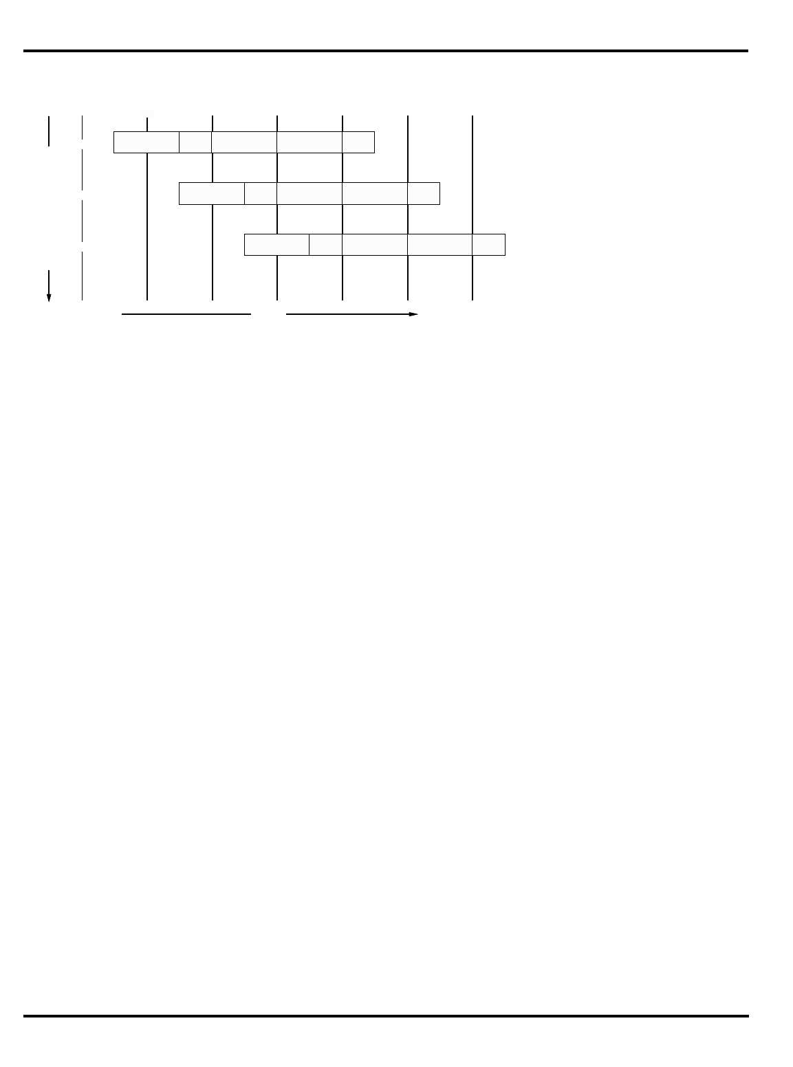
"Figure 1.1. MIPS 5-stage pipeline”, illustrates this operation.
Instruction execution activity can be described as occurring in the
individual pipestages:
•
IF
: (‘‘instruction fetch’’) gets the next instruction from the instruction
cache (
I-cache
).
•
RD
: (‘‘read registers’’) decodes the instruction and fetches the
contents of any CPU registers it uses.
•
ALU
: (‘‘arithmetic/logic unit’’) performs an arithmetic or logical
operation in one clock (floating point math and integer multiply/
divide can’t be done in one clock and are done differently; this is
described later).
instr 1
instr 2
instr 3
ALU
I-cache D-cache
register
file register
file
RDIF ALU MEM WB
RDIF ALU MEM WB
RDIF ALU MEM WB
Time
Instruction sequence

INTRODUCTION CHAPTER 1
1–3
•
MEM
: the stage where the instruction can read/write memory
variables in the data cache (
D-cache
). Note that for typical programs,
three out of four instructions do nothing in this stage; but allocating
the stage to each instruction ensures that the processor never has
two instructions wanting the data cache at the same time.
•
WB
: (‘‘write back’’) store the value obtained from an operation back to
the register file.
A rigid pipeline does limit the kinds of things instructions can do; in
particular:
•
Instruction length
: ALL instructions are 32 bits (exactly one machine
‘‘word’’) long, so that they can be fetched in a constant time. This itself
discourages complexity; there are not enough bits in the instruction
to encode really complicated addressing modes, for example.
•
No arithmetic on memory variables
: data from cache or memory is
obtained only in stage 4, which is much too late to be available to the
ALU. Memory accesses occur only as simple load or store instructions
which move the data to or from registers (this is described as a ‘‘load/
store architecture’’).
However, the MIPS project architects also attended to the best thinking
of the time about what makes a CPU an easy target for efficient optimizing
compilers. So MIPS CPUs have 32 general purpose registers, 3-operand
arithmetical/logical instructions and eschew complex special-purpose
instructions which compilers can’t usually generate.
THE IDT R3xxx FAMILY CPUS
MIPS Corporation was formed in 1984 to make a commercial version of
the Stanford MIPS CPU. The commercial CPU was enhanced with memory
management hardware, first appearing late in 1985 as the R2000. An
ambitious external floating point math co-processor (the R2010 FPA) first
shipped in mid-87. The R3000, shipped in 1988, is almost identical from
the programmer’s viewpoint (although small hardware enhancements
combined to give a substantial boost to performance). The R3000A was
done in 1989, to improve the frequency of operation over the original
R3000 (other minor enhancements were added, such as the ability for user
tasks to operate with the opposite “endianness” from the kernel).
The R2000/R3000 chips include a cache controller – the
implementation of external caches merely required a few industry
standard SRAMs and some address latches. The math co-processor shares
the cache buses to interpret instructions (in parallel with the integer CPU)
and transfer operands and results between the FPA and memory or the
integer CPU.
The division of function was ingenious, practical and workable, allowing
the R2000/3000 generation to be built without extravagant ultra-high pin-
count packages. However, as clock speeds increased the very high-speed
signals in the cache interface increased design complexity and limited
operational frequency. In addition, overall chip count for the basic
execution core proved to be a limitation for area and power sensitive
embedded systems.
The R3051, R3052, R3071, R3081 and R3041 are the members (so far)
of a family of products defined, designed, and manufactured by IDT. The
chips integrate the functions of the R3000A CPU, cache memory and
(R3081 only) math co-processor. This means that all the fastest logic is on
chip; so the integrated chips are not only cheaper and smaller than the
original implementation, but also much easier to use.
The parts differ in their cache sizes, whether they include onchip MMU
and/or FPA, clock rates and packaging options. In addition, although all
parts can be used pin-compatibly, certain products feature optional
enhancements in their bus-interface that may serve to reduce system cost
or complexity, and other subtle enhancements for cost or performance.
The major differences are summarized in "Table 1.1. R30xx family
members compared”.

CHAPTER 1 INTRODUCTION
1–4
MIPS ARCHITECTURE LEVELS
There are multiple generations of the MIPS architecture. The most
commonly discussed are the MIPS-1, MIPS-2, and MIPS-3 architectures.
MIPS-1 is the ISA found in the R2000 and R3000 generation CPUs. It is
a 32-bit ISA, and defines the basic instruction set. Any application written
with the MIPS-1 instruction set will operate correctly on all generations of
the architecture.
The MIPS-2 ISA is also 32-bit. It adds some instructions to speed up
floating point data movement, branch-likely instructions, and other minor
enhancements. This was first implemented in the MIPS R6000 ECL
microprocessor.
The MIPS-3 ISA is a 64-bit ISA. In addition to supporting all MIPS-1 and
MIPS-2 instructions, the MIPS-3 ISA contains 64-bit equivalents of certain
earlier instructions that are sensitive to operand size (e.g. load double and
load word are both supported), including doubleword (64-bit) data
movement and arithmetic. This ISA was first implemented in the R4000 as
a clean (“seamless”) transition from the existing 32-bit architecture.
Note that these ISA levels do not necessarily imply a particular structure
for the MMU, caches, exception model, or other kernel specific resources.
Thus, different implementations of ISA compatible chips may require
different kernels.
In the case of the R30xx family, all devices implement the MIPS-1 ISA.
Many devices are also kernel compatible with the R3000A, but some
devices (most notably those without an MMU) may require small kernel
changes or different boot modules†.
MIPS-1 COMPARED WITH CISC ARCHITECTURES
Although the MIPS architecture is fairly straight-forward, there are a few
features, visible only to assembly programmers, which may at first appear
surprising. In addition, operations familiar to CISC architectures are
† Historically, many embedded MIPS applications have run
exclusively out of the “kseg0 and kseg1” memory regions
(described later in the book). For these applications, the presence
or absence of the MMU is largely irrelevant.
Part Cache
I + D MMU FPA Clock
(MHz) Package
Options System Interface
3051 4K + 1K – – 20-40 PLCC 32-bit MUX’ed A/D
3051E
×
3052 8K + 2K – – 20-40 PLCC 32-bit MUX’ed A/D
3052E
×
3081 16K+4K/
8K+8K –
×
20-50 PLCC Optional 1/2 frequency
bus operation
Optional 1x Clock Input
3081E 16K+4K/
8K+8K
×
3071 16K+4K/
8K+8K – – 33-50 PLCC 1/2 frequency bus
operation
1x Clock Input
3071E 16K+4K/
8K+8K
×
3041 2K + 0.5K – – 16-25 PLCC
TQFP Variable port width
interface.
Table 1.1. R30xx family members compared

INTRODUCTION CHAPTER 1
1–5
irrelevant to the MIPS architecture. For example, the MIPS architecture
does not mandate a stack pointer or stack usage; thus, programmers may
be surprised to find that push/pop instructions do not exist directly.
The most notable of these features are summarized here.
Unusual instruction encoding features
•
All instructions are 32-bits long
: as mentioned above. This means, for
example, that it is impossible to incorporate a 32-bit constant into a
single instruction (there would be no instruction bits left to encode
the operation and the registers!). A ‘‘load immediate’’ instruction is
limited to a 16-bit value; a special ‘‘load upper immediate’’ must be
followed by an ‘‘or immediate’’ to put a 32-bit constant value into a
register.
•
Instruction actions must fit the pipeline
: actions can only be carried out
in the designated pipeline phase, and must be complete in one clock.
For example, the register writeback phase provides for just one value
to be stored in the register file, so instructions can only change one
register.
•
3-operand instructions
: arithmetic/logical operations don’t have to
specify memory locations, so there are plenty of instruction bits to
define two independent source and one destination register.
Compilers love 3-operand instructions, which give optimizers more
scope to improve the code which handles complex expressions.
•
32 registers
: the choice of 32 has become universal; compilers like a
large (but not necessarily too large) number of registers, but there is
a cost in context-saving and in encoding the registers to be used by
an instruction. Register $0 always returns zero, to give a compact
encoding of that useful constant.
•
No condition codes
: the MIPS architecture does not provide condition
code flags implicitly set by arithmetical operations. The motivation is
to make sure that execution state is stored in one place – the register
file. Conditional branches (in MIPS) test a single register for sign/zero,
or a pair of registers for equality.
Addressing and memory accesses
•
Memory references are always register loads and stores
: arithmetic on
memory variables upsets the pipeline, so is not done. Memory
references only occur due to explicit load or store instructions. The
large register file allows multiple variables to be “on-chip”
simultaneously.
•
Only one data addressing mode
: all loads and stores define the
memory location with a single base register value modified by a 16-bit
signed displacement. Note that the assembler/compiler tools can use
the $0 register, along with the immediate value, to synthesize
additional addressing modes from this one directly supported mode.
•
Byte-addressed
: the instruction set includes load/store operations
for 8- and 16-bit variables (referred to as
byte
and
halfword
). Partial-
word load instructions come in two flavors – sign-extend and zero-
extend.
•
Loads/stores must be address-aligned
: memory word operations can
only load or store data from a single 4-byte aligned word; halfword
operations must be aligned on half-word addresses. Many CISC
microprocessors will load/store a multi-byte item from any byte
address (although unaligned transfers always take longer).
Techniques to generate code which will handle unaligned data
efficiently will be explained later.
•
Jump instructions
: The smallest op-code field in a MIPS instruction is
6 bits; leaving 26 bits to define the target of a jump. Since all
instructions are 4-byte aligned in memory the two least-significant

CHAPTER 1 INTRODUCTION
1–6
address bits need not be stored, allowing an address range of 2
28
=
256Mbytes. Rather than make this branch PC-relative, this is
interpreted as an absolute address within a 256Mbyte ‘‘segment’’. In
theory, this could impose a limit on the size of a single program; in
reality, it hasn’t been a problem.
Branches out of segment can be achieved by using a
jr
instruction,
which uses the contents of a register as the target.
Conditional branches have only a 16-bit displacement field (2
18
byte
range since instructions are 4-byte aligned) which is interpreted as a
signed PC-relative displacement. Compilers can only code a simple
conditional branch instruction if they know that the target will be
within 128Kbytes of the instruction following the branch.
Operations not directly supported
•
No byte or halfword arithmetic
: all arithmetical and logical operations
are performed on 32-bit quantities. Byte and/or halfword arithmetic
would require significant extra resources, many more op-codes, and
is an understandable omission. Most C programmers will use the
int
data type for most arithmetic, and for MIPS an
int
is 32 bits and such
arithmetic will be efficient. C’s rules are to perform arithmetic in
int
whenever any source or destination variable is as long as
int
.
However, where a program explicitly does arithmetic as
short
the
compiler must insert extra code to make sure that wraparound and
overflows have the appropriate effect.
•
No special stack support
: conventional MIPS assembler usage does
define a
sp
register, but the hardware treats
sp
just like any other
register. There is a recommended format for the stack frame layout of
subroutines, so that programs can mix modules from different
languages and compilers; it is recommended that programmers stick
to these conventions, but they have no relationship to the hardware.
•
Minimal subroutine overhead
: there is one special feature; jump
instructions have a ‘‘jump and link’’ option which stores the return
address into a register. $31 is the default, so for convenience and by
convention $31 becomes the ‘‘return address’’ register.
•
Minimal interrupt overhead
: The MIPS architecture makes very few
presumptions about system exception handling, allowing fast
response and a wide variety of software models. In the R30xx family,
the CPU stashes away the restart location in the special register
EPC,
modifies the machine state just enough to signal why the trap
happened and to disallow further interrupts; then it jumps to a single
predefined location† in low memory. Everything else is up to the
software.
Just to emphasize this: on an interrupt or trap a MIPS CPU
does not
store anything on a stack, or write memory, or preserve any registers
by itself.
By convention, two registers ($k0, $k1; register conventions are
explained in chapter 2) are reserved so that interrupt/trap routines
can ‘‘bootstrap’’ themselves – it is impossible to do anything on a MIPS
CPU without using some registers. For a program running in any
system which takes interrupts or traps, the values of these registers
may change at any time, and thus should not be used.
† One particular kind of trap (a TLB miss on an address in the
user-privilege address space) has a different dedicated entry point.
INTRODUCTION CHAPTER 1
1–7
Multiply and divide operations
The MIPS CPU does have an integer multiply/divide unit; worth
mentioning because many RISC machines don’t have multiply hardware.
The multiply unit is relatively independent of the rest of the CPU, with its
own special output registers.
Programmer-visible pipeline effects
In addition to the discussion above, programmers of R3xxx architecture
CPUs also must be aware of certain effects of the MIPS pipeline.
Specifically, the results of certain operations may not be available in the
immediately subsequent instruction; the programmer may need to be
explicitly aware of such cases.
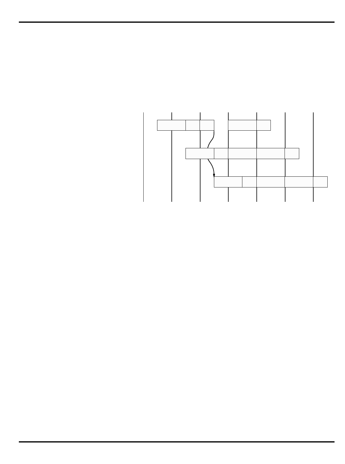
Figure 1.2. The pipeline and branch delays
•
Delayed branches
: the pipeline structure of the MIPS CPU (see "Figure
1.2. The pipeline and branch delays”) means that when a jump
instruction reaches the ‘‘execute’’ phase and a new program counter
is generated, the instruction after the jump will already have been
decoded. Rather than discard this potentially useful work, the
architecture rules state that the
instruction after a branch is always
executed before the instruction at the target of the branch
.
"Figure 1.2. The pipeline and branch delays” show that a special path
is provided through the ALU to make the branch address available a
half-clock early, ensuring that there is only a one cycle delay before
the outcome of the branch is determined and the appropriate
instruction flow (branch taken or not taken) is initiated.
It is the responsibility of the compiler system or the assembler-
programmer to allow for and even to exploit this “branch delay slot”;
it turns out that it is usually possible to arrange code such that the
instruction in the ‘‘delay slot’’ does useful work. Quite often, the
instruction which would otherwise have been placed before the
branch can be moved into the delay slot.
This can be a bit tricky on a conditional branch, where the branch
delay instruction must be (at least) harmless on the path where it isn’t
wanted. Where nothing useful can be done the delay slot is filled with
a ‘‘
nop
’’ (no-op, or no-operation) instruction.
Many MIPS assemblers will hide this feature from the programmer
unless explicitly told not to, as described later.
•
Load data not available to next instruction
: another consequence of
the pipeline is that a load instruction’s data arrives from the cache/
memory system AFTER the
next
instruction’s ALU phase starts – so it
is not possible to use the data from a load in the following instruction.
See "Figure 1.3. The pipeline and load delays” for how this works. On
the MIPS-1 architecture, the programmer must insure that this rule
is not violated
branch
branch
delay
branch
target
IF RF MEM WBALU
IF RF MEM WBALU
branch
addr
IF RF MEM WB

CHAPTER 1 INTRODUCTION
1–8
•.
Figure 1.3. The pipeline and load delays
Again, most assemblers will hide this if they can. Frequently, the
assembler can move an instruction which is independent of the load
into the load delay slot; in the worst case, it can insert a
NOP
to insure
proper program execution.
A NOTE ON MACHINE AND ASSEMBLER LANGUAGE
To simplify assembly level programming, the MIPS Corp’s assembler
(and many other MIPS assemblers) provides a set of “synthetic”
instructions. Typically, a synthetic instruction is a common assembly level
operation that the assembler will map into one or more true instructions.
This mapping can be more intelligent than a mere macro expansion. For
example, an immediate load may map into one instruction if the datum is
small enough, or multiple instructions if the datum is larger. However,
these instructions can dramatically simplify assembly level programming.
For example, the programmer just writes a ‘‘load immediate’’ instruction
and the assembler will figure out whether it needs to generate multiple
machine instructions or can get by with just one (in this example,
depending on the size of the immediate datum).
This is obviously useful, but can be confusing. This manual will try to
use synthetic instructions sparingly, and indicate when it happens.
Moreover, the instruction tables below will consistently distinguish
between synthetic and machine instructions.
These features are there to help human programmers; most compilers
generate instructions which are one-for-one with machine code. However,
some compilers will in fact generate synthetic instructions.
Helpful things the assembler does:
•
32-bit load immediates
: The programmer can code a load with any
value (including a memory location which will be computed at link
time), and the assembler will break it down into two instructions to
load the high and low half of the value.
•
Load from memory location
: The programmer can code a load from a
memory-resident variable. The assembler will normally replace this
by loading a temporary register with the high-order half of the
variable’s address, followed by a load whose displacement is the low-
order half of the address.
Of course, this does not apply to variables defined inside C functions,
which are implemented either in registers or on the stack.
•
Efficient access to memory variables
: some C programs contain many
references to
static
or
extern
variables, and a two-instruction
sequence to load/store any of them is expensive. Some compilation
systems, with run-time support, get around this. Certain variables
are selected at compile/assemble time (by default MIPS Corp’s
assembler selects variables which occupy 8 or less bytes of storage)
D-cache rd
load
load
delay
use
data
RDIF ALU MEM WB
RDIF ALU MEM WB
RDIF ALU MEM WB

INTRODUCTION CHAPTER 1
1–9
and kept together in a single section of memory which must end up
smaller than 64Kbytes. The run-time system then initializes one
register ($28 or
gp
(global pointer) by convention) to point to the
middle of this section.
Loads and stores to these variables can now be coded as a single
gp
relative load or store.
•
More types of branch condition
: the assembler synthesizes a full set of
branches conditional on an arithmetic test between two registers.
•
Simple or different forms of instructions
: unary operations such as
not
and
neg
are produced as a
nor
or
sub
with the zero-valued register
$0.
Two-operand forms of 3-operand instructions can be written; the
assembler will put the result back into the first-specified register.
•Hiding the branch delay slot: in normal coding most assemblers will
not allow access the branch delay slot. MIPS Corp.’s assembler, in
particular, is exceptionally ingenious and may re-organize the
instruction sequence substantially in search of something useful to
do in the delay slot. An assembler directive ‘‘.noreorder’’ is available
where this must not happen.
•Hiding the load delay: many assemblers will detect an attempt to use
the result of a load in the next instruction, and will either move code
around or insert a nop.
•Unaligned transfers: the ‘‘unaligned’’ load/store instructions will
fetch halfword and word quantities correctly, even if the target
address turns out to be unaligned.
•Other pipeline corrections: some instructions (such as those which use
the integer multiply unit) have additional constraints that are
implementation specific (see the Appendix on hazards). Many
assemblers will just “handle” these cases automatically, or at least
warn the programmer about possible hazards violations.
•Other optimizations: some MIPS instructions (particularly floating
point) take multiple clocks to produce results. However, the hardware
is ‘‘interlocked’’, so the programmer does not need to be aware of these
delays to write correct programs. But MIPS Corp.’s assembler is
particularly aggressive in these circumstances, and will perform
substantial code movement to try to make it run faster. This may need
to be considered when debugging.
In general, it is best to use a dis-assembler utility to disassemble a
resulting binary during debug. This will show the system designers the
true code sequence being executed, and thus “uncover” the modifications
made by the assembler or compiler.

2–1
MIPS-1 (R30xx)
ARCHITECTURE
®
Integrated Device Technology, Inc.
CHAPTER 2
PROGRAMMER’S VIEW OF THE PROCESSOR
ARCHITECTURE
This chapter describes the assembly programmer’s view of the CPU
architecture, in terms of registers, instructions, and computational
resources. This viewpoint corresponds, for example, to an assembly
programmer writing user applications (although more typically, such a
programmer would use a high-level language).
Information about kernel software development (such as handling
interrupts, traps, and cache and memory management) are described in
later chapters.
Registers
There are 32 general purpose registers: $0 to $31. Two, and only two,
are special to the hardware:
• $0 always returns zero, no matter what software attempts to store to
it.
• $31 is used by the normal subroutine-calling instruction (jal) for the
return address. Note that the call-by-register version (jalr) can use
ANY register for the return address, though practice is to use only
$31.
In all other respects all registers are identical and can be used in any
instruction ($0 can be used as the destination of instructions; the value of
$0 will remain unchanged, however, so the instruction would be effectively
a
NOP
).
In the MIPS architecture the ‘‘program counter’’ is not a register, and it
is probably better to not think of it that way. The return address of a
jal
is
two instructions later
in sequence (the instruction after the jump delay slot
instruction); the instruction after the call is the call’s ‘‘delay slot’’ and is
typically used to set up the last parameter.
There are no condition codes and nothing in the ‘‘status register’’ or
other CPU internals is of any consequence to the user-level programmer.
There are two registers associated with the integer multiplier. These
registers, referred to as “HI” and “LO”, contain the 64-bit product result of
a multiply operation, or the quotient and remainder of a divide.
The floating point math co-processor (called
FPA
for floating point
accelerator), if available, adds 32 floating point registers†; in simple
assembler language they are just called $0 to $31 again – the fact that
these are floating point registers is implicitly defined by the instruction.
Actually, only the 16 even-numbered registers are usable for math; but
they can be used for either single-precision (32 bit) or double-precision
(64-bit) numbers, When performing double-precision arithmetic, odd
numbered register $N+1 holds the remaining bits of the even numbered
register identified $N. Only moves between integer and FPA, or FPA load/
store instructions, ever refer to odd-numbered registers (and even then the
assembler helps the programmer forget...)
† The FPA also has a different set of registers called ‘‘co-processor
1 registers’’ for control purposes. These are typically used to
manage the actions/state of the FPA, and should not be confused
with the FPA data registers.
1

CHAPTER 2 MIPS-1 (R30xx) ARCHITECTURE
2–2
Conventional names and uses of general-purpose registers
Although the hardware makes few rules about the use of registers, their
practical use is governed by a number of conventions. These conventions
allow inter-changeability of tools, operating systems, and library modules.
It is strongly recommended that these conventions be followed.
With the conventional uses of the registers go a set of conventional
names. Given the need to fit in with the conventions, use of the
conventional names is pretty much mandatory. The common names are
described in Table 2.1, “Conventional names of registers with usage
mnemonics”.
Notes on conventional register names
•
at
: this register is reserved for use inside the synthetic instructions
generated by the assembler. If the programmer must use it explicitly
the directive
.noat
stops the assembler from using it, but then there
are some things the assembler won’t be able to do.
•
v0-v1
: used when returning non-floating-point values from a
subroutine. To return anything bigger than 2
×
32 bits, memory must
be used (described in a later chapter).
•
a0-a3
: used to pass the first four non-FP parameters to a subroutine.
That’s an occasionally-false oversimplification; the actual convention
is fully described in a later chapter.
•
t0-t9
: by convention, subroutines may use these values without
preserving them. This makes them easy to use as ‘‘temporaries’’ when
evaluating expressions – but a caller must remember that they may
be destroyed by a subroutine call.
•
s0-s8
: by convention, subroutines must guarantee that the values of
these registers on exit are the same as they were on entry – either by
not using them, or by saving them on the stack and restoring before
exit.
This makes them eminently suitable for use as ‘‘register variables’’ or
for storing any value which must be preserved over a subroutine call.
Reg No Name Used for
0 zero Always returns 0
1 at (assembler temporary) Reserved for use by assembler
2-3 v0-v1 Value (except FP) returned by subroutine
4-7 a0-a3 (arguments) First four parameters for a subroutine
8-15 t0-t7 (temporaries) subroutines may use without saving
24-25 t8-t9
16-23 s0-s7 Subroutine ‘‘register variables’’; a subroutine which will write
one of these must save the old value and restore it before it
exits, so the
calling
routine sees their values preserved.
26-27 k0-k1 Reserved for use by interrupt/trap handler - may change
under your feet
28 gp global pointer - some runtime systems maintain this to give
easy access to (some) ‘‘static’’ or ‘‘extern’’ variables.
29 sp stack pointer
30 s8/fp 9th register variable. Subroutines which need one can use
this as a ‘‘frame pointer’’.
31 ra Return address for subroutine
Table 2.1. Conventional names of registers with usage mnemonics

MIPS-1 (R30xx) ARCHITECTURE CHAPTER 2
2–3
•
k0-k1
: reserved for use by the trap/interrupt routines, which will not
restore their original value; so they are of little use to anyone else.
•
gp
: (global pointer). If present, it will point to a load-time-determined
location in the midst of your static data. This means that loads and
stores to data lying within 32Kbytes either side of the
gp
value can be
performed in a single instruction using
gp
as the base register.
Without the global pointer, loading data from a static memory area
takes two instructions: one to load the most significant bits of the 32-
bit constant address computed by the compiler and loader, and one
to do the data load.
To use
gp
a compiler must know at compile time that a datum will end
up linked within a 64Kbyte range of memory locations. In practice it
can’t know, only guess. The usual practice is to put ‘‘small’’ global
data items in the area pointed to by
gp
, and to get the linker to
complain if it still gets too big. The definition of what is “small” can
typically be specified with a compiler switch (most compilers use “-
G“). The most common default size is 8 bytes or less.
Not all compilation systems or OS loaders support
gp.
•
sp
: (stack pointer). Since it takes explicit instructions to raise and
lower the stack pointer, it is generally done only on subroutine entry
and exit; and it is the responsibility of the subroutine being called to
do this.
sp
is normally adjusted, on entry, to the lowest point that the
stack will need to reach at any point in the subroutine. Now the
compiler can access stack variables by a constant offset from
sp.
Stack usage conventions are explained in a later chapter.
•
fp
: (also known as s8). A subroutine will use a ‘‘frame pointer’’ to keep
track of the stack if it wants to use operations which involve extending
the stack by an amount which is determined at run-time. Some
languages may do this explicitly; assembler programmers are always
welcome to experiment; and (for many toolchains) C programs which
use the ‘‘alloca’’ library routine will find themselves doing so.
In this case it is not possible to access stack variables from
sp,
so
fp
is initialized by the function prologue to a constant position relative
to the function’s stack frame. Note that a ‘‘frame pointer’’ subroutine
may call or be called by subroutines which do not use the frame
pointer; so long as the functions it calls preserve the value of
fp
(as
they should) this is OK.
•
ra
: (return address). On entry to any subroutine, ra holds the address
to which control should be returned – so a subroutine typically ends
with the instruction ‘‘jr ra’’.
Subroutines which themselves call subroutines must first save
ra,
usually on the stack.
Integer multiply unit and registers
MIPS’ architects decided that integer multiplication was important
enough to deserve a hard-wired instruction. This is not so common in
RISCs, which might instead:
• implement a ‘‘multiply step’’ which fits in the standard integer
execution pipeline, and require software routines for every
multiplication (e.g. Sparc or AM29000); or
• perform integer multiplication in the floating point unit – a good
solution but which compromises the optional nature of the MIPS
floating point ‘‘co-processor’’.
The multiply unit consumes a small amount of die area, but
dramatically improves performance (and cache performance) over
“multiply step” operations. It’s basic operation is to multiply two 32-bit
values together to produce a 64-bit result, which is stored in two 32-bit

CHAPTER 2 MIPS-1 (R30xx) ARCHITECTURE
2–4
registers (called ‘‘hi’’ and ‘‘lo’’) which are private to the multiply unit.
Instructions
mfhi
,
mflo
are defined to copy the result out into general
registers.
Unlike results for integer operations, the multiply result registers are
interlocked
. An attempt to read out the results before the multiplication is
complete results in the CPU being stopped until the operation completes.
The integer multiply unit will also perform an integer division between
values in two general-purpose registers; in this case the ‘‘lo’’ register stores
the quotient, and the ‘‘hi’’ register the remainder.
In the R30xx family, multiply operations take 12 clocks and division
takes 35. The assembler has a synthetic multiply operation which starts
the multiply and then retrieves the result into an ordinary register. Note
that MIPS Corp.’s assembler may even substitute a series of shifts and
adds for multiplication by a constant, to improve execution speed.
Multiply/divide results are written into ‘‘hi’’ and ‘‘lo’’ as soon as they are
available; the effect is not deferred until the writeback pipeline stage, as
with writes to general purpose (GP) registers. If a
mfhi
or
mflo
instruction
is interrupted by some kind of exception before it reaches the writeback
stage of the pipeline, it will be aborted with the intention of restarting it.
However, a subsequent multiply instruction which has passed the ALU
stage will continue (in parallel with exception processing) and would
overwrite the ‘‘hi’’ and ‘‘lo’’ register values, so that the re-execution of the
mfhi
would get wrong (i.e. new) data. For this reason it is recommended
that a multiply should not be started within two instructions of an
mfhi/
mflo
. The assembler will avoid doing this where it can.
Integer multiply and divide operations never produce an exception,
though divide by zero produces an undefined result. Compilers will often
generate code to trap on errors, particularly on divide by zero. Frequently,
this instruction sequence is placed after the divide is initiated, to allow it
to execute concurrently with the divide (and avoid a performance loss).
Instructions
mthi
,
mtlo
are defined to setup the internal registers from
general-purpose registers. They are essential to restore the values of ‘‘hi’’
and ‘‘lo’’ when returning from an exception, but probably not for anything
else.
Instruction types
A full list of R30xx family integer instructions is presented in Appendix
A. Floating point instructions are listed in Appendix B of this manual.
Currently, floating point instructions are only available in the R3081, and
are described in the R3081 User’s Manual.
The MIPS-1 ISA uses only three basic instruction encoding formats; this
is one of the keys to the high-frequencies attained by RISC architectures.
Instructions are mostly in numerical order; to simplify reading, the list
is occasionally re-ordered for clarity.
Throughout this manual, the description of various instructions will
also refer to various subfields of the instruction. In general, the following
typical nomenclature is used:
op The basic op-code, which is 6 bits long. Instructions which large
sub-fields (for example, large immediate values, such as required
for the ‘‘long’’
j/jal
instructions, or arithmetic with a 16-bit
constant) have a unique ‘‘op’’ field. Other instructions are
classified in groups sharing an ‘‘op’’ value, distinguished by
other fields (‘‘op2’’ etc.).
rs, rs1,
rs2 One or two fields identifying source registers.
rd The register to be changed by this instruction.
sa Shift-amount: How far to shift, used in shift-by-constant
instructions.

MIPS-1 (R30xx) ARCHITECTURE CHAPTER 2
2–5
op2 Sub-code field used for the 3-register arithmetic/logical group of
instructions (
op
value of zero).
offset 16-bit signed
word
offset defining the destination of a ‘‘PC-
relative’’ branch. The branch target will be the instruction
‘‘offset’’ words away from the ‘‘delay slot’’ instruction
after
the
branch; so a branch-to-self has an offset of -1.
target 26-bit
word
address to be jumped to (it corresponds to a 28-bit
byte address, which is always word-aligned). The long
j
instruction is rarely used, so this format is pretty much
exclusively for function calls (
jal
).
The high-order 4 bits of the target address can’t be specified by
this instruction, and are taken from the address of the jump
instruction. This means that these instructions can reach
anywhere in the 256Mbyte region around the instructions’
location. To jump further use a
jr
(jump register) instruction.
constant
16-bit integer constant for ‘‘immediate’’ arithmetic or logic
operations.
mf Yet another extended opcode field, this time used by ‘‘co-
processor’’ type instructions.
rg Field which may hold a source or destination register.
crg Field to hold the number of a CPU control register (different from
the integer register file). Called ‘‘crs’’/‘‘crd’’ in contexts where it
must be a source/destination respectively.
The instruction encodings have been chosen to facilitate the design of a
high-frequency CPU. Specifically:.
• The instruction encodings do reveal portions of the internal CPU
design. Although there are variable encodings, those fields which are
required very early in the pipeline are encoded in a very regular way:
•
Source registers are always in the same place
: so that the CPU can
fetch two instructions from the integer register file without any
conditional decoding. Some instructions may not need both registers
– but since the register file is designed to provide two source values
on every clock nothing has been lost.
•
16-bit constant is always in the same place
: permitting the
appropriate instruction bits to be fed directly into the ALU’s input
multiplexer, without conditional shifts.
Loading and storing: addressing modes
As mentioned above, there is only one basic ‘‘addressing mode’’. Any
load or store machine instruction can be written as:
operation dest-reg, offset(src-reg)
e.g.:lw $1, offset($2); sw $3, offset($4)
Any of the GP registers can be used for the destination and source. The
offset is a signed, 16-bit number (so can be anywhere between -32768 and
32767); the program address used for the load is the sum of
dest-reg
and
the
offset
. This address mode is normally enough to pick out a particular
member of a C structure (‘‘offset’’ being the distance between the start of
the structure and the member required); it implements an array indexed
by a constant; it is enough to reference function variables from the stack
or frame pointer; to provide a reasonable sized global area around the
gp
value for static and extern variables.
The assembler provides the semblance of a simple direct addressing
mode, to load the values of memory variables whose address can be
computed at link time.

CHAPTER 2 MIPS-1 (R30xx) ARCHITECTURE
2–6
More complex modes such as double-register or scaled index must be
implemented with sequences of instructions.
Data types in Memory and registers
The R30xx family CPUs can load or store between 1 and 4 bytes in a
single operation. Naming conventions are used in the documentation and
to build instruction mnemonics:
Integer data types
Byte and halfword loads come in two flavors:
•
Sign-extend
:
lb
and
lh
load the value into the least significant bits of
the 32-bit register, but fill the high order bits by copying the ‘‘sign bit’’
(bit 7 of a byte, bit 16 of a half-word). This correctly converts a signed
value to a 32-bit signed integer.
•
Zero-extend
: instructions
lbu
and
lhu
load the value into the least
significant bits of a 32-bit register, with the high order bits filled with
zero. This correctly converts an unsigned value in memory to the
corresponding 32-bit unsigned integer value; so byte value 254
becomes 32-bit value 254.
If the byte-wide memory location whose address is in
t1
contains the
value
0xFE
(-2, or 254 if interpreted as unsigned), then:
lb t2, 0(t1)
lbu t3, 0(t1)
will leave
t2
holding the value
0xFFFF FFFE
(-2 as signed 32-bit) and
t3
holding the value
0x0000 00FE
(254 as signed or unsigned 32-bit).
Subtle differences in the way shorter integers are extended to longer
ones are a historical cause of C portability problems, and the modern C
standards have elaborate rules. On machines like the MIPS, which does
not perform 8- or 16-bit precision arithmetic directly, expressions
involving
short
or
char
variables are less efficient than word operations.
Unaligned loads and stores
Normal loads and stores in the MIPS architecture must be aligned; half-
words may be loaded only from 2-byte boundaries, and words only from 4-
byte boundaries. A load instruction with an unaligned address will
produce a trap. Because CISC architectures such as the MC680x0 and
iAPXx86 do handle unaligned loads and stores, this could complicate
porting software from one of these architectures. The MIPS architecture
does provide mechanisms to support this type of operation; in extremity,
software can provide a trap handler which will emulate the desired load
operation and hide this feature from the application.
All data items declared by C code will be correctly aligned.
But when it is known in advance that the program will transfer a word
from an address whose alignment is unknown and will be computed at run
time, the architecture does allow for a special 2-instruction sequence
(much more efficient than a series of byte loads, shifts and assembly). This
sequence is normally generated by the macro-instruction
ulw
(unaligned
load word).
‘‘C’’ name MIPS name Size(bytes) Assembler
mnemonic
int word 4 ‘‘w’’ as in
lw
long word 4 ‘‘w’’ as in
lw
short halfword 2 ‘‘h’’ as in
lh
char byte 1 ‘‘b’’ as in
lb

MIPS-1 (R30xx) ARCHITECTURE CHAPTER 2
2–7
(A macro-instruction
ulh
, unaligned load half, is also provided, and is
synthesized by two loads, a shift, and a bitwise ‘‘or’’ operation.)
The special machine instructions are lwl and lwr (load word left, load
word right). ‘‘Left’’ and ‘‘right’’ are arithmetical directions, as in ‘‘shift left’’;
‘‘left’’ is movement towards more significant bits, ‘‘right’’ is towards less
significant bits.
These instructions do three things:
• load 1, 2, 3 or 4 bytes from within one aligned 4-byte (word) location;
• shift that data to move the byte selected by the address to either the
most-significant (lwl) or least-significant (lwr) end of a 32-bit field;
• merge the bytes fetched from memory with the data already in the
destination.
This breaks most of the rules the architecture usually sticks by; it does
a logical operation on a memory variable, for example. Special hardware
allows the lwl, lwr pair to be used in consecutive instructions, even though
the second instruction uses the value generated by the first.
For example, on a CPU configured as big-endian the assembler
instruction:
ulw t1, 0(t2)
add t4, t3, t1
is implemented as:
lwl t1, 0(t2)
lwr t1, 3(t2)
nop
add t4, t3, t1
Where:
• the lwl picks up the lowest-addressed byte of the unaligned 4-byte
region, together with however many more bytes which fit into an
aligned word. It then shifts them left, to form the most-significant
bytes of the register value.
• the lwr is aimed at the highest-addressed byte in the unaligned 4-byte
region. It loads it, together with any bytes which precede it in the
same memory word, and shifts it right to get the least significant bits
of the register value. The merge leaves the high-order bits unchanged.
• Although special hardware ensures that a nop is not required between
the lwl and lwr, there is still a load delay between the second of them
and a normal instruction.
Note that if t2 was in fact 4-byte aligned, then both instructions load the
entire word; duplicating effort, but achieving the desired effect.
CPU behavior when operating with little-endian byte order is described
in a later chapter.
Floating point data in memory
Loads into floating point registers from 4-byte aligned memory move
data without any interpretation – a program can load an invalid floating
point number and no FP error will result until an arithmetic operation is
requested with it as an operand.
This allows a programmer to load single-precision values by a load into
an even-numbered floating point register; but the programmer can also
load a double-precision value by a macro instruction, so that:
ldc1 $f2, 24(t1)
is expanded to two loads to consecutive registers:
lwc1 $f2, 24(t1)
lwc1 $f3, 28(t1)

CHAPTER 2 MIPS-1 (R30xx) ARCHITECTURE
2–8
The C compiler aligns 8-byte long double-precision floating point
variables to 8-byte boundaries. R30xx family hardware does not require
this alignment; but it is done to avoid compatibility problems with
implementations of MIPS-2 or MIPS-3 CPUs such as the IDT R4600
(Orion), where the ldc1 instruction is part of the machine code, and the
alignment is necessary.
BASIC ADDRESS SPACE
The way in which MIPS processors use and handle addresses is subtly
different from that of traditional CISC CPUs, and may appear confusing.
Read the first part of this section carefully. Here are some guidelines:
• The addresses put into programs are rarely the same as the physical
addresses which come out of the chip (sometimes they’re close, but
not the same). This manual will refer to them as program addresses
and physical addresses respectively. A more common name for
program addresses is “virtual addresses”; note that the use of the
term “virtual address” does not necessarily imply that an operating
system must perform virtual memory management (e.g. demand
paging from disks...), but rather that the address undergoes some
transformation before being presented to physical memory. Although
virtual address is a proper term, this manual will typically use the
term “program address” to avoid confusing virtual addresses with
virtual memory management requirements.
• A MIPS-1 CPU has two operating modes: user and kernel. In user
mode, any address above 2Gbytes (most-significant bit of the address
set) is illegal and causes a trap. Also, some instructions cause a trap
in user mode.
• The 32-bit program address space is divided into four big areas with
traditional names; and different things happen according to the area
an address lies in:
kuseg 0000 0000 – 7FFF FFFF (low 2Gbytes): these are the addresses
permitted in user mode. In machines with an MMU (“E” versions
of the R30xx family), they will always be translated (more about
the R30xx MMU in a later chapter). Software should not attempt
to use these addresses unless the MMU is set up.
For machines without an MMU (“base” versions of the R30xx
family), the kuseg “program address” is transformed to a
physical address by adding a 1GB offset; the address
transformations for “base versions” of the R30xx family are
described later in this chapter. Note, however, that many
embedded applications do not use this address segment (those
applications which do not require that the kernel and its
resources be protected from user tasks).
kseg0 0x8000 0000 – 9FFF FFFF (512 Mbytes): these addresses are
‘‘translated’’ into physical addresses by merely stripping off the
top bit, mapping them contiguously into the low 512 Mbytes of
physical memory. This transformation operates the same for
both “base” and “E” family members. This segment is referred to
as “unmapped” because “E” version devices cannot redirect this
translation to a different area of physical memory.
Addresses in this region are always accessed through the cache,
so may not be used until the caches are properly initialized. They
will be used for most programs and data in systems using “base”
family members; and will be used for the OS kernel for systems
which do use the MMU (“E” version devices).

MIPS-1 (R30xx) ARCHITECTURE CHAPTER 2
2–9
kseg1 0xA000 0000 – BFFF FFFF (512 Mbytes): these addresses are
mapped into physical addresses by stripping off the leading three
bits, giving a duplicate mapping of the low 512 Mbytes of
physical memory. However, kseg1 program address accesses will
not use the cache.
The kseg1 region is the only chunk of the memory map which is
guaranteed to behave properly from system reset; that’s why the
after-reset starting point (0xBFC0 0000, commonly called the
“reset exception vector”) lies within it. The physical address of
the starting point is 0x1FC0 0000 – which means that the
hardware should place the boot ROM at this physical address.
Software will therefore use this region for the initial program
ROM, and most systems also use it for I/O registers. In general,
IO devices should always be mapped to addresses that are
accessible from Kseg1, and system ROM is always mapped to
contain the reset exception vector. Note that code in the ROM
can then be accessed uncacheably (during boot up) using kseg1
program addresses, and also can be accessed cacheably (for
normal operation) using kseg0 program addresses.
kseg2 0xC000 0000 – FFFF FFFF (1 Gbyte): this area is only
accessible in kernel mode. As for kuseg, in “E” devices program
addresses are translated by the MMU into physical addresses;
thus, these addresses must not be referenced prior to MMU
initialization. For “base versions”, physical addresses are
generated to be the same as program addresses for kseg2.
Note that many systems will not need this region. In “E” versions,
it frequently contains OS structures such as page tables; simpler
OS’es probably will have little need for kseg2.
SUMMARY OF SYSTEM ADDRESSING
MIPS program addresses are rarely simply the same as physical
addresses, but simple embedded software will probably use addresses in
kseg0 and kseg1, where the program address is related in an obvious and
unchangeable way to physical addresses.
Physical memory locations from 0x2000 0000 (512Mbyte) upward may
be difficult to access. In “E” versions of the R30xx family, the only way to
reach these addresses is through the MMU. In “base” family members,
certain of these physical addresses can be reached using kseg2 or kuseg
addresses: the address transformations for base R30xx family members is
described later in this chapter.
Kernel vs. user mode
In kernel mode (the CPU resets into this state), all program addresses
are accessible.
In user mode:
• Program addresses above 2Gbytes (top bit set) are illegal and will
cause a trap.
Note that if the CPU has an MMU, this means all valid user mode
addresses must be translated by the MMU; thus, User mode for “E”
devices typically requires the use of a memory-mapped OS.
For “base” CPUs, kuseg addresses are mapped to a distinct area of
physical memory. Thus, kernel memory resources (including IO
devices) can be made inaccessible to User mode software, without
requiring a memory-mapping function from the OS. Alternately, the
hardware can choose to “ignore” high-order address bits when
performing address decoding, thus “condensing” kuseg, kseg2, kseg1,
and kseg0 into the same physical memory.

CHAPTER 2 MIPS-1 (R30xx) ARCHITECTURE
2–10
• Instructions beyond the standard user set become illegal. Specifically,
the kernel can prevent User mode software from accessing the on-
chip CP0 (system control coprocessor, which controls exception and
machine state and performs the memory management functions of
the CPU).
Thus, the primary differences between User and Kernel modes are:
• User mode tasks can be inhibited from accessing kernel memory
resources, including OS data structures and IO devices. This also
means that various user tasks can be protected from each other.
• User mode tasks can be inhibited from modifying the basic machine
state, by prohibiting accesses to CP0.
Note that the kernel/user mode bit does not change the interpretation
of anything – just some things cease to be allowed in user mode. In kernel
mode the CPU can access low addresses just as if it was in user mode, and
they will be translated in the same way.
Memory map for CPUs without MMU hardware
The treatment of kseg0 and kseg1 addresses is the same for all IDT
R30xx CPUs. If the system can be implemented using only physical
addresses in the low 512Mbytes, and system software can be written to use
only kseg0 and kseg1, then the choice of “base” vs. “E” versions of the
R30xx family is not relevant.
For versions without the MMU (“base versions”), addresses in kuseg and
kseg2 will undergo a fixed address translation, and provide the system
designer the option to provide additional memory.
The base members of the R30xx family provide the following address
translations for kuseg and kseg2 program addresses:
•kuseg: this region (the low 2Gbytes of program addresses) is
translated to a contiguous 2Gbyte physical region between 1-
3Gbytes. In effect, a 1GB offset is added to each kuseg program
address. In hex:
•kseg2: these program addresses are genuinely untranslated. So
program addresses from 0xC000 0000 – 0xFFFF FFFF emerge as
identical physical addresses.
This means that “base” versions can generate most physical addresses
(without the use of an MMU), except for a gap between 512Mbyte and
1Gbyte (0x2000 0000 through 0x3FFF FFFF). As noted above, many
systems may ignore high-order address bits when performing address
decoding, thus condensing all physical memory into the lowest 512MB
addresses.
Subsegments in the R3041 – memory width configuration
The R3041 CPU can be configured to access different regions of memory
as either 32-, 16- or 8-bits wide. Where the program requests a 32-bit
operation to a narrow memory (either with an uncached access, or a cache
miss, or a store), the CPU may break a transaction into multiple data
phases, to match the datum size to the memory port width.
The width configuration is applied independently to subsegments of the
normal kseg regions, as follows:
•kseg0 and kseg1: as usual, these are both mapped onto the low
512Mbytes. This common region is split into 8 subsegments
(64Mbytes each), each of which can be programmed as 8-, 16- or 32-
bits wide. The width assignment affects both kseg0 and kseg1
accesses (that is, one can view these as subsegments of the
corresponding “physical” addresses).
Program address Physical Address
0x0000 0000 -
0x7FFF FFFF → 0x4000 0000 -
0xBFFF FFFF

MIPS-1 (R30xx) ARCHITECTURE CHAPTER 2
2–11
•kuseg: is divided into four 512Mbyte subsegments, each
independently programmable for width. Thus, kuseg can be broken
into multiple portions, which may have varying widths. An example of
this may be a 32-bit main memory with some 16-bit PCMCIA font
cards and an 8-bit NVRAM.
•kseg2: is divided into two 512Mbyte subsegments, independently
programmable for width. Again, this means that kseg2 can support
multiple memory subsystems, of varying port width.
Note that once the various memory port widths have been configured
(typically at boot time), software does not have to be aware of the actual
width of any memory system. It can choose to treat all memory as 32-bit
wide, and the CPU will automatically adjust when an access is made to a
narrower memory region. This simplifies software development, and also
facilitates porting to various system implementations (which may or may
not choose the same memory port widths).

2–1
MIPS-1 (R30xx)
ARCHITECTURE
®
Integrated Device Technology, Inc.
CHAPTER 2
PROGRAMMER’S VIEW OF THE PROCESSOR
ARCHITECTURE
This chapter describes the assembly programmer’s view of the CPU
architecture, in terms of registers, instructions, and computational
resources. This viewpoint corresponds, for example, to an assembly
programmer writing user applications (although more typically, such a
programmer would use a high-level language).
Information about kernel software development (such as handling
interrupts, traps, and cache and memory management) are described in
later chapters.
Registers
There are 32 general purpose registers: $0 to $31. Two, and only two,
are special to the hardware:
• $0 always returns zero, no matter what software attempts to store to
it.
• $31 is used by the normal subroutine-calling instruction (jal) for the
return address. Note that the call-by-register version (jalr) can use
ANY register for the return address, though practice is to use only
$31.
In all other respects all registers are identical and can be used in any
instruction ($0 can be used as the destination of instructions; the value of
$0 will remain unchanged, however, so the instruction would be effectively
a
NOP
).
In the MIPS architecture the ‘‘program counter’’ is not a register, and it
is probably better to not think of it that way. The return address of a
jal
is
two instructions later
in sequence (the instruction after the jump delay slot
instruction); the instruction after the call is the call’s ‘‘delay slot’’ and is
typically used to set up the last parameter.
There are no condition codes and nothing in the ‘‘status register’’ or
other CPU internals is of any consequence to the user-level programmer.
There are two registers associated with the integer multiplier. These
registers, referred to as “HI” and “LO”, contain the 64-bit product result of
a multiply operation, or the quotient and remainder of a divide.
The floating point math co-processor (called
FPA
for floating point
accelerator), if available, adds 32 floating point registers†; in simple
assembler language they are just called $0 to $31 again – the fact that
these are floating point registers is implicitly defined by the instruction.
Actually, only the 16 even-numbered registers are usable for math; but
they can be used for either single-precision (32 bit) or double-precision
(64-bit) numbers, When performing double-precision arithmetic, odd
numbered register $N+1 holds the remaining bits of the even numbered
register identified $N. Only moves between integer and FPA, or FPA load/
store instructions, ever refer to odd-numbered registers (and even then the
assembler helps the programmer forget...)
† The FPA also has a different set of registers called ‘‘co-processor
1 registers’’ for control purposes. These are typically used to
manage the actions/state of the FPA, and should not be confused
with the FPA data registers.
1

3–1
SYSTEM CONTROL CO-
PROCESSOR ARCHITECTURE
®
Integrated Device Technology, Inc.
CHAPTER 3
This chapter concentrates on the aspects of the R30xx family
architecture that must be managed by the OS programmer. Note that most
of these features are transparent to the user program author; however, the
nature of embedded systems is such that most embedded systems
programmers will have a view of the underlying CPU and system
architecture, and thus will find this material important.
CPU CONTROL SUMMARY
This chapter, coupled with chapters on cache management, memory
management, and exception processing, provide details on managing the
machine and OS state. The areas of interest include:
•
CPU control and co-processor
: how privileged instructions are
organized, with shortform descriptions. There are relatively few
privileged instructions; most of the low-level control over the CPU is
exercised by reading and writing bit-fields within special registers.
•
Exceptions
: external interrupts, invalid operations, arithmetic errors
– all result in ‘‘exceptions’’, where control is transferred to an
exception handler
routine.
MIPS exceptions are extremely simple – the hardware does the
absolute minimum, allowing the programmer to tailor the exception
mechanism to the needs of the particular system.
A later chapter describes MIPS exceptions, why they are ‘‘precise’’,
exception vectors, and conventions about how to code exception
handling routines.
Special problems can arise with
nested exceptions
: exceptions
occurring while the CPU is still handling an earlier exception.
Co-processors
MIPS uses the term “co-processor” both in a traditional fashion, and also
in a non-traditional fashion. Specifically, the FPA device is a traditional
microprocessor co-processor: it is an optional part of the architecture,
with its own particular instruction set.
Opcodes are reserved and instruction fields defined for up to four ‘‘co-
processors’’. Architecturally, the co-processors can be tightly coupled to
the base integer CPU; for example, the ISA defines instructions to move
data directly between memory and the coprocessor, rather than requiring
it to be moved into the integer processor first.
However, MIPS also uses the term “co-processor” for the functions
required to manage the CPU environment, including exception
management, cache control, and memory management. This
segmentation insures that the chip architecture can be varied (e.g. cache
architecture, interrupt controller, etc.), without impacting user mode
software compatibility.
These functions are grouped by MIPS into the on-chip “co-processor 0”,
or ‘‘system control co-processor’’ - and these instructions implement the
whole CPU control system. Note that co-processor 0 has no independent
existence, and is certainly not optional. It provides a standard way of
encoding the instructions which access the CPU status register; so that,
although the definition of the status register changes among
implementations, programmers can use the same assembler for both
CPUs. Similarly, the exception and memory management strategies can
be varied among implementations, and these effects isolated to particular
portions of the OS kernel.
1

CHAPTER 3 SYSTEM CONTROL CO-PROCESSOR ARCHITECTURE
3–2
Hardware interrupts have their own style and rules.
The Exception Management chapter includes an annotated example
of a moderately-complicated exception handler.
•
Caches and cache management
: all R30xx implementations have dual
caches (the I-cache for instructions, the D-cache for data). On-chip
hardware is provided to manage the caches, and the programmer
working with I/O devices, particularly with DMA devices, may need to
explicitly manage the caches in particular situations.
To manipulate the caches, the CPU allows software to
isolate
them,
inhibiting cache/memory traffic and allowing the processor to access
cache as if it were simple memory; and the CPU can
swap
the roles of
the I-cache and D-cache (the only way to make the I-cache writable).
Caches must sometimes be cleared of stale or invalid/uninitialized
data. Even following power-up, the R30xx caches are in a random
state and must be cleaned up before they can be used. A later chapter
will discuss the techniques used by software to manage the on-chip
cache resources.
In addition, techniques to determine the on-chip cache sizes will be
shown (greatest flexibility is achieved if software can be written to be
independent of cache sizes).
For the diagnostics programmer, techniques to test the cache memory
and probe for particular entries will be discussed.
On some CPU implementations the system designer may make
configuration choices about the cache (e.g. the R3081 and R3071
allow the cache organization to be selected between 16kB of I-cache/
4kB of D-cache and 8kB each of I- and D- cache). The cache
management chapter will also discuss some of the considerations to
apply to make a proper selection.
•
Write buffer
: on R30xx family CPUs the D-cache is always
write
through
; all writes go to main memory as well as the cache. This
simplifies the caches, but main memory won’t be able to accept data
as fast as the CPU can write it. Much of the performance loss can be
made up by using a FIFO store which holds a number of ‘‘write cycles’’
(it stores both address and data). In the R30xx family, this FIFO,
called the write buffer, is integrated on-chip.
System programmers may need to know that writes happen later than
the code sequence suggests. The chapter on cache management
discusses this.
•
Starting up
: at reset almost nothing is defined, so the software must
build carefully. In MIPS CPUs, reset is implemented in almost exactly
the same way as the exceptions.
A later chapter on reset initialization discusses ways of finding out
which CPU is executing the software, and how to get a ROM program
to run.
An example of a C runtime environment, attending to the stack and
special registers, is provided.
•
Memory management and the TLB
: A later chapter will discuss
address translation and managing the translation hardware (the
TLB). This section is mostly for OS programmers.
CPU CONTROL AND ‘‘CO-PROCESSOR 0’’
CPU control instructions
Most control functions are implemented with registers (most of which
consist of multiple bitfields). The MIPS architecture has an escape
mechanism to define instructions for ‘‘co-processors’’ – and the CPU
control instructions are coded for ‘‘co-processor 0’’.

SYSTEM CONTROL CO-PROCESSOR ARCHITECTURE CHAPTER 3
3–3
There are several CPU control instructions used in the memory
management implementation, which are described in a later chapter. But
leaving aside the MMU, CPU control defines just one instruction beyond
the necessary move to and from the control registers.
mtc0
rs, <nn> –Move to co-processor zero
Loads ‘‘co-processor 0’’ register number
nn
from CPU general register
rs
. It
is unusual, and not good practice, to refer to CPU control registers by their
number in assembler sources; normal practice is to use the names listed
in Table 3.1, “Summary of CPU control registers (not MMU)”. In some tool-
chains the names are defined by a C-style ‘‘include’’ file, and the C pre-
processor run as a front-end to the assembler; the assembler manual
should provide guidance on how to do this. This is the only way of setting
bits in a CPU control register.
mfc0
rd, <nn >–Move from co-processor zero
General register
rd
is loaded with the values from CPU control register
number
nn
. Once again, it is common to use a symbolic name and a
macro-processor to save remembering the numbers. This is the only way
of inspecting bits in a control register.
rfe
–Restore from exception
Note that this is not ‘‘return from exception’’. This instruction restores the
status register to go back to the state prior to the trap. To understand what
it does, refer to the status register
SR
defined later in this chapter. The only
secure way of returning to user mode from an exception is to return with
a
jr
instruction which has the
rfe
in its delay slot.
Standard CPU control registers
This table describes the general CPU control registers (ignoring the
MMU control registers). Also note that typical convention is to reserve k0
and k1 for exception processing, although they are proper GP registers of
the integer CPU unit.
Register
Mnemonic Description CP0
reg no.
PRId CP0 type and rev level 15
SR (status register) CPU mode flags 12
Cause Describes the most recently recognized
exception 13
EPC Return address from trap 14
BadVaddr Contains the last invalid program address
which caused a trap. It is set by address
errors of all kinds, even if there is no MMU
8
Config CPU configuration (R3081 and R3041 only) 3
BusCtrl (R3041 only) configure bus interface signals.
Needs to be setup to match the hardware
implementation.
2
PortSize (R3041 only) used to flag some program
address regions as 8- or 16-bits wide. Must be
programmed to match the hardware
implementation.
10
Count (R3041 only, read/write) a 24-bit counter
incrementing with the CPU clock. 9
Compare (R3041 only, read/write) a 24-bit value used
to wraparound the
Count
value and set an
output signal.
11
Table 3.1. Summary of CPU control registers (not MMU)

CHAPTER 3 SYSTEM CONTROL CO-PROCESSOR ARCHITECTURE
3–4
PRId Register
Figure 3.1, “PRId Register fields” shows the layout of the
PRId
register,
a read-only register to be consulted to identify the CPU type (more
properly, this register describes CP0, allowing the kernel to dynamically
configure itself for various CPU implementations). ‘‘Imp’’ should be related
to the CPU control register set. The encoding of Imp is described below:
Note that when the Imp field indicates IDT unique, the revision number
can be used to distinguish among various CP0 implementations. Refer to
the R3041 User’s manual for the revision level appropriate for that device.
Since the R3051, 52, 71, and 81 are kernel compatible with the R3000A,
they share the same Imp value.
When printing the value of this register, it is conventional to print them
out as ‘‘x.y’’ where ‘‘x’’ and ‘‘y’’ are the decimal values of Imp and Rev
respectively. Try not to use this register and the CPU manuals to size
things, or to establish the presence or absence of particular features;
software will be more portable and robust if it is designed to include code
sequences to probe for the existence of individual features. This manual
will provide numerous examples designed to determine cache sizes,
presence or absence of TLB, FPA, etc.
SR Register
Encoding of control registers
The next section describes the format of the control registers, with a
sketch of the function of each field. In most cases, more information
about how things work is to be found in separate sections or chapters
later.
A note about reserved fields is in order here. Many unused control
register fields are marked ‘‘0’’. Bits in such fields are guaranteed to read
zero, and should be written as zero. Other reserved fields are marked
‘‘reserved’’ or ‘‘
×
’’; software must always write them as zero, and should
not assume that it will get back zero or any other particular value.
Registers specific to the memory management system are described in a
later chapter.
31 16 15 8 7 0
reserved
Imp Rev
Figure 3.1. PRId Register fields
CPU type ‘‘Imp’’ value
R3000A (including
R3051, R3052, R3071,
and R3081)
3
IDT unique (R3041) 7
31 30 29 28 27 26 25 24 23 22 21 20 19 18 17 16
CU3 CU2 CU1 CU0 0 RE 0 BEV TS PE CM PZ SwC IsC
15 8 7 6 5 4 3 2 1 0
IM 0 KUo IEo KUp IEp KUc IEc
Figure 3.2. Fields in status register (SR)

SYSTEM CONTROL CO-PROCESSOR ARCHITECTURE CHAPTER 3
3–5
The MIPS CPU has remarkably few mode bits; those that exist are
defined by fields in the CPU status register
SR,
as shown in Figure 3.2,
“Fields in status register (SR)”.
Note that there are no modes such as non-translated or non-cached in
MIPS CPUs; all translation and caching decisions are made on the basis of
the program address. Fields are:
CU3,
CU2 Bits (31:30) control the usability of ‘‘co-processors’’ 3 and 2
respectively. In the R30xx family, these might be enabled if
software wishes to use the BrCond(3:2) input pins for polling, or
to speed exception decoding.
CU1 ‘‘co-processor 1 usable’’: 1 to use FPA if present, 0 to disable.
When 0, all FPA instructions cause an exception, even for the
kernel. It can be useful to turn off an FPA even when one is
available; it may also be enabled in devices which do not include
an FPA, if the intent is to use the BrCond(1) pin as a polled input.
CU0 ‘‘co-processor 0 usable’’: set 1 to be able to use some nominally-
privileged instructions in user mode (this is rarely if ever done).
The CPU control instructions encoded as ‘‘co-processor 0’’ type
are always usable in kernel mode, regardless of the setting of this
bit.
RE ‘‘reverse endianness in user mode’’. The MIPS processors can be
configured, at reset time, with either ‘‘endianness’’ (byte ordering
convention, discussed in the various CPU’s User’s Manuals and
later in this manual). The RE bit allows binaries intended to be
run with one byte ordering convention to be run in systems with
the opposite convention, presuming OS software provided the
necessary support.
When RE is active, user-privilege software runs as if the CPU had
been configured with the opposite endianness.
However, achieving cross-universe running would require a large
software effort as well, and should not be necessary in embedded
systems.
BEV ‘‘boot exception vectors’’: when BEV == 1, the CPU uses the ROM
(kseg1) space exception entry point (described in a later chapter).
BEV is usually set to zero in running systems; this relocates the
exception vectors. to RAM addresses, speeding accesses and
allowing the use of “user supplied” exception service routines.
TS ‘‘TLB shutdown’’: In devices which implement the full R3000A
MMU, TS gets set if a program address simultaneously matches
two TLB entries. Prolonged operation in this state, in some
implementations, could cause internal contention and damage
to the chip. TLB shutdown is terminal, and can be cleared only
by a hardware reset.
In base family members, which do not include the TLB, this bit
is set by reset; software can rely on this feature to determine the
presence or absence of TLB support hardware.
PE set if a cache parity error has occurred. No exception is
generated by this condition, which is really only useful for
diagnostics. The MIPS architecture has cache diagnostic
facilities because earlier versions of the CPU used external
caches, and this provided a way to verify the timing of a
particular system. For those implementations the cache parity
error bit was an essential design debug tool.
For CPUs with on-chip caches this feature is rarely needed; only
the R3071 and R3081 implement parity over the on-chip caches.

CHAPTER 3 SYSTEM CONTROL CO-PROCESSOR ARCHITECTURE
3–6
CM shows the result of the last load operation performed with the D-
cache isolated (described in the chapter on cache management).
CM is set if the cache really contained data for the addressed
memory location (i.e. if the load would have hit in the cache even
if the cache had not been isolated).
PZ When set, cache parity bits are written as zero and not checked.
This was useful in old R3000A systems which required external
cache RAMs, but is of little relevance to the R30xx family.
SwC,
IsC ‘‘swap caches’’ and ‘‘isolate (data) cache’’. Cache mode bits for
cache management and diagnostics; their use is described in
detail in a later chapter on cache management. In simple terms:
• IsC set 1: makes all loads and stores access only the data
cache, and never memory; and in this mode a partial-
word store invalidates the cache entry. Note that when
this bit is set, even uncached data accesses will not be
seen on the bus; further, this bit is not initialized by reset.
Boot-up software must insure this bit is properly
initialized before relying on external data references.
• SwC set 1: reverses the roles of the I-cache and D-cache,
so that software can access and invalidate I-cache entries.
IM ‘‘interrupt mask’’: an 8 bit field defining which interrupt sources,
when active, will be allowed to cause an exception. Six of the
interrupt sources are external pins (one may be used by the FPA,
which although it lives on the same chip is logically external); the
other two are the software-writable interrupt bits in the
Cause
register.
No interrupt prioritization is provided by the CPU: the hardware
treats all interrupt bits the same. This is described in greater
detail in the chapter dealing with exceptions.
KUc,
IEc The two basic CPU protection bits.
KUc is set 1 when running with kernel privileges, 0 for user
mode. In kernel mode, software can get at the whole program
address space, and use privileged (‘‘co-processor 0’’)
instructions. User mode restricts software to program addresses
between 0x0000 0000 and
0x7FFF FFFF
, and can be denied
permission to run privileged instructions; attempts to break the
rules result in an exception.
IEc is set 0 to prevent the CPU taking any interrupt, 1 to enable.
KUp, IEp‘‘KU previous, IE previous’’:
on an exception, the hardware takes the values of KUc and IEc
and saves them here; at the same time as changing the values of
KUc, IEc to [1, 0] (kernel mode, interrupts disabled). The
instruction
rfe
can be used to copy KUp, IEp back into KUc, IEc.
KUo, IEo‘‘KU old, IE old’’:
on an exception the KUp, IEp bits are saved here. Effectively, the
six KU/IE bits are operated as a 3-deep, 2-bit wide stack which
is pushed on an exception and popped by an
rfe
.
This provides a chance of recovering cleanly from an exception
occurring so early in an exception handling routine that the first
exception has not yet saved
SR.
The circumstances in which this
can be done are limited, and it is probably only really of use in
allowing the user TLB refill code to be made a little shorter, as
described in the chapter on memory management.
SYSTEM CONTROL CO-PROCESSOR ARCHITECTURE CHAPTER 3
3–7
Cause Register
Figure 3.3, “Fields in the Cause register” shows the fields in the
Cause
register, which are consulted to determine the kind of exception which
happened and will be used to decide which exception routine to call.
BD ‘‘branch delay’’: if set, this bit indicates that the EPC does not
point to the actual “exception” instruction, but rather to the
branch instruction which immediately precedes it.
When the exception restart point is an instruction which is in the
‘‘delay slot’’ following a branch,
EPC
has to point to the branch
instruction; it is harmless to re-execute the branch, but if the
CPU returned from the exception to the branch delay instruction
itself the branch would not be taken and the exception would
have broken the interrupted program.
The only time software might be sensitive to this bit is if it must
analyze the ‘‘offending’’ instruction (if BD == 1 then the
instruction is at
EPC
+ 4). This would occur if the instruction
needs to be emulated (e.g. a floating point instruction in a device
with no hardware FPA; or a breakpoint placed in a branch delay
slot).
CE ‘‘co-processor error’’: if the exception is taken because a ‘‘co-
processor’’ format instruction was for a ‘‘co-processor’’ which is
not enabled by the CUx bit in
SR,
then this field has the co-
processor number from that instruction.
IP ‘‘Interrupt Pending’’: shows the interrupts which are currently
asserted (but may be “masked” from actually signalling an
exception). These bits follow the CPU inputs for the six hardware
levels. Bits 9 and 8 are read/writable, and contain the value last
written to them. However, any of the 8 bits active when enabled
by the appropriate IM bit and the global interrupt enable flag IEc
in
SR,
will cause an interrupt.
IP is subtly different from the rest of the
Cause
register fields; it
doesn’t indicate what happened when the exception took place,
but rather shows what is happening now.
ExcCode
A 5-bit code which indicates what kind of exception happened,
as detailed in Table 3.2, “ExcCode values: different kinds of
exceptions”.
31 30 29 28 27 16 15 8 7 6 2 1 0
BD 0 CE 0 IP 0 ExcCode 0
Figure 3.3. Fields in the Cause register
ExcCode
Value Mnemonic Description
0 Int Interrupt
1 Mod ‘‘TLB modification’’
2 TLBL ‘‘TLB load/TLB store’’
3 TLBS
4 AdEL Address error (on load/I-fetch or store respectively).
Either an attempt to access outside kuseg when in user
mode, or an attempt to read a word or half-word at a
misaligned address.
5 AdES
Table 3.2. ExcCode values: different kinds of exceptions

CHAPTER 3 SYSTEM CONTROL CO-PROCESSOR ARCHITECTURE
3–8
EPC Register
This is a 32-bit register containing the 32-bit address of the return point
for this exception. The instruction causing (or suffering) the exception is at
EPC, unless BD is set in
Cause,
in which case EPC points to the previous
(branch) instruction.
BadVaddr Register
A 32-bit register containing the address whose reference led to an
exception; set on any MMU-related exception, on an attempt by a user
program to access addresses outside kuseg, or if an address is wrongly
aligned for the datum size referenced.
After any other exception this register is undefined. Note in particular
that it is not set after a bus error.
R3041, R3071, and R3081 specific registers
Count and Compare Registers (R3041 only)
Only present in the R3041, these provide a simple 24-bit counter/timer
running at CPU cycle rate.
Count
counts up, and then wraps around to
zero once it has reached the value in the
Compare
register. As it wraps
around the
Tc*
CPU output is asserted. According to CPU configuration
(bit TC of the
BusCtrl
register),
Tc*
will either remain active until reset by
software (re-write
Compare
), or will pulse. In either case the counter just
keeps counting. To generate an interrupt
Tc*
must be connected to one of
the interrupt inputs.
From reset
Compare
is setup to its maximum value (
0xFF FFFF
), so the
counter runs up to 2
24
-1 before wrapping around.
Config Register (R3071 and R3081)
6 IBE Bus error (instruction fetch or data load, respectively).
External hardware has signalled an error of some kind;
proper exception handling is system-dependent. The
R30xx family CPUs can’t take a bus error on a store;
the write buffer would make such an exception
“imprecise”.
7 DBE
8 Syscall Generated unconditionally by a
syscall
instruction.
9 Bp Breakpoint - a
break
instruction.
10 RI ‘‘reserved instruction’’
11 CpU ‘‘Co-Processor unusable’’
12 Ov ‘‘arithmetic overflow’’. Note that ‘‘unsigned’’ versions of
instructions (e.g.
addu
) never cause this exception.
13-31 - reserved. Some are already defined for MIPS CPUs such
as the R6000 and R4xxx
31 30 29 28 26 25 24 23 22 0
Lock Slow
Bus DB
Refill FPInt Halt RF AC reserved
Figure 3.4. Fields in the R3071/81 Config Register
ExcCode
Value Mnemonic Description
Table 3.2. ExcCode values: different kinds of exceptions

SYSTEM CONTROL CO-PROCESSOR ARCHITECTURE CHAPTER 3
3–9
•
Lock
: set this bit to write to the register for the last time; all future
writes to
Config
will be ignored. The intention is that initialization
software will set the register and can then lock it in case some ill-
behaved piece of software developed on some earlier version of the
MIPS architecture tries to stomp on
Config;
this would have had no
effect on earlier CPUs.
•
Slow Bus
: hardware may require that this bit be set. It only matters
when the CPU performs a store while running from a cached location.
The system hardware design determines the proper setting for this
bit; setting it to ‘1’ should be permissible for any system, but loses
some performance in memory systems able to support more
aggressive bus performance.
If set 1, an idle bus cycle is guaranteed between any read and write
transfer. This enables additional time for bus tri-stating, control logic
generation, etc.
•
DB
: ‘‘data cache block refill’’, set 1 to reload 4 words into the data
cache on any miss, set 0 to reload just one word. Can be initialized
either way on the R3081, by a reset-time hardware input.
•
FPInt
: controls the CPU interrupt level on which FPA interrupts are
reported. On original R3000 CPUs the FPA was external and this was
determined by wiring; but the R3081’s FPA is on the chip and it would
be inefficient (and jeopardize pin-compatibility) to send the interrupt
off chip and on again.
Set FPInt to the binary value of the CPU interrupt pin number which
is dedicated to FPA interrupts. By default the field is initialized to
“011’’ to select the pin
Int3
†; MIPS convention put the FPA on
external interrupt pin 3. For whichever pin is dedicated to the FPA,
the CPU will then ignore the value on the external pin; the IP field of
the cause register will simply follow the FPA.
On the R3071, this field is “reserved”, and must be written as “000”.
•
Halt
: set to bring the CPU to a standstill. It will start again as soon as
any interrupt input is asserted (regardless of the state of the interrupt
mask). This is useful for power reduction, and can also be used to
emulate old MC68000 “Halt” operation.
•
RF
: slows the CPU to 1/16th of the normal clock rate, to reduce power
consumption. Illegal unless the CPU is running at 33Mhz or higher.
Note that the CPUs output clock (which is normally used to
synchronize all the interface logic) slows down too; the hardware
design should also accommodate this feature if software desires to
use it.
•
AC
: ‘‘alternate cache’’. 0 for 16K I-cache/4K D-cache, but set 1 for 8K
I-cache/8K D-cache.
•
Reserved
: must only be written as zero. It will probably read as zero,
but software should not rely on this.
Config Register (R3041)
† Take care: the external pin
Int3
corresponds to the bit numbered
‘‘5’’ in IP of the Cause register or IM of the SR register. That’s
because both the Cause and SR fields support two ‘‘software
interrupts’’ numbered as bits 0 and 1.
31 30 29 28 20 19 18 0
Lock
1 DBR 0 FDM 0
Figure 3.5. Fields in the R3041 Config (Cache Configuration) Register

CHAPTER 3 SYSTEM CONTROL CO-PROCESSOR ARCHITECTURE
3–10
•Lock: set 1 to finally configure register (additional writes will not have
any effect until the CPU is reset).
•1
and 0
: set fields to exactly the value shown.
•DBR: ‘‘DBlockRefill’’, set 1 to read 4 words into the cache on a miss,
0 to refill just the word missed on. The proper setting for a given
system is dependent on a number of factors, and may best be
determined by measuring performance in each mode and selecting
the best one. Note that it is possible for software to dynamically
reconfigure the refill algorithm depending on the current code
executing, presuming the register has not been “locked”.
•FDM: “Force D-Cache Miss”, set 1 for an R3041-specific cache mode,
where all loads result in data being fetched from memory (missing in
the data cache), but the incoming data is still used to refill the cache.
Stores continue to write the cache. This is useful when software
desires to obtain the high-bandwidth of the cache and cache refills,
but the corresponding main memory is “volatile” (e.g. a FIFO, or
updated by DMA).
BusCtrl Register (R3041 only)
The R3041 CPU has many hardware interface options not available on
other members of the R30xx family, which are intended to allow the use of
simpler and cheaper interface and memory components. The BusCtrl
register does most of the configuration work. It needs to be set strictly in
accordance with the needs of the hardware implementation. Note also that
its default settings (from reset) leave the interface compatible with other
R30xx family members.
Figure 3.6, “Fields in the R3041 Bus Control (BusCtrl) Register” shows
the layout of the fields, and their uses are provided for completeness.
•Lock: when software has initialized BusCtrl to its desired state it may
write this bit to prevent its contents being changed again until the
system is reset.
•10
and other numbers
: write exactly the specified bit pattern to this
field (hex used for big ones, but others are given as binary). Improper
values may cause test modes and other unexpected side effects.
•Mem: ‘‘MemStrobe* control’’. Set this field to xy binary, where x set
means the strobe activates on reads, and y set makes it active on
writes.
•ED: ‘‘ExtDataEn* control’’. Encoded as for ‘‘Mem’’. Note that the BR
bit must be zero for this pin to function as an output.
•IO: ‘‘IOStrobe* control’’. Encoded as for ‘‘Mem’’. Note that the BR bit
must be zero for this pin to function as an output.
•BE16: ‘‘BE16(1:0)* read control’’ – 0 to make these pins active on
write cycles only.
•BE: ‘‘BE(3:0)* read control’’ – 0 to make these pins active on write
cycles only.
•BTA: ‘‘Bus turn around time’’. Program with a binary number
between 0 and 3, for 0-3 cycles of guaranteed delay between the end
of a read cycle and the start of the address phase of the next cycle.
This field enables the use of devices with slow tri-state time, and
enables the system designer to save cost by omitting data
transceivers.
31 3
0
2
8
2
7
2
6
2
5
2
4
2
3
2
2
21 2
0 1
9 1
8 1
6 1
5 1
4 13 1
2 1
1 1
0
0
Loc
k 10 Mem ED IO BE
16
1 B
E 11 BTA DM
A T
C
B
R
0x30
0
Figure 3.6. Fields in the R3041 Bus Control (BusCtrl) Register

SYSTEM CONTROL CO-PROCESSOR ARCHITECTURE CHAPTER 3
3–11
•DMA: ‘‘DMA Protocol Control’’, enables ‘‘DMA pulse protocol’’. When
set, the CPU uses its DMA control pins to communicate its desire for
the bus even while a DMA is in progress.
•TC: ‘‘TC* negation control’’. TC* is the output pin which is activated
when the internal timer register Count reaches the value stored in
Compare. Set TC zero to make the TC* pin just pulse for a couple of
clock periods; leave TC as 1, and TC* will be asserted on a compare
and remain asserted until software explicitly clears it (by re-writing
Compare with any value).
If TC* is used to generate a timer interrupt, then use the default (TC
== 0). The pulse is more useful when the output is being used by
external logic (e.g. to signal a DRAM refresh).
•BR: ‘‘SBrCond(3:2) control’’. Set zero to recycle the SBrCond(3:2)
pins as IOStrobe and ExtDataEn respectively.
PortSize Register (R3041 only)
The PortSize register is used to flag different parts of the program
address space for accesses to 8-, 16- or 32-bit wide memory.
Settings of this register have to be made at a time and to values which
will be mandated by the hardware design. See ‘‘IDT79R3041 Hardware
User’s Manual’’ for details.
What registers are relevant when?
The various CP0 registers and their fields provide support at specific
times during system operation.
•After hardware reset: software must initialize SR to get the CPU into
the right state to bootstrap itself.
•Hardware configuration at start-up: an R3041, R3071, or R3081
require initialization of Config, BusCtrl, and/or PortSize before very
much will work. The system hardware implementation will dictate the
proper configuration of these registers.
•After any exception: any MIPS exception (apart from one particular
MMU event) invokes a single common ‘‘general exception handler’’
routine, at a fixed address.
On entry, no program registers are saved, only the return address in
EPC. The MIPS hardware knows nothing about stacks. In any case the
exception routine cannot use the user-mode stack for any purpose;
the exception might have been a TLB miss on stack memory.
Exception software will need to use at least one of k0 and k1 to point
to some ‘‘safe’’ (exception-proof) memory space. Key information can
be saved, using the other k0 or k1 register to stage data from control
registers where necessary.
Consult the Cause register to find out what kind of exception it was
and dispatch accordingly.
•Returning from exception: control must eventually be returned to the
value stored in EPC on entry.
Whatever kind of exception it was, software will have to adjust SR
back upon return from exception. The special instruction rfe does the
job; but note that it does not transfer control. To make the jump back
software must load the original EPC value back into a general-
purpose register and use a jr operation.
•Interrupts: SR is used to adjust the interrupt masks, to determine
which (if any) interrupts will be allowed ‘‘higher priority’’ than the
current one. The hardware offers no interrupt prioritization, but the
software can do whatever it likes.
•Instructions which always cause exceptions: are often used (for
system calls, breakpoints, and to emulate some kinds of instruction).
These sometimes requires partial decoding of the offending

CHAPTER 3 SYSTEM CONTROL CO-PROCESSOR ARCHITECTURE
3–12
instruction, which can usually be found at the location EPC. But
there is a complication; suppose that an exception occurs just after a
branch but in time to prevent the branch delay slot instruction from
running. Then EPC will point to the branch instruction (resuming
execution starting at the delay slot would cause the branch to be
ignored), and the BD bit will be set.
This Cause register bit flags this event; to find the instruction at
which the exception occurred, add 4 to the EPC value when the BD
bit is set.
•Cache management routines: SR contains bits defining special modes
for cache management. In particular they allow software to isolate the
data cache, and to swap the roles of the instruction and data caches.
The subsequent chapters will describe appropriate treatment of these
registers, and provide software examples of their use.

CHAPTER 2 MIPS-1 (R30xx) ARCHITECTURE
2–2
Conventional names and uses of general-purpose registers
Although the hardware makes few rules about the use of registers, their
practical use is governed by a number of conventions. These conventions
allow inter-changeability of tools, operating systems, and library modules.
It is strongly recommended that these conventions be followed.
With the conventional uses of the registers go a set of conventional
names. Given the need to fit in with the conventions, use of the
conventional names is pretty much mandatory. The common names are
described in Table 2.1, “Conventional names of registers with usage
mnemonics”.
Notes on conventional register names
•
at
: this register is reserved for use inside the synthetic instructions
generated by the assembler. If the programmer must use it explicitly
the directive
.noat
stops the assembler from using it, but then there
are some things the assembler won’t be able to do.
•
v0-v1
: used when returning non-floating-point values from a
subroutine. To return anything bigger than 2
×
32 bits, memory must
be used (described in a later chapter).
•
a0-a3
: used to pass the first four non-FP parameters to a subroutine.
That’s an occasionally-false oversimplification; the actual convention
is fully described in a later chapter.
•
t0-t9
: by convention, subroutines may use these values without
preserving them. This makes them easy to use as ‘‘temporaries’’ when
evaluating expressions – but a caller must remember that they may
be destroyed by a subroutine call.
•
s0-s8
: by convention, subroutines must guarantee that the values of
these registers on exit are the same as they were on entry – either by
not using them, or by saving them on the stack and restoring before
exit.
This makes them eminently suitable for use as ‘‘register variables’’ or
for storing any value which must be preserved over a subroutine call.
Reg No Name Used for
0 zero Always returns 0
1 at (assembler temporary) Reserved for use by assembler
2-3 v0-v1 Value (except FP) returned by subroutine
4-7 a0-a3 (arguments) First four parameters for a subroutine
8-15 t0-t7 (temporaries) subroutines may use without saving
24-25 t8-t9
16-23 s0-s7 Subroutine ‘‘register variables’’; a subroutine which will write
one of these must save the old value and restore it before it
exits, so the
calling
routine sees their values preserved.
26-27 k0-k1 Reserved for use by interrupt/trap handler - may change
under your feet
28 gp global pointer - some runtime systems maintain this to give
easy access to (some) ‘‘static’’ or ‘‘extern’’ variables.
29 sp stack pointer
30 s8/fp 9th register variable. Subroutines which need one can use
this as a ‘‘frame pointer’’.
31 ra Return address for subroutine
Table 2.1. Conventional names of registers with usage mnemonics

MIPS-1 (R30xx) ARCHITECTURE CHAPTER 2
2–3
•
k0-k1
: reserved for use by the trap/interrupt routines, which will not
restore their original value; so they are of little use to anyone else.
•
gp
: (global pointer). If present, it will point to a load-time-determined
location in the midst of your static data. This means that loads and
stores to data lying within 32Kbytes either side of the
gp
value can be
performed in a single instruction using
gp
as the base register.
Without the global pointer, loading data from a static memory area
takes two instructions: one to load the most significant bits of the 32-
bit constant address computed by the compiler and loader, and one
to do the data load.
To use
gp
a compiler must know at compile time that a datum will end
up linked within a 64Kbyte range of memory locations. In practice it
can’t know, only guess. The usual practice is to put ‘‘small’’ global
data items in the area pointed to by
gp
, and to get the linker to
complain if it still gets too big. The definition of what is “small” can
typically be specified with a compiler switch (most compilers use “-
G“). The most common default size is 8 bytes or less.
Not all compilation systems or OS loaders support
gp.
•
sp
: (stack pointer). Since it takes explicit instructions to raise and
lower the stack pointer, it is generally done only on subroutine entry
and exit; and it is the responsibility of the subroutine being called to
do this.
sp
is normally adjusted, on entry, to the lowest point that the
stack will need to reach at any point in the subroutine. Now the
compiler can access stack variables by a constant offset from
sp.
Stack usage conventions are explained in a later chapter.
•
fp
: (also known as s8). A subroutine will use a ‘‘frame pointer’’ to keep
track of the stack if it wants to use operations which involve extending
the stack by an amount which is determined at run-time. Some
languages may do this explicitly; assembler programmers are always
welcome to experiment; and (for many toolchains) C programs which
use the ‘‘alloca’’ library routine will find themselves doing so.
In this case it is not possible to access stack variables from
sp,
so
fp
is initialized by the function prologue to a constant position relative
to the function’s stack frame. Note that a ‘‘frame pointer’’ subroutine
may call or be called by subroutines which do not use the frame
pointer; so long as the functions it calls preserve the value of
fp
(as
they should) this is OK.
•
ra
: (return address). On entry to any subroutine, ra holds the address
to which control should be returned – so a subroutine typically ends
with the instruction ‘‘jr ra’’.
Subroutines which themselves call subroutines must first save
ra,
usually on the stack.
Integer multiply unit and registers
MIPS’ architects decided that integer multiplication was important
enough to deserve a hard-wired instruction. This is not so common in
RISCs, which might instead:
• implement a ‘‘multiply step’’ which fits in the standard integer
execution pipeline, and require software routines for every
multiplication (e.g. Sparc or AM29000); or
• perform integer multiplication in the floating point unit – a good
solution but which compromises the optional nature of the MIPS
floating point ‘‘co-processor’’.
The multiply unit consumes a small amount of die area, but
dramatically improves performance (and cache performance) over
“multiply step” operations. It’s basic operation is to multiply two 32-bit
values together to produce a 64-bit result, which is stored in two 32-bit

CHAPTER 2 MIPS-1 (R30xx) ARCHITECTURE
2–4
registers (called ‘‘hi’’ and ‘‘lo’’) which are private to the multiply unit.
Instructions
mfhi
,
mflo
are defined to copy the result out into general
registers.
Unlike results for integer operations, the multiply result registers are
interlocked
. An attempt to read out the results before the multiplication is
complete results in the CPU being stopped until the operation completes.
The integer multiply unit will also perform an integer division between
values in two general-purpose registers; in this case the ‘‘lo’’ register stores
the quotient, and the ‘‘hi’’ register the remainder.
In the R30xx family, multiply operations take 12 clocks and division
takes 35. The assembler has a synthetic multiply operation which starts
the multiply and then retrieves the result into an ordinary register. Note
that MIPS Corp.’s assembler may even substitute a series of shifts and
adds for multiplication by a constant, to improve execution speed.
Multiply/divide results are written into ‘‘hi’’ and ‘‘lo’’ as soon as they are
available; the effect is not deferred until the writeback pipeline stage, as
with writes to general purpose (GP) registers. If a
mfhi
or
mflo
instruction
is interrupted by some kind of exception before it reaches the writeback
stage of the pipeline, it will be aborted with the intention of restarting it.
However, a subsequent multiply instruction which has passed the ALU
stage will continue (in parallel with exception processing) and would
overwrite the ‘‘hi’’ and ‘‘lo’’ register values, so that the re-execution of the
mfhi
would get wrong (i.e. new) data. For this reason it is recommended
that a multiply should not be started within two instructions of an
mfhi/
mflo
. The assembler will avoid doing this where it can.
Integer multiply and divide operations never produce an exception,
though divide by zero produces an undefined result. Compilers will often
generate code to trap on errors, particularly on divide by zero. Frequently,
this instruction sequence is placed after the divide is initiated, to allow it
to execute concurrently with the divide (and avoid a performance loss).
Instructions
mthi
,
mtlo
are defined to setup the internal registers from
general-purpose registers. They are essential to restore the values of ‘‘hi’’
and ‘‘lo’’ when returning from an exception, but probably not for anything
else.
Instruction types
A full list of R30xx family integer instructions is presented in Appendix
A. Floating point instructions are listed in Appendix B of this manual.
Currently, floating point instructions are only available in the R3081, and
are described in the R3081 User’s Manual.
The MIPS-1 ISA uses only three basic instruction encoding formats; this
is one of the keys to the high-frequencies attained by RISC architectures.
Instructions are mostly in numerical order; to simplify reading, the list
is occasionally re-ordered for clarity.
Throughout this manual, the description of various instructions will
also refer to various subfields of the instruction. In general, the following
typical nomenclature is used:
op The basic op-code, which is 6 bits long. Instructions which large
sub-fields (for example, large immediate values, such as required
for the ‘‘long’’
j/jal
instructions, or arithmetic with a 16-bit
constant) have a unique ‘‘op’’ field. Other instructions are
classified in groups sharing an ‘‘op’’ value, distinguished by
other fields (‘‘op2’’ etc.).
rs, rs1,
rs2 One or two fields identifying source registers.
rd The register to be changed by this instruction.
sa Shift-amount: How far to shift, used in shift-by-constant
instructions.

MIPS-1 (R30xx) ARCHITECTURE CHAPTER 2
2–5
op2 Sub-code field used for the 3-register arithmetic/logical group of
instructions (
op
value of zero).
offset 16-bit signed
word
offset defining the destination of a ‘‘PC-
relative’’ branch. The branch target will be the instruction
‘‘offset’’ words away from the ‘‘delay slot’’ instruction
after
the
branch; so a branch-to-self has an offset of -1.
target 26-bit
word
address to be jumped to (it corresponds to a 28-bit
byte address, which is always word-aligned). The long
j
instruction is rarely used, so this format is pretty much
exclusively for function calls (
jal
).
The high-order 4 bits of the target address can’t be specified by
this instruction, and are taken from the address of the jump
instruction. This means that these instructions can reach
anywhere in the 256Mbyte region around the instructions’
location. To jump further use a
jr
(jump register) instruction.
constant
16-bit integer constant for ‘‘immediate’’ arithmetic or logic
operations.
mf Yet another extended opcode field, this time used by ‘‘co-
processor’’ type instructions.
rg Field which may hold a source or destination register.
crg Field to hold the number of a CPU control register (different from
the integer register file). Called ‘‘crs’’/‘‘crd’’ in contexts where it
must be a source/destination respectively.
The instruction encodings have been chosen to facilitate the design of a
high-frequency CPU. Specifically:.
• The instruction encodings do reveal portions of the internal CPU
design. Although there are variable encodings, those fields which are
required very early in the pipeline are encoded in a very regular way:
•
Source registers are always in the same place
: so that the CPU can
fetch two instructions from the integer register file without any
conditional decoding. Some instructions may not need both registers
– but since the register file is designed to provide two source values
on every clock nothing has been lost.
•
16-bit constant is always in the same place
: permitting the
appropriate instruction bits to be fed directly into the ALU’s input
multiplexer, without conditional shifts.
Loading and storing: addressing modes
As mentioned above, there is only one basic ‘‘addressing mode’’. Any
load or store machine instruction can be written as:
operation dest-reg, offset(src-reg)
e.g.:lw $1, offset($2); sw $3, offset($4)
Any of the GP registers can be used for the destination and source. The
offset is a signed, 16-bit number (so can be anywhere between -32768 and
32767); the program address used for the load is the sum of
dest-reg
and
the
offset
. This address mode is normally enough to pick out a particular
member of a C structure (‘‘offset’’ being the distance between the start of
the structure and the member required); it implements an array indexed
by a constant; it is enough to reference function variables from the stack
or frame pointer; to provide a reasonable sized global area around the
gp
value for static and extern variables.
The assembler provides the semblance of a simple direct addressing
mode, to load the values of memory variables whose address can be
computed at link time.

CHAPTER 2 MIPS-1 (R30xx) ARCHITECTURE
2–6
More complex modes such as double-register or scaled index must be
implemented with sequences of instructions.
Data types in Memory and registers
The R30xx family CPUs can load or store between 1 and 4 bytes in a
single operation. Naming conventions are used in the documentation and
to build instruction mnemonics:
Integer data types
Byte and halfword loads come in two flavors:
•
Sign-extend
:
lb
and
lh
load the value into the least significant bits of
the 32-bit register, but fill the high order bits by copying the ‘‘sign bit’’
(bit 7 of a byte, bit 16 of a half-word). This correctly converts a signed
value to a 32-bit signed integer.
•
Zero-extend
: instructions
lbu
and
lhu
load the value into the least
significant bits of a 32-bit register, with the high order bits filled with
zero. This correctly converts an unsigned value in memory to the
corresponding 32-bit unsigned integer value; so byte value 254
becomes 32-bit value 254.
If the byte-wide memory location whose address is in
t1
contains the
value
0xFE
(-2, or 254 if interpreted as unsigned), then:
lb t2, 0(t1)
lbu t3, 0(t1)
will leave
t2
holding the value
0xFFFF FFFE
(-2 as signed 32-bit) and
t3
holding the value
0x0000 00FE
(254 as signed or unsigned 32-bit).
Subtle differences in the way shorter integers are extended to longer
ones are a historical cause of C portability problems, and the modern C
standards have elaborate rules. On machines like the MIPS, which does
not perform 8- or 16-bit precision arithmetic directly, expressions
involving
short
or
char
variables are less efficient than word operations.
Unaligned loads and stores
Normal loads and stores in the MIPS architecture must be aligned; half-
words may be loaded only from 2-byte boundaries, and words only from 4-
byte boundaries. A load instruction with an unaligned address will
produce a trap. Because CISC architectures such as the MC680x0 and
iAPXx86 do handle unaligned loads and stores, this could complicate
porting software from one of these architectures. The MIPS architecture
does provide mechanisms to support this type of operation; in extremity,
software can provide a trap handler which will emulate the desired load
operation and hide this feature from the application.
All data items declared by C code will be correctly aligned.
But when it is known in advance that the program will transfer a word
from an address whose alignment is unknown and will be computed at run
time, the architecture does allow for a special 2-instruction sequence
(much more efficient than a series of byte loads, shifts and assembly). This
sequence is normally generated by the macro-instruction
ulw
(unaligned
load word).
‘‘C’’ name MIPS name Size(bytes) Assembler
mnemonic
int word 4 ‘‘w’’ as in
lw
long word 4 ‘‘w’’ as in
lw
short halfword 2 ‘‘h’’ as in
lh
char byte 1 ‘‘b’’ as in
lb

MIPS-1 (R30xx) ARCHITECTURE CHAPTER 2
2–7
(A macro-instruction
ulh
, unaligned load half, is also provided, and is
synthesized by two loads, a shift, and a bitwise ‘‘or’’ operation.)
The special machine instructions are lwl and lwr (load word left, load
word right). ‘‘Left’’ and ‘‘right’’ are arithmetical directions, as in ‘‘shift left’’;
‘‘left’’ is movement towards more significant bits, ‘‘right’’ is towards less
significant bits.
These instructions do three things:
• load 1, 2, 3 or 4 bytes from within one aligned 4-byte (word) location;
• shift that data to move the byte selected by the address to either the
most-significant (lwl) or least-significant (lwr) end of a 32-bit field;
• merge the bytes fetched from memory with the data already in the
destination.
This breaks most of the rules the architecture usually sticks by; it does
a logical operation on a memory variable, for example. Special hardware
allows the lwl, lwr pair to be used in consecutive instructions, even though
the second instruction uses the value generated by the first.
For example, on a CPU configured as big-endian the assembler
instruction:
ulw t1, 0(t2)
add t4, t3, t1
is implemented as:
lwl t1, 0(t2)
lwr t1, 3(t2)
nop
add t4, t3, t1
Where:
• the lwl picks up the lowest-addressed byte of the unaligned 4-byte
region, together with however many more bytes which fit into an
aligned word. It then shifts them left, to form the most-significant
bytes of the register value.
• the lwr is aimed at the highest-addressed byte in the unaligned 4-byte
region. It loads it, together with any bytes which precede it in the
same memory word, and shifts it right to get the least significant bits
of the register value. The merge leaves the high-order bits unchanged.
• Although special hardware ensures that a nop is not required between
the lwl and lwr, there is still a load delay between the second of them
and a normal instruction.
Note that if t2 was in fact 4-byte aligned, then both instructions load the
entire word; duplicating effort, but achieving the desired effect.
CPU behavior when operating with little-endian byte order is described
in a later chapter.
Floating point data in memory
Loads into floating point registers from 4-byte aligned memory move
data without any interpretation – a program can load an invalid floating
point number and no FP error will result until an arithmetic operation is
requested with it as an operand.
This allows a programmer to load single-precision values by a load into
an even-numbered floating point register; but the programmer can also
load a double-precision value by a macro instruction, so that:
ldc1 $f2, 24(t1)
is expanded to two loads to consecutive registers:
lwc1 $f2, 24(t1)
lwc1 $f3, 28(t1)

CHAPTER 2 MIPS-1 (R30xx) ARCHITECTURE
2–8
The C compiler aligns 8-byte long double-precision floating point
variables to 8-byte boundaries. R30xx family hardware does not require
this alignment; but it is done to avoid compatibility problems with
implementations of MIPS-2 or MIPS-3 CPUs such as the IDT R4600
(Orion), where the ldc1 instruction is part of the machine code, and the
alignment is necessary.
BASIC ADDRESS SPACE
The way in which MIPS processors use and handle addresses is subtly
different from that of traditional CISC CPUs, and may appear confusing.
Read the first part of this section carefully. Here are some guidelines:
• The addresses put into programs are rarely the same as the physical
addresses which come out of the chip (sometimes they’re close, but
not the same). This manual will refer to them as program addresses
and physical addresses respectively. A more common name for
program addresses is “virtual addresses”; note that the use of the
term “virtual address” does not necessarily imply that an operating
system must perform virtual memory management (e.g. demand
paging from disks...), but rather that the address undergoes some
transformation before being presented to physical memory. Although
virtual address is a proper term, this manual will typically use the
term “program address” to avoid confusing virtual addresses with
virtual memory management requirements.
• A MIPS-1 CPU has two operating modes: user and kernel. In user
mode, any address above 2Gbytes (most-significant bit of the address
set) is illegal and causes a trap. Also, some instructions cause a trap
in user mode.
• The 32-bit program address space is divided into four big areas with
traditional names; and different things happen according to the area
an address lies in:
kuseg 0000 0000 – 7FFF FFFF (low 2Gbytes): these are the addresses
permitted in user mode. In machines with an MMU (“E” versions
of the R30xx family), they will always be translated (more about
the R30xx MMU in a later chapter). Software should not attempt
to use these addresses unless the MMU is set up.
For machines without an MMU (“base” versions of the R30xx
family), the kuseg “program address” is transformed to a
physical address by adding a 1GB offset; the address
transformations for “base versions” of the R30xx family are
described later in this chapter. Note, however, that many
embedded applications do not use this address segment (those
applications which do not require that the kernel and its
resources be protected from user tasks).
kseg0 0x8000 0000 – 9FFF FFFF (512 Mbytes): these addresses are
‘‘translated’’ into physical addresses by merely stripping off the
top bit, mapping them contiguously into the low 512 Mbytes of
physical memory. This transformation operates the same for
both “base” and “E” family members. This segment is referred to
as “unmapped” because “E” version devices cannot redirect this
translation to a different area of physical memory.
Addresses in this region are always accessed through the cache,
so may not be used until the caches are properly initialized. They
will be used for most programs and data in systems using “base”
family members; and will be used for the OS kernel for systems
which do use the MMU (“E” version devices).

MIPS-1 (R30xx) ARCHITECTURE CHAPTER 2
2–9
kseg1 0xA000 0000 – BFFF FFFF (512 Mbytes): these addresses are
mapped into physical addresses by stripping off the leading three
bits, giving a duplicate mapping of the low 512 Mbytes of
physical memory. However, kseg1 program address accesses will
not use the cache.
The kseg1 region is the only chunk of the memory map which is
guaranteed to behave properly from system reset; that’s why the
after-reset starting point (0xBFC0 0000, commonly called the
“reset exception vector”) lies within it. The physical address of
the starting point is 0x1FC0 0000 – which means that the
hardware should place the boot ROM at this physical address.
Software will therefore use this region for the initial program
ROM, and most systems also use it for I/O registers. In general,
IO devices should always be mapped to addresses that are
accessible from Kseg1, and system ROM is always mapped to
contain the reset exception vector. Note that code in the ROM
can then be accessed uncacheably (during boot up) using kseg1
program addresses, and also can be accessed cacheably (for
normal operation) using kseg0 program addresses.
kseg2 0xC000 0000 – FFFF FFFF (1 Gbyte): this area is only
accessible in kernel mode. As for kuseg, in “E” devices program
addresses are translated by the MMU into physical addresses;
thus, these addresses must not be referenced prior to MMU
initialization. For “base versions”, physical addresses are
generated to be the same as program addresses for kseg2.
Note that many systems will not need this region. In “E” versions,
it frequently contains OS structures such as page tables; simpler
OS’es probably will have little need for kseg2.
SUMMARY OF SYSTEM ADDRESSING
MIPS program addresses are rarely simply the same as physical
addresses, but simple embedded software will probably use addresses in
kseg0 and kseg1, where the program address is related in an obvious and
unchangeable way to physical addresses.
Physical memory locations from 0x2000 0000 (512Mbyte) upward may
be difficult to access. In “E” versions of the R30xx family, the only way to
reach these addresses is through the MMU. In “base” family members,
certain of these physical addresses can be reached using kseg2 or kuseg
addresses: the address transformations for base R30xx family members is
described later in this chapter.
Kernel vs. user mode
In kernel mode (the CPU resets into this state), all program addresses
are accessible.
In user mode:
• Program addresses above 2Gbytes (top bit set) are illegal and will
cause a trap.
Note that if the CPU has an MMU, this means all valid user mode
addresses must be translated by the MMU; thus, User mode for “E”
devices typically requires the use of a memory-mapped OS.
For “base” CPUs, kuseg addresses are mapped to a distinct area of
physical memory. Thus, kernel memory resources (including IO
devices) can be made inaccessible to User mode software, without
requiring a memory-mapping function from the OS. Alternately, the
hardware can choose to “ignore” high-order address bits when
performing address decoding, thus “condensing” kuseg, kseg2, kseg1,
and kseg0 into the same physical memory.

CHAPTER 2 MIPS-1 (R30xx) ARCHITECTURE
2–10
• Instructions beyond the standard user set become illegal. Specifically,
the kernel can prevent User mode software from accessing the on-
chip CP0 (system control coprocessor, which controls exception and
machine state and performs the memory management functions of
the CPU).
Thus, the primary differences between User and Kernel modes are:
• User mode tasks can be inhibited from accessing kernel memory
resources, including OS data structures and IO devices. This also
means that various user tasks can be protected from each other.
• User mode tasks can be inhibited from modifying the basic machine
state, by prohibiting accesses to CP0.
Note that the kernel/user mode bit does not change the interpretation
of anything – just some things cease to be allowed in user mode. In kernel
mode the CPU can access low addresses just as if it was in user mode, and
they will be translated in the same way.
Memory map for CPUs without MMU hardware
The treatment of kseg0 and kseg1 addresses is the same for all IDT
R30xx CPUs. If the system can be implemented using only physical
addresses in the low 512Mbytes, and system software can be written to use
only kseg0 and kseg1, then the choice of “base” vs. “E” versions of the
R30xx family is not relevant.
For versions without the MMU (“base versions”), addresses in kuseg and
kseg2 will undergo a fixed address translation, and provide the system
designer the option to provide additional memory.
The base members of the R30xx family provide the following address
translations for kuseg and kseg2 program addresses:
•kuseg: this region (the low 2Gbytes of program addresses) is
translated to a contiguous 2Gbyte physical region between 1-
3Gbytes. In effect, a 1GB offset is added to each kuseg program
address. In hex:
•kseg2: these program addresses are genuinely untranslated. So
program addresses from 0xC000 0000 – 0xFFFF FFFF emerge as
identical physical addresses.
This means that “base” versions can generate most physical addresses
(without the use of an MMU), except for a gap between 512Mbyte and
1Gbyte (0x2000 0000 through 0x3FFF FFFF). As noted above, many
systems may ignore high-order address bits when performing address
decoding, thus condensing all physical memory into the lowest 512MB
addresses.
Subsegments in the R3041 – memory width configuration
The R3041 CPU can be configured to access different regions of memory
as either 32-, 16- or 8-bits wide. Where the program requests a 32-bit
operation to a narrow memory (either with an uncached access, or a cache
miss, or a store), the CPU may break a transaction into multiple data
phases, to match the datum size to the memory port width.
The width configuration is applied independently to subsegments of the
normal kseg regions, as follows:
•kseg0 and kseg1: as usual, these are both mapped onto the low
512Mbytes. This common region is split into 8 subsegments
(64Mbytes each), each of which can be programmed as 8-, 16- or 32-
bits wide. The width assignment affects both kseg0 and kseg1
accesses (that is, one can view these as subsegments of the
corresponding “physical” addresses).
Program address Physical Address
0x0000 0000 -
0x7FFF FFFF → 0x4000 0000 -
0xBFFF FFFF

MIPS-1 (R30xx) ARCHITECTURE CHAPTER 2
2–11
•kuseg: is divided into four 512Mbyte subsegments, each
independently programmable for width. Thus, kuseg can be broken
into multiple portions, which may have varying widths. An example of
this may be a 32-bit main memory with some 16-bit PCMCIA font
cards and an 8-bit NVRAM.
•kseg2: is divided into two 512Mbyte subsegments, independently
programmable for width. Again, this means that kseg2 can support
multiple memory subsystems, of varying port width.
Note that once the various memory port widths have been configured
(typically at boot time), software does not have to be aware of the actual
width of any memory system. It can choose to treat all memory as 32-bit
wide, and the CPU will automatically adjust when an access is made to a
narrower memory region. This simplifies software development, and also
facilitates porting to various system implementations (which may or may
not choose the same memory port widths).

4–1
EXCEPTION MANAGEMENT
®
Integrated Device Technology, Inc.
CHAPTER 4
This chapter describes the software techniques used to recognize and
decode exceptions, save state, dispatch exception service routines, and
return from exception. Various code examples are provided.
EXCEPTIONS
In the MIPS architecture interrupts, traps, system calls and everything
else which disrupts the normal flow of execution are called ‘‘exceptions’’
and handled by a single mechanism. These kinds of events include:
•
External events
: interrupts, or a bus error on a read. Note that for the
R30xx floating point exceptions are reported as interrupts, since
when the R3000A was originally implemented the FPA was indeed
external.
Interrupts are the only exception conditions which can be disabled
under software control.
•
Program errors and unusual conditions
: non-existent instructions
(including ‘‘co-processor’’ instructions executed with the appropriate
SR
disabled), integer overflow, address alignment errors, accesses
outside
kuseg
in user mode.
•
Memory translation exceptions
: using an invalid translation, or a write
to a write-protected page; and access to a page for which there is no
translation in the TLB.
•
System calls and traps
: exceptions deliberately generated by software
to access kernel facilities in a secure way (syscalls, conditional traps
planted by careful code, and breakpoints).
Some things do not cause exceptions, although other CPU architectures
may handle them that way. Software must use other mechanisms to
detect:
• bus errors on write cycles (R30xx CPUs don’t detect these as
exceptions at all; the use of a write buffer would make such an
exception “imprecise”, in that the instruction which generated the
store data is not guaranteed to be the one which recognizes the
exception).
• parity errors detected in the cache (the PE bit in
SR
is set, but no
exception is signalled).
Precise exceptions
The MIPS architecture implements
precise exceptions
. This is quite a
useful feature, as it provides:
•
Unambiguous proof of cause
: after an exception caused by any
internal error, the EPC points to the instruction which caused the
error (it might point to the preceding branch for an instruction which
is in a branch delay slot, but will signal occurrence of this using the
BD bit).
•
Exceptions are seen in instruction sequence
: exceptions can arise at
several different stages of execution, creating a potential hazard. For
example, if a load instruction suffers a TLB miss the exception won’t
be signalled until the ‘‘MEM’’ pipestage; if the next instruction suffers
an instruction TLB miss (at the ‘‘IF’’ pipestage) the logically second
exception will be signalled first (since the IF occurs earlier in the pipe
than MEM).
1

CHAPTER 4 EXCEPTION MANAGEMENT
4–2
To avoid this problem, early-detected exceptions are not activated
until it is known that all previous instructions will complete
successfully; in this case, the instruction TLB miss is suppressed and
the exception caused by the earlier instruction handled. The second
exception will likely happen again upon return from handling the data
fault.
•
Subsequent instructions nullified
: because of the pipelining,
instructions lying in sequence after the EPC may well have been
started. But the architecture guarantees that no effects produced by
these instructions will be visible in the registers or CPU state; and no
effect at all will occur which will prevent execution being restarted at
the EPC.
Note that this isn’t quite true of, for example, the result registers in
the integer multiply unit (logically, the architecture considers these
changed by the initiation of a multiply or divide). But provided that
the instruction arrangement rules required by the assembler are
followed, no problems will arise.
The implementation of precise exceptions requires a number of clever
techniques. For example, the FPA cannot update the register file until it
knows that the operation will not generate an exception. However, the
R30xx family contains logic to allow multi-cycle FPA operations to occur
concurrently with integer operations, yet maintain precise exceptions.
When exceptions happen
Since exceptions are precise, the architecture determines that an
exception seems to have happened just before the execution of the
instruction which caused it. The first fetch from the exception routine will
be made within 1 clock of the time when the faulting instruction would
have finished; in practice it is often faster.
On an interrupt, the last instruction to be completed before interrupt
processing starts will be the one which has just finished its MEM stage
when the interrupt is detected. The
EPC
target will be the one which has
just finished its ALU stage.
However, take care; some of the interrupt inputs to R30xx family CPUs
are resynchronised internally (to support interrupt signalling from
asynchronous sources) and the interrupt will be detected only on the rising
edge of the second clock after the interrupt becomes active.
Exception vectors
Unlike most CISC processors, the MIPS CPU does no part of the job of
dispatching exceptions to specialist routines to deal with individual
conditions. The rationale for this is twofold:
• on CISC CPUs this feature is not so useful in practice as one might
hope. For example, most interrupts are likely to share code for saving
registers and it is common for CISC microcode to spend time
dispatching to different interrupt entry points, where system software
loads a code number and jumps back to a common handler.
• on a RISC CPU ordinary code is fast enough to be used in preference
to microcode.
Only one exception is handled differently; a TLB miss on an address in
kuseg
. Although the architecture uses software to handle this condition
(which occurs very frequently in a heavily-used multi-tasking, virtual
memory OS), there is significant architectural support for a ‘‘preferred’’
scheme for TLB refill. The preferred refill scheme can be completed in
about 13 clocks.
It is also useful to have two alternate pairs of entry points. It is essential
for high performance to locate the vectors in cached memory for OS use,
but this is highly undesirable at start-up; the need for a robust and self-
diagnosing start-up sequence mandates the use of uncached read-only
memory for vectors.

EXCEPTION MANAGEMENT CHAPTER 4
4–3
So the exception system adds four more “magic” addresses to the one
used for system start-up. The reset mechanism on the MIPS CPU is
remarkably like the exception mechanism, and is sometimes referred to as
the
reset exception
. The complete list of exception vector addresses is
shown in Table 4.1, “Reset and exception entry points (vectors) for R30xx
family”:
The 128 byte (
0x80
) gap between the two exception vectors is because
the MIPS architects felt that 32 instructions would be enough to code the
user-space TLB miss routine, saving a branch instruction without wasting
too much memory.
So on an exception, the CPU:
1) sets up
EPC
to point to the restart location.
2) the pre-existing user-mode and interrupt-enable flags in
SR
are
saved by pushing the 3-entry stack inside
SR,
and changing to
kernel mode with interrupts disabled.
3)
Cause
is setup so that software can see the reason for the
exception. On address exceptions
BadVaddr
is also set. Memory
management system exceptions set up some of the MMU
registers too; see the chapter on memory management for more
detail.
4) transfers control to the exception entry point.
Exception handling – basics
Any MIPS exception handler has to go through the same stages:
•
Bootstrapping
: on entry to the exception handler very little of the state
of the interrupted program has been saved, so the first job is to
provide room to preserve relevant state information.
Almost inevitably, this is done by using the
k0
and
k1
registers (which
are reserved for ‘‘kernel mode’’ use, and therefore should contain no
application program state), to reference a piece of memory which can
be used for other register saves.
•
Dispatching different exceptions
: consult the
Cause
register. The
initial decision is likely to be made on the ‘‘ExcCode’’ field, which is
thoughtfully aligned so that its code value (between 0 and 31) can be
used to index an array of words without a shift. The code will be
something like this:
mfc0 t1, C0_CAUSE
and t2, t1, 0x3f
lw t2, tablebase(t2)
jr t2
Program
address ‘‘segment’’ Physical
Address Description
0x8000 0000
kseg0
0x0000 0000
TLB miss on
kuseg
reference only.
0x8000 0080
kseg0
0x0000 0080
All other exceptions.
0xbfc0 0100
kseg1
0x1fc0 0100
Uncached alternative
kuseg
TLB
miss entry point (used if
SR
bit
BEV set).
0xbfc0 0180
kseg1
0x1fc0 0180
Uncached alternative for all other
exceptions, used if
SR
bit BEV set).
0xbfc0 0000
kseg1
0x1fc0 0000
The ‘‘reset exception’’.
Table 4.1. Reset and exception entry points (vectors) for R30xx family

CHAPTER 4 EXCEPTION MANAGEMENT
4–4
•
Constructing the exception processing environment
: complex exception
handling routines may be written in a high level language; in addition,
software may wish to be able to use standard library routines. To do
this, software will have to switch to a suitable stack, and save the
values of all registers which “called subroutines” may use.
•
Processing the exception
: this is system and cause dependent.
•
Returning from an exception
: The return address is contained in the
EPC
register on exception entry; the value must be placed into a
general purpose register for return from exception (note that the EPC
value may have been placed on the stack at exception entry).
Returning control is now done with a
jr
instruction, and the change
of state back from kernel to the previous mode is done by an
rfe
instruction after the
jr
, in the delay slot.
Nesting exceptions
In many cases the system may wish to permit (or will not be able to
avoid) further exceptions occurring within the exception processing
routine –
nested
exceptions.
If improperly handled, this could cause chaos; vital state for the
interrupted program is held in
EPC
and
SR,
and another exception would
overwrite them. To permit nested exceptions, these values must be saved
elsewhere. Moreover, once exceptions are re-enabled, software can no
longer rely on the values of
k0
and
k1
, since a subsequent (nested)
exception may alter their values
.
The normal approach to this is to define an
exception frame
; a memory-
resident data structure with fields to store incoming register values, so
that they can be retrieved on return. Exception frames are usually
arranged logically as a stack.
Stack resources are consumed by each exception, so arbitrarily nested
exceptions cannot be tolerated. Most systems sort exceptions into a
priority order, and arrange that while an exception is being processed only
higher-priority exceptions are permitted. Such systems need have only as
many exception frames as there are priority levels.
Software can inhibit certain exceptions, as follows:
•
Interrupts
: can be individually masked by software to conform to
system priority rules;
•
Privilege Violations
: can’t happen in kernel mode; virtually all
exception service routines will execute in kernel mode;
•
Addressing errors and TLB misses
: software must be written to
ensure that these never happen when processing higher priority
exceptions.
Typical system priorities are (lowest first): non-exception code, TLB miss
on
kuseg
address, TLB miss on
kseg2
address, interrupt (lowest)...
interrupt (highest), illegal instructions and traps, bus errors.
An exception routine
The following is an exception routine from IDT/sim.
It receives exceptions, saves all state, and calls the appropriate service
routine. It also shows the code used to install the exception handler in
memory.
/*
** exception.s - contains functions for setting up and
** handling exceptions
**
** Copyright 1989 Integrated Device Technology, Inc.
** All Rights Reserved
**
*/

EXCEPTION MANAGEMENT CHAPTER 4
4–5
#include "iregdef.h"
#include "idtcpu.h"
#include "idtmon.h"
#include "setjmp.h"
#include "excepthdr.h"
/*
** move_exc_code() - moves the exception code to the utlb and
gen
** exception vectors
*/
FRAME(move_exc_code,sp,0,ra)
.set noreorder
la t1,exc_utlb_code
la t2,exc_norm_code
li t3,UT_VEC
li t4,E_VEC
li t5,VEC_CODE_LENGTH
1: lw t6,0(t1)
lw t7,0(t2)
sw t6,0(t3)
sw t7,0(t4)
addiu t1,4
addiu t3,4
addiu t4,4
subu t5,4
bne t5,zero,1b
addiu t2,4
move t5,ra # assumes clear_cache doesnt use t5
li a0,UT_VEC
jal clear_cache
li a1,VEC_CODE_LENGTH
nop
li a0,E_VEC
jal clear_cache
li a1,VEC_CODE_LENGTH
move ra,t5 # restore ra
jra
nop
.set reorder
ENDFRAME(move_exc_code)
/*
** enable_int(mask) - enables interrupts - mask is positoned so it
only
** needs to be or'ed into the status reg. This
** also does some other things !!!! caution
should
** be used if invoking this while in the middle
** of a debugging session where the client may
have
** nested interrupts.
**
*/
FRAME(enable_int,sp,0,ra)
.set noreorder
la t0,client_regs
lw t1,R_SR*4(t0)
nop
or t1,0x4
or t1,a0
sw t1,R_SR*4(t0)
mfc0 t0,C0_SR
or a0,1
or t0,a0
mtc0 t0,C0_SR
jra

CHAPTER 4 EXCEPTION MANAGEMENT
4–6
nop
.set reorder
ENDFRAME(enable_int)
/*
** disable_int(mask) - disable the interrupt - mask is the
compliment
** of the bits to be cleared - i.e. to clear
ext int
** 5 the mask would be - 0xffff7fff
*/
FRAME(disable_int,sp,0,ra)
.set noreorder
la t0,client_regs
lw t1,R_SR*4(t0)
nop
and t1,a0
sw t1,R_SR*4(t0)
mfc0 t0,C0_SR
nop
and t0,a0
mtc0 t0,C0_SR
jra
nop
.set reorder
ENDFRAME(disable_int)
/*
** the following sections of code are copied to the vector area
** at location 0x80000000 (utlb miss) and location 0x80000080
** (general exception).
**
*/
.set noreorder
.set noat # must be set so la does not use at
FRAME(exc_norm_code,sp,0,ra)
la k0,except_regs
sw AT,R_AT*4(k0)
sw gp,R_GP*4(k0)
sw v0,R_V0*4(k0)
li v0,NORM_EXCEPT
la AT,exception
jAT
nop
ENDFRAME(exc_norm_code)
FRAME(exc_utlb_code,sp,0,ra)
la k0,except_regs
sw AT,R_AT*4(k0)
sw gp,R_GP*4(k0)
sw v0,R_V0*4(k0)
li v0,UTLB_EXCEPT
la AT,exception
jAT
nop
.set reorder
/*
** common exception handling code
** Save various registers so we can print informative messages
** for faults (whether in monitor or client mode)
** Reg.(k0) points to the exception register save area.
** If we are in client mode then some of these values will
** have to be copied to the client register save area.
*/ .set noreorder

EXCEPTION MANAGEMENT CHAPTER 4
4–7
exception:
sw v0,R_EXCTYPE*4(k0) # save exception type (gen or
utlb) sw v1,R_V1*4(k0)
mfc0 v0,C0_EPC
mfc0 v1,C0_SR
sw v0,R_EPC*4(k0)# save the pc at the time of the
exception
sw v1,R_SR*4(k0)
.set noat
la AT,client_regs# get address of client reg save area
mfc0 v0,C0_BADVADDR
mfc0 v1,C0_CAUSE
sw v0,R_BADVADDR*4(k0)
sw v0,R_BADVADDR*4(AT)
sw v1,R_CAUSE*4(k0)
sw v1,R_CAUSE*4(AT)
sw sp,R_SP*4(k0)
sw sp,R_SP*4(AT)
lw v0,user_int_fast#see if a client wants a shot at it
sw a0,R_A0*4(k0)
sw a0,R_A0*4(AT)
sw ra,R_RA*4(k0)
sw ra,R_RA*4(AT)
lw sp,fault_stack # use "fault" stack
beq v0,zero,1f # skip the following if no client
nop
move a0,AT
jal v0
nop
la k0,except_regs
la AT,client_regs
beq v0,zero,1f # returns false if user did not
handle nop
la v1,except_regs
lw ra,R_RA*4(v1)
lw AT,R_AT*4(v1)
lw gp,R_GP*4(v1)
lw v0,R_V0*4(v1)
lw sp,R_SP*4(v1)
lw a0,R_A0*4(v1)
lw k0,R_EPC*4(v1)
lw v1,R_V1*4(v1)
jk0
rfe
/*
** Save registers if in client mode
** then change mode to prom mode currently k0 is pointing
** exception reg. save area - v0, v1, AT, gp, sp regs were saved
** epc, sr, badvaddr and cause were also saved.
*/
1: lw v0,R_MODE*4(AT)# get the current op. mode
lw v1,R_EXCTYPE*4(k0)
sw v0,R_MODE*4(k0)# save the current prom mode
sw v1,R_EXCTYPE*4(AT)
li v1,MODE_MONITOR# see if it
beq v0,v1,nosave # was in prom mode
nop
li v0,MODE_MONITOR
sw v0,R_MODE*4(AT)# now in prom mode
lw v0,R_GP*4(k0)
lw v1,R_EPC*4(k0)
sw v0,R_GP*4(AT)
sw v1,R_EPC*4(AT)
lw v0,R_SR*4(k0)
lw v1,R_AT*4(k0)

CHAPTER 4 EXCEPTION MANAGEMENT
4–8
sw v0,R_SR*4(AT)
sw v1,R_AT*4(AT)
lw v0,R_V0*4(k0)
lw v1,R_V1*4(k0)
sw v0,R_V0*4(AT)
sw v1,R_V1*4(AT)
sw a1,R_A1*4(AT)
sw a2,R_A2*4(AT)
sw a3,R_A3*4(AT)
sw t0,R_T0*4(AT)
sw t1,R_T1*4(AT)
sw t2,R_T2*4(AT)
sw t3,R_T3*4(AT)
sw t4,R_T4*4(AT)
sw t5,R_T5*4(AT)
sw t6,R_T6*4(AT)
sw t7,R_T7*4(AT)
sw s0,R_S0*4(AT)
sw s1,R_S1*4(AT)
sw s2,R_S2*4(AT)
sw s3,R_S3*4(AT)
sw s4,R_S4*4(AT)
sw s5,R_S5*4(AT)
sw s6,R_S6*4(AT)
sw s7,R_S7*4(AT)
sw t8,R_T8*4(AT)
li v0,0xbababadd #This reg (k0) is invalid
sw t9,R_T9*4(AT)
sw v0,R_K0*4(AT) # should be obvious
sw k1,R_K1*4(AT)
sw fp,R_FP*4(AT)
lw v0,status_base
move v1,AT
and v0,SR_CU1
beq v0,zero,1f # only save fpu regs if
present
move AT,v1
lw v1,R_SR*4(AT)
and v0,v1
mtc0 v0,C0_SR
nop
cfc1 v0,$30
cfc1 v1,$31
sw v0,R_FEIR*4(AT)
sw v1,R_FCSR*4(AT)
swc1 fp0,R_F0*4(AT)
swc1 fp1,R_F1*4(AT)
swc1 fp2,R_F2*4(AT)
swc1 fp3,R_F3*4(AT)
swc1 fp4,R_F4*4(AT)
swc1 fp5,R_F5*4(AT)
swc1 fp6,R_F6*4(AT)
swc1 fp7,R_F7*4(AT)
swc1 fp8,R_F8*4(AT)
swc1 fp9,R_F9*4(AT)
swc1 fp10,R_F10*4(AT)
swc1 fp11,R_F11*4(AT)
swc1 fp12,R_F12*4(AT)
swc1 fp13,R_F13*4(AT)
swc1 fp14,R_F14*4(AT)
swc1 fp15,R_F15*4(AT)
swc1 fp16,R_F16*4(AT)
swc1 fp17,R_F17*4(AT)
swc1 fp18,R_F18*4(AT)
swc1 fp19,R_F19*4(AT)
swc1 fp20,R_F20*4(AT)
swc1 fp21,R_F21*4(AT)
swc1 fp22,R_F22*4(AT)

EXCEPTION MANAGEMENT CHAPTER 4
4–9
swc1 fp23,R_F23*4(AT)
swc1 fp24,R_F24*4(AT)
swc1 fp25,R_F25*4(AT)
swc1 fp26,R_F26*4(AT)
swc1 fp27,R_F27*4(AT)
swc1 fp28,R_F28*4(AT)
swc1 fp29,R_F29*4(AT)
swc1 fp30,R_F30*4(AT)
swc1 fp31,R_F31*4(AT)
1: mflo v0
mfhi v1
sw v0,R_MDLO*4(AT)
sw v1,R_MDHI*4(AT)
mfc0 v0,C0_INX
mfc0 v1,C0_RAND
sw v0,R_INX*4(AT)
sw v1,R_RAND*4(AT)
mfc0 v0,C0_TLBLO
mfc0 v1,C0_TLBHI
sw v0,R_TLBLO*4(AT)
mfc0 v0,C0_CTXT
sw v1,R_TLBHI*4(AT)
sw v0,R_CTXT*4(AT)
.set at
nosave:
.set reorder
j exception_handler
ENDFRAME(exc_utlb_code)
/*
** resume -- resume execution of client code
*/
FRAME(resume,sp,0,ra)
jal install_sticky
jal clr_extern_brk
jal clear_remote_int
.set noat
.set noreorder
la AT,client_regs
lw v0,status_base
move v1,AT
and v0,SR_CU1
beq v0,zero,1f # only save fpu regs if present
move AT,v1
lw v1,R_SR*4(AT)
nop
or v0,v1
mtc0 v0,C0_SR
lw v1,R_FCSR*4(AT)
lwc1 fp0,R_F0*4(AT)
ctc1 v1,$31
lwc1 fp1,R_F1*4(AT)
lwc1 fp2,R_F2*4(AT)
lwc1 fp3,R_F3*4(AT)
lwc1 fp4,R_F4*4(AT)
lwc1 fp5,R_F5*4(AT)
lwc1 fp6,R_F6*4(AT)
lwc1 fp7,R_F7*4(AT)
lwc1 fp8,R_F8*4(AT)
lwc1 fp9,R_F9*4(AT)
lwc1 fp10,R_F10*4(AT)
lwc1 fp11,R_F11*4(AT)
lwc1 fp12,R_F12*4(AT)
lwc1 fp13,R_F13*4(AT)
lwc1 fp14,R_F14*4(AT)
lwc1 fp15,R_F15*4(AT)
lwc1 fp16,R_F16*4(AT)

CHAPTER 4 EXCEPTION MANAGEMENT
4–10
lwc1 fp17,R_F17*4(AT)
lwc1 fp18,R_F18*4(AT)
lwc1 fp19,R_F19*4(AT)
lwc1 fp20,R_F20*4(AT)
lwc1 fp21,R_F21*4(AT)
lwc1 fp22,R_F22*4(AT)
lwc1 fp23,R_F23*4(AT)
lwc1 fp24,R_F24*4(AT)
lwc1 fp25,R_F25*4(AT)
lwc1 fp26,R_F26*4(AT)
lwc1 fp27,R_F27*4(AT)
lwc1 fp28,R_F28*4(AT)
lwc1 fp29,R_F29*4(AT)
lwc1 fp30,R_F30*4(AT)
lwc1 fp31,R_F31*4(AT)
1: lw a0,R_A0*4(AT)
lw a1,R_A1*4(AT)
lw a2,R_A2*4(AT)
lw a3,R_A3*4(AT)
lw t0,R_T0*4(AT)
lw t1,R_T1*4(AT)
lw t2,R_T2*4(AT)
lw t3,R_T3*4(AT)
lw t4,R_T4*4(AT)
lw t5,R_T5*4(AT)
lw t6,R_T6*4(AT)
lw t7,R_T7*4(AT)
lw s0,R_S0*4(AT)
lw s1,R_S1*4(AT)
lw s2,R_S2*4(AT)
lw s3,R_S3*4(AT)
lw s4,R_S4*4(AT)
lw s5,R_S5*4(AT)
lw s6,R_S6*4(AT)
lw s7,R_S7*4(AT)
lw t8,R_T8*4(AT)
lw t9,R_T9*4(AT)
lw k1,R_K1*4(AT)
lw gp,R_GP*4(AT)
lw fp,R_FP*4(AT)
lw ra,R_RA*4(AT)
lw v0,R_MDLO*4(AT)
lw v1,R_MDHI*4(AT)
mtlo v0
mthi v1
lw v0,R_INX*4(AT)
lw v1,R_TLBLO*4(AT)
mtc0 v0,C0_INX
mtc0 v1,C0_TLBLO
lw v0,R_TLBHI*4(AT)
lw v1,R_CTXT*4(AT)
mtc0 v0,C0_TLBHI
mtc0 v1,C0_CTXT
lw v0,R_CAUSE*4(AT)
lw v1,R_SR*4(AT)
mtc0 v0,C0_CAUSE /* only sw0 and 1 writable */
move v0,AT
and v1,~(SR_KUC|SR_IEC|SR_PE)/* make sure we aren't
intr */
mtc0 v1,C0_SR
li k0,MODE_USER
move AT,v0
sw k0,R_MODE*4(AT) /* reset mode */
lw v1,R_V1*4(AT)
lw sp,R_SP*4(AT)
lw k0,R_EPC*4(AT)
lw v0,R_V0*4(AT)

EXCEPTION MANAGEMENT CHAPTER 4
4–11
lw AT,R_AT*4(AT)
jk0
rfe
.set reorder
.set at
ENDFRAME(resume)
/*
** do_call(procedure, arg1, arg2, arg3, arg4, arg5, arg6, arg7,
arg8)
** interface for call command to client code
** copies arguments to new frame and sets up gp for client
*/
#define CALLFRM ((8*4)+4+4)
FRAME(do_call, sp,CALLFRM,ra)
subu sp,CALLFRM
sw ra,CALLFRM-4(sp)
sw gp,CALLFRM-8(sp)
move v0,a0
move a0,a1
move a1,a2
move a2,a3
lw a3,CALLFRM+(4*4)(sp)
lw v1,CALLFRM+(5*4)(sp)
sw v1,4*4(sp)
lw v1,CALLFRM+(6*4)(sp)
sw v1,5*4(sp)
lw v1,CALLFRM+(7*4)(sp)
sw v1,6*4(sp)
lw v1,CALLFRM+(8*4)(sp)
sw v1,7*4(sp)
la t1,client_regs
lw gp,R_GP*4(t1)
jal v0
lw gp,CALLFRM-8(sp)
lw ra,CALLFRM-4(sp)
addu sp,CALLFRM
jra
ENDFRAME(do_call)
/*
** clear_stat() -- clear status register
** returns current sr
*/
FRAME(clear_stat,sp,0,ra)
.set noreorder
lw v1,status_base
mfc0 v0,C0_SR
mtc0 v1,C0_SR
jra
nop
ENDFRAME(clear_stat)
.set reorder
/*
** setjmp(jmp_buf) -- save current context for non-local goto's
** return 0
*/
FRAME(setjmp,sp,0,ra)
sw ra,JB_PC*4(a0)
sw sp,JB_SP*4(a0)
sw fp,JB_FP*4(a0)
sw s0,JB_S0*4(a0)
sw s1,JB_S1*4(a0)
sw s2,JB_S2*4(a0)
sw s3,JB_S3*4(a0)
sw s4,JB_S4*4(a0)

CHAPTER 4 EXCEPTION MANAGEMENT
4–12
sw s5,JB_S5*4(a0)
sw s6,JB_S6*4(a0)
sw s7,JB_S7*4(a0)
move v0,zero
jra
ENDFRAME(setjmp)
/*
** longjmp(jmp_buf, rval)
*/
FRAME(longjmp,sp,0,ra)
lw ra,JB_PC*4(a0)
lw sp,JB_SP*4(a0)
lw fp,JB_FP*4(a0)
lw s0,JB_S0*4(a0)
lw s1,JB_S1*4(a0)
lw s2,JB_S2*4(a0)
lw s3,JB_S3*4(a0)
lw s4,JB_S4*4(a0)
lw s5,JB_S5*4(a0)
lw s6,JB_S6*4(a0)
lw s7,JB_S7*4(a0)
move v0,a1
jra
ENDFRAME(longjmp)
/*
** wbflush() flush the write buffer - this is specific for each
hardware
** configuration.
*/
FRAME(wbflush,sp,0,ra)
.set noreorder
lw t0,wbflush#read an uncached memory location
j ra
nop
.set reorder
ENDFRAME(wbflush)
INTERRUPTS
The MIPS CPUs are provided with 6 individual hardware interrupt bits,
activated by CPU input pins (in the case of the R3081, one pin is used
internally by the FPA), and 2 additional software-settable interrupt bits. An
active level on any pin is sensed in each cycle, and will cause an exception
if enabled.
The interrupt enable comes in two parts:
• The global interrupt enable bit (IEc) in the status register – when zero
no interrupt exception will occur. Simple, fast and comprehensive,
this is what prevents interrupts occurring during the early and
vulnerable stages of processing exceptions. Also, the global interrupt
enable is usually switched back on by an rfe instruction at the end of
an exception routine; this means that the interrupt cannot take effect
until the CPU has returned from the exception and finished with the
EPC register, avoiding undesirable recursion in the interrupt routine.
• The individual interrupt mask bits IM in the status register, one for
each interrupt. Set the bit 1 to enable the corresponding interrupt.
These are manipulated by software to allow whichever interrupts are
appropriate to the system.

EXCEPTION MANAGEMENT CHAPTER 4
4–13
Changes to the individual bits are usually made “under cover”, with
the global interrupt enable off.
Interrupt processing proper begins after an exception is received and the
Type field in Cause signals that it was caused by an interrupt. Table 4.2,
“Interrupt bitfields and interrupt pins” describes the relationship between
Cause bits and input pins.
Once the interrupt exception is “recognized” by the CPU, the stages are:
• Consult the Cause register IP field, logically-‘‘and’’ it with the current
interrupt masks in the SR IM field to obtain a bit-map of active,
enabled interrupt requests. There may be more than one, and any of
them would have caused the interrupt.
• Select one active, enabled interrupt for attention. The selection can be
done simply by using fixed priorities; however, software is free to
implement whatever priority mechanism is appropriate for the
system.
• Software needs to save the old interrupt mask bits of the SR register,
but it is quite likely that the whole SR register was saved in the main
exception routine.
• Change IM in SR to ensure that the current interrupt and all
interrupts of equal or lesser priority are inhibited.
• If not already performed by the main exception routine, save the state
required for nested exception processing.
• Set the global interrupt enable bit IEc in SR to allow higher-priority
interrupts to be processed.
What are the software interrupt bits for?
One commonly asked question is: “Why does the CPU provide two bits in
the Cause register which, when set, immediately cause an interrupt
unless masked?”
The clue is in ‘‘unless masked’’. Typically this is used as a mechanism for
high-priority interrupt routines to flag actions which will be performed by
lower-priority interrupt routines, once the system has dealt with all high
priority business. As the high-priority processing completes, the software
will open up the interrupt mask, and the pending software interrupt will
occur.
There is no definitive reason why the same effect should not be simulated
by system software (using flags in memory, for example) but the soft
interrupt bits are convenient because they fit in with the already
provided interrupt handling mechanism.
Pin SR/Cause
bit no Notes
8 software interrupt
9 software interrupt
Int0* 10 Cause bit reads 1 when pin low (active)
Int1* 11
Int2* 12
Int3* 13 Usual choice for FPA. The pin corresponding to the
interrupt selected for FPA interrupts on an R3081 is
effectively a no-connect.
Int4* 14
Int5* 15
Table 4.2. Interrupt bitfields and interrupt pins

CHAPTER 4 EXCEPTION MANAGEMENT
4–14
• Call the particular interrupt service routine for the selected, current
interrupt.
• On return, disable interrupts again by clearing IEc in SR, before
returning to the normal exception stream.
Conventions and Examples
The following is as simple as an exception routine can be. It does nothing
except increment a counter on each exception:
.set noreorder
.set noat
xcptgen:
la k0,xcptcount# get address of counter
lw k1,0(k0)# load counter
nop # (load delay)
addu k1,1 # increment counter
sw k1,0(k0)# store counter
mfc0 k0,C0_EPC# get EPC
nop # (load delay, mfc0 slow)
j k0 # return to program
rfe # branch delay slot
.set at
.set reorder
Note that this routine cannot survive a nested exception (the original
return address in EPC would be lost, for example). It doesn’t re-enable
interrupts; but note that the counter xcptcount should be at an address
which can’t possibly suffer a TLB miss.
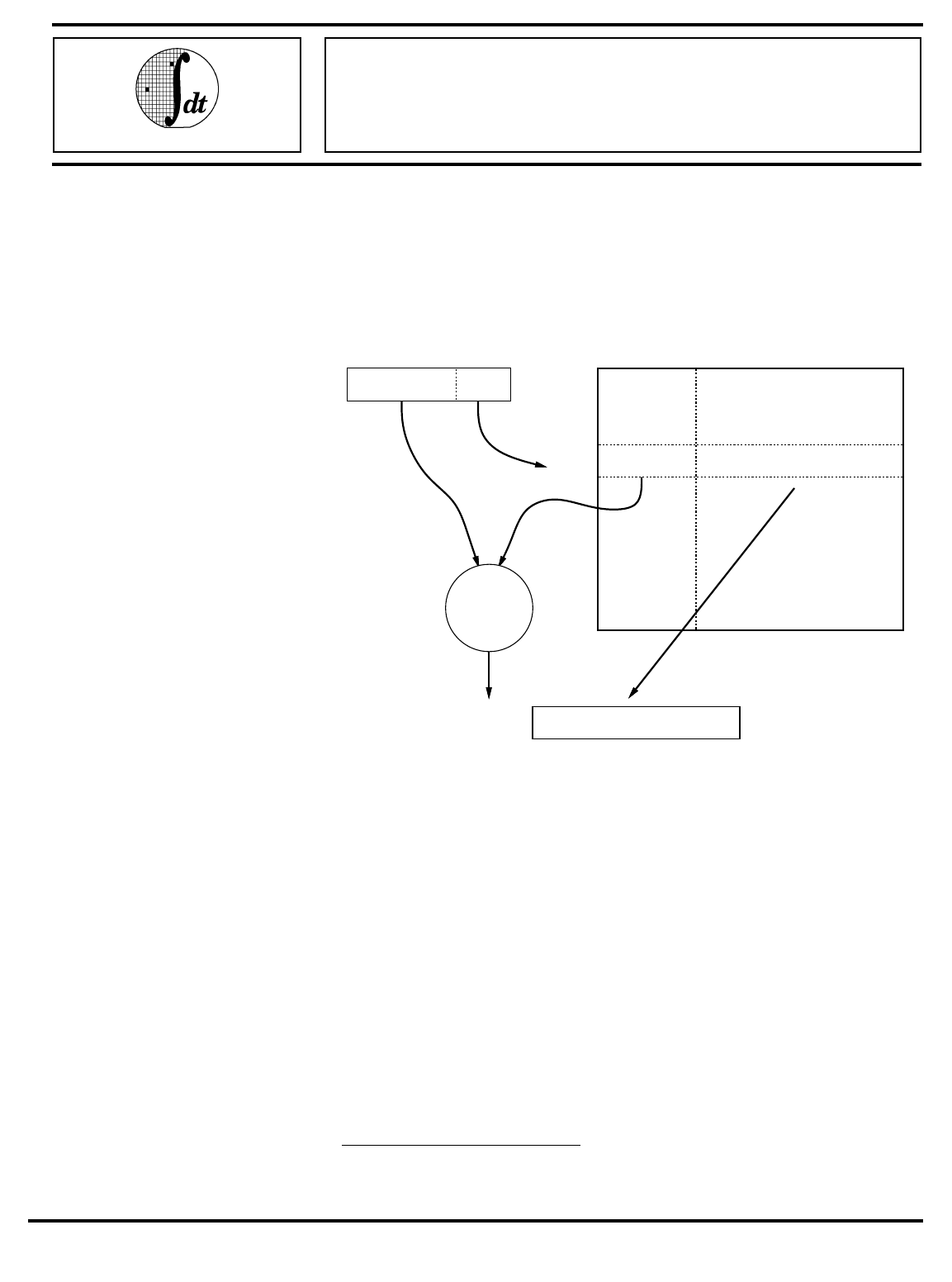
5–1
CACHE MANAGEMENT
®
Integrated Device Technology, Inc.
CHAPTER 5
CACHES AND CACHE MANAGEMENT
R30xx family CPUs implement separate on-chip caches for instructions
(I-cache) and data (D-cache). Following RISC principles, hardware
functions are provided only for normal operation of the caches; software
routines must be provided to initialize the cache following system start-up,
and to invalidate cache data when required†.
Figure 5.1. Direct mapped cache
The cache’s job is to hold a copy of memory data which has been recently
read or written, so it can be returned quickly to the CPU; in the R30xx
architecture data accesses in the cache take just one clock, and an I-cache
and a D-cache operation can occur together.
When a cacheable location is read (a data load):
• It will be returned from the D-cache if the cache contains the
corresponding physical address and the cache line is valid there
(called a cache ‘‘hit’’). In this case nothing happens at the CPUs
memory interface, so the read is invisible to the outside world.
• If the data is not found in the D-cache (called a cache “miss”), the data
will be read from external memory. According to the CPU type and
how it is set up, it may read one or more words from memory. The
data is loaded into the cache, and normal operation then resumes.
In normal operation, cache miss processing will cause the targeted
cache line to “invalidate” the valid data already present in the cache.
In the R30xx caches, cache data is never more up-to-date than
memory (because the cache is
write-through
, described below), so the
previously cached data can be discarded without any trouble.
† Note that the R3071 and R3081 do implement a DMA protocol
that allows automatic, hardware-based data cache invalidation.
tagstore cache data store
0
memory address
lo bitshigher bits
index
match?
Cache Memory
data
hit?
1

CHAPTER 5 CACHE MANAGEMENT
5–2
When data is loaded from an uncacheable location, it is always obtained
from external memory (or a memory-mapped IO location). Most systems
never access the same data locations as cached and uncached; however,
the results of such a system would be predictable. On an uncacheable load
cache data is neither used nor updated.
When software writes a cached location:
• If the CPU is doing a 32-bit store, the cache is always updated
(possibly discarding data from a previously cached location).
• For byte or half-word stores, the cache will only be updated if the
reference hits in the cache; then data will be extracted from the cache,
merged with the store data, and written back†.
• If the partial-word store misses in the cache, then the cache is left
alone.
• In all cases, the write is also made to main memory.
When the store target is an uncached location the cache is not consulted
or modified.
Figure 5.1, “Direct mapped cache” is a diagrammatic representation of
the way the MIPS cache works. Both caches are:
•
Physically indexed, physically tagged
: the CPUs program address
(virtual address) is translated to a physical address, just as is used to
address real memory, before being used for the cache lookup. The
TAG comparison (checking for a hit) is also based on physical
addresses.
On certain other CPU families the cache index is based on program
addresses (which are available a bit earlier); some CPUs even use
virtual TAGs, which then require that the cache be flushed at context
switch. But physical caches are easier to manage.
•
Direct mapped
: Each physical address has only one location in each
cache where it may reside. At each cache index there is only one data
item stored – this will be just one word in the D-cache but is usually
a 4-word
line
for the I-cache (see Figure 5.1, “Direct mapped cache”).
Next to the data is kept the
tag
, which stores the memory address for
which this data is a copy.
If the tag matches the high-order (higher number) address bits then
the cache line contains the data the CPU is looking for; the data is
returned and execution continues.
For an I-cache access, the CPU must select one of the four words
based on the lowest address bits.
This is a
direct mapped
cache because there is only one tag/data pair
at each cache index. More complex caches may have more than one
tag field, and compare them simultaneously with the physical
address.
A direct-mapped cache is very simple, but can suffer from cache
thrashing; so the CPU can run slowly if a program loop is regularly
accessing a pair of locations whose low-order addresses happen to be
equal. To avoid this situation, the R30xx family implements relatively
large caches, which minimize the probability of reasonable program
loops causing CPU thrashing.
•
Cache lines
: the line size is the number of data elements stored with
each tag. For R30xx family CPUs the I-cache implements a 4-word
line size; the D-cache always has 1-word lines.
† In the R30xx family, the data will be merged in the D-Cache.
However, the CPU bus will perform the store only to the bytes
which were actually changed (i.e. the store datum size), facilitating
debugging.

CACHE MANAGEMENT CHAPTER 5
5–3
When a cache miss occurs the whole line must be filled from memory.
But it is quite possible to fetch more than a line’s worth of data; and
R30xx family CPUs can be configured to fetch 4 words of data on a D-
cache miss, refilling 4 1-word ‘‘lines’’.
•
Write through
: the D-cache is write-through, meaning that all store
operations result in a store to main memory. This means that all data
in the cache is duplicated in main memory, and can therefore be
discarded at any time. In particular, when data is being read following
a cache miss it can always be stored in the cache without regard for
the data which was previously stored at the same index.
•
Partial word write implementations
: when the CPU writes only part of
a word, it is essential that any valid cache data should still end up as
a duplicate of main memory. One simple approach is to invalidate the
cache line and to write only to main memory (the main memory must
be byte-addressable). But the R30xx family uses a more efficient
strategy:
a) if the location being written is present in the cache (cache hit) the
cache data is read into the CPU, the partial-word data merged
with it, the whole word written back to the cache, and the
partial-word written to memory.
b) where the write misses in the cache the partial-word write is
performed to memory only, and the cache left alone.
Note that this takes an extra clock, so a partial-word write which hits
in the cache is slower than a whole-word write.
Cache isolation and swapping
No special instructions are provided to explicitly access the caches;
everything has to be done with load and store instructions.
To distinguish operations for cache management from regular memory
references, without having to dedicate a special address region for this
purpose, the R30xx architecture provides bits in the
SR
to support cache
management:
• The
SR
mode bit “IsC” will
isolate
the D-cache; in this mode loads and
stores affect only the cache, and loads also ‘‘hit’’ regardless of whether
the tag matches. As a special mechanism, with the D-cache isolated
a partial-word write will invalidate the appropriate cache line.
Caution: when the D-cache is isolated, not even loads/stores marked
by their address or TLB entry as ‘‘uncached’’ will operate normally.
One consequence of this is that the cache management routines must
not make any data accesses; they are typically written in assembler,
using only register variables.
• The CPU provides a mode where the caches are
swapped
(SR SwC
bit), to allow the I-Cache to be targeted by store instructions; then the
D-cache acts as an I-cache, and the I-cache acts as the D-cache. Once
the caches are swapped and isolated I-cache entries may be read,
written and invalidated (invalidation uses the same partial word write
mechanism described above).
Note that cache isolation does not stop instruction fetches from
referencing main memory.
The D-cache behaves ‘‘perfectly’’ as an I-cache (provided it was
sufficiently initialized to work as a D-cache) but the I-cache does not
behave properly as a D-cache. It is unlikely that it will ever be useful
to have the caches swapped but not isolated.
If software does use a swapped I-cache for word stores (a partial-word
store invalidates the line, as before) it must make sure those locations
are invalidated before returning to normal operation.

CHAPTER 5 CACHE MANAGEMENT
5–4
Initializing and sizing the caches
At machine start-up the caches are in a random state, so the result of a
cached read is unpredictable. In addition, following a reset the status
register SwC and IsC bits are also in a random state, so start-up software
had better set them to a known state before attempting any load or store
(even uncached).
Different members of the R3051 family have different cache sizes.
Software will be more portable if it dynamically determines the size of the
I-cache and D-cache at initialization time, rather than hard-wiring a
particular value.
A number of algorithms are possible. Shown below is the code contained
in IDT/sim for cache sizing. The basic algorithm works as follows:isolate
the D-cache;
• swap the caches when sizing the I-cache;
• Write a marker into the initial cache entry.
• Start with the smallest permissible cache size.
• Read memory at the location for the current cache size. If it contains
the marker, that is the correct size. Otherwise, double the size to try
and repeat this step until the marker is found.
/*
** Config_cache() -- determine sizes of i and d caches
** Sizes stored in globals dcache_size and icache_size
*/
#define CONFIGFRM ((4*4)+4+4)
FRAME(config_cache,sp, CONFIGFRM, ra)
.set noreorder
subu sp,CONFIGFRM
sw ra,CONFIGFRM-4(sp)# save return address
sw s0,4*4(sp) # save s0 in first regsave slot
mfc0 s0,C0_SR # save SR
mtc0 zero,C0_SR # disable interrupts
.set reorder
jal _size_cache
sw v0,dcache_size
li v0,SR_SWC # swap caches
.set noreorder
mtc0 v0,C0_SR
jal _size_cache
nop
sw v0,icache_size
mtc0 zero,C0_SR # swap back caches
and s0,~SR_PE # do not inadvertantly clear PE
mtc0 s0,C0_SR # restore SR
.set reorder
lw s0,4*4(sp) # restore s0
lw ra,CONFIGFRM-4(sp)# restore ra
addu sp,CONFIGFRM # pop stack
jra
ENDFRAME(config_cache)
/*
** _size_cache()
** return size of current data cache
*/
FRAME(_size_cache,sp,0,ra)
.set noreorder
mfc0 t0,C0_SR # save current sr
and t0,~SR_PE # do not inadvertently clear PE
or v0,t0,SR_ISC # isolate cache
mtc0 v0,C0_SR
/*
* First check if there is a cache there at all
*/
move v0,zero
li v1,0xa5a5a5a5 # distinctive pattern

CACHE MANAGEMENT CHAPTER 5
5–5
sw v1,K0BASE # try to write into cache
lw t1,K0BASE # try to read from cache
nop
mfc0 t2,C0_SR
nop
.set reorder
and t2,SR_CM
bne t2,zero,3f # cache miss, must be no cache
bne v1,t1,3f # data not equal -> no cache
/*
* Clear cache size boundries to known state.
*/
li v0,MINCACHE
1: sw zero,K0BASE(v0)
sll v0,1
ble v0,MAXCACHE,1b
li v0,-1
sw v0,K0BASE(zero)# store marker in cache
li v0,MINCACHE # MIN cache size
2: lw v1,K0BASE(v0) # Look for marker
bne v1,zero,3f # found marker
sll v0,1 # cache size * 2
ble v0,MAXCACHE,2b# keep looking
move v0,zero # must be no cache
.set noreorder
3: mtc0 t0,C0_SR # restore sr
jra
nop
ENDFRAME(_size_cache)
.set reorder
In a properly initialized cache, every cache entry is either invalid or
correctly corresponds to a memory location, and also contains correct
parity. Again, the sample code shown is from IDT/sim. The code works as
follows:
• Check that
SR
bit PZ is cleared to zero (1 disables parity; the R3071
and R3081 contain parity bits, and thus PZ=1 could cause the caches
to be initialized improperly).
• Isolate the D-cache, swap to access the I-cache.
• For each word of the cache: first write a word value (writing correct
tag, data and parity), then write a byte (invalidating the line).
Note that for an I-cache with 4 words per line this is inefficient; it
would be enough to write just one byte in the line to invalidate the
entry. Unless the system uses the invalidate routine often it doesn’t
seem worth the trouble.
FRAME(flush_cache,sp,0,ra)
lw t1,icache_size
lw t2,dcache_size
.set noreorder
mfc0 t3,C0_SR # save SR
nop
and t3,~SR_PE # dont inadvertently clear PE
beq t1,zero,_check_dcache# if no i-cache check d-cache
nop
li v0,SR_ISC|SR_SWC# disable intr, isolate and swap
mtc0 v0,C0_SR
li t0,K0BASE
.set reorder
or t1,t0,t1
1: sb zero,0(t0)

CHAPTER 5 CACHE MANAGEMENT
5–6
sb zero,4(t0)
sb zero,8(t0)
sb zero,12(t0)
sb zero,16(t0)
sb zero,20(t0)
sb zero,24(t0)
addu t0,32
sb zero,-4(t0)
bne t0,t1,1b
/*
* flush data cache
*/
_check_dcache:
li v0,SR_ISC # isolate and swap back caches
.set noreorder
mtc0 v0,C0_SR
nop
beq t2,zero,_flush_done
.set reorder
li t0,K0BASE
or t1,t0,t2
1: sb zero,0(t0)
sb zero,4(t0)
sb zero,8(t0)
sb zero,12(t0)
sb zero,16(t0)
sb zero,20(t0)
sb zero,24(t0)
addu t0,32
sb zero,-4(t0)
bne t0,t1,1b
.set noreorder
_flush_done:
mtc0 t3,C0_SR # un-isolate, enable interrupts
.set reorder
jra
ENDFRAME(flush_cache)
Invalidation
Invalidation refers to the act of setting specified cache lines to contain
no valid references to main memory, but to otherwise be consistent (e.g.
valid parity). Software needs to invalidate:
• the D-cache when memory contents have been changed by something
other than store operations from the CPU. Typically this is done when
some DMA device is reading into memory.
• the I-cache when instructions have been either written by the CPU or
obtained by DMA. The hardware does nothing to prevent the same
locations being used in the I- and D-cache; and an update by the
processor will not change the I-cache contents.
Note that the system could be constructed to use unmapped accesses to
those variables shared with a DMA device; the only difference is in
performance. In general small areas where DMA is frequent compared to
CPU activity should be mapped uncached; and larger areas where CPU
activity predominates should be invalidated by the driver at appropriate
points. Bear in mind that invalidating a word of data in the cache is faster
(probably 4-7 times faster) than an uncached load.
To invalidate the cache:
• Figure out the address range to invalidate. Invalidating a region larger
than the cache size is a waste of time.

CACHE MANAGEMENT CHAPTER 5
5–7
• isolate the D-cache. Once it is isolated, the system must insure at all
costs against an exception (since the memory interface will be
temporarily disabled). Disable interrupts and ensure that software
which follows cannot cause a memory access exception;
• to work on the I-cache, swap the caches;
• write a byte value to each cache line in the range;
• (unswap and) unisolate.
The invalidate routine is normally executed with its instructions
cacheable. This sounds like a lot of trouble; but in fact shouldn’t require
any extra steps to run cached. An invalidation routine in uncached space
will run 4-10 times slower.
Again, the example code fragment shown is taken from IDT/sim:
/*
** clear_cache(base_addr, byte_count)
** flush portion of cache
*/
FRAME(clear_cache,sp,0,ra)
/*
* flush instruction cache
*/
lw t1,icache_size
lw t2,dcache_size
.set noreorder
mfc0 t3,C0_SR # save SR
and t3,~SR_PE # dont inadvertently clear PE
nop
nop
li v0,SR_ISC|SR_SWC# disable intr, isolate and swap
mtc0 v0,C0_SR
.set reorder
bltu t1,a1,1f # cache is smaller than region
move t1,a1
1: addu t1,a0 # ending address + 1
move t0,a0
sb zero,0(t0)
sb zero,4(t0)
sb zero,8(t0)
sb zero,12(t0)
sb zero,16(t0)
sb zero,20(t0)
sb zero,24(t0)
addu t0,32
sb zero,-4(t0)
bltu t0,t1,1b
/*
* flush data cache
*/
.set noreorder
nop
li v0,SR_ISC # isolate and swap back caches
mtc0 v0,C0_SR
nop
.set reorder
bltu t2,a1,1f # cache is smaller than region
move t2,a1
1: addu t2,a0 # ending address + 1
move t0,a0
1: sb zero,0(t0)
sb zero,4(t0)
sb zero,8(t0)
sb zero,12(t0)

CHAPTER 5 CACHE MANAGEMENT
5–8
sb zero,16(t0)
sb zero,20(t0)
sb zero,24(t0)
addu t0,32
sb zero,-4(t0)
bltu t0,t2,1b
.set noreorder
mtc0 t3,C0_SR # un-isolate, enable interrupts
.set reorder
jra
ENDFRAME(clear_cache)
Testing and probing
During test, debug or when profiling, it may be useful to build up a
picture of the cache contents. Software cannot read the tag value directly,
but, for a valid line, can determine the tag value by exhaustive search:
• isolate the cache;
• load from the cache line at each possible line start address (low order
bits fixed, high order bits ranging over physical memory which exists
in the system). After each load consult the CM bit in
SR,
which will be
‘‘0’’ only when the tag value matches.
This takes a long time by computer terms; but to fully search a 1K D-
cache with 4Mbytes of cacheable physical memory on a 20Mhz processor
will take only a couple of seconds, and will provide very valuable debugging
information. IDT/sim provides this capability.
Configuration (R3041/71/81 only)
The R3041, R3071, and R3081 processors allow the programmer to
make choices about the cache by setting fields in the
Config
register:
•
Cache refill burst size (R3041/71/81)
: by default the R3041 refills
only 1 word in the D-cache on a cache miss; but software can program
it to use 4-word burst reads instead, by setting the
Config
DBR bit.
The bit can be changed at any time, without needing to invalidate the
cache.
The refill of R3071 and R3081 processors can be configured by
hardware at reset-time, but software can override that choice.
This support is provided in the hope of enhancing performance. The
proper selection for a given system will depend on both the hardware
and the application. Some systems may find an advantage in
“toggling” the bit for various portions of the software. In general, the
proper burst size selection can be determined as follows:
Burst reads make most sense when the memory is capable of
returning a burst of data significantly faster than it can return 4
individual words. Many DRAM systems are like this; most ROM and
static RAM memories are not. Similarly, data accessed from narrow
memory ports should rarely be configured for a multi-word burst.
If programs tend to access memory sequentially (working up or down
a large array, for example) then the burst refill will offer a very useful
degree of data prefetch, and performance will be enhanced. If cache
access is more random, the burst refill may actually reduce
performance (since it involves overwriting cached data with memory
data the program may never use).
As a general rule, the bigger the D-cache, the smaller the penalty for
burst refills.
•
Bigger I-cache in exchange for smaller D-cache (R3071/81)
: the R3081
cache can be organized either with both I-cache and D-cache 8Kbytes
in size, or with a 16Kbyte I-cache and 4Kbyte D-cache. The
configuration is programmed using the AC bit in the
Config
register.

CACHE MANAGEMENT CHAPTER 5
5–9
After changing the cache configuration both caches should be re-
initialized, while running uncached. This means that most systems
will not dynamically reconfigure the caches.
Which configuration is best for a given system is mainly dependent on
the software. Cache effects are extremely hard to predict, and it is
recommended that both configurations be tried and measured, while
running as much of the real system as possible.
As a general rule: with large applications (like in a big OS) the big I-
cache will probably be best. If the system spends most of its time
manipulating lots of data from tight program loops, the big D-cache
may be better.
WRITE BUFFER
The write-through cache common to all R30xx family CPUs can be a big
performance bottleneck. In the average C program only about 10% of
instructions are stores, but these accesses tend to come in bursts; for
example, when a function prologue saves a few registers.
DRAM memory frequently has the characteristic that the first write of a
group takes quite a long time (5-10 clocks typical on these CPUs), and
subsequent ones are relatively fast so long as they follow quickly.
If the CPU simply waits for all writes to complete, the performance hit
will be significant. So the R30xx provides a
write buffer
, a FIFO store which
keeps a number of entries each containing both data to be written, and the
address at which to write it. The 4-entry queue provided by R30xx family
CPUs is efficient for well-tuned DRAM.
In general, the operation of the write buffer is completely transparent to
software. Occasionally, the programmer needs to be aware of what is
happening:
•
Timing relations for IO register accesses
: When software performs a
store to write an IO register, the store reaches memory after a small,
but indeterminate, delay. Some consequences are:
—other communication with the IO system (e.g. interrupts) may
happen more quickly – for example, the CPU may get an interrupt
from a device ‘‘after’’ it has been programmed to generate no
interrupts.
—if the IO device needs some time to recover after a write the program
must ensure that the write buffer FIFO is empty before counting
out that time period.
—at the end of interrupt service, when writing to an IO device to clear
the interrupt it is asserting, software must insure that the
command is actually written to the device, and that it has had to
respond, before re-enabling that interrupt; otherwise, spurious
interrupts may be signalled.
In these cases the programmer must ensure that the CPU waits while
the write buffer empties. It is good practice to define a subroutine
which does this job; it is traditionally called
wbflush()
. Hints on
implementing this function are provided later in this chapter.
On CPUs outside the R30xx family, even stranger things can happen:
•
Reads overtaking writes
: a load instruction (uncached or missing in
the cache) executed while the write buffer FIFO is not empty gives the
CPU a choice: should it finish off the write, or use the memory
interface to fetch data for the load?
The R3041, R3051, R3052 and R3081 all have the same rule, which
avoids potential problems: the write buffer is emptied before the load
occurs.
Although it seems tempting to instead implement a scheme which
checks for conflicts, and allows the read to progress if no write buffer
entry matches the read target address, such a scheme does not avoid
the possible system problems. Specifically, writes to locations which

CHAPTER 5 CACHE MANAGEMENT
5–10
may have side effects (e.g. semaphores, IO registers, etc.), are not
detected under such a scheme, and can cause great headaches to the
programmer.
•
Byte gathering
: some write buffers watch for partial-word writes
within the same memory word, and will combine those partial writes
into a single operation. This is not done by any current R30xx family
CPU, because such operation would pose problems with IO register
writes.
Implementing
wbflush()
IDT R30xx family CPUs enforce strict write priority (all pending writes
retired to memory before main memory is read). Thus, implementing
wbflush()
is as simple as implementing an uncached load (e.g. from the
boot PROM vector). This will stall the CPU until the writes have finished,
and the load finished too. Alternately, the overhead can be minimized by
performing an uncached load from the fastest memory available in the
system.
The code fragment below shows an implementation of WbFlush, taken
from IDT/sim:
/*
** wbflush() flush the write buffer - this is specific for each
hardware
** configuration.
*/
FRAME(wbflush,sp,0,ra)
.set noreorder
lw t0,wbflush#read an uncached memory location
j ra
nop
.set reorder
ENDFRAME(wbflush)

6–1
MEMORY MANAGEMENT AND
THE TLB
®
Integrated Device Technology, Inc.
CHAPTER 6
MEMORY MANAGEMENT AND THE TLB
Some R30xx family processors (“E” versions) have on-chip memory
management hardware. This provides a mechanism for dynamically
translating program addresses in the
kuseg
and
kseg2
regions. The key
piece of hardware is the ‘‘TLB†’’.
The memory management is
paged
: with a fixed page size of 4Kbytes.
The low-order 12 bit of the program address are used directly as the low
order bits of the physical address, so address translation operates in 4K
chunks.
The TLB is a 64-entry
associative memory
. Each entry in an associative
memory consists of a key field and a data field; when presented with a key,
the memory returns the data of any entry where the key matches.
In the R30xx family, the TLB is referred to as ‘‘fully-associative’’; this
emphasizes that all keys are really compared with the input value in
parallel.
The TLB’s key field contains two sections:
•
Virtual page number
: (VPN) this is just a program address with the low
12 bits cut off, since the low-order bits don’t participate in the
translation process.
•
Address Space Identifier.
(ASID): this is a magic number used to
stamp translations, and (optionally) is compared with an extended
part of the key. Why?
In multi-tasking systems it is common to have all user-level tasks
executing at the same sort of program addresses (though of course
they are using different physical addresses); they are said to be using
different
address spaces
. So translation records for different tasks
will often share the same value of ‘‘VPN’’. If the TLB mechanism was
not supported with an ASID, when the OS switches from one task to
another, it would have to find and invalidate all TLB translations
relating to the old task’s address space, to prevent them from being
erroneously used for the new one. This would be desperately
inefficient.
Instead, the OS assigns a 6-bit unique code to each task’s distinct
address space. During normal running this code is kept in the ASID
field of the
EntryHi
register, and is used together with the program
address to form the lookup key; so a translation with an ASID code
which doesn’t match is quietly ignored.
Since the ASID is only 6 bits long, OS software does have to lend a
hand if there are ever more than 64 address spaces in concurrent use;
but it probably won’t happen too often. In such a system, new tasks
are assigned new ASIDs until all 64 are assigned; at that time, all
tasks are flushed of their ASIDs “de-assigned” and the TLB flushed;
as each task is re-entered, a new ASID is given. Thus, ASID flushing
is relatively infrequent.
The TLB data field includes:
•
Physical frame number (PFN)
: the physical address with the low 12
bits cut off. In an address translation, the VPN bits are replaced by
the corresponding PFN bits to form the true physical address.
•
Cache control bit (N)
: set 1 to make the page uncacheable.
† This is an acronym for ‘‘translation lookaside buffer’’, which is a
look-up table of virtual to physical address translations.
1

CHAPTER 6 MEMORY MANAGEMENT AND THE TLB
6–2
•
Write control bit (D)
: set 1 to allow stores to this page to happen. The
‘‘D’’ comes from this being called the ‘‘dirty bit’’; a later section on
“Simulating dirty bits” describes a typical use for these bits.
•
Valid bit (V)
: set 0 to make this entry usable. This seems pretty
pointless; why have a record loaded into the TLB if the translation is
not usable? But an access to an invalid page produces a different trap
from a TLB refill exception, so making a page invalid means that some
strange conditions can be made to take a different trap, which does
not have to be handled by the superfast refill code.
•
Global bit (G)
: set to disable the ASID-matching scheme, allowing an
OS to map some program addresses to the same physical address for
all tasks; it can be useful to have some corner of each address space
mapped to the same physical locations. Sharp-eyed or experienced
readers will notice that this means that the global bit is really more
like part of the key than part of the data; the distinction tends to get
blurred in associative memories.
Translating an address is now simple, and goes like this:
•
CPU generates a program address
: either for an instruction fetch, a
load or a store, in one of the translated address regions. The low 12
bits are separated off, and the resulting VPN together with the current
value of the ASID field in
EntryHi
used as the key to the TLB.
•
TLB matches key
: selecting the matching entry. The PFN is glued to
the low-order bits of the program address to form a complete physical
address.
•
Valid?
: the V and D bits are consulted. If it isn’t valid, or a store is
being attempted with D cleared, the CPU takes a trap. As with all
translation traps, the
BadVaddr
register will be filled with the
offending program address and TLB registers
Context
and
EntryHi
pre-filled with relevant information. The system software can use
these registers to obtain data for exception service.
•
Cached?
: if the N bit is set the CPU looks in the cache for a copy of
the physical location’s data; if it isn’t there it will be fetched from
memory and a copy left in the cache. Where the C bit is clear the CPU
neither looks in nor refills the cache.
Of course, there are only 64 entries in the TLB, which can hold
translations for a maximum of 256 Kbytes of program addresses. This is
far short of enough for most systems. The TLB is almost always going to be
used as a software-maintained ‘‘cache’’ for a much larger set of
translations.
When a program address lookup in the TLB fails, a
TLB refill
trap is
taken. System software has the job of:
• figuring out whether there is a correct translation; if not the trap will
be dispatched to the software which handles address errors.
• if there is a correct translation, constructing a TLB entry which will
implement it;
• if the TLB is already full (and it almost always is full in running
systems), selecting an entry which can be discarded;
• writing the new entry into the TLB.

MEMORY MANAGEMENT AND THE TLB CHAPTER 6
6–3
See below for how this can be tackled; but note here that although
special CPU features help out with one particular class of
implementations, the software can refill the TLB any way it likes.
MMU registers described
EntryHi, EntryLo
These two registers represent a TLB entry, and are best considered as a
pair. Fields in
EntryHi
are:
•
VPN
: ‘‘virtual page number’’, the high-order bits of a program address.
On a refill exception this field is set up automatically to match the
program address which could not be translated. To write a different
TLB entry, or attempt a TLB probe, software must set it up
“manually”.
•
ASID
: ‘‘address space identifier’’, normally left holding the OS’ value
for the current address space. This is not changed by exceptions.
Most software systems will deliberately write this field only to setup
the current address space.
However, software must be careful when using
tlbr
to inspect TLB
entries; the operation overwrites the whole of
EntryHi,
so software
needs to restore the correct current ASID value afterwards.
Register
Mnemonic Description CP0
reg no
EntryHi Together these registers hold a TLB entry. All reads and
writes to the TLB must be staged through them.
EntryHi also remembers the current ASID.
10
EntryLo 2
Index Determines which TLB entry will be read/written by
appropriate instructions 0
Random pseudo-random value (actually a free-running counter)
used by a
tlbwr
to write a new TLB entry into a ‘‘randomly’’
selected location.
1
Context Convenience register provided to speed up the processing
of TLB refill traps. The high-order bits are read/write; the
low-order 21 bits reflect the
BadVaddr
value.
(The register is designed so that, if the system uses the
‘‘favored’’ arrangement of memory-held copies of memory
translation records, it will be setup by a TLB refill trap to
point to the memory location of the record needed to map
the offending address. This speeds up the process of
finding the current memory mapping, and arranging
EntryHi/Lo properly).
4
Table 6.1. CPU control registers for memory management
31 12 11 6 5 0
VPN ASID 0
EntryHi Register (TLB key fields)
Figure 6.1. EntryHi and EntryLo register fields
31 12 11 10 9 8 7 0
PFN N D V G 0
EntryLo Register (TLB data fields)
Figure 6.2. EntryHi and EntryLo register fields

CHAPTER 6 MEMORY MANAGEMENT AND THE TLB
6–4
Fields in
EntryLo
are:
•
PFN
: the high-order bits of the physical address to which values
matching
EntryHi’s
VPN will be translated.
•
N
: ‘‘noncacheable’’; 0 to make the access cacheable, 1 for
uncacheable.
•
D
: ‘‘dirty’’, but really a write-enable bit. 1 to allow writes, 0 and any
store using this translation will be trapped.
•
V
: ‘‘valid’’, if 0 any address matching this entry will cause an
exception.
•
G
: ‘‘global’’. When the G bit in a TLB entry is set, that TLB entry will
match solely on the VPN field, regardless of whether the TLB entry’s
ASID field matches the value in
EntryHi.
•
Fields called ‘‘0’’
: these fields always return zero; but unlike many
reserved fields, they do not need to be written as zero (nothing
happens regardless of the data written). This is important; it means
that the memory-resident data which is used to generate
EntryLo
when refilling the TLB can contain some software-interpreted data in
these fields, which the TLB hardware will ignore without the need to
spend precious CPU cycles masking it.
Index
The ‘‘P’’ field is set when a
tlbp
instruction (tlb probe, used to see if the
TLB can translate a particular VPN) failed to find a valid translation; since
it is the top bit it appears to make the 32-bit value negative, which is easy
to test for.
Random
Most systems never have to read or write the
Random
register, shown as
Figure 6.4, “Fields in the Random register”, in normal use; but it may be
useful for diagnostics. The hardware initializes the
Random
field to its
maximum value (63) on reset, and it decrements every clock period until it
reaches 8, when it wraps back to 63 and starts again.
Context
•
PTEBase
: a location which just stores what is put in it. In the
‘‘standard’’ refill handler, this will be the high-order bits of the
(1Mbyte aligned) starting address of a memory-resident page table.
•
Bad VPN
: following an addressing exception this holds the high-order
bits of the address; exactly the same as the high-order bits of
BadVaddr.
However, if the system uses the ‘‘standard’’ TLB refill
31 30 14 13 8 7 0
P
×
Index
×
Figure 6.3. Fields in the Index register
31 14 13 8 7 0
×
Random
×
Figure 6.4. Fields in the Random register
31 21 20 2 1 0
PTEBase Bad VPN 0
Figure 6.5. Fields in the Context Register

MEMORY MANAGEMENT AND THE TLB CHAPTER 6
6–5
exception handling code the 32-bit value formed by
Context
is directly
usable as a pointer to the memory-resident page table, considerably
shortening the refill exception code.
•
Fields marked 0
: can be written with any value, but they will always
read zero.
MMU control instructions
tlbr
– Read TLB entry at index
tlbwi
–
Write TLB entry at index
The above two instructions move MMU data between the TLB entry
selected by the
Index
register and the
EntryHi
and
EntryLo
registers.
tlbwr
–
Write TLB entry selected by Random
copies the contents of
EntryHi
&
EntryLo
into the TLB entry indexed
by the
random
register. This saves time when using the
recommended random replacement policy. In practice,
tlbwr
will be
used to write a new TLB entry in a TLB refill exception handler;
tlbwi
will be used anywhere else.
tlbp
–
TLB lookup
searches (probes) the TLB for an entry whose virtual page number
and ASID matches those currently in
EntryHi
, and stores the index
of that entry in the
index
register (
index
is set to a negative value if
nothing matches). If more than one entry matches, anything might
happen. Note that
tlbp
does not fetch data from the TLB. The
instruction following a
tlbp
must not be a load or store.
Programming interface to the TLB
TLB entries are set up by writing the required fields into
EntryHi
and
EntryLo
and using a
tlbwr
or
tlbwi instruction to copy that entry into the
TLB proper.
When handling a TLB refill exception, EntryHi has been set up
automatically, with the current ASID and the required VPN.
Be very careful not to create two entries which will match the same
program address/ASID pair. If the TLB contains duplicate entries an
attempt to translate such an address, or probe for it, produces a fatal ‘‘TLB
shutdown’’ condition (indicated by the TS bit in SR being set). It can be
cleared only by a hardware reset.
System software often won’t need to read TLB entries at all. But if
necessary, software can find the TLB entry matching some particular
program address using tlbp to setup the Index register. Don’t forget to save
EntryHi and restore it afterwards because its ASID field is likely to be
important.
Use a tlbr to read the TLB entry into EntryHi and EntryLo.
How refill happens
When a program makes an access in kuseg or kseg2 to a page for which
no translation record is present, the CPU takes a TLB refill exception. The
assumption is that system software is maintaining a large number of page
translations and is using the TLB as a cache of recently-used translations;
so the refill exception will normally be handled by finding a correct
translation, installing it, and returning to user code.
In ‘‘CISC’’ CPUs the TLB is a cache (usually implemented by microcode),
and the CPU automatically reads memory-resident ‘‘page tables’’ whose
structure is part of the CPU architecture.
In the MIPS architecture software is fast enough, and offers greater
flexibility.
To save time on user-program TLB refill exceptions (which will happen
frequently in a ‘‘big’’ OS):
• refill exceptions on kuseg program addresses are vectored through a
low-memory address used for no other exception;

CHAPTER 6 MEMORY MANAGEMENT AND THE TLB
6–6
• special exception rules permit the kuseg refill handler to risk a nested
TLB refill exception on a kseg2 address.
The problem is that before an exception routine can itself suffer an
exception it must first save the previous program state, represented
by the EPC return address and some SR bits. This is helped out by a
hardware feature and a software convention:
a) the KUo, IEo bits in the status register act as a third level of the
processor-state stack, so that the CPU state already saved as a
result of the kuseg refill exception can be preserved during the
nested exception.
b) The kuseg refill handler copies EPC into the k1 register; the
general exception code and kseg2 refill handler are then careful
to preserve its value, enabling a clean return.
Refill exceptions on kseg2 addresses are expected to be rare enough that
it will not matter if they share in the overhead of the ‘‘all other exceptions’’
entry point. However, once software determines the type of exception the
handling is similar.
Using ASIDs
By setting up TLB entries with a particular ASID setting and with the
EntryLo G bit zero, those entries will only ever match a program address
when the CPU’s ASID register is set the same. This allows software to map
up to 64 different address spaces simultaneously, without requiring that
the OS clear out the TLB on a context change.
In typical usage, new tasks are assigned an “un-initialized” ASID. The
first time the task is invoked, it will presumably miss in the TLB, allowing
the assignment of an ASID. If the system does run out of new ASIDs, it will
flush the TLB and mark all tasks as “new”. Thus, as each task is re-
entered, it will be assigned a new ASID. This sequence is expected to
happen infrequently if ever.
The Random register and wired entries
The hardware offers no way of finding out which TLB entries have been
used most recently. When the system needs to replace a mapping
dynamically (using the TLB as a cache) the only practicable strategy is to
replace an entry at random. The CPU makes this easy by maintaining the
Random register, which counts (down) with every processor cycle.
However, it is often useful to have some TLB entries which are
guaranteed to stay there unless explicitly removed. These may be useful to
map pages which are known to be required very often; they are critical
because they allow the system to map pages and guarantee that no refill
exception will be generated on them.
The stable TLB entries are described as ‘‘wired’’ and on R30xx family
CPUs consist of TLB entries 0 through 7. There is nothing special about
these entries; the magic is in the Random register, which never takes
values 0-7; it cycles directly from 63 down to 8 before reloading with 63.
So conventional random replacement leaves TLB entries 0 through 7
unaffected, and entries written there will stay until explicitly removed.
Memory translation – setup
The following code fragment initializes the TLB to ensure no match on
any kuseg or kseg2 address. This is important, and is preferable to
initializing with all “0”’s (which is a kuseg address, and which would cause
multiple matches if referenced):
LEAF(mips_init_tlb)
mfc0 t0,C0_ENTRYHI # save asid
mtc0 zero,C0_ENTRYLO# tlblo = !valid
li a1,NTLBID<<TLBIDX_SHIFT # index
li a0,KSEG1_BASE # tlbhi = impossible vpn
.set noreorder

MEMORY MANAGEMENT AND THE TLB CHAPTER 6
6–7
1: subu a1,1<<TLBIDX_SHIFT
mtc0 a0,C0_ENTRYHI
mtc0 a1,C0_INDEX
bnez a1,1b
tlbwi # BDSLOT
.set reorder
mtc0 t0,C0_ENTRYHI # restore asid
j ra
END(mips_init_tlb)
TLB exception sample code
There are two examples provided. The first is written in C, and assumes
that the OS provides a low-level handler which saves state, including
copying the exception registers into an ‘‘xcpcontext’’ structure, and
dispatches through programmable tables to a C routine:
Basic exception handler
/* install C exception handler for TLB miss exception */
xcption (XCPTTLBMISS, tlbmiss);
...
#define VMPGSHIFT12/* convert address to page number */
tlbmiss (int code, struct xcptcontext *xcp)
{
unsigned pfn = map_virt_to_phys (xcp->vaddr) >> VMPGSHIFT;
unsigned vpn = xcp->vaddr >> VMPGSHIFT;
unsigned asid = 0;
/* write a random tlb (entryhi, entrylo) pair */
/* mark it valid, global, uncached, and not writable/dirty */
r3k_tlbwr ((vpn <<TLBHI_VPNSHIFT) | (asid <<TLBHI_PIDSHIFT),
(pfn <<TLBLO_PFNSHIFT) | TLB_V | TLB_G | TLB_N);
return 0;
}
The macro (or routine) map_virt_to_phys() which does the actual work,
will be system dependent.
Fast kuseg refill from page table
This routine implements the translation mechanism which the MIPS
architects had in mind for user addresses in a Unix-like OS. It relies upon
building a page table in memory, for each address space. The page table
consists of a linear array of one-word entries, indexed by the VPN, whose
format is matched to the bitfields of the EntryLo register.
Such a scheme is simple, but has one problem. Since each 4Kbytes of
user address space takes 4 bytes of table space, the entire 2Gbyte user
space needs a 2Mbyte table, which is a large chunk of data. Moreover,
most user address spaces are used at the bottom (for code and data) and
at the top (for a downward growing stack) with a huge gap in between. The
solution adopted is inspired by Digital’s VAX architecture, and is to locate
the page table itself in virtual memory, in the kseg2 region. This neatly
solves two problems at once:
• saves physical memory, since the unused gap in the middle of the
page table will never be referenced.
• provides an easy mechanism for remapping a new user page table
when changing context, without having to find enough virtual
addresses in the OS to map all the page tables at once.

CHAPTER 6 MEMORY MANAGEMENT AND THE TLB
6–8
The MIPS architecture gives positive support to this mechanism in the
form of the Context register. If the page table starts at a 1Mbyte boundary
(since it is in virtual memory, any gap created won’t use up physical
memory space) and the Context PTEBase field is filled with the high-order
bits of the page table starting address, then following a user refill exception
the Context register will contain the address of the entry needed for the
refill, with no further calculation.
The resulting routine looks like this:
.set noreorder
.set noat
xcpt_vecfastutlb:
mfc0 k1,C0_CONTEXT
mfc0 k0,C0_EPC # mfc0 delay slot
lw k1,0(k1) # may double fault (k0 = orig EPC)
nop
mtc0 k1,C0_ENTRYLO
nop
tlbwr
jr k0
rfe
xcpt_endfastutlb:
.set at
.set reorder
Simulating dirty bits
An operating system providing a page for an application program to use
often wants to keep track of whether that page has been modified since the
OS last obtained it (perhaps from disc or network) or saved a copy of it.
Non-modified pages are cheap to discard, since they can easily be replaced
if required.
In OS parlance such modified pages are called ‘‘dirty’’ and the OS must
take care of them until the application program exits, or the dirty page
saved away to backing store.
To help out with this process it is common for CISC CPUs to maintain a
bit in the memory-resident page table indicating that a write operation to
the page has occurred.
The MIPS CPU does not directly implement this feature, even in the TLB
entries. The ‘‘D’’ bit of the page table (found in the EntryLo register) is a
write-enable, and is of course used to flag read-only pages.
To simulate “dirty” bits, the OS should mark new pages (in the page
table) with D clear. Since the CPU will consider that page “write-protected”,
a trap will result when the page is first modified; system software can
identify this as a legitimate write but use the event to set a ‘‘modified’’ bit
in the memory resident tables (it will also want to set the D bit in the TLB
entry so that the write can proceed, but since TLB entries are randomly
and unpredictably replaced this would be useless as a way of remembering
the modified state).
USE OF TLB IN DEBUGGING
In systems which do not require the TLB for normal execution, it still
may prove useful during initial system debug. Although its use for this
purpose will be system dependent, some general ideas follow:
• To hit a “trap” when software “wanders into the weeds” (e.g. makes
mysterious references or instruction fetches from strange memory
locations), software can initialize the TLB with only those mappings
which correspond to valid program addresses. Thus, a TLB trap will
occur in the exact instruction which makes the reference, and full
processor state will be visible.

MEMORY MANAGEMENT AND THE TLB CHAPTER 6
6–9
• To identify which task or subroutine is modifying a particular memory
location, that location can be “write-protected”, generating a trap on
store.
The TLB may have one additional consequence in debugging. In a virtual
memory OS, the actual physical memory location of a task (or even of
portions of the OS) can move around as memory is paged. This can make
low-level debugging difficult, since one cannot set a logic analyzer to trap
on the right physical address.
To resolve this situation, software can utilize a system specific “NOP”
instruction. Recall that updates to the zero register $0 will be ignored;
software can use this fact to generate a specific NOP instruction for the
reference in question; the logic analyzer can then be used to search for this
particular instruction fetch, correctly identifying the current virtual to
physical mapping.
TLB MANAGEMENT UTILITIES
The following routines implement the most common TLB management
functions. These code fragments are taken from IDT/sim.
/* Functions dealing with the TLB.
** Use resettlb() defined here and called from excepthand.c
** to initialize tlb.
*/
/*
** idttlb.s - fetch the registers associated with and the
contents
** of the tlb.
**
*/
#include "iregdef.h"
#include "idtcpu.h"
#include "idtmon.h"
.text
/*
** ret_tlblo -- returns the 'entrylo' contents for the TLB
** 'c' callable - as ret_tlblo(index) - where index is the
** tlb entry to return the lo value for - if called from
assembly
** language then index should be in register a0.
*/
FRAME(ret_tlblo,sp,0,ra)
.set noreorder
mfc0 t0,C0_SR # save sr
nop
and t0,~SR_PE # dont inadvertantly clear PE
mtc0 zero,C0_SR # clear interrupts
mfc0 t1,C0_TLBHI # save pid
sll a0,TLBINX_INXSHIFT# position index
mtc0 a0,C0_INX # write to index register
nop
tlbr # put tlb entry in entrylo and
hi nop
mfc0 v0,C0_TLBLO # get the requested entry lo
mtc0 t1,C0_TLBHI # restore pid
mtc0 t0,C0_SR # restore status register
jra
nop
ENDFRAME(ret_tlblo)
/*
** ret_tlbhi -- return the tlb entry high content for tlb entry
** index

CHAPTER 6 MEMORY MANAGEMENT AND THE TLB
6–10
*/
FRAME(ret_tlbhi,sp,0,ra)
mfc0 t0,C0_SR # save sr
nop
and t0,~SR_PE
mtc0 zero,C0_SR # disable interrupts
mfc0 t1,C0_TLBHI # save current pid
sll a0,TLBINX_INXSHIFT# position index
mtc0 a0,C0_INX # drop it in C0 register
nop
tlbr # read entry to entry hi/lo
nop
mfc0 v0,C0_TLBHI # to return value
mtc0 t1,C0_TLBHI # restore current pid
mtc0 t0,C0_SR # restore sr
jra
nop
ENDFRAME(ret_tlbhi)
/*
** ret_tlbpid() -- return tlb pid contained in the current entry hi
*/
FRAME(ret_tlbpid,sp,0,ra)
mfc0 v0,C0_TLBHI # fetch tlb high
nop
and v0,TLBHI_PIDMASK# isolate and position
srl v0,TLBHI_PIDSHIFT
jra
nop
ENDFRAME(ret_tlbpid)
/*
** tlbprobe(address, pid) -- probe the tlb to see if address is
currently
** mapped
** a0 = vpn - virtual page numbers are 0=0 1=0x1000,
2=0x2000...
** virtual page numbers for the r3000 are in
** entry hi bits 31-12
** a1 = pid - this is a process id ranging from 0 to 63
** this process id is shifted left 6 bits and or'ed
into
** the entry hi register
** returns an index value (0-63) if successful -1 -f not
*/
FRAME(tlbprobe,sp,0,ra)
mfc0 t0,C0_SR /* fetch status reg */
and a0,TLBHI_VPNMASK/* isolate just the vpn */
and t0,~SR_PE /* don't inadvertantly clear pe */
mtc0 zero,C0_SR
mfc0 t1,C0_TLBHI
sll a1,TLBHI_PIDSHIFT/* possition the pid */
and a1,TLBHI_PIDMASK
or a0,a1 /* build entry hi value */
mtc0 a0,C0_TLBHI
nop
tlbp /* do the probe */
nop
mfc0 v1,C0_INX
li v0,-1
bltz v1,1f
nop
sra v0,v1,TLBINX_INXSHIFT/* get index positioned for
return */
1: mtc0 t1,C0_TLBHI /* restore tlb hi */
mtc0 t0,C0_SR /* restore the status reg */
jra

MEMORY MANAGEMENT AND THE TLB CHAPTER 6
6–11
nop
ENDFRAME(tlbprobe)
/*
** resettlb(index) Invalidate the TLB entry specified by index
*/
FRAME(resettlb,sp,0,ra)
mfc0 t0,C0_TLBHI # fetch the current hi
mfc0 v0,C0_SR # fetch the status reg.
li t2,K0BASE&TLBHI_VPNMASK
and v0,~SR_PE # dont inadvertantly clear PE
mtc0 zero,C0_SR
mtc0 t2,C0_TLBHI # set up tlbhi
mtc0 zero,C0_TLBLO
sll a0,TLBINX_INXSHIFT
mtc0 a0,C0_INX
nop
tlbwi # do actual invalidate
nop
mtc0 t0,C0_TLBHI
mtc0 v0,C0_SR
jra
nop
ENDFRAME(resettlb)
/*
** Setup TLB entry
**
** map_tlb(index, tlbhi, phypage)
** a0 = TLB entry index
** a1 = virtual page number and PID
** a2 = physical page
*/
FRAME(map_tlb,sp,0,ra)
sll a0,TLBINX_INXSHIFT
mfc0 v0,C0_SR # fetch the current status
mfc0 a3,C0_TLBHI # save the current hi
and v0,~SR_PE # dont inadvertantly clear parity
mtc0 zero,C0_SR
mtc0 a1,C0_TLBHI # set the hi entry
mtc0 a2,C0_TLBLO # set the lo entry
mtc0 a0,C0_INX # load the index
nop
tlbwi # put the hi/lo in tlb entry
indexed
nop
mtc0 a3,C0_TLBHI # put back the tlb hi reg
mtc0 v0,C0_SR # restore the status register
jra
nop
ENDFRAME(map_tlb)
/*
** Set current TLBPID. This assumes PID is positioned correctly in
reg.
** a0.
*/
FRAME(set_tlbpid,sp,0,ra)
sll a0,TLBHI_PIDSHIFT
mtc0 a0,C0_TLBHI
jra
nop
.set reorder
ENDFRAME(set_tlbpid)

7–1
RESET INITIALIZATION
®
Integrated Device Technology, Inc.
CHAPTER 7
STARTING UP
In terms of its effect on the CPU, “reset” is almost the same as an
exception. Following reset,
EPC
points to the instruction being executed
when reset was detected, and most registers are unchanged. However,
reset disrupts normal operation and a register being loaded or a cache
location being stored to or refilled at the moment reset occurred may be
trashed.
It is quite possible to use the preservation of state through reset to
implement some useful post-mortem debugging, but the system hardware
engineer needs to help; the CPU cannot tell whether reset occurred to a
running system or from power-up. This chapter will focus on starting up
the system from scratch.
The CPU responds to reset with a jump to program location
0xBFC0 0000
. This is physical address
0x1FC0 0000
in the uncached
kseg1
region.
Following reset, enough state is defined so that the CPU can execute
uncached instructions. Virtually nothing else is defined:
• Only a few state bits are guaranteed in
SR;
these are that the CPU is
in kernel mode (KUc = 0), interrupts are disabled (IEc = 0), exceptions
will vector through the uncached entry points (BEV = 1); the TS bit is
guaranteed in R30xx family CPUs (it will be cleared to 0 if the CPU has
MMU hardware (“E” versions), set to 1 for base versions).
• The D-cache may or may not be isolated (IsC = 1), so software cannot
rely on data loads and stores working, even to uncached space,
without first initializing this field to ‘0’.
• The cache may be in a random, undefined state; so a cached load
might return uninitialized cache data without reading memory.
• For “E” versions, the TLB may be in a random state and
must not be
accessed or referenced
until initialized (the hardware has only
minimal protection against the possibility that there are duplicate
matches in the TLB, and the result will be a TLB shutdown which can
be amended only by a further reset).
The traditional start-up sequence is:
• branch to the main ROM code. Why do a branch now?
a) the exception vectors must start at
0xBFC0 0100
, which
wouldn’t leave enough space for start-up code to get to a ‘‘natural
break’’;
b) the branch represents a very simple test that the CPU is
functioning and is successfully reading instructions. If
something terrible goes wrong with the hardware, the CPU is
most likely to keep fetching instructions in sequence.
Test equipment which can track the addresses of CPU reads and
writes will show the CPUs uncached instruction fetches from
reset; if the CPU starts up and branches to the right place, then
evidence is strong that the CPU is getting mostly-correct data
from the ROM.
By contrast, if the ROM software plows straight in and
manipulates
SR,
strange and undiagnosable consequences may
be produced by simple faults.
• Set the status register to some known and sensible state. Now
software can load and store reliably in uncached space.

CHAPTER 7 RESET INITIALIZATION
7–2
• Software will probably have to run using registers only until it has
initialized and (most likely) run a quick check on the integrity of RAM
memory. This will be slow (the CPU is still running uncached from
ROM), so it may be desirable to constrain the initialization and check
function to the data which the ROM program itself will use.
• The system will probably have to make some contact with the outside
world (a console port or diagnostic register) so it can report any
problem with the initialization process.
• Software can now assign some stack space and set up enough
registers to be able to call a standard C routine.
• Now the caches can be initialized, and the CPU can be used for more
strenuous tasks. Some systems can run code from ROM cached, and
some can’t; the CPU can only cache instructions from a memory
which is capable of supplying data in 4-word bursts, and the ROM
subsystem may or may not oblige.
The following start-up code is taken from IDT/sim:
/*
** Copyright 1989 Integrated Device Technology, Inc.
** All Rights Reserved
**
** sample initialization (reset) code
*/
#include "excepthdr.h"
#include "iregdef.h"
#include "idtcpu.h"
#include "idtmon.h"
#include "under.h"
/*--------------------------------------------------------------
** external declarations - defined in the module shown in
** parenthesis
*--------------------------------------------------------------
*/
.externmem_start,4 /*start loc. for mem test */
.externmem_end,4 /*end loc. for mem test */
.extern parity_error,4 /* global parity error count
(idtglobals.c) */
.extern status_base,4 /* contains value to be loaded into status
*/ /* register on startup */
.extern fp_int_line,4 /* fpu external interrupt line */
.extern fp_int_num,4 /* fpu external interrupt number */
.text
FRAME(start,sp,0,ra)
.set noreorder
li v0,SR_PE|SR_CU1# enable coproc 1 clear parity error
and set
mtc0 v0,C0_SR # state unknown on reset
mtc0 zero,C0_CAUSE # clear software interrupts
# check to see if R3041
mfc0 t0, CO_PRID
nop
li t2, 0x00000700# R3041 has rev no 0x00000700
bne t0, t2,not41
# R3041 specific initialization code here
# load appropriate values in busctrl and portsize
registers.
# disable coprocessor 1
j commcod

RESET INITIALIZATION CHAPTER 7
7–3
not41: # check to see if R3081
li t3,0xaaaa5555
mtc1 t3, $f0 #put 0xaaaa5555 in f0
mtc1 zero, $f1# 0 in f1
mfc1 t0, $f0
mfc1 t4, $f1 # read registers back
bne t0, t3, its51# no FPA, must be 3051(52)
bne t4, zer0, its51 # no FPA, must be 3051(52)
# R3081 specific initialization code here
j commcod
its51: # R3051 specific initialization here
# disable coprocessor 1
commcod:
# code common to all processors
li v0,K1BASE # verify that ram can be accessed
li t0,0xaaaa5555
sw t0,0(v0)
sw zero,4(v0)# put a different pattern on bus
lw t1,0(v0)
nop
beq t1,t0,2f# is memory accessable
/* memory not accessable, hang here, no point in proceeding */
1: nop
b1b
nop
2: li t0,-1
sw t0,8(v0)
sw zero,4(v0)
lw t1,8(v0)
nop
bne t0,t1,1b
nop
.set reorder
sw zero,parity_error# clear parity error count
jal initmem # initializes sp
jal initialize # initialize memory and tlb
j yourcode
ENDFRAME(start)
/*
** initmem -- config and init cache, clear prom bss
** clears memory between PROM_STACK-0x2000 and PROM_STACK-4
inclusive
*/
#define INITMEMFRM ((4*4)+4)
FRAME(initmem,sp, INITMEMFRM, ra)
la v0,_fbss # clear bss
la v1,end # end of bss
.set noreorder
1: sw zero,0(v0)/* clear bss */
bltu v0,v1,1b
add v0,4
/*
** Initialize stack
*/ add v1,v0,P_STACKSIZE/* end of prom stack */
sw v1,mem_start
sub v1,v1,(4*4)

CHAPTER 7 RESET INITIALIZATION
7–4
sw v1,fault_stack/* top of fault stack */
subu sp,v1,P_STACKSIZE/4/* monitor stack top */
subu sp,INITMEMFRM
1: sw zero,0(v0)
bltu v0,v1,1b
add v0,4
sw ra,INITMEMFRM-4(sp)
.set reorder
jal config_cache /* determine cache sizes */
jal flush_cache /* flush cache */
lw ra,INITMEMFRM-4(sp)
addu sp,INITMEMFRM
jra
ENDFRAME(initmem)
/*
** initialize -- initializes memory and tlb
*/
#define INITFRM ((4*4)+4)
FRAME(initialize,sp, INITFRM,ra)
subu sp,INITFRM
sw ra,INITFRM-4(sp)
jal init_io /* initialize io */
jal init_memory /* initialize memory and tlb */
lw ra,INITFRM-4(sp)
addu sp,INITFRM
jra
ENDFRAME(initialize)
Probing and recognizing the CPU
The
PRId
register Imp and Rev fields is useful for the first check, to
differentiate the R3041 from other family members. The Imp field will be
‘‘2’’ for the R3051, R3052, R3071 and R3081 (indicating that their control
register sets are identical to the R3000A), but ‘‘7’’ for the R3041†, which
has no MMU and assigns some control register numbers differently.
Diagnostic software should also make the “Rev” field visible.
Software can investigate the presence of FPA hardware. The ‘‘official’’
technique is to set CU1 in
SR
to enable co-processor 1 operations, and use
a
cfc1
instruction from co-processor 1 register 0, which is defined to hold
the revision ID. A non-zero value in bits 15-8 indicates the presence of FPA
hardware; the value ‘‘3’’ is standard for the FPA type which partners the
R3000 CPU. Don’t forget to reset CU1 in
SR
afterwards! A skeptical
programmer will probably follow this up by checking that it is possible to
store and retrieve data from the FPA registers.
The size of the on-chip caches can be determined, as described in
chapter 5. The programmer can NOT assume the cache sizes based on the
value of the PrId register; instead, the cache sizes must be explicitly
measured.
The test for the presence of a TLB in an R30xx family CPU is that the TS
bit will be clear in
SR
following a hardware reset.
It is often useful to work out the system clock rate. This can be
accomplished by running a loop of known length, cached, which will take
a fixed large number of CPU cycles, and comparing with ‘‘before’’ and
‘‘after’’ values of a counter which increments at known speed.
Printing out the CPU type, clock rate and cache sizes as part of a sign-
on message may be useful.
† Actually, “7” indicates an IDT specified CP0 architecture. When
the IMP field matches ‘7’, the revision field is used to distinguish
among incompatible CP0’s. In the case of the R3041, the REV field
will match “0”.

RESET INITIALIZATION CHAPTER 7
7–5
Bootstrap sequences
Start-up code suffers from the clash of two opposing but desirable goals:
• Make minimal assumptions about the integrity of the hardware, and
attempt to check each subsystem before using it (think of climbing a
ladder and trying to check each rung before putting weight on it);
• Minimize the amount of tricky assembler code. Bootstrap sequences
are almost never performance-sensitive, so an early change to a high-
level language is desirable. But high-level language code tends to
require more subsystems to be operational.
After basic initialization (like setting up
SR
so that the CPU can at least
perform loads and stores) the major question is how soon read/write
memory is available to the program, which is essential for calling functions
written in C.
Software has an option here. R30xx family CPUs all have data cache on
chip, and it is reasonable to regard on-chip resources as the lowest rungs
on the ladder. The data cache can provide enough storage for C functions
during bootstrap; memory might be read or written, but provided software
uses less than a cache-size chunk of memory space it will never need to
read memory data back from main memory.
Starting up an application
To be able to start a C application the system needs:
•
Stack space
: assign a large enough piece of writable memory and
initialize the
sp
register to its upper limit (aligned to an 8-byte
boundary). Working out how large the stack should be can be
difficult, so a large guess helps.
• Many systems implement a strategy of determining the amount of
system RAM available, and assigning the start of the stack to the top
of physical RAM. This is the technique used by IDT/sim. With such a
strategy, the stack can have as much RAM as is available in the
system, after the program.
•
Initialized data
: normally the C data area is initialized by the program
loader to set up any variables which have been allocated values. Some
compilation systems permit read-only data (implicit strings and data
items declared
const
) to be managed in a separate ‘‘segment’’ of object
code and put into ROM memory.
Initialized writable data can be used only if the compilation system
and run-time system co-operate to arrange to copy writable data
initialization from ROM into RAM. IDT/sim provides code which does
this for the IDT/c and MIPS compilers.
•
Zeroed data (bss)
: in C all
static
and
extern
data items which are not
explicitly initialized will be set up with a zero value. The compilation
system may provide a routine for use at run time which zeroes the
data segments.
•
global pointer initialization
: some compilation systems use the
gp
register for more efficient access to global variables. If the system
software is compiled with this option, the OS must set the register to
the right value.
•
Extra effort needed
: routines which may cause non-fatal exceptions
require more run-time support. In particular, software should be
aware that the architecture permits the FPA to abort an instruction
with the ‘‘illegal opcode’’ trap when confronted with legal (but
unusual) operand values (see the chapter on FPA architecture, later
in this manual). Many ordinary arithmetic operations will produce an
exception if they overflow.

8–1
FLOATING POINT CO-
PROCESSOR
®
Integrated Device Technology, Inc.
CHAPTER 8
In 1987 the MIPS FPA set a new benchmark for performance for
microprocessor math performance. The FPA was a leading-edge silicon
design bristling with innovation and ingenuity.
In the R30xx family, the R3081 contains this same FPA device, providing
a combination of large caches, and high-performance integer and floating-
point computation. This chapter describes the architecture of the FPA on-
board the R3081 CPU.
THE IEEE754 STANDARD AND ITS BACKGROUND
Floating point deals with the approximate representations of numbers
(in the same way as decimals do); early computer implementations differed
in the details of their behavior with very small or large numbers. This
meant that numerical routines, identically coded, might behave differently.
In some sense these differences shouldn’t have mattered; systems would
only produce different answers in circumstances where no implementation
could really produce a ‘‘correct’’ answer.
Numerical routines are hard to prove correct. Small differences in values
could accumulate and could mean, for example, that a routine relying on
repeated approximation might converge to the correct result on one CPU,
and fail to do so on another.
The IEEE754 standard (in full ‘‘ANSI/IEEE Std 754–1985 IEEE
Standard for Binary Floating-Point Arithmetic’’) was introduced to bring
order to this situation. The standard defines exactly what result will be
produced by a small class of basic operations, even under extreme
situations, ensuring that programmers can obtain identical results from
identical inputs regardless of the machine used. IEEE754 has perhaps too
many options, but is a huge improvement on the chaos which motivated
it; since it became a real international standard in 1985, it has become the
basis for all new implementations.
The operations regulated by IEEE754 include every operation which any
MIPS R3000 FPA can do in hardware, plus some that must be emulated by
software. IEEE754 legislates for:
•
Rounding and precision of results
: even results of the simplest
operations may not be representable as finite fractions – in decimals
is infinitely recurring and can’t be written precisely. IEEE754 allows
the user to choose between four options: round up, round down,
round towards zero and round to nearest. The rounded result will be
that which would have been achieved by computing with infinite
precision and then rounding. This would leave an ambiguity in
‘‘round to nearest’’ when the infinite-precision result is exactly half-
way between two representable forms; the rules provide that in this
cas, rounding towards zero is proper.
•
When is a result exceptional?
: IEEE754 has its own meaning for the
word ‘‘exception’’. A computation can produce a result which is:
a) nonsense, such as the square root of -1 (‘‘invalid’’);
b) ‘‘division by zero’’ is given special treatment;
c) too big to represent (‘‘overflow’’);
d) so small that its representation becomes problematic and
precision is lost (‘‘underflow’’);
e) not perfectly represented, like 1/3 (‘‘inexact’’). This is usually
ignored.
13⁄0.3333…=
1

CHAPTER 8 FLOATING POINT CO-PROCESSOR
8–2
All these are bundled together and described as ‘‘exceptional’’.
•
Action taken on IEEE exception
: for each exception class listed above
the user can opt:
a) To ignore the problem, in which case the standard lays down
what value will be produced. Overflows and division by zero
generate ‘‘infinity’’ (with a positive and negative type); invalid
operations generate ‘‘NaN’’ (for Not a Number) in two flavors
called ‘‘Quiet’’ and ‘‘Signalling’’.
The standard defines the results when operations are carried out
on exceptional values (most often a NaN). A Quiet Nan as
operand will not cause another exception (though the result will
be a NaN too). A Signalling NaN causes an exception whenever it
is used.
b) To have the computation interrupted, and the user program
signalled in some OS- and language-dependent manner.
Most programs leave all the IEEE exceptions off, but do rely on the
system producing the right exceptional values.
WHAT IS FLOATING POINT?
This section describes the various components of the data (always using
the same bit-arrangement as does the MIPS implementation) and what
they mean. Many readers will feel familiar with these concepts already;
however, this section can still prove useful in providing insight to the
R3081 treatment of these concepts.
Scientists wanting to write numbers which may be very large or very
small are used to using exponential notation; so the distance from Earth
to the Sun is:
The number is defined by ‘‘93’’, the
mantissa
†, and ‘‘6’’, the
exponent
. Of
course the same distance can be written:
Numerical analysts like to use the second form; a decimal exponential
with a mantissa between 1.0 and 9.999... is called
normalized
. The
normalized form is useful for computer representation, since it doesn’t
require separate information about the position of the decimal point.
Floating point numbers are an exponential form, but base 2, not base
10. Not only are the mantissa and exponent held as binary fields, but the
number is formed differently. The distance quoted above is:
The mantissa can be expressed as a binary ‘‘decimal’’, which is just like
a real decimal:
is the same value as binary:
However, neither the mantissa nor the exponent are stored just like this
in IEEE formats.
† The mantissa may also be called ‘‘the fractional part’’ or
‘‘fraction’’
93 106miles×
9.3 107miles×
1.3858079910278320312 226miles×
1.3858079910278320312 1 3 1 10⁄× 8 1 100⁄× 5 1 1000⁄×…++ + +=
1.0110001011000101 1 0 1 2⁄× 114⁄× 118⁄×…++++=

FLOATING POINT CO-PROCESSOR CHAPTER 8
8–3
IEEE exponent field and bias
The exponent is not stored as a signed binary number, but
biased
so
that the exponent field remains positive for the most negative legitimate
exponent value; for the 64-bit IEEE format the exponent field is 11 bits
long, so the bias is:
For a number
the exponent field will contain:
The biased exponent (together with careful ordering of the fields) has the
rather useful effect of ensuring that FP comparisons (equality, greater
than, less than, etc.) have the same result as would be obtained from
comparing two signed integers composed of the same bits. FP compare
operations can therefore be provided by cheap, fast and familiar logic.
Only exponents from 1 through 2046 represent ordinary numbers; the
biggest and smallest exponent field values (all-zeroes and all ones) are
reserved for special purposes, described later.
IEEE mantissa and normalization
The IEEE format defines a single sign bit separate from the mantissa, (0
for positive, 1 for negative). So the stored mantissa only has to represent
positive numbers. All properly-represented numbers in IEEE format are
normalized, so
This means that the most significant bit of the mantissa (the single
binary digit before the point) is always a ‘‘1’’ – so it doesn’t actually need to
be stored. The IEEE standard calls this the
hidden
bit.
So now the number 93,000,000, whose normalized representation has
a binary mantissa of 1.01100010110001000101 and a binary exponent of
26, is represented in IEEE 64-bit format by setting the fields:
Looking at it the other way; a 64-bit IEEE number with an exponent field
of
E
and a mantissa field of
m
represents the number
num
where:
(‘‘1.m’’ represents the binary fraction with 1 before the point and the
mantissa field contents after it).
Strange values use reserved exponent values
The smallest and biggest exponent field values are used to represent
otherwise-illegal quantities:
•
E == 0
: used to represent zero (with a zero mantissa) and
‘‘denormalized’’ forms, where the number is too small. The
denormalized number with E zero and mantissa
m
represents
num
where:
210 1– 1023=
mantissa 2exp
×
exponent 1023+
1mantissa 2<≤
mantissafield 011000101100010001010…=
exponentfield 1049 10000011001==
num 1.m2E1023–
×=
num 0.m21022–
×=
CHAPTER 8 FLOATING POINT CO-PROCESSOR
8–4
No R3000 series MIPS FPA is able to cope with either generating or
computing with denormalized numbers, and operations creating or
involving them will be punted to the software exception handler. The
R4600 can be configured to replace denormalized results by zero and
keep going.
•
E == 111...1
: (i.e. the binary representation of 2047 in the 11-bit field
used for an IEEE double) is used to represent:
a) with the mantissa zero, the ‘‘illegal’’ values +inf, -inf
(distinguished by the usual sign bit);
b) with the mantissa non-zero, it is a NaN. For MIPS, the most
significant bit of the mantissa determines whether the NaN is
quiet (ms bit zero) or signalling (ms bit one).
MIPS FP Data formats
The MIPS architecture uses two FP formats recommended by IEEE754:
•
Single precision
: fitted into 32 bits of storage. Compilers for MIPS use
single precision for
float
variables.
•
Double precision
: uses 64 bits of storage. C compilers use double
precision for C
double
types.
The memory and register layout is shown in Table 8.1, “Floating point
data formats”, with some examples of how the data works out. Note that
the
float
representation can’t hold a number as big as 93,000,000 exactly.
The way that the two words making up a double are ordered in memory
depends on the CPU configuration; for ‘‘big-endian’’ configuration the high-
order word is at the lowest, 8-byte aligned location; for little endian the
low-order word is at the lower location.
The following C structure types define the fields of the two FP types for
a MIPS CPU.
#if BYTE_ORDER == BIG_ENDIAN
31 30 23 22 0
single
sign exponent mantissa
93000000 0 0001 1010 101 1000 1011 0001 0001
0 0 0000 0000 000 0000 0000 0000 0000
+infinity 0 1111 1111 000 0000 0000 0000 0000
-infinity 1 1111 1111 000 0000 0000 0000 0000
Quiet NaN x 1111 1111 0xx xxxx xxxx xxxx xxxx
Signalling NaN x 1111 1111 1xx xxxx xxxx xxxx xxxx
high-order word low-order word
31 30 20 19 0 31 0
double
sign exponent mantissa
93000000 0 000 0001 1010 1011 0001 0110 0010 0010 1000 0000 ....
0 0 000 0000 0000 0000 0000 0000 0000 0000 0000 ....
+infinity 0 111 1111 1111 0000 0000 0000 0000 0000 0000 ....
-infinity 1 111 1111 1111 0000 0000 0000 0000 0000 0000 ....
Quiet NaN x 111 1111 1111 0xxx xxxx xxxx xxxx xxxx xxxx ....
Signalling
Nan x 111 1111 1111 1xxx xxxx xxxx xxxx xxxx ....
Table 8.1. Floating point data formats

FLOATING POINT CO-PROCESSOR CHAPTER 8
8–5
struct ieee754dp_konst {
unsigned sign:1;
unsigned bexp:11;
unsigned manthi:20; /* cannot get 52 bits into... */
unsigned mantlo:32; /* .. a regular C bitfield */
};
struct ieee754sp_konst {
unsigned sign:1;
unsigned bexp:8;
unsigned mant:23;
};
#else /* little-endian */
struct ieee754dp_konst {
unsigned mantlo:32;
unsigned manthi:20;
unsigned exp:11;
unsigned sign:1;
};
struct ieee754sp_konst {
unsigned mant:23;
unsigned bexp:8;
unsigned sign:1;
};
#endif
MIPS IMPLEMENTATION OF IEEE754
IEEE754 is quite demanding, and sets two major problems:
•
Reporting exceptions makes pipelining harder
: If the user opts to be
told when an IEEE exception happens, then to be useful this should
happen synchronously†; after the trap, the user will want to see all
previous instructions complete, all FP registers still in the pre-
instruction state, and will want to be sure that no subsequent
instruction has had any effect.
In the MIPS architecture hardware traps (as noted in an earlier
chapter) are always like this. This does limit the opportunities for
pipelining FP operations, because the CPU cannot commit the
following instruction until the hardware can be sure that the FP
operation will not produce a trap. To avoid adding to the execution
time, an FP operation must decide to trap or not in the first clock
phase after the operands are fetched. This is possible for most kinds
of exceptional result; but if the FPA is configured to trap on the IEEE
‘‘inexact’’ exception all FP pipelining is inhibited, and everything slows
down.
•
Denormalized numbers
: The representation of very small
(“denormalized’’) numbers and the exceptional values is too awkward
for the FPA hardware to attempt, and they are instead passed on to
the exception handler.
Note that
the MIPS architecture does not prescribe exactly what
calculations will be performed without software intervention
. A complete
software floating point emulator may be required for some systems.
† Elsewhere in this manual and the MIPS documentation this will
be referred to as a ‘‘precise exception’’. But since both ‘‘precise’’
and ‘‘exception’’ are used to mean different things by the IEEE
standard, this chapter will describe them as a ‘‘synchronous trap’’.

CHAPTER 8 FLOATING POINT CO-PROCESSOR
8–6
In practice, the FPA traps only on a very small proportion of the
calculations which a program is likely to produce. Most systems are quite
unlikely ever to produce anything that the hardware can’t handle.
Existing R30xx family FPAs take the unimplemented trap whenever an
operation should produce any IEEE exception or exceptional result other
than ‘‘inexact’’ and ‘‘overflow’’. For overflow, the hardware will generate an
infinity or a largest-possible value (depending on the current rounding
mode). The FPA hardware will not accept or produce denormalized
numbers or NaNs.
FLOATING POINT REGISTERS
The MIPS architecture defines 16 FP registers, usually given even
numbers
$f0
-
$f30.
There are also a set of 16 odd-numbered registers,
each of which can take care of high-order bits of a 64-bit
double
value
stored in the preceding even-numbered register†. The odd-numbered
registers can be accessed by move and load/store instructions; but the
assembler provides synthetic ‘‘macro’’ instructions for move and load/
store double, so the assembly programmer may never reference the odd-
numbered registers when writing code.
FLOATING POINT EXCEPTIONS/INTERRUPTS
Floating point ‘‘exceptions’’ (enabled IEEE traps, or the ‘‘unimplemented
operation’’ trap) are reported with an interrupt. In the R3081, one of the
CPU interrupts will be dedicated to the FPA; the interrupt bit used is
programmed in the R3081 Configuration register, defined in chapter 3. The
default is to use the fifth interrupt bit in the CPU
Cause
register,
corresponding to hardware interrupt 3; however, the mapping is software-
configurable, enabling a variety of priority schemes.
Provided the corresponding interrupt-enable bit in the CPU status
register
SR
is set, a floating point exception will happen ‘‘immediately’’; no
FP or integer operation following the FP instruction which caused the
exception will have had any effect. At this point
epc
will point to the correct
place to restart the instruction. As described earlier,
epc
will either point
to the offending instruction, or to a branch instruction immediately
preceding it. If it is the branch instruction, the BD bit will be set in the CPU
status register
SR.
If software performs FP operations with the FPA’s interrupt disabled the
system cannot guarantee IEEE754 compliance; even with all the IEEE
traps disabled, the hardware will still attempt to trap on some conditions
and will not produce IEEE754-approved results.
THE FLOATING POINT CONTROL/STATUS REGISTER
The floating point control/status register (shown below) is coprocessor
1 control register 31 (mnemonic FCR31) and is accessed by
mtc1
,
mfc1
instructions.
Notes on Figure 8.1, “FPA control/status register fields”
Fields marked ‘‘0’’ will read, and must be written, as zero.
•
C
: condition bit. This is set only by FP compare operations and tested
by conditional branches.
† The role of the odd-numbered registers is not affected by the
CPU’s ‘‘endianness’’.
31 24 23 22 18 17 16 12 11 7 6 2 1 0
0 C 0 UnImp Cause Enables Flags RM
Figure 8.1. FPA control/status register fields

FLOATING POINT CO-PROCESSOR CHAPTER 8
8–7
•
RM
: rounding mode, as required by IEEE754. The values are:
Most systems define ‘‘RN’’ as the default behavior.
•
UnImp
: following an FPA trap, this bit will be set to mark an
‘‘unimplemented instruction’’ exception†.
This bit will be set and an interrupt raised whenever:
a) there really is no instruction like this which the FPA will perform
(but it is a ‘‘coprocessor 1’’ encoding); OR
b) the FPA is not confident that it can produce IEEE754-correct
result and/or exception signalling on this operation, with these
operands.
For whatever reason, when ‘‘UnImp’’ is set the offending instruction
should be re-executed by a software emulator.
If FP operations are run without the interrupt enabled, then any FPA
operation which wants to take an exception will leave the destination
register unaffected and the FP ‘‘Cause’’ bits undefined.
•
Cause/Enables/Flags
: Each of these is a 5-bit field, one bit for each
IEEE exception type:
Bit4 invalid operation.
Bit3 division by zero.
Bit2 overflow.
Bit1 underflow.
Bit0 inexact.
The three different fields work like this:
Cause bits are set (by hardware or emulation software) if and only if the
last FP instruction executed resulted in that kind of exception.
Flag bits are ‘‘sticky’’ versions of the Cause bits, and are left set by any
instruction encountering that exception. The Flag bits can only
be zeroed again by writing
FPC31.
Enablebits, when set, allow the corresponding ‘‘Cause’’ field bit to signal
an interrupt.
The architecture promises that if the FPA doesn’t set the ‘‘UnImp’’ bit
but does set a ‘‘Cause’’ bit, then both the ‘‘Cause’’ bit setting and the result
produced (if the corresponding ‘‘Enable’’ bit is off) are in accordance with
the IEEE754 standard.
The R3081 FPA will always rely on software emulation (i.e. uses the
‘‘unimplemented’’ trap) for some things:
† The MIPS documentation looks slightly different because it
treats this as part of the ‘‘Cause’’ field.
RM
Value Description
0 ‘‘RN’’ (round to nearest). Round a result to the nearest representable
value; if the result is exactly half way between two representable
values, round to zero.
1 ‘‘RZ’’ (round towards zero). Round a result to the closest
representable value whose absolute value is less than or equal to the
infinitely accurate result.
2 ‘‘RP’’ (round up, or towards +infinity). Round a result to the next
representable value up.
3 ‘‘RN’’ (round down, or towards -infinity). Round a result to the next
representable value down.
Table 8.2. Rounding modes encoded in FP control/status register

CHAPTER 8 FLOATING POINT CO-PROCESSOR
8–8
• Any operation which is given a denormalized operand or ‘‘underflows’’
(produces a denormalized result) will trap to the emulator. The
emulator itself must test whether the ‘‘Enable underflow’’ bit is set,
and either cause an IEEE-compliant exception or produce the correct
result.
• Operations which should produce the ‘‘invalid’’ trap are correctly
identified; so if the trap is enabled the emulator must do nothing. But
if the ‘‘invalid’’ bit is disabled the software emulator is invoked to
generate the appropriate result (usually a Quiet NaN).
Exactly the same is done with a Signalling NaN operand.
• FP hardware can handle overflow on arithmetic (producing either the
extreme finite value or a signed infinity, depending on the rounding
mode). But the software emulator is needed to implement a convert to
integer operation which overflows.
The ‘‘Cause’’ bits are not reliable after an unimplemented exception.
A full emulator (capable of delivering IEEE-compatible arithmetic on a
CPU with no FPA fitted) to back up the FPA hardware may prove necessary
in certain applications.
FP Control instructions require care with the pipeline. See the appendix
on pipeline hazards to see when the results are available to software.
FLOATING POINT IMPLEMENTATION/REVISION
REGISTER
This read-only register’s fields are shown in Figure 8.2, “FPA
implementation/revision register”.
This register is co-processor 1 control register 0 (mnemonic FCR0), and
is accessed by
mtc1
and
mfc1
instructions.
Unlike the CPU’s field, the ‘‘Imp’’ field is useful. In the R30xx family it
will contain one of two values:
0 No FPA is available. Reading this register is the recommended
way of sensing the presence of an FPA. Note that software must
enable ‘‘coprocessor 1’’ instructions before trying to read this
register.
3 The FPA is compatible with that used for the R3000 CPU and its
successors.
The ‘‘Rev’’ field contains no relevant software data.
GUIDE TO FP INSTRUCTIONS
Load/store
These operations load or store 32 bits of memory in or out of an FP
register. General notes:
• The data is unconverted and uninspected, so no exception can occur
even if the data does not represent a valid FP value.
• These operations can specify the odd-numbered FP registers.
• The load operation has a delay of one clock, and (like loading to an
integer register) this is not interlocked. The compiler and/or
assembler will usually take care of this; but it is invalid for an FP load
to be immediately followed by an instruction using the loaded value.
31 16 15 8 7 0
0 Imp Rev
Figure 8.2. FPA implementation/revision register

FLOATING POINT CO-PROCESSOR CHAPTER 8
8–9
• When writing in assembly, use the synthetic instructions. It is
permissible to use any addressing mode which the assembler can
understand (as described below).
Move between registers
No data conversion is done here (bit patterns are copied as-is) and no
exception results from any value. These instructions can specify the odd-
numbered FP registers.
3-operand arithmetic operations
• All arithmetic operations can cause any IEEE exception type, and
may result in an ‘‘unimplemented’’ trap if the hardware is not happy
with the operands.
• All these instructions come in single-precision (32-bit, C float) and
double-precision (64-bit, C double) format; the instructions are
distinguished by a ‘‘.s’’ or ‘‘.d’’ on the opcode.
Machine instructions (disp is signed 16-bit)
lwc1 fd, disp(rs) fd <- *(rs + disp)
swc1 fs, disp(rs) *(rs + disp) <- fs;
Synthesized by assembler
l.d fd, addr fd = (double)*addr;
l.s fd, addr fd = (float)*addr;
s.d fs, addr (double)*addr = fs;
s.s fs, addr (float)*addr = fs;
Table 8.3. FP load/store instructions
Between integer and FP registers
mtc1 rs, fd /* 32-bits uninterpreted */
fd = rs;
mfc1 rd, fs rs = fd;
Between FP registers
mov.d fd,fs /* move 64-bits between reg pairs */
fd = fs;
mov.s fd,fs /* 32-bits between registers */
fd = fs;
Table 8.4. FP move instructions

CHAPTER 8 FLOATING POINT CO-PROCESSOR
8–10
Software can’t mix formats; both source values and the result will all
be either single or double. To mix singles and doubles use explicit
conversion operations.
Unary (sign-changing) operations
Although nominally arithmetic functions, these operations only change
the sign bit and so can’t produce most IEEE exceptions. They can produce
an ‘‘invalid’’ trap if fed with a Signalling NaN value.
Conversion operations
Note that ‘‘convert from single to double’’ is written ‘‘cvt.d.s’’. All these
use the current rounding mode, even when converting to and from
integers. When converting data from CPU integer registers, the move from
FP to CPU registers must be coded separately from the conversion
operation.
Conversion operations can result in any IEEE exception.
When converting from FP formats to 32-bit integer, the result produced
depends on the current rounding mode.
Conditional branch and test instructions
The FP test and branch instructions are separate. A test instruction
compares two FP values and set the FPA condition bit accordingly (C in the
FP status register); the branch instructions branch on whether the bit is
set or unset.
add.d fd,fs1,fs2 fd = fs1 + fs2
add.s fd,fs1,fs2
div.d fd,fs1,fs2 fd = fs1/fs2
div.s fd,fs1,fs2
mul.d fd,fs1,fs2 fd = fs1 x fs2
mul.s fd,fs1,fs2
sub.d fd,fs1,fs2 fd = fs1 - fs2
sub.s fd,fs1,fs2
Table 8.5. FPA 3-operand arithmetic
abs.d fd,fs fd = abs(fs)
abs.s fd,fs
neg.d fd,fs fd = -fs
neg.s fd,fs
Table 8.6. FPA sign-changing operators
cvt.d.s fd,fs fd = (double) fs;/* float -> double */
cvt.d.w fd,fs fd = (double) fs;/* int -> double */
cvt.s.d fd,fs fd = (float) fs;/* double -> float */
cvt.s.w fd,fs fd = (float) fs;/* int -> float */
cvt.w.s fd,fs fd = (int) fs;/* float -> int */
cvt.w.s fd,fs fd = (int) fs;/* double -> int */
Table 8.7. FPA data conversion operations

FLOATING POINT CO-PROCESSOR CHAPTER 8
8–11
The branch instructions are:
Like the CPU’s other conditional branch instructions disp is PC-relative,
with a signed 16-bit field as a word displacement. disp is usually coded as
the name of a label, which is unlikely to end up more than 128Kbytes
away.
But before executing the branch, the condition bit must be set
appropriately. The comparison operators are:
Where <cond> is any of 16 conditions called: eq, f, le, lt, nge, ngl, ngle,
ngt, ole, olt, seq, sf, ueq, ule, ult, un. Why so many? These test for any ‘‘OR’’
combination of three mutually incompatible conditions:
fs1 <fs2
fs1 == fs2
unordered (fs1, fs2)
The IEEE standard defines ‘‘unordered’’, and this relation is true for
values such as infinities and NaN which do not compare meaningfully.
To test for conditions like ‘‘greater than’’ and ‘‘not equal’’, invert the test
and then use a bc1f rather than a bc1t branch.
In addition to these combinations, each test comes in two flavors: one
which takes an invalid trap if the operands are unordered, and one which
never takes such a trap.
The compare instruction produces its result too late for the branch
instruction to be the immediately following instruction; a delay slot is
required.
For example:
if (f0 <= f2) goto foo;/* and don’t branch if unordered */
c.le.d $f0, $f2
nop # the assembler will do this
bc1t foo
if (f0 > f2) goto foo;/* and trap if unordered */
bc1f disp Branch if C bit ‘‘false’’ (zero)
bc1t disp Branch if C bit ‘‘true’’ (one)
c.<cond>.d fs1,fs2 Compare fs1 and fs2 and set C
c.<cond>.s fs1,fs2
C bit is set if.... Mnemonic
trap no
trap
always false f sf
unordered(fs1,fs2) un ngle
fs1 == fs2 eq seq
fs1 == fs2 || unordered(fs1,fs2) ueq ngl
fs1 <fs2 olt lt
fs1 <fs2 || unordered(fs1,fs2) ult nge
fs1 <fs2 || fs1 == fs2 ole le
fs1 <fs2 || fs1 == fs2 || unordered(fs1,fs2) ule ngt
Table 8.8. FP test instructions

CHAPTER 8 FLOATING POINT CO-PROCESSOR
8–12
c.ole.d $f0, $f2
nop # the assembler will do this...
bc1f foo
Fortunately, many assemblers recognize and manage this delay slot
properly.
INSTRUCTION TIMING REQUIREMENTS
FP arithmetic instructions are interlocked (the instruction flow “stalls”
automatically until results are available; the programmer does not need to
be explicitly aware of execution times), and there is no need to interpose
‘‘nops’’ or to reorganize code for correctness. However, optimal
performance will be achieved by code which lays out FP instructions to
make the best use of overlapped execution of integer instructions, and the
FP pipeline.
However, the compiler, assembler or (in the end) the programmer must
take care about the timing of:
•Operations on the FP control and status register: moves between FP
and integer registers complete late, and the resulting value cannot be
used in the following instruction.
•FP register loads: like integer loads, take effect late. The value can’t be
used in the following instruction.
•Test condition and branch: the test of the FP condition bit using the
bc1t, bc1f instructions must be carefully coded, because the
condition bit is tested a clock earlier than might be expected. So the
conditional branch cannot immediately follow a test instruction.
INSTRUCTION TIMING FOR SPEED
The R30xx family FPA takes more than one clock for most arithmetic
instructions, and so the pipelining becomes visible. The pipeline can show
up in three ways:
•Hazards: where the software must ensure the separation of
instructions to work correctly;
•Interlocks: where the hardware will protect the software by delaying
use of an operand until it is ready, but knowledgable re-arrangement
of the code will improve performance;
•Overlapping: where the hardware is prepared to start one operation
before another has completed, provided there are no data
dependencies. This is discussed later.
Hazards and interlocks arise when instructions fail to stick to the
general MIPS rule of taking exactly one clock period between needing
operands and making results ready. Some instructions either need
operands earlier (branches, particularly, do this), or produce results late
(e.g. loads). All R30xx family instructions which can cause trouble are
tabulated in an appendix of this manual.
INITIALIZATION AND ENABLE ON DEMAND
Reset processing will normally initialize the CPU’s SR register to disable
all optional co-processors, which includes the FPA (alias coprocessor 1).
The SR bit CU1 has to be set for the FPA to work.

FLOATING POINT CO-PROCESSOR CHAPTER 8
8–13
To determine availability of a hardware FPA, software should read the
FPA implementation register; if it reads zero, no FP is fitted and software
should run the system with CU1 off†. Once CU1 is enabled, software
should setup the control/status register FCR31 with the system choice of
rounding modes and trap enables.
Once the FPA is operating, the FP registers should be saved and restored
during interrupts and context switches. Since this is (relatively) time-
consuming, software can optimize this:
• Leave the FPA disabled by default when running a new task. Since the
task cannot now access the FPA, the OS doesn’t have to save and
restore registers.
• On a FP instruction trap, mark the task as an FP user and enable the
FP before returning to it.
• Disable FP operations while in the kernel, or in any software called
directly or indirectly from an interrupt routine. This avoids saving FP
registers on an interrupt; instead FP registers need be saved only
when context-switching to or from an FP using task.
FLOATING POINT EMULATION
The low-cost members of the R30xx family do not have a hardware FPA.
Floating point functions for these processors are provided by software, and
are slower than the hardware. Software FP is useful for systems where
floating point is employed in some rarely-used routines.
There are two approaches:
•Soft-float: Some compilers can be requested to implement floating
point operations with software. In such a system, the instruction
stream does not contain actual floating point operations; instead,
when the software requests floating point from the compiler, the
compiler inserts a call to a dedicated floating point library. This
eliminates the overhead of emulating a floating point register file, and
also the overhead of decoding the requested operation.
•Run-time emulation: The compiler can produce the regular FP
instruction set. The CPU will then take a trap on each FP instruction,
which is caught by the FP emulator. The emulator decodes the
instruction and performs the requested operation in software.
Part of the emulator’s job will be emulating the FP register set in
memory.
This technique is much slower than the soft-float technique; however,
the binaries generated will automatically gain significant performance
when executed by an R3081, simplifying system upgrades.
As described above, a run-time emulator may also be required to back
up FP hardware for very small operands or obscure operations; and, for
maximal flexibility that emulator is usually complete. However, it will be
written to ensure exact IEEE compatibility and is only expected to be called
occasionally, so it will probably be coded for correctness rather than speed.
Compiled-in floating point (soft-float) is much more efficient on integer
only chips; the emulator has a high overhead on each instruction from the
trap handler, instruction decoder, and emulated register file.
† Some systems may still enable CP1, to use the BrCond(1) input
pin as an input port. The software must then insure that no FPA
operations are actually required, since the CPU will presume that
they are actually executed.

9–1
ASSEMBLER LANGUAGE
PROGRAMMING
®
Integrated Device Technology, Inc.
CHAPTER 9
9–1
ASSEMBLER LANGUAGE
PROGRAMMING
®
Integrated Device Technology, Inc.
CHAPTER 9
This chapter details the techniques and conventions associated with
writing and reading MIPS assembler code. This is different from just
looking at the list of machine instructions because:
1) MIPS assemblers provide a large number of extra ‘‘macro’’
instructions which provide a richer instruction set than in fact
exists at the machine level.
2) Programmers need to know the exact syntax of directives to start
and end functions, define data, control instruction ordering and
optimization, etc.
Before reading much further, it may be a good idea to go back and review
Chapter 2 (MIPS Architecture). It describes the low-level machine
instruction set, data types, addressing modes, and conventional register
usage.
SYNTAX OVERVIEW
Appendix C of this manual contains the formal syntax for the original
MIPS Corp. assembler; most assemblers from other vendors follow this
closely, although they may differ in their support of certain directives.
These directives and conventions are similar to those found in other
assemblers, especially a UNIX† assembler.
Key points to note
• The assembler allows more than one statement on each line, as long
as they are separated by semi-colons.
• "White space" (tabs and spaces) is permitted between any symbols.
• All text from a ‘#’ to the end of the line is a comment and is ignored,
but do not put a ‘#’ in column 1.
• Identifiers for labels, variables, etc. can be any combination of alpha-
numeric characters plus ‘
$
’, ‘_’ and ‘.’, except for the first character
which cannot be numeric:
Good labels:
AVeryLongIdentifier # lower case is different from upper case
frog$spawn # dollars allowed in names
frog.spawn # ’.’ is also valid
__peculiar2 # leading underscores often used to
# avoid name clashes in C
Bad labels:
7down # leading decimal
frog-spawn # "-" not allowed
• The assembler allows the use of numbers (decimal between 1-99) as
a label. These are treated as ‘‘temporary’’, and are “re-usable”. In a
branch instruction ‘‘1f’’ (forward) refers to the next ‘‘1:’’ label in the
code, and ‘‘1b’’ (back) refers to the last-met ‘‘1:’’ label.
This eliminates the need for inventing unique but meaningless names
for little branches and loops. Many programmers reserve named
labels for subroutine entry points.
† UNIX is a trademark of Univel Inc.
1

CHAPTER 9 ASSEMBLER LANGUAGE PROGRAMMING
9–2
CHAPTER 9 ASSEMBLER LANGUAGE PROGRAMMING
9–2
• The MIPS Corp. assembler, among others, provides the conventional
register names (
a0, t5
, etc.) as C pre-processor macros; thus, the
programmer must pass the source through the C preprocessor and
include the file <
regdef.h
>†.
• If the C preprocessor is indeed used, then typically it is permitted to
also use C-style /* comments */ and macros.
• Hexadecimal constants are numbers preceded by ‘‘
0x
’’ or ‘‘
0X
’’; octal
constants must be preceded by ‘‘
0
’’; be careful not to put a redundant
zero on the front of a decimal constant. Constants are:
0 # strictly octal zero, but who cares?
0x80000000 # the biggest negative integer
0377 # 255 decimal, probably what was meant
08 # illegal (0 implies octal)
01024 # octal for 528, probably not what was meant
•
P
ointer values can be used; in a word context, a label or relocatable
symbol stands for its address as a 32-bit integer. The identifier ‘.’ (dot)
represents the current location counter.
Many assemblers even allow some limited arithmetic.
• Character constants and strings can contain the following special
characters, introduced by the backslash ‘\’ escape character:
A character can be represented as a one-, two-, or three-digit octal
number (
\
followed by octal digits), or as a one-, two-, or three-digit
hexadecimal number (
\x
followed by hexadecimal digits).
• The precedence of binary and unary operations in constant
expressions follows the C definition.
REGISTER-TO-REGISTER INSTRUCTIONS
Most MIPS machine instructions are three-register operations, i.e. they
are arithmetic or logical functions with two inputs and one output, for
example:
† In IDT/c version 5.0 and later, the header files exist in the
directory “/idtc”. The pre-processor is automatically invoked if the
extension of the filename is anything other than “.s”. To force the
pre-processor to be used with “.s” files, use the switch “-
xassemble-with-cpp” in the command line.
character generated code
\a alert (bell)
\b backspace
\e escape
\f formfeed
\n newline
\r carriage return
\t horizontal tab
\v vertical tab
\\ backslash
\’ single quote
\" double quote
\0 null (integer 0)

ASSEMBLER LANGUAGE PROGRAMMING CHAPTER 9
9–3
ASSEMBLER LANGUAGE PROGRAMMING CHAPTER 9
9–3
rd = rs + rt
•
rd
: is the
destination
register, which receives the result of functions
op
;
•
rs
: is a
source
register (operand);
•
rt
: is a second
source
register.
In MIPS assembly language these type of instructions are written:
opcode rd, rs, rt
For example
:
addu $2, $4, $5 # $2 = $4 + $5
Of course any or all of the register operands may be identical. To
produce a CISC-style, two-operand instruction just use the destination
register as a source operands; the assembler will do this automatically if
rs
is omitted.
addu $4, $5
→
addu $4, $4, $5 # $4 = $4 + $5
Unary operations (e.g.
neg
,
not
) are always synthesized from one or
more of the three-register instructions. The assembler expects maximum
of two operands for these instructions (
dst
and
src
):
neg $2, $4
→
sub $2, $0, $4 # $2 = -$4
not $3
→
nor $3, $0, $3 # $3 = ~$3
Probably the most common register-to-register operation is
move
. This
ubiquitous instruction is in fact implemented by an
addu
with the always
zero-valued register
$0
:
move $3, $5
→
addu $3, $5, $0 # $3 = $5
IMMEDIATE (CONSTANT) OPERANDS
An immediate operand is the traditional term for a constant value found
in a field of the instruction. Many of the MIPS arithmetic and logical
operations have an alternative form which use a 16-bit immediate in place
of
rt
. The immediate value is first sign-extended or zero-extended to 32-
bits, for arithmetic or logical operations respectively.
Although an immediate operand implies different low-level machine
instruction from its three-register version (e.g.
addi
instead of
add
), there
is no need for the programmer to write this explicitly. The assembler will
spot the case when the final operand is an immediate, and use the correct
machine instruction. For example:
add $2, $4, 64
→
addi $2, $4, 64
If an immediate value is too large to fit into the 16-bit field in the
machine instruction, then the assembler helps out again. It automatically
loads the constant into the
assembler temporary
register
$at/$1
and then
performs the operation using that.
add $4, 0x12345
→
li $at, 0x12345
add $4, $4, $at
Note the
li
(
load immediate
) instruction, which again isn’t found in the
machine’s instruction set;
li
is a heavily-used macro instruction which
loads a 32-bit integer value into a register, without the programmer having
to worry about how it gets there:

CHAPTER 9 ASSEMBLER LANGUAGE PROGRAMMING
9–4
CHAPTER 9 ASSEMBLER LANGUAGE PROGRAMMING
9–4
• When the 32-bit value lies between
±
32K it can use a single
addiu
with
$0
; when bits 31-16 are all zero it can use
ori
; when the bits 15-
0 are all zero it will be
lui
; and when none of these is possible it will
be a an
lui/ori
pair:
li $3, -5
→
addiu $3, $0, -5
li $4, 0x8000
→
ori $4, $0, 0x8000
li $5, 0x120000
→
lui $5, 0x12
li $6, 0x12345
→
lui $6, 0x1
ori $6, $6, 0x2345
MULTIPLY/DIVIDE
The multiply and divide machine instructions are unusual:
• they do not accept immediate operands;
• they do not perform overflow or divide-by-zero tests;
• they operate asynchronously – so other instructions can be executed
while they do their work;
• they store their results in two separate result registers (
hi
and
lo
),
which can only be read with the two special instructions
mfhi
and
mflo
;
• the result registers are interlocked – they can be read at any time after
the operation is started, and the processor will stall until the result is
ready.
However the conventional assembler multiply/divide instructions will
hide this: they are complex macro instructions which simulate a three-
operand instruction and perform overflow checking. A signed divide may
generate about 13 instructions, but they execute in parallel with the
hardware divider so that no time is wasted (the divide itself takes 35
cycles).
Some MIPS assemblers will convert constant multiplication, and
division/remainder by constant powers of two, into the appropriate shifts,
masks, etc. Don’t rely on this though, as most toolchains expect the
compiler or assembly-language programmer to spot this sort of
optimization.
To explicitly control the multiplication, specify a
dst
of
$0
. The
assembler will issue the raw machine instruction to start the operation; it
is then up to the programmer to fetch the result from
hi
and/or
lo
and, if
required, perform overflow checking.
Instruction Description
mul simple unsigned multiply, no checking
mulo signed multiply, checks for overflow above 32-bits
mulou unsigned multiply, checks for overflow above 32-bits
div signed divide, checks for zero divisor or divisor of -1 with most
negative dividend.
divu unsigned divide, checks for zero divisor
rem signed remainder, checks for zero divisor or divisor of -1 with
most negative dividend.
remu unsigned remainder, checks for zero divisor
ASSEMBLER LANGUAGE PROGRAMMING CHAPTER 9
9–5
ASSEMBLER LANGUAGE PROGRAMMING CHAPTER 9
9–5
LOAD/STORE INSTRUCTIONS
The following table lists all the assembler’s load/store instructions. The
signed load instructions sign-extend the memory data to 32-bits; the
unsigned instructions zero-extend.
Don’t forget the architectural constraints of load/store instructions:
•Strict alignment: addresses must be aligned correctly (i.e. a multiple
of 4 for words, and 2 for halfwords), except for the special left, right
and unaligned variants (described below), or else they will cause an
exception.
•Load delay: all load instructions require at least one other instruction
between them and the instruction which uses their result – but most
assemblers should guarantee this by inserting a nop if necessary.
There is a special exception to this rule for lwl followed immediately
by lwr to the same register, or vice versa (the last instruction of the
pair will still have the delay slot, but no delay slot is required between
the instructions in the pair).
Unaligned loads and store
As noted above, normal load and store instructions must have a
correctly aligned address. This can occasionally cause problems when
porting software from CISC architectures which allow unaligned
addresses.
All data structures that are declared as part of a standard C program
will be aligned correctly. But addresses computed at run-time, or data
structures declared using a non-standard language extension, may
require that software copes with unaligned addresses. While this can be
done by a combination of byte loads, shifts and adds, the MIPS
architecture provides the special purpose lwl, lwr, swl and swr
instructions. An unaligned word can be accessed using just two of these
special instructions as a pair, however they are not usually used directly,
but are generated by the ulw (unaligned load word) and usw (unaligned
store word) macro instructions.
The ulh, ulhu, and ush unaligned halfword macro instructions do not
use the special instructions. Unaligned halfwords loads generate two lb’s,
a shl and an or (4 instructions); stores generate two sb’s and a shr (3
instructions).
Load Store Description
Signed Unsigned
lw sw word
lh lhu sh halfword
lb lbu sb byte
ulw usw unaligned word
ulh ulhu ush unaligned halfword
lwl swl word left
lwr swr word right
l.d s.d double precision floating-point
l.s s.s single precision floating-point (i.e.,
coprocessor 1 register)
lwc1 swc1

CHAPTER 9 ASSEMBLER LANGUAGE PROGRAMMING
9–6
CHAPTER 9 ASSEMBLER LANGUAGE PROGRAMMING
9–6
ADDRESSING MODES
As discussed above, the hardware supports only one addressing mode:
base_reg+offset, where offset is in the range –32768 to 32767. However the
assembler simulates direct and direct+index-reg addressing modes by
using two or three machine instructions, and the assembler-temporary
register.
lw $2, ($3) →lw $2, 0($3)
lw $2, 8+4($3) →lw $2, 12($3)
lw $2, addr →lui $at, %hi_addr
lw $2, %lo_addr($at)
sw $2, addr($3) →lui $at, %hi_addr
addu $at, $at, $3
sw $2, %lo_addr($at)
The store instruction is written with the source register first and the
address second, to look like a load; for other operations the destination is
first.
The symbol addr in the above examples can be any of these things:
•a relocatable symbol – the name of a label or variable (whether in this
module or elsewhere);
• a relocatable symbol ± a constant expression;
• a 32-bit constant expression (e.g. the absolute address of a device
register).
The constructs ‘‘%hi_’’ and ‘‘%lo_’’ do not actually exist in the assembler,
but represent the high and low 16-bits of the address. This is not quite the
straightforward division into low and high words that it looks, because the
16-bit offset field of a lw is treated as signed. So if the ‘‘addr’’ value is such
that bit 15 is a ‘‘1’’, then the %lo_addr value will act as negative, and the
assembler needs to increment %hi_addr to compensate:
The la (load address) macro instruction provides a similar service for
addresses as the li instruction provides for integer constants:
la $2, 4($3) →addiu $2, $3, 4
la $2, addr →lui $at, %hi_addr
addiu $2, $at, %lo_addr
la $2, addr($3) →lui $at, %hi_addr
addiu $2, $at, %lo_addr
addu $2, $2, $3
In principle, la could avoid apparently-negative ‘‘%lo_’’ values by using
an ori instruction. But the linker has to be able to fix up addresses in the
signed ‘‘%lo_’’ format found for load/store instructions – so la uses the add
instruction so as to use the same kind of address fixup.
Gp-relative addressing
Loads and stores to global variables or constants usually require at least
two instructions, e.g.:
lw $2, addr →lui $at, %hi_addr
lw $2, %lo_addr($at)
addr %hi_addr %lo_addr
0x12345678 0x1234 0x5678
0x10008000 0x1001 0x8000

ASSEMBLER LANGUAGE PROGRAMMING CHAPTER 9
9–7
ASSEMBLER LANGUAGE PROGRAMMING CHAPTER 9
9–7
sw $2, addr($3) →lui $at, %hi_addr
addu $at, $at, $3
sw $2, %lo_addr($at)
A common low-level optimization supported by many toolchains is to
use gp-relative addressing. This technique requires the cooperation of the
compiler, assembler, linker and run-time start-up code to pool all of the
‘‘small’’ variables and constants into a single region of maximum size
64Kb, and then set register $28 (known as the global pointer or gp register)
to point to the middle of this region†. With this knowledge the assembler
can reduce the number of instructions used to access any of these small
variables, e.g.:
lw $2, addr →lw $2, addr – _gp($at)
sw $2, addr($3) →addu $at, $gp, $3
sw $2, addr – _gp($at)
By default most toolchains consider objects less than or equal to 8 bytes
in size to be ‘‘small’’. This limit can usually be controlled by the ‘-G n’
compiler/assembler option; specifying ‘-G 0’ will switch this optimization
off altogether.
While it is a useful optimization, there are some pitfalls to beware of:
• The programmer must take special care when writing assembler code
to declare global data items correctly:
a) Writable, initialized data of 8 bytes or less must be put explicitly
into the .sdata section.
b) Global common data must be declared with the correct size, e.g:
.comm smallobj, 4
.comm bigobj, 100
c) Small external variables should also be explicitly declared, e.g:
.externsmallext, 4
d) Most assemblers are effectively one-pass, so make sure that the
program declares data before using it in the code, to get the most
out of the optimization.
• In C, global variables must be declared correctly in all modules which
use them. For external arrays either omit the size (e.g. extern int
extarray[]), or give the correct size (e.g. int cmnarray[NARRAY]).
Don’t just give a dummy size of 1.
• A very large number of small data items or constants may cause the
64Kb limit to be exceeded, causing strange relocation errors when
linking. The simplest solution here is to completely disable gp-relative
addressing (i.e. use –G 0).
• Some real-time operating systems, and many PROM monitors, can be
entered by direct subroutine calls, rather then via a single ‘‘system
call’’ interface. This makes it impossible (or at least very difficult) to
switch back and forth between the two different values of gp that will
be used by the application, and by the o/s or monitor. In this case
either the applications or the o/s (but not necessarily both) must be
built with –G 0.
• When the –G 0 option has been used for compilation of any set of
modules, then it is usually essential that all libraries should also be
compiled that way, to avoid relocation errors.
† The actual handling may be toolchain dependent; this is the
most common technique.

CHAPTER 9 ASSEMBLER LANGUAGE PROGRAMMING
9–8
CHAPTER 9 ASSEMBLER LANGUAGE PROGRAMMING
9–8
JUMPS, SUBROUTINE CALLS AND BRANCHES
The MIPS architecture follows Motorola nomenclature:
• PC-relative instructions are called ‘‘branch’’, and absolute-addressed
instructions ‘‘jump’’; the operation mnemonics begin with a b or j.
• A subroutine call is ‘‘jump and link’’ or ‘‘branch and link’’, and the
mnemonics end ..al.
• All the branch instructions, even branch-and-link, are conditional,
testing one or two registers. They are therefore described in the next
section. However, unconditional versions can be readily synthesized,
e.g.: beq $0, $0, label.
Jump instructions are:
•j: this instruction (jump) transfers control unconditionally to an
absolute address. Actually, j doesn’t quite manage a 32-bit address;
the top 4 address bits of the target are not defined by the instruction
and the top 4 bits of the current ‘‘PC’’ value is used instead.
Most of the time this doesn’t matter: 28-bits still gives a maximum
code size of 256 Mb. It can be argued that it is useful in system
software, because it avoids changing the top 3 address bits which
select the address segment (described earlier in this manual).
To reach a really long way away, use the jr (jump to register)
instruction; which is also used for computed jumps.
•jal, jalr: these instructions implement a direct and indirect
subroutine call. As well as jumping to the specified address, they
store the current pc + 8 in register $31 (ra). Why add 8 to the program
counter? Remember that jump instructions, like branches, always
execute the following instruction (at pc + 4), so the return address is
the instruction after the branch delay slot. Subroutine return is
normally done with jr $31.
Position independent subroutine calls can use the bal, bgezal and
bltzal instructions.
CONDITIONAL BRANCHES
The MIPS architecture does not include a condition code register.
Conditional branch machine instructions test one or two registers; and,
together with a small group of compare-and-set instructions, are used to
synthesize a complete set of arithmetic conditional branches.
Conditional branches are always PC-relative.
Branch instructions are listed below. Again there are architectural
considerations:
•Limited branch offset for PC-relative branches: the maximum branch
displacement is ±32768 instructions (±128K bytes), because a 16-bit
field is used for the offset.
•Branch delay slot: the instruction immediately after a branch (or a
jump) is always executed, whether or not the branch is taken. Many
assemblers will normally hide this from the programmer, and will try
to fill the branch delay slot with a useful instruction, or a nop if this
is not possible.
•No carry flag: due to the lack of condition codes; if software need to
check for carry, then compare the operands and results to work out
when it occurs (typically, this requires only one slt instruction).
•No overflow flag: though the add and subtract instructions are
available in an optional form which causes a trap if the result
overflows into the sign bit. C compilers typically won’t generate those
instructions, but Fortran might.

ASSEMBLER LANGUAGE PROGRAMMING CHAPTER 9
9–9
ASSEMBLER LANGUAGE PROGRAMMING CHAPTER 9
9–9
Co-processor conditional branches
There are four pairs of branches, testing true/false on four ‘‘coprocessor
condition’’ values CPCOND0-3. In the R3081, CPCOND1 is an internal flag
which tests the floating point condition set by the FP compare instructions.
Note that the coprocessor must be enabled for the branch instruction to be
executed.
COMPARE AND SET
The compare-and-set instructions conform to the C standard; they set
their destination to 1 if the condition is true, and zero otherwise. Their
mnemonics start with an ‘‘s’’: so seq rd, rs, rt sets rd to a 1 or zero
depending on whether rs is equal to rt. These instructions operate just like
any 3-operand MIPS instruction.
Floating point comparisons are done quite differently, and are described
in the Floating-Point Accelerator chapter.
COPROCESSOR TRANSFERS
CPU control functions are provided by a set of registers, which the
instruction set accesses as ‘‘co-processor 0’’ data registers. These registers
deal with catching exceptions and interrupts, and accessing the memory
management unit and caches. A R3051 family CPU has at least 12
registers; some have more. There’s much more about this in earlier
chapters.
The floating point accelerator is ‘‘co-processor 1’’, and is described in an
earlier chapter. It has 16 64-bit registers to hold single- or double-
precision FP values, which come apart into 32 32-bit registers when doing
loads, stores and transfers to/from the integer registers. There are also two
floating point control registers accessed with ctc1, cfc1 instructions.
‘‘Co-processor’’ instructions are encoded in a standard way, and the
assembler doesn’t have to know much about what they do.
There are a range of instructions for moving data to and from the
coprocessor data and control registers. The assembler expects numbers
specified with ‘‘$’’ in front (except for floating point registers, which are
called $f0 to $f31); but most toolchains provide a header file for the C pre-
processor which provides meaningful names for the CPU control and FP
control registers.
The assembler syntax makes no special provisions for ‘‘co-processor’’
registers; so if the program contains “obvious” mistakes (like reversing the
CPU and special register names) the assembler will just silently do the
wrong thing.
Like conventional load instructions, there must always be one
instruction after the move before the result can be used (the load-delay
slot), whichever direction data is being moved.
Instruction Description
mfc0 dst, dr move from CPU control register (to integer register)
mtc0 src, dr move to CPU control register (from integer register)
cfc1 dst, cr move from fpa control register (to integer register)
ctc1 src, cr move to fpa control register (from integer register)
mfc1 dst, dr move from FP register to integer register
mtc1 src, dr move to FP register from integer register
swc1 dr, offs(base) store FP register (to memory)
lwc1 dr, offs(base) load FP register (from memory)

CHAPTER 9 ASSEMBLER LANGUAGE PROGRAMMING
9–10
CHAPTER 9 ASSEMBLER LANGUAGE PROGRAMMING
9–10
Coprocessor Hazards
A pipeline hazard occurs when the architecture definition allows the
internal pipelining to ‘‘show through’’ and affect the software: examples
being the load and branch delay slots. Most MIPS assemblers will usually
shield the programmer from hazards by moving instructions around or
inserting NOP’s, to ensure that the code executes as written.
However some CPU control register writes have side-effects which
require pipeline-aware programming; since most assemblers don’t
understand anything about what these instructions are doing, they may
not help.
One outstanding example is the use of interrupt control fields in the
Status and Cause registers. In these cases the programmer must account
for any side-effects, and the fact that they are delayed for up to three
instructions. For example, after an mtc0 to the Status register which
changes an interrupt mask bit, it will be two further instructions before the
interrupt is actually enabled or disabled. The same is also true when
enabling or disabling floating-point coprocessor instructions (i.e. changing
the CU1 bit).
To cope with these situations usually requires the programmer to take
explicit action to prevent the assembler from scheduling inappropriate
instructions after a dangerous mtc0. This is done by using the .set
noreorder directive, discussed below.
A comprehensive summary of pipeline hazards can be found later in this
chapter.
ASSEMBLER DIRECTIVES
Sections
The names of, and support for different code and data sections is likely
to differ from one toolchain to another. Most will at least support the
original MIPS conventions, which are illustrated (for ROMable programs)
by Figure 9.1, “Program segments in memory”.
Within an assembler program the sections are selected as shown in
Figure 9.1, “Program segments in memory”.
.text, .rdata, .data
Simply put the appropriate section name before the data or instructions,
for example:
.rdata
msg: .asciiz"Hello world!\n"
.data
table: .word 1
.word 2
.word 3
.text
func: sub sp, 64
...
.lit4, .lit8
These sections cannot be selected explicitly by the programmer. They
are read-only data sections used implicitly by the assembler to hold
floating-point constants which are given as arguments to the li.s or li.d
macro instructions. Some assemblers and linkers will save space by
combining identical constants.

ASSEMBLER LANGUAGE PROGRAMMING CHAPTER 9
9–11
ASSEMBLER LANGUAGE PROGRAMMING CHAPTER 9
9–11
ROM
etext
.rdata
read-only data
.text
1fc0000 program code _ftext
RAM
????????
stack
grows down from top of memory
heap
grows up towards stack
end
.bss
uninitialized writable data
.sbss
uninitialized writable small data _fbss
edata
.lit8
64-bit floating point constants
.lit4
32-bit floating point constants
.sdata
writable small data
.data
00000200 writable data _fdata
exception vectors
00000000
Figure 9.1: Program segments in memory

CHAPTER 9 ASSEMBLER LANGUAGE PROGRAMMING
9–12
CHAPTER 9 ASSEMBLER LANGUAGE PROGRAMMING
9–12
.bss
This section is used to collect uninitialized data, the equivalent of C and
Fortran’s common data. An uninitialized object is declared, together with
its size. The linker then allocates space for it in the .bss section, using the
maximum size from all those modules which declare it. If any module
declares it in a real, initialized data section, then all the sizes are ignored
and that definition is used.
.comm dbgflag, 4 # global common variable, 4 bytes
.lcomm sum, 4 # local common variable, 8 bytes
.lcomm array, 100 # local common variable, 100 bytes
“Uninitialized” is actually a misnomer: although these sections occupy
no space in the object file, the run-time start-up code or operating-system
must clear the .bss area to zero before entering the program; most C
programs will rely on this behavior. Many tool chains will accommodate
this need through the start up file provided with the tool, to be linked with
the user program†.
.sdata, .sbss
These sections are equivalent to the .data and .bss sections above, but
are used in some toolchains to hold small‡ data objects. This was
described earlier in this chapter, when the use of the gp was discussed.
Stack and heap
The stack and heap are not real sections that are recognized by the
assembler or linker. Typically they are initialized and maintained by the
run-time system by setting the sp register to the top of physical memory
(aligned to an 8-byte boundary), and setting the initial heap pointer (used
by the malloc functions) to the address of the end symbol.
Special symbols
Figure 9.1, “Program segments in memory” also shows a number of
special symbols which are automatically defined by the linker to allow
programs to discover the start and end of their various sections. Some of
these are part of the normal UNIX†† environment expected by many
programs; others are specific to the MIPS environment.
Data definition and alignment
Having selected the correct section, the data objects themselves are
specified using the directives described in this section.
† IDT/c provides this code in the file “/idtc/idt_csu.S”.
‡ The default for “small” is 8 bytes. This number can be changed
with the “-G” compiler/assembler switch.
†† UNIX is a trademark of Univel Inc.
Symbol Standard? Value
_ftext start of text (code) segment
etext ✓ end of text (code) segment
_fdata start of initialized data segment
edata ✓ end of initialized data segment
_fbss start of uninitialized data segment
end ✓ end of uninitialized data segment

ASSEMBLER LANGUAGE PROGRAMMING CHAPTER 9
9–13
ASSEMBLER LANGUAGE PROGRAMMING CHAPTER 9
9–13
.byte, .half, .word
These directives output integers which are 1, 2, or 4 bytes long,
respectively. A list of values may be given, separated by commas. Each
value may be repeated a number of times by following it with a colon and
a repeat count. For example.
.byte 3 # 1 byte:3
.half 1, 2, 3 # 3 halfwords:1 2 3
.word 5 : 3, 6, 7 # 5 words:5 5 5 6 7
Note that the section’s location counter is automatically aligned to the
appropriate boundary before the data is emitted. To actually emit
unaligned data, explicit action must be taken using the .align directive
described below.
.float, .double
These output single or double precision floating-point values,
respectively. Multiple values and repeat counts may be used in the same
way as the integer directives.
.float 1.4142175 # 1 single-precision value
.double1e+10, 3.1415 # 2 double-precision values
.ascii, .asciiz
These directives output ASCII strings, either without or with a
terminating null character respectively. The following example outputs two
identical strings:
.ascii "Hello\0"
.asciiz"Hello"
.align
This directive allows the programmer to specify an alignment greater
than that which would normally be required for the next data directive. The
alignment is specified as a power of two, for example:
.align 4 # align to 16-byte boundary (24)
var: .word 0
If a label (var in this case) comes immediately before the .align , then the
label will still be aligned correctly. For example, the following is exactly
equivalent to the above:
var: .align 4 # align to 16-byte boundary (24)
.word 0
For ‘‘packed’’ data structures this directive allows the programmer to
override the automatic alignment feature of .half, .word, etc., by specifying
a zero alignment. This will stay in effect until the next section change. For
example:
.half 3 # correctly aligned halfword
.align 0 # switch off auto-alignment
.word 100 # word aligned on halfword boundary
.comm, .lcomm
These directives declare a common, or uninitialized data object by
specifying the object’s name and size.

CHAPTER 9 ASSEMBLER LANGUAGE PROGRAMMING
9–14
CHAPTER 9 ASSEMBLER LANGUAGE PROGRAMMING
9–14
An object declared with .comm is shared between all modules which
declare it: it is allocated space by the linker, which uses the largest
declared size. If any module declares it in one of the initialized .data,
.sdata or .rdata sections, then all the sizes are ignored and the initialized
definition is used instead†.
An object declared with .lcomm is local to the current module, and is
allocated space in the ‘‘uninitialized’’ .bss (or .sbss) section by the
assembler.
.comm dbgflag, 4 # global common variable, 4 bytes
.lcomm array, 100 # local uninitialized object, 100 bytes
.space
The .space directive increments the current section’s location counter
by a number of bytes, for example:
struc: .word 3
.space 120 # 120 byte gap
.word -1
For normal data and text sections it just emits that many zero bytes, but
in assemblers which allow the programmer to declare new sections with
labels but no real content (like .bss), it will just increment the location
counter without emitting any data.
Symbol binding attributes
Symbols (i.e. labels in one of the code or data segments) can be made
visible and used by the linker which joins separate modules into a single
program. The linker binds a symbol to an address and substitutes the
address for assembler-language references to the symbol.
Symbols can have three levels of visibility:
•Local: invisible outside the module they are declared in, and unused
by the linker. The programmer does not need to worry about whether
the same local symbol name is used in another module.
•Global: made public for use by the linker. Programs can refer to a
global symbol in another module without defining any local space for
it, using the .extern directive.
•Weak global: obscure feature provided by some toolchains. This
allows the programmer to arrange that a symbol nominally referring
to a locally-defined space will actually refer to a global symbol, if the
linker finds one. If the linked program has no global symbol with that
name, the local version is used instead.
The preferred programming practice is to use the .comm directive
whenever possible.
.globl
Unlike C, where module-level data and functions are automatically
global unless declared with the static keyword, all assembler labels have
local binding unless explicitly modified by the .globl directive.
To define a label as having global binding that is visible to other
modules, use the directive as follows:
.data
.globl status # global variable
status:.word 0
.text
.globl set_status# global function
† The actual handling may be toolchain dependent; this is the
most common technique.

ASSEMBLER LANGUAGE PROGRAMMING CHAPTER 9
9–15
ASSEMBLER LANGUAGE PROGRAMMING CHAPTER 9
9–15
set_status:
subu sp,24
...
Note that .globl is not required for objects declared with the .comm
directive; these automatically have global binding.
.extern
All references to labels which are not defined within the current module
are automatically assumed to be references to globally-bound symbols in
another module (i.e. external symbols). In some cases the assembler can
generate better code if it knows how big the referenced object is (e.g. the
global pointer, described earlier). An external object’s size is specified
using the .extern directive, as follows:
.externindex, 4
.externarray, 100
lw $3, index # load a 4 byte (1 word) external
lw $2, array($3) # load part of a 100 byte external
sw $2, value # store in an unknown size external
.weakext
Some assemblers and toolchains support the concept of weak global
binding. This allows the program to specify a provisional binding for a
symbol, which may be overridden if a normal, or strong global definition is
encountered. For example:
.data
.weakext errno
errno: .word 0
.text
lw $2,errno # may use local or external
# definition
This module, and others which access errno, will use this local definition
of errno, unless some other module also defines it with a .globl.
It is also possible to declare a local variable with one name, but make it
weakly global with a different name:
.data
myerrno: .word0
.weakext errno, myerrno
.text
lw $2,myerrno # always use local definition
lw $2,errno # may use local definition, or
# other
Function directives
Some MIPS assemblers expect the programmer to mark the start and
end of each function, and describe the stack frame which it uses. In some
toolchains this information is used by the debugger to perform stack
backtraces and the like.
.ent, .end
These directives mark the start and end of a function. A trivial leaf
function might look like this:
.text
.ent localfunc
localfunc:
addu v0,a1,a2 # return (arg1 + arg2)

CHAPTER 9 ASSEMBLER LANGUAGE PROGRAMMING
9–16
CHAPTER 9 ASSEMBLER LANGUAGE PROGRAMMING
9–16
j ra
.end localfunc
The label name may be omitted from the .end directive, which then
defaults to the name used in the last .ent. Specifying the name explicitly
allows the assembler to check that the programmer did not miss earlier
.ent or .end directives.
.aent
Some functions may provide multiple, alternative entry-points. The
.aent directive identifies labels as such. For example:
.text
.globl memcpy
.ent memcpy
memcpy:move t0,a0 # swap first two arguments
move a0,a1
move a1,t0
.globl bcopy
.aent bcopy
bcopy: lb t0,0(a0) # very slow byte copy
sb t0,0(a1)
addu a0,1
addu a1,1
subu a2,1
bne a2,zero,bcopy
j ra
.end memcpy
.frame, .mask, .fmask
Most functions need to allocate a stack frame in which to:
• save the return address register ($31);
• save any of the registers s0 - s9 and $f20 - $f31 which they modify
(known as the callee-saves registers);
• store local variables and temporaries;
• pass arguments to other functions.
In some CISC architectures the stack frame allocation, and possibly
register saving, is done by special purpose enter and leave instructions,
but in the MIPS architecture it is coded by the compiler or assembly-
language programmer. However debuggers need to know the layout of each
stack frame to do stack backtraces and the like, and in the original MIPS
Corp. toolchain these directives provided this information; in other
toolchains they may be quietly ignored, and the stack layout determined
at run-time by disassembling the function prologue. Putting them in the
code is therefore not always essential, but does no harm and may make
the code more portable. Many toolchains supply a header file <asm.h>,
which provides C-style macros to generate the appropriate directives, as
required (the procedure call protocol, and stack usage, is described in a
later chapter).
The .frame directive takes 3 operands:
•framereg: the register used to access the local stack frame – usually
$sp.
•returnreg: the register which holds the return address. Usually this is
$0, which indicates that the return address is stored in the stack
frame, or $31 if this is a leaf function (i.e. it doesn’t call any other
functions) and the return address is not saved.
•framesize: the total size of stack frame allocated by this function; it
should always be the case that $sp + framesize = previous $sp.

ASSEMBLER LANGUAGE PROGRAMMING CHAPTER 9
9–17
ASSEMBLER LANGUAGE PROGRAMMING CHAPTER 9
9–17
.frame framereg, framesize, returnreg
The .mask directive indicates where the function saves general registers
in the stack frame; .fmask does the same for floating-point registers. Their
first argument is regmask, a bitmap of which registers are being saved (i.e.
bit 1 set = $1, bit 2 set = $2, etc.); the second argument is regoffset, the
distance from framereg + framesize to the start of the register save area.
.mask regmask, regoffset
.fmask fregmask, fregoffs
How these directives relate to the stack frame layout, and examples of
their use, can be found in the next chapter. Remember that the directives
do not create the stack frame, they just describe its layout; that code still
has to be written explicitly by the compiler or assembly-language
programmer.
Assembler control (.set)
The original MIPS Corp. assembler is an ambitious program which
performs intelligent macro expansion of synthetic instructions, delay-slot
filling, peephole optimization, and sophisticated instruction reordering, or
scheduling, to minimize pipeline stalls. Many assemblers will be less
complex: modern optimizing compilers usually prefer to do these sort of
optimizations themselves. However in the interests of source code
compatibility, and to make the programmer’s life easier, most MIPS
assemblers perform macro expansion, insert extra nops as required to
hide branch and load delay-slots, and prevent pipeline hazards in normal
code (pipeline hazards are described in detail later).
With a reordering assembler it is sometimes necessary to restrict the
reordering, to guarantee correct timing, or to account for side-effects of
instructions which the assembler cannot know about (e.g. enabling and
disabling interrupts). The .set directives provide this control.
.set noreorder/reorder
By default most assemblers are in reorder mode, which allow them to
reorder instructions to avoid pipeline hazards and (perhaps) to achieve
better performance; in this mode it will not allow the programmer to insert
nops. Conversely, code that is an a noreorder region will not be optimized
or changed in any way. This means that the programmer can completely
control the instruction order, but the downside is that the code must now
be scheduled manually, and delay slots filled with useful instructions or
nops. For example:
.set noreorder
lw t0, 0(a0)
nop # LDSLOT
subu t0, 1
bne t0, zero, loop
nop # BDSLOT
.set reorder
.set volatile/novolatile
Any load or store instruction within a volatile region will not be moved
with respect to other loads and stores. This can be important for accesses
to memory mapped device registers, where the order of reads and writes is
important. For example, if the following code fragment did not use .set
volatile, then the assembler might decide to move the second lw before the
sw, to fill the first load delay-slot. Hazard avoidance and other
optimizations are not affected by this option.

CHAPTER 9 ASSEMBLER LANGUAGE PROGRAMMING
9–18
CHAPTER 9 ASSEMBLER LANGUAGE PROGRAMMING
9–18
.set volatile
lw t0,0(a0)
sw t0,0(a1)
lw t1,4(a0)
.set novolatile
.set noat/at
The assembler reserves register $1 (known as the assembler temporary,
or $at register) to hold intermediate values when performing macro
expansions; if code attempts to use the register, a warning or error
message will be sent. It is not always obvious when the assembler will use
$at, and there are certain circumstances when the programmer may need
to ensure that it does not (for example in exception handlers before $1 has
been saved). Switching on noat will make the assembler generate an error
message if it needs to use $1 in a macro instruction, and allows the
programmer to use it explicitly without receiving warnings. For example:
xcptgen:
.set noat
subu k0,sp,XCP_SIZE
sw $at,XCP_AT(k0)
.set at
.set nomacro/macro
Most of the time the programmer will not care whether an assembler
statement generates more than one real machine instruction, but of course
there are exceptions. For instance when manually filling a branch delay-
slot in a noreorder region, it would almost certainly be wrong to use a
complex macro instruction; if the branch was taken, only the first
instruction of the macro would be executed. Switching on nomacro will
cause a warning if any statement expands to more than one machine
instruction. For example, compare the following two code fragments:
.set noreorder
blt a1,a2,loop
.set nomacro
li a0,0x1234 # BDSLOT
.set macro
.set reorder
.set noreorder
blt a1,a2,loop
.set nomacro
li a0,0x12345 # BDSLOT
.set macro
.set reorder
The first will assemble successfully, but the second will generate an
assembler error message, because its li is expanded into two machine
instructions (lui and ori). Some assemblers will catch this mistake
automatically.
.set nobopt/bopt
Setting the nobopt control prevents the assembler from carrying out
certain types of branch optimization. It is usually used only by compilers.
THE COMPLETE GUIDE TO ASSEMBLER INSTRUCTIONS
Table 9.2, “Assembler instructions” below shows, for every mnemonic
defined by the MIPS assemblers for the R3000 (MIPS 1) instruction set,
how it is likely to be implemented, and what it does.
Some naming conventions in the assembler may appear confusing:

ASSEMBLER LANGUAGE PROGRAMMING CHAPTER 9
9–19
ASSEMBLER LANGUAGE PROGRAMMING CHAPTER 9
9–19
•Unsigned versions: a ‘‘u’’ suffix on the assembler mnemonic is usually
to be read as ‘‘unsigned’’. Usually this follows the conventional
meaning; but the most common u-suffix instructions are addu and
subu: and here the u means that overflow into the sign bit will not
cause a trap. Regular add is never generated by C compilers.
Many compilers, not expecting there to be a run-time system to
handle overflow traps, will always use the ‘‘u’’ variant.
However, because the integer multiply instructions mult and multu
generate 64-bit results the signed and unsigned versions are really
different – and neither of the machine instructions produce a trap
under any circumstances.
•Immediate operands: as mentioned above, the programmer can use
immediate operands with most instructions (e.g. add rd, rs, 1); quite
a few arithmetic/logic instructions really do have ‘‘immediate’’
versions (called addi etc.). Most assemblers do not require the
programmer to explicitly know which machine instructions support
immediate variants.
•Building addresses, %lo_ and %hi_: synthesis of addressing modes
was described earlier. The table typically will list only one address-
mode variant for each instruction in the table.
•What it does: the function of each instruction is described using ‘‘C’’
expression syntax; it is easy to get a rough idea, but a thorough
knowledge of C allows the exact behavior to be understood.
The assembler descriptions use the following conventions:
Word Used for
rs,rt CPU registers used as operands
rd CPU register which receives the result
fs,ft floating point register operands
fd floating point register which receives the result
imm 16-bit ‘‘immediate’’ constant
label the name of an entry point in the instruction stream
addr one of a number of different address expressions
%hi_addr where addr is a symbol defined in the data segment,
‘‘%hi_addr’’ and ‘‘%lo_addr’’ are as described above; that
is, they are the high and low parts of the value which can
be used in an lui/addui sequence.
%lo_addr
%gpoff_addr the offset in the ‘‘small data’’ segment of an address
$at register $1, the ‘‘assembler temporary’’ register
$zero register $0, which always contains a zero value
$ra the ‘‘return address’’ register $31
RETURN the point to where control returns to after a subroutine
call; this is the next instruction but one after the branch/
jump to subroutine, and is normally loaded into $ra by
the ‘‘.. and link’’ instructions.
trap(CAUSE, code) Take a CPU trap; ‘‘CAUSE’’ determines the setting of the
Cause register, and ‘‘code’’ is a value not interpreted by
the hardware, but which system software can obtain by
looking at the trap instruction.
CAUSE values can be BREAK; FPINT (for floating point
exception); SYSCALL.
Table 9.1: Assembler register and identifier conventions

CHAPTER 9 ASSEMBLER LANGUAGE PROGRAMMING
9–20
CHAPTER 9 ASSEMBLER LANGUAGE PROGRAMMING
9–20
unordered(fs,ft) some exceptional floating point values cannot be sensibly
compared; it is not sensible to ask whether one NaN is
bigger than another (NaN, ‘‘not a number’’, is produced
when the result of an operation is not defined). The
IEEE754 standard requires that for such a pair that ‘‘fs
<ft’’, ‘‘fs == ft’’ and ‘‘fs > ft’’ shall all be false.
‘‘unordered(fs,ft)’’ returns true for an unordered pair, false
otherwise.
fpcond the floating point ‘‘condition bit’’ found in the FP control/
status register, and tested by the bc1f and bc0t
instructions.
Assembler Expands To What it does
move rd,rs addu rd,rs,$zero rd = rs;
Branch (PC-relative, all conditional)
b label beq
$zero,$zero,label goto label;
beq rs,rt,label if (rs == rt) goto label;
bge rs,rt,label slt $at,rs,rt
beq $at,$zero,label if ((signed) rs >= (signed) rt)
goto label;
bgeu
rs,rt,label sltu $at,rs,rt
beq $at,$zero,label if ((unsigned) rs >= (unsigned) rt)
goto label;
bgt rs,rt,label slt $at,rt,rs
bne $at,$zero,label if ((signed) rs > (signed) rt)
goto label;
bgtu rs,rt,label slt $at,rt,rs
beq $at,$zero,label if ((unsigned) rs > (unsigned) rt)
goto label;
ble rs,rt,label sltu $at,rt,rs
beq $at,$zero,label if ((signed) rs <= (signed) rt)
goto label;
bleu rs,rt,label sltu $at,rt,rs
beq $at,$zero,label if ((unsigned) rs <= (unsigned) rt)
goto label;
blt rs,rt,label slt $at,rs,rt
bne $at,$zero,label if ((signed) rs <(signed) rt)
goto label;
bltu rs,rt,label sltu $at,rs,rt
bne $at,$zero,label if ((unsigned) rs <(unsigned) rt)
goto label;
bne rs,rt,label if (rs != rt) goto label;
beqz rs,label beq rs,$zero,label if (rs == 0) goto label;
bgez rs,label if ((signed) rs >= 0) goto label;
bgtz rs,label if ((signed) rs > 0) goto label;
blez rs,label if ((signed) rs <= 0) goto label;
Table 9.2: Assembler instructions
Word Used for
Table 9.1: Assembler register and identifier conventions

ASSEMBLER LANGUAGE PROGRAMMING CHAPTER 9
9–21
ASSEMBLER LANGUAGE PROGRAMMING CHAPTER 9
9–21
bltz rs,label if ((signed) rs <0) goto label;
bnez rs,label bne rs,$zero,label if (rs != 0) goto label;
bal label bgezal $zero,label ra = RETURN;
goto label;
bgezal rs,label if ((signed) rs >= 0) {
ra = RETURN;
goto label;
}
bltzal rs,label if ((signed) rs <0) {
ra = RETURN;
goto label;
}
Unary arithmetic/logic instructions
abs rd,rs sra $at,rs,31
xor rd,rs,$at
sub rd,rd,$at
rd = rs <0 ? -rs: rs;
abs rd sra $at,rd,31
xor rd,rd,$at
sub rd,rd,$at
rd = rd <0 ? -rd: rd;
neg rd,rs sub rd,$zero,rs rd = -rs; /* trap on overflow */
neg rd sub rd,$zero,rd rd = -rd; /* trap on overflow */
negu rd,rs subu rd,$zero,rs rd = -rs; /* no trap */
negu rd subu rd,$zero,rd rd = -rd; /* no trap */
not rd,rs nor rd,rs,$zero rd = ~rs;
not rd nor rd,rd,$zero rd = ~rd;
Binary arithmetic/logical operations
add rd,rs,rt rd = rs + rt; /* trap on overflow */
add rd,rs add rd,rd,rs rd += rs; /* trap on overflow */
addu rd,rs,rt rd = rs + rt; /* no trap on overflow */
addu rd,rs rd += rs; /* no trap on overflow */
and rd,rs,rt rd = rs & rt;
and rd,rs and rd,rd,rs rd &= rs;
Assembler Expands To What it does
Table 9.2: Assembler instructions

CHAPTER 9 ASSEMBLER LANGUAGE PROGRAMMING
9–22
CHAPTER 9 ASSEMBLER LANGUAGE PROGRAMMING
9–22
div rd,rs,rt div rs,rt
bne rt,$zero,1f
nop
break 7
1:
li $at,-1
bne rt,$at,2f
nop
lui $at,0x8000
bne rs,$at,2f
nop
break 6
2:
mflo rd
rd = rs/rt;
/* trap divide by zero */
/* trap overflow conditions */
div rd,rs as above rd = rd/rt; /* trap on errors */
divu rd,rs,rt divu rs,rt
bne rt,$zero,1f
nop
break 7
1:
mflo rd
rd = rs/rt;
/* trap on divide by zero */
/* no check for overflow */
or rd,rs,rt rd = rs | rt;
mul rd,rs,rt multu rs,rt
mflo rd rd = rs*rt; /* no checks */
mulo rd,rs,rt mult rs,rt
mfhi rd
sra rd,rd,31
mflo $at
beq rd,$at,1f
nop
break 6
1:
mflo rd
rd = rs * rt; /* signed */
/* trap on overflow */
mulou rd,rs,rt multu rs,rt
mfhi $at
mflo rd
beq $at,$zero,1f
nop
break 6
1:
rd = (unsigned) rs * rt;
/* trap on overflow */
nor rd,rs,rt rd = ~(rs | rt);
Assembler Expands To What it does
Table 9.2: Assembler instructions

ASSEMBLER LANGUAGE PROGRAMMING CHAPTER 9
9–23
ASSEMBLER LANGUAGE PROGRAMMING CHAPTER 9
9–23
rem rd,rs,rt div rs,rt
bne rt,$zero,1f
nop
break 7
1:
li $at,-1
bne rt,$at,2f
nop
lui $at,0x8000
bne rs,$at,2f
nop
break 6
2:
mfhi rd
rd = rs%rt;
/* trap if rt == 0 */
/* trap if it will overflow */
remu rd,rs,rt divu rs,rt
bne rt,$zero,1f
nop
break 7
1:
mfhi rd
/* unsigned operation, ignore overflow */
rd = rs%rt;
/* trap if rt == 0 */
rol rd,rs,rt negu $at,rt
srlv $at,rs,$at
sllv rd,rs,rt
or rd,rd,$at
/* rd = rs rotated left by rt */
ror rd,rs,rt negu $at,rt
sllv $at,rs,$at
srlv rd,rs,rt
or rd,rd,$at
/* rd = rs rotated right by rt */
seq rd,rs,rt xor rd,rs,rt
sltiu rd,rd,1 rd = (rs == rt) ? 1: 0;
sge rd,rs,rt slt rd,rs,rt
xori rd,rd,1 rd = ((signed)rs >= (signed)rt) ? 1: 0;
sgeu rd,rs,rt sltu rd,rs,rt
xori rd,rd,1 rd = ((unsigned)rs >= (unsigned)rt) ? 1: 0;
sgt rd,rs,rt slt rd,rt,rs rd = ((signed)rs > (signed)rt) ? 1: 0;
sgtu rd,rs,rt sltu rd,rt,rs rd = ((unsigned)rs > (unsigned)rt) ? 1: 0;
sle rd,rs,rt slt rd,rt,rs
xori rd,rd,1 rd = ((signed)rs <= (signed)rt) ? 1: 0;
sleu rd,rs,rt sltu rd,rt,rs
xori rd,rd,1 rd = ((unsigned)rs <= (unsigned)rt) ? 1: 0;
slt rd,rs,rt rd = ((signed)rs <(signed)rt) ? 1: 0;
sltu rd,rs,rt sltu rd,rs,rt
xor rd,rs,rt rd = ((unsigned)rs <(unsigned)rt) ? 1: 0;
sne rd,rs,rt sltu rd,$zero,rd rd = (rs == rt) ? 1: 0;
Assembler Expands To What it does
Table 9.2: Assembler instructions

CHAPTER 9 ASSEMBLER LANGUAGE PROGRAMMING
9–24
CHAPTER 9 ASSEMBLER LANGUAGE PROGRAMMING
9–24
sll rd,rs,rt sllv rd,rs,rt rd = rs <<rt;
sra rd,rs,rt srav rd,rs,rt rd = ((signed) rs) >> rt;
srl rd,rs,rt srlv rd,rs,rt rd = ((unsigned) rs) >> rt;
sub rd,rs,rt sub rd,rs,rt rd = rs - rt; /* trap on overflow */
subu rd,rs,rt subu rd,rs,rt rd = rs - rt; /* no trap on overflow */
xor rd,rs,rt xor rd,rs,rt rd = rs ^ rt;
Binary instructions with one constant operand (‘‘immediate’’)
addi opcode is legal but unnecessary
add rd,rs,imm addi rd,rs,imm /* “add” traps on overflow */
/* when -32768 <= imm <32768 */
rd = rs + (signed) imm;
lui rd,hi_imm
ori rd,rd,lo_imm
add rd,rs,rd
/* for big values add and ALL signed ops
* expand like this */
rd = imm & 0xFFFF0000;
rd |= imm & 0xFFFF;
rd = rs + rd;
addu
rd,rs,imm addiu rd,rs,imm /* “addu” won’t trap on overflow */
/* will expand if imm bigger than 16 bit */
rd = rs + (signed) imm;
sub rd,rs,imm addi rd,rs,-imm /* trap on overflow */
/* will expand if imm bigger than 16 bit */
rd = rs - (signed) imm;
subu
rd,rs,imm addiu rd,rs,-imm /* no trap on overflow */
/* will expand if imm bigger than 16 bit */
rd = rs - (signed) imm;
and rd,rs,imm andi rd,rs,imm rd = rs & imm; /* 0 <= imm <65535 */
lui rd,hi_imm
ori rd,rd,lo_imm
and rd,rs,rd
/* for big values add and ALL unsigned
ops
* expand like this */
rd = imm & 0xFFFF0000;
rd |= imm & 0xFFFF;
rd = rs & rd;
or rd,rs,imm ori rd,rs,imm rd = rs | imm; /* 0 <= imm <65535 */
slt rd,rs,imm slti rd,rs,imm /* -32768 <= imm <32768 */
rd = ((signed) rs <(signed) imm) ? 1: 0;
/* expanded as for add if imm big */
sltu rd,rs,imm sltiu rd,rs,imm rd = ((unsigned) rs <(unsigned) imm) ? 1:
0;
/* expanded as for “and”if imm big */
xor rd,rs,imm xori rd,rs,imm rd = rs ^ imm;
li rd,imm ori rd,$zero,imm rd = (unsigned) imm; /* imm <= 65335 */
lui rd,hi_imm
ori rd,$zero,lo_imm
/* for big imm value expand to... */
rd = imm & 0xFFFF0000;
rd |= imm & 0xFFFF;
lui rd,imm rd = imm << 32;
Multiply/divide unit machine instructions
Assembler Expands To What it does
Table 9.2: Assembler instructions

ASSEMBLER LANGUAGE PROGRAMMING CHAPTER 9
9–25
ASSEMBLER LANGUAGE PROGRAMMING CHAPTER 9
9–25
mult rs,rt /* Start signed multiply of rs and rd.
* Result can be retrieved, in a while,
* using mfhi/mflo
*/
multu rs,rt /* start unsigned multiply of rs and rd */
divd rs,rt /* start signed divide rs/rd */
divdu rs,rt /* start unsigned divide rs/rd */
mfhi rd /* retrieve remainder from divide or high-
* order word of result of multiply */
mflo rd /* retrieve result of divide or low-order
* word of result of multiply */
mthi rs /* load multiply unit ‘‘hi’’ register */
mtlo rs /* load multiply unit ‘‘lo’’ register */
Unconditional (absolute) branch and call
jal label ra = RETURN;
goto label;
jalr rd,rs rd = RETURN;
goto *rs;
jalr rs jalr rs,$ra ra = RETURN;
goto *rs;
jal rd,addr lui $at,%hi_addr
addiu
$at,$at,%lo_addr
jalr rd,$at
rs = RETURN;
goto label;
goto *at;
j label goto label;
jr rs goto *rs;
No-op
nop sll
$zero,$zero,$zero
/* no-op, instruction code == 0 */
Load address
la rd,label lui rd,%hi_label
addiu
rd,rd,%lo_label
rd = %hi_addr <<32
rd += (signed) %lo_label;
Address mode implementation for load/store
lw rd,label lui rd,%hi_label
lw rd,%lo_label(rd) /* link-time determined location */
/* note can use rd or $at for lw */
lw
rd,%gpoff_addr($gp
)
/* link-time location, in gp segment */
lw rd,offset(rs) lw rd,offset(rsO) /* single instruction if offset fits
* in 16 bits */
lui rd,%hi_offset
addu rd,rd,rs
lw rd,%lo_offset(rd)
/* sequence for big offset */
Load and store instructions
Assembler Expands To What it does
Table 9.2: Assembler instructions

CHAPTER 9 ASSEMBLER LANGUAGE PROGRAMMING
9–26
CHAPTER 9 ASSEMBLER LANGUAGE PROGRAMMING
9–26
lw rd,addr /* load word */
rd = *((int *) addr);
lh rd,addr /* load half-word,sign-extend */
rd = *((short *) addr);
lhu rd,addr /* load half-word,zero-extend */
rd = *((unsigned short *) addr);
lb rd,addr /* load byte, sign-extend */
rd = *((signed char *) addr);
lbu rd,addr /* load byte, sign-extend */
rd = *((unsigned char *) addr);
ld $t2,addr lui $at,%hi_addr
addiu
$at,$at,%lo_addr
lw $t2,0($at)
lw $t3,4($at)
/* load 64-bit integer into pair of regs */
sw rs,addr /* store word */
*((int *) addr) = rs;
sh rs,addr /* store half-word */
*((short *) addr) = rs;
sb rs,addr /* store byte */
*((char *) addr) = rs;
sd $t2,addr lui $at,%hi_addr
addiu
$at,$at,%lo_addr
sw $t2,0($at)
sw $t3,4($at)
/* store 64-bit integer */
ulw rd,addr lui $at,%hi_addr
addiu
$at,$at,%lo_addr
lwl rd,0($at)
lwr rd,3($at)
/* load word unaligned */
/* if addr is aligned, does same load
* twice */
usw rs,addr lui $at,%hi_addr
addiu
$at,$at,%lo_addr
swl rs,0($at)
swr rs,3($at)
/* store word unaligned */
/* if addr is aligned, does same store
* twice */
lwl rd,addr load/store word left/right, see “Unaligned
loads and store” on page 1-5
lwr rd,addr
swl rs,addr
swr rs,addr
l.s fd,addr lui $at,%hi_addr
lwc1
fd,%lo_addr($at)
/* load FP single */
fd = *((float *) addr);
l.d $f6,addr lui $at,%hi_addr
addiu
$at,$at,%lo_addr
lwc1 $f7,0($at)
lwc1 $f6,4($at)
/* load FP double into reg pair */
fd = *((double *) addr);
s.s fs,addr swc1 fs,addr /* store FP single */
*((float *) addr) = fs;
Assembler Expands To What it does
Table 9.2: Assembler instructions

ASSEMBLER LANGUAGE PROGRAMMING CHAPTER 9
9–27
ASSEMBLER LANGUAGE PROGRAMMING CHAPTER 9
9–27
s.d $f2,addr lui $at,%hi_addr
addiu
$at,$at,%lo_addr
swc1 $f3,0($at)
swc1 $f2,4($at)
/* store FP double from reg pair */
*((double *) addr) = fs;
Co-processor ‘‘condition’’ tests
bc0t label
bc2t label
bc3t label
/* goto label if corresponding BrCond
* input is active */
bc0f label
bc2f label
bc3f label
/* goto label if corresponding BrCond
* input is inactive */
Trap instructions
break code trap(BREAK, code);
syscall trap(SYSCALL, 0)
teq rs,rt,code bne rs,rt,1f
nop
break code
1:
/* R4000 compatibility instruction */
if (rs == rt)
trap(BREAK, code);
tge rs,rt,code slt $at,rs,rt
bne $at,$zero,1f
nop
break code
1:
if ((signed)rs >= (signed)rt)
trap(BREAK, code);
tgeu rs,rt,code sltu $at,rs,rt
bne $at,$zero,1f
nop
break code
1:
if ((unsigned)rs >= (unsigned)rt)
trap(BREAK, code);
tlt rs,rt,code slt $at,rs,rt
beq $at,$zero,1f
nop
break code
1:
if ((signed)rs <(signed)rt)
trap(BREAK, code);
tltu rs,rt,code sltu $at,rs,rt
beq $at,$zero,1f
nop
break code
1:
if ((unsigned)rs <(unsigned)rt)
trap(BREAK, code);
tne rs,rt,code beq rs,rt,1f
nop
break code
1:
if (rs != rt)
trap(BREAK, code);
Floating point instructions.
All come in both ‘‘.d’’ (64-bit) and ‘‘.s’’ (32-bit) forms
Only ‘‘.d’’ listed.
Test and set condition flag instructions
c.f.d if (unordered(fs,ft))
trap(FPINT);
fpcond = 0;
c.sf.d fpcond = 0;
Assembler Expands To What it does
Table 9.2: Assembler instructions

CHAPTER 9 ASSEMBLER LANGUAGE PROGRAMMING
9–28
CHAPTER 9 ASSEMBLER LANGUAGE PROGRAMMING
9–28
c.un.d if (unordered(fs,ft))
trap(FPINT);
fpcond = unordered(fs,ft);
c.ngle.d fpcond = unordered(fs,ft);
c.eq.d if (unordered(fs,ft))
trap(FPINT);
fpcond = (fs == ft);
c.seq.d fpcond = (fs == ft);
c.ueq.d if (unordered(fs,ft))
fpcond = (fs == ft) || unordered(fs,ft);
c.ngl.d fpcond = (fs == ft) || unordered(fs,ft);
c.olt.d if (unordered(fs,ft))
trap(FPINT);
fpcond = (fs <ft);
c.lt.d fpcond = (fs <ft);
c.ult.d if (unordered(fs,ft))
trap(FPINT);
fpcond = (fs <ft) || unordered(fs,ft);
c.nge.d fpcond = (fs <ft) || unordered(fs,ft);
c.ole.d if (unordered(fs,ft))
trap(FPINT);
fpcond = (fs <= ft);
c.le.d fpcond = (fs <= ft);
c.ule.d if (unordered(fs,ft))
trap(FPINT);
fpcond = (fs <= ft) || unordered(fs,ft);
c.ngt.d fpcond = (fs <= ft) || unordered(fs,ft);
FP move
mov.d fd,fs fd = fs;
Unary arithmetic. These operations are implemented by
operating only on the sign bit, so never worry about invalid
values, and they never trap.
abs.d fd,fs fd = (fs > 0) ? fs: -fs;
abs.d fd abs.d fd,fd fd = (fd > 0) ? fd: -fd;
neg.d fd,fs fd = -fs;
neg.d fd neg.d fd,fd fd = -fd;
Convert between formats
cvt.X.Y should be read “convert TO X FROM Y”
cvt.d.s fd,fs fd = (double) ((float) fs);
cvt.d.s fd cvt.d.s fd,fd fd = (double) ((float) fd);
cvt.d.w fd,fs fd = (double) ((int) fs);
cvt.d.w fd cvt.d. fd,fs fd = (double) ((int) fd);
cvt.s.d fd,fs fd = (float) ((double) fs);
cvt.s.d fd cvt.s.d fd,fd fd = (float) ((double) fd);
Assembler Expands To What it does
Table 9.2: Assembler instructions

ASSEMBLER LANGUAGE PROGRAMMING CHAPTER 9
9–29
ASSEMBLER LANGUAGE PROGRAMMING CHAPTER 9
9–29
cvt.s.w fd,fs fd = (float)((int) fs);
cvt.s.w fd cvt.s.w fd,fd fd = (float)((int) fd);
cvt.w.d fd,fs /* note integer value is chosen
* according to rounding mode */
fd = (int)((double) fs);
cvt.w.d fd cvt.w.d fd,fd fd = (int)((double) fd);
cvt.w.s fd,fs fd = (int)((float) fs);
cvt.w.s fd cvt.w.s fd,fd fd = (int)((float) fd);
Convert from floating-point to integer
using an explicit rounding mode.
Note: rt is used as a temporary.
ceil.w.d fd,fs,rt cfc1 rt,$31
nop
ori $at,rt,3
xori $at,$at,1
ctc1 $at,$31
nop
cvt.w.d fd,fs
ctc1 rt,$31
fd = ceil((double) fd);
floor.w.d
fd,fs,rt cfc1 rt,$31
nop
ori $at,rt,3
xori $at,$at,0
ctc1 $at,$31
nop
cvt.w.d fd,fs
ctc1 rt,$31
fd = floor((double) fd);
round.w.d
fd,fs,rt cfc1 rt,$31
nop
ori $at,rt,3
xori $at,$at,2
ctc1 $at,$31
nop
cvt.w.d fd,fs
ctc1 rt,$31
fd = round((double) fd);
trunc.w.d
fd,fs,rt cfc1 rt,$31
nop
ori $at,rt,3
xori $at,$at,2
ctc1 $at,$31
nop
cvt.w.d fd,fs
ctc1 rt,$31
fd = (int) ((double) fd);
ceil.w.s fd,fs,rt see above fd = ceil((float) fd);
floor.w.s
fd,fs,rt see above fd = floor((float) fd);
round.w.s
fd,fs,rt see above fd = round((float) fd);
trunc.w.s
fd,fs,rt see above fd = (int) ((float) fd);
Arithmetic operations
all can trap under some circumstances
Assembler Expands To What it does
Table 9.2: Assembler instructions

CHAPTER 9 ASSEMBLER LANGUAGE PROGRAMMING
9–30
CHAPTER 9 ASSEMBLER LANGUAGE PROGRAMMING
9–30
ALPHABETIC LIST OF ASSEMBLER INSTRUCTIONS
In this list real hardware instructions are marked with a dagger.
abs rd,rs: integer absolute value
abs.d fd,fs†: FP double precision absolute value
abs.s fd,fs†: FP single precision absolute value
add.d fd,fs,ft fd = fs + ft;
add.d fd,fs add.d fd,fd,fs fd += fs;
div.d fd,fs,ft fd = fs/ft;
div.d fd,fs div.d fd,fd,,fs fd /= fs;
mul.d fd,fs,ft fd = fs*ft;
mul.d fd,fs mul.d fd,fd,fs fd *= fs;
sub.d fd,fs,ft fd = fs - ft;
sub.d fd,fs sub.d fd,fd,fs fd -= fs;
Conditional branch following test
bc1f label if (!fpcond)
goto label;
bc1t label if (fpcond)
goto label;
Move data between FP and integer register
mfc1 rd,fs /* no format conversion done, just copies
* bits. Can use odd-numbered fp
registers */
rd = fs;
mtc1 rs,fd /* no format conversion done, just copies
* bits. Can use odd-numbered fp
registers */
fd = rs;
mfc1.d $t2,$f2 mfc1 $t2,$f3 /* move a double value (just bits, no
* conversion) from integer register pair
*to FP reg pair */
mfc1 $t3,$f2
mtc1.d $t2,$f2 mtc1 $t2,$f3 /* move a double value (just bits, no
* conversion)from integer register pair
*to FP reg pair */
mtc1 $t3,$f2
CPU control instructions (privileged mode only)
mfc0 rd, nn rd = (contents of CPU control reg nn);
mtc0 rs, nn (CPU control reg nn) = rs;
tlbr These instructions are used to setup the
TLB (memory management hardware) and
are described in Chapters 2 & 3.
tlbwi
tlbwr
tlbpr
rfe Used at the end of an exception routine
Restores kernel-mode and global
interrupt enable bits from the 3-level
“stack” in the status register SR. See
chapter 3.
Assembler Expands To What it does
Table 9.2: Assembler instructions

ASSEMBLER LANGUAGE PROGRAMMING CHAPTER 9
9–31
ASSEMBLER LANGUAGE PROGRAMMING CHAPTER 9
9–31
add rd,rs,rt_imm†: add, trap on overflow
add.d fd,fs,ft†: FP double precision add
add.s fd,fs1,fs2†: FP single precision add
addi rd,rs,imm†: add immediate, trap on overflow
addiu rd,rs,imm†: add immediate, never trap
addu rd,rs,rt_imm†: add, never trap
and rd,rs,rt_imm†: logical AND
andi rd,rs,imm†: logical AND immediate
bal label: PC-relative subroutine call
bc0f offset†: branch if CPCOND input signal inactive
bc0t offset†: branch if CPCOND input signal active
bc1f label†: branch if FP condition bit clear
bc1t label†: branch if FP condition bit set
beq rs,rt,label†: branch if rs == rt
beqz rs,label: branch if rs is zero
bge rs,rt,label: branch if rs ≥ rt (signed compare)
bgeu rs,rt,label: branch if rs ≥ rt (unsigned compare)
bgez rs,label†: branch if rs ≥ 0 (signed)
bgezal rs,label†: branch to subroutine if rs == 0
bgt rs,rt,label: branch if rs > rt (signed)
bgtu rs,rt,label: branch if rs > rt (unsigned)
bgtz rs,label†: branch if rs > 0 (signed)
ble rs,rt,label: branch if rs ≤ rt (signed)
bleu rs,rt,label: branch if rs ≤ rt (unsigned)
blez rs,label†: branch if rs ≤ 0 (signed)
blt rs,rt,label: branch rs <rt (signed)
bltu rs,rt,label: branch rs <rt (unsigned)
bltz rs,label†: branch if rs <0 (signed)
bltzal rs,label†: branch to subroutine if rs <0 (signed)
bne rs,rt,label†: branch if rs not equal to rt
bnez rs,label: branch if rs not zero
break†: trap with ‘‘breakpoint’’ Cause field
c.
XXX
.d fs1,fs2†: FP compare, set FP condition (double).
c.
XXX
.s fs1,fs2†: FP compare, set FP condition (single)
cfc1 rd, crs†: move FP control register ‘‘crs’’ contents to rd
ctc1 rs, crd†: move rs contents to FP control register ‘‘crs’’
cvt.
X.Y
fd,fs†: FP convert from format Y to X. Y and X can be
‘‘d’’ for double-precision, ‘‘s’’ for single-precision, and
‘‘w’’ for 32-bit signed integer value held in an FP register.
div rd,rs,rt†: rd = rs/rt, trap division by zero or overflow
div.d fd,fs,ft†: FP double precision divide
div.s fd,fs1,fs2†: FP single precision divide
divu rd,rs,rt†: rd = rs/rt; trap divide by zero but not
overflow
j label†: jump to label
jal label†: call subroutine at label (return address in ra/
$31)
jal rd,label: call subroutine but put return address in rd
jalr rs†: call subroutine who’s address is in rs (return in
ra/$31)
jalr rd,rs†: call subroutine at rs but put return address in
rd
jr rs†: indirect jump to address stored in rs
l.d fd, offset(rs): load 64 bits to FP register
l.s fd, offset(rs): load 32 bits to FP register
la rd,label: load rd with address of label
lb rd,offset(rs)†: load byte from memory and sign-extend
lbu rd,offset(rs)†: load byte from memory and zero-extend
lh rd,offset(rs)†: load half-word (16bits) from memory and
sign-extend
lhu rd,offset(rs)†: load half-word (16bits) from memory and
sign-extend

CHAPTER 9 ASSEMBLER LANGUAGE PROGRAMMING
9–32
CHAPTER 9 ASSEMBLER LANGUAGE PROGRAMMING
9–32
li rd,imm: load constant value ‘‘imm’’ into rd
lui rd,imm†: load ‘‘imm’’ into the high bits of rd, zeroing
low bits
lw rd,offset(rs)†: load word (32bits) into register
lwc1 fd,offset(rs)†: load 32-bits from memory to FP register
lwl rd,offset(rs)†: load word left, used for unaligned loads.
lwr rd,offset(rs)†: load word right, used for unaligned loads.
mfc0 rd, crs†: move contents of CPU control register crs to rd
mfc1 rd,fs†: move contents of FP register fs to rd
mfc1.d rd,fs: move contents of FP register pair fs to rd and
next reg
mfhi rd†: put multiply result high word or divide’s remainder
in rd
mflo rd†: put multiply result low word or divide result in rd
mov.d fd,fs†: move FP double from fs to fd
mov.s fd,fs†: move FP single from fs to fd
move rd,rs: move data from register rs to rd
mtc0 rs, crd†: put contents of rs into CPU control register
crd
mtc1 rs,fd†: put bits from rs into FP register
mtc1.d $t2,$f2: put 64 bits from register pair starting at rs
to FP register
mthi rs†: put contents of rs into multiply unit ‘‘hi’’
register
mtlo rs†: put contents of rs into multiply unit ‘‘lo’’
register
mul rd,rs,rt: rd = rs*rt, signed multiply, no overflow trap
mul.d fd,fs,ft†: FP double precision multiply
mul.s fd,fs1,fs2†: FP single precision multiply
mulo rd,rs,rt: rd = rs*rt, signed, will trap if overflows
mulou rd,rs,rt: rd = rs*rt unsigned, will trap if overflows
mult rs,rt†: start multiplying rs*rt as signed values
multu rs1, rs2†: start multiplying rs*rt as unsigned values
neg rd,rs: rd = -rs, trap on overflow
neg.d fd,fs†: fd = -fs, double FP, never traps
neg.s fd,fs†: fd = -fs, single FP, never traps
negu rd,rs: rd = -rs, no overflow check
nor rd,rs,rt†: rd = logical NOR of rs and rt
not rd,rs: rd = ~rs, logical NOT
or rd,rs,rt_imm†: rd = rs | rt, logical OR
ori rd,rs,imm†: logical OR, immediate form (don’t need to code
this)
rem rd,rs,rt: rd = remainder of rs/rt, signed, trap divide by
zero and overflow
remu rd,rs,rt: rd = remainder of rs/rt, unsigned, trap divide
by zero
rfe†: restores CPU status register at end of exception
processing
rol rd,rs,rt: rd = rs rotated left by rt
ror rd,rs,rt: rd = rs rotated right by rt
s.d fs,offset(rs): store 64 bits from FP register
s.s fs,offset(rs): store 32 bits from FP register
sb rs2,offset(rs1)†: store byte to memory
seq rd,rs,rt: set rd to 1 if rs == rt, 0 otherwise
sge rd,rs,rt: set rd to 1 if rs ≥ rt (signed), 0 otherwise
sgeu rd,rs,rt: set rd to 1 if rs ≥ rt (unsigned), 0 otherwise
sgt rd,rs,rt: set rd to 1 if rs > rt (signed), 0 otherwise
sgtu rd,rs,rt: set rd to 1 if rs > rt (unsigned), 0 otherwise
sh rs2,offset(rs1)†: store half-word (16bits) to memory
sle rd,rs,rt: set rd to 1 if rs ≤ rt (signed), 0 otherwise
sleu rd,rs,rt: set rd to 1 if rs ≤ rt (unsigned), 0 otherwise
sll rd,rs,rt†: rd = rs shifted left (bigger) by rt (max 31)

ASSEMBLER LANGUAGE PROGRAMMING CHAPTER 9
9–33
ASSEMBLER LANGUAGE PROGRAMMING CHAPTER 9
9–33
sllv rd,rs1,rs2†: rd = rs shifted left (bigger) by rt (max 31)
slt rd,rs,rt_imm†: set rd to 1 if rs <rt_imm (unsigned), 0
otherwise
slti rd,rs,imm†: set rd to 1 if rs <imm (signed), 0 otherwise
sltiu rd,rs,imm†: set rd to 1 if rs <imm (unsigned), 0
otherwise
sltu rd,rs,rt_imm†: set rd to 1 if rs <rt_imm (unsigned), 0
otherwise
sne rd,rs,rt: set rd to 1 if rs not equal to rt, 0 otherwise
sra rd,rs,rt†: rd = rs shifted right by rt, sign bit
propagates down
srav rd,rs,rt†: rd = rs shifted right by rt, sign bit
propagates down
srl rd,rs,rt†: rd = rs shifted right by rt, zeroes from top
srlv rd,rs,rt†: rd = rs shifted right by rt, zeroes from top
sub rd,rs,rt_imm†: rd = rs – rt_imm, trap if overflows
sub.d fd,fs,ft†: FP double precision subtract
sub.s fd,fs1,fs2†: FP single precision subtract
subu rd,rs,rt†: rd = rs – rt, no trap on overflow
sw rs2,offset(rs1)†: store word (32 bits) to memory
swc1 fs, offset(rs)†: store FP register value to memory
swl rs2,offset(rs1)†: store word left, used for unaligned
stores
swr rs2,offset(rs1)†: store word right, used for unaligned
stores
syscall†: trap with a ‘‘syscall’’ cause value
tlbp†: TLB (memory management unit) maintenance instruction
tlbr†: TLB (memory management unit) maintenance instruction
tlbwi†: TLB (memory management unit) maintenance instruction
tlbwr†: TLB (memory management unit) maintenance instruction
xor rd,rs,rt_imm†: rd = bitwise exclusive-OR of rs and rt_imm
xori rd,rs,imm†: explicit immediate form of ‘‘xor’’

10–1
C PROGRAMMING
®
Integrated Device Technology, Inc.
CHAPTER 10
An efficient C run-time environment relies on conventions (enforced by
compilers and assembly language programmers) about register usage
within C-compatible functions.
THE STACK, SUBROUTINE LINKAGE, PARAMETER
PASSING
Many MIPS programs are written in mixed languages – for embedded
systems programmers, this is most likely to be a mix of C (maybe C++) and
assembler.
From the very start MIPS Corporation established a set of conventions
about how to pass arguments to functions (pass parameters to
subroutines’), and how to return values from functions.
These complex conventions start off quite simply: all arguments are
allocated space in a data structure on the stack, but the first few
arguments are placed in CPU registers and the stack contents left
undefined. In practice, this optimization means that for most function calls
the arguments are all passed in registers; but the stack data structure is
the best starting point for understanding the process.
Stack Argument structure
The MIPS hardware does not directly support a stack, but the calling
convention requires one. The stack is grown downwards and the current
stack bottom is kept in register
sp
(alias $29). Any OS which is providing
protection and security will make no assumptions about the user’s stack,
and the value of
sp
doesn’t really matter except at the point where a
function is called. But it is conventional to keep
sp
at or below the lowest
stack location your function has used.
At the point where a function is called
sp
must be 8-byte aligned (not
required by R3000 CPU hardware, but defined to simplify future
compatibility and part of the rules).
So, to call a subroutine according to the MIPS standard, the caller
creates a data structure on the stack to hold the arguments and sets
sp
to
point to it. The first argument (left-most in the C source) is lowest in
memory. Each argument is expanded to at least 1 word (32 bits);
double
(double-precision, 64-bit, floating point) values are aligned on an 8-byte
boundary (as are data structures which contain a
double
field).
The argument structure really does look like a C
struct
, but there are two
differences:
• There are always at least 16 bytes of the structure, even if the
arguments would fit in less;
• each partial word (
char
or
short
) argument appears in the structure
as what is effectively an
int
in memory. This does not apply to partial-
word fields inside a
struct
argument.
Which arguments go in what registers
Arguments assigned in the first 16 bytes (4 words) of the argument
structure are passed in registers, and the caller can and does leave the first
16 bytes of the structure undefined. The called function can save the
values back in memory if it needs to reconstruct memory-held arguments.
The four words of register argument values go in
a0
through
a3
respectively ($4 through $7), except where the caller can be sure that the
data would be better loaded into floating point (FP) registers. The criteria
for using FP registers can seem mystifying, but the rules are actually
straight-forward:
1

CHAPTER 10 C PROGRAMMING
10–2
•
First value must be FP
: unless the first argument takes a FP value, the
FP registers are not used. This ensures that traditional functions like
printf
still work, although the number and type of arguments are
variable. Moreover, it is relatively harmless: the majority of simple FP
routines take only FP arguments.
•
Only two FP values may be passed in registers
: and will be in FP
registers $f12 and $f14 (implicitly using $f13 and $f15 for double-
precision values).
Two
doubles
occupy 16 bytes, which is all the data anyone expected
to be in registers. Historically, functions with lots of single-precision
arguments are not frequent enough to make another rule.
Just one more consideration: if a function returns a structure type, then
the return-value convention involves the invention of a pointer as the
implicit first argument before the first (visible) argument; this is described
in detail below.
Examples from the C library
thesame = strncmp("bear", "bearer", 4);
Leads to an argument structure whose fields are allocated as:
There are less than 16 bytes of arguments, so they all fit in registers.
That seems like a complex way of deciding to put three arguments into
the usual registers. However, its value is clearer in the case of something
a bit more tricky from the math library:
double ldexp (double, int);
y = ldexp(x, 23); /* y = x * (2**23) */
The arguments come out as
Exotic example; passing structures
C allows the programmer to use structure types as arguments (it is
much more common practice to pass pointers to structures instead, but
the language supports both). In MIPS the structure forms part of the
‘‘argument structure’’. In the following example:
struct thing {
char letter;
short count;
int value;
} = {"z", 46, 100000};
Location Contents In register
sp+12 <undefined> -
sp+8 4 a2
sp+4 address of "bearer" a1
sp+0 address of "bear" a0
Location Contents In register
sp+12 <undefined> -
sp+8 23 a2
sp+4 (double) x $f12/$f13
sp+0

C PROGRAMMING CHAPTER 10
10–3
(void) processthing (thing);
In a big-endian CPU, the result of this is that the
char
value in the
structure should end up in the most-significant 8 bits of the argument
register, but packed together with the
short
.
How printf() and varargs work
Consider this example:
printf ("length = %f, width = %f, num = %dn", 1.414, 1.0, 12);
Note:
• The padding at
sp
+4 is required to get correct alignment of the
double
values (the C rule is that floating point arguments are always passed
as double unless the programmer explicitly asks otherwise with a
typecast or function prototype).
• Because the first argument is not a floating point value, the compiler
doesn’t use an FP register for the second argument either. The data
will instead be loaded into the two registers
a2
and
a3.
This turns out to be very useful.
The
printf
() subroutine is defined with the ‘‘stdarg’’ or ‘‘varargs’’ macro
package, which provides a portable cover for the register and stack
manipulation involved. The
printf
routine picks off the arguments by
taking the address of the first or second argument, and then can advance
up the argument structure to find further arguments.
However, the macro package also has to persuade the C compiler to copy
a0
through
a3
into their ‘‘shadow’’ locations in the argument structure.
Some compilers will detect the use of the address of an argument and take
the hint; ANSI C compilers should react to ‘‘...’’ in the function definition;
others may need a ‘‘pragma’’.
This should clarify the value of placing the
double
value into the integer
registers; that way ‘‘stdarg’’ and the compiler can just store the registers
a0-
a3
into the first 16 bytes of the argument structure, regardless of the
type or number of the arguments.
Location Contents In register
sp+4 100000 a1
sp+0 ‘‘z’’ <pad> 46 a0
Location Contents In register
sp+24 12 <value here>
sp+20 (double) 1.0 <value here>
sp+16
sp+12 (double) 1.414 a3
sp+8 a2
sp+4 <padding> -
sp+0 pointer to format string a0

CHAPTER 10 C PROGRAMMING
10–4
Returning value from a function
An integer or pointer return value will be in register
v0
($2). Register
v1
($3) is reserved by the MIPS ABI but many compilers don’t use it. However,
expect it to be used for returning 64-bit integer values in certain compilers
(probably as a
long long
data type).
Any floating point result comes back in register
$f0
(implicitly using
$f1
if the value is double precision).
If a function is declared in C as returning a structure value, that value
is not returned in registers. Instead an additional implicit argument, a
pointer to a caller-supplied structure template, is prepended to the explicit
arguments; and the called function copies its return value to the template.
Following the normal rules for arguments the ‘‘implicit’’ first argument will
be in register
a0
when the function is called. On return
v0
points to the
returned structure, too.
Macros for prologues and epilogues
Most assemblers seem to provide a partial prologue macro, which at
least hides the pseudo-ops required to define a function and to record, in
the object file, information for debuggers to use when conversing about
your function.
Stack-frame allocation
Provided that a function (written in any language) adheres to the calling
conventions, it can do anything it likes with the stack. There are some
additional conventions which, if adhered to, can ease the task of a
debugger while doing a stack backtrace. These conventions are not
described here; use of the recommended function prologue and epilogue
macros enables code to support them.
Functions can be divided into three classes; three different approaches
satisfy most programming needs.
Leaf functions
Functions which contain no calls to other functions are called
leaf
functions. Because of this they don’t have to worry about setting up
argument structures and can safely maintain data in the non-preserved
registers
t0
–
t7,
a0
–
a3
and
v0
–
v1,
and may use the stack for storage if
required. They can leave the return address in register
ra
and return
directly to it.
Most functions written in assembler for tuning reasons, or as
convenience functions for accessing features not visible in C, will be leaf
functions. The declaration of such a function is very simple, e.g.:
#include <idtc/asm.h>
#include <idtc/regdef.h>
LEAF(myleaf)
...
<system specific code goes here>
...
j ra
END(myleaf)
Most toolchains can pass assembler source code through the C macro
pre-processor before assembling it. The files <
idtc/asm.h
> and <
idtc/
regdef.h
> include useful macros (like
LEAF
and
END
, above) for declaring
global functions and data; they also allow the use of software register
names, e.g.
a0
instead of
$4.
If using the MIPS Corp. toolchain, for
example, the above fragment would be expanded to:
.globl myleaf
.ent myleaf,0
...
<system specific code goes here>
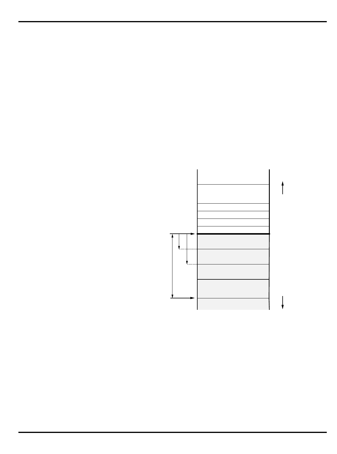
C PROGRAMMING CHAPTER 10
10–5
...
j $31
.end myleaf
Other toolchains may have different definitions for these macros, as
appropriate to their needs.
Non-leaf functions
Non-leaf functions are those which contain calls to other functions.
Normally the function starts with code (the ‘‘function prologue’’) to reset
sp
to the low-water mark of argument structures for any functions which may
be called, and to save the incoming values of any of the registers
s0
–
s8
which the function uses. Stack locations must also be reserved for
ra,
automatic (i.e. stack-based local) variables, and any further registers
whose value this function needs preserved over its own calls (if the values
of the argument registers
a0
–
a3
need to be preserved, they can be saved
into their standard positions on the ‘‘argument structure’’).
Note that, since
sp
is set only once (in the function prologue) all stack-
held locations can be referenced by fixed offsets from
sp.
This is illustrated in the non-leaf function listed below, in conjunction
with the picture of the stackframe in Figure 10.1, “Stackframe for a non-
leaf function”.
Figure 10.1. Stackframe for a non-leaf function
#include <idtc/asm.h>
#include <idtc/regdef.h>
#
# myfunc (arg1, arg2, arg3, arg4, arg5)
#
# framesize = locals + regsave (ra,s0) + pad + fregsave (f20/21)
+ args + pad
myfunc_frmsz= 4 + 8 + 4 + 8 + (5 * 4) + 4
NESTED(myfunc, myfunc_frmsz, zero)
subu sp,myfunc_frmsz
.mask 0x80010000, -4
space for arg 1
space for arg 2
space for arg 3
space for arg 4
more arguments
(if won’t fit in 16 bytes)
automatic (local) variables
integer register save area
f.p. register save area
space for building
arguments for nested calls
higher lowerAddresses
entry
sp on
running
sp while
framesize
regoffs
fregoffs
(>= 16 bytes)

CHAPTER 10 C PROGRAMMING
10–6
sw ra,myfunc_frmsz-8(sp)
sw s0,myfunc_frmsz-12(sp)
.fmask 0x00300000, -16
s.d $f20,myfunc_frmsz-24(sp)
...
<your code goes here, e.g>
# local = otherfunc (arg5, arg2, arg3, arg4, arg1)
sw a0,16(sp) # arg5 (out) = arg1 (in)
lw a0,myfunc_frmsz+16(sp)# arg1 (out) = arg5 (in)
jal otherfunc
sw v0,myfunc_frmsz-4(sp)# local = result
...
l.d $f20,myfunc_frmsz-24(sp)
lw s0,myfunc_frmsz-12(sp)
lw ra,myfunc_frmsz-8(sp)
addu sp,myfunc_frmsz
jr ra
END(myfunc)
Analyzing the above example, one step at a time:
#
# myfunc (arg1, arg2, arg3, arg4, arg5)
#
The function myfunc expects five arguments: on entry the first four of
these will be in registers a0 – a3, and the fifth will be at sp+16.
# framesize = locals + regsave (ra,s0) + pad + fregsave (f20/21)
+ args + pad
myfunc_frmsz= 4 + 8 + 4 + 8 + 20 + 4
The total frame size is calculated as follows:
•locals (4 bytes): keep one local variable on the stack, rather than in a
register; the example may need to pass the address of the variable to
another function.
•regsave (8 bytes): save the return address register ra, because this
function calls another function; this function also plans to use the
callee-saved register s0.
•pad (4 bytes): the rules say that double precision floating-point must
by 8-byte aligned, so add one word of padding to align the stack.
•fregsave (8 bytes): the function plans to use $f20, which is one of the
callee-saved floating-point registers.
•argsize (20 bytes): this function is going to call another function
which needs five argument words; this size must never be less than
16 bytes if a nested function is called, even if it takes no arguments.
•pad (4 bytes): the rules say that the stack pointer must always be 8-
byte aligned, so add another word of padding to align it.
NESTED(myfunc, myfunc_frmsz, zero)
subu sp,myfunc_frmsz
In the MIPS Corp. toolchain this would be expanded to:
.globl myfunc
.ent myfunc,0
.frame $29,myfunc_frmsz,$0
subu $29,myfunc_frmsz
This declares the start of the function, and makes it globally accessible.
The .frame function tells the debugger the size of stack frame to be
created, and finally the subu instruction creates the stack frame itself.

C PROGRAMMING CHAPTER 10
10–7
.mask 0x80010000, -4
sw ra,myfunc_frmsz-8(sp)
sw s0,myfunc_frmsz-12(sp)
The function must save the return address and any callee-saved integer
registers used, in the stack frame. The .mask directive tells the debugger
which registers will be saved($31 and $20), and the offset from the top of
the stack frame to the top of the save area: this corresponds to regoffs. The
sw instructions then save the registers: the higher the register number, the
higher up the stack it is placed (i.e. the registers are saved in order).
.fmask 0x00300000, -16
s.d $f20,myfunc_frmsz-24(sp)
The code then does the same thing for the callee-saved floating-point
registers $f20 and (implicitly) $f21. The .fmask offset corresponds to
fregoffs, i.e. local variable area + integer register save area + padding word.
# local = otherfunc (arg5, arg2, arg3, arg4, arg1)
sw a0,16(sp) # arg5 (out) = arg1 (in)
lw a0,myfunc_frmsz+16(sp)# arg1 (out) = arg5 (in)
jal otherfunc
This program calls the function otherfunc. Its arguments 2 to 4 are the
same as this programs’ arguments 2 to 4, so these can pass straight
through without being moved. However, the code must swap argument 5
and argument 1, so it copies:
• its input arg1 (in register a0) to the arg5 position in the outgoing
argument build area (new sp + 16).
• its input arg5 (at old sp + 16) to outgoing argument 1 (register a0).
sw v0,myfunc_frmsz-4(sp)# local = result
The return value from otherfunc is stored in the local (automatic)
variable, allocated the top 4 bytes of the stack frame.
l.d $f20,myfunc_frmsz-24(sp)
lw s0,myfunc_frmsz-12(sp)
lw ra,myfunc_frmsz-8(sp)
addu sp,myfunc_frmsz
jr ra
END(myfunc)
Finally the function epilogue reverses the prologue operations: restores
the floating-point, integer and return address registers; pops the stack
frame; and returns.
Functions needing run-time computed stack locations
In some languages dynamic variables can be created whose size varies
at run-time. Some C compilers support this, by using the useful library
function alloca. This means that sp has been lowered by an amount
unknown at compile time, so the compiler can’t use it to reach stack
locations.
In this case the function prologue grabs another register, s8, also known
as fp, and points it to the post-prologue value of sp.
Since fp is one of the saved registers, the prologue must also save its old
value. In the function body, all stack location references to automatic
variables, and saved-register positions are made via fp. But when calling
other functions, and putting data into the argument structure, that will be
done with relation to sp.

CHAPTER 10 C PROGRAMMING
10–8
Assembler buffs may enjoy the observation that, when creating space
with alloca the address returned is actually a bit higher than sp, since the
compiler has still reserved space for the largest argument structure
required by any function call.
This example is a slightly modified version of the function used in the
last section, with the addition of a ‘‘call’’ to alloca.
#include <idtc/asm.h>
#include <idtc/regdef.h>
#
# myfunc (arg1, arg2, arg3, arg4, arg5)
#
# framesize = locals + regsave (ra,s8,s0) + fregsave (f20/21) +
args + pad
myfunc_frmsz= 4 + 12 + 8 + (5 * 4) + 4
.globl myfunc
.ent myfunc,0
.frame fp,myfunc_frmsz,$0
subu sp,myfunc_frmsz
.mask 0xc0010000, -4
sw ra,myfunc_frmsz-8(sp)
sw fp,myfunc_frmsz-12(sp)
sw s0,myfunc_frmsz-16(sp)
.fmask 0x00300000, -16
s.d $f20,myfunc_frmsz-24(sp)
move fp,sp # save bottom of fixed
frame
...
# t6 = alloca (t5)
addu t5,7 # make sure that size
and t5,~7 # is multiple of 8
subu sp,t5 # allocate stack
addu t6,sp,20 # leave room for args
...
<your code goes here, e.g>
# local = otherfunc (arg5, arg2, arg3, arg4, arg1)
sw a0,16(sp) # arg5 (out) = arg1 (in)
lw a0,myfunc_frmsz+16(fp)# arg1 (out) = arg5 (in)
jal otherfunc
sw v0,myfunc_frmsz-4(fp)# local = result
...
move sp,fp # restore stack
pointer
l.d $f20,myfunc_frmsz-24(sp)
lw s0,myfunc_frmsz-16(sp)
lw fp,myfunc_frmsz-12(sp)
lw ra,myfunc_frmsz-8(sp)
addu sp,myfunc_frmsz
jr ra
END(myfunc)
There are a few notable differences from the previous example:
.globl myfunc
.ent myfunc,0
.frame fp,myfunc_frmsz,$0
The function can’t use the NESTED macro any more, since it is using a
separate frame pointer which must be explicitly declared using the .frame
directive.
.mask 0xc0010000, -4
sw ra,myfunc_frmsz-8(sp)

C PROGRAMMING CHAPTER 10
10–9
sw fp,myfunc_frmsz-12(sp)
sw s0,myfunc_frmsz-16(sp)
Since the program will modify fp (= s8 = $30), it must save it in the
stackframe too.
# t6 = alloca (t5)
addu t5,7 # make sure that size
and t5,~7 # is multiple of 8
subu sp,t5 # allocate stack
addu t6,sp,20 # leave room for args
This sequence allocates a variable number of bytes on the stack, and
sets a register (t6) to point to it. The program must make sure that the size
is rounded up to a multiple of 8, so that the stack stays correctly aligned.
In addition, it must add 20 to the stack pointer, to leave room for the five
argument words that will be used in future calls.
sw a0,16(sp) # arg5 (out) = arg1 (in)
lw a0,myfunc_frmsz+16(fp)# arg1 (out) = arg5 (in)
jal otherfunc
sw v0,myfunc_frmsz-4(fp)# local = result
When building another function’s arguments, use the sp register; but
when accessing input arguments or local variables the program must use
the fp register.
move sp,fp # restore stack
pointer
l.d $f20,myfunc_frmsz-24(sp)
lw s0,myfunc_frmsz-16(sp)
lw fp,myfunc_frmsz-12(sp)
Finally, at the start of the function epilogue, restore the stack pointer to
its post-prologue position, and then restore the registers (not forgetting to
restore the old value of fp, of course).
SHARED AND NON-SHARED LIBRARIES
A C object library is a collection of pre-compiled modules, which are
automatically linked into a program’s binary when it refers to a function or
variable whose name is defined in the module. Many standard C functions
like printf are defined in libraries.
Libraries provide a simple and powerful way of extending the language;
but in a multi-tasking OS every program will carry its own copy of the
library function. Modern library functions may be huge; for example the
graphics interface libraries to the widely-used X window system add about
300Kbytes to the size of a MIPS object, dwarfing the application code of
many simpler programs.
In response to this problem most modern OS’ provide some way in which
library code may be shared between different applications. There are
different approaches:
Sharing code in single-address space systems
In a single address-space OS like VxWorks†, programs can be linked to
library functions by deferring the link operation (which actually fixes up
the program code) until the program is loaded into system memory. In this
kind of system the library function becomes part of a single large program.
But:
• The libraries must be written to be ‘‘re-entrant’’; they may be used by
different tasks, and one task may be suspended in the middle of a
library function and that function re-used by another.
† VxWorks is a trademark of Wind River Systems, Inc.

CHAPTER 10 C PROGRAMMING
10–10
For simple operations, re-entrancy is easily achieved by avoiding any
use of static modifiable data (so that all computation is done on the
stack and in machine registers). However, where library functions
must maintain internal data life gets much more complicated;
accesses to shared variables must use the programming technique of
critical regions protected by semaphores.
This does mean that library programmers must respect these rules,
and can’t just recompile existing code into libraries without
modification.
• The run-time system must maintain a symbol table for loading.
System utilities such as the debugger also need access to the symbol
table and relocation information.
In such a system a little extra work at load time allows a single copy of
a library function to be freely used by the OS kernel, drivers and any
number of application tasks. Simple functions suffer very little run-time
overhead (the convenient gp-relative addressing optimization, described in
the last chapter, cannot be used); the critical region overhead for shared
data is unavoidable.
Sharing code across address spaces
In a ‘‘protected’’ OS where separate applications run in separate virtual
address spaces, the problems are quite different. This section will outline
the way in which Unix-like systems conforming to the MIPS/ABI standard
provide libraries which can be shared between different applications, with
no restriction on how the libraries and applications can be programmed.
Every MIPS/ABI application runs in its own virtual address space. The
application code is fixed to particular locations in this address space when
it is linked. Library code is not built in; the application carries a table of
the names of library functions and variables which are used, but not yet
included. In addition, the application’s symbol table defines public items
which may be called from the library; under MIPS/ABI, library routines
may freely refer to public data, or call public functions, in application
code†.
In the MIPS/ABI model the binary application code must not be
modified; it may itself be shared by multiple invocations of the application
by multiple users.
It is not possible to predefine the actual virtual addresses at which a
library’s code and data will be located, but the offset from the start of its
code to the start of its data is fixed, and this permits a number of tricks to
be used.
•Position-independent code: the compiler and assembler (by a
command line option, used for library functions) can generate fully
‘‘position independent code’’ (PIC). All MIPS branch instructions are
PC-relative; somewhat more complex sequences must be used to load
a PC-relative address into a register, but if necessary it can be done:
la rd, label –> bgezal $zero, 1f
nop
1: addu rd, $31, label – 1b
•Indirection and the Global offset table: PIC is suitable for references to
code within a single module of a library (because the module’s code is
loaded as a single entity into consecutive virtual addresses). Data, or
external functions, will be at locations which cannot be determined
until the application and library are loaded, and so their addresses
cannot be embedded in the program text.
† Though this may not be good programming practice.

C PROGRAMMING CHAPTER 10
10–11
Such addresses are held in a table built in the each library’s per-
process data space, the ‘‘global offset table’’ (GOT). Since the data
space is not shared and is writable, the table can be built as the
application and its libraries are loaded.
A library function refers to a variable or external function through the
GOT at a table index fixed when the library was compiled and linked.
A load of the external integer type ‘‘errno’’ will come out as:
lw rd, errno →la gp, ThisLibsGOTBase
lw rd, errno_offset(gp)
nop
lw rd, 0(rd)
Similarly, invocation of the shared-library function
exit()
would
look like this:
/* setup argument */
jal exit →la gp, ThisLibsGOTBase
lw t9, exit_offset(gp)
nop
jalr t9
The register gp (or $28 ) is a good choice for the table base. Because
of its role in providing fast access to short variables it is not modified
by standard functions. As an optimization it is calculated only once
per function, in the function prologue. The calculation uses the fact
that the function’s actual virtual address will be in t9 (see previous
example), and that the library’s GOT is at a fixed offset from its code.
So a position-independent function prologue might start like this:
func: la gp, _gp_disp
addu gp, gp, t9
addu sp, sp, framesize
sw gp, 32(sp)
In the above example, _gp_disp is a magic symbol which is
recognized by the linker when building a shared library: it’s value will
be the offset between the instruction and the GOT. The calculated
value is saved on the stack, and must be restored from there after a
call to an external function, since that function may itself have
modified gp.
There is much more that could be said about the way in which the
MIPS/ABI implementation is optimized. For example, no attempt is made
to link in libraries when an application is first loaded into memory; dummy
GOT entries are used instead. When and if the application uses a library
module, the reference is caught and fixed up in much the same way as a
virtual-memory system incrementally pages-in a program image.
AN INTRODUCTION TO OPTIMIZATION
The compiler writer’s first responsibility is to ensure that the generated
code does precisely what the language semantics say it should; and that is
hard enough. In modern compilers, the optimizer has a secondary
purpose, which is to allow the compiler’s basic code generator to be simple
(and therefore easier to implement correctly).
Common optimizations
Most compilers will do all of the following. Occasionally the assembler
may get in on some of them too.

CHAPTER 10 C PROGRAMMING
10–12
•Common sub-expression elimination (CSE): this detects when the code
is doing the same work twice. At first sight this looks like it is just
making up for dumb programming; but in fact CSE is critically
important, and tends to be run many times to tidy up after other
stages:
a) It is CSE which gives the compiler the ability to optimize across
the function. The basic code generator works through the
program expression-by-expression; even for well-written source-
code, the expansion of simple C statements into multiple MIPS
instructions will lead to a lot of duplicated effort. The very first
CSE pass factors out the duplication and clears the way for
register allocation.
b) Most memory-reference optimization is actually done by CSE –
the code which fetches a variable from memory is itself a sub-
expression.
The enemy of CSE is unpredictable flow of control: the
conditional branch. Once code turns into spaghetti, the compiler
finds it difficult to know what computation has run before which;
with some straightforward exceptions, CSE can really only
operate inside basic blocks (a piece of code delimited by, but not
containing, either an entry point or a conditional branch). CSE
markedly improves both code density and run-time
performance.
Similar to CSE are the optimizations of constant folding, constant
propagation and arithmetic simplification. These pre-compute
arithmetic performed on constants, and modify other expressions
using standard algebraic rules so as to permit further constant
folding and better CSE.
•Jump optimization: removes redundant tests and jumps. Code
produced by earlier compiler stages often contains jumps to jumps,
jumps around unreachable code, redundant conditional jumps, and
so on. These optimizations will remove this redundancy.
•Strength reduction: means the replacement of computationally
expensive operations by cheaper ones. For example; multiplication by
a constant value can be replaced by a series of shifts and adds. This
actually tends to increase the code size while reducing run-time.
•Loop optimization: studies loops in the code, starting with the inner
ones (which, the compiler guesses, will be where most time is spent).
There are a number of useful things which can be done:
a) Sub-expressions which depend on variables which don’t change
inside the loop can be pre-computed before the loop starts.
b) Expressions which depend in some simple way on a loop variable
can be simplified. For example, in:
int i, x[NX];
for (i = 0; i <NX; i++)
x[i]++;
the array index (which would normally involve a multiplication and
addition) can be replaced by an incrementing pointer.
This kind of optimization will usually recognize only a particular set
of stylized opportunities.
c) Loops can be ‘‘unrolled’’, allowing the work of 2 to a few iterations
of the loop to be performed in line. On some processors where
branches are inherently slow, this is inherently effective; but this
isn’t true for the R30xx family.

C PROGRAMMING CHAPTER 10
10–13
But the unrolled loop offers much better opportunity for other
optimizations (CSE and register allocation being the main
beneficiaries).
Loop unrolling may significantly increase the size of the compiled
program, and usually must be requested as a specific compiler
option.
•Function inlining: the compiler may guess that some small functions
can be expanded in-line, like a macro, rather than calling them. This
is another optimization which increases the size of the program to give
better performance, and usually requires an explicit compiler option.
Some compilers may recognize the inline keyword used in C++ to
allow the programmer to specify which functions should be ‘‘inlined’’.
•Minimize Register allocation: by far the most important optimization
stage is to make the best possible use of the 32 general purpose
registers, to make code faster and smaller. The compiler identifies
global variables (static and external data stored in memory);
automatic variables (defined within a function, and notionally stored
on the stack); and intermediate products of expression evaluation.
Any variable must eventually be assigned to a machine register, and
input data copied to that register, before the CPU can do anything
useful with it. The register allocator’s job is to minimize the amount
of work done in shuffling data in and out of registers; it does this by
maintaining some variables in registers for all or part of a function’s
run-time.
Note:
a) This process usually entirely ignores the old-fashioned ‘‘C’’
register attribute. It might be used as a hint; but most compilers
figure out for themselves which variables are best kept in registers,
and when.
b) The MIPS convention provides the compiler with 9 registers s0-s8
which can be freely used as automatic variables. Any function
using one of these must save its value on entry, and restore it on
exit. These registers tend to be suitable for long-term storage of
user variables.
It also has a set of 10 ‘‘temporary’’ registers t0-t9 which are typically
used for intermediate values in expression evaluation. The
‘‘argument’’ registers a0-a3 and ‘‘result’’ registers v0-v1 can be
freely used too. However, these values don’t survive a function call;
if data is to be kept past a function call it is more efficient to use
one of the ‘‘callee saved’’ registers s0-s8, because then the work of
saving and restoring the value will be done only if a called function
really wants to use that register.
c) C’s semantics mean that any write through a pointer could
potentially alter almost any memory location; so a compiler’s ability
to maintain a user-defined variable in a register is strictly limited.
It is safe to do so for any function variable (automatic variable)
which is nowhere subject to the ‘‘address-of’’ operator ‘‘ &’’. It may
be able to do this for a variable inside a loop where there is neither
a store-through-pointer operation nor a function call.
•Pipeline-specific code re-scheduling: the compiler or assembler can
sometimes move the logical instruction flow around so as to make
good use of the branch and load ‘‘delay slots’’. In practice, the delay
slots are fine grain and tied to specific machine instructions; and this
can only be done late in the compilation process.
The most obvious techniques are:
a) If the instruction succeeding a load doesn’t depend on the loaded
value, just leave out the nop which would have been placed in the
delay slot.

CHAPTER 10 C PROGRAMMING
10–14
b) Move the logically-preceding instruction into the delay slot. The
optimizer may be able to find an instruction a few positions
preceding the branch or load, provided there are no intervening
entry points.
The register-register architecture makes it fairly simple to pick out
instructions which depend on each other and cannot be re-
sequenced.
c) For a load, the optimizer may be able to find an instruction in the
code after the load which is independent of the load value and is
able to be moved into the delay slot.
d) Moving the instruction just before a branch into the branch delay
slot.
e) Duplicating the instruction at a branch target into the branch delay
slot, and fixing up the branch to go one more instruction forward.
This is particularly effective with loop-closing instructions. If the
branch is conditional, though, the compiler can only do it if the
inserted instruction can be seen to be harmless when the branch
is not taken.
How to prevent unwanted effects from optimization
Some code may rely on system effects invisible to the compiler.
Examples include software intended to poll the status register of a serial
port and send a character when it’s ready:
unsigned char *usart_sr = (unsigned char *) 0xBFF00000;
unsigned char *usart_data = (unsigned char *) 0xBFF20000;
#defined TX_RDY 0x40
void putc (ch)
char ch;
{
while ((*usart_sr & TX_RDY) == 0)
;
*usart_data = ch;
}
A compiler, left to optimize this as for any other program, may send 2
characters and then enter an infinite loop. The compiler sees the memory
reference implied by *usart_sr as a loop-invariant fetch; there are no
stores in the ‘‘while’’ loop so this seems a safe optimization. The compiler
has actually coded for:
void putc (ch)
char ch;
{
tmp = (*usart_sr & TX_RDY);
while (tmp)
;
*usart_data = ch;
}
With most compilers, this particular problem is prevented by defining
registers carefully:
volatile unsigned char
*usart_sr = (unsigned char *) 0xBFF00000;
volatile unsigned char
*usart_data = (unsigned char *) 0xBFF20000;

C PROGRAMMING CHAPTER 10
10–15
A similar situation can exist if software must examine a variable that is
modified by an interrupt or other exception handler. Again, declaring the
variable as ‘‘volatile’’ should fix the problem.
Although the C rules describe the operation of ‘‘volatile’’ as
implementation dependent, most compilers which ignore the ‘‘volatile’’
keyword are expected to play safe.
There are other, more subtle, ways in which optimizations can break a
program. For example, it may change the order in which some loads and
stores occur. It may be easier to write and maintain hardware driver code
in C than in assembler, but it’s the programmer’s responsibility to know
exactly what the compiler did, and to make sure it’s what was wanted.
Optimizer-unfriendly code and how to avoid it
Certain kinds of C programs will cause problems for a MIPS CPU and its
optimizing compiler, and will cause unnecessary loss of performance.
Some things to avoid are:
•Sub-word arithmetic : use of short or char variables in arithmetic
operations is less efficient than using full word arithmetic. The MIPS
CPU lacks sub-word arithmetic functions and will have to do extra
work to make sure that expressions overflow and wrap around when
they should. The int data type represents the optimum arithmetic
type for the R30xx family; most of the time short and char values can
be correctly manipulated by int automatic variables.
•Taking the address of a local variable: the compiler will now have to
consider the possibility that any function call or write through a
pointer might have changed the variable’s value; so it won’t live long
in a machine register.
Perhaps the best way of seeing this is that defining a variable local to
a function (and whose address is not taken) is essentially free. It will
be assigned to a register, which would have been needed in any case
for the intermediate result.
•Nested Function calls: in the MIPS architecture the direct overhead of
a function call is very small (2-3 clocks). But the function call makes
it difficult for the compiler to make good use of registers, so may be
much more costly in terms of lost optimization opportunity. Inside a
function with a fairly complex set of local variables a nested call could
be as slow as a typical CISC function call, and add a lot of code.

11–1
PORTABILITY
CONSIDERATIONS
®
Integrated Device Technology, Inc.
CHAPTER 11
This chapter discusses three distinct facets of portability to be
concerned about:
• Migrating existing software from another CPU architecture to the
R30xx family.
• Writing code that can readily be used on multiple R30xx family
members.
• Writing code that will be easily portable to future family members.
Techniques such as modular programming can be used to facilitate
virtually all of these areas, but are beyond the scope of this manual.
Instead, this manual will focus in on the architecture-specific portability
issues.
Since most modern embedded programming uses the “C” programming
language, this chapter will begin with a review of the portability concerns
associated with this programming language.
Additionally, this chapter will review some of the historical obstacles to
program portability: byte ordering conventions, word sizes, alignment
constraints, and so on; and will discuss the manner in which the MIPS
architecture deals with these issues. This review is intended to discuss the
issues which complicate porting existing code, developed for execution on
other architectures, to the R30xx family.
Finally, this chapter will discuss generating an environment to support
multiple family members, both existing and possible future members, to
enable the investment in porting to be applied to a wide variety of system
cost-performance points.
WRITING PORTABLE C
‘‘C’’ is one of a class of languages which originally aimed to abstract the
abilities of a class of simple minicomputers, to add some terse and
powerful syntax for flow of control, and to provide simple but adequate
mechanisms for data structuring.
A language standard such as Pascal or Ada sets out to make portability
compulsory; the language attempts to make it impossible for program
behavior to be dependent on what kind of CPU is being used. C lets the
underlying implementation show through; it is possible to write portable C
by programming discipline, but it doesn’t happen automatically.
C’s low-level origins contribute to its power and efficiency, but make it
inherently prone to non-portability. Good examples are the following:
•
Basic data types
: change in their size (i.e. the number of bits of
precision) between different implementations.
•
Pointers
: (inevitably implemented as real machine pointers) expose
the memory layout of data, which is implementation-dependent.
Some things have got easier with time; early C implementations had to
target machines with 7-, 8- and 9-bit
char
types, and with 36-bit machine
words. It is now entirely reasonable to assume that targets will have an 8-
bit
char
which is the smallest addressable unit of memory, and other basic
types will be 16-, 32- or 64-bits in size.
C Language Standards
C has evolved continuously since its early days. It has definitely gone
up-level; most changes have tended to increase the amount of abstraction
and checking. To date, there are three main “variants”, or standards, for
the C language.

CHAPTER 11 PORTABILITY CONSIDERATIONS
11–2
•
K&R
: named after the C Programming Manual by Kernighan and
Richie, this reflects the standard used for the first few years of Unix
life. It has little type-checking, many defaults, and the compilers
rarely complain. However, it provides a useful
lingua franca
: most
compilers will (sometimes unwillingly and with warnings) correctly
translate programs written to K&R.
In practice the language was, during this period, defined by a single
implementation: AT&T Bell Lab’s Portable C compiler.
•
ANSI
: the ANSI standard collects together ‘‘improvements’’ made over
the years and regulates them. ANSI defines syntax allowing the
programmer to make far more well-defined declarations of functions,
and then checks programmer usage against them. ANSI compilers
tend to produce more warning messages than K&R compilers,
reflecting the greater amounts of type-checking performed.
A number of compilers use “compliance test suites” to “guarantee”
ANSI compliance. A common test suite is the “Plum-Hall” test suite,
which includes modules to test a compiler (and its libraries)
compliance to the ANSI rules. The IDT/C compiler uses this
compliance suite to validate its ANSI compliance.
•
GNU
: the Free Software Foundation’s GNU compiler is set to restore
the dominance of a single implementation of the compiler, and thus
permit the emergence of a new dialect†. Note that the GNU compiler
does support ANSI compliance; it is just that, as an “experimental”
toolchain, it may also support more “cutting edge” extensions to ANSI
than are currently supported by the standards body.
GNU also adds a number of very valuable features; including function
inlining, a robust ‘‘asm’’ statement,
alloca()
.
GNU provides the benefit of being available across multiple hosts and
target architectures. Thus, porting applications developed using the GNU
toolchain from some other architecture to the R30xx will avoid the porting
problems associated with compiler PRAGMAs, compiler directives, and the
like.
Similarly, porting ANSI compliant code from a different architecture
should be relatively straight-forward. However, differences in supported
PRAGMAs, and other environmental differences, may cause a higher level
of porting activity.
C Library Functions and POSIX
C supports separate compilation of modules, allowing the resulting
object code files to be linked together without recourse to the source. C
libraries are bunches of pre-compiled object code defining common
functions. The ‘‘standard’’ C library of everyday functions is to all intents
and purposes part of the language.
The ANSI standard addresses a subset of common library functions and
lays down their function. But this deliberately steers clear of ‘‘OS-
dependent’’ functions; and these include the simplest input/output
routines.
The POSIX (IEEE1003.4) standard is probably the best candidate,
defining a standard C language interface to a workable IO system. POSIX
has its problems:
• it does not yet cover all OS features (and probably shouldn’t);
† GNU C is also an extraordinary experiment; a major piece of
ingenuity and intellectual work being maintained and continually
developed by a large, loose-knit, worldwide community of workers,
many of them volunteers. No other piece of free software has
filtered quite so far into the body of the computer industry.

PORTABILITY CONSIDERATIONS CHAPTER 11
11–3
• its definers occasionally felt obliged to standardize an ‘‘improvement’’
of current practice, so POSIX compliance is still hard to find even in
big OS’es.
But it is a huge improvement on earlier single-camp standards and will
undoubtedly become important. Programs adhering to POSIX should be
able to be rebuilt on a large range of OS, including Desktop OS’es (such as
UNIX) and RTOS environments. Using POSIX compliant library functions
will further enhance portability across toolchains and architectures.
DATA REPRESENTATIONS AND ALIGNMENT
The MIPS architecture can only load multi-byte data which is
‘‘naturally’’ aligned – a 4-byte quantity only from a 4-byte boundary, etc.
Many CISC architectures don’t have this restriction (although many RISC
architectures do follow this restriction, and in fact may offer less support
than the MIPS machine code does for this situation). The compiler is
designed to ensure that data lands up in the right place; and this requires
far-reaching (and not always obvious) behaviors. These include:
• Padding between fields of data structures.
• Defensive alignment; base addresses of structures, or stack frames,
are aligned to the largest unit to which the architecture is sensitive (4
or 8 bytes in the MIPS architecture).
The toolchain used for previous development, targeted to a different CPU
architecture, may do this differently.
Consider the following examples:
struct foo {
char small;
short medium;
char again;
int big;
}
This will be laid out in memory as shown in Figure 11.1, “Structure
layout and padding in memory”:
Notes on structure layout and padding
These notes should be taken as typical of what a good compiler will do.
They are required by, for example, a MIPS/ABI compliant compiler; but
beware – a compiler
could
still be fully compliant with C standards and use
wholly counterintuitive data representations – so long as these were
internally consistent.
•
Alignment of structure base address
: the data structure itself will
always be placed on a 4-byte boundary; a structure’s alignment is
that of its most demanding subfield.
struct foo
contains an
int
requiring 4-byte alignment, so the structure itself will be 4-byte
aligned.
Dynamic memory allocation, either on the stack or by software
routines such as
malloc
() could give rise to alignment problems; so
they are specified to return pointers aligned to the largest size which
the architecture cares about. In the case of the R30xx family this need
only be 4 bytes, but in fact is usually 8 bytes: a gesture towards
compatibility with future 64-bit implementations.
•
Memory order
: fields within structures are stored into memory in the
order declared.
offset (bytes) 0 1 2 3 4 5 7 8 11
small
×
medium again
×
big
Figure 11.1. Structure layout and padding in memory

CHAPTER 11 PORTABILITY CONSIDERATIONS
11–4
•
Padding
: is generated whenever the next field would otherwise have
the ‘‘wrong’’ alignment with respect to the structure’s base address.
•
Endianness
: has no effect on the picture shown by Figure 11.2, “Data
representation with #pragma pack(1)”. Endianness determines how
an integer value is related to the values of its constituent bytes (when
they are considered separately); it does not affect the relative byte
locations used for storing those values.
Endianness does have some effect on C bitfields, which are discussed
below.
There’s an irrefutable, pure and correct position on data structures and
portability; the memory representation of data is compiler dependent, and
the programmer should not expect it to be in any way portable – even
between two different compilers for the same architecture. In general, it is
reasonable to expect to be able to exchange a sequence or consecutive
array of
char
s (each taking a value between 0 and 255), but not more. But
in the real world it would be inefficient to make sure that all data ever
exchanged or published by programs was in the form of byte strings.
ANSI compilers may support an option using the ‘‘pack’’ PRAGMA:
#pragma pack(1)
struct foo {
char small;
short medium;
char again;
int big;
}
has the effect of causing the compiler to omit all padding, producing the
layout shown in Figure 11.2, “Data representation with #pragma pack(1)”:
A structure packed like this has no inherent alignment, so in addition
to the lack of any padding, the structure base address may also be
unaligned. The compiler will always generate load and store sequences to
its fields which are alignment independent (and therefore to some extent
inefficient) – even though, in this particular case, the
big
field happens to
have the correct 4-byte alignment from the structure base.
Structure packing is most frequently used when storing large files of a
particular structure in memory; for example, when storing the
“description” of a font in the ROMs of a printer. By eliminating padding,
more font structures can be saved in a smaller amount of memory; the cost
of doing this occurs at run-time, when more conservative code sequences
must be used to read fields from the structure.
The ‘‘1’’ in
pack(1)
refers to the maximum alignment which must be
respected, so ‘‘pack(2)’’ means align only to 2-byte boundaries:
#pragma pack(2)
struct foo {
char small;
short medium;
char again;
int big;
}
offset (bytes) 0 1 2 3 4 7
small medium again big
Figure 11.2. Data representation with #pragma pack(1)

PORTABILITY CONSIDERATIONS CHAPTER 11
11–5
The preceding code fragment has the effect of causing the compiler to
pad items of 2 bytes or larger to 2-byte boundaries, producing the layout
shown in Figure 11.3, “Data representation with #pragma pack(2)”:
The
#pragma pack
feature is not the only potential source of data
representation incompatibility; endianness, discussed below, can also
pose a significant portability issue. Nonetheless, used with care this
feature can reduce the amount of difference between sources for two
different architectures.
ISOLATING SYSTEM DEPENDENCIES
It is unlikely that the source code to be ported is literally the complete
system. Most programs depend on an environment implemented by
underlying independent software (perhaps from a 3rd party); this may be
bound in at run time (an operating system or system monitor), or at link
time (library functions, “include” files). Quite often, sources may not be
available; sometimes they will just be more trouble to port than to
reproduce.
This is the point at which the programmer will appreciate the purpose
of attempts to standardize a C runtime library. If only the boundary
between the “application” program and its environment consisted of well-
defined standard calls and include files, the job would be trivial. It isn’t,
usually.
Locating system dependencies
In general, the “core application” consists of the code which does NOT
meet the following criteria:
• Supplied as part of an OS the new system won’t be using;
• A library function which is not available (with
exactly
the same
semantics) in the target compilation system;
• Not licensed for use on the new target system.
There are two ‘‘concentric’’ boundaries which can be drawn, and in a
sense they divide the original code up into three parts:
• The inner part is the application to be ported. The new system may
carry this code through unchanged (except where portability
problems mean the code needs to be changed); so usually, after
porting, this code should still be usable on the original system.
• System dependent code, libraries, OS etc. which are clearly not going
to be taken to the new system. Porting should not be an issue for
these.
• Glue functions and data which join the two up. These will have to be
modified, or sometimes re-implemented, to adapt the application to
the new environment.
The glue probably represents 10% of the code; but requires 90% of the
work. In a program which has been ported often, the glue will be neatly
separated; in a program which evolved in a single system, the glue may be
rather deeply mixed with the application.
Fixing up dependencies
To remove these dependencies, the programmer must first of all, try to
find the best boundaries and divide the code into application, glue and
environment. Since there will be a new “environment” on the new system,
the latter code is more or less irrelevant (and is likely written in assembler,
to a great extent).
offset (bytes) 0 1 2 3 4 5 6 9
small
×
medium again
×
big
Figure 11.3. Data representation with #pragma pack(2)

CHAPTER 11 PORTABILITY CONSIDERATIONS
11–6
This is art as well as science; there is no single right way to do it. The
objective will be to minimize the scope for introducing new errors, while
minimizing the amount of work done.
The ‘‘application’’ part should be recompilable on the new system,
generating a list of unresolved definitions which need to be patched up.
Some of these, when investigated, will turn out to be used in code which
really belonged in the ‘‘glue’’; move the boundary and iterate until the list
of unresolved names makes sense.
The glue now needs to be re-implemented for the new environment. The
programmer has two choices for each function:
• Recompile the function, using some ‘‘underglue’’ definitions or
functions to mimic the behavior of the old environment using the new
one. In a sense, the programmer is pragmatically deciding that what
was seen as glue is now application.
• Reimplement the function (using the old one for inspiration and as a
source for cut-and-paste), aiming to mimic the function as a ‘‘black
box’’.
For each function or module, choose one of these strategies. It is nearly
always a bad idea to mix strategies in the same module.
Isolating Non-Portable Code
In general, it is difficult to write a “stand-alone” program entirely
portably. In the desktop environment, programmers write programs to an
OS standard; thus, porting a program to a new system is limited to porting
that OS. This is the model for UNIX and even for many RTOS-based
systems.
As examples, it is easy to write a portable routine to calculate prime
numbers; it is much harder to write a portable routine to accept typed
input, providing line editing and simple argument parsing (are characters
7- or 8-bit? Is the language English? What accented characters are
acceptable? How does the display device implement backspace?)
The best programs hide the nonportable parts of code in modules, whose
interfaces consist of stable data declarations and functions whose
operation can be expressed succinctly and clearly.
Using assembler
There are three reasons for using assembler:
•
Efficient implementation of critical functions
: getting the last clock
cycle out of
strcpy
may well be worthwhile.
•
Access to instructions not supported by the compiler
: e.g. access to
control registers. These can sometimes be replaced by using ‘‘tiny’’
subroutines; and sometimes by C
asm
statements. Tiny subroutines
are particularly apt when, although the implementation will be
completely machine dependent the desired effect is machine-
independent – prefer a ‘‘disable interrupts’’ function to a ‘‘set status
register bits’’ function.
•
Some critical environmental deficiency
: (most commonly) inability to
provide the free use of CPU registers and the stack which the compiler
relies on. Classic examples are interrupt handlers. To maximize ease
of portability, the programmer can at least make it a priority, in these
routines, to build an environment from which software can call C
functions.

PORTABILITY CONSIDERATIONS CHAPTER 11
11–7
ENDIANNESS
The word ‘‘endianness’’ was introduced by a famous short paper† in the
Journal of the ACM, in the early 1980’s. The author observed that
computer architectures had divided up into two camps, based on an
“arbitrary” choice of the way in which byte and word addressing are
related. In ‘‘Gulliver’s Travels’’ the little-endians and big-endians fought a
war over the correct end at which to start eating a boiled egg; a war notable
for the inability of the protagonists to comprehend the arbitrary nature of
their difference. The joke was appreciated, and the name has stuck.
The problem comes up in both software and hardware fields – but
slightly differently:
•
Endianness – the hardware problem
: this arises when a byte-
addressed system is wired up with buses which are multiple-bytes
wide. When the system transfers a multi-byte datum across the bus,
each byte of that datum has its own, individual address. So:
If the lowest-addressed byte in the datum travels on the 8 bus
lines (‘‘byte lane’’) with the lowest bit-numbers, the bus is
little-
endian
.
If the lowest-addressed byte in the datum travels on the byte
lane with the
highest
bit-numbers, the bus is
big-endian
.
Note that there is no longer any dispute in the industry as to how bit
numbers relate to arithmetic significance; high bit numbers are
always most significant. In particular this means that bits-within-
byte have an unambiguous meaning.
All byte addressable CPUs announce themselves as either big- or
little-endian every time they transfer data. Intel and DEC CPUs are in
general little-endian; Motorola, Sun SPARC and most IBM CPUs are
big-endian. MIPS CPUs can be either, as configured from power-up.
For a hardware engineer, endianness only matters when a system
includes buses, CPUs or peripherals whose endianness doesn’t
match.
The choice facing the hardware engineer is not a happy one; if two
components or buses don’t match, the system designer must choose
one of two undesirable situations:
a) If the data buses are connected to preserve byte address, then bit
numbering for multi-byte data moving through the system will
be inconsistent; so multi-byte data is likely to require re-
interpretation by software.
b) If the data buses are connected with matching bit numbers, then
the two sides will see the sequence of bytes in memory
differently. This problem can be managed by keeping all data
strictly word-aligned, and ‘‘byteswapping’’ before and after
transfer.
Where a system includes a MIPS CPU which can be configured
with either endianness with no external hardware provided,
option (b) is what happens whenever the CPU configuration is
changed to mismatch the rest of the system.
•
Endianness – software visibility
: software engineers writing in a high
level language apparently have no need to number bits, so might
believe themselves immune from this problem. But on closer
inspection, it turns out that normal binary numbers (i.e. 2-s
complement integers) bigger than 8 bits implicitly define an ordering
– some bits are arithmetically more significant.
In software:
† “On holy wars and a plea for peace”, Danny Cohen, IEEE
Computer, October 1981 pp. 48-54
CHAPTER 11 PORTABILITY CONSIDERATIONS
11–8
An architecture where the lowest addressed byte of a multi-byte
integer holds the least-significant bits is called little-endian.
An architecture where the lowest addressed byte of a multi-byte
integer holds the most significant bits is called big-endian.
Software problems occur on any system afflicted by hardware
incompatibility; but the software problem also emerges when a
program deals with ‘‘foreign’’ data originating from a system using the
opposite convention. The data may arrive on a communications link,
on a tape or floppy disk.
•
Why is it so confusing?
: it is difficult even to describe the problem
without taking a side. The origin of the two types lies in two different
ways of drawing the pictures and describing the data; both natural in
different contexts.
Big-endians typically draw their pictures organized around words (32
bits in a MIPS system), like Figure 11.4, “Typical big-endians
picture'”. What’s more, big-endians see words as a sort of number, so
they put the highest bit number (most significant) on the left, like our
familiar Arabic numbers. And a big endian sees memory extending up
and down the page from the picture in Figure 11.4, “Typical big-
endians picture'”.
union either {
int as_int;
short as_short[2];
char as_char[4];
}
;
Little-endians
are
little-endians because they think in bytes, so the
same data structure looks like Figure 11.5, “Little endians picture'”.
Little-endians don’t think of computer data as primarily numeric, so
they tend to put all the low numbers (bits, bytes, whatever) on the left.
A little endian sees memory extending off to the left and right of the
picture...
What it means to the programmer
Software can very easily find out if it is executing as a big-endian, or
little-endian, CPU – by a piece of deliberately non-portable code:
bit no 31 24 23 16 15 8 7 0
as_int
as_short[0] as_short[1]
as_char[0] as_char[1] as_char[2] as_char[3]
byte offset 0 1 2 3
Figure 11.4. Typical big-endians picture'
byte
offset 0 1 2 3
0 7 8 15 16 23 24 31
as_int
0 7 8 15 0 7 8 15
as_short[0] as_short[1]
as_char[0] as_char[1] as_char[2] as_char[3]
Figure 11.5. Little endians picture'

PORTABILITY CONSIDERATIONS CHAPTER 11
11–9
union either {
int as_int;
short as_short[2];
char as_char[4];
};
either.as_int = 0x12345678;
if (sizeof(int) == 4 && either.as_char[0] == 0x78) {
printf ("Little endian\n");
}
else if (sizeof(int) == 4 && either.as_char[0] == 0x12 {
printf ("Big endian\n");
}
else {
printf ("Probably not MIPS architecture\n");
}
In application software, so long as software doesn’t carelessly access the
same piece of data as two different integer types, endianness should create
no problems. But as soon as the program needs to know how data is stored
in memory, it is very important.
Bitfield layout and endianness
C permits programs to define bitfields in structures; as an example, the
chapter on floating point used a bitfield structure to map the fields of an
IEEE floating point value stored in memory. An FP single value is multi-
byte, so this definition is expected to be endianness-dependent. It looked
like this:
struct ieee754sp_konst {
unsignedsign:1;
unsignedbexp:8;
unsigned mant:23;
};
C bitfields are always packed, and the fields are therefore not padded
out to yield any particular alignment. But bitfields may not, in fact, span
‘‘word’’ boundaries (usually corresponding to the size of a
long
: 32 bits for
the R30xx family). The structure and mapping for a big-endian CPU is
shown in Figure 11.6, “Bitfields and big-endian” (using a typical big-
endian’s picture); for a little-endian version it is shown in Figure 11.7,
“Bitfields and little-endian”.
The little-endian version of the structure defines the fields in the other
direction; the C compiler insists that, even for bitfields, items declared first
in the structure occupy lower addresses:
To make that work, as shown in Figure 11.7, “Bitfields and little-endian”
that in little-endian mode the compiler packs bits into structures starting
from low-numbered bits.
struct ieee754sp_konst {
unsigned mant:23;
unsignedbexp:8;
unsignedsign:1;
}
;
bit no 31 30 23 22 0
sign bexp mant
byte offset 0 1 2 3
Figure 11.6. Bitfields and big-endian

CHAPTER 11 PORTABILITY CONSIDERATIONS
11–10
Changing the endianness of a MIPS CPU
Programming a board which can be configured with either byte ordering
is tricky, but possible.
The MIPS CPU doesn’t have to do too much to change endianness. The
only parts of the instruction set which recognize objects smaller than 32
bits are partial-word loads and stores. The instruction:
lbu $t0, 1($zero)
takes the byte at byte program address 1, loads it into the least-significant
bits (0 through 7) of register
$t0,
and fills the rest of the register with zero
bits.
This
description
is endianness-independent; and the signals produced
by the CPU are identical in the two cases – the address will be the
appropriate translation of the program address ‘‘1’’, and the transfer-width
code will indicate 1 byte. But:
in big-endian mode the data loaded into the
register will be taken from bits 23-16 of the CPU data bus; in little-endian
mode the byte is loaded from bits 8-15 of the CPU data bus.
It is exactly this shift of byte-lane associated with a particular byte
address, no more or less, which implements the endianness switch.
The default effect of this switch on a system built for the other
endianness is that the CPU’s view of byte addressing becomes scrambled
with respect to the rest of the system;
but the CPU’s view of bit numbering
within aligned 32-bit words continues to match the rest of the system.
This
is the case described in (b) above; and it has some advantages.
Complementing the chip’s ability to reconfigure itself, most MIPS
compilers can produce code of either byte-ordering convention.
Designing and specifying for configurable endianness
Some hard thinking and good advice before the design is committed,
may help a great deal. To summarize:
•
Read-only instruction memory
: should be connected to the CPU with
bit-number-preserving connections, regardless of configuration. Even
if the ROM is less than 32 bits wide, the way in which ROM data is
built into words should also be independent of the CPU configuration.
•
IO system or external world connection
: if the system makes any
connection to a standard bus, or connects to a memory which gets
filled by an agent other than the CPU, or uses a multibyte-wide DMA
controller, then it may be appropriate to include a configurable byte-
lane swapper between the CPU and IO.
•
Local writable memory
: normally it is best to let this attach in a simple
bit-number-preserving way to the CPU bus. If there is a byte-lane
swapper in the system, it should also swap lanes between the IO
system and the local memory.
Read-only instruction memory
All MIPS instructions are aligned 32-bit words. If a read-only program
memory is attached to the CPU by bit-number-preserving connections
which are unaltered between modes, then big-endian and little-endian
CPUs run the same instruction set, bit for bit.
byte offset 0 1 2 3
0 22 0 7
mant bexp sign
Figure 11.7. Bitfields and little-endian
PORTABILITY CONSIDERATIONS CHAPTER 11
11–11
The endianness mode shows up only when the CPU attempts a partial-
word operation; so a program written without partial-word operations will
run the same in either mode. It is reasonably straightforward to build a
PROM which could bootstrap the system in either mode.
Algorithmics have used this to build enough ‘‘bi-directional’’ code to at
least display an error message when the rest of the PROM program
discovers that it mismatches the CPU configuration:
.align 4
.ascii "remEcneg\000\000\000y"
that’s what the string "Emergency" (with its standard C terminating null
and two bytes of essential padding) looks like when viewed with the wrong
endianness. It would be even worse if it didn’t start on a 4-byte aligned
location. Figure 11.8, “Garbled string storage when mixing modes” (drawn
from the bit-orientated point of view of a confirmed big-endian) shows what
is going on.
Writable (volatile) memory
The above applies to any program memory; but the system may want to
treat volatile program memory differently. Why?
Volatile program memory must be loaded at run-time. Most loading
processes ultimately involve fetching instructions from a file, and most
files are defined as byte sequences. Thus the 32-bit instruction words
must be constructed (one way or the other) from byte sequences. The
standard way of storing code in files does change between the two options:
big-endian code is stored with the most significant byte of each instruction
first, and little endian code with the least significant byte first.
Byte-lane swapping
It may happen that somewhere in the system there is a bus or device
whose byte-order doesn’t change when the CPU’s does. The best solution
(from a software engineer’s perspective), is to persuade the hardware
designer to put a programmable byte-lane swapper between the CPU and
the IO system. The way this works is shown diagrammatically in Figure
11.9, “Byte-lane swapper”.
This is referred to as a byte-lane swapper, not a byte-swapper, to
emphasize that it does not discriminate on a per-transfer basis, and in
particular it is not switched on and off for transfers of different sizes. Such
discrimination would be futile; the hardware transfer size does not
31 24 23 16 15 8 7 0
’r’ ’e’ ’m’ ’E’
byte address from BE CPU 0 1 2 3
byte address from LE CPU 3 2 1 0
’c’ ’n’ ’e’ ’g’
byte address from BE CPU 4 5 6 7
byte address from LE CPU 7 6 5 4
× × ’\000’ ’y’
byte address from BE CPU 8 9 10 11
byte address from LE CPU 11 10 9 8
Figure 11.8. Garbled string storage when mixing modes
CHAPTER 11 PORTABILITY CONSIDERATIONS
11–12
consistently reflect the way in which software is interpreting data (for
example, cache-line refills may contain byte values). There is no external
hardware mechanism which can hide endianness problems.
What a byte-lane swapper does achieve is to ensure that, when the CPU
configuration is changed, the relationship between the CPU and the now
non-matching external bus or device is one where byte sequence is
preserved.
Figure 11.9. Byte-lane swapper
When the system includes a byte-lane swapper between the CPU and
some memory, it is probably not viable to swap it when using cached
memory. It really can be used only:
a) at system configuration time;
b) when talking to uncached, IO system locations. The system
could discriminate (to swap or not to swap) based on the address
regions which select various sub-buses or sub-devices.
The system doesn’t normally need to put the byte-lane swapper between
the CPU and its local memory; avoiding the use of one in this path is
desirable, because the CPU/local memory connection is fast and wide, so
the swapper will be expensive. Since the swapper configuration is
determined at reset time, and the memory is then completely undefined,
the system can treat the CPU/local memory as a unit; the swapper is
installed between the CPU/memory unit and the rest of the system. In this
case the relationship between bit number and byte order in the local
memory changes with the CPU, but this fact is concealed from the rest of
the world.
Configurable IO controllers
Some newer IO controllers can themselves be configured into big-endian
and little-endian modes. Use of such devices must be done carefully,
particularly when using it not as a static (design-time) option but rather a
jumper (reset-time) option.
24-310-7 8-15 16-23
MIPS CPU
(little -endian) MIPS CPU
(big-endian)
24-310-7 8-15 16-23
"U" "N" "I" "X"
0123
0
4
.
.
.
8
"U" "N" "I" "X" "U""N""I""X"

PORTABILITY CONSIDERATIONS CHAPTER 11
11–13
It is quite common for such a feature to affect only data transfers,
leaving the programmer to handle other endianness issues, such as access
to bit-coded device registers.
Portability and endianness-independent code
Any code which exposes data to two different views will be endianness-
dependent (and likely to be architecture- and compiler-dependent too).
Many MIPS compilers define the symbol ‘‘BYTE_ORDER’’ so programmers
can include endianness dependent code, such as:
#if BYTE_ORDER == BIG_ENDIAN
/* big-endian version... /
#else
/* little-endian version... */
#endif
With ingenuity and patience the programmer can probably represent the
difference with common code but conditional data declarations; that
should be more maintainable. However, endianness-independent code
should be used wherever possible.
Endianness-independent code
All data references which pick up data from an ‘‘external’’ source or
device are potentially endianness-dependent. But according to how the
system is wired, software may be able to work both ways:
•If the device is byte-sequence compatible: then it should be
programmed strictly with byte operations.
If ever, for reasons of efficiency or necessity, the system must transfer
more than one byte at a time, the programmer must figure out how
those bytes should pack in to a machine word. This code will be
explicitly endianness-dependent, and can be made conditional.
•If the device is bit-number compatible: then program it strictly with
word (32-bit) operations. This may well mean that device data comes
and goes into slightly inconvenient parts of a CPU register; 8-bit
registers in system originally conceived as big-endian are commonly
wired via bits 31–24. So software may need to shift them up and down
appropriately.
COMPATIBILITY WITHIN THE R30XX FAMILY
It should be relatively straightforward to make R30xx programs
compatible across the entire R30xx family. The device user’s manuals
detail potential areas of incompatibility, most of which can easily be
accommodated by software†. The software-visible differences in these
CPUs are as follows:
•Cache size: all CPUs have separate I- and D-caches each of between
512 bytes and 16Kbytes. All D-caches are write-through, so the only
cache maintenance operation required is that of invalidating an entry.
The cache management software uses the same basic code sequences
for all family members (which follows the original R3000), using
status-register control bits to ‘‘isolate’’ and ‘‘swap’’ the caches.
To maximize portability, system software should measure the cache
size at system initialization, as described earlier. Do not rely on the
CPU type and revision fields in the ID register.
† Perhaps the most notable exception has to do with the TLB.
Software environments which utilize kuseg and/or kseg2 will
probably not be able to substitute “E” and base-versions for each
other.

CHAPTER 11 PORTABILITY CONSIDERATIONS
11–14
To simplify porting to other MIPS devices, such as the IDT R4600,
software should probably structure cache invalidation software as
using a single entry point. Thus, when porting to these upscale
devices, the amount of software to change is minimized.
•Cache line size: All caches are direct mapped. The D-cache always has
a line size of one word, and all I-caches have a 4-word line size. The
4-word line size does offer the potential for a faster I-cache
invalidation routine; but invalidating each word of a region still works
correctly with a 4-word line.
•Cache-hit write policy: All of these CPU’s will use a read-modify-write
sequence when performing a partial-word write to a location already
present in the D-cache. This can lead to some curious problems if
another memory master is simultaneously accessing the same word;
all software should assume that the read-modify-write sequence
might occur.
•Write buffer differences and
wbflush()
: To make the write-through
cache efficient, all R30xx CPUs have a four deep write buffer, which
holds the address/data of a write while the CPU runs on. The
operation of the write buffer should be invisible when writing and
reading regular, side-effect free memory; but it can have effects when
accessing IO buffers.
The programmer only needs an implementation of wbflush(); a
routine defined to hold the CPU in a loop until all pending writes have
been completed. In the R30xx family, wbflush() can be implemented
by performing an uncached read (for example, to the reset exception
vector location, since the programmer is assured that the system will
provide uncached memory at that location).
In other devices, such as the R4600, a different wbflush() may be
required. However, by isolating this code into a single routine, porting
to the R4600 is simplified.
•FP hardware: Currently, only the R3081 integrates the hardware FPA
on-chip. For occasional FP instruction trap-based software emulators
may be appropriate; the use of the emulator can be completely
software-transparent. But for any serious use the emulator will be far
too slow.
•MMU hardware: If present, it is always the same software-refilled TLB
and control set, as described above. Base versions provide consistent
mappings for kuseg and kseg2; however, maximum portability is
achieved when programs only use the kseg0, kseg1 regions which are
supported by all processors (including the R4600).
•Integrated IO devices: Some future CPUs may integrate timers, DRAM
controllers, DMA and other memory-mapped peripherals. If the
programmer isolates such code into ‘‘driver’’ modules for existing
systems, porting to these devices will be simplified.
•Perform device-type identification at boot-time: The reset chapter
discussed how to identify the particular CPU being used at reset time.
Performing device identification allows the software to then branch to
the appropriate device specific initialization code (e.g. to initialize the
R3041 control registers, or CP1 usability for the R3081). Providing
this basic structure as part of reset only enables software to be
quickly adapted to support other family members.
•Isolate CP0 code from applications code. The MIPS architecture allows
CP0 to vary by implementation. By writing the code modularly, so that
system and exception management functions are modularized out of
the application code, porting to new generations of processors is
simplified (e.g. the R4600, which uses a slightly different exception
state management mechanism and slightly different vectors, but is
otherwise very familiar to an R30xx programmer).

PORTABILITY CONSIDERATIONS CHAPTER 11
11–15
PORTING TO MIPS: FREQUENTLY ENCOUNTERED ISSUES
The following issues have come up fairly frequently:
•Moving from 16-bit int: a significant number of programs are being
moved up from x86 or other CPUs whose standard mode is 16-bit, so
that the C int is a 16-bit value. Such programs may rely, very subtly,
on the limited size and overflow characteristics of 16-bit values. While
the programmer can get correct operation by translating such types
into short, this may be very inefficient. Take particular care with
signed comparisons.
•Negative pointers: when running in unmapped mode on a MIPS CPU
all pointers are in the kseg0 or kseg1 areas; and both use pointers
whose 32-bit value has the top bit set. It is therefore extremely
important that any implicit aliasing of integer and pointer types (quite
common in C) specify an unsigned integer type (preferably an
unsigned long).
Unmapped programs on certain other architectures deal with
physical addresses, which are invariably a lot smaller than 2GB.
•Signed vs. unsigned characters: K&R C made the default char type
(used for strings, and so on) signed char; this is consistent with the
convention for larger integer values. However, as soon as
programmers have to deal with character encodings using more than
7-bit values, this is dangerous when converting or comparing. So the
ANSI standard determines that char declarations should, by default,
be unsigned char.
If the old program may depend on the default sign-extension of char
types, there is often a compiler option to restore the traditional
convention.
•Data alignment and memory layout: if a program makes assumptions
about memory layout (such as using C struct declarations to map
input files, or the results of data communications) the programmer
should review and check the structure declarations. It will often not
be possible to interpret such data without a conversion routine (for
example, to convert little-endian format integers to big-endian).
It is probably better to remove such dependencies; but it may be
possible to work around them. By setting up the R30xx system to
match the software’s assumptions about endianness, and judicious
use of the #pragma pack(xx) feature, the problem may be avoided.
•Stack issues – varargs/alloca: as pointed out above, the MIPS CPU
doesn’t have much in the way of a stack. The C stack is synthesized
using standard register/register instructions to form a single stack
containing both return addresses and local variables; but the stack
frame may not be generated in functions which don’t need it.
If the C code thinks it knows something about the stack, it may not
work.
However, two respectable and standards-conformant macro/library
operations are available:
a) varargs: use this include file based macro package to implement
routines with a variable number of parameters. C code should
make no other assumptions about the calling stack.
b) alloca: use this ‘‘library function’’ (it is implemented as a built-in
by many compilers) to allocate memory at run-time, which is ‘‘on
the stack’’ in the sense that it will be automatically freed when
the function allocating the memory returns. Don’t assume that
such memory is actually at an address with some connection
with the stack.

CHAPTER 11 PORTABILITY CONSIDERATIONS
11–16
•Argument passing – autoconversions: arguments passed to a function,
and not explicitly defined by a function prototype, are often
‘‘promoted’’; typically to an int type, for sub-word integers. This can
cause surprises, particularly when promoting data unexpectedly
interpreted as signed.
•Endianness: the system architect may be able to configure the R30xx
system to match the endianness of the existing system, to save the
many trials described above.
•Ambiguous behavior of library functions: library functions may behave
unexpectedly at the margins – a classic example is using the
memcpy() routine (defined in many C environments) to copy bytes,
and accidentally feeding it a source and destination area which
overlap.
•Include file usage: this is closer to a system dependency; but the
programmer can spend hours trying to untangle an incompatible
forest of ‘‘.h’’ files. Moral: if a program is supposed to be largely OS-
independent, try not to use the OS’ standard include files.
CONSIDERATIONS FOR PORTABILITY TO FUTURE
DEVICES
In general, it is difficult to perfectly plan for future, unknown devices.
However, the techniques described above should minimize the effort
required to take advantage of changing technology:
•develop code portable across existing family members. Future family
members may continue to vary cache sizes, TLB structures, inclusion
of FPA, etc. However, many of them can be expected to be compatible
with the basic CP0 mechanisms described in the earlier chapters.
Code which is independent of cache size, resides in kseg0 and kseg1,
and which allows the inclusion of new/additional device drivers is
likely to be readily portable to newer family members.
•Use modular programming. Specifically, map device specific functions
such as cache invalidation, device initialization exception decoding
and exception service dispatch, to independent modules (rather than
intertwine these functions throughout the program). This will
facilitate the porting to family members such as the R4600, which
offer different CP0 architectures.
•Isolate the key algorithms to be device independent. For example,
image rasterization of routing table look-up should be implemented in
code which is device independent (but may rely on underlying,
independent exception or cache structures).

12–1
WRITING POWER-ON
DIAGNOSTICS
®
Integrated Device Technology, Inc.
CHAPTER 12
Large companies with established product lines will already have
guidelines for systems diagnostics; programmers may find this chapter
useful for particular information about the MIPS architecture and how its
features can be employed.
However, a large number of engineers will be dealing not just with a new
CPU architecture, but also with a new level of system complexity. For
those, this chapter is a pragmatic, hands-on guide to producing usable
diagnostics. There is much academic literature about the efficiency and
thoroughness of tests (particularly memory tests) which won’t be
addressed in this manual.
GOLDEN RULES FOR DIAGNOSTICS PROGRAMMING
•
Test only the minimum required at each stage
: tests which run very
early must be written in an environment which makes the
programmers’ life difficult. Whole chunks of the hardware cannot be
trusted, the CPU may not be able to run at full speed, and it may be
impossible to use high level languages.
The structure of the early tests is therefore pretty much unaffected by
the hardware specification; they are focussed on getting enough
confidence in the CPU, program memory and writable memory (and,
more importantly, the interconnects between them) to make it safe to
use high-level language routines.
•
Keep it simple
: diagnostic routines are particularly hard to prove,
since the only way to check them is to simulate hardware faults.
When the hardware really does go wrong, the diagnostics are quite
likely to crash silently; a computer going wrong frequently goes so
badly wrong that not even the most paranoid test will get running.
Routines so simple that they are almost certain to be correct by
inspection will probably be robust when needed; and the programmer
will be more confident in pointing the finger at the hardware.
•
Find some way to communicate
: the worst thing any diagnostic can do
in the face of an error is to say nothing. But since most faults are
near-catastrophic, this worst case happens often. The diagnostics
programmer will therefore do everything possible to get diagnostic
routines to do something visible with the absolute minimum of
hardware.
Many hardware products are fitted with some kind of write-only
output device with diagnostics in mind – perhaps an LED, a 7-
segment display or (if the designer could afford its space and cost) a
miniature alphanumeric LED or liquid crystal display showing 4 or
more characters. This device should be wired up so that, provided the
CPU and ROM memory are functional, the minimal amount of further
hardware has to work for the display to show something.
Don’t forget that even where software can’t flash an LED, it can make
software’s activity visible to a simple piece of test equipment—a
voltmeter, oscilloscope or logic analyzer. For example, the IDT
Micromonitor will perform a software loop at an “error address”; a
logic analyzer can then trigger on this address to see the sequence of
events immediately prior to the error.

CHAPTER 12 WRITING POWER-ON DIAGNOSTICS
12–2
•
Never poll anything forever
: of course, it is common practice in simple
device drivers to code a loop which is exited when some status bit
changes. But when dealing with unproven subsystems, it is best to
keep some track of real time so that the code can recognize that the
status bit is not going to change, and report it.
•
Good diagnostics are fast
: some fault conditions are dynamic or
pattern-sensitive, and careful, slow diagnostics won’t ever find them.
•
Fighting past programmable hardware
: one major problem for the
diagnostics programmer is the use of software-configurable
hardware. For example, Algorithmics’ SL–3000 single-board
computer uses a VLSI component (VAC068) for the external bus
address path. This component integrates a programmable address
decoder and wait-state generator. This is convenient and saves a lot
of random logic; BUT this means that even the simplest operations
(e.g. access to a UART register) won’t work until the VAC068 has been
configured.
The hardware engineer should have been talking with the systems
programmers about this as the system was designed, since it is quite
possible to build a system which cannot be bootstrapped.
•
Work with (not for) the user
: good diagnostic tests may well be able to
give quite a clear indication of where a problem lies. But never forget
that diagnostics are meant to be run and watched by an intelligent,
knowledgable person. So give the user’s intelligence a chance by being
informative about what is happening. If a test prints out ‘‘Trying
master access from Ethernet chip’’ and then nothing more, it is much
more helpful than silently sticking in an infinite loop trying to figure
out something more specific to say.
WHAT SHOULD TESTS DO?
•
Diagnostics versus go/no-go
: a major conceptual difference; is the test
intended to direct service or repair effort to a particular subsystem, or
is it merely intended to come up with a ‘‘yes/no’’ answer?
In practice most test software seems to be expected to do both. This
is not a major problem in terms of what is tested and how, but there
is one big difference – time. A power-on ‘‘yes/no’’ test needs to be
completed before it exhausts the patience of the person operating the
power switch (empirically, 20 or 30 seconds seems about the limit).
A diagnostic test can run for much longer. To address both needs with
one test, find some way of configuring the test so that it can be asked
to be more thorough at the cost of taking longer.
•
Black boxes and internals
: in theory each subsystem can be treated
as a ‘‘black box’’, purely in terms of its logical functions, and tested at
that level without regard for its implementation. However, perfect
tests usually require too long to run, and thus shortcuts are needed;
knowing what shortcuts will be sensible is usually based on the
internal design.
Build a simple logical block diagram of complex subsystems, working
with the hardware designer, and refer to it when figuring out a test
sequence.
Bear in mind that malfunctioning hardware can behave in ways
which have no relation to its correct function. Note that this can cause
‘‘false positives’’; for example when a write/read-back test returns
correct data which has been retained by stray capacitance on a set of
undriven signal wires (this is a fairly common occurrence in tests
designed to determine the amount of system RAM available).
Hardware engineers will have some feel for what may happen inside a
component when it is abused; for example, it is useful to know that
certain kinds of timing violation will cause the loss of data in a whole
‘‘row’’ of cells inside a dynamic RAM chip.

WRITING POWER-ON DIAGNOSTICS CHAPTER 12
12–3
•
Connections are more unreliable than components
: probably 10-50
times more unreliable. Short-circuits between signals are fairly
common (very common on boards which have not been auto-tested)
and can produce subtle and peculiar behavior.
•
Microcontrollers and other smart hardware
: any independently-acting
programmable subsystem causes testing problems; this is probably
the best reason for keeping subsystems dumb whenever possible. The
same principles apply to test software executing on an intelligent
subsystem, as to the whole test software. But communicating results
to the user is often even more difficult.
•
Testing internals of components
: few systems really need to do this, or
can do a good job of it. The diagnostics programmer can’t find out how
VLSI components are really built, so any tests beyond the simplest
and most obvious are unlikely to be useful. What is possible is to set
out to exercise components up from the most primitive operations
they perform as ‘‘black boxes’’, with a view to proving the whole
interface between the device and the rest of the system.
•
Specifying tests
: an art form, like any specification. DO agree in
advance on how to signal information (LED flash codes, signal levels,
logic analyzers); DON’T bother to agree in advance what algorithm to
use for memory tests.
HOW TO TEST THE DIAGNOSTIC TESTS?
Verifying the tests can be extremely difficult; the diagnostics engineer
would ideally like to take the tests down all possible paths (e.g. the memory
is good vs. the memory is bad). Doing so requires a method to make the
test find faults in what may be an actual, good system. There are two
primary techniques for doing this:
•
Software test harnesses
: these use some kind of simulator, which can
be programmed to be defective.
•
Hardware test harnesses
: with this technique, hardware faults can be
very tricky.
Do make sure that software is exposed to some basic tests. Many a
highly-sophisticated memory test has continued running without
reporting any faults despite a screwdriver shorting out RAM pins.
OVERVIEW OF ALGORITHMICS’ POWER-ON SELFTEST
This section describes the functions and construction of a set of ROM-
resident test routines designed for Algorithmics’ SL–3000 VMEbus single-
board computer, which is based on an IDT R3081-40 CPU.
The primary purpose of the tests is as power-up confidence tests, which
must run in a short period of time; but they can be configured (using
information held in a small nonvolatile writable store) to run slowly and
carefully. They are useful as diagnostics, particularly for units which are
too faulty to load more sophisticated routines.
Starting points
Unless a reasonable amount of logic is working correctly the SL–3000
will be unable to run test code. The minimum requirements are:
•
PROM
: is correctly readable.
•
Onboard data and address interconnects
: are fault-free, at least
between the PROM and CPU (at least when all possible subunits are
held in reset.)
•
CPU
: capable of executing code correctly.
The tests do not have to assume correct operation of the on-chip
caches (they are tested), the FPA (the tests merely look to see whether
there is one there, and the test software does not need it to work), and
the TLB (memory-management hardware, described earlier.)

CHAPTER 12 WRITING POWER-ON DIAGNOSTICS
12–4
•
Error Reporting
: the SL–3000 has a front-panel 7-segment ‘‘hex’’ LED
display provided mainly for this purpose. Where the console serial
port is available, connected and functional it is used to provide fuller
information.
In some circumstances the diagnostics will also leave warning
messages and codes in the nonvolatile memory, for higher-level
software to find.
Under serious failure conditions the tests make a last-ditch attempt
to pass back information by a series of writes to PROM space;
information is encoded in the store target addresses. The writes have
no effect on the hardware†, but can be monitored with test equipment
in laboratory conditions.
•
Underlying hardware
: the ‘‘minimal’’ functions described above
implicitly require the use of other logic on the board. In particular, the
VMEbus interface components (VIC068 and VAC068) integrate a
variety of local bus control functions, and code will be impossible to
run if these are faulty.
Control and Environment variables
The nonvolatile RAM provides configuration and other information
shared between several different levels of software. Rather than attempting
to legislate for a rigid fixed-field map, the bulk of the NVRAM storage is
organized as an ‘‘environment’’ modelled after the UNIX facility. This
provides a set of key/value pairs, all of which are ASCII strings.
The environment is used both to set up options for the power-on tests
(e.g. whether to spend time on thorough DRAM tests), and to return
information discovered by those tests (e.g. to report the size of the caches).
The integrity of the environment store is protected by a checksum. If the
power-on test detects a corrupted NVRAM, it will ignore the NVRAM
contents and use a set of default values for the environment variables.
Users have to have some way of inspecting and altering the
environment. Normally this will be provided as
setenv
,
getenv
commands
implemented by an interactive ROM monitor. The power-on self-test code
includes subroutines accessing the environment, but is designed to work
with a variety of monitors.
A few NVRAM locations are predefined and strictly reserved for some
other piece of software. They are ignored by the power-on tests.
Reporting
Progress through the tests is shown as a sequence of numbers displayed
on the front-panel LED. Failure is shown by a (possibly multi-digit) code
flashed on the display.
Total collapse of the hardware under test is inferred by failure to keep
incrementing the count, so the tests make sure that the display is changed
every few seconds (exception: when the user has deliberately set an option
variable to request the exhaustive version of a test, the user is expected to
be patient).
Usually test progress and results are also reported to the console
(always to serial port 0, always at 9600 baud); but most console output can
be suppressed by setting an appropriate environment variable, in case
some systems have some other equipment permanently attached to the
console port. However, fatal error messages will be reported to the console
regardless of the environment state.
† Such a methodology may not be compatible with the use of a
ROM emulator; instead, it may be appropriate to define an “error
reporting space” in the address map, which performs the
appropriate handshake back to the CPU, but which does not
decode into any actual memory devices.

WRITING POWER-ON DIAGNOSTICS CHAPTER 12
12–5
Unexpected exceptions during test sequence
If something is really wrong with the machine, the CPU will usually get
some kind of exception (illegal instruction, illegal or unmapped address).
These conditions are usually to be regarded as fatal. They are usually a
sign of something very seriously wrong, so the priority is to make the code
robust enough that something will get reported.
Exception reporting to the hex display should be done with the most
pessimistic assumptions about the state of the machine; i.e. without using
memory or the console. Once a minimal report has been made this way, it
is permissible to assume memory is working in order to produce a better
report to the console.
The boot test sequence will always use the ‘‘bootstrap exception vector’’,
described earlier in this manual, so that exceptions are trapped into PROM
space with the instruction cache not used. Since the CPU can be
reconfigured to vector exceptions through cached low memory, the test
code does not have to provide any software mechanisms for intercepting its
own exceptions.
Driving test output devices
Test device software is pessimistic about the status of the hardware it
talks to, to ensure that tests cannot be hung-up by malfunctioning
outputs. For example, the serial port routines do not wait forever for
characters to be transmitted.
Restarting the system
System restart (as far as possible equivalent to a hardware reset) will
occur if software jumps to the reset location
0xbfc00000
. No ‘‘warm
restart’’ is provided for by this code; it is assumed that anyone wanting to
preserve machine state will not want to run the test sequence.
Standard test sequence
The tests are summarized in Table 12.1, “Test Sequence in brief”:
Mnemonic Test summary
init setup CPU and system (from a cold start)
vac-reg register access tests on VAC068
led display "8" then "0"
endian check consistency of bigend jumpers and ROM, stop on error
can use byte variables now
mem-conf check memory size and that configuration is OK (there is a jumper
which needs to match the type of DRAM chips used)
mem-min uncached write/read address test on PROM data area
in C from here on...
prom checksum PROM sections and warn
nvram checksum environment region, use defaults if wrong
can use environment variables from here on...
cache sizes caches and then performs internal write/read test (address
in address)
refill d-cache from PROM, then d-cache from main memory
vac-timer check that programmable timers run, and that interrupt signals
are reaching the VAC
Table 12.1. Test Sequence in brief

CHAPTER 12 WRITING POWER-ON DIAGNOSTICS
12–6
Notes on the test sequence
•
From Reset
: The CPU restarts at the usual PROM location, running
uncached. This PROM is intended to restart in the same way
regardless of whether the starting location was reached by a hardware
reset or a software jump; so everything which can be is reset.
The sequence is complex and goes like this:
1. There is a branch instruction at the boot location. A failure to
read the ROM correctly will lead to the CPU getting an immediate
exception, failing to branch, or branching to the wrong address.
All are pretty obvious to an engineer watching addresses on a
logic analyzer.
2. Initialize the status register to place the CPU in a reasonable
mode. Software preserves the prior-to-reset values of
ra
and
epc.
They have to be put into general purpose registers, since at this
stage the memory can not be trusted.
3. The part of the ROM containing the test code is now check-
summed. If this passes, ROM code should be able to be correctly
read and executed. This is a reasonable piece of confidence
testing, but in fact if the PROM doesn’t work perfectly software
would probably never have got here.
Now perform IO system initialization.
4. Write to PROM space (required by the VAC068 chip to drop it out
of ‘‘reset mode’’ – where ALL cycles are decoded as for ROM).
fpa test for presence, interrupt wiring
nvram-rtc check clock (built in with nonvolatile RAM module) for reasonable
value, warn if it lost power.
vic-reg register access tests on VIC068
vic-timeout check local bus timeout
vic-timer confirm timer working
vic-int check that VIC interrupts are getting through to the CPU, and that
the interrupt acknowledge mechanism works.
vic-scon Is this system a VMEbus controller? set env variable
mem-best fast address-based confidence check
mem-parity check out that the parity check logic is accepting good and
detecting bad parity
mem-soak sequence of ‘‘thorough’’ memory tests
uart-reg register write/read tests on 72001 (UART)
uart-init initialize 72001 (suspiciously) and send a character
eth-reg register access tests on SONIC
eth-read get SONIC to read memory and check (also detects interrupt)
eth-write get SONIC to write (or copy) memory and check
scsi-reg register access tests on 53C710. Also check out the byte-swapper
which is available for little-endian mode if required.
scsi-read get 53C710 to read memory and check (and check its interrupt)
scsi-write get 53C710 to write (or copy) memory and check
Mnemonic Test summary
Table 12.1. Test Sequence in brief

WRITING POWER-ON DIAGNOSTICS CHAPTER 12
12–7
5. Initialize the VIC and VAC chips (which control onboard IO
cycles) with a series of register writes. The register addresses,
and the data to be written to them, are defined in a table – which,
as it consists only of constant data, can be defined in a C
module.
6. The SL–3000 is equipped with a board control register whose
outputs hold various subsystems in reset; program it to reset
everything which can be.
7. Program the serial ports. They can now be used for reporting any
problem (although they cannot yet be trusted to work).
8. Wait 1 second while the user takes in the existing state of the
LED (just in case it might be important).
•
vac-reg
: a typical first test on an intelligent controller; pick a register
which can be written with any 16-bit value, and read back, and which
has no harmful side effects. This proves out the basic address paths
in the IO system, and (half of) the data bus; and the system will
shortly need to program the VAC device before many other parts of the
system will work.
•
led
: enable hex display and flash it from ‘‘0’’ to ‘‘8’’. From now on
software will go on flashing the display to demonstrate progress.
•
endian
: check that the PROM endianness makes sense (up to this
point all the code is ‘‘bi-directional’’, which involves avoiding all
partial-word loads and stores). If the board’s configuration jumper
and the PROM type are mismatched, flash/print an error message
and stop.
•
mem-conf
: check that the board is not equipped with small DRAMs
but configured for big ones (this state leaves holes in the memory).
•
mem-min
: perform minimal memory test. In the event of any
problems, report and carry on (no good can be accomplished by
stopping).
These tests need only cover uncached accesses to memory made while
running uncached from PROM, and can be restricted to that portion
of the memory used by the PROM software. They need to be restricted
too; since the system is still running uncached, a test of the whole of
memory would take too long.
Once this has passed, the system is capable of supporting compiled
test code.
•
prom
: compute and compare a simple 32-bit add/carry checksum on
each ‘‘package’’ in the PROM, intended to detect single-bit dropout
and mis-programming. A zero stored checksum (an impossible result
with add/carry) suppresses the check for those who can’t be bothered
to maintain the checksum during PROM development.
•
nvram
: verify checksum on NVRAM environment area. If it is wrong,
use default environment settings. The default settings will cause tests
to be more verbose and more thorough.
If environment does not suppress console output, print a console
sign-on message.
•
cache
: figure out the size of the I- and D-caches, using the diagnostic
isolate/swap cache features (see the chapter on cache management).
The cache size is left in an environment variable, because system
software will want to know it later.
Now do simple memory tests in the caches, using an address-in-data
test to produce different patterns. The test is coded in C and run
uncached, using a tiny assembler subroutine to read/write a single
word in the cache; the emphasis is on making the code as obvious as
possible. This module cannot be tested except by chance (since all
R30xx family CPUs work and the caches are internal) – so it had
better be right by design.

CHAPTER 12 WRITING POWER-ON DIAGNOSTICS
12–8
•
Refill from ROM
: check out cache refill from PROM. This exercises
some logic which puts together ROM cycles into (slow) bursts on
request, to allow ROM code to be run cached.
•
Refill from main memory
: the main memory logic provides real high-
speed bursts of data. Check that at least a pattern (which is designed
to cause each data bit to change as much as possible) can be read.
If all cache tests pass, further test software can be run cached where
necessary. This is really needed – it is impracticable to run a thorough
memory test in a reasonable period of time unless the caches are
enabled.
•
vac-timer
: see whether the VAC timers will run.
•
fpa
: check for presence and consistent interrupt configuration, but do
not expect to perform a functional test.
•
nvram-rtc
: check for a plausible value in the real time clock registers
and record it.
•
vic-reg
: write/read test on VIC068 registers.
•
vic-timeout
: the VIC068 is used to timeout local bus accesses to
nonexistent locations. Make sure this works and causes a bus error
(involves catching the exception).
•
vic-timer
: check that the VIC068 interval timer is giving periodic
interrupts.
•
vic-int
: check that VIC interrupts are getting through to the CPU, and
that the interrupt acknowledge mechanism works.
•
vic-scon
: obtain whatever detail is available on the VMEbus
environment without doing anything. This includes reporting on
whether the board is configured as system controller, and the state of
the backplane SYSRESET* and ACFAIL* lines.
•
mem-best
: ‘‘best-efforts’’ is necessarily relative to the amount of time
allowed for testing memory (Algorithmics believes something around
10s is sensible). This small amount of time allows nothing more
complex than an address-in-address test. Speed is probably more
useful than theoretical thoroughness.
The diagnostic will report the memory size into an environment
variable.
•
mem-parity
: use the diagnostic area to write bad parity to a memory
location, and then test that it is detected and reported.
•
mem-soak
: optionally (enabled by an NVRAM environment entry) run
a much more complete memory test. Parity checking can be used to
detect errors.
•
uart-reg
: check out 72001 UART connections by write/read registers.
•
uart-init
: check out that serial ports are responding (to the extent
possible without writing characters to any but the console).
•
eth-reg
: write and read-back test of register bits. Program up the
controller and look for plausible status.
Note that no test is made for the presence of a transceiver or a
network connection. Higher level bootstrap software should take care
to report such conditions.
•
eth-read/eth-int
: persuade the SONIC to read memory as master, by
issuing a ‘‘load CAM’’ command.
Completion of the load will cause an interrupt; track this through the
VIC and to the CPU pin. Note that it is quite legitimate to do this with
interrupts disabled in the CPU; the CPU can see the state of its pins.
•
eth-write
: persuade the ethernet to write something to memory and
check it. This may involve an internal loopback command, but
anything which writes memory will do.
After the test the ethernet controller will be reset.

WRITING POWER-ON DIAGNOSTICS CHAPTER 12
12–9
•
scsi-reg
: register write/read of 53C710 controller.
The way the SCSI controller is wired -up allows diagnostic software to
check that the IO bus byte swapper is configured as expected by the
PROM. This is particularly important because the byte-swapper is
mainly used for network and SCSI data, and corruption to these won’t
be noticed until an embarrassingly long way into bootstrapping.
Software records the actual CPU and IO endianness in environment
variables.
•
scsi-read
: persuade the 53C710 to read memory (by persuading it to
read a very simple SCRIPT) and check. This causes an interrupt,
which the diagnostic checks can be delivered all the way to the CPU
pins.
•
scsi-write
: get the 53C710 to write to memory and check it.
Leave the SCSI controller reset after the test.
Annotated examples from the test code
These examples concentrate on the first, low-level code which has to be
in assembler (since writable memory is not yet trusted, and C code can’t
be used without some memory for a stack).
•
Starting Up
: the PROM is linked with its first module starting like this
(observe that the ‘‘li’’ which identifies this as an absolute reset is
explicitly placed in the branch delay slot of the jump):
.text
.set noreorder
_stext:
bt_rvec:
j bt_bootpkg; li a0, 7
...
/* a lot later is the exception vector, 0x180 bytes
* up
*/
...
j it_bevgen; nop
This jumps to start off the real code, which in this case is designed for
a PROM space broken up into ‘‘packages’’ each of which is a
separately-linked program. But the first few instructions are likely to
be required on pretty much any start-up PROM.
Zero is placed into
k0
because the exception routine uses this as a flag
– a nonzero value in
k0
will be taken as the address of a user-installed
exception routine.
LEAF(bt_bootpkg)
move k0,zero
.set noreorder
li s1,SR_BEV /* complete SR initialization:-} */
mtc0 s1,sr
nop
nop
After two ‘‘nop’’s the new status register has taken effect and the CPU
can be trusted. Software can now save the
epc
and
ra
registers, which
are potentially useful in telling users what was happening before
reset:
/*
* save epc & ra so that they can be passed to package
*/

CHAPTER 12 WRITING POWER-ON DIAGNOSTICS
12–10
mfc0 s1,epc
.set reorder
move s2,ra
Now read the ‘‘package’’ record, which is a little bit of PROM space at
a well known address (1024 bytes above the start of the PROM). Each
of 8 possible records contains 4 words of information: a magic
number, the start address, end address, a checksum, and a start
location.
The register a0 (conventionally used for the first argument of a
subroutine) is used to pick one of 8 packages to run, and the 7th
points to the start of the power-on tests:
bltu a0,NPKG,1f # make sure package is in range
li a0,NPKG-1
1: /* get pointer to package info */
sll a0,PKGSHIFT+2
la s0,bt_pkginfo
addu s0,a0
lw t0,oMAGIC(s0) # get magic number
li a0,BT_BADPKG
bne t0,+BTMAGIC,bt_fail# must be same as us
Now the diagnostic will calculate a checksum for all the PROM
locations for the code and constant data of the power-on test code.
Note that, even without a stack, software can call a subroutine; recall
that the MIPS hardware implements no stack functions, and the
subroutine call instruction (‘‘jal’’ for jump-and-link) puts the return
address into register ra.
lw a0,oSTART(s0)
lw a1,oEND(s0)
jal bt_chksum
lw t0,oSUM(s0)
beq t0,v0,1f # good checksum?
1: /* jump at selected code */
move a0,s1
move a1,s2
lw t0,oENTRY(s0)
j t0
END(bt_bootpkg)
Now the boot process really gets started. it_main implements the test
sequence. Once again it is possible to call one level of subroutine
without a problem:
/*
* entry point for integrated tests
* a0,a1 contains epc,ra
*/
NESTED(it_main,0,ra)
li v0,SR_BEV|SR_PE
.set noreorder
mtc0 v0,sr
.set reorder
move s0,a0
move s1,a1

WRITING POWER-ON DIAGNOSTICS CHAPTER 12
12–11
/*
* initialize the board and IO systems
*/
jal sbd_init
jal sbd_ioinit
/* to see LED state */
li a0,250
jal sbd_msdelay/* a VERY rough 250ms pause */
jal sbd_basic/* tests before memory sizing */
move s2,v0 /* save memory size */
li a0,PA_TO_KVA1(0)
li a1,0x10000
jal sbd_memmin/* test 1 Mbyte of memory from 0 */
Now the software can trust the memory. After saving a few things in
their assigned global locations, a stack is defined and the program is
written in C:
/* at last put them into memory */
sw s0,epc_at_restart
sw s1,ra_at_restart
sw s2,mem_size
/*
* might have usable memory so give up on the
* assembler and use C
*/
li sp,PA_TO_KVA1(0xfffc)
jal it_cmain
Note that it doesn’t really return, just goes off and finds the next
package.
jal sbd_closedown
/*
* tests have completed so execute next package
*/
move a0,v0
j bt_bootpkg
END(it_main)
This next section describes how some of the more significant
subroutines are implemented.
•sbd_init: The SL–3000 hardware suffers from intelligent peripheral
controllers which require to be programmed in a precise sequence;
until this is done many ‘‘normal’’ functions just don’t work.
The code has to do a dummy write to ROM space first (the programmable
decoder, from reset, will map every cycle onto ROM space):
/*
* basic initialization
*/
LEAF(sbd_init)
/* kick VAC068 out of force eprom mode */
sw zero,PA_TO_KVA1(LOCAL_PROM)
Now the program uses a table of register addresses and values to be
written to them. The table itself can be defined in a C module, making it
readable and allowing the use of the same header files as for more complex
device drivers:

CHAPTER 12 WRITING POWER-ON DIAGNOSTICS
12–12
/* initialize VAC registers */
la a0,vicvacresettab
vicvacdefloop:
/* v0 gets pointer to VIC/VAC register */
lw v0,0(a0)
beqz v0,vicvacdefend
lw v1,4(a0)
sw v1,0(v0)
add a0,8
b vicvacdefloop
vicvacdefend:
Now the board appears to work, so the code kind of starts again. The
‘‘BCRR’’ address is a hardware register whose outputs hold most
subsystems in reset:
/*
* hold all devices in reset and disable LED
*/
li v0,BCRR_LBLK
sw v0,PA_TO_KVA1(BCRR)
/*
* VIC will bus error any accesses made while SYSRST
* is active so wait until SYSRST goes away
*/
li v0,PA_TO_KVA1(BCRR)
1: lw v1,0(v0)
and v1,BCRR_SYSRST
beqz v1,1b
This breaks the earlier rules (this is a loop which can continue for ever)
but with all local bus cycles being terminated with a bus error the system
should not hang in an infinite loop.
The VMEbus power-on test convention is that each board should assert
the SYSFAIL* signal until it has passed its power-on tests. So for the
moment, assert it:
/* make sure that SYSFAIL is asserted with a ’reset’
* code
*/
li v0,VIC_SYSFAIL|VIC_STATLRESET
sw v0,VIC_VSTATUS
j ra
END(sbd_init)
•Doing without a stack: more complex test software would like to be
able to call subroutines. But without a memory-based stack, it is
impossible to properly track the return address. Therefor, the early
tests borrow three of the 32 registers and define a pseudo-stack and
a couple of macros to use at the beginning and end of subroutines.
These are for use in assembly code, but are implemented with the C
preprocessor:
#define _t6$14
#define _t7$15
#define _gp$28
#define PUSHRA move_gp,_t6; \

WRITING POWER-ON DIAGNOSTICS CHAPTER 12
12–13
move _t6,_t7; \
move _t7,ra
#define POPRA movera,_t7; \
move _t7,_t6; \
move _t6,_gp; \
move _gp,zero
‘‘POPRA’’ puts zero into the stack bottom; if the program should
underrun the stack the result will be an attempt to return to address zero,
which would be trapped by the memory-management hardware, if fitted.
The MIPSCO assembler defines the conventional register names using
the C preprocessor; so to make sure these registers aren’t used, they are
“undefined”:
/* of course this means the programmer can’t use these... */
#undef gp
#undef t6
#undef t7
•First test of first device: on the SL–3000 board the VAC068 device
(which connects the address lines of the VMEbus) integrates onboard
device decode and control functions. Although it is initialized, unless
it works nothing else will; so it must be a good place to start:
/*
* The VAC has already been initialized
* Here just try writing/reading a VAC register
*/
SLEAF(tst_vacreg)
/*
* checkerboard test on VACPIODATO register
* luckily this does not affect anything on the board
*/
li t0,0xaaaa0000
sw t0,VACPIODATAO/* store data in register */
not t0
sw t0,VACID/* complement to VACID (read-only) */
not t0
lw t1,VACPIODATAO/* reread register */
#ifdef ALLFAIL
xor t1,0x80000000
#endif
and t1,0xffff0000
bne t1,t0,9f/* was it ok? */
Earlier, this chapter discussed the difficulty in testing the test software;
the ‘‘#ifdef ALLFAIL’’ can be used to build in automatic failure, so at least
the error reporting routines are tested.
/*
* now try the other bits
*/
li t0,0x55550000
sw t0,VACPIODATAO/* store data in register */
not t0
sw t0,VACID/* complement to VACID (read-only) */
not t0
lw t1,VACPIODATAO/* reread register */
and t1,0xffff0000
bne t1,t0,9f/* was it ok? */
/* read the VAC ID register and check the contents */

CHAPTER 12 WRITING POWER-ON DIAGNOSTICS
12–14
lw t0,VACID
and t1,t0,VAC_IDENTMASK
bne t1,VAC_IDENT,9f
/* return the revision ID */
and t0,VAC_REVMASK
srl t0,16
j ra
9: li a0,IT_VACREG
j _it_signal
SEND(tst_vacreg)
The routine _it_signal() attempts, by all means available, to
communicate the result of a test:
•Reporting errors without printf:
/* assembler doesn’t support character literals */
#define NL0x0a
/*
* low level error report
* trashes: a2;a0,v0,a1,v1
*/
LEAF(_it_signal)
PUSHRA
Here is a use of the register-stack macro, allowing the error routines to
nest to a depth of four:
jal _sbd_signal
jal sbd_displaycode
move a2,a0 /* don’t change sbd_printmsg :-) */
la a0,errormsg
jal sbd_printmsg
move a0,a2
jal sbd_printcode
li a0,NL
jal sbd_printc
POPRA
j ra
END(_it_signal)
The constituent routines are:
i. _sbd_signal controls one of the system’s way of telling the world
its troubles – in this case, by placing an error code in an 8-bit
register dual-ported to the VMEbus (implemented in the VIC
controller), and driving the wire-OR'ed VMEbus SYSFAIL line.
ii. sbd_displaycode uses the LED display to show the same 8-bit
error value; it does this by blanking the display momentarily,
then showing the byte value as two nibbles (most-significant
first).
iii. sbd_printmsg, sbd_printcode between them report the error to
the console. Used only for desperate conditions, it entirely
ignores the user’s expressed wishes about the serial ports – on
the grounds that for a fatal error silence is always wrong. The
‘‘printcode’’ routine explains the error code with a message from
the table codemessages (tstmessages.c).

WRITING POWER-ON DIAGNOSTICS CHAPTER 12
12–15
•Endianness-proof code and testing endianness: the SL–3000 board
can be set up (with option jumpers) to run either in big-endian or
little-endian mode. Usually, software has to be built for the correct
endianness, but Algorithmics wanted to ensure that the power-on test
would at least tell the user if the jumpers were set wrongly for the
installed ROM.
However, MIPS instructions are all 32-bit words, and are all designed
as bit codes. Provided the system correctly wires up the bit numbers
within each 32-bit word (which is the most ‘‘natural’’ way to wire up
a 32-bit MIPS processor), the instruction encoding does not change
between big- and little-endian. What does change is the effect of
partial-word load and store instructions; but so long as the software
doesn’t use partial-word operations the code will run in either mode.
A CPU can easily sense its own endianness by comparing the result
of a byte load with the word-value contents of the location:
.rdata
littleflag:
.word 1
.text .align 2
ycnegreme:.ascii"remEcneg 00 :y"
It is quite difficult to spell in the wrong endianness...
LEAF(tst_endian)
la v0,littleflag
lbu v0,0(v0)
#if BYTE_ORDER==LITTLE_ENDIAN
beq v0,zero,9f
#endif
#if BYTE_ORDER==BIG_ENDIAN
bne v0,zero,9f
#endif
j ra
9: la a0,ycnegreme/* "Emergency" backwards */
jal sbd_printmsg
li a0,IT_ENDIAN
/* message in code table is backwards too */
jal sbd_printcode
li a0,NL
jal sbd_printc
1: li a0,IT_ENDIAN
jal sbd_displaycode
b 1b
SEND(tst_endian)

13–1
INSTRUCTION TIMING AND
OPTIMIZATION
®
Integrated Device Technology, Inc.
CHAPTER 13
The great majority of MIPS instructions require their operands by the
end of the ‘‘RD’’ (second) pipeline stage, and produce their result at the end
of the ‘‘ALU’’ (third) stage. If all instructions could always stick to these
rules, any instruction sequence could be correctly run at maximum speed.
The great power of the MIPS architecture is that the vast majority of
instructions can stick to this rule.
Where this can’t be done for some reason, an instruction taking
operands from the immediately preceding instruction may not run
correctly. A lot of the time, this will produce unpredictable behavior – a
pipeline hazard
, and it is up to the programmer, compiler and assembler
(together) to keep those instruction pairs apart. This can sometimes be
done by moving code around, but otherwise the programmer can insert a
nop
.
In other cases, the sequence will work but will result in execution
pausing while the desired result is produced – an
interlock
. Compilers,
assemblers and programmers would like to move code around to avoid
interlocks too, to maximize performance.
Table 13.1, “Instructions with scheduling implications” lists all R30xx
family (MIPS-1) instructions which either require their operands to be
delivered earlier than usual, or which deliver their results late.
If one instruction delivers a result used by a subsequent instruction,
and either instruction is listed in Table 13.1, “Instructions with scheduling
implications”, the sum of the late-result count of the first instruction and
the early-operand count of the second gives the number of
nop
or other
intervening (non-dependent) instructions required to prevent a hazard or
interlock.
A tick in the ‘‘hazard’’ column means that failure to observe these
conditions will break a program – and the assembler, unless inhibited, will
probably insert
nop
instructions to avoid the problem. No tick means the
problem is interlocked.
Notes and examples
• Any branch takes effect late, so the instruction following the branch
is always executed. It’s often possible to move the last instruction
which logically precedes the branch around; clever compilers may be
able to figure out that the instruction normally at the branch target
can successfully be put in the delay slot, speeding up loops; failing all
else, the slot can be filled with a
nop
.
• A load from memory into any register produces its result late, so a
‘‘delay slot’’ is needed before the result is used:
lwc1 $f0, 42(t0)
nop
add.s $f4, $f2, $f0
• A branch on FP condition needs the C bit early, so a gap is needed
between a ‘‘set’’ instruction and the branch:
c.eq.s $f0, $f2
nop
bc1t thesame
1

CHAPTER 13 INSTRUCTION TIMING AND OPTIMIZATION
13–2
• The sequence below requires
two
nops (though this sequence may be
highly unlikely)
ctc1 t0, $31
nop
nop
bc1t somewhere
ADDITIONAL HAZARDS
Early modification of HI and LO
An interrupt or trap will abort most instructions, and the result
writeback will be inhibited. But this isn’t done in the integer multiply unit;
changes to the multiply unit registers cannot be prevented once multiply
and divide instructions start.
An exception might occur just in time to prevent an
mfhi
or
mflo
from
completing its writeback, but still allow a subsequent multiply or divide
instruction to start. By the time the exception completes (or equivalently,
Instruction Early
Operand
Late
Result
Hazard? Notes
Branch instructions
1
✓
where result is new
‘‘PC’’ value, i.e.
delayed branch
Load instructions lw, lh, lhu, lb,
lbu, lwc1 1 3 load delay
lwl, lwr 0/-1 1
✓
late
read of value to
merge, so no delay
needed between
lwl
/
lwr
pair
mult, multu 11 result interlocked
div, divu 35 result interlocked
Integer/control
register moves:
mfc0, mtc0
1 3
FP conditional
branches: bc1t, bc1f 1 1 3
Integer/FP moves
mfc1, mtc1, ctc1,
cfc1
1 3
FP addition unit ops
add.s, add.d, sub.s,
sub.d
+1
mul.s +3 interlocked
mul.d +4 interlocked
div.s +11 interlocked
div.d +18 interlocked
cvt.w.s, cvt.w.d,
cvt.s.d +1 interlocked
cvt.s.w, cvt.d.w +2 interlocked
Table 13.1. Instructions with scheduling implications

INSTRUCTION TIMING AND OPTIMIZATION CHAPTER 13
13–3
by the time the exception routine saves the
lo
or
hi
register values) the
multiply/divide could have overwritten the data and exception recovery
won’t happen properly.
To avoid this ensure that at least two instruction times separate an
mfhi
or
mflo
instruction from a following multiply or divide instruction.
Bitfields in CPU control registers
Some of the CPU control registers (‘‘coprocessor 0’’) contain bitfield
values or flags which have side effects on the operation of other
instructions. Unless specifically documented below, software must
assume that any such side effects will be unpredictable on the three
instruction periods following the execution of an
mtc0
.
The following are specifically noted:
•
Enabling/disabling a group of co-processor instructions
: use of CP
instructions in the following two instructions is unpredictable – in
particular the CPU may, or may not, trap.
•
Enabling/disabling interrupts
: the enable won’t allow an interrupt to
affect (i.e. get in before, abort the writeback phase of) the following two
instructions; it can happen before the third.
Similarly, when disabling interrupts the following two instructions
may nonetheless be interrupted.
•
TLB changes and instruction fetches
: there is a 2 instruction delay
between a change to the TLB and it taking any effect on instruction
translation. Additionally, there is a single-entry cache used for
instruction translations (called the
micro-TLB
) which is implicitly
flushed by loading
EntryHi,
which can also delay the effect.
The OS should only perform TLB updates in code running in an
unmapped space...
Non-obvious Hazards
There are other device “hazards” which can’t be determined by
examining the processor pipeline. In general, these are due to the amount
of time required for changes to CP0 registers to “propagate” to the cache,
bus interface, or exception controller of the device.
The CPU hardware user’s manual specifies a number of clock cycles,
and whether software can operate cached, for modifications to R3041 and
R3081 specific CP0 registers. The programmer is referred to those manuals
for additional information.
One other common “hazard” bears particular note: modifying the IEc
and IM bits of the status register in a single CP0 instruction is not
recommended. The effects of these bit fields may or may not be seen in
different clock cycles; thus, changing both with a single mtc0 or ctc0
instruction may result in side effects such as spurious interrupts (if for
example the new value unmasked a previously masked interrupt but was
also attempting to clear the global IEc bit).

14–1
SOFTWARE TOOLS FOR BOARD
BRING-UP
®
Integrated Device Technology, Inc.
CHAPTER 14
This appendix describes the software tools typically used by IDT when
debugging a board for the first time.
Additional detail on the design and debug of R30xx systems is available
from IDT in the forms of applications notes, evaluation boards, and design
guides.
TOOLS USED IN DEBUG
In a typical system, IDT engineers use the following tools for initial board
debug:
•
Logic analyzer
: This tool is indispensable for determining why a
particular memory sub-system is malfunctioning. Although other
diagnostic tools are used to determine which subsystems are mis-
behaving, ultimately a logic analyzer is used to trace the mis-
behavior, so a work-around or fix can be applied.
The use of the logic analyzer may be complemented by the use of a
device specific “pod”. These pods are designed to be inserted into the
CPU socket, and recognize the device bus protocols. These pods
typically can dis-assemble incoming instructions as well, facilitating
debug of programs as well as hardware.
•
ROM emulator
: IDT frequently applies ROM emulator tools to
minimize the hassle of burning new sets of EPROMs as higher levels
of code is developed. A word of caution: some ROM emulators may
take actions (desired or not) when the ROM space is written to; the
hardware designer should review the requirements of the ROM
emulator to insure system compatibility.
•
In-circuit Emulator
: In some cases, IDT will apply an in-circuit
emulator to a debug task.
Many developers rely heavily on the use of in-circuit emulation for
system debug; others rely exclusively on software-based debug
techniques coupled with generic measurement equipment. In-circuit
emulation can certainly be a useful tool, although it may prove to be
outside the project development budget.
•
IDT Micromonitor
: The IDT micromonitor is a small program designed
to help discover and debug problems in the system RAM.
Since the micromonitor is designed to help debug system RAM, it can
not assume that RAM resources are available to it. Thus, the
micromonitor is written in assembly and does not require a stack or
variable storage; it uses the on-chip register file for temporary data
storage.
For the Micromonitor to operate, the ROM sub-system must work,
and the system console must work.
The Micromonitor contains a number of diagnostics for system RAM,
designed to insure that address and data lines are correctly
connected; that DRAM refresh works properly; that cached and
uncached accesses function properly; etc. Successful use of the
micromonitor gives the debugger confidence in the board memory
system.
•
IDT/sim (system integration manager)
: This is a PROM monitor/
debugger program, designed to run in a target system. IDT/sim gives
the engineer the ability to set breakpoints, peek and poke memory,
install new commands, examine machine state, single step, etc.
1

CHAPTER 14 SOFTWARE TOOLS FOR BOARD BRING-UP
14–2
In addition, IDT/sim contains the communications interface to a
number of host-resident remote target high-level language debuggers,
including GDB and MIPS DBX. With IDT/sim executing on the target
board, the programmer can perform high-level language debugging on
the target from the development host.
INITIAL DEBUGGING
When debugging is first begun, the engineer will not even be confident
of the proper behavior of the ROM and RAM memory subsystems.
A number of techniques can be used during this initial debug. Some
engineers prefer to use an in-circuit emulator with overlay memory to
cause the CPU to make repetitive accesses to the memory while the
engineer probes it with a logic-analyzer and/or oscilloscope. Other
engineers will just “try the boot prom” and use a logic-analyzer to see the
first few cycles after reset (typically to the boot prom). Again, a logic-
analyzer pod may prove helpful in showing what instruction finally arrives
back at the CPU data pins.
Debugging the ROM and UART subsystem are preliminary steps
required for the micromonitor, SIM, and remote target debug. There is no
particular “mystery” to doing this with the R30xx family; just good old-
fashioned debugging.
PORTING MICROMONITOR
Porting the micromonitor typically requires only two steps:
•
determining the UART address
: this will be system specific. In
micromonitor, there is an assembler directive inside the source file
used to define the UART_BASE address. The programmer needs to
modify this line to reflect the system address map.
•
provide the UART driver
: if the system uses an 8530 or compatible, or
a 2681/68681 or compatible, then the programmer can use one of the
drivers provided with the micromonitor. Otherwise, the programmer
needs to provide a rudimentary UART driver for the system UART.
There is an advantage to patterning new drivers after UART drivers
provided with the micromonitor. In general, a full device driver is
probably not required--fixed baud rates, a single receive or transmit
character from a CPU register, and programming in assembly are all
appropriate to the goals of the micromonitor.
If selecting one of the existing UART drivers, the programmer should
set the appropriate assembly file line to indicate the selected driver.
RUNNING MICROMONITOR
The micromonitor documentation describes the proper running of the
micromonitor program. In general, the micromonitor should be used until
all of the diagnostic tests of system RAM can be completed successfully
and repeatedly, running both cached and uncached.
At this time, the engineer is confident that the ROM and RAM systems
operate correctly, and can be accessed cacheably (in four word bursts) and
non-cacheably. In addition, partial word accesses to the system RAM are
now verified.
The engineer is now free to move on to porting SIM, and debugging the
remainder of the IO subsystems.
INITIAL IDT/SIM ACTIVITY
The first goal for running IDT/sim is to merely get to the basic IDT/sim
prompt. This should not rely on subsystems other than those already
confirmed using micromonitor: the ROM, RAM, and UART. Thus, the only
problems that should be expected are programming, not system,
problems.
However, there is one common problem that can slow progress:

SOFTWARE TOOLS FOR BOARD BRING-UP CHAPTER 14
14–3
•
Improper memory sizing algorithm.
IDT/sim usually performs a RAM
area sizing operation, to determine the amount of system RAM. It then
places the stack pointer at the top of system RAM. If the memory
sizing algorithm does not work properly, the stack could be placed in
non-existent memory, or SIM could be fooled into thinking there is
0kB of memory. In either case, SIM would not boot or execute
properly.
To avoid this problem many engineers “hard-wire” a memory size into
SIM for initial boot and system test. For example, an evaluation board
might be populated with 1MB of DRAM, and SIM hardwired for 1MB
of RAM. The memory sizing algorithm could then be debugged later.
Once IDT/sim is at the system prompt, the engineer can complete the
process of system debug. At this point, the ROM, RAM, and console UART
subsystems are executing properly.
The engineer may choose to use “Peek” and “Poke” operations into the
memory space to test accesses to peripherals, or instead may begin porting
drivers and diagnostics. IDT/sim will provide a rich execution
environment, including breakpoints, single step, cache and memory
housekeeping, in-line assembly, download, etc.
The system engineer can also choose to apply other traditional
microprocessor development tools, including ROM emulators, in-circuit
emulators, and also use remote target debugging, during the actual system
software port.
A FINAL NOTE ON IDT/KIT
In addition to the functions found in IDT/sim, IDT offers the Kernel
Integration Toolkit. IDT/kit contains many bits of “housekeeping” code for
the system environment builder, including functions such as cache
flushing/management software and exception decode and dispatch. IDT/
kit contains the “processor specific” bits and pieces of an operating system,
allowing the OS programmer to be freed from many of the details of the
CPU architecture and implementation.

15–1
SOFTWARE DESIGN
EXAMPLES
®
Integrated Device Technology, Inc.
CHAPTER 15
APPLICATION SOFTWARE
This example will use the most common first C program: ‘‘Hello World’’.
It will be run in RAM, by downloading it to an R30xx evaluation board
using the IDT/sim PROM monitor. It is illustrative of a range of simple
application programs and benchmarks which will probably work,
regardless of hardware or operating system, and require no more than a
ANSI C library.
#include <stdio.h>
main (int argc, char **argv)
{
printf ("hello world!\n");
return (0);
}
Memory map
A simple stand-alone program will usually have all of memory to itself,
except for a small amount at the bottom (and possibly the top) which is
reserved for use by the PROM monitor.
In such an environment, the programmer will not have to worry about
virtual memory: the program can be linked to run in the cacheable kseg0
address region or, to see the program with a logic analyzer, in the
uncacheable kseg1 region. These regions map one-to-one with physical
memory.
A typical base address for the program code would be 0x80020000 (i.e.
at offset 0x20000 in the KSEG0 region). This leaves 128 Kbytes free for the
PROM monitor’s own data and stack, which is enough for IDT/sim. Above
this will come the program’s initialized data, then BSS (uninitialized data),
followed by its ‘‘heap’’ (free memory for use by
malloc
et al
). The PROM
monitor will usually put the stack pointer near the top of memory, and the
stack and heap will grow towards each other.
Starting up
Having downloaded the program to the evaluation board and told the
PROM monitor to start the program, it will set the stack pointer to the top
of memory and jump to the program’s
entrypoint
, often defined by a label
with a standard name (e.g.
_start
), or simply by jumping to the first
address in the program.
The code following the entrypoint has to ensure that the run-time
environment required for a C program and library is set up. For a
downloaded program this is usually a simple matter of zeroing the BSS
segment, and initializing the
$gp
register and stack. It should then call the
program’s
main
function, after ensuring that its
argc
,
argv
and
envp
arguments are initialized. If
main
returns, then its return value is passed
to the
exit
function, which will close open files and in turn call
_exit
. The
_exit
function should transfer control back to the PROM monitor (the
exact manner this is done is system or tool dependent)†.
The following code fragment shows how a start-up module might be
implemented; it is commonly provided as part of the development system.
† The above functionality is provided by the “idt_csu.S” program
provided with IDT/c.
1

CHAPTER 15 SOFTWARE DESIGN EXAMPLES
15–2
.comm environ,4
.data
#defineARGC 1
argv0: .asciiz"prog"
argvec:.word argv0, 0
envvec:.word 0
.text
LEAF(_start)
/* initialize $gp */
la gp,_gp
/* clear the BSS */
la t0,_fbss
la t1,end
1: sw zero,0(t0)
addu t0,4
bltu t0,t1,1b
/* make sure stack is in same KSEG as .data */
and t0,sp,0x1fffffff # get stack physical
# address
and t1,~0x1fffffff # get KSEG of "end"
or sp,t0,t1 # put sp in same KSEG
/* align to 8 byte boundary and allocate an argsave
area */
and sp,~7
subu sp,16
/* initialize argc, argv, and environ (IDT/sim zeroes
a0-a2) */
li a0,ARGC # dummy argc
la a1,argvec # dummy argv
la a2,envvec # dummy envp
sw a2,environ
/* exit (main (argc, argv, environ)) */
jal main
move a0,v0
jal exit
/* in case exit returns */
1: break 1
b 1b
END(_start)
LEAF(_exit)
li ra,0xbfc00000+(17*8)# IDT/sim prom return
# vector
j ra
END(_exit)
C Library functions
Many C application programs will expect to have access to a C library
which conforms to the ANSI definition, as described in [reference K&R].
Most development systems will supply a library that conforms to at least
some parts of this standard. The rest of this section follows Appendix B of
[reference K&R] to warn the programmer about those areas where some
cross-development system libraries may deviate from the standard – refer
to the toolchain documentation for specific information.

SOFTWARE DESIGN EXAMPLES CHAPTER 15
15–3
Input and output
The <
stdio.h
> header file is almost certain to be present, but the
library will often provide only a small subset of the expected standard i/o
facilities. In particular it will usually provide access to only a single console
device via
stdin
and
stdout
, with no file i/o. Some systems may provide
remote file access facilities, but this is often via a distinct set of non-
standard function calls†.
•
File operations
: are unlikely to be present, and if they are will usually
support only the system console device.
•
Formatted output
: the
printf
functions will usually be present, but
may omit some of the newer ANSI formatting options, and may not
support floating-point formats.
•
Formatted input
: the
scanf
functions are often absent.
•
Character input and output
: usually provided, but often only to the
system console.
•
Direct input and output
: sometimes provided, but often only to the
system console. or serial I/O ports.
•
File positioning
: probably absent.
•
Error handling
: probably absent.
Character class tests
The <
ctype.h
> header file and its associated functions and/or macros
are usually provided. The
isxdigit
function is sometimes absent or has
a different name.
String functions
The older string functions are usually present, although often not very
optimized. Some of the newer string functions such as
strspn
,
strcspn
,
strpbrk
,
strstr
,
strerror
and
strtok
may be absent.
The
mem...
functions are sometimes absent, and in their place the older
bcopy
,
bcmp
and
bzero
functions may be provided.
Mathematical functions
The mathematical functions, if provided at all, will often be in a separate
maths library. If this library is supplied, it will probably implement all of
the required functions. Note that it may be impossible, or tricky, to run
floating-point code on CPUs which do not have an on-chip FPA. Even if it
does have one, the system may still need a trap handler for serious
floating-point use). Some compilers can be instructed to implement
floating-point operations by making calls to an emulation library.
Utility functions
The
strto...
functions are sometimes absent, but the older
atoi
and
atol
will usually be available. The floating point conversions may be
absent.
The following functions are often absent:
rand
,
srand
,
atexit
,
system
,
getenv
,
bsearch
,
qsort
,
labs
,
div
and
ldiv
.
The
malloc
family will probably exist in some form, although
realloc
is sometimes absent. At the lowest level they will probably call the
sbrk
function to acquire memory from the system, which the programmer may
be required to implement. A simple
sbrk
will just return consecutive
chunks of memory starting from
&end
(i.e. just after the program’s declared
data), until it reaches somewhere near the bottom of the stack, as follows:
† The IDT/c toolchain does provide many of these and other
referenced functions. The programmer should consult the
reference manuals for a particular toolchain to determine which
functions are supported.

CHAPTER 15 SOFTWARE DESIGN EXAMPLES
15–4
extern char end[];
extern interrno;
static void *curbrk = end;
static void *maxbrk = 0;
#define MAXSTACK (64 * 1024)
void *
sbrk (int n)
{
void *p;
/* calculate limit for curbrk on first call */
if (!maxbrk)
maxbrk = (void *)&n – MAXSTACK; /* &n is approx value of
$sp */
/* check that there is room for this request */
if (curbrk + n > maxbrk) {
/* no room */
errno = ENOMEM;
return (void *)-1;
}
/* zero the requested region */
memset (curbrk, 0, n);
/* advance curbrk past region and return pointer to it */
p = curbrk;
curbrk += n;
return p;
}
Diagnostics
The
assert
macro is often absent.
Variable argument lists
Variable arguments are usually supported, but sometimes only via the
old
vararg
mechanism rather than the newer ANSI
stdarg
.
Non-local jumps
The
setjmp
and
longjmp
functions are usually supplied.
Signals
It is unlikely that the signal functions will be supported, although
sometimes a limited form is provided in order to support SIGINT only.
Date and time
It is likely that none of these functions will be available. Timing
benchmarks will often require a stop-watch, or some software mechanism
which is very specific to the PROM monitor and/or development system†.
Running the program
Having typed in the ‘‘hello world’’ program, the programmer must then
compile it, link it, and convert it into a form suitable for downloading to an
evaluation board. This process is very dependent on the particular
† IDT typically provides timer utilities as part of a utility disk
provided with an evaluation board, and also with the IDT/c
toolchain. These utilities are often board specific, since they rely
on an underlying hardware timer mechanism.

SOFTWARE DESIGN EXAMPLES CHAPTER 15
15–5
development system, which should provide some sort of automated
mechanism: many UNIX-hosted toolchains provide a set of makefiles
which control the whole process, via the well-known make utility.
When the compilation has completed successfully, a down-loadable file
is created (typically using S-records or other standard format).
Downloading this file will require the use of a terminal emulator (in IDT/
sim, use the “load” command on the board, and the “cp” command on the
host), or some other special utility, to transmit the file down an RS232 line
to the board. More advanced evaluation boards may provide an Ethernet
or parallel interface in order to download large programs at high speed.
Finally, it is then only necessary to instruct the PROM monitor to execute
the program.
So a complete edit, compile, download and run cycle on a SUN platform
using IDT/c might look like this:
On development system:
C> cd /idt/samples change to source code directory
C> vi hello.c enter/edit the source file
C> cp MakeBE Makefile create the makefile from the template
C> vi Makefile change ”stanford” in template to “hello”
C> make compile and link for IDT 79RS385 board ;
this creates a “hellof.srec” file
On eval board’s console:
IDT>> l -a tty1 srec download via RS232 port #1
On development system:
C> cat hellof.srec > /dev/ttyb download via ttyb port
On eval board’s console:
IDT>> go start the program
Debugging the program
Hopefully not too much can go wrong with ‘‘hello world’’, but larger
application programs may require some debugging before they work.
Most PROM monitors, including IDT/sim, incorporate a command-line
driven, machine-level debugger. This will allow the programmer to
disassemble the code, examine registers and memory, set breakpoints and
single-step through code one machine-instruction at a time.
Source-level debuggers allow the programmer to work in terms of the
original source code and data structures instead of MIPS machine
instructions. These debuggers run on the host development system – so
that they can get at the source files and compiler-generated debugging
information. They operate the program on the evaluation board by ‘‘remote
control’’, via a serial line or network connection. Many PROM monitors will
incorporate a special protocol to support this feature, although some may
require that the code for it be downloaded along with the program.
Source-level debuggers may themselves be command-line driven (e.g.
MIPS dbx and IDT’s/GNU’s gdb), or may offer a multi-window, GUI
interface. In all cases they are very complex programs, with many different
commands and options. The development system’s documentation should
provide more details of how to use them with a target board.
EMBEDDED SYSTEM SOFTWARE
Many aspects of ‘‘embedded software’’ are the same as ‘‘application
software’’, and its early development may be carried out in exactly the
same way, on an evaluation board. But ultimately it is likely to be running
in EPROM, on custom hardware, and require lower-level access to the
processor in order to initialize it, test it, and handle machine traps and
interrupts.

CHAPTER 15 SOFTWARE DESIGN EXAMPLES
15–6
Memory map
Compared to a program which is downloaded into RAM, embedded
software will (at least initially) have its code and read-only data in EPROM.
The EPROM, and thus the code, should be located at physical address
0x1fc00000, which corresponds to the processor’s reset vector of
0xbfc00000. The data area should probably be located near the bottom of
RAM (DRAM or SRAM), but just above the area used for the processor’s
(non-boot) exception vectors: 0x400 should be safe for all existing
RISController processors. Device registers should be decoded at high
physical addresses, but below 512 Mb. If the hardware engineer suggests
putting RAM at anywhere other than zero, or device registers anywhere
outside of the bottom 512 Mb, then complain loudly: it will make software
much more complicated, and performance may suffer.
Starting up
After a hardware reset, code will be running in KSEG1 (i.e. uncached),
with the caches, TLB (if present), internal registers, and RAM in an
undefined state. Its first job is to initialize these resources. A detailed
discussion and example of this can be found in earlier chapters of this
manual.
For higher performance, code will need to be located in the cacheable
KSEG0 region (i.e. at 0x9fc00000), rather than the uncached KSEG1
(0xbfc00000). This has implications for start-up code. Before the caches
are initialized, branches and absolute jumps (i.e. j and jal) are safe,
because they do not alter the top four bits of the program counter, but any
reference to data, or an attempt take the address of a function for use with
jr or jalr will generate a KSEG0 address before it is valid to do so. The
programmer must take care that any such references are explicitly
mapped to KSEG1, by logically or-ing in the KSEG1 base address (i.e.
0xa0000000). Once the caches are initialized, switch to running cached
by use of an explicit jr instruction, as follows:
/* switch to running cached, if so linked */
la t0,1f
jr t0
1:
Even running cached from EPROM will not give optimal performance,
since cache refill cycles from EPROM will be slower than from RAM. A
higher performance option is to link the code to run in RAM, and arrange
for the start-up code to copy itself and the rest of the software from ROM
to RAM. This is also useful when debugging the ROM, since it is not
possible to set breakpoints or single-step code which is in ROM. Note,
however, that this requires even more careful programming of the start-up
code. Even jumps cannot be used until the code has been moved: only pc-
relative branches are safe, and the bal instruction should be used in place
of jal (though beware its limited +-128Kb range). Any attempt to access
data or take the address of a function must be relocated by explicitly
adding in the offset between the code in RAM and its temporary location in
EPROM. It is sensible to calculate this offset just once, and keep it in a
reserved register, such as $k1.
Another complication is initialized data. Initialized data can be declared
in assembler or C, e.g.
.data
base: .word 10
or
int base = 10;

SOFTWARE DESIGN EXAMPLES CHAPTER 15
15–7
The initialized data is writable, and so must be in RAM. But how does it
get there?
Some cross-development toolchains are not very helpful, and require
that all data must be either uninitialized, or if initialized then read-only.
Other toolchains provide various different mechanisms by which to
initialize this data. SDE-MIPS, for example, takes the straight-forward
step, when generating a ROM image, of placing a copy of the initialized
data segment (i.e. .data) at the next 16-byte boundary after the code. It is
then easy to copy this from ROM to its final in RAM.
The following code fragment illustrates a flexible mechanism for
handling these different possibilities for moving code and data to RAM.
_reset_vec:
b _reset
...
_reset:
move k1,zero # assume no relocation
bal 1f # ra := current pc
1: la t0,1b # t8 := linked pc
beq t0,ra,2f # when they match, then no reloc is
# correct
/* executing at other than the linked address */
li k1,0xbfc00000 # k1 := actual EPROM base
la t0,_reset_vec # t8 := linked EPROM base (may be RAM)
subu k1,t0 # k1 := reloc factor (actual – linked)
2:
/* initialize CPU, RAM, caches, tlb & stack
(hardware specific) */
...
/* skip code move if it is linked for ROM */
and t0,k1,~0x20000000 # ignore simple KSEG1->KSEG0 reloc
beqz t0,3f
/* copy code to linked address in RAM */
la a0,_ftext # a0 := destination (RAM) address
addu a1,a0,k1 # a1 := source (ROM) address
la a2,etext # a2 := code size (etext – _ftext)
subu a2,a0
bal memcpy
3:
/* copy initialized data to RAM (SDE-MIPS specific) */
la a0,_fdata # a0 := destination (RAM) address
la a1,etext # a1 := source address (after ROM code)
addu a1,k1
addu a1,15 # round address up to 16-byte boundary
and a1,~15
la a2,edata # a2 := data size (edata – _fdata)
subu a2,a0
bal memcpy
/* jump to C start-up at linked address */
la t0,_start
j t0
Embedded system library functions
Embedded system software written in C or C++ will still need access to
the MIPS Coprocessor 0 registers and instructions in order to control
interrupts, catch exceptions, handle the caches and TLB, and so on. Some
cross-compiler vendors will supply a toolkit of low-level library routines to
do this, and sometimes it will include full source code. At a minimum such

CHAPTER 15 SOFTWARE DESIGN EXAMPLES
15–8
a kit should include assembler functions which read and write each CPU
control register, initialize and update the TLB (if present), and initialize and
invalidate all or part of the caches. Unfortunately there are no standard
interfaces for these functions, and the programmer will have to read the
cross-development system’s documentation. The examples in this manual
could serve as a baseline reference for programmers which choose to
generate these functions themselves.†
Trap and interrupt handling
Beyond routines to manipulate the CPU control registers and caches,
the system software may need a mechanism by which to catch machine
exceptions (the generic name for traps and interrupts), and cause
appropriate C handler functions to be called. Vendor-supplied embedded
system toolkits probably contain some code to help with this, although this
is often at the very low level, and require more work to interface to C-level
functions. SDE–MIPS includes some relatively high-level exception
handling code that allows the programmer to route different exceptions to
different C functions, and pass them a pointer to a structure which
contains the complete CPU context at the time of the exception.
Choices about stacks
An exception handler has several choices regarding its use of stacks:
1) Remain on the current stack, shared with the main, or current
application. This is usually adequate for simple, single-threaded
applications.
2) Have an exception stack, which it switches to upon receiving an
exception when not already at exception level. This avoids
overrunning an application’s stack, if it is small, and avoids
problems if the exception was caused by a bad value stack
pointer value.
3) Have several exception stacks, one per ‘‘process’’. This is
essential in multi-processing applications.
Simple interrupt routines
If any of the CPU’s six interrupt pins or two software interrupt bits are
active, and not masked by the CPU’s Status register, the CPU takes an
immediate Interrupt exception. Once the generic exception handler has
routed the exception to the specific Interrupt exception function, it is the
this function’s responsibility to sort the interrupts into priority order and
dispatch to the correct device’s interrupt handler. The simplest technique
is to make interrupt priorities correspond directly to interrupt pin number,
allowing a simple bit-scan of the Cause register.
A very simple, fixed-priority interrupt handler might look something like
this:
extern void softclock(), softnet();
extern void diskintr();
extern void netintr();
extern void ttyintr();
extern void fpuintr();
extern void clkintr();
extern void dbgintr();
/* interrupt handler table */
void (*intrhand())[8] = {
softclock, /* [0] SInt0: clock */
softnet, /* [1] SInt1: network */
diskintr, /* [2] Intr0: disk controller */
netintr, /* [3] Intr1: network interface */
† Alternately, the programmer could obtain IDT/sim and/or IDT/
kit from IDT, or a similar product from other 3rd party tools
vendors.

SOFTWARE DESIGN EXAMPLES CHAPTER 15
15–9
ttyintr, /* [4] Intr2: uart */
fpuintr, /* [5] Intr3: fpu interrupt */
clkintr, /* [6] Intr4: timer interrupt */
dbgintr /* [7] Intr5: bus errors, debug
button, etc. */
};
/*
* Interrupt exception handler.
* 1) The xcp argument points to a structure which maps to
* the stack frame in which the CPU context (i.e. all
* registers) are saved.
* 2) On entry all interrupts are masked (disabled).
* 3) It calls the mips_setsr() function to modify the CPU
* Status register.
*/
interrupt (struct xcption *xcp)
{ unsigned int pend, intrno;
/* find all pending, unmasked interrupts */
pend = xcp->cause & xcp->status & SR_IMASK;
/* dispatch each pending interrupt, starting with
* highest */
for (intrno = 7; (pend & SR_IMASK) != 0;
pend <<= 1, intrno--) {
if (pend & SR_IBIT7) {
/* enable only interrupts of higher priority
* than this one. */
unsigned int imask = SR_IMASK <<(intrno + 1)
mips_setsr (imask | SR_IEC);
/* call interrupt handler */
*intrhand[intrno]) (xcp);
}
}
/* disable all interrupts */
mips_setsr (0);
}
Floating-point traps and interrupts
The previous section shows how to recognize a floating point interrupt.
Following the interrupt the EPC will either point at the FP instruction or (if
the FP instruction is in a branch delay slot) at the immediately preceding
branch.
To find out what happened, look first at the CPU Cause register. If it
shows a ‘‘co-processor unusable’’ condition, then the FPA instruction set
is not enabled. If it shows an interrupt at the FPA’s level, the handler can
get further details of exactly what has gone wrong by consulting the
floating point status register. However, there are only three cases of
interest:
• The FPA is disabled (CU1 == 0 in the CPU status register). If the CPU
does not have an FPA, the software might want to emulate the
instruction. If the FPA is available, the system might have been doing
an “enable-on-demand”†. If so enable it and return to retry the
instruction.

CHAPTER 15 SOFTWARE DESIGN EXAMPLES
15–10
• The chip includes an FPA, and it’s enabled, and the FCR31 UnImp bit
is set. The FPA has interrupted because it can’t perform this
particular operation, with these particular operands. The normal
approach is to emulate the instruction – though in this case software
will want to put the result back in the real FP registers.
In theory there are a rather restricted range of operations and
operands which cause this condition: underflows, operations which
should produce the ‘‘illegal’’ NaN value, denormalised operands, NaN
operands, and infinite operands.
The system could put in special case code to handle just these
conditions. But it is very hard to get assurances about exactly when
the FPA may refuse an operation.
• The system has an enabled FPA, and the FP status register UnImp bit
is clear. It looks as if the FPA operation has produced an IEEE-
exception. Software may need to report this to the application, in
some OS-dependent manner.
Emulating floating point instructions
•Locate the instruction: it will either be at EPC (when the CPU status
register, SR bit BD, is clear); or when BD is set, indicating that the
exception happened in a branch delay slot, the FP instruction will be
at EPC+4.
•Decode the instruction: The encoding of FP arithmetic instructions is
very regular.
•Fetch the operands: the instruction encoding tells which FP registers
hold the operand(s).
•Call the emulator: to perform the actual operation.
•Check for exceptions: if there are any enabled IEEE exceptions. If the
system architect knows that IEEE exceptions can’t usefully happen
(perhaps because there is no mechanism in place for applications to
catch them), skip this stage.
•Patch the result: back into the appropriate FP destination register.
•Hop over the emulated instruction: if BD was clear, just restart at
EPC+4.
But if BD was set the program is going to have to decode and emulate
the branch instruction (at EPC) too, and restart at the branch target
location.
Debugging
Once the developer leaves behind the relative safety of a PROM monitor
and its debug support to develop the system PROM, finding out why the
code is not working correctly may become much more tedious.
At the worst, the programmer will have to use judicious calls to printf,
link the program in KSEG1 (i.e. uncached) and monitor CPU addresses
with a logic analyzer. Armed with a list of function addresses (e.g. the
output of the nm utility), and possibly a detailed disassembler listing for
the suspect function, it is often possible to deduce the bug. It is seldom
necessary to capture data values, although a few bits or a byte can be
useful if the analyzer has enough probes.
Some vendors offer R30xx disassemblers and special pods for an
analyzer to trace both instruction and data accesses.
Another technique is to include support for remote source-level
debugging in the new PROM. The use of a ROM emulator device may prove
helpful. This would allow the debugger to place “breakpoints” into the ROM
code.
† Some systems do this to avoid saving FP registers at context
switch if the application is not using the FPA.

SOFTWARE DESIGN EXAMPLES CHAPTER 15
15–11
UNIX-LIKE SYSTEM S/W
It is obviously impossible, in a few pages, to give a comprehensive
description of a big operating system. This section will provide some
background on what a portable big system does, and how it does it on
MIPS – so if the system needs to implement some fragment of this
functionality the programmer won’t be starting entirely from scratch. In
specific examples shown, the description below relates to the freely
redistributable ‘‘NetBSD’’ system, part of the Berkeley family.
The description is arranged as follows:
•Terminology: key words, often used with very particular meanings in
Unix-like systems:
•Components of a process:
•Protection: how the kernel protects itself and other processes from
misbehaving software;
•Kernel services:
•Virtual memory: how the MIPS architecture is used to build VM.
•Interrupts: how the CPU’s features relate to the needs of the OS.
Terminology
•Task: a thread of control, identified by a program counter and a stack.
In other contexts this may be called a ‘‘process’’ or ‘‘thread’’.
•Address space: the program memory context seen by an application.
For MIPS this is a single, simple 32-bit space, divided into two. The
lower 2Gbytes is accessible in user mode, but the upper 2Gbytes is
not usable except in kernel mode. Note that the address mapping
doesn’t change with CPU mode. There are no segments, no separate
I- and D-space.
This MIPS model fits very well onto the BSD family of Unix-like
systems, and was probably conceived with BSD’s requirements in
mind.
•Program: a bunch of code and data initialization, held on disc and
loaded when required.
A ‘‘process’’ combines all these three: it is a task in an address space
running a program.
•File: a named sequence of bytes coming from ‘‘outside’’. At its simplest
it is just data which can be written out to disc and subsequently read
back.
•Device: abstract, fairly unified interface to diverse real-world
peripherals. Devices are named like files, and offer the same basic
byte-stream model. Beneath this interface the kernel buffers data,
handles interrupts and hardware details, and also provides an escape
mechanism to keep device-specific functions tidy.
‘‘Device drivers’’ are the lowest layer of kernel software which deals
with hardware, and are supposed to isolate dependencies on
particular controllers/peripherals.
Network interfaces are handled differently, and networking code is
way beyond the scope of this chapter.
•Page fault: the OS maintains a mapping of program (virtual)
addresses to physical addresses. But it doesn’t have to keep all the
process pages in memory. Access to a page for which no translation
is defined causes a trap (a page fault which invokes a piece of software
which checks that the address is legitimate, and if so brings the page
into memory. When a page is touched for the first time, it will either
be loaded from disc (if it is program text or initialized data) or supplied
set to zero (if it is uninitialized data or stack).
CHAPTER 15 SOFTWARE DESIGN EXAMPLES
15–12
Components of a process
The above description refers to a BSD ‘‘process’’ as a task, address space
and program all at the same time. This is a restriction, but it does keep
things simpler.
“Processes” are laid out in memory as shown in Figure 11.1, “Memory
layout of a BSD process”.
Figure H.1. Memory layout of a BSD process
•Program text: every process has a program in memory which it can
run (it may be ‘‘virtual memory’’, but to the process it seems to be
there).
•Stack: every process has a stack, which grows downwards from the
top of the user-accessible space. Since the MIPS architecture has no
architecture-specified stack pointer, the OS is always willing to
allocate pages of memory in the stack region if ever the program gets
a page fault.
•Declared data: the data declared in a C program is noted in the object
file, and explicitly accessed by compiled-in code. Initialized data is
paged from the program file as needed, uninitialized data is supplied
as zero-filled pages.
•Heap: this is the traditional name for data space allocated during
program run-time. At the top of the data section the kernel maintains
a boundary address (the break); on a page fault addresses above this
are rejected as invalid. To allocate extra data the process can invoke
the sbrk() system call; this is usually done implicitly when calling a
free-space manager function such as malloc().
kseg0
kseg1
kseg2
0x0000 0000
0x8000 0000
0xA000 0000
0xC000 0000
0xFFFF FFFF
kuseg
program code
declared data
heap (grows up)
stack (grows down)
kernel code
kernel data
IO registers (h/w dependent)
per-process data

SOFTWARE DESIGN EXAMPLES CHAPTER 15
15–13
•Kernel data structures: when a process in BSD makes a system call
the process continues execution, but in kernel mode. Some kernel
activity (such as interrupts) doesn’t run on a particular process
context, but most does.
So important parts of the process address space are inside the kernel,
and are not accessible while the process is running in user mode. In
particular, the process in kernel mode gets access to the whole kernel
code and data (mapped into kseg0) and to all IO registers (mapped in
kseg1).
It is a boon that, while a process is running in the kernel, all its user-
mode data is accessible at exactly the same addresses as in user
mode. Some architectures have to implement a special-case ‘‘copy
user data to/from kernel space’’ instruction.
•proc structure: lurking in the kernel data area are the two key data
structures which define the process. Why two? The smaller of these is
the proc structure and contains information which may be required
even when the process is not itself executing, and;
•per-process data area (
u
area): this is the larger process structure,
and is accessible only when the process is active. By a special trick of
the MMU, the per-process data area is mapped to a constant virtual
address inside the kernel, in the kseg2 region.
•kernel stack: attached to the per-process area, mapped into kseg2, is
the stack used by the process when executing in the kernel. It is this
stack which is ‘‘borrowed’’ by interrupts.
System calls and protection
One of the goals of BSD is protection for robustness; to ensure that a
user-level program which goes wrong cannot disrupt the rest of the
system. This is basically achieved by the process address space:
• In user mode, the process can only get at its user-mode virtual
addresses, which are only those pages allocated by the kernel.
• To get into kernel mode, the process has to drop through a system call
trap and can then perform only the function the system call allows. It
is the duty of the system call itself to check its arguments for sanity,
and to make sure that it behaves properly.
Interrupts and inadvertent traps behave much like system calls,
albeit ones which don’t work on behalf of the user process.
Of course, since the process has the whole kernel mapped it can at any
time attempt a reference to kernel code or data; but in user mode this will
be immediately trapped, and find its way to a memory reference error
handler – which by default will kill the process.
R30xx security features are pretty much the minimum that will support
a BSD-style OS. Many architectures offer much more; but portable OS’,
since they want to be portable, use only the lowest common denominator
of security functions – and since all significant microprocessor OS’ are now
portable, the extra functionality is wasted.
What the kernel does
In the BSD system the kernel is the essential common ground between
processes, and must share out access to any resource for which processes
compete (CPU time, memory, disc bandwidth etc.). It must also provide
basic mechanisms so that processes which want to co-operate can
communicate with each other. BSD and other Unix-like systems are
traditionally rather kernel-heavy; more modern OS’ try to provide only
minimum functions in the kernel (which is then often called a microkernel),
handing over other jobs to distinct ‘‘server’’ processes.
•File system: the kernel provides access to the file system, which is
based on open/read/write/close functions. In practice this splits into
two; resolving names and then implementing file I/O.

CHAPTER 15 SOFTWARE DESIGN EXAMPLES
15–14
There will usually be multiple file system implementations (but each
offering the same service); a file I/O system call will be redirected to
the correct code according to whether the file is local, on NFS, on a
DOS floppy disc, etc.
•Scheduling: BSD decides which process to run. Most of the time,
processes will run until they need some input – and then they’ll make
a system call to get the input and block until the input is ready.
But sometimes a process needs to compute for longer; in this case it
will be time-sliced; it will be allowed to run only for a second or so and
then another process will be given a go.
To prevent a compute-bound process from clogging up the CPU,
processes are given priorities, and any process which uses up its time
slice has its priority reduced. A priority-based scheduling decision is
made often – potentially, after any interrupt.
•Paging: the kernel shares memory by picking pages of memory which
don’t appear to have been used for a while, and throwing them out. A
data page which has been written by a process since it came in must
first be saved to a disc swap file.
The MIPS architecture gives no direct help in tracing what happens to
pages; in many architectures the MMU hardware notes (separately)
whenever a page is either referenced or written. In MIPS this must be
simulated; so the kernel picks pages and marks them as (from the
point of view of the hardware) ‘‘read only’’ or ‘‘invalid’’. Then it waits;
if a process references or writes the page a trap will be generated, and
the trap handler will look at the page status and set a software
referenced/written bit.
In this way processes which are not active slowly migrate out of
memory.
•Caching and sharing code: it often happens, particularly in a multi-
user system, that there are multiple processes all running the same
program. NetBSD treats code pages (i.e. read-only pages marked as
loadable from a file) as sharable; when they are kept in memory they
are indexed by their disc location. During periods of relatively light
load (which is most of the time in most systems) much of memory has
nothing very useful in it; so code pages are allowed to stay there,
forming a least-recently used cache.
This means that a program which is repeatedly re-run to completion
goes much faster. Although each time a process must be created and
the whole program nominally ‘‘paged in’’, in practice all that is needed
is to construct a set of entries referencing the already memory-
resident code.
Virtual memory implementation for MIPS
The R30xx hardware supports an arbitrary (though small) set of
translations in its 64-entry TLB. When an address is encountered which
doesn’t match with one of these, the CPU takes an exception (a tlbmiss)
and software must find a new translation and load it.
‘‘tlbmiss’’ events can occur very frequently when running large
programs, and the trap handler must run quickly. Misses for user-mode
addresses are vectored through a dedicated trap vector, to the utlbmiss
routine; since MIPS kernels can be built to run largely in the kseg0/kseg1
areas (which don’t require the TLB) the vast majority of TLB misses are
user ones.
To speed the trap handler, most systems will keep memory-resident
tables of page entries, in a format already bit-for-bit compatible with the
hardware-determined TLB entries.
It would be nice to do this by keeping a simple array of TLB entries,
indexed by virtual address. However, with a 2Gbyte range of user
addresses and 4Kbyte pages, the array would require 512K entries,

SOFTWARE DESIGN EXAMPLES CHAPTER 15
15–15
occupying 2Mbytes of memory. Since the program address space has huge
‘‘holes’’ in it, most of this 2Mbytes of memory would be full of nothing –
which is a lot of memory to dedicate,
Two different solutions to this problem are used. MIPS Corp’s UMIPS
and RISC/os variants use a linear page table but don’t keep it all in
memory; NetBSD uses a memory-held secondary cache of page table
entries supporting a machine-independent data structure:
•Linear Page table not all in memory: the linear page table is located in
the virtual space kseg2. Although the whole page table is very large,
most of it is never referenced, never allocated a kseg2 translation, and
therefore costs nothing. The active parts of the page table correspond
with the stack, data and code parts of the process address space; and
for these the kseg2 translation is likely to remain live.
The CPU’s Context register is explicitly designed to do the work of
computing where the desired page table entry lies, saving a few more
instructions.
This does require that the utlbmiss handler can safely suffer a regular
trap, to cope with those occasions where the page table read falls on
a kseg2 address which is not currently translated by the TLB. This
nested exception is not allowed to happen in any other
circumstances; but its use here motivates another feature of the MIPS
hardware, and a convention:
a) The status register’s internal stack of processor state (2 bits for
kernel/user mode and interrupt on/off) is three deep; allowing
an exception to occur in an exception handler, before the status
register gets saved.
b) The ‘‘nested’’ exception overwrites the EPC value (return address)
from the original address reference, so the utlbmiss handler
saves EPC into the general-purpose register k1; the regular trap
handler which deals with kernel TLB misses has to detect the
double-exception and return to the right place.
This is why there are two registers (k0,k1) reserved for exception
handling: most of the time only one is needed.
•Secondary cache of page table entries: NetBSD uses a different
technique. Here the TLB miss handler consults a software cache of
recently used page table entries. The software cache is implemented
with a simple 2-set hashing function, with a fast path for translations
which are in the same set as their predecessor. A modestly large cache
gives an excellent hit rate – so those few translations which miss here
can be computed by a C-language routine using architecture-
independent tables.
Interrupt handling for MIPS
Interrupt handling in Unix-like OS’ are descended from the priority-
based system implemented in hardware by DEC’s PDP-11 and VAX
architectures. Priorities are numbered from 0 to 7 (though not all are
always used) – more recently, the numeric priorities have been getting
names.
•Priority model and spl: kernel code is arranged so that, in general,
each piece of code is accessible only at or above a particular priority
level. So, for example, once a program is at level 4 the CPU will only
accept interrupt requests prioritized at level 5 and above.
Most of the kernel code used by system calls runs at level 0.
Device code which needs to lock itself against asynchronously-
occurring interrupt events can call a function such as spl4() (spl
stands for ‘‘set processor level’’): there is a separate call for each level.
spl4() returns a value representing the priority level when it was
called, so the code sequence:

CHAPTER 15 SOFTWARE DESIGN EXAMPLES
15–16
p = spl4();
/* do something which can’t be interrupted */
splx(p);
restores whatever is required to lower the level again.
Note that interrupt handlers can get called at two points: either as
soon as the interrupt signal is activated, or (if the processor is
currently at a higher spl) the handler will be called when a call to
splx() lowers the level below the interrupt’s priority.
How it works
The MIPS interrupt hardware knows nothing of levels, with only an
unprioritized mask for the interrupt inputs. But if an spl level can be
assigned to each of the interrupt inputs, then each of the spl..() routines
can be implemented by setting the interrupt mask to a value enabling only
those interrupts allocated a higher level.

16–1
ASSEMBLY LANGUAGE
PROGRAMMING TIPS
®
Integrated Device Technology, Inc.
CHAPTER 16
The MIPS-1 architecture found in the R30xx family is designed for high-
frequency, single-cycle instruction operation. Also, as noted earlier, the
MIPS architecture does not carry a status register, nor does it directly
support various addressing formats. As a result, some operations that may
have been found in older CISC architectures must by synthesized from
multiple instructions in the MIPS architecture. The net execution time is
typically improved, however, since these complex instructions were
inherently multi-cycle in these older CISC architectures.
This chapter describes common programming problems and their
implementation in the MIPS architecture. Many of these operations are
directly supported by the synthetic instructions, described earlier.
Also note that many of these instructions require the use of $at (the
assembler temporary register) described earlier.
32-bit Address or Constant Values
As noted earlier in this manual, the MIPS-1 instruction set does not
have enough room in the bit encoding to directly support 32-bit constants
or constant address values. Thus, programmers must use combinations of
instructions to generate 32-bit values.
Again, these are commonly handled using the synthetic
la
or
li
instructions. Depending on the immediate value, the assembler will
generate one or two instructions to implement the immediate load into the
register:
To jump to an absolute 32-bit address, a similar construct must be
used. The
la
synthetic instruction is used to load the target address into a
register; a
jr
(jump register) is then used to perform the jump.
Note that
j
and
jal
may be used in many instances. However, these
instructions take the high-order four bits of the current “PC” as the upper
four bits of the target address, and thus limit the program space that can
be reached. In practice, this limit may be larger than the address space of
most typical embedded applications.
Use of “Set” Instructions
The MIPS ISA provides a very powerful operation to enable the easy
synthesis of complex test operations.
The “set” instructions place a value of ‘1’ (true) or ‘0’ (false) into the
specified destination register to reflect the outcome of a specified
comparison operation. When used with conditional branch operations,
complex comparison sequences can be implemented, as well add-with-
carry or subtract-with-borrow operation.
Operand Instruction Sequence
Upper 16 bits
all zero
ori rd, value
15..0
Upper 17 bits
all one
addi rd, $0, value
15..0
Lower 16 bits
all zero
lui rd, value
31..16
All other
values
lui rd, value
15..0
ori rd, value
31..16
Table 16.1. 32-bit immediate values
1

CHAPTER 16 ASSEMBLY LANGUAGE PROGRAMMING TIPS
16–2
Use of “Set” with Complex Branch Operations
The MIPS instruction set directly implements branch comparisons for
the following cases:
- two registers equal
- two registers not equal
- register greater-than-or-equal to zero
- register less-than-or-equal to zero
- register greater-than zero
- register less-than zero
These branch comparisons directly implement a wide range of common
test conditions directly in hardware. However, in certain situations the
programmer may require a more complicated test between two non-zero
registers. This is where the “set” instructions are used.
For example, if the programmer wishes to branch conditionally if one
register is less than another, a two instruction sequence is used:
slt $at, $a, $b
bne $at, $0, target # branch to target if a < b
Using analogous instruction sequences, the programmer can synthesize
virtually any comparison between two registers using the various set
instructions.
Similarly, comparisons with immediate values can be implemented. For
example, to compare whether a register value is less-than-or-equal-to an
immediate:
slti $at, $a, imm+1
bne $at, $0, target # branch to target of a <= imm
Of course, if the immediate value is large, then the programmer must
first build it into a register as described earlier in this chapter, and then
perform the comparison.
Many of these common operations are already built into the synthetic
instruction set supported by a given toolchain assembler package. The
programmer is advised to consult the reference manual.
Carry, borrow, overflow, and multi-precision math
The MIPS-1 ISA does not directly support a carry bit. Instead, the effects
of a carry bit can be synthesized when needed using the “set” constructs.
This enables the programmer to implement tests for overflow, multi-
precision math, and add-with-carry operations.
For example, these constructs enable the programmer to perform tests
to determine whether an arithmetic operation resulted in a carry (or
borrow).
For add sequences, there are two cases to consider:
Subtract with borrow works analogously:
Case Instruction Sequence
No possible carry from
previous operation
addu temp, A, B
sltu carryout, temp, B # carryout from A + B
Carry-in from previous
operation
not temp, A
sltu carryout, B, temp
xor carryout, 1 # carry-out from A+B+1
Table 16.2. Add-with-carry

ASSEMBLY LANGUAGE PROGRAMMING TIPS CHAPTER 16
16–3
Testing for overflow also uses the set instructions, coupled with two
basic rules:
• An addition operation has overflowed if:
—the sign of both operands is the same
—the sign of the result differs from the sign of the operands
• A subtraction has overflowed if
—the signs of the two operands are different
—the sign of the result is different from the sign of the minuend
Testing for these conditions is a simple programming exercise. For
example, testing for overflow in signed addition:
/* branch to Label if t1+t2 overflows */
addu t0, t1, t2 /* result in t0*/
xor t3, t1, t2 /* check signs of operands*/
bltz t3, 1f /* then no overflow*/
xor t3, t0, t1 /* check sign of result */
bltz t3, Label /* overflow...*/
1f: /* no overflow */
Case Instruction Sequence
No borrow-in
sltu borrow, B, A #borrow-out from A-B
Borrow-in from previous
sltu borrow, B, A
xor borrow, 1 #borrow out from A-B-1
Table H.3. Subtract-with-borrow operation

A–1
MACHINE INSTRUCTIONS
REFERENCE
®
Integrated Device Technology, Inc.
APPENDIX A
CPU Instruction Overview
This appendix provides a detailed description of the operation of each
user mode CPU Instruction for the MIPS I architecture. The instructions
are listed in alphabetical order.
Exceptions that may occur due to the execution of each instruction are
listed after the description of each instruction. Descriptions of the
immediate cause and manner of handling exceptions are omitted from the
instruction descriptions in this appendix.
Instruction Classes
CPU instructions are divided into the following classes:
•
Load
and
Store
instructions move data between memory and general
registers. They are all I-type instructions, since the only addressing
mode supported for the general registers is
base register + 16-bit
immediate offset
.
•
Computational
instructions perform arithmetic, logical and shift
operations on values in registers. They occur in both R-type (both
operands are registers) and I-type (one operand is a 16-bit immediate)
formats.
•
Jump
and
Branch
instructions change the control flow of a program.
Jumps are always made to absolute 26-bit word addresses (J-type
format), or register addresses (R-type), for returns and dispatches.
Branches have 16-bit offsets relative to the program counter (I-type).
Jump and Link
instructions save their return address in register
31
.
•
Co
p
rocessor
instructions perform operations in the coprocessors.
Coprocessors have up to two register sets separate from the CPU.
Coprocessor loads and stores, similar to those for the general
registers, are defined for the coprocessors and are I-type.
Coprocessor computational instructions have coprocessor-dependent
formats.
•
Special
instructions perform a variety of tasks, including movement
of data between special and general registers, trap, and breakpoint.
They are always R-type.
APPENDIX A MACHINE INSTRUCTIONS REFERENCE
A–2
Instruction Formats
Every CPU instruction consists of a single word (32 bits) aligned on a
word boundary and the major instruction formats are shown in Figure
A.1:.
Figure A.1: CPU Instruction Formats
Instruction Notation Conventions
In this appendix, all variable subfields in an instruction format (such as
rs, rt, immediate
, etc.) are shown in lowercase names.
For the sake of clarity, an alias is sometimes used for a variable subfield
in the formats of specific instructions. For example,
rs = base
is used in the
format for load and store instructions. Such an alias is always lower case,
since it refers to a variable subfield.
In the instruction descriptions that follow, the
Operation
section
describes the operation performed by each instruction using a high-level
language notation.
Special symbols used in the notation are described below.
015162021252631
015162021252631
0252631
op rs rt immediate
op target
funct
op rs rt
1110 65
rd shamt
R-Type (Register)
J-Type (Jump)
I-Type (Immediate)
op 6-bit operation code
rs 5-bit source register specifier
rt 5-bit target (source/destination) or branch condition
immediate 16-bit immediate, branch displacement or address
displacement
target 26-bit jump target address
rd 5-bit destination register specifier
shamt 5-bit shift amount
funct 6-bit function field

MACHINE INSTRUCTIONS REFERENCE APPENDIX A
A–3
Instruction Notation Examples
The following examples illustrate the application of some of the
instruction notation conventions:
COC[
z
] Coprocessor unit
z
condition signal.
BigEndianMem Big-endian mode as configured at reset (0 → Little, 1 → Big). Specifies the
endianness of the memory interface (see LoadMemory and StoreMemory),
and the endianness of Kernel and Supervisor mode execution.
ReverseEndian Signal to reverse the endianness of load and store instructions. This feature is
available in User mode only, and is effected by setting the
RE
bit of the
Status
register. Thus, ReverseEndian may be computed as (SR25 and User mode).
BigEndianCPU The endianness for load and store instructions (0 → Little, 1 → Big). In User
mode, this endianness may be reversed by setting SR25. Thus, BigEndianCPU
may be computed as BigEndianMem XOR ReverseEndian.
LLbit Only valid for MIPS-II instructions.
T+
i
: Indicates the time steps between operations. Each of the statements within a
time step are defined to be executed in sequential order (as modified by con-
ditional and loop constructs). Operations which are marked
T+i:
are executed
at instruction cycle
i
relative to the start of execution of the instruction. Thus,
an instruction which starts at time
j
executes operations marked T+
i
:
at time
i + j
. The interpretation of the order of execution between two instructions or
two operations which execute at the same time should be pessimistic; the or-
der is not defined.
Table A.4: CPU Instruction Operation Notations
←
||
Symbol
Assignment.
Bit string concatenation.
+ - 2’s complement or floating-point arithmetic: addition, subtraction, multiplication.
div 2’s complement integer division.
mod 2’s complement modulo.
/Floating-point division.
2’s complement less than comparison.
Bit-wise logical XOR.
<
xor
and Bit-wise logical AND.
or Bit-wise logical OR.
GPRlen The length, in bits (32for MIPS-I), of the CPU General Purpose Registers)
xy
xy..z
Replication of bit value
x
into
a
y
-bit string. Note:
x
is always a single-bit value.
Selection of bits
y
through
z
of bit string
x
. Little-endian bit notation is always
used. If
y
is less than
z
, this expression is an empty (zero length) bit string.
GPR[
x
]
CPR[
z,x
]
CCR[
z,x
]
Coprocessor unit
z
, general register
x.
Coprocessor unit
z
, control register
x.
Bit-wise logical NOR.
nor
Meaning
General-Register
x
. The content of GPR[0] is always zero. Attempts to alter
the content of GPR[0] have no effect.
*
FCC[
cc
]Floating-Point condition code
cc.
FCC[0] has the same value as COC[1].

APPENDIX A MACHINE INSTRUCTIONS REFERENCE
A–4
Load and Store Instructions
In R30xx family processors all loads are implemented with a delay of
one instruction. The instruction immediately following a load may not use
the destination register of the load instruction; at least one instruction
must come between load and use. The hardware does not enforce this
restriction nor detect a failure to follow it. One exception to the load delay
is that Load Word Right and Load Word Left may specify a destination
register that is the same register used as the destination of an immediately
preceding load. This allows a LWL, LWR pair without intervening
instructions. The regular I-type load and store instructions use
base_register
+
offset
addressing. In the load and store descriptions, the
functions listed below are used to summarize the handling of virtual
addresses and physical memory.s
As shown below, the
Access Type
field indicates the size of the data item
to be loaded or stored. Regardless of access type or byte-numbering order
(endianness), the address specifies the byte which has the smallest byte
Function Meaning
AddressTranslation Determines the physical address given the virtual address.
The function fails and an exception is taken if the required
translation is not present in the TLB (“E” parts only).
LoadMemory
Uses the cache and main memory to find the contents of the
word containing the specified physical address. The low-
order two bits of the address and the
Access Type
field
indicates which of each of the four bytes within the data
word need to be returned. If the cache is enabled for this
access, the entire word is returned and loaded into the
cache.
StoreMemory
Uses the cache, write buffer, and main memory to store the
word or part of word specified as data in the word
containing the specified physical address. The low-order
two bits of the address and the
Access Type
field indicates
which of each of the four bytes within the data word should
be stored.
Table A.5: Load and Store Common Function
Example #1:
GPR[rt] ←
Sixteen zero bits are concatenated with an immediate
value (typically 16 bits), and the 32-bit string (with the lower
16 bits set to zero) is assigned to General-Purpose Register rt.
Example #2:
Bit 15 (the sign bit) of an immediate value is extended for
16 bit positions, and the result is concatenated with bits 15
through 0 of the immediate value to form a 32-bit sign
extended value.
immediate || 016
(immediate15)16 || immediate15...0
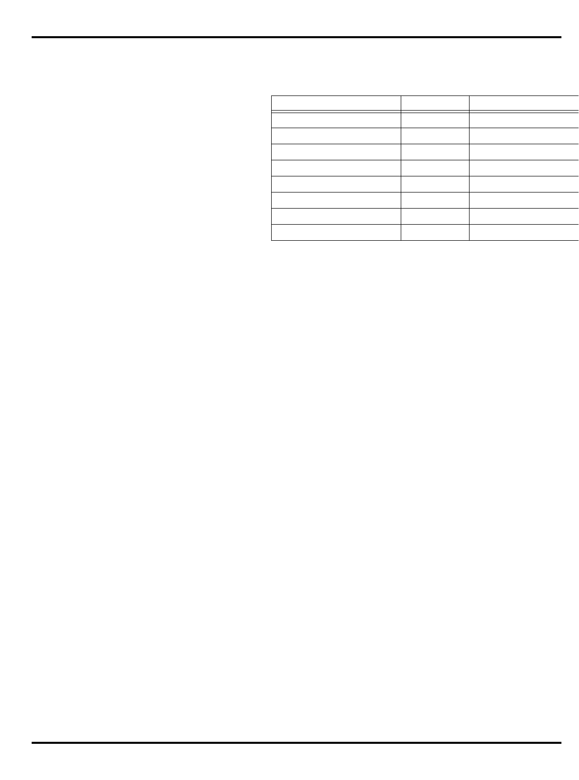
MACHINE INSTRUCTIONS REFERENCE APPENDIX A
A–5
address in the addressed field. For a big-endian machine, this is the
leftmost byte and contains the sign for a 2’s complement number; for a
little-endian machine, this is the rightmost byte. Note for R30xx CPUs, the
only sizes valid are word and smaller.s
The bytes within the addressed doubleword which are used can be
determined directly from the access type and the three low-order bits of the
address.
Jump and Branch Instructions
All jump and branch instructions have an architectural delay of exactly
one instruction. That is, the instruction immediately following a jump or
branch (that is, occupying the delay slot) is always executed while the
target instruction is being fetched from storage. A delay slot may not itself
be occupied by a jump or branch instruction; however, this error is not
detected and the results of such an operation are undefined.
If an exception or interrupt prevents the completion of a legal instruction
during a ranch delay slot, the hardware sets the
EPC
register to point at
the jump or branch instruction and an indication that the exception was
caused by the instruction in the delay slot. To continue the instruction
stream and re-execute the instruction that faulted, both the jump or
branch instruction and the instruction in the delay slot are reexecuted.
Because jump and branch instructions may be restarted after
exceptions or interrupts, they must be restartable. Therefore, when a
jump or branch instruction stores a return link value, register
31
(the
register in which the link is stored) may not be used as a source register.
Since instructions must be word-aligned, a
Jump Register
or
Jump
and Link Register
instruction must use a register containing a valid word
address. If the two low-order bits are not zero, an address exception will
occur when the jump target instruction is subsequently fetched.
Coprocessor Instructions
Coprocessors are alternate execution units, which have register files
separate from the CPU. The MIPS architecture provides a uniform
abstraction for a few coprocessor units, some of which are implemented in
any particular processor. The coprocessors may have two register spaces,
each space containing up to thirty-two registers. Coprocessor
computational instructions may alter registers in either space.
• The first space,
coprocessor general
registers
,
may be directly loaded
from memory and stored into memory, and their contents may be
transferred between the coprocessor and processor general registers.
• The second space,
coprocessor control
registers
,
may only have their
contents transferred directly between the coprocessor and the
processor general registers.
Access Type Mnemonic Value Meaning
DOUBLEWORD 7 8 bytes (64 bits)
SEPTIBYTE 6 7 bytes (56 bits)
SEXTIBYTE 5 6 bytes (48 bits)
QUINTIBYTE 4 5 bytes (40 bits)
WORD 3 4 bytes (32 bits)
TRIPLEBYTE 2 3 bytes (24 bits)
HALFWORD 1 2 bytes (16 bits)
BYTE 0 1 byte (8 bits)
Table A.6: Access Type Specifications for Loads/Store

APPENDIX A MACHINE INSTRUCTIONS REFERENCE
A–6
System control for all MIPS processors is implemented as Coprocessor
0 (CP0)
–
the System Control Coprocessor. It provides the processor
control, memory management, and exception handling functions. The
CP0 instructions are specific to each CPU and are documented with the
CPU-specific information.
If a system includes a Floating Point Unit for floating-point computation,
it is implemented as Coprocessor 1 (CP1). The FPU instructions are
documented in Appendix B.
System Control Coprocessor (CP0) Instructions
There are some special limitations imposed on operations involving CP0
that is incorporated within the CPU. Load and store instructions are not
valid for CP0 registers; the move to/from coprocessor instructions are the
only valid mechanism for writing to and reading from the CP0 registers.
Instruct Set Details
The following pages contain an alphabetical listing of the CPU
instructions for the R30xx family.

MACHINE INSTRUCTIONS REFERENCE APPENDIX A
A–7
Format:
ADD rd, rs, rt
Purpose:
Add two 32-bit values and produce a 32-bit result; arithmetic overflow causes an exception.
Description:
The word value in general register rt is added to the word value in general register rs and the result
word value is placed into general register rd.If the addition results in 32-bit 2’s complement
arithmetic overflow (carries out of bits 30 and 31 differ) then the destination register rd is not
modified and an integer overflow exception occurs.
Operation:
Exceptions:
Integer overflow exception
ADD
Add Word
31 2526 2021 1516
SPECIAL rs rt
655
rd 0 ADD
55 6
11 10 6 5 0
0 0 0 0 0 0 0 0 0 0 0 1 0 0 0 0 0
ADD
T: GPR[rd] ←GPR[rs] + GPR[rt]

APPENDIX A MACHINE INSTRUCTIONS REFERENCE
A–8
Format:
ADDI rt, rs, immediate
Description:
The 16-bit immediate is sign-extended and added to the contents of general register rs to form the
result. The result is placed into general register rt.
An overflow exception occurs if carries out of bits 30 and 31 differ (2’s complement overflow). The
destination register rt is not modified when an integer overflow exception occurs.
Operation:
Exceptions:
Integer overflow exception
ADDI Add Immediate Word
31 2526 2021 1516 0
ADDI rs rt immediate
655 16
0 0 1 0 0 0
ADDI
T: GPR [rt] ← GPR[rs] +(immediate15)16 || immediate15...0

MACHINE INSTRUCTIONS REFERENCE APPENDIX A
A–9
Format:
ADDIU rt, rs, immediate
Description:
The 16-bit immediate is sign-extended and added to the contents of general register rs to form the
result. The result is placed into general register rt. No integer overflow exception occurs under any
circumstances.
The only difference between this instruction and the ADDI instruction is that ADDIU never causes
an overflow exception.
Operation:
Exceptions:
None
ADDIU
Add Immediate Unsigned
31 2526 2021 1516 0
ADDIU rs rt immediate
655 16
0 0 1 0 0 1
ADDIU Word
T: temp ← GPR[rs] + (immediate15)48 || immediate15...0
if 32-bit-overflow (temp) then
GPR[rt] ← (temp31)32 || temp31...0
else
GPR[rt] ← temp

APPENDIX A MACHINE INSTRUCTIONS REFERENCE
A–10
Format:
ADDU rd, rs, rt
Description:
Add two 32-bit values and produce a 32-bit result; arithmetic overflow is ignored (does not cause
an exception).
The word value in general register rt is added to the word value in general register rs and the result
word value is placed into general register rd. ADDU differs from ADD only when an arithmetic
overflow occurs. If the addition results in 32-bit 2’s complement overflow (carries out of bits 30 and
31 differ), the result word value is placed into register rd and no exception occurs.
Operation:
Exceptions:
None
ADDU Add Unsigned Word
31 2526 2021 1516
SPECIAL rs rt
655
rd 0 ADDU
55 6
11 10 6 5 0
0 0 0 0 0 0 0 0 0 0 0 1 0 0 0 0 1
ADDU
T: GPR[rd] ←GPR[rs] + GPR[rt]

MACHINE INSTRUCTIONS REFERENCE APPENDIX A
A–11
Format:
AND rd, rs, rt
Description:
The contents of general register rs are combined with the contents of general register rt in a bit-wise
logical AND operation. The result is placed into general register rd.
Operation:
Exceptions:
None
AND
And
31 2526 2021 1516
SPECIAL rs rt
655
rd 0 AND
55 6
11 10 6 5 0
0 0 0 0 0 0 0 0 0 0 0 1 0 0 1 0 0
AND
T: GPR[rd] ← GPR[rs]
and GPR[rt]

APPENDIX A MACHINE INSTRUCTIONS REFERENCE
A–12
Format:
ANDI rt, rs, immediate
Description:
The 16-bit immediate is zero-extended and combined with the contents of general register rs in a bit-
wise logical AND operation. The result is placed into general register rt.
Operation:
Exceptions:
None
ANDI And Immediate
31 2526 2021 1516 0
ANDI rs rt immediate
655 16
0 0 1 1 0 0
ANDI
T: GPR[rt] ← 016 || (immediate and GPR[rs]15...0)

MACHINE INSTRUCTIONS REFERENCE APPENDIX A
A–13
Format:
BEQ rs, rt, offset
Description:
A branch target address is computed from the sum of the address of the instruction in the delay slot
and the 16-bit offset, shifted left two bits and sign-extended. The contents of general register rs and
the contents of general register rt are compared. If the two registers are equal, then the program
branches to the target address, with a delay of one instruction.
Operation:
Exceptions:
None
BEQ
Branch On Equal
BEQ
31 2526 2021 1516 0
BEQ rs rt offset
655 16
0 0 0 1 0 0
T: target ← (offset15)14 || offset || 02
condition ← (GPR[rs] = GPR[rt])
T+1: if condition then
PC ← PC + target
endif

APPENDIX A MACHINE INSTRUCTIONS REFERENCE
A–14
Format:
BGEZ rs, offset
Description:
A branch target address is computed from the sum of the address of the instruction in the delay slot
and the 16-bit offset, shifted left two bits and sign-extended. If the contents of general register rs
have the sign bit cleared, then the program branches to the target address, with a delay of one
instruction.
Operation:
Exceptions:
None
BGEZ
Or Equal To Zero
Branch On Greater Than
31 2526 2021 1516 0
REGIMM rs BGEZ offset
655 16
0 0 0 0 0 1 0 0 0 0 1
BGEZ
T: target ← (offset15)14 || offset || 02
condition ← (GPR[rs]31 = 0)
T+1: if condition then
PC ← PC + target
endif

MACHINE INSTRUCTIONS REFERENCE APPENDIX A
A–15
Format:
BGEZAL rs, offset
Description:
A branch target address is computed from the sum of the address of the instruction in the delay slot
and the 16-bit offset, shifted left two bits and sign-extended. Unconditionally, the address of the
instruction after the delay slot is placed in the link register, r31. If the contents of general register
rs have the sign bit cleared, then the program branches to the target address, with a delay of one
instruction.
General register rs may not be general register 31, because such an instruction is not restartable. An
attempt to execute this instruction is not trapped, however.
Operation:
Exceptions:
None
BGEZAL Or Equal To Zero And Link
Branch On Greater Than
31 2526 2021 1516 0
REGIMM rs BGEZAL offset
655 16
0 0 0 0 0 1 1 0 0 0 1
BGEZAL
T: target ← (offset15)14 || offset || 02
condition ← (GPR[rs]31 = 0)
T+1: if condition then
PC ← PC + target
endif
GPR[31] ← PC + 8

APPENDIX A MACHINE INSTRUCTIONS REFERENCE
A–16
Format:
BGTZ rs, offset
Description:
A branch target address is computed from the sum of the address of the instruction in the delay slot
and the 16-bit offset, shifted left two bits and sign-extended. The contents of general register rs are
compared to zero. If the contents of general register rs have the sign bit cleared and are not equal
to zero, then the program branches to the target address, with a delay of one instruction.
Operation:
Exceptions:
None
BGTZ
Branch On Greater Than Zero
31 2526 2021 1516 0
BGTZ rs 0 offset
655 16
0 0 0 1 1 1 0 0 0 0 0
BGTZ
T: target ← (offset15)14 || offset || 02
condition ← (GPR[rs]31 = 0) and (GPR[rs] ≠ 032)
T+1: if condition then
PC ← PC + target
endif

MACHINE INSTRUCTIONS REFERENCE APPENDIX A
A–17
Format:
BLEZ rs, offset
Description:
A branch target address is computed from the sum of the address of the instruction in the delay slot
and the 16-bit offset, shifted left two bits and sign-extended. The contents of general register rs are
compared to zero. If the contents of general register rs have the sign bit set, or are equal to zero,
then the program branches to the target address, with a delay of one instruction.
Operation:
Exceptions:
None
BLEZ
Branch on Less Than
31 2526 2021 1516 0
BLEZ rs 0 offset
655 16
Or Equal To Zero
0 0 0 1 1 0 0 0 0 0 0
BLEZ
T: target ← (offset15)14 || offset || 02
T+1: if condition then
PC ← PC + target
endif
condition ← (GPR[rs]31 = 1) or (GPR[rs] = 032)

APPENDIX A MACHINE INSTRUCTIONS REFERENCE
A–18
Format:
BLTZ rs, offset
Description:
A branch target address is computed from the sum of the address of the instruction in the delay slot
and the 16-bit offset, shifted left two bits and sign-extended. If the contents of general register rs
have the sign bit set, then the program branches to the target address, with a delay of one
instruction.
Operation:
Exceptions:
None
BLTZ
Branch On Less Than Zero
31 2526 2021 1516 0
REGIMM rs BLTZ offset
655 16
0 0 0 0 0 1 0 0 0 0 0
BLTZ
T: target ← (offset15)14 || offset || 02
condition ← (GPR[rs]31 = 1)
T+1: if condition then
PC ← PC + target
endif

MACHINE INSTRUCTIONS REFERENCE APPENDIX A
A–19
Format:
BLTZAL rs, offset
Description:
A branch target address is computed from the sum of the address of the instruction in the delay slot
and the 16-bit offset, shifted left two bits and sign-extended. Unconditionally, the address of the
instruction after the delay slot is placed in the link register, r31. If the contents of general register
rs have the sign bit set, then the program branches to the target address, with a delay of one
instruction.
General register rs may not be general register 31, because such an instruction is not restartable. An
attempt to execute this instruction with register 31 specified as rs is not trapped, however.
Operation:
Exceptions:
None
BLTZAL Than Zero And Link
Branch On Less
31 2526 2021 1516 0
REGIMM rs BLTZAL offset
655 16
0 0 0 0 0 1 1 0 0 0 0
BLTZAL
T: target ← (offset15)14 || offset || 02
condition ← (GPR[rs]31 = 1)
T+1: if condition then
PC ← PC + target
endif
GPR[31] ← PC + 8

APPENDIX A MACHINE INSTRUCTIONS REFERENCE
A–20
Format:
BNE rs, rt, offset
Description:
A branch target address is computed from the sum of the address of the instruction in the delay slot
and the 16-bit offset, shifted left two bits and sign-extended. The contents of general register rs and
the contents of general register rt are compared. If the two registers are not equal, then the program
branches to the target address, with a delay of one instruction.
Operation:
Exceptions:
None
BNE
Branch On Not Equal
31 2526 2021 1516 0
BNE rs rt offset
655 16
0 0 0 1 0 1
BNE
T: target ← (offset15)14 || offset || 02
condition ← (GPR[rs] ≠ GPR[rt])
T+1: if condition then
PC ← PC + target

MACHINE INSTRUCTIONS REFERENCE APPENDIX A
A–21
Format:
BREAK
Description:
A breakpoint trap occurs, immediately and unconditionally transferring control to the exception
handler.
The code field is available for use as software parameters, but is retrieved by the exception handler
only by loading the contents of the memory word containing the instruction.
Operation:
Exceptions:
Breakpoint exception
BREAK
Breakpoint
31 2526
SPECIAL
6
0
BREAKcode
6 5
6
20
0 0 0 0 0 0 0 0 1 1 0 1
BREAK
T: BreakpointException
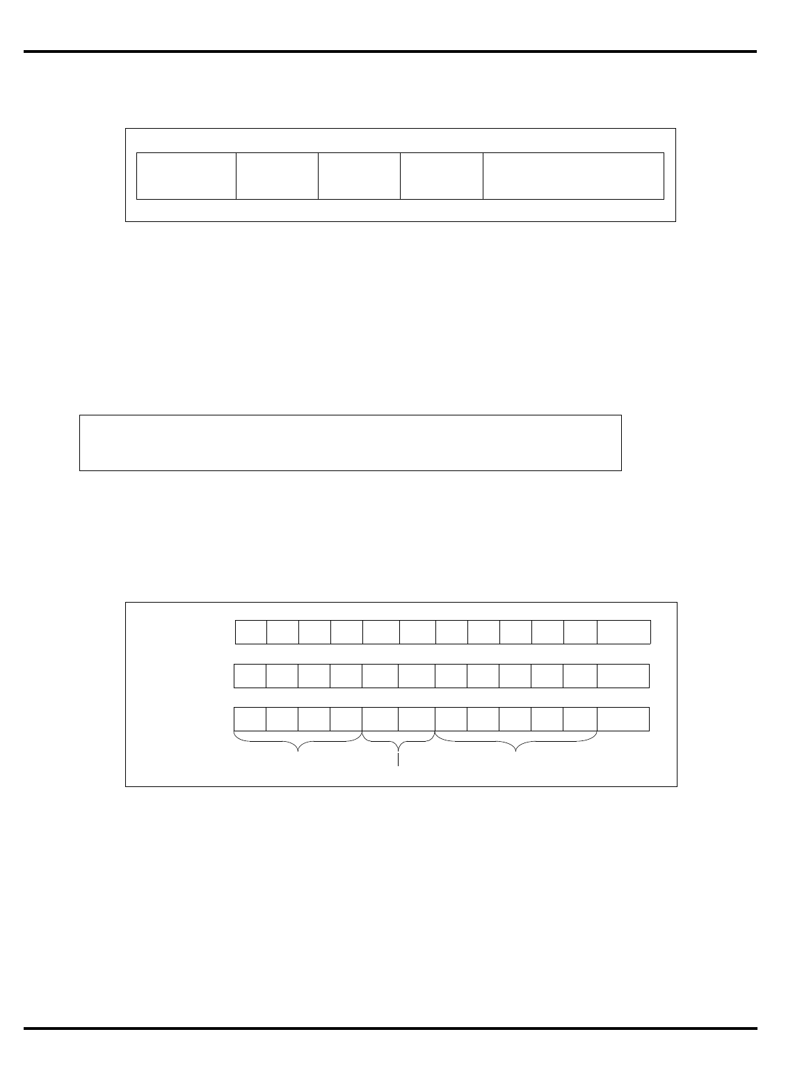
APPENDIX A MACHINE INSTRUCTIONS REFERENCE
A–22
Format:
CFCz rt, rd
Description:
The contents of coprocessor control register rd of coprocessor unit z are loaded into general register
rt.
This instruction is not valid for CP0.
Operation:
Exceptions:
Coprocessor unusable exception
*Opcode Bit Encoding:
Coprocessor
CFCz
11
Move Control From
31 2526 2021 1516
COPz CF rt
655
rd 0
5
11 10 0
0 1 0 0 x x* 0 0 0 1 0 0 0 0 0 0
CFCz
T: data ← CCR[z,rd]
T+1: GPR[rt] ← data
CFCz 000011
31 30 29 28 27 26
Bit # 25 0
CFC1 00100
24 23 22 21
000101
31 30 29 28 27 26
Bit # 25 0
CFC2 00100
24 23 22 21
000111
31 30 29 28 27 26
Bit # 25 0
CFC3 00100
24 23 22 21
Coprocessor Unit Number
Coprocessor SuboperationOpcode
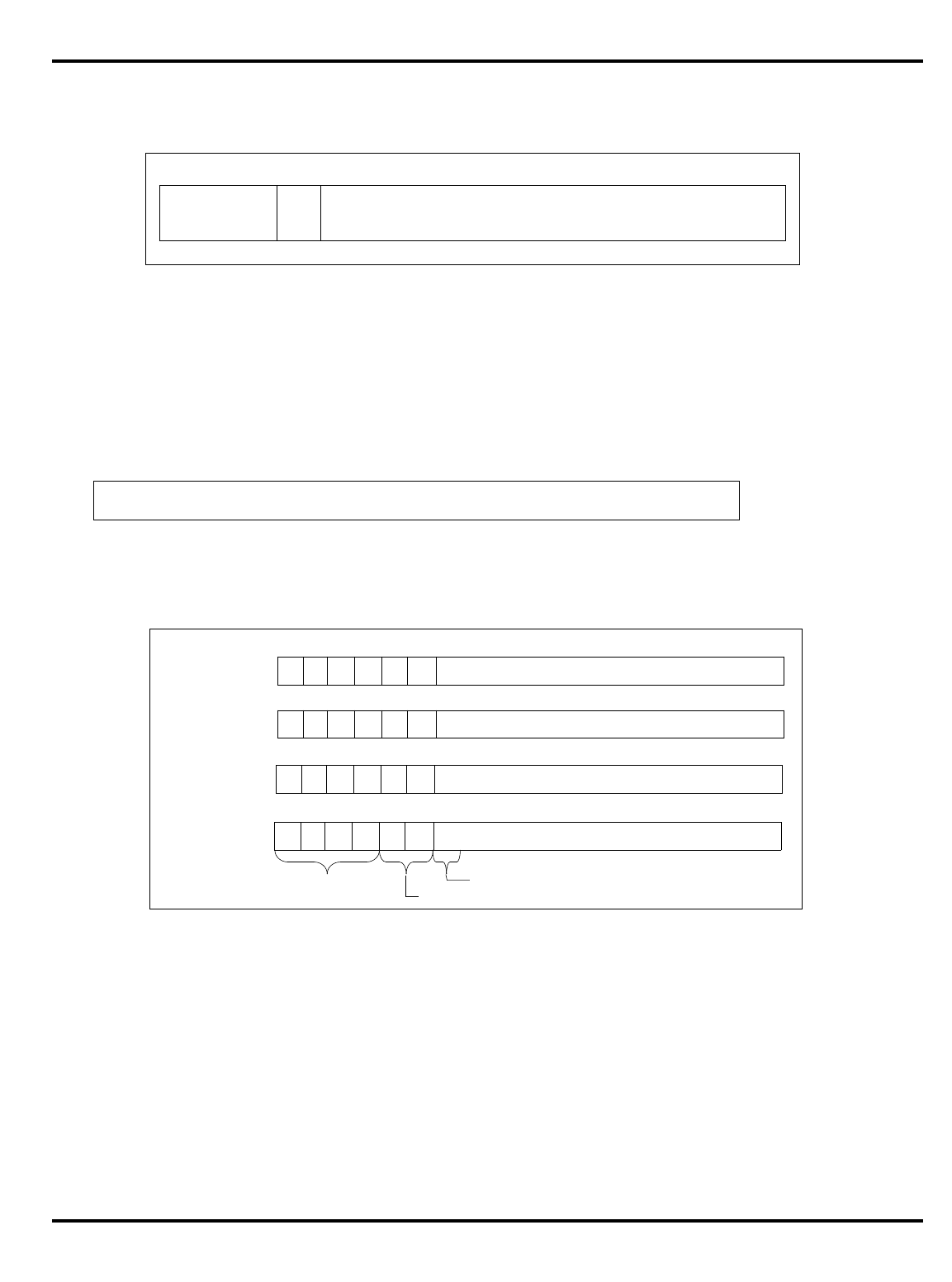
MACHINE INSTRUCTIONS REFERENCE APPENDIX A
A–23
Format:
COPz cofun
Description:
A coprocessor operation is performed. The operation may specify and reference internal
coprocessor registers, and may change the state of the coprocessor condition line, but does not
modify state within the processor or the cache/memory system. Details of coprocessor operations
are contained in other appendices.
Operation:
Exceptions:
Coprocessor unusable exception
Coprocessor interrupt or Floating-Point Exception (CP1 only for some processors)
*Opcode Bit Encoding:
COPz
Coprocessor Operation
31 25 2426
COPz
6
0
cofun
25
1
CO
0 1 0 0 x x* 1
COPz
CoprocessorOperation (z, cofun)
COPz 000001
31 30 29 28 27 26
Bit # 25 0
C0P0 1
CO sub-opcode (see end of Appendix A)
000011
31 30 29 28 27 26
Bit # 25 0
C0P1 1
000101
31 30 29 28 27 26
Bit # 25 0
C0P2 1
000111
31 30 29 28 27 26
Bit # 25 0
C0P3 1
Coprocessor Unit Number
Opcode

APPENDIX A MACHINE INSTRUCTIONS REFERENCE
A–24
Format:
CTCz rt, rd
Description:
The contents of general register rt are loaded into control register rd of coprocessor unit z.
This instruction is not valid for CP0.
Operation:
Exceptions:
Coprocessor unusable
CTCz
11
Move Control to Coprocessor
31 2526 2021 1516
COPz CT rt
655
rd 0
5
11 10 0
0 1 0 0 z z * 0 0 1 1 0 0 0 0 0 0 0 0 0 0 0 0
CTCz
T: data ← GPR[rt]
T + 1: CCR[z,rd] ← data

MACHINE INSTRUCTIONS REFERENCE APPENDIX A
A–25
Format:
DIV rs, rt
Description:
The contents of general register rs are divided by the contents of general register rt, treating both
operands as 2’s complement values. No overflow exception occurs under any circumstances, and
the result of this operation is undefined when the divisor is zero.
This instruction is typically followed by additional instructions to check for a zero divisor and for
overflow.
When the operation completes, the quotient word of the double result is loaded into special register
LO, and the remainder word of the double result is loaded into special register HI.
If either of the two preceding instructions is MFHI or MFLO, the results of those instructions are
undefined. Correct operation requires separating reads of HI or LO from writes by two or more
instructions.
DIV
Divide Word
31 2526 2021 1516 0
rs rt
655
65
10 6
SPECIAL 0DIV
0 0 0 0 0 0 0 0 0 0 0 0 0 0 0 0 0 1 1 0 1 0
DIV

APPENDIX A MACHINE INSTRUCTIONS REFERENCE
A–26
Operation:
Exceptions:
None
DIV Divide Word (Continued) DIV
← undefined
← undefined
← undefined
HI ← GPR[rs] mod GPR[rt]
T–2: LO ← undefined
T: LO ← GPR[rs] div GPR[rt]
HI
T–1: LO
HI

MACHINE INSTRUCTIONS REFERENCE APPENDIX A
A–27
Format:
DIVU rs, rt
Description:
The contents of general register rs are divided by the contents of general register rt, treating both
operands as unsigned values. No integer overflow exception occurs under any circumstances, and
the result of this operation is undefined when the divisor is zero.
On processors with 64-bit registers the operands must be valid sign-extended 32-bit values. If they
are not, the result is undefined.
This instruction is typically followed by additional instructions to check for a zero divisor.
When the operation completes, the quotient word of the double result is loaded into special register
LO, and the remainder word of the double result is loaded into special register HI.
If either of the two preceding instructions is MFHI or MFLO, the results of those instructions are
undefined. Correct operation requires separating reads of HI or LO from writes by two or more
instructions.
Operation:
Exceptions:
None
DIVU Divide Unsigned Word
31 2526 2021 1516 0
rs rt
655
65
10 6
SPECIAL 0 DIVU
0 0 0 0 0 0 0 0 0 0 0 0 0 0 0 0 0 1 1 0 1 1
DIVU
← undefined
← undefined
← undefined
HI ← (0 || GPR[rs]) mod
(0 || GPR[rt])
T–2: LO ← undefined
T: LO ← (0 || GPR[rs]) div
(0 || GPR[rt])
HI
T–1: LO
HI

APPENDIX A MACHINE INSTRUCTIONS REFERENCE
A–28
Format:
J target
Description:
The 26-bit target address is shifted left two bits and combined with the high-order bits of the
address of the delay slot. The program unconditionally jumps to this calculated address with a
delay of one instruction.
Operation:
Exceptions:
None
JJump
31 2526
J
6
0
target
26
0 0 0 0 1 0
J
T: temp ← target
T+1: PC ← PC31...28 || temp || 02

MACHINE INSTRUCTIONS REFERENCE APPENDIX A
A–29
Format:
JAL target
Description:
The 26-bit target address is shifted left two bits and combined with the high-order bits of the
address of the delay slot. The program unconditionally jumps to this calculated address with a
delay of one instruction. The address of the instruction after the delay slot is placed in the link
register, r31.
Operation:
Exceptions:
None
JAL Jump And Link
31 2526
JAL
6
0
target
26
0 0 0 0 1 1
JAL
GPR[31] ← PC + 8
T: temp ← target
T+1: PC ← PC 31...28 || temp || 02

APPENDIX A MACHINE INSTRUCTIONS REFERENCE
A–30
Format:
JALR rs
JALR rd, rs
Description:
The program unconditionally jumps to the address contained in general register rs, with a delay of
one instruction. The address of the instruction after the delay slot is placed in general register rd.
The default value of rd, if omitted in the assembly language instruction, is 31.
Register specifiers rs and rd may not be equal, because such an instruction does not have the same
effect when re-executed. However, an attempt to execute this instruction is not trapped, and the
result of executing such an instruction is undefined.
A Jump and Link Register instruction that uses a register whose low-order 2 bits are non-zero, or
specifies an address outside of the accessible address space, causes an Address Error Exception
when the jump is executed. The Exception PC points to the location of the Jump instruction causing
the error, and the instruction in the delay slot is not executed. If desired, system software can
emulate the delay instruction and advance the PC to the target of the jump before delivering the
exception to the user program.
Operation:
Exceptions:
Address error exception
JALR Jump And Link Register
31 2526 2021 1516
SPECIAL rs
655
rd JALR
55 6
11 10 6 5 0
0 0 1 0 0 10 0 0 0 00 0 0 0 00 0 0 0 0 0
JALR
T: temp ← GPR [rs]
GPR[rd] ← PC + 8
T+1: PC ← PC + target

MACHINE INSTRUCTIONS REFERENCE APPENDIX A
A–31
Format:
JR rs
Description:
The program unconditionally jumps to the address contained in general register rs, with a delay of
one instruction.
Since instructions must be word-aligned, a Jump Register instruction must specify a target register
(rs) whose two low-order bits are zero. If these low-order bits are not zero, an address exception
will occur when the jump target instruction is subsequently fetched.
Operation:
Exceptions:
Address error exception
JR
Jump Register
21 2031 2526
SPECIAL
6
0
JRrs
6 5
515 6
0 0 0 0 0 0 0 0 0 0 0 0 0 0 0 0 0 0 0 0 0 0 0 1 0 0 0
JR
T: temp ← GPR[rs]
T+1: PC ← PC + target

APPENDIX A MACHINE INSTRUCTIONS REFERENCE
A–32
Format:
LB rt, offset(base)
Description:
The 16-bit offset is sign-extended and added to the contents of general register base to form a virtual
address. The contents of the byte at the memory location specified by the effective address are sign-
extended and loaded into general register rt.
Operation:
Exceptions:
TLB refill exception
TLB invalid exception
Bus error exception
Address error exception
LB Load Byte
31 2526 2021 1516 0
LB base rt offset
655 16
1 0 0 0 0 0
LB
T: vAddr ← ((offset15)16 || offset15...0) + GPR[base]
(pAddr, uncached) ← AddressTranslation (vAddr, DATA)
mem ← LoadMemory (uncached, BYTE, pAddr, vAddr, DATA)
byte ← vAddr1...0 xor BigEndianCPU2
GPR[rt]
← ( mem7+8* byte)24||mem7+8*byte..8*byte
pAddr ← pAddrPSIZE – 1 ... 2 || (pAddr1...0 xor ReverseEndian2)
T+1:

MACHINE INSTRUCTIONS REFERENCE APPENDIX A
A–33
Format:
LBU rt, offset(base)
Description:
The 16-bit offset is sign-extended and added to the contents of general register base to form a virtual
address. The contents of the byte at the memory location specified by the effective address are zero-
extended and loaded into general register rt.
Operation:
Exceptions:
TLB refill exception
TLB invalid exception
Bus error exception
Address error exception
LBU
Load Byte Unsigned
31 2526 2021 1516 0
LBU base rt offset
655 16
1 0 0 1 0 0
LBU
T: vAddr ← ((offset15)16 || offset15...0) + GPR[base]
(pAddr, uncached) ← AddressTranslation (vAddr, DATA)
pAddr ← pAddrPSIZE – 1 ... 2 || (pAddr1...0 xor
ReverseEndian2)
mem ← LoadMemory (uncached, BYTE, pAddr, vAddr, DATA)
byte ← vAddr1...0 xor BigEndianCPU2
T+1: GPR[rt]
← 024 || mem7+8* byte...8* byte

APPENDIX A MACHINE INSTRUCTIONS REFERENCE
A–34
Format:
LH rt, offset(base)
Description:
The 16-bit offset is sign-extended and added to the contents of general register base to form a virtual
address. The contents of the halfword at the memory location specified by the effective address are
sign-extended and loaded into general register rt.
If the least-significant bit of the effective address is non-zero, an address error exception occurs.
Operation:
Exceptions:
TLB refill exception
TLB invalid exception
Bus error exception
Address error exception
LH Load Halfword
31 2526 2021 1516 0
LH base rt offset
655 16
1 0 0 0 0 1
LH
T: vAddr ← ((offset15)16 || offset15...0) + GPR[base]
(pAddr, uncached) ← AddressTranslation (vAddr, DATA)
byte ← vAddr1...0 xor (BigEndianCPU || 0)
T+1: GPR[rt] ← (mem15+8*byte)16 || mem15+8*byte...8* byte
pAddr ← pAddrPSIZE – 1...2 || (pAddr1...0 xor (ReverseEndian || 0))
mem ← LoadMemory (uncached, HALFWORD, pAddr, vAddr, DATA)

MACHINE INSTRUCTIONS REFERENCE APPENDIX A
A–35
Format:
LHU rt, offset(base)
Description:
The 16-bit offset is sign-extended and added to the contents of general register base to form a virtual
address. The contents of the halfword at the memory location specified by the effective address are
zero-extended and loaded into general register rt.
If the least-significant bit of the effective address is non-zero, an address error exception occurs.
Operation:
Exceptions:
TLB refill exception TLB invalid exception
Bus Error exception Address error exception
LHU
Load Halfword Unsigned
31 2526 2021 1516 0
LHU base rt offset
655 16
1 0 0 1 0 1
LHU
T: vAddr ← ((offset15)16 || offset15...0) + GPR[base]
(pAddr, uncached) ← AddressTranslation (vAddr, DATA)
mem ← LoadMemory (uncached, HALFWORD, pAddr, vAddr, DATA)
byte ← vAddr1...0 xor (BigEndianCPU || 0)
T+1: GPR[rt] ← 016 || mem15+8*byte...8*byte
pAddr ← pAddrPSIZE – 1...2 || (pAddr1...0 xor (ReverseEndian || 0))

APPENDIX A MACHINE INSTRUCTIONS REFERENCE
A–36
Format:
LUI rt, immediate
Description:
The 16-bit immediate is shifted left 16 bits and concatenated with 16 bits of low-order zeros. The
32-bit result is then placed into general register rt. If rt is a 64-bit register, then the result is sign
extended.
Operation:
GPR[rt] ← immediate || 016
Exceptions:
None
LUI Load Upper Immediate
31 2526 2021 1516 0
LUI rt immediate
655 16
0 0 1 1 1 1
LUI
0
0 0 0 0 0

MACHINE INSTRUCTIONS REFERENCE APPENDIX A
A–37
Format:
LW rt, offset(base)
Description:
The 16-bit offset is sign-extended and added to the contents of general register base to form a virtual
address. The contents of the word at the memory location specified by the effective address are
loaded into general register rt. In 64-bit mode, the loaded word is sign-extended.
If either of the two least-significant bits of the effective address is non-zero, an address error
exception occurs.
Operation:
Exceptions:
TLB refill exception
TLB invalid exception
Bus error exception
Address error exception
LW
Load Word
31 2526 2021 1516 0
LW base rt offset
655 16
1 0 0 0 1 1
LW
T: vAddr ← ((offset15)16 || offset15...0) + GPR[base]
(pAddr, uncached) ← AddressTranslation (vAddr, DATA)
mem ← LoadMemory (uncached, WORD, pAddr, vAddr, DATA)
T+1: GPR[rt] ← mem

APPENDIX A MACHINE INSTRUCTIONS REFERENCE
A–38
Format:
LWCz rt, offset(base)
Description:
The 16-bit offset is sign-extended and added to the contents of general register base to form a virtual
address. The processor reads a word from the addressed memory location, and makes the data
available to coprocessor unit z.
The manner in which each coprocessor uses the data is defined by the individual coprocessor
specifications.
If either of the two least-significant bits of the effective address is non-zero, an address error
exception occurs.
This instruction is not valid for use with CP0.
LWCz Load Word To Coprocessor
31 2526 2021 1516 0
LWCz base rt offset
655 16
1 1 0 0 x x*
LWCz
MACHINE INSTRUCTIONS REFERENCE APPENDIX A
A–39
Operation:
Exceptions:
TLB refill exception
TLB invalid exception
Bus error exception
Address error exception
Coprocessor unusable exception
Opcode Bit Encoding:
(continued)
LWCz Load Word To Coprocessor LWCz
T: vAddr ← ((offset15)16 || offset15...0) + GPR[base]
(pAddr, uncached) ← AddressTranslation (vAddr, DATA)
T+1: COPzLW (rt, mem)
byte ← vAddr1...0
mem ← LoadMemory (uncached, DOUBLEWORD, pAddr, vAddr, DATA)
LWCz 100011
31 30 29 28 27 26
Bit # 0
LWC1
100101
31 30 29 28 27 26
Bit # 0
LWC2
100111
31 30 29 28 27 26
Bit # 0
LWC3
Coprocessor Unit Number
Opcode
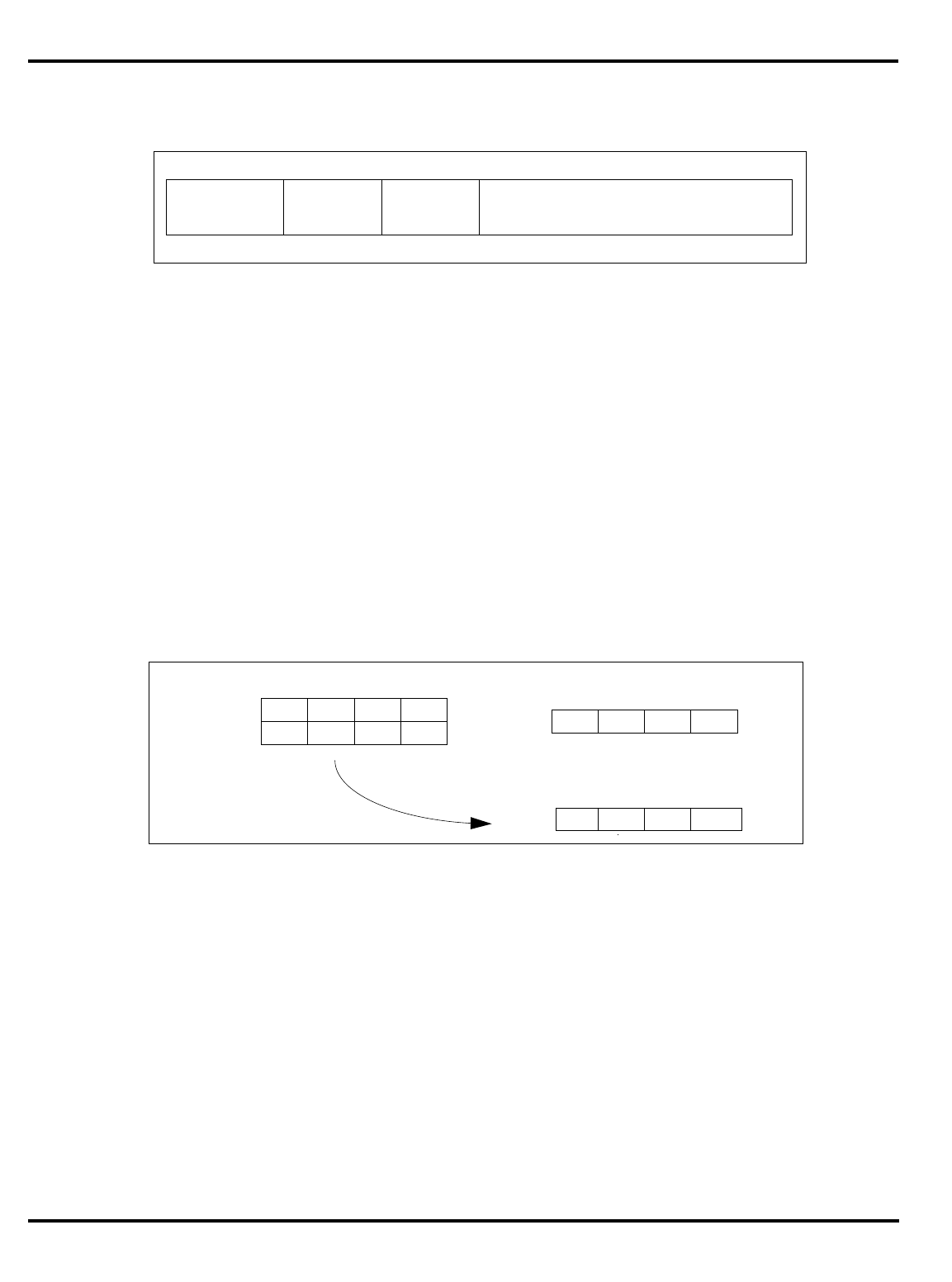
APPENDIX A MACHINE INSTRUCTIONS REFERENCE
A–40
Format:
LWL rt, offset(base)
Description:
This instruction can be used in combination with the LWR instruction to load a register with four
consecutive bytes from memory, when the bytes cross a word boundary. LWL loads the left
portion of the register with the appropriate part of the high-order word; LWR loads the right
portion of the register with the appropriate part of the low-order word.
The LWL instruction adds its sign-extended 16-bit offset to the contents of general register base to
form a virtual address which can specify an arbitrary byte. It reads bytes only from the word in
memory which contains the specified starting byte. From one to four bytes will be loaded,
depending on the starting byte specified.
Conceptually, it starts at the specified byte in memory and loads that byte into the high-order (left-
most) byte of the register; then it loads bytes from memory into the register until it reaches the low-
order byte of the word in memory. The least-significant (right-most) byte(s) of the register will not
be changed.
LWL Load Word Left
31 2526 2021 1516 0
LWL base rt offset
655 16
1 0 0 0 1 0
LWL
address 0
address 4
0123
4567
memory
ABCD
register
$24
(big-endian)
before
after
123D
$24
LWL $24,1($0)

MACHINE INSTRUCTIONS REFERENCE APPENDIX A
A–41
The contents of general register rt are internally bypassed within the processor so that no NOP is
needed between an immediately preceding load instruction which specifies register rt and a
following LWL (or LWR) instruction which also specifies register rt.
No address exceptions due to alignment are possible.
Operation:
(continued)
LWL Load Word Left LWL
endif
T: vAddr ← ((offset15)16 || offset15...0) + GPR[base]
(pAddr, uncached) ← AddressTranslation (vAddr, DATA)
pAddr ← pAddrPSIZE–1...2 || (pAddr1...0 xor ReverseEndian2)
pAddr ← pAddrPSIZE–31...2 || 02
GPR[rt] ← mem7+8*byte...0 || GPR[rt]23–8*byte...0
mem ← LoadMemory (uncached, byte, pAddr, vAddr, DATA)
if BigEndianMem = 0 then
byte ← vAddr1...0 xor BigEndianCPU2
APPENDIX A MACHINE INSTRUCTIONS REFERENCE
A–42
Given a doubleword in a register and a doubleword in memory, the operation of LWL is as follows:
LEM Little-endian memory (BigEndianMem = 0)
BEM BigEndianMem = 1
Type AccessType sent to memory
Offset pAddr2...0 sent to memory
Ssign-extend of destination31
Exceptions:
TLB refill exception
TLB invalid exception
Bus error exception
Address error exception
LWL LWL
(continued)
Load Word Left
LWL
ACDB
Register
IKLJ
Memory
EGHF
MOPN
0 SSSSPFGH 0 0 7 SSSSI JKL 3 4 0
1 SSSSOPGH 1 0 6 SSSSJKL H 2 4 1
2 SSSSNOPH 2 0 5 SSSSKLGH 1 4 2
3 SSSSMNOP 3 0 4 SSSSLFGH 0 4 3
4 SSSSLFGH 0 4 3 SSSSMNOP 3 0 4
5 SSSSKLGH 1 4 2 SSSSNOPH 2 0 5
6 SSSSJ KLH 2 4 1 SSSSOPGH 1 0 6
7 SSSSI JKL 3 4 0 SSSSPFGH 0 0 7
BigEndianCPU = 0
vAddr2..0 destination destination
type type offset
offset
BigEndianCPU = 1
LEM BEM LEM BEM
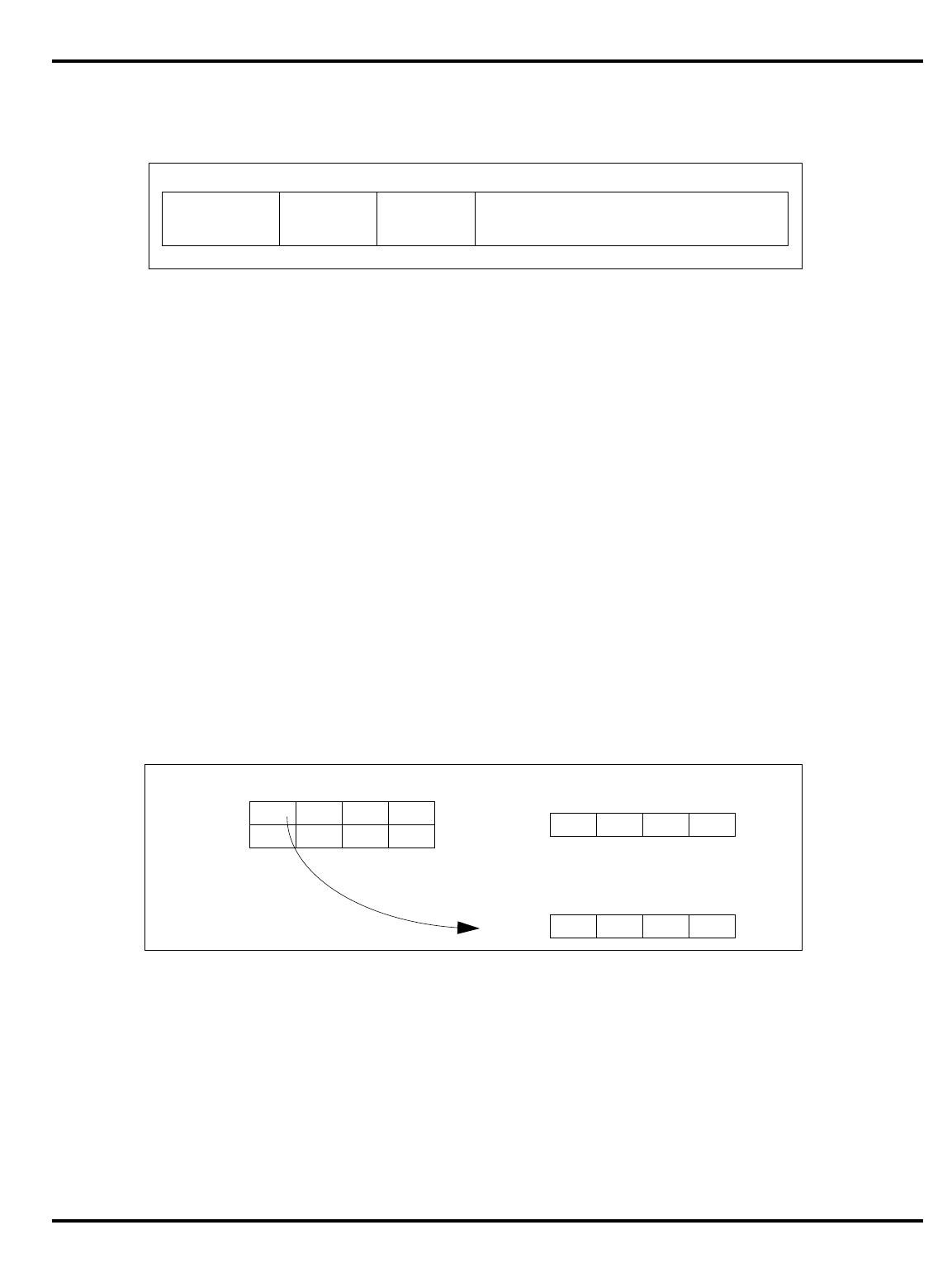
MACHINE INSTRUCTIONS REFERENCE APPENDIX A
A–43
Format:
LWR rt, offset(base)
Description:
This instruction can be used in combination with the LWL instruction to load a register with four
consecutive bytes from memory, when the bytes cross a word boundary. LWR loads the right
portion of the destination register rt with the appropriate part of the low-order word; LWL loads
the left portion of the register with the appropriate part of the high-order word.
The LWR instruction adds its sign-extended 16-bit offset to the contents of general register base to
form a virtual address which can specify an arbitrary byte. It loads bytes only from the word in
memory which contains the specified starting byte. From one to four bytes will be merged into the
destination register rt, depending on the starting byte specified.
Conceptually, it starts at the specified byte in memory and loads that byte into the low-order (right-
most) byte of the register; then it loads bytes from memory into the register until it reaches the high-
order byte of the word in memory. The most significant (left-most) byte(s) of the register will not
be changed
The contents of general register rt are internally bypassed within the processor so that no NOP is
needed between an immediately preceding load instruction which specifies register rt and a
following LWR (or LWL) instruction which also specifies register rt.
No address exceptions due to alignment are possible.
LWR
Load Word Right
31 2526 2021 1516 0
LWR base rt offset
655 16
1 0 0 1 1 0
LWR
address 0
address 4
0123
4567 ABCD
register
LWR $24,4($0)
$24
memory
(big-endian)
before
after
ABC4
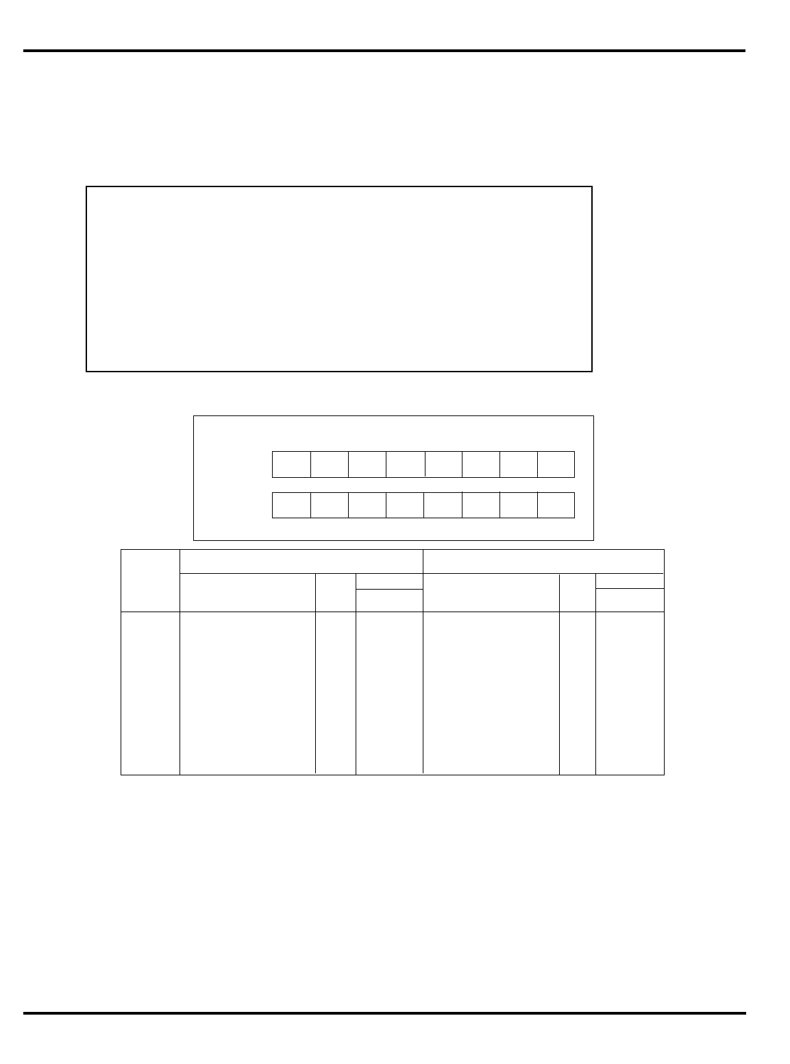
APPENDIX A MACHINE INSTRUCTIONS REFERENCE
A–44
Operation:
T: vAddr ← ((offset15)16 || offset15..0) + GPR[base]
(pAddr, uncached) ← AddressTranslation (vAddr, DATA)
pAddr ← pAddrPSIZE–1..2 || (pAddr1..0 xor ReverseEndian2)
if BigEndianMem = 0 then
pAddr ← pAddrPSIZE–31..2 || 02
endif
byte ← vAddr1..0
xor BigEndianCPU2
mem ← LoadMemory (uncached, byte, pAddr, vAddr, DATA)
GPR[rt] ← mem31..32-8*byte || GPR[rt]31–8*byte..0
Given a word in a register and a word in memory, the operation of LWR is as follows:
LEM Little-endian memory (BigEndianMem = 0)
BEM BigEndianMem = 1
Type AccessType sent to memory
Offset pAddr2...0 sent to memory
Ssign-extend of destination31
Xunchanged or sign-extend of destination31
Exceptions:
TLB refill exception
TLB invalid exception
Bus error exception
Address error exception
(continued) LWR
Load Word Right
LWR
LWR
ACDB
Register
IKLJ
Memory
EGHF
MOPN
0 SSSSMNOP 0 0 4 XXXXEFGI 0 7 0
1 XXXX EMNO 1 1 4 XXXXEFI J 1 6 0
2 XXXXEFMN 2 2 4 XXXXEI J K 2 5 0
3 XXXXEFGM 3 3 4 SSSSI JKL 3 4 0
4 SSSSI JKL 0 4 0 XXXXEFGM 0 3 4
5 XXXXEI JK 1 5 0 XXXXEFMN 1 2 4
6 XXXXEFI J 2 6 0 XXXXEMNO 2 1 4
7 XXXXEFGI 3 7 0 SSSSMNOP 3 0 4
BigEndianCPU = 0
vAddr2..0 destination destination
type type offset
offset
BigEndianCPU = 1
LEM BEM LEM BEM
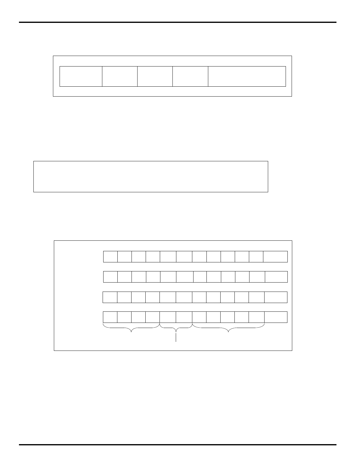
MACHINE INSTRUCTIONS REFERENCE APPENDIX A
A–45
Format:
MFCz rt, rd
Description:
The contents of coprocessor register rd of coprocessor z are loaded into general register rt.
Operation:
Exceptions:
Coprocessor unusable exception
Reserved instruction exception (coprocessor 3)
Opcode Bit Encoding:
MFCz
11
Move From Coprocessor
31 2526 2021 1516
COPz MF rt
655
rd 0
5
11 10 0
0 1 0 0 x x* 0 0 0 0 0 0 0 0 0 0 0 0 0 0 0 0
MFCz
T: data ← CPR[z,rd]
T+1: GPR[rt] ← data
MFCz
000011
31 30 29 28 27 26
Bit # 25 0
MFC1 00000
24 23 22 21
000101
31 30 29 28 27 26
Bit # 25 0
MFC2 00000
24 23 22 21
000111
31 30 29 28 27 26
Bit # 25 0
MFC3 00000
24 23 22 21
Coprocessor Suboperation
000001
31 30 29 28 27 26
Bit # 25 0
MFC0 00000
24 23 22 21
Coprocessor Unit Number
Opcode

APPENDIX A MACHINE INSTRUCTIONS REFERENCE
A–46
Format:
MFHI rd
Description:
The contents of special register HI are loaded into general register rd.
To ensure proper operation in the event of interruptions, the two instructions which follow a MFHI
instruction may not be any of the instructions which modify the HI register: MULT, MULTU, DIV,
DIVU, MTHI.
Operation:
Exceptions:
None
MFHI
0
Move From HI
31 2526 1516 0
rd
6105
65
6
SPECIAL MFHI0
5
11 10
0 0 0 0 0 0 0 0 0 0 0 0 0 0 0 0 0 0 0 0 0 0 1 0 0 0 0
MFHI
T: GPR[rd] ← HI

MACHINE INSTRUCTIONS REFERENCE APPENDIX A
A–47
MFLO rd
Description:
The contents of special register LO are loaded into general register rd.
To ensure proper operation in the event of interruptions, the two instructions which follow a MFLO
instruction may not be any of the instructions which modify the LO register: MULT, MULTU, DIV,
DIVU, MTLO.
Operation:
Exceptions:
None
MFLO
Move From Lo
0
31 2526 1516 0
rd
6105
65
6
SPECIAL MFLO0
5
11 10
0 0 0 0 0 0 0 0 0 0 0 0 0 0 0 0 0 0 0 0 0 0 1 0 0 1 0
MFLO
T: GPR[rd] ← LO
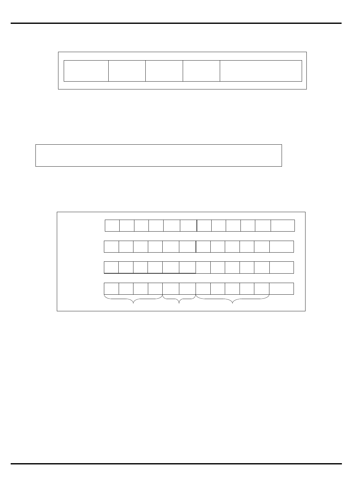
APPENDIX A MACHINE INSTRUCTIONS REFERENCE
A–48
Format:
MTCz rt, rd
Description:
The contents of general register rt are loaded into coprocessor register rd of coprocessor z.
Operation:
Exceptions:
Coprocessor unusable exception
*Opcode Bit Encoding:
MTCz
11
Move To Coprocessor
31 2526 2021 1516
COPz MT rt
655
rd 0
5
11 10 0
0 1 0 0 x x* 0 0 1 0 0 0 0 0 0 0 0 0 0 0 0 0
MTCz
32 T: data ← GPR[rt]
T+1: CPR[z,rd] ← data
MTCz
000011
31 30 29 28 27 26
Bit # 25 0
C0P1 01000
24 23 22 21
000101
31 30 29 28 27 26
Bit # 25 0
C0P2 01000
24 23 22 21
000111
31 30 29 28 27 26
Bit # 25 0
C0P3 01000
24 23 22 21
Coprocessor Suboperation
000001
31 30 29 28 27 26
Bit # 25 0
C0P0 01000
24 23 22 21
Coprocessor Unit Number
Opcode

MACHINE INSTRUCTIONS REFERENCE APPENDIX A
A–49
Format:
MTHI rs
Description:
The contents of general register rs are loaded into special register HI.
Instructions that write to the HI and LO registers are not interlocked and serialized; a result written
to the HI/LO pair must be read before another result is written. If a MTHI operation is executed
following a MULT, MULTU, DIV, or DIVU instruction, but before any MFLO, MFHI, MTLO, or
MTHI instructions, the contents of the companion special register LO are undefined.
Operation:
Exceptions:
None
rs
MTHI Move To HI
21 2031 2526
SPECIAL
6
0
MTHI0
6 5
515 6
0 0 0 0 0 0 0 0 0 0 0 0 0 0 0 0 0 0 0 0 0 0 1 0 0 0 1
MTHI
T–2: HI ← undefined
T–1: HI ← undefined
T: HI ← GPR[rs]

APPENDIX A MACHINE INSTRUCTIONS REFERENCE
A–50
Format:
MTLO rs
Description:
The contents of general register rs are loaded into special register LO.
Instructions that write to the HI and LO registers are not interlocked and serialized; a result written
to the HI/LO pair must be read before another result is written. If a MTLO operation is executed
following a MULT, MULTU, DIV, or DIVU instruction, but before any MFLO, MFHI, MTLO, or
MTHI instructions, the contents of the companion special register HI are undefined.
Operation:
Exceptions:
None
rs
MTLO
Move To LO
21 2031 2526
SPECIAL
6
0
MTLO0
6 5
515 6
0 0 0 0 0 0 0 0 0 0 0 0 0 0 0 0 0 0 0 0 0 0 1 0 0 1 1
MTLO
T–2: LO ← undefined
T–1: LO ← undefined
T: LO ← GPR[rs]

MACHINE INSTRUCTIONS REFERENCE APPENDIX A
A–51
Format:
MULT rs, rt
Description:
The contents of general registers rs and rt are multiplied, treating both operands as 32-bit 2’s
complement values. No integer overflow exception occurs under any circumstances.
When the operation completes, the low-order word of the double result is loaded into special
register LO, and the high-order word of the double result is loaded into special register HI.
If either of the two preceding instructions is MFHI or MFLO, the results of these instructions are
undefined. Correct operation requires separating reads of HI or LO from writes by a minimum of
two other instructions.
Operation:
Exceptions:
None
31 2526 2021 1516 0
rs rt
655
65
10 6
SPECIAL 0 MULT
0 0 0 0 0 0 0 0 0 0 0 0 0 0 0 0 0 1 1 0 0 0
MULT Multiply Word MULT
T–2: LO ← undefined
HI ← undefined
T–1: LO ← undefined
HI ← undefined
T: t ← GPR[rs] * GPR[rt]
LO ← t31...0
H I ← t63...32

APPENDIX A MACHINE INSTRUCTIONS REFERENCE
A–52
Format:
MULTU rs, rt
Description:
The contents of general register rs and the contents of general register rt are multiplied, treating
both operands as unsigned values. No overflow exception occurs under any circumstances.
When the operation completes, the low-order word of the double result is loaded into special
register LO, and the high-order word of the double result is loaded into special register HI.
If either of the two preceding instructions is MFHI or MFLO, the results of these instructions are
undefined. Correct operation requires separating reads of HI or LO from writes by a minimum of
two instructions.
Operation:
Exceptions:
None
MULTU
Multiply Unsigned Word
31 2526 2021 1516 0
rs rt
655
65
10 6
SPECIAL 0 MULTU
0 0 0 0 0 0 0 0 0 0 0 0 0 0 0 0 0 1 1 0 0 1
MULTU
T–2: LO ← undefined
HI ← undefined
T–1: LO ← undefined
HI ← undefined
T: t ← (0 || GPR[rs]) * (0 || GPR[rt])
LO ← t31...0
HI ← t63...32

MACHINE INSTRUCTIONS REFERENCE APPENDIX A
A–53
Format:
NOR rd, rs, rt
Description:
The contents of general register rs are combined with the contents of general register rt in a bit-wise
logical NOR operation. The result is placed into general register rd.
Operation:
Exceptions:
None
NOR Nor
31 2526 2021 1516
SPECIAL rs rt
655
rd 0 NOR
55 6
11 10 6 5 0
0 0 0 0 0 0 0 0 0 0 0 1 0 0 1 1 1
NOR
T: GPR[rd] ← GPR[rs] nor GPR[rt]

APPENDIX A MACHINE INSTRUCTIONS REFERENCE
A–54
Format:
OR rd, rs, rt
Description:
The contents of general register rs are combined with the contents of general register rt in
a bit-wise logical OR operation. The result is placed into general register rd.
Operation:
Exceptions:
None
OR
Or
31 2526 2021 1516
SPECIAL rs rt
655
rd 0 OR
55 6
11 10 6 5 0
0 0 0 0 0 0 0 0 0 0 0 1 0 0 1 0 1
OR
T: GPR[rd] ← GPR[rs] or GPR[rt]

MACHINE INSTRUCTIONS REFERENCE APPENDIX A
A–55
Format:
ORI rt, rs, immediate
Description:
The 16-bit immediate is zero-extended and combined with the contents of general register rs in a bit-
wise logical OR operation. The result is placed into general register rt.
Operation:
Exceptions:
None
31 2526 2021 1516 0
ORI rs rt immediate
655 16
0 0 1 1 0 1
ORI
Or Immediate
ORI
T: GPR[rt] ← GPR[rs]31...16 || (immediate or
GPR[rs]15...0)

APPENDIX A MACHINE INSTRUCTIONS REFERENCE
A–56
Format:
SB rt, offset(base)
Description:
The 16-bit offset is sign-extended and added to the contents of general register base to form a virtual
address. The least-significant byte of register rt is stored at the effective address.
Operation:
Exceptions:
TLB refill exception
TLB invalid exception
TLB modification exception
Bus error exception
Address error exception
SB
Store Byte
31 2526 2021 1516 0
SB base rt offset
655 16
1 0 1 0 0 0
SB
T: vAddr ← ((offset15)16 || offset15...0) + GPR[base]
(pAddr, uncached) ← AddressTranslation (vAddr, DATA)
byte ← vAddr1...0
xor BigEndianCPU2
data ← GPR[rt]31–8*byte...0 || 08*byte
StoreMemory (uncached, BYTE, data, pAddr, vAddr, DATA)
pAddr ← pAddrPSIZE-1...2 || (pAddr1...0 xor ReverseEndian2)

MACHINE INSTRUCTIONS REFERENCE APPENDIX A
A–57
Format:
SH rt, offset(base)
Description:
The 16-bit offset is sign-extended and added to the contents of general register base to form an
unsigned effective address. The least-significant halfword of register rt is stored at the effective
address. If the least-significant bit of the effective address is non-zero, an address error exception
occurs.
Operation:
Exceptions:
TLB refill exception
TLB invalid exception
TLB modification exception
Bus error exception
Address error exception
SH Store Halfword
31 2526 2021 1516 0
SH base rt offset
655 16
1 0 1 0 0 1
SH
T: vAddr ← ((offset15)16 || offset15...0) + GPR[base]
(pAddr, uncached) ← AddressTranslation (vAddr, DATA)
byte ← vAddr1...0 xor (BigEndianCPU || 0)
data ← GPR[rt]31–8*byte...0 || 08*byte
StoreMemory (uncached, HALFWORD, data, pAddr, vAddr, DATA)
pAddr ← pAddrPSIZE-1...2 || (pAddr1...0 xor (ReverseEndian || 0))

APPENDIX A MACHINE INSTRUCTIONS REFERENCE
A–58
Format:
SLL rd, rt, sa
Description:
The contents of the low-order word of general register rt are shifted left by sa bits, inserting zeros
into the low-order bits. The word result is placed in register rd.
If rd is a 64-bit register, the result word is sign-extended when it is placed in the register. The result
word is sign extended even if the shift amount is zero; this instructions with a zero shift amount
can be used to truncate a 64-bit value and sign extend the lower word. Unlike nearly all other word
operations the input operand does not have to be a properly sign-extended word value to produce
a valid result.
Operation:
Exceptions:
None
SLL
Shift Word Left Logical
31 2526 2021 1516
SPECIAL 0rt
655
rd sa SLL
55 6
11 10 6 5 0
0 0 0 0 0 0 0 0 0 0 0 0
SLL
0 0 0 0 0
T: GPR[rd] ← GPR[rt]31– sa...0 || 0sa

MACHINE INSTRUCTIONS REFERENCE APPENDIX A
A–59
Format:
SLLV rd, rt, rs
Description:
The contents of the low-order word of general register rt are shifted left the number of bits specified
by the low-order five bits contained in general register rs, inserting zeros into the low-order bits.
The word-value result is placed in register rd.
Operation:
Exceptions:
None
SLLV Shift Word Left Logical Variable
31 2526 2021 1516
SPECIAL rt
655
rd 0 SLLV
55 6
11 10 6 5 0
0 0 0 0 0 0 0 0 0 1 0 00 0 0 0 0
SLLV
rs
T: s ← GP[rs]4...0
GPR[rd]← GPR[rt](31–s)...0 || 0s

APPENDIX A MACHINE INSTRUCTIONS REFERENCE
A–60
Format:
SLT rd, rs, rt
Description:
The contents of general register rt are subtracted from the contents of general register rs.
Considering both quantities as signed integers, if the contents of general register rs are less than the
contents of general register rt, the result is set to one; otherwise the result is set to zero.
The result is placed into general register rd.
No integer overflow exception occurs under any circumstances. The comparison is valid even if
the subtraction used during the comparison overflows.
Operation:
Exceptions:
None
SLT
Set On Less Than
31 2526 2021 1516
SPECIAL rs rt
655
rd 0 SLT
55 6
11 10 6 5 0
0 0 0 0 0 0 1 0 1 0 1 00 0 0 0 0
SLT
T: if GPR[rs] < GPR[rt] then
GPR[rd] ← 031 || 1
else GPR[rd] ← 032
endif

MACHINE INSTRUCTIONS REFERENCE APPENDIX A
A–61
Format:
SLTI rt, rs, immediate
Description:
The 16-bit immediate is sign-extended and subtracted from the contents of general register rs.
Considering both quantities as signed integers, if rs is less than the sign-extended immediate, the
result is set to one; otherwise the result is set to zero.
The result is placed into general register rt.
No integer overflow exception occurs under any circumstances. The comparison is valid even if
the subtraction used during the comparison overflows.
Operation:
Exceptions:
None
SLTI Set On Less Than Immediate
31 2526 2021 1516 0
SLTI rs rt immediate
655 16
0 0 1 0 1 0
SLTI
T: if GPR[rs] < (immediate15)16 || immediate15...0 then
GPR[rd] ← 031 || 1
else
GPR[rd] ← 032
endif

APPENDIX A MACHINE INSTRUCTIONS REFERENCE
A–62
Format:
SLTIU rt, rs, immediate
Description:
The 16-bit immediate is sign-extended and subtracted from the contents of general register rs.
Considering both quantities as unsigned integers, if rs is less than the sign-extended immediate, the
result is set to one; otherwise the result is set to zero.
The result is placed into general register rt.
No integer overflow exception occurs under any circumstances. The comparison is valid even if
the subtraction used during the comparison overflows.
Operation:
Exceptions:
None
SLTIU
Immediate Unsigned
Set On Less Than
31 2526 2021 1516 0
SLTIU rs rt immediate
655 16
0 0 1 0 1 1
SLTIU
T: if (0 || GPR[rs]) < (immediate15)16 || immediate15...0 then
GPR[rd] ← 031 || 1
else
GPR[rd] ← 032
endif
endif

MACHINE INSTRUCTIONS REFERENCE APPENDIX A
A–63
Format:
SLTU rd, rs, rt
Description:
The contents of general register rt are subtracted from the contents of general register rs.
Considering both quantities as unsigned integers, if the contents of general register rs are less than
the contents of general register rt, the result is set to one; otherwise the result is set to zero.
The result is placed into general register rd.
No integer overflow exception occurs under any circumstances. The comparison is valid even if
the subtraction used during the comparison overflows.
Operation:
Exceptions:
None
SLTU Set On Less Than Unsigned
31 2526 2021 1516
SPECIAL rs rt
655
rd 0 SLTU
55 6
11 10 6 5 0
0 0 0 0 0 0 0 0 0 0 0 1 0 1 0 1 1
SLTU
T: if (0 || GPR[rs]) < 0 || GPR[rt] then
GPR[rd] ← 031 || 1
else
GPR[rd] ← 032
endif

APPENDIX A MACHINE INSTRUCTIONS REFERENCE
A–64
Format:
SRA rd, rt, sa
Description:
The contents of the low-order word of general register rt are shifted right by sa bits, sign-extending
the high-order bits.
The result is placed in register rd.
Operation:
Exceptions:
None
SRA
Shift Word Right Arithmetic
31 2526 2021 1516
SPECIAL 0 rt
655
rd sa SRA
55 6
11 10 6 5 0
0 0 0 0 0 0 0 0 0 0 0 0 0 0 0 1 1
SRA
T: GPR[rd] ← (GPR[rt]31)sa || GPR[rt] 31...sa

MACHINE INSTRUCTIONS REFERENCE APPENDIX A
A–65
Format:
SRAV rd, rt, rs
Description:
The contents of general register rt are shifted right by the number of bits specified by the low-order
five bits of general register rs, sign-extending the high-order bits.
The result is placed in register rd.
Operation:
Exceptions:
None
SRAV Shift Word Right
31 2526 2021 1516
SPECIAL rs rt
655
rd 0 SRAV
55 6
11 10 6 5 0
0 0 0 0 0 0 0 0 0 0 0 0 0 0 1 1 1
SRAV
Arithmetic Variable
T: s ← GPR[rs]4...0
GPR[rd] ← (GPR[rt]31)s || GPR[rt]31...s

APPENDIX A MACHINE INSTRUCTIONS REFERENCE
A–66
Format:
SRL rd, rt, sa
Description:
The low-order word of general register rt is shifted right by sa bits, inserting zeros into the high-
order bits.
The result is placed in register rd.
Operation:
Exceptions:
None
SRL
Shift Word Right Logical
31 2526 2021 1516
SPECIAL rt
655
rd sa SRL
55 6
11 10 6 5 0
0 0 0 0 0 0 0 0 0 0 1 0
SRL
0
0 0 0 0 0
T: GPR[rd] ← 0 sa || GPR[rt]31...sa

MACHINE INSTRUCTIONS REFERENCE APPENDIX A
A–67
Format:
SRLV rd, rt, rs
Description:
The low-order word of general register rt are shifted right by the number of bits specified by the
low-order five bits of general register rs, inserting zeros into the high-order bits.
The result is placed in register rd.
Operation:
Exceptions:
None
SRLV Shift Word Right Logical Variable
31 2526 2021 1516
SPECIAL rs rt
655
rd 0 SRLV
55 6
11 10 6 5 0
0 0 0 0 0 0 0 0 0 0 0 0 0 0 1 1 0
SRLV
T: s ← GPR[rs]4...0
GPR[rd] ← 0s || GPR[rt]31...s

APPENDIX A MACHINE INSTRUCTIONS REFERENCE
A–68
Format:
SUB rd, rs, rt
Description:
The contents of general register rt are subtracted from the contents of general register rs to form a
result. The result is placed into general register rd.
The only difference between this instruction and the SUBU instruction is that SUBU never traps on
overflow.
An integer overflow exception takes place if the carries out of bits 30 and 31 differ (2’s complement
overflow). The destination register rd is not modified when an integer overflow exception occurs.
Operation:
Exceptions:
Integer overflow exception
SUB SUB
Subtract Word
31 2526 2021 1516
SPECIAL rs rt
655
rd 0 SUB
55 6
11 10 6 5 0
0 0 0 0 0 0 0 0 0 0 0 1 0 0 0 1 0
T: GPR[rd] ← GPR[rs] – GPR[rt]

MACHINE INSTRUCTIONS REFERENCE APPENDIX A
A–69
Format:
SUBU rd, rs, rt
Description:
The contents of general register rt are subtracted from the contents of general register rs to form a
result.
The result is placed into general register rd.
The only difference between this instruction and the SUB instruction is that SUBU never traps on
overflow. No integer overflow exception occurs under any circumstances.
Operation:
Exceptions:
None
SUBU Subtract Unsigned Word
31 2526 2021 1516
SPECIAL rs rt
655
rd 0 SUBU
55 6
11 10 6 5 0
0 0 0 0 0 0 0 0 0 0 0 1 0 0 0 1 1
SUBU
T: GPR[rd] ← GPR[rs] – GPR[rt]

APPENDIX A MACHINE INSTRUCTIONS REFERENCE
A–70
Format:
SW rt, offset(base)
Description:
The 16-bit offset is sign-extended and added to the contents of general register base to form a virtual
address. The contents of general register rt are stored at the memory location specified by the
effective address.
If either of the two least-significant bits of the effective address are non-zero, an address error
exception occurs.
Operation:
Exceptions:
TLB refill exception
TLB invalid exception
TLB modification exception
Bus error exception
Address error exception
SW
Store Word
31 2526 2021 1516 0
SW base rt offset
655 16
1 0 1 0 1 1
SW
T: vAddr ← ((offset15)16 || offset15...0) +
(pAddr, uncached) ← AddressTranslation (vAddr, DATA)
data ← GPR[rt]
StoreMemory (uncached, WORD, data, pAddr, vAddr, DATA)

MACHINE INSTRUCTIONS REFERENCE APPENDIX A
A–71
Format:
SWCz rt, offset(base)
Description:
The 16-bit offset is sign-extended and added to the contents of general register base to form a virtual
address. Coprocessor unit z sources a word, which the processor writes to the addressed memory
location.
The data to be stored is defined by individual coprocessor specifications.
This instruction is not valid for use with CP0.
If either of the two least-significant bits of the effective address is non-zero, an address error
exception occurs.
Execution of the instruction referencing coprocessor 3 causes a reserved instruction exception, not
a coprocessor unusable exception.
Operation:
Exceptions:
TLB refill exception
TLB invalid exception
TLB modification exception
Bus error exception
Address error exception
Coprocessor unusable exception
Opcode Bit Encoding:
SWCz Store Word From Coprocessor
31 2526 2021 1516 0
SWCz base rt offset
655 16
1 1 1 0 x x*
SWCz
T: vAddr ← ((offset15)16 || offset15...0) + GPR[base]
(pAddr, uncached) ← AddressTranslation (vAddr, DATA)
byte ← vAddr1...0
data ← COPzSW (byte, rt)
StoreMemory (uncached, WORD, data, pAddr, vAddr, DATA)
SWCz 110011
31 30 29 28 27 26
Bit # 0
SWC1
110101
31 30 29 28 27 26
Bit # 0
SWC2
110111
31 30 29 28 27 26
Bit # 0
SWC3
Coprocessor Unit NumberSW opcode
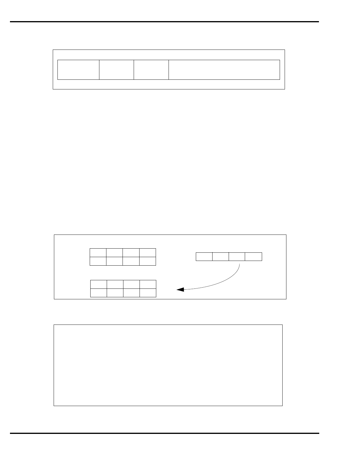
APPENDIX A MACHINE INSTRUCTIONS REFERENCE
A–72
Format:
SWL rt, offset(base)
Description:
This instruction can be used with the SWR instruction to store the contents of a register into four
consecutive bytes of memory, when the bytes cross a word boundary. SWL stores the left portion
of the register into the appropriate part of the high-order word of memory; SWR stores the right
portion of the register into the appropriate part of the low-order word.
The SWL instruction adds its sign-extended 16-bit offset to the contents of general register base to
form a virtual address which may specify an arbitrary byte. It alters only the word in memory
which contains that byte. From one to four bytes will be stored, depending on the starting byte
specified.
Conceptually, it starts at the most-significant byte of the register and copies it to the specified byte
in memory; then it copies bytes from register to memory until it reaches the low-order byte of the
word in memory.
No address exceptions due to alignment are possible.
Operation:
SWL Store Word Left
31 2526 2021 1516 0
SWL base rt offset
655 16
1 0 1 0 1 0
SWL
address 0
address 4
0123
4567 ABCD
register
address 0
address 4
0
4567
ABC
$24
memory
(big-endian)
before
after
SWL $24,1($0)
T: vAddr ← ((offset15)16 || offset 15...0) + GPR[base]
(pAddr, uncached) ← AddressTranslation (vAddr, DATA)
pAddr ← pAddrPSIZE –1...2 || (pAddr1...0 xor ReverseEndian2)
If BigEndianMem = 0 then
pAddr ← pAddrPSIZE – 1...2 || 02
endif
byte ← vAddr1...0 xor BigEndianCPU2
data ← 024–8*byte || GPR[rt]31...24–8*byte
Storememory (uncached, byte, data, pAddr, vAddr, DATA)
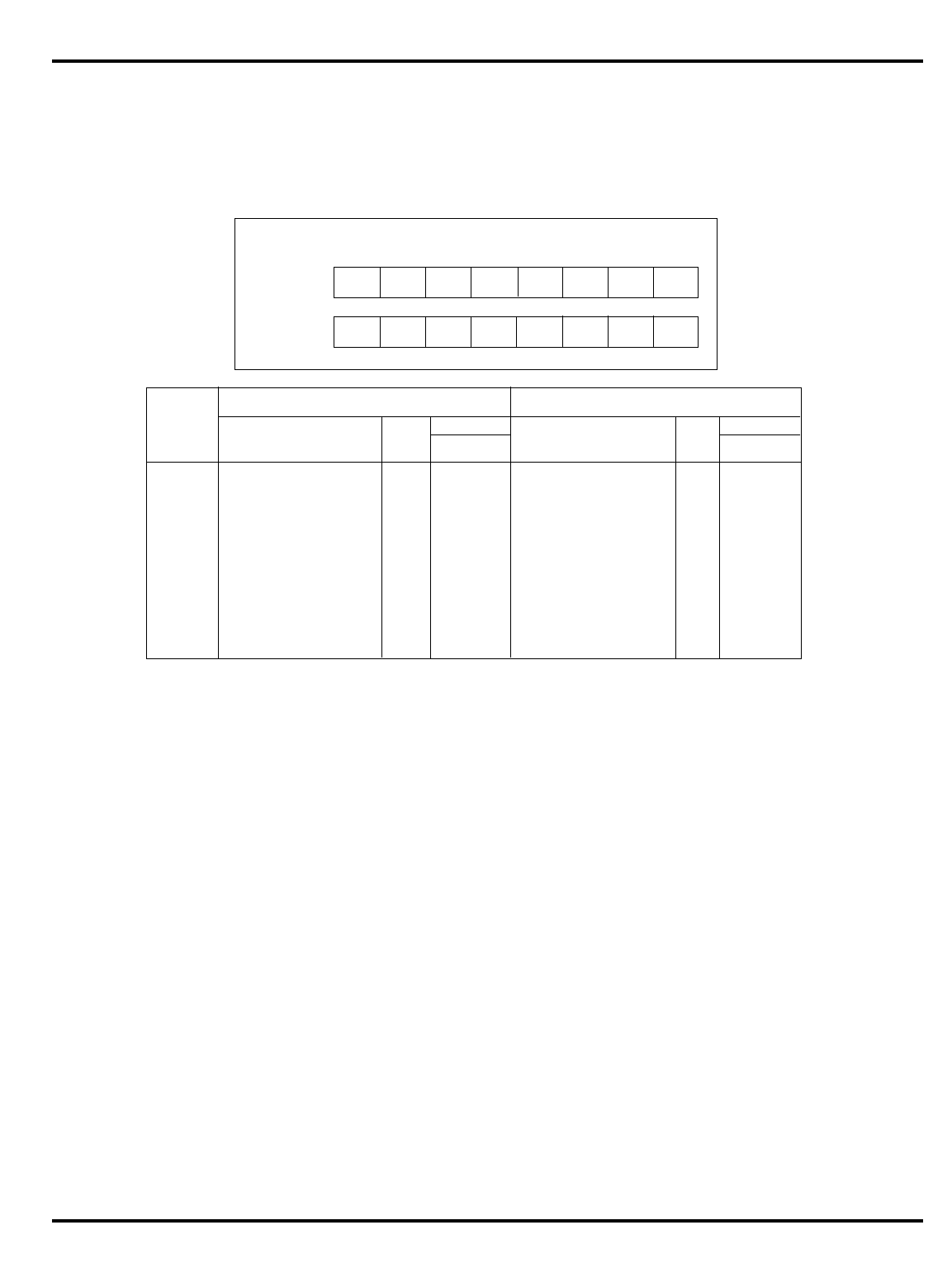
MACHINE INSTRUCTIONS REFERENCE APPENDIX A
A–73
Given a doubleword in a register and a doubleword in memory, the operation of SWL is as follows:
LEM Little-endian memory (BigEndianMem = 0)
BEM BigEndianMem = 1
Type AccessType sent to memory
Offset pAddr2...0 sent to memory
Exceptions:
TLB refill exception
TLB invalid exception
TLB modification exception
Bus error exception
Address error exception
SWL Store Word Left SWL
(Continued)
SWL
ACDB
Register
IKLJ
Memory
EGHF
MOPN
0 IJKLMNOE0 07 EFGHMNOP3 4 0
1IJKLMNEF106IEFGMNOP241
2IJKLMEFG205IJEFMNOP142
3 I J KLEFGH 3 0 4 I J KEMNOP 0 4 3
4IJKEMNOP043IJKLEFGH304
5 IJEFMNOP1 42 IJKLMEFG2 0 5
6IEFGMNOP241IJKLMNEF106
7EFGHMNOP340IJKLMNOE007
offset
BigEndianCPU = 1BigEndianCPU = 0
offset
LEM BEM LEM BEM
vAddr2..0 type
destination destination type
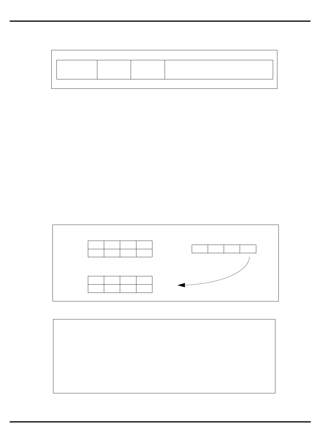
APPENDIX A MACHINE INSTRUCTIONS REFERENCE
A–74
Format:
SWR rt, offset(base)
Description:
This instruction can be used with the SWL instruction to store the contents of a register into four
consecutive bytes of memory, when the bytes cross a boundary between two words. SWR stores
the right portion of the register into the appropriate part of the low-order word; SWL stores the left
portion of the register into the appropriate part of the low-order word of memory.
The SWR instruction adds its sign-extended 16-bit offset to the contents of general register base to
form a virtual address which may specify an arbitrary byte. It alters only the word in memory
which contains that byte. From one to four bytes will be stored, depending on the starting byte
specified.
Conceptually, it starts at the least-significant (rightmost) byte of the register and copies it to the
specified byte in memory; then copies bytes from register to memory until it reaches the high-order
byte of the word in memory.
No address exceptions due to alignment are possible.
Operation:
31 2526 2021 1516 0
SWR base rt offset
655 16
1 0 1 1 1 0
SWR Store Word Right SWR
address 0
address 4
0123
4567 ABCD
register
address 0
address 4
0
D5 6 7
123
$24
memory
(big-endian)
before
after
SWR $24,1($0)
T: vAddr ← ((offset15)16 || offset 15...0) + GPR[base]
(pAddr, uncached) ← AddressTranslation (vAddr, DATA)
pAddr ← pAddrPSIZE – 1...2 || (pAddr1...0 xor ReverseEndian2)
BigEndianMem = 0 then
pAddr ← pAddrPSIZE – 31...2 || 02
endif
byte ← vAddr1...0 xor BigEndianCPU2
data ← GPR[rt]31–8*byte || 08*byte
Storememory (uncached, WORD-byte, data, pAddr, vAddr, DATA)
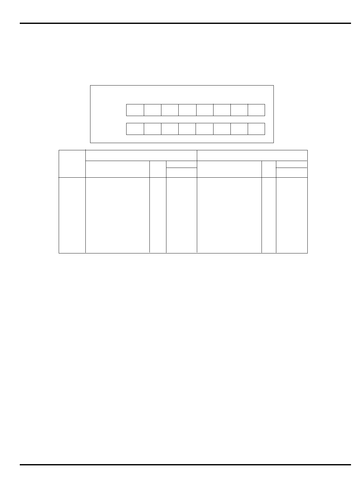
MACHINE INSTRUCTIONS REFERENCE APPENDIX A
A–75
Given a doubleword in a register and a doubleword in memory, the operation of SWR is as follows:
LEM Little-endian memory (BigEndianMem = 0)
BEM BigEndianMem = 1
Type AccessType sent to memory
Offset pAddr2...0 sent to memory
Exceptions:
TLB refill exception
TLB invalid exception
TLB modification exception
Bus error exception
Address error exception
SWR Store Word Right SWR
(Continued)
SWR
ACDB
Register
IKLJ
Memory
EGHF
MOPN
0IJKLEFGH304HJKLMNOP070
1 IJKLFGHP2 14 GHKLMNOP1 6 0
2IJKLGHOP124FGHLMNOP250
3IJKLHNOP034EFGHMNOP340
4 EFGHMNOP3 40 IJKLHNOP0 3 4
5 FGHLMNOP2 50 IJKLGHOP1 2 4
6GHKLMNOP160IJKLFGHP214
7 HJKLMNOP0 70 IJKLEFGH3 0 4
offset
BigEndianCPU = 1
BigEndianCPU = 0
offset
LEM BEM LEM BEM
vAddr2..0 type
destination destination type

APPENDIX A MACHINE INSTRUCTIONS REFERENCE
A–76
Format:
SYSCALL
Description:
A system call exception occurs, immediately and unconditionally transferring control to the
exception handler.
The code field is available for use as software parameters, but is retrieved by the exception handler
only by loading the contents of the memory word containing the instruction.
Operation:
Exceptions:
System Call exception
System Call
31 2526
SPECIAL
620
Code SYSCALL
6
65 0
0 0 0 0 0 0 0 0 1 1 00
SYSCALL SYSCALL
T: SystemCallException

MACHINE INSTRUCTIONS REFERENCE APPENDIX A
A–77
Format:
XOR rd, rs, rt
Description:
The contents of general register rs are combined with the contents of general register rt in a bit-wise
logical exclusive OR operation.
The result is placed into general register rd.
Operation:
Exceptions:
None
XOR
Exclusive Or
31 2526 2021 1516
SPECIAL rs rt
655
rd 0 XOR
55 6
11 10 6 5 0
0 0 0 0 0 0 1 0 0 1 1 00 0 0 0 0
XOR
T: GPR[rd] ← GPR[rs] xor GPR[rt]

APPENDIX A MACHINE INSTRUCTIONS REFERENCE
A–78
Format:
XORI rt, rs, immediate
Description:
The 16-bit immediate is zero-extended and combined with the contents of general register rs in a bit-
wise logical exclusive OR operation.
The result is placed into general register rt.
Operation:
Exceptions:
None
XORI Exclusive OR Immediate
31 2526 2021 1516 0
XORI rs rt immediate
655 16
0 0 1 1 1 0
XORI
T: GPR[rt] ← GPR[rs] xor (016 || immediate)
MACHINE INSTRUCTIONS REFERENCE APPENDIX A
A–79
Instruction Summary
Instr Fields
Asm Description
op func
31-26 25-21 20-16 15-11 10-6 5-0
‘‘Register’’ format instructions
0 rs1 rs2 rd sa 0 sll Shift left (to smaller bits) by
a constant. sll is ‘‘logical’’,
brings in zeroes from the
top. srl is ‘‘arithmetic’’,
duplicating bit 31, so
implementing a correct
signed division by 2^n
0 rs1 rs2 rd sa 2 srl
0 rs1 rs2 rd sa 3 sra Shift right (to higher bits) by
a constant, bringing in
zeroes to the low bits
0 rs1 rs2 rd 0 4 sllv shift (left logical, left
arithmetic, and right) by the
amount stored in another
register
0 rs1 rs2 rd 0 6 srlv
0 rs1 rs2 rd 0 7 srav
0 rs 0 8 jr Jump to address in register
(no offset)
0 rs 0 rd 0 9 jalr
Call function at address
from register. Can store the
return address in any
register, even though
anything but ra is nor
normally useful.
0 × 12 syscall Cause ‘‘syscall’’ trap,
conventionally used for
system call from user-mode
to operating system
0 × 13 break
Cause ‘‘Bp’’ trap,
conventionally used for
debugger breakpoint.
0 0 rd 0 16 mfhi
Access to multiply/divide
unit registers ‘‘lo’’ and ‘‘hi’’.
mflo/mfhi move data from
‘‘lo’’/‘‘hi’’ into an integer
register; mtlo/mthi go the
other way.
0 rs 0 17 mthi
0 0 rd 0 18 mflo
0 rs 0 19 mtlo
0 rs1 rs2 0 24 mult Multiply two integer
registers, put result into
‘‘hi’’/‘‘lo’’ when done. mult
sign-extends the result, but
multu does not.
0 rs1 rs2 0 25 multu
0 rs1 rs2 0 26 div (signed and unsigned
versions of) divide two
integer registers and put the
result (quotient) and
remainder in ‘‘lo’’ and ‘‘hi’’
respectively.
0 rs1 rs2 0 27 divu
APPENDIX A MACHINE INSTRUCTIONS REFERENCE
A–80
0 rs1 rs2 rd 0 32 add 3-operand add. The only
difference between them is
that add causes a trap if a
result overflows into bit 31,
but addu never traps.
0 rs1 rs2 rd 0 33 addu
0 rs1 rs2 rd 0 34 sub 3-operand subtract. sub
can trap on overflow, subu
won’t.
0 rs1 rs2 rd 0 35 subu
0 rs1 rs2 rd 0 36 and
3-operand bitwise logical
operations
0 rs1 rs2 rd 0 37 or
0 rs1 rs2 rd 0 38 xor
0 rs1 rs2 rd 0 39 nor
0 rs1 rs2 rd 0 42 slt Set destination to 1 if rs1
<rs2, set destination to zero
otherwise. slt uses signed
comparision, and sltu
unsigned.
0 rs1 rs2 rd 0 43 sltu
‘‘PC-relative’’ test and branch
1 rs 0 offset bltz branch if rs1 <0 (top bit set)
1 rs 1 offset bgez branch if rs1 >= 0
1 rs 16 offset bltzal if rs1 <0 or rs1 >= 0
respectively, branch to
function. Set ra to the
notional ‘‘return’’ address,
even if the branch is not
taken.
1 rs 17 offset bgezal
Long ‘‘in-region’’ jump and call
2 word address j
unconditional jump (26-bit
word address). Note that the
top 4 bits of the program
address of the target
location comes from the
instruction’s own location.
You have to use a jr (jump
register) instruction to
reach outside of your
256Mbyte region.
3 word address jal
function call (26-bit word
address)
Compare and branch instructions
4 rs1 rs2 offset beq branch if rs1 == rs2
5 rs1 rs2 offset bne branch if rs1 != rs2
6 rs1 0 offset blez branch if rs1 <= 0 or rs1 > 0
respectively. Encoded as if
they had two source
operands with rs2 selecting
zero.
7 rs1 0 offset bgtz
‘‘Immediate’’ arithmetic and logical instructions
Instr Fields
Asm Description
op func
31-26 25-21 20-16 15-11 10-6 5-0
MACHINE INSTRUCTIONS REFERENCE APPENDIX A
A–81
8 rs rd signed constant addi Arithmetic operations with
one source register, a 16-bit
signed constant, and a
separate destination. As for
3-operand arithmetic, the
unsigned forms addiu and
subiu have identical results
but never cause an overflow
trap.
Note that ‘‘load immediate
signed’’ can be synthesised
as an addi with register zero.
9 rs rd signed constant addiu
10 rs rd signed constant subi
11 rs rd signed constant subiu
12 rs rd unsigned constant andi Logical operation with 16-bit
constant, zero-extended for
these instructions. ‘‘load
immediate unsigned’’ is
synthesised with an ori with
register zero.
13 rs rd unsigned constant ori
14 rs rd unsigned constant xori
15 × rd unsigned
constant lui
Load UPPER immediate (not
unsigned). The 16-bit
constant is loaded into the
high-order 16-bits of the
register, and the low-order
bits cleared to zero.
A ‘‘load immediate’’ with a
value which won’t fit into 16
bits is synthesised by a lui
followed by an ori, which fills
in the low 16 bits.
CPU control instructions (‘‘Co-processor zero’’)
24 0 rd cs 0 mfc0
These instructions are
described in the chapter
‘‘System Software
Considerations’’
24 4 rs cd 0 mtc0
24 8 0 offset bc0f
24 8 1 offset bc0t
24 16 0 1 tlbr
24 16 0 2 tlbwi
24 16 0 6 tlbwr
24 16 0 8 tlbp
24 16 0 16 rfe
Floating point instructions (except load/store)
25 Functions of these are detailed in the chapter ‘‘FLOATING POINT CO-
PROCESSOR’’ above. Their encodings are detailed in the appendix ‘‘FP
Instruction encoding’’, below.
Load and store instructions
32 rs rd offset lb Load byte and sign-extend
33 rs rd offset lh Load halfword and sign-
extend
Instr Fields
Asm Description
op func
31-26 25-21 20-16 15-11 10-6 5-0

APPENDIX A MACHINE INSTRUCTIONS REFERENCE
A–82
34 rs rd offset lwl ‘‘Load word left’’, see section
on ‘‘Unaligned loads and
stores’’
35 rs rd offset lw load word
36 rs rd offset lbu Load byte and zero-extend
37 rs rd offset lhu Load halfword and zero-
extend
38 rs rd offset lwr ‘‘Load word right’’, see
section on ‘‘Unaligned loads
and stores’’
40 rs1 rs2 offset sb store byte
41 rs1 rs2 offset sh store halfword
42 rs1 rs2 offset swl ‘‘Store word left’’, see section
on ‘‘Unaligned loads and
stores’’
43 rs1 rs2 offset sw store word
46 rs1 rs2 offset swr ‘‘Store word right’’, see
section on ‘‘Unaligned loads
and stores’’
49 rs fs offset swc1
Store word from FP register
fs
57 rs fd offset lwc1 Load word into FP register fd
Instr Fields
Asm Description
op func
31-26 25-21 20-16 15-11 10-6 5-0

B–1
FPA INSTRUCTION
REFERENCE
®
Integrated Device Technology, Inc.
APPENDIX B
FPU Instruction Set Details
This section documents the instructions for the floating-point unit (FPU)
in MIPS processors. It contains some descriptive material at the beginning,
a detailed description for each instruction in alphabetic order, and an
instruction opcode encoding table at the end of the section.
The descriptive material describes the FPU instruction categories, the
instruction encoding formats, the valid operands for FPU computational
instructions, compare and condition values, FPU use of the coprocessor
registers, and a description of the notation used for the detailed instruction
description.
This section does not describe the operation of floating-point arithmetic,
the exception conditions within FP arithmetic, the exception mechanism of
the FPU, or the handling of these FP exceptions.
FPU Instructions
The floating-point unit (FPU) is implemented as Coprocessor unit 1
(CP1) within the MIPS architecture. A floating-point instruction needs
access to coprocessor 1 to execute; if CP1 is not enabled, an FP instruction
will cause a Coprocessor Unusable exception. The FPU has a load/store
architecture. All computations are done on data held in registers, and data
is transferred between registers and the rest of the system with dedicated
load, store, and move instructions.
The FPU instructions fall into the following categories:
• Data Transfer
• Conversion
• Arithmetic
• Register-to-Register Data Movement
• Branch
Floating-Point Data Transfer
All movement of data between the floating-point coprocessor general
registers and the rest of the system is accomplished by:
• Load memory to CP1 general register
• Store CP1 general register to memory
• Move CPU register to CP1 general register
• Move CP1 general register to CPU register
These operations are unformatted; no format conversions are performed
and, therefore, no floating-point exceptions can occur.
The coprocessor also contains floating-point control
registers. The only
data movement operations supported for them are:
• Copy CPU register to FPU control register
• Copy FPU control register to CPU register
Floating-Point Conversions
The floating-point unit has instructions to convert among the operand
types as well as operations which combine conversion with rounding using
a particular rounding mode. The conversion operations are:
• fixed-point to floating-point
• floating to fixed
• floating to floating (of another size)
APPENDIX B FPA INSTRUCTION REFERENCE
B–2
Floating-Point Arithmetic
The floating-point arithmetic instructions are:
• add
• subtract
• multiply
• divide
• absolute value
• negate
• compare
All operations satisfy the requirements of IEEE Standard 754
requirements for accuracy; a result which is identical to an infinite-
precision result rounded to the specified format, using the current
rounding mode.
Floating-Point Register-to-Register Move
There are FPU instructions to move formatted operands among
registers:
• FP move
• FP register move-conditional on FP condition code
• FP register move-conditional on CPU register value
• CPU register move-conditional on FP condition code
Floating-Point Branch
The FP compare instruction produces a condition code. The FPU has
instructions to conditionally branch on the FP condition.
FP Computational Instructions and Valid Operands
The Floating-point unit computational instructions operate on
structured data and the operands can have one of several operand
formats
.
The format of the operands, and perhaps the result, for an instruction is
specified by either the 5-bit
fmt
field or 3-bit
fmt3
field in the instruction
encoding; decoding for these fields is shown in Table B.7.
A particular operation is valid only for operands of certain formats.
fmt fmt3
Mnemonic Size Format
0-15 - Reserved
16 0 S single Binary floating-point
17 1 D double Binary floating-point
18 2 Reserved
for E extended Reserved for Extended
binary floating-point
19 3 Reserved
for Q quad Reserved for Quad binary
floating-point.
20 4 W single 32-bit binary fixed-point
21 5 Reserved
for L longword 64-bit binary fixed-point
22–31 6-7 Reserved
Table B.7. Format Field Decoding

FPA INSTRUCTION REFERENCE APPENDIX B
B–3
FP Compare and Condition values
The coprocessor branch on condition true/false instructions can be
used to logically negate any predicate. Thus, the 32 possible conditions
require only 16 distinct comparisons, as shown below.
FPU Register Specifiers
The data transfer instructions and the computational instructions view
the Coprocessor 1 general registers and the data in them in different ways.
This section describes the general registers in the coprocessor, how data
transfer instructions transfer operand data, how the FPU uses registers to
hold the different types and sizes of operands, and how the FPU
computational instructions specify operands.
The
CP1 register
is the fundamental addressable unit in the
coprocessor. All instructions that refer to the CP1 registers use the 32 CP1
general register numbers as register specifiers in the instruction encoding.
Some register numbers are not valid specifiers for some instructions; this
is discussed below.
The data transfer operations consist of memory load/store and move to/
from CPU register instructions. These instructions, with one exception
noted below, transfer unformatted data to/from a single CP1 register.
Most of the transfer instructions are the generic load/store/move
instructions used with all coprocessors and they do not have any special
operation for CP1.
The FPU operates on operands of different lengths. Some operands
exceed the CP1 general register size, so the FPU computational
instructions use the CP1 general registers in a structured way. If the FPU
operand exceeds the CP1 register size, a set of adjacent CP1 general
registers are used to hold the data for the operand. All multi-register
Condition Compare Relations Invalid
Operation
Exception If
Unordered
Branch Mnemonic Code Greater
Than Less
Than Equal Unordere
d
True False
F T 0 F F F F No
UN OR 1 F F F T No
EQ NEQ 2 F F T F No
UEQ OGL 3 F F T T No
OLT UGE 4 F T F F No
ULT OGE 5 F T F T No
OLE UGT 6 F T T F No
ULE OGT 7 F T T T No
SF ST 8 F F F F Yes
NGLE GLE 9 F F F T Yes
SEQ SNE 10 F F T F Yes
NGL GL 11 F F T T Yes
LT NLT 12 F T F F Yes
NGE GE 13 F T F T Yes
LE NLE 14 F T T F Yes
NGT GT 15 F T T T Yes
Table B.8. Logical Negation of Predicates by Condition True/False

APPENDIX B FPA INSTRUCTION REFERENCE
B–4
operands must be in “aligned” sets of registers; an operand that requires
two registers must be in an even register and the next-higher odd register.
When the FPU operand is in a set of CP1 registers, the lowest-numbered
register in the set is used as the
FPU operand specifier
or
FPU register
specifier
in the instruction encoding.
The sets of registers are structured in a big-endian order for both big
and little endian processors. The least-significant portion of the operand
is put into the lowest-numbered CP1 register in the set, and the most-
significant is put into the highest-numbered register.
32-bit CP1 registers
All 32-bit processors have 32-bit CP1 registers. The 64-bit processors
have a 32-bit-CP1-register emulation mode in which CP1 appears to
possess 32-bit registers. The primary FP data type is double floating-point,
which requires 64 bits of register space. For simplicity in implementation,
the minimum FPU operand size is a doubleword in the CP1 register file.
Operands of type word size (W and S), are placed into the low word of the
doubleword.
The MIPS I version of the architecture has only word load/store/move
instructions. To transfer anything but a W or S operand takes multiple
instructions that each reference one of the 32-bit CP1 general registers.
The load/store/move instructions use all the CP1 register numbers as
specifiers because they do not refer to formatted FP operands.
Table B.9. Valid FP Operand Specifiers with 32-bit Coprocessor 1 Registers.
32-bit CP1 register use and significance by operand
type
W,S L, D
Valid specifiers unused /
undefined data most least
01010
23232
45454

FPA INSTRUCTION REFERENCE APPENDIX B
B–5
FPU Register Access for 32-bit CP1 Registers
Instruction Notation Conventions
For the FPU instruction detail documentation, all variable subfields in
an instruction format (such as
fs, ft, immediate
, and so on) are shown in
lower-case. The instruction name (such as ADD, SUB, and so on) is shown
in upper-case.
For the sake of clarity, an alias may be used for a variable subfield in the
formats of specific instructions. For example,
rs = base
is used in the
format for load and store instructions. Such an alias is always lower case,
since it refers to a variable subfield.
In some instructions, the instruction subfields
op
and
function
can have
constant 6-bit values. When reference is made to these instructions,
upper-case mnemonics are used. For instance, in the floating-point ADD
instruction we use
op
= COP1 and
function
= ADD. In other cases, a single
field has both fixed and variable subfields, so the name contains both
upper and lower case characters. Bit encodings for mnemonics are shown
at the end of this section, and are also included with each individual
instruction.
The instruction description includes an
Operation
section that describes
the operation of the instruction in a pseudocode resembling a
programming language.
In the instruction description examples that follow, the
Operation
section describes the operation performed by each instruction using a
high-level language notation.
value <-- ValueFPR(fpr, fmt)/* undefined for odd fpr */
case fmt of
S, W:
value <-- FGR[fpr+0]
D:
/* undefined for fpr not even */
value <-- FGR[fpr+1] || FGR[fpr+0]
end
StoreFPR(fpr, fmt, value):/* undefined for odd fpr */
case fmt of
S, W:
FGR[fpr+1] <-- undefined
FGR[fpr+0] <-- value
D:
FGR[fpr+1] <-- value63...32
FGR[fpr+0] <-- value31...0
end
NOTE: The notation “FGR[fpr]” is either the physical
32-bit register or the logical 32-bit register for a 64-bit
processor in 32-bit register emulation mode. It does not
imply a specific mechanism for the 32-bit register

APPENDIX B FPA INSTRUCTION REFERENCE
B–6
Load and Store Memory
In the load and store operation descriptions, the functions listed below
are used to summarize the handling of virtual addresses and physical
memory.
All coprocessor loads and stores reference aligned-word data items.
Thus, for word loads and stores, the access type field is always WORD, and
the low-order two bits of the address must always be zero.
Regardless of byte-numbering order (endianness), the address specifies
that byte which has the smallest byte-address in the addressed field. For
a big-endian machine, this is the leftmost byte; for a little-endian machine,
this is the rightmost byte.
Instruction Descriptions
The FP instructions are described in detail in alphabetic order. Each
page contains the following information for the instruction:
• Instruction mnemonic and name
• Assembler format
• Description of the instruction
• Operation of the instruction described in pseudocode.
• Exceptions that the instruction can cause
• FP exception conditions that the instruction can cause (as Floating-
Point Exceptions)
Function Meaning
AddressTranslation
Determines the physical address given the virtual
address. The function fails and an exception is taken if
the required translation is not present in the TLB (“E”
versions only).
LoadMemory
Uses the cache and main memory to find the contents of
the word containing the specified physical address. The
low-order two bits of the address and the
Access Type
field
indicates which of each of the four bytes within the data
word need to be returned. If the cache is enabled for this
access, the entire word is returned and loaded into the
cache.
StoreMemory
Uses the cache, write buffer, and main memory to store
the word or part of word specified as data in the word
containing the specified physical address. The low-order
two bits of the address and the
Access Type
field indicates
which of each of the four bytes within the data word
should be stored.
Table B.10. Load and Store Common Functions

FPA INSTRUCTION REFERENCE APPENDIX B
B–7
Format:
ABS.fmt fd, fs
Description:
fd
←
|fs|
The contents of the FPU register specified by
fs
are interpreted in the specified format and the
arithmetic absolute value is taken. The result is placed in the floating-point register specified by
fd
.
The absolute value operation is arithmetic; a NaN operand signals invalid operation.
This instruction is valid only for single- and double-precision floating-point formats.
The fields
fs
and
fd
must specify valid operand registers for the type
fmt
and the logical size of
coprocessor 1 general registers. If they are not valid specifiers, the result is undefined.
Operation:
Exceptions:
Coprocessor unusable exception
Coprocessor exception trap
Floating-Point Exceptions:
Unimplemented operation exception
Invalid operation exception
ABS.fmt Floating-Point
31 0
655556
COP1 fmt 0 fs fd ABS
11 1021 20 16 1526 25 6 5
0 1 0 0 0 1 0 0 0 0 0 0 0 0 1 0 1
ABS.fmt
Absolute Value
T: StoreFPR(fd, fmt, AbsoluteValue(ValueFPR(fs, fmt)))

APPENDIX B FPA INSTRUCTION REFERENCE
B–8
Format:
ADD.fmt fd, fs, ft
Description:
fd
←
fs + ft
The contents of the FPU registers specified by
fs
and
ft
are interpreted in the specified format and
arithmetically added. The result is rounded as if calculated to infinite precision and then rounded
to the specified format (
fmt
), according to the current rounding mode. The result is placed in the
floating-point register (
FPR
) specified by
fd
.
The fields
fs
,
ft
, and
fd
must specify valid operand registers, given the logical size of coprocessor 1
general registers, for the type
fmt
. If they are not valid specifiers, the result is undefined.
Operation:
Exceptions:
Coprocessor unusable exception
Floating-Point exception
Floating-Point Exceptions:
Unimplemented operation exception
Invalid operation exception
Inexact exception
Overflow exception
Underflow exception
ADD.fmt
Floating-Point Add
31 0
655556
COP1 fmt ft fs fd ADD
11 1021 20 16 1526 25 6 5
0 1 0 0 0 1 0 0 0 0 0 0
ADD.fmt
T: StoreFPR (fd, fmt, ValueFPR(fs, fmt) + ValueFPR(ft, fmt))

FPA INSTRUCTION REFERENCE APPENDIX B
B–9
Format:
BC1F offset (cc=0)
Description:
A branch target address is computed from the sum of the address of the instruction in the delay
slot, and the 16-bit
offset
, shifted left two bits and sign-extended. If the contents of the floating point
condition code specified by
cc
are zero (equal to the value of the tf field), the target address is
branched to with a delay of one instruction.
The condition codes are set by the floating-point compare instruction.
MIPS I specifies a single floating-point condition that is available as the coprocessor 1 condition
signal (Cp1Cond) and the C bit in the FP
Control and Status
register. This instruction always tests
the Cp1Cond signal. The first assembler format instruction shown, with an implied
cc
field of zero,
is the only form allowed for processors that implement the MIPS I instruction.
This instruction has a scheduling restriction. The condition information is sampled during the
preceding instruction and there must be at least one instruction between this branch instruction
and the compare instruction that changes the condition code. Hardware does not enforce this
restriction.
Operation:
Exceptions:
Coprocessor unusable exception
Floating-Point exception
Floating-Point Exceptions:
Unimplemented operation exception
BC1F
Branch On Floating-Point False
3
15
BC
31 2526
COP1
6
0
16
offset
nd
21 20
5
0 1 0 0 0 1 0 1 0 0 0 0
BC1F
cc
11
0
tf
18 11
76
MIPS I has a single condition signal, the COprocessor Condition signal Cp-
Cond(1).
T–1: condition ← COC[1] = tf
T: target ← (offset15)GPRlen-(16+2) || offset || 02
T+1: if condition then
PC ← PC + target

APPENDIX B FPA INSTRUCTION REFERENCE
B–10
Format:
BC1T offset (cc=0)
Description:
A branch target address is computed from the sum of the address of the instruction in the delay
slot, and the 16-bit offset, shifted left two bits and sign-extended. If the contents of the floating point
condition code specified by cc are one (equal to the value of the tf field), the target address is
branched to with a delay of one instruction.
The condition codes are set by the floating-point compare instruction.
MIPS I specifies a single floating-point condition that is available as the coprocessor 1 condition
signal (Cp1Cond) and the C bit in the FP Control and Status register. This instruction always tests
the Cp1Cond signal. The first assembler format instruction shown, with an implied cc field of zero,
is the only form allowed for processors that implement the MIPS I instruction.
This instruction has a scheduling restriction. The condition information is sampled during the
preceding instruction and there must be at least one instruction between this branch instruction
and the compare instruction that changes the condition code. Hardware does not enforce this
restriction.
Operation:
Exceptions:
Coprocessor unusable exception
Floating-Point exception
Floating-Point Exceptions:
Unimplemented operation exception
BC1T
Branch On Floating Point True
BC1T
3
15
BC
31 2526
COP1
6
0
16
offset
nd
21 20
5
0 1 0 0 0 1 0 1 0 0 0 0
cc
11
1
tf
18 11
76
MIPS I has a single condition signal, the COprocessor Condition signal COC.
T–1: condition ← COC[1] = tf
T: target ← (offset15)GPRlen-(16+2) || offset || 02
T+1: if condition then
PC ← PC + target

FPA INSTRUCTION REFERENCE APPENDIX B
B–11
Format:
C.cond.fmt fs, ft (cc=0)
Description:
The contents of the floating-point registers specified by fs and ft are interpreted in the specified
format and arithmetically compared. A result is determined based on the comparison and the
condition, cond, specified in the instruction. The result is stored in the condition code specified by
cc. If one of the values is a “Not a Number,” and the high-order bit of the condition field is set, an
invalid operation trap is taken.
MIPS I specifies a single floating-point condition that is available as the coprocessor 1 condition
signal (Cp1Cond) and as the C bit in the FP Control and Status register. This instruction always sets
the Cp1Cond signal. The first assembler format instruction shown, with an implied cc field of zero,
is the only form allowed for processors that implement the MIPS I instruction.
Comparisons are exact and neither overflow nor underflow. Four mutually exclusive relations are
possible results: “less than,” “equal,” “greater than,” and “unordered.” The last case arises when
one or both of the operands are NaN; every NaN compares “unordered” with everything,
including itself. Comparisons ignore the sign of zero, so +0 “equals” -0.
This instruction has a timing restriction. The contents of the destination condition code specified
by cc, or the Cp1Cond signal is immediately available only within the floating-point unit. A one-
instruction delay is provided to propagate the condition code to the remainder of the processor.
The value of the condition code is undefined during this one-instruction delay. No hardware
interlock is provided to detect this hazard.
The implications for compiler code scheduling is that a compare instruction may be immediately
followed by a dependent floating-point conditional move instruction, but may not be immediately
followed by a dependent branch on floating-point coprocessor condition instruction or a
dependent integer conditional move instruction. Note that this restriction applies only to the
particular condition code specified by cc; the other condition codes are unaffected.
The fields fs and ft must specify valid operand registers for the type fmt and the logical size of
coprocessor 1 general registers. If they are not valid specifiers, the result is undefined.
C.cond.fmt Compare
31 2526 2021 1516 0
COP1
655
C.cond.fmt
3465871011
42235
ft fs cc 0FC cond
fmt
0 1 0 0 0 1 1 1
Floating-Point
0 0

APPENDIX B FPA INSTRUCTION REFERENCE
B–12
Operation:
if NaN(Value FPR(fs, fmt)) or NaN(ValueFPR(ft, fmt)) then
less ← false
equal ← false
unordered ← true
if cond3 then
signal InvalidOperationException
endif
else
less ← ValueFPR(fs, fmt) < ValueFPR(ft, fmt)
equal ← ValueFPR(fs, fmt) = ValueFPR(ft, fmt)
unordered ← false
endif
condition ← (cond2 and less) or (cond1 and equal) or
cond0 and unordered)
COC[1] ← condition
Exceptions:
Coprocessor unusable exception
Floating-Point exception
Floating-Point Exceptions:
Unimplemented operation exception
Invalid operation exception
C.cond.fmt Compare C.cond.fmt
Floating-Point
(Continued)

FPA INSTRUCTION REFERENCE APPENDIX B
B–13
Format:
CFC1 rt, fs
Description:
The contents of the FPU control register fs are loaded into general register rt.
This operation is only defined when fs equals 0 or 31.
The contents of general register rt are undefined for time T of the instruction immediately following
this load instruction.
Operation:
Exceptions:
Coprocessor unusable exception
from Floating-Point (CP1)
CFC1
11
Move Control Word
31 2526 2021 1516
COP1 CF rt
655
fs 0
5
11 10 0
0 1 0 0 0 1 0 0 0 1 0 0 0 0 0 0 0 0 0 0 0 0
CFC1
T: temp ← FCR[fs]
T+1: GPR[rt] ← (temp31)GPRlen-32 || temp

APPENDIX B FPA INSTRUCTION REFERENCE
B–14
Format:
CTC1 rt, fs
Description:
The contents of general register rt are loaded into FPU control register fs. This operation is only
defined when fs equals 0 or 31.
Writing to Control Register 31, the floating-point Control/Status register, causes an interrupt or
exception if any cause bit and its corresponding enable bit are both set. The register will be written
before the exception occurs. The contents of floating-point control register fs are undefined for time
T of the instruction immediately following this load instruction.
Operation:
Exceptions:
Coprocessor unusable exception
Floating-Point exception
Floating-Point Exceptions:
Unimplemented operation exception
Invalid operation exception
Division by zero exception
Inexact exception
Overflow exception
Underflow exception
CTC1
11
Move Control Word
31 2526 2021 1516
COP1 CT rt
655
fs 0
5
11 10 0
to Floating-Point (CP1)
0 1 0 0 0 1 0 0 1 1 0 0 0 0 0 0 0 0 0 0 0 0
CTC1
T: temp ← GPR[rt]31...0
T+1: FCR[fs] ← temp
COC[1] ← FCR[31]23

FPA INSTRUCTION REFERENCE APPENDIX B
B–15
Format:
CVT.D.fmt fd, fs
Description:
The contents of the floating-point register specified by fs is interpreted in the specified source
format, fmt, and arithmetically converted to the double floating-point format. The result is placed
in the floating-point register specified by fd.
This instruction is valid only for conversions from single floating-point format or 32-bit fixed-point
format.
If fmt specifies the single floating-point or single fixed-point format then the operation is exact.
The field fs, and fd must specify valid operand registers given the logical size of coprocessor 1
general registers; fs for the type fmt and fd for double floating-point. If they are not valid specifiers,
the result is undefined.
Operation:
Exceptions:
Coprocessor unusable exception
Floating-Point exception
Floating-Point Exceptions:
Invalid operation exception
Unimplemented operation exception
Inexact exception
Overflow exception
Underflow exception
CVT.D.fmt Floating-Point
31 0
655556
COP1 fmt 0 fs fd CVT.D
11 1021 20 16 1526 25
Floating-Point Format
65
0 1 0 0 0 1 1 0 0 0 0 10 0 0 0 0
Convert to Double CVT.D.fmt
T: StoreFPR (fd, D, ConvertFmt(ValueFPR(fs, fmt), fmt, D))

APPENDIX B FPA INSTRUCTION REFERENCE
B–16
Format:
CVT.S.fmt fd, fs
Description:
The contents of the floating-point register specified by fs are interpreted in the specified source
format, fmt, and arithmetically converted to the single binary floating-point format. The result is
placed in the floating-point register specified by fd. Rounding occurs according to the currently
specified rounding mode.
This instruction is valid only for conversions from double floating-point format, or from 32-bit
fixed-point format.
The field fs, and fd must specify valid operand registers given the logical size of coprocessor 1
general registers; fs for the type fmt and fd for single floating-point. If they are not valid specifiers,
the result is undefined.
Operation:
Exceptions:
Coprocessor unusable exception
Floating-Point exception
Floating-Point Exceptions:
Invalid operation exception
Unimplemented operation exception
Inexact exception
Overflow exception
Underflow exception
CVT.S.fmt
Floating-Point
31 0
655556
COP1 fmt 0 fs fd CVT.S
11 1021 20 16 1526 25
Floating-Point Format
65
0 1 0 0 0 1 1 0 0 0 0 00 0 0 0 0
Convert to Single
CVT.S.fmt
T: StoreFPR(fd, S, ConvertFmt(ValueFPR(fs, fmt), fmt, S))

FPA INSTRUCTION REFERENCE APPENDIX B
B–17
Format:
CVT.W.fmt fd, fs
Description:
The contents of the floating-point register specified by fs are interpreted in the specified source
format, fmt, and arithmetically converted to the single-word fixed-point format. The result is
placed in the floating-point register specified by fd.
This instruction is valid only for conversion from a single- or double-precision floating-point
formats.
The field fs, and fd must specify valid operand registers given the logical size of coprocessor 1
general registers; fs for the type fmt and fd for single-word fixed-point. If they are not valid
specifiers, the result is undefined.
When the source operand is an Infinity or NaN, or the correctly rounded integer result is outside
the range of the single-word fixed-point result type (–231 to 231- 1), the Invalid operation exception
is raised. If the Invalid operation is not enabled then no exception is taken and the largest positive
result (231–1) is returned.
Operation:
Exceptions:
Coprocessor unusable exception
Floating-Point exception
Floating-Point Exceptions:
Invalid operation exception
Unimplemented operation exception
Inexact exception
Overflow exception
CVT.W.fmt Floating-Point
31 0
655556
COP1 fmt 0 fs fd CVT.W
11 1021 20 16 1526 25
Fixed-Point Format
65
0 1 0 0 0 1 1 0 0 1 0 00 0 0 0 0
Convert to CVT.W.fmt
T: StoreFPR(fd, W, ConvertFmt(ValueFPR(fs, fmt), fmt, W))

APPENDIX B FPA INSTRUCTION REFERENCE
B–18
Format:
DIV.fmt fd, fs, ft
Description:
fd ← fs / ft
The contents of the floating-point registers specified by fs and ft are interpreted in the specified
format and fs is arithmetically divided by ft. The result is rounded as if calculated to infinite
precision and then rounded to the specified format, according to the current rounding mode. The
result is placed in the floating-point register specified by fd.
This instruction is valid for only single or double precision floating-point formats.
The fields fs, ft, and fd must specify valid operand registers, given the logical size of coprocessor 1
general registers, for the type fmt. If they are not valid specifiers, the result is undefined.
Operation:
Exceptions:
Coprocessor unusable exception
Floating-Point exception
Floating-Point Exceptions:
Unimplemented operation exception Invalid operation exception
Division-by-zero exception Inexact exception
Overflow exception Underflow exception
DIV.fmt
Floating-Point Divide
31 0
655556
COP1 fmt ft fs fd DIV
11 1021 20 16 1526 25 6 5
0 1 0 0 0 1 0 0 0 0 1 1
DIV.fmt
T: StoreFPR (fd, fmt, ValueFPR(fs, fmt)/ValueFPR(ft, fmt))

FPA INSTRUCTION REFERENCE APPENDIX B
B–19
Format:
LWC1 ft, offset(base)
Description:
The 16-bit offset is sign-extended and added to the contents of general register base to form an
unsigned effective address. The contents of the word at the memory location specified by the
effective address are loaded into floating-point (coprocessor 1) general register ft.
The effective address must be word-aligned. If either of the two least-significant bits of the effective
address is non-zero, an address error exception occurs.
LWC1
Load Word
31 2526 2021 1516 0
LWC1 base ft offset
655 16
to Floating-Point (CP1)
1 1 0 0 0 1
LWC1

APPENDIX B FPA INSTRUCTION REFERENCE
B–20
Format:
MFC1 rt, fs
Description:
The contents of register fs from the floating-point coprocessor are stored into processor register rt.
The contents of register rt are undefined for time T of the instruction immediately following this
load instruction.
Operation:
Exceptions:
Coprocessor unusable exception
MFC1
11
Move Word from Floating-Point (CP1)
31 2526 2021 1516
COP1 MF rt
655
fs 0
5
11 10 0
0 1 0 0 0 1 0 0 0 0 0 0 0 0 0 0 0 0 0 0 0 0
MFC1
T: data ← CPR[1, fs];
T+1: GPR[rt] ← data

FPA INSTRUCTION REFERENCE APPENDIX B
B–21
Format:
MOV.fmt fd, fs
Description:
fd ← fs
The contents of the FPU register specified by fs are interpreted in the specified format and are copied
into the FPU register specified by fd.
The move is non-arithmetic; it causes no IEEE 754 exceptions.
This instruction is valid only for single- or double-precision floating-point formats.
The fields fs and fd must specify valid operand registers for the type fmt and the logical size of
coprocessor 1 general registers. If they are not valid specifiers, the result is undefined.
Operation:
Exceptions:
Coprocessor unusable exception
Floating-Point exception
Floating-Point Exceptions:
Unimplemented operation exception
MOV.fmt
Floating-Point Move
31 0
655556
COP1 fmt 0 fs fd MOV
11 1021 20 16 1526 25 6 5
0 1 0 0 0 1 0 0 0 1 1 00 0 0 0 0
MOV.fmt
T: StoreFPR(fd, fmt, ValueFPR(fs, fmt))

APPENDIX B FPA INSTRUCTION REFERENCE
B–22
Format:
MTC1 rt, fs
Description:
The contents of register rt are loaded into the FPU general register at location fs.
The contents of floating-point register fs is undefined for time T of the instruction immediately
following this load instruction.
Operation:
Exceptions:
Coprocessor unusable exception
MTC1
11
Move Word to Floating-Point (CP1)
31 2526 2021 1516
COP1 MT rt
655
fs 0
5
11 10 0
0 1 0 0 0 1 0 0 0 0 0 0 0 0 0 0 00 0 1 0 0
MTC1
T: data ← GPR[rt]
T+1: CPR[1, fs] ← data

FPA INSTRUCTION REFERENCE APPENDIX B
B–23
Format:
MUL.fmt fd, fs, ft
Description:
fd ← fs × ft
The contents of the floating-point registers specified by fs and ft are interpreted in the specified
format and arithmetically multiplied. The result is rounded as if calculated to infinite precision and
then rounded to the specified format, according to the current rounding mode. The result is placed
in the floating-point register specified by fd.
This instruction is valid only for single- or double-precision floating-point formats.
The fields fs, ft, and fd must specify valid operand registers, given the logical size of coprocessor 1
general registers, for the type fmt. If they are not valid specifiers, the result is undefined.
Operation:
Exceptions:
Coprocessor unusable exception
Floating-Point exception
Floating-Point Exceptions:
Unimplemented operation exception
Invalid operation exception
Inexact exception
Overflow exception
Underflow exception
MUL.fmt
Floating-Point Multiply
31 0
655556
COP1 fmt ft fs fd MUL
11 1021 20 16 1526 25 6 5
0 1 0 0 0 1 0 0 0 0 1 0
MUL.fmt
T: StoreFPR (fd, fmt, ValueFPR(fs, fmt) * ValueFPR(ft, fmt))

APPENDIX B FPA INSTRUCTION REFERENCE
B–24
Format:
NEG.fmt fd, fs
Description:
fd ← - fs
The contents of the FPU register specified by fs are interpreted in the specified format and the
arithmetic negation is taken (polarity of the sign-bit is changed). The result is placed in the FPU
register specified by fd.
The negate operation is arithmetic; an NaN operand signals invalid operation.
The fields fs and fd must specify valid operand registers for the type fmt and the logical size of
coprocessor 1 general registers. If they are not valid specifiers, the result is undefined.
Operation:
Exceptions:
Coprocessor unusable exception
Floating-Point exception
Floating-Point Exceptions:
Unimplemented operation exception
Invalid operation exception
NEG.fmt Floating-Point Negate
31 0
655556
COP1 fmt 0 fs fd NEG
11 1021 20 16 1526 25 6 5
0 1 0 0 0 1 0 0 0 1 1 10 0 0 0 0
NEG.fmt
T: StoreFPR(fd, fmt, Negate(ValueFPR(fs, fmt)))

FPA INSTRUCTION REFERENCE APPENDIX B
B–25
Format:
SUB.fmt fd, fs, ft
Description:
The contents of the floating-point registers specified by fs and ft are interpreted in the specified
format and arithmetically subtracted. The result is rounded as if calculated to infinite precision and
then rounded to the specified format, according to the current rounding mode. The result is placed
in the floating-point register specified by fd.
This instruction is valid only for single- or double-precision floating-point formats.
The fields fs, ft, and fd must specify valid operand registers, given the logical size of coprocessor 1
general registers, for the type fmt. If they are not valid specifiers, the result is undefined.
Operation:
Exceptions:
Coprocessor unusable exception
Floating-Point exception
Floating-Point Exceptions:
Unimplemented operation exception
Invalid operation exception
Inexact exception
Overflow exception
Underflow exception
SUB.fmt
Floating-Point Subtract
31 0
655556
COP1 fmt ft fs fd SUB
11 1021 20 16 1526 25 6 5
0 1 0 0 0 1 0 0 0 0 0 1
SUB.fmt
T: StoreFPR (fd, fmt, ValueFPR(fs, fmt) – ValueFPR(ft, fmt))

APPENDIX B FPA INSTRUCTION REFERENCE
B–26
Format:
SWC1 ft, offset(base)
Description:
The 16-bit offset is sign-extended and added to the contents of general register base to form an
unsigned effective address. The word from floating-point (coprocessor 1) general register ft is
stored at the memory location specified by the effective address.
The effective address must be word-aligned. If either of the two least-significant bits of the effective
address is non-zero, an address error exception occurs.
Operation:
Exceptions:
Coprocessor unusable
TLB refill exception
TLB invalid exception
TLB modification exception
Bus error exception
Address error exception
SWC1 Store Word
31 2526 2021 1516 0
SWC1 base ft offset
655 16
from Floating-Point (CP1)
1 1 1 0 0 1
SWC1
T: vAddr ← ((offset15)GPRlen-16 || offset15...0) + GPR[base]
(pAddr, uncached) ← AddressTranslation (vAddr, DATA)
data ← CPR[1, ft]
StoreMemory (uncached, WORD, data, pAddr, vAddr, DATA)

FPA INSTRUCTION REFERENCE APPENDIX B
B–27
FPA Instruction Set Summary
Instr Fields
Asm Description
op func
31-26 25-21 20-16 15-11 10-6 5-0
Single Precision Arithmetic Instructions
17 16 fs2 fs1 fd 0 add.s 3-operand single precision
add.
17 16 fs2 fs1 fd 1 sub.s 3-operand single precision
subtraction.
17 16 fs2 fs1 fd 2 mul.s 3-operand single precision
multiply.
17 16 fs2 fs1 fd 3 div.s 3-operand single precision
divide.
17 16 0 fs fd 5 abs.s Single-precision absolute
value of fs is placed into fd.
17 16 0 fs fd 6 mov.s Single precision move of val-
ue in fs into fd.
Format Conversion
17 17 0 fs fd 32 cvt.s.d Convert a double precision
value to single precision.
17 16 0 fs fd 33 cvt.d.s Convert a single precision
value to double precision.
17 20 0 fs fd 32 cvt.s.
wConvert an integer “word”
value to single precision.
17 20 0 fs fd 33 cvt.d.
wConvert an integer “word”
value to double precision.
17 16 0 fs fd 36 cvt.w.
sConvert a single precision
value to a word value.
17 17 0 fs fd 36 cvt.w.
dConvert a double precision
value to a word value
Single Precision Comparison Operations:
No Invalid Operation Exception taken for Unordered Operands
17 16 fs1 fs2 0 48 c.f.s Result will be false
17 16 fs1 fs2 0 49 c.un.s True if fp values are “unor-
dered”
17 16 fs1 fs2 0 50 c.eq.s True if the two values are
equal
17 16 fs1 fs2 0 51 c.ueq.
sTrue if equal or unordered.
17 16 fs1 fs2 0 51 c.ueq.
sTrue if equal or unordered.
17 16 fs1 fs2 0 52 c.olt.s True if ordered and less than
17 16 fs1 fs2 0 53 c.ult.s True if unordered or less
than
17 16 fs1 fs2 0 54 c.ole.s Ordered and (equal or less
than)

APPENDIX B FPA INSTRUCTION REFERENCE
B–28
17 16 fs1 fs2 0 55 c.ule.s Unordered or less than or
equal.
Single Precision Comparison Operations:
Invalid Operation Exception Signalled for Unordered Operands
17 16 fs1 fs2 0 56 c.sf.s Result will be false
17 16 fs1 fs2 0 57 c.ngle.
sTrue if fp values are “unor-
dered”
17 16 fs1 fs2 0 58 c.seq.
sTrue if the two values are
equal
17 16 fs1 fs2 0 59 c.ngl.s True if equal or unordered.
17 16 fs1 fs2 0 60 c.lt.s True if equal or unordered.
17 16 fs1 fs2 0 61 c.nge.
sTrue if ordered and less than
17 16 fs1 fs2 0 62 c.le.s True if unordered or less
than
17 16 fs1 fs2 0 63 c.ngt.s Ordered and (equal or less
than)
Double Precision Comparison Operations:
No Invalid Operation Exception taken for Unordered Operands
17 17 fs1 fs2 0 48 c.f.d Result will be false
17 17 fs1 fs2 0 49 c.un.d True if fp values are “unor-
dered”
17 17 fs1 fs2 0 50 c.eq.d True if the two values are
equal
17 17 fs1 fs2 0 51 c.ueq.
dTrue if equal or unordered.
17 17 fs1 fs2 0 51 c.ueq.
dTrue if equal or unordered.
17 17 fs1 fs2 0 52 c.olt.d True if ordered and less than
17 17 fs1 fs2 0 53 c.ult.d True if unordered or less
than
17 17 fs1 fs2 0 54 c.ole.d Ordered and (equal or less
than)
17 17 fs1 fs2 0 55 c.ule.d Unordered or less than or
equal.
Double Precision Comparison Operations:
Invalid Operation Exception Signalled for Unordered Operands
17 17 fs1 fs2 0 56 c.sf.d Result will be false
17 17 fs1 fs2 0 57 c.ngle.
dTrue if fp values are “unor-
dered”
17 17 fs1 fs2 0 58 c.seq.
dTrue if the two values are
equal
17 17 fs1 fs2 0 59 c.ngl.d True if equal or unordered.
Instr Fields
Asm Description
op func
31-26 25-21 20-16 15-11 10-6 5-0

FPA INSTRUCTION REFERENCE APPENDIX B
B–29
17 17 fs1 fs2 0 60 c.lt.d True if equal or unordered.
17 17 fs1 fs2 0 61 c.nge.
dTrue if ordered and less than
17 17 fs1 fs2 0 62 c.le.d True if unordered or less
than
17 17 fs1 fs2 0 63 c.ngt.
dOrdered and (equal or less
than)
Double Precision Arithmetic Instructions
17 17 fs2 fs1 fd 0 add.d 3-operand double precision
add.
17 17 fs2 fs1 fd 1 sub.d 3-operand double precision
subtraction.
17 17 fs2 fs1 fd 2 mul.d 3-operand double precision
multiply.
17 17 fs2 fs1 fd 3 div.d 3-operand double precision
divide.
17 17 0 fs fd 5 abs.d Double-precision absolute
value of fs is placed into fd.
17 17 0 fs fd 6 mov.d Double precision move of val-
ue in fs into fd.
Data Movement Operations
49 rs fd offset lwc1 Load word to FPA
57 rs fd offset swc1 Store word from FPA
Instr Fields
Asm Description
op func
31-26 25-21 20-16 15-11 10-6 5-0

C–1
CP0 OPERATION REFERENCE
®
Integrated Device Technology, Inc.
APPENDIX C
CP0 Operation Details
This section documents the operations for the on-chip CP0 in R30xx
family processors. It contains a detailed description for each instruction in
alphabetic order.
MMU Operations
Most of the CP0 operations are designed to manage the on-chip TLB of
“E” versions of the family. Instructions are provided to read, write, and
probe the TLB.
Exception Operations
A single instruction is provided to support exception operation: the
rfe
instruction restores the proper Interrupt Enable and Kernel/User mode
bits of the status register on return from exception.
Dand Register Movement Operations
The standard
mtc0, ctc0, mfc0,
and
cfc0
operations were described in
Appendix A.
Operation Descriptions
The CP0 instructions are described in detail in alphabetic order. Each
page contains the following information for the instruction:
• Instruction mnemonic and name
• Assembler format
• Description of the instruction
• Operation of the instruction described in pseudocode.
• Exceptions that the instruction can cause

APPENDIX C CP0 OPERATION REFERENCE
C–2
Format:
RFE
Description:
RFE restores the “previous” interrupt enable mask bit and kernel/user mode bit (IEp and KUp) of
the Status Register into the corresponding “current” status bits (IEc and KUc), and restores the
“old” Status bits (IEo and KUo) into the corresponding “previous” status bits (IEp and KUp). The
“old” status bits remain unchanged.
The MIPS architecture does not specify the operation of memory references associated with load/
store instructions immediately prior to an RFE instruction. Normally, the RFE instruction follows
in the delay slot of a JR instruction to restore the PC.
Operation:
Exceptions:
Coprocessor unusable exception
RFE Restore from
31 0
6 1 19 6
COP0 0RFE
2126 25 6 5
0 1 0 0 0 0 0 1 0 0 0 0
RFE
Exception
CO
1
T: SR←SR31..4||SR5..2

CP0 OPERATION REFERENCE APPENDIX C
C–3
Format:
TLBP
Description:
The Index register is loaded with the address of the TLB entry whose contents match the contents
of the EntryHi register. If no TLB entry matches, the high-order bit of the Index register is set.
The architecture does not specify the operation of memory references associated with instructions
immediately after a TLBP instruction, nor is the operation specified if more than one TLB entry
matches.
This instruction is only valid for “E” versions of the R30xx family. Its result for members without
an on-chip TLB is undefined.
Operation:
Exceptions:
Coprocessor unusable exception
TLBP
TLB Probe
TLBP
31 0
6 1 19 6
COP0 0TLBP
2126 25 6 5
0 1 0 0 0 0 0 01 0 0 0
CO
1
T: Index ←1||031)
for i in 0..63
if (TLB[i]63..44 = EntryHi31..12) and {TLB[i]8 or (TLB[i]43..38 = EntryHi11..6)) then
Index ← 018||i5..0||08
endif
endfor

APPENDIX C CP0 OPERATION REFERENCE
C–4
Format:
TLBR
Description:
The EntryHi and EntryLo registers are loaded with the contents of the TLB entry pointed at by the
contents of the TLB Index register.
This operation is only valid for “E” version members of the R30xx family. Its result for members
without an on-chip TLB is undefined.
Operation:
Exceptions:
Coprocessor unusable exception
TLBR
Read Indexed TLB Entry
TLBR
31 0
6 1 19 6
COP0 0TLBR
2126 25 6 5
0 1 0 0 0 0 0 0 0 0 0 1
CO
1
T: EntryHi ←TLB[Index13..8]63..32
EntryHi ←TLB[Index13..8]31..0

CP0 OPERATION REFERENCE APPENDIX C
C–5
Format:
TLBWI
Description:
The TLB entry pointed at by the contents of the Index register is loaded with the contents of the
EntryHi and EntryLo registers.
This operation is only valid for “E” version members of the R30xx family. Its result for members
without an on-chip TLB is undefined.
Operation:
Exceptions:
Coprocessor unusable exception
TLBWI
Write Indexed TLB Entry
TLBWI
31 0
6 1 19 6
COP0 0TLBWI
2126 25 6 5
0 1 0 0 0 0 0 0 0 0 1 0
CO
1
T: TLB[Index13..8] ← EntryHi||EntryLo

APPENDIX C CP0 OPERATION REFERENCE
C–6
Format:
TLBWR
Description:
The TLB entry pointed at by the contents of the Random register is loaded with the contents of the
EntryHi and EntryLo registers.
This operation is only valid for “E” version members of the R30xx family. Its result for members
without an on-chip TLB is undefined.
Operation:
Exceptions:
Coprocessor unusable exception
TLBWR
Write Random TLB Entry
TLBWR
31 0
6 1 19 6
COP0 0TLBWR
2126 25 6 5
0 1 0 0 0 0 0 0 0 1 1 0
CO
1
T: TLB[Random13..8] ← EntryHi||EntryLo

D–1
ASSEMBLER LANGUAGE
SYNTAX
®
Integrated Device Technology, Inc.
APPENDIX D
This appendix describes the assembler syntax valid for most R30xx
assemblers..
The
compiler-dir
directives in the syntax are for use by compilers only,
and they are not described in this book.
statement-list:
statement
statement statement-list
statement:
stat \
n
stat
;
stat: label
label instruction
label data
instruction
data
symdef
directive
label: identifier
:
decimal
:
identifier:
[A-Za-z.$_][A-Za-z0-9.$_]
instruction:
opcode
opcode operand
opcode operand
,
operand
opcode operand
,
operand
,
operand
opcode:
add
sub
etc.
o
perand:
register
(
register
)
addr-immed
(
register
)
addr-immed
float-register
float-const
register:
$
decimal
float-register:
$f
decimal

APPENDIX D ASSEMBLER LANGUAGE SYNTAX
D–2
addr-immed:
label-expr
label-expr
+
expr
label-expr
-
expr
expr
label-expr:
label-ref
label-ref
-
label-ref
label-ref:
numeric-ref
identifier
.
numeric-ref:
decimal
f
decimal
b
data: data-mode data-list
.ascii
string
.
asciiz
string
.
space
expr
data-mode:
.byte
.half
.hword
.word
.int
.long
.short
.float
.single
.double
.quad
.octa
data-list:
data-expr
data-list
,
data-expr
data-expr:
expr
float-const
expr
:
repeat
float-const
:
repeat
repeat: expr
symdef:
constant-id
=
expr
constant-id:
identifier
directive:
set-dir
segment-dir

ASSEMBLER LANGUAGE SYNTAX APPENDIX D
D–3
align-dir
symbol-dir
block-dir
compiler-dir
set-dir:
.set [no]volatile
.set [no]reorder
.set [no]at
.set [no]macro
.set [no]bopt
.set [no]move
segment-dir:
.text
.data
.rdata
.sdata
align-dir:
.align
expr
symbol-dir:
.
globl
identifier
.
extern
identifier
,
constant
.
comm
identifier
,
constant
.
lcomm
identifier
,
constant
block-dir:
.ent
identifier
.ent
identifier
,
constant
.aent
identifier
,
constant
.mask
expr
,
expr
.fmask
expr
,
expr
.frame
register
,
expr
,
register
.end
identifier
.end
compiler-dir:
.alias
register
,
register
.bgnb
expr
.endb
expr
.file
constant string
.galive
.gjaldef
.gjrlive
.lab
identifier
.livereg
expr
,
expr
.noalias register
,
register
.option flag
.verstamp constant constant
.vreg expr
,
expr
expr: expr binary-op expr
term
term: unary-operator term
primary
primary:

APPENDIX D ASSEMBLER LANGUAGE SYNTAX
D–4
constant
(
expr
)
binary-op: one of
*/%
+–
<< >>
&
^
|
unary-operator: one of
+–~!
constant:
decimal
hexadecimal
octal
character-const
constant-id
decimal:
[1-9][0-9]+
hexadecimal:
0x[0-9a-fA-F]+
0X[0-9a-fA-F]+
octal:
0[0-7]+
character-const:
’x’
string:
"xxxx"
float-const: for example
1.23 .23 0.23 1. 1.0 1.2e101.2e-15

E–1
OBJECT CODE FORMATS
®
Integrated Device Technology, Inc.
APPENDIX E
This appendix describes two object file formats that are often used in
MIPS development systems. Object files are created by the compiler and/
or assembler, and the link editor. An object file is a binary representation
of part or all of a program, and usually has two distinct forms:
•
Relocatable object file
: holds the code and data resulting from the
compilation of a single module, suitable for linking with other
relocatable object files to create an executable object file. A relocatable
file includes relocation information and symbol tables which allow the
link editor to combine the individual modules, and to patch (relocate)
instructions or data which depend on the program’s final location in
memory. Other parts of the file may encode information to support
symbolic debugging.
•
Executable object file
: holds a complete program, suitable for direct
execution by a CPU. This file will not include relocation information,
but may add a simple header which tells the operating system or
bootstrap loader where each part of the object file is to be located in
memory.
The software development system should be equipped with tools to allow
the programmer to inspect the contents of an object file, or to convert it
into alternative (possibly ASCII) formats which can be downloaded to a
PROM programmer or evaluation board. Common tools are described
below.
SECTIONS AND SEGMENTS
An object file consists of a number of separate
sections
: most correspond
to the program’s instructions and data, but some additional sections hold
information for linkers and debuggers. Each section has a name to identify
it (e.g. ‘‘
.text
’’ and ‘‘
.rdata
’’), and a complete list of the standard program
sections recognized by the development toolchain should be included in its
documentation.
The reason for splitting the program up like this is so that the link editor
can then merge the different parts of the program that need to be located
together in memory (e.g. a ROMable program needs all code and read-only
data in ROM, but writable data in RAM). When the link editor produces the
final executable object file it concatenates all
sections
of the same name
together, and then further merges those sections which are located
together in memory into a smaller number of contiguous
segments
. An
object file header is prepended to identify the position of each segment in
the file, and its intended location in memory.
ECOFF OBJECT FILE FORMAT (RISC/OS)
The original MIPS Corp. compilers were Unix-based and until fairly
recently used the ECOFF object code format. Development systems from
other vendors often use or at least support inter-linking with this format,
in the interests of compatibility. ECOFF is based on an earlier format
called COFF, which stands for
Common Object File Format
, and first
appeared in early versions of Unix System V. COFF was a brave (and
largely unsuccessful) attempt to define a flexible object code format that
would be portable to a large number of processor architectures.
The ‘‘E’’ in ‘‘ECOFF’’ stands for
Extended
. The MIPS engineers wanted
the flexibility of COFF to support gp-relative addressing, which would have
been impossible with the restrictive format used on earlier Unix systems.
However they decided to replace the COFF symbol table and debug data

APPENDIX E OBJECT CODE FORMATS
E–2
with a completely different design. The ECOFF symbol table format is
certainly much more powerful and compact than the rather primitive
COFF format, but it is also much more difficult to generate and interpret.
Fortunately, embedded system applications are unlikely to be
concerned with the internal structure of the symbol tables. The
programmer probably only needs to recognize the COFF
file header
and
‘‘optional’’
a.out
header, which are largely unchanged from the original
COFF definitions.
File header
The COFF file header consists of the following 20 bytes at the start of the
file:
From this list only the following fields are really important:
•
f_magic
: must be one of the following values: Object files with the
SMIPS...
magic numbers were generated on hosts of the opposite
endianness, and software will have to individually byte-swap each
field required from the file and
a.out
headers.
•
f_opthdr
: the size in the file of the
a.out
header: this valueis used to
work out the program’s offset in the file.
•
f_nscns
: the number of
section
headers in the file: this is also needed
to work out the program’s offset.
Optional a.out header
The
a.out
header is a left-over from earlier Unix versions, which has
been shoe-horned into COFF. It follows the COFF file header, and does the
job of coalescing the COFF
sections
into exactly three contiguous
segments
: text (instructions and read-only data); data (initialized, writable
data); and BSS (uninitialized data, set to zero).
Offset Type Name Purpose
0 unsigned short f_magic Magic number (see
below)
2 unsigned short f_nscns Number of sections
4 long f_timdat Time and date stamp
(Unix style)
8 long f_symptr File offset of symbol
table
12 long f_nsyms Number of symbols
16 unsigned short f_opthdr Size of optional header
18 unsigned short f_flags Various flag bits
Name Value Meaning
MIPSEBMAGIC 0x0160 Big-endian MIPS binary
MIPSELMAGIC 0x0162 Little-endian MIPS binary
SMIPSEBMAGIC 0x6001 Big-endian MIPS binary
with little-endian headers
SMIPSELMAGIC 0x6201 Little-endian MIPS binary
with big-endian headers
Offset Type Name Purpose
0 short magic Magic number
2 short vstamp Version stamp
OBJECT CODE FORMATS APPENDIX E
E–3
Those fields marked ‡ are new to ECOFF, and not found in the original
COFF definition.
The magic number in this structure does not specify the type of CPU,
but describes the layout of the object file, as follows: The following macro
shows how to calculate the file offset of the text segment. In words, and
ignoring ZMAGIC files, it is found after the COFF file header,
a.out
header
and COFF section headers, rounded up to the next 8 or 16 byte boundary
(depending on the compiler version).
#define FILHSZ sizeof(struct filehdr)
#define SCNHSZ /*sizeof(struct scnhdr)*/ 40
#define N_TXTOFF(f, o) \
((a).magic == ZMAGIC ? 0 : ((a).vstamp <23 ? \
((FILHSZ + (f).opthdr + (f).f_nscns * SCNHSZ + 7) & ~7) : \
((FILHSZ + (f).opthdr + (f).f_nscns * SCNHSZ + 15) & ~15) ) )
Example loader
The following code fragment draws together the above information to
implement a very simple-minded ECOFF file loader, as might be found in
a bootstrap PROM which can read files from disk or network. It returns the
entry-point address of the program, or zero on failure.
unsigned long load_ecoff (int fd)
{
struct filhdr fh;
struct aouthdr ah;
/* read file header and check */
read (fd, &fh, sizeof (fh));
#ifdef MIPSEB
if (fh.f_magic != MIPSEBMAGIC)
#else
if (fh.f_magic != MIPSELMAGIC)
#endif
return 0;
4 long tsize Text size
8 long dsize Data size
12 long bsize BSS size
16 long entry Entry-point address
20 long text_start Text base address
24 long data_start Data base address
28 long bss_start‡ BSS base address
32 long gprmask‡ General registers ‘‘used’’
mask
36 long cprmask[4]‡ Coprocessor registers
used masks
52 long gpvalue‡ GP value for this file
Name Value Meaning
OMAGIC 0x0107 Text segment is writable
NMAGIC 0x0108 Text segment is read-only
ZMAGIC 0x010b File is demand-pageable (not for
embedded use)

APPENDIX E OBJECT CODE FORMATS
E–4
/* read a.out header and check */
read (fd, &ah, sizeof (ah));
if (ah.magic != OMAGIC && ah.magic != NMAGIC)
return 0;
/* read text and data segments, and clear bss */
lseek (fd, N_TXTOFF (fh, ah), SEEK_SET);
read (fd, ah.text_start, ah.tsize);
read (fd, ah.data_start, ah.dsize);
memset (ah.bss_start, 0, ah.bsize);
return ah.entry;
}
Further reading
For more detailed information on the original COFF format, consult a
Unix System V.3 Programmer’s Guide
. The ECOFF symbol table extensions
are not documented, but the header files which define it (which are
copyright of MIPS Corporation, now MTI) have now been made available for
re-use and redistribution. You’ll find copies with the rights documented in
recent versions of GNU binary utilities.
ELF (MIPS ABI)
ELF, which stands for
Executable and Linking Format
, is an attempt to
improve on COFF and define an object file format which supports a range
of different processors, while allowing vendor-specific extensions that do
not break compatibility with other tools. It first appeared in Unix System
V Release 4, and is used by recent versions of MIPS Corp compilers, and
some other development systems.
As in the examination of COFF, this manual will look only at the
minimum amount of the structure which is necessary to load an
executable file into memory.
File header
The ELF file header consists of 52 bytes at the start of the file, and
provides the means to determine the location of all the other parts of the
file. The following fields are relevant when loading an ELF file:
Offset Type Name Purpose
0 unsigned char e_ident[16] File format identification
16 unsigned short e_type Type of object file
18 unsigned short e_machine CPU type
20 unsigned long e_version File format
24 unsigned long e_entry Entry point address
28 unsigned long e_phoff Program header file
offset
32 unsigned long e_shoff Section header file offset
36 unsigned long e_flags CPU-specific flags
40 unsigned short e_ehsize File header size
42 unsigned short e_phentsize Program header entry
size
44 unsigned short e_phnum Number of program
header entries
46 unsigned short e_shentsize Section header entry size
OBJECT CODE FORMATS APPENDIX E
E–5
•
e_ident
: contains machine-independent data to identify this as an
ELF file, and describe its layout. The individual bytes within it are as
follows:
•
e_machine
: Specifies the CPU type for which this file is intended,
selected from the values in the table below.
Obviously for this discussion the value should be EM_MIPS.
•
e_entry
: The entry point address of the program.
•
e_phoff
: The file offset of the program header, which will be required
to load the program.
•
e_phentsize
: The size (in bytes) of each program header entry.
•
e_phnum
: The number of entries in the program header.
Program Header
Having verified the ELF file header, software will require the program
header. This part of the file contains a variable number of entries, each of
which specify a
segment
to be loaded into memory. Each entry is at least
32 bytes long and has the following layout:
48 unsigned short e_shnum Number of section
header entries
50 unsigned short e_shstrndx Section header string
table index
Offset Name Expected Value Purpose
0 EI_MAG0 ELFMAG0=0x7f Magic number
identifying an ELF file
1 EI_MAG1 ELFMAG1=’E’
2 EI_MAG1 ELFMAG2=’L’
3 EI_MAG3 ELFMAG3=’F’
4 EI_CLASS ELFCLASS32=1 Identifies file’s word
size.
5 EI_DATA ELFDATA2LSB=1 Indicates little-endian
headers and program
ELFDATA2MSB=2 Indicates big-endian
headers and program
6 EI_VERSION EV_CURRENT=1 Gives file format
version number
Name Value Meaning
EM_M32 1 AT&T WE32100
EM_SPARC 2 SPARC
EM_386 3 Intel 80386
EM_68K 4 Motorola 68000
EM_88K 5 Motorola 88000
EM_860 7 Intel 80860
EM_MIPS 8 MIPS R3000
Offset Type Name Purpose
0 unsigned long p_type Type of entry

APPENDIX E OBJECT CODE FORMATS
E–6
The relevant fields are as follows:
•
p_type
: Only entries marked with a type of PT_LOAD (1) should be
loaded; others can be safely ignored.
•
p_offset
: The absolute offset in the file of the start of this segment.
•
p_vaddr
: The virtual address in memory at which the segment should
be loaded.
•
p_filesz
: The size of the segment in the file; this may be zero.
•
p_memsz
: The size of the segment in memory. If this is greater than
p_filesz
, then the extra bytes should be cleared to zero.
•
p_flags
: A bitmap giving read, write and execute permissions for the
segment. This is largely irrelevant for embedded systems, but does
allow the code segment to be identified.
Example loader
The following code fragment draws together the above information to
implement a very simple-minded ELF file loader, as might be found in a
bootstrap PROM which can read files from disk or network. It returns the
entry-point address of the program, or zero on failure.
unsigned long load_elf (int fd)
{
Elf32_Ehdr eh;
Elf32_Phdr ph[16];
int i;
/* read file header and check */
read (fd, &eh, sizeof (eh));
/* check header validity */
if (eh.e_ident[EI_MAG0] != ELFMAG0 ||
eh.e_ident[EI_MAG1] != ELFMAG1 ||
eh.e_ident[EI_MAG2] != ELFMAG2 ||
eh.e_ident[EI_MAG3] != ELFMAG3 ||
eh.e_ident[EI_CLASS] != ELFCLASS32 ||
#ifdef MIPSEB
eh.e_ident[EI_DATA] != ELFDATA2MSB ||
#else
eh.e_ident[EI_DATA] != ELFDATA2LSB ||
#endif
eh.e_ident[EI_VERSION] != EV_CURRENT ||
eh.e_machine != EM_MIPS)
return 0;
4 unsigned long p_offset File offset of segment
8 unsigned long p_vaddr Virtual address of
segment
12 unsigned long p_paddr Physical address of
segment (unused)
16 unsigned long p_filesz Size of segment in file
20 unsigned long p_memsz Size of segment in memory
24 unsigned long p_flags Segment attribute flags
28 unsigned long p_align Segment alignment (power
of 2)
Name Value Meaning
PF_X 0x1 Execute
PF_W 0x2 Write
PF_R 0x4 Read

OBJECT CODE FORMATS APPENDIX E
E–7
/* is there a program header of the right size */
if (eh.e_phoff == 0 || eh.e_phnum == 0 || eh.e_phnum > 16 ||
eh.e_phentsize != sizeof(Elf32_Phdr))
return 0;
/* read program header */
lseek (fd, eh.e_phoff, SEEK_SET);
read (fd, ph, eh.e_phnum * eh.e_phentsize);
/* load each program segments */
for (i = 0; i <eh.e_phnum; i++) {
if (ph[i].p_type == PT_LOAD) {
if (ph->p_filesz) {
lseek (fd, ph[i].p_offset, SEEK_SET);
read (fd, ph[i].p_vaddr, ph[i].p_filesz);
}
if (ph[i].p_filesz <ph[i].p_memsz)
memset (ph[i].p_vaddr + ph[i].p_filesz, 0,
ph[i].p_memsz – ph[i].p_filesz);
}
}
return eh.eh_entry;
}
Further Reading
The ELF format, including MIPS-specific extensions, is extensively
documented in
Unix System V.4 MIPS Processor-Specific ABI
book.
OBJECT CODE TOOLS
A particular software development system will be equipped with a
number of tools for examining and manipulating object files. The following
list assumes Unix-type names, but systems with a different ancestry will
probably offer similar tools, even if the names are different:
Program Name Function
ar This tool allows you to list, add and remove object files from a
library. The name comes from
archive
, the historical Unix
name for the file type used to store libraries and later
specialized for this purpose.
convert
(objcopy) Converts executable object file from binary to some other
format which can be downloaded to a PROM programmer or
evaluation board.
ld The link/loader, used to glue object codes together and also
to assign fixed target-system addresses to sections (in some
systems this would involve two separate programs typically
called
link
and
locate
).
nm Lists the names in an object file’s symbol table in alphabetic
or numeric order.
objdump/odump Displays the program data of the object file in various useful
forms; in particular, can usually disassemble the code
sections.
ranlib if present, builds a global ‘‘table of contents’’ in a library
which makes it much faster for
ld
to read. On modern
systems
ar
usually has an option to do this job, and
ranlib
may well just be an alias for that option.
size Displays the size of each
section
in the object file.

APPENDIX E OBJECT CODE FORMATS
E–8
strip Removes everything from the object file which is not
necessary to load the program, making it (much) smaller; gets
rid of symbol tables and debug information. Some people do
this to make it harder to disassemble the program.

F–1
GLOSSARY OF COMMON "MIPS"
TERMS
®
Integrated Device Technology, Inc.
APPENDIX F
$fnn register
: one of the 32 general-purpose 32-bit floating point registers.
Only even-numbered ones can be used for arithmetic (the odd-
numbered registers hold the low-order bits of 64-bit, double-
precision, numbers).
$nn register
: one of the CPU’s 32 general-purpose registers.
a0-a3 register
: aliases for CPU registers $4-$7, conventionally used for
passing the first four words of the arguments to a function.
address regions
: refers to the division of the MIPS program address space
into regions called kuseg, kseg0, kseg1 and kseg2.
alignment
: positioning of data in a memory with respect to size boundaries
(keeping words aligned on modul0-4 addresses, and half-words
aligned on modulo-2 addresses).
alloca
: C library function returning a memory area which will be implicitly
freed on return from the function where the call is made from.
ALU
: arithmetic/logic unit – a term applied to the part of the CPU which
does computational functions
analyzer
: see logic analyzer.
Apache group (SVR4.2)
: an industry group of suppliers of MIPS-
architecture ‘‘Unix’’ systems who are co-operating on a standard
version of Univel’s System V Release 4.2 operating system.
architecture
: see ISA.
argument
: a value passed to a function, in ‘‘C’’ terminology – often called a
parameter in other languages. ‘‘C’’ arguments are ‘‘parameters passed
by value’’ – if that helps.
ASCII
: used very loosely for the character encoding used by the C language.
ASID
: the address space ID maintained in the CPU register ‘‘EntryHi’’. Used
to select a particular set of address translations – only those
translations whose own ASID field matches the current value will
produce valid physical addresses.
associative store
: a memory which can be looked up by presenting part of
the stored data. It requires a separate comparator for each data field,
so large associative stores use up prodigious amounts of logic. The
R30xx family TLB (“E” versions) is a fully-associative 64-entry store.
BadVaddr register
: CPU control register which holds the value of an
address which just caused a trap for some reason (misaligned,
inaccessible, TLB miss etc.).
bcopy
: C library function to copy the contents of a chunk of memory.
BEV
: ‘‘boot exception vectors’’: a bit in the CPU status register which
causes traps to go through a pair of alternate vectors located in
uncached (kseg1) memory. The locations are close to the reset-time
start point, so that they can both conveniently be mapped to the same
read-only memory.
big-endian
: describes an architecture where the most-significant part of a
multi-byte integer is stored at the lowest byte address.
bitfield
: a part of a word which is interpreted as a collection of individual
bits.
branch and link
: a PC-relative subroutine call.
1

APPENDIX F GLOSSARY OF COMMON "MIPS" TERMS
F–2
branch delay slot
: the position in the instruction sequence immediately
following a jump/branch instruction. The instruction in the branch
delay slot is always executed, before the instruction which is the
target of the branch. It is sometimes necessary to fill the branch delay
slot with a ‘‘nop’’ instruction.
branch optimization
: the process (carried out by the compiler, assembler or
programmer) of adjusting the sequence of instructions so as to make
the best use of branch delay slots.
branch
: in the MIPS instruction set, a PC-relative jump.
BrCond3-0
: CPU inputs which are directly tested by the ‘‘coprocessor
conditional branch’’ instructions.
breakpoint
: when debugging a program, a breakpoint is an instruction
position where the debugger will take a trap and return control to the
user. Implemented by pasting a ‘‘break’’ instruction into the
instruction sequence under test.
bss
: in a compiled C program, that chunk of memory which holds variables
declared but not explicitly initialized. Corresponds to a ‘‘segment’’ of
object code.
burst read cycles
: R30xx family CPUs often refill their caches by fetching 4
words at a time from memory in a burst read cycle.
busctrl register
: CPU register, implemented on the R3041 CPU only, which
allows the programmer to set up some options for how bus accesses
are carried out.
byte gathering, write merging
: when writes are stored in a
write buffer
it
may happen that two writes to the same word (often to different bytes
in the same word) may happen before the address and data are sent
to memory. R30xx family CPUs don’t do this, to avoid problems when
writing to IO subsystems.
byte order
: used to emphasize the ordering of items in memory by byte
address.
byteswap
: the action of reversing the order of the constituent bytes within
a word. This may be required when adapting data acquired from a
machine of non-matching ‘‘endianness’’.
cache – direct mapped
: a direct mapped cache has, for any particular line
in memory, only one slot where it can cache the contents of that line.
Direct-mapped caches are simple, so they can run fast.
R30xx family onchip caches are direct-mapped.
cache – physical addressed
: a cache which is accessed entirely by using
physical (translated) addresses. All R30xx family on-chip caches are
physical.
cache – snooping
: in a cache, snooping is the action of monitoring the bus
activity of some other device (another CPU or DMA master) to look for
references to data which are held in the cache. Originally, ‘‘snooping’’
was used for caches which can
intervene
, offering their own version of
the data where it is more up to date than the memory data which will
otherwise be obtained by the other master; but the word has come to
be used for any cache which monitors bus traffic.
cache coherency
: the process of insuring that the CPU caches match,
precisely, the contents of the memory which lie behind them.
cache flush
: In the R30xx family, this term is used as a synonym for
‘‘invalidate’’.
cache invalidation
: marks a line of cache data as no longer to be used.
There’s always some kind of ‘‘valid’’ bit in the control bits of the cache
line for this purpose.

GLOSSARY OF COMMON "MIPS" TERMS APPENDIX F
F–3
cache lines
: A cache line refers to the number of datum elements which
share a single tag field. In the R30xx family, the instruction-cache
uses a 4-word (16-byte) line size, and the data cache uses a 1 word (4
byte) line size.
cache miss
: A reference into the cache for memory not currently contained
in the cache.
cache profiling
: measuring the cache traffic generated when a particular
program runs, with a view to re-arranging the program in memory to
minimize the number of cache misses, or to selecting the appropriate
R30xx family member (or configuration of the R3071 or R3081) for a
particular system.
cache refill
: the memory read which is used to obtain a cache line of data
after a cache miss. This is first read into the cache, and the CPU then
restarts execution – this time ‘‘hitting’’ in the cache.
cache simulator
: a software tool used for cache profiling.
cache tag
: the information held with the cache line which identifies the
main memory location of the data.
cacheable
: applied to an address region or a page defined by the memory
translation system, this means that the contents of the memory
region may be resident in the on-chip caches.
callee
: in a function call, the ‘‘callee’’ is the function which is called.
Cause register
: CPU control register which, following a trap, indicates the
kind of trap.
Cause
also shows which external interrupt signals are
active.
CohReq* (R3081 only)
: an external signal fed into an R3081 CPU which will
cause a D-cache entry to be automatically invalidated by a write to the
appropriate memory location performed by an external bus master.
Note that even where the addressed location is not present in the
R3081 D-cache, this still causes the CPU to be stopped for a few
cycles while the D-cache tags are invalidated.
Compare register
: CPU control register provided on CPUs implementing a
timer (just the R3041 at the time of writing).
Config register
: CPU control register for configuring basic CPU behavior,
provided only on R3041, R3071, and R3081.
const
: ‘‘C’’ data declaration attribute, implying that the data is read-only.
It will often then be packed together with the instructions.
Context register
: CPU control register only seen on CPU types with a TLB
(‘‘-E’’ variants). Provides a fast way to process page faults on systems
using a certain arrangement of page tables.
context switch
: the job of changing the software environment from one
‘‘task’’ to another in a multitasking OS.
coprocessor conditional branches
: the instructions
bc0t label
etc. branch
according to the sense of ‘‘coprocessor conditions’’ which are usually
CPU input signals; can be useful for input pin polling, fast exception
decode, etc. If there is a floating point unit onchip, ‘‘coprocessor
condition bit 1’’ is hard-wired to the FP condition code.
coprocessor zero
: the bits of CPU function which are connected with the
privileged control instructions for memory mapping, exception
handling, and such like.
coprocessor
: some part of the CPU, or some closely-coupled other thing,
which executes some particular set of reserved instruction encodings.
Count register
: running timer register (R3041).
CPCOND
: see BrCond(3:0).
D-cache
: data cache (R30xx CPUs always have separate instruction and
data caches).

APPENDIX F GLOSSARY OF COMMON "MIPS" TERMS
F–4
data dependencies
: the relationship between an instruction which
produces a value in a register, and a subsequent instruction which
wants to use that value.
data path swapper
: see byte swapper.
data/instruction cache coherency
: the job of keeping the I-cache and D-
cache coherent. This can become an issue in a number of
circumstances: it is vital to invalidate I-cache locations whenever
writing or modifying an instruction stream; D-Cache coherency may
be an issue in systems where an external DMA master updates some
portion of cacheable memory. See coherency.
DECstation
: Digital Equipment Corporation’s trade name for DEC’s MIPS-
architecture workstations.
delayed branches
: see branch delay slot.
delayed loads
: see load delay slot.
denormalized
: a floating point number is ‘‘denormalized’’ when it is holding
a value too small to be represented with the usually precision. The
way the IEEE765 standard is defined makes it quite hard for
hardware to cope directly with denormalized representations, so The
R3081 FPA always traps when presented with them or asked to
compute them.
direct mapped
: see cache (direct mapped).
dirty
: in a virtual memory system, describes the state of a page of memory
which has been written to since it was last fetched from or written
back to secondary storage. ‘‘Dirty’’ pages must not be lost.
dis-assembler
: a program which takes a binary instruction sequence in
memory and produces a listing in assembler mnemonics.
DMA
: ‘‘direct memory access’’, an external device transferring data to or
from memory without CPU intervention.
double
: ‘‘C’’ and assembler-language name for a double-precision (64-bit)
format floating point number.
download
: the act of transferring data from ‘‘host’’ to “target” (typically, the
host is the computer which runs the compiler and/or debugger, and
the target is the system with the R30xx CPU).
DRAM
: used to refer to large memory systems (which are usually built from
DRAM components). Sometimes used to discuss the typical attributes
of memories built from DRAMs.
ECOFF
: an object code format, particularly used by MIPS Corporation and
Silicon Graphics, extensively evolved from Unix Systems Laboratories’
‘‘COFF’’ format.
ELF
: an object code format defined by Univel for Unix SVR4.2, and which
is mandated by the MIPS/ABI standard.
embedded
: describes a processing system, which may be part of a larger
object, which is not (primarily) seen as a computer. Specifically,
embedded systems usually have their “programs” determined when
the machine is built.
emulator
: see in-circuit emulator, software instruction emulator.
endianness
: whether a machine is big-endian or little-endian. See the
chapter on ‘‘Portability’’ for details.
endif
: see ifdef.
EntryHi/EntryLo register
: CPU control registers implemented only in CPUs
with a TLB. Used to stage data to and from TLB entries.
epc register
: ‘‘exception program counter’’: CPU control register telling
where to restart the CPU after an exception.
EPROM
: ‘‘erasable programmable read-only memory’’: the device most
commonly used to provide read-only code for system bootstrap, and
used in this manual to mean the location of that read-only code.

GLOSSARY OF COMMON "MIPS" TERMS APPENDIX F
F–5
ExcCode
: the bitfield in the
Cause
register which contains a code showing
what type of exception just occurred.
exception
: in the MIPS architecture, an exception is any interrupt or trap
which causes control to be diverted to one of the trap entry points.
Executable
: describes a file of object code which is ready to run.
exponent: part of a floating point number, described in the chapter on
floating point.
Extended floating point: not provided by the MIPS hardware, this usually
refers to a floating point format using 80 bits of storage.
extern: ‘‘C’’ data attribute for a variable which is defined in another module,
FCR31 register: this is the floating point control/status register, described
in the floating point chapter.
fixup: in object code, this is the action of a linker/locator program when it
adjusts addresses in the instruction or data segments to match the
location at which the program will eventually execute. This term is
also used to describe a particular CPU clock cycle in which the
conditions which caused the processor to stall are “fixed-up” to allow
the CPU to resume execution.
float: A name for a single precision floating point number.
Floating point accelerator (FPA): the name for the part of the MIPS CPU
which does floating point math. Historically, it was a separate chip.
floating point bias: an offset added to the exponent of a floating point
number held in IEEE format, to make sure that the exponent is
positive for all legitimate values.
floating point condition code/flag: a single bit set by FP compare
instructions, which is communicated back to the main part of the
CPU and tested by bc1t and bc1f instructions.
floating point emulation trap: a trap taken by the CPU when it cannot
implement a floating point (coprocessor 1) operation. A software trap
handler can be built which mimics the action of the FPU and returns
control, so that application software need not know whether FPA
hardware is installed or not. The software routine is likely to be 50-
300 times slower than hardware, and 10 or more times slower than a
“soft-float” approach.
fp register (frame pointer): a CPU general purpose register ($30) sometimes
used conventionally to mark the base address of a stack frame.
fpcond: another name for the FP condition bit (also known as coprocessor
1 condition bit etc.).
fraction: part of a floating point value, described in the FPA chapter.
Free Software Foundation: the (loose) organization behind GNU software.
fully-associative: see associative store.
function epilogue: in assembler code, the stereotyped sequence of
instructions and directives found at the end of a function, and
concerned with returning to the caller.
function inlining: an optimization offered by advanced compilers, where a
function call is replaced by an interpolated copy of the complete
instruction sequence of the called function. In many architectures
this is a big win (for very small functions) because it eliminates the
function-call overhead. In the MIPS architecture the function-call
overhead is negligible, but inlining is still sometimes valuable because
it allows the optimizer to work on the function in context.
function prologue: in assembler language, a stereotyped set of instructions
and directives which start a function, saving registers and setting up
the stack frame.
global pointer: see gp register.

APPENDIX F GLOSSARY OF COMMON "MIPS" TERMS
F–6
globl: assembler declaration attribute, for data items or code entry points
which are to be visible from outside the module.
GNU C compiler: the freely-redistributable compiler developed by the Free
Software Foundation. An excellent MIPS code generator is available.
GOT: the ‘‘global offset table’’, an essential part of the dynamic linking
mechanism underlying MIPS/ABI applications.
gp register: CPU register $28, often used as a pointer to program data.
Program data which can be linked within +-32K of the pointer value
can be loaded with a single instruction. Not all toolchains, nor all
runtime environments, support this.
halfword: a 16-bit data type.
hazard: see pipeline hazard.
heap: program data space allocated at run-time.
I-cache: the instruction cache of a MIPS CPU.
IDT: Integrated Device Technology Corporation.
IEEE754 floating point standard: an industry standard for the
representation of arithmetic values. It mandates the precise behavior
of a group of basic functions. This provides a stable base for the
development of portable numeric algorithms.
ifdef : ‘‘#ifdef’’ and ‘‘#endif’’ bracket conditionally-compiled code in the C
language.
immediate: in the instruction set descriptions, an ‘‘immediate’’ value is a
constant which is embedded in the code sequence. In assembler
language, it is any constant value.
in-circuit emulator (ICE): a device which replaces a CPU chip with a module
which, as well as being able to exactly imitate the behavior of the CPU,
provides some means to control execution and examine CPU
internals. Microprocessor ICE units are inevitably based on a version
of the microprocessor chip (often a higher speed grade).
Index register: CPU control register used to define which TLB entry’s
contents will be read into or written from EntryHi/EntryLo.
inexact: describes a floating point calculation which has lost precision.
Note that this happens very frequently on the most everyday
calculations – the number 1/3 has no exact representation. IEEE754
compliance requires that MIPS CPUs can trap on an inexact result,
although that trap is rarely enabled.
infinity: a floating point data value standing in for any value too big (or too
negative) to represent. IEEE754 defines how computations with
positive and negative versions of ‘‘infinity’’ should behave.
instruction scheduling: the process of moving instructions around to make
the best use of ‘‘delay slots’’, performed by the compiler and
(sometimes) by the assembler.
instruction set architecture (ISA): the functional description of the CPU,
which defines exactly what it does with any legitimate instruction
stream (but does not have to define how it is implemented).
instruction synthesis by assembler: the MIPS instruction set omits many
useful and familiar operations (such as an instruction to load a
constant outside the range +-32K). Most assemblers for the MIPS
architecture will accept instructions (sometimes called macro
instructions or synthetic instructions) which they implement with a
short sequence of machine instructions.
interlock: a hardware feature where the execution of one instruction is
delayed until something is ready.
interrupt mask: a bit-per-interrupt mask, held in the CPU Status register,
which determines which interrupt inputs are allowed to cause an
interrupt at any given time.

GLOSSARY OF COMMON "MIPS" TERMS APPENDIX F
F–7
interrupt priority: in many architectures the interrupt inputs have built-in
priority; an interrupt will not take effect during the execution of an
interrupt handler at equal or higher priority. The MIPS hardware
doesn’t do this directly; but the system software can impose a priority
on the interrupt inputs.
interrupt: an external signal which can cause an exception (if not masked).
isolate cache: the basic mechanism for D-cache maintenance. Puts the
CPU into a mode where data loads/stores occur only to the cache and
not to memory. In this mode partial-word stores cause the cache line
to be invalidated. The Cache Management chapter details how to do
the same to the I-cache.
jump and link (jal) instruction: MIPS instruction set name for a function
call, which puts the return address (the ‘‘link’’) into ra.
k0 and k1 registers: two general-purpose registers which are reserved, by
convention, for the use of trap handlers. It is difficult to contrive a
trap handler which does not use at least one register before it saves it.
kseg0 and kseg1: the ‘‘unmapped’’ address spaces (actually they are
mapped in the sense that the resulting physical addresses are in the
low 512Mbytes). kseg0 is for cached references, kseg1 for uncached
references. Standalone programs, or programs using simple OS’, are
likely to run wholly in kseg0/kseg1.
KU: the kernel/user privilege bit in the status register.
kuseg: the low half of the program address space, which is accessible by
programs running with user privileges. The translation to a physical
address is either through the TLB (“E” versions) or through a fixed
translation (“base” versions).
leaf function: a function which itself contains no other function call. This
kind of function can return directly through the ra register, and
typically uses no stack space.
level sensitive: an attribute of a signal (particularly an interrupt signal)
that says that the receiving logic will react if the signal is provided at
a designated logic level (as opposed to “edge sensitive”, whereby the
receiving logic reacts to a change in the signal level). MIPS interrupt
inputs are level sensitive; they will cause an interrupt any time they
are active and unmasked.
linker: the program which joins together object code modules, resolving
external references.
little-endian: describes an architecture where the least-significant part of a
multi-byte integer is stored at the lowest byte address.
lo, hi registers: dedicated output registers of the integer multiply/divide
unit. These registers are interlocked – an attempt to copy data from
them into a general-purpose register will be stalled until the multiply/
divide can complete.
load delay slot: the position in the instruction sequence immediately
following a load. An instruction in the load delay slot cannot use the
value just loaded (the results would be unpredictable). The compiler,
assembler or programmer may move code around to try to make best
use of load delay slots, or use a “nop” if the code can’t be re-ordered.
load delay: see delayed loads.
load/store architecture: describes an ISA like MIPS, where memory data
can be accessed only by explicit load and store instructions. Many
other architectures define instructions (e.g. ‘‘push’’, or arithmetic on
a memory variable) which implicitly access memory.
loader: the program which takes an object code module and assigns fixed
program addresses to instructions and data, in order to make an
executable file.

APPENDIX F GLOSSARY OF COMMON "MIPS" TERMS
F–8
logic analyzer: a piece of test equipment which simultaneously monitors
the logic level (i.e. as 1 or zero) of many signals. It is often used to keep
a list of the addresses of accesses made by a microprocessor.
loop unrolling: an optimization used by advanced compilers. Program loops
are compiled to code which can implement several iterations of the
loop without branching out of line. This can be particularly
advantageous on architectures (unlike MIPS) where a long pipeline
and instruction prefetching makes taken branches costly. However,
even on the MIPS architecture it can help by allowing intermingling of
code from different loop iterations.
macro instructions: see instruction synthesis by assembler.
mantissa: a part of the representation of a floating point number.
micro-TLB: the MIPS TLB is dedicated to translating data addresses. Use of
the TLB to translate addresses for I-fetch would lead to resource
conflict and would slow the CPU. The micro-TLB remembers the last
used I-fetch program pages, and physical pages, and saves a
reference to the real TLB until execution occurs outside the two most
recently referenced pages. When this happens, a 1-clock stall occurs
while the micro-TLB is refilled from the data TLB.
MIPS System VR3, RISC/os and Irix: these are all ways of referring to the
same basic operating system, a derivative of Unix System V Release
3. This OS supports ‘‘RISCware’’ applications.
MIPS UMIPS 4.3BSD: MIPS Corp.'s first operating system was a derivative
of Berkeley’s BSD4.3 version of Unix.
MIPS: used alternately to refer to the name of the company which
originated this processor architecture, or the name of the architecture
itself. It has another meaning, referring to “Millions of Instructions
Per Second”, a performance metric.
MIPS/ABI: the latest standard for MIPS applications, supported by all Unix
system vendors using the MIPS architecture in big-endian form.
MIPSCO: MIPS Corporation, now the MIPS Technologies Inc. subsidiary of
Silicon Graphics Corporation.
MIPSEB and MIPSEL: these are the words used to request big-endian and
little-endian output (respectively) from the MIPS Co. compiler
toolchain and some others.
misaligned: see unaligned.
MMU, Memory management unit: the only memory-management hardware
provided in the MIPS architecture is the TLB which can translate
program addresses from any of up to 64 pages into physical
addresses. See TLB for details.
NaN: ‘‘not a number’’ – a special floating point value defined by IEEE754
as the value to be returned from operations presented with illegal
operands.
naturally aligned: a datum of length n is naturally aligned if its base
address is zero mod n. A word is naturally aligned if it is on a 4-byte
boundary; a half-word if it is on a 2-byte boundary.
noalias – noat – nobopt – nomacro – noreorder – novolatile: assembler
language controls, which turn off various aspects of the way the
assembler works.
non-leaf function: a function which somewhere calls another function.
Normally the compiler will translate them with a function prologue
which saves the return address (and possibly other register values) on
a stack, and a function epilogue which restores these values.
nop: no-operation. This is actually an alias for sllv zero,zero,zero - which
will actually not do anything.

GLOSSARY OF COMMON "MIPS" TERMS APPENDIX F
F–9
nullified: applied to an instruction which, although it has been started in
the pipeline, will not be allowed to change the processor context. In
general, instructions never change context until at least the MEM
pipestage. In the R30xx family instructions are only nullified when an
exception occurs before they have committed to the MEM stage.
NVRAM: non-volatile RAM, used rather generically to refer to any writable
storage which is preserved while the system is powered down.
object code: a special file format containing compiled program source and
data, in a form which can be quickly and easily converted to
executable format.
operand: a value used by an operation.
overflow: when the result of an operation is too big to be represented in the
output format, it is said to overflow.
padding: ‘‘spaces’’ left in memory data structures and representations,
caused by the compilers’ need to align data to the boundaries which
the hardware prefers.
page mode memory: a way of using a DRAM memory array. In DRAMs it is
much faster to make repeated access to a single region of memory
where the ‘‘row’’ address presented to the DRAM component is
common. R30xx family components give specific support to page
mode access, particularly to speed writes.
page table: a possible implementation of the TLB miss exception is to keep
a large number of page translations in a table indexed by the high-
order virtual address; such a thing is called a page table.
paged: describes a memory management system (like MIPS) where fixed-
size pages (in the R30xx “E” versions they are 4Kbytes in size) are
mapped; high bits are translated while the low bits (11 bits for 4kB
pages) are passed through unchanged.
partial-word: any transfer which is not a whole word. In the MIPS
architecture this can be 1-, 2- or 3 bytes.
PC-relative: an instruction is PC-relative if it generates an address which is
an offset from the instruction’s own location.
peephole optimization: a form of optimization which recognizes particular
patterns of instruction sequence and replaces them by shorter,
simpler patterns. Peephole optimization is not terribly important for
RISCs, but they are very important to CISCs – where they provide the
only mechanism by which compilers can exploit complex
instructions.
PFN: ‘‘page frame number’’ – the high-order part of the program address
which is submitted to the address translation mechanism of a paged
MMU.
pipeline re-organization: see peephole optimization.
pipeline concealment by assembler: MIPS assembler language does not
usually require the programmer to take account of the pipeline – even
though the machine language does. The assembler moves code
around, or inserts ‘‘nop’’s, to prevent unwanted behavior.
pipeline hazard: this is the name for a case where an instruction sequence
won’t work due to pipeline problems.
pipeline: the critical architectural feature by which several instructions are
executed at once.
pipestage: one of the five phases of the MIPS pipeline.
pixie, pixstats, and prof: see profiling. pixie is a special tool provide by MIPS
Corp., which can be used to measure the instruction-by-instruction
behavior of programs at high speed. It works by translating the
original program binary into a version which includes ‘‘metering’’

APPENDIX F GLOSSARY OF COMMON "MIPS" TERMS
F–10
instructions which count the number of times each basic block is
executed (a basic block is a section of code delimited by branches
and/or branch targets).
pixstats and prof take the huge indigestible array of counts produced
by a pixie run and munches them down into useful statistics.
PortSize register: CPU control register provided on the R3041, and used to
define the bus transfer width used for accesses in various regions.
position-independent code (PIC): code which can execute correctly
regardless of where it is positioned in program address space. This is
usually produced by making sure all references are PC and/or GP-
relative. PIC is an essential part of the MIPS/ABI standard, where
sharable library code must be compiled position-independent.
POSIX: a still-evolving IEEE standard for the programming interface
provided by a compliant operating system.
PPN: physical page number; the high order part of the physical address,
which is the output of the paged MMU.
pragma: the C compiler ‘‘#pragma’’ directive is used to select compiler
options from within the source code.
precise exception: the MIPS architecture offers precise exceptions. This
means that, following an exception, all instructions earlier in
instruction sequence than the instruction referenced by EPC are
completed, whereas all instructions later in instruction sequence
have not changed processor state.
precision of data type: the number of bits available for its representation.
PRId register: CPU control register (read-only) which tells the type and
revision number of the CPU.
primary cache: in a system with more than one level of cache, this is the
cache closest to the CPU. Most R30xx family implementations will
have only one level of cache (the on-chip cache).
privilege level: CPUs capable of running a secure OS must be able to
operate at different privilege levels. The MIPS CPU can operate at two:
kernel and user.
profiling: running a program with some kind of instrumentation, to derive
information about its resource usage and running.
program address: the software engineer’s view of addresses, as generated
by the program. Also known as ‘‘virtual address’’.
PROM: programmable read-only memory, used to mean any read-only
program memory.
quad-precision (128-bit) floating point: not supported by R30xx hardware,
but referred to in some documentation.
R2000, R3000: the original implementations of the MIPS ISA, packaged to
use external static RAMs as cache.
ra register: CPU register $31, conventionally used for the return address
from subroutines. This use is supported by the ISA in that it is used
by jal instruction (whose 26-bit target address field leaves it no room
to specify which register should receive the return address value).
Random register: a CPU control register present only if there is a TLB. It
increments continually and autonomously, and is used for pseudo-
random replacement of TLB entries.
ranlib: a program used to maintain object-code libraries – it makes
indexes.
read buffer: on a burst-mode cache read, the MIPS R3000A core used in
the R30xx family needs to be fed with data at 1-clock intervals (once
it is told to restart). A read buffer permits the actual memory timings

GLOSSARY OF COMMON "MIPS" TERMS APPENDIX F
F–11
to be a little slower; the CPU fills the read buffer at memory speed and
empties it at CPU speed. The R30xx family implements a read buffer
on-chip to ease system hardware design.
read priority: because of the write buffer, the CPU may simultaneously
want to do a read and a (delayed) write. It is possible, and can boost
performance, to do the read first – the CPU will always be waiting for
the read data; this is called ‘‘read priority’’. But it causes coherency
problems when the location being read is affected by a pending write;
the R30xx uses read priority for I-Cache misses, but write priority for
D-Cache misses and uncached fetches (I- or D-).
reset: used in this manual for the event which happens when the system
activates the Reset* input to the CPU; this happens at power-on or
system reinitialization.
rounding mode: defines the exact behavior of floating point operations, and
configurable through the floating point status/control register.
s0-s9 register: a collection of CPU general purpose registers ($16-$23 and
$30) conventionally used for variables of function scope, and which
must be saved by any function which modifies them.
secondary cache: in a system with more than one level of cache, this is the
cache second closest to the CPU.
segment: see kseg0/kseg1.
software instruction emulators: a program which emulates the operation of
a CPU/memory system. It can be used to check out software too low-
level to be compatible with a debugger.
software interrupts: interrupts invoked by setting bits in the Cause
register, and which happen when those bits are unmasked.
source-level debugger: a debugger which interprets current program state
in terms of the source program (instruction lines, variable names,
data structures). Source-level debuggers need access to source code;
so when working with embedded system software the debugger must
run on the host, and obtains information about the program state
from a simple ‘‘debug monitor’’ running on the target.
sp register/stack pointer: CPU register $29, used by convention as a stack
pointer.
SR register: CPU ‘‘status register’’, one of the privileged control registers.
Contains control bits for any modes which the CPU respects.
SRAM: static RAM – writable random-access memory which does not
require periodic refresh, and typically has faster initial access time.
SBrCond: see BRCOND.
stack argument structure: a conceptual data structure used to explain how
arguments are passed to functions according to the MIPS convention.
stack backtrace: a debugger function, which interprets the state of the
program stack to show the nest of function calls which has got to the
current position. Depends wholly on strict stack usage conventions,
which assembler programs must notate with standard directives.
stack frame: a phrase for the piece of stack used by a particular function.
stack underrun: the error where software attempts to pop more off a stack
than was ever put on it.
stall: the condition where the pipeline is frozen (no instruction state is
advanced) while the CPU waits for some resource to become available.
standalone software: software operating without the benefit of any kind of
operating system or standard run-time environment.
strcpy: C library function which copies a (null-terminated) string.

APPENDIX F GLOSSARY OF COMMON "MIPS" TERMS
F–12
strength reduction: optimization technique where a time ‘‘expensive’’
operation is replaced, where possible, by one or a short sequence of
‘‘cheaper’’ operations. For example, multiply by a constant may be
more efficiently replaced by a sequence of shift and add operations.
swap caches: temporarily reverse the roles of the I- and D-cache, so that
the cache maintenance functions can operate on the I-cache.
Controlled by a status register bit.
swapper: see byte-swapper.
synthesized instructions: see instruction synthesis by assembler.
syscall: system call – an instruction which produces a trap. It has a spare
field, uninterpreted by the hardware, which software can use to
encode different system call types.
t0-t9 register/temporaries: CPU registers $8-$15 and $24-$25,
conventionally used as ‘‘temporaries’’; any function can use these
registers regardless. The values aren’t guaranteed to survive any
function call.
TLB (translation lookaside buffer): the 64-entry associative store which
translates program to physical page numbers. When the TLB doesn’t
contain the translation entry needed, the CPU takes an exception and
it is up to system software to load an appropriate entry before
returning to re-execute the faulting reference.
TLB – wired entries: the first 8 TLB entries are conventionally reserved for
statically-configured entries, and are not randomly replaced.
TLB Invalid exception: the exception taken when a TLB entry matches the
address, but is marked as not valid.
TLB miss: the exception taken when no TLB entry matches the program
address.
TLB Modified exception: the exception taken when a TLB entry matches a
store address, but that entry is not flagged as writable.
TLB Probe: an instruction used to submit a program address to the TLB to
see what translations are currently in force.
TLB refill: the process of adding a new entry to the TLB following a miss.
toolchain: the complete set of tools required to produce runnable programs
starting from source code (compiler, assembler, linker, librarian etc.).
trap: an exception caused by some internal event affecting a particular
instruction.
tribyte: a load/store which carries 3 bytes of data. Produced only by the
special instructions lwl/lwr.
Ultrix: DEC’s trade name for their BSD family operating system running on
MIPS-based DECstation computers. Note that Ultrix, unlike
practically all other MIPS Unix-like systems, runs in little-endian
mode so is completely software-incompatible with MIPS/ABI or
RISCware.
unaligned access exception: trap caused by a memory reference (load/store
word or half-word) at a misaligned address.
unaligned data: data stored in memory but not guaranteed to be on the
‘‘proper’’ alignment boundary. Unaligned data can only be accessed
reliably by special code sequences.
uncacheable: describes the region kseg1 (which may never be cached) and
translated address regions where the TLB entry is flagged as
uncached.
unimplemented instruction exception: trap taken when the CPU does not
recognize the instruction code; also used when it cannot successfully
complete a floating point instruction and wants the software emulator
to take over.

GLOSSARY OF COMMON "MIPS" TERMS APPENDIX F
F–13
union: a ‘‘C’’ declaration of an item of data which is going to have
alternative interpretations with different data types. This is highly
non-portable.
Unisoft V.4 – ‘‘Uniplus+’’: yet another version of Unix SVR4, this one MIPS/
ABI compliant.
unmapped: describes the kseg0/kseg1 address spaces.
utlbmiss: a TLB miss exception caused by a user-privilege address for
which no mapping is present in the TLB is vectored to a unique,
second, exception entry point. This was done because this is by far
the most common trap in a hard-working UNIX-like operating system,
and it saves time to avoid the code which decodes which kind of trap
has occurred.
v0-v1 register: CPU registers $2-$3, conventionally used to hold values
being returned by functions.
varargs: a software mechanism, implemented by the compiler prompted by
a special include file and macros, providing a portable way of defining
and using functions with variable numbers of arguments.
virtual address: see program address.
void: a data type used to tidy up C programs, indicating that no value is
available.
volatile: an attribute of declared data in either C or assembler. A volatile
variable is one which may not simply behave like memory (i.e. does
not simply return the value last stored in it). In the absence of this
attribute, an optimizer may assume that it is unnecessary to re-read
a value; and if the variable represents a memory-mapped IO location
being polled, this will be a mistake. Most compiler optimizers will
insure this does not happen to “volatile” data.
watchpoint: a debugger feature which causes the running program to be
suspended and control passed back to the user whenever an access
is made to the specified address.
wbflush: a standard name for the routine/macro which ensures that the
write buffer is empty.
wraparound: some memory systems (including the MIPS cache when
isolated) have the property that accesses beyond the memory array
size simply wrap round and start accessing the memory again at the
beginning.
write buffer: a FIFO store which keeps both the address and data of a CPU
write cycle (the R30xx family contain four of each). The CPU can
continue execution while the writes are carried out as fast as the
memory system will manage.
A write buffer is particularly effective when used with a write-through
cache.
write-through cache: a D-cache where every write operation is made both
to the cache (if the access hits a cached location) and simultaneously
to memory. The advantage is that the cache never contains data
which is not already in memory, so cache lines can be freely
discarded.
zero register: CPU register $0, which is very special. Regardless of what is
written to it, it always returns the value zero.
