RB751V 40S2 Datasheet. Www.s Manuals.com. Cystek
User Manual: Marking of electronic components, SMD Codes 5E, 5E*, 5E=**. Datasheets BC808-16, MM1Z13, MM5Z9V1, PDTA115EE , RB751V-40S2, RB751V40, RT8248AGQW.
Open the PDF directly: View PDF ![]() .
.
Page Count: 7
CYStech Electronics Corp.
Spec. No. : C345S2
Issued Date : 2004.04.27
Revised Date : 2013.04.15
Page No. : 1/6
RB751V-40S2 CYStek Product Specification
Small Signal Schottky diode
RB751V-40S2
Description
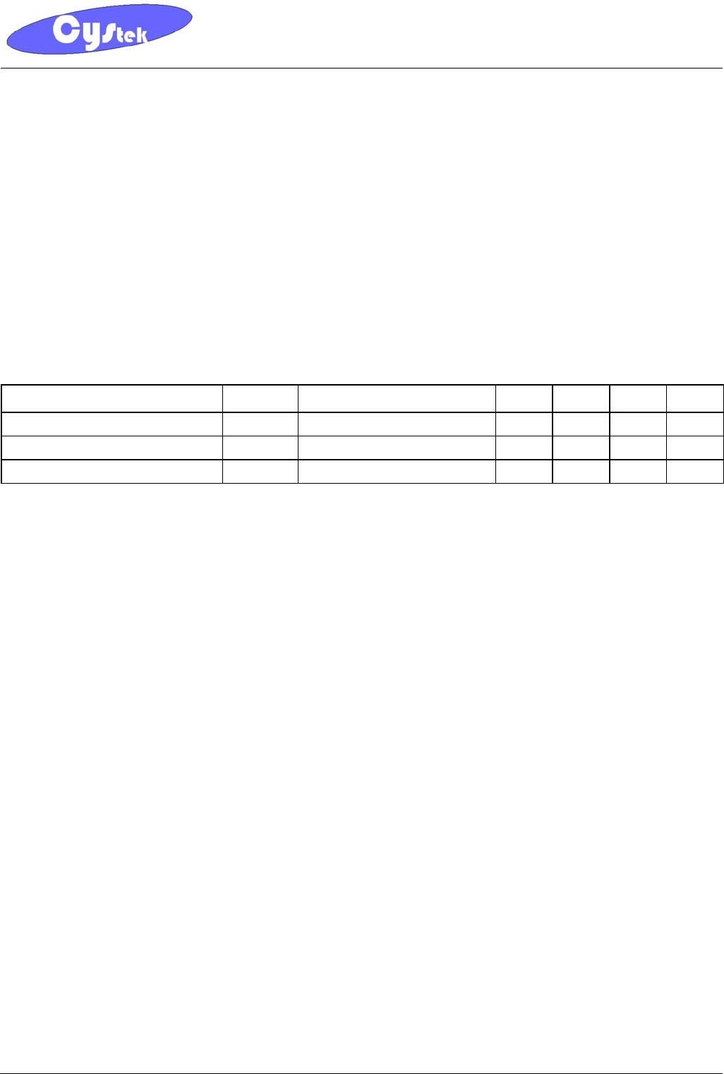
Planar silicon Schottky barrier diode encapsulated in a SOD-323 plastic SMD package.
Features
•Small surface mounting type SC-76/SOD323
•Low reverse current and low forward voltage
•High reliability
•Pb-free lead plating and halogen-free package
Applications
Low current rectification and high speed switching
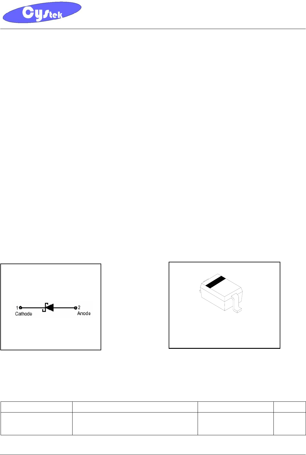
Symbol Outline
RB751V-40S2
SOD-323
2 (Anode)
Ordering Information
Device Package Shipping
Marking
RB751V-40S2-0-T1-G SOD-323 (Pb-free lead plating
and halogen-free package) 3000 pcs / Tape & Reel 5E
CYStech Electronics Corp.
Spec. No. : C345S2
Issued Date : 2004.04.27
Revised Date : 2013.04.15
Page No. : 2/6
RB751V-40S2 CYStek Product Specification
Absolute Maximum Ratings
• Maximum Temperatures
Storage Temperature Tstg..................................................................................................... -40~+125°C
Junction Temperature Tj .............................................................................................................. +125°C
• Maximum Voltages and Currents (Ta=25°C)
Peak Reverse Voltage VRM…………………………………………………………………………. 40 V
DC Reverse Voltage VR...................................................................................................................... 30 V
Mean Rectifying Current IO........................................................................................................... 30 mA
Peak Forward Surge Current IFSM………………………………….. ……………………………………….200 mA
Characteristics (Ta=25°C)
Characteristic Symbol Condition Min. Typ Max. Unit
Forward Voltage VF IF=1mA -
- 370 mV
Reverse Leakage Current IR VR=30V -
- 0.5 μA
Capacitance Between Terminals CT VR=1V, f=1MHz - 2 - pF
CYStech Electronics Corp.
Spec. No. : C345S2
Issued Date : 2004.04.27
Revised Date : 2013.04.15
Page No. : 3/6
RB751V-40S2 CYStek Product Specification
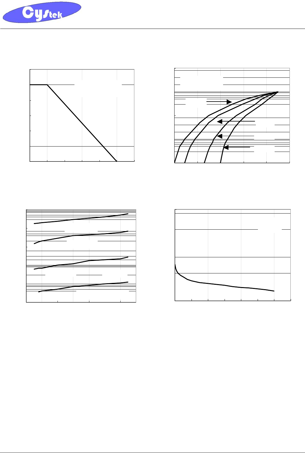
Characteristic Curves
Forward Current Derating Curve
0
20
40
60
80
100
120
0 25 50 75 100 125 150
Ambient Temperature---TA(℃)
Percentage of Rated Forward Current---(%)
Mounting on glass
epoxy PCBs
Forward Current vs Forward Voltage
0.01
0.1
1
10
100
0 0.10.20.30.40
Forward Voltage---VF(V)
Forward Current---I F(mA)
.5
- 25℃
25℃
75℃
125℃
Typ.
pulse measurement
Reverse Leakage Current vs Reverse Voltage
0.001
0.01
0.1
1
10
100
0102030
Reverse Voltage---VR(V)
Reverse Leakage Current---IR(μA)
Ta= 75℃
Ta= 25℃
Ta= 125℃
Ta=-25℃
Typ. pulse easurement
Capacitance vs Reverse Voltage
1
10
0246810121
Reverse Voltage---VR(V)
Capacitance between terminals---C T(pF)
4
f=1MHz
Ta=25℃
CYStech Electronics Corp.
Spec. No. : C345S2
Issued Date : 2004.04.27
Revised Date : 2013.04.15
Page No. : 4/6
RB751V-40S2 CYStek Product Specification
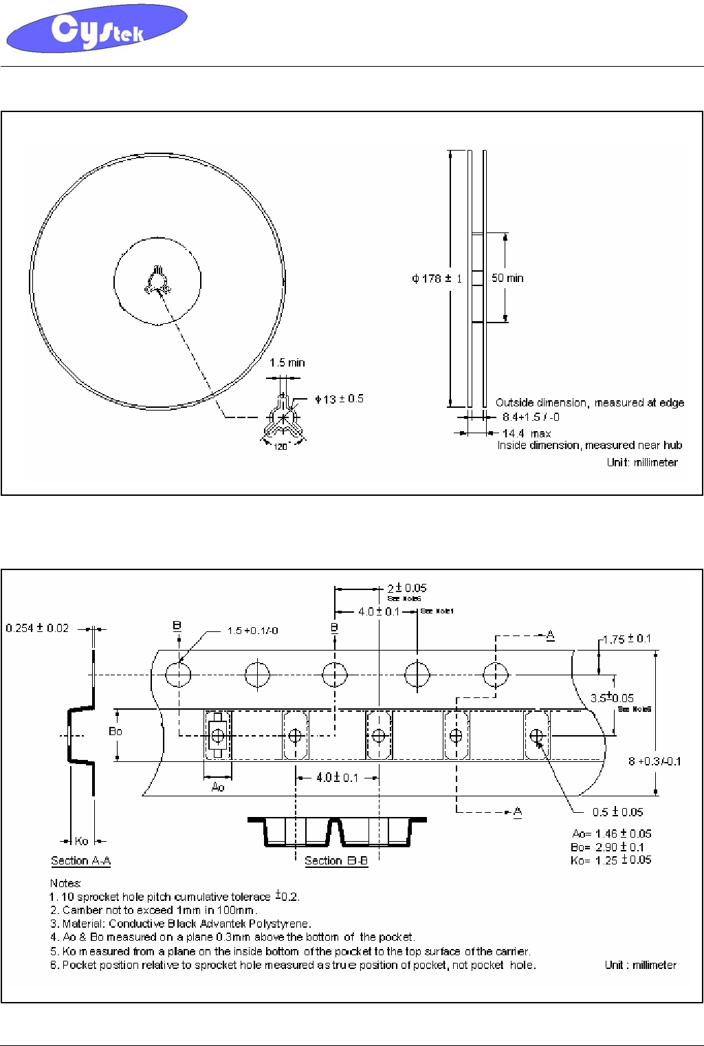
Reel Dimension
Carrier Tape Dimension
CYStech Electronics Corp.
Spec. No. : C345S2
Issued Date : 2004.04.27
Revised Date : 2013.04.15
Page No. : 5/6
RB751V-40S2 CYStek Product Specification
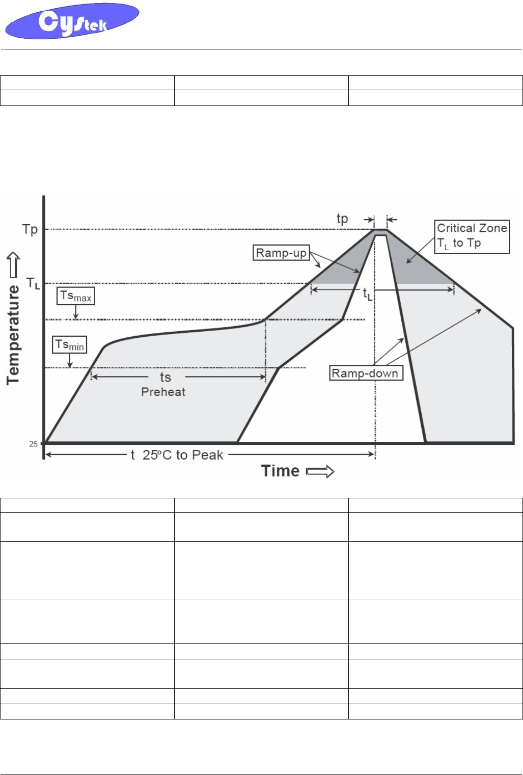
Recommended wave soldering condition
Product Peak Temperature Soldering Time
Pb-free devices 260 +0/-5 °C 5 +1/-1 seconds
Recommended temperature profile for IR reflow
Profile feature Sn-Pb eutectic Assembly Pb-free Assembly
Average ramp-up rate
(Tsmax to Tp) 3°C/second max. 3°C/second max.
Preheat
−Temperature Min(TS min)
−Temperature Max(TS max)
−Time(ts min to ts max)
100°C
150°C
60-120 seconds
150°C
200°C
60-180 seconds
Time maintained above:
−Temperature (TL)
− Time (tL)
183°C
60-150 seconds
217°C
60-150 seconds
Peak Temperature(TP) 240 +0/-5 °C 260 +0/-5 °C
Time within 5°C of actual peak
temperature(tp) 10-30 seconds 20-40 seconds
Ramp down rate 6°C/second max. 6°C/second max.
Time 25 °C to peak temperature 6 minutes max. 8 minutes max.
Note : All temperatures refer to topside of the package, measured on the package body surface.
CYStech Electronics Corp.
Spec. No. : C345S2
Issued Date : 2004.04.27
Revised Date : 2013.04.15
Page No. : 6/6
RB751V-40S2 CYStek Product Specification
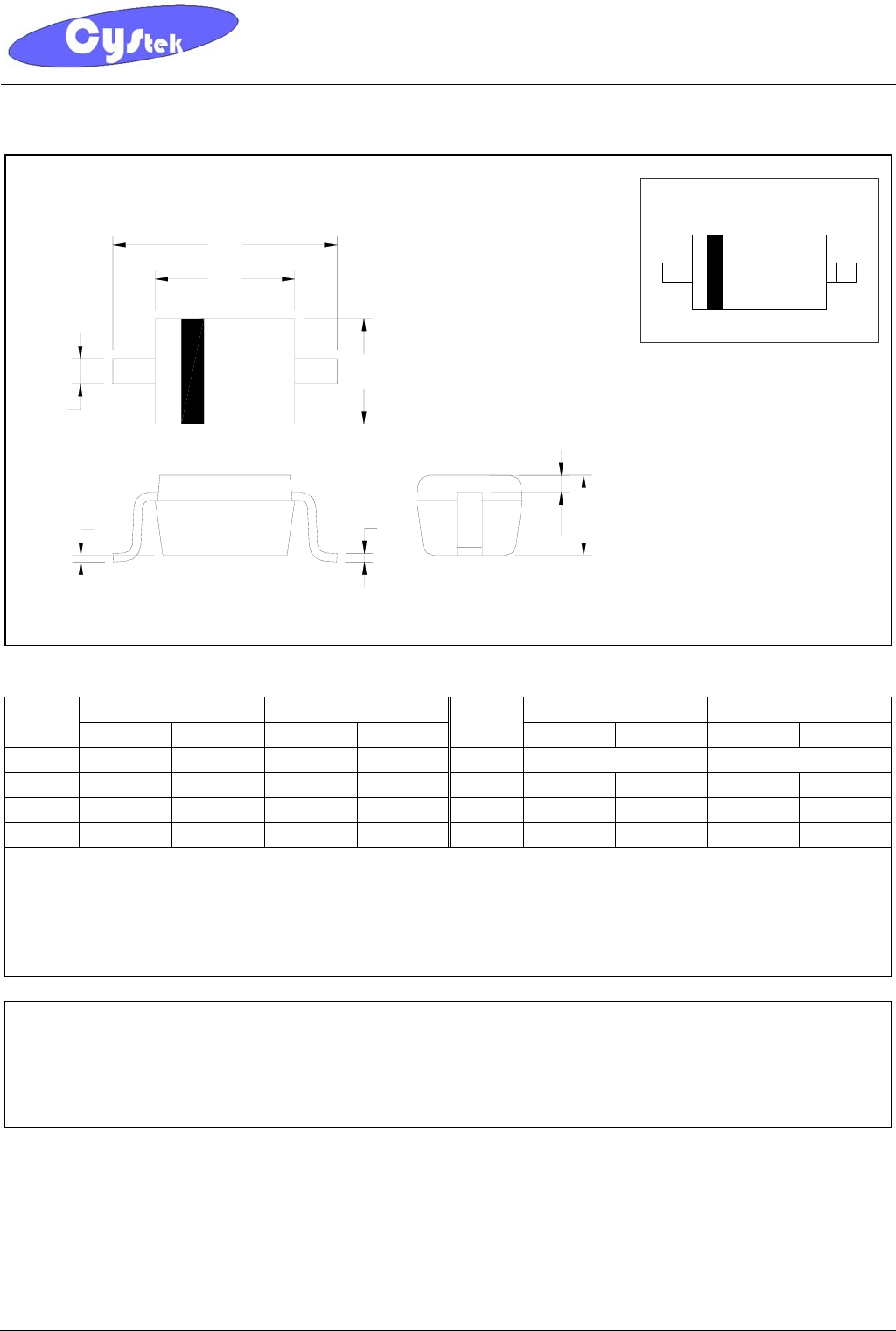
SOD-323 Dimension
*: Typical
Inches
D
A
HJ
K
C
E
B
12
Style: Pin 1.Cathode 2.Anode
2-Lead SOD-323 Plastic Surface
Mounted Package,
CYStek Package Code: S2
Marking:
5 H
5E
Millimeters Inches Millimeters
DIM Min. Max. Min. Max.
DIM Min. Max. Min. Max.
A 0.0630 0.0709 1.60 1.80 E 0.0060 REF 0.15 REF
B 0.0453 0.0531 1.15 1.35 H 0.0000 0.0040 0.00 0.10
C 0.0315 0.0394 0.80 1.00 J 0.0035 0.0070 0.089 0.177
D 0.0098 0.0157 0.25 0.40 K 0.0906 0.1063 2.30 2.70
Notes: 1.Controlling dimension : millimeters.
2.Lead thickness specified per L/F drawing with solder plating.
3.If there is any question with packing specification or packing method, please contact your local CYStek sales office.
Material:
• Lead: Pure tin plated.
• Mold Compound: Epoxy resin family, flammability solid burning class: UL94V-0.
Important Notice:
• All rights are reserved. Reproduction in whole or in part is prohibited without the prior written approval of CYStek.
• CYStek reserves the right to make changes to its products without notice.
• CYStek semiconductor products are not warranted to be suitable for use in Life-Support Applications, or systems.
• CYStek assumes no liability for any consequence of customer product design, infringement of patents, or application assistance.