RT7266 Datasheet. Www.s Manuals.com. Richtek
User Manual: Datasheets RT7266, RT7266ZSP.
Open the PDF directly: View PDF ![]() .
.
Page Count: 14
RT7266
®
DS7266-02 September 2012 www.richtek.com
1
©
Copyright 2012 Richtek Technology Corporation. All rights reserved. is a registered trademark of Richtek Technology Corporation.
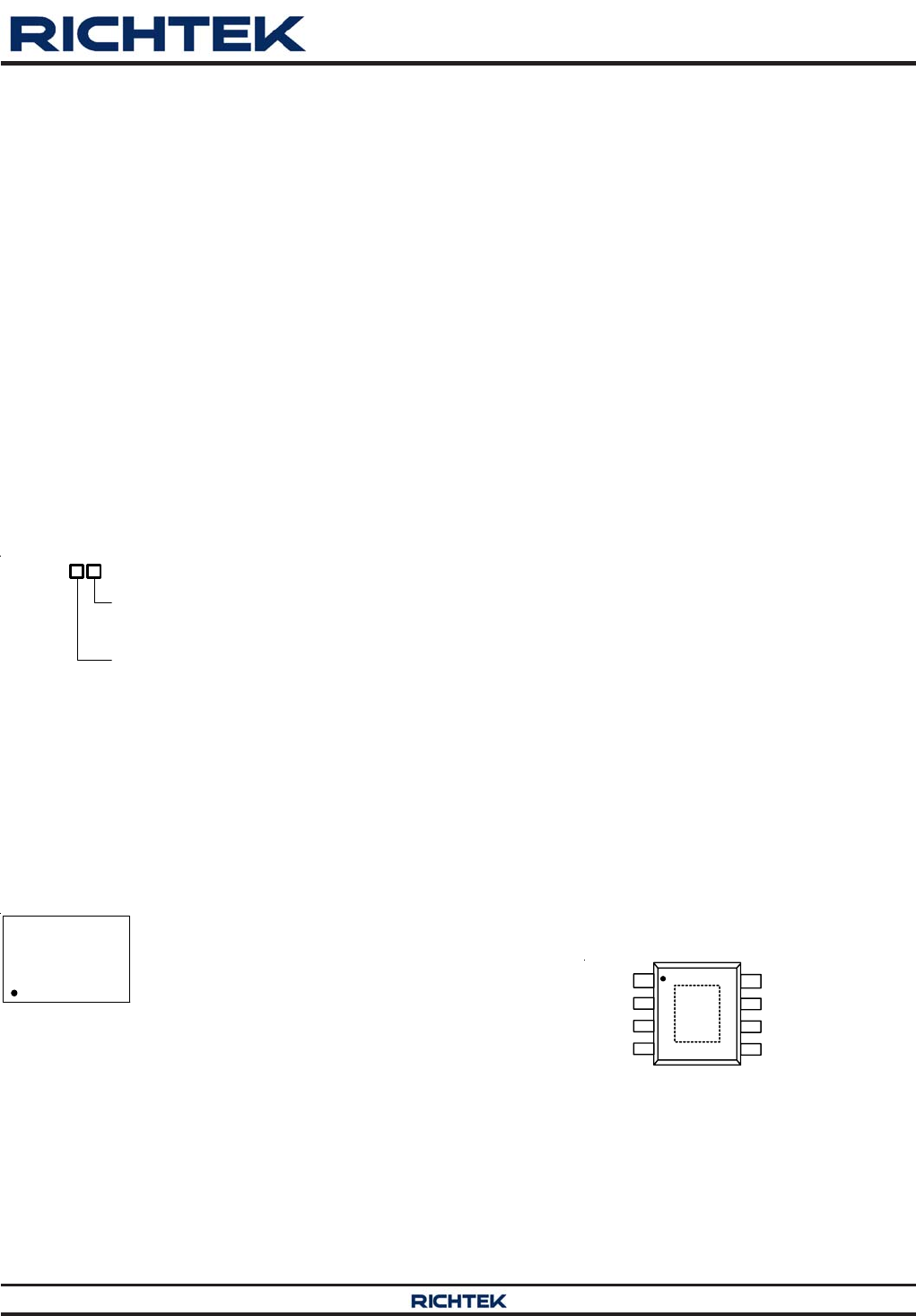
Pin Configurations
(TOP VIEW)
General Description
The RT7266 is an adaptive on-time ACOTTM mode
synchronous buck converter. The adaptive on-time ACOTTM
mode control provides a very fast transient response with
few external components. The low impedance internal
MOSFET can support high efficiency operation with wide
input voltage range from 4.5V to 18V . The proprietary
circuit of the RT7266 enables to support all ceramic
capacitors. The output voltage can be adjustable between
0.8V and 8V. The soft-start is adjustable by an external
capacitor.
Ordering Information
Note :
Richtek products are :
RoHS compliant and compatible with the current require-
ments of IPC/JEDEC J-STD-020.
Suitable for use in SnPb or Pb-free soldering processes.
SOP-8 (Exposed Pad)
Marking Information
Features
zz
zz
zACOTTM Mode Enables Fast Transient Response
zz
zz
z4.5V to 18V Input Voltage Range
zz
zz
z3A Output Current
zz
zz
z60mΩΩ
ΩΩ
Ω Internal Low Site N-MOSFET
zz
zz
zAdaptive On-Time Control
zz
zz
zFast Transient Response
zz
zz
zSupport All Ceramic Capacitors
zz
zz
zUp to 95% Efficiency
zz
zz
z700kHz Switching Frequency
zz
zz
zAdjustable Output Voltage from 0.8V to 8V
zz
zz
zAdjustable Soft-Start
zz
zz
zCycle-by-Cycle Current Limit
zz
zz
zInput Under Voltage Lockout
zz
zz
zThermal Shutdown Protection
zz
zz
zRoHS Compliant and Halogen Free
EN
FB
PVCC
SS
VIN
BOOT
GND
SW
GND
2
3
45
6
7
8
9
Applications
zIndustrial and Commercial Low Power Systems
zComputer Peripherals
zLCD Monitors and TVs
zGreen Electronics/Appliances
zPoint of Load Regulation for High-Performance DSPs,
FPGAs, and ASICs
RT7266
Package Type
SP : SOP-8 (Exposed Pad-Option 2)
Lead Plating System
Z : ECO (Ecological Element with
Halogen Free and Pb free)
RT7266
ZSPYMDNN
RT7266ZSP : Product Number
YMDNN : Date Code
3A, 18V, 700kHz ACOTTM Synchronous Step-Down
Converter
RT7266
2
DS7266-02 September 2012www.richtek.com
©
Copyright 2012 Richtek Technology Corporation. All rights reserved. is a registered trademark of Richtek Technology Corporation.
Pin No. Pin Name Pin Function
1 EN
Enable Input. A logic-high enables the converter; a logic-low forces the RT7266
into shutdown mode reducing the supply current to less than 10μA. Attach this
pin to VIN with a 100kΩ pull up resistor for automatic start-up.
2 FB
Feedback Input. It is used to regulate the output of the converter to a set value
via an external resistive voltage divider. The feedback reference voltage is
0.765V typically.
3 PVCC
Internal Regulator Output. Connect a 1μF capacitor to GND to stabilize
output voltage.
4 SS
Soft-Start Control Input. SS controls the soft-start period. Connect a capacitor
from SS to GND to set the soft-start period. A 3.9nF capacitor sets the soft-start
period to 1.5ms.
5, 9 (Exposed pad) GND Ground. The Exposed pad should be soldered to a large PCB and connected to
GND for maximum thermal dissipation.
6 SW Switch Node. Connect this pin to an external L-C filter.
7 BOOT
Bootstrap for High Side Gate Driver. Connect a 0.1μF or greater ceramic
capacitor from BOOT to SW pins.
8 VIN
Supply Input. The input voltage range is from 4.5V to 18V. Must bypass with a
suitable large ( ≥10μF x 2) ceramic capacitor.
Functional Pin Description
Table 1. Suggested Component Values
VOUT (V) R1 (kΩ) R2 (kΩ) C3 (pF) L1 (μH) C7 (μF)
1 6.81 22.1 -- 1.4 22 to 68
1.05 8.25 22.1 -- 1.4 22 to 68
1.2 12.7 22.1 -- 1.4 22 to 68
1.8 30.1 22.1 5 to 22 2 22 to 68
2.5 49.9 22.1 5 to 22 2 22 to 68
3.3 73.2 22.1 5 to 22 2 22 to 68
5 124 22.1 5 to 22 3.3 22 to 68
7 180 22.1 5 to 22 3.3 22 to 68
Typical Application Circuit
EN
RT7266
PVCC
FB
GND
VIN
VIN
10µF x 2
C1 0.1µF
C2
BOOT
L1
1.4µH
0.1µF
C6 22µF x 2
C7
SW
Chip Enable
SS
3.9nF
C5
1µF
C4
VOUT
1.05V/3A
8
1
3
4
2
7
6
5, 9 (Exposed Pad)
8.25k
R1
22.1k
R2
C3
VPVCC
RT7266
3
DS7266-02 September 2012 www.richtek.com
©
Copyright 2012 Richtek Technology Corporation. All rights reserved. is a registered trademark of Richtek Technology Corporation.
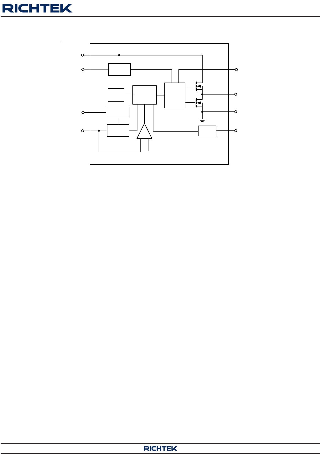
Function Block Diagram
VIN
Reg
UGATE
LGATE
Driver
BOOT
Control
FB On-Time
OC
EN EN
Comparator
Soft-Start
SS
SW
GND
PVCC
VREF
+
-
RT7266
4
DS7266-02 September 2012www.richtek.com
©
Copyright 2012 Richtek Technology Corporation. All rights reserved. is a registered trademark of Richtek Technology Corporation.
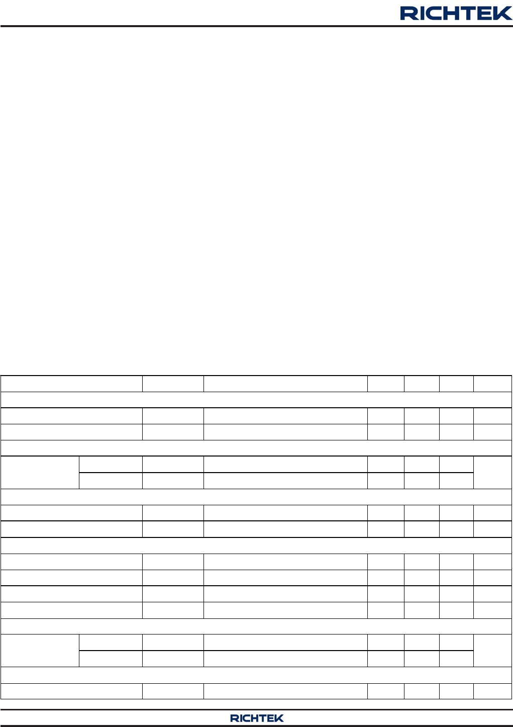
(VIN = 12V, TA = 25°C, unless otherwise specified)
Electrical Characteristics
Recommended Operating Conditions (Note 3)
zSupply Voltage, VIN ----------------------------------------------------------------------------------------------- 4.5V to 18V
zJunction Temperature Range ------------------------------------------------------------------------------------- −40°C to 125°C
zAmbient Temperature Range------------------------------------------------------------------------------------- −40°C to 85°C
Absolute Maximum Ratings (Note 1)
zSupply Voltage, VIN ----------------------------------------------------------------------------------------------- −0.3V to 20V
zSwitch Voltage, SW ----------------------------------------------------------------------------------------------- −0.8V to (VIN + 0.3V)
< 10ns----------------------------------------------------------------------------------------------------------------- −5V to 25V
zBOOT to SW -------------------------------------------------------------------------------------------------------- −0.3V to 6V
zAll Other Pins ------------------------------------------------------------------------------------------------------- −0.3V to 6V
zPower Dissipation, PD @ TA = 25°C
SOP-8 (Exposed Pad) -------------------------------------------------------------------------------------------- 1.333W
zPackage Thermal Resistance (Note 2)
SOP-8 (Exposed Pad), θJA --------------------------------------------------------------------------------------- 75°C/W
SOP-8 (Exposed Pad), θJC -------------------------------------------------------------------------------------- 15°C/W
zJunction Temperature Range ------------------------------------------------------------------------------------- 150°C
zLead Temperature (Soldering, 10 sec.)------------------------------------------------------------------------ 260°C
zStorage Temperature Range ------------------------------------------------------------------------------------- −65°C to 150°C
Parameter Symbol Test Conditions Min Typ Max Unit
Supply Current
Shutdown Current ISHDN V
EN = 0V -- 1 10 μA
Quiescent Current IQ V
EN = 3V, VFB = 1V -- 0.7 -- mA
Logic Threshold
Logic-High 2 -- 5.5
EN Voltage Logic-Low -- -- 0.4 V
VREF Voltage and Discharge Resistance
Feedback Reference Voltage VREF 4.5V ≤ VIN ≤ 18V 0.753 0.765 0.777 V
Feedback Input Current IFB V
FB = 0.8V −0.1 0 0.1 μA
VPVCC Output
VPVCC Output Voltage VPVCC 6V ≤ VIN ≤ 18V, 0 < IPVCC < 5mA 4.7 5.1 5.5 V
Line Regulation 6V ≤ VIN ≤ 18V, IPVCC = 5mA -- -- 20 mV
Load Regulation 0 < IPVCC < 5mA -- -- 60 mV
Output Current IPVCC V
IN = 6V, VPVCC = 4V -- 110 -- mA
RDS(ON)
High Side RDS(ON)_H -- 90 --
Switch On
Resistance Low Side RDS(ON)_L -- 60 -- mΩ
Current Limit
Current limit ILIM 3.5 4.1 5.7 A
RT7266
5
DS7266-02 September 2012 www.richtek.com
©
Copyright 2012 Richtek Technology Corporation. All rights reserved. is a registered trademark of Richtek Technology Corporation.
Note 1. Stresses beyond those listed “Absolute Maximum Ratings” may cause permanent damage to the device. These are
stress ratings only, and functional operation of the device at these or any other conditions beyond those indicated in
the operational sections of the specifications is not implied. Exposure to absolute maximum rating conditions may
affect device reliability.
Note 2. θJA is measured at TA = 25°C on a high effective thermal conductivity four-layer test board per JEDEC 51-7. θJC is
measured at the exposed pad of the package.
Note 3. The device is not guaranteed to function outside its operating conditions.
Parameter Symbol Test Conditions Min Typ Max Unit
Thermal Shutdown
Thermal Shutdown Threshold TSD -- 150 --
Thermal Shutdown
Hysteresis ΔTSD -- 20 --
°C
On-Time Timer Control
On-Time tON V
IN = 12V, VOUT = 1.05V -- 145 -- ns
Minimum On-Time tON(MIN) -- 60 -- ns
Minimum Off-Time tOFF(MIN) -- 230 -- ns
Soft-Start
SS Charge Current VSS = 0V 1.4 2 2.6 μA
SS Discharge Current VSS = 0.5V 0.05 0.1 -- mA
UVLO
UVLO Threshold VIN Rising to Wake up VPVCC 3.55 3.85 4.15
Hysteresis -- 0.3 --
V
RT7266
6
DS7266-02 September 2012www.richtek.com
©
Copyright 2012 Richtek Technology Corporation. All rights reserved. is a registered trademark of Richtek Technology Corporation.
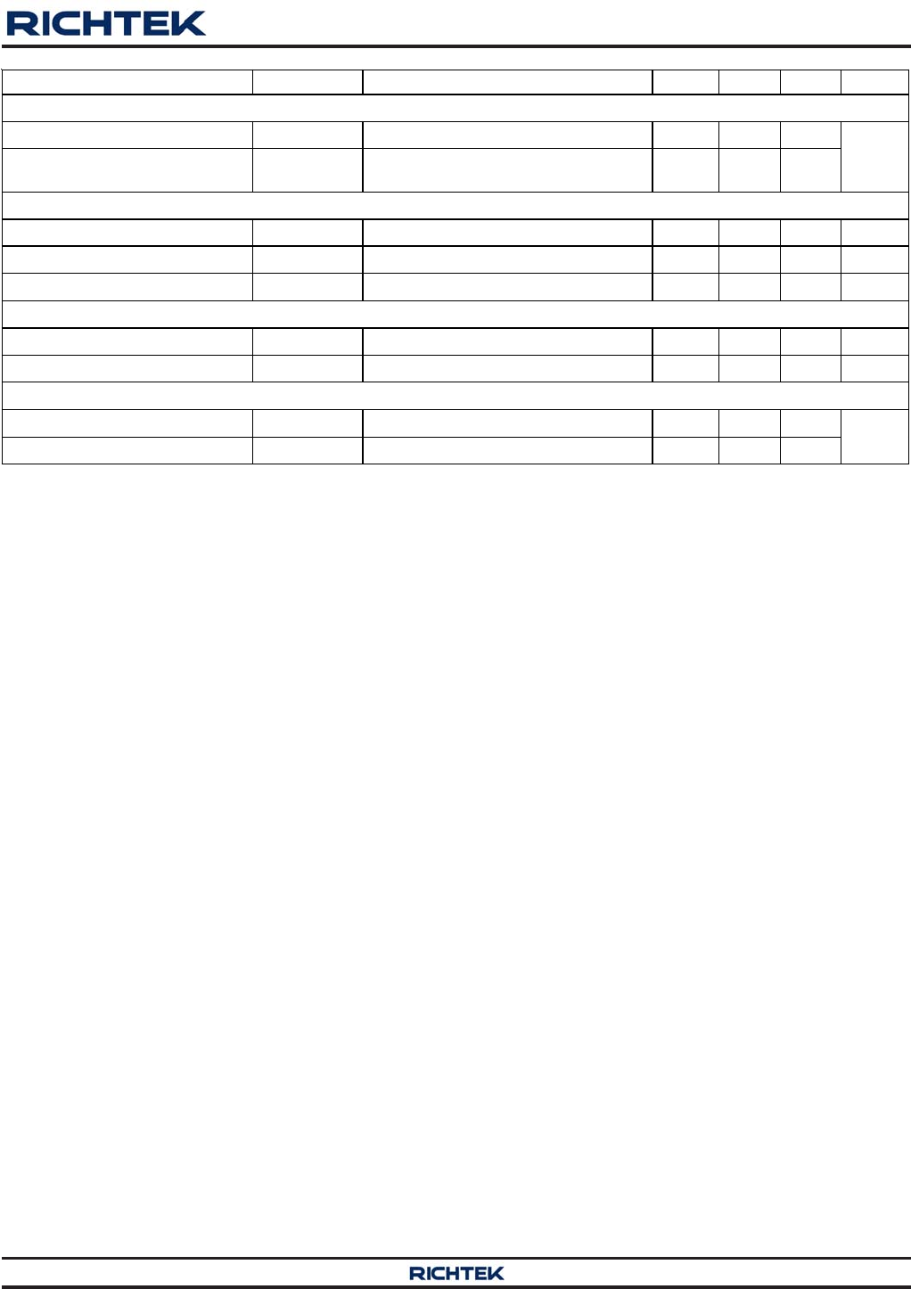
Typical Operating Characteristics
Output Voltage vs. Output Current
1.03
1.04
1.05
1.06
1.07
0 0.5 1 1.5 2 2.5 3
Output Current (A)
Output Voltage (V)
VIN = 4.5V
VIN = 12V
VIN = 17V
VOUT = 1.05V
Efficiency vs. Output Current
0
10
20
30
40
50
60
70
80
90
100
0 0.5 1 1.5 2 2.5 3
Output Current (A)
Efficiency (%)
VOUT = 5V
VOUT = 3.3V
VOUT = 1.05V
VIN = 12V
Frequency vs. Input Voltage
400
500
600
700
800
900
4 6 8 1012141618
Input Voltage (V)
Frequency (kHz) 1
VOUT = 1.05V, ILOAD = 0.1A
Reference Voltage vs. Input Voltage
0.750
0.755
0.760
0.765
0.770
0.775
0.780
4 6 8 1012141618
Input Voltage (V)
Reference Voltage (V)
No Load, VOUT = 1.05V
Output Voltage vs. Input Voltage
1.03
1.04
1.05
1.06
1.07
4 6 8 1012141618
Input Voltage (V)
Output Voltage (V)
VOUT = 1.05V
IOUT = 0A
IOUT = 1A
IOUT = 2A
IOUT = 3A
Reference Voltage vs. Temperature
0.750
0.755
0.760
0.765
0.770
0.775
0.780
-50 -25 0 25 50 75 100 125
Temperature (°C)
Reference Voltage (V)
VIN = 17V
VIN = 12V
VIN = 4.5V
No Load, VOUT = 1.05V
RT7266
7
DS7266-02 September 2012 www.richtek.com
©
Copyright 2012 Richtek Technology Corporation. All rights reserved. is a registered trademark of Richtek Technology Corporation.
Output Voltage Ripple
VSW
(10V/Div)
Time (500ns/Div)
VOUT
(10mV/Div)
VIN = 12V, VOUT = 1.05V, IOUT = 3A
Shutdown Current vs. Temperature
0
1
2
3
4
5
6
7
8
9
10
-50-25 0 25 50 75100125
Temperature (°C)
Shutdown Current (µA) 1
VIN = 17V
VIN = 12V
VIN = 4.5V
VEN = 0V
Load Transient Response
VOUT
(20mV/Div)
Time (100μs/Div)
IOUT
(2A/Div)
VIN = 12V, VOUT = 1.05V, IOUT = 0A to 3A
Quiescent Current vs. Temperature
0.3
0.4
0.4
0.5
0.5
0.6
0.6
0.7
0.7
0.8
0.8
-50 -25 0 25 50 75 100 125
Temperature (°C)
Quiescent Current (mA
)
VIN = 17V
VIN = 12V
VIN = 4.5V
VEN = 3V, VFB = 1V
Current Limit vs. Input Voltage
0
1
2
3
4
5
6
7
8
4 6 8 1012141618
Input Voltage (V)
Current Limit (A)
VOUT = 0V
Current Limit vs. Temperature
0
1
2
3
4
5
6
7
8
-50-250 255075100125
Temperature (°C)
Current Limit (A)
VIN = 17V
VIN = 12V
VIN = 4.5V
VOUT = 0V
RT7266
8
DS7266-02 September 2012www.richtek.com
©
Copyright 2012 Richtek Technology Corporation. All rights reserved. is a registered trademark of Richtek Technology Corporation.
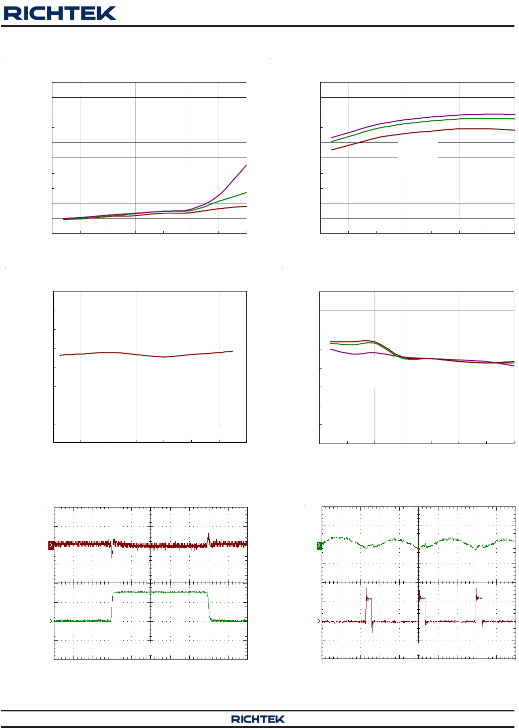
Power Off from VIN
VOUT
(1V/Div)
Time (10ms/Div)
IOUT
(5A/Div)
VIN = 12V, VOUT = 1.05V, IOUT = 3A
VSW
(10V/Div)
VIN
(20V/Div)
Power Off from VEN
VOUT
(1V/Div)
Time (100μs/Div)
IOUT
(5A/Div)
VIN = 12V, VOUT = 1.05V, IOUT = 3A
VSW
(10V/Div)
VEN
(5V/Div)
Power On from VEN
VOUT
(1V/Div)
Time (5ms/Div)
IOUT
(5A/Div)
VIN = 12V, VOUT = 1.05V, IOUT = 3A
VSW
(10V/Div)
VEN
(5V/Div)
Power On from VIN
VOUT
(1V/Div)
Time (5ms/Div)
IOUT
(5A/Div)
VIN = 12V, VOUT = 1.05V, IOUT = 3A
VSW
(10V/Div)
VIN
(20V/Div)
RT7266
9
DS7266-02 September 2012 www.richtek.com
©
Copyright 2012 Richtek Technology Corporation. All rights reserved. is a registered trademark of Richtek Technology Corporation.
Application Information
The RT7266 is a synchronous high voltage buck converter
that can support the input voltage range from 4.5V to 18V
and the output current can be up to 3A. It operates using
adaptive on-time ACOTTM mode control and provides a very
fast transient response with few external compensation
components. The RT7266 allows low external component
count configuration with both low ESR and ceramic output
capacitors.
PWM Operation
It is suitable for low external component count
configuration with appropriate amount of Equivalent Series
Resistance (ESR) capacitor(s) at the output. The output
ripple valley voltage is monitored at a feedback point
voltage. The synchronous high side MOSFET is turned
on at the beginning of each cycle. After the internal one
shot timer expires, the MOSFET is turned off. The pulse
width of this one shot is determined by the converter's
input and output voltages to keep the frequency fairly
constant over the entire input voltage range.
Adaptive On-Time Control
The RT7266 has a unique circuit to ensure the switching
frequency on 700kHz over full input voltage range and full
loading range. This circuit sets the on-time one-shot timer
by monitoring the input voltage and SW signal. The
switching frequency will keep constant if the duty ratio is
VOUT/VIN.
Duty Ratio = VOUT/VIN = tON / T
For Fixed T, Ton is proportional to VOUT/VIN.
Soft-Start
The RT7266 contains an external soft-start clamp that
gradually raises the output voltage. The soft-start timing
can be programmed by the external capacitor between
SS pin and GND. The chip provides a 2μA charge current
for the external capacitor. If a 3.9nF capacitor is used,
the soft-start will be 2ms (typ.). The available capacitance
range is from 2.7nF to 220nF.
SS SS
C5 (nF) 1.065
t (ms) = I (A)
μ
×
Chip Enable Operation
The EN pin is the chip enable input. Pulling the EN pin
low (<0.4V) will shutdown the device. During shutdown
mode, the RT7266 quiescent current drops to lower than
10μA. Driving the EN pin high (>2V, <5.5V) will turn on
the device again. For external timing control, the EN pin
can also be externally pulled high by adding a REN* resistor
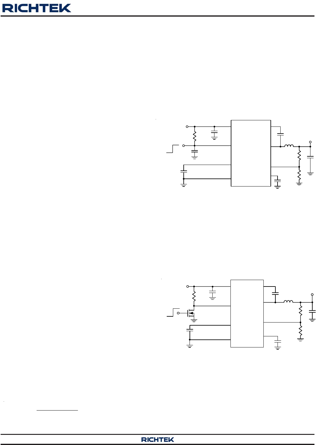
and CEN* capacitor from the VIN pin (see Figure 1).
Figure 1. External Timing Control
An external MOSFET can be added to implement digital
control on the EN pin when no system voltage above 2V
is available, as shown in Figure 2. In this case, a 100kΩ
pull-up resistor, REN, is connected between VIN and the
EN pin. MOSFET Q1 will be under logic control to pull
down the EN pin.
Figure 2. Logic Control with Low Voltage
VIN
EN
GND
BOOT
FB
SW
1
2
8
6
7
L1
R1
R2
VOUT
Chip Enable
VIN
RT7266
SS
4
C5
PVCC 3
C6
C7
C1
REN
Q1
100k
5,
9 (Exposed Pad) C4
VIN
EN
GND
BOOT
FB
SW
1
2
8
6
7
L1
R1
R2
VOUT
Chip Enable
VIN
4.5V to 18V RT7266
SS
4
C5 PVCC C4
3
5,
9 (Exposed Pad)
C6
C7
C1
REN*
CEN*
* : Optional
RT7266
10
DS7266-02 September 2012www.richtek.com
©
Copyright 2012 Richtek Technology Corporation. All rights reserved. is a registered trademark of Richtek Technology Corporation.
OUT OUT
LIN
VV
I = 1
fL V
⎡⎤⎡ ⎤
Δ×−
⎢⎥⎢ ⎥
×
⎣⎦⎣ ⎦
Having a lower ripple current reduces not only the ESR
losses in the output capacitors but also the output voltage
ripple. High frequency with small ripple current can achieve
highest efficiency operation. However, it requires a large
inductor to achieve this goal. For the ripple current
selection, the value of ΔIL = 0.2(IMAX) will be a reasonable
starting point. The largest ripple current occurs at the
highest VIN. To guarantee that the ripple current stays
below the specified maximum, the inductor value should
be chosen according to the following equation :
OUT OUT
L(MAX) IN(MAX)
VV
L = 1
fI V
⎡⎤⎡ ⎤
×−
⎢⎥⎢ ⎥
×Δ
⎣⎦⎣ ⎦
CIN and COUT Selection
The input capacitance, CIN, is needed to filter the
trapezoidal current at the source of the high side MOSFET.
To prevent large ripple current, a low ESR input capacitor
sized for the maximum RMS current should be used. The
RMS current is given by :
OUT IN
RMS OUT(MAX) IN OUT
VV
I = I 1
VV
−
This formula has a maximum at VIN = 2VOUT, where
IRMS = IOUT/2. This simple worst-case condition is
commonly used for design because even significant
deviations do not offer much relief.
Choose a capacitor rated at a higher temperature than
required. Several capacitors may also be paralleled to
meet size or height requirements in the design. For the
input capacitor, two 10μF and 0.1μF low ESR ceramic
capacitors are recommended.
Output Voltage Setting
The resistive divider allows the FB pin to sense the output
voltage as shown in Figure 4.
Where VFB is the feedback reference voltage (0.765V
typ.).
Under Voltage Lockout Protection
The RT7266 has Under Voltage Lockout Protection (UVLO)
that monitors the voltage of PVCC pin. When the VPVCC
voltage is lower than UVLO threshold voltage, the RT7266
will be turned off in this state. This is non-latch protection.
Over Temperature Protection
The RT7266 equips an Over Temperature Protection (OTP)
circuitry to prevent overheating due to excessive power
Figure 4. Output Voltage Setting
The output voltage is set by an external resistive divider
according to the following equation. It is recommended to
use 1% tolerance or better divider resistors.
)
OUT FB R1
V = V ( 1 +
R2
×
RT7266
GND
FB
R1
R2
VOUT
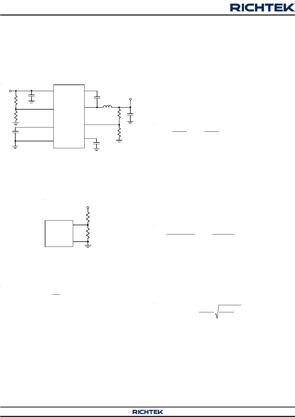
To prevent enabling circuit when VIN is smaller than the
VOUT target value, a resistive voltage divider can be placed
between the input voltage and ground and connected to
the EN pin to adjust IC lockout threshold, as shown in
Figure 3. For example, if an 8V output voltage is regulated
from a 12V input voltage, the resistor REN2 can be selected
to set input lockout threshold larger than 8V.
Figure 3. The Resistors can be Selected to Set IC
Lockout Threshold
dissipation. The OTP will shut down switching operation
when junction temperature exceeds 150°C. Once the
junction temperature cools down by approximately 20°C
the main converter will resume operation. To maintain
continuous operation maximum, the junction temperature
should be prevented from rising above 150°C.
Inductor Selection
The inductor value and operating frequency determine the
ripple current according to a specific input and an output
voltage. The ripple current ΔIL increases with higher VIN
and decreases with higher inductance.
VIN
EN
GND
BOOT
FB
SW
1
2
8
6
7
L1
R1
R2
VOUT
VIN
RT7266
SS
4
C5
PVCC C4
3
C6
C7
C1
100k
8V
12V
REN2
REN1
5,
9 (Exposed Pad)
RT7266
11
DS7266-02 September 2012 www.richtek.com
©
Copyright 2012 Richtek Technology Corporation. All rights reserved. is a registered trademark of Richtek Technology Corporation.
OUT L OUT
1
VIESR
8fC
⎡⎤
Δ≤Δ +
⎢⎥
⎣⎦
The output ripple will be highest at the maximum input
voltage since ΔIL increases with input voltage. Multiple
capacitors placed in parallel may be needed to meet the
ESR and RMS current handling requirements.
Higher values, lower cost ceramic capacitors are now
becoming available in smaller case sizes. Their high ripple
current, high voltage rating and low ESR make them ideal
for switching regulator applications. However, care must
be taken when these capacitors are used at input and
output. When a ceramic capacitor is used at the input
and the power is supplied by a wall adapter through long
wires, a load step at the output can induce ringing at the
input, VIN. At best, this ringing can couple to the output
and be mistaken as loop instability. At worst, a sudden
inrush of current through the long wires can potentially
cause a voltage spike at VIN large enough to damage the
part.
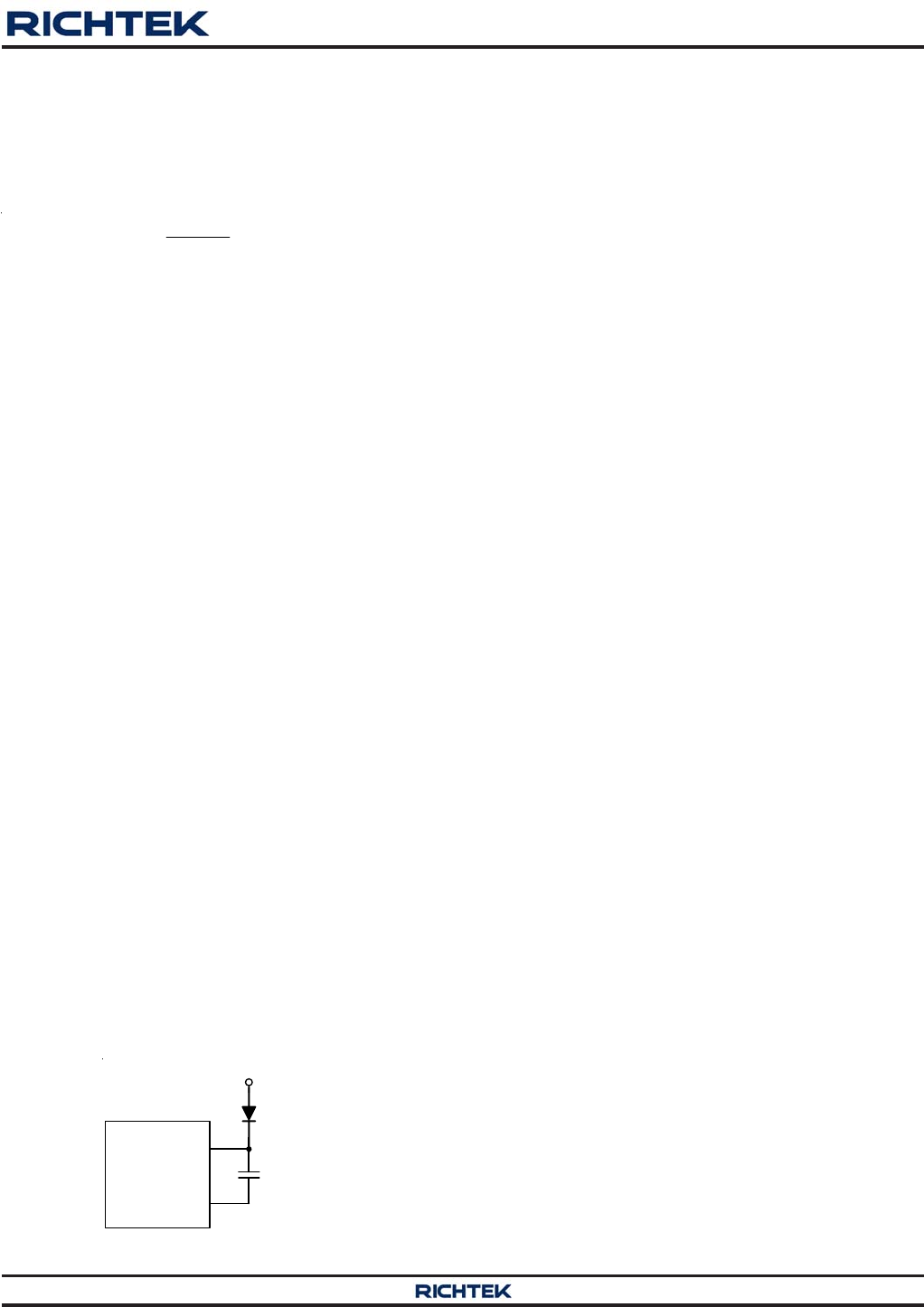
External Bootstrap Diode
Connect a 0.1μF low ESR ceramic capacitor between the
BOOT and SW pins. This capacitor provides the gate driver
voltage for the high side MOSFET. It is recommended to
add an external bootstrap diode between an external 5V
and the BOOT pin for efficiency improvement when input
voltage is lower than 5.5V or duty ratio is higher than 65%.
The bootstrap diode can be a low cost one such as 1N4148
or BAT54. The external 5V can be a 5V fixed input from
system or a 5V output of the RT7266. Note that the external
boot voltage must be lower than 5.5V
SW
BOOT
5V
RT7266 0.1µF
Figure 5. External Bootstrap Diode
PVCC Capacitor Selection
Decouple with a 1μF ceramic capacitor. X7R or X5R grade
dielectric ceramic capacitors are recommended for their
stable temperature characteristics.
Over Current Protection
When the output shorts to ground, the inductor current
decays very slowly during a single switching cycle. A over
current detector is used to monitor inductor current to
prevent current runaway. The over current detector monitors
the voltage between SW and GND during the low-side MOS
turn-on state. This is cycle-by-cycle protection. The over
current detector also supports temperature compensated.
Thermal Considerations
For continuous operation, do not exceed absolute
maximum junction temperature. The maximum power
dissipation depends on the thermal resistance of the IC
package, PCB layout, rate of surrounding airflow, and
difference between junction and ambient temperature. The
maximum power dissipation can be calculated by the
following formula :
PD(MAX) = (TJ(MAX) − TA) / θJA
where TJ(MAX) is the maximum junction temperature, TA is
the ambient temperature, and θJA is the junction to ambient
thermal resistance.
For recommended operating condition specifications, the
maximum junction temperature is 125°C. The junction to
ambient thermal resistance, θJA, is layout dependent. For
SOP-8 (Exposed Pad) packages, the thermal resistance,
θJA, is 75°C/W on a standard JEDEC 51-7 four-layer
thermal test board. The maximum power dissipation at
TA = 25°C can be calculated by the following formulas :
PD(MAX) = (125°C − 25°C) / (75°C/W) = 1.333W for
SOP-8 (Exposed Pad) package
The maximum power dissipation depends on the operating
ambient temperature for fixed TJ(MAX) and thermal
resistance, θJA. The derating curves in Figure 6 allow the
designer to see the effect of rising ambient temperature
on the maximum power dissipation.
The selection of COUT is determined by the required ESR
to minimize voltage ripple.
Moreover, the amount of bulk capacitance is also a key
for COUT selection to ensure that the control loop is stable.
The output ripple, ΔVOUT , is determined by :
RT7266
12
DS7266-02 September 2012www.richtek.com
©
Copyright 2012 Richtek Technology Corporation. All rights reserved. is a registered trademark of Richtek Technology Corporation.
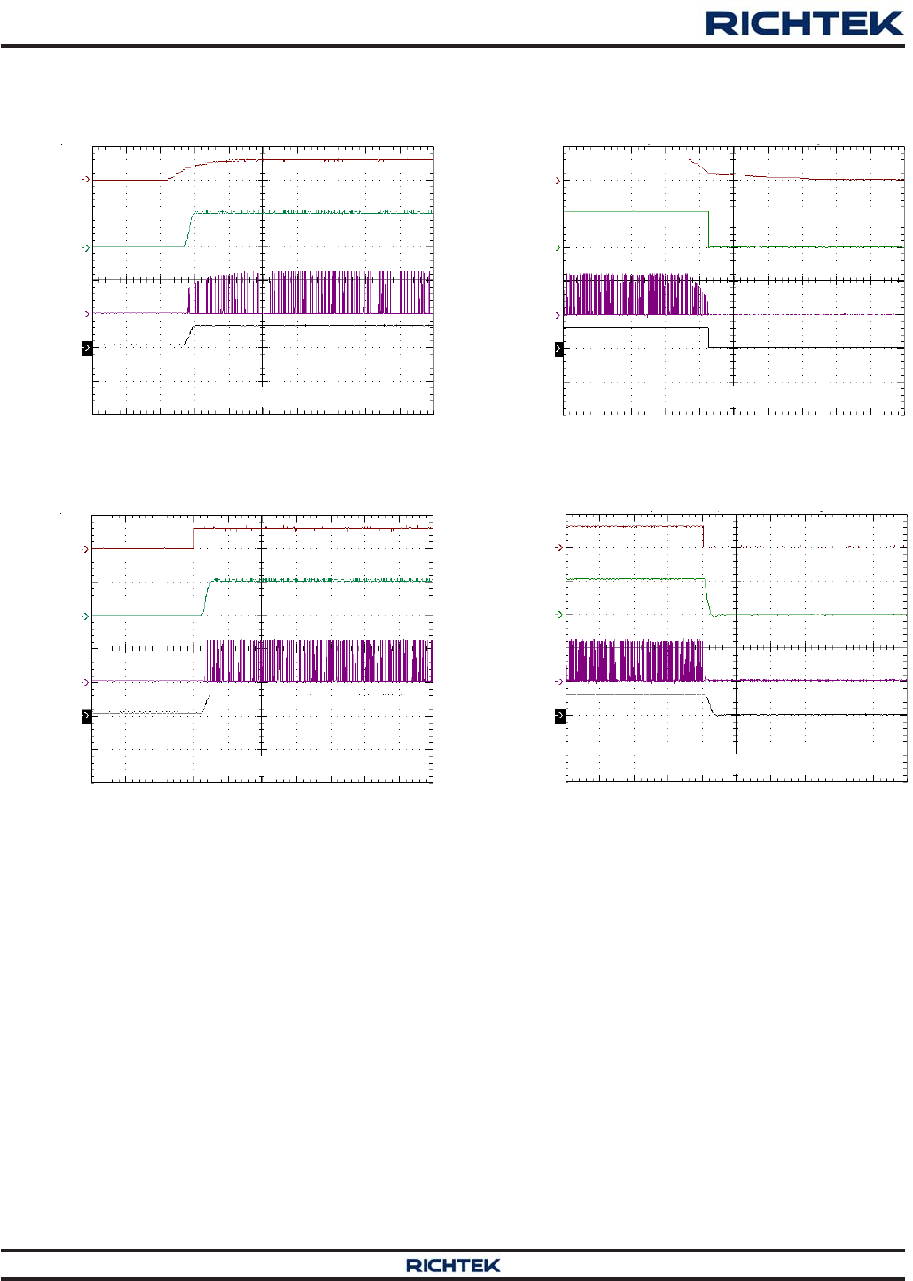
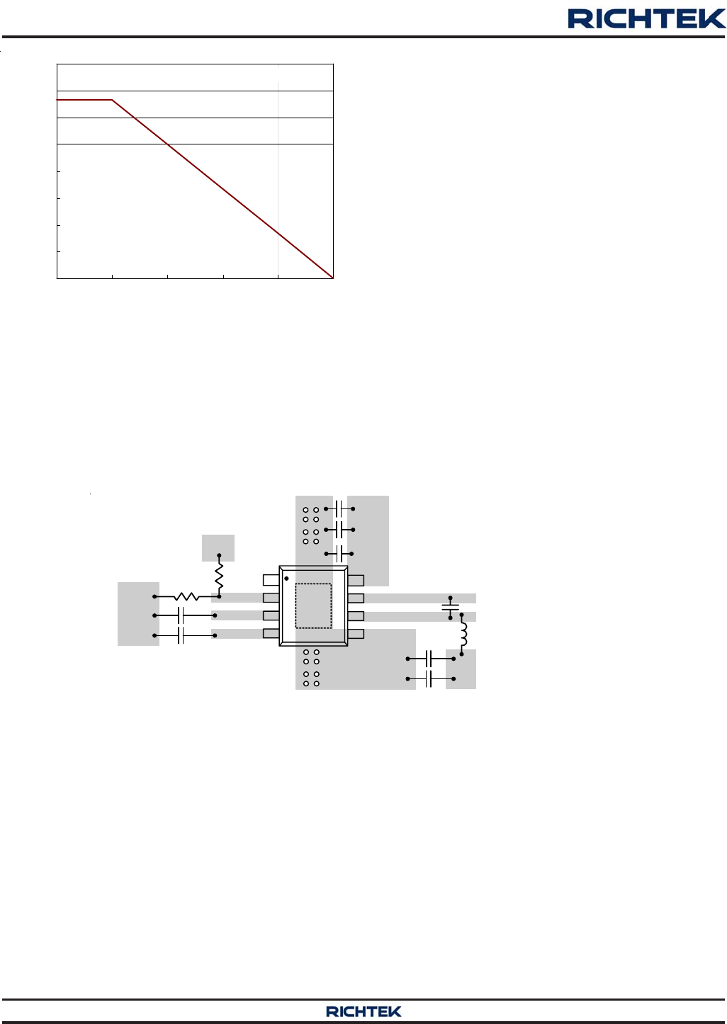
Figure 7. PCB Layout Guide
Figure 6. Derating Curve of Maximum Power Dissipation
0.0
0.2
0.4
0.6
0.8
1.0
1.2
1.4
1.6
0 25 50 75 100 125
Ambient Temperature (°C)
Maximum Power Dissipation (W) 1
Four-Layer PCB Layout Consideration
Follow the PCB layout guidelines for optimal performance
of the RT7266
Keep the traces of the main current paths as short and
wide as possible.
Put the input capacitor as close as possible to the device
pins (VIN and GND).
SW node is with high frequency voltage swing and
should be kept at small area. Keep sensitive
components away from the SW node to prevent stray
capacitive noise pickup.
Connect feedback network behind the output capacitors.
Keep the loop area small. Place the feedback
components near the RT7266.
The GND and Exposed Pad should be connected to a
strong ground plane for heat sinking and noise protection.
EN
FB
PVCC
SS
VIN
BOOT
GND
SW
GND
2
3
45
6
7
8
9
C2
C1
C6
L1
VOUT
C7
VOUT
C4
C5
R1
R2
GND
Input capacitor must be placed
as close to the IC as possible.
SW should be connected to inductor by
wide and short trace. Keep sensitive
components away from this trace.
The resistor divider must be connected
as close to the device as possible.
RT7266
13
DS7266-02 September 2012 www.richtek.com
Richtek Technology Corporation
5F, No. 20, Taiyuen Street, Chupei City
Hsinchu, Taiwan, R.O.C.
Tel: (8863)5526789
Richtek products are sold by description only. Richtek reserves the right to change the circuitry and/or specifications without notice at any time. Customers should
obtain the latest relevant information and data sheets before placing orders and should verify that such information is current and complete. Richtek cannot
assume responsibility for use of any circuitry other than circuitry entirely embodied in a Richtek product. Information furnished by Richtek is believed to be
accurate and reliable. However, no responsibility is assumed by Richtek or its subsidiaries for its use; nor for any infringements of patents or other rights of third
parties which may result from its use. No license is granted by implication or otherwise under any patent or patent rights of Richtek or its subsidiaries.
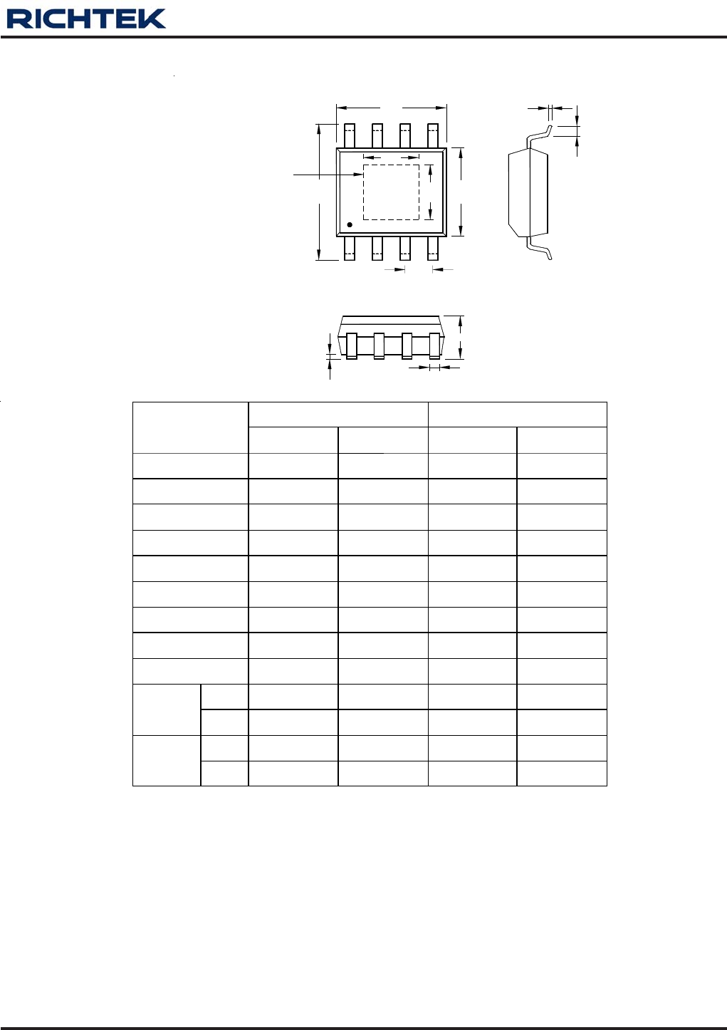
A
B
J
F
H
M
C
D
I
Y
X
EXPOSED THERMAL PAD
(Bottom of Package)
8-Lead SOP (Exposed Pad) Plastic Package
Dimensions In Millimeters Dimensions In Inches
Symbol Min Max Min Max
A 4.801 5.004 0.189 0.197
B 3.810 4.000 0.150 0.157
C 1.346 1.753 0.053 0.069
D 0.330 0.510 0.013 0.020
F 1.194 1.346 0.047 0.053
H 0.170 0.254 0.007 0.010
I 0.000 0.152 0.000 0.006
J 5.791 6.200 0.228 0.244
M 0.406 1.270 0.016 0.050
X 2.000 2.300 0.079 0.091
Option 1 Y 2.000 2.300 0.079 0.091
X 2.100 2.500 0.083 0.098
Option 2 Y 3.000 3.500 0.118 0.138
Outline Dimension