RT8223L, RT8223M Datasheet. Www.s Manuals.com. R04 Richtek
User Manual: Marking of electronic components, SMD Codes EP, EP **, EP*, EP**, EP=**, Ep. Datasheets BD4853FVE, BD4853G, BD49E52G, BD49K52G, BZX585-B51, CMDZ3L0, MAX6314US30D3-T, RT8016-12PQW, RT8223LGQW, RT8223LZQW, SMBJ160CA.
Open the PDF directly: View PDF ![]() .
.
Page Count: 25

RT8223L/M
1
DS8223L/M-04 April 2011 www.richtek.com
Ordering Information
Note :
Richtek products are :
` RoHS compliant and compatible with the current require-
ments of IPC/JEDEC J-STD-020.
` Suitable for use in SnPb or Pb-free soldering processes.
High Efficiency, Main Power Supply Controller
for Notebook Computer
General Description
The RT8223L/M is a dual step-down, switch-mode power
supply controller generating logic-supply voltages in
battery-powered systems. It includes two Pulse Width
Modulation (PWM) controllers adjustable from 2V to 5.5V,
and also features fixed 5V/3.3V linear regulators. Each
linear regulator provides up to 100mA output current with
automatic linear regulator bootstrapping to the PWM
outputs. The RT8223L/M includes on-board power up
sequencing, a power good output, internal soft-start, and
soft-discharge output that prevents negative voltage during
shutdown.
The constant on-time PWM scheme can operate without
sense resistors and provide 100ns load transient response
while maintaining nearly constant switching frequency. To
eliminate noise in audio applications, an ultrasonic mode
is included, which maintains the switching frequency
above 25kHz. Moreover, the diode-emulation mode
maximizes efficiency for light load applications. The
RT8223L/M is available in a WQFN-24L 4x4 package.
Features
zz
zz
zConstant On-time Control with 100ns Load Step
Response
zz
zz
zWide Input Voltage Range : 6V to 25V
zz
zz
zDual Adjustable Outputs from 2V to 5.5V
zz
zz
zFixed 3.3V and 5V LDO Output : 100mA
zz
zz
z2V Reference Voltage
zz
zz
zFrequency Selectable via TONSEL Setting
zz
zz
z4700ppm/°°
°°
°C RDS(ON) Current Sensing
zz
zz
zProgrammable Current Limit Combined with
Enable Control
zz
zz
zSelectable PWM, DEM, or Ultrasonic Mode
zz
zz
zInternal Soft-Start and Soft-Discharge
zz
zz
zHigh Efficiency up to 97%
zz
zz
z5mW Quiescent Power Dissipation
zz
zz
zThermal Shutdown
zz
zz
zRoHS Compliant and Halogen Free
Applications
zNotebook and Sub-Notebook Computers
z3-Cell and 4-Cell Li+ Battery-Powered Devices
Package Type
QW : WQFN-24L 4x4 (W-Type)
Lead Plating System
G : Green (Halogen Free and Pb Free)
Z : ECO (Ecological Element with
Halogen Free and Pb free)
RT8223
Pin Function
L : Default
M : With ENC
RT8223L/M
2
DS8223L/M-04 April 2011www.richtek.com
Pin Configurations
WQFN-24L 4x4
RT8223L
(TOP VIEW)
WQFN-24L 4x4
RT8223M
ENTRIP1
FB1
REF
TONSEL
FB2
ENTRIP2
LGATE2
VOUT2
VREG3
BOOT2
PHASE2
UGATE2
NC
VREG5
GND
SKIPSEL
EN
VIN
UGATE1
LGATE1
VOUT1
PGOOD
BOOT1
PHASE1
GND
1
2
3
4
5
6
78910 1211
18
17
16
15
14
13
21 20 1924 2223
25
ENTRIP1
FB1
REF
TONSEL
FB2
ENTRIP2
LGATE2
VOUT2
VREG3
BOOT2
PHASE2
UGATE2
ENC
VREG5
GND
SKIPSEL
EN
VIN
UGATE1
LGATE1
VOUT1
PGOOD
BOOT1
PHASE1
GND
1
2
3
4
5
6
78910 1211
18
17
16
15
14
13
21 20 1924 2223
25
Marking Information
EP= : Product Code
YMDNN : Date Code
RT8223LGQW RT8223MGQW
EQ= : Product Code
YMDNN : Date Code
RT8223MZQW
EQ : Product Code
YMDNN : Date Code
EP YM
DNN
EP=YM
DNN EQ=YM
DNN
EQ YM
DNN
RT8223LZQW
EP : Product Code
YMDNN : Date Code
RT8223L/M
3
DS8223L/M-04 April 2011 www.richtek.com
Typical Application Circuit
RT8223L
PHASE1
LGATE1
BOOT1
UGATE1
VOUT1
V
OUT1
5V
VIN
VREG5
VREG3
PGOOD
GND
16
25 (Exposed Pad)
19
22
20
21
24
23
17
8
PHASE2
LGATE2
BOOT2
UGATE2
VOUT2
V
OUT2
Q2
L2
C11
C17
3.3V
R10C12
V
IN
10µF10µF
0.1µF
R11
C14
10
11
9
12
7
BSC119
N03S
Q4
BSC119
N03S
0
R
BOOT2
0
C13
4.7µH
220µF
Q1
L1C2
C3
R4
10µF
0.1µF
R5
C4
BSC119
N03S
Q3
BSC119
N03S
0
R
BOOT1
0
C1
6.8µH
220µF
R8
3.9
C10
0.1µF
5V Always On
3.3V Always On
ENTRIP1
ENTRIP2
1
6
FB2
FB1
2
5
R
ILIM1
150k
150k
C9
4.7µFR6
100k
PGOOD Indicator
C16
4.7µF
REF
3
C15
0.22µF
TONSEL
SKIPSEL
4
14
Frequency Control
PWM/DEM/Ultrasonic
EN
ON
OFF
13
R14
6.5k
R15
10k
C21
C20
0.1µF
R12
15k
R13
10k
C18
C19
0.1µF
GND 15
6V to 25V
VREF
2V
R
ILIM2
V
OUT1
5V
0.1µF
RT8223M
PHASE1
LGATE1
BOOT1
UGATE1
VOUT1
VIN
VREG5
VREG3
PGOOD
GND
16
25 (Exposed Pad)
19
22
20
21
24
23
17
8
PHASE2
LGATE2
BOOT2
UGATE2
VOUT2
V
OUT2
Q2
L2
C11
C17
3.3V
R10C12
V
IN
10µF10µF
0.1µF
R11
C14
10
11
9
12
7
BSC119
N03S
Q4
BSC119
N03S
0
0
C13
4.7µH
220µF
Q1
L1C2
C3
R4
10µF
0.1µF
R5
C4
BSC119
N03S
Q3
BSC119
N03S
0
R
BOOT1
0
C1
6.8µH
220µF
R8
3.9
C10
0.1µF
5V Always On
3.3V Always On
ENTRIP1
ENTRIP2
1
6
FB2
FB1
2
5
150k
150k
C9
4.7µFR6
100k
PGOOD Indicator
C16
4.7µF
REF
3
C15
0.22µF
TONSEL
SKIPSEL
4
14
Frequency Control
PWM/DEM/Ultrasonic
EN
ON
OFF
13
R14
6.5k
R15
10k
C21
C20
R12
15k
R13
10k
C18
C19
0.1µF
GND 15
6V to 25V
VREF
2V
ENC
18
ON
OFF
R
BOOT2
R
ILIM1
R
ILIM2

RT8223L/M
4
DS8223L/M-04 April 2011www.richtek.com
Functional Pin Description
Pin No. Pin Name Pin Function
1 ENTRIP1
Channel 1 Enable and Current Limit Setting Input. Connect a resistor to GND to
set the threshold for channel 1 synchronous RDS(ON) sense. The GND − PHASE1
current limit threshold is 1/10th the voltage seen at ENTRIP1 over a 0.515V to 3V
range. There is an internal 10μA current source from VREG5 to ENTRIP1. Leave
ENTRIP1 floating or drive it above 4.5V to shut down channel 1.
2 FB1 SMPS1 Feedback Input. Connect FB1 to a resistive voltage divider from VOUT1
to GND to adjust output from 2V to 5.5V.
3 REF 2V Reference Output. Bypass to GND with a minimum 0.22μF capacitor. REF can
source up to 100μA for external loads. Loading REF degrades FBx and output
accuracy according to the REF load-regulation error.
4 TONSEL
Frequency Selectable Input for VOUT1/VOUT2 respectively.
400kHz/500kHz : Connect to VREG5 or VREG3
300kHz/375kHz : Connect to REF
200kHz/250kHz : Connect to GND
5 FB2 SMPS2 Feedback Input. Connect FB2 to a resistive voltage divider from VOUT2
to GND to adjust output voltage from 2V to 5.5V.
6 ENTRIP2
Channel 2 Enable and Current Limit Setting Input. Connect a resistor to GND to
set the threshold for channel 2 synchronous RDS(ON) sense. The GND − PHASE2
current limit threshold is 1/10th the voltage seen at ENTRIP2 over a 0.515V to 3V
range. There is an internal 10μA current source from VREG5 to ENTRIP2. Leave
ENTRIP1 floating or drive it above 4.5V to shut down channel 2.
7 VOUT2
Bypass Pin for SMPS2. Connect to the SMPS2 output to bypass efficient power
for VREG3 pin. VOUT2 is also for the SMPS2 output soft-discharge.
8 VREG3 3.3V Linear Regulator Output.
9 BOOT2
Boost Flying Capacitor Connection for SMPS2. Connect to an external capacitor
according to the typical application circuits.
10 UGATE2
Upper Gate Driver Output for SMPS2. UGATE2 swings between PHASE2 and
BOOT2.
11 PHASE2
Switch Node for SMPS2. PHASE2 is the internal lower supply rail for the
UGATE2 high side gate driver. PHASE2 is also the current-sense input for the
SMPS2.
12 LGATE2
Lower Gate Driver Output for SMPS2. LGATE2 swings between GND and
VREG5.
13 EN Master Enable Input. The REF/VREG5/VREG3 are enabled if it is within logic
high level and disabled if it is less than the logic low level.
14 SKIPSEL
Operation Mode Selectable Input.
Connect to VREG5 or VREG3 : Ultrasonic Mode
Connect to REF : PWM Mode
Connect to GND : DEM Mode
16 VIN Supply Input for 5V/3.3V LDO and Feed Forward On-Time circuitry.
17 VREG5 5V Linear Regulator Output. VREG5 is also the supply voltage for the lower gate
driver and analog supply voltage for the device.
NC
(RT8223L) No Internal Connection.
18 ENC
(RT8223M) SMPS Enable Input. Pull up to VREG3 or VREG5 to turn on both switch channels.
Short to GND to shutdown them.
19 LGATE1
Lower Gate Driver Output for SMPS1. LGATE1 swings between GND and
VREG5.
To be continued
RT8223L/M
5
DS8223L/M-04 April 2011 www.richtek.com
Pin No. Pin Name Pin Function
20 PHASE1
Switch Node for SMPS1. PHASE1 is the internal lower supply rail for the
UGATE1 high side gate driver. PHASE1 is also the current-sense input for the
SMPS1.
21 UGATE1
Upper Gate Driver Output for SMPS1. UGATE1 swings between PHASE1 and
BOOT1.
22 BOOT1 Boost Flying Capacitor Connection for SMPS1. Connect to an external capacitor
according to the typical application circuits.
23 PGOOD Power Good Output for Channel 1 and Channel 2. (Logical AND).
24 VOUT1 Bypass Pin for SMPS1. Connect to the SMPS1 output to bypass efficient power
for VREG5 pin. VOUT1 is also for the SMPS1 output soft-discharge.
15,25
(Exposed Pad) GND Ground for SMPS Controller. The exposed pad must be soldered to a large PCB
and connected to GND for maximum power dissipation.
Function Block Diagram
SMPS2
PWM Buck
Controller
BOOT2
UGATE2
PHASE2
LGATE2
GND
VREG5
VOUT2
FB2
ENTRIP2
PGOOD
SMPS1
PWM Buck
Controller
BOOT1
UGATE1
PHASE1
LGATE1
VREG5
VOUT1
FB1
ENTRIP1
VREG5
Thermal
Shutdown
REF
SW5 Threshold
TONSEL SKIPSEL
VIN
VREG5
Power-On
Sequence
Clear Fault Latch
EN
VREG3
SW3 Threshold
REF
VREG3
ENC
VREG5
10µA
VREG5
10µA

RT8223L/M
6
DS8223L/M-04 April 2011www.richtek.com
Recommended Operating Conditions (Note 4)
zSupply Voltage, VIN -------------------------------------------------------------------------------------------- 6V to 25V
zJunction Temperature Range --------------------------------------------------------------------------------- −40°C to 125°C
zAmbient Temperature Range --------------------------------------------------------------------------------- −40°C to 85°C
Absolute Maximum Ratings (Note 1)
zVIN, EN to GND ------------------------------------------------------------------------------------------------- −0.3V to 30V
zPHASEx to GND
DC------------------------------------------------------------------------------------------------------------------ −0.3V to 30V
< 20ns ------------------------------------------------------------------------------------------------------------ −8V to 38V
zBOOTx to PHASEx -------------------------------------------------------------------------------------------- −0.3V to 6V
zENTRIPx, SKIPSEL, TONSEL, PGOOD to GND ------------------------------------------------------- −0.3V to 6V
zVREG5, VREG3, FBx , VOUTx, ENC, REF to GND -------------------------------------------------- −0.3V to 6V
zUGATEx to PHASEx
DC------------------------------------------------------------------------------------------------------------------ −0.3V to (VREG5 + 0.3V)
< 20ns ------------------------------------------------------------------------------------------------------------ −5V to 7.5V
zLGATEx to GND
DC------------------------------------------------------------------------------------------------------------------ −0.3V to (VREG5 + 0.3V)
< 20ns ------------------------------------------------------------------------------------------------------------ −2.5V to 7.5V
z Power Dissipation, PD @ TA = 25°C
WQFN-24L 4x4 ------------------------------------------------------------------------------------------------- 1.923W
zPackage Thermal Resistance (Note 2)
WQFN-24L 4x4, θJA -------------------------------------------------------------------------------------------- 52°C/W
WQFN-24L 4x4, θJC ------------------------------------------------------------------------------------------- 7°C/W
zLead Temperature (Soldering, 10 sec.)-------------------------------------------------------------------- 260°C
zJunction Temperature ------------------------------------------------------------------------------------------ 150°C
zStorage Temperature Range --------------------------------------------------------------------------------- −65°C to 150°C
zESD Susceptibility (Note 3)
HBM (Human Body Mode) ----------------------------------------------------------------------------------- 2kV
MM (Machine Mode) ------------------------------------------------------------------------------------------- 200V
RT8223L/M
7
DS8223L/M-04 April 2011 www.richtek.com
Electrical Characteristics
To be continued
(VIN = 12V, VEN = VENC = 5V, VENTRIP1 = VENTRIP2 = 2V, No Load, TA = 25°C, unless otherwise specified)
Parameter Symbol Test Conditions Min Typ Max Unit
Input Supply
VIN Standby Current IVIN_SBY V
IN = 6V to 25V, ENTRIPx = GND -- 200 -- μA
VIN Shutdown Supply
Current IVIN_SHDN VIN = 6V to 25V,
ENTRIPx = EN = GND -- 20 40 μA
Quiescent Power
Consumption PVIN
+PPVCC
Both SMPS On, VFBx = 2.1V,
SKIPSEL = GND, VOUT1 = 5V, VOUT2 = 3.3V
(Note 5)
-- 5 7 mW
SMPS Output and FB Voltage
FBx Voltage VFBx
DEM Mode 1.975 2 2.025
V
PWM Mode (Note 6) -- 2 --
Ultrasonic Mode -- 2.032 --
Output Voltage Adjust
Range VOUTx SMPS1, SMPS2 2 -- 5.5 V
VOUTx Discharge
Current V
OUTx = 0.5V, VENTRIPx = 0V 10 45 -- mA
On-Time
On-Time Pulse Width tON
TONSEL =
GND
VOUT1 = 5.05V (200kHz) 1895 2105 2315
ns
VOUT2 = 3.33V (250kHz) 999 1110 1221
TONSEL = REF VOUT1 = 5.05V (300kHz) 1227 1403 1579
VOUT2 = 3.33V (375kHz) 647 740 833
TONSEL =
VREG5
VOUT1 = 5.05V (400kHz) 895 1052 1209
VOUT2 = 3.33V (500kHz) 475 555 635
Minimum Off-Time tOFF V
FBx = 1.9V 200 300 400 ns
Ultrasonic Mode
Frequency SKIPSEL = VREG5 or VREG3 22 33 -- kHz
Soft-Start
Soft-Start Time tSSx Internal Soft-Start -- 2 -- ms
Current Sense
ENTRIPx Source
Current IENTRIPx V
ENTRIPx = 0.9V 9.4 10 10.6 μA
ENTRIPx Current
Temperature
Coefficient
TCIENTRIPx In Comparison with 25°C (Note 6) -- 4700 -- ppm/°C
ENTRIPx Adjustment
Range V
ENTRIPx = IENTRIPx x RENTRIPx -- -- 3 V
Current Limit
Threshold GND − PHASEx, VENTRIPx = 2V 180 200 220 mV
Zero-Current
Threshold GND − PHASEx in DEM -- 3 -- mV
RT8223L/M
8
DS8223L/M-04 April 2011www.richtek.com
To be continued
Parameter Symbol Test Conditions Min Typ Max Unit
Internal Regulator and Reference
VOUT1 = GND, IVREG5 < 100mA 4.8 5 5.2
VOUT1 = GND, 6.5V < VIN < 25V,
IVREG5 < 100mA 4.75 5 5.25
VREG5 Output Voltage VVREG5
VOUT1 = GND, 5.5V < VIN < 25V,
IVREG5 < 50mA 4.75 5 5.25
V
VOUT2 = GND, IVREG3 < 100mA 3.2 3.33 3.46
VOUT2 = GND, 6.5V < VIN < 25V,
IVREG3 < 100mA 3.13 3.33 3.5
VREG3 Output Voltage VVREG3
VOUT2 = GND, 5.5V < VIN < 25V,
IVREG3 < 50mA 3.13 3.33 3.5
V
VREG5 Output Current IVREG5 V
VREG5 = 4.5V, VOUT1 = GND 100 175 250 mA
VREG3 Output Current IVREG3 V
VREG3 = 3V, VOUT2 = GND 100 175 250 mA
VOUT1 Rising Edge 4.6 4.75 4.9 V
VREG5 Switch-over
Threshold to VOUT1 VSW5 VOUT1 Falling Edge 4.3 4.4 4.5 V
VOUT2 Rising Edge 2.975 3.125 3.25 V
VREG3 Switch-over
Threshold to VOUT2 VSW3 VOUT2 Falling Edge 2.775 2.875 2.975 V
VREGx Switch-over
Equivalent Resistance RSWx VREGx to VOUTx, 10mA -- 1.5 3 Ω
REF Output Voltage VREF No External Load 1.98 2 2.02 V
REF Load Regulation 0 < ILOAD < 100μA -- 10 -- mV
REF Sink Current REF in Regulation 5 -- -- μA
UVLO
Rising Edge -- 4.2 4.45
VREG5 Under Voltage
Lockout Threshold Falling Edge 3.7 3.9 4.1 V
VREG3 Under Voltage
Lockout Threshold SMPSx off -- 2.5 -- V
Power Good
PGOOD Detect, FBx falling Edge 82 85 88
PGOOD Threshold Hysteresis, Rising Edge with SS Delay
Time -- 6 --
%
PGOOD Propagation
Delay Falling Edge, 50mV Overdrive -- 10 -- μs
PGOOD Leakage Current High State, Forced to 5.5V -- -- 1 μA
PGOOD Output Low
Voltage I
SINK = 4mA -- -- 0.3 V
Fault Detection
Over Voltage Protection
Trip Threshold VFB_OVP OVP Detect, FBx Rising Edge 109 112 116 %
Over Voltage Protection
Propagation Delay FBx = 2.35V -- 5 -- μs
Under Voltage Protection
Trip Threshold VFB_UVP UVP Detect, FBx Falling Edge 49 52 56 %
RT8223L/M
9
DS8223L/M-04 April 2011 www.richtek.com
Parameter Symbol Test Conditions Min Typ Max Unit
UVP Shutdown Blanking Time tSHDN_UVP From ENTRIPx Enable -- 5 -- ms
Thermal Shutdown
Thermal Shutdown TSHDN -- 150 -- °C
Thermal Shutdown Hysteresis -- 10 -- °C
Logic Input
Low Level (DEM Mode) -- -- 0.8
REF Level (PWM Mode) 1.8 -- 2.3
SKIPSEL Input Voltage
High Level (Ultrasonic Mode) 2.7 -- --
V
On Level (SMPS On) -- -- 3
ENTRIPx Input Voltage VENTRIPx High Level (SMPS Off) 4.5 -- -- V
Logic-High VIH 2.4 -- --
EN Threshold
Voltage Logic-Low VIL -- -- 0.4
V
EN Voltage VEN Floating, Default Enable 2.4 3.3 4.2 V
VEN = 0.2V, Source 1.5 3 5
EN Current IEN VEN = 5V, Sink -- 3 8
μA
Logic-High VIH_ENC 2 -- --
ENC Threshold
Voltage
(RT8223M) Logic-Low VIL_ENC -- -- 0.6 V
VOUT1 / VOUT2 = 200kHz/250kHz -- -- 0.8
VOUT1 / VOUT2 = 300kHz/375kHz 1.8 -- 2.3
TONSEL Setting Voltage
VOUT1 / VOUT2 = 400kHz/500kHz 2.7 -- --
V
VTONSEL, VSKIPSEL = 0V or 5V −1 -- 1
Input Leakage Current VENC = 0V or 5V −1 -- 1 μA
Internal BOOT Switch
Internal Boost Switch
On-Resistance
VREG5 to BOOTx, 10mA -- 40 80 Ω
Power MOSFET Drivers
UGATEx, High State,
BOOTx to PHASEx Forced to 5V -- 4 8
UGATEx On-Resistance UGATEx, Low State,
BOOTx to PHASEx Forced to 5V -- 1.5 4
Ω
LGATEx, High State -- 4 8
LGATEx On-Resistance LGATEx, Low State -- 1.5 4 Ω
LGATEx Rising -- 30 --
Dead Time UGATEx Rising -- 40 -- ns

RT8223L/M
10
DS8223L/M-04 April 2011www.richtek.com
Note 1. Stresses listed as the above "Absolute Maximum Ratings" may cause permanent damage to the device. These are for
stress ratings. Functional operation of the device at these or any other conditions beyond those indicated in the
operational sections of the specifications is not implied. Exposure to absolute maximum rating conditions for extended
periods may remain possibility to affect device reliability.
Note 2. θJA is measured in natural convection at TA = 25°C on a high effective thermal conductivity four-layer test board of
JEDEC 51-7 thermal measurement standard. The measurement case position of θJC is on the exposed pad of the
package.
Note 3. Devices are ESD sensitive. Handling precaution is recommended.
Note 4. The device is not guaranteed to function outside its operating conditions.
Note 5. PVIN + PVREG5
Note 6. Guaranteed by Design.
RT8223L/M
11
DS8223L/M-04 April 2011 www.richtek.com
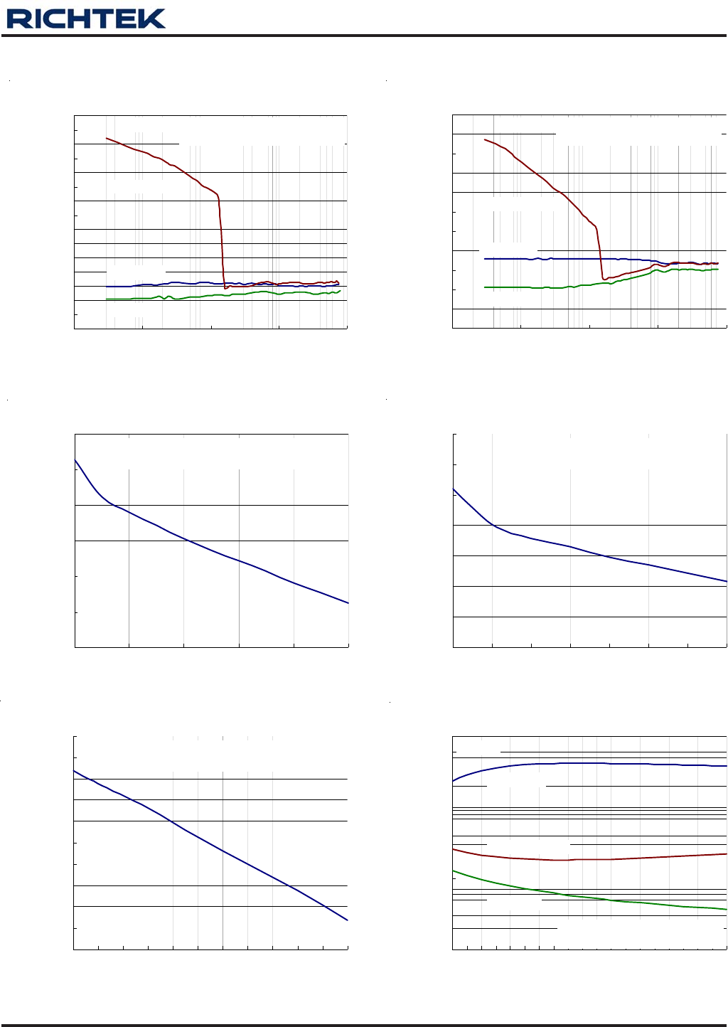
Typical Operating Characteristics
VOUT1 Efficiency vs. Load Current
0
10
20
30
40
50
60
70
80
90
100
0.001 0.01 0.1 1 10
Load Current (A)
Efficiency (%) 1
DEM Mode
Ultrasonic Mode
PWM Mode
VIN = 20V
TONSEL = GND, EN = FLOATING,
VENTRIP1 = 1.5V, VENTRIP2 = 5V
VOUT2 Efficiency vs. Load Current
0
10
20
30
40
50
60
70
80
90
100
0.001 0.01 0.1 1 10
Load Current (A)
Efficiency (%) 1
DEM Mode
Ultrasonic Mode
PWM Mode
VIN = 12V
TONSEL = GND, EN = FLOATING,
VENTRIP1 = 5V, VENTRIP2 = 1.5V
VOUT2 Efficiency vs. Load Current
0
10
20
30
40
50
60
70
80
90
100
0.001 0.01 0.1 1 10
Load Current (A)
Efficiency (%) 1
DEM Mode
Ultrasonic Mode
PWM Mode
VIN = 20V
TONSEL = GND,EN = FLOATING,
VENTRIP1 = 5V, VENTRIP2 = 1.5V
VOUT1 Efficiency vs. Load Current
0
10
20
30
40
50
60
70
80
90
100
0.001 0.01 0.1 1 10
Load Current (A)
Efficiency (%) 1
DEM Mode
Ultrasonic Mode
PWM Mode
VIN = 8V, TONSEL = GND, EN = FLOATING,
VENTRIP1 = 1.5V, VENTRIP2 = 5V
VOUT1 Efficiency vs. Load Current
0
10
20
30
40
50
60
70
80
90
100
0.001 0.01 0.1 1 10
Load Current (A)
Efficiency (%) 1
DEM Mode
Ultrasonic Mode
PWM Mode
TONSEL = GND, EN = FLOATING,
VENTRIP1 = 1.5V, VENTRIP2 = 5V
VIN = 12V
VOUT2 Efficiency vs. Load Current
0
10
20
30
40
50
60
70
80
90
100
0.001 0.01 0.1 1 10
Load Current (A)
Efficiency (%) 1
DEM Mode
Ultrasonic Mode
PWM Mode
VIN = 8V
TONSEL = GND, EN = FLOATING,
VENTRIP1 = 5V, VENTRIP2 = 1.5V
RT8223L/M
12
DS8223L/M-04 April 2011www.richtek.com
VOUT1 Switching Frequency vs. Load Current
0
20
40
60
80
100
120
140
160
180
200
220
0.001 0.01 0.1 1 10
Load Current (A)
Switching Frequency (kHz) 1
DEM Mode
Ultrasonic Mode
PWM Mode
VIN = 8V
TONSEL = GND, EN = FLOATING,
VENTRIP1 = 1.5V, VENTRIP2 = 5V
VOUT1 Switching Frequency vs. Load Current
0
20
40
60
80
100
120
140
160
180
200
220
0.001 0.01 0.1 1 10
Load Current (A)
Switching Frequency (kHz) 1
DEM Mode
Ultrasonic Mode
PWM Mode
VIN = 12V
TONSEL = GND, EN = FLOATING,
VENTRIP1 = 1.5V, VENTRIP2 = 5V
VOUT1 Switching Frequency vs. Load Current
0
20
40
60
80
100
120
140
160
180
200
220
0.001 0.01 0.1 1 10
Load Current (A)
Switching Frequency (kHz) 1
DEM Mode
Ultrasonic Mode
PWM Mode
VIN = 20V
TONSEL = GND, EN = FLOATING,
VENTRIP1 = 1.5V, VENTRIP2 = 5V
VOUT2 Switching Frequency vs. Load Current
0
20
40
60
80
100
120
140
160
180
200
220
240
260
280
0.001 0.01 0.1 1 10
Load Current (A)
Switching Frequency (kHz) 1
DEM Mode
Ultrasonic Mode
PWM Mode
VIN = 8V
TONSEL = GND, EN = FLOATING,
VENTRIP1 = 5V, VENTRIP2 = 1.5V
VOUT2 Switching Frequency vs. Load Current
0
20
40
60
80
100
120
140
160
180
200
220
240
260
280
0.001 0.01 0.1 1 10
Load Current (A)
Switching Frequency (kHz) 1
DEM Mode
Ultrasonic Mode
PWM Mode
VIN = 12V
TONSEL = GND, EN = FLOATING,
VENTRIP1 = 5V, VENTRIP2 = 1.5V
VOUT2 Switching Frequency vs. Load Current
0
20
40
60
80
100
120
140
160
180
200
220
240
260
280
0.001 0.01 0.1 1 10
Load Current (A)
Switching Frequency (kHz) 1
DEM Mode
Ultrasonic Mode
PWM Mode
VIN = 20V
TONSEL = GND, EN = FLOATING,
VENTRIP1 = 5V, VENTRIP2 = 1.5V
RT8223L/M
13
DS8223L/M-04 April 2011 www.richtek.com
Battery Current vs. Input Voltage
0.1
1.0
10.0
100.0
6 7 8 9 10 11 12 13 14 1516 17 18 19 20 2122 23 24 25
Input Voltage (V)
Battery Current (mA) 1
DEM Mode
Ultrasonic Mode
PWM Mode
TONSEL = GND, EN = FLOATING,
VENTRIP1 = VENTRIP2 = 0.91V
No Load
Reference Voltage vs. Output Current
2.0000
2.0008
2.0016
2.0024
2.0032
2.0040
2.0048
2.0056
2.0064
2.0072
2.0080
-10 0 10 20 30 40 50 60 70 80 90 100
Output Current (µA)
Reference Voltage (V) 1
VIN = 12V, TONSEL = GND, EN = FLOATING,
VENTRIP1 = VENTRIP2 = 5V
VREG3 Output Voltage vs. Output Current
3.330
3.334
3.338
3.342
3.346
3.350
3.354
3.358
0 10203040506070
Output Current (mA)
Output Voltage (V) 1
VIN = 12V, TONSEL = GND, EN = FLOATING,
VENTRIP1 = VENTRIP2 = 5V
VREG5 Output Voltage vs. Output Current
4.970
4.976
4.982
4.988
4.994
5.000
5.006
0 20406080100
Output Current (mA)
Output Voltage (V) 1
VIN = 12V, TONSEL = GND, EN = FLOATING,
VENTRIP1 = VENTRIP2 = 5V
VOUT1 Output Voltage vs. Load Current
5.000
5.006
5.012
5.018
5.024
5.030
5.036
5.042
5.048
5.054
5.060
5.066
5.072
5.078
5.084
5.090
0.001 0.01 0.1 1 10
Load Current (A)
Output Voltage (V) 1
DEM Mode
Ultrasonic Mode
PWM Mode
VIN = 12V, TONSEL = GND, EN = FLOATING,
VENTRIP1 = 1.5V, VENTRIP2 = 5V
VOUT2 Output Voltage vs. Load Current
3.380
3.386
3.392
3.398
3.404
3.410
3.416
3.422
3.428
3.434
3.440
3.446
0.001 0.01 0.1 1 10
Load Current (A)
Output Voltage (V) 1
DEM Mode
Ultrasonic Mode
PWM Mode
VIN = 12V, TONSEL = GND, EN = FLOATING,
VENTRIP1 = 5V, VENTRIP2 = 1.5V
RT8223L/M
14
DS8223L/M-04 April 2011www.richtek.com
Reference Voltage vs. Temperature
1.984
1.987
1.990
1.993
1.996
1.999
2.002
2.005
2.008
2.011
-50 -25 0 25 50 75 100 125
Temperature (°C)
Reference Voltage (V) 1
VIN = 12V, VENTRIP1 = VENTRIP2 = 5V,
EN = FLOATING, TONSEL = GND
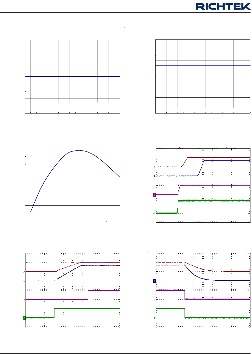
Time (400μs/Div)
REF
(2V/Div)
EN
(2V/Div) EN = FLOATING, VENTRIP1 = VENTRIP2 = 5V
VREG5, VREG3 and REF Start Up
No Load, VIN = 12V, TONSEL = GND,
VREG5
(5V/Div)
VREG3
(2V/Div)
Standby Input Current vs. Input Voltage
240
241
242
243
244
245
246
247
248
249
250
7 8 9 101112131415161718192021222324
Input Voltage (V)
Standby Input Current (µA) 1
No Load,
EN = FLOATING, VENTRIP1 = VENTRIP2 = 5V
Shutdown Input Current vs. Input Voltage
8
9
10
11
12
13
14
15
16
17
18
19
20
21
22
7 8 9 101112131415161718192021222324
Input Voltage (V)
Shutdown Input Current (µA) 1
No Load, EN = GND, VENTRIP1 = VENTRIP2 = 5V
Power On From ENC (8223M)
Time (1ms/Div)
ENC
(5V/Div)
VOUT1
(5V/Div)
PGOOD
(5V/Div)
No Load
VIN = 12V, TONSEL = GND,
SKIPSEL = REF, EN = FLOATING,
VENTRIP1 = VENTRIP2 = 1.5V, VENC = 5V
VOUT2
(2V/Div)
Power Off From ENC (8223M)
Time (4ms/Div)
No Load
ENC
(5V/Div)
VOUT1
(5V/Div)
PGOOD
(5V/Div)
VOUT2
(2V/Div)
VIN = 12V, TONSEL = GND,
SKIPSEL = REF, EN = FLOATING,
VENTRIP1 = VENTRIP2 = 1.5V, VENC = 5V
RT8223L/M
15
DS8223L/M-04 April 2011 www.richtek.com
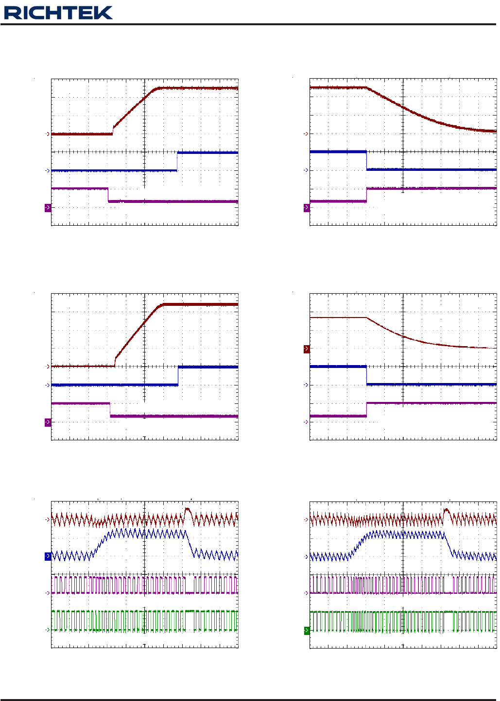
VOUT1 PWM Mode Load Transient Response
Time (20μs/Div)
UGATE1
(20V/Div)
VOUT1_AC
(50mV/Div)
LGATE1
(5V/Div)
VIN = 12V, TONSEL = GND,
Inductor
Current
(5A/Div)
EN = FLOATING, SKIPSEL = REF, IOUT1 = 0A to 6A
VOUT2 PWM Mode Load Transient Response
Time (20μs/Div)
VOUT2_AC
(50mV/Div)
LGATE2
(5V/Div)
Inductor
Current
(5A/Div)
EN = FLOATING, SKIPSEL = REF, IOUT2 = 0A to 6A
VIN = 12V, TONSEL = GND,
UGATE2
(20V/Div)
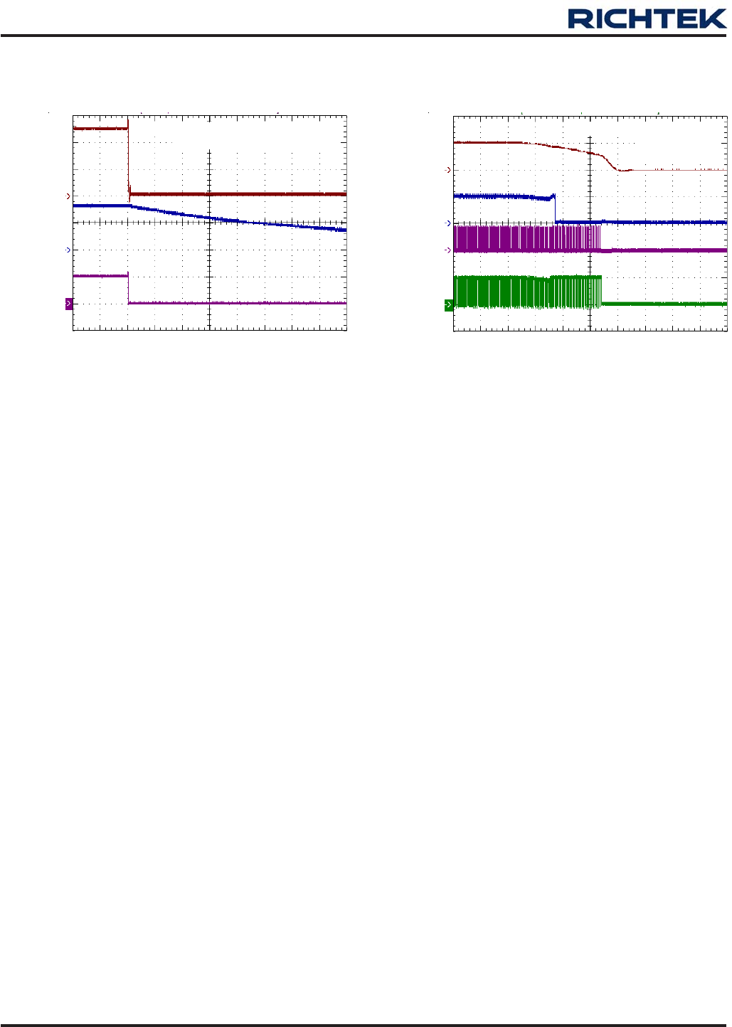
Power Off from ENTRIP2
Time (2ms/Div)
No Load
VIN = 12V, TONSEL = GND,
SKIPSEL = REF, EN = FLOATING,
VENTRIP1 = VENTRIP2 = 1.5V
ENTRIP2
(5V/Div)
VOUT2
(2V/Div)
PGOOD
(5V/Div)
Power On from ENTRIP1
Time (1ms/Div)
ENTRIP1
(5V/Div)
VOUT1
(2V/Div)
VIN = 12V, TONSEL = GND,
SKIPSEL = REF, EN = FLOATING,
No Load
VENTRIP1 = VENTRIP2 = 1.5V
PGOOD
(5V/Div)
Time (2ms/Div)
Power Off from ENTRIP1
No Load
VIN = 12V, TONSEL = GND,
SKIPSEL = REF, EN = FLOATING,
VENTRIP1 = VENTRIP2 = 1.5V
ENTRIP1
(5V/Div)
VOUT1
(2V/Div)
PGOOD
(5V/Div)
Power On from ENTRIP2
Time (1ms/Div)
ENTRIP2
(5V/Div)
VOUT2
(2V/Div)
VIN = 12V, TONSEL = GND,
SKIPSEL = REF, EN = FLOATING,
No Load
VENTRIP1 = VENTRIP2 = 1.5V
PGOOD
(5V/Div)
RT8223L/M
16
DS8223L/M-04 April 2011www.richtek.com
OVP
Time (4ms/Div)
PGOOD
(5V/Div)
VOUT1
(2V/Div)
No Load, VIN = 12V, TONSEL = GND,
EN = FLOATING, SKIPSEL = GND
VOUT2
(2V/Div)
UVP
Time (100μs/Div)
VOUT1
(5V/Div)
VIN = 12V, TONSEL = GND,
UGATE1
(20V/Div)
LGATE1
(5V/Div)
PGOOD
(5V/Div)
EN = FLOATING,
SKIPSEL = REF

RT8223L/M
17
DS8223L/M-04 April 2011 www.richtek.com
Application Information
The RT8223L/M is a dual, Mach ResponseTM DRVTM dual
ramp valley mode synchronous buck controller. The
controller is designed for low voltage power supplies for
notebook computers. Richtek's Mach ResponseTM
technology is specifically designed for providing 100ns
“instant-on” response to load steps while maintaining a
relatively constant operating frequency and inductor
operating point over a wide range of input voltages. The
topology circumvents the poor load-transient timing
problems of fixed-frequency current mode PWMs while
avoiding the problems caused by widely varying switching
frequencies in conventional constant on-time and constant
off-time PWM schemes. The DRVTM mode PWM
modulator is specifically designed to have better noise
immunity for such a dual output application. The
RT8223L/M includes 5V (VREG5) and 3.3V (VREG3) linear
regulators. VREG5 linear regulator can step down the
battery voltage to supply both internal circuitry and gate
drivers. The synchronous-switch gate drivers are directly
powered from VREG5. When VOUT1 voltage is above
4.75V, an automatic circuit will switch the power of the
device from VREG5 linear regulator to VOUT1.
PWM Operation
The Mach ResponseTM DRVTM mode controller relies on
the output filter capacitor's effective series resistance
(ESR) to act as a current sense resistor, so the output
ripple voltage provides the PWM ramp signal. Refer to the
RT8223L/M's function block diagram, the synchronous
high side MOSFET will be turned on at the beginning of
each cycle. After the internal one-shot timer expires, the
MOSFET will be turned off. The pulse width of this one
shot is determined by the converter's input voltage and
the output voltage to keep the frequency fairly constant
over the input voltage range. Another one shot sets a
minimum off-time (300ns typ.). The on-time one shot will
be triggered if the error comparator is high, the low side
switch current is below the current limit threshold, and
the minimum off-time one shot has timed out.
PWM Frequency and On-Time Control
The Mach ResponseTM control architecture runs with
pseudo constant frequency by feed-forwarding the input
/
ON OUT IN
t= K(V V)×
where “K”is set by the TONSEL pin connection (Table
1). The on-time guaranteed in the Electrical Characteristics
table is influenced by switching delays in the external
high side power MOSFET. Two external factors that
influence switching frequency accuracy are resistive drops
in the two conduction loops (including inductor and PC
board resistance) and the dead time effect. These effects
are the largest contributors to the change in frequency
with changing load current. The dead-time effect increases
the effective on-time by reducing the switching frequency
. It occurs only in PWM mode (SKIPSEL= REF) when
the inductor current reverses at light or negative load
currents. With reversed inductor current, the inductor's
EMF causes PHASEx to go high earlier than normal, thus
extending the on-time by a period equal to the low-to-
high dead time. For loads above the critical conduction
point, the actual switching frequency is :
/
OUT DROP1 ON IN DROP1 DROP2
f = (V V ) (t (V V V ))+×+−
where VDROP1 is the sum of the parasitic voltage drops in
the inductor discharge path,which includes the
synchronous rectifier, inductor, and PC board resistances.
VDROP2 is the sum of the resistances in the charging path,
and tON is the on-time.
and output voltage into the on-time one-shot timer. The
high side switch on-time is inversely proportional to the
input voltage as measured by VIN, and proportional to the
output voltage. There are two benefits of a constant
switching frequency. First, the frequency can be selected
to avoid noise-sensitive regions such as the 455kHz IF
band. Second, the inductor ripple current operating point
remains relatively constant, resulting in easy design
methodology and predictable output voltage ripple.
Frequency for the 3V SMPS is set at 1.25 times higher
than the frequency for 5V SMPS. This is done to prevent
audio-frequency “Beating” between the two sides, which
switch asynchronously for each side. The frequencies are
set by the TONSEL pin connection as shown in Table 1.
The on-time is given by :
RT8223L/M
18
DS8223L/M-04 April 2011www.richtek.com
Table 1. TONSEL Connection and Switching Frequency
TONSEL SMPS 1
K-Factor (μs) SMPS 1
Frequency (kHz) SMPS 2
K-Factor (μs) SMPS 2
Frequency (kHz) Approximate
K-Factor Error (%)
GND 5 200 4 250 ±10
REF 3.33 300 2.67 375 ±10
VREG5 or
VREG3 2.5 400 2 500 ±10
Operation Mode Selection (SKIPSEL)
The RT8223L/M supports three operation modes : Diode-
Emulation Mode, Ultrasonic Mode, and Forced-CCM
Mode. User can set operation mode via the SKIPSEL pin.
Diode-Emulation Mode (SKIPSEL=GND)
In Diode-Emulation Mode, the RT8223L/M automatically
reduces switching frequency at light-load conditions to
maintain high efficiency. This reduction of frequency is
achieved smoothly. As the output current decreases from
heavy-load condition, the inductor current is also reduced
and eventually comes to the point when its valley touches
zero current, which is the boundary between continuous
conduction and discontinuous conduction modes. By
emulating the behavior of diodes, the low side MOSFET
allows only partial negative current when the inductor free-
wheeling current becomes negative. As the load current
is further decreased, it takes longer and longer to discharge
the output capacitor to the level that requires the next
“ON” cycle. The on-time is kept the same as that in the
heavy-load condition. In reverse, when the output current
increases from light load to heavy-load, the switching
frequency increases to the preset value as the inductor
current reaches the continuous conduction. The transition
load point to the light-load operation is shown as follows
(Figure 1) :
Figure 1. Boundary Condition of CCM/DEM
IN OUT
LOAD (SKIP) ON
(V V )
It
2L
−
≈×
where tON is the On-time.
The switching waveforms may appear noisy and
asynchronous when light loading causes Diode-Emulation
Mode operation. However this is normal and results in
high efficiency. Trade-offs in PFM noise vs. light load
efficiency is made by varying the inductor value. Generally,
low inductor values produce a broader efficiency vs. load
curve, while higher values result in higher full-load efficiency
(assuming that the coil resistance remains fixed) and less
output voltage ripple.
Penalties for using higher inductor values include larger
physical size and degraded load transient response
(especially at low input-voltage levels).
Ultrasonic Mode (SKIPSEL = VREG5 or VREG3)
The RT8223L/M activates an unique Diode-Emulation Mode
with a minimum switching frequency of 25kHz, called the
Ultrasonic Mode. The Ultrasonic Mode avoids audio-
frequency modulation that would otherwise be present
when a lightly loaded controller automatically skips
pulses. In Ultrasonic Mode, the high side switch gate driver
signal is OR with an internal oscillator (>25kHz). Once
the internal oscillator is triggered, the controller enters
constant off-time control. When output voltage reaches
the setting peak threshold, the controller turns on the low
side MOSFET until the controller detects that the inductor
current dropped has below the zero-crossing threshold.
The internal timer provides a constant off-time control and
it is effective to regulate the output voltage under light
load conditions.
IL
t
0TON
Slope = (VIN -VOUT) / L
IL, PEAK
ILoad = IL, PEAK / 2
RT8223L/M
19
DS8223L/M-04 April 2011 www.richtek.com
Forced CCM Mode (SKIPSEL = REF)
The low noise, Forced CCM mode (SKIPSEL = REF)
disables the zero-crossing comparator, which controls the
low side switch on-time. This causes the low side gate-
driver waveform to become the complement of the high
side gate-driver waveform. This in turn causes the inductor
current to reverse at light loads as the PWM loop to
maintain a duty ratio of VOUT/VIN. The benefit of Forced
CCM Mode is to keep the switching frequency fairly
constant, but it comes at a cost. The no load battery
current can be from 10mA to 40mA, depending on the
external MOSFETs.
Reference and linear Regulators (REF, VREGx)
The 2V reference (REF) is accurate within ±1% over the
entire operating temperature range, making REF useful
as a precision system reference. Bypass REF to GND
with a minimum 0.22μF ceramic capacitor. REF can supply
up to 100μA for external loads. Loading REF reduces the
VOUTx output voltage slightly because of the reference
load-regulation error.
The RT8223L/M includes 5V (VREG5) and 3.3V (VREG3)
linear regulators. The VREG5 regulator supplies a total of
100mA for internal and external loads, including the
MOSFET gate driver and PWM controller. The VREG3
regulator supplies up to 100mA for external loads. Bypass
VREG5 and VREG3 with a minimum 4.7μF ceramic
capacitor.
When the 5V main output voltage is above the VREG5
switch over threshold (4.75V), an internal 1.5Ω P-Channel
MOSFET switch connects VOUT1 to VREG5, while
simultaneously shutting down the VREG5 linear regulator.
Similarly, when the 3.3V main output voltage is above the
VREG3 switch over threshold (3.125V), an internal 1.5Ω
P-Channel MOSFET switch connects VOUT2 to VREG3,
while simultaneously shutting down the VREG3 linear
regulator. It can decrease the power dissipation from the
same battery, because the converted efficiency of SMPS
is better than the converted efficiency of the linear
regulator.
Current-Limit Setting (ENTRIPx)
The RT8223L/M has a cycle-by-cycle current-limit control.
The current-limit circuit employs an unique “valley” current
sensing algorithm. If the magnitude of the current sense
signal at PHASEx is above the current-limit threshold, the
PWM is not allowed to initiate a new cycle (Figure 2).
The actual peak current is greater than the current-limit
threshold by an amount equal to the inductor ripple current.
Therefore, the exact current-limit characteristic and
maximum load capability are functions of the sense
resistance, inductor value, and battery and output voltage.
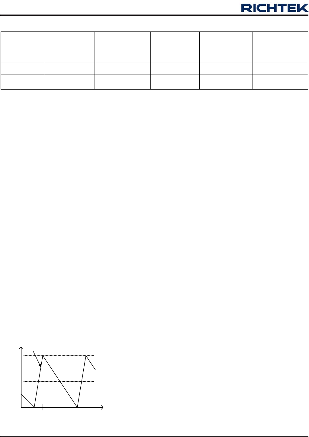
Figure 2. “Valley” Current-Limit
The RT8223L/M uses the on-resistance of the synchronous
rectifier as the current-sense element and supports
temperature compensated MOSFET RDS(ON) sensing. The
RILIMX resistor between the ENTRIPX pin and GND sets
the current-limit threshold. The resistor RILIMX is connected
to a current source from ENTRIPx, which is 10μA typically
at room temperature. The current source has a 4700ppm/
°C temperature slope to compensate the temperature
dependency of the RDS(ON). When the voltage drop across
the sense resistor or low side MOSFET equals 1/10 the
voltage across the RILIMX resistor, positive current limit
will be activated. The high side MOSFET will not be turned
on until the voltage drop across the MOSFET falls below
1/10 the voltage across the RILIMX resistor.
Choose a current limit resistor by following equations
VILIMx = (RILIMx x10μA)/10 = IILIMx x RDS(ON)
RILIMx = (IILIMx x RDS(ON)) x 10/10μA
Carefully observe the PC board layout guidelines to ensure
that noise and DC errors do not corrupt the current-sense
signal at PHASEx and GND. Mount or place the IC close
to the low side MOSFET.
MOSFET Gate Driver (UGATEx, LGATEx)
The high side driver is designed to drive high-current, low
RDS(ON) N-MOSFET(s). When configured as a floating driver,
a 5V bias voltage is delivered from the VREG5 supply.
IL
t
0
IL, PEAK
ILIM
ILOAD
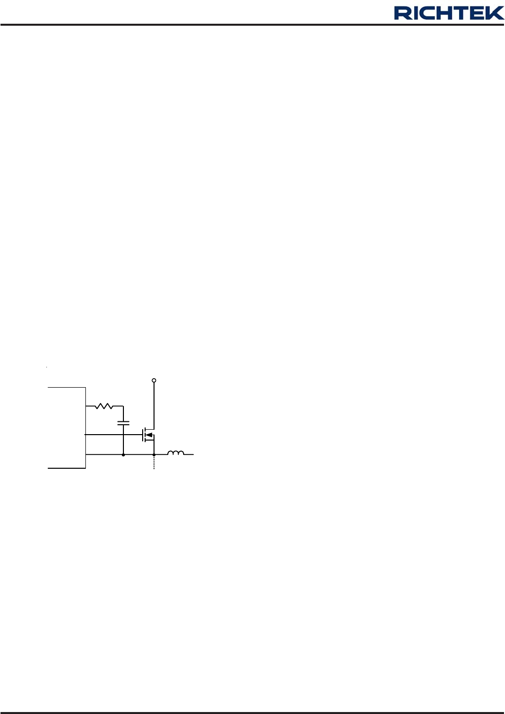
RT8223L/M
20
DS8223L/M-04 April 2011www.richtek.com
The average drive current is calculated by the gate charge
at VGS = 5V times the switching frequency. The
instantaneous drive current is supplied by the flying
capacitor between the BOOTx and PHASEx pins. A dead
time to prevent shoot through is internally generated
between high side MOSFET off to the low side MOSFET
on, and the low side MOSFET off to the high side MOSFET
on.
The low side driver is designed to drive high current, low
RDS(ON) N-MOSFET(s). The internal pull-down transist or
that drives LGATEX low is robust, with a 1.5Ω typical on-
resistance. A 5V bias voltage is delivered from the VREG5
supply. The instantaneous drive current is supplied by an
input capacitor connected between VREG5 and GND.
For high current applications, some combinations of high
and low side MOSFETs might be encountered that will
cause excessive gate-drain coupling, which can lead to
efficiency killing, EMI-producing shoot-through currents.
This can be remedied by adding a resistor in series with
BOOTx, which increases the turn-on time of the high side
MOSFET without degrading the turn-off time (Figure 3).
Figure 3. Reducing the UGATEx Rise Time
Soft-Start
The RT8223L/M provides an internal soft-start function to
prevent large inrush current and output voltage overshoot
when the converter starts up. The soft-start (SS)
automatically begins once the chip is enabled. During soft-
start, it clamps the ramping of internal reference voltage
which is compared with FBx signal. The typical soft-
start duration is 2 ms. A unique PWM duty limit control
that prevents output over voltage during soft-start period
is designed specifically for FBx floating.
UVLO Protection
The RT8223L/M features VREG5 under voltage lockout
protection (UVLO). When the VREG5 voltage is lower than
3.9V (typ.) and the VREG3 voltage is lower than 2.5V
(typ.), both switch power supplies are shut off. This is
non-latch protection.
Power Good Output (PGOOD)
PGOOD is an open-drain type output and requires a pull-
up resistor. PGOOD is actively held low in soft-start,
standby, and shutdown. It is released when both output
voltages are above 91% of the nominal regulation point.
The PGOOD goes low if either output turns off or is 15%
below its nominal regulator point.
Output Over Voltage Protection (OVP)
The output voltage can be continuously monitored for over
voltage. If the output voltage exceeds 12% of its set voltage
threshold, the over voltage protection is triggered and the
LGATEx low side gate drivers are forced high. This activates
the low side MOSFET switch, which rapidly discharges
the output capacitor and pulls the input voltage downward.
The RT8223L/M is latched once OVP is triggered and can
only be released by toggling EN, ENTRIPx or cycling VIN.
There is a 5μs delay built into the over voltage protection
circuit to prevent false alarm.
Note that the LGATEx latching high causes the output
voltage to dip slightly negative when energy has been
previously stored in the LC tank circuit. For loads that
cannot tolerate a negative voltage, place a power Schottky
diode across the output to act as a reverse polarity clamp.
If the over-voltage condition is caused by a short in the
high side switch, completely turning on the low side
MOSFET can create an electrical short between the
battery and GND, which will blow the fuse and disconnect
the battery from the output.
Output Under Voltage Protection (UVP)
The output voltage can be continuously monitored for under
voltage protection. If the output is less than 52% of its set
voltage threshold, under voltage protection will be triggered,
and then both UGATEx and LGATEx gate drivers will be
forced low. The UVP will be ignored for at least 5ms (typ.)
after start-up or a rising edge on ENTRIPx. Toggle
BOOTx
UGATEx
PHASEx
RBOOT
VIN
RT8223L/M
21
DS8223L/M-04 April 2011 www.richtek.com
ENTRIPx or cycle VIN to reset the UVP fault latch and
restart the controller.
Thermal Protection
The RT8223L/M features thermal shutdown protection to
prevent overheat damage to the device. Thermal shutdown
occurs when the die temperature exceeds +150°C. All
internal circuitry is inactive during thermal shutdown. The
RT8223L/M triggers thermal shutdown if VREGx is not
supplied from VOUTx, while the input voltage on VIN and
the drawing current from VREGx are too high. Even if
VREGx is supplied from VOUTx, large power dissipation
on automatic switches caused by overloading VREGx,
may also result in thermal shutdown.
Discharge Mode (Soft-Discharge)
When ENTRIPx is low and a transition to standby or
shutdown mode occurs, or the output under voltage fault
latch is set, the output discharge mode will be triggered.
During discharge mode, the output capacitors' residual
charge will be discharged to GND through an internal
switch.
Table 2. Operation Mode Truth Table
MODE Condition Comment
Power UP VREGx < UVLO threshold Transitions to discharge mode after a VIN POR and after
REF becomes valid. VREG5, VREG3, and REF remain
active.
RUN EN = high, VOUT1 or VOUT2
enabled Normal Operation.
Over Voltage
Protection Either output > 111% of the nominal
level. LGATEx is forced high. VREG3, VREG5 and REF active.
Exited by VIN POR or by toggling EN, ENTRIPx, ENC
Under
Voltage
Protection
Either output < 52% of the nominal
level after 3ms time-out expires and
output is enabled
Both UGATEx and LGATEx are forced low and enter
discharge mode. VREG3, VREG5 and REF are active.
Exited by VIN POR or by toggling EN, ENTRIPx, ENC
Discharge Either SMPS output is still high in
either standby mode or shutdown
mode
During discharge mode, there is one path to discharge the
outputs capacitor residual charge. That is output capacitor
discharge to GND through an internal switch.
Standby ENTRIPX<startup threshold, EN
=high. VREG3, VREG5 and REF are active.
Shutdown EN =low All circuitry off.
Thermal
Shutdown TJ > +150°C All circuitry off. Exit by VIN POR or by toggling EN, ENTRIPx,
ENC
Shutdown Mode
The RT8223L/M SMPS1, SMPS2, VREG3 and VREG5
have independent enabling controls. Drive EN, ENTRIP1
and ENTRIP2 below the precise input falling-edge trip level
to place the RT8223L/M in its low power shutdown state.
The RT8223L/M consumes only 20μA of input current while
in shutdown. When shutdown mode is activated, the
reference turns off. The accurate 0.4V falling-edge threshold
on the EN pin can be used to detect a specific analog
voltage level as well as to shutdown the device. Once in
shutdown, the 2.4V rising-edge threshold activates,
providing sufficient hysteresis for most applications.
Power Up Sequencing and On/Off Controls (ENC)
ENTRIP1 and ENTRIP2 control the SMPS power up
sequencing. When the RT8223L/M is in single channel
mode, ENTRIP1 or ENTRIP2 enables the respective output
when ENTRIPx voltage descends below 3V. Furthermore,
the RT8223M can also be in dual channel mode. In this
mode, outputs are enabled when ENC voltage rises above
2V.
RT8223L/M
22
DS8223L/M-04 April 2011www.richtek.com
Table 3. Power Up Sequencing
EN
(V)
ENC
(V) ENTRIP1 ENTRIP2 REF VREG5 VREG3 SMPS1 SMPS2
Low Low X X Off Off Off Off Off
“>2.4V”
=> High Low X X On On On Off Off
“>2.4V”
=> High
“>2V”
=> High Off Off On On On Off Off
“>2.4V”
=> High
“>2V”
=> High Off On On On On Off On
“>2.4V”
=> High
“>2V”
=> High On Off On On On On Off
“>2.4V”
=> High
“>2V”
=> High On On On On On On On
Output Voltage Setting (FBx)
Connect a resistor voltage-divider at the FBx pin between
VOUTx and GND to adjust the respective output voltage
between 2V and 5.5V (Figure 4). Referring to Figure 4 as
an example, choose R2 to be approximately 10kΩ, and
solve for R1 using the equation :
OUTX FBX R1
VV1
R2
⎛⎞
⎛⎞
=×+
⎜⎟
⎜⎟
⎝⎠
⎝⎠
where VFBX is 2V.
Figure 4. Setting VOUTX with a Resistor Voltage Divider
Output Inductor Selection
The switching frequency (on-time) and operating point (%
ripple or LIR) determine the inductor value as shown in
the following equation :
()
ON IN OUTx
LOAD(MAX)
tVV
LLIR I
×−
=×
where LIR is the ratio of the peak to peak ripple current to
the average inductor current.
Find a low-loss inductor having the lowest possible DC
resistance that fits in the allotted dimensions. Ferrite cores
are often the best choice, although powdered iron is
inexpensive and can work well at 200kHz. The core must
be large enough not to saturate at the peak inductor current
(IPEAK) :
PEAK LOAD(MAX) LOAD(MAX)
II (LIR/2)I
⎡⎤
=+×
⎣⎦
The calculation above shall serve as a general reference.
To further improve the transient response, the output
inductance can be reduced even further. This needs to be
considered along with the selection of the output capacitor.
Output Capacitor Selection
The capacitor value and ESR determine the amount of
output voltage ripple and load transient response. Thus,
the capacitor value must be greater than the largest value
calculated from below equations :
()
2OUTx
LOAD OFF(MIN)
IN
SAG IN OUTx
OUT OUTx OFF(MIN)
IN
V
(I ) L K t
V
VVV
2C V K t
V
Δ×××+
=⎡⎤
⎛⎞
−
×× ×× −
⎢⎥
⎜⎟
⎝⎠
⎣⎦
2
2
LOAD
SOAR OUT OUTx
(I ) L
VCV
Δ×
=××
PHASEx
LGATEx R1
R2
VOUTx
VIN
UGATEx
VOUTx
FBx
RT8223L/M
23
DS8223L/M-04 April 2011 www.richtek.com
P P LOAD(MAX) OUT
1
V LIR I ESR 8C f
−
⎛⎞
=× × +
⎜⎟
××
⎝⎠
where VSAG and VSOAR are the allowable amount of
undershoot voltage the and overshoot voltage in load
transient, Vp-p is the output ripple voltage, tOFF(MIN) is the
minimum off-time, and K is a factor listed in Table 1.
Thermal Considerations
For continuous operation, do not exceed absolute
maximum junction temperature. The maximum power
dissipation depends on the thermal resistance of the IC
package, PCB layout, rate of surrounding airflow, and
difference between junction and ambient temperature. The
maximum power dissipation can be calculated by the
following formula :
PD(MAX) = (TJ(MAX) − TA) / θJA
where TJ(MAX) is the maximum junction temperature, TA is
the ambient temperature, and θJA is the junction to ambient
thermal resistance.
For recommended operating condition specifications of
the RT8223L/M, the maximum junction temperature is
125°C and TA is the ambient temperature. The junction to
ambient thermal resistance, θJA, is layout dependent. For
WQFN-24L 4x4 packages, the thermal resistance, θJA, is
52°C/W on a standard JEDEC 51-7 four-layer thermal test
board. The maximum power dissipation at TA = 25°C can
be calculated by the following formula :
PD(MAX) = (125°C − 25°C) / (52°C/W) = 1.923W for
WQFN-24L 4x4 package
The maximum power dissipation depends on the operating
ambient temperature for fixed TJ(MAX) and thermal
resistance, θJA. For the RT8223L/M package, the derating
curve in Figure 5 allows the designer to see the effect of
rising ambient temperature on the maximum power
dissipation.
Figure 5. Derating Curve for the RT8223L/M Package
0.0
0.3
0.6
0.9
1.2
1.5
1.8
2.1
0 25 50 75 100 125
Ambient Temperature (°C)
Maximum Power Dissipation (W) 1
Four-Layer PCB
Layout Considerations
Layout is very important in high frequency switching
converter designs, the PCB could radiate excessive noise
and contribute to the converter instability with improper
layout. Certain points must be considered before starting
a layout using the RT8223L/M.
`Place the filter capacitor close to the IC, within 12mm
(0.5 inch) if possible.
`Keep current limit setting network as close as possible
to the IC. Routing of the network should avoid coupling
to high voltage switching nodes.
`Connections from the drivers to the respective gate of
the high side or the low side MOSFET should be as
short as possible to reduce stray inductance. Use
0.65mm (25mils) or wider trace.
`All sensitive analog traces and components such as
VOUTx, FBx, GND, ENTRIPx, PGOOD, and TONSEL
should be placed away from high voltage switching
nodes such as PHASEx, LGATEx, UGATEx, or BOOTx
nodes to avoid coupling. Use internal layer(s) as ground
plane(s) and shield the feedback trace from power traces
and components.
`Place the ground terminal of VIN capacitor(s), VOUTx
capacitor(s), and source of low side MOSFETs as close
as possible. The PCB trace defined as PHASEX node,
which connects to source of high side MOSFET, drain
of low side MOSFET and high voltage side of the
inductor, should be as short and wide as possible.
RT8223L/M
24
DS8223L/M-04 April 2011www.richtek.com
Information that is provided by Richtek Technology Corporation is believed to be accurate and reliable. Richtek reserves the right to make any change in circuit
design, specification or other related things if necessary without notice at any time. No third party intellectual property infringement of the applications should be
guaranteed by users when integrating Richtek products into any application. No legal responsibility for any said applications is assumed by Richtek.
Richtek Technology Corporation
Headquarter
5F, No. 20, Taiyuen Street, Chupei City
Hsinchu, Taiwan, R.O.C.
Tel: (8863)5526789 Fax: (8863)5526611
Richtek Technology Corporation
Taipei Office (Marketing)
5F, No. 95, Minchiuan Road, Hsintien City
Taipei County, Taiwan, R.O.C.
Tel: (8862)86672399 Fax: (8862)86672377
Email: marketing@richtek.com
Outline Dimension
A
A1
A3
D
E
D2
E2
L
be
1
SEE DETAIL A
Dimensions In Millimeters Dimensions In Inches
Symbol Min Max Min Max
A 0.700 0.800 0.028 0.031
A1 0.000 0.050 0.000 0.002
A3 0.175 0.250 0.007 0.010
b 0.180 0.300 0.007 0.012
D 3.950 4.050 0.156 0.159
D2 2.300 2.750 0.091 0.108
E 3.950 4.050 0.156 0.159
E2 2.300 2.750 0.091 0.108
e 0.500 0.020
L 0.350 0.450
0.014 0.018
W-Type 24L QFN 4x4 Package
Note : The configuration of the Pin #1 identifier is optional,
but must be located within the zone indicated.
DETAIL A
Pin #1 ID and Tie Bar Mark Options
1
1
22

