RT8237E Datasheet. Www.s Manuals.com. R00 Richtek
User Manual: Marking of electronic components, SMD Codes 88, 88 **, 88A. Datasheets MMBD1704, MMBD1704A, RT8237EZQW.
Open the PDF directly: View PDF ![]() .
.
Page Count: 19
RT8237E
®
DS8237E-00 December 2012 www.richtek.com
1
Copyright 2012 Richtek Technology Corporation. All rights reserved. is a registered trademark of Richtek Technology Corporation.
©
High Efficiency Single Synchronous Buck PWM Controller
General Description
The RT8237E PWM controller provides high efficiency,
excellent transient response, and high DC output accuracy
needed for stepping down high voltage batteries to
generate low voltage CPU core, I/O, and chipset RAM
supplies in notebook computers.
The constant on-time PWM control scheme handles wide
input/output voltage ratios with ease and provides 100ns
“instant-on” response to load transients while maintaining
a relatively constant switching frequency.
The RT8237E achieves high efficiency at a reduced cost
by eliminating the current sense resistor found in
traditional current mode PWMs. Efficiency is further
enhanced by its ability to drive very large synchronous
rectifier MOSFETs and enter diode emulation mode at
light load condition. The Buck conversion allows this device
to directly step down high voltage batteries at the highest
possible efficiency. The pre-set frequency selections
minimize design effort required for new designs. The
RT8237E is intended for CPU core, chipset, DRAM, or
other low voltage supplies as low as 0.7V. The RT8237E
is available in the WDFN-10L 3x3 package.
Features
zWide Input Voltage Range : 4.5V to 26V
zOutput Voltage Range : 0.7V to 3.3V
zBuilt-in 0.5% 0.7V Reference Voltage
zQuick Load-Step Response within 100ns
z4700ppm/°°
°°
°C Current Source for Current Limit
RDS(ON)
zAdjustable Current Limit with Low Side MOSFET
z4 Selectable Frequency Setting
zSoft-Start Control
zDrives Large Synchronous-Rectifier FETs
zIntegrated Boot Switch
zBuilt-in OVP/OCP/UVP
zThermal Shutdown
zPower Good Indicator
zRoHS Compliant and Halogen Free
Applications
zNotebook Computers
zCPU Core Supply
zChipset/RAM Supply as Low as 0.7V
zGeneric DC/DC Power Regulator
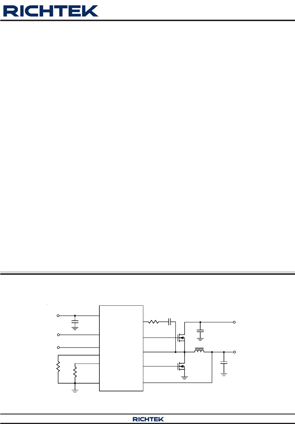
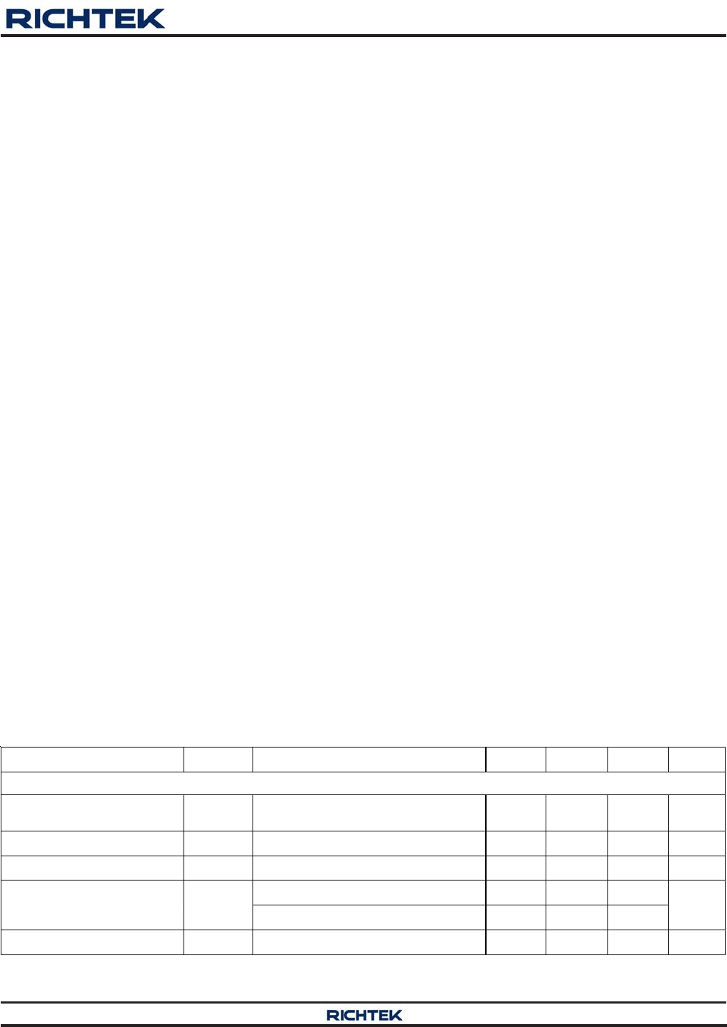
Simplified Application Circuit
VCC
CS
UGATE
FB
RT8237E
LGATE
BOOT
PHASE
PGOOD
GND
EN
VIN
VOUT
VCC
RF
RT8237E
2
DS8237E-00 December 2012www.richtek.com
©
Copyright 2012 Richtek Technology Corporation. All rights reserved. is a registered trademark of Richtek Technology Corporation.
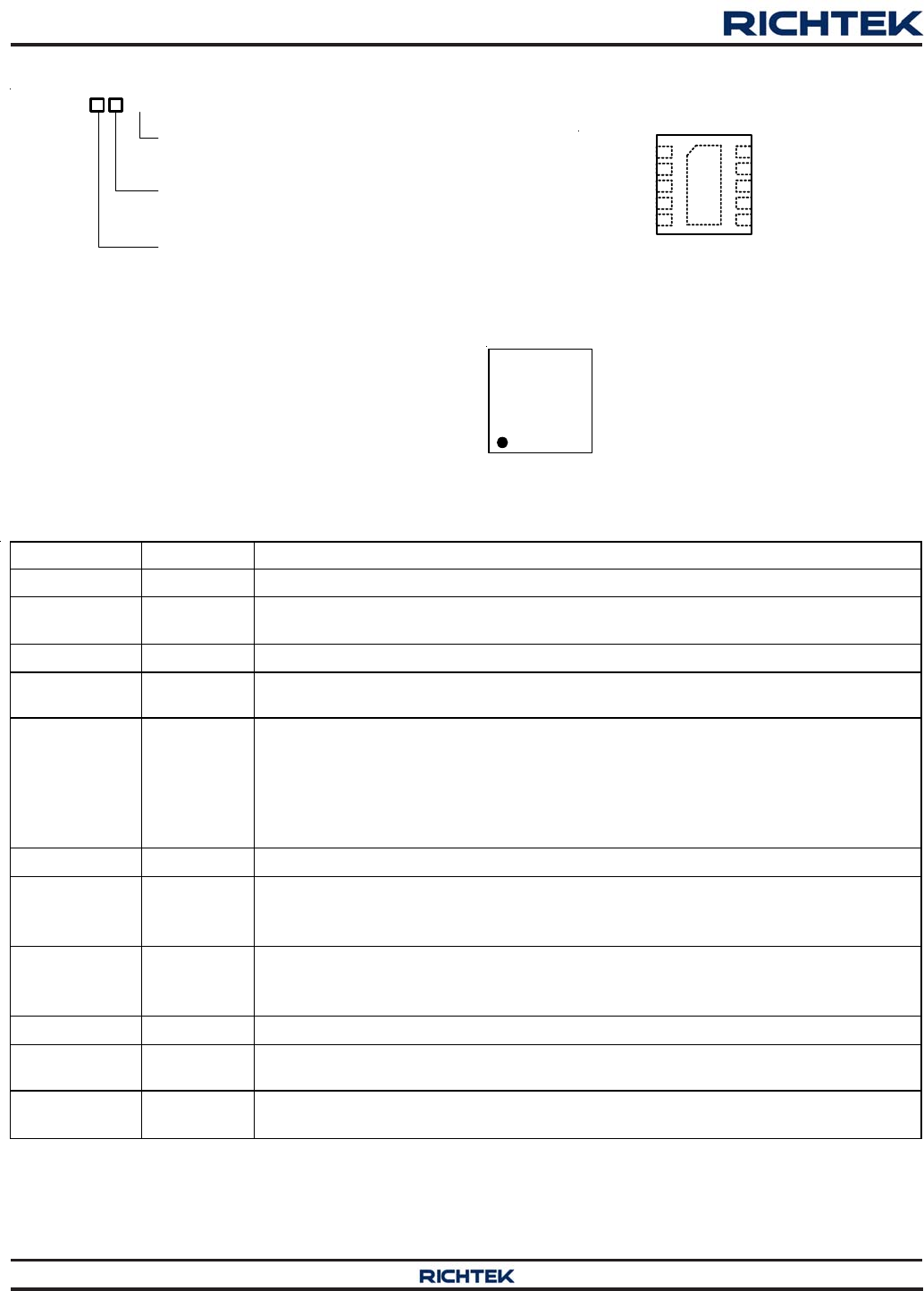
Pin No. Pin Name Pin Function
1 PGOOD Open Drain Power Good Indicator. High impedance indicates power is good.
2 CS Current Limit Threshold Setting Input. Connect a setting resistor to GND and the
current limit threshold is equal to 1/8 of the voltage at this pin.
3 EN Enable Control Input. Pull low to GND to disable the PWM.
4 FB VOUT Feedback Input. Connect FB to a resistor voltage divider from VOUT to GND
to adjust the output from 0.7V to 3.3V
5 RF
Switching Frequency Selection. Connect a resistance to select switching
frequency as shown in Electrical Characteristics. The switching frequency is
detected and latched after startup. This pin also controls diode emulation mode or
forced CCM selection.
Pull down to GND with resistor : Diode Emulation Mode.
Connect to PGOOD with resistor : forced CCM after PGOOD becomes high.
6 LGATE Gate Drive Output for Low Side External MOSFET.
7 VCC
Supply Voltage Input. This pin provides the power for the Buck controller, the low
side driver and the bootstrap circuit for high side driver. Bypass to GND with a 1μF
ceramic capacitor.
8 PHASE
External Inductor Connection Pin for PWM Converter. It behaves as the current
sense comparator input for low side MOSFET RDS(ON) sensing and reference
voltage for on time generation.
9 UGATE Gate Drive Output for High Side External MOSFET.
10 BOOT
Bootstrap Supply for High Side Gate Driver. Connect through a capacitor to the
floating node (PHASE).
11
(Exposed Pad) GND Ground. The exposed pad must be soldered to a large PCB and connected to
GND for maximum power dissipation.
Functional Pin Description
Ordering Information
Note :
Richtek products are :
` RoHS compliant and compatible with the current require-
ments of IPC/JEDEC J-STD-020.
` Suitable for use in SnPb or Pb-free soldering processes.
RT8237E
Package Type
QW : WDFN-10L 3x3 (W-Type)
Lead Plating System
Z : ECO (Ecological Element with
Halogen Free and Pb free)
(2)
Pin 1 Orientation
(2) : Quadrant 2, Follow EIA-481-D
Pin Configurations
(TOP VIEW)
WDFN-10L 3x3
PGOOD
CS
RF
FB
BOOT
UGATE
PHASE
LGATE
VCC
EN
9
8
7
1
2
3
4
5
10
6
GND
11
Marking Information
88 DF
A26
88 : Product Code
DFA26 : Date Code
RT8237E
3
DS8237E-00 December 2012 www.richtek.com
©
Copyright 2012 Richtek Technology Corporation. All rights reserved. is a registered trademark of Richtek Technology Corporation.
Function Block Diagram
+
-COMP
VREF
S1 Q
Latch
S1 Q
Latch
+
-
OV
+
-
UV
125%
VREF
70%
VREF
+
-
125% VREF
Thermal
Shutdown
DEM/FCCM
DRV
DRV
FB
VCC
UGATE
PHASE
PGOOD
GND
LGATE
RF BOOT
EN
R
QS
X(-1/8)
+
-
PWM
+
-
90% VREF
SS
Timer
POR
CS
VCC
PHASE
10µA
+
-
X(1/8)
Min. tOFF
QTRIG
On-time
Compute
TRIG
RT8237E
4
DS8237E-00 December 2012www.richtek.com
©
Copyright 2012 Richtek Technology Corporation. All rights reserved. is a registered trademark of Richtek Technology Corporation.
Operation
The RT8237E integrates a Constant-On-Time (COT) PWM
controller, and the controller provides the PWM signal
which relies on the output ripple voltage comparing with
internal reference voltage.
The UGATE driver is turned on at the beginning of each
cycle. After the internal one-shot timer expires, the UGATE
driver will be turned off. The pulse width of this one-shot is
determined by the converter's input voltage and the output
voltage to keep the frequency fairly constant over the input
voltage and output voltage range.
Power On Reset, UVLO
Power On Reset (POR) occurs when VCC rises above to
approximately 4.1V (typical), the RT8237E will reset the
fault latch and prepare the PWM for operation. When the
input voltage below 3.7V(min), the Under Voltage Lockout
(UVLO) circuitry inhibits switching by keeping UGATE and
LGATE low.
Soft-Start
The output voltage will track the internal ramp voltage during
soft-start interval to prevent large inrush current and output
voltage overshoot while the converter is being powered
up.
Mode Selection
The RT8237E supports mode selection through the RF
by connecting a resistor from the RF pin to either GND or
PGOOD. When the resistor is connected to GND, the
controller operates in diode emulation mode. When the
resistor is connected to PGOOD, the controller operates
in CCM mode.
Current Limit Setting
The RT8237E has a cycle-by-cycle current limit control.
The current limit circuit employs a unique “valley” current
sensing algorithm. If the magnitude of the sensing signal
at PHASE is above the current limit threshold, the PWM
is not allowed to initiate a new cycle.
Over Voltage Protection
The output voltage can be continuously monitored for over
voltage condition. When the output voltage exceeds 25%
of its set voltage threshold, the UGATE goes low and the
LGATE is forced high.
Under Voltage Protection
The output voltage can be continuously monitored for under
voltage condition. When the output voltage is less than
70% of its set voltage, under voltage protection is triggered
and then both UGATE and LGATE gate drivers are forced
low.
RT8237E
5
DS8237E-00 December 2012 www.richtek.com
©
Copyright 2012 Richtek Technology Corporation. All rights reserved. is a registered trademark of Richtek Technology Corporation.
Electrical Characteristics
(VCC = 5V, TA = 25°C, unless otherwise specified)
Absolute Maximum Ratings (Note 1)
zVCC, FB, PGOOD, EN, CS, RF to GND ----------------------------------------------------------------------------- −0.3V to 6V
zBOOT to PHASE ----------------------------------------------------------------------------------------------------------- −0.3V to 6V
zPHASE to GND
DC------------------------------------------------------------------------------------------------------------------------------ −0.3V to 32V
<20ns ------------------------------------------------------------------------------------------------------------------------- −8V to 38V
zUGATE to PHASE --------------------------------------------------------------------------------------------------------- −0.3V to 6V
DC------------------------------------------------------------------------------------------------------------------------------ −0.3V to 6V
<20ns ------------------------------------------------------------------------------------------------------------------------- −5V to 7.5V
zLGATE to GND -------------------------------------------------------------------------------------------------------------- −0.3V to 6V
DC------------------------------------------------------------------------------------------------------------------------------ −0.3V to 6V
<20ns ------------------------------------------------------------------------------------------------------------------------- −2.5V to 7.5V
zPower Dissipation, PD @ TA = 25°C
WDFN-10L 3x3 -------------------------------------------------------------------------------------------------------------- 3.28W
zPackage Thermal Resistance (Note 2)
WDFN-10L 3x3, θJA -------------------------------------------------------------------------------------------------------- 30.5°C/W
WDFN-10L 3x3, θJC -------------------------------------------------------------------------------------------------------- 7.5°C/W
zLead Temperature (Soldering, 10 sec.)-------------------------------------------------------------------------------- 260°C
zJunction Temperature ------------------------------------------------------------------------------------------------------ 150°C
zStorage Temperature Range --------------------------------------------------------------------------------------------- −65°C to 150°C
zESD Susceptibility (Note 3)
HBM (Human Body Model) ----------------------------------------------------------------------------------------------- 2kV
Recommended Operating Conditions (Note 4)
zInput Voltage, VIN ---------------------------------------------------------------------------------------------------------- 4.5V to 26V
zControl Voltage, VCC ----------------------------------------------------------------------------------------------------- 4.5V to 5.5V
zJunction Temperature Range--------------------------------------------------------------------------------------------- −40°C to 125°C
zAmbient Temperature Range--------------------------------------------------------------------------------------------- −40°C to 85°C
Parameter Symbol Test Conditions Min Typ Max Unit
Input Power Supply
VCC Quiescent Supply
Current IQ FB forced above the regulation
point, VEN = 5V, -- 0.5 1.25 mA
VCC Shutdown Current ISHDN V
CC current, VEN = 0V -- -- 1 μA
CS Shutdown Current CS pull to GND -- -- 1 μA
DEM 0.7005 0.704 0.7075
FB Error Comparator
Threshold VREF DEM, TA = −40 to 85°C (Note 5) 0.697 0.704 0.711 V
FB Input Bias Current V
FB = 0.735V −1 0.01 1 μA
RT8237E
6
DS8237E-00 December 2012www.richtek.com
©
Copyright 2012 Richtek Technology Corporation. All rights reserved. is a registered trademark of Richtek Technology Corporation.
Parameter Symbol Test Conditions Min Typ Max Unit
VOUT Voltage Range 0.7 -- 3.3 V
RRF = 470kΩ (Note 6) -- 290 --
RRF = 200kΩ (Note 6) -- 340 --
RRF = 100kΩ (Note 6) -- 380 --
Switching Frequency fSW
RRF = 39kΩ (Note 6) -- 430 --
kHz
Minimum Off-Time 250 400 550 ns
Current Sensing
CS Source Current ICS 9 10 11 μA
CS Source Current TC -- 4700 -- ppm/°C
Zero Crossing Threshold DEM −10 -- 5 mV
GND − PHASE, VCS = 2.4V 280 300 320
GND − PHASE, VCS = 1.6V 185 200 215
Current Limit Threshold VLIM
GND − PHASE, VCS = 0.4V 40 50 60
mV
PHASE − GND, VCS = 2.4V -- 300 --
PHASE − GND, VCS = 1.6V -- 200 --
Negative Current Limit
Threshold PHASE − GND, VCS = 0.4V -- 50 --
mV
Protection Function
Output UV Threshold With respect to error
comparator threshold 65 70 75 %
OVP Threshold With respect to error
comparator threshold 120 125 130 %
OV Fault Delay FB forced above OV threshold -- 5 -- μs
VCC Under Voltage Lockout
Threshold UVLO Falling edge,
hysteresis = 100mV, PWM
disabled below this level
3.7 3.9 4.1 V
VOUT Soft-Start From EN = high to VOUT = 95% -- 1300 -- μs
UV Blank Time From EN signal going high -- 3 -- ms
Thermal Shutdown TSD -- 150 -- °C
Driver On Resistance
UGATE Drive Source RUGATEsr BOOT − PHASE forced to 5V -- 1.8 3.6 Ω
UGATE Drive Sink RUGATEsk BOOT − PHASE forced to 5V -- 1.2 2.4 Ω
LGATE Drive Source RLGATEsr LGATE, High State -- 1.8 3.6 Ω
LGATE Drive Sink RLGATEsk LGATE, Low State -- 0.8 1.6 Ω
LGATE Rising (VPHASE = 1.5V) -- 30 --
Dead Time UGATE Rising -- 30 --
ns
Internal Boost Charging Switch
On Resistance VCC to BOOT, 10mA -- -- 80 Ω
RT8237E
7
DS8237E-00 December 2012 www.richtek.com
©
Copyright 2012 Richtek Technology Corporation. All rights reserved. is a registered trademark of Richtek Technology Corporation.
Note 1. Stresses beyond those listed “Absolute Maximum Ratings” may cause permanent damage to the device. These are
stress ratings only, and functional operation of the device at these or any other conditions beyond those indicated in
the operational sections of the specifications is not implied. Exposure to absolute maximum rating conditions may
affect device reliability.
Note 2. θJA is measured at TA = 25°C on a high effective thermal conductivity four-layer test board per JEDEC 51-7. θJC is
measured at the exposed pad of the package.
Note 3. Devices are ESD sensitive. Handling precaution is recommended.
Note 4. The device is not guaranteed to function outside its operating conditions.
Note 5. Guaranteed by design. Not production tested.
Note 6. Not production tested. Test condition is VIN = 8V, VOUT = 1.1V, IOUT = 10A using application circuit.
Parameter Symbol Test Conditions Min Typ Max Unit
EN Threshold
Logic-High VIH 1.8 -- --
EN Input
Voltage Logic-Low VIL -- -- 0.5
V
Mode Decision
VRF Threshold for DEM -- -- 0.5 V
VRF Threshold for FCCM 1.8 -- -- V
PGOOD
Trip Threshold (falling,
leaving PGOOD) Measured at FB, with respect to
reference, Hysteresis = 3% 87 90 93 %
Trip Threshold (rising,
leaving PGOOD) Measured at FB, with respect to
reference, Hysteresis = 3% 120 125 130 %
Fault Propagation Delay Falling Edge, FB forced below PGOOD
trip threshold -- 2.5 -- μs
Output Low Voltage ISINK = 1mA -- -- 0.4 V
Leakage Current High State, forced to 5V -- -- 1 μA
RT8237E
8
DS8237E-00 December 2012www.richtek.com
©
Copyright 2012 Richtek Technology Corporation. All rights reserved. is a registered trademark of Richtek Technology Corporation.
Typical Application Circuit
VCC
CS
UGATE
FB
RT8237E
LGATE
BOOT
PHASE
PGOOD
GND
EN
LOUT
VIN
VOUT
VCC
R1 RBOOT
RUGATE
ROC_SET
R2*
RFB1
RFB2
R3*
C1
CBOOT
C2
C3*
C4*
R5
C6
C5*
RLGATE
470k
Enable
RF
* : Optional
9
8
7
1
2
3
4
5
10
6
11 (Exposed Pad)
Q1
Q2
0
1µF
16V 100k
RRF
30k
0
0.1µF
50V
0
0
10µF x 3
50V
0.45µH
5.1k
10k
10µF x 2
16V
COUT
330µF x 2
16V
1.05V
RT8237E
9
DS8237E-00 December 2012 www.richtek.com
©
Copyright 2012 Richtek Technology Corporation. All rights reserved. is a registered trademark of Richtek Technology Corporation.
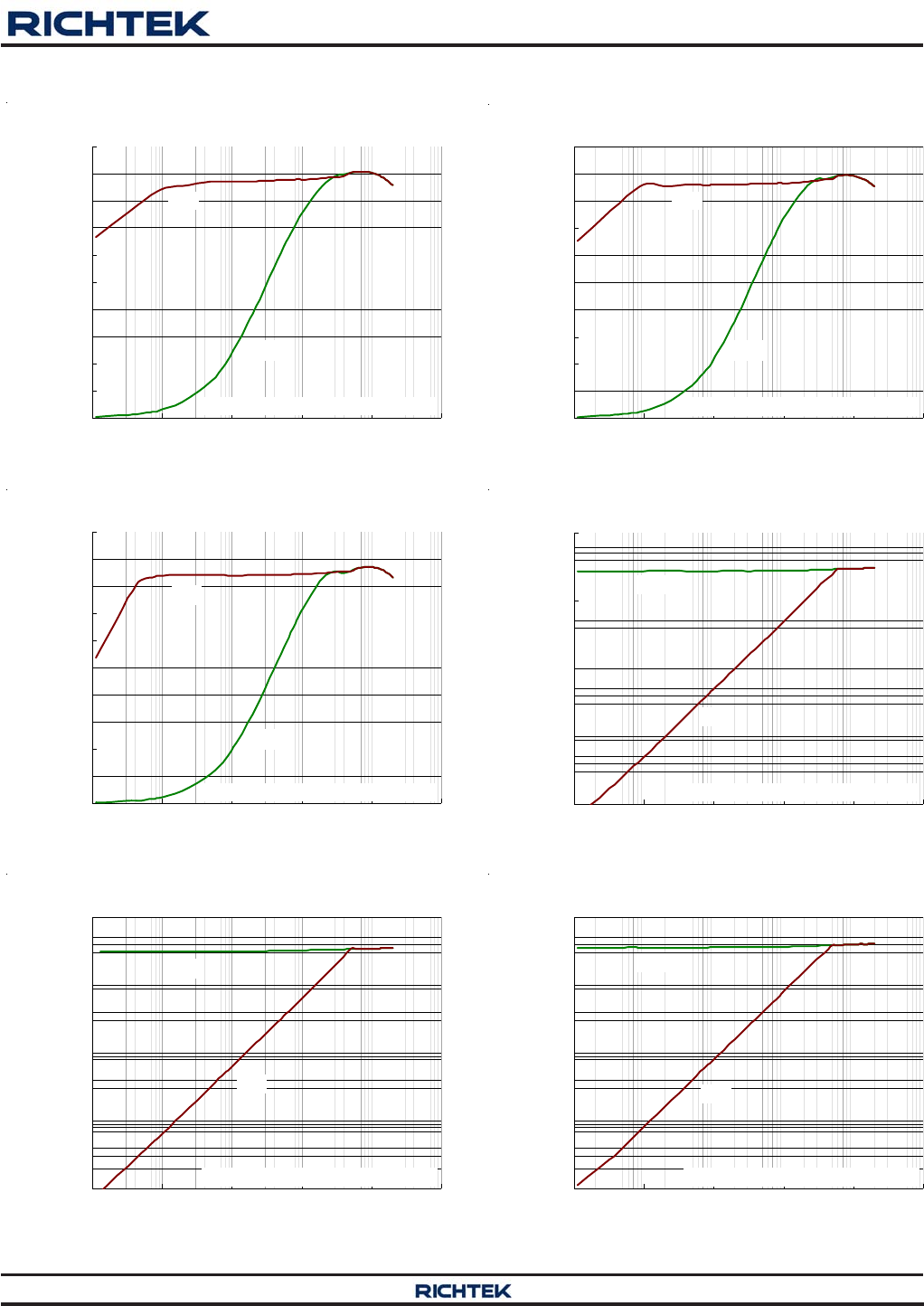
Typical Operating Characteristics
Efficiency vs. Load Current
0
10
20
30
40
50
60
70
80
90
100
0.001 0.01 0.1 1 10 100
Load Current (A)
Efficiency (%)
VIN = 8V, VOUT = 1.05V, RRF = 470kΩ
DEM
CCM
Efficiency vs. Load Current
0
10
20
30
40
50
60
70
80
90
100
0.001 0.01 0.1 1 10 100
Load Current (A)
Efficiency (%)
DEM
CCM
VIN = 12V, VOUT = 1.05V, RRF = 470kΩ
Efficiency vs. Load Current
0
10
20
30
40
50
60
70
80
90
100
0.001 0.01 0.1 1 10 100
Load Current (A)
Efficiency (%)
DEM
CCM
VIN = 20V, VOUT = 1.05V, RRF = 470kΩ
Switching Frequency vs. Load Current
0.1
1
10
100
1000
0.001 0.01 0.1 1 10 100
Load Current (A)
Switching Frequency (kHz) 1
DEM
CCM
VIN = 12V, VOUT = 1.05V, RRF = 470kΩ
Switching Frequency vs. Load Current
0.1
1
10
100
1000
0.001 0.01 0.1 1 10 100
Load Current (A)
Switching Frequency (kHz) 1
DEM
CCM
VIN = 12V, VOUT = 1.05V, RRF = 200kΩ
Switching Frequency vs. Load Current
0.1
1
10
100
1000
0.001 0.01 0.1 1 10 100
Load Current (A)
Switching Frequency (kHz) 1
DEM
CCM
VIN = 12V, VOUT = 1.05V, RRF = 100kΩ
RT8237E
10
DS8237E-00 December 2012www.richtek.com
©
Copyright 2012 Richtek Technology Corporation. All rights reserved. is a registered trademark of Richtek Technology Corporation.
CS Source Current vs. Temperature
0
2
4
6
8
10
12
14
16
18
20
-50 -25 0 25 50 75 100 125
Temperature (°C)
CS Source Current (µA)
VCC = 5V
Switching Frequency vs. Input Voltage
200
225
250
275
300
325
350
375
400
425
450
475
500
4 6 8 10 12 14 16 18 20 22 24 26
Input Voltage (V)
Switching Frequency (kHz) 1
IOUT = 10A
RRF = 39k
RRF = 100k
RRF = 200k
RRF = 470k
Line Regulation vs. Temperature
-1.0
-0.8
-0.6
-0.4
-0.2
0.0
0.2
0.4
0.6
0.8
1.0
-50 -25 0 25 50 75 100 125
Temperature (°C)
Line Regulation (%
)
VIN = 12V, VOUT = 1.05V, RRF = 470kΩ, No Load
DEM
Switching Frequency vs. Load Current
0.1
1
10
100
1000
0.001 0.01 0.1 1 10 100
Load Current (A)
Switching Frequency (kHz) 1
VIN = 12V, VOUT = 1.05V, RRF = 39kΩ
DEM
CCM
Load Regulation vs. Temperature
-1.0
-0.8
-0.6
-0.4
-0.2
0.0
0.2
0.4
0.6
0.8
1.0
-50 -25 0 25 50 75 100 125
Temperature (°C)
Load Regulation (%
)
VIN = 12V, VOUT = 1.05V, IOUT = 10A, RRF = 470kΩ
CCM
Load Transient Response
Time (40μs/Div)
UGATE
(20V/Div)
VIN = 12V, IOUT = 0A to 20A, VOUT = 1.05V
LGATE
(5V/Div)
IOUT
(10A/Div)
VOUT
(50mV/Div)
RT8237E
11
DS8237E-00 December 2012 www.richtek.com
©
Copyright 2012 Richtek Technology Corporation. All rights reserved. is a registered trademark of Richtek Technology Corporation.
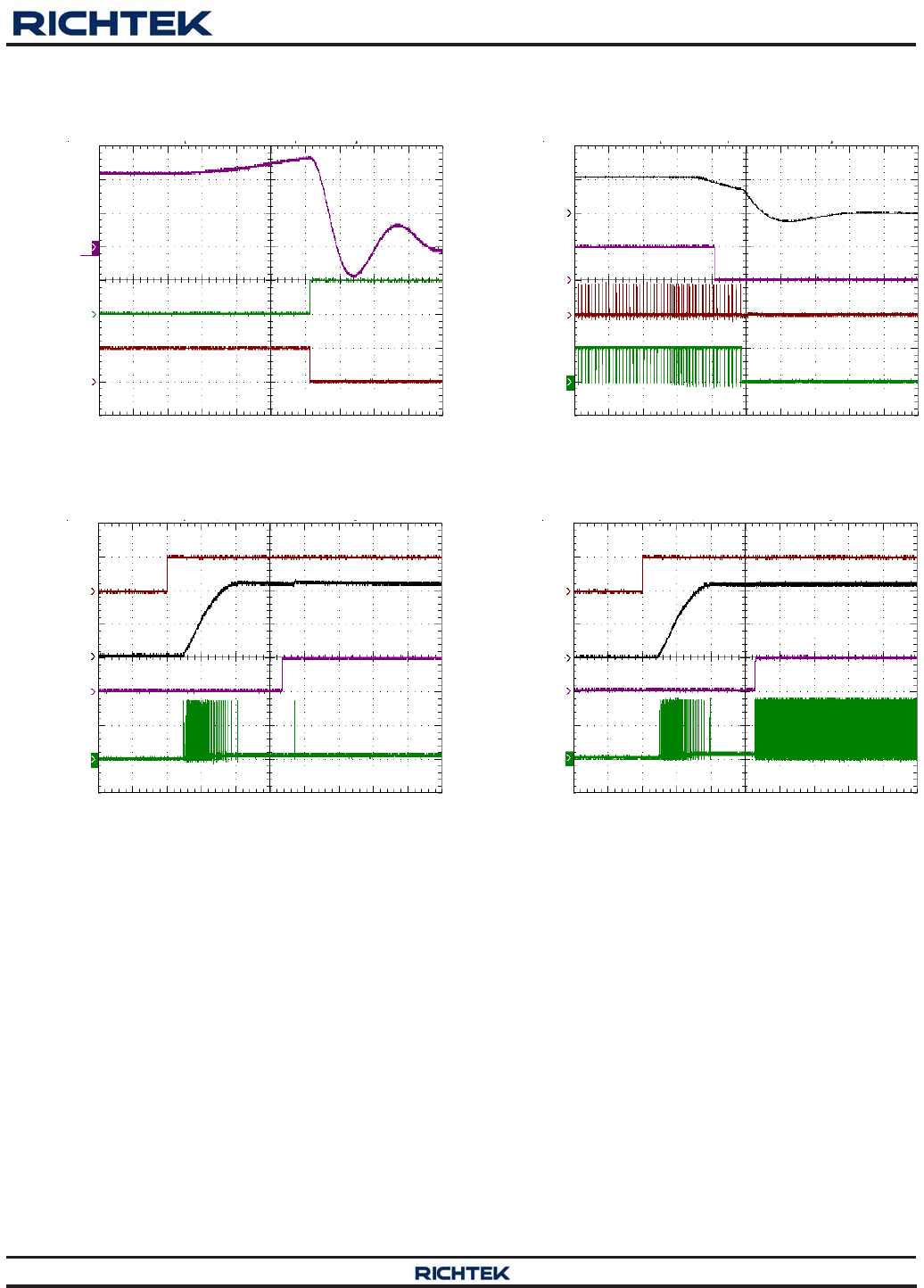
OVP
Time (40μs/Div)
DEM, VIN = 12V, No Load
PGOOD
(5V/Div)
VOUT
(500mV/Div)
LGATE
(5V/Div)
UVP
UGATE
(20V/Div)
Time (40μs/Div)
VIN = 12V, VOUT = 1.05V
PGOOD
(5V/Div)
VOUT
(1V/Div)
LGATE
(5V/Div)
Power On from EN
Time (1ms/Div)
DEM, VIN = 12V, No Load
VOUT
(500mV/Div)
UGATE
(10V/Div)
PGOOD
(5V/Div)
EN
(5V/Div)
Power On from EN
Time (1ms/Div)
CCM, VIN = 12V, No Load
UGATE
(10V/Div)
PGOOD
(5V/Div)
EN
(5V/Div)
VOUT
(500mV/Div)
RT8237E
12
DS8237E-00 December 2012www.richtek.com
©
Copyright 2012 Richtek Technology Corporation. All rights reserved. is a registered trademark of Richtek Technology Corporation.
Application Information
The RT8237E PWM controller provides high efficiency,
excellent transient response, and high DC output accuracy
needed for stepping down high voltage batteries to
generate low voltage CPU core, I/O, and chipset RAM
supplies in notebook computers. Richtek Mach
ResponseTM technology is specifically designed for
providing 100ns“instant-on” response to load steps while
maintaining a relatively constant operating frequency and
inductor operating point over a wide range of input voltages.
The topology solves the poor load transient response timing
problems of fixed frequency current mode PWMs and
avoids the problems caused by widely varying switching
frequencies in conventional constant on-time and constant
off-time PWM schemes.
On-Time Control (TON/MODE)
The on-time one-shot comparator has two inputs. One
input monitors the output voltage from the PHASE pin,
while the other input samples the input voltage and converts
it to a current. This input voltage proportional current is
used to charge an internal on-time capacitor. The on-time
is the time required for the voltage on this capacitor to
charge from zero volts to VOUT, thereby making the on-
time of the high side switch directly proportional to output
voltage and inversely proportional to input voltage.
The on-time is given by :
tON = (VOUT / VIN) / fSW
Table 1. RF Connection and Switching Frequency
Enable and Disable
The EN pin allows for power sequencing between the
controller bias voltage and another voltage rail. The
RT8237E remains in shutdown if the EN pin is lower than
500mV. When the EN pin rises above the VEN trip point,
the RT8237E will begin a new initialization and soft-start
cycle.
POR, UVLO and Soft-Start
Power-on reset (POR) occurs when VCC rises above
approximately 4.1V, in which the RT8237E resets the fault
latch and prepares the PWM for operation. When the input
voltage below 3.7V (min), the VCC Under Voltage Lockout
(UVLO) circuitry inhibits switching by keeping UGATE and
LGATE low. A built-in soft-start is used to prevent the power
supply input from surge currents after PWM is enabled. A
ramping up current limit threshold eliminates the VOUT
folded-back current during the soft-start duration.
Mode Selection (RF) Operation
To select the operation mode, connect a resistor from the
RF pin to either GND or PGOOD. When the resistor is
connected to GND, the controller operates in diode
emulation mode. When the resistor is connected to
PGOOD, the controller operates in CCM mode.
Diode-Emulation Mode (RRF connected to GND)
In diode-emulation mode, the RT8237E automatically
reduces switching frequency at light load conditions to
maintain high efficiency. This reduction of frequency is
achieved smoothly without increasing VOUT ripple or load
regulation. As the output current decreases from heavy
load condition, the inductor current is reduced and
eventually comes to the point where its valley touches
zero current, which is the boundary between continuous
conduction and discontinuous conduction modes. To
emulate the behavior of diodes, the low side MOSFET
allows only partial negative current to flow when the
inductor freewheeling current reaches negative. As the load
current is further decreased, it takes longer and longer to
discharge the output capacitor to the level that requires
Note : For DEM, connect RRF to GND; for CCM, connect
RRF to PGOOD.
RRF (kΩ) Switching Frequency (kHz)
470kΩ 290
200kΩ 340
100kΩ 380
39kΩ 430
RT8237E
13
DS8237E-00 December 2012 www.richtek.com
©
Copyright 2012 Richtek Technology Corporation. All rights reserved. is a registered trademark of Richtek Technology Corporation.
the next “ON” cycle. The on-time is kept the same as
that in heavy load condition. On the contrary, when the
output current increases from light load to heavy load, the
switching frequency increases to the preset value as the
inductor current reaches the continuous condition. This
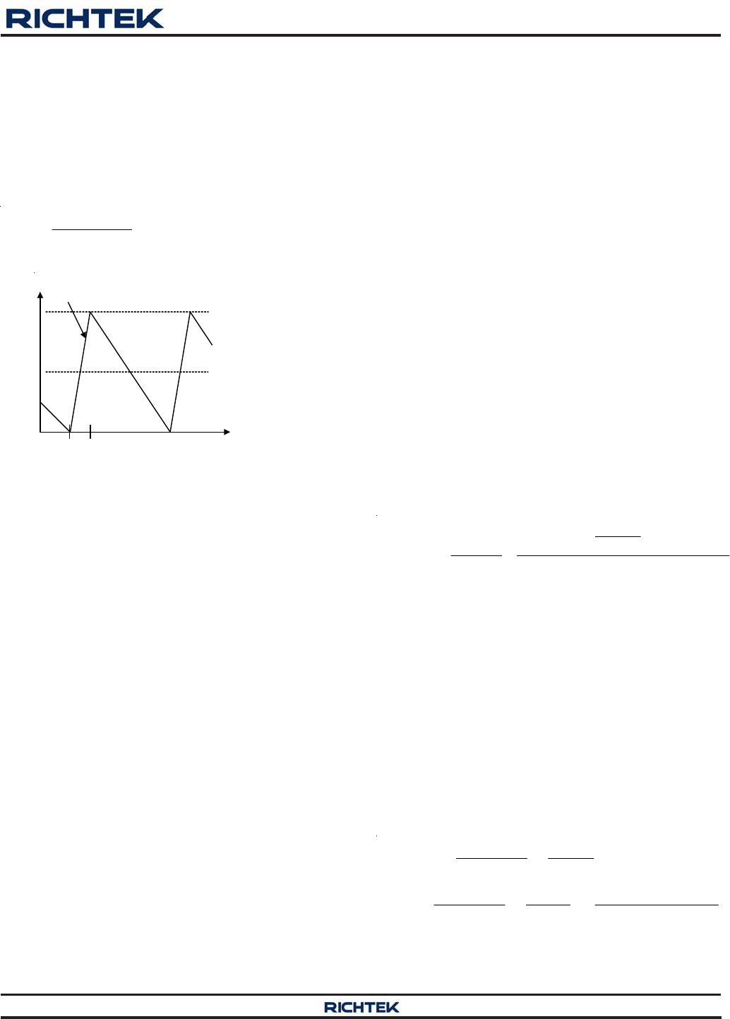
is shown in Figure 1. The transition load point to the light
load operation is calculated as follows :
(
)
IN OUT
LOAD ON
VV
It
2L
−
≈×
where tON is the on-time.
Figure 1. Boundary Condition of CCM/DCM
The switching waveforms may appear noisy and
asynchronous when light loading causes diode-emulation
operation, but this is a normal operating condition that
results in high light load efficiency. Trade-offs in DEM noise
vs. light load efficiency is made by varying the inductor
value. Generally, low inductor values produce a broader
efficiency vs. load curve, while higher values result in higher
full load efficiency (assuming that the coil resistance
remains fixed) and less output voltage ripple. The
disadvantages for using higher inductor values include
larger physical size and degraded load transient response
(especially at low input voltage levels).
Forced-CCM Mode (FCCM)
The low noise, forced-CCM mode disables the zero-
crossing comparator, which controls the low side switch
on-time. This causes the low side gate drive waveform to
become the complement of the high side gate drive
waveform. This in turn causes the inductor current to
reverse at light loads as the PWM loop to maintain duty
ratio VOUT/VIN. A fairly constant switching frequency is
the benefit of forced-CCM mode, but this comes at a cost.
The no load battery current can be up to 10mA to 40mA,
depending on the external MOSFETs.
Current Limit Setting (CS)
The RT8237E has a cycle-by-cycle current limit control.
The current limit circuit employs a unique “valley” current
sensing algorithm. If the magnitude of the current sense
signal at PHASE is above the current limit threshold, the
PWM is not allowed to initiate a new cycle (see Figure
2). In order to provide both good accuracy and a cost
effective solution, the RT8237E supports temperature
compensated MOSFET RDS(ON) sensing.
The CS pin of the RT8237E is a multiplexed pin for PWM
enable/disable control and current limit threshold setting.
Connect a setting resistor from this pin to GND via an N-
MOSFET. When the N-MOSFET is turned off, the PWM
is disabled. When the N-MOSFET is turned on, the PWM
is enabled and the current limit threshold is equal to 1/8
of the voltage at this pin.
Choose a current limit resistor by following below equation:
RIPPLE
LOAD_OC DS(ON)
CS_OC
OC_SET CS CS
I
I8R
V2
RII
⎛⎞
−××
⎜⎟
⎝⎠
==
Inductor current is monitored by the voltage between the
GND and PHASE pins, so the PHASE pin should be
connected to the Drain terminal of the low side MOSFET.
ICS has a temperature coefficient to compensate the
temperature dependency of the RDS(ON). GND is used as
the positive current sensing node, so GND should be
connected to the Source terminal of the low side MOSFET.
As the comparison is being done during the OFF state,
VLIMIT (current limit threshold) sets the valley level of the
inductor current. Thus, the load current at over current
threshold, ILOAD_OC, can be calculated as follows :
CS_OC RIPPLE
LOAD_OC DS(ON)
CS_OC IN OUT OUT
DS(ON) IN
VI
I = +
8R 2
V(V V ) V
1
= +
8R 2Lf V
×
−×
×
×××
IL
t
0tON
Slope = (VIN -VOUT) / L
IL, PEAK
ILOAD = IL, PEAK / 2
RT8237E
14
DS8237E-00 December 2012www.richtek.com
©
Copyright 2012 Richtek Technology Corporation. All rights reserved. is a registered trademark of Richtek Technology Corporation.
In an over current condition, the current to the load exceeds
the current to the output capacitor. Thus, the output voltage
falls and eventually crosses the under voltage protection
threshold, inducing IC shutdown.
Figure 2. “Valley” Current Limit
MOSFET Gate Driver
The high side driver is designed to drive high current, low
RDS(ON) N-MOSFET(s). When configured as a floating
driver, 5V bias voltage is delivered from the VCC supply.
The average drive current is proportional to the gate charge
at VGS = 5V times switching frequency. The instantaneous
drive current is supplied by the flying capacitor between
the BOOT and PHASE pins. To prevent shoot through, a
dead-time is internally generated between high side
MOSFET off to low side MOSFET on, and low side
MOSFET off to high side MOSFET on. The low side driver
is designed to drive high current low RDS(ON)
N-MOSFET(s). The internal pull-down transistor that drives
LGATE low is robust, with a 0.5Ω typical on-resistance.
A 5V bias voltage is delivered from the VCC supply. The
instantaneous drive current is supplied by the flying
capacitor between VCC and GND.
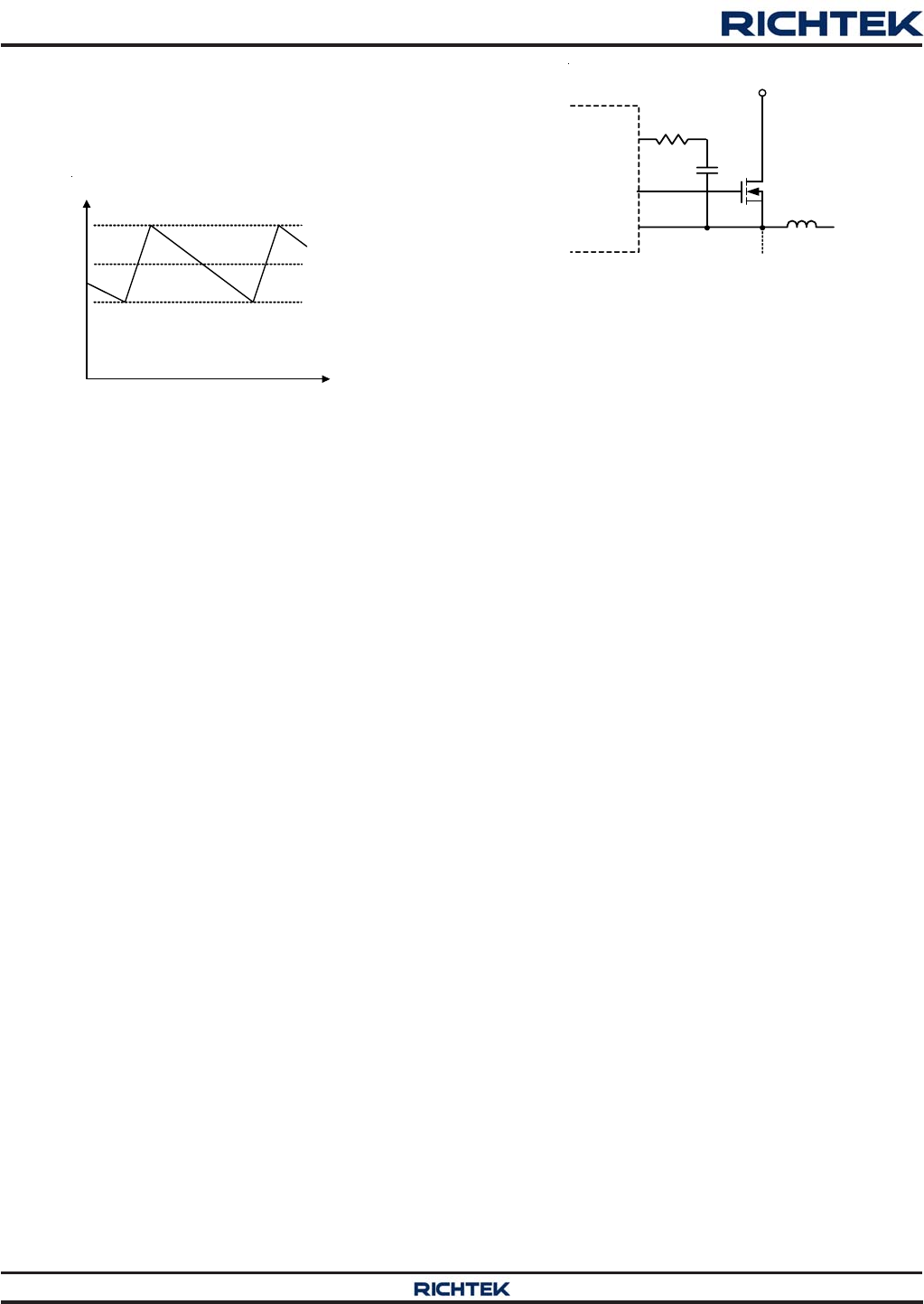
For high current applications, certain combinations of high
and low side MOSFETs may cause excessive gate-drain
coupling, which can lead to efficiency-killing, EMI-
producing shoot-through currents. This is often remedied
by adding a resistor in series with BOOT, which increases
the turn-on time of the high side MOSFET without degrading
the turn-off time (see Figure 3).
BOOT
UGATE
PHASE
R
VIN
Figure 3. Reducing the UGATE Rise Time
Power Good Output (PGOOD)
The power good output is an open-drain output and requires
a pull-up resistor. When the output voltage is 20% above
or 10% below its set voltage, PGOOD will be pulled low. It
is held low until the output voltage returns to within these
tolerances once more. During soft-start, PGOOD is actively
held low and is allowed to transition high only after soft-
start is over and the output reaches 90% of its set voltage.
There is a 2.5μs delay built into the PGOOD circuitry to
prevent false transitions.
Output Over Voltage Protection (OVP)
The output voltage is continuously monitored for over
voltage condition. When the output voltage exceeds 25%
of its set voltage threshold, over voltage protection will be
triggered and the low side MOSFET is latched on. This
activates the low side MOSFET to discharge the output
capacitor. The RT8237E is latched once OVP is triggered
and can only be released by VCC or EN power on reset.
There is a 5μs delay built into the over voltage protection
circuit to prevent false transitions.
Output Under Voltage Protection (UVP)
The output voltage can be continuously monitored for under
voltage condition. When the output voltage is less than
70% of its set voltage threshold, under voltage protection
will be triggered and then both UGATE and LGATE gate
drivers are forced low. There is a 2.5μs delay built into the
under voltage protection circuit to prevent false transitions.
During soft-start, the UVP blanking time is 3ms.
Thermal Shutdown (OTP)
The device implements an internal thermal shutdown to
protect itself if junction temperature exceeds 150°C. When
the junction temperature exceeds the thermal shutdown
threshold that the OTP function will be triggered and the
When the device is operating in the FCCM, the negative
current limit protects the external component. The negative
current limit detect threshold is set as the same value as
positive current limit but negative polarity. The threshold
still is the valley value of the inductor current.
IL
t
0
IL, PEAK
ILIMIT
ILOAD_OC
RT8237E
15
DS8237E-00 December 2012 www.richtek.com
©
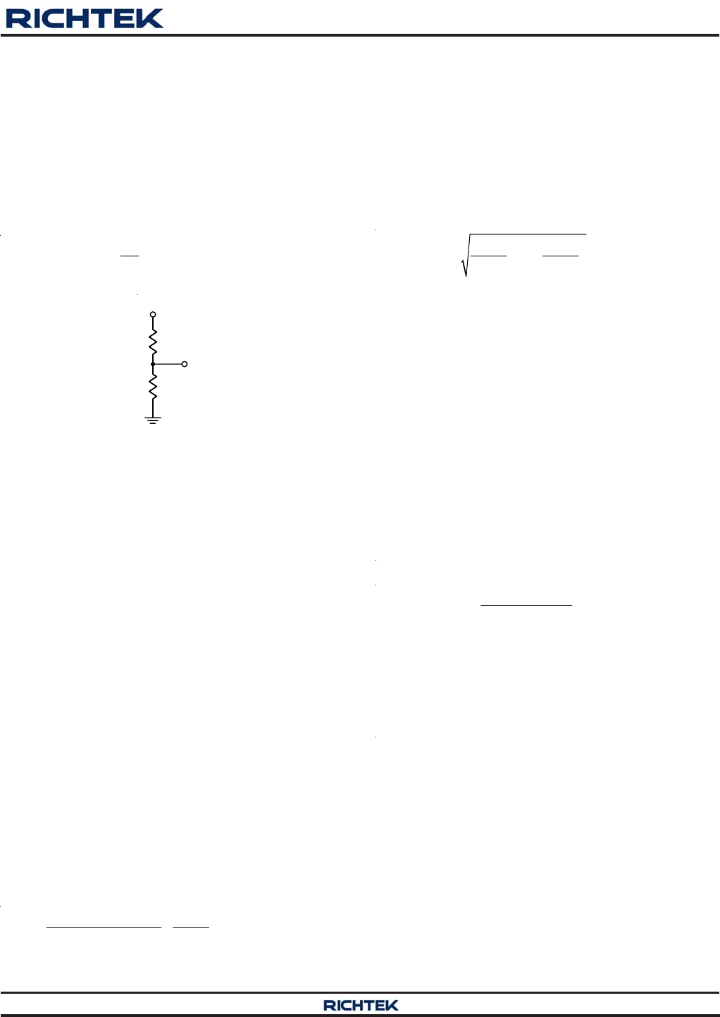
Copyright 2012 Richtek Technology Corporation. All rights reserved. is a registered trademark of Richtek Technology Corporation.
OUT REF R1
V = V 1+
R2
⎛⎞
×⎜⎟
⎝⎠
where VREF is 0.704V (typ.).
R1
R2
VOUT
FB
Figure 4. Setting VOUT with a Resistive Voltage Divider
Inductor Selection
The inductor plays an important role in step-down
converters because it stores the energy from the input
power rail and then releases the energy to the load. From
the viewpoint of efficiency, the dc resistance (DCR) of the
inductor should be as small as possible to minimize the
conduction loss. In addition, because the inductor takes
up a significant portion of the board space, its size is also
important. Low profile inductors can save board space
especially when there is a height limitation. However, low
DCR and low profile inductors are usually cost ineffective.
Additionally, larger inductance results in lower ripple
current, which means lower power loss. The inductor
current rising time increases with inductance value. This
means the transient response will be slower. Therefore,
the inductor design is a compromise between
performance, size and cost.
In general, the inductance is designed such that the ripple
current ranges between 20% to 40% of the full load current.
The inductance can be calculated using the following
equation : IN OUT OUT
MIN SW OUT_rated IN
VV V
LfkI V
−
=×
××
where k is the ratio between inductor ripple current and
rated output current.
Input Capacitor Selection
Voltage rating and current rating are the key parameters
in selecting an input capacitor. For a conservatively safe
design, an input capacitor should generally have a voltage
rating 1.5 times greater than the maximum input voltage.
The input capacitor is used to supply the input RMS
current, which is approximately calculated using the
following equation :
OUT OUT
RMS OUT IN IN
VV
II 1
VV
⎛⎞
=× ×−
⎜⎟
⎝⎠
The next step is to select a proper capacitor for RMS
current rating. Placing more than one capacitor with low
Equivalent Series Resistance (ESR) in parallel to form a
capacitor bank is a good design. Also, placing ceramic
capacitor close to the Drain of the high side MOSFET is
helpful in reducing the input voltage ripple at heavy load.
Output Capacitor Selection
The output capacitor and the inductor form a low-pass filter
in the buck topology. In steady-state condition, the ripple
current that flows into or out of the capacitor results in
ripple voltage. The output voltage ripples contains two
components, ΔVOUT_ESR and ΔVOUT_C.
OUT_ESR L
V I ESRΔ=Δ×
OUT_C L OUT SW
1
VI
8C f
Δ=Δ×
××
When load transient occurs, the output capacitor supplies
the load current before the controller can respond.
Therefore, the ESR will dominate the output voltage sag
during load transient. The output voltage sag can be
calculated using the following equation :
OUT_sag OUT
VESRI=×Δ
For a given output voltage sag specification, the ESR value
can be determined.
Another parameter that has influence on the output voltage
sag is the equivalent series inductance (ESL). A rapid
change in load current results in di/dt during transient.
Therefore, ESL contributes to part of the voltage sag. Use
a capacitor that has low ESL to obtain better transient
performance. Generally, using several capacitors in parallel
will have better transient performance than using single
capacitor for the same total ESR.
RT8237E will shut down and enter Latch-Off Mode. In
Latch-Off Mode, the RT8237E can be reset by EN or power
input VCC.
Output Voltage Setting (FB)
The output voltage can be adjusted from 0.7V to 3.3V by
setting the feedback resistors, R1 and R2 (see Figure 4).
Choose R2 to be approximately 10kΩ and solve for R1
using the equation below :
RT8237E
16
DS8237E-00 December 2012www.richtek.com
©
Copyright 2012 Richtek Technology Corporation. All rights reserved. is a registered trademark of Richtek Technology Corporation.
Unlike the electrolytic capacitor, the ceramic capacitor has
relative low ESR and can reduce the voltage deviation during
load transient. However, the ceramic capacitor can only
provide low capacitance value. Therefore, use a mixed
combination of electrolytic capacitor and ceramic capacitor
for better transient performance.
MOSFET Selection
The majority of power loss in the step-down power
conversion is due to the loss in the power MOSFETs. For
low voltage high current applications, the duty cycle of
the high side MOSFET is small. Therefore, the switching
loss of the high side MOSFET is of concern. Power
MOSFETs with lower total gate charge are preferred in
such applications.
However, the small duty cycle means the low side MOSFET
is on for most of the switching cycle. Therefore, the
conduction loss tends to dominate the total power loss of
the converter. To improve the overall efficiency, MOSFETs
with low RDS(ON) are preferred in circuit design. In some
cases, more than one MOSFET are connected in parallel
to further decrease the on-state resistance. However, this
depends on the low side MOSFET driver capability and
the budget.
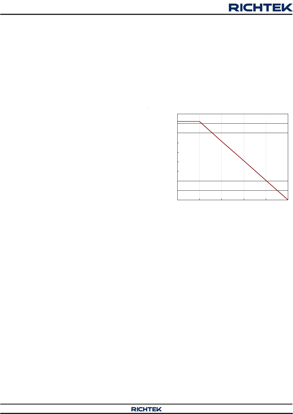
Thermal Considerations
For continuous operation, do not exceed absolute
maximum junction temperature. The maximum power
dissipation depends on the thermal resistance of the IC
package, PCB layout, rate of surrounding airflow, and
difference between junction and ambient temperature. The
maximum power dissipation can be calculated by the
following formula :
PD(MAX) = (TJ(MAX) − TA) / θJA
where TJ(MAX) is the maximum junction temperature, TA is
the ambient temperature, and θJA is the junction to ambient
thermal resistance.
For recommended operating condition specifications, the
maximum junction temperature is 125°C. The junction to
ambient thermal resistance, θJA, is layout dependent. For
WDFN-10L 3x3 packages, the thermal resistance, θJA, is
30.5°C/W on a standard JEDEC 51-7 four-layer thermal
Figure 5. Derating Curve of Maximum Power Dissipation
Layout Considerations
Layout is very important in high frequency switching
converter design. If designed improperly, the PCB may
radiate excessive noise and contribute to converter
instability. Certain points must be considered before
starting a layout for the RT8237E.
` Connect an RC low pass filter for VCC; 1μF and 10Ω
are recommended. Place the filter capacitor close to
the IC.
` Keep current limit setting network as close to the IC as
possible. Routing of the network should avoid coupling
to high voltage switching node.
` Connections from the drivers to the respective gate of
the high side or the low side MOSFET should be as
short as possible to reduce stray inductance.
test board. The maximum power dissipation at TA = 25°C
can be calculated by the following formula :
PD(MAX) = (125°C − 25°C) / (30.5°C/W) = 3.28W for
WDFN-10L 3x3 package
The maximum power dissipation depends on the operating
ambient temperature for fixed TJ(MAX) and thermal
resistance, θJA. The derating curve in Figure 5 allows the
designer to see the effect of rising ambient temperature
on the maximum power dissipation.
0.0
0.4
0.8
1.2
1.6
2.0
2.4
2.8
3.2
3.6
0255075100125
Ambient Temperature (°C)
Maximum Power Dissipation (W) 1
Four-Layer PCB
RT8237E
17
DS8237E-00 December 2012 www.richtek.com
©
Copyright 2012 Richtek Technology Corporation. All rights reserved. is a registered trademark of Richtek Technology Corporation.
` All sensitive analog traces and components such as
FB, GND, EN, CS, PGOOD, VCC, and RF should be
placed away from high voltage switching nodes such as
PHASE, LGATE, UGATE, or BOOT nodes to avoid
coupling. Use internal layer(s) as ground plane(s) and
shield the feedback trace from power traces and
components.
` Current sense connections must always be made using
Kelvin connections to ensure an accurate signal, with
the current limit resistor located at the device.
` Power sections should connect directly to ground
plane(s) using multiple vias as required for current
handling (including the chip power ground connections).
Power components should be placed close to the IC to
minimize loops and reduce losses.
RT8237E
18
DS8237E-00 December 2012www.richtek.com
Richtek Technology Corporation
5F, No. 20, Taiyuen Street, Chupei City
Hsinchu, Taiwan, R.O.C.
Tel: (8863)5526789
Richtek products are sold by description only. Richtek reserves the right to change the circuitry and/or specifications without notice at any time. Customers should
obtain the latest relevant information and data sheets before placing orders and should verify that such information is current and complete. Richtek cannot
assume responsibility for use of any circuitry other than circuitry entirely embodied in a Richtek product. Information furnished by Richtek is believed to be
accurate and reliable. However, no responsibility is assumed by Richtek or its subsidiaries for its use; nor for any infringements of patents or other rights of third
parties which may result from its use. No license is granted by implication or otherwise under any patent or patent rights of Richtek or its subsidiaries.
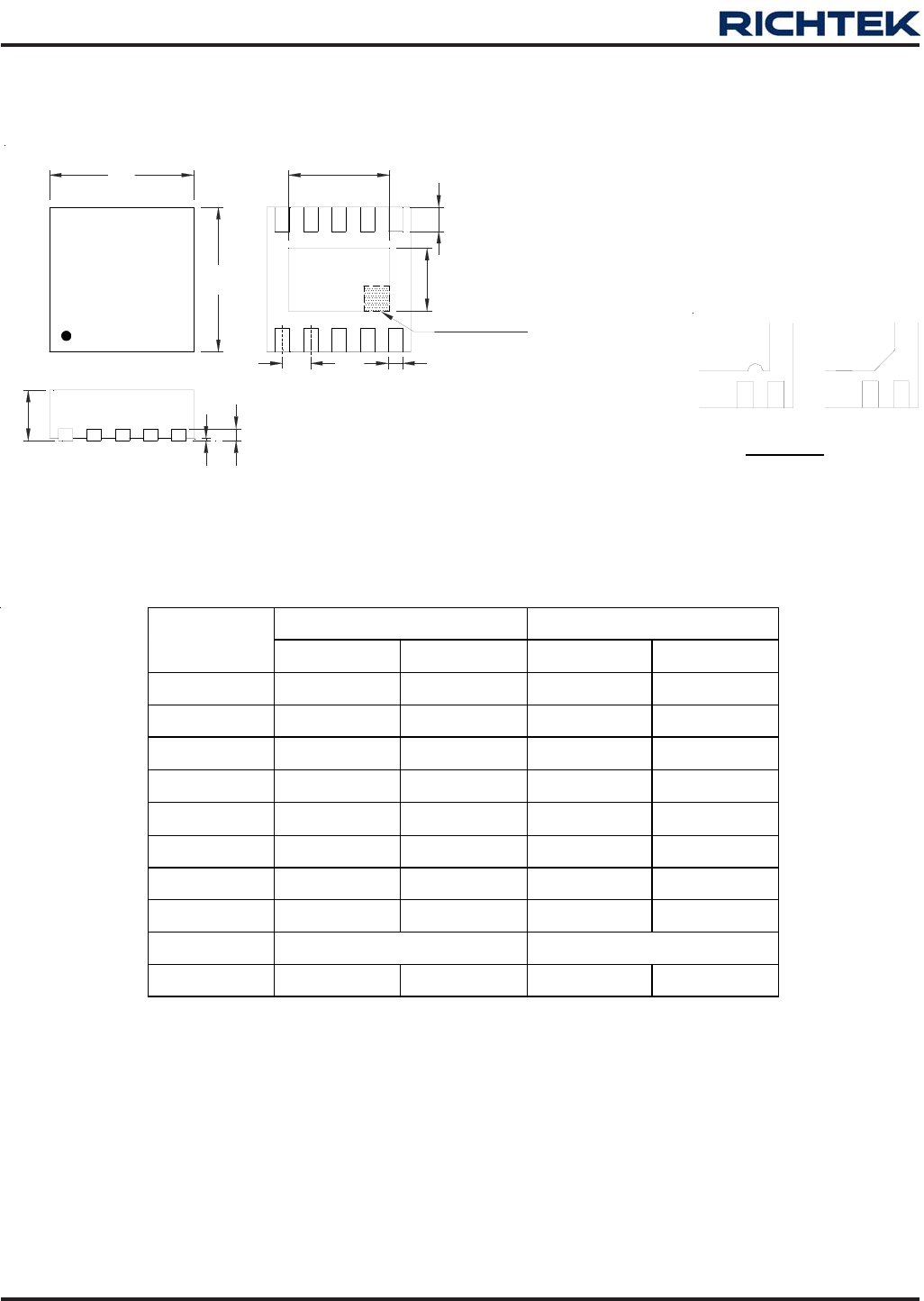
Outline Dimension
Dimensions In Millimeters Dimensions In Inches
Symbol Min Max Min Max
A 0.700 0.800 0.028 0.031
A1 0.000 0.050 0.000 0.002
A3 0.175 0.250 0.007 0.010
b 0.180 0.300 0.007 0.012
D 2.950 3.050 0.116 0.120
D2 2.300 2.650 0.091 0.104
E 2.950 3.050 0.116 0.120
E2 1.500 1.750 0.059 0.069
e 0.500 0.020
L 0.350 0.450
0.014 0.018
W-Type 10L DFN 3x3 Package
11
2
2
Note : The configuration of the Pin #1 identifier is optional,
but must be located within the zone indicated.
DETAIL A
Pin #1 ID and Tie Bar Mark Options
D
1
E
A3
A
A1
D2
E2
L
b
e
SEE DETAIL A