RT8248A Datasheet. Www.s Manuals.com. R04 Richtek
User Manual: Marking of electronic components, SMD Codes 5E, 5E*, 5E=**. Datasheets BC808-16, MM1Z13, MM5Z9V1, PDTA115EE , RB751V-40S2, RB751V40, RT8248AGQW.
Open the PDF directly: View PDF ![]() .
.
Page Count: 21
RT8248A
®
DS8248A-04 October 2014 www.richtek.com
1
Copyright 2014 Richtek Technology Corporation. All rights reserved. is a registered trademark of Richtek Technology Corporation.
©
Complete DDR Memory Power Supply Controller
General Description
The RT8248A provides a complete power supply for DDR2/
DDR3/DDR3L/LPDDR3/DDR4 memory systems. It
integrates a synchronous PWM Buck controller with a
1.5A sink/source tracking linear regulator and buffered low
noise reference.
The PWM controller provides the low quiescent current,
high efficiency, excellent transient response, and high DC
output accuracy needed for stepping down high-voltage
batteries to generate low-voltage chipset RAM supplies
in notebook computers. The constant on-time PWM
control scheme handles wide input/output voltage ratios
with ease and provides 100ns “instant-on” response to
load transients while maintaining a relatively constant
switching frequency.
The RT8248A achieves high efficiency at a reduced cost
by eliminating the current-sense resistor found in
traditional current mode PWMs. Efficiency is further
enhanced by its ability to drive very large synchronous
rectifier MOSFETs. The Buck conversion allows this device
to directly step down high-voltage batteries for the highest
possible efficiency.
The 1.5A sink/source LDO maintains fast transient
response only requiring a 10μF ceramic output capacitor.
In addition, the LDO supply input is available externally
to significantly reduce the total power losses. The IC
supports all of the sleep state controls placing VTT at
high-Z in S3 and discharging VDDQ, VTT and VTTREF
(soft-off) in S4/S5.
The RT8248A provides protections including OVP, UVP,
and thermal shutdown and available in the WQFN-20L 3x3
package.
Simplified Application Circuit
RT8248A
VDD
PHASE
LGATE
BOOT
UGATE
FB
GND
V
VDDQ
VVDD
VIN
TON
VLDOIN
VTT
VTT
VTTSNS
VTTREF
CS
S3
S5
VID
VDDQ
PGOODPGOOD
Features
--
--
-PWM Controller
Adjustable Current Limit with Low-Side RDS(ON)
Sensing
Low Quiescent Supply Current
Quick Load-Step Response within 100ns
1% VVDDQ Accuracy Over Line and Load
Adjustable 0.675V to 3.3V Output Range for 1.8V
(DDR2), 1.5V (DDR3), 1.35V (DDR3L), 1.2V (LPDDR3)
and 1.2V (DDR4)
4.5V to 26V Battery Input Range
Resistor Adjustable Frequency
Over-/Under-Voltage Protection
Internal Voltage Ramp Soft-Start
Drives Large Synchronous Rectifier MOSFETs
Power Good Indicator
--
--
-1.5A LDO (VTT), Buffered Reference (VTTREF)
Capable to Sink and Source Up to 1.5A
LDO Input Available to Optimize Power Losses
Requires Only 10μμ
μμ
μF Ceramic Output Capacitor
Integrated Divider Tracks 1/2 VDDQ for both VTT
and VTTREF
Accuracy ±±
±±
±20mV for both VTTREF and VTT
Supports High-Z in S3 and Soft-Off in S4/S5
RT8248A
2
DS8248A-04 October 2014www.richtek.com
©
Copyright 2014 Richtek Technology Corporation. All rights reserved. is a registered trademark of Richtek Technology Corporation.
Functional Pin Description
Pin No. Pin Name Pin Function
1 VTTGND Power Ground for the VTT LDO.
2 VTTSNS Voltage Sense Input for the VTT LDO. Connect to the terminal of the VTT_LDO
output capacitor.
3, 21
(Exposed Pad) GND The exposed pad must be soldered to a large PCB and connected to GND for
maximum power dissipation.
4 VTTREF VTTREF Buffered Reference Output.
5 VDDQ Reference Input for VTT and VTTREF.
6 FB Feedback Voltage Input. Connect to a resistive voltage divider from VDDQ to
GND to adjust the output voltage.
7 S3 VTT LDO Enable Control Input. Do not leave this pin floating.
8 S5 PWM Enable Control Input. Do not leave this pin floating.
9 TON Set the UGATE On-Time Through a Pull-Up Resistor Connecting to VIN.
10 PGOOD
Power Good Open-Drain Output. In high state when VDDQ output voltage is
within the target range.
11 VID Internal Reference Voltage Setting.
12 VDD Supply Voltage Input for the Analog Supply and LGATE Gate Driver.
13 CS Current Limit Threshold Setting Input. Connect to GND through the voltage
setting resistor.
14 PGND Power Ground for Low-Side MOSFET.
15 LGATE Low-Side Gate Driver Output for VDDQ.
16 PHASE
Switch Node. External inductor connection for VDDQ and behave as the current
sense comparator input for Low-Side MOSFET RDS
(
ON
)
sensing.
17 UGATE High-Side Gate Driver Output for VDDQ.
18 BOOT Bootstrap Supply for High-Side Gate Driver.
19 VLDOIN Power Supply for VTT LDO.
20 VTT Power Output for the VTT LDO.
Ordering Information
Note :
Richtek products are :
RoHS compliant and compatible with the current require-
ments of IPC/JEDEC J-STD-020.
Suitable for use in SnPb or Pb-free soldering processes.
Applications
-DDR2/DDR3/DDR3L/LPDDR3/DDR4 Memory Power
Supplies
-Notebook computers
-SSTL18, SSTL15 and HSTL bus termination
Pin Configurations
(TOP VIEW)
WQFN-20L 3x3
VTT
VLDOIN
VTTREF
GND
VTTGND
VTTSNS
LGATE
PGND
VDD
CS
FB
S3
TON UGATE
BOOT
PHASE
VDDQ VID
PGOOD
S5
15
14
13
12
17181920
1
2
3
4
9876
GND
21
115
16
10
Marking Information
5E= : Product Code
YMDNN : Date Code
RT8248AGQW
5E=YM
DNN
RT8248A
Package Type
QW : WQFN-20L 3x3 (W-Type)
Lead Plating System
G : Green (Halogen Free and Pb Free)

RT8248A
3
DS8248A-04 October 2014 www.richtek.com
©
Copyright 2014 Richtek Technology Corporation. All rights reserved. is a registered trademark of Richtek Technology Corporation.
Function Block Diagram
Buck Controller
VTT LDO
GND
+
-
+
-
+
-
+
-
VTTREF
VTT
VLDOIN
VTTGND
Non-Tracking
Discharge
VTTSNS
S3
S5
VDDQ
Thermal
Shutdown
R
QS
Comp
S1 Q
Latch
S1 Q
Latch
+
-
OV
+
-
UV
115%VREF
0.45V
+
-
85% VREF
SS Timer Thermal
Shutdown
DEM
+
-
On-Time
1-SHOT
CS
FB
VDDQ
UGATE
PHASE
VDD
PGOOD
PGND
LGATE
TON
BOOT
TRIG
S5
5µA
SS Int
+
-
+
1/10
VREF
Reference
Voltage
Selector
VID
VREF
Min. TOFF
TRIG
VDD
RT8248A
4
DS8248A-04 October 2014www.richtek.com
©
Copyright 2014 Richtek Technology Corporation. All rights reserved. is a registered trademark of Richtek Technology Corporation.
Operation
The RT8248A is a constant on-time synchronous step-
down controller. In normal operation, the high-side
N-MOSFET is turned on when the output voltage is lower
than VREF, and is turned off after the internal one-shot
timer expires. While the high-side N-MOSFET is turned
off, the low-side N-MOSFET is turned on to conduct the
inductor current until next cycle begins.
Soft-Start (SS)
For internal soft-start function, an internal current source
charges an internal capacitor to build the soft-start ramp
voltage. The output voltage will track the internal ramp
voltage during soft-start interval.
PGOOD
The power good output is an open-drain architecture. When
the soft-start is finished, the PGOOD open-drain output
will be high impedance.
Current Limit
The current limit circuit employs a unique “valley” current
sensing algorithm. If the magnitude of the current sense
signal at PHASE is above the current limit threshold, the
PWM is not allowed to initiate a new cycle. The current
limit threshold can be set with an external voltage setting
resistor on the CS pin.
Over-Voltage Protection (OVP) & Under-Voltage
Protection (UVP)
The output voltage is continuously monitored for over-
voltage and under-voltage protection. When the output
voltage exceeds its set voltage threshold( 115% of VOUT),
UGATE goes low and LGATE is forced high. When the
feedback voltage is less than 0.45V, under-voltage
protection is triggered and then both UGATE and LGATE
gate drivers are forced low. The controller is latched until
VDD is re-supplied and exceeds the POR rising threshold
voltage or S5 is reset.
VTT Linear Regulator and VTTREF
This VTT linear regulator employs ultimate fast response
feedback loop so that small ceramic capacitors are enough
for keeping track of VTTREF within 40mV at all conditions,
including fast load transient. The VTTREF block consists
of on-chip 1/2 divider, LPF and buffer. This regulator also
has sink and source capability up to 10mA. Bypass
VTTREF to GND with a 33nF ceramic capacitor for stable
operation.
RT8248A
5
DS8248A-04 October 2014 www.richtek.com
©
Copyright 2014 Richtek Technology Corporation. All rights reserved. is a registered trademark of Richtek Technology Corporation.
Electrical Characteristics
Parameter Symbol Test Conditions Min Typ Max Unit
PWM Controller
Quiescent Supply Current FB Forced abov e the Regulation Point,
VS5 = 5V, VS3 = 0V, Not Switching -- 135 -- A
TON Operating Current RTON = 620k, VIN = 12V -- 19 -- A
IVLDOIN BIAS Current VS5 = VS3 = 5V, VTT = No Load -- 1 -- A
IVLDOIN Standby Current VS5 = 5V, VS3 = 0, VTT = No Load -- 0.1 10 A
(VDD = 5V, VIN = 12V, RTON = 620kΩ, TA = 25°C, unless otherwise specified)
Absolute Maximum Ratings (Note 1)
-Supply Input Voltage, TON to GND ------------------------------------------------------------------------------------ −0.3V to 32V
-BOOT to PHASE ---------------------------------------------------------------------------------------------------------- −0.3V to 6V
-PHASE to GND
DC ----------------------------------------------------------------------------------------------------------------------------- −0.3V to 32V
< 20ns ----------------------------------------------------------------------------------------------------------------------- −8V to 38V
-LGATE to GND
DC ----------------------------------------------------------------------------------------------------------------------------- −0.3V to 6V
< 20ns ----------------------------------------------------------------------------------------------------------------------- −2.5V to 7.5V
-UGATE to PHASE
DC ----------------------------------------------------------------------------------------------------------------------------- −0.3V to 6V
< 20ns ----------------------------------------------------------------------------------------------------------------------- −5V to 7.5V
-VDD, CS, S3, S5, VTTSNS, VDDQ, VID, VTTREF, VTT, VLDOIN, FB, PGOOD to GND ---------------- −0.3V to 6V
-PGND, VTTGND to GND ------------------------------------------------------------------------------------------------- −0.3V to 0.3V
-Other Pins------------------------------------------------------------------------------------------------------------------- −0.3V to 6.5V
-Power Dissipation, PD @ TA = 25°C
WQFN-20L 3x3 ------------------------------------------------------------------------------------------------------------ 3.33W
-Package Thermal Resistance (Note 2)
WQFN-20L 3x3, θJA ------------------------------------------------------------------------------------------------------- 30°C/W
WQFN-20L 3x3, θJC ------------------------------------------------------------------------------------------------------ 7.5°C/W
-Junction Temperature ----------------------------------------------------------------------------------------------------- 150°C
-Lead Temperature (Soldering, 10 sec.) ------------------------------------------------------------------------------- 260°C
-Storage Temperature Range -------------------------------------------------------------------------------------------- −65°C to 150°C
-ESD Susceptibility (Note 3)
HBM (Human Body Model) ---------------------------------------------------------------------------------------------- 2kV
Recommended Operating Conditions (Note 4)
-Input Voltage, VIN --------------------------------------------------------------------------------------------------------- 4.5V to 26V
-Control Voltage, VDD ----------------------------------------------------------------------------------------------------- 4.5V to 5.5V
-Junction Temperature Range -------------------------------------------------------------------------------------------- −40°C to 125°C
-Ambient Temperature Range -------------------------------------------------------------------------------------------- −40°C to 85°C
RT8248A
6
DS8248A-04 October 2014www.richtek.com
©
Copyright 2014 Richtek Technology Corporation. All rights reserved. is a registered trademark of Richtek Technology Corporation.
Parameter Symbol Test Conditions Min Typ Max Unit
VDD -- 0.1 10 A
TON -- 0.1 5 A
S5/S3 1 0.1 1 A
VLDOIN -- 0.1 1 A
Shutdown Current
(VS5 = VS3 = 0V) ISHDN
VID -- 0.5 1 A
FB Error Comparator
Threshold VREF V
REF = 0.675V/0.75V 1 0 1 %
VDDQ Voltage Range 0.675 -- 3.3 V
Switch Frequency fSW RTON = 620k, VIN = 12V,
VDDQ = 1 .5V, IOUT = 20A (Note 5) 320 400 480 kHz
Minimum Off-Time 250 400 550 ns
VDDQ Shutdown Discharge
Resistance V
S5 = 0V, VS3 = 0V -- 15 --
Current Sensing
CS Pin Source Current 4.5 5 5.5 A
Zero Crossing Threshold GND PHASE 5 -- 10 mV
Fault Protection
Current Limit (Positive) GND PHASE, RCS = 160k 70 80 90 mV
Output UV Threshold VUVP VFB Falling. For both VID is high or
low. 0.4 0.45 0.5 V
UVP Latch Delay FB Forced below UV Threshold -- 30 -- s
OVP Threshold VOVP With Respect to Error Comparator
Threshold 110 115 120 %
OVP Latch Delay FB Forced above OV Threshold -- 5 -- s
VDD POR Threshold Rising Edge, Hysteresis = 120mV,
PWM Disabled below this Level 3.9 4.2 4.5 V
Voltage Ramp Soft-Start Time From S5 Going High to VFB = 0.675V -- 1 -- mS
UV Blank Time From S5 Signal Going High -- 5 -- mS
Thermal Shutdown TSD -- 165 -- C
Driver On-Resistance
UGATE Gate Driver Source RUGATEsr BOOT PHASE Forced to 5V -- 2.5 5
UGATE Gate Driver Sink RUGATEsk BOOT PHASE Forced to 5V -- 1.5 3
LGATE Gate Driver Source RLGATEsr DL, High State -- 2.5 5
LGATE Gate Driver Sink RLGATEsk DL, Low State -- 0.8 1.6
LGATE Rising (Phase = 1.5V) -- 40 --
Dead Time UGATE Rising -- 40 -- ns
Internal Boost Charging Switch
On-Resistance VDD to BOOT, 10mA -- -- 80
RT8248A
7
DS8248A-04 October 2014 www.richtek.com
©
Copyright 2014 Richtek Technology Corporation. All rights reserved. is a registered trademark of Richtek Technology Corporation.
Parameter Symbol Test Conditions Min Typ Max Unit
Logic I/O
Logic-High 2 -- --
S3, S5 Input
Voltage Logic-Low -- -- 0.8 V
Logic Input Current S3, S5 = VDD / GND 1 0 1 A
Logic-High 750 -- --
VID Input
Threshold Voltage Logic-Low -- -- 300 mV
PGOOD (Upper Side Threshold Decide by OV Threshold)
Trip Threshold (Falling) Measured at FB, with Respect to
Reference, No Load. Hysteresis = 2% 20 15 10 %
Fault Propagation Delay Falling Edge, FB Forced below
PGOOD Trip Threshold -- 5 -- s
Output Low Voltage ISINK = 1mA -- -- 0.4 V
Leakage Current ILEA K High State, Forced to 5V -- -- 1 A
VTT LDO
VDDQ = VLDOI N = 1.2V/1.35V/1.5V/
1.8V, |IVTT| = 0A 20 -- 20
VDDQ = VLDOI N = 1.2V/1.35V/1.5V/
1.8V, |IVTT| < 1A 30 -- 30
VDDQ = VLDOI N = 1.2V/1.35V,
|IVTT| < 1.2A 40 -- 40
VTT Output Tolerance VVTTTOL
VDDQ = VLDOI N = 1.5V/1.8V,
|IVTT| < 1.5A 40 -- 40
mV
VTT Source Current Limit IVTTOCLSRC V
TT = 0V 1.6 2.6 3.6 A
VTT Sink Current Limit IVTTOCLSNK V
TT = VDDQ 1.6 2.6 3.6 A
VTT Leakage Current IVTTLK S5 = 5V, S3 = 0V,
VDDQ
V
VTT = 2 10 -- 10 A
VTTSNS Leakage Current IVTTSNSLK I
SINK = 1mA 1 -- 1 A
VTT Discharge Current IDSCHRG V
DDQ = 0V, VTT = 0.5V, S5 = S3 = 0V 10 30 -- mA
VTTREF Output Voltage VVTTREF VVTT =
VDDQ
VTTREF V
V = 2,
VVDDQ = 1.5V
-- 0.75 -- V
VLDOIN = VVDDQ = 1.5V,
|IVTTREF| < 10mA 15 -- 15
VDDQ/2, VTTREF Output
Voltage Tolerance VVTTREFTOL VLDOIN = VVDDQ = 1.8V,
|IVTTREF| < 10mA 18 -- 18
mV
VTTREF Source Current Limit IVTTREFOCL V
VTTREF = 0V 10 40 80 mA
RT8248A
8
DS8248A-04 October 2014www.richtek.com
©
Copyright 2014 Richtek Technology Corporation. All rights reserved. is a registered trademark of Richtek Technology Corporation.
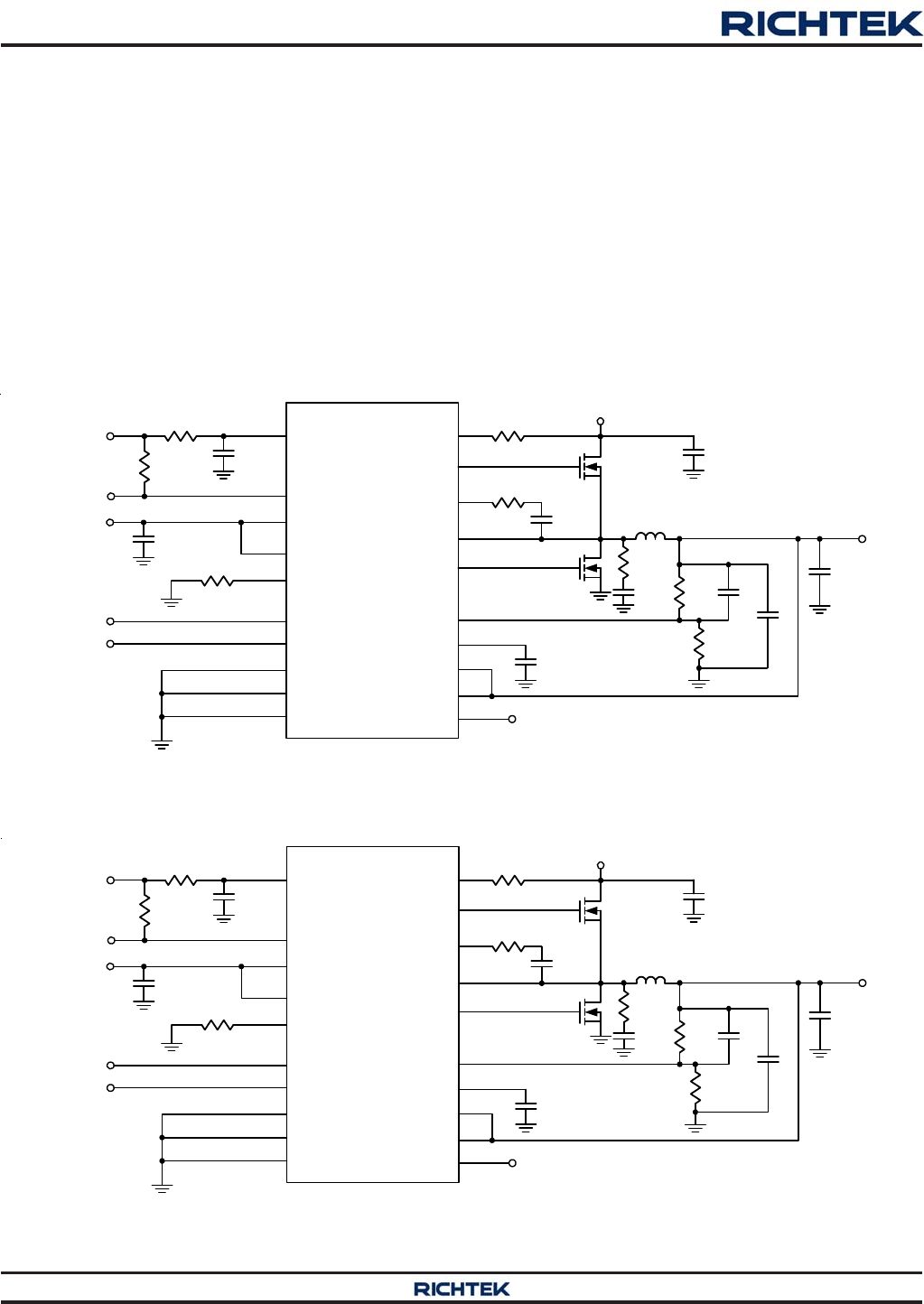
Typical Application Circuit
Figure 1. Typical Application Circuit with POSCAP Solution
Figure 2. Typical Application Circuit with Pure MLCC Solution
RT8248A
VDD
PHASE
LGATE
BOOT
UGATE
FB
GND
PGOOD
V
VDDQ
VVDD
VIN
PGOOD
TON
VLDOIN
VTTREF
S3
S5
VID
VDDQ
9
17
18
15
16
6
4
5
19
12
10
7
8
11
VTT
VTT
VTTSNS
CS
20
2
13
VTT Control
VDDQ Control
3,
21 (Exposed Pad)
PGND
VTTGND
1
14
(Optional)
1µF
C1
100k
R1
10µF
C2
270k
R2
620k
R3
0
R4 Q1
886N03LS
10µF x 2
C3
0.1µF
C4
Q2
886N03LS
R7
C7
L1
1µH
16k
R5
20k
R6
C8
C9
220µF
C5
1.35V
33nF
C6
Low
0.675V
RT8248A
VDD
PHASE
LGATE
BOOT
UGATE
FB
GND
PGOOD
V
VDDQ
VVDD
VIN
PGOOD
TON
VLDOIN
VTTREF
S3
S5
VID
VDDQ
9
17
18
15
16
6
4
5
19
12
10
7
8
11
VTT
VTT
VTTSNS
CS
20
2
13
VTT Control
VDDQ Control
3,
21 (Exposed Pad)
PGND
VTTGND
1
14
(Optional)
1µF
C1
100k
R1
10µF
C2
270k
R2
620k
R3
0
R4 Q1
886N03LS
10µF x 2
C3
0.1µF
C4
Q2
886N03LS
R7
C7
L1
1µH
16k
R5
20k
R6
C8
C9
22µF x 4
C5
1.35V
33nF
C6
0.675V
Low
Note 1. Stresses beyond those listed “Absolute Maximum Ratings” may cause permanent damage to the device. These are
stress ratings only, and functional operation of the device at these or any other conditions beyond those indicated in
the operational sections of the specifications is not implied. Exposure to absolute maximum rating conditions may
affect device reliability.
Note 2. θJA is measured at TA = 25°C on a high effective thermal conductivity four-layer test board per JEDEC 51-7. θJC is
measured at the exposed pad of the package.
Note 3. Devices are ESD sensitive. Handling precaution is recommended.
Note 4. The device is not guaranteed to function outside its operating conditions.
Note 5. Not production tested. Test condition refer to electrical characteristics using application circuit.
RT8248A
9
DS8248A-04 October 2014 www.richtek.com
©
Copyright 2014 Richtek Technology Corporation. All rights reserved. is a registered trademark of Richtek Technology Corporation.
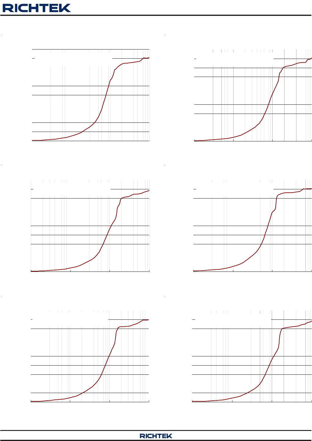
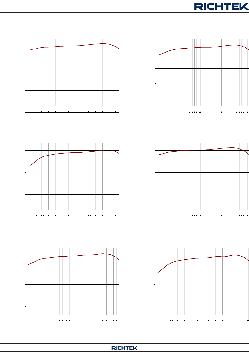
Typical Operating Characteristics
Switching Frequency vs. Load Current
0
50
100
150
200
250
300
350
400
450
500
0.01 0.1 1 10
Load Current (A)
Switching Frequency (kHz) 1
DDR3L, VIN = 7.4V, VDDQ = 1.35V,
S3 = GND, S5 = 5V, RTON = 620kΩ
Switching Frequency vs. Load Current
0
50
100
150
200
250
300
350
400
450
500
0.01 0.1 1 10
Load Current (A)
Switching Frequency (kHz) 1
DDR3L, VIN = 12V, VDDQ = 1.35V,
S3 = GND, S5 = 5V, RTON = 620kΩ
Switching Frequency vs. Load Current
0
50
100
150
200
250
300
350
400
450
500
0.01 0.1 1 10
Load Current (A)
Switching Frequency (kHz) 1
DDR3L, VIN = 19V, VDDQ = 1.35V,
S3 = GND, S5 = 5V, RTON = 620kΩ
Switching Frequency vs. Load Current
0
50
100
150
200
250
300
350
400
450
500
0.01 0.1 1 10
Load Current(A)
Switching Frequency (kHz) 1
DDR4, VIN = 7.4V, VDDQ = 1.2V,
S3 = GND, S5 = 5V, RTON = 620kΩ
Switching Frequency vs. Load Current
0
50
100
150
200
250
300
350
400
450
500
0.01 0.1 1 10
Load Current (A)
Switching Frequency (kHz) 1
DDR4, VIN = 12V, VDDQ = 1.2V,
S3 = GND, S5 = 5V, RTON = 620kΩ
Switching Frequency vs. Load Current
0
50
100
150
200
250
300
350
400
450
500
0.01 0.1 1 10
Load Current (A)
Switching Frequency (kHz) 1
DDR4, VIN = 19V, VDDQ = 1.2V,
S3 = GND, S5 = 5V, RTON = 620kΩ
RT8248A
10
DS8248A-04 October 2014www.richtek.com
©
Copyright 2014 Richtek Technology Corporation. All rights reserved. is a registered trademark of Richtek Technology Corporation.
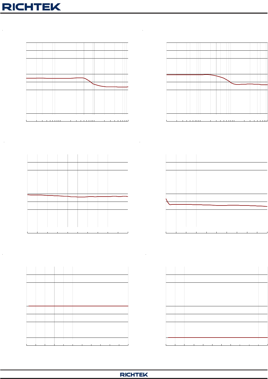
Efficiency vs. Load Current
0
10
20
30
40
50
60
70
80
90
100
0.001 0.010 0.100 1.000 10.000
Load Current (A)
Efficiency (%)
DDR3L, VIN = 12V, VDDQ = 1.35V, S3 = S5 = 5V
Efficiency vs. Load Current
0
10
20
30
40
50
60
70
80
90
100
0.001 0.010 0.100 1.000 10.000
Load Current (A)
Efficiency (%)
DDR3L, VIN = 7.4V, VDDQ = 1.35V, S3 = S5 = 5V
Efficiency vs. Load Current
0
10
20
30
40
50
60
70
80
90
100
0.001 0.010 0.100 1.000 10.000
Load Current (A)
Efficiency (%)
DDR3L, VIN = 19V, VDDQ = 1.35V, S3 = S5 = 5V
Efficiency vs. Load Current
0
10
20
30
40
50
60
70
80
90
100
0.001 0.010 0.100 1.000 10.000
Load Current (A)
Efficiency (%)
DDR4, VIN = 7.4V, VDDQ = 1.2V, S3 = S5 = 5V
Efficiency vs. Load Current
0
10
20
30
40
50
60
70
80
90
100
0.001 0.010 0.100 1.000 10.000
Load Current (A)
Efficiency (%)
DDR4, VIN = 12V, VDDQ = 1.2V, S3 = S5 = 5V
Efficiency vs. Load Current
0
10
20
30
40
50
60
70
80
90
100
0.001 0.010 0.100 1.000 10.000
Load Current (A)
Efficiency (%)
DDR4, VIN = 19V, VDDQ = 1.2V, S3 = S5 = 5V
RT8248A
11
DS8248A-04 October 2014 www.richtek.com
©
Copyright 2014 Richtek Technology Corporation. All rights reserved. is a registered trademark of Richtek Technology Corporation.
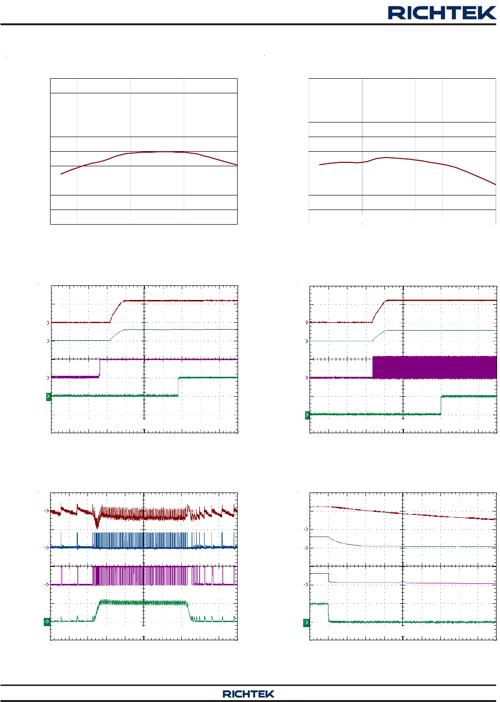
VTT Output Voltage vs. Load Current
0.650
0.655
0.660
0.665
0.670
0.675
0.680
0.685
0.690
0.695
0.700
-1.5 -1.2 -0.9 -0.6 -0.3 0 0.3 0.6 0.9 1.2 1.5
Load Current (A)
Output Voltage (V)
DDR3L, VIN = 12V, VTT = 0.675V, S3 = S5 = 5V
VTT Output Voltage vs. Load Current
0.575
0.580
0.585
0.590
0.595
0.600
0.605
0.610
0.615
0.620
0.625
-1.5 -1.2 -0.9 -0.6 -0.3 0 0.3 0.6 0.9 1.2 1.5
Load Current (A)
Output Voltage (V)
DDR4, VIN = 12V, VTT = 0.6V, S3 = S5 = 5V
Quiescent Current vs. Input Voltage
130
132
134
136
138
140
142
144
146
148
150
4 6 8 10 12 14 16 18 20 22 24 26
Input Voltage (V)
Quiescent Current (µA)
No Switching, S3 = GND, S5 = 5V
Shutdown Current vs. Input Voltage
0.0
0.1
0.2
0.3
0.4
0.5
0.6
0.7
0.8
0.9
1.0
4 6 8 101214161820222426
Input Voltage (V)
Shutdown Current (µA
)
S3 = S5 = GND
VDDQ Output Voltage vs. Load Current
1.15
1.16
1.17
1.18
1.19
1.20
1.21
1.22
1.23
1.24
1.25
0.01 0.1 1 10
Load Current (A)
Output Voltage (V)
DDR4, VIN = 12V, VDDQ = 1.2V, S3 = S5 = 5V
VDDQ Output Voltage vs. Load Current
1.30
1.31
1.32
1.33
1.34
1.35
1.36
1.37
1.38
1.39
1.40
0.01 0.1 1 10
Load Current (A)
Output Voltage (V)
DDR3L, VIN = 12V, VDDQ = 1.35V, S3 = S5 = 5V
RT8248A
12
DS8248A-04 October 2014www.richtek.com
©
Copyright 2014 Richtek Technology Corporation. All rights reserved. is a registered trademark of Richtek Technology Corporation.
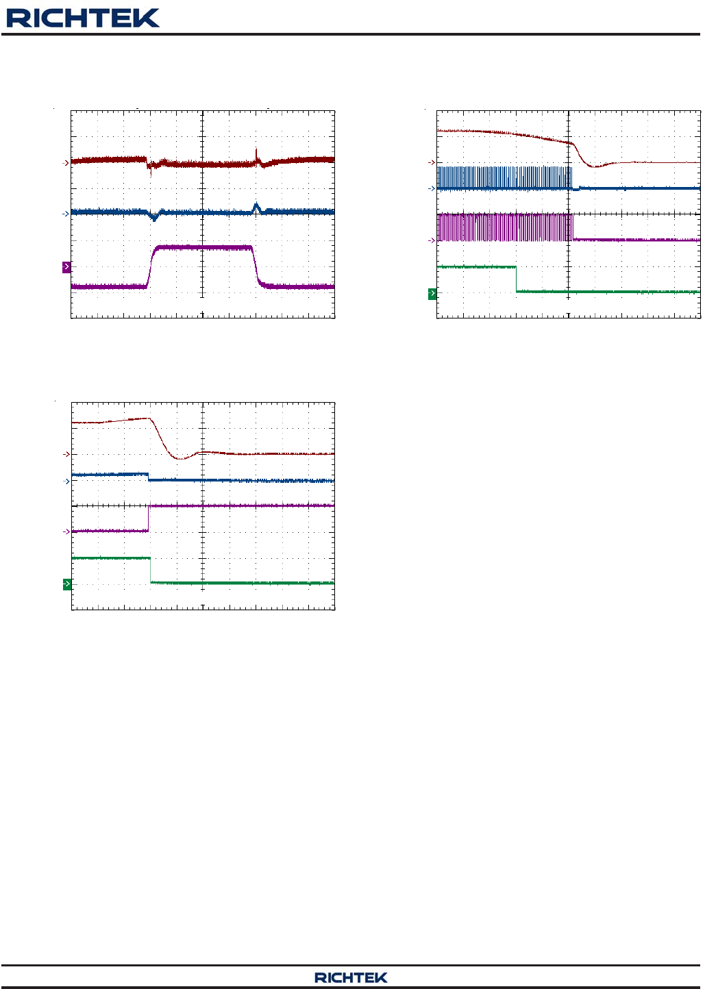
Non-Tracking Discharge Shutdown
Time (200μs/Div)
S5
(5V/Div)
VTT
(1V/Div)
VDDQ
(1V/Div)
VTTREF
(1V/Div)
No Load, VIN = 12V, VDDQ = 1.2V, S3 = S5 = 5V
VDDQ and VTT Start Up
Time (1ms/Div)
PGOOD
(5V/Div)
VTT
(1V/Div)
VDDQ
(1V/Div)
S5
(5V/Div)
No Load, VIN = 12V, VDDQ = 1.2V, S3 = S5 = 5V
VTT Voltage vs. Temperature
0.575
0.580
0.585
0.590
0.595
0.600
0.605
0.610
0.615
0.620
0.625
-50 -25 0 25 50 75 100 125
Temperature (°C)
VTT Voltage (V)
DDR4, VIN = 12V, VTT = 0.6V, S3 = S5 = 5V
VDDQ Voltage vs. Temperature
1.15
1.16
1.17
1.18
1.19
1.20
1.21
1.22
1.23
1.24
1.25
-50 -25 0 25 50 75 100 125
Temperature (°C)
VDDQ Voltage (V)
DDR4, VIN = 12V, VDDQ = 1.2V, S3 = S5 = 5V
VDDQ Start Up
Time (1ms/Div)
PGOOD
(5V/Div)
VTT
(1V/Div)
VDDQ
(1V/Div)
PHASE
(10V/Div)
VIN = 12V, VDDQ = 1.2V, S3 = S5 = 5V, ILoad = 10A
VDDQ Load Transient Response
Time (40μs/Div)
IL
(10A/Div)
UGATE
(20V/Div)
VDDQ
(50mV/Div)
LGATE
(5V/Div)
VDDQ = 1.2V, S3 = S5 = 5V, ILoad = 0.1A to 10A
DDR4, VIN = 12V
RT8248A
13
DS8248A-04 October 2014 www.richtek.com
©
Copyright 2014 Richtek Technology Corporation. All rights reserved. is a registered trademark of Richtek Technology Corporation.
Under Voltage Protection
Time (40μs/Div)
PGOOD
(5V/Div)
UGATE
(20V/Div)
VDDQ
(1V/Div)
LGATE
(5V/Div)
VIN = 12V, VDDQ = 1.2V, S3 = S5 = 5V
Over Voltage Protection
Time (40μs/Div)
PGOOD
(5V/Div)
PHASE
(5V/Div)
VDDQ
(1V/Div)
LGATE
(5V/Div)
No Load, VIN = 12V, VDDQ = 1.2V, S3 = S5 = 5V
VTT Load Transient Response
Time (50μs/Div)
IVTT
(2A/Div)
VTTREF
(20mV/Div)
VTT
(20mV/Div)
VDDQ = 1.2V, S3 = S5 = 5V, ILoad = −1.5A to 1.5A
DDR4, VIN = 12V
RT8248A
14
DS8248A-04 October 2014www.richtek.com
©
Copyright 2014 Richtek Technology Corporation. All rights reserved. is a registered trademark of Richtek Technology Corporation.
Application Information
The RT8248A PWM controller provides the high efficiency,
excellent transient response, and high DC output accuracy
needed for stepping down high voltage batteries to
generate low voltage chipset RAM supplies in notebook
computers. Richtek's Mach ResponseTM technology is
specifically designed for providing 100ns “instant-on”
response to load steps while maintaining a relatively
constant operating frequency and inductor operating point
over a wide range of input voltages. The topology solves
the poor load transient response timing problems of fixed-
frequency current mode PWMs, and avoids problems
caused by widely varying switching frequencies in
conventional constant-on-time and constant- off-time PWM
schemes. The DRVTM mode PWM modulator is
specifically designed to have better noise immunity for
such a single output application.
The 1.5A sink/source LDO maintains fast transient
response, only requiring 10μF of ceramic output
capacitance. In addition, the LDO supply input is available
externally to significantly reduce the total power losses.
The RT8248A supports all of the sleep state controls,
placing VTT at high-Z in S3 and discharging VDDQ, VTT
and VTTREF (soft-off) in S4/S5.
PWM Operation
The Mach ResponseTM
DRVTM mode controller relies on
the output filter capacitor's Effective Series Resistance
(ESR) to act as a current-sense resistor, so the output
ripple voltage provides the PWM ramp signal. Referring to
the function block diagrams of the RT8248A, the
synchronous high-side MOSFET is turned on at the
beginning of each cycle. After the internal one-shot timer
expires, the MOSFET will be turned off. The pulse width
of this one-shot is determined by the converter's input
and output voltages to keep the frequency fairly constant
over the entire input voltage range. Another one-shot sets
a minimum off-time (400ns typ.).
On-Time Control
The on-time one-shot comparator has two inputs. One
input looks at the output voltage, while the other input
samples the input voltage and converts it to a current.
This input voltage proportional current is used to charge
an internal on-time capacitor. The on-time is the time
required for the voltage on this capacitor to charge from
zero volts to VVDDQ, thereby making the on-time of the
high-side switch directly proportional to the output voltage
and inversely proportional to the input voltage. This
implementation results in a nearly constant switching
frequency without the need of a clock generator, as shown
below :
ON TON VDDQ IN TON
t 3.85p x R x V / (V 0.5) + R x 1
And then the switching frequency is :
VDDQ IN ON
f V / (V x t )
where RTON is the resistor connected from VIN to the TON
pin. Note that the setting on-time must be longer than
100ns (typ.) of the minimum on-time and shorter than 3μs
(typ.) of the maximum on-time.
Diode Emulation Mode
In diode emulation mode, the RT8248A automatically
reduces switching frequency at light load conditions to
maintain high efficiency. As the output current decreases
from heavy load condition, the inductor current will also
be reduced and eventually come to the point where its
valley touches zero current, which is the boundary between
continuous conduction and discontinuous conduction
modes. To emulate the behavior of diodes, the low-side
MOSFET allows only partial negative current to flow when
the inductor freewheeling current reaches negative. As the
load current is further decreased, it takes longer and longer
time to discharge the output capacitor to the level that
requires the next “ON” cycle. The on-time is kept the
same as that in the heavy load condition. In contrast, when
the output current increases from light load to heavy load,
the switching frequency increases to the preset value as
the inductor current reaches the continuous condition. The
transition load point to the light load operation is shown in
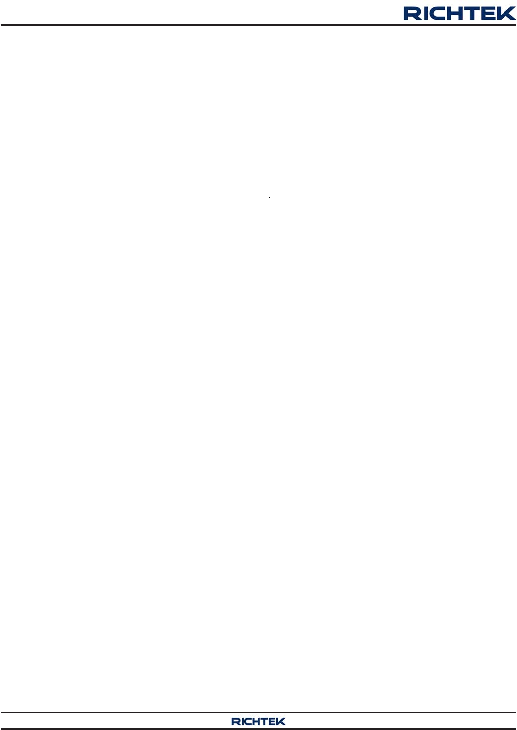
Figure 3 and can be calculated as follows :
IN VDDQ
LOAD(SKIP) ON
VV
I x t
2L
where tON is the on-time.
RT8248A
15
DS8248A-04 October 2014 www.richtek.com
©
Copyright 2014 Richtek Technology Corporation. All rights reserved. is a registered trademark of Richtek Technology Corporation.
Figure 3. Boundary Condition of CCM/DCM
The switching waveforms may appear noisy and
asynchronous when light load causes diode-emulation
operation, but this is a normal operating condition that
results in high light load efficiency. Trade offs in DEM
noise vs. light load efficiency is made by varying the
inductor value. Generally, low inductor values produce a
broader efficiency vs. load curve, while higher values result
in higher full load efficiency (assuming that the coil
resistance remains fixed) and less output voltage ripple.
The disadvantages for using higher inductor values include
larger physical size and degraded load transient response
(especially at low input voltage levels).
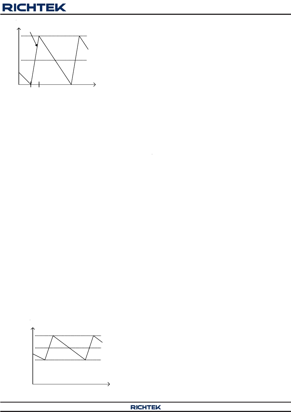
Current Limit Setting for VDDQ (CS)
The RT8248A provides cycle-by-cycle current limit control.
The current limit circuit employs a unique “valley” current
sensing algorithm. If the magnitude of the current sense
signal at PHASE is above the current limit threshold, the
PWM is not allowed to initiate a new cycle (Figure 4).
The actual peak current is greater than the current limit
threshold by an amount equal to the inductor ripple current.
Therefore, the exact current limit characteristic and
maximum load capability are a function of the sense
resistance, inductor value, battery and output voltage.
IL
t
0
IPEAK
ILIM
ILOAD
Figure 4. “Valley” Current Limit
The RT8248A uses the on resistance of the synchronous
rectifier as the current sense element and supports
temperature compensated MOSFET RDS(ON) sensing. The
setting resistor, RILIM, between the CS pin and VDD sets
the current limit threshold. The CS pin sources an internal
5μA (typ.) current source at room temperature. This current
has a 4700ppm/°C temperature slope to compensate the
temperature dependency of RDS(ON). When the voltage
drop across the low-side MOSFET equals the voltage
across the RILIM setting resistor, the positive current limit
will activate. The high-side MOSFET will not be turned on
until the voltage drop across the low-side MOSFET falls
below the current limit threshold.
Choose a current limit setting resistor via the following
equation :
LIMIT LIMIT DS(ON)
RI x R 10/ 5μ
A
And then the CS pin voltage is
VCS = RLIMIT x 5μA
Note that the VCS should be set from 0.4V to 3V.
Carefully observe the PCB layout guidelines to ensure
that noise and DC errors do not corrupt the current-sense
signal seen by PHASE and PGND.
Current Protection for VTT
The LDO has an internally fixed constant over-current limit
of 2.6A while operating at normal condition. From then
on, when the output voltage exceeds 20% of its set
voltage, the internal power good signal will transit from
high to low.
MOSFET Gate Driver (UGATE, LGATE)
The high-side driver is designed to drive high current, low
RDS(ON) N-MOSFET(s). When configured as a floating
driver, 5V bias voltage is delivered from the VDD supply.
The average drive current is proportional to the gate charge
at VGS = 5V times switching frequency. The instantaneous
drive current is supplied by the flying capacitor between
the BOOT and PHASE pins.
A dead-time to prevent shoot through is internally
generated between high-side MOSFET off to low-side
MOSFET on, and low-side MOSFET off to high-side
MOSFET on.
IL
t
0tON
Slope = (VIN - VVDDQ) / L
IPEAK
ILOAD = IPEAK / 2
RT8248A
16
DS8248A-04 October 2014www.richtek.com
©
Copyright 2014 Richtek Technology Corporation. All rights reserved. is a registered trademark of Richtek Technology Corporation.
The low-side driver is designed to drive high current, low
RDS(ON) N-MOSFET(s). The internal pull down transistor
that drives LGATE low is robust, with a 0.8Ω typical on-
resistance. A 5V bias voltage is delivered from the VDD
supply. The instantaneous drive current is supplied by the
flying capacitor between VDD and PGND.
For high current applications, some combinations of high-
and low-side MOSFETs may cause excessive gate drain
coupling, which leads to efficiency killing, EMI producing
shoot through currents. This is often remedied by adding
a resistor in series on BOOT, which increases the turn-
on rising time of the high-side MOSFET without degrading
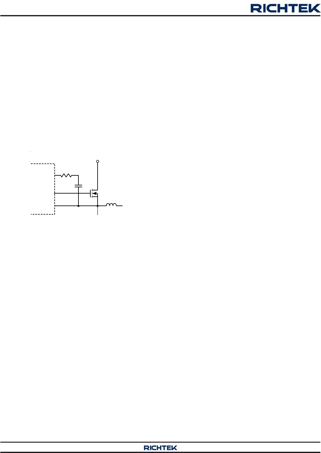
the turn-off time (Figure 5).
BOOT
UGATE
PHASE
R
VIN
Figure 5. Increasing the UGATE Rise Time
Power Good Output (PGOOD)
The power good output is an open drain output that requires
a pull-up resistor. When the output voltage is 15% below
its set voltage, PGOOD will be pulled low. It is held low
until the output voltage returns to 87% of its set voltage
once more. During soft-start, PGOOD is actively held low
and only allowed to be pulled high after soft-start is over
and the output reaches 87% of its set voltage. There is a
5μs delay built into PGOOD circuitry to prevent false
transition.
POR Protection
The RT8248A has a VDD supply power on reset protection
(POR). When the VDD voltage is higher than 4.2V (typ.),
VDDQ, VTT and VTTREF will be activated. This is a non-
latch protection.
Soft-Start
The RT8248A provides an internal soft-start function to
prevent large inrush current and output voltage overshoot
when the converter starts up. Soft-start (SS) automatically
begins once the chip is enabled. During soft-start, internal
bandgap circuit gradually ramps up the reference voltage
from zero. The maximum reference value is set externally
as described in Table 1.
The soft-start function of VTT is achieved by the current
limit and VTTREF voltage through the internal RC delay
ramp up after S3 is high. During VTT startup, the current
limit level is 2.6A. This allows the output to start up
smoothly and safely under enough source/sink ability.
Output Over-Voltage Protection (OVP)
The output voltage can be continuously monitored for over-
voltage condition. If the output exceeds 15% of its set
voltage threshold, over voltage protection will be triggered
and the LGATE low-side gate driver will be forced high.
This activates the low-side MOSFET switch which rapidly
discharges the output capacitor and reduces the output
voltage. There is a 5μs latch delay built into the over-
voltage protection circuit. The RT8248A will be latched if
the output voltage remains above the OV threshold after
the latch delay period. The latched OVP will pull low
PGOOD and can only be released by VDD power on reset
or S5.
Note that latching the LGATE high will cause the output
voltage to dip slightly negative when energy has been
previously stored in the LC tank circuit. For loads that
cannot tolerate a negative voltage, place a power Schottky
diode across the output to act as a reverse polarity clamp.
If the over voltage condition is caused by a shorted high-
side switch, turning the low-side MOSFET on 100% will
create an electrical shorted circuit between the battery
and GND, to blow the fuse and disconnecting the battery
from the output.
RT8248A
17
DS8248A-04 October 2014 www.richtek.com
©
Copyright 2014 Richtek Technology Corporation. All rights reserved. is a registered trademark of Richtek Technology Corporation.
Output Voltage Setting (FB)
Connect a resistive voltage divider at FB between VDDQ
and GND to adjust the respective output voltage between
0.675V and 3.3V (Figure 6). Choose R2 to be
approximately 10kΩ and solve for R1 using the equation
as follows :
Table 1. VID and Reference Voltage Setting
VID Reference Voltage (V)
High 0.675
Low 0.75
VDDQ (Valley) REF
R1
VV x 1
R2
where VREF is 0.75V or 0.675V depends on the VID setting
in Table 1.
Note that when the RT8248A operates from CCM to DEM,
the reference voltage will add 10mV offset.
PHASE
LGATE
R1
R2
VVDDQ
VIN
UGATE
VDDQ
FB
GND
Figure 6. Setting VDDQ with a Resistive Voltage Divider
When the reference voltage is changed from 0.75V to
0.675V, the OVP latch will be masked for 120μs to prevent
an unexpected shutdown.
VTT Linear Regulator and VTTREF
The RT8248A integrates a high performance low dropout
linear regulator that is capable of sourcing and sinking
currents up to 1.5A. This VTT linear regulator employs
ultimate fast response feedback loop so that small ceramic
capacitors are enough for keeping track of VTTREF within
40mV at all conditions, including fast load transient. To
achieve tight regulation with minimum effect of wiring
resistance, a remote sensing terminal, VTTSNS, should
be connected to the positive node of the VTT output
capacitor(s) as a separate trace from the VTT pin. For
stable operation, total capacitance of the VTT output
terminal can be equal to or greater than 10μF. It is
recommended to attach two 10μF ceramic capacitors in
parallel to minimize the effect of ESR and ESL. If ESR of
the output capacitor is greater than 2mΩ, insert an RC
filter between the output and VTTSNS input to achieve
loop stability. The RC filter time constant should be almost
the same or slightly lower than the time constant made
by the output capacitor and its ESR. The VTTREF block
consists of on-chip 1/2 divider, LPF and buffer. This regulator
also has sink and source capability up to 10mA. Bypass
VTTREF to GND with a 33nF ceramic capacitor for stable
operation.
Output Management by S3, S5 Control
In DDR2/DDR3 memory applications, it is important to
always keep VDDQ higher than VTT/VTTREF, even during
start-up and shutdown. The RT8248A provides this
management by simply connecting both S3 and S5
terminals to the sleep-mode signals such as SLP_S3 and
SLP_S5 in notebook PC system. All VDDQ, VTTREF and
VTT are turned on at S0 state (S3 = S5 = high). In S3
state (S3 = low, S5 = high), VDDQ and VTTREF voltages
are kept on while VTT is turned off and left at high
Output Under-Voltage Protection (UVP)
The output voltage can be continuously monitored for under-
voltage condition. When UVP is enabled, the under voltage
protection is triggered if the FB is less than 0.45V. Then,
both UGATE and LGATE gate drivers will be forced low
until next VDD or S5 reset. During soft-start, the UVP has
a blanking time around 5ms.
Thermal Protection
The RT8248A features a thermal protection function. If
the temperature exceeds the threshold, 165°C (typ.), the
PWM output, VTTREF and VTT will be shut down. The
RT8248A is latched once thermal shutdown is triggered
and can only be released by VDD power on reset or S5.
RT8248A
18
DS8248A-04 October 2014www.richtek.com
©
Copyright 2014 Richtek Technology Corporation. All rights reserved. is a registered trademark of Richtek Technology Corporation.
impedance (high-Z) state. The VTT output is floated and
does not sink or source current in this state. In S4/S5
states (S3 = S5 = low), all of the three outputs are disabled
and discharged to ground. The code of each state
represents the following: S0 = full ON, S3 = suspend to
RAM (STR), S4 = suspend to disk (STD), S5 = soft OFF.
(See Table 2)
ON IN VDDQ
IR LOAD(MAX)
t x (V V )
LL x I
where LIR is the ratio of the peak-to-peak ripple current to
the maximum average inductor current.
Find a low loss inductor having the lowest possible DC
resistance that fits in the allotted dimensions. Ferrite cores
are often the best choice, although powdered iron is
inexpensive and can work well at 200kHz. The core must
be large enough and not saturate at the peak inductor
current (IPEAK) :
PEAK LOAD(MAX) IR LOAD(MAX)
I I (L /2) x I
()
SAG
2
LOAD ON OFF(MIN)
OUT IN ON VDDQ ON OFF(MIN)
V
I x L x (tt )
2 x C x V x t V x (t t )
where minimum off-time, tOFF(MIN), is 400ns typically.
Output Capacitor Selection
The output filter capacitor must have low enough ESR to
meet output ripple and load-transient requirements, yet
have high enough ESR to satisfy stability requirements.
Also, the capacitance must be high enough to absorb the
inductor energy going from a full-load to no-load condition
without tripping the OVP circuit.
For CPU core voltage converters and other applications
where the output is subject to violent load transients, the
output capacitor's size depends on how much ESR is
needed to prevent the output from dipping too low under a
load transient. Ignoring the sag due to finite capacitance :
PP
LOAD(MAX)
V
ESR I
Table 2. S3 and S5 truth table
S
TATE S3 S5 VDDQ VTTREF VTT
S0 Hi Hi On On On
S3 Lo Hi On On Off (Hi-Z)
S4/S5 Lo Lo Off
(Discharge)
Off
(Discharge)
Off
(Discharge)
This inductor ripple current also impacts transient-response
performance, especially at low VIN − VVDDQ differences.
Low inductor values allow the inductor current to slew
faster, replenishing charge removed from the output filter
capacitors by a sudden load step. The peak amplitude of
the output transient (VSAG) is also a function of the output
transient. VSAG also features a function of the maximum
duty factor, which can be calculated from the on-time and
minimum off-time :
In non-CPU applications, the output capacitor's size
depends on how much ESR is needed to maintain an
acceptable level of output voltage ripple :
PP
IR LOAD(MAX)
V
ESR L x I
where VP−P is the peak-to-peak output voltage ripple.
Organic semiconductor capacitor(s) or specialty polymer
capacitor(s) are recommended.
The amount of overshoot due to stored inductor energy
can be calculated as :
2
PEAK
SOAR
OUT VDDQ
(I ) x L
V2 x C x V
where IPEAK is the peak inductor current.
VDDQ and VTT Discharge Mode
The RT8248A discharges VDDQ, VTTREF and VTT outputs
when S5 is low or in the S4/S5 state.
When in non-tracking discharge mode, the RT8248A
discharges outputs using internal MOSFETs which are
connected to VDDQ and VTT. The current capability of
these MOSFETs is limited to discharge slowly. Note that
the VDDQ discharge current flows from VDDQ to GND in
this mode. In order to discharge smoothly, the RT8248A
provides a special function that the low-side MOSFET
will switch periodically as phase pin with remaining
voltage.
Output Inductor Selection
The switching frequency (on-time) and operating point (%
ripple or LIR) determine the inductor value as follows :
RT8248A
19
DS8248A-04 October 2014 www.richtek.com
©
Copyright 2014 Richtek Technology Corporation. All rights reserved. is a registered trademark of Richtek Technology Corporation.
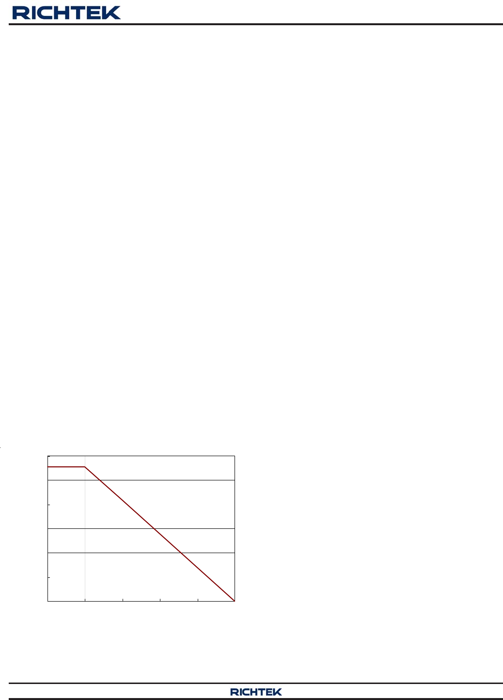
Figure 7. Derating Curve of Maximum Power Dissipation
Layout Considerations
Layout is very important in high frequency switching
converter design. If designed improperly, the PCB could
radiate excessive noise and contribute to the converter
instability. Certain points must be considered before
starting a layout for the RT8248A.
Keep current limit setting network as close as possible
to the IC. Routing of the network should avoid coupling
to high voltage switching node.
Connections from the drivers to the respective gate of
the high-side or the low-side MOSFET should be as
short as possible to reduce stray inductance.
All sensitive analog traces and components such as
VDDQ, FB, PGND, PGOOD, CS, VDD, and TON should
be placed away from high voltage switching nodes such
as PHASE, LGATE, UGATE, and BOOT to avoid
coupling. Use internal layer(s) as ground plane(s) and
shield the feedback trace from power traces and
components.
VLDOIN should be connected to VDDQ output with short
and wide trace. If different power source is used for
VLDOIN, an input bypass capacitor should be placed as
close as possible to the pin with short and wide trace.
The output capacitor for VTT should be placed close to
the pin with short and wide connection in order to avoid
additional ESR and/or ESL of the trace.
It is strongly recommended to connect VTTSNS to the
positive node of VTT output capacitor(s) as a separate
trace from the high current power line to avoid additional
ESR and/or ESL. If it is needed to sense the voltage of
the point of the load, it is recommended to attach the
output capacitor(s) at that point. It is also recommended
to minimize any additional ESR and/or ESL of ground
trace between the GND pin and the output capacitor(s).
Current sense connections must always be made using
Kelvin connections to ensure an accurate signal, with
the current limit resistor located at the device.
Power sections should connect directly to ground
plane(s) using multiple vias as required for current
handling (including the chip power ground connections).
Power components should be placed as close to the IC
as possible to minimize loops and reduce losses.
0.0
0.6
1.2
1.8
2.4
3.0
3.6
0 25 50 75 100 125
Ambient Temperature (°C)
Maximum Power Dissipation (W) 1
Four-Layer PCB
Thermal Considerations
For continuous operation, do not exceed absolute
maximum junction temperature. The maximum power
dissipation depends on the thermal resistance of the IC
package, PCB layout, rate of surrounding airflow, and
difference between junction and ambient temperature. The
maximum power dissipation can be calculated by the
following formula :
PD(MAX) = (TJ(MAX) − TA) / θJA
where TJ(MAX) is the maximum junction temperature, TA is
the ambient temperature, and θJA is the junction to ambient
thermal resistance.
For recommended operating condition specifications, the
maximum junction temperature is 125°C. The junction to
ambient thermal resistance, θJA, is layout dependent. For
WQFN-20L 3x3 package, the thermal resistance, θJA, is
30°C/W on a standard JEDEC 51-7 four-layer thermal test
board. The maximum power dissipation at TA = 25°C can
be calculated by the following formula :
PD(MAX) = (125°C − 25°C) / (30°C/W) = 3.33W for
WQFN-20L 3x3 package
The maximum power dissipation depends on the operating
ambient temperature for fixed TJ(MAX) and thermal
resistance, θJA. The derating curves in Figure 7 allow the
designer to see the effect of rising ambient temperature
on the maximum power dissipation.
RT8248A
20
DS8248A-04 October 2014www.richtek.com
Richtek Technology Corporation
14F, No. 8, Tai Yuen 1st Street, Chupei City
Hsinchu, Taiwan, R.O.C.
Tel: (8863)5526789
Richtek products are sold by description only. Richtek reserves the right to change the circuitry and/or specifications without notice at any time. Customers should
obtain the latest relevant information and data sheets before placing orders and should verify that such information is current and complete. Richtek cannot
assume responsibility for use of any circuitry other than circuitry entirely embodied in a Richtek product. Information furnished by Richtek is believed to be
accurate and reliable. However, no responsibility is assumed by Richtek or its subsidiaries for its use; nor for any infringements of patents or other rights of third
parties which may result from its use. No license is granted by implication or otherwise under any patent or patent rights of Richtek or its subsidiaries.
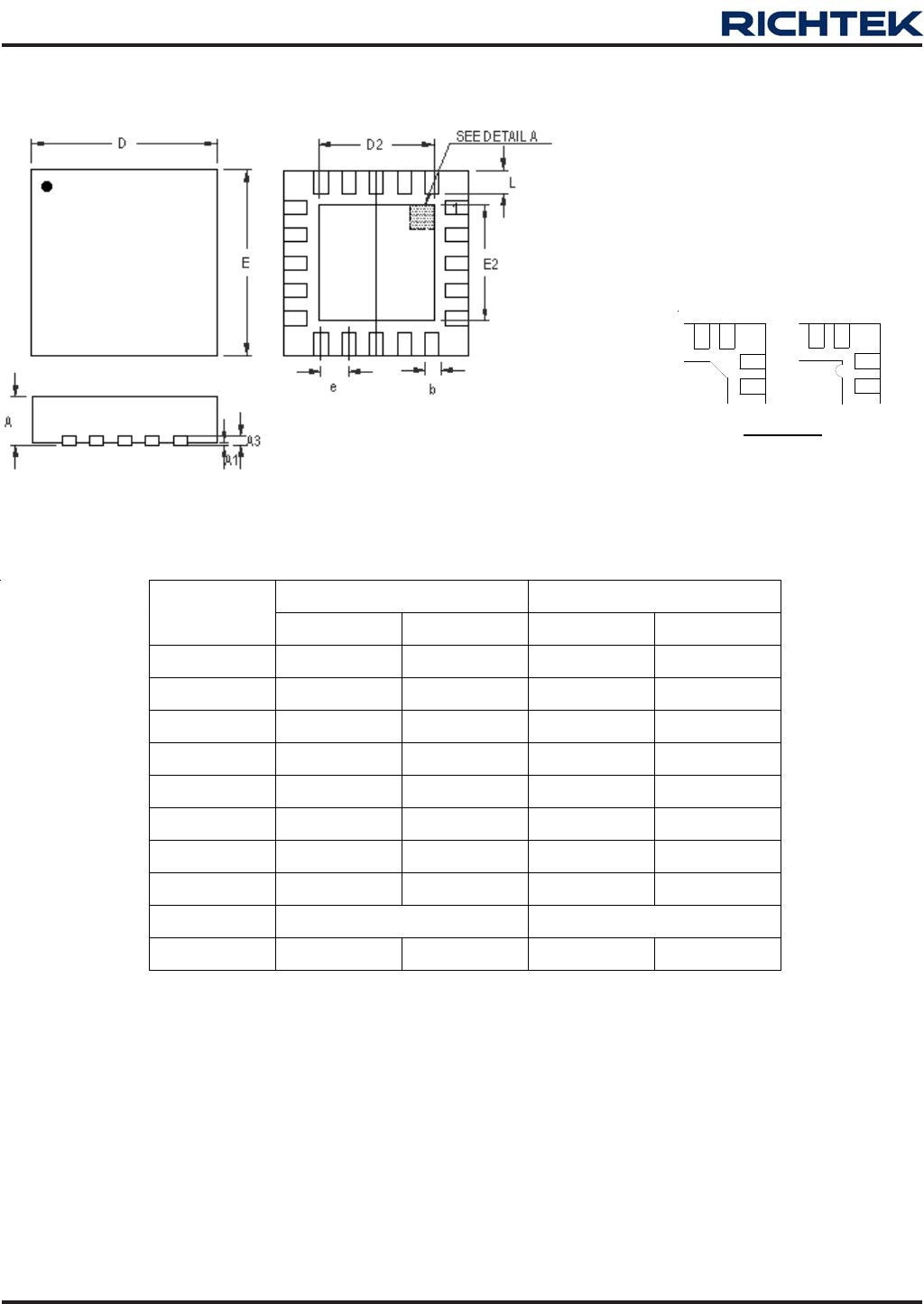
Outline Dimension
Dimensions In Millimeters Dimensions In Inches
Symbol Min Max Min Max
A 0.700 0.800 0.028 0.031
A1 0.000 0.050 0.000 0.002
A3 0.175 0.250 0.007 0.010
b 0.150 0.250 0.006 0.010
D 2.900 3.100 0.114 0.122
D2 1.650 1.750 0.065 0.069
E 2.900 3.100 0.114 0.122
E2 1.650 1.750 0.065 0.069
e 0.400 0.016
L 0.350 0.450
0.014 0.018
W-Type 20L QFN 3x3 Package
Note : The configuration of the Pin #1 identifier is optional,
but must be located within the zone indicated.
DETAIL A
Pin #1 ID and Tie Bar Mark Options
1
1
22