RTL8111D(L) GR Datasheet. Www.s Manuals.com. Rtl8111d Series R1.6 Realtek
User Manual: Datasheets RTL8111, RTL8111B-GR, RTL8111C-GR, RTL8111D-GR, RTL8111D-VB-GR, RTL8111DL-GR, RTL8111DL-VB-GR, RTL8111E-VL-CG.
Open the PDF directly: View PDF ![]() .
.
Page Count: 47
- General Description
- Features
- System Applications
- Pin Assignments
- Pin Descriptions
- Functional Description
- Switching Regulator
- Characteristics
- Mechanical Dimensions
- Ordering Information

RTL8111D-GR
RTL8111DL-GR
RTL8111D-VB-GR
RTL8111DL-VB-GR
INTEGRATED GIGABIT ETHERNET CONTROLLER
FOR PCI EXPRESS APPLICATIONS
DATASHEET
(CONFIDENTIAL: Development Partners Only)
Rev. 1.6
10 March 2009
Track ID: JATR-1076-21
Realtek Semiconductor Corp.
No. 2, Innovation Road II, Hsinchu Science Park, Hsinchu 300, Taiwan
Tel.: +886-3-578-0211. Fax: +886-3-577-6047
www.realtek.com
RTL8111D(L)/RTL8111D(L)-VB
Datasheet
Integrated Gigabit Ethernet Controller for PCI Express ii Track ID: JATR-1076-21 Rev. 1.
6
COPYRIGHT
©2009 Realtek Semiconductor Corp. All rights reserved. No part of this document may be reproduced,
transmitted, transcribed, stored in a retrieval system, or translated into any language in any form or by any
means without the written permission of Realtek Semiconductor Corp.
DISCLAIMER
Realtek provides this document “as is”, without warranty of any kind, neither expressed nor implied,
including, but not limited to, the particular purpose. Realtek may make improvements and/or changes in
this document or in the product described in this document at any time. This document could include
technical inaccuracies or typographical errors.
TRADEMARKS
Realtek is a trademark of Realtek Semiconductor Corporation. Other names mentioned in this document
are trademarks/registered trademarks of their respective owners.
LICENSE
This product is covered by one or more of the following patents: US5,307,459, US5,434,872,
US5,732,094, US6,570,884, US6,115,776, and US6,327,625.
USING THIS DOCUMENT
This document is intended for the software engineer’s reference and provides detailed programming
information.
Though every effort has been made to ensure that this document is current and accurate, more information
may have become available subsequent to the production of this guide. In that event, please contact your
Realtek representative for additional information that may help in the development process.
REVISION HISTORY
Revision Release Date Summary
1.0 2008/05/13 First release.
1.1 2008/07/03 Revised section 6.2.6, page 12.
Added section 9.2, page 38.
Added section 9.3, page 39.
1.2 2008/07/29 Updated licensing information.
1.3 2008/08/08 Added Deep Slumber Mode (DSM) power saving to features list on page 2.
1.4 2008/08/29 Revised Figure 2, page 4 (Pin23).
1.5 2009/01/07 Switching regulator output revised from 1.2V to 1.05V.
Revised Table 19 Crystal Requirements, page 28, Drive Level value.
1.6 2009/03/10 Added RTL8111D-VB-GR & RTL8111DL-VB-GR product numbers.
Added Deep Slumber Mode (DSM) V2 Feature on page 2.
Added section 6.2.6 Deep Slumber Mode (DSM) V1 & V2, page 12.

RTL8111D(L)/RTL8111D(L)-VB
Datasheet
Integrated Gigabit Ethernet Controller for PCI Express iii Track ID: JATR-1076-21 Rev. 1.
6
Table of Contents
1. GENERAL DESCRIPTION..............................................................................................................................................1
2. FEATURES.........................................................................................................................................................................2
3. SYSTEM APPLICATIONS...............................................................................................................................................2
4. PIN ASSIGNMENTS .........................................................................................................................................................3
4.1. RTL8111D & RTL8111D-VB (64-PIN QFN) .............................................................................................................3
4.2. PACKAGE IDENTIFICATION...........................................................................................................................................3
4.3. RTL8111DL & RTL8111DL-VB (48-PIN LQFP).......................................................................................................4
4.4. PACKAGE IDENTIFICATION...........................................................................................................................................4
5. PIN DESCRIPTIONS.........................................................................................................................................................5
5.1. POWER MANAGEMENT/ISOLATION ..............................................................................................................................5
5.2. PCI EXPRESS INTERFACE .............................................................................................................................................5
5.3. TRANSCEIVER INTERFACE............................................................................................................................................6
5.4. CLOCK .........................................................................................................................................................................6
5.5. REGULATOR AND REFERENCE......................................................................................................................................6
5.6. EEPROM ....................................................................................................................................................................7
5.7. LEDS...........................................................................................................................................................................7
5.8. POWER AND GROUND ..................................................................................................................................................8
5.9. GPIO PINS ...................................................................................................................................................................8
5.10. TEST PINS ....................................................................................................................................................................8
5.11. NC PINS .......................................................................................................................................................................8
6. FUNCTIONAL DESCRIPTION.......................................................................................................................................9
6.1. PCI EXPRESS BUS INTERFACE......................................................................................................................................9
6.1.1. PCI Express Transmitter ........................................................................................................................................9
6.1.2. PCI Express Receiver.............................................................................................................................................9
6.2. LED FUNCTIONS..........................................................................................................................................................9
6.2.1. Link Monitor...........................................................................................................................................................9
6.2.2. Rx LED .................................................................................................................................................................10
6.2.3. Tx LED .................................................................................................................................................................10
6.2.4. Tx/Rx LED ............................................................................................................................................................11
6.2.5. LINK/ACT LED ....................................................................................................................................................11
6.2.6. Deep Slumber Mode (DSM) V1 & V2...................................................................................................................12
6.2.7. Customizable LED Configuration ........................................................................................................................12
6.3. PHY TRANSCEIVER ...................................................................................................................................................13
6.3.1. PHY Transmitter...................................................................................................................................................13
6.3.2. PHY Receiver .......................................................................................................................................................13
6.4. NEXT PAGE ................................................................................................................................................................14
6.5. EEPROM INTERFACE ................................................................................................................................................14
6.6. POWER MANAGEMENT...............................................................................................................................................15
6.7. VITAL PRODUCT DATA (VPD)...................................................................................................................................17
6.8. RECEIVE-SIDE SCALING (RSS) ..................................................................................................................................18
6.8.1. Receive-Side Scaling (RSS) Initialization.............................................................................................................18
6.8.2. RSS Operation ......................................................................................................................................................19
7. SWITCHING REGULATOR..........................................................................................................................................19
7.1. PCB LAYOUT.............................................................................................................................................................19
7.2. INDUCTOR AND CAPACITOR PARTS LIST ....................................................................................................................20
7.3. MEASUREMENT CRITERIA..........................................................................................................................................21
7.4. TYPICAL SWITCHING REGULATOR PCB LAYOUT ......................................................................................................25

RTL8111D(L)/RTL8111D(L)-VB
Datasheet
Integrated Gigabit Ethernet Controller for PCI Express iv Track ID: JATR-1076-21 Rev. 1.
6
7.5. EFFICIENCY MEASUREMENT ......................................................................................................................................26
7.6. POWER SEQUENCE .....................................................................................................................................................27
8. CHARACTERISTICS......................................................................................................................................................28
8.1. ABSOLUTE MAXIMUM RATINGS ................................................................................................................................28
8.2. RECOMMENDED OPERATING CONDITIONS .................................................................................................................28
8.3. CRYSTAL REQUIREMENTS..........................................................................................................................................28
8.4. OSCILLATOR REQUIREMENTS ....................................................................................................................................29
8.5. THERMAL CHARACTERISTICS.....................................................................................................................................29
8.6. DC CHARACTERISTICS...............................................................................................................................................29
8.7. AC CHARACTERISTICS...............................................................................................................................................30
8.7.1. Serial EEPROM Interface Timing........................................................................................................................30
8.8. PCI EXPRESS BUS PARAMETERS................................................................................................................................31
8.8.1. Differential Transmitter Parameters ....................................................................................................................31
8.8.2. Differential Receiver Parameters.........................................................................................................................32
8.8.3. REFCLK Parameters............................................................................................................................................32
8.8.4. Auxiliary Signal Timing Parameters ....................................................................................................................36
9. MECHANICAL DIMENSIONS......................................................................................................................................37
9.1. RTL8111D & RTL8111D-VB (64-PIN QFN) ...........................................................................................................37
9.2. RTL8111DL & RTL8111DL-VB (48-PIN LQFP).....................................................................................................38
9.3. MECHANICAL DIMENSIONS NOTES (RTL8111DL/RTL8111DL-VB 48-PIN)............................................................39
10. ORDERING INFORMATION...................................................................................................................................40

RTL8111D(L)/RTL8111D(L)-VB
Datasheet
Integrated Gigabit Ethernet Controller for PCI Express v Track ID: JATR-1076-21 Rev. 1.
6
List of Tables
TABLE 1. POWER MANAGEMENT/ISOLATION ...............................................................................................................................5
TABLE 2. PCI EXPRESS INTERFACE..............................................................................................................................................5
TABLE 3. TRANSCEIVER INTERFACE ............................................................................................................................................6
TABLE 4. CLOCK ..........................................................................................................................................................................6
TABLE 5. REGULATOR AND REFERENCE ......................................................................................................................................6
TABLE 6. EEPROM .....................................................................................................................................................................7
TABLE 7. LEDS............................................................................................................................................................................7
TABLE 8. POWER AND GROUND ...................................................................................................................................................8
TABLE 9. GPIO PINS ....................................................................................................................................................................8
TABLE 10. TEST PINS ....................................................................................................................................................................8
TABLE 11. NC PINS .......................................................................................................................................................................8
TABLE 12. LED SELECT (IO REGISTER OFFSET 18H~19H)..........................................................................................................12
TABLE 13. CUSTOMIZED LEDS...................................................................................................................................................12
TABLE 14. EEPROM INTERFACE ................................................................................................................................................14
TABLE 15. INDUCTOR AND CAPACITOR PARTS LIST ....................................................................................................................20
TABLE 16. POWER SEQUENCE PARAMETER.................................................................................................................................27
TABLE 17. ABSOLUTE MAXIMUM RATINGS ................................................................................................................................28
TABLE 18. RECOMMENDED OPERATING CONDITIONS .................................................................................................................28
TABLE 19. CRYSTAL REQUIREMENTS..........................................................................................................................................28
TABLE 20. OSCILLATOR REQUIREMENTS ....................................................................................................................................29
TABLE 21. THERMAL CHARACTERISTICS.....................................................................................................................................29
TABLE 22. DC CHARACTERISTICS ...............................................................................................................................................29
TABLE 23. EEPROM ACCESS TIMING PARAMETERS ..................................................................................................................30
TABLE 24. DIFFERENTIAL TRANSMITTER PARAMETERS ..............................................................................................................31
TABLE 25. DIFFERENTIAL RECEIVER PARAMETERS.....................................................................................................................32
TABLE 26. REFCLK PARAMETERS .............................................................................................................................................32
TABLE 27. AUXILIARY SIGNAL TIMING PARAMETERS.................................................................................................................36
TABLE 28. ORDERING INFORMATION ..........................................................................................................................................40

RTL8111D(L)/RTL8111D(L)-VB
Datasheet
Integrated Gigabit Ethernet Controller for PCI Express vi Track ID: JATR-1076-21 Rev. 1.
6
List of Figures
FIGURE 1. RTL8111D & RTL8111D-VB (64-PIN QFN) PIN ASSIGNMENTS ...............................................................................3
FIGURE 2. RTL8111DL & RTL8111DL-VB (48-PIN LQFP) PIN ASSIGNMENTS ........................................................................4
FIGURE 3. RX LED.....................................................................................................................................................................10
FIGURE 4. TX LED.....................................................................................................................................................................10
FIGURE 5. TX/RX LED...............................................................................................................................................................11
FIGURE 6. LINK/ACT LED .......................................................................................................................................................11
FIGURE 7. SWITCHING REGULATOR ILLUSTRATION ...................................................................................................................19
FIGURE 8. INPUT VOLTAGE OVERSHOOT <4V (GOOD)...............................................................................................................21
FIGURE 9. INPUT VOLTAGE OVERSHOOT >4V (BAD) .................................................................................................................21
FIGURE 10. CERAMIC 22µF 1210 (X5R) (GOOD).........................................................................................................................22
FIGURE 11. CERAMIC 22µF 0805 (Y5V) (BAD) ...........................................................................................................................22
FIGURE 12. ELECTROLYTIC 100µF (RIPPLE TOO HIGH)...............................................................................................................23
FIGURE 13. 4R7GTSD32 (GOOD) ...............................................................................................................................................24
FIGURE 14. 1µH BEAD (BAD) ......................................................................................................................................................24
FIGURE 15. TYPICAL SWITCHING REGULATOR PCB LAYOUT (TOP LAYER)................................................................................25
FIGURE 16. TYPICAL SWITCHING REGULATOR PCB LAYOUT (BOTTOM LAYER) ........................................................................25
FIGURE 17. SWITCHING REGULATOR EFFICIENCY MEASUREMENT CHECKPOINT ........................................................................26
FIGURE 18. POWER SEQUENCE ....................................................................................................................................................27
FIGURE 19. SERIAL EEPROM INTERFACE TIMING......................................................................................................................30
FIGURE 20. SINGLE-ENDED MEASUREMENT POINTS FOR ABSOLUTE CROSS POINT AND SWING .................................................34
FIGURE 21. SINGLE-ENDED MEASUREMENT POINTS FOR DELTA CROSS POINT ..........................................................................34
FIGURE 22. SINGLE-ENDED MEASUREMENT POINTS FOR RISE AND FALL TIME MATCHING .......................................................34
FIGURE 23. DIFFERENTIAL MEASUREMENT POINTS FOR DUTY CYCLE AND PERIOD ...................................................................35
FIGURE 24. DIFFERENTIAL MEASUREMENT POINTS FOR RISE AND FALL TIME ...........................................................................35
FIGURE 25. DIFFERENTIAL MEASUREMENT POINTS FOR RINGBACK............................................................................................35
FIGURE 26. REFERENCE CLOCK SYSTEM MEASUREMENT POINT AND LOADING .........................................................................36
FIGURE 27. AUXILIARY SIGNAL TIMING......................................................................................................................................36

RTL8111D(L)/RTL8111D(L)-VB
Datasheet
Integrated Gigabit Ethernet Controller for PCI Express 1 Track ID: JATR-1076-21 Rev. 1.
6
1. General Description
The Realtek RTL8111D(L)/RTL8111D(L)-VB Gigabit Ethernet controllers combine a triple-speed IEEE
802.3 compliant Media Access Controller (MAC) with a triple-speed Ethernet transceiver, PCI Express
bus controller, and embedded memory. With state-of-the-art DSP technology and mixed-mode signal
technology, the RTL8111D(L)/RTL8111D(L)-VB offers high-speed transmission over CAT 5 UTP cable
or CAT 3 UTP (10Mbps only) cable. Functions such as Crossover Detection and Auto-Correction,
polarity correction, adaptive equalization, cross-talk cancellation, echo cancellation, timing recovery, and
error correction are implemented to provide robust transmission and reception capability at high speeds.
The RTL8111D(L)/RTL8111D(L)-VB complies with the IEEE 802.3u specification for 10/100Mbps
Ethernet and the IEEE 802.3ab specification for 1000Mbps Ethernet. It also supports an auxiliary power
auto-detect function, and will auto-configure related bits of the PCI power management registers in PCI
configuration space.
Advanced Configuration Power management Interface (ACPI)—power management for modern
operating systems that are capable of Operating System-directed Power Management (OSPM)—is
supported to achieve the most efficient power management possible. PCI MSI (Message Signaled
Interrupt) and MSI-X are also supported.
In addition to the ACPI feature, remote wake-up (including AMD Magic Packet™ and Microsoft®
Wake-up frame) is supported in both ACPI and APM (Advanced Power Management) environments. To
support WOL from a deep power down state (e.g., D3cold, i.e., main power is off and only auxiliary
exists), the auxiliary power source must be able to provide the needed power for the
RTL8111D(L)/RTL8111D(L)-VB.
The RTL8111D(L)/RTL8111D(L)-VB is fully compliant with Microsoft® NDIS5, NDIS6(IPv4, IPv6,
TCP, UDP) Checksum and Segmentation Task-offload (Large send and Giant send) features, and
supports IEEE 802 IP Layer 2 priority encoding and IEEE 802.1Q Virtual bridged Local Area Network
(VLAN). The above features contribute to lowering CPU utilization, especially benefiting performance
when in operation on a network server.
The RTL8111D(L)/RTL8111D(L)-VB supports Receive Side Scaling (RSS) to hash incoming TCP
connections and load-balance received data processing across multiple CPUs. RSS improves the number
of transactions per second and number of connections per second, for increased network throughput.
The device also features inter-connect PCI Express technology. PCI Express is a high-bandwidth, low pin
count, serial, interconnect technology that offers significant improvements in performance over
conventional PCI and also maintains software compatibility with existing PCI infrastructure. The device
embeds an adaptive equalizer in the PCIe PHY for ease of system integration and excellent link quality.
The equalizer enables the length of the PCB traces to reach 40 inches.
The RTL8111D(L)/RTL8111D(L)-VB is suitable for multiple market segments and emerging
applications, such as desktop, mobile, workstation, server, communications platforms, and embedded
applications.
The RTL8111D(L)/RTL8111D(L)-VB supports the Deep Slumber Mode (DSM) power saving feature.
See the separate DSM application notes for details.

RTL8111D(L)/RTL8111D(L)-VB
Datasheet
Integrated Gigabit Ethernet Controller for PCI Express 2 Track ID: JATR-1076-21 Rev. 1.
6
2. Features
Integrated 10/100/1000 transceiver
Auto-Negotiation with Next Page capability
Supports PCI Express 1.1
Supports pair swap/polarity/skew correction
Crossover Detection & Auto-Correction
Wake-on-LAN and remote wake-up support
Microsoft® NDIS5, NDIS6 Checksum
Offload (IPv4, IPv6, TCP, UDP) and
Segmentation Task-offload (Large send v1
and Large send v2) support
Supports Full Duplex flow control (IEEE
802.3x)
Supports jumbo frame to 9K bytes
Fully compliant with IEEE 802.3,
IEEE 802.3u, IEEE 802.3ab
Supports IEEE 802.1P Layer 2 Priority
Encoding
Supports IEEE 802.1Q VLAN tagging
Embedded OTP memory can replace the
external EEPROM
Serial EEPROM
Transmit/Receive on-chip buffer support
Supports power down/link down power
saving
Built-in Switching regulator
Supports PCI MSI (Message Signaled
Interrupt) and MSI-X
Supports quad core Receive-Side Scaling
(RSS)
Embeds an adaptive equalizer in PCI
express PHY (PCB traces to reach 40
inches)
Supports Deep Slumber Mode (DSM) power
saving V1/V2 features (V2 for
RTL8111D(L)-VB only)
Customized LEDs
Packages
64-pin QFN ‘Green’ package
(RTL8111D & RTL8111D-VB)
48-pin LQFP ‘Green’ package
(RTL8111DL & RTL8111DL-VB)
3. System Applications
PCI Express Gigabit Ethernet on Motherboard, Notebook, or Embedded system
RTL8111D(L)/RTL8111D(L)-VB
Datasheet
Integrated Gigabit Ethernet Controller for PCI Express 3 Track ID: JATR-1076-21 Rev. 1.
6
4. Pin Assignments
4.1.
RTL8111D & RTL8111D-VB (64-Pin QFN)
Figure 1. RTL8111D & RTL8111D-VB (64-Pin QFN) Pin Assignments
4.2.
Package Identification
‘Green’ package is indicated by a ‘G’ in the location marked ‘T’ in Figure 1.

RTL8111D(L)/RTL8111D(L)-VB
Datasheet
Integrated Gigabit Ethernet Controller for PCI Express 4 Track ID: JATR-1076-21 Rev. 1.
6
4.3.
RTL8111DL & RTL8111DL-VB (48-Pin LQFP)
Figure 2. RTL8111DL & RTL8111DL-VB (48-Pin LQFP) Pin Assignments
4.4.
Package Identification
‘Green’ package is indicated by a ‘G’ in the location marked ‘T’ in Figure 2.
RTL8111D(L)/RTL8111D(L)-VB
Datasheet
Integrated Gigabit Ethernet Controller for PCI Express 5 Track ID: JATR-1076-21 Rev. 1.
6
5. Pin Descriptions
The signal type codes below are used in the following tables:
I: Input S/T/S: Sustained Tri-State
O: Output O/D: Open Drain
T/S: Tri-State bi-directional input/output pin P: Power
5.1.
Power Management/Isolation
Table 1. Power Management/Isolation
Symbol Type Pin No
(64-pin)
Pin No
(48-pin)
Description
LANWAKEB O/D 19 26
Power Management Event: Open drain, active low.
Used to reactivate the PCI Express slot’s main power rails and reference
clocks.
ISOLATEB I 36 28
Isolate Pin: Active low.
Used to isolate the RTL8111D(L)/RTL8111D(L)-VB from the PCI Express
bus. The RTL8111D(L)/RTL8111D(L)-VB will not drive its PCI Express
outputs (excluding LANWAKEB) and will not sample its PCI Express
input as long as the Isolate pin is asserted.
5.2.
PCI Express Interface
Table 2. PCI Express Interface
Symbol Type Pin No
(64-pin)
Pin No
(48-pin)
Description
REFCLK_P I 26 17
REFCLK_N I 27 18
PCI Express Differential Reference Clock Source: 100MHz ± 300ppm.
HSOP O 29 20
HSON O 30 21
PCI Express Transmit Differential Pair.
HSIP I 23 15
HSIN I 24 16
PCI Express Receive Differential Pair.
PERSTB I 20 27
PCI Express Reset Signal: Active low.
When the PERSTB is asserted at power-on state, the
RTL8111D(L)/RTL8111D(L)-VB returns to a pre-defined reset state and is
ready for initialization and configuration after the de-assertion of the
PERSTB.
CLKREQB O/D 33 25
Reference Clock Request Signal.
This signal is used by the RTL8111D(L)/RTL8111D(L)-VB to request
starting of the PCI Express reference clock.
RTL8111D(L)/RTL8111D(L)-VB
Datasheet
Integrated Gigabit Ethernet Controller for PCI Express 6 Track ID: JATR-1076-21 Rev. 1.
6
5.3.
Transceiver Interface
Table 3. Transceiver Interface
Symbol Type Pin No
(64-pin)
Pin No
(48-pin)
Description
MDIP0 IO 3 2
MDIN0 IO 4 3
In MDI mode, this is the first pair in 1000Base-T, i.e., the BI_DA+/- pair,
and is the transmit pair in 10Base-T and 100Base-TX.
In MDI crossover mode, this pair acts as the BI_DB+/- pair, and is the
receive pair in 10Base-T and 100Base-TX.
MDIP1 IO 6 5
MDIN1 IO 7 6
In MDI mode, this is the second pair in 1000Base-T, i.e., the BI_DB+/-
pair, and is the receive pair in 10Base-T and 100Base-TX.
In MDI crossover mode, this pair acts as the BI_DA+/- pair, and is the
transmit pair in 10Base-T and 100Base-TX.
MDIP2 IO 9 8
MDIN2 IO 10 9
In MDI mode, this is the third pair in 1000Base-T, i.e., the BI_DC+/- pair.
In MDI crossover mode, this pair acts as the BI_DD+/- pair.
MDIP3 IO 12 11
MDIN3 IO 13 12
In MDI mode, this is the fourth pair in 1000Base-T, i.e., the BI_DD+/- pair.
In MDI crossover mode, this pair acts as the BI_DC+/- pair.
5.4.
Clock
Table 4. Clock
Symbol Type Pin No
(64-pin)
Pin No
(48-pin)
Description
CKTAL1 I 60 41 Input of 25MHz Clock Reference.
CKTAL2 O 61 42 Output of 25MHz Clock Reference.
5.5.
Regulator and Reference
Table 5. Regulator and Reference
Symbol Type Pin No
(64-pin)
Pin No
(48-pin)
Description
SROUT12 O 1 48 Switching Regulator 1.05V Output. Connect to 5µH inductor.
FB12 I 5 4 Feedback Pin for Switching Regulator.
ENSR I 62 43
3.3V: Enable switching regulator.
0V: Disable switching regulator.
VDDSR P 63 44, 45 Digital 3.3V Power Supply for Switching Regulator.
RSET I 64 46 Reference. External resistor reference.
Note: See section 7, page 19 for switching regulator layout.
RTL8111D(L)/RTL8111D(L)-VB
Datasheet
Integrated Gigabit Ethernet Controller for PCI Express 7 Track ID: JATR-1076-21 Rev. 1.
6
5.6.
EEPROM
Table 6. EEPROM
Symbol Type Pin No
(64-pin)
Pin No
(48-pin)
Description
EESK O 48 35 Serial Data Clock.
EEDI/AUX O/I 47 34
EEDI: Output to serial data input pin of EEPROM.
AUX: Input pin to detect if Aux. Power exists or not on initial power-on.
This pin should be connected to EEPROM. To support wakeup from ACPI
D3cold or APM power-down, this pin must be pulled high to Aux. Power via
a resistor. If this pin is not pulled high to Aux. Power, the
RTL8111D(L)/RTL8111D(L)-VB assumes that no Aux. Power exists.
EEDO I 45 33 Input from Serial Data Output Pin of EEPROM.
EECS O 44 32 EECS: EEPROM chip select.
5.7.
LEDs
Table 7. LEDs
Symbol Type Pin No
(64-pin)
Pin No
(48-pin)
Description
LED0 O
57 38
LED1 O
56 35
LED2 O 55 34
LED3 O 54 33
LEDS1-0 00 01 10 11
LED0 Tx/Rx Tx/Rx Tx LINK10/
ACT
LED1 LINK100
LINK10/
100/1000 LINK LINK100/
ACT
LED2 LINK10
LINK10/
100 Rx FULL
LED3 LINK1000 LINK1000 FULL LINK1000
/ACT
Note 1: During power down mode, the LED signals are logic high.
Note 2: LEDS1-0’s initial value comes from the EEPROM If there is no EEPROM, the default value of the
(LEDS1, LEDS0)=(1, 1).
RTL8111D(L)/RTL8111D(L)-VB
Datasheet
Integrated Gigabit Ethernet Controller for PCI Express 8 Track ID: JATR-1076-21 Rev. 1.
6
5.8.
Power and Ground
Table 8. Power and Ground
Symbol Type Pin No
(64-pin)
Pin No
(48-pin)
Description
VDD33 P 16, 37, 46, 53 29, 37 Digital 3.3V Power Supply.
DVDD12 P 21, 32, 38, 43, 49, 52 13, 30, 36 Digital 1.05V Power Supply.
AVDD12 P 8, 11, 14, 58 10, 39 Analog 1.05V Power Supply.
EVDD12 P 22, 28 19 Analog 1.05V Power Supply.
AVDD33 P 2, 59 1, 40 Analog 3.3V Power Supply.
EGND P 25, 31 22 Analog Ground.
GND P 65 7, 14, 31, 47 Ground (Exposed Pad).
Note: Refer to the most updated schematic circuit for correct configuration.
5.9.
GPIO Pins
Table 9. GPIO Pins
Symbol Type Pin No
(64-pin)
Pin No
(48-pin)
Description
GPI I 50 - General Purpose Input Pin.
GPO O 51 23
General Purpose Output Pin.
This pin reflects the link up or link down state.
High: Link up
Low: Link down
5.10.
Test Pins
Table 10. Test Pins
Symbol Type Pin No
(64-pin)
Pin No
(48-pin)
Description
Test - 34, 35, 39, 40, 41, 42 - Realtek Internal Use Only.
5.11.
NC Pins
Table 11. NC Pins
Symbol Type Pin No
(64-pin)
Pin No
(48-pin)
Description
NC - 15, 17, 18 24 Not Connected.

RTL8111D(L)/RTL8111D(L)-VB
Datasheet
Integrated Gigabit Ethernet Controller for PCI Express 9 Track ID: JATR-1076-21 Rev. 1.
6
6. Functional Description
6.1.
PCI Express Bus Interface
The RTL8111D(L)/RTL8111D(L)-VB is compliant with PCI Express Base Specification Revision 1.1,
and runs at a 2.5GHz signaling rate with X1 link width, i.e., one transmit and one receive differential pair.
The RTL8111D(L)/RTL8111D(L)-VB supports four types of PCI Express messages: interrupt messages,
error messages, power management messages, and hot-plug messages. To ease PCB layout constraints,
PCI Express lane polarity reversal and link reversal are also supported.
6.1.1. PCI Express Transmitter
The RTL8111D(L)/RTL8111D(L)-VB’s PCI Express block receives digital data from the Ethernet
interface and performs data scrambling with Linear Feedback Shift Register (LFSR) and 8B/10B coding
technology into 10-bit code groups. Data scrambling is used to reduce the possibility of electrical
resonance on the link, and 8B/10B coding technology is used to benefit embedded clocking, error
detection, and DC balance by adding an overhead to the system through the addition of 2 extra bits. The
data code groups are passed through its serializer for packet framing. The generated 2.5Gbps serial data is
transmitted onto the PCB trace to its upstream device via a differential driver.
6.1.2. PCI Express Receiver
The RTL8111D(L)/RTL8111D(L)-VB’s PCI Express block receives 2.5Gbps serial data from its
upstream device to generate parallel data. The receiver’s PLL circuits are re-synchronized to maintain bit
and symbol lock. Through 8B/10B decoding technology and data de-scrambling, the original digital data
is recovered and passed to the RTL8111D(L)/RTL8111D(L)-VB’s internal Ethernet MAC to be
transmitted onto the Ethernet media.
6.2.
LED Functions
The RTL8111D(L)/RTL8111D(L)-VB supports four LED signals in four different configurable operation
modes. The following sections describe the various LED actions.
6.2.1. Link Monitor
The Link Monitor senses link integrity, such as LINK10, LINK100, LINK1000, LINK10/100/1000,
LINK10/ACT, LINK100/ACT, or LINK1000/ACT. Whenever link status is established, the specific link
LED pin is driven low. Once a cable is disconnected, the link LED pin is driven high, indicating that no
network connection exists.
RTL8111D(L)/RTL8111D(L)-VB
Datasheet
Integrated Gigabit Ethernet Controller for PCI Express 10 Track ID: JATR-1076-21 Rev. 1.
6
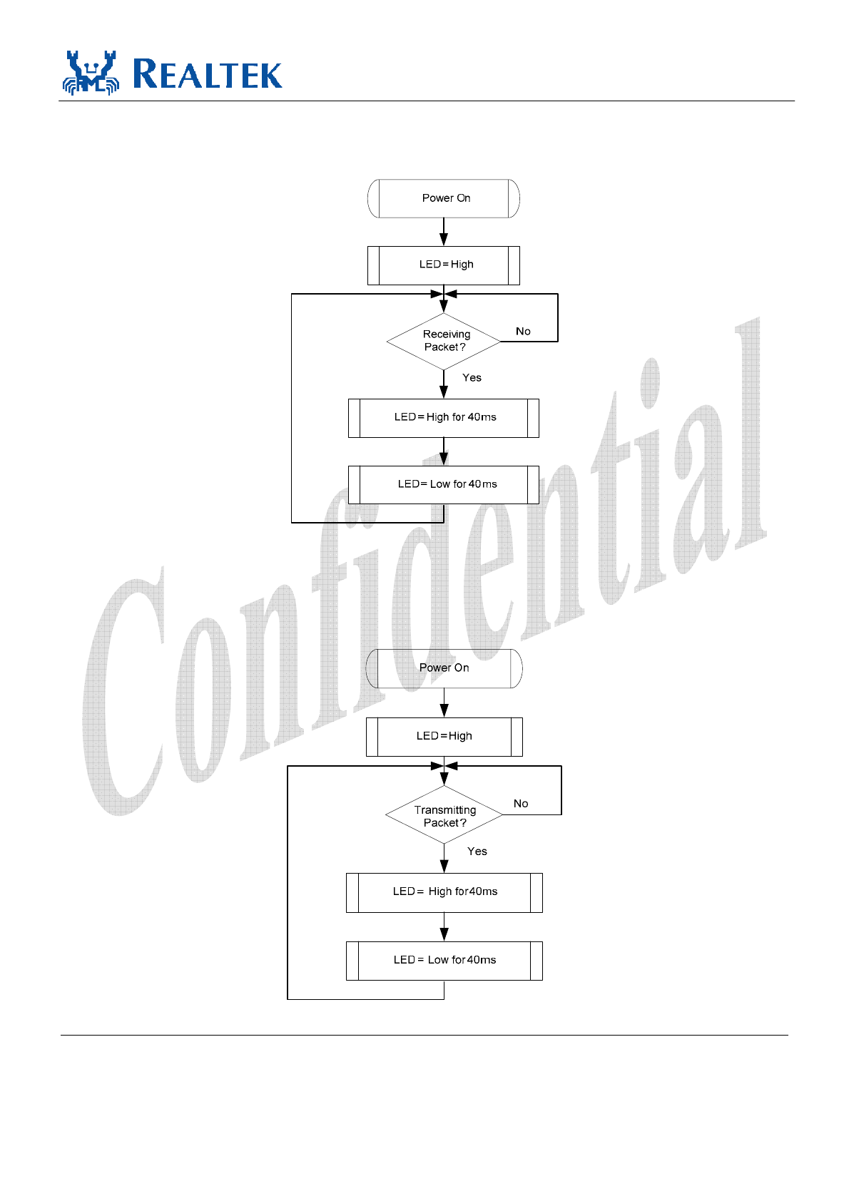
6.2.2. Rx LED
In 10/100/1000Mbps mode, blinking of the Rx LED indicates that receive activity is occurring.
Figure 3. Rx LED
6.2.3. Tx LED
In 10/100/1000Mbps mode, blinking of the Tx LED indicates that transmit activity is occurring.
Figure 4. Tx LED
RTL8111D(L)/RTL8111D(L)-VB
Datasheet
Integrated Gigabit Ethernet Controller for PCI Express 11 Track ID: JATR-1076-21 Rev. 1.
6
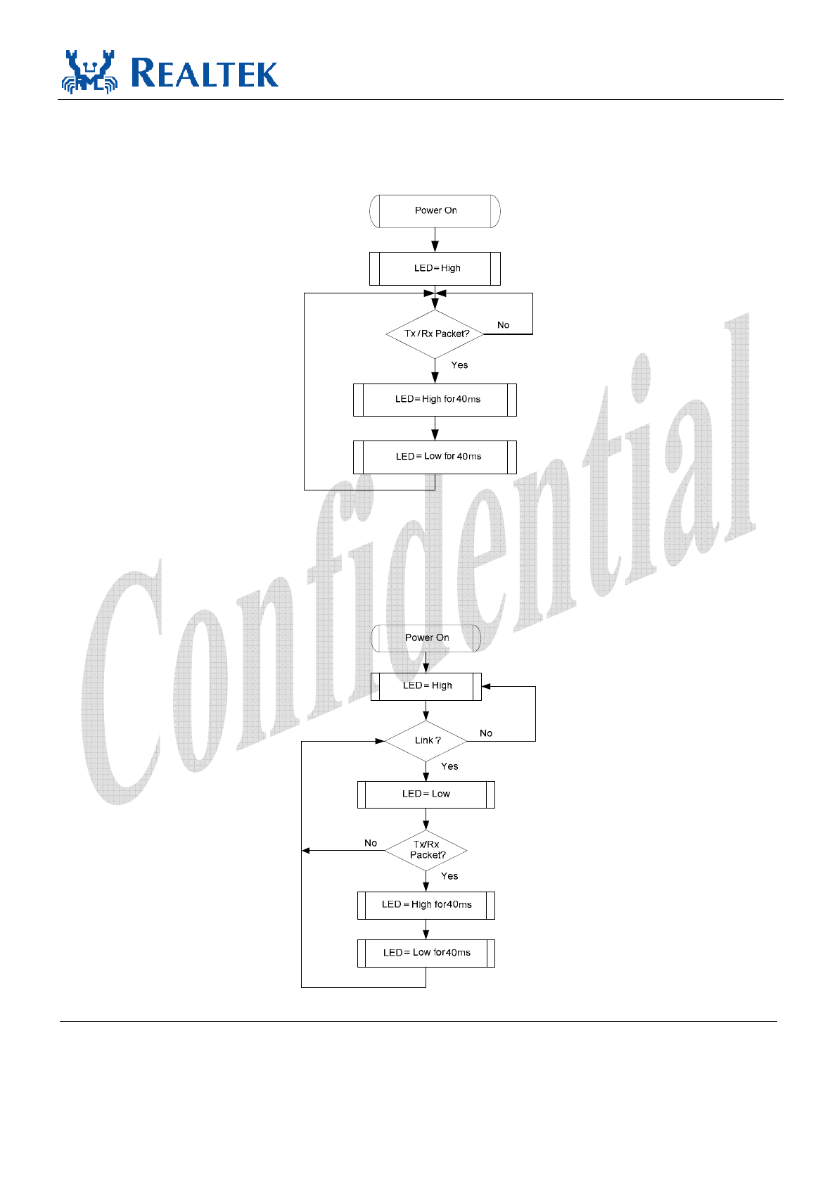
6.2.4. Tx/Rx LED
In 10/100/1000Mbps mode, blinking of the Tx/Rx LED indicates that both transmit and receive activity is
occurring.
Figure 5. Tx/Rx LED
6.2.5. LINK/ACT LED
In 10/100/1000Mbps mode, blinking of the LINK/ACT LED indicates that the
RTL8111D(L)/RTL8111D(L)-VB is linked and operating properly. When this LED is high for extended
periods, it indicates that a link problem exists.
Figure 6. LINK/ACT LED
RTL8111D(L)/RTL8111D(L)-VB
Datasheet
Integrated Gigabit Ethernet Controller for PCI Express 12 Track ID: JATR-1076-21 Rev. 1.
6
6.2.6. Deep Slumber Mode (DSM) V1 & V2
The RTL8111D(L)/RTL8111D(L)-VB supports Link Down power saving mode via communication with
the BIOS and external circuitry. Note that DSMv2 is a simplified implementation of DSMv1, and is only
supported in the RTL8111D(L)-VB. Refer to the separate DSM application note for details.
6.2.7. Customizable LED Configuration
The RTL8111D(L)/RTL8111D(L)-VB supports customizable LED operation modes via IO register offset
18h~19h. Table 12 describes the different LED actions.
Table 12. LED Select (IO Register Offset 18h~19h)
Bit Symbol RW Description
15:12 LEDSEL3 RW LED Select for PINLED3
11:8 LEDSEL2 RW LED Select for PINLED2
7:4 LEDSEL1 RW LED Select for PINLED1
3:0 LEDSEL0 RW LED Select for PINLED0
When implementing customized LEDs:
1. Set IO register offset 0x55 bit 6 to 1h to enable the customized LED function
2. Configure IO register offset 18h~19h to support your own LED signals. For example, if the value in the
IO offset 0x18 is 0x8C51h (1000110010100001b), the LED actions are:
• LED 0 is only on in 10M mode, with no blinking of TX/RX
• LED 1 is only on and with TX/RX blinking in 100M mode
• LED 2 is only on and with TX/RX blinking in 100M full duplex mode
• LED 3 is only on in full duplex mode
Table 13. Customized LEDs
LINK ACT/Full
Speed Link 10M Link 100M Link 1000M -
LED 0 Bit 0 Bit 1 Bit 2 Bit 3
LED 1 Bit 4 Bit 5 Bit 6 Bit 7
LED 2 Bit 8 Bit 9 Bit 10 Bit 11
LED 3 Bit 12 Bit 13 Bit 14 Bit 15
LED Pin ACT=0 ACT=1
LINK=0 Floating LED On when Full Duplex Mode
LINK>0 LED On when Selected Speed is Linked LED Blinking when Selected Speed TX/RX
Note1: ACT means blinking TX and RX. LINK indicates Link 10M and Link 100M.
Note2: There are two special modes:
Mode A: LED OFF Mode
Æ
Set all bits to 0.
Mode B: TX/RX Mode
Æ
Set LED 0=0, and either LED 1, LED 2, or LED 3 >0
LED 0 = Blinking TX/RX. LED 1 = Follow Customized LED rule.
LED 2 = Follow Customized LED rule. LED 3= Follow Customized LED rule.

RTL8111D(L)/RTL8111D(L)-VB
Datasheet
Integrated Gigabit Ethernet Controller for PCI Express 13 Track ID: JATR-1076-21 Rev. 1.
6
6.3.
PHY Transceiver
6.3.1. PHY Transmitter
Based on state-of-the-art DSP technology and mixed-mode signal processing technology, the
RTL8111D(L)/RTL8111D(L)-VB operates at 10/100/1000Mbps over standard CAT.5 UTP cable
(100/1000Mbps), and CAT.3 UTP cable (10Mbps).
GMII (1000Mbps) Mode
The RTL8111D/RTL8111D-VB’s PCS layer receives data bytes from the MAC through the GMII
interface and performs the generation of continuous code-groups through 4D-PAM5 coding technology.
These code groups are passed through a waveform-shaping filter to minimize EMI effects, and are
transmitted onto the 4-pair CAT5 cable at 125MBaud/s through a D/A converter.
MII (100Mbps) Mode
The transmitted 4-bit nibbles (TXD[3:0]) from the MAC, clocked at 25MHz (TXC), are converted into
5B symbol code through 4B/5B coding technology, then through scrambling and serializing, are
converted to 125Mhz NRZ and NRZI signals. After that, the NRZI signals are passed to the MLT3
encoder, then to the D/A converter and transmitted onto the media.
MII (10Mbps) Mode
The transmitted 4-bit nibbles (TXD[3:0]) from the MAC, clocked at 2.5MHz (TXC), are serialized into
10Mbps serial data. The 10Mbps serial data is converted into a Manchester-encoded data stream and is
transmitted onto the media by the D/A converter.
6.3.2. PHY Receiver
GMII (1000Mbps) Mode
Input signals from the media pass through the sophisticated on-chip hybrid circuit to separate the
transmitted signal from the input signal for effective reduction of near-end echo. Afterwards, the received
signal is processed with state-of-the-art technology, e.g., adaptive equalization, BLW (Baseline Wander)
correction, cross-talk cancellation, echo cancellation, timing recovery, error correction, and 4D-PAM5
decoding. Then, the 8-bit-wide data is recovered and is sent to the GMII interface at a clock speed of
125MHz. The Rx MAC retrieves the packet data from the receive MII/GMII interface and sends it to the
Rx Buffer Manager.
MII (100Mbps) Mode
The MLT3 signal is processed with an ADC, equalizer, BLW (Baseline Wander) correction, timing
recovery, MLT3 and NRZI decoder, descrambler, 4B/5B decoder, and is then presented to the MII
interface in 4-bit-wide nibbles at a clock speed of 25MHz.
MII (10Mbps) Mode
The received differential signal is converted into a Manchester-encoded stream first. Next, the stream is
processed with a Manchester decoder and is de-serialized into 4-bit-wide nibbles. The 4-bit nibbles are
presented to the MII interface at a clock speed of 2.5MHz.
RTL8111D(L)/RTL8111D(L)-VB
Datasheet
Integrated Gigabit Ethernet Controller for PCI Express 14 Track ID: JATR-1076-21 Rev. 1.
6
6.4.
Next Page
If 1000Base-T mode is advertised, three additional Next Pages are automatically exchanged between the
two link partners. Users can set PHY Reg4.15 to 1 to manually exchange extra Next Pages via Reg7 and
Reg8 as defined in IEEE 802.3ab.
6.5.
EEPROM Interface
The RTL8111D(L)/RTL8111D(L)-VB requires the attachment of an external EEPROM. The
93C46/93C56 is a 1K-bit/2K-bit EEPROM. The EEPROM interface permits the
RTL8111D(L)/RTL8111D(L)-VB to read from, and write data to, an external serial EEPROM device.
Values in the external EEPROM allow default fields in PCI configuration space and I/O space to be
overridden following a power-on or software EEPROM auto-load command. The
RTL8111D(L)/RTL8111D(L)-VB will auto-load values from the EEPROM. If the EEPROM is not
present, the RTL8111D(L)/RTL8111D(L)-VB initialization uses default values for the appropriate
Configuration and Operational Registers. Software can read and write to the EEPROM using bit-bang
accesses via the 9346CR Register, or using PCI VPD (Vital Product Data). The interface consists of
EESK, EECS, EEDO, and EEDI.
The correct EEPROM (i.e., 93C46/93C56) must be used in order to ensure proper LAN function.
Table 14. EEPROM Interface
EEPROM Description
EECS 93C46/93C56 Chip Select.
EESK EEPROM Serial Data Clock.
EEDI/Aux
Input Data Bus/Input Pin to Detect Whether Aux. Power Exists on Initial Power-On.
This pin should be connected to EEPROM. To support wakeup from ACPI D3cold or APM
power-down, this pin must be pulled high to Aux. Power via a resistor. If this pin is not pulled
high to Aux. Power, the RTL8111D(L)/RTL8111D(L)-VB assumes that no Aux. Power exists.
EEDO Output Data Bus.

RTL8111D(L)/RTL8111D(L)-VB
Datasheet
Integrated Gigabit Ethernet Controller for PCI Express 15 Track ID: JATR-1076-21 Rev. 1.
6
6.6.
Power Management
The RTL8111D(L)/RTL8111D(L)-VB complies with ACPI (Rev 1.0, 1.0b, 2.0), PCI Power Management
(Rev 1.1), PCI Express Active State Power Management (ASPM), and Network Device Class Power
Management Reference Specification (V1.0a), such as to support an Operating System-directed Power
Management (OSPM) environment.
The RTL8111D(L)/RTL8111D(L)-VB can monitor the network for a Wakeup Frame, a Magic Packet,
and notify the system via a PCI Express Power Management Event (PME) Message, Beacon, or
LANWAKEB pin when such a packet or event occurs. Then the system can be restored to a normal state
to process incoming jobs.
When the RTL8111D(L)/RTL8111D(L)-VB is in power down mode (D1 ~ D3):
• The Rx state machine is stopped. The RTL8111D(L)/RTL8111D(L)-VB monitors the network for
wakeup events such as a Magic Packet and Wakeup Frame in order to wake up the system. When in
power down mode, the RTL8111D(L)/RTL8111D(L)-VB will not reflect the status of any incoming
packets in the ISR register and will not receive any packets into the Rx on-chip buffer.
• The on-chip buffer status and packets that have already been received into the Rx on-chip buffer
before entering power down mode are held by the RTL8111D(L)/RTL8111D(L)-VB.
• Transmission is stopped. PCI Express transactions are stopped. The Tx on-chip buffer is held.
• After being restored to D0 state, the RTL8111D(L)/RTL8111D(L)-VB transmits data that was not
moved into the Tx on-chip buffer during power down mode. Packets that were not transmitted
completely last time are re-transmitted.
The D3cold_support_PME bit (bit15, PMC register) and the Aux_I_b2:0 bits (bit8:6, PMC register) in PCI
configuration space depend on the existence of Aux power. If aux. power is absent, the above 4 bits are
all 0 in binary.
Example:
If EEPROM D3c_support_PME = 1:
• If aux. power exists, then PMC in PCI config space is the same as EEPROM PMC
(if EEPROM PMC = C3 FF, then PCI PMC = C3 FF)
• If aux. power is absent, then PMC in PCI config space is the same as EEPROM PMC except the
above 4 bits are all 0’s (if EEPROM PMC = C3 FF, then PCI PMC = 03 7E)
In the above case, if wakeup support is desired when main power is off, it is suggested that the EEPROM
PMC be set to C3 FF (Realtek EEPROM default value).

RTL8111D(L)/RTL8111D(L)-VB
Datasheet
Integrated Gigabit Ethernet Controller for PCI Express 16 Track ID: JATR-1076-21 Rev. 1.
6
If EEPROM D3c_support_PME = 0:
• If aux. power exists, then PMC in PCI config space is the same as EEPROM PMC
(if EEPROM PMC = C3 7F, then PCI PMC = C3 7F)
• If aux. power is absent, then PMC in PCI config space is the same as EEPROM PMC except the
above 4 bits are all 0’s (if EEPROM PMC = C3 7F, then PCI PMC = 03 7E)
In the above case, if wakeup support is not desired when main power is off, it is suggested that the
EEPROM PMC be set to 03 7E.
Magic Packet Wakeup occurs only when the following conditions are met:
• The destination address of the received Magic Packet is acceptable to the
RTL8111D(L)/RTL8111D(L)-VB, e.g., a broadcast, multicast, or unicast packet addressed to the
current RTL8111D(L)/RTL8111D(L)-VB.
• The received Magic Packet does not contain a CRC error.
• The Magic bit (CONFIG3#5) is set to 1, the PMEn bit (CONFIG1#0) is set to 1, and the
corresponding wake-up method (message, beacon, or LANWAKEB) can be asserted in the current
power state.
• The Magic Packet pattern matches, i.e., 6 * FFh + MISC (can be none) + 16 * DID (Destination ID)
in any part of a valid Ethernet packet.
A Wakeup Frame event occurs only when the following conditions are met:
• The destination address of the received Wakeup Frame is acceptable to the
RTL8111D(L)/RTL8111D(L)-VB, e.g., a broadcast, multicast, or unicast address to the current
RTL8111D(L)/RTL8111D(L)-VB.
• The received Wakeup Frame does not contain a CRC error.
• The PMEn bit (CONFIG1#0) is set to 1.
• The 16-bit CRCA of the received Wakeup Frame matches the 16-bit CRC of the sample Wakeup
Frame pattern given by the local machine’s OS. Or, the RTL8111D(L)/RTL8111D(L)-VB is
configured to allow direct packet wakeup, e.g., a broadcast, multicast, or unicast network packet.
Note: 16-bit CRC: The RTL8111D(L)/RTL8111D(L)-VB supports eight long wakeup frames (covering 128
mask bytes from offset 0 to 127 of any incoming network packet).

RTL8111D(L)/RTL8111D(L)-VB
Datasheet
Integrated Gigabit Ethernet Controller for PCI Express 17 Track ID: JATR-1076-21 Rev. 1.
6
The corresponding wake-up method (message or LANWAKEB) is asserted only when the following
conditions are met:
• The PMEn bit (bit0, CONFIG1) is set to 1.
• The PME_En bit (bit8, PMCSR) in PCI Configuration Space is set to 1.
• The RTL8111D(L)/RTL8111D(L)-VB may assert the corresponding wake-up method (message or
LANWAKEB) in the current power state or in isolation state, depending on the PME_Support
(bit15-11) setting of the PMC register in PCI Configuration Space.
• A Magic Packet, LinkUp, or Wakeup Frame has been received.
• Writing a 1 to the PME_Status (bit15) of the PMCSR register in the PCI Configuration Space clears
this bit and causes the RTL8111D(L)/RTL8111D(L)-VB to stop asserting the corresponding wake-up
method (message or LANWAKEB) (if enabled).
When the RTL8111D(L)/RTL8111D(L)-VB is in power down mode, e.g., D1-D3, the IO and MEM
accesses to the RTL8111D(L)/RTL8111D(L)-VB are disabled. After a PERSTB assertion, the device’s
power state is restored to D0 automatically if the original power state was D3cold. There is almost no
hardware delay at the device’s power state transition. When in ACPI mode, the device does not support
PME (Power Management Enable) from D0 (this is the Realtek default setting of the PMC register
auto-loaded from EEPROM). The setting may be changed from the EEPROM, if required.
6.7.
Vital Product Data (VPD)
Bit 31 of the Vital Product Data (VPD) capability structure in the RTL8111D/RTL8111D-VB’s PCI
Configuration Space is used to issue VPD read/write commands and is also a flag used to indicate
whether the transfer of data between the VPD data register and the 93C46/93C56 has completed or not.
Write VPD register: (write data to the 93C46/93C56)
Set the flag bit to 1 at the same time the VPD address is written to write VPD data to EEPROM. When
the flag bit is reset to 0 by the RTL8111D/RTL8111D-VB, the VPD data (4 bytes per VPD access) has
been transferred from the VPD data register to EEPROM.
Read VPD register: (read data from the 93C46/93C56
Reset the flag bit to 0 at the same time the VPD address is written to retrieve VPD data from EEPROM.
When the flag bit is set to 1 by the RTL8111D/RTL8111D-VB, the VPD data (4 bytes per VPD access)
has been transferred from EEPROM to the VPD data register.
Note1: Refer to the PCI 2.3 Specifications for further information.
Note2: The VPD address must be a DWORD-aligned address as defined in the PCI 2.3 Specifications.
VPD data is always consecutive 4-byte data starting from the VPD address specified.
Note3: Realtek reserves offset 60h to 7Fh in EEPROM mainly for VPD data to be stored.
Note4: The VPD function of the RTL8111D(L)/RTL8111D(L)-VB is designed to be able to access the full
range of the 93C46/93C56 EEPROM.

RTL8111D(L)/RTL8111D(L)-VB
Datasheet
Integrated Gigabit Ethernet Controller for PCI Express 18 Track ID: JATR-1076-21 Rev. 1.
6
6.8.
Receive-Side Scaling (RSS)
The RTL8111D(L)/RTL8111D(L)-VB is compliant with the new Network Driver Interface Specification
(NDIS) 6.0 Receive-Side Scaling (RSS) technology for the Microsoft Windows family of operating
systems. RSS allows packet receive-processing from a network adapter to be balanced across the number
of available computer processors, increasing performance on multi CPU platforms.
6.8.1. Receive-Side Scaling (RSS) Initialization
During RSS initialization, the Windows operating system will inform the
RTL8111D(L)/RTL8111D(L)-VB to store the following parameters: hash function, hash type, hash bits,
indirection table, BaseCPUNumber, and the secret hash key.
Hash Function
The default hash function is the Toeplitz hash function.
Hash Type
The hash types indicate which field of the packet needs to be hashed to get the hash result. There are
several combinations of these fields, mainly, TCP/IPv4, IPv4, TCP/IPv6, IPv6, and IPv6 extension
headers.
• TCP/IPv4 requires hash calculations over the IPv4 source address, the IPv4 destination address, the
source TCP port and the destination TCP port.
• IPv4 requires hash calculations over the IPv4 source address and the IPv4 destination address.
• TCP/IPv6 requires hash calculations over the IPv6 source address, the IPv6 destination address, the
source TCP port and the destination TCP port.
• IPv6 requires hash calculations over the IPv6 source address and the IPv6 destination address
(Note: The RTL8111D(L)/RTL8111D(L)-VB does not support the IPv6 extension header hash type in
RSS).
Hash Bits
Hash bits are used to index the hash result into the indirection table
Indirection Table
The Indirection Table stores values that are added to the BaseCPUNumber to enable RSS interrupts to be
restricted from some CPUs. The OS will update the Indirection Table to rebalance the load.
BaseCPUNumber
The lowest number CPU to use for RSS. BaseCPUNumber is added to the result of the indirection table
lookup.
Secret hash key
The key used in the Toeplitz function. For different hash types, the key size is different.
RTL8111D(L)/RTL8111D(L)-VB
Datasheet
Integrated Gigabit Ethernet Controller for PCI Express 19 Track ID: JATR-1076-21 Rev. 1.
6
6.8.2. RSS Operation
After the parameters are set, the RTL8111D(L)/RTL8111D(L)-VB will start hash calculation on each
incoming packet and forward each packet to its correct queue according to the hash result. If the incoming
packet is not in the hash type, it will be forwarded to the primary queue. The hash result plus the
BaseCPUNumber will be indexed into the indirection table to get the correct CPU number. The
RTL8111D(L)/RTL8111D(L)-VB uses three methods to inform the system of incoming packets: inline
interrupt, MSI, and MSIX. Periodically the OS will update the indirection table to rebalance the load
across the CPUs.
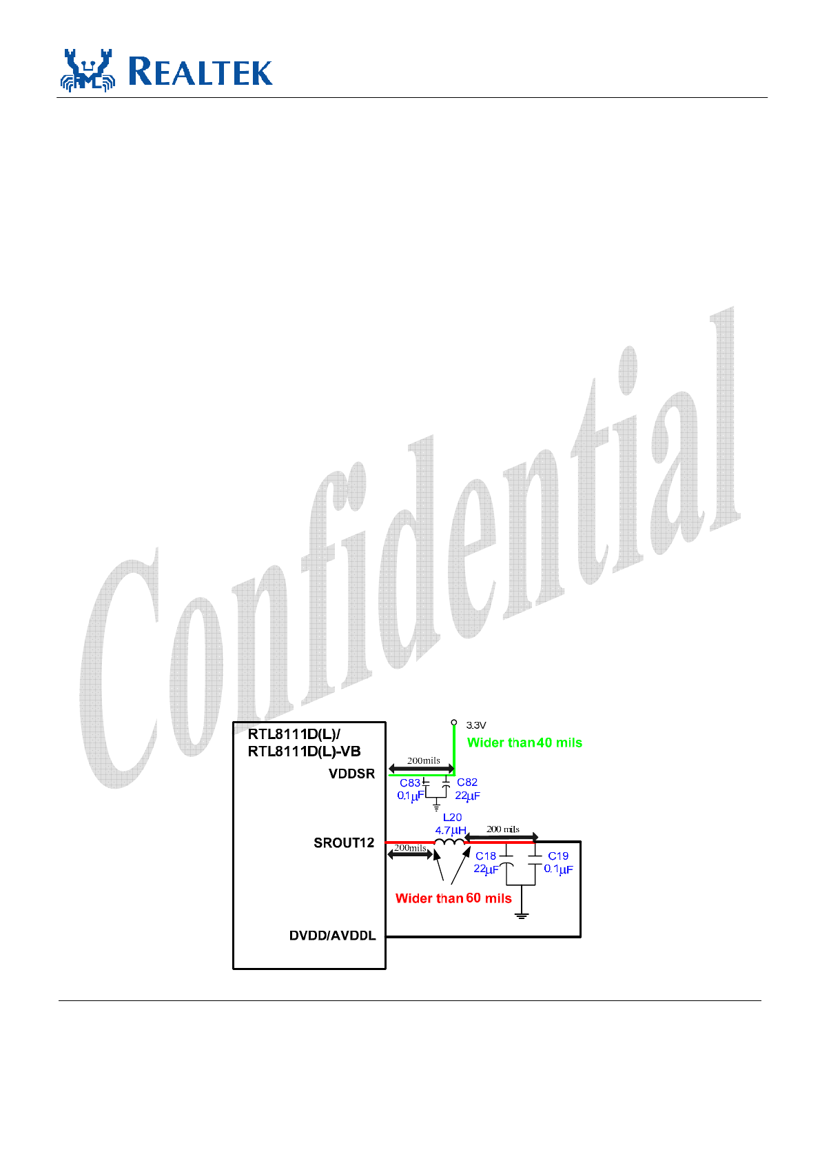
7. Switching Regulator
The RTL8111D(L)/RTL8111D(L)-VB incorporates a state-of-the-art switching regulator that requires a
well-designed PCB layout in order to achieve good power efficiency and lower the output voltage ripple
and input overshoot.
7.1.
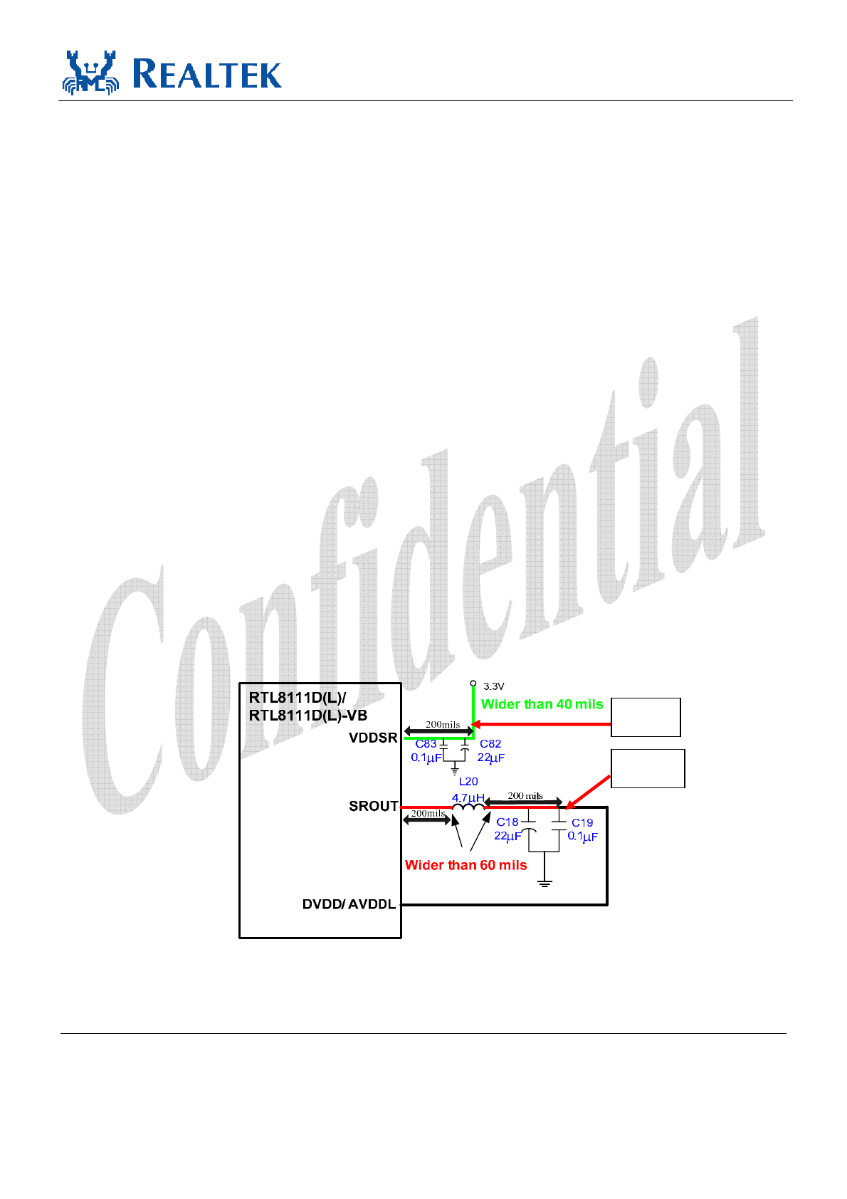
PCB Layout
• The input 3.3V power trace connected to the VDDSR pin should be wider than 40mils.
• The bulk de-coupling capacitors (C82 and C83) should be placed within 200mils (0.5cm) of the
VDDSR pin to prevent input voltage overshoot.
• The output power trace out of the SROUT12 pin should be wider than 60mils.
• Keep L20 within 200mils (0.5cm) of the SROUT12 pin.
• Keep C18 and C19 within 200mils (0.5cm) of L20 to ensure stable output power and better power
efficiency.
• Both C18 and C82 are strongly recommended to be ceramic capacitors.
Note: Violation of the above rules will damage the IC.
Figure 7. Switching Regulator Illustration
RTL8111D(L)/RTL8111D(L)-VB
Datasheet
Integrated Gigabit Ethernet Controller for PCI Express 20 Track ID: JATR-1076-21 Rev. 1.
6
7.2.
Inductor and Capacitor Parts List
Table 15. Inductor and Capacitor Parts List
Inductor Type Inductance ESR at 1MHz (mΩ) Max IDC (mA) Output Ripple (mV)
4R7GTSD32 4.7µH 712 1100 12.6
6R8GTSD32 6.8µH 784 900 12
6R8GTSD53 6.8µH 737 1510 10.4
Note 1: The ESR is equivalent to RDC or DCR. Lower ESR inductor values will promote a higher efficiency switching
regulator.
Note 2: The power inductor used by the switching regulator should be able to withstand 600mA of current.
Note 3: Typically, if the power inductor’s ESR at 1MHz is below 0.8
Ω
, the switching regulator efficiency will be above
75%. However the actual switching regulator efficiency should be measured according to the method described in section
7.5 Efficiency Measurement, page 26.
Capacitor Type Capacitance ESR at 1MHz (mΩ) Output Ripple (mV)
22µF 1210 TDK 21.5µF 33.53 9.6
22µF 1210 X5R 22.15µF 34.11 10.4
Note: Capacitors (C18 & C82) are suggested to be ceramic due to their low ESR value. Lower ESR values will yield
lower output voltage ripple.
RTL8111D(L)/RTL8111D(L)-VB
Datasheet
Integrated Gigabit Ethernet Controller for PCI Express 21 Track ID: JATR-1076-21 Rev. 1.
6
7.3.
Measurement Criteria
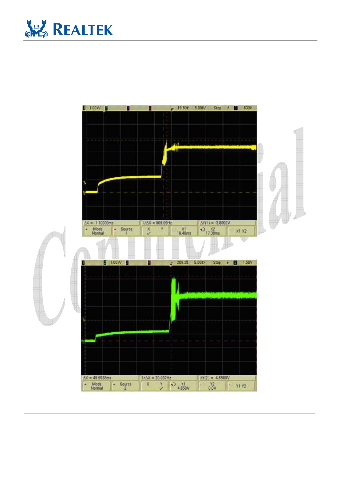
In order for the switching regulator to operate properly, the input and output voltage measurement criteria
must be met. From the input side, the voltage overshoot cannot exceed 4V; otherwise the chip may be
damaged. Note that the voltage signal must be measured directly at the VDDSR pin, not at the capacitor.
In order to reduce the input voltage overshoot, the C82 and C83 must be placed close to the VDDSR pin.
The following figures show what a good input voltage and a bad one look like.
Figure 8. Input Voltage Overshoot <4V (Good)
Figure 9. Input Voltage Overshoot >4V (Bad)
RTL8111D(L)/RTL8111D(L)-VB
Datasheet
Integrated Gigabit Ethernet Controller for PCI Express 22 Track ID: JATR-1076-21 Rev. 1.
6
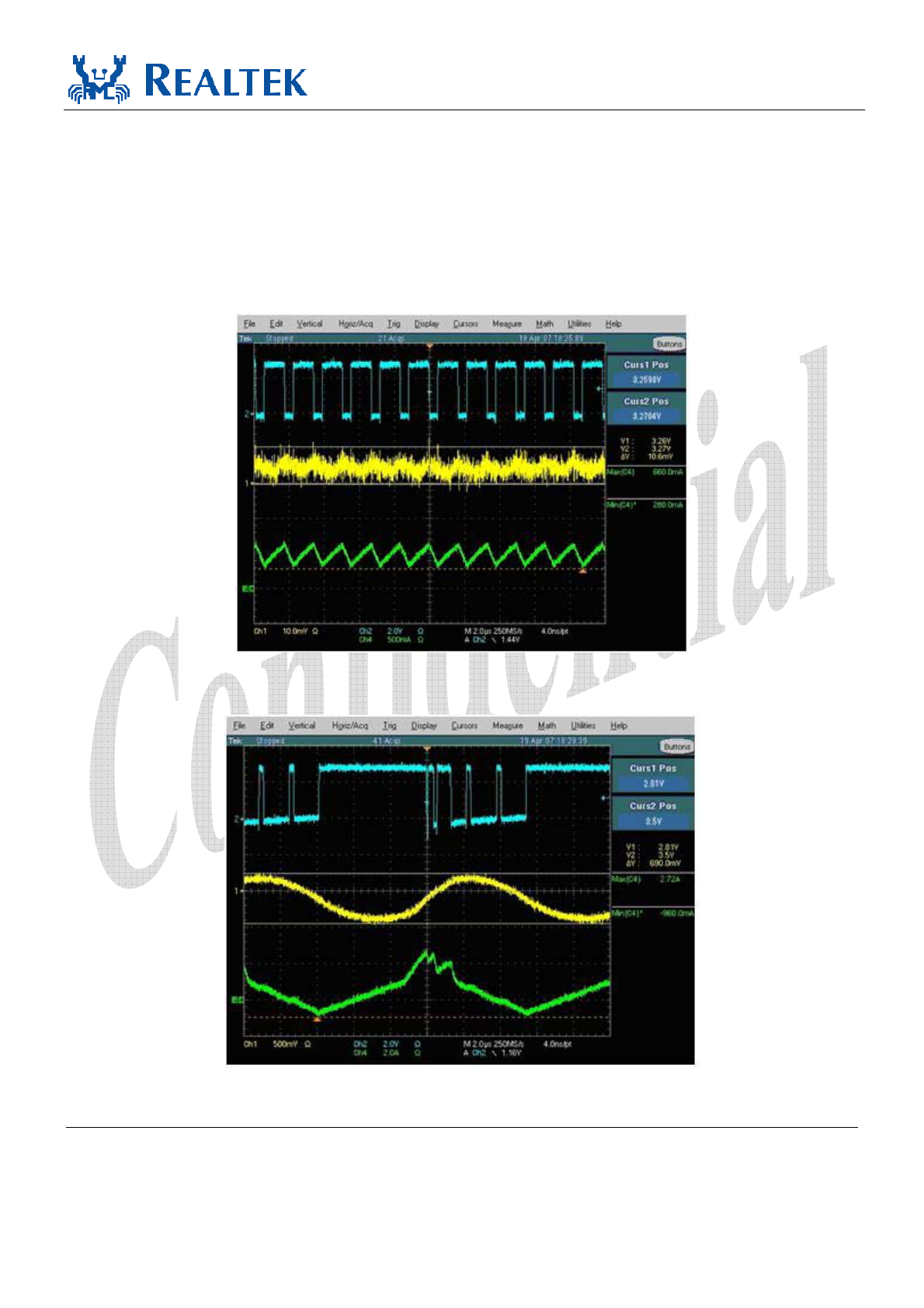
From the output side measured at the SROUT12 pin, the voltage ripple must be within 100mV. Choosing
different types and values of output capacitor (C18, C19) and power inductor (L20) will seriously affect
the efficiency and output voltage ripple of switching regulators. The following figures show the effects of
different types of capacitors on the switching regulator’s output voltage.
The blue square wave signal (top row) is measured at the output the SROUT12 pin before the power
inductor (L20). The yellow signal (second row) is measured after the power inductor (L20), and shows
there is a voltage ripple. The green signal (lower row) is the current. Data in the following figures was
measured at gigabit speed.
Figure 10. Ceramic 22µF 1210 (X5R) (Good)
Figure 11. Ceramic 22µF 0805 (Y5V) (Bad)
RTL8111D(L)/RTL8111D(L)-VB
Datasheet
Integrated Gigabit Ethernet Controller for PCI Express 23 Track ID: JATR-1076-21 Rev. 1.
6
A ceramic 22µF (X5R) will have a lower voltage ripple compared to the electrolytic 100µF. The key to
choosing a proper output capacitor is to choose the lowest ESR to reduce the output voltage ripple.
Choosing a ceramic 22µF 0805 (Y5V) in this case will cause malfunction of the switching regulator.
Placing several Electrolytic capacitors in parallel will help lower the output voltage ripple.
Figure 12. Electrolytic 100µF (Ripple Too High)

RTL8111D(L)/RTL8111D(L)-VB
Datasheet
Integrated Gigabit Ethernet Controller for PCI Express 24 Track ID: JATR-1076-21 Rev. 1.
6
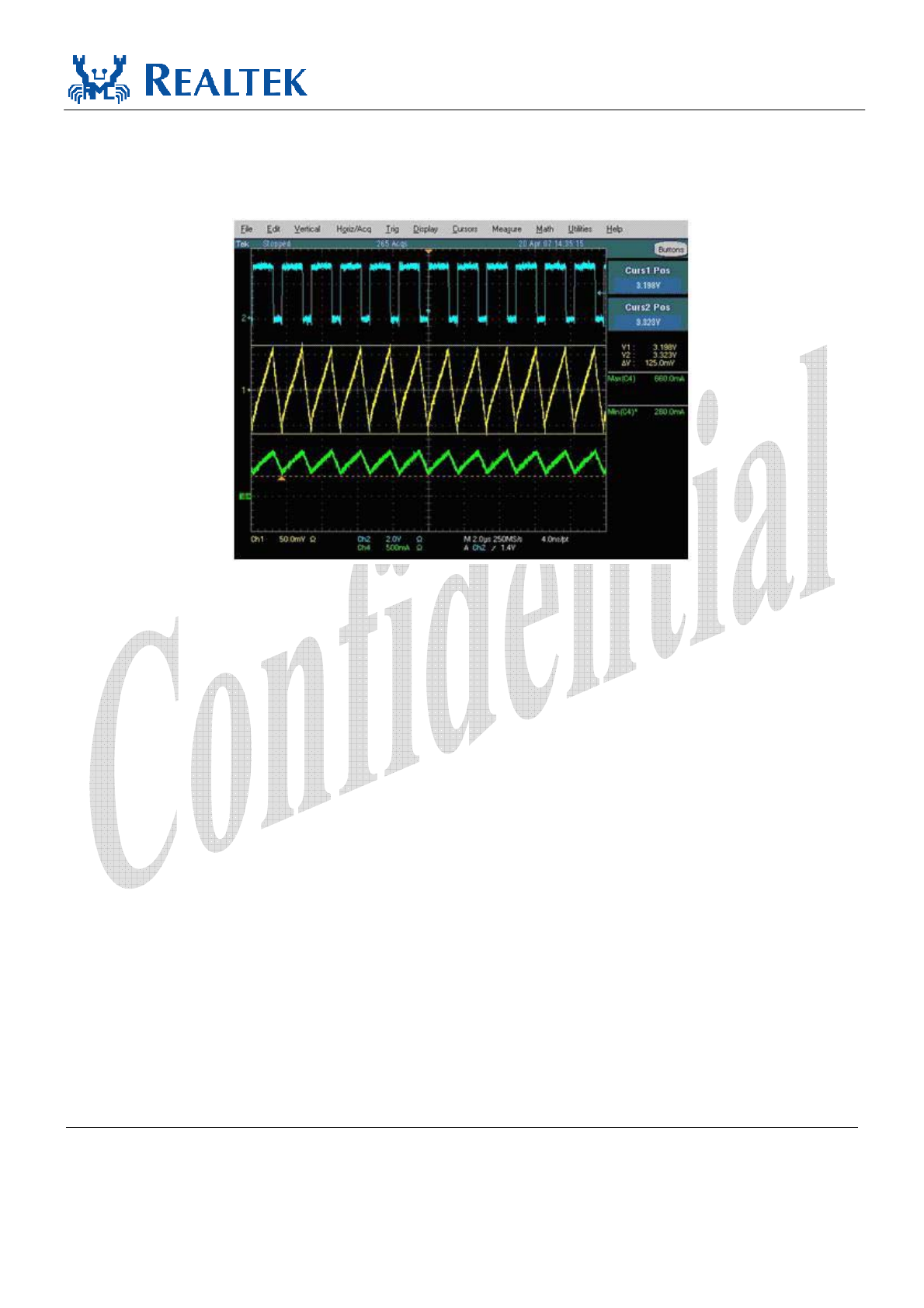
The following figures show how different inductors affect the SROUT12 pin output waveform. The
typical waveform should look like Figure 13, which has a square waveform with a dip at the falling edge
and the rising edge. If the inductor is not carefully chosen, the waveform may look like Figure 14, where
the waveform looks like a distorted square. This will cause insufficient current supply and will undermine
the stability of the system at gigabit speed. Data in the following figures was measured at gigabit speed.
Figure 13. 4R7GTSD32 (Good)
Figure 14. 1µH Bead (Bad)
RTL8111D(L)/RTL8111D(L)-VB
Datasheet
Integrated Gigabit Ethernet Controller for PCI Express 25 Track ID: JATR-1076-21 Rev. 1.
6
7.4.
Typical Switching Regulator PCB Layout
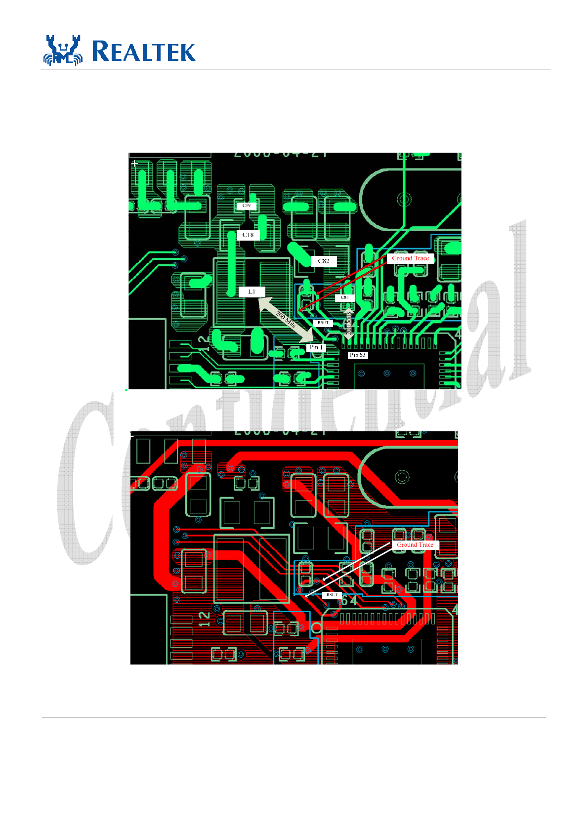
The typical layout of Figure 15 and Figure 16 are similar. The trace from RSET should pass through a via
to the lower layer, and the trace should be protected by a ground trace. The width of the ground trace
should be more than 5 mils.
Figure 15. Typical Switching Regulator PCB Layout (Top Layer)
Figure 16. Typical Switching Regulator PCB Layout (Bottom Layer)
RTL8111D(L)/RTL8111D(L)-VB
Datasheet
Integrated Gigabit Ethernet Controller for PCI Express 26 Track ID: JATR-1076-21 Rev. 1.
6
7.5.
Efficiency Measurement
The efficiency of the switching regulator is designed to be above 75% in gigabit traffic mode. It is very
important to choose a suitable inductor before Gerber certification, as the Inductor ESR value will affect
the efficiency of the switching regulator. An inductor with a lower ESR value will result in a higher
efficiency switching regulator.
The efficiency of the switching regulator is easily measured using the following method.
Figure 17 shows two checkpoints, checkpoint A (CP_A) and checkpoint B (CP_B). The switching
regulator input current (Icpa) should be measured at CP_A, and the switching regulator output current
(Icpb) should be measured at CP_B.
To determine efficiency, apply the following formula:
Efficiency = Vcpb*Icpb / Vcpa*Icpa
Where Vcpb is 1.05V; Vcpa is 3.3V. The measurements should be performed in gigabit traffic mode.
For example: The inductor used in the evaluation board is a GOTREND GTSD32-4R7M:
• The ESR value @ 1MHz is approximately 0.712ohm
• The measured Icpa is 101mA at CP_A
• The measured Icpb is 263mA at CP_B
These values are measured in gigabit traffic mode, so the efficiency of the GOTREND GTSD32-4R7M
can be calculated as follows:
Efficiency = (1.05V*263mA) / (3.3V*101mA) = 0.823 = 82.3%.
We strongly recommend that when choosing an inductor for the switching regulator, the efficiency should
be measured, and that the inductor should yield an efficiency rating higher than 75%. If the efficiency
does not meet this requirement, there may be risk to the switching regulator reliability in the long run.
Figure 17. Switching Regulator Efficiency Measurement Checkpoint
CP_B
CP_A
RTL8111D(L)/RTL8111D(L)-VB
Datasheet
Integrated Gigabit Ethernet Controller for PCI Express 27 Track ID: JATR-1076-21 Rev. 1.
6
7.6.
Power Sequence
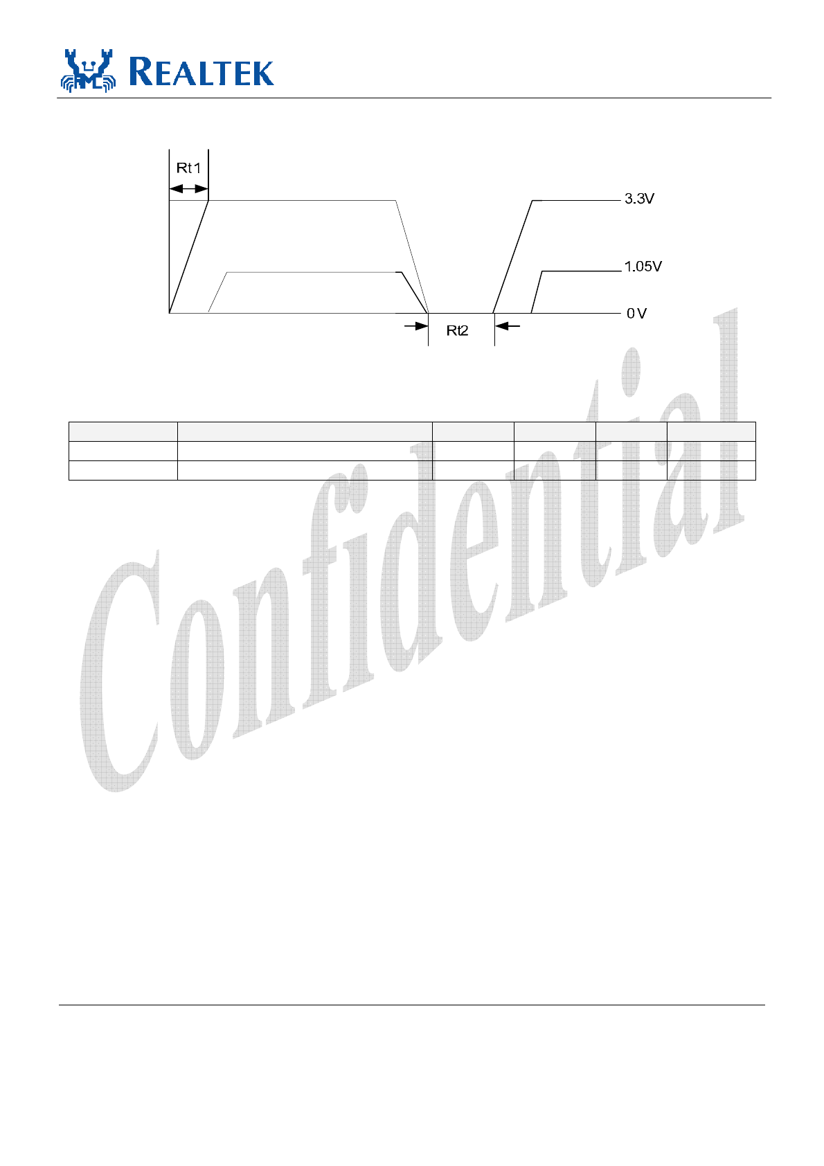
Figure 18. Power Sequence
Table 16. Power Sequence Parameter
Symbol Description Min Typical Max Units
Rt1 3.3V Rise Time 1 - 100 ms
Rt2 3.3V Fall Time 200 - - ms
Note 1: The RTL8111D(L)/RTL8111D(L)-VB does not support fast 3.3V rising. The 3.3V rise time must be controlled over
1ms. If the rise time is too short it will induce a peak voltage in PIN63, which may cause permanent damage to the
switching regulator.
Note 2: If there is any action that involves consecutive ON/OFF toggling of the switching-regulator source (3.3V), the
design must makes sure the OFF state of both the switching-regulator source (3.3V) and output (1.05V) reach 0V, and the
time period between the consecutive ON/OFF toggling action must be longer than 200ms.
RTL8111D(L)/RTL8111D(L)-VB
Datasheet
Integrated Gigabit Ethernet Controller for PCI Express 28 Track ID: JATR-1076-21 Rev. 1.
6
8. Characteristics
8.1.
Absolute Maximum Ratings
WARNING: Absolute maximum ratings are limits beyond which permanent damage may be caused to
the device, or device reliability will be affected. All voltages are specified reference to GND unless
otherwise specified.
Table 17. Absolute Maximum Ratings
Symbol Description Minimum Maximum Unit
VDD33, AVDD33 Supply Voltage 3.3V -0.3 +0.30 V
AVDD12, DVDD12 Supply Voltage 1.05V -0.3 +0.12 V
EVDD12 Supply Voltage 1.05V -0.3 +0.12 V
DCinput Input Voltage -0.3 Corresponding Supply Voltage + 0.5 V
DCoutput Output Voltage -0.3 Corresponding Supply Voltage + 0.5 V
N/A Storage Temperature -55 +125 °C
Note: Refer to the most updated schematic circuit for correct configuration.
8.2.
Recommended Operating Conditions
Table 18. Recommended Operating Conditions
Description Pins Minimum Typical Maximum Unit
VDD33, AVDD33 2.97 3.3 3.63 V
AVDD12, DVDD12 1.0 1.05 1.09 V
Supply Voltage VDD
EVDD12 1.0 1.05 1.09 V
Ambient Operating Temperature TA - 0 - 70
°C
Maximum Junction Temperature - - - 125 °C
Note: Refer to the most updated schematic circuit for correct configuration.
8.3.
Crystal Requirements
Table 19. Crystal Requirements
Symbol Description/Condition Minimum Typical Maximum Unit
Fref Parallel resonant crystal reference frequency,
fundamental mode, AT-cut type. - 25 - MHz
Fref Stability
Parallel resonant crystal frequency stability,
fundamental mode, AT-cut type.
Ta = 0°C ~ +70°C.
-30 - +30 ppm
Fref Tolerance
Parallel resonant crystal frequency tolerance,
fundamental mode, AT-cut type.
Ta = 25°C.
-50 - +50 ppm
Fref Duty Cycle Reference Clock Input Duty Cycle. 40 - 60 %
ESR Equivalent Series Resistance. - - 30
DL Drive Level. - - 0.3 mW
Note: The CLK source can come from other places in the system, but it must accord with the parameters above.
RTL8111D(L)/RTL8111D(L)-VB
Datasheet
Integrated Gigabit Ethernet Controller for PCI Express 29 Track ID: JATR-1076-21 Rev. 1.
6
8.4.
Oscillator Requirements
Table 20. Oscillator Requirements
Parameter Condition Minimum Typical Maximum Unit
Frequency - - 25 - MHz
Frequency Stability Ta = 0°C ~ +70°C -30 - +30 ppm
Frequency Tolerance Ta = 25°C -50 - +50 ppm
Duty Cycle - 40 - 60 %
Jitter - - - 50 ps
Vp-p - 3.15 3.3 3.45 V
Rise Time - - - 10 ns
Fall Time - - - 10 ns
Operation Temp Range - 0 - 70
°C
Note: The CLK source can come from other places in the system, but it must accord with the parameters above.
8.5.
Thermal Characteristics
Table 21. Thermal Characteristics
Parameter Minimum Maximum Units
Storage Temperature -55 +125 °C
Ambient Operating Temperature 0 70
°C
8.6.
DC Characteristics
Table 22. DC Characteristics
Symbol Parameter Conditions Minimum Typical Maximum Units
VDD33,
AVDD33 3.3V Supply Voltage - 2.97 3.3 3.63 V
DVDD12,
AVDD12 1.05V Supply Voltage - 1.0 1.05 1.09 V
EVDD12 1.05V Supply Voltage - 1.0 1.05 1.09 V
Voh Minimum High Level
Output Voltage Ioh = -4mA 0.9*VDD33 - VDD33 V
Vol Maximum Low Level
Output Voltage Iol = 4mA 0 - 0.1*VDD33 V
Vih Minimum High Level
Input Voltage - 2.0 - - V
Vil Maximum Low Level
Input Voltage - - - 0.8 V
Iin Input Current Vin = VDD33 or GND 0 - 0.5 µA
Icc33 Average Operating Supply
Current from 3.3V
At 1Gbps with heavy
network traffic - 66 - mA
Icc12 Average Operating Supply
Current from 1.05V
At 1Gbps with heavy
network traffic - 272 - mA
Note: Refer to the most updated schematic circuit for correct configuration.
RTL8111D(L)/RTL8111D(L)-VB
Datasheet
Integrated Gigabit Ethernet Controller for PCI Express 30 Track ID: JATR-1076-21 Rev. 1.
6
8.7.
AC Characteristics
8.7.1. Serial EEPROM Interface Timing
93C46(64*16)/93C56(128*16)
EESK
EECS
EEDI
EEDO
110An A2 A0A1
Dn D1 D0
EESK
(Read)
(Write)
(Read)
(Write)
0
tcs
EESK
EECS
EEDI
EEDO
110An A0 ...
Dn
tcs
...
BUSY READY
High Impedance
High Impedance
twp
EECS
EEDI
EEDO
EEDO
(Read)
(Program) STATUS VALID
tsk
tskh tskl
tcss
tdis tdih
tdos tdoh
tcsh
tsv
D0
Figure 19. Serial EEPROM Interface Timing
Table 23. EEPROM Access Timing Parameters
Symbol Parameter EEPROM Type Min. Max. Unit
tcs Minimum CS Low Time 9346 1000 - ns
twp Write Cycle Time 9346 - 10 ms
tsk SK Clock Cycle Time 9346 4 - µs
tskh SK High Time 9346 1000 - ns
tskl SK Low Time 9346 1000 - ns
tcss CS Setup Time 9346 200 - ns
tcsh CS Hold Time 9346 0 - ns
tdis DI Setup Time 9346 400 - ns
tdih DI Hold Time 9346 400 - ns
tdos DO Setup Time 9346 2000 - ns
tdoh DO Hold Time 9346 - 2000 ns
tsv CS to Status Valid 9346 - 1000 ns
RTL8111D(L)/RTL8111D(L)-VB
Datasheet
Integrated Gigabit Ethernet Controller for PCI Express 31 Track ID: JATR-1076-21 Rev. 1.
6
8.8.
PCI Express Bus Parameters
8.8.1. Differential Transmitter Parameters
Table 24. Differential Transmitter Parameters
Symbol Parameter Min Typical Max Units
UI Unit Interval 399.88 400 400.12 ps
VTX-DIFFp-p Differential Peak to Peak Output Voltage 0.800 - 1.05 V
VTX-DE-RATIO De-Emphasized Differential Output Voltage (Ratio) -3.0 -3.5 -4.0 dB
TTX-EYE Minimum Tx Eye Width 0.75 - - UI
TTX-EYE-MEDIAN-
to-MAX-JITTER
Maximum Time between The Jitter Median and
Maximum Deviation from The Median
- - 0.125 UI
TTX-RISE, TTX-FALL D+/D- Tx Output Rise/Fall Time 0.125 - - UI
VTX-CM-ACp RMS AC Peak Common Mode Output Voltage - - 20 mV
VTX-CM-DCACTIVE-
IDLEDELTA
Absolute Delta of DC Common Mode Voltage During
L0 and Electrical Idle
0 - 100 mV
VTX-CM-DCLINE-
DELTA
Absolute Delta of DC Common Mode Voltage
between D+ and D-
0 - 25 mV
VTX-IDLE-DIFFp Electrical Idle Differential Peak Output Voltage 0 - 20 mV
VTX-RCV-DETECT The Amount of Voltage Change Allowed During
Receiver Detection
- - 600 mV
VTX-DC-CM The Tx DC Common Mode Voltage 0 - 3.6 V
ITX-SHORT Tx Short Circuit Current Limit - - 90 mA
TTX-IDLE-MIN Minimum Time Spent in Electrical Idle 50 - - UI
TTX-IDLE- SETTO-IDLE Maximum Time to Transition to A Valid Electrical Idle
After Sending An Electrical Idle Ordered Set
- - 20 UI
TTX-IDLE-TOTO-
DIFF-DATA
Maximum Time to Transition to Valid Tx
Specifications After Leaving An Electrical Idle
Condition
- - 20 UI
RLTX-DIFF Differential Return Loss 10 - - dB
RLTX-CM Common Mode Return Loss 6 - - dB
ZTX-DIFF-DC DC Differential Tx Impedance 80 100 120
LTX-SKEW Lane-to-Lane Output Skew - - 500+2*UI ps
CTX AC Coupling Capacitor 75 - 200 nF
Tcrosslink Crosslink Random Timeout 0 - 1 ms
Note1: Refer to PCI Express Base Specification, rev.1.1, for correct measurement environment setting of each parameter.
Note2: The data rate can be modulated with an SSC (Spread Spectrum Clock) from +0 to -0.5% of the nominal data rate
frequency, at a modulation rate in the range not exceeding 30kHz – 33kHz. The ±300ppm requirement still holds, which
requires the two communicating ports be modulated such that they never exceed a total of 600ppm difference.
RTL8111D(L)/RTL8111D(L)-VB
Datasheet
Integrated Gigabit Ethernet Controller for PCI Express 32 Track ID: JATR-1076-21 Rev. 1.
6
8.8.2. Differential Receiver Parameters
Table 25. Differential Receiver Parameters
Symbol Parameter Min. Typical Max. Units
UI Unit Interval 399.88 400 400.12 ps
VRX-DIFFp-p Differential Input Peak to Peak Voltage 0.175 - 1.05 V
TRX-EYE Minimum Receiver Eye Width 0.4 - - UI
TRX-EYE-MEDIAN-to-
MAX-JITTER
Maximum Time Between The Jitter Median and
Maximum Deviation from The Median
- - 0.3 UI
VRX-CM-ACp AC Peak Common Mode Input Voltage - - 150 mV
RLRX-DIFF Differential Return Loss 10 - - dB
RLRX-CM Common Mode Return Loss 6 - - dB
ZRX-DIFF-DC DC Differential Input Impedance 80 100 120
ZRX--DC DC Input Impedance 40 50 60
ZRX-HIGH-IMP-DC Powered Down DC Input Impedance 200k - -
VRX-IDLE-DET-DIFFp-p Electrical Idle Detect Threshold 65 - 175 mV
TRX-IDLE-DET-
DIFFENTERTIME
Unexpected Electrical Idle Enter Detect Threshold
Integration Time
- - 10 ms
LRX-SKEW Total Skew - - 20 ns
Note: Refer to PCI Express Base Specification, rev.1.1, for correct measurement environment setting of each parameter.
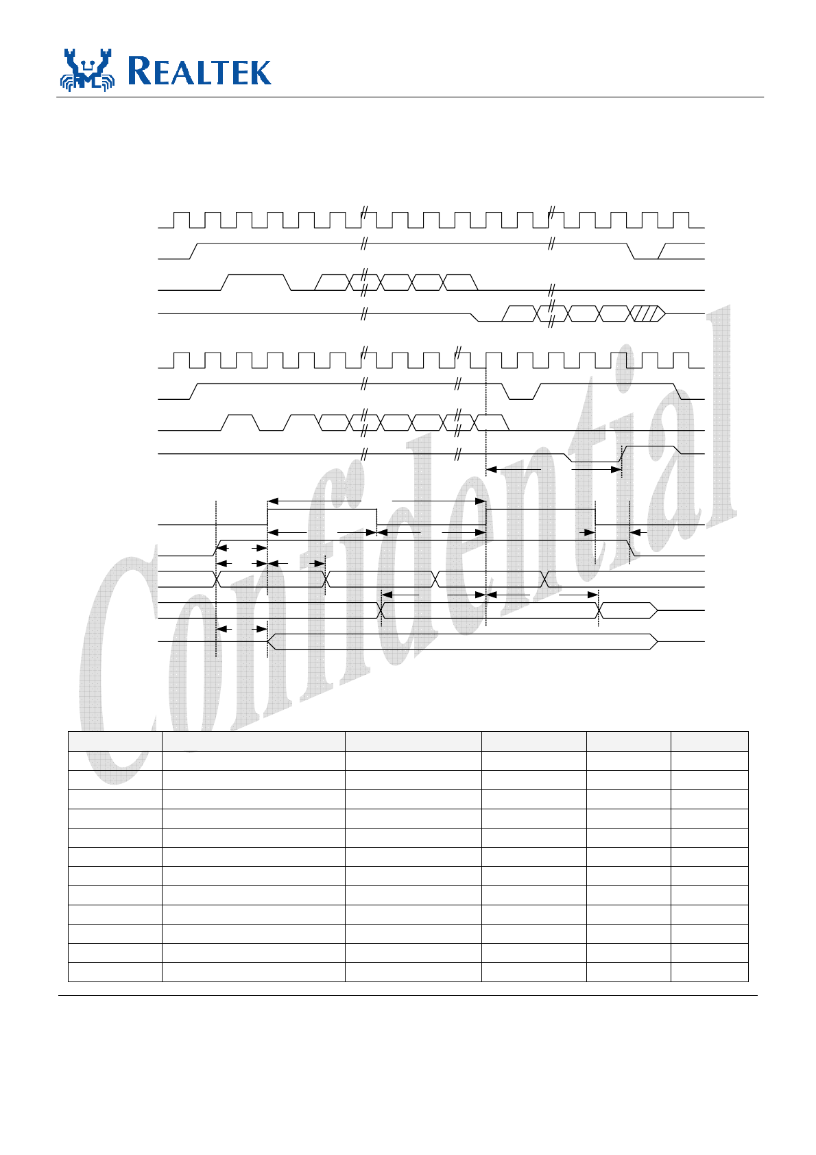
8.8.3. REFCLK Parameters
Table 26. REFCLK Parameters
Symbol Parameter 100MHz Input
Min Max
Units Note
Rise Edge Rate Rising Edge Rate 0.6 4.0 V/ns 2, 3
Fall Edge Rate Falling Edge Rate 0.6 4.0 V/ns 2, 3
VIH Differential Input High Voltage +150 - mV 2
VIL Differential Input Low Voltage - -150 mV 2
VCROSS Absolute Crossing Point Voltage +250 +550 mV 1, 4, 5
VCROSS DELTA Variation of VCROSS Over All Rising Clock Edges - +140 mV 1, 4, 9
VRB Ring-Back Voltage Margin -100 +100 mV 2, 12
TSTABLE Time before VRB is Allowed 500 - ps 2, 12
TPERIOD AVG Average Clock Period Accuracy -300 +2800 ppm 2, 10, 13
TPERIOD ABS Absolute Period
(Including Jitter and Spread Spectrum)
9.847 10.203 ns 2, 6
TCCJITTER Cycle to Cycle Jitter - 150 ps 2
VMAX Absolute Maximum Input Voltage - +1.15 V 1, 7
VMIN Absolute Minimum Input Voltage - -0.3 V 1, 8

RTL8111D(L)/RTL8111D(L)-VB
Datasheet
Integrated Gigabit Ethernet Controller for PCI Express 33 Track ID: JATR-1076-21 Rev. 1.
6
Symbol Parameter 100MHz Input
Min Max
Units Note
Duty Cycle Duty Cycle 40 60 % 2
Rise-Fall Matching Rising Edge Rate (REFCLK+) to
Falling Edge Rate (REFCLK-) Matching
- 20 % 1, 14
ZC-DC Clock Source DC Impedance 40 60 1, 11
Note1: Measurement taken from single-ended waveform.
Note2: Measurement taken from differential waveform.
Note3: Measured from -150mV to +150mV on the differential waveform (derived from REFCLK+ minus REFCLK-). The
signal must be monotonic through the measurement region for rise and fall time. The 300mV measurement window is
centered on the differential zero crossing. See Figure 23, page 35.
Note4: Measured at crossing point where the instantaneous voltage value of the rising edge of REFCLK+ equals the
falling edge of REFCLK-. See Figure 20, page 34.
Note5: Refers to the total variation from the lowest crossing point to the highest, regardless of which edge is crossing.
Refers to all crossing points for this measurement. See Figure 20, page 34.
Note6: Defines as the absolute minimum or maximum instantaneous period. This includes cycle to cycle jitter, relative
ppm tolerance, and spread spectrum modulation. See Figure 22, page 34.
Note7: Defined as the maximum instantaneous voltage including overshoot. See Figure 20, page 34.
Note8: Defined as the minimum instantaneous voltage including undershoot. See Figure 20, page 34.
Note9: Defined as the total variation of all crossing voltages of Rising REFCLK+ and Falling REFCLK-. This is the
maximum allowed variance in VCROSS for any particular system. See Figure 20, page 34.
Note10: Refer to Section 4.3.2.1 of the PCI Express Base Specification, Revision 1.1 for information regarding ppm
considerations.
Note11: System board compliance measurements must use the test load card described in Figure 26, page 36. REFCLK+
and REFCLK- are to be measured at the load capacitors CL. Single ended probes must be used for measurements
requiring single ended measurements. Either single ended probes with math or differential probe can be used for
differential measurements. Test load CL=2pF.
Note12: TSTABLE is the time the differential clock must maintain a minimum ±150mV differential voltage after rising/falling
edges before it is allowed to droop back into the VRB ±100mV differential range. See Figure 25, page 35.
Note13: PPM refers to parts per million and is a DC absolute period accuracy specification. 1ppm is 1/1,000,000th of
100.000000MHz exactly, or 100Hz. For 300ppm then we have an error budget of 100Hz/ppm*300ppm=30kHz. The
period is to be measured with a frequency counter with measurement window set to 100ms or greater. The ±300ppm
applies to systems that do not employ Spread Spectrum or that use common clock source. For systems employing Spread
Spectrum there is an additional 2500ppm nominal shift in maximum period resulting from the 0.5% down spread resulting
in a maximum average period specification of +2800ppm.
Note14: Matching applies to rising edge rate for REFCLK+ and falling edge rate for REFCLK-. It is measured using a
±75mV window centered on the median cross point where REFCLK+ rising meets REFCLK- falling. The median cross
point is used to calculate the voltage thresholds the oscilloscope is to use for the edge rate calculations. The Rise Edge
Rate of REFCLK+ should be compared to the Fall Edge Rate of REFCLK-; the maximum allowed difference should not
exceed 20% of the slowest edge rate. See Figure 21, page 34.
Note15: Refer to PCI Express Card Electromechanical Specification, rev.1.1, for correct measurement environment
setting of each parameter.
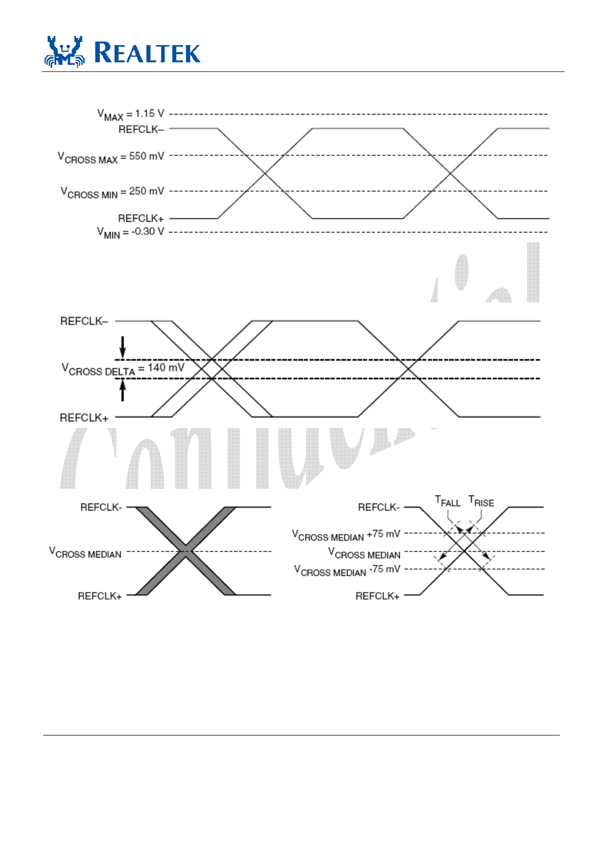
RTL8111D(L)/RTL8111D(L)-VB
Datasheet
Integrated Gigabit Ethernet Controller for PCI Express 34 Track ID: JATR-1076-21 Rev. 1.
6
Figure 20. Single-Ended Measurement Points for Absolute Cross Point and Swing
Figure 21. Single-Ended Measurement Points for Delta Cross Point
Figure 22. Single-Ended Measurement Points for Rise and Fall Time Matching
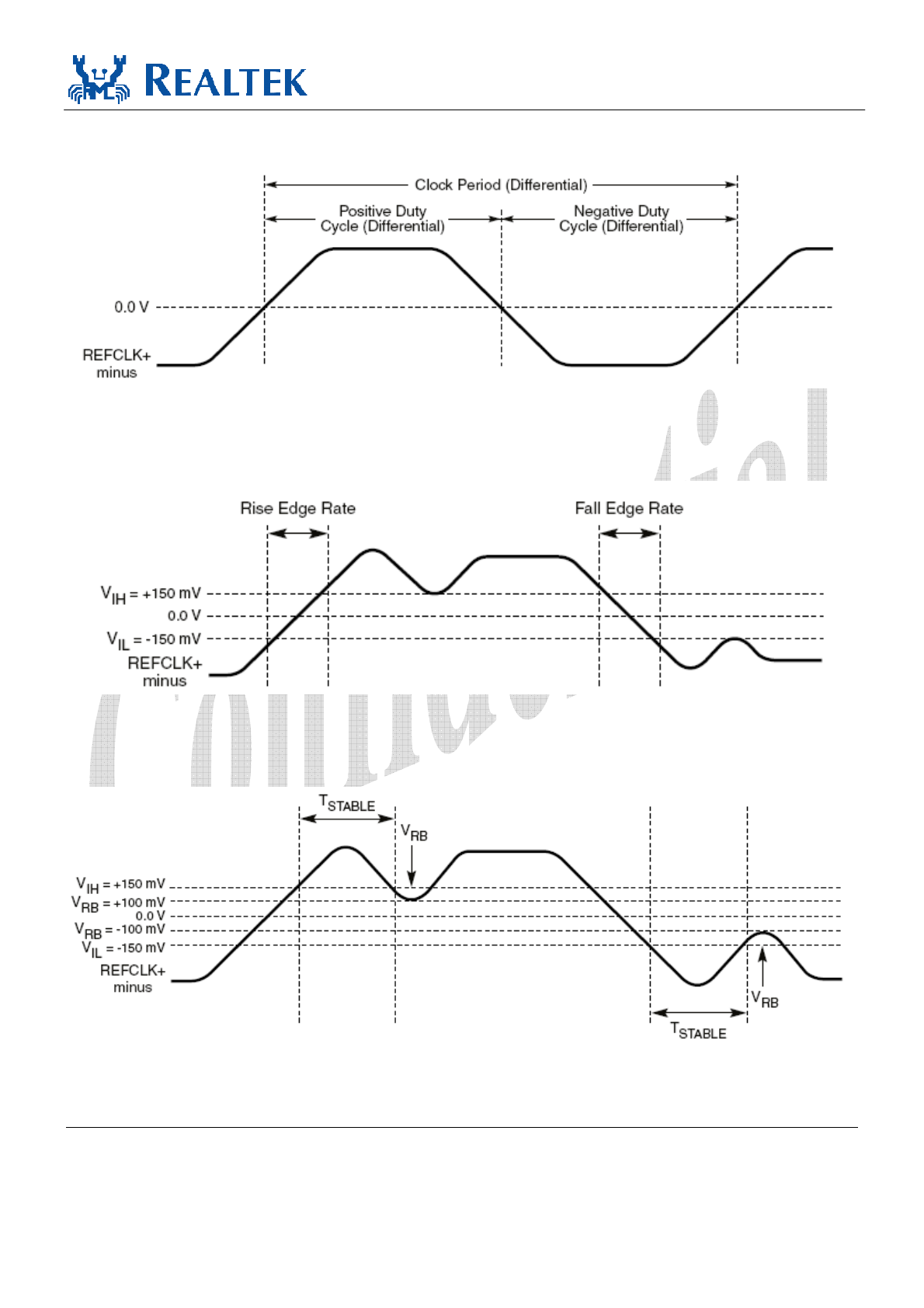
RTL8111D(L)/RTL8111D(L)-VB
Datasheet
Integrated Gigabit Ethernet Controller for PCI Express 35 Track ID: JATR-1076-21 Rev. 1.
6
Figure 23. Differential Measurement Points for Duty Cycle and Period
Figure 24. Differential Measurement Points for Rise and Fall Time
Figure 25. Differential Measurement Points for Ringback
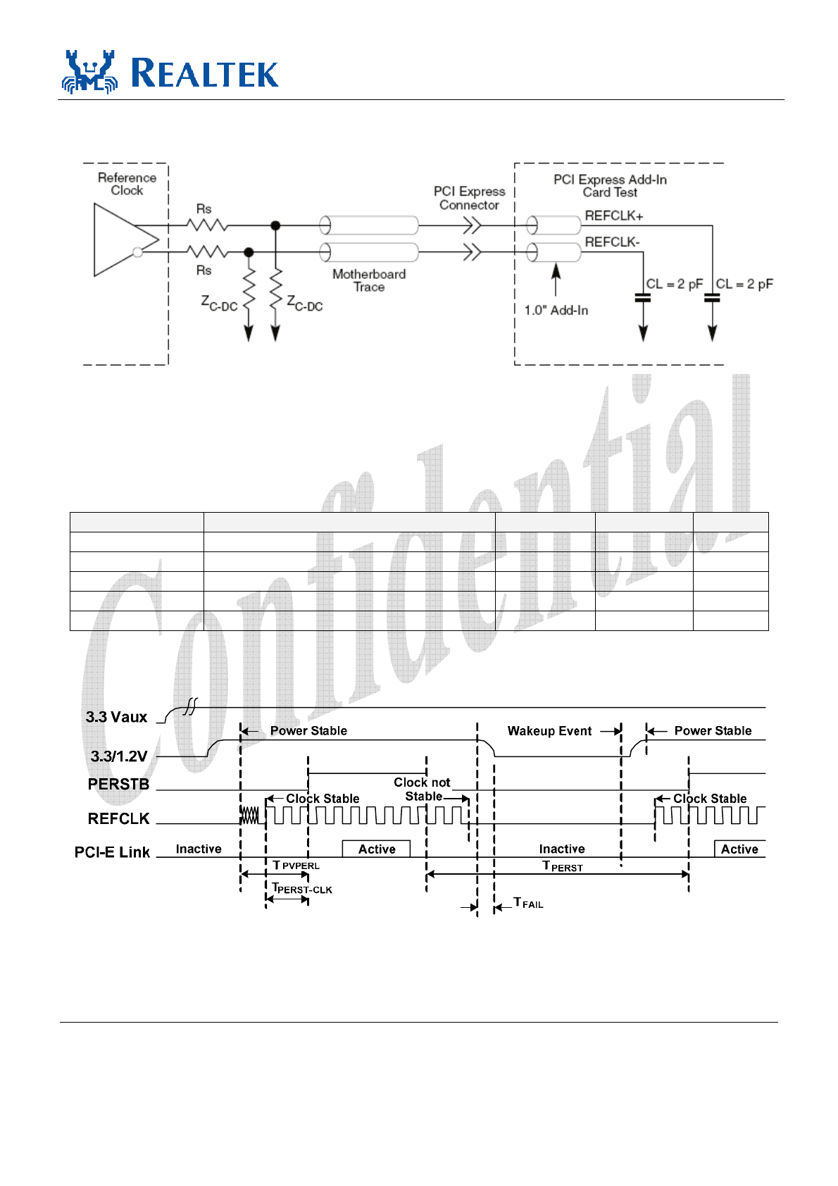
RTL8111D(L)/RTL8111D(L)-VB
Datasheet
Integrated Gigabit Ethernet Controller for PCI Express 36 Track ID: JATR-1076-21 Rev. 1.
6
Figure 26. Reference Clock System Measurement Point and Loading
8.8.4. Auxiliary Signal Timing Parameters
Table 27. Auxiliary Signal Timing Parameters
Symbol Parameter Min Max Units
TPVPERL Power Stable to PERSTB Inactive 100 - ms
TPERST-CLK REFCLK Stable before PERSTB Inactive 100 - µs
TPERST PERSTB Active Time 100 - µs
TFAIL Power Level Invalid to PWRGD Inactive - 500 ns
TWKRF LANWAKEB Rise – Fall Time - 100 ns
Figure 27. Auxiliary Signal Timing

RTL8111D(L)/RTL8111D(L)-VB
Datasheet
Integrated Gigabit Ethernet Controller for PCI Express 37 Track ID: JATR-1076-21 Rev. 1.
6
9. Mechanical Dimensions
9.1.
RTL8111D & RTL8111D-VB (64-Pin QFN)
NOTE: The RTL8111D(-VB)’s exposed pad size is L/F 3
RTL8111D(L)/RTL8111D(L)-VB
Datasheet
Integrated Gigabit Ethernet Controller for PCI Express 38 Track ID: JATR-1076-21 Rev. 1.
6
9.2.
RTL8111DL & RTL8111DL-VB (48-Pin LQFP)
RTL8111D(L)/RTL8111D(L)-VB
Datasheet
Integrated Gigabit Ethernet Controller for PCI Express 39 Track ID: JATR-1076-21 Rev. 1.
6
9.3.
Mechanical Dimensions Notes
(RTL8111DL/RTL8111DL-VB 48-Pin)
Notes:
1. To be determined at seating plane -c-
2. Dimensions D1 and E1 do not include mold protrusion.
Symbol Dimension in
inchs
Dimension in
millimeters
D1 and E1 are maximum plastic body size dimensions
including mold mismatch.
Min Nom Max Min Nom Max 3. Dimension b does not include dambar protrusion.
A - - 0.067 - - 1.70 Dambar cannot be located on the lower radius of the foot.
A1 0.000 0.004 0.008 0.00 0.1 0.20 4. Exact shape of each corner is optional.
A2 0.051 0.055 0.059 1.30 1.40 1.50 5. These dimensions apply to the flat section of the lead
b 0.006 0.009 0.011 15 0.22 0.29 between 0.10 mm and 0.25 mm from the lead tip.
b1 0.006 0.008 0.010 0.15 0.20 0.25 6. A1 is defined as the distance from the seating plane to
c1 0.004 - 0.006 0.09 - 0.16 the lowest point of the package body.
D 0.354 BSC 9.00 BSC 7. Controlling dimension: millimeter.
D1 0.276 BSC 7.00 BSC 8. Reference document: JEDEC MS-026, BBC
E 0.354 BSC 9.00 BSC TITLE: 48LD LQFP ( 7x7x1.4mm)
E1 0.276 BSC 7.00 BSC PACKAGE OUTLINE DRAWING, FOOTPRINT 2.0mm
e 0.020 BSC 0.50 BSC LEADFRAME MATERIAL:
L 0.016 0.024 0.031 0.40 0.60 0.80 DOC. NO.
L1 0.039 REF 1.00 REF VERSION 1
θ 0° 3.5° 9° 0° 3.5° 9°
APPROVE
PAGE OF
θ1 0° - -
0° - - DWG NO. SS048 - P1
θ2 12° TYP 12° TYP
CHECK
DATE
θ3 12° TYP 12° TYP REALTEK SEMICONDUCTOR CORP.

RTL8111D(L)/RTL8111D(L)-VB
Datasheet
Integrated Gigabit Ethernet Controller for PCI Express 40 Track ID: JATR-1076-21 Rev. 1.
6
10. Ordering Information
Table 28. Ordering Information
Part Number Package Status
RTL8111D-GR 64-Pin QFN ‘Green’ Package Production
RTL8111DL-GR 48-Pin LQFP ‘Green’ Package Production
RTL8111D-VB-GR 64-Pin QFN ‘Green’ Package; version B silicon Production
RTL8111DL-VB-GR 48-Pin LQFP ‘Green’ Package; version B silicon Production
Note: See page 3 and page 4 for package identification information.
Realtek Semiconductor Corp.
Headquarters
No. 2, Innovation Road II
Hsinchu Science Park, Hsinchu 300, Taiwan
Tel.: +886-3-578-0211. Fax: +886-3-577-6047
www.realtek.com