Samsung CLP 300 Service Manual. Www.s Manuals.com. Manual
User Manual: Color Laser Printer Samsung CLP-300 - Service manuals and Schematics, Disassembly / Assembly. Free.
Open the PDF directly: View PDF ![]() .
.
Page Count: 160 [warning: Documents this large are best viewed by clicking the View PDF Link!]
- 20060904105713984_00-Cover
- 20060904105713984_01-Precautions_
- 20061025134239187_02-Product_Specifications
- 20061025134239187_03-System_Overview
- 20060904105713984_04-S_W_Structure
- 20060904105713984_05-Disassembly
- 20060908150228031_06-Alignment
- 20060904105713984_07-Troubleshooting
- 20061031144024656_08-Exploded_Views
- 20060904105713984_09-Block_Diagram.pdf
- 20060904105713984_10-Connection_Diagram.pdf
- 20060904105713984_11-Schematic_Diagram
- 20060904105713984_12-Reference_Information

Manual
SERVICE
Color Laser Printer
CLP-300 Series
CLP-300/XSG
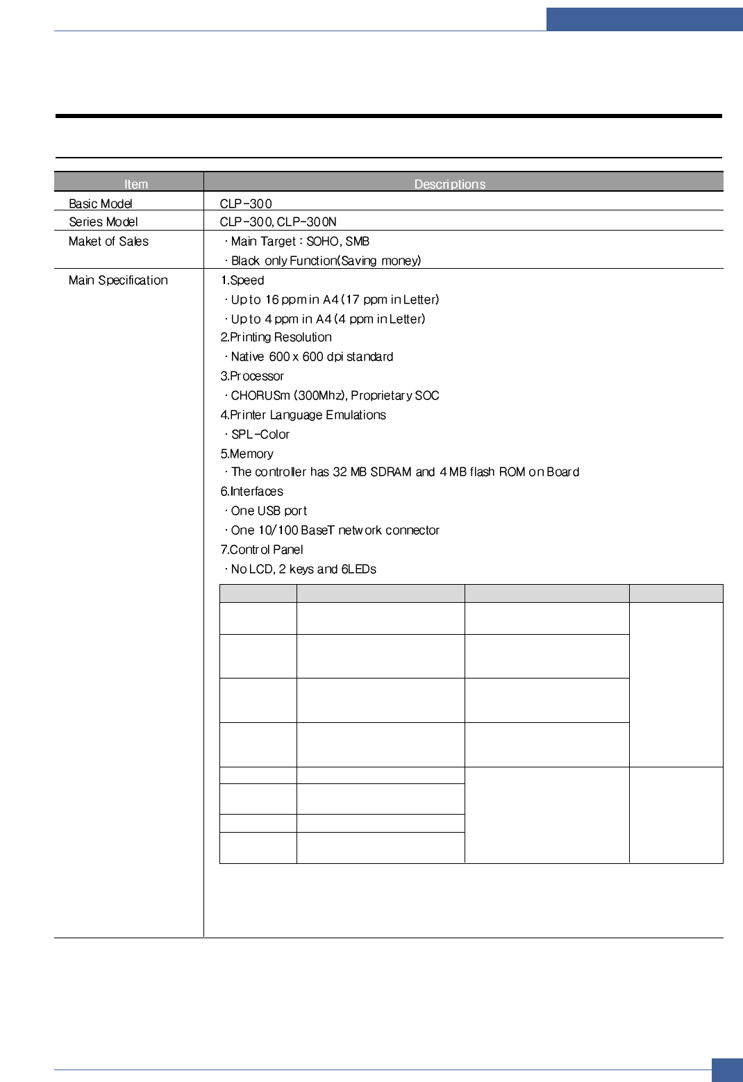
Basic Model :CLP-300
Samsung Color Laser Printer The keynote of Product
[The keynote of Product]
[Series Model]
.CLP-300: B/W 16 ppm, Color 4 ppm, SPL-C
.CLP-300N: CLP-300 + Network
[Resolution]
. 2400 x 600 dpi
[CPU]
.Samsung CorrusM 170MHz
[Interface]
.CLP-300 : USB 2.0
.CLP-300N : USB 2.0, Ethernet 10/100 Base TX
[Consumables]
.2K black toner cartridge
.1K color toner cartridge
.Waste toner box
[Paper Handling]
.150 sheets Semi-cassette
.1 sheet manual slot
.150 sheet Face-Down
CLP-300

ELECTRONICS
Samsung Electronics Co.,Ltd. June. 2006
Printed in Korea.
VERSION NO. : 1.00 CODE : JC-0164K
* This service manual is a property of Samsung Electronics Co., Ltd.
Any unauthorized use of Manual can be punished under applicable
international and/or domestic law.
* This service manual is also provided on the web, the ITSELF
system Samsung Electronics Co., Ltd.
“http://itself.sec.samsung.co.kr”

Contents
1. Precautions
1.1 Safety Warning 1-1
1.2 Caution for safety 1-2
1.3 ESD Precautions 1-5
1.4 Super Capacitor or Lithium Battery Precautions 1-5
2. Product Specification
2.1 Product Overview 2-1
2.2 Specifications 2-2
2.3 Model Comparison Table 2-7
3. System Overview
3.1 System Structure 3-1
3.2 Main PBA Description 3-7
3.3 CRUM 3-17
3.4 General Description 3-19
4. S/W Structure and Descriptions
4.1 Architecture 4-1
4.2 Language Monitor 4-1
4.3 Status Monitor 4-1
4.4 Network Interface 4-2
4.5 Printer Driver <-> Status Monitor 4-2
4.6 System F/W Flow 4-3
4.7 Alarm Shortage 4-4
4.8 Error status 4-4

Continued
4.9 CRUM Overview 4-5
4.10 FW Upgrade 4-5
4.11 Initailize Flow 4-6
5. Disassembly and Reassembly
5.1 Precautions When Replacing Parts 5-2
5.2 Parts for Maintenance and Repair 5-3
5.3 Information Related in Disassembly and Assembly 5-5
5.4 Disassembly Procedure 5-10
6. Alignment and Adjustments
6.1 Control Panel 6-1
6.2 Function 6-2
6.3 Jam Removal 6-6
6.4 Sample Pattern 6-9
6.5 Periodic Defective Image 6-10
6.6 How to use EDC (Engine Diagnostic Control) Mode 6-11
6.7 Error Message 6-17
7. Troubleshooting
7.1 Procedure of Checking the Symptoms 7-1
7.2 Troubleshooting Checklist 7-2
7.3 Solving General Printing Problems 7-3
7.4 Solving Print Quality Problems 7-7
7.5 Common Windows Problems 7-11
7.6 Common Macintosh Problems 7-11
7.7 Common Linux Problems 7-12
7.8 Major Problems Trouble shooting 7-15

Continued
8. Exploded Views & Parts List
8.1 Main 8-2
8.2 Top Cover 8-3
8.3 Rear Cover 8-4
8.4 Front Cover 8-5
8.5 Main Driver 8-6
8.6 Main Frame 8-8
8.7 LSU Cover 8-10
8.8 Fuser Unit 8-11
8.9 ELA-UNIT OPC DEV 8-12
8.10 ITB Unit 8-13
8.11 Casstte Unit 8-14
9. Block diagram
9.1 Block Diagram 9-1
10. Connection Diagram
10.1 Connection Diagram 10-1
11. Schematic Diagram
11.1 Main Board 11-1
11.2 Panel 11-16
11.3 DEVE INF 11-17
11.4 ITB INF 11-18
11.5 SMPS-110V 11-19
11.6 SMPS-220V 11-20
11.7 HVPS 11-21

Continued
12. Reference Information
12.1 Tools for Troubleshooting 12-1
12.2 Acronyms and Abbreviations 12-2
12.3 Select a location for the printer 12-4
12.4 A4 ISO 19752 Standard Pattern 12-5
Precautions
Samsung Electronics Service Manual
1-1
1
1
1. Precautions
In order to prevent accidents and to prevent damage to the equipment please read the precautions listed
below carefully before servicing the printer and follow them closely.
1.1 Safety Warning
(1) Only to be serviced by appropriately qualified service engineers.
High voltages and lasers inside this product are dangerous. This printer should only be serviced by a suitably
trained and qualified service engineer.
(2) Use only Samsung replacement parts
There are no user serviceable parts inside the printer. Do not make any unauthorized changes or
additions to the printer, these could cause the printer to malfunction and create electric shock or fire hazards.
(3) Laser Safety Statement
The Printer is certified in the U.S. to conform to the requirements of DHHS 21 CFR, chapter 1 Subchapter J for
Class 1(1) laser products, and elsewhere, it is certified as a Class I laser product
conforming to the requirements of IEC 825. Class I laser products are not considered to be hazardous. The
laser system and printer are designed so there is never any human access to laser radiation above a Class I
level during normal operation, user maintenance, or prescribed service condition.
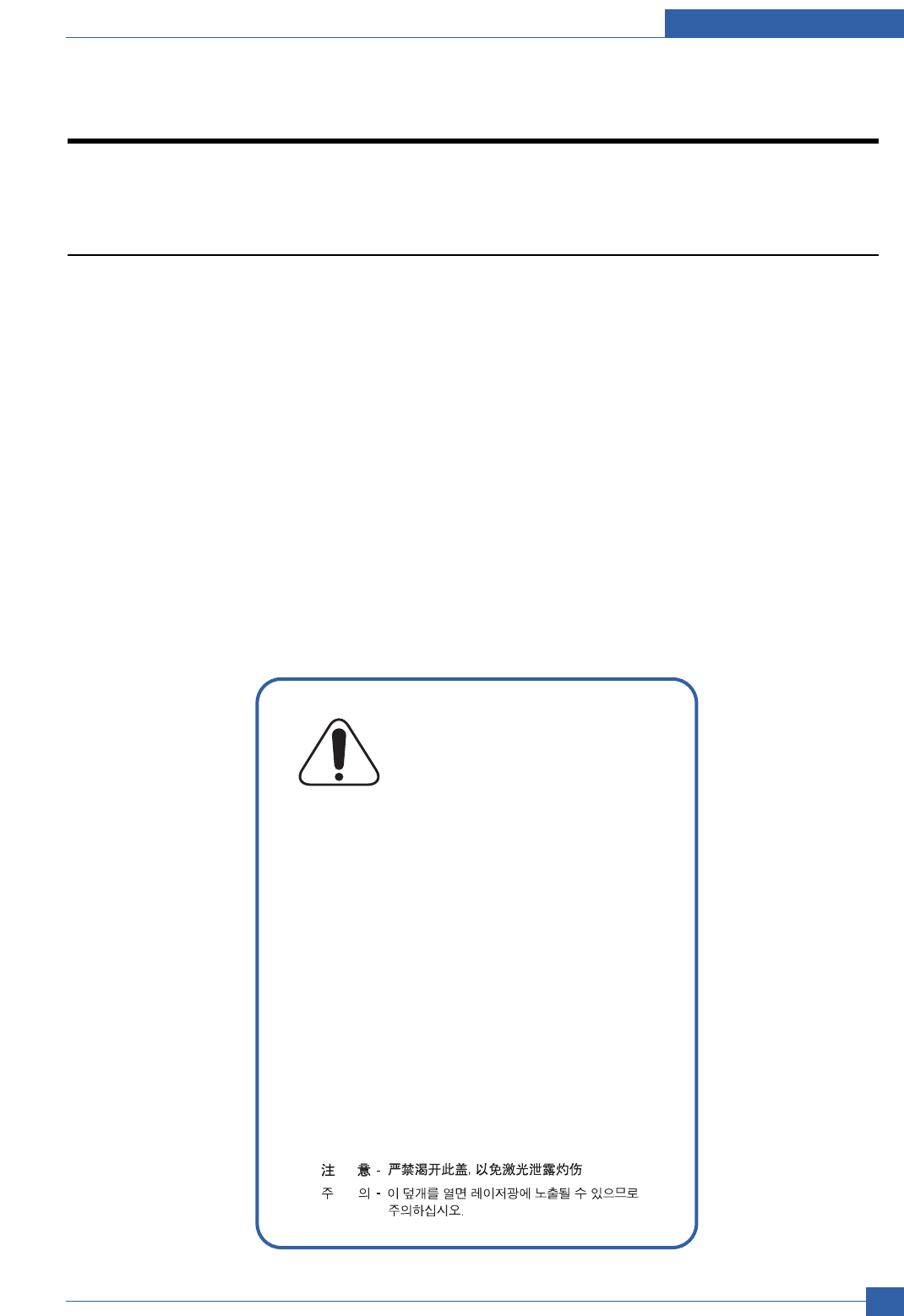
Warning >> Never operate or service the printer with the protective cover removed from Laser/Scanner assembly. The
reflected beam, although invisible, can damage your eyes. When using this product, these basic safety
pre-cautions should always be followed to reduce risk of fire, electric shock, and injury to persons.
CAUTION - INVISIBLE LASER RADIATION
WHEN THIS COVER OPEN.
DO NOT OPEN THIS COVER.
VORSICHT - UNSICHTBARE LASERSTRAHLUNG,
WENN ABDECKUNG GE FFNET.
NICHT DEM STRAHL AUSSETZEN.
ATTENTION - RAYONNEMENT LASER INVISIBLE EN CAS
D OUVERTURE. EXPOSITION DANGEREUSE
AU FAISCEAU.
ATTENZIONE - RADIAZIONE LASER INVISIBILE IN CASO DI
APERTURA. EVITARE L ESPOSIZIONE AL
FASCIO.
PRECAUCION - RADIACION LASER IVISIBLE CUANDO SE ABRE.
EVITAR EXPONERSE AL RAYO.
ADVARSEL. - USYNLIG LASERSTR LNING VED BNING, N R
SIKKERHEDSBRYDERE ER UDE AF FUNKTION.
UNDG UDSAETTELSE FOR STR LNING.
ADVARSEL. - USYNLIG LASERSTR LNING N R DEKSEL
PNES. STIRR IKKE INN I STR LEN.
UNNG EKSPONERING FOR STR LEN.
VARNING - OSYNLIG LASERSTR LNING N R DENNA DEL
R PPNAD OCH SP RREN R URKOPPLAD.
BETRAKTA EJ STR LEN. STR LEN R FARLIG.
VARO! - AVATTAESSA JA SUOJALUKITUS OHITETTAESSA
OLET ALTTIINA N KYM TT M LLE LASER-
S TEILYLLE L KATSO S TEESEEN.

Samsung Electronics
Service Manual
Precautions
1-2
1.2 Caution for safety
1.2.1 Toxic material
This product contains toxic materials that could cause illness if ingested.
(1) If the LCD control panel is damaged it is possible for the liquid inside to leak. This liquid is toxic. Contact with the skin
should be avoided, wash any splashes from eyes or skin immediately and contact your doctor. If the liquid gets into
the mouth or is swallowed see a doctor immediately.
(2) Please keep toner cartridges away from children. The toner powder contained in the toner cartridge may be harmful
and if swallowed you should contact a doctor.
1.2.2 Electric Shock and Fire Safety Precautions
Failure to follow the following instructions could cause electric shock or potentially cause a fire.
(1) Use only the correct voltage, failure to do so could damage the printer and potentially cause a fire or electric
shock.
(2) Use only the power cable supplied with the printer. Use of an incorrectly specified cable could cause the cable
to overheat and potentially cause a fire.
(3) Do not overload the power socket, this could lead to overheating of the cables inside the wall and could lead to
a fire.
(4) Do not allow water or other liquids to spill into the printer, this can cause electric shock. Do not allow paper
clips, pins or other foreign objects to fall into the printer these could cause a short circuit leading to an electric
shock or fire hazard..
(5) Never touch the plugs on either end of the power cable with wet hands, this can cause electric shock. When
servicing the printer remove the power plug from the wall socket.
(6) Use caution when inserting or removing the power connector. The power connector must be inserted com-
pletely otherwise a poor contact could cause overheating possibly leading to a fire. When removing the power
connector grip it firmly and pull.
(7) Take care of the power cable. Do not allow it to become twisted, bent sharply round corners or otherwise
damaged. Do not place objects on top of the power cable. If the power cable is damaged it could overheat and
cause a fire or exposed cables could cause an electric shock. Replace a damaged power cable immediately,
do not reuse or repair the damaged cable. Some chemicals can attack the coating on the power cable,
weakening the cover or exposing cables causing fire and shock risks.
(8) Ensure that the power sockets and plugs are not cracked or broken in any way. Any such defects should be
repaired immediately. Take care not to cut or damage the power cable or plugs when moving the machine.
(9) Use caution during thunder or lightening storms. Samsung recommend that this machine be disconnected from
the power source when such weather conditions are expected. Do not touch the machine or the power cord if it
is still connected to the wall socket in these weather conditions.
(10) Avoid damp or dusty areas, install the printer in a clean well ventilated location. Do not position the machine
near a humidifier. Damp and dust build up inside the machine can lead to overheating and cause a fire.
(11) Do not position the printer in direct sunlight. This will cause the temperature inside the printer to rise possibly
leading to the printer failing to work properly and in extreme conditions could lead to a fire.
(12) Do not insert any metal objects into the machine through the ventilator fan or other part of the casing, it could
make contact with a high voltage conductor inside the machine and cause an electric shock.

Precautions
Samsung Electronics Service Manual
1-3
1.2.3 Handling Precautions
The following instructions are for your own personal safety, to avoid injury and so as not to damage the printer
(1) Ensure the printer is installed on a level surface, capable of supporting its weight. Failure to do so could cause
the printer to tip or fall.
(2) The printer contains many rollers, gears and fans. Take great care to ensure that you do not catch your fingers,
hair or clothing in any of these rotating devices.
(3) Do not place any small metal objects, containers of water, chemicals or other liquids close to the printer which if
spilled could get into the machine and cause damage or a shock or fire hazard.
(4) Do not install the machine in areas with high dust or moisture levels, beside on open window or close to a
humidifier or heater. Damage could be caused to the printer in such areas.
(5) Do not place candles, burning cigarettes, etc. on the printer, these could cause a fire.
1.2.4 Assembly / Disassembly Precautions
Replace parts carefully, always use Samsung parts. Take care to note the exact location of parts and also
cable routing before dismantling any part of the machine. Ensure all parts and cables are replaced correctly.
Please carry out the following procedures before dismantling the printer or replacing any parts.
(1) Check the contents of the machine memory and make a note of any user settings. These will be erased if the
mainboard is replaced.
(2) Ensure that power is disconnected before servicing or replacing any electrical parts.
(3) Disconnect printer interface cables and power cables.
(4) Only use approved spare parts. Ensure that part number, product name, any voltage, current or temperature
rating are correct.
(5) When removing or re-fitting any parts do not use excessive force, especially when fitting screws into plastic.
(6) Take care not to drop any small parts into the machine.
(7) Handling of the OPC Drum
- The OPC Drum can be irreparably damaged if it exposed to light.
Take care not to expose the OPC Drum either to direct sunlight or to fluorescent or incandescent room
lighting. Exposure for as little as 5 mins can damage the surface’s photoconductive properties and will result
in print quality degradation. Take extra care when servicing the printer. Remove the OPC Drum and store it in
a black bag or other lightproof container. Take care when working with the covers(especially the top cover)
open as light is admitted to the OPC area and can damage the OPC Drum.
- Take care not to scratch the green surface of OPC Drum Unit.
If the green surface of the Drum Cartridge is scratched or touched the print quality will be compromised.

Samsung Electronics
Service Manual
Precautions
1-4
1.2.5 Disregarding this warning may cause bodily injury
(1) Be careful with the high temperature part.
The fuser unit works at a high temperature. Use caution when working on the printer. Wait for the fuser to cool
down before disassembly.
(2) Do not put finger or hair into the rotating parts.
When operating a printer, do not put hand or hair into the rotating parts (Paper feeding entrance, motor, fan,
etc.). If do, you can get harm.
(3) When you move the printer.
This printer weighs 13.6kg including Consumables. Use safe lifting and handling techniques. Back injury could
be caused if you do not lift carefully.
(4) Ensure the printer is installed safely.
The printer weighs 13.6Kg, ensure the printer is installed on a level surface, capable of supporting its weight.
Failure to do so could cause the printer to tip or fall possibly causing personal injury or damaging the printer.
(5) Do not install the printer on a sloping or unstable surface. After installation, double check that the printer is stable.

Precautions
Samsung Electronics Service Manual
1-5
1.3 ESD Precautions
Certain semiconductor devices can be easily damaged by static electricity. Such components are commonly called
“Electrostatically Sensitive (ES) Devices”, or ESDs. Examples of typical ESDs are: integrated circuits, some field
effect transistors, and semiconductor “chip” components.
The techniques outlined below should be followed to help reduce the incidence of component damage caused by
static electricity.
Caution >>Be sure no power is applied to the chassis or circuit, and observe all other safety precautions.
1. Immediately before handling a semiconductor component or semiconductor-equipped assembly, drain off any
electrostatic charge on your body by touching a known earth ground. Alternatively, employ a commercially avail-
able wrist strap device, which should be removed for your personal safety reasons prior to applying power to the
unit under test.
2. After removing an electrical assembly equipped with ESDs, place the assembly on a conductive surface, such as
aluminum or copper foil, or conductive foam, to prevent electrostatic charge buildup in the vicinity of the assem-
bly.
3. Use only a grounded tip soldering iron to solder or desolder ESDs.
4. Use only an “anti-static” solder removal device. Some solder removal devices not classified as “anti-static” can
generate electrical charges sufficient to damage ESDs.
5. Do not use Freon-propelled chemicals. When sprayed, these can generate electrical charges sufficient to dam-
age ESDs.
6. Do not remove a replacement ESD from its protective packaging until immediately before installing it. Most
replacement ESDs are packaged with all leads shorted together by conductive foam, aluminum foil, or a compa-
rable conductive material.
7. Immediately before removing the protective shorting material from the leads of a replacement ESD, touch the pro-
tective material to the chassis or circuit assembly into which the device will be installed.
8. Maintain continuous electrical contact between the ESD and the assembly into which it will be installed, until com-
pletely plugged or soldered into the circuit.
9. Minimize bodily motions when handling unpackaged replacement ESDs. Normal motions, such as the brushing
together of clothing fabric and lifting one’s foot from a carpeted floor, can generate static electricity sufficient to
damage an ESD.
1. Exercise caution when replacing a super capacitor or Lithium battery. There could be a danger of explosion and
subsequent operator injury and/or equipment damage if incorrectly installed.
2. Be sure to replace the battery with the same or equivalent type recommended by the manufacturer.
3. Super capacitor or Lithium batteries contain toxic substances and should not be opened, crushed, or burned for
disposal.
4. Dispose of used batteries according to the manufacture’s instructions.
1.4 Super Capacitor or Lithium Battery Precautions
Product Specifications
Samsung Electronics Service Manual
2-1
2
2
2. Product Specifications
2.1 Product Overview
Item(s) Pages Printed Part number Remark
Black tonerApprox. Initial : 1,500 pages*CLP-K300A
cartridgeSales : 2,000 pages*
Color tonerApprox. Initial : 700 pages* CLP-C300A : Cyan
cartridge Sales : 1,000 pages* CLP-M300A : Magenta
CLP-Y300A : Yellow
Imaging unit Approx. 20,000 black CLP-R300A
pages or approx.
12,500 color pages
Waste toner Approx. 5,000 images** CLP-W300A
container or Approx. 1,250 pages
(fulll color Standard image)
Pick-up roller Approx. 50,000 pages Contact a service
Fuser unit Approx. 100,000 black pages representative
or 50,000 color pages
T2 roller Approx. 100,000 pages
ITB Approx. 60,000 black pages
or 15,000 color pages
* Average A4-/letter-sized page count based on Standard coverage of individual colors on each page.
Usage conditions and print patterns may cause results to vary.
** Image counts based on one color on each page. If you print documents in full color (Cyan, Magenta,
Yellow, Black), the life of this item will be reduced by 25%.
User
Replacement
Engineer
Replacement
Samsung Electronics
Service Manual
Product Specifications
2-2
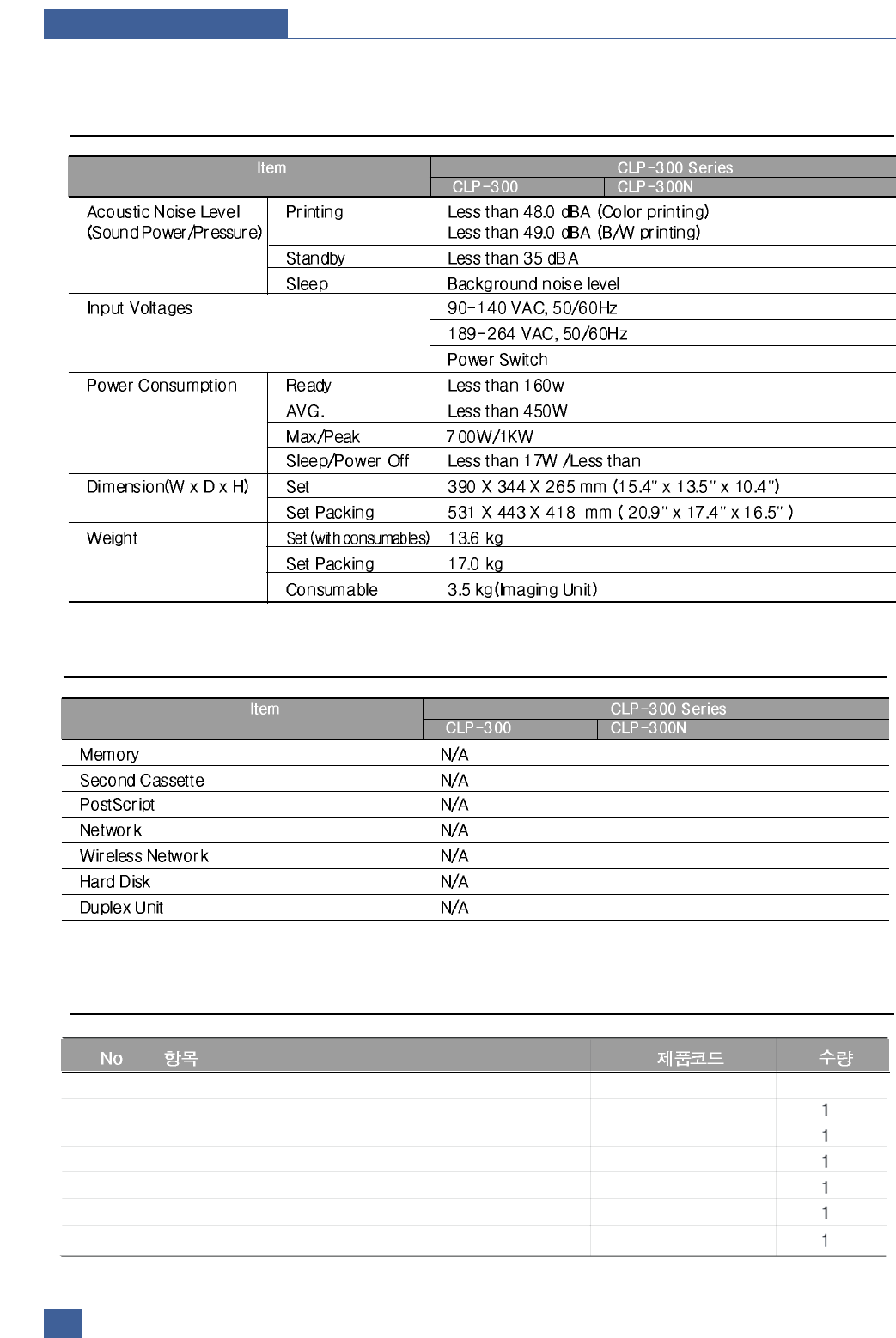
2.2 Specifications
Specifications are correct at the time of printing. Product specifications are subject to change without notice.
See below for product specifications.
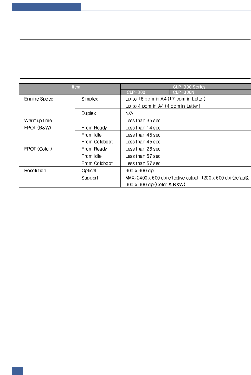
2.2.1 General Specifications
Product Specifications
Samsung Electronics Service Manual
2-3
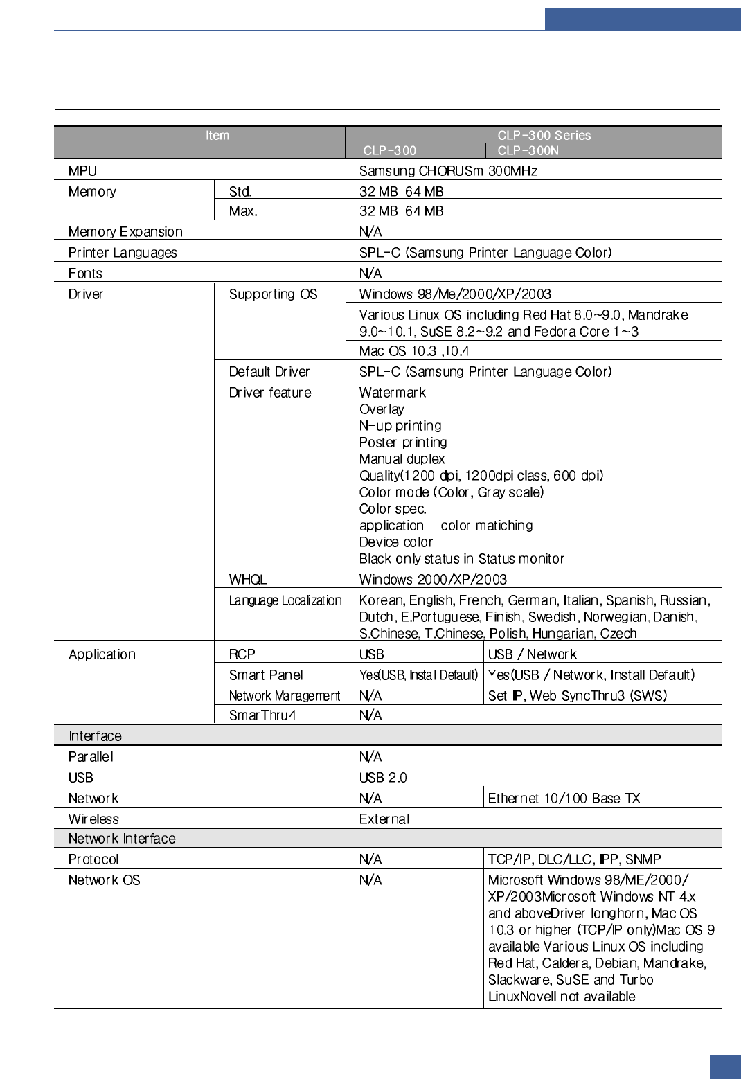
2.2.2 Controller & S/W
∫∞
Samsung Electronics
Service Manual
Product Specifications
2-4
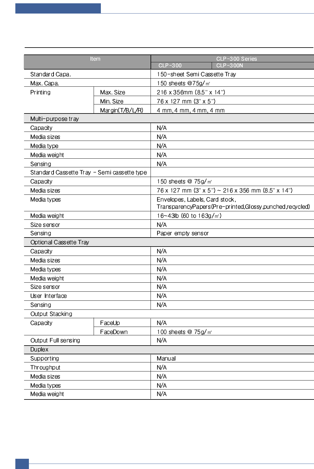
2.2.3 Paper Handling
Product Specifications
Samsung Electronics Service Manual
2-5
2.2.4 Consumables
CRU
No. of CRUs 6 (C/M/Y/K toner, Imaging Unit, Waste toner container)
K toner cartridge: CLP-K300A
C toner cartridge: CLP-C300A
M toner cartridge: CLP-M300A
Y toner cartridge: CLP-Y300A
Imaging unit : CLP-R300A
Waste toner container: CLP-W300A
TonerBlack : Initial : 1,500 (Sales : 2,000) A4/Letter pages,
at ISO 19752 Standard Coverage,Semi glossy
Color Initial : 700 (Sales : 1,000) A4/Letter pages,
at ISO 19752 Standard Coverage Semi glossy
Key Unique, Electronic key(CRUM)
Life detectSensor (Y)Remain % (90% : warning,100%: empty,
120% : hardstop)
Imaging Kit(OPC+Deve) Yield Approx. 20K black pages (or 12.5K color pages)
Key Unique, Electronic key(CRUM)
Sensor None, that would be traced via software
Replace method 6 steps for install/replacing
Waste Toner ContainerYield1,250 sheets (Full Color Std. Image) or 5,000 images, Full Sensor
Key N/A
FRU
No. of FRUs 4 (ITB, Fuser, T2 roller, Pick-up roller)
ITBYieldApprox. 60K black pages (or 15K color pages)
Key None
Sensor None
Fuser Yield 100,000 sheets B&W or 50,000 sheets Color
Key None
T2 Roller Yield 100,000 sheets, Replacable
Key None
Pick-up RollerYield50,000 sheets, Replacable
Key None
Samsung Electronics
Service Manual
Product Specifications
2-6
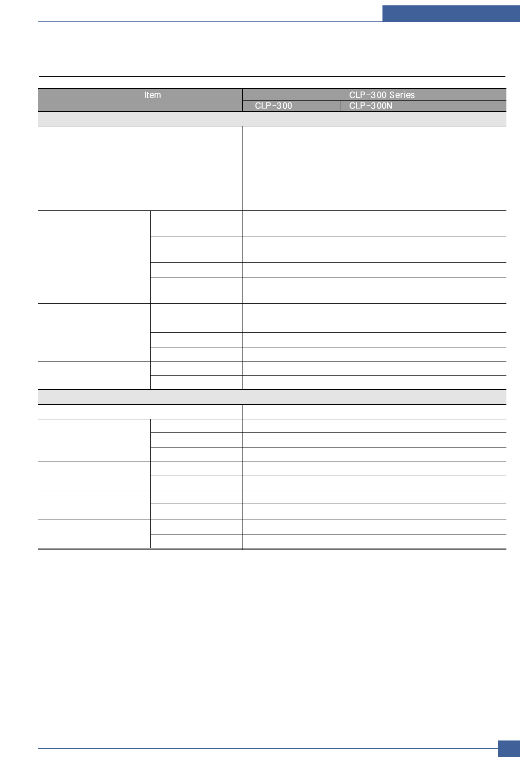
2.2.5 Environment
2.2.6 Options
2.2.7 Accessory
S/W APPLICATION-CD
INA-ACCESSORY
CBF-POWER CORD
BAG PE
S/W APPLICATION-CD
MANUAL-(CARD)WARRANTY CARD
LABEL(P)-BLANK 90*25
JC99-02015A
3903-000042
6902-000288
JC46-00257A
JC46-00313A
JC68-00690A
JC68-01584A
-
Product Specifications
Samsung Electronics Service Manual
2-7
2.3 Model Comparison Table
System Overview
Samsung Electronics Service Manual
3-1
3
3
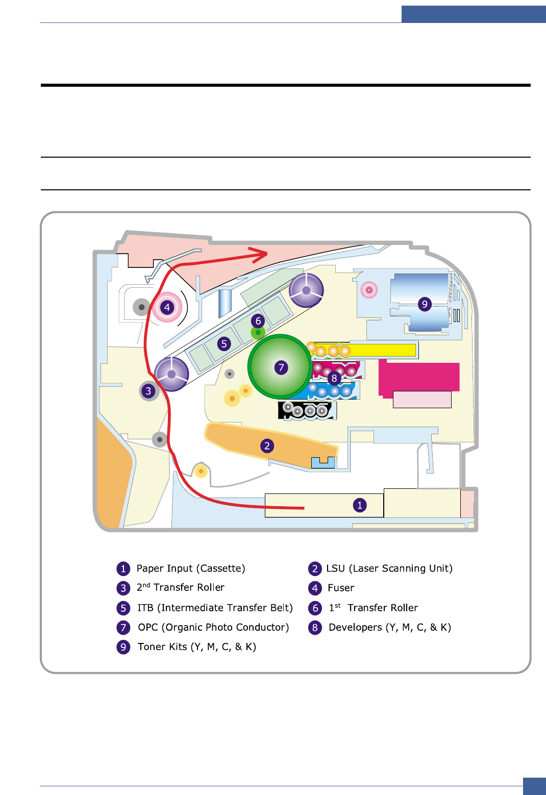
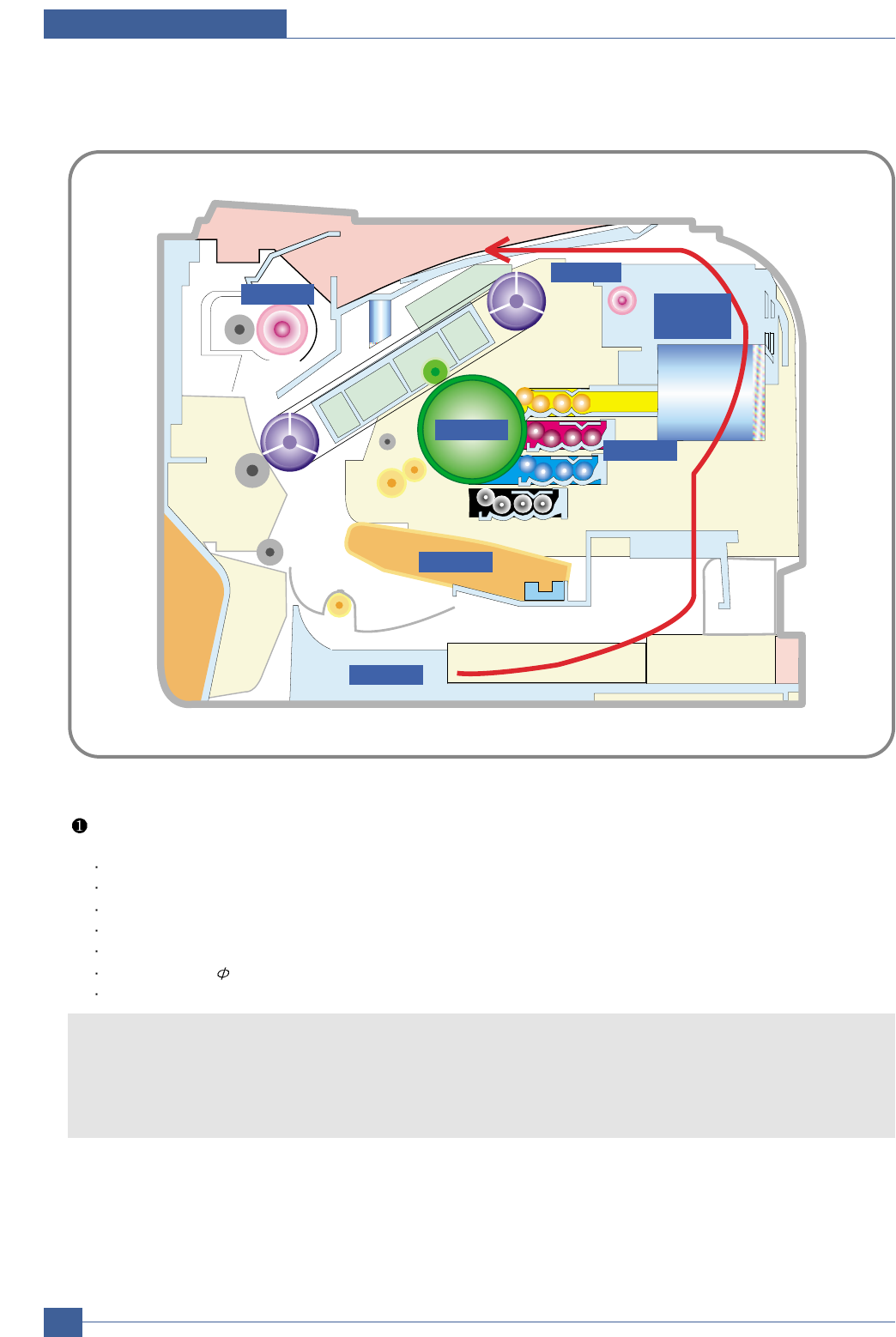
3. System Overview
This chapter describes the functions and operating principles of the main components.
3.1 System Structure
3.1.1 Main Parts of System

Samsung Electronics
Service Manual
System Overview
3-2
Cassette
Feeding Method : Cassette Type
Feeding Standard : Center Loading
Feeding Capacity : Cassette 150 Sheets(75g/ , 20lb Paper Standard)
No Manual Feeder
Paper Detecting Sensor : Photo Sensor (Empty, Registration, Exit)
Paper Size Sensor : None
LSU(Laser Scan Unit)
Consisted of LD(Laser Diode) and Polygon Motor Control.
2nd Transfer Ass y
The life span: Print over 100,000 sheets (in 15~30 )
Specification: Similar to CLP-500 Series
Fuser Ass y
Heat Lamp : New Part - Knuckle Type
Heat Roller : Similar to CLP-500 Series
2 Pressure Roller : One is similar to HummingBird, the Other is a new added part comparing with
other Fuser
Thermistor - Temperature-Measuring Device
Thermostat - Critical Temperature-Detecting Device
&ITB(Intermediate Transfer Belt) & 1st Transfer Roller
The life span: Print over 100,000 Images
The ITB unit includes 1st Transfer Roller
&OPC(Organic Photo-Conductor) & Developer
The life span: Print over 44,000 Images (Both)
Imagine Unit consists of 4 kinds of Developer , OPC, and Deve. Main Frame
Toner Kits
The life span: Color -> Initial 700 / Sales 1,000 images (ISO 19752 Standard Coverage Print-Out)
Black -> Initial 1,000 / Sales 2,000images (ISO 19752 Standard Coverage Print-Out)
Driver Ass y
It is a power delivery unit by gearing
By driving the motor, it supplies the power to the feeding unit, the fusing unit, and the distributing unit.
The Main Motor is similar to CLP-500 Series Main Motor.
Error Phenomenon
Polygon Motor Error The Rotation of Polygon Motor can not reach stable
Hsync Error Though the rotation of Polygon Motor reach stable, the sig-
nal of Hsync is not occurred
System Overview
Samsung Electronics Service Manual
3-3
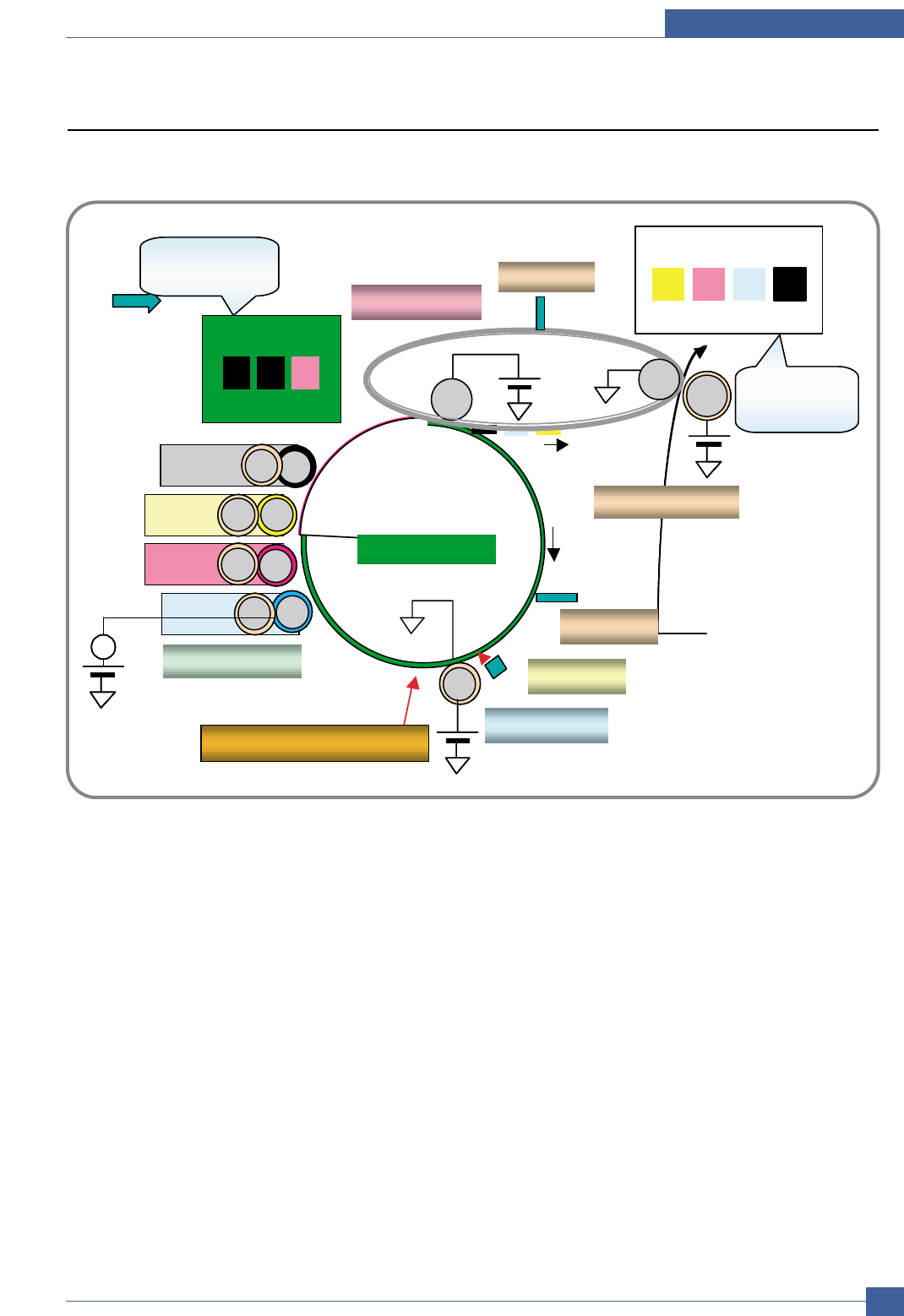
3.1.2 EP Process
- Structure of EP Process
Charger
Developer
Laser Scanning Unit
OPC
ITB Unit
Eraser
Blade
Blade
Media Path
P2: Image
on Media
P1: Image
on OPC
~
Charger
Developer
Laser Scanning Unit
OPC
ITB Unit
Eraser
Blade
Blade
Media Path
P2: Image
on Media
P1: Image
on OPC
~~
Samsung Electronics
Service Manual
System Overview
3-4
- System Outline
Paper path
Exit
Fuser
ITB
OPC
LSU
Cassette
Toner
Cartridge
Dev-YDev-Y
Dev-MDev-M
Dev-CDev-C
Dev-KDev-K
Dev-Y
Dev-M
Dev-C
Dev-K
Charging
Conductive Roller charging
Roller resistivity : ~ 10^5 ohm-cm
Applied voltage : -1.1kV
Charge acceptance : -520V
OPC coating thickness : 21um
OPC diameter : 60mm
Non eraser system
1. Organic Photoconductor is charged to uniform voltage by conductive roll charging method
2. No ozone is produced because corona is not used
3. Charger roll is cleaned with cleaning roll
4. Toner remained on OPC after T1 process is cleaned by cleaning blade and retrieved into waste toner
box by auger and belt driving mechanism

System Overview
Samsung Electronics Service Manual
3-5
Exposing
One polygon motor ( 6 facet )
Single beam LD (1ea)
LD wavelength : 785nm
Polygon motor rpm : 23747.5
LSU energy : 0.25uJ/cm^2
OPC exposed potential : -50V
1. Exposing is implemented by laser striking on to OPC with uniform potential
2. Laser beam is modulated according to image to be printed that is from PC
3. Latent Image is formed on OPC, which is developed with toner
Developing
Non-magnetic, mono component
Non-contact development
Developing bias : DC + AC
AC peak to peak : 1.5 ~ 2.0kV
Mass on developing roller : 550 ~ 600ug/cm^2
Toner coulomb : 15 ~ 20uC/g
Roller diameter : 10mm
Roller resistivity : 10^5 ~ 10^6 ohm-cm
Process speed ratio : 1.2 (OPC=1.0)
Color order : Y -> M -> C -> K
1. Only latent image formed by exposing process is developed with toner
2. AC + DC Voltage is being used to develop toner into latent image on OPC because non-contact
developing method is adopted
3. Y, M, C, and K Images are sequentially developed onto OPC and transferred onto Intermediate
Transfer Belt (hereafter ITB) to form a color image on ITB
4. Toner Bottles are used to supply toner into developer compartment
5. Toner level is being sensed to control toner supply from toner bottle to developer
Transfer 1
Multi-pass transfer
Indirect transfer
Transfer voltage : 0.5 ~ 2.0kV (controllable)
Roller diameter : 14mm
Roller resistivity : ~ 10^7 ohm-cm
Belt resistivity : 10^9 ~ 10^11 ohm-cm
Environment sensing by Y-transfer roller
Transfer unit life : 50K images
1. Developed Image on OPC is transferred onto ITB by T1 Process
2. T1 Voltage is positive which attract toner to ITB
3. 4 times of T1 process is required to make a color image on ITB, which means multi-pass process
4. ITB has a hole as a fiducial mark for timing. Engine control for color image is synchronous with it,
ITB Home Sensing Signal

Samsung Electronics
Service Manual
System Overview
3-6
Transfer 2
Indirect transfer
Transfer voltage : 1 ~ 4.0kV (controllable)
Roller diameter : 18.6mm
Roller resistivity : ~ 10^7 ohm-cm
Belt resistivity : 10^9 ~ 10^11 ohm-cm
Transfer unit life : 50 K images
1. Color image formed on ITB is transferred onto media by T2 process
2. T2 voltage is also positive to get color image moved onto media
3. Toner remained on ITB after T2 process is cleaning by ITB cleaning blade and collected and
4. Transported and retrieved into waste toner box by auger and belt driving system
5. T2 Roll is engaged when color image is being transferred onto media. Otherwise it is disengaged. Clutch is used
for driving T2 Roll engagement and disengagement
Fusing
3 Roll system
-> short warm-up time (45sec)
Post Pressure Roll
1. Color Image on media is melted down and fixed into media by fusing process
System Overview
Samsung Electronics Service Manual
3-7
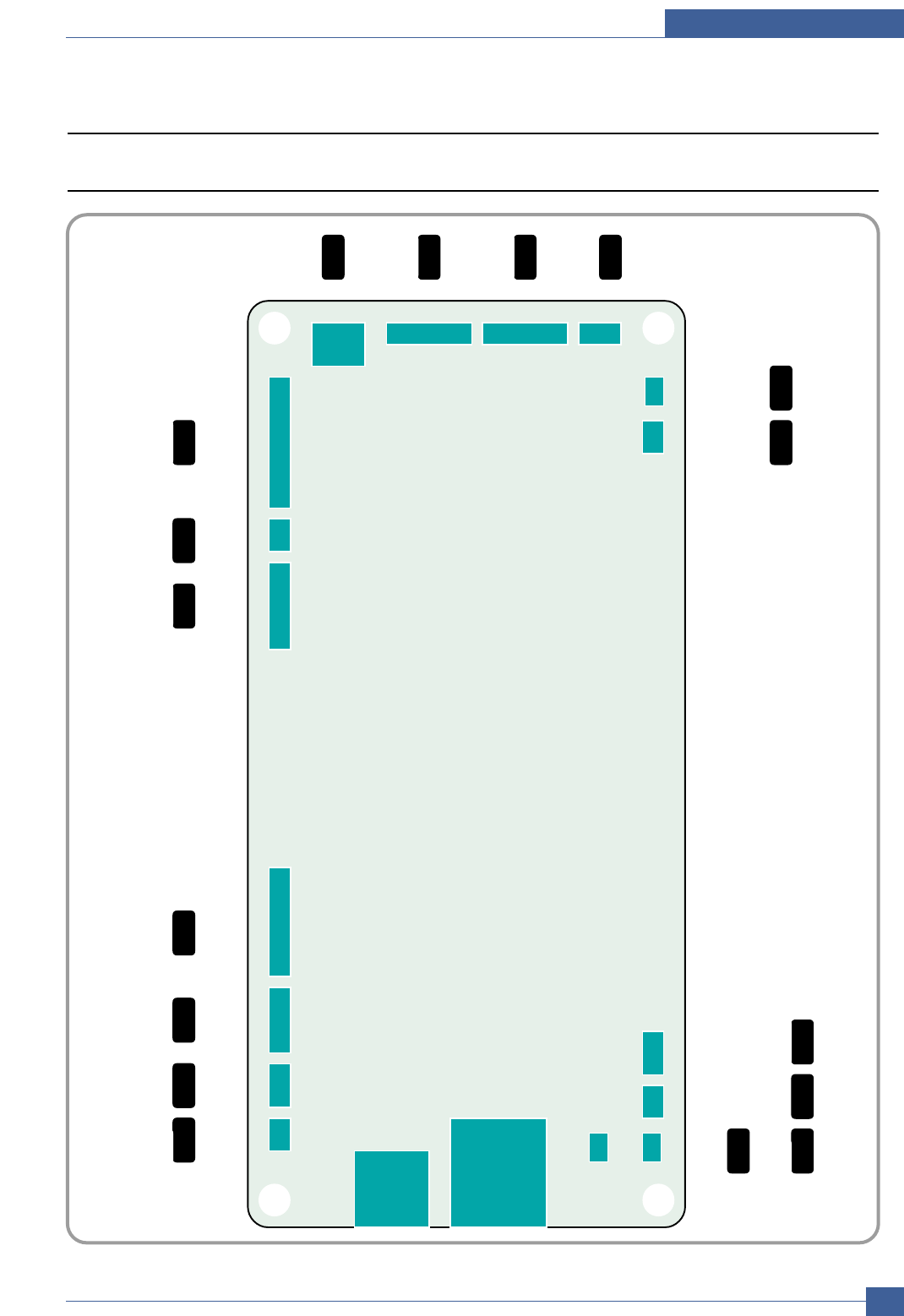
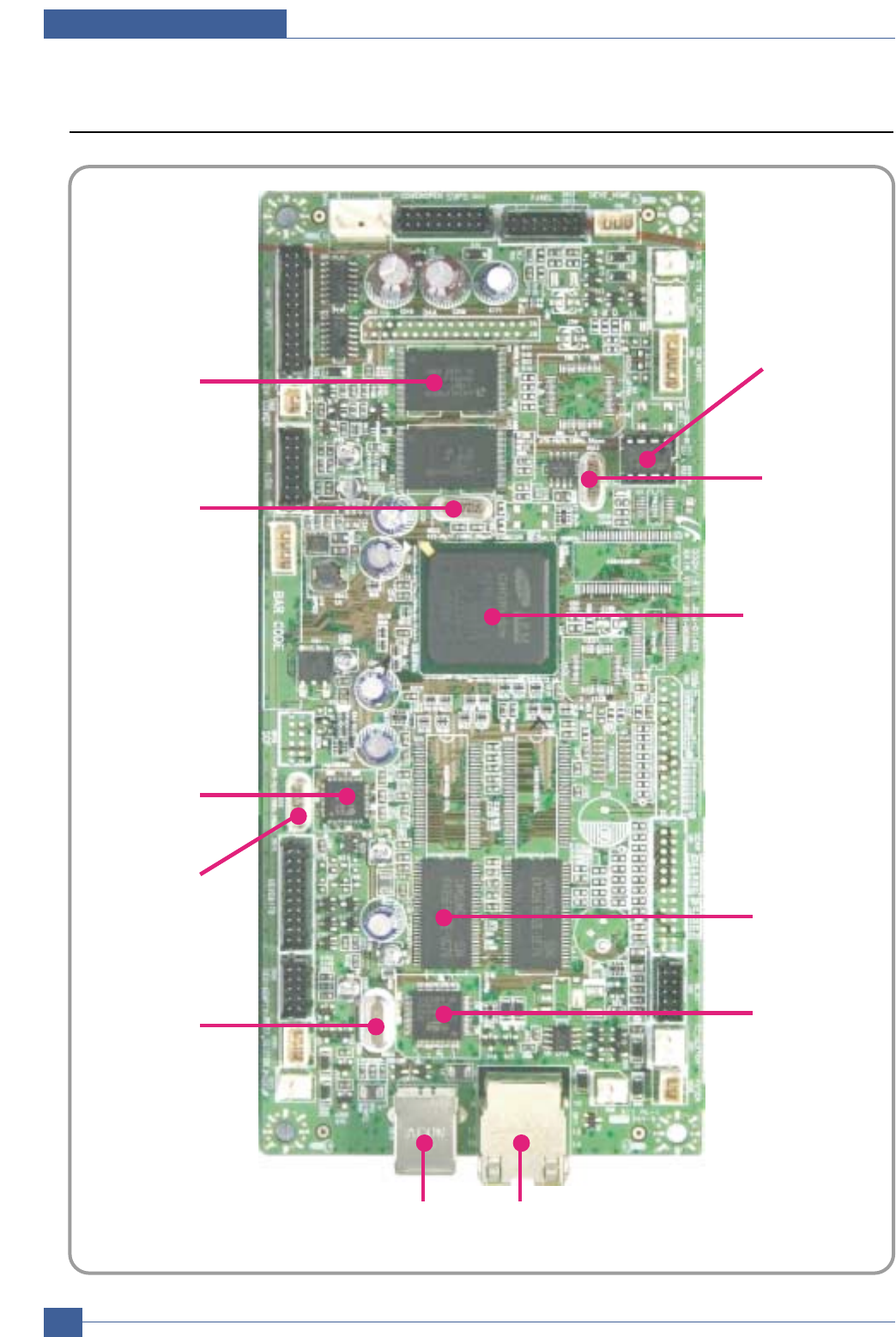
3.2 Main PBA Description
3.2.1 Main Controller PBA
CN4 CN10
CN2 CN7 CN28
CN20 CN24 CN25CN19
USB
RJ45
CN8
CN20 CN24
CN16
CN19
CN15
CN13
CN5
DEVE_
HOME
DEV_
SOL
ITB_
CLUTCH
PANEL
SMPS
COVER
OPEN
HVPS 5V
SWITCH
LSU DEVE&
ITB
REG&
EMPTY
REGI
CLUTCH
PICKUP
BLDC T2_
CLUTCH
FUSER
FUSER
CLUTCH
Samsung Electronics
Service Manual
System Overview
3-8
3.2.2 Main PBA
USB2.0
Device
CHORUSm
Main Control
SoC
USB
Connector
RJ45
SDRAM
Network
Physical Chip
EEPROM
64Kbit
Flash
Memory
OSC5
12MHz
OSC2
12MHz
OSC6
12MHz
OSC4
25MHz
USB2.0
Device
CHORUSm
Main Control
SoC
USB
Connector
RJ45
SDRAM
Network
Physical Chip
EEPROM
64Kbit
Flash
Memory
OSC5
12MHz
OSC2
12MHz
OSC6
12MHz
OSC4
25MHz
System Overview
Samsung Electronics Service Manual
3-9
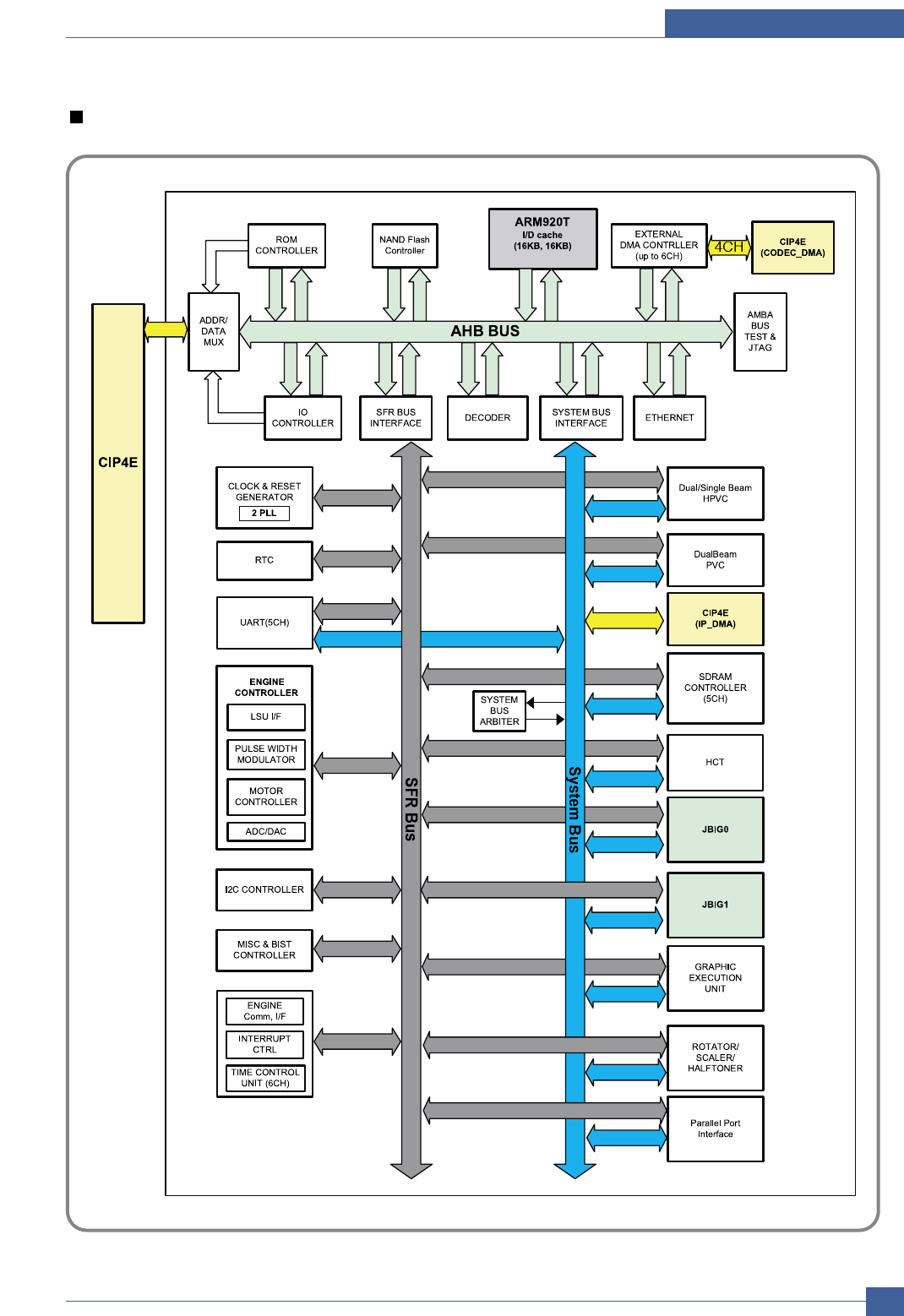
1) CHORUSm
CHORUSm involves in itself the functions to control ARM Processor Core and various H/W devices. CHORUSm,
therefore, controls Main PBA and all engine mechanism, processing the print job received from host and enabling the
engine to print image.
Function
Process
0.13um Technology
Package
496 PBGA
CPU Core
ARM 920T - 300MHz
Cache : I-Cache 16KB, D-Cache 16KB
System Bus
32-bit width, 100MHz
SDRAM Controller
32-bit width, 100MHz operation
5 Banks, Up to 128MB Address space per Bank
Programmable Timing to Control SDRAM A.C Characteristics
Support Self Refresh for Data Retention
ROM Controller
32-bit width, 4 Banks, Up to 16MB Address space per Bank
Burst Capability
Programmable Timing per Bank
3.2.3 Main PBA Description

Samsung Electronics
Service Manual
System Overview
3-10
IO Controller
6 Channels, Up to 16MB Address space per Bank
Programmable Timing per Bank
DMA Controller
6 Channels General Purpose DMA
HPVC Controller
Hyper Printer Video Controller
High Performance DMA-based Interface to Printer Engine
Support Dual/Single Beam LSU, LVDS Video Output
Support A3, 1200dpi
UART Controller
5 Channels Indepenent Full Duplex UART
Interrupt Controller
Support 6 External Interrupts
Support 26 Internal Interrupts
Timer Controller
6 System Timers and Watch Dog Timer for S/W Trap
Scanner Controller
300/400/600/1200dpi CIS/CCD Interface
Color/Mono grey image, Binary image scan support
600dpi Color/Mono Copy support
Image Processing for High-End MFP,Digital Copier
MH/MR/MMR CODEC for Fax
Scan image : A4 1200dpi processing
Copy image : A4 600dpi processing
MAC Controller
10/100Mbps
Full IEEE 802.3 compatibility
PPI Controller
IEEE1284 compliant parallel port interface
DMA-Based or Interrupt-Based operation
GEU Controller
Graphic Engine Unit for Banding support of Printer Language
Scan Line Buffer, Polygon Filling
CODEC Controller
2 Channels JBIG Encoding and Decoding
I2C Controller
1 Channel, Operated at max frequency 400kHz
RTC Controller
Engine Controller
LSU Control and Interface Unit
2 Channels STEP Motor Control Unit
8 Channels PWM Control Unit
8 Channels ADC Control Unit
2 Channels DAC Control Unit
System Overview
Samsung Electronics Service Manual
3-11
CHORUSm (Internal Block Diagram)

Samsung Electronics
Service Manual
System Overview
3-12
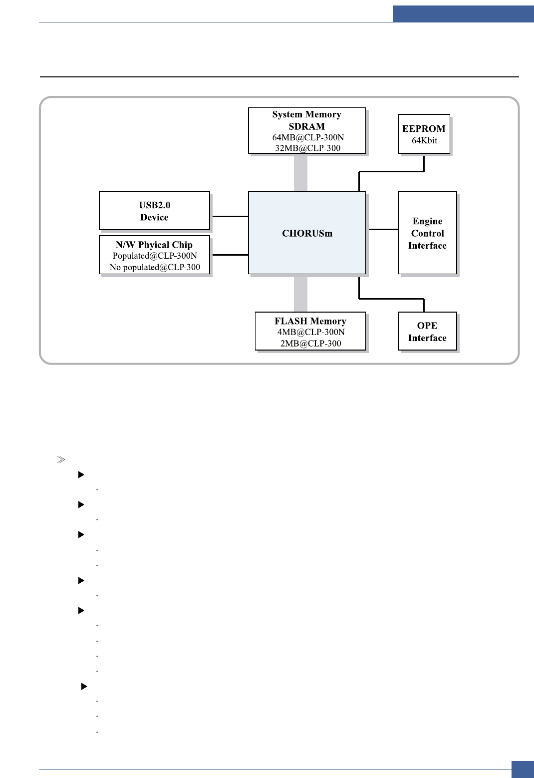
2) System Memory Block
Memory saves program and video data and print jobs received from host. Its volume is 64MB with network function
and 32MB without network function. It has no separate device for extension. SDRAM is used, driven at width of 32-bit
and 100MHz, and controlled by memory controller built in CHORUSm.
3) Flash Memory Block
Flash memory is the space used for saving program. Its volume is 4MB with network function and 2MB without net-
work function. It has no separate device for extension. NOR type flash memory is used and accessed at 32-bit width
burst, being controlled by the ROM controller built in CHORUSm.
4) USB2.0 Device Block
This block supports USB2.0 high speed (480Mbps). ISP1582 of Philips company is used and connected to the IO
Bus of CHORUSm at 16-bit, controlled by IO controller built in CHORUSm. Through this I/O port it receives print job
from host.
5) Network Block
This block has 10/100Mbps wired network function and is controlled by MAC controller built in CHORUSm. It is con-
nected to host through physical layer chip outside, and thus receives print job from host. STE100P is used for physi-
cal layer chip.
6) EEPROM Block
System EEPROM is controlled by the I2C controller built in CHORUSm, connected to the other non-volatile memory
on I2C bus. It works at the speed of 400KHz. This system EEPROM contains all drive information and production
information necessary for the operation of printer. Its size is 16k-bit.
7) OPE Control
The panel is driven in the form of PIO by GPIO controller built in CHORUSm. OPE consists of one key and four
monochrome LED, and one dual LED.
8) LSU Control
Laser Scanning Unit is controlled by LSU controller built in CHORUSm. It makes use of all functions such as Polygon
Mirror Motor Control necessary for driving LSU and Synchronized Signal Generation Control, and helps to scan laser
beam on the photosensitive drum to form latent image.
9) BLDC Control
It is controlled by BLDC controller built in CHORUSm. It controls the drive of printer mechanism and helps it to be dri-
ven at an equal speed.
10) Sensors Control
GPIO controller built in CHORUSm collects the status of all sensors. According to this status of sensors, it controls
printer mechanism to help normal printing. There are sensors such as Paper Empty Sensor, Registration Sensor and
Developer Home Sensor, etc.

System Overview
Samsung Electronics Service Manual
3-13
11) Clutches Control
GPIO Controller built in CHORUSm controls all clutches, which help printer to do print job normally. There are clutch-
es such as Paper Pick-up Clutch, Registration Clutch, Developer Home Clutch, ITB Clutch, T2 Clutch, Fuser Clutch,
Developer Toner Supply Clutch, etc.
12) PWM Control
PWM Controller built in CHORUSm controls the parts that require PWM for normal printing, such as BLDC drive
speed and HVPS high voltage level, etc.
13) ADC Control
It is controlled by ADC Controller built in CHORUSm, and is used for perception of charged voltage and current, 1st
and 2nd transfer voltage and current, fusing temperature, used-up toner and toner amount, and interior temperature,
etc.
14) DAC Control
It is controlled by DAC Controller built in CHORUSm and used to set standard level of light amount of LSU Laser
Diode.
Samsung Electronics
Service Manual
System Overview
3-14
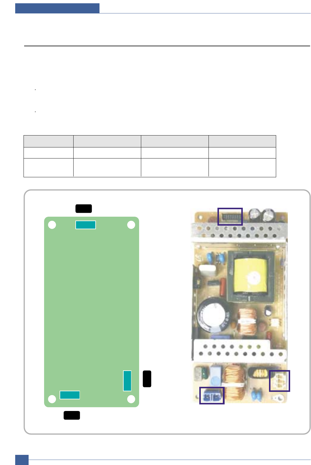
3.2.4 SMPS(Switching Mode Power Supply) PBA
SMPS is consisted of SMPS part which supplies DC power for driving system and AC Heat Control part which supplies
power to Fuser. Standard TYPE III is used.
1) DC Output
Main Controller PBA, OP Panel, BLDC, Sensors, Clutches, Other PBAs
2) AC Output
Fuser Unit(Heat Lamp, Thermostat)
3) Output Voltage
CON2
To Main PBA
CON1
CON3
AC Input
Fuser AC
CHANNEL +5.0V +24V +24VF
V_out +5.0V +/-5% +24.0V +15%/-10% +24.0V +15%/-10%
Load MicroController, LSU MOTOR, CLUTCH,
CMOS, LOGIC HVPS
System Overview
Samsung Electronics Service Manual
3-15
3.2.5 HVPS(High Voltage Power Supply) PBA
HVPS PBA generates high voltage of charger, supply, T1 and T2 which is supplied to Developer, ensuring optimum con-
dition for image formation. HVPS receives input of 24V and generates high voltage, supplying it to Toner, OPC,
Cartridge, ITB Unit and Transfer Roller.

Samsung Electronics
Service Manual
System Overview
3-16
1) Charger Voltage : Charger
Function: voltage that charges OPC surface up to ?500V~ -800V.
Output voltage: -1.0KV ~ -2.0KV DC 3%
Error type: if the voltage fails to be output to Charger Roll, OPC surface will not be charged, and the toner on the
developer roller will be transferred to OPC Drum, printing black paper.
2) 1st Transfer High Voltage : T1(+)
Function: voltage necessary for transferring toner developed on OPC Drum surface onto ITB.
Output voltage: Max +2.0KV 3%(Duty variable, no load)
ERROR type: if T1(+) output fails, the toner on OPC drum will not be transferred to ITB normally and the image will
be blurred.
3) 2nd Transfer High Voltage : T2(+)
Function: voltage used to transfer the toner primarily transferred on ITB again onto paper.
Output voltage: Max +5.0KV 3%(Duty variable, no load)
ERROR type: if T2(+) output fails, the toner on ITB will not be transferred to paper normally and the image will be
blurred.
4) T2 Cleaning Voltage : Clean : T2(-)
Function: prevent reverse side of paper from being dirtied, by recovering the negatively charged toner remaining at
Transfer Roller and sending it onto ITB.
Output voltage: with no feedback control, output fixed voltage(-1300V +/- 15%)
ERROR type: reverse side of paper will be dirtied.
5) Supplying Voltage : Supply AC+DC(-)
Function: voltage that makes toner to develop on the area exposed by LSU by means of potential difference, output
will be the voltage of AC+DC overlapped form.
Output voltage: AC 600V ~ 2000V p-p +/-1.5%
DC -50V ~ -600V DC +/- 3%
ERROR type: 1. if supply is GND, density will be extremely low.
2. if supply is floating (for insecure terminal contact), density will be down so slightly that it is impossible
to make out with naked eyes.
6) Developing Voltage : Deve AC+DC(-)
Function: voltage that supplies toner to Developing Roller
Output voltage: AC 300V ~ 1700Vp-p 1.5% (supply voltage is connected to ZENER Diode 300V)
DC -50V ~ -600V DC +/- 3%
ERROR type: 1. if Deve is GND, density will be extremely down.
2. if Deve is floating (for insecure terminal contact), density will be extremely down.
System Overview
Samsung Electronics Service Manual
3-17
3.3 CRUM
In the case of Refill Toner Install
1) Perception of Refill Cartridge (when power is on or the cover is closed)
End of Life / life span data initialization -> judge to be Refill Cartridge
End of Life / life exhausted (simple refill) -> stop printing caused by life exhaustion
2) Operating
It is impossible to control appropriate development parameters, for there s no toner specification data.
It runs with the setting of default development parameter. (Image quality will be degraded, for the lack of appropriate
respond to the change of time and environment.)
3) Service Response
It is possible to response appropriately, for the information of cartridge life is saved at Back Up Area.
Process after CRU life expiration
1) Record the information of End of Life.
2) Copy the information of Operating Area into Back up Area.
3) Write-Protect Back up Area.
4) Clear some information of Operation Area.
-> Supplier/Model Name/MFC date/Serial Number (Manufacture Information)
-> Let cartridge refiller initialize manufacture information and life span information.
Samsung Electronics
Service Manual
System Overview
3-18
CRUM Position
Cap
Agitator
Washer
Bottle
Agitator
Seal
CRUM
Coupling
Cap- CRUM

System Overview
Samsung Electronics Service Manual
3-19
3.4 General Description
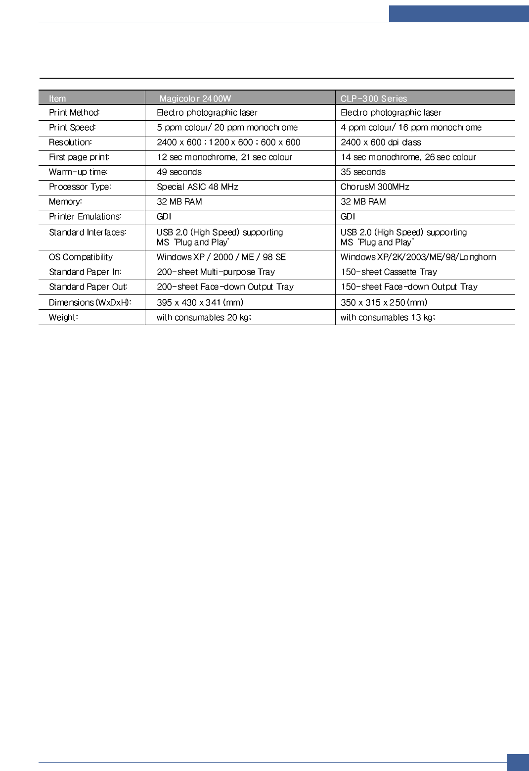
This chapter is the product specification for the CLP-300 Series. The CLP-300 Series is a Color Laser Printer. The CLP-
300 Series series can be expanded to multi functional printer (MFP). CLP-300 Series is developed for two target users.
Those are small office users who sometimes need color printouts, and medium business users who mainly use B/W
printouts. The main product concept is “the world smallest and lightest color laser printer”. This model has 16ppm B/W
print-speed and 4ppm color print-speed, 2400 x 600 dpi class (optical 600 x 600 dpi) color laser printer.
3.4.1 Controller
-The video controller board is located on the right side of the printer.
-Basic Memory is 32 Mbytes SDRAM.
-Field F/W upgradeable FLASH ROM firmware for controller, 1024 byte EEPROM
-Printing Resolution :
Native 600 x 600 dpi standard
Resolution can be enhanced up to 2400 x 600 dpi class, 1200 x 600 dpi (default), 600 x 600 dpi
3.4.2 Processor
CHORUSm (300Mhz), Proprietary SOC
3.4.3 Printer Language Emulations
SPL-Color
3.4.4 Memory
The controller has 32 MB SDRAM and 4 MB flash ROM on Board.
Samsung Electronics
Service Manual
System Overview
3-20
3.4.5 Interfaces
The system supports the following standard interfaces:
One USB port
- USB v.2.0 compliant
- Color-coded to meet WHQL requirements, connector must be Pantone 426C
One 10/100 BaseT network connector
- The printer supports an internal Network Interface that can be installed pre-configured on the video
controller board at the factory. This supports all of the major Network Operating Systems such as the Novell
NetWare, TCP/IP, etc. Details of the network specification will be provided separately.
3.4.6 Control Panel
No LCD, 2 keys and 6LEDs
3.4.7 Periodic Replacing Parts
Samsung shall specify parts requiring replacement and the frequency of replacement. The parts identified may be
deemed customer replaceable parts. Periodic replacement parts shall be recommended as follows
* Average A4-/letter-sized page count based on ISO 19752 Standard coverage of individual colors on each page. Usage
conditions and print patterns may cause results to vary.
** Image counts based on one color on each page. If you print documents in full color (Cyan, Magenta, Yellow, Black), the life
of this item will be reduced by 25%.
Item(s) Pages Printed Part number Remark
Black toner cartridge Approx. Initial : 1,500 pages*CLP-K300A User
Sales : 2,000 pages*Replacement
Color toner cartridge Approx. Initial : 700 pages*CLP-C300A:Cyan
Sales : 1,000 pages*CLP-M300A:Magenta
CLP-Y300A:Yellow
Imaging unit Approx. 20,000 black pages or approx. CLP-R300A
12,500 color pages
Waste toner Approx. 5,000 images** or Approx. CLP-W300A
container1,250 pages (fulll color standard image)
Pick-up roller Approx. 50,000 pages Contact a service Engineer
Fuser unit Approx. 100,000 black pages representative Replacement
or 50,000 color pages
T2 roller Approx. 100,000 pages
ITB Approx. 60,000 black pages
or 15,000 color pages
System Overview
Samsung Electronics Service Manual
3-21
3.4.10 Sensor
Paper empty (Cassette)
3.4.11 CRUMS
The CLP-300 Series engine will be equipped with electronics that can read and write data into NVRAMs otherwise
known as CRUMs that reside within 1) C, M, Y, K Toner cartridges and 2) Imaging kit(Developer, OPC, ITB). The CRUM
has a company ID, and Samsunga electronics logo.
The toner CRUM also identifies the type of toner cartridge (Standard or High Capacity). The CRUMs contain fixed data
such as the low warning point, specified life point, and hard stop point (on toner, not on IBT unit) and also store the cur-
rent life count (pages count, pixels count, images count) and % of usage (gas gauge) data.
3.4.12 LOW / OUT Behavior for consumables
The consumable low and out behavior on CLP-300 Series engine is specified by SEC.
FP Device for life end Law(90%) Life(100%) Hard stop Reset to 0
message detection
Toner CRUM Yes Yes Yes(115%) No
Imaging Kit CRUM Yes Yes No No
Fuser No Yes Yes No Yes
T2 Roller No Yes Yes No Yes
Pick-up No No No No No
3.4.8 Power Switch
The Switch is located at rear-side of printer and must be marked to indicate on and off.
3.4.9 Operator Panel
LCD: None
KEY: 2 keys (Stop, Black only)
LED: 6 LEDs (C, M, Y, K Toner, Status, Black only)

S/W Structure and Descriptions
Samsung Electronics Service Manual
4-1
4
4
4. S/W Structure and Descriptions
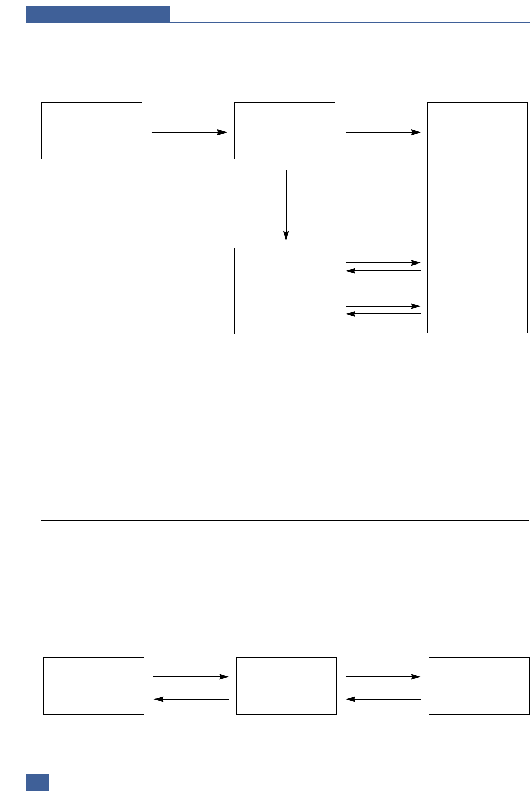
4.1 Architecture
The belt CRUM interface board is a transmission belt CRUM interface board of the photoelectric Dry Color Laser
Printer, mounted on the printer body, making it possible to physically combine the body and the belt CRUM board.
4.2 Language Monitor
Language Monitor is a part of the Printer Driver and the Windows Spool System. The main roll of the Language
Monitor is that sends a job start message to the Status Monitor. Therefore the Status Monitor
can start polling to get the printer status.
The second roll is that sends the job information such as User ID and Job ID to the Status Monitor and the Printer
F/W. Hence the Status Monitor can stop polling because the Printer F/W informs the Status Monitor that printing
job is complete.
4.3 Status Monitor
Status Monitor has no user interface. It shows only HTML help when any error occurs during printing jobs.
Printer Driver
Language Monitor
Status Monitor
Printer F/W Network Card F/W
Samsung Electronics
Service Manual
S/W Structure and Descriptions
4-2
4.4 Network Interface
After polling is started, Status Monitor has to know when it stops the polling. For this reason, the Network
Printer Server should inform of completing job when the printing job is finished.
When Status Monitor requests a job status, the Printer Server returns the job table that contains user id, job
id, and job status (printing or complete or canceled).
4.5 Printer Driver <-> Status Monitor
The Printer Driver and the Status Monitor can set/get some data to the system registry to share the Status Monitor
information such as the polling interval.
When the user wants to set the option of the Status Monitor manually, he or she can set it using the Printer Driver
User Interface. So, if the user set option that the Status Monitor is disabled, the Status Monitor can’s show HTML
Help to the user although the error has occurred while printing.
Printer Driver Language
Monitor
Printer Server
(Kernel / NPC)
Job ID
Status Monitor
Status Monitor Data Flow
User ID + Job ID
+
Printer Data
SNMP
Request Printer Status
Printer Status
Request Job Status
Job Table
Printer Server
(Kernel / NPC)
Printer Name
Port Name
User ID
Job ID
Printer Server IP Addr
Printer Data
Status Monitor Printer Driver
System
Registry
Set last error status
Get option value
enable/disable
or
polling interval
Get last error status
Set option value
enable/disable
or
polling interval
S/W Structure and Descriptions
Samsung Electronics Service Manual
4-3
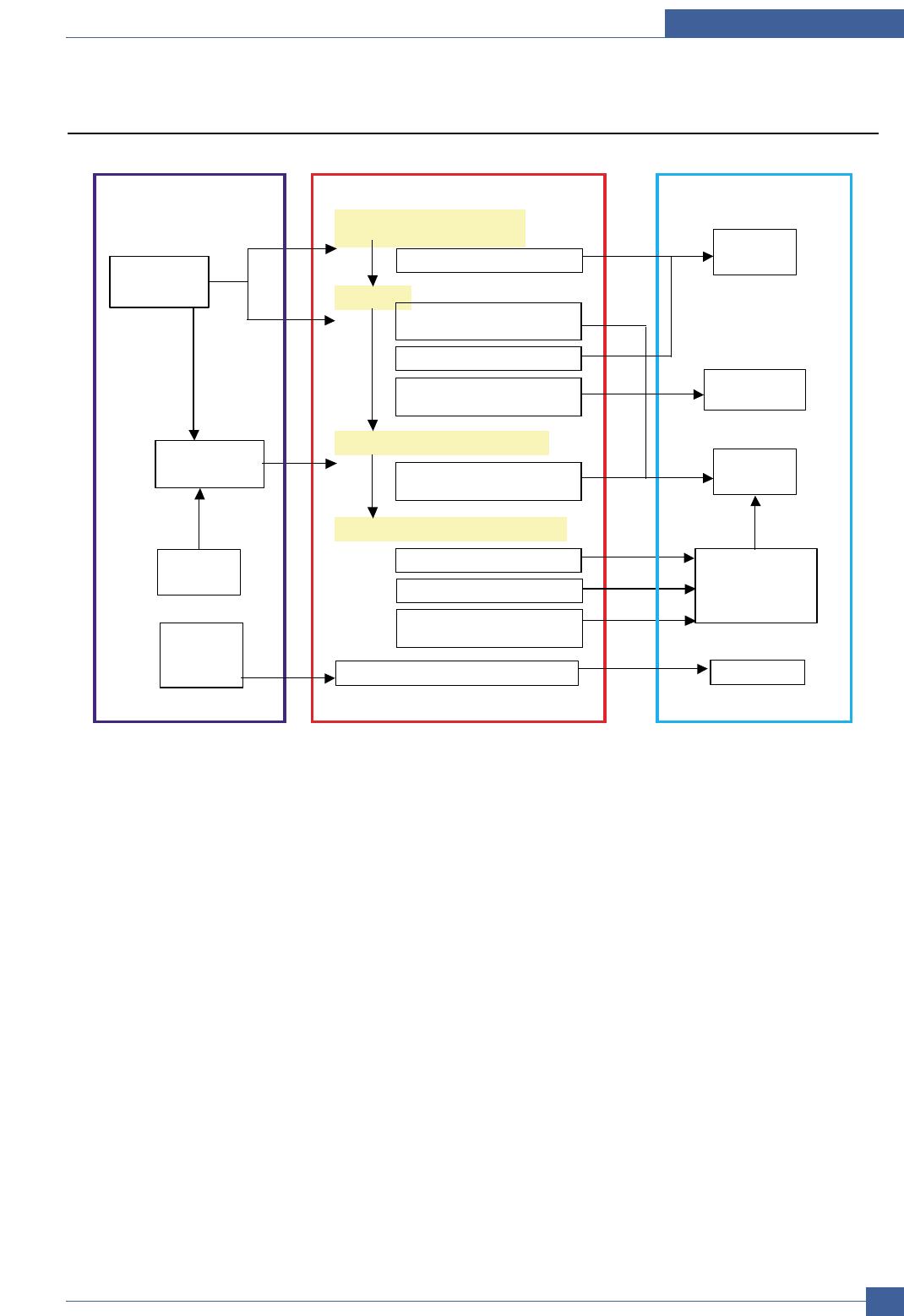
Input Process Output
Photo Sensor ( intensity
of radiation )
LED PWM Output
density
LED PWM decision
Comparator Threshold
voltage PWM decision
Color Registration measure
Auto Color Registration
pattern printing
Color Registration adjustment
Page Sync. mo dify
Line Sync. mo dify
Video Clock Freq.
modify
Density pattern
printing
LSU temperature control
LED
LSU
Video signal
generator
P Sync.
L Sync.
clock
Video data
PWM
Comparator
PWM
SMPS Fan
PWM
Auto color
registration
sensor
LPEC2
ACR module
LSU
ADC
ACR data
H Sync.
LSU
temperat
ure
sensor ADC
4.6 System F/W Flow

Samsung Electronics
Service Manual
S/W Structure and Descriptions
4-4
4.7 Alarm Shortage
4.8 Error status
1. Missing/Invalid Consumables
Install Cyan (Magenta, Yellow, Black) Toner
Install Transfer Belt
Invalid Cyan (Magenta, Yellow, Black) Toner
Invalid Transfer Belt
2. Paper Empty/Mismatch
Paper Empty In MP(Tray1, Tray2)
Load A4 In MP(Tray1, Tray2)
3. Paper JAM
Jam 0 In MP(Tray1, Tray2)
Jam Inside Printer
Jam In Exit Area
4. Cover
Cover Open : Message toggles between
Cover Open and Install Transfer Belt
SCF Cove Open
5. Service Call : Unrecoverable Error
Engine LSU Error
Main Motor Error / Dev. Motor Error
Engine Fuser Over(Low) Heat Error
Rear Fan Error / Left Fan Error / SMPS Fan Error
6. Others
Memory Overflow Error
Ready IP Conflict
Toner (C,M,Y,K)
Transfer Belt
Fuser
Pickup Rollers
(MP/Tray1/Tray2)
90 ~ 100 %
Ready Yellow Toner Low
Replace Transfer Belt Soon
Replace Fuser Soon
100 ~ 110 %
Replace Yellow Toner
Replace Transfer Belt
Replace Fuser
Replace MP Pick-Roller
110 %~
Yellow Toner Empty
S/W Structure and Descriptions
Samsung Electronics Service Manual
4-5
4.9 CRUM Overview
- Stands for “Customer Replaceable Unit Monitor”
- EEPROM is used for CRUM Memory.
- CRUM stores various information on consumables
(including consumables’ life).
- In CLP600, total five CRUM’s are used
(four on toner cartridges and one on transfer belt)
CRUM stores the following information
Model Name
Supplier ID
Serial Number
Company ID
MFG Date
Capacity
Page Count
- Toner Cartridge and Transfer Belt
- Indicates how many pages are printed by using the consumable
Dot Count
- Toner Cartridge Only
- Indicates how many dots are printed by using the toner cartridge
4.10 FW Upgrade
Via USB or Network (SWS/SWAS)
You can upgrade F/W via USB or Network whenever the printer is “Ready”
Via Using F/W Download Mode :
Step 1) Power on while pressing the Online Key
Step 2) Press Online Key one more time if “Press Key Again” is displayed on LCD
Step 3) Download F/W via USB
Samsung Electronics
Service Manual
S/W Structure and Descriptions
4-6
4.11 Initailize Flow
S/W Structure and Descriptions
Samsung Electronics Service Manual
4-7

Disassembly and Reassembly
Samsung Electronics Service Manual
5-1
5
5
5. Disassembly and Reassembly
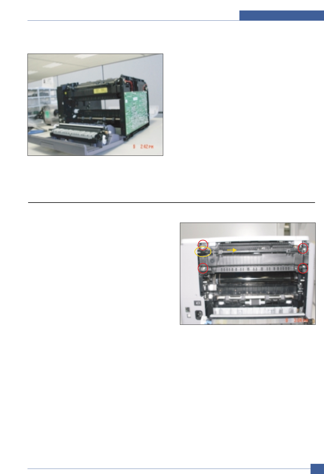
5.1 Precautions When Replacing Parts page(5-2)
5.1.1 Precautions when assembling and disassembling page(5-2)
5.1.2 Precautions when handling PBA page(5-2)
5.2 Parts for Maintenance and Repair page(5-3)
5.2.1 Replacement interval for parts with a limited life page(5-3)
5.2.2 Printer Cleaning page(5-4)
5.3 Information Related in Disassembly and Assembly page(5-5)
5.3.1 Special Service Parts page(5-5)
1) Disassemble of LSU Unit page(5-5)
2) Disassemble of ITB Unit page(5-5)
3) Custody of OPC Unit page(5-5)
4) Custody of Toner Cartridge page(5-5)
5) Disassemble of DEVE Drive Ass’y and Main Drive Ass’y page(5-5)
6) Disassemble of Terminal Parts page(5-5)
7) Disassemble of Fuser Unit page(5-5)
5.3.2 Screws Used in the Printer page(5-6)
5.3.3 Opening Covers and replacing Consumable parts page(5-10)
>> Consumable parts removal page(5-10)
5.4 Disassembly Procedure page(5-10)
5.4.1 Cover Unit page(5-10)
5.4.2 Fuser Ass’ypage(5-11)
5.4.3 LSU(Laser Scan Unit) page(5-12)
5.4.4 HVPS(High Voltage Power Supply page(5-12)
5.4.5 Main Board page(5-13)
5.4.6 SMPS(Switching Mode Power Supply) page(5-13)
5.4.7 Drive Ass’ypage(5-14)
5.4.8 Transfer Roller page(5-14)

Samsung Electronics
Service Manual
Disassembly and Reassembly
5-2
5.1.1 Precautions when assembling and disassembling
* Use only approved Samsung spare parts. Ensure that part number, product name, any voltage, current or
temperature rating are correct. Failure to do so could result in damage to the machine, circuit overload,
fire or electric shock.
* Do not make any unauthorized changes or additions to the printer, these could cause the printer to mal-
function and create electric shock or fire hazards.
* Take care when dismantling the unit to note where each screw goes. There are 19 different screws. Use of
the wrong screw could lead to system failure, short circuit or electric shock.
* Do not disassemble the LSU unit. Once it is disassembled dust is admitted to the mirror chamber and will
seriously degrade print quality. There are no serviceable parts inside.
* Regularly check the condition of the power cord, plug and socket. Bad contacts could lead to overheating
and firfe. Damaged cables could lead to electric shock or unit malfunction.
5.1.2 Preautions when handling PBA
Static electricity can damage a PBA, always used approved anti-static precautions when
handling or storing a PBA.
>> Precautions when moving and storing PBA
1. Please keep PBA in a conductive case, anti-static bag, or wrapped in aluminum foil.
2. Do not store a PBA where it is exposed to direct sunlight.
>> Precautions when replacing PBA
1. Disconnect power connectors first, before disconnecting other cables
2. Do not touch any soldered connections, connector terminals or other electronic parts when handling
insulated parts.
>> Precautions when checking PBA
1. Before touching a PBA, please touch other grounded areas of the chassis to discharge any static elec-
trical charge on the body.
2. Take care not to touch the PBA with your bare hands or metal objects as you could create a short cir-
cuit or get an electric shock. Take extra care when handling PBAs with moving parts fitted such as sen-
sors, motors or lamps as they may get hot.
3. Take care when fitting, or removing, screws. Look out for hidden screws. Always ensure that the correct
screw is used and always ensure that when toothed washers are removed they are refitted in their orig-
inal positions.
5.1.3 Releasing Plastic Latches
Many of the parts are held in place with plastic latches. The latches break easi-
ly; release them carefully.
To remove such parts, press the hook end of the latch away from the part to
which it is latched.
5.1 Precautions when replacing parts
Disassembly and Reassembly
Samsung Electronics Service Manual
5-3
5.2 Parts for Maintenance and Repair
5.2.1 Replacement interval for parts with a limited life
Some of the parts in this printer have a limited life, shorter than that of the whole machine. These parts
must be replaced periodically.
The table below shows the interval at which these parts should be replaced.
The table shows the life of each part, and is measured when using A4 paper. When servicing a machine
always check the status of these parts using the control panel and ensure that parts are replaced at the
appropriate times otherwise a general degradation in print quality will occur.
Item(s) Pages Printed Part number
Black toner cartridgeApprox. 1,500 pages*CLP-K300A
Color toner cartridge Approx. 700 pages*CLP-C300A:Cyan
CLP-M300A:Magenta
CLP-Y300A:Yellow
Imaging unit Approx. 20,000 black pages or approx. CLP-R300A
12,500 color pages
Waste toner Approx. 5,000 images** or Approx. CLP-W300A
container1,250 pages (fulll color ISO 19752 Standard image)
Pick-up roller Approx. 50,000 pages Contact a service
Fuser unit Approx. 100,000 black pages representative
or 50,000 color pages
T2 roller Approx. 100,000 pages
ITB Approx. 60,000 black pages
or 25,000 color pages
* Average A4-/letter-sized page count based on ISO 19752 Standard coverage of individual colors on each page.
Usage conditions and print patterns may cause results to vary.
** Image counts based on one color on each page. If you print documents in full color (Cyan, Magenta, Yellow, Black), the life
of this item will be reduced by 25%.

Samsung Electronics
Service Manual
Disassembly and Reassembly
5-4
5.2.2 Printer Cleaning
A printer should be regularly cleaned, especially if it is used in a dusty environment. This will ensure that
print quality remains high and failure due to contamination of printing services is less likely to occur.
* Clean the printer with a soft, lint free, cloth dipped in a "Recommended cleaner"
"Recommended cleaner" can be purchased from our service center. (where available)
* Do not touch the transfer roller when cleaning the inside of the printer. Grease and oils from the
skin will contaminate the surface and reduce print quality.
* Do not touch transfer roller when cleaning inside of machine. If transfer roller gets dirty, printing
quality could be low.
* Please refer to the User Manual for cleaning instructions.

Disassembly and Reassembly
Samsung Electronics Service Manual
5-5
1) Disassembly of the LSU unit
There are no serviceable parts inside the
LSU. Alignment of the mirrors is critical.
Opening the LSU will allow dust into the
laser and significantly reduce print quality.
It is very dangerous to operate or service
a machine with the LSU open or system
interlocks disabled. Exposure to laser
radiation can cause blindness.
2) Disassembly of the ITB unit
Do not disassemble the ITB. The align-
ment of the home sensor is critical and is
set up in the factory on a special jig.
Incorrect re-assembly will cause print
quality degradation.
3) Care of the Toner cartridge
Toner cartridges contain an extremely fine
powder. Please keep toner cartridges
away from children. The toner powder
contained in the toner cartridge may be
harmful and if swallowed you should con-
tact a doctor. Take care not to spill toner -
spillages should be cleaned with a
vacume cleaner and washed in could
water (hot water sets the toner). Do not
touch the developer roller surface as cont-
amination will reduce print quality. Take
care not to damage the roller's surface
when installing or removing a toner car-
tridge.
4) Disassembly of DEVE drive ass'y
and the main drive ass'y
The alignment of the drive mechanism is
critical and it has been set up in factory
using a jig and a driving gear. It is adjust-
ed for the best gearing alignment. If the
motor is disassembled alignment would
not be maintained and this could cause
operational noise and image problems:
image alignment and toner distribution
may be affected.
5) Disassembly of terminal parts
Do not adjust the variable resistors on the
PBA. They have been already adjusted in
the factory.
6) Disassembly of the fuser unit
- The fuser melts toner onto the paper at
a high temperature: therefore, you need
to take special care not to get burned by
a hot fuser. When removing the fuser
from a set that has recently been operat-
ing you need to take extra care.
- Do not touch an AC line (Copper con-
tact) on a main frame even after remov-
ing the fuser.
5.3 Information Related to Disassembly and Assembly.
5.3.1 Special service parts
Never disassemble or adjust the items mentioned, a stock of these items should be maintained.
7) When you replace ITB Unit,
be careful with following things;
- When you replace ITB Unit, carefully handle
with ITB Belt. If not, it harms ITB Belt.
- Do not turn ITB Belt back and forth.
If not, waste toner powder would be leaked.
- When shutter is working on an outlet of
waste toner, be careful that waste toner
powder would be leaked
Samsung Electronics
Service Manual
Disassembly and Reassembly
5-6
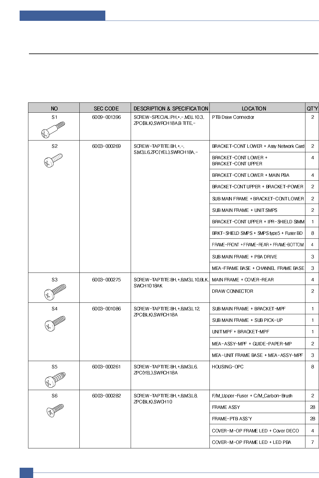
5.3.2 Screws used in the printer
The screws listed in the table below are used in this printer. Please ensure that, when
you disassemble the printer, you keep a note of which screw is used for which part and
that, when reassembling the printer, the correct screws are used in the appropriate
places.
Disassembly and Reassembly
Samsung Electronics Service Manual
5-7
Samsung Electronics
Service Manual
Disassembly and Reassembly
5-8
Disassembly and Reassembly
Samsung Electronics Service Manual
5-9
Samsung Electronics
Service Manual
Disassembly and Reassembly
5-10
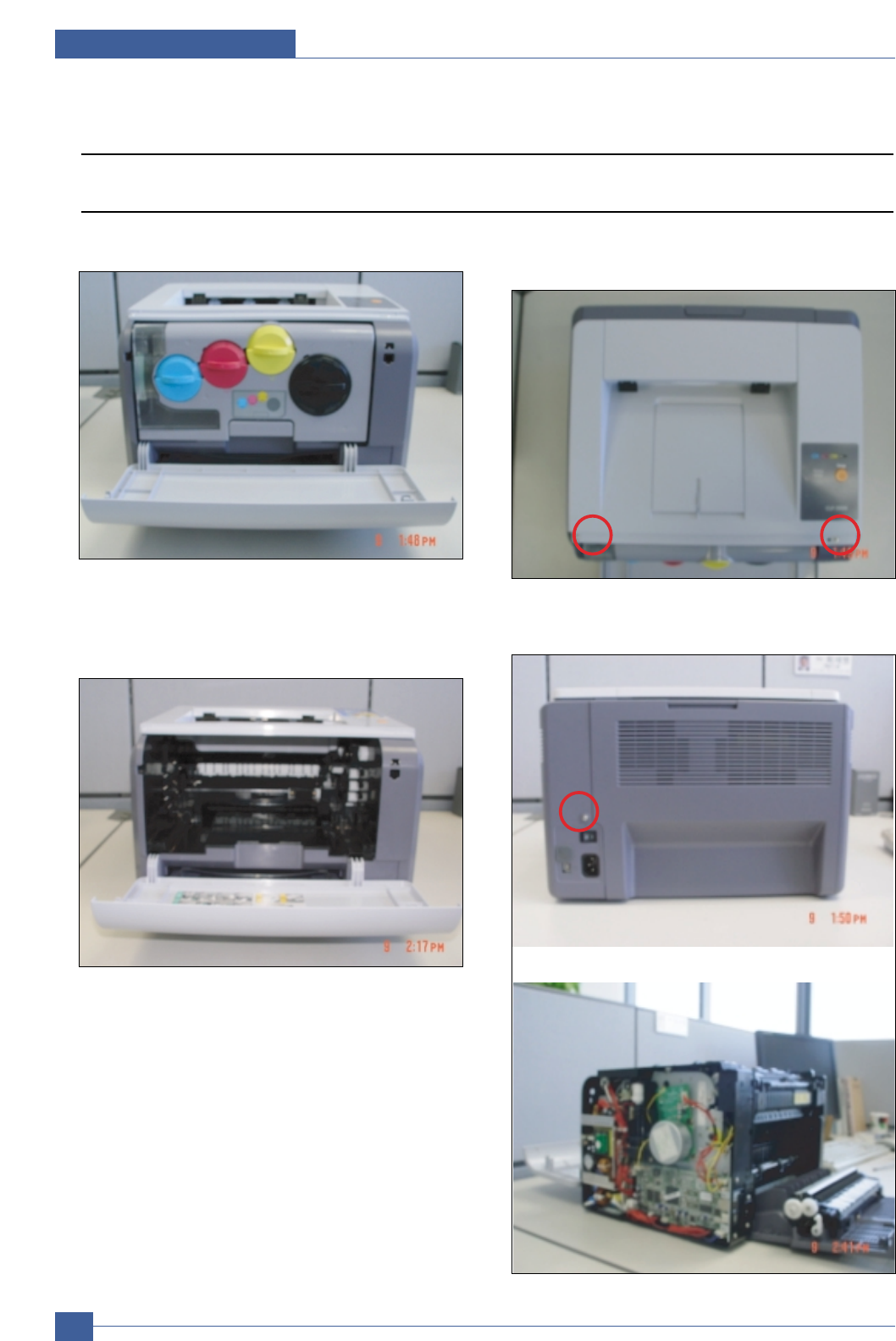
1. Open a Front-Cover and Remove the Imagine Unit.
2. Remove the ITB Unit
1) Pull out the unit toward out side of printer slightly.
2) Lift up the unit gently.
3) Pull out the unit gently.
3. Unscrew 2 screws on the Top Cover and then remove
the Top Cover.
4. Unscrew 1 screw on the Right Cover and then
remove the Right Cover after open the Rear Cover.
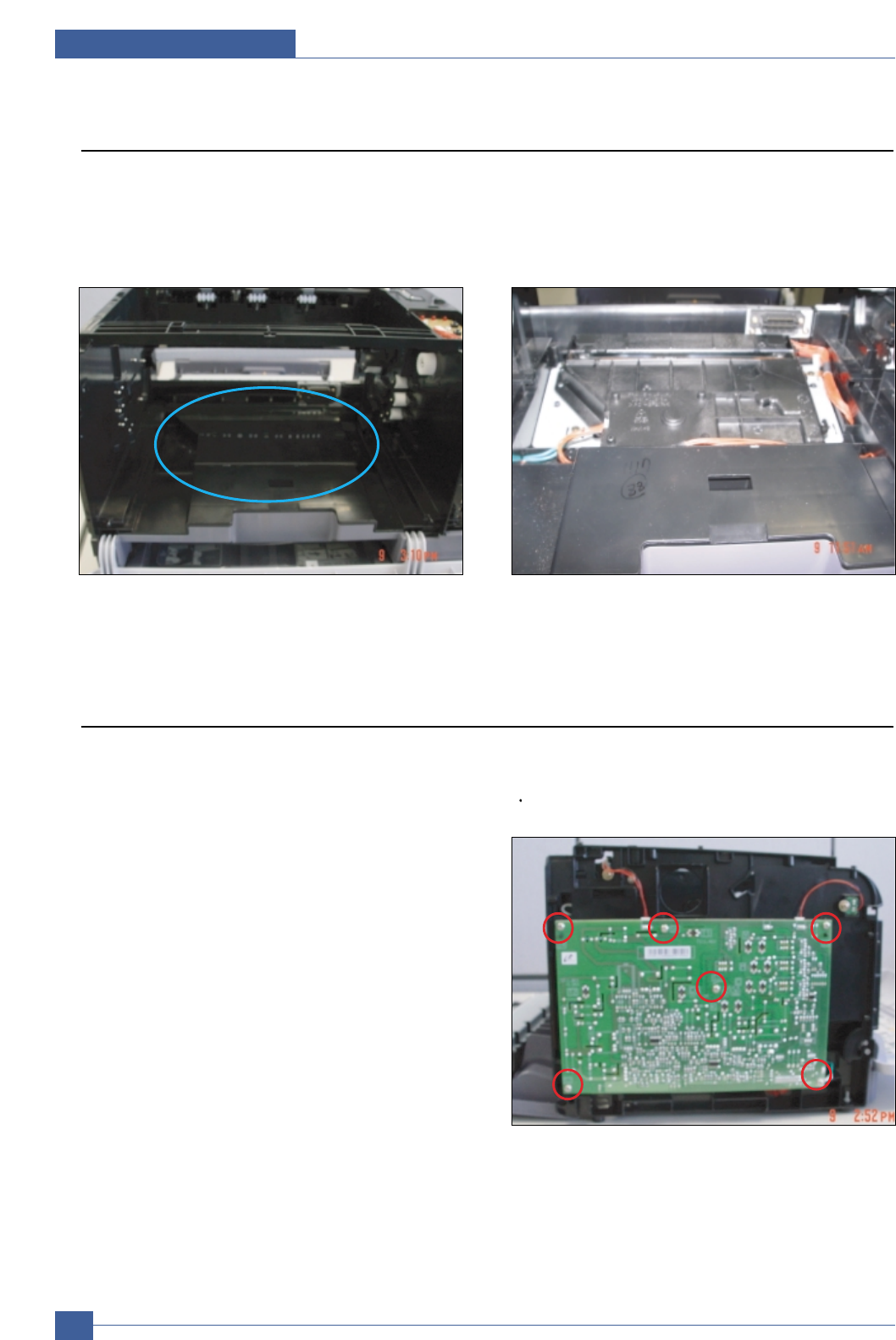
5.4 Disassembly Procedure
5.4.1 Cover Unit
Disassembly and Reassembly
Samsung Electronics Service Manual
5-11
5. Remove the Left Cover.
1. Unscrew 4 screws on the Fuser after open the Rear
Cover.
2. Push the Holder Shaft Fuser as shown in Picture.
3. Take out the Fuser Ass'y from Printer.
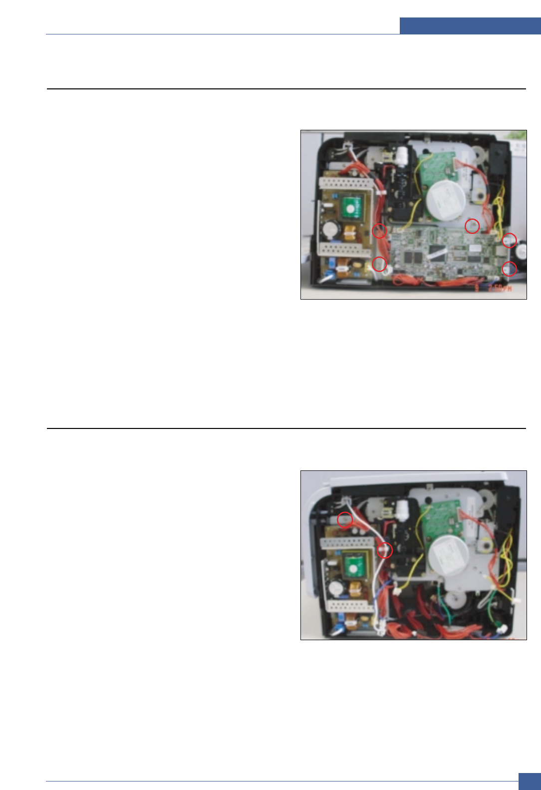
5.4.2 Fuser Ass’y
Samsung Electronics
Service Manual
Disassembly and Reassembly
5-12
1. Follow step 1 through step 3 in Cover Unit
Disassembly
2. Lift up the LSU Cover(as shown in Picture) and then
take out.
3. Remove 4 screws and then take out the LSU.
5.4.3 LSU(Laser Scan Unit)
1. Follow step 1 through step 5 in Cover Unit
Disassembly except removing Righ Cover 2. Unscrew 6 screws and then take out the HVPS.
Be careful of taking out the HVPS because there are
7 High Voltage Terminal behind HVPS.
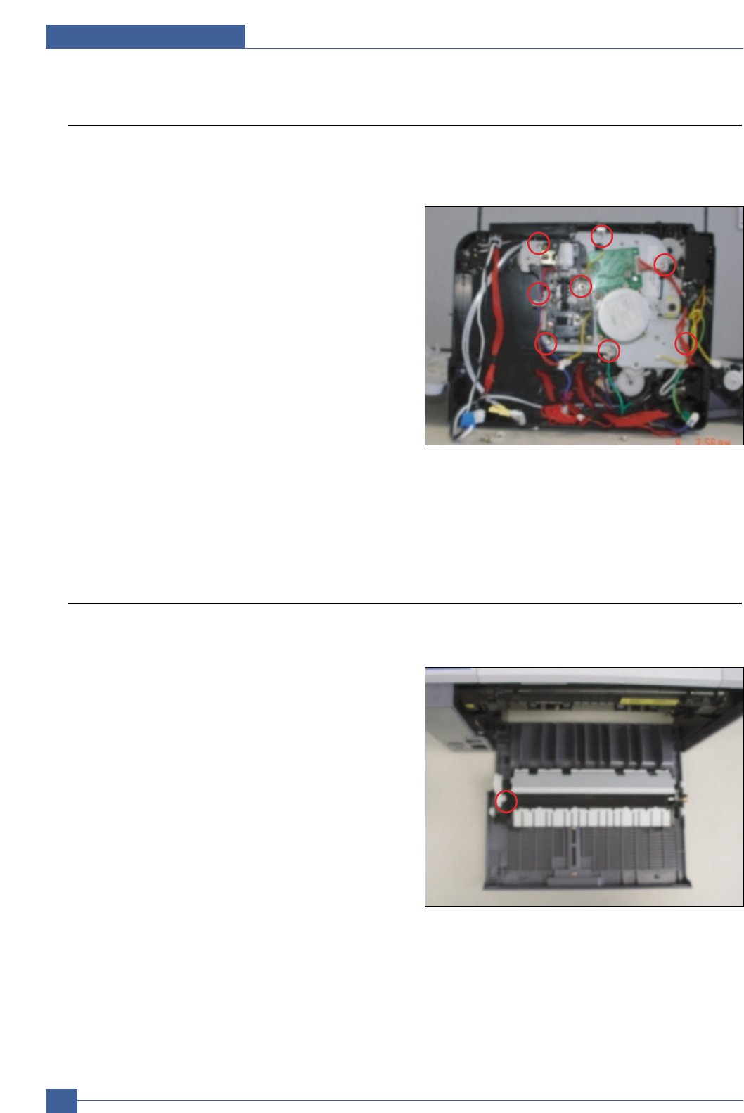
5.4.4 HVPS(High Voltage Power Supply)
Disassembly and Reassembly
Samsung Electronics Service Manual
5-13
1. Follow step 1 through step 4 in Cover Unit
Disassembly 2. Unscrew 5 screws and then take out the Main Board
after plug out all the Harness.
5.4.5 Main Board
1. Follow step 1 through step 4 in Cover Unit
Disassembly
2. Remove the Main Board
3. Unscrew 2 screws and then take out the SMPS after
plug out all the Harness.
5.4.6 SMPS(Switching Mode Power Supply)
Samsung Electronics
Service Manual
Disassembly and Reassembly
5-14
1. Follow step 1 through step 4 in Cover Unit
Disassembly
2. Remove the Main Board
3. Remove the SMPS
4. Unscrew 8 screws and then take out the Drive Ass’y.
5.4.7 Drive Ass’y
1. Open Rear Cover. 2. Pull back the hook, which holds the Roller, like below
picture and remove the Transfer Roller
5.4.8 Transfer Roller
Alignment and Adjustmens
Samsung Electronics Service Manual
6-1
6
6
6. Alignment and Adjustments
This chapter describes some of the main service procedures including:
Using the EDC mode; Clearing paper jam and test patterns.
Much of this chapter is also included in the user's guide.
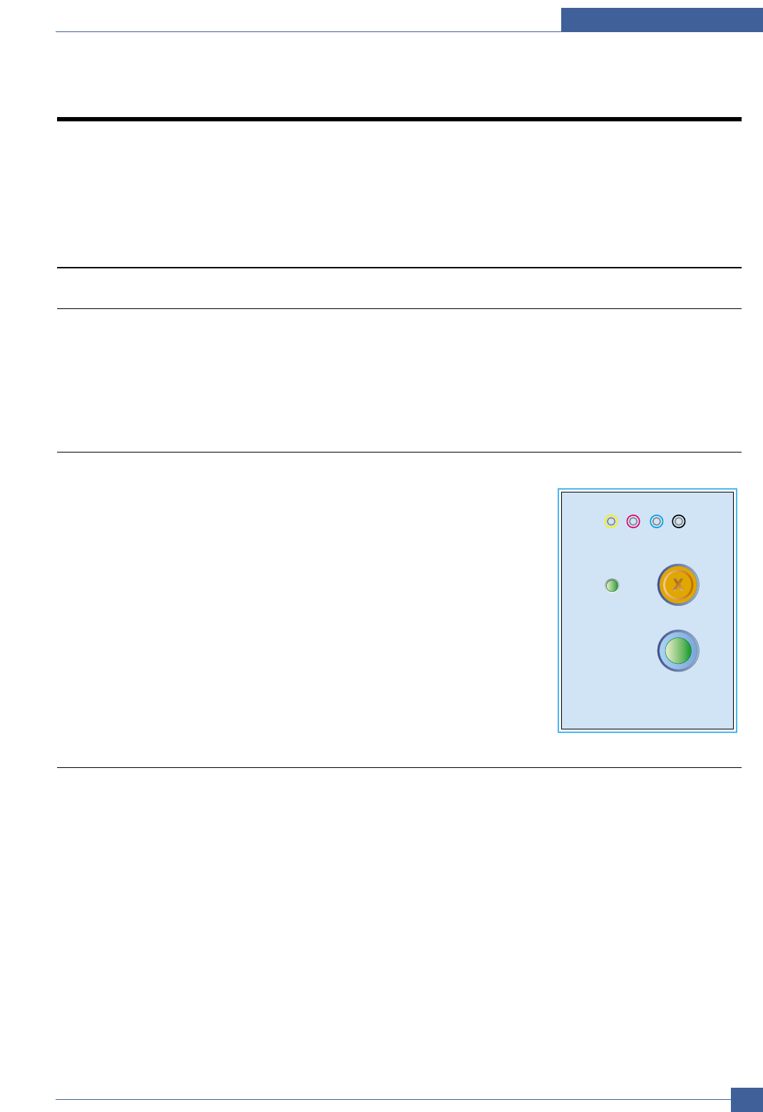
6.1. Control Panel
6.1.1 Overview
- The CLP-300 printers do not have LCD panel which is used in other color model printers. On the contrary
to other models of color printers, they show the status of the printer only with their LEDs.
- The CLP-300 printers have 2 keys and 6 LEDs. The ‘User Interface’ module handles the processing of the
‘Key Press’ and ‘Led control’ at different states of the machine.
6.1.2 Architecture
KEY (2 key): Stop key, Black only key
LED (6 LEDs):
4 LED for CMYK toners : toner-low(cyan, magenta, yellow, black) LEDs
1 LED for status : ready (green) or error(red) status LED (two color LED)
1 LED for Black only: If Black only key is pressed, Black only led glows.
6.1.3 Data and Control Flow
User interface (panel) is made up of
- KEY input detection & process
- LED control
The initial process to use the panel checks register°Øs values of key and LED.
If user input key value, the operation to be defined by key value is processed and the LED operation to be
defined by printer status is controlled.
Status
Stop
Black Only
CLP-300

Samsung Electronics
Service Manual
Alignment and Adjustmens
6-2
6.2 Function
6.2.1 KEY Function
There are two keys present. The one is Stop key and the other is Black only key.
If users input key value, the key input is transferred via GIP (General Input Port) and the operation to be
defined by key value is processed.
6.2.1.1 Functions
Stop key function is made up of
- Demo page/Configuration sheet printing function
- Job cancels function
- Start manual feeding function
- Firmware downloads mode function
Black only key function is made up of
- Change printer mode to Black-only mode function
- Black only LED light function
6.2.1.2 Detail Description
KEY input detection & process order
1) User KEY input
2) KEY input detection
: If the key input is detected when the key input check per timer tick 10ms, The 10ms interrupt service
routine sends the key detection event to panel task.
3) KEY input process
Stop key input process
: After the panel task is received the Stop key detection event, it checks the engine error status two times
and process the operation to be defined by key value.
- Demo page/Configuration sheet function
This button will have multiple functions when the printer is in idle state.
Demo page printing
Press and hold this button for about 2 seconds until the control panel lights blink slowly to print a
demo page.
Configuration sheet printing
Press and hold this button for about 6 seconds until the control panel lights blink rapidly to print a con-
figuration sheet.
- Job cancels function
When the printer is printing an active printing job, press and holds this button until the control panel
lights blink to cancel a job the printer is currently except the manual job.
- Start manual feeding function
When you select manual feed for paper source, press this button each time you feed a sheet of paper
manually.
The application of manual feeding function in CLP-300 will be determined

Alignment and Adjustmens
Samsung Electronics Service Manual
6-3
- Firmware downloads mode function
Turn on the printer at the same time that the button is pressed.
If all LEDs scroll, release the button and download the firmware ROM file via USB port
Black only key input process
: After the panel task is received the Black only key detection event, it changes printer mode to Black only
mode and notifies driver that the printer mode is changed to Black only mode. If printer mode is Black
only mode, driver makes printer image by only mono excepting color and the Black only LED glows.
6.2.2 LED Function
There are six LEDs present. Status led indicate the error/online status of the printer in idle mode. In error
mode, the status LED glows by red color and in ready mode, it glows by green color. The other four LEDs
indicate the toner status. If the black toner needs to change, the toner-low (black) LED glows and if the
color (yellow, magenta, cyan) toners need to change, the toner-low (yellow, magenta, cyan) LED glows.
Black only LED indicate the printer mode. If the users press the Black only button, the printer mode
changes to Black only mode and Black only LED glows.
6.2.2.1 Functions
LED function is made up of
- Ready/Printing status display
- Error status display
- Toner low status display
- Black only status display
6.2.2.2 Detail Description
LED control order
1) Control LED according to current printer state
: After the panel task is received each event, the LED operation is controlled by current printer status.
2) Write LED value to GOP (General Output Port)
Samsung Electronics
Service Manual
Alignment and Adjustmens
6-4
LED behavior
Status LED Black-only Toner-low Status
(Green/Red) LED (CMYK)LEDs
Green LED ON N/A N/A Ready to receive the data.
Green LEDS N/A N/A Receiving the data from the host.
LOWLY BLINK
Green LED N/A N/A Printing the page.
FAST BLINK
Red LED BLINK N/A N/A Paper source is set to MANUAL .
Need to push the button to start the
printing
Red LED ON N/A N/A Out of paper
Red LED ON N/A N/A Cover open
Red LED ON N/A N/A Paper jam
Green/Red BLINK BLINK CMYK BLINK Service error ( LSU or Fuser error)
N/A N/A Toner-low(black) ON Black toner needs to change
N/A N/A Toner-low(cyan) ON Cyan toner needs to change
N/A N/A Toner-low(magenta) ON Magenta toner needs to change
N/A N/A Toner-low(yellow) ON Yellow toner needs to change
N/A ON N/A Black only key is pressed
Service Error LED Operation
All LEDs blink the each time interval.
Service Error LED operation
Fuser Error Open Fuser Error All LEDs (Toner low LEDs, Status (Red) LED, Black only LED) blink
a time interval of 1 second.
No Heat Error All LEDs (Toner low LEDs, Status (Red) LED, Black only LED) blink
a time interval of 4 seconds.
Over Heat Error All LEDs (Toner low LEDs, Status (Green/Red) LED, Black only
LED) blink a time interval of 1 second.
Scanner Error P Motor Error All LEDs (Toner low LEDs, Status (Green) LED, Black only
(=LSU Error) LED) blink a time interval of 1 second.
H Sync Error All LEDs (Toner low LEDs, Status(Green) LED, Black only LED)
blink a time interval of 4 seconds.
Alignment and Adjustmens
Samsung Electronics Service Manual
6-5
Assert Error LED Operation
The panel LED operation display the line number of assert error occurrence.
Line number LED operation
start & end All LEDs(Toner low LEDs, Status(Red) LED, Black only LED) turn ON for approximately 2 sec-
onds and then All LEDs turn OFF for approximately 3 seconds.
1 After Status (Red) LED blinks one time, Toner low LEDs blink one time.
2 After Status (Red) LED blinks two times, Toner low LEDs blink one time.
3 After Status (Red) LED blinks three times, Toner low LEDs blink one time.
4 After Status (Red) LED blinks four times, Toner low LEDs blink one time.
5 After Status (Red) LED blinks five times, Toner low LEDs blink one time.
6 After Status (Red) LED blinks six times, Toner low LEDs blink one time.
7 After Status (Red) LED blinks seven times, Toner low LEDs blink one time.
8 After Status (Red) LED blinks eight times, Toner low LEDs blink one time.
9 After Status (Red) LED blinks nine times, Toner low LEDs blink one time.
Samsung Electronics
Service Manual
Alignment and Adjustmens
6-6
6.3 Jam Removal
When a jam occurs while printing a jam message is displayed on the control panel.
* Jam0 In Tray 1:
Paper jam in the main cassette.
* Jam0 In MP Tray:
Paper jam in the MP tray
* Jam Inside Printer:
Jam 1, Paper is jammed inside the printer.
* Jam In Exit Area:
Jam2, Paper is jammed in the exit area when ejecting paper.
CAUTION: When removing jammed paper, always pull it firmly and evenly without any sudden jerks. If
at all possible, remove the paper as a single sheet. If the paper tears ensures ALL paper
fragments are removed. Any fragments left inside the machine will cause it to jam again.
6.3.1 Clearing Paper Jams
NOTE: When removing paper that is jammed in the printer, if possible always pull the paper in the direction
that it normally moves so as not to damage internal components. Always pull firmly and evenly; do
not jerk the paper. If the paper tears, ensure that all fragments of paper are removed; otherwise a
jam will occur again.
If a paper jam occurs, the Status LED on the control panel lights red. Find and remove the jammed paper.
To resume printing after clearing paper jams, you must open and close the front cover or rear cover.
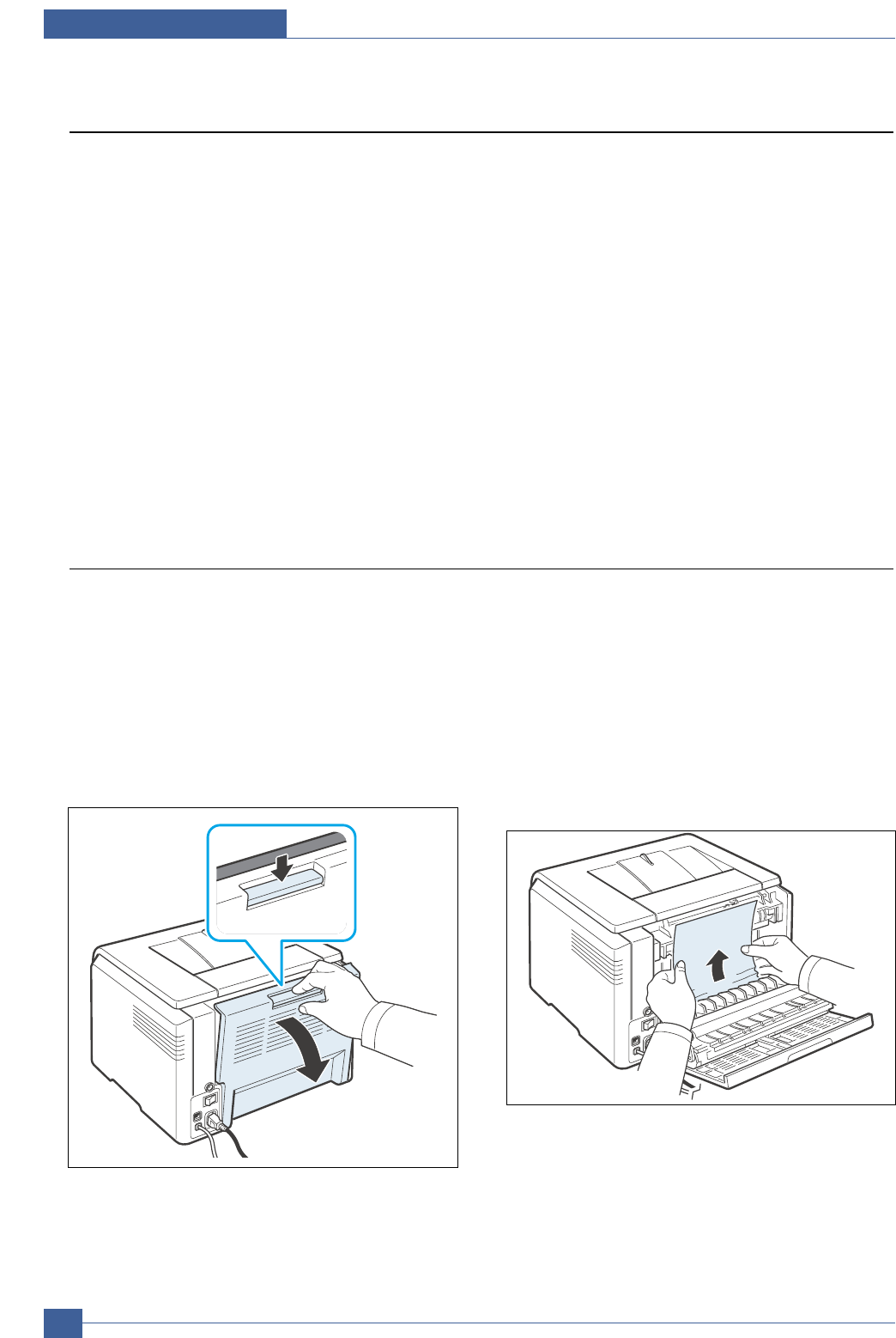
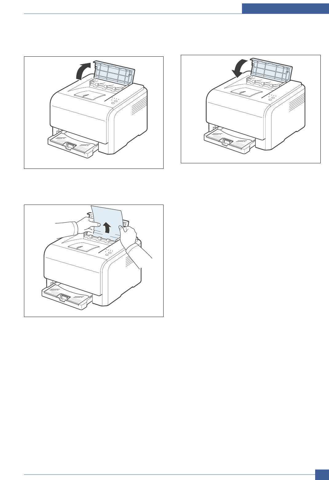
1. To remove the jammed paper, open the rear
cover. 2. Carefully remove the paper by pulling in the
direction as shown below. Most of the jammed
paper can be removed in this step.
If you cannot find the jammed paper, or if there
is any resistance removing the paper, stop
pulling and go to the next step.
Alignment and Adjustmens
Samsung Electronics Service Manual
6-7
3. Close the rear cover and then open the top
cover.
4. Holding the inner cover open, carefully take the
jammed paper out of the printer. The inner
cover will then close automatically.
5. Close the top cover. Make sure that it is
securely latched.
6. Open and then close the rear cover or front
cover to resume printing.

Samsung Electronics
Service Manual
Alignment and Adjustmens
6-8
6.3.2 Tips for Avoiding Paper Jams
By selecting the correct paper types, most paper jams can be avoided.
• Follow the procedures Jam remove. Ensure that the adjustable guides are positioned correctly.
• Do not overload the paper tray.
• Do not remove the paper from the tray while printing.
• Flex, fan, and straighten the paper before loading.
• Do not use creased, damp, or highly curled paper.
• Do not mix paper types in a tray.
• Use only recommended print materials.
• Ensure that the recommended print side of print materials is facing up in the paper tray.
Alignment and Adjustmens
Samsung Electronics Service Manual
6-9
6.4 Sample Pattern
This product provides several printable test patterns for maintenance purposes. These patterns can be used to aid the
diagnosis of print quality problems.
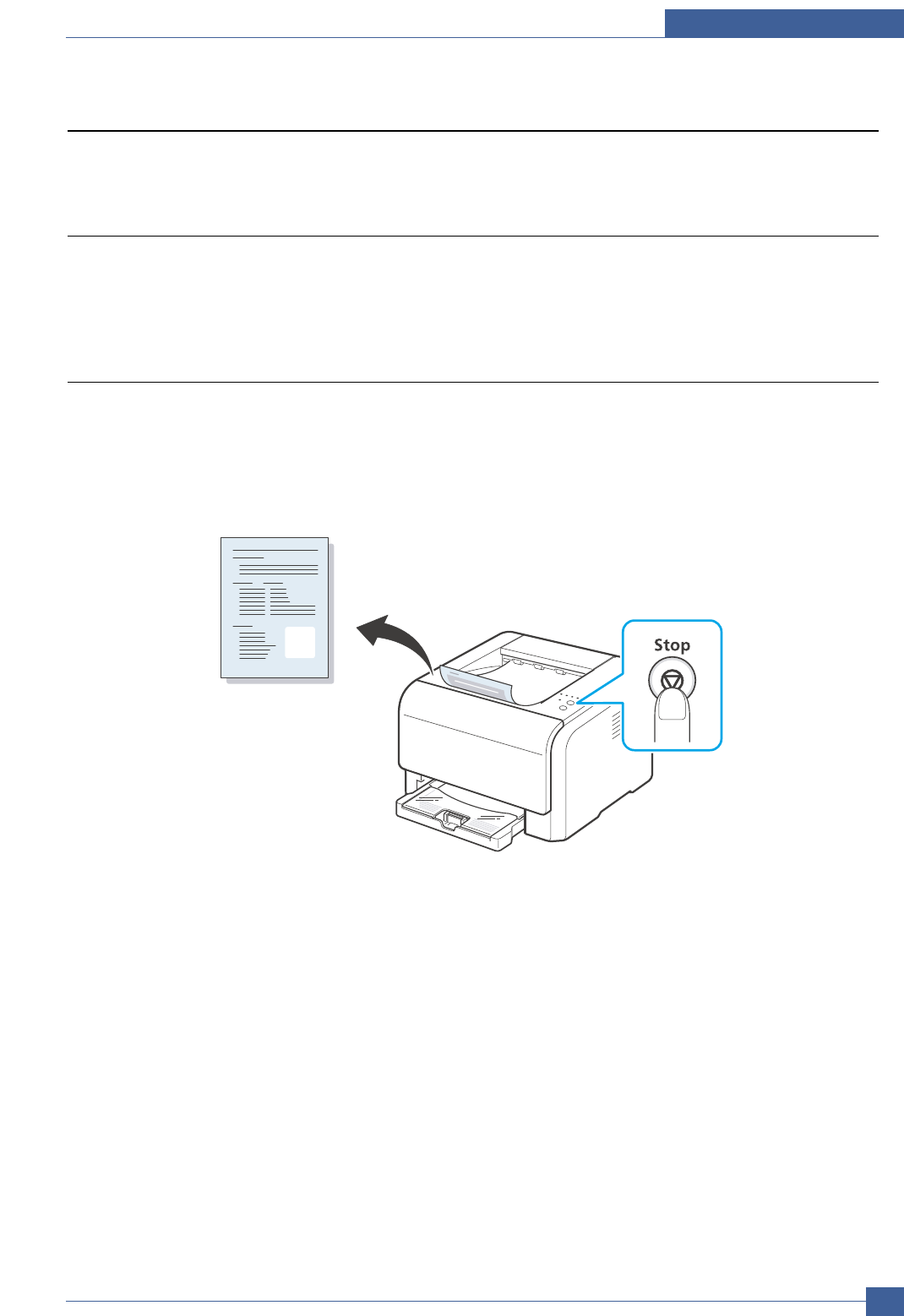
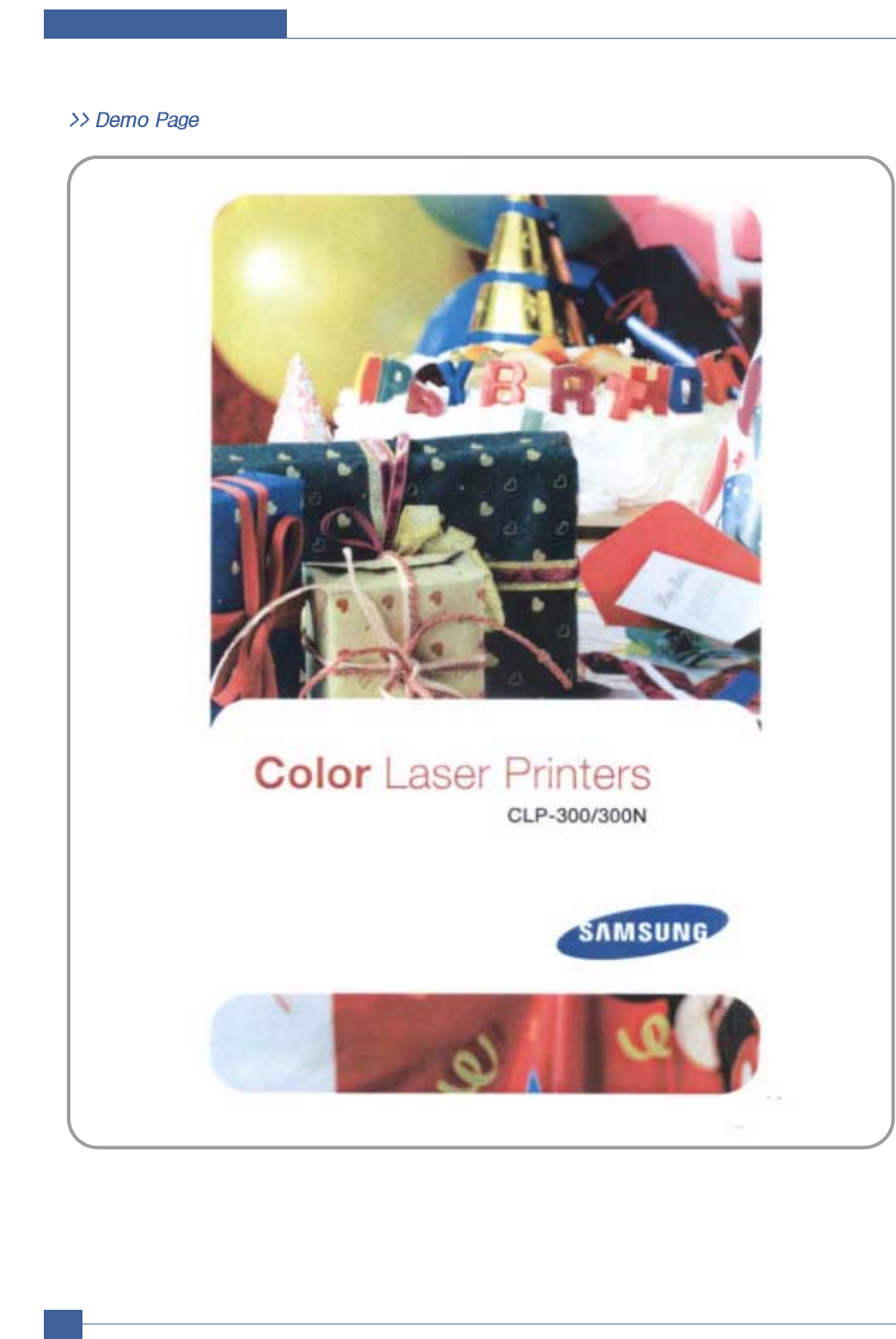
6.4.1 Printing a Demo Page
Print a demo page to make sure that the printer is operating correctly.
To print a demo page: In ready mode, press and hold the Stop button for 2 seconds.
A demo page showing the printer’s features and capabilities is printed.
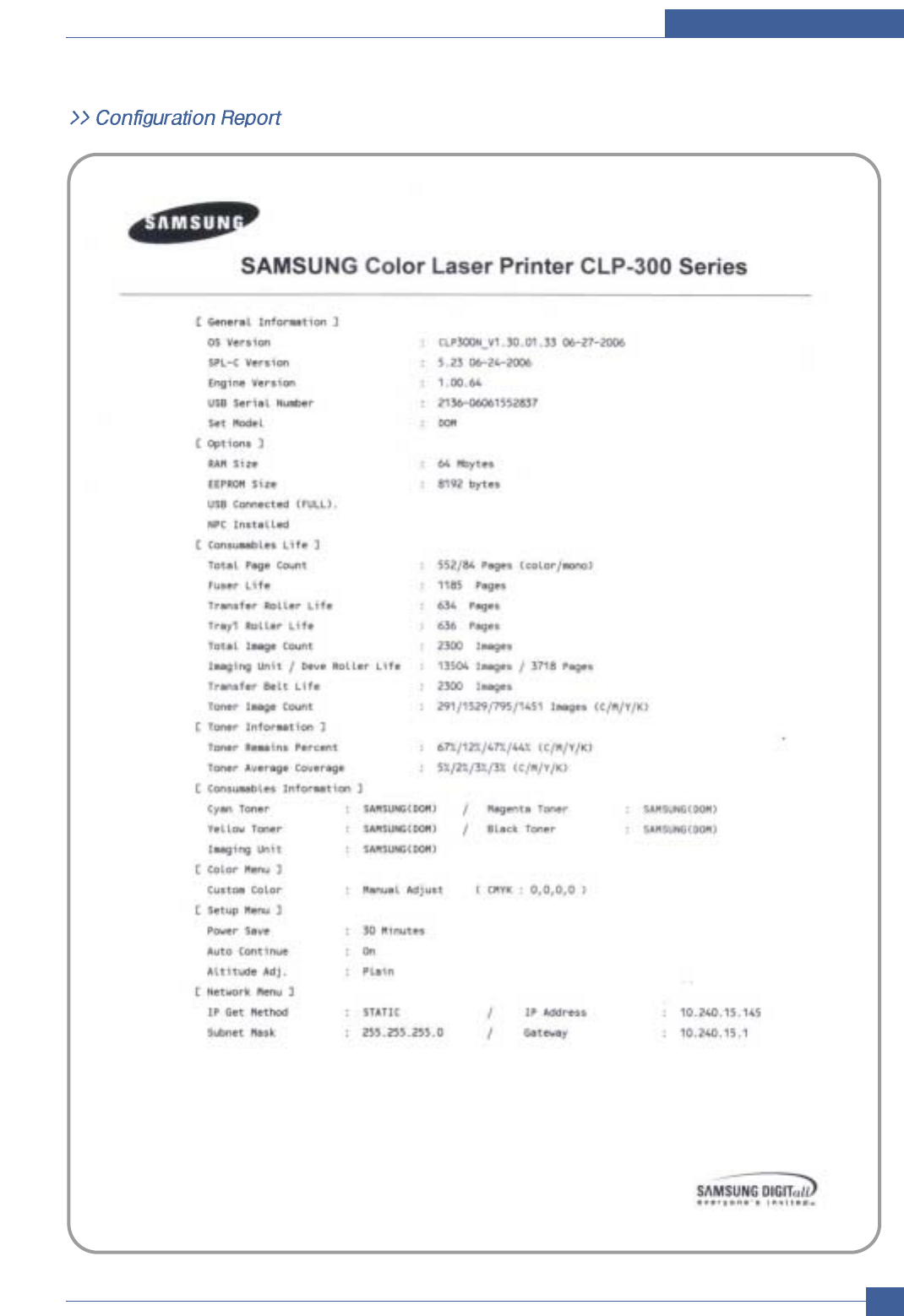
6.4.2 Printing a Configuration Page
You can print a configuration page from the printer’s control panel. Use the configuration page to view the current
settings, to help troubleshoot problems.
To print a configuration page: In ready mode, press and hold the Stop button on the control panel for 5 seconds.
A configuration page prints out.
Samsung Electronics
Service Manual
Alignment and Adjustmens
6-10
Samsung Electronics
Alignment and Adjustmens
Samsung Electronics Service Manual
6-11
Samsung Electronics
Service Manual
Alignment and Adjustmens
6-12
6.5 Periodic Defective Image
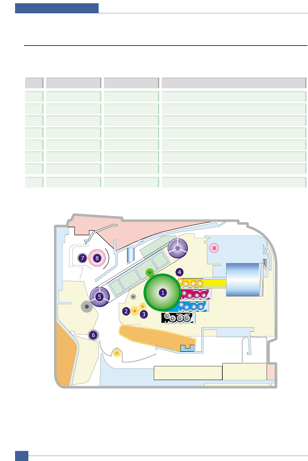
If an image defects appears at regular intervals on the printed-paper, it is due to a faulty or damaged roller.
Refer to the table below and check the condition of the appropriate roller.
No Roller Period Phenomenon
1OPC Drum 188.5 mm White and Black Spots
2Charge Roller 37.7mm Black Spot and line and Periodic Band
3Supply Roller 47.5mm Periodic Band by little difference of density
4
Developing Roller
26.0mm White Spot, Horizontal black band
5
1
st
Transfer Roller
32.7mm Ghost, Damaged Image by abnormal tranfer
6
2
nd
Transfer Roller
57.5mm Ghost, Damaged Image by abnormal tranfer
786.6mm Black Spots or Vertical Black BandHeat Roller
886.6mm BackgroundPressure Roller
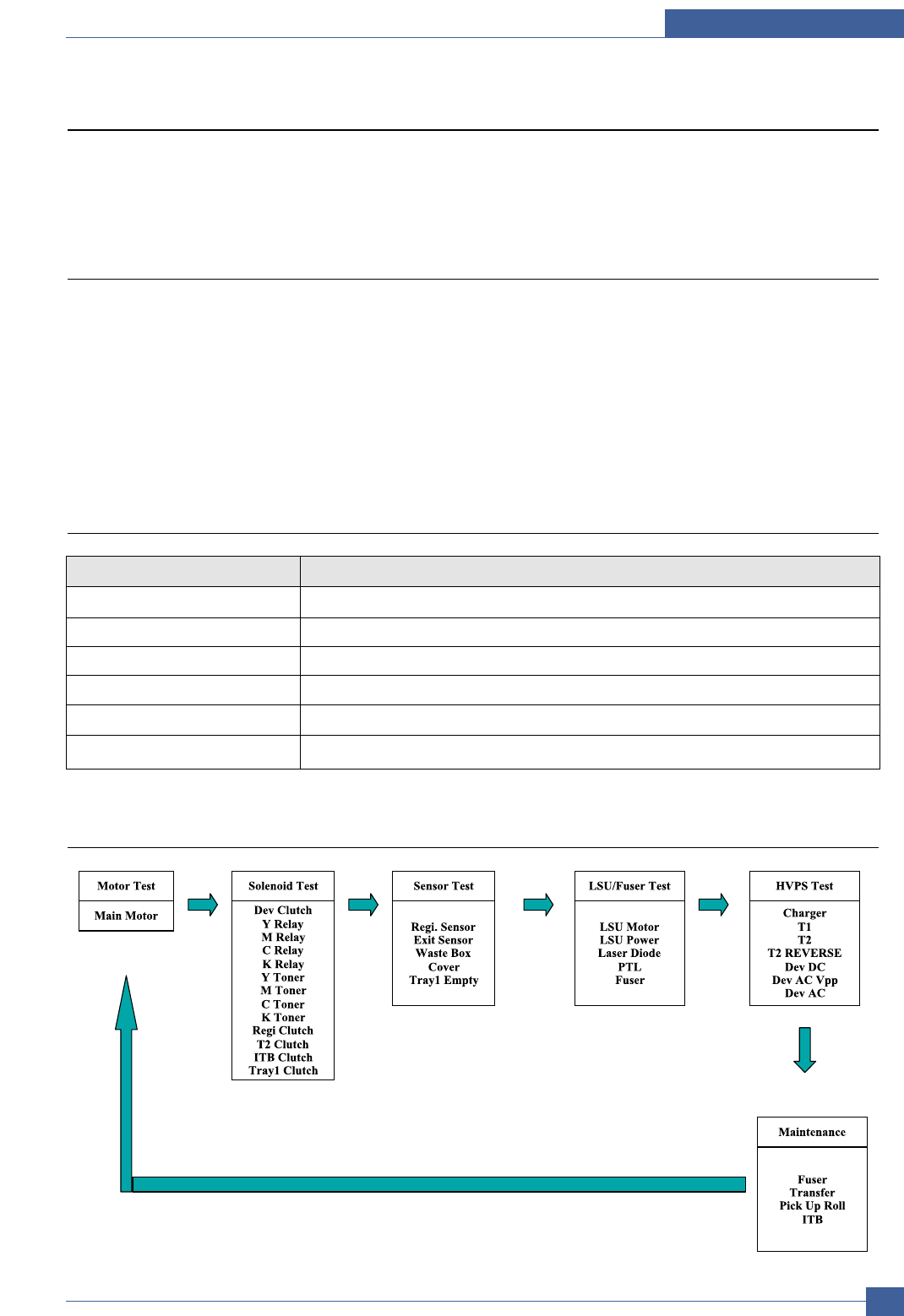
Alignment and Adjustmens
Samsung Electronics Service Manual
6-13
6.6 How to use EDC (Engine Diagnostic Control) Mode
EDC Mode is feature that allows the engineer to check the condition of the print engine. It can check the operating condi-
tion of the motors, sensors, solenoids and clutches, measure the High Voltage from the HVPS and check the operation of
the fuser and LSU.
6.6.1 Enterence
When trying to check the CLP-300 Series EDC Mode, additional EDC execution program needed.
[ Procedure of EDC Mode operation ]
a) First, turn on the Power of Printer, wait until Ready state
b) In this state, Run the EDC program on the computer
c) After that, click the menu of screen
d) Then <Motor Test> appears on the initial screen
e) Should you get out of this program, press Exit of screen
6.6.2 Keys
Key Discription
Exit Close program
Update LCD Update value (ex : sensor value)
Menu Move to the top menu
Left/Right arrow Move test item
Enter Start testing or select Sub-item
Upper level Stop testing or the upper menu
6.6.3 EDC Map
Samsung Electronics
Service Manual
Alignment and Adjustmens
6-14
6.6.3.1 Motor Test
6.6.3.2 Solenoid Test
Item Discription
Main Motor If motor lock signal is normal, “Successed” message will be displayed.
When motor lock signal is abnormal, “failed” message will be displayed.
When “Upper Level” is pushed, “off ” message will be displayed.
Item Discription
Dev Clutch When select key is pushed, Dev Clutch ON message will be displayed.
Upper Level is pushed, Dev Clutch Off message will be displayed.
Y Relay When select key is pushed, Y Relay ON message will be displayed. Upper
Level is pushed, Y Relay Off message will be displayed on.
M Relay When select key is pushed, M Relay ON message will be displayed. Upper
Level is pushed, M Relay Off message will be displayed.
C Relay When select key is pushed, C Relay ON message will be displayed. Upper
Level is pushed, C Relay Off message will be displayed.
K Relay When select key is pushed, K Relay ON message will be displayed. Upper
Level is pushed, K Relay Off message will be displayed.
Y Toner When select key is pushed, Y Toner ON message will be displayed. Upper
Level is pushed, Y Toner Off message will be displayed.
M Toner When select key is pushed, M Toner ON message will be displayed. Upper
Level is pushed, M Toner Off message will be displayed.
C Toner When select key is pushed, C Toner ON message will be displayed. Upper
Level is pushed, C Toner Off message will be displayed.
K Toner When select key is pushed, K Toner ON message will be displayed. Upper
Level is pushed, K Toner Off message will be displayed.
Regi Clutch When select key is pushed, REGI Clutch ON message will be displayed.
Upper Level is pushed, REGI Clutch Off message will be displayed.
T2 Clutch When select key is pushed, T2 Clutch ON message will be displayed.
Upper Level is pushed, T2 Clutch Off message will be displayed.
ITB Clutch When select key is pushed, ITB Clutch ON message will be displayed.
Upper Level is pushed, ITB Clutch Off message will be displayed.
Tray1 Clutch When select key is pushed, Tray1 Clutch ON message will be displayed.
Upper Level is pushed, Tray1 Clutch Off message will be displayed.
Regi. Sensor If actuator is checked by sensor, "Without Paper" message will be displayed. if
not, "With Paper" message will be.
Exit Sensor If actuator is checked by sensor, "Without Paper" message will be displayed. if
not, "With Paper" message will be.
Waste Box If waste Box exists , Installed message will be displayed.
If not, Not Installed message will be.
Cover If cover is opened, " Opened message will be displayed.
If not, "Closed" message will be.
Tray1 Empty If paper exists in the tray, "With Paper" will be displayed.
If not, "Without Paper" message will be.
Alignment and Adjustmens
Samsung Electronics Service Manual
6-15
6.6.3.3 LSU/ Fuser Test
Item Discription
LSU Motor If LSU motor lock signal is normal, "Successed" message will be displayed.
When LSU motor lock signal is abnormal , failed" message will be displayed.
When Upper Level is pushed, off message will be displayed.
LSU Power When select key is pushed, LSU Power On message will be displayed.
If not, LSU Power Off" message will be.
Laser Diode When select key is pushed, Laser Diode On message will be displayed.
If not, Laser Diode Off message will be.
PTL When select key is pushed, PTL On message will be displayed .
If not, PTL Off message will be.
Fuser When select key is pushed, Fuser On message will be displayed.
If not, Fuser Off message will be.
Samsung Electronics
Service Manual
Alignment and Adjustmens
6-16
6.6.3.4 HVPS Test
Item Discription
Charger When select key is pushed, DUTY : x%* message will be displayed.
And then Left/Right arrow is selected, x% is increased or decreased.
And DUTY : x% message will be displayed. * is disappeared.
And then select key is pushed, x%* message will be displayed.
When Upper Level is pushed, * is disappeared.
T1 When select key is pushed, DUTY : x%* message will be displayed.
And then Left/Right arrow is selected, x% is increased or decreased.
And DUTY : x% message will be displayed. * is disappeared.
And then select key is pushed, x%* message will be displayed.
When Upper Level is pushed, * is disappeared.
T2 When select key is pushed, DUTY : x%* message will be displayed.
And then Left/Right arrow is selected, x% is increased or decreased.
And DUTY : x% message will be displayed. * is disappeared.
And then select key is pushed, x%* message will be displayed.
When Upper Level is pushed, * is disappeared.
T2 REVERSE When select key is pushed, T2 REVERSE On message will be displayed.
If not, T2 REVERSE Off will be.
Dev DC When select key is pushed, DUTY : x%* message will be displayed.
And then Left/Right arrow is selected, x% is increased or decreased.
And DUTY : x% message will be displayed. * is disappeared.
And then select key is pushed, x%* message will be displayed.
When Upper Level is pushed, * is disappeared.
Dev AC Vpp When select key is pushed, DUTY : x%* message will be displayed.
And then Left/Right arrow is selected, x% is increased or decreased.
And DUTY : x% message will be displayed. * is disappeared.
And then select key is pushed, x%* message will be displayed.
When Upper Level is pushed, * is disappeared.
Dev AC When select key is pushed, DUTY : x%* message will be displayed.
And then Left/Right arrow is selected, x% is increased or decreased.
And DUTY : x% message will be displayed. * is disappeared.
And then select key is pushed, x%* message will be displayed.
When Upper Level is pushed, * is disappeared.
Charger Duty : 50% -> -789V , Range : -81V ~ -1689V
T1 Duty : 50% -> 1159V , Range : 122V ~ 2188V
T2 Duty : 50% -> 2552V , Range : 264V ~ 4730V
Supply DC Duty : 50% -> -269V , Range : -1V ~ -591V
AC, Vpp Duty : 50%-> 1210V , Range : 800V ~ 2160V

Alignment and Adjustmens
Samsung Electronics Service Manual
6-17
6.6.3.5 Maintenance
6.6.3.6 Error list and recovery
Paper Empty / Paper Mismatch
- Load specified paper in the tray 1
Paper does not exist in the tray1
Load Paper, When you still want to continue printing
- Paper mismatch in the tray 1
Paper is mismatched
Press stop key for a while, When you still want to continue printing
Cover Open
- Cover Open
Cover is opened
Close the door, When you still want to continue printing
Waster Tank Full or not installed
- Waste Tank Full
Toner of Waste toner box is full
Empty or Insert the waste toner box
Paper Jam
- Paper Jam at the tray1
Paper is not picked up
Cover Open /Close, When you still want to continue printing
- Paper Jam inside printer
There is a paper inside printer
After cover Open , Paper must be removed, and then close the cover
Item Discription
Fuser When select key is pushed, Initialized message will be displayed.
When Upper Level is pushed, Off message is disappeared.
Transfer When select key is pushed, Initialized message will be displayed.
When Upper Level is pushed, Off message is disappeared.
Pick Up Roll When select key is pushed, Initialized message will be displayed.
When Upper Level is pushed, Off message is disappeared.
ITB When select key is pushed, Initialized message will be displayed.
When Upper Level is pushed, Off message is disappeared.

Samsung Electronics
Service Manual
Alignment and Adjustmens
6-18
- Paper Jam at the paper exit area
There is a paper at exit area
After cover Open , Paper must be removed, and then close the cover
- Motor Lock Error
Motor does not run or runs abnormal speed
Motor or Main board must be checked
- LSU Motor Lock Error
LSU motor does not run or runs abnormal speed
Hsync is not detected
LSU or Main board must be checked
- Transfer Belt Error
ITB home sensor is not checked for a normal time
ITB must be checked
- Fuser Over Heat error
Temperature of fuser is high
Fuser or Main board must be checked
- Fuser Low Heat error
Temperature of fuser is low
Fuser or Main board must be checked
- Dev. Home error
Home of Development is not checked or checked at the abnormal time
Clutch of Development or Main board must be checked
- ADC not Confirm Error
Signal of confirmation for ADC is not detected
Main board must be checked
Alignment and Adjustmens
Samsung Electronics Service Manual
6-19
6.7 Error Message
When the printer experiences an error, the control panel will indicate an error message with the indicator
lights and the Smart Panel program window will display to show the printer’s status or errors. Find the light
pattern below that matches the printer light pattern and follow the solutions to clear the error.
LED status legend
The blinking toner cartridge is low. Order a new toner cartridge. You can temporar-
ily improve print quality by redistributing the toner.
The lighting toner cartridge is empty.
Remove the old toner cartridge and install a new one.
The blinking toner cartridge is totally exhausted. Remove the old toner cartridge
and install a new one.
The blinking toner cartridge is wrong. Only install a Samsung toner
cartridge, designed for your printer.
A paper jam has occurred. To solve the problem.
The front cover is open. Close the front cover.
There is no paper in the tray. Load paper in the tray.
The waste toner container is open or full. Check the container.
Your system has some problems. If this problem occurs, contact your service
representative.
LED pattern Possible Problem and Solution
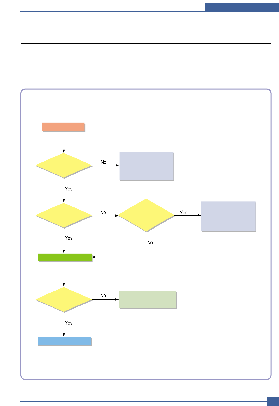
Troubleshooting
Samsung Electronics Service Manual
7-1
7
7
7. Troubleshooting
7.1 Procedure of Checking the Symptoms
Before attempting to repair the printer first obtain a detailed description of the problem from the customer.
Power On
Indicate
"Red Lamp ON"
Status LED
Green OK?
Print(test pattern)
printing
Quality is
Nomal?
Refer to "Solution
of Image Problem"
Refer to
"6.2.2 LED Function"
END
- No Power
- Power Module error
- Main PBA
LED Panel
ON?

Samsung Electronics
Service Manual
Troubleshooting
7-2
7.2 Troubleshooting Checklist
If the printer is not working properly, consult the following checklist. If the printer does not pass a step, follow the
corresponding troubleshooting suggestions.
Make sure that the Status LED on
the control panel green and
"Ready" is shown on the Smart
Panel program window.
If the Status LED is off, check the power cord connection. Check the
power switch. Check the power source by plugging the power cord into
another outlet.
If the Status LED blinks or lights red, solve the problems.
Status Response
Print a demo page to verify that the
printer is feeding paper correctly. If a demo page does not print, check the paper supply in the paper tray.
If the paper jams in the printer, go to "Clearing Paper Jams"
Check the demo page to see if it is
printed correctly. If there is a print quality problem, go to "Solving Print Quality Problems"
If completing the checklist does not
resolve the printer problem, check
the following troubleshooting
sections.
See "Solving General Printing Problems"
See "Solving Print Quality Problems"
See "Common Windows Problems"
See "Common Macintosh Problems"
See "Common Linux Problems"
Print a short document from a
software application to verify that
the computer and printer are
connected and communicating
correctly.
If the page does not print, check the cable connection between the printer
and the computer.
Check the print queue or print spooler to see if the printer has been
paused.
Check the software application to ensure that you are using the proper
printer driver and communication port. If the page is interrupted during
printing, go to "Solving General Printing Problems"
Troubleshooting
Samsung Electronics Service Manual
7-3
7.3 Solving General Printing Problems
For problems with the operation of your printer, refer to the table for suggested solutions.
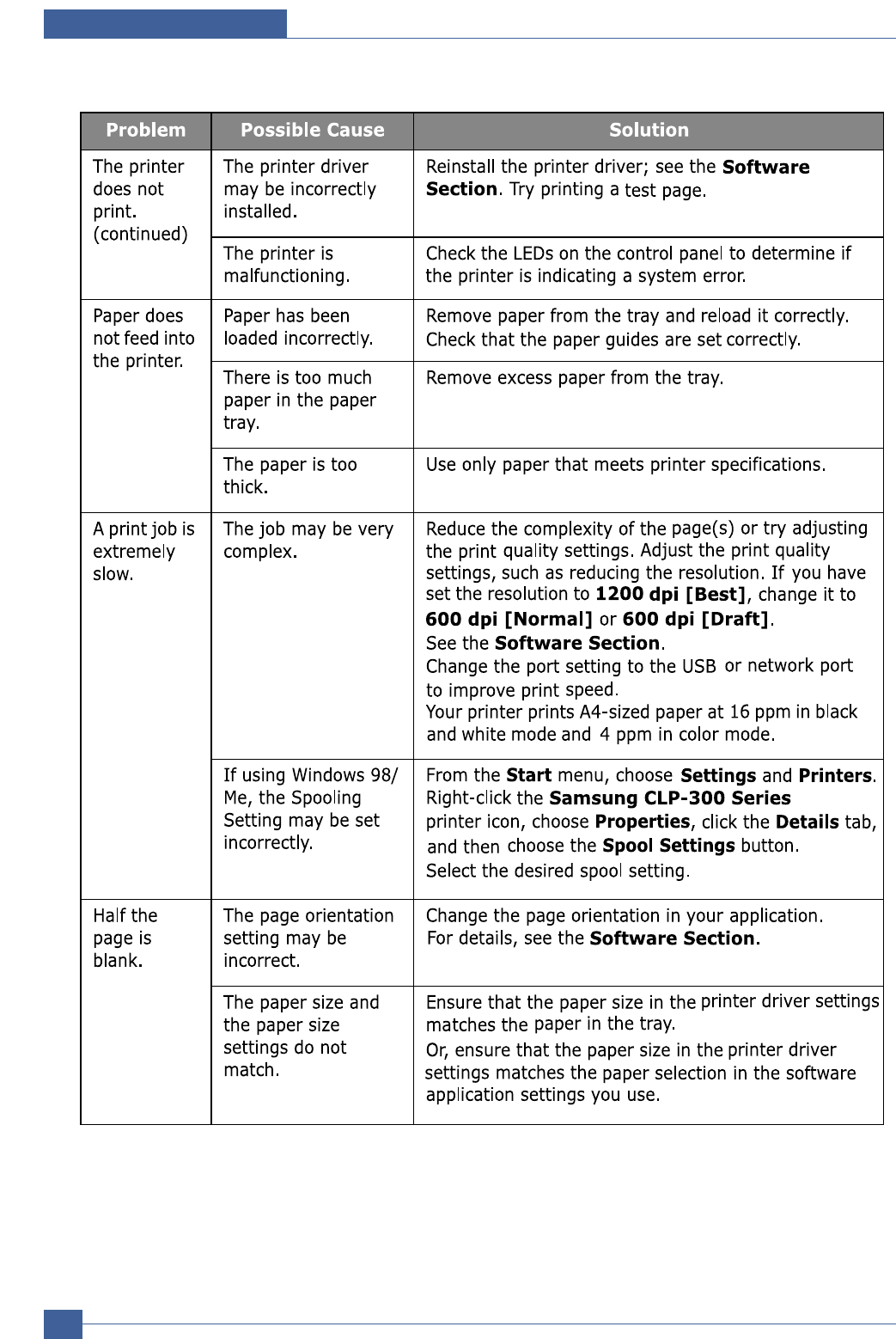
Samsung Electronics
Service Manual
Troubleshooting
7-4
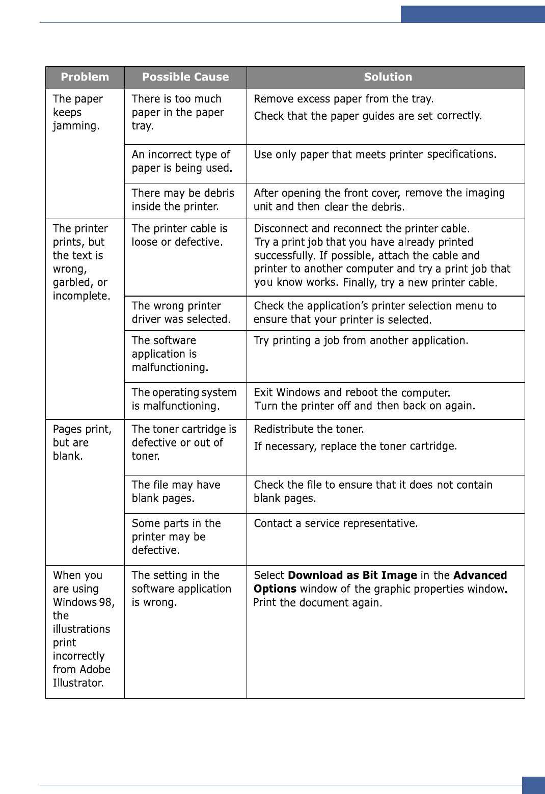
Troubleshooting
Samsung Electronics Service Manual
7-5

Samsung Electronics
Service Manual
Troubleshooting
7-6
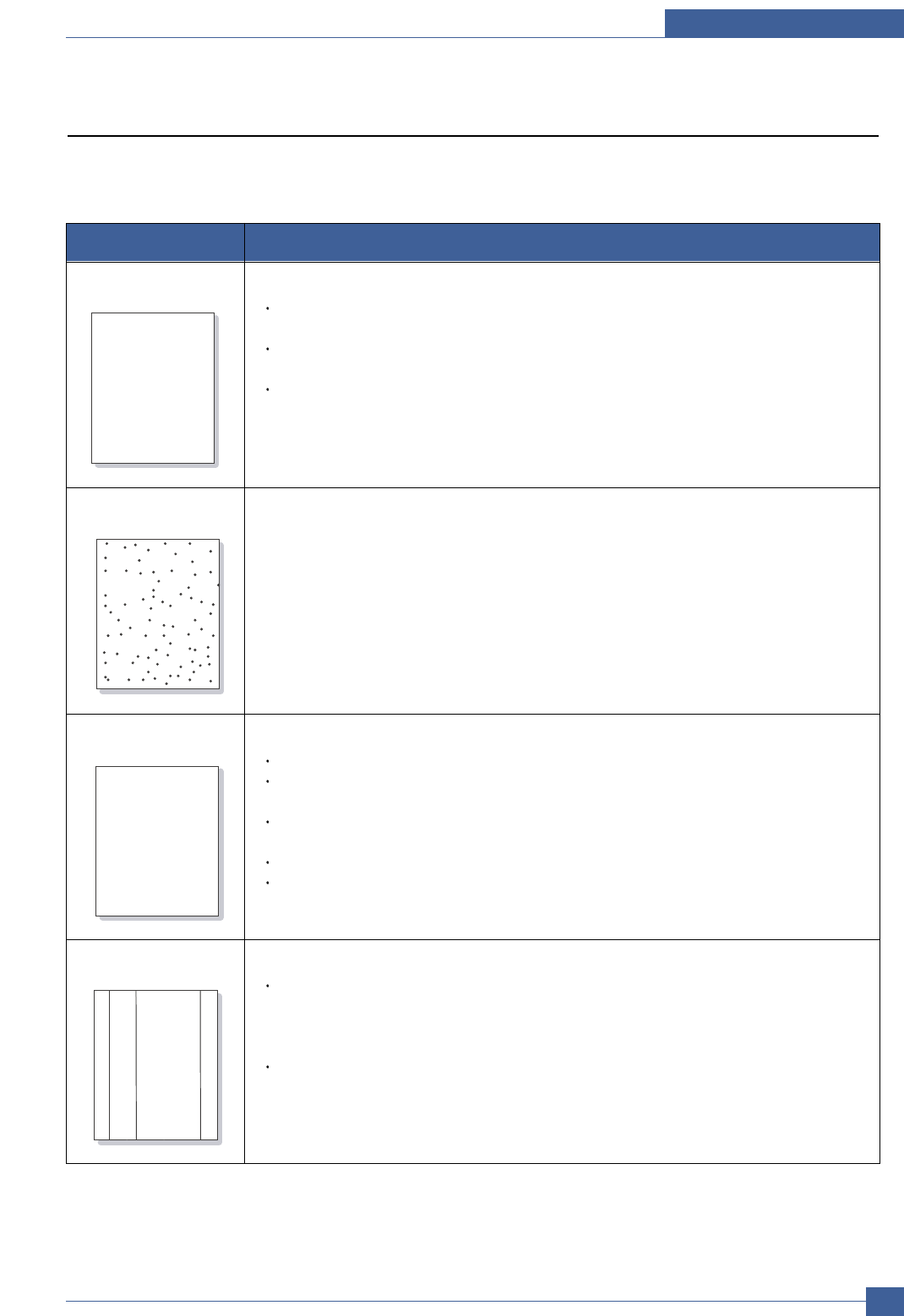
Troubleshooting
Samsung Electronics Service Manual
7-7
7.4 Solving Print Quality Problems
Dirt inside of the printer or improper paper loading may reduce print quality. See the table below to troubleshoot
problems.
Light or faded print If a vertical white streak or faded area appears on the page:
The toner supply is low. You may be able to temporarily extend the toner cartridge life.
If this does not improve print quality, install a new toner cartridge.
The paper may not meet paper specifications (for example, the paper is too moist or too
rough).
A combination of faded or smeared defects may indicate that the printer needs cleaning.
Problem Solution
AaBbCc
AaBbCc
AaBbCc
AaBbCc
AaBbCc
Toner specks The paper may not meet specifications (for example, the paper is too moist or too rough).
AaBbCc
AaBbCc
AaBbCc
AaBbCc
AaBbCc
Dropouts If generally rounded, faded areas occur randomly on the page:
A single sheet of paper may be defective. Try reprinting the job.
The moisture content of the paper is uneven or the paper has moist spots on its sur-
face. Try a different brand of paper.
The paper lot is bad. The manufacturing process can cause some areas to reject toner.
Try a different kind or brand of paper.
The toner cartridge may be defective. See "Vertical repetitive defects" on the next page.
If these steps do not correct the problems, contact a service representative.
AaBbCc
AaBbCc
AaBbCc
AaBbCc
AaBbCc
Vertical lines If black vertical streaks appear on the page:
A imaging unit has probably been scratched.
Remove the imaging unit and install a new one.
If white vertical lines appear on the page:
Clean the inside of the printer. If you still have the same problems, replace the imaging
unit with a new one.
AaBbCc
AaBbCc
AaBbCc
AaBbCc
AaBbCc
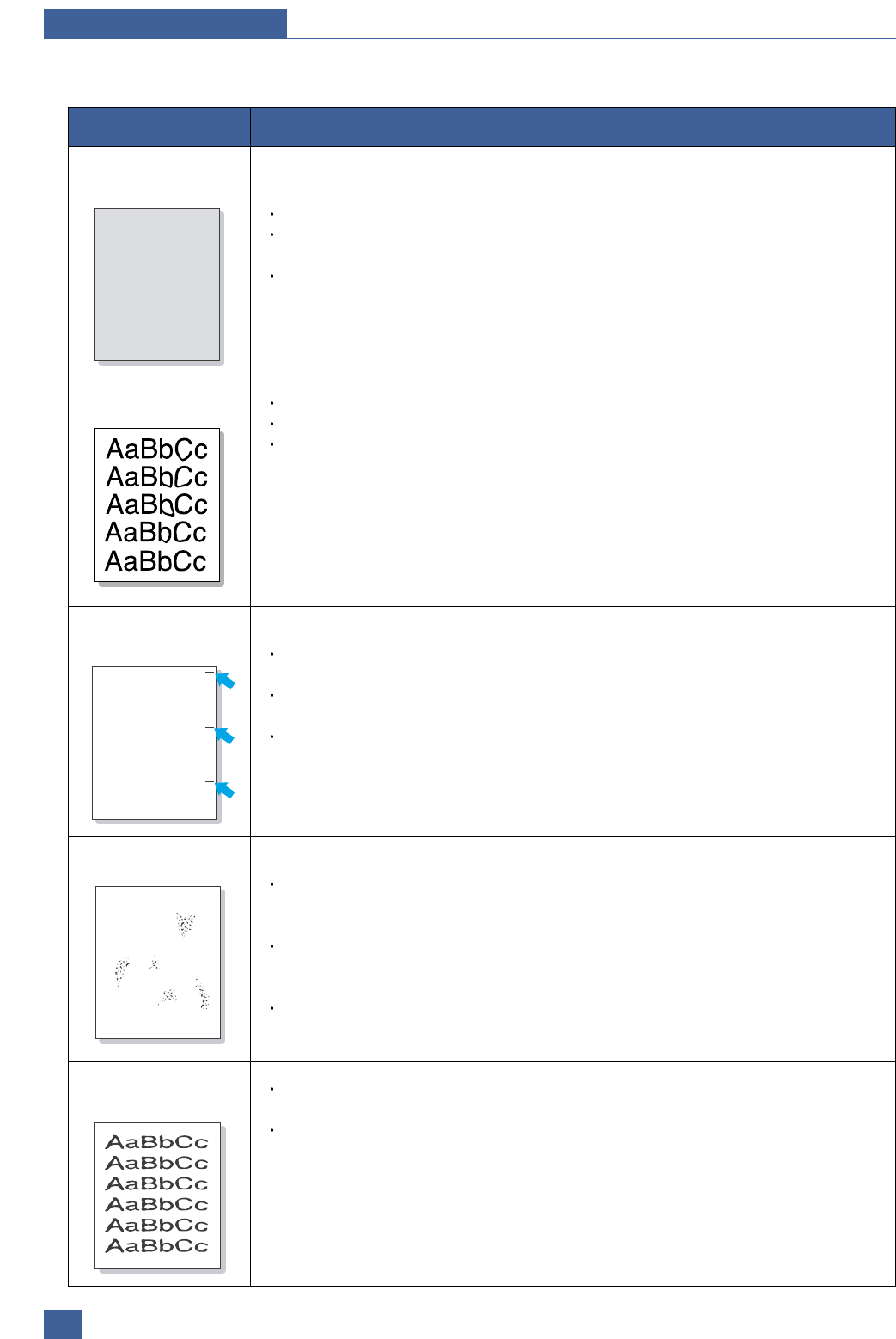
Samsung Electronics
Service Manual
Troubleshooting
7-8
Color or Black
background If the amount of background shading becomes unacceptable, the procedures below may
fix the problem.
Change to lighter weight paper.
heck the printer's environment; very dry (low humidity) or high humidity (higher than
80% RH) conditions can increase the amount of background shading.
Remove one of the old toner cartridges and install a new one.
Problem Solution
AaBbCc
AaBbCc
AaBbCc
AaBbCc
AaBbCc
Toner smear Clean the inside of the printer.
Check the paper type and quality.
Remove the imaging unit and install a new one.
Vertical repetitive
defects If marks repeatedly appear on the printed side of the page at even intervals:
Clean the inside of the printer. After cleaning the inside of the printer, if you still have the
same problems, install a new toner cartridge of the problem color.
Parts of the printer may have toner on them. If the defects occur on the back of the
page, the problem will likely correct itself after a few more pages.
The fusing assembly may be damaged. Contact a service representative.
AaBbCc
AaBbCc
AaBbCc
AaBbCc
AaBbCc
Background scatter Background scatter results from bits of toner distributed on the printed page.
The paper may be too damp. Try printing with a different batch of paper. Do not open
packages of paper until necessary so that the paper does not absorb too much mois-
ture.
If background scatter occurs on an envelope, change the printing layout to avoid print-
ing over areas that have overlapping seams on the reverse side. Printing on seams can
cause problems.
If background scatter covers the entire surface area of a printed page, adjust the print
resolution through your software application or via the printer properties window.
A
Misformed
characters If characters are improperly formed and producing hollowed images, the paper stock
may be too slick. Try a different paper.
If characters are improperly formed and producing a wavy effect, the printer may need
service. Verify that it also occurs on a demo page.
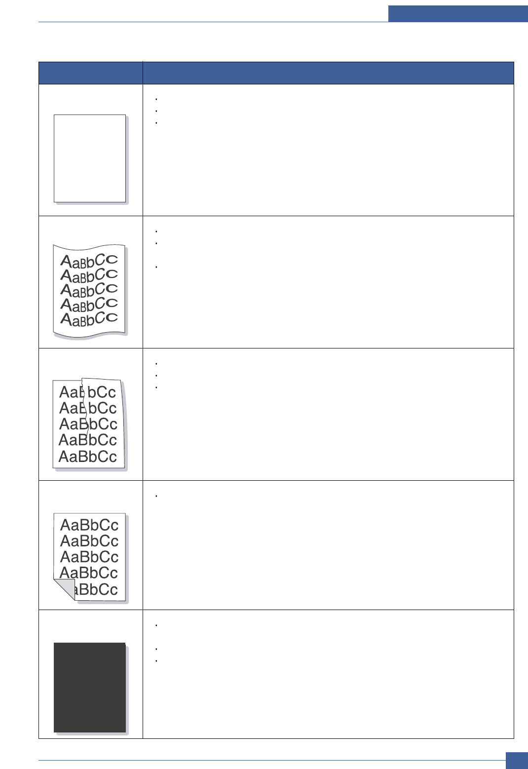
Troubleshooting
Samsung Electronics Service Manual
7-9
Page skew Ensure that the paper is loaded properly.
Check the paper type and quality.
Ensure that the paper or other material is loaded correctly and the guides are not too
tight or too loose against the paper stack.
Problem Solution
AaBbCc
AaBbCc
AaBbCc
AaBbCc
AaBbCc
Curl or wave Ensure that the paper is loaded properly.
Check the paper type and quality. Both high temperature and high humidity can cause
paper curl.
Turn the stack of paper over in the tray. Also try rotating the paper 180° in the tray.
Wrinkles or creases Ensure that the paper is loaded properly.
Check the paper type and quality.
Turn the stack of paper over in the paper tray. Also try rotating the paper 180° in the
tray.
Back of printouts
aredirty Check for leaking toner. Clean the inside of the printer.
Solid Color or
Black pages The toner cartridge may not be installed properly.
Remove the toner cartridge and reinsert.
The toner cartridge may be defective and need replacing. Install a new toner cartridge.
The printer may require repair. Contact a service representative.
A
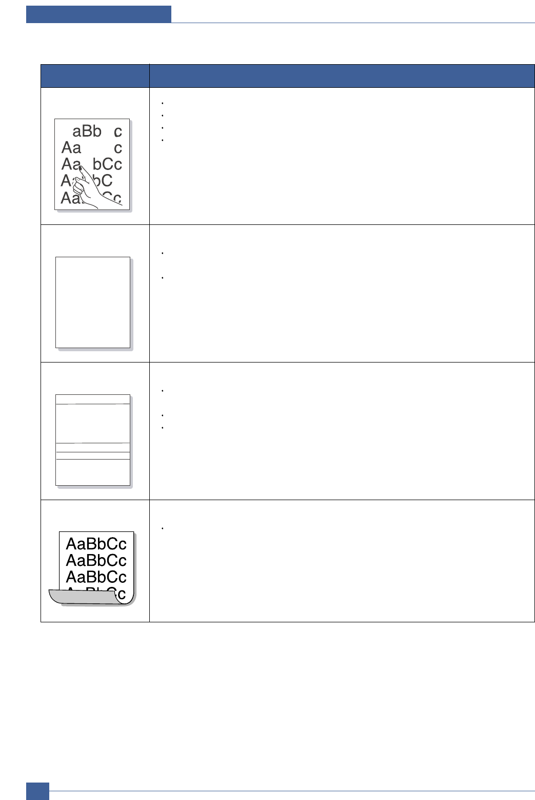
Samsung Electronics
Service Manual
Troubleshooting
7-10
Loose toner Clean the inside of the printer.
Check the paper type and quality.
Install a new toner cartridge.
If the problem persists, the printer may require repair. Contact a service representative.
Problem Solution
Character Voids Character voids are white areas within characters that should be solid black:
You may be printing on the wrong surface of the paper. Remove the paper and turn it
over.
The paper may not meet paper specifications.
A
Horizontal stripes If horizontally aligned color or black streaks or smears appear:
A toner cartridge may be installed improperly.
Remove the toner cartridge and reinsert.
A toner cartridge may be defective. Install a new toner cartridge.
If the problem persists, the printer may require repair. Contact a service representative.
AaBbCc
AaBbCc
AaBbCc
AaBbCc
AaBbCc
Curl If the printed paper is curled or paper does not feed into the printer:
Turn the stack of paper over in the paper tray. Also try rotating the paper 180° in the
tray.
Troubleshooting
Samsung Electronics Service Manual
7-11
7.5 Common Windows Problems
"File in Use" message appears
during installation. Exit all software applications. Remove all software from the StartUp Group,
then restart Windows. Reinstall the printer driver.
Problem Possible Cause and Solution
"Error Writing to LPTx" message
appears. Ensure that all cables are connected correctly and the printer is on.
If bi-directional communication is not turned on in the driver, it will also
cause this message.
"General Protection Fault",
"Exception OE", "Spool32", or
"Illegal Operation" messages
appear.
Close all other applications, reboot Windows and try printing again.
"Fail To Print", "A printer timeout
error occurred." messages appear. These messages may appear during printing. Just keep waiting until the
printer finishes printing. If the message appears in standby mode or after
printing has been completed, check the connection and/or whether an error
has occurred.
NOTE: Refer to the Microsoft Windows 98/Me/NT 4.0/2000/2003/XP User's Guide that came with your PC for further
information on Windows error messages.
7.6 Common Macintosh Problems
The printer does not print a
document from Acrobat Reader. You should change the Print Method option to Print as Image when you print
from Acrobat Reader.
Problem Possible Cause and Solution
The document has printed, but the
print job has not disappeared from
the spooler in Mac OS 10.3.2.
Update your Mac OS to OS 10.3.3 or higher.

Samsung Electronics
Service Manual
Troubleshooting
7-12
7.7 Common Linux Problems
I can't change settings in the
configuration tool. You need to have administrator privileges to be able to change global
settings.
Problem Possible Cause and Solution
I am using the KDE desktop but
the configuration tool and LLPR
won't start.
You may not have the GTK libraries installed. These usually come with most
Linux distributions, but you may have to install them manually. Refer to your
distribution's installation manual for more details about installing additional
packages.
I just installed this package but
can't find entries in the KDE/
Gnome menus.
Some versions of the KDE or GNOME desktop environments may require
that you restart your session for the changes to take effect.
I get a "Some options are not
selected" error message while
editing the printer settings.
Some printers have conflicting settings, meaning that some settings for two
options can't be selected at the same time. When you change a setting and
the Printer Package detects such a conflict, the conflicting option is changed
to a "No Choice" value. You have to choose an option that does not conflict
before being able to submit the changes.
The N-up setting does not work
correctly for some of my
documents.
The N-up feature is achieved through post-processing of the PostScript data
that is sent to the printing system. However, such post-processing can
only be adequately achieved if the PostScript data conforms to the Adobe
Document Structing Conventions. Problems may arise when using N-up
and other features that rely on post-processing if the document being printed
isn't compliant.
I am using BSD lpr (Slackware,
Debian, older distributions) and
some options chosen in LLPR
don't seem to take effect.
Legacy BSD lpr systems have a hard limitation on the length of the option
string that can be passed to the printing system. As such, if you selected a
number of different options, you may have exceeded the length of the
options and some of your choices won't be passed to the programs
responsible for implementing them. Try to select fewer options that deviate
from the defaults, to save on memory usage.
I can't make a printer the system
default. In some conditions, it may not be possible to change the default queue. This
happens with some variants of LPRng, especially on recent RedHat systems
that use the "printconf" database of queues.
When using printconf, the /etc./printcap file is automatically refreshed from
the database of printers managed by the system (usually through the "print-
tool" command), and the queues in /etc./printcap.local are appended to the
resulting file. The default queue in LPRng is defined as the first queue in
/etc./printcap, and therefore it is not possible for the Linux Printer Package to
change the default when some queues have otherwise been defined using
printtool.
LPD systems identify the default queue as the one named "lp". Thus, if there
is already a queue by this name, and if it doesn't have an alias, then you
won't be able to change the default. To work around this, you can either
delete the queue or rename it by manually editing the /etc./printcap file.

Troubleshooting
Samsung Electronics Service Manual
7-13
I am trying to print a document in
Landscape mode, but it prints
rotated and cropped.
Most Unix applications that offer a Landscape orientation option in their print-
ing options will generate correct PostScript code that should be printed as is.
In that case, you need to make sure that you leave the LLPR option set to its
default Portrait setting, to avoid unwanted rotations of the page that would
result in cropped output.
Problem Possible Cause and Solution
I can't print to an SMB (Windows)
printer. To be able to configure and use SMB-shared printers (such as printers
shared on a Windows printer), you need to have a correct installation of the
SAMBA package that enables that feature. The "smbclient" command should
be available and usable on your system.
My application seems to be frozen
while LLPR is running. Most Unix applications will expect a command like the regular "lpr" command
to be non-interactive and thus return immediately. Since LLPR is waiting
for user input before passing the job on to the print spooler, very often the
application will wait for the process to return, and thus will appear to be
frozen (its windows won't refresh). This is normal and the application should
resume functioning correctly after the user exits LLPR.
How do I specify the IP address of
my SMB server? It can be specified in the "Add Printer" dialogue of the configuration tool, if
you don't use the CUPS printing system. Unfortunately, CUPS currently
doesn't allow you to specify the IP address of SMB printers, so you will have
to be able to browse the resource with SAMBA in order to be able to print.
Some documents come out as
white pages when printing. Some versions of CUPS, especially those shipped with Mandrake Linux
before the 8.1 release, have some known bugs when processing PostScript
output from some applications. Try upgrading to the latest version of CUPS
(at least 1.1.14). Some RPM packages for the most popular distributions are
provided as a convenience with this Linux Printing Package.
I have CUPS and some options
(such as N-up) seem to be always
enabled even though I don't
choose them in LLPR.
There may be some local options defined in your ~/ .lpoptions file, which are
manipulated by the lpoptions command. These options are always used
if not overridden by LLPR settings. To get rid of all options for a printer, run
the following command, replacing "printer" with the name of the queue:
lpoptions -x printer
I configured a printer to print to a
file, but I get "Permission denied"
errors.
Most printing systems will not run as the super-user but as a special user
(usually "lp"). Therefore, make sure that the file you have chosen to print to is
accessible to the user owning the spooler daemon.
Some pages come out all white
(nothing is printed), and I am using
CUPS.
If the data being sent is in Encapsulated PostScript (EPS) format, some earli-
er versions of CUPS (1.1.10 and before) have a bug preventing them from
being processed correctly. When going through LLPR to print, the Printer
Package will work around this issue by converting the data to regular
PostScript.
However, if your application bypasses LLPR and feeds EPS data to CUPS,
the document may not print correctly.

Samsung Electronics
Service Manual
Troubleshooting
7-14
On my PCL (or GDI) printer, I
sometimes get error messages
printing instead of my document.
Unfortunately, some Unix applications may generate non-compliant
PostScript output that may not be supported by Ghostscript, or even the
printer itself in PostScript mode. You can try to capture the output to a file and
view the results with Ghostscript (gv or ghostview will allow you to do so
interactively) and see if you get error messages.
However, since the application is probably at fault, contact your software ven-
dor to inform them of the issue.
Problem Possible Cause and Solution
Some color images come out all
black. This is a known bug in Ghostscript (until GNU Ghostscript version 7.05)
when the base color space of the document is indexed color space and it is
converted through CIE color space. Because Postscript uses CIE color
space for Color Matching System, you should upgrade Ghostscript on your
system to at least GNU Ghostscript version 7.06 or later. You can find recent
Ghostscript versions at www.ghostscript.com.
Troubleshooting
Samsung Electronics Service Manual
7-15
7.8 Major Problems Trouble shooting
7.8.1 Vertical Line and Band
7.8.2 Vertical White Line
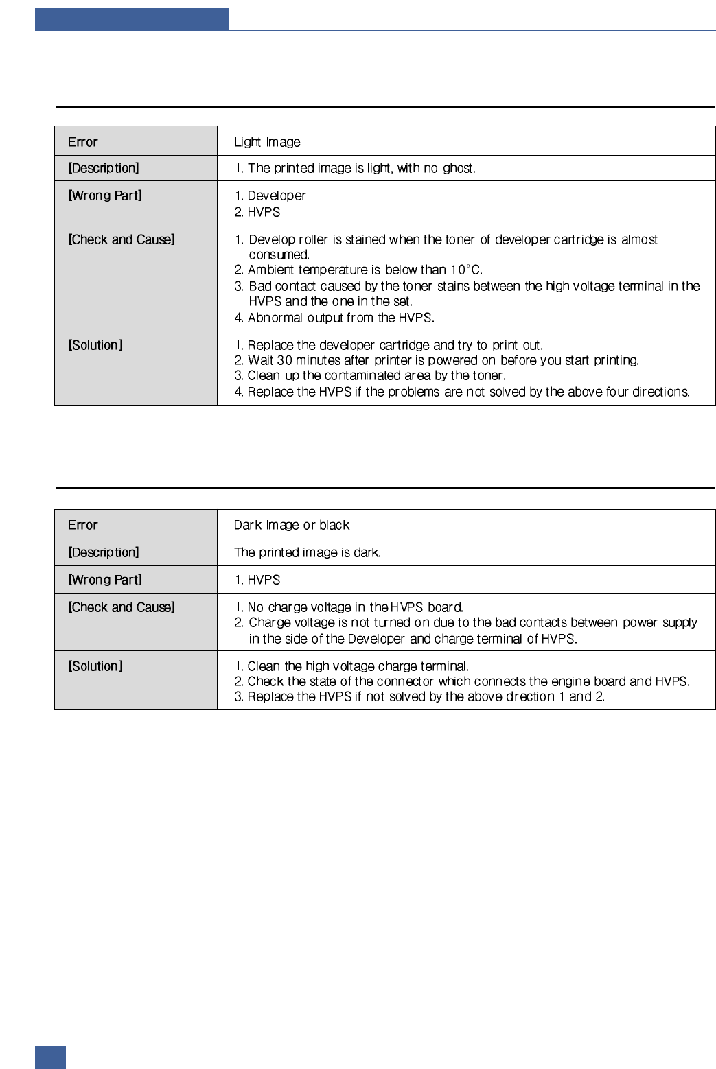
Samsung Electronics
Service Manual
Troubleshooting
7-16
7.8.3 Light Image
7.8.4 Dark Image or black
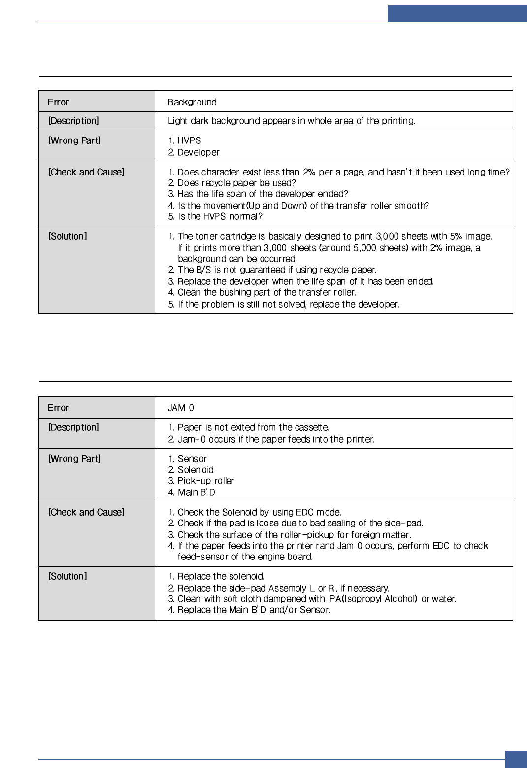
Troubleshooting
Samsung Electronics Service Manual
7-17
7.8.5 Background
7.8.6 JAM 0
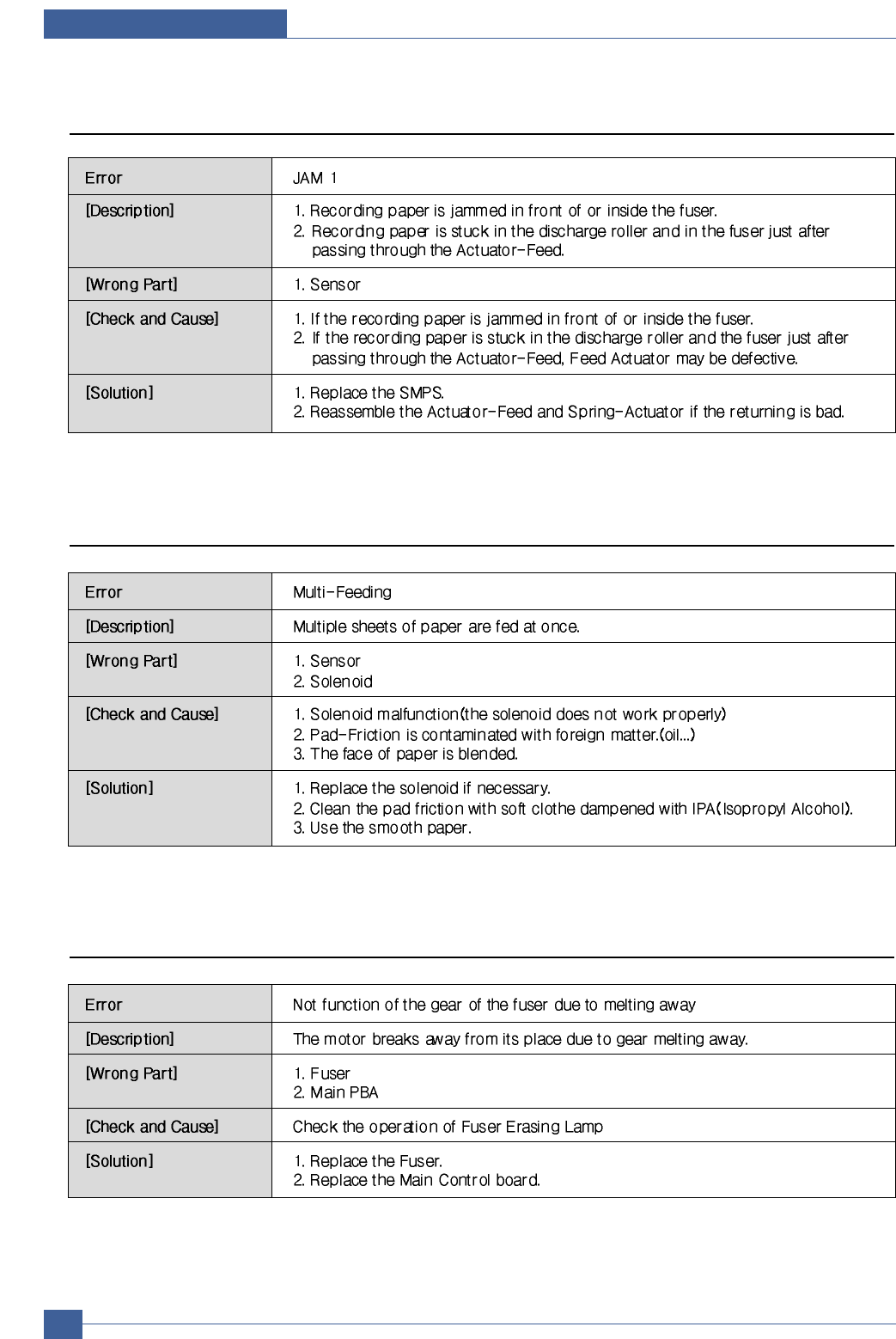
Samsung Electronics
Service Manual
Troubleshooting
7-18
7.8.7 JAM 1
7.8.8 Multi-Feeding
7.8.9 Not function of the gear of the fuser due to melting away
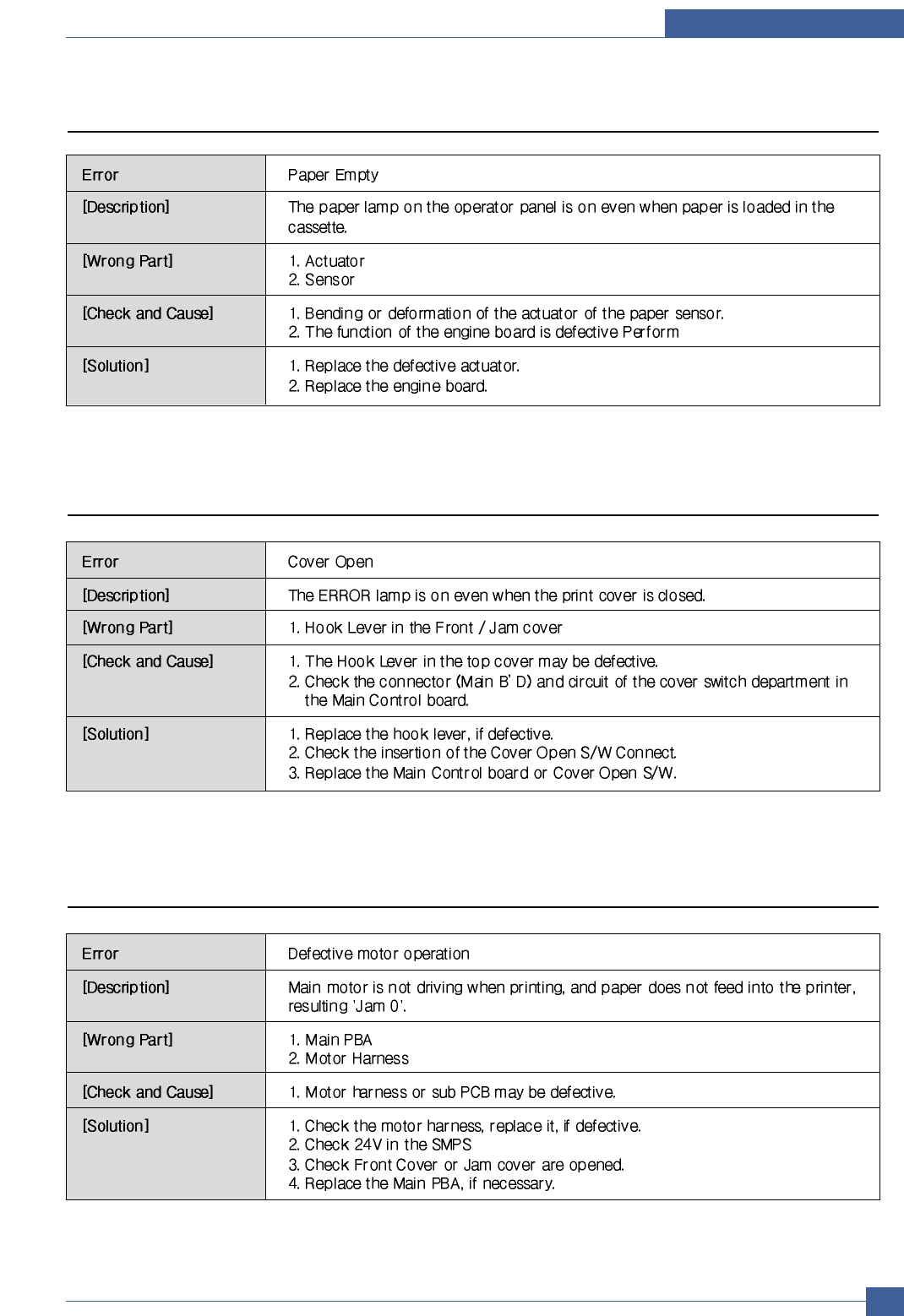
Troubleshooting
Samsung Electronics Service Manual
7-19
7.8.10 Paper Empty
7.8.11 Cover Open
7.8.12 Defective motor operation
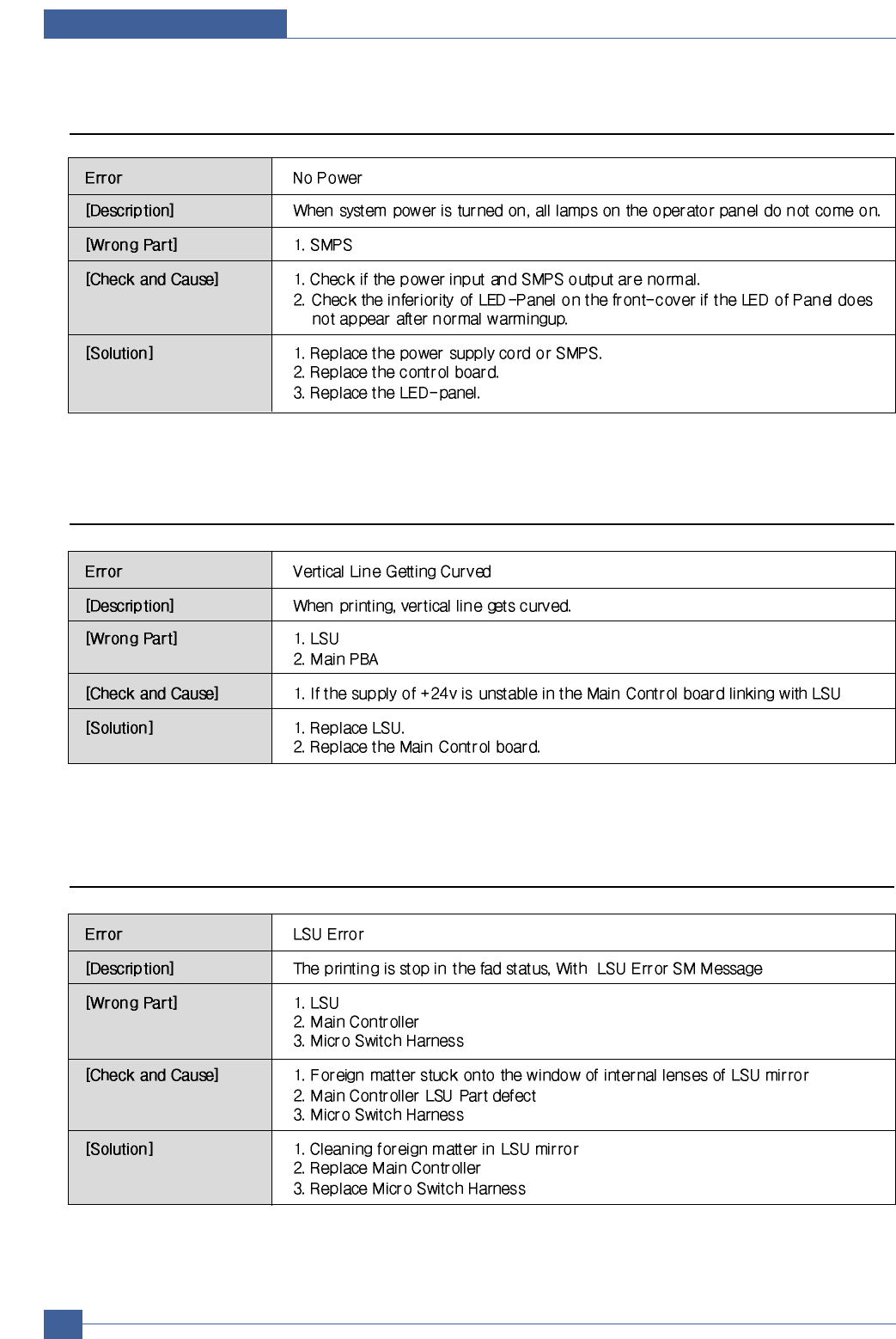
Samsung Electronics
Service Manual
Troubleshooting
7-20
7.8.13 No Power
7.8.14 Vertical Line Getting Curved
7.8.15 LSU Error
Exploded Views & Parts List
Samsung Electronics Service Manual
8-1
8
88.1 Main 8-2
8.2 Top Cover 8-3
8.3 Rear Cover 8-4
8.4 Front Cover 8-5
8.5 Main Driver 8-6
8.6 Main Frame 8-9
8.7 LSU Cover 8-10
8.8 Fuser Unit 8-11
8.9 ELA-UNIT OPC DEV 8-12
8.10 ITB Unit 8-13
8.11 Casstte Unit 8-14
Contents
8. Exploded Views and Parts List
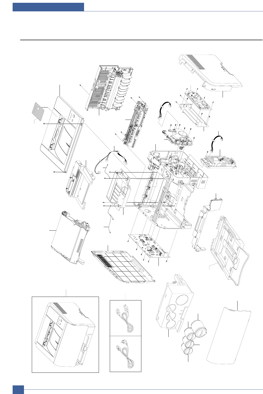
Samsung Electronics
Service Manual
Exploded Views & Parts List
8-2
8.1 Main
0
1
2
3
4
5
7
8
9
10
11
12
13
14
15
16
17
18
19
20
21
22
23
24 25
26
27
28
6
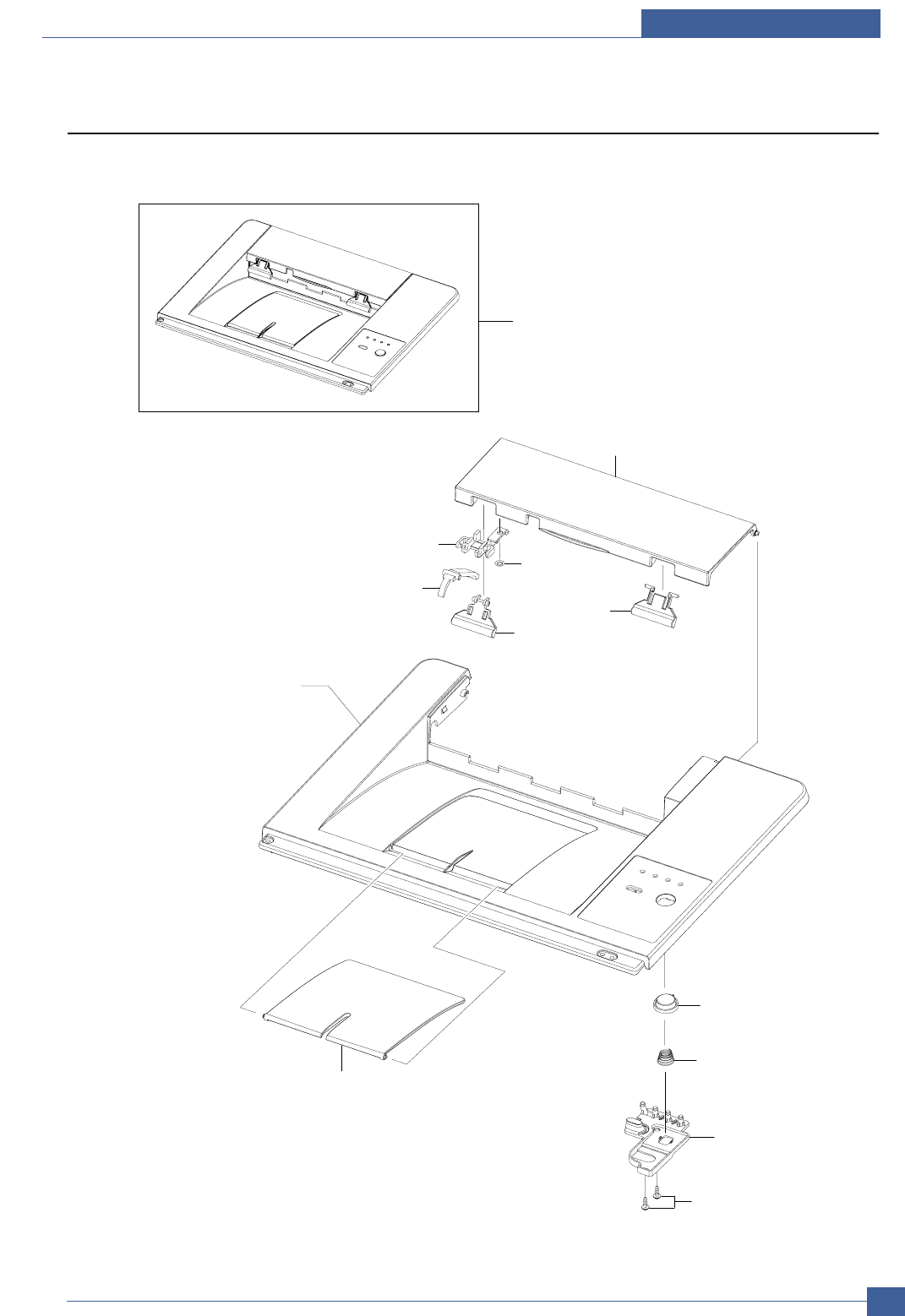
8.2 Top Cover
0
3
8
9
10
11
7
2
1
4
6
5
12
Samsung Electronics Service Manual
8-3
Exploded Views & Parts List
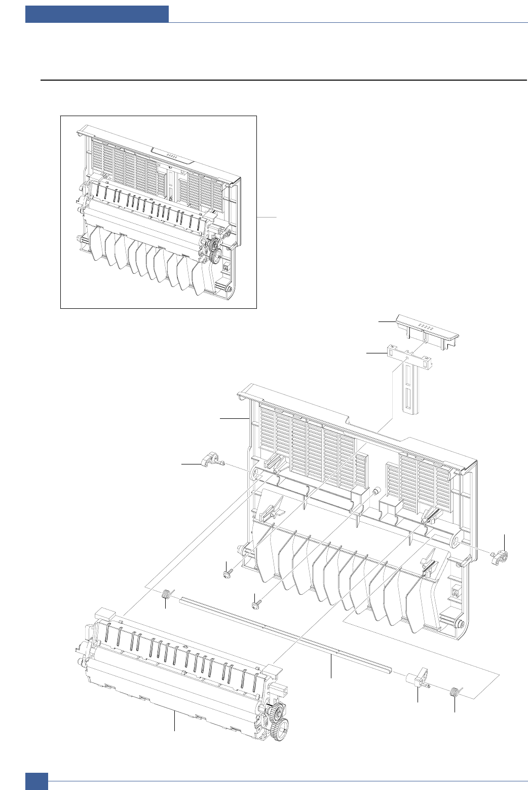
Samsung Electronics
Service Manual
Exploded Views & Parts List
8-4
8.3 Rear Cover
0
2
7
1
5
4
9
9
8
3
6
8
10
8.4 Front Cover
0
2
1
Samsung Electronics Service Manual
8-5
Exploded Views & Parts List
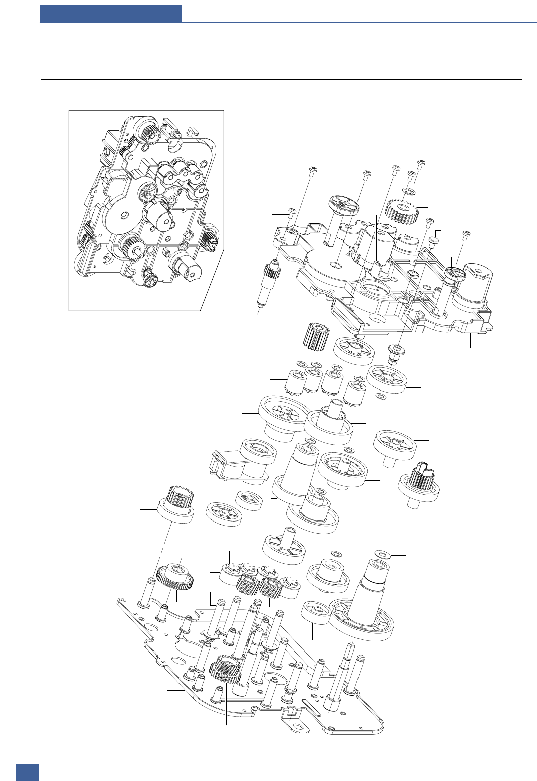
Exploded Views & Parts List
Samsung Electronics
Service Manual
8-6
8.5 Main Driver(1)
0
31 30 29
32
36
34
25
26
27
27
28
37
35
20
7
19
15
2
14
17
16
18
13
12
1
2
3
45
8
21
22 23 24
7
6
9
10
11
33
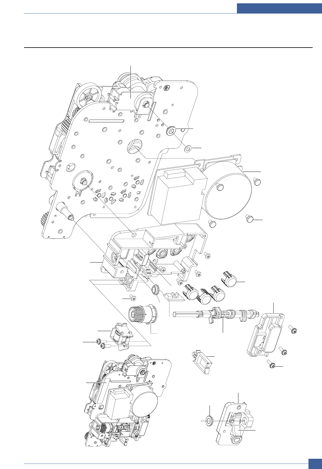
Main Driver(2)
49
11
23
28 38
42
43
50
49
48
47
49
47
45
46
44
41
42
52
40
39
Samsung Electronics Service Manual
8-7
Exploded Views & Parts List
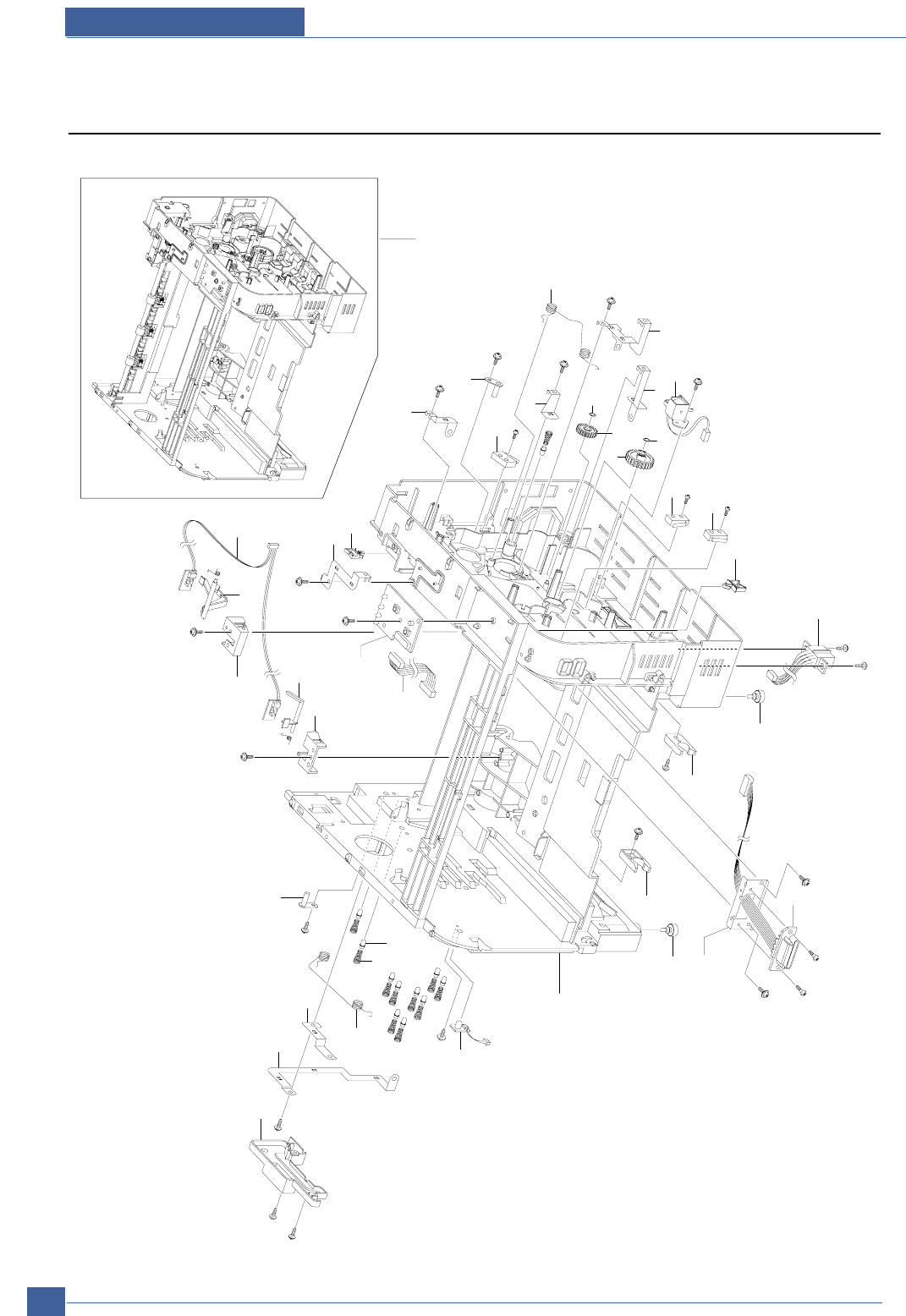
Exploded Views & Parts List
8.6 Main Frame(1)
0
1
2
2
3
3
4
5
6
7
8
8
8
7
9
10
11
11
12
13 14
15
16
17
18
19
20
21
22
23
24
25
26
27
28
17
29
30 31
32
33
34
35
Samsung Electronics
Service Manual
8-8
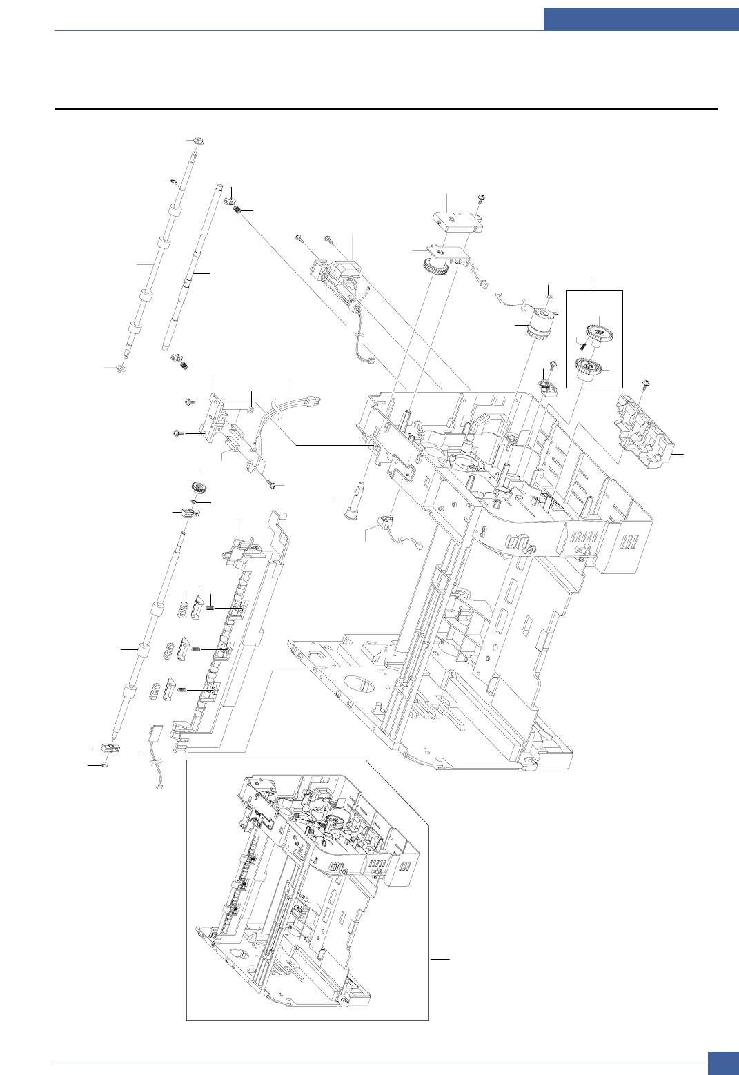
Main Frame(2)
0
36
37
38
39
40
41
42
43
43
42
44
45
46
47
48
49
50
51
52
53
54
55
56
57
58
58-1
58-2
58-3
59
60
61
62
63
64
65
63
Samsung Electronics Service Manual
8-9
Exploded Views & Parts List
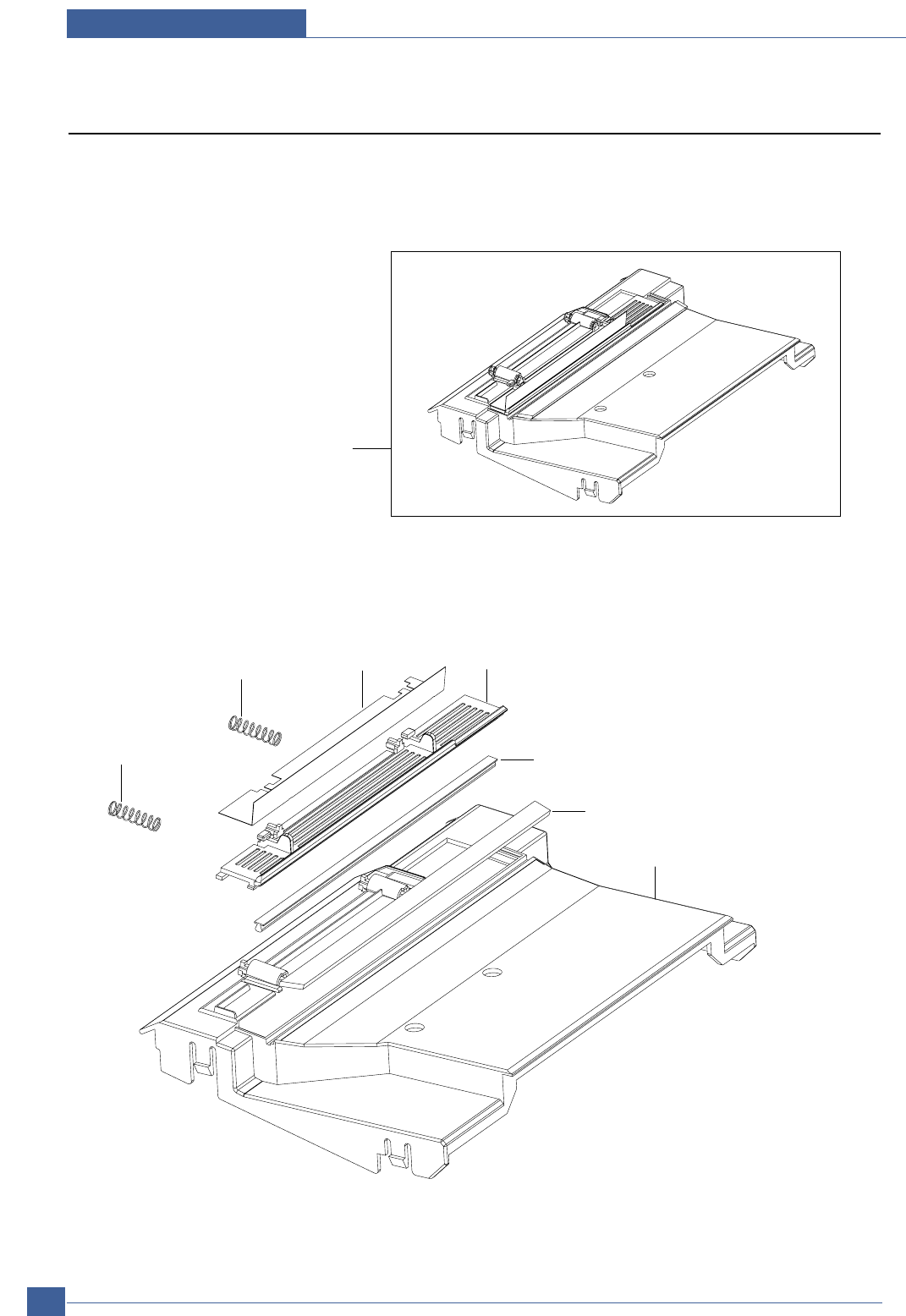
Exploded Views & Parts List
8.7 LSU Cover
0
5
4
4
2
1
6
3
Samsung Electronics
Service Manual
8-10
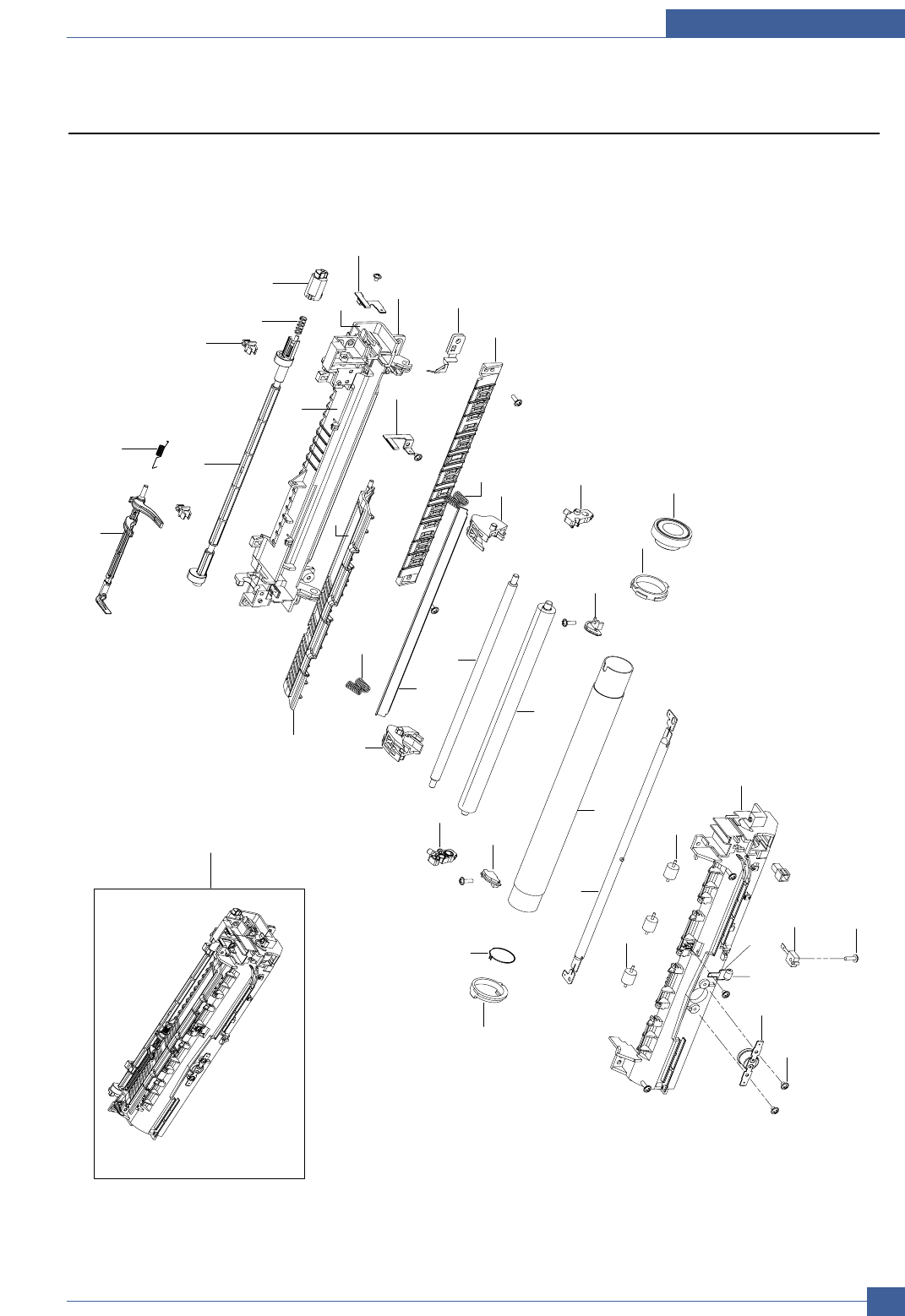
Exploded Views & Parts List
Samsung Electronics Service Manual
8-11
8.8 Fuser Unit
0
15
38
33 32
40 34
17
2
18
14
10
16
22
19
20
21
39
9
8
13
11
3
28
36
4
5
12
35
43
6
31
30
1
29
26
27
740 41
37
23
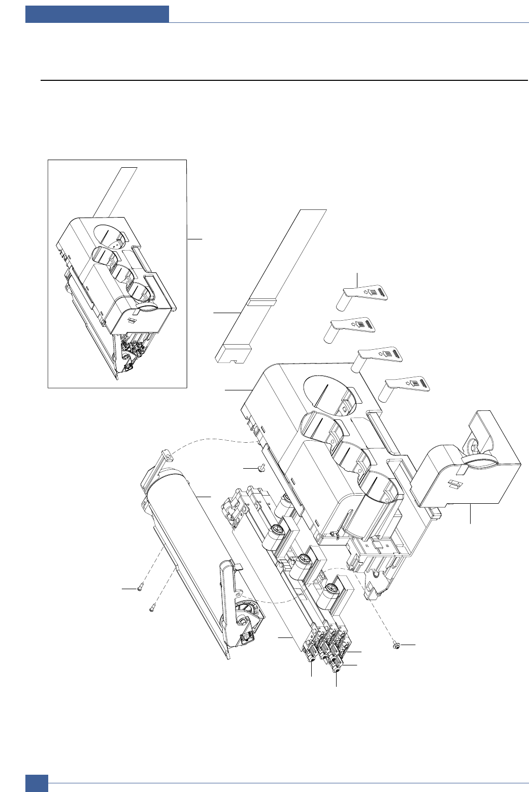
Samsung Electronics
Service Manual
Exploded Views & Parts List
8-12
8.9 ELA-UNIT OPC DEV
0
3
2
10 9
11
6
16
2
15
13
14
12
5
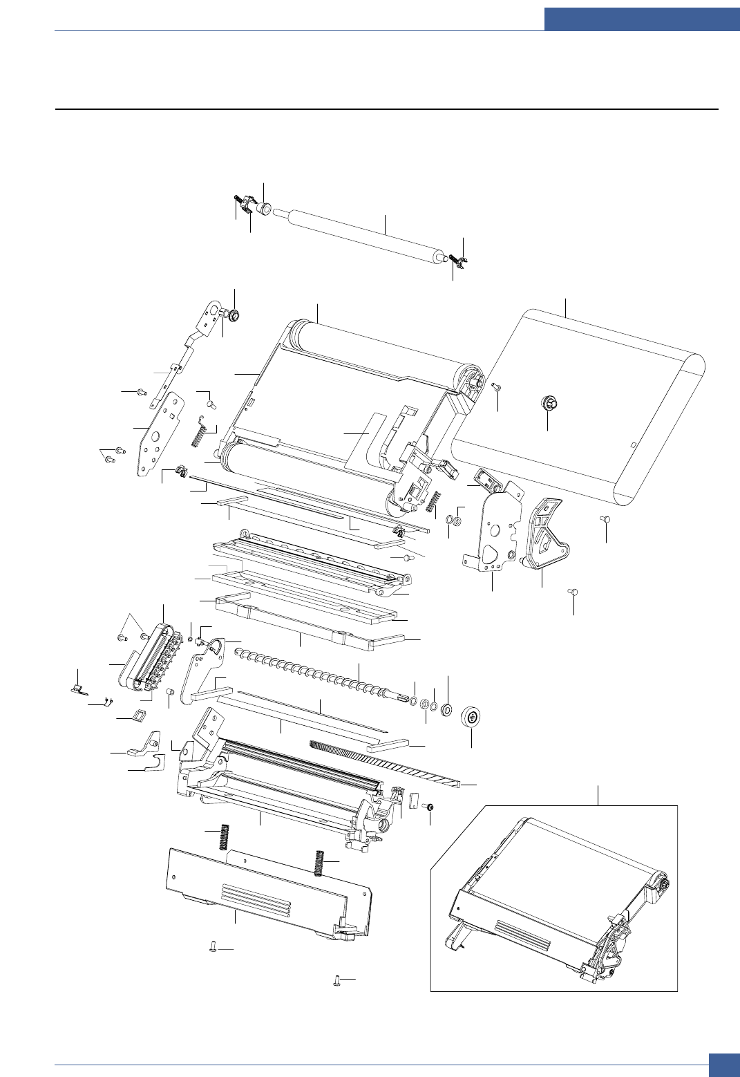
8.10 ITB Unit
0
9
26
14
9
17
29
13 72
64
61
51 6
25
60
6
6
56
20
59
24
58
41
54
48
52 32
7
22 5
16
50
6
38
38
43 37
37
36
34
68
33 53
40
76
6
6
6
27
31
55 46
57
15
47
6
49
30 35 28
65
44
39
1842
8
8
62
39
7
7
27
40
45
23
10
6
19
21
6
Samsung Electronics Service Manual
8-13
Exploded Views & Parts List
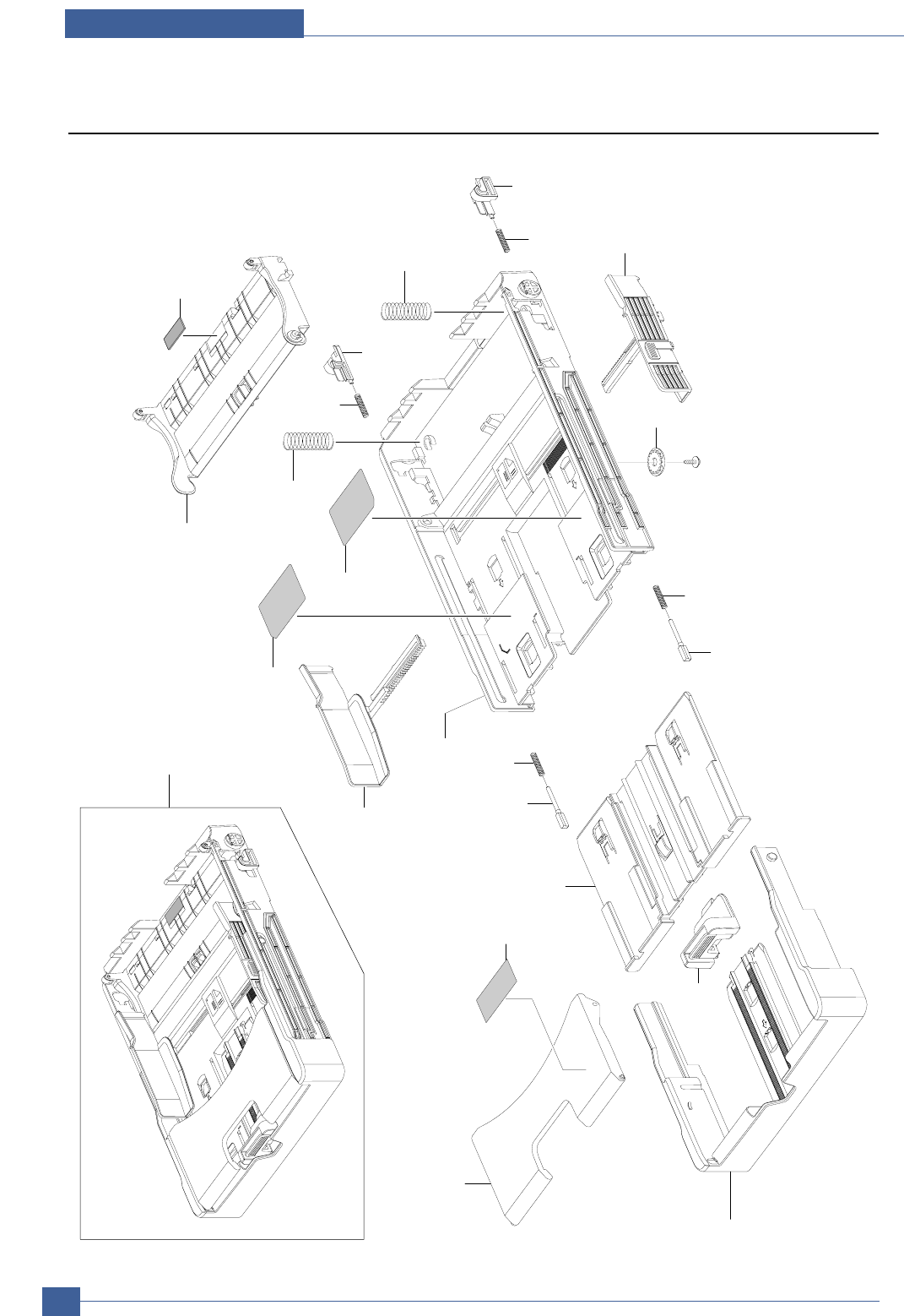
8.11 Casstte Unit
0
1
2
3
4
5
67
6
7
8
9
10
11
12
13
14
14
15
16
17
17
18 19
Samsung Electronics
Service Manual
Exploded Views & Parts List
8-14

Parts List
Drawer# SEC-Code Description & Specification Location Service
8.1-1 JC97-02330A MEA UNIT-FRAME;CLP-300,SEC,WORLD,-,-,-,- Z4398 SA
8.1-2 JC63-00842A COVER-M-LEFT SIDE;CLP-300,ABS FR,T2.5,23 Z4399 SA
8.1-3 JC63-00847A COVER-M-DUMMY FRONT;CLP-300,ABS FR,T2.5, Z4400 SA
8.1-4 JC63-01102B SHEET-COVER TOP;CLP-300,PC SHEET,T0.5,W7 SA
8.1-6 JC96-03608A ELA UNIT-DRIVE MAIN;CLP-300,SEC,WORLD,-, Z4403 SA
8.1-7 JC96-03610F ELA UNIT-OPC DEV_SET;CLP-300,SEC,EXPORT, SA
8.1-8 JC96-03611A ELA UNIT-ITB_SET;CLP-300,SEC,WORLD,SET,- Z4404 SA
8.1-9 JC96-03615A ELA UNIT-TONER TANK C;CLP-300,SEC,EXPORT SNA
8.1-10 JC96-03614A ELA UNIT-TONER TANK M;CLP-300,SEC,EXPORT SNA
8.1-11 JC96-03613A ELA UNIT-TONER TANK Y;CLP-300,SEC,EXPORT SNA
8.1-12 JC96-03616A ELA UNIT-TONER TANK K;CLP-300,SEC,EXPORT SNA
8.1-13 JC97-02332A MEA-UNIT CASSETTE;CLP-300,SEC,WORLD,-,-, Z4405 SA
8.1-14 JC97-02439A MEA UNIT-COVER TOP;CLP-300,SEC,WORLD,-,- Z4406 SA
8.1-15 JC97-02440A MEA UNIT-COVER REAR;CLP-300,SEC,WORLD,-, Z4407 SA
8.1-16 JC97-02659A MEA-UNIT COVER FRONT;CLP-300,SEC,WORLD,- Z4408 SA
8.1-18 JC63-00863A SHIELD-P-MAIN LOWER;CLP-300,SECC,T1.0,99 SNA
8.1-19 JC44-00090A SMPS-PSP_TYPE3_V2C;SCX-4521F,*,AC/DC,-,2 D2114 SA
8.1-20 JC44-00089A HVPS-GOGH;-,24V,21.6V~26.4V,-,-,-,- Z4410 SA
8.1-21 JC59-00018E UNIT-LSU;CLP-300,-,-,STANDARD SINGLEBEAM Z4411 SA
8.1-22 JC97-02656A MEA UNIT-COVER LSU;CLP-300,SEC,EXPORT,-, Z4412 SA
8.1-23 JC96-03609A ELA UNIT-FUSER 220V;CLP-300,SEC,WORLD,-, Z4413 SA
8.1-29 JC97-01771A MEA UNIT-TERMINAL S;CLP-500,SEC,EXPORT,S K3635 SA
8.1-30 3903-000042 CBF-POWER CORD;DT,EU,FP3/YES,IEC320 C13/ C0022 SA
8.2-1 JC61-01460A GUIDE-M-STACKER COVER;CLP-300,ABS FR V0, SNA
8.2-2 JC63-00846A COVER-M-TOP;CLP-300,ABS FR,T2.5,279.3,37 SNA
8.2-3 JC63-00843A COVER-M-JAM COVER;CLP-300,ABS FR,-,79.4, SNA
8.2-4 JC64-00211A KEY-M-OP1;CLP-300,ABS,-,-,36024,-,HF-066 Z4414 SA
8.2-5 JC63-00860A COVER-M-LED;CLP-300,ABS,T1.5,52,77.9,-,- SNA
8.2-6 6107-001169 SPRING-CS;SUS304-WPB,-,PI0.55,D9.3,14.25 Z4415 SA
8.2-6 6107-001306 SPRING-CS;SUS304-WPB,-,PI0.55,D6.45,L11, SA
8.2-6 6107-001285 SPRING-CS;SUS304-WPB,-,PI0.45,D8.85,L12, SNA
8.2-6 6107-001278 SPRING-CS;SUS304 WPB,-,PI0.7,D6.9,L20,-, Z4416 SA
8.2-6 6107-001292 SPRING-CS;SUS304-WPB,-,PI0.55,-,L11.1,-, SNA
8.2-7 JC72-01343A PMO-SUB_M_STACKER;ML-1520,PC,BLACK,39*25 Z4139 SA
8.2-8 JC61-01761A HOLDER-LEVER BLOCKING;CLP-300,PC,2.5,30. SNA
8.2-9 JC66-01297A LEVER-MID BLOCKING;CLP-300,PC+GF20,2.5,1 SNA
8.2-10 JC66-01296A LEVER-BLOCKING;CLP-300,PC,2.5,39.6,30.2, SNA
8.2-11 6044-000001 RING-CS;ID3,OD3,T0.25,BLACK,SUS304 SNA
8.2-11 6044-001005 RING-CS;ID4.8,OD10.0,T0.25,PASS,SUS-30 Z4417 SA
8.2-12 6002-000440 SCREW-TAPPING;PWH,+,-,2,M3,L8,ZPC(BLK),S Z4418 SA
8.3-1 JC63-00844A COVER-M-REAR;CLP-300,ABS,T3.0,249.3,296. SNA
8.3-2 JC64-00215A BUTTON-M-OPEN REAR;CLP-300,ABS FR V0,80. SNA
8.3-3 JC66-01089A SHAFT-P-LOCKBAR REAR;CLP-300,SECC,284,6, SNA
8.3-4 JC61-01461A HOLDER-M-HOOK REAR R;CLP-300,POM,T5.0,19 SNA
8.3-5 JC61-01456A HOLDER-M-HOOK REAR L;CLP-300,POM,T5.0,19 SNA
8.3-6 JC61-01462A HOLDER-M-HOOK REAR C;CLP-300,POM,T5.0,19 SNA
8.3-7 JC66-01071A LEVER-M-REAR LOCK;CLP-300,HIPS,T2.5,55.1 SNA
8.3-8 6107-001268 SPRING-TS;SUS304 WPB,-,PI0.9,D8.9,L7,-,- Z4419 SA
8.3-8 6107-001283 SPRING-TS;SWRS82A,-,1.0X0.6,D13.70,L12.1 Z4420 SA
8.3-8 6107-001284 SPRING-TS;SWRS82A,-,0.75X0.5,-,L8.4,-,-, SNA
8.3-10 JC96-03990A ELA UNIT-TRANSFER;CLP-300,SEC,EXPORT,-,- Z4421 SA
8.4-1 JC63-00841A COVER-M-FRONT;CLP-300,ABS FR,T2.5,185.3, SNA
8.4-2 JC68-01678A LABEL-INSTRUCTION;CLP-300,-,YUPO 150G,15 SNA
Service Parts List (Model code : CLP-300/XSG)
SA : SERVICE AVAILABLE SNA : SERVICE not AVAILABLE DNA : DELIVERY not AVAILABLE
1

Parts List
Drawer# SEC-Code Description & Specification Location Service
SA : SERVICE AVAILABLE SNA : SERVICE not AVAILABLE DNA : DELIVERY not AVAILABLE
8.5-1 JC61-01450A BRACKET-P-DRIVE MOTOR;CLP-300,SECC,T1.2, SNA
8.5-2 6031-001528 WASHER-PLAIN;POLYMIDE,-,ID6,OD13.5,T0.5, Z4422 SA
8.5-2 6031-001051 WASHER-PLAIN;M4,ID4.1,OD7.0,T0.13,*,POLY SNA
8.5-2 6031-001543 WASHER-PLAIN;POLY,-,ID5.1,OD8,T0.13,-,- SNA
8.5-2 6031-001547 WASHER-PLAIN;POLY,-,ID6.5,OD12,T0.5,-,- SNA
8.5-2 6031-001577 WASHER-PLAIN;POLY,-,ID5.1,OD14,T0.5,BLK, SNA
8.5-3 JC66-01042A GEAR-IDLE DEVE Z19;CLP-300,POM,M0.8,Z19, Z4423 SA
8.5-4 JC66-01052A GEAR-RDCN DEVE CAM;CLP-300,POM,M0.8/M0.6 Z4424 SA
8.5-5 JC66-01041A GEAR-DEVE COUPLING;CLP-300,POM,M0.8,Z18, Z4425 SA
8.5-6 6107-001271 SPRING-CS;SUS304 WPB,-,PI0.55,D6.75,L9.0 Z4426 SA
8.5-7 JC66-01047A GEAR-IDLE Z39;CLP-300,POM,M0.8,Z39,-,WHI Z4427 SA
8.5-8 JC66-01065A GEAR-TONER DRIVE;CLP-300,POM,M0.8/Z0.8,Z Z4428 SA
8.5-9 JC66-01046A GEAR-IDLE Z33;CLP-300,POM,M0.8,Z33,-,WHI Z4429 SA
8.5-10 JC66-00763A GEAR-M-PICK UP IDLE;CLP-600,POM,M0.8,SPU G0031 SA
8.5-11 JC47-00007E MEP-CLUTCH CAM;-,CLP-300,-,DC24V,0.133A, Z4430 SA
8.5-12 JC66-01208A GEAR-RDCN FUSER CAM;CLP-300,POM,M0.8/Z0. Z4431 SA
8.5-13 JC66-01045A GEAR-IDLE ITB Z43;CLP-300,POM,M0.5,Z43,- Z4432 SA
8.5-14 JC66-01048A GEAR-ITB DRIVE;CLP-300,POM,M0.5/M0.5,Z10 Z4433 SA
8.5-15 JC66-01054A GEAR-RDCN OPC;CLP-300,POM,M0.5/M0.6,Z79/ Z4434 SA
8.5-16 JC63-01049A SHEET-HOUSING ITB;CLP-300,PET FILM,T0.18 SNA
8.5-17 JC66-01051A GEAR-RDCN DEVE;CLP-300,POM,M0.5/M0.8,Z73 Z4435 SA
8.5-18 JC66-01055A GEAR-RDCN P_PATH;CLP-300,POM,M0.5/M0.8,Z Z4436 SA
8.5-19 JC66-01050A GEAR-PICK UP DRIVE;CLP-300,POM,M0.8/M0.8 Z4437 SA
8.5-20 JC66-01044A GEAR-FUSER DRIVE 1;CLP-300,POM,M0.8,Z45, Z4438 SA
8.5-21 JC66-01053A GEAR-RDCN EXIT;CLP-300,POM,M0.8/M0.8,Z51 Z4439 SA
8.5-22 JC66-01043A GEAR-DEVE DRIVE;CLP-300,POM,M0.6,Z21,-,W Z4440 SA
8.5-23 6031-001255 WASHER-PLAIN;NYLON,CUTTING,ID5,OD9,T0.5, W0004 SA
8.5-24 JC66-00771A GEAR-_M_IDLE PICKUP;CLP-600,POM,M0.8,SPU G0010 SA
8.5-25 JC61-01459A BRACKET-M-DRIVE FRONT;CLP-300,PC,T2.5,W1 SNA
8.5-26 JC66-01061A SHAFT-IDLE D8;CLP-300,SUM24L+NI,L16.7,D1 SNA
8.5-27 JC66-01064A GEAR-IDLE Z37;CLP-300,POM,M0.8,Z37,-,WHI Z4441 SA
8.5-28 6003-000301 SCREW-TAPTITE;BH,+,S,M4,L6,ZPC(YEL),SWRC SNA
8.5-28 6003-000152 SCREW-TAPTITE;PH,+,B,M2,L10,ZPC(YEL),SWR Z4442 SA
8.5-28 6002-000308 SCREW-TAPTITE;PH,+,B,M2.6,L6,ZPC(YEL),SW Z4443 SA
8.5-29 JC66-01060A SHAFT-WORM GEAR;CLP-300,SUM24L+NI,L44.6, SNA
8.5-30 JC66-01057A GEAR-WORM DEVE CAM;CLP-300,POM,M0.6/M0.6 Z4444 SA
8.5-31 6044-000159 RING-C;ID3,OD7,T0.6,PASS,STSC Z4357 SA
8.5-32 6001-000130 SCREW-MACHINE;BH,+,M3,L6,ZPC(WHT),SWRCH1 Z4445 SA
8.5-32 6001-000485 SCREW-MACHINE;PH,+,M2.6,L4,ZPC(YEL),SWRC SNA
8.5-33 JC66-01070A LATCH-M-HUB CLUTCH;CLP-300,POM,T2.0,D18. SNA
8.5-34 JC66-01155A GEAR-FUSER RDCN OUT V;ML-3560,HTNFR52G30 SNA
8.5-35 6044-000231 RING-E;ID5.0,OD11.0,T0.6,PASS,STS304 R0006 SA
8.5-36 JC66-01068A SHAFT-M-T2 CAM;CLP-300,POM,L52,D20,BLACK Z4446 SA
8.5-37 JC66-01067A SHAFT-M-ITB CLEAN CAM;CLP-300,POM,L44,D2 Z4447 SA
8.5-38 JC31-00041A MOTOR DC-DEVE DRIVE;50M843A152,CLP-600,2 M0024 SA
8.5-39 JC33-00015C SOLENOID-PICK UP;-,CLP-300,DC24V,48§Ù¡¾1 S Z4448 SA
8.5-40 6003-000269 SCREW-TAPTITE;BH,+,-,S,M3,L6,ZPC(YEL),SW Z4449 SA
8.5-41 JC61-01458A BRACKET-M-DEVE CAM;CLP-300,PC+ABS,T2.5,W SNA
8.5-42 6003-000196 SCREW-TAPTITE;PWH,+,B,M3,L10,NI PLT,SWRC Z4397 SA
8.5-43 JC67-00130A CAP-M-PUSH COUPLING;CLP-300,POM,T2.0,D13 Z4450 SA
8.5-44 JC97-01788B MEA UNIT-CLUTCH DEV;CLP-300,-,WORLD,M0.6 Z4451 SA
8.5-45 JC66-01066A SHAFT-M-DEVE CAM;CLP-300,POM,L116,D18.3, Z4452 SA
8.5-46 JC92-01720A PBA SUB-DEVE_HOME;CLP-300,SEC,KOREA,DEVE Z4453 SA
8.5-47 JC61-01453A HOLDER-M-LINK BLACK;CLP-300,PC+ABS,T2.5, Z4454 SA
8.5-48 JC66-01097A LINK-M-PUSH BLACK CAP;CLP-300,POM,22,T2. Z4455 SA
8.5-49 JC61-00699A BUSH-D6/L4;CLP-500,BRONZE+ST,ID6.0,OD9.0 B0027 SA
8.5-50 6502-001093 CABLE CLAMP;DAWS-3NE,ID11*L34.8,-,NYLON6 C0002 SA
2

Parts List
Drawer# SEC-Code Description & Specification Location Service
SA : SERVICE AVAILABLE SNA : SERVICE not AVAILABLE DNA : DELIVERY not AVAILABLE
8.5-50 6502-000121 CABLE CLAMP;DAMC-101,D7~8,L19,SCP-1,NTR SNA
8.5-51 0205-001003 GREASE-BEARING;NYOGEL788,DAMPING GREASE, SNA
8.5-51 0205-001059 GREASE-BEARING;PETAMO GHV 133,BEIGE,15KG SNA
8.5-51 0205-001144 GREASE-BEARING;SF-112,HANARL,NOISE TAMPI SNA
8.5-51 0205-001080 GREASE-BEARING;NYOGEL 774H,NOISE DAMPING SNA
8.5-51 0205-001095 GREASE-BEARING;NYE8512,NOISE DAMPING(BLU SNA
8.5-52 JF68-10532B LABEL(P)-BAR CODE;CLP-500,-,YUPO PAPER,1 SNA
8.6-27 JC66-01133A LEVER-M-ACTUATOR FEED;CLP-300,POM,T2.5,3 SNA
8.6-65 6044-000125 RING-E;ID4,OD9,T0.6,PASS,STSC R0004 SA
8.6-11 6107-001282 SPRING-CS;C5210W,-,PI0.6,-,L12.5,-,-,ID3 Z4456 SA
8.6-34 JC39-00302A CBF HARNESS-100M_GND;CLP-500,-,-,1 PIN,5 C0007 SA
8.6-34 JC61-01486A PLATE-P-GROUND PICKUP;CLP-300,C5210P,T0. SNA
8.6-35 JC63-00854A COVER-M-GROUND OPC;CLP-300,ABS HB,T1.5, SNA
8.6-35 JC39-00493A CBF HARNESS-THER;CLP-300,WIRE HARNESS,UL Z4457 SA
8.6-54 JC39-00497A CBF HARNESS-INLET;CLP-300,WIRE HARNESS,U Z4458 SA
8.6-37 6107-001163 SPRING-CS;SUS304-WPB,-,PI0.4,D3.9,L13,-, Z4460 SA
8.6-37 JC39-00498A CBF HARNESS-COVER S/W;CLP-300,WIRE HARNE Z4459 SA
8.6-38 JC39-00578A CBF HARNESS-GND_BRK;CLP-300,WIRE HARNESS Z4461 SA
8.6-38 JC61-00829B HOLDER-BEARING EXIT F/DOWN;CLP-300,POM(A Z4462 SA
8.6-39 JC66-01149A ROLLER-EXIT MAIN;CLP-300,PFA,D8.5,L23,BL Z4464 SA
8.6-39 JC39-00579A CBF HARNESS-LSU_S/W;CLP-300,WIRE HARNESS Z4463 SA
8.6-47 JC39-00581A CBF HARNESS-FUSER_AC;CLP-300,WIRE HARNES Z4465 SA
8.6-41 JC39-00583A HARNESS-GND_FRAME;CLP-300,WIRE HARNESS,U Z4466 SA
8.6-41 JC66-01040A ROLLER-EXIT F DOWN;CLP-300,SUM22/EPDM,D4 SNA
8.6-55 JC61-01546A SPRING ETC-OPC LOCK L;CLP-300,C5210W,D1. Z4468 SA
8.6-55 JC47-00009C MEP-CLUTCH REGI;-,CLP-300,3.0W,DC24V,125 Z4467 SA
8.6-58 JC47-00014A MEP-CLUTCH CAM;-,CLP-300,-,DC24V,0.18A,C Z4469 SA
8.6-58 JC61-01566A HOLDER-M-CLUTCH FUSER;CLP-300,PC+ABS,T2. SNA
8.6-1 JC61-01443A FRAME-M BASE GOGH;CLP-300,PC+ABS,NH-1000 SNA
8.6-33 JC61-01451A PLATE-P-GROUND OPC L;CLP-300,C5210P,T0.2 SNA
8.6-59 JC61-01478A GUIDE-M-HARNESS;CLP-300,ABS,HB,T2.5,118. SNA
8.6-18 JC61-01482A PLATE-P-GROUND FUSER;CLP-300,SUS304-CSP, SNA
8.6-13 JC61-01483A PLATE-P-GROUND LSU;CLP-300,C5210P,T0.2,1 SNA
8.6-16 JC61-01484A PLATE-P-GROUND T2;CLP-300,C5210P,T0.2,21 SNA
8.6-14 JC61-01485A PLATE-P-GROUND REGI;CLP-300,SUS304 CSP,T SNA
8.6-19 JC61-01489A PLATE-P-GROUND EXIT;CLP-300,SUS 304 CSP, SNA
8.6-17 JC61-01537A PLATE-P-SHAFT LACK;CLP-300,SECC,T1.0,4,1 SNA
8.6-15 JC61-01547A SPRING ETC-OPC LOCK R;CLP-300,C5210W,D1. Z4470 SA
8.6-57 JC61-01548A HOLDER-M-CAM;CLP-300,POM (DE8903),T2.0,1 SNA
8.6-2 JC61-40001A FOOT-ML80;ML-80,NBR,-,GRAY,-,-,- F0003 SA
8.6-60 JC61-70940A SPRING ETC-TR(12);ML-5500,-,4.5,-,12.7,1 O1054 SA
8.6-3 JC66-00050A CAM-CATCH;ML-9400W,POM,-,34¡¿18¡¿7,WHITE S C0004 SA
8.6-12 JC66-00346A GEAR-MP/DUP DRV;SCX-5100,POM,SW-01,M0.8, G0340 SA
8.6-10 JC66-01056A GEAR-REGI DRIVE;CLP-300,POM,M0.8,Z32,-,W Z4471 SA
8.6-62 JC66-01120A SHAFT-FEED IDLE;CLP-300,SUM22+NI,L237,D8 SNA
8.6-64 JC66-01128A ROLLER-REGI;CLP-300,SUM22+EPDM,D6.0/D14. SNA
8.6-67 JC66-01207A SHAFT-M-CLUTCH FUSER;CLP-300,POM,L39.8,D Z4472 SA
8.6-68 JC70-00050A IPR-TERMINAL;SF-5100,SWRCH1018,-,-,-,-,8 SNA
8.6-61 JC72-00102A PMO-BUSHING_TR(L);SF-5100,POM (CH-15),BL O1101 SA
8.6-20 JC92-01714A PBA SUB-PANEL;CLP-300,SEC,KOREA,PANEL,-, Z4473 SA
8.6-32 JC92-01723A PBA SUB-WASTE_T;CLP-300,SEC,KOREA,WASTE_ Z4474 SA
8.6-72 JC92-01718A PBA SUB-EXIT;CLP-300,SEC,KOREA,EXIT SENS Z4475 SA
8.6-49 6006-000127 SCREW-MACHINE;WS,PH,+,M3,L6,ZPC(YEL),SWR SNA
8.6-75 6021-000222 NUT-HEXAGON;2C,M3,ZPC(YEL),SM20C,- SNA
8.6-46 JC70-10961A IPR-TERMINAL FU;ML-165,C5210P,-,T0.3,-,- K3422 SA
8.6-45 JC72-41010A PMO-HOUSING TERMINAL;ML-165,ABS GF10%,BL H6086 SA
8.6-78 JC97-02362A MEA UNIT-DRAW;CLP-300,SEC,WORLD,-,-,-,- Z4476 SA
3

Parts List
Drawer# SEC-Code Description & Specification Location Service
SA : SERVICE AVAILABLE SNA : SERVICE not AVAILABLE DNA : DELIVERY not AVAILABLE
8.6-79 6009-001396 SCREW-SPECIAL;PH,+,-,M3,L10.3,ZPC(BLK),S SNA
8.6-5 JC39-00488A CBF HARNESS-MAIN_DRAW;CLP-300,WIRE HARNE Z4477 SA
8.6-4 JC61-01521A PLATE-P-DRAW CONNECTOR;CLP-300,SECC,T1.0 SNA
8.6-26 JC61-00018A SPRING ETC-SENSOR;SF-5100,SUS304WPB,0.2, SNA
8.6-28 JC61-01480A HOLDER-M-ACTUATOR FEED;CLP-300,ABS,T2.5, SNA
8.6-87 JC72-00463A PMO-CAP CONNECTOR L;ML-6060A,POM,BLACK,- Z0013 SA
8.6-88 JC72-00465A PMO-CAP CONNECTOR U;ML-6060A,POM,BLACK,- Z0014 SA
8.6-36 JC61-01477A FRAME-M-EXIT;CLP-300,PC,NH-1035,5V,BLACK SNA
8.6-42 JC61-01568A HOLDER-M-EXIT F DOWN;CLP-300,PC,T2.5,26. SNA
8.6-44 JC66-00810A GEAR-EXIT_DRV17;ML-1610,POM,0.8,17,-,BLK O1073 SA
8.6-100 6107-001167 SPRING-CS;SUS304-WPB,-,PI0.25,D3.25,L9.6 Z4318 SA
8.6-101 JC61-01151A HOUSING-M-PICK_U;ML-1610,POM,-,-,35,NATU P2067 SA
8.6-102 JC61-01173A HOUSING-M-PICK_UP B;ML-1610,ABS HB,-,-,3 P2068 SA
8.6-103 JC61-01473A GUIDE-M-PICK UP;CLP-300,PC+ABS,HB,T2.5,5 SNA
8.6-104 JC61-01533A PLATE-P-PICK UP;CLP-300,SECC,T1.0,264,43 SNA
8.6-105 JC61-01538A HOLDER-M-PAD;CLP-300,PC+ABS,HB,T2.5,-,-, SNA
8.6-106 JC61-01570A GUIDE-M-PAPER;CLP-300,POM M90-44,T2.0,15 SNA
8.6-107 JC61-70911A SPRING ETC-EXIT ROLL FD;ML-165,SUS304 WP O1053 SA
8.6-108 JC66-00815A LEVER-M-KICKER P/U;ML-1610,POM,-,10.5,31 R1120 SNA
8.6-109 JC66-01076A GEAR-PICK UP A;CLP-300,POM,M0.8,Z45,-,WH Z4478 SA
8.6-110 JC66-01077A GEAR-PICK UP B;CLP-300,POM,M0.8,Z45,-,WH Z4479 SA
8.6-111 JC66-01080A SHAFT-P-PICKUP;CLP-300,SECC,L286,T1.2,-, SNA
8.6-112 JC66-01105A CAM-M-PICK UP;CLP-300,POM M90-44,-,-,WHI SNA
8.6-113 JC69-00961A PAD-FRICTION;CLP-300,NBB,T1.0,W9.0,L39.5 Z4480 SA
8.6-114 JC73-00211A RUBBER-PICK_UP;ML-1610,EPDM+IR,MM,-,-,-, P2148 SA
8.6-23 JB61-00076A SPRING ETC-TORSION DOC (CC2-F);SCX-1110F O1013 SA
8.6-25 JC61-01481A HOLDER-M-ACTUATOR EMPTY;CLP-300,ABS,T2.5 SNA
8.6-24 JC66-01119A LEVER-M-ACTUATOR EMPTY;CLP-300,PC,T2.5,5 SNA
8.7-1 JC67-00168A BRUSH-LSU;CLP-300,PP BRUSH,-,W4.5,L180.6 SNA
8.7-2 JC64-00267A SHUTTER-LSU;CLP-300,ABS GF20,T2.5,W11.5, SNA
8.7-3 JC63-00839A COVER-M-LSU;CLP-300,ABS HB,T2.0,239.5,1 SNA
8.7-4 6107-001295 SPRING-CS;SUS304,-,PI0.45,D5.45,L22.5,-, SNA
8.7-5 JC63-01093A SHEET-LSU FRONT;CLP-300,PET SHEET,T0.188 SNA
8.7-6 JC62-00338A SEAL-COVER LSU;CLP-300,EPDM,-,T2.5,W8,L1 SNA
8.8-1 JC61-01474A FRAME-M-UPPER FUSER;CLP-300,PET+GF30%,BN SNA
8.8-2 JC61-01475A FRAME-M-LOWER FUSER;CLP-300,PET+GF30%,BN SNA
8.8-3 JC66-01078A ROLLER-HEAT;CLP-300,AL5052+RUBBER,D27.5, SNA
8.8-4 JC66-00669A GEAR-FUSER;SCX-5315F,PPS, OFL4036,1,34,P Z4481 SA
8.8-5 JC66-10902A BEARING-H/R L;ML-165,PPS(RBA313N),-,ID26 B1019 SA
8.8-6 JC72-00814A PMO-BEARING H/R-F;SCX-5100,-,PPS,BLK,V0, B1040 SA
8.8-7 4712-001027 THERMOSTAT;125/250VAC,15/7.5A,170+-5C,0C T0002 SA
8.8-8 JC66-01079A ROLLER-PRESSURE;CLP-300,SUM22,D16,L237.5 SNA
8.8-9 JC66-01111A ROLLER-PRESSURE SHAFT;CLP-300,SUM22,D8.0 SNA
8.8-10 JC61-01490A HOLDER-M-BUSH 2PR_R;CLP-300,PBT,T2.0,33. SNA
8.8-11 JC61-01491A HOLDER-M-BUSH 2PR_L;CLP-300,PBT,T2.0,33. SNA
8.8-12 JC61-01534A BUSH-M-2PR L;CLP-300,PPS(RBA313N),-,-,5. SNA
8.8-13 JC61-01535A BUSH-M-2PR R;CLP-300,PPS(RBA313N),-,5.3, SNA
8.8-14 JC61-01522A GUIDE-M-INPUT FUSER;CLP-300,PET+GF30%,5V SNA
8.8-15 JC66-01110A LEVER-M-ACTUATOR EXIT;CLP-300,PET+GF30%, SNA
8.8-16 JC61-01476A PLATE-P-GROUND FUSER;CLP-300,SUS 304 CSP SNA
8.8-17 JC70-00518A ELECTRODE-P-AC R;CLP-300,C5210P T0.8,D3. SNA
8.8-18 JC70-00519A ELECTRODE-P-AC L;CLP-300,C5210P T0.8,D3. SNA
8.8-19 JC68-00407A LABEL(R)-HV FUSER;ML-6060,PVC,-,220V,-,, L0006 SNA
8.8-20 JC68-01134A LABEL(P)-BLANK(FUSER);ML-1710D3,-,WHITE SNA
8.8-21 JC68-01581A LABEL(P)-CAUTION HOT;COMMON,SAMSUNG,PET, SNA
8.8-22 6107-001246 SPRING-CS;SWP-B,-,PI0.9,D5.6,L16.6,-,-,I SNA
8.8-23 6107-001267 SPRING-CS;SWP-B,-,PI1.0,D5.9,L17,-,-,ID4 Z4482 SA
4

Parts List
Drawer# SEC-Code Description & Specification Location Service
SA : SERVICE AVAILABLE SNA : SERVICE not AVAILABLE DNA : DELIVERY not AVAILABLE
8.8-24 JC39-00500A CBF HARNESS-FUSE_LINK1;CLP-300,WIRE HARN Z4483 SA
8.8-25 JC39-00501A CBF HARNESS-FUSE_LINK2;CLP-300,WIRE HARN Z4484 SA
8.8-27 6003-000261 SCREW-TAPTITE;BH,+,B,M3,L6,ZPC(YEL),SWRC SNA
8.8-28 4713-001210 LAMP-HALOGEN;230V,-,850W,-,-,-,8x299.5mm Z4485 SA
8.8-29 1404-001368 THERMISTOR-NTC ASSY;1KOHM,-,4537K,0.25MW Z4486 SA
8.8-30 JC70-00064A IPR-PIN ROLLER EXIT;SF-5100,SUS304,PI1.8 SNA
8.8-31 JC72-20902A PEX-ROLLER F/UP(2);ML-5000A,TEFLON,WHT,- O1106 SA
8.8-32 JC72-00382A PMO-BUSHING TX;ML-6060A,POM M9044,BLK,-, SNA
8.8-33 JC66-01206A SHAFT-M-CAM FUSER;CLP-300,PC+GF30%,L252. SNA
8.8-34 JC61-01647A HOLDER-M-SHAFT FUSER;CLP-300,PC,T2.0,-,L SNA
8.8-35 JC66-01147A LEVER-M-RELEASE;CLP-300,PET+GF30%,T1.5,W SNA
8.8-36 JC66-01148A LEVER-M-LINK FUSER;CLP-300,PET+GF30%,T1. Z4487 SA
8.8-37 JC61-01523A GUIDE-M-OUTPUT FUSER;CLP-300,PET+GF30%,5 SNA
8.8-38 JC61-01271A SPRING ETC-ACTUATOR;CLP-600,SUS304 ,0.35 S0018 SA
8.8-39 JC97-02778A MEA UNIT-GUIDE PR;CLP-300,SEC,EXPORT,-,- SNA
8.8-40 6107-001290 SPRING-CS;SUS304 WPB,-,PI0.55,D5.55,L16, Z4488 SA
8.8-41 JC66-01309A ROLLER-DUMMY;CLP-300,PFA,OD6.0,L10.0,-,- SNA
8.8-42 JC61-01685A SPRING ETC-DUMMY;CLP-600,SUS,0.5,-,-,20. Z4489 SA
8.8-43 JC61-01679A SPRING ETC-GROUND;CLP-300,SUS 304 WPB,¥Õ Z4490 SA
8.9-2 6006-001078 SCREW-TAPTITE;WSP,PH,+,M3,L10,ZPC(YEL),S SNA
8.9-4 JC39-00499A CBF HARNESS-JOIN_DRAW;CLP-300,WIRE HARNE SNA
8.9-5 JC63-01142A SHEET-FILM YELLOW UP;CLP-300,PC,T0.38,W5 SNA
8.9-6 JC67-00199A CAP-DEVE;CLP-300,PP,-,31.5,62,-,- SNA
8.9-7 JC68-01708A LABEL-INFORMATION;CLP-300,-,WHITE POLY,T SNA
8.9-7 JC68-01766A LABEL-INFORMATION;CLP-300,DSL,YUPO,0.08, SNA
8.9-8 JC68-10914D LABEL(P)-SERIAL NO;ML-85,ART,70X15,G100, SNA
8.9-9 JC69-01013A CUSHION-DEVE;CLP-300,EPP,T10,W75,L351,-, SNA
8.9-10 JC96-03911A ELA UNIT-DEV MAIN SET;CLP-300,SEC,EXPORT SNA
8.9-11 JC97-02571A MEA UNIT-OPC SET;CLP-300,SEC,WORLD,-,-,- SNA
8.9-12 JC97-02613A MEA UNIT-DEV Y;CLP-300,SEC,EXPORT,-,-,-, SNA
8.9-13 JC97-02614A MEA UNIT-DEV M;CLP-300,SEC,EXPORT,-,-,-, SNA
8.9-14 JC97-02615A MEA UNIT-DEV C;CLP-300,SEC,EXPORT,-,-,-, SNA
8.9-15 JC97-02616A MEA UNIT-DEV K;CLP-300,SEC,EXPORT,-,-,-, SNA
8.9-16 JC97-02619A MEA UNIT-TONER WASTE;CLP-300,SEC,EXPORT, SNA
8.10-4 0604-001257 PHOTO-INTERRUPTER;TR,-,-,DIP-4,BK SNA
8.10-4 0604-001154 PHOTO-INTERRUPTER;TR,0.2-1.0MA,80MW,DIP, P0012 SA
8.10-5 6003-000282 SCREW-TAPTITE;BH,+,-,B,M3,L8,ZPC(BLK),SW Z4491 SA
8.10-6 6031-000019 WASHER-PLAIN;-,ID6.1,OD8.5,T0.1,BLK,POLY SNA
8.10-7 6107-001287 SPRING-CS;SUS304-WPB,-,PI0.6,D6.5,L25,-, SNA
8.10-8 6107-001288 SPRING-CS;SUS304-WPB,-,PI0.35,D3.55,L12, SNA
8.10-9 6107-001289 SPRING-CS;SUS304-WPB,-,PI0.95,-,L21.2,-, SNA
8.10-10 JC02-00054A TONER-BLACK;CLP-300,SAK-79JG-K1,BLACK,8. SNA
8.10-11 JC39-00489A CBF HARNESS-ITB_JOINT;CLP-300,WIRE HARNE SNA
8.10-12 JC39-00502A CBF HARNESS-ITB_HOME;CLP-300,WIRE HARNES SNA
8.10-14 JC61-01494A FRAME-M-ITB;CLP-300,ABS+GF20%,GR-4020,-, SNA
8.10-15 JC61-01495A FRAME-M-WASTE ITB;CLP-300,ABS GF20%,GR-4 SNA
8.10-16 JC61-01497A HOUSING-M-CLEANING ITB;CLP-300,ABS GF 20 SNA
8.10-17 JC61-01498A HOLDER-M-BUSH CHARGE;CLP-300,POM(M90-44) SNA
8.10-18 JC61-01499A GUIDE-M-POLE ITB;CLP-300,ABS HF-0660I,-, SNA
8.10-19 JC61-01502A BRACKET-P-HOUSING LEFT;CLP-300,SECC,1.2T SNA
8.10-20 JC61-01503A BRACKET-P-HOUSING RIGHT;CLP-300,SECC,1.2 SNA
8.10-21 JC61-01504A PLATE-P-GND ITB;CLP-300,BRONZE(C5210P-H) SNA
8.10-22 JC61-01505A HOLDER-M-PTL;CLP-300,ABS HB HF-0660I,10. SNA
8.10-23 JC61-01506A HOLDER-M-HOME SENSOR;CLP-300,ABS HB(HF-0 SNA
8.10-24 JC61-01536A BUSH-M-CHARGE CLEANING;CLP-300,POM(M90-4 SNA
8.10-25 JC61-01539A BUSH-M-DRIVE ITB;CLP-300,POM(M90-44),ID6 SNA
8.10-26 JC61-01540A BUSH-M-ITB;CLP-300,POM(M90-44),ID6,OD8.1 SNA
5

Parts List
Drawer# SEC-Code Description & Specification Location Service
SA : SERVICE AVAILABLE SNA : SERVICE not AVAILABLE DNA : DELIVERY not AVAILABLE
8.10-27 JC61-01541A BUSH-M-TR ITB;CLP-300,POM(AT-15CF),ID6,- SNA
8.10-28 JC61-01542A BUSH-M-IDLER WASTE BELT;CLP-300,POM(M90- SNA
8.10-29 JC61-01543A BUSH-CHARGE LEFT;CLP-300,SINTERED BRONZE SNA
8.10-30 JC61-01701A SPRING ETC-SHUTTER;CLP-300,SWP-B,¡Ë0.35,S SNA
8.10-31 JC61-01704A SPRING ETC-GROUND ITB;CLP-300,SUS304-WPB SNA
8.10-32 JC62-00210A SEAL-AUGER OPC;CLP-300,PORON LE-20,-,5T, SNA
8.10-33 JC62-00212A SEAL-BELT ITB;CLP-300,URETHANE FILM,-,0. SNA
8.10-34 JC62-00213A SEAL-LOW ITB;CLP-300,POLYURETHANE,-,6T,W SNA
8.10-35 JC62-00217A SEAL-COVER WASTE;CLP-300,PORON,-,T2,W11. SNA
8.10-36 JC62-00219A SEAL-BACK ITB;CLP-300,POLYURETHANE FOAM, SNA
8.10-37 JC62-00221A SEAL-BACK ITB RIGHT;CLP-300,POLYURETHANE SNA
8.10-38 JC62-00222A SEAL-SIDE ITB LEFT;CLP-300,POLYURETHANE SNA
8.10-39 JC62-00223A SEAL-SIDE ITB RIGHT;CLP-300,POLYURETHANE SNA
8.10-40 JC62-00229A SEAL-BLADE ITB LEFT;CLP-300,POLYURETHANE SNA
8.10-41 JC62-00232A SEAL-TOP ITB;CLP-300,POLYURETHANE,-,10T, SNA
8.10-42 JC62-00257A SEAL-FRAME WASTE ITB;CLP-300,PORON LE-20 SNA
8.10-43 JC62-00258A SEAL-WASTE OPC;CLP-300,PORON LE-20,-,T0. SNA
8.10-44 JC62-00281A SEAL-HOUSING ITB L;CLP-300,PORON LE-20,B SNA
8.10-45 JC62-00282A SEAL-HOUSING ITB R;CLP-300,PORON LE-20,B SNA
8.10-46 JC62-00326A SEAL-WASTE SIDE;CLP-300,POLY URETHANE FO SNA
8.10-47 JC63-00857A COVER-M-WASTE ITB;CLP-300,PC,2.0T,W49.4, SNA
8.10-48 JC63-00859A COVER-M-WASTE EXIT;CLP-300,POM(M90-44),T SNA
8.10-49 JC63-00862A COVER-M-HANDLE ITB;CLP-300,ABS HF-0660I, SNA
8.10-50 JC63-01045A SHEET-FRAME ITB;CLP-300,PC,T0.125,W80.5, SNA
8.10-52 JC63-01124A SHEET-HOUSING ITB F;CLP-300,PET,T0.188,W SNA
8.10-53 JC63-01170A SHEET-BLADE ITB;CLP-300,PC,T0.5,5,222.5, SNA
8.10-54 JC66-01082A ARM-M-BLADE ITB;CLP-300,PC,T5.0,53,L71,B SNA
8.10-55 JC66-01083A SHAFT-M-BELT WASTE;CLP-300,POM(M90-44),L SNA
8.10-56 JC66-01085A SHAFT-M-AUGER ITB;CLP-300,ABS+GF20%,253, SNA
8.10-57 JC66-01087A GEAR-AUGER ITB;CLP-300,POM (M90-44),M0.8 SNA
8.10-58 JC66-01112A DRUM-ITB BELT;CLP-300,PI,OD120,W240,L376 SNA
8.10-59 JC66-01131A ROLLER-T1;CLP-300,NBR + ECO FORM,OD14,L2 SNA
8.10-60 JC67-00027A LENS-PTL;ML-1710,PMMA,NTR,-,-,-,- K3433 SA
8.10-62 JC72-40332A PMO-BUSHING_CHARGE;ML-80,POM,BLK,HB,- SNA
8.10-63 JC73-00222A RUBBER-BELT WASTE ITB;CLP-300,CR+NR20%,1 SNA
8.10-64 JC92-01709A PBA SUB-ITB_JOINT;CLP-300,SEC,KOREA,ITB- SNA
8.10-71 JC92-01724A PBA SUB-PTL;CLP-300,SEC,KOREA,PTL,-,-,-, SNA
8.10-75 JC97-02645A MEA UNIT-BLADE ITB;CLP-300,SEC,EXPORT,-, SNA
8.10-81 JC97-02646A MEA UNIT-ROLL DRV ITB;CLP-300,SEC,EXPORT SNA
8.10-85 JC97-02695A MEA UNIT-ROLL IDL ITB;CLP-300,SEC,WORLD, SNA
8.11-1 JC61-01530A FRAME-M-SEMI CASSETTE;CLP-300,ABS,HF-066 SNA
8.11-2 JG61-70531A SPRING ETC-LOCKER,PLATE;SF6000,STS304WPB S0025 SA
8.11-3 JC64-00222A LOCKER-M-KNOCK UP R;CLP-300,POM (M90-44) Z4492 SA
8.11-4 JC64-00223A LOCKER-M-KNOCK UP L;CLP-300,POM (M90-44) Z4493 SA
8.11-5 JC97-02218A MEA UNIT-PLATE KNOCK_UP;ML-1610,SAMSUNG, K3602 SA
8.11-6 6107-001240 SPRING-CS;SUS304-WPB,GROUND END,PI0.6,D1 D4084 SA
8.11-7 JC70-00516A ADJUST-M-CASSETTE R;CLP-300,ABS HB,T2.5, Z4494 SA
8.11-8 JC70-00517A ADJUST-M-CASSETTE L;CLP-300,ABS HB,T2.5, Z4495 SA
8.11-9 JG66-40003A GEAR-PINION;SF4000,POM,WHT,M1,Z16 O1127 SA
8.11-13 JC63-00869A TRAY-M-EXTENSION SMALL;CLP-300,ABS,T2.5, SNA
8.11-14 JC63-00855A COVER-M-CASSETTE;CLP-300,ABS,T2.5,77,224 SNA
8.11-16 JC68-01679A LABEL-INSTRUCTION;CLP-300,-,WHITE PET,T0 SNA
8.11-17 JC68-01680A LABEL-INSTRUCTION;CLP-300,-,WHITE PET,T0 SNA
#N/A JC61-01531A STOPPER-M-PAPER REAR;CLP-300,ABS HB,T2.5 SNA
#N/A JC61-01572A HOLDER-M-SHAFT CLUTCH;CLP-300,POM,T1.5,D SA
#N/A JC62-00227A SEAL-SHUTTER BOTTLE;CLP-300,POLYURETHANE SNA
#N/A JC62-00237A SEAL-AGITATOR BOTTLE;CLP-300,PORON,BLACK SNA
6

Parts List
Drawer# SEC-Code Description & Specification Location Service
SA : SERVICE AVAILABLE SNA : SERVICE not AVAILABLE DNA : DELIVERY not AVAILABLE
#N/A 3704-000349 SOCKET-IC;8P,DIP,SN,2.54MM SNA
#N/A JC62-00259A SEAL-BOTTLE AUGER;CLP-300,PORON LE-20,-, SNA
#N/A JC63-00864A SHIELD-P-SMPS;CLP-300,SECC,T1.0,109.7,19 SNA
#N/A JC63-00872A TRAY-M-EXT CASSETTE;CLP-300,ABS,T2.5,118 SNA
#N/A JC63-01110A SHEET-BRACKET ITB;CLP-300,PET FILM,T0.18 SNA
#N/A JC64-00218A SHUTTER-M-TONER BOTTLE;CLP-300,POM HB,-, SNA
#N/A JC66-01095A GEAR-AGITATOR BOTTLE;CLP-300,POM(DE8903) SNA
#N/A JC66-01139A GEAR-AUGER A;CLP-300,POM,M0.6,Z89,T4.1,B SNA
#N/A JC66-01144A SHAFT-AUGER;CLP-300,POM,L67,OD16,BLACK,- SNA
#N/A JC67-00135A CAP-M-TONER BOTTLE;CLP-300,ABS HB,-,PI59 SNA
#N/A JC92-01711A PBA SUB-CRUM_M;CLP-300,SEC,KOREA,CRUM_M, SNA
#N/A JC92-01712A PBA SUB-CRUM_C;CLP-300,SEC,KOREA,CRUM_C, SNA
#N/A JC92-01713A PBA SUB-CRUM_K;CLP-300,SEC,KOREA,CRUM_K, SNA
#N/A JC96-04001A ELA UNIT-CONNECTOR;CLP-300,SEC,EXPORT,-, SA
#N/A JC97-02688A MEA UNIT-PICK UP GEAR;CLP-300,SEC,WORLD, SA
#N/A 6601-001384 BEARING-BALL;676ZZ,ID6,OD10,L3,GCr 15 + SNA
#N/A 6902-000288 BAG PE;LDPE,T0.05,W250,L450,TRP,8,2- SNA
#N/A JC68-01765A LABEL-POP;CLP-300,DSH,YUPO,0.08,360,154, SNA
#N/A 0201-001235 ADHESIVE-TS;DEH-390D,RED,400,- SNA
#N/A JC99-01896A PAA MAIN-PACKING;CLP-300,SAMSUNG,EXPORT, SNA
#N/A JC64-00260C HANDLE-BOTTLE M;CLP-300,ABS,T5.4,-,L43.6 SNA
#N/A JC99-01897B PAA WOOD-LABEL(SEE);CLP-300/SEE,EU,GOGH, SNA
#N/A JC64-00260D HANDLE-BOTTLE C;CLP-300,ABS,T5.4,-,L43.6 SNA
#N/A JC99-01898J INA-ACCESSORY;CLP-300/XSG,SAMSUNG,-,GOGH SNA
#N/A 0202-001240 SOLDER-WIRE;HSE-01,-,D3,SN/0.5CU/0.03NI/ SNA
#N/A JC63-00894A COVER-INNER;CLP-300,ABS,T2.0,PI 56,-,HB, SNA
#N/A 0202-001459 SOLDER-CREAM;S3X58-M405,-,D20~38§-,96.5SS SNA
#N/A JC68-01564B MANUAL-INSTALL;CLP-300,SEC,10 ,GOGH,M150 SNA
#N/A JC92-01707B PBA MAIN-GOGH_NET;CLP-300,SEC,KOREA,GDI, SA
#N/A JC64-00260A HANDLE-M-BOTTLE;CLP-300,ABS,T5.9,W32.3,L SNA
#N/A JC66-01049A GEAR-OPC DRIVE;CLP-300,POM,M0.6/M0.6,Z53 SA
#N/A JC39-00484A CBF HARNESS-SMPS;CLP-300,WIRE HARNESS,UL SA
#N/A JC39-00485A CBF HARNESS-HVPS;CLP-300,WIRE HARNESS,UL SA
#N/A JC67-00135B CAP-TONER BOTTLE C;CLP-300,ABS HB,T10.87 SNA
#N/A 6902-000775 BAG PE;HDPE,T0.015,W1000,L900,TRP,28,0, SNA
#N/A 0201-001162 ADHESIVE-CYA;LOCTITE403,NTR,1250,20G SNA
#N/A JC61-01466A FRAME-M-T2 BASE;CLP-300,PC+ABS,-,HB,BLAC SNA
#N/A JC61-01468A GUIDE-P-T2 OUTPUT;CLP-300,SECC,T0.6,-,22 SNA
#N/A JC61-01677A SPRING ETC-RETURN;CLP-300,SUS304,¡Ë0.65,S SNA
#N/A JC66-01084A SHAFT-M-AUGER OPC;CLP-300,ABS+GF20%,L250 SNA
#N/A JC66-01086A GEAR-DRUM OPC;CLP-300,PC(LF1025),M0.6,Z9 SNA
#N/A JC66-01088A SHAFT-OPC;CLP-300,SUS303,L284.5,OD6,-,-, SNA
#N/A JC66-01113A GEAR-IDLE M08Z30R;CLP-300,POM (M90-44),M SNA
#N/A JC69-01016A CUSHION-CASSETTE IN;CLP-300,HONEY PAD,T3 SNA
#N/A JC74-00011A MPR-PAD KNOCK UP MP;ML-6060A,CR+CORK,10* O1109 SA
#N/A JC39-00487A CBF HARNESS-OPE;CLP-300,WIRE HARNESS,UL1 SA
#N/A JC66-01124A GEAR-IDLE OPC;CLP-300,POM (M90-44),M0.6/ SNA
#N/A JC61-01500A BRACKET-P-CLEANING ITB;CLP-300,SECC,1.6T SNA
#N/A JC61-01496A HOUSING-M-CLEANING OPC;CLP-300,ABS GF 20 SNA
#N/A JC39-00486A CBF HARNESS-BLDC;CLP-300,WIRE HARNESS,UL SA
#N/A JC39-00580A CBF HARNESS-DEVE_HOME;CLP-300,WIRE HARNE SA
#N/A JC61-01493A FRAME-M-RIGHT OPC;CLP-300,ABS+GF20%,-,-, SNA
#N/A JC66-01299A SHAFT-AUGER SUPPLY M;CLP-300,ABS GF20% G SNA
#N/A JC61-01529A HOLDER-M-CRUM;CLP-300,ABS(XR-409),T2.0,W SNA
#N/A JC66-01074A LEVER-M-RELEASE R;CLP-300,ABS+GF20%,T2.0 SNA
#N/A JC61-01669A GUIDE-M-SENSOR L;CLP-300,PS,T10.29,W11.7 SNA
#N/A JC66-01069A GEAR-CLUTCH DEVE CAM;CLP-300,POM,M0.6,Z2 SA
7

Parts List
Drawer# SEC-Code Description & Specification Location Service
SA : SERVICE AVAILABLE SNA : SERVICE not AVAILABLE DNA : DELIVERY not AVAILABLE
#N/A JC73-00220A RUBBER-BELT BLACK;CLP-300,NBR,0.7T,-,22, SNA
#N/A JC72-00382B PMO-BUSHING FEED;ML-1710,POM(DERLIN 8903 O1102 SA
#N/A JC46-00257A S/W APPLICATION-CD;-,CLP-300,PRT DRV,1.0 SNA
#N/A JC39-00494A CBF HARNESS-REGI_EMT;CLP-300,WIRE HARNES SA
#N/A JC61-01675A SPRING ETC-AUGER;CLP-300,SUS304,¡Ë1.2,-,S SNA
#N/A JC61-01676A SPRING ETC-AUGER K;CLP-300,SWP-B,¡Ë1.2,IS SNA
#N/A JC72-01384A SPONGE-CAP BOTTLE;CLP-300,POLYURETHANE F SNA
#N/A JC66-01140A GEAR-AUGER B;CLP-300,POM,M0.6,Z56,T4.1,W SNA
#N/A JC66-01141A GEAR-AUGER Z15;CLP-300,POM,M0.6,Z15,T3.5 SNA
#N/A JC66-01301A LEVER-COVER OPEN;CLP-300,PET+GF30,2.0,24 SNA
#N/A JC70-50901A IPR-IPM BUSHING DEV R;ML-5000,BRONZE,-,D SNA
#N/A JC94-01153A PHANTOM AU JC92-01707B SNA
#N/A JC72-41105A PMO-BUSHING DEV;ML-5000,POM,NTR,-,-,-,-, SNA
#N/A JC66-00720A SHAFT-P-CORE;ML-1750,SECC 1.2T,203,-,-,- O1068 SA
#N/A JC63-00897A COVER-M-WIRE;CLP-300,ABS,T2.0,W18.9,L133 SNA
#N/A JC33-00018A SOLENOID-TONER;-,CLP-300,DC24V,120§Ù¡¾10SN SNA
#N/A JC64-00229A HANDLE-LOCK;CLP-300,ABS,T34.26,W39.3,L83 SNA
#N/A JC68-01245A MANUAL-WARRANTY CARD;COMMON,XSG,ARABIC,U SNA
#N/A 3711-000198 HEADER-BOARD TO CABLE;1WALL,3P,1R,2.5MM, SA
#N/A JC92-01710A PBA SUB-CRUM_Y;CLP-300,SEC,KOREA,CRUM_Y, SNA
#N/A JC72-01389A SPONGE-CRUM;CLP-300,PORON,-,T2,W8,L12,-, SNA
#N/A JC61-01777A HOLDER-BLADE ITB;CLP-300,PC,-,W10,L17.2, SNA
#N/A JC67-00134A TANK-M-TONER BOTTLE BK;CLP-300,ABS HB,-, SNA
#N/A JC97-01401A MEA UNIT-TERMINAL:TR;ML-5000A,SAMSUNG,KO SA
#N/A JC97-02638A MEA UNIT-TERMINAL GND;CLP-300,SEC,EXPORT SA
#N/A JC97-02639A MEA UNIT-FU TERMINAL;CLP-300,SEC,EXPORT, SA
#N/A JC97-02640A MEA UNIT-REGIACTUATOR;CLP-300,SEC,EXPORT SA
#N/A JC97-02641A MEA UNIT-EXIT ROLLER;CLP-300,SEC,EXPORT, SA
#N/A JC68-01154A LABEL(R)-POP(A);COMMON,-,PC+HOLOGRAM,T0. SNA
#N/A JC68-01825A LABEL-CAUTION;CLP-300,SEC,WHITE POLY,-,W SNA
#N/A JC69-01014A CUSHION-MAIN BOTTOM;CLP-300,EPP,87,502,4 SNA
#N/A JC63-00845A COVER-M-RIGHT SIDE;CLP-300,ABS FR,T2.5,2 SA
#N/A JC69-00919B BOX(P)-MAIN;CLP-300,OFFSET4,A-1,515,424, SA
#N/A JC96-03590A ELA UNIT-MAIN LINE;CLP-300,SEC,WORLD,220 SNA
#N/A 0202-001492 SOLDER-WIRE FLUX;HSE-02 LFM48 SR-34 S,-, SNA
#N/A 0203-000007 TAPE-FILAMENT;3M,T0.15,W18,L55M,TRP SNA
#N/A 0203-001100 TAPE-OPP MASKING;OPP/W75/CLR,T0.05,W75,L SNA
#N/A 0203-001159 TAPE-FILAMENT;#8915,T0.15,W12,L55000,CLR SNA
#N/A 0204-000469 THINNER;#4662,-,0.795,- SNA
#N/A 0204-002978 FLUX;KSP-70M,-,84%,FLUX,SPRAY SNA
#N/A 0205-001214 GREASE;LUBTECH FF 662,WHITE,- SNA
#N/A 1103-001273 IC-EEPROM;24C64A,64Kbit,8Kx8Bit,DIP,8P,9 SA
#N/A 2801-003886 CRYSTAL-UNIT;12MHz,50ppm,28-AAA,16pF,50o SNA
#N/A 3711-000164 HEADER-BOARD TO CABLE;1WALL,2P,1R,2.5mm, SNA
#N/A 3711-000203 HEADER-BOARD TO CABLE;1WALL,2P/3P,1R,7.9 SA
#N/A 3711-002410 HEADER-BOARD TO CABLE;BOX,10P,2R,2mm,STR SNA
#N/A 3711-003035 HEADER-BOARD TO CABLE;BOX,14P,2R,2mm,STR SA
#N/A 3711-003204 HEADER-BOARD TO CABLE;BOX,24P,2R,2mm,STR SA
#N/A 3711-003340 HEADER-BOARD TO CABLE;BOX,16P,2R,2mm,STR SA
#N/A 3711-003408 HEADER-BOARD TO CABLE;BOX,2P,1R,2mm,STRA SNA
#N/A 3722-002303 JACK-USB;4P/1C,AU30U,BLK,ANGLE,B TYPE SA
#N/A 6902-000732 BAG PE;LDPE,T0.1,W120,L200,TRP,0,0,- SNA
#N/A 6902-000734 BAG PE;LDPE,T0.1,W140,L250,TRP,-,-,- SNA
#N/A JB68-00073A LABEL(R)-BAR CODE;SF-3000,PY,38X6.5,T0.1 SNA
#N/A JB68-00916A LABEL RATING-BLANK;SF-340,SEC,TETRON,0.0 SNA
#N/A JC02-00052A TONER-MAGENTA;CLP-300,SAM-79GZ-K1,MAGENT SNA
#N/A JC02-00053A TONER-CYAN;CLP-300,SAC-79GZ-K1,CYAN,8.5? SNA
8

Parts List
Drawer# SEC-Code Description & Specification Location Service
SA : SERVICE AVAILABLE SNA : SERVICE not AVAILABLE DNA : DELIVERY not AVAILABLE
#N/A JC02-00055A TONER-YELLOW;CLP-300,SAY-79GZ-K1,YELLOW, SNA
#N/A JC39-00483A CBF HARNESS-LSU;CLP-300,WIRE HARNESS,UL1 SA
#N/A JC39-00496A CBF HARNESS-LSU_GND;CLP-300,WIRE HARNESS SA
#N/A JC62-00261A SEAL-SHUTTER A;CLP-300,PE FOAM,-,T10,ID3 SNA
#N/A JC63-00895A COVER-INNER BK;CLP-300,ABS,T2.0,R75,-,HB SNA
#N/A JC63-01046A SHEET-AGITATOR;CLP-300,PET,T0.125,W25.5, SNA
#N/A JC63-01047A SHEET-AGITATOR BK;CLP-300,PET,T0.125,W35 SNA
#N/A JC64-00260B HANDLE-BOTTLE Y;CLP-300,ABS,T5.4,-,L43.6 SNA
#N/A JC66-01145A SHAFT-SPRING;CLP-300,POM,L16.5,OD11.5,BL SNA
#N/A JC66-01146A SHAFT-AUGER K;CLP-300,POM,L70.3,OD10,WHI SNA
#N/A JC67-00131A TANK-M-TONER BOTTLE Y;CLP-300,ABS HB,-,P SNA
#N/A JC67-00135C CAP-TONER BOTTLE M;CLP-300,ABS HB,T10.87 SNA
#N/A JC67-00136A CAP-M-TONER BOTTLE BK;CLP-300,ABS HB,-,P SNA
#N/A JC67-00137A CAP-M-CRUM BOTTLE;CLP-300,ABS HB,-,PI52, SNA
#N/A JC67-00140A CAP-M-CRUM BOTTLE BK;CLP-300,ABS(HF-0660 SNA
#N/A JC67-00141A CAP-M-CRUM BOTTLE C;CLP-300,ABS(HF-0660I SNA
#N/A JC67-00142A CAP-M-CRUM BOTTLE M;CLP-300,ABS(HF-0660I SNA
#N/A JC67-00145A CAP-M-TONER;CLP-300,PP,T4.5,ID16.7,OD19, SNA
#N/A JC67-00187A CAP-BOTTLE Y;CLP-300,PET,T0.65,W64.53,L5 SNA
#N/A JC67-00188A CAP-BOTTLE BK;CLP-300,PET,T0.65,R39.1,L5 SNA
#N/A JC68-01032A MANUAL-REGISTRATION CARD;COMMON,XGE,ARAB SNA
#N/A JC68-01381B LABEL(R)-PPID(DEVE);COMMON,DELL,ART,0.05 SNA
#N/A JC68-01584A LABEL(P)-BLANK 90*25;CLP-510,SEE,ART 100 D2120 SA
#N/A JC68-01707A LABEL-FUNCTION;CLP-300,-,YUPO,T0.2,W10,L SNA
#N/A JC68-01805A LABEL-FUNCTION;CLP-300,SEC,YUPO,T0.2,W10 SNA
#N/A JC68-10932A LABEL(P)-BLANK(ML);ML-85,ART,70X60,G100, SNA
#N/A JC69-01014B CUSHION-MAIN TOP;CLP-300,EPP,184,502,411 SNA
#N/A JC96-04002A ELA HOU-REGI_EMP;CLP-300,KOREA,KOREA,REG SA
#N/A JC97-02642A MEA UNIT-EMPTY ACT;CLP-300,SEC,EXPORT,-, SA
#N/A JC97-02647A MEA UNIT-PICKUP ROLL;CLP-300,SEC,EXPORT, SA
#N/A JG61-40001A FOOT-SF4000;SF4000,CR,-,BLK,CR,3,-,- F1017 SA
#N/A 0201-001183 ADHESIVE-AA;ARON ALPHA #202F,NTR,100,20G SNA
#N/A 0205-001056 GREASE-GRAPHITE;CRS841,WHT,- SNA
#N/A 0205-001067 GREASE-GRAPHITE;NYOGEL 756G,HYDRO CARBON SNA
#N/A 0401-000116 DIODE-SWITCHING;MMSD914T1,100V,200MA,SOD SNA
#N/A 0407-000122 DIODE-ARRAY;KDS226,80V,300mA,C2-3,SOT-23 SA
#N/A 0501-000462 TR-SMALL SIGNAL;MMBT2907A,PNP,350mW,SOT- SA
#N/A 0505-001326 FET-SILICON;SI2308DS,N,60V,2A,0.22OHM,1. SA
#N/A 0601-001226 LED;SMD,RED,1.2x0.8mm,660nm,1.6x0.8mm SA
#N/A 0601-001383 LED;ROUND,RED,3.0MM,700NM SNA
#N/A 0803-000634 IC-TTL;74LS07,BUFFER/DRIVER,SOP,14,150MI SA
#N/A 0904-001989 IC-USC;ISP1582BS,-,HVQFN56,56P,8X8X0.85M SA
#N/A 1105-001535 IC-DRAM;M12L128168A-7T,-,128MBIT,4X2MX16 SA
#N/A 1107-001302 IC-FLASH MEMORY;29LV800,1Mx8/512Kx16,TSO SA
#N/A 1202-000164 IC-VOLTAGE COMP.;393,SOP,8P,150MIL,DUAL, SA
#N/A 1203-001455 IC-POSI.FIXED REG.;1117,DPAK,3P,265MIL,P SA
#N/A 1203-002233 IC-RESET;XC61F,SOT-23,3P,-,PLASTIC,0.7/1 SNA
#N/A 1203-003739 IC-DC/DC CONVERTER;MVPG31,DFN,12P,4X3MM, SNA
#N/A 1205-002339 IC-CLOCK GENERATOR;CY25811SC,SOIC,8P,150 SA
#N/A 2007-000066 R-CHIP;20Kohm,1%,1/10W,TP,1608 SA
#N/A 2007-000067 R-CHIP;15Kohm,1%,1/10W,TP,1608 SA
#N/A 2007-000077 R-CHIP;470ohm,5%,1/10W,TP,1608 SA
#N/A 2007-000080 R-CHIP;2Kohm,5%,1/10W,TP,1608 SA
#N/A 2007-000082 R-CHIP;3.3Kohm,5%,1/10W,TP,1608 SA
#N/A 2007-000094 R-CHIP;22Kohm,5%,1/10W,TP,1608 SA
#N/A 2007-000097 R-CHIP;47Kohm,5%,1/10W,TP,1608 SA
#N/A 2007-000105 R-CHIP;200Kohm,5%,1/10W,TP,1608 SA
9

Parts List
Drawer# SEC-Code Description & Specification Location Service
SA : SERVICE AVAILABLE SNA : SERVICE not AVAILABLE DNA : DELIVERY not AVAILABLE
#N/A 2007-000113 R-CHIP;33ohm,5%,1/10W,TP,1608 SA
#N/A 2007-000123 R-CHIP;1.5Kohm,5%,1/10W,TP,1608 SA
#N/A 2007-000134 R-CHIP;33Kohm,5%,1/10W,TP,1608 SA
#N/A 2007-000239 R-CHIP;1.5Kohm,1%,1/10W,TP,1608 SA
#N/A 2007-000309 R-CHIP;10ohm,5%,1/10W,TP,1608 SA
#N/A 2007-000402 R-CHIP;150ohm,5%,1/10W,TP,1608 SA
#N/A 2007-000475 R-CHIP;1Mohm,1%,1/10W,TP,1608 SA
#N/A 2007-000539 R-CHIP;200ohm,5%,1/10W,TP,1608 SA
#N/A 2007-000729 R-CHIP;300ohm,5%,1/10W,TP,1608 SA
#N/A 2007-000965 R-CHIP;5.1Kohm,5%,1/10W,TP,1608 SA
#N/A 2007-001056 R-CHIP;6.2Kohm,5%,1/10W,TP,1608 SA
#N/A 2007-002901 R-CHIP;12.1Kohm,1%,1/10W,TP,1608 SA
#N/A 2007-007239 R-CHIP;31.6Kohm,1%,1/10W,TP,1608 SNA
#N/A 2007-008371 R-CHIP;280Kohm,1%,1/10W,TP,1608 SNA
#N/A 2011-001011 R-NET;10Kohm,5%,1/16W,L,CHIP,8P,TP,3.2x1 SNA
#N/A 2011-001261 R-NET;33ohm,5%,1/16W,L,CHIP,8P,TP,2.0x1. SA
#N/A 2203-000236 C-CER,CHIP;0.1nF,5%,50V,C0G,1608 SA
#N/A 2203-000384 C-CER,CHIP;0.015nF,5%,50V,C0G,1608 SA
#N/A 2203-000426 C-CER,CHIP;0.018nF,5%,50V,C0G,1608 SA
#N/A 2203-000491 C-CER,CHIP;2.2nF,10%,50V,X7R,1608 SA
#N/A 2203-005384 C-CER,CHIP;4700nF,+80-20%,10V,Y5V,2012 SA
#N/A 2203-005819 C-CER,CHIP;1000nF,+80-20%,16V,Y5V,-,1608 SNA
#N/A 2203-006474 C-CER,CHIP;22000nF,20%,6.3V,X5R,2012 SA
#N/A 2203-006646 C-CER,CHIP;10000nF,10%,6.3V,X5R,2012 SA
#N/A 2401-000042 C-AL;100uF,20%,16V,GP,TP,6.3x7,5 SA
#N/A 2401-000207 C-AL;100uF,20%,50V,WT,TP,8x12,5 SNA
#N/A 2401-002300 C-AL;47uF,20%,50V,GP,TP,6.3x11,5 SA
#N/A 2402-001049 C-AL,SMD;10uF,20%,16V,GP,TP,3.3x3.3x5.4 SA
#N/A 2703-000300 INDUCTOR-SMD;1uH,10%,1608 SA
#N/A 2703-002055 INDUCTOR-SMD;2.2UH,20%,6363 SNA
#N/A 2901-001178 FILTER-EMI SMD;25V,2A,-,100000pF,2x1.25x SA
#N/A 3301-000325 BEAD-SMD;60ohm,3.2x2.5x1.3mm,400mA,TP,,, SNA
#N/A 3301-001122 BEAD-SMD;600ohm,1.6x0.8x0.8mm,TP,-,- SNA
#N/A 3301-001240 BEAD-SMD;120ohm,1608,200mA,,393ohm/305MH SNA
#N/A 3404-000165 SWITCH-TACT;12V,50mA,160gf,6x6mm,SPST D2158 SA
#N/A 3711-003409 HEADER-BOARD TO CABLE;BOX,3P,1R,2mm,STRA SNA
#N/A 3711-003410 HEADER-BOARD TO CABLE;BOX,4P,1R,2mm,STRA SNA
#N/A 3711-003411 HEADER-BOARD TO CABLE;BOX,5P,1R,2mm,STRA SNA
#N/A 6044-001035 RING-ETC;ID2.2,OD6.4,T3,BLK,STS304 SNA
#N/A JC13-00031B IC ASIC-CHORUSM;CHORUSM,SCX-4920N_VE,496 SA
#N/A JC39-00036A CBF HARNESS-OPE GND;SF-5100,#18,UL 1007, SA
#N/A JC39-00490A WIRE HARNESS-WASTE_T;CLP-300,WIRE HARNES SA
#N/A JC39-00492A CBF HARNESS-PTL;CLP-300,WIRE HARNESS,UL1 SNA
#N/A JC39-00495A CBF HARNESS-EXIT;CLP-300,WIRE HARNESS,UL SA
#N/A JC39-00577A CBF HARNESS-DEVE_ITB;CLP-300,WIRE HARNES SNA
#N/A JC41-00300A PCB MAIN-GOGH_GDI;CLP-300,FR-4,6L,-,1.6T SNA
#N/A JC60-00014A FLANGE-M-DRUM OPC;CLP-300,PC(LF1025),W11 SNA
#N/A JC60-00015A SPACER-M-DR G;CLP-300,KL4540,-,ID6.03,OD SNA
#N/A JC61-00424A BUSH-4;ML-9400W,NTN B-F4-42,-,-,-,NTR,- K2867 SA
#N/A JC61-01120B PLATE-CRUM;CLP-300,C5210P,0.15,W3,L5.2,- SNA
#N/A JC61-01158A PLATE-M-KNOCK_UP;ML-1610,HIPS HB,T2,W80, K5002 SA
#N/A JC61-01281A BRACKET-P-BAR_PICK_UP;ML-1610,SECC,T1.0, SNA
#N/A JC61-01467A PLATE-P-T2 GROUND;CLP-300,C5210P 1/2H TA SNA
#N/A JC61-01469A HOLDER-M-LOCATE SHAFT;CLP-300,POM (M90-4 SNA
#N/A JC61-01470A GUIDE-P-T2 INPUT;CLP-300,SECC,T0.6,-,230 SNA
#N/A JC61-01492A FRAME-M-LEFT OPC;CLP-300,ABS+GF20%,-,-,B SNA
#N/A JC61-01501A PLATE-P-EARTH OPC;CLP-300,C5210P,T0.2,ID SNA
10

Parts List
Drawer# SEC-Code Description & Specification Location Service
SA : SERVICE AVAILABLE SNA : SERVICE not AVAILABLE DNA : DELIVERY not AVAILABLE
#N/A JC61-01508A FRAME-M-DEVE YELLOW;CLP-300,ABS+GF20%,GR SNA
#N/A JC61-01509A FRAME-M-DEVE MAGENTA;CLP-300,ABS+GF20%,G SNA
#N/A JC61-01510A FRAME-M-DEVE CYAN;CLP-300,ABS+GF20%,GR40 SNA
#N/A JC61-01511A FRAME-M-DEVE BLACK;CLP-300,ABS+GF20%,GR4 SNA
#N/A JC61-01512A HOLDER-M-DEVE YELLOW L;CLP-300,ABS+GF20% SNA
#N/A JC61-01516A GUIDE-M-DEVE;CLP-300,ABS+GF20%,GR4020,22 SNA
#N/A JC61-01518A PLATE-P-SUPPLY ROLLER;CLP-300,SUS 301-CS SNA
#N/A JC61-01519A PLATE-P-DEVE ROLLER;CLP-300,SUS 301-CSP SNA
#N/A JC61-01520A FRAME-M-DEVE MAIN;CLP-300,ABS GF20%,GR-4 SNA
#N/A JC61-01526A GUIDE-M-BUSH IDL ITB R;CLP-300,POM M90-4 SNA
#N/A JC61-01527A HOLDER-P-SEAL DEVE L;CLP-300,SUS301-CSP SNA
#N/A JC61-01528A HOLDER-P-SEAL DEVE R;CLP-300,SUS301-CSP SNA
#N/A JC61-01561A HOLDER-M-DEVE ROLLER;CLP-300,POM M90-44, SNA
#N/A JC61-01562A GUIDE-M-DRIVE ITB;CLP-300,POM(M90-44),-, SNA
#N/A JC61-01573A HOLDER-SUPPORT;CLP-300,ABS,T14.5,W26.5,L SNA
#N/A JC61-01576A BUSH-SHAFT;CLP-300,POM,ID3.0,OD4.5,T3.5, SNA
#N/A JC61-01670A GUIDE-M-SENSOR R;CLP-300,PS,T10.29,W11.7 SNA
#N/A JC61-01671A GUIDE-M-SENSOR BK R;CLP-300,PS,T10,W13.4 SNA
#N/A JC61-01672A GUIDE-M-SENSOR BK L;CLP-300,PS,T10,W13.4 SNA
#N/A JC61-01673A BLADE-CLEANING ITB;CLP-300,POLYURETHANE, SNA
#N/A JC61-01684A BLADE-SENSOR;CLP-300,PET FILM,-,W6.3*L9. SNA
#N/A JC61-01687A SPRING ETC-LOCK;CLP-300,PW-2,PI1.3,-,-,L SNA
#N/A JC61-01700A GUIDE-WASTE;CLP-300,PC,-,31,41,TRANSPARE SNA
#N/A JC61-01706A STUD-GEAR ITB;CLP-300,SUM22L,-,-,-,-,OD6 SNA
#N/A JC61-01750A BRACKET-P_GUIDE PR;CLP-300,SUS,T1.0,W232 SNA
#N/A JC61-01751A GUIDE-P_PAPER PR;CLP-300,SUS304,T0.1,W21 SNA
#N/A JC61-01753A PLATE-_P-DEVE SUPPORT;CLP-300,STSC301-CS SNA
#N/A JC61-01775A BRACKET-CAM BAR;CLP-300,SECC,T1.2,W4.5,L SNA
#N/A JC61-70929A SPRING ETC-HV LARGE;ML-5000A,SUS304-WPB, Z4437 SA
#N/A JC62-00211A SEAL-DRUM OPC;CLP-300,URETHANE FILM,-,T0 SNA
#N/A JC62-00215A SEAL-SIDE DEVE;CLP-300,PORON LE20,BLACK, SNA
#N/A JC62-00216A SEAL-BRACKET OPC;CLP-300,EPDM,-,T2.7,W3, SNA
#N/A JC62-00226A SEAL-DOCTOR BLADE;CLP-300,EPDM,-,T4.0,W4 SNA
#N/A JC62-00230A SEAL-SIDE RIGHT OPC;CLP-300,POLYURETHANE SNA
#N/A JC62-00231A SEAL-SIDE LEFT OPC;CLP-300,POLYURETHANE SNA
#N/A JC62-00234A SEAL-DEVE BLOCK;CLP-300,POLYURETHANE,-,3 SNA
#N/A JC62-00235A SEAL-DEVE ROLLER;CLP-300,PET Film,-,0.07 SNA
#N/A JC62-00236A SEAL-DEVE FRONT;CLP-300,PET FILM,-,0.075 SNA
#N/A JC62-00240A SEAL-AUGER;CLP-300,PORON ,BLACK,T5.0,ID4 SNA
#N/A JC62-00241A SEAL-COVER DUCT;CLP-300,PE FOAM,-,T2.0,W SNA
#N/A JC62-00256A SEAL-FRAME WASTE OPC;CLP-300,PORON LE-20 SNA
#N/A JC62-00260A SEAL-CAP CRUM;CLP-300,Polyurethane Foam( SNA
#N/A JC62-00262A SEAL-WASTE;CLP-300,PE FORM,-,T3.0,W4,L13 SNA
#N/A JC62-00269A SEAL-COVER FRONT;CLP-300,PE FOAM,-,T2.0, SNA
#N/A JC62-00270A SEAL-COVER BOTTOM;CLP-300,POLYURETHANE F SNA
#N/A JC62-00271A SEAL-COVER DEV K;CLP-300,PE FOAM,-,T3.0, SNA
#N/A JC62-00272A SEAL-LSU REAR;CLP-300,URETHAN FILM,NTR,T SNA
#N/A JC62-00273A SEAL-DEVE ROLLER K;CLP-300,PET FILM,-,T0 SNA
#N/A JC62-00274A SEAL-SIDE GAP OPC;CLP-300,POLYURETHAN FO SNA
#N/A JC62-00275A SEAL-BLADE;CLP-300,PE FOAM,-,T3.0,W3,L8. SNA
#N/A JC62-00279A SEAL-SENSOR BK;CLP-300,FLOCKING(DOBIRU), SNA
#N/A JC62-00280A SEAL-SENSOR Y;CLP-300,FLOCKING(DOBIRU),B SNA
#N/A JC62-00306A SEAL-CAP DUCT;CLP-300,FLOCKING,-,T0.5,W8 SNA
#N/A JC62-00307A SEAL-SENSOR;CLP-300,FLOCKING,-,T0.5,W13. SNA
#N/A JC62-00308A SEAL-DOCTOR BLADE S;CLP-300,EPDM,-,T2.0, SNA
#N/A JC62-00320A SEAL-WASTE F;CLP-300,PE FOAM,GRAY,2.0T,W SNA
#N/A JC62-00321A SEAL-WASTE R;CLP-300,PE FOAM,GRAY,2.0T,w SNA
11

Parts List
Drawer# SEC-Code Description & Specification Location Service
SA : SERVICE AVAILABLE SNA : SERVICE not AVAILABLE DNA : DELIVERY not AVAILABLE
#N/A JC62-00324A SEAL-WASTE B;CLP-300,POLY-URETHANE(SHL), SNA
#N/A JC62-00341A SEAL-WASTE EXIT;CLP-300,PORON LE-20 + PE SNA
#N/A JC62-00342A SEAL-SIDE CLN OPC;CLP-300,POLYURETHANE F SNA
#N/A JC62-00343A SEAL-SENSOR TOP;CLP-300,EPDM,-,T2.5,W4,L SNA
#N/A JC63-00853A COVER-M-TONER BOTTLE;CLP-300,ABS HB HF-0 SNA
#N/A JC63-00858A COVER-M-WASTE OPC;CLP-300,ABS,T2,W15.8,L SNA
#N/A JC63-00883A COVER-M-WASTE;CLP-300,PC(141R),T2.0,W77, SNA
#N/A JC63-00898A COVER-M-DEVE Y;CLP-300,ABS HF0660I,T1.5, SNA
#N/A JC63-00899A COVER-M-DEVE M;CLP-300,ABS HF0660I,T1.5, SNA
#N/A JC63-00900A COVER-M-DEVE C;CLP-300,ABS HF0660I,T1.5, SNA
#N/A JC63-00901A COVER-M-DEVE K;CLP-300,ABS HF0660I,T1.5, SNA
#N/A JC63-01048A SHEET-COVER HARNESS;CLP-300,PC,T0.125,W4 SNA
#N/A JC63-01086A SHEET-WASTE;CLP-300,PET,T0.188,W24,L24,B SNA
#N/A JC63-01087A SHEET-LSU COVER;CLP-300,PC,T0.38,W17,L23 SNA
#N/A JC63-01164A SHEET-HOUSING REAR;CLP-300,PC,T0.38,W11. SNA
#N/A JC64-00217A HANDLE-M-UNIT;CLP-300,ABS,7.0T,50.5,130, SNA
#N/A JC64-00276A LOCKER-FRAME;CLP-300,PC,BLK,-,-,- SNA
#N/A JC66-00494A GEAR-OPC ROLL CLEAN_Z18;CLP-500,POM,M0.8 SNA
#N/A JC66-00604A ROLLER-CHARGER CLEANING;CLP-500,URETHAN+ SNA
#N/A JC66-00830A ROLLER-M-EXIT FR;ML-1610,TEFLON,6.5,L22. SNA
#N/A JC66-01058A LATCH-M-CLUTCH SPRING;CLP-300,POM,T1.2,D SNA
#N/A JC66-01072A SHAFT-LOCATE;CLP-300,SUM 22+NI(COATING), SNA
#N/A JC66-01075A LEVER-M-RELEASE L;CLP-300,ABS+GF20%,T2.0 SNA
#N/A JC66-01081A GEAR-RDCN T2 DRIVE;CLP-300,POM,M0.8/M0.8 SA
#N/A JC66-01090A GEAR-DEVE ROLLER;CLP-300,POM DE8903,M0.6 SNA
#N/A JC66-01091A GEAR-SUPPLY ROLLER;CLP-300,POM DE588P,M0 SNA
#N/A JC66-01092A SHAFT-M-AUGER SUPPLY;CLP-300,ABS GF20% G SNA
#N/A JC66-01093A SHAFT-M-BELT;CLP-300,POM(M90-44),24.8,¥ÕS SNA
#N/A JC66-01094A LEVER-M-WASTE SENSOR;CLP-300,ABS,3.0T,18 SNA
#N/A JC66-01099A SHAFT-M-AUGER TONER Y;CLP-300,ABS GF20% SNA
#N/A JC66-01100A SHAFT-M-AUGER TONER M;CLP-300,ABS GF20% SNA
#N/A JC66-01101A SHAFT-M-AUGER TONER C;CLP-300,ABS GF20% SNA
#N/A JC66-01102A SHAFT-M-AUGER TONER K;CLP-300,ABS GF20% SNA
#N/A JC66-01103A LEVER-M-LOCK DEVE FRAME;CLP-300,ABS,2.0T SNA
#N/A JC66-01107A GEAR-AUGER SUPPLY;CLP-300,POM DE588P,M0. SNA
#N/A JC66-01108A GEAR-IDLE;CLP-300,POM DE8903,M0.6/M0.5,Z SNA
#N/A JC66-01109A GEAR-AUGER TONER;CLP-300,POM DE588P,M0.5 SNA
#N/A JC66-01114A GEAR-DRIVE Z20;CLP-300,POM (DE588P),M0.8 SNA
#N/A JC66-01115A GEAR-WORM AGITATOR;CLP-300,PC-141R,-,-,- SNA
#N/A JC66-01116A GEAR-IDLE M08Z30L;CLP-300,POM (M90-44),M SNA
#N/A JC66-01117A GEAR-IDLE ITB;CLP-300,POM (M90-44),M0.8, SNA
#N/A JC66-01121A LEVER-M-T2 HOLDER R;CLP-300,ABS+GF20%,T2 SNA
#N/A JC66-01122A LEVER-M-T2 HOLDER L;CLP-300,ABS+GF20%,T2 SNA
#N/A JC66-01123A GEAR-AUGER OPC;CLP-300,POM (M90-44),M0.5 SNA
#N/A JC66-01125A ROLLER-DEVE;CLP-300,NBR+ECO,OD10,L295.3, SNA
#N/A JC66-01126A ROLLER-SUPPLY;CLP-300,Fur Brush,OD9.15,L SNA
#N/A JC66-01127A DRUM-OPC;CLP-300,AL,ID58,OD60,L248,-,- SNA
#N/A JC66-01129A ROLLER-DRIVE ITB;CLP-300,AL+EPDM,OD29.7, SNA
#N/A JC66-01130A ROLLER-IDLE ITB;CLP-300,AL,OD30,L234,-,- SNA
#N/A JC66-01137A GEAR-DRIVE ITB;CLP-300,PC(LF1025),M0.5,Z SNA
#N/A JC66-01142A ROLLER-SLIDE A;CLP-300,POM,L10,OD10.2,BL SNA
#N/A JC66-01143A ROLLER-SLIDE B;CLP-300,POM,L20,OD14,BLAC SNA
#N/A JC66-01230A SHAFT-DEVE FRAME;CLP-300,SUS303,L28.4,¡ËS SNA
#N/A JC66-01295A SHAFT-AUGER SUPPLY Y;CLP-300,ABS GF20% G SNA
#N/A JC66-01298A SHAFT-AUGER SUPPLY C;CLP-300,ABS GF20% G SNA
#N/A JC66-01302A SHAFT-HOUSING PICK UP;CLP-300,SUM22+NI C SNA
#N/A JC67-00143A CAP-M-WASTE BOTTLE;CLP-300,LDPE(MB9205), SNA
12

Parts List
Drawer# SEC-Code Description & Specification Location Service
SA : SERVICE AVAILABLE SNA : SERVICE not AVAILABLE DNA : DELIVERY not AVAILABLE
#N/A JC67-00144A TANK-M-WASTE;CLP-300,ABS(TR557A),T2.0,W1 SNA
#N/A JC67-00162A CAP-DUCT;CLP-300,NBR,T0.7,17.8,19.7,-,- SNA
#N/A JC67-00191A CAP-DUMMY;CLP-300,ABS,-,-,L31.4,DM GRAY, SNA
#N/A JC70-10232A IPR-PLATE SAW;ML-80,SUS304 CSP 1/2H,-,T0 O1099 SA
#N/A JC70-40912A ICT-SHAFT HV LARGE;ML-5000A,SWCH18A,-,¥÷ O1100 SA
#N/A JC71-00009A NPM-BUSHING DEV R;ML-6060,BRONZE,D7*12,- SNA
#N/A JC72-01004A PMO-IDLE KNOCK UP MP;ML-2150,POM,BLK,-,M P0041 SA
#N/A JC73-00217A RUBBER-BELT YELLOW;CLP-300,NBR,0.7T,-,22 SNA
#N/A JC73-00221A RUBBER-BELT WASTE OPC;CLP-300,NBR,L335.9 SNA
#N/A JC92-01708A PBA SUB-DEVE_JOINT;CLP-300,SEC,KOREA,DEV SNA
#N/A JC92-01721A PBA SUB-REGI_EMPTY;CLP-300,SEC,KOREA,REG SNA
#N/A JC92-01722A PBA SUB-WASTE_R;CLP-300,SEC,KOREA,WASTE_ SNA
#N/A JC94-01119A 0 SNA
#N/A JC94-01120A 0 SNA
#N/A JC94-01121A 0 SNA
#N/A JC94-01122A 0 SNA
#N/A JC94-01123A 0 SNA
#N/A JC94-01124A 0 SNA
#N/A JC94-01125A 0.1 SNA
#N/A JC94-01126A 0.1 SNA
#N/A JC94-01129A 0.1 SNA
#N/A JC94-01130A 0.2 SNA
#N/A JC97-01788C MEA UNIT-CLUTCH TONER;CLP-300,-,WORLD,M0 SNA
#N/A JC97-02620A MEA UNIT-SUS BLADE;CLP-300,SEC,WORLD,-,- SNA
#N/A JC97-02628A MEA UNIT-T2 ROLLER;CLP-300,SEC,WORLD,-,- SA
#N/A JC97-02643A MEA UNIT-BLADE OPC;CLP-300,SEC,EXPORT,-, SNA
#N/A JC97-02644A MEA UNIT-CHARGE OPC;CLP-300,SEC,EXPORT,- SNA
#N/A JC97-02694A MEA-GUIDE IDL ITB;CLP-300,SEC,WORLD,-,-, SNA
#N/A 0407-000101 DIODE-ARRAY;DA204K,20V,100mA,C2-3,SOT-23 SA
#N/A 0501-000457 TR-SMALL SIGNAL;MMBT2222A,NPN,350mW,SOT- SA
#N/A 0601-000003 LED;ROUND,RED/GRN,3.1MM,650/563NM,3.8X5. SA
#N/A 0601-001138 LED-IR;ROUND,5mm,150mW,4V,950nm,BK SNA
#N/A 0601-001908 LED;ROUND,RED,3MM,630NM,3.2X4.6MM SNA
#N/A 0603-001021 PHOTO TR;NPN,20V,5V,20mA,75mW,TP SA
#N/A 1103-001366 IC-EEPROM;34C02,2KBIT,256X8BIT,SOP,8P,5X SNA
#N/A 2001-000831 R-CARBON;510OHM,5%,1/4W,AA,TP,2.4X6.4MM SA
#N/A 2007-000033 R-CHIP;0ohm,5%,1/4W,TP,3216 SA
#N/A 2007-000070 R-CHIP;0ohm,5%,1/10W,TP,1608 SA
#N/A 2007-000078 R-CHIP;1Kohm,5%,1/10W,TP,1608 SA
#N/A 2007-000086 R-CHIP;5.6Kohm,5%,1/10W,TP,1608 SA
#N/A 2007-000090 R-CHIP;10Kohm,5%,1/10W,TP,1608 SA
#N/A 2007-000730 R-CHIP;300ohm,5%,1/4W,TP,3216 SA
#N/A 2007-001003 R-CHIP;510ohm,5%,1/4W,TP,3216 SNA
#N/A 2201-000021 C-CERAMIC,DISC;100NF,+80-20%,50V,Y5V,TP, DNA
#N/A 2203-000189 C-CER,CHIP;100nF,+80-20%,25V,Y5V,1608 SA
#N/A 2203-000626 C-CER,CHIP;0.022nF,5%,50V,C0G,1608 SA
#N/A 2203-005249 C-CER,CHIP;100nF,10%,50V,X7R,1608 SNA
#N/A 2404-001102 C-TA,CHIP;33uF,20%,16V,GP,TP,6032,- SNA
#N/A 3711-002001 HEADER-BOARD TO CABLE;BOX,20P,2R,2MM,STR SA
#N/A JC39-00491A CBF HARNESS-WASTE_R;CLP-300,WIRE HARNESS SNA
#N/A JC41-00171C PCB-PTL (1LAYER);SCX-4100,FR-1,1,-,1.6T, SNA
#N/A JC41-00201A PCB-TONER_TX;CLP-500,FR-1,1L,-,1.2,15*10 SNA
#N/A JC41-00296A PCB SUB-ITB_JOINT;CLP-300,FR-1,1L,-,1.6T SNA
#N/A JC41-00298A PCB SUB-TONER_CRUM;CLP-300,FR-4,2L,-,1.6 SNA
#N/A JC41-00299A PCB SUB-PANEL;CLP-300,FR-1,1L,-,1.6T,45* SNA
#N/A JC61-01471A HOLDER-M-T2 ROLLER R;CLP-300,POM (M90-44 SNA
#N/A JC61-01507A PLATE-P-DOCTOR BLADE;CLP-300,SECC,1.2T,3 SNA
13

Parts List
Drawer# SEC-Code Description & Specification Location Service
SA : SERVICE AVAILABLE SNA : SERVICE not AVAILABLE DNA : DELIVERY not AVAILABLE
#N/A JC61-01525A GUIDE-M-BUSH IDL ITB L;CLP-300,POM M90-4 SNA
#N/A JC61-01545A BRACKET-P-CLEANING OPC;CLP-300,SECC,T1.2 SNA
#N/A JC61-01575A BLADE-P-DOCTOR;CLP-300,SUS,NATURAL,223*1 SNA
#N/A JC61-01668A COLLAR-M-CLUTCH;CLP-300,POM,ID11.4,OD13. SNA
#N/A JC61-01674A BLADE-CLEANING OPC;CLP-300,POLY URETHANE SNA
#N/A JC66-01073A GEAR-T2 ROLLER;CLP-300,POM,M0.8,Z28,-,WH SA
#N/A JC66-01098A GEAR-CHARGE;CLP-300,POM (M90-44),M0.8,Z1 SNA
#N/A JC66-01104A ROLLER-TRANSFER;CLP-300,SUM22+HYBRID FOA SNA
#N/A JC66-01224A GEAR-WORM CLUTCH;CLP-300,POM,M0.8,Z2,-,W SNA
#N/A JC66-01308A ROLLER-CHARGE;CLP-300,NBR+ECO,D12,L230,- SNA
#N/A JC70-00525A HUB-M-CLUTCH SPRING;CLP-300,POM,-,D13.4, SNA
#N/A JC71-10322B NPR-EARTH OPC;-,ML-80,C5210P-1/2H,T0.2,- SNA
#N/A JC94-01118A 0 SNA
#N/A JC94-01127A 0.1 SNA
#N/A JC94-01128A 0.1 SNA
#N/A 0402-001189 DIODE-RECTIFIER;M4,400V,1A,TS-1,TP SA
#N/A 1001-000170 IC-ANALOG SWITCH;MC14051BD,SPDT CMOS,SOP SA
#N/A 1404-001141 THERMISTOR-NTC;5.6Kohm,5%,3200K,2.1mW/C, SNA
#N/A 2001-000281 R-CARBON;100OHM,5%,1/8W,AA,TP,1.8X3.2MM SA
#N/A 2007-000074 R-CHIP;100ohm,5%,1/10W,TP,1608 SA
#N/A 2007-000084 R-CHIP;4.7Kohm,5%,1/10W,TP,1608 SA
#N/A 2007-000119 R-CHIP;560ohm,5%,1/10W,TP,1608 SA
#N/A 2007-000122 R-CHIP;1.2Kohm,5%,1/10W,TP,1608 SA
#N/A 2007-000839 R-CHIP;39ohm,5%,1/10W,TP,1608 SA
#N/A 2007-000939 R-CHIP;47Kohm,1%,1/10W,TP,1608 SNA
#N/A 2007-007233 R-CHIP;61.9ohm,1%,1/10W,TP,1608 SNA
#N/A 2007-007550 R-CHIP;3.16Kohm,1%,1/10W,TP,1608 SNA
#N/A 2007-007613 R-CHIP;121ohm,1%,1/10W,TP,1608 SNA
#N/A 2203-000257 C-CER,CHIP;10nF,10%,50V,X7R,1608 SA
#N/A 2203-000440 C-CER,CHIP;1nF,10%,50V,X7R,1608 SA
#N/A 3711-005561 CONNECTOR-HEADER;BOX,5P,1R,2MM,SMD-S,SN, SA
#N/A 3711-005596 HEADER-BOARD TO CABLE;BOX,3P,1R,2MM,SMD- SNA
#N/A 3711-005851 HEADER-BATTERY;NOWALL,2P,1R,4.25MM,BATTE SA
#N/A 3711-006032 CONNECTOR-HEADER;BOX,2P,1R,2MM,SMD-A,SN, SNA
#N/A JC41-00133A PCB-SENSOR;SCX-5100,FR-1,1L,-,1.6T,22X12 SNA
#N/A JC41-00202A PCB-TONER_RX;CLP-500,FR-1,1L,-,1.2,15*10 SNA
#N/A JC41-00295A PCB SUB-DEVE_JOINT;CLP-300,FR-1,1L,-,1.6 SNA
14
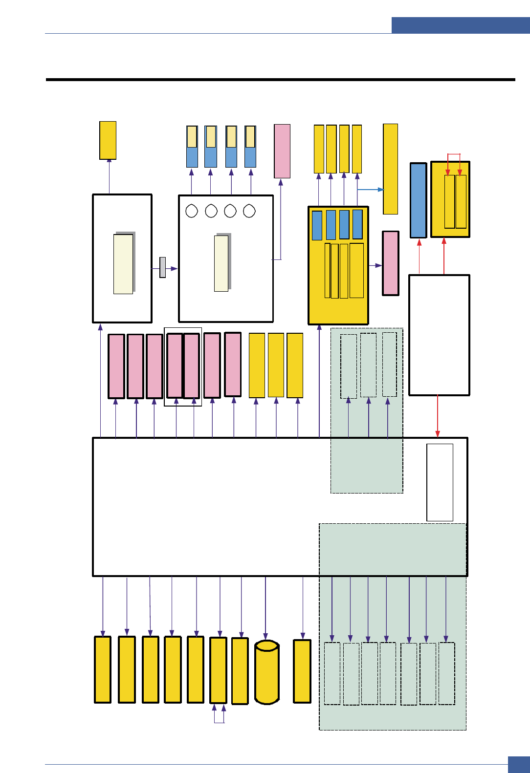
Block Diagram
Samsung Electronics Service Manual
9-1
9
9
MA IN
SMPS
IT B JOINT
DEDEVE JOINT
LSU
TEMP2
HVPS
THERMISTOR
EXIT SEN
REGI
FUSER
COVER
S/ W
TEMP1
BLDC
DISP PANEL
PTL
WASTE SEN
INLET&SWITCH
DRAWER CON.
14 P
3P
3P
11
P
10 P
5P
2P
2P
DEV_SOL
T2_CLT
CTD
PANEL(PDL&CP)
FAN_MAIN
REGI_CLT
PICKUP HOME
16 P
3P3P
4P
22P
P_EMPTY
E- Coil
Thermostat
DAA
GDI PANEL
SW
BA T
SCF
MP_EMPTY
USB
RJ- 45
SCAN
CCD
HOME
2P
2P
ITB_CLT
PICKUP_CLT
3P
8P
24P
2P
3P
3P
3P
3P
6P
2P
3
P
4P
2P
6P
1P
1
P
5P
3P
2P
CHA RGER 1EA
T1 1EA
T2 1EA
Bias AC 1EA
DC 1EA
RELAY
RELAY
RELAY
RELAY
Bias Y
Bias M
Bias C
Bias K
Deve Cr um
MC34C 0 2
IT B HOME
Sensor
YCRUM
MCRUM
CCRUM
KCRUM
CON.
SUPPLY Y,M,C,K
T YPE 3
+ 24V 4.5A , + 5V 3A
DC- DC
+3 .3V
Reserve
Reserve
PCB Contact
9. Block Diagram
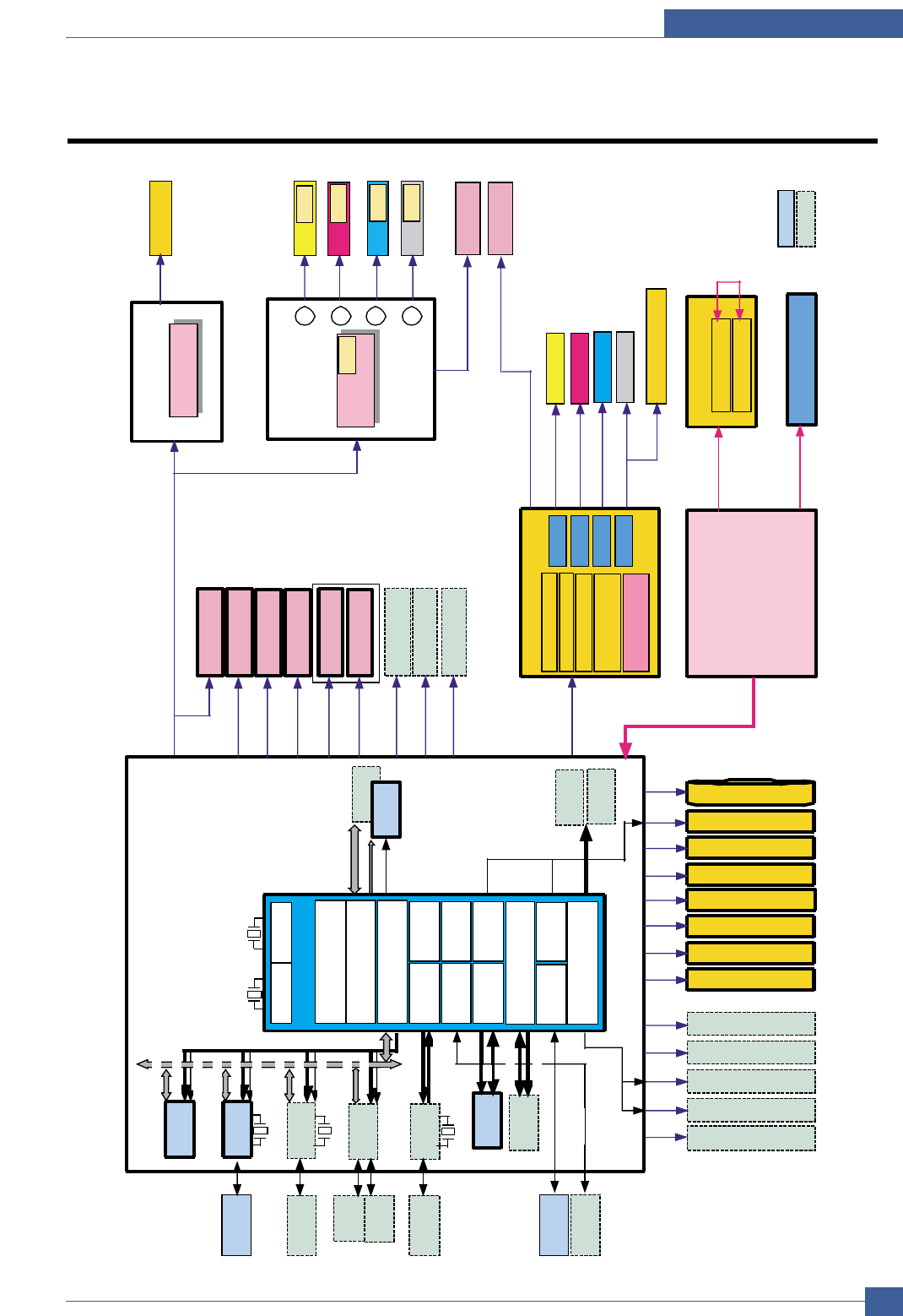
Connection Diagram
Samsung Electronics Service Manual
10-1
10
10
10. Connection Diagram
ITB JOI NTNT
DEDEV E JOINT
THERMISTOR
EXIT SENSOR
FUSER
B
L
D
C
PTL
INLET&SWITCH
DRA WER CON.
14 P3P
12 P
10 P
2P
2P
CTD
F
A
N
_
M
A
I
N
16P
2P
22 P
E- Coil
Thermo stat
B
A
T
MP_EMPTY
A
D
F
C
C
D
DEVE HOME
SENSOR
2P 2P
P
I
C
K
U
P
_
C
L
T
3P8P24 P
2P
3P
3P
3P
3P
2P
3P
4P
2P
1P
5P
3P
2P
DeDevBi as Y
DeDevBias M
DeDevBias C
DeDevBias K
ITB HOMEITB HOME
SENSORSENSOR
YCRCRUM
MCRCRUM
CCRCRUM
KCRCRUM
SUPPLY Y,M,C,K
SMSMPS
Standadard Typepe 3
+24V 4.4.5A5A, +5V5V 3A3A
PCB Cont ac t
Zener
Di ode
2P
Light - Rec ei v er
2P 24 P
5P
7P
P_EMPTY
SENSOR
PICKUP
HOME WASTE
SENSOR
WASTE
SENSOR
HVHVPSPS
Charger 1ea
T1 1ea
T2 1ea
Bias AC 1ea
DC 1ea
RELAY
RELAY
RELAY
RELAY
TEMP2
SE NSOR
TEMP1
SENSOR
D
E
V
_
S
O
L
T
2
_
C
L
T
I
T
B
_
C
L
T
C
O
V
E
R
S
/
W
L
S
U
R
E
G
I
_
C
L
T
MAMAIN
SR A M
64K B
EEPROM
32K bit
N/W
STE100P
SD[31:0]
SA[12:0],BA0,1
nSCS0,1
SDRAM
SDRAM
32MB
nRAS,nCAS,
nWE,DQM,CKE,
SDCLK0,1
ADDR[13:2]
ADDR[22:2]
ADDR[9:2]
nRD,n WR,nCS
DATA[31:16]
DATA[31:0]
DATA[31:16]
nRD,nWR,nCS
nRD,nWR,nCS
6MHz
12MHz
Flash
2MB
USB2.
0
Dev
USB2.0
Hos t
TX_CLK,RX_CLK,
MAC_TXD[3:0]
MAC_RXD[3:0]
SCL
SDA
AFE
HT82V 26
LV DS
FIN1047
AFE,CCD
Control
DATA[ 31:24]
ADDR[8:2]
nRD,nWR, nCS
RJ- 11
USB_D
Conn
USB_H
Module
OP E G D I
7k e y, 2 L E D
25MHz
12MHz 32.768KHz
System Clock
CHCHORUS
m
ARM9-
300MHz
SDRA M Con t rol ler
Loc al Con t rol ler
MAC
I2C
UART
ADC 8ch
PWM 8ch
LSU
Cont rolle
r
Image Proce s sor
PLL RTC
HPVC
STEP
Motor
GPIO
Sm art
DAA
RJ- 11
RJ- 45
OP E M F P
16 * 2 L C D
SRAM_D[15:0]
SRAM_A[15:0]
9600bps
Res erv ed
in Use
[ Not e]
S
C
F
REGI
SENSOR
Light - Em it
DeDev e
MC34 C02
CRCRUM
2P
Schematic Diagram
Service Manual
11-1
This Document can not be used without Samsung’s authorization.
Samsung Electronics
11. Schematic Diagrams
11.1
Main Board(1/15)
Clock & Power On Reset
A
3
11
3
Page
12
Index
67 8
05.06.03
INDEX
F
A
15
B
CHORUSm(2)
CHORUSm(1)
HVPS, SMPS, COVER_OPEN
14
Scanner Interface
Hyper Terminal, EEPROM, OPE
5
6
7
8
SmartDAA Interface
1
DEVE_HOME, SCF, FUSER THER
MFG ENGR CHK
Function
Ethernet Physical Layer
USB Host & Device Controller
12
13
SDRAM
BLDC, CLUTCH, DEVE & ITB JOINT
B
C
D
E
DOC CTRL CHK
R&D CHK S.D.AN
Drawn by
Engineer K.C.LEE
CLP-300(N)/CLX-3160N(FN)
10
9
LSU
A3
1/15
Flash Memory
C
Main_V0.11
R&D 5
Digtal Printing Division
TITLE: Size
45
4
2
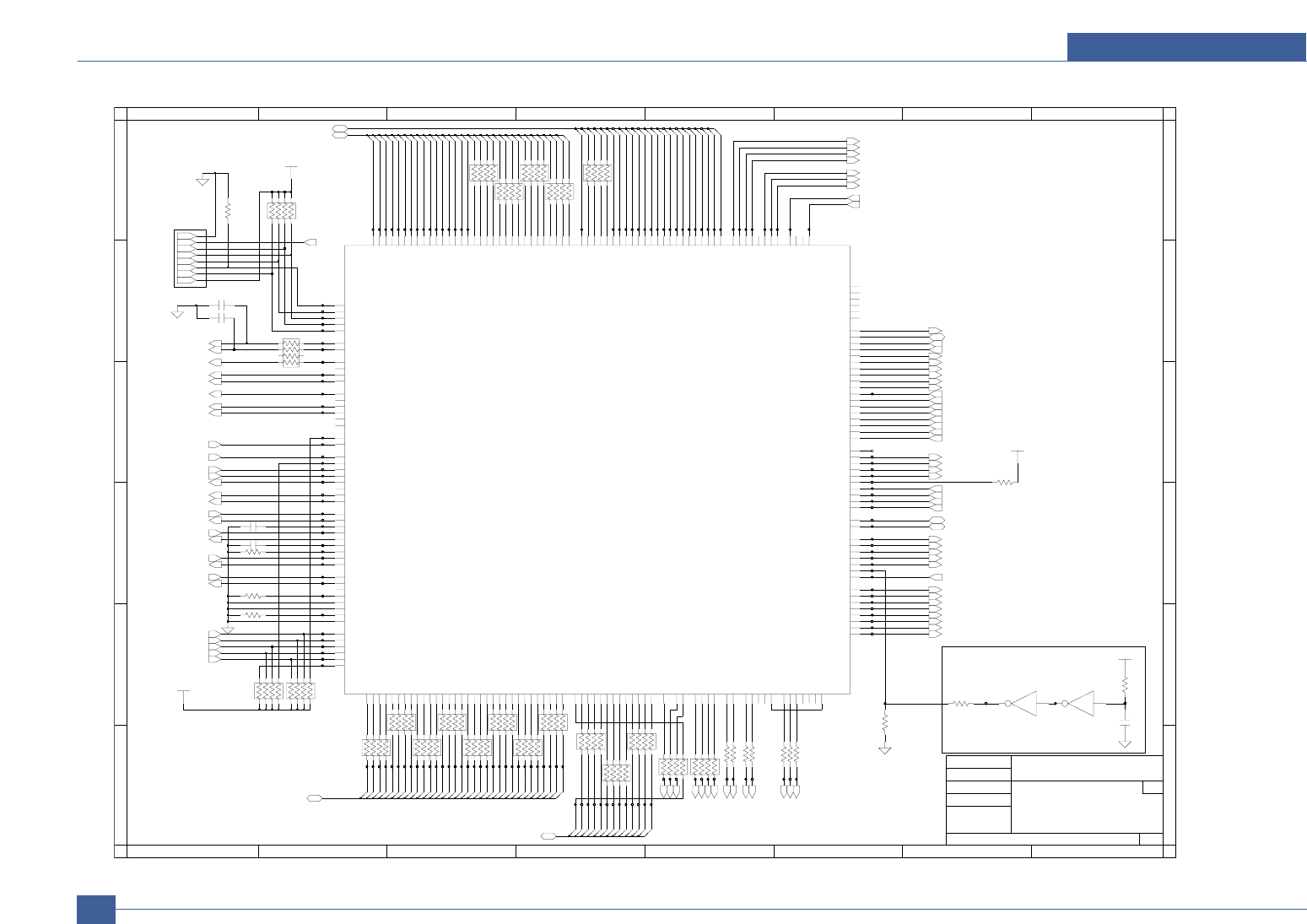
Schematic Diagram
Service Manual
11-2
This Document can not be used without Samsung’s authorization. Samsung Electronics
D
8
C
TEST JIG
Size
2
B
Drawn by
R&D CHK S.D.AN
MFG ENGR CHK
R&D 5
5
8
A
2
67
JTAG
5
C
F
2/15
A3
CLP-300(N)/CLX-3160N(FN)
F
1
3
CHORUSm(1)
Main_V0.11
64
E
1
4
7
A
D
3
CLX-3160N(FN) Only
B
TITLE:
Digtal Printing Division
DOC CTRL CHK
Engineer K.C.LEE
E
33
RA23
+3.3V
R77 10K
RA15
10K
10K
R72
8
4
DGND
33
RA22
C86 15pF
33
RA18
220K
R3
7
74LCX14
U1-4
98
11
10
74LCX14
U1-5
R66 10K
2
68R97
RA12
33
RA7
33
33
RA8
RA9
33
33
RA10
+3.3V
33
RA30
DGND
R81 68
nWAIT0_GPI_0
U4
nWAIT1_GPI_1
U5
nWE
AC17
nWR
R5
T3
nROMCS3_GPO_3
U3
nRSTOUT_GPO_0
E10
nSCS0
AF16
nSCS1
AE15
nSCS2
AE16
nSCS3_GPO_13
AE17
nSCS4_GPO_14
AE18
nSELECTIN A14
nSTROBE B14
nTRST
AD5
nIOCS1
R2
nIOCS2
R3
nIOCS3_GPO_4
R4
nIOCS4_nIOCS4_CIP4E_GPO_5
P3
nIOCS5_GPO_6
P4
nRAS
AC15
nRD
T4
D9 nRESET
nROMCS0
T5
nROMCS1
T2
nROMCS2_GPO_2
nDACK0_nDACK0_CIP4E_GPO_7
nDACK1_nDACK1_CIP4E_GPO_8
H4
nDACK2_nDACK2_CIP4E_GPO_9
G2
nDACK3_GPO_10
G3
nDREQ0_nDREQ0_CIP4E_GPI_2
H3
nDREQ1_nDREQ1_CIP4E_GPI_3
J5
nDREQ2_nDREQ2_CIP4E_GPI_4
H5
nDREQ3_nDREQ3_CIP4E_GPI_5
G4
nFAULT D15
nINIT E14
nIOCS0
R1
F4
TX_EN_GPO_24 F5
TX_ERR_GPO_25 G5
VCLK_FILTER
A10
XI_MAIN
A12
XI_VCLK
C10
XOUT_MAIN
B12
XOUT_VCLK
D10
nACK C14
nAUTOFD D14
nCAS
AC16
H2
TCK
AF5
AE4 TDI
TDO
AD4
TESTMODE
AC5
TMS
AE5
TXD0 E13
TXD1 C12
TXD2 D12
TXD3_GPO_17 AE25
TXD4_GPO_18 AE26
TX_CLK_GPI_10
AE8
SD8
AD8
SD9
AC8
SDA AD22
SDCLK0
AF11
SDCLK1
AF14
SDCLK2
AF17
SDCLK3_GPO_11
AF7
AF21 SDCLK4_GPO_12
SDCLK_FBK
AE22
SLCT_OUT E15
AD13 SD26
SD27
AC13
SD28
AB13
SD29
AE14
SD3
AC7
SD30
AD14
SD31
AC14
SD4
AB7
SD5
AA7
SD6
AF8
SD7
SD16
AC10
SD17
AE11
AD11 SD18
AC11 SD19
AD7 SD2
SD20
AB11
SD21
AF12
SD22
AE12
SD23
AD12
SD24
AC12
SD25
AE13
AB20
SA9
AE21
SCL AA21
SD0
AE6
SD1
AE7
AE9 SD10
SD11
AD9
SD12
AC9
SD13
AB9
SD14
AE10
SD15
AD10
SA1
AD19
AD21 SA10
SA11
AC21
SA12
AB21
AC19 SA2
SA3
AB19
SA4
AF20
SA5
AE20
SA6
AD20
SA7
AC20
SA8
A13
RTC_XOUT
B13
RXD0 C9
B9
RXD1
RXD2 E12
RXD3_GPI_7 AD24
RXD4_GPI_8 AF26
RX_CLK_GPI_13 G6
RX_DV_GPI_18 C1
RX_ERR_GPI_11 C2
SA0
AE19
PDE A17
PERROR C15
PPD0_TESTOUT0 B15
E16
PPD1_TESTOUT1
PPD2__TESTOUT2 D16
PPD3_TESTOUT3 C16
PPD4_TESTOUT4 B16
PPD5_TESTOUT5 A16
PPD6_TESTOUT6 D17
PPD7_TESTOUT7 C17
RTC_XI
NF_CLE_GPIO2_0 AF1
NF_RnB_GPIO2_5 AF4
NF_nCE_GPIO2_2 AF3
NF_nRE_GPIO2_3 AE1
NF_nWE_GPIO2_4 AE2
OM0
AC6
OM1
AB6
OM2
AA6
OM3
AD6
PCIPLL_CLK
A9
MAC_RXD3_GPI_17 D4
MAC_TXD0_GPO_20 D1
MAC_TXD1_GPO_21 D2
E2
MAC_TXD2_GPO_22
MAC_TXD3_GPO_23 E3
MAIN_FILTER
C11
MDC_GPO_19 B1
MDIO_GPIO1_31 D3
NF_ALE_GPIO2_1 AF2
NF_BOOT AE3
GPIO_A1_TX_EN4_TESTOUT9_GPIO_7 AE24
GPIO_A2_TX_C_TESTOUT10_GPIO_8 AF25
GPIO_A3_TX_D_TESTOUT11_GPIO_9 AF24
GPIO_A4_nTX_C_TESTOUT12_GPIO_10 AC22
GPIO_A5_nTX_D_TESTOUT13_GPIO_11 AD23
GPIO_A6_SAM_HOLD0_TESTOUT14_GPIO_12 AE23
GPIO_A7_SAM_HOLD1_TESTOUT15_GPIO_13 AF23
MAC_RXD0_GPI_14 F6
MAC_RXD1_GPI_15 E5
MAC_RXD2_GPI_16 C3
AD15
DQM1
AD16
AD17 DQM2
DQM3
AD18
EINT0
F1
EINT1
F2
EINT2_GPI_19
J25
EINT3_GPI_20
H25
EINT4_GPI_21
F3
EINT5_GPI_22
J24
GPIO_A0_TX_EN3_TESTOUT8_GPIO_6 AC23
DATA2_NFCON_IO_2 AD3
DATA30 U1
U2
DATA31
DATA3_NFCON_IO_3 AC1
DATA4_NFCON_IO_4 AC2
DATA5_NFCON_IO_5 AC3
DATA6_NFCON_IO_6 AC4
DATA7_NFCON_IO_7 AB1
DATA8_NFCON_IO_8 AB2
DATA9_NFCON_IO_9 AB3
DQM0
DATA1_NFCON_IO_1 AD2
DATA20 Y4
DATA21 Y5
DATA22 W1
DATA23 W2
DATA24 W3
DATA25 W4
DATA26 W5
DATA27 V2
DATA28 V3
DATA29 V4
AD1
DATA10_NFCON_IO_10 AB4
DATA11_NFCON_IO_11 AB5
DATA12_NFCON_IO_12 AA1
DATA13_NFCON_IO_13 AA2
DATA14_NFCON_IO_14 AA3
DATA15_NFCON_IO_15 AA4
DATA16 AA5
DATA17 Y1
DATA18 Y2
DATA19 Y3
ADDR7 N5
ADDR8 M1
ADDR9 M2
BA0
AB17
BA1
AC18
BUSY A18
CKE
AB15
CLKOUT_GPO_1
G1
COL_GPI_9 E1
CRS_GPI_12 E4
DATA0_NFCON_IO_0
K3
ADDR19 K4
ADDR2 P2
J1
ADDR20_CfgAdvFlash
ADDR21_CfgBusWidth J2
ADDR22_CfgAddCycle J3
ADDR23_CfgPageSize J4
ADDR3 N1
ADDR4 N2
ADDR5 N3
ADDR6 N4
ADDR1 P1
ADDR10 M3
ADDR11 M4
ADDR12 L2
ADDR13 L3
ADDR14 L4
ADDR15 L5
ADDR16 K1
ADDR17 K2
ADDR18
chrousm
JC13-00031A
U10-1
DGND
33
RA21
R17
10K 100nF
C10
RA11 33
RA16
10K
33
RA24
RA29
33
RA33
33
6
0R70
RA19
DGND
33
33
RA20
3
2.2nFC145
DGND
68R196
+3.3V
5
RA32
R76
33
68
R15 5.1K
15pF
C85
33
RA26
68R195
C154
1
2.2nF
35303-0850
CN9-1
RA34
10K
R194 68
R193 68
+3.3V
NR3
RA25
0
DQM3
nRAS
nCAS
SD_CKE
nSCS0
33
ADDR(5)
ADDR(4)
ADDR(3)
ADDR(2)
nSDRAM_WR
BA0
BA1
DQM0
DQM1
DQM2
DATA(24)
DATA(25)
DATA(26)
DATA(27)
DATA(20)
DATA(21)
DATA(22)
DATA(23)
DATA(16)
DATA(17)
DATA(18)
DATA(19)
SA(4)
SA(5)
SA(6)
SA(7)
SA(8)
SA(10)
SA(11)
SA(12)
DATA(28)
DATA(29)
DATA(30)
DATA(31)
nOP_KEY_ONLINE
SDCLK0
SDCLK1
nSCS1
nCS_BOOT
nRESET
SA(1)
SA(2)
SA(3)
ADDR(14)
ADDR(13)
ADDR(12)
ADDR(11)
ADDR(10)
ADDR(1)
ADDR(6)
ADDR(7)
ADDR(8)
nRST_NIC
nOP_KEY_MODE
DATA(12)
DATA(11)
DATA(10)
DATA(0)
MAC_CRS
MAC_COL
ADDR(9)
ADDR(23)
ADDR(22)
ADDR(21)
ADDR(20)
ADDR(19)
ADDR(18)
ADDR(17)
ADDR(16)
ADDR(15)
nINT_WNIC
nINT_USB_HOST
nINT_MODEM
nINT_USB_DEVICE
DATA(9)
DATA(8)
DATA(7)
DATA(6)
DATA(5)
DATA(4)
DATA(3)
DATA(2)
DATA(1)
DATA(15)
DATA(14)
DATA(13)
MAC_TXD2
MAC_TXD1
MAC_TXD0
MAC_RXD3
MAC_RXD2
MAC_RXD1
MAC_RXD0
LSU_SH2
LSU_SH1
FLAT_MOT_MS2
FLAT_MOT_MS1
FLAT_MOT_DIR
nFLAT_MOT_SLEEP
nFLAT_MOT_EN
FLAT_MOT_PLS
OP_C_LED
OP_M_LED
OP_Y_LED
NF_nWE
NF_nRE
NF_nCE
NF_RnB
NF_CLE
NF_ALE
MAC_MDIO
MAC_MDC
MAC_TXD3
MAC_RX_ERR
MAC_RX_DV
MAC_RX_CLK
nSCF_RDY
SCF_RXD
PANEL_RXD
DEBUG_RXD
XO_RTC
XI_RTC
OP_MODE_LED
OP_STA_LED2
OP_STA_LED1
OP_K_LED
SCL
XI_MCLK
MAC_LED_CON
MAC_TX_EN
MAC_TX_CLK
SCF_CLK
SCF_TXD
PANEL_TXD
DEBUG_TXD
SDA
nRST_PANEL
nRST_USB_DEVICE
nCS_USB_HOST
nCS_MODEM
nCS_USB_DEVICE
nADF_P_REG
nADF_P_POS
nDREQ_USB_DEVICE
nRST_USB_HOST
nRST_MODEM
nDACK_USB_DEVICE
XO_VCLK
XO_MCLK
XI_VCLK
SD(29)
SD(30)
SD(31)
SA(0)
nRESET
SA(9)
SA(0:12)
nITB_HOME
ADDR(1:23)
DATA(0:31)
nADF_P_DET
SD(13)
SD(14)
SD(15)
SD(16)
SD(17)
SD(18)
SD(19)
SD(20)
SD(21)
SD(22)
SD(23)
SD(24)
SD(25)
SD(26)
SD(27)
SD(28)
nRD
nWR
SD(0:31)
SD(0)
SD(1)
SD(2)
SD(3)
SD(4)
SD(5)
SD(6)
SD(7)
SD(8)
SD(9)
SD(10)
SD(11)
SD(12)
Main Board(2/15)
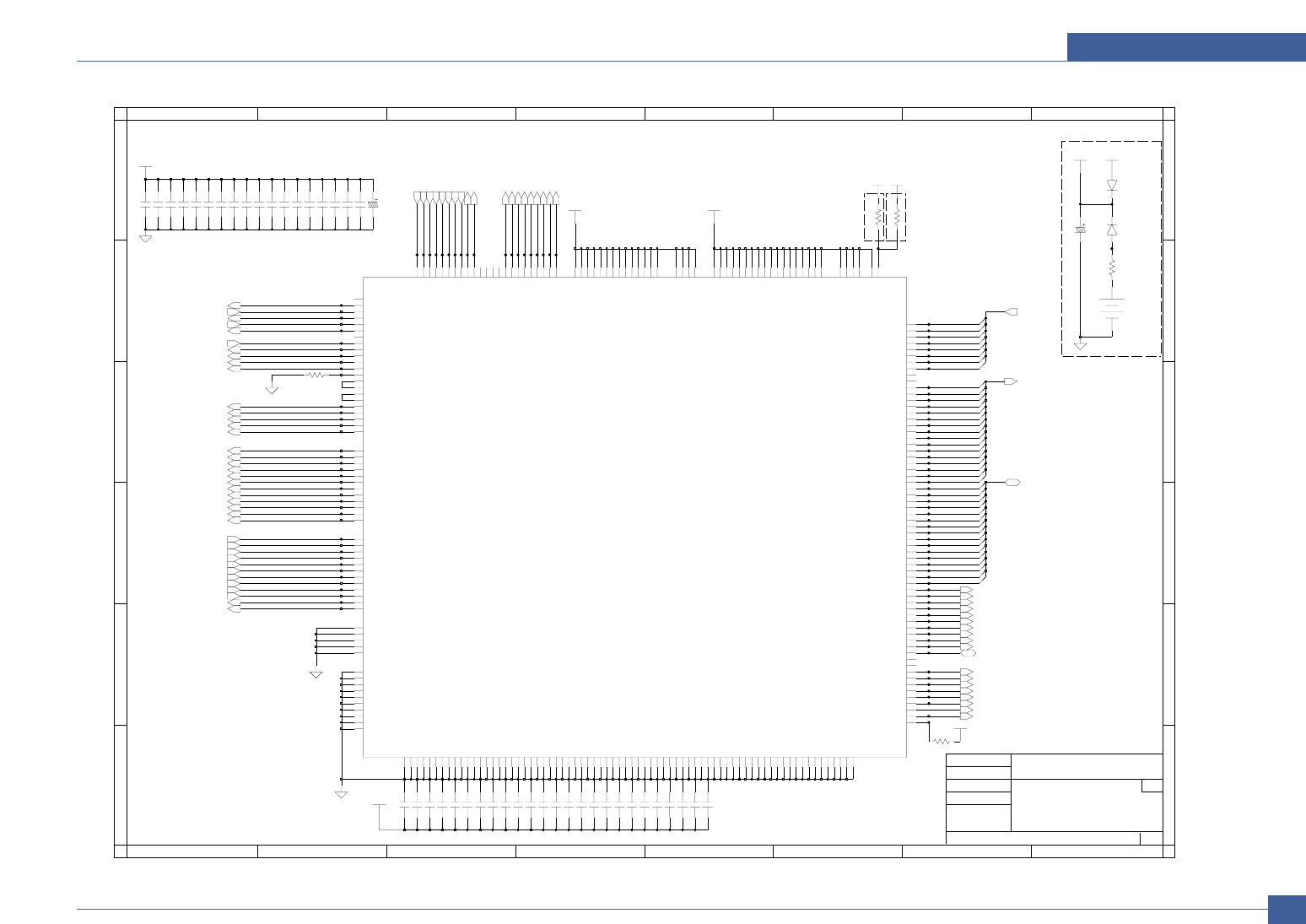
Schematic Diagram
Service Manual
11-3
This Document can not be used without Samsung’s authorization.
Samsung Electronics
Main Board(3/15)
1
F
D
5
RTC
4
C
FOR FUTURE MODEL FOR CLX-3160FN MODEL
6
E
67
2402-001049
B
CHORUSm(2)
MFG ENGR CHK
DOC CTRL CHK
3/15
A3
3
A
B
Digtal Printing Division
7
CLP-300(N)/CLX-3160N(FN)
Engineer K.C.LEE
R&D CHK S.D.AN
8
Drawn by
5
Size
TITLE:
C
Main_V0.11
F
E
34
A
2
R&D 5
82
D
1
3.3K
0
DGND
R89
Vb
NR5
C110 100nF
100nFC188
C104 100nF
C114
C118
100nF
C228
100nF
100nF
100nF
C173 100nF
2
1
+3.3V
C180
200
+3.3V
CR-2032T6
BAT1
+3.3VVSB
DGND
R112
MMSD914T1
D22
+1.2V
RB420D T147
D23
DGND +3.3V
DGND
VSB
NR113 0
DGND
+1.2V
C70 100uF
16V
10uF
R107
10K
C226
16V
C197
C149 100nF
100nF
100nF
C131 100nF
C179 100nF
C134
100nF
C163
C61
100nF
C170 100nF
C62 100nF
C124 100nF
C126 100nF
C101 100nF
C158 100nF
C182 100nF
C174 100nF
100nFC286
C218
C214 100nF
100nF
100nF
100nF
C136
100nF
C148
C159
C187
100nF
C204 100nF
C221 100nF
C227 100nF
C254 100nF
100nF
C267 100nF
C219
C222 100nF
C135
C125
100nF
C215
100nF
100nF
C22 nHSYNC1_GPIO1_0
B21 nHSYNC1_Minus
A21 nHSYNC1_Plus
D22 nHSYNC2_GPIO1_1
B22 nHSYNC2_Minus
A22 nHSYNC2_Plus
B18 nLREADY_nEMSG
D20 nPRINT_nCMSG
M23
nTX_A M24
nTX_B
A25 VDO1_GPO_15
B19 VDO1_Minus
A19 VDO1_Plus
B24 VDO2_GPO_16
B20 VDO2_Minus
A20 VDO2_Plus
C20 VDO_OUT1_MOD_GPIO1_4
C23 VDO_OUT2_MOD_GPIO1_5
C18 VLCK_MOD_GPIO1_6
D18 nFSYNC_GPI_6
SRAM_D5_GPIO_5 V23
SRAM_D6_GPIO_6 V24
SRAM_D7_GPIO_7 V25
SRAM_D8_GPIO_8 U22
SRAM_D9_GPIO_9
T25
SRAM_nWR
A2
TONE_OUT_GPO_31
N25
TX_A M22
TX_B
N24
TX_EN1 N23
TX_EN2
U23
SRAM_D10_GPIO_10
SRAM_D11_GPIO_11 U24
U25
SRAM_D12_GPIO_12 U26
SRAM_D13_GPIO_13 T23
SRAM_D14_GPIO_14 T24
SRAM_D15_GPIO_15
Y25
SRAM_D1_GPIO_1 W23
SRAM_D2_GPIO_2 W24
SRAM_D3_GPIO_3 W25
SRAM_D4_GPIO_4 V22
Y22
SRAM_A14 Y23
SRAM_A15
AD25
SRAM_A2 AC26
SRAM_A3 AC25
SRAM_A4 AC24
SRAM_A5 AB25
SRAM_A6 AB24
SRAM_A7 AB23
SRAM_A8 AA22
SRAM_A9
Y24
SRAM_D0_GPIO_0
P24
Pltg2_GPIO_23
Pltg3_GPIO_19 R24
P23
RLED_GPIO_22
C13
RTC3.0_VDD
AB22
SRAM_A0 AD26
SRAM_A1
AA23
SRAM_A10 AA24
SRAM_A11 AA25
SRAM_A12 Y21
SRAM_A13
T26
PIrs
P25
PItg1
A7
PWM_OUT0 B7
PWM_OUT1 C7
PWM_OUT2 C8
PWM_OUT3 D8
PWM_OUT4_GPO_27 E8
PWM_OUT5_GPO_28 E9
PWM_OUT6_GPO_29 B8
PWM_OUT7_GPO_30
R23
Plsh_GPIO_18
PD2_MOD3_OUT_CLK_PIX_GPIO1_22
F26 PD2_MOD4_OUT_IWIN_GPIO1_23
G21 PD2_MOD5_OUT_BIN_GPIO1_24
G22 PD2_MOD6_AFE_D10_GPIO1_25
G23 PD2_MOD7_AFE_D10_GPIO1_26
G24 PD2_MOD8_AFE_D12_GPIO1_27
G25 PD2_MOD9_AFE_D13_GPIO1_28
D19 PHIALVDS
AA26
PI1 W26
PI2
P26
PIcp
D25 PD1_MOD5_GPIO1_12
PD1_MOD6_GPIO1_13
E22
E23 PD1_MOD7_GPIO1_14
E24 PD1_MOD8_GPIO1_15
E25 PD1_MOD9_GPIO1_16
F22 PD2_MOD0_CLK_LINE_GPIO1_19
H23 PD2_MOD10_AFE_D14_GPIO1_29
H24 PD2_MOD11_AFE_D15_GPIO1_30
F23 PD2_MOD1_CLK_PIX_IWIN_GPIO1_20
F24 PD2_MOD2_OUT_CLK_LINE_GPIO1_21
F25
F7
MOT_B_nEPRDY
D7
MOT_nA_nEBSY
MOT_nB_GPO_26 E7
A26 PD1_MOD0_GPIO1_7
D26 PD1_MOD10_GPIO1_17
E26 PD1_MOD11_GPIO1_18
D24 PD1_MOD1_GPIO1_8
C25 PD1_MOD2_GPIO1_9
B26 PD1_MOD3_GPIO1_10
C26 PD1_MOD4_GPIO1_11
GND_RING_2
R22
LEVEL_SHIFT_GPIO_17
C24 LSUCLK_cCLK
E18 LSYNC1_MOD_GPIO1_2
D23 LSYNC2_MOD_GPIO1_3
C19
LVDS3.3_VDD1 C21
LVDS3.3_VDD2 D21
LVDS3.3_VDD3 E19
LVDS3.3_VDD4
M25
MOTOR_POL
B3
MOT_A_nCBSY
AF13 GND_79
K10 GND_8
AF15 GND_80
AF18 GND_81
AF22 GND_82
K11 GND_9
B6 GND_A
B10 GND_PLL_1
D11 GND_PLL_2
B23 GND_RING_1
F20
U12 GND_69
H1 GND_7
U13 GND_70
U14 GND_71
GND_72
U15
U16 GND_73
U17 GND_74
V26 GND_75
AB26 GND_76
AF6 GND_77
AF10 GND_78
GND_59
G26 GND_6
T11 GND_60
T12 GND_61
T13 GND_62
T14 GND_63
T15 GND_64
T16 GND_65
T17 GND_66
U10 GND_67
U11 GND_68
E20 GND_5
R11 GND_50
R12 GND_51
R13 GND_52
R14 GND_53
R15 GND_54
R16 GND_55
R17 GND_56
R26 GND_57
T1 GND_58
T10
B17 GND_4
N26 GND_40
P10 GND_41
P11 GND_42
GND_43
P12
P13 GND_44
P14 GND_45
P15 GND_46
P16 GND_47
P17 GND_48
R10 GND_49
GND_3
M16 GND_30
M17 GND_31
N10 GND_32
N11 GND_33
N12 GND_34
N13 GND_35
N14 GND_36
N15 GND_37
N16 GND_38
N17 GND_39
L14 GND_20
L15 GND_21
L16 GND_22
L17 GND_23
M10 GND_24
M11 GND_25
M12 GND_26
M13 GND_27
M14 GND_28
M15 GND_29
A24
K12 GND_10
K13 GND_11
K14 GND_12
K15 GND_13
GND_14
K16
K17 GND_15
L10 GND_16
L11 GND_17
L12 GND_18
L13 GND_19
A11 GND_2
B4
AIN4 A3
AIN5 D5
AIN6 C4
AIN7
R25
BLED_GPIO_20
H26
CDS2_CLK
A6
DAC1_OUT D6
DAC2_OUT
P22
GLED_GPIO_21
A1 GND_1
AFE_D3 K24
AFE_D4 K23
AFE_D5 L25
AFE_D6 L24
AFE_D7 L23
AFE_D8 L22
AFE_D9
A5
AIN0 B5
AIN1 A4
AIN2 C5
AIN3
K22
3.3VDD_5 L1
3.3VDD_6 M26
3.3VDD_7 P5
3.3VDD_8 T22
3.3VDD_9
C6
A3.3_VDD
L26
ADC_CLK
J23
AFE_D0 J22
AFE_D1 K26
AFE_D2 K25
V5
3.3VDD_11 Y26
3.3VDD_12 AA20
3.3VDD_13 AB8
3.3VDD_14 AB12
3.3VDD_15 AB16
3.3VDD_16 AF9
3.3VDD_17 AF19
3.3VDD_18
B25
3.3VDD_2 E17
3.3VDD_3 K5
3.3VDD_4
1.2VDD_5 H22
1.2VDD_6 J26
1.2VDD_7 M5
1.2VDD_8 N22
1.2VDD_9
B11
1.2VDD_PLL_1 E11
1.2VDD_PLL_2
1.2VDD_RING_1 A23
E21
1.2VDD_RING_2
A15
3.3VDD_1
V1
3.3VDD_10
A8
1.2VDD_1
W22
1.2VDD_10 Y6
1.2VDD_11 AB10
1.2VDD_12 AB14
1.2VDD_13 AB18
1.2VDD_14
B2
1.2VDD_2 D13
1.2VDD_3 E6
1.2VDD_4 F21
C189
U10-2
100nF
100nFC164
100nFC181
AFE_D(6)
AFE_D(5)
AFE_D(4)
AFE_D(3)
AFE_D(2)
AFE_D(1)
AFE_D(0)
AFE_D(0:7)nHSYNC1
nADF_MOT_NB
SRAM_D(14)
SRAM_D(13)
SRAM_D(12)
SRAM_D(11)
SRAM_D(10)
SRAM_D(9)
SRAM_D(8)
SRAM_D(7)
SRAM_D(6)
SRAM_D(5)
SRAM_D(4)
SRAM_D(3)
SRAM_D(2)
SRAM_D(1)
SRAM_D(0)
AFE_D(7)
PWM_THV
PWM_MHV
TEST_LED3
AFE_ADC_CLK
AFE_CDS2_CLK
SCANNER_PI_TG1
SCANNER_PI1
SCANNER_PI2
SCANNER_PI_RS
SCANNER_PI_CP
nADF_MOT_PHA
nADF_MOT_PHB
nADF_MOT_A
nADF_MOT_B
nADF_MOT_NA
SRAM_D(15)
BLDC_MOTOR_READY
nBLDC_MOTOR_EN
AFE_SLOAD
nLSU_READY
REGI_CLUTCH
PICKUP_CLUTCH
nLSU_MOTOR_EN
nLD_EN
PWM_ITHV
KEYCLICK
AFE_SCLK
AFE_SDATA
SCANNER_DPI_CONTROL
SCANNER_PI_SH
LSU_MOT_CLK
PWM_DEV_DC
PWM_DEV_AC
PWM_DEV_VPP
FLAT_MOT_DAC
LD_POWER1
OUT_TEMP
INNER_TEMP
FUSER_THERM2
FUSER_THERM1
WASTE_LEVEL
ITHV_READ
THV_READ
MHV_READ
nSCANNER_HOME
VDO1_minus
VDO1_plus
SRAM_A(5)
SRAM_A(4)
SRAM_A(3)
SRAM_A(2)
SRAM_A(1)
SRAM_A(0)
SRAM_D(0:15)
nFUSER_EN
VDO2_minus
VDO2_plus
ERASE_LAMP
DEV_SOL3
DEV_SOL2
nFLAT_COVER_OPEN
SCANNER_BW_CONTROL
PWM_CCD_LAMP
PWM_MOT
PTL
FAN_MAIN
nBIN_FULL
nSRAM_WR
SRAM_A(0:15)
SRAM_A(15)
SRAM_A(14)
SRAM_A(13)
SRAM_A(12)
SRAM_A(11)
SRAM_A(10)
SRAM_A(9)
SRAM_A(8)
SRAM_A(7)
SRAM_A(6)
WASTE_LED
nADF_MODULE_DETECT
WASTE_EMPTY
nDEV_HOME
nCOVER_OPEN
nREGI_SENS
nP_EXIT
nP_EMPTY
DEV_SOL4
DEV_SOL1
nDEV_EN
THV_CLUTCH
ITB_CLUTCH
DEV_CLUTCH
nTHV_EN

Schematic Diagram
Service Manual
11-4
This Document can not be used without Samsung’s authorization. Samsung Electronics
Main Board(4/15)
S0 S1
1
LOW
CLX-3160FN ONLY
N.C
[ VCLK ]
[ SYSTEM CLOCK ]
C
[ RTC ]
Digtal Printing Division
BB
TITLE:
Main_V0.11
4
3
0%
7
C
Drawn by
N.C
DOC CTRL CHK
Clock & Power On Reset
A
B
0.4%
5
D
E
N.C
1.3%
78
Engineer K.C.LEE
A
B
6
F
8623
2
CLP-300(N)/CLX-3160N(FN)
D
E
1
F
1
MFG ENGR CHK
Size
45
BB
R&D CHK S.D.AN
R&D 5
100.5%
N.C 01.1%
00
[ SYSTEM RESET ]
2.2uH
L9
4/15
A3
R190
0
DGND
+5V +1.2V
+5V
16V
100uF
C255
R151
470K
ATS-49/U,12MHz,50ppm
OSC5
R170
1K
+3.3V
+3.3V
KSC1623-Y
Q11
13
2
100nF
C234
Vb
DGND
16V
10uF
C303
MC-306,32.768KHz
22pF
OSC3
+5V
C155
R172
100
NR114
DGND
+3.3V
0
4SGND
SHDN
10
8SVIN
SW 6
11
VSET
U19
MVPG31
1
NC1
NC2 2
NC3 3
9NC4
13 PGND
PSET 12
PVIN
7
5
SFB
56
2
13
R161
R105 31.6K,1%
STS104B
F1
1nF
Q12
KSA1182-Y
1
3
2
C302
R162 56
R142 300
DGND
SLS-NNGA102TS
LED1
C128 15pF
DGND DGND
+3.3V
ATS-49/U,12MHz,50ppm
OSC2
DGND
DGND
L8
5.1K
C178
15pF
2
13
R175
C194
F3
STS104B
100nF
+3.3V
C129 15pF
R115
10 100nF
C301
R109 280K,1%
DGND
DGND
15pF
2
13
C210
GND
1
IN
32
OUT
F2
STS104B LD1117DT33C
U24
0R121
D27
RB420D T147
3301-000325|R3225_BEAD
L5
XC61FN3112MR
U25
3Vin
1
Vout
2
Vss
DGND
C243
22uF
+3.3V
R152 5.6K
2
1XIN/CLKIN 8
XOUT
U12
CY25811
6
FRSEL
S0
4
3S1
5
SSCLK
7
VDDVSS
C308
C244
10uF
16V
47uF
C211
DGND
NR6
15pF
1
DGND
30K KSB1151-Y
Q9
3
2
22pFC165
FGND
C277
100nF
+3.3V
R88 33
R189
0C312
22pF
DGND
nRESET
VBIN
XI_MCLK
XI_RTC
XO_RTC
TEST_LED3
XI_VCLK
XO_VCLK
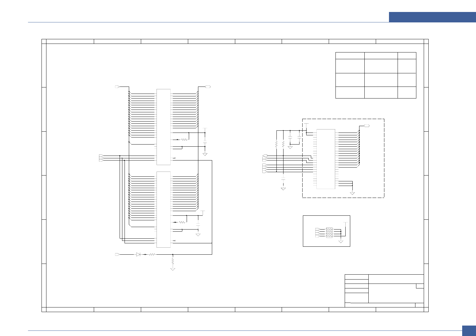
Schematic Diagram
Service Manual
11-5
This Document can not be used without Samsung’s authorization.
Samsung Electronics
Main Board(5/15)
Main_V0.11
6
C
D
E
F
734
7
MFG ENGR CHK
Size
TITLE:
Digtal Printing Division
R&D 5
Model Configuration Size
CLP-300
CLP-300N
CLX-3160N
86
8Mbit * 2
16Mbit * 2
2MB
4MB
(1107-001302)
(1107-001286)
CLX-3160FN 16Mbit * 2
3 854
C
D
E
F
5/15
A3
[ NAND SETTING ]
5
12
DOC CTRL CHK
(1107-001286) 4MB
FOR FUTURE PDL
12
Engineer K.C.LEE
CLP-300(N)/CLX-3160N(FN)
R&D CHK S.D.AN
Drawn by
Flash Memory
A
B
A
B
5.1K
DGND
R96100nF
C146
VCC1
VCC2
37
48
VSS1
VSS2 25
13
VSS3
18 WE|
WP|
19
NC4
4
5NC5
NC6
6
10 NC7
NC8
11
14 NC9
8RE|
R|B*
7
12
NC14
NC15
24
34
NC16
NC17 35
36
NC18
NC19 39
NC2
2
3NC3
IO8 27
29
IO9
LOCKPRE 38
1NC1
15 NC10
NC11
20
21 NC12
NC13
22
23
IO14 45
47
IO15
IO2 30
32
IO3
IO4 40
42
IO5
IO6 44
46
IO7
CE|
9
16 CLE
IO0 26
28
IO1
IO10 31
33
IO11
IO12 41
43
IO13
NU1
K9F5616U0C
ALE
17
DGND
+3.3V
+3.3V
C202
100nF
DGND
DGND
D6 42
44
D7
30
D8
32
D9
NC2
10
13 NC3
14 NC4
37
VCC
VSS1 46
VSS2 27
15
_BUSY
_BYTE 47
_CE
26
28 _OE 12
_RESET_WE
11
19 A6
A7
18 A8
8A9
7
D0 29
31
D1
34
D10
D11 36
39
D12
41
D13
43
D14
45
D15
D2 33
D3 35
38
D4
40
D5
25 A0
A1
24
A10
6
5A11
4A12
3A13
2A14
1A15
A16
48
17 A17
16 A18
9A19
A2
23 A3
22 A4
21 A5
20
AM29LV160D
U13
100pF
C195
R95
1K
DGND
RA14
10K
R106
DGND
10K
C116
+3.3V
DGND
100nF
C212
100nF
R86
10K
+3.3V
D6
44
D7
30
D8
32
D9
NC2
10
13 NC3
14 NC4
VCC 37
VSS1 46
VSS2 27
_BUSY 15
_BYTE 47
_CE
26
28 _OE 12
_RESET
11 _WE
19 A7
18 A8
8A9
7
D0 29
31
D1
34
D10
36
D11
39
D12
41
D13
D14 43
45
D15
D2 33
D3 35
38
D4
40
D5
42
A0
A1
24
A10
6
5A11
4A12
3A13
2A14
A15
1A16
48
17 A17
A18
16
9A19
A2
23 A3
22 A4
21 A5
20 A6
AM29LV160D
U9
1107-001286
25
R201
100K
33
R197
D39
MMSD914T1
DATA(10)
DATA(12)
DATA(14)
DATA(31:0)
ADDR(23)
ADDR(21)
ADDR(20)
ADDR(22)
nRESET
DATA(13)
DATA(11)
DATA(16)
DATA(18)
DATA(19)
DATA(20)
DATA(21)
DATA(22)
DATA(23)
DATA(24)
DATA(25)
DATA(26)
DATA(28)
DATA(30)
DATA(9)
DATA(4)
DATA(5)
DATA(6)
DATA(7)
DATA(8)
DATA(17)
DATA(27)
DATA(31)
DATA(29)
DATA(15)
ADDR(20)
ADDR(22)
ADDR(21)
ADDR(21)
ADDR(22)
NF_RnB
DATA(0)
DATA(1)
DATA(2)
DATA(3)
ADDR(13)
ADDR(12)
ADDR(11)
ADDR(10)
ADDR(9)
ADDR(8)
ADDR(7)
ADDR(6)
ADDR(5)
ADDR(4)
ADDR(3)
ADDR(2)
ADDR(20)
ADDR(9)
ADDR(8)
ADDR(7)
ADDR(6)
ADDR(5)
ADDR(4)
ADDR(3)
ADDR(2)
ADDR(19)
ADDR(18)
ADDR(17)
ADDR(16)
ADDR(15)
ADDR(14)
ADDR(19)
ADDR(18)
ADDR(17)
ADDR(16)
ADDR(15)
ADDR(14)
ADDR(13)
ADDR(12)
ADDR(11)
ADDR(10)
DATA(0:15)
NF_nRE
NF_nCE
NF_CLE
NF_ALE
NF_nWE
NF_nWP
DATA(0)
DATA(1)
DATA(2)
DATA(3)
DATA(4)
DATA(5)
DATA(6)
DATA(7)
DATA(8)
DATA(9)
DATA(10)
DATA(11)
DATA(12)
DATA(13)
DATA(14)
DATA(15)
ADDR(22:2)
nCS_BOOT
nRD
nWR
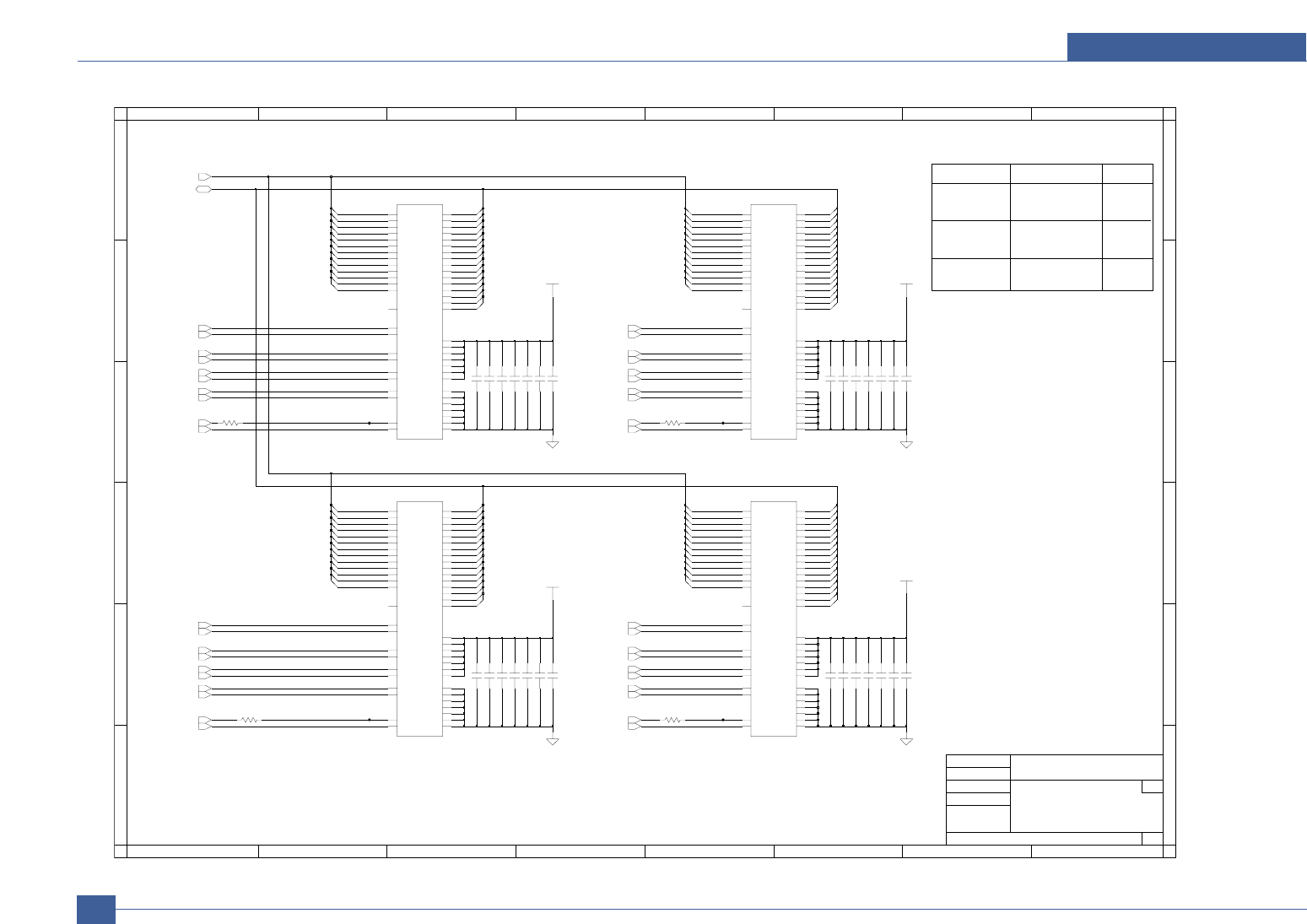
Schematic Diagram
Service Manual
11-6
This Document can not be used without Samsung’s authorization. Samsung Electronics
Main Board(6/15)
(1105-001384)
(1105-001384)CLX-3160FN
1
B
2
F
256Mbit * 2
256Mbit * 4
E
A
8
82 4
MFG ENGR CHK
Configuration Size
CLP-300
CLP-300N
CLX-3160N
128Mbit * 2
CC
6
5
E
1 6
(1105-001357)
128MB
4
6/15
A3
7
F
3
Size
TITLE:
Digtal Printing Division
R&D 5
Main_V0.11
B
53
32MB
64MB
CLP-300(N)/CLX-3160N(FN)
Engineer K.C.LEE
Drawn by
R&D CHK S.D.AN
DOC CTRL CHK
D
7
SDRAM
A
D
Model
100nF
C216 100nF
Vb
C183
6
12
VSSQ2 46
VSSQ3 52
VSSQ4
27
3
VDDQ1 9
VDDQ2 43
VDDQ3
VDDQ4 49
VSS1 28
VSS2 41
VSS3 54
VSSQ1
13
42
DQ8
44
DQ9
15 LDQM
NC/RFU
40
UDQM
39
VDD1 1
14
VDD2
VDD3
50
51
DQ14
53
DQ15
5
DQ2
DQ3 7
8
DQ4
DQ5 10
11
DQ6
DQ7
21
37 CKE
CLK
38
2
DQ0
DQ1 4
45
DQ10
DQ11 47
48
DQ12
DQ13
A3
A4
29
30 A5
A6
31
32 A7
A8
33
34 A9
20 BA0
BA1
*RAS
16 *WE
A0
23
24 A1
A10
22
35 A11
A12
36
A2
25
26
U16
K4S561632B-TC1L
*CAS
17
19 *CS
18
C88 100nF
DGND
C87 100nF
0
C207
R64
R100
100nF
0
R101 0
100nF
Vb
VSSQ3 46
VSSQ4 52
+3.3V
C107
VDDQ2 9
VDDQ3 43
49
VDDQ4
28
VSS1 41
VSS2 54
VSS3 6
VSSQ1
VSSQ2 12
DQ9 44
LDQM
15
NC/RFU
40
39 UDQM
1
VDD1
VDD2 14
27
VDD3
VDDQ1 3
DQ15 53
DQ2 5
7
DQ3
DQ4 8
10
DQ5
DQ6 11
13
DQ7
DQ8 42
38 CLK
DQ0 2
4
DQ1
DQ10 45
47
DQ11
DQ12 48
50
DQ13
DQ14 51
A5
30
31 A6
A7
32
33 A8
A9
34
BA0
20
21 BA1
CKE
37
23 A0
A1
24
22 A10
A11
35
36 A12
25 A2
A3
26
29 A4
1105-001384
K4S561632B-TC1L
U7
17 *CAS
*CS
19
*RAS
18
*WE
16
100nFC147
C220 100nF
100nFC201
+3.3V
C175 100nF
VSSQ1
VSSQ2 12
VSSQ3 46
VSSQ4 52
DGND
C184 100nF
VDD3
VDDQ1 3
VDDQ2 9
VDDQ3 43
49
VDDQ4
28
VSS1 41
VSS2 54
VSS3 6
DQ7
DQ8 42
DQ9 44
15 LDQM
NC/RFU
40
UDQM
39
1
VDD1
VDD2 14
27
DQ13
DQ14 51
DQ15 53
DQ2 5
7
DQ3
8
DQ4
10
DQ5
DQ6 11
13
BA1
37 CKE
38 CLK
DQ0 2
4
DQ1
45
DQ10
47
DQ11
DQ12 48
50
26
29 A4
A5
30
31 A6
A7
32 A8
33 A9
34
BA0
20
21
18
*WE
16
23 A0
A1
24
A10
22 A11
35 A12
36
25 A2
A3
U15
K4S561632B-TC1L
*CAS
17
*CS
19
*RAS
C82 100nF
100nFC94
100nF
C150
100nFC100
0
R65
VSSQ4
100nF
C99
VDDQ3
VDDQ4 49
VSS1 28
VSS2 41
VSS3 54
VSSQ1 6
12
VSSQ2 46
VSSQ3 52
15
NC/RFU
40
39 UDQM
VDD1 1
14
VDD2
VDD3 27
3
VDDQ1 9
VDDQ2 43
DQ2
DQ3 7
DQ4 8
DQ5 10
11
DQ6
DQ7 13
42
DQ8
44
DQ9
LDQM
DQ0
DQ1 4
DQ10 45
DQ11 47
48
DQ12
DQ13 50
51
DQ14
53
DQ15
5
31
32 A7
33 A8
34 A9
20 BA0
BA1
21
CKE
37 CLK
38
2
A1
22 A10
35 A11
36 A12
A2
25
26 A3
A4
29
30 A5
A6
U6
17 *CAS
19 *CS
18 *RAS
16 *WE
A0
23
24
K4S561632B-TC1L
DGND
100nF
C83
100nFC73
100nFC106
C200 100nF
C161 100nF
100nFC96
100nFC191
C206
100nF
100nF
C72
100nFC176
100nFC192
100nF
DGND
C162
SD(16)
nCAS
nSCS1
DQM3
DQM2
nRAS
nSDRAM_WR
BA0
BA1
SD_CKE
SA(10) SA(10)
SA(12) SA(12)
SD_CKE
SDCLK0
BA1
BA0
nSDRAM_WR
nRAS
DQM0
DQM1
nSCS0
nCAS
SD(0:31)
SA(0:12)
SD(31)
SD(30)
SD(29)
SD(28)
SD(27)
SD(26)
SD(25)
SD(24)
SD(23)
SD(22)
SD(21)
SD(20)
SD(19)
SD(18)
SD(17)
SD(4)
SD(5)
SD(6)
SD(7)
SD(8)
SD(9)
SA(11)
SA(9)
SA(8)
SA(7)
SA(6)
SA(5)
SA(4)
SA(3)
SA(2)
SA(1)
SA(0)
SA(6)
SA(7)
SA(8)
SA(9)
BA0
BA1
SDCLK1 SDCLK1
SD_CKE
SD(0)
SD(1)
SD(10)
SD(11)
SD(12)
SD(13)
SD(14)
SD(15)
SD(2)
SD(3)
SA(5)
SA(6)
SA(7)
SA(8)
SA(9)
SA(11)
nCAS
nSCS0
nRAS
BA0
BA1
SDCLK0
SD_CKE
nCAS
nSCS1
DQM1
DQM0
nRAS
nSDRAM_WR
SA(0)
SA(1)
SA(11)
SA(2)
SA(3)
SA(4)
SA(5)
SD(20)
SD(19)
SD(18)
SD(17)
SD(16)
DQM3
DQM2
nSDRAM_WR
SA(10)
SA(12) SA(12)
SA(10)
SA(0)
SA(1)
SA(2)
SA(3)
SA(4)
SD(5)
SD(6)
SD(7)
SD(8)
SD(9)
SD(31)
SD(30)
SD(29)
SD(28)
SD(27)
SD(26)
SD(25)
SD(24)
SD(23)
SD(22)
SD(21)
SA(0)
SA(1)
SA(11)
SA(2)
SA(3)
SA(4)
SA(5)
SA(6)
SA(7)
SA(8)
SA(9)
SD(0)
SD(1)
SD(10)
SD(11)
SD(12)
SD(13)
SD(14)
SD(15)
SD(2)
SD(3)
SD(4)
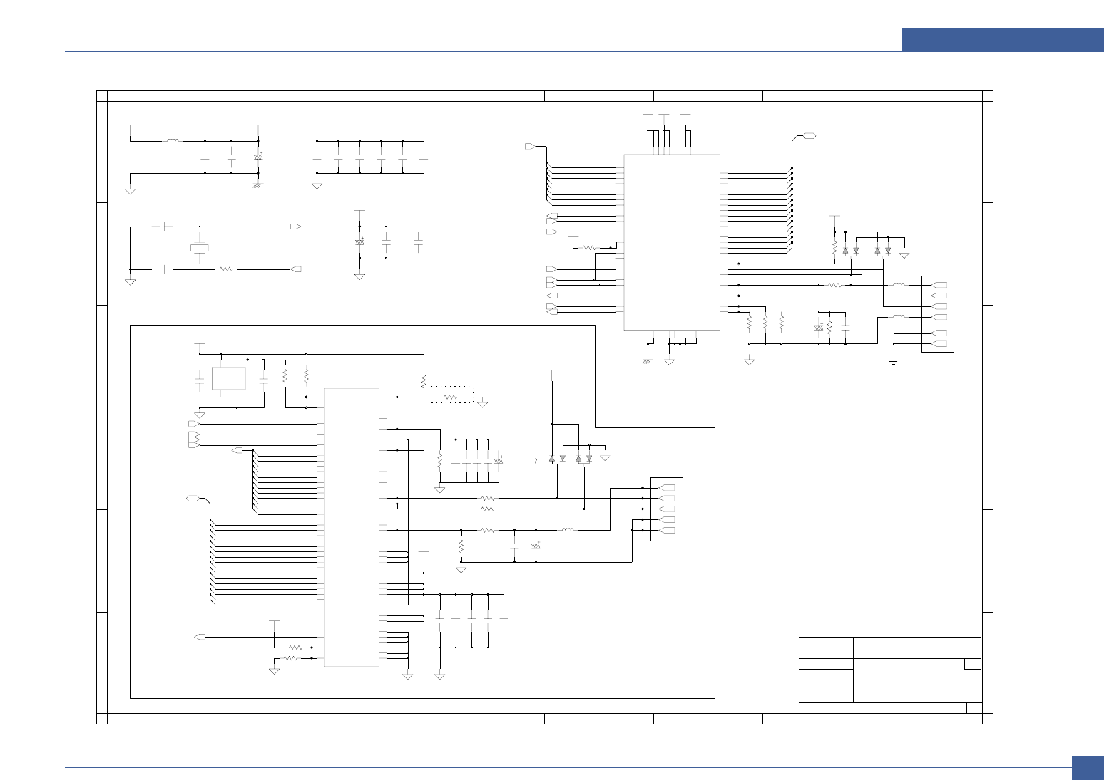
Schematic Diagram
Service Manual
11-7
This Document can not be used without Samsung’s authorization.
Samsung Electronics
Main Board(7/15)
F
A
8
B4
B
A
TITLE:
Digtal Printing Division
NOT USED
B
CLP-300(N)/CLX-3160N(FN)
Engineer K.C.LEE
C
USB Host & Device Controller
Drawn by
R&D 5
7
CLX-3160N(FN) Only
2402-001049
1 5
2402-001049
1
2402-001049
567
E
F
6
1
32
B
DD
E
7/15
A3
DOC CTRL CHK
R&D CHK S.D.AN
BB
2402-001049
C
MFG ENGR CHK
Size
423
Main_V0.11
0904-001865
8
3
R114
DGND
100nF
10K
C6
C3
5
100nF
INSTPAR
NC2 15pF
L6
C190
1000NF
10K
DGND DGND
USB_3.3VA
3
OUTVCC
4
R23
OSC1
SCO-10325AD-6M
2
GNDNC
1
100nF
C7C57 100nF
100
R111
LK16081ROK-T
+3.3V
+3.3V
USB_3.3VA
1uH
L10
INSTPARL7
C22
16V
10uF
C239
100nF
2
10nF
C231
DGND
DGND
+3.3V
R7
10K
47uF
C203
16V
OSC6
ATS-49/U,12MHz,50ppm
10KR98
C236
15pF KDS226
D20
1
3
2
D19
KDS226
1
3
2
10K
C230
NR4
100nF
R11
100nF
C229
USB_1V8
10K
DGND
R108
1.5K
12.1Kohm,1%
R102
R1
+3.3V
33
C8 100nF
35303-0550
CN6-1
1
DGND
C32 100nF
16V
10uF
C59
Vcc_54 54
Vcc_I_O_21 21
Vcc_I_O_34 34
Vcc_I_O_48 48
WAKEUP 55
XTAL1
52
XTAL2
51
nCS
15
nRD
16
nWR
17
EOT
8
INT
14
RESET_N
7
RPU 2
RREF 6
SUSPEND 56
57 TGND
VBUS 49
Vcc_1V8_28 28
Vcc_1V8_50 50
Vcc_53 53
39
DATA9 40
DGND_13
13
DGND_26
26
DGND_29
29
DGND_41
41
DIOR
11
DIOW
12
DM 4
DP 3
DREQ
9
DATA12 44
DATA13 45
DATA14 46
DATA15 47
DATA2 32
DATA3 33
DATA4 35
DATA5 36
DATA6 37
DATA7 38
DATA8
A4
23
A5
24
A6
25
A7
27
AGND_1
1
AGND_5
5
DACK
10
DATA0 30
DATA1 31
DATA10 42
DATA11 43
isp1582bs
U18
A0
18
A1
19
A2
20
A3
22
L1
+5V
4
5
C224
100nF
C198
100nF
100nF
C45
4
100nF
C58
D2
KDS226
1
3
2
+3.3V
DGND
10K
200K
R16
R94
2
CN14-1
787780-1
1
DGND
FGND
KDS226
D1
1
3
2
USB_GND
16V
10uF
C205
100nF
DGND
C60
10uF
16V
+3.3V
C46
6
R10 10K
USB_GND
100
R25
100nF
C232
DGND
+3.3V
_RESET
47
12 _WR
10K
R36
VSS28 28
VSS54 54
_CS
30
_EXVBO
37
11 _INT
_OC 36
_PO 39
_RD
13
VDD2_5_53 53
35
VDD3_3_35
21
VDDW_21
VDDW_5 5
VDDW_55 55
VREG_EN 41
42
VREG_OUT
VSS15 15
ID 40
63 OSC1 OSC2 64
48 TEST
VBP 38
46
VBUS
VDD2_5_10 10
29
VDD2_5_29
D6
58
59 D7
D8
1
2D9
34
DM1
32
DM2
DP1 33
DP2 31
D12
6
7D13
D14
8
9D15
D2
51
52 D3
D4
56
57 D5
AVDD3_3_45 45
44
AVSS44
AVSS61 61
CLKW
60
D0
49
50 D1
D10
3
4D11
A4
18 A5
19
20 A6
A7
22
23 A8
A9
24
62
AVDD2_5_62
AVDD3_3_43 43
A1
14
25 A10
A11
26
27 A12
16 A2
A3
17
U2
OTG242_LQFP64
+3.3V
C238
100nF
10K
USB_1V8
R110
15pF
C235 DGND
33
DGND
+3.3V
1M
R6
DGND
R93
C213
10nF 10nF
C217
DGND
P1
3
MINISMDC075-2
10nF
C199
100nFC31
4.7KR2
ADDR(2)
ADDR(3)
ADDR(4)
ADDR(5)
ADDR(2:13)
DATA(17)
DATA(18)
DATA(19)
DATA(20)
DATA(21)
DATA(22)
DATA(23)
DATA(24)
DATA(25)
DATA(26)
DATA(27)
DATA(28)
DATA(29)
DATA(30)
DATA(31)
DATA(31:16)
ADDR(6)
ADDR(7)
ADDR(8)
ADDR(9)
ADDR(11)
ADDR(13)
ADDR(5)
ADDR(4)
ADDR(3)
ADDR(2)
DATA(31:16)
DATA(16)
DATA(18)
DATA(17)
DATA(19)
DATA(20)
DATA(21)
DATA(22)
DATA(23)
DATA(24)
DATA(25)
DATA(26)
DATA(27)
DATA(28)
DATA(29)
DATA(30)
DATA(31)
nRST_USB_HOST
nCS_USB_HOST
ADDR(12)
ADDR(10)
ADDR(9:2)
XI_USB
nWR
nRD
nINT_USB_HOST
DATA(16)
ADDR(6)
ADDR(7)
ADDR(8)
ADDR(9)
nDACK_USB_DEVICE
nRST_USB_DEVICE
nCS_USB_DEVICE
nRD
nWR
nINT_USB_DEVICE
XI_USB
XO_USB
nDREQ_USB_DEVICE
XO_USB
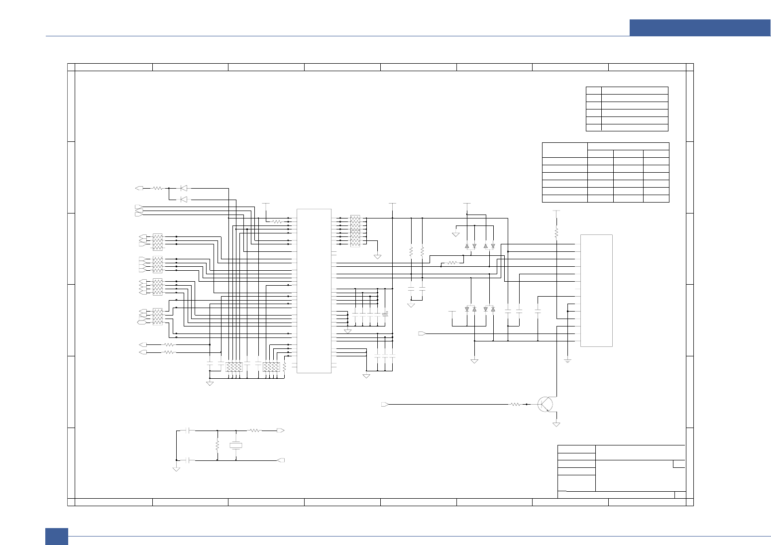
Schematic Diagram
Service Manual
11-8
This Document can not be used without Samsung’s authorization. Samsung Electronics
Main Board(8/15)
1
C
Function
Ethernet Physical Layer
1
mf0
E
5
CFG1
1
TITLE:
CLP-300(N)/CLX-3160N(FN)
0
1
Input Value
mf1
Drawn by
Configuration
0
FDE
1
2
Advertise 100 HD/FD
C
Advertise 100 HD
Auto-Negotiation
4
1
(2804-004414)
1
0
78
7
A
Advertise All
8
Operating Configurations/ Auto-Negotiation Enabled
D
R&D CHK S.D.AN
6
3
Advertise 10 HD 0
1
Scrambler Operation Disable
4B/5B Codeing Enable
DOC CTRL CHK
3
6
Advertise 10 HD/FD
Pin
F
A
MF4 10/100 Mbps Speed Select
MFG ENGR CHK
0
Digtal Printing Division
R&D 5
1
8/15
A3
mf4
B
D
B1
2402-001049
Desired
Size
1
Engineer K.C.LEE
mf3
Multi-Function pins
Enable NRZ-NRZI conversion
0
CFG0
Advertise 10/100 HD
1
CLP-300N & CLX-3160N(FN) Only
4
5
E
Main_V0.11
0
F
mf2
1
2
7NC
5RCT
6RDN
4RDP
TCT
2
3TDN
1TDP
1605713-7
CN11
8CT_REF
10 FGND_10
9FGND_9
11 LED1_ANODE
12 LED1_CATHOD
13 LED2_ANODE
14 LED2_CATHOD
C130
DGND
100
100nF
R87
C123
33pF
R55
C168
10pF
10K
100nF
C119
1/16W
33
RA6
1/16W
MMSD914T1
D9
RA35
33
KDS226
D17 1
3
2
KDS226
D14
1
3
2
63mW
10K
RA36
+3.3V
10pF
C167
R74 49.9
C112 100nF
C102
DGND
33pF
R52
200
100nF
C113
10pF
C153
C157 100nF
RA3
10K
63mW
10K
63mW
R177
RA37 D16
KDS226
1
3
2
1M
62
X1
12
11 X2
+3.3V
TX_ER
52
9
VCCA1
VCCA2 13
VCCA3 16
17
VCCA4
VCCA5 22
39
VCCE_I1 45
VCCE_I2
VCCE_I3
55 TX1
56
57 TX2
TX3
58
TXN 23
21
TXP
TX_CLK
53
54 TX_EN
RXD3
43
18
RXN
RXP 19
RX_CLK
49
48 RX_DV
51 RX_ER
26 TEST
TEST_SE
33
TX0
30
NC3
NC4 8
PWDDWN
27
RESET
28
29
RIP
47 RXD0
RXD1
46
44 RXD2
41
MF0 5
4
MF1 3
MF2
MF3 2
1
MF4
NC1
32
NC2
31
15 IREF
35 LEDC
LEDL
36 LEDR10
38
LEDS
34
37 LEDTR
42 MDC
MDINT 61
MDIO
7
10
GNDA2 14
GNDA3
GNDA4 20
24
GNDA5
25
GNDE_I1 40
GNDE_I2 50
GNDE_I3
ste100p
U8
CG0 64
CG1 63
COL
59
60 CRS
FDE 6
GNDA1
C144
10pF
R68 100
R83
100R61
49.9
DGND
1/16W
33
RA4
D18
KDS226 1
3
2
R67 100
DGND
R85
200
C111 100nF
C71
13
2
DGND
DGND
16V
10uF
Q8
MMBT2222ALT1
RA38
10K
63mW
5.1K
+3.3V
+3.3V
R73
100nF
C133
100nF
C140
1KR84
100nF
C139
DGND
DGND
+3.3V
U1F25000-35D16N
OSC4
FGND
100nF
C156
MMSD914T1
D11
DGND
C90
1nF
RA5
33
1/16W
1nF
C89
MAC_RX_ERR
MAC_MDC
MAC_MDIO
XO_PCLK
XI_PCLK
XI_PCLK
XO_PCLK
MAC_RXD2
MAC_RXD1
MAC_RXD0
MAC_RX_CLK
MAC_TXD2
MAC_TXD3
MAC_RX_DV
MAC_TX_CLK
nRST_NIC
MAC_CRS
MAC_COL
MAC_TX_EN
MAC_TXD1
MAC_TXD0
LAN_LINK
LAN_LINK
MAC_LED_CON
MAC_RXD3
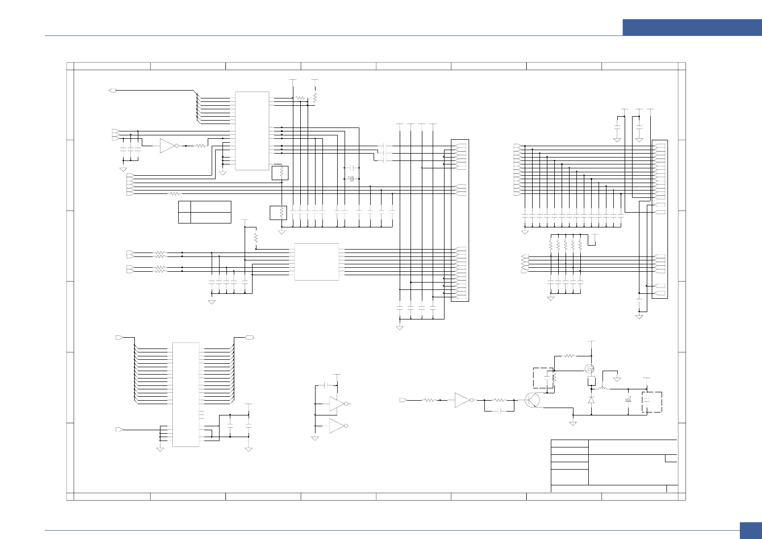
Schematic Diagram
Service Manual
11-9
This Document can not be used without Samsung’s authorization.
Samsung Electronics
Main Board(9/15)
2203-005249
50V
CLP-300(N)/CLX-3160N(FN)
Size
R&D CHK S.D.AN
DOC CTRL CHK
MFG ENGR CHK
B
3
R&D 5
Main_V0.11
2
2
Drawn by
NOT USED
D
C
7
5
D
3
A
F
4
F
C
Scanner Interface
4
TITLE:
E
Digtal Printing Division
50V
R46
1
1
HT82v26 ONLY USED
CIP40 ONLY USED
HT82V26 : 1K USED
CIP40 : 0ohm USED
HT82V26 USED
CIP40 NOT USED
R53
NOT USED
A
5
CLX-3160N(FN) Only
6
6
Engineer K.C.LEE
7
9/15
A3
8
E
B
8
DR
L4
3
DGND
C48 15pF
SS26
D12
2
47K
R186
R185 47K
47KR184
47K
C1
R183
1
DGND
100nF
20
CN1
DF11-24DP-2DSA(20)
U1-3
56
1nF
+3.3V +5V
15pF
C76
C37
18
100nFC310
15
C311
100nF
100nF
C27
1
100nF
C2
1EN
8EN_
5GND
VCC
4
FPC_24
CN3-1
DIN2
6DIN3
7DIN4
15
DOUT1+
16
DOUT1-
14
DOUT2+ 13
DOUT2-
11
DOUT3+
12
DOUT3-
10
DOUT4+
DOUT4- 9
DGND
FIN1047M
U3
DIN1
2
3
4
15pFC36
14
17
16V10uF
C105
2
+3.3V
+3.3V
22
C42 100nF
VCOM 23
VDDA1 18
28
VDDA2
5
VDDDR
VSSA1
19
27 VSSA2
6VSSDR
4OEB
25
OFFSET
REFB 20
21
REFT
R_VIN 26
SCLK
16
SDATA 15
17 SLOAD
D1
13
12 D2
D3
11
10 D4
D5
9
8D6
D7
7
24
G_VIN
HT82V26
U4
ADCCLK
3
B_VIN 22
CDS1_CLK
1
2CDS2_CLK
14 D0
C39 1nF
C26
17
1nF
R53
2K
C52 1nF
33R4
100nFC47
100
8
7
R49
6
DGND
4
C93 100nF
22
DGND
R8
+3.3V
INV_POWER
33
13
2
1nFC41
MMBT2222ALT1
Q5
C69 100nF
C77 15pF
20
C17 100pF
C40
+3.3V
1nF
C75 15pF
15pF
C74
R43
10K
1nFC65
C51
+5V
21
1nF
100
R50
C91
DGND
C92
100nF
100nF
24
DGND
6
1nF
C53
16
C23 15pF
1nF
19
+24V
C25
R48 100
33
R200
1nFC64
74LCX14
U1-2
34
U1-6
13 12
+3.3V
DGND
1nFC24
13
100nF
C248
C13 100nF
C15 100pF
47K
R182
DGND
19
C63 100nF
C38
12
1nF
11
10
8
9
7
C9
100nF
14
13
24
1
R191
NR115
0
C35
0
100nF
U1-1
7
14 2
DGND
74LCX14
C67
1000nF
R46
1K
15
1000NFC49
16
11
9
100nF
4.7K
R34
C80
C291
100nF
+24V
DGND
100nF
2203-005249|R1608_CAP
C54
1nFC78
C55 100nF
DGND
21
R51 100
18
100nFC12
S3
100nF
NC3
12
NDT2955
Q2
2
D1 D2
4
G1
100nF
10
C4
C66
10K
1nF
23
R29
1nF
C?
C84
1nF
_CS
39 _LB
41 _OE
_UB
40
17 _WE
I_O9
22
NC1
NC2 23
28
NC3
VCC1 11
VCC2 33
VSS1 12
VSS2 34
6
I_O14
I_O15 37
I_O16 38
10
I_O4 13
I_O5 14
I_O6 15
I_O7 16
I_O8 29
24
7
I_01 8
I_02 9
I_O3
30
I_O10 31
I_O11 32
I_O12 35
I_O13 36
A15
3A2
4A3
A4
5
18 A5
19 A6
20 A7
21 A8
A9
1A0
2A1
A10
25
26 A11
27 A12
42 A13
43 A14
44
U23
K6R1016V1D
5
100nFC14
3
4.7K
5
DGND
+24V
R38
C28
23
1nF
100nF
+3.3V
C16
NC1
50V
INV_POWER
100pF
+5V
100uF
C50
FLAT_MOT_DIR
FLAT_MOT_MS2
nFLAT_MOT_SLEEP
nFLAT_MOT_EN
FLAT_MOT_DAC
nADF_MOT_NB
nADF_MODULE_DETECT
PWM_CCD_LAMP
AFE_ADC_CLK
nADF_MOT_NA
FLAT_MOT_PLS
FLAT_MOT_MS1
nADF_P_REG
nADF_P_DET
nFLAT_COVER_OPEN
nADF_P_POS
AFE_CDS2_CLK
SCANNER_PI_SH
SCANNER_PI_TG1
AFE_SDATA
nBIN_FULL
SCANNER_DPI_CONTROL
SCANNER_BW_CONTROL
SRAM_D(13)
SRAM_D(14)
SRAM_D(15)
SRAM_D(0)
SRAM_A(15)
SRAM_A(14)
SRAM_A(4)
SRAM_A(13)
SRAM_A(12)
SRAM_A(11)
SRAM_A(10)
SRAM_A(9)
SRAM_A(8)
SRAM_A(7)
SRAM_A(6)
SRAM_A(5)
SRAM_A(3)
SRAM_A(1)
SRAM_A(2)
SRAM_A(0)
SRAM_A(0:15)
nSRAM_WR
AFE_D(0:7)
AFE_D(1)
AFE_D(0)
SCANNER_PI1
SCANNER_PI2
SCANNER_PI_CP
SCANNER_PI_RS
SRAM_D(0:15)
SRAM_D(1)
SRAM_D(2)
SRAM_D(3)
SRAM_D(4)
SRAM_D(5)
SRAM_D(6)
SRAM_D(7)
SRAM_D(8)
SRAM_D(9)
SRAM_D(10)
SRAM_D(11)
SRAM_D(12)
AFE_D(7)
AFE_D(6)
AFE_D(5)
AFE_D(4)
AFE_D(3)
AFE_D(2)
AFE_SLOAD
AFE_SCLK
nADF_MOT_A
nADF_MOT_PHB
nADF_MOT_PHA
nADF_MOT_B
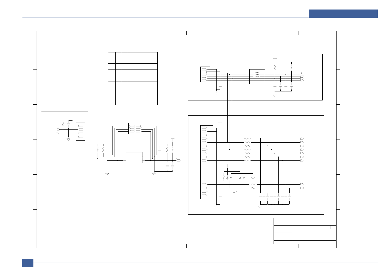
Schematic Diagram
Service Manual
11-10
This Document can not be used without Samsung’s authorization. Samsung Electronics
Main Board(10/15)
OPC
FOR DEBUG
1
I2C Address Configuration
2
R&D CHK S.D.AN
Hyper Terminal, EEPROM, OPE
0
1
10
1
A2
7
1
Not Used
2
F
A
8
1
Deve C
0
0
B
Drawn by
0
8
11
0
I2C Address
R&D 5
OPE2 : CLX-3160N(FN) Only
CLP-300(N)/CLX-3160N(FN)
5
A1
1
1
Deve Y
OPE1 : CLP-300(N) Only
7
0
3301-001122
Not Used
A
00
D
B
NPC & NVRAM
4
Deve M
010
1
4
Deve K
Digtal Printing Division
3 6
Main_V0.11
MFG ENGR CHK
Size
TITLE:
1
1
E
56
0
2
10/15
A3
E
F
Engineer K.C.LEE
C
DISPLAY_PANEL
C
D
A0
3
DOC CTRL CHK
9
C151
100nF
+5V
6
100
10K
R60
C121
R82
1nF
C141
1nF
DGND
+5V
NL1 B600
R75
8
100
2
1
1nFC142
U11_A-1
WSDIF-8T
100R57
DGND
100nFC307
R69
1nF
100
C138
C120
+3.3V
15pF
7
3
14
47K
R192
13
1nF
4
8
C115
3
2
C117
C95 1nF
1nF
C109
C132
100nF
+3.3V
1nF
35303-0750
CN12-1
1
2
+3.3V
100nF
C172 1K
R80
R62 100
C127 1nF
DGND
6
12
R92
10K
5
DGND
DGND
5
4
1
3
2
7
100R56
KDS226
D15
3
1nF
D13
KDS226
1
3
2
C152
C103 1nF
SDA
8
VCC
VSS
4
DGND
CN13-1
DF11-14DP-2DSA
1
U11
*WC 7
1E0
E1
2
3E2 SCL 6
5
11
M24C64
10
R63 100
10K
R91
R71
47K
DGND
4
6
35303-0450
CN27-1
1
+5V
10KR174
NL3 B600
1nF
C108
1nF
1K
C98
7
DGND
R79
R59
B600
NL2
+3.3V
100
3
4
R78 100
C137
15pF
VBIN
SDA
SCL
5
OP_STA_LED2
OP_MODE_LED
nOP_KEY_MODE
nOP_KEY_ONLINE
nSCANNER_HOME
VBIN
DEBUG_TXD
DEBUG_RXD
nRST_PANEL
PANEL_TXD
PANEL_RXD
OP_Y_LED
OP_M_LED
OP_C_LED
OP_K_LED
OP_STA_LED1
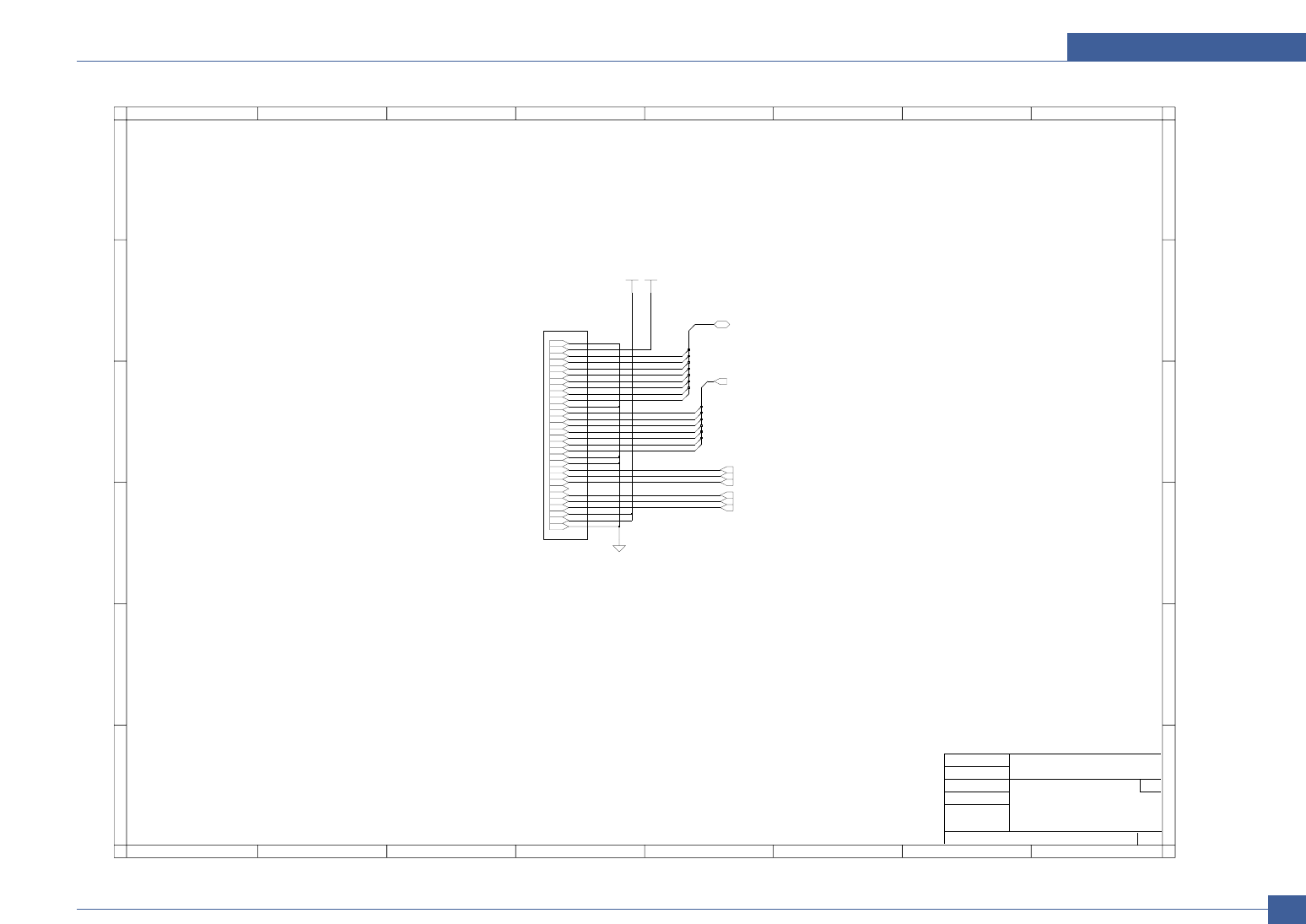
Schematic Diagram
Service Manual
11-11
This Document can not be used without Samsung’s authorization.
Samsung Electronics
Main Board(11/15)
23 67 8
123 4
C
D
E
SmartDAA Interface
R&D CHK S.D.AN
DOC CTRL CHK CLP-300(N)/CLX-3160N(FN)
Engineer K.C.LEE
Drawn by
CLX-3160FN Only
F
11/15
A3
54
E
MFG ENGR CHK
Size
TITLE:
Digtal Printing Division
R&D 5
Main_V0.11
D
C
B
5
B
A
F
A
876
1
27
18
+3.3V +5V
17
4
16
5
21
22
20
13
23
DGND
12
11
9
10
8
6
7
3
2
24
25
28
30
29
15
14
CN17-1
00-6232-030-807-800
1
19
nRST_MODEM
26
DATA(31:24)
DATA(24)
DATA(25)
DATA(26)
DATA(27)
DATA(28)
DATA(29)
DATA(30)
DATA(31)
ADDR(8)
ADDR(7)
ADDR(6)
ADDR(5)
ADDR(4)
ADDR(3)
ADDR(2)
nCS_MODEM
nRD
nWR
ADDR(2:8)
nINT_MODEM
KEYCLICK
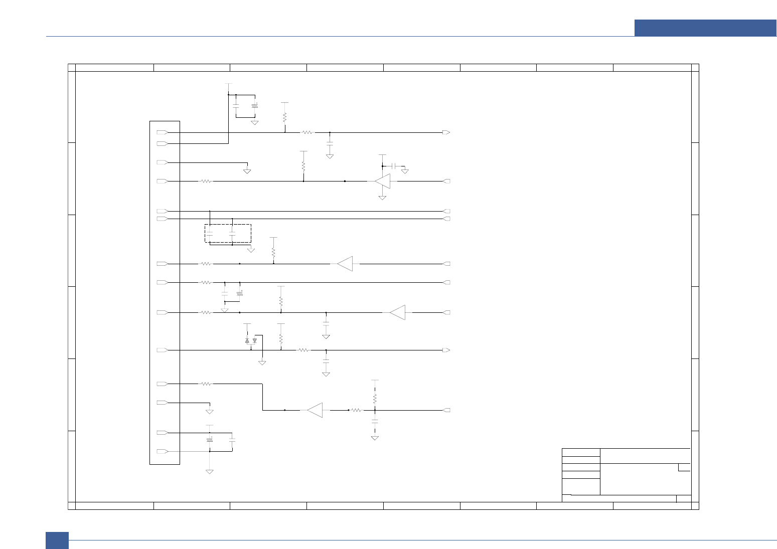
Schematic Diagram
Service Manual
11-12
This Document can not be used without Samsung’s authorization. Samsung Electronics
Main Board(12/15)
2402-001049
Engineer K.C.LEE
Drawn by
R&D CHK S.D.AN
2402-001049
F
A
21
8
Main_V0.11
B
C
DOC CTRL CHK
756
F
NOT USED
A3
54
4
7
A
B
D
E
6 8
CLP-300(N)/CLX-3160N(FN)
MFG ENGR CHK
Size
TITLE:
Digtal Printing Division
D
LSU
12
R&D 5
E
C
LSU
3
3
50V
+5V_LSU
12/15
10K
10uF
16V R144
DGND
C209
1
100nF
C306
CN22-1
DF11-14DP-2DSA
C223
15pF
NC5
7
100nF
KDS226
D36 1
3
2DGND
9
+5V_LSU
1K
+5V_LSU
5.1K
R118
4
DGND
R171
100
DM7407MX
U22-2
3
DGND
R169 DM7407MX
U22-3
56
100
R143
6
+5V
DGND
13
DGND +3.3V
DGND
100nF
C237
50V
47uF
C233
R145
10
DGND
+5V
10K
11
R168
DGND
DGND
10nF
C260
100
10nF
C284
R158
100nF
10K
+5V
C300
100
14
R167
4
5
10K
100
DGND
R137
DGND
8
R138
100nF
C241
U22-1
7
1
14
2
R117
100
DM7407MX
R103
100
NC4
15pF
+5V
2
+24V
10uF
C266
12
DGND
+5V_LSU
16V
100
DM7407MX
U22-4
98
R139
1nF
LSU_SH1
LSU_MOT_CLK
3
C285
nLD_EN
VDO1_plus
VDO1_minus
nHSYNC1
nLSU_READY
nLSU_MOTOR_EN
LD_POWER1
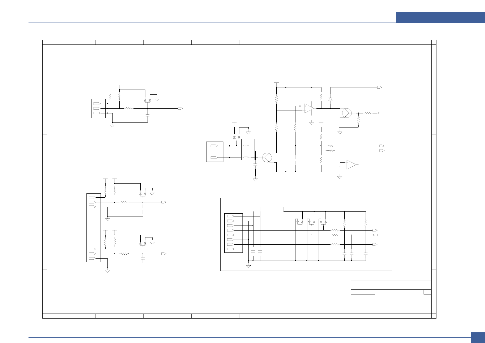
Schematic Diagram
Service Manual
11-13
This Document can not be used without Samsung’s authorization.
Samsung Electronics
Main Board(13/15)
B
67
BBB
3
CLP-300(N)/CLX-3160N(FN)
67
1%
DEVE_HOME,SCF,FUSER THER
3301-001122
Engineer K.C.LEE
Drawn by
R&D CHK S.D.AN
A
5
DOC CTRL CHK
Size
TITLE:
B
MFG ENGR CHK
SCF
Main_V0.11
1
D
C
E
1
1 8
E
F
C
Digtal Printing Division
R&D 5
8
F
FUSER THER.
7
13/15
A3
2
3
DEVE_HOME
2
D
4
B
A
4
5
+3.3V
INSTPAR
L2
5
67
R148
150
LM393D
U5-2
1nF
C268
DGND
KDS226
D6
1
3
2
100nF
C279
3
210nF
C21
MMBT2222ALT1
Q1
1
2
C81
100nF
2
+3.3V
R149
R127 100
DGND
100
3
3
2
DGND
CN18-1
DF11-8DP-2DSA
1
D32
KDS226
1
R132
+5V
DGND
10K
6
R126
10K
1KR155
DGND
+3.3V
3K,1%
R31
150
C270
1nF
4
R163
C20
10nF
8
DF11-6DP-2DSA
CN20-1
1
+5V
5
47K
R14 R24
20K
DGND
DGND
10nF
C264
R13
100
DGND
3
D26
KDS226
1
3
2
+3.3V
DGND DGND
L3
INSTPAR
4
3
5
2
5045-02A
CN8-1
1
2
+24V
+3.3V
6
+3.3V
D4
KDS226
1
3
C34
1nF
MMSD914T1
D10
+3.3V
+3.3V
R164
47K
2
R33 0
1
Q4
MMBT2222ALT1 1
3
LM393D
U5-1
3
2
8
4
D33
KDS226
1
3
2
DGND
4.7K
R47
1K
R41
D30
KDS226
1
3
2
30K,1%
R32
R150
100
R44
4.7K
1
2
35303-0350
CN5-1
DGND
150
R5
C246
1nF
R165
47K
5.6K
R20
C280
100nF,50V
33K
+5V
KDS226
D25
1
3
2
R19
100R153
15.4K,1%
R18
10nF
C263
nP_EMPTY
nDEV_HOME
nREGI_SENS
SCF_TXD
SCF_RXD
nSCF_RDY
FUSER_THERM2
FUSER_ON
FUSER_THERM1
nFUSER_EN
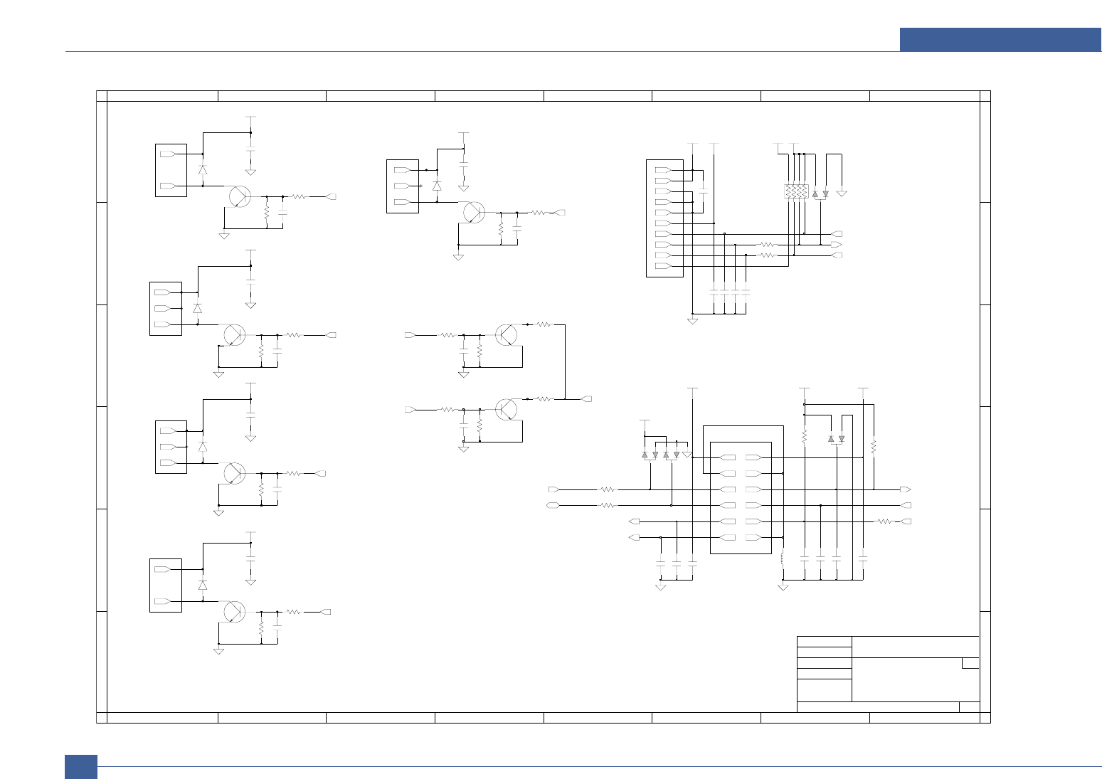
Schematic Diagram
Service Manual
11-14
This Document can not be used without Samsung’s authorization. Samsung Electronics
Main Board(14/15)
2
ITB_CLUTCH
DEVE & ITB JOINT
50V,10%
50V,10%
56
4
PICK UP
DEV_SOL BLDC
1
4
2203-005249
2203-005249
5
50V,10%
50V,10%
PTL
CLP-300(N)/CLX-3160N(FN)
R&D 5
A
B
Engineer K.C.LEE
Size
TITLE:
78
A
B
8
2203-005249
1%
2203-005249
BB
Drawn by
Digtal Printing Division
BB
F
Main_V0.11
R&D CHK S.D.AN
DOC CTRL CHK
3
C
D
2203-005249
14/15
A3
12
E
7
REGI_CLUTCH
BLDC, CLUTCH, DEVE & ITB JOINT
3
C
D
E
1 6
50V,10%
T2_CLUTCH
MFG ENGR CHK
F
INSTPAR
L11
33
R199
R198
3
DF11-10DP-2DSA
CN2-1
1
33
2
1
3
CN19-1
1
35303-0350
CN24-1
R129
DF11-12DP-2DSA
1
470
M4
D3
5045-02A
CN25-1
1nFC283
10K
RA2
CN7-1
1
R40
100nF
DGND
DGND
4.7K
C5
C262 100nF
10nFC282
R35 4.7K
D34
M4
R130 13
2
1.2K
+3.3V
Q14
MMBT2222ALT1
DGND
+5V
R22
C33 100nF
1.2K
100
3
R42
R166
1.2K
1nFC30
10K
1.2K
R39
R122
7
4.7K
DGND
100nF
R141
7
C11
M4
D8
2
Q6
MMBT2222ALT1
1
3
9
2
R156 4.7K
1
3
2
4.7K
MMBT2222ALT1
Q3
R120
11
R45
560
DGND
C305
100nF
3
2
R157 4.7K
1
3
2
KDS226
D38
1
2
D37
KDS226
8
+24VF
100nFC281
C43
100nF
8
1
3
2
+3.3V
C252 1nF
MMBT2222ALT1
Q7
MMBT2222ALT1
1
3
2
13
2
Q10
Q13
MMBT2222ALT1
M4
D7
+5V
DGND
+24VF
6
D5
KDS226
1
3
2
+24VF
5
0R128
R140
4.7K
R160
4
1.2K
1
+3.3V
DGND
+3.3V
R37 4.7K
5045-02A
CN4-1
DGND
1nF
DGND
C68
100
C29 10nF
3
R21
9
100nFC261
100nFC278
10nFC56
+5V
1nFC79
DGND
12
3
2DGND
+24VF
+24VF
C245 1nF
5045-03A
D31
1
3
2
560
R119
KDS226
Q16
MMBT2222ALT1
1
3
2
C19
2
100nF
DGND
M4
D35
4
DGND
DGND
10nFC292
2
5045-03A
CN10-1
1
DGND
DGND
C271 1nF
C44 1nF
1nFC265
100nF
C304
10
+24VF
2
DGND
10
6
3K
R125
5
ERASE_LAMP
SDA
WASTE_EMPTY
WASTE_LEVEL
PTL_LAMP
INNER_TEMP
SCL nITB_HOME
PTL_LAMP
REGI_CLUTCH
ITB_CLUTCH
PICKUP_CLUTCH
DEV_CLUTCH
PWM_MOT
BLDC_MOTOR_READY
THV_CLUTCH PTL
nBLDC_MOTOR_EN
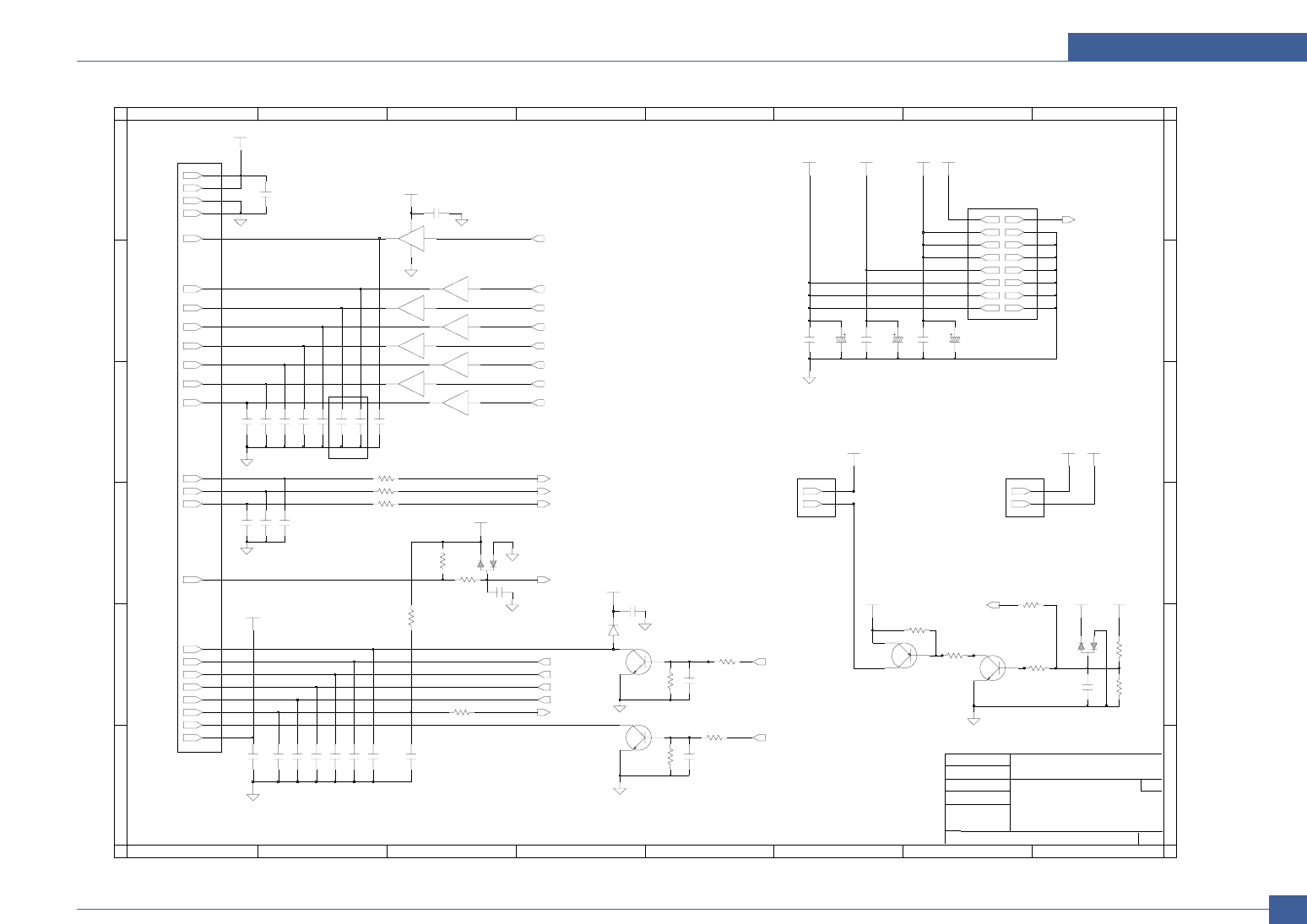
Schematic Diagram
Service Manual
11-15
This Document can not be used without Samsung’s authorization.
Samsung Electronics
Main Board(15/15)
A
5
B
81 6
HVPS
C
8
2
SMPS
HVPS, SMPS, COVER_OPEN
6
N.C
Size
3
F
+5V_COVER SWITCH +24V_COVER SWITCH
2203-005249
7
A
C
73
TITLE:
4
4
D
F
B
CLP-300(N)/CLX-3160N(FN)
12
E
+5V
15/15
A3
Drawn by
5
D
E
R&D 5
Engineer K.C.LEE
R&D CHK S.D.AN
DOC CTRL CHK
MFG ENGR CHK
Digtal Printing Division
Main_V0.11
100nFC249
C258
4
10nF
C196
100nF
R123 1.2K
C274
10nF
DGND
1
2
14
35303-0250
CN26-1
12
10nF
C242
16
D24
KDS226 1
3
2
DGND
21
1
3
2
+24VA
MMBT2222ALT1
Q15
16
47K
R180
C273
5096-02C
CN16-1
1
1nF
R187
R179
560
14
300
6
1nFC290
C288 1nF
1nF
C272
NC7 1nF
3
4
R124 10K
11
100
R146
8
10
9
8
10nF
C297
M4
D28
15
+5V_LSU
2
U20-3
DM7407MX 56
18
1nF
C296
C257 1nF
C253 1nF
R135 10K
+3.3V
13
R116
3K
1nF
C247
3K,1%
7
1
14
2
+24VF
C208
DGND
DM7407MX
U20-1
7
100uF
50V
2401-000207
7
+5V +24V
R99
22K
U20-2
DM7407MX 34
5.1K
R104
100nF
C251
13
DGND
+3.3V
16V
100uF
C171
2401-000042
R188
DM7407MX
U20-4
98
+24VA
4.7K
U20-6
DM7407MX
1312
DGND
+24VF
DGND
6
+5V
C299 1nF
DGND
10
+24VF
DM7407MX
U20-5
11
1
C298 1nF
10
CN15-1
DF11-16DP-2DSA
23
CN21-1
DF11-24DP-2DSA(20)
1
5
DGND
DGND
DGND
50V
100uF
C240
2401-000207
10KR159
4.7KR131
1nF
NC6
DGND
DM7407MX
U22-6
1312
R178
1nF
6.2K
17
3
C287
100nF
10K
C309
15
R134
5
DGND
22
Q18
1
3
2
+24VF
MMBT2222ALT1
2
C259 1nF
11
DM7407MX
U22-5
1110
3
2
24
MMBT2907A
Q19
1
C276
+24VF
1.2K
1nF
R136
R147 4.7K
100nF
C294
19
20
KDS226
D21
1
3
2
C225
100nF
12
+5V
C185
100nF
100nF
C166
9
1nF
C275
MMBT2222ALT1
Q17
1
3
2
C293
DGND
100nF
2
WASTE_LED
nP_EXIT
FAN_MAIN
THV_READ
ITHV_READ
MHV_READ
DEV_SOL4
DEV_SOL3
DEV_SOL2
DEV_SOL1
PWM_DEV_VPP
nCOVER_OPEN
OUT_TEMP
FUSER_ON
PWM_DEV_AC
PWM_DEV_DC
PWM_ITHV
PWM_THV
PWM_MHV
nTHV_EN
nDEV_EN
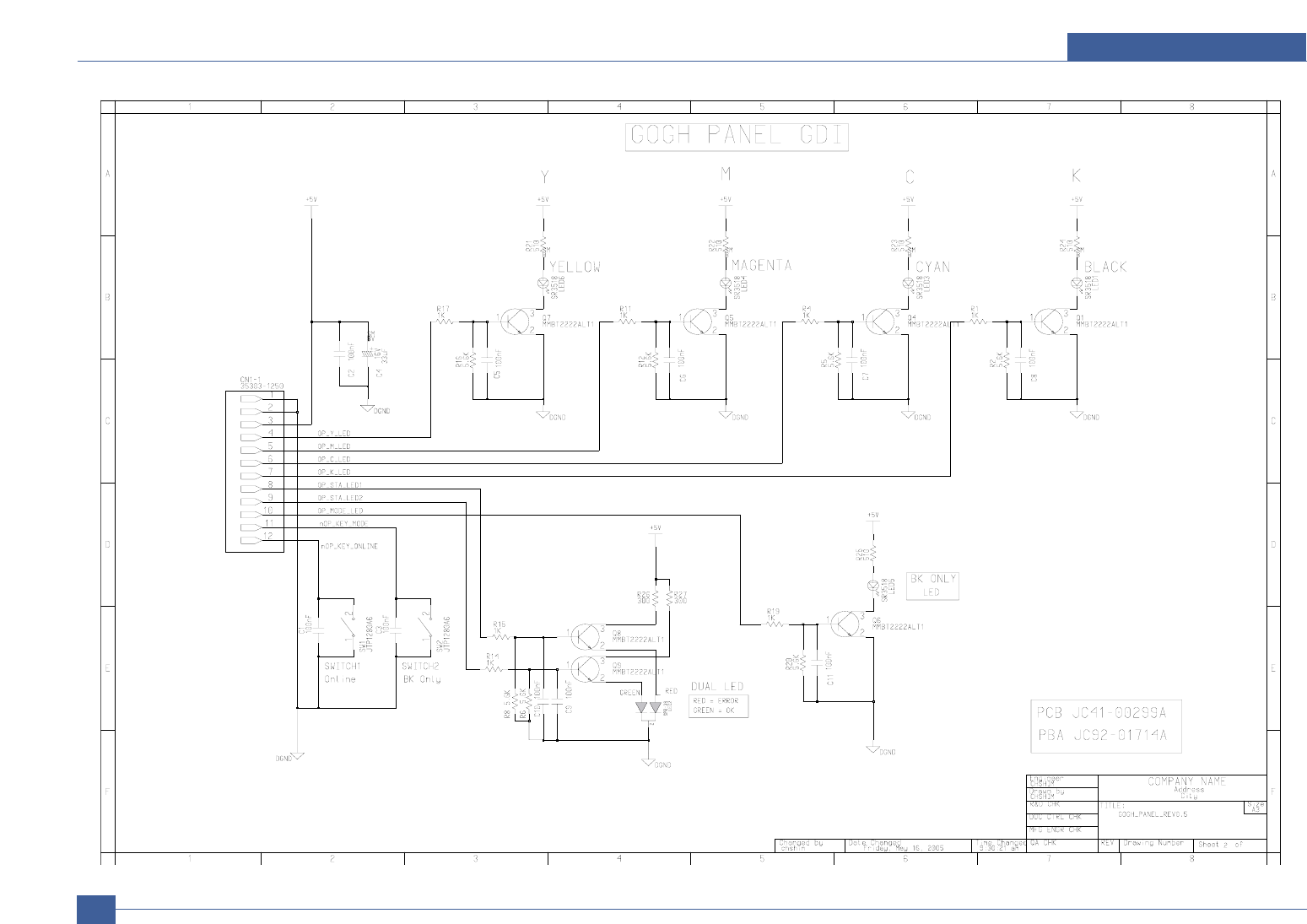
Schematic Diagram
Service Manual
11-16
This Document can not be used without Samsung’s authorization. Samsung Electronics
MAIN PANEL
11.2 Panel
Schematic Diagram
Service Manual
11-17
This Document can not be used without Samsung’s authorization.
Samsung Electronics
TONER_CRUM_CONTACT_K
0
00
WASTE LEVEL
FROM MAIN BOARD
WASTE EMPTY
A0A0
A1A1
TONER_CRUM_CONTACT_M
A2A2
Y
TONER_CRUM_CONTACT_C
DEVE CRUM
TONER_CRUM_CONTACT_Y
DEVE
0
11
1
MC K
0101
0000
DGN D
DGN DDGN D
DGN D
DGN D
15K
R7
DGN D
2
3
DGN D
DGN D
DGN D DGN D
DGN D
DGN D
CN3-1
35303-0350
1
DGN D
11.3 DEVE INF
Schematic Diagram
Service Manual
11-18
This Document can not be used without Samsung’s authorization. Samsung Electronics
ITB_HO MEPTL
FROM_DRAW_CON
11.4 ITB INF
Schematic Diagram
Service Manual
11-19
This Document can not be used without Samsung’s authorization.
Samsung Electronics
A A
B B
C C
D D
1
1
2
2
3
3
4
4
Title
Size No. Rev.
File Date Time of
Top Circuit
A3 .docno. .rev.
C:\...\ \TYPE III-V1_050602.sch 2005/06/02 19:44 1 1
note1
note2
note3
note4
note5
R51
1W50m
TNR01
14D221
F01
250V8A LF01
DV508080S
CON1
C01
224
R52
R53
91JX2_2012
0
0
00
PC51
TLP3061F
C52
104K_2012
AR02
1KV
Q51
600V16A
C04
104
R010
1W22(mini) D01
1KV1A-CHIP
BD01
600V6A
TH01
10D9
Q01
600V12A
R04
1K_2012
C11
200V680uF
R12
R13
R11
200KX3_3216
R15
R16
R14
39KX3_3216
C12
630V333K
Q11
600V4A
Q12
500V21A
DEMAG 1
FB
2
GND
4
CS
3
OUT
5
VCC 6
NC
7
VI 8
U11
IC_1207A-CHIP
R20
10K_2012
R21
100_2012
R19
100_2012
D12
MMSD4148
R18
10_2012
R23
47_3216
R24
100K_2012
C16
20p_2012
C14
100n_2012
C15
35V47uF
D11
1KV1A-CHIP
R22
5W0.13
C13
1n_2012
D103
D105
200V20AX2
D104
60V20A
C72
1KV103K
C73
1KV103K
C75
35V1000uFX2
C71
C18
AD102
TNR11
7D221
ZD71
20V-CHIP
L71
5uH
R92
1K_2012
C91
225_2012
R93
1KF_2012
R94
1KF_2012
R76
470_2012
C77
35V470uF
R77
3W120
Q71
2222A-CHIP
C78
50V104(mono)
F71
250V5A
ZD11
20V-CHIP
R75
200_2012
C76
16V1000uF
PC11-1
817B
C74
16V1000uF
U91
431-CHIP
C17
AD102
AR03
1KV
AR01
600V
AR04
600V
C05
104K_2012
R59
100_2012
R17
100_2012
L01
F02
250V5A
LF002
CV930160
R55
1/2W180(MINI)
L51
R54
1W50m
R02
R03
C02
AD102
C03
AD102
R01
200K_3216X3
ZD12
20V-CHIP
R91
220_2012
PC11-2
817B
R57
1K_2012
Q52
2222A-CHIP
R56
1W1.5KJ(mini)
R58
4.7K_2012
C51
630V333k
CON2-1
CON2-2
CON3-11,13,15
HEATSINK
CON3-3,5,7,9
CON3-4,6,8,10
CON3-12,14,16
CON3-2
CON3-1
T1
8
24V 4.4A
GND
5V 3A
GND
Fuser Count
24VS
11.5 SMPS-110V
Schematic Diagram
Service Manual
11-20
This Document can not be used without Samsung’s authorization. Samsung Electronics
A A
B B
C C
D D
1
1
2
2
3
3
4
4
Title
Size No. Rev.
File Date Time of
Top Circuit
A3 .docno. .rev.
C:\...\ \TYPE III-V2_050602.sch 2005/06/02 19:47 1 1
note1
note2
note3
note4
note5
R51
1W50m
TNR01
10D561
F01
250V8A LF01
CV505110B
CON1
C01
224
R52
R53
91JX2_2012
0
0
00
PC51
TLP3061F
C52
104K_2012
C51
630V333k
AR02
1KV
Q51
600V16A
C04
104
R010
1W22(mini) D01
1KV1A-CHIP
BD01
600V6A
TH01
10D9
Q01
600V12A
R04
1K_2012
C11
450V220uF
R12
R13
R11
200KX3_3216
R15
R16
R14
91KX3_3216
C12
630V333K
Q11
600V4A
Q12
600V11A
DEMAG 1
FB
2
GND
4
CS
3
OUT
5
VCC 6
NC
7
VI 8
U11
IC_1207A-CHIP
R20
10K_2012
R21
100_2012
R19
100_2012
D12
MMSD4148
R18
10_2012
R23
47_3216
R24
100K_2012
C16
20p_2012
C14
100n_2012
C15
35V47uF
D11
1KV1A-CHIP
R22
5W0.25
C13
1n_2012
D103
D105
200V20AX2
D104
60V20A
C72
1KV103K
C73
1KV103K
C75
35V1000uFX2
C71
C18
AD102
TNR11
7D221
ZD71
20V-CHIP
L71
5uH
R92
1K_2012
C91
225_2012
R93
1KF_2012
R94
1KF_2012
R76
470_2012
C77
35V470uF
R77
3W120
Q71
2222A-CHIP
C78
50V104(mono)
F71
250V5A
ZD11
20V-CHIP
R75
200_2012
C76
16V1000uF
PC11-1
817B
C74
16V1000uF
U91
431-CHIP
C17
AD102
AR03
1KV
AR01
600V
AR04
600V
C05
104K_2012
R59
22_2012
R17
100_2012
L01
F02
250V5A
LF002
CV930160P
R55
1/2W180(MINI)
L51
R54
1W50m
R02
R03
C02
AD102
C03
AD102
R01
200K_3216X3
ZD12
20V-CHIP
R91
220_2012
PC11-2
817B
R57
1K_2012
Q52
2222A-CHIP
R56
1W1.5KJ(mini)
R58
4.7K_2012
CON2-1
CON2-2
CON3-11,13,15
HEATSINK
CON3-3,5,7,9
CON3-4,6,8,10
CON3-12,14,16
CON3-2
CON3-1
T1
8
24V 4.4A
GND
5V 3A
GND
Fuser Count
24VS
11.6 SMPS-220V
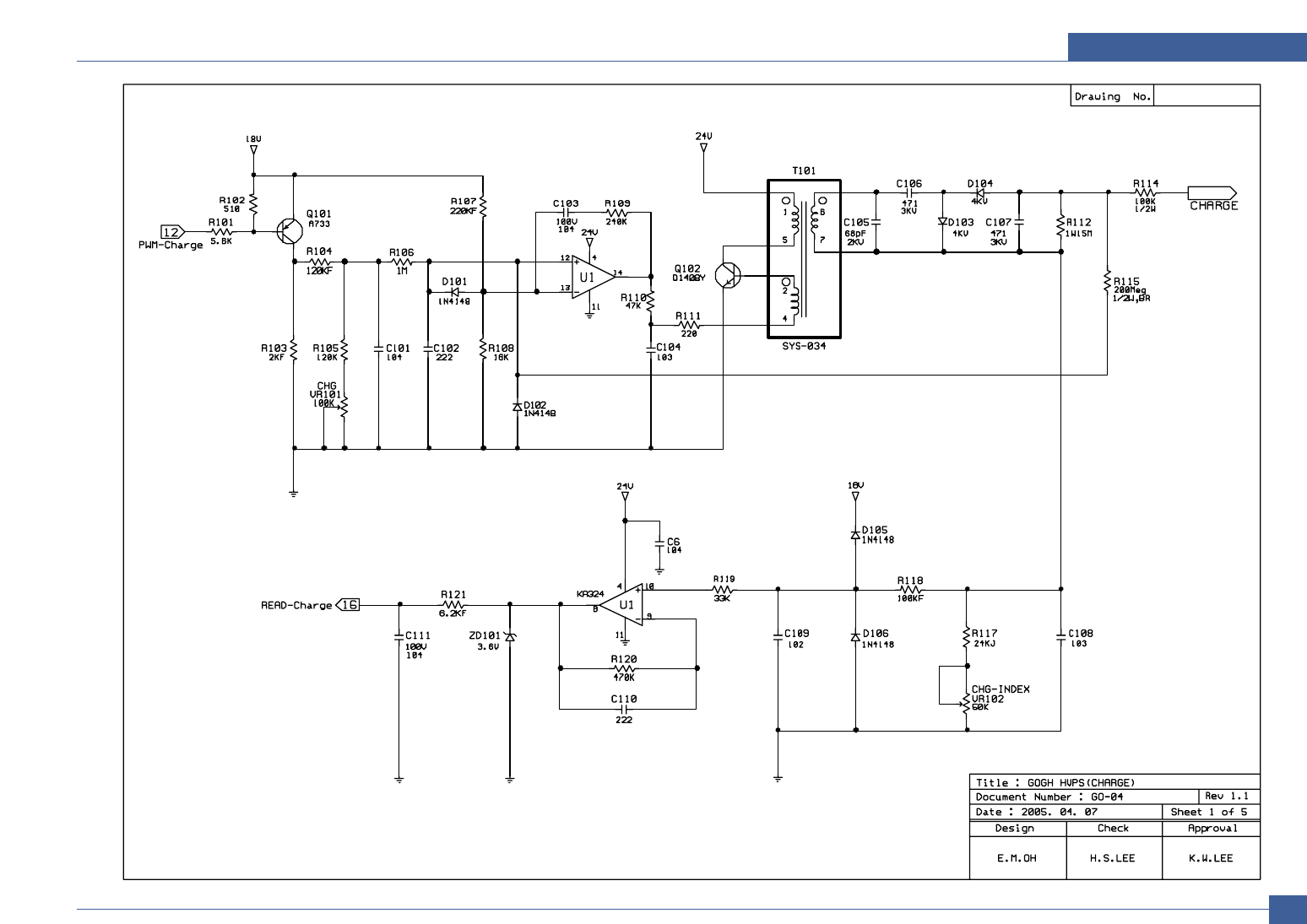
Schematic Diagram
Service Manual
11-21
This Document can not be used without Samsung’s authorization.
Samsung Electronics
11.7 HVPS (1/5)
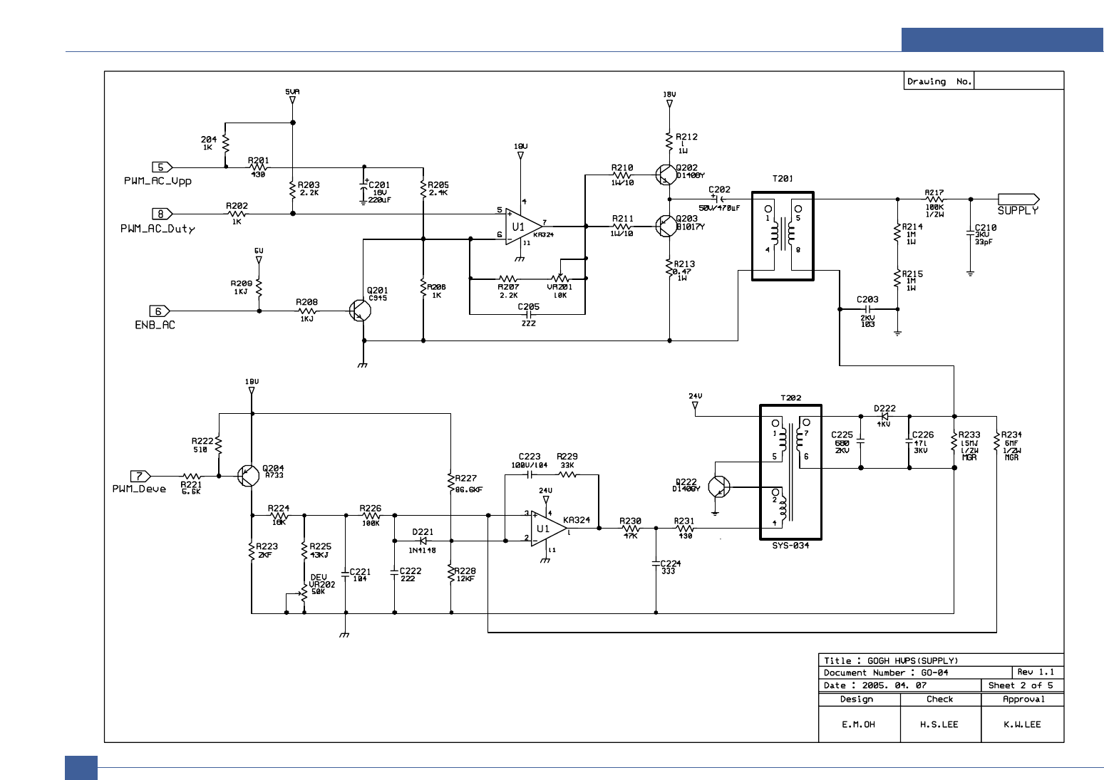
Schematic Diagram
Service Manual
11-22
This Document can not be used without Samsung’s authorization. Samsung Electronics
HVPS (2/5)
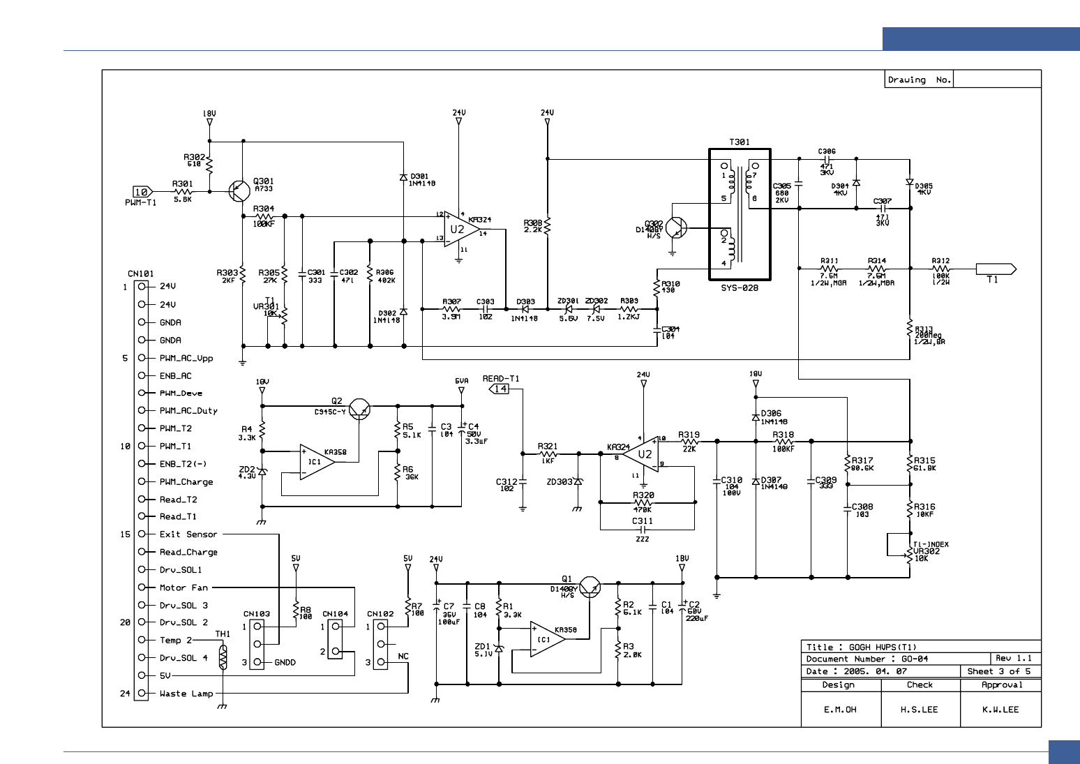
Schematic Diagram
Service Manual
11-23
This Document can not be used without Samsung’s authorization.
Samsung Electronics
HVPS (3/5)
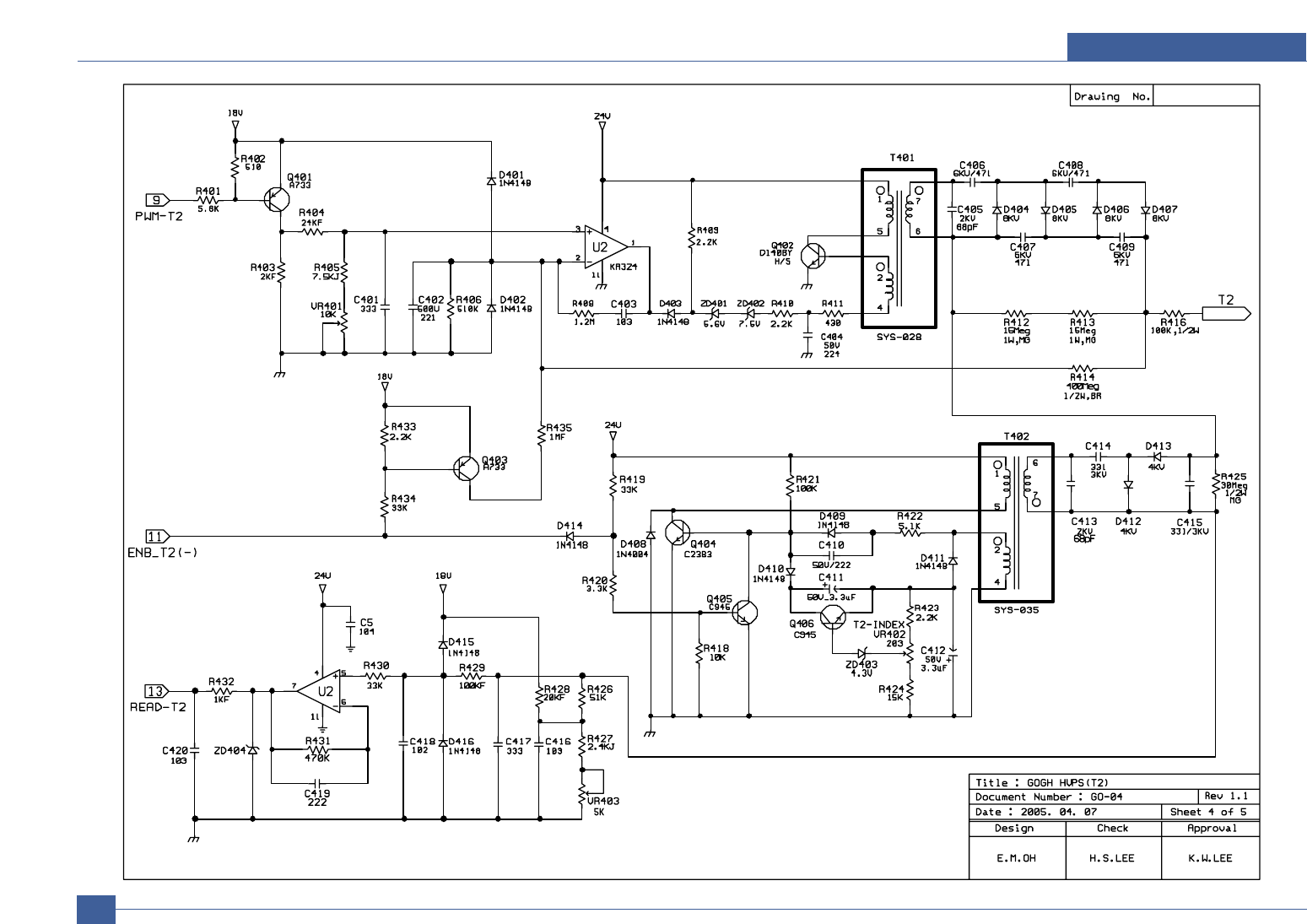
Schematic Diagram
Service Manual
11-24
This Document can not be used without Samsung’s authorization. Samsung Electronics
HVPS (4/5)
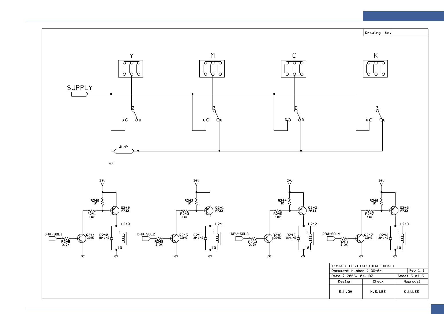
Schematic Diagram
Service Manual
11-25
This Document can not be used without Samsung’s authorization.
Samsung Electronics
HVPS (5/5)
Reference Information
Samsung Electronics Service Manual
12-1
12
12
12. Reference Information
This chapter contains the tools list, list of abbreviations used in this manual, and a guide to the
location space required when installing the printer. A definition of tests pages and Wireless
Network information definition is also included.
12.1 Tools for Troubleshooting
The following tools are recommended safe and easy troubleshooting as described in this service manual.
• DVM(Digital Volt Meter)
Standard : Indicates more than 3 digits.
• Driver
Standard : "-" type, "+" type (M3 long, M3 short, M2
long, M2 short).
• Tweezers
Standard : For general home use, small type.
• Cotton Swab
Standard : For general home use, for medical service.
• Cleaning Equipments
Standard : An IPA(Isopropyl Alcohol)dry wipe tissue or a
gentle neutral detergent and lint-free cloth.
• Vacuum Cleaner
• Brush
• Software (Driver) installation CD ROM
Install Driver CD
Network S/W CD

Samsung Electronics
Service Manual
Reference Information
12-2
12.2 Acronyms and Abbreviations
The table below explains the abbreviations and acronyms used in this service manual. Where abbreviations
or acronyms are used in the text please refer to this table.
ADC Analog-to-Digital-Conversion
AP Access Point
AC Alternating Current
ASIC Application Specific Integrated
Circuit
ASSY Assembly
BIOS Basic Input Output System
BLDC Motor Brushless DC Motor
CLBP Color Laser Beam Printer
CMOS Complementary Metal Oxide
Semiconductor
CMYK Cyan, Magenta, Yellow, Black
CN Connector
CON Connector
CPU Central Processing Unit
CTD Sensor Color Toner Density Sensor
dB Decibel
dBA A-Weighted decibel
dBm Decibel milliwatt
DC Direct Current
DCU Diagnostic Control Unit
DIMM Dual In-line Memory Module
DPI Dot Per Inch
DRAM Dynamic Random Access Memory
DVM Digital Voltmeter
ECP Enhanced Capability Port
ECU Engine Control Unit
EEPROM Electronically Erasable
Programmable Read Only Memory
EMI Electro Magnetic Interference
EP Electro photographic
EPP Enhanced Parallel Port
F/W Firmware
FCF/FCT First Cassette Feeder/First
Cassette Tray
FISO Front-In, Side-Out
FPOT First Print out Time
GDI Windows Graphic Device Interface
GIF Graphic Interchange Format
GND Ground
HBP Host Based Printing
HDD Hard Disk Drive
HTML Hyper Text Transfer Protocol
HV High Voltage
HVPS High Voltage Power Supply
I/F Interface
I/O Input and Output
lb Pound(s)
IC Integrated Circuit
ICC International Color Consortium
IDE Intelligent Drive Electronics or
Integrated Drive Electronics
IEEE Institute of Electrical and
Electronics Engineers. Inc
IOT Image Output Terminal (Color print-
er, Copier)
IPA Isopropy Alcohol
IPC Inter Process CommunicationEPP
Enhanced parallel Port
IPM Images Per Minute
ITB Image Transfer Belt
LAN local area network
LBP Laser Beam Printer

Reference Information
Samsung Electronics Service Manual
12-3
LCD Liquid Crystal Display
LED Light Emitting Diode
LSU Laser Scanning Unit
MB Megabyte
MHz Megahertz
MPBF Mean Prints Between Failure
MPF/MPT Multi Purpose Feeder/Multi
Purpose Tray
NIC Network Interface Card
NPC Network Printer Card
NVRAM Nonvolatile Random Access
Memory
OPC Organic Photo Conductor
PBA Printed Board Assembly
PCL Printer Command Language ,
Printer Control Language
PCI Peripheral Component
Interconnect by Intel 1992/6/22, is
a local bus standard developed by
Intel and introduced in April, 1993 :
A60, B60 Pins
PCL5Ce Printer Command Language 5Ce-
Color
PCL6 Printer Command Language 6
PDF Portable Document Format
PDL Page Description Language
Ping Packet internet or Inter-Network
Groper
PPD Postscript Printer Discription
PPM Page Per Minute
PS Post Script
PS3 Post Script Level3
PTL Pre-Transfer Lamp
PTB Paper-Transfer Belt
PWM Pulse Width Moduration
Q’ty Quantity
RAM Random Access Memory
RCP Remote Control Panel
ROM Read Only Memory
SCF/SCT Second Cassette Feeder/Second
Cassette Tray
SMPS Switching Mode Power Supply
SPGP Samsung Printer Graphic
Processor
SPL Samsung Printer Language
SPL-C Samsung Printer Language-Color
Spool Simultaneous Peripheral Operation
Online
SRS Software Requirment Specification
SURF Surface Rapid Fusing
SW Switch
sync Synchronous or Synchronization
T1 ITB
T2 Transfer Roller
TRC Toner Reproduction Curve
PnP Universal Plug and Play
U.I. User Interface
URL Uniform Resource Locator
USB Universal Serial Bus
VCCI Voluntary Control Council for
Interference Information
Technology Equipment
WECA Wireless Ethernet Compatibility
Alliance
Wi-Fi Wireless Fidelity
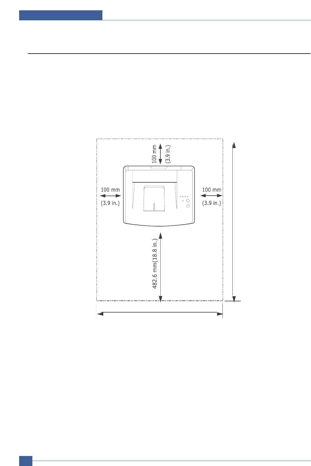
Samsung Electronics
Service Manual
Reference Information
12-4
12.3 Select a location for the printer
• Leave enough room to open the printer trays, covers, and allow for proper ventilation. (see diagram
below)
• Provide the proper environment :
- A firm, level surface
- Away from the direct airflow of air conditioners, heaters, or ventilators
- Free of extreme fluctuations of temperature, sunlight, or humidity
- Clean, dry, and free of dust
Reference Information
Samsung Electronics Service Manual
12-5
12.4 A4 ISO 19752 Standard Pattern
This test page is reproduced at 70% of the normal A4 size