Samsung Galaxy Tab S 8.4 SM T705 Service Manual. Www.s Manuals.com. Manual 8
User Manual: Tablet Samsung SM-T705 Galaxy Tab S 8.4 - Service manuals and Schematics, Disassembly / Assembly. Free.
Open the PDF directly: View PDF ![]() .
.
Page Count: 118 [warning: Documents this large are best viewed by clicking the View PDF Link!]
8. Level 3Repair
8-1
Confidential and proprietary-the contents in this service guide subject to change without prior notice.
Distribution, transmission, or infringement of any content or data from this document without Samsung’s written authorization is strictly prohibited.
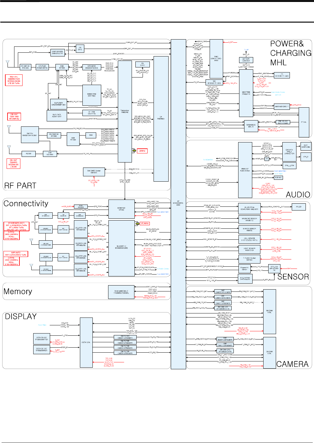
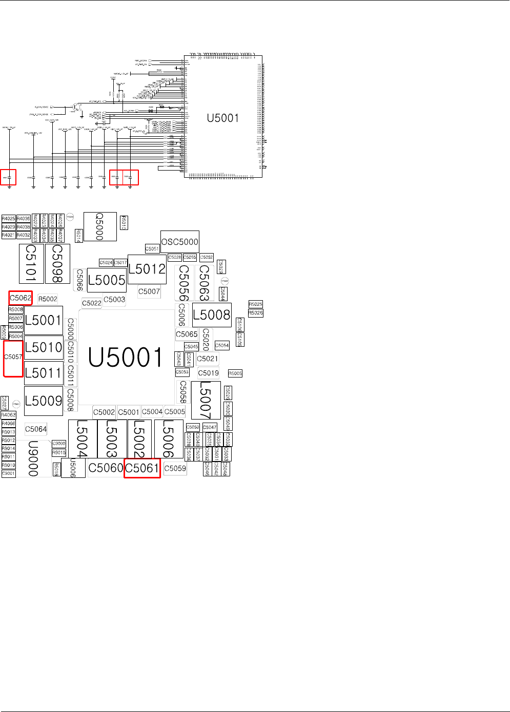
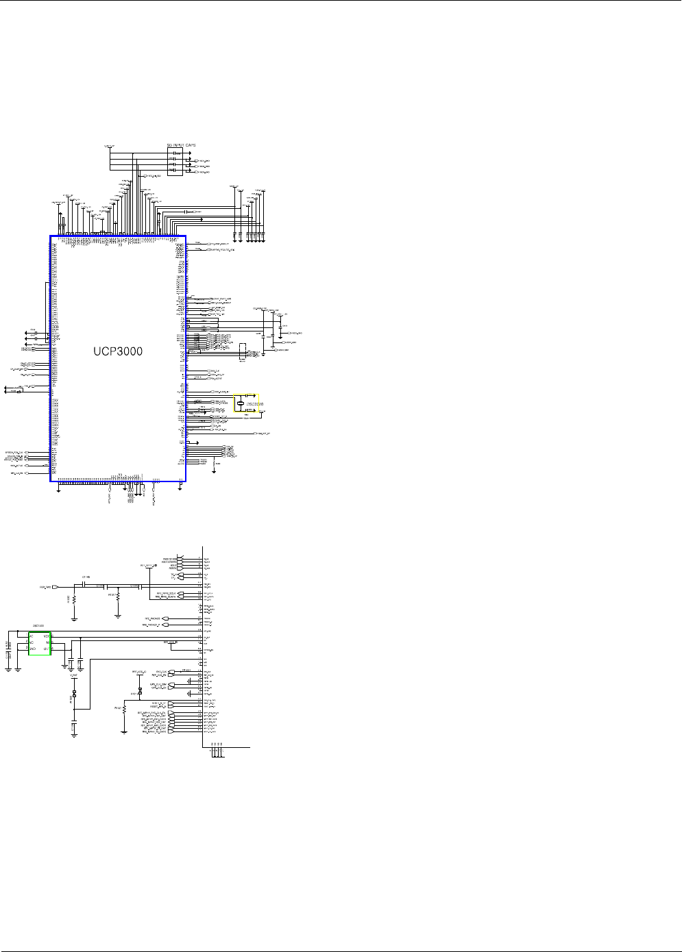
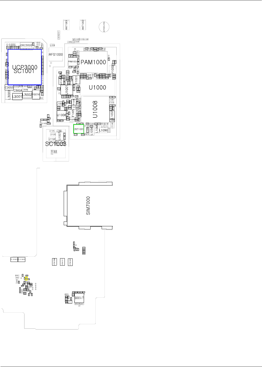
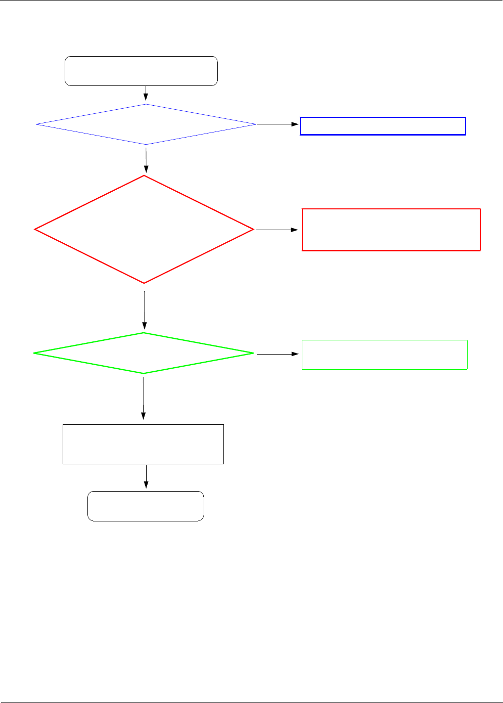
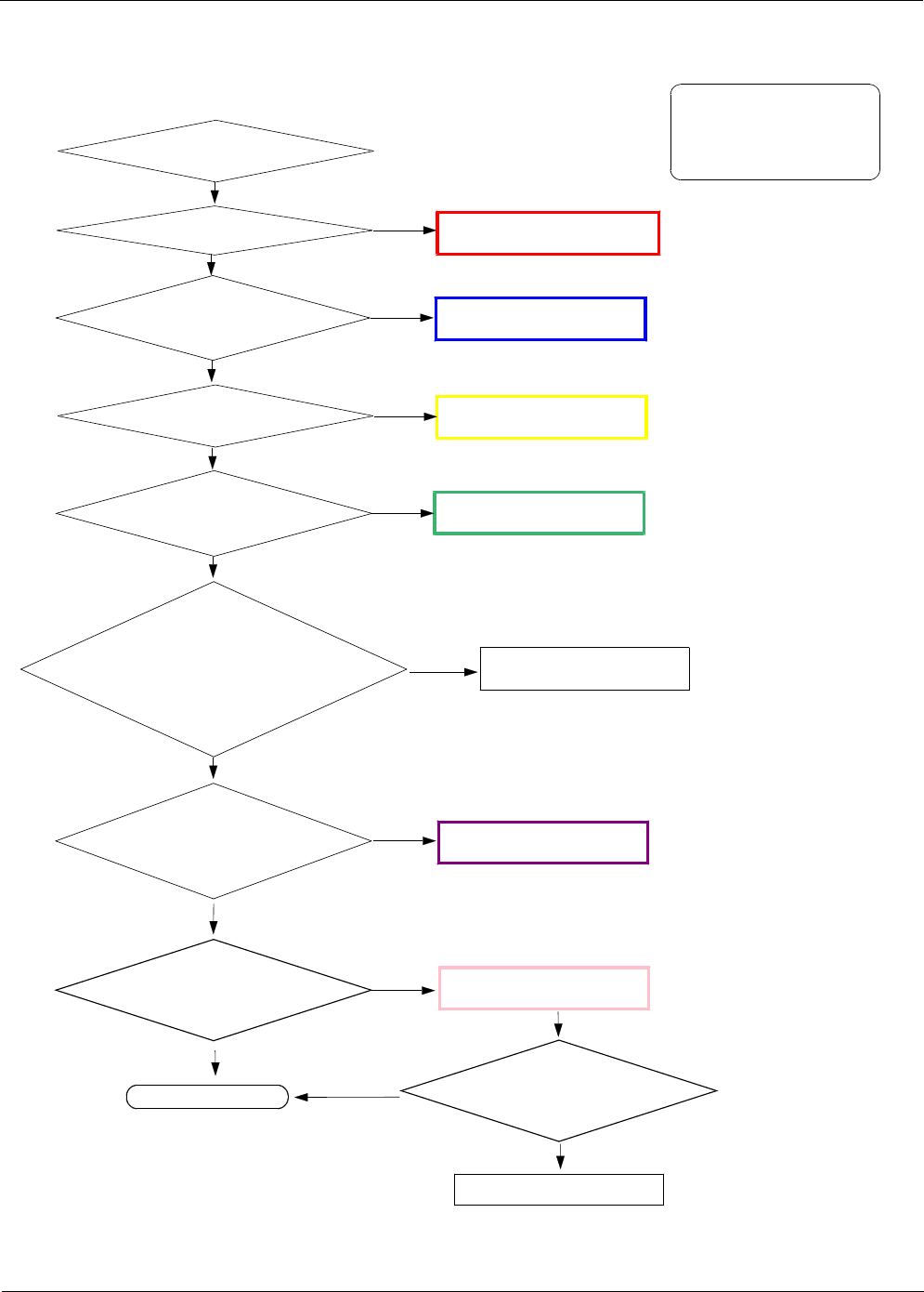
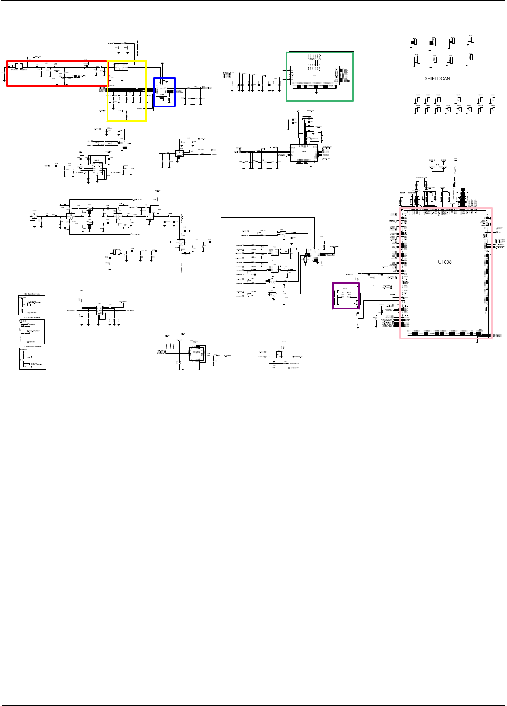
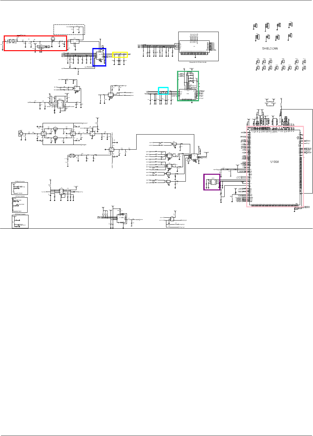
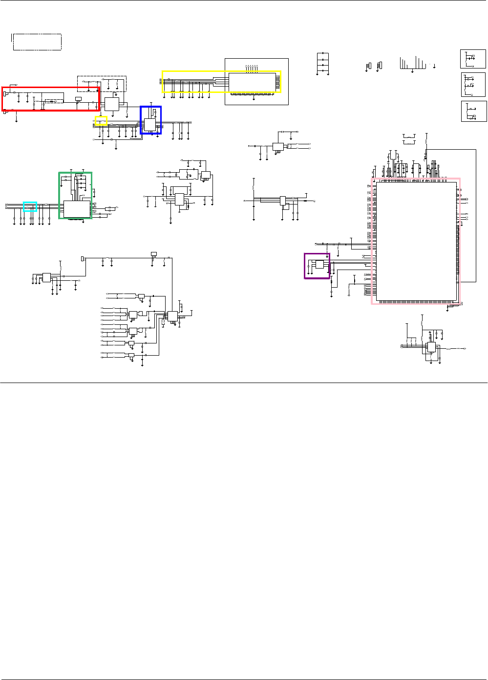
8-1. Block Diagram
Level 3Repair
Distribution, transmission, or infringement of any content or data from this document without Samsung’s written authorization is strictly prohibited.
Confidential and proprietary-the contents in this service guide subject to change without prior notice.
8-2
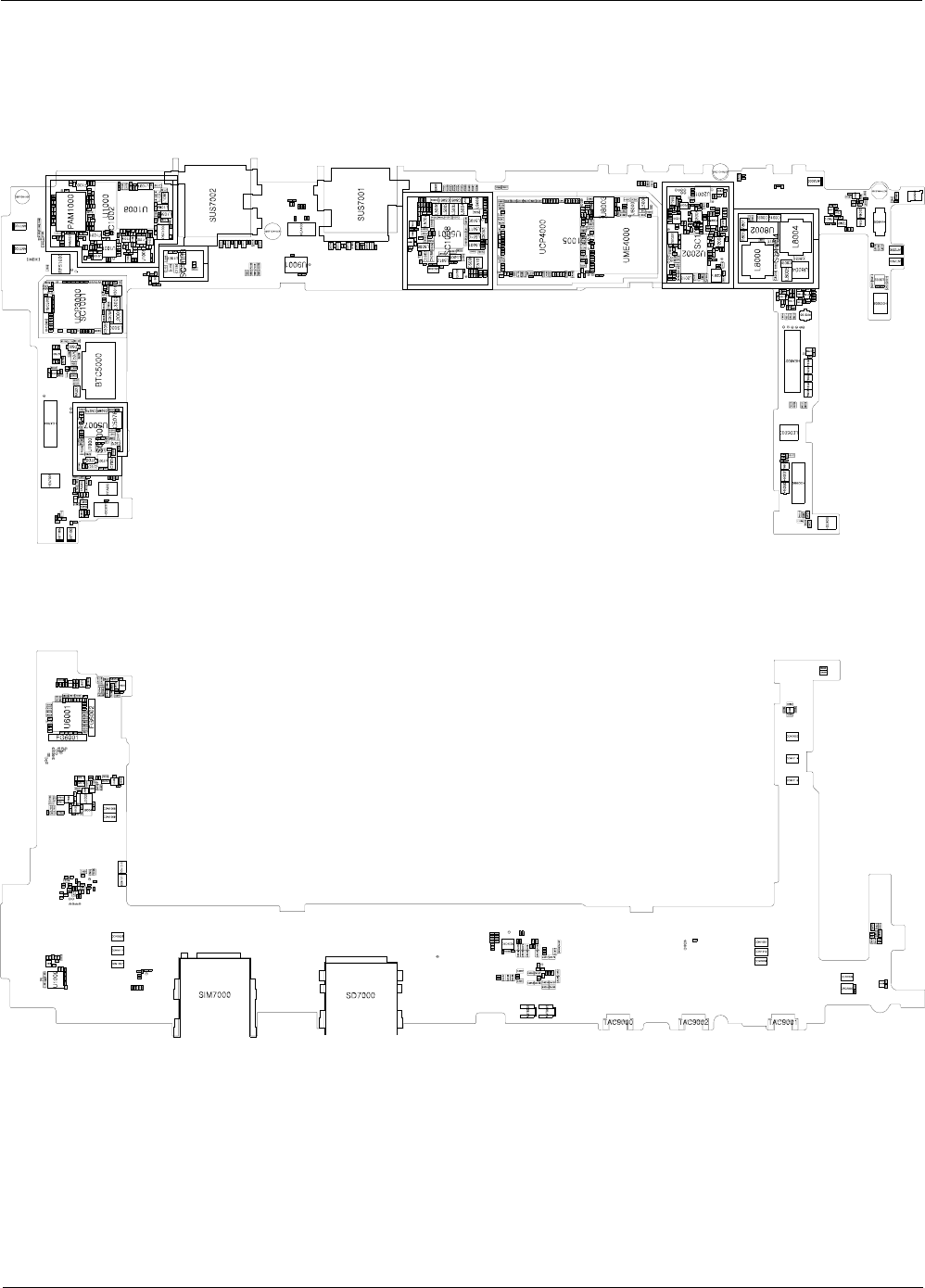
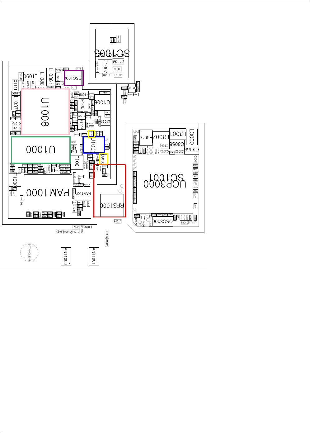
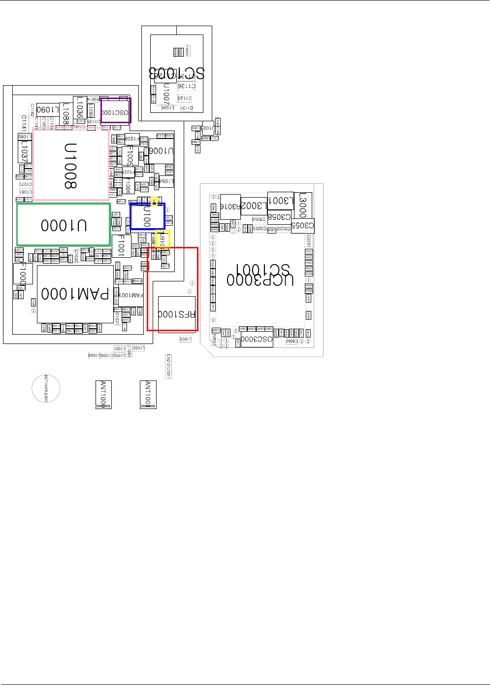
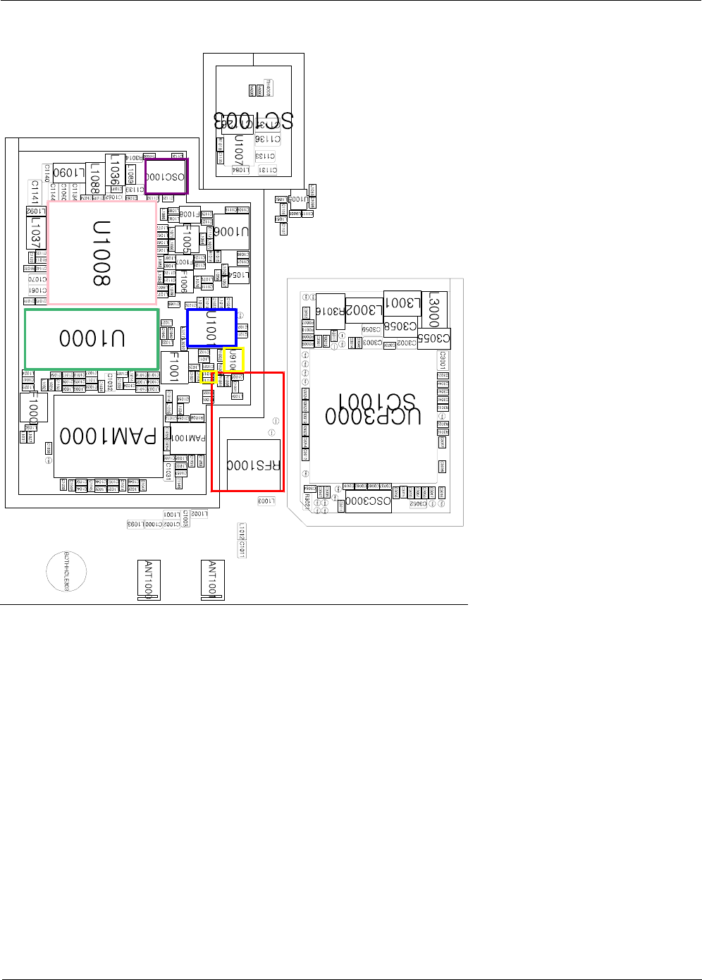
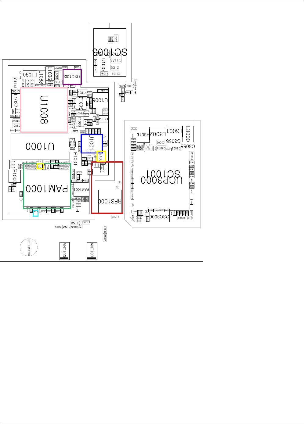
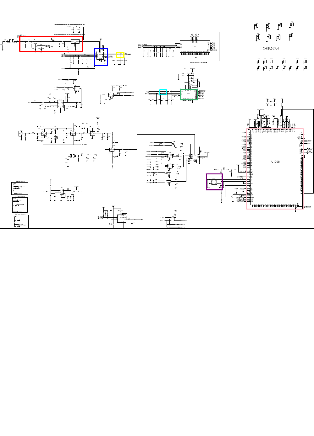
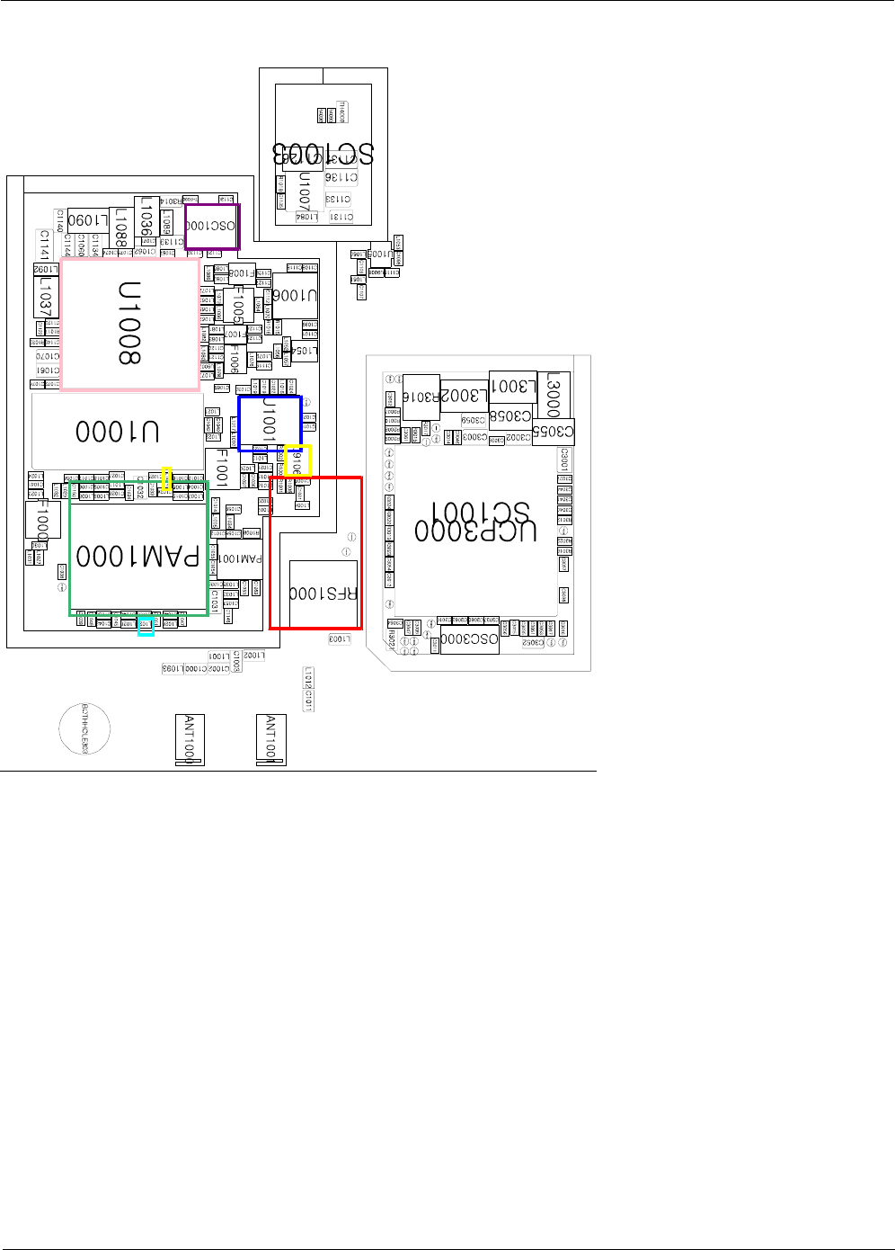
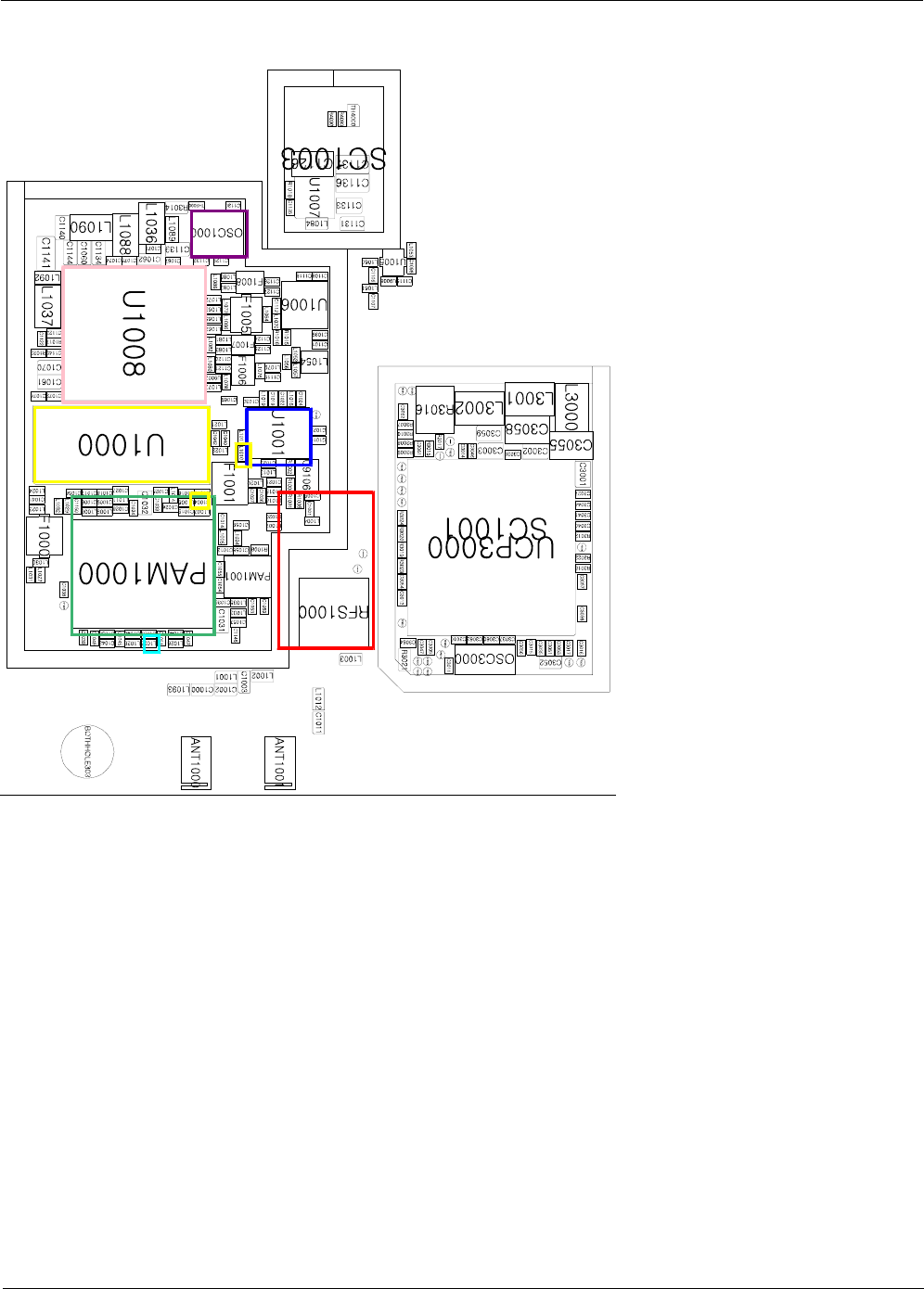
8-2. PCB Diagrams
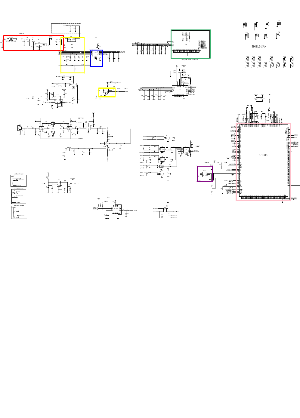
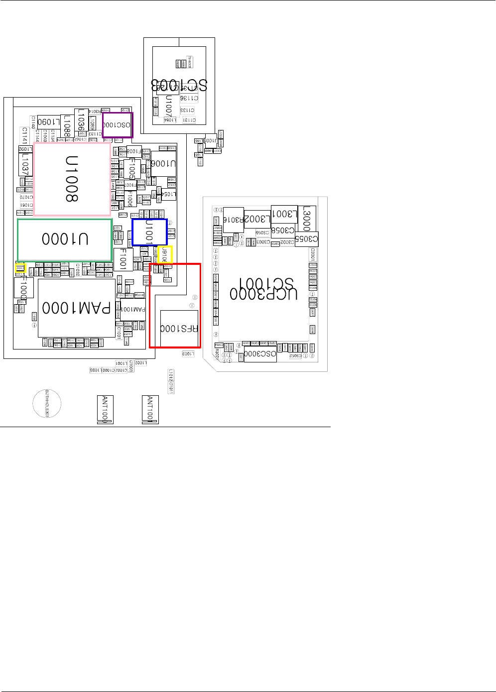
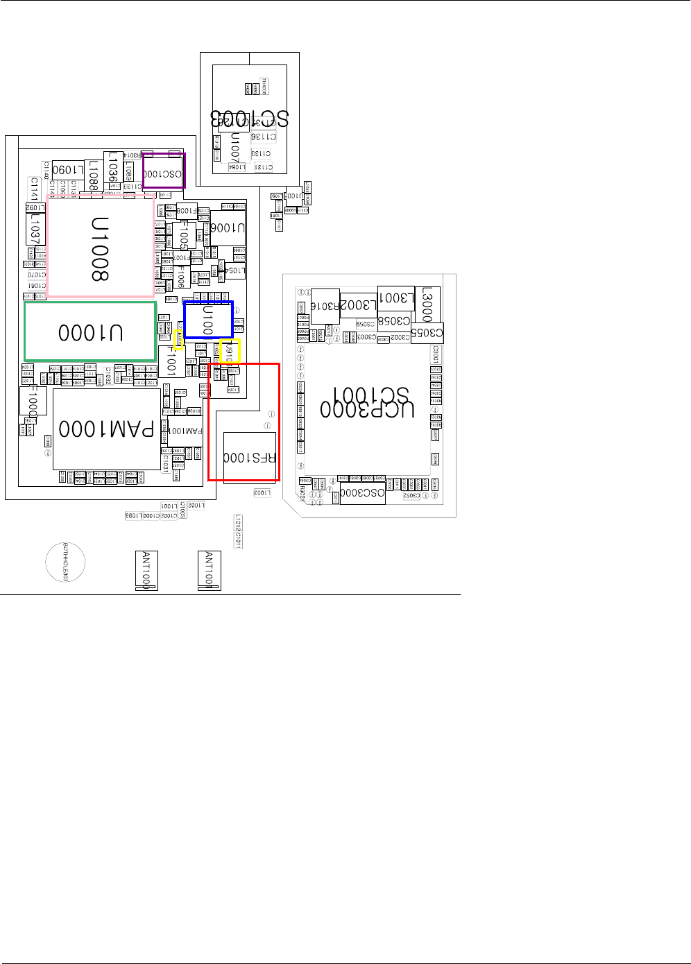
8-2-1. Main PCB Top
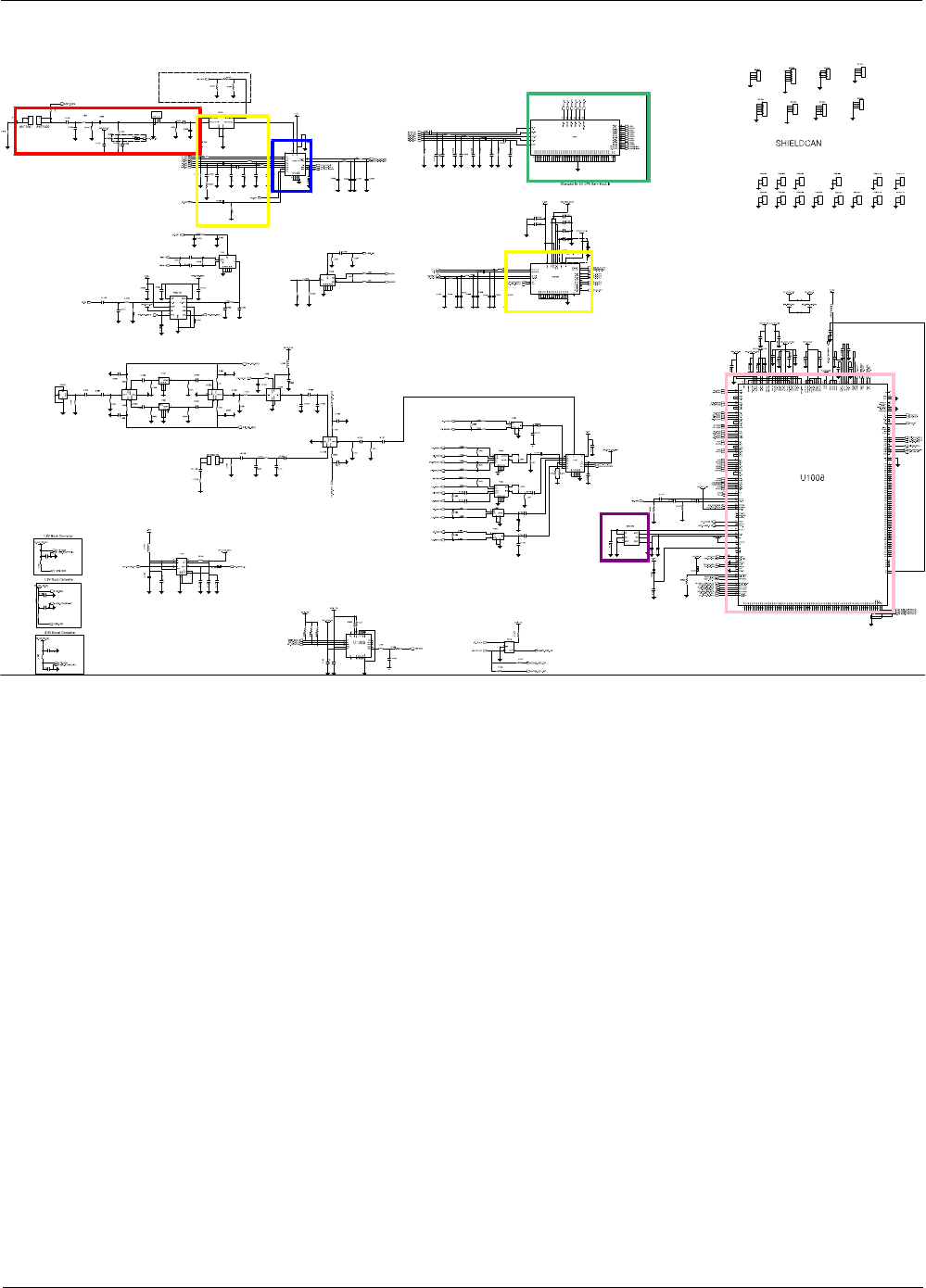
8-2-2. Bottom
Level 3Repair
Distribution, transmission, or infringement of any content or data from this document without Samsung’s written authorization is strictly prohibited.
Confidential and proprietary-the contents in this service guide subject to change without prior notice.
8-3
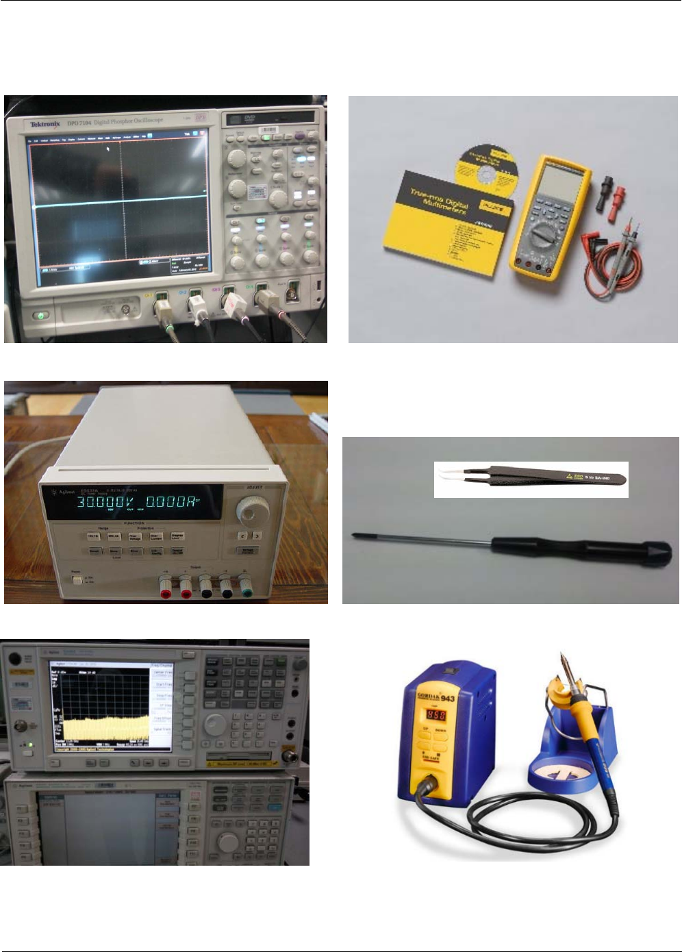
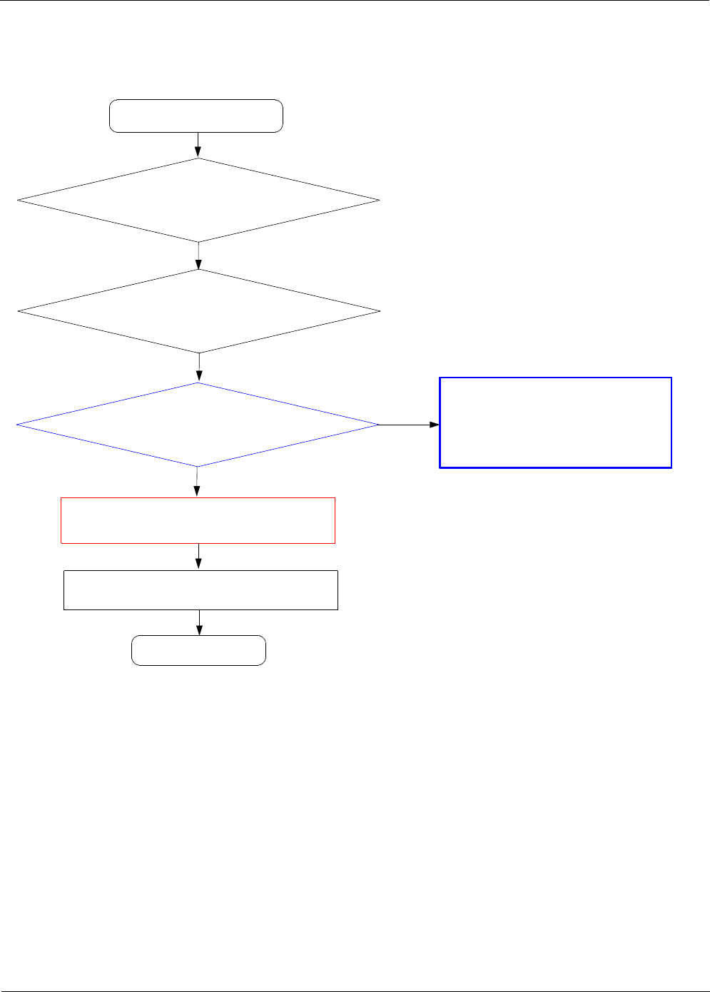
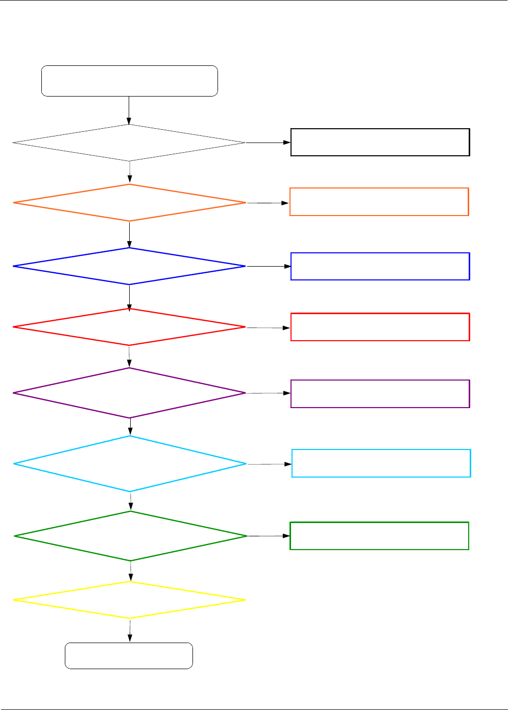
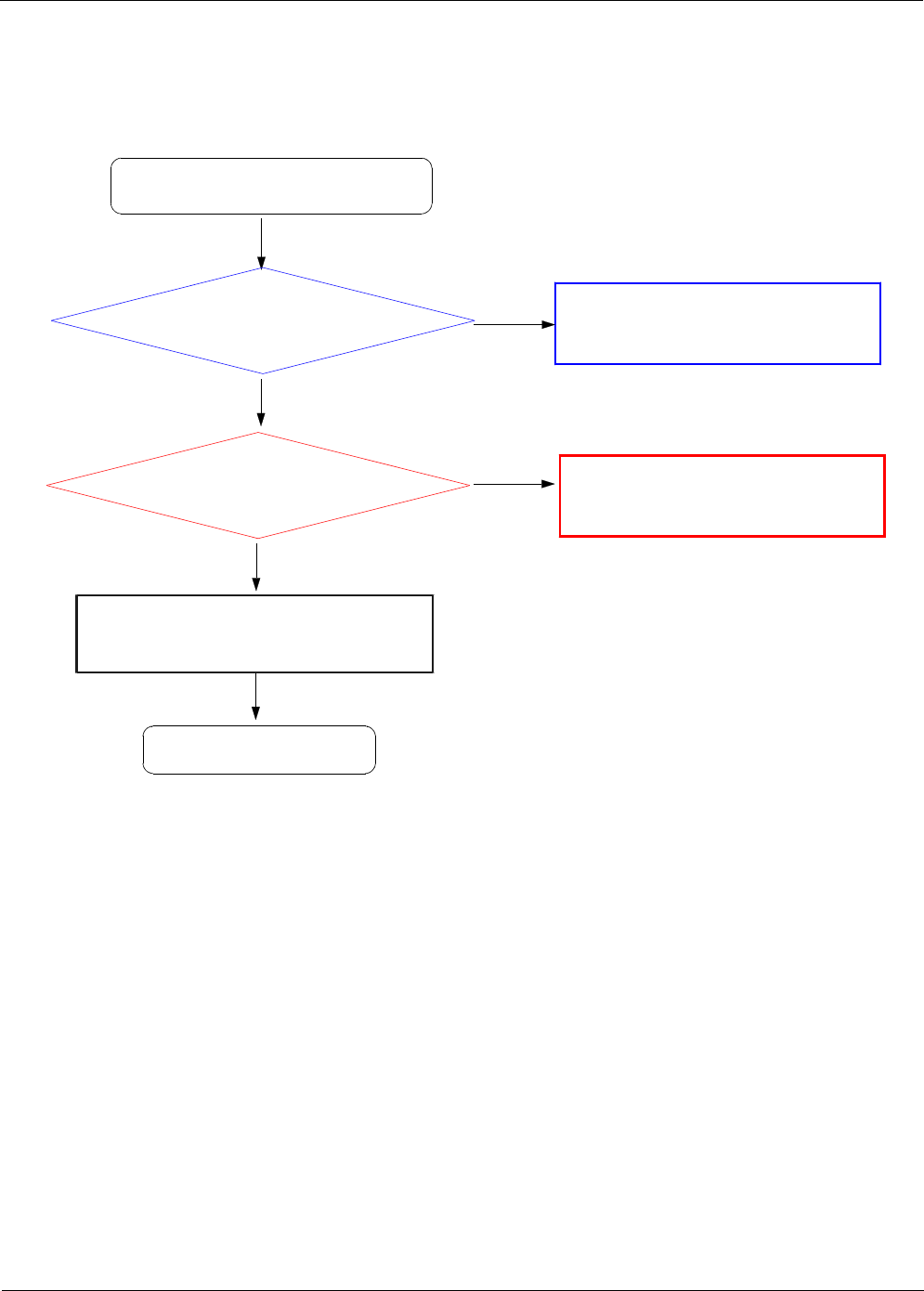
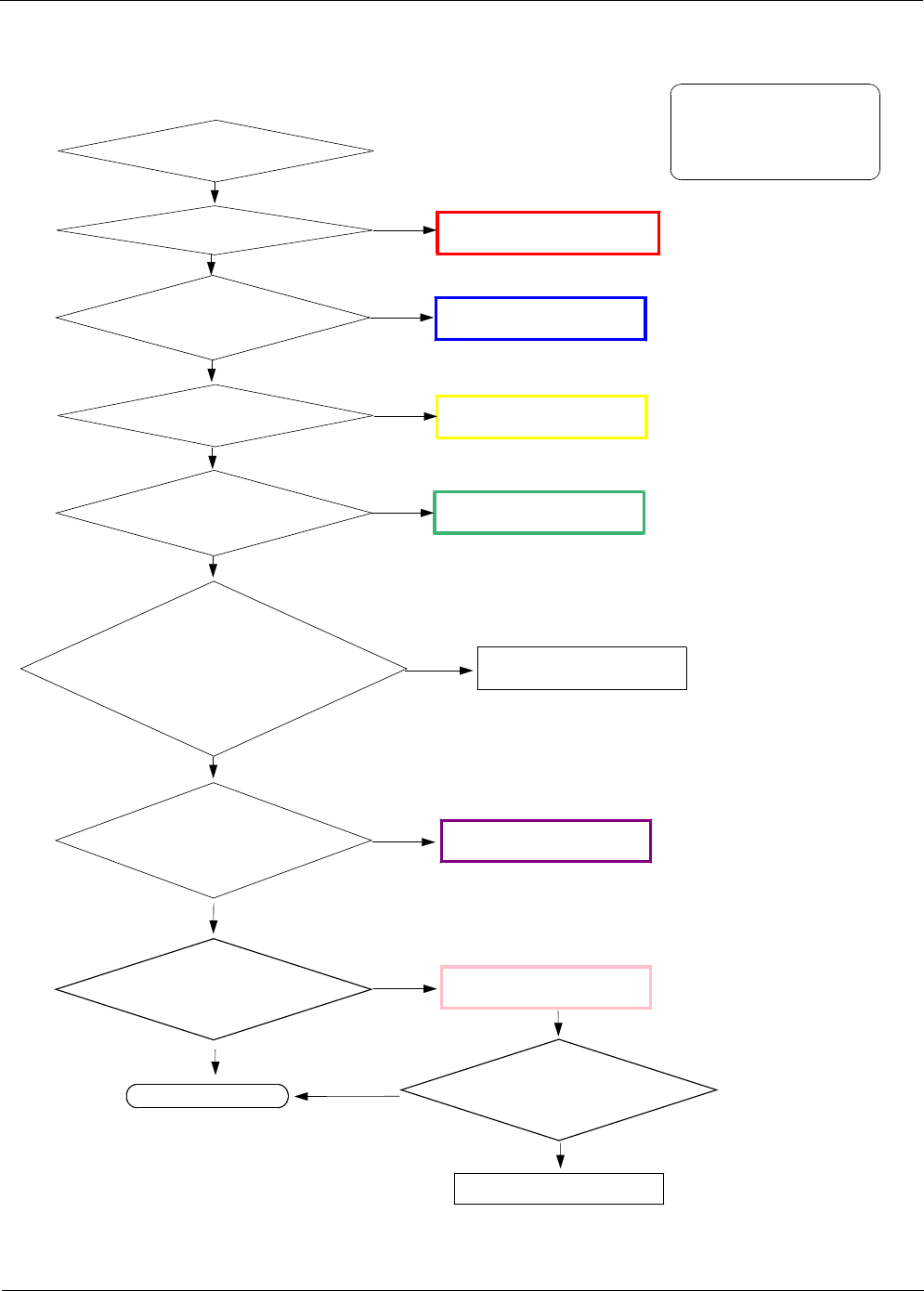
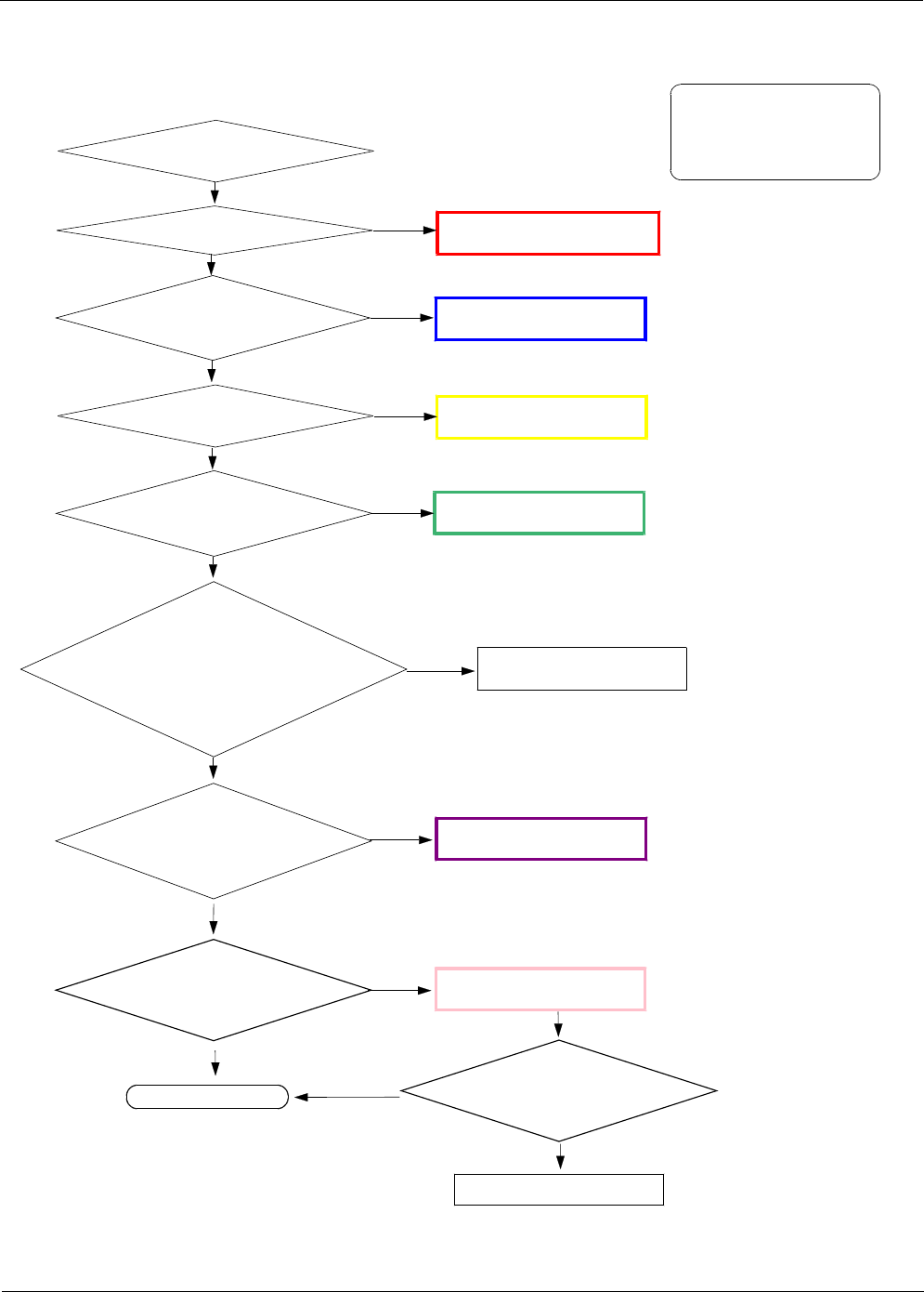
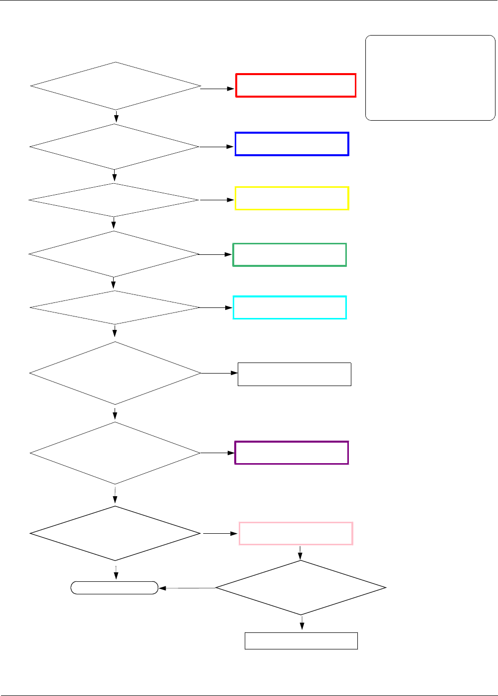
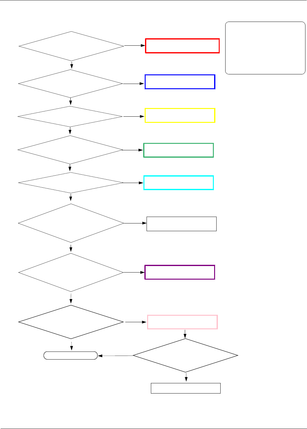
8-3. Flow Chart of Troubleshooting
Equipments
Oscilloscope Digital Multimeter
Power Supply +driver, ESD Safe Tweezer
8960 & Spectrum Analyzer Soldering iron
Level 3Repair
Distribution, transmission, or infringement of any content or data from this document without Samsung’s written authorization is strictly prohibited.
Confidential and proprietary-the contents in this service guide subject to change without prior notice.
8-4
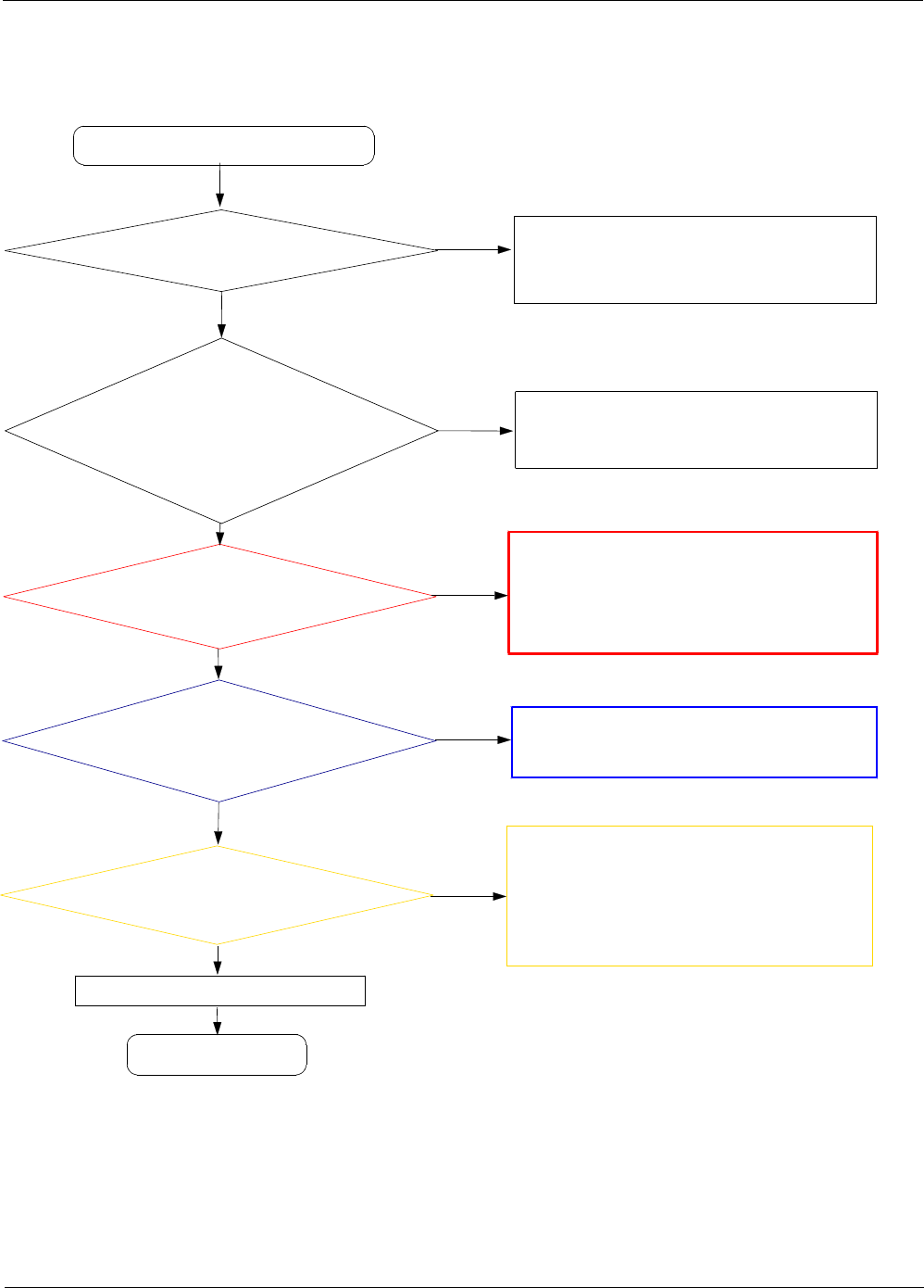
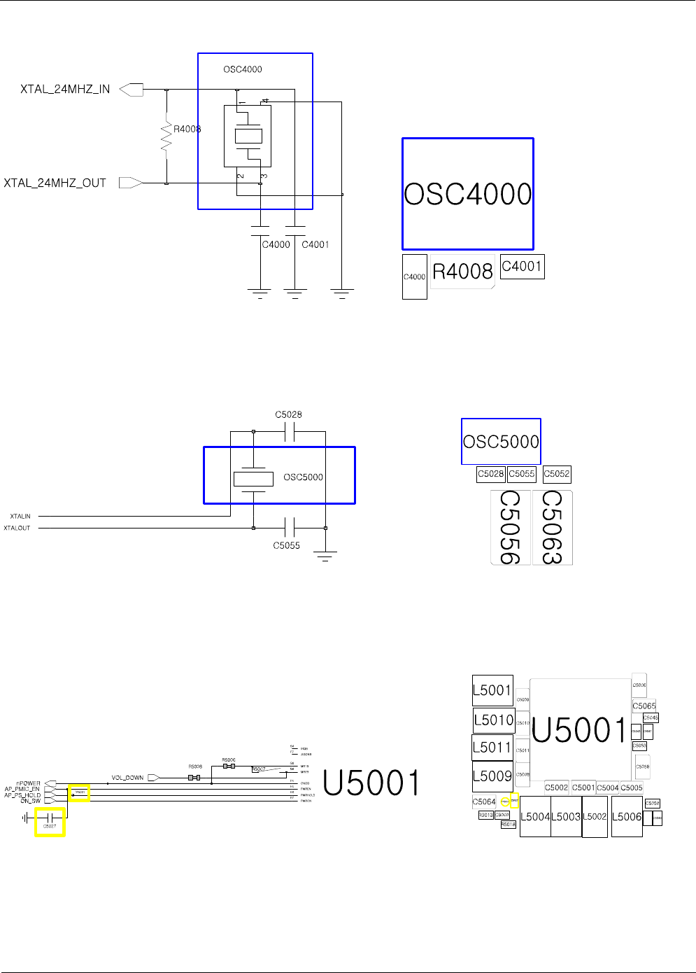
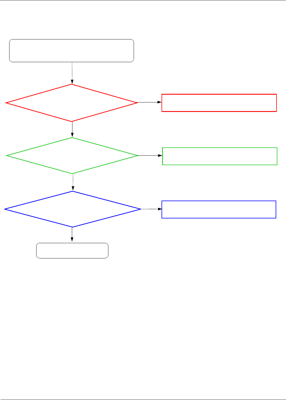
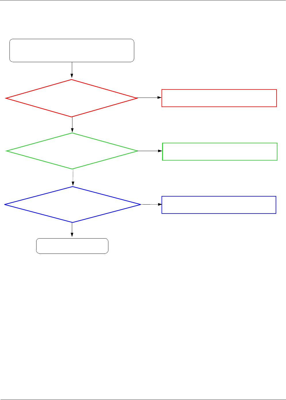
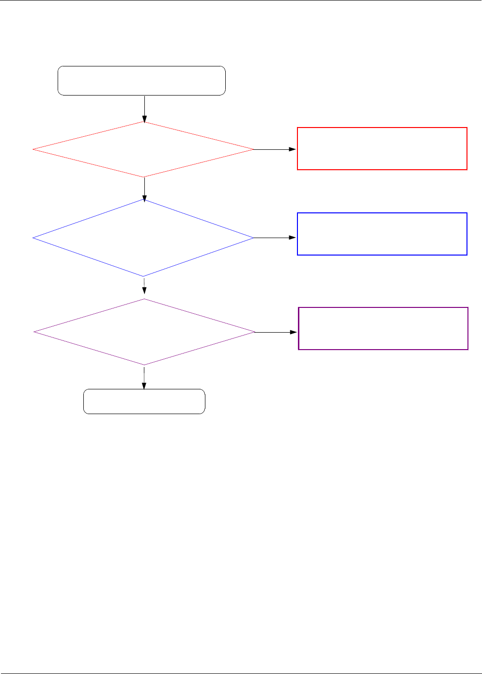
8-3-1. Power On
Mobile phone does not power on.
END
No
Yes
Check the TP5001, C5027
TP5000 Voltage level.
Is it over 1.5V?
It Can be Damaged AP.
(UCP4000-1 or LPDDR3 Memory)
It is Needed to dump Memory or Check with S/W
Team to Analyze.
So, Change the PBA.
No
Yes
Check the U5001 output voltage
(C5062 >1
V,C5057 >1
V, C5061
>1
V)
If the output voltage is not satisfied with normal
condition, Change the U5001.
※Each voltage level has ±10% margin.
No
Yes
Yes
Check the Battery Voltage.
Is it more than 3.8V?
Charging the battery by TA.
If its voltage level is extremely low(under 3.3V),
Change the battery.
Check the initial operation
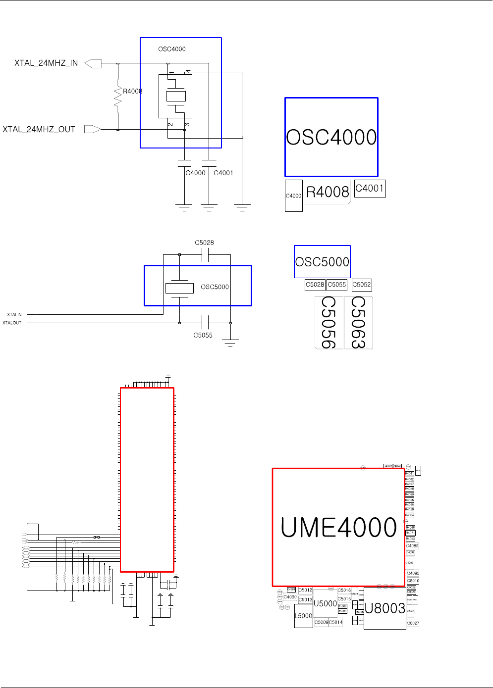
Check the Clock OSC4000,
OSC5000
Is that frequency 24Mhz,
32khz each?
Change the OSC4000. or OSC5000
No
Yes
No
Change the FRONT-OCTA
or OCTA Con-to-Con Connector
Yes
Push the Power Button for 8seconds. Then
wait 3minutes, check the power-on sound or
motor Vibration or light on touch key.
Sound or Vibration is ok?
Level 3Repair
Distribution, transmission, or infringement of any content or data from this document without Samsung’s written authorization is strictly prohibited.
Confidential and proprietary-the contents in this service guide subject to change without prior notice.
8-5
Level 3Repair
Distribution, transmission, or infringement of any content or data from this document without Samsung’s written authorization is strictly prohibited.
Confidential and proprietary-the contents in this service guide subject to change without prior notice.
8-6
Level 3Repair
Distribution, transmission, or infringement of any content or data from this document without Samsung’s written authorization is strictly prohibited.
Confidential and proprietary-the contents in this service guide subject to change without prior notice.
8-7
TP5000
R5001
C5009
VMEM_VDDF_2.85V
C5014
R5000
C5012
VCC_SUB_2.0V
C5016
C5015
C4
SW1
VINB C5
D1
VOUT
SW2 D2
D3
GNDB
SW1 D4
D5
VINB
B1
FB
EN_BB
B2
B3AGND
SCL
B4
B5 VBAT
VOUT C1
C2
SW2
GNDB C3
U5000
VLDO
A1
A2 VINL
SDA
A3
A4 AGND
EN_LDO
A5
VMEM_VDD_1.8V
VCC_1.8V_AP
C5013
V_BAT
L5000
V_BAT
MEM_LDO_SDA
eMMC_EN
MEM_LDO_SCL
C4090
C4091
C5009
C5012
C5013
C5014
C5015
C5016
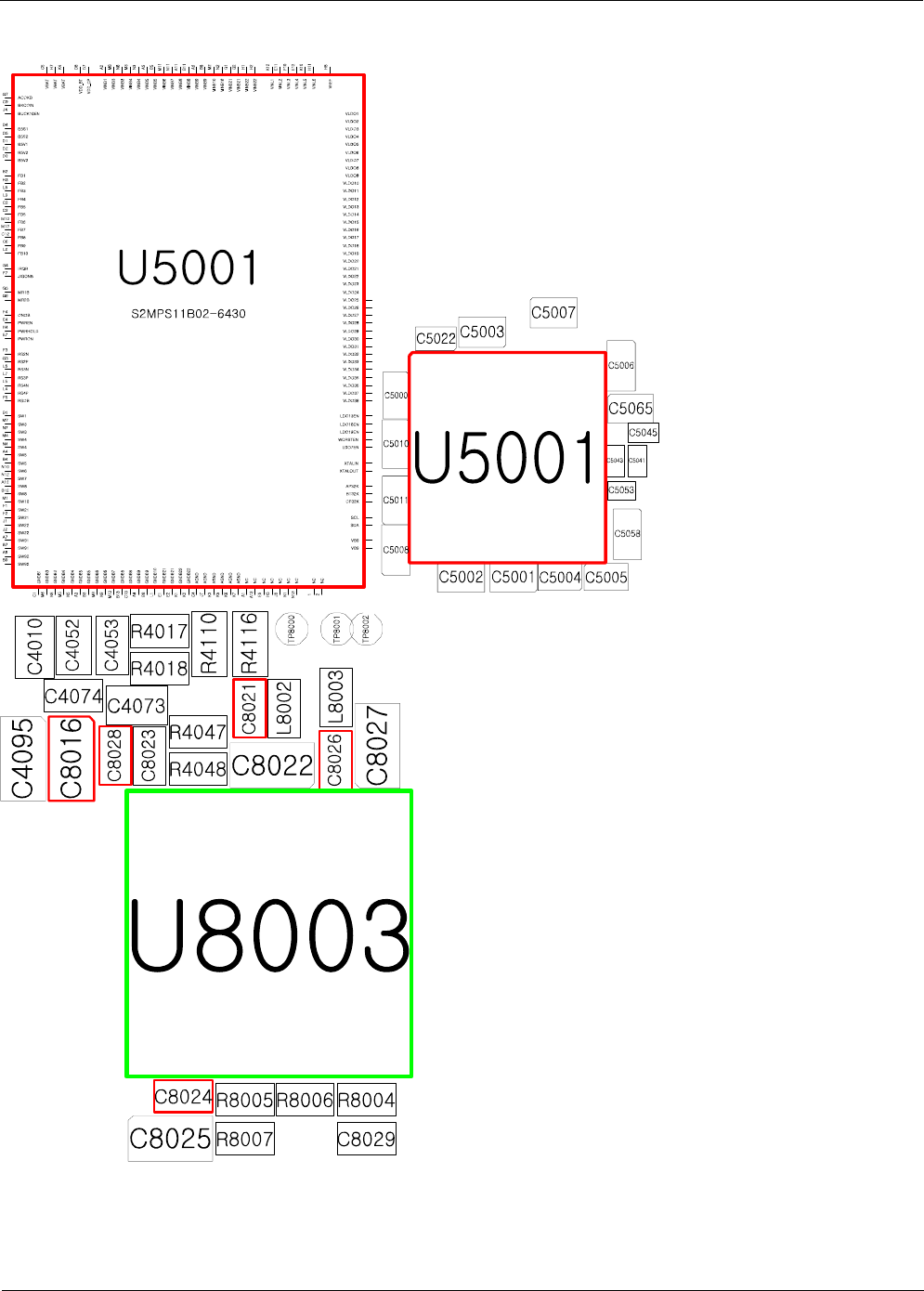
C8024
C8025
C8029
L5000
R5000
R5001
R8004
R8005
R8006
R8007
TP2019TP2020
TP5000
TP8000
TP8001
TP8002
TP8004 TP8006TP8007
U5000 U8003
UME4000
Level 3Repair
Distribution, transmission, or infringement of any content or data from this document without Samsung’s written authorization is strictly prohibited.
Confidential and proprietary-the contents in this service guide subject to change without prior notice.
8-8
8-3-2. Initial
Initial Failure
END
Re Check "8-3-1 Power on"
Trouble shooting process
Check the OSC4000, OSC500.
(Crack, open etc.)
Check the U5001.
(Crack etc.)
Abnormal
Normal
Change UME4000 that is ROM flashed.
Do not use Blank MEMORY.
Abnormal
Change PBA
Yes
Re-download latest SW on the
mobile phone.
Abnormal
Try the Boot Recovery by SD
CARD.
Follow the Recovery Guide.
Abnormal
Level 3Repair
Distribution, transmission, or infringement of any content or data from this document without Samsung’s written authorization is strictly prohibited.
Confidential and proprietary-the contents in this service guide subject to change without prior notice.
8-9
R4060
R4061
VMEM_VDD_1.8V
R4056
R4062
C4092
VSSQ
P6
P7
RFU
P8
NC
P9
NC
NC P11
P12
NC P13
NC
NC P14
P2
NC
P3
VCCQ
P4VSSQ
P5
VCCQ
N4
VCCQ
N5VSSQ
N6
NC N7
NC
N8
NC N9
NC
P1
NC
P10
RFU
NC N1
N10
NC
NC N11
N12
NC N13
NC
N14
NC
N2VSSQ
N3
NC
NC M2
M3
NC
M4
VCCQ
M5 CMD
M6 CLK
M7
NC M8
NC M9
NC
NC L2
NC
L3
M1
NC
M10
NC M11
NC M12
NC M13
NC M14
NC
RFU
K6
K7
RFU
K8VSS
K9
VCC
L1
NC
L12
NC L13
NC L14
NC
K1
NC
K10
RFU
K12
NC K13
NC K14
NC
K2
NC K3
NC
K5 RST_N
NC J1
J10
VCC
J12
NC
J13
NC J14
NC
J2
NC
J3
NC
J5VSS
H1
H10VSS
H12
H13
H14
NC
H2
H3
H5 DS
NC
G1
RFU G10
G12
NC
G13 NC
G14
G2 NC
G3
RFU
G5VSS
NC
F1
F10VSF
F12 NC
F13
NC
F14 NC
F2 NC
F3
NC
F5
VCC
E14 NC
E2 NC
E3 NC
E5
RFU
E6
VCC
E7VSS
RFU E8
E9VSF
NC
D14
D2 NC
D3 NC
D4 NC
E1 NC
E10
VSF
E12 NC
E13 NC
C5 NC
C6
VCCQ
C7 NC
C8 NC
C9 NC
D1 NC
D12 NC
D13 NC
NC
C10
C11 NC
C12 NC
C13 NC
C14 NC
C2
VDDI
C3 NC
C4VSSQ
DAT4
B3
B4 DAT5
B5 DAT6
B6 DAT7
B7 NC
B8 NC
B9 NC
C1 NC
A9
NC
B1
NC
B10
NC
B11 NC
B12 NC
B13 NC
B14 NC
B2 DAT3
NC
A14
A2
NC
A3 DAT0
A4 DAT1
A5 DAT2
A6VSS
A7
RFU
A8 NC
1MARK
2MARK
A1 NC
NC
A10
A11
NC
A12 NC
A13
NC
UME4000
C4095
VMEM_VDD_1.8V
R4055
C4097
R4068
VMEM_VDDF_2.85V
R4057
R4058
TP_SDC4000
C4089
TP4000
C4090 C4091
R4053
R4064
R4059
TP4007
R4071
SDC1_CLK
SDC1_DATA_0
SDC1_DATA_1
SDC1_DATA_2
SDC1_DATA_3
SDC1_DATA_4
SDC1_DATA_5
SDC1_DATA_6
SDC1_DATA_7
SDC1_CMD
EMMC_RCLK
Level 3Repair
Distribution, transmission, or infringement of any content or data from this document without Samsung’s written authorization is strictly prohibited.
Confidential and proprietary-the contents in this service guide subject to change without prior notice.
8-10
8-3-3. No Service
No service
END
Check the voltage level
R3025 =HIGH
Yes
Replace the U5001
Yes
Check OSC1000
Frequency =26
MHz Replace the OSC1000
Yes
No
No
Check memu setting
Menu →applications →setting →wireless and network →
mobile networks →network mode →setting is auto mode ?
Check the contact of RF antenna clipㅁ
Replace UCP3000
PHONE :T705XXXX
PHONE :unknown
Menu →Phone →Keypad →
*#1234# →check Phone version →
PHONE :T705XXXX or
PHONE :unknown
Yes
Level 3Repair
Distribution, transmission, or infringement of any content or data from this document without Samsung’s written authorization is strictly prohibited.
Confidential and proprietary-the contents in this service guide subject to change without prior notice.
8-11
Level 3Repair
Distribution, transmission, or infringement of any content or data from this document without Samsung’s written authorization is strictly prohibited.
Confidential and proprietary-the contents in this service guide subject to change without prior notice.
8-12
Level 3Repair
Distribution, transmission, or infringement of any content or data from this document without Samsung’s written authorization is strictly prohibited.
Confidential and proprietary-the contents in this service guide subject to change without prior notice.
8-13
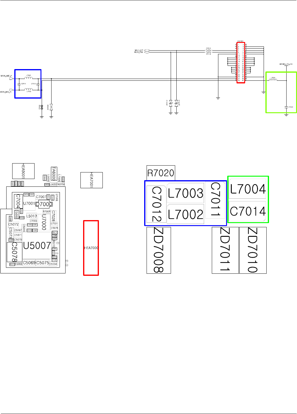
8-3-4-1 Main Microphone Part
Check microphone function in voice call /mVoIP
Handset mode or Camera(camcording) mode
Check connector where
HEA7000 (IF Conn.(+ MIC))
is placed
for any damage
Check component soldering
statuses of
C7011,C7012,L7002,L7003
Set the HEA7000 connection
resolder or replace HEA7000 /IF Conn(+ MIC)
Resolder or replace C7011,C7012,L7002,L7003
END
No
Yes
Yes
Yes
No
Check the voltage at
C7014, L7004 =2.8V resolder or replace L7004
Check the U6001 (Codec IC)
No
Yes
Level 3Repair
Distribution, transmission, or infringement of any content or data from this document without Samsung’s written authorization is strictly prohibited.
Confidential and proprietary-the contents in this service guide subject to change without prior notice.
8-14
Level 3Repair
Distribution, transmission, or infringement of any content or data from this document without Samsung’s written authorization is strictly prohibited.
Confidential and proprietary-the contents in this service guide subject to change without prior notice.
8-15
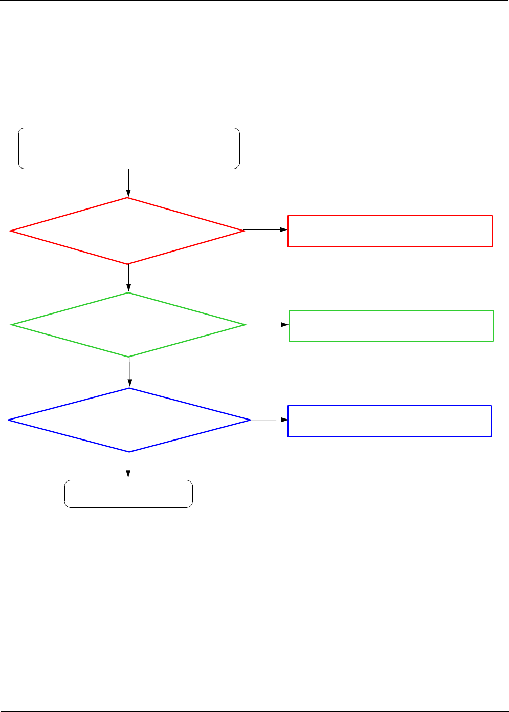
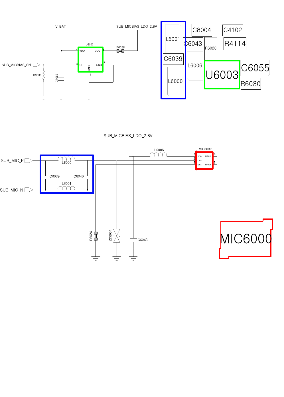
8-3-4-2 SUB Microphone Part
Check board MIC6000
Check component soldering
statuses of
C6039,C6040,L6000,L6001
resolder or replace MIC6000
Resolder or replace C6039,C6040,L6000,L6001
END
No
Yes
Yes
Yes
No
Check microphone function in voice call Hands-free
mode or Camera(camcording) mode
Check the voltage at
C6043 =2.8V resolder or replace U6003
No
Yes
Level 3Repair
Distribution, transmission, or infringement of any content or data from this document without Samsung’s written authorization is strictly prohibited.
Confidential and proprietary-the contents in this service guide subject to change without prior notice.
8-16
Level 3Repair
Distribution, transmission, or infringement of any content or data from this document without Samsung’s written authorization is strictly prohibited.
Confidential and proprietary-the contents in this service guide subject to change without prior notice.
8-17
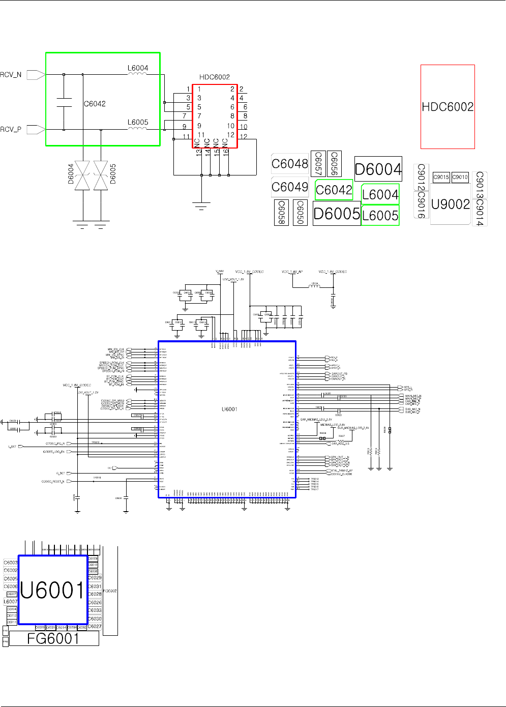
8-3-4-3. RCV Part
Check connector where
HDC6002 is placed
for any damage
Check component soldering
statuses of U6001
Set the HDC6002 connection
resolder or replace HDC6002 /RCV Module
Resolder or replace U6001
No
Yes
Yes
Yes
No
Check RCV function in Voice call /mVoIP
Handset Mode with maximum volume level.
Check component soldering
statuses of C6042, L6004,
L6005 resolder or replace C6042, L6004, L6005
No
Yes
END
Level 3Repair
Distribution, transmission, or infringement of any content or data from this document without Samsung’s written authorization is strictly prohibited.
Confidential and proprietary-the contents in this service guide subject to change without prior notice.
8-18
Level 3Repair
Distribution, transmission, or infringement of any content or data from this document without Samsung’s written authorization is strictly prohibited.
Confidential and proprietary-the contents in this service guide subject to change without prior notice.
8-19
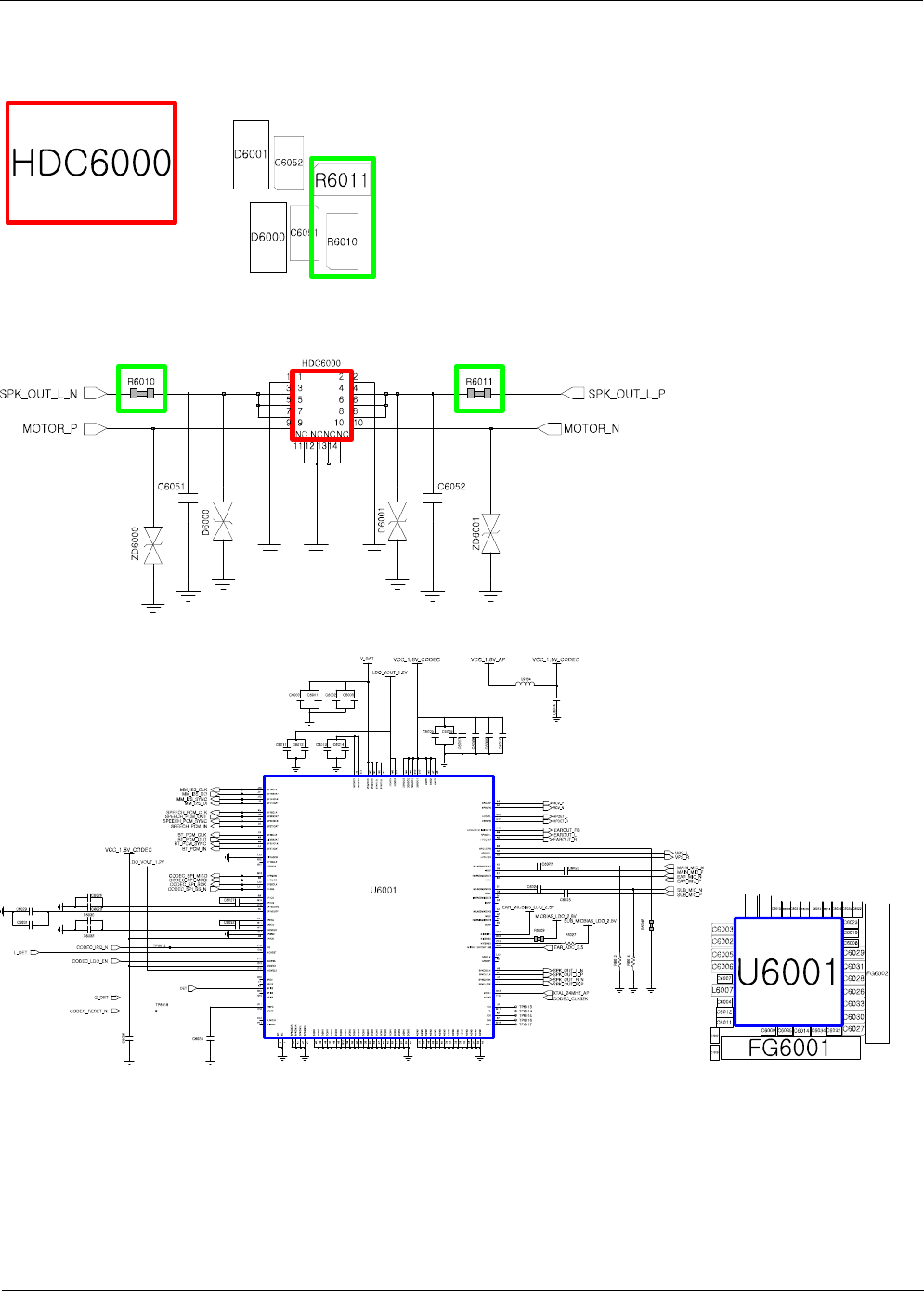
8-3-4-4. Speaker Part (LEFT)
Check connector where LEFT
Speaker is placed
for any damage
Check component soldering
statuses of U6001
Set the HDC6000 connection
Resolder or replace U6001
No
Yes
Yes
Yes
No
Check speaker function.
Play MP3 with maximum volume level.
Check component soldering
statuses of R6010, R6011 resolder or replace R6010, R6011
No
Yes
END
Level 3Repair
Distribution, transmission, or infringement of any content or data from this document without Samsung’s written authorization is strictly prohibited.
Confidential and proprietary-the contents in this service guide subject to change without prior notice.
8-20
Level 3Repair
Distribution, transmission, or infringement of any content or data from this document without Samsung’s written authorization is strictly prohibited.
Confidential and proprietary-the contents in this service guide subject to change without prior notice.
8-21
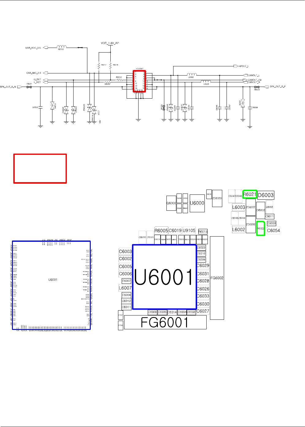
8-3-4-5. Speaker Part (RIGHT)
Check contact where Right
Speaker is placed
for any damage
Check component soldering
statuses of U6001
Set or resolder HDC6001
resolder or replace U6001
END
No
Yes
Yes
Yes
No
Check speaker function.
Play MP3 with maximum volume level.
Check component soldering
statuses of R6021, R6022 resolder or replace R6021, R6022
No
Yes
Level 3Repair
Distribution, transmission, or infringement of any content or data from this document without Samsung’s written authorization is strictly prohibited.
Confidential and proprietary-the contents in this service guide subject to change without prior notice.
8-22
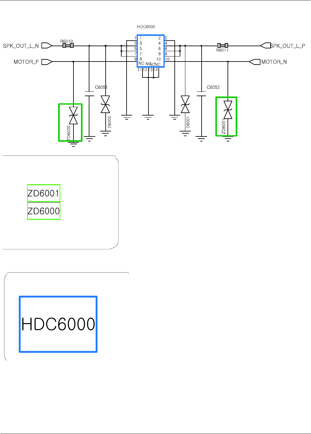
HDC6001
Level 3Repair
Distribution, transmission, or infringement of any content or data from this document without Samsung’s written authorization is strictly prohibited.
Confidential and proprietary-the contents in this service guide subject to change without prior notice.
8-23
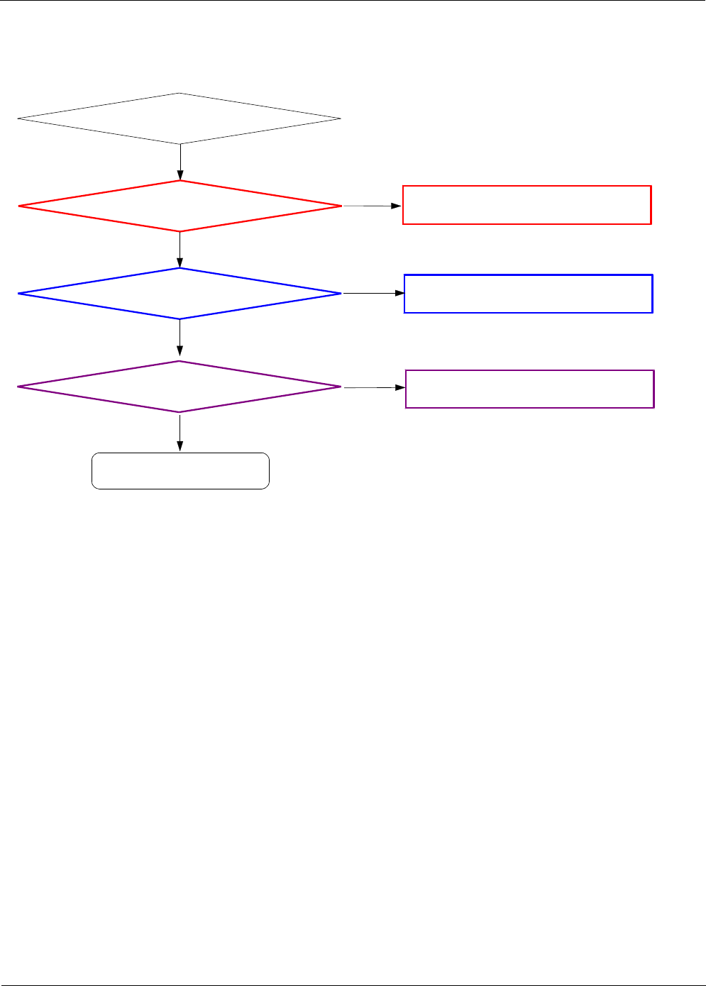
8-3-5. Charging Part
TA /USB Insert
Yes
END
Charging Sequence Start
VBUS_5V =5V
No Check C727 =5
V,
or may not connected TA /USB
Yes
Check the CHG_IN_5V(C728)=5V No Resolder and Replace U703
Yes
Battery is Charging? No Resolder or Replace U504
Yes
Level 3Repair
Distribution, transmission, or infringement of any content or data from this document without Samsung’s written authorization is strictly prohibited.
Confidential and proprietary-the contents in this service guide subject to change without prior notice.
8-24
Level 3Repair
Distribution, transmission, or infringement of any content or data from this document without Samsung’s written authorization is strictly prohibited.
Confidential and proprietary-the contents in this service guide subject to change without prior notice.
8-25
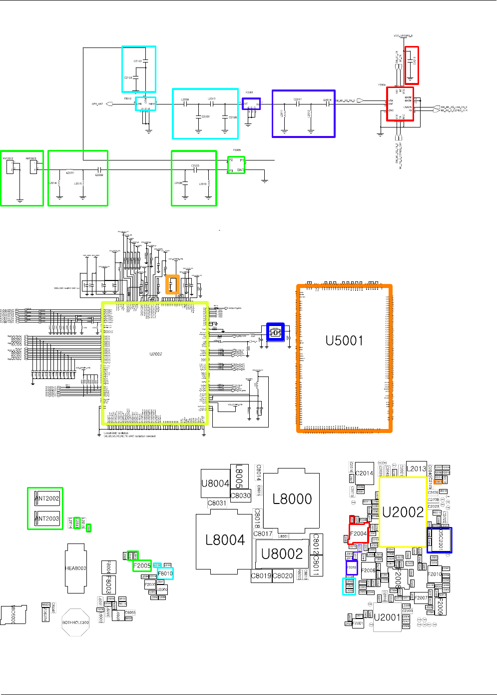
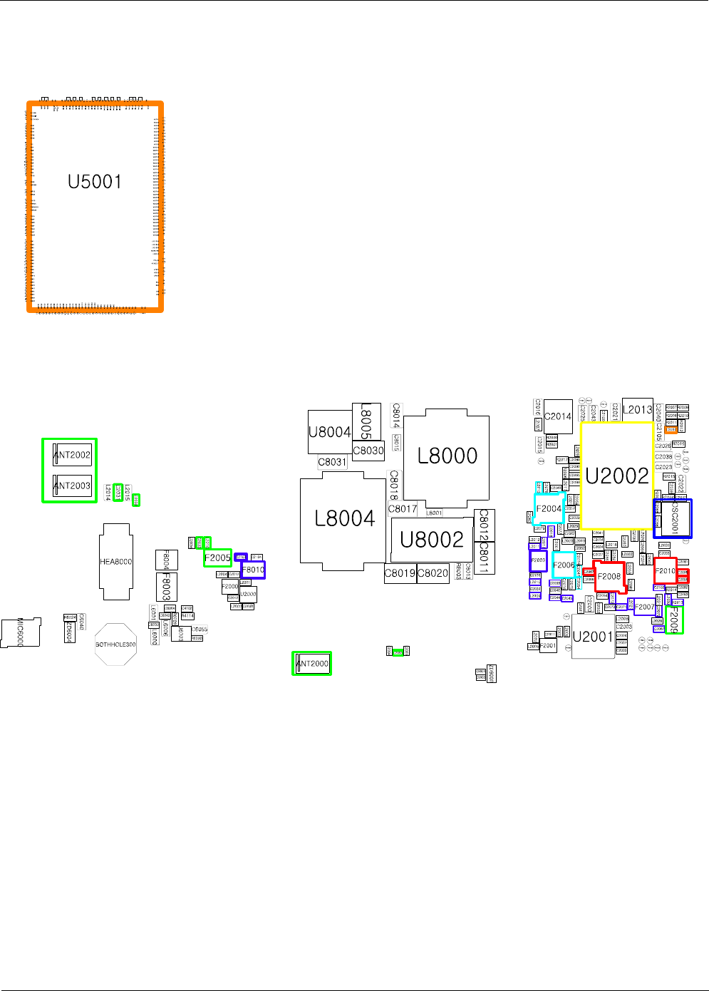
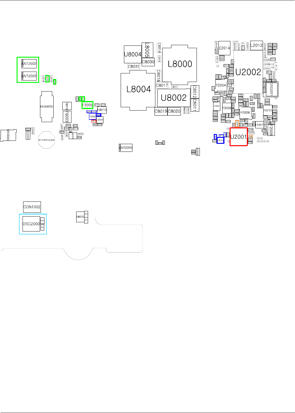
8-3-6. BT Part
BT is not working
Check BT function ON No Enable BT Function
Yes
END
Check the Voltage on
C2037= 1.8V No Check the U5001
(crack, open, damaged, etc.)
Yes
Check 37.4 MHz Clock at
C2066, C2068 No Check the OSC2001 (crack, open, etc.)
Yes
Check the Voltage on C2013 No Check the F2004 (crack, open, damaged, etc.)
Yes
Check the Status of
L2011, C2017, C2018, F2003 No Resolder or replace L2011, C2017, C2018,
F2003
Yes
Resolder or Replace U2002
Yes
Yes
Yes
Check the Status of F2005,
C2031, C2032, C2033, L2016,
ANT2002, ANT 2003
No Resolder or Replace F2005, C2031, C2032,
C2033, L2016, ANT2002, ANT 2003
Check the Status of
C2103 L2009, L2010, F8010 No Resolder or replace C2103, L2009, L2010,
F8010
Yes
Level 3Repair
Distribution, transmission, or infringement of any content or data from this document without Samsung’s written authorization is strictly prohibited.
Confidential and proprietary-the contents in this service guide subject to change without prior notice.
8-26
Level 3Repair
Distribution, transmission, or infringement of any content or data from this document without Samsung’s written authorization is strictly prohibited.
Confidential and proprietary-the contents in this service guide subject to change without prior notice.
8-27
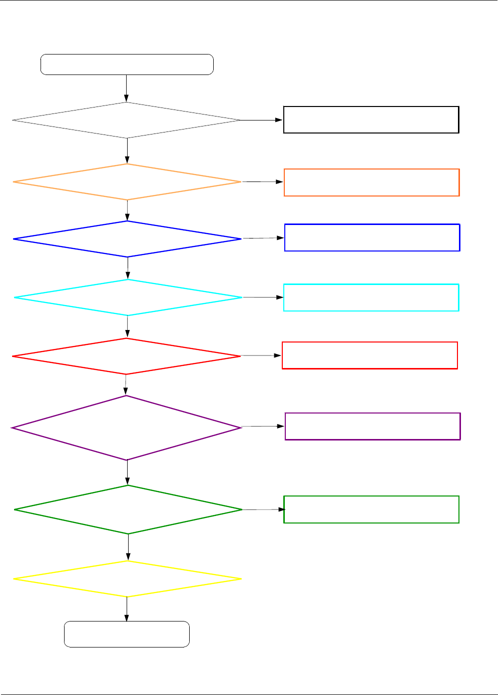
8-3-7. WIFI Part
WIFI is not working
Check WIFI function ON No Enable WIFI Function
Yes
END
Check the Voltage on
C2037= 1.8V
No Check the U5001
(crack, open, damaged, etc.)
Yes
Check 37.4 MHz Clock at
C2066, C2068
No Check the OSC2001 (crack, open, etc.)
Yes
Check the Voltage on C2013,
C2047, C2054
No Check the F2004, F2006
(crack, open, damaged, etc.)
Yes
Check the Status of
C2103, F8010, L2009, L2010, F2003,
L2011, C2017, C2018, C2045, C2044,
C2099, C2087, C2070, F2007, L2027,
C2071, C2072, R2013, L2030, C2102
No Resolder or Replace C2103, F8010, L2009, L2010,
F2003, L2011, C2017, C2018, C2045, C2044, C2099, C2087,
C2070, F2007, L2027, C2071, C2072, R2013, L2030, C2102
Yes
Resolder or Replace U2002
Yes
Yes
Yes
Check the Status of C2031, C2032,
C2033, L2016, F2005, C2093, F2009,
ANT2000, ANT2002, ANT2003
No Resolder or Replace C2031, C2032, C2033, L2016, F2005,
C2093, F2009, ANT2000, ANT2002, ANT2003
Check the Voltage on C2067,
C2095, C2096
Yes
No Check the F2008, F2010
(crack, open, damaged, etc.)
Level 3Repair
Distribution, transmission, or infringement of any content or data from this document without Samsung’s written authorization is strictly prohibited.
Confidential and proprietary-the contents in this service guide subject to change without prior notice.
8-28
Level 3Repair
Distribution, transmission, or infringement of any content or data from this document without Samsung’s written authorization is strictly prohibited.
Confidential and proprietary-the contents in this service guide subject to change without prior notice.
8-29
Level 3Repair
Distribution, transmission, or infringement of any content or data from this document without Samsung’s written authorization is strictly prohibited.
Confidential and proprietary-the contents in this service guide subject to change without prior notice.
8-30
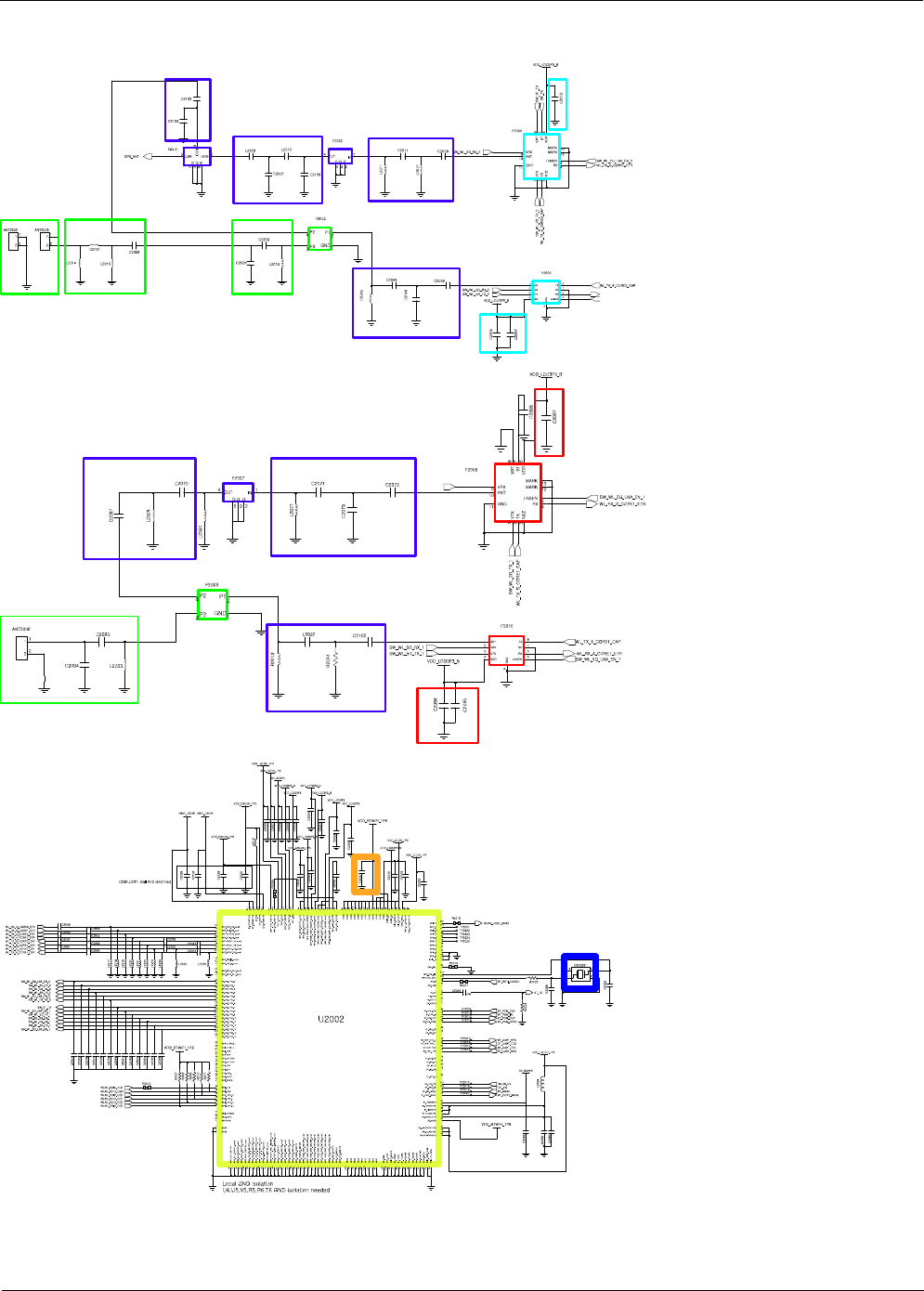
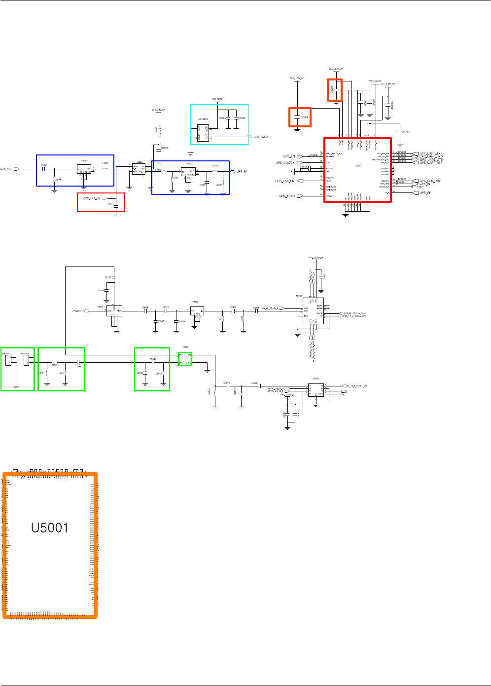
8-3-8. GPS Part
GPS is not working
Check GPS function ON No Enable GPS Function
Yes
END
Check the Voltage on
C2004 =1.8
V, C2000 =2.8V
No Check the U5001
(crack, open, damaged, etc.)
Yes
Check 26MHz Clock at
C2005, C2006
No Check the OSC2000 (crack, open, etc.)
Yes
Check the Voltage of
GPS_LNA_EN (at C2012),
No Resolder or change the U2001
Yes
Check the Status of
C2010, L2004, F2000, L2001,
L2002, F2001, C2011, L2003
No Resolder or Replace C2010, L2004, F2000,
L2001, L2002, F2001, C2011, L2003
Yes
Yes
Yes
Check the Status of
C2031, C2032, C2033, L2016,
F2005, ANT2002, ANT2003
No Resolder or Replace C2031, C2032, C2033,
L2016, F2005, ANT2002, ANT2003
Resolder or Replace U2001
Yes
Level 3Repair
Distribution, transmission, or infringement of any content or data from this document without Samsung’s written authorization is strictly prohibited.
Confidential and proprietary-the contents in this service guide subject to change without prior notice.
8-31
Level 3Repair
Distribution, transmission, or infringement of any content or data from this document without Samsung’s written authorization is strictly prohibited.
Confidential and proprietary-the contents in this service guide subject to change without prior notice.
8-32
Level 3Repair
Distribution, transmission, or infringement of any content or data from this document without Samsung’s written authorization is strictly prohibited.
Confidential and proprietary-the contents in this service guide subject to change without prior notice.
8-33
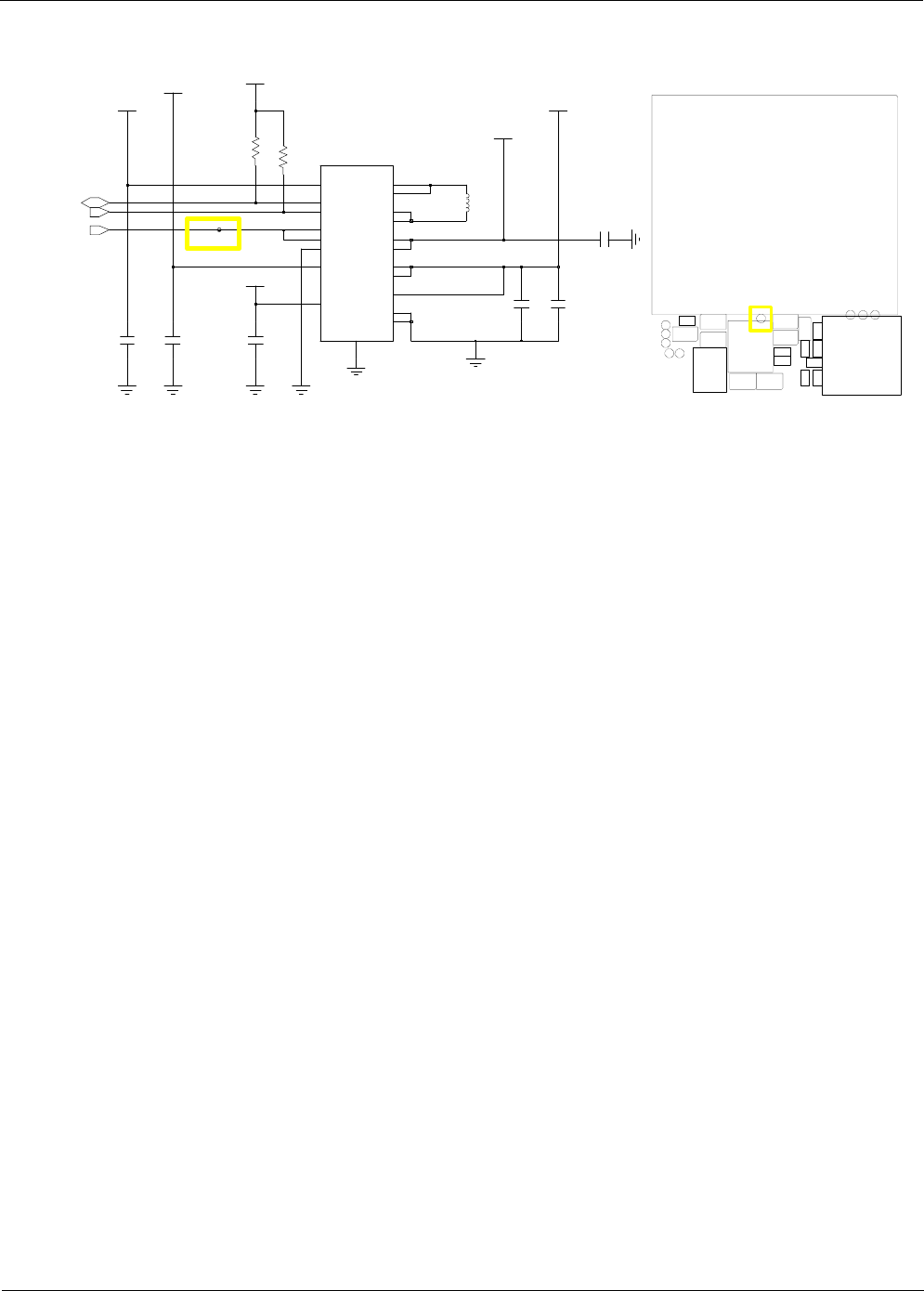
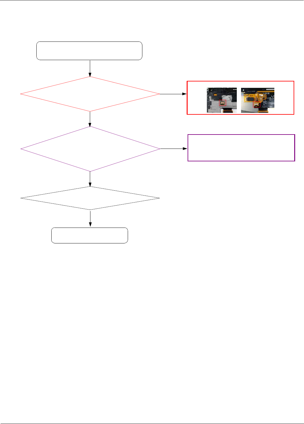
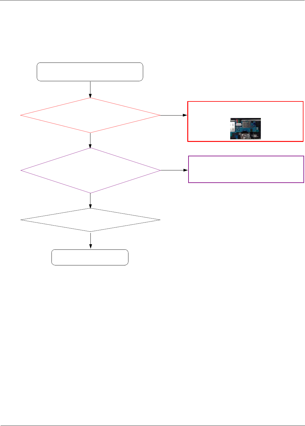
8-3-9. OCTA(TSP)
Touch Screen does not work
Yes
No Reconnect the TSP Connector
Check TSP Connector on
OCTA Main FPCB
Yes
END
Yes
Replace OCTA Module
Yes
No
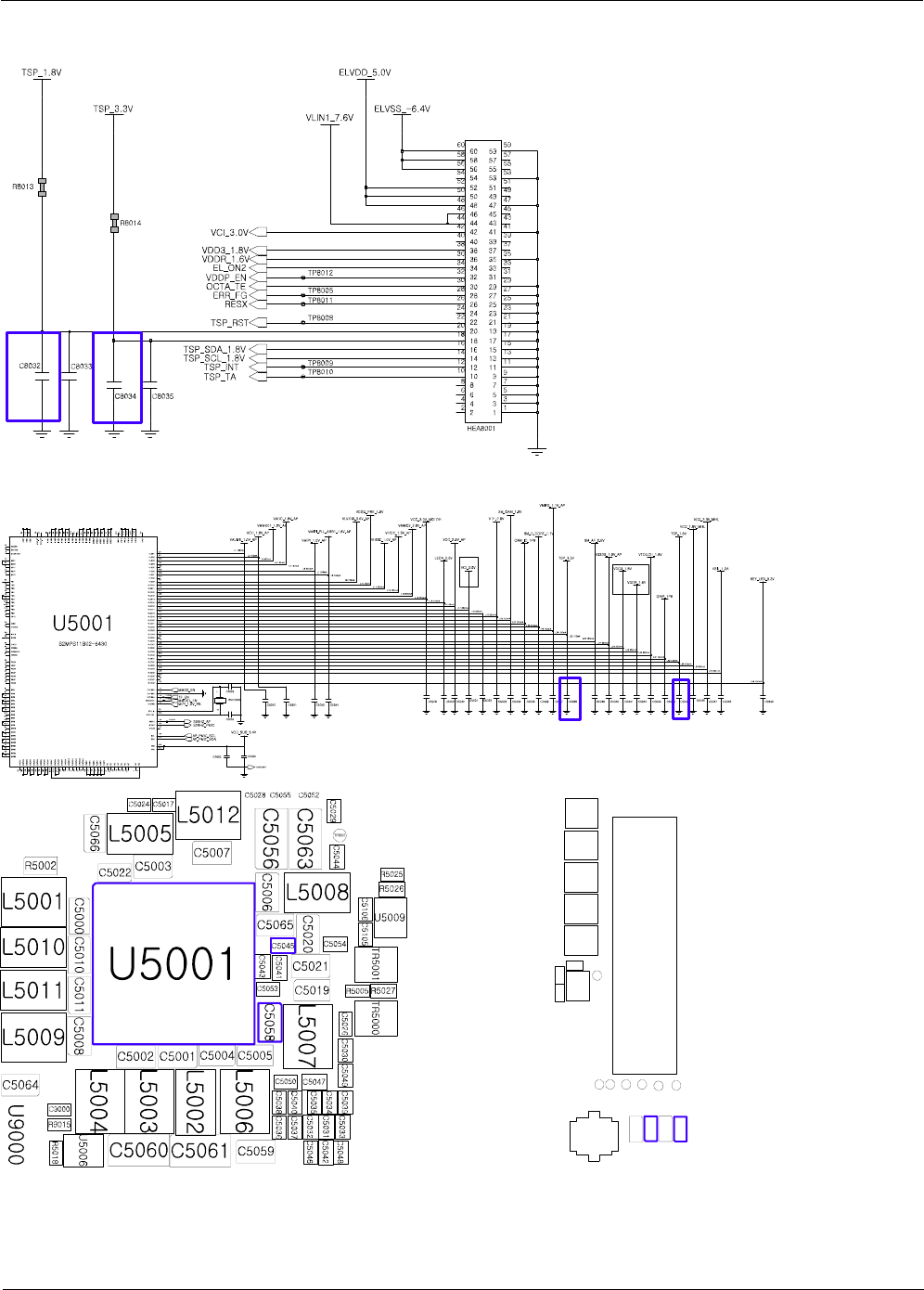
Check the
TSP_1.8V(C8032),
TSP_3.3V(C8034) Check U5001 -TSP_1.8V VLDO32(C5045),
U5001 -TSP_3.3V VLDO24(C5038)
Level 3Repair
Distribution, transmission, or infringement of any content or data from this document without Samsung’s written authorization is strictly prohibited.
Confidential and proprietary-the contents in this service guide subject to change without prior notice.
8-34
C8032
C8034
F8005F8006F8007F8008F8009
HEA8001
R4015R4016
R5024
R8013
R8014
RFS1001
TP8003TP8005TP8008 TP8009
TP8010
TP8011
TP8012
U5008
Level 3Repair
Distribution, transmission, or infringement of any content or data from this document without Samsung’s written authorization is strictly prohibited.
Confidential and proprietary-the contents in this service guide subject to change without prior notice.
8-35
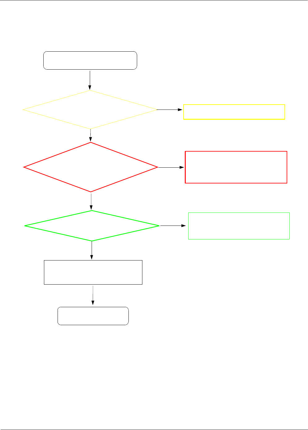
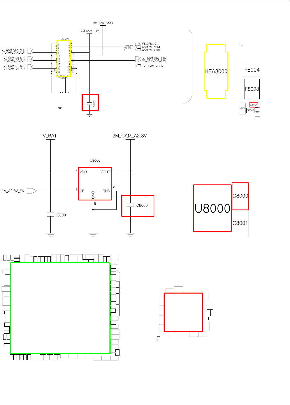
8-3-10. VT CAM
"Camera" function does not work
Yes
Check the Camera
connector on Main PBA Reconnect the HEA8000
No
Check the voltage
C8000 =2.8V
C8004 =1.8V
No
Yes
Yes
END
Replace the camera module
No
Yes
Replace U8000
Replace U5001
Check VTCAM_MCLK
is 24MHz Replace UCP4000
Abnormal
Level 3Repair
Distribution, transmission, or infringement of any content or data from this document without Samsung’s written authorization is strictly prohibited.
Confidential and proprietary-the contents in this service guide subject to change without prior notice.
8-36
C4002
C4003
C4004
C4005
C4006
C4007
C4008
C4009
C4010
C4011
C4013
C4039
C4040
C4041
C4042
C4043
C4044
C4045
C4046
C4047
C4048
C4049 C4050
C4051
C4052
C4053
C4067
C4069
C4070
C4075
C4076
C4093
C4096
C4098
C4099
C4100
C4101
C5000
C5001C5002
C5003
C5004 C5005
C5006
C5008
C5010
C5011
C5022
C5027
C5041C5043
C5045
C5053
C5058
C5065
R4009R4010 R4011R4012 R4013R4014
R4015R4016
R4017R4018
R4019R4020
R4024
R4026
R4027
R4028
R4030
R4035
R4037
R4041
R4042
R4049
R4050 R4051
R4063
R4065
R4066
R4067
R4069
R4070
R4074
R4078
R4079 R4080 R4081
R4082
R4083
R4084
R4086
R4088
R4089
R4091R4094
R4096
R4097
R4098
R4099
R4100
R4102
R4103 R4104 R4105 7014R6014R R4108 R4109
R4110
R4113
R4115
R4116
TH4001
TP4002
U5001
UCP4000
Level 3Repair
Distribution, transmission, or infringement of any content or data from this document without Samsung’s written authorization is strictly prohibited.
Confidential and proprietary-the contents in this service guide subject to change without prior notice.
8-37
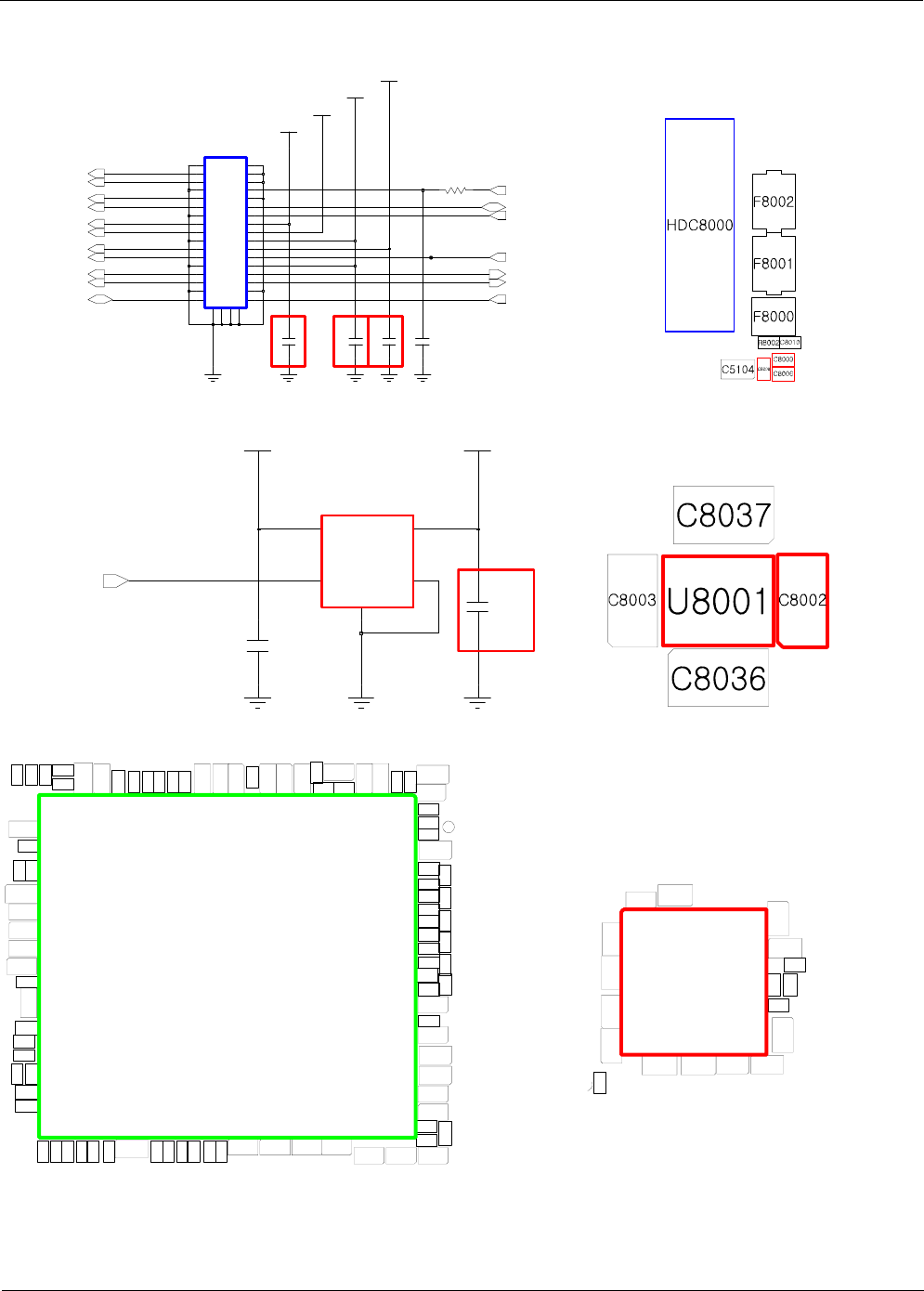
8-3-11. 8M CAM
"Camera" function does not work
Yes
Check the Camera
connector on Main PBA Reconnect the HDC8000
No
Check the voltage
C8002 =2.8V
C8009 =1.1V
C8006 =2.8V
C8008 =1.8V
Replace U8001
Replace U5001
No
Yes
Replace UCP4000
Check CAM_MCLK
is 24MHz
END
Replace the camera module
No
Yes
Yes
Abnormal
Level 3Repair
Distribution, transmission, or infringement of any content or data from this document without Samsung’s written authorization is strictly prohibited.
Confidential and proprietary-the contents in this service guide subject to change without prior notice.
8-38
C8008
CAM_IO_1P8
8M_S_CORE_1.1V
C8006
R8002
C8009
8M_AF_2.8V
8M_AVDD_2.8V
77 88
99
NC
35 36
NC
37
NCNC
38
30
30
31 31 32
32
33 33 34
34
44
5566
23 23 24
24
25 25 26
26
27
27 28
28
29
29
33
16
16
17
17 18
18
19 19
22
20
20
21 21 22
22
11
1010
1111 1212
13
13 14
14
15
15
HDC8000
TP8002
C8010
8M_CAM_SDA_1.8V
8M_CAM_MCLK
8M_AF_SDA_1.8V
8M_AF_SCL_1.8V
8M_CAM_RESET
8M_EEPROM_SCL_1.8
V
8M_EEPROM_SDA_1.8
V
8M_CAM_D0_N_F
8M_CAM_D0_P_F
8M_CAM_CLK_N_F
8M_CAM_CLK_P_F
8M_CAM_D1_N_F
8M_CAM_D1_P_F
8M_CAM_D2_N_F
8M_CAM_D2_P_F
8M_CAM_D3_N_F
8M_CAM_D3_P_F
8M_CAM_SCL_1.8V
C8003
VOUT 1
U8001
CE
3
5
GND
2
GND
VDD
4
C8002
V_BAT 8M_AVDD_2.8V
8M_AVDD_LDO_EN
C4002
C4003
C4004
C4005
C4006
C4007
C4008
C4009
C4010
C4011
C4013
C4039
C4040
C4041
C4042
C4043
C4044
C4045
C4046
C4047
C4048
C4049 C4050
C4051
C4052
C4053
C4067
C4069
C4070
C4075
C4076
C4093
C4096
C4098
C4099
C4100
C4101
C5000
C5001C5002
C5003
C5004 C5005
C5006
C5008
C5010
C5011
C5022
C5027
C5041C5043
C5045
C5053
C5058
C5065
R4009R4010 R4011R4012 R4013R4014
R4015R4016
R4017R4018
R4019R4020
R4024
R4026
R4027
R4028
R4030
R4035
R4037
R4041
R4042
R4049
R4050 R4051
R4063
R4065
R4066
R4067
R4069
R4070
R4074
R4078
R4079 R4080 R4081
R4082
R4083
R4084
R4086
R4088
R4089
R4091R4094
R4096
R4097
R4098
R4099
R4100
R4102
R4103 R4104 R4105 7014R6014R R4108 R4109
R4110
R4113
R4115
R4116
TH4001
TP4002
U5001
UCP4000
Level 3Repair
Distribution, transmission, or infringement of any content or data from this document without Samsung’s written authorization is strictly prohibited.
Confidential and proprietary-the contents in this service guide subject to change without prior notice.
8-39
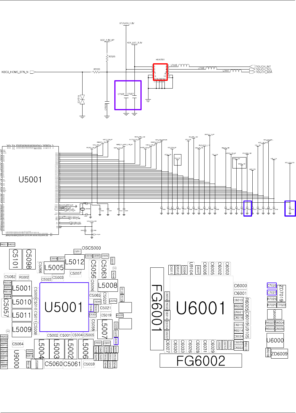
8-3-12. Touch Key
Touch Key does not work
Yes
No Reconnect the Touch Key Connector
HEA7001
Check Touch Key Connector
on Main PBA
Yes
END
Yes
Replace Touch Key Module
Yes
No
Check the
VTOUCH_1.8V(C7026),
KEY LED_3.3V(C7027)
Check U5001 -VTOUCH_1.8V VLDO30(C5043)
U5001 -KEY LED_3.3V VLDO38(C5049)
Level 3Repair
Distribution, transmission, or infringement of any content or data from this document without Samsung’s written authorization is strictly prohibited.
Confidential and proprietary-the contents in this service guide subject to change without prior notice.
8-40
Level 3Repair
Distribution, transmission, or infringement of any content or data from this document without Samsung’s written authorization is strictly prohibited.
Confidential and proprietary-the contents in this service guide subject to change without prior notice.
8-41
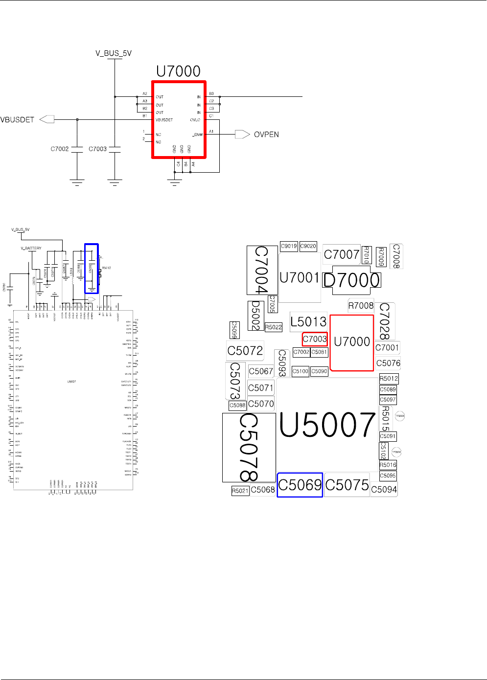
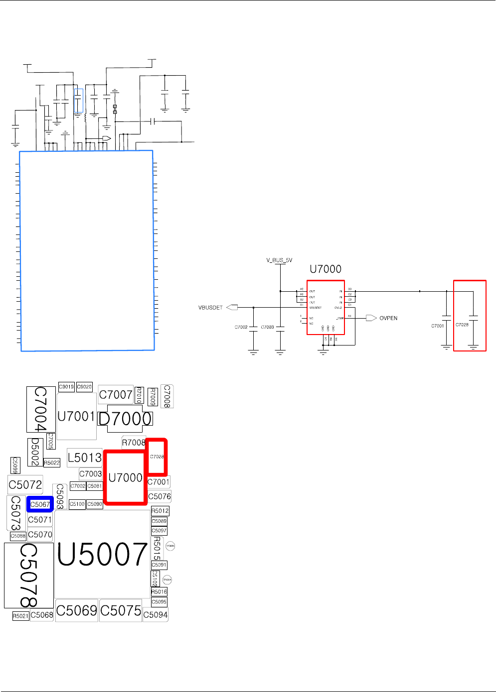
8-3-13. OTG
OTG does not work
Yes
No Check U5007
Check IF PMIC
CHGIN(C5067)=5V
Yes
END
Yes
No Check U7000
Check V_BUS_5V(C7028)
=5V
Yes
Change the IF FPCB
Level 3Repair
Distribution, transmission, or infringement of any content or data from this document without Samsung’s written authorization is strictly prohibited.
Confidential and proprietary-the contents in this service guide subject to change without prior notice.
8-42
J5SYS
J6
BATTJ7
BATT
J8DN1
J9DP2
H7
BATT
H8MVIO
H9UID
CORNER
CORNER
J2
CHGPGJ3
CHGPG
J4SYS
G9UR2
H1
CHGPG
H10COMP2
H2BAT_SN
H3BAT_SP
H4SYS
H5SYS
H6
BATT
G10COMN1
G2AVL
GND_A
GND_A
G5MIC_USBG6
JIG
G7IDB
G8
AUR2
F3INOKB
F4DETBATB
F5
SDA
F6
MVBAT
F7
BC
F8SR2
F9
ADP2
G1
CHGLX
E5
VIO
E6SYS_A
E7
AUT1
E8UT1
E9
MVBUS
F1
CHGLX
F10
ADN1
F2
CHGLX
GND_A
D8
AIN
D9
VBATTFG
E1
BYP
E10SL1
E2
BYPE3
BYP
GND_D
C9
ALRT
D1
CHGIN
D10
SDAFG
D2
CHGIN
D3
VBUSDET
D4OVPENB
D5DISQBAT
D6
SCL
C10
THRM
C2
SAFEOUT2
C3
FLASHEN
C4
TORCHEN
GND_Q
C6
MRSTB
C7
RESETB
C8
SCLFG
B3MPWM
B4MDN
GNDM
B6
INTB
B7
VCCTEST
B8
SNS
B9
VBFG
C1
CHGIN
A5IN_MOT
A6
TEST1A7
TEST2A8
TEST3A9
TEST4
B1
SAFEOUT1
B10KVSS
B2
FLED
NC
NC
CORNER
CORNER
A2
FLED
A3MGAIN
A4MDP
U5007
C5076
C5080
C5068
C5069
V_BAT
C5067
V_BATTERY
C5075
C5072
L5013
C5073
V_BUS_5V
C5070
C5071
R5012
CHG_LX
Level 3Repair
Distribution, transmission, or infringement of any content or data from this document without Samsung’s written authorization is strictly prohibited.
Confidential and proprietary-the contents in this service guide subject to change without prior notice.
8-43
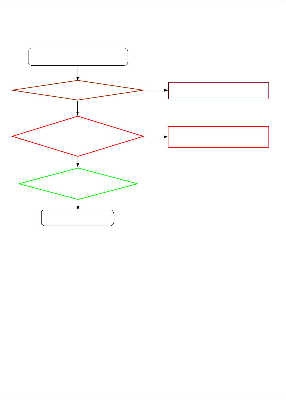
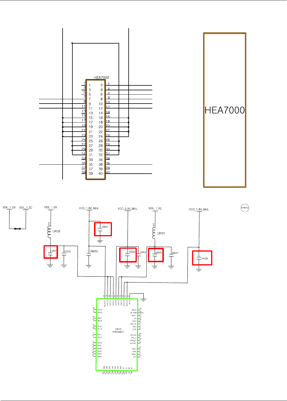
8-3-14. MHL
MHL Does not work
Yes
No Check if HEA7000 is well connected
Check the SUB Con to con
on Main PBA
Yes
No Check the U5001
Check the voltage of
C8021(1.2V), C8016(1.8V),
C8024(3.3V), C8026(1.2V),
C8028(1.8V)
Replace U8003
Yes
END
Yes
Level 3Repair
Distribution, transmission, or infringement of any content or data from this document without Samsung’s written authorization is strictly prohibited.
Confidential and proprietary-the contents in this service guide subject to change without prior notice.
8-44
Level 3Repair
Distribution, transmission, or infringement of any content or data from this document without Samsung’s written authorization is strictly prohibited.
Confidential and proprietary-the contents in this service guide subject to change without prior notice.
8-45
Level 3Repair
Distribution, transmission, or infringement of any content or data from this document without Samsung’s written authorization is strictly prohibited.
Confidential and proprietary-the contents in this service guide subject to change without prior notice.
8-46
8-3-15. Motor
Motor does not work
Yes
No
Replace :Motor/SPK FPCB
Check the Motor/SPK FPCB
Yes
END
Check the Main PBA's
connector(HDC6000)
Yes
PBA's Connector HDC6000
No
Check the C5100(3V), TP5009,
Replace U5007
Check the Pin signal.
1.7Vrms Check ZD6000,
ZD6001
Yes
No
Level 3Repair
Distribution, transmission, or infringement of any content or data from this document without Samsung’s written authorization is strictly prohibited.
Confidential and proprietary-the contents in this service guide subject to change without prior notice.
8-47

Level 3Repair
Distribution, transmission, or infringement of any content or data from this document without Samsung’s written authorization is strictly prohibited.
Confidential and proprietary-the contents in this service guide subject to change without prior notice.
8-48

Level 3Repair
Distribution, transmission, or infringement of any content or data from this document without Samsung’s written authorization is strictly prohibited.
Confidential and proprietary-the contents in this service guide subject to change without prior notice.
8-49
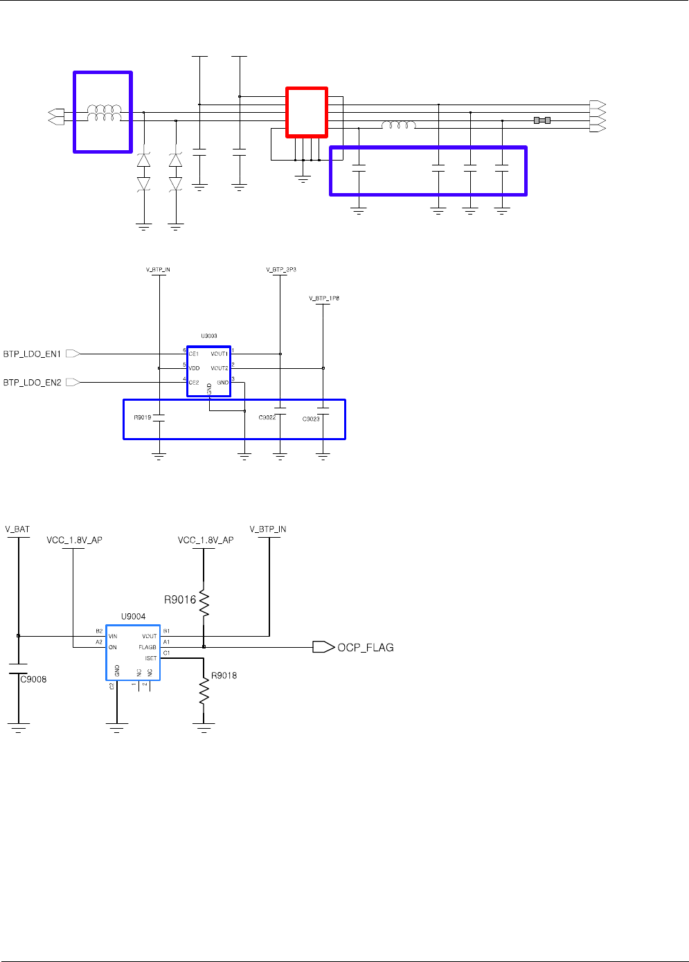
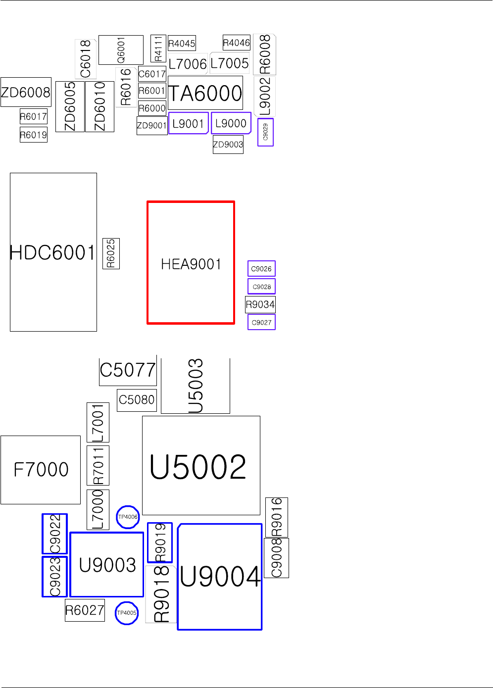
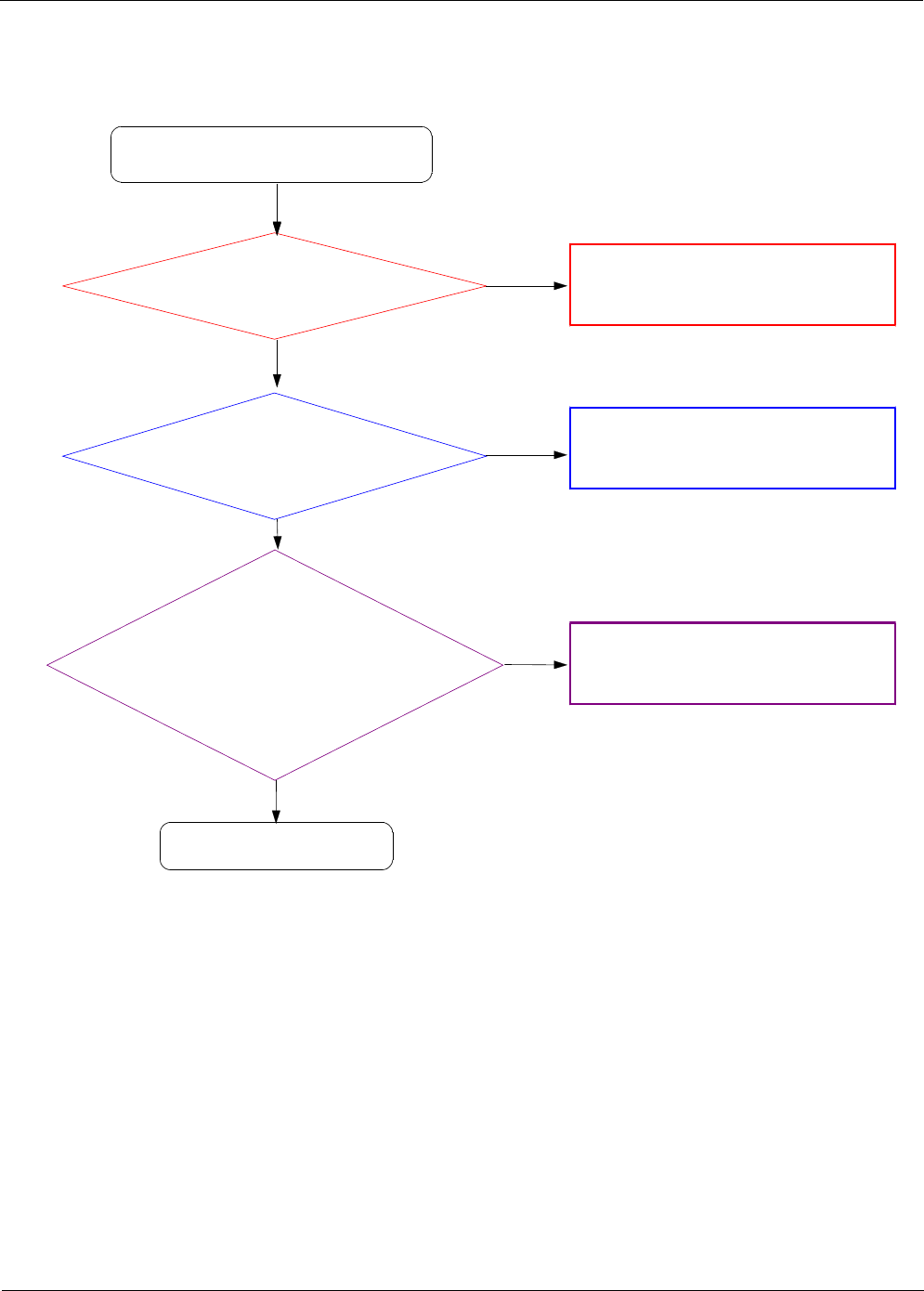
8-3-16. FingerPrint Sensor
FingerPrint Sensor does not work
Yes
No Replace :FingerPrint Sensor FPCB or
PBA's connector(HEA9001)
Check the FingerPrint Sensor
FPCB, PBA's
Connector(HEA9001)
Yes
END
Check the
V_BTP_IN(C9019),
V_BTP_3P3(C9022),
V_BTP_1P8(C9023)
Yes
Check the
BTP_LDO_EN1(TP4006),
BTP_LDO_EN2(TP4005),
U9003, U9004
No
Check the AP(UCP4000-1)
Check the
BTP_IRQ(L9000),
BTP_SLEEP(L9001),
BTP_SPI_MISO(C9026),
BTP_SPI_MOSI(C9028),
BTP_SPI_CLK(C9027),
BTP_SPI_CS_N(C9029)
Yes
No
Level 3Repair
Distribution, transmission, or infringement of any content or data from this document without Samsung’s written authorization is strictly prohibited.
Confidential and proprietary-the contents in this service guide subject to change without prior notice.
8-50
C9027
C9028
R9034
ZD9003
2
1
ZD9001
2
1
L9000
L9001
C9026
V_BTP_3P3
C9020 C9019
V_BTP_1P8
C9029
L9002
NC
13 14
NC
5566
7788
99
NC
11 12
NC
HEA9001
11
1010
22
3344
BTP_IRQ
BTP_SLEEP BTP_SPI_CS_
N
BTP_SPI_MIS
O
BTP_SPI_CLK
BTP_SPI_MOS
I
Level 3Repair
Distribution, transmission, or infringement of any content or data from this document without Samsung’s written authorization is strictly prohibited.
Confidential and proprietary-the contents in this service guide subject to change without prior notice.
8-51
Level 3Repair
Distribution, transmission, or infringement of any content or data from this document without Samsung’s written authorization is strictly prohibited.
Confidential and proprietary-the contents in this service guide subject to change without prior notice.
8-52
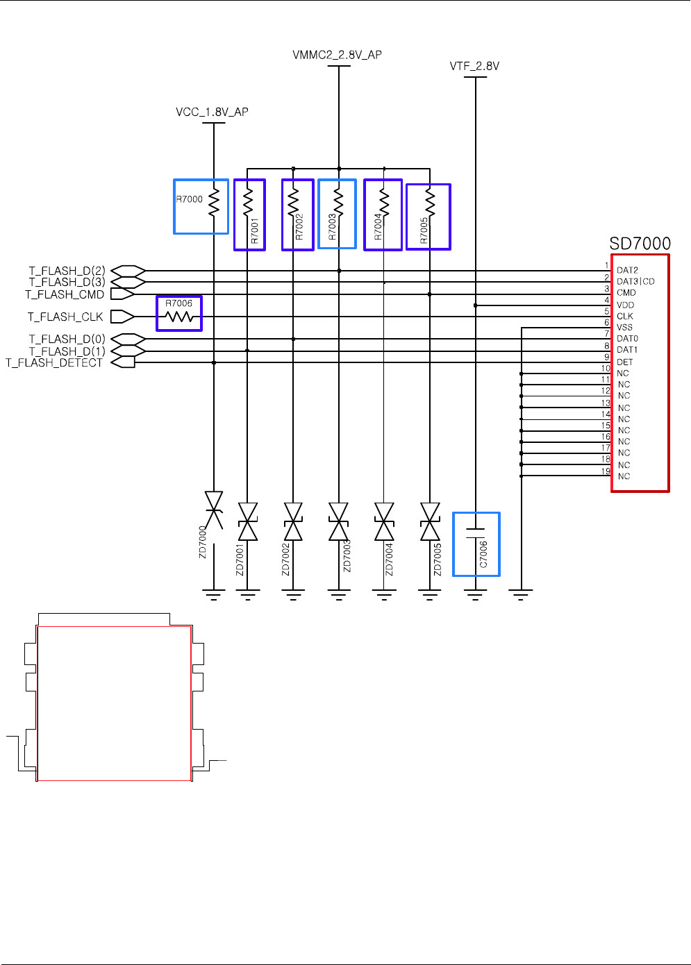
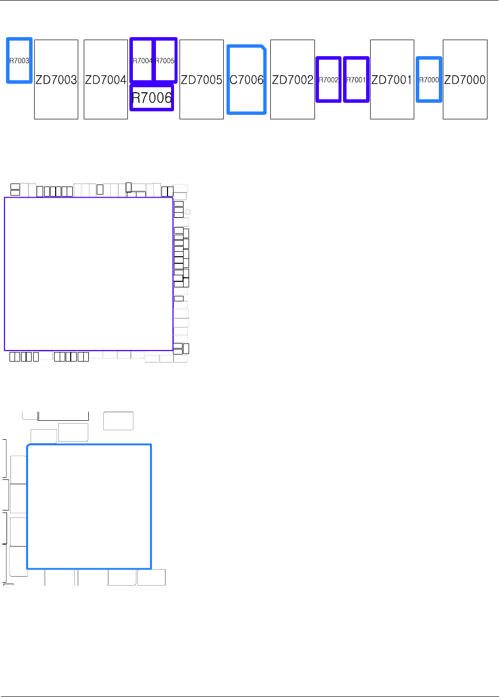
8-3-17. SD Part
SD Card does not work
Yes
No Change :SD Card or
Replace :PBA's Socket (SD7000)
Check the Micro SD Card,
PBA's Socket (SD7000)
Yes
END
Check the
VCC_1.8V_AP(R7000),
VMMC2_2.8V_AP(R7003),
VTF_2.8V(C7006)
Yes
Check the
PMIC(U5001)
No
Check the PBA's Socket (SD7000)
AP(UCP4000),
Check the
T_FLASH_D(0)~D(3)
R7001~7004,
T_FLASH_CMD R7005
T_FLASH_CLK R7006,
T_FLASH_DETECT R7000
Yes
No
Level 3Repair
Distribution, transmission, or infringement of any content or data from this document without Samsung’s written authorization is strictly prohibited.
Confidential and proprietary-the contents in this service guide subject to change without prior notice.
8-53
SD7000
Level 3Repair
Distribution, transmission, or infringement of any content or data from this document without Samsung’s written authorization is strictly prohibited.
Confidential and proprietary-the contents in this service guide subject to change without prior notice.
8-54
C5000
C5001C5002
C5003
C5004 C5005
C5007
C5008
C5010
C5011
C5022
9
0
U5001
C4002
C4003
C4004
C4005
C4006
C4007
C4008
C4013
C4039
C4040
C4041
C4042
C4043
C4044
C4045
C4046
C4047
C4049 C4050
C4051
C4067
C4069
C4070
C4075
C4076
C4093
C4096
C4098
C4101
R4009R4010 R4011R4012 R4013
R4019R4020
R4024
R4026
R4027R4030
R4035
R4037
R4041
R4042
R4049
R4050 R4051
R4063
R4065
R4066
R4067
R4070
R4074
R4079 R4080 R4081
R4082 R4084
R4089
R4091R4094
R4096
R4097
R4098
R4099
R4100
R4102
R4103 R4104 R4105 7014R6014R R4108 R4109
R4113
TH4001
TP400 2
UCP4000
Level 3Repair
Distribution, transmission, or infringement of any content or data from this document without Samsung’s written authorization is strictly prohibited.
Confidential and proprietary-the contents in this service guide subject to change without prior notice.
8-55
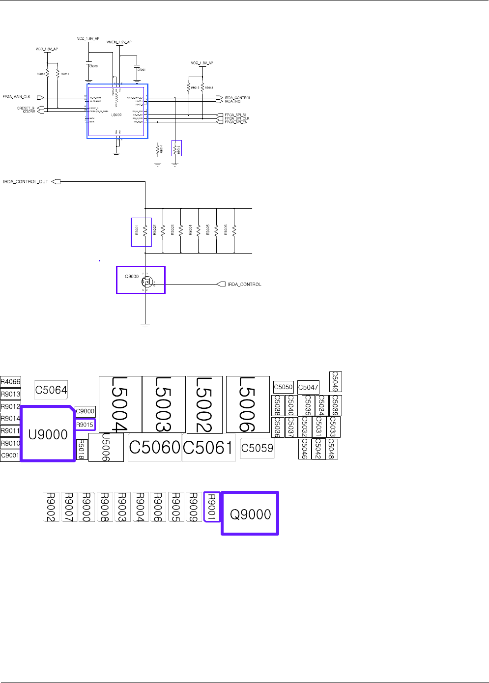
8-3-18. IR LED Part
IR LED does not work
Yes
No Change :IR LED FPCB or
Replace :PBA's Contact Pin
(CON9000, CON9001)
Check the IR LED FPCB,
PBA's Contact Pin
(CON9000, CON9001)
Yes
END
Check the
FPGA_SPI_EN(R5026),
IRLED_3.3V(C9002)
Yes
Check the
U5009, U9000
No
Yes
Check the
IRDA_CONTROL_OUT(R9001),
IRDA_CONTROL(R9015)
Check the
Q9000, U9000
No
Level 3Repair
Distribution, transmission, or infringement of any content or data from this document without Samsung’s written authorization is strictly prohibited.
Confidential and proprietary-the contents in this service guide subject to change without prior notice.
8-56
ANT9000
ANT9001
Level 3Repair
Distribution, transmission, or infringement of any content or data from this document without Samsung’s written authorization is strictly prohibited.
Confidential and proprietary-the contents in this service guide subject to change without prior notice.
8-57
Level 3Repair
Distribution, transmission, or infringement of any content or data from this document without Samsung’s written authorization is strictly prohibited.
Confidential and proprietary-the contents in this service guide subject to change without prior notice.
8-58
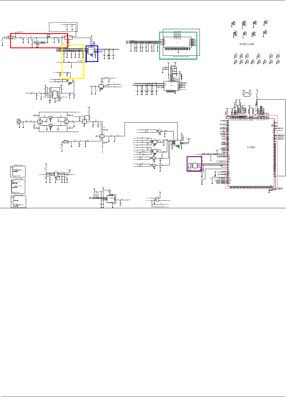
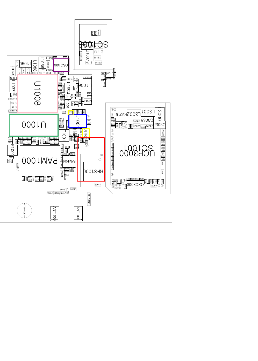
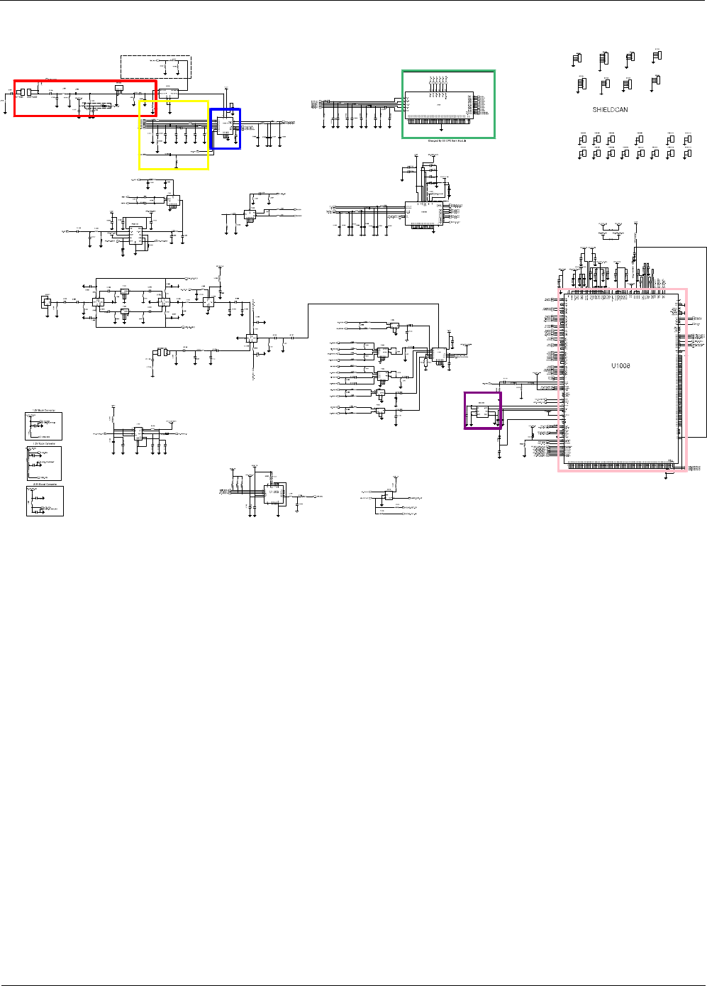
Check C1001 ≤-65dBm ?
8-3-19. GSM850/ WCDMA Band5 /LTE5 RX
Check the voltage at
{L1036= VBATT?}
&{
C1074 =1.2V?}
&{
C1075 =2.5V?}
&{
C1070 =1.5
V?}
CHECK soldered
C1000,L1001,L1020 RFS1000
Resolder or change
U5000
Check the freq. at
OSC1000 PIN4 :26
MHz ?Change or resolder
OSC1000
WCDMA Band5
/GSM 850 LTE5
Receiver is O.K?
END
YES
NO
NO
NO
YES
NO
YES
WCDMA Band5
/GSM 850 / LTE5
Receiver is O.K?
NO
YES
YES
Resolder or change
UCP3000
NO
Resolder or change
U1008
CONTINUO
US RX ON
RF INPUT : 4408CH
AMP :-50
dBm
NORMAL CONDITION
catch the channel?
Check the Voltage at
C1010 =VATT?
Check L1013
≥-65dBm ?
Check component
soldering status OK at
U1000
Resolder or change
U1001, C1010
Resolder or change
Check L1013, U9106
Resolder or change
U1000
NO
NO
NO
NO
YES
YES
YES

Level 3Repair
Distribution, transmission, or infringement of any content or data from this document without Samsung’s written authorization is strictly prohibited.
Confidential and proprietary-the contents in this service guide subject to change without prior notice.
8-59

Level 3Repair
Distribution, transmission, or infringement of any content or data from this document without Samsung’s written authorization is strictly prohibited.
Confidential and proprietary-the contents in this service guide subject to change without prior notice.
8-60
Level 3Repair
Distribution, transmission, or infringement of any content or data from this document without Samsung’s written authorization is strictly prohibited.
Confidential and proprietary-the contents in this service guide subject to change without prior notice.
8-61
Check C1001 ≤-65dBm ?
8-3-20. GSM900/ WCDMA Band8 /LTE8 RX
CONTINUO
US RX ON
RF INPUT : 3013CH
AMP :-50
dBm
NORMAL CONDITION
catch the channel?
Check the voltage at
{L1036= VBATT?}
&{
C1074 =1.2V?}
&{
C1075 =2.5V?}
&{
C1070 =1.5
V?}
Check the Voltage at
C1010 =VATT?
Check component
soldering status OK at
U1000
CHECK soldered
C1000,L1001,L1020 RFS1000
Resolder or change
U1001, C1010
Resolder or change
U1000
Resolder or change
U5000
Check the freq. at
OSC1000 PIN4 :26
MHz ?Change or resolder
OSC1000
Check C1030
≥-65dBm ?Resolder or change
Check C1030, U9106
WCDMA Band8
/GSM 900 LTE8
Receiver is O.K?
END
NO
YES
NO
NO
YES
NO
YES
NO
YES
NO
NO
YES
NO
YES
WCDMA Band8
/GSM 900 LTE8
Receiver is O.K?
NO
YES
YES
Resolder or change
UCP3000
NO
Resolder or change
U1008
Level 3Repair
Distribution, transmission, or infringement of any content or data from this document without Samsung’s written authorization is strictly prohibited.
Confidential and proprietary-the contents in this service guide subject to change without prior notice.
8-62
Level 3Repair
Distribution, transmission, or infringement of any content or data from this document without Samsung’s written authorization is strictly prohibited.
Confidential and proprietary-the contents in this service guide subject to change without prior notice.
8-63

Level 3Repair
Distribution, transmission, or infringement of any content or data from this document without Samsung’s written authorization is strictly prohibited.
Confidential and proprietary-the contents in this service guide subject to change without prior notice.
8-64
Check C1001 ≤-65dBm ?
8-3-21. GSM1800 RX
CONTINUOUS RX ON
RF INPUT : 698CH
AMP :-50
dBm
NORMAL CONDITION
catch the channel?
Check the voltage at
{L1036= VBATT?}
&{
C1074 =1.2V?}
&{
C1075 =2.5V?}
&{
C1070 =1.5
V?}
Check the Voltage at
C1010 =VATT?
Check component
soldering status OK at
U1000
CHECK soldered
C1000,L1001,L1020 RFS1000
Resolder or change
U1001, C1010
Resolder or change
U1000
Resolder or change
U5000
Check the freq. at
OSC1000 PIN4 :26
MHz ?Change or resolder
OSC1000
Check C1019
≥-65dBm ?Resolder or change
Check C1019, U9106
DCS1800
Receiver is O.K?
END
NO
YES
NO
NO
YES
NO
YES
NO
YES
NO
NO
YES
NO
YES
DCS1800
Receiver is O.K?
NO
YES
YES
Resolder or change
UCP3000
NO
Resolder or change
U1008
Level 3Repair
Distribution, transmission, or infringement of any content or data from this document without Samsung’s written authorization is strictly prohibited.
Confidential and proprietary-the contents in this service guide subject to change without prior notice.
8-65
Level 3Repair
Distribution, transmission, or infringement of any content or data from this document without Samsung’s written authorization is strictly prohibited.
Confidential and proprietary-the contents in this service guide subject to change without prior notice.
8-66
Level 3Repair
Distribution, transmission, or infringement of any content or data from this document without Samsung’s written authorization is strictly prohibited.
Confidential and proprietary-the contents in this service guide subject to change without prior notice.
8-67
Check C1001 ≤-65dBm ?
8-3-22. GSM1900/ WCDMA Band2 RX
CONTINUOUS RX ON
RF INPUT : 9800CH
AMP :-50
dBm
NORMAL CONDITION
catch the channel?
Check the voltage at
{L1036= VBATT?}
&{
C1074 =1.2V?}
&{
C1075 =2.5V?}
&{
C1070 =1.5
V?}
Check the Voltage at
C1010 =VATT?
Check component
soldering status OK at
U1000
CHECK soldered
C1000,L1001,L1020 RFS1000
Resolder or change
U1001, C1010
Resolder or change
U1000
Resolder or change
U5000
Check the freq. at
OSC1000 PIN4 :26
MHz ?Change or resolder
OSC1000
Check L1016
≥-65dBm ?Resolder or change
Check L1016 U9106
PCS1900 /WCDMA2
Receiver is O.K?
END
NO
YES
NO
NO
YES
NO
YES
NO
YES
NO
NO
YES
NO
YES
PCS1900 /WCDMA2
Receiver is O.K?
NO
YES
YES
Resolder or change
UCP3000
NO
Resolder or change
U1008

Level 3Repair
Distribution, transmission, or infringement of any content or data from this document without Samsung’s written authorization is strictly prohibited.
Confidential and proprietary-the contents in this service guide subject to change without prior notice.
8-68
Level 3Repair
Distribution, transmission, or infringement of any content or data from this document without Samsung’s written authorization is strictly prohibited.
Confidential and proprietary-the contents in this service guide subject to change without prior notice.
8-69

Level 3Repair
Distribution, transmission, or infringement of any content or data from this document without Samsung’s written authorization is strictly prohibited.
Confidential and proprietary-the contents in this service guide subject to change without prior notice.
8-70
Check C1001 ≤-65dBm ?
8-3-23. LTE B3 RX
CONTINUOUS RX ON
RF INPUT : 1575CH
AMP :-50
dBm
NORMAL CONDITION
catch the channel?
Check the voltage at
{L1036= VBATT?}
&{
C1074 =1.2V?}
&{
C1075 =2.5V?}
&{
C1070 =1.5
V?}
Check the Voltage at
C1010 =VATT?
Check component
soldering status OK at
U1000
CHECK soldered
C1000,L1001,L1020 RFS1000
Resolder or change
U1001, C1010
Resolder or change
U1000
Resolder or change
U5000
Check the freq. at
OSC1000 PIN4 :26
MHz ?
Change or resolder
OSC1000
Check L1015
≥-65dBm ?Resolder or change
Check L1015, U9106
LTE Band3
Receiver is O.K?
END
NO
YES
NO
NO
YES
NO
YES
NO
YES
NO
NO
YES
NO
YES
LTE Band 3
Receiver is O.K?
NO
YES
YES
Resolder or change
UCP3000
NO
Resolder or change
U1008

Level 3Repair
Distribution, transmission, or infringement of any content or data from this document without Samsung’s written authorization is strictly prohibited.
Confidential and proprietary-the contents in this service guide subject to change without prior notice.
8-71
Level 3Repair
Distribution, transmission, or infringement of any content or data from this document without Samsung’s written authorization is strictly prohibited.
Confidential and proprietary-the contents in this service guide subject to change without prior notice.
8-72
Level 3Repair
Distribution, transmission, or infringement of any content or data from this document without Samsung’s written authorization is strictly prohibited.
Confidential and proprietary-the contents in this service guide subject to change without prior notice.
8-73
Check C1001 ≤-65dBm ?
8-3-24. LTE B7 RX
CONTINUOUS RX ON
RF INPUT : 3100CH
AMP :-50
dBm
NORMAL CONDITION
catch the channel?
Check the voltage at
{L1036= VBATT?}
&{
C1074 =1.2V?}
&{
C1075 =2.5V?}
&{
C1070 =1.5
V?}
Check the Voltage at
C1010 =VATT?
Check component
soldering status OK at
F1001
CHECK soldered
C1000,L1001,L1020 RFS1000
Resolder or change
U1001, C1010
Resolder or change
F1001
Resolder or change
U5000
Check the freq. at
OSC1000 PIN4 :26
MHz ?
Change or resolder
OSC1000
Check L1020
≥-65dBm ?Resolder or change
Check L1020, U9106
LTE Band7
Receiver is O.K?
END
NO
YES
NO
NO
YES
NO
YES
NO
YES
NO
NO
YES
NO
YES
LTE Band7
Receiver is O.K?
NO
YES
YES
Resolder or change
UCP3000
NO
Resolder or change
U1008
Level 3Repair
Distribution, transmission, or infringement of any content or data from this document without Samsung’s written authorization is strictly prohibited.
Confidential and proprietary-the contents in this service guide subject to change without prior notice.
8-74

Level 3Repair
Distribution, transmission, or infringement of any content or data from this document without Samsung’s written authorization is strictly prohibited.
Confidential and proprietary-the contents in this service guide subject to change without prior notice.
8-75

Level 3Repair
Distribution, transmission, or infringement of any content or data from this document without Samsung’s written authorization is strictly prohibited.
Confidential and proprietary-the contents in this service guide subject to change without prior notice.
8-76
Check C1001 ≤-65dBm ?
8-3-25. LTE B20 RX
CONTINUOUS RX ON
RF INPUT : 6300CH
AMP :-50
dBm
NORMAL CONDITION
catch the channel?
Check the voltage at
{L1036= VBATT?}
&{
C1074 =1.2V?}
&{
C1075 =2.5V?}
&{
C1070 =1.5
V?}
Check the Voltage at
C1010 =VATT?
Check component
soldering status OK at
U1008
CHECK soldered
C1000,L1001,L1020 RFS1000
Resolder or change
U1001, C1010
Resolder or change
U1008
Resolder or change
U5000
Check the freq. at
OSC1000 PIN4 :26
MHz ?Change or resolder
OSC1000
Check C1041
≥-65dBm ?Resolder or change
Check C1041, U9106
LTE Band20
Receiver is O.K?
END
NO
YES
NO
NO
YES
NO
YES
NO
YES
NO
NO
YES
NO
YES
LTE Band20
Receiver is O.K?
NO
YES
YES
Resolder or change
UCP3000
NO
Resolder or change
U1008
Level 3Repair
Distribution, transmission, or infringement of any content or data from this document without Samsung’s written authorization is strictly prohibited.
Confidential and proprietary-the contents in this service guide subject to change without prior notice.
8-77
Level 3Repair
Distribution, transmission, or infringement of any content or data from this document without Samsung’s written authorization is strictly prohibited.
Confidential and proprietary-the contents in this service guide subject to change without prior notice.
8-78

Level 3Repair
Distribution, transmission, or infringement of any content or data from this document without Samsung’s written authorization is strictly prohibited.
Confidential and proprietary-the contents in this service guide subject to change without prior notice.
8-79
Check C1001 ≤-65dBm ?
8-3-26. WCDMA Band1 LTE B1 RX
CONTINUOUS RX ON
RF INPUT : 10700CH
AMP :-50
dBm
NORMAL CONDITION
catch the channel?
Check the voltage at
{L1036= VBATT?}
&{
C1074 =1.2V?}
&{
C1075 =2.5V?}
&{
C1070 =1.5
V?}
Check the Voltage at
C1010 =VATT?
Check component
soldering status OK at
U1008
CHECK soldered
C1000,L1001,L1020 RFS1000
Resolder or change
U1001, C1010
Resolder or change
U1008
Resolder or change
U5000
Check the freq. at
OSC1000 PIN4 :26
MHz ?Change or resolder
OSC1000
Check L1010
≥-65dBm ?Resolder or change
Check L1010, U9106
WCDMA Bandd1 LTE
Band1
Receiver is O.K?
END
NO
YES
NO
NO
YES
NO
YES
NO
YES
NO
NO
YES
NO
YES
WCDMA Bandd1 LTE
Band1
Receiver is O.K?
NO
YES
YES
Resolder or change
UCP3000
NO
Resolder or change
U1008
Level 3Repair
Distribution, transmission, or infringement of any content or data from this document without Samsung’s written authorization is strictly prohibited.
Confidential and proprietary-the contents in this service guide subject to change without prior notice.
8-80
Level 3Repair
Distribution, transmission, or infringement of any content or data from this document without Samsung’s written authorization is strictly prohibited.
Confidential and proprietary-the contents in this service guide subject to change without prior notice.
8-81
Level 3Repair
Distribution, transmission, or infringement of any content or data from this document without Samsung’s written authorization is strictly prohibited.
Confidential and proprietary-the contents in this service guide subject to change without prior notice.
8-82
U9106 PIN1 :About
30dBm ?
8-3-27. GSM850/ GSM900 TX
Check the voltage at
{L1036= VBATT?}
&{
C1074 =1.2V?}
&{
C1075 =2.5V?}
Check the Voltage at
C1010 =VBATT? ?
Check the Voltage at
c1032 =VBATT? ?
CHECK soldered
C1000,L1001,L1020 RFS1000
Resolder or change
U1001, C1010
Resolder or change
c1032 PAM1000
Resolder or change
U5000
Check the freq. at
OSC1000 PIN4 :26
MHz ?Change or resolder
OSC1000
Check L1011
about 30dBm ?
Resolder or change
L1011
GSM850/900
Transmitter is O.K?
END
YES
NO
NO
YES
NO
YES
NO
YES
NO
NO
YES
NO
YES
GSM850/900
Transmitter is O.K?
NO
YES
YES
Resolder or change
UCP3000
NO
Resolder or change
U1008
CONTINOUS TX ON CONDITION
TX POWER DAC:14500 CODE
APPLIED
GSM850 CH : 190
GSM900 CH :62
RBW : 100KHz
VBW : 100KHz
SPAN :10
MHz
REF LEV. :10
dBm
ATT. :20
dB
Check C1043
about 0dBm ?Resolder or change
C1043
NO
YES
Level 3Repair
Distribution, transmission, or infringement of any content or data from this document without Samsung’s written authorization is strictly prohibited.
Confidential and proprietary-the contents in this service guide subject to change without prior notice.
8-83
Level 3Repair
Distribution, transmission, or infringement of any content or data from this document without Samsung’s written authorization is strictly prohibited.
Confidential and proprietary-the contents in this service guide subject to change without prior notice.
8-84
Level 3Repair
Distribution, transmission, or infringement of any content or data from this document without Samsung’s written authorization is strictly prohibited.
Confidential and proprietary-the contents in this service guide subject to change without prior notice.
8-85
U9106 PIN1 :About
30dBm ?
8-3-28. GSM1800/ GSM1900 TX
Check the voltage at
{L1036= VBATT?}
&{
C1074 =1.2V?}
&{
C1075 =2.5V?}
Check the Voltage at
C1010 =VBATT? ?
Check the Voltage at
c1032 =VBATT? ?
CHECK soldered
C1000,L1001,L1020 RFS1000
Resolder or change
U1001, C1010
Resolder or change
c1032 PAM1000
Resolder or change
U5000
Check the freq. at
OSC1000 PIN4 :26
MHz ?Change or resolder
OSC1000
Check L1014
about 30dBm ?
Resolder or change
L1014
DCS1800/PCS1900
Transmitter is O.K?
END
YES
NO
NO
YES
NO
YES
NO
YES
NO
NO
YES
NO
YES
DCS1800/PCS1900
Transmitter is O.K?
NO
YES
YES
Resolder or change
UCP3000
NO
Resolder or change
U1008
CONTINOUS TX ON CONDITION
TX POWER DAC:14500 CODE
APPLIED
DCS CH : 685
PCS CH : 661
RBW : 100KHz
VBW : 100KHz
SPAN :10
MHz
REF LEV. :10
dBm
ATT. :20
dB
Check L1025
about 0dBm ?Resolder or change
L1025
NO
YES
Level 3Repair
Distribution, transmission, or infringement of any content or data from this document without Samsung’s written authorization is strictly prohibited.
Confidential and proprietary-the contents in this service guide subject to change without prior notice.
8-86
Level 3Repair
Distribution, transmission, or infringement of any content or data from this document without Samsung’s written authorization is strictly prohibited.
Confidential and proprietary-the contents in this service guide subject to change without prior notice.
8-87

Level 3Repair
Distribution, transmission, or infringement of any content or data from this document without Samsung’s written authorization is strictly prohibited.
Confidential and proprietary-the contents in this service guide subject to change without prior notice.
8-88
U9106 PIN1 :About
20dBm ?
8-3-29. WCDMA BAND1 Tx
Check the voltage at
{L1036= VBATT?}
&{
C1074 =1.2V?}
&{
C1075 =2.5V?}
Check the Voltage at
C1010 =VBATT? ?
Check the Voltage at
c1032 =VBATT? ?
CHECK soldered
C1000,L1001,L1020 RFS1000
Resolder or change
U1001, C1010
Resolder or change
c1032 PAM1000
Resolder or change
U5000
Check the freq. at
OSC1000 PIN4 :26
MHz ?Change or resolder
OSC1000
Check L1010
about 20dBm ?
Resolder or change
L1010 C1004 U1000
WCDMA BAND1
Transmitter is O.K?
END
YES
NO
NO
YES
NO
YES
NO
YES
NO
NO
YES
NO
YES
WCDMA BAND1
Transmitter is O.K?
NO
YES
YES
Resolder or change
UCP3000
NO
Resolder or change
U1008
CONTINOUS TX ON CONDITION
TX POWER DAC:14500 CODE
APPLIED
WCDMA Band1 CH : 10700
RBW : 100KHz
VBW : 100KHz
SPAN :10
MHz
REF LEV. :10
dBm
ATT. :20
dB
Check L1025
about 0dBm ?Resolder or change
L1025
NO
YES

Level 3Repair
Distribution, transmission, or infringement of any content or data from this document without Samsung’s written authorization is strictly prohibited.
Confidential and proprietary-the contents in this service guide subject to change without prior notice.
8-89
Level 3Repair
Distribution, transmission, or infringement of any content or data from this document without Samsung’s written authorization is strictly prohibited.
Confidential and proprietary-the contents in this service guide subject to change without prior notice.
8-90

Level 3Repair
Distribution, transmission, or infringement of any content or data from this document without Samsung’s written authorization is strictly prohibited.
Confidential and proprietary-the contents in this service guide subject to change without prior notice.
8-91
U9106 PIN1 :About
20dBm ?
8-3-30. WCDMA BAND2 TX
Check the voltage at
{L1036= VBATT?}
&{
C1074 =1.2V?}
&{
C1075 =2.5V?}
Check the Voltage at
C1010 =VBATT? ?
Check the Voltage at
c1032 =VBATT? ?
CHECK soldered
C1000,L1001,L1020 RFS1000
Resolder or change
U1001, C1010
Resolder or change
c1032, PAM1000
Resolder or change
U5000
Check the freq. at
OSC1000 PIN4 :26
MHz ?Change or resolder
OSC1000
Check C1019
about 20dBm ?
Resolder or change
C1019 L1005 U1000
WCDMA BAND2
Transmitter is O.K?
END
YES
NO
NO
YES
NO
YES
NO
YES
NO
NO
YES
NO
YES
WCDMA BAND2
Transmitter is O.K?
NO
YES
YES
Resolder or change
UCP3000
NO
Resolder or change
U1008
CONTINOUS TX ON CONDITION
TX POWER DAC:14500 CODE
APPLIED
WCDMA Band2 CH : 9880
RBW : 100KHz
VBW : 100KHz
SPAN :10
MHz
REF LEV. :10
dBm
ATT. :20
dB
Check L1025
about 0dBm ?Resolder or change
L1025
NO
YES

Level 3Repair
Distribution, transmission, or infringement of any content or data from this document without Samsung’s written authorization is strictly prohibited.
Confidential and proprietary-the contents in this service guide subject to change without prior notice.
8-92

Level 3Repair
Distribution, transmission, or infringement of any content or data from this document without Samsung’s written authorization is strictly prohibited.
Confidential and proprietary-the contents in this service guide subject to change without prior notice.
8-93

Level 3Repair
Distribution, transmission, or infringement of any content or data from this document without Samsung’s written authorization is strictly prohibited.
Confidential and proprietary-the contents in this service guide subject to change without prior notice.
8-94
U9106 PIN1 :About
20dBm ?
8-3-31. WCDMA BAND5 TX
Check the voltage at
{L1036= VBATT?}
&{
C1074 =1.2V?}
&{
C1075 =2.5V?}
Check the Voltage at
C1010 =VBATT? ?
Check the Voltage at
c1032 =VBATT? ?
CHECK soldered
C1000,L1001,L1020 RFS1000
Resolder or change
U1001, C1010
Resolder or change
c1032, PAM1000
Resolder or change
U5000
Check the freq. at
OSC1000 PIN4 :26
MHz ?Change or resolder
OSC1000
Check L1013
about 20dBm ?
Resolder or change
L1013 C1006 U1008
WCDMA BAND5
Transmitter is O.K?
END
YES
NO
NO
YES
NO
YES
NO
YES
NO
NO
YES
NO
YES
WCDMA BAND5
Transmitter is O.K?
NO
YES
YES
Resolder or change
UCP3000
NO
Resolder or change
U1008
CONTINOUS TX ON CONDITION
TX POWER DAC:14500 CODE
APPLIED
WCDMA Band5 CH : 4408
RBW : 100KHz
VBW : 100KHz
SPAN :10
MHz
REF LEV. :10
dBm
ATT. :20
dB
Check C1043
about 0dBm ?Resolder or change
C1043
NO
YES

Level 3Repair
Distribution, transmission, or infringement of any content or data from this document without Samsung’s written authorization is strictly prohibited.
Confidential and proprietary-the contents in this service guide subject to change without prior notice.
8-95

Level 3Repair
Distribution, transmission, or infringement of any content or data from this document without Samsung’s written authorization is strictly prohibited.
Confidential and proprietary-the contents in this service guide subject to change without prior notice.
8-96

Level 3Repair
Distribution, transmission, or infringement of any content or data from this document without Samsung’s written authorization is strictly prohibited.
Confidential and proprietary-the contents in this service guide subject to change without prior notice.
8-97
U9106 PIN1 :About
20dBm ?
8-3-32. WCDMA BAND8 TX
Check the voltage at
{L1036= VBATT?}
&{
C1074 =1.2V?}
&{
C1075 =2.5V?}
Check the Voltage at
C1010 =VBATT? ?
Check the Voltage at
c1032 =VBATT? ?
CHECK soldered
C1000,L1001,L1020 RFS1000
Resolder or change
U1001, C1010
Resolder or change
c1032, PAM1000
Resolder or change
U5000
Check the freq. at
OSC1000 PIN4 :26
MHz ?Change or resolder
OSC1000
Check C1030
about 20dBm ?
Resolder or change
C1030 C1009 U1008
WCDMA BAND8
Transmitter is O.K?
END
YES
NO
NO
YES
NO
YES
NO
YES
NO
NO
YES
NO
YES
WCDMA BAND8
Transmitter is O.K?
NO
YES
YES
Resolder or change
UCP3000
NO
Resolder or change
U1008
CONTINOUS TX ON CONDITION
TX POWER DAC:14500 CODE
APPLIED
WCDMA Band8 CH : 3013
RBW : 100KHz
VBW : 100KHz
SPAN :10
MHz
REF LEV. :10
dBm
ATT. :20
dB
Check C1043
about 0dBm ?Resolder or change
C1043
NO
YES

Level 3Repair
Distribution, transmission, or infringement of any content or data from this document without Samsung’s written authorization is strictly prohibited.
Confidential and proprietary-the contents in this service guide subject to change without prior notice.
8-98

Level 3Repair
Distribution, transmission, or infringement of any content or data from this document without Samsung’s written authorization is strictly prohibited.
Confidential and proprietary-the contents in this service guide subject to change without prior notice.
8-99

Level 3Repair
Distribution, transmission, or infringement of any content or data from this document without Samsung’s written authorization is strictly prohibited.
Confidential and proprietary-the contents in this service guide subject to change without prior notice.
8-100
U9106 PIN1 :About
20dBm ?
8-3-33. LTE BAND1 TX
Check the voltage at
{L1036= VBATT?}
&{
C1074 =1.2V?}
&{
C1075 =2.5V?}
Check the Voltage at
C1010 =VBATT? ?
Check the Voltage at
c1032 =VBATT? ?
CHECK soldered
C1000,L1001,L1020 RFS1000
Resolder or change
U1001, C1010
Resolder or change
c1032 PAM1000
Resolder or change
U5000
Check the freq. at
OSC1000 PIN4 :26
MHz ?Change or resolder
OSC1000
Check L1010
about 20dBm ?
Resolder or change
L1010 C1004 U1000
LTE BAND1
Transmitter is O.K?
END
YES
NO
NO
YES
NO
YES
NO
YES
NO
NO
YES
NO
YES
LTE BAND1
Transmitter is O.K?
NO
YES
YES
Resolder or change
UCP3000
NO
Resolder or change
U1008
CONTINOUS TX ON CONDITION
TX POWER DAC:14500 CODE
APPLIED
LTE Band1 CH : 18300
RBW : 100KHz
VBW : 100KHz
SPAN :10
MHz
REF LEV. :10
dBm
ATT. :20
dB
Check L1026
about 0dBm ?Resolder or change
L1026
NO
YES
Level 3Repair
Distribution, transmission, or infringement of any content or data from this document without Samsung’s written authorization is strictly prohibited.
Confidential and proprietary-the contents in this service guide subject to change without prior notice.
8-101
1.5V Buck Converter
GRIP SENSOR
DUMMY CAP
RF_PART
SUB ANTENNA
1.2V Buck Converter
SMD SHIELDCAN
2.5V Boost Converter
BOTH
Changed By EU DPX Bank Module
C1232
C1118
L1013
C1003
C1216
L1007
SHORT
R1003
L1040
L1031
L1010
C1195
L1048
TP1001
C1227
L1028
C1048
C1238
L1009
C1222
C1012
C1009
A
2
1C
3G
4
G
1%
R1015
RFS1001
C1246
C1223
L1026
C1204
V_2P80_VPROG2
R1011
5%
C1020
C1234
C1052
C1247
C1013
L1044
V_2P80_VPROG2
C1245
RFE_VCC2_MMPA
C1235
C1115
BH1009
L1059
C1049
C1226
C1237
5%
R1010
G
25
G
1
IN
OUT
3
OUT
4
L1056
F1005
C1121
7
GND
8
GSM_HB_OUT 9
C1132
36
GND
37
GND
38
GND
39
GSM_LB_OUT 4
40GND
VCC2G5
VBATT6
VCC1
29 B8_OUT 3
GND
30
VBIAS31
GND
32VCC2_LB33
GND
34
B13_OUT 35
B17_OUT
21
GND
22
4G_HB_IN
23
2G|3G_HB_IN
24
4G_LB_IN
25
2G|3G_LB_IN
26
VIO27
CLK
28
DATA
14
GND
15
VCC2_HB16
GND
17
NC
18
GND
19
B5_OUT 2
GND
20
GND
B20_OUT
1
B3_OUT 10
B4_OUT 11
12GND
B1_OUT 13
B2_OUT
5
VDD
NC6
7
GND
LCAP18
9INT
PAM1001
GND
13NC
LPF2
14
15LCAP2
LPF1
16
17 GND
SHLD 2
3
NC
CR 4
U1045
1
CS
SCL
10
11 SDA
12
R1014
RFE_VCC2_MMPA
A
2
1C
3G
G
4
C1001
RFS1000
C1142
L1046
C1137
OPEN
C1037
8
2RF_IN RF_OUT9
VBATT
3
VCC1
110
VCC2
4VIO
PAM1002
6
CLKDATA
5
7
GND
11GND
NC
C1192
C1019
BH1003
R1013
C1264
BOTHHOLE1003
C1123
L1002
L1042
C1032
C1025
C1016
BH1005
C1146
2
3G
5G
G
10
1
UNBAL8
UNBAL14
F1006
9BAL8
BAL8
8
7BAL1
BAL1
6
G
C1051
C1055
C1047
G
25
G
1
IN
OUT
3
4OUT
10
11 NC
PORT1 2
PORT2 4
PORT3 8
1RF_GND
3RF_GND
7
VDD
F1009
U1051
5
CTL
GND
6
9GND
NC
R1034 5%
C1258
C1041
C1007
C1018
C1252
L1029
C1251
R1000
C1244
C1224
C1010
1
2G
G
3
G
5
10G
4
UNBAL
F1007
BAL1
9
8BAL1
BAL2
7
6BAL2 COIL
SC1000
1
1
22
3
3
44
C1178
R1018
C1053
F1008
2
GG
5
IN 1
OUT
3
4OUT
C1113
5%
R1002
L1006
6RX7
ANT
7
8
GND
VDD 9
L1012
14 RX6
RX5
15
16GND
GND
17
2
RX3
GND
3
4RX2
RX1
5
U1043
RX4
110
VIO
SCLK
11
12
SDAT
GND
13
RFE_VDD_2V5_SDH
C1149
C1147
R1001
L1037
C1194
C1134
C1199
RFE_RFFE_VIO_FEM
R1020
L1023
C1024
C1002
C1050
C1131
C1229
V_2P80_VPROG2
C1057
C1236
C1117
C1221
R1004
5%
9TX_B3
BOTHHOLE1006
VOUT_CHARGER
58
59GND
GND
6
ANT_B360
61NC
NC
62
7TX_B2
GND
8
50
51GND
ANT_B552
53GND
ANT_B854
55GND
ANT_G180056
GND
57
ANT_B2
43GND
GND
44
45GND
GND
46
47GND
GND
48
49GND
5GND
GND
36GND
GND
37
GND
38
39GND
GND
4
GND
40
41GND
GND
42
29
3TX_B8
30GND
GND
31
32GND
GND
33
34GND
GND
35
21
22
RX_G1800
RX_G1800 23
24
RX_B8
RX_B8 25
26
RX_B5
RX_B5 27
28GND
GND
14
ANT_B1
GND
15
16
RX_B1
RX_B1 17
18
RX_B3
RX_B3 19
GND
2
20
RX_B2
RX_B2
U1008
1TX_B5
GND
10
11 TX_B1
GND
12
13GND
C1260
C1148
C1046
C1006
C1005
R1012
L1030
R1033
5%
C1228
BOTHHOLE1002
R1019
C1023
C1242
C1256
C1014
L1004
1
1
22
3
3
44
5
5
L1018
SC1001
L1022
L1003
C1191
BH1007
L1005
C1203
L1045
RFE_VDD_1V5_SDL
G
4
G
5
G
G
7
G
9
OPT
8
1RX 3
TX
11
2
2
F1002
6
ANT
2
ANT1000
6
CP2_RF1
2
3
CP2_RF2
GND8
GND
4
1
RF1_IO
5
RF2_IO
F1000 CP1_RF1
7
CP1_RF2
C1233
L1000
C1114
L1038
C1243
C1133
C1017
C1011
C1139
VOUT_CHARGER
RFE_RFFE_VIO
RFE_VDD_1V2_SDD
R1006
C1119
L1008
C1253
C1015
C1030
C1021
C1257
L1016
C1255
VOUT_CHARGER
L1001
L1043
C1056
C1127
L1039
L1017
C1250
SHORT
R1022
C1112
BH1004
C1000
C1150
L1020
C1198
C1120
BOTHHOLE1001
C1225
C1054
C1116
C1008
BH1008
C1028
L1025
C1004
C1027
C1196
L1055
C1259
C1145
VOUT_CHARGER
C1240
RFE_RFFE_VIO
L1019
L1057
ANT1001
11
2
2
R1017
C1109
C1042
ANT103
11
2
2
C1045
C1254
C1193
C1231
C1031
C1202
V_1P80_VCCAON
4TRX4
GND
56
ANT
VDD7
8
VIO
SCLK
9
C1249
14 TRX7
TRX8
15
16
2G_TXLB
GND
17
18
2GTX_MB|HB
GND
19
2TRX2
TRX3
3U1033
TRX1
1
10
SDAT
TRX5
11
12
GND
TRX6
13
C1144
C1230
C1140
C1239
RD_H3
U10
RD_H1X
U11 RD_H1
U12
NC
U13
XO_SUP
U14
NC
U15
XOX
U16
NC U17
VSS
U2
RD_L1X
U3 RD_L1
U4
RD_L4X
U5 RD_L4
U6
RD_M1X
U7 RD_M1
U8
RD_H3X
U9
RD_H2
T11
VSS
T12
NC T13
VDDH1_MAIN2T14
SYS_CLK
T15
VSS
T16
XO
T17
NC U1
RD_L3
T3 RD_L2X
T4 RD_L2
T5
RD_M2X
T6 RD_M2
T7
RD_H4X
T8 RD_H4
T9
RD_H2X
T10
VCTCXO_EN
R12
R13VSS
AFC_DAC
R14
VSS
R15
FSYS3
R16
FSYS3_EN
R17
VDDL_RX1T1
RD_L3X
T2
VSS
R4
R5VSS
VSS
R6
VSS
R7
VSS
R8
VSS
R9
VSS
R10
VSS
R11
VDDL_MAIN3
P13
P14
VDD1V8_DIGSBY
VDDL_MAIN2P15
FSYS2_EN
P16 FSYS2
P17
RX_H1
R1
VSS
R2
VSS
R3
VSS
P5
P6
VSS
VSS
P7
VSS
P8
VSS
P9
VDDL_RX2P10
VSS
P11
SYS_CLK_LEVEL
P12
VDD_TESTN14
VSS
N15
FSYS1
N16
FSYS1_EN
N17
RX_H1X
P1
RX_H2
P2
VSS
P3
VSS
P4
VSS
N6
VSS
N7
VSS
N8
VSS
N9
VSS
N10
RESET_TRX_N
N11
VSS
N12
VDD_TEST2N13
REF_CLK_EN
M15
DIG3_RX_DATX M16
DIG3_TX_DATX M17
RX_H3
N1 RX_H2X
N2
VSS
N3
VSS
N4
VSS
N5
VSS
M6
VSS
M7
M9VSS
VDDL_RX4M10
RESET_MAIN_N
M11
VSS
M12
VDDIOM13
VSS
M14
VSS
L15
DIG3_RX_DAT L16
L17
DIG3_TX_DAT
RX_H3X
M1
RX_H4
M2
VSS
M3
VSS
M4
VDDL_RX5M5
VSS
L6
VDDL_RX7L7
VSS
L9
L10VSS
MI2
L11 MI1
L12
TEST0 L13
CONF L14
VDDH1_MAIN3K15
MPHY_TX_DAT
K16
MPHY_TX_DATX
K17
L1 RX_M1
RX_H4X
L2
VSS
L3
VSS
L4
VSS
L5
VSS
K7
VDDL_RX6K8
CEXT_RX1K9
VSS
K10
VSS
K11
MI3
K12
TEST1 K13
DIG3_SYS_CLK_EN K14
MPHY_RX1_DAT
J16
MPHY_RX1_DATX
J17
RX_M1X
K1
RX_M3
K2
VSS
K3
VSS
K4
VSS
K5
VSS
K6
VSS
J8
VDDH1_TX1J9
VSS
J10
VSS
J11J12
VDD_DIGCORE
SPI_VSPI J13
MPHY_SYS_CLK_EN
J14
VDDL_MAIN1J15
MPHY_RX2_DAT
H16
MPHY_RX2_DATX
H17
RX_M2
J1
RX_M3X
J2
VSS J3
VSS
J4
VSS
J5
GPO0 J6
CEXT_TX1
H8
VSS H9
VSS H10
VSS H11
SPI_CLK
H12
SPI_DRW H13
SPI_SS H14
VDDH1_MAIN1H15
VDD_RFLDO1G17
RX_M2X
H1
RX_L2
H2
VSS H3
VSS
H4
GPO3
H5
GPO1 H6
VDDH1_RX1H7
VSS G9
VSS
G10
VSS G11
RFFE_SDATA
G12
RFFE_SCLK
G13
RFFE_VIO
G14
VSS G15
VDD_RFH1
G16
RX_L1
G1
RX_L2X
G2
VSS G3
GPO4 G4
VSS
G5
GPO2 G6
VSS G7
VSS
G8
VSS F10
F11
VSS
RFFE2_SDATA
F12 RFFE2_SCLK
F13
RFFE2_VIO
F14
VSS F15
FB_SDDF16
VDD_BAT
F17
SW_SDDE17
F1 RX_L1X
RX_L3
F2
VSS F3
VDDL_TX4F5
VDDL_TX5F7
VSS F8
VDDL_TX3F9
VSS
E9
VDDH1_TX3E10
VSS E11
GPO6 E12
GPO7 E13
GPO8 E14
VSS
E15
VSS_SDD
E16
RX_L4
E1 RX_L3X
E2
VSS E3
VSS E4
VSS E5
VSS E6
VSS E7
VSS E8
CEXT_TX2D10
PADACF_N
D11
PADACF_P
D12
CEXT_PMU1D13
VSS D14
VSS D15
VSS D16
VSS_SDL
D17
FB_SDLC16
SW_SDLC17
D1 RX_L4X
VSS D2
VDDL_TX2D6
VDDH2D7
VDDH2
D8
VSS D9
TP_L
C8
VSS
C9
C10 TP_H
PADACS
C11
VDDH1_TX2C12
CEXT_PMU2C13
VSS C14
FB_SDH
C15
VDD_BATB17
VDDH1_TX4C1
C2
VSS
VSS C3
VSS C4
VSS C5
VSS C6
VSS
C7
VSS B9
VSS B10
B11
VSS
VSS B12
VSS B13
VDD_BATB14
SW2_SDHB15
VSS B16
NC A17
GPO5 B1
B2
VDD_RFLDO2
TQ_X_ B3
TQ_H B4
TQ_L B5
VSS B6
VSS
B8
VSS
A6
VDDL_TX1A10
FBR_RF1
A11
A12VSS
FBR_RF2
A13
VDD_BATA14
SW1_SDHA15
VSS_SDH
A16
U1046
NC 1
NC 2
NC A1
VDD_RFH2A2
VSS A3
TQ_L2 A4
TQ_T A5
C1211
C1040
RFE_VDD_2V5_SDH
RFE_VDD_IO
C1043
C1210
RFE_VDD_IO
RFE_VDD_1V2_SDD
L1047
C1039
C1035
SHORT
R1032
C1208
RFE_VDD_1V5_SDL
C1207
C1044C1029
VDD_RFLDO2
C1205
C1036
C1033
VDD_RFLDO
VDD_RFLDO
C1034
C1209
C1089
VDD_RFLDO2
C1026
C1212
RFE_RFFE_VIO
RFE_VDD_IO
C1090
C1038
C1206
RFE_VDD_IOCP_VSD2_1.8V
L1058
C1072
C1071
TP1000
C1106
RFE_RFFE_VIO
R1035
RFE_RFFE_VIO_FEM
VOUT_CHARGER
R1036
C1074
C1073
R1009
VOUT_CHARGER
L1054
C1263
C1262
C1261
C3
OUT
L1053
A2
REFIN
PGND
A3
B1 EN
B2 INS
LX B3
C1 MODE
INL
C2
U1040
1
NC
NC 2
AGND
A1
C1151
SHORT
R1008
C1152
L1036
C1022
L1032
R1021
SHORT
RFE_VCC2_MMPA
VOUT_CHARGER
L1033
L1015
L1034
L1035
2
4G
G
5
7G
9G
1
RX
RX 8
TX
3
NC
4
OUT
VC
1VCC 6
F1001
ANT6
G
OSC1000
GND
3
5
NC
2
TQ_LTE_L
TQ_LTE_H
TQ_B7
VSS_STARPOINT
B17_B20_PA_OUT
B20_ANT
RXB20X
RXB20
VSW_SDD
VSS_STARPOINT
SUB_SEL0
RFE_PADCDC_EN
RXB20X
VSS_STARPOINT
RFE_PADACF_P
VSW_SDL
FB_SDL
FB_SDH
RFE_PADACS
TP_H
TP_L
RXB2X
RXDCS1800
RFE_MPHY_RX2_DATX
RFE_MPHY_RX2_DAT
SUB_SEL1
RXB8
RXDCS1800X
RFE_RFFE_SCLK
RFE_RFFE_SDATA
RXB8X
RXB5
FB_SDD
RXB20
RXB5X
REF_CLK_EN
RESET_RFE_N
RXB1X
RXB3
RFE_MPHY_TX_DATX
RFE_MPHY_TX_DAT
RXB2
RXB3X
RFE_MPHY_RX1_DATX
RFE_MPHY_RX1_DAT
RFE_MPHY_SYS_CLK_EN
SYS_CLK
DIV_RXB3
DIV_RXB3X
DIV_RXB20
DIV_RXB20X
RXB7
GPS_CLK_26M
GPS_CLK_EN
RXB7X
RESET_N_RF
RXB1
DIV_RXB7
DIV_RXB7X
DIV_RXB1/B4
DIV_RXB1/B4X
DIV_RXB2
DIV_RXB2X
DIV_RXB8
DIV_RXB8X
DIV_RXB5
DIV_RXB5X
VSS_STARPOINT
FBR_FWD
FBR_REV
B1_ANT
B5_ANT
B8_ANT
DCS_RX
B2_ANT
B3_ANT
RFE_PADACF_PRFE_PADCDC_EN
RXB1
RXB1X
RXB3
RXB3X
RXB2
RXB2X
RXDCS1800
RXB8
RXB8X
RXB5
RXB5X
RXDCS1800X
TQ_B7
ANT_COM
GRIP_SCL
GRIP_SDA
RF_TOUCH
DIV_RXB20
DIV_RXB20X
B2_ANT
B20_ANT
B7_ANT
RFE_RFFE_SCLK
RFE_RFFE_SDATA
RFE_RFFE_VIO
B1_ANT
B8_ANT
B3_ANT
DCS_RX
B5_ANT
B7_ANT
RFE_RFFE_SCLKRFE_RFFE_SDATA
GSM_LB_PA_OUT
GSM_HB_PA_OUT
TQ_LTE_H
B17_B20_PA_OUT
B3_B4_PA_OUT
RFE_PADACS
RXB7
RXB7X
TP_L
TP_H
B1_PA_OUT
GSM_HB_PA_OUT
B8_PA_OUT
B5_PA_OUT
GSM_LB_PA_OUT
TQ_LTE_L B2_PA_OUT
RFE_RFFE_SCLK
RFE_RFFE_SDATA
FBR_FWD
FBR_REV
SUB_SEL1
DIV_RXB2X
DIV_RXB3
DIV_RXB3X
ANT_COM
ADJ_DET_AP
DIV_RXB8X
DIV_RXB8
DIV_RXB1/B4X
DIV_RXB1/B4
DIV_RXB5
DIV_RXB5X
DIV_RXB2
DIV_RXB7
DIV_RXB7X
FB_SDD
VSW_SDD
VSS_STARPOINT
FB_SDH
VSS_STARPOINT
FB_SDL
VSS_STARPOINT
VSW_SDL
RFE_RFFE_SCLK
RFE_RFFE_SDATA
B2_PA_OUT
B3_B4_PA_OUT
B1_PA_OUT
B8_PA_OUT
B5_PA_OUT

Level 3Repair
Distribution, transmission, or infringement of any content or data from this document without Samsung’s written authorization is strictly prohibited.
Confidential and proprietary-the contents in this service guide subject to change without prior notice.
8-102

Level 3Repair
Distribution, transmission, or infringement of any content or data from this document without Samsung’s written authorization is strictly prohibited.
Confidential and proprietary-the contents in this service guide subject to change without prior notice.
8-103
U9106 PIN1 :About
20dBm ?
8-3-34. LTE BAND3 TX
Check the voltage at
{L1036= VBATT?}
&{
C1074 =1.2V?}
&{
C1075 =2.5V?}
Check the Voltage at
C1010 =VBATT? ?
Check the Voltage at
c1032 =VBATT? ?
CHECK soldered
C1000,L1001,L1020 RFS1000
Resolder or change
U1001, C1010
Resolder or change
c1032, PAM1000
Resolder or change
U5000
Check the freq. at
OSC1000 PIN4 :26
MHz ?Change or resolder
OSC1000
Check L1015
about 20dBm ?
Resolder or change
L1015 L1006 U1000
LTE BAND3
Transmitter is O.K?
END
YES
NO
NO
YES
NO
YES
NO
YES
NO
NO
YES
NO
YES
LTE BAND3
Transmitter is O.K?
NO
YES
YES
Resolder or change
UCP3000
NO
Resolder or change
U1008
CONTINOUS TX ON CONDITION
TX POWER DAC:14500 CODE
APPLIED
LTE Band3 CH : 19575
RBW : 100KHz
VBW : 100KHz
SPAN :10
MHz
REF LEV. :10
dBm
ATT. :20
dB
Check L1026
about 0dBm ?Resolder or change
L1026
NO
YES

Level 3Repair
Distribution, transmission, or infringement of any content or data from this document without Samsung’s written authorization is strictly prohibited.
Confidential and proprietary-the contents in this service guide subject to change without prior notice.
8-104

Level 3Repair
Distribution, transmission, or infringement of any content or data from this document without Samsung’s written authorization is strictly prohibited.
Confidential and proprietary-the contents in this service guide subject to change without prior notice.
8-105

Level 3Repair
Distribution, transmission, or infringement of any content or data from this document without Samsung’s written authorization is strictly prohibited.
Confidential and proprietary-the contents in this service guide subject to change without prior notice.
8-106
U9106 PIN1 :About
20dBm ?
8-3-35. LTE BAND5 TX
Check the voltage at
{L1036= VBATT?}
&{
C1074 =1.2V?}
&{
C1075 =2.5V?}
Check the Voltage at
C1010 =VBATT? ?
Check the Voltage at
c1032 =VBATT? ?
CHECK soldered
C1000,L1001,L1020 RFS1000
Resolder or change
U1001, C1010
Resolder or change
c1032, PAM1000
Resolder or change
U5000
Check the freq. at
OSC1000 PIN4 :26
MHz ?Change or resolder
OSC1000
Check L1013
about 20dBm ?
Resolder or change
L1013 C1006 U1008
LTE BAND5
Transmitter is O.K?
END
YES
NO
NO
YES
NO
YES
NO
YES
NO
NO
YES
NO
YES
LTE BAND5
Transmitter is O.K?
NO
YES
YES
Resolder or change
UCP3000
NO
Resolder or change
U1008
CONTINOUS TX ON CONDITION
TX POWER DAC:14500 CODE
APPLIED
LTE Band5 CH : 20525
RBW : 100KHz
VBW : 100KHz
SPAN :10
MHz
REF LEV. :10
dBm
ATT. :20
dB
Check L1028
about 0dBm ?Resolder or change
L1028
NO
YES
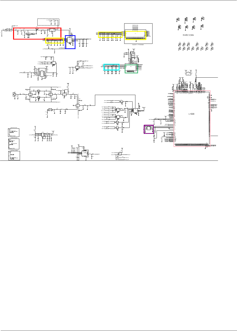
Level 3Repair
Distribution, transmission, or infringement of any content or data from this document without Samsung’s written authorization is strictly prohibited.
Confidential and proprietary-the contents in this service guide subject to change without prior notice.
8-107

Level 3Repair
Distribution, transmission, or infringement of any content or data from this document without Samsung’s written authorization is strictly prohibited.
Confidential and proprietary-the contents in this service guide subject to change without prior notice.
8-108

Level 3Repair
Distribution, transmission, or infringement of any content or data from this document without Samsung’s written authorization is strictly prohibited.
Confidential and proprietary-the contents in this service guide subject to change without prior notice.
8-109
U9106 PIN1 :About
20dBm ?
8-3-36. LTE BAND8 TX
Check the voltage at
{L1036= VBATT?}
&{
C1074 =1.2V?}
&{
C1075 =2.5V?}
Check the Voltage at
C1010 =VBATT? ?
Check the Voltage at
c1032 =VBATT? ?
CHECK soldered
C1000,L1001,L1020 RFS1000
Resolder or change
U1001, C1010
Resolder or change
c1032, PAM1000
Resolder or change
U5000
Check the freq. at
OSC1000 PIN4 :26
MHz ?Change or resolder
OSC1000
Check C1030
about 20dBm ?
Resolder or change
C1030 C1009 U1008
LTE BAND8
Transmitter is O.K?
END
YES
NO
NO
YES
NO
YES
NO
YES
NO
NO
YES
NO
YES
LTE BAND8
Transmitter is O.K?
NO
YES
YES
Resolder or change
UCP3000
NO
Resolder or change
U1008
CONTINOUS TX ON CONDITION
TX POWER DAC:14500 CODE
APPLIED
LTE Band8 CH : 21625
RBW : 100KHz
VBW : 100KHz
SPAN :10
MHz
REF LEV. :10
dBm
ATT. :20
dB
Check L1028
about 0dBm ?Resolder or change
L1028
NO
YES

Level 3Repair
Distribution, transmission, or infringement of any content or data from this document without Samsung’s written authorization is strictly prohibited.
Confidential and proprietary-the contents in this service guide subject to change without prior notice.
8-110

Level 3Repair
Distribution, transmission, or infringement of any content or data from this document without Samsung’s written authorization is strictly prohibited.
Confidential and proprietary-the contents in this service guide subject to change without prior notice.
8-111
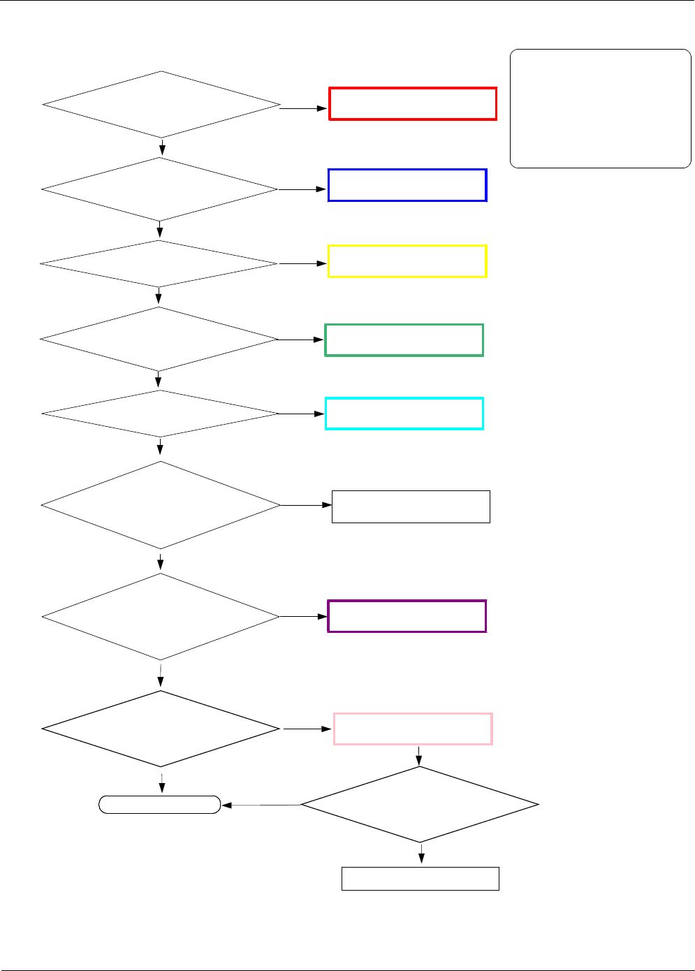
Level 3Repair
Distribution, transmission, or infringement of any content or data from this document without Samsung’s written authorization is strictly prohibited.
Confidential and proprietary-the contents in this service guide subject to change without prior notice.
8-112
U9106 PIN1 :About
20dBm ?
8-3-37. LTE BAND7
Check the voltage at
{L1036= VBATT?}
&{
C1074 =1.2V?}
&{
C1075 =2.5V?}
Check the Voltage at
C1010 =VBATT? ?
Check the Voltage at
C1053 =VBATT? ?
CHECK soldered
C1000,L1001,L1020 RFS1000
Resolder or change
U1001, C1010
Resolder or change
C1053 PAM1001
Resolder or change
U5000
Check the freq. at
OSC1000 PIN4 :26
MHz ?Change or resolder
OSC1000
Check L1020
about 20dBm ?
Resolder or change
L1020 L1034 F1001
LTE BAND7
Transmitter is O.K?
END
YES
NO
NO
YES
NO
YES
NO
YES
NO
NO
YES
NO
YES
LTE BAND7
Transmitter is O.K?
NO
YES
YES
Resolder or change
UCP3000
NO
Resolder or change
U1008
CONTINOUS TX ON CONDITION
TX POWER DAC:14500 CODE
APPLIED
LTE Band7 CH : 21100
RBW : 100KHz
VBW : 100KHz
SPAN :10
MHz
REF LEV. :10
dBm
ATT. :20
dB
Check C1146 L1033
about 0dBm ?Resolder or change
C1146 L1033
NO
YES
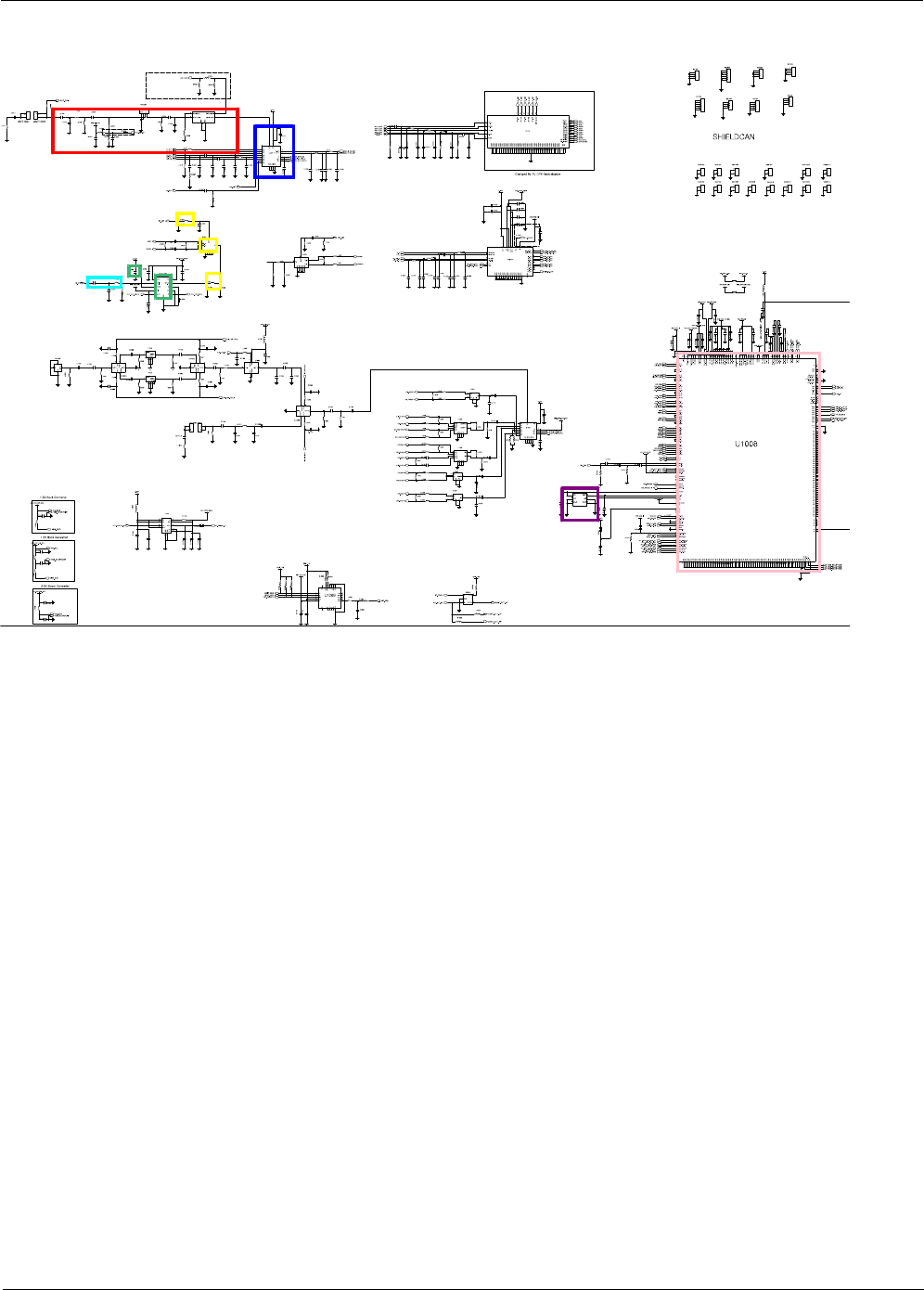
Level 3Repair
Distribution, transmission, or infringement of any content or data from this document without Samsung’s written authorization is strictly prohibited.
Confidential and proprietary-the contents in this service guide subject to change without prior notice.
8-113
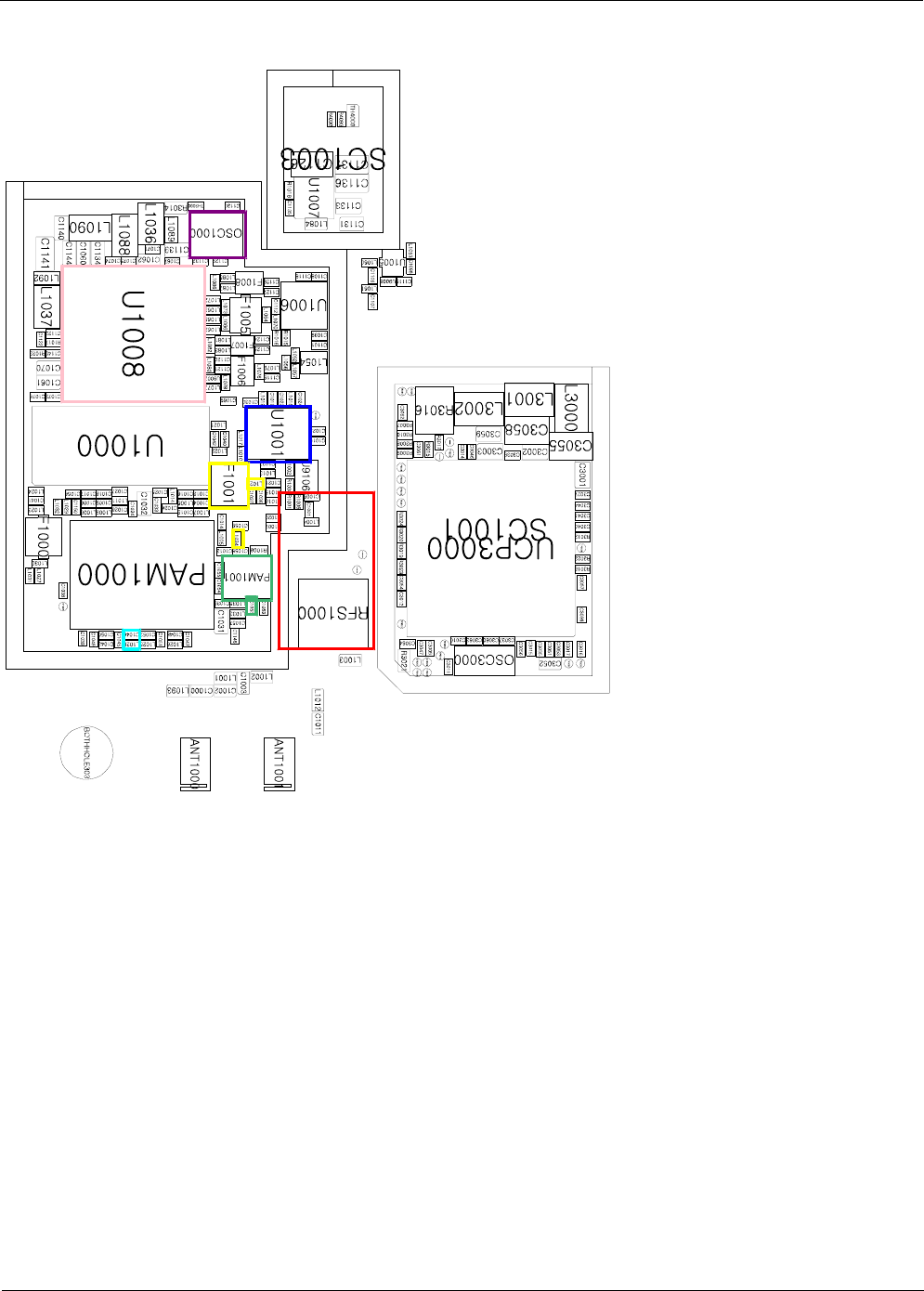
Level 3Repair
Distribution, transmission, or infringement of any content or data from this document without Samsung’s written authorization is strictly prohibited.
Confidential and proprietary-the contents in this service guide subject to change without prior notice.
8-114

Level 3Repair
Distribution, transmission, or infringement of any content or data from this document without Samsung’s written authorization is strictly prohibited.
Confidential and proprietary-the contents in this service guide subject to change without prior notice.
8-115
U9106 PIN1 :About
20dBm ?
8-3-38. LTE BAND20
Check the voltage at
{L1036= VBATT?}
&{
C1074 =1.2V?}
&{
C1075 =2.5V?}
Check the Voltage at
C1010 =VBATT? ?
Check the Voltage at
c1032 =VBATT?
CHECK soldered
C1000,L1001,L1020 RFS1000
Resolder or change
U1001, C1010
Resolder or change
c1032 PAM1000
Resolder or change
U5000
Check the freq. at
OSC1000 PIN4 :26
MHz ?Change or resolder
OSC1000
Check C1041
about 20dBm ?
Resolder or change
C1041 C1150 L1029 F1000
LTE BAND20
Transmitter is O.K?
END
YES
NO
NO
YES
NO
YES
NO
YES
NO
NO
YES
NO
YES
LTE BAND20
Transmitter is O.K?
NO
YES
YES
Resolder or change
UCP3000
NO
Resolder or change
U1008
CONTINOUS TX ON CONDITION
TX POWER DAC:14500 CODE
APPLIED
LTE Band20 CH : 24300
RBW : 100KHz
VBW : 100KHz
SPAN :10
MHz
REF LEV. :10
dBm
ATT. :20
dB
Check L1028
about 0dBm ?Resolder or change
L1028
NO
YES
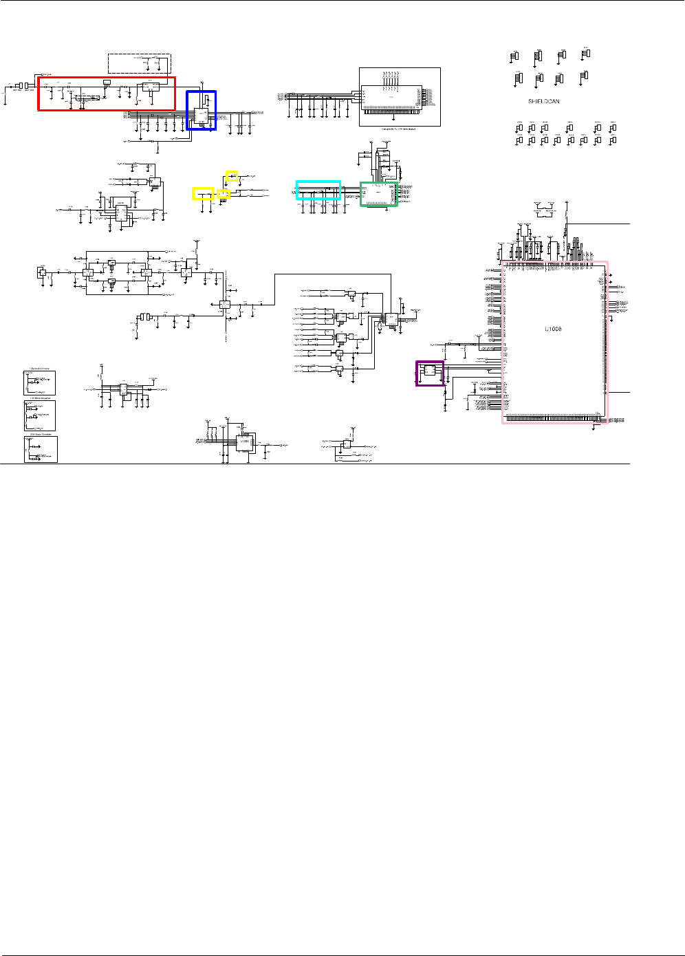
Level 3Repair
Distribution, transmission, or infringement of any content or data from this document without Samsung’s written authorization is strictly prohibited.
Confidential and proprietary-the contents in this service guide subject to change without prior notice.
8-116

Level 3Repair
Distribution, transmission, or infringement of any content or data from this document without Samsung’s written authorization is strictly prohibited.
Confidential and proprietary-the contents in this service guide subject to change without prior notice.
8-117