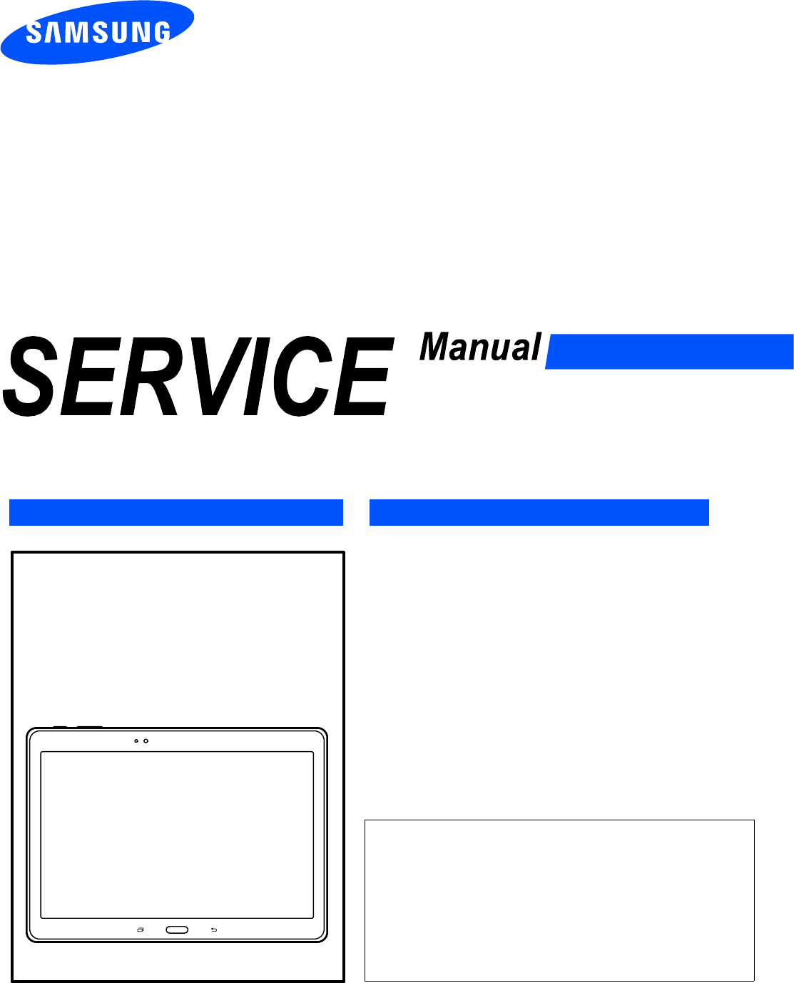
Samsung Galaxy Tab S 10.5 SM T805 Service Manual. Www.s Manuals.com. Manual
User Manual: Tablet Samsung SM-T805 Galaxy Tab S 10.5 - Service manuals and Schematics, Disassembly / Assembly. Free.
Open the PDF directly: View PDF ![]() .
.
Page Count: 184 [warning: Documents this large are best viewed by clicking the View PDF Link!]
N
GSM TELEPHONE
SM-T805
1. Safety Precautions
2. Specification
3. Product Function
4. Exploded View and Parts list
5. MAIN Electrical Parts List
6. Level 1Repair
7. Level 2Repair
8. Level 3Repair
9. Reference data
Notice: All functionality, features, specifications, and
other product information provided in this document,
including but not limited to, benefits, design, pricing,
components, performance, availability, and capabiliti
-es of the product are subject to change without
notice. Samsung reserves the right to alter this doc
-ument or the product described herein at anytime,
without obligation to provide notification of such
changes.
GSM TELEPHONE CONTENTS

1. Safety Precautions
1-1
Confidential and proprietary-the contents in this service guide subject to change without prior notice.
Distribution, transmission, or infringement of any content or data from this document without Samsung’s written authorization is strictly prohibited.
1-1. Repair Precaution
Before attempting any repair or detailed tuning, shield the device from RF noise or static
electricity discharges.
Use only demagnetized tools that are specifically designed for small electronic repairs,
as most electronic parts are sensitive to electromagnetic forces.
Use only high quality screwdrivers when servicing products. Low quality screwdrivers can
easily damage the heads of screws.
Use only conductor wire of the properly gauge and insulation for low resistance, because of
the low margin of error of most testing equipment.
We recommend 22-gauge twisted copper wire.
Hand-soldering is not recommended, because printed circuit boards (PCBs) can be easily
damaged, even with relatively low heat. Never use asoldering iron with apower rating of
more than 100 watts and use only lead-free solder with a melting point below 250°C (482°F).
Prior to disassembling the battery charger for repair, ensure that the AC power is disconnected.
Always use the replacement parts that are registered in the SEC system. Third-party replac
ement parts may not function properly.

Safety Precautions
Distribution, transmission, or infringement of any content or data from this document without Samsung’s written authorization is strictly prohibited.
Confidential and proprietary-the contents in this service guide subject to change without prior notice.
1-2
1-2. ESD(Electrostatically Sensitive Devices) Precaution
Many semiconductors and ESDs in electronic devices are particularly sensitive to static discha
rge and can be easily damaged by it. We recommend protecting these components with cond
uctive anti-static bags when you store or transport them.
Always use an anti-static strap or wristband and remove electrostatic buildup or dissipate
static electricity from your body before repairing ESDs.
Ensure that soldering irons have AC adapter with ground wires and that the ground wires are
properly connected.
Use only desoldering tools with plastic tips to prevent static discharge.
Properly shield the work environment from accidental electrostatic discharge before opening
packages containing ESDs.
The potential for static electricity discharge may be increased in low humidity environments,
such as air-conditioned rooms. Increase the airflow to the working area to decrease the
chance of accidental static electricity discharges.

2. Specification
2-1
Confidential and proprietary-the contents in this service guide subject to change without prior notice.
Distribution, transmission, or infringement of any content or data from this document without Samsung’s written authorization is strictly prohibited.
2-1. GSM General Specification
GSM850 EGSM 900 DCS1800 PCS1900 WCDMA
2100
WCDMA
900
WCMDA
850
WCDMA
1900
Freq.
Band[MHz]
Uplink/
Downlink
824~849
869~894
880~915
925~960
1710~1785
1805~1880
1850~1910
1930~1990
1922~1977
2112~2167
880~915
925~960
824~849
869~894
1852~1907
1932~1987
ARFCN
range 128~251 0~124 &
975~1023 512~885 512~810
UL:
9612~9888
DL:
10562~10838
UL:
2712~2863
DL:
2937~3088
UL:
4132~4233
DL:
4357~4458
UL:
9612~9888
DL:
10562~10838
Tx/Rx
spacing 45MHz 45MHz 95MHz 80MHz 190MHz 45MHz 45MHz 80MHz
Mod. Bit
rate/
Bit Period
270.833kbps
3.692us
270.833kbps
3.692us
270.833kbps
3.692us
270.833kbps
3.692us 3.84Mcps 3.84Mcps 3.84Mcps 3.84Mcps
Time Slot
Period/
Frame
Period
576.9us
4.615ms
576.9us
4.615ms
576.9us
4.615ms
576.9us
4.615ms
FrameLength:
10ms
Slotlength:
0.667ms
FrameLength:
10ms
Slotlength:
0.667ms
FrameLength:
10ms
Slotlength:
0.667ms
FrameLength:
10ms
Slotlength:
0.667ms
Modulation 0.3GMSK 0.3GMSK 0.3GMSK 0.3GMSK QPSKHQPSK QPSKHQPSK QPSKHQPSK QPSKHQPSK
MS Power 33dBm~5dBm 33dBm~5dBm 30dBm~0dBm 30dBm~0dBm 24dBm~
-50dBm 24dBm~
-50dBm 24dBm~
-50dBm 24dBm~
-50dBm
Power Class 5pcl ~ 19pcl 5pcl ~19
pcl 0pcl ~15
pcl 0pcl ~15
pcl 3(max+24dBm) 3(max+24dBm) 3(max+24dBm) 3(max+24dBm)
Sensitivity -102dBm -102dBm -100dBm -100dBm -106.7dBm -103.7dBm -104.7dBm -104.7dBm
TDMAMux8888----
Cell Radius 35Km 35Km 2Km 2Km 2Km 2Km 2Km 2Km
Specification
Distribution, transmission, or infringement of any content or data from this document without Samsung’s written authorization is strictly prohibited.
Confidential and proprietary-the contents in this service guide subject to change without prior notice.
2-2
2-2. GSM Tx Power Class
TX Power
control
level
GSM850
533±2
dBm
631±2
dBm
729±2
dBm
827±2
dBm
925±2
dBm
10 23±2 dBm
11 21±2 dBm
12 19±2 dBm
13 17±2 dBm
14 15±2 dBm
15 13±2 dBm
16 11±3 dBm
17 9±3dBm
18 7±3 dBm
19 5±3 dBm
TX Power
control
level
EGSM900
533±2
dBm
631±2
dBm
729±2
dBm
827±2
dBm
925±2
dBm
10 23±2 dBm
11 21±2 dBm
12 19±2 dBm
13 17±2 dBm
14 15±2 dBm
15 13±2 dBm
16 11±3 dBm
17 9±3dBm
18 7±3 dBm
19 5±3 dBm
TX Power
control
level
DCS1800
030±3
dBm
128±3
dBm
226±3
dBm
324±3
dBm
422±3
dBm
520±3
dBm
618±3
dBm
716±3
dBm
814±3
dBm
912±4
dBm
10 10±4 dBm
11 8±4 dBm
12 6±4 dBm
13 4±4 dBm
14 2±5 dBm
15 0±5 dBm
TX Power
control
level
PCS1900
030±3
dBm
128±3
dBm
226±3
dBm
324±3
dBm
422±3
dBm
520±3
dBm
618±3
dBm
716±3
dBm
814±3
dBm
912±4
dBm
10 10±4 dBm
11 8±4 dBm
12 6±4 dBm
13 4±4 dBm
14 2±5 dBm
15 0±5 dBm

Specification
Distribution, transmission, or infringement of any content or data from this document without Samsung’s written authorization is strictly prohibited.
Confidential and proprietary-the contents in this service guide subject to change without prior notice.
2-3
2-3. LTE General Specification
LTE Band1 LTE Band3 LTE Band5 LTE Band7 LTE Band8 LTE Band20
Freq.
Band[MHz]
Uplink/
Downlink
1920~1980
2110~2170
1710~1785
1805~1880
824~849
869~894
2500~2570
1805~1880
880~914.9
925~959.9
832~862
791~821
ARFCN
range
UL:
18000~18599
DL:
0~599
UL:
19200~19950
DL:
1805~1880
UL:
20400~20649
DL:
2400~2649
UL:
2500~2570
DL:
2620~2690
UL:
21450-21799
DL:
3450-3799
UL:
24150~24450
DL:
6150~6450
Tx/Rx
spacing 190MHz 95MHz 45MHz 120MHz 45MHZ 41MHz
Channel
Bandwidth 5/10/15/20 MHz 1.4/3/5/10/15/20
MHz 1.4/3/5/10 MHz 5/10/15/20 MHz 1.4/3/5/10MHz 5/10/15/20 MHz
Modulation QPSK,16/64QAM QPSK,16/64QAM QPSK,16/64QAM QPSK,16/64QAM QPSK,16/64QAM QPSK,16/64QAM
MS Power
(MPR) -35~25.7 dBm -35~25.7 dBm -35~25.7 dBm -35~25.7 dBm -35~25.7 dBm -35~25.7 dBm
Sensitivit
(QPSK)
(BW 10MHz) -94 dBm -92 dBm -92 dBm -95dBm -95dBm -94dBm
Cell Radius >5Km >5Km >5Km >5Km >5Km >5Km

3. Operation Instruction and Installation
3-1
Confidential and proprietary-the contents in this service guide subject to change without prior notice.
Distribution, transmission, or infringement of any content or data from this document without Samsung’s written authorization is strictly prohibited.
Main Function
•Android OS: KitKat (4.4)
• 10.5" WQXGA On-Cell Touch AMOLED (OCTA)
•A-GPS /GLONASS /BT v4.0 +EDR with LE /USB v2.0 /Wi-Fi (802.11 a/b/g/n/ac VHT80) /MHL 2.1 / OTG
•Main 8.0 MP, Sub 2.0 MP
•Recording definition: 1080p
•Sensors: Accelerometer, Gyro, Geomagnetic, Light Sensor, Fingerprint
•Additional :
-Octa core AP (1.9 GHz Quad Core /1.3
GHz Quad Core)
-CP (LTE baseband controller)
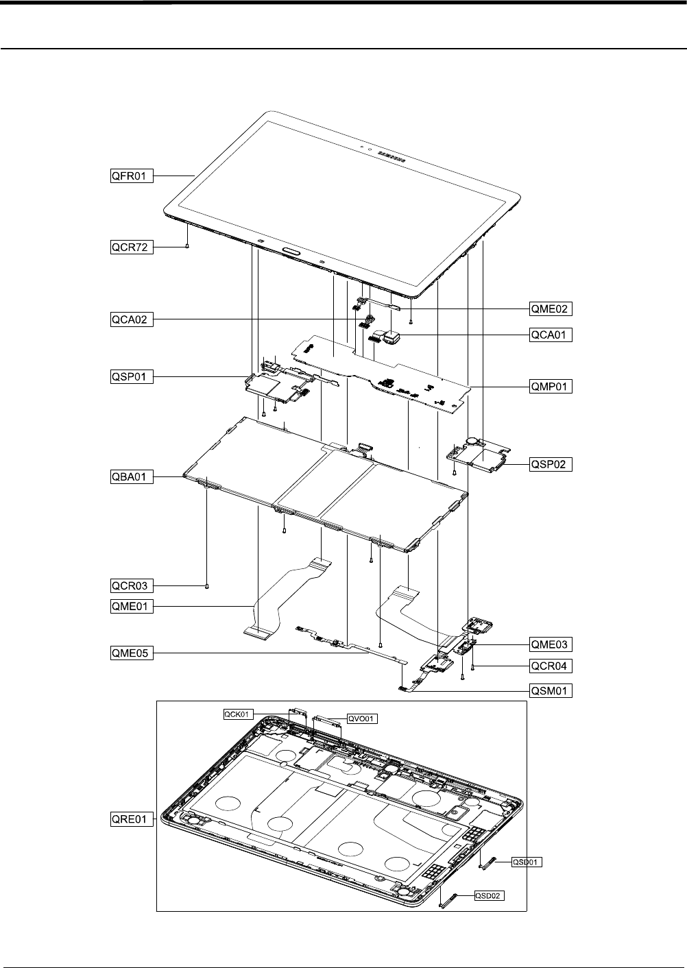
4. Exploded View and Parts List
4-1
Confidential and proprietary-the contents in this service guide subject to change without prior notice.
Distribution, transmission, or infringement of any content or data from this document without Samsung’s written authorization is strictly prohibited.
4-1. Cellular phone Exploded View

5. MAIN Electrical Parts List
5-1
Confidential and proprietary-the contents in this service guide subject to change without prior notice.
Distribution, transmission, or infringement of any content or data from this document without Samsung’s written authorization is strictly prohibited.
SEC CODE Design Location Description
0403-001688 ZD500 DIODE-ZENER
0403-001688 ZD700 DIODE-ZENER
0404-001250 D501 DIODE-SCHOTTKY
0404-001782 D500 DIODE-SCHOTTKY
0404-001782 D502 DIODE-SCHOTTKY
0406-001223 ZD711 DIODE-TVS
0406-001223 ZD712 DIODE-TVS
0406-001375 ZD501 DIODE-TVS
0406-001375 ZD502 DIODE-TVS
0406-001413 ZD702 DIODE-TVS
0406-001413 ZD703 DIODE-TVS
0406-001413 ZD709 DIODE-TVS
0406-001413 ZD710 DIODE-TVS
0406-001413 ZD716 DIODE-TVS
0406-001413 ZD717 DIODE-TVS
0406-001413 ZD718 DIODE-TVS
0406-001459 ZD701 DIODE-TVS
0406-001494 ZD606 DIODE-TVS
0406-001494 ZD607 DIODE-TVS
0406-001494 ZD608 DIODE-TVS
0406-001494 ZD611 DIODE-TVS
0406-001494 ZD613 DIODE-TVS
0406-001494 ZD614 DIODE-TVS
0406-001494 ZD615 DIODE-TVS
0406-001494 ZD616 DIODE-TVS
0406-001494 ZD707 DIODE-TVS
0406-001494 ZD800 DIODE-TVS
0406-001494 ZD801 DIODE-TVS
0406-001494 ZD802 DIODE-TVS
0406-001494 ZD803 DIODE-TVS
0406-001494 ZD804 DIODE-TVS
0406-001494 ZD807 DIODE-TVS
0406-001505 ZD600 DIODE-TVS
0406-001505 ZD601 DIODE-TVS
0406-001505 ZD602 DIODE-TVS
0406-001505 ZD603 DIODE-TVS
0406-001505 ZD604 DIODE-TVS
0406-001505 ZD605 DIODE-TVS
0406-001505 ZD708 DIODE-TVS
0406-001505 ZD713 DIODE-TVS
0406-001505 ZD714 DIODE-TVS
0406-001505 ZD715 DIODE-TVS

Main Electrical Parts List
Distribution, transmission, or infringement of any content or data from this document without Samsung’s written authorization is strictly prohibited.
Confidential and proprietary-the contents in this service guide subject to change without prior notice.
5-2
0406-001506 ZD720 DIODE-TVS
0406-001506 ZD721 DIODE-TVS
0406-001549 ZD704 DIODE-TVS
0406-001549 ZD705 DIODE-TVS
0505-002088 TR500 FET-SILICON
0505-002088 TR501 FET-SILICON
0505-002341 TR503 FET-SILICON
0505-002341 TR701 FET-SILICON
0505-002384 TR900 FET-SILICON
0505-002720 U700 FET-SILICON
0505-003070 TR700 FET-SILICON
0505-003234 TR600 FET-SILICON
0505-003234 TR601 FET-SILICON
0601-003398 LED500 LED
0801-003228 U508 IC-CMOS LOGIC
0801-003228 U509 IC-CMOS LOGIC
0801-003228 U510 IC-CMOS LOGIC
0801-003437 U1010 IC-CMOS LOGIC
0902-003074 UCP4001 IC-MICROPROCESSOR
1001-001394 U506 IC-ANALOG SWITCH
1107-002297 UME4000 IC-EMMC
1201-003642 PAM1002 IC-POWER AMP
1201-003645 PAM1001 IC-POWER AMP
1201-003729 U201 IC-GPS AMP
1202-001120 U600 IC-VOLTAGE COMP.
1203-002250 U504 IC-VOL. DETECTOR
1203-004776 U505 IC-POSI.FIXED REG.
1203-006182 U702 IC-VOL. DETECTOR
1203-006766 U203 IC-VOL. DETECTOR
1203-006766 U302 IC-VOL. DETECTOR
1203-006767 U903 IC-MULTI REG.
1203-007766 U1003 IC-DC/DC CONVERTER
1203-007791 U800 IC-POSI.FIXED REG.
1203-007791 U801 IC-POSI.FIXED REG.
1203-007823 U802 IC-DC/DC CONVERTER
1203-008004 U701 IC-VOL. DETECTOR
1203-008158 U502 IC-POWER SUPERVISOR
1203-008172 U500 IC-SWITCH REG.
1203-008193 U512 IC-POWER SUPERVISOR
1203-008217 U805 IC-DC/DC CONVERTER
1205-004753 U804 IC-TRANSMITTER
1205-004772 U602 IC-CODEC
1205-004863 UCP301 IC-MODEM

Main Electrical Parts List
Distribution, transmission, or infringement of any content or data from this document without Samsung’s written authorization is strictly prohibited.
Confidential and proprietary-the contents in this service guide subject to change without prior notice.
5-3
1205-004884 U1007 IC-TRANSMITTER
1205-004916 U904 IC-SWITCH
1205-005012 U206 IC-WIFI
1205-005016 U202 IC-GPS RECEIVER
1209-002245 U902 IC-SENSOR
1209-002246 U901 IC-SENSOR
1209-002252 U1009 IC-SENSOR
1301-002167 U900 IC-FPGA
1404-001694 TH4000 THERMISTOR-NTC
1404-001694 TH4001 THERMISTOR-NTC
1404-001694 TH4002 THERMISTOR-NTC
1404-001728 TH301 THERMISTOR-NTC
1405-001375 V1001 VARISTOR
2007-000148 R617 R-CHIP
2007-000148 R618 R-CHIP
2007-000148 R619 R-CHIP
2007-000169 R1005 R-CHIP
2007-000174 R904 R-CHIP
2007-000174 R905 R-CHIP
2007-000174 R906 R-CHIP
2007-000174 R907 R-CHIP
2007-000174 R908 R-CHIP
2007-000174 R909 R-CHIP
2007-000174 R910 R-CHIP
2007-000174 R911 R-CHIP
2007-000174 R912 R-CHIP
2007-000174 R913 R-CHIP
2007-001308 R4082 R-CHIP
2007-001308 R4109 R-CHIP
2007-001325 R613 R-CHIP
2007-001325 R614 R-CHIP
2007-003015 R502 R-CHIP
2007-007107 R314 R-CHIP
2007-007136 R4087 R-CHIP
2007-007136 R4088 R-CHIP
2007-007139 R807 R-CHIP
2007-007142 R514 R-CHIP
2007-007312 R4051 R-CHIP
2007-007312 R4054 R-CHIP
2007-007312 R4067 R-CHIP
2007-007312 R4071 R-CHIP
2007-007312 R4098 R-CHIP
2007-007312 R4099 R-CHIP

Main Electrical Parts List
Distribution, transmission, or infringement of any content or data from this document without Samsung’s written authorization is strictly prohibited.
Confidential and proprietary-the contents in this service guide subject to change without prior notice.
5-4
2007-007312 R4100 R-CHIP
2007-007312 R4102 R-CHIP
2007-007318 R1025 R-CHIP
2007-007517 R4072 R-CHIP
2007-007517 R4073 R-CHIP
2007-007517 R4080 R-CHIP
2007-007517 R4081 R-CHIP
2007-007517 R4096 R-CHIP
2007-007517 R4097 R-CHIP
2007-007585 R202 R-CHIP
2007-007627 R919 R-CHIP
2007-007741 R4085 R-CHIP
2007-007741 R805 R-CHIP
2007-007942 R4008 R-CHIP
2007-007942 R4200 R-CHIP
2007-007946 R4201 R-CHIP
2007-008045 R511 R-CHIP
2007-008045 R525 R-CHIP
2007-008045 R707 R-CHIP
2007-008049 R710 R-CHIP
2007-008049 R719 R-CHIP
2007-008051 R705 R-CHIP
2007-008052 R4049 R-CHIP
2007-008052 R4050 R-CHIP
2007-008052 R4068 R-CHIP
2007-008052 R515 R-CHIP
2007-008052 R523 R-CHIP
2007-008052 R803 R-CHIP
2007-008052 R804 R-CHIP
2007-008052 R806 R-CHIP
2007-008052 R902 R-CHIP
2007-008052 R903 R-CHIP
2007-008055 R315 R-CHIP
2007-008055 R4031 R-CHIP
2007-008055 R4032 R-CHIP
2007-008055 R4034 R-CHIP
2007-008055 R4035 R-CHIP
2007-008055 R4036 R-CHIP
2007-008055 R4038 R-CHIP
2007-008055 R4084 R-CHIP
2007-008055 R700 R-CHIP
2007-008055 R711 R-CHIP
2007-008055 R724 R-CHIP

Main Electrical Parts List
Distribution, transmission, or infringement of any content or data from this document without Samsung’s written authorization is strictly prohibited.
Confidential and proprietary-the contents in this service guide subject to change without prior notice.
5-5
2007-008057 R1002 R-CHIP
2007-008057 R1003 R-CHIP
2007-008403 R521 R-CHIP
2007-008419 R319 R-CHIP
2007-008419 R321 R-CHIP
2007-008419 R500 R-CHIP
2007-008419 R501 R-CHIP
2007-008420 R510 R-CHIP
2007-008420 R516 R-CHIP
2007-008420 R517 R-CHIP
2007-008420 R518 R-CHIP
2007-008420 R601 R-CHIP
2007-008420 R723 R-CHIP
2007-008478 R4015 R-CHIP
2007-008478 R4016 R-CHIP
2007-008483 R209 R-CHIP
2007-008483 R210 R-CHIP
2007-008483 R211 R-CHIP
2007-008483 R212 R-CHIP
2007-008483 R213 R-CHIP
2007-008483 R716 R-CHIP
2007-008483 R717 R-CHIP
2007-008483 R721 R-CHIP
2007-008483 R722 R-CHIP
2007-008486 R503 R-CHIP
2007-008486 R512 R-CHIP
2007-008486 R520 R-CHIP
2007-008516 R4001 R-CHIP
2007-008516 R4002 R-CHIP
2007-008516 R4003 R-CHIP
2007-008516 R4004 R-CHIP
2007-008516 R4022 R-CHIP
2007-008516 R4026 R-CHIP
2007-008516 R4027 R-CHIP
2007-008516 R4063 R-CHIP
2007-008516 R4086 R-CHIP
2007-008516 R4103 R-CHIP
2007-008516 R4104 R-CHIP
2007-008516 R4105 R-CHIP
2007-008516 R4106 R-CHIP
2007-008516 R4107 R-CHIP
2007-008516 R4108 R-CHIP
2007-008516 R4115 R-CHIP

Main Electrical Parts List
Distribution, transmission, or infringement of any content or data from this document without Samsung’s written authorization is strictly prohibited.
Confidential and proprietary-the contents in this service guide subject to change without prior notice.
5-6
2007-008516 R513 R-CHIP
2007-008516 R701 R-CHIP
2007-008516 R704 R-CHIP
2007-008516 R706 R-CHIP
2007-008516 R720 R-CHIP
2007-008516 R900 R-CHIP
2007-008516 R901 R-CHIP
2007-008516 R915 R-CHIP
2007-008516 R916 R-CHIP
2007-008531 R4064 R-CHIP
2007-008531 R4079 R-CHIP
2007-008579 R205 R-CHIP
2007-008588 R1019 R-CHIP
2007-008588 R1020 R-CHIP
2007-008588 R1021 R-CHIP
2007-008588 R1022 R-CHIP
2007-008588 R1023 R-CHIP
2007-008588 R307 R-CHIP
2007-008588 R308 R-CHIP
2007-008588 R309 R-CHIP
2007-008774 R702 R-CHIP
2007-008774 R708 R-CHIP
2007-008774 R709 R-CHIP
2007-008798 R508 R-CHIP
2007-008806 R1006 R-CHIP
2007-008806 R1024 R-CHIP
2007-008808 R201 R-CHIP
2007-009084 R504 R-CHIP
2007-009084 R522 R-CHIP
2007-009084 R603 R-CHIP
2007-009084 R616 R-CHIP
2007-009084 R703 R-CHIP
2007-009084 R715 R-CHIP
2007-009111 R4069 R-CHIP
2007-009155 R316 R-CHIP
2007-009155 R726 R-CHIP
2007-009157 R4074 R-CHIP
2007-009157 R4075 R-CHIP
2007-009157 R4076 R-CHIP
2007-009157 R4077 R-CHIP
2007-009157 R4078 R-CHIP
2007-009157 R4089 R-CHIP
2007-009157 R4090 R-CHIP

Main Electrical Parts List
Distribution, transmission, or infringement of any content or data from this document without Samsung’s written authorization is strictly prohibited.
Confidential and proprietary-the contents in this service guide subject to change without prior notice.
5-7
2007-009157 R4091 R-CHIP
2007-009157 R4092 R-CHIP
2007-009157 R4093 R-CHIP
2007-009157 R4094 R-CHIP
2007-009157 R4095 R-CHIP
2007-009157 R918 R-CHIP
2007-009171 R4053 R-CHIP
2007-009171 R4055 R-CHIP
2007-009171 R4056 R-CHIP
2007-009171 R4057 R-CHIP
2007-009171 R4058 R-CHIP
2007-009171 R4059 R-CHIP
2007-009171 R4060 R-CHIP
2007-009171 R4061 R-CHIP
2007-009171 R4062 R-CHIP
2007-009171 R4112 R-CHIP
2007-009171 R4113 R-CHIP
2007-009199 R1001 R-CHIP
2007-009199 R313 R-CHIP
2007-009212 R604 R-CHIP
2007-009223 R602 R-CHIP
2007-009233 R324 R-CHIP
2007-009361 R1004 R-CHIP
2007-009408 R4009 R-CHIP
2007-009408 R4010 R-CHIP
2007-009408 R4011 R-CHIP
2007-009408 R4012 R-CHIP
2007-009408 R4013 R-CHIP
2007-009408 R4014 R-CHIP
2007-009408 R4019 R-CHIP
2007-009408 R4020 R-CHIP
2007-009408 R4039 R-CHIP
2007-009408 R4040 R-CHIP
2007-009408 R4041 R-CHIP
2007-009408 R4042 R-CHIP
2007-009408 R4043 R-CHIP
2007-009408 R4044 R-CHIP
2007-009408 R4118 R-CHIP
2007-009408 R4119 R-CHIP
2007-009801 R1017 R-CHIP
2007-009801 R1018 R-CHIP
2007-009805 R1013 R-CHIP
2007-009920 R312 R-CHIP

Main Electrical Parts List
Distribution, transmission, or infringement of any content or data from this document without Samsung’s written authorization is strictly prohibited.
Confidential and proprietary-the contents in this service guide subject to change without prior notice.
5-8
2007-009969 R605 R-CHIP
2007-010233 R320 R-CHIP
2007-011511 R524 R-CHIP
2203-000233 C1014 C-CER,CHIP
2203-000233 C1015 C-CER,CHIP
2203-000233 C1119 C-CER,CHIP
2203-000233 C1123 C-CER,CHIP
2203-000386 C710 C-CER,CHIP
2203-000425 C1122 C-CER,CHIP
2203-000425 C633 C-CER,CHIP
2203-000438 C214 C-CER,CHIP
2203-000438 C707 C-CER,CHIP
2203-000489 C4099 C-CER,CHIP
2203-000489 C4100 C-CER,CHIP
2203-000725 C248 C-CER,CHIP
2203-000725 C597 C-CER,CHIP
2203-000812 C653 C-CER,CHIP
2203-000812 C654 C-CER,CHIP
2203-000812 C656 C-CER,CHIP
2203-000812 C813 C-CER,CHIP
2203-000995 C577 C-CER,CHIP
2203-000995 C580 C-CER,CHIP
2203-000995 C581 C-CER,CHIP
2203-001072 C711 C-CER,CHIP
2203-001101 C708 C-CER,CHIP
2203-001239 C632 C-CER,CHIP
2203-001383 C1016 C-CER,CHIP
2203-002677 C1093 C-CER,CHIP
2203-002687 C576 C-CER,CHIP
2203-002687 C578 C-CER,CHIP
2203-002687 C579 C-CER,CHIP
2203-005056 C1013 C-CER,CHIP
2203-005482 C563 C-CER,CHIP
2203-005682 C1003 C-CER,CHIP
2203-005682 C1092 C-CER,CHIP
2203-005682 C1107 C-CER,CHIP
2203-005682 C1108 C-CER,CHIP
2203-005682 C212 C-CER,CHIP
2203-005682 C712 C-CER,CHIP
2203-005682 C713 C-CER,CHIP
2203-005717 C1037 C-CER,CHIP
2203-005719 C1004 C-CER,CHIP
2203-005725 C201 C-CER,CHIP

Main Electrical Parts List
Distribution, transmission, or infringement of any content or data from this document without Samsung’s written authorization is strictly prohibited.
Confidential and proprietary-the contents in this service guide subject to change without prior notice.
5-9
2203-005725 C4102 C-CER,CHIP
2203-005725 C528 C-CER,CHIP
2203-005725 C551 C-CER,CHIP
2203-005725 C715 C-CER,CHIP
2203-005725 C716 C-CER,CHIP
2203-005725 C717 C-CER,CHIP
2203-005725 C839 C-CER,CHIP
2203-005726 C275 C-CER,CHIP
2203-005727 C272 C-CER,CHIP
2203-005727 C596 C-CER,CHIP
2203-005731 C4000 C-CER,CHIP
2203-005731 C4001 C-CER,CHIP
2203-005731 C649 C-CER,CHIP
2203-005731 C651 C-CER,CHIP
2203-005734 C648 C-CER,CHIP
2203-005734 C650 C-CER,CHIP
2203-005734 C702 C-CER,CHIP
2203-005736 C1002 C-CER,CHIP
2203-005736 C1020 C-CER,CHIP
2203-005736 C1025 C-CER,CHIP
2203-005736 C1035 C-CER,CHIP
2203-005736 C1038 C-CER,CHIP
2203-005736 C1056 C-CER,CHIP
2203-005736 C1077 C-CER,CHIP
2203-005736 C1104 C-CER,CHIP
2203-005736 C1106 C-CER,CHIP
2203-005736 C1110 C-CER,CHIP
2203-005736 C1112 C-CER,CHIP
2203-005736 C211 C-CER,CHIP
2203-005736 C213 C-CER,CHIP
2203-005736 C223 C-CER,CHIP
2203-005777 C1009 C-CER,CHIP
2203-005777 C1031 C-CER,CHIP
2203-005777 C221 C-CER,CHIP
2203-005777 C228 C-CER,CHIP
2203-005777 C276 C-CER,CHIP
2203-005777 C292 C-CER,CHIP
2203-005789 C1006 C-CER,CHIP
2203-005789 C1039 C-CER,CHIP
2203-005789 C258 C-CER,CHIP
2203-005792 C1008 C-CER,CHIP
2203-005792 C1010 C-CER,CHIP
2203-005792 C1034 C-CER,CHIP

Main Electrical Parts List
Distribution, transmission, or infringement of any content or data from this document without Samsung’s written authorization is strictly prohibited.
Confidential and proprietary-the contents in this service guide subject to change without prior notice.
5-10
2203-005792 C1109 C-CER,CHIP
2203-005792 C218 C-CER,CHIP
2203-006048 C4094 C-CER,CHIP
2203-006048 C4098 C-CER,CHIP
2203-006048 C833 C-CER,CHIP
2203-006194 C1096 C-CER,CHIP
2203-006194 C227 C-CER,CHIP
2203-006194 C291 C-CER,CHIP
2203-006194 C574 C-CER,CHIP
2203-006305 C208 C-CER,CHIP
2203-006305 C216 C-CER,CHIP
2203-006305 C225 C-CER,CHIP
2203-006305 C254 C-CER,CHIP
2203-006305 C271 C-CER,CHIP
2203-006305 C273 C-CER,CHIP
2203-006305 C277 C-CER,CHIP
2203-006305 C278 C-CER,CHIP
2203-006305 C279 C-CER,CHIP
2203-006305 C280 C-CER,CHIP
2203-006305 C281 C-CER,CHIP
2203-006305 C282 C-CER,CHIP
2203-006305 C283 C-CER,CHIP
2203-006305 C284 C-CER,CHIP
2203-006305 C285 C-CER,CHIP
2203-006305 C286 C-CER,CHIP
2203-006305 C287 C-CER,CHIP
2203-006305 C288 C-CER,CHIP
2203-006305 C289 C-CER,CHIP
2203-006305 C293 C-CER,CHIP
2203-006305 C295 C-CER,CHIP
2203-006305 C296 C-CER,CHIP
2203-006305 C719 C-CER,CHIP
2203-006399 C1021 C-CER,CHIP
2203-006399 C1022 C-CER,CHIP
2203-006399 C522 C-CER,CHIP
2203-006399 C718 C-CER,CHIP
2203-006399 C720 C-CER,CHIP
2203-006399 C721 C-CER,CHIP
2203-006399 C722 C-CER,CHIP
2203-006400 C1023 C-CER,CHIP
2203-006400 C1036 C-CER,CHIP
2203-006400 C1046 C-CER,CHIP
2203-006400 C1072 C-CER,CHIP

Main Electrical Parts List
Distribution, transmission, or infringement of any content or data from this document without Samsung’s written authorization is strictly prohibited.
Confidential and proprietary-the contents in this service guide subject to change without prior notice.
5-11
2203-006400 C1079 C-CER,CHIP
2203-006400 C1088 C-CER,CHIP
2203-006400 C1103 C-CER,CHIP
2203-006400 C1105 C-CER,CHIP
2203-006410 C1007 C-CER,CHIP
2203-006423 C1045 C-CER,CHIP
2203-006423 C1047 C-CER,CHIP
2203-006423 C1048 C-CER,CHIP
2203-006423 C1051 C-CER,CHIP
2203-006423 C1052 C-CER,CHIP
2203-006423 C1053 C-CER,CHIP
2203-006423 C1055 C-CER,CHIP
2203-006423 C1057 C-CER,CHIP
2203-006423 C1058 C-CER,CHIP
2203-006423 C1061 C-CER,CHIP
2203-006423 C1065 C-CER,CHIP
2203-006423 C1066 C-CER,CHIP
2203-006423 C1067 C-CER,CHIP
2203-006423 C1068 C-CER,CHIP
2203-006423 C1069 C-CER,CHIP
2203-006423 C1070 C-CER,CHIP
2203-006423 C1071 C-CER,CHIP
2203-006423 C1118 C-CER,CHIP
2203-006423 C206 C-CER,CHIP
2203-006423 C238 C-CER,CHIP
2203-006423 C240 C-CER,CHIP
2203-006423 C241 C-CER,CHIP
2203-006423 C305 C-CER,CHIP
2203-006423 C306 C-CER,CHIP
2203-006423 C307 C-CER,CHIP
2203-006423 C309 C-CER,CHIP
2203-006423 C310 C-CER,CHIP
2203-006423 C312 C-CER,CHIP
2203-006423 C316 C-CER,CHIP
2203-006423 C317 C-CER,CHIP
2203-006423 C318 C-CER,CHIP
2203-006423 C319 C-CER,CHIP
2203-006423 C320 C-CER,CHIP
2203-006423 C321 C-CER,CHIP
2203-006423 C322 C-CER,CHIP
2203-006423 C323 C-CER,CHIP
2203-006423 C324 C-CER,CHIP
2203-006423 C325 C-CER,CHIP

Main Electrical Parts List
Distribution, transmission, or infringement of any content or data from this document without Samsung’s written authorization is strictly prohibited.
Confidential and proprietary-the contents in this service guide subject to change without prior notice.
5-12
2203-006423 C326 C-CER,CHIP
2203-006423 C327 C-CER,CHIP
2203-006423 C328 C-CER,CHIP
2203-006423 C331 C-CER,CHIP
2203-006423 C332 C-CER,CHIP
2203-006423 C333 C-CER,CHIP
2203-006423 C334 C-CER,CHIP
2203-006423 C335 C-CER,CHIP
2203-006423 C338 C-CER,CHIP
2203-006423 C343 C-CER,CHIP
2203-006423 C348 C-CER,CHIP
2203-006423 C349 C-CER,CHIP
2203-006423 C351 C-CER,CHIP
2203-006423 C352 C-CER,CHIP
2203-006423 C354 C-CER,CHIP
2203-006423 C4003 C-CER,CHIP
2203-006423 C4004 C-CER,CHIP
2203-006423 C4007 C-CER,CHIP
2203-006423 C4011 C-CER,CHIP
2203-006423 C4013 C-CER,CHIP
2203-006423 C4015 C-CER,CHIP
2203-006423 C4017 C-CER,CHIP
2203-006423 C4030 C-CER,CHIP
2203-006423 C4032 C-CER,CHIP
2203-006423 C4043 C-CER,CHIP
2203-006423 C4048 C-CER,CHIP
2203-006423 C4051 C-CER,CHIP
2203-006423 C4053 C-CER,CHIP
2203-006423 C4060 C-CER,CHIP
2203-006423 C4064 C-CER,CHIP
2203-006423 C4066 C-CER,CHIP
2203-006423 C4068 C-CER,CHIP
2203-006423 C4070 C-CER,CHIP
2203-006423 C4072 C-CER,CHIP
2203-006423 C4074 C-CER,CHIP
2203-006423 C4076 C-CER,CHIP
2203-006423 C4088 C-CER,CHIP
2203-006423 C517 C-CER,CHIP
2203-006423 C518 C-CER,CHIP
2203-006423 C526 C-CER,CHIP
2203-006423 C573 C-CER,CHIP
2203-006423 C590 C-CER,CHIP
2203-006423 C609 C-CER,CHIP

Main Electrical Parts List
Distribution, transmission, or infringement of any content or data from this document without Samsung’s written authorization is strictly prohibited.
Confidential and proprietary-the contents in this service guide subject to change without prior notice.
5-13
2203-006423 C610 C-CER,CHIP
2203-006423 C611 C-CER,CHIP
2203-006423 C612 C-CER,CHIP
2203-006423 C618 C-CER,CHIP
2203-006423 C641 C-CER,CHIP
2203-006423 C714 C-CER,CHIP
2203-006423 C817 C-CER,CHIP
2203-006423 C818 C-CER,CHIP
2203-006423 C820 C-CER,CHIP
2203-006423 C821 C-CER,CHIP
2203-006423 C823 C-CER,CHIP
2203-006423 C825 C-CER,CHIP
2203-006423 C826 C-CER,CHIP
2203-006423 C902 C-CER,CHIP
2203-006423 C903 C-CER,CHIP
2203-006423 C910 C-CER,CHIP
2203-006423 C911 C-CER,CHIP
2203-006556 C1049 C-CER,CHIP
2203-006556 C203 C-CER,CHIP
2203-006556 C357 C-CER,CHIP
2203-006556 C358 C-CER,CHIP
2203-006562 C242 C-CER,CHIP
2203-006562 C297 C-CER,CHIP
2203-006562 C562 C-CER,CHIP
2203-006562 C569 C-CER,CHIP
2203-006562 C571 C-CER,CHIP
2203-006562 C706 C-CER,CHIP
2203-006562 C831 C-CER,CHIP
2203-006562 C838 C-CER,CHIP
2203-006562 C840 C-CER,CHIP
2203-006562 C841 C-CER,CHIP
2203-006562 C908 C-CER,CHIP
2203-006562 C909 C-CER,CHIP
2203-006648 C1097 C-CER,CHIP
2203-006665 C1054 C-CER,CHIP
2203-006665 C1063 C-CER,CHIP
2203-006674 C1080 C-CER,CHIP
2203-006674 C1081 C-CER,CHIP
2203-006707 C1120 C-CER,CHIP
2203-006707 C1121 C-CER,CHIP
2203-006707 C226 C-CER,CHIP
2203-006707 C259 C-CER,CHIP
2203-006707 C260 C-CER,CHIP

Main Electrical Parts List
Distribution, transmission, or infringement of any content or data from this document without Samsung’s written authorization is strictly prohibited.
Confidential and proprietary-the contents in this service guide subject to change without prior notice.
5-14
2203-006707 C261 C-CER,CHIP
2203-006707 C262 C-CER,CHIP
2203-006707 C267 C-CER,CHIP
2203-006707 C268 C-CER,CHIP
2203-006707 C269 C-CER,CHIP
2203-006707 C270 C-CER,CHIP
2203-006707 C290 C-CER,CHIP
2203-006824 C1078 C-CER,CHIP
2203-006824 C1095 C-CER,CHIP
2203-006824 C1098 C-CER,CHIP
2203-006824 C1101 C-CER,CHIP
2203-006824 C703 C-CER,CHIP
2203-006839 C1114 C-CER,CHIP
2203-006839 C1115 C-CER,CHIP
2203-006839 C219 C-CER,CHIP
2203-006839 C582 C-CER,CHIP
2203-006839 C583 C-CER,CHIP
2203-006839 C584 C-CER,CHIP
2203-006839 C585 C-CER,CHIP
2203-006839 C812 C-CER,CHIP
2203-006844 C572 C-CER,CHIP
2203-006872 C1042 C-CER,CHIP
2203-006872 C202 C-CER,CHIP
2203-006872 C308 C-CER,CHIP
2203-006872 C350 C-CER,CHIP
2203-006872 C353 C-CER,CHIP
2203-006872 C4005 C-CER,CHIP
2203-006872 C4041 C-CER,CHIP
2203-006872 C4046 C-CER,CHIP
2203-006872 C4050 C-CER,CHIP
2203-006872 C4089 C-CER,CHIP
2203-006872 C816 C-CER,CHIP
2203-006872 C819 C-CER,CHIP
2203-006872 C822 C-CER,CHIP
2203-006872 C824 C-CER,CHIP
2203-006896 C1089 C-CER,CHIP
2203-006896 C1090 C-CER,CHIP
2203-006896 C1091 C-CER,CHIP
2203-006979 C705 C-CER,CHIP
2203-007210 C243 C-CER,CHIP
2203-007210 C245 C-CER,CHIP
2203-007210 C246 C-CER,CHIP
2203-007210 C311 C-CER,CHIP

Main Electrical Parts List
Distribution, transmission, or infringement of any content or data from this document without Samsung’s written authorization is strictly prohibited.
Confidential and proprietary-the contents in this service guide subject to change without prior notice.
5-15
2203-007210 C314 C-CER,CHIP
2203-007210 C315 C-CER,CHIP
2203-007210 C341 C-CER,CHIP
2203-007210 C342 C-CER,CHIP
2203-007210 C344 C-CER,CHIP
2203-007210 C345 C-CER,CHIP
2203-007210 C346 C-CER,CHIP
2203-007210 C347 C-CER,CHIP
2203-007210 C4091 C-CER,CHIP
2203-007210 C4092 C-CER,CHIP
2203-007240 C557 C-CER,CHIP
2203-007240 C564 C-CER,CHIP
2203-007240 C593 C-CER,CHIP
2203-007269 C356 C-CER,CHIP
2203-007269 C359 C-CER,CHIP
2203-007269 C829 C-CER,CHIP
2203-007269 C830 C-CER,CHIP
2203-007269 C834 C-CER,CHIP
2203-007269 C835 C-CER,CHIP
2203-007269 C836 C-CER,CHIP
2203-007269 C837 C-CER,CHIP
2203-007269 C842 C-CER,CHIP
2203-007269 C843 C-CER,CHIP
2203-007270 C1019 C-CER,CHIP
2203-007270 C567 C-CER,CHIP
2203-007270 C568 C-CER,CHIP
2203-007270 C700 C-CER,CHIP
2203-007270 C701 C-CER,CHIP
2203-007270 C814 C-CER,CHIP
2203-007270 C832 C-CER,CHIP
2203-007270 C906 C-CER,CHIP
2203-007270 C907 C-CER,CHIP
2203-007271 C200 C-CER,CHIP
2203-007271 C205 C-CER,CHIP
2203-007271 C233 C-CER,CHIP
2203-007271 C234 C-CER,CHIP
2203-007271 C301 C-CER,CHIP
2203-007271 C4093 C-CER,CHIP
2203-007271 C623 C-CER,CHIP
2203-007271 C704 C-CER,CHIP
2203-007312 C524 C-CER,CHIP
2203-007317 C251 C-CER,CHIP
2203-007317 C4040 C-CER,CHIP

Main Electrical Parts List
Distribution, transmission, or infringement of any content or data from this document without Samsung’s written authorization is strictly prohibited.
Confidential and proprietary-the contents in this service guide subject to change without prior notice.
5-16
2203-007317 C4044 C-CER,CHIP
2203-007317 C4045 C-CER,CHIP
2203-007317 C4049 C-CER,CHIP
2203-007317 C4090 C-CER,CHIP
2203-007317 C500 C-CER,CHIP
2203-007317 C504 C-CER,CHIP
2203-007317 C505 C-CER,CHIP
2203-007317 C519 C-CER,CHIP
2203-007369 C337 C-CER,CHIP
2203-007369 C340 C-CER,CHIP
2203-007385 C4008 C-CER,CHIP
2203-007385 C4009 C-CER,CHIP
2203-007385 C4039 C-CER,CHIP
2203-007385 C904 C-CER,CHIP
2203-007385 C905 C-CER,CHIP
2203-007391 C313 C-CER,CHIP
2203-007391 C336 C-CER,CHIP
2203-007391 C355 C-CER,CHIP
2203-007391 C630 C-CER,CHIP
2203-007393 C1001 C-CER,CHIP
2203-007393 C1005 C-CER,CHIP
2203-007393 C1024 C-CER,CHIP
2203-007393 C1040 C-CER,CHIP
2203-007393 C1041 C-CER,CHIP
2203-007393 C1050 C-CER,CHIP
2203-007393 C1059 C-CER,CHIP
2203-007393 C1062 C-CER,CHIP
2203-007393 C1117 C-CER,CHIP
2203-007393 C339 C-CER,CHIP
2203-007393 C4181 C-CER,CHIP
2203-007393 C565 C-CER,CHIP
2203-007393 C566 C-CER,CHIP
2203-007393 C900 C-CER,CHIP
2203-007449 C204 C-CER,CHIP
2203-007449 C209 C-CER,CHIP
2203-007449 C247 C-CER,CHIP
2203-007449 C362 C-CER,CHIP
2203-007449 C363 C-CER,CHIP
2203-007449 C4002 C-CER,CHIP
2203-007449 C4006 C-CER,CHIP
2203-007449 C4014 C-CER,CHIP
2203-007449 C4016 C-CER,CHIP
2203-007449 C4029 C-CER,CHIP

Main Electrical Parts List
Distribution, transmission, or infringement of any content or data from this document without Samsung’s written authorization is strictly prohibited.
Confidential and proprietary-the contents in this service guide subject to change without prior notice.
5-17
2203-007449 C4031 C-CER,CHIP
2203-007449 C4042 C-CER,CHIP
2203-007449 C4047 C-CER,CHIP
2203-007449 C4052 C-CER,CHIP
2203-007449 C4059 C-CER,CHIP
2203-007449 C4063 C-CER,CHIP
2203-007449 C4065 C-CER,CHIP
2203-007449 C4069 C-CER,CHIP
2203-007449 C4071 C-CER,CHIP
2203-007449 C4075 C-CER,CHIP
2203-007449 C4086 C-CER,CHIP
2203-007449 C4087 C-CER,CHIP
2203-007449 C4097 C-CER,CHIP
2203-007449 C4104 C-CER,CHIP
2203-007449 C4105 C-CER,CHIP
2203-007449 C4107 C-CER,CHIP
2203-007449 C4108 C-CER,CHIP
2203-007449 C4111 C-CER,CHIP
2203-007449 C4112 C-CER,CHIP
2203-007449 C4113 C-CER,CHIP
2203-007449 C4115 C-CER,CHIP
2203-007449 C4116 C-CER,CHIP
2203-007449 C4118 C-CER,CHIP
2203-007449 C4119 C-CER,CHIP
2203-007449 C4121 C-CER,CHIP
2203-007449 C4122 C-CER,CHIP
2203-007449 C4124 C-CER,CHIP
2203-007449 C4125 C-CER,CHIP
2203-007449 C4127 C-CER,CHIP
2203-007449 C4128 C-CER,CHIP
2203-007449 C4130 C-CER,CHIP
2203-007449 C4131 C-CER,CHIP
2203-007449 C4133 C-CER,CHIP
2203-007449 C4134 C-CER,CHIP
2203-007449 C4136 C-CER,CHIP
2203-007449 C4137 C-CER,CHIP
2203-007449 C4139 C-CER,CHIP
2203-007449 C4140 C-CER,CHIP
2203-007449 C4142 C-CER,CHIP
2203-007449 C4143 C-CER,CHIP
2203-007449 C4146 C-CER,CHIP
2203-007449 C4147 C-CER,CHIP
2203-007449 C4149 C-CER,CHIP

Main Electrical Parts List
Distribution, transmission, or infringement of any content or data from this document without Samsung’s written authorization is strictly prohibited.
Confidential and proprietary-the contents in this service guide subject to change without prior notice.
5-18
2203-007449 C4150 C-CER,CHIP
2203-007449 C4152 C-CER,CHIP
2203-007449 C4153 C-CER,CHIP
2203-007449 C4155 C-CER,CHIP
2203-007449 C4156 C-CER,CHIP
2203-007449 C4158 C-CER,CHIP
2203-007449 C4159 C-CER,CHIP
2203-007449 C4161 C-CER,CHIP
2203-007449 C4162 C-CER,CHIP
2203-007449 C4164 C-CER,CHIP
2203-007449 C4165 C-CER,CHIP
2203-007449 C4167 C-CER,CHIP
2203-007449 C4168 C-CER,CHIP
2203-007449 C4170 C-CER,CHIP
2203-007449 C4171 C-CER,CHIP
2203-007449 C4173 C-CER,CHIP
2203-007449 C4174 C-CER,CHIP
2203-007449 C4176 C-CER,CHIP
2203-007449 C4177 C-CER,CHIP
2203-007449 C4179 C-CER,CHIP
2203-007449 C4180 C-CER,CHIP
2203-007449 C4182 C-CER,CHIP
2203-007449 C5000 C-CER,CHIP
2203-007449 C529 C-CER,CHIP
2203-007449 C530 C-CER,CHIP
2203-007449 C533 C-CER,CHIP
2203-007449 C534 C-CER,CHIP
2203-007449 C535 C-CER,CHIP
2203-007449 C536 C-CER,CHIP
2203-007449 C537 C-CER,CHIP
2203-007449 C538 C-CER,CHIP
2203-007449 C539 C-CER,CHIP
2203-007449 C541 C-CER,CHIP
2203-007449 C543 C-CER,CHIP
2203-007449 C545 C-CER,CHIP
2203-007449 C546 C-CER,CHIP
2203-007449 C547 C-CER,CHIP
2203-007449 C549 C-CER,CHIP
2203-007449 C589 C-CER,CHIP
2203-007449 C594 C-CER,CHIP
2203-007449 C607 C-CER,CHIP
2203-007449 C620 C-CER,CHIP
2203-007449 C621 C-CER,CHIP

Main Electrical Parts List
Distribution, transmission, or infringement of any content or data from this document without Samsung’s written authorization is strictly prohibited.
Confidential and proprietary-the contents in this service guide subject to change without prior notice.
5-19
2203-007449 C638 C-CER,CHIP
2203-007449 C801 C-CER,CHIP
2203-007449 C804 C-CER,CHIP
2203-007449 C806 C-CER,CHIP
2203-007449 C807 C-CER,CHIP
2203-007449 C809 C-CER,CHIP
2203-007449 C901 C-CER,CHIP
2203-007474 C302 C-CER,CHIP
2203-007474 C303 C-CER,CHIP
2203-007474 C304 C-CER,CHIP
2203-007474 C501 C-CER,CHIP
2203-007474 C502 C-CER,CHIP
2203-007474 C503 C-CER,CHIP
2203-007474 C506 C-CER,CHIP
2203-007474 C507 C-CER,CHIP
2203-007474 C508 C-CER,CHIP
2203-007474 C509 C-CER,CHIP
2203-007474 C514 C-CER,CHIP
2203-007474 C520 C-CER,CHIP
2203-007474 C521 C-CER,CHIP
2203-007474 C554 C-CER,CHIP
2203-007474 C555 C-CER,CHIP
2203-007474 C558 C-CER,CHIP
2203-007474 C815 C-CER,CHIP
2203-007775 C229 C-CER,CHIP
2203-007775 C230 C-CER,CHIP
2203-007775 C231 C-CER,CHIP
2203-007775 C239 C-CER,CHIP
2203-007775 C249 C-CER,CHIP
2203-007781 C552 C-CER,CHIP
2203-007781 C559 C-CER,CHIP
2203-007781 C575 C-CER,CHIP
2203-007795 C360 C-CER,CHIP
2203-007796 C207 C-CER,CHIP
2203-007796 C232 C-CER,CHIP
2203-007796 C235 C-CER,CHIP
2203-007796 C236 C-CER,CHIP
2203-007796 C237 C-CER,CHIP
2203-007796 C244 C-CER,CHIP
2203-007796 C629 C-CER,CHIP
2203-007796 C637 C-CER,CHIP
2203-007796 C800 C-CER,CHIP
2203-007796 C802 C-CER,CHIP

Main Electrical Parts List
Distribution, transmission, or infringement of any content or data from this document without Samsung’s written authorization is strictly prohibited.
Confidential and proprietary-the contents in this service guide subject to change without prior notice.
5-20
2203-007796 C803 C-CER,CHIP
2203-007796 C912 C-CER,CHIP
2203-008095 C1060 C-CER,CHIP
2203-008097 C294 C-CER,CHIP
2203-008123 C595 C-CER,CHIP
2203-008126 C587 C-CER,CHIP
2203-008126 C588 C-CER,CHIP
2203-008126 C598 C-CER,CHIP
2203-008176 C586 C-CER,CHIP
2203-008199 C553 C-CER,CHIP
2203-008199 C556 C-CER,CHIP
2203-008217 C298 C-CER,CHIP
2203-008217 C5001 C-CER,CHIP
2203-008217 C570 C-CER,CHIP
2203-008242 C4010 C-CER,CHIP
2203-008242 C4012 C-CER,CHIP
2203-008242 C4058 C-CER,CHIP
2203-008242 C4067 C-CER,CHIP
2203-008242 C4073 C-CER,CHIP
2203-008242 C4103 C-CER,CHIP
2203-008242 C4106 C-CER,CHIP
2203-008242 C4109 C-CER,CHIP
2203-008242 C4110 C-CER,CHIP
2203-008242 C4114 C-CER,CHIP
2203-008242 C4117 C-CER,CHIP
2203-008242 C4120 C-CER,CHIP
2203-008242 C4123 C-CER,CHIP
2203-008242 C4126 C-CER,CHIP
2203-008242 C4129 C-CER,CHIP
2203-008242 C4132 C-CER,CHIP
2203-008242 C4135 C-CER,CHIP
2203-008242 C4138 C-CER,CHIP
2203-008242 C4141 C-CER,CHIP
2203-008242 C4145 C-CER,CHIP
2203-008242 C4148 C-CER,CHIP
2203-008242 C4151 C-CER,CHIP
2203-008242 C4154 C-CER,CHIP
2203-008242 C4157 C-CER,CHIP
2203-008242 C4160 C-CER,CHIP
2203-008242 C4163 C-CER,CHIP
2203-008242 C4166 C-CER,CHIP
2203-008242 C4169 C-CER,CHIP
2203-008242 C4172 C-CER,CHIP

Main Electrical Parts List
Distribution, transmission, or infringement of any content or data from this document without Samsung’s written authorization is strictly prohibited.
Confidential and proprietary-the contents in this service guide subject to change without prior notice.
5-21
2203-008242 C4175 C-CER,CHIP
2203-008242 C4178 C-CER,CHIP
2203-008242 C515 C-CER,CHIP
2203-008242 C516 C-CER,CHIP
2203-008242 C531 C-CER,CHIP
2203-008242 C532 C-CER,CHIP
2203-008242 C540 C-CER,CHIP
2203-008242 C542 C-CER,CHIP
2203-008242 C544 C-CER,CHIP
2203-008242 C548 C-CER,CHIP
2203-008242 C550 C-CER,CHIP
2203-008243 C527 C-CER,CHIP
2203-008394 C1073 C-CER,CHIP
2203-008394 C210 C-CER,CHIP
2203-008394 C215 C-CER,CHIP
2203-008394 C222 C-CER,CHIP
2203-008394 C224 C-CER,CHIP
2203-008394 C250 C-CER,CHIP
2203-008394 C252 C-CER,CHIP
2203-008394 C253 C-CER,CHIP
2203-008394 C255 C-CER,CHIP
2203-008394 C256 C-CER,CHIP
2203-008394 C263 C-CER,CHIP
2203-008394 C264 C-CER,CHIP
2203-008394 C265 C-CER,CHIP
2203-008394 C266 C-CER,CHIP
2203-008529 C605 C-CER,CHIP
2203-008529 C606 C-CER,CHIP
2203-008529 C608 C-CER,CHIP
2203-008529 C615 C-CER,CHIP
2203-008529 C616 C-CER,CHIP
2203-008529 C624 C-CER,CHIP
2203-008529 C625 C-CER,CHIP
2203-008529 C635 C-CER,CHIP
2203-008691 C914 C-CER,CHIP
2203-008691 C915 C-CER,CHIP
2203-008691 C916 C-CER,CHIP
2203-008876 C709 C-CER,CHIP
2203-008885 C5003 C-CER,CHIP
2203-008885 C510 C-CER,CHIP
2203-008885 C511 C-CER,CHIP
2203-008885 C512 C-CER,CHIP
2203-008885 C513 C-CER,CHIP

Main Electrical Parts List
Distribution, transmission, or infringement of any content or data from this document without Samsung’s written authorization is strictly prohibited.
Confidential and proprietary-the contents in this service guide subject to change without prior notice.
5-22
2203-008885 C523 C-CER,CHIP
2203-008885 C525 C-CER,CHIP
2203-008885 C560 C-CER,CHIP
2203-008885 C561 C-CER,CHIP
2404-001516 TA600 C-TA,CHIP
2703-001178 L1009 INDUCTOR-SMD
2703-002205 L1041 INDUCTOR-SMD
2703-002208 L1070 INDUCTOR-SMD
2703-002309 L605 INDUCTOR-SMD
2703-002309 L606 INDUCTOR-SMD
2703-002309 L607 INDUCTOR-SMD
2703-002309 L608 INDUCTOR-SMD
2703-002309 L609 INDUCTOR-SMD
2703-002313 L1010 INDUCTOR-SMD
2703-002313 L1065 INDUCTOR-SMD
2703-002314 L1011 INDUCTOR-SMD
2703-002367 L202 INDUCTOR-SMD
2703-002367 L232 INDUCTOR-SMD
2703-002369 L1072 INDUCTOR-SMD
2703-002596 L1013 INDUCTOR-SMD
2703-002649 L208 INDUCTOR-SMD
2703-002951 L1044 INDUCTOR-SMD
2703-002951 L1046 INDUCTOR-SMD
2703-002958 L1042 INDUCTOR-SMD
2703-002999 L1058 INDUCTOR-SMD
2703-003121 L1071 INDUCTOR-SMD
2703-003260 L1036 INDUCTOR-SMD
2703-003545 L217 INDUCTOR-SMD
2703-003755 L1001 INDUCTOR-SMD
2703-003755 L1007 INDUCTOR-SMD
2703-003755 L1031 INDUCTOR-SMD
2703-003781 L610 INDUCTOR-SMD
2703-003781 L611 INDUCTOR-SMD
2703-003873 L301 INDUCTOR-SMD
2703-003873 L302 INDUCTOR-SMD
2703-003873 L303 INDUCTOR-SMD
2703-004000 L1052 INDUCTOR-SMD
2703-004000 L1059 INDUCTOR-SMD
2703-004012 L1012 INDUCTOR-SMD
2703-004012 L1014 INDUCTOR-SMD
2703-004012 L1019 INDUCTOR-SMD
2703-004018 L1034 INDUCTOR-SMD
2703-004018 L1060 INDUCTOR-SMD

Main Electrical Parts List
Distribution, transmission, or infringement of any content or data from this document without Samsung’s written authorization is strictly prohibited.
Confidential and proprietary-the contents in this service guide subject to change without prior notice.
5-23
2703-004030 L201 INDUCTOR-SMD
2703-004032 L1002 INDUCTOR-SMD
2703-004032 L1016 INDUCTOR-SMD
2703-004032 L1025 INDUCTOR-SMD
2703-004032 L1055 INDUCTOR-SMD
2703-004032 L1057 INDUCTOR-SMD
2703-004032 L1066 INDUCTOR-SMD
2703-004032 L206 INDUCTOR-SMD
2703-004032 L220 INDUCTOR-SMD
2703-004034 L1035 INDUCTOR-SMD
2703-004034 L245 INDUCTOR-SMD
2703-004035 L1017 INDUCTOR-SMD
2703-004035 L1074 INDUCTOR-SMD
2703-004035 L204 INDUCTOR-SMD
2703-004035 L230 INDUCTOR-SMD
2703-004035 L231 INDUCTOR-SMD
2703-004036 L1023 INDUCTOR-SMD
2703-004036 L1028 INDUCTOR-SMD
2703-004037 L1073 INDUCTOR-SMD
2703-004038 L1030 INDUCTOR-SMD
2703-004038 L213 INDUCTOR-SMD
2703-004038 L236 INDUCTOR-SMD
2703-004231 L800 INDUCTOR-SMD
2703-004249 L804 INDUCTOR-SMD
2703-004249 L806 INDUCTOR-SMD
2703-004295 L1015 INDUCTOR-SMD
2703-004295 L1048 INDUCTOR-SMD
2703-004299 L1003 INDUCTOR-SMD
2703-004300 L246 INDUCTOR-SMD
2703-004301 L1047 INDUCTOR-SMD
2703-004301 L1049 INDUCTOR-SMD
2703-004302 L1051 INDUCTOR-SMD
2703-004302 L1053 INDUCTOR-SMD
2703-004302 L1064 INDUCTOR-SMD
2703-004302 L1067 INDUCTOR-SMD
2703-004328 L1038 INDUCTOR-SMD
2703-004328 L1054 INDUCTOR-SMD
2703-004362 L1008 INDUCTOR-SMD
2703-004363 L1005 INDUCTOR-SMD
2703-004366 L1056 INDUCTOR-SMD
2703-004366 L1062 INDUCTOR-SMD
2703-004367 L200 INDUCTOR-SMD
2703-004371 L1024 INDUCTOR-SMD

Main Electrical Parts List
Distribution, transmission, or infringement of any content or data from this document without Samsung’s written authorization is strictly prohibited.
Confidential and proprietary-the contents in this service guide subject to change without prior notice.
5-24
2703-004371 L1040 INDUCTOR-SMD
2703-004371 L1050 INDUCTOR-SMD
2703-004554 L513 INDUCTOR-SMD
2703-004775 L500 INDUCTOR-SMD
2703-004775 L501 INDUCTOR-SMD
2703-004775 L503 INDUCTOR-SMD
2703-004775 L504 INDUCTOR-SMD
2703-004775 L506 INDUCTOR-SMD
2703-004775 L507 INDUCTOR-SMD
2703-004775 L509 INDUCTOR-SMD
2703-004775 L512 INDUCTOR-SMD
2703-004901 L502 INDUCTOR-SMD
2703-004901 L505 INDUCTOR-SMD
2703-004901 L508 INDUCTOR-SMD
2703-004901 L510 INDUCTOR-SMD
2703-004901 L511 INDUCTOR-SMD
2703-004976 L1027 INDUCTOR-SMD
2703-005058 L1068 INDUCTOR-SMD
2801-005051 OSC200 CRYSTAL-SMD
2801-005163 OSC4000 CRYSTAL-SMD
2801-005319 OSC500 OSCILLATOR-TCXO
2805-001106 OSC201 OSCILLATOR-TCXO
2809-001376 OSC1001 OSCILLATOR-VCTCXO
2901-001625 F700 FILTER-EMI/ESD
2901-001625 F800 FILTER-EMI/ESD
2901-001625 F803 FILTER-EMI/ESD
2901-001647 F801 FILTER-EMI SMD
2901-001647 F802 FILTER-EMI SMD
2901-001647 F804 FILTER-EMI SMD
2901-001690 C329 FILTER-EMI SMD
2901-001690 C330 FILTER-EMI SMD
2901-001743 F805 FILTER-EMI/ESD
2901-001743 F806 FILTER-EMI/ESD
2901-001743 F807 FILTER-EMI/ESD
2901-001743 F808 FILTER-EMI/ESD
2901-001743 F809 FILTER-EMI/ESD
2904-002015 F1004 FILTER-SAW
2904-002020 F1005 FILTER-SAW
2904-002024 F1008 FILTER-SAW
2904-002091 F1006 FILTER-SAW
2904-002133 F201 FILTER-SAW
2904-002133 F206 FILTER-SAW
2904-002145 F1007 FILTER-SAW

Main Electrical Parts List
Distribution, transmission, or infringement of any content or data from this document without Samsung’s written authorization is strictly prohibited.
Confidential and proprietary-the contents in this service guide subject to change without prior notice.
5-25
2904-002168 F200 FILTER-GPS SAW
2904-002168 F202 FILTER-GPS SAW
2910-000223 U1001 DUPLEXER-SAW
2910-000224 F1003 DUPLEXER-SAW
2910-000256 F1002 DUPLEXER-SAW
2911-000267 U1008 DUPLEXER-ASM
2911-000268 U1002 DUPLEXER-ASM
2911-000294 F203 DUPLEXER-FEM
2911-000294 F207 DUPLEXER-FEM
2911-000295 F205 DUPLEXER-FEM
2911-000295 F209 DUPLEXER-FEM
3301-001789 L805 BEAD-SMD
3301-001820 L702 BEAD-SMD
3301-001820 L703 BEAD-SMD
3301-001851 L807 BEAD-SMD
3301-001851 L808 BEAD-SMD
3301-001885 L612 BEAD-SMD
3301-001895 L203 BEAD-SMD
3301-001895 L238 BEAD-SMD
3301-001895 L239 BEAD-SMD
3301-001956 L1026 BEAD-SMD
3301-002065 L602 BEAD-SMD
3301-002078 L603 BEAD-SMD
3301-002078 L604 BEAD-SMD
3301-002122 L1033 BEAD-SMD
3301-002228 L601 BEAD-SMD
3301-002237 L802 BEAD-SMD
3301-002237 L803 BEAD-SMD
3705-001731 RFS1001 CONNECTOR-COAXIAL
3708-003131 SCL800 CONNECTOR-FPC/FFC/PIC
3708-003187 HEA700 CONNECTOR-FPC/FFC/PIC
3711-006852 HDC600 HEADER-BOARD TO BOARD
3711-006925 HEA801 HEADER-BOARD TO BOARD
3711-007295 HEA800 HEADER-BOARD TO BOARD
3711-007467 HEA4000 HEADER-BOARD TO BOARD
3711-007478 HDC900 HEADER-BOARD TO BOARD
3711-008421 BTC500 CONNECTOR-HEADER
3712-001490 ANT100 CONNECTOR-TERMINAL
3712-001490 ANT101 CONNECTOR-TERMINAL
3712-001490 ANT102 CONNECTOR-TERMINAL
3712-001490 ANT103 CONNECTOR-TERMINAL
3712-001490 ANT200 CONNECTOR-TERMINAL
3712-001490 ANT201 CONNECTOR-TERMINAL

Main Electrical Parts List
Distribution, transmission, or infringement of any content or data from this document without Samsung’s written authorization is strictly prohibited.
Confidential and proprietary-the contents in this service guide subject to change without prior notice.
5-26
3712-001490 ANT202 CONNECTOR-TERMINAL
3712-001490 ANT203 CONNECTOR-TERMINAL
3712-001493 ANT600 CONNECTOR-TERMINAL
3712-001493 ANT601 CONNECTOR-TERMINAL
3712-001493 ANT602 CONNECTOR-TERMINAL
3712-001493 ANT603 CONNECTOR-TERMINAL
4709-001672 CPL200 FREQ-DISTRIBUTER
4709-002028 F204 FREQ-DISTRIBUTER
4709-002028 F208 FREQ-DISTRIBUTER
4709-002178 F1001 COUPLER-DIRECTION
GH62-00034A CON800 PAD GAP-SMD GASKET(SM_T230)
GH80-03320A R302 SOLDER-CREAM/SMT KOREA(FREE)
GH80-03320A R4116 SOLDER-CREAM/SMT KOREA(FREE)
GH98-31347A SC102 ASSY COVER-SHIELD COVER A
GH98-31349A SC103 ASSY COVER-SHIELD COVER C
GH98-31350A SC101 ASSY COVER-SHIELD COVER D
GH98-31942A SC104 ASSY COVER-SHIELD FRAME B
Please consult the GSPN website (Samsung Portal) for the most recent version of the product's part list.
6. Level 1Repair
6-1
Confidential and proprietary-the contents in this service guide subject to change without prior notice.
Distribution, transmission, or infringement of any content or data from this document without Samsung’s written authorization is strictly prohibited.
6-1. S/W installation
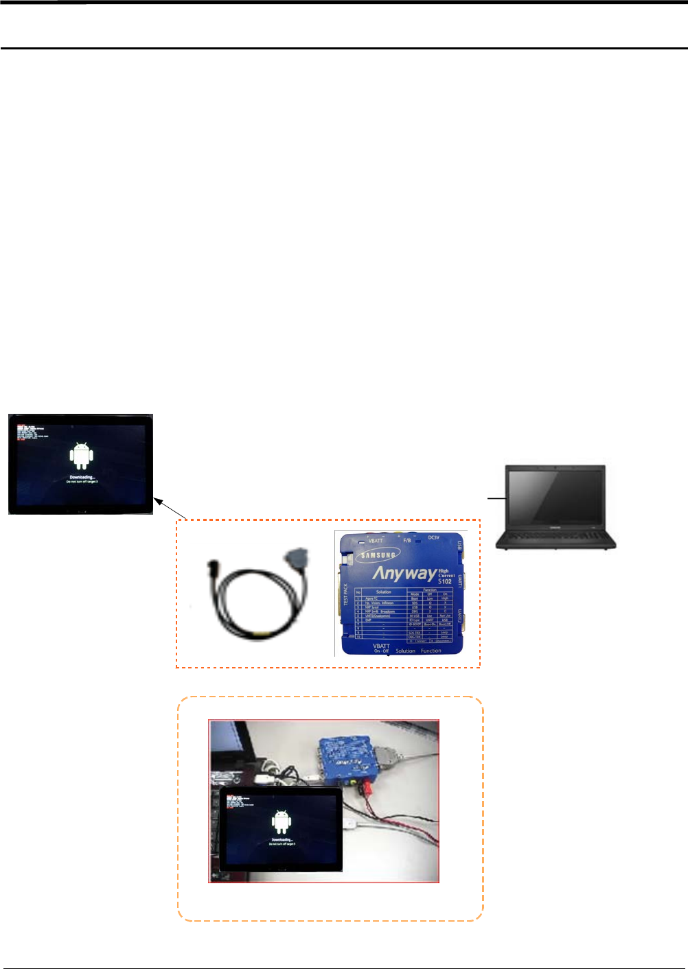
6-1-1. Required items in order to install S/W
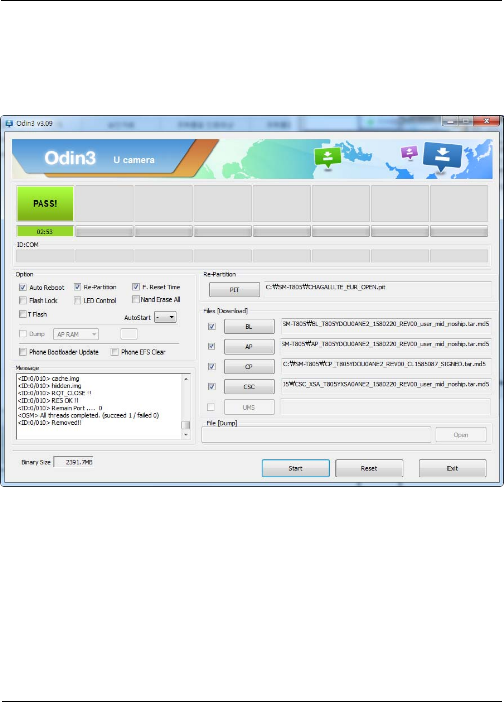
Installation program: Downloader Program (Odin3 v3.09.3.exe)
SM-T805 Galaxy Tab S
Data Cable (GH39-01661A)
JIG BOX (GH99-36900B)
JIG Cable (GH81-10623A)
Adapter (GH99-38251A)
Serial Cable
Mobile device specific S/W: Binary files
※Settings
Connect ANYWAY JIG BOX
with JIG CABLE (Phone to JIG)
or PC to Phone Using Data Cable
Level 1Repair
Distribution, transmission, or infringement of any content or data from this document without Samsung’s written authorization is strictly prohibited.
Confidential and proprietary-the contents in this service guide subject to change without prior notice.
6-2
6-1-2. S/W Installation Program (Downloader program)
Open up the S/W Installation Program by executing the "Odin3 v3.09.3.exe"
Level 1Repair
Distribution, transmission, or infringement of any content or data from this document without Samsung’s written authorization is strictly prohibited.
Confidential and proprietary-the contents in this service guide subject to change without prior notice.
6-3
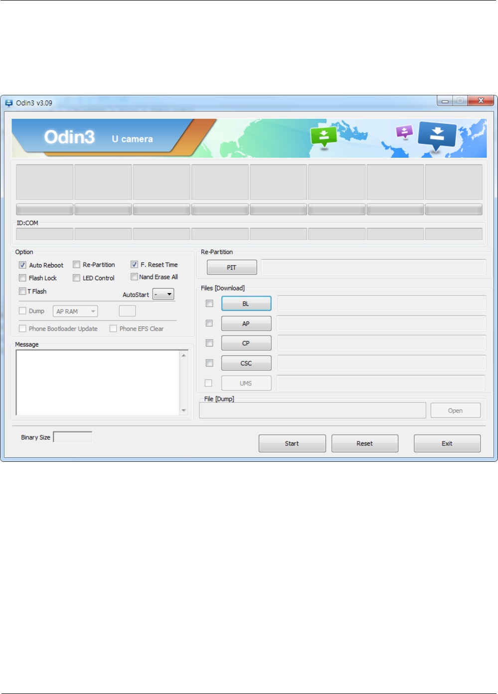
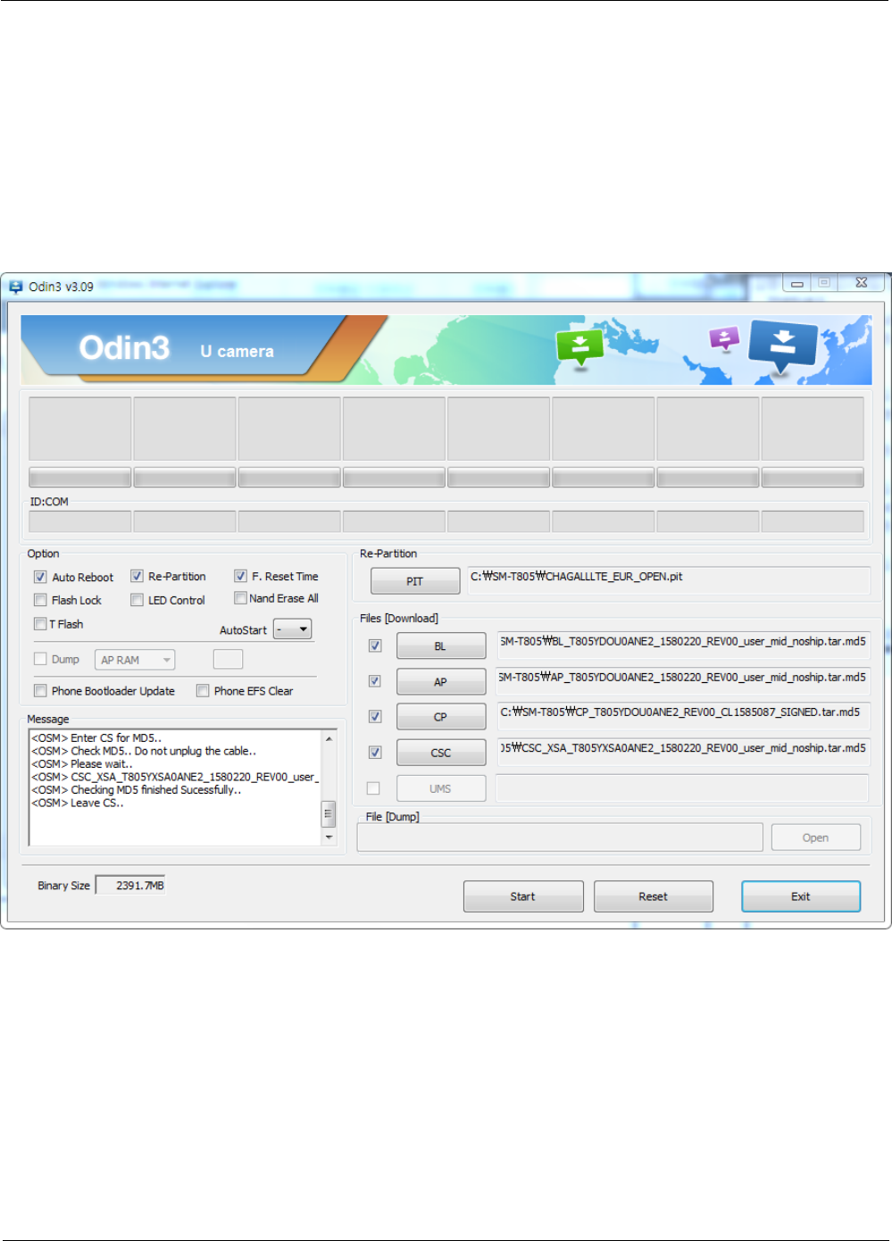
1. Enable the check mark by click on the following options,
-Check Auto Reboot, Re-Partition, and F. Reset Time
-Check PIT
-Check BL, AP, CP, and CSC Files
*Note :"
Odin v3.09 or above" checks MD5 checksum just after file selection.
Level 1Repair
Distribution, transmission, or infringement of any content or data from this document without Samsung’s written authorization is strictly prohibited.
Confidential and proprietary-the contents in this service guide subject to change without prior notice.
6-4
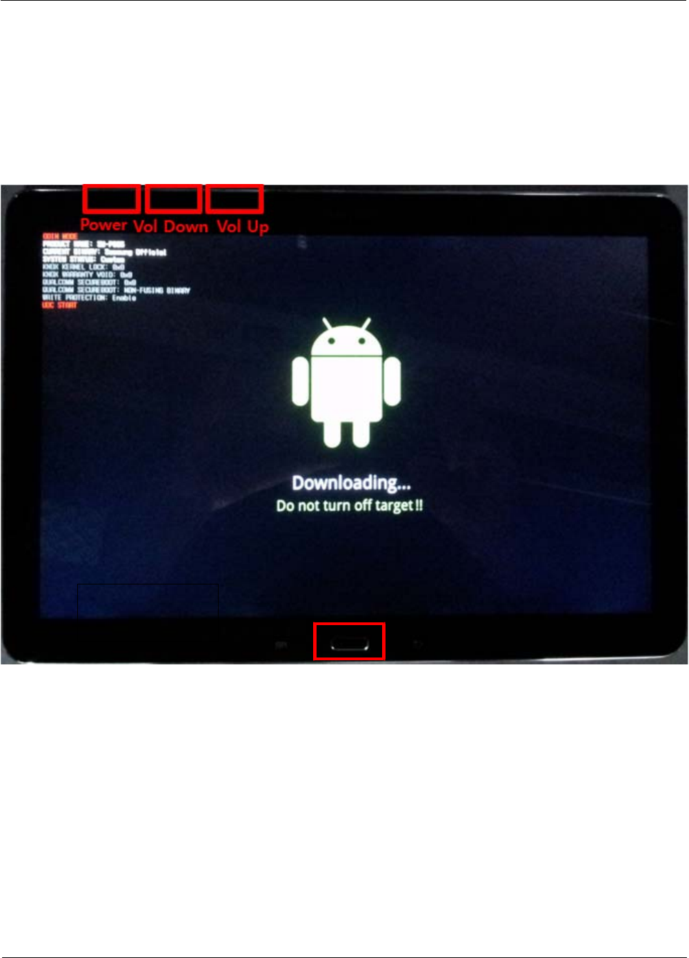
2. Enter into Download Mode
Enter into Download Mode by pressing Home button ,Volume Down button and
Power Button simultaneously followed by pressing Volume up button as adirection
of the phone.
Home
Level 1Repair
Distribution, transmission, or infringement of any content or data from this document without Samsung’s written authorization is strictly prohibited.
Confidential and proprietary-the contents in this service guide subject to change without prior notice.
6-5
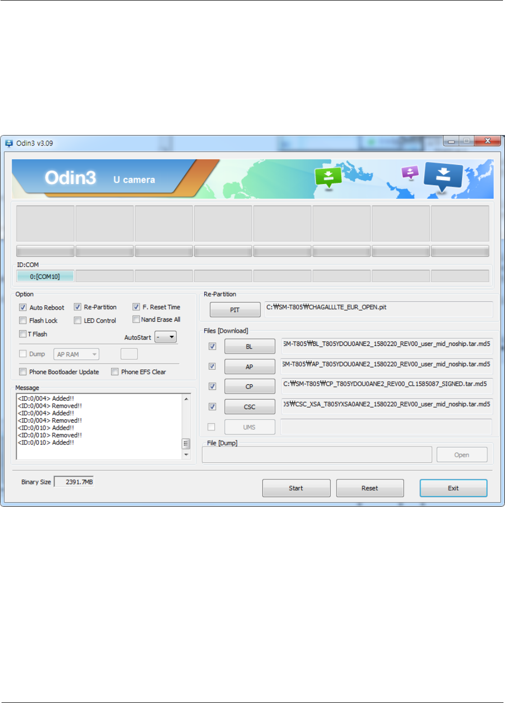
3. Connect the device to PC via Data Cable.
Make sure that the one of communication ports [ID:COM] box is highlighted in
sky blue. The device is now connected with the PC and ready to download the
binary files in it.
Level 1Repair
Distribution, transmission, or infringement of any content or data from this document without Samsung’s written authorization is strictly prohibited.
Confidential and proprietary-the contents in this service guide subject to change without prior notice.
6-6
4. Start downloading the binary files into the device by clicking Start button on the
screen. The green colored "PASS!" sign will appear on the upper-left box if the
binary files have been successfully downloaded into the device.
5. Disconnect the device from the Data cable.
6. Once the device boots up, you can check the version of the binary file or name
by pressing the following code in sequence;
*#1234#
You can perform Factory Reset by Settings →Accounts →Backup and reset
7. Level 2Repair
7-1
Confidential and proprietary-the contents in this service guide subject to change without prior notice.
Distribution, transmission, or infringement of any content or data from this document without Samsung’s written authorization is strictly prohibited.
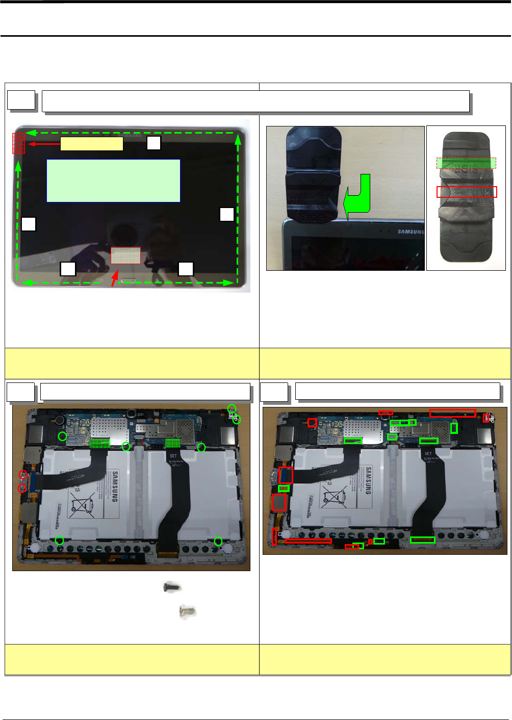
2
14
5
3
MIC
To prevent damage,
dismantling to lift up in REAR
by hand at the end without Ear
-jack HOOK dismantling
followed.
important
STEP 1,2,3 →4,5
1) Be careful not to make scratch and molding damage! 1) Use Band point of disassembly jig
Red point(2EA) : Black screw
Green point(7EA) : Silver screw
GREEN: Connector
RED : be careful not to crack FPCB(both sides tape)
Be careful, use of different screws Be careful, do not damage FPCB connector
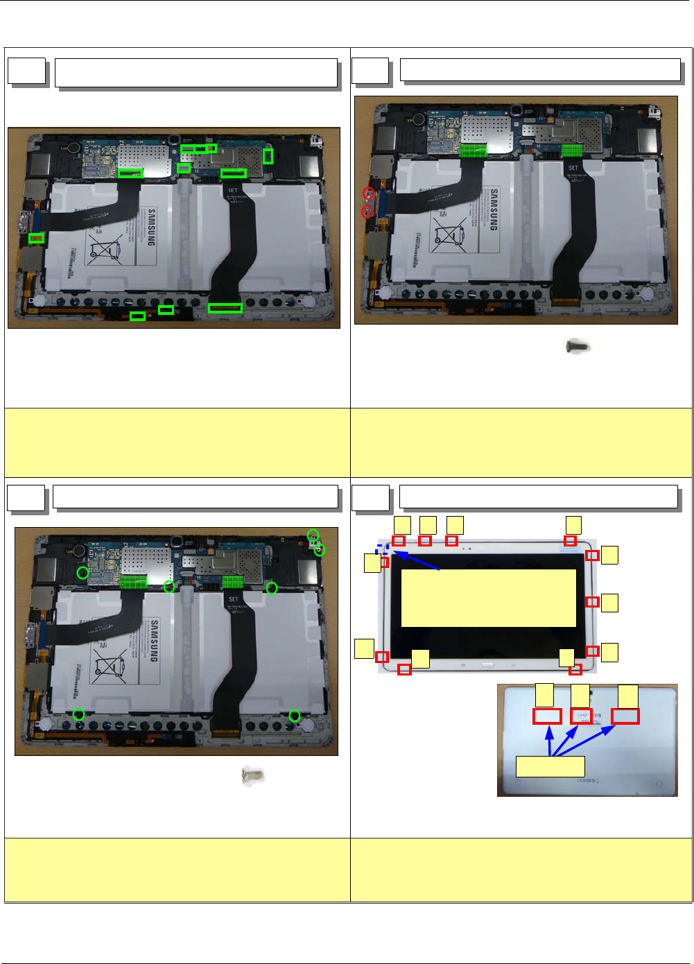
7-1. Disassembly and Assembly Instructions
7-1-1. Disassembly
1
2 3
Disjoint Hook at REAR // Disassemble REAR
Remove the screw(9EA) Disconnect the connector and tape
SM-T800_5
disassemble tool
Level 2Repair
Distribution, transmission, or infringement of any content or data from this document without Samsung’s written authorization is strictly prohibited.
Confidential and proprietary-the contents in this service guide subject to change without prior notice.
7-2
Be careful, do not damage FPCB Be careful, do not damage Battery
Be careful, do not damage FPCB
4 5
6
Disassemble SPK(L),(R) Remove the battery
Remove the PBA
Level 2Repair
Distribution, transmission, or infringement of any content or data from this document without Samsung’s written authorization is strictly prohibited.
Confidential and proprietary-the contents in this service guide subject to change without prior notice.
7-3
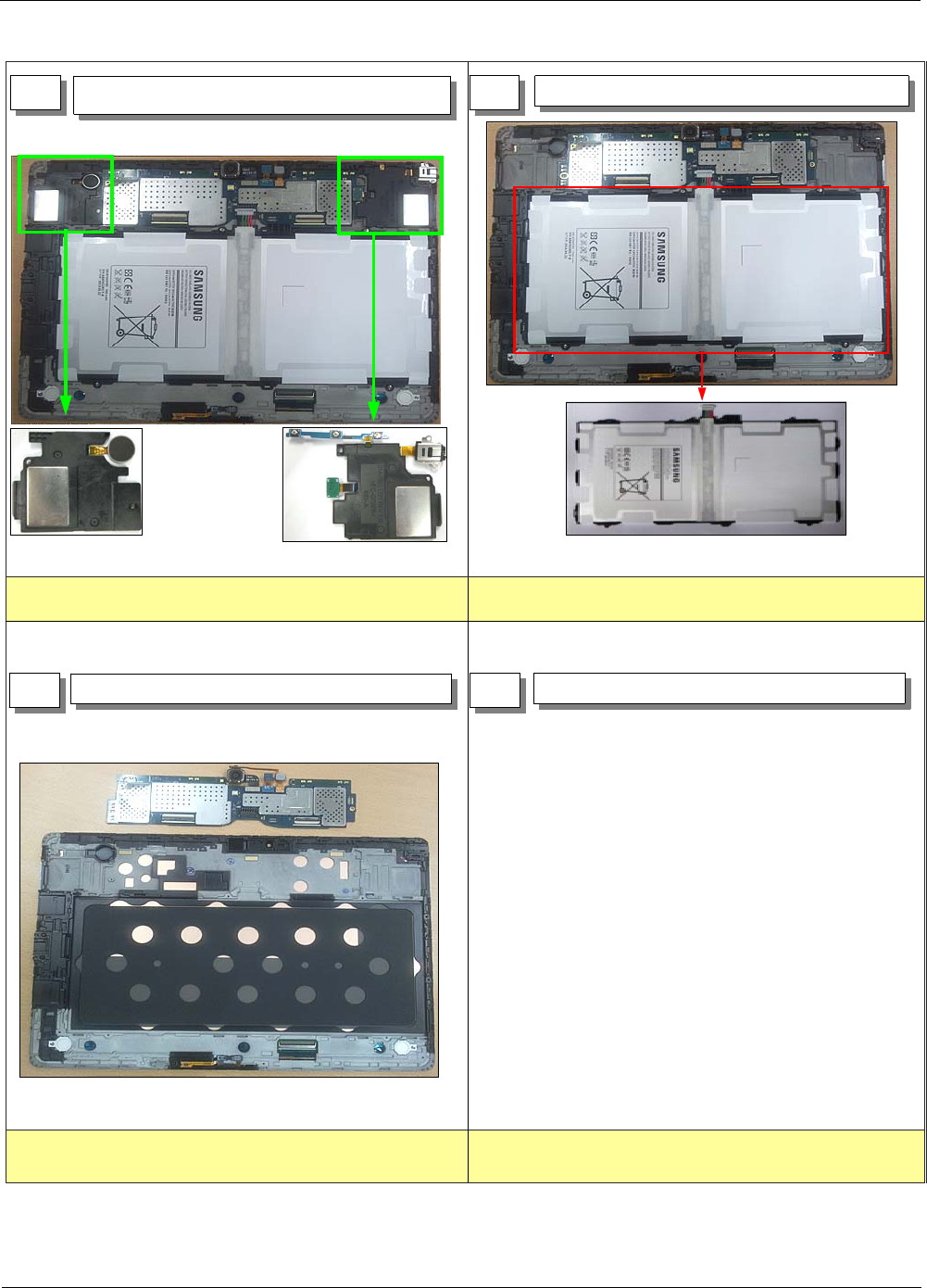
Be careful, do not damage FPCB Be careful, do not damage Battery
Be careful, do not damage FPCB
Check Ear-jack SUS Be careful, do not damage FPCB
7-1-2. Assembly
1 2
3 4
Assemble PBA Assemble the battery
Assemble SPK(L),(R) Assemble the MIC/USB/SIM FPCB
Level 2Repair
Distribution, transmission, or infringement of any content or data from this document without Samsung’s written authorization is strictly prohibited.
Confidential and proprietary-the contents in this service guide subject to change without prior notice.
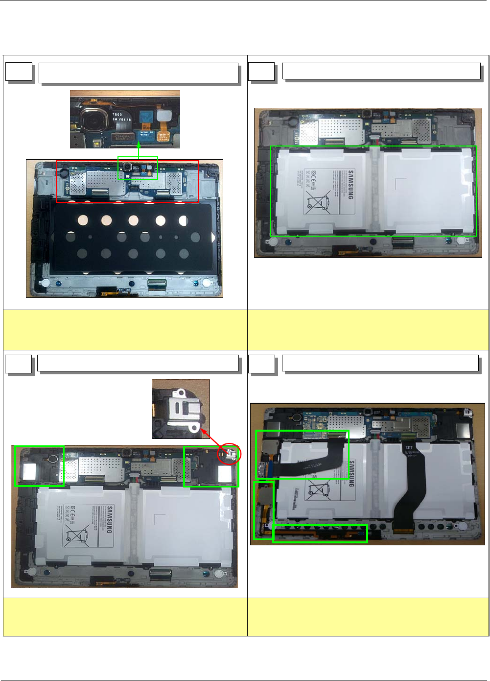
7-4
Red point(2EA) : Black screw
Be careful, do not damage FPCB connector ● Torque : 1.1 ~ 1.3 Kgf·cm /
● Size : 1.4 * 4 (6001-001479)
Green point(7EA) : Silver screw
[important]
In order to prevent damage to the
EAR JACK section, to start the
assembly after it had across first.
2
1
345
6
7
8
9
10
11
12 14
13
Press Hook
Assembly STEP 1 ~14
● Torque : 1.1 ~ 1.3 Kgf·cm /
● Size : 1.4 * 3 (6001-001811) Be careful, do not assemble hook
5 6
7 8
Assemble the connector & tape tightening the IF screws(2EA)
tightening the screws(7EA) Assemble Rear
8. Level 3Repair
8-1
Confidential and proprietary-the contents in this service guide subject to change without prior notice.
Distribution, transmission, or infringement of any content or data from this document without Samsung’s written authorization is strictly prohibited.
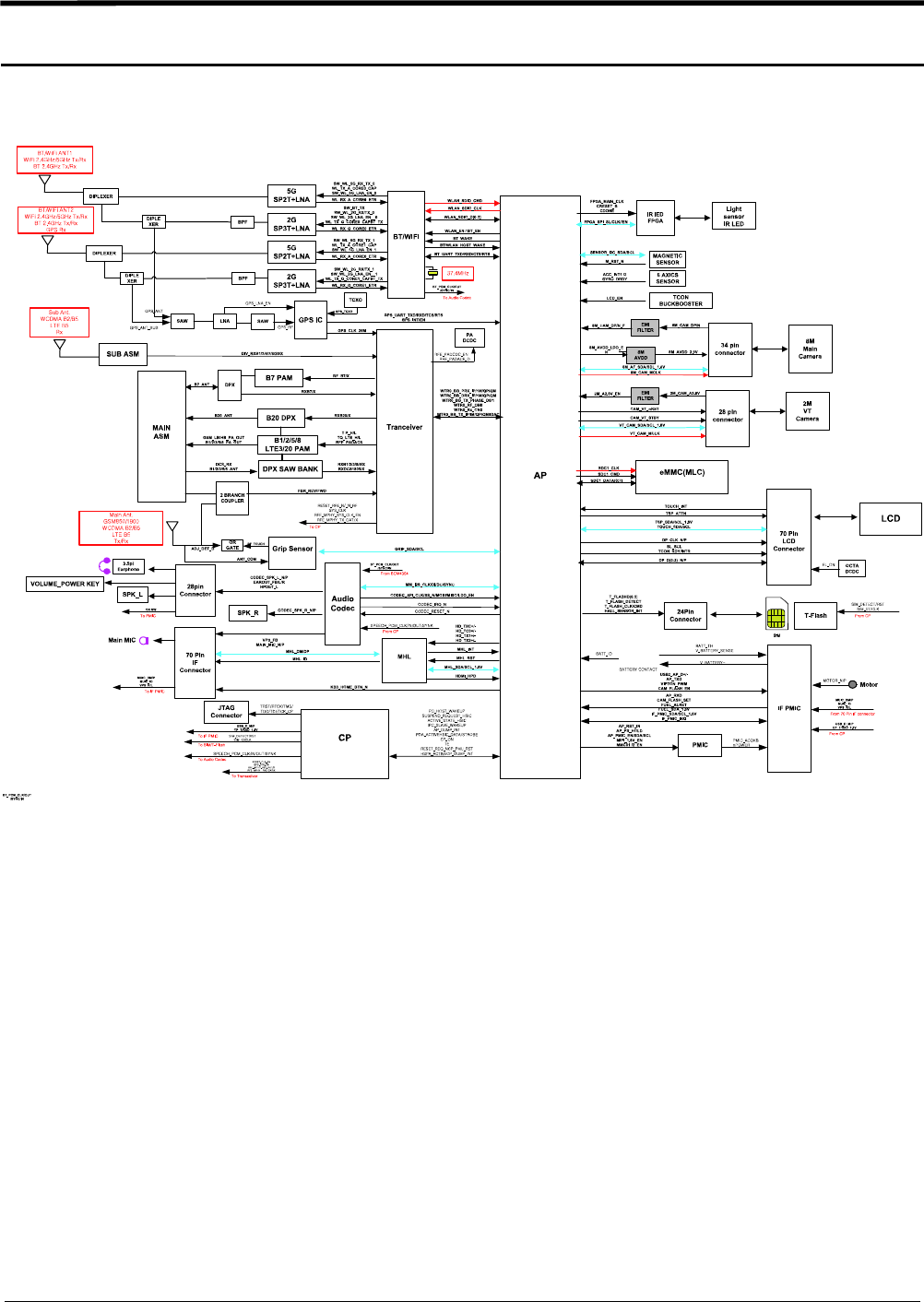
8-1. Block Diagram
Level 3Repair
Distribution, transmission, or infringement of any content or data from this document without Samsung’s written authorization is strictly prohibited.
Confidential and proprietary-the contents in this service guide subject to change without prior notice.
8-2
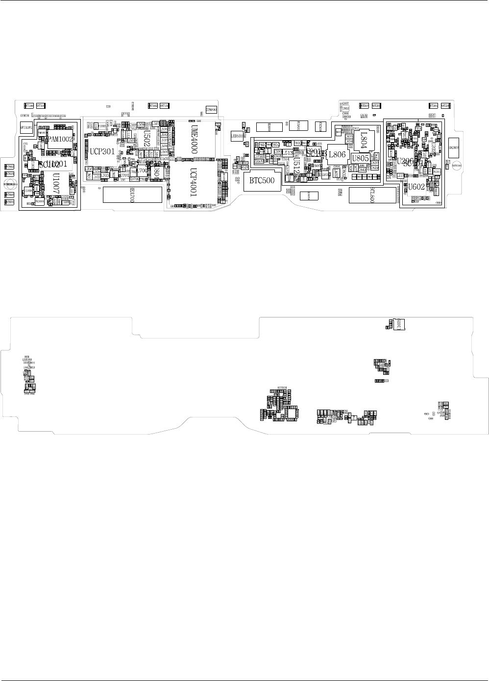
8-2. PCB Diagrams
8-2-1. Main PCB Top
8-2-2. Bottom

Level 3Repair
Distribution, transmission, or infringement of any content or data from this document without Samsung’s written authorization is strictly prohibited.
Confidential and proprietary-the contents in this service guide subject to change without prior notice.
8-3
8-3. Flow Chart of Troubleshooting
Equipments
Oscilloscope Digital Multimeter
Power Supply +driver, ESD Safe Tweezer
8960 & Spectrum Analyzer Soldering iron
Level 3Repair
Distribution, transmission, or infringement of any content or data from this document without Samsung’s written authorization is strictly prohibited.
Confidential and proprietary-the contents in this service guide subject to change without prior notice.
8-4
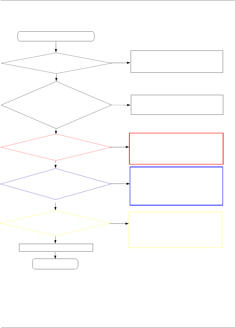
8-3-1. Power On
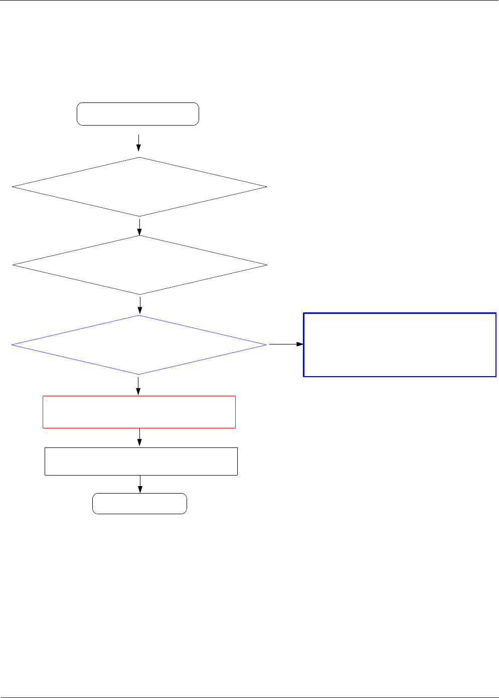
Mobile phone does not power on.
END
No
Yes
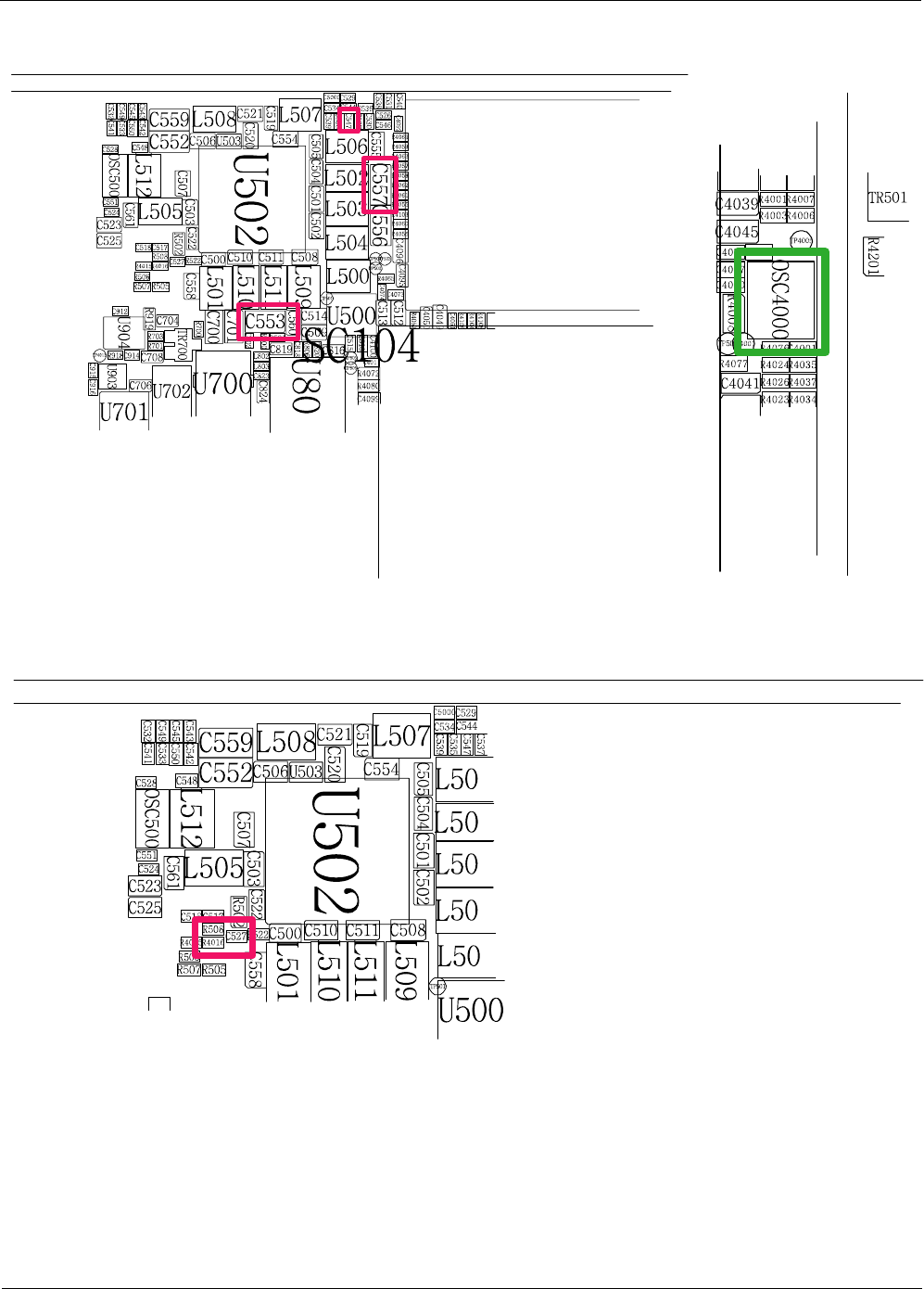
Check the C527, R508 Votage
level.
Is it over 1.5V??
It Can be Damaged AP(UCP40001-1) or LPDDR3
Memory.
It is Needed to dump Memory or Check with S/W
Team to Analyze.
So, Change the PBA.
No
Yes
Check the U502 output voltage
(C547 >1.0
V, C557 >1.0
V,
C553 >1.0
V)
If the output voltage is not satisfied with normal
condition, Change the U502
※Each voltage level has ±10% margin.
No
Yes
Yes
Check the Battery Voltage.
Is it more than 3.8V?
Charging the battery by TA.
If its voltage level is extremely low(under 3.3V),
Change the battery.
check the initial operation
Check the Clock OSC400
Is that frequency 24Mhz,? Change the OSC4000
No
Yes
No
Change the FRONT-LCD ASSY
or LCD Con-to-Con Connector
Yes
Push the Power Button for 8seconds. Then
wait 3minutes, check the power-on sound or
motor Vibration or light on touch key.
Sound or Vibration is ok?
Level 3Repair
Distribution, transmission, or infringement of any content or data from this document without Samsung’s written authorization is strictly prohibited.
Confidential and proprietary-the contents in this service guide subject to change without prior notice.
8-5
C556
V_BAT
VCC_SUB_3.4V
C554
C524
VMIPI_PLL_ABB1_1.8V_AP
C549
C517
C528
C553
VCC_SUB_2.0V
C552
VCC_SUB_1.4V
TP503
R504
R507
R505
C555
C521
C511
G
2S
VCC_1.8V_AP
TR500
3D
1
C519
VDD_CAM_ISP_1.0V
L512
VCC_SUB_3.4V
C557
C503
C520
VKFC_1.0V_AP
L502
L501
C560
L506
V_BAT
VMEM2_1.2V_AP
C507
21
OSC500
R502
VG3D_1.0V_AP
V_BAT
VINT_1.0V_AP
C527
C548
V_BAT
VCC_1.8V_AP
C506
C522
C561
VDD_CAM_ISP_1.0V
VARM_1.0V_AP
L511
TP502
C518
VINT_1.0V_AP
L504
C510
R526
C504
C526
TR501
D3
G
1
S2
C551
VADC_1.8V_AP
TP504
VMMC01_1.8V_AP
L503
C5003
C523
VCC_SUB_1.4V
C558
C525
VCC_SUB_2.0V
R506
C505
C559
VCC_SUB_3.4V
VRTC_1.8V
N4 SW4
N5GNDB4
N6GNDB3
N7 SW3
N8
VINB3
N9GNDB6
M9GNDB6
N1NC
N10 SW6
N11
VINB7
N12 SW7
N13NC
N2
VINB10
N3
VINB4
M13GNDB7
M2
VINB10
VINB4M3
M4 SW4
M5GNDB4
M6GNDB3
M7 SW3
M8
VINB3
L6 RS3N
L7 RS3P
FB3
L8
L9
VLDO24
M1 SW10
M10 FB6
M11
VINB6
M12 FB7
L10
VLDO13
L11
VLDO1
VLDO27 L12
L13
VLDO22
L2 FB10
L3 FB4
L4 RS4P
L5 RS4N
K3AGND
K4
VBAT
AGND
K5
K6AGND
K7AGND
K8
VLDO38
K9
VLDO16
L1GNDB10
NC
J9
VLDO14
GNDB22
K1
K10
VINL5
K11
VLDO9
K12
VINL1
K13
VLDO6
K2GNDB22
VLDO11
J13
VLDO35
J2 SW22
J3
WDRSTEN
J4 BUCK10EN
J5
LDO7EN
J6
LDO13EN
J7AGND
J8
H6
LDO19EN
H7
VBAT
H8
VREF
H9
VLDO26
J1 SW22
J10
VLDO19
J11
VLDO23
J12
H10
VLDO34
H11
VINL6
H12
VLDO17
H13
VLDO28
H2
VINB22
H3 FB2
H4 PWRHOLD
H5NC
G3 RS2P
G4 IRQB
G5 MR1B
G6 MR2B
G7 ACOKB
G8
VLDO37
G9
VLDO25
H1
VINB22
F8
VLDO31
F9
VLDO20
G1
VINB21
G10
VLDO21
G11
VLDO15
G12
VLDO36
G13
VLDO30
G2
VINB21
F12
VLDO33
F13
VLDO29
F2 SW21
F3 RS2N
F4 ONOB
F5 RSOB
F6
SDA
F7 JIGONB
E4 PWREN
E5NC
E6
SCL
E7 PWRON
E8
VLDO10
E9
VLDO4
F1 SW21
F10
VINL3
F11
VLDO18
D9
VLDO5
E1GNDB21
E10
VLDO12
E11
VINL2
E12
VINL4
E13
VLDO32
E2GNDB21
E3
LDO18EN
D13
VLDO7
D2 B5V2
D3 B5V3
D4 B5S1
D5 B5S2
D6
AP32K
D7
VDD_CP
D8
VDD_BT
C6 FB9
C7
CP32K
C8
BT32K
C9 BKCOIN
D1 B5V1
D10
VLDO8
D11
VLDO2 D12
VLDO3
C10
XTALOUT
C11
XTALIN
C12 FB8
C13GNDB8
C2 FB5
C3 FB5
C4AGND
C5
VBAT
B3GNDB5
B4 SW5
B5
VINB5
B6
VINB9
B7 SW91
B8GNDB9
B9 SW92
C1GNDB1
A8GNDB9
A9 SW92
B1 SW1
B10
VB9
B11
VINB8
B12 SW8
B13GNDB8
B2 FB1
A12 SW8
A13NC
A2
VINB1
A3GNDB5
A4 SW5
A5
VINB5
A6
VINB9
A7 SW91
1NC
NC
2
A1NC
A10
VB9
A11
VINB8
U502
R503
VMIPI_1.0V_AP
VMEM_1.2V_AP
L509
C500
VKFC_1.0V_AP
VARM_1.0V_AP
VMIF_1.1V_AP
VALIVE_1.0V_AP
C508
C547
VCC_1.8V_AP
TP501
VCC_1.8V_AP
VMIF_1.1V_AP
L507
C501
VG3D_1.0V_AP
L505
R508
VCC_SUB_1.4V
L508
L510
VMEM_1.2V_AP
R512
C550
VCC_SUB_2.0V
IF_CON_SENSE
JTAG_IF_CON_SENSE
C502
JTAG_IF_CON_SENSE
VOL_DOWN
32KHZ_CP
BUCK9_GND
MIPI_1.8V_EN
32KHZ_AP
AP_PMIC_SCL
AP_PMIC_SDA
VG3D_1.0V_AP_SNSN
VINT_1.0V_AP_SNSN
VINT_1.0V_AP_SNSP
BUCK7_GND
BUCK4_GND
BUCK3_GND
BUCK6_GND
32KHZ_PMIC
MMC01_EN
MMC2_EN
BUCK2B_GND
BUCK10_GND
VG3D_1.0V_AP_SNSP
ON_SW
VARM_1.0V_AP_SNSN
nPOWER
VARM_1.0V_AP_SNSP
AP_PS_HOLD
BUCK5_GND
BUCK9_GND
BUCK8_GND
BUCK1_GND
BUCK2A_GND
AP_PMIC_EN
AP_PMIC_IRQ
PMIC_ACOKB
AP_N_RST_IN
TF_EN
AP_PMIC_EN
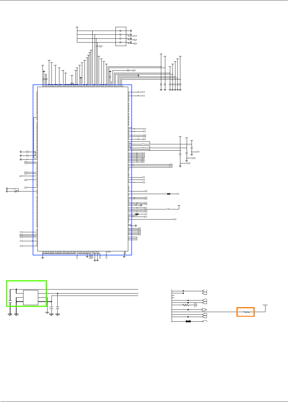
4
OSC4000
C4001
C4000
R4008
XTAL_24MHZ_OUT
XTAL_24MHZ_IN
C556
V_BAT
C554
C524
C517
C553
VCC_SUB_2.0V
VCC_SUB_1.4V
R504
R507
R505
C555
G
2S
TR500
3D
1
VDD_CAM_ISP_1.0V
L512
VCC_SUB_3.4V
C557
VKFC_1.0V_AP
L502
L501
C560
L506
VMEM2_1.2V_AP
R502
VG3D_1.0V_AP
V_BAT
VINT_1.0V_AP
C527
VCC_1.8V_AP
C522
C561
VDD_CAM_ISP_1.0V
VARM_1.0V_AP
L511
C518
VINT_1.0V_AP
L504
R526
TR501
D3
G
1
S2
L503
C5003
C523
VCC_SUB_1.4V
C558
C525
VCC_SUB_2.0V
R506
VRTC_1.8V
N4 SW4
N5GNDB4
N6GNDB3
N7 SW3
N8
VINB3
N9GNDB6
M9GNDB6
N1NC
N10 SW6
N11
VINB7
N12 SW7
N2
VINB10
N3
VINB4
M13GNDB7
M2
VINB10
VINB4M3
M4 SW4
M5GNDB4
M6GNDB3
M7 SW3
M8
VINB3
L6 RS3N
L7 RS3P
FB3
L8
M1 SW10
M10 FB6
M11
VINB6
M12 FB7
L2 FB10
L3 FB4
L4 RS4P
L5 RS4N
K3AGND
K4
VBAT
AGND
K5
K6AGND
K7AGND
L1GNDB10
NC
GNDB22
K1
K12
VINL1
K2GNDB22
J2 SW22
J4 BUCK10EN
J7AGND
J8
H7
VBAT
J1 SW22
H2
VINB22
H3 FB2
H4 PWRHOLD
H5NC
G3 RS2P
G4 IRQB
G5 MR1B
G6 MR2B
G7 ACOKB
H1
VINB22
G1
VINB21G2
VINB21
F2 SW21
F3 RS2N
F4 ONOB
F5 RSOB
F7 JIGONB
E4 PWREN
E5NC
E7 PWRON
F1 SW21
F10
VINL3
E1GNDB21
E11
VINL2
E2GNDB21
D2 B5V2
D3 B5V3
D4 B5S1
D5 B5S2
D7
VDD_CP
D8
VDD_BT
C6 FB9
C9 BKCOIN
D1 B5V1
C12 FB8
C13GNDB8
C2 FB5
C3 FB5
C4AGND
C5
VBAT
B3GNDB5
B4 SW5
B5
VINB5
B6
VINB9
B7 SW91
B8GNDB9
B9 SW92
C1GNDB1
A8GNDB9
A9 SW92
B1 SW1
B11
VINB8
B12 SW8
B13GNDB8
B2 FB1
A12 SW8
A13NC
A2
VINB1
A3GNDB5
A4 SW5
A5
VINB5
A6
VINB9
A7 SW91
A1NC
A11
VINB8
U502
R503
VMEM_1.2V_AP
L509
VKFC_1.0V_AP
VARM_1.0V_AP
VMIF_1.1V_AP
VCC_1.8V_AP
TP501
VCC_1.8V_AP
VMIF_1.1V_AP
L507
VG3D_1.0V_AP
L505
R508
VCC_SUB_1.4V
L508
L510
VMEM_1.2V_AP
R512
VCC_SUB_2.0V
IF_CON_SENSE
JTAG_IF_CON_SENSE
JTAG_IF_CON_SENSE
VOL_DOWN
VG3D_1.0V_AP_SNSN
VINT_1.0V_AP_SNSN
VINT_1.0V_AP_SNSP
BUCK7_GND
BUCK4_GND
BUCK3_GND
BUCK6_GND
BUCK2B_GND
BUCK10_GND
VG3D_1.0V_AP_SNSP
ON_SW
VARM_1.0V_AP_SNSN
nPOWER
VARM_1.0V_AP_SNSP
AP_PS_HOLD
BUCK5_GND
BUCK9_GND
BUCK8_GND
BUCK1_GND
BUCK2A_GND
AP_PMIC_EN
AP_PMIC_IRQ
PMIC_ACOKB
AP_N_RST_IN
AP_PMIC_EN
Level 3Repair
Distribution, transmission, or infringement of any content or data from this document without Samsung’s written authorization is strictly prohibited.
Confidential and proprietary-the contents in this service guide subject to change without prior notice.
8-6
Level 3Repair
Distribution, transmission, or infringement of any content or data from this document without Samsung’s written authorization is strictly prohibited.
Confidential and proprietary-the contents in this service guide subject to change without prior notice.
8-7
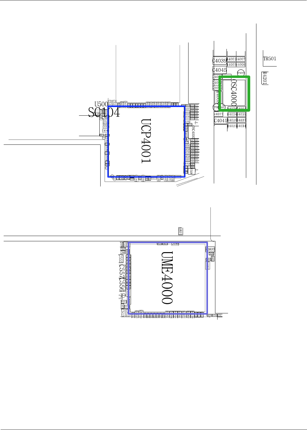
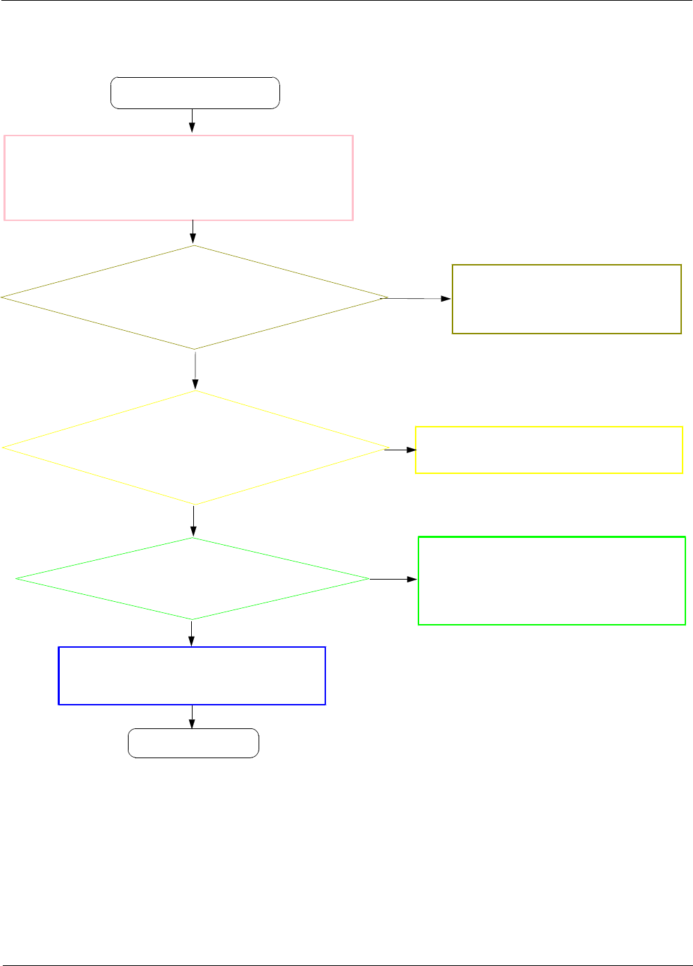
8-3-2. Initial
Initial Failure
END
Re Check "8-3-1 Power on"
Trouble shooting process Check the OSC4000(Crack, open etc.)
Check the UCP4001-1 (Crack etc)
Abnormal
Normal
Change UME4000 that is ROM flashed.
Do not use Blank MEMORY.
Abnormal
Change PBA
Yes
Re-download latest SW on the
mobile phone.
Abnormal
Try the Boot Recovery by SD
CARD.
Follow the Recovery Guide.
Abnormal
Level 3Repair
Distribution, transmission, or infringement of any content or data from this document without Samsung’s written authorization is strictly prohibited.
Confidential and proprietary-the contents in this service guide subject to change without prior notice.
8-8
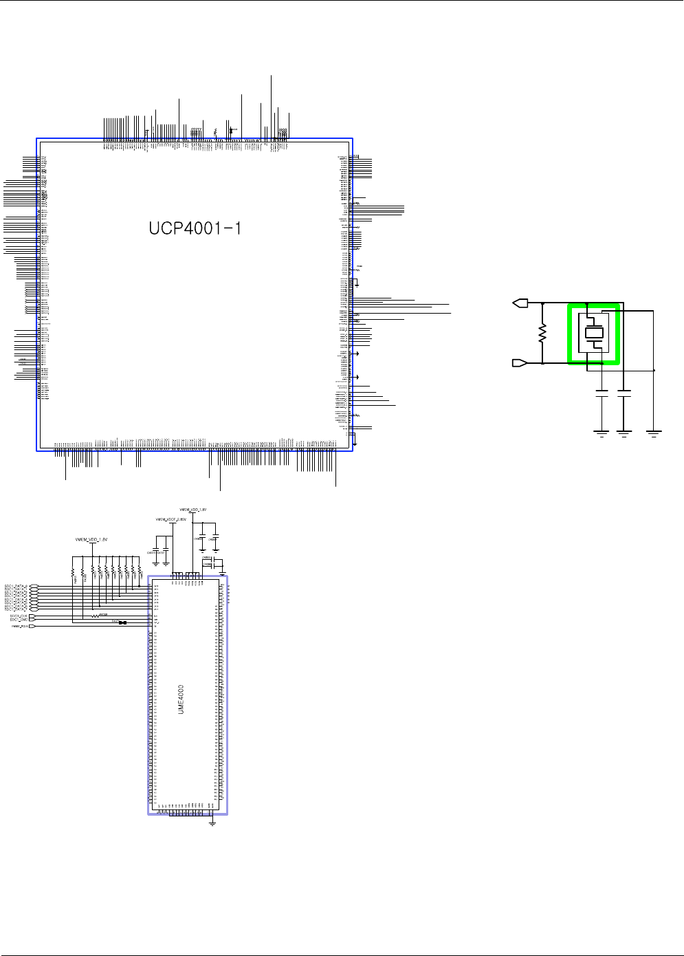
4
OSC4000
C4001
C4000
R4008
XTAL_24MHZ_OUT
XTAL_24MHZ_IN
Level 3Repair
Distribution, transmission, or infringement of any content or data from this document without Samsung’s written authorization is strictly prohibited.
Confidential and proprietary-the contents in this service guide subject to change without prior notice.
8-9
Level 3Repair
Distribution, transmission, or infringement of any content or data from this document without Samsung’s written authorization is strictly prohibited.
Confidential and proprietary-the contents in this service guide subject to change without prior notice.
8-10
8-3-3. No Service
No service
END
Check the voltage level
R324 =HIGH
Yes
Replace the U502
Yes
Check OSC1001
Frequency =26
MHz Replace the OSC1001
Yes
No
No
Check memu setting
Menu →applications →setting →wireless and network →
mobile networks →network mode →setting is auto mode ?
Check the contact of RF antenna clipㅁ
Replace UCP301
PHONE :T805XXXX
PHONE :unknown
Menu →Phone →Keypad →
*#1234# →check Phone version →
PHONE :T805XXXX or
PHONE :unknown
Yes
Level 3Repair
Distribution, transmission, or infringement of any content or data from this document without Samsung’s written authorization is strictly prohibited.
Confidential and proprietary-the contents in this service guide subject to change without prior notice.
8-11
CP_VSD2_1.8V
CP_VSIM
L301
CP_VSD2_1.8V
CP_VSD1_1.2V
L303
CP_VSD1_1.2V
CP_VSD1_1.2V
C347
C303
V_BATT_CP
VUSB_IO_3.1V
VDIGRF_1.2V
VPLL_1.2V
VDIGRF_1.2V
VUSB_IO_3.1V
CP_VSD3_1.2V
VUSB_PD_1.1V
C359
VPLL_1.2V
C356
CP_VSD3_1.2V
CP_VSD3_1.2V
TP310
CP_VSD1_1.2V
TP312
C360
C340
C301
L302
CP_VSD2_1.8V
CP_VSD3_1.2V
VUSB_ANA_1.8V
C343
TP323
C344
R314
VUSB_ANA_1.8V
TP324
TH301
C345
VUSB_PD_1.1V
R320
VRTC_1.8V
CP_VSD2_1.8V
VPLL_1.2V
FSS
Y6VSS
Y7VSS
Y8 ANAMON
Y9 TM_EN
M3
Y13VSS
Y14 TRIG_IN
Y15
T_OUT0
Y17
TPIU_TRACEPKT3
Y18
TPIU_TRACECLK
Y2
VDD_VIN_SD1
Y4
SD1_FB
Y5
T_OUT1
W17
TPIU_TRACEPKT6
W18
TPIU_TRACEPKT2
W5VSS
W9 M1
Y1
VDD_VIN_SD1
Y10VSS
Y11
ON
Y12
VSS
V6
RTC_ALARM
V8
TRIG_B
W10 M4
W11
TDI
W12
TCK
W13
TMS
W14
TRST_n
W15
OFF_N
V1
VPMU
V10 M2
V13 HW_MON1
V15
T_OUT2
V17
TPIU_TRACEPKT5
V18
TPIU_TRACEPKT7
V2
VUSB_PD
V4
RESET_RFE_N
U14 HW_MON2
U15
T_OUT3
U17
TPIU_TRACEPKT4
U18VSS
U2
VPLL
U3VSS
U7
RESET_BB_N U9
USIF3_SCLK
T17 I2S1_RX
T18 I2S1_WA0
T2 HW_MON26
T7 HW_MON27
U1
VDIGRF
U10
RESET_ALL_N
U11
REF_CLK_EN
U12
HW_MON23
R4
VDD_CORE_LTE
R5 HW_MON17
R7
VDD_CORE_LTE
R8 HW_MON29
R9 HW_MON25
T12 HW_MON28
T14
USIF3_TXD_MTSR
T15
USIF_LTE_TXD
R10 HW_MON24
R11
VDD_CORE_LTE
R12 HW_MON30
R14
USIF3_RXD_MRST
R15
USIF3_CTS_N
R17 I2S1_WA1
R18 I2S1_CLK1
R2
VDD_CORE_LTE
P17 I2S1_CLK0
P18 I2S1_TX
P2 HW_MON20
P4 HW_MON32
P5 HW_MON22
P7 HW_MON21
P8 HW_MON18
R1
NAND_ADQ_1
N3 ZQ_MEM
N4 NAND_ADQ_11
N5VSS
N7VSS
P11 HW_MON31
P12 HW_MON19
P14
USIF3_RTS_N
P15
VSS
N10
MMCI1_DAT_1
N11
MMCI1_DAT_3
N12
MMCI1_CMD
N14
MMCI1_CLK
N15
MMCI1_CD
N17
XRESET_N
N18VSS
N2
VDD_IO_MMC
M13
VPP
M17
DIGRFEN
M18
RXDATANLANE2
M2 NAND_CE_N
M3 DDR_VREF_DQ_M
M4 NAND_ADQ_12
M5 NAND_ALE
N1
NAND_ADQ_6
L4VSS_SENSE
L5 NAND_ADQ_0
L6
VDD_IO_1V8
L7 NAND_ADQ_5
L9
EINT1
M1 DDR_DQ_10
M10
VDD_IO_1V8
M12
DDR_DQM_0
L11
EINT3
L12
MMCI1_DAT_2
L14
CLKOUT0
L15
CLKOUT2
L17
VDD_MPHY_RX_1V2
L18
RXDATAPLANE2
L2 DDR_DQ_7
L3
RXDATAPLANE1
K2 DDR_DQ_4
K3 NAND_CLE
K4 NAND_ADQ_3
K5 NAND_ADQ_8
K6 NAND_ADQ_15
K7 NAND_ADQ_4
K9
VDD1_MEM
L1
DDR_DQ_0
K10
EINT2
K11 I2S2_WA0
K12 I2S2_CLK0
K13
MMCI1_DAT_0
K14
CLKOUT1
K15
VDD_IO_1V8
K17VSS
K18
DDR_VREF_DQ
J3 NAND_ADQ_2
J4 NAND_RB_N
J5 NAND_WP_N
J6 NAND_ADQ_10
J7 NAND_WE_N
J8 NAND_ADQ_7
J9
VDD1_MEM
K1
I2S2_CLK1
J11
VDD_CORE_3G
J12 I2S2_RX
J13
RCT_MON1 J14
RCT_MON2
J15
VDD_IO_SIM2
J17VSS_MPHY_RX
J18
RXDATANLANE1
J2
VDD_IO_1V8
H4 NAND_ADQ_9
H5 NAND_ADQ_14
H6
VDD_CORE_MAIN
H7 NAND_CLK_X_IN
H8
VDD_CORE_3G
H9VSS_MEM
J1 DDR_DQ_2
J10
I2S2_TX
H13
VDD_CORE_3G
H14
RESET2_N
H15
DPLUS2
H16
CC2_RST
H17
TXDATAN
H18
TXDATAP
H2 NAND_RE_N
H3
DDR_CA_3
G6VSS
G7VSS_MEM
G8 DDR_CA_6
G9 DDR_CKE_0
H1VSS
H10
VDD2_MEM
H11 I2S2_WA1
H12
CC1_RST
G14
CC2_IO
G15
DMINUS2
G17VSS_MPHY_TXG18
VDD_MPHY_TX_1V2
G2 DDR_DQ_13
G3 NAND_CLK_X_OUT
G4 DDR_CA_0
G5
VSS_PLL_1F7
VDD_PLL_1
F8VSS_MEM
F9 DDR_CKE_1
G1 DDR_DQS_T_0
G10 CKE_M
G11VSS
G12VSS
G13
SYS_CLK
F16 I2C1_SCL
F17VSS_PLLF18
VDD_PLL
F2 DDR_DQ_9
F3 NAND_ADQ_13
F4 DDR_CA_2
F5 DDR_CA_7
F6
DDR_CAS
E9 DDR_CA_5
F1 DDR_DQS_C_0
F10 DDR_WE
F11VSS_MEM
F12
VDD2_MEM
F13
CC1_IO
F14
CC2_CLK
F15
I2C1_SDA
E18
HSIC_USB_STRB
E2 DDR_DQ_6
E3 DDR_DQ_15
E4 DDR_DQ_3
E5 DDR_CA_4
E6 DDR_CA_1
E7 DDR_A_12
E8
DDR_A_11
D8
VDD_CORE_MAIN
D9 DDR_CS_1
E1 DDR_DQ_1
E10VSS
E11 DDR_BA_0
E12
CC1_CLK
E13VSS
E17
VSS_USB
D17VSS
D18
HSIC_USB_DATA
D2 DDR_DQ_12
D3
VDD_IO_EMIC
D4
VDD_CORE_EMIC_1V2
D5
VDD_DLL_EMIC
D6 DDR_CA_9
D7
VDD_IO_EMIC
C8VSSQ_MEM
C9
MIPI_HSI_TX_RDY
D1VSS
D10
MIPI_HSI_RX_DATA D11
MIPI_HSI_RX_FLG
D12
MIPI_HSI_TX_WAKE
D13
VDD_IO_SIM1
D14
VDD_USB_ANAC17
VDD_USB_PD
C18
VDD_IO_HSIC_1V2
C2
VDD_IO_EMIC_1V8
C3VSSQ_MEM
C4
VDDQ_MEMC5
VDDQ_MEM
C6
VDD_CORE_EMIC_1V2
C7
MIPI_HSI_RX_RDY
C1 DDR_DQ_5
C10
MIPI_HSI_TX_DATA
C11 DDR_VREF_CA_M
C12
DPLUS
C13
DMINUS
C14
VDD_CORE_MAIN
C15
VDD_IO_1V8
C16
VSS
B2 DDR_DQ_8
B3VSS
B4 DDR_DQ_11
B5 DDR_CK_C
B6 DDR_DQ_14
B7 DDR_A_13
B8 DDR_A_10
B9
MIPI_HSI_RX_WAKE
B11
MIPI_HSI_TX_FLG
B12VSS
B13VSS
B14
USB_ID
B15
VBUS
B16
VDD_IO_USB
B17
USB_TUNE
B18
SD2_SW AC4
SD2_SW
AC5VSS_SD2
AC6
VCP_BSTP
AC7
VCP_BSTN
AC8
VSIM1
AC9
VDD_VIN_SD3
B1 DDR_DQM_1
B10
VUSB_ANA
AC13
VREF
AC14
TDO
AC15
USIF1_RXD_MRST
AC16
USIF1_RTS_N
AC17
USIF1_SCLK
AC18NC
AC2
VDD_VIN_SD2
AC3
TPIU_TRACEPKT0
AB2VSS_SD1
AB6
VCP
AB7
VUSB_IO
AB8
VSIM2
AC1NC
AC10
SD3_SW
AC11VSS_SD3
AC12
VSS
AB1VSS_SD1
AB12
VRTC
AB13AGND
AB14
DSP_AUDIO_IN1
AB15
RTCK
AB16
USIF1_CTS_N
AB17
USIF1_TXD_MTSR
AB18
AGND_SENSE
AA17
TPIU_TRACEPKT1
AA18
TPIU_TRACECTL
AA2
SD1_SW AA4
SD2_FB
AA5
VDD_VIN_PMU
AA6
VDD_VSD2
AA8VSS
AA9
DDR_CK_T
A6 DDR_CA_8
A7 DDR_VREF_CA
A8 DDR_RAS
A9 DDR_BA_1
AA1
SD1_SW
AA10
SD3_FB
AA11VSS
AA13
VDD_RTC
A15
USB_TEST
A16
USB_DMINUS
A17
USB_DPLUS
A18NC
A2
VDD_IO_EMIC
A3 DDR_DQS_C_1
A4 DDR_DQS_T_1
A5
NC
1
NC
2
A1NC
A10 DDR_CS_0
A11
VDD_IO_MIPI
A12
F32K A13
OSC32K
A14
TP309
UCP301
TP311
TP313
TP308
TP318
USB_VBUS_CP_4.9V
C339
TP_HSIC_STROBE
C302
C304
CP_VSIM
CP_VSD3_1.2V
C342
C341
VRTC_1.8V
R312
C315
TP306
TP317
TP326
TP304
C358
TP322
TP314
VRTC_1.8V
TP307
TP_HSIC_DATA
TP_ACTIVE_STATE_HSIC
TP315
TP303
R325
TP321
R326
TP305
TP316
R313
C357
CP_VSD2_1.8V
TP325
TP_IPC_SLAVE_WAKEUP
CP_VSD3_1.2V
TP302
R324
TP301
C328
TP320
C346
32KHZ_CP
SUSPEND_REQUEST_HSIC
IPC_HOST_WAKEUP
ACTIVE_STATE_HSIC
IPC_SLAVE_WAKEUP
HSIC_DATA
HSIC_STROBE
CP_DUMP_INT
COND_DET_CP
SIM_CLK
SIM_RST
SIM_IO
CP_PMU_RST
RESET_REQ_N
SYS_CLK
REF_CLK_EN
SPEECH_PCM_IN
SPEECH_PCM_OUT
SPEECH_PCM_SYNC
HSPA_ACTIVE
TCK_CP
TDO_CP
TDI_CP
TMS_CP
AGND
SPEECH_PCM_CLK
PDA_ACTIVE
AP_DUMP_INT
RESET_RFE_N
TRST_N_CP
TRIG_IN
RFE_MPHY_RX1_DAT
RFE_MPHY_RX2_DAT
RFE_MPHY_RX1_DATX
RFE_MPHY_RX2_DATX
RFE_MPHY_TX_DAT
RFE_MPHY_TX_DATX
SIM_DETECT
DSP_AUDIO_IN1
GPS_CLK_EN
RTCK_CP
HW_MON2
HW_MON1
RFE_MPHY_SYS_CLK_EN
VSD3_GND
VSD2_GND
VSD1_GND
RESET_N_RF
HW_ID2_CP
CP_RXD_1.8V
HW_ID1_CP
HW_ID3_CP
CP_TXD_1.8V
CP_ON
VSD1_GND
VSD2_GND
VSD3_GND
USB_D_M
USB_D_P
VRTC_GND
VDD_VIN_SD2
VSD1_GND
AGND
VDD_VIN_SD2
VSD3_GND
VSD2_GND
C1099
U14 XO_SUP
T17
XO
R14 AFC_DAC
C1096
C1097
NC 5
NC
2
4
OUT
1VC 6
VCC
OSC1001
3GND
R320
Y11
ON V8
OFF_N
RESET_RFE_N
U7
RESET_BB_N U9
U10
RESET_ALL_N
U12
E18
HSIC_USB_STRB
HSIC_USB_DATA
B14
USB_ID
B17
USB_TUNE
A15
USB_TEST
A16
USB_DMINUS
A17
USB_DPLUS
TP318
TP_HSIC_STROBE
TP317 VRTC_1.8V
TP_HSIC_DATA
R325
TP316
R324
TP320
HSIC_DATA
HSIC_STROBE
CP_PMU_RST
RESET_REQ_N
RESET_RFE_N
CP_ON
USB_D_M
USB_D_P
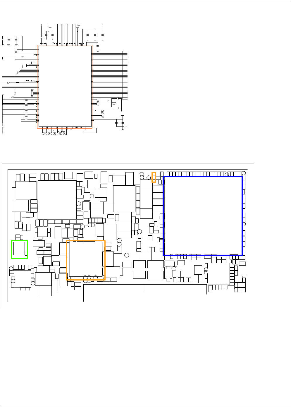
Level 3Repair
Distribution, transmission, or infringement of any content or data from this document without Samsung’s written authorization is strictly prohibited.
Confidential and proprietary-the contents in this service guide subject to change without prior notice.
8-12
TP503
C524
VCC_SUB_2.0V
R507
R505
C517
C528
L501
C521
L506
C552
21
VDD_CAM_ISP_1.0V
OSC500
L512
VCC_SUB_3.4V
VKFC_1.0V_AP
L502
C519
L511
TP502
R502
C520
VG3D_1.0V_AP
VINT_1.0V_AP
V_BAT
VCC_SUB_1.4V
C518
V_BAT
C526
C551
C522
L503
C525
R506
VCC_SUB_2.0V
L504
C559
L509
VRTC_1.8V
N9GNDB6
VMIF_1.1V_AP
N13NC
N2
VINB10
N3
VINB4
N4 SW4
N5GNDB4
N6GNDB3
N7 SW3
N8
VINB3
M6GNDB3
M7 SW3
M8
VINB3
M9GNDB6
N1NC
N10 SW6
N11
VINB7
N12 SW7
M10 FB6
M11
VINB6
M12 FB7
M13GNDB7
M2
VINB10
VINB4M3
M4 SW4
M5GNDB4
L3 FB4
L4 RS4P
L5 RS4N
L6 RS3N
L7 RS3P
FB3
L8
L9
VLDO24
M1 SW10
K8
VLDO38
K9
VLDO16
L1GNDB10
L10
VLDO13
L11
VLDO1
VLDO27 L12
L13
VLDO22
L2 FB10
K12
VINL1
K13
VLDO6
K2GNDB22
K3AGND
K4
VBAT
AGND
K5
K6AGND
K7AGND
J5
LDO7EN
J6
LDO13EN
J7AGND
J8NC
J9
VLDO14
GNDB22
K1
K10
VINL5
K11
VLDO9
J1 SW22
J10
VLDO19
J11
VLDO23
J12
VLDO11
J13
VLDO35
J2 SW22
J3
WDRSTEN
J4 BUCK10EN
H2
VINB22
H3 FB2
H4 PWRHOLD
H5NC
H6
LDO19EN
H7
VBAT
H8
VREF
H9
VLDO26
G7 ACOKB
G8
VLDO37
G9
VLDO25
H1
VINB22
H10
VLDO34
H11
VINL6
H12
VLDO17
H13
VLDO28
G11
VLDO15
G12
VLDO36
G13
VLDO30
G2
VINB21
G3 RS2P
G4 IRQB
G5 MR1B
G6 MR2B
F4 ONOB
F5 RSOB
F6
SDA
F7 JIGONB
F8
VLDO31
F9
VLDO20
G1
VINB21
G10
VLDO21
E9
VLDO4
F1 SW21
F10
VINL3
F11
VLDO18
F12
VLDO33
F13
VLDO29
F2 SW21
F3 RS2N E13
VLDO32
E2GNDB21
E3
LDO18EN
E4 PWREN
E5NC
E6
SCL
E7 PWRON
E8
VLDO10
D6
AP32K
D7
VDD_CP
D8
VDD_BT
D9
VLDO5
E1GNDB21
E10
VLDO12
E11
VINL2
E12
VINL4
D10
VLDO8
D11
VLDO2 D12
VLDO3
D13
VLDO7
D2 B5V2
D3 B5V3
D4 B5S1
D5 B5S2
C3 FB5
C4AGND
C5
VBAT
C6 FB9
C7
CP32K
C8
BT32K
C9 BKCOIN
D1 B5V1
B8GNDB9
B9 SW92
C1GNDB1
C10
XTALOUT
C11
XTALIN
C12 FB8
C13GNDB8
C2 FB5
B12 SW8
B13GNDB8
B2 FB1
B3GNDB5
B4 SW5
B5
VINB5
B6
VINB9
B7 SW91
A5
VINB5
A6
VINB9
A7 SW91
A8GNDB9
A9 SW92
B1 SW1
B10
VB9
B11
VINB8
A1NC
A10
VB9
A11
VINB8
A12 SW8
A13NC
A2
VINB1
A3GNDB5
A4 SW5
U502
1NC
NC
2
TP504
VMEM_1.2V_AP
C523
VCC_SUB_3.4V
VARM_1.0V_AP
L505
L507
VCC_1.8V_AP
VCC_1.8V_AP
L510
VCC_SUB_1.4V
L508
R508
32KHZ_CP
BUCK9_GND
MIPI_1.8V_EN
32KHZ_AP
AP_PMIC_SCL
AP_PMIC_SDA
VG3D_1.0V_AP_SNSN
VINT_1.0V_AP_SNSN
VINT_1.0V_AP_SNSP
BUCK7_GND
BUCK4_GND
BUCK3_GND
BUCK6_GND
32KHZ_PMIC
MMC01_EN
MMC2_EN
BUCK2B_GND
BUCK10_GND
VG3D_1.0V_AP_SNSP
VARM_1.0V_AP_SNSN
VARM_1.0V_AP_SNSP
BUCK5_GND
BUCK9_GND
BUCK8_GND
BUCK1_GND
BUCK2A_GND
PMIC_ACOKB
AP_N_RST_IN
TF_EN
AP_PMIC_EN
C1100C1110
C1111
C1146
C401
C402
C403
C404
C407
C408
C409
C410
C411
C500
C501
C502
C503
C504
C505
C506
C507
C508
C509
C514
C515
C516
C517
C518
C519
C520
C521
C522
C523
C524
C541
C542
C543
C544
C545
C546
C548
C549
C550
C551
C553
C556
C557
C558
C559
C560
C561
C562
C564
C565
C566
C567
C568
C569
C572
C573
C574
C575
C576
C577
C578
C579
C580
C581
C582
C583
C584
C585
C586
C587
C588
C601
C602
C604
C605
C606
C607
C608
C609
C610
C611
C612
C613
C614
C615
C616
C617
C618
C619
C620C621
C622
C623
C624
C625
C626
C627
C628
C629
C630
C631
C632
C633
C634
C635
C636
C637
C638
C639
C640
C641
C642C643
C644
C645
C647
C648
C649
C650
C651
C652
C653
C654
C655
C656
C657
C658
C659
C660
C684
C685
C686
C690
C691
C692
C696
C697
C698
C699
C800
C801
C804
C805
C806
C814
C815
C817
C832
C837
C838
C902
C903
C904
C909
C910
C911
C912
C913
C916
C917
C918
C919
C920
C921
C922
C923
C929
C945
C946
C947
C950
C951
C955
C956
C957
C965
C966
C967
C968
C969
C970
C971
C972
C973
C974
C976
C977
C978
C979
C980
D800
F800
L601
L602
L603
L604
L605
L606
L607
L608
L609
L610
L611
L614
L800
L801
L904
L905
L909
L910
OSC600
R1100
R1102
R1103
R1104
R1105
R1106
R400
R401
R402
R403
R404
R410
R411
R416
R417
R418
R420
R422
R423
R424
R431
R432
R433
R434
R436
R437
R438
R440
R441
R442
R443
R444
R445
R447
R448
R451
R452
R457
R458
R459
R502
R503
R600
R603
R607
R610
R611
R617
R626
R630
R640
R641
R652
R653
R654
R800
R802
R803
R824
R825
R846
R847
R906
R908
R909
R912
R915
R923
R925
R926
R928
R929
R930
R931
R932
R933
SC105
TP_605
TP_BAT_ID
TP_BAT_THERM
TP_CDONE
TP_GRFC_400
TP_IF_RXDTP_IF_TXD
TP_MUIC_INT
TP_PON_OUT
TP_TFLASH_CMD
TP_TFLASH_CMD_1100
TP_TFLASH_D1100
TP_TFLASH_D1101
TP_TSP_INT
TP_USB_PHY_VBUS
TP_VREF_BAT
TP_VREG_600
TP400
TP601
TP602
TP603
TP604
TP800
TP801
TP901
TP902
TP904
TR600
TR601
TR603
TXDAC400
U1102
U600
U601
U603
U605
U609
U611
U801
U803
U806
U905
U908
U909
U911
U912
U914
U915
UCP400
VR601
ZD803
ZD820
ZD821
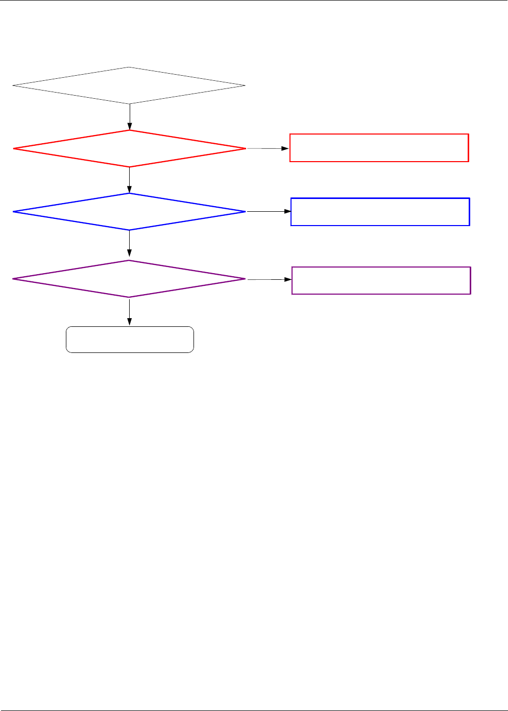
Level 3Repair
Distribution, transmission, or infringement of any content or data from this document without Samsung’s written authorization is strictly prohibited.
Confidential and proprietary-the contents in this service guide subject to change without prior notice.
8-13
8-3-4. Charging Part
TA /USB Insert
Yes
END
Check OVP input Voltage
C707 =5V
No Replace GH59-13985A
Yes
Check the Charger IC Input
Voltage(C565)=5V
No Replace U701(OVP IC)
Yes
Battery is Charging? No Replace U512
Yes
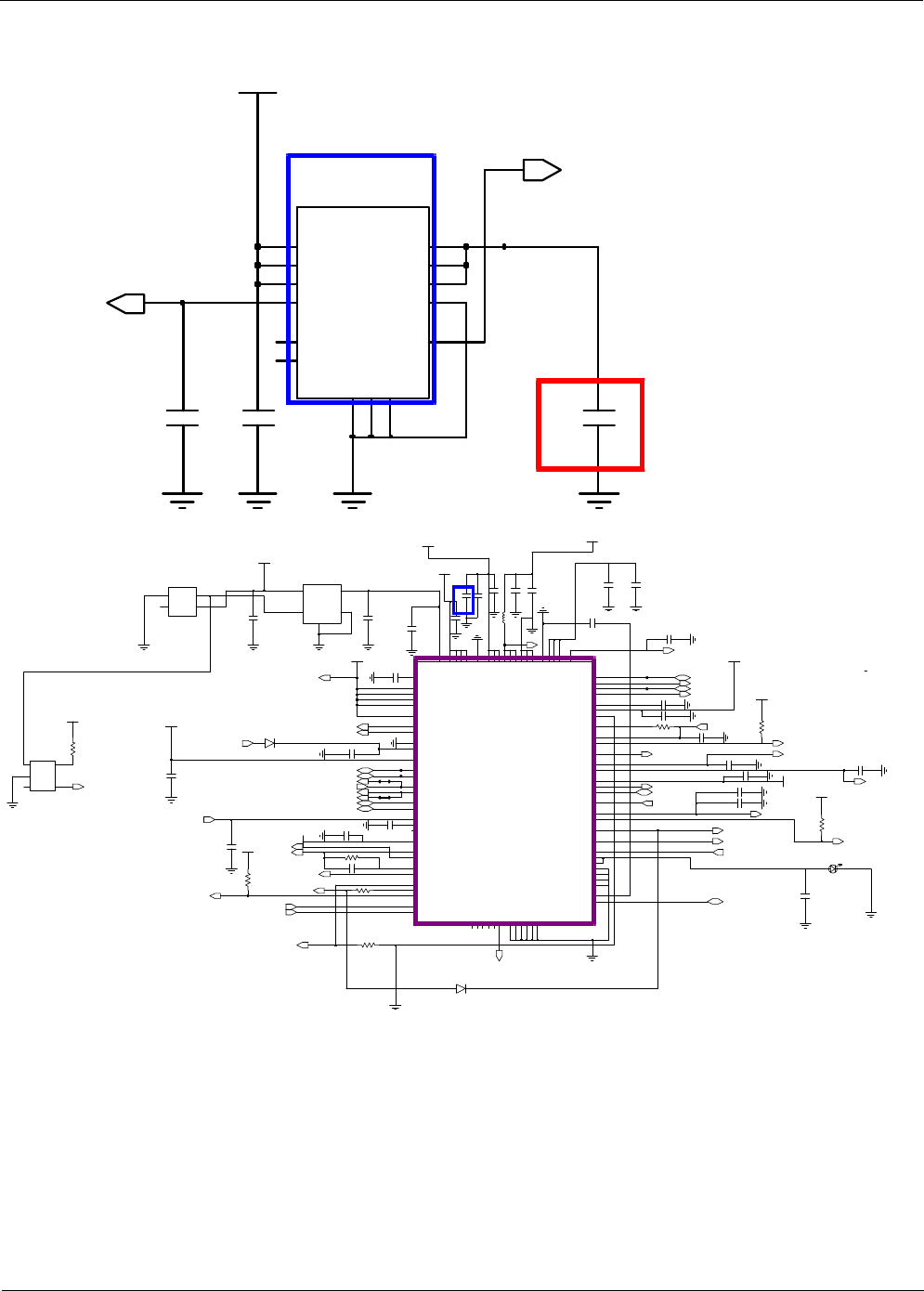
Level 3Repair
Distribution, transmission, or infringement of any content or data from this document without Samsung’s written authorization is strictly prohibited.
Confidential and proprietary-the contents in this service guide subject to change without prior notice.
8-14
C706
V_BUS_5V
VBUSDET
B1
B2 OUT
IN B3
B4GND
OVLO C1
C2
IN
IN C3
C4GND
U701
NC
1
2NC
_EN\ A1
A2 OUT
OUT
A3
A4GND
C707
C705
OVPEN
VBUSDET
C565
C590
C587
D501 C588
TP507
C583
R521
C564
C567
C568
VCC_1.8V_AP
C572
C586
R515
C592
R514
LED500
R524
2
VDD
U504
4GND
NC
3
1
OUT
U508
2GND
INA
1
3NC 4
OUTY
5
VCC
C594
L513
V_BAT
VCC_1.8V_AP
VCC_1.8V_AP
C591
VCC_1.8V_AP
TP508
C570
C571
V_BAT
R523
C566
BATTJ7
BATT
J8 DN1
J9 DP2
MVIO
H9 UID
J1CORNER
J10CORNER
J2
CHGPGJ3
CHGPG
J4 SYS
J5 SYS
J6
CHGPG
H10 COMP2
H2 BAT_SN
H3 BAT_SP
H4 SYS
H5 SYS
H6
BATTH7
BATT
H8
AVL
G3GND_A
G4GND_A
G5 MIC_USB G6
JIG
G7 IDB
G8
AUR2
G9 UR2
H1
DETBATB
F5
SDA
F6
MVBAT
F7
BC
F8 SR2
F9
ADP2
G1
CHGLX
G10 COMN1
G2
SYS_A
E7
AUT1
E8 UT1
E9
MVBUS
F1
CHGLX
F10
ADN1
F2
CHGLX
F3 INOKB
F4 AIN
D9
VBATTFG
E1
BYP
E10 SL1
E2
BYPE3
BYP
E4GND_D
E5
VIO
E6
CHGIN
D10
SDAFG
D2
CHGIN
D3
VBUSDET
D4 OVPENB
D5 DISQBAT
D6
SCL
D7GND_A
D8
SAFEOUT2
C3
FLASHEN
C4
TORCHEN
C5GND_Q
C6
MRSTB
C7
RESETB
C8
SCLFG
C9
ALRT
D1
MDN
B5GNDM
B6
INTB
B7
VCCTEST
B8
SNS
B9
VBFG
C1
CHGIN
C10
THRM
C2
TEST1 A7
TEST2 A8
TEST3 A9
TEST4
B1
SAFEOUT1
B10 KVSS
B2
FLED
B3 MPWM
B4
NC
2NC
A1CORNER
A10CORNER
A2
FLED
A3 MGAIN
A4 MDP
A5 IN_MOT
A6
U512
1
C589
V_BATTERY
C585
C573
V_BAT
TP506
C569
VDD 1
VOUT
VCC_3.0V_MOTOR
U505
3CE
GND
5
GND 2
4
R516
D502
C596
TP505
VCC_1.8V_AP
V_BUS_5V
C597
C562
R522
C5002
VBATFG
C574
V_BAT
200K
R520
C563
C584
C598
C582
FUEL_ALERT
FUEL_SDA_1.8V
VBUSDET
IF_PMIC_SCL_1.8V
BATT_TH
CP_TXD_1.8V
USB_D_M
IF_PMIC_SDA_1.8V
USB_D_P
CHG_LX
CP_RXD_1.8V
PMIC_JIGONB
AP_JTAG_EXTRST
MUIC_RST_INT
PMIC_ACOKB
CHG_LX
USB_VBUS_AP_4.9V
IF_PMIC_IRQ
USB_VBUS_CP_4.9V
CAM_FLASH_EN
CAM_FLASH_SET
nPOWER
FUEL_SCL_1.8V
VPS_L
VPS_R
MOTOR_N
MOTOR_P
VIBTONE_PWM
OVPEN
IF_CON_SENSE
V_BATTERY-
V_JIG_SENSE
V_BATTERY-
V_BATTERY_SENSE
USB2_AP_D-
USB2_AP_D+
AP_RXD
AP_TXD
JTAG_TXD
JTAG_RXD
MUIC_DM
MUIC_DP
MUIC_ID
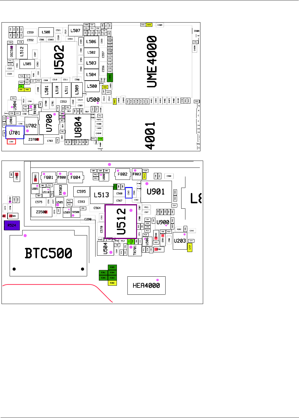
Level 3Repair
Distribution, transmission, or infringement of any content or data from this document without Samsung’s written authorization is strictly prohibited.
Confidential and proprietary-the contents in this service guide subject to change without prior notice.
8-15
C401
1
C404
0
C404
8
C404
9
C405
0
C4051
C407
3
C407
4
C408
9
C409
0
C4091
C409
2
C409
3
C409
4
C409
6
C409
9
C410
0
C500
0
C501
C50
2
C50
4
C50
5
C50
9
C51
2
C51
3
C51
4
C51
5
C51
6
C51
7
C51
8
C52
0
C52
3
C52
4
C52
5
C52
6
C52
9
C53
0
C531
C53
2
C53
3
C53
4
C53
5
C53
6
C53
7
C53
8
C53
9
C54
0
C541
C54
2
C54
3
C54
4
C54
5
C54
6
C54
7
C54
9
C55
0
C55
1
C55
2
C55
5
C55
6
C55
7
C56
0
C561
C70
2
C81
6
C81
8
C81
9
C82
0
C821
C82
2
C82
3
C82
4
C82
5
C82
6
C83
9
C91
2
L80
2
L80
3
R400
8
R401
5
R401
6
R402
8
R403
1
R4041
R404
2
R404
9
R405
0
R4051
R405
2
R405
3
R405
4
R405
5
R405
6
R405
7
R405
8
R405
9
R406
0
R4061
R406
2
R406
3
R406
5
R406
9
R407
0
R407
2
R407
3
R407
5
R408
0
R4081
R408
2
R408
7
R409
4
R410
3
R410
4
R410
5
R410
6
R410
7
R410
8
R410
9
R50
0
R501
R50
5
R50
6
R50
7
R50
8
R52
2
R70
0
R701
R70
2
R70
3
R80
3
R80
4
R80
5
R80
6
T
P50
0
TP50
1
TP50
2
T
P50
3
TP80
4
TP80
5
TP80
6
ZD80
0
C570
C80
6
R201
R51
8
ZD80
3
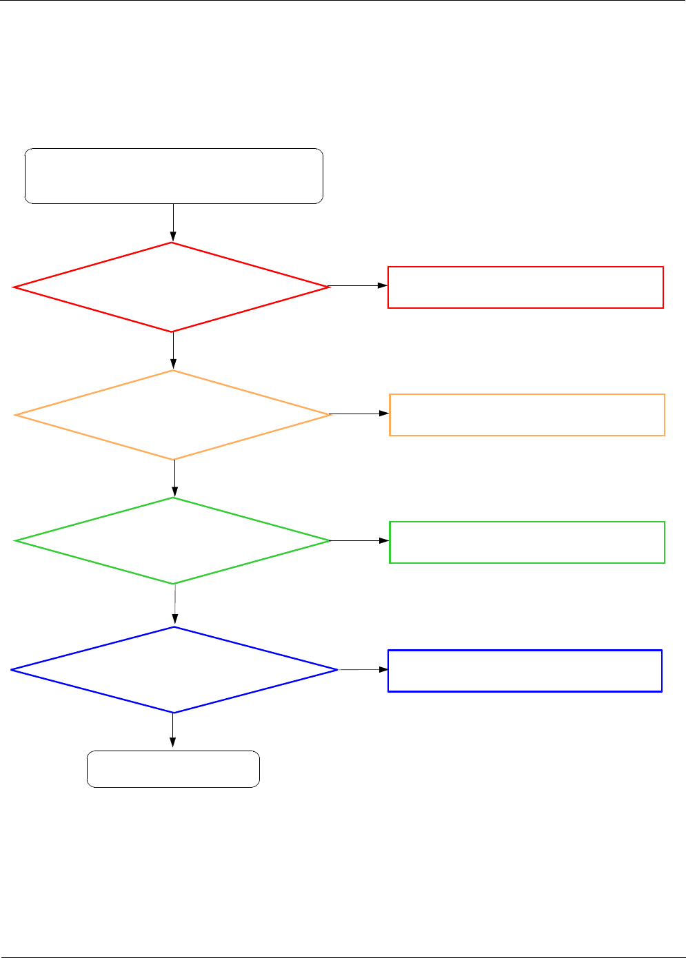
Level 3Repair
Distribution, transmission, or infringement of any content or data from this document without Samsung’s written authorization is strictly prohibited.
Confidential and proprietary-the contents in this service guide subject to change without prior notice.
8-16
8-3-5 Microphone Part
Check board
connection(HEA700) and
check connection IF FPCB to
Mic FPCB
Check the voltage at
TP614 =2.6V
Set the HEA700 connection
Set the IF FPCB to Hall IC FPCB connection
Set the Hall IC FPCB to Mic FPCB connection
resolder or replace U602
END
No
Yes
Yes
Yes
No
Check microphone function in voice call Hands-free
mode or Camera(camcording) mode
Check component soldering
statuses of L702,L703 Resolder or replace L702,L703
No
Yes
Check status of FPCB
(damaged or tore FPCB,
broken connector) Replace problem FPCB
No
Yes
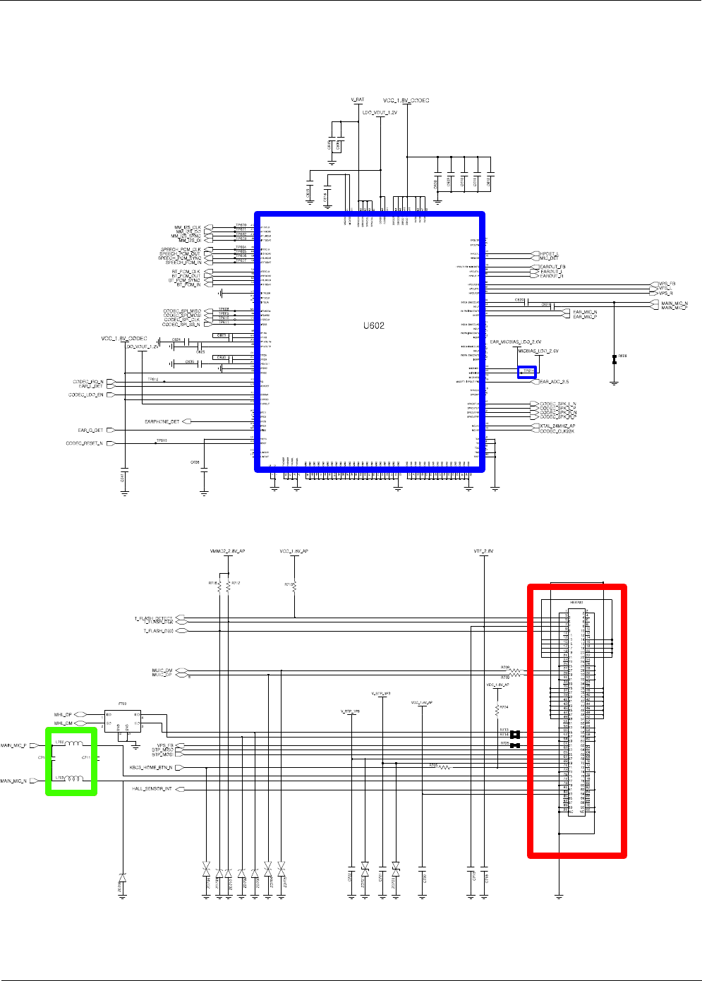
Level 3Repair
Distribution, transmission, or infringement of any content or data from this document without Samsung’s written authorization is strictly prohibited.
Confidential and proprietary-the contents in this service guide subject to change without prior notice.
8-17
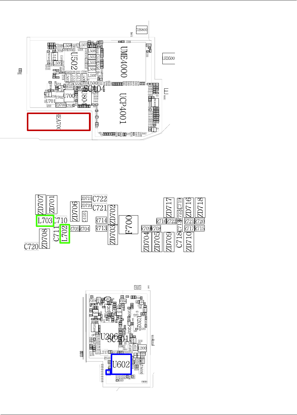
Level 3Repair
Distribution, transmission, or infringement of any content or data from this document without Samsung’s written authorization is strictly prohibited.
Confidential and proprietary-the contents in this service guide subject to change without prior notice.
8-18
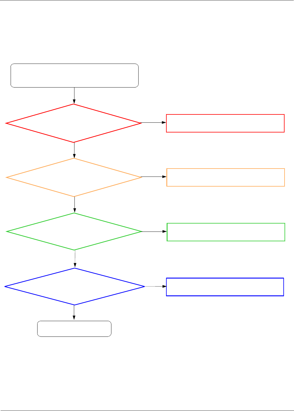
Level 3Repair
Distribution, transmission, or infringement of any content or data from this document without Samsung’s written authorization is strictly prohibited.
Confidential and proprietary-the contents in this service guide subject to change without prior notice.
8-19
8-3-6-1. Speaker Part (LEFT)
Check connection(HDC600)
Check component soldering
statuses of U602 and the
voltage at C605,C606 =VBAT
Connect HDC600
Resolder or replace U602
END
No
Yes
Yes
Yes
No
Check speaker function.
Play MP3 with maximum volume level.
Check component soldering
statuses of L610, L611 resolder or replace L610, L611
No
Yes
Connect other SPK Lmodule Replace SPK Lmodule
No
Yes
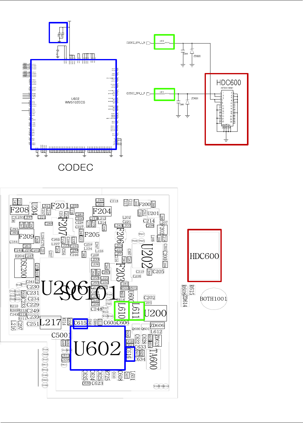
Level 3Repair
Distribution, transmission, or infringement of any content or data from this document without Samsung’s written authorization is strictly prohibited.
Confidential and proprietary-the contents in this service guide subject to change without prior notice.
8-20
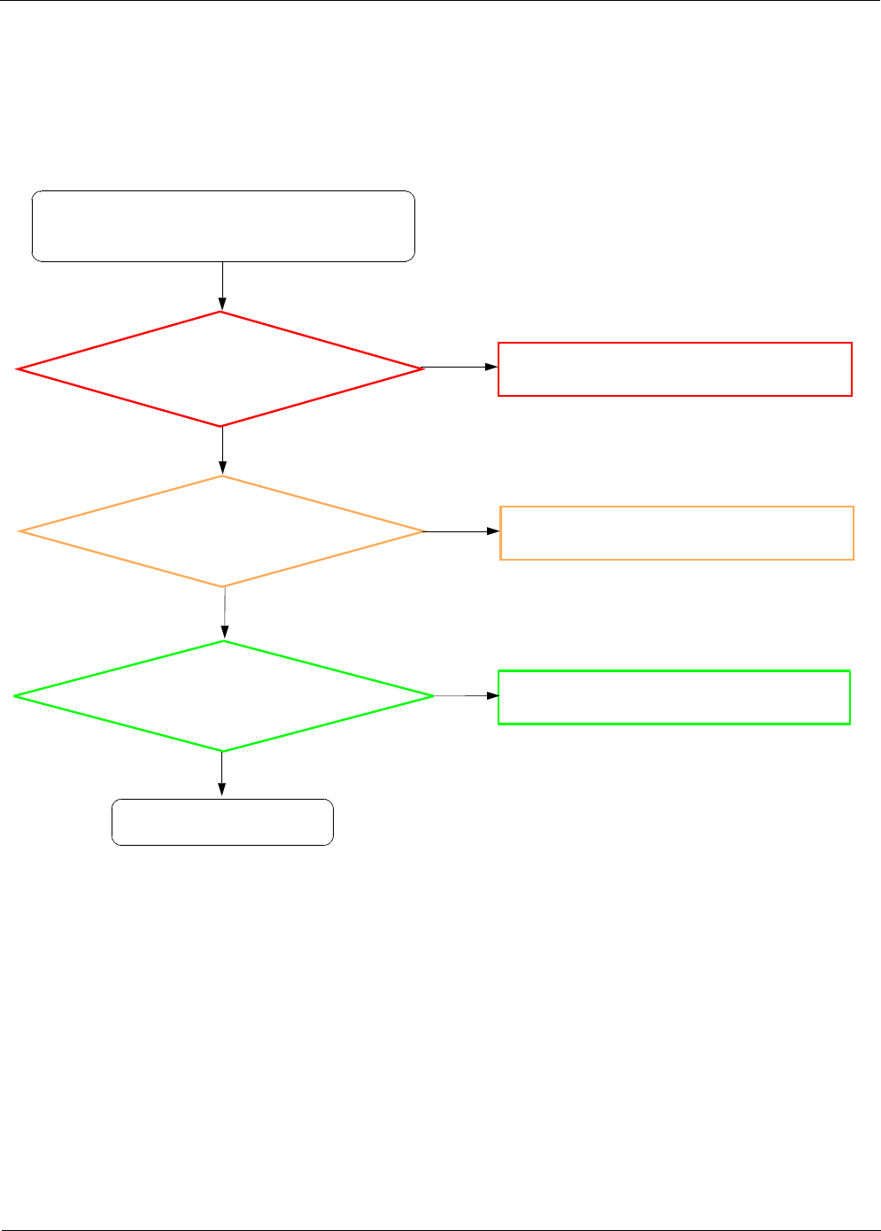
Level 3Repair
Distribution, transmission, or infringement of any content or data from this document without Samsung’s written authorization is strictly prohibited.
Confidential and proprietary-the contents in this service guide subject to change without prior notice.
8-21
8-3-6-2. Speaker Part (RIGHT)
Check clips for connection
where SPK Rmodule is
placed for any damage
Check component soldering
statuses of U602 and the
voltage at C605,C606 =VBAT
replace ANT600, ANT601
resolder or replace L610, L611
No
Yes
Yes
Yes
No
Check speaker function.
Play MP3 with maximum volume level.
Connect other SPK Rmodule Replace SPK Rmodule
No
Yes
END
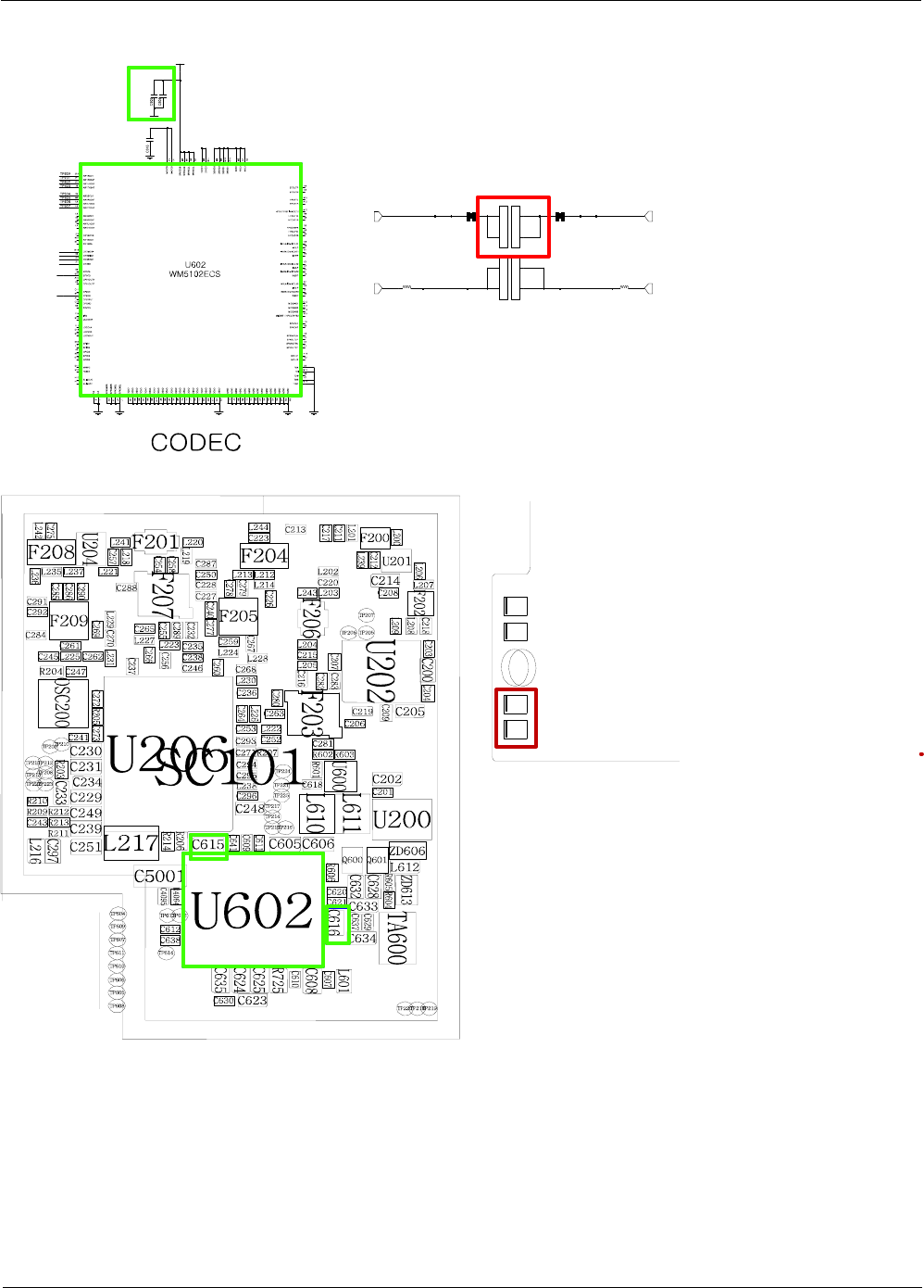
Level 3Repair
Distribution, transmission, or infringement of any content or data from this document without Samsung’s written authorization is strictly prohibited.
Confidential and proprietary-the contents in this service guide subject to change without prior notice.
8-22
L609L608
1
1
22
ANT600
HJ-1115-NB
11
2
2
HJ-1115-NB
ANT602 ANT603
HJ-1115-NB
1
1
22
HJ-1115-NB
ANT601
11
2
2
R622R621
MOTOR_P
CODEC_SPK_R_P
MOTOR_N
CODEC_SPK_R_N
ANT60
0
ANT60
1
ANT60
2
ANT60
3
BOTH100
2
BOTH100
3
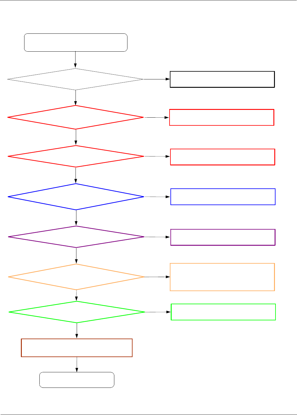
Level 3Repair
Distribution, transmission, or infringement of any content or data from this document without Samsung’s written authorization is strictly prohibited.
Confidential and proprietary-the contents in this service guide subject to change without prior notice.
8-23
8-3-7. BT
BT is not working
Check BT function ON No Enable BT Function
Yes
END
Check the antenna c-clip
has no problem? No Replace antenna c-clip, ANT200&ANT201
Yes
Check the REAR antenna pattern
(open, crack, deviation, etc)
No Replace REAR
Yes
Check the Voltage on
TP223,C243 =1.8VC294=1.2V No Check the AP(UCP4001),
(crack, open, damaged, etc.)
Check L238 open
Yes
Yes
Yes
No Check the CHARGER IC(U512)
(crack, open, damaged, etc.)
Yes
Check the Voltage on
C244 ≥3.4V
Check the Status of
OSC200, R205,C272,C273
No Resolder or change the
OSC200, R205,C272,C273
Resolder or Replace U206
Check (crack,open,etc)
L202, C223, F204, C208, C210, F206, L204,
C215, C216, F203, C271
Resolder or change the wrong element
(open, crack, deviation, etc)
No
Yes
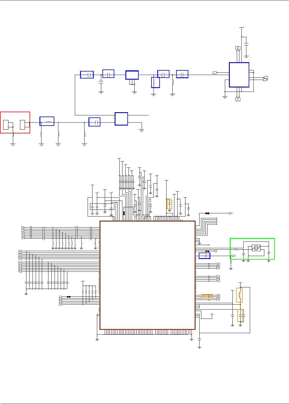
Level 3Repair
Distribution, transmission, or infringement of any content or data from this document without Samsung’s written authorization is strictly prohibited.
Confidential and proprietary-the contents in this service guide subject to change without prior notice.
8-24
L204 L205
C208
C210
L245
GND1
2
P1
P2
4
P3
3
F204
L211
C223
ANT201
1
1
22
L202
C215 C216
C220
G
2
G
3
G
5
IN 1
4OUT
F206
L244
LNAEN
6
VDD
7
BT
VBT8
9VRX
VTX
1
ANT
10
11 GND
MARK 12
13
MARK
TX
2
N|C
3
4
RX 5
F203
C206
VDD_LDO3P3_B
L210
ANT200
1
1
22
SW_WL_2G_LNA_EN_0
SW_BT_TX
SW_WL_2G_RX_0
SW_WL_2G_TX_0
WL_TX_G_CORE0_CAP
WL_RX_G_CORE0_ETR
BT_TX
C285
L217
R210
R205
C294
C279
C234
C273
C296
OSC200
2
43
1
C263
R214
C288
TP209
R209
TP225
VDD_CBUCK_1P35
L229
L222
VDD_LDO3P3_B
C278
VDD_LDO3P3_B
TP219
C230
C270
VDD_BTWIFI_1P8
C251
C233
TP218
VDD_LNLDO_1P2
TP216
TP208
VDD_CLDO_1P2
TP210
L238
BTLDO2P5
C293
VDD_LDO3P3_B
C286
L228
C229
C260
TP224
R212
C284
C247
C243
TP223
WRF_SYNTH_VBAT_VDD3P3V6
WRF_RFIN_2G_core1
V7
V8 WRF_RFOUT_2G_core1
WRF_PA2G_VBAT_VDD3P3_core1V9
WRF_RFIN_5G_core0
V1
WRF_PA5G_VBAT_VDD3P3_core1V10
V11 WRF_RFOUT_5G_core1
WRF_RFIN_5G_core1
V12
WRF_LNA_5G_GND1P2_core0
V2
WRF_RX5G_GND1P2_core0
V3
WRF_BUCK_GND1P5_core0
V4
WRF_CP_GND1P2
V5
WRF_PA5G_VBAT_GND3P3_core0
U2
WRF_TSSI_A_core0
U3
U4
WRF_BUCK_VDD1P5_core0
WRF_PFD_GND1P2
U5
WRF_VCO_GND1P2
U6
WRF_LNA_2G_GND1P2_core1
U7
WRF_PA2G_VBAT_GND3P3_core1
U8WRF_PA2G_VBAT_GND3P3_core1
U9
WRF_MMD_GND1P2
T6
WRF_RX2G_GND1P2_core1
T7
T8WRF_TX_GND1P2_core1
WRF_PADRV_VBAT_VDD3P3_core1T9
WRF_RFOUT_5G_core0
U1
WRF_PA5G_VBAT_GND3P3_core1
U10
WRF_PA5G_VBAT_GND3P3_core1
U11
WRF_LNA_5G_GND1P2_core1
U12
WRF_PA5G_VBAT_VDD3P3_core0T1
WRF_PADRV_VBAT_GND3P3_core1
T10
T11 WRF_TSSI_A_core1
WRF_RX5G_GND1P2_core1
T12
WRF_PA5G_VBAT_GND3P3_core0
T2
WRF_PADRV_VBAT_GND3P3_core0
T3
WRF_PFD_VDD1P2T4
WRF_MMD_VDD1P2T5
WRF_PA2G_VBAT_GND3P3_core0
R2
WRF_PADRV_VBAT_VDD3P3_core0R3
R4 WRF_GPIO_OUT_core0
WRF_LOGENG_GND1P2
R5WRF_LOGEN_GND1P2
R6
RF_SW_CTRL_0
R7
WRF_AFE_GND1P2_core1
R8
WRF_GPIO_OUT_core1
R9
WRF_TX_GND1P2_core0
P3
WRF_AFE_GND1P2_core0
P4
P5 RF_SW_CTRL_6
RF_SW_CTRL_5
P7
RF_SW_CTRL_2
P9
WRF_PA2G_VBAT_VDD3P3_core0R1
WRF_BUCK_VDD1P5_core1R11
WRF_BUCK_GND1P5_core1
R12
WRF_RX2G_GND1P2_core0
N3
RF_SW_CTRL_4
N5
N7 RF_SW_CTRL_3
RF_SW_CTRL_1
N8
WRF_RFOUT_2G_core0
P1
WRF_XTAL_VDD1P5P11
WRF_XTAL_IN P12
WRF_PA2G_VBAT_GND3P3_core0
P2
BT_PCM_CLK M6
VDDCM7
M8 RF_SW_CTRL_7
WRF_RFIN_2G_core0
N1
WRF_XTAL_VDD1P2N10
WRF_XTAL_GND1P2
N11
WRF_XTAL_OUT N12
WRF_LNA_2G_GND1P2_core0
N2
RF_SW_CTRL_15
L8
RF_SW_CTRL_11
L9
M1
BT_PAVDD2P5
RF_SW_CTRL_14
M10
RF_SW_CTRL_10
M12
BT_IFVSS
M3
VSSC
M4
VDDCM5
VDDCL10
VSSC
L11
L2BT_PAVSS
BT_PLLVSS
L3
BT_DEV_WAKE L4
BT_UART_CTS_L L5
BT_I2S_WS L6
VSSC
L7
RF_SW_CTRL_8
K12
BT_PLLVDD1P2 K2
K3
BT_IFVDD1P2
BT_GPIO_4 K4
BT_UART_RTS_L K5
BT_PCM_SYNC K6
BT_VDDO K7
BT_RF L1
BT_HOST_WAKE J3
BT_PCM_IN J4
J5
BT_UART_TXD
BT_I2S_CLK J6
VDDCJ8
RF_SW_CTRL_12
J9
BT_LNAVDD1P2 K1
RF_SW_CTRL_13
K10
BT_PCM_OUT H4
BT_UART_RXD H5
H7
AVDD_BBPLL
GPIO_4 H9
BT_VCOVDD1P2 J1
RF_SW_CTRL_9
J11
VDDCJ12
BT_VCOVSS
J2
AVSS_BBPLL
G7
VSSC
G8
G9
GPIO_3
FM_RFIN H1
VDDIO_RFH11
GPIO_10 H12
FM_LNAVSS
H2
VDDCH3
VDDCG10
GPIO_0 G11
G12VSSC
FM_VCOVSS
G2
FM_PLLVSS
G3
VSSC
G4
BT_I2S_DI G5
BT_I2S_DO G6
FM_PLLVDD1P2 F3
CLK_REQ F4
F5
BT_USB_DP
LPO_IN F6
GPIO_8 F7
GPIO_6 F8
GPIO_5 F9
FM_LNAVCOVDD1P2 G1
GPIO_7 E7
VDDIO_SDE8
E9
VDDC
FM_AOUT2 F1
GPIO_1 F10
GPIO_2 F11
VOUT_3P3F12
FM_AUDIOVSS
F2
FM_AOUT1 E1
VDDIOE10
E11
VOUT_LDO3P3_B
LDO_VDDBAT5VE12
FM_AUDIOVDD1p2 E2
VDDCE4
BT_USB_DN E5
GPIO_9 E6
VOUT_LNLDOD11
VOUT_BTLDO2P5D12
D3VSSC
VDDCD4
PCIE_CLKREQ_L
D5
VSSC
D6
RREFHSIC
D7
JTAG_SEL D9
PCIE_TESTP
C3
PCIE_PERST_L
C4
C5 PCIE_PME_L
HSIC_DVDD12C6
HSIC_AVDD12C7
SDIO_DATA_3
C8
SDIO_DATA_1
C9
BT_REG_ON D10
VDDCB7
SDIO_DATA_2
B8
B9 SDIO_DATA_0
PCIE_RDP
C1
VSSC
C10
VOUT_CLDOC11
LDO_VDD1P5C12
PCIE_TESTN
C2
PMU_AVSS
B10
SR_VDDBATA5VB11
B12
SR_VDDBATP5V
PCIE_RXTX_AVDD1P2B2
PCIE_PLL_AVDD1P2B3
PCIE_RXTX_AVSS
B4
PCIE_PLL_AVSS
B5
HSIC_AGND12
B6
PCIE_TDN
A3 PCIE_REFCLKP
A4
A5 PCIE_REFCLKN
HSIC_DATA
A6 HSIC_STROBE
A7
SDIO_CLK
A8
SDIO_CMD
A9
PCIE_RDN
B1
U206
1MARK
MARK
2
WL_REG_ON A10
SR_VLXA11
SR_PVSS
A12
PCIE_TDP
A2
L224
C265
C248
C237
TP220
C289
C245
C259
TP212
TP215
VDD_LDO3P3
C249
C277
R207
C231
C261
C283
VDD_CBUCK_1P35
C235
C256
L231
TP222
C266
TP221
C246
VDD_CBUCK_1P35
BTLDO2P5
R213
C295
L227
C236
VDD_BTWIFI_1P8
C267
VDD_LDO3P3
VDD_LDO3P3
C232
VDD_LNLDO_1P2
TP214
C264
VDD_BTWIFI_1P8
C255
L223
VDD_LDO3P3_B
C271
C281
C238
TP217
VBAT_4354K
VBAT_4354K
C269
L230
TP211
C282
L225
R211
TP213
C268
C253
R203
C262
C287
C241
C252
C239
VDD_LDO3P3_B
R206
C280
VDD_CLDO_1P2
R204
VDD_CLDO_1P2
C272
L226
WLAN_HOST_WAKE
BT_TX
BT_WIFI_CLK32K
SW_BT_TX
SW_WL_5G_LNA_EN_1
SW_WL_5G_TX_1
SW_WL_5G_RX_1
SW_WL_2G_TX_1
WL_TX_G_CORE1_CAP
WL_RX_G_CORE1_ETR
WL_TX_A_CORE1_CAP
WL_RX_A_CORE1_ETR
WL_TX_A_CORE0_CAP
WL_RX_A_CORE0_ETR
WL_TX_G_CORE0_CAP
WL_RX_G_CORE0_ETR
BT_PCM_CLK
BT_PCM_IN
BT_PCM_OUT
BT_WAKE
BT_HOST_WAKE
WLAN_SDIO_D(3)
WLAN_SDIO_D(0)
WLAN_SDIO_CLK
BT_UART_RTS
BT_UART_TXD
BT_UART_CTS
BT_UART_RXD
BT_EN
WLAN_EN
BT_PCM_SYNC
WLAN_SDIO_CMD
WLAN_SDIO_D(2)
WLAN_SDIO_D(1)
SW_WL_5G_TX_0
SW_WL_2G_RX_0
SW_WL_5G_RX_0
SW_WL_5G_LNA_EN_0
SW_WL_2G_LNA_EN_1
SW_WL_2G_RX_1
SW_WL_2G_TX_0
SW_WL_2G_LNA_EN_0
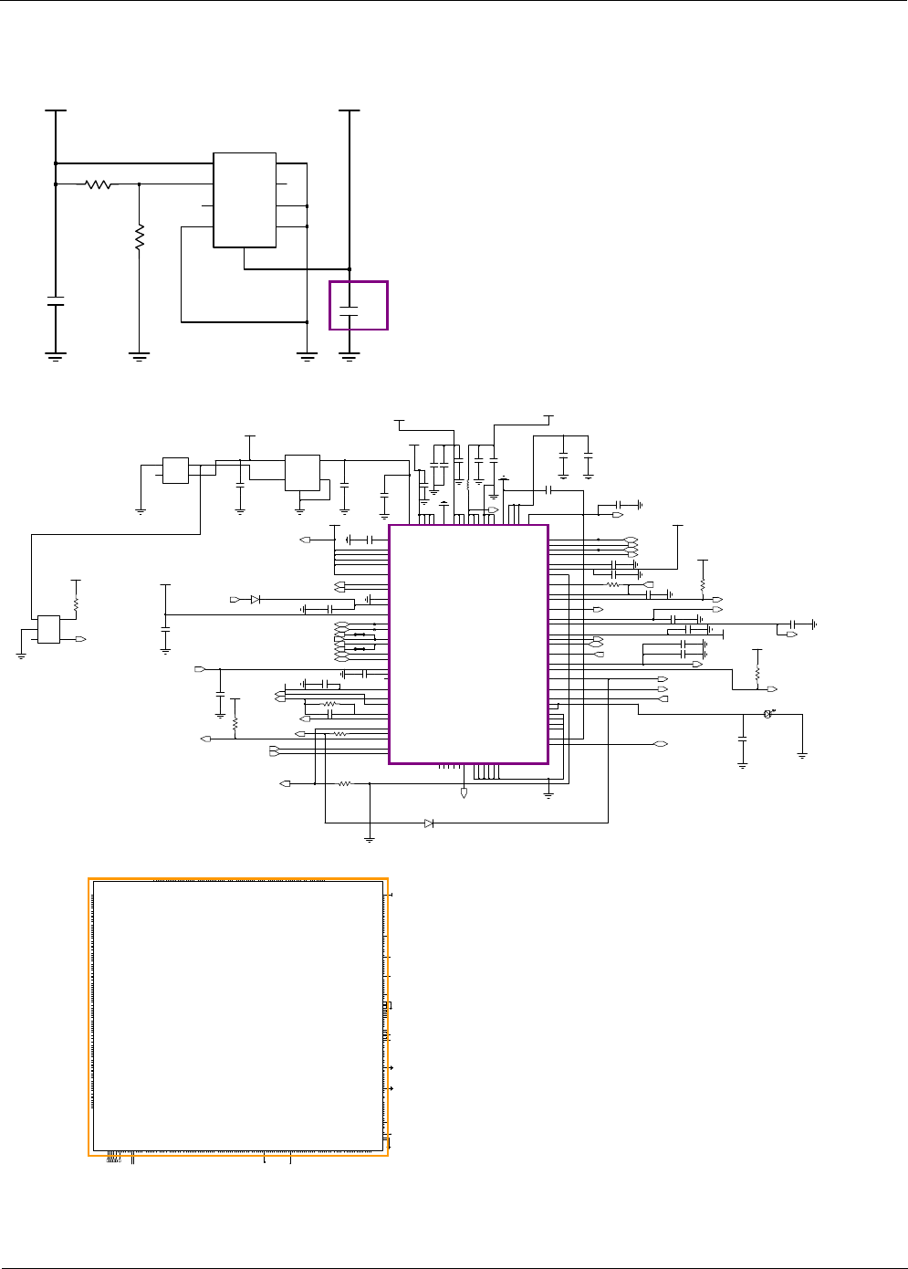
Level 3Repair
Distribution, transmission, or infringement of any content or data from this document without Samsung’s written authorization is strictly prohibited.
Confidential and proprietary-the contents in this service guide subject to change without prior notice.
8-25
C244
V_BAT
_EN 5
7
_FLAG
R201
GND 8
6
GS
ILIM
4
IN
1
NC
3
9OUT
2VBAT
U203
C242
R202
VBAT_WIFI
C565
C590
C587
D501 C588
TP507
C583
R521
C564
C567
C568
VCC_1.8V_AP
C572
C586
R515
C592
R514
LED500
R524
2
VDD
U504
4GND
NC
3
1
OUT
U508
2GND
INA
1
3NC 4
OUTY
5
VCC
C594
L513
V_BAT
VCC_1.8V_AP
VCC_1.8V_AP
C591
VCC_1.8V_AP
TP508
C570
C571
V_BAT
R523
C566
BATTJ7
BATT
J8 DN1
J9 DP2
MVIO
H9 UID
J1CORNER
J10CORNER
J2
CHGPGJ3
CHGPG
J4 SYS
J5 SYS
J6
CHGPG
H10 COMP2
H2 BAT_SN
H3 BAT_SP
H4 SYS
H5 SYS
H6
BATTH7
BATT
H8
AVL
G3GND_A
G4GND_A
G5 MIC_USB G6
JIG
G7 IDB
G8
AUR2
G9 UR2
H1
DETBATB
F5
SDA
F6
MVBAT
F7
BC
F8 SR2
F9
ADP2
G1
CHGLX
G10 COMN1
G2
SYS_A
E7
AUT1
E8 UT1
E9
MVBUS
F1
CHGLX
F10
ADN1
F2
CHGLX
F3 INOKB
F4 AIN
D9
VBATTFG
E1
BYP
E10 SL1
E2
BYPE3
BYP
E4GND_D
E5
VIO
E6
CHGIN
D10
SDAFG
D2
CHGIN
D3
VBUSDET
D4 OVPENB
D5 DISQBAT
D6
SCL
D7GND_A
D8
SAFEOUT2
C3
FLASHEN
C4
TORCHEN
C5GND_Q
C6
MRSTB
C7
RESETB
C8
SCLFG
C9
ALRT
D1
MDN
B5GNDM
B6
INTB
B7
VCCTEST
B8
SNS
B9
VBFG
C1
CHGIN
C10
THRM
C2
TEST1 A7
TEST2 A8
TEST3 A9
TEST4
B1
SAFEOUT1
B10 KVSS
B2
FLED
B3 MPWM
B4
NC
2NC
A1CORNER
A10CORNER
A2
FLED
A3 MGAIN
A4 MDP
A5 IN_MOT
A6
U512
1
C589
V_BATTERY
C585
C573
V_BAT
TP506
C569
VDD 1
VOUT
VCC_3.0V_MOTOR
U505
3CE
GND
5
GND 2
4
R516
D502
C596
TP505
VCC_1.8V_AP
V_BUS_5V
C597
C562
R522
C5002
VBATFG
C574
V_BAT
200K
R520
C563
C584
C598
C582
FUEL_ALERT
FUEL_SDA_1.8V
VBUSDET
IF_PMIC_SCL_1.8V
BATT_TH
CP_TXD_1.8V
USB_D_M
IF_PMIC_SDA_1.8V
USB_D_P
CHG_LX
CP_RXD_1.8V
PMIC_JIGONB
AP_JTAG_EXTRST
MUIC_RST_INT
PMIC_ACOKB
CHG_LX
USB_VBUS_AP_4.9V
IF_PMIC_IRQ
USB_VBUS_CP_4.9
V
CAM_FLASH_EN
CAM_FLASH_SET
nPOWER
FUEL_SCL_1.8V
VPS_L
VPS_R
MOTOR_N
MOTOR_P
VIBTONE_PWM
OVPEN
IF_CON_SENSE
V_BATTERY-
V_JIG_SENSE
V_BATTERY-
V_BATTERY_SENSE
USB2_AP_D-
USB2_AP_D+
AP_RXD
AP_TXD
JTAG_TXD
JTAG_RXD
MUIC_DM
MUIC_DP
MUIC_ID
(I2C_5_SCL)
(I2C_2_SDA)
(I2C_4_SDA)
(I2C_6_SCL)
(I2C_5_SDA)
(I2C_2_SCL)
(I2C_3_SCL)
(I2C_3_SDA)
(I2C_7_SDA)
(I2C_7_SCL)
(I2C_4_SCL)
(I2C_6_SDA)
C4100
R4087
Y7 XUTXD_3
Y1
XUSB30OVERCUR_U2
Y2
XUSB30VBUSCTRL_U3
Y3
XUFSNRESET
Y33
XJTMS
Y34
XJDBGSEL
Y4
XUHOSTOVERCUR Y5
XUHOSTPWREN
Y6 XURXD_3
W3
XUSB31OVERCUR_U3
W33
XJTCK
W34
XJTRSTN
W4
XUSB31VBUSCTRL_U2
W5
XUSB31OVERCUR_U2
W6
XI2C8SDA_HS
W7 XUTXD_2
W8
XI2C9SCL_HS
V3 XI2C1SDA
V4
XUSB31VBUSCTRL_U3
V5
XI2C8SCL_HS
V6 XI2C1SCL
V7
XI2C10SDA_HS
V8 XI2C0SDA
W1
XUSB30OVERCUR_U3
W2
XUSB30VBUSCTRL_U2
U4 XURTSN_2
XI2C10SCL_HS
U5
U6
XI2C9SDA_HS
U7 XUTXD_0
U8 XPWMTOUT_1
V21
XTSTEST_OUT0
V23
XTSTEST_OUT4
V24
XTSEXT_RES4
T5 XPWMTOUT_0
T6
XURXD_1
T7 XURTSN_0
T8
XI2C0SCL
U12
XTSEXT_RES1
U20
XTSEXT_RES0
U3 XURTSN_1
R6 XI2S2SCLK
R7
XURXD_0
R8 XUCTSN_2
T1
POP_VREFCA_E2
T12
XTSTEST_OUT1
T3 XPWMTOUT_3
T32
XDRAM1VREF2
T4
XPWMTOUT_2
P1
XUSB3RX0M_1
P2
POP_ZQ_E2
P4
XUHOSTDP
P5
XI2S2SDO
P7 XUCTSN_0
P8 XURXD_2
R2 XI2S1LRCK
POP_VREFDQ_E2R32
R5 XI2S2CDCLK
M7
XI2S2LRCK
M8 XI2S1SDI
N1
XUSB3RX0P_1
N3
XUHOSTVBUS
N4
XUHOSTDM
N5
XUHOSTREXT
N7 XUTXD_1
N8 XUCTSN_1
L3
XUSB3REFPADCLKP_1 L5
XUSB3RESREF_1
L6 XSPIMISO_0
L7 XSPICLK_1
L8 XI2S1SCLK
M2
POP_ZQ1_E2
M5
XUHOSTANALOGTEST
M6 XSPIMOSI_0
J8 XI2S1SDO
K1
XUSB3TX0P_1
K3
XUSB3DP0_1
K6 XSPICSN_1
K7 XSPIMISO_1
K8 XI2S1CDCLK
L1
XUSB3TX0M_1
L2
XUSB3REFPADCLKM_1
H4
XUSB3VBUS0_1
H6 XSPICLK_0
H7
XADC0AIN_0
H8 XI2S2SDI
J3
XUSB3DM0_1
J5
XUSB3ID0_1
J6 XSPIMOSI_1
J7 XSPICSN_0
G2
XUSB3REFPADCLKP_0 G3
XUSB3RESREF_0
G6
XADC0AIN_2
G7
XADC0AIN_5
G8
XADC0AIN_1
G9
XADC0AIN_4
H1
XUSB3RX0M_0
H33
XDRAM1VREF0
F7
XADC0AIN_3
F9XGPIO15
G1
XUSB3RX0P_0
G10
XADC0AIN_7
G11
XADC0AIN_8
G12
XADC0AIN_9
G13
XTSTEST_OUT2
G14
XTSEXT_RES2
F11XEINT_0
F14
XCLKOUT
F15XEINT_6
F18
XTSEXT_RES3
F19
XTSTEST_OUT3
F2
XUSB3REFPADCLKM_0
F33
XDRAM1ZQ
F6
XADC0AIN_6
E19
XNWRESET
E3
XUSB3DP0_0
E4
XUSB3VBUS0_0
XUSB3ID0_0E5
E7
XGPIO8
E8XGPIO9
E9
XGPIO10
F10
XGPIO12
D3
XUSB3DM0_0
D4
XAUDI2S0CDCLK
D6XGPIO3
D7XGPIO6
D9
XGPIO14
E1
XUSB3TX0M_0
E10XGPIO11
E14
XNRESET
D20
XDRAM0VREF0
D21
XOM_0
D22XEINT_4
D24XEINT_2
D25XEINT_10
D26XEINT_11
D27
XDRAM0VREF2
D28XEINT_16
C6XGPIO2
C7XGPIO5
C8XGPIO7
D1
XUSB3TX0P_0
D10XGPIO13
D13
XPWRRGTON
D18
XDRAM0ZQ
D19
XOM_5
C26
XRTCCLKO
C28XEINT_25
C29XEINT_27
C3XAUDI2S0LRCK
C30XEINT_30
C31XEINT_29
C4XAUDI2S0SCLK
C5XAUDI2S0SDO_0
C18
XPSHOLD
C19
XOM_6
C20
POP_VREFDQ_E1
C21XEINT_31
C22XEINT_21
C23XEINT_17
C24XEINT_18
C25XEINT_20
B6XGPIO0
XGPIO1
B7
C10
XHSICSTROBE1 C11
XHSICDATA1
C12
XEINT_3
C13
XOM_3
C15
XOM_1
XNRSTOUTC17
B20
XOM_2
B22XEINT_19
B26XEINT_14
B27XEINT_28
B28XEINT_23
B30XEINT_24
B31XEINT_22
B5
XAUDI2S0SDO_1
AV16
POP_VREFCA_E1
AV27
XADC1AIN_1
AV30
XV1FRM
B12
XXTI
B15
XEINT_5
B16
XRTCXTI
B17
XOM_4
B18XEINT_15
AU13
XMIPI1VREG_0P4V
AU19
XHDMIREXT
AU27
XADC1AIN_0
AU28
XADC1AIN_3
AU29
XADC1AIN_2
AU30
XV1VSYNC_LDI
AU31XGPIO17
AV12
POP_ZQ_E1
AT3
XMIPI0VREG_0P4V
AT31
XGPIO16
AT4
XMIPI0MDP3 AT5
XMIPI0MDP2
AT6
XMIPI0MDPCLK
AT7
XMIPI0MDP1
AT8
XMIPI0MDP0
AU12
POP_ZQ1_E1
AT19
XHDMITX2P
AT20
XHDMIXTI
AT21
XDPRBIAS
AT22
XDPAUXP
AT23
XDPTX0P
AT24
XDPTX1P
AT25
XDPTX2P
AT26
XDPTX3P
AT11
XMIPI1MDP2
AT12
XMIPI1MDPCLK
AT13
XMIPI1MDP1
AT14
XMIPI1MDP0
AT16
XHDMITXCP
AT17
XHDMITX0P
AT18
XHDMITX1P
AR28 XISPGP4
AR29 XISPI2C2SDA
AR30 XISPI2C0SCL
AR4
XMIPI0MDN3 AR5
XMIPI0MDN2
AR6
XMIPI0MDNCLK
AR7
XMIPI0MDN1 AR8
XMIPI0MDN0
AT10
XMIPI1MDP3
AR19
XHDMITX2N
AR20
XHDMIXTO
AR22
XDPAUXN
AR23
XDPTX0N
AR24
XDPTX1N
AR25
XDPTX2N
AR26
XDPTX3N
AR27 XISPGP5
AR10
XMIPI1MDN3
AR11
XMIPI1MDN2
AR12
XMIPI1MDNCLK
AR13
XMIPI1MDN1
AR14
XMIPI1MDN0
AR16
XHDMITXCN
AR17
XHDMITX0N
AR18
XHDMITX1N
AP28 XISPGP1
AP29 XISPGP0
AP30 XISPI2C0SDA
AP4
XMIPI0SDP3 AP5
XMIPI0SDP2
AP6
XMIPI0SDPCLK
XMIPI0SDP1
AP7
AP8
XMIPI0SDP0
AP19 XISPSPI0CSN
AP20 XISPGP6
AP21 XISPSPI1MISO
AP22 XISPSPI1CSN
XISPI2C2SCL
AP23
AP24 XISPI2C1SDA
AP25 XISPGP7
AP27
XISPGP2
XMIPI0SDN0
AN9
XMMC2DATA_2
AP1
XUFSXTI
AP10
XMIPI1SDP3
AP11
XMIPI1SDP2
AP12
XMIPI1SDPCLK
AP13
XMIPI1SDP1
AP14
XMIPI1SDP0
XISPGP8
AN25 XISPSPI0CLK
AN27 XISPGP3
AN28 XISPI2C1SCL
AN4
XMIPI0SDN3 AN5
XMIPI0SDN2
AN6
XMIPI0SDNCLK
AN7
XMIPI0SDN1 AN8
AN14
XMIPI1SDN0
AN16
XCI1RGB_4
AN17
XCI1RGB_0
AN19 XISPGP9
AN20 XISPSPI1MOSI
AN21 XISPSPI0MISO
AN22 XISPSPI1CLK
AN23 XISPSPI0MOSI
AN24
AM6
XMMC2BIUVR
AM7 XMMC2CLK
AM9 XMMC0CMD
AN1
XUFSXTO
AN10
XMIPI1SDN3
AN11
XMIPI1SDN2
AN12
XMIPI1SDNCLK
AN13
XMIPI1SDN1
AM13
XCI1VSYNC
AM14XCI1RGB_9
AM15
XCI1RGB_10
AM16XCI1RGB_3
AM17XCI1RGB_7
AM3
XUFSTXDP1
AM4
XUFSTXDN1
AM5 XMMC2DATA_0
AL17
XCI1PCLK
AL3
XUFSTXDP0
XUFSTXDN0 AL4
AL5 XMMC2DATA_3
AL6 XMMC2CDN
AM10 XMMC2DATA_1
AM11 XMMC2CMD
AM12XCI1HSYNC
AK9
XMMC0RDQS
AL10
XMMC0CLK
XMMC0DATA_3
AL11
AL12XCI1MCLK
AL13XCI1RGB_13
AL14XCI1RGB_5
AL15
XCI1RGB_6
AL16XCI1RGB_1
AK14XCI1RGB_12
AK15
XCI1RGB_8
AK16
XCI1RGB_2
AK3
XUFSREFCLK_OUT
AK4
XUFSREFCLK
AK5 XMMC2WP
AK6 XMMC0CDN
AK7 XMMC0DATA_6
AJ3
XUFSRXDP0
AJ4
XUFSRXDN0
AJ5 XMMC1DATA_2
AJ6 XMMC1DATA_3
AJ8 XMMC0DATA_2
AJ9 XMMC0DATA_7
AK10 XMMC1CDN
XCI1RGB_11
AK13
AH3
XUFSRXDP1
AH4
XUFSRXDN1
AH5
XMMC1DATA_7
AH6 XMMC1INTN
AH8 XMMC1DATA_1
AH9XSRAMCSN_0
AJ10 XMMC1DATA_0
AJ11XSRAMCSN_2
AG5XSRAMBEN_1
AG6
XSRAMWAITN
AG7
XSRAMBEN_0
AG8XSRAMDATA_1
AG9XSRAMDATA_0
AH10
XSRAMCSN_3
AH11
XSRAMCSN_1
AH2
XUFSREXT
AF8
XSRAMDATA_4
AF9
XSRAMDATA_6
AG1 XMMC0DATA_1
AG10XSRAMDATA_RDN
AG11
XSRAMWEN
AG2 XMMC0DATA_0
AG3 XMMC0DATA_4
AG4XSRAMOEN
AE8XSRAMDATA_11
AE9XSRAMDATA_13
AF10XSRAMDATA_3
AF3 XMMC0DATA_5
AF4
XSRAMDATA_2
AF5XSRAMDATA_5
AF6XSRAMDATA_7
AF7
XSRAMDATA_8
AD7
XSRAMDATA_14
AD8XSRAMFRNB_2
AD9XSRAMFCLE
AE10
XSRAMDATA_10
AE3
XMMC0RESETOUT
AE5XSRAMFALE
AE6
XSRAMDATA_12
XSRAMDATA_9
AE7
AC7XSRAMADDR_5
AC8XSRAMFRNB_1
AD1 XMMC1CMD
AD10XSRAMDATA_15
AD2 XMMC1CLK
AD3
XMMC1RDQS
AD5XSRAMFRNB_0
AD6XSRAMADDR_1
AC1 XMMC1DATA_5
AC2 XMMC1DATA_4
AC3 XMMC1BEPW
AC33
XOMCCI
AC34
XJTDI
AC4XSRAMADDR_3
AC5XSRAMFRNB_3
AC6XSRAMADDR_0
AB2 XMMC1DATA_6
AB3
XMMC1WP
AB33
XJTDO
AB4XSRAMADDR_8
AB5XSRAMADDR_11
AB6XSRAMADDR_4
AB7XSRAMADDR_7
AB8XSRAMADDR_2
AA1
XEFFSOURCE_0
AA2XSRAMADDR_6
AA3XSRAMADDR_10
AA4XSRAMADDR_15
XSRAMADDR_13
AA5
AA6XSRAMADDR_14
AA7XSRAMADDR_12
AA8XSRAMADDR_9
A21XEINT_9
A23XEINT_8
A25XEINT_12
A28XEINT_13
A29XEINT_26
A4
XAUDI2S0SDI
A6XAUDI2S0SDO_2
A8XGPIO4
NC
1
NC 2
A12
XXTO
XEINT_1
A13
A16
XRTCXTO
A17
XEINT_7
UCP4001-1
R4109
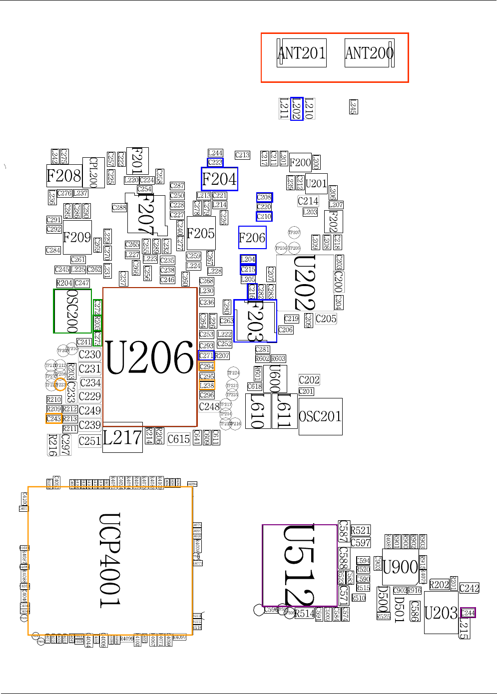
Level 3Repair
Distribution, transmission, or infringement of any content or data from this document without Samsung’s written authorization is strictly prohibited.
Confidential and proprietary-the contents in this service guide subject to change without prior notice.
8-26
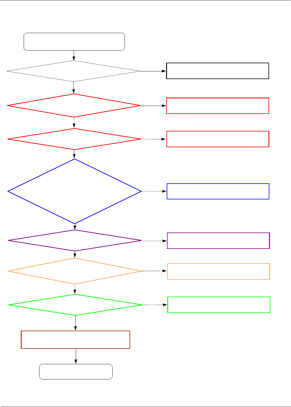
Level 3Repair
Distribution, transmission, or infringement of any content or data from this document without Samsung’s written authorization is strictly prohibited.
Confidential and proprietary-the contents in this service guide subject to change without prior notice.
8-27
8-3-8. WIFI
WIFI is not working
Check WIFI function ON No Enable WIFI Function
Yes
END
Check the antenna C-clip has no
problem?
No Replace the antenna c-clip
ANT200,ANT201,ANT202,ANT203
Yes
Check the REAR antenna pattern
(open, crack, deviation, etc)
No Replace REAR
Yes
Check the Voltage on
TP222&C243=1.8V,C294=1.2V
No Check the AP(UCP4001)
(crack, open, damaged, etc.)
Check L238 open
Yes
Yes
Yes
No Check the CHARGER IC(U512)
(crack, open, damaged, etc.)
Yes
Check the Voltage on
C244 ≥3.4V
Check the Status of
OSC200, R205,C272,C273
No Resolder or change the
OSC200, R205,C272,C273
Resolder or Replace U206
Check WIFI MIMO RF
PATH(crack,open,etc)
L202,C223,F204,C208,C210,F206,L204,C215,
C216,F203,L213,C221,C226,F205,L232,C275,
F208,CPL200,C225,C222,F201,C224,C254,
F207,L236,C276,C290,F209,C252,C253,C255,
C256,C259,C260,C261,C262,C263,C264,
C265,C266,C267,C268,C269,C270
Resolder or change the wrong element
(open, crack, deviation, etc)
No
Yes
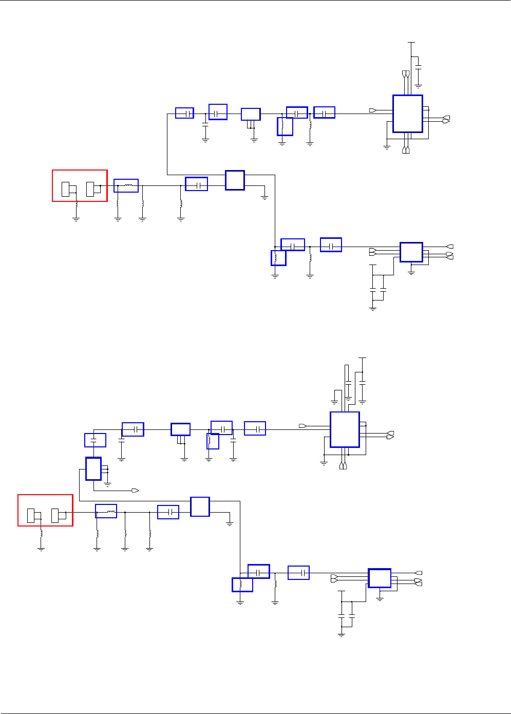
Level 3Repair
Distribution, transmission, or infringement of any content or data from this document without Samsung’s written authorization is strictly prohibited.
Confidential and proprietary-the contents in this service guide subject to change without prior notice.
8-28
L246
L204 L205
C208
C226
C210
L232
C228
L245
L234
GND
1
2
P1
P2
4
P3
3
C257
F204
C250
L211
C223
L237
L240
4VDD LANEN 5
6
RX
NC 7
8
TX
GND
9
F209
ANT
1
VRX
2
VTX
3
GND
ANT
2VRX
VTX
3
4VDD LANEN 5
6
RX
NC 7
8
TX
9
F205
1
L214
ANT201
1
1
22
L202
11
2
2
L213
ANT203
1
2
2
C227
ANT202
1
C215 C216
C220
G
2
G
3
G
5
IN 1
4OUT
F206
C221
L242
L244
C276
C291
LNAEN
6
VDD
7
BT
VBT8
9VRX
VTX
1
ANT
10
11 GND
MARK 12
13
MARK
TX
2
N|C
3
4
RX 5
F203
5COM
G2
G4
G6
3
HIGH
1LOW
CPL200
VDD_LDO3P3_B
VDD_LDO3P3_B
C225
C222
C206
C275
C224
F201
2
G
3
G
5
G
1
IN
OUT
4
4
RX 5
LNAEN
VDD6
BT7
8
VBT
VRX
9
VTX
1
10 ANT
GND
11
12
MARK
MARK 13
2TX
3N|C
F207
C290
VDD_LDO3P3_B
L220 C258
C292
C254
P3
F208
1
GND
P1 2
P2
4
3
L236
L210
VDD_LDO3P3_B
C240
ANT200
1
1
22
GPS_ANT_SUB
SW_WL_2G_LNA_EN_1
SW_WL_2G_RX_1
SW_WL_2G_TX_1
WL_TX_G_CORE1_CAP
WL_RX_G_CORE1_ETR
SW_WL_2G_LNA_EN_0
SW_BT_TX
SW_WL_2G_RX_0
SW_WL_2G_TX_0
WL_TX_G_CORE0_CAP
WL_RX_G_CORE0_ETR
BT_TX
SW_WL_5G_LNA_EN_1
WL_RX_A_CORE1_ETR
WL_TX_A_CORE1_CAP
SW_WL_5G_RX_1
SW_WL_5G_TX_1
SW_WL_5G_RX_0
SW_WL_5G_TX_0
SW_WL_5G_LNA_EN_0
WL_RX_A_CORE0_ETR
WL_TX_A_CORE0_CAP
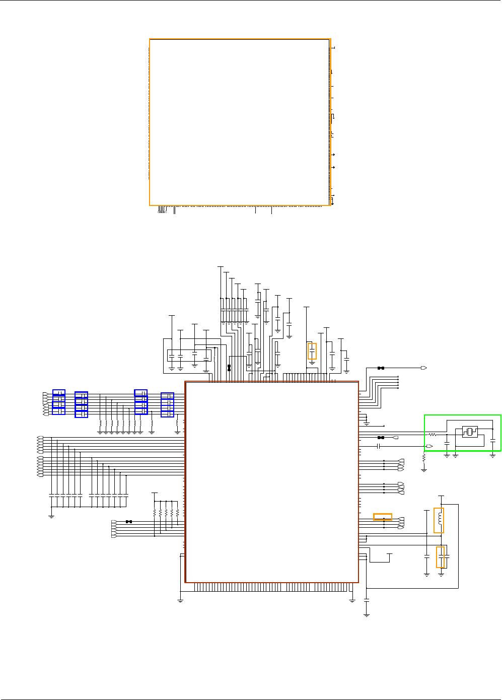
Level 3Repair
Distribution, transmission, or infringement of any content or data from this document without Samsung’s written authorization is strictly prohibited.
Confidential and proprietary-the contents in this service guide subject to change without prior notice.
8-29
C285
L217
R210
R205
C294
C279
C234
C273
C296
OSC200
2
43
1
C263
R214
C288
TP209
R209
TP225
VDD_CBUCK_1P35
L229
L222
VDD_LDO3P3_B
C278
VDD_LDO3P3_B
TP219
C230
C270
VDD_BTWIFI_1P8
C251
C233
TP218
VDD_LNLDO_1P2
TP216
TP208
VDD_CLDO_1P2
TP210
L238
BTLDO2P5
C293
VDD_LDO3P3_B
C286
L228
C229
C260
TP224
R212
C284
C247
C243
TP223
WRF_SYNTH_VBAT_VDD3P3V6
WRF_RFIN_2G_core1
V7
V8 WRF_RFOUT_2G_core1
WRF_PA2G_VBAT_VDD3P3_core1V9
WRF_RFIN_5G_core0
V1
WRF_PA5G_VBAT_VDD3P3_core1V10
V11 WRF_RFOUT_5G_core1
WRF_RFIN_5G_core1
V12
WRF_LNA_5G_GND1P2_core0
V2
WRF_RX5G_GND1P2_core0
V3
WRF_BUCK_GND1P5_core0
V4
WRF_CP_GND1P2
V5
WRF_PA5G_VBAT_GND3P3_core0
U2
WRF_TSSI_A_core0
U3
U4
WRF_BUCK_VDD1P5_core0
WRF_PFD_GND1P2
U5
WRF_VCO_GND1P2
U6
WRF_LNA_2G_GND1P2_core1
U7
WRF_PA2G_VBAT_GND3P3_core1
U8WRF_PA2G_VBAT_GND3P3_core1
U9
WRF_MMD_GND1P2
T6
WRF_RX2G_GND1P2_core1
T7
T8WRF_TX_GND1P2_core1
WRF_PADRV_VBAT_VDD3P3_core1T9
WRF_RFOUT_5G_core0
U1
WRF_PA5G_VBAT_GND3P3_core1
U10
WRF_PA5G_VBAT_GND3P3_core1
U11
WRF_LNA_5G_GND1P2_core1
U12
WRF_PA5G_VBAT_VDD3P3_core0T1
WRF_PADRV_VBAT_GND3P3_core1
T10
T11 WRF_TSSI_A_core1
WRF_RX5G_GND1P2_core1
T12
WRF_PA5G_VBAT_GND3P3_core0
T2
WRF_PADRV_VBAT_GND3P3_core0
T3
WRF_PFD_VDD1P2T4
WRF_MMD_VDD1P2T5
WRF_PA2G_VBAT_GND3P3_core0
R2
WRF_PADRV_VBAT_VDD3P3_core0R3
R4 WRF_GPIO_OUT_core0
WRF_LOGENG_GND1P2
R5WRF_LOGEN_GND1P2
R6
RF_SW_CTRL_0
R7
WRF_AFE_GND1P2_core1
R8
WRF_GPIO_OUT_core1
R9
WRF_TX_GND1P2_core0
P3
WRF_AFE_GND1P2_core0
P4
P5 RF_SW_CTRL_6
RF_SW_CTRL_5
P7
RF_SW_CTRL_2
P9
WRF_PA2G_VBAT_VDD3P3_core0R1
WRF_BUCK_VDD1P5_core1R11
WRF_BUCK_GND1P5_core1
R12
WRF_RX2G_GND1P2_core0
N3
RF_SW_CTRL_4
N5
N7 RF_SW_CTRL_3
RF_SW_CTRL_1
N8
WRF_RFOUT_2G_core0
P1
WRF_XTAL_VDD1P5P11
WRF_XTAL_IN P12
WRF_PA2G_VBAT_GND3P3_core0
P2
BT_PCM_CLK M6
VDDCM7
M8 RF_SW_CTRL_7
WRF_RFIN_2G_core0
N1
WRF_XTAL_VDD1P2N10
WRF_XTAL_GND1P2
N11
WRF_XTAL_OUT N12
WRF_LNA_2G_GND1P2_core0
N2
RF_SW_CTRL_15
L8
RF_SW_CTRL_11
L9
M1
BT_PAVDD2P5
RF_SW_CTRL_14
M10
RF_SW_CTRL_10
M12
BT_IFVSS
M3
VSSC
M4
VDDCM5
VDDCL10
VSSC
L11
L2BT_PAVSS
BT_PLLVSS
L3
BT_DEV_WAKE L4
BT_UART_CTS_L L5
BT_I2S_WS L6
VSSC
L7
RF_SW_CTRL_8
K12
BT_PLLVDD1P2 K2
K3
BT_IFVDD1P2
BT_GPIO_4 K4
BT_UART_RTS_L K5
BT_PCM_SYNC K6
BT_VDDO K7
BT_RF L1
BT_HOST_WAKE J3
BT_PCM_IN J4
J5
BT_UART_TXD
BT_I2S_CLK J6
VDDCJ8
RF_SW_CTRL_12
J9
BT_LNAVDD1P2 K1
RF_SW_CTRL_13
K10
BT_PCM_OUT H4
BT_UART_RXD H5
H7
AVDD_BBPLL
GPIO_4 H9
BT_VCOVDD1P2 J1
RF_SW_CTRL_9
J11
VDDCJ12
BT_VCOVSS
J2
AVSS_BBPLL
G7
VSSC
G8
G9
GPIO_3
FM_RFIN H1
VDDIO_RFH11
GPIO_10 H12
FM_LNAVSS
H2
VDDCH3
VDDCG10
GPIO_0 G11
G12VSSC
FM_VCOVSS
G2
FM_PLLVSS
G3
VSSC
G4
BT_I2S_DI G5
BT_I2S_DO G6
FM_PLLVDD1P2 F3
CLK_REQ F4
F5
BT_USB_DP
LPO_IN F6
GPIO_8 F7
GPIO_6 F8
GPIO_5 F9
FM_LNAVCOVDD1P2 G1
GPIO_7 E7
VDDIO_SDE8
E9
VDDC
FM_AOUT2 F1
GPIO_1 F10
GPIO_2 F11
VOUT_3P3F12
FM_AUDIOVSS
F2
FM_AOUT1 E1
VDDIOE10
E11
VOUT_LDO3P3_B
LDO_VDDBAT5VE12
FM_AUDIOVDD1p2 E2
VDDCE4
BT_USB_DN E5
GPIO_9 E6
VOUT_LNLDOD11
VOUT_BTLDO2P5D12
D3VSSC
VDDCD4
PCIE_CLKREQ_L
D5
VSSC
D6
RREFHSIC
D7
JTAG_SEL D9
PCIE_TESTP
C3
PCIE_PERST_L
C4
C5 PCIE_PME_L
HSIC_DVDD12C6
HSIC_AVDD12C7
SDIO_DATA_3
C8
SDIO_DATA_1
C9
BT_REG_ON D10
VDDCB7
SDIO_DATA_2
B8
B9 SDIO_DATA_0
PCIE_RDP
C1
VSSC
C10
VOUT_CLDOC11
LDO_VDD1P5C12
PCIE_TESTN
C2
PMU_AVSS
B10
SR_VDDBATA5VB11
B12
SR_VDDBATP5V
PCIE_RXTX_AVDD1P2B2
PCIE_PLL_AVDD1P2B3
PCIE_RXTX_AVSS
B4
PCIE_PLL_AVSS
B5
HSIC_AGND12
B6
PCIE_TDN
A3 PCIE_REFCLKP
A4
A5 PCIE_REFCLKN
HSIC_DATA
A6 HSIC_STROBE
A7
SDIO_CLK
A8
SDIO_CMD
A9
PCIE_RDN
B1
U206
1MARK
MARK
2
WL_REG_ON A10
SR_VLXA11
SR_PVSS
A12
PCIE_TDP
A2
L224
C265
C248
C237
TP220
C289
C245
C259
TP212
TP215
VDD_LDO3P3
C249
C277
R207
C231
C261
C283
VDD_CBUCK_1P35
C235
C256
L231
TP222
C266
TP221
C246
VDD_CBUCK_1P35
BTLDO2P5
R213
C295
L227
C236
VDD_BTWIFI_1P8
C267
VDD_LDO3P3
VDD_LDO3P3
C232
VDD_LNLDO_1P2
TP214
C264
VDD_BTWIFI_1P8
C255
L223
VDD_LDO3P3_B
C271
C281
C238
TP217
VBAT_4354K
VBAT_4354K
C269
L230
TP211
C282
L225
R211
TP213
C268
C253
R203
C262
C287
C241
C252
C239
VDD_LDO3P3_B
R206
C280
VDD_CLDO_1P2
R204
VDD_CLDO_1P2
C272
L226
WLAN_HOST_WAKE
BT_TX
BT_WIFI_CLK32K
SW_BT_TX
SW_WL_5G_LNA_EN_1
SW_WL_5G_TX_1
SW_WL_5G_RX_1
SW_WL_2G_TX_1
WL_TX_G_CORE1_CAP
WL_RX_G_CORE1_ETR
WL_TX_A_CORE1_CAP
WL_RX_A_CORE1_ETR
WL_TX_A_CORE0_CAP
WL_RX_A_CORE0_ETR
WL_TX_G_CORE0_CAP
WL_RX_G_CORE0_ETR
BT_PCM_CLK
BT_PCM_IN
BT_PCM_OUT
BT_WAKE
BT_HOST_WAKE
WLAN_SDIO_D(3)
WLAN_SDIO_D(0)
WLAN_SDIO_CLK
BT_UART_RTS
BT_UART_TXD
BT_UART_CTS
BT_UART_RXD
BT_EN
WLAN_EN
BT_PCM_SYNC
WLAN_SDIO_CMD
WLAN_SDIO_D(2)
WLAN_SDIO_D(1)
SW_WL_5G_TX_0
SW_WL_2G_RX_0
SW_WL_5G_RX_0
SW_WL_5G_LNA_EN_0
SW_WL_2G_LNA_EN_1
SW_WL_2G_RX_1
SW_WL_2G_TX_0
SW_WL_2G_LNA_EN_0
(I2C_5_SCL)
(I2C_2_SDA)
(I2C_4_SDA)
(I2C_6_SCL)
(I2C_5_SDA)
(I2C_2_SCL)
(I2C_3_SCL)
(I2C_3_SDA)
(I2C_7_SDA)
(I2C_7_SCL)
(I2C_4_SCL)
(I2C_6_SDA)
C4100
R4087
Y7 XUTXD_3
Y1
XUSB30OVERCUR_U2
Y2
XUSB30VBUSCTRL_U3
Y3
XUFSNRESET
Y33
XJTMS
Y34
XJDBGSEL
Y4
XUHOSTOVERCUR Y5
XUHOSTPWREN
Y6 XURXD_3
W3
XUSB31OVERCUR_U3
W33
XJTCK
W34
XJTRSTN
W4
XUSB31VBUSCTRL_U2
W5
XUSB31OVERCUR_U2
W6
XI2C8SDA_HS
W7 XUTXD_2
W8
XI2C9SCL_HS
V3 XI2C1SDA
V4
XUSB31VBUSCTRL_U3
V5
XI2C8SCL_HS
V6
XI2C1SCL
V7
XI2C10SDA_HS
V8 XI2C0SDA
W1
XUSB30OVERCUR_U3
W2
XUSB30VBUSCTRL_U2
U4 XURTSN_2
XI2C10SCL_HS
U5
U6
XI2C9SDA_HS
U7 XUTXD_0
U8 XPWMTOUT_1
V21
XTSTEST_OUT0
V23
XTSTEST_OUT4
V24
XTSEXT_RES4
T5 XPWMTOUT_0
T6
XURXD_1
T7 XURTSN_0
T8
XI2C0SCL
U12
XTSEXT_RES1
U20
XTSEXT_RES0
U3 XURTSN_1
R6
XI2S2SCLK
R7
XURXD_0
R8 XUCTSN_2
T1
POP_VREFCA_E2
T12
XTSTEST_OUT1
T3 XPWMTOUT_3
T32
XDRAM1VREF2
T4
XPWMTOUT_2
P1
XUSB3RX0M_1
P2
POP_ZQ_E2
P4
XUHOSTDP
P5
XI2S2SDO
P7
XUCTSN_0
P8 XURXD_2
R2 XI2S1LRCK
POP_VREFDQ_E2R32
R5 XI2S2CDCLK
M7
XI2S2LRCK
M8 XI2S1SDI
N1
XUSB3RX0P_1
N3
XUHOSTVBUS
N4
XUHOSTDM
N5
XUHOSTREXT
N7 XUTXD_1
N8 XUCTSN_1
L3
XUSB3REFPADCLKP_1 L5
XUSB3RESREF_1
L6 XSPIMISO_0
L7 XSPICLK_1
L8 XI2S1SCLK
M2
POP_ZQ1_E2
M5
XUHOSTANALOGTEST
M6 XSPIMOSI_0
J8 XI2S1SDO
K1
XUSB3TX0P_1
K3
XUSB3DP0_1
K6 XSPICSN_1
K7 XSPIMISO_1
K8 XI2S1CDCLK
L1
XUSB3TX0M_1
L2
XUSB3REFPADCLKM_1
H4
XUSB3VBUS0_1
H6 XSPICLK_0
H7
XADC0AIN_0
H8 XI2S2SDI
J3
XUSB3DM0_1
J5
XUSB3ID0_1
J6 XSPIMOSI_1
J7 XSPICSN_0
G2
XUSB3REFPADCLKP_0 G3
XUSB3RESREF_0
G6
XADC0AIN_2
G7
XADC0AIN_5
G8
XADC0AIN_1
G9
XADC0AIN_4
H1
XUSB3RX0M_0
H33
XDRAM1VREF0
F7
XADC0AIN_3
F9XGPIO15
G1
XUSB3RX0P_0
G10
XADC0AIN_7
G11
XADC0AIN_8
G12
XADC0AIN_9
G13
XTSTEST_OUT2
G14
XTSEXT_RES2
F11XEINT_0
F14
XCLKOUT
F15XEINT_6
F18
XTSEXT_RES3
F19
XTSTEST_OUT3
F2
XUSB3REFPADCLKM_0
F33
XDRAM1ZQ
F6
XADC0AIN_6
E19
XNWRESET
E3
XUSB3DP0_0
E4
XUSB3VBUS0_0
XUSB3ID0_0E5
E7
XGPIO8
E8XGPIO9
E9
XGPIO10
F10
XGPIO12
D3
XUSB3DM0_0
D4
XAUDI2S0CDCLK
D6XGPIO3
D7XGPIO6
D9
XGPIO14
E1
XUSB3TX0M_0
E10XGPIO11
E14
XNRESET
D20
XDRAM0VREF0
D21
XOM_0
D22XEINT_4
D24XEINT_2
D25XEINT_10
D26XEINT_11
D27
XDRAM0VREF2
D28XEINT_16
C6XGPIO2
C7XGPIO5
C8XGPIO7
D1
XUSB3TX0P_0
D10XGPIO13
D13
XPWRRGTON
D18
XDRAM0ZQ
D19
XOM_5
C26
XRTCCLKO
C28XEINT_25
C29XEINT_27
C3XAUDI2S0LRCK
C30XEINT_30
C31XEINT_29
C4XAUDI2S0SCLK
C5XAUDI2S0SDO_0
C18
XPSHOLD
C19
XOM_6
C20
POP_VREFDQ_E1
C21XEINT_31
C22XEINT_21
C23XEINT_17
C24XEINT_18
C25XEINT_20
B6XGPIO0
XGPIO1
B7
C10
XHSICSTROBE1 C11
XHSICDATA1
C12
XEINT_3
C13
XOM_3
C15
XOM_1
XNRSTOUTC17
B20
XOM_2
B22XEINT_19
B26XEINT_14
B27XEINT_28
B28XEINT_23
B30XEINT_24
B31XEINT_22
B5
XAUDI2S0SDO_1
AV16
POP_VREFCA_E1
AV27
XADC1AIN_1
AV30
XV1FRM
B12
XXTI
B15
XEINT_5
B16
XRTCXTI
B17
XOM_4
B18XEINT_15
AU13
XMIPI1VREG_0P4V
AU19
XHDMIREXT
AU27
XADC1AIN_0
AU28
XADC1AIN_3
AU29
XADC1AIN_2
AU30
XV1VSYNC_LDI
AU31XGPIO17
AV12
POP_ZQ_E1
AT3
XMIPI0VREG_0P4V
AT31
XGPIO16
AT4
XMIPI0MDP3
AT5
XMIPI0MDP2
AT6
XMIPI0MDPCLK
AT7
XMIPI0MDP1
AT8
XMIPI0MDP0
AU12
POP_ZQ1_E1
AT19
XHDMITX2P
AT20
XHDMIXTI
AT21
XDPRBIAS
AT22
XDPAUXP
AT23
XDPTX0P
AT24
XDPTX1P
AT25
XDPTX2P
AT26
XDPTX3P
AT11
XMIPI1MDP2
AT12
XMIPI1MDPCLK
AT13
XMIPI1MDP1
AT14
XMIPI1MDP0
AT16
XHDMITXCP
AT17
XHDMITX0P
AT18
XHDMITX1P
AR28 XISPGP4
AR29 XISPI2C2SDA
AR30 XISPI2C0SCL
AR4
XMIPI0MDN3 AR5
XMIPI0MDN2
AR6
XMIPI0MDNCLK
AR7
XMIPI0MDN1 AR8
XMIPI0MDN0
AT10
XMIPI1MDP3
AR19
XHDMITX2N
AR20
XHDMIXTO
AR22
XDPAUXN
AR23
XDPTX0N
AR24
XDPTX1N
AR25
XDPTX2N
AR26
XDPTX3N
AR27 XISPGP5
AR10
XMIPI1MDN3
AR11
XMIPI1MDN2
AR12
XMIPI1MDNCLK
AR13
XMIPI1MDN1
AR14
XMIPI1MDN0
AR16
XHDMITXCN
AR17
XHDMITX0N
AR18
XHDMITX1N
AP28 XISPGP1
AP29
XISPGP0
AP30 XISPI2C0SDA
AP4
XMIPI0SDP3 AP5
XMIPI0SDP2
AP6
XMIPI0SDPCLK
XMIPI0SDP1
AP7
AP8
XMIPI0SDP0
AP19 XISPSPI0CSN
AP20 XISPGP6
AP21 XISPSPI1MISO
AP22 XISPSPI1CSN
XISPI2C2SCL
AP23
AP24 XISPI2C1SDA
AP25 XISPGP7
AP27
XISPGP2
XMIPI0SDN0
AN9
XMMC2DATA_2
AP1
XUFSXTI
AP10
XMIPI1SDP3
AP11
XMIPI1SDP2
AP12
XMIPI1SDPCLK
AP13
XMIPI1SDP1
AP14
XMIPI1SDP0
XISPGP8
AN25 XISPSPI0CLK
AN27 XISPGP3
AN28 XISPI2C1SCL
AN4
XMIPI0SDN3 AN5
XMIPI0SDN2
AN6
XMIPI0SDNCLK
AN7
XMIPI0SDN1 AN8
AN14
XMIPI1SDN0
AN16
XCI1RGB_4
AN17
XCI1RGB_0
AN19 XISPGP9
AN20 XISPSPI1MOSI
AN21 XISPSPI0MISO
AN22 XISPSPI1CLK
AN23 XISPSPI0MOSI
AN24
AM6
XMMC2BIUVR
AM7 XMMC2CLK
AM9 XMMC0CMD
AN1
XUFSXTO
AN10
XMIPI1SDN3
AN11
XMIPI1SDN2
AN12
XMIPI1SDNCLK
AN13
XMIPI1SDN1
AM13
XCI1VSYNC
AM14XCI1RGB_9
AM15
XCI1RGB_10
AM16XCI1RGB_3
AM17XCI1RGB_7
AM3
XUFSTXDP1
AM4
XUFSTXDN1
AM5 XMMC2DATA_0
AL17
XCI1PCLK
AL3
XUFSTXDP0
XUFSTXDN0 AL4
AL5 XMMC2DATA_3
AL6 XMMC2CDN
AM10 XMMC2DATA_1
AM11 XMMC2CMD
AM12XCI1HSYNC
AK9
XMMC0RDQS
AL10
XMMC0CLK
XMMC0DATA_3
AL11
AL12XCI1MCLK
AL13XCI1RGB_13
AL14XCI1RGB_5
AL15
XCI1RGB_6
AL16XCI1RGB_1
AK14XCI1RGB_12
AK15
XCI1RGB_8
AK16
XCI1RGB_2
AK3
XUFSREFCLK_OUT
AK4
XUFSREFCLK
AK5 XMMC2WP
AK6
XMMC0CDN
AK7 XMMC0DATA_6
AJ3
XUFSRXDP0
AJ4
XUFSRXDN0
AJ5 XMMC1DATA_2
AJ6 XMMC1DATA_3
AJ8 XMMC0DATA_2
AJ9 XMMC0DATA_7
AK10 XMMC1CDN
XCI1RGB_11
AK13
AH3
XUFSRXDP1
AH4
XUFSRXDN1
AH5
XMMC1DATA_7
AH6 XMMC1INTN
AH8 XMMC1DATA_1
AH9XSRAMCSN_0
AJ10 XMMC1DATA_0
AJ11XSRAMCSN_2
AG5XSRAMBEN_1
AG6
XSRAMWAITN
AG7
XSRAMBEN_0
AG8XSRAMDATA_1
AG9XSRAMDATA_0
AH10
XSRAMCSN_3
AH11
XSRAMCSN_1
AH2
XUFSREXT
AF8
XSRAMDATA_4
AF9
XSRAMDATA_6
AG1 XMMC0DATA_1
AG10XSRAMDATA_RDN
AG11
XSRAMWEN
AG2 XMMC0DATA_0
AG3 XMMC0DATA_4
AG4XSRAMOEN
AE8XSRAMDATA_11
AE9XSRAMDATA_13
AF10XSRAMDATA_3
AF3 XMMC0DATA_5
AF4
XSRAMDATA_2
AF5XSRAMDATA_5
AF6XSRAMDATA_7
AF7
XSRAMDATA_8
AD7
XSRAMDATA_14
AD8XSRAMFRNB_2
AD9XSRAMFCLE
AE10
XSRAMDATA_10
AE3
XMMC0RESETOUT
AE5XSRAMFALE
AE6
XSRAMDATA_12
XSRAMDATA_9
AE7
AC7XSRAMADDR_5
AC8XSRAMFRNB_1
AD1 XMMC1CMD
AD10XSRAMDATA_15
AD2 XMMC1CLK
AD3
XMMC1RDQS
AD5XSRAMFRNB_0
AD6XSRAMADDR_1
AC1 XMMC1DATA_5
AC2 XMMC1DATA_4
AC3 XMMC1BEPW
AC33
XOMCCI
AC34
XJTDI
AC4XSRAMADDR_3
AC5XSRAMFRNB_3
AC6XSRAMADDR_0
AB2 XMMC1DATA_6
AB3
XMMC1WP
AB33
XJTDO
AB4XSRAMADDR_8
AB5XSRAMADDR_11
AB6XSRAMADDR_4
AB7XSRAMADDR_7
AB8XSRAMADDR_2
AA1
XEFFSOURCE_0
AA2XSRAMADDR_6
AA3XSRAMADDR_10
AA4XSRAMADDR_15
XSRAMADDR_13
AA5
AA6XSRAMADDR_14
AA7XSRAMADDR_12
AA8XSRAMADDR_9
A21XEINT_9
A23XEINT_8
A25XEINT_12
A28XEINT_13
A29XEINT_26
A4
XAUDI2S0SDI
A6XAUDI2S0SDO_2
A8XGPIO4
NC 1
NC 2
A12
XXTO
XEINT_1
A13
A16
XRTCXTO
A17
XEINT_7
UCP4001-1
R4109
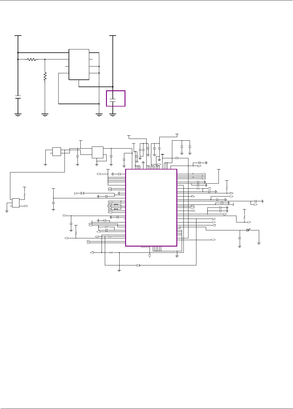
Level 3Repair
Distribution, transmission, or infringement of any content or data from this document without Samsung’s written authorization is strictly prohibited.
Confidential and proprietary-the contents in this service guide subject to change without prior notice.
8-30
C244
V_BAT
_EN 5
7
_FLAG
R201
GND 8
6
GS
ILIM
4
IN
1
NC
3
9OUT
2VBAT
U203
C242
R202
VBAT_WIFI
C565
C590
C587
D501 C588
TP507
C583
R521
C564
C567
C568
VCC_1.8V_AP
C572
C586
R515
C592
R514
LED500
R524
2
VDD
U504
4GND
NC
3
1
OUT
U508
2GND
INA
1
3NC 4
OUTY
5
VCC
C594
L513
V_BAT
VCC_1.8V_AP
VCC_1.8V_AP
C591
VCC_1.8V_AP
TP508
C570
C571
V_BAT
R523
C566
BATTJ7
BATT
J8 DN1
J9 DP2
MVIO
H9 UID
J1CORNER
J10CORNER
J2
CHGPGJ3
CHGPG
J4 SYS
J5 SYS
J6
CHGPG
H10 COMP2
H2 BAT_SN
H3 BAT_SP
H4 SYS
H5 SYS
H6
BATTH7
BATT
H8
AVL
G3GND_A
G4GND_A
G5 MIC_USB G6
JIG
G7 IDB
G8
AUR2
G9 UR2
H1
DETBATB
F5
SDA
F6
MVBAT
F7
BC
F8 SR2
F9
ADP2
G1
CHGLX
G10 COMN1
G2
SYS_A
E7
AUT1
E8 UT1
E9
MVBUS
F1
CHGLX
F10
ADN1
F2
CHGLX
F3 INOKB
F4 AIN
D9
VBATTFG
E1
BYP
E10 SL1
E2
BYPE3
BYP
E4GND_D
E5
VIO
E6
CHGIN
D10
SDAFG
D2
CHGIN
D3
VBUSDET
D4 OVPENB
D5 DISQBAT
D6
SCL
D7GND_A
D8
SAFEOUT2
C3
FLASHEN
C4
TORCHEN
C5GND_Q
C6
MRSTB
C7
RESETB
C8
SCLFG
C9
ALRT
D1
MDN
B5GNDM
B6
INTB
B7
VCCTEST
B8
SNS
B9
VBFG
C1
CHGIN
C10
THRM
C2
TEST1 A7
TEST2 A8
TEST3 A9
TEST4
B1
SAFEOUT1
B10 KVSS
B2
FLED
B3 MPWM
B4
NC
2NC
A1CORNER
A10CORNER
A2
FLED
A3 MGAIN
A4 MDP
A5 IN_MOT
A6
U512
1
C589
V_BATTERY
C585
C573
V_BAT
TP506
C569
VDD 1
VOUT
VCC_3.0V_MOTOR
U505
3CE
GND
5
GND 2
4
R516
D502
C596
TP505
VCC_1.8V_AP
V_BUS_5V
C597
C562
R522
C5002
VBATFG
C574
V_BAT
200K
R520
C563
C584
C598
C582
FUEL_ALERT
FUEL_SDA_1.8V
VBUSDET
IF_PMIC_SCL_1.8V
BATT_TH
CP_TXD_1.8V
USB_D_M
IF_PMIC_SDA_1.8V
USB_D_P
CHG_LX
CP_RXD_1.8V
PMIC_JIGONB
AP_JTAG_EXTRST
MUIC_RST_INT
PMIC_ACOKB
CHG_LX
USB_VBUS_AP_4.9V
IF_PMIC_IRQ
USB_VBUS_CP_4.9
V
CAM_FLASH_EN
CAM_FLASH_SET
nPOWER
FUEL_SCL_1.8V
VPS_L
VPS_R
MOTOR_N
MOTOR_P
VIBTONE_PWM
OVPEN
IF_CON_SENSE
V_BATTERY-
V_JIG_SENSE
V_BATTERY-
V_BATTERY_SENSE
USB2_AP_D-
USB2_AP_D+
AP_RXD
AP_TXD
JTAG_TXD
JTAG_RXD
MUIC_DM
MUIC_DP
MUIC_ID
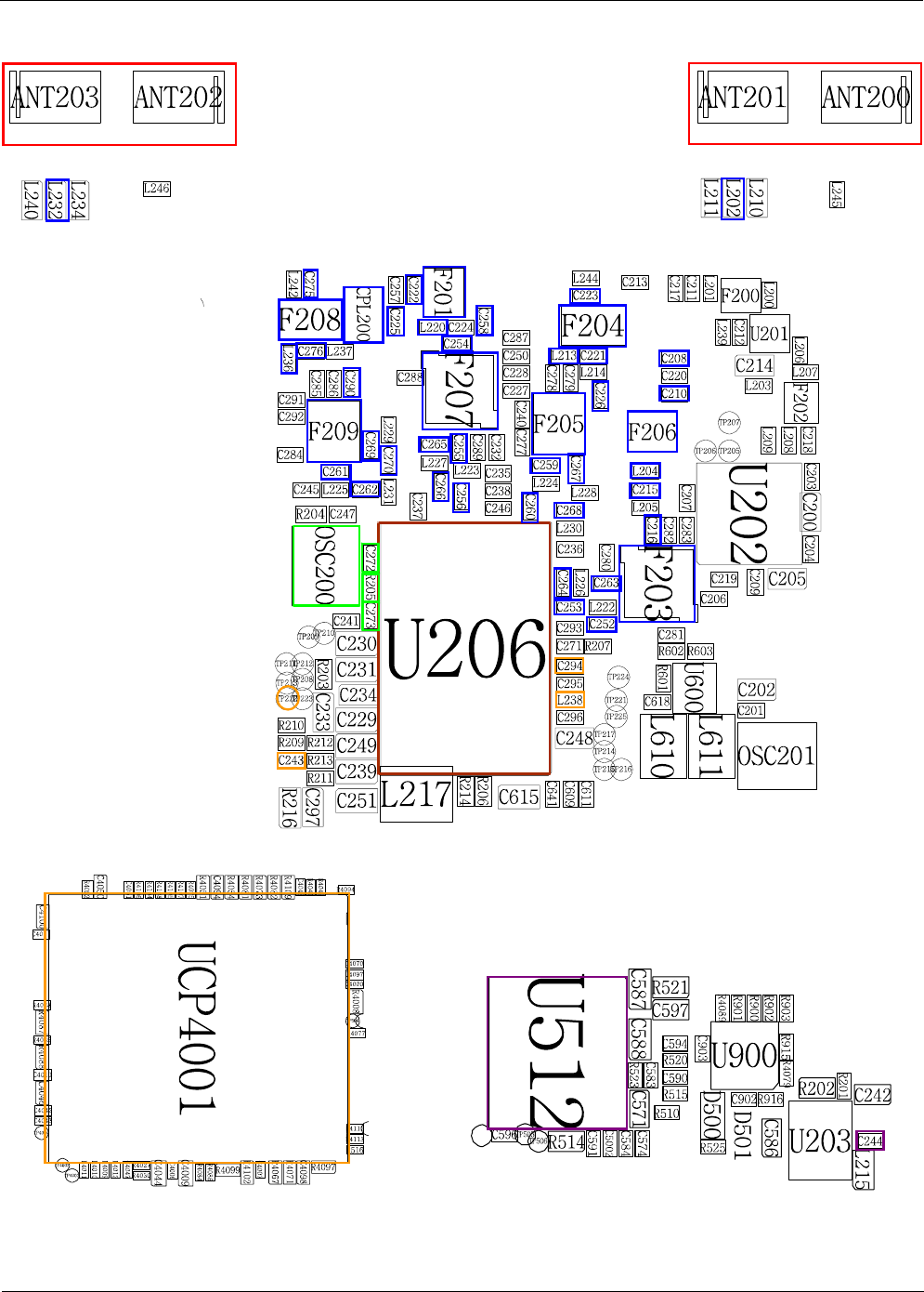
Level 3Repair
Distribution, transmission, or infringement of any content or data from this document without Samsung’s written authorization is strictly prohibited.
Confidential and proprietary-the contents in this service guide subject to change without prior notice.
8-31
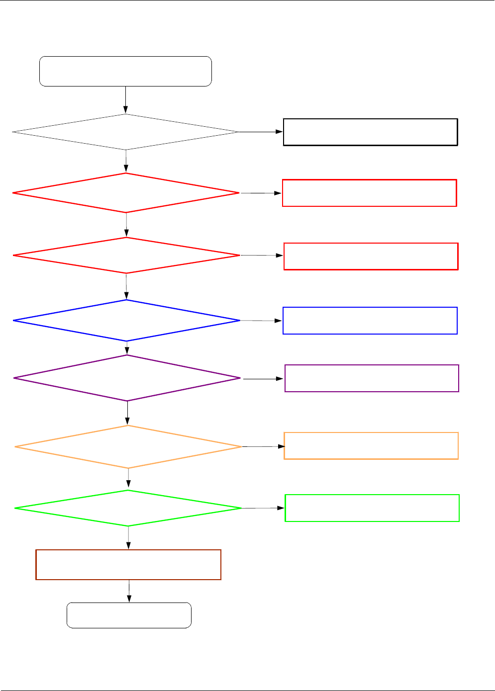
Level 3Repair
Distribution, transmission, or infringement of any content or data from this document without Samsung’s written authorization is strictly prohibited.
Confidential and proprietary-the contents in this service guide subject to change without prior notice.
8-32
8-3-9. GPS
Check GPS function ON No Enable GPS Function
Yes
END
Check the antenna C-clip has no
problem? No Replace the antenna c-clip, ANT202,ANT203
Yes
Check the REAR antenna pattern
(open, crack, deviation, etc)
No Replace REAR
Yes
Check the Voltage on
C205,C207 = 1.8V & C214= 2.8V
(When activating GPS, using app)
No Check the PMIC(U502)
(crack, open, damaged, etc.)
Yes
Yes
Yes
No Check the AP(UCP4001)
(crack, open, damaged, etc.)
Yes
Check the Voltage on
C212= 1.8V
(When activating GPS, using app)
Check the Status of
C201, C202, OSC201
No Resolder or change the
C201, C202, OSC201
Resolder or Replace U202
Check (crack,open,etc)
L208,F202,L206,U201,L200,F200,C211,C213,
CPL200,F208,C275,L232
Resolder or change the wrong element
(open, crack, deviation, etc)
No
Yes
GPS is not working
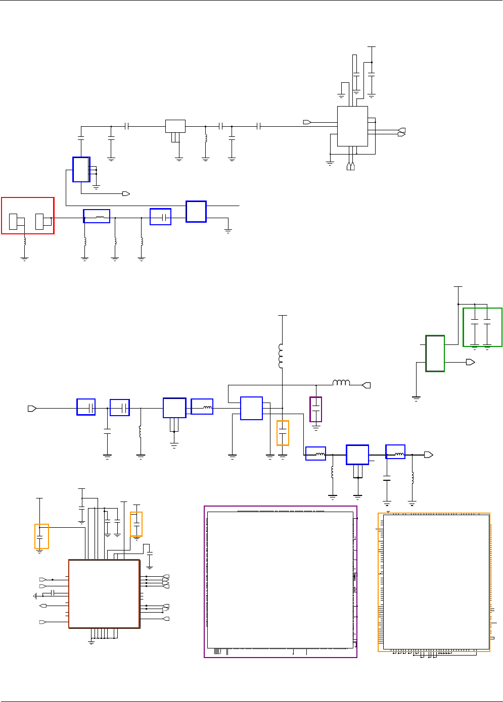
Level 3Repair
Distribution, transmission, or infringement of any content or data from this document without Samsung’s written authorization is strictly prohibited.
Confidential and proprietary-the contents in this service guide subject to change without prior notice.
8-33
C214
OSC201
2
GND1
NC
OUT
3VCC
4
L203
RF_IN
6ENABLE
U201
1
GND 2
VCC 3
RF_OUT
4GNDRF
5
VCC_2.8V_AP
L200
L209
L208
G
3
G
5
1IN
NC 6
4
OUT
F200
G
2
C201
C212
C218
L239
C217
C211
VDD_AUXO
C20
2
G
2
G
3
G
5
1IN
NC 6
4
OUT
F202
L207
L201
L206
C213
GPS_LNA_EN
GPS_ANT_SUB
GPS_TC
X
GPS_RF
TP205
C207
TP201
C204
C219
TP204
TP206
C203
VDD_AUXO
C209
VCC_1.8V_AP
VCC_2.8V_AP
RF_IN E6
RESERVED F1
VDD1P2_GRFF2
VDD_AUX_INF3
TCXO_IN
F4
VDD_IFF5
VDD_LNAF6
TM0
D4
IF_TEST_OUT D5
VSS_IF
D6
RESERVED E1
VSS
E2
VDD1P8_AUXE3
RESERVED E4
VSS_LNA
E5
REF_CAP
C2
VSS_CORE
C3
VSS_CORE
C4
LNA_EN
C5 SYNC_PPS
C6
VDD1P1_CORED1
VDD_PMU_IND2
VSS_PMU
D3
GNSS_CAL A6
UART_NRTS/HOST_REQ B1
UART_NCTS B2
NSTANDBY
B3
MOTION_INT2
B4
MOTION_INT3
B5
CLK32
B6
VDD_COREC1
MARK
1
MARK
2
UART_RXD_SDA A1
UART_TXD_SCL A2
IFVALID_MOTION_INT1
A3
VDD_IOA4
HOST_WAKE A5
U202
TP203
VCC_1.8V_AP
TP207
C205
TP202
C200
TP200
GPS_TCXO
GPS_LNA_EN
GPS_CLK32K
GPS_EN
GPS_INT
GPS_UART_CT
S
GPS_UART_RT
S
GPS_UART_RX
D
GPS_UART_TX
D
GPS_CLK_26M
GPS_RF
N4 SW4
N5
GNDB4
N6
GNDB3
N7 SW3
N8
VINB3
N9
GNDB6
M9
GNDB6
N1
NC
N10 SW6
N11
VINB7
N12 SW7
N13
NC
N2
VINB10
N3
VINB4
M13
GNDB7
M2
VINB10
VINB4M3
M4 SW4
M5
GNDB4
M6
GNDB3
M7 SW3
M8
VINB3
L6 RS3N
L7 RS3P
FB3
L8
L9
VLDO24
M1 SW10
M10 FB6
M11
VINB6
M12 FB7
L10
VLDO13
L11
VLDO1
VLDO27 L12
L13
VLDO22
L2 FB10
L3 FB4
L4 RS4P
L5 RS4N
K3
AGND
K4
VBAT
AGND
K5
K6AGND
K7
AGND
K8
VLDO38
K9
VLDO16
L1
GNDB10
NC
J9
VLDO14
GNDB22
K1
K10
VINL5
K11
VLDO9
K12
VINL1
K13
VLDO6
K2
GNDB22
VLDO11
J13
VLDO35
J2 SW22
J3
WDRSTEN
J4 BUCK10EN
J5
LDO7EN
J6
LDO13EN
J7
AGND
J8
H6
LDO19EN
H7
VBAT
H8
VREF
H9
VLDO26
J1 SW22
J10
VLDO19
J11
VLDO23
J12
H10
VLDO34
H11
VINL6
H12
VLDO17
H13
VLDO28
H2
VINB22
H3 FB2
H4 PWRHOLD
H5NC
G3 RS2P
G4 IRQB
G5 MR1B
G6 MR2B
G7 ACOKB
G8
VLDO37
G9
VLDO25
H1
VINB22
F8
VLDO31
F9
VLDO20
G1
VINB21
G10
VLDO21
G11
VLDO15
G12
VLDO36
G13
VLDO30
G2
VINB21
F12
VLDO33
F13
VLDO29
F2 SW21
F3 RS2N
F4 ONOB
F5 RSOB
F6
SDA
F7 JIGONB
E4 PWREN
E5
NC
E6
SCL
E7 PWRON
E8
VLDO10
E9
VLDO4
F1 SW21
F10
VINL3
F11
VLDO18
D9
VLDO5
E1
GNDB21
E10
VLDO12
E11
VINL2
E12
VINL4
E13
VLDO32
E2GNDB21
E3
LDO18EN
D13
VLDO7
D2 B5V2
D3 B5V3
D4 B5S1
D5 B5S2
D6
AP32K
D7
VDD_CP
D8
VDD_BT
C6 FB9
C7
CP32K
C8
BT32K
C9 BKCOIN
D1 B5V1
D10
VLDO8
D11
VLDO2 D12
VLDO3
C10
XTALOUT
C11
XTALIN
C12 FB8
C13GNDB8
C2 FB5
C3 FB5
C4
AGND
C5
VBAT
B3GNDB5
B4 SW5
B5
VINB5
B6
VINB9
B7 SW91
B8
GNDB9
B9 SW92
C1GNDB1
A8GNDB9
A9 SW92
B1 SW1
B10
VB9
B11
VINB8
B12 SW8
B13GNDB8
B2 FB1
A12 SW8
A13
NC
A2
VINB1
A3GNDB5
A4 SW5
A5
VINB5
A6
VINB9
A7 SW91
1NC
NC
2
A1
NC
A10
VB9
A11
VINB8
U502
L246
L232
L234
C257
C250
L240
11
2
2
ANT203
1
2
2
ANT202
1
L242
5COM
G2
G4
G6
3
HIGH
1LOW
CPL200
C225
C222
C275
C224
F201
2
G
3
G
5
G
1
IN
OUT
4
4
RX 5
LNAEN
VDD6
BT7
8
VBT
VRX
9
VTX
1
10 ANT
GND
11
12
MARK
MARK 13
2TX
3N|C
F207
L220 C258
C254
P3
F208
1
GND
P1 2
P2
4
3
VDD_LDO3P3_B
C240
GPS_ANT_SUB
SW_WL_2G_LNA_EN
_
SW_WL_2G_RX_1
SW_WL_2G_TX_1
WL_TX_G_CORE1_CAP
WL_RX_G_CORE1_E
T
(I2C_5_SCL)
(I2C_2_SDA)
(I2C_4_SDA)
(I2C_6_SCL)
(I2C_5_SDA)
(I2C_2_SCL)
(I2C_3_SCL)
(I2C_3_SDA)
(I2C_7_SDA)
(I2C_7_SCL)
(I2C_4_SCL)
(I2C_6_SDA)
C4100
R4087
Y7 XUTXD_3
Y1
XUSB30OVERCUR_U2
Y2
XUSB30VBUSCTRL_U3
Y3
XUFSNRESET
Y33
XJTMS
Y34
XJDBGSEL
Y4
XUHOSTOVERCUR Y5
XUHOSTPWREN
Y6 XURXD_3
W3
XUSB31OVERCUR_U3
W33
XJTCK
W34
XJTRSTN
W4
XUSB31VBUSCTRL_U2
W5
XUSB31OVERCUR_U2
W6
XI2C8SDA_HS
W7 XUTXD_2
W8
XI2C9SCL_HS
V3 XI2C1SDA
V4
XUSB31VBUSCTRL_U3
V5
XI2C8SCL_HS
V6
XI2C1SCL
V7
XI2C10SDA_HS
V8 XI2C0SDA
W1
XUSB30OVERCUR_U3
W2
XUSB30VBUSCTRL_U2
U4 XURTSN_2
XI2C10SCL_HS
U5
U6
XI2C9SDA_HS
U7 XUTXD_0
U8 XPWMTOUT_1
V21
XTSTEST_OUT0
V23
XTSTEST_OUT4
V24
XTSEXT_RES4
T5 XPWMTOUT_0
T6
XURXD_1
T7 XURTSN_0
T8 XI2C0SCL
U12
XTSEXT_RES1
U20
XTSEXT_RES0
U3 XURTSN_1
R6
XI2S2SCLK
R7 XURXD_0
R8 XUCTSN_2
T1
POP_VREFCA_E2
T12
XTSTEST_OUT1
T3 XPWMTOUT_3
T32
XDRAM1VREF2
T4
XPWMTOUT_2
P1
XUSB3RX0M_1
P2
POP_ZQ_E2
P4
XUHOSTDP
P5
XI2S2SDO
P7
XUCTSN_0
P8 XURXD_2
R2 XI2S1LRCK
POP_VREFDQ_E2R32
R5 XI2S2CDCLK
M7 XI2S2LRCK
M8 XI2S1SDI
N1
XUSB3RX0P_1
N3
XUHOSTVBUS
N4
XUHOSTDM
N5
XUHOSTREXT
N7 XUTXD_1
N8 XUCTSN_1
L3
XUSB3REFPADCLKP_1 L5
XUSB3RESREF_1
L6 XSPIMISO_0
L7 XSPICLK_1
L8 XI2S1SCLK
M2
POP_ZQ1_E2
M5
XUHOSTANALOGTEST
M6 XSPIMOSI_0
J8 XI2S1SDO
K1
XUSB3TX0P_1
K3
XUSB3DP0_1
K6 XSPICSN_1
K7 XSPIMISO_1
K8 XI2S1CDCLK
L1
XUSB3TX0M_1
L2
XUSB3REFPADCLKM_1
H4
XUSB3VBUS0_1
H6 XSPICLK_0
H7
XADC0AIN_0
H8 XI2S2SDI
J3
XUSB3DM0_1
J5
XUSB3ID0_1
J6 XSPIMOSI_1
J7 XSPICSN_0
G2
XUSB3REFPADCLKP_0 G3
XUSB3RESREF_0
G6
XADC0AIN_2
G7
XADC0AIN_5
G8
XADC0AIN_1
G9
XADC0AIN_4
H1
XUSB3RX0M_0
H33
XDRAM1VREF0
F7
XADC0AIN_3
F9XGPIO15
G1
XUSB3RX0P_0
G10
XADC0AIN_7
G11
XADC0AIN_8
G12
XADC0AIN_9
G13
XTSTEST_OUT2
G14
XTSEXT_RES2
F11XEINT_0
F14
XCLKOUT
F15XEINT_6
F18
XTSEXT_RES3
F19
XTSTEST_OUT3
F2
XUSB3REFPADCLKM_0
F33
XDRAM1ZQ
F6
XADC0AIN_6
E19
XNWRESET
E3
XUSB3DP0_0
E4
XUSB3VBUS0_0
XUSB3ID0_0E5
E7
XGPIO8
E8XGPIO9
E9
XGPIO10
F10
XGPIO12
D3
XUSB3DM0_0
D4
XAUDI2S0CDCLK
D6XGPIO3
D7XGPIO6
D9
XGPIO14
E1
XUSB3TX0M_0
E10XGPIO11
E14
XNRESET
D20
XDRAM0VREF0
D21
XOM_0
D22XEINT_4
D24XEINT_2
D25XEINT_10
D26XEINT_11
D27
XDRAM0VREF2
D28XEINT_16
C6XGPIO2
C7XGPIO5
C8XGPIO7
D1
XUSB3TX0P_0
D10XGPIO13
D13
XPWRRGTON
D18
XDRAM0ZQ
D19
XOM_5
C26
XRTCCLKO
C28XEINT_25
C29XEINT_27
C3XAUDI2S0LRCK
C30XEINT_30
C31XEINT_29
C4XAUDI2S0SCLK
C5XAUDI2S0SDO_0
C18
XPSHOLD
C19
XOM_6
C20
POP_VREFDQ_E1
C21XEINT_31
C22XEINT_21
C23XEINT_17
C24XEINT_18
C25XEINT_20
B6XGPIO0
XGPIO1
B7
C10
XHSICSTROBE1 C11
XHSICDATA1
C12
XEINT_3
C13
XOM_3
C15
XOM_1
XNRSTOUTC17
B20
XOM_2
B22XEINT_19
B26XEINT_14
B27XEINT_28
B28XEINT_23
B30XEINT_24
B31XEINT_22
B5
XAUDI2S0SDO_1
AV16
POP_VREFCA_E1
AV27
XADC1AIN_1
AV30
XV1FRM
B12
XXTI
B15
XEINT_5
B16
XRTCXTI
B17
XOM_4
B18XEINT_15
AU13
XMIPI1VREG_0P4V
AU19
XHDMIREXT
AU27
XADC1AIN_0
AU28
XADC1AIN_3
AU29
XADC1AIN_2
AU30
XV1VSYNC_LDI
AU31XGPIO17
AV12
POP_ZQ_E1
AT3
XMIPI0VREG_0P4V
AT31
XGPIO16
AT4
XMIPI0MDP3 AT5
XMIPI0MDP2
AT6
XMIPI0MDPCLK
AT7
XMIPI0MDP1
AT8
XMIPI0MDP0
AU12
POP_ZQ1_E1
AT19
XHDMITX2P
AT20
XHDMIXTI
AT21
XDPRBIAS AT22
XDPAUXP
AT23
XDPTX0P
AT24
XDPTX1P
AT25
XDPTX2P
AT26
XDPTX3P
AT11
XMIPI1MDP2
AT12
XMIPI1MDPCLK
AT13
XMIPI1MDP1
AT14
XMIPI1MDP0
AT16
XHDMITXCP
AT17
XHDMITX0P
AT18
XHDMITX1P
AR28 XISPGP4
AR29 XISPI2C2SDA
AR30 XISPI2C0SCL
AR4
XMIPI0MDN3 AR5
XMIPI0MDN2
AR6
XMIPI0MDNCLK
AR7
XMIPI0MDN1 AR8
XMIPI0MDN0
AT10
XMIPI1MDP3
AR19
XHDMITX2N
AR20
XHDMIXTO
AR22
XDPAUXN
AR23
XDPTX0N
AR24
XDPTX1N
AR25
XDPTX2N
AR26
XDPTX3N
AR27 XISPGP5
AR10
XMIPI1MDN3
AR11
XMIPI1MDN2
AR12
XMIPI1MDNCLK
AR13
XMIPI1MDN1
AR14
XMIPI1MDN0
AR16
XHDMITXCN
AR17
XHDMITX0N
AR18
XHDMITX1N
AP28 XISPGP1
AP29 XISPGP0
AP30 XISPI2C0SDA
AP4
XMIPI0SDP3 AP5
XMIPI0SDP2
AP6
XMIPI0SDPCLK
XMIPI0SDP1
AP7
AP8
XMIPI0SDP0
AP19 XISPSPI0CSN
AP20 XISPGP6
AP21 XISPSPI1MISO
AP22 XISPSPI1CSN
XISPI2C2SCL
AP23
AP24 XISPI2C1SDA
AP25 XISPGP7
AP27
XISPGP2
XMIPI0SDN0
AN9
XMMC2DATA_2
AP1
XUFSXTI
AP10
XMIPI1SDP3
AP11
XMIPI1SDP2
AP12
XMIPI1SDPCLK
AP13
XMIPI1SDP1
AP14
XMIPI1SDP0
XISPGP8
AN25 XISPSPI0CLK
AN27 XISPGP3
AN28 XISPI2C1SCL
AN4
XMIPI0SDN3 AN5
XMIPI0SDN2
AN6
XMIPI0SDNCLK
AN7
XMIPI0SDN1 AN8
AN14
XMIPI1SDN0
AN16
XCI1RGB_4
AN17
XCI1RGB_0
AN19 XISPGP9
AN20 XISPSPI1MOSI
AN21 XISPSPI0MISO
AN22 XISPSPI1CLK
AN23 XISPSPI0MOSI
AN24
AM6
XMMC2BIUVR
AM7 XMMC2CLK
AM9 XMMC0CMD
AN1
XUFSXTO
AN10
XMIPI1SDN3
AN11
XMIPI1SDN2
AN12
XMIPI1SDNCLK
AN13
XMIPI1SDN1
AM13
XCI1VSYNC
AM14XCI1RGB_9
AM15
XCI1RGB_10
AM16XCI1RGB_3
AM17XCI1RGB_7
AM3
XUFSTXDP1
AM4
XUFSTXDN1
AM5 XMMC2DATA_0
AL17
XCI1PCLK
AL3
XUFSTXDP0
XUFSTXDN0 AL4
AL5 XMMC2DATA_3
AL6 XMMC2CDN
AM10 XMMC2DATA_1
AM11 XMMC2CMD
AM12XCI1HSYNC
AK9
XMMC0RDQS
AL10 XMMC0CLK
XMMC0DATA_3
AL11
AL12XCI1MCLK
AL13XCI1RGB_13
AL14XCI1RGB_5
AL15
XCI1RGB_6
AL16XCI1RGB_1
AK14XCI1RGB_12
AK15
XCI1RGB_8
AK16
XCI1RGB_2
AK3
XUFSREFCLK_OUT
AK4
XUFSREFCLK
AK5 XMMC2WP
AK6
XMMC0CDN
AK7 XMMC0DATA_6
AJ3
XUFSRXDP0
AJ4
XUFSRXDN0
AJ5 XMMC1DATA_2
AJ6 XMMC1DATA_3
AJ8 XMMC0DATA_2
AJ9 XMMC0DATA_7
AK10 XMMC1CDN
XCI1RGB_11
AK13
AH3
XUFSRXDP1
AH4
XUFSRXDN1
AH5
XMMC1DATA_7
AH6
XMMC1INTN
AH8 XMMC1DATA_1
AH9XSRAMCSN_0
AJ10 XMMC1DATA_0
AJ11XSRAMCSN_2
AG5XSRAMBEN_1
AG6
XSRAMWAITN
AG7
XSRAMBEN_0
AG8XSRAMDATA_1
AG9XSRAMDATA_0
AH10
XSRAMCSN_3
AH11
XSRAMCSN_1
AH2
XUFSREXT
AF8
XSRAMDATA_4
AF9
XSRAMDATA_6
AG1 XMMC0DATA_1
AG10XSRAMDATA_RDN
AG11
XSRAMWEN
AG2 XMMC0DATA_0
AG3 XMMC0DATA_4
AG4XSRAMOEN
AE8XSRAMDATA_11
AE9XSRAMDATA_13
AF10XSRAMDATA_3
AF3 XMMC0DATA_5
AF4
XSRAMDATA_2
AF5XSRAMDATA_5
AF6XSRAMDATA_7
AF7
XSRAMDATA_8
AD7
XSRAMDATA_14
AD8XSRAMFRNB_2
AD9XSRAMFCLE
AE10
XSRAMDATA_10
AE3
XMMC0RESETOUT
AE5XSRAMFALE
AE6
XSRAMDATA_12
XSRAMDATA_9
AE7
AC7XSRAMADDR_5
AC8XSRAMFRNB_1
AD1 XMMC1CMD
AD10XSRAMDATA_15
AD2 XMMC1CLK
AD3
XMMC1RDQS
AD5XSRAMFRNB_0
AD6XSRAMADDR_1
AC1 XMMC1DATA_5
AC2 XMMC1DATA_4
AC3 XMMC1BEPW
AC33
XOMCCI
AC34
XJTDI
AC4XSRAMADDR_3
AC5XSRAMFRNB_3
AC6XSRAMADDR_0
AB2 XMMC1DATA_6
AB3
XMMC1WP
AB33
XJTDO
AB4XSRAMADDR_8
AB5XSRAMADDR_11
AB6XSRAMADDR_4
AB7XSRAMADDR_7
AB8XSRAMADDR_2
AA1
XEFFSOURCE_0
AA2XSRAMADDR_6
AA3XSRAMADDR_10
AA4XSRAMADDR_15
XSRAMADDR_13
AA5
AA6XSRAMADDR_14
AA7XSRAMADDR_12
AA8XSRAMADDR_9
A21XEINT_9
A23XEINT_8
A25XEINT_12
A28XEINT_13
A29XEINT_26
A4
XAUDI2S0SDI
A6XAUDI2S0SDO_2
A8XGPIO4
NC
1
NC 2
A12
XXTO
XEINT_1
A13
A16
XRTCXTO
A17
XEINT_7
UCP4001-1
R4109
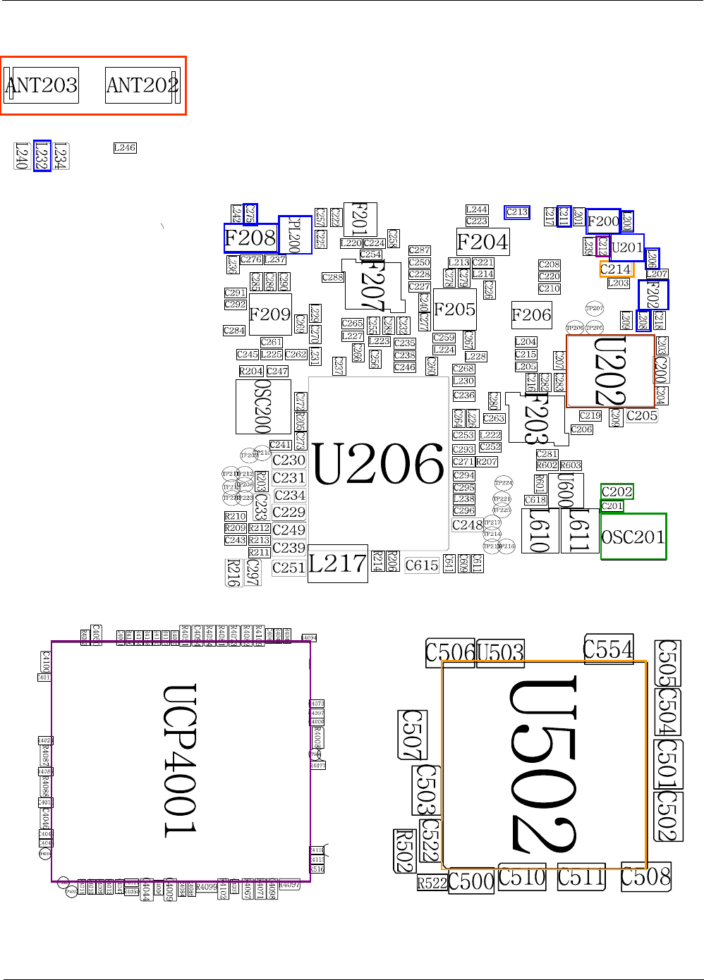
Level 3Repair
Distribution, transmission, or infringement of any content or data from this document without Samsung’s written authorization is strictly prohibited.
Confidential and proprietary-the contents in this service guide subject to change without prior notice.
8-34
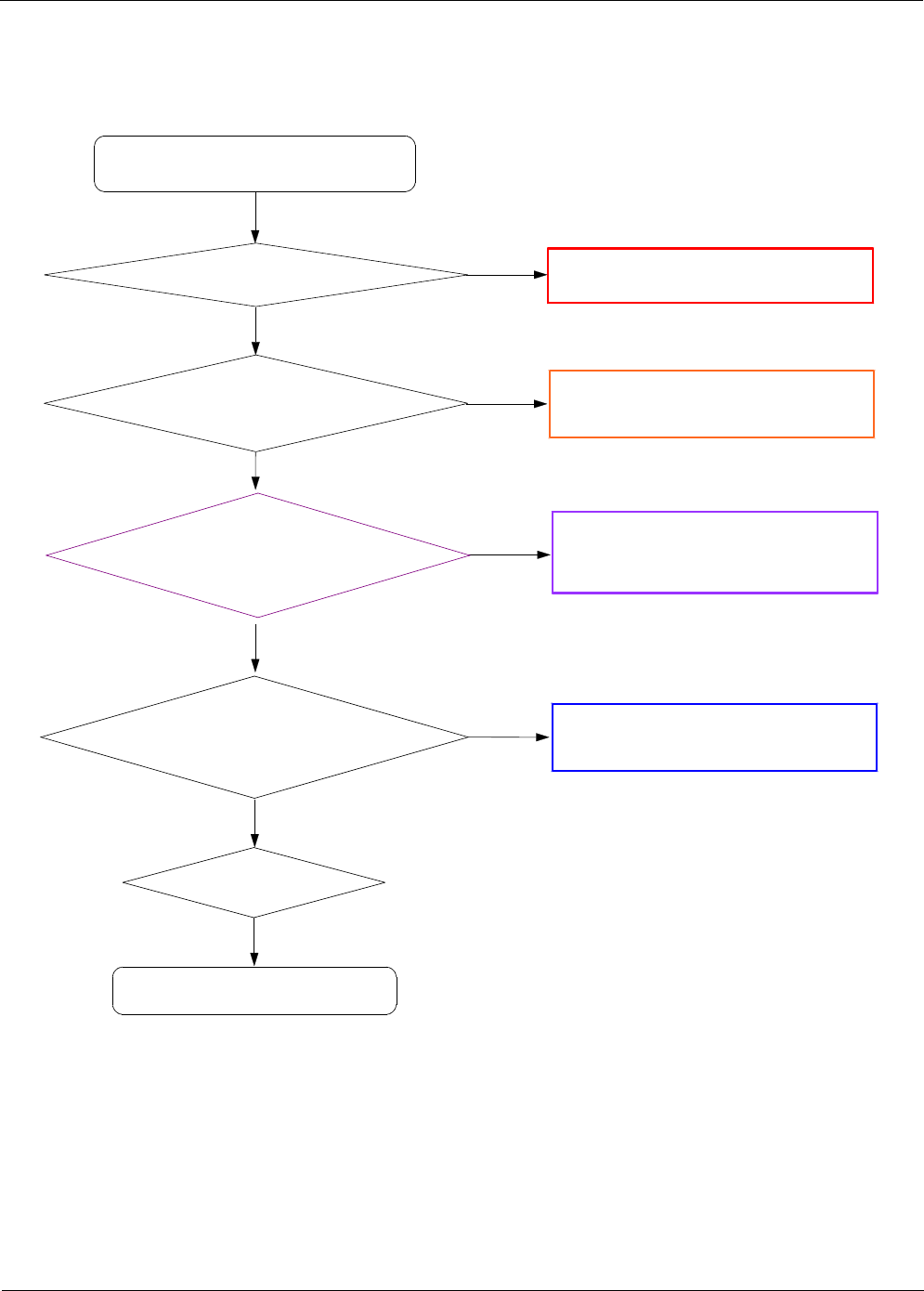
Level 3Repair
Distribution, transmission, or infringement of any content or data from this document without Samsung’s written authorization is strictly prohibited.
Confidential and proprietary-the contents in this service guide subject to change without prior notice.
8-35
8-3-10. LCD
LCD is still off after PWR ON
Yes
No Reconnect the SLC800
Check the connection of
SLC800
END
No
Resolder or Replace the DCDC(U802)
Yes
Check OCTA_VDD_3.3V=3.3V
(C817),
Yes
Yes
Replace LCD
Module
Yes
Check
ELVDD_+5V(C842)
ELVDD_-5V(C843) Resolder or Replace the DCDC(U805)
No
Yes
No Resolder or Replace the PMIC(U502)
Check the TCON_1.8V
(C838)
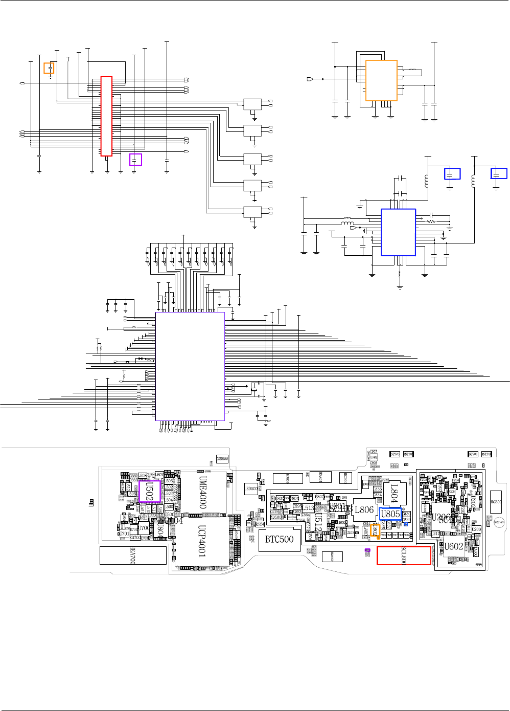
Level 3Repair
Distribution, transmission, or infringement of any content or data from this document without Samsung’s written authorization is strictly prohibited.
Confidential and proprietary-the contents in this service guide subject to change without prior notice.
8-36
F807
GND
5
GND
6
I|O 1
2
I|OI|O
3
4I|O
ELVSS_-5V
ELVDD_+5V
1
I|O
I|O 2
I|O
3
I|O
4
F805
GND
5
GND
6
ELVSS_-5V
OCTA_VDD_3.3V
C817
TCON_1.8V
VTOUCH_1.8V
GND
5
6GND
I|O 1
I|O 2
I|O
3
4I|O
F809
C838
3
4I|O
F806
GND
5
GND
6
I|O 1
2
I|OI|O
TSP_1.8V
C841
C840
NC
72
67
67 68
68
69 69
77
70 70
88
9
9
NC
71
60
60
61 61 62 62
63
63 64
64
65 65 66 66
53 53 54 54
55
55 56
56
57 57 58 58
59
59
6
6
46 46
47 47 48
48
49 49
5
5
50 50
51 51 52
52
38 38
39 39
44
40
40
41
41 42 42
43 43 44
44
45
45
30
31 31 32
32
33
33 34 34
35
35 36
36
37 37
24
24
25
25 26
26
27 27 28 28
29
29
3
3
30
16 16
17 17 18
18
19
19
2
2
20 20
21
21 22 22
23 23
SCL800
1
1
10
10
11 11 12 12
13
13 14
14
15
15
3I|O
I|O
4
F808
5GND
GND
6
1
I|O
2
I|O
TSP_3.3V KEY_LED_3.3V
TOUCH_SDA
TOUCH_SCL
TOUCH_INT
TCON_INTR
TSP_SCL_1.8V
TCON_RDY
TSP_SDA_1.8V
TSP_ATTN
SL_SDA
SL_SCL
DP_D1_N
DP_D1_P
DP_CLK_
N
DP_CLK_P
DP_D0_N
DP_D0_P
DP_D2_N
DP_D2_P
DP_D3_N
DP_D3_P
TSP_TA
EL_ON
TE
C8
17
C838
TP503
C524
C549
VCC_SUB_2.0V
VCC_SUB_3.4V
R507
R505
C517
C528
VCC_1.8V_AP VMIPI_PLL_ABB1_1.8V_AP
L501
C521
L506
C552
21
VDD_CAM_ISP_1.0V
OSC500
L512
VCC_SUB_3.4V
C503
VKFC_1.0V_AP
L502
C511
C519
VMEM2_1.2V_AP
L511
TP502
R502
C520
VG3D_1.0V_AP
VINT_1.0V_AP
C504
VCC_1.8V_AP
C506
V_BAT
C507
VCC_SUB_1.4V
C518
V_BAT
VINT_1.0V_AP
C548
V_BAT
C526
C551
VADC_1.8V_AP
C522
L503
VMIF_1.1V_AP
C508
C558
C525
R506
VCC_SUB_2.0V
L504
C559
C510
L509
VRTC_1.8V
N9GNDB6
VMIF_1.1V_AP
N13NC
N2
VINB10
N3
VINB4
N4 SW4
N5GNDB4
N6GNDB3
N7 SW3
N8
VINB3
M6GNDB3
M7 SW3
M8
VINB3
M9GNDB6
N1NC
N10 SW6
N11
VINB7
N12 SW7
M10 FB6
M11
VINB6
M12 FB7
M13GNDB7
M2
VINB10
VINB4M3
M4 SW4
M5GNDB4
L3 FB4
L4 RS4P
L5 RS4N
L6 RS3N
L7 RS3P
FB3
L8
L9
VLDO24
M1 SW10
K8
VLDO38
K9
VLDO16
L1GNDB10
L10
VLDO13
L11
VLDO1
VLDO27 L12
L13
VLDO22
L2 FB10
K12
VINL1
K13
VLDO6
K2GNDB22
K3AGND
K4
VBAT
AGND
K5
K6AGND
K7AGND
J5
LDO7EN
J6
LDO13EN
J7AGND
J8NC
J9
VLDO14
GNDB22
K1
K10
VINL5
K11
VLDO9
J1 SW22
J10
VLDO19
J11
VLDO23
J12
VLDO11
J13
VLDO35
J2 SW22
J3
WDRSTEN
J4 BUCK10EN
H2
VINB22
H3 FB2
H4 PWRHOLD
H5NC
H6
LDO19EN
H7
VBAT
H8
VREF
H9
VLDO26
G7 ACOKB
G8
VLDO37
G9
VLDO25
H1
VINB22
H10
VLDO34
H11
VINL6
H12
VLDO17
H13
VLDO28
G11
VLDO15
G12
VLDO36
G13
VLDO30
G2
VINB21
G3 RS2P
G4 IRQB
G5 MR1B
G6 MR2B
F4 ONOB
F5 RSOB
F6
SDA
F7 JIGONB
F8
VLDO31
F9
VLDO20
G1
VINB21
G10
VLDO21
E9
VLDO4
F1 SW21
F10
VINL3
F11
VLDO18
F12
VLDO33
F13
VLDO29
F2 SW21
F3 RS2N E13
VLDO32
E2GNDB21
E3
LDO18EN
E4 PWREN
E5NC
E6
SCL
E7 PWRON
E8
VLDO10
D6
AP32K
D7
VDD_CP
D8
VDD_BT
D9
VLDO5
E1GNDB21
E10
VLDO12
E11
VINL2
E12
VINL4
D10
VLDO8
D11
VLDO2 D12
VLDO3
D13
VLDO7
D2 B5V2
D3 B5V3
D4 B5S1
D5 B5S2
C3 FB5
C4AGND
C5
VBAT
C6 FB9
C7
CP32K
C8
BT32K
C9 BKCOIN
D1 B5V1
B8GNDB9
B9 SW92
C1GNDB1
C10
XTALOUT
C11
XTALIN
C12 FB8
C13GNDB8
C2 FB5
B12 SW8
B13GNDB8
B2 FB1
B3GNDB5
B4 SW5
B5
VINB5
B6
VINB9
B7 SW91
A5
VINB5
A6
VINB9
A7 SW91
A8GNDB9
A9 SW92
B1 SW1
B10
VB9
B11
VINB8
A1NC
A10
VB9
A11
VINB8
A12 SW8
A13NC
A2
VINB1
A3GNDB5
A4 SW5
U502
1NC
NC
2
TP504
VMMC01_1.8V_AP
VMIPI_1.0V_AP
VMEM_1.2V_AP
C523
VCC_SUB_3.4V
VARM_1.0V_AP
VALIVE_1.0V_AP
L505
C505
L507
C501C500 C502
VCC_1.8V_AP
R503
C547
VCC_1.8V_AP
L510
R512
VCC_SUB_1.4V
L508
R508
VOL_DOWN
32KHZ_CP
BUCK9_GND
MIPI_1.8V_EN
32KHZ_AP
AP_PMIC_SCL
AP_PMIC_SDA
VG3D_1.0V_AP_SNSN
VINT_1.0V_AP_SNSN
VINT_1.0V_AP_SNSP
BUCK7_GND
BUCK4_GND
BUCK3_GND
BUCK6_GND
32KHZ_PMIC
MMC01_EN
MMC2_EN
BUCK2B_GND
BUCK10_GND
VG3D_1.0V_AP_SNSP
VARM_1.0V_AP_SNSN
VARM_1.0V_AP_SNSP
BUCK5_GND
BUCK9_GND
BUCK8_GND
BUCK1_GND
BUCK2A_GND
PMIC_ACOKB
AP_N_RST_IN
TF_EN
AP_PMIC_EN
R807
C831
C833
C832
ELVDD_+5V
C813
C830
C829
PGNDN
6
PGNDN
7
8PVIN
PVIN
9
OUTP
SWP
3
30
OUTP
PGNDP
31
32
PGNDP
THER_PAD33
4VIN
CTRL
5
PGNDN
PGNDN
22
NC 23
24
AGND
OUTSNS 25
26
CT
VL
27
28
SNSP
29
SWN
14
SWN
15
16PGNDN
PGNDN 17
18
OUTN
OUTN 19
2SWP
20
OUTN
21
U805
PGNDP
1
10 PVIN
PGNDN
11
12PGNDN
SWN
13
C835
V_BAT
C4PGND
GND
C5
D1 PG
_BAT
D2
D3 MODE|SYNC
GND
D4
D5
FB
B1 PVIN LX1 B2
B3PGND
LX2 B4
B5
VOUT
VIN
C1
C2 EN
PGND
C3
NC1
2
NC
PVIN
A1 A2
LX1
PGND
A3
A4
LX2
VOUT A5
U802
L800
C842 C843
L808L807
L805
L804
V_BAT
C834
TP808
C815
TP807
TP803
C836
L806
V_BAT
C814
C837
ELVSS_-5V
OCTA_VDD_3.3V
C812
EL_ON
LCD_EN
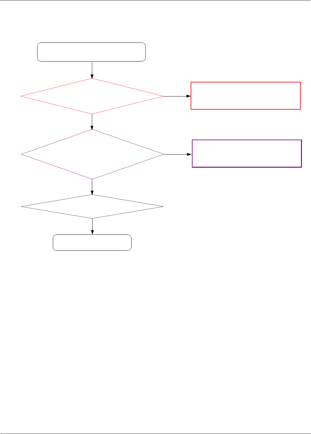
Level 3Repair
Distribution, transmission, or infringement of any content or data from this document without Samsung’s written authorization is strictly prohibited.
Confidential and proprietary-the contents in this service guide subject to change without prior notice.
8-37
8-3-11. TSP
Touch Screen does not work
Yes
No Reconnect the TSP Connector SLC800
Check TSP Connector on
Main PBA
Yes
END
Yes
Replace TSP+LCD Module
Yes
No
Check the
TSP_3.3V(C841),
TSP_1.8V(C840) Resolder or Replace the PMIC(U502)
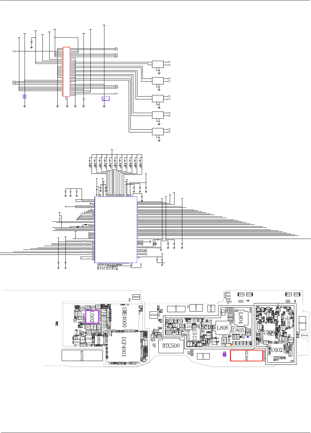
Level 3Repair
Distribution, transmission, or infringement of any content or data from this document without Samsung’s written authorization is strictly prohibited.
Confidential and proprietary-the contents in this service guide subject to change without prior notice.
8-38
C817
ELVSS_-5V
C841
TCON_1.8V
ELVDD_+5V
TSP_1.8V
OCTA_VDD_3.3V
GND
6GND
I|O 1
2
I|O
3I|O
4I|O
F805
5
VTOUCH_1.8V
5GND
GND
6
1
I|O
2
I|O
3I|O
I|O
4
F809
TSP_3.3V
C838
KEY_LED_3.3V
3I|O
I|O
4
F806
5GND
6GND
1
I|O
I|O 2
1
I|O 2
I|O
3
4I|O
F808
GND
5
6GND
I|O
ELVSS_-5V
GND
1
I|O
I|O 23 I|O
I|O
4
NC
72NC
F807
5GND
6
67 67 68 68
69
69
7
7
70
70
8
8
99
71
59
66
60 60
61
61 62
62
63 63 64 64
65
65 66
66
51 52 52
53
53 54
54
55 55 56 56
57
57 58
58
59
45 45 46
46
47
47 48 48
49
49
55
50
50
51
37 38
38
39
39
4
4
40 40
41 41 42
42
43
43 44 44
3
30
30
31
31 32 32
33 33 34
34
35 35 36 36
37
22
23
23 24 24
25 25 26 26
27
27 28
28
29 29
3
15 16
16
17
17 18 18
19 19
22
20
20
21 21 22
11
10 10
11
11 12
12
13 13 14 14
15
SCL800
C840
TOUCH_SDA
TOUCH_SCL
DP_D3_P
TOUCH_INT
TCON_INTR
TSP_SCL_1.8V
TCON_RDY
TSP_SDA_1.8V
TSP_ATTN
SL_SDA
SL_SCL
DP_D1_N
DP_D1_P
DP_CLK_
N
DP_CLK_
P
DP_D0_N
DP_D0_P
DP_D2_N
DP_D2_P
DP_D3_N
TSP_TA
EL_ON
TE
TP503
C524
C549
VCC_SUB_2.0V
VCC_SUB_3.4V
R507
R505
C517
C528
VCC_1.8V_AP VMIPI_PLL_ABB1_1.8V_AP
L501
C521
L506
C552
21
VDD_CAM_ISP_1.0V
OSC500
L512
VCC_SUB_3.4V
C503
VKFC_1.0V_AP
L502
C511
C519
VMEM2_1.2V_AP
L511
TP502
R502
C520
VG3D_1.0V_AP
VINT_1.0V_AP
C504
VCC_1.8V_AP
C506
V_BAT
C507
VCC_SUB_1.4V
C518
V_BAT
VINT_1.0V_AP
C548
V_BAT
C526
C551
VADC_1.8V_AP
C522
L503
VMIF_1.1V_AP
C508
C558
C525
R506
VCC_SUB_2.0V
L504
C559
C510
L509
VRTC_1.8V
N9GNDB6
VMIF_1.1V_AP
N13NC
N2
VINB10
N3
VINB4
N4 SW4
N5GNDB4
N6GNDB3
N7 SW3
N8
VINB3
M6GNDB3
M7 SW3
M8
VINB3
M9GNDB6
N1NC
N10 SW6
N11
VINB7
N12 SW7
M10 FB6
M11
VINB6
M12 FB7
M13GNDB7
M2
VINB10
VINB4M3
M4 SW4
M5GNDB4
L3 FB4
L4 RS4P
L5 RS4N
L6 RS3N
L7 RS3P
FB3
L8
L9
VLDO24
M1 SW10
K8
VLDO38
K9
VLDO16
L1GNDB10
L10
VLDO13
L11
VLDO1
VLDO27 L12
L13
VLDO22
L2 FB10
K12
VINL1
K13
VLDO6
K2GNDB22
K3AGND
K4
VBAT
AGND
K5
K6AGND
K7AGND
J5
LDO7EN
J6
LDO13EN
J7AGND
J8NC
J9
VLDO14
GNDB22
K1
K10
VINL5
K11
VLDO9
J1 SW22
J10
VLDO19
J11
VLDO23
J12
VLDO11
J13
VLDO35
J2 SW22
J3
WDRSTEN
J4 BUCK10EN
H2
VINB22
H3 FB2
H4 PWRHOLD
H5NC
H6
LDO19EN
H7
VBAT
H8
VREF
H9
VLDO26
G7 ACOKB
G8
VLDO37
G9
VLDO25
H1
VINB22
H10
VLDO34
H11
VINL6
H12
VLDO17
H13
VLDO28
G11
VLDO15
G12
VLDO36
G13
VLDO30
G2
VINB21
G3 RS2P
G4 IRQB
G5 MR1B
G6 MR2B
F4 ONOB
F5 RSOB
F6
SDA
F7 JIGONB
F8
VLDO31
F9
VLDO20
G1
VINB21
G10
VLDO21
E9
VLDO4
F1 SW21
F10
VINL3
F11
VLDO18
F12
VLDO33
F13
VLDO29
F2 SW21
F3 RS2N E13
VLDO32
E2GNDB21
E3
LDO18EN
E4 PWREN
E5NC
E6
SCL
E7 PWRON
E8
VLDO10
D6
AP32K
D7
VDD_CP
D8
VDD_BT
D9
VLDO5
E1GNDB21
E10
VLDO12
E11
VINL2
E12
VINL4
D10
VLDO8
D11
VLDO2 D12
VLDO3
D13
VLDO7
D2 B5V2
D3 B5V3
D4 B5S1
D5 B5S2
C3 FB5
C4AGND
C5
VBAT
C6 FB9
C7
CP32K
C8
BT32K
C9 BKCOIN
D1 B5V1
B8GNDB9
B9 SW92
C1GNDB1
C10
XTALOUT
C11
XTALIN
C12 FB8
C13GNDB8
C2 FB5
B12 SW8
B13GNDB8
B2 FB1
B3GNDB5
B4 SW5
B5
VINB5
B6
VINB9
B7 SW91
A5
VINB5
A6
VINB9
A7 SW91
A8GNDB9
A9 SW92
B1 SW1
B10
VB9
B11
VINB8
A1NC
A10
VB9
A11
VINB8
A12 SW8
A13NC
A2
VINB1
A3GNDB5
A4 SW5
U502
1NC
NC
2
TP504
VMMC01_1.8V_AP
VMIPI_1.0V_AP
VMEM_1.2V_AP
C523
VCC_SUB_3.4V
VARM_1.0V_AP
VALIVE_1.0V_AP
L505
C505
L507
C501C500 C502
VCC_1.8V_AP
R503
C547
VCC_1.8V_AP
L510
R512
VCC_SUB_1.4V
L508
R508
VOL_DOWN
32KHZ_CP
BUCK9_GND
MIPI_1.8V_EN
32KHZ_AP
AP_PMIC_SCL
AP_PMIC_SDA
VG3D_1.0V_AP_SNSN
VINT_1.0V_AP_SNSN
VINT_1.0V_AP_SNSP
BUCK7_GND
BUCK4_GND
BUCK3_GND
BUCK6_GND
32KHZ_PMIC
MMC01_EN
MMC2_EN
BUCK2B_GND
BUCK10_GND
VG3D_1.0V_AP_SNSP
VARM_1.0V_AP_SNSN
VARM_1.0V_AP_SNSP
BUCK5_GND
BUCK9_GND
BUCK8_GND
BUCK1_GND
BUCK2A_GND
PMIC_ACOKB
AP_N_RST_IN
TF_EN
AP_PMIC_EN
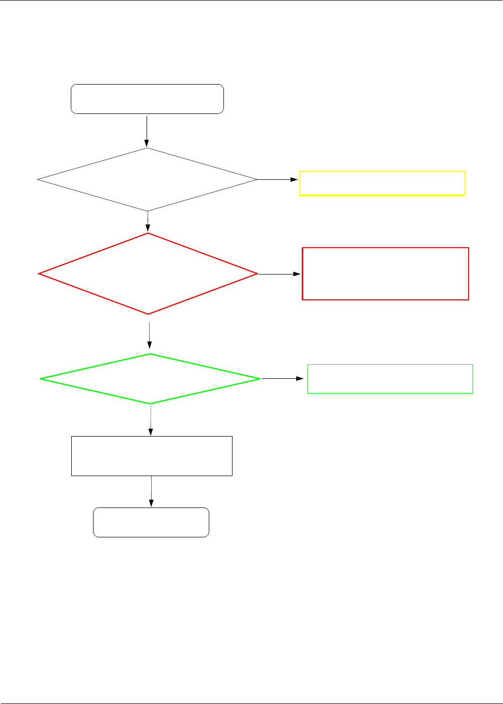
Level 3Repair
Distribution, transmission, or infringement of any content or data from this document without Samsung’s written authorization is strictly prohibited.
Confidential and proprietary-the contents in this service guide subject to change without prior notice.
8-39
8-3-12. VT CAM
"Camera" function does not work
Yes
Check the Camera
connector on Main PBA Reconnect the HEA801
No
Check the voltage
C809 =1.8V
C800 =2.8V
No
Yes
Yes
END
Replace the camera module
No
Yes
Replace U502
Replace U800
Check
VT_CAM_MCLK(R4114) Replace UCP4001
Abnormal
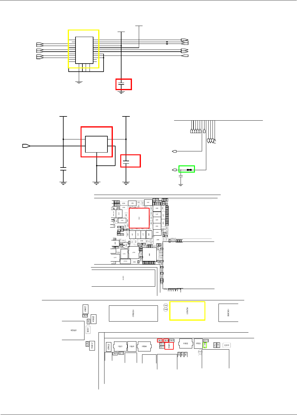
Level 3Repair
Distribution, transmission, or infringement of any content or data from this document without Samsung’s written authorization is strictly prohibited.
Confidential and proprietary-the contents in this service guide subject to change without prior notice.
8-40
C809
99
NC
2526
NC
27
NCNC
28
23
23 24
24
3
34
4
556
6
7
78
8
16
16
17
17 18 18
19
19
22
20
20
21 21 22 22
11
10 10
11
11 12
12
13 13 14 14
15
15
HEA801
2M_CAM_1.8V
TP801
2M_CAM_A2.8V
TP802
VT_CAM_D1_P_F VT_CAM_MCLK
CAM_VT_STBY
CAM_VT_nRST
VT_CAM_ID
VT_CAM_SDA_1.8
V
VT_CAM_SCL_1.8
V
VT_CAM_CLK_N_F
VT_CAM_CLK_P_F
VT_CAM_D0_N_F
VT_CAM_D0_P_F
VT_CAM_D1_N_F
VOUT 1
3EN 2
GND
5GND
VIN
4
U800
V_BAT 2M_CAM_A2.8V
C802
C800
2M_A2.8V_EN
E7
XGPIO8
E8XGPIO9
E9
XGPIO10
D6XGPIO3
D7XGPIO6
E10XGPIO11
C6XGPIO2
C7XGPIO5
C8XGPIO7
B6XGPIO0
XGPIO1
B7
A8XGPIO4
C4102
R4114
TA_INT
2M_A2.8V_EN
IRDA_IRQ
VT_CAM_ID
HW_REV2
8M_CAM_MCLK
HW_REV3
FPGA_SPI_EN
HW_REV0
HW_REV1
FPGA_SPI_CLK
VT_CAM_MCLK
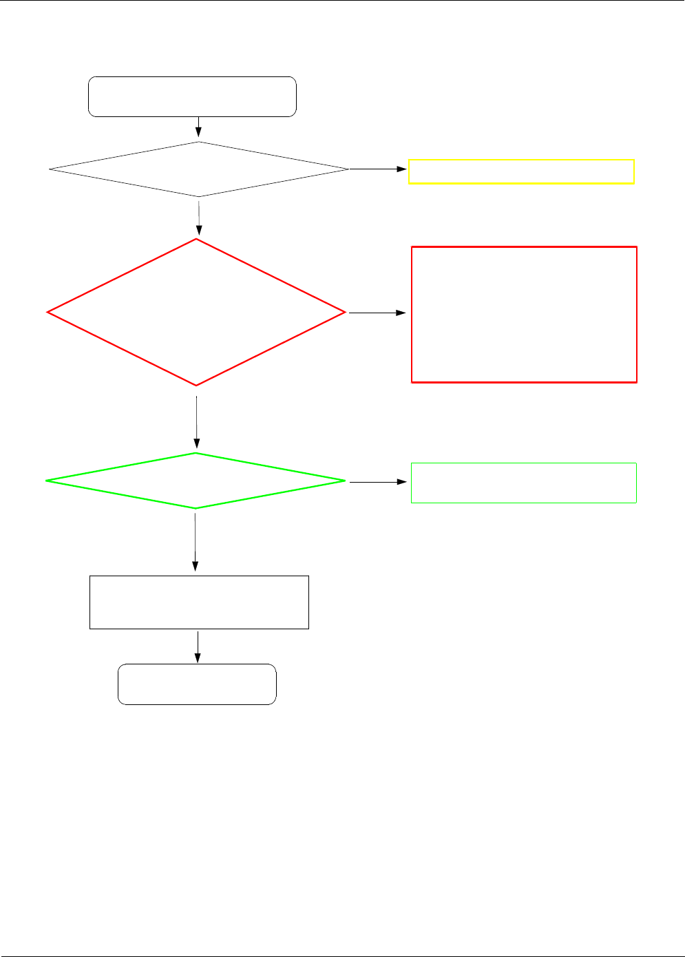
Level 3Repair
Distribution, transmission, or infringement of any content or data from this document without Samsung’s written authorization is strictly prohibited.
Confidential and proprietary-the contents in this service guide subject to change without prior notice.
8-41
8-3-13. 8M CAM
"Camera" function does not work
Yes
Check the Camera
connector on Main PBA Reconnect the HEA800
No
Check the voltage
C807 =1.1
V,
C806 =1.8V
C801 =2.8V
C804 =2.8V
Replace U502
Replace U502
Replace U801
Replace U502
No
Yes
Replace UCP4001
Check
8M_CAM_MCLK(R802)
END
Replace the camera module
No
Yes
Yes
Abnormal
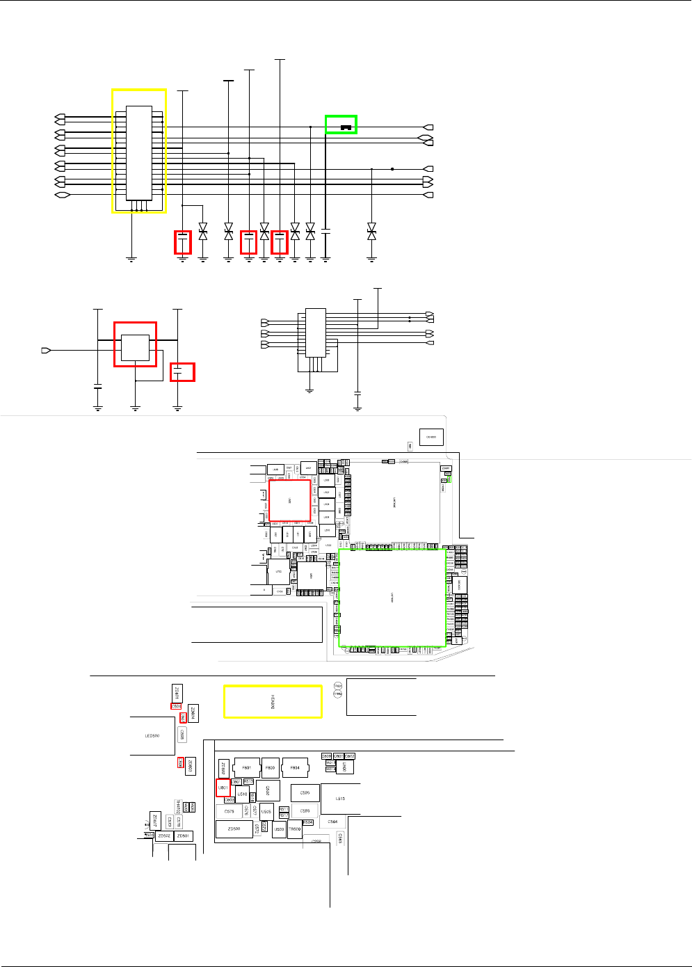
Level 3Repair
Distribution, transmission, or infringement of any content or data from this document without Samsung’s written authorization is strictly prohibited.
Confidential and proprietary-the contents in this service guide subject to change without prior notice.
8-42
NC NC
36
NC
37 38
NC
33
33 34 34
44
55 66
778
8
99
35
26 26
27 27 28 28
29 29
33
30 30
31
31 32 32
19
22
20 20
21
21 22 22
23
23 24 24
25
25
11 11 12 12
13 13 14 14
15 15 16 16
17 17 18 18
19
HEA800
11
10 10
ZD800
ZD803
C806
ZD801
C807
8M_AF_2.8V
ZD802
ZD807
R802
ZD804
8M_S_CORE_1.1V
C839
TP800
C804
8M_AVDD_2.8V
CAM_IO_1P8
8M_CAM_RESET
8M_CAM_SDA_1.8V 8M_CAM_SCL_1.8V
8M_AF_SDA_1.8V
8M_CAM_D0_N_F
8M_CAM_D0_P_F
8M_CAM_CLK_N_F
8M_CAM_CLK_P_F
8M_CAM_D1_N_F
8M_CAM_D1_P_F
8M_CAM_D2_N_F
8M_CAM_D2_P_F
8M_CAM_D3_N_F
8M_CAM_D3_P_F
8M_CAM_MCLK
8M_AF_SCL_1.8V
8M_EEPROM_SCL_1.8
V
8M_EEPROM_SDA_1.8
V
V_BAT 8M_AVDD_2.8V
C803
C801
5GND
VIN
41
VOUT
U801
3EN GND 2
8M_AVDD_LDO_EN
C809
99
NC
2526
NC
27
NCNC
28
23
23 24
24
3
34
4
556
6
7
78
8
16
16
17
17 18 18
19
19
22
20
20
21 21 22 22
11
10 10
11
11 12
12
13 13 14 14
15
15
HEA801
2M_CAM_1.8V
TP801
2M_CAM_A2.8V
TP802
VT_CAM_D1_P_F VT_CAM_MCLK
CAM_VT_STBY
CAM_VT_nRST
VT_CAM_ID
VT_CAM_SDA_1.8
V
VT_CAM_SCL_1.8
V
VT_CAM_CLK_N_F
VT_CAM_CLK_P_F
VT_CAM_D0_N_F
VT_CAM_D0_P_F
VT_CAM_D1_N_F
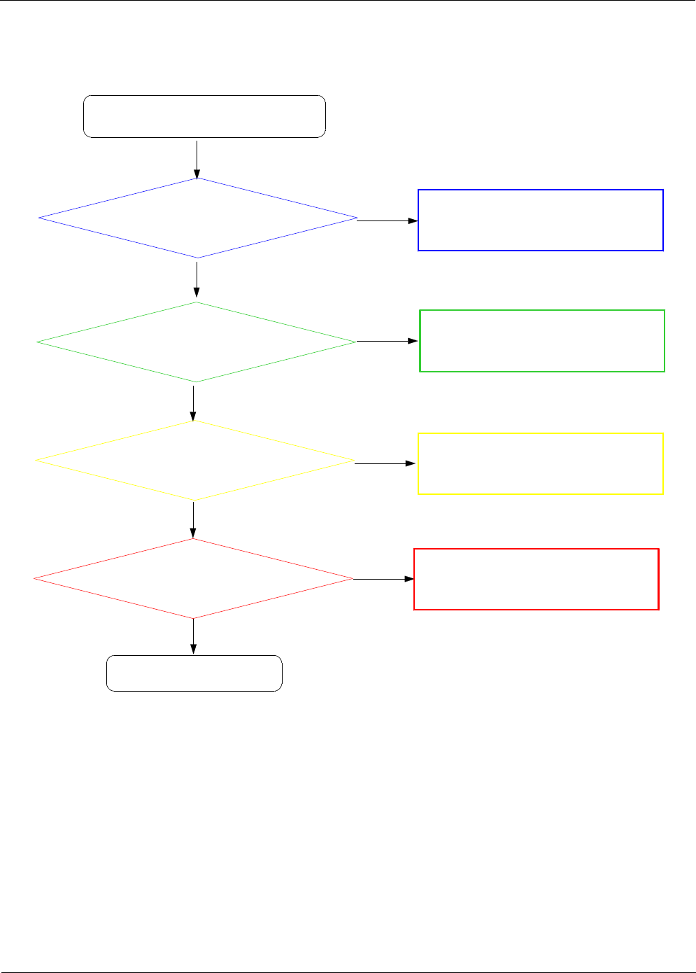
Level 3Repair
Distribution, transmission, or infringement of any content or data from this document without Samsung’s written authorization is strictly prohibited.
Confidential and proprietary-the contents in this service guide subject to change without prior notice.
8-43
8-3-13. OTG
OTG does not work
Yes
No Check HEA700
Check 90pin Connector
on the Main PBA
Yes
END
Yes
No Replace U701
Check the voltage
C706(5.0V), C707(5.0V)
C562(5.0V)
Yes
No Check R708, R709
Yes
Check sub PMIC
on the MAIN PBA No Replace U512
Check the resistor
on the MAIN PBA
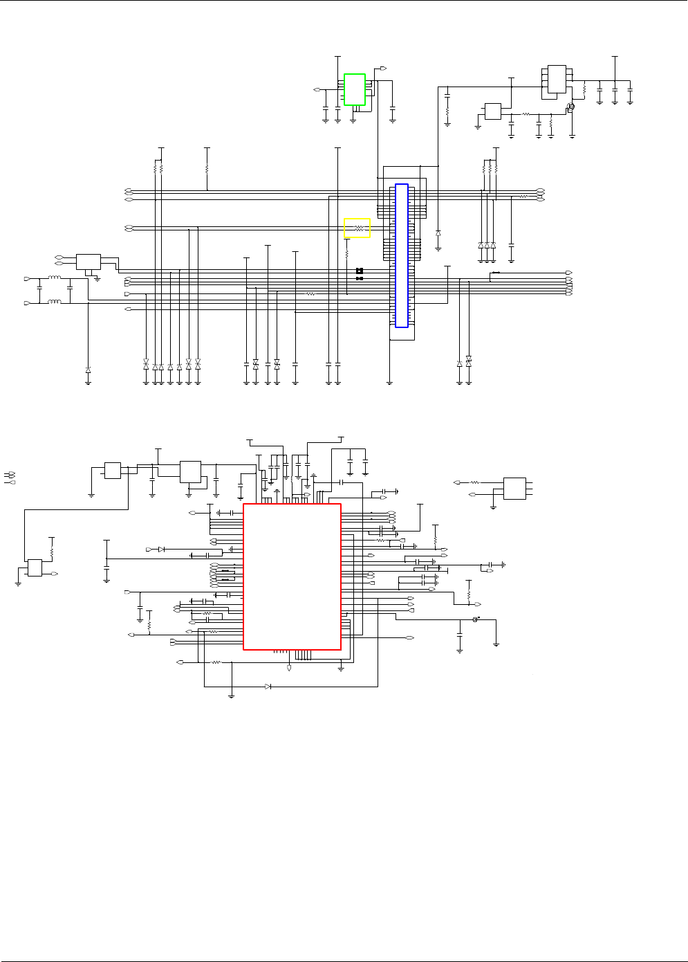
Level 3Repair
Distribution, transmission, or infringement of any content or data from this document without Samsung’s written authorization is strictly prohibited.
Confidential and proprietary-the contents in this service guide subject to change without prior notice.
8-44
3D
1
G
2S
TR700
L702
L703
VMMC2_2.8V_AP
R722
C721
MICBIAS_LDO_2.6V
VTF_2.8V
C706
R725
R716
ZD709
VMMC2_2.8V_AP
ZD720
ZD717
C703
C718
R709
VCC_1.8V_AP
R701
ZD708
V_BUS_5V
ZD704
R705
ZD701
R713
R714
ZD702
ZD703
ZD718
R723
R708
1
2I|O 3
I|O
4
I|O
F700
GND
5
6GND
I|O
R717
R720
C700
GND
NC
3
1
OUT
2
VDD
IF_VOUT_CHARGER
C702
V_BAT
U702
4
ZD707
R721
R704
VBUSDET
B1
B2 OUT
IN B3
B4GND
OVLO C1
C2
IN
IN C3
C4GND
U701
NC
1
2NC
_EN\ A1
A2 OUT
OUT
A3
A4GND
88
88
89 89
99
90 90
91 NC NC 92
C704
80
80
81 81 82 82
83
83 84
84
85 85 86 86
87
87
73 73 74 74
75
75 76
76
77 77 78 78
79
79
8
8
66 66
67
67 68
68
69 69
7
7
70 70
71
71 72
72
59
59
66
60
60
61 61 62 62
63
63 64
64
65 65
51
51 52
52
53 53 54 54
55
55 56
56
57 57 58 58
44
44
45 45 46 46
47
47 48
48
49 49
55
50 50
37 37 38 38
39
39
4
4
40
40
41 41 42 42
43
43
3
3
30 30
31
31 32
32
33 33 34 34
35
35 36
36
22 22
23
23 24
24
25 25 26 26
27
27 28
28
29 29
15
15 16
16
17 17 18 18
19
19
22
20
20
21 21
11
10 10
11
11 12
12
13 13 14 14
ZD716
HEA700
C720
ZD700
VCC_1.8V_AP
R700
ZD710
R703
C701
ZD705
C707
C719
C713
C708
R715
V_BTP_3P3
3
S
C722
U700
D
5
6D
D
7
8D
D
9
4
G
1
S
2
S
C710
R702
ZD721
C705
ZD706
C711
VCC_1.8V_AP
MHL_DP V_BTP_1P8
VPS_FB
KBC3_HOME_BTN_N
MAIN_MIC_P
MAIN_MIC_N
MHL_ID
MUIC_ID
JTAG_USB_ID
T_FLASH_DETECT
MHL_DM
T_FLASH_D(1)
T_FLASH_D(2)
T_FLASH_D(3) T_FLASH_CMD
BTP_MISO
BTP_MOSI BTP_SCK
BTP_SSN
BTP_SLEEP
BTP_DRDY_N_IRQ
HALL_SENSOR_INT
T_FLASH_D(0)
OVPEN
VBUSDET
T_FLASH_CLK
MUIC_DP
MUIC_DM
C565
C590
R510
C587
D501 C588
TP507
C583
R521
C564
C567
C568
VCC_1.8V_AP
C572
C586
R515
C592
R514
LED500
R524
2
VDD
U504
4GND
NC
3
1
OUT
U508
2GND
INA
1
3NC 4
OUTY
5
VCC
C594
L513
V_BAT
VCC_1.8V_AP
VCC_1.8V_AP
C591
VCC_1.8V_AP
TP508
C570
C571
V_BAT
R523
C566
BATTJ7
BATT
J8 DN1
J9 DP2
MVIO
H9 UID
J1CORNER
J10CORNER
J2
CHGPGJ3
CHGPG
J4 SYS
J5 SYS
J6
CHGPG
H10 COMP2
H2 BAT_SN
H3 BAT_SP
H4 SYS
H5 SYS
H6
BATTH7
BATT
H8
AVL
G3GND_A
G4GND_A
G5 MIC_USB G6
JIG
G7 IDB
G8
AUR2
G9 UR2
H1
DETBATB
F5
SDA
F6
MVBAT
F7
BC
F8 SR2
F9
ADP2
G1
CHGLX
G10 COMN1
G2
SYS_A
E7
AUT1
E8 UT1
E9
MVBUS
F1
CHGLX
F10
ADN1
F2
CHGLX
F3 INOKB
F4 AIN
D9
VBATTFG
E1
BYP
E10 SL1
E2
BYPE3
BYP
E4GND_D
E5
VIO
E6
CHGIN
D10
SDAFG
D2
CHGIN
D3
VBUSDET
D4 OVPENB
D5 DISQBAT
D6
SCL
D7GND_A
D8
SAFEOUT2
C3
FLASHEN
C4
TORCHEN
C5GND_Q
C6
MRSTB
C7
RESETB
C8
SCLFG
C9
ALRT
D1
MDN
B5GNDM
B6
INTB
B7
VCCTEST
B8
SNS
B9
VBFG
C1
CHGIN
C10
THRM
C2
TEST1 A7
TEST2 A8
TEST3 A9
TEST4
B1
SAFEOUT1
B10 KVSS
B2
FLED
B3 MPWM
B4
NC
2NC
A1CORNER
A10CORNER
A2
FLED
A3 MGAIN
A4 MDP
A5 IN_MOT
A6
U512
1
C589
V_BATTERY
C585
C573
V_BAT
TP506
C569
VDD 1
VOUT
VCC_3.0V_MOTOR
U505
3CE
GND
5
GND 2
4
R516
D502
6
IN
3NC
1NO
VCC 5
C596
U506
COM 4
GND
2
TP505
VCC_1.8V_AP
V_BUS_5V
C597
C562
R522
C5002
VBATFG
C574
V_BAT
R520
C563
C584
C598
C582
FUEL_ALERT
FUEL_SDA_1.8V
VBUSDET
IF_PMIC_SCL_1.8V
BATT_TH
CP_TXD_1.8V
USB_D_M
IF_PMIC_SDA_1.8V
USB_D_P
CHG_LX
CP_RXD_1.8V
PMIC_JIGONB
AP_JTAG_EXTRST
MUIC_RST_INT
PMIC_ACOKB
CHG_LX
USB_VBUS_AP_4.9V
IF_PMIC_IRQ
USB_VBUS_CP_4.9V
CAM_FLASH_EN
CAM_FLASH_SET
nPOWER
FUEL_SCL_1.8V
VPS_L
VPS_R
V_BATTERY_SENSE
V_JIG_SENSE
MOTOR_N
MOTOR_P
VIBTONE_PWM
OVPEN
BATT_TH
BATT_ID
V_BATTERY-
IF_CON_SENSE
V_BATTERY-
V_JIG_SENSE
V_BATTERY-
V_BATTERY_SENSE
USB2_AP_D-
USB2_AP_D+
AP_RXD
AP_TXD
JTAG_TXD
JTAG_RXD
MUIC_DM
MUIC_DP
MUIC_ID
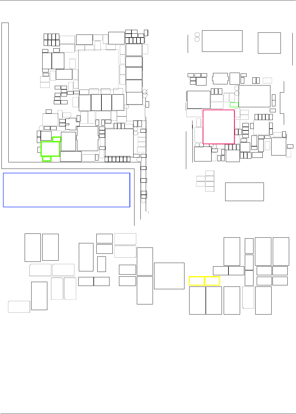
Level 3Repair
Distribution, transmission, or infringement of any content or data from this document without Samsung’s written authorization is strictly prohibited.
Confidential and proprietary-the contents in this service guide subject to change without prior notice.
8-45
C244
C4010
C4011
C4040
C4042
C4043
C4046
C4074
C4099
C4100
C4102
C500
C5000
C5002
C501C502
C503
C504
C505
C506
C507
C508
C509
C510 C511
C513
C514
C515
C516
C517C518
C519
C520
C521
C522
C523
C524
C525
C527
C528
C529
C530
C532
C533
C534
C535
C536
C537
C538
C539
C541
C542
C543
C544
C545
C547
C548
C549
C550
C551
C552
C553
C554
C555C556
C557
C558
C559
C560
C561
C562
C563
C564
C565
C566
C567
C568
C569
C570
C571C574
C582
C583
C584
C585
C586
C587C588
C589
C590
C591
C592
C594
C596
C597
C700
C701
C702
C703
C704
C705
C706
C707
C708
C709
C800 C802C809
C816
C818
C819
C820
C821
C822
C823
C824
C825
C826
C900
C901
C902
C903
C910
C911
C912
C914
C915C916
D500
D501
D502
F802 F803
HDC900
HEA4000
HEA700
HEA801
L215
L500
L501
L502
L503
L504
L505
L506
L507
L508
L509
L510
L511
L512
L513
L802
L803
OSC500
Q700
R201
R202
R301
R302
R303
R304
R305
R306
R4013
R4014
R4015 R4016
R4028R4031
R4039
R4040
R4049
R4050
R4072
R4079
R4080
R4085
R4087R4088
R4089
R4114
R500
R501
R502
R505
R506
R507
R508
R510
R514
R515
R520
R521
R522
R523
R525
R700
R701
R702
R703
R706R707
R710
R711
R724
R803
R804
R805
R806
R900
R901
R902
R903R915
R916
R918
R919
SC103
SC104
TP107
TP4004
TP4007
TP4013
TP500
TP501
TP502
TP505
TP506
TP507TP508
TP801
TP802
TP804
TP805
TP806
TR700
U203
U500
U502
U503
U504
U506
U512
U700
U701
U702
U800
U804
U900
U901
U903
U904
ZD700
C4101
C710
C711
C713
C718C719
C720
C721
C722
F700
L702
L703
R70 4R70 5 R708R709R71 3
R71 4
R715
R716
R717
R720R721R72 2
R723
ZD701
ZD702
ZD703
ZD704
ZD705
ZD706
ZD707
ZD708
ZD709
ZD710ZD716
ZD717
ZD718
ZD720
ZD721
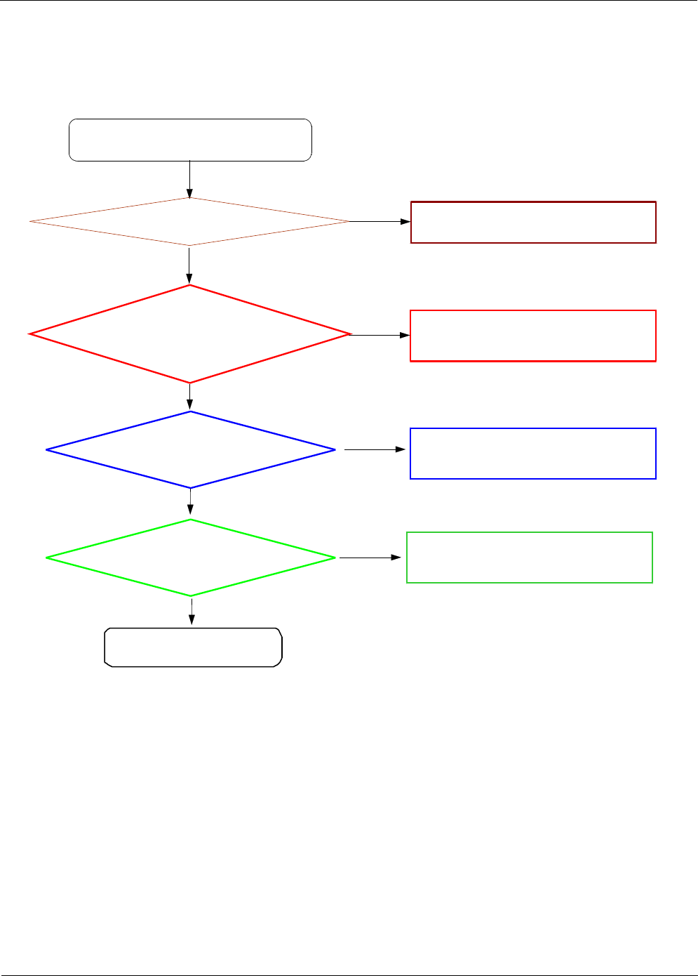
Level 3Repair
Distribution, transmission, or infringement of any content or data from this document without Samsung’s written authorization is strictly prohibited.
Confidential and proprietary-the contents in this service guide subject to change without prior notice.
8-46
8-3-14. MHL
MHL Does not work
Yes
No Check if HEA700 is well connected
Check the IF FPCB
ContocononMainPBA
Yes
No Check the U502
Check the voltage of
L802(1.2V), C821(3.3V),
L803(1.2V), C820(1.8V),
C825(1.8V)
Check CMF
on then MAIN PBA
Yes
END
Yes
Replace F700
Check MHL IC
on then MAIN PBA Replace U804
No
No
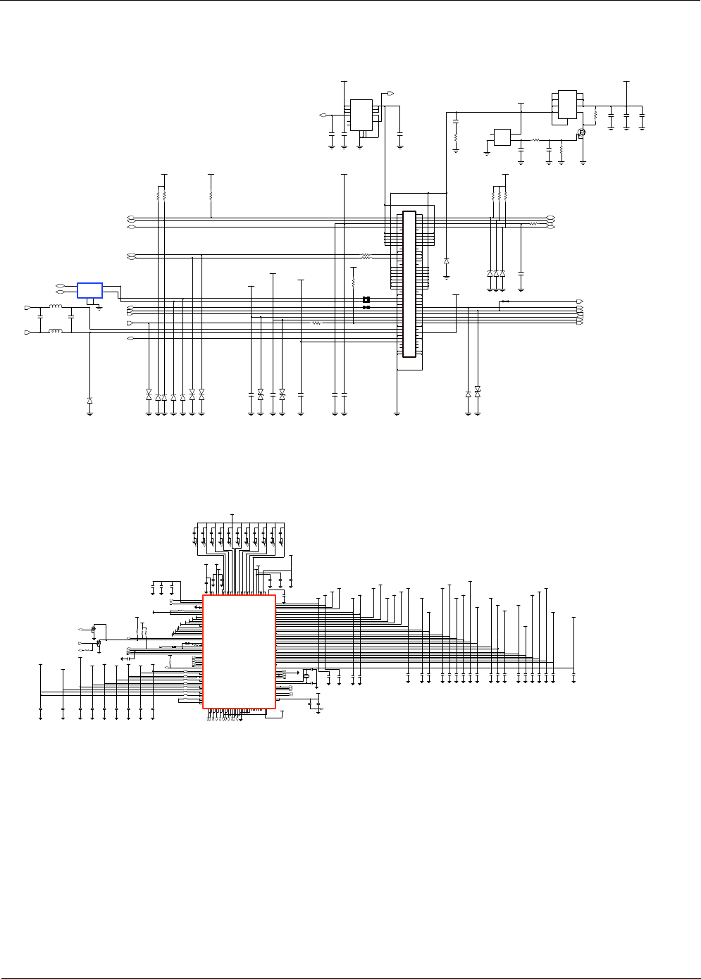
Level 3Repair
Distribution, transmission, or infringement of any content or data from this document without Samsung’s written authorization is strictly prohibited.
Confidential and proprietary-the contents in this service guide subject to change without prior notice.
8-47
3D
1
G
2S
TR700
L702
L703
VMMC2_2.8V_AP
R722
C721
MICBIAS_LDO_2.6V
VTF_2.8V
C706
R725
R716
ZD709
VMMC2_2.8V_AP
ZD720
ZD717
C703
C718
R709
VCC_1.8V_AP
R701
ZD708
V_BUS_5V
ZD704
R705
ZD701
R713
R714
ZD702
ZD703
ZD718
R723
R708
1
2I|O 3
I|O
4
I|O
F700
GND
5
6GND
I|O
R717
R720
C700
GND
NC
3
1
OUT
2
VDD
IF_VOUT_CHARGER
C702
V_BAT
U702
4
ZD707
R721
R704
VBUSDET
B1
B2 OUT
IN B3
B4GND
OVLO C1
C2
IN
IN C3
C4GND
U701
NC
1
2NC
_EN\ A1
A2 OUT
OUT
A3
A4GND
88
88
89 89
99
90 90
91 NC NC 92
C704
80
80
81 81 82 82
83
83 84
84
85 85 86 86
87
87
73 73 74 74
75
75 76
76
77 77 78 78
79
79
8
8
66 66
67
67 68
68
69 69
7
7
70 70
71
71 72
72
59
59
66
60
60
61 61 62 62
63
63 64
64
65 65
51
51 52
52
53 53 54 54
55
55 56
56
57 57 58 58
44
44
45 45 46 46
47
47 48
48
49 49
55
50 50
37 37 38 38
39
39
4
4
40
40
41 41 42 42
43
43
3
3
30 30
31
31 32
32
33 33 34 34
35
35 36
36
22 22
23
23 24
24
25 25 26 26
27
27 28
28
29 29
15
15 16
16
17 17 18 18
19
19
22
20
20
21 21
11
10 10
11
11 12
12
13 13 14 14
ZD716
HEA700
C720
ZD700
VCC_1.8V_AP
R700
ZD710
R703
C701
ZD705
C707
C719
C713
C708
R715
V_BTP_3P3
3
S
C722
U700
D
5
6D
D
7
8D
D
9
4
G
1
S
2
S
C710
R702
ZD721
C705
ZD706
C711
VCC_1.8V_AP
MHL_DP V_BTP_1P8
VPS_FB
KBC3_HOME_BTN_N
MAIN_MIC_P
MAIN_MIC_N
MHL_ID
MUIC_ID
JTAG_USB_ID
T_FLASH_DETECT
MHL_DM
T_FLASH_D(1)
T_FLASH_D(2)
T_FLASH_D(3) T_FLASH_CMD
BTP_MISO
BTP_MOSI BTP_SCK
BTP_SSN
BTP_SLEEP
BTP_DRDY_N_IRQ
HALL_SENSOR_INT
T_FLASH_D(0)
OVPEN
VBUSDET
T_FLASH_CLK
MUIC_DP
MUIC_DM
C556
V_BAT
VSIL_1.2A
VCC_SUB_3.4V
KEY_LED_3.3V
C554
C524
VMIPI_PLL_ABB1_1.8V_AP
C549
C517
C545
C528
C542
C553
C530
VCC_SUB_2.0V
C552
C537
VMMC2_2.8V_AP
VCC_SUB_1.4V
VDDQ_PRE_1.8V
TP503
R504
R507
R505
GRIP_1P8
C539C535
C555
C536
VHSIC_1.8V_AP
C521
IrLED_3.3V
VCC_2.8V_AP
C511
G
2S
VCC_1.8V_AP
TR500
3D
1
C519
VDD_CAM_ISP_1.0V
L512
C543
VCC_SUB_3.4V
C557
C503
C520
C534
VKFC_1.0V_AP
L502
L501
VTOUCH_1.8V
C560
L506
2M_CAM_1.8V
V_BAT
VTF_2.8V
VMEM2_1.2V_AP
C507
21
OSC500
R502
VG3D_1.0V_AP
V_BAT
VINT_1.0V_AP
TSP_3.3V
C527
C548
V_BAT
VCC_1.8V_AP
VCC_1.8V_MHL
C506
C522
C561
CAM_IO_1P8
VDD_CAM_ISP_1.0V
VHSIC_1.0V_AP
VARM_1.0V_AP
L511
TP502
C518
C529
VINT_1.0V_AP
L504
C510
R526
C504
C526
TR501
D3
G
1
S2
C551
VADC_1.8V_AP
C5000
TP504
VMMC01_1.8V_AP
L503
C5003
C523
VCC_SUB_1.4V
C558
C525
VCC_SUB_2.0V
R506
C505
C559
VCC_SUB_3.4V
C533
VRTC_1.8V
N4 SW4
N5GNDB4
N6GNDB3
N7 SW3
N8
VINB3
N9GNDB6
M9GNDB6
N1NC
N10 SW6
N11
VINB7
N12 SW7
N13NC
N2
VINB10
N3
VINB4
M13GNDB7
M2
VINB10
VINB4M3
M4 SW4
M5GNDB4
M6GNDB3
M7 SW3
M8
VINB3
L6 RS3N
L7 RS3P
FB3
L8
L9
VLDO24
M1 SW10
M10 FB6
M11
VINB6
M12 FB7
L10
VLDO13
L11
VLDO1
VLDO27 L12
L13
VLDO22
L2 FB10
L3 FB4
L4 RS4P
L5 RS4N
K3AGND
K4
VBAT
AGND
K5
K6AGND
K7AGND
K8
VLDO38
K9
VLDO16
L1GNDB10
NC
J9
VLDO14
GNDB22
K1
K10
VINL5
K11
VLDO9
K12
VINL1
K13
VLDO6
K2GNDB22
VLDO11
J13
VLDO35
J2 SW22
J3
WDRSTEN
J4 BUCK10EN
J5
LDO7EN
J6
LDO13EN
J7AGND
J8
H6
LDO19EN
H7
VBAT
H8
VREF
H9
VLDO26
J1 SW22
J10
VLDO19
J11
VLDO23
J12
H10
VLDO34
H11
VINL6
H12
VLDO17
H13
VLDO28
H2
VINB22
H3 FB2
H4 PWRHOLD
H5NC
G3 RS2P
G4 IRQB
G5 MR1B
G6 MR2B
G7 ACOKB
G8
VLDO37
G9
VLDO25
H1
VINB22
F8
VLDO31
F9
VLDO20
G1
VINB21
G10
VLDO21
G11
VLDO15
G12
VLDO36
G13
VLDO30
G2
VINB21
F12
VLDO33
F13
VLDO29
F2 SW21
F3 RS2N
F4 ONOB
F5 RSOB
F6
SDA
F7 JIGONB
E4 PWREN
E5NC
E6
SCL
E7 PWRON
E8
VLDO10
E9
VLDO4
F1 SW21
F10
VINL3
F11
VLDO18
D9
VLDO5
E1GNDB21
E10
VLDO12
E11
VINL2
E12
VINL4
E13
VLDO32
E2GNDB21
E3
LDO18EN
D13
VLDO7
D2 B5V2
D3 B5V3
D4 B5S1
D5 B5S2
D6
AP32K
D7
VDD_CP
D8
VDD_BT
C6 FB9
C7
CP32K
C8
BT32K
C9 BKCOIN
D1 B5V1
D10
VLDO8
D11
VLDO2 D12
VLDO3
C10
XTALOUT
C11
XTALIN
C12 FB8
C13GNDB8
C2 FB5
C3 FB5
C4AGND
C5
VBAT
B3GNDB5
B4 SW5
B5
VINB5
B6
VINB9
B7 SW91
B8GNDB9
B9 SW92
C1GNDB1
A8GNDB9
A9 SW92
B1 SW1
B10
VB9
B11
VINB8
B12 SW8
B13GNDB8
B2 FB1
A12 SW8
A13NC
A2
VINB1
A3GNDB5
A4 SW5
A5
VINB5
A6
VINB9
A7 SW91
1NC
NC
2
A1NC
A10
VB9
A11
VINB8
U502
C540
R503
VMIPI_1.0V_AP 8M_AF_2.8V
VMEM_1.2V_AP
L509
C500
VUOTG_3.0V_AP
VKFC_1.0V_AP
C541
8M_S_CORE_1.1V
VARM_1.0V_AP
VMIF_1.1V_AP
C544
VALIVE_1.0V_AP
C508
C532 C538
C547
VG3DS_1.0V_AP
TSP_1.8V
VCC_1.8V_AP
TP501
VCC_1.8V_AP
VMIF_1.1V_AP
L507
VMIFS_1.1V_AP
C501
C546
VG3D_1.0V_AP
L505
R508
VCC_SUB_1.4V
VCC_3.3V_MHL
L508
VCC_3.0V_MOTOR
C531
L510
VMEM_1.2V_AP
R512
C550
VCC_SUB_2.0V
TCON_1.8V
IF_CON_SENSE
JTAG_IF_CON_SENSE
C502
JTAG_IF_CON_SENSE
VOL_DOWN
32KHZ_CP
BUCK9_GND
MIPI_1.8V_EN
32KHZ_AP
AP_PMIC_SCL
AP_PMIC_SDA
VG3D_1.0V_AP_SNSN
VINT_1.0V_AP_SNSN
VINT_1.0V_AP_SNSP
BUCK7_GND
BUCK4_GND
BUCK3_GND
BUCK6_GND
32KHZ_PMIC
MMC01_EN
MMC2_EN
BUCK2B_GND
BUCK10_GND
VG3D_1.0V_AP_SNSP
ON_SW
VARM_1.0V_AP_SNSN
nPOWER
VARM_1.0V_AP_SNSP
AP_PS_HOLD
BUCK5_GND
BUCK9_GND
BUCK8_GND
BUCK1_GND
BUCK2A_GND
AP_PMIC_EN
AP_PMIC_IRQ
PMIC_ACOKB
AP_N_RST_IN
TF_EN
AP_PMIC_EN
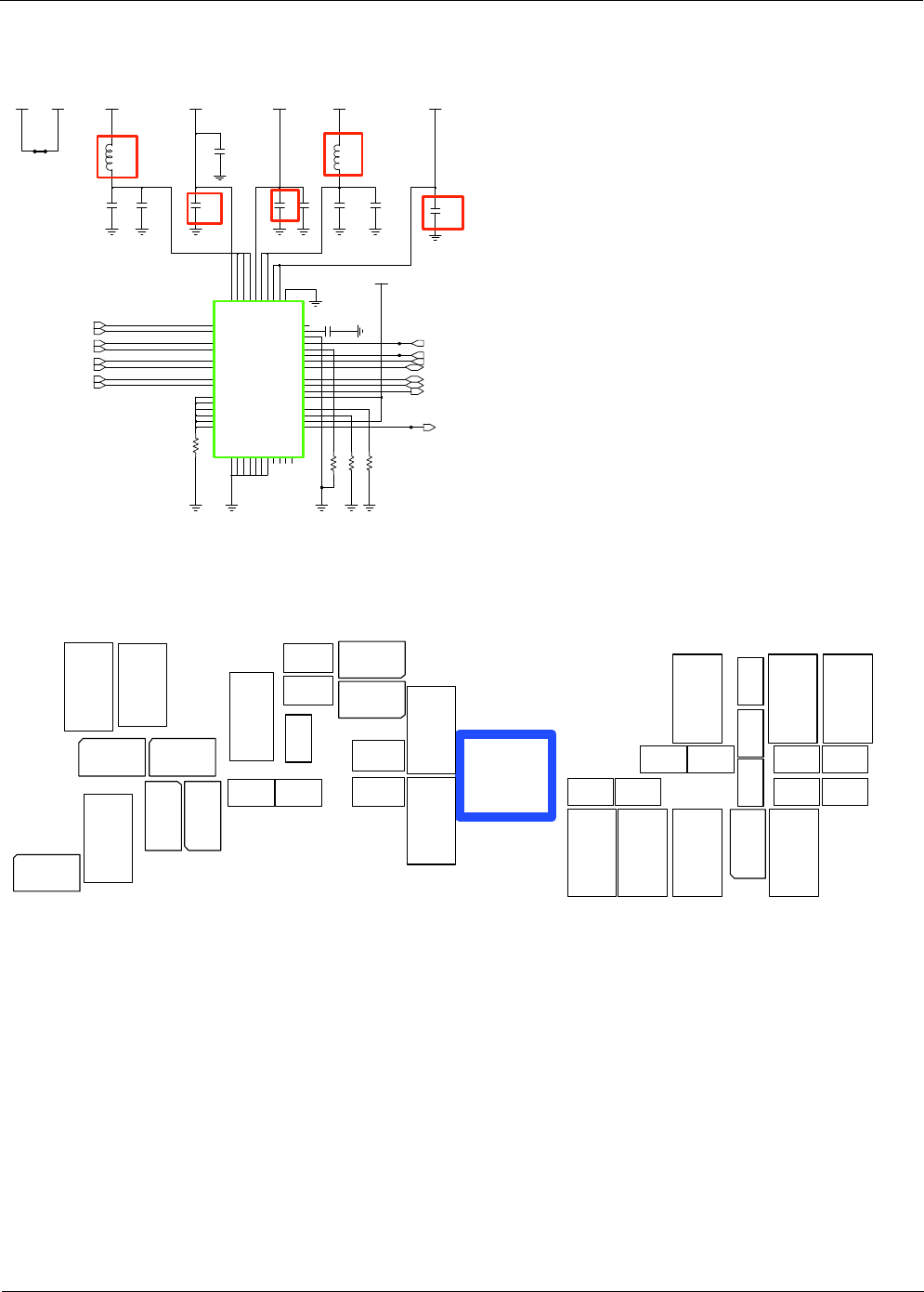
Level 3Repair
Distribution, transmission, or infringement of any content or data from this document without Samsung’s written authorization is strictly prohibited.
Confidential and proprietary-the contents in this service guide subject to change without prior notice.
8-48
L803
C826
TP806
VCC_3.3V_MHL
C820
C819 C822
TP805
R805
C825
RX1_P
G2
RX1_N
G3
RX0_P
G4
RX0_N
G5
RXC_P
G6
RXC_N
G7
RX2_P
F1
GND
F2
RPWR F3
DSCL F4
AVCC12F5
GND
F6
HPD F7
RX2_N
G1
RESET_N D7
DSDA E1
GND
E2
IOVCC18E3
CVCC12E4
RX_AVCCE5
AVCC12E6
GND
E7
V_SENSE C6
INT C7
CSDA D1
RSVD5
D2
GND
D3
IOVCC18D4
CVCC12D5
CI2CA D6
AVCC33B5
USB_ID B6
RSVDL B7
CSCL C1
RSVD2
C2
RSVD0
C3
AVCC12C4
GND
C5
MHL_DB A4
NC
A5
NC
A6
CBUS_ID A7
RSVD4
B1
RSVD1
B2
CM-TERM B3
GND
B4
U804
1NC
2NC
RSVD3
A1
VDDQA2
MHL_D A3
VSIL_1.2A VCC_1.8V_MHL
R806
VSIL_1.2C
C821
R804
C824
VSIL_1.2CVSIL_1.2A
R803
C823
VCC_1.8V_MHL
TP804
C818
C816
VCC_1.8V_MHL
L802
MHL_ID
MHL_SCL_1.8V
MHL_INT
MHL_SDA_1.8
V
MHL_RST
MHL_DM
HD_TX2+
HD_TX2-
HD_TX1+
HD_TX1-
HD_TX0+
HD_TX0-
HD_TXC+
HD_TXC-
HDMI_HPD
MHL_DP
C4101
C710
C711
C713
C718C719
C720
C721
C722
F700
L702
L703
R704R705 R708R709R713
R714
R715
R716
R717
R720R721R722
R723
ZD701
ZD702
ZD703
ZD704
ZD705
ZD706
ZD707
ZD708
ZD709
ZD710ZD716
ZD717
ZD718
ZD720
ZD721
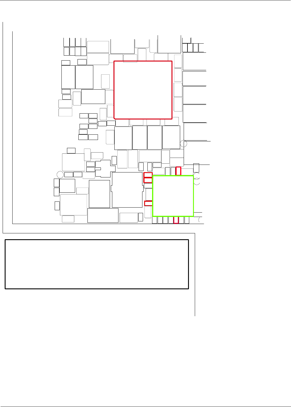
Level 3Repair
Distribution, transmission, or infringement of any content or data from this document without Samsung’s written authorization is strictly prohibited.
Confidential and proprietary-the contents in this service guide subject to change without prior notice.
8-49
C500
C501C502
C503
C504
C505
C506
C507
C508
C509
C510 C511
C514
C515
C517C518
C519
C520
C521
C522
C523
C524
C525
C527
C528
C532
C533
C534
C535
C539
C541
C542
C543
C544
C545
C547
C548
C549
C550
C551
C552
C553
C554
C558
C559
C560
C561
C700
C701
C702
C703
C704
C705
C706
C707
C708 C816
C818
C819
C820
C821
C822
C823
C824
C825
C826
C912
C914
C915C916
HEA700
L500
L501
L502
L503
L504
L505
L506
L507
L508
L509
L510
L511
L512
L802
L803
OSC500
R4015 R4016
R4031
R4049
R4050
R500
R501
R502
R505
R506
R507
R508 R522
R700
R701
R702
R703
R803
R804
R805
R806
R918
R919
SC104
TP4013
TP501
TP804
TP805
TP806
TR700
U500
U502
U503
U700
U701
U702
U804
U903
U904
ZD700
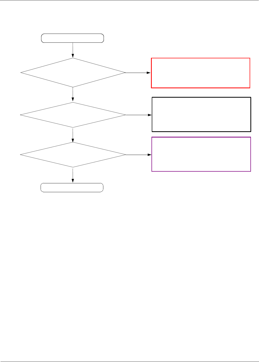
Level 3Repair
Distribution, transmission, or infringement of any content or data from this document without Samsung’s written authorization is strictly prohibited.
Confidential and proprietary-the contents in this service guide subject to change without prior notice.
8-50
8-3-16. Sim Part
Insert SIM card
Is SIM/SD FPCB Connector
and USB FPCB Connector
and PBA Connetor(HEA700)
ok?
Yes
Yes
No
END
Check the SIM Voltage.
(C716) >= 1.8 or 3.0?
Replace :SIM/SD FPCB or USB FPCB
or PBA Connector(HEA700)
Replace U502 and UCP301
Yes
No
Is the SIM Card OK? Change to the new SIM card.
No
Yes
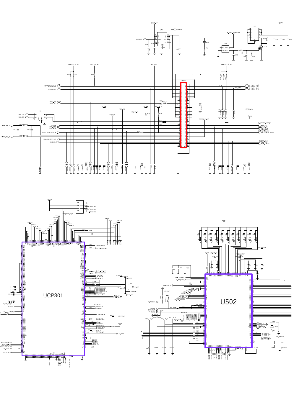
Level 3Repair
Distribution, transmission, or infringement of any content or data from this document without Samsung’s written authorization is strictly prohibited.
Confidential and proprietary-the contents in this service guide subject to change without prior notice.
8-51
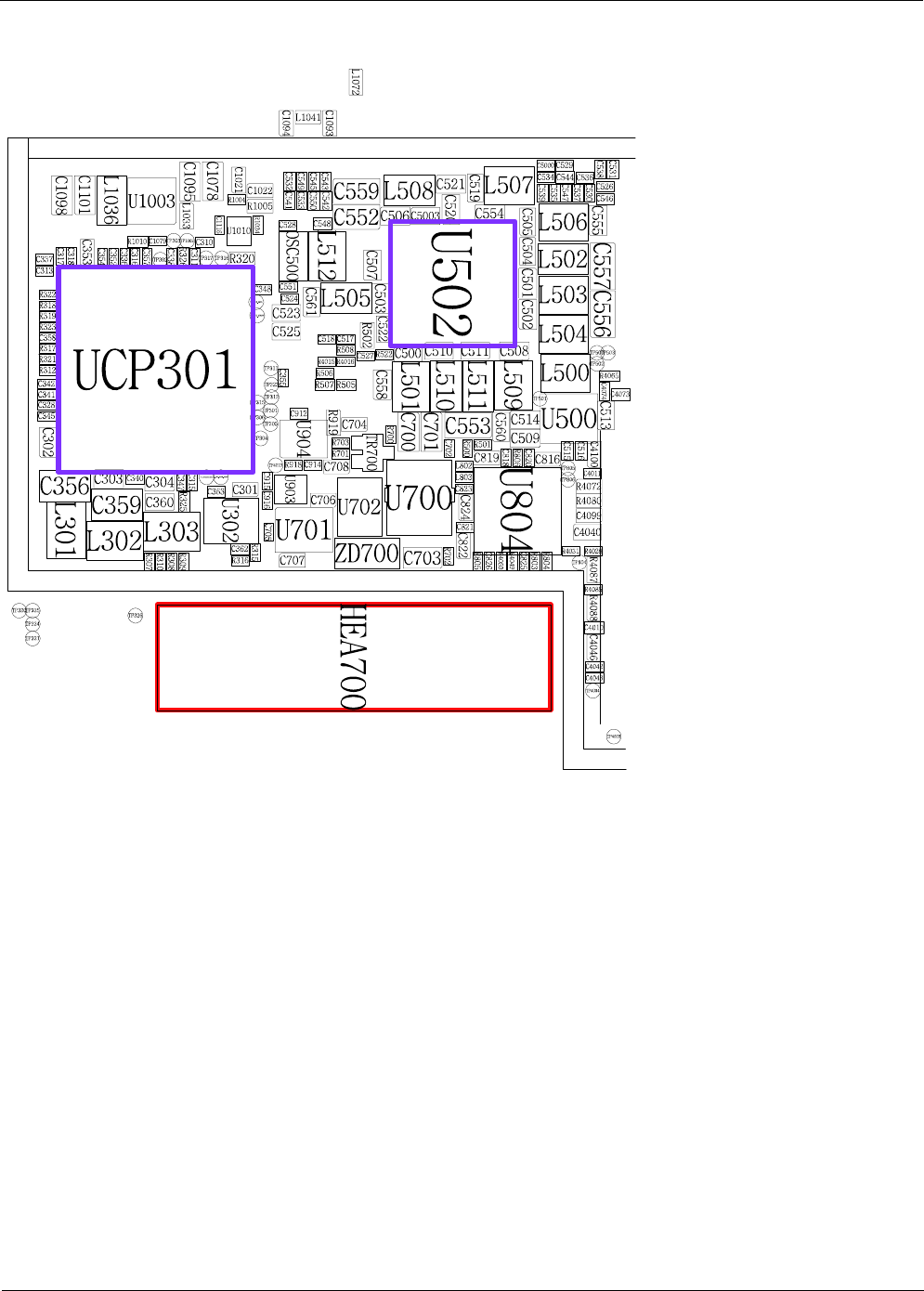
Level 3Repair
Distribution, transmission, or infringement of any content or data from this document without Samsung’s written authorization is strictly prohibited.
Confidential and proprietary-the contents in this service guide subject to change without prior notice.
8-52
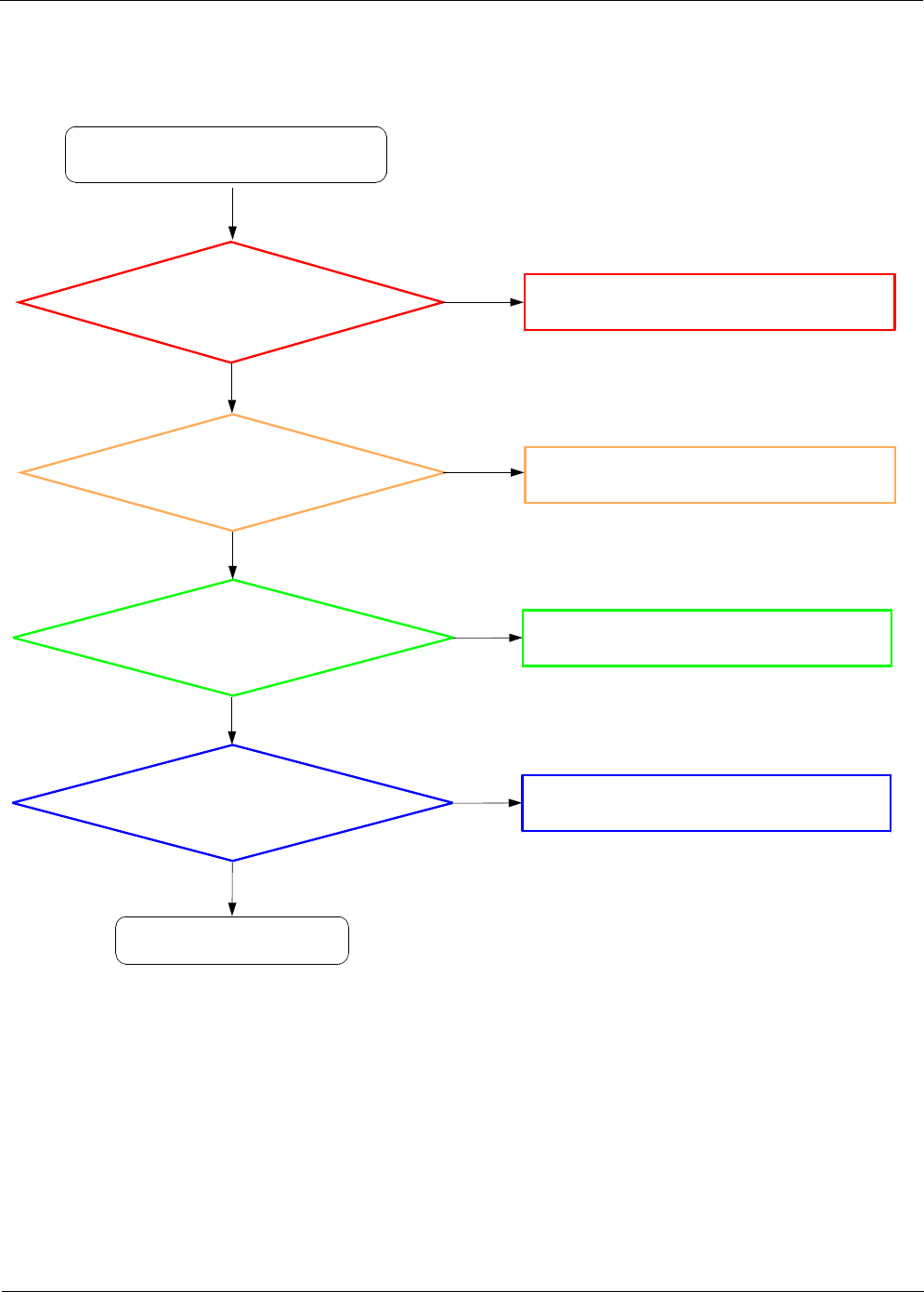
Level 3Repair
Distribution, transmission, or infringement of any content or data from this document without Samsung’s written authorization is strictly prohibited.
Confidential and proprietary-the contents in this service guide subject to change without prior notice.
8-53
8-3-17. Motor
Motor does not work
Yes
END
Yes
Check clips for connection
where SPK Rmodule is
placed for any damage
Check component soldering
statuses of L608, L609
replace ANT602, ANT603
resolder or replace L608, L609
No
Yes
No
Connect other SPK Rmodule Replace SPK Rmodule
No
Yes
Yes
Check component soldering
statuses of U512 and check
voltage C594 =3.0V resolder or replace U512
No
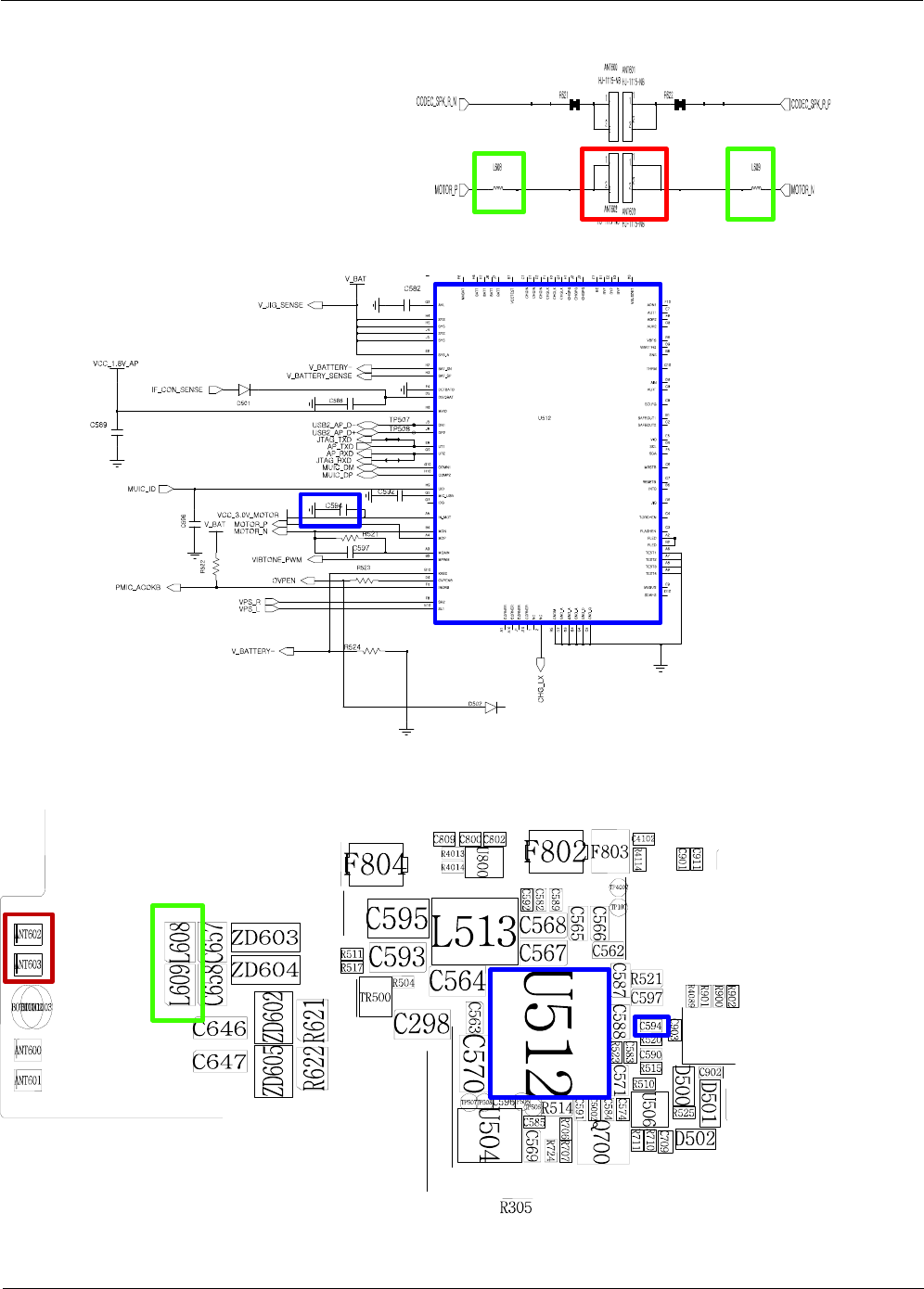
Level 3Repair
Distribution, transmission, or infringement of any content or data from this document without Samsung’s written authorization is strictly prohibited.
Confidential and proprietary-the contents in this service guide subject to change without prior notice.
8-54
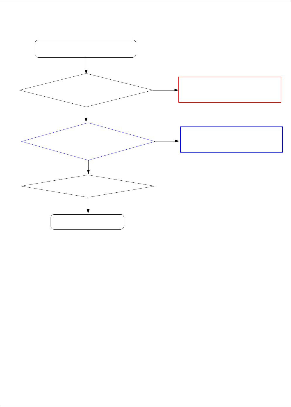
Level 3Repair
Distribution, transmission, or infringement of any content or data from this document without Samsung’s written authorization is strictly prohibited.
Confidential and proprietary-the contents in this service guide subject to change without prior notice.
8-55
8-3-18. Fingerprint
Fingerprint does not work
Yes
No
Replace :Fingerprint FPCB or HEA700
Check the Fingerprint FPCB
Connector and Main PBA's
connector(HEA700)
Yes
END
Replace Fingerprint FPCB
Yes
Check Check
the Fingerprint Voltage.
(C915) >= 3.3V?
(C916) >= 1.8V?
Yes
Replace :U903
No
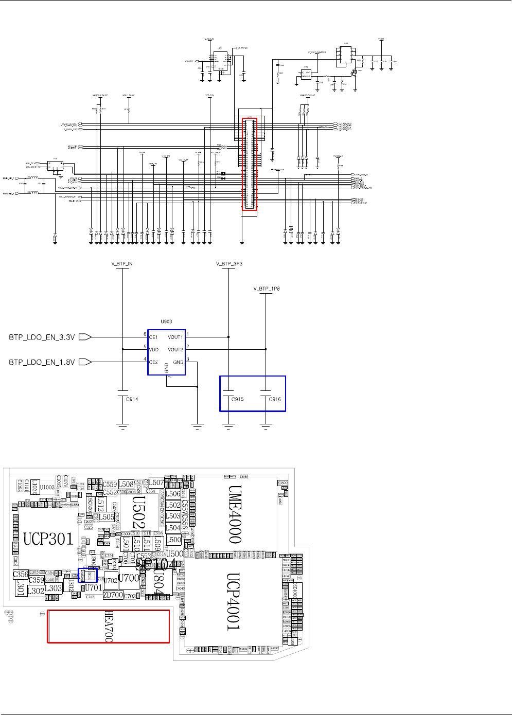
Level 3Repair
Distribution, transmission, or infringement of any content or data from this document without Samsung’s written authorization is strictly prohibited.
Confidential and proprietary-the contents in this service guide subject to change without prior notice.
8-56
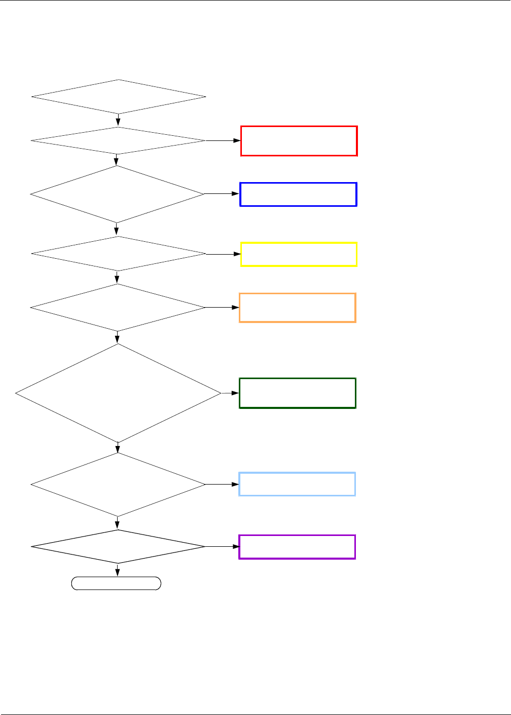
Level 3Repair
Distribution, transmission, or infringement of any content or data from this document without Samsung’s written authorization is strictly prohibited.
Confidential and proprietary-the contents in this service guide subject to change without prior notice.
8-57
Check C1026 ≤-65dBm ?
8-3-19. GSM1800 RX
NORMAL CONDITION
catch the channel?
Check the voltage at
{C1058, =1.8V?}
&{
C1055 =1.2V?}
&{
C1048 =1.5V?}
&{
C1057 =2.5V?}
Check the Voltage at
{C1023 >3.6
V?}
Check C1025
≥-65dBm ?
CHECK soldered
RFS1001, F1001, C1015,
L1011, C1018
Resolder or change
U1002, C1023
Resolder or change
U1001
Resolder or change
U1007
Check the freq. at
C1099 : 26.0MHz ?Change or resolder
OSC1001
Check C1029
≥-65dBm ?Resolder or change
C1025, C1029
NO
YES
NO
NO
YES
NO
YES
NO
YES
NO
YES
NO
YES
GSM1800 Receiver is O.K? Resolder or change
UCP301
END
NO
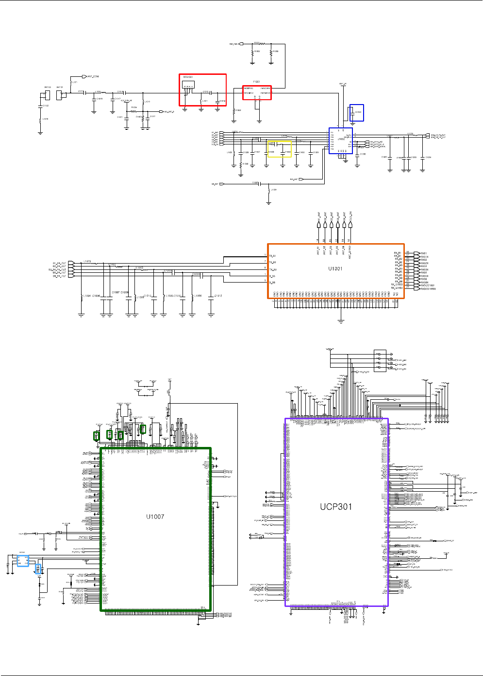
Level 3Repair
Distribution, transmission, or infringement of any content or data from this document without Samsung’s written authorization is strictly prohibited.
Confidential and proprietary-the contents in this service guide subject to change without prior notice.
8-58
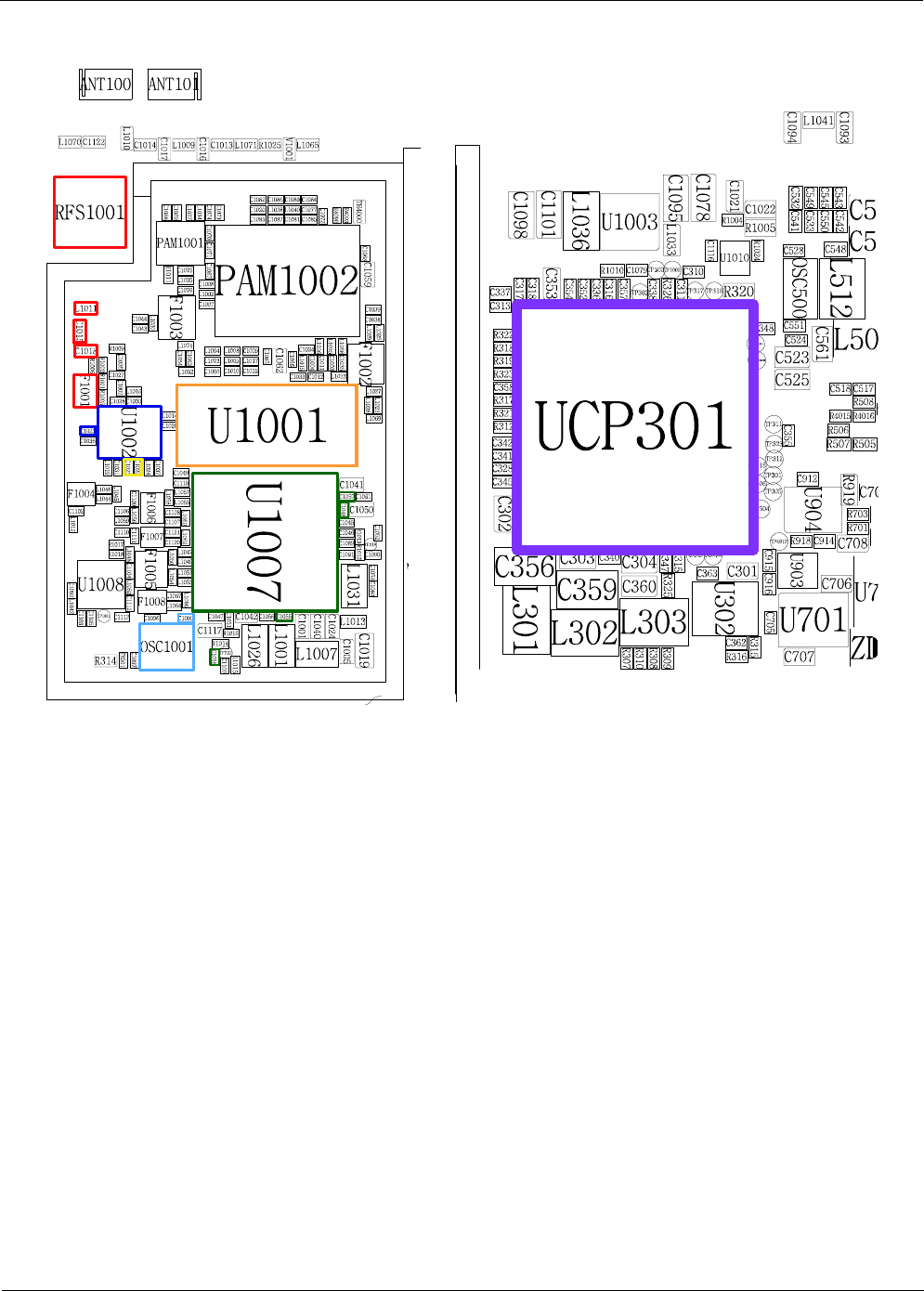
Level 3Repair
Distribution, transmission, or infringement of any content or data from this document without Samsung’s written authorization is strictly prohibited.
Confidential and proprietary-the contents in this service guide subject to change without prior notice.
8-59

Level 3Repair
Distribution, transmission, or infringement of any content or data from this document without Samsung’s written authorization is strictly prohibited.
Confidential and proprietary-the contents in this service guide subject to change without prior notice.
8-60
Check C1026 ≤-65dBm ?
8-3-20. LTE Band1/ WCDMA Band1 RX
NORMAL CONDITION
catch the channel?
Check the voltage at
{C1058, =1.8V?}
&{
C1055 =1.2V?}
&{
C1048 =1.5V?}
&{
C1057 =2.5V?}
Check the Voltage at
{C1023 >3.6
V?}
Check C1025
≥-65dBm ?
CHECK soldered
RFS1001, F1001, C1015,
L1011, C1018
Resolder or change
U1002, C1023
Resolder or change
U1001
Resolder or change
U1007
Check the freq. at
C1099 : 26.0MHz ?Change or resolder
OSC1001
Check L1014
≥-65dBm ?Resolder or change
L1014, L1020
NO
YES
NO
NO
YES
NO
YES
NO
YES
NO
YES
NO
YES
LTE B1 /WCDMA B1
Receiver is O.K? Resolder or change
UCP301
END
NO
CONTINUOUS RX ON
WCDMA1 CH : 10700
LTE B1 CH : 300
AMP :-50
dBm

Level 3Repair
Distribution, transmission, or infringement of any content or data from this document without Samsung’s written authorization is strictly prohibited.
Confidential and proprietary-the contents in this service guide subject to change without prior notice.
8-61
Level 3Repair
Distribution, transmission, or infringement of any content or data from this document without Samsung’s written authorization is strictly prohibited.
Confidential and proprietary-the contents in this service guide subject to change without prior notice.
8-62
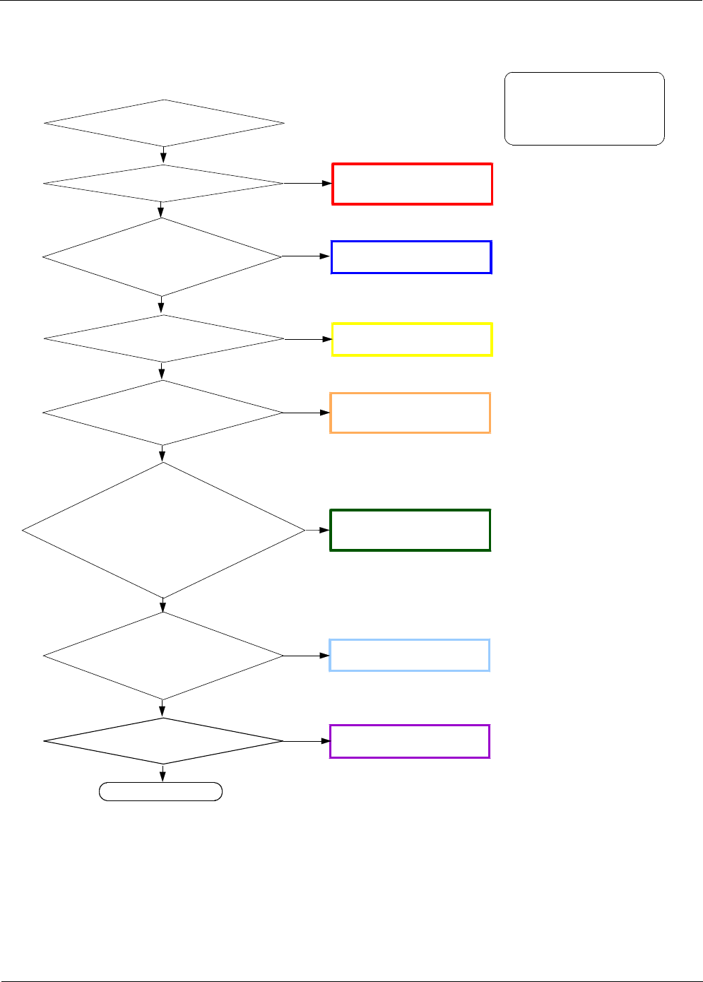
Level 3Repair
Distribution, transmission, or infringement of any content or data from this document without Samsung’s written authorization is strictly prohibited.
Confidential and proprietary-the contents in this service guide subject to change without prior notice.
8-63
Check C1026 ≤-65dBm ?
8-3-21. WCDMA Band2 RX
NORMAL CONDITION
catch the channel?
Check the voltage at
{C1058, =1.8V?}
&{
C1055 =1.2V?}
&{
C1048 =1.5V?}
&{
C1057 =2.5V?}
Check the Voltage at
{C1023 >3.6
V?}
Check C1025
≥-65dBm ?
CHECK soldered
RFS1001, F1001, C1015,
L1011, C1018
Resolder or change
U1002, C1023
Resolder or change
U1001
Resolder or change
U1007
Check the freq. at
C1099 : 26.0MHz ?Change or resolder
OSC1001
Check C1031
≥-65dBm ?Resolder or change
C1031, L1019
NO
YES
NO
NO
YES
NO
YES
NO
YES
NO
YES
NO
YES
WCDMA B2 Receiver is O.K? Resolder or change
UCP301
END
NO
CONTINUOUS RX ON
WCDMA2 CH : 9800
AMP :-50
dBm
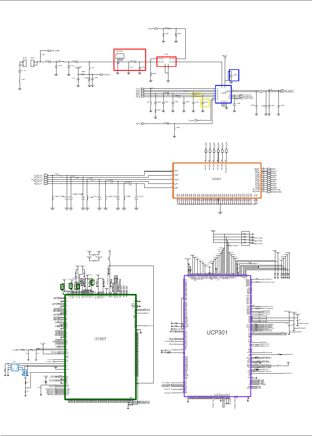
Level 3Repair
Distribution, transmission, or infringement of any content or data from this document without Samsung’s written authorization is strictly prohibited.
Confidential and proprietary-the contents in this service guide subject to change without prior notice.
8-64
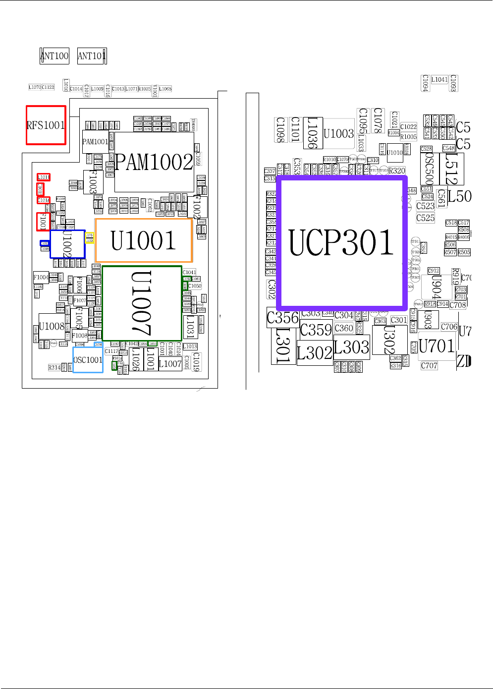
Level 3Repair
Distribution, transmission, or infringement of any content or data from this document without Samsung’s written authorization is strictly prohibited.
Confidential and proprietary-the contents in this service guide subject to change without prior notice.
8-65

Level 3Repair
Distribution, transmission, or infringement of any content or data from this document without Samsung’s written authorization is strictly prohibited.
Confidential and proprietary-the contents in this service guide subject to change without prior notice.
8-66
Check C1026 ≤-65dBm ?
8-3-22. LTE Band3 RX
NORMAL CONDITION
catch the channel?
Check the voltage at
{C1058, =1.8V?}
&{
C1055 =1.2V?}
&{
C1048 =1.5V?}
&{
C1057 =2.5V?}
Check the Voltage at
{C1023 >3.6
V?}
Check C1025
≥-65dBm ?
CHECK soldered
RFS1001, F1001, C1015,
L1011, C1018
Resolder or change
U1002, C1023
Resolder or change
U1001
Resolder or change
U1007
Check the freq. at
C1099 : 26.0MHz ?Change or resolder
OSC1001
Check C1028
≥-65dBm ?
Resolder or change
C1028, C1002, C1027,
C1026, R1009
NO
YES
NO
NO
YES
NO
YES
NO
YES
NO
YES
NO
YES
LTE B3 Receiver is O.K? Resolder or change
UCP301
END
NO
CONTINUOUS RX ON
RF INPUT : 1575CH
AMP :-50
dBm

Level 3Repair
Distribution, transmission, or infringement of any content or data from this document without Samsung’s written authorization is strictly prohibited.
Confidential and proprietary-the contents in this service guide subject to change without prior notice.
8-67
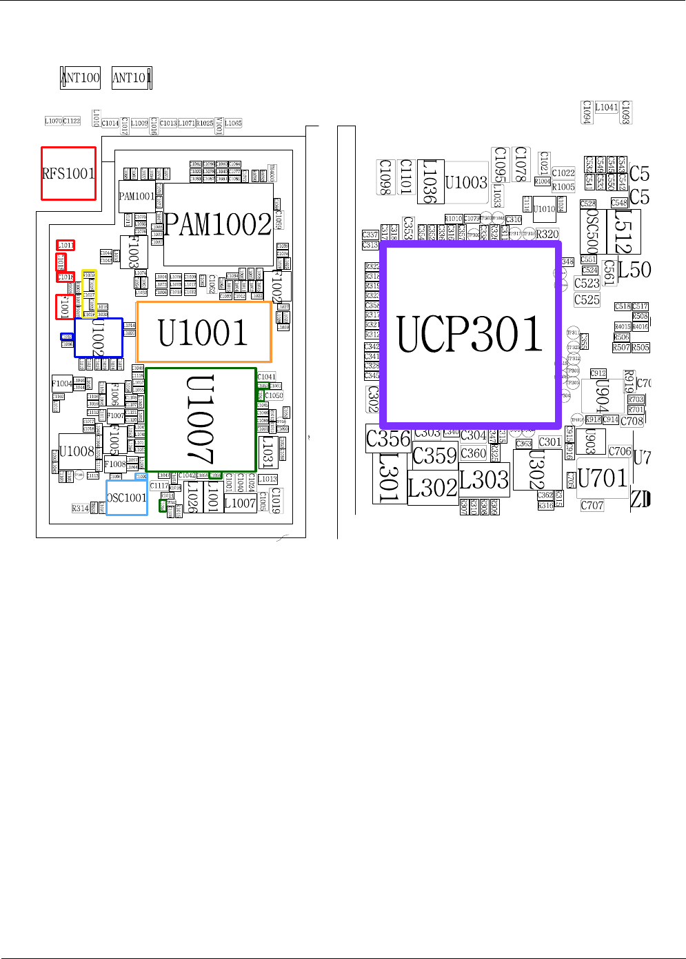
Level 3Repair
Distribution, transmission, or infringement of any content or data from this document without Samsung’s written authorization is strictly prohibited.
Confidential and proprietary-the contents in this service guide subject to change without prior notice.
8-68

Level 3Repair
Distribution, transmission, or infringement of any content or data from this document without Samsung’s written authorization is strictly prohibited.
Confidential and proprietary-the contents in this service guide subject to change without prior notice.
8-69
Check C1026 ≤-65dBm ?
8-3-23. LTE Band5 /WCDMA Band5 /GSM850 RX
NORMAL CONDITION
catch the channel?
Check the voltage at
{C1058, =1.8V?}
&{
C1055 =1.2V?}
&{
C1048 =1.5V?}
&{
C1057 =2.5V?}
Check the Voltage at
{C1023 >3.6
V?}
Check C1025
≥-65dBm ?
CHECK soldered
RFS1001, F1001, C1015,
L1011, C1018
Resolder or change
U1002, C1023
Resolder or change
U1001
Resolder or change
U1007
Check the freq. at
C1099 : 26.0MHz ?Change or resolder
OSC1001
Check C1030
≥-65dBm ?Resolder or change
C1030, L1016
NO
YES
NO
NO
YES
NO
YES
NO
YES
NO
YES
NO
YES
LTE B5 /WCDMA B5 /GSM850
Receiver is O.K? Resolder or change
UCP301
END
NO
CONTINUOUS RX ON
WCDMA5 CH : 4408
LTE B5 CH : 2525
AMP :-50
dBm
Level 3Repair
Distribution, transmission, or infringement of any content or data from this document without Samsung’s written authorization is strictly prohibited.
Confidential and proprietary-the contents in this service guide subject to change without prior notice.
8-70
Level 3Repair
Distribution, transmission, or infringement of any content or data from this document without Samsung’s written authorization is strictly prohibited.
Confidential and proprietary-the contents in this service guide subject to change without prior notice.
8-71
Level 3Repair
Distribution, transmission, or infringement of any content or data from this document without Samsung’s written authorization is strictly prohibited.
Confidential and proprietary-the contents in this service guide subject to change without prior notice.
8-72
Check C1026 ≤-65dBm ?
8-3-24. LTE Band7 RX
NORMAL CONDITION
catch the channel?
Check the voltage at
{C1058, =1.8V?}
&{
C1055 =1.2V?}
&{
C1048 =1.5V?}
&{
C1057 =2.5V?}
Check the Voltage at
{C1023 >3.6
V?}
Check L1074
≥-65dBm ?
CHECK soldered
RFS1001, F1001, C1015,
L1011, C1018
Resolder or change
U1002, C1023
Resolder or change
L1074, C1054, C1063, L1032
Resolder or change
U1007
Check the freq. at
C1099 : 26.0MHz ?Change or resolder
OSC1001
Check C1043
≥-65dBm ?Resolder or change
C1043, L1030, C1044, F1003
NO
YES
NO
NO
YES
NO
YES
NO
YES
NO
YES
NO
YES
LTE B7 Receiver is O.K? Resolder or change
UCP301
END
NO
CONTINUOUS RX ON
RF INPUT : 3100CH
AMP :-50
dBm
Level 3Repair
Distribution, transmission, or infringement of any content or data from this document without Samsung’s written authorization is strictly prohibited.
Confidential and proprietary-the contents in this service guide subject to change without prior notice.
8-73
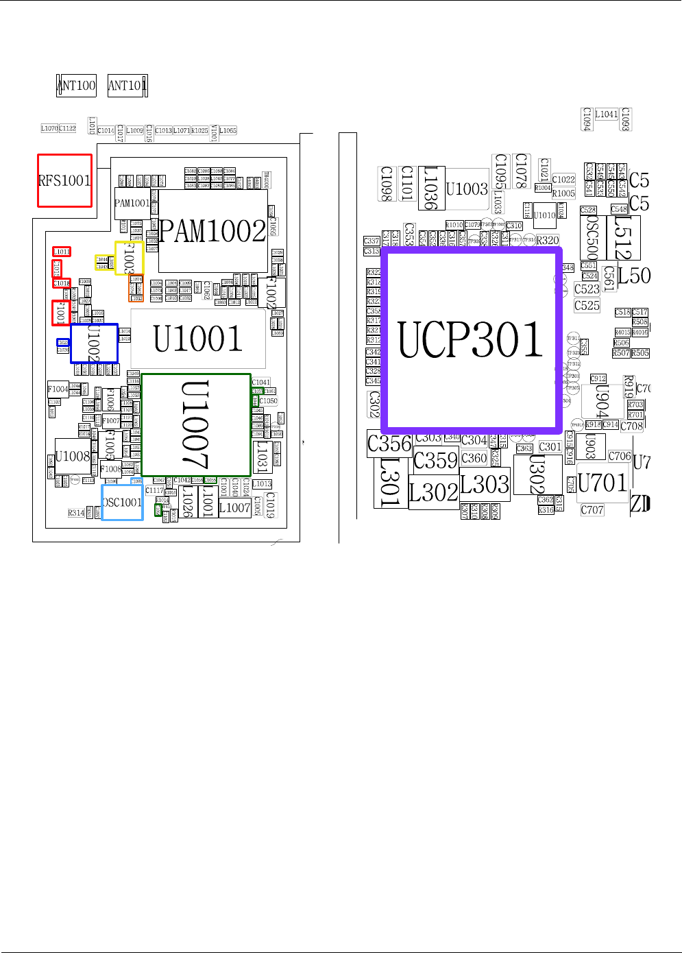
Level 3Repair
Distribution, transmission, or infringement of any content or data from this document without Samsung’s written authorization is strictly prohibited.
Confidential and proprietary-the contents in this service guide subject to change without prior notice.
8-74
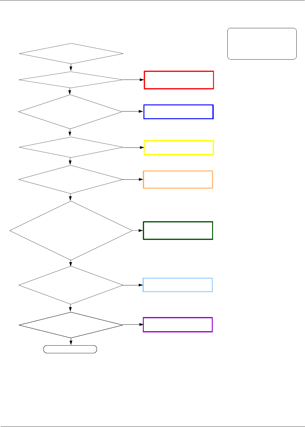
Level 3Repair
Distribution, transmission, or infringement of any content or data from this document without Samsung’s written authorization is strictly prohibited.
Confidential and proprietary-the contents in this service guide subject to change without prior notice.
8-75
Check C1026 ≤-65dBm ?
8-3-25. LTE Band8 /WCDMA Band8 /GSM900 RX
NORMAL CONDITION
catch the channel?
Check the voltage at
{C1058, =1.8V?}
&{
C1055 =1.2V?}
&{
C1048 =1.5V?}
&{
C1057 =2.5V?}
Check the Voltage at
{C1023 >3.6
V?}
Check C1025
≥-65dBm ?
CHECK soldered
RFS1001, F1001, C1015,
L1011, C1018
Resolder or change
U1002, C1023
Resolder or change
U1001
Resolder or change
U1007
Check the freq. at
C1099 : 26.0MHz ?Change or resolder
OSC1001
Check L1024
≥-65dBm ?Resolder or change
L1024, L1037
NO
YES
NO
NO
YES
NO
YES
NO
YES
NO
YES
NO
YES
LTE B8 /WCDMA B8 /GSM900
Receiver is O.K? Resolder or change
UCP301
END
NO
CONTINUOUS RX ON
WCDMA8 CH : 3013
LTE B8 CH : 3625
AMP :-50
dBm

Level 3Repair
Distribution, transmission, or infringement of any content or data from this document without Samsung’s written authorization is strictly prohibited.
Confidential and proprietary-the contents in this service guide subject to change without prior notice.
8-76
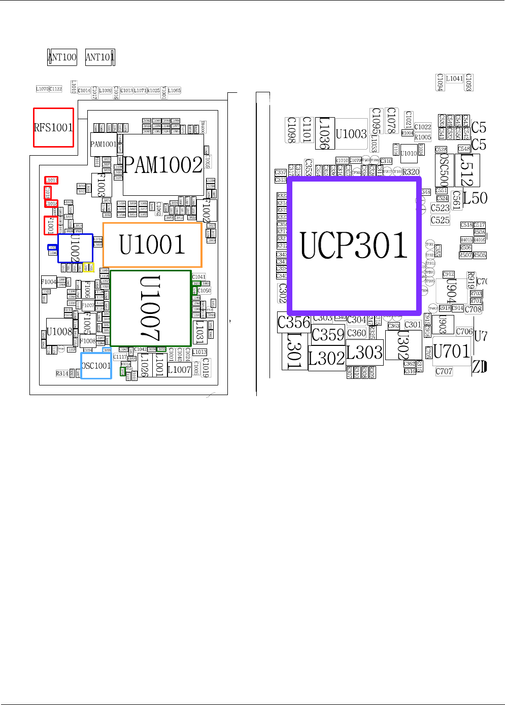
Level 3Repair
Distribution, transmission, or infringement of any content or data from this document without Samsung’s written authorization is strictly prohibited.
Confidential and proprietary-the contents in this service guide subject to change without prior notice.
8-77

Level 3Repair
Distribution, transmission, or infringement of any content or data from this document without Samsung’s written authorization is strictly prohibited.
Confidential and proprietary-the contents in this service guide subject to change without prior notice.
8-78
Check C1026 ≤-65dBm ?
8-3-26. LTE Band20 RX
NORMAL CONDITION
catch the channel?
Check the voltage at
{C1058, =1.8V?}
&{
C1055 =1.2V?}
&{
C1048 =1.5V?}
&{
C1057 =2.5V?}
Check the Voltage at
{C1023 >3.6
V?}
Check L1027
≥-65dBm ?
CHECK soldered
RFS1001, F1001, C1015,
L1011, C1018
Resolder or change
U1002, C1023
Resolder or change
L1027, L1023, L1028, L1069
Resolder or change
U1007
Check the freq. at
C1099 : 26.0MHz ?Change or resolder
OSC1001
Check L1022
≥-65dBm ?Resolder or change
L1022, C1035, L1068, F1002
NO
YES
NO
NO
YES
NO
YES
NO
YES
NO
YES
NO
YES
LTE B20 Receiver is O.K? Resolder or change
UCP301
END
NO
CONTINUOUS RX ON
RF INPUT : 6300CH
AMP :-50
dBm
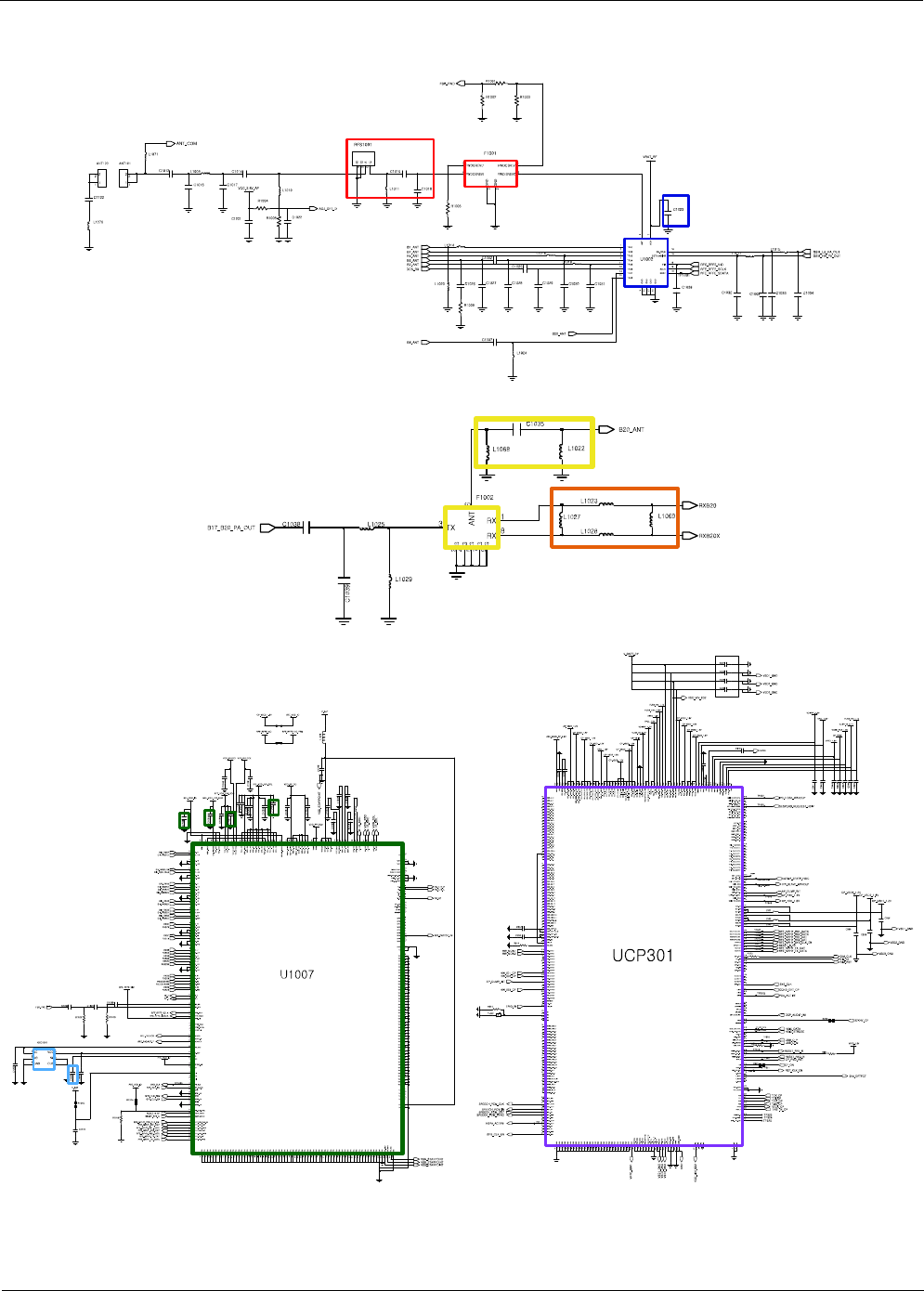
Level 3Repair
Distribution, transmission, or infringement of any content or data from this document without Samsung’s written authorization is strictly prohibited.
Confidential and proprietary-the contents in this service guide subject to change without prior notice.
8-79
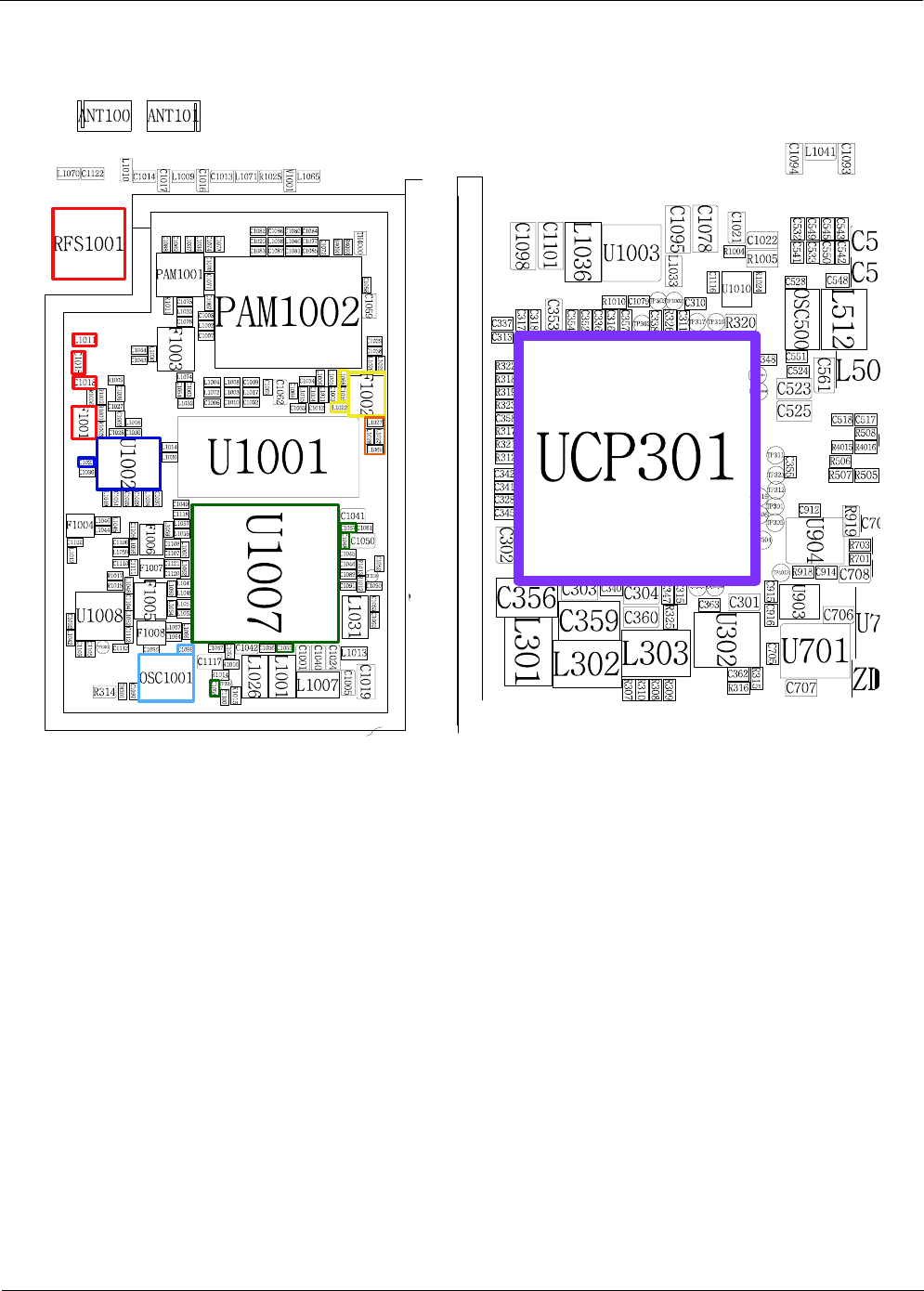
Level 3Repair
Distribution, transmission, or infringement of any content or data from this document without Samsung’s written authorization is strictly prohibited.
Confidential and proprietary-the contents in this service guide subject to change without prior notice.
8-80

Level 3Repair
Distribution, transmission, or infringement of any content or data from this document without Samsung’s written authorization is strictly prohibited.
Confidential and proprietary-the contents in this service guide subject to change without prior notice.
8-81
U1002 PIN6 :About
30dBm ?
8-3-27. GSM850 / GSM900 TX
Check the Voltage at
C1062, C1059 >3V?
Resolder or change
PAM1002, C1062, C1066,
C1059, C1065, C1067, C1068,
U1003, C1078, C1095,
C1098, C1101
Check C1034 :About
30dBm ?Resolder or change
C1034, L1015, C1033
NO
YES
YES
NO
NO
YES
Check C1084 :About
0dBm ?Resolder or change
C1084, C1077, C1085
YES
GSM850/900 Transmitter is O.K?
CONTINOUS TX ON CONDITION
TX POWER DAC:14500 CODE
APPLIED
GSM850 CH : 190
GSM900 CH :62
RBW : 100KHz
VBW : 100KHz
SPAN :10
MHz
REF LEV. :10
dBm
ATT. :20
dB
NO
END
CHECK soldered
RFS1001, F1001, C1015,
L1011, C1018
Resolder or change
U1002, C1023
YES
NO
Check the Voltage at
{C1023 >3.6
V?}
Check the voltage at
{C1058, =1.8V?}
&{
C1055 =1.2V?}
&{
C1048 =1.5V?}
&{
C1057 =2.5V?}
Resolder or change
U1007
Check the freq. at
C1099 : 26.0MHz ?Change or resolder
OSC1001
NO
YES
NO
YES
Resolder or change
UCP301
NO
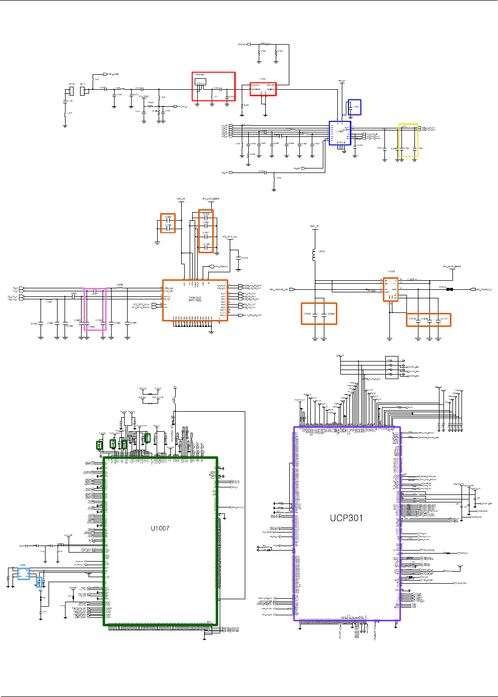
Level 3Repair
Distribution, transmission, or infringement of any content or data from this document without Samsung’s written authorization is strictly prohibited.
Confidential and proprietary-the contents in this service guide subject to change without prior notice.
8-82
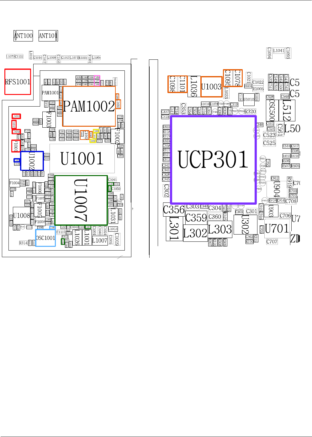
Level 3Repair
Distribution, transmission, or infringement of any content or data from this document without Samsung’s written authorization is strictly prohibited.
Confidential and proprietary-the contents in this service guide subject to change without prior notice.
8-83
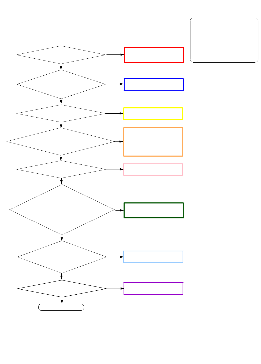
Level 3Repair
Distribution, transmission, or infringement of any content or data from this document without Samsung’s written authorization is strictly prohibited.
Confidential and proprietary-the contents in this service guide subject to change without prior notice.
8-84
U1002 PIN6 :About
30dBm ?
8-3-28. DCS/ PCS TX CONTINOUS TX ON CONDITION
TX POWER DAC:14500 CODE
APPLIED
DCS CH : 685
PCS CH : 661
RBW : 100KHz
VBW : 100KHz
SPAN :10
MHz
REF LEV. :10
dBm
ATT. :20
dB
Check the Voltage at
C1062, C1059 >3V?
Resolder or change
PAM1002, C1062, C1066,
C1059, C1065, C1067, C1068,
U1003, C1078, C1095,
C1098, C1101
Check C1009 :About
30dBm ?Resolder or change
C1032, L1017, C1009
NO
YES
YES
NO
NO
YES
Check C1086 :About
0dBm ?Resolder or change
C1086, C1087, L1038
YES
DCS/PCS Transmitter is O.K?
NO
END
CHECK soldered
RFS1001, F1001, C1015,
L1011, C1018
Resolder or change
U1002, C1023
YES
NO
Check the Voltage at
{C1023 >3.6
V?}
Check the voltage at
{C1058, =1.8V?}
&{
C1055 =1.2V?}
&{
C1048 =1.5V?}
&{
C1057 =2.5V?}
Resolder or change
U1007
Check the freq. at
C1099 : 26.0MHz ?Change or resolder
OSC1001
NO
YES
NO
YES
Resolder or change
UCP301
NO
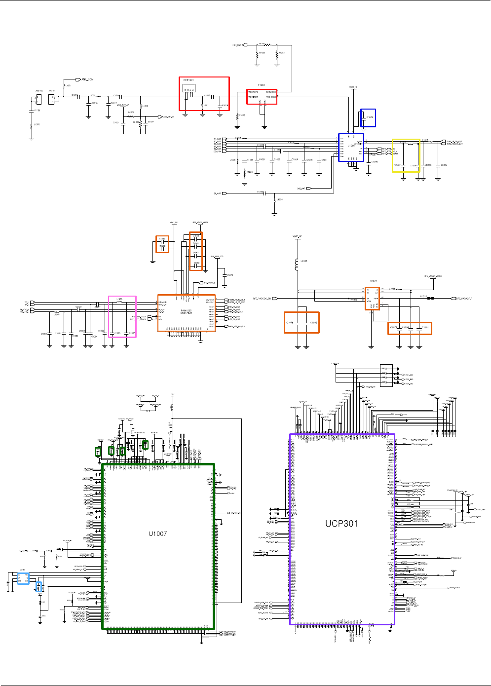
Level 3Repair
Distribution, transmission, or infringement of any content or data from this document without Samsung’s written authorization is strictly prohibited.
Confidential and proprietary-the contents in this service guide subject to change without prior notice.
8-85
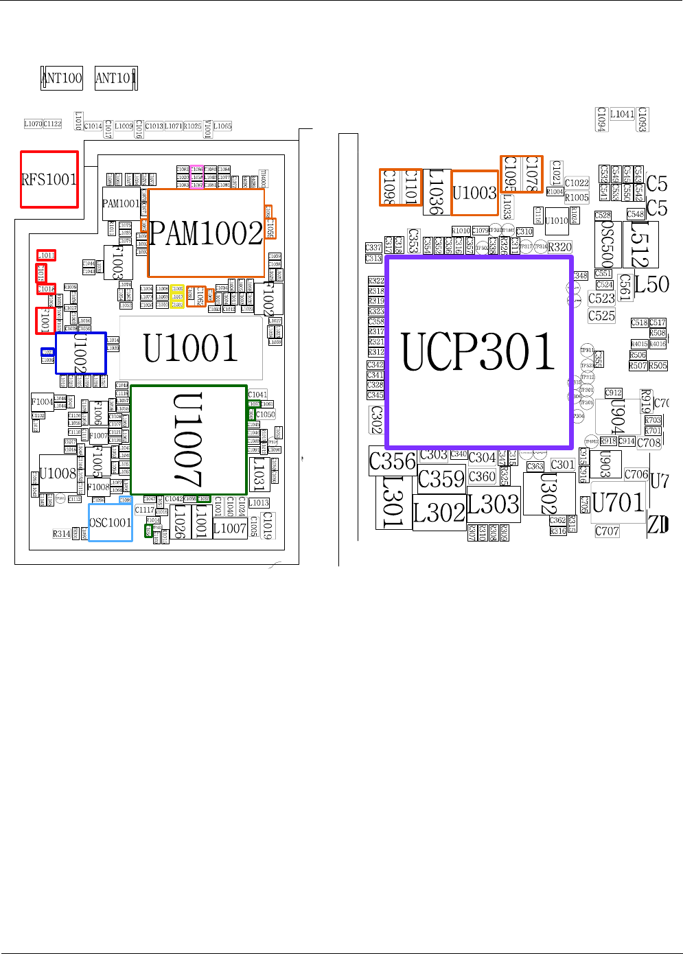
Level 3Repair
Distribution, transmission, or infringement of any content or data from this document without Samsung’s written authorization is strictly prohibited.
Confidential and proprietary-the contents in this service guide subject to change without prior notice.
8-86

Level 3Repair
Distribution, transmission, or infringement of any content or data from this document without Samsung’s written authorization is strictly prohibited.
Confidential and proprietary-the contents in this service guide subject to change without prior notice.
8-87
U1002 PIN6 :About
30dBm ?
8-3-28. WCDMA Band1 TX
Check the Voltage at
C1062, C1059 >3V?
Resolder or change
PAM1002, C1062, C1066,
C1059, C1065, C1067, C1068,
U1003, C1078, C1095,
C1098, C1101
Check L1020 :About
20dBm ?Resolder or change
L1020, L1014
NO
YES
YES
NO
NO
YES
Check C1086 :About
0dBm ?Resolder or change
C1086, C1087, L1038
YES
WCDMA B1 Transmitter is O.K?
NO
END
CHECK soldered
RFS1001, F1001, C1015,
L1011, C1018
Resolder or change
U1002, C1023
YES
NO
Check the Voltage at
{C1023 >3.6
V?}
Check the voltage at
{C1058, =1.8V?}
&{
C1055 =1.2V?}
&{
C1048 =1.5V?}
&{
C1057 =2.5V?}
Resolder or change
U1007
Check the freq. at
C1099 : 26.0MHz ?Change or resolder
OSC1001
NO
YES
NO
YES
Resolder or change
UCP301
NO
Check L1004 :About
20dBm ?Resolder or change
U1001, L1004, L1073, C1006
NO
NO
CONTINOUS TX ON CONDITION
TX POWER DAC:14500 CODE
APPLIED
WCDMA Band1 CH : 9750
RBW : 100KHz
VBW : 100KHz
SPAN :10
MHz
REF LEV. :10
dBm
ATT. :20
dB
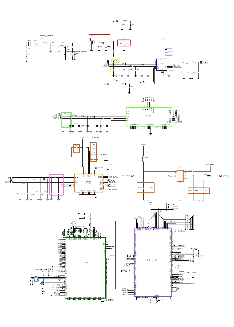
Level 3Repair
Distribution, transmission, or infringement of any content or data from this document without Samsung’s written authorization is strictly prohibited.
Confidential and proprietary-the contents in this service guide subject to change without prior notice.
8-88
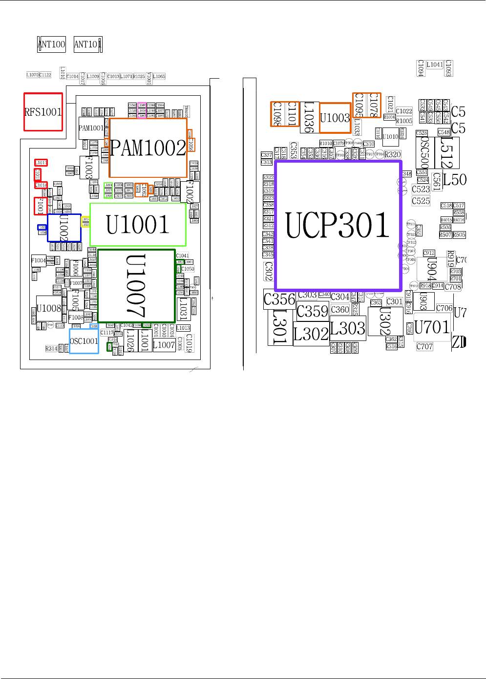
Level 3Repair
Distribution, transmission, or infringement of any content or data from this document without Samsung’s written authorization is strictly prohibited.
Confidential and proprietary-the contents in this service guide subject to change without prior notice.
8-89
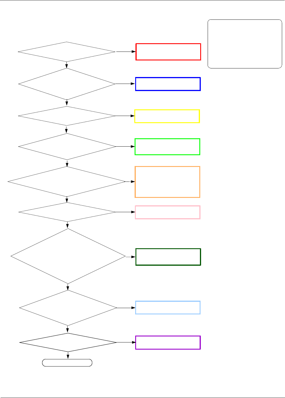
Level 3Repair
Distribution, transmission, or infringement of any content or data from this document without Samsung’s written authorization is strictly prohibited.
Confidential and proprietary-the contents in this service guide subject to change without prior notice.
8-90
U1002 PIN6 :About
30dBm ?
8-3-28. WCDMA Band2 TX
Check the Voltage at
C1062, C1059 >3V?
Resolder or change
PAM1002, C1062, C1066,
C1059, C1065, C1067, C1068,
U1003, C1078, C1095,
C1098, C1101
Check L1019 :About
20dBm ?Resolder or change
L1019, C1031
NO
YES
YES
NO
NO
YES
Check C1086 :About
0dBm ?Resolder or change
C1086, C1087, L1038
YES
WCDMA B2 Transmitter is O.K?
NO
END
CHECK soldered
RFS1001, F1001, C1015,
L1011, C1018
Resolder or change
U1002, C1023
YES
NO
Check the Voltage at
{C1023 >3.6
V?}
Check the voltage at
{C1058, =1.8V?}
&{
C1055 =1.2V?}
&{
C1048 =1.5V?}
&{
C1057 =2.5V?}
Resolder or change
U1007
Check the freq. at
C1099 : 26.0MHz ?Change or resolder
OSC1001
NO
YES
NO
YES
Resolder or change
UCP301
NO
Check C1007 :About
20dBm ?Resolder or change
U1001, C1007, L1002, C1008
NO
NO
CONTINOUS TX ON CONDITION
TX POWER DAC:14500 CODE
APPLIED
WCDMA Band2 CH : 9400
RBW : 100KHz
VBW : 100KHz
SPAN :10
MHz
REF LEV. :10
dBm
ATT. :20
dB
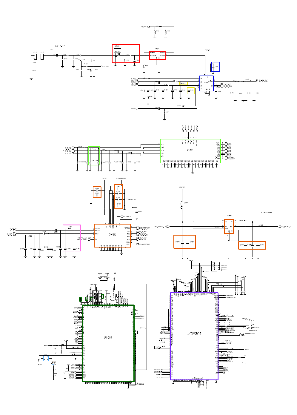
Level 3Repair
Distribution, transmission, or infringement of any content or data from this document without Samsung’s written authorization is strictly prohibited.
Confidential and proprietary-the contents in this service guide subject to change without prior notice.
8-91
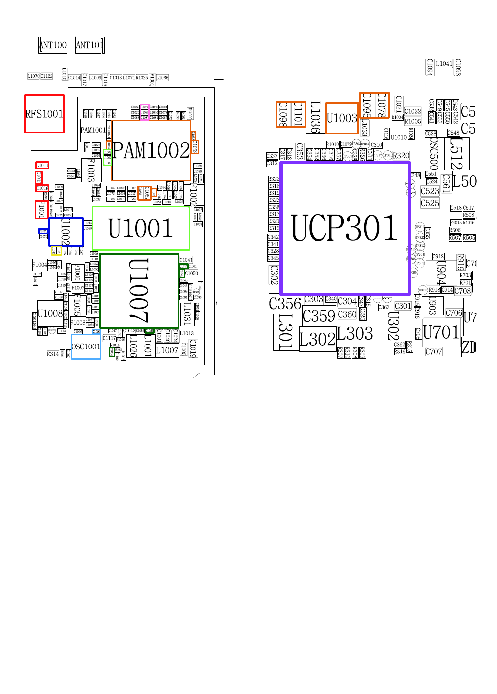
Level 3Repair
Distribution, transmission, or infringement of any content or data from this document without Samsung’s written authorization is strictly prohibited.
Confidential and proprietary-the contents in this service guide subject to change without prior notice.
8-92

Level 3Repair
Distribution, transmission, or infringement of any content or data from this document without Samsung’s written authorization is strictly prohibited.
Confidential and proprietary-the contents in this service guide subject to change without prior notice.
8-93
U1002 PIN6 :About
30dBm ?
8-3-28. WCDMA Band5 TX
Check the Voltage at
C1062, C1059 >3V?
Resolder or change
PAM1002, C1062, C1066,
C1059, C1065, C1067, C1068,
U1003, C1078, C1095,
C1098, C1101
Check L1016 :About
20dBm ?Resolder or change
L1016, C1030
NO
YES
YES
NO
NO
YES
Check C1084 :About
0dBm ?Resolder or change
C1084, C1077, C1085
YES
WCDMA B5 Transmitter is O.K?
NO
END
CHECK soldered
RFS1001, F1001, C1015,
L1011, C1018
Resolder or change
U1002, C1023
YES
NO
Check the Voltage at
{C1023 >3.6
V?}
Check the voltage at
{C1058, =1.8V?}
&{
C1055 =1.2V?}
&{
C1048 =1.5V?}
&{
C1057 =2.5V?}
Resolder or change
U1007
Check the freq. at
C1099 : 26.0MHz ?Change or resolder
OSC1001
NO
YES
NO
YES
Resolder or change
UCP301
NO
Check L1005 :About
20dBm ?Resolder or change
U1001, C1003, L1005, C1011
NO
NO
CONTINUOUS TX ON CONDITION
TX POWER IDX1 APPLIED
WCDMA850 CH : 4182
RBW : 100KHz
VBW : 100KHz
SPAN :10
MHz
REF LEV. :10
dBm
ATT. :20
dB
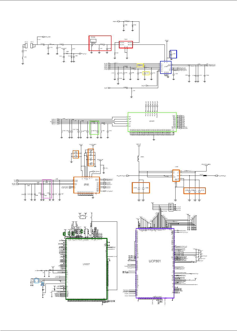
Level 3Repair
Distribution, transmission, or infringement of any content or data from this document without Samsung’s written authorization is strictly prohibited.
Confidential and proprietary-the contents in this service guide subject to change without prior notice.
8-94

Level 3Repair
Distribution, transmission, or infringement of any content or data from this document without Samsung’s written authorization is strictly prohibited.
Confidential and proprietary-the contents in this service guide subject to change without prior notice.
8-95

Level 3Repair
Distribution, transmission, or infringement of any content or data from this document without Samsung’s written authorization is strictly prohibited.
Confidential and proprietary-the contents in this service guide subject to change without prior notice.
8-96
U1002 PIN6 :About
30dBm ?
8-3-28. WCDMA Band8 TX
Check the Voltage at
C1062, C1059 >3V?
Resolder or change
PAM1002, C1062, C1066,
C1059, C1065, C1067, C1068,
U1003, C1078, C1095,
C1098, C1101
Check C1037 :About
20dBm ?Resolder or change
C1037, L1024
NO
YES
YES
NO
NO
YES
WCDMA B8 Transmitter is O.K?
END
CHECK soldered
RFS1001, F1001, C1015,
L1011, C1018
Resolder or change
U1002, C1023
YES
NO
Check the Voltage at
{C1023 >3.6
V?}
Check the voltage at
{C1058, =1.8V?}
&{
C1055 =1.2V?}
&{
C1048 =1.5V?}
&{
C1057 =2.5V?}
Resolder or change
U1007
Check the freq. at
C1099 : 26.0MHz ?Change or resolder
OSC1001
NO
YES
NO
YES
Resolder or change
UCP301
NO
Check L1006 :About
20dBm ?Resolder or change
U1001, L1006, C1004, C1012
NO
NO
Check C1084 :About
0dBm ?Resolder or change
C1084, C1077, C1085
YES
NO
CONTINOUS TX ON CONDITION
TX POWER DAC:14500 CODE
APPLIED
WCDMA Band900 CH : 2788
RBW : 100KHz
VBW : 100KHz
SPAN :10
MHz
REF LEV. :10
dBm
ATT. :20
dB
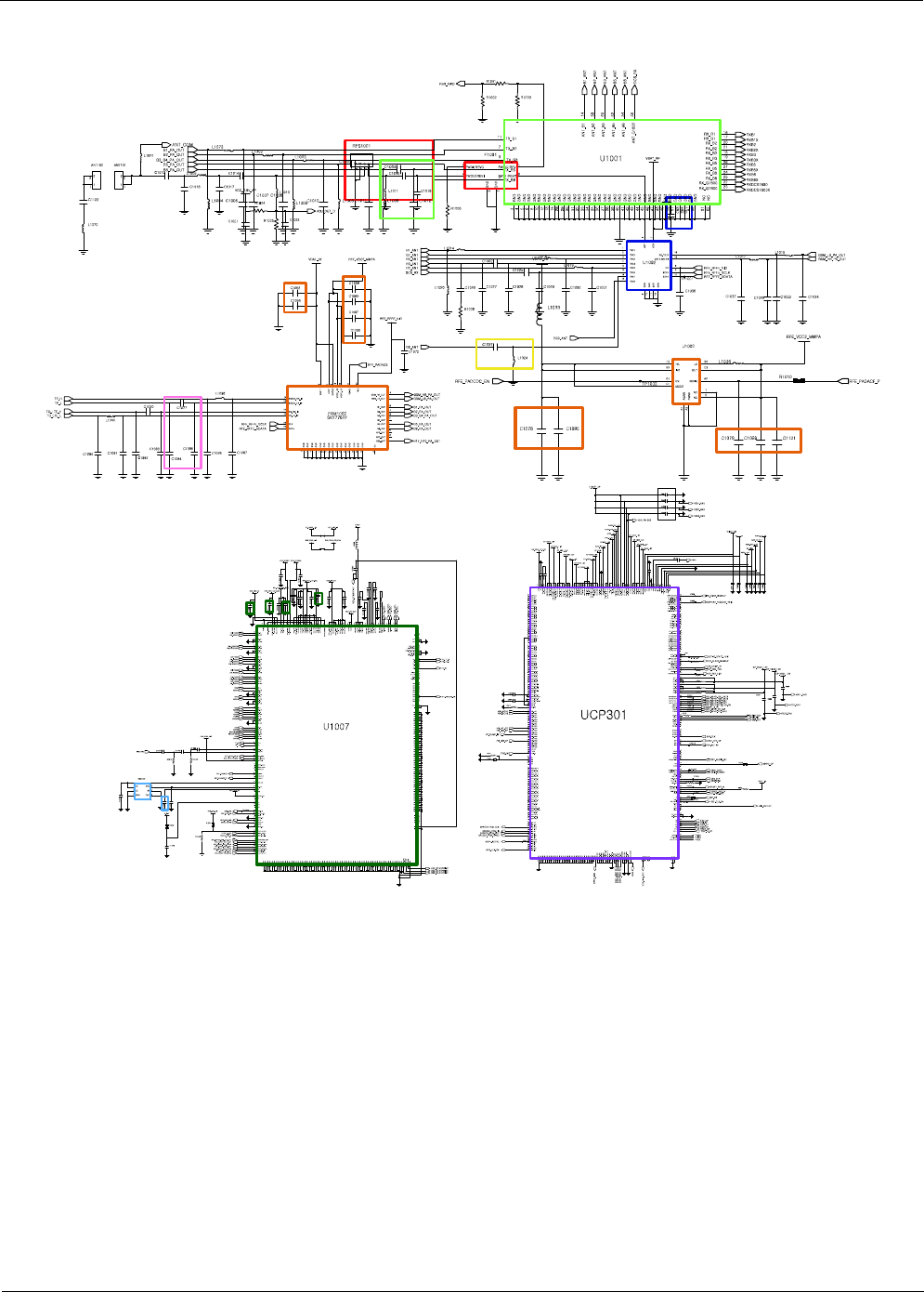
Level 3Repair
Distribution, transmission, or infringement of any content or data from this document without Samsung’s written authorization is strictly prohibited.
Confidential and proprietary-the contents in this service guide subject to change without prior notice.
8-97
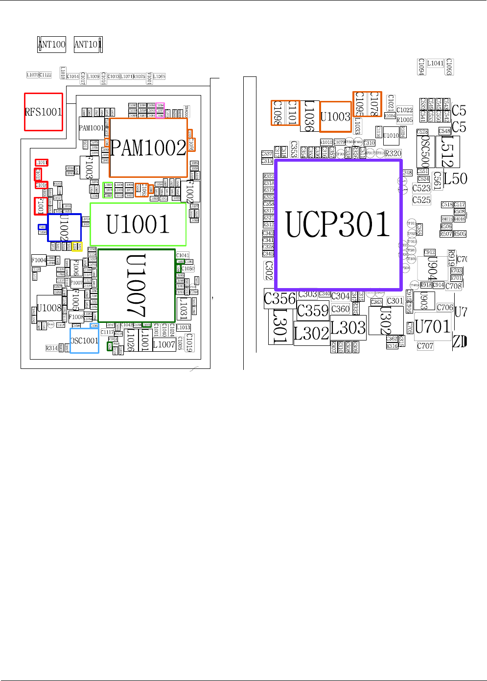
Level 3Repair
Distribution, transmission, or infringement of any content or data from this document without Samsung’s written authorization is strictly prohibited.
Confidential and proprietary-the contents in this service guide subject to change without prior notice.
8-98

Level 3Repair
Distribution, transmission, or infringement of any content or data from this document without Samsung’s written authorization is strictly prohibited.
Confidential and proprietary-the contents in this service guide subject to change without prior notice.
8-99
U1002 PIN6 :About
30dBm ?
8-3-28. LTE Band1 TX
Check the Voltage at
C1062, C1059 >3V?
Resolder or change
PAM1002, C1062, C1066,
C1059, C1065, C1067, C1068,
U1003, C1078, C1095,
C1098, C1101
Check L1020 :About
20dBm ?Resolder or change
L1020, L1014
NO
YES
YES
NO
NO
YES
Check C1082 :About
0dBm ?Resolder or change
C1082, C1020, C1083
YES
LTE B1 Transmitter is O.K?
NO
END
CHECK soldered
RFS1001, F1001, C1015,
L1011, C1018
Resolder or change
U1002, C1023
YES
NO
Check the Voltage at
{C1023 >3.6
V?}
Check the voltage at
{C1058, =1.8V?}
&{
C1055 =1.2V?}
&{
C1048 =1.5V?}
&{
C1057 =2.5V?}
Resolder or change
U1007
Check the freq. at
C1099 : 26.0MHz ?Change or resolder
OSC1001
NO
YES
NO
YES
Resolder or change
UCP301
NO
Check L1004 :About
20dBm ?Resolder or change
U1001, L1004, L1073, C1006
NO
NO
CONTINOUS TX ON CONDITION
TX POWER DAC:14500 CODE
APPLIED
LTE Band1 CH : 18300
RBW : 100KHz
VBW : 100KHz
SPAN :10
MHz
REF LEV. :10
dBm
ATT. :20
dB
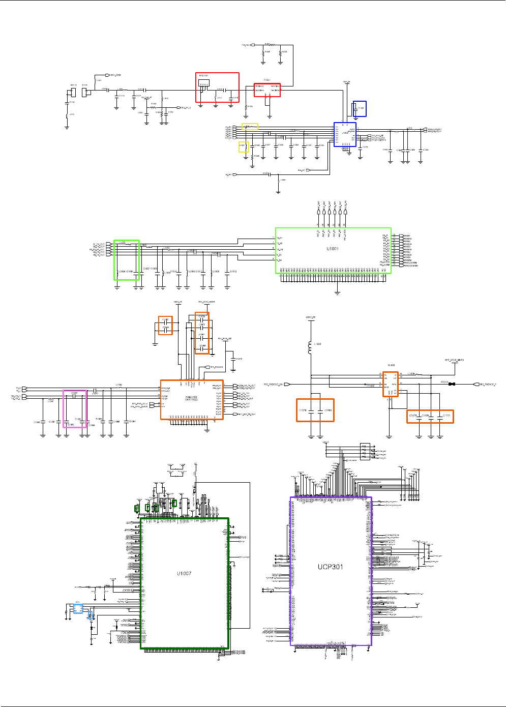
Level 3Repair
Distribution, transmission, or infringement of any content or data from this document without Samsung’s written authorization is strictly prohibited.
Confidential and proprietary-the contents in this service guide subject to change without prior notice.
8-100
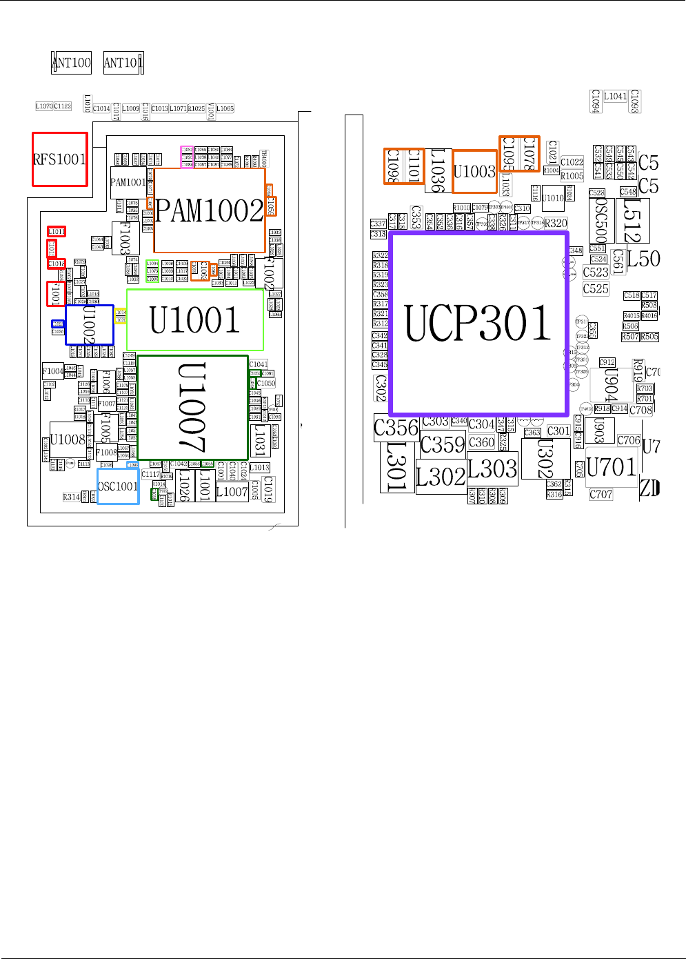
Level 3Repair
Distribution, transmission, or infringement of any content or data from this document without Samsung’s written authorization is strictly prohibited.
Confidential and proprietary-the contents in this service guide subject to change without prior notice.
8-101

Level 3Repair
Distribution, transmission, or infringement of any content or data from this document without Samsung’s written authorization is strictly prohibited.
Confidential and proprietary-the contents in this service guide subject to change without prior notice.
8-102
U1002 PIN6 :About
30dBm ?
8-3-28. LTE Band3 TX
Check the Voltage at
C1062, C1059 >3V?
Resolder or change
PAM1002, C1062, C1066,
C1059, C1065, C1067, C1068,
U1003, C1078, C1095,
C1098, C1101
Check C1026 :About
20dBm ?
Resolder or change
C1026, R1009, C1027, C1002,
C1028
NO
YES
YES
NO
NO
YES
Check C1082 :About
0dBm ?Resolder or change
C1082, C1020, C1083
YES
LTE B3 Transmitter is O.K?
NO
END
CHECK soldered
RFS1001, F1001, C1015,
L1011, C1018
Resolder or change
U1002, C1023
YES
NO
Check the Voltage at
{C1023 >3.6
V?}
Check the voltage at
{C1058, =1.8V?}
&{
C1055 =1.2V?}
&{
C1048 =1.5V?}
&{
C1057 =2.5V?}
Resolder or change
U1007
Check the freq. at
C1099 : 26.0MHz ?Change or resolder
OSC1001
NO
YES
NO
YES
Resolder or change
UCP301
NO
Check L1008 :About
20dBm ?Resolder or change
U1001, L1008, L1003, C1010
NO
NO
CONTINUOUS TX ON CONDITION
APPLIED
LTE Band3 CH : 19575
RBW : 100KHz
VBW : 100KHz
SPAN :10
MHz
REF LEV. :10
dBm
ATT. :20
dB
Level 3Repair
Distribution, transmission, or infringement of any content or data from this document without Samsung’s written authorization is strictly prohibited.
Confidential and proprietary-the contents in this service guide subject to change without prior notice.
8-103
Level 3Repair
Distribution, transmission, or infringement of any content or data from this document without Samsung’s written authorization is strictly prohibited.
Confidential and proprietary-the contents in this service guide subject to change without prior notice.
8-104
Level 3Repair
Distribution, transmission, or infringement of any content or data from this document without Samsung’s written authorization is strictly prohibited.
Confidential and proprietary-the contents in this service guide subject to change without prior notice.
8-105
U1002 PIN6 :About
30dBm ?
8-3-28. LTE Band5 TX
Check the Voltage at
C1062, C1059 >3V?
Resolder or change
PAM1002, C1062, C1066,
C1059, C1065, C1067, C1068,
U1003, C1078, C1095,
C1098, C1101
Check L1016 :About
20dBm ?Resolder or change
L1016, C1030
NO
YES
YES
NO
NO
YES
LTE B5 Transmitter is O.K?
END
CHECK soldered
RFS1001, F1001, C1015,
L1011, C1018
Resolder or change
U1002, C1023
YES
NO
Check the Voltage at
{C1023 >3.6
V?}
Check the voltage at
{C1058, =1.8V?}
&{
C1055 =1.2V?}
&{
C1048 =1.5V?}
&{
C1057 =2.5V?}
Resolder or change
U1007
Check the freq. at
C1099 : 26.0MHz ?Change or resolder
OSC1001
NO
YES
NO
YES
Resolder or change
UCP301
NO
Check L1005 :About
20dBm ?Resolder or change
U1001, L1005, C1003, C1011
NO
NO
Check C1080 :About
0dBm ?Resolder or change
C1080, L1040, C1081
YES
NO
CONTINUOUS TX ON CONDITION
TX POWER IDX1 APPLIED
LTE Band5 CH : 20525
RBW : 100KHz
VBW : 100KHz
SPAN :10
MHz
REF LEV. :10
dBm
ATT. :20
dB
Level 3Repair
Distribution, transmission, or infringement of any content or data from this document without Samsung’s written authorization is strictly prohibited.
Confidential and proprietary-the contents in this service guide subject to change without prior notice.
8-106

Level 3Repair
Distribution, transmission, or infringement of any content or data from this document without Samsung’s written authorization is strictly prohibited.
Confidential and proprietary-the contents in this service guide subject to change without prior notice.
8-107

Level 3Repair
Distribution, transmission, or infringement of any content or data from this document without Samsung’s written authorization is strictly prohibited.
Confidential and proprietary-the contents in this service guide subject to change without prior notice.
8-108
U1002 PIN6 :About
30dBm ?
8-3-28. LTE Band7 TX
Check the Voltage at
C1069, C1070 >3V?
Resolder or change
PAM1001, C1069, C1070,
C1071, U1003, C1078,
C1095, C1098, C1101
Check C1044 :About
20dBm ?Resolder or change
F1003, C1044, L1030, C1043
NO
YES
YES
NO
NO
YES
Check C1073 :About
0dBm ?Resolder or change
C1073, C1074, L1034, L1037
YES
LTE B7 Transmitter is O.K?
NO
END
CHECK soldered
RFS1001, F1001, C1015,
L1011, C1018
Resolder or change
U1002, C1023
YES
NO
Check the Voltage at
{C1023 >3.6
V?}
Check the voltage at
{C1058, =1.8V?}
&{
C1055 =1.2V?}
&{
C1048 =1.5V?}
&{
C1057 =2.5V?}
Resolder or change
U1007
Check the freq. at
C1099 : 26.0MHz ?Change or resolder
OSC1001
NO
YES
NO
YES
Resolder or change
UCP301
NO
Check C1075 :About
20dBm ?Resolder or change
C1075, L1035, C1076
NO
NO
CONTINUOUS TX ON CONDITION
APPLIED
LTE Band7 CH : 21100
RBW : 100KHz
VBW : 100KHz
SPAN :10
MHz
REF LEV. :10
dBm
ATT. :20
dB
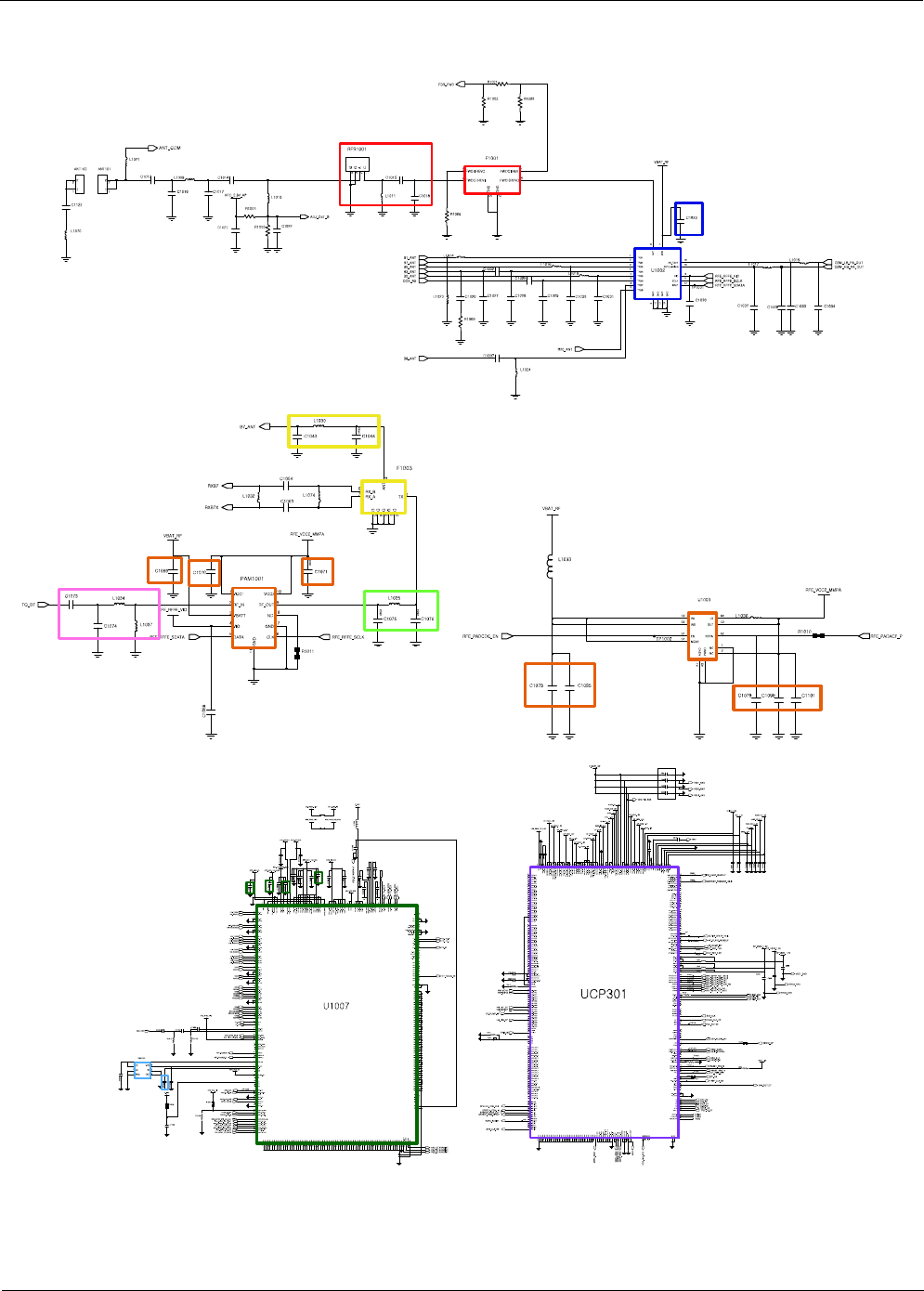
Level 3Repair
Distribution, transmission, or infringement of any content or data from this document without Samsung’s written authorization is strictly prohibited.
Confidential and proprietary-the contents in this service guide subject to change without prior notice.
8-109
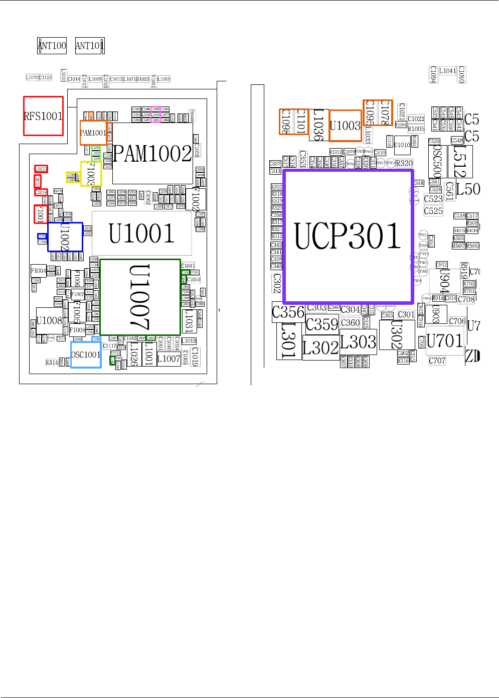
Level 3Repair
Distribution, transmission, or infringement of any content or data from this document without Samsung’s written authorization is strictly prohibited.
Confidential and proprietary-the contents in this service guide subject to change without prior notice.
8-110

Level 3Repair
Distribution, transmission, or infringement of any content or data from this document without Samsung’s written authorization is strictly prohibited.
Confidential and proprietary-the contents in this service guide subject to change without prior notice.
8-111
U1002 PIN6 :About
30dBm ?
8-3-28. LTE Band8 TX
Check the Voltage at
C1062, C1059 >3V?
Resolder or change
PAM1002, C1062, C1066,
C1059, C1065, C1067, C1068,
U1003, C1078, C1095,
C1098, C1101
Check C1037 :About
20dBm ?Resolder or change
C1037, L1024
NO
YES
YES
NO
NO
YES
LTE B8 Transmitter is O.K?
END
CHECK soldered
RFS1001, F1001, C1015,
L1011, C1018
Resolder or change
U1002, C1023
YES
NO
Check the Voltage at
{C1023 >3.6
V?}
Check the voltage at
{C1058, =1.8V?}
&{
C1055 =1.2V?}
&{
C1048 =1.5V?}
&{
C1057 =2.5V?}
Resolder or change
U1007
Check the freq. at
C1099 : 26.0MHz ?Change or resolder
OSC1001
NO
YES
NO
YES
Resolder or change
UCP301
NO
Check L1006 :About
20dBm ?Resolder or change
U1001, L1006, C1004, C1012
NO
NO
Check C1084 :About
0dBm ?Resolder or change
C1080, L1040, C1081
YES
NO
CONTINOUS TX ON CONDITION
TX POWER DAC:14500 CODE
APPLIED
LTE Band8 CH : 21625
RBW : 100KHz
VBW : 100KHz
SPAN :10
MHz
REF LEV. :10
dBm
ATT. :20
dB
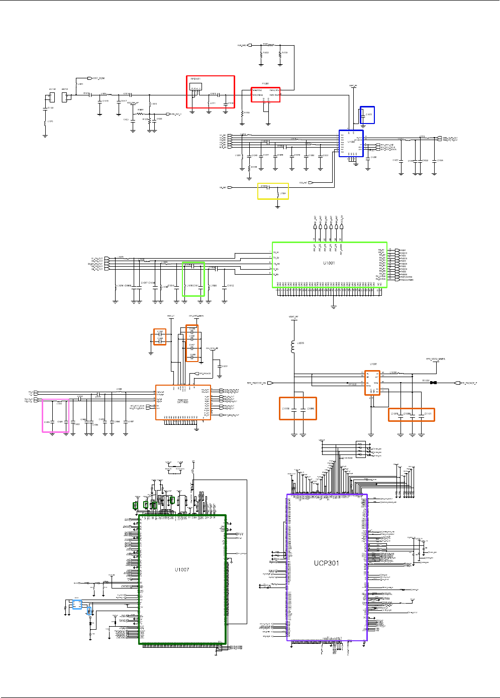
Level 3Repair
Distribution, transmission, or infringement of any content or data from this document without Samsung’s written authorization is strictly prohibited.
Confidential and proprietary-the contents in this service guide subject to change without prior notice.
8-112
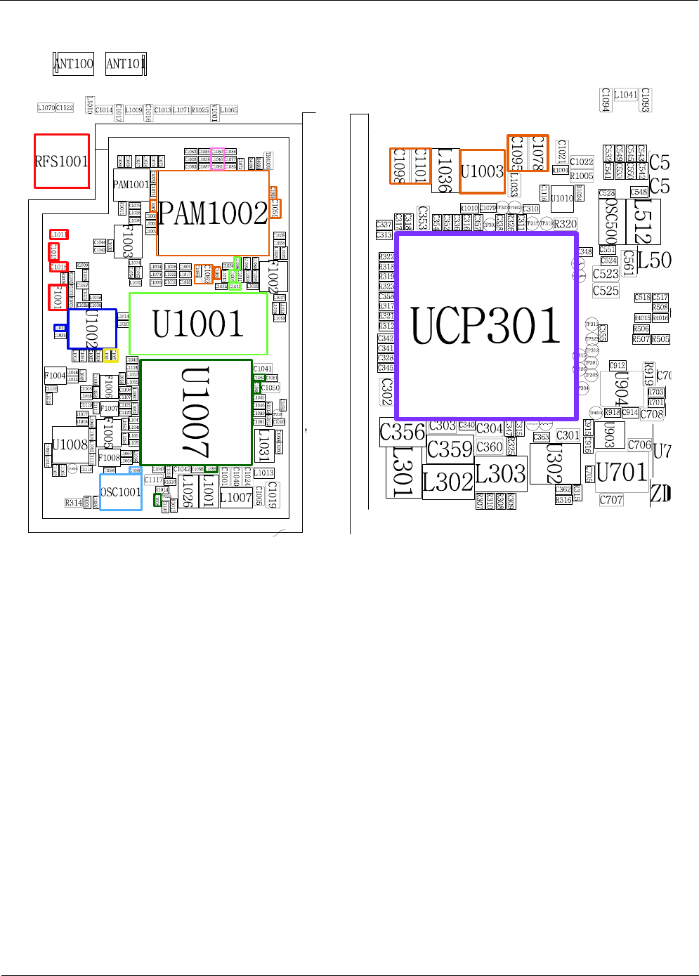
Level 3Repair
Distribution, transmission, or infringement of any content or data from this document without Samsung’s written authorization is strictly prohibited.
Confidential and proprietary-the contents in this service guide subject to change without prior notice.
8-113
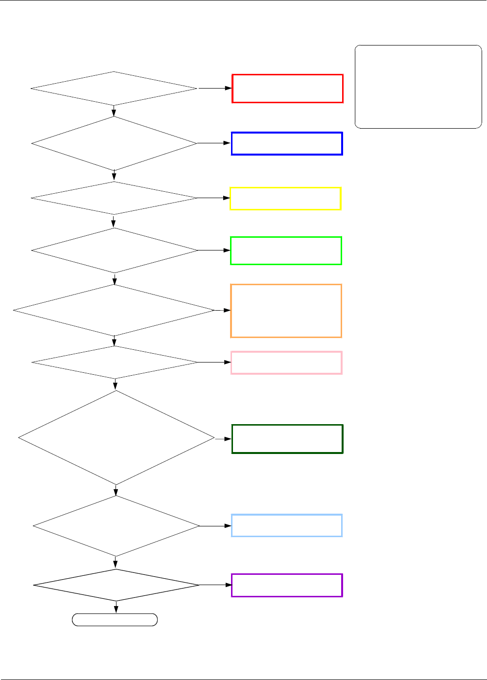
Level 3Repair
Distribution, transmission, or infringement of any content or data from this document without Samsung’s written authorization is strictly prohibited.
Confidential and proprietary-the contents in this service guide subject to change without prior notice.
8-114
U1002 PIN6 :About
30dBm ?
8-3-28. LTE Band20 TX
Check the Voltage at
C1062, C1059 >3V?
Resolder or change
PAM1002, C1062, C1066,
C1059, C1065, C1067, C1068,
U1003, C1078, C1095,
C1098, C1101
Check L1068 :About
20dBm ?Resolder or change
F1002, L1068, C1035, L1022
NO
YES
YES
NO
NO
YES
LTE B20 Transmitter is O.K?
END
CHECK soldered
RFS1001, F1001, C1015,
L1011, C1018
Resolder or change
U1002, C1023
YES
NO
Check the Voltage at
{C1023 >3.6
V?}
Check the voltage at
{C1058, =1.8V?}
&{
C1055 =1.2V?}
&{
C1048 =1.5V?}
&{
C1057 =2.5V?}
Resolder or change
U1007
Check the freq. at
C1099 : 26.0MHz ?Change or resolder
OSC1001
NO
YES
NO
YES
Resolder or change
UCP301
NO
Check C1038 :About
20dBm ?Resolder or change
C1038, C1039, L1025, L1029
NO
NO
Check C1084 :About
0dBm ?Resolder or change
C1080, L1040, C1081
YES
NO
CONTINUOUS TX ON CONDITION
APPLIED
LTE Band20 CH : 24300
RBW : 100KHz
VBW : 100KHz
SPAN :10
MHz
REF LEV. :10
dBm
ATT. :20
dB
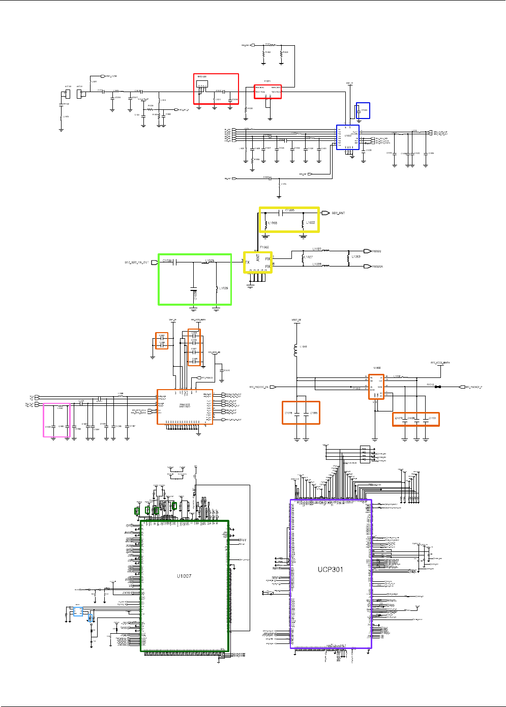
Level 3Repair
Distribution, transmission, or infringement of any content or data from this document without Samsung’s written authorization is strictly prohibited.
Confidential and proprietary-the contents in this service guide subject to change without prior notice.
8-115
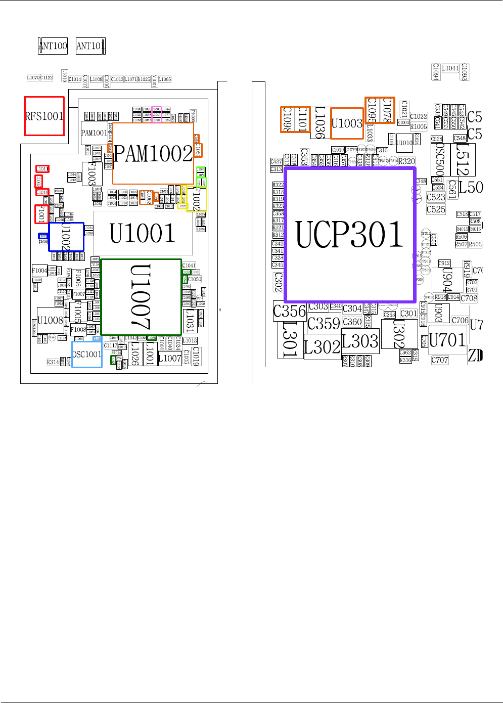
Level 3Repair
Distribution, transmission, or infringement of any content or data from this document without Samsung’s written authorization is strictly prohibited.
Confidential and proprietary-the contents in this service guide subject to change without prior notice.
8-116

Level 3Repair
Distribution, transmission, or infringement of any content or data from this document without Samsung’s written authorization is strictly prohibited.
Confidential and proprietary-the contents in this service guide subject to change without prior notice.
8-117
Check C1093 ≤-65dBm ?
8-3-24. LTE Band1 /WCDMA Band1 DRX
NORMAL CONDITION
catch the channel?
Check the voltage at
{C1058, =1.8V?}
&{
C1055 =1.2V?}
&{
C1048 =1.5V?}
&{
C1057 =2.5V?}
Check the Voltage at
{C1023 >3.6
V?}
Check L1051, L1053
≥-65dBm ?
CHECK soldered
C1093, L1041, C1094,
C1119, L1042, C1092
Resolder or change
U1008, C1103
Resolder or change
F1005, L1051, L1053, L1054
Resolder or change
U1007
Check the freq. at
C1099 : 26.0MHz ?Change or resolder
OSC1001
Check L1048
≥-65dBm ?Resolder or change
C1104, L1052, L1048
NO
YES
NO
NO
YES
NO
YES
NO
YES
NO
YES
NO
YES
WCDMA B1 /LTE B1
Receiver is O.K? Resolder or change
UCP301
END
NO
CONTINUOUS RX ON
RF INPUT :LTE B1: 300CH
WCDMA B1: 10700CH
AMP :-50
dBm
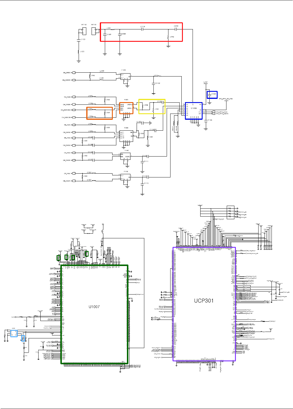
Level 3Repair
Distribution, transmission, or infringement of any content or data from this document without Samsung’s written authorization is strictly prohibited.
Confidential and proprietary-the contents in this service guide subject to change without prior notice.
8-118
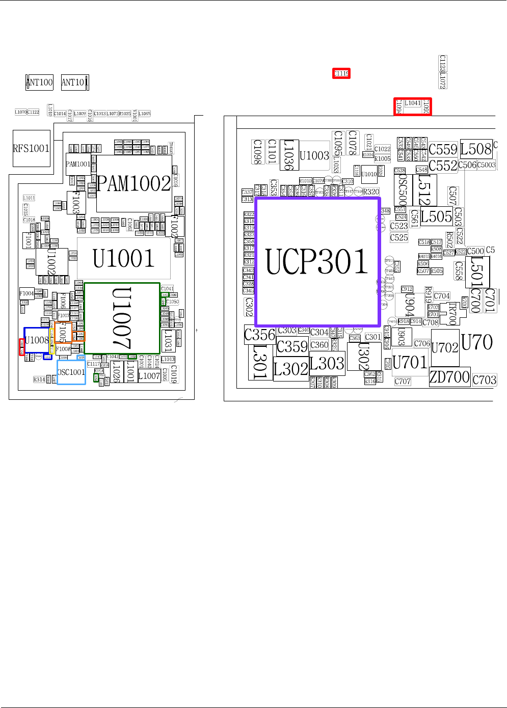
Level 3Repair
Distribution, transmission, or infringement of any content or data from this document without Samsung’s written authorization is strictly prohibited.
Confidential and proprietary-the contents in this service guide subject to change without prior notice.
8-119

Level 3Repair
Distribution, transmission, or infringement of any content or data from this document without Samsung’s written authorization is strictly prohibited.
Confidential and proprietary-the contents in this service guide subject to change without prior notice.
8-120
Check C1093 ≤-65dBm ?
8-3-24. WCDMA Band2 DRX
NORMAL CONDITION
catch the channel?
Check the voltage at
{C1058, =1.8V?}
&{
C1055 =1.2V?}
&{
C1048 =1.5V?}
&{
C1057 =2.5V?}
Check the Voltage at
{C1023 >3.6
V?}
Check L1060
≥-65dBm ?
CHECK soldered
C1093, L1041, C1094,
C1119, L1042, C1092
Resolder or change
U1008, C1103
Resolder or change
F1006, L1060, C1107, C1108
Resolder or change
U1007
Check the freq. at
C1099 : 26.0MHz ?Change or resolder
OSC1001
Check L1056
≥-65dBm ?Resolder or change
C1109, L1056, L1059, C1106
NO
YES
NO
NO
YES
NO
YES
NO
YES
NO
YES
NO
YES
WCDMA B2 Receiver is O.K? Resolder or change
UCP301
END
NO
CONTINUOUS RX ON
RF INPUT :WCDMA B2:
9800CH
AMP :-50
dBm
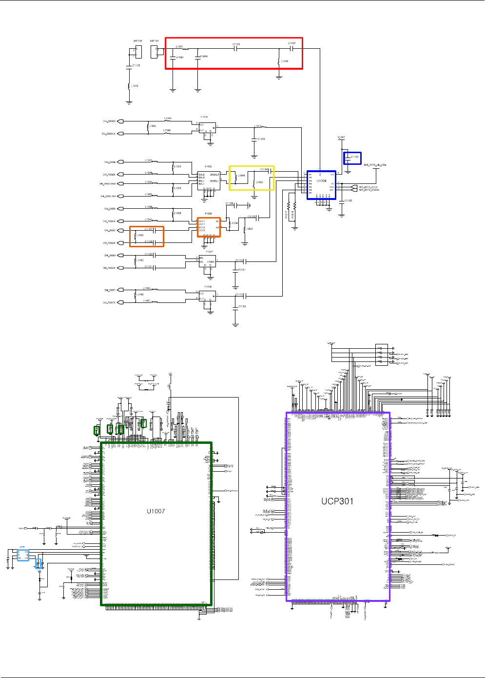
Level 3Repair
Distribution, transmission, or infringement of any content or data from this document without Samsung’s written authorization is strictly prohibited.
Confidential and proprietary-the contents in this service guide subject to change without prior notice.
8-121
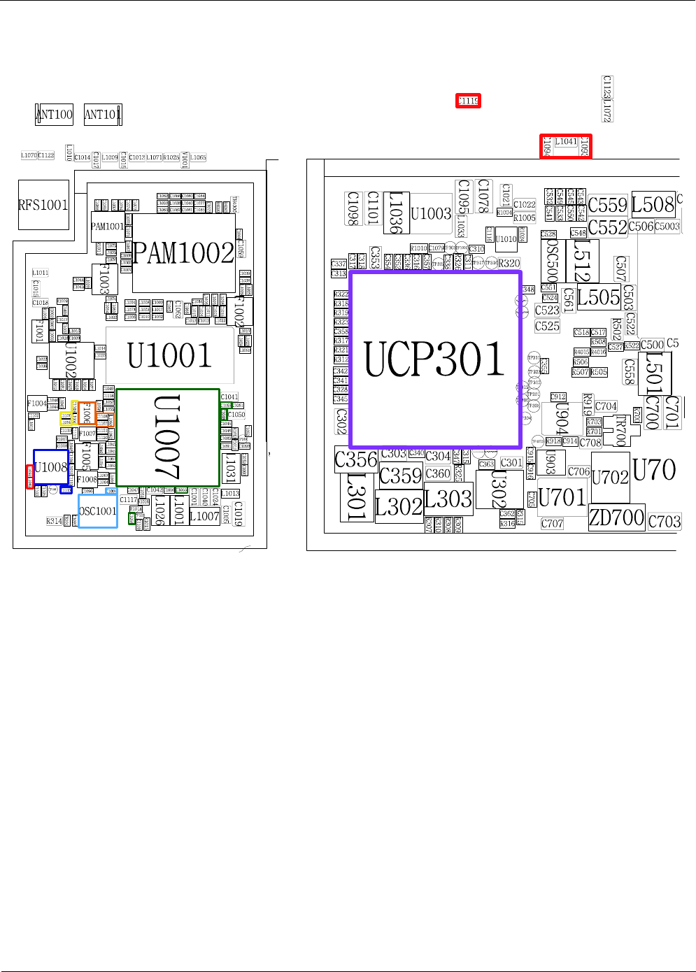
Level 3Repair
Distribution, transmission, or infringement of any content or data from this document without Samsung’s written authorization is strictly prohibited.
Confidential and proprietary-the contents in this service guide subject to change without prior notice.
8-122

Level 3Repair
Distribution, transmission, or infringement of any content or data from this document without Samsung’s written authorization is strictly prohibited.
Confidential and proprietary-the contents in this service guide subject to change without prior notice.
8-123
Check C1093 ≤-65dBm ?
8-3-24. LTE Band3 DRX
NORMAL CONDITION
catch the channel?
Check the voltage at
{C1058, =1.8V?}
&{
C1055 =1.2V?}
&{
C1048 =1.5V?}
&{
C1057 =2.5V?}
Check the Voltage at
{C1023 >3.6
V?}
Check L1062
≥-65dBm ?
CHECK soldered
C1093, L1041, C1094,
C1119, L1042, C1092
Resolder or change
U1008, C1103
Resolder or change
F1007, L1062, C1120, C1121
Resolder or change
U1007
Check the freq. at
C1099 : 26.0MHz ?Change or resolder
OSC1001
Check C1111
≥-65dBm ?Resolder or change
C1111, C1110
NO
YES
NO
NO
YES
NO
YES
NO
YES
NO
YES
NO
YES
LTE B3 Receiver is O.K? Resolder or change
UCP301
END
NO
CONTINUOUS RX ON
RF INPUT :LTE B3: 1575CH
AMP :-50
dBm
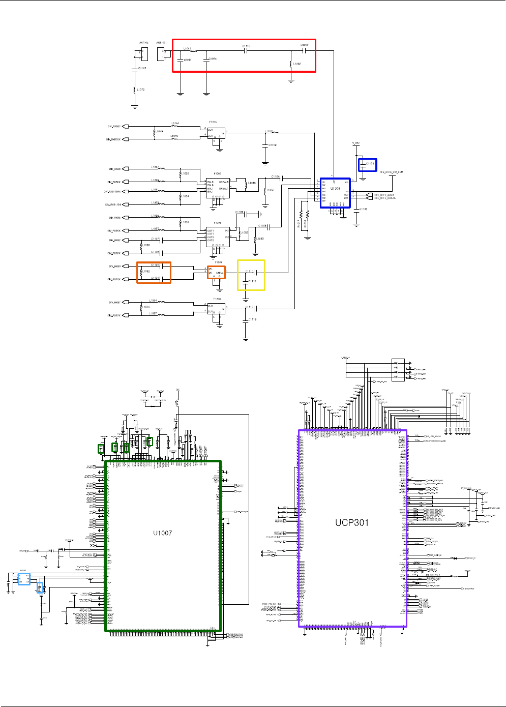
Level 3Repair
Distribution, transmission, or infringement of any content or data from this document without Samsung’s written authorization is strictly prohibited.
Confidential and proprietary-the contents in this service guide subject to change without prior notice.
8-124

Level 3Repair
Distribution, transmission, or infringement of any content or data from this document without Samsung’s written authorization is strictly prohibited.
Confidential and proprietary-the contents in this service guide subject to change without prior notice.
8-125

Level 3Repair
Distribution, transmission, or infringement of any content or data from this document without Samsung’s written authorization is strictly prohibited.
Confidential and proprietary-the contents in this service guide subject to change without prior notice.
8-126
Check C1093 ≤-65dBm ?
8-3-24. LTE Band5 /WCDMA Band5 DRX
NORMAL CONDITION
catch the channel?
Check the voltage at
{C1058, =1.8V?}
&{
C1055 =1.2V?}
&{
C1048 =1.5V?}
&{
C1057 =2.5V?}
Check the Voltage at
{C1023 >3.6
V?}
Check L1055, L1057
≥-65dBm ?
CHECK soldered
C1093, L1041, C1094,
C1119, L1042, C1092
Resolder or change
U1008, C1103
Resolder or change
F1006, L1055, L1057, L1058
Resolder or change
U1007
Check the freq. at
C1099 : 26.0MHz ?Change or resolder
OSC1001
NO
YES
NO
NO
NO
YES
NO
YES
NO
YES
LTE B5 /WCDMA B5
Receiver is O.K? Resolder or change
UCP301
END
NO
Check L1056
≥-65dBm ?Resolder or change
C1109, L1056, L1059, C1106
YES
NO
YES
CONTINUOUS RX ON
RF INPUT :LTE B5: 2525CH
WCDMA B5: 4408CH
AMP :-50
dBm

Level 3Repair
Distribution, transmission, or infringement of any content or data from this document without Samsung’s written authorization is strictly prohibited.
Confidential and proprietary-the contents in this service guide subject to change without prior notice.
8-127
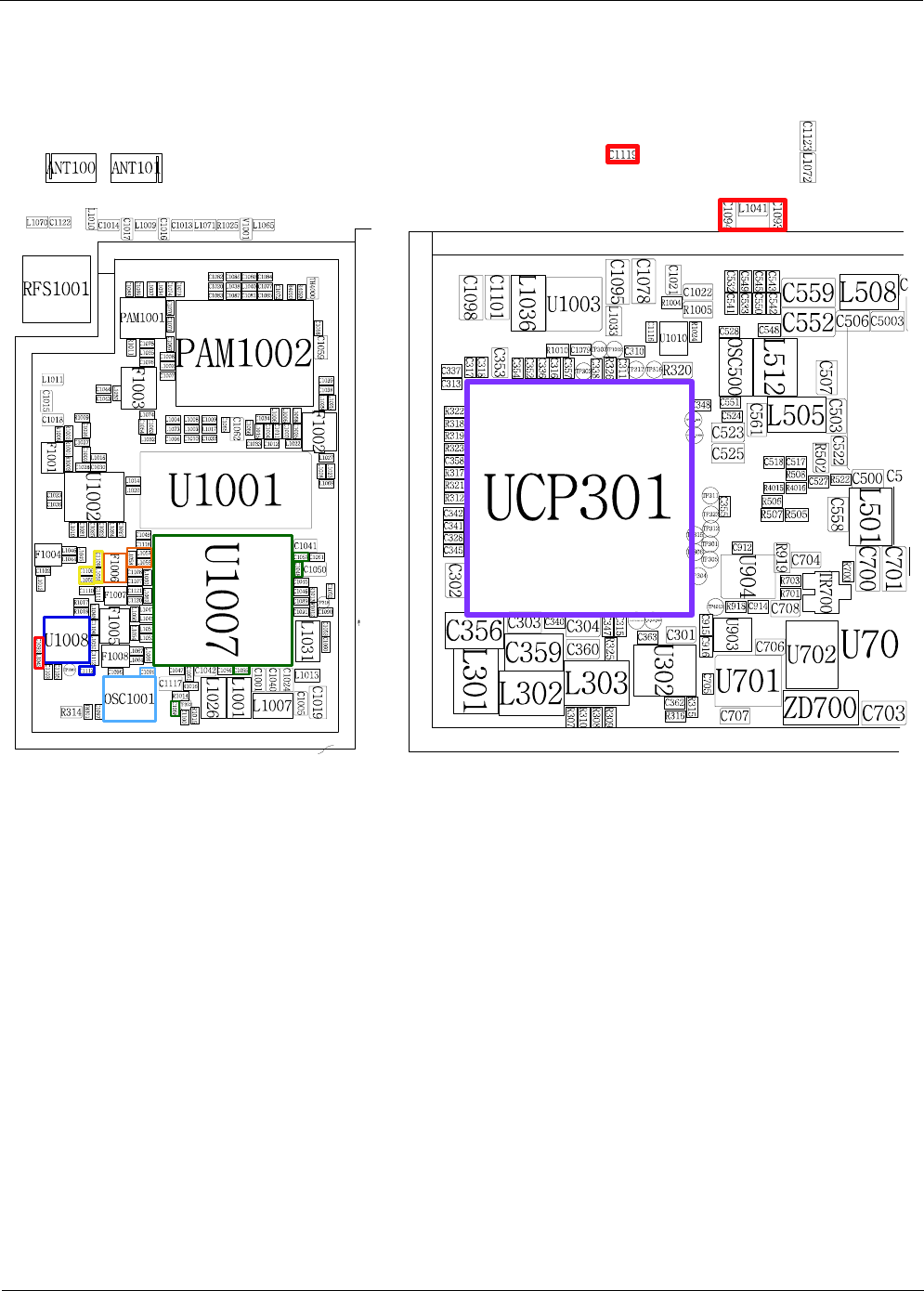
Level 3Repair
Distribution, transmission, or infringement of any content or data from this document without Samsung’s written authorization is strictly prohibited.
Confidential and proprietary-the contents in this service guide subject to change without prior notice.
8-128

Level 3Repair
Distribution, transmission, or infringement of any content or data from this document without Samsung’s written authorization is strictly prohibited.
Confidential and proprietary-the contents in this service guide subject to change without prior notice.
8-129
Check C1093 ≤-65dBm ?
8-3-24. LTE Band7 DRX
NORMAL CONDITION
catch the channel?
Check the voltage at
{C1058, =1.8V?}
&{
C1055 =1.2V?}
&{
C1048 =1.5V?}
&{
C1057 =2.5V?}
Check the Voltage at
{C1023 >3.6
V?}
Check L1066
≥-65dBm ?
CHECK soldered
C1093, L1041, C1094,
C1119, L1042, C1092
Resolder or change
U1008, C1103
Resolder or change
F1008, L1066, L1064, L1067
Resolder or change
U1007
Check the freq. at
C1099 : 26.0MHz ?Change or resolder
OSC1001
Check C1113
≥-65dBm ?Resolder or change
C1113, C1112
NO
YES
NO
NO
YES
NO
YES
NO
YES
NO
YES
NO
YES
LTE B7 Receiver is O.K? Resolder or change
UCP301
END
NO
CONTINUOUS RX ON
RF INPUT :LTE B7: 3100CH
AMP :-50
dBm
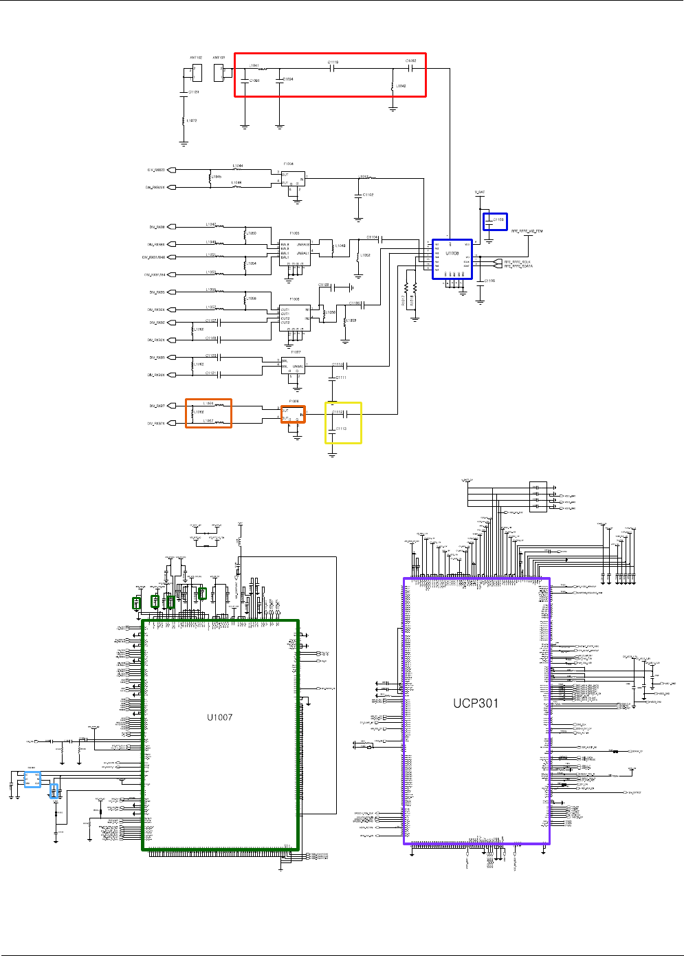
Level 3Repair
Distribution, transmission, or infringement of any content or data from this document without Samsung’s written authorization is strictly prohibited.
Confidential and proprietary-the contents in this service guide subject to change without prior notice.
8-130
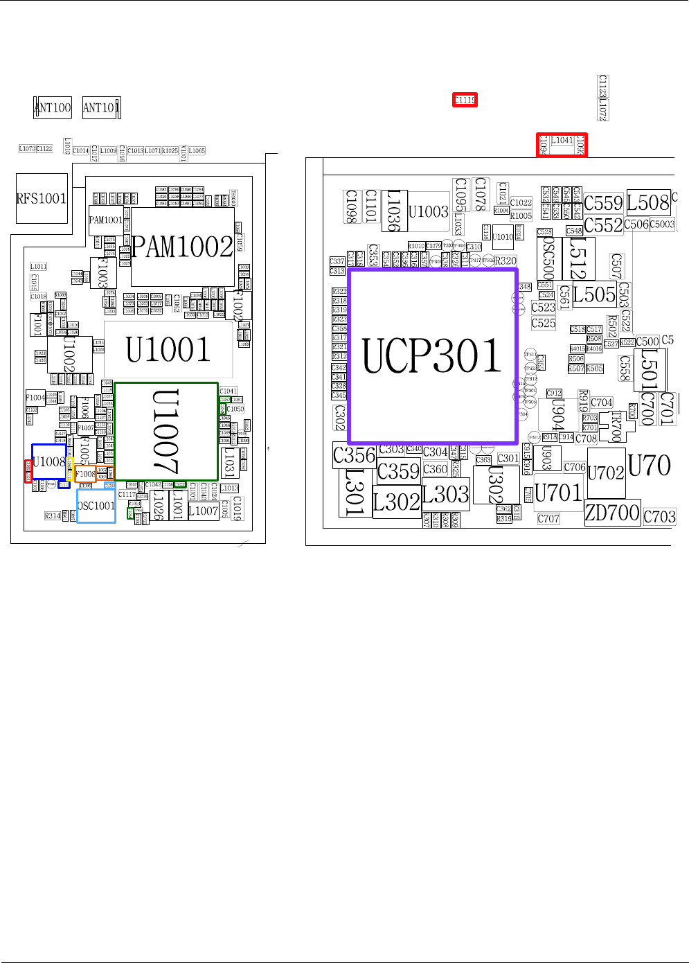
Level 3Repair
Distribution, transmission, or infringement of any content or data from this document without Samsung’s written authorization is strictly prohibited.
Confidential and proprietary-the contents in this service guide subject to change without prior notice.
8-131
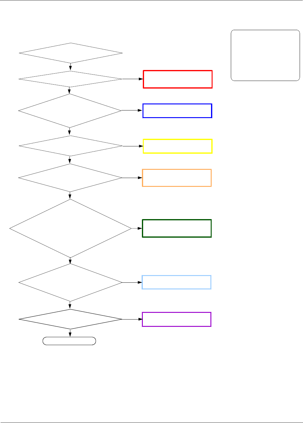
Level 3Repair
Distribution, transmission, or infringement of any content or data from this document without Samsung’s written authorization is strictly prohibited.
Confidential and proprietary-the contents in this service guide subject to change without prior notice.
8-132
Check C1093 ≤-65dBm ?
8-3-24. LTE Band8 /WCDMA Band8 DRX
NORMAL CONDITION
catch the channel?
Check the voltage at
{C1058, =1.8V?}
&{
C1055 =1.2V?}
&{
C1048 =1.5V?}
&{
C1057 =2.5V?}
Check the Voltage at
{C1023 >3.6
V?}
Check L1047, L1049
≥-65dBm ?
CHECK soldered
C1093, L1041, C1094,
C1119, L1042, C1092
Resolder or change
U1008, C1103
Resolder or change
F1005, L1047, L1049, L1050
Resolder or change
U1007
Check the freq. at
C1099 : 26.0MHz ?Change or resolder
OSC1001
Check L1048
≥-65dBm ?Resolder or change
C1104, L1052, L1048
NO
YES
NO
NO
YES
NO
YES
NO
YES
NO
YES
NO
YES
LTE B8 /WCDMA B8
Receiver is O.K? Resolder or change
UCP301
END
NO
CONTINUOUS RX ON
RF INPUT :LTE B8: 3625CH
WCDMA B8: 3013CH
AMP :-50
dBm
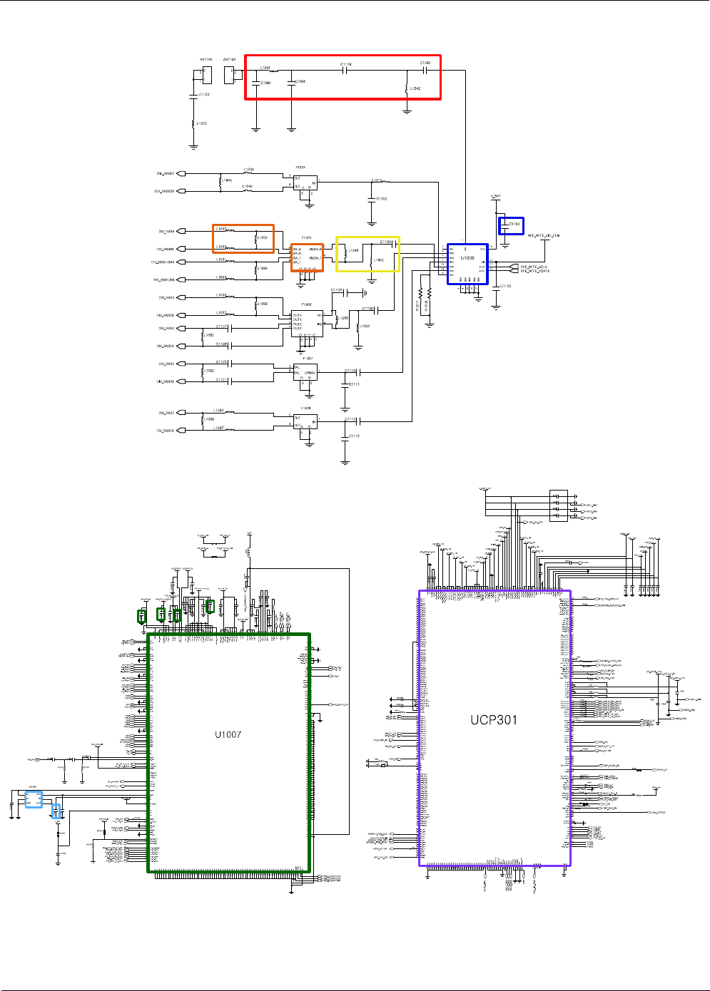
Level 3Repair
Distribution, transmission, or infringement of any content or data from this document without Samsung’s written authorization is strictly prohibited.
Confidential and proprietary-the contents in this service guide subject to change without prior notice.
8-133
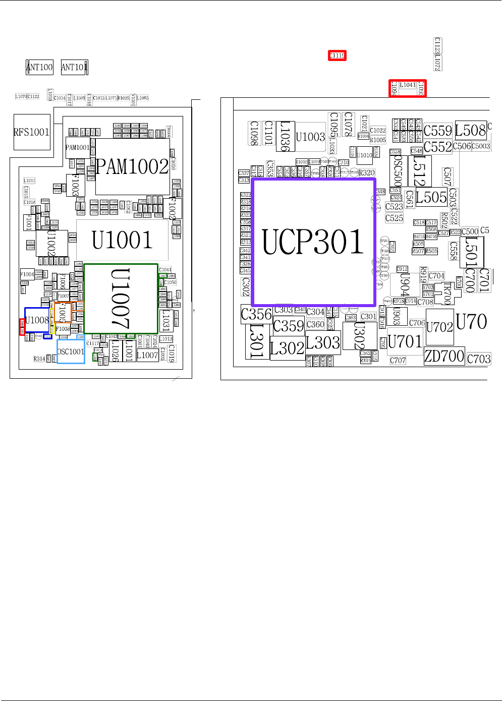
Level 3Repair
Distribution, transmission, or infringement of any content or data from this document without Samsung’s written authorization is strictly prohibited.
Confidential and proprietary-the contents in this service guide subject to change without prior notice.
8-134

Level 3Repair
Distribution, transmission, or infringement of any content or data from this document without Samsung’s written authorization is strictly prohibited.
Confidential and proprietary-the contents in this service guide subject to change without prior notice.
8-135
Check C1093 ≤-65dBm ?
8-3-24. LTE Band20 DRX
NORMAL CONDITION
catch the channel?
Check the voltage at
{C1058, =1.8V?}
&{
C1055 =1.2V?}
&{
C1048 =1.5V?}
&{
C1057 =2.5V?}
Check the Voltage at
{C1023 >3.6
V?}
Check L1045
≥-65dBm ?
CHECK soldered
C1093, L1041, C1094,
C1119, L1042, C1092
Resolder or change
U1008, C1103
Resolder or change
F1004, L1045, L1046, L1044
Resolder or change
U1007
Check the freq. at
C1099 : 26.0MHz ?Change or resolder
OSC1001
Check C1102
≥-65dBm ?Resolder or change
C1102, L1012
NO
YES
NO
NO
YES
NO
YES
NO
YES
NO
YES
NO
YES
LTE B20 Receiver is O.K? Resolder or change
UCP301
END
NO
CONTINUOUS RX ON
RF INPUT :LTE B20: 6300CH
AMP :-50
dBm
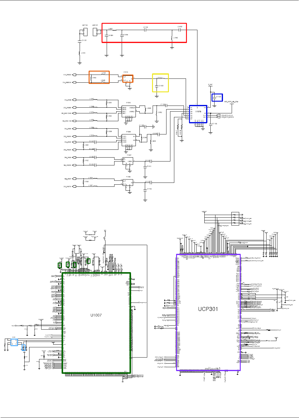
Level 3Repair
Distribution, transmission, or infringement of any content or data from this document without Samsung’s written authorization is strictly prohibited.
Confidential and proprietary-the contents in this service guide subject to change without prior notice.
8-136
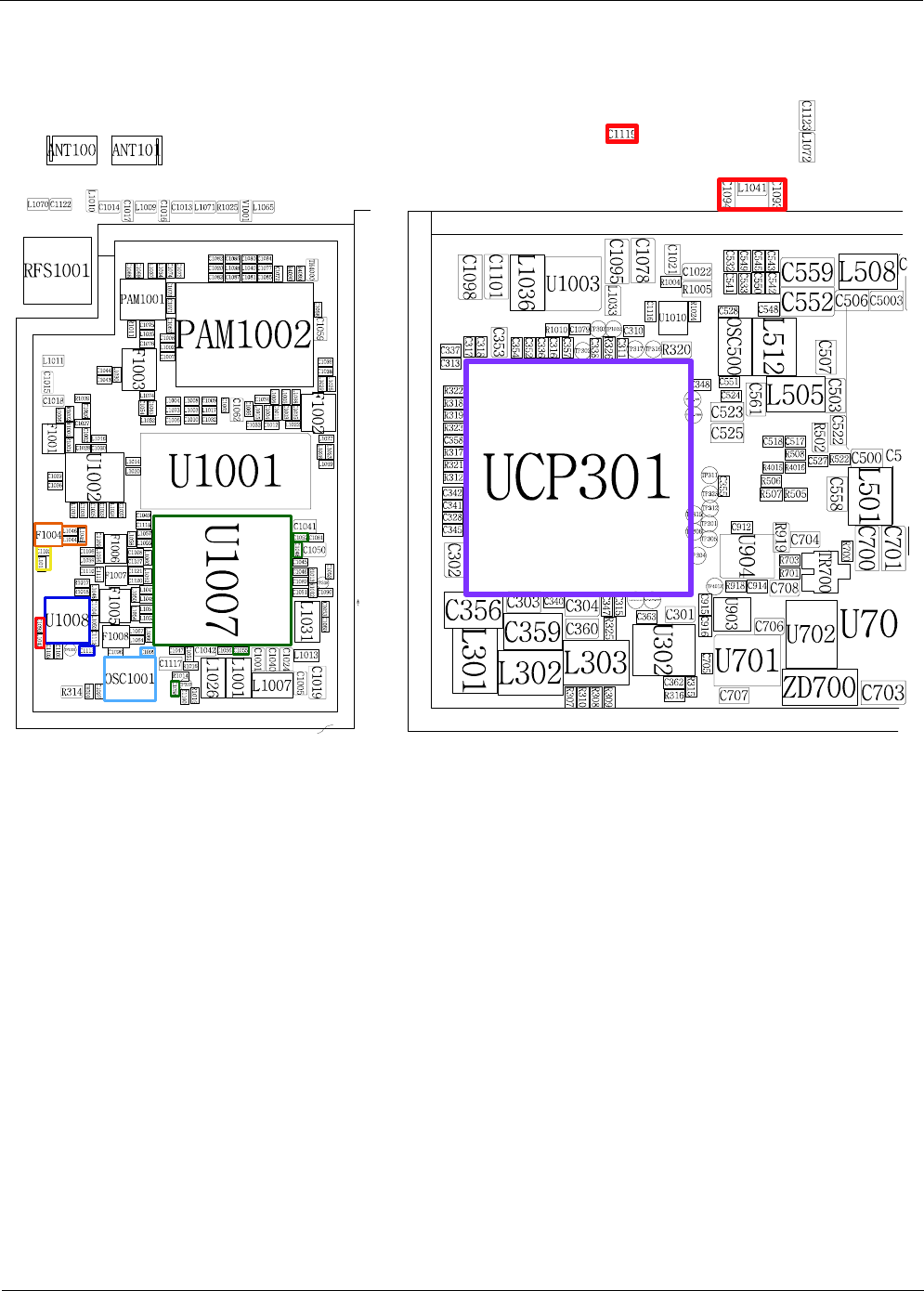
Level 3Repair
Distribution, transmission, or infringement of any content or data from this document without Samsung’s written authorization is strictly prohibited.
Confidential and proprietary-the contents in this service guide subject to change without prior notice.
8-137

9. Reference Abbreviate
9-1
Confidential and proprietary-the contents in this service guide subject to change without prior notice.
Distribution, transmission, or infringement of any content or data from this document without Samsung’s written authorization is strictly prohibited.
Reference Abbreviate
―AAC:Advanced Audio Coding.
―AVC :Advanced Video Coding.
―BER :Bit Error Rate
―BPSK:Binary Phase Shift Keying
―CA :Conditional Access
―CDM :Code Division Multiplexing
―C/I :Carrier to Interference
―DMB :Digital Multimedia Broadcasting
―EN :European Standard
―ES :Elementary Stream
―ETSI:European Telecommunications Standards Institute
―MPEG:Moving Picture Experts Group
―PN :Pseudo-random Noise
―PS :Pilot Symbol
―QPSK:Quadrature Phase Shift Keying
―RS :Reed-Solomon
―SI :Service Information
―TDM :Time Division Multiplexing
―TS :Transport Stream

This Service Manual is aproperty of Samsung Electronics Co.,Ltd.
Any unauthorized use of Manual can be punished under applicable
International and/or domestic law.
Samsung Electronics Co.,Ltd.
2014. 05. Rev.1.0
ⓒ