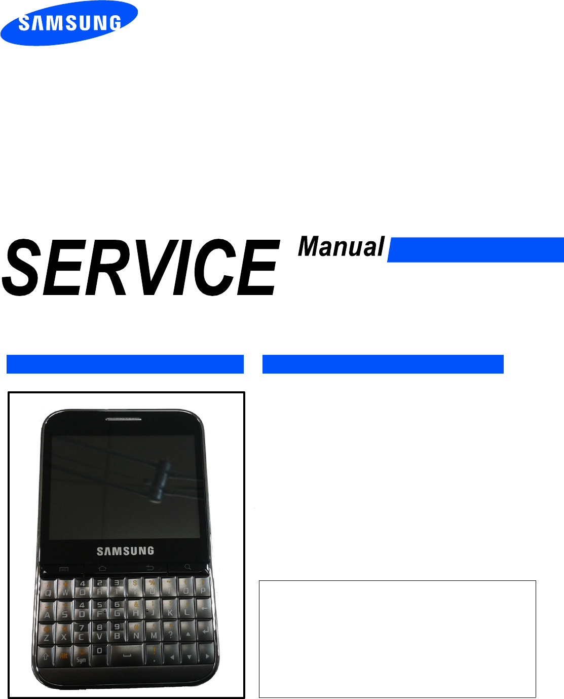
Samsung GT B7510 Service Manual. Www.s Manuals.com. Manual
User Manual: Smartphone Samsung GT-B7510 - Service manuals and Schematics, Disassembly / Assembly. Free.
Open the PDF directly: View PDF ![]() .
.
Page Count: 64
GSM TELEPHONE
GT-B7510
1. Safety Precautions
2. Specification
3. Product Function
4. Exploded View and Parts list
5. MAIN Electrical Parts List
6. Level 1Repair
7. Level 2Repair
8. Level 3Repair
9. Reference data
Notice :
All functionality, features, specifications and other
product information provided in this document inclu
ding, but not limited to, the benefits, design, pricing,
components, performance, availability, and capabiliti
-es of the product are subject to change without
notice or obligation. Samsung reserves the right to
make changes to this document and the product
described herein, at anytime, without obligation on
Samsung to provide notification of such change.
GSM TELEPHONE CONTENTS

This Service Manual is aproperty of Samsung Electronics Co.,Ltd.
Any unauthorized use of Manual can be punished under applicable
International and/or domestic law.
Samsung Electronics Co.,Ltd.
2011. 02. Rev.1.0
ⓒ
2. Specification
2-1
2-1. GSM General Specification
GSM850
Phase 1
EGSM 900
Phase 2
DCS1800
Phase 1 PCS1900 WCDMA
2100 WCDMA900
Freq.
Band[MHz]
Uplink/Downlin
k
824~849
869~894
880~915
925~960
1710~1785
1805~1880
1850~1910
1930~1990
1922~1977
2112~2167
880~915
925~960
ARFCN range 128~251 0~124 &
975~1023 512~885 512~810
UL:9612~98
88DL:10562
~10838
UL:2712~28
63,DL:2937
~3088
Tx/Rx spacing 45MHz 45MHz 95MHz 80MHz 190MHz 45MHz
Mod. Bit rate/
Bit Period
270.833kbp
s
3.692us
270.833kbp
s
3.692us
270.833kbp
s
3.692us
270.833kbp
s
3.692us
3.84Mcps 3.84Mcps
Time Slot
Period/Frame
Period
576.9us
4.615ms
576.9us
4.615ms
576.9us
4.615ms
576.9us
4.615ms
FrameLengt
h:
10ms
Slotlength:
0.667ms
FrameLengt
h:
10ms
Slotlength:
0.667ms
Modulation 0.3GMSK 0.3GMSK 0.3GMSK 0.3GMSK QPSKHQPS
K
QPSKHQPS
K
MS Power 33dBm~5dB
m
33dBm~5dB
m
30dBm~0dB
m
30dBm~0dB
m
24dBm~-
50dBm
24dBm~-
50dBm
Power Class 5pcl ~
19pcl 5pcl ~19
pcl 0pcl ~15
pcl 0pcl ~15
pcl 3(max+24dB
m)
3(max+24dB
m)
Sensitivity -102dBm -102dBm -100dBm -100dBm -106.7dBm -106.7dBm
TDMA Mux 8 8 8 8 88
Cell Radius 35Km 35Km 2Km 2Km 2Km 2Km
Specification
2-2
2-2. GSM Tx Power Class
TX Power
control
level
GSM850
533±2
dBm
631±2
dBm
729±2
dBm
827±2
dBm
925±2
dBm
10 23±2 dBm
11 21±2 dBm
12 19±2 dBm
13 17±2 dBm
14 15±2 dBm
15 13±2 dBm
16 11±3 dBm
17 9±3dBm
18 7±3 dBm
19 5±3 dBm
TX Power
control
level
EGSM900
533±2
dBm
631±2
dBm
729±2
dBm
827±2
dBm
925±2
dBm
10 23±2 dBm
11 21±2 dBm
12 19±2 dBm
13 17±2 dBm
14 15±2 dBm
15 13±2 dBm
16 11±3 dBm
17 9±3dBm
18 7±3 dBm
19 5±3 dBm
TX Power
control
level
DCS1800
030±3
dBm
128±3
dBm
226±3
dBm
324±3
dBm
422±3
dBm
520±3
dBm
618±3
dBm
716±3
dBm
814±3
dBm
912±4
dBm
10 10±4 dBm
11 8±4 dBm
12 6±4 dBm
13 4±4 dBm
14 2±5 dBm
15 0±5 dBm
TX Power
control
level
PCS1900
030±3
dBm
128±3
dBm
226±3
dBm
324±3
dBm
422±3
dBm
520±3
dBm
618±3
dBm
716±3
dBm
814±3
dBm
912±4
dBm
10 10±4 dBm
11 8±4 dBm
12 6±4 dBm
13 4±4 dBm
14 2±5 dBm
15 0±5 dBm

SAMSUNG Proprietary-Contents may change without notice
3. Operation Instruction and Installation
3-1
This Document can not be used without Samsung's authorization
Main Function
-GoogleAndroid OS 2.2 Froyo
-Size: 108.6x66.7x10.65
-Band :GSM QUAD BAND GSM850/900/1800/1900 (Release :R99)
-BAND :HSDPA 7.2M B1/B8
-3Mega pixel AF Camera, 1/5" CMOS
-LCD: 2.8" LQVGA TFT
-1350mA standard Battery
-3.5pi Earjack/ Earphone
-Micro USB/ Power, Data
-Wi-Fi 802.11b/g/n
-Bluetooth v3.0
-USB v2.0 High Speed,
-A-GPS
-FM w/RDS
-input :QWERTY Key, C-Type single TSP
-Audio :mp3, ogg, aac, mid, xmf, rtttl, imy, rtx, ota, amr, wav, mxmf
-Image :bmp, gif, jpg, png, wbmp, agif
-Video :MPEG4, H.263, H.264, 3gp, mp4
-B/B: MSM7227 turbo 800M
-PMIC: MAX8899
-Tranceiver: RTR6285
-PAM: SKY77554(2G)
-RF7201(3G Dual)
-Intenna :Carrier type
-LCD: 2.8" LQVGA TFT
-MEMORY: 4G+3G
SAMSUNG Proprietary-Contents may change without notice
6. Level 1Repair
6-1
This Document can not be used without Samsung's authorization
6-1. S/W Download
6-1-1. Pre-requsite for S/W Downloading
•GT-B7510 Mobile Phone
•Battery
•USB cable
•JIG BOX (GH99-36900A)
•RF Test Cable (GH39-00985A)
•JIG Cable (GH39-01339A)
•Adapter (GH99-38251A)
•Downloader Program(Odin Multi Downloader v4.38)
•Binary files
•PC (Windows XP, 7)
★The settings for download.
SAMSUNG Proprietary-Contents may change without notice
Level 1Repair
6-2
This Document can not be used without Samsung's authorization
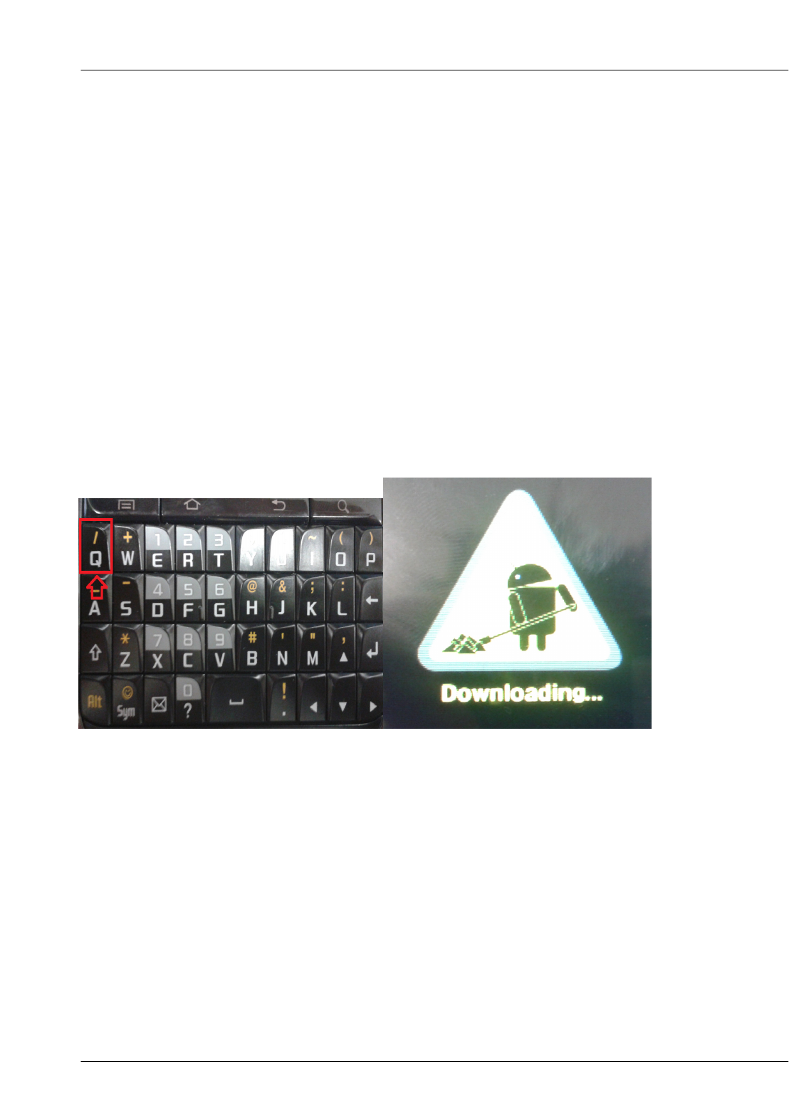
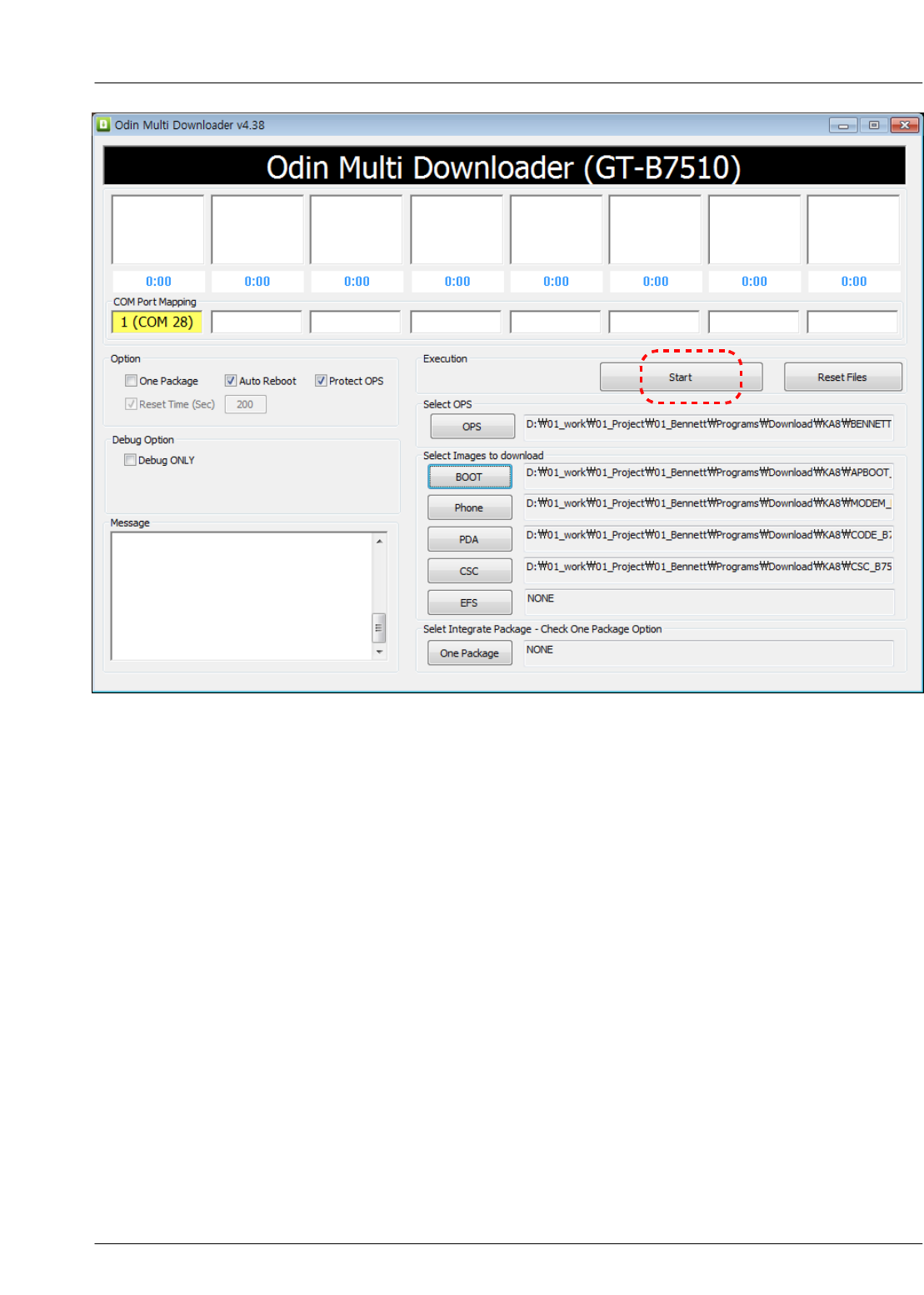
6-1-2. S/W Downloader Program
1. Execute the binary download program,which is "Odin Multi Downloader v4.38".
2. Load the files of OPS, BOOT, PHONE, PDS, CSC from the folder that you saved
binary files. (CLICK the each Naming Button and select the file)
-OPS :OPS file
-BOOT :APBOOT_...
-phone :MODEM_...
-PDA :CODE_...
-CSC :CSC_...
3. Turn On the Mobile with push 'Q' Button to enter the Download mode and check
the Download Logo on LCD
<QWERTY Key Pad ><
Download Logo>
4. Click the Start button when aport is ready
SAMSUNG Proprietary-Contents may change without notice
Level 1Repair
6-3
This Document can not be used without Samsung's authorization
5. After downloading finished successfully, there is a"PASS" message.
6. Check the binary version using key streaming, "*#1234#".

SAMSUNG Proprietary-Contents may change without notice
9. Reference Abbreviate
This Document can not be used without Samsung's authorization
9-1
Reference Abbreviate
―AAC:Advanced Audio Coding.
―AVC :Advanced Video Coding.
―BER :Bit Error Rate
―BPSK:Binary Phase Shift Keying
―CA :Conditional Access
―CDM :Code Division Multiplexing
―C/I :Carrier to Interference
―DMB :Digital Multimedia Broadcasting
―EN :European Standard
―ES :Elementary Stream
―ETSI:European Telecommunications Standards Institute
―MPEG:Moving Picture Experts Group
―PN :Pseudo-random Noise
―PS :Pilot Symbol
―QPSK:Quadrature Phase Shift Keying
―RS :Reed-Solomon
―SI :Service Information
―TDM :Time Division Multiplexing
―TS :Transport Stream

SAMSUNG Proprietary-Contents may change without notice
1. Safety Precautions
1-1
This Document can not be used without Samsung's authorization
1-1. Repair Precaution
―Repair in Shield Box, during detailed tuning. Take specially care of tuning or test, because
specipicty of cellular phone is sensitive for surrounding interference(RF noise).
―Be careful to use akind of magnetic object or tool, because performance of parts is damaged by
the influence of magnetic force.
―Surely use astandard screwdriver when you disassemble this product, otherwise screw will be
worn away.
―Use athicken twisted wire when you measure level.
Athicken twisted wire has low resistance, therefore error of measurement is few.
―Repair after separate Test Pack and Set because for short danger (for example an overcurrent
and furious flames of parts etc) when you repair board in condition of connecting Test Pack and
tuning on.
―Take specially care of soldering, because Land of PCB is small and weak in heat.
―Surely tune on/off while using AC power plug, because arepair of battery charger is dangerous
when tuning ON/OFF PBA and Connector after disassembling charger.
―Don't use as you pleases after change other material than replacement registered on SEC System.
Otherwise engineer in charge isn't charged with problem that you don't keep this rules.

SAMSUNG Proprietary-Contents may change without notice
Safety Precautions
1-2
This Document can not be used without Samsung's authorization
1-2. ESD(Electrostatically Sensitive Devices) Precaution
Several semiconductor may be damaged easily by static electricity. Such parts are called by ESD
(Electrostatically Sensitive Devices), for example IC,BGA chip etc. Read Precaution below.
You can prevent from ESD damage by static electricity.
―Remove static electricity remained your body before you touch semiconductor or parts with
semiconductor. There are ways that you touch an earthed place or wear static electricity prevention
string on wrist.
―Use earthed soldering steel when you connect or disconnect ESD.
―Use soldering removing tool to break static electricity. ,otherwise ESD will be damaged by static
electricity.
―Don't unpack until you set up ESD on product. Because most of ESD are packed by box and
aluminum plate to have conductive power,they are prevented from static electricity.
―You must maintain electric contact between ESD and place due to be set up until ESD is
connected completely to the proper place or acircuit board.
SAMSUNG Proprietary-Contents may change without notice
4. Exploded View and Parts List
4-1
This Document can not be used without Samsung's authorization
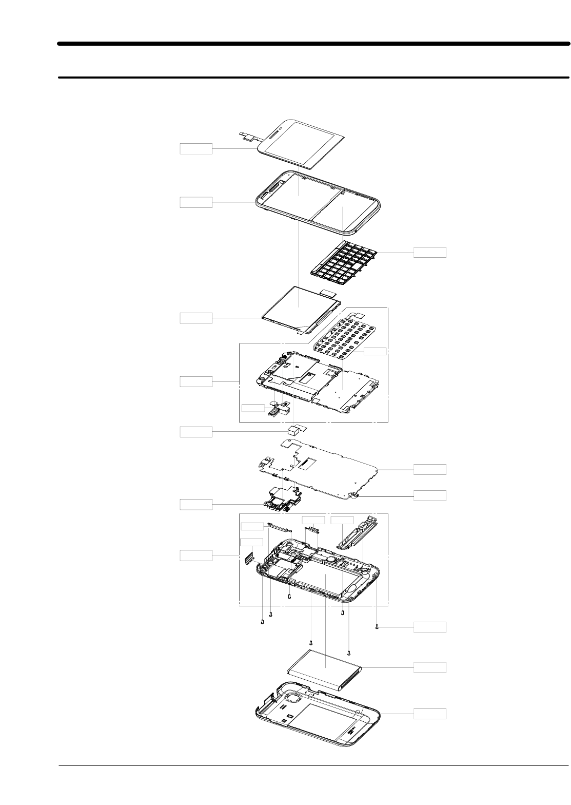
4-1. Cellular phone Exploded View
QLB01
QRE01
QCA01
QSP01
QME03
QFR01
QLC01
QKP01
QMI01
QCR67
QBA01
QBC00
QMP01
QME01
QAR01
QVO01
QRF06
QCK01 QAN02
SAMSUNG Proprietary-Contents may change without notice
Exploded View and Parts List
4-2
This Document can not be used without Samsung's authorization
Design LOC Description SEC CODE
QCR67 SCREW-MACHINE 6001-002083
QMI01 MICROPHONE-ASSY-GT-B7510 GH30-00722A
QBA01 INNER BATTERY PACK-EB494358VU,GT-S5830,L GH43-03504A
QSP01 MODULE-SPK+SIM S/C GH59-10724A
QME03 TOUCH/PANEL-GT-B7510 GH59-10728A
QMP01 A/S ASSY-PBAMAIN(COMM)GT-B7510 GH82-05631A
QLC01 ELA MODULE-LCD MODULE(GT-B7510) GH96-05085A
QCA01 ASSY CAMERA-3M AF MODULE(GT-B7510 GH96-05091A
QFR01 ASSY CASE-FRONT GH98-18418A
QBC00 ASSY COVER-BATT GH98-18420A
QKP01 ASSY KEYPAD-QWERTY GH98-18421A
QLB01 ASSY BRACKET-LCD GH98-18430A
QME01 KEY FPCB-QWERTY KEY(GT-B7510) GH59-10713A
QAR01 ASSY ETC-RCV&EAR JACK ASSY GH59-10737A
QRE01 ASSY CASE-REAR GH98-18419A
QAN02 INTENNA-GTB7510 MAIN GH42-02892A
QRF06 PMO COVER-DC USB GH72-61733A
QCK01 PMO KEY-POWER HOLD GH72-61734A
QVO01 PMO KEY-VOLUME GH72-61735A
4-2. Cellular phone Parts list
SAMSUNG Proprietary-Contents may change without notice
7. Level 2Repair
7-1
This Document can not be used without Samsung's authorization
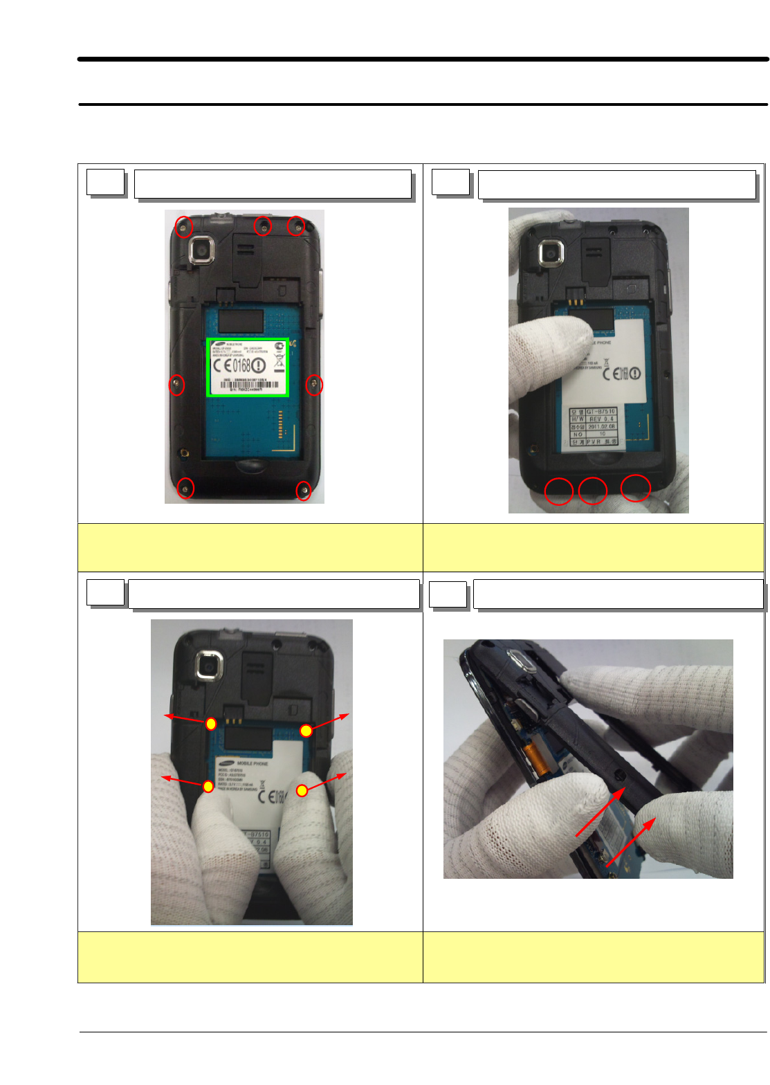
1) Be careful not to make scratch and molding damage! 1) Be careful not to make scratch and molding damage!
1) Push out REAR to both side. 1) Detach Power Key FPCB and Cammera Key FPCB.
2) Be careful not to damage to FPCB (Use tweezer!)
7-1. Disassembly and Assembly Instructions
7-1-1. Disassembly
Release Screw 7Point at REAR
1 2
3Disjoint hook on the both side of the REAR Disassemble REAR
4
Disjoint Hook on the bottom of the REAR
SAMSUNG Proprietary-Contents may change without notice
7. Level 2Repair
7-2
This Document can not be used without Samsung's authorization
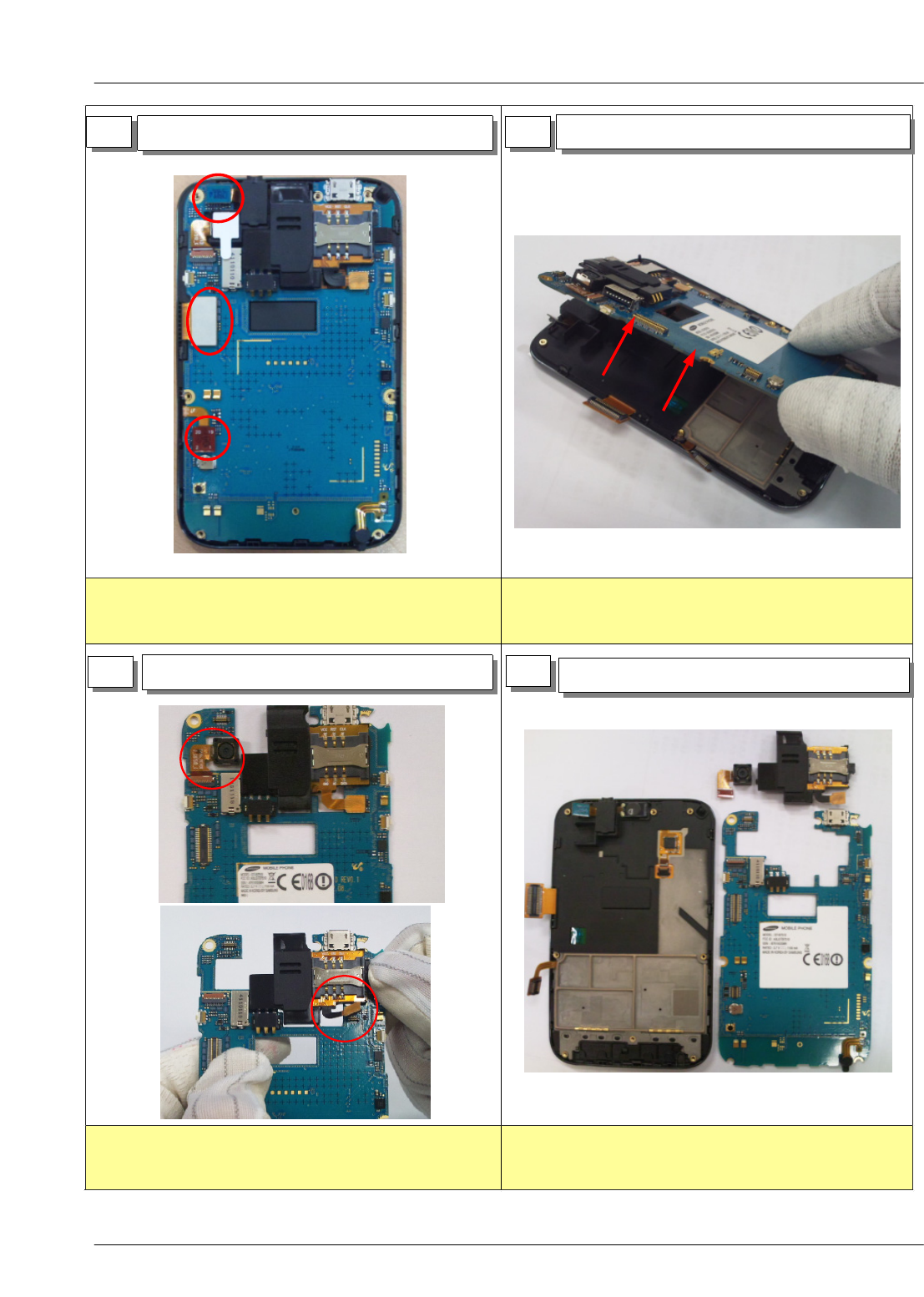
1) Detach Earjack/LCD/Qwerty key FPCB.(3point) 1) Hold up Main PBA from left.
1) Disassemble Cammera Module from PBA.
2) Disassemble SPK Module from PBA.
8
7Disassemble Module from PBA.
5Disassemble FPCB. Disassemble Main PBA from the FRONT Ass'y
6
Complete disassembly.
SAMSUNG Proprietary-Contents may change without notice
7. Level 2Repair
7-3
This Document can not be used without Samsung's authorization
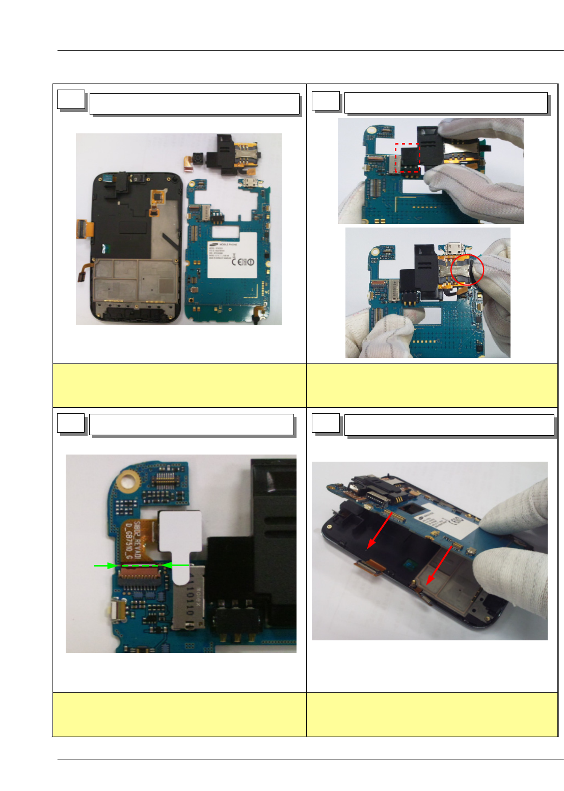
1) Assemble left hook first.
2) Assemble right hook.
1) Assemble fiting to silk line
7-1-1. Assembly
12
34
Set aPBA and FRONT Ass'y.
Assemble PBA on FRONT Ass'y.
Assemble Camera module
Assemble SPK module.
SAMSUNG Proprietary-Contents may change without notice
7. Level 2Repair
7-4
This Document can not be used without Samsung's authorization
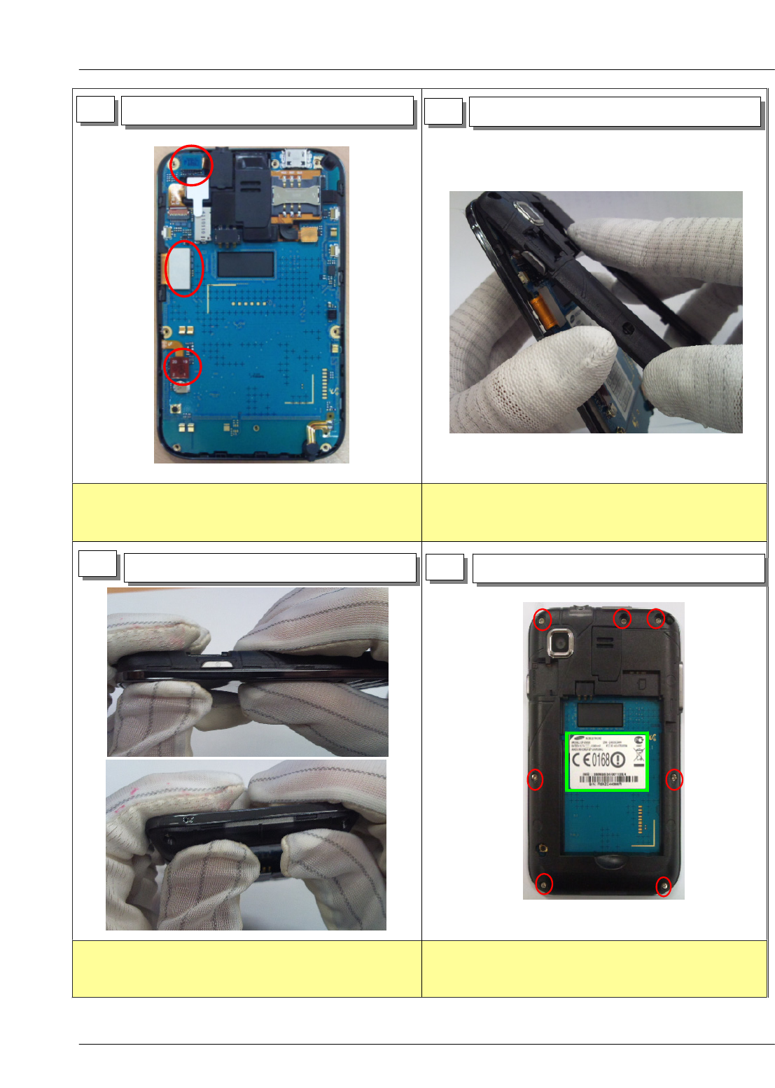
1) Assemble Earjack/LCD/Qwerty key FPCB.(3point).
2) Be careful not to damage to FPCB.
1) Assemble matching location from earjack of rear
upper
1) Be careful not to make scratch and molding damage! 1) Drive Screws at 6points with torque
1.1 +/- 0.1 Kgf/㎠
56Assemble FRONT Ass'y on REAR.
Assemble PBA on FRONT Ass'y.
Drive Screws at 6points
7Assemble FRONT Ass'y on REAR. 8
SAMSUNG Proprietary-Contents may change without notice
8. Level 3Repair
8-1
This Document can not be used without Samsung's authorization
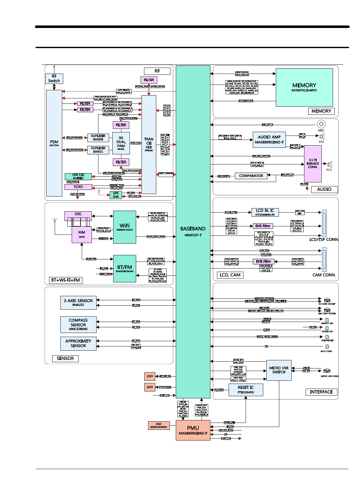
8-1. Block Diagram
SAMSUNG Proprietary-Contents may change without notice
Level 3Repair
8-2
This Document can not be used without Samsung's authorization
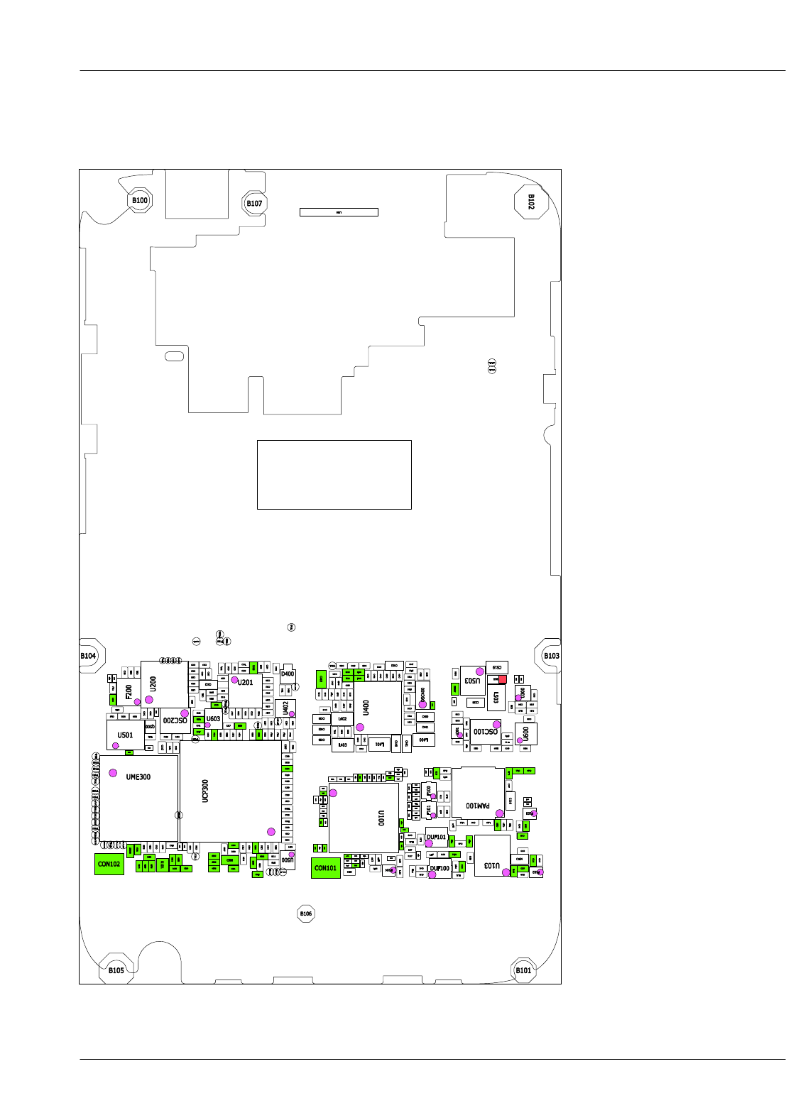
8-2. PCB Diagrams
8-2-1. Top
SAMSUNG Proprietary-Contents may change without notice
Level 3Repair
8-3
This Document can not be used without Samsung's authorization
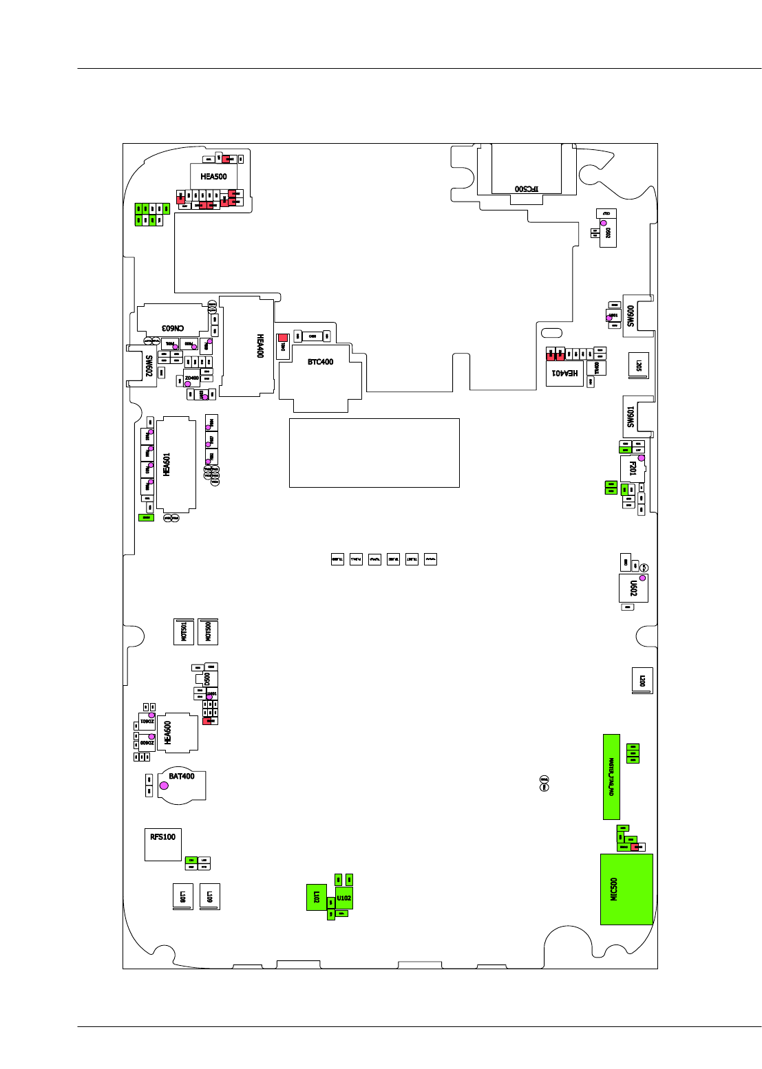
8-2-2. Bottom
SAMSUNG Proprietary-Contents may change without notice
Level 3Repair
8-4
This Document can not be used without Samsung's authorization
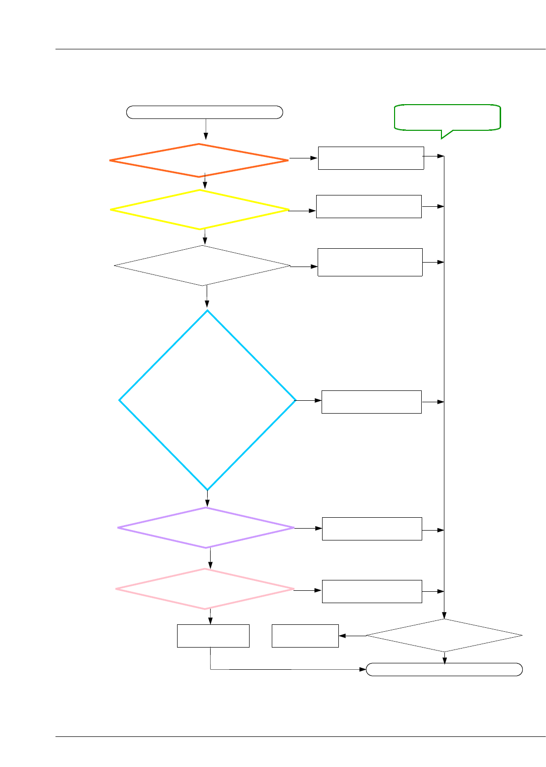
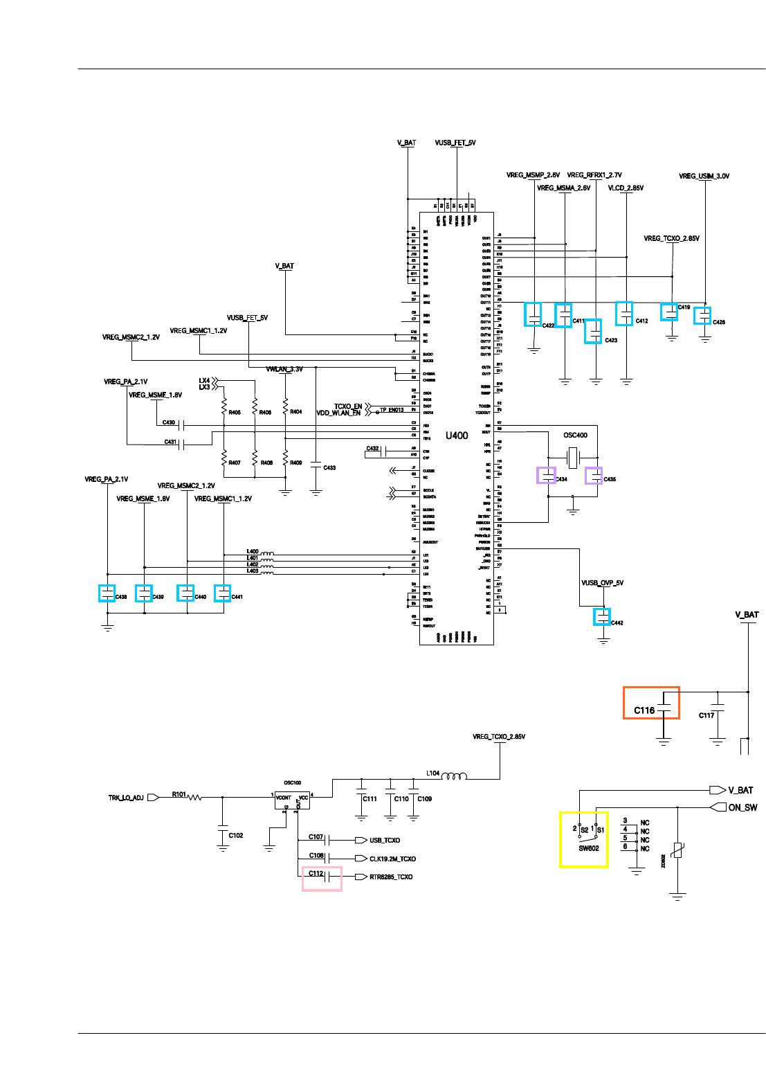
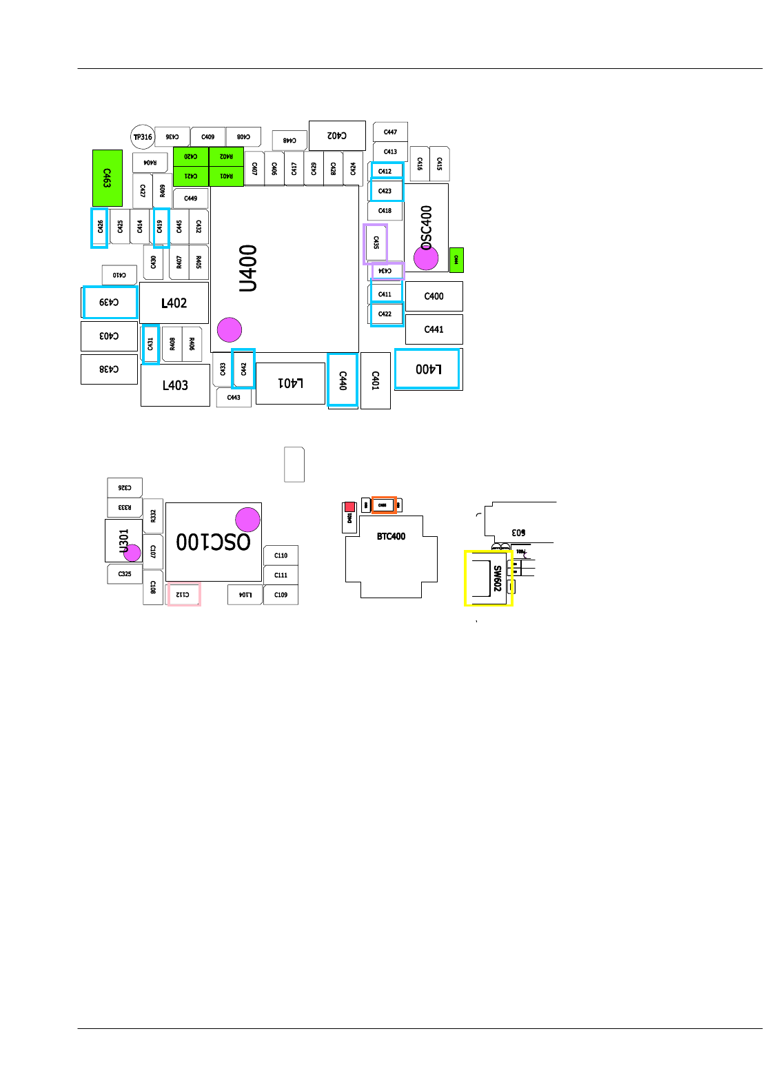
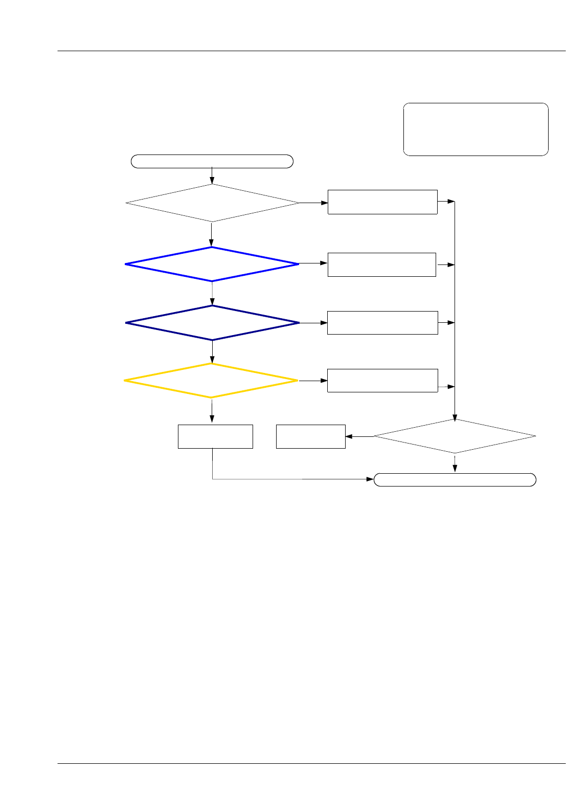
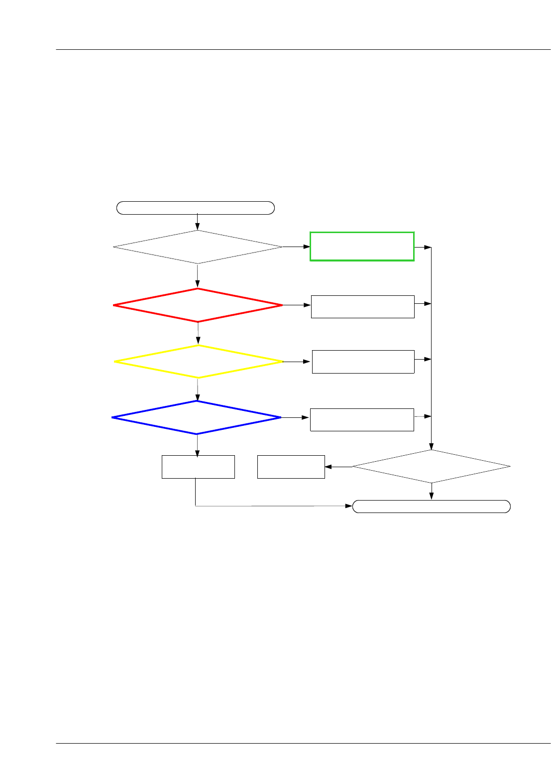
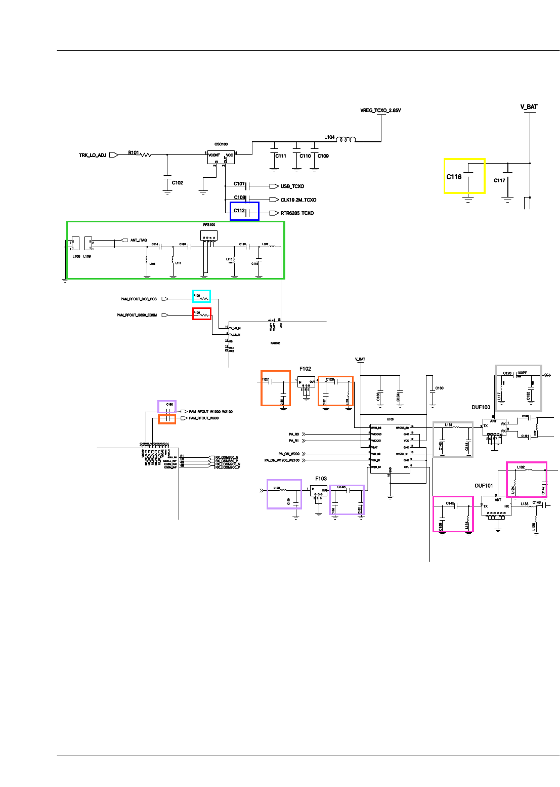
Check the power
VREG_TCXO_2.85V(C419)
VLCD_2.85V(C412)
VREG_RFRX_2.7V(C423)
VREG_MSMA_2.6V(C411)
VREG_MSMP_2.6V(C422)
VREG_MSME_1.8V(C439)
VREG_PA_2.1V(C431)
VREG_MEMC1_1.2V(C441)
VREG_MSMC2_1.2V(C440)
VUSB_OVP_5V(C442)
VREG_USIM_3.0V(C426)
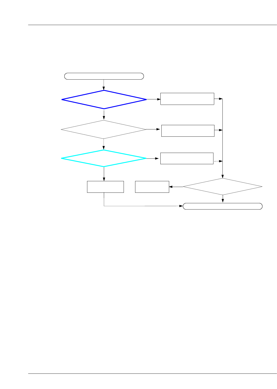
8-3-1. Power On
Put more lead soler
each terminal
inner clock problem.
Put more lead solder
each terminal
1.Charge the Battery.
2.If 0V, put more lead
@C455
NO
NO
YES
Check the VBAT Voltage
@C455 >=3.3V
YES
NO
Download binary again
NO
Current consumption
>= 100mA?
NO
YES
END
Is the soldered status of
SW602(ON KEY) O.K?
YES
1.Put more lead each terminal
2.Replace KEY602
NO
YES
YES
Is It power turned on?
YES
NO
Back to
previous step
If you #1 try and fail,
do #2!!!
Replace Board(PBA)
"Power On"does not work
power management problem.
Put more lead solder
each terminal
Check the OSC400
(C434,434)=32.768KHz?
Check the TCX100
@C112=19.2MHz?
SAMSUNG Proprietary-Contents may change without notice
Level 3Repair
8-5
This Document can not be used without Samsung's authorization
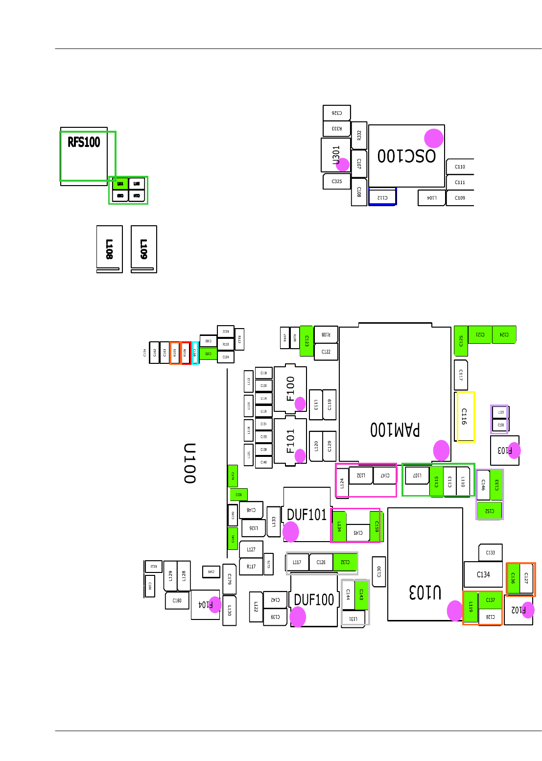
C153
SAMSUNG Proprietary-Contents may change without notice
Level 3Repair
8-6
This Document can not be used without Samsung's authorization
SAMSUNG Proprietary-Contents may change without notice
Level 3Repair
8-7
This Document can not be used without Samsung's authorization
8-3-2. SIM part
Check the connection of
HEA401 to SIM card
insert SIM card again
after check connection HEA401
Replace the SIM(SPK) module
NO
YES
YES
NO
END
Does Phone accept
the SIM card?
YES
NO
Put more lead each terminal
YES
Back to
previous step
Replace Board(PBA)
Check the voltage
@C461 =3.0V?
"Insert SIM card" is displayed on the LCD
NO
Check the SIM(SPK)
Module
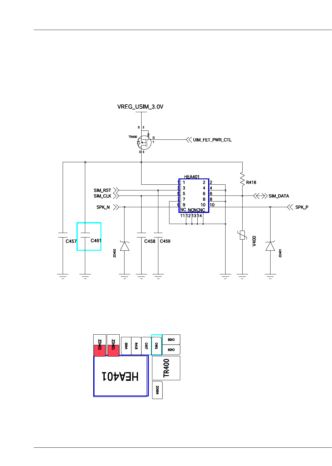
SAMSUNG Proprietary-Contents may change without notice
Level 3Repair
8-8
This Document can not be used without Samsung's authorization
SAMSUNG Proprietary-Contents may change without notice
Level 3Repair
8-9
This Document can not be used without Samsung's authorization
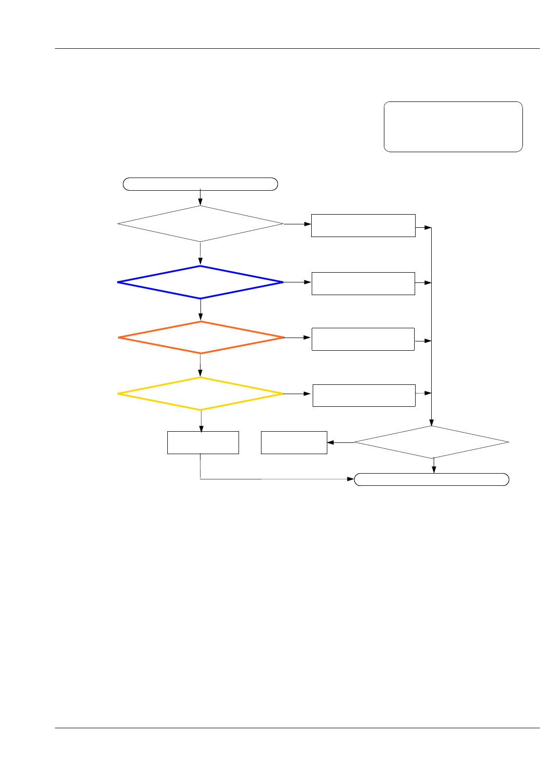
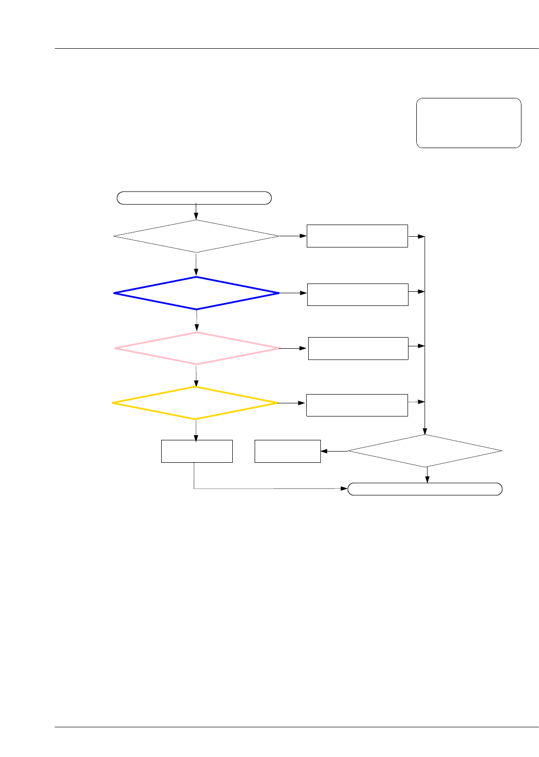
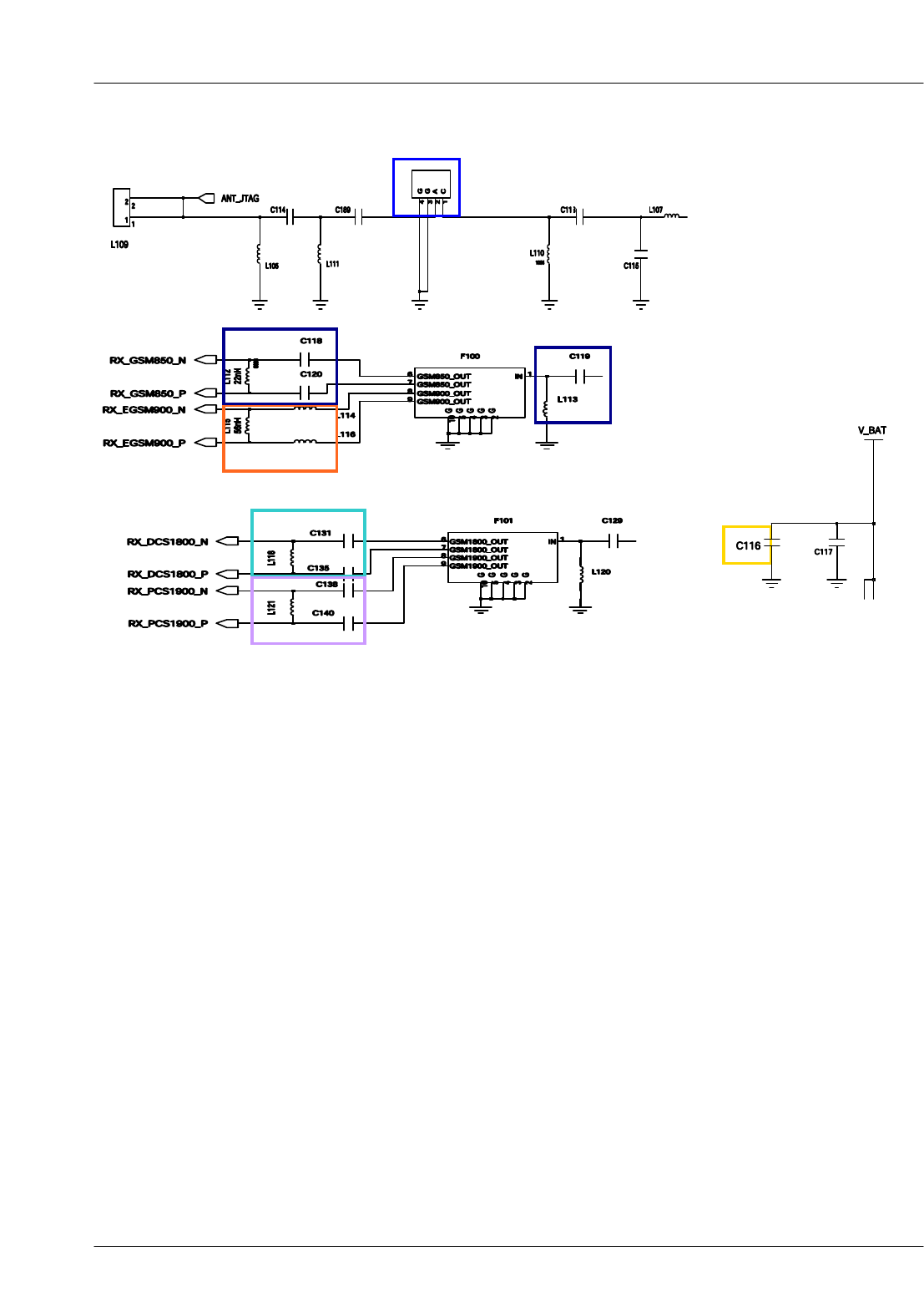
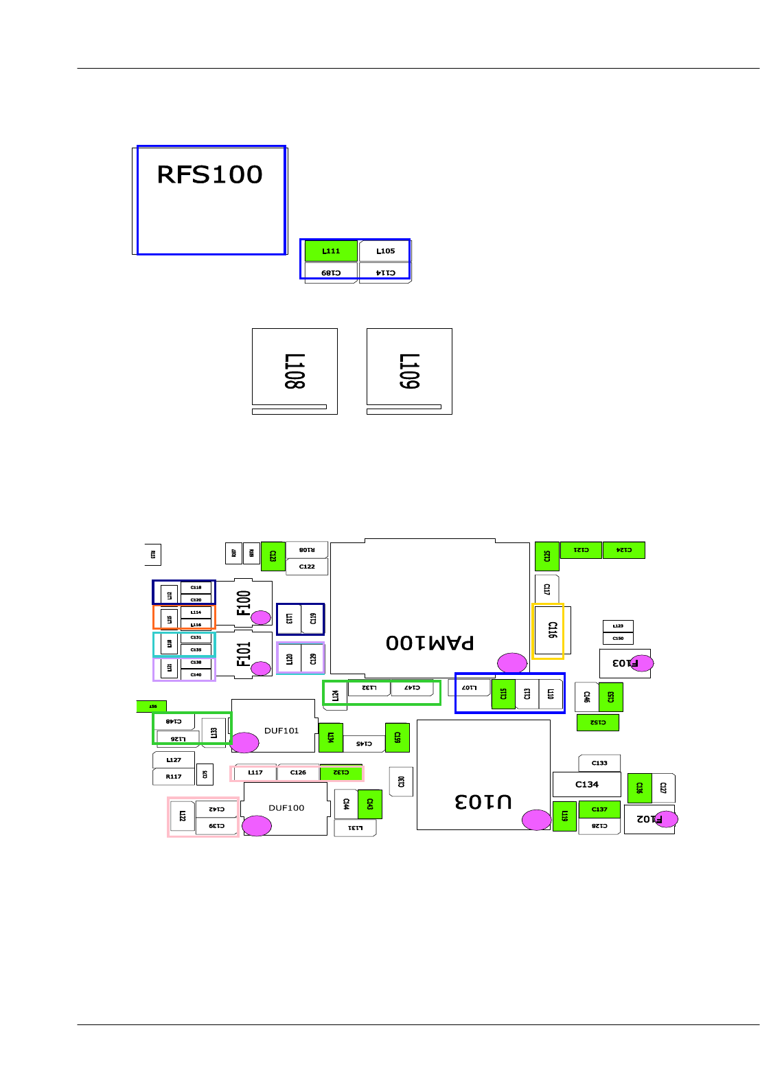
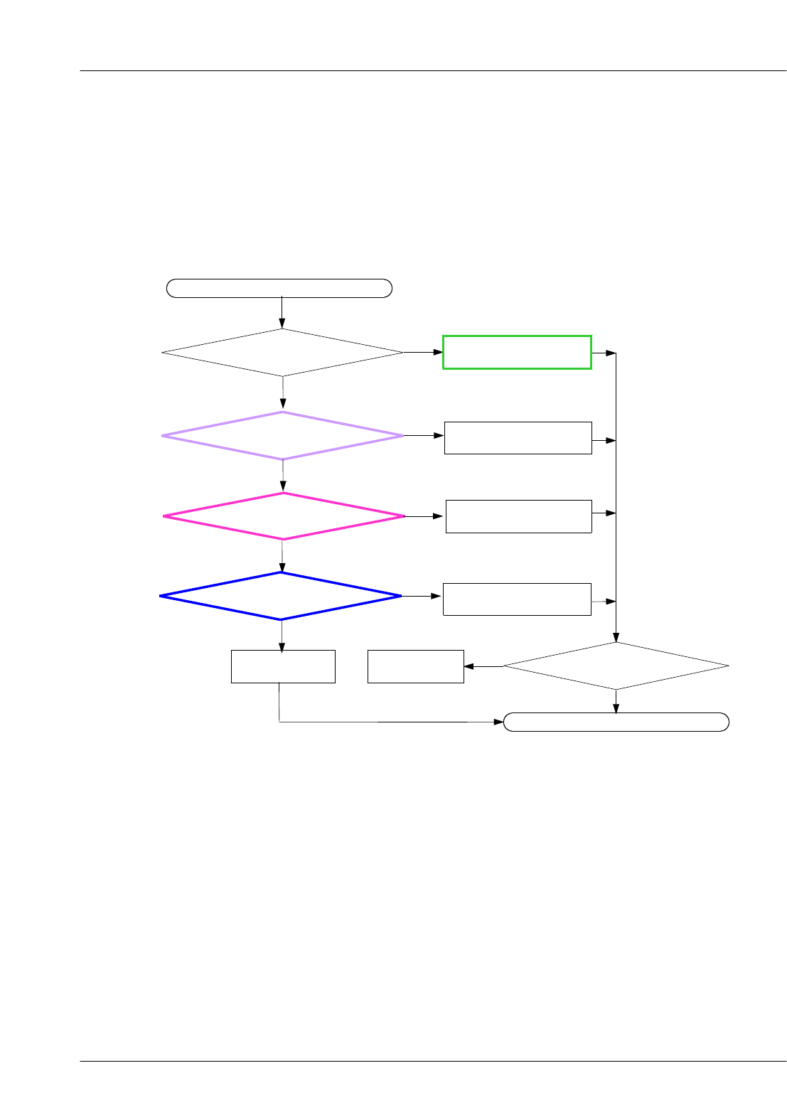
8-3-3. GSM850 RX
Put more lead solder
@L105,C114,C189,L111,
L110,C113,C115,L107
PAM100 CHECK
@RFS100 ≥-65dBm ?
Put more lead solder RFS100,
L110,C113,C115,L107
NO
YES
NO
NO
YES
YES
Check the voltage
PAM100 @C116≥3.0V ?
YES
NO
Put more lead solder
C119, L113,
C118,C120,L112
END
Does Phone catch
the GSM850 network?
YES
Back to
previous step
Replace Board(PBA)
Phone can't catch GSM850 network
NORMAL CONDITION
catch the channel?
Check the connection
GSM850 RX LINE
Put more lead solder
each terminal
CONTINUOUS RX ON
RF INPUT : 190CH
Amplitude :-50
dBm
SAMSUNG Proprietary-Contents may change without notice
Level 3Repair
8-10
This Document can not be used without Samsung's authorization
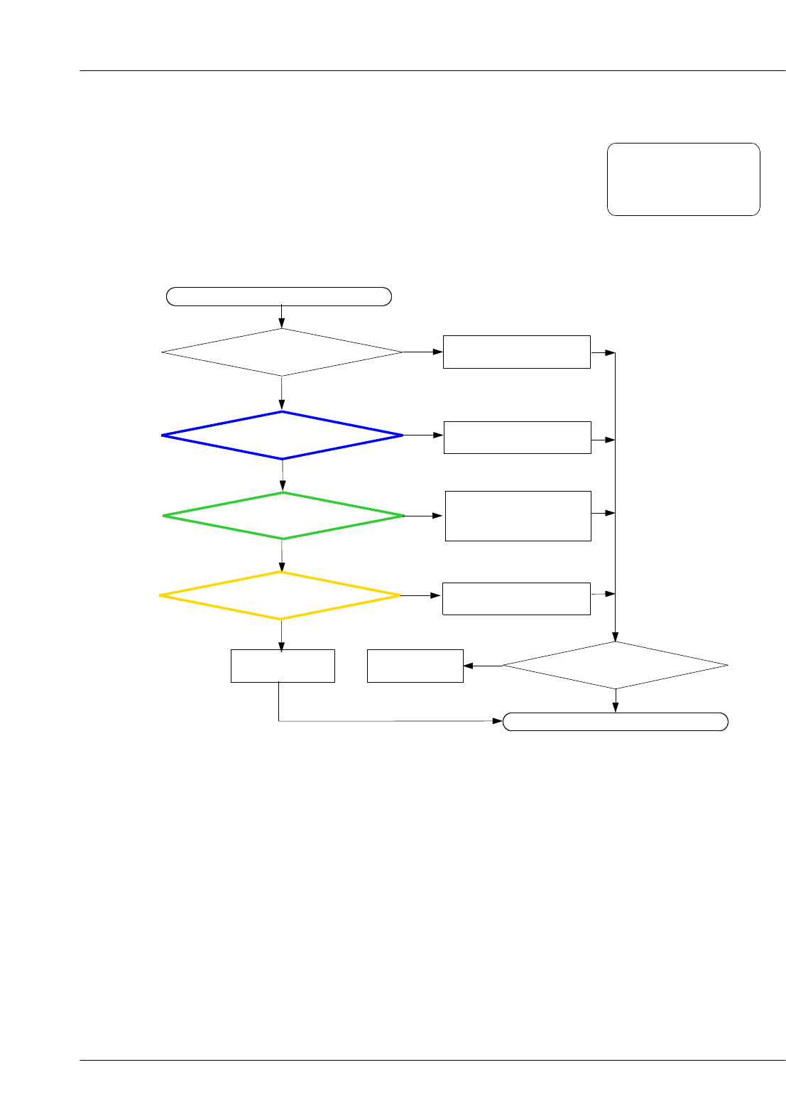
Check the connection
GSM900 RX LINE
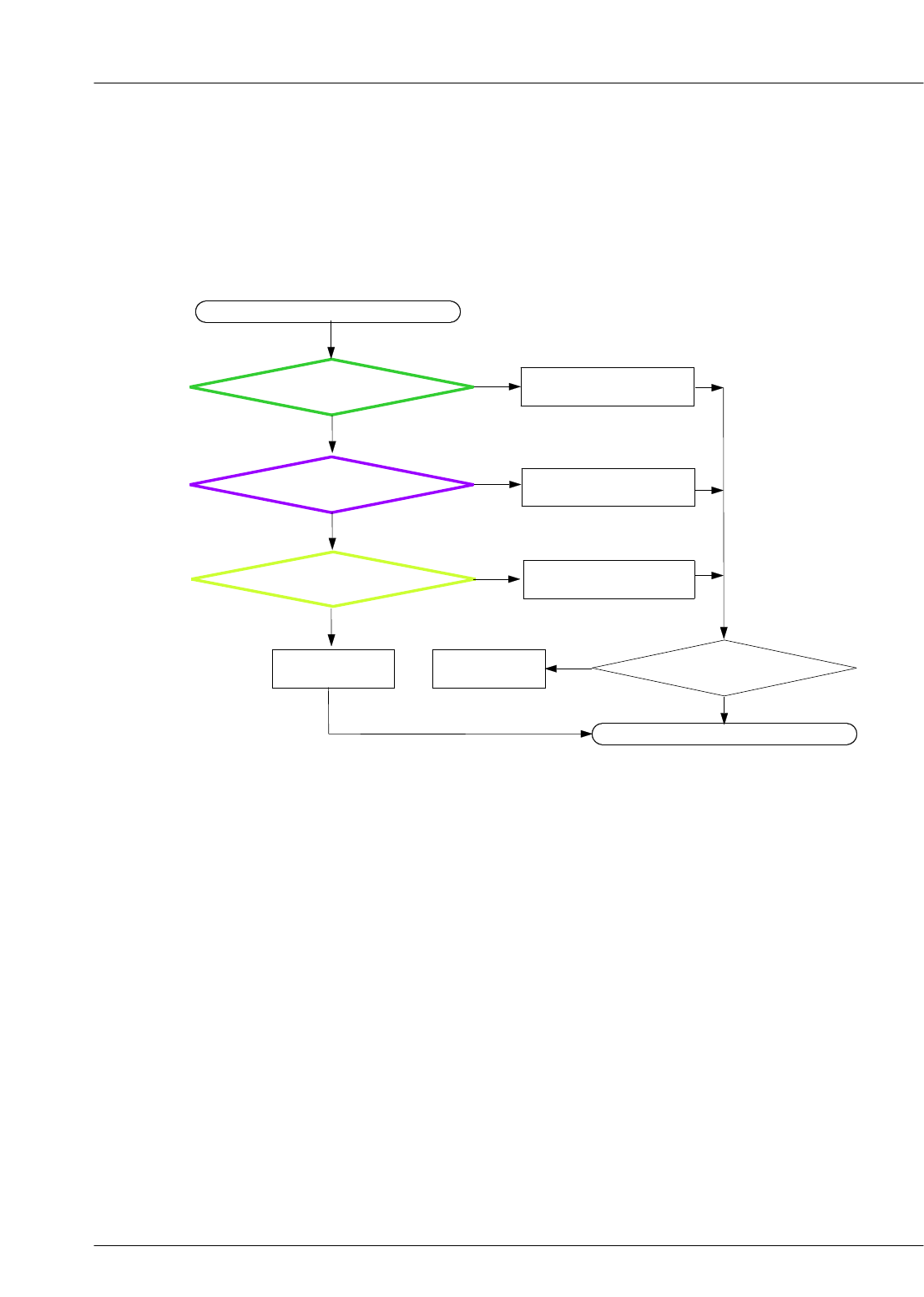
8-3-4. GSM900 RX
CONTINUOUS RX ON
RF INPUT :62
CH
Amplitude :-50
dBm
Put more lead solder
@L105,C114,C189,L111,
L110,C113,C115,L107
PAM100 CHECK
@RFS100 ≥-65dBm ?
Put more lead solder RFS100,
L110,C113,C115,L107
Put more lead solder
each terminal
NO
YES
NO
NO
YES
YES
Check the voltage
PAM100 @C116≥3.0V
YES
NO
Put more lead solder
C119,L113,L114,L115,L116
NORMAL CONDITION
catch the channel?
Phone can't catch GSM900 network
END
Does Phone catch
the GSM900 network?
YES
Back to
previous step
Replace Board(PBA)
NO
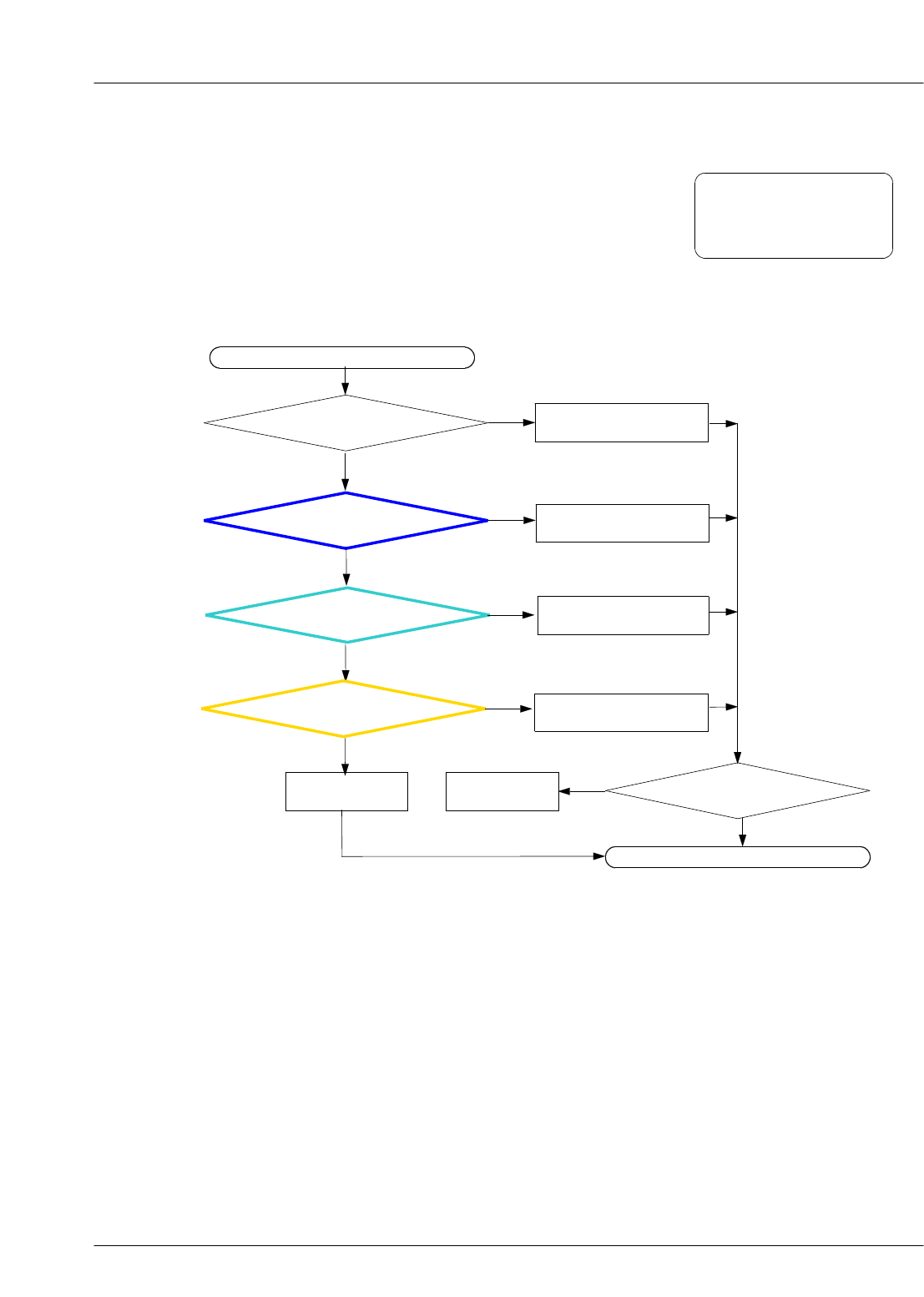
SAMSUNG Proprietary-Contents may change without notice
Level 3Repair
8-11
This Document can not be used without Samsung's authorization
Check the connection
DCS RX LINE
8-3-5. DCS RX
Put more lead solder
C129,L120,C131,C135,L118
CONTINUOUS RX ON
RF INPUT : 698CH
Amplitude :-50
dBm
PAM100 CHECK
@RFS100 ≥-65dBm ?Put more lead solder RFS100,
L110,C113,C115,L107
Put more lead solder
each terminal
NO
YES
NO
NO
YES
YES
Check the voltage
PAM100 @C116≥3.0V ?
YES
NO
Phone can't catch DCS network
NORMAL CONDITION
catch the channel?
END
Does Phone catch
the DCS network?
YES
Back to
previous step
Replace Board(PBA)
NO
Put more lead solder
@L105,C114,C189,L111,
L110,C113,C115,L107
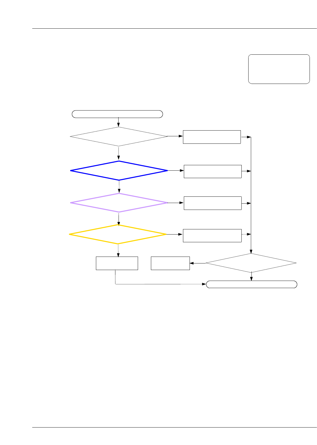
SAMSUNG Proprietary-Contents may change without notice
Level 3Repair
8-12
This Document can not be used without Samsung's authorization
Check the connection
PCS RX LINE
8-3-6. PCS RX
CONTINUOUS RX ON
RF INPUT : 644CH
Amplitude :-50
dBm
AM100 CHECK
@RFS100 ≥-65dBm ?
Put more lead solder RFS100,
L110,C113,C115,L107
Put more lead solder
each terminal
NO
YES
NO
NO
YES
YES
Check the voltage
PAM100 @C116≥3.0V ?
YES
NO
Put more lead solder
C129,L120,C138,C140,L121
Phone can't catch PCS network
NORMAL CONDITION
catch the channel?
Put more lead solder
@L105,C114,C189,L111,
L110,C113,C115,L107
END
Does Phone catch
the PCS network?
YES
Back to
previous step
Replace Board(PBA)
NO
SAMSUNG Proprietary-Contents may change without notice
Level 3Repair
8-13
This Document can not be used without Samsung's authorization
Check the connection
WCDMA900 RX LINE
8-3-7. WCDMA Band 8RX
Put more lead solder
C126,L117,C139,C142,L122
PAM100 CHECK
@RFS100 ≥-65dBm ?Put more lead solder RFS100,
L110,C113,C115,L107
Put more lead solder
each terminal
NO
YES
NO
NO
YES
YES
Check the voltage
PAM100 @C116≥3.0V ?
YES
NO
Phone can't catch WCDMA900 network
NORMAL CONDITION
catch the channel?
END
Does Phone catch
WCDMA900 network?
YES
Back to
previous step
Replace Board(PBA)
NO
Put more lead solder
@L105,C114,C189,L111,
L110,C113,C115,L107
CONTINUOUS RX ON
RF INPUT : 10700CH
Amplitude :-50
dBm
SAMSUNG Proprietary-Contents may change without notice
Level 3Repair
8-14
This Document can not be used without Samsung's authorization
Check the connection
WCDMA2100 RX LINE
8-3-8. WCDMA Band 1RX
Put more lead solder
L132,C147,L124,L133,L126
C148,C149, C179, L130,
C180,L128,L129
PAM100 CHECK
@RFS100 ≥-65dBm ?Put more lead solder RFS100,
L110,C113,C115,L107
Put more lead solder
each terminal
NO
YES
NO
NO
YES
YES
Check the voltage
PAM100 @C116≥3.0V ?
YES
NO
Phone can't catch WCDMA2100 network
NORMAL CONDITION
catch the channel?
END
Does Phone catch
WCDMA2100 network?
YES
Back to
previous step
Replace Board(PBA)
NO
Put more lead solder
@L105,C114,C189,L111,
L110,C113,C115,L107
CONTINUOUS RX ON
RF INPUT : 10700CH
Amplitude :-50
dBm
SAMSUNG Proprietary-Contents may change without notice
Level 3Repair
8-15
This Document can not be used without Samsung's authorization
SAMSUNG Proprietary-Contents may change without notice
Level 3Repair
8-16
This Document can not be used without Samsung's authorization
SAMSUNG Proprietary-Contents may change without notice
Level 3Repair
8-17
This Document can not be used without Samsung's authorization
SAMSUNG Proprietary-Contents may change without notice
Level 3Repair
8-18
This Document can not be used without Samsung's authorization
Check the voltage
PAM100 @C116≥3.0V ?
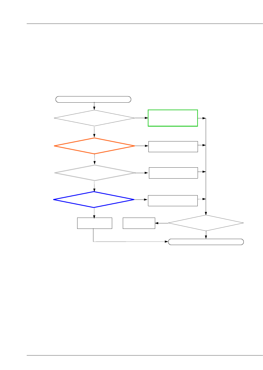
8-3-9. GSM850/900 TX
Put more lead solder
each terminal
Check the connection
R106 Put more lead solder
each terminal
Put more lead solder
each terminal
NO
YES
NO
NO
YES
YES
Check TCXO CLOCK
@C112=19.2MHz?
YES
NO
Can't make acall in GSM network
NORMAL CONDITION
catch the channel?
END
Can Phone make acall
GSM network?
YES
Back to
previous step
Replace Board(PBA)
NO
Put more lead solder
@L105,C114,C189,L111,
L110,C113,C115,L107
SAMSUNG Proprietary-Contents may change without notice
Level 3Repair
8-19
This Document can not be used without Samsung's authorization
Check the voltage
PAM100 @C116≥3.0V ?
8-3-10. DCS/ PCS TX
Put more lead solder
each terminal
heck the connection
R105 Put more lead solder
each terminal
Put more lead solder
each terminal
NO
YES
NO
NO
YES
YES
Check TCXO CLOCK
@C112=19.2MHz?
YES
NO
Can't make acall in DCS/PCS network
NORMAL CONDITION
catch the channel?
END
Can Phone make acall
DCS/PCS network?
YES
Back to
previous step
Replace Board(PBA)
NO
Put more lead solder
@L105,C114,C189,L111,
L110,C113,C115,L107
SAMSUNG Proprietary-Contents may change without notice
Level 3Repair
8-20
This Document can not be used without Samsung's authorization
Check the connection
L131,C114,C126,L117
8-3-11. WCDMA BAND 8TX
Put more lead solder
each terminal
Check the connection
C162,C127,C128 Put more lead solder
each terminal
Put more lead solder
each terminal
NO
YES
NO
NO
YES
YES
Check TCXO CLOCK
@C112=19.2MHz?
YES
NO
Can't make acall in WCDMA900 network
NORMAL CONDITION
catch the channel?
END
Can Phone make acall
WCDMA900 network?
YES
Back to
previous step
Replace Board(PBA)
NO
Put more lead solder
@L105,C114,C189,L111,
L110,C113,C115,L107
SAMSUNG Proprietary-Contents may change without notice
Level 3Repair
8-21
This Document can not be used without Samsung's authorization
Check the connection
C145,L124,L132,C147
8-3-12. WCDMA BAND 1TX
Put more lead solder
each terminal
Check the connection
C162,L123,C150,C146 Put more lead solder
each terminal
Put more lead solder
each terminal
NO
YES
NO
NO
YES
YES
Check TCXO CLOCK
@C112=19.2MHz?
YES
NO
Can't make acall in WCDMA2100 network
NORMAL CONDITION
catch the channel?
END
Can Phone make acall
WCDMA2100 network?
YES
Back to
previous step
Replace Board(PBA)
NO
Put more lead solder
@L105,C114,C189,L111,
L110,C113,C115,L107
SAMSUNG Proprietary-Contents may change without notice
Level 3Repair
8-22
This Document can not be used without Samsung's authorization
SAMSUNG Proprietary-Contents may change without notice
Level 3Repair
8-23
This Document can not be used without Samsung's authorization
SAMSUNG Proprietary-Contents may change without notice
Level 3Repair
8-24
This Document can not be used without Samsung's authorization
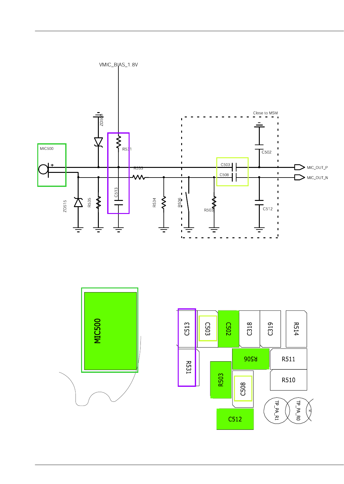
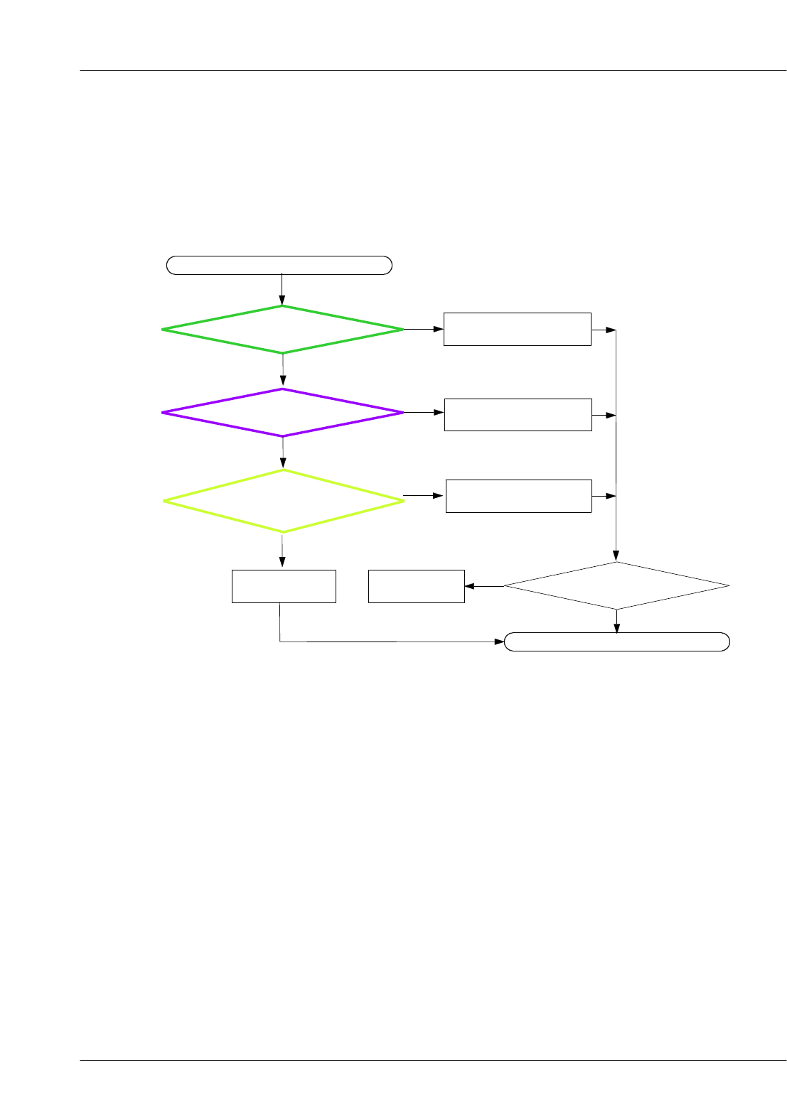
Check the connection
C503, C508
8-3-13. Microphone
Put more lead solder
each terminal
Check voltage
@R531≒1.8V ? Put more lead solder
@C531,C513
NO
YES
NO
NO
YES
YES
Microphone does not work
Is the connection of
MIC500 O.K ?
END
Does MIC work well?
(ex.voice recording)
YES
Back to
previous step
Replace Board(PBA)
NO
Put more lead solder
@MIC500
SAMSUNG Proprietary-Contents may change without notice
Level 3Repair
8-25
This Document can not be used without Samsung's authorization
SAMSUNG Proprietary-Contents may change without notice
Level 3Repair
8-26
This Document can not be used without Samsung's authorization
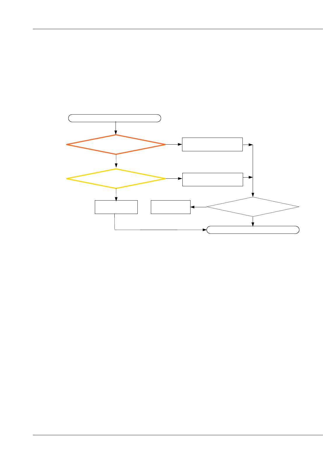
Check the connection
C507,L507
8-3-14. Earphone MIC
Put more lead solder
each terminal
Check voltage
@C500≒1.8V ? Put more lead solder
@R500
NO
YES
NO
NO
YES
YES
Earphone MIC does not work
Is the connection of
Earphone MIC O.K ?
END
Does MIC work well?
(ex.voice recording)
YES
Back to
previous step
Replace Board(PBA)
NO
1. contact Earphone in Earjack
connector again
2. Replace Earjack connector
SAMSUNG Proprietary-Contents may change without notice
Level 3Repair
8-27
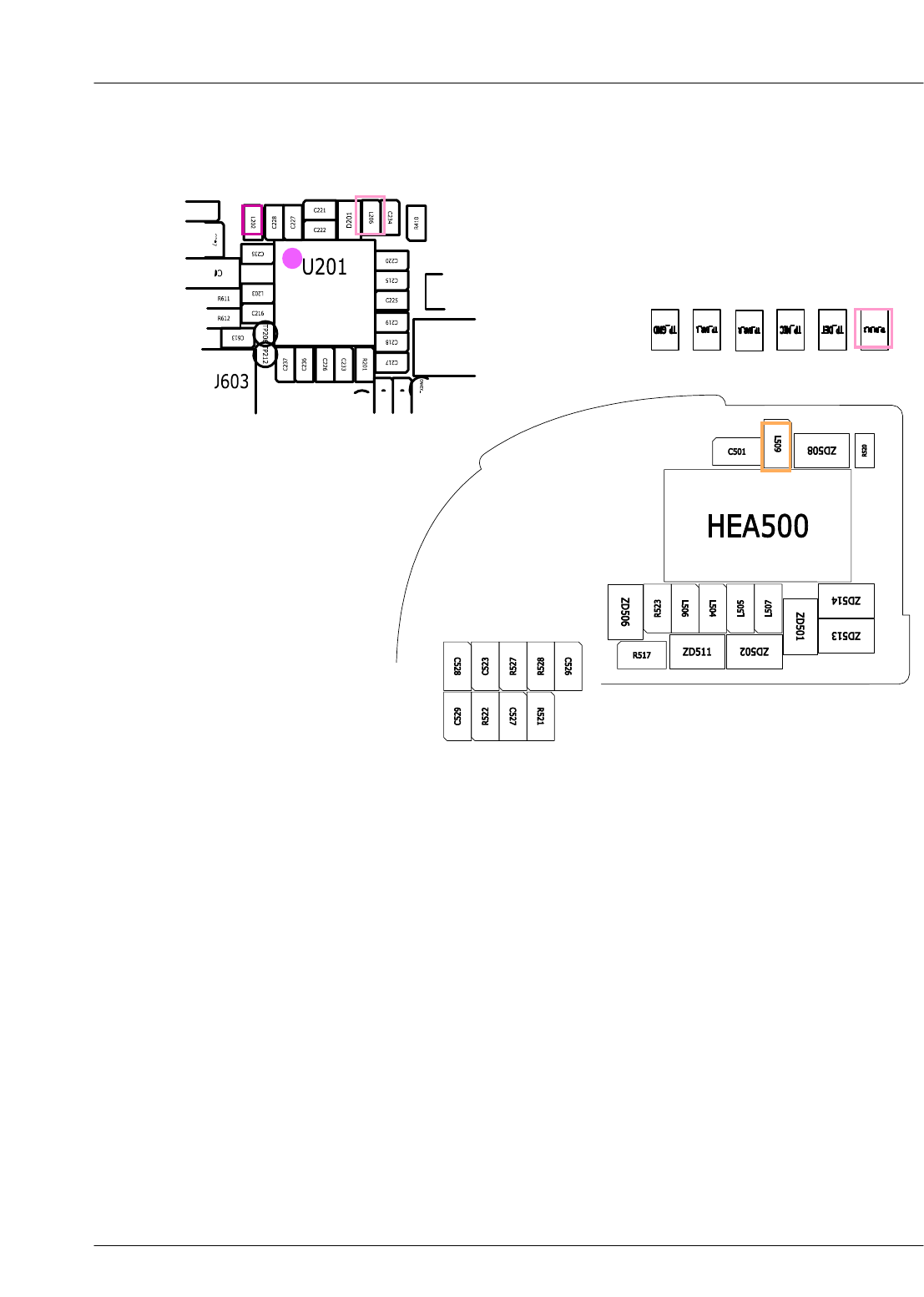
This Document can not be used without Samsung's authorization
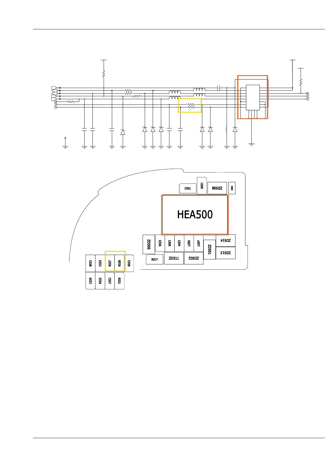
ZD506
TP_MIC
TP_EAR_R
C527
TP_DET
C528
R517
VREG_MSMP_2.6V
C529
ZD501
ZD502
R522
ZD514
TP_GND
ZD508
R523
R520
C501
L509
R528
L506
L505
R521 L504
C526
L507
R527
TP_EAR_L
ZD513
R524
88
99
17NC
NC
18
19NC
NC
20
VREG_MSMP_2.6V
15
15 16 16
22
3344
5566
77
11
1010
1111 1212
13 13 14
14
HEA500
C523
VLCD_2.85V
TP_FM_IN_2
ZD511
FM_ANT
RCV_N
RCV_P
EAR_SPK_L
EAR_SPK_R
EAR_MIC_P
JACK_INT_N
PROXI_IN
T
I2C_SCL
EAR_ADC_3.5
I2C_SDA
SAMSUNG Proprietary-Contents may change without notice
Level 3Repair
8-28
This Document can not be used without Samsung's authorization
8-3-15. Receiver
Check the connection
R527,R528 Put more lead solder
@R527,R528
NO
YES
NO
YES
There is no sound from Receiver(call)
Is the connection of
Receiver(HEA500) O.K ?
END
Can hear sound
from Receiver?
YES
Back to
previous step
Replace Board(PBA)
NO
1. contact receiver again
2. Replace receiver
SAMSUNG Proprietary-Contents may change without notice
Level 3Repair
8-29
This Document can not be used without Samsung's authorization
ZD506
TP_MIC
TP_EAR_R
C527
TP_DET
C528
R517
VREG_MSMP_2.6V
C529
ZD501
ZD502
R522
ZD514
TP_GND
ZD508
R523
R520
C501
L509
R528
L506
L505
R521 L504
C526
L507
R527
TP_EAR_L
ZD513
R524
88
99
17NC
NC
18
19NC
NC
20
VREG_MSMP_2.6V
15
15 16 16
22
3344
5566
77
11
1010
1111 1212
13 13 14
14
HEA500
C523
VLCD_2.85V
TP_FM_IN_2
ZD511
FM_ANT
RCV_N
RCV_P
EAR_SPK_L
EAR_SPK_R
EAR_MIC_P
JACK_INT_N
PROXI_IN
T
I2C_SCL
EAR_ADC_3.5
I2C_SDA
SAMSUNG Proprietary-Contents may change without notice
Level 3Repair
8-30
This Document can not be used without Samsung's authorization
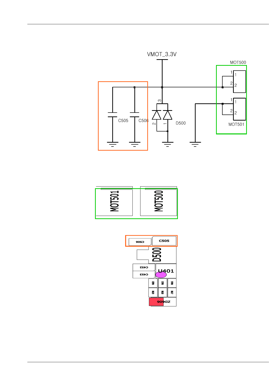
8-3-16. Speaker, Motor
NO
YES
Is the connection of
Speaker Module O.K ?1. contact Speaker Module
again
There is no sound from Speaker(play songs)
Replace Speaker Module
END
Is there problem
at Speaker Module?
YES
Back to
previous step
Replace Board(PBA)
Still no sound from
Speaker?
NO
NO
NO
YES
There is no vibration from vibration motor
Is the connection of
motor O.K?
END
Is there problem
at vibration?
YES
Replace Board(PBA)
NO
1. Check motor
contact(MOT500/501)
2. Check if motor lied on the
'rear' appropriately
Replace vibration motor
Is the
voltage(@C505,C506) 3.3V?
NO
YES
SAMSUNG Proprietary-Contents may change without notice
Level 3Repair
8-31
This Document can not be used without Samsung's authorization
SAMSUNG Proprietary-Contents may change without notice
Level 3Repair
8-32
This Document can not be used without Samsung's authorization
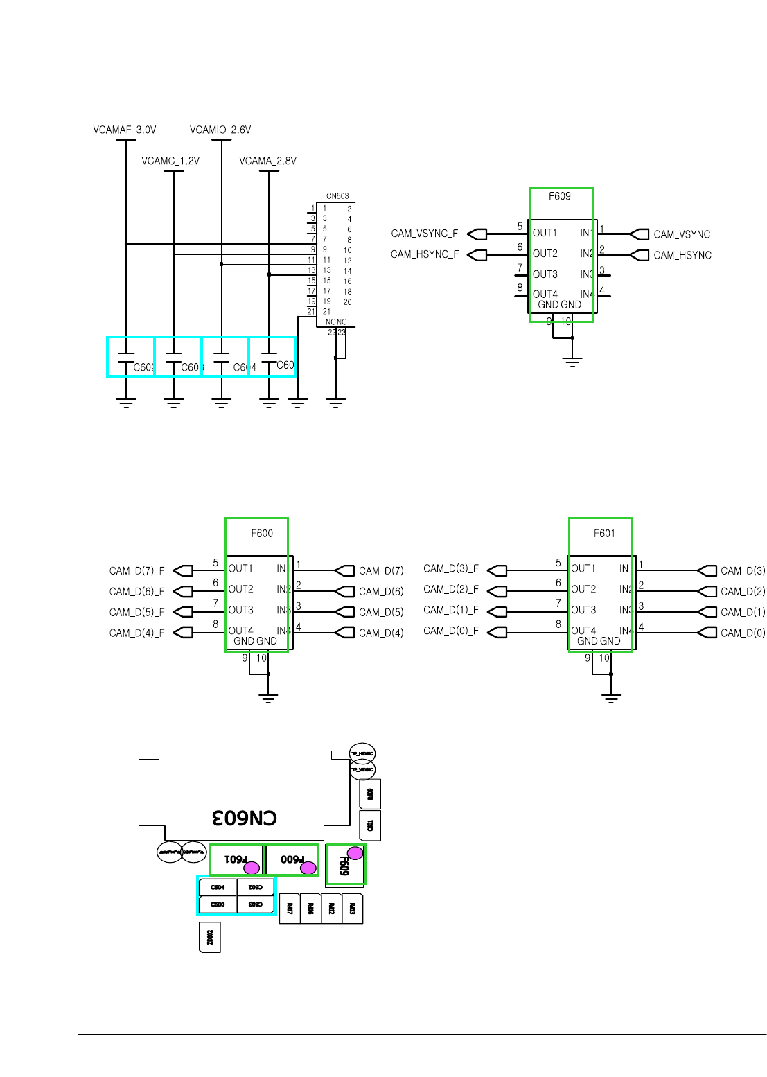
8-3-17. Camera
CASE 1
CASE 2
Check the connection
C602,C603,C604,C600 Put more lead solder
each terminal
NO
YES
NO
YES
Occur 'Camera fail'pop-up
Is the connection of
Camera O.K ?
END
Can enter camera
mode?
YES
Back to
previous step
Replace Board(PBA)
NO
1. contact Camera again
2. Replace Camera
Check the connection
F600, F601, F609 Put more lead solder
each terminal
NO
YES
NO
YES
unusual color when phone camera mode
Is the connection of
Camera O.K ?
END
when camera mode,
normal color?
YES
Replace Board(PBA)
NO
1. contact Camera again
2. Replace Camera
Back to
previous step
SAMSUNG Proprietary-Contents may change without notice
Level 3Repair
8-33
This Document can not be used without Samsung's authorization
SAMSUNG Proprietary-Contents may change without notice
Level 3Repair
8-34
This Document can not be used without Samsung's authorization
Check the voltage
@C202=1.2V?
Check the connection
L509
8-3-18. FM radio
Put more lead solder
each terminal
Check the connection
fromTP_FM_IN_2 to L206
Put more lead solder
each terminal
NO
YES
NO
NO
YES
YES
FM Radio does not work well
Is the connection of
earphone O.K ?
END
Can you turn on
and search channel?
YES
Back to
previous step
Replace Board(PBA)
NO
1. contact earphone again
2. Replace earphone
Put more lead solder
each terminal
NO
SAMSUNG Proprietary-Contents may change without notice
Level 3Repair
8-35
This Document can not be used without Samsung's authorization
ZD506
TP_MIC
TP_EAR_R
C527
TP_DET
C528
R517
VREG_MSMP_2.6V
C529
ZD501
ZD502
R522
ZD514
TP_GND
ZD508
R523
R520
C501
L509
R528
L506
L505
R521 L504
C526
L507
R527
TP_EAR_L
ZD513
R524
88
99
17NC
NC
18
19NC
NC
20
VREG_MSMP_2.6V
15
15 16 16
22
3344
5566
77
11
1010
1111 1212
13 13 14
14
HEA500
C523
VLCD_2.85V
TP_FM_IN_2
ZD511
FM_ANT
RCV_N
RCV_P
EAR_SPK_L
EAR_SPK_R
EAR_MIC_P
JACK_INT_N
PROXI_IN
T
I2C_SCL
EAR_ADC_3.5
I2C_SDA
SAMSUNG Proprietary-Contents may change without notice
Level 3Repair
8-36
This Document can not be used without Samsung's authorization
SAMSUNG Proprietary-Contents may change without notice
Level 3Repair
8-37
This Document can not be used without Samsung's authorization
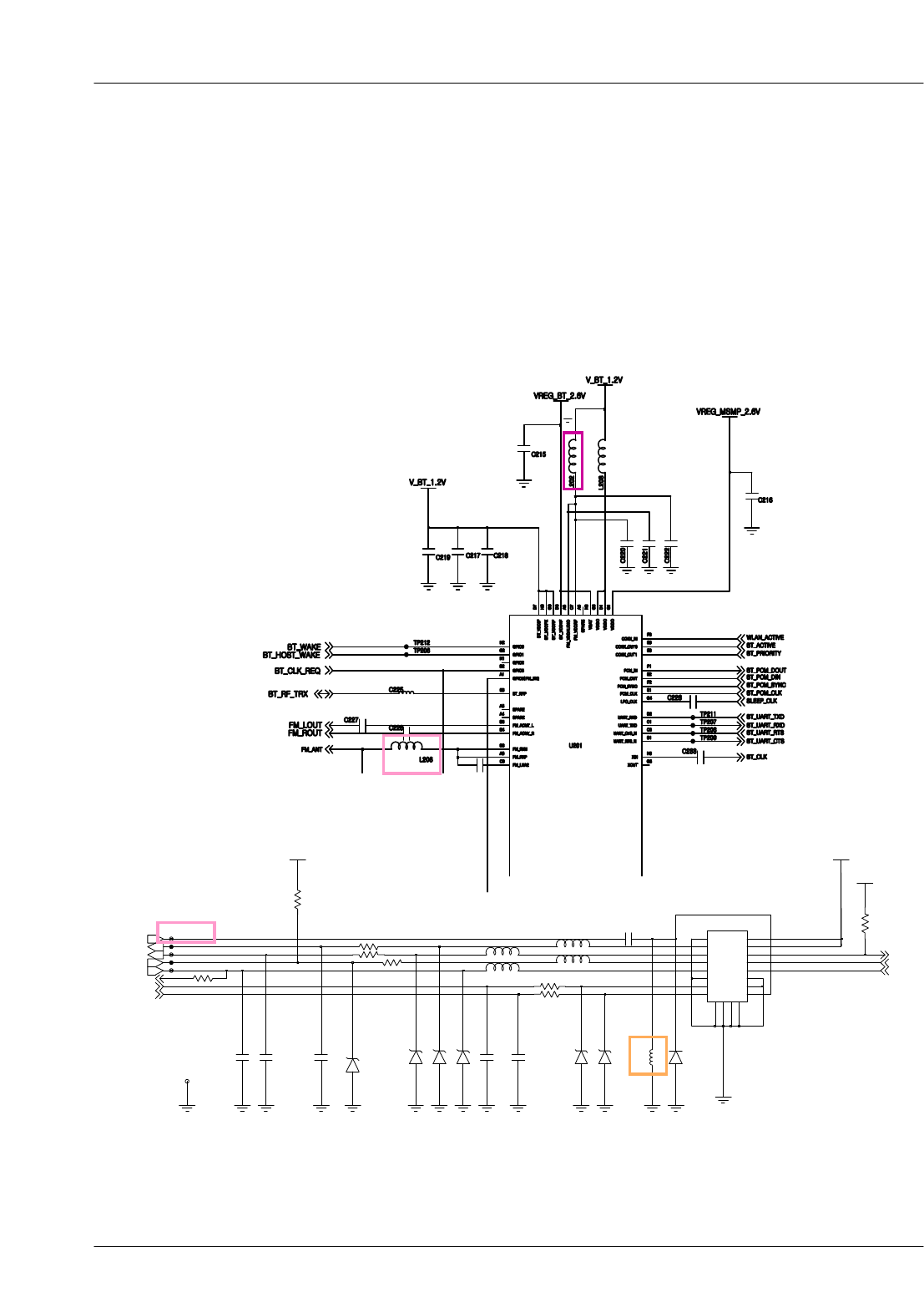
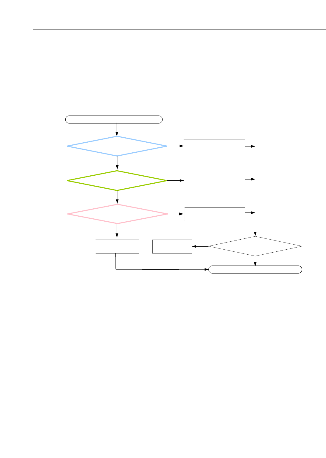
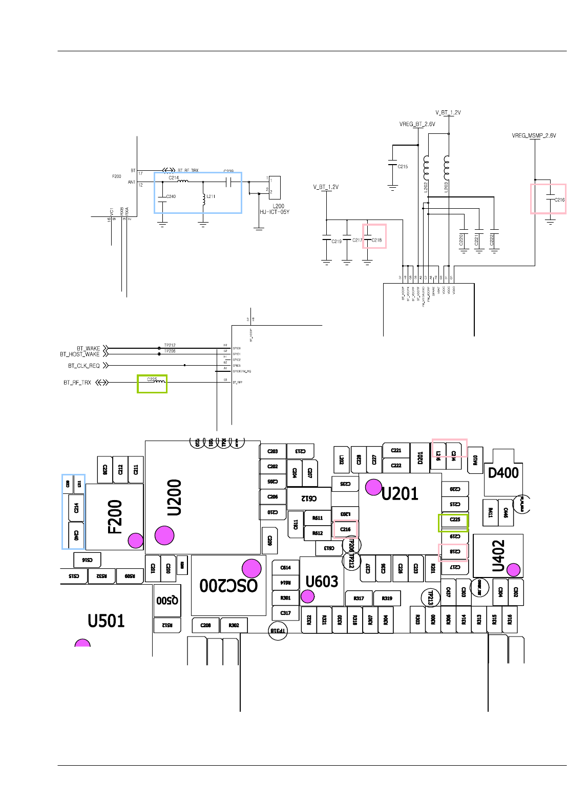
@C218=1.2V?
@C216=2.6V?
8-3-19. Bluetooth
Put more lead solder
each terminal
Check the connection
C225 Put more lead solder
each terminal
NO
YES
NO
NO
YES
YES
Can't activate or search any Bluetooth devices
Check the connection
C239,L211,C214
END
Can it Bluetooth
activating &searching?
YES
Back to
previous step
Replace Board(PBA)
NO
1. Put more lead solder
each terminal
2. Replace BT_ANT
SAMSUNG Proprietary-Contents may change without notice
Level 3Repair
8-38
This Document can not be used without Samsung's authorization
SAMSUNG Proprietary-Contents may change without notice
Level 3Repair
8-39
This Document can not be used without Samsung's authorization
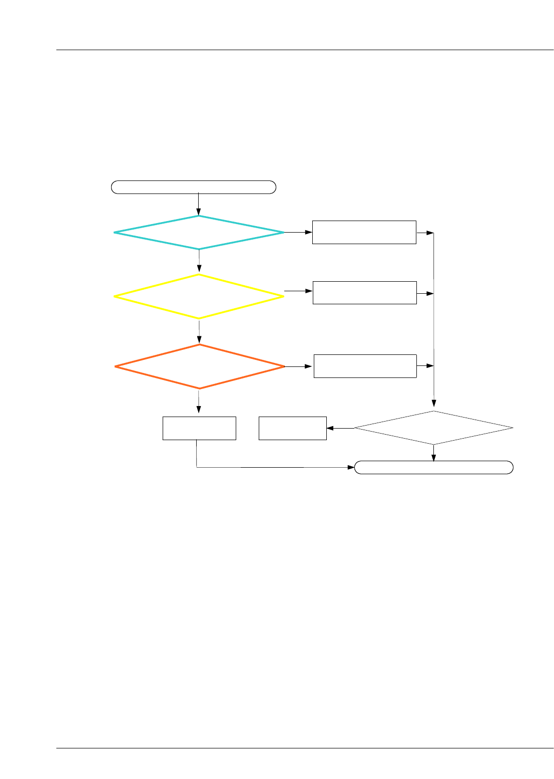
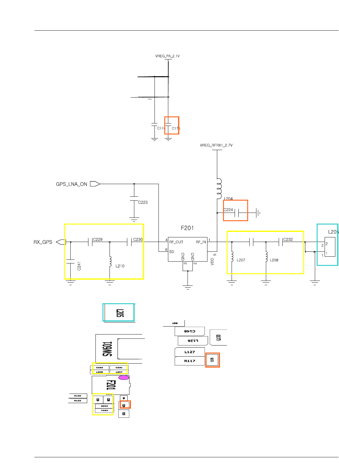
Check the voltage
@C224=2.7V?
@C175=2.7V
8-3-20. GPS
Put more lead solder
each terminal
Is the soldered status of
C232,C231,L207
C230,C229,C241
Put more lead solder
each terminal
NO
YES
NO
NO
YES
YES
GPS does not work
Is the soldered status of
L205 O.K?
END
Does GPS work well?
YES
Back to
previous step
Replace Board(PBA)
NO
1. Put more lead solder
2. Replace L205
SAMSUNG Proprietary-Contents may change without notice
Level 3Repair
8-40
This Document can not be used without Samsung's authorization
SAMSUNG Proprietary-Contents may change without notice
Level 3Repair
8-41
This Document can not be used without Samsung's authorization
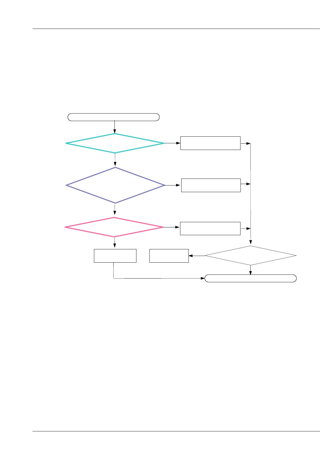
Check the Voltage
@C211=3.3V?
@C206=1.8V?
8-3-21. Wi-Fi Rx/ Tx
Put more lead solder
each terminal
Put more lead solder
each terminal
NO
YES
NO
YES
Check TCXO CLOCK
@C208,C209=26MHz?
YES
NO
Wi-Fi does not work
Check the connection
C239,L211,C214
END
Can it wifi
activation &searching?
YES
Back to
previous step
Replace Board(PBA)
NO
1. Put more lead solder
each terminal
2. Replace BT_ANT
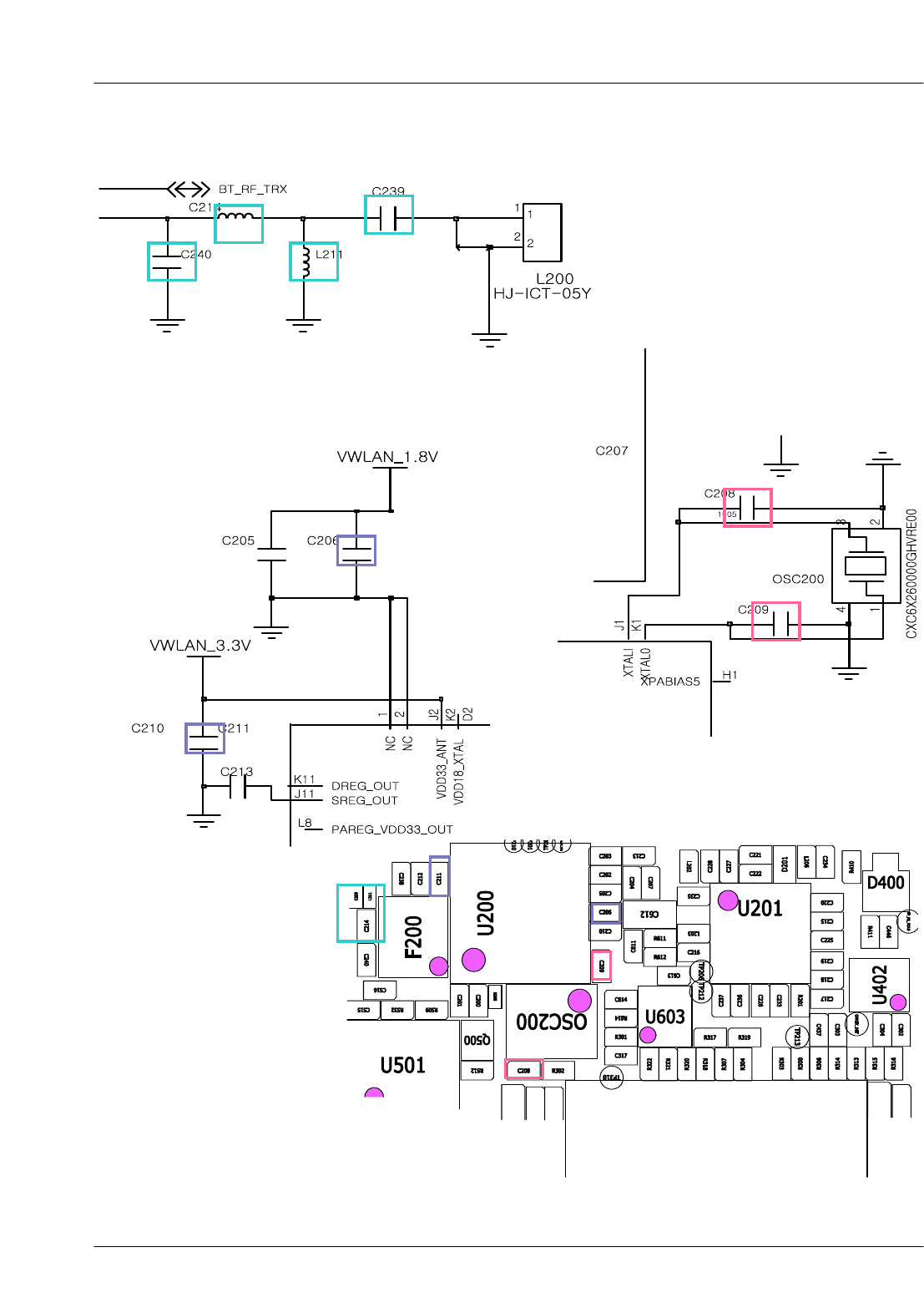
SAMSUNG Proprietary-Contents may change without notice
Level 3Repair
8-42
This Document can not be used without Samsung's authorization
SAMSUNG Proprietary-Contents may change without notice
Level 3Repair
8-43
This Document can not be used without Samsung's authorization
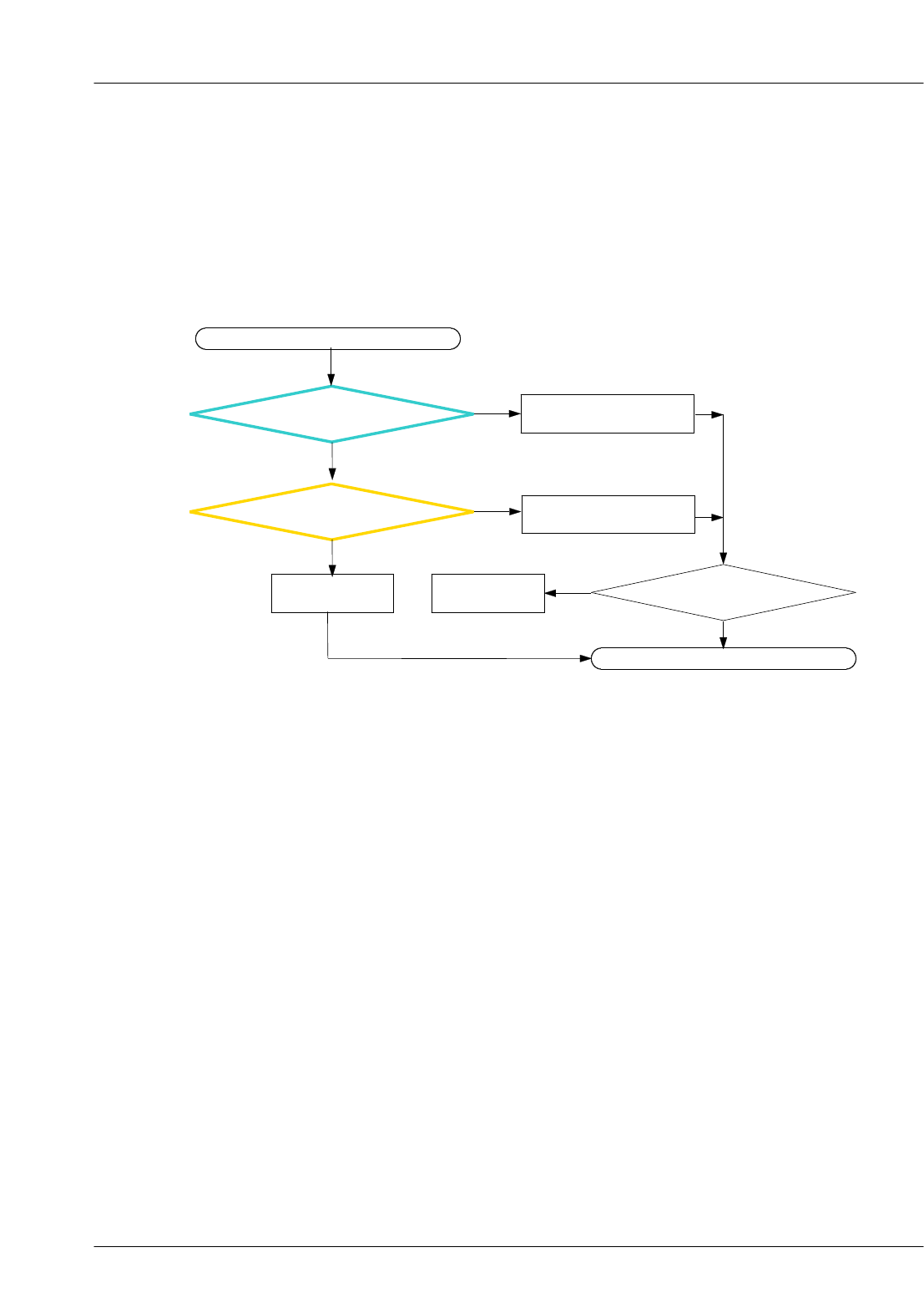
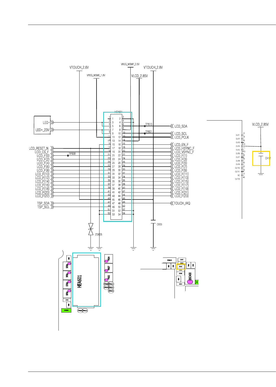
8-3-22. LCD
Check the connection
C412 Put more lead solder
each terminal
NO
YES
NO
YES
LCD does not work
Is the connection of LCD
O.K ?
END
Does LCD work well?
YES
Back to
previous step
Replace Board(PBA)
NO
1. contact LCD again
2. Replace LCD
SAMSUNG Proprietary-Contents may change without notice
Level 3Repair
8-44
This Document can not be used without Samsung's authorization
SAMSUNG Proprietary-Contents may change without notice
Level 3Repair
8-45
This Document can not be used without Samsung's authorization
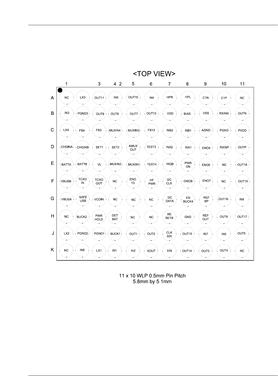
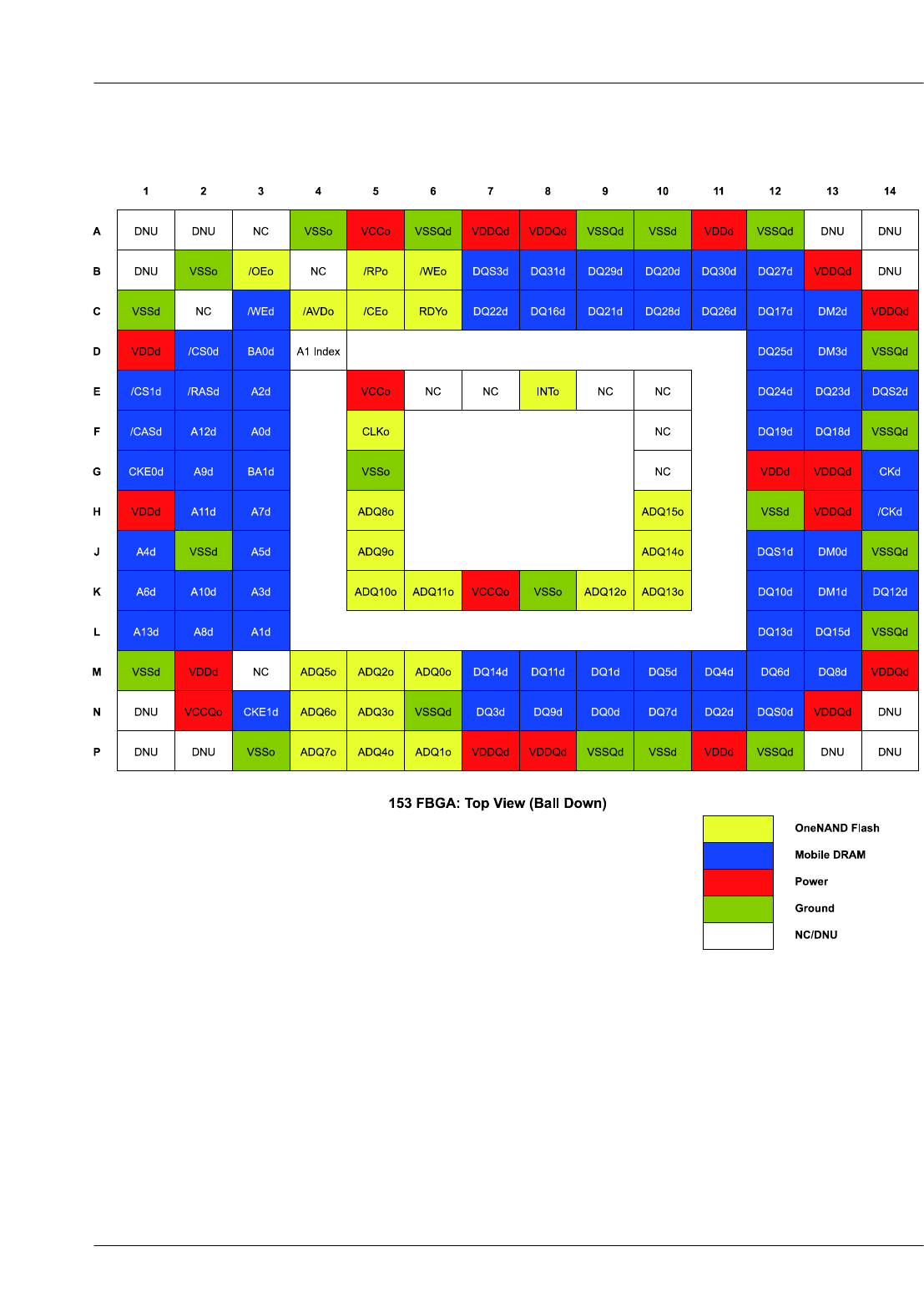
8-4. Schematic Diagram
-NC Point
U400
SAMSUNG Proprietary-Contents may change without notice
Level 3Repair
8-46
This Document can not be used without Samsung's authorization
UME300