Samsung GT C3510 Service Manual. Www.s Manuals.com. Manual
User Manual: Smartphone Samsung GT-C3510 - Service manuals and Schematics, Disassembly / Assembly. Free.
Open the PDF directly: View PDF ![]() .
.
Page Count: 71

GSM TELEPHONE
GT-C3510
1. Safety Precautions
2. Specification
3. Product Function
4. Array course control
5. Exploded View and Parts list
6. MAIN Electrical Parts List
7. Block Diagrams
8. PCB Diagrams
9. Chart of Troubleshooting
10. Reference data
11. Disassembly and Assembly
Instructions
GSM TELEPHONE CONTENTS
This Service Manual is aproperty of Samsung Electronics Co.,Ltd.
Any unauthorized use of Manual can be punished under applicable
International and/or domestic law.
Samsung Electronics Co.,Ltd.
2009. 12. Rev.1.0
ⓒ
Country Web Site
North America service.samsungportal.com
Latin America latin.samsungportal.com
CIS cis.samsungportal.com
Europe europe.samsungportal.com
China china.samsungportal.com
Asia asia.samsungportal.com
Mideast &Africa mea.samsungportal.com
GSPN (Global Service Partner Network)
SAMSUNG Proprietary-Contents may change without notice
11. Disassembly and Assembly Instructions
11-1
This Document can not be used without Samsung's authorization
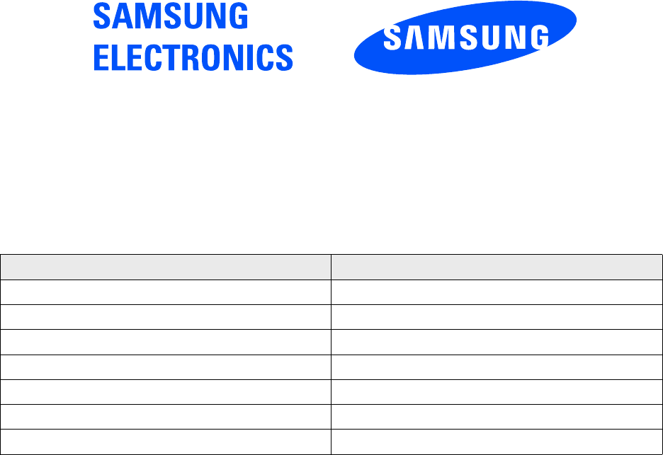
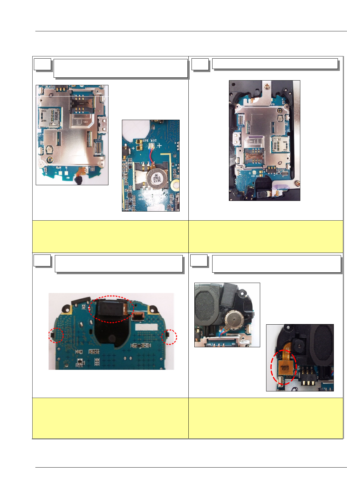
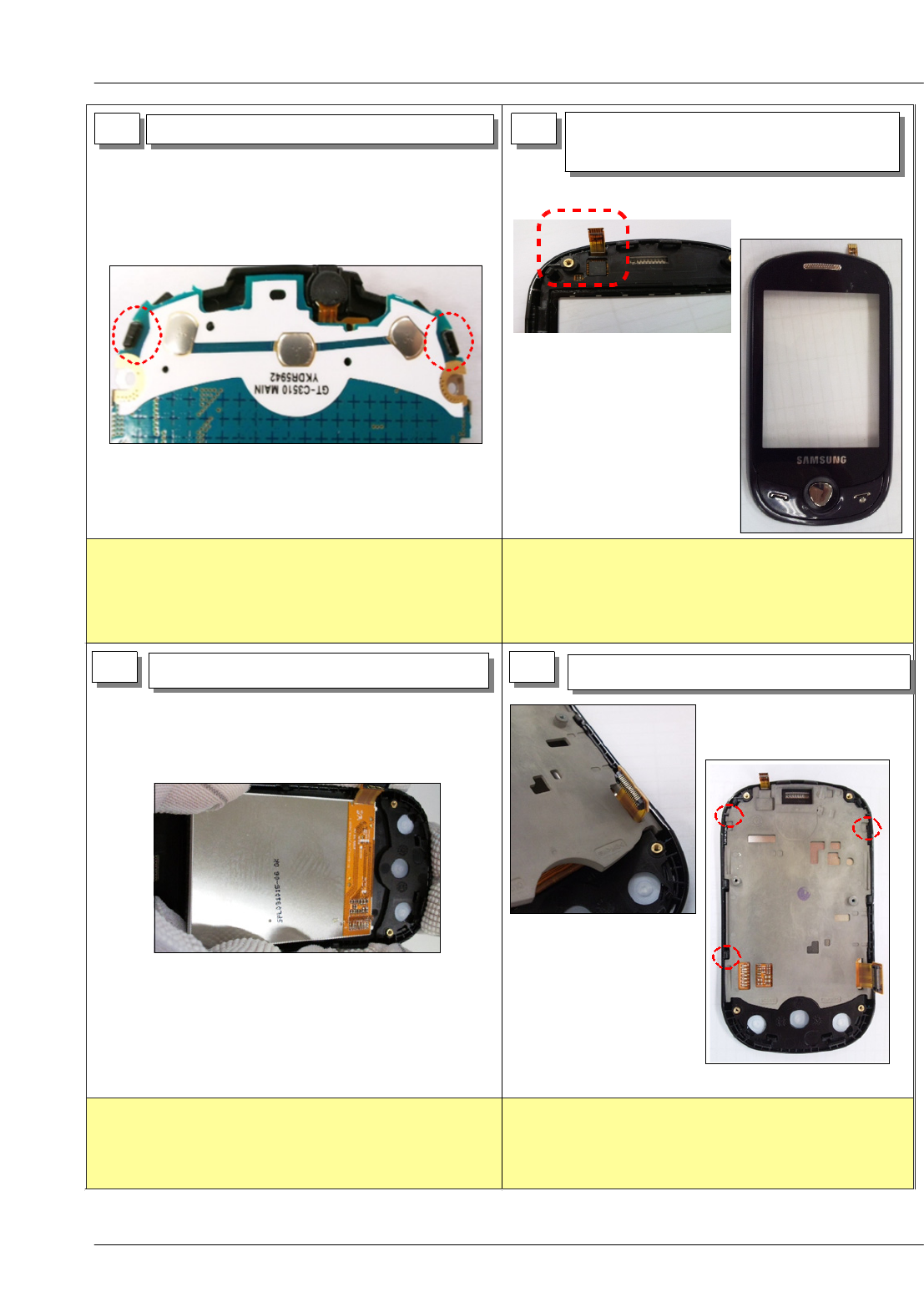
11-1. Disassembly
※Caution
1) Be careful not to make scratch and molding
damage.
※Caution
1) Be careful not to make scratch and molding
damage.
※Caution
1) Be careful not to make damage to INTENNA
※Caution
1) Be careful not to make scratch and molding
damage.
1) Unscrew the 6points.
1
1) Perform TSP FPCB visual check
2
34
1) Separate the rear case.
1) Separate the LCD connectors, then
unhook at the 4points.
After
disassembling the
rear case, check
the TSP FPCB
damage.
Be careful not to damage the SMD material.
Don't use DISASSEMBLE JIG deeply.
SAMSUNG Proprietary-Contents may change without notice
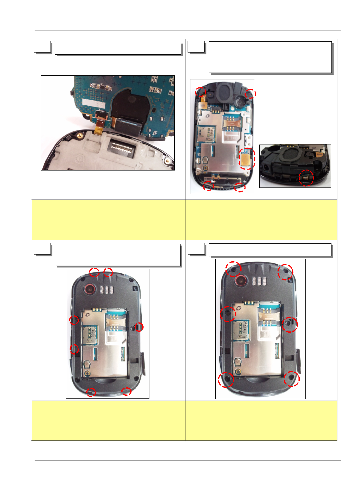
Exploded View and Parts List
11-2
This Document can not be used without Samsung's authorization
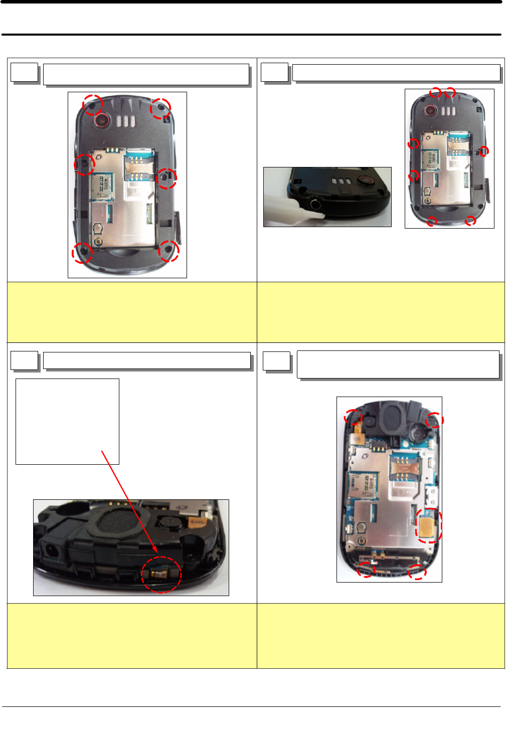
※Caution
1) Be careful not to make scratch and molding
damage.
※Caution
1) Be careful not to make scratch and molding
damage.
2) Be careful not to damage the PBA.
※Caution
1) Be careful not to damage LCD FPCB. ※Caution
5 6
78
1) After lifting PBA upward,
disassemble TSP FPCB under the board.
1) Separate PBA and the front Assembly.
1) Separate bracket hooks on 3points
2) Separate LCD connector from the bracket.
1) Lift LCD top and separate it from the
front case.
SAMSUNG Proprietary-Contents may change without notice
Exploded View and Parts List
11-3
This Document can not be used without Samsung's authorization
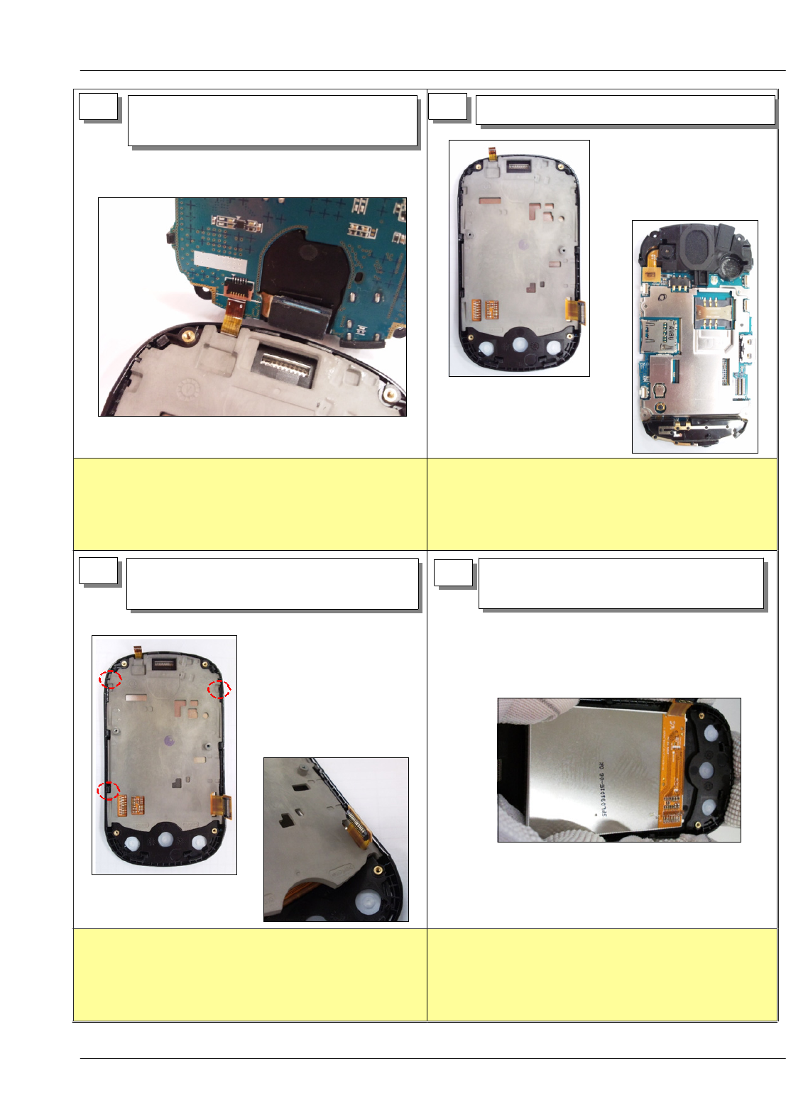
※Caution
1) Be careful not to make intenna hook damage.
※Caution
1) Be careful not to make SPK Hook damage.
※Caution
1) Be careful not to damage FPCB. ※Caution
910
11 12
1) Disassemble intenna's left/right hooks
on 2points.
1) Separate camera connector.
2) Disassemble SPK Carrier's left/right hooks
on 2points and remove solder.
1) Remove RCV/MIC solder. 1) Remove screw at 1point
2) Separate the motor/shield can from the
PBA.
SAMSUNG Proprietary-Contents may change without notice
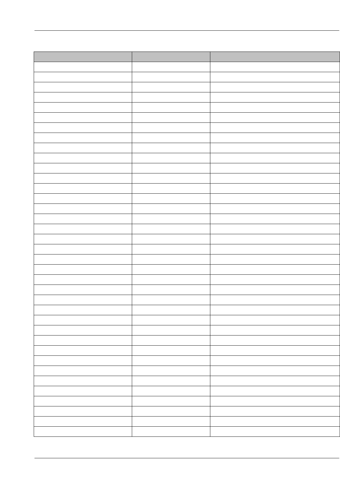
Exploded View and Parts List
11-4
This Document can not be used without Samsung's authorization
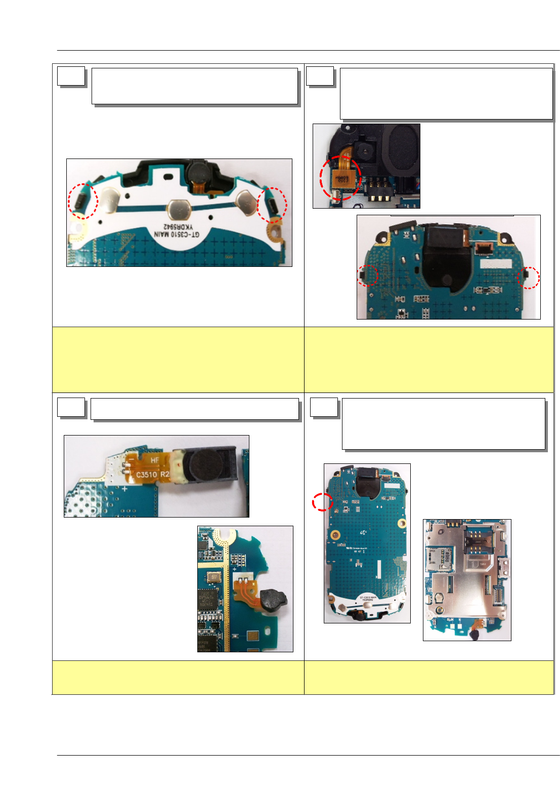
※Caution
1) Be careful not to damage the FPCB.
※Caution
1) Be careful not to damage the receiver FPCB
&SPK WIRE.
※Caution
1) Confirm receiver's location
2) Be careful not to make SPK Hook damage.
※Caution
1) Be careful not to damage PBA.
11-2. Assembly
1 2
3 4
1) Assemble the shield can and screw at 1point
2) Solder the motor
1) Solder the receiver and Mic.
1) Solder and assemble the speaker module
and PBA.
1) Assemble the camera carrier.
2) Assemble the motor.
SAMSUNG Proprietary-Contents may change without notice
Exploded View and Parts List
11-5
This Document can not be used without Samsung's authorization
※Caution
1) Be careful not to make Intenna hook damage.
※Caution
1) Be careful not to damage the motor wire .
※Caution
1) Be careful not to damage LCD.
※Caution
1) Be careful not to damage to LCD connector.
5 6
7 8
1) Assemble the Intenna to PBA 1) Attach the TSP.
2) Assemble the keypad
1) Attach and assemble the LCD 1) Assemble the bracket.
SAMSUNG Proprietary-Contents may change without notice
Exploded View and Parts List
11-6
This Document can not be used without Samsung's authorization
※Caution
1) Be careful not to damage TSP FPCB.
※Caution
1) Be careful not to make scratch and molding
damage.
2)Be careful not to damage TSP FPCB.
※Caution
1)Be careful not to make scratch and molding
damage.
※Caution
1)Be careful not to make scratch and molding
damage.
910
11 12
1) Assemble TSP FPCB to PBA connector. 1) Locate and make sure of assembly hooks
after placing PBA on the top.
2) Assemble LCD connector
1) Confirm assembly hooks after assembling
the rear case.
1) Screw at 6points

SAMSUNG Proprietary-Contents may change without notice
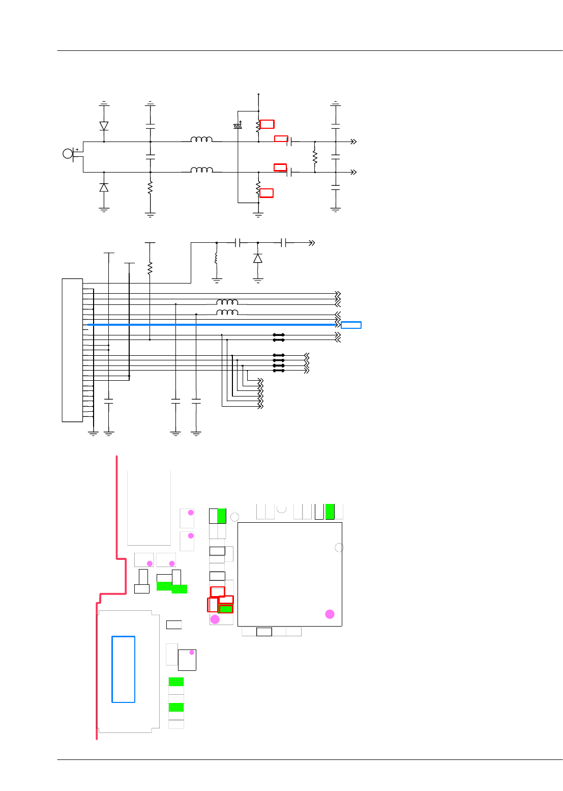
6. MAIN Electrical Parts List
6-1
This Document can not be used without Samsung's authorization
SEC CODE DESIGN LOC DESCRIPTION
0403-001547 ZD301 DIODE-ZENER
0406-001286 ZD405 DIODE-TVS
0406-001286 ZD406 DIODE-TVS
0406-001293 ZD400 DIODE-TVS
0406-001293 ZD402 DIODE-TVS
0406-001293 ZD500 DIODE-TVS
0406-001293 ZD501 DIODE-TVS
0406-001293 ZD502 DIODE-TVS
0406-001293 ZD503 DIODE-TVS
0406-001329 D400 DIODE-TVS
0406-001361 ZD300 DIODE-TVS
0505-001325 Q400 FET-SILICON
1003-002047 U400 IC-MOTOR DRIVER
1108-000297 UME200 IC-MCP
1201-002933 PAM100 IC-POWER AMP
1203-005728 U302 IC-POWER SUPERVISOR
1203-005770 U300 IC-MULTI REG
1203-006077 U301 IC-BACKLIGHT DRIVER
1205-003310 U103 IC-TRANSCEIVER
1205-003874 UCP200 IC-MODEM
1205-003883 U100 IC-BLUETOOTH
1404-001221 VR200 THERMISTOR-NTC
2007-000140 R207 R-CHIP
2007-000141 R303 R-CHIP
2007-000141 R401 R-CHIP
2007-000141 R409 R-CHIP
2007-000141 R416 R-CHIP
2007-000141 R420 R-CHIP
2007-000143 R309 R-CHIP
2007-000143 R402 R-CHIP
2007-000143 R417 R-CHIP
2007-000148 R104 R-CHIP
2007-000148 R105 R-CHIP
2007-000148 R315 R-CHIP
2007-000149 R206 R-CHIP
2007-000149 R314 R-CHIP
2007-000152 R318 R-CHIP

SAMSUNG Proprietary-Contents may change without notice
Main Electrical Parts List
6-2
This Document can not be used without Samsung's authorization
SEC CODE DESIGN LOC DESCRIPTION
2007-000152 R319 R-CHIP
2007-000152 R427 R-CHIP
2007-000157 R107 R-CHIP
2007-000157 R108 R-CHIP
2007-000157 R313 R-CHIP
2007-000159 R310 R-CHIP
2007-000159 R311 R-CHIP
2007-000159 R312 R-CHIP
2007-000159 R316 R-CHIP
2007-000160 R100 R-CHIP
2007-000160 R200 R-CHIP
2007-000165 R425 R-CHIP
2007-000166 R317 R-CHIP
2007-000170 R407 R-CHIP
2007-000170 R415 R-CHIP
2007-000170 R426 R-CHIP
2007-000173 R320 R-CHIP
2007-000566 R201 R-CHIP
2007-001292 R300 R-CHIP
2007-001292 R301 R-CHIP
2007-001319 R202 R-CHIP
2007-001319 R203 R-CHIP
2007-001319 R204 R-CHIP
2007-001319 U401 R-CHIP
2007-001333 R304 R-CHIP
2007-001333 R306 R-CHIP
2007-001333 R429 R-CHIP
2007-001333 R440 R-CHIP
2007-001339 R307 R-CHIP
2007-002970 R102 R-CHIP
2007-002970 R103 R-CHIP
2007-007573 R302 R-CHIP
2007-007875 R308 R-CHIP
2007-008354 R305 R-CHIP
2203-000233 C106 C-CER,CHIP
2203-000233 C400 C-CER,CHIP
2203-000233 C509 C-CER,CHIP

SAMSUNG Proprietary-Contents may change without notice
Main Electrical Parts List
6-3
This Document can not be used without Samsung's authorization
SEC CODE DESIGN LOC DESCRIPTION
2203-000254 C108 C-CER,CHIP
2203-000254 C111 C-CER,CHIP
2203-000254 C203 C-CER,CHIP
2203-000311 C340 C-CER,CHIP
2203-000386 C335 C-CER,CHIP
2203-000386 C338 C-CER,CHIP
2203-000386 C401 C-CER,CHIP
2203-000386 C402 C-CER,CHIP
2203-000386 C410 C-CER,CHIP
2203-000386 C411 C-CER,CHIP
2203-000386 C431 C-CER,CHIP
2203-000386 C432 C-CER,CHIP
2203-000438 C209 C-CER,CHIP
2203-000438 C437 C-CER,CHIP
2203-000438 C438 C-CER,CHIP
2203-000585 C428 C-CER,CHIP
2203-000585 C433 C-CER,CHIP
2203-000585 C434 C-CER,CHIP
2203-000679 C117 C-CER,CHIP
2203-000725 C423 C-CER,CHIP
2203-000812 C103 C-CER,CHIP
2203-000812 C105 C-CER,CHIP
2203-000812 C144 C-CER,CHIP
2203-000812 C148 C-CER,CHIP
2203-000854 C348 C-CER,CHIP
2203-000854 C349 C-CER,CHIP
2203-000854 C405 C-CER,CHIP
2203-000854 C414 C-CER,CHIP
2203-000995 C134 C-CER,CHIP
2203-002709 C429 C-CER,CHIP
2203-002709 C430 C-CER,CHIP
2203-005050 C114 C-CER,CHIP
2203-005053 C121 C-CER,CHIP
2203-005234 C147 C-CER,CHIP
2203-005281 C123 C-CER,CHIP
2203-005281 C128 C-CER,CHIP
2203-005288 C101 C-CER,CHIP

SAMSUNG Proprietary-Contents may change without notice
Main Electrical Parts List
6-4
This Document can not be used without Samsung's authorization
SEC CODE DESIGN LOC DESCRIPTION
2203-005288 C120 C-CER,CHIP
2203-005288 C122 C-CER,CHIP
2203-005395 C100 C-CER,CHIP
2203-005450 C202 C-CER,CHIP
2203-005450 C207 C-CER,CHIP
2203-005480 C320 C-CER,CHIP
2203-005480 C322 C-CER,CHIP
2203-005483 C215 C-CER,CHIP
2203-006048 C107 C-CER,CHIP
2203-006048 C130 C-CER,CHIP
2203-006048 C133 C-CER,CHIP
2203-006048 C201 C-CER,CHIP
2203-006048 C204 C-CER,CHIP
2203-006048 C206 C-CER,CHIP
2203-006048 C208 C-CER,CHIP
2203-006048 C210 C-CER,CHIP
2203-006048 C211 C-CER,CHIP
2203-006048 C316 C-CER,CHIP
2203-006048 C326 C-CER,CHIP
2203-006048 C336 C-CER,CHIP
2203-006048 C347 C-CER,CHIP
2203-006048 C351 C-CER,CHIP
2203-006048 C353 C-CER,CHIP
2203-006048 C403 C-CER,CHIP
2203-006048 C406 C-CER,CHIP
2203-006048 C412 C-CER,CHIP
2203-006048 C415 C-CER,CHIP
2203-006190 C124 C-CER,CHIP
2203-006190 C125 C-CER,CHIP
2203-006190 C314 C-CER,CHIP
2203-006190 C315 C-CER,CHIP
2203-006201 C307 C-CER,CHIP
2203-006257 C113 C-CER,CHIP
2203-006260 C313 C-CER,CHIP
2203-006260 C323 C-CER,CHIP
2203-006260 C325 C-CER,CHIP
2203-006348 C301 C-CER,CHIP

SAMSUNG Proprietary-Contents may change without notice
Main Electrical Parts List
6-5
This Document can not be used without Samsung's authorization
SEC CODE DESIGN LOC DESCRIPTION
2203-006399 C200 C-CER,CHIP
2203-006399 C212 C-CER,CHIP
2203-006399 C213 C-CER,CHIP
2203-006399 C300 C-CER,CHIP
2203-006399 C302 C-CER,CHIP
2203-006399 C303 C-CER,CHIP
2203-006399 C304 C-CER,CHIP
2203-006399 C305 C-CER,CHIP
2203-006399 C308 C-CER,CHIP
2203-006399 C309 C-CER,CHIP
2203-006399 C310 C-CER,CHIP
2203-006399 C311 C-CER,CHIP
2203-006399 C312 C-CER,CHIP
2203-006399 C321 C-CER,CHIP
2203-006399 C328 C-CER,CHIP
2203-006399 C339 C-CER,CHIP
2203-006399 C350 C-CER,CHIP
2203-006399 C421 C-CER,CHIP
2203-006399 C500 C-CER,CHIP
2203-006399 C501 C-CER,CHIP
2203-006399 C502 C-CER,CHIP
2203-006399 C503 C-CER,CHIP
2203-006399 C504 C-CER,CHIP
2203-006562 C317 C-CER,CHIP
2203-006562 C324 C-CER,CHIP
2203-006562 C327 C-CER,CHIP
2203-006824 C343 C-CER,CHIP
2203-006824 C344 C-CER,CHIP
2203-006838 C205 C-CER,CHIP
2203-006838 C214 C-CER,CHIP
2203-006838 C306 C-CER,CHIP
2203-006872 C109 C-CER,CHIP
2203-006872 C110 C-CER,CHIP
2203-006872 C112 C-CER,CHIP
2203-006872 C115 C-CER,CHIP
2203-006890 C217 C-CER,CHIP
2203-006890 C318 C-CER,CHIP
SAMSUNG Proprietary-Contents may change without notice
Main Electrical Parts List
6-6
This Document can not be used without Samsung's authorization
SEC CODE DESIGN LOC DESCRIPTION
2203-006890 C330 C-CER,CHIP
2203-007279 C104 C-CER,CHIP
2203-007279 C341 C-CER,CHIP
2203-007279 C342 C-CER,CHIP
2203-007279 C352 C-CER,CHIP
2203-007279 C418 C-CER,CHIP
2203-007317 C345 C-CER,CHIP
2203-007425 C337 C-CER,CHIP
2203-007425 C439 C-CER,CHIP
2404-001377 C319 C-TA,CHIP
2404-001377 TA400 C-TA,CHIP
2404-001496 TA300 C-TA,CHIP
2409-001172 BAT300 C-ETC
2703-002170 L110 INDUCTOR-SMD
2703-002170 L113 INDUCTOR-SMD
2703-002202 L111 INDUCTOR-SMD
2703-002202 L112 INDUCTOR-SMD
2703-002202 L115 INDUCTOR-SMD
2703-002203 L109 INDUCTOR-SMD
2703-002207 L102 INDUCTOR-SMD
2703-002207 L120 INDUCTOR-SMD
2703-002208 L116 INDUCTOR-SMD
2703-002208 L121 INDUCTOR-SMD
2703-002268 L101 INDUCTOR-SMD
2703-002268 L103 INDUCTOR-SMD
2703-002269 L100 INDUCTOR-SMD
2703-002313 L106 INDUCTOR-SMD
2703-002313 L107 INDUCTOR-SMD
2703-002313 L406 INDUCTOR-SMD
2703-002313 L407 INDUCTOR-SMD
2703-002368 L118 INDUCTOR-SMD
2703-003121 L412 INDUCTOR-SMD
2703-003260 L300 INDUCTOR-SMD
2703-003476 L400 INDUCTOR-SMD
2801-004339 OSC300 CRYSTAL-SMD
2801-004893 OSC100 CRYSTAL-SMD
2901-001576 F500 FILTER-EMI/ESD
SAMSUNG Proprietary-Contents may change without notice
Main Electrical Parts List
6-7
This Document can not be used without Samsung's authorization
SEC CODE DESIGN LOC DESCRIPTION
2901-001576 F501 FILTER-EMI/ESD
2901-001576 F502 FILTER-EMI/ESD
2901-001576 F503 FILTER-EMI/ESD
2901-001576 F504 FILTER-EMI/ESD
2904-001889 F102 FILTER-SAW
2904-001920 F101 FILTER-SAW
2909-001312 F100 FILTER-LC
3301-001659 L415 BEAD-SMD
3301-001659 L416 BEAD-SMD
3301-001659 L419 BEAD-SMD
3301-001659 L420 BEAD-SMD
3301-001729 L401 BEAD-SMD
3301-001729 L402 BEAD-SMD
3301-001729 L421 BEAD-SMD
3301-001729 L422 BEAD-SMD
3404-001152 TAC_CAM SWITCH-TACT
3404-001152 TAC_DN SWITCH-TACT
3404-001152 TAC_HOLD SWITCH-TACT
3404-001152 TAC_UP SWITCH-TACT
3705-001503 RFS100 CONNECTOR-COAXIAL
3708-002015 HDC500 CONNECTOR-FPC/FFC/PIC
3709-001447 SIM300 CONNECTOR-CARD EDGE
3709-001575 CD300 CONNECTOR-CARD EDGE
3710-002683 IFC400 SOCKET-INTERFACE
3711-005296 HDC503 HEADER-BOARD TO BOARD
3711-005793 HDC501 HEADER-BOARD TO BOARD
3711-006808 BTC300 HEADER-BATTERY
3722-003003 EAR400 JACK-EAR PHONE
4202-001463 ANT102 ANTENNA-CHIP
GH70-04132A SC100 ICT SHIELD-CAN CLIP
GH80-03320A R109 SHORT PAD
GH80-03320A R208 SHORT PAD
GH80-03320A R428 SHORT PAD
Please consult the GSPN website (Samsung Portal) for the most recent version of the product's
part list.
SAMSUNG Proprietary-Contents may change without notice
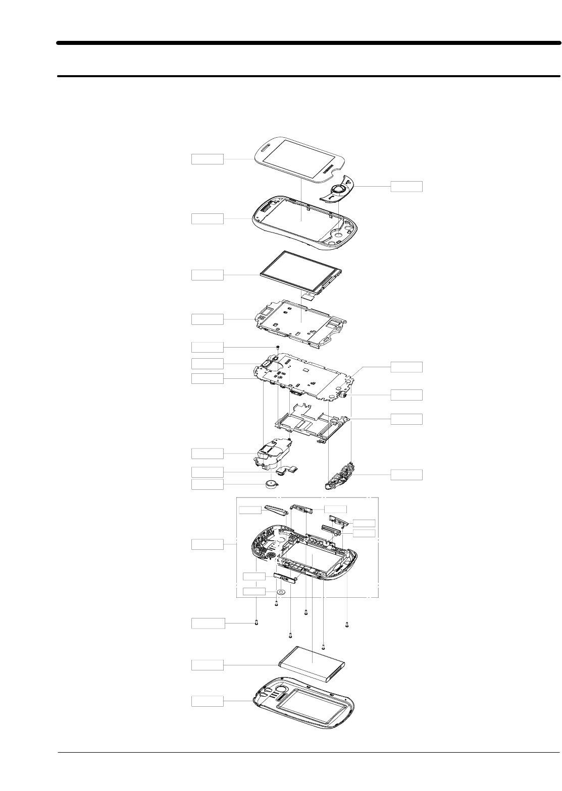
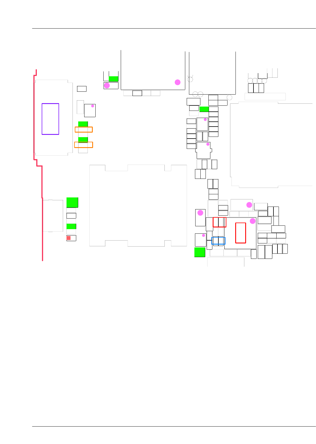
5. Exploded View and Parts List
5-1
This Document can not be used without Samsung's authorization
5-1. Cellular phone Exploded View
QRE01
QME03
QFR01
QLC01
QLB01
QCR72
QSP01
QCA01
QMO01
QCR101
QBA01
QBC00
QAR01
QMP01
QKP01
QME01
QMI01
QSH01
QAN02
QCK01
QSD01
QCK02
QIF01
QVO01
QCW01

- This Document can not be used without Samsung's authorization -
5-2. Cellular phone Parts list : GT-C3510CWAXEF
Design LOC
Description
SEC CODE
QAN02
INTENNA-MAIN (GT-C3510)
GH42-02300A
QAR01
AUDIO-RECEIVER
3009-001428
QBA01
INNER BATTERY PACK-AB463651BU,960MAH
GH43-03216A
QBC00
ASSY COVER-BATT V3(OPTION)
GH98-16285D
QCA01
CAMERA MODULE-GT-C3510
GH59-08802A
QCK01
ASSY KEY-CAM
GH98-16235D
QCK02
ASSY KEY-HOLD
GH98-16234D
QCR101
SCREW-MACHINE
6001-002005
QCR72
SCREW-MACHINE
6001-002051
QCW01
PCT WINDOW-CAMERA
GH72-56746A
QFR01
ASSY CASE-FRONT
GH98-15114D
QIF01
ASSY CASE-IF
GH98-16231D
QKP01
ASSY KEYPAD-(OPEN/WHITE)
GH98-15117D
QLB01
ASSY BRACKET-LCD
GH98-15118A
QLC01
ASSY LCD-2.8",TFT(GT-C3510)
GH96-04335A
QME01
DOME SHEET-GT-C3510(MAIN)
GH59-08590A
QME03
TOUCH/PANEL-GT-C3510(WHT)
GH59-08654B
QMI01
MICROPHONE-ASSY-GT-C3510
GH30-00627A
QMO01
MOTOR LINEAR VIBRATION-GT_S7330
GH31-00449A
QMP01
A/S ASSY-PBA MAIN,ECC,GT-C3510(SVC)
GH82-04359A
QRE01
ASSY CASE-REAR
GH98-15116D
QSD01
ASSY CASE-SD
GH98-16232D
QSP01
MODULE-SPKCARRIER ASSY(GT-C3510)
GH59-08765A
QVO01
ASSY KEY-VOL
GH98-16233D
2. Specification
2-1
2-1. GSM General Specification
GSM850 GSM900 DCS1800 PCS1900
Freq.
Band[MHz]
Uplink/Downlink
824~849
869~894
880~915
925~960
1710~1785
1805~1880
1850~1910
1930~1990
ARFCN range 128~251 0~124 &
975~1023 512~885 512~810
Tx/Rx spacing 45MHz 45MHz 95MHz 80MHz
Mod. Bit rate/
Bit Period
270.833kbps
3.692us
270.833kbps
3.692us
270.833kbps
3.692us
270.833kbps
3.692us
Time Slot
Period/Frame
Period
576.9us
4.615ms
576.9us
4.615ms
576.9us
4.615ms
576.9us
4.615ms
Modulation 0.3GMSK 0.3GMSK 0.3GMSK 0.3GMSK
MS Power 33dBm~5dBm 33dBm~5dBm 30dBm~0dBm 30dBm~0dBm
Power Class 4
(max +33dBm)
4
(max +33dBm)
1
(max +30dBm)
1
(max +30dBm)
Sensitivity -102dBm -102dBm -100dBm -100dBm
TDMAMux8888
Cell Radius 35Km 35Km 2Km 2Km
Speclflcation
2-2
TX Power
control level
GSM850
GSM900
533±3
dBm
631±3
dBm
729±3
dBm
827±3
dBm
925±3
dBm
10 23±3 dBm
11 21±3 dBm
12 19±3 dBm
13 17±3 dBm
14 15±3 dBm
15 13±3 dBm
16 11±5 dBm
17 9±5 dBm
18 7±5 dBm
19 5±5 dBm
TX Power
control level DCS1800
030±3
dBm
128±3
dBm
226±3
dBm
324±3
dBm
422±3
dBm
520±3
dBm
618±3
dBm
716±3
dBm
814±3
dBm
912±4
dBm
10 10±4 dBm
11 8±4dBm
12 6±4 dBm
13 4±4 dBm
14 2±5 dBm
15 0±5 dBm
TX Power
control level PCS1900
030±3
dBm
128±3
dBm
226±3
dBm
324±3
dBm
422±3
dBm
520±3
dBm
618±3
dBm
716±3
dBm
814±3
dBm
912±4
dBm
10 10±4 dBm
11 8±4dBm
12 6±4 dBm
13 4±4 dBm
14 2±5 dBm
15 0±5 dBm
2-2. GSM Tx Power Class
Speclflcation
2-3
TX Power
control level
GSM900
GSM850
827±3
dBm
925±3
dBm
10 23±3 dBm
11 21±3 dBm
12 19±3 dBm
13 17±3 dBm
14 15±3 dBm
15 13±3 dBm
16 11±5 dBm
17 9±5 dBm
18 7±5 dBm
19 5±5 dBm
TX Power
control level DCS1800
226±3
dBm
324±3
dBm
422±3
dBm
520±3
dBm
618±3
dBm
716±3
dBm
812±3
dBm
910±3
dBm
10 14±3 dBm
11 12±4 dBm
12 10±4 dBm
13 8±4dBm
14 6±4 dBm
15 4±4 dBm
2-3. GSM EDGE TX power class
TX Power
control level PCS1900
226±3
dBm
324±3
dBm
422±3
dBm
520±3
dBm
618±3
dBm
716±3
dBm
812±3
dBm
910±3
dBm
10 14±3 dBm
11 12±4 dBm
12 10±4 dBm
13 8±4dBm
14 6±4 dBm
15 4±4 dBm
Only in Master

SAMSUNG Proprietary-Contents may change without notice
3. Operation Instruction and Installation
3-1
This Document can not be used without Samsung's authorization
Main Function
-1.3Mega Pixel Camera
-QVGA 2.8 inch TSP
-SMS/MMS/EMS (OMA v1.2 )
-WAP 2.0 Browser
-MP3/AMR/AAC/AAC+/e-AAC+/WMA/i-melody
-Quad Band(EGSM900/DCS,PCS,EDGE)
-MicroSD Card Support
-External Memory
-USB v2.0 High-speed, Bluetooth v2.1
-FM Radio Support,Radio Data System
SAMSUNG Proprietary-Contents may change without notice
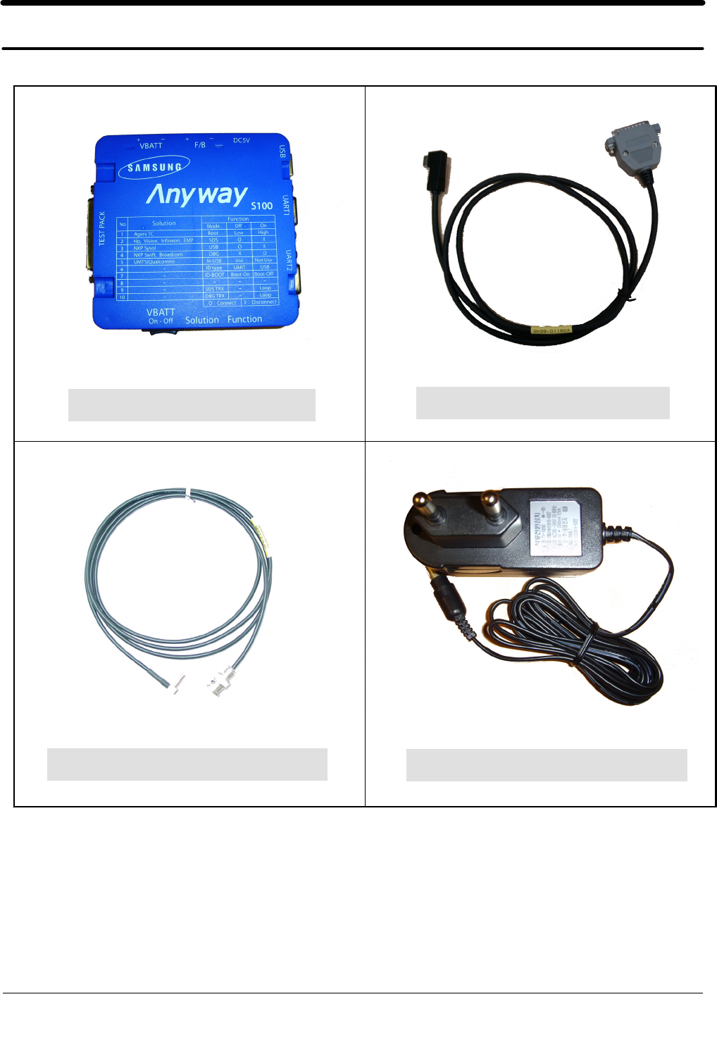
4. Array course control
4-1
This Document can not be used without Samsung's authorization
4-1. Software Adjustments
Test Jig (GH99-36900A)
RF Test Cable (GH39-00985A) Adapter (GH99-38251A)
Test Cable (GH39-01313A)
SAMSUNG Proprietary-Contents may change without notice
Array course control
4-2
This Document can not be used without Samsung's authorization
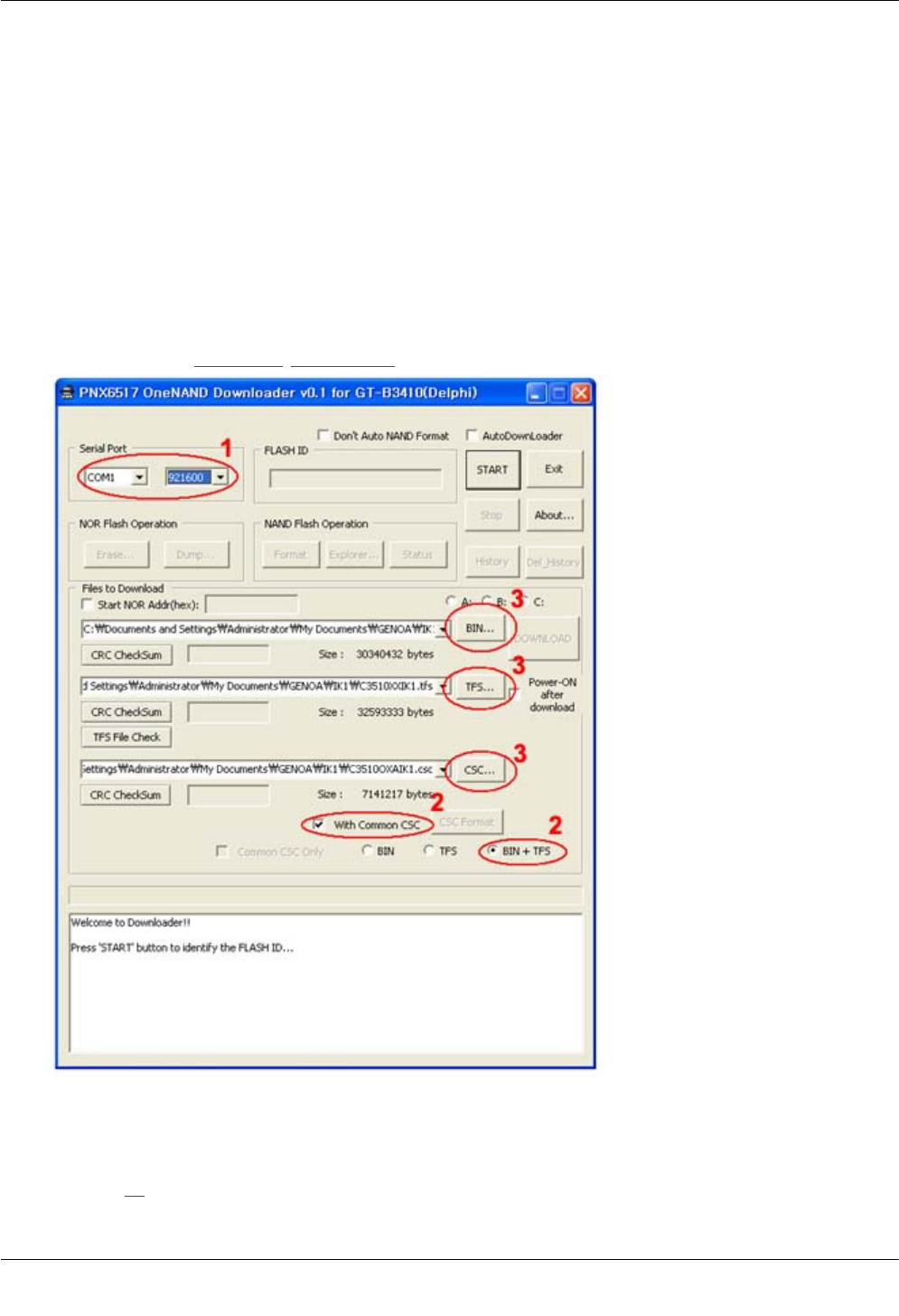
4-2. Software Downloading
4-2-1. Pre-requsite for Downloading
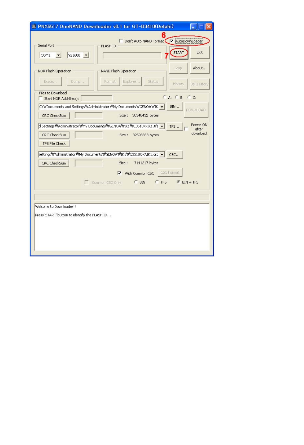
•Downloader Program(PNX6517 OneNAND Downloader v0.1 for GT-B3410(Delphi))
•GT-C3510 Mobile Phone
•Data Cable
•Binary file, TFS file, CSC file
4-2-2. S/W Downloader Program
■ the binary download program by executing the
"PNX6517 OneNAND Downloader v0.1 for GT-B3410(Delphi).exe"
1.Select the connected serial port and the rate of speed.
2.Select the check box, the mode you want to download.
-if only binary file update is needed, check "BIN"
-if only tfs file update is needed, check "TFS"
SAMSUNG Proprietary-Contents may change without notice
Array course control
4-3
This Document can not be used without Samsung's authorization
-if only csc file update is needed, check "Common CSC ONLY"
-if all file updates are needed, check both "BIN+TFS" and "with Common CSC"
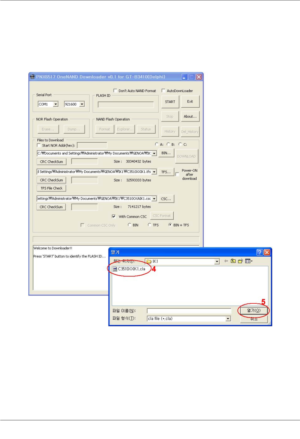
3.Click the corresponding button to select the file(s) that you want to download.
4/5.Choose each binary/tfs/csc file, then click open button.
6/7. After all necessary binary/tfs/csc file(s) are selected, check "AutoDownLoader" and click "START"
button. Then, connect aphone with test cable at the designated serial port. If connection is
successful, the downloader will start with pre-downloading and continue to main downloading.
SAMSUNG Proprietary-Contents may change without notice
Array course control
4-4
This Document can not be used without Samsung's authorization
4-3. Memory Full Reset
After download has completed, follow the below procedure for full memory reset.
Full Reset :
*2767*3855#

SAMSUNG Proprietary-Contents may change without notice
10. Reference data
10-1
This Document can not be used without Samsung's authorization
Reference Abbreviate
―AAC:Advanced Audio Coding.
―AVC :Advanced Video Coding.
―BER :Bit Error Rate
―BPSK:Binary Phase Shift Keying
―CA :Conditional Access
―CDM :Code Division Multiplexing
―C/I :Carrier to Interference
―DMB :Digital Multimedia Broadcasting
―EN :European Standard
―ES :Elementary Stream
―ETSI:European Telecommunications Standards Institute
―MPEG:Moving Picture Experts Group
―PN :Pseudo-random Noise
―PS :Pilot Symbol
―QPSK:Quadrature Phase Shift Keying
―RS :Reed-Solomon
―SI :Service Information
―TDM :Time Division Multiplexing
―TS :Transport Stream

SAMSUNG Proprietary-Contents may change without notice
1. Safety Precautions
1-1
This Document can not be used without Samsung's authorization
1-1. Repair Precaution
―Repair in Shield Box, during detailed tuning. Take specially care of tuning or test, because
specipicty of cellular phone is sensitive for surrounding interference(RF noise).
―Be careful to use akind of magnetic object or tool, because performance of parts is damaged by
the influence of magnetic force.
―Surely use astandard screwdriver when you disassemble this product, otherwise screw will be
worn away.
―Use athicken twisted wire when you measure level.
Athicken twisted wire has low resistance, therefore error of measurement is few.
―Repair after separate Test Pack and Set because for short danger (for example an overcurrent
and furious flames of parts etc) when you repair board in condition of connecting Test Pack and
tuning on.
―Take specially care of soldering, because Land of PCB is small and weak in heat.
―Surely tune on/off while using AC power plug, because arepair of battery charger is dangerous
when tuning ON/OFF PBA and Connector after disassembling charger.
―Don't use as you pleases after change other material than replacement registered on SEC System.
Otherwise engineer in charge isn't charged with problem that you don't keep this rules.

SAMSUNG Proprietary-Contents may change without notice
Safety Precautions
1-2
This Document can not be used without Samsung's authorization
1-2. ESD(Electrostatically Sensitive Devices) Precaution
Several semiconductor may be damaged easily by static electricity. Such parts are called by ESD
(Electrostatically Sensitive Devices), for example IC,BGA chip etc. Read Precaution below.
You can prevent from ESD damage by static electricity.
―Remove static electricity remained your body before you touch semiconductor or parts with
semiconductor. There are ways that you touch an earthed place or wear static electricity prevention
string on wrist.
―Use earthed soldering steel when you connect or disconnect ESD.
―Use soldering removing tool to break static electricity. ,otherwise ESD will be damaged by static
electricity.
―Don't unpack until you set up ESD on product. Because most of ESD are packed by box and
aluminum plate to have conductive power,they are prevented from static electricity.
―You must maintain electric contact between ESD and place due to be set up until ESD is
connected completely to the proper place or acircuit board.
SAMSUNG Proprietary-Contents may change without notice
9-1
This Document can not be used without Samsung's authorization
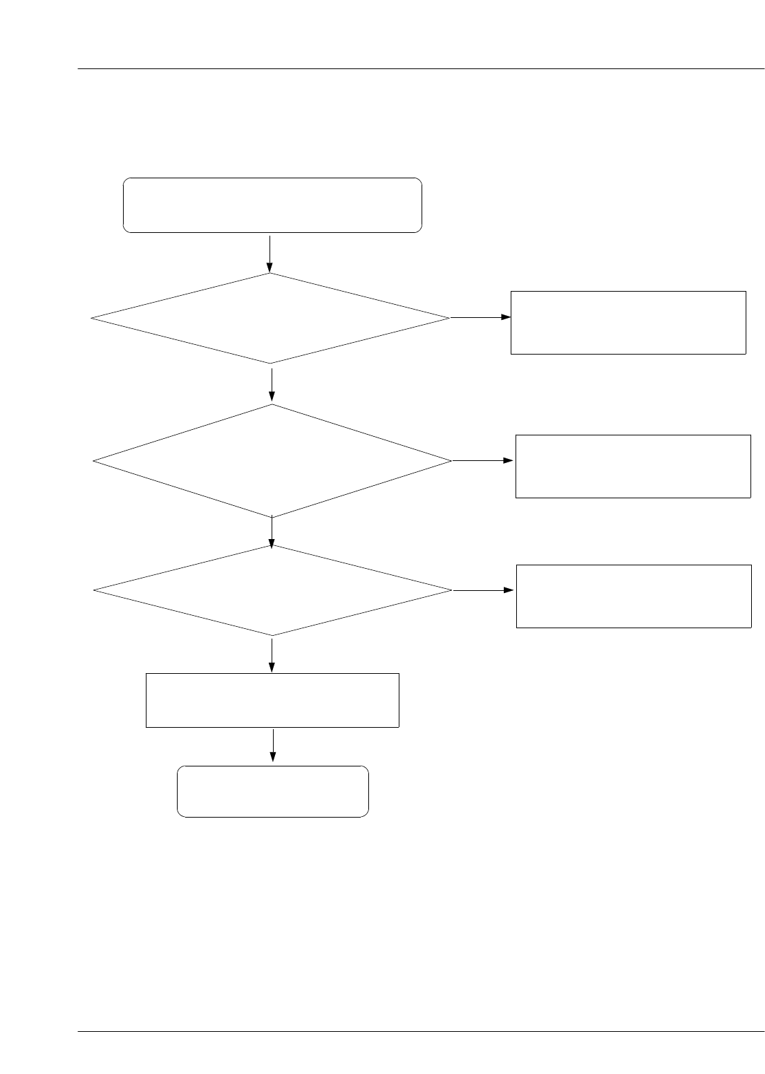
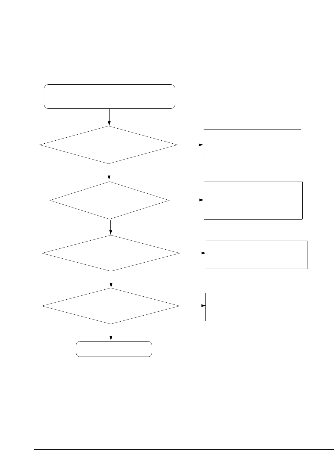
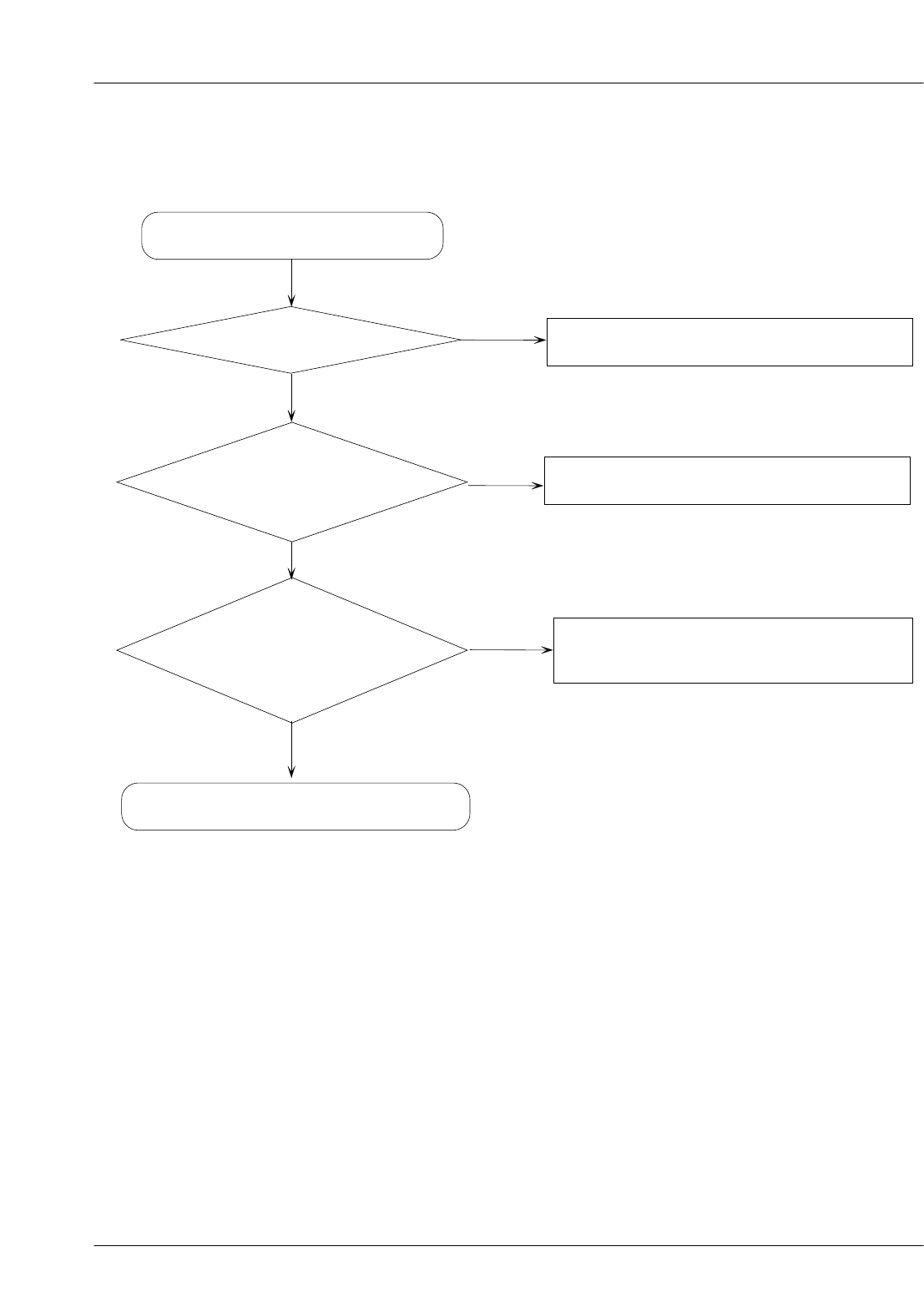
9. Flow Chart of Troubleshooting
9-1.Baseband
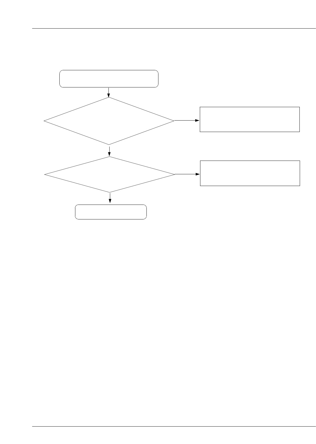
9-1-1Power ON
Check the Battery
Voltage
is it more than 3.4V?
'Power On' does not work
Change the Battery
END
No
Yes
U302 C330(VISA)=
2.6V? Check the PMU related to VINT
No
Yes
Check the Clock at
C338 =32
KHz Resolder OSC300
No
Yes
C306(VDD_IO_LOW_1.8V) &
C312(VDD_IO_HIGH_2.9V) =
"H"?
Check the related circuit
No
Yes
L300(VDD_GSM_CORE_
1.2V) =1.2
V?
Check the
VDD_GSM_CORE_1.2V circuit
No
Yes
Check for the clock at
CLK =26
MHz?
Check the clock generation
circuit
(related to TCX101)
No
Yes
Check the initial operation
Yes
Yes
SAMSUNG Proprietary-Contents may change without notice
Flow Chart of Troubleshooting
9-2
This Document can not be used without Samsung's authorization
C316
C310
R303
C311
C304
3
4
3
C
2
4
3
C
C340
BAT300
C318
C335
C326
M4
D
N
G
A
6
M
8
M2
D
N
G
P
C309
L1
OUTP
L11
L3
HPR
IN8
L5
S
S
V
7
L
C1P
L9
IN9
M10
IN1
M2
HPL
J7
TEST2
J9
RXINP K10
IN7
K12
1
D
N
G
P
2
K
VBIAS K4
IN6
K6
C1N
K8
LX
H2
CLK32K H4
INA2
H6
INB2
H8
XOUT
J1
3
D
N
G
P
1
1
J
FB J3
INA1
J5
INB1
G1
D
N
G
1
1
G
REC1B G3
RESETB G5
REC2B G7
TEST1
G9
RXINN H10
OUTN
H12
XIN E7
B
T
T
A
B9
E
CHGINB
F10 CHGIN
F12
MICBIAS F2
SIMOFFB F4
ONKEYB F6
REFBP F8
VISA
2
D
IRQB D4
SDA D6
S
T
T
A
B8
D
D
D
V
O
I1
E
T
T
A
B1
1
E
VSAVE E3
PWREN2
E5
SCL
1
C
D
D
V
4
D1
1
C
IN2
C3
D
D
V
C
L5
C
SIMVCC C7
PWREN1
C9
VL D10
S
U
B
V2
1
D
D
D
V
3
D
7
A
D
D
V
6
D9
A
IN4
B10
USBLDO B12
D
D
V
2
D2
B
IN3
B4
2
D
D
V
F
R6
B
IN5
B8
D
D
V
1
D
C
N
1
C
N
2
D
D
V
5
D1
1
A
D
D
V
C
H3
A
D
D
V
P
L5
A
D
D
V
1
F
R
U302
C336
C322
C323
C306
C338
21
C320
OSC300
R305
C325
C300
C337
C312
C302
L300
1
4
3
C
R301
MIC_BIAS_2.15V
C321
R300
C317
C327
C308
V_EXT_CHARGE
R302
C330
C345
C339
VBAT
C307
TP300
C303
R308
C328
TA300
4
4
3
C
R307
C305
C301
C319
SPK_P
EARSPK_ROUT
EARSPK_LOUT
SPK_N
RSTON
EAR_N
EAR_P
3PI_L
3PI_R
VDD_IO_LOW_1.8V
SCL
VDD_USB_3.3V
VDD_SD_3.3V
ONKEY_N
JACK_IN
AUX_ON
REF_ON_PMU
VCORE_CTRL
INT_PMU
SIMOFFn
CLK32K
MES_BATT
VDD_GSM_CORE_1.2
V
AVDD_HFA_2.6V
AVDD_2.6V
VCC_SYN_2.8VVDD_TSP_2.9V
+VBUS_DETECT
VDD_IO_HIGH_2.9V
VDD_RX_TX_2.8V
VDD_MOT_3.0V
VDD_PLL_1.2V
VCC_SIM_3.0V
+VBUS
VDD_CAM_IO_2.8V
SDA
C300
1
0
3
C
C302C30 3 C304
5
0
3
C
C306
C307
C308
9
0
3
C
0
1
3
C
1
1
3
C
2
1
3
C
7
1
3
C
C318
9
1
3
C
0
2
3
C
1
2
3
C
2
2
3
C
3
2
3
C
5
2
3
C
C326
7
2
3
C
C330
C335
C336
7
3
3
C
C338
9
3
3
C
C340
C341C34 2 C343
C344
C345
2
2
4
C
6
2
4
C
0
0
3
L
OSC300
0
0
3
R
1
0
3
R
R307
R308
0
0
3
A
T
2
0
3
U
ZD405
SAMSUNG Proprietary-Contents may change without notice
Flow Chart of Troubleshooting
9-3
This Document can not be used without Samsung's authorization
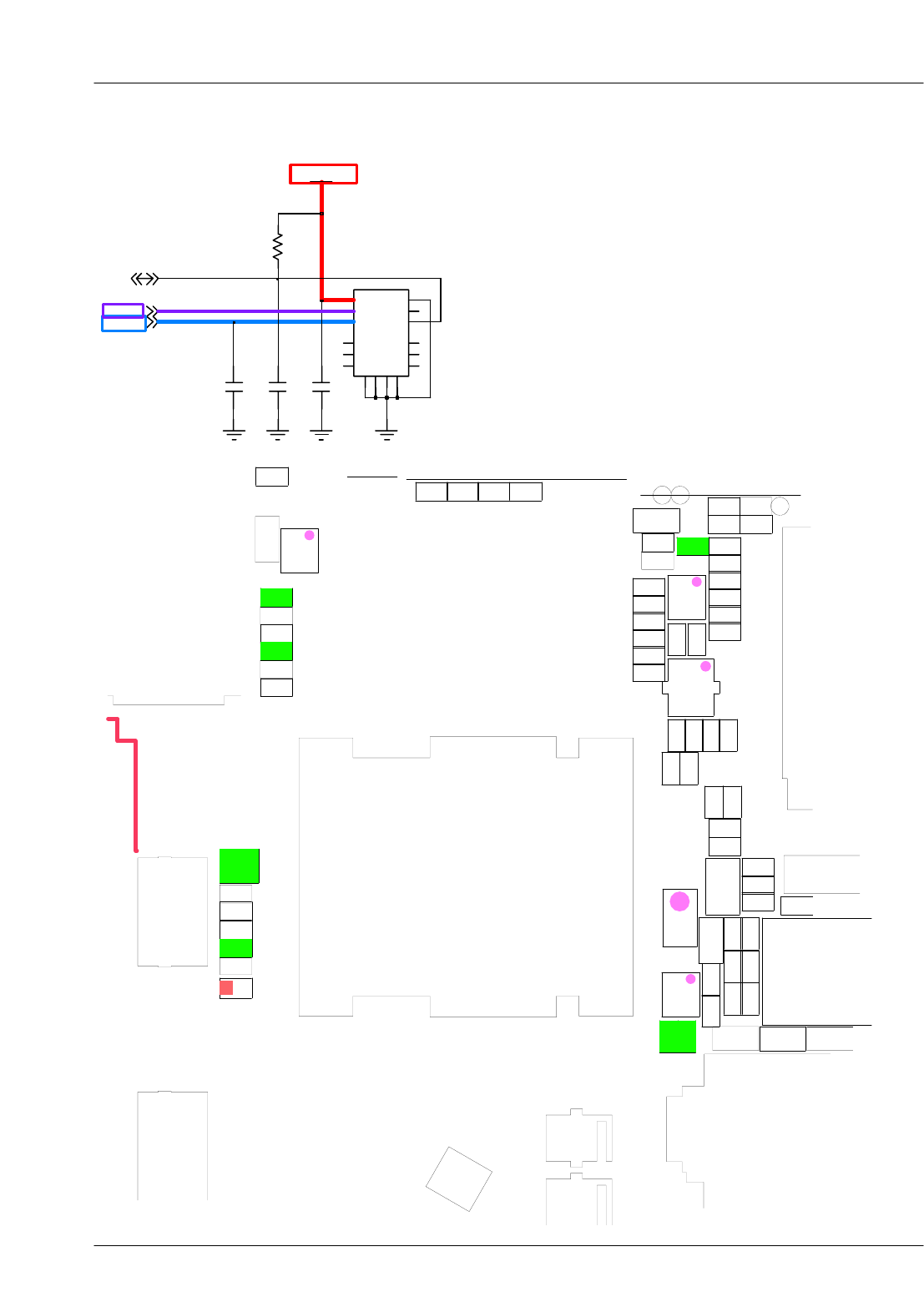
9-1-2. Initial
C316
C310
R303
C311
C304
3
4
3
C
2
4
3
C
C340
BAT300
C318
C335
C326
M4
D
N
G
A
6
M
8
M2
D
N
G
P
C309
L1
OUTP
L11
L3
HPR
IN8
L5
S
S
V
7
L
C1P
L9
IN9
M10
IN1
M2
HPL
J7
TEST2
J9
RXINP K10
IN7
K12
1
D
N
G
P
2
K
VBIAS K4
IN6
K6
C1N
K8
LX
H2
CLK32K H4
INA2
H6
INB2
H8
XOUT
J1
3
D
N
G
P
1
1
J
FB J3
INA1
J5
INB1
G1
D
N
G
1
1
G
REC1B G3
RESETB G5
REC2B G7
TEST1
G9
RXINN H10
OUTN
H12
XIN E7
B
T
T
A
B9
E
CHGINB
F10 CHGIN
F12
MICBIAS F2
SIMOFFB F4
ONKEYB F6
REFBP F8
VISA
2
D
IRQB D4
SDA D6
S
T
T
A
B8
D
D
D
V
O
I1
E
T
T
A
B1
1
E
VSAVE E3
PWREN2
E5
SCL
1
C
D
D
V
4
D1
1
C
IN2
C3
D
D
V
C
L5
C
SIMVCC C7
PWREN1
C9
VL D10
S
U
B
V2
1
D
D
D
V
3
D
7
A
D
D
V
6
D9
A
IN4
B10
USBLDO B12
D
D
V
2
D2
B
IN3
B4
2
D
D
V
F
R6
B
IN5
B8
D
D
V
1
D
C
N
1
C
N
2
D
D
V
5
D1
1
A
D
D
V
C
H3
A
D
D
V
P
L5
A
D
D
V
1
F
R
U302
C336
C322
C323
C306
C338
21
C320
OSC300
R305
C325
C300
C337
C312
C302
L300
1
4
3
C
R301
MIC_BIAS_2.15V
C321
R300
C317
C327
C308
V_EXT_CHARGE
R302
C330
C345
C339
VBAT
C307
TP300
C303
R308
C328
TA300
4
4
3
C
R307
C305
C301
C319
SPK_P
EARSPK_ROUT
EARSPK_LOUT
SPK_N
RSTON
EAR_N
EAR_P
3PI_L
3PI_R
VDD_IO_LOW_1.8V
SCL
VDD_USB_3.3V
VDD_SD_3.3V
ONKEY_N
JACK_IN
AUX_ON
REF_ON_PMU
VCORE_CTRL
INT_PMU
SIMOFFn
CLK32K
MES_BATT
VDD_GSM_CORE_1.2V
AVDD_HFA_2.6V
AVDD_2.6V
VCC_SYN_2.8VVDD_TSP_2.9V
+VBUS_DETECT
VDD_IO_HIGH_2.9V
VDD_RX_TX_2.8V
VDD_MOT_3.0V
VDD_PLL_1.2V
VCC_SIM_3.0V
+VBUS
VDD_CAM_IO_2.8V
SDA
U302 pin G5 (RSTON)
="H"?
Initial Failure
Check the circuit related to reset
END
No
Yes
Yes
Check the 16bit data signal
&memory CE
Yes
SAMSUNG Proprietary-Contents may change without notice
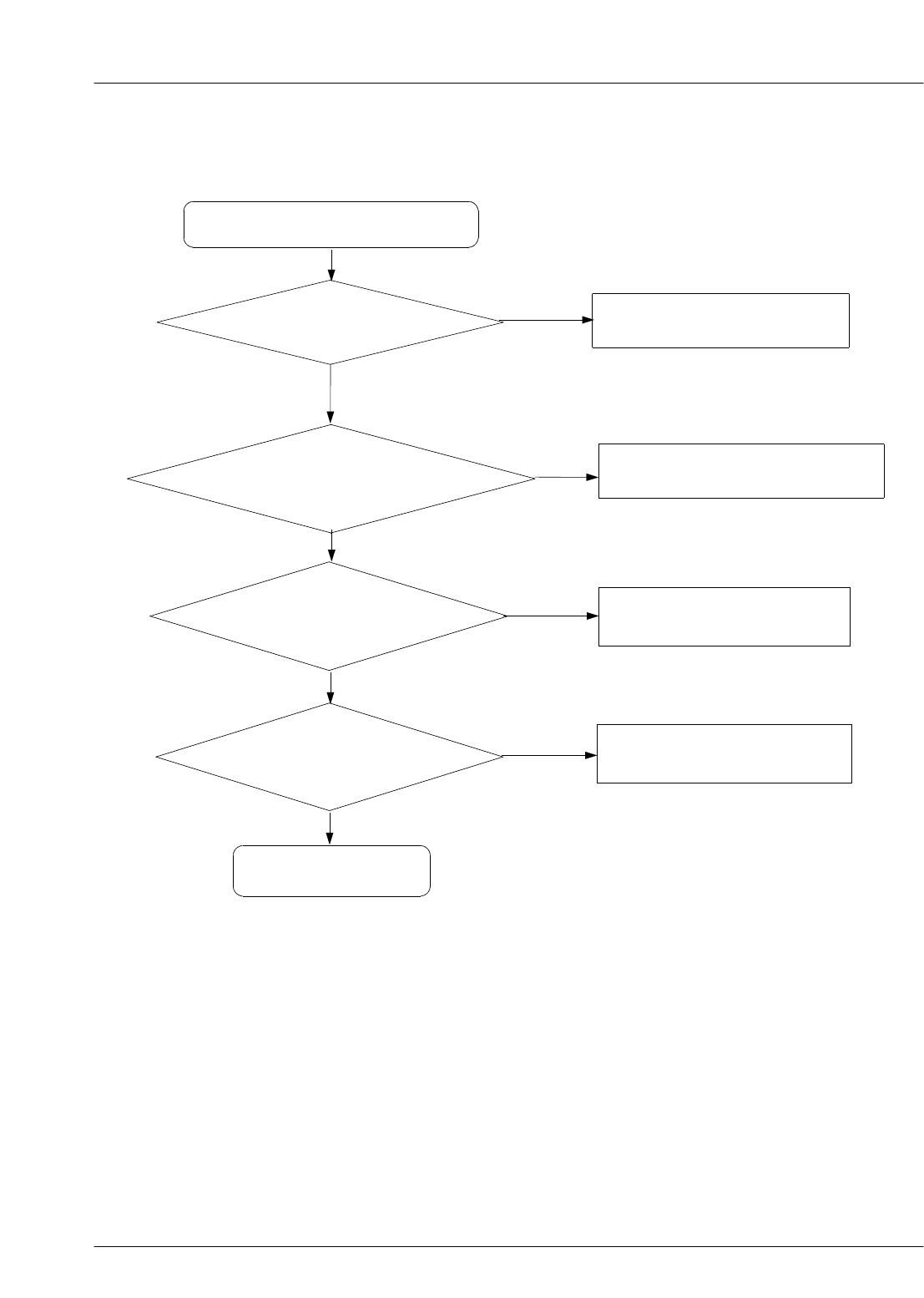
Flow Chart of Troubleshooting
9-4
This Document can not be used without Samsung's authorization
9-1-3. SIM Part
SIM300 pin 1="
H"? Resolder or replace SIM501
Check the SIM Card
END
No
Yes
Yes
Yes
No
Check the Clock
After Power ON,
Check SIM_CLK Signal on
pin 3of SIM300 in afew
second
Yes
No
Resolder or replace UCP301
After SIM card insert,
SIM300 pin 2=
"H(SIM_RST)"?
Yes
Phone can't access SIM Card
SAMSUNG Proprietary-Contents may change without notice
Flow Chart of Troubleshooting
9-5
This Document can not be used without Samsung's authorization
R314
VCC_SIM_3.0V
C349
C347
C348
15
GG
16
4
4
55
6
6
7
7
88
99
13
GG
14
1
1
1010
11 11
1212
22
3
3
SIM300
SIM_RST
SIM_CLK
SIM_IO
BTC300
C200
C201
C202
C209C210
C214
C216
C217
9
1
3
C
0
2
3
C
2
2
3
C
3
2
3
C
5
2
3
C
7
2
3
C
C328
C335
9
3
3
C
C340
C34 2 C343
C345
C347
C348
C349
C350
C410
C413
C417
8
1
4
C
1
2
4
C2
2
4
C
C423
C424
6
2
4
C
C437
C438
0
0
4
C
F
I
0
0
3
L
L402
6
0
4
L
7
0
4
L
L415
L416
L422
0
0
4
T
O
M
OSC300
2
0
2
R
3
0
2
R
4
0
2
R
R206
R207
0
0
3
R
1
0
3
R
R307
R308
R309
R310
R311
R312
3
1
3
R
R314
R316
R317R320
R421
R425
8
2
4
R
R429
0
4
4
R
SIM300
SPK400
SPK401
0
0
3
A
T
TAC_DN
TAC_UP
TP109
TP201
0
1
2
P
T
2
0
3
U
U400
1
0
4
U
ZD300
3
0
4
D
Z
4
0
4
D
Z
ZD405
ZD406
ZD503
SAMSUNG Proprietary-Contents may change without notice
Flow Chart of Troubleshooting
9-6
This Document can not be used without Samsung's authorization
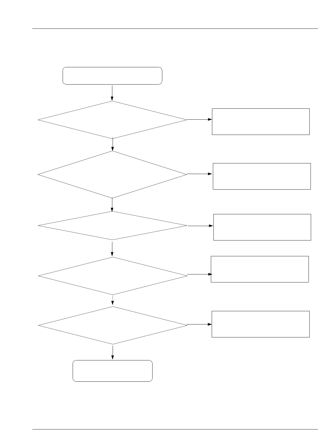
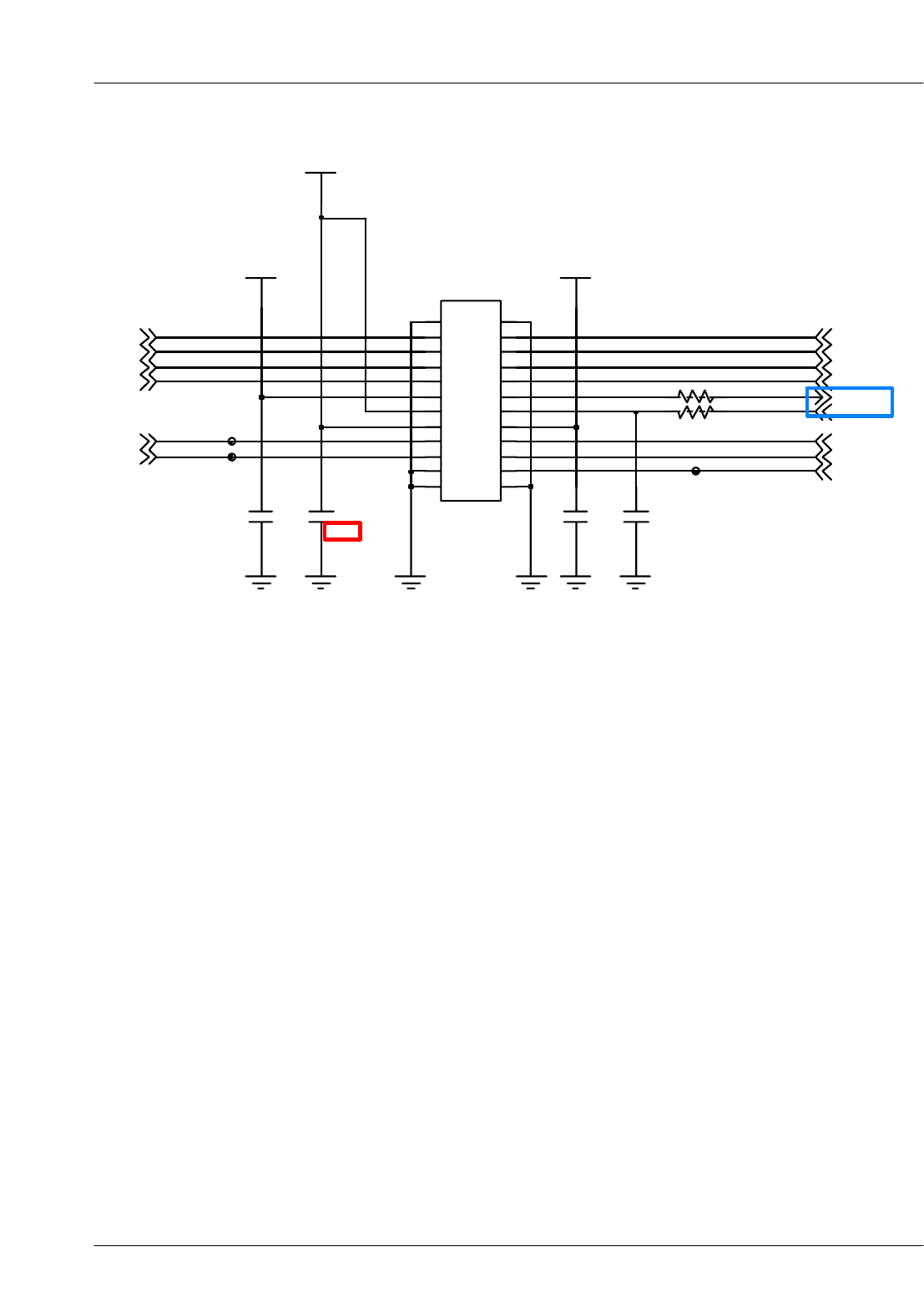
9-1-4. Charging Part
Check the U302 pin F10,
F12 >4.9V
Abnormal charging part
END
No
Yes
U302 pin G3
(AUX_ON) ="
L"?
No
Yes
Check the circuit related to
V_EXT_CHARGE
Check the circuit related to
AUX_ON signal
Yes
SAMSUNG Proprietary-Contents may change without notice
Flow Chart of Troubleshooting
9-7
This Document can not be used without Samsung's authorization
C316
C310
R303
C311
C304
3
4
3
C
2
4
3
C
C340
BAT300
C318
C335
C326
M4
D
N
G
A
6
M
8
M2
D
N
G
P
C309
L1
OUTP
L11
L3
HPR
IN8
L5
S
S
V
7
L
C1P
L9
IN9
M10
IN1
M2
HPL
J7
TEST2
J9
RXINP K10
IN7
K12
1
D
N
G
P
2
K
VBIAS K4
IN6
K6
C1N
K8
LX
H2
CLK32K H4
INA2
H6
INB2
H8
XOUT
J1
3
D
N
G
P
1
1
J
FB J3
INA1
J5
INB1
G1
D
N
G
1
1
G
REC1B G3
RESETB G5
REC2B G7
TEST1
G9
RXINN H10
OUTN
H12
XIN E7
B
T
T
A
B9
E
CHGINB
F10 CHGIN
F12
MICBIAS F2
SIMOFFB F4
ONKEYB F6
REFBP F8
VISA
2
D
IRQB D4
SDA D6
S
T
T
A
B8
D
D
D
V
O
I1
E
T
T
A
B1
1
E
VSAVE E3
PWREN2
E5
SCL
1
C
D
D
V
4
D1
1
C
IN2
C3
D
D
V
C
L5
C
SIMVCC C7
PWREN1
C9
VL D10
S
U
B
V2
1
D
D
D
V
3
D
7
A
D
D
V
6
D9
A
IN4
B10
USBLDO B12
D
D
V
2
D2
B
IN3
B4
2
D
D
V
F
R6
B
IN5
B8
D
D
V
1
D
C
N
1
C
N
2
D
D
V
5
D1
1
A
D
D
V
C
H3
A
D
D
V
P
L5
A
D
D
V
1
F
R
U302
C336
C322
C323
C306
C338
21
C320
OSC300
R305
C325
C300
C337
C312
C302
L300
1
4
3
C
R301
MIC_BIAS_2.15V
C321
R300
C317
C327
C308
V_EXT_CHARGE
R302
C330
C345
C339
VBAT
C307
TP300
C303
R308
C328
TA300
4
4
3
C
R307
C305
C301
C319
SPK_P
EARSPK_ROUT
EARSPK_LOUT
SPK_N
RSTON
EAR_N
EAR_P
3PI_L
3PI_R
VDD_IO_LOW_1.8V
SCL
VDD_USB_3.3V
VDD_SD_3.3V
ONKEY_N
JACK_IN
AUX_ON
REF_ON_PMU
VCORE_CTRL
INT_PMU
SIMOFFn
CLK32K
MES_BATT
VDD_GSM_CORE_1.2V
AVDD_HFA_2.6V
AVDD_2.6V
VCC_SYN_2.8VVDD_TSP_2.9V
+VBUS_DETECT
VDD_IO_HIGH_2.9V
VDD_RX_TX_2.8V
VDD_MOT_3.0V
VDD_PLL_1.2V
VCC_SIM_3.0V
+VBUS
VDD_CAM_IO_2.8V
SDA
BTC300
C300
1
0
3
C
C302C30 3 C304
5
0
3
C
C306
C307
C308
9
0
3
C
0
1
3
C
1
1
3
C
2
1
3
C
7
1
3
C
C318
9
1
3
C
0
2
3
C
1
2
3
C
2
2
3
C
3
2
3
C
5
2
3
C
C326
7
2
3
C
C330
C335
C336
7
3
3
C
C338
9
3
3
C
C340
C341C34 2 C343
C344
1
5
3
C
2
2
4
C
6
2
4
C
0
0
5
C
C501
0
0
3
L
OSC300
0
0
3
R
1
0
3
R
R307
R308
5
1
3
R
8
1
3
R
0
0
3
A
T
2
0
3
U
ZD405
SAMSUNG Proprietary-Contents may change without notice
Flow Chart of Troubleshooting
9-8
This Document can not be used without Samsung's authorization
9-1-5. Microphone Part
Check the connection
from MIC
Check the circuit
from UCP200 to
MIC
Resolder MIC
Resolder the C403, C406, R401,
R409
END
No
Yes
Yes
Yes
Yes
No
Check IFC400 PIN 9
='H' ?No Check the JACK_IN signal
Microphone does not work
Yes
Check the MIC No Replace the MIC
SAMSUNG Proprietary-Contents may change without notice
Flow Chart of Troubleshooting
9-9
This Document can not be used without Samsung's authorization
C402
TA400
ZD400
C406
C404
R409
R402
R401
L421
MIC_BIAS_2.15V
L401
C431
ZD402
C401
MIC400
C405
R410
C403
MIC_N
MIC_P
C400
L400
L416
L415
NC 26
NC 27
77
8
8
99
NC 21
22
NC
23
NC
NC 24
25
NC
19 19
2
2
20
20
33
4
4
55
6
6
11 11
12
12
13
13 14
14
15 15
16
16
17 17
18
18
IFC400
11
10
10
V_EXT_CHARGE
R429
VDD_IO_HIGH_2.9V
C418
C430
VBAT
D401
C437 C438
EARSPK_R
EARSPK_L
AUX_ON
USB_D+_IF
USB_D-_IF
+VBUS
FM_ANT
EARMIC_N
EARMIC_P
JACK_IN
EAR_SWITCH
TXD1_J
RXD1_J
USB_D+_J
TXD1
RXD1
AUX_ON_J
USB_D-_J
+VBUS_J
1
1
1
C
C201
5
0
2
C
6
0
2
C
C209C210
3
1
2
C
5
1
2
C
C402
C403
C405
C406
C411
2
1
4
C
C414
5
1
4
C
C417
8
1
4
C
C424
1
3
4
C
2
3
4
C
C435 C436
C437
C438
C503
4
0
5
C
1
0
5
F
F502
3
0
5
F
F504
C
D
H
0
0
4
C
F
I
L415
L416
5
0
2
R
R206
3
0
3
R
1
0
4
R
R402
7
0
4
R
R409
R415
6
1
4
R
R417
0
2
4
R
R429
TA400
TP120
5
0
2
P
T
TP300
UCP200
ZD406
SAMSUNG Proprietary-Contents may change without notice
Flow Chart of Troubleshooting
9-10
This Document can not be used without Samsung's authorization
9-1-6. Speaker Part
U302 E11 =3.7
V?
No
Yes
Resolder or replace U302
Is there any signal at
pin J7(EAR_P) &
J8(EAR_N)?
No
Yes
No
END
Is Speaker working? Change the Speaker
Yes
Yes
Is there any signal at
pin L11(SPK_P) &
H12(SPK_N) ?
Resolder or replace U302
No
Yes
Speaker does not work
Resolder or replace C323, C325
SAMSUNG Proprietary-Contents may change without notice
Flow Chart of Troubleshooting
9-11
This Document can not be used without Samsung's authorization
C316
C310
R303
C311
C304
3
4
3
C
2
4
3
C
C340
BAT300
C318
C335
C326
M4
D
N
G
A
6
M
8
M2
D
N
G
P
C309
L1
OUTP
L11
L3
HPR
IN8
L5
S
S
V
7
L
C1P
L9
IN9
M10
IN1
M2
HPL
J7
TEST2
J9
RXINP K10
IN7
K12
1
D
N
G
P
2
K
VBIAS K4
IN6
K6
C1N
K8
LX
H2
CLK32K H4
INA2
H6
INB2
H8
XOUT
J1
3
D
N
G
P
1
1
J
FB J3
INA1
J5
INB1
G1
D
N
G
1
1
G
REC1B G3
RESETB G5
REC2B G7
TEST1
G9
RXINN H10
OUTN
H12
XIN E7
B
T
T
A
B9
E
CHGINB
F10 CHGIN
F12
MICBIAS F2
SIMOFFB F4
ONKEYB F6
REFBP F8
VISA
2
D
IRQB D4
SDA D6
S
T
T
A
B8
D
D
D
V
O
I1
E
T
T
A
B1
1
E
VSAVE E3
PWREN2
E5
SCL
1
C
D
D
V
4
D1
1
C
IN2
C3
D
D
V
C
L5
C
SIMVCC C7
PWREN1
C9
VL D10
S
U
B
V2
1
D
D
D
V
3
D
7
A
D
D
V
6
D9
A
IN4
B10
USBLDO B12
D
D
V
2
D2
B
IN3
B4
2
D
D
V
F
R6
B
IN5
B8
D
D
V
1
D
C
N
1
C
N
2
D
D
V
5
D1
1
A
D
D
V
C
H3
A
D
D
V
P
L5
A
D
D
V
1
F
R
U302
C336
C322
C323
C306
C338
21
C320
OSC300
R305
C325
C300
C337
C312
C302
L300
1
4
3
C
R301
MIC_BIAS_2.15V
C321
R300
C317
C327
C308
V_EXT_CHARGE
R302
C330
C345
C339
VBAT
C307
TP300
C303
R308
C328
TA300
4
4
3
C
R307
C305
C301
C319
SPK_P
EARSPK_ROUT
EARSPK_LOUT
SPK_N
RSTON
EAR_N
EAR_P
3PI_L
3PI_R
VDD_IO_LOW_1.8V
SCL
VDD_USB_3.3V
VDD_SD_3.3V
ONKEY_N
JACK_IN
AUX_ON
REF_ON_PMU
VCORE_CTRL
INT_PMU
SIMOFFn
CLK32K
MES_BATT
VDD_GSM_CORE_1.2V
AVDD_HFA_2.6V
AVDD_2.6V
VCC_SYN_2.8VVDD_TSP_2.9V
+VBUS_DETECT
VDD_IO_HIGH_2.9V
VDD_RX_TX_2.8V
VDD_MOT_3.0V
VDD_PLL_1.2V
VCC_SIM_3.0V
+VBUS
VDD_CAM_IO_2.8V
SDA
BTC300
C300
1
0
3
C
C302C30 3 C304
5
0
3
C
C306
C307
C308
9
0
3
C
0
1
3
C
1
1
3
C
2
1
3
C
7
1
3
C
C318
9
1
3
C
0
2
3
C
1
2
3
C
2
2
3
C
3
2
3
C
5
2
3
C
C326
7
2
3
C
C330
C335
C336
7
3
3
C
C338
9
3
3
C
C340
C341C34 2 C343
C344
C345
1
5
3
C
C352
C353
2
2
4
C
6
2
4
C
0
0
5
C
C501
HDC503
0
0
3
L
OSC300
0
0
3
R
1
0
3
R
R307
R308
5
1
3
R
8
1
3
R
SPK400
SPK401
0
0
3
A
T
TAC_HOLD
TP500TP501
2
0
3
U
ZD301
ZD405
SAMSUNG Proprietary-Contents may change without notice
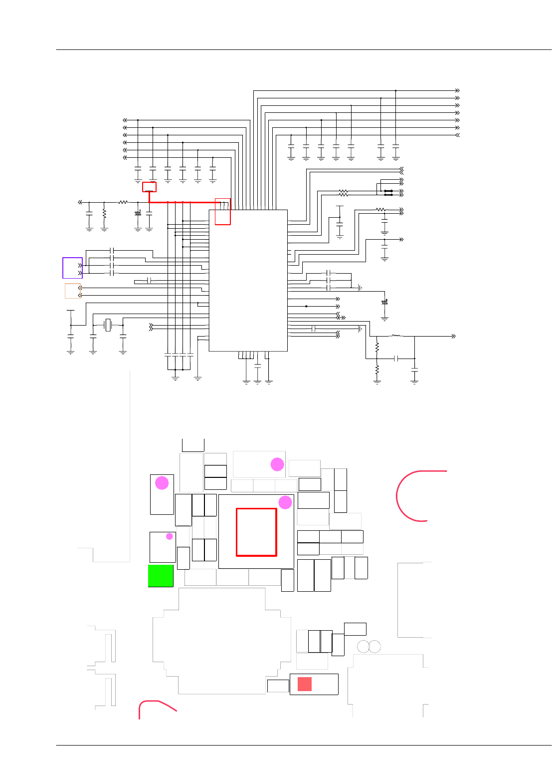
Flow Chart of Troubleshooting
9-12
This Document can not be used without Samsung's authorization
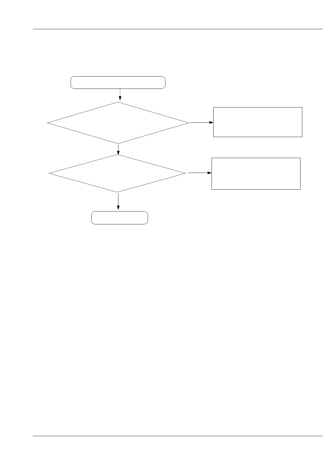
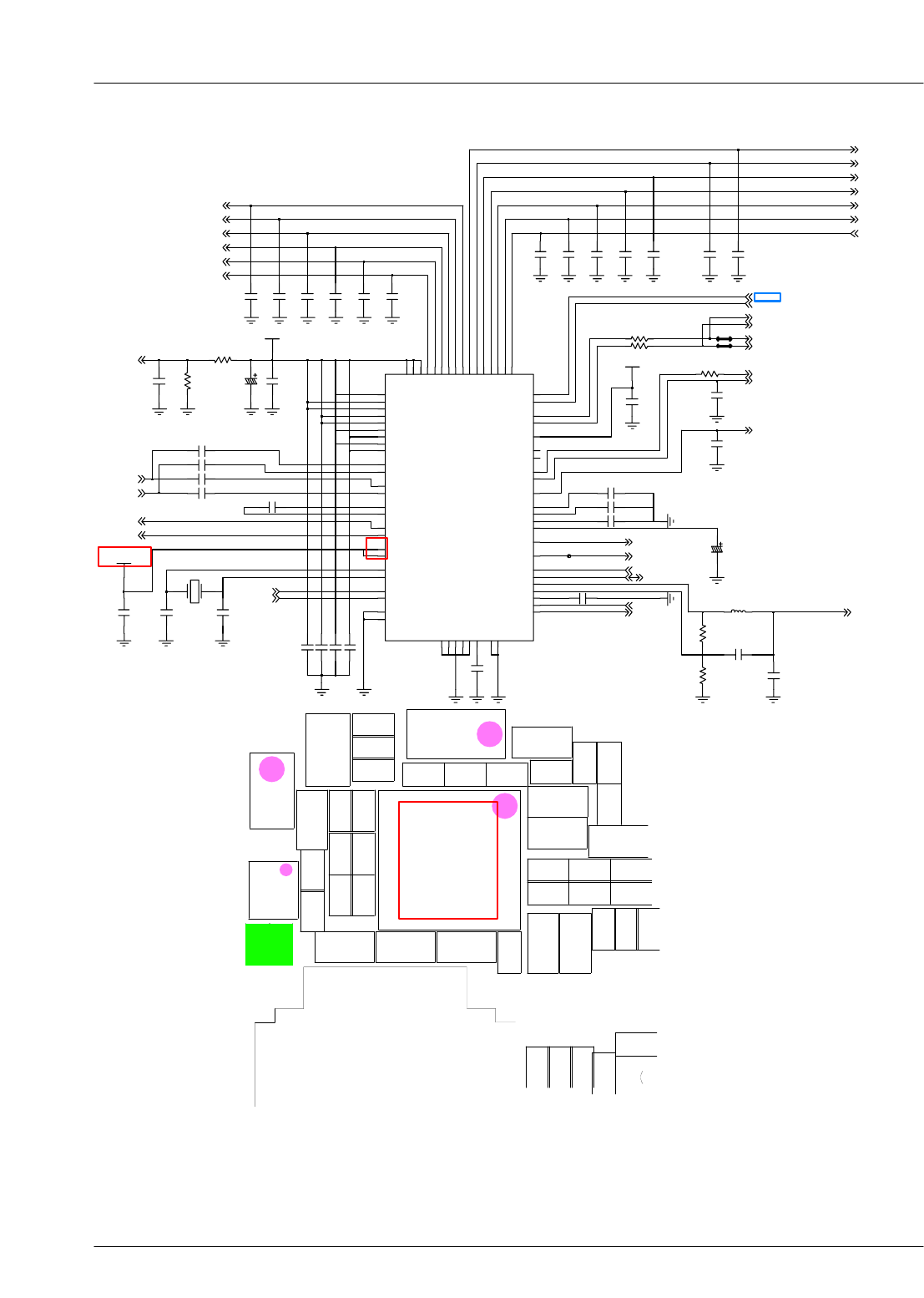
9-1-7. Receiver Part
Is there any signal at
UCP200 pin
E18(RCV_P) &
G18(RCV_N) ?
Resolder UCP200 or change PBA
END
No
Yes
Yes
Receiver does not work
No
Replace the Receiver
Yes
Is Receiver working?
SAMSUNG Proprietary-Contents may change without notice
Flow Chart of Troubleshooting
9-13
This Document can not be used without Samsung's authorization
1
1
1
C
4
3
1
4
4
1
C148
C200
C201
C202
5
0
2
C
6
0
2
C
C209C210
3
1
2
C
C214
5
1
2
C
C216
C217
C350
C402
C403
C405
C406
C411
2
1
4
C
C414
5
1
4
C
8
1
4
C
1
3
4
C
2
3
4
C
C435 C436
C503
4
0
5
C
1
0
5
F
F502
3
0
5
F
F504
1
0
5
C
D
H
F
I
R102
3
0
1
4
0
1
5
0
2
R
R206
R207
3
0
3
R
R317R320
1
0
4
R
R402
7
0
4
R
R409
R415
6
1
4
R
R417
0
2
4
R
R429
TA400
TP109
TP120
0
0
2
P
T
TP201
TP202
TP203
TP204
5
0
2
P
T
TP206
TP207
TP208
9
0
2
P
T
0
1
2
P
T
TP212
4
1
2
P
T
5
1
2
P
T
TP300
TP504
TP505
TP506
TP507
UCP200
UME200
ZD406
VDD_IO_HIGH_2.9VVDD_GSM_CORE_1.2V
VDD_IO_LOW_1.8V
U401
R206
VDD_IO_LOW_1.8V
C215
VDD_IO_LOW_1.8V
AVDD_2.6V
R203
VDD_PLL_1.2V
VDD_USB_3.3V VDD_USB_3.3V
HDP0
4
V
B
B
S
S
V
V5
QP
V6
IP
7
V
K
L
C
S
S
V
MCLK V8
9
V
E
D
N
G
V12
AUXDAC3
3
1
V
F
E
R
D
D
V
V14
VREF
MICBIAS
V15
6
1
V
B
V
D
D
V
V17
GPIOB12
8
1
V
C
N
V2
WE_E
V3
QN
U6
IN
7
U
K
L
C
D
D
V
8
U
4
A
S
S
V9
U
1
E
D
D
V
1
V
C
N
V10
AUXDAC1
V11
AUXDAC2
4
1
U
F
E
R
S
S
V
5
1
U5
A
S
S
V
6
1
U
E
D
N
G
U17
GPIOA15
U18 GPIOA21
U2
GPIOA6
U3 BE1
4
U
B
B
D
D
V
U5
HDP17
T8 HDP14
T9
GPIOA11
U1
HDP4
U10
GPIOB5
U11
GPIOA28
U12
GPIOA24
3
1
UE
D
N
G
T16
GPIOA20
T17
GPIOA30
T18
GPIOA22
T2
HDP7
T3
HDP6
T4
OE_R_W
HDP5
T5
6
T
R
P
E
D
D
V
T7
GPIOA2
T1
HDP8
T10
TXDP1
T11
GPIOA25
T12 GPIOA27
GPIOB8
T13
GPIOB10
T14
T15
GPIOB13
R18
GPIOA23
R2
HDP9
R3
GPIOA8
R4
HDP1
R5
HDP3
R6 HDP11
HDP16
R7
R8 GPIOA10
R9
GPIOA18
R11
GPIOA16
R12 GPIOA13
R13
GPIOA14
R14
GPIOB9
GPIOB11
R15
RFSIG0
R16
R17
RFSIG1
P3
GPIOA0
P4
HDP2
P5
HDP12
P6
HDP15
7
P
C
D
N
G
P8
GPIOA1
GPIOA12
P9
R1
GPIOA5
R10
GPIOA26
P13
GPIOA29
P14
GPIOA17
P15
KCOL0
P16
RFSIG2
RFSIG6
P17
GPIOA3
P18
P2
CS0
N18
ANL
N2
ADD20
N3
CS3
N4
CS1
N5 HDP13
P1
ADD27
GPIOA19
P10
P11
GPIOA31
P12
1
E
D
D
V
8
M
C
D
D
V
9
M
2
E
D
D
V
N1
GPIOA4
N14
KCOL1
KCOL3
N15
N16
RFSIG7
N17
ANR
M15
KROW2
M16
RFDO1
M17
AUXMICP
M18
AUXMICN
M2
ADD18
M3
ADD19
M4
ADD23
M5
HDP10
7
M
1
E
D
D
V
8
LE
D
N
G
9
L
E
D
N
G
M1
GPIOB2
0
1
M
C
D
D
V
2
E
D
D
V
1
1
M
2
1
M
5
E
D
D
V
M14
KCOL2
L15
KROW4
L16
SCL2
L17
MICP
L18
MICN
L2
TDO
L3
RTCK
L4 ADD22
L5 GPIOA7
7
L
1
E
D
D
V
8
K
C
D
N
G
9
KC
D
N
G
1
L
C
D
N
G
0
1
L
E
D
N
G
1
E
D
D
V1
1
L
2
1
L
C
D
D
V
L14
KCOL4
K15
KROW1
K16
RFEN0
K17
CAMDATA2
8
1
K
B
V
S
S
V
K2
ADC4
K3
JSEL
K4
GPIOA9
K5
ADD21
7
K
1
E
D
D
V
8
J
C
D
N
G
9
J
E
D
N
G
K1
ADC3
0
1
K
E
D
N
G
C
D
N
G
1
1
K
2
1
K
C
D
N
G
K14
KROW0
J15
CAMCLKI
J16
RFCLK1
J17
CAMCLKO
J18 EAR2
J2 ADC2
J3
TCK
J4 IO30
J5
GPON1
7
J
C
D
D
V
8
H
E
D
N
G
9
H
C
D
D
V
J1
ADC1
0
1
J
E
D
N
G
E
D
N
G
1
1
J
2
1
J
7
E
D
D
V
J14
KROW3
H15
H16
SDA1
H17
EAR1
8
1
H
C
D
D
V
H2
TRST
H3
TMS
H4
IO28
H5
GPON0
7
H
7
G
1
E
D
D
V
8
G
1
E
D
D
V9
G
1
E
D
D
V
1
H
C
D
D
V
0
1
HC
D
N
G
E
D
N
G
1
1
H
2
1
H
E
D
N
G
H14
SCL1
CAMDATA1
G15
G16
CAMHS
G17
CAMDATA4
G18
HFR2
2
G
2
D
S
S
V
G3
IO26
G4
IO29
G5
IO31
F3 IO27
F4
IO25
F5
ADV
1
G
2
D
D
D
V
0
1
G
6
E
D
D
V
6
E
D
D
V
1
1
G
2
1
G
4
E
D
D
V
G14
SDA2
CAMDATA3
9
E
2
A
D
D
V
F1
TDI
F14
CAMDATA0
F15
CAMDATA5
F16
CAMDATA6
F17
SIMIO
8
1
F
O
B
V
S
S
V
F2
RESET
HFR1
E2 IO24
E3
IO21
E4
IO23
E5
IO19
C
D
D
V
6
E
7
E
E
D
N
G
E8
CLK32I
E10
RSTBB
E11
VDED2
E12
CAMDATA7
E13
CAMVS
E14
SIMPWR
E15
VDED4
E16
VDED6
E17
VDED0
E18
IO20
D4
IO14
5
D
E
D
N
G
D6
IO11
D7
RSTEXT
CKITST D8
9
D
2
A
D
N
G
E1 IO22
D12
SIMCLK
D13
VDED1
D14
VDED3
D15
VDED7
D16
VDED9
D17
VDED5
8
1
D
O
B
V
D
D
V
D2
IO18
D3
R
P
E
D
D
V
C6
IO3
C7
IO1
8
C
U
G
C
D
D
V
C9
VDED_C
R
P
E
D
D
V
1
D
D10
VDECS2
D11
SIMRST
C14
USBRREF
C15
VDED11
C16
VDED12
C17
VDED8
C18
VDED10
C2
IO17
C3
IO12
C4
ADD0_BE0
5
C
IO0
B8
FSC
9
B
2
D
D
D
V
C1 IO16
C10
VDECS1
GPIOC18
C11
C12
USBVBUS
3
1
C
3
E
D
D
V
B16
VDEEOF_CLK27M
B17
VDED15
B18
VDED13
B2
IO15
B3 IO10
B4
IO7
B5
IO5
B6 IO2
B7
2
D
S
S
V
B1 ADD1_BE2
B10
MCLKSEL
A
D
D
V
B
S
U1
1
B
B12
USBGNDA
M
R
E
T
A
S
S
V
B
S
U
3
1
B
B14
USBID
B15
VDERD
8
1
A
C
N
A2
IO13
A3
IO9
IO8
A4
A5
IO6
A6
IO4
A7
DD A8
DU
9
A
DCL
1
1
A
V
R
D
A
D
D
V
B
S
U
A12
USBDP
A13
USBDM
4
1
AF
E
R
A
S
S
V
B
S
U
3
A
D
D
V5
1
A
A16
VDEWR
A17
VDED14
UCP200
1
C
N
2C
N
1
A
C
N
A10
AVDD_HFA_2.6V
VDD_SD_3.3V
VDD_CAM_IO_2.8V
R204
VDD_CAM_IO_2.8V
VCC_SIM_3.0V
R207
R202
AVDD_2.6V
RF_RESET
PON_3587_SYNTH
CAM_EN
KEY_ROW(2)
L_RD
LCD_BL_EN
SD_DETECT
L_RST
MOT_EN
3PI_DETECT
TSP_SDA
VCORE_CTRL
HA(18:23)
TSP_RST
BT_INT
PON_PA
MOT_PWM
INT_PMU
EAR_SWITCH
AUXMIC_N
AUXMIC_P
LCDD(15)
Y(0)
Y(1)
Y(2)
Y(3)
Y(4)
Y(5)
P_CLK
M_CLK
CS3n_NAND
Y(0:5)
LCDD(0)
LCDD(1)
LCDD(2)
LCDD(3)
LCDD(4)
LCDD(5)
LCDD(6)
LCDD(7)
LCDD(8)
LCDD(9)
LCDD(10)
LCDD(11)
LCDD(12)
LCDD(13)
LCDD(14)
SIM_IO
SIM_RST
L_WR
+VBUS_DETECT
L_CS
L_RS
FLM
VSYNC
HSYNC
SDA
SCL
LCDD(0:15)
USB_D+
BAND_SEL
RAMP
RX_Q_P
RX_I_P
RX_Q_N
RX_I_N
D_REF_CLK
CLK32K
TRSTn
SIM_CLK
CAM_SCL
TDI
TCK
CS1n_RAM
TDO
TXD1
MIC_N
J_SEL
MIC_P
RF_DATA
CS0n_FLASH
RF_EN
WEn
RF_CLK
OEn
USB_D-
KEY_ROW(0:2)
KEY_ROW(0)
KEY_ROW(1)
PCM_IN
PCM_CLK
PCM_SYNC
PCM_OUT
RSTEXTn
RSTON
RSTEXTn
TMS
RTCK
CAM_SDA
HA(1)
MOD_STANDBY
TSP_SCL
CAM_RESET
TSP_INT
Y(7)
Y(6)
KEY_COL(0:1)
KEY_COL(0)
KEY_COL(1)
SD_DATA(3)
RCV_P
RCV_N
EAR_P
EAR_N
HA(18)
HA(21)
HA(22)
HA(23)
HA(19)
HA(20)
HA(0)
BE1n
CLKBURST
WAITn
RXD1
REF_ON
RXD2
CTS2
SD_CMD
SD_DATA(0)
SD_CLK
SIMOFFn
ADVn
FM_L
FM_R
SD_DATA(1)
SD_DATA(2)
HD(15)
HA(2:17) HA(2)
HA(3)
HA(4)
HA(5)
HA(6)
HA(7)
HA(8)
HA(9)
HA(10)
HA(11)
HA(12)
HA(13)
HA(14)
HA(15)
HA(16)
HA(17)
HD(12)
HD(13)
MES_BATT
VF
TEMP_PRODUCT
RTS2
TXD2
HA(24)
BT_RESET
HD(0:15) HD(0)
HD(1)
HD(2)
HD(3)
HD(4)
HD(5)
HD(6)
HD(7)
HD(8)
HD(9)
HD(10)
HD(11)
HD(14)
SAMSUNG Proprietary-Contents may change without notice
Flow Chart of Troubleshooting
9-14
This Document can not be used without Samsung's authorization
9-1-8. Headset Part
Earphone does not work
Yes
Is there any signal at
U302 R300, R301?Resolder or replace U302
END
No
Yes
Yes
No Resolder the C323, C325
or Check the UCP200
Is there any signal at
U302 J7, H8 ?
Yes
No
Resolder or replace IFC400
IFC400 pin 5,6,7 short?
Yes
Is Earphone working? Replace the earphone
No
Yes
Is there any signal at
IFC400 pin 5, 7 ?
Resolder the L415,L416
No
SAMSUNG Proprietary-Contents may change without notice
Flow Chart of Troubleshooting
9-15
This Document can not be used without Samsung's authorization
100PFC400
1005
L400
270nH
5
0
0
1
BLM15AG601SN1
1005
1005
BLM15AG601SN1L416
L415
NC 26
NC 27
77
8
8
99
NC 21
22
NC
23
NC
NC 24
25
NC
19 19
2
2
20
20
33
4
4
55
6
6
11 11
12
12
13
13 14
14
15 15
16
16
17 17
18
18
HY20-AB0310
IFC400
11
10
10
V_EXT_CHARGE
5
0
0
1
18K
R429
VDD_IO_HIGH_2.9V
10000nF
C418
C430
1005
100NF
VBAT
D401
NC
5
0
0
1
C437
1NF
5
0
0
1
1NF
C438
EARSPK_R
EARSPK_L
AUX_ON
USB_D+_IF
USB_D-_IF
+VBUS
FM_ANT
EARMIC_N
EARMIC_P
JACK_IN
EAR_SWITCH
TXD1_J
RXD1_J
USB_D+_J
TXD1
RXD1
AUX_ON_J
USB_D-_J
+VBUS_J
C316
C310
R303
C311
C304
3
4
3
C
2
4
3
C
C340
BAT300
C318
C335
C326
M4
D
N
G
A
6
M
8
M2
D
N
G
P
C309
L1
OUTP
L11
L3
HPR
IN8
L5
S
S
V
7
L
C1P
L9
IN9
M10
IN1
M2
HPL
J7
TEST2
J9
RXINP K10
IN7
K12
1
D
N
G
P
2
K
VBIAS K4
IN6
K6
C1N
K8
LX
H2
CLK32K H4
INA2
H6
INB2
H8
XOUT
J1
3
D
N
G
P
1
1
J
FB J3
INA1
J5
INB1
G1
D
N
G
1
1
G
REC1B G3
RESETB G5
REC2B G7
TEST1
G9
RXINN H10
OUTN
H12
XIN E7
B
T
T
A
B9
E
CHGINB
F10 CHGIN
F12
MICBIAS F2
SIMOFFB F4
ONKEYB F6
REFBP F8
VISA
2
D
IRQB D4
SDA D6
S
T
T
A
B8
D
D
D
V
O
I1
E
T
T
A
B1
1
E
VSAVE E3
PWREN2
E5
SCL
1
C
D
D
V
4
D1
1
C
IN2
C3
D
D
V
C
L5
C
SIMVCC C7
PWREN1
C9
VL D10
S
U
B
V2
1
D
D
D
V
3
D
7
A
D
D
V
6
D9
A
IN4
B10
USBLDO B12
D
D
V
2
D2
B
IN3
B4
2
D
D
V
F
R6
B
IN5
B8
D
D
V
1
D
C
N
1
C
N
2
D
D
V
5
D1
1
A
D
D
V
C
H3
A
D
D
V
P
L5
A
D
D
V
1
F
R
U302
C336
C322
C323
C306
C338
21
C320
OSC300
R305
C325
C300
C337
C312
C302
L300
1
4
3
C
R301
MIC_BIAS_2.15V
C321
R300
C317
C327
C308
V_EXT_CHARGE
R302
C330
C345
C339
VBAT
C307
TP300
C303
R308
C328
TA300
4
4
3
C
R307
C305
C301
C319
SPK_P
EARSPK_ROUT
EARSPK_LOUT
SPK_N
RSTON
EAR_N
EAR_P
3PI_L
3PI_R
VDD_IO_LOW_1.8V
SCL
VDD_USB_3.3V
VDD_SD_3.3V
ONKEY_N
JACK_IN
AUX_ON
REF_ON_PMU
VCORE_CTRL
INT_PMU
SIMOFFn
CLK32K
MES_BATT
VDD_GSM_CORE_1.2V
AVDD_HFA_2.6V
AVDD_2.6V
VCC_SYN_2.8VVDD_TSP_2.9V
+VBUS_DETECT
VDD_IO_HIGH_2.9V
VDD_RX_TX_2.8V
VDD_MOT_3.0V
VDD_PLL_1.2V
VCC_SIM_3.0V
+VBUS
VDD_CAM_IO_2.8V
SDA
SAMSUNG Proprietary-Contents may change without notice
Flow Chart of Troubleshooting
9-16
This Document can not be used without Samsung's authorization
C110
2
1
C200
C201
C202
C209C210
C214
C216
C217
C300
1
0
3
C
C302C30 3 C304
5
0
3
C
C306
C307
C308
9
0
3
C
0
1
3
C
1
1
3
C
2
1
3
C
7
1
3
C
C318
9
1
3
C
0
2
3
C
1
2
3
C
2
2
3
C
3
2
3
C
5
2
3
C
C326
7
2
3
C
C328
C330
C335
C336
7
3
3
C
C338
9
3
3
C
C340
C341C34 2 C343
C344
C345
C347
C348
C349
C350
C406
C410
C413
C417
8
1
4
C
1
2
4
C2
2
4
C
C423
C424
6
2
4
C
C437
C438
0
0
3
D
C
0
0
4
C
F
I
0
0
3
L
L402
6
0
4
L
7
0
4
L
L415
L416
L422
OSC300
R108
0
0
2
R
1
0
2
R
2
0
2
R
3
0
2
R
4
0
2
R
R206
R207
0
0
3
R
1
0
3
R
R307
R308
R309
R310
R311
R312
3
1
3
R
R314
R316
R317R320
1
0
4
R409
R421
R425
8
2
4
R
R429
0
4
4
R
SC100
SIM300
0
0
3
A
T
TA400
TAC_DN
TP106
8
0
1
P
T
TP109
TP110
3
1
1
P
T
TP201
TP204
TP206
0
1
2
P
T
2
0
3
U
U400
1
0
4
U
0
0
2
R
V
ZD300
3
0
4
D
Z
4
0
4
D
Z
ZD405
ZD406
ZD503
SAMSUNG Proprietary-Contents may change without notice
Flow Chart of Troubleshooting
9-17
This Document can not be used without Samsung's authorization
9-1-9. Camera Part (Mega and VGA)
Camera function does not work
Check camera FPCB and connector NO Re-connect the camera FPCB
NO
NO
YES
YES
Check HDC503(pin12, 14) if
operating at 26MHz and UCP200
Check the U302
YES
Replace the New Camera &END
HDC503 C501 =2.8V
HDC503 pin 12, 14 =26
MHz?
SAMSUNG Proprietary-Contents may change without notice
Flow Chart of Troubleshooting
9-18
This Document can not be used without Samsung's authorization
R501
C500
TP503
VDD_CAM_IO_2.8V
C502
C509
C501
VCAM_CORE_1.5VVCAM_A_2.8V
99
23 24 24
33 44
55 6
6
77 88
16 16
1717 1818
19 19
2
2
20 20
2121 2222
23
11
10
10
11 11 12 12
1313 1414
15 15
HDC503
TP501
TP500
R502
CAM_SCLHSYNC
VSYNC
Y(1)
Y(3)
Y(7)
Y(5)
Y(6)
Y(4)
Y(2)
P_CLK
CAM_SDA
CAM_RESET
M_CLK
Y(0)
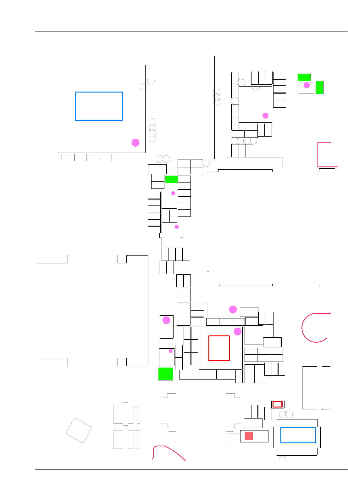
SAMSUNG Proprietary-Contents may change without notice
Flow Chart of Troubleshooting
9-19
This Document can not be used without Samsung's authorization
BTC300
C106
7
0
1
C
9
0
1
C
8
0
C110
2
1
1
C
3
1
C115
C117
1
2
1
C
C124
C125
C200
C201
C202
C209C210
C214
C216
C217
C300
1
0
3
C
C302C30 3 C304
5
0
3
C
C306
C307
C308
9
0
3
C
0
1
3
C
1
1
3
C
2
1
3
C
7
1
3
C
C318
9
1
3
C
0
2
3
C
1
2
3
C
2
2
3
C
3
2
3
C
5
2
3
C
C326
7
2
3
C
C328
C330
C335
C336
7
3
3
C
C338
9
3
3
C
C340
C341C34 2 C343
C344
C345
C347
C348
C349
C350
1
5
3
C
C352
C353
1
2
4
C2
2
4
C
C423
6
2
4
C
0
0
5
C
C501
0
0
3
D
C
F100
HDC503
L104
5
0
1
L
L107
0
0
3
L
6
0
4
L
7
0
4
L
0
0
4
T
O
M
OSC300
0
0
1
5
0
1
R
7
0
R108
0
0
2
R
1
0
2
R
2
0
2
R
3
0
2
R
4
0
2
R
R206
R207
0
0
3
R
1
0
3
R
R307
R308
R309
R310
R311
R312
3
1
3
R
R314
5
1
3
R
R316
R317
8
1
3
R
R320
R425
8
2
4
R
0
4
4
R
SC100
SIM300
SPK400
SPK401
0
0
3
A
T
TAC_HOLD
4
0
1
P
T
TP106
7
0
1
P
T
8
0
1
P
T
TP109
TP110
1
1
1
P
T
3
1
1
P
T
0
0
2
P
T
TP201
TP204
5
0
2
P
T
TP206
TP207
TP208
9
0
2
P
T
0
1
2
P
T
4
1
2
P
T
5
1
2
P
T
TP500TP501
TP503
U100
2
0
3
U
U400
1
0
4
U
UCP200
UME200
0
0
2
R
V
ZD300
ZD301
ZD405
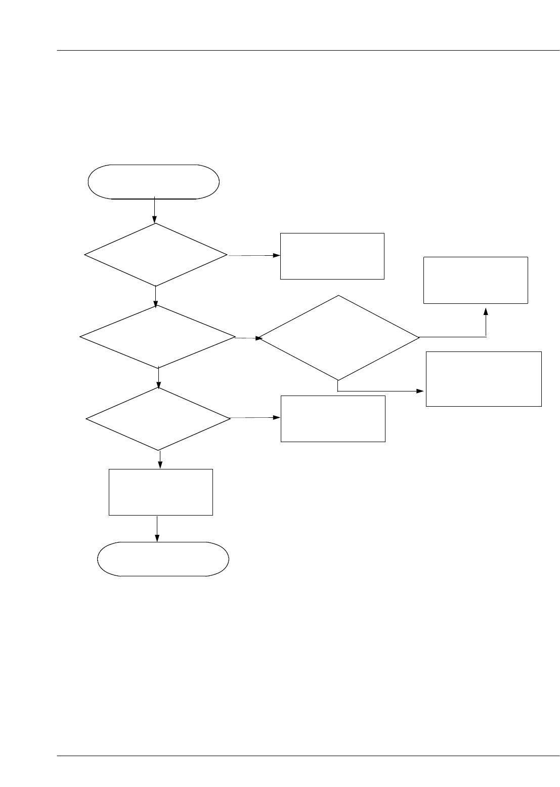
SAMSUNG Proprietary-Contents may change without notice
Flow Chart of Troubleshooting
9-20
This Document can not be used without Samsung's authorization
9-2. RF
** When testing TX chain, check ALL RF devices, resistors, inductors, and capacitors.
9-2-1. GSM850/GSM900 Transmitter
TX ON: Level 5
Check Antenna
Switch Control
Re-solder or Change
PAM100
END
Check OSC100
U103 pin31 ≥
2.65V
Check PAM100
PIN8=H, PIN9=L
PIN10=H
PAM100 pin2
≥-15dBm
Re-solder R103,
C144
U103 PIN15
≥-15dBm
Check U103,
PAM100
NO
YES
NO
YES
YES
NO
YES
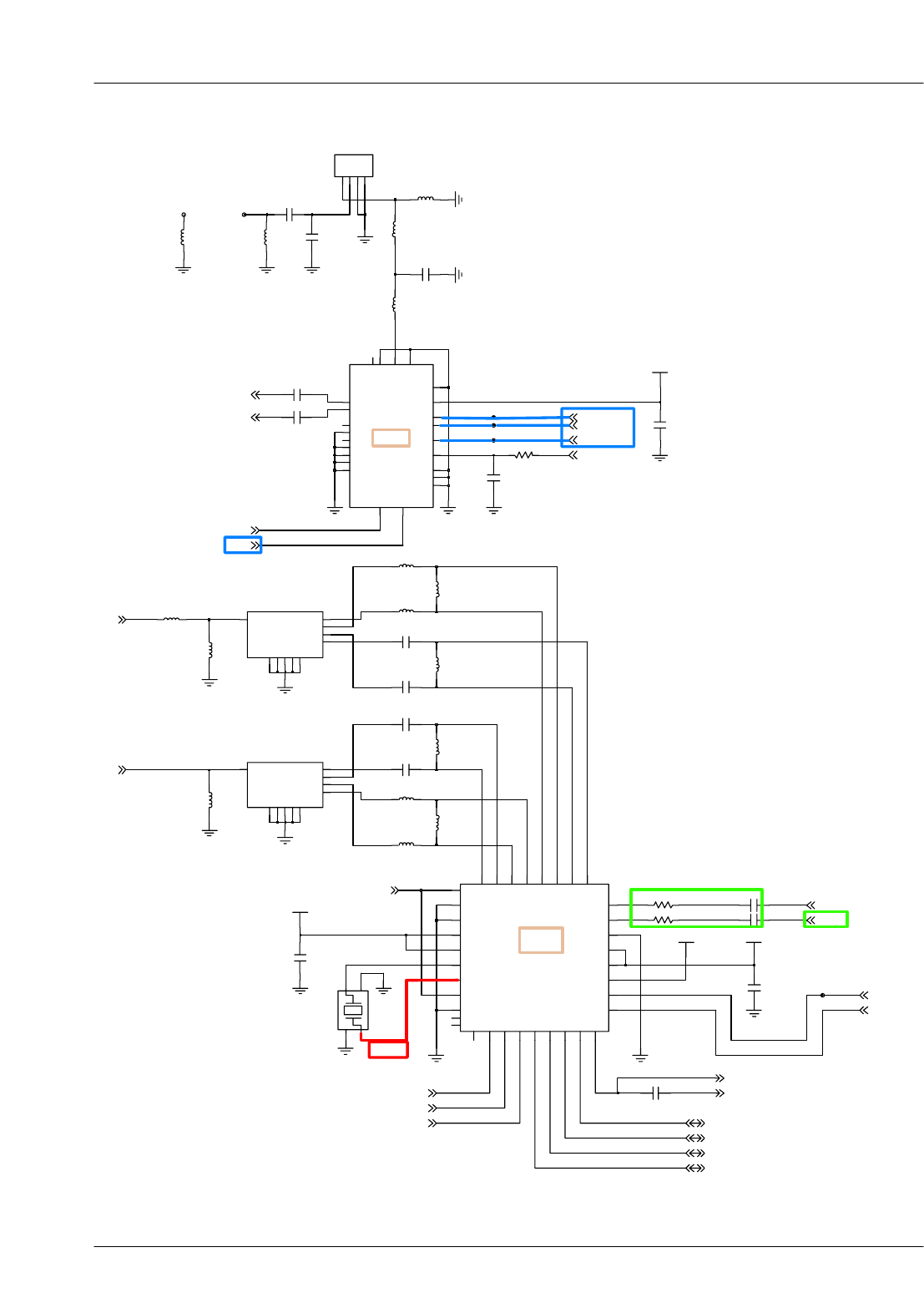
SAMSUNG Proprietary-Contents may change without notice
Flow Chart of Troubleshooting
9-21
This Document can not be used without Samsung's authorization
ANT103
C148
TP101
L103
L108
L101
L116
L102
TP120
L113
C120
L111
C101
C144
L114
L109
C104
C128
ANT101
C134
L110
C130
R102
RFS100
2A
C
1
G
3
4G
VBAT
B
H
_
N
I
F
R
4B
L
_
NI
F
R
RX0
18
RX1
17
8
TX_EN
VBATT 11
VRAMP 7
GND
GND
13
D
N
G0
2
GPCTRL0 9
10
GPCTRL1
NC
12
C
N6
1
19 NC
2
GND 21
22
GND
GND 23
24
GND
D
N
G4
1
GND
3
GND
5
6
PAM100
T
N
A5
1
GND
1
L115
2
3
4
1
OSC100
C123
L112
L118
7
GSM900_OUT 8
9
GSM900_OUT
IN
1
G
2
3G
G
4
5G
G
0
1
6
GSM850_OUT
GSM850_OUT
F102
VDD_RX_TX_2.8V
C111
XMODE
T
U
O
X
8
XTAL1
1
3
XTAL2
0
3
9
_PDN
0
1
_RESET
2N
E
S
_
O
I
D
S
2
1
VDD
VDD
3
1
8
2
VDD
9
2
VDD
VIO
1
1
XDIV
6
2
2
3
XEN
5
2
P
DI
F
R
2
2
N
E
I
F
R
1
2
P
E
I
F
R
8
1
N
PI
F
R
7
1
P
PI
F
R
6
1
RFOH
RFOL
5
1
1K
L
C
S
3
GND
4
1
3
3
GND
4
3
NC
5
3
NC
C
N
6
3
4
2
N
AI
F
R
3
2
P
A
I
F
R
0
2
N
D
I
F
R
9
1
U103
AFC
7
2
NI
B
6
7PI
B
4N
Q
B
5P
Q
B
L100
R104
L121
R103
C100
TP102
TP100
GSM1900_OUT 9
1IN
VCC_SYN_2.8V
VDD_IO_LOW_1.8V
2G
G
3
G
4
5G
0
1G
GSM1800_OUT 6
7
GSM1800_OUT
8
GSM1900_OUT
F101
L120
C147
C105
C103
HB_TX
RAMP
RF_CLK
RF_EN
RF_DATA
D_REF_CLK
LB_TX
RF_RESET
PON_3587_SYNTH
REF_ON_PMU
HB_RX
RX_I_N
RX_I_P
RX_Q_N
RX_Q_P
BT_CLK
BAND_SEL
MOD_STANDBY
HB_TX
LB_TX
PON_PA
HB_RX
LB_RX
LB_RX
SAMSUNG Proprietary-Contents may change without notice
Flow Chart of Troubleshooting
9-22
This Document can not be used without Samsung's authorization
3
0
1
C
4
0
1
C
C105
9
0
1
C
8
0
1
C
1
1
1
C
C120
C122
C123
C128
C130
C133
4
3
1
C
4
4
1
C
C148
5
0
2
C
6
0
2
C
3
1
2
C
5
1
2
C
C402
C405
C411
2
1
4
C
C414
5
1
4
C
2
3
4
C
1
0
1
F2
0
1
F
L101
L103
8
0
1
L0
1
1
L
L111
2
1
1
L
3
1
1
L
4
1
1
L
L115
8
1
1
L
L120
1
2
1
L
0
0
1
C
S
O
0
0
1
M
A
P
1
0
1
R
R102
3
0
1
R
4
0
1
R
5
0
1
R
7
0
1
R
5
0
2
R
8
0
2
R
3
0
3
R
R402
6
1
4
R
R417
0
2
4
R
RFS100
TP100
1
0
1
P
T
TP102
TP105
7
0
1
P
T
1
1
1
P
T
2
1
1
P
T
TP120
TP202
TP203
5
0
2
P
T
TP208
9
0
2
P
T
TP212
4
1
2
P
T
5
1
2
P
T
TP300
U100
U103
UCP200
UME200
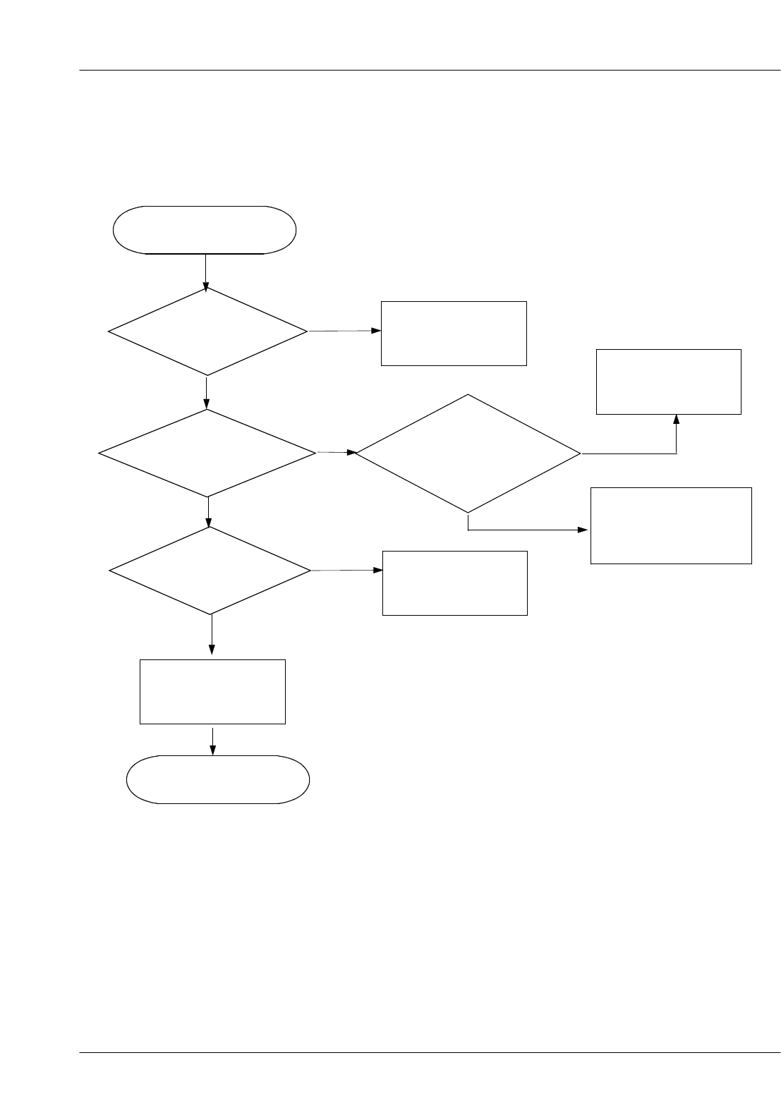
SAMSUNG Proprietary-Contents may change without notice
Flow Chart of Troubleshooting
9-23
This Document can not be used without Samsung's authorization
9-2-2. DCS1800/PCS1900 Transmitter
TX ON: Level 0
Check Antenna
Switch Control
Re-solder or Change
PAM100
END
Check OSC100
U103 PIN31 ≥
2.65V
Check PAM100
PIN8=H, PIN9=H
PIN10=H
PAM100 PIN2
≥-15dBm
Re-solder R102,
C148
U103 PIN16
≥-15dBm
Check U103,
PAM100
NO
YES
NO
YES
YES
NO
YES
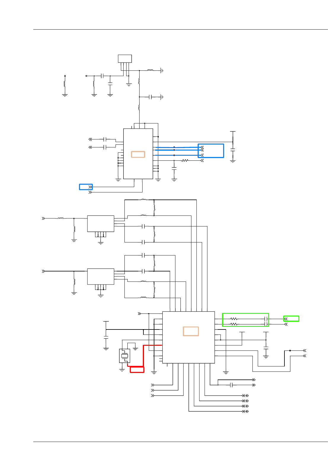
SAMSUNG Proprietary-Contents may change without notice
Flow Chart of Troubleshooting
9-24
This Document can not be used without Samsung's authorization
ANT103
C148
TP101
L103
L108
L101
L116
L102
TP120
L113
C120
L111
C101
C144
L114
L109
C104
C128
ANT101
C134
L110
C130
R102
RFS100
2A
C
1
G
3
4G
VBAT
B
H
_
N
I
F
R
4B
L
_
NI
F
R
RX0
18
RX1
17
8
TX_EN
VBATT 11
VRAMP 7
GND
GND
13
D
N
G0
2
GPCTRL0 9
10
GPCTRL1
NC
12
C
N6
1
19 NC
2
GND 21
22
GND
GND 23
24
GND
D
N
G4
1
GND
3
GND
5
6
PAM100
T
N
A5
1
GND
1
L115
2
3
4
1
OSC100
C123
L112
L118
7
GSM900_OUT 8
9
GSM900_OUT
IN
1
G
2
3G
G
4
5G
G
0
1
6
GSM850_OUT
GSM850_OUT
F102
VDD_RX_TX_2.8V
C111
XMODE
T
U
O
X
8
XTAL1
1
3
XTAL2
0
3
9
_PDN
0
1
_RESET
2N
E
S
_
O
I
D
S
2
1
VDD
VDD
3
1
8
2
VDD
9
2
VDD
VIO
1
1
XDIV
6
2
2
3
XEN
5
2
P
DI
F
R
2
2
N
E
I
F
R
1
2
P
E
I
F
R
8
1
N
PI
F
R
7
1
P
PI
F
R
6
1
RFOH
RFOL
5
1
1K
L
C
S
3
GND
4
1
3
3
GND
4
3
NC
5
3
NC
C
N
6
3
4
2
N
AI
F
R
3
2
P
A
I
F
R
0
2
N
D
I
F
R
9
1
U103
AFC
7
2
NI
B
6
7PI
B
4N
Q
B
5P
Q
B
L100
R104
L121
R103
C100
TP102
TP100
GSM1900_OUT 9
1IN
VCC_SYN_2.8V
VDD_IO_LOW_1.8V
2G
G
3
G
4
5G
0
1G
GSM1800_OUT 6
7
GSM1800_OUT
8
GSM1900_OUT
F101
L120
C147
C105
C103
HB_TX
RAMP
RF_CLK
RF_EN
RF_DATA
D_REF_CLK
LB_TX
RF_RESET
PON_3587_SYNTH
REF_ON_PMU
HB_RX
RX_I_N
RX_I_P
RX_Q_N
RX_Q_P
BT_CLK
BAND_SEL
MOD_STANDBY
HB_TX
LB_TX
PON_PA
HB_RX
LB_RX
LB_RX
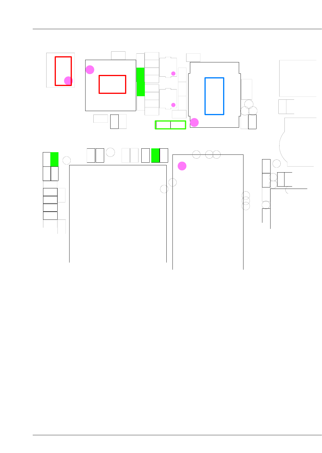
SAMSUNG Proprietary-Contents may change without notice
Flow Chart of Troubleshooting
9-25
This Document can not be used without Samsung's authorization
3
0
1
C
4
0
1
C
C105
9
0
1
C
8
0
1
C
1
1
1
C
C120
C122
C123
C128
C130
C133
4
3
1
C
4
4
1
C
C148
5
0
2
C
6
0
2
C
3
1
2
C
5
1
2
C
C402
C405
C411
2
1
4
C
C414
5
1
4
C
2
3
4
C
1
0
1
F2
0
1
F
L101
L103
8
0
1
L0
1
1
L
L111
2
1
1
L
3
1
1
L
4
1
1
L
L115
8
1
1
L
L120
1
2
1
L
0
0
1
C
S
O
0
0
1
M
A
P
1
0
1
R
R102
3
0
1
R
4
0
1
R
5
0
1
R
7
0
1
R
5
0
2
R
8
0
2
R
3
0
3
R
R402
6
1
4
R
R417
0
2
4
R
RFS100
TP100
1
0
1
P
T
TP102
TP105
7
0
1
P
T
1
1
1
P
T
2
1
1
P
T
TP120
TP202
TP203
5
0
2
P
T
TP208
9
0
2
P
T
TP212
4
1
2
P
T
5
1
2
P
T
TP300
U100
U103
UCP200
UME200
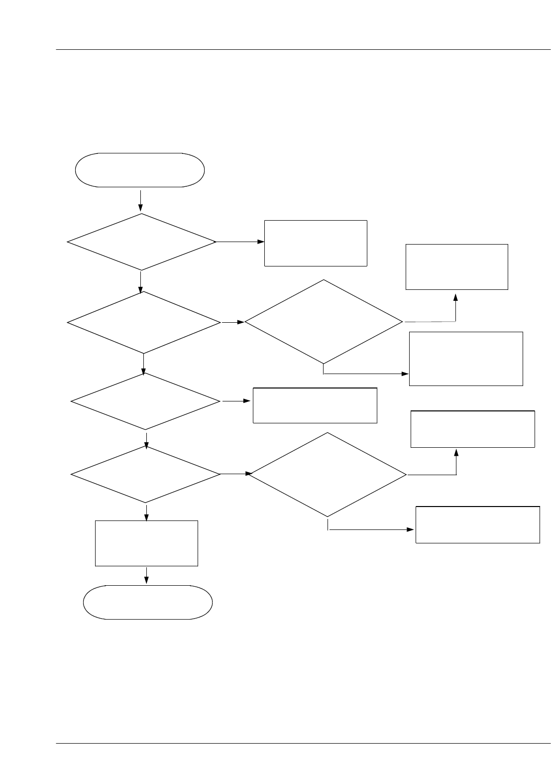
SAMSUNG Proprietary-Contents may change without notice
Flow Chart of Troubleshooting
9-26
This Document can not be used without Samsung's authorization
9-2-3. GSM850 Receiver
RX ON
AMP-50dBm
NO Resolder RFS100,
L116,L121 Check Antenna
Switch Control
YES
PAM100 PIN17
≥-70dBm
NO
Resolder or Change
PAM100
YES
YES
Check U103,
PAM100
END
F102 PIN1
≥-70dBm
Check PAM100
PIN8=L, PIN9=H
PIN10=H
NO
Resolder or change
C105
YES
U103 PIN23,24
≥-75dBm
Check F102
PIN6,PIN7
≥-75dBm
NO
YES Resolder or change
C123,C128,L112
Resolder or change
F102
YES
PAM100 PIN15
≥-55dBm

SAMSUNG Proprietary-Contents may change without notice
Flow Chart of Troubleshooting
9-27
This Document can not be used without Samsung's authorization
ANT103
C148
TP101
L103
L108
L101
L116
L102
TP120
L113
C120
L111
C101
C144
L114
L109
C104
C128
ANT101
C134
L110
C130
R102
RFS100
2A
C
1
G
3
4G
VBAT
B
H
_
N
I
F
R
4B
L
_
NI
F
R
RX0
18
RX1
17
8
TX_EN
VBATT 11
VRAMP 7
GND
GND
13
D
N
G0
2
GPCTRL0 9
10
GPCTRL1
NC
12
C
N6
1
19 NC
2
GND 21
22
GND
GND 23
24
GND
D
N
G4
1
GND
3
GND
5
6
PAM100
T
N
A5
1
GND
1
L115
2
3
4
1
OSC100
C123
L112
L118
7
GSM900_OUT 8
9
GSM900_OUT
IN
1
G
2
3G
G
4
5G
G
0
1
6
GSM850_OUT
GSM850_OUT
F102
VDD_RX_TX_2.8V
C111
XMODE
T
U
O
X
8
XTAL1
1
3
XTAL2
0
3
9
_PDN
0
1
_RESET
2N
E
S
_
O
I
D
S
2
1
VDD
VDD
3
1
8
2
VDD
9
2
VDD
VIO
1
1
XDIV
6
2
2
3
XEN
5
2
P
DI
F
R
2
2
N
E
I
F
R
1
2
P
E
I
F
R
8
1
N
PI
F
R
7
1
P
PI
F
R
6
1
RFOH
RFOL
5
1
1K
L
C
S
3
GND
4
1
3
3
GND
4
3
NC
5
3
NC
C
N
6
3
4
2
N
AI
F
R
3
2
P
A
I
F
R
0
2
N
D
I
F
R
9
1
U103
AFC
7
2
NI
B
6
7PI
B
4N
Q
B
5P
Q
B
L100
R104
L121
R103
C100
TP102
TP100
GSM1900_OUT 9
1IN
VCC_SYN_2.8V
VDD_IO_LOW_1.8V
2G
G
3
G
4
5G
0
1G
GSM1800_OUT 6
7
GSM1800_OUT
8
GSM1900_OUT
F101
L120
C147
C105
C103
HB_TX
RAMP
RF_CLK
RF_EN
RF_DATA
D_REF_CLK
LB_TX
RF_RESET
PON_3587_SYNTH
REF_ON_PMU
HB_RX
RX_I_N
RX_I_P
RX_Q_N
RX_Q_P
BT_CLK
BAND_SEL
MOD_STANDBY
HB_TX
LB_TX
PON_PA
HB_RX
LB_RX
LB_RX
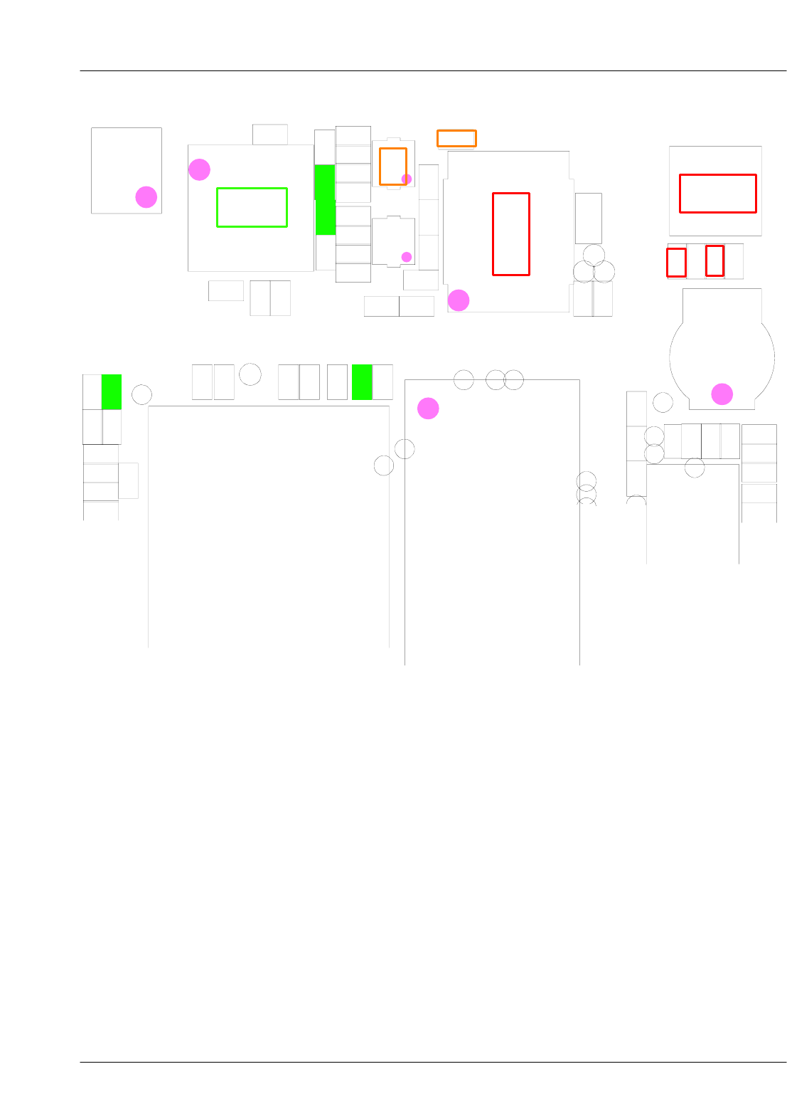
SAMSUNG Proprietary-Contents may change without notice
Flow Chart of Troubleshooting
9-28
This Document can not be used without Samsung's authorization
0
0
3
T
A
B
3
0
1
C
4
0
1
C
C105
9
0
1
C
8
0
1
C
1
1
1
C
3
1
1
C
C117
C120
C122
C123
C124
C128
C130
C133
4
3
1
C
4
4
1
C
7
4
1
C
C148
5
0
2
C
6
0
2
C
3
1
2
C
5
1
2
C
C411
2
1
4
C
C414
5
1
4
C
2
3
4
C
1
0
1
F2
0
1
F
0
0
1
L
L101
L103
L106
L107
8
0
1
L0
1
1
L
L111
2
1
1
L
3
1
1
L
4
1
1
L
L115
6
1
1
L
8
1
1
L
L120
1
2
1
L
0
0
1
C
S
O
0
0
1
M
A
P
0
0
1
R
1
0
1
R
R102
3
0
1
R
4
0
1
R
7
0
1
R
5
0
2
R
8
0
2
R
3
0
3
R
6
1
4
R
R417
0
2
4
R
RFS100
TP100
1
0
1
P
T
TP102
4
0
1
P
T
TP105
7
0
1
1
1
P
T
2
1
1
P
T
TP120
TP202
TP203
5
0
2
P
T
TP208
9
0
2
P
T
TP212
4
1
2
P
T
5
1
TP300
U100
U103
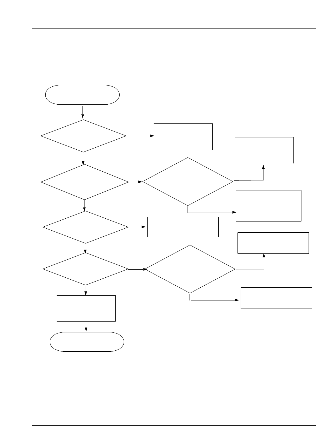
SAMSUNG Proprietary-Contents may change without notice
Flow Chart of Troubleshooting
9-29
This Document can not be used without Samsung's authorization
9-2-4. GSM900 Receiver
RX ON
AMP-50dBm
NO Resolder RFS100,
L116,L121 Check Antenna
Switch Control
YES
PAM100 PIN17
≥-70dBm
NO
Resolder or Change
PAM100
YES
YES
Check U103,
PAM100
END
F102 PIN1
≥-70dBm
Check PAM100
PIN8=L, PIN9=H
PIN10=H
NO
Resolder or change
C105
YES
U103 PIN21,22
≥-75dBm
Check F102
PIN8,PIN9
≥-75dBm
NO
YES Resolder or change
L111,L114,L115
Resolder or change
F102
YES
PAM100 PIN15
≥-55dBm
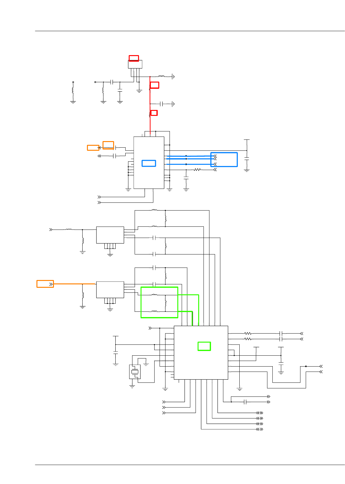
SAMSUNG Proprietary-Contents may change without notice
Flow Chart of Troubleshooting
9-30
This Document can not be used without Samsung's authorization
ANT103
C148
TP101
L103
L108
L101
L116
L102
TP120
L113
C120
L111
C101
C144
L114
L109
C104
C128
ANT101
C134
L110
C130
R102
RFS100
2A
C
1
G
3
4G
VBAT
B
H
_
N
I
F
R
4B
L
_
NI
F
R
RX0
18
RX1
17
8
TX_EN
VBATT 11
VRAMP 7
GND
GND
13
D
N
G0
2
GPCTRL0 9
10
GPCTRL1
NC
12
C
N6
1
19 NC
2
GND 21
22
GND
GND 23
24
GND
D
N
G4
1
GND
3
GND
5
6
PAM100
T
N
A5
1
GND
1
L115
2
3
4
1
OSC100
C123
L112
L118
7
GSM900_OUT 8
9
GSM900_OUT
IN
1
G
2
3G
G
4
5G
G
0
1
6
GSM850_OUT
GSM850_OUT
F102
VDD_RX_TX_2.8V
C111
XMODE
T
U
O
X
8
XTAL1
1
3
XTAL2
0
3
9
_PDN
0
1
_RESET
2N
E
S
_
O
I
D
S
2
1
VDD
VDD
3
1
8
2
VDD
9
2
VDD
VIO
1
1
XDIV
6
2
2
3
XEN
5
2
P
DI
F
R
2
2
N
E
I
F
R
1
2
P
E
I
F
R
8
1
N
PI
F
R
7
1
P
PI
F
R
6
1
RFOH
RFOL
5
1
1K
L
C
S
3
GND
4
1
3
3
GND
4
3
NC
5
3
NC
C
N
6
3
4
2
N
AI
F
R
3
2
P
A
I
F
R
0
2
N
D
I
F
R
9
1
U103
AFC
7
2
NI
B
6
7PI
B
4N
Q
B
5P
Q
B
L100
R104
L121
R103
C100
TP102
TP100
GSM1900_OUT 9
1IN
VCC_SYN_2.8V
VDD_IO_LOW_1.8V
2G
G
3
G
4
5G
0
1G
GSM1800_OUT 6
7
GSM1800_OUT
8
GSM1900_OUT
F101
L120
C147
C105
C103
HB_TX
RAMP
RF_CLK
RF_EN
RF_DATA
D_REF_CLK
LB_TX
RF_RESET
PON_3587_SYNTH
REF_ON_PMU
HB_RX
RX_I_N
RX_I_P
RX_Q_N
RX_Q_P
BT_CLK
BAND_SEL
MOD_STANDBY
HB_TX
LB_TX
PON_PA
HB_RX
LB_RX
LB_RX
SAMSUNG Proprietary-Contents may change without notice
Flow Chart of Troubleshooting
9-31
This Document can not be used without Samsung's authorization
0
0
3
T
A
B
3
0
1
C
4
0
1
C
C105
9
0
1
C
8
0
1
C
1
1
1
C
3
1
1
C
C117
C120
C122
C123
C124
C128
C130
C133
4
3
1
C
4
4
1
C
7
4
1
C
C148
5
0
2
C
6
0
2
C
3
1
2
C
5
1
2
C
C411
2
1
4
C
C414
5
1
4
C
2
3
4
C
1
0
1
F2
0
1
F
0
0
1
L
L101
L103
L106
L107
8
0
1
L0
1
1
L
L111
2
1
1
L
3
1
1
L
4
1
1
L
L115
6
1
1
L
8
1
1
L
L120
1
2
1
L
0
0
1
C
S
O
0
0
1
M
A
P
0
0
1
R
1
0
1
R
R102
3
0
1
R
4
0
1
R
7
0
1
R
5
0
2
R
8
0
2
R
3
0
3
R
6
1
4
R
R417
0
2
4
R
RFS100
TP100
1
0
1
P
T
TP102
4
0
1
P
T
TP105
7
0
1
1
1
P
T
2
1
1
P
T
TP120
TP202
TP203
5
0
2
P
T
TP208
9
0
2
P
T
TP212
4
1
2
P
T
5
1
TP300
U100
U103
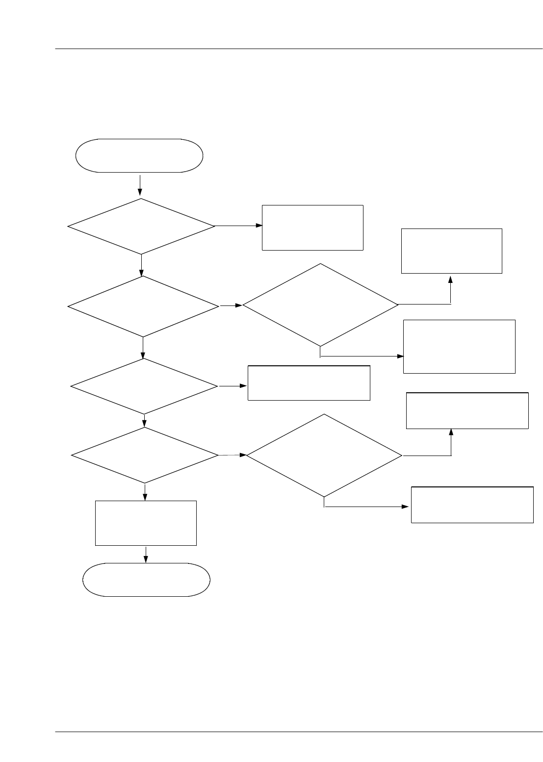
SAMSUNG Proprietary-Contents may change without notice
Flow Chart of Troubleshooting
9-32
This Document can not be used without Samsung's authorization
9-2-5. DCS1800 Receiver
RX ON
AMP-50dBm
NO Resolder RFS100,
L116,L121 Check Antenna
Switch Control
YES
PAM100 PIN18
≥-70dBm
NO
Resolder or Change
PAM100
YES
YES
Check U103,
PAM100
END
F101 PIN1
≥-70dBm
Check PAM100
PIN8=L, PIN9=L
PIN10=H
NO
Resolder or change
C103,L118
YES
U103 PIN19,20
≥-75dBm
Check F101
PIN6,PIN7
≥-75dBm
NO
YES Resolder or change
L101,L103,L108
Resolder or change
F102
YES
PAM100 PIN15
≥-55dBm
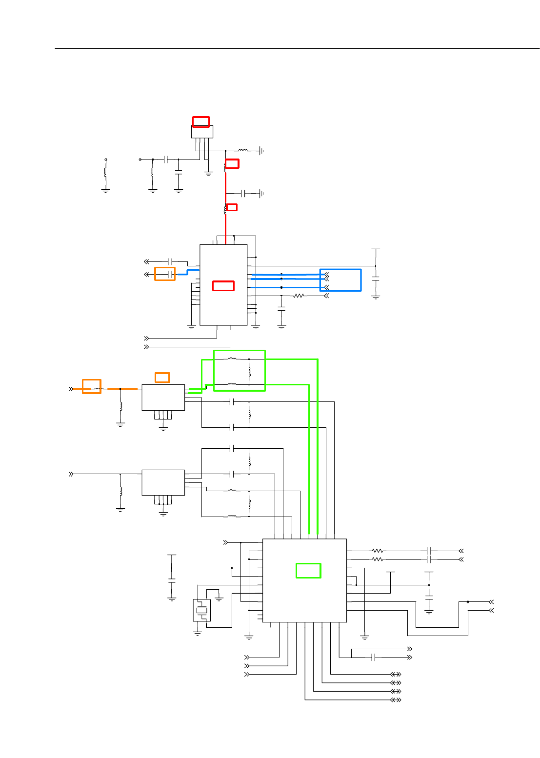
SAMSUNG Proprietary-Contents may change without notice
Flow Chart of Troubleshooting
9-33
This Document can not be used without Samsung's authorization
ANT103
C148
TP101
L103
L108
L101
L116
L102
TP120
L113
C120
L111
C101
C144
L114
L109
C104
C128
ANT101
C134
L110
C130
R102
RFS100
2A
C
1
G
3
4G
VBAT
B
H
_
N
I
F
R
4B
L
_
NI
F
R
RX0
18
RX1
17
8
TX_EN
VBATT 11
VRAMP 7
GND
GND
13
D
N
G0
2
GPCTRL0 9
10
GPCTRL1
NC
12
C
N6
1
19 NC
2
GND 21
22
GND
GND 23
24
GND
D
N
G4
1
GND
3
GND
5
6
PAM100
T
N
A5
1
GND
1
L115
2
3
4
1
OSC100
C123
L112
L118
7
GSM900_OUT 8
9
GSM900_OUT
IN
1
G
2
3G
G
4
5G
G
0
1
6
GSM850_OUT
GSM850_OUT
F102
VDD_RX_TX_2.8V
C111
XMODE
T
U
O
X
8
XTAL1
1
3
XTAL2
0
3
9
_PDN
0
1
_RESET
2N
E
S
_
O
I
D
S
2
1
VDD
VDD
3
1
8
2
VDD
9
2
VDD
VIO
1
1
XDIV
6
2
2
3
XEN
5
2
P
DI
F
R
2
2
N
E
I
F
R
1
2
P
E
I
F
R
8
1
N
PI
F
R
7
1
P
PI
F
R
6
1
RFOH
RFOL
5
1
1K
L
C
S
3
GND
4
1
3
3
GND
4
3
NC
5
3
NC
C
N
6
3
4
2
N
AI
F
R
3
2
P
A
I
F
R
0
2
N
D
I
F
R
9
1
U103
AFC
7
2
NI
B
6
7PI
B
4N
Q
B
5P
Q
B
L100
R104
L121
R103
C100
TP102
TP100
GSM1900_OUT 9
1IN
VCC_SYN_2.8V
VDD_IO_LOW_1.8V
2G
G
3
G
4
5G
0
1G
GSM1800_OUT 6
7
GSM1800_OUT
8
GSM1900_OUT
F101
L120
C147
C105
C103
HB_TX
RAMP
RF_CLK
RF_EN
RF_DATA
D_REF_CLK
LB_TX
RF_RESET
PON_3587_SYNTH
REF_ON_PMU
HB_RX
RX_I_N
RX_I_P
RX_Q_N
RX_Q_P
BT_CLK
BAND_SEL
MOD_STANDBY
HB_TX
LB_TX
PON_PA
HB_RX
LB_RX
LB_RX
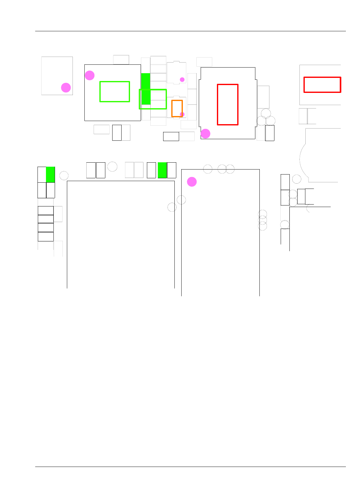
SAMSUNG Proprietary-Contents may change without notice
Flow Chart of Troubleshooting
9-34
This Document can not be used without Samsung's authorization
3
0
1
C
4
0
1
C
C105
9
0
1
C
8
0
1
C
1
1
1
C
C120
C122
C123
C128
C130
C133
4
3
1
C
4
4
1
C
C148
5
0
2
C
6
0
2
C
3
1
2
C
5
1
2
C
C402
C405
C411
2
1
4
C
C414
5
1
4
C
2
3
4
C
1
0
1
F2
0
1
F
L101
L103
8
0
1
L0
1
1
L
L111
2
1
1
L
3
1
1
L
4
1
1
L
L115
8
1
1
L
L120
1
2
1
L
0
0
1
C
S
O
0
0
1
M
A
P
1
0
1
R
R102
3
0
1
R
4
0
1
R
5
0
1
R
7
0
1
R
5
0
2
R
8
0
2
R
3
0
3
R
R402
6
1
4
R
R417
0
2
4
R
RFS100
TP100
1
0
1
P
T
TP102
TP105
7
0
1
P
T
1
1
1
P
T
2
1
1
P
T
TP120
TP202
TP203
5
0
2
P
T
TP208
9
0
2
P
T
TP212
4
1
2
P
T
5
1
2
P
T
TP300
U100
U103
UCP200
UME200
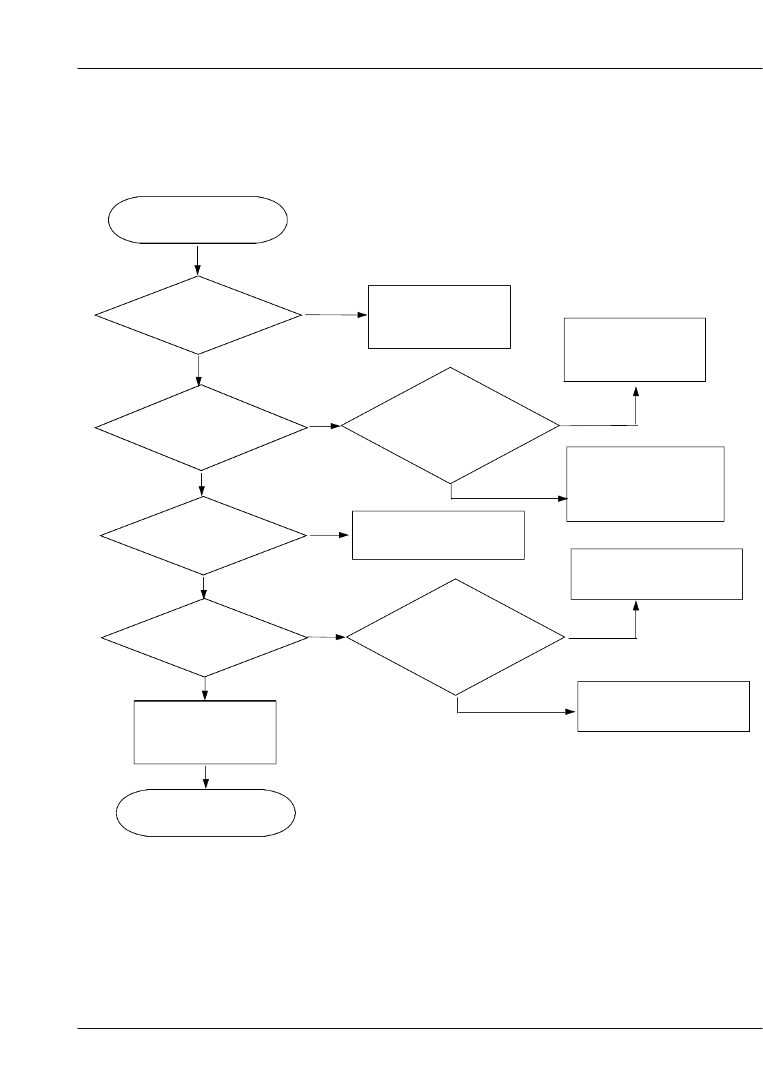
SAMSUNG Proprietary-Contents may change without notice
Flow Chart of Troubleshooting
9-35
This Document can not be used without Samsung's authorization
9-2-6. PCS1900 Receiver
RX ON
AMP-50dBm
NO Resolder RFS100,
L116,L121 Check Antenna
Switch Control
YES
PAM100 PIN18
≥-70dBm
NO
Resolder or Change
PAM100
YES
YES
Check U103,
PAM100
END
F101 PIN1
≥-70dBm
Check PAM100
PIN8=L, PIN9=L
PIN10=H
NO
Resolder or change
C103,L118
YES
U103 PIN17,18
≥-75dBm
Check F101
PIN8,PIN9
≥-75dBm
NO
YES Resolder or change
C120,C122,L110
Resolder or change
F102
YES
PAM100 PIN15
≥-55dBm
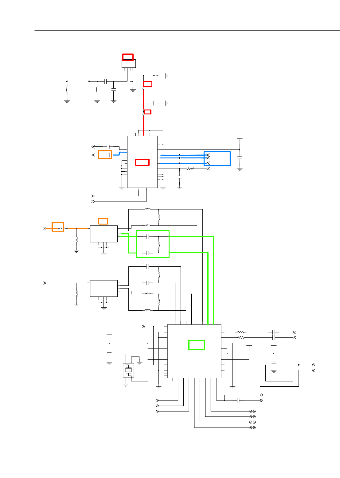
SAMSUNG Proprietary-Contents may change without notice
Flow Chart of Troubleshooting
9-36
This Document can not be used without Samsung's authorization
ANT103
C148
TP101
L103
L108
L101
L116
L102
TP120
L113
C120
L111
C101
C144
L114
L109
C104
C128
ANT101
C134
L110
C130
R102
RFS100
2A
C
1
G
3
4G
VBAT
B
H
_
N
I
F
R
4B
L
_
NI
F
R
RX0
18
RX1
17
8
TX_EN
VBATT 11
VRAMP 7
GND
GND
13
D
N
G0
2
GPCTRL0 9
10
GPCTRL1
NC
12
C
N6
1
19 NC
2
GND 21
22
GND
GND 23
24
GND
D
N
G4
1
GND
3
GND
5
6
PAM100
T
N
A5
1
GND
1
L115
2
3
4
1
OSC100
C123
L112
L118
7
GSM900_OUT 8
9
GSM900_OUT
IN
1
G
2
3G
G
4
5G
G
0
1
6
GSM850_OUT
GSM850_OUT
F102
VDD_RX_TX_2.8V
C111
XMODE
T
U
O
X
8
XTAL1
1
3
XTAL2
0
3
9
_PDN
0
1
_RESET
2N
E
S
_
O
I
D
S
2
1
VDD
VDD
3
1
8
2
VDD
9
2
VDD
VIO
1
1
XDIV
6
2
2
3
XEN
5
2
P
DI
F
R
2
2
N
E
I
F
R
1
2
P
E
I
F
R
8
1
N
PI
F
R
7
1
P
PI
F
R
6
1
RFOH
RFOL
5
1
1K
L
C
S
3
GND
4
1
3
3
GND
4
3
NC
5
3
NC
C
N
6
3
4
2
N
AI
F
R
3
2
P
A
I
F
R
0
2
N
D
I
F
R
9
1
U103
AFC
7
2
NI
B
6
7PI
B
4N
Q
B
5P
Q
B
L100
R104
L121
R103
C100
TP102
TP100
GSM1900_OUT 9
1IN
VCC_SYN_2.8V
VDD_IO_LOW_1.8V
2G
G
3
G
4
5G
0
1G
GSM1800_OUT 6
7
GSM1800_OUT
8
GSM1900_OUT
F101
L120
C147
C105
C103
HB_TX
RAMP
RF_CLK
RF_EN
RF_DATA
D_REF_CLK
LB_TX
RF_RESET
PON_3587_SYNTH
REF_ON_PMU
HB_RX
RX_I_N
RX_I_P
RX_Q_N
RX_Q_P
BT_CLK
BAND_SEL
MOD_STANDBY
HB_TX
LB_TX
PON_PA
HB_RX
LB_RX
LB_RX
C122
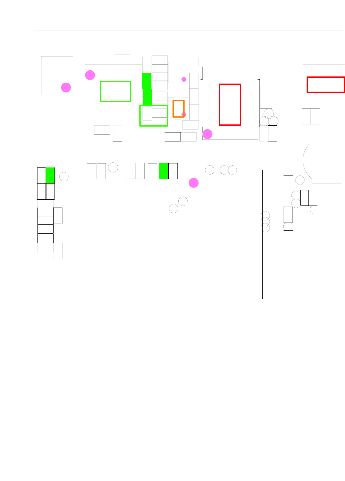
SAMSUNG Proprietary-Contents may change without notice
Flow Chart of Troubleshooting
9-37
This Document can not be used without Samsung's authorization
3
0
1
C
4
0
1
C
C105
9
0
1
C
8
0
1
C
1
1
1
C
C120
C122
C123
C128
C130
C133
4
3
1
C
4
4
1
C
C148
5
0
2
C
6
0
2
C
3
1
2
C
5
1
2
C
C402
C405
C411
2
1
4
C
C414
5
1
4
C
2
3
4
C
1
0
1
F2
0
1
F
L101
L103
8
0
1
L0
1
1
L
L111
2
1
1
L
3
1
1
L
4
1
1
L
L115
8
1
1
L
L120
1
2
1
L
0
0
1
C
S
O
0
0
1
M
A
P
1
0
1
R
R102
3
0
1
R
4
0
1
R
5
0
1
R
7
0
1
R
5
0
2
R
8
0
2
R
3
0
3
R
R402
6
1
4
R
R417
0
2
4
R
RFS100
TP100
1
0
1
P
T
TP102
TP105
7
0
1
P
T
1
1
1
P
T
2
1
1
P
T
TP120
TP202
TP203
5
0
2
P
T
TP208
9
0
2
P
T
TP212
4
1
2
P
T
5
1
2
P
T
TP300
U100
U103
UCP200
UME200
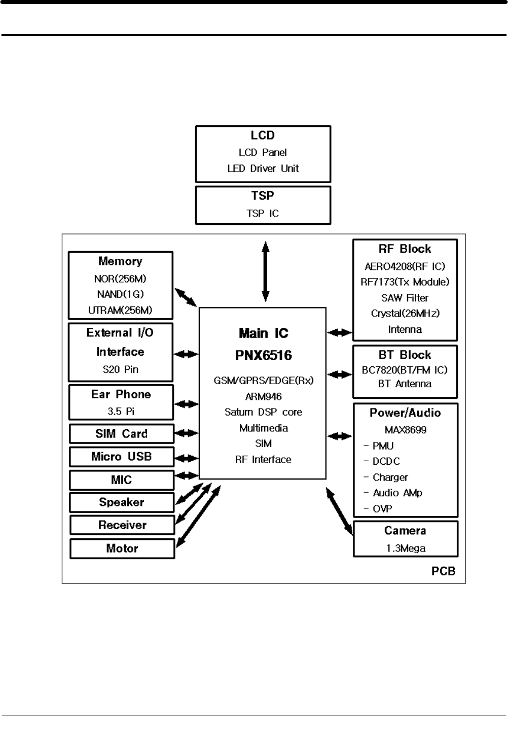
SAMSUNG Proprietary-Contents may change without notice
7. Block Diagrams
7-1
This Document can not be used without Samsung's authorization
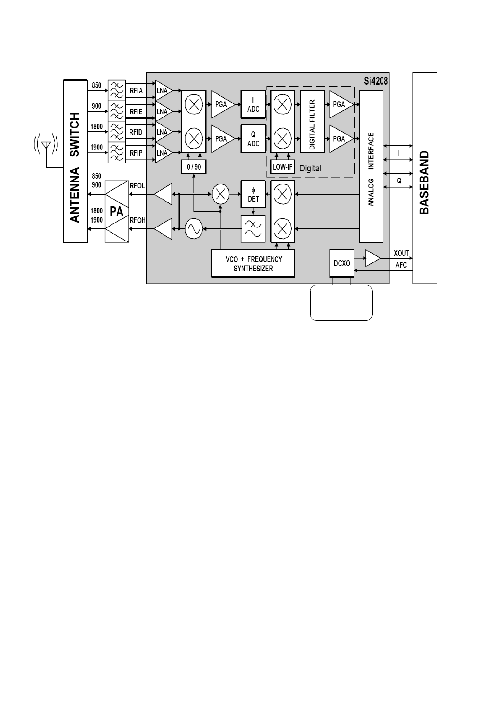
SAMSUNG Proprietary-Contents may change without notice
Block Diagrams
7-2
This Document can not be used without Samsung's authorization
Y]to¡
j
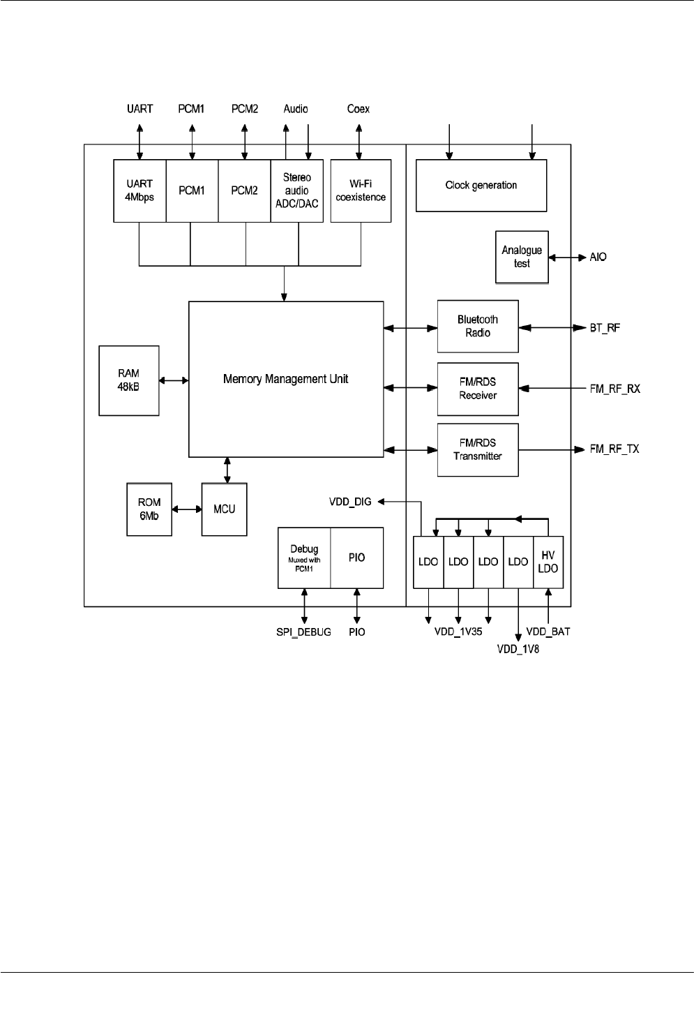
SAMSUNG Proprietary-Contents may change without notice
Block Diagrams
7-3
This Document can not be used without Samsung's authorization
OY]to¡
P
OZYo¡
P
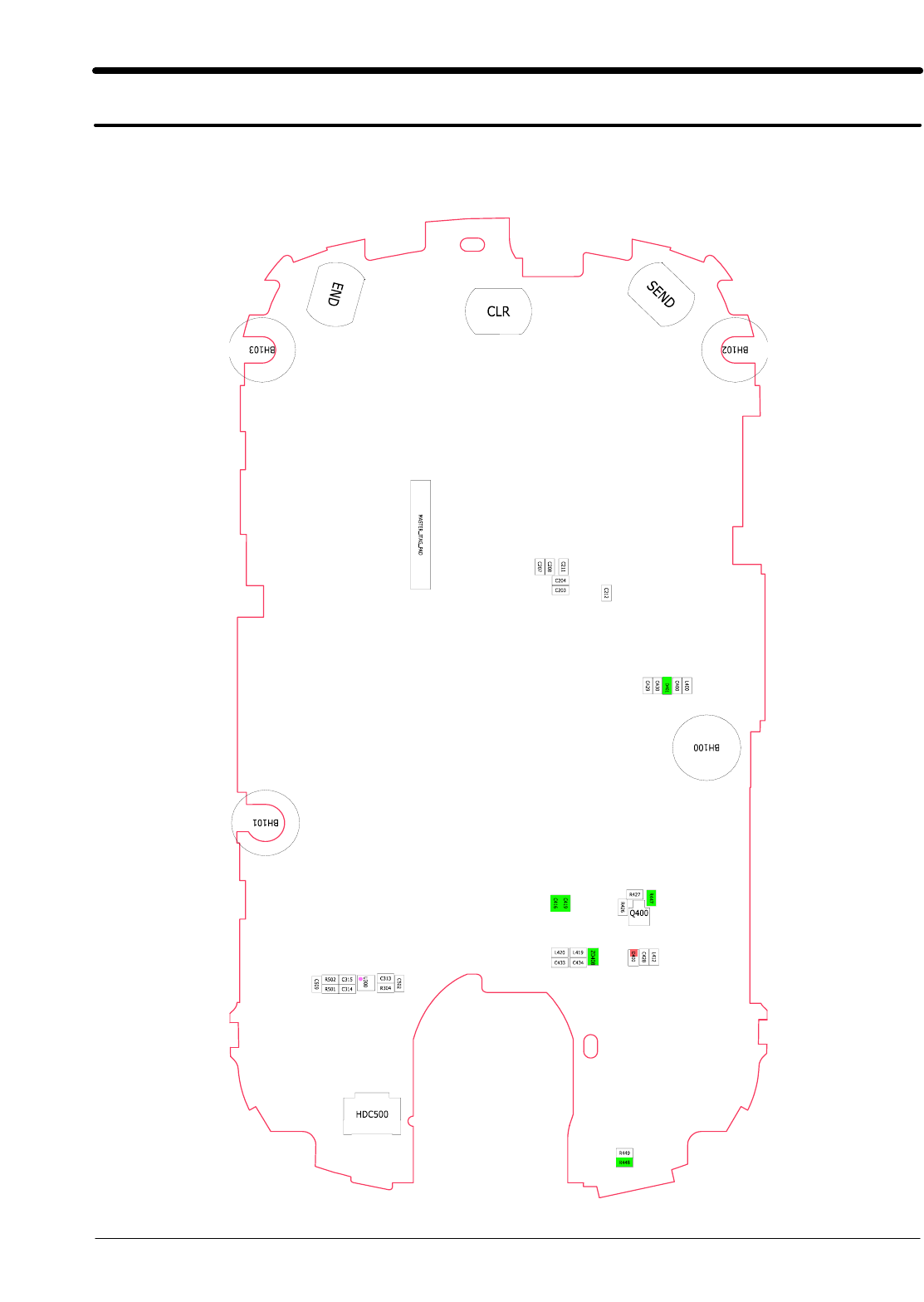
SAMSUNG Proprietary-Contents may change without notice
8. PCB Diagrams
8-1
This Document can not be used without Samsung's authorization
8-1. Top
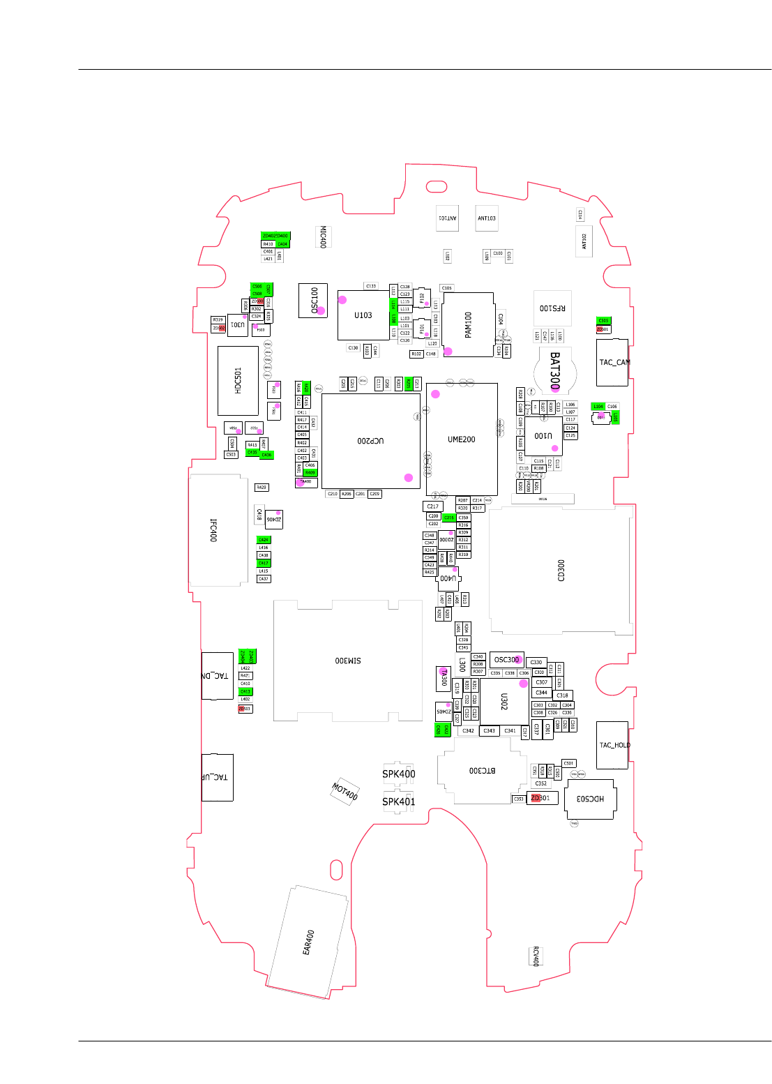
SAMSUNG Proprietary-Contents may change without notice
PCB Diagrams
8-2
This Document can not be used without Samsung's authorization
8-2. Bottom