Samsung GT C3530 Service Manual. Www.s Manuals.com. Manual
User Manual: Phone Samsung GT-C3530 - Service manuals and Schematics, Disassembly / Assembly. Free.
Open the PDF directly: View PDF ![]() .
.
Page Count: 81
GSM TELEPHONE
GT-C3530
1. Safety Precautions
2. Specification
3. Product Function
4. Exploded View and Parts list
5. MAIN Electrical Parts List
6. Level 1Repair
7. Disassembly and Assembly
Instructions
8. Chart of Troubleshooting
9. Reference data
Notice :
All functionality, features, specifications and other
product information provided in this document inclu
ding, but not limited to, the benefits, design, pricing,
components, performance, availability, and capabiliti
-es of the product are subject to change without
notice or obligation. Samsung reserves the right to
make changes to this document and the product
described herein, at anytime, without obligation on
Samsung to provide notification of such change.
GSM TELEPHONE CONTENTS
This Service Manual is aproperty of Samsung Electronics Co.,Ltd.
Any unauthorized use of Manual can be punished under applicable
International and/or domestic law.
Samsung Electronics Co.,Ltd.
2010. 10. Rev.1.0
ⓒ
Country Web Site
North America service.samsungportal.com
Latin America latin.samsungportal.com
CIS cis.samsungportal.com
Europe europe.samsungportal.com
China china.samsungportal.com
Asia asia.samsungportal.com
Mideast &Africa mea.samsungportal.com
GSPN (Global Service Partner Network)
SAMSUNG Proprietary-Contents may change without notice
8. Level 3Repair
8-1
This Document can not be used without Samsung's authorization
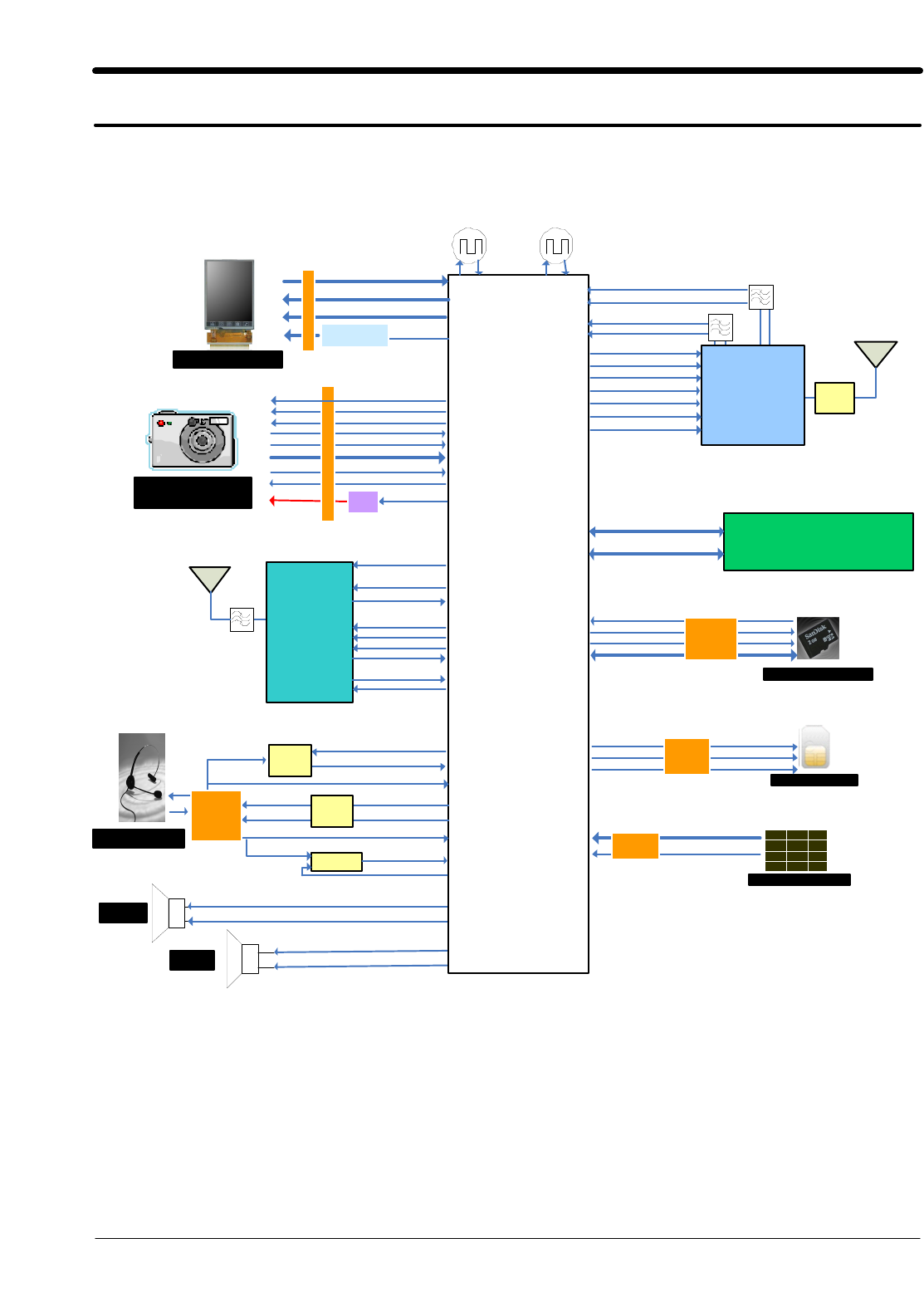
8-1. Block Diagram
RCV_N
RCV_P
SPK _P
SP K _N
SPK
KEY_ROW(0:4)
KEY_COL(0:4)
MAINKEY
CON
Main Key
Base Band
Catfish213
PMB8810
TCXO
BS1
BS2
TX_EN
VL OGI C
RAMP
LB _TX
HB_TX
Main ANT
GSM850_RX
GSM900_RX
DCS1800_RX
PCS1 9 00_ RX
SAW
RF
SW
2G PAM
SWITCH
Module
RF7161
SAW
RCV
SEN D_END_D IR EC T
SI M_ R ST
SIM_C LK
SI M Card
SI M _ I O
SIM
So ck e t
SD _DA TA(0:3)
SD_C LK T-F LA SH
Socket
DETECT _SD
T-FLA SH Card
SD_CMD
ONKEY_N
1 2 3
4 5 6
7 8 9
* 0 #
AD (0: 1 5 )
A(16:26)
256 NOR/1G On eN a n d /256 UtRAM
MEMORY
KAP202N00 M-B WE W
26MHz RTC 32.736KHz
EN_LC D_BL
CAM_SD A
CAM_ RST
CAM _HSYN C
CAM_VSYNC
CAM_DATA(0:7)
CAM
LDO
CAM_ MCLK_OUT
CAM_PC LK_ IN
EN _C AM_ PW R
CA M _C ON
3 ME GA
CAM Module
CAM_SCL
CLK26M_BT
BT
BC63B239A04
BT_ R EQ_ CL K
BT _RST
PCM_CL K
PCM _S YNC
PCM_T XD
PCM _RX D
UART2_TXD
UART2_RXD
SAW
BT ANT
EAR PHONE
FM_LNA_SW
FM_LNA_OUT
COMP
FM_ANT_EAR FM
LNA
EA R _ S PK _ L
EAR_SPK_R
EAR _MIC_P
SE N D _ EN D
3.5_ CON_D ET ECT
EAR _SW
EA R
AMP
EAR _3 .5_L
EAR _3. 5_R
3.5pi
Soc ket
BA CKLIGHT
DRIVER
LCD_CON
LCD _RS,C S,WR,RD
FLM,LCD_RST
LCD _D(0: 7)
LCD Module
SAMSUNG Proprietary-Contents may change without notice
Level 3Repair
8-2
This Document can not be used without Samsung's authorization
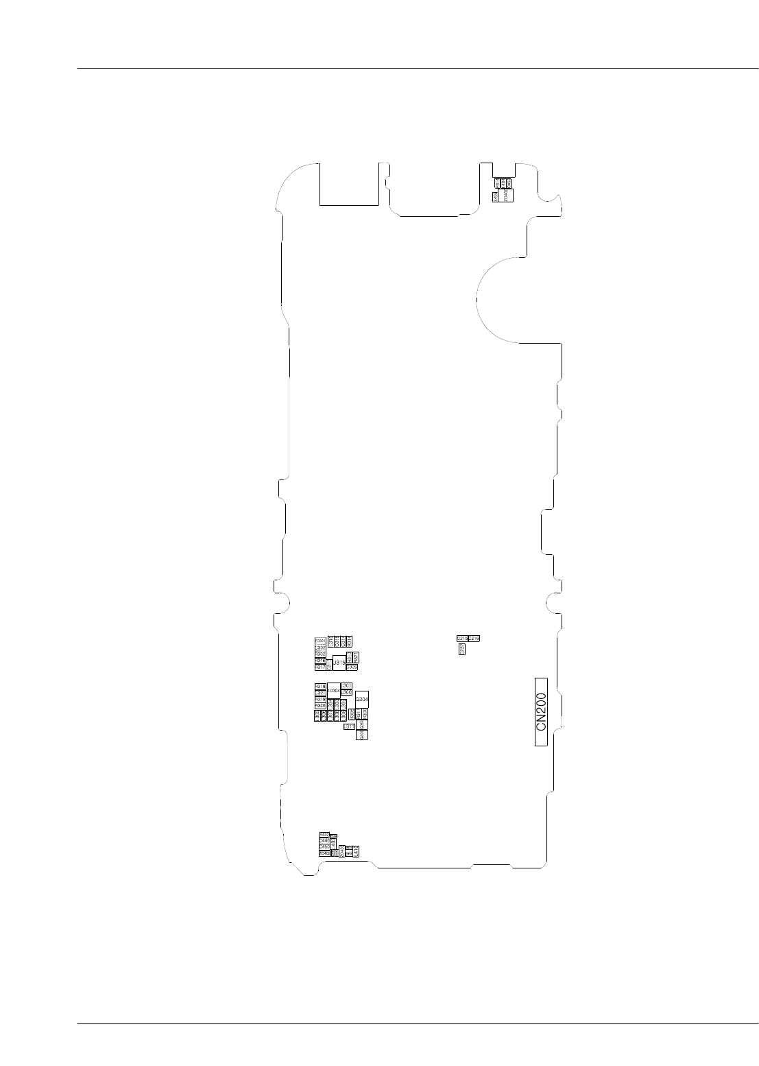
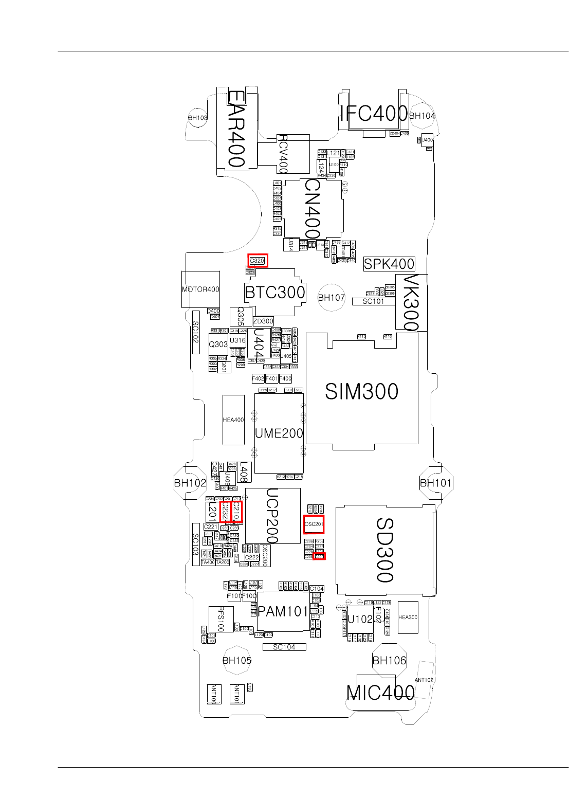
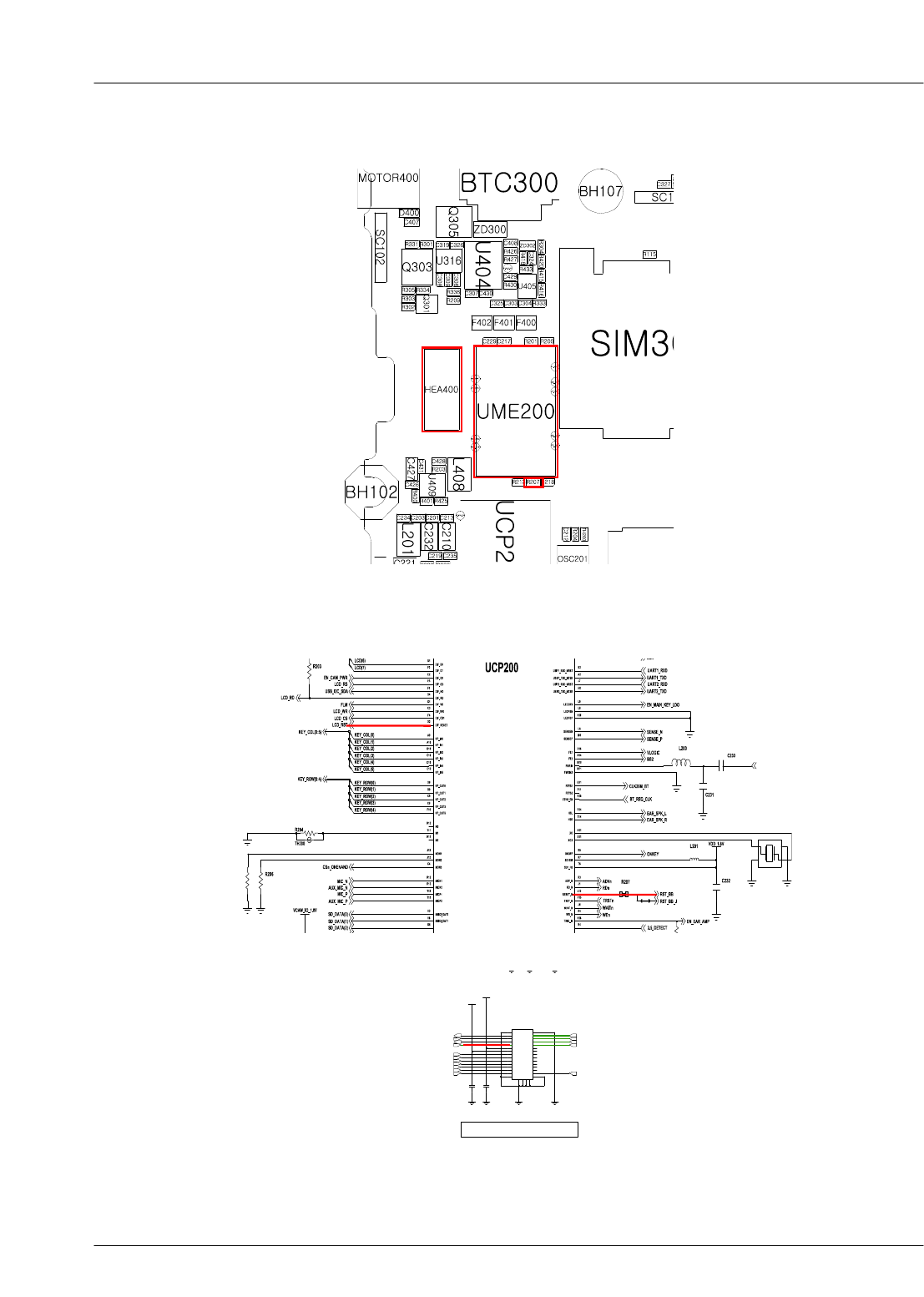
8-2. PCB Diagrams
8-2-1. Top
SAMSUNG Proprietary-Contents may change without notice
Level 3Repair
8-3
This Document can not be used without Samsung's authorization
8-2-1. Bottom
SAMSUNG Proprietary-Contents may change without notice
Level 3Repair
8-4
This Document can not be used without Samsung's authorization
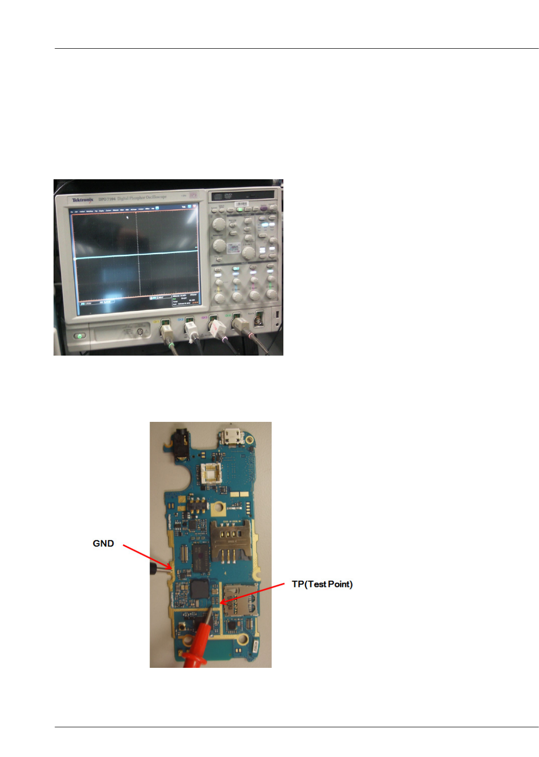
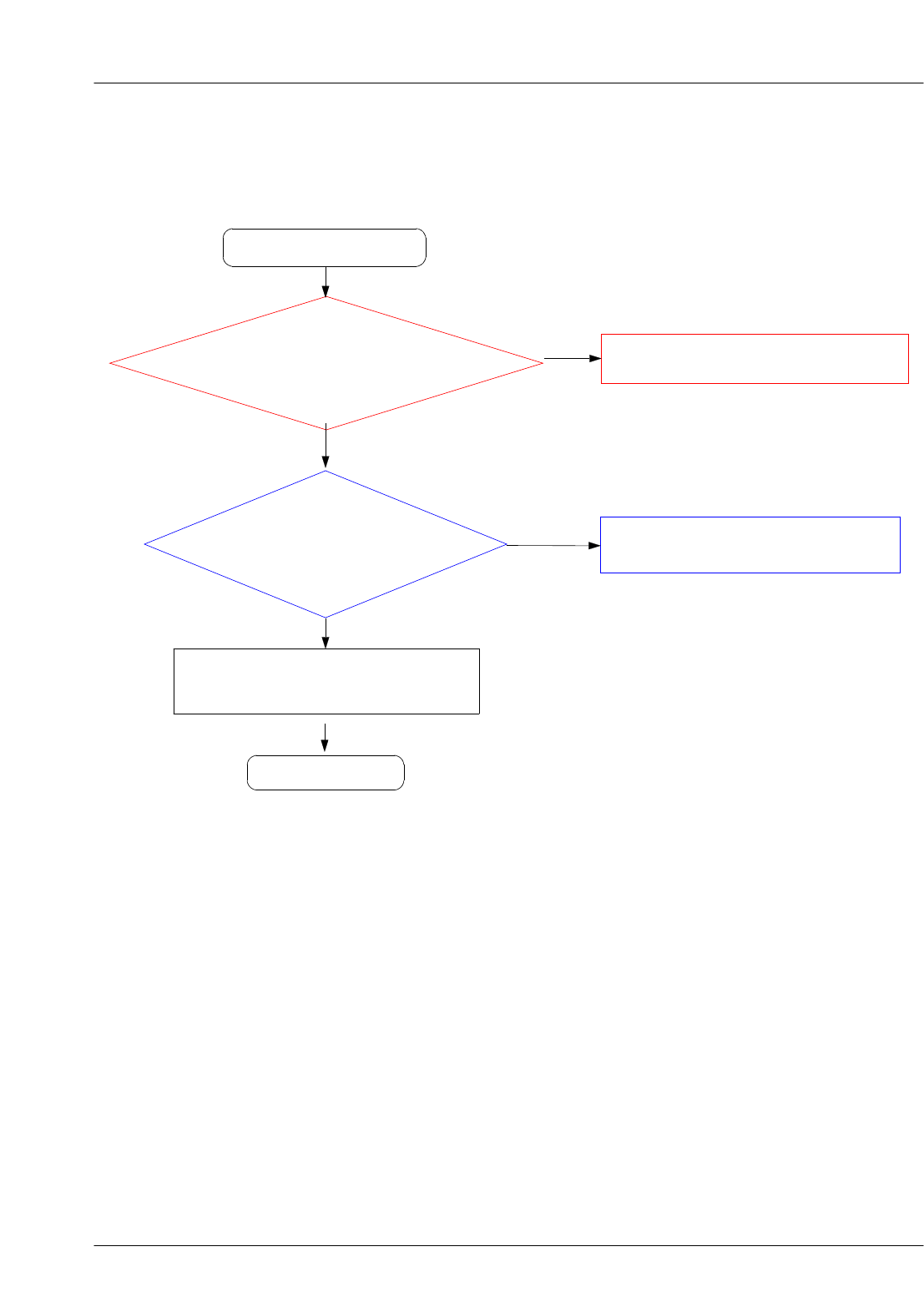
8-3. Flow Chart of Troubleshooting
(presetting methods for checking TP
-GND &TP(exp. VBAT=C210, C210, C320)using Oscilloscope
-look over the coming out signal.
Oscilloscope
SAMSUNG Proprietary-Contents may change without notice
Level 3Repair
8-5
This Document can not be used without Samsung's authorization
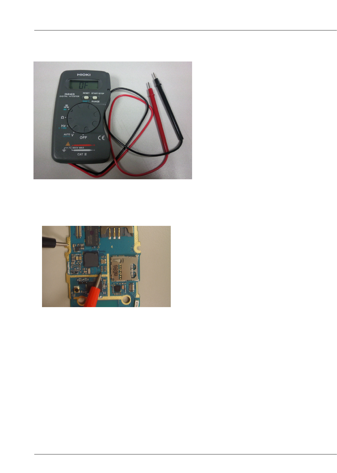
Multi-meter
Checking the TP(test point) using Multi-meter
-EX) to look up the TP, shunt Cap. -if checking the GND, you can listen "beep"
if checking the Signal, you can't listen it.
SAMSUNG Proprietary-Contents may change without notice
Level 3Repair
8-6
This Document can not be used without Samsung's authorization
8-3-1. Power On
Check the Battery Voltage
is more than 3.7V
(TP:C210 C220, C320)
'Power On 'does not work
Change the Battery
(Because of low batt. power)
END
No
Yes
VDD_1.8V =1.8V?
(TP: C232) Check the UCP200 is demaged.
No
Yes
Check the Clock at
UCP200 A11pin
(CLK26M)=26MHZ
(TP:OSC201 1,3pin)Change the OSC201.
No
Yes
Yes
Check the UCP200 is demaged.
Yes
SAMSUNG Proprietary-Contents may change without notice
Level 3Repair
8-7
This Document can not be used without Samsung's authorization
SAMSUNG Proprietary-Contents may change without notice
Level 3Repair
8-8
This Document can not be used without Samsung's authorization
SAMSUNG Proprietary-Contents may change without notice
Level 3Repair
8-9
This Document can not be used without Samsung's authorization
8-3-2. Initial
Check R207 (RST_BB) > 1.7V?
using the oscilloscope.
Initial Failure
Resolder the R208.
It must be higher than 1.7V.
END
No
Yes
Check UCP200 pin D2 >
1.7V ?
(TP: HEA400 9pin)
Yes
Yes
No
Change the UCP200.
Check the 16bit data signalsare correct.
Yes
SAMSUNG Proprietary-Contents may change without notice
Level 3Repair
8-10
This Document can not be used without Samsung's authorization
R209
2
43
1
OSC201
R205
K5
MMCI_DAT2 T2IN
FM_LNA_OUT
2.2" QVGA LCD
VDD_2.9V
C431
NC
32
33NC
NC
34
33
30 30
4
4
5566
77 8
8
99
31NC
22 22
2323 24
24
2525 26 26
27 27 28
28
29
29
1515 16
16
17 17 18 18
1919
22
20
20
21 21
HEA400
11
10 10
1111 12
12
13 13 14 14
VDD_1.8V
C428
LCD_D(6)
FLM_OUT
LCD_D(0)
LCD_D(2)
LCD_D(3)
LCD_D(4)
LCD_D(5)
LCD_CS_OUT
LED-
LED+_12V
LCD_D(1)
LCD_D(7)
LCD_RST LCD_WR_OUT
LCD_RD
LCD_RS_OUT
SAMSUNG Proprietary-Contents may change without notice
Level 3Repair
8-11
This Document can not be used without Samsung's authorization
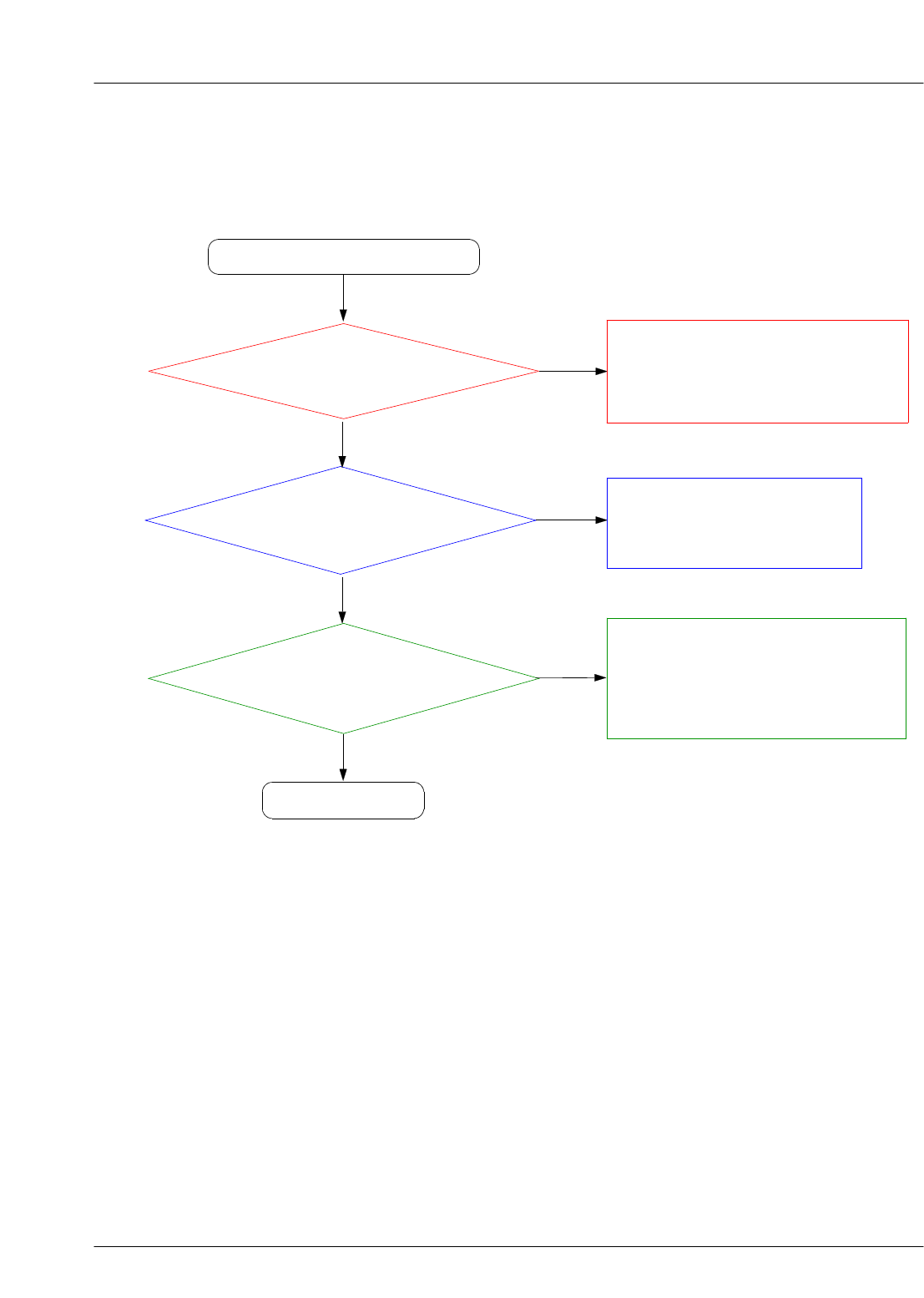
8-3-3. Charging Part
Check the Battery &TA
connection.
Abnormal charging part
END
No
Yes
Check the R301 >4.9V? No
Yes
Check the Q303 pin3
>4.9V ?
No
Yes
Reinsert the Battery or TA.
Resolder the R301
Replace the Q303 using aHeatgun
Yes
SAMSUNG Proprietary-Contents may change without notice
Level 3Repair
8-12
This Document can not be used without Samsung's authorization
Routed as a Pair FROM R315(0.1T)
CHARGING CIRCUIT
R331
R301
3
4
Q303
R305
R303
VBAT
VBUS_5V_OUT
Q301
1
2
34
5
6
R302
R334
SENSE_P
TNHSVBSC
CS
VDDCHG
SENSE_N
VCHG
SAMSUNG Proprietary-Contents may change without notice
Level 3Repair
8-13
This Document can not be used without Samsung's authorization
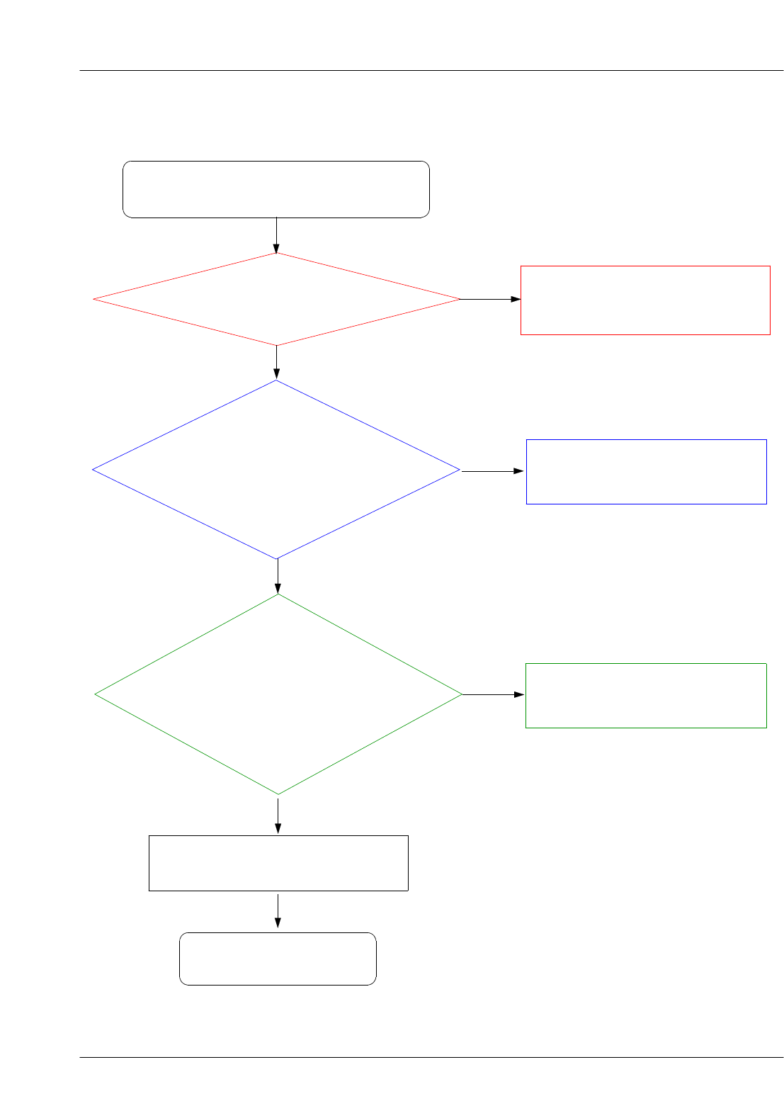
8-3-4. Sim Part
Check the
SIM300 pin 1(C325) 】2.85V
Phone can't access SIM Card
Resolder the UCP200 using heatgun.
Check the SIM Card is demaged.
END
No
Yes
Yes
Yes
No Resolder or Replace SIM300 connector.
(Because of not soldering well)
After Power ON,
Check the SIM_CLK signal is on.
(TP :C303)
(method :wire the pin 3(C303)
and check its waveform using an
oscilloscope)
Yes
No
Change the PBA.
After SIM card insert,
Check the SIM300
pin2(R333,C304: SIM_RST) 】
2.85V?
(method :wirethe pin 2and
check its waveform using an
oscilloscope)
Yes
SAMSUNG Proprietary-Contents may change without notice
Level 3Repair
8-14
This Document can not be used without Samsung's authorization
SIM SOCKET
C325
VSIM_2.85V
ZD301
C302
R333
5
5
66
7
GG
89
GG
10
SIM300
11
22
33
44
C303 C304
R332
SIM_IO SIM_CLK
SIM_RST
SAMSUNG Proprietary-Contents may change without notice
Level 3Repair
8-15
This Document can not be used without Samsung's authorization
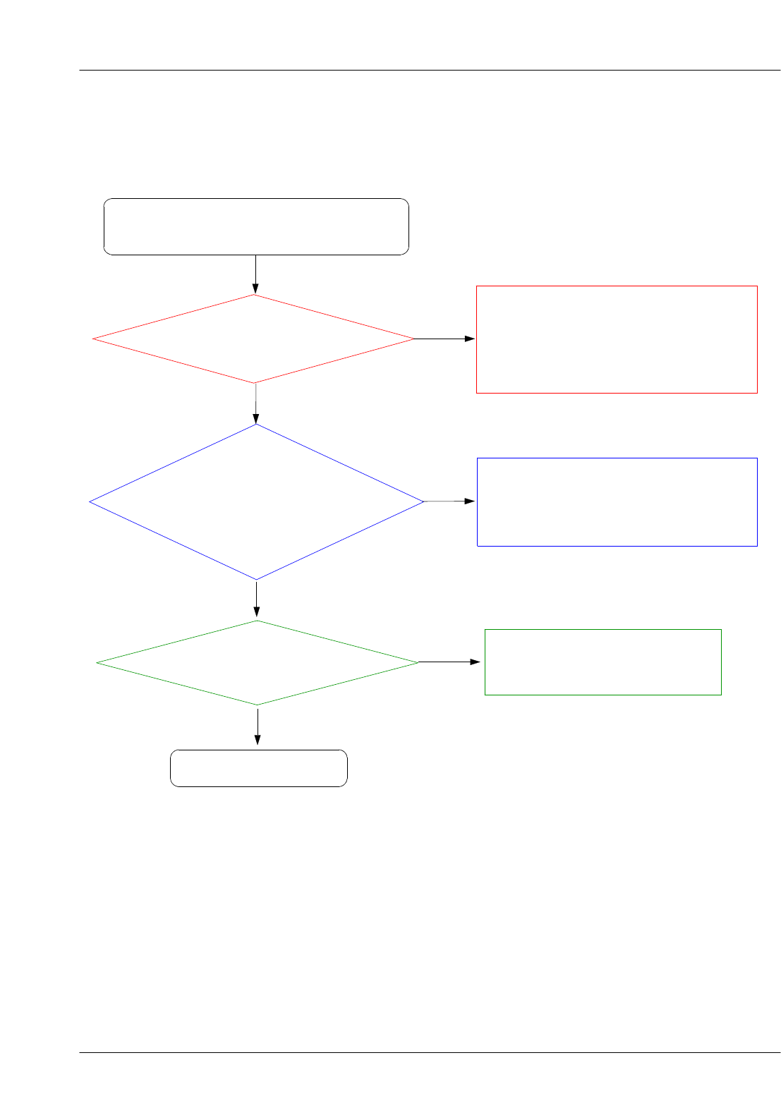
8-3-5. Microphone Part
Check R432 =2.2V
at Mic Active?
Check the MIC signal paths.
MIC signals are on.
(TP :L403,L410,C422,
C420,R432,R435,R437)
Replace the UCP200 using aHeatgun
(Because of not soldering well)
Resolder L403, L410, C422, C420, R432, R435,
R437
(not work if those is not connected.)
END
No
Yes
Yes
Yes
Yes
No
Check the MIC is demaged.
No
Replace an another MIC
Microphone does not work
SAMSUNG Proprietary-Contents may change without notice
Level 3Repair
8-16
This Document can not be used without Samsung's authorization
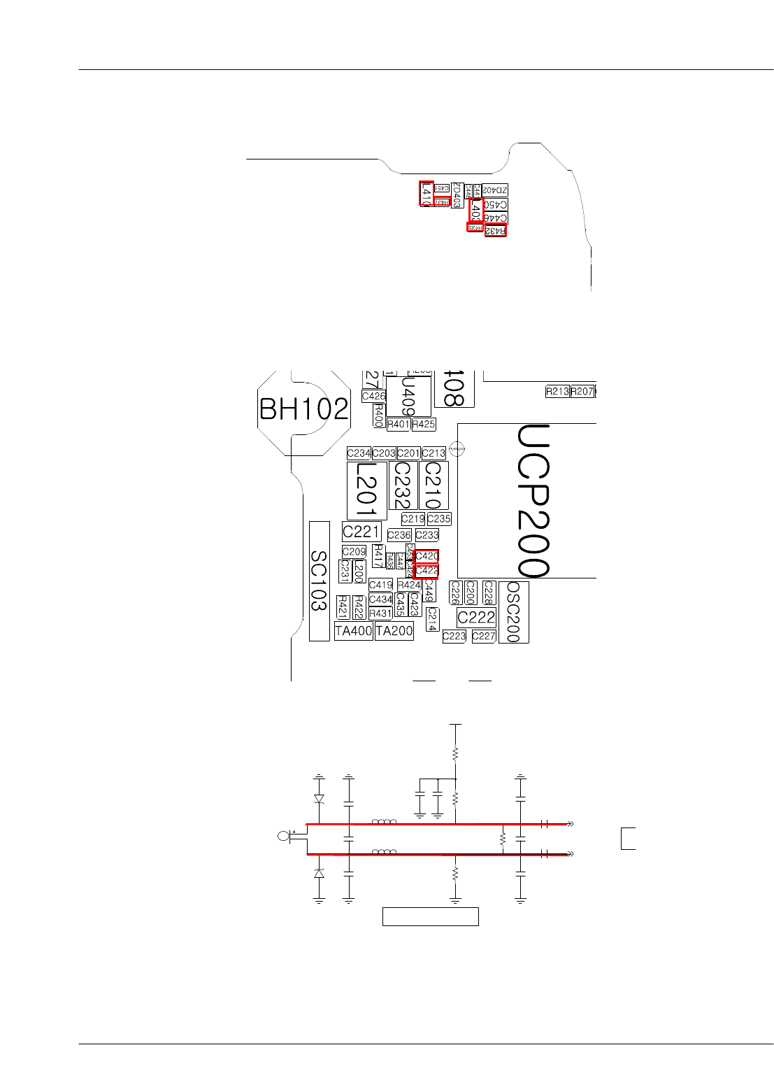
P
A
MAIN MIC
C453
ZD402
ZD403
R436
R437
L410
C448
C450
MIC400
L403
R432
R435
V_MIC_2.2V
C446
C420
C422
C441
C451
C447
C424
MIC_P
MIC_N
AU
X
AU
X
SAMSUNG Proprietary-Contents may change without notice
Level 3Repair
8-17
This Document can not be used without Samsung's authorization
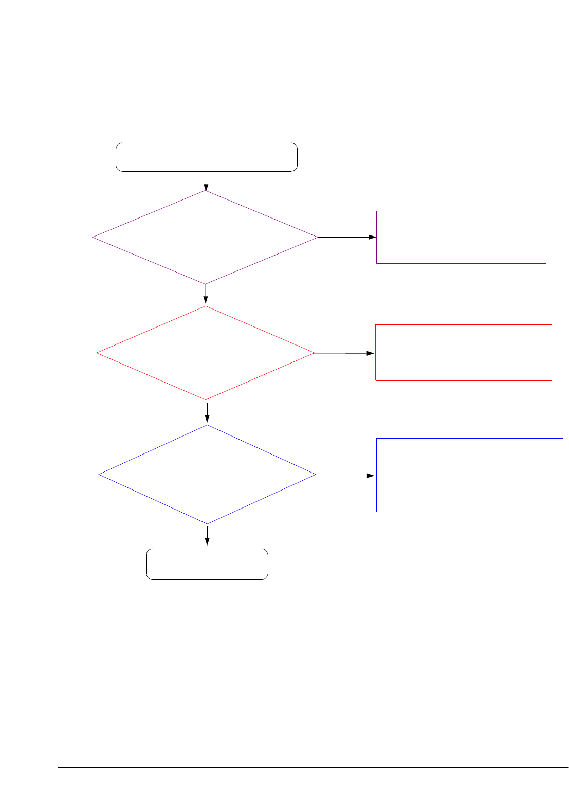
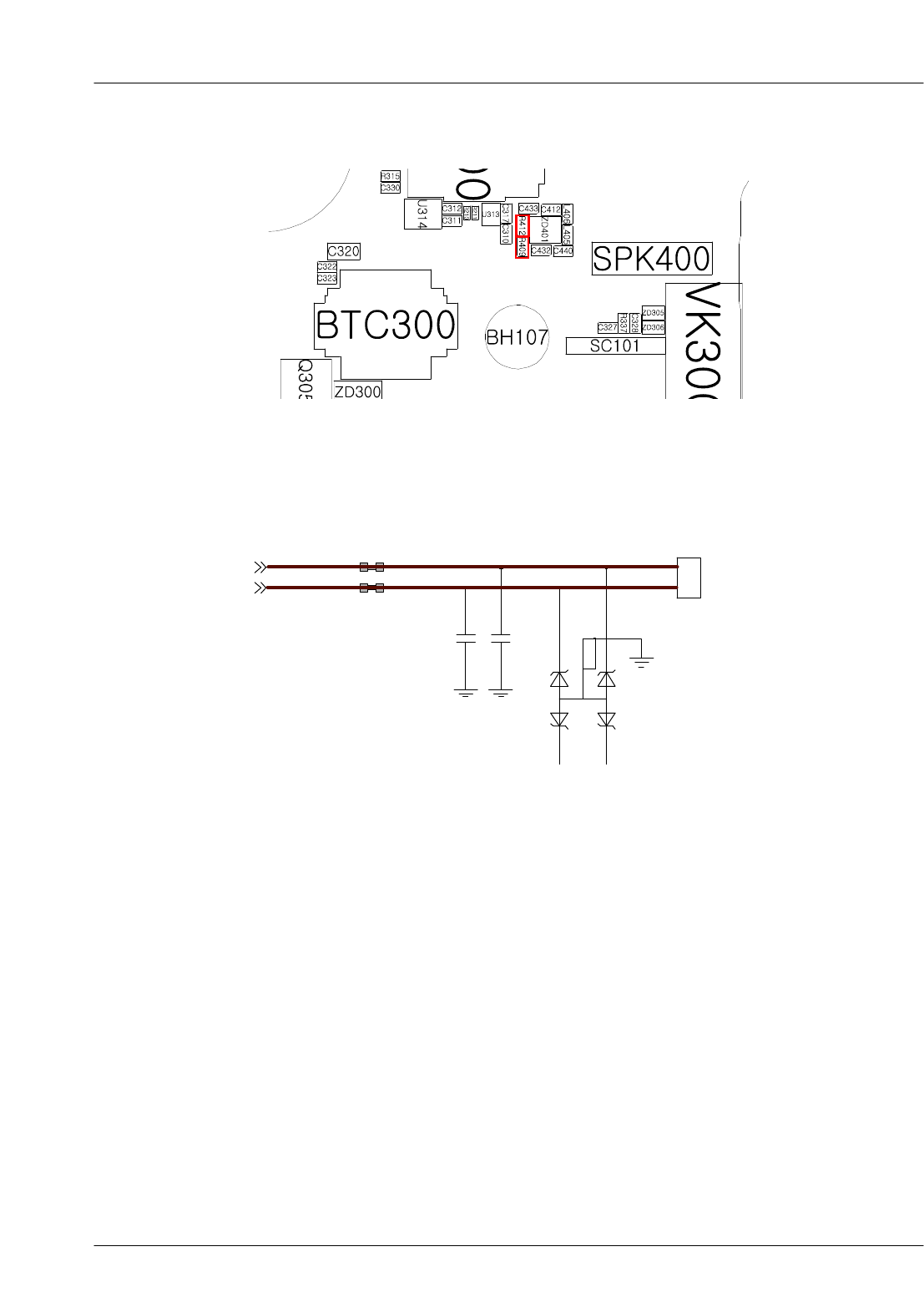
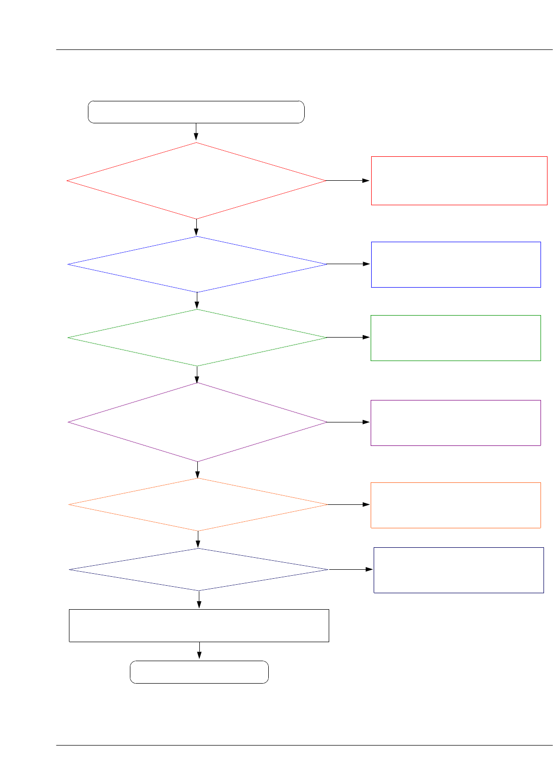
8-3-6. Speaker Part
Check the UCP N15,N16 pin
signals are on.
(TP :L405, L406)
Speaker does not work
Check the SPK signal
paths.
Are signal on?.
(TP :C412,C440)
Resolder the L405, L406.
No
Yes
No
Replace the UCP200 using the Heatgun.
(because of soldering not well)
Yes
Check the Speaker module
is Okay. Replace the SPK module.
No
END
Yes
Yes
SAMSUNG Proprietary-Contents may change without notice
Level 3Repair
8-18
This Document can not be used without Samsung's authorization
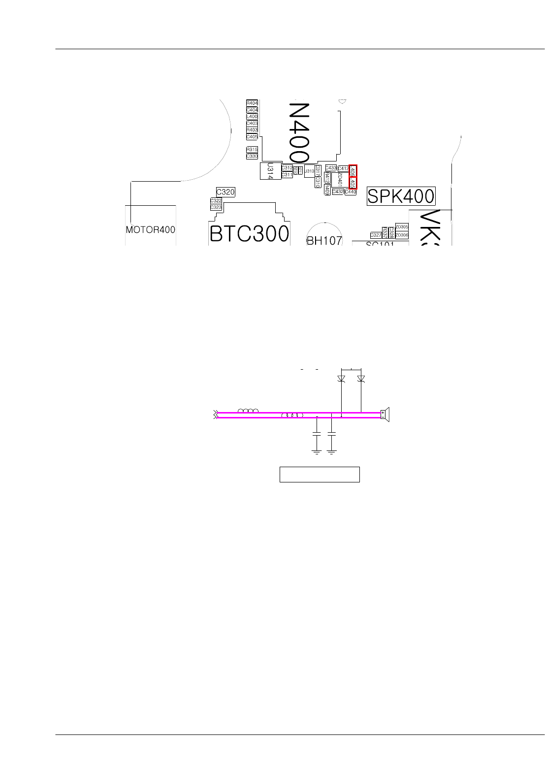
SPK / RCV
ZD401
4
6
SPK400
L406
F400
L405
C440C412
SPK_P
SPK_N

SAMSUNG Proprietary-Contents may change without notice
Level 3Repair
8-19
This Document can not be used without Samsung's authorization
8-3-7. RCV Part
Check the UCP M15,M16
pin signal is on.
(TP :R412, R409)
Receiver does not work
Check the RCV signal
paths
Are signals on?.
(TP :C432,C433)
Resolder the R412, R409.
No
Yes
No
Replace the UCP200 using the Heatgun.
(because of soldering not well)
Yes
Check the RCV module is
Okay. Replace the RCV module.
No
END
Yes
Yes
SAMSUNG Proprietary-Contents may change without notice
Level 3Repair
8-20
This Document can not be used without Samsung's authorization
ZD401
1
2
3
4
5
6
MIC400
R409
R412
C433C432
11
2
2
RCV400
RCV_N
RCV_P
SAMSUNG Proprietary-Contents may change without notice
Level 3Repair
8-21
This Document can not be used without Samsung's authorization
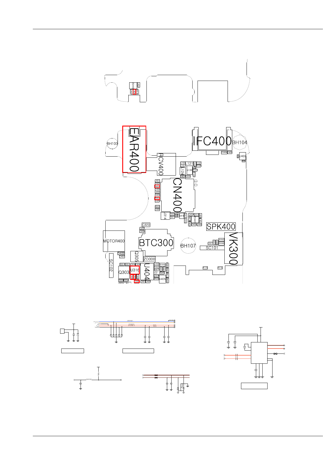
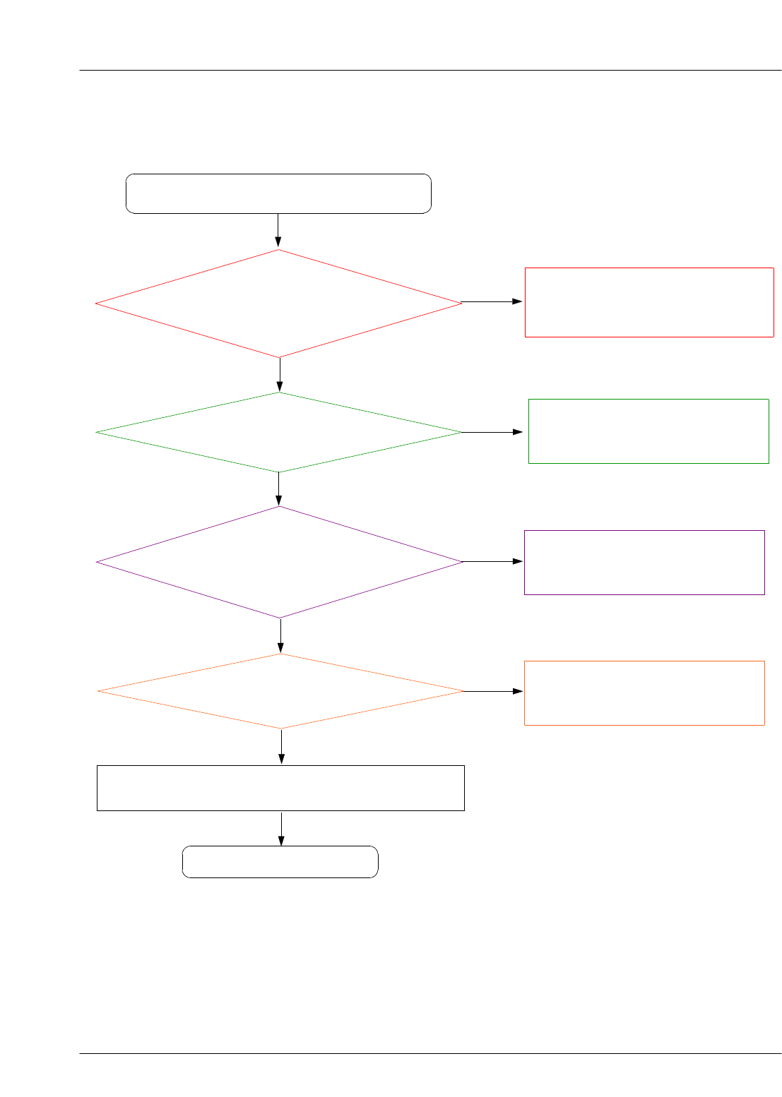
8-3-8. EAR_Speaker Part
Check the earphone connector is
demaged.
Check the L404 =0V
Ear_Speaker is not working.
Resolder the L404 or Replace the EAR
connector(EAR400)
END
No
Yes
No
Resolder the R336 or Replace the UCP200.
Check EarAmp enable signal is
correct.
(TP :R336 =1.8
V)
No Resolder the C308, C309 or Replace the
UCP200.
Check the Ear signals are on,
while playing the sound.
(TP :C308, C309)
Check the Ear signals passing
the Ear AMP are on, while
playing the sound.
(TP :R404, R403)
No
Resolder the Ear AMP(U316).
Yes
Yes
Yes
Yes
Resolder the R404, R403, L401, L400.
No
Check the ear signal paths
Are signals on?.
(TP :L401,L400)
Yes
Check EAR400 pin 6, 7 is
demaged.
Yes
No
Change the Ear phone.
Change the EAR400.
Yes
SAMSUNG Proprietary-Contents may change without notice
Level 3Repair
8-22
This Document can not be used without Samsung's authorization
3.5PI EAR JACK
MOTOR
ZD401
1
2
3
5
C405 C404
L401
VDD 1 8V
L404
D400
ZD400
1
2
3
4
5
6
C403C402
C452
L402
C407
VDD_1.8V
L400
R404
R409
R412
MOTOR400
11
22
V_MOT_3.3V
CON-A
CON-B
3
4CON-C
CON-D
5
CON-E
6
CON-F
7
EAR400
2
R414
C433C432
R403
FM_ANT_EAR
3.5_CON_DETECT
EAR_MIC_P
SEND_END
EAR_3.5_R
EAR_3.5_L
3.5_DETECT3.5_CON_DETECT
RCV_N
RCV_P
EAR_AMP
B2
1
2
NC
B1
OUTL
A1
OUTR
B4PGND
C3
PVDD
C4
PVIN
PVSS
A2
_SHDN
C1N
A3
A4 C1P
B3GND
INL
C1
C2 INR NC
U316
VDD_1.8V
C306 C307
C308
C309
R336
C326
C319
EN_EAR_AMP
EAR_SPK_L
EAR_SPK_R
EAR_3.5_L
EAR_3.5_R
SAMSUNG Proprietary-Contents may change without notice
Level 3Repair
8-23
This Document can not be used without Samsung's authorization
8-3-9. EAR_MIC Part
Check the EAR connector is
demaged.
(TP :L402 signal is on.)
Resolder the L402 or Replace the EAR
connector(EAR400)
END
No
Yes
No
Resolder the R421 or Replace the UCP200.
Check the Ear_Mic voltage is on.
(TP :R421 =2.2
V)
Check the signal paths
Are signals on?.
(TP :C434, C423, R431, R422)
No
Resolder the C434, C423, R431, R422
Check the EAR phone.
No
Check the UCP200 is demaged.
Resolder the UCP200 using the heatgun.
Ear_Microphone is not working.
Yes
Yes
Yes
Yes
Yes
SAMSUNG Proprietary-Contents may change without notice
Level 3Repair
8-24
This Document can not be used without Samsung's authorization
3.5PI EAR JACK
C405 C404
L401
ZD400
1
2
3
4
5
6
C403C402
L402
L400
R404
CON-A
CON-B
3
4CON-C
CON-D
5
CON-E
6
CON-F
7
EAR400
2
R403
FM_ANT_EAR
3.5_CON_DETECT
EAR_MIC_P
SEND_END
EAR_3.5_R
EAR_3.5_L
EAR MIC
PARALLEL
10V
1005
100nFC434
R422
C419 TA400
V_EARMIC_2.2V
R431
C423
R424
C449
C435
R421
EAR_MIC_PAUX_MIC_P
AUX_MIC_N
SAMSUNG Proprietary-Contents may change without notice
Level 3Repair
8-25
This Document can not be used without Samsung's authorization
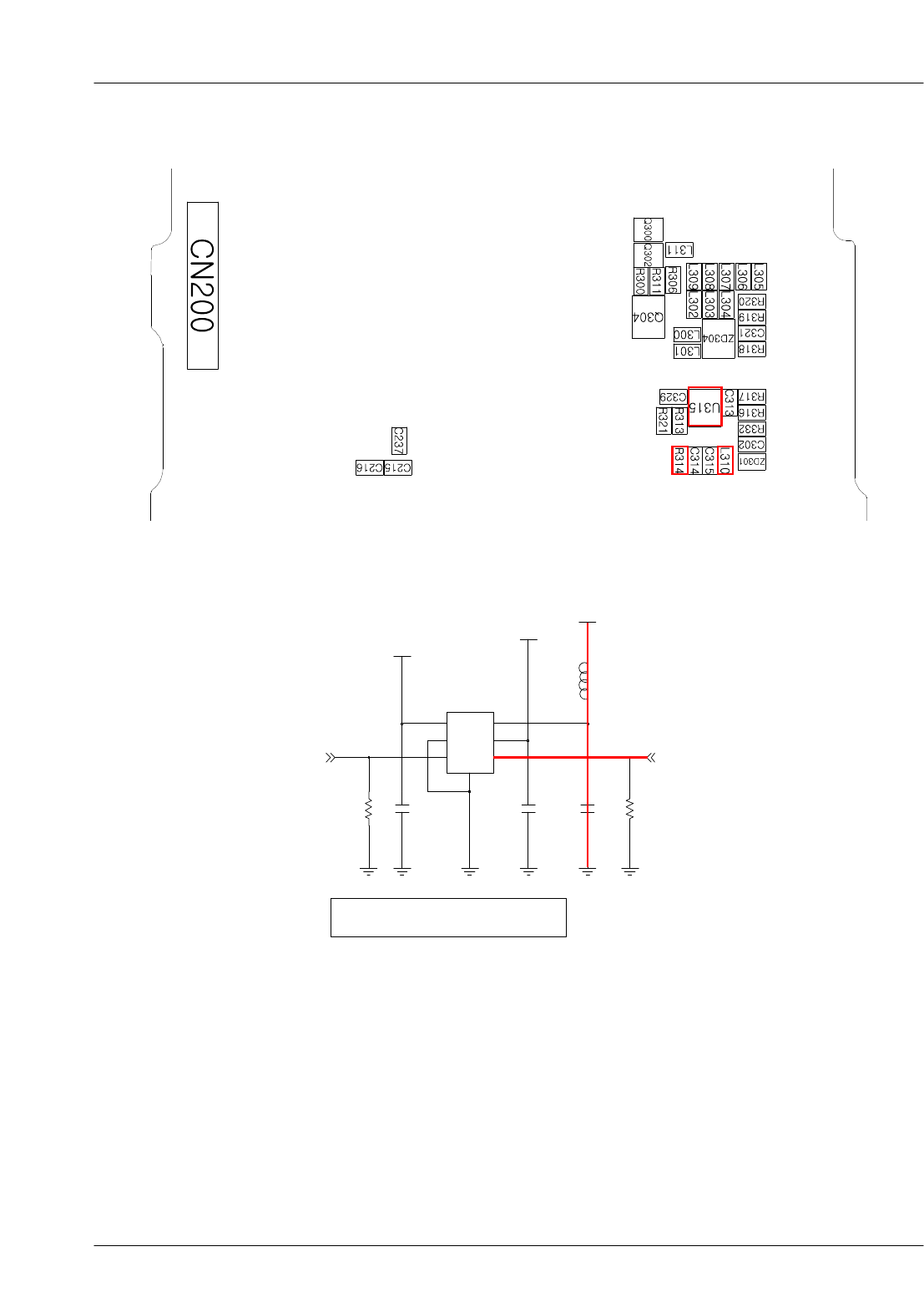
8-3-10. Vibrator Part
Check the Enable signal is
on.
(TP :R313 is not 0V)
Vibrator does not work
Check the motor operating
voltage =3.3
V.
(TP :C314)
Resolder the U315.
No
Yes
No
Resolder the UCP200 using the heatgun.
END
Yes
Yes
Change the Motor module.
Yes
SAMSUNG Proprietary-Contents may change without notice
Level 3Repair
8-26
This Document can not be used without Samsung's authorization
KEY / MOT LDO
L310
MAIN_KEY_3.3V
R314
EN1
EN2
3
2
GND
GND
7
1
VIN 6VOUT1
VOUT2 5
VBAT
U315
4
C315
V_MOT_3.3V
C314
R313
C313
MOT_EN EN_MAIN_KEY_LDO
MOTOR
D400C407
MOTOR400
11
22
V_MOT_3.3V
SAMSUNG Proprietary-Contents may change without notice
Level 3Repair
8-27
This Document can not be used without Samsung's authorization
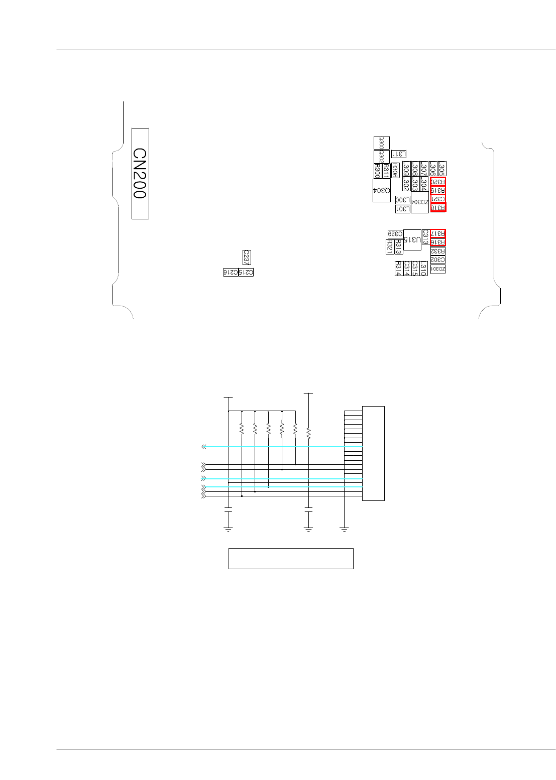
8-3-11. SD_Card Part
Check the Vdd_IO=1.8V.
(TP :R321)
Check VMMC_2.85 =2.85
V.
(TP :R316)
Replace the UCP200.
END
No
Yes
No Resolder the R316, R317, R318, R319,
R320, R321.
Check the Pull-up Registor is
soldered well.
(TP :R316, R317, R318, R319,
R320, R321 are not 0V.)
Check the SD_CLK is on.
(TP :SD300 5pin)
No
Resolder the UCP200.
Check the SD card is demaged.
No
Check the SD300 is demaged.
Resolder the SD300 using the heatgun.
SD card does not work.
Yes
Yes
Yes
Yes
Yes
SAMSUNG Proprietary-Contents may change without notice
Level 3Repair
8-28
This Document can not be used without Samsung's authorization
T-FLASH SOCKET
15 NC
NC
16
17 NC
NC
18
NC
19
20 NC
4VDD
6VSS
DAT0
7
8DAT1
DAT2
1
2DAT3|CD
GND
9
10 GND
NC
13
14 NC
SD300
12 CD
CLK
5
CMD
3
COMMON
11
R317
C321
VDD_IO1_1.8V
C329
R321
R320
VMMC_2.85V
R316 R318 R319
SD_DATA(0)
SD_DATA(1)
SD_DATA(2)
SD_DATA(3)
DETECT_SD
SD_CLK
SD_CMD
SAMSUNG Proprietary-Contents may change without notice
Level 3Repair
8-29
This Document can not be used without Samsung's authorization
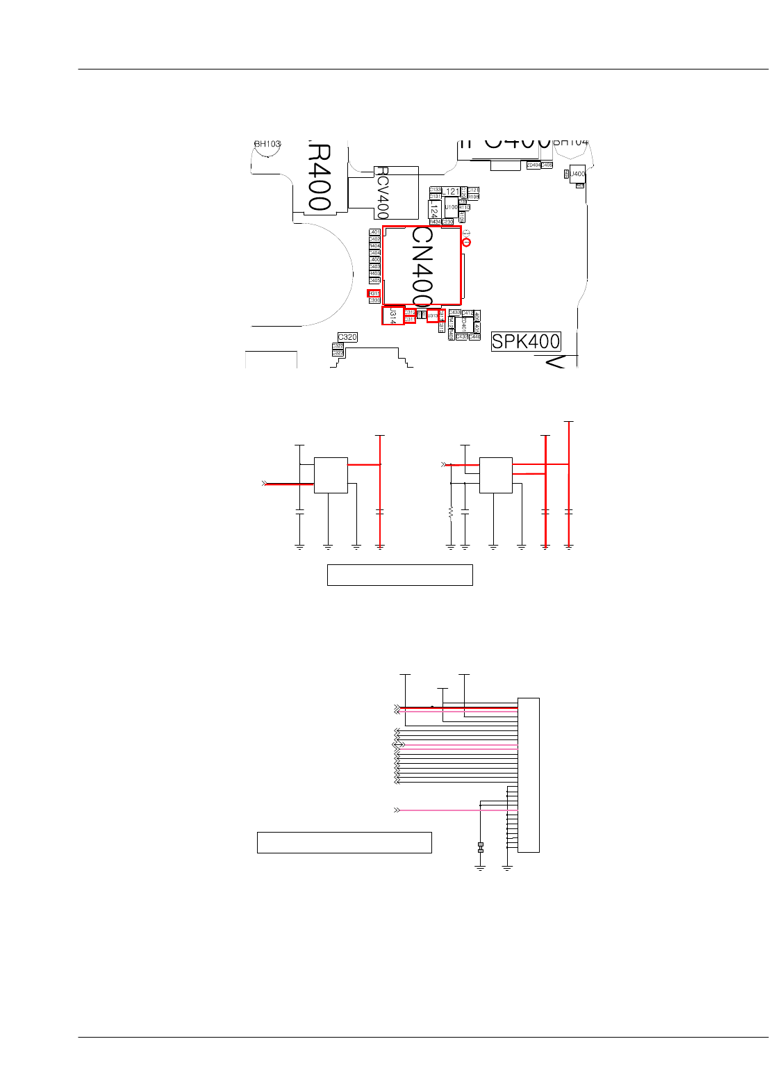
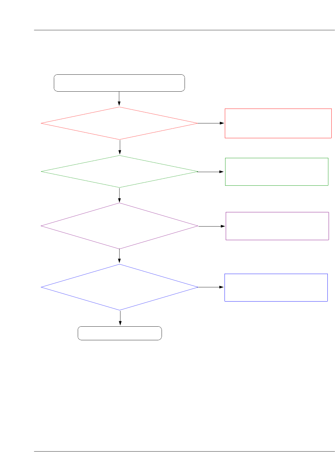
8-3-12. Camera Part
Check the Camera Enable signal
is High.
(TP :R315 =1.8
V)
Replace the UCP200, using the heatgun.
END
No
Yes
No If C317 is not 1.8V, Replace the U313.
If C311, C312 is wrong, Replace the U314.
Check the Camera operating
voltage is correct.
(TP :C317 =1.2
V, C311 =1.8V
C312 =2.8
V)
Check CAM_RST is high,as soon
as camera works.
(TP :TP_CAM_RST =1.8
V)
No
Replace the UCP200, using the heatgun.
Change the CN400.
No
Check the Camera is demaged.
Change the Camera module.
Camera does not work.
Yes
Yes
Yes
Yes
Yes
SAMSUNG Proprietary-Contents may change without notice
Level 3Repair
8-30
This Document can not be used without Samsung's authorization
3M CAM LDO
VBAT
GND
5
GND
2
4VDD 1
VOUT
U313
3CE
C311
VCAM_IO_1.8VVCAM_CORE_1.2V
C317
C310
VCAM_A_2.8V
C312
R315
VBAT
EN2
1
7
GND
VIN
2VOUT1 5
VOUT2 6
VSS 4
U314
3
EN1
C330
EN_CAM_PWR
EN_CAM_PWR
3M CAM SOCKET
VCAM_IO_1.8V
VCAM_CORE_1.2V VCAM_A_2.8V
R434
TP_CAM_RST
31
32 32
4
4
55
6
6
77
8
8
99
24
25 25
26
26
27 27
28
28
29 29
33
30 30
31
18
18
19 19
2
2
20
20
21 21
22
22
23 23
24
10
10
11 11
12
12
13
13
14
14
15 15
16 16
17 17
CN400
11
CAM(1)
CAM_SCL
CAM(3)
CAM(4)
CAM(0)
CAM_PCLK_IN
CAM_MCLK_OUT
CAM_SDA
CAM_VSYNC
CAM_HSYNC
CAM(7)
CAM(6)
CAM(5)
CAM_RST
CAM(2)
SAMSUNG Proprietary-Contents may change without notice
Level 3Repair
8-31
This Document can not be used without Samsung's authorization
8-3-13. FM Radio Part
Check the FM ant signal is GND.
(TP :L124 =0
V) Resolder the L124.
END
No
Yes
No
Replace the UCP200.
Check the FMR LNA operating
voltage is correct.
(TP :C130 =2.9
V)
Check the FMR_LNA_SW is high.
(TP :TP_FM_LNA_SW =1.8
V)
No
Replace the UCP200.
Replace the UCP200.
No
Resolder the U100, C133, L121,
C121, R108, R109, R110.
FM radio does not work.
Yes
Yes
Yes
Yes
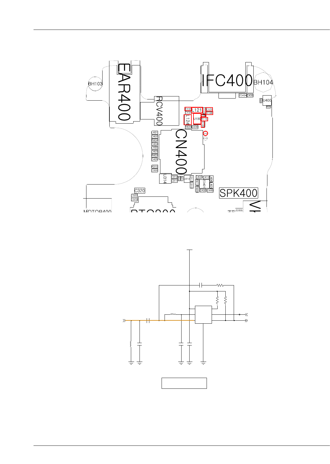
SAMSUNG Proprietary-Contents may change without notice
Level 3Repair
8-32
This Document can not be used without Samsung's authorization
FMR LNA
VDD_2.9V
L124
C131
R108
TP_FM_LNA_SW
C121
R110R109
C129 C130
L121
BIAS-OUT 52
CTRL-SW
CURRENT-AD 6
3RF-IN RF-OUT 4
1VCC
7
VSS
U100
C133
FM_ANT_EAR
FM_LNA_SW
FM_LNA_OUT
SAMSUNG Proprietary-Contents may change without notice
Level 3Repair
8-33
This Document can not be used without Samsung's authorization
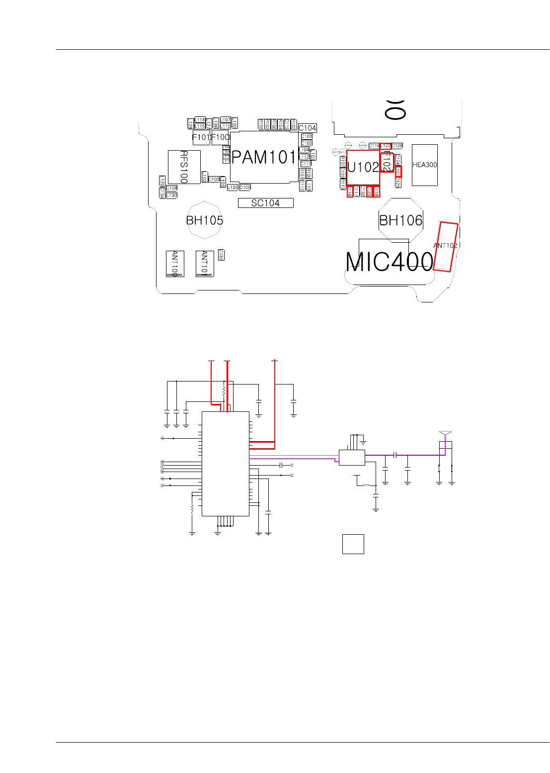
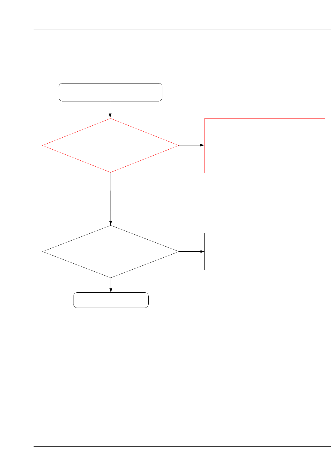
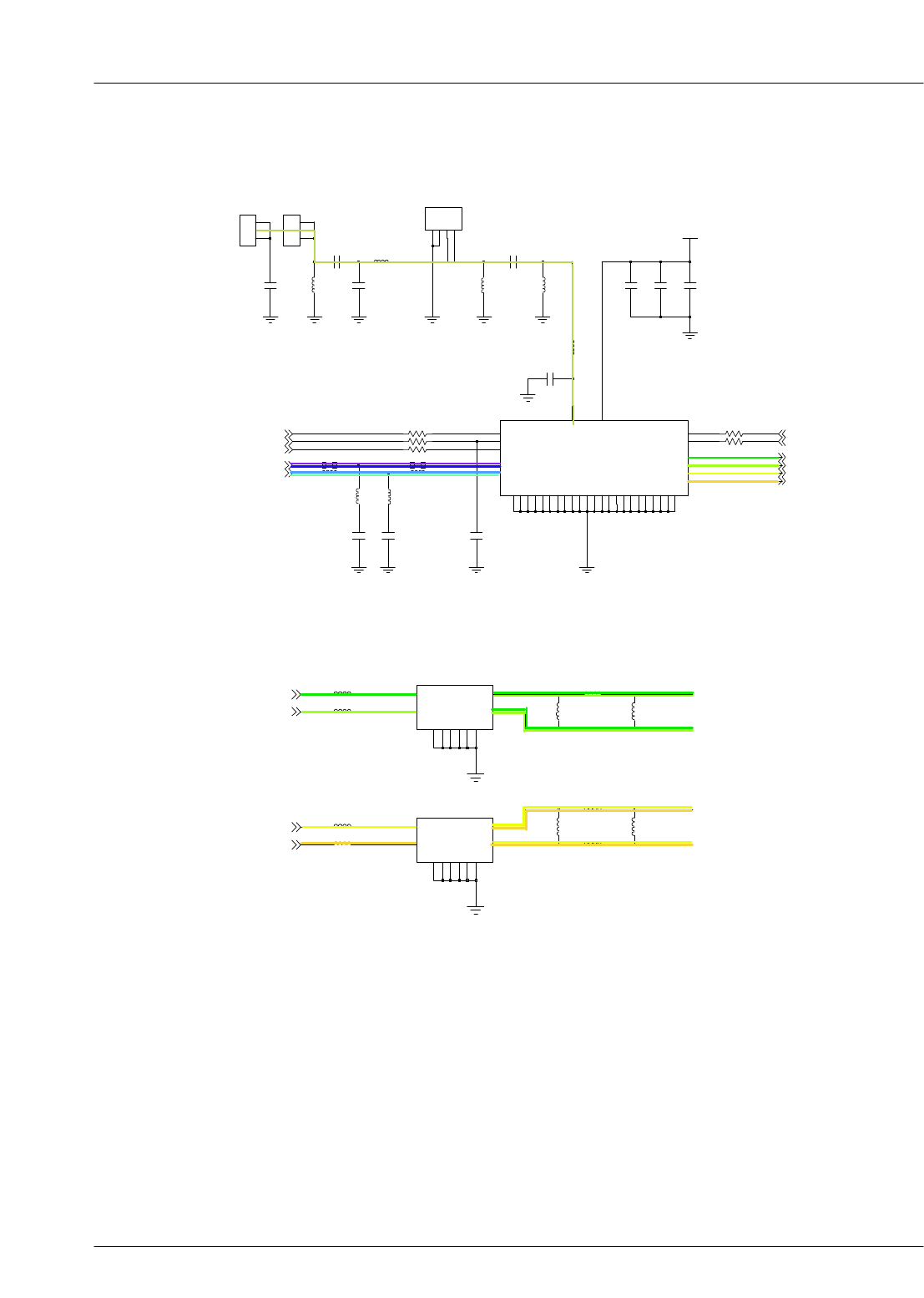
8-3-14. Bluetooth Part
Check Operatiog voltage is Okay.
(TP :C116=1.8V) Replace the UCP200.
END
No
Yes
No
Resolder the C123 or replace the UCP200.
Check 26Mhz Clock is on.
(TP :C123)
Check the Vbt_1.5V is on.
(TP :L122 =1.5
V)
No
Replace the U101.
Change the BT ant path elements.
(Resolder the F102, C101,
ANT102)
Bluetooth does not work.
Yes
Yes
Yes
Yes
Replace the UCP200.
No
SAMSUNG Proprietary-Contents may change without notice
Level 3Repair
8-34
This Document can not be used without Samsung's authorization
BT
TP_REQ_CLK
C132
VBT_1.5V
C118 C119
C120
R107
C116
C117
H1
SPI_CLK
H2 PCM_OUT
H3
PCM_CLK
H4 PCM_SYNC
H5
VSS_DIG
H6
VDD_PADS
H7 SDIO_CLKCSPI_CLK
F7 SDIO_DATA2|UART_RX
G1
VDD_RADIO
G2
SPI_MOSI
G3
RST#
PCM_IN
G4
G5
TEST_EN
G6
SDIO_DATA3|CSPI_CS#|UART_CTS
G7 SDIO_DATA0|CSPI_MISO|UART_TX
SDIO_SD_CS#
E6
CLK_32K
E7
PIO4
F2
RF_P
F3VSS_SCREEN
F4
SPI_MISO
F5
N|CS
F6
SDIO_DATA1|CSPI_INT|UART_RTS
D2
N|CS
N|CS
D4
D5
PIO7
D6
SDIO_CMDCSPI_MOSI
D7
VDD_CORE
E1
VSS_RADIO
E2
RF_N
E4
SPI_CS#
E5
B7
PIO5
C1
VSS_LO
C2
N|CS
C3
VSS_ANA
C4
PIO0
C5
PIO2
C6
PIO3
C7
PIO9
A5
VREGIN_H
A6
VREGENABLE
A7
VDD_PADS
B2
VREGIN_L
B3
LO_REF
B4
AIO0
B5 PIO1
B6
VSS_DIG
U102
1
NC 2
NC
A1
VDD_ANA
A2
XTAL_OUT
A3
XTAL_IN
A4
VREGOUT_H
TP_UART100
C123
TP_UART101
VDD_1.8VVBT_1.5V VDD_1.8V
8
GNC
3
1
UNBAL
F102
4BAL
6BAL
DC 2
G
57
G
L122
C128
R113
ANT102
132
C124
C101
UART2_RXD
BT_RST
CLK26M_BT
BT_REQ_CLK
PCM_RXD
PCM_TXD
PCM_CLK
PCM_SYNC
UART2_TXD
SAMSUNG Proprietary-Contents may change without notice
Level 3Repair
8-35
This Document can not be used without Samsung's authorization
8-3-15. Key Data Input
Check Initial Operation
Yes
When you pushed all of the
Key, does the key have
tension?
Change Domesheet
(#1 : look over the Dome situation
whether be sunken
#2 : look over the Dome location
whether be out of line)
Yes
All of the key doesn't work
except POWER ON KEY ?
Replace the PBA
(over the insturctions again
and change the board
because of be possible for PBA to get damaged)
Yes
No
END
No
SAMSUNG Proprietary-Contents may change without notice
Level 3Repair
8-36
This Document can not be used without Samsung's authorization
MAIN KEY
L311
MAIN_KEY_3.3V
L301
L300
L309
L307
L308
2
34
5
6
ZD304
1
L303
L302
L306
L305
99
17NC
NC
18
19NC
NC
20
15
15 16 16
22
3344
5566
7788
11
1010
1111 1212
13 13 14
14
HEA300
L304
KEY_ROW(3)
KEY_ROW(4)
VOL_KEY_ROW(0)
VOL_KEY_ROW(1)
ONKEY_N
KEY_ROW(0)
KEY_ROW(1)
KEY_ROW(2)
KEY_COL(4)
KEY_COL(3)
KEY_COL(2)
KEY_COL(1)
KEY_COL(0)
POWER ON CIRCUIT
R306
Q304
1
3
2
ONKEY_N
KEY_ROW(4)
KEY_COL(3)
SAMSUNG Proprietary-Contents may change without notice
Level 3Repair
8-37
This Document can not be used without Samsung's authorization
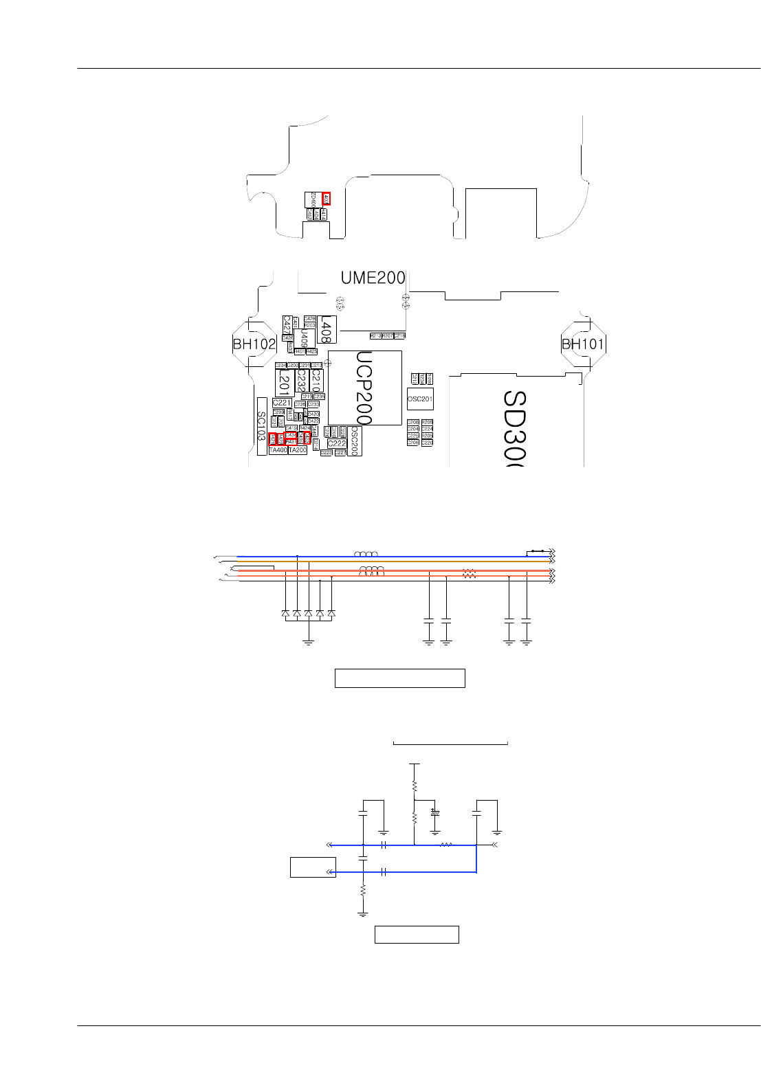
8-3-16. Back Light (for Color Main LCD)
Backlight does not work
Yes
Is LCD Contrast set on high
level in the Menu?
(menu->settings->display-
>Brightness->level)
No Set LCD Contrast on high level
(menu->settings->display->Brightness->level/
select 5Level (level :1~5)
Yes
#1 : Resolder R400
(with an soldering iron)
#2 : Repalce LCD Module
(to check if it has the problem)
No
Is R40 =1.8V?
(Wiring U409 pin3,
EN_LCD_BL)
Yes
END
SAMSUNG Proprietary-Contents may change without notice
Level 3Repair
8-38
This Document can not be used without Samsung's authorization
R400
C427
R425R401
VBAT
C426
L408
4
GND
6
7GND
SW
5VIN 2
1
VOUT
U409
EN 3
FB
EN_LCD_BLLED-
LED+_12V
SAMSUNG Proprietary-Contents may change without notice
Level 3Repair
8-39
This Document can not be used without Samsung's authorization
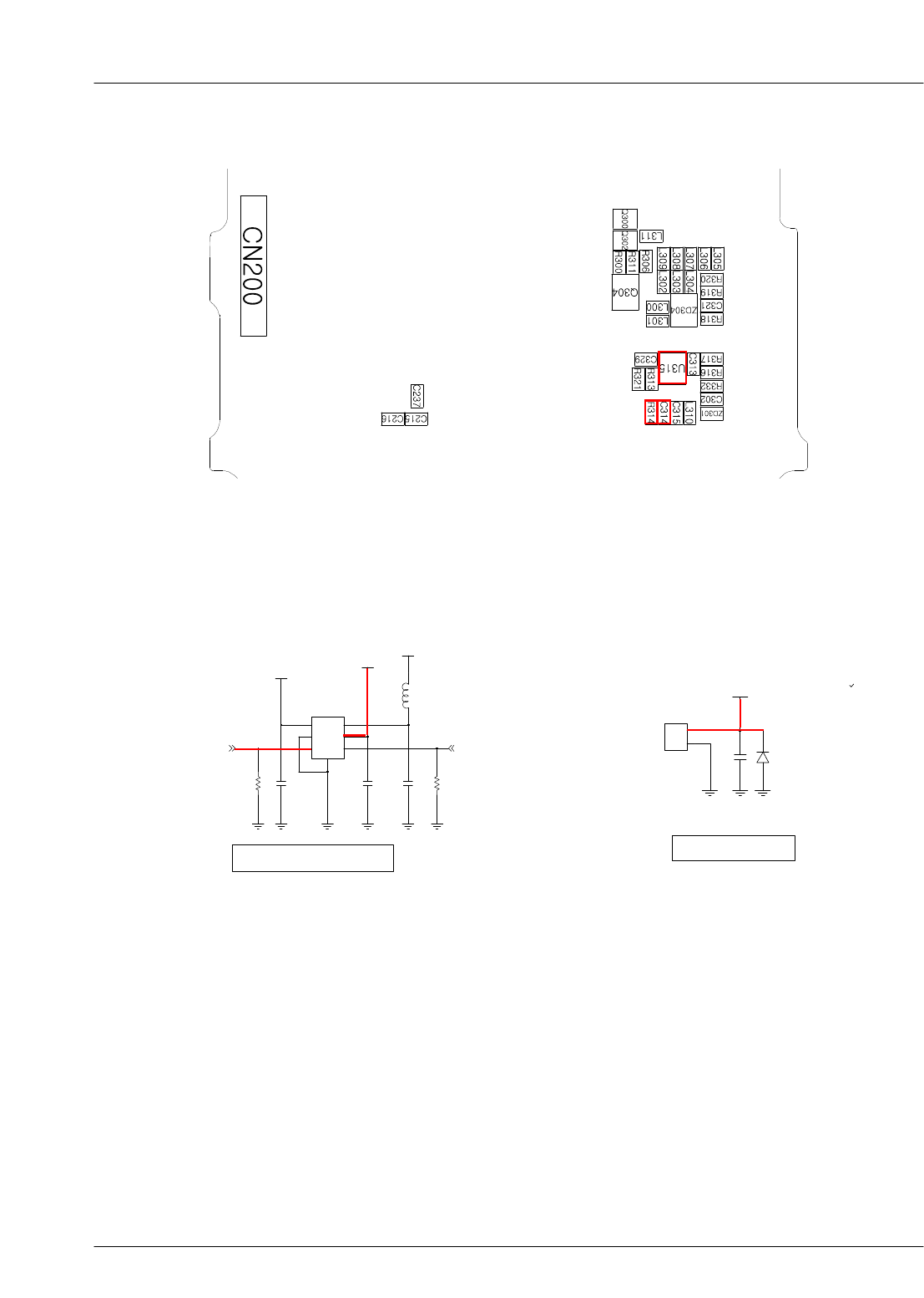
8-3-17. Key Back Light
Main Key LED does not work
Yes
No Replace the UCP200 using aHeatgun
Check the Key LDO enable is
high.
(TP :R314 =1.8
V)
Yes
#1 : Replace the LED
(be possible that the sample has the problem)
#2 : Change PBA
Key LED does not work?
(look over the LED light)
END
Yes
No
Check the Main key voltage
is high.
(TP :L310 =3.3
V)
Yes
Replace the U315 using aHeatgun
No
SAMSUNG Proprietary-Contents may change without notice
Level 3Repair
8-40
This Document can not be used without Samsung's authorization
KEY / MOT LDO
L310
MAIN_KEY_3.3V
R314
EN1
EN2
3
2
GND
GND
7
1
VIN 6VOUT1
VOUT2 5
VBAT
U315
4
C315
V_MOT_3.3V
C314
R313
C313
MOT_EN EN_MAIN_KEY_LDO
SAMSUNG Proprietary-Contents may change without notice
Level 3Repair
8-41
This Document can not be used without Samsung's authorization
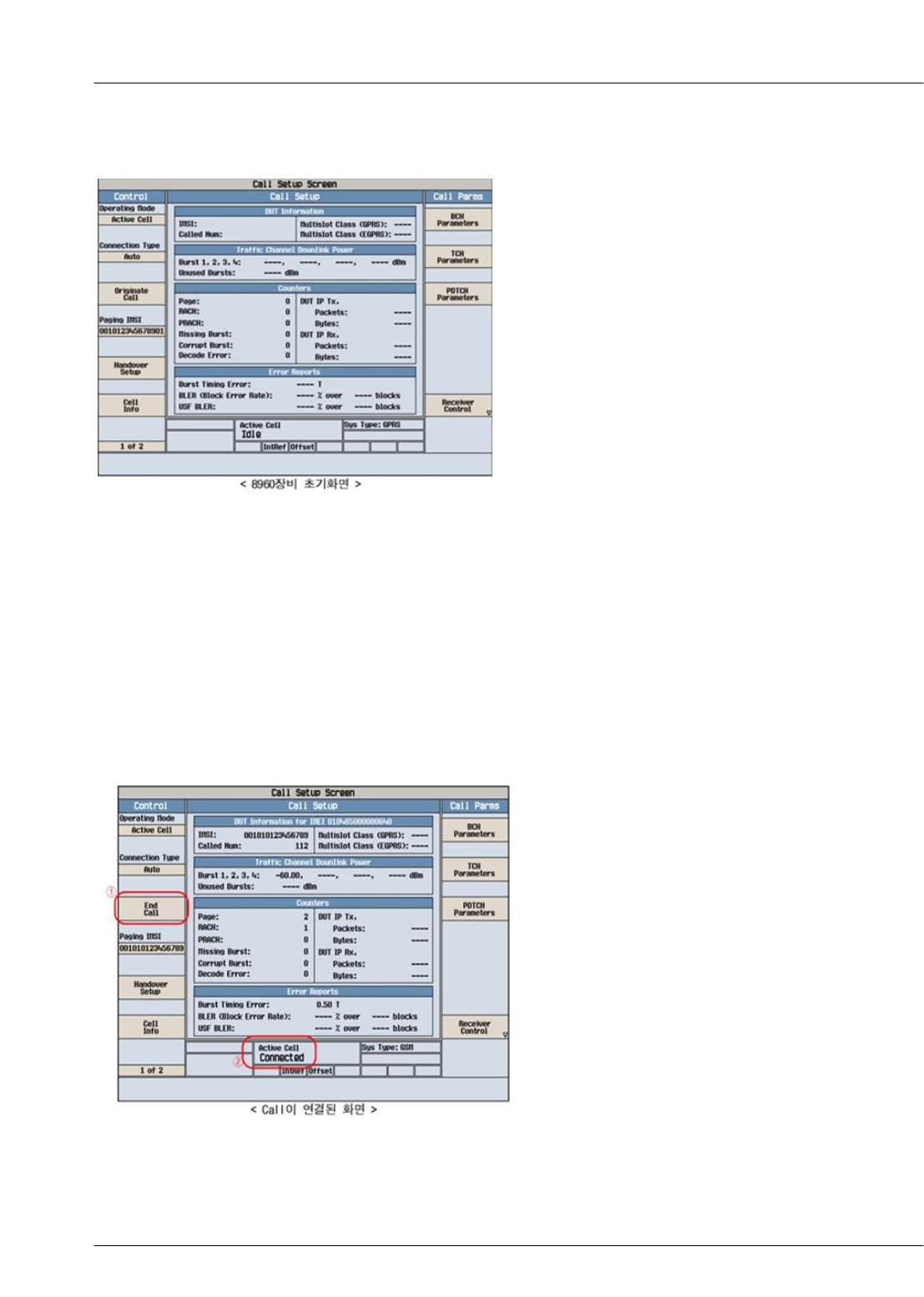
(presetting 8960
(Rx setting)
1. Active Cell
:select GSM or GPRS
2. Connetion Type
:select Auto(GSM), BLER(GPRS)
3. BCH Parameter
:select measuring band (DCS or EGSM)
4. Cell power
:-60
dBm

SAMSUNG Proprietary-Contents may change without notice
Level 3Repair
8-42
This Document can not be used without Samsung's authorization
(Tx setting)
(After setting 8960 ( EGSM /DCS )
1. After setting, prepare the call setup Display
2. UsinganOriginateCall,makeacall.
3. Confirm the display "connected"
4. start the measuring
SAMSUNG Proprietary-Contents may change without notice
Level 3Repair
8-43
This Document can not be used without Samsung's authorization
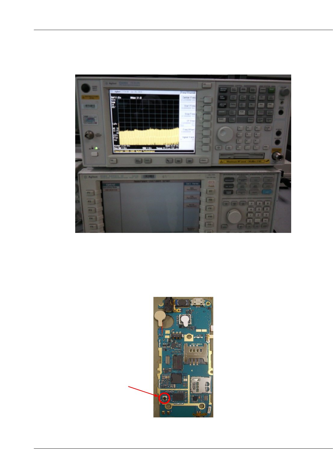
(8960 & spectrum analyzer (down &up at picture)
-spectrum analyzer :testing method =the way using an Osciliscope
-8960:connect using RF Cable between 8960 & RF Connector in board.
RF Connector
SAMSUNG Proprietary-Contents may change without notice
Level 3Repair
8-44
This Document can not be used without Samsung's authorization
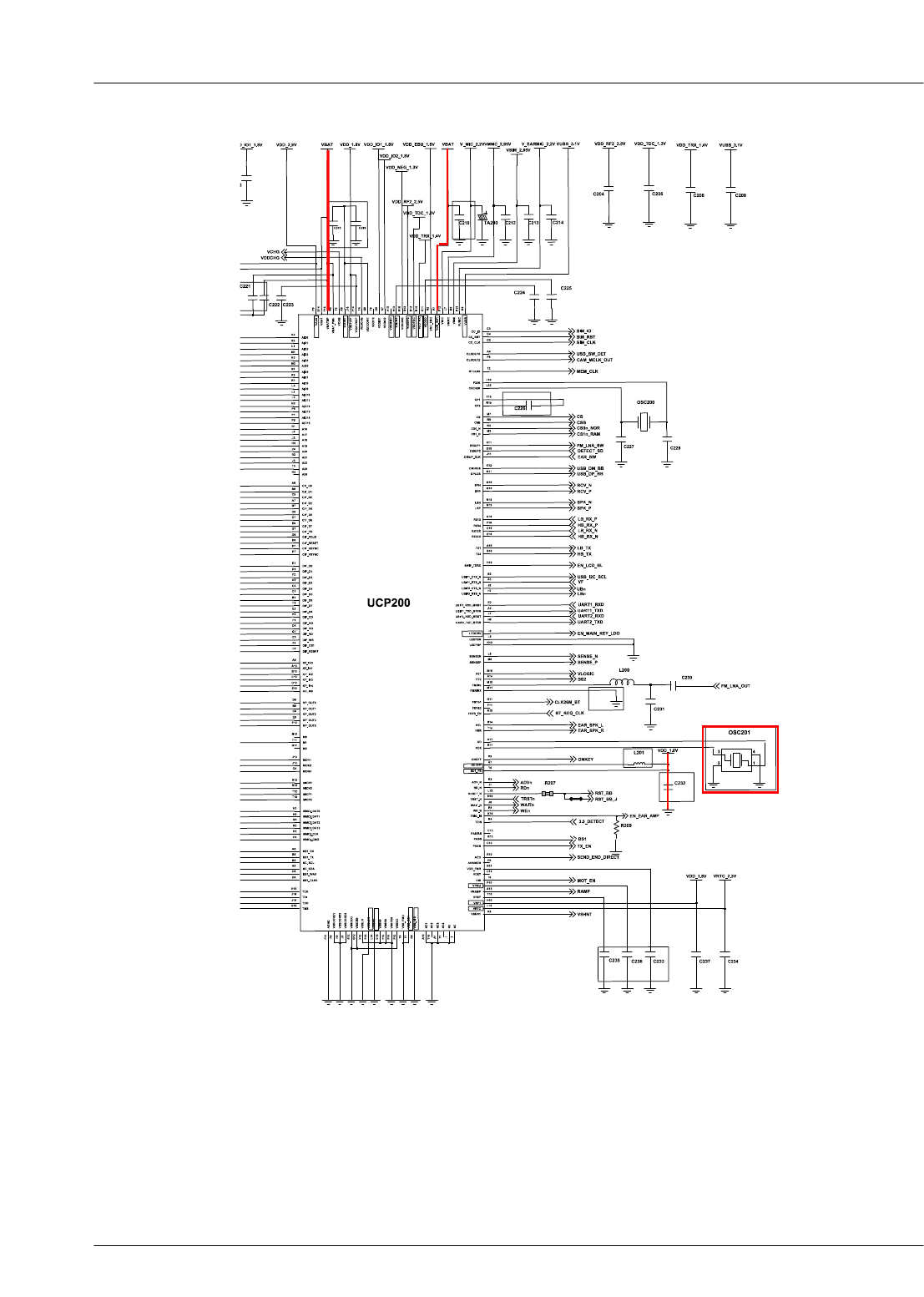
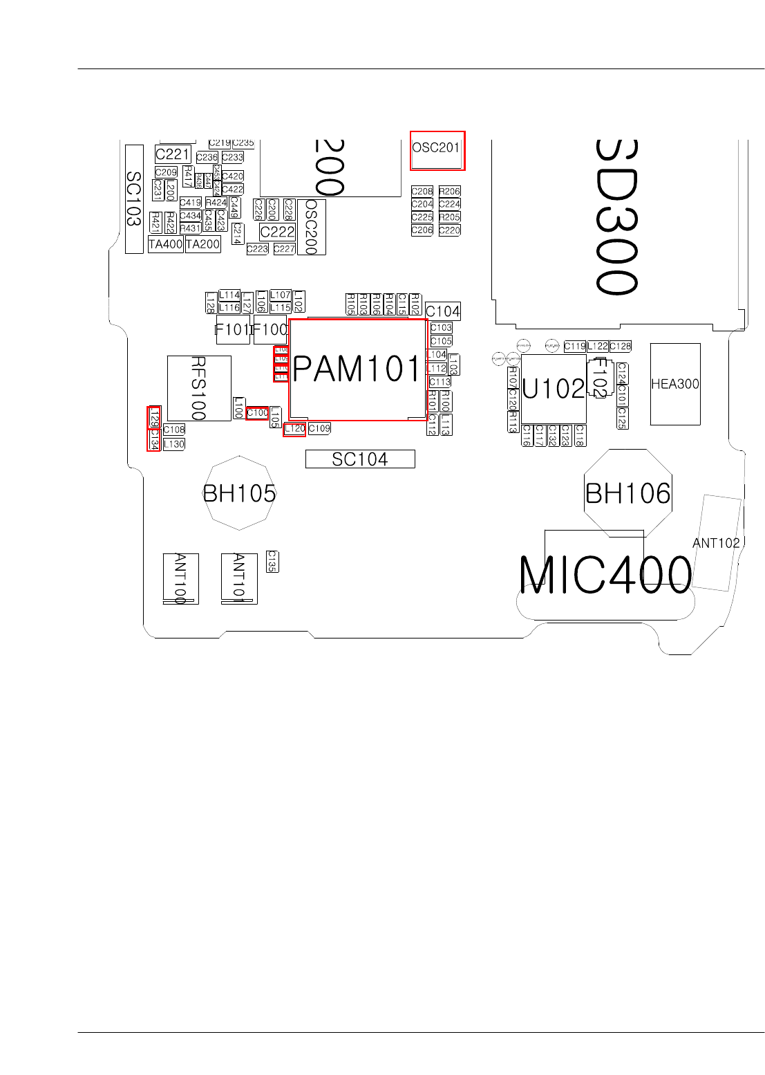
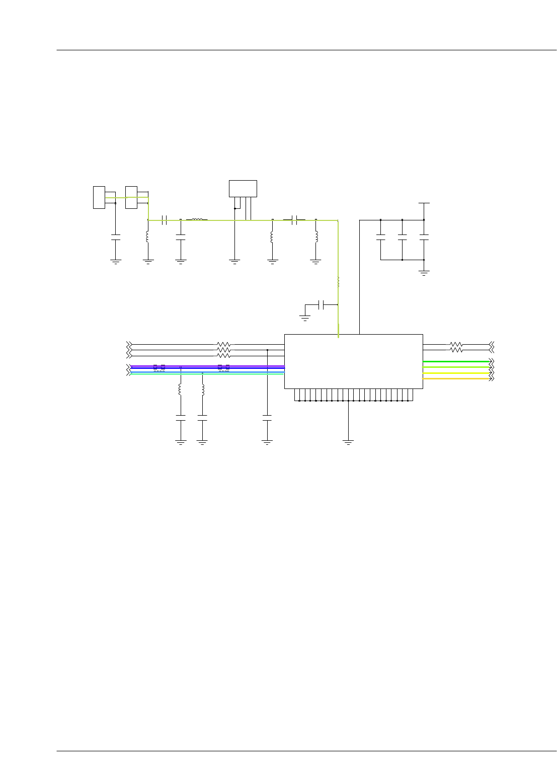
8-3-10. GSM850 Receiver
RX ON
Cell Power :-60
dBm
PAM101 Pin17
-65dBm
(TP:L120 using
spectrum analyzer)
Yes
Resolder PAM101, C134, L129,
C100, L120)
No
Yes
No
Check PAM101
pin5=L, pin6=L
PAM101 Pin11
-68dBm
(TP:L108 using
specturm analyzer)
Check ANT Switch
or ANT is demaged.
No
Yes
Resolder PAM101
Yes
Resolder OSC201
TCXO CLOCK
CHECK?
26MHz @OSC201
pin 1,3
Yes
No
Check UCP200
Yes
END

SAMSUNG Proprietary-Contents may change without notice
Level 3Repair
8-45
This Document can not be used without Samsung's authorization
8-3-11. GSM900 Receiver
RX ON
Cell Power :-60
dBm
PAM101 Pin17
-65dBm
(TP:L120 using
spectrum analyzer)
Yes
Resolder PAM101, C134, L129,
C100, L120
No
Yes
No
Check PAM101
pin5=L, pin6=H
PAM101 Pin12
-68dBm
(TP:L109 using
specturm analyzer)
Check ANT Switch
or ANT is demaged.
No
Yes
Resolder PAM101
Yes
Resolder OSC201
TCXO CLOCK
CHECK?
26MHz @OSC201
pin 1,3
Yes
No
Check UCP200
Yes
END

SAMSUNG Proprietary-Contents may change without notice
Level 3Repair
8-46
This Document can not be used without Samsung's authorization
8-3-12. DCS Receiver
RX ON
Cell Power :-60
dBm
PAM101 Pin17
-65dBm
(TP:L120 using
spectrum analyzer)
Yes
Resolder PAM101, C134, L129,
C100, L120
No
Yes
No
Check PAM101
pin5, pin6=H
PAM101 Pin13
-68dBm
(TP:L110 using
specturm analyzer)
Check ANT Switch
or ANT is demaged.
No
Yes
Resolder PAM101
Yes
Resolder OSC201
TCXO CLOCK
CHECK?
26MHz @OSC201
pin 1,3
Yes
No
Check UCP200
Yes
END

SAMSUNG Proprietary-Contents may change without notice
Level 3Repair
8-47
This Document can not be used without Samsung's authorization
8-3-13. PCS Receiver
RX ON
Cell Power :-60
dBm
PAM101 Pin17
-65dBm
(TP:L120 using
spectrum analyzer)
Yes
Resolder PAM101, C134, L129,
C100, L120
No
Yes
No
Check PAM101
pin5=H, pin6=L
PAM101 Pin14
-68dBm
(TP:L111 using
specturm analyzer)
Check ANT Switch
or ANT is demaged.
No
Yes
Resolder PAM101
Yes
Resolder OSC201
TCXO CLOCK
CHECK?
26MHz @OSC201
pin 1,3
Yes
No
Check UCP200
Yes
END
SAMSUNG Proprietary-Contents may change without notice
Level 3Repair
8-48
This Document can not be used without Samsung's authorization
SAMSUNG Proprietary-Contents may change without notice
Level 3Repair
8-49
This Document can not be used without Samsung's authorization
1
1
22
ANT100
VBAT
RFS100
A
2
1C
3G
G
4
R106
R102
C115
L105
R104
C103 C104
L120
L100
22
C100
ANT101
1
1
401L301L
L112
C113
L113
C112
R101R100
R103
4
30
VBATT
VLOGIC
2
3VRAMP
R105
16
G
18
19G
27 GSM_IN
RX1 11
RX2 12
13
RX3
RX4 14
TX_EN
G
G
34
35G
G
36
G
8
9G
G
10
15G
G
G
G
24
25G
G
26
G
28
31G
G
32
7G
33
ANT
5
BS1
BS2 6
DCS|PCS_IN
29
G
1
G
20
21G
G
22
23
PAM101
17
C109
C105
C134
L130
C108
C135
L129
LB_TX
GSM850_RX
PCS1900_RX
DCS1800_RX
BS2
TX_EN
GSM900_RX
VLOGIC BS1
RAMP
HB_TX
L116
L128
L127
L106
L107
L102
L109 L115
L108
G
10G
4UNBAL
1UNBAL
F101
BAL1 6
BAL2 9
2G
G
3
G
5
G
7
8
5G
G
7
8G
G
10
UNBAL
4
1UNBAL
F100
BAL1
BAL2 9
G
2
3G
L114
L111
L110
DCS1800_RX
PCS1900_RX
HB_RX_N
HB_RX_P
GSM850_RX
GSM900_RX
LB_RX_P
LB_RX_N
SAMSUNG Proprietary-Contents may change without notice
Level 3Repair
8-50
This Document can not be used without Samsung's authorization
Check the Voltage
C104 <3.3
V?
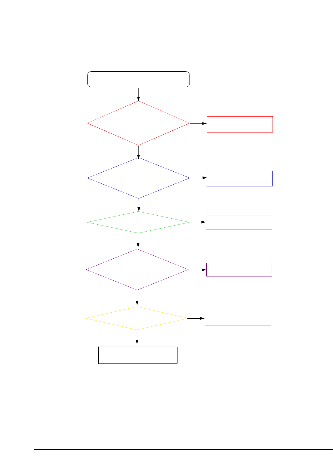
8-3-14. GSM850/GSM900 Transmitter
TX Power is too Low!!
TX ON (5Level)
TCXO CLOCK
CHECK?
26MHz @OSC201
pin 1,3
NO
Re-solder OSC201
YES
PAM101 pin27 -4
dBm
(TP:R101 using
spectrum analyzer)
NO Re-solder or change
UCP200
YES
NO
Check the UCP200 &VBAT
circuit.
YES
NO
Resolder PAM101
PAM101 Pin17
30dBm
(TP:L120 using
spectrum analyzer)
YES
Resolder RFS100.
Check the RFS100
connection with PCB?
YES
Antenna
re-solder or change
NO
SAMSUNG Proprietary-Contents may change without notice
Level 3Repair
8-51
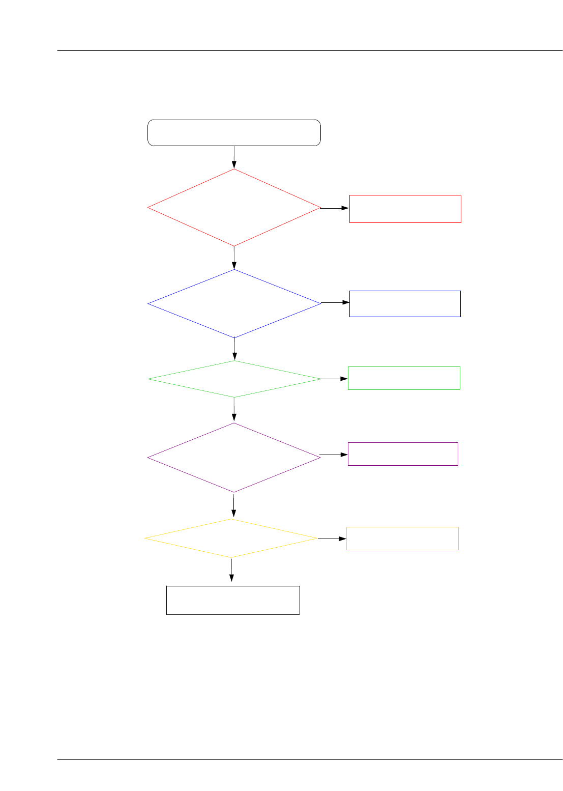
This Document can not be used without Samsung's authorization
Check the Voltage
C104 <3.3
V?
8-3-15. DCS/PCS Transmitter
TX Power is too Low!!
TX ON (5Level)
TCXO CLOCK
CHECK?
26MHz @OSC201
pin 1,3
NO
Re-solder OSC201
YES
PAM101 pin29 -4
dBm
(TP:L104 using
spectrum analyzer)
NO
Re-solder or change
UCP200
YES
NO
Check the UCP200 &VBAT
circuit.
YES
NO
Resolder PAM101
PAM101 Pin17
30dBm
(TP:L120 using
spectrum analyzer)
YES
Resolder RFS100.
Check the RFS100
connection with PCB?
YES
Antenna
re-solder or change
NO
SAMSUNG Proprietary-Contents may change without notice
Level 3Repair
8-52
This Document can not be used without Samsung's authorization
1
1
22
ANT100
VBAT
RFS100
A
2
1C
3G
G
4
R106
R102
C115
L105
R104
C103 C104
L120
L100
22
C100
ANT101
1
1
401L301L
L112
C113
L113
C112
R101R100
R103
4
30
VBATT
VLOGIC
2
3VRAMP
R105
16
G
18
19G
27 GSM_IN
RX1 11
RX2 12
13
RX3
RX4 14
TX_EN
G
G
34
35G
G
36
G
8
9G
G
10
15G
G
G
G
24
25G
G
26
G
28
31G
G
32
7G
33
ANT
5
BS1
BS2 6
DCS|PCS_IN
29
G
1
G
20
21G
G
22
23
PAM101
17
C109
C105
C134
L130
C108
C135
L129
LB_TX
GSM850_RX
PCS1900_RX
DCS1800_RX
BS2
TX_EN
GSM900_RX
VLOGIC BS1
RAMP
HB_TX
SAMSUNG Proprietary-Contents may change without notice
Level 3Repair
8-53
This Document can not be used without Samsung's authorization
SAMSUNG Proprietary-Contents may change without notice
Level 3Repair
8-54
This Document can not be used without Samsung's authorization
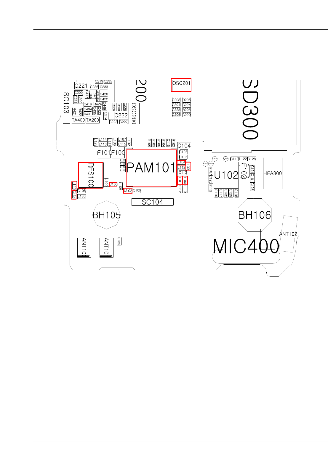
8-4. Service Schematics
-NC Point(Top View)
:NC
U101
1234567
A.......
B......
C.......
D.....
E.. ....
F......
G.......
H.......
UME200
12345678910
A.....
B......
C..... .
D.. .
E.... ..
F
G
H
J
K.
L..
M.. .
N.........
P.........
R..........
T..........
U........
SAMSUNG Proprietary-Contents may change without notice
Level 3Repair
8-55
This Document can not be used without Samsung's authorization
UCP200
12345678910111213141516
A..............
B................
C.......... .....
D.... ... .
E... ....... .
F.... ...........
G.............. .
H.... ........ ..
J.... ........ ..
K........ ... ..
L.... ..... ....
M... ...... ..
N.... ... ..
P..... ..........
R................
T..............
SAMSUNG Proprietary-Contents may change without notice
7. Level 2Repair
7-1
This Document can not be used without Samsung's authorization
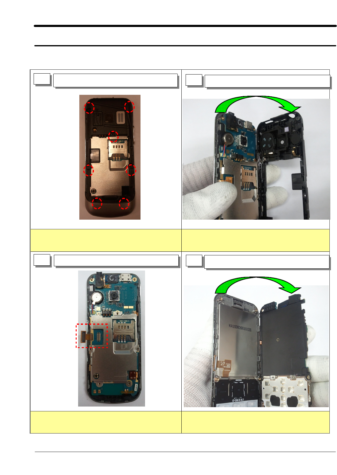
7-1. Disassembly and Assembly Instructions
7-1-1. Disassembly
※Caution
1) Torque : 1.1±0.1 kgf.cm
※Caution
1) Be careful Hook on Mech. not to be broken.
※Caution
1) Be careful Hook on Mech. not to be broken.
1) Unscrew 7Points.
11) Disassemble the Rear.
2
31) Disassemble LCD FPCB connector. 41) 1) Disassemble PBA and Front Ass'y
SAMSUNG Proprietary-Contents may change without notice
7. Level 2Repair
7-2
This Document can not be used without Samsung's authorization
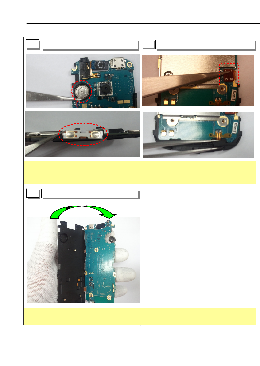
※Caution
1) Be careful Motor &FPCB not to be damaged.
※Caution
1) Be careful 3*4 Key FPCB connector & MIC
module not to be damaged.
1) Detach Motor, Volume Key FPCB.
51) Disassemble 3*4 Key FPCB connector, MIC.
6
71) Disassemble PBA with Bracket.
SAMSUNG Proprietary-Contents may change without notice
7. Level 2Repair
7-3
This Document can not be used without Samsung's authorization
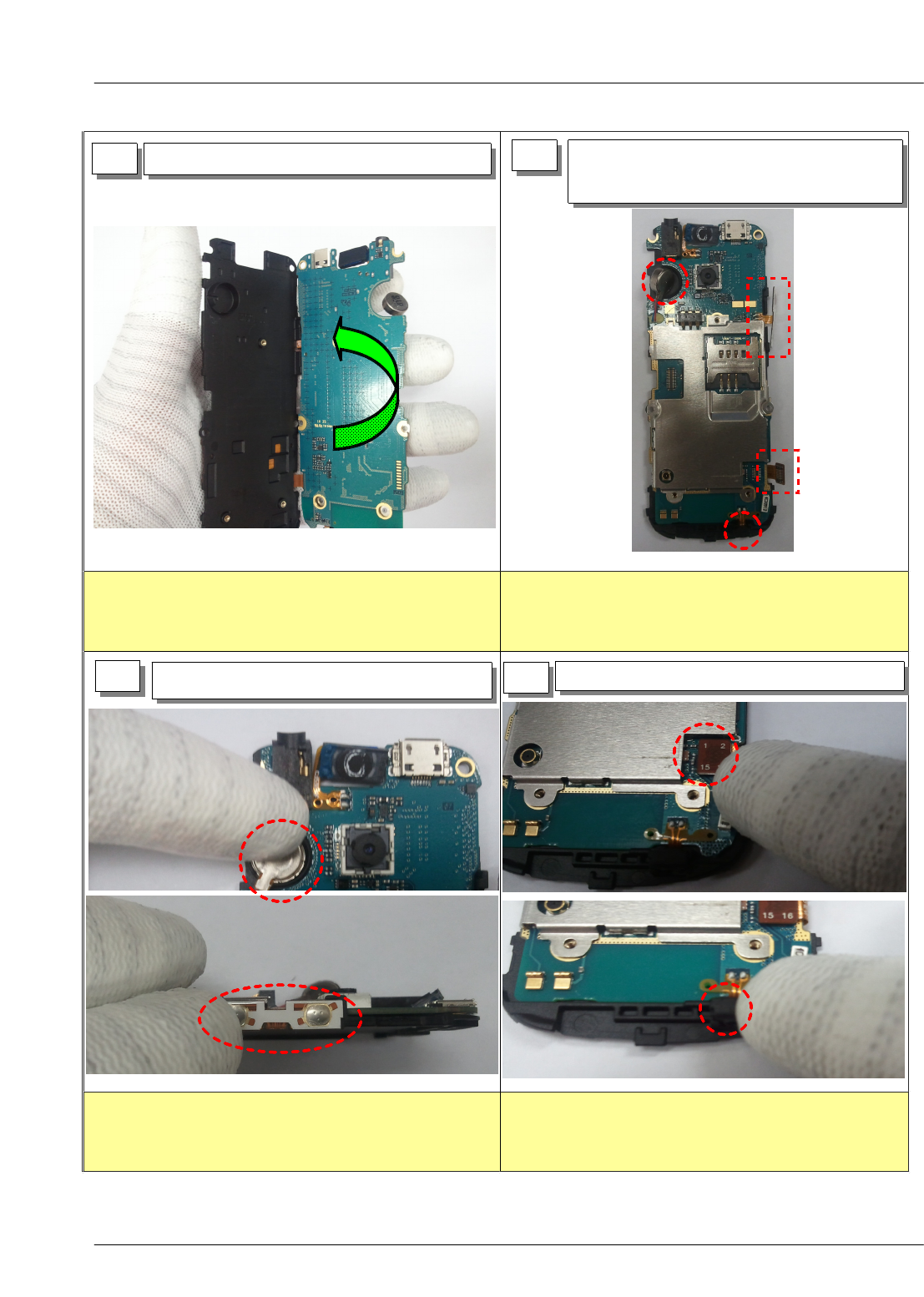
7-1-2. Assembly
※Caution
1) Assemble following boss hole & guide on the
bracket.
※Caution
1) Check Motor fully settled down in the Bracket.
2) Assemble FPCB following guide on the Bracket.
※Caution
1) Check MIC fully settled down in the Bracket.
11) Assemble the PBA with the Bracket.
31) Attach Motor, Volume Key FPCB. 41) Assemble 3*4 Key FPCB connector, MIC.
21) Attach Motor, Volume Key FPCB, 3*4
Key FPCB, MIC on the Bracket & PBA
SAMSUNG Proprietary-Contents may change without notice
7. Level 2Repair
7-4
This Document can not be used without Samsung's authorization
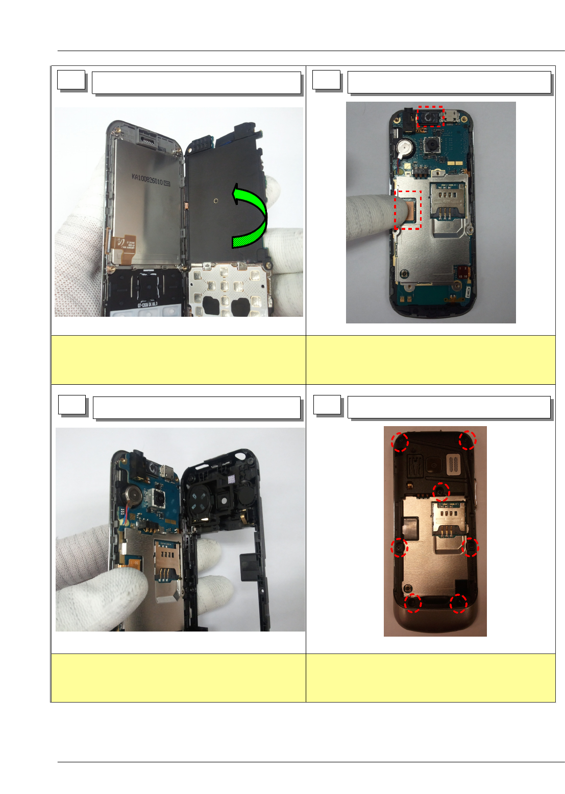
※Caution
1) Assemble following boss hole on the bracket.
2) Check 3*4 Keypad assembled at the right place.
※Caution
1) Check Receiver fully settled down in the
Bracket.
※Caution
1) Be careful Volume Key &SPK module
assembled at the right place.
※Caution
1) Torque : 1.1±0.1 kgf.cm
5 6
1) Assemble PBA and Front Ass'y 1) Assemble LCD FPCB connector.
7 8
1) Assemble Rear. 1) Screw 7points.

SAMSUNG Proprietary-Contents may change without notice
5. MAIN Electrical Parts List
5-1
This Document can not be used without Samsung's authorization
Design LOC SEC CODE Description
D400 0401-001141 DIODE-SWITCHING
ZD300 0403-001688 DIODE-ZENER
ZD304 0406-001167 DIODE-TVS
ZD401 0406-001169 DIODE-TVS
ZD402,ZD403,ZD404 0406-001231 DIODE-TVS
ZD301,ZD302,ZD305 0406-001293 DIODE-TVS
ZD306 0406-001293 DIODE-TVS
ZD400 0406-001361 DIODE-TVS
U400 0406-001369 DIODE-TVS
Q301 0501-002606 TR-SMALL SIGNAL
Q304 0501-002663 TR-SMALL SIGNAL
Q303 0502-001322 TR-POWER
Q300,Q302 0504-001140 TR-DIGITAL
Q305 0505-001165 FET-SILICON
U404 1001-001645 IC
U100 1201-002944 IC
PAM101 1201-003025 IC
U316 1201-003111 IC
U405 1202-001068 IC
U314 1203-003643 IC
U313 1203-005574 IC
U315 1203-005851 IC
U409 1203-006111 IC
U102 1205-003517 IC
UCP200 1205-004030 IC
TH200 1404-001224 THERMISTOR
R102,R103,R105,R106 2007-000138 R-CHIP
R304,R337,R416,R430 2007-000138 R-CHIP
R104,R306,R333 2007-000140 R-CHIP
R109,R315,R332,R400 2007-000143 R-CHIP
R200,R213 2007-000146 R-CHIP
R203,R311,R316,R317 2007-000148 R-CHIP
R318,R319,R320,R426 2007-000148 R-CHIP
R427 2007-000148 R-CHIP
R313,R314,R321 2007-000157 R-CHIP
R113,R205,R206,R209 2007-000162 R-CHIP
R414 2007-000162 R-CHIP
R420 2007-000166 R-CHIP
R418 2007-000168 R-CHIP
R415,R433 2007-000170 R-CHIP

SAMSUNG Proprietary-Contents may change without notice
Main Electrical Parts List
5-2
This Document can not be used without Samsung's authorization
Design LOC SEC CODE Description
R403,R404 2007-000174 R-CHIP
R334,R422,R431 2007-000242 R-CHIP
R305 2007-000831 R-CHIP
R303 2007-000932 R-CHIP
R108,R421,R432 2007-001119 R-CHIP
R110 2007-001307 R-CHIP
R401 2007-002965 R-CHIP
R107 2007-003015 R-CHIP
R302 2007-007001 R-CHIP
R300 2007-007015 R-CHIP
R204 2007-007142 R-CHIP
R417 2007-007156 R-CHIP
R210,R211 2007-008052 R-CHIP
R435,R436 2007-008478 R-CHIP
R405,R406 2007-008531 R-CHIP
R437 2007-008588 R-CHIP
R331 2007-008780 R-CHIP
C101,C135 2203-000233 C-CERAMIC,CHIP
C116,C132,C329 2203-000254 C-CERAMIC,CHIP
C105 2203-000278 C-CERAMIC,CHIP
C119,C412,C440,C449 2203-000386 C-CERAMIC,CHIP
C452 2203-000386 C-CERAMIC,CHIP
C404,C405 2203-000425 C-CERAMIC,CHIP
C123,C214,C327,C328 2203-000438 C-CERAMIC,CHIP
C227,C228 2203-000550 C-CERAMIC,CHIP
C131 2203-000679 C-CERAMIC,CHIP
C115,C302,C303,C304 2203-000812 C-CERAMIC,CHIP
C325,C419,C432,C433 2203-000812 C-CERAMIC,CHIP
C435 2203-000854 C-CERAMIC,CHIP
C121,C133,C230 2203-002443 C-CERAMIC,CHIP
C225,C233 2203-002487 C-CERAMIC,CHIP
C231 2203-002668 C-CERAMIC,CHIP
C118,C223 2203-002709 C-CERAMIC,CHIP
C408 2203-002982 C-CERAMIC,CHIP
C100 2203-005057 C-CERAMIC,CHIP
C113 2203-005234 C-CERAMIC,CHIP
C128 2203-005281 C-CERAMIC,CHIP
C108,C109 2203-005288 C-CERAMIC,CHIP
C134 2203-005395 C-CERAMIC,CHIP
C226 2203-005480 C-CERAMIC,CHIP
SAMSUNG Proprietary-Contents may change without notice
Main Electrical Parts List
5-3
This Document can not be used without Samsung's authorization
Design LOC SEC CODE Description
C129,C206,C224 2203-005481 C-CERAMIC,CHIP
C441,C448,C451 2203-005731 C-CERAMIC,CHIP
C424,C447,C453 2203-005734 C-CERAMIC,CHIP
C103,C200,C203,C209 2203-006048 C-CERAMIC,CHIP
C213,C218,C229,C236 2203-006048 C-CERAMIC,CHIP
C323,C423,C430,C434 2203-006048 C-CERAMIC,CHIP
C204,C420,C422 2203-006190 C-CERAMIC,CHIP
C212,C219 2203-006257 C-CERAMIC,CHIP
C216,C234,C235 2203-006260 C-CERAMIC,CHIP
C221,C222 2203-006324 C-CERAMIC,CHIP
C427 2203-006348 C-CERAMIC,CHIP
C208,C217,C237,C306 2203-006399 C-CERAMIC,CHIP
C307,C310,C311,C314 2203-006399 C-CERAMIC,CHIP
C315,C317,C319,C321 2203-006399 C-CERAMIC,CHIP
C326,C407,C428,C431 2203-006399 C-CERAMIC,CHIP
C220,C313,C322,C426 2203-006562 C-CERAMIC,CHIP
C130 2203-006647 C-CERAMIC,CHIP
C308,C309 2203-006844 C-CERAMIC,CHIP
C117,C120,C312 2203-006872 C-CERAMIC,CHIP
C210 2203-007133 C-CERAMIC,CHIP
C232 2203-007269 C-CERAMIC,CHIP
C429 2203-007271 C-CERAMIC,CHIP
C104,C320 2203-007279 C-CERAMIC,CHIP
C446,C450 2203-007317 C-CERAMIC,CHIP
C406 2203-007393 C-CERAMIC,CHIP
TA200,TA400 2404-001225 C-TA,CHIP
L121 2703-000213 INDUCTOR-SMD
L103,L104 2703-001750 INDUCTOR-SMD
L102,L106 2703-002198 INDUCTOR-SMD
L100,L122,L130 2703-002204 INDUCTOR-SMD
L129 2703-002205 INDUCTOR-SMD
L127,L128 2703-002208 INDUCTOR-SMD
L116 2703-002313 INDUCTOR-SMD
L112,L120 2703-002369 INDUCTOR-SMD
L108,L109 2703-002842 INDUCTOR-SMD
L408 2703-003485 INDUCTOR-SMD
L124 2703-003781 INDUCTOR-SMD
L201 2703-003869 INDUCTOR-SMD
L110,L111 2703-003904 INDUCTOR-SMD
OSC201 2801-004896 CRYSTAL-UNIT
SAMSUNG Proprietary-Contents may change without notice
Main Electrical Parts List
5-4
This Document can not be used without Samsung's authorization
Design LOC SEC CODE Description
OSC200 2801-004909 CRYSTAL-UNIT
F400,F401,F402 2901-001408 FILTER-EMI SMD
F101 2904-001923 FILTER-SAW
F100 2904-001924 FILTER-SAW
L400,L401,L402,L404 3301-001812 CORE-FERRITE BEAD
L403,L405,L406,L410 3301-001917 CORE-FERRITE BEAD
L200,L300,L301,L302 3301-002074 CORE-FERRITE BEAD
L303,L304,L305,L306 3301-002074 CORE-FERRITE BEAD
L307,L308,L309,L310 3301-002074 CORE-FERRITE BEAD
L311 3301-002074 CORE-FERRITE BEAD
RFS100 3705-001731 CONNECTOR-COAXIAL
SD300 3709-001575 CONNECTOR-CARD EDGE
SIM300 3709-001645 CONNECTOR-CARD EDGE
CN400 3710-003306 CONNECTOR-SOCKET
HEA400 3711-006882 CONNECTOR-HEADER
HEA300 3711-006923 CONNECTOR-HEADER
BTC300 3711-007393 CONNECTOR-HEADER
IFC400 3722-002871 JACK-PHONE
F102 4709-001615 RF-MODULE
SC101,SC102,SC103 GH70-03349A IPR SHIELD-CAN CLIP
SC104 GH70-03349A IPR SHIELD-CAN CLIP
ANT100,ANT101 GH71-08731A NPR-CONTACT ANT
R115 GH80-03320A PB-SHORT-1005
R100,R101,R207,R301 GH80-03320A PB-SHORT-1005
R336,R409,R412,R434 GH80-03320A PB-SHORT-1005
EAR400 3722-003139 JACK-PHONE
UME200 1108-000355 MEMORY
ANT102 4202-001525 ANTENNA-CHIP
Please consult the GSPN website (Samsung Portal) for the most recent version of the product's
part list.
SAMSUNG Proprietary-Contents may change without notice
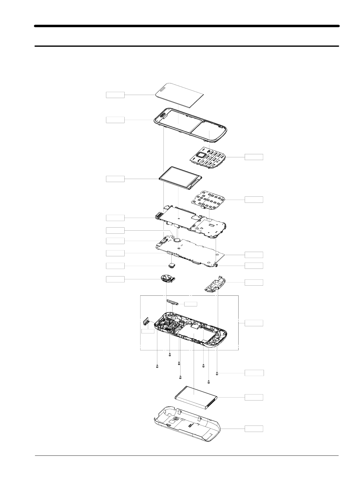
4. Exploded View and Parts List
4-1
This Document can not be used without Samsung's authorization
4-1. Cellular phone Exploded View
QFR01
QLC01
QBR01
QAR01
QVK01
QCA01
QMO01
QSP01
QMW01
QCO01
QRE01
QAN02
QMI01
QMP01
QME01
QKP01
QCR101
QBA01
QBC00
QRF06
- This Document can not be used without Samsung's authorization -
5-2. Cellular phone Parts list : GT-C3530HSATUR
Design LOC
Description
SEC CODE
QAN02
INTENNA-GT-C3530
GH42-02703A
QAR01
AUDIO-RECEIVER
3009-001512
QBA01
INNER BATTERY PACK-AB463651BU,960MAH
GH43-03216A
QBC00
ASSY COVER-BATTERY
GH98-18172A
QBR01
ASSY CASE-BRACKET
GH98-18134A
QCA01
CAMERA MODULE
GH59-09685A
QCO01
PMO KEY-VOLUME V2
GH72-61919A
QCR101
SCREW-MACHINE
6001-002005
QFR01
ASSY CASE-FRONT
GH98-18133A
QKP01
ASSY KEYPAD-MAIN KEY
GH98-18136A
QLC01
ASSY LCD-GT-C3530_2.2",QVGA
GH96-04930A
QME01
KEY FPCB-MAIN KEY PBA(GT-C3530)
GH59-09911A
QMI01
MICROPHONE-ASSY-GT-C3530
GH30-00700A
QMO01
MOTOR DC-SGHT539
GH31-00328A
QMP01
A/S ASSY-PBA MAIN(TURK)GT-C3530
GH82-05330A
QMW01
ASSY COVER-MAIN WINDOW
GH98-18449A
QRE01
ASSY CASE-REAR
GH98-18135A
QRF06
PMO COVER-USB V2
GH72-61917A
QSP01
SPEAKER
3001-002529
QVK01
KEY FPCB-VOLUME KEY(GT-C3530)
GH59-09915A
2. Specification
2-1
2-1. GSM General Specification
GSM900
Phase 1
GSM850
Phase 1
DCS1800
Phase 1 PCS1900
Freq.
Band[MHz]
Uplink/Downlink
880~915
925~960
824.2~848.8
869.2~893.8
1710~1785
1805~1880
1850~1910
1930~1990
ARFCN range 0~124 &
975~1023 128~251 512~885 512~810
Tx/Rx spacing 45MHz 45MHz 95MHz 80MHz
Mod. Bit rate/
Bit Period
270.833kbps
3.692us
270.833kbps
3.692us
270.833kbps
3.692us
270.833kbps
3.692us
Time Slot
Period/Frame
Period
576.9us
4.615ms
576.9us
4.615ms
576.9us
4.615ms
576.9us
4.615ms
Modulation 0.3GMSK 0.3GMSK 0.3GMSK 0.3GMSK
MS Power 33dBm~5dBm 33dBm~5dBm 30dBm~0dBm 30dBm~0dBm
Power Class 5pcl ~ 19pcl 5pcl ~ 19pcl 0pcl ~15
pcl 0pcl ~15
pcl
Sensitivity -102dBm -102dBm -100dBm -100dBm
TDMAMux8888
Cell Radius 35Km 35Km 2Km -
Speclflcation
2-2
2-2. GSM Tx Power Class
TX Power
control level
GSM850
GSM900
533±3
dBm
631±3
dBm
729±3
dBm
827±3
dBm
925±3
dBm
10 23±3 dBm
11 21±3 dBm
12 19±3 dBm
13 17±3 dBm
14 15±3 dBm
15 13±3 dBm
16 11±5 dBm
17 9±5 dBm
18 7±5 dBm
19 5±5 dBm
TX Power
control level DCS1800
030±3
dBm
128±3
dBm
226±3
dBm
324±3
dBm
422±3
dBm
520±3
dBm
618±3
dBm
716±3
dBm
814±3
dBm
912±4
dBm
10 10±4 dBm
11 8±4dBm
12 6±4 dBm
13 4±4 dBm
14 2±5 dBm
15 0±5 dBm
TX Power
control level PCS1900
030±3
dBm
128±3
dBm
226±3
dBm
324±3
dBm
422±3
dBm
520±3
dBm
618±3
dBm
716±3
dBm
814±3
dBm
912±4
dBm
10 10±4 dBm
11 8±4dBm
12 6±4 dBm
13 4±4 dBm
14 2±5 dBm
15 0±5 dBm
Speclflcation
2-3
TX Power
control level
GSM900
GSM850
827±3
dBm
925±3
dBm
10 23±3 dBm
11 21±3 dBm
12 19±3 dBm
13 17±3 dBm
14 15±3 dBm
15 13±3 dBm
16 11±5 dBm
17 9±5 dBm
18 7±5 dBm
19 5±5 dBm
TX Power
control level DCS1800
2 26±3 dBm
3 24±3 dBm
4 22±3 dBm
5 20±3 dBm
6 18±3 dBm
7 16±3 dBm
8 12±3 dBm
9 10±3 dBm
10 14±3 dBm
11 12±4 dBm
12 10±4 dBm
13 8±4dBm
14 6±4 dBm
15 4±4 dBm
2-3. GSM EDGE TX power class
TX Power
control level PCS1900
226±3
dBm
324±3
dBm
422±3
dBm
520±3
dBm
618±3
dBm
716±3
dBm
812±3
dBm
910±3
dBm
10 14±3 dBm
11 12±4 dBm
12 10±4 dBm
13 8±4dBm
14 6±4 dBm
15 4±4 dBm
Only in Master

SAMSUNG Proprietary-Contents may change without notice
3. Operation Instruction and Installation
3-1
This Document can not be used without Samsung's authorization
Main Function
•Quad Band 2G(GSM850+EGSM900+DCS1800+PCS1900)
•GPRS Class12, EDGE Class12(Rx only)
•FM Radio
•Bluetooth v2.1 +EDR
•TFT 2.2" 262k Color
•3M
CMOS Camera
•MP3 Player
•3.5
mm EAR-JACK
SAMSUNG Proprietary-Contents may change without notice
6. Level 1Repair
6-1
This Document can not be used without Samsung's authorization
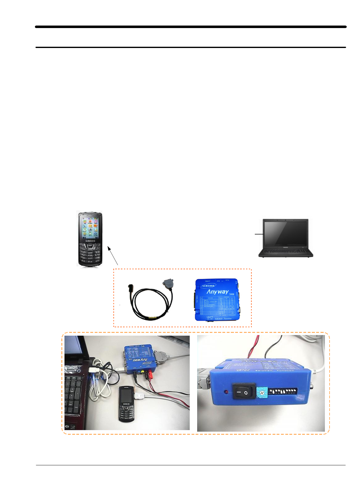
6-1. S/W Download
6-1-1. Pre-requsite for S/W Downloading
•Downloader Program (Flash tool_E2)
•GT-C3530 Mobile Phone
•Data Cable
•JIG BOX (GH99-36900A)
•RF Test Cable (GH39-00985A)
•JIG Cable (GH39-01160A)
•Adapter (GH99-38251A)
•Serial Cable
•Binary files
(Settings
Connect to ANYWAY JIG BOX
&JIG CABLE (Phone to JIG)
SAMSUNG Proprietary-Contents may change without notice
Level 1Repair
6-2
This Document can not be used without Samsung's authorization
6-1-2. S/W Downloader Program
]Load the binary download program by executing the
"Flash tool_E2 "enter this file.
1.Select the connected serial port and the rate of speed.
SAMSUNG Proprietary-Contents may change without notice
Level 1Repair
6-3
This Document can not be used without Samsung's authorization
2.Select communication driver as Infineon USB driver.
SAMSUNG Proprietary-Contents may change without notice
Level 1Repair
6-4
This Document can not be used without Samsung's authorization
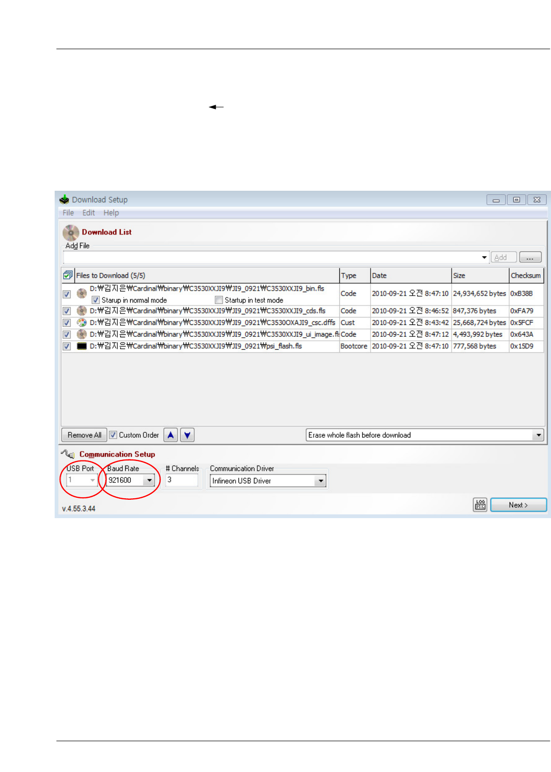
3.Select the Binary in sequence of
"_bin.fls", "_cds.fls", ".dffs", "_ui_image.fls", "psi_flash.fls"
SAMSUNG Proprietary-Contents may change without notice
Level 1Repair
6-5
This Document can not be used without Samsung's authorization
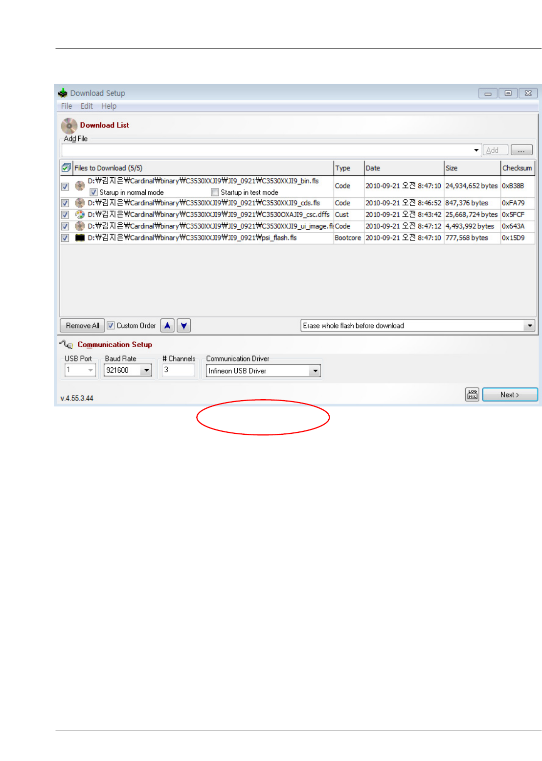
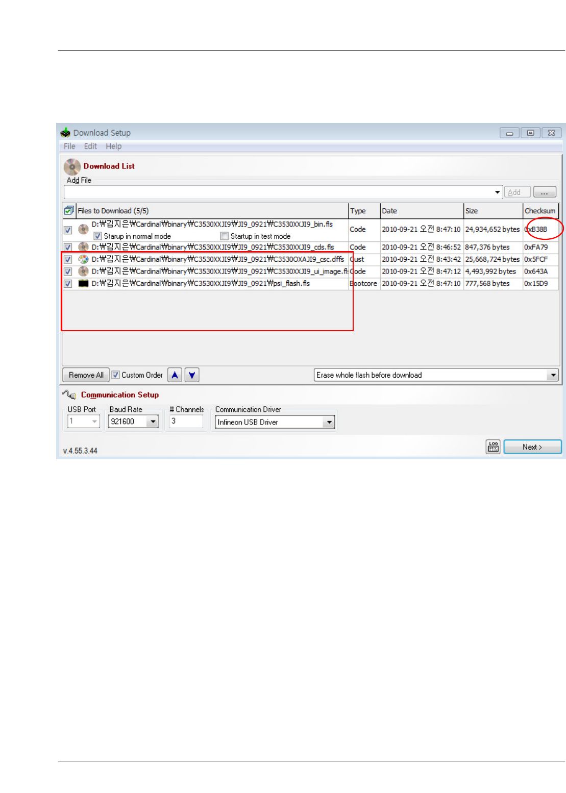
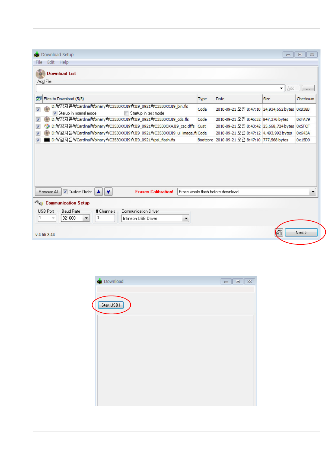
4.P
ress the "Next" button.
5.Press Start USB1 and connect the Handset.
SAMSUNG Proprietary-Contents may change without notice
Level 1Repair
6-6
This Document can not be used without Samsung's authorization
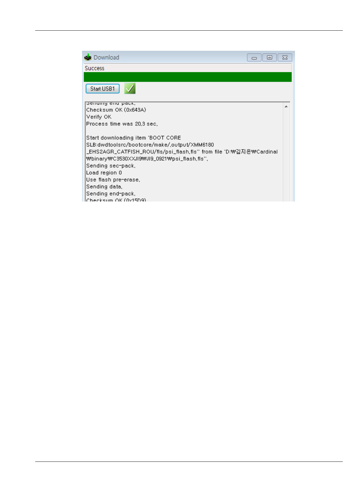
6.When downloading is complete, you can see green bar.
7. Confirm the downloaded version name and etc. :
*#1234#
Full Reset :
*2767*3855#

SAMSUNG Proprietary-Contents may change without notice
9. Reference Abbreviate
This Document can not be used without Samsung's authorization
9-1
Reference Abbreviate
―AAC:Advanced Audio Coding.
―AVC :Advanced Video Coding.
―BER :Bit Error Rate
―BPSK:Binary Phase Shift Keying
―CA :Conditional Access
―CDM :Code Division Multiplexing
―C/I :Carrier to Interference
―DMB :Digital Multimedia Broadcasting
―EN :European Standard
―ES :Elementary Stream
―ETSI:European Telecommunications Standards Institute
―MPEG:Moving Picture Experts Group
―PN :Pseudo-random Noise
―PS :Pilot Symbol
―QPSK:Quadrature Phase Shift Keying
―RS :Reed-Solomon
―SI :Service Information
―TDM :Time Division Multiplexing
―TS :Transport Stream

SAMSUNG Proprietary-Contents may change without notice
1. Safety Precautions
1-1
This Document can not be used without Samsung's authorization
1-1. Repair Precaution
―Repair in Shield Box, during detailed tuning. Take specially care of tuning or test, because
specipicty of cellular phone is sensitive for surrounding interference(RF noise).
―Be careful to use akind of magnetic object or tool, because performance of parts is damaged by
the influence of magnetic force.
―Surely use astandard screwdriver when you disassemble this product, otherwise screw will be
worn away.
―Use athicken twisted wire when you measure level.
Athicken twisted wire has low resistance, therefore error of measurement is few.
―Repair after separate Test Pack and Set because for short danger (for example an overcurrent
and furious flames of parts etc) when you repair board in condition of connecting Test Pack and
tuning on.
―Take specially care of soldering, because Land of PCB is small and weak in heat.
―Surely tune on/off while using AC power plug, because arepair of battery charger is dangerous
when tuning ON/OFF PBA and Connector after disassembling charger.
―Don't use as you pleases after change other material than replacement registered on SEC System.
Otherwise engineer in charge isn't charged with problem that you don't keep this rules.

SAMSUNG Proprietary-Contents may change without notice
Safety Precautions
1-2
This Document can not be used without Samsung's authorization
1-2. ESD(Electrostatically Sensitive Devices) Precaution
Several semiconductor may be damaged easily by static electricity. Such parts are called by ESD
(Electrostatically Sensitive Devices), for example IC,BGA chip etc. Read Precaution below.
You can prevent from ESD damage by static electricity.
―Remove static electricity remained your body before you touch semiconductor or parts with
semiconductor. There are ways that you touch an earthed place or wear static electricity prevention
string on wrist.
―Use earthed soldering steel when you connect or disconnect ESD.
―Use soldering removing tool to break static electricity. ,otherwise ESD will be damaged by static
electricity.
―Don't unpack until you set up ESD on product. Because most of ESD are packed by box and
aluminum plate to have conductive power,they are prevented from static electricity.
―You must maintain electric contact between ESD and place due to be set up until ESD is
connected completely to the proper place or acircuit board.