Samsung GT I9300 Service Manual. Www.s Manuals.com. Manual R1.0
samsung_gt-i9300_service_manual Samsung - Schematics & Service Manuals PDF
User Manual: Smartphone Samsung GT-i9300 Galaxy S III - Service manuals and Schematics, Disassembly / Assembly. Free.
Open the PDF directly: View PDF ![]() .
.
Page Count: 121 [warning: Documents this large are best viewed by clicking the View PDF Link!]
GSM TELEPHONE
GT-I9300
1. Safety Precautions
2. Specification
3. Product Function
4. Exploded View and Parts list
5. MAIN Electrical Parts List
6. Level 1Repair
7. Level 2Repair
8. Level 3Repair
9. Reference data
Notice: All functionality, features, specifications, and
other product information provided in this document,
including but not limited to, benefits, design, pricing,
components, performance, availability, and capabiliti
-es of the product are subject to change without
notice. Samsung reserves the right to alter this doc
-ument or the product described herein at anytime,
without obligation to provide notification of such
changes.
GSM TELEPHONE CONTENTS

This Service Manual is aproperty of Samsung Electronics Co.,Ltd.
Any unauthorized use of Manual can be punished under applicable
International and/or domestic law.
Samsung Electronics Co.,Ltd.
2012. 04. Rev.1.0
ⓒ

2. Specification
2-1
Confidential and proprietary-the contents in this service guide subject to change without prior notice.
Distribution, transmission, or infringement of any content or data from this document without Samsung’s written authorization is strictly prohibited.
2-1. GSM General Specification
GSM850 EGSM 900 DCS1800 PCS1900 WCDMA
2100
WCDMA
1900
WCDMA
900
WCMDA
850
Freq.
Band[MHz]
Uplink/
Downlink
824~849
869~894
880~915
925~960
1710~1785
1805~1880
1850~1910
1930~1990
1922~1977
2112~2167
1852~1907
1932~1987
880~915
925~960
824~849
869~894
ARFCN
range 128~251 0~124 &
975~1023 512~885 512~810
UL:
9612~9888
DL:
10562~1083
8
UL:
9262~9538
DL:
9662~9938
UL:
2712~2863
DL:
2937~3088
UL:
4132~4233
DL:
4357~4458
Tx/Rx
spacing 45MHz 45MHz 95MHz 80MHz 190MHz 80MHz 45MHz 45MHz
Mod. Bit
rate/
Bit Period
270.833kbp
s
3.692us
270.833kbp
s
3.692us
270.833kbp
s
3.692us
270.833kbp
s
3.692us
3.84Mcps 3.84Mcps 3.84Mcps 3.84Mcps
Time Slot
Period/
Frame
Period
576.9us
4.615ms
576.9us
4.615ms
576.9us
4.615ms
576.9us
4.615ms
FrameLengt
h:
10ms
Slotlength:
0.667ms
FrameLengt
h:
10ms
Slotlength:
0.667ms
FrameLengt
h:
10ms
Slotlength:
0.667ms
FrameLengt
h:
10ms
Slotlength:
0.667ms
Modulation 0.3GMSK 0.3GMSK 0.3GMSK 0.3GMSK QPSKHQPS
K
QPSKHQPS
K
QPSKHQPS
K
QPSKHQPS
K
MS Power 33dBm~5dB
m
33dBm~5dB
m
30dBm~0dB
m
30dBm~0dB
m
24dBm~
-50dBm
24dBm~
-50dBm
24dBm~
-50dBm
24dBm~
-50dBm
Power
Class
5pcl ~
19pcl 5pcl ~19
pcl 0pcl ~15
pcl 0pcl ~15
pcl 3(max+24dB
m)
3(max+24dB
m)
3(max+24dB
m)
3(max+24dB
m)
Sensitivity -102dBm -102dBm -100dBm -100dBm -106.7dBm -106.7dBm -106.7dBm -106.7dBm
TDMA Mux 8 8 8 8 8888
Cell Radius 35Km 35Km 2Km 2Km 2Km 2Km 2Km 2Km

Specification
Distribution, transmission, or infringement of any content or data from this document without Samsung’s written authorization is strictly prohibited.
Confidential and proprietary-the contents in this service guide subject to change without prior notice.
2-2
2-2. GSM Tx Power Class
TX Power
control
level
GSM850
533±2
dBm
631±2
dBm
729±2
dBm
827±2
dBm
925±2
dBm
10 23±2 dBm
11 21±2 dBm
12 19±2 dBm
13 17±2 dBm
14 15±2 dBm
15 13±2 dBm
16 11±3 dBm
17 9±3dBm
18 7±3 dBm
19 5±3 dBm
TX Power
control
level
EGSM900
533±2
dBm
631±2
dBm
729±2
dBm
827±2
dBm
925±2
dBm
10 23±2 dBm
11 21±2 dBm
12 19±2 dBm
13 17±2 dBm
14 15±2 dBm
15 13±2 dBm
16 11±3 dBm
17 9±3dBm
18 7±3 dBm
19 5±3 dBm
TX Power
control
level
DCS1800
030±3
dBm
128±3
dBm
226±3
dBm
324±3
dBm
422±3
dBm
520±3
dBm
618±3
dBm
716±3
dBm
814±3
dBm
912±4
dBm
10 10±4 dBm
11 8±4 dBm
12 6±4 dBm
13 4±4 dBm
14 2±5 dBm
15 0±5 dBm
TX Power
control
level
PCS1900
030±3
dBm
128±3
dBm
226±3
dBm
324±3
dBm
422±3
dBm
520±3
dBm
618±3
dBm
716±3
dBm
814±3
dBm
912±4
dBm
10 10±4 dBm
11 8±4 dBm
12 6±4 dBm
13 4±4 dBm
14 2±5 dBm
15 0±5 dBm

3. Operation Instruction and Installation
3-1
Confidential and proprietary-the contents in this service guide subject to change without prior notice.
Distribution, transmission, or infringement of any content or data from this document without Samsung’s written authorization is strictly prohibited.
Main Function
•Android OS: ICS
•HSPA+ 21Mbps /HSUPA 5.76Mbps
•8
MP AF with LED Flash
•4.8
Super AMOLED MIPI (C-Type)
•A-GPS /BT v4.0 USB v2.0 /WiFi (802.11 a/b/g/n)
•Recording definition: 1080p / Playback at 1080p resolution
•Sensors: Acceleration, Electromagnetic, Gyro, RGB, Proximity, Barometer
•Additional :
-1.4
GHz Quad Core CPU
6. Level 6Repair
6-1
Confidential and proprietary-the contents in this service guide subject to change without prior notice.
Distribution, transmission, or infringement of any content or data from this document without Samsung’s written authorization is strictly prohibited.
6-1. S/W installation
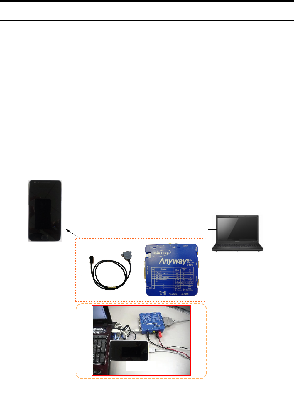
6-1-1. Required items in order to install S/W
yInstallation program: Downloader Program (Odin3 v3.04.exe)
yGT-I9300 Mobile Phone
yData Cable
yJIG BOX (GH99-36900B)
yRF TEST CABLE (GH39-00985A)
yOCTA LCD (GH97-13630A)
yJIG Cable (GH81-10631A)
yAdapter (GH99-38251A)
ySerial Cable
yMobile device specific S/W: Binary files
※Settings
Connect ANYWAY JIG BOX
with JIG CABLE (Phone to JIG)
or PC to Phone Using Data Cable
Level 6Repair
Distribution, transmission, or infringement of any content or data from this document without Samsung’s written authorization is strictly prohibited.
Confidential and proprietary-the contents in this service guide subject to change without prior notice.
6-2
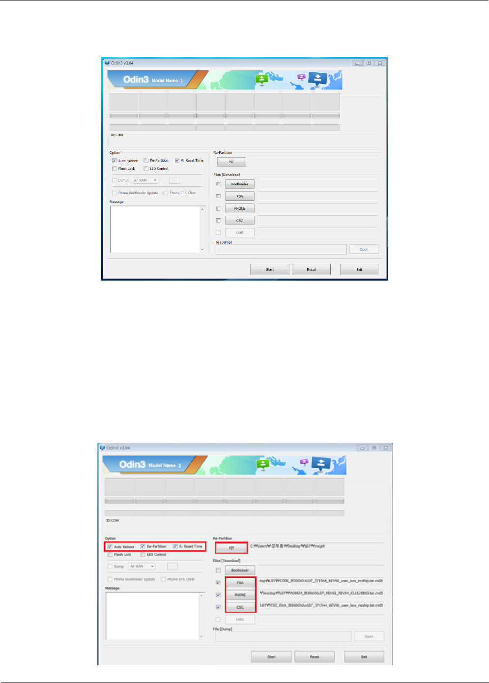
6-1-2. S/W Installation Program (Downloader program)
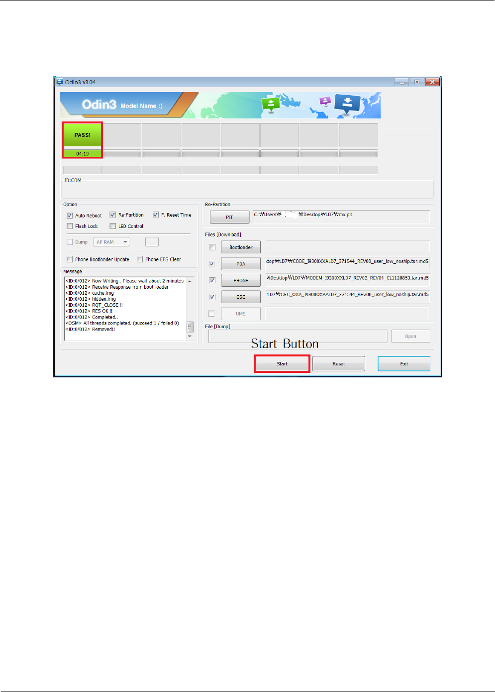
Open up the S/W Installation Program by executing the "Odin3 v3.04.exe"
1.Enable the check mark by click on the following options,
-Check Re-Partition, Auto Reboot, and F. Reset Time
-Check PIT
-Check PDA, PHONE, and CSC Files
2.Enter into Download Mode
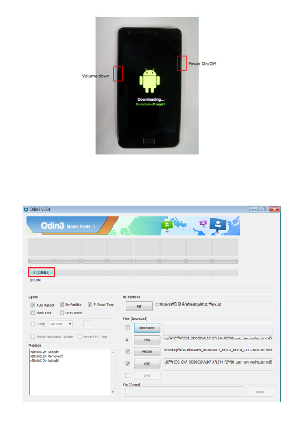
-Enter into Download Mode by pressing Volume Down button, and ON/OFF Button
simultaneously. And then, press Volume UP button in Warning Page to enter the
Download Mode.
Level 6Repair
Distribution, transmission, or infringement of any content or data from this document without Samsung’s written authorization is strictly prohibited.
Confidential and proprietary-the contents in this service guide subject to change without prior notice.
6-3
3.Connect the device to PC via Data Cable.
Make sure that the one of communication port [ID:COM] box is highlighted in
light blue. The device is now connected with the PC and ready to download the
binary file into the device.
Level 6Repair
Distribution, transmission, or infringement of any content or data from this document without Samsung’s written authorization is strictly prohibited.
Confidential and proprietary-the contents in this service guide subject to change without prior notice.
6-4
4.Start downloading binary file into the device by clicking Start Button on the screen.
the green colored "PASS!" sign will appear on the upper-left box if the binary file
has been successfully downloaded into the device.
5. Disconnect the device from the Data cable.
6.Once the device boots up, you can check the version of the binary file or name
by pressing the following code in sequence;
*#1234#
You can perform full reset by pressing the following code in sequence;
*2767*3855#

9. Reference Abbreviate
9-1
Confidential and proprietary-the contents in this service guide subject to change without prior notice.
Distribution, transmission, or infringement of any content or data from this document without Samsung’s written authorization is strictly prohibited.
Reference Abbreviate
―AAC: AdvancedAudioCoding.
―AVC: AdvancedVideoCoding.
―BER: BitErrorRate
―BPSK: BinaryPhaseShiftKeying
―CA: ConditionalAccess
―CDM: CodeDivisionMultiplexing
―C/I: CarriertoInterference
―DMB: DigitalMultimediaBroadcasting
―두:EuropeanStandard
―ES: ElementaryStream
―ETSI: EuropeanTelecommunicationsStandardsInstitute
―MPEG: MovingPictureExpertsGroup
―PN: Pseudo-randomNoise
―PS: PilotSymbol
―QPSK: QuadraturePhaseShiftKeying
―RS: Reed-Solomon
―SI: ServiceInformation
―TDM: TimeDivisionMultiplexing
―TS: TransportStream

1. Safety Precautions
1-1
Confidential and proprietary-the contents in this service guide subject to change without prior notice.
Distribution, transmission, or infringement of any content or data from this document without Samsung’s written authorization is strictly prohibited.
1-1. Repair Precaution
Before attempting any repair or detailed tuning, shield the device from RF noise or static
electricity discharges.
Use only demagnetized tools that are specifically designed for small electronic repairs,
as most electronic parts are sensitive to electromagnetic forces.
Use only high quality screwdrivers when servicing products. Low quality screwdrivers can
easily damage the heads of screws.
Use only conductor wire of the properly gauge and insulation for low resistance, because of
the low margin of error of most testing equipment.
We recommend 22-gauge twisted copper wire.
Hand-soldering is not recommended, because printed circuit boards (PCBs) can be easily
damaged, even with relatively low heat. Never use asoldering iron with apower rating of
more than 100 watts and use only lead-free solder with a melting point below 250°C (482°F).
Prior to disassembling the battery charger for repair, ensure that the AC power is disconnected.
Always use the replacement parts that are registered in the SEC system. Third-party replac
ement parts may not function properly.

Safety Precautions
Distribution, transmission, or infringement of any content or data from this document without Samsung’s written authorization is strictly prohibited.
Confidential and proprietary-the contents in this service guide subject to change without prior notice.
1-2
1-2. ESD(Electrostatically Sensitive Devices) Precaution
Many semiconductors and ESDs in electronic devices are particularly sensitive to static discha
rge and can be easily damaged by it. We recommend protecting these components with cond
uctive anti-static bags when you store or transport them.
Always use an anti-static strap or wristband and remove electrostatic buildup or dissipate
static electricity from your body before repairing ESDs.
Ensure that soldering irons have AC adapter with ground wires and that the ground wires are
properly connected.
Use only desoldering tools with plastic tips to prevent static discharge.
Properly shield the work environment from accidental electrostatic discharge before opening
packages containing ESDs.
The potential for static electricity discharge may be increased in low humidity environments,
such as air-conditioned rooms. Increase the airflow to the working area to decrease the
chance of accidental static electricity discharges.
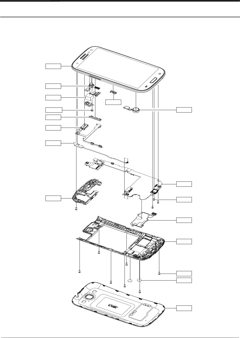
4. Exploded View and Parts List
4-1
Confidential and proprietary-the contents in this service guide subject to change without prior notice.
Distribution, transmission, or infringement of any content or data from this document without Samsung’s written authorization is strictly prohibited.
4-1. Cellular phone Exploded View
QFR01
QCA02
QCA01
QCR106
QVO01
QAR01
QAN04
QSP01
QMO01
QMP01
QCR12
QRE01
QCR67
QRF01
QBC00
QME02
QCK01

5. MAIN Electrical Parts List
5-1
Confidential and proprietary-the contents in this service guide subject to change without prior notice.
Distribution, transmission, or infringement of any content or data from this document without Samsung’s written authorization is strictly prohibited.
Design LOC SEC CODE Description
D500 0403-001688 BZX884-C5V6
D700 0403-001832 RCLAMP0521P
ZD500 0406-001267 PESD5V0L5UF
ZD300 0406-001327 RCLAMP3654P.TCT
U713 0406-001369 PESD24VS1UL
ZD502 0406-001390 PESD5V0F1BL
ZD600 0406-001413 RD1301B
ZD604,ZD606,ZD607,ZD700 0406-001459 UCLAMP0541Z
ZD601,ZD602,ZD603,ZD605,ZD608 0406-001506 PTVS26VS1UR
ZD701 0406-001526 EMD5T2R
U501 0504-001176 PMR280UN
Q200,Q201 0505-002384 SPFCW04301BLS0D0T0
LED500 0601-003079 TC7SG32AFS
U302 0801-003024 74AUP1T34
U704 0801-003449 SC54412ACA-A030
UCP400 0902-002909 XM0860SH-DL0668TMP
U107 1001-001536 STG5223QTR
U505 1001-001546 FSA2259UMX
U608 1001-001635 SKY13397-388LF
U105 1001-001733 AN30259A
U301 1003-002337 FXMA2102UMX
U709 1003-002469 KMVTU000LM-B503
UME300 1108-000472 SFMG2S0D001
U200 1201-003378 SKY77604-31
U106 1201-003406 NCX2200GM
U714 1202-001120 RP103K281D-TR
U600,U603,U701,U702,U703 1203-004819 MIC5365-3.3YMT
U715 1203-005512 RF6590
U108 1203-006801 RP154L006A-E2
U710 1203-006874 LM3242
U104 1203-006985 AAT2146MIJS-0.6-T1
U707 1203-007142 AAT1290AIWO-T1
U509 1203-007256 STOD13CMTPUR
U706 1203-007269 MAX77693EWQ+T
U506 1203-007321 MAX77686EWE+T
U500 1203-007322 MAX14607EWL+T

Main Electrical Parts List
Distribution, transmission, or infringement of any content or data from this document without Samsung’s written authorization is strictly prohibited.
Confidential and proprietary-the contents in this service guide subject to change without prior notice.
5-2
Design LOC SEC CODE Description
U502 1203-007323 MAX14607EWL+T
U504 1203-007323 RP114K121D-TR
U712 1203-007324 ES305B
U604 1204-003328 S5C73M3X01-Y040
U711 1204-003364 SI4705-D50-GM
U203 1204-003365 TPS22922YFPR
U401 1205-003611 SII9244BO
U708 1205-004233 BCM47511IUB2G
U201 1205-004396 WM1811AECS
U605 1205-004509 PN65NET1/C3
U207 1205-004510 PMB9811C
UCP300 1205-004511 PMB5712A2
U102 1205-004515 AK8975C
U204 1209-002041 LSM330DLC
U205 1209-002149 LPS331AP
U206 1209-002150 NCP03XH223E05RL
V100 1404-001726 NCP03WB473J05RL
TH300,TH400,TH401 1404-001728 LXES15AAA1-117
V600,V601 1405-001346 RC1005J101CS
R219 2007-000138 RC1005J102CS
R456,R457 2007-000140 RC1005J222CS
R214 2007-000141 RC1005J272CS
R222 2007-000142 RC1005J472CS
R722,R723 2007-000143 RC1005F1003CS
R315 2007-007107 RC1005F393CS
R338 2007-007134 RC1005F472CS
R471 2007-007136 MCR01MZP5F2002
R475,R476 2007-007312 RK73H1ETP1503F
R716 2007-007489 MCR01MZP5F2400
R447,R448,R473,R474 2007-007517 RK73H1ETP5602F
R719 2007-007538 M5534204B10E0R
R450,R464,R512,R513,R727,R730 2007-007741 RC1005F0100CS
R703 2007-007798 RK73H1ETP1603F
R529 2007-007875 RC-1005F105CS
R408 2007-007942 ERJ1GEJ101C
R337,R521,R528 2007-008045 RC0603J121CS

Main Electrical Parts List
Distribution, transmission, or infringement of any content or data from this document without Samsung’s written authorization is strictly prohibited.
Confidential and proprietary-the contents in this service guide subject to change without prior notice.
5-3
Design LOC SEC CODE Description
R109 2007-008046 ERJ1GENJ201X
R200,R731,R732 2007-008048 MCR006YZPJ202
R224 2007-008049 ERJ1GENJ472X
R324,R432,R433,R460,R461,
R472,R515,R706,R725 2007-008052 ERJ1GENJ104X
R202,R406,R407,R413,R414,
R415,R416,R465,R470,R511,
R530,R531,R611,R616,R622,
R745,R753
2007-008055 RC1005F364CS
R526 2007-008403 ERJ1GEJ102C
R466,R467 2007-008419 RMC-1/20-330JPA
R330,R632,R744 2007-008420 RMC1/20152JPA
R443,R444,R453,R454 2007-008478 RMC1/20473JPA
R205,R206,R207,R208,R209,
R325,R326,R328,R329,R428 2007-008483 ERJ1GEJ204C
R501,R505,R518 2007-008486 ERJ1GEJ103C
R313,R327,R400,R402,R410,
R411,R412,R427,R429,R469,
R481,R534,R612,R721,R726
2007-008516 MCR006MZPJ0100
R314 2007-008531 MCR006YZPJ222
R310,R311,R331,R332,R333,
R335,R336,R426,R451,R452,
R733,R734,R739,R740
2007-008588 ERJ1GEJ750C
R110,R111 2007-008686 ERJ1GEJ2R2C
R633,R634,R741,R742 2007-008774 RMC1/20K333JTP
R748 2007-008786 MCR006YZPJ153
R504 2007-008798 MCR006MZPF2002
R445,R446 2007-008800 RC0603J510CS
R115 2007-008806 MCR006YZPJ105
R220,R225,R502,R503,R626,
R717,R718,R746,R747 2007-009084 RC0603J240CS
R708,R709 2007-009115 MCR006YZPJ474
R342 2007-009155 MCR006YZPF1003
R417,R418,R420,R421,R449,R738 2007-009157 MCR006MZPF1503
R728,R729 2007-009158 MCR006YZPJ513
R302,R303,R304,R305,R306,R307,
R308,R309,R312 2007-009171 MCR006YZPF1001
R618 2007-009212 MCR006MZPJ334
R533 2007-009314 RC0603J4R7CS

Main Electrical Parts List
Distribution, transmission, or infringement of any content or data from this document without Samsung’s written authorization is strictly prohibited.
Confidential and proprietary-the contents in this service guide subject to change without prior notice.
5-4
Design LOC SEC CODE Description
R301 2007-009315 ERJ1GEF222C
R430,R431,R434,R435,R436,R437,
R439,R440,R441,R442,R458,R459,
R462,R463
2007-009408 MCR006YZPF1000
R104,R105 2007-009801 MCR01MZP5F44R2
R468 2007-009964 MCR006YZPF1201
R620 2007-009969 RC1005F4021CS
R319 2007-010233 GRP1555C1H101J
C101,C786 2203-000233 GRP155R71C103K
C216 2203-000254 GRP1555C1H100D
C241,C242 2203-000278 GRP1555C1H150J
C636 2203-000386 GRP155R71H102K
L208 2203-000438 GRP1555C1H1R0C
L103 2203-000466 GRP155R71H222K
C450 2203-000489 GRP155R71H271KD01E
C255 2203-000654 04025C332KAT2A
C451,C453 2203-000714 GRP155R71H392KA01E
C585 2203-000725 GRP155R71E682KA01E
C572 2203-001101 GRP1555C1H820JD01E
C571,C640 2203-001239 GRP155R71H331KD01E
C257 2203-002443 CL05CR75BB5NNNC
L102 2203-002677 C1005Y5V1C104ZT
C240,C246,C268 2203-002709 GRP1555C1H2R7BZ01E
C228 2203-005446 GRP0335C1E330JD01E
C135,C137,C157,C163,C209,
C349,L105 2203-005682 GRP0335C1E8R0DD01E
C203,C205 2203-005683 GRP0335C1E220JD01E
C200,C269,C270,C505,C506,
C767,C768,C769,C770 2203-005725 GRM0335C1E560J
C112,C197,C198,C260,C261,
C613,C634 2203-005726 CL03C120JA3GNNC
C582,C587 2203-005727 CL03C150JAGC
C115,C138,C614,C632,C635 2203-005729 GRM0335C1E180J
C426,C427,C654,C655,C656 2203-005731 GRM0335C1E820JD01D
C254,C259,C663,C664 2203-005734 GRP0335C1E101JD01E
C116,C117,C136,C208,C211,
C219,L104 2203-005736 CL03C010CA3GNNC
C124 2203-005777 ECJZEC1E0R5B

Main Electrical Parts List
Distribution, transmission, or infringement of any content or data from this document without Samsung’s written authorization is strictly prohibited.
Confidential and proprietary-the contents in this service guide subject to change without prior notice.
5-5
Design LOC SEC CODE Description
C118,C140 2203-005789 GRP033R71C102KD01E
C131,C207,C253,C744 2203-005806 GRM155R71A104K
C300,C454 2203-006048 GRM33X7R471K16PT
C665,C666 2203-006121 GRM155R60J224KE01E
C302 2203-006190 GRP033R70J103KA01E
C142,C305,C307,C568,C569,
C608,C611,C622 2203-006194 CV105X5R105K25AT
C563,C578 2203-006348 GRP033R70J472KA01
C128 2203-006379 GRM155R60J105KE19D
C503,C597,C601,C621,C700,
C701,C714,C715,C716,C717 2203-006399 GRM33X5R104K6.3
C108,C109,C125,C132,C133,
C143,C146,C178,C179,C180,
C181,C182,C187,C188,C189,
C206,C247,C262,C303,C304,
C308,C309,C311,C312,C316,
C319,C320,C322,C324,C325,
C326,C327,C330,C331,C333,
C334,C335,C338,C339,C340,
C347,C400,C402,C405,C409,
C415,C444,C445,C449,C500,
C501,C504,C576,C610,C616,
C651,C703,C718,C719,C721,
C722,C724,C726,C728,C740,
C751,C752
2203-006423 GRM0335C1E470JD01D
C196 2203-006556 CV05X5R105K10AH
C171,C172,C235,C236,C580,
C581 2203-006562 GRM033R71E331KA01D
C416,C418,C422 2203-006642 GRM033R60J473KE19D
C183,C184,C185,C190 2203-006647 GRM033R61A222K
C738 2203-006668 GRM0335C1E4R7C
C153,C154 2203-006707 GRM033R70J682K
C130,C134 2203-006815 CV105X5R475K10AT
C119,C176,C177 2203-006824 CL03A104KP3NNNC
C147,C148,C220,C237,C239,
C351,C573,C739 2203-006839 CV05X5R474K10AH
C245 2203-006844 GRM155R60J225ME15D

Main Electrical Parts List
Distribution, transmission, or infringement of any content or data from this document without Samsung’s written authorization is strictly prohibited.
Confidential and proprietary-the contents in this service guide subject to change without prior notice.
5-6
Design LOC SEC CODE Description
C173,C186,C201,C202,C204,
C212,C213,C357,C401,C408,
C414,C431,C435,C442,C443,
C446,C507,C508,C509,C510,
C511,C517,C526,C527,C534,
C541,C545,C546,C547,C553,
C554,C646,C647,C648,C720,
C723,C725,C727,C737,C743,
C746,C757,C760
2203-006872 CL03B103KP3NNNC
C107,C110,C579 2203-006979 CL21A106KOCLRNC
C729,C733,C765 2203-007133 CV03X5R224K06AH
C174,C310,C315,C317,C321,
C323,C328,C332,C336,C337,
C341,C348,C502,C592
2203-007210 CL10A226MQ8NRNE
C436,C556,C557,C558,C559,
C560,C574 2203-007240 CL21A226MPCLRNC
C342,C344 2203-007269 CL10A106KP8NNNC
C114,C160 2203-007270 CL05A225KP5NSNC
C126,C702 2203-007271 CV105X5R106M10AT
C588 2203-007279 CV05X5R475M06AH
C591 2203-007317 CV05X5R475M06AH
C170,C175,C222,C403,C406,
C410,C439,C519,C520,C521,
C522,C523,C524,C551,C552,
C555,C561,C564,C609,C617,
C618,C624,C638
2203-007317 CV05X5R225M10AH
C788,C790 2203-007342 CL05A106MR5NRNC
C238,C250,C428,C432 2203-007385 CL05A475KP5NRNC
C129,C144,C158,C301,C708,
C736 2203-007393 CL03A105MQ3CSNH
C243,C249,C251,C329,C350,
C356,C404,C407,C411,C412,
C413,C417,C419,C420,C421,
C424,C425,C429,C430,C433,
C434,C437,C438,C440,C441,
C518,C525,C528,C530,C531,
C532,C533,C535,C536,C538,
C539,C540,C542,C543,C544,
C548,C549,C550,C575,C577,
C583,C595,C600,C604,C605,
C606,C607,C612,C615,C619,
C623,C626,C628,C631,C644,
C652,C662,C706,C709,C710,
C711,C750,C753,C754,C763,
C764
2203-007449 CL03A105MQ3CSNH

Main Electrical Parts List
Distribution, transmission, or infringement of any content or data from this document without Samsung’s written authorization is strictly prohibited.
Confidential and proprietary-the contents in this service guide subject to change without prior notice.
5-7
Design LOC SEC CODE Description
C529,C537 2203-007449 CL05A105KA5NQNC
C565,C586 2203-007456 CL05A106MQ5NUNC
C263,C313,C314,C318,C512,
C513,C514,C515,C516,C735 2203-007474 CL10A474KB8NNNC
C707,C785 2203-007687 CV05X5R475M10AH
C218,C306 2203-007775 CL05A106MP5NUNC
C566,C567,C593,C620,C730,
C731,C732 2203-007795 CL03A105MP3NSNC
C145,C447,C448,C594,C633,
C637,C643,C645,C649,C650,
C705,C712,C713,C734,C758,
C761,C766
2203-007796 CL03A224KP3NNNC
C742,C748,C756,C762 2203-008095 CL03A104KA3NNNC
C248,C252,C741,C745,C747,
C749,C755,C759 2203-008097 CL03A103KA3NNNC
C244 2203-008243 TLJN226M010R3800
TA600,TA700 2404-001516 F981A476MSAFZH
TA500 2404-001652 CPH3225A/PAS3225P
BAT500 2409-001243 LK1608-100K-T
L511 2703-001231 LL1005-FH1N0S
C191 2703-001749 CIH05T82NJNC
L514,L515,L517,L518 2703-002309 LQW15AN15NH00D
L128,L131 2703-002596 LLV0603-F6N8J
L116 2703-002649 HK0603-4N7S-T
C120 2703-002858 LLV0603-F8N2J
L120 2703-002907 CIH03T12NJNC
L118 2703-002951 LQG15HSR27J02D
L270 2703-003476 CIG21L4R7MNE
L708 2703-003685 CIG21L1R0MNE
L500,L507,L508,L509 2703-003687 MIPSZ2012D4R7-SS
L127,L129,L130 2703-003755 LQM2HPN3R3MGCL
L302,L303 2703-003869 1239AS-H-4R7N
L702,L707 2703-003897 CML0306-2N7-BNH
C221,L203 2703-003908 CML0306-5N6-JNH
L121 2703-003915 LQP03TN47NJ02D
L109,L117,L122,L124 2703-004000 LQP03TN2N2B02D
C210 2703-004012 LQP03TN1N8B02D
L108,L115 2703-004013 LQP03TN1N2B02D

Main Electrical Parts List
Distribution, transmission, or infringement of any content or data from this document without Samsung’s written authorization is strictly prohibited.
Confidential and proprietary-the contents in this service guide subject to change without prior notice.
5-8
Design LOC SEC CODE Description
C127,C149,C150 2703-004014 LQP03TN1N0B02D
C161,C164 2703-004034 LQP03TN3N3B02D
L126,L133 2703-004035 LQP03TN12NJ02D
L112 2703-004036 CIG21LR47MNE
L111 2703-004185 LQW15CN70NJ00
L608 2703-004197 CIG22E1R0MNE
L501,L502,L503,L504,L505,
L506,L510,L512,L513 2703-004297 LQM18PN2R5ND0D
L205 2703-004338 CIL10NR33JNC
L209,L210 2703-004344 FA-128-37.4MHZ
OSC201 2801-005051 TFX-03
OSC500 2801-005157 SQBD02400D2JCG
OSC400 2801-005163 8Z26000021
OSC100 2801-005166 XRCGB27M120F3M10R0
OSC202 2802-001287 KT2016A26000ACW18TAG
OSC200 2805-001098 ICMEF112P900MFR
F700 2901-001625 ICMEF112P500MFR
F702 2901-001634 SAFEA1G58KA0F00
F200 2904-001988 SAWEN942MCA0F00
F101 2904-002020 B40251EY2045G
F100 2910-000125 SKY18106-455LF
U103 2911-000191 SPU0410HR5H
MIC600,MIC602 3003-001136 BLM15AG121SN1D
L305,L611 3301-001534 BLM15AG601SN1
L201 3301-001659 BLM15AG102SN1D
L700,L701,L704,L705,L709 3301-001729 BLM15EG121SN1D
L703,L706 3301-001789 BLM15HD102SN1
L206,L211 3301-001812 BLM15HD182SN1D
L601,L602,L609,L610,L616,
R628 3301-001885 BLM03AG601SN1D
L200 3301-001895 BLM15AG100SN1D
L600 3301-001929 BLM21PG220SN1D
L300,L301 3301-001956 BLM18KG601SN1
L516 3301-002037 BLM18HE102SN1D
L119 3301-002062 MMZ1005A182ET
L603 3301-002065 BLM15AX102SN1D

Main Electrical Parts List
Distribution, transmission, or infringement of any content or data from this document without Samsung’s written authorization is strictly prohibited.
Confidential and proprietary-the contents in this service guide subject to change without prior notice.
5-9
Design LOC SEC CODE Description
L605,L607 3301-002078 BLM15AX601SN1D
L614,L615 3301-002085 BLM15PX121SN1
L132 3301-002122 LS12K2-T
SW600 3404-001303 20369-001E
RFS101 3705-001448 KMS-560-002-BEF
RFS100,RFS102 3705-001731 14-5802-044-002-829
HDC702 3711-006843 14-5802-016-002-829
HDC300 3711-006923 AXE622124AW1
HEA700 3711-007071 AXE634124AW1
HDC701 3711-007295 202-03060-00440
BTC500 3711-007841 14-5804-016-000-829+
HDC600 3711-008151 14-5804-010-000-829+
HDC601 3711-008157 HJ-BCT-02Y
ANT500,ANT501 3712-001373 HJ-ICT-06Y
ANT102,ANT103,ANT200,
ANT203,CON306,KEY500,
KEY501
3712-001375 HJ-ICT-03Y
MOT500,MOT501 3712-001378 2108171-3
IFC700 3722-003512 LBEH5DKVMC-534TEMP
U202 4709-002092 SUS-C1-TOP
CN300 GH61-00827A SUS-I9300-TOP
CN301 GH61-00926A PTC3121N
SC300,SC301,SC302,SC304,SC305,
SC306,SC307,SC309,SC310,SC311,
SC312,SC313,SC314,SC315
GH70-07467A SHIELDCAN-GTI9300
SC700 GH98-23256A AXE420124AW1
HDC301 NEW-056767 1
SAMSUNG Proprietary-Contents may change without notice
7. Level 2Repair
7-1
This Document can not be used without Samsung's authorization
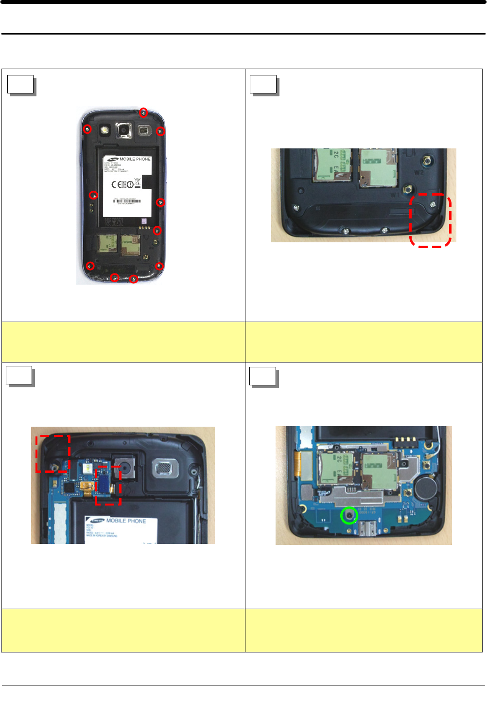
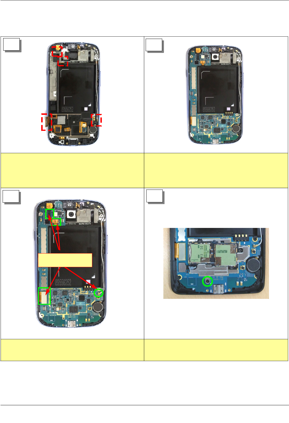
1) Disassembly Screw 10points. 1) It dismantles an REAR side part.
1) It dismantles aspeaker connector and Module. 1) Unscrew 1points.
7-1. Disassembly and Assembly Instructions
7-1-1.
1 2
34
SAMSUNG Proprietary-Contents may change without notice
7. Level 2Repair
7-2
This Document can not be used without Samsung's authorization
4POINT
1) Detach the Con to con and then Disassemble PBA 1) It separates PBA.
56
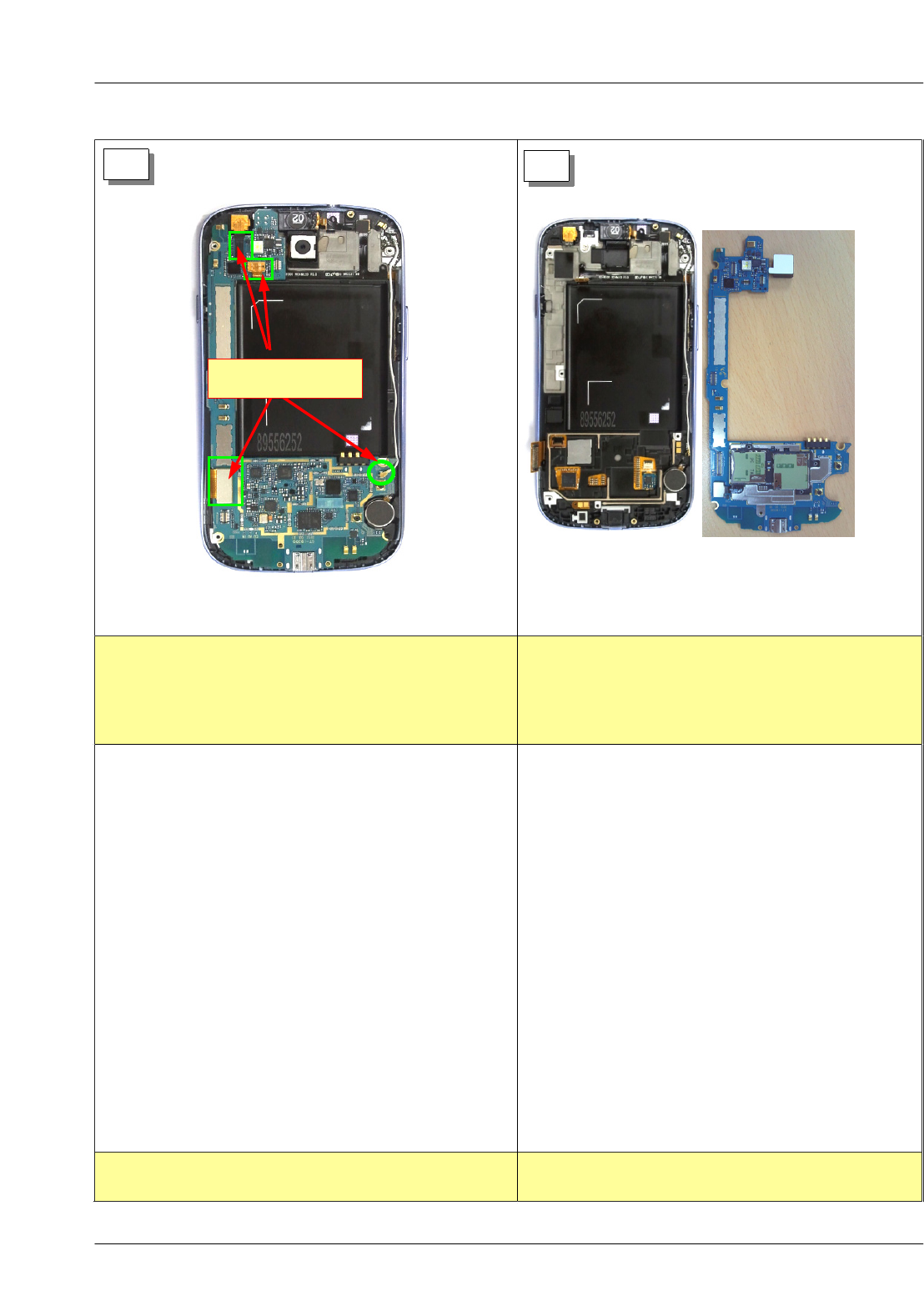
SAMSUNG Proprietary-Contents may change without notice
7. Level 2Repair
7-3
This Document can not be used without Samsung's authorization
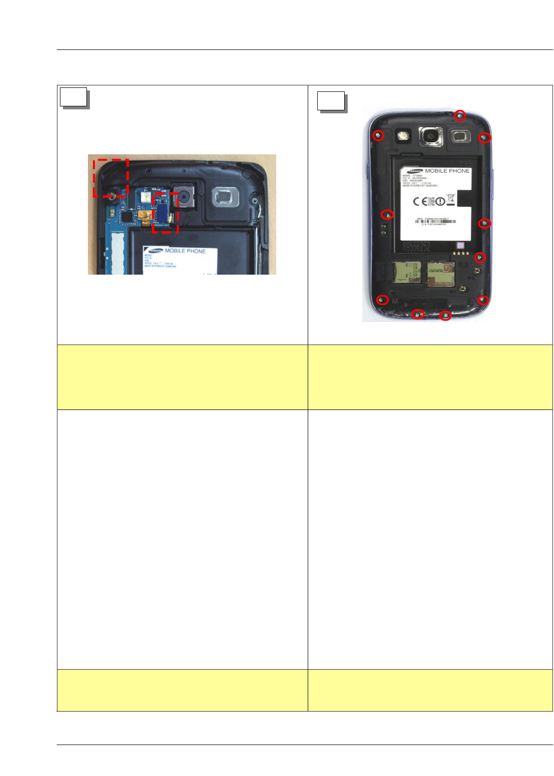
1) Stand all FPCB (LCD, Earjack, Sub Cam, Ant Cable
)1) PBA on the front case
4POINT
1) Conect all FPCB(LCD, Earjack, Sub Cam, Ant Cable
)1) It assembles screw 1point.
7-1-2. Assembly
12
34
Torque :1.0 ~ 1.2 Kgf·cm
/Size :1.4 * 2.5
SAMSUNG Proprietary-Contents may change without notice
7. Level 2Repair
7-4
This Document can not be used without Samsung's authorization
1) It assembles SPEAKER. 1)It assembles REAR.
2)It assembles Screw 10 Point.
56
8. Level 3Repair
8-1
Confidential and proprietary-the contents in this service guide subject to change without prior notice.
Distribution, transmission, or infringement of any content or data from this document without Samsung’s written authorization is strictly prohibited.
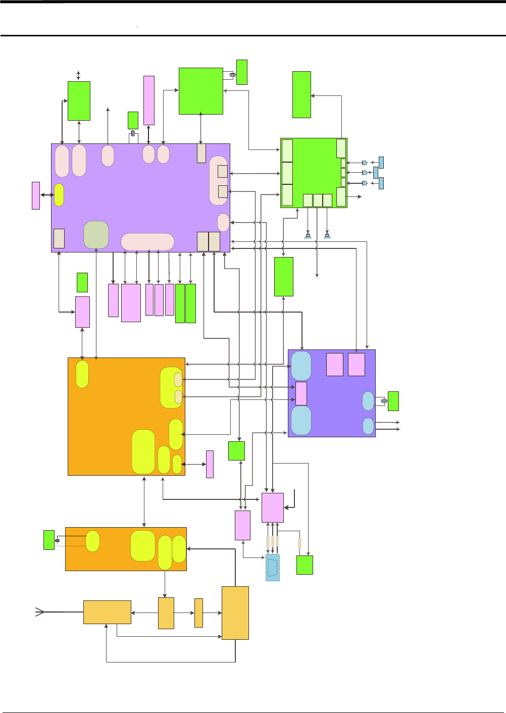
8-1. Block Diagram
Application Processor
+ Memory
(POP)
POP
MCP
MEMORY
(4G/4G/1G)
AUDIO
I2S1I2S0
MIPI
LCD IF
MMC
0/1
UART 2
MMC3
UART 0
UART 3
GPIO
Audio Codec
EAR
AMP
PCM / I2S
IF Port 2
PCM / I2S
IF Port 1
PCM / I2S
IF Port 3
RCV
AMP
SPK
AMP
MIC1
LINE1
L/R
MM_I2S_CLK
MM_I2S_SYNC
MM_I2S_DI
MM_I2S_DO
BT/Wifi
Module
BT_UART_RXD
BT_UART_TXD
BT_UART_CTS
BT_UART_RTS
BT_PCM_CLK
BT_PCM_DIN
BT_PCM_DOUT
BT_PCM_SYNC
CP +CP PMIC
AUDIO
SIM I2S1I2S2
UART
USB
GPS
interface
SPEECH_PCM_CLK
SPEECH_PCM_IN
SPEECH_PCM_OUT
SPEECH_PCM_SYNC
REC_PCM_CLK
REC_PCM_IN
REC_PCM_OUT
REC_PCM_SYNC
Main mic_P/N
Ear mic_P/N
MICBIAS
LDO
MICBIAS_LDO_2.8V
3.5phi Ear MIC
3.5ø
EAR
SPK_OUT_P
SPK_OUT_N
EAR_L
EAR_R
RCV_OUT_P
RCV_OUT_N
24-BIT
RGB IF(1.8V)
24MHz
TCXO
AP_FLM_RXD_2.8V
AP_FLM_TXD_2.8V
AP_FLM_RXD
AP_FLM_TXD
CP_RXD_1.8V
CP_TXD_1.8V
AP PMIC
A/S 1
AP_RXD
AP_TXD
CP_RXD
CP_TXD
MICRO
USB S/W IC
IF_RXD
IF_TXD
GPS reciever
UART 1
GPS_UART_RXD
GPS_UART_TXD
GPS_UART_RTS
GPS_UART_CTS
VT CAMERA
/PROXY sensor
VT_CAM_SCL_2.8V
VT_CAM_SDA_2.8V
PS_ALS_SCL_2.8V
PS_ALS_SDA_2.8V
TOUCH KEY
TOUCH_SCL_2.8V
TOUCH_SDA_2.8V
WiFi 2.8V
GYRO
SENSOR
SENSE_SCL_2.8V
SENSE_SDA_2.8V
ACC SENSOR
MAGNETIC
SENSOR
16G i/Movinand
(2.8V)
ISP
MEMORY 16-BIT IF
GPIO
MEGA_CAM_SCL_2.8V
MEGA_CAM_SDA_2.8V
8M
AP_PMIC_SCL
AP_PMIC_SDA
RESET
IC
RTC
32.768
KHz
OVP
USB_VBUS_CP_5V
USB_VBUS_AP_5V
LINE2
L/R
MICRO USB
USB_DP
USB_DM
USB_ID
JTAG
FOG
USB_ID
JTAG_RXD
JTAG_TXD
CP_D+
CP_D-
USB
AP_D+/-
SIM CARD
Digital RF interface
TRANSCEIVER
OSC
control
Digital RF
2G/3G Rx
2G/3G Tx
2G/3G PAM
PM_L
PM_H
ASM
2G_TX_LB
2G_TX_HB
DUP/SAW BANK
BAND S/W
3G_LB
3G_HB
3G_TX
RX
3G_TX
2G/3G_RX
A/S 2
RADIO_L
RADIO_R
VPS_P
VPS_N
VPS_P
VPS_N
26MHz
26MHz
FM Radio
X-TAL
37.4MHz
T-FLASH
T-FLASH
LV.
SHIFTER
FUEL_I2C
FUEL
GAUGE
Charger IC
USB_OTG
MIC2MIC3
Sub mic_P/N
MICBIAS
LDO
MICBIAS
LDO
Main MIC
Sub MIC
2-MIC Chip
SPEECH_PCM_IN/OUTSPEECH_PCM_IN/OUT_
CODEC
2MIC_I2C_1.8V_CP
MHL
MHL_DM/DP/IDMHL_I2C/MSENSOR_MHL_I2C
Switch IC
USB_DP/DMPMIC_DP/DM
Level 3Repair
Distribution, transmission, or infringement of any content or data from this document without Samsung’s written authorization is strictly prohibited.
Confidential and proprietary-the contents in this service guide subject to change without prior notice.
8-2
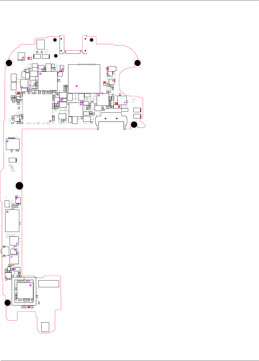
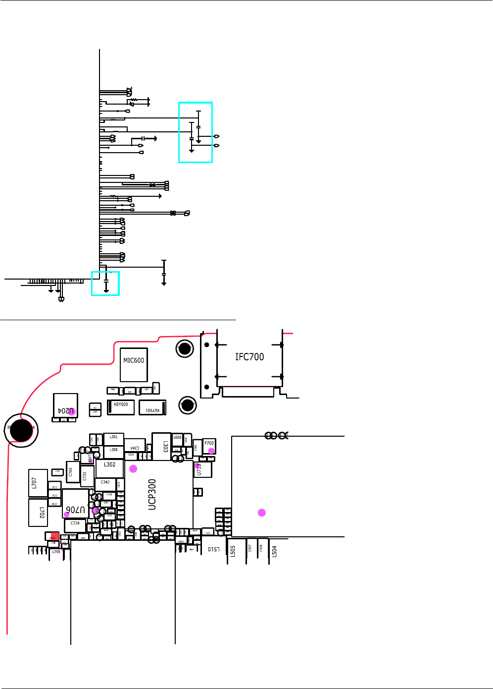
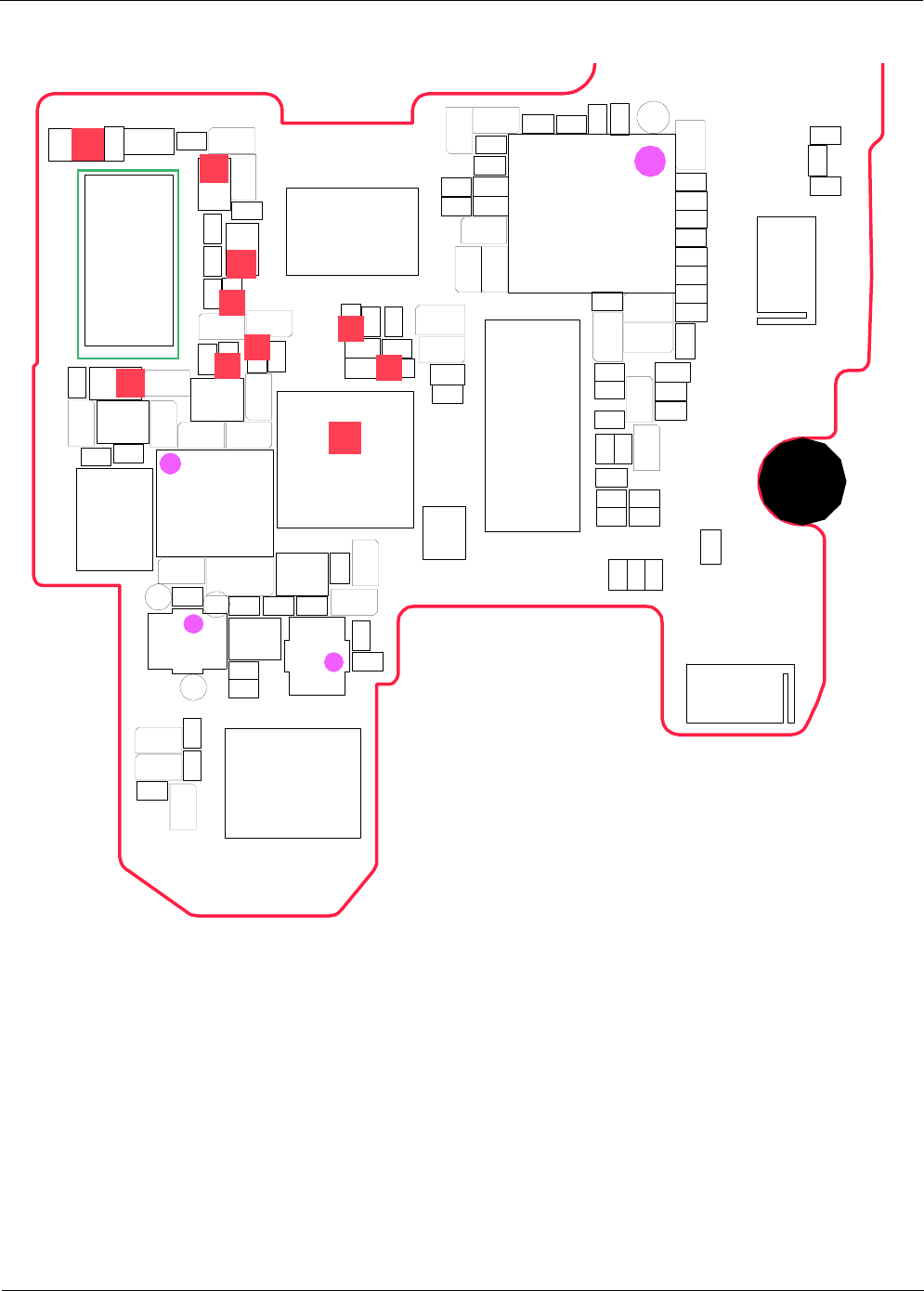
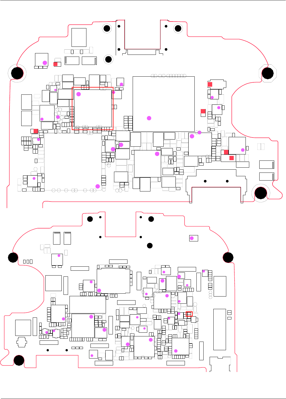
8-2. PCB Diagrams
8-2-1. Top
ANT102
ANT103
ANT200
ANT203
ANT500
ANT501
BAT500
C101
C102C104
C107
C108 C109
C110
C112
C113
C114
C115
C116C117
C118
C119
C120
C122
C123
C124
C125
C126
C127
C128
C129
C130
C131
C132C133
C134
C135
C136
C137
C138
C139
C140
C141
C142
C143
C144
C145
C146
C147
C148
C149
C150
C152
C153
C154
C156
C157
C158
C159
C160
C161
C163
C164
C170
C171
C172
C173
C174
C175
C176
C177
C178
C179
C180
C181
C182
C183
C184
C185
C186
C187
C188
C189
C190
C191
C192
C193
C195
C196
C197
C198
C208
C214
C215
C217
C221
C223
C224
C241
C242
C243
C245
C247
C248
C249
C251
C252
C253
C254
C255
C256
8
5
2
C
7
5
2
C
C259
C260
C261
C262
C263
C336
C337
C338
C339
C340
C343
C349
C350
C351
C401
C402
C410
C411
C412
C416
C424
C428
C429
C430
C431
C432
C433
C434
C435
C436
C437
C438
C439
C440
C441
C442
C449
C502
C527
C536
C540
C542
C543
C545
C547
C548
C578
C588
C591
C592
C596
C604C605
C606
C607
C608
C609
C610
C611
C612
C615
C616
C617
C618
C619
C621
C622
C623
C624
C625
C626
C627
C628
C629
C633
C637
C638
C643
C645
C646
C647
C648
C649
C650
C651
C652
C653
C654
C655
C656
C657
C658
C659
C660
C661
C662
C663
C664
C665
C666
C700
C701
C702
C703
C704
C705
C708
C712
C713
C714
C715
C716
C717
C720
C721
C722
C723
C724
C725
C726
C727
C728
C735
C736
C740
C750
C751
C752
C753
C754
C763
C764
C767
C768
C769
C770
C786
C787
C788
C790
CN300
CN301
F100
F101
F702
HDC300
HDC301
HDC600
HDC601
HDC702
HEA700
L102
L103
L104
L105
L106
L107
L108
L109
L110
L111
L112
L113
L114
L115
L116
L117
L118
L119
L120
L121
L122
L124
L125
L126
L127
L128
L129
L130
L131
L132
L133
L209
L210
L513
L516
L600
L605
L607
L608
L611
L612
L613
L614
L615
L701
L704
L705
L708
LED500
MIC601
OSC100
OSC202
Q200
Q201
R101
R102
R105
R106
R107
R108
R109
R110
R111
R112
R113
R114
R115
R116
R117
R217
R218
R219
R220
R222
R224
R225
R310
R311
R320
R321
R322
R323
R324
R325
R326
R327
R328
R329
R330
R339
R340
R341
R410
R411
R412
R413
R414
R415
R416
R418
R419
R421
R426
R430
R431
R436
R437
R439
R440
R443
R444
R445
R446
R453
R454
R458
R459
R466
R467
R472
R481
R482
R511
R521
R528
R529
R530
R531
R611
R612
R614
R616
R617
R619
R622
R624
R625
R626
R628
R629
R630
R632
R633R634
R700
R701
R702
R703
R704
R705
R706
R707
R716
R718
R719
R720
R721
R722
R723
R724
R725
R726
R727
R728
R729
R730
R731
R732
R744
R745
R746
R747
R748
R749
R750
R751
R752
R753
RFS100
RFS101
RFS102
SC300
SC301
SC302
SC304 SC305
SC306
SC307
SC309
SC310
SC311
SC312
SC313
SC314
SC315
TA700
TH401
TP_100
TP_329
TP_330
TP_331
TP_600
TP_601
TP_602
TP_603TP_604
TP_605
TP_606
TP_607
TP_FLASH_SET
TP_GPS_EN
TP_ISP_FLASH
TP_TORCH_SET
TP208
TP209
TP210
TP323
TP517
TP704
TP705
TP711
U101
U102
U103
U104
U105
U106
U107
U108
U207
U401
U504
U505
U509
U603
U604
U605
U606
U607
U608
U700
U701
U702
U703
U707
U708
U709
U710
U712
U714
U715
V100
V101
V602
ZD300
ZD600
ZD601
ZD602
ZD603
ZD604
ZD605
ZD606
ZD607
ZD608
Level 3Repair
Distribution, transmission, or infringement of any content or data from this document without Samsung’s written authorization is strictly prohibited.
Confidential and proprietary-the contents in this service guide subject to change without prior notice.
8-3
8-2-2. Bottom
AP_PMIC_EN
AP_PS_HOLD
BOTHHOLE100
BOTHHOLE101
BOTHHOLE102
BOTHHOLE103
BOTHHOLE104
BOTHHOLE106
BOTHHOLE107
BOTHHOLE108
BTC500
C200
C201
C202
C203
C204
C205
C206
C207
C209
C210
C211
C212
C213
C216
C218
C219
C220
C222
C228
C235C236
C237
C238
C239
C240
C244
C246
C250
C268
C269
C270
C300
C301
C302
C303
C304
C305
C306
C307
C308
C309
C310
C311
C312
C313
C314
C315
C316
C317
C318
C319
C320
C321
C322
C323
C324
C325
C326
C327
C328
C329
C330
C331
C332
C333
C334
C335
C341
C342
C344
C347
C348
C356
C357
C400
C403
C404
C405
C406
C407
C408
C409
C413
C414
C415
C417
C418
C419
C420
C421
C422
C425
C426
C427
C443
C444
C445
C446
C447
C448
C450
C451
C452
C453
C454
C500
C501
C503
C504
C505
C506
C507
C508
C509
C510
C511
C512
C513
C514
C515
C516
C517
C518
C519
C520
C521
C522
C523
C524
C525
C526
C528
C529
C530
C531
C532
C533
C534
C535
C537
C538
C539
C541
C544
C546
C549
C550
C551
C552
C553
C554
C555
C556
C557
C558
C559
C560
C561
C563
C564
C565
C566
C567
C568
C569
C570
C571
C572
C573
C574
C575
C576
C577
C579
C580
C581
C582
C583
C585
C586
C587
C593
C594
C595
C600
C601
C613
C614
C620
C631
C632
C634
C635
C636C640
C642
C644
C706
C707
C709
C710
C711
C718
C719
C729
C730
C731
C732
C733
C734
C737
C738
C739
C741
C742
C743
C744
C745
C746
C747
C748
C749
C755
C756
C757
C758
C759
C760
C761
C762
C765
C766
C785
CON306
D500
D700
F200
F700
FM_RST
HDC701
IFC700
KEY500
KEY501
L200
L201
L202
L203
L204
L205
L206
L208
L211
L270
L300
L301
L302
L303
L305
L500
L501
L502
L503
L504
L505
L506
L507
L508
L509
L510
L511
L512
L514
L515
L517
L518
L601
L602
L603
L609
L610
L616
L700
L702
L703
L706
L707
L709
MIC600
MIC602
MOT500
MOT501
OSC200
OSC201
OSC400
OSC500
R104
R200
R201
R202
R205
R206
R207
R208
R209
R214
R300
R301
R302
R303
R304
R305
R306
R307
R308
R309
R312
R313
R314
R315
R318
R319
R331
R332
R333
R334
R335
R336
R337
R338
R342
R400
R401
R402
R403
R404
R405
R406
R407
R408
R417R420
R427
R428
R429
R432
R433
R434
R435
R438
R441
R442
R447
R448
R449
R450
R451
R452
R455
R456
R457
R460R461
R462
R463
R464
R465
R468
R469
R470
R471
R473
R474
R475
R476
R483
R500
R501
R502
R503
R504
R505
R507
R512
R513
R515
R516
R517
R518
R519
R526
R532
R533
R534
R618
R620
R631
R708
R709
R717
R733
R734
R735
R738
R739
R740
R741R742
R743
RESET300
SC700
SW600
TA500
TA600
TH300
TH400
TP_201
TP_202
TP_212
TP_213
TP_214
TP_215
TP_AP_DTP_AP_D+
TP_eMMC_EN
TP_SPI_SCLK
TP_TORCH_EN
TP200
TP201
TP202
TP203
TP204
TP205
TP206
TP207
TP211
TP212
TP300
TP301
TP302
TP303
TP304
TP305
TP306
TP307
TP308
TP309
TP310TP311
TP312
TP313
TP314
TP315
TP316
TP317
TP318
TP319
TP320
TP321
TP322
TP324
TP325
TP326
TP327
TP328
TP400
TP401
TP402
TP403
TP501
TP502
TP504
TP505
TP506
TP507
TP508
TP509
TP518
TP519
TP706
TP708
TP709
TP710
U200
U201
U202
U203
U204
U205
U206
U301
U302
U500
U501
U502
U506
U600
U704
U706
U711
U713
U718
U719
UCP300
UCP400
UME300
V600
V601
VIBTONE_PWM
ZD500
ZD501
ZD502
ZD700
ZD701
Level 3Repair
Distribution, transmission, or infringement of any content or data from this document without Samsung’s written authorization is strictly prohibited.
Confidential and proprietary-the contents in this service guide subject to change without prior notice.
8-4
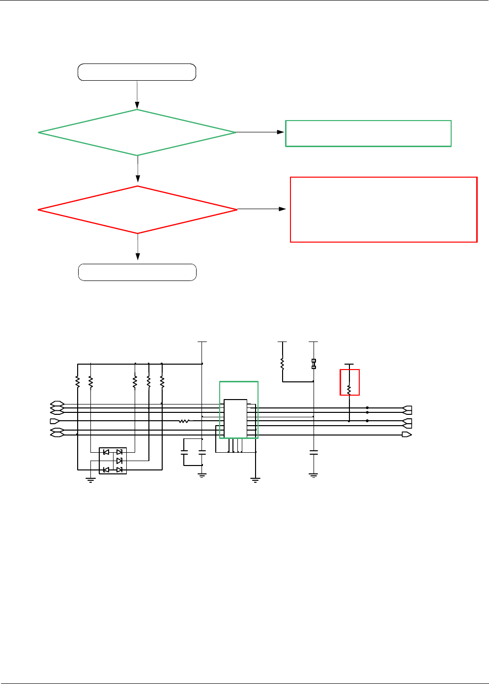
8-3. Flow Chart of Troubleshooting
Equipments
ÇOscilloscope ÇDigital Multimeter
ÇPower Supply Ç+driver, ESD Safe Tweezer
Ç8960 & Spectrum Analyzer ÇSoldering iron
Level 3Repair
Distribution, transmission, or infringement of any content or data from this document without Samsung’s written authorization is strictly prohibited.
Confidential and proprietary-the contents in this service guide subject to change without prior notice.
8-5
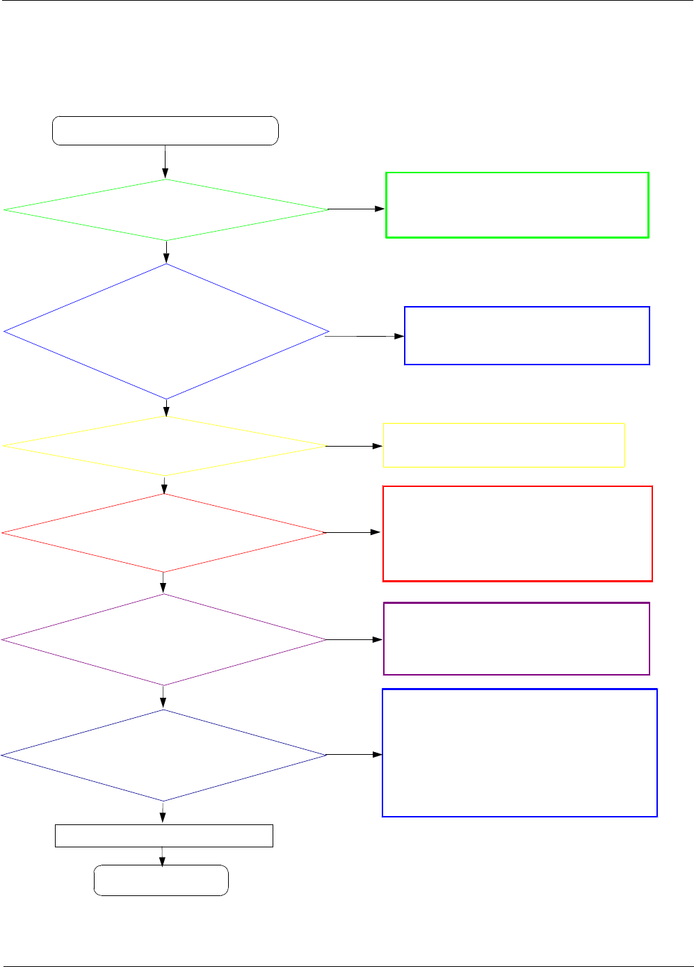
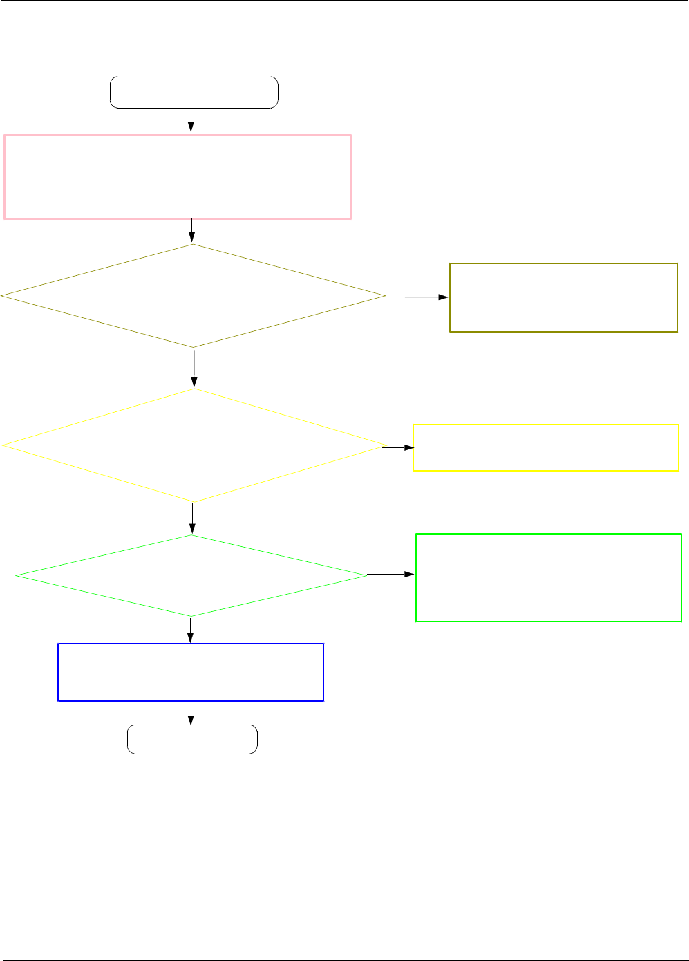
8-3-1. Power On
Check the SW600
(soldering crack, open, etc)
Cell-phone can`t power on.
Change the SW600(Power-key)
And retry to the power-on operation.
END
No
Yes
Check the U500 output voltage
(C561 =1.0
V, C559 =1.1
V,
C558 =1.0
V, C556 =1.0
V)
If the output voltage is not satisfied with normal
condition, Change the U501.
※Each voltage will be changed from 0.9V to
1.3V during booting.
No
Yes
Check the U500 output signal
(AP_PS_HOLD(TP) >1.8
V)
If the output voltage is not satisfied with normal.
condition, Change the U500.
※Each voltage level has ±10% margin.
No
Yes
Check the Battery Voltage.
Is it more than 3.4V?
Charging the battery by TA.
If its voltage level is extremely low(under 3.0V),
Change the battery.
check the initial operation
Yes
Abnormal
Check the Clock OSC500(C505)
Is that frequency 32Khz?
Change the OSC500.
If OSC400 does not still work, Change the U501
This problem is internal oscillator of U501.
※Test condition (Oscilloscope setting)
:20.0
us.div (time division)
No
Yes
Yes
Change the MEA FRONT-OCTA LCD ASSY
Power-on the phone and check
the power-on sound
or motor biration.
Sound or Biration is ok?
Yes
No
Level 3Repair
Distribution, transmission, or infringement of any content or data from this document without Samsung’s written authorization is strictly prohibited.
Confidential and proprietary-the contents in this service guide subject to change without prior notice.
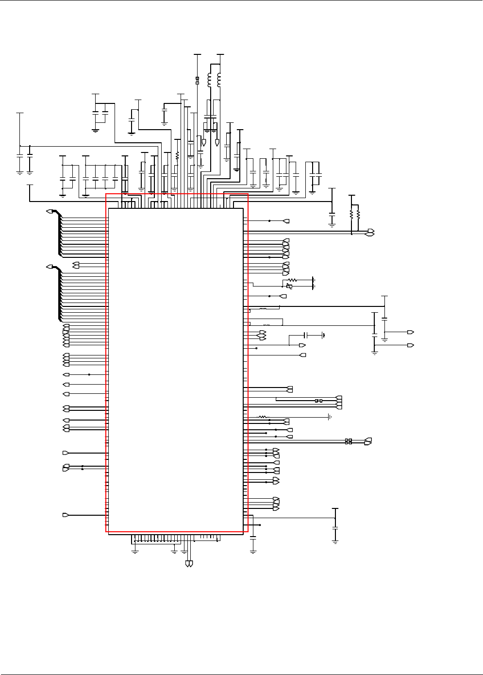
8-6
C302
C31
C4
4
C500
C501
C503
C505
C506
C507
C508
C509
C510
C511
C512
C513
C514
C515
C516
C517
C518
C519
C520
C521
C522
C523
C524
C525
C526
C528
C529
C530
C531
C532
C533
C534
C535
C537
C538
C541
C544
C546
C549
C550
C551
C552
C553
C554
C555
C556
C557
C558
C559
C560
C561 C565
C566
C567
C573
C574
C580
C581
L500
L501
L502
L503
L504
L505
L506
L507
L508
L509
L510
L51
2
OSC500
R447
R448
R483
R500
R
5
R
5
TP_eMMC_EN
3
12
T
P
2
TP507
TP508
TP519
U500
0
6
L501
L506
C558C559
L505
L503
L504
L510
L508
L507
LX2B
M6
LX2A
M9
LX2A
L9
LX9
M2
LX8
L12
LX2B
L6
LX4B
J2
LX4B
J1
LX3
H11
LX3
H12
LX4A
F1
LX4A
F2
LX1
D1
LX5
D12
LX7
B12
LX6
A2
INL7
L509
L500
C560
L502
VMIF_1.0V_AP
VINT_1.0V_AP
C561
C557
VARM_1.1V_AP
BUCK1_GND
BUCK2A_GND
BUCK2B_GND
BUCK3_GND
BUCK4A_GND
Level 3Repair
Distribution, transmission, or infringement of any content or data from this document without Samsung’s written authorization is strictly prohibited.
Confidential and proprietary-the contents in this service guide subject to change without prior notice.
8-7
AP_PMIC_EN
AP_PS_HOLD
C307
C308
C310
C311
C312
C313
C315
C316
C318
C322
C324
C325
C327
C328
C329
C330
C331
C332
C333
C334
C335
C342
C347
C348
C400
C403
C404
C406
C408
C409
C417
C418
C421
C422
C425
C426
C427
C447
C448
C451
C453
C501
C504
C505
C506
C507
C508
C509
C510
C511
C512
C513
C514
C515
C516
C517
C526
C532
C533
C534
C535
C538
C539
C541
C544
C549
C550
C551
C552
C553
C
C5
5
C556
C557
C558
C559
C560
C
6
6
FM_RST
L302
L500
L501
L502
L503
L504
L505
L506
L507
L508
L509
L510
OSC400
OSC500
R104
R300
R301
R302
R303
R304
R305
R306
R307
R308
R309
R314
R315
R319
R331
R332
R333
R334
R408
R438
R447
R448
R449
R450
R465
R468
R469
R470
R474
R483
R501
R504
R505
1
7
TH300
TP_eMMC_EN
TP201
TP2
0
TP304
TP307
TP308
TP310TP311
TP312
TP313
T
TP324
TP3
2
TP400
TP401
TP402
TP4
0
TP501
TP502
TP504
TP505
TP506
TP507
TP508
TP509
0
7
P
T
8
1
5
P
T
U500
U713
U718
UCP300
UCP400
UME300
VIBTONE_PWM
22pF
0603
C505
OSC500
TFX-03
21
XIN
M4
XOUT
L4
0603
22pF
C506
V
C
Level 3Repair
Distribution, transmission, or infringement of any content or data from this document without Samsung’s written authorization is strictly prohibited.
Confidential and proprietary-the contents in this service guide subject to change without prior notice.
8-8
8-3-2. Initial
Initial Failure
END
Check the AP Reset
AP_N_RST_IN(R504) =1.8
V(High)
Yes
Check the U500 and R504 (crack, open, etc.)
Check the oscillator clock waveforms.
32.768KHz :OSC500(TP213),
24Mhz :OSC400(C427)
Check the OSC500, OSC400 and R408.
(Crack, open etc.)
Check the output clock waveforms and frequency.
※Test condition (Oscilloscope setting)
:20.0
us.div (time division)
Abnorma
l
Yes
Normal
No
Re-download SW the cell-phone.
Change UCP400,U501
Abnormal
Abnormal
Change PBA
Level 3Repair
Distribution, transmission, or infringement of any content or data from this document without Samsung’s written authorization is strictly prohibited.
Confidential and proprietary-the contents in this service guide subject to change without prior notice.
8-9
VCC_1.8V_AP
0603
R504
15K
R503
0603
1M
R502
1M
0603
V_BAT
200K
0603
R505
A
A
AP CLOCK
C426
18PF
25V
0603
1005
1M
R408
2
4
3
1
SQBD02400D2JCG
OSC400
18PF
25V
0603
C427
XTAL_24MHZ_OUT
XTAL_24MHZ_IN
AP_PMIC_EN
AP_PS_HOLD
C237
C238
C239
C244
C356
C405
C413
C414
C415
C417
C418
C419
C420
C421
C422
C425
C426
C427
C445
C446
C450
C451
C453
C454
C505
C539
C719
CON306
FM_RST
L305
O
SC400
R335
R336
R338
R400
R401
R402
R403
R408
R417R420
R427
R429
R441
R442
R447
R448
R449
R451
R452
R456
R457
R460R461
R464
R465
R469
R470
R471
7
3
R475
R476
R483
R501
R504
R505
R709
TH400
TP_201
TP_202
TP_212
TP_213
TP_214
TP_215
P
_eMMC_EN
TP_TORCH_EN
TP201
TP202
TP207
TP211
TP212
TP401
TP403
TP504
TP509
TP518
P
519TP708
TP709
TP710
U205
U301
UCP400
VIBTONE_PWM
Level 3Repair
Distribution, transmission, or infringement of any content or data from this document without Samsung’s written authorization is strictly prohibited.
Confidential and proprietary-the contents in this service guide subject to change without prior notice.
8-10
8-3-3. No Service
No service
END
Check the CP_VSD1,CP_VSD2_1.8V
CP_VSD1 (C342) =0.9~1.4V
CP_VSD2 (C344) =1.8V
Yes
Replace the UCP300
Yes
Check VREF
VREF (C348) =600
mV Replace the UCP300
Yes
No
No
Check memu setting
Menu →applications →setting →wireless and network →
mobile networks →network mode →setting is auto mode ?
Check the contact of antenna.
(ANT102, ANT103@ page2 )
Change the board
PHONE :I9300XXXX
PHONE :unknown
Menu →Phone →Keypad →
*#1234# →check Phone version →
PHONE :I9300XXXX or
PHONE :unknown
Abnormal
Level 3Repair
Distribution, transmission, or infringement of any content or data from this document without Samsung’s written authorization is strictly prohibited.
Confidential and proprietary-the contents in this service guide subject to change without prior notice.
8-11
For RF Reset
For Modem and PMIC, RF Reset
TP319
SHORT
R320
1005
TP313
LQM2HPN3R3MGCL
L302
TP324
R319
1005
C342
NC
1005
C343
TP311
C347
0603
TP321
TP326
C344
TP325
VRTC_1.8V
TP309
TP322
R321
SHORT
1005
TP310
CP_VSD1_1.2V
SHORT
0603
R315
1005
TP323
L303
TP312
LQM2HPN3R3MGCL
CP_VSD2_1.8V
C348
0603
U718
TP327
TP308
NCP03WB473J05RL
TH300
0603
U8
DI3_RX_DATX
SYSCLKEN
U9
U16
VSS
U17NC
USIF1_CTS_N U2
U3
USIF1_RTS_N
TDO U4
U5
TDI
TMS U6
DI3_RX_DAT
T9
XRESET_N
U1
NC
U10
ALERT_N
U11
DPLUS
U12
HSIC_USB_STRB
U13
HSIC_USB_DATA
U14
CC_CLK
T17
USB_DPLUS
T2
USIF1_RXD_MRST T3
USIF1_TXD_MTSR
T4
TRST_N
T5
TRIG_IN
T6
TCK
T7
DI3_TX_DAT
T8
DI3_TX_DATX
T1
USIF1_SCLK
T11
DMINUS
T13
CC_IO
T14
CC_RST
T16
USB_TUNE
R17
USB_DMINUS
R4NC
R5
RESET2_N
R6
HW_MON1
R9VSS
P17
USB_TEST
P3
T_OUT1
P7
HW_MON2
P8VSS
P10
CLKOUT2
P11VSS_PLL
P12
SYS_CLK
N14VSS_USB
N16
USB_ID
N4
T_OUT0
N8
CLKOUT0
M16
VSS_RTC
M17
OSC32K
F32K
L10VSS
L14
VSS
L16VSS
L17
K2
RESET_BB_N
K3
REF_CLK_EN
TM_EN K4
J4
M4
J5
M3
J6
M2
J8
VSS
K13VSS
J2
ON2_N
RESET_PWRDWN_N J3
H2
ON1
H6
M1
H8
RESERVED
J1
VREF
VSS
J11
VSS
G8
F4
VRTC
F6
TRIG_B
FSS
E4VSS_PMU
F1
VSS_SD1
VSS
SD1_SW
E3
D3
SD1_FB
ANAMON D4
E1
C2
D1
SD1_SW
B6
DSP_AUDIO_IN1
B8
FWP
SD2_FB
A6
FCDP_RBN
VSS_SD2
B1
A17NC
A2
SD2_SW
A3
SD2_SW
UCP300
1NC
2NC
NC
A1
32KHZ_CP
ACTIVE_STATE_HSIC
2MIC_UART_RXD
2MIC_UART_TXD
IPC_SLAVE_WAKEUP
XTAL_26MHZ_CP
IPC_HOST_WAKEUP
RESET_N_RF
HSIC_STROBE1
HSIC_DATA1
SIM_CLK
TDO_CP
TDI_CP
TMS_CP
DI3_RX_DAT
DI3_RX_DATX
SYS_CLK_EN
VSD2_GND
VSD1_GND
CP_D-
HW_MON1
SIM_IO
SIM_RST
CP_D+
TRST_N_CP
TRIG_IN
TCK_CP
DI3_TX_DAT
DI3_TX_DATX
RESET_PWRDWN_N
RESET_REQ_N
REF_CLK_EN
SYS_CLK_26M
HW_MON2
VSD2_GND
DSP_AUDIO_IN1
VSD1_GND
CP_ON
Level 3Repair
Distribution, transmission, or infringement of any content or data from this document without Samsung’s written authorization is strictly prohibited.
Confidential and proprietary-the contents in this service guide subject to change without prior notice.
8-12
8-3-4. Sim Part
R330
R327R326
CP_VSIM
C351
NFC_SIMVCC
R322
VTF_2.8V
NC
17
18NC
NC
19
20NC
22
33 44
55 66
77 88
99
11
10 10
11 11 12 12
13
13 14 14
15 15 16
16
HDC300
R325
TP_330
C350
CP_VSIM
R323
1
2
43
5
6
ZD300
C349
R328
R324
TP_331
TP_329
R329
SIM_RST
SIM_IO
SIM_CLK
T_FLASH_D(1)
T_FLASH_D(2)
T_FLASH_D(3)
T_FLASH_CMD
NFC_SWP
T_FLASH_DETECT
T_FLASH_CLK
T_FLASH_D(0)
Insert SIM card
Check the Pin Soldering
of HDC300
Yes
Yes
No
END
Check the SIM Voltage.
(R324) >= 1.8 or 3.0?
Resoldering and recheck
Change to the new SIM card.
If it doesn`t still work SIM card after changeing
the SIM card, Check the UCP300 (Crack etc)
Yes
No
Level 3Repair
Distribution, transmission, or infringement of any content or data from this document without Samsung’s written authorization is strictly prohibited.
Confidential and proprietary-the contents in this service guide subject to change without prior notice.
8-13
VPMU_1.3V
VUSB_ANA_1.8V
For RF Reset
For Modem and PMIC, RF Reset
VIO_1.2V
CP_VSD2_1.8V
C341
TP319
R320
C311
TP313
C316
L300
CP_VSD2_1.8V
C339
C324
CP_VSD1_1.2V
L302
C329
CP_VSD2_1.8V
R310
TP324
C327
TP307
C312
C333
CP_VSD1_1.2V
C335
R319
V_BAT
C336
C325
TP304
C342
C340
CP_VSIM
C320
C343
C338
TP311
C347
TP321
TP326
C321
C344
C332
TP325
C326
VRTC_1.8V
TP309
CP_VSD2_1.8V
TP322
VUSB_PD_1.1V
CP_VSD1_1.2V
L301
C310
R321
VUSB_PD_1.1V
TP310
VPLL_1.2V
R311
VIO_1.2V
CP_VSD1_1.2V
USB_VBUS_CP_4.9V
R318
C315
C314
C337
C328
R315
R301
CP_VSD2_1.8V
TP323
C323
VUSB_IO_3.1V
C313
C334
C317
VPLL_1.2V
C330
CP_VSD2_1.8V
R300
C331
U719
C322
L303
TP312
CP_VSD2_1.8V
RESET300
C348
U718
TP327
TP308
TP328
VPLL_1.2V
V_BAT
TH300
C319
C318
U8
DI3_RX_DATX
SYSCLKEN
U9
U16
VSS
U17NC
USIF1_CTS_N U2
U3
USIF1_RTS_N
TDO U4
U5
TDI
TMS U6
U7
DI3_RX_DAT
T9
XRESET_N
U1
NC
U10
ALERT_N
U11
DPLUS
U12
HSIC_USB_STRB
U13
HSIC_USB_DATA
U14
CC_CLK
U15
VDD_IO12
T17
USB_DPLUS
T2
USIF1_RXD_MRST T3
USIF1_TXD_MTSR
T4
TRST_N
T5
TRIG_IN
T6
TCK
T7
DI3_TX_DAT
T8
DI3_TX_DATX
T1
USIF1_SCLK
T10
VDD_DIGRF
T11
DMINUS
T12
VDD_SIM
T13
CC_IO
T14
CC_RST
T15
VDD_USB_PD
T16
USB_TUNE
R16
VDD_USBIO
R17
USB_DMINUS
R2
I2S2_WA1
R4NC
R5
RESET2_N
R6
HW_MON1
R8
VDDCORE
R9VSS
P17
USB_TEST
P2
I2S2_TX
P3
T_OUT1
P7
HW_MON2
P8VSS
P9
I2C1_SDA
R1
I2S2_WA0
R12
VDD_PLL
N9
VPP
P1
I2S2_RX
P10
CLKOUT2
P11VSS_PLL
P12
SYS_CLK
P13
MIPI_HSI_RX_WAKE
P14
VDD_USB_ANA
P16
VBUS
MIPI_HSI_RX_DATA
N14VSS_USB
N16
USB_ID
N17
VDD_RTC
N2
I2S2_CLK1
N4
T_OUT0
N5
MMCI1_CD
N8
CLKOUT0
M5 MMCI1_DAT_0
M6 MMCI1_DAT_3
M8
EINT2
M9
EINT1
N1
I2S2_CLK0
N10
I2C1_SCL
N11
VDD_IO18
N12 MIPI_HSI_TX_DATA
N13
M13
M14 MIPI_HSI_RX_FLG
M15
MIPI_HSI_TX_RDY
M16
VSS_RTC
M17
OSC32K
M2
MMCI1_DAT_1
MMCI1_CLK
M3
MMCI1_DAT_2
M4
F32K
ETM11_TRACEPKT3
L2
L4 ETM11_TRACEPKT2
ETM11_TRACEPKT6
L5
L7 MMCI1_CMD
L8
VDD_MMC
L9 ETM11_TRACEPKT5
M1
ETM11_TRACEPKT0
MIPI_HSI_TX_WAKE
K8
VDD_IO18
K9
VDDCORE
L1 ETM11_TRACEPKT1
L10VSS
L11 MIPI_HSI_TX_FLG
L13 MIPI_HSI_RX_RDY
L14
VSS
L16VSS
L17
K14
VDDCORE
K16
VDD_MIPI
K17 MEM_WAIT_N|C2C_WAKEREQ_IN
K2
RESET_BB_N
K3
REF_CLK_EN
TM_EN K4
K5
ETM11_TRACEPKT4
K7 ETM11_TRACECLK
J4
M4
J5
M3
J6
M2
J8
VSS
K1
ETM11_TRACEPKT7
K10
EINT3
VDD_IO18K11
K13VSS
J12 MEM_AD_14|C2C_TX_D_14
MEM_CS1_N|C2C_NC
J13
J14
MEM_CS0_N|C2C_NC
J15 MEM_A_18|C2C_NC
J16 MEM_A_16|C2C_NC
J17
VDD_IO18|VDD_EBUIO
J2
ON2_N
RESET_PWRDWN_N J3
H17 MEM_A_15|C2C_RX_D_15
H2
ON1
H3AGND
H6
M1
H8
RESERVED
H9
VDDCORE
J1
VREF
VSS
J11
VSS
MEM_AD_2|C2C_TX_D_2
G9
H1
VUSB_IO
MEM_AD_10|C2C_TX_D_10
H10
H11
MEM_AD_0|C2C_TX_D_0
H13 MEM_CS3_N|C2C_NC
H14 MEM_CS2_N|C2C_NC
H16
MEM_A_17|C2C_NC
G10
MEM_ADV_N|C2C_NC
G11 MEM_AD_1|C2C_TX_D_1
G13 MEM_BE1_N|C2C_NC
G14 MEM_BE0_N|C2C_NC
G15 MEM_A_19|C2C_NC
G16
MEM_BC3_N|C2C_RX_CLK_1
G17 MEM_A_14|C2C_RX_D_14
G2
VPMU
G8
F16 MEM_BC1_N|C2C_NC
F17
MEM_A_13|C2C_RX_D_13
F2
VUSB_ANA
VDD_VBAT_PMU
F3
F4
VRTC
F6
TRIG_B
F9
MEM_AD_4|C2C_TX_D_4
G1
VSIM
FSS
E4VSS_PMU
MEM_AD_5|C2C_TX_D_5
E8
MEM_AD_6|C2C_TX_D_6
E9
F1
VSS_SD1
F13
MEM_AD_15|C2C_TX_D_15
F14VSS
F15
VDD_IO18|VDD_EBUIO
SD1_SW
E10
VDDCORE
E11
MEM_AD_8|C2C_TX_D_8
E12
VDDCORE_EBU
VDDCORE
E13
E14 MEM_RAS_N|C2C_NC
E16 MEM_A_20|C2C_NC
E17 MEM_A_12|C2C_RX_D_12
E3
D13
D14
VSS
D16
MEM_A_21|C2C_NC
MEM_A_11|C2C_RX_D_11
D17
D3
SD1_FB
ANAMON D4
D8 MEM_AD_3|C2C_TX_D_3
D9
VSS
E1
C2
C3
VDD_VSD2
C4
VUSB_PD
MEM_A_7|C2C_RX_D_7
C9
D1
SD1_SW
D10
MEM_AD_7|C2C_TX_D_7
MEM_AD_11|C2C_TX_D_11
D11
D12
MEM_AD_12|C2C_TX_D_12
MEM_AD_13|C2C_TX_D_13
B6
DSP_AUDIO_IN1
B7 MEM_CAS_N|C2C_NC
B8
FWP
MEM_A_6|C2C_RX_D_6
B9
C1
VDD_VBAT_SD1
C12 MEM_A_5|C2C_RX_D_5
MEM_A_22|C2C_NC
C16
C17
MEM_A_10|C2C_RX_D_10
SD2_FB
B11
B12 MEM_WR_N|C2C_NC
B13
MEM_RD_N|C2C_NC
B14
MEM_CKE|C2C_WAKEREQ_OUT
B15 MEM_BFCLKO_0|C2C_NC
B16 MEM_A_23|C2C_NC
B17
MEM_A_9|C2C_RX_D_9
VIO_12
B4
VDD_VBAT_SD2
VPLLA5
A6
FCDP_RBN
MEM_AD_9|C2C_TX_D_9
A7
A8 MEM_A_4|C2C_RX_D_4
A9 MEM_A_3|C2C_RX_D_3
VSS_SD2
B1
B10 MEM_BC2_N|C2C_RX_CLK_0
VDD_IO18|VDD_EBUIO
MEM_BC0_N|C2C_NC
MEM_A_0|C2C_RX_D_0
A13
A14 MEM_SDCLKO|C2C_TX_CLK_0
A15 MEM_BFCLKO_1|C2C_TX_CLK_1
A16 MEM_A_8|C2C_RX_D_8
A17NC
A2
SD2_SW
A3
SD2_SW
A4
UCP300
1NC
2NC
NC
A1
A10
MEM_A_2|C2C_RX_D_2
A11 MEM_A_1|C2C_RX_D_1
A12
VUSB_IO_3.1V
CP_VSIM
VRTC_1.8V
AP_DUMP_INT
32KHZ_CP
ACTIVE_STATE_HSIC
2MIC_UART_RXD
2MIC_UART_TXD
SD_CKE
MEM_WE
SD_nCLK
SD_CAS
SD_RAS
SD_CS
SD_DQM0
SD_DQM1
SD_DQS0
SD_DQS1
IPC_SLAVE_WAKEUP
CP_A1(11)
CP_A1(12)
CP_D1(0:15)
CP_D1(0)
CP_D1(1)
CP_D1(2)
CP_D1(3)
CP_D1(4)
CP_D1(5)
CP_D1(6)
CP_D1(7)
CP_D1(8)
CP_D1(9)
CP_D1(10)
CP_D1(11)
CP_D1(12)
CP_D1(13)
CP_D1(14)
CP_D1(15)
SD_BA0
SD_BA1
SD_CLK
CP_A1(0:12)
CP_A1(0)
CP_A1(1)
CP_A1(2)
CP_A1(3)
CP_A1(4)
CP_A1(5)
CP_A1(6)
CP_A1(7)
CP_A1(8)
CP_A1(9)
CP_A1(10)
2MIC_RST_CP
2MIC_WAKE_CP XTAL_26MHZ_CP
2MIC_SDA_1.8V_CP
REC_PCM_IN
REC_PCM_OUT
REC_PCM_SYNC
REC_PCM_CLK
VSD2_GND
VSD1_GND
IPC_HOST_WAKEUP
RESET_N_RF
HSIC_STROBE1
HSIC_DATA1
SIM_CLK
TDO_CP
TDI_CP
TMS_CP
DI3_RX_DAT
DI3_RX_DATX
SYS_CLK_EN
VSD2_GND
VSD1_GND
CP_D-
GPS_CLK_EN
HW_MON1
SIM_IO
SIM_RST
CP_D+
TRST_N_CP
TRIG_IN
TCK_CP
DI3_TX_DAT
DI3_TX_DATX
SPEECH_PCM_CLK
RESET_PWRDWN_N
RESET_REQ_N
REF_CLK_EN
CP_RXD
PDA_ACTIVE
2MIC_SCL_1.8V_CP
CP_TXD
HSPA_ACTIVE
RTCK_CP SYS_CLK_26M
HW_MON2
VSD2_GND
DSP_AUDIO_IN1
SPEECH_PCM_SYNC
VSD1_GND
SUSPEND_REQUEST_HSIC
SPEECH_PCM_IN_CP
CP_DUMP_INT
CP_ON
SPEECH_PCM_OUT_CP
Level 3Repair
Distribution, transmission, or infringement of any content or data from this document without Samsung’s written authorization is strictly prohibited.
Confidential and proprietary-the contents in this service guide subject to change without prior notice.
8-14
ANT200
ANT203
C208
C214
C215
C217
C221
C223
C224
C588
C591
C592
C604C605
C606
C609
C610
C615
C616
C617
C618
C619
C623
C624
C625
C626
C627
C628
C629
C633
C637
C638
C643
C645
C646
C647
C648
C649
C650
C651
C652
C653
C654
C655
C656
C657
C658
C659
C660
C661
C662
C663
C664
C665
C666
C700
C701
C702
C703
C704
C705
C714
C715
C716
C717
C767
C768
C769
C770
HDC600
HDC601
HEA700
L513
L600
L605
L607
L608
L611
L612
L613
L614
L615
L701
LED500
MIC601
R426
R439
R440
R521
R528
R529
R530
R531
R611
R617
R619
R624
R625
R626
R628
R629
R630
R632
R633R634
R703
R704
R707
TP_606
TP_FLASH_SET
TP_ISP_FLASH
TP_TORCH_SET
U505
U509
U603
U605
U607
U608
U701
U702
U703
V602
ZD600
ZD601
ZD602
ZD603
ZD604
ZD605
ZD606
ZD607
ZD608
Level 3Repair
Distribution, transmission, or infringement of any content or data from this document without Samsung’s written authorization is strictly prohibited.
Confidential and proprietary-the contents in this service guide subject to change without prior notice.
8-15
AP_PMIC_EN
AP_PS_HOLD
BOTHHOLE100
BOTHHOLE102
BOTHHOLE104
BOTHHOLE106
BOTHHOLE107
BOTHHOLE108
BTC500
C240
C246
C250
C268
C300
C301
C302
C303
C304
C305
C306
C307
C308
C309
C310
C311
C312
C313
C314
C315
C316
C317
C318
C319
C320
C321
C322
C323
C324
C325
C326
C327
C328
C329
C330
C331
C332
C333
C334
C335
C341
C342
C344
C347
C348
C356
C357
C400
C403
C404
C405
C406
C407
C408
C409
C413
C414
C415
C417
C418
C419
C420
C421
C422
C425
C426
C427
C443
C444
C445
C446
C447
C448
C450
C451
C453
C454
C500
C501
C503
C504
C505
C506
C507
C508
C509
C510
C511
C512
C513
C514
C515
C516
C517
C518
C519
C520
C521
C522
C523
C524
C525
C526
C528
C529
C530
C531
C532
C533
C534
C535
C537
C538
C539
C541
C544
C546
C549
C550
C551
C552
C553
C554
C555
C556
C557
C558
C559
C560
C561
C563
C564
C565
C566
C567
C568
C569
C570
C571
C572
C573
C574
C575
C576
C577
C579
C580
C581
C582
C583
C585
C586
C587
C593
C594
C595
C600
C601
C613
C614
C620
C707
C718
C719
C729
C730
C731
C732
C733
C734
C765
C766
C785
D500
D700
F700
FM_RST
IFC700
KEY500
KEY501
L300
L301
L302
L303
L305
L500
L501
L502
L503
L504
L505
L506
L507
L508
L509
L510
L511
L512
L514
L515
L517
L518
L601
L602
L702
L703
L706
L707
MIC600
MOT500
MOT501
OSC400
OSC500
R104
R300
R301
R302
R303
R304
R305
R306
R307
R308
R309
R312
R313
R314
R315
R318
R319
R331
R332
R333
R334
R335
R336
R337
R338
R342
R400
R401
R402
R403
R404
R405
R406
R407
R408
R417R420
R427
R428
R429
R432
R433
R434
R435
R438
R441
R442
R447
R448
R449
R450
R451
R452
R456
R457
R464
R465
R468
R469
R470
R471
R473
R474
R475
R476
R483
R500
R501
R502
R503
R504
R505
R507
R512
R513
R515
R516
R517
R518
R519
R526
R532
R533
R534
R708
R709
R717
R741R742
R743
RESET300
TA500
TH300
TH400
TP_AP_DTP_AP_D+
TP_eMMC_EN
TP_TORCH_EN
TP201
TP202
TP207
TP300
TP301
TP302
TP303
TP304
TP305
TP306
TP307
TP308
TP309
TP310TP311
TP312
TP313
TP314
TP315
TP316
TP317
TP318
TP319
TP320
TP321
TP322
TP324
TP325
TP326
TP327
TP328
TP400
TP401
TP402
TP403
TP501
TP502
TP504
TP505
TP506
TP507
TP508
TP509
TP518
TP519TP708
TP710
U204
U206
U301
U302
U500
U501
U502
U506
U600
U704
U706
U713
U718
U719
UCP300
UCP400
UME300
V600
VIBTONE_PWM
ZD500
ZD501
ZD502
ZD701
ANT102
ANT103
BAT500
C101
C102C104
C107
C108 C109
C110
C112
C113
C114
C115
C116C117
C118
C119
C120
C122
C123
C124
C125
C126
C127
C128
C129
C130
C131
C132C133
C134
C135
C136
C137
C138
C139
C140
C141
C142
C143
C144
C145
C146
C147
C148
C149
C150
C152
C153
C154
C156
C157
C158
C159
C160
C161
C163
C164
C170
C171
C172
C173
C174
C175
C176
C177
C178
C179
C180
C181
C182
C183
C184
C185
C186
C187
C188
C189
C190
C191
C192
C193
C195
C196
C197
C198
C241
C242
C243
C245
C247
C248
C249
C251
C252
C253
C254
C255
C256
8
5
2
C
7
5
2
C
C259
C260
C261
C262
C263
C336
C337
C338
C339
C340
C343
C349
C350
C351
C401
C402
C410
C411
C412
C416
C424
C428
C429
C430
C431
C432
C433
C434
C435
C436
C437
C438
C439
C440
C441
C442
C449
C502
C527
C536
C540
C542
C543
C545
C547
C548
C578
C607
C608
C611
C612
C621
C622
C708
C712
C713
C720
C721
C722
C723
C724
C725
C726
C727
C728
C735
C736
C740
C750
C751
C752
C753
C754
C763
C764
C786
C787
C788
C790
F100
F101
F702
HDC300
HDC702
L102
L103
L104
L105
L106
L107
L108
L109
L110
L111
L112
L113
L114
L115
L116
L117
L118
L119
L120
L121
L122
L124
L125
L126
L127
L128
L129
L130
L131
L132
L133
L209
L210
L704
L705
L708
OSC100
OSC202
Q200
Q201
R101
R102
R105
R106
R107
R108
R109
R110
R111
R112
R113
R114
R115
R116
R117
R217
R218
R219
R220
R222
R224
R225
R310
R311
R320
R321
R322
R323
R324
R325
R326
R327
R328
R329
R330
R339
R340
R341
R410
R411
R412
R413
R414
R415
R416
R418
R419
R421
R430
R431
R436
R437
R443
R444
R445
R446
R453
R454
R458
R459
R466
R467
R472
R482
R511
R612
R614
R616
R622
R700
R701
R702 R705
R706
R716
R718
R719
R720
R721
R722
R723
R724
R725
R726
R727
R728
R729
R730
R731
R732
R744
R745
R746
R747
R748
R749
R750
R751
R752
R753
RFS100
RFS101
RFS102
SC300
SC301
SC302
SC304 SC305
SC306
SC307
SC309
SC310
SC311
SC312
SC313
SC314
SC315
TA700
TH401
TP_100
TP_329
TP_330
TP_331
TP_600
TP_601
TP_602
TP_603TP_604
TP_605
TP_607
TP_GPS_EN
TP208
TP209
TP210
TP323
TP517
TP704
TP705
TP711
U101
U102
U103
U104
U105
U106
U107
U108
U207
U401
U504
U604
U606
U700
U707
U708
U709
U710
U712
U714
U715
V100
V101
ZD300
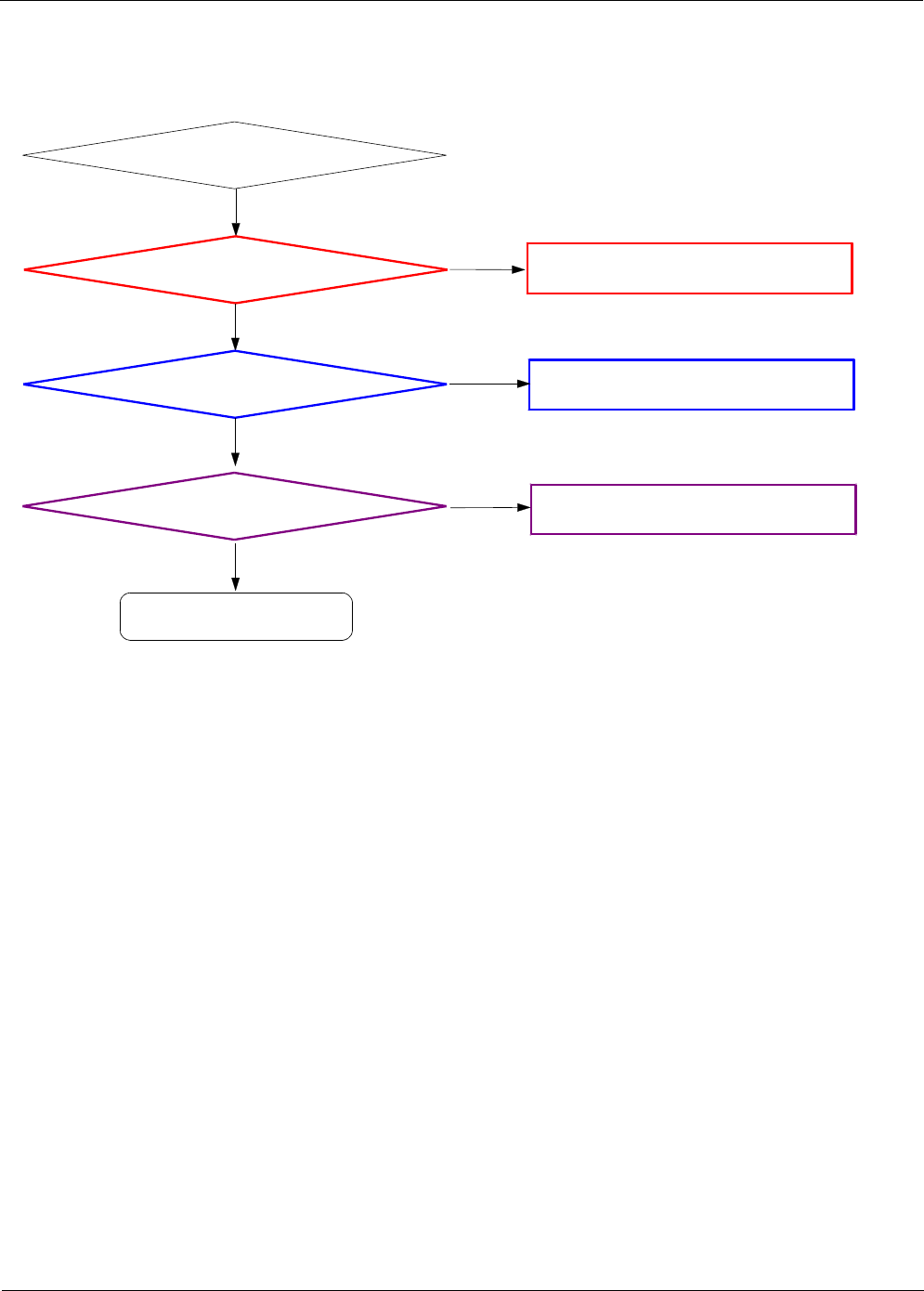
Level 3Repair
Distribution, transmission, or infringement of any content or data from this document without Samsung’s written authorization is strictly prohibited.
Confidential and proprietary-the contents in this service guide subject to change without prior notice.
8-16
8-3-5. Charging Part
TA /USB Insert
Yes
END
Charging Sequence Start
V_BUS_5V =5V
No Check C563 =5
V,
or may not connected TA /USB
Yes
Check the CHG_IN_5V(C565)=5V No Resolder and Replace U502
Yes
Battery is Charging? No
Resolder or Replace U506
Yes
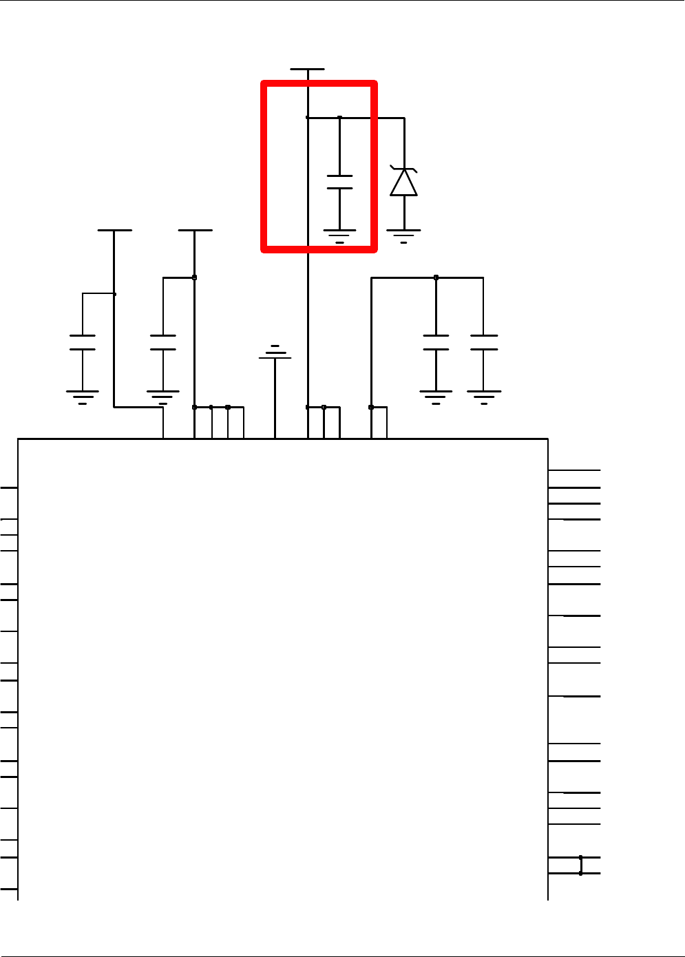
Level 3Repair
Distribution, transmission, or infringement of any content or data from this document without Samsung’s written authorization is strictly prohibited.
Confidential and proprietary-the contents in this service guide subject to change without prior notice.
8-17
ZD502
C565
C594
DP2
K
9
SYS
K
3
SYS
K
4
BATT
K5
BATT
K6
ADP2
K7
DN1
K
8
BAT_SP
J
3
SYS
J
4
BATTJ5
BATT
J6
ADN1 J7
MVIO
J
8
SYS_A
H
5
MVBAT
H7
BAT_SN
J
2
AUR2
G7
G8
CHGLX
H
1
AVL
H
2
SYS_A
H
4
CHGLX
G
1
BYPF2
MRST1B
F5
MRST2B
F6
AUT1
F7
UT1
F
8
DETBATB
E
4
E5
AIN E8
VBATTFG E9
BYPF1
SYS_Q
D
5
SCLFG
D8
ALRT D9
CHGIN
E1
CHGIN
E2
SNS
C8
VBFG C9
CHGIN
D1
THRM
D10
INOKB
D
4
SAFEOUT1 C1
SAFEOUT2
C2
SDA C6
VIO
B10
SCL
B6
VCCTESTA4
U506
CHG_IN_5V
V_BATTERY
C564
C566
R
5
C567
V_BAT
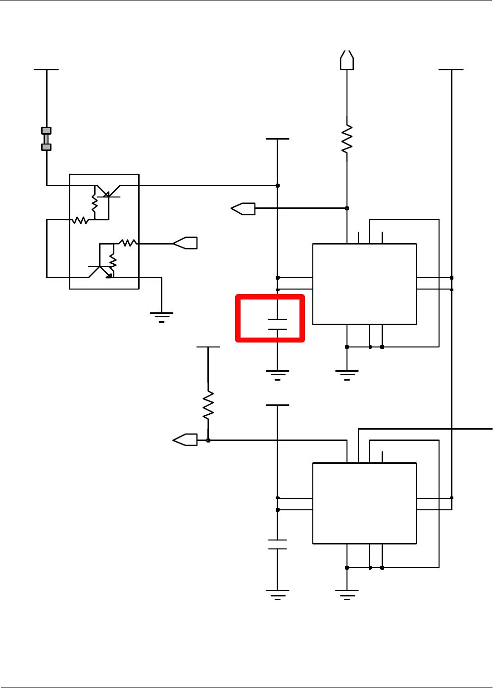
Level 3Repair
Distribution, transmission, or infringement of any content or data from this document without Samsung
’s written authorization isstrictly prohibited.
Confidential and proprietary-the contents in this service guide subject to change without prior notice.
8-18
B2
B1 IN
IN
C1
1
NC
NC
2
B3
OUT
OUT C3
A2
OVLO
U502
ACOK_
A1
EN_
A3
C2
GND
IC
C563
C3
OUT
OVLO
A2
A3
EN_
GND
C2
B2
IC
IN
B1
C1 IN
NC
1
2
NC
OUT B3
U504
A1
ACOK_
U501
2
5
6
3
1
4
V_BUS_5V
WPC_5V
R533
C578
R507
CHG_IN_5V
VCC_1.8V_AP
R511
CHG_IN_5V
TA_ACOK
OTG_EN
WPC_INT
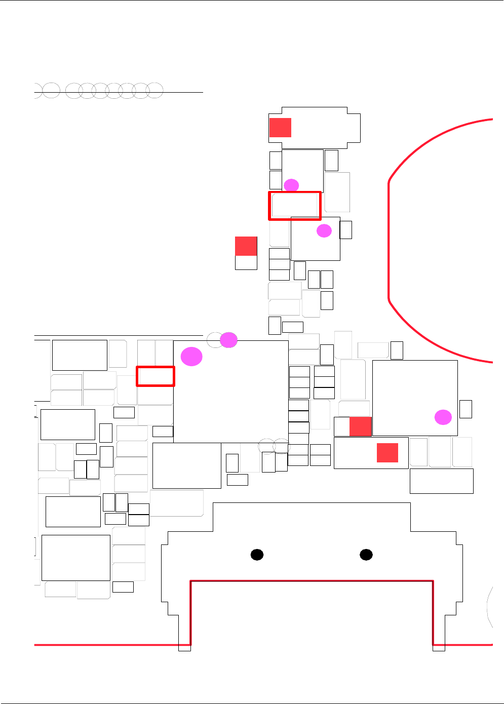
Level 3Repair
Distribution, transmission, or infringement of any content or data from this document without Samsung’s written authorization is strictly prohibited.
Confidential and proprietary-the contents in this service guide subject to change without prior notice.
8-19
BTC500
C246
C250
C300
C301
C302
C303
C304
C305
C306
C309
C319
C320
C326
C357
C500
C501
C503
C509
C510
C511
C517
C518
C519
C520
C521
C522
C523
C524
C525
C526
C528
C529
C530
C531
C532
C537
C541
C546
C549
C553
C554
C555
C561
C563
C564
C565
C566
C567
C568
C569
C570
C571
C572
C573
C574
C575
C576
C577
C579
C580
C581
C582
C583
C585
C586
C587
C593
C594
C595
C707
D500
L500
L506
L507
L508
L511
L512
R312
R313
R432
R433
R500
R502
R503
R507
R512
R513
R515
R516
R517
R518
R519
R526
R532
R533
TA500
TP_AP_D TP_AP_D+
TP300
TP301
TP302
TP303
TP305
TP316
TP322
TP327
TP328
U206
U501
U502
U506
U719
UME300
ZD500
ZD502
ZD701
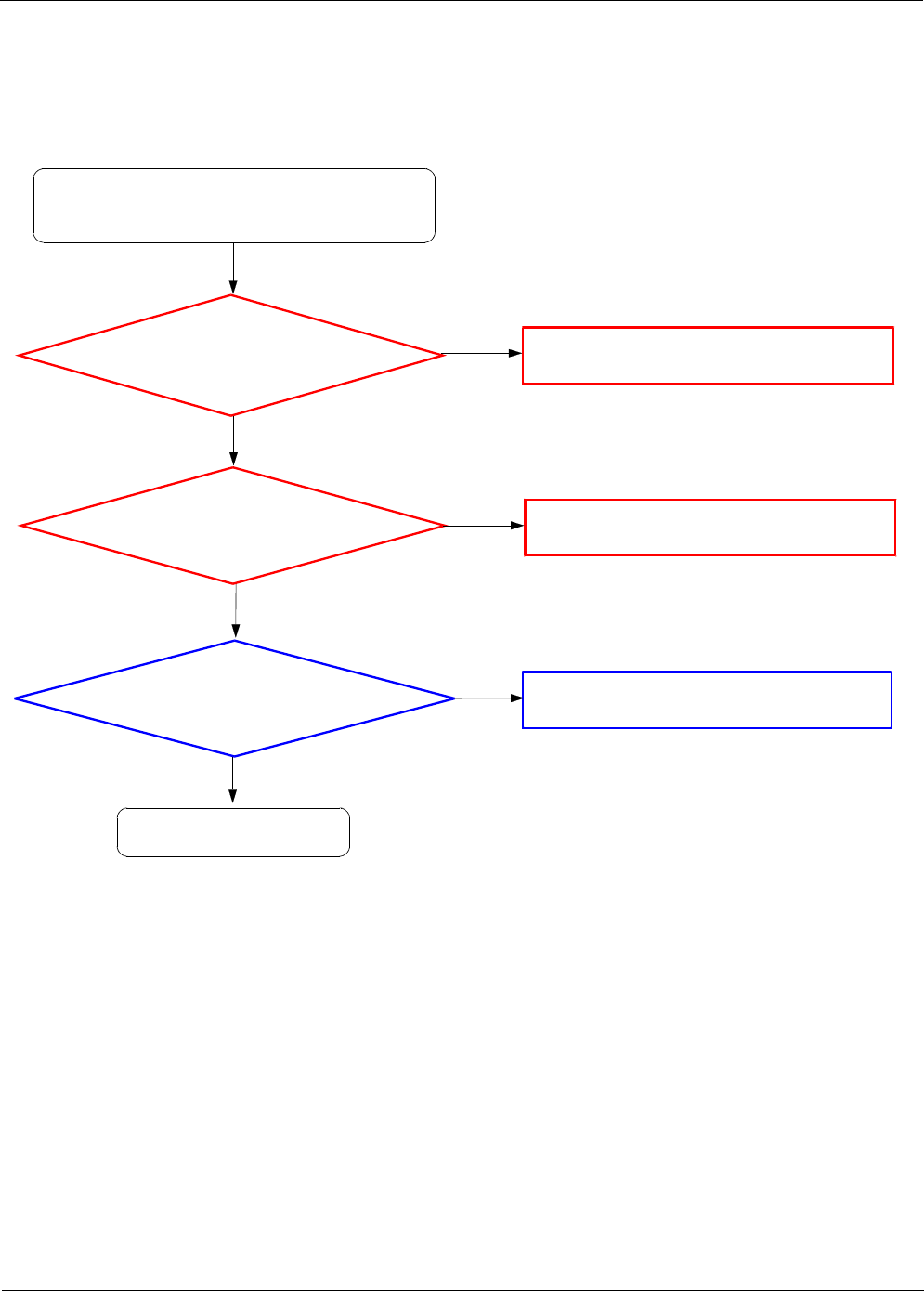
Level 3Repair
Distribution, transmission, or infringement of any content or data from this document without Samsung’s written authorization is strictly prohibited.
Confidential and proprietary-the contents in this service guide subject to change without prior notice.
8-20
8-3-6. Microphone Part (Main MIC)
Check PCB where main MIC
is placed
for any damage
Check component soldering
statuses of C633, C637
Change the PCB module
Resolder or replace C633, C637
END
No
Yes
Yes
Yes
No
Check main microphone function
in voice call receiver mode
or in Voice Recording mode
Check the voltage at
C601 =2.8V Resolder or replace U600
No
Yes
Level 3Repair
Distribution, transmission, or infringement of any content or data from this document without Samsung’s written authorization is strictly prohibited.
Confidential and proprietary-the contents in this service guide subject to change without prior notice.
8-21
C615
VCC_1.8V_AP VCC_1.8V_AP
C623
C609
C628
C610
R624
C647
C606
C616
C649
L600
C629
C638
TP_607
C633
EAR_MICBIAS_LDO_2.8V
R619
VCC_1.8V_AP
CPVDD
BCLK2
K1
K2 GPIO6|ADCLRCLK2
GPIO8|DACDAT3
K3
GPIO11|BCLK3
K4
DGND
K5
CPVOUTN K7
K8
CPCB
CPGND
K9
ADCLRCLK1|GPIO1
DBVDD2J2
J3 LRCLK2
GPIO9|ADCDAT3
J4
HPOUT1R J5
HPOUT1L J6
J7
CPVOUTP
CPCA J8
J9
H2
SCLK
SDA H3
H4 ADCDAT2
DBVDD3H5
H6
HPOUT1FB
HPOUT2P H7
H8HP2GND
J1
G1 LRCLK1
DCVDDG2
G3 BCLK1
DACDAT2
G4
G5 GPIO10|LRCLK3
HPOUT2N G8
G9
AVDD1
DACDAT1
H1
E9
AVDD1
MCLK1 F1
F2
MCLK2
ADDR F3
F4 ADCDAT1
VREFC
F7
F8
LDO1VDD
MICDET
F9
D6 LDO2ENA
IN1LN
D7
D8 IN1LP
AGND
D9
E1
DBVDD1
SPKVDD2E2
E7
VMIDC
AVDD2E8
C7 IN1RP
IN2LN|DMICDAT
C8
C9 IN2LP|VRXN
SPKOUTRN D1
D2
SPKVDD2
SPKGND2
D3
D4
SPKOUTRP
SPKMODE D5
B8 IN2RP|VRXP
IN1RN
B9
C1
SPKOUTRN
SPKGND2
C2
C3
SPKOUTRP
SPKGND1
C4
C5
LINEOUTFB
LINEOUT1N C6
A9
MICBIAS1
SPKOUTLN B1
B2SPKGND1
SPKOUTLP B3
B4
SPKOUTLP
LINEOUT2P B5
B6
LINEOUT1P
IN2RN
B7
NC
A1
SPKOUTLN
SPKVDD1A2
A3
SPKVDD1
LDO1ENA
A4
A5
REFGND
LINEOUT2N A6
A7
MICBIAS2
DMICCLK
A8
U605
1NC
2
C648
C646
C624
C650
R617
C627
C645
C618
TP_606
C637
C626
R611
V_BAT
C619
C625
C643
R625
SUB_MIC_N
SUB_MIC_P
EAR_DET
IN2RN
IN2RP
MAIN_MIC_N
SPEECH_PCM_OUT_CODEC
MAIN_MIC_P
EAR_SEND_END
EAR_ADC_3.5
SPK_OUT_L_N
SPK_OUT_L_P
EAROUT_L
EAROUT_R
VPS_L
VPS_R
EAR_MIC_P
RCV_P
RCV_N
MM_I2S_SYNC
MM_I2S_DO
MM_I2S_DI
MM_I2S_CLK
CODEC_LDO_EN
CODEC_CLK32K
EAROUT_FB
SPEECH_PCM_IN_CODEC
CODEC_SCL_1.8V
CODEC_SDA_1.8V
XTAL_24MHZ_AP
SPEECH_PCM_SYNC
SPEECH_PCM_CLK
BT_PCM_OUT
BT_PCM_IN
BT_PCM_SYNC
BT_PCM_CLK
EAR_MIC_N
C600
MICBIAS_LDO_2.8V
C601
V_BAT
2
4VDD 1
VOUT
U600
3CE
GND
5
GND
3_MIC
MICBIAS_EN
Level 3Repair
Distribution, transmission, or infringement of any content or data from this document without Samsung’s written authorization is strictly prohibited.
Confidential and proprietary-the contents in this service guide subject to change without prior notice.
8-22
AP_PMIC_EN
AP_PS_HOLD
BOTHHOLE102
BOTHHOLE104
BOTHHOLE108
BTC500
C240
C246
C250
C268
C300
C301
C302
C303
C304
C305
C306
C307
C308
C309
C310
C311
C312
C313
C314
C315
C316
C317
C318
C319
C320
C321
C322
C323
C324
C325
C326
C327
C328
C329
C330
C331
C332
C333
C334
C335
C341
C342
C344
C347
C348
C356
C357
C400
C403
C404
C405
C406
C407
C408
C409
C413
C414
C415
C417
C418
C419
C420
C421
C422
C425
C426
C427
C443
C444
C445
C446
C447
C448
C450
C451
C453
C454
C500
C501
C503
C504
C505
C506
C507
C508
C509
C510
C511
C512
C513
C514
C515
C516
C517
C518
C519
C520
C521
C522
C523
C524
C525
C526
C528
C529
C530
C531
C532
C533
C534
C535
C537
C538
C539
C541
C544
C546
C549
C550
C551
C552
C553
C554
C555
C556
C557
C558
C559
C560
C561
C563
C564
C565
C566
C567
C568
C569
C570
C571
C572
C573
C574
C575
C576
C577
C579
C580
C581
C582
C583
C585
C586
C587
C593
C594
C595
C600
C601
C620
C707
C718
C719
C729
C730
C731
C732
C733
C734
C765
C766
C785
D500
D700
F700
FM_RST
L300
L301
L302
L303
L305
L500
L501
L502
L503
L504
L505
L506
L507
L508
L509
L510
L511
L512
L514
L515
L702
L703
L706
L707
MOT500
MOT501
OSC400
OSC500
R104
R300
R301
R302
R303
R304
R305
R306
R307
R308
R309
R312
R313
R314
R315
R318
R319
R331
R332
R333
R334
R335
R336
R337
R338
R342
R400
R401
R402
R403
R404
R405
R406
R407
R408
R417R420
R427
R428
R429
R432
R433
R438
R441
R442
R447
R448
R449
R450
R451
R452
R456
R457
R464
R465
R468
R469
R470
R471
R473
R474
R475
R476
R483
R500
R501
R502
R503
R504
R505
R507
R512
R513
R515
R516
R517
R518
R519
R526
R532
R533
R708
R709
R717
R741R742
R743
RESET300
TA500
TH300
TH400
TP_AP_DTP_AP_D+
TP_eMMC_EN
TP_TORCH_EN
TP201
TP202
TP207
TP300
TP301
TP302
TP303
TP304
TP305
TP306
TP307
TP308
TP309
TP310TP311
TP312
TP313
TP314
TP315
TP316
TP317
TP318
TP319
TP320
TP321
TP322
TP324
TP325
TP326
TP327
TP328
TP400
TP401
TP402
TP403
TP501
TP502
TP504
TP505
TP506
TP507
TP508
TP509
TP518
TP519TP708
TP710
U206
U301
U302
U500
U501
U502
U506
U600
U704
U706
U713
U718
U719
UCP300
UCP400
UME300
VIBTONE_PWM
ZD500
ZD502
ZD701
ANT200
ANT203
C208
C214
C215
C217
C221
C223
C224
C588
C591
C592
C604C605
C606
C609
C610
C615
C616
C617
C618
C619
C623
C624
C625
C626
C627
C628
C629
C633
C637
C638
C643
C645
C646
C647
C648
C649
C650
C651
C652
C653
C654
C655
C656
C657
C658
C659
C660
C661
C662
C663
C664
C665
C666
C700
C701
C702
C703
C704
C705
C714
C715
C716
C717
C767
C768
C769
C770
HDC600
HDC601
HEA700
L513
L600
L605
L607
L608
L611
L612
L613
L614
L615
L701
LED500
MIC601
R426
R439
R440
R521
R528
R529
R530
R531
R611
R617
R619
R624
R625
R626
R628
R629
R630
R632
R633R634
R703
R704
R707
TP_606
TP_FLASH_SET
TP_ISP_FLASH
TP_TORCH_SET
U505
U509
U603
U605
U607
U608
U701
U702
U703
V602
ZD600
ZD601
ZD602
ZD603
ZD604
ZD605
ZD606
ZD607
ZD608

Level 3Repair
Distribution, transmission, or infringement of any content or data from this document without Samsung’s written authorization is strictly prohibited.
Confidential and proprietary-the contents in this service guide subject to change without prior notice.
8-23
8-3-6-1. Microphone Part (Sub MIC)
Check PCB where Sub MIC
is placed
for any damage
Check component soldering
statuses of C643, C645
Replace the PCB module
Resolder or replace C643, C645
END
No
Yes
Yes
Yes
No
Check Sub microphone function
in voice call loudSPK mode
or in camcording mode
Check the voltage at
C605 =2.8V Resolder or replace U603
No
Yes
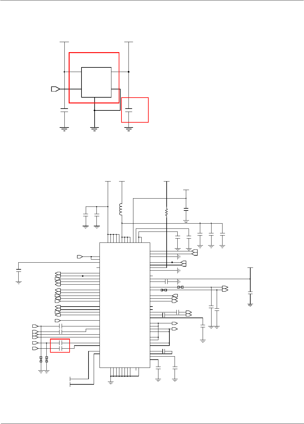
Level 3Repair
Distribution, transmission, or infringement of any content or data from this document without Samsung’s written authorization is strictly prohibited.
Confidential and proprietary-the contents in this service guide subject to change without prior notice.
8-24
SUB_MICBIAS_LDO_2.8V
C604
3CE
GND
5
GND
2
4VDD 1
VOUT
U603
V_BAT
C605
SUB_MICBIAS_EN
C615
VCC_1.8V_AP VCC_1.8V_AP
C623
C609
C628
C610
R624
C647
062032
C606
C616
L600
C629
C638
TP_607
C633
EAR_MICBIAS_LDO_2.8V
R619
VCC_1.8V_AP
C617
CPVDD
BCLK2
K1
K2 GPIO6|ADCLRCLK2
GPIO8|DACDAT3
K3
GPIO11|BCLK3
K4
DGND
K5
CPVOUTN K7
K8
CPCB
CPGND
K9
ADCLRCLK1|GPIO1
DBVDD2J2
J3 LRCLK2
GPIO9|ADCDAT3
J4
HPOUT1R J5
HPOUT1L J6
J7
CPVOUTP
CPCA J8
J9
H2
SCLK
SDA H3
H4 ADCDAT2
DBVDD3H5
H6
HPOUT1FB
HPOUT2P H7
H8HP2GND
J1
G1 LRCLK1
DCVDDG2
G3 BCLK1
DACDAT2
G4
G5 GPIO10|LRCLK3
HPOUT2N G8
G9
AVDD1
DACDAT1
H1
E9
AVDD1
MCLK1 F1
F2
MCLK2
ADDR F3
F4 ADCDAT1
VREFC
F7
F8
LDO1VDD
MICDET
F9
D6 LDO2ENA
IN1LN
D7
D8 IN1LP
AGND
D9
E1
DBVDD1
SPKVDD2E2
E7
VMIDC
AVDD2E8
C7 IN1RP
IN2LN|DMICDAT
C8
C9 IN2LP|VRXN
SPKOUTRN D1
D2
SPKVDD2
SPKGND2
D3
D4
SPKOUTRP
SPKMODE D5
B8 IN2RP|VRXP
IN1RN
B9
C1
SPKOUTRN
SPKGND2
C2
C3
SPKOUTRP
SPKGND1
C4
C5
LINEOUTFB
LINEOUT1N C6
A9
MICBIAS1
SPKOUTLN B1
B2SPKGND1
SPKOUTLP B3
B4
SPKOUTLP
LINEOUT2P B5
B6
LINEOUT1P
IN2RN
B7
NC
A1
SPKOUTLN
SPKVDD1A2
A3
SPKVDD1
LDO1ENA
A4
A5
REFGND
LINEOUT2N A6
A7
MICBIAS2
DMICCLK
A8
U605
1NC
2
C648
C646
C624
R617
C627
C645
C618
TP_606
C637
C626
R611
V_BAT
C619
C625
C643
R625
SUB_MIC_N
SUB_MIC_P
EAR_DET
MAIN_MIC_N
SPEECH_PCM_OUT_CODEC
MAIN_MIC_P
EAR_SEND_END
EAR_ADC_3.5
SPK_OUT_L_N
SPK_OUT_L_P
EAROUT_L
EAROUT_R
VPS_L
VPS_R
EAR_MIC_P
RCV_P
RCV_N
MM_I2S_SYNC
MM_I2S_DO
MM_I2S_DI
MM_I2S_CLK
CODEC_LDO_EN
CODEC_CLK32K
EAROUT_FB
SPEECH_PCM_IN_CODEC
CODEC_SCL_1.8V
CODEC_SDA_1.8V
XTAL_24MHZ_AP
SPEECH_PCM_SYNC
SPEECH_PCM_CLK
BT_PCM_OUT
BT_PCM_IN
BT_PCM_SYNC
BT_PCM_CLK
EAR_MIC_N
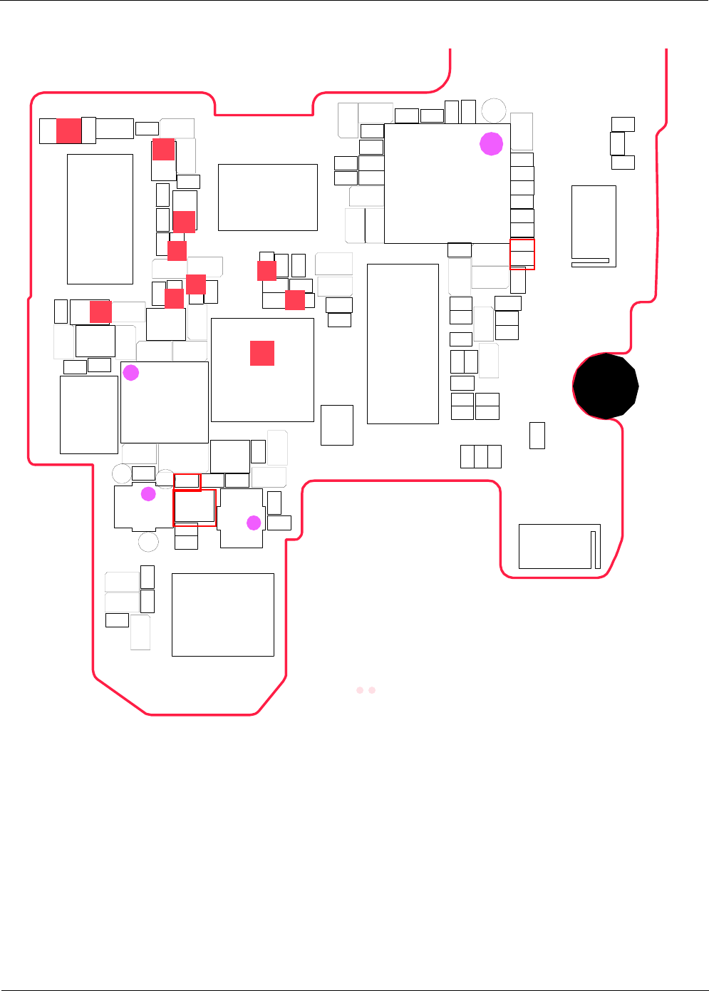
Level 3Repair
Distribution, transmission, or infringement of any content or data from this document without Samsung’s written authorization is strictly prohibited.
Confidential and proprietary-the contents in this service guide subject to change without prior notice.
8-25
ANT200
ANT203
C208
C214
C215
C217
C221
C223
C224
C588
C591
C592
C604C605
C606
C609
C610
C615
C616
C617
C618
C619
C623
C624
C625
C626
C627
C628
C629
C633
C637
C638
C643
C645
C646
C647
C648
C649
C650
C651
C652
C653
C654
C655
C656
C657
C658
C659
C660
C661
C662
C663
C664
C665
C666
C700
C701
C702
C703
C704
C705
C714
C715
C716
C717
C767
C768
C769
C770
HDC600
HDC601
HEA700
L513
L600
L605
L607
L608
L611
L612
L613
L614
L615
L701
LED500
MIC601
R426
R439
R440
R521
R528
R529
R530
R531
R611
R617
R619
R624
R625
R626
R628
R629
R630
R632
R633R634
R703
R704
R707
TP_606
TP_FLASH_SET
TP_ISP_FLASH
TP_TORCH_SET
U505
U509
U603
U605
U607
U608
U701
U702
U703
V602
ZD600
ZD601
ZD602
ZD603
ZD604
ZD605
ZD606
ZD607
ZD608
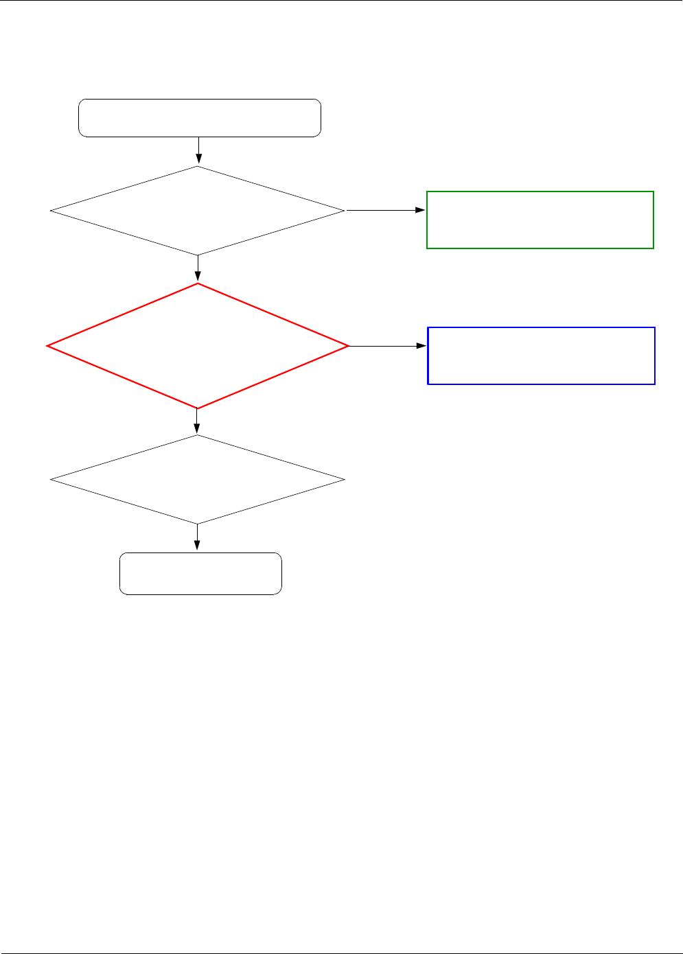
Level 3Repair
Distribution, transmission, or infringement of any content or data from this document without Samsung’s written authorization is strictly prohibited.
Confidential and proprietary-the contents in this service guide subject to change without prior notice.
8-26
8-3-7. Speaker Part
Check the signals on
C665, C666
Check speaker function.
Play MP3 with maximum volume level.
No
Resolder or replace C665, C666
END
Yes
Yes
Replace the speaker
module
Yes
Check the connection of
HDC600
Yes
No
Reconnect HDC600
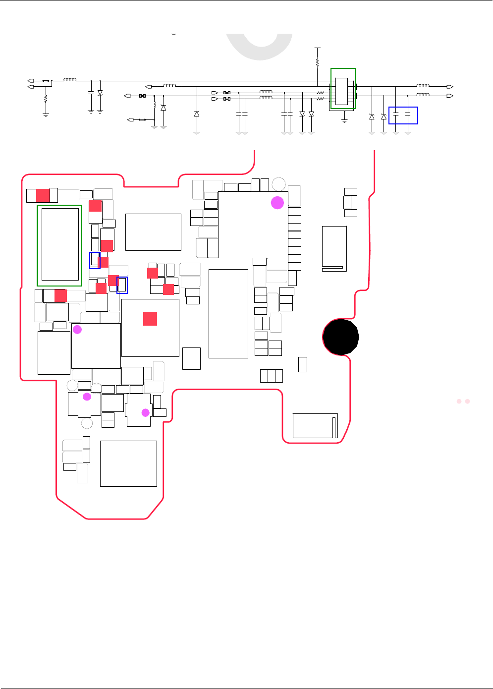
Level 3Repair
Distribution, transmission, or infringement of any content or data from this document without Samsung’s written authorization is strictly prohibited.
Confidential and proprietary-the contents in this service guide subject to change without prior notice.
8-27
R630
ZD602
OPEN
R631
L616
L615
L614
R628
R634
C655
ZD600
R626
R629
ZD601
C654
C663
8
8
9
9
15
15 16 16
2
2
3
3 4
4
5
5 6
6
7
7
HDC600
1
1
10
10
11
11 12
12
13 13 14 14
C665
ZD606
ZD604
R633
L608
L607
C666
C664
VCC_1.8V_AP
C653
C656
L605
ZD607
ZD605
SPK_OUT_L_N
SPK_OUT_L_P
EAR_DETEAR_ADC_3.5
EAROUT_L
_
EAROUT_FB
FM_RADIO_ANT
EAROUT_R
EAR_MIC_3.5
ANT200
ANT203
C208
C214
C215
C217
C221
C223
C224
C588
C591
C592
C604C605
C606
C609
C610
C615
C616
C617
C618
C619
C623
C624
C625
C626
C627
C628
C629
C633
C637
C638
C643
C645
C646
C647
C648
C649
C650
C651
C652
C653
C654
C655
C656
C657
C658
C659
C660
C661
C662
C663
C664
C665
C666
C700
C701
C702
C703
C704
C705
C714
C715
C716
C717
C767
C768
C769
C770
HDC600
HDC601
HEA700
L513
L600
L605
L607
L608
L611
L612
L613
L614
L615
L701
LED500
MIC601
R426
R439
R440
R521
R528
R529
R530
R531
R611
R617
R619
R624
R625
R626
R628
R629
R630
R632
R633R634
R703
R704
R707
TP_606
TP_FLASH_SET
TP_ISP_FLASH
TP_TORCH_SET
U505
U509
U603
U605
U607
U608
U701
U702
U703
V602
ZD600
ZD601
ZD602
ZD603
ZD604
ZD605
ZD606
ZD607
ZD608
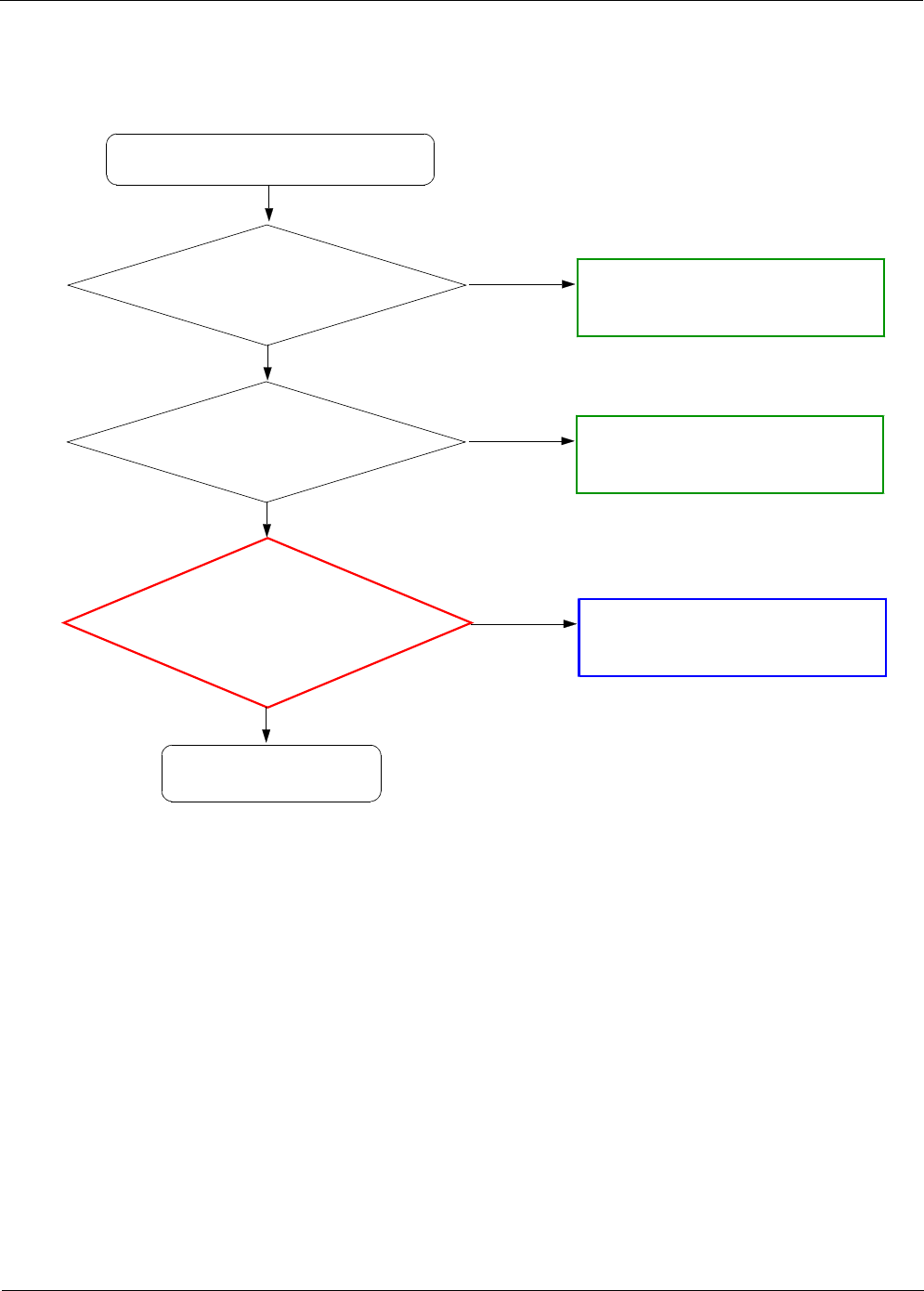
Level 3Repair
Distribution, transmission, or infringement of any content or data from this document without Samsung’s written authorization is strictly prohibited.
Confidential and proprietary-the contents in this service guide subject to change without prior notice.
8-28
8-3-8. Receiver Part
Check the signals on
C651,ZD603,ZD608
Check receiver function
in voice call receiver mode.
No
Resolder or replace U605
END
Yes
Yes
Check the connection of
HDC601
Yes
No
Reconnect HDC601
Check RCV module where
RCV's placed
for any damage
Yes
No
Replace the RCV module
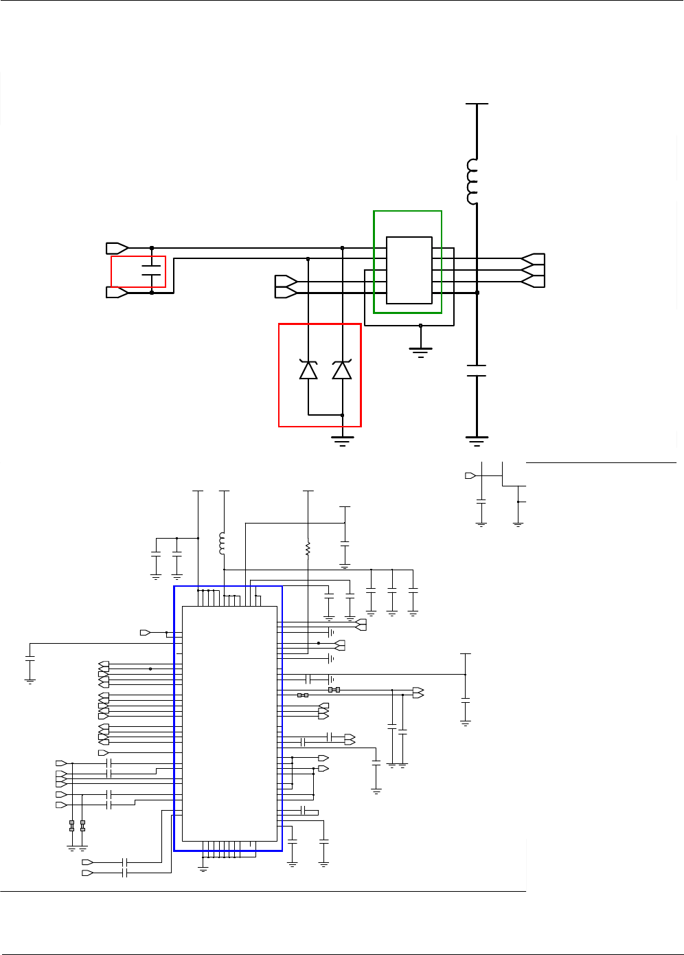
Level 3Repair
Distribution, transmission, or infringement of any content or data from this document without Samsung’s written authorization is strictly prohibited.
Confidential and proprietary-the contents in this service guide subject to change without prior notice.
8-29
C652
V_BAT
062032
1000nF
ZD603
UCLAMP0541Z
34
4
5
56
6
7
78
8
9
9
14-5804-010-829
HDC601
1
1
10
10
2
2
3
100nF
C651
0603
6.3V
L611
BLM15AG121SN1D
1005
UCLAMP0541Z
ZD608
RCV_P
RCV_N
LED_R
LED_G
LED_BVOL_UP
VOL_DOWN
1000nF
C615
VCC_1.8V_AP
062032
6.3V
VCC_1.8V_AP
C623
1000nF
6.3V
062032
1106
6.3V
4700nF
C609
C628 1000nF
062032
C610
100nF
6.3V
0603
1000nF
C604
6.3V
0603
0ohm
R624
SHORT
C647
2200nF
6.3V
1005
062032
6.3V
1000nF
C606
6.3V
0603
C616
100nF
10V0603
C649
L600
1000nF
BLM15AG100SN1D
1005
OPEN
1106
0603
C629
4700nF
C638
TP_607
1000nFC633
0603
10V
EAR_MICBIAS_LDO_2.8V
SHORT
0ohm
R619
0603
1106
4700nF
6.3V
VCC_1.8V_AP
C617
CPVDD
BCLK2
K1
K2 GPIO6|ADCLRCLK2
GPIO8|DACDAT3
K3
GPIO11|BCLK3
K4
DGND
K5
CPVOUTN K7
K8
CPCB
CPGND
K9
ADCLRCLK1|GPIO1
DBVDD2J2
J3 LRCLK2
GPIO9|ADCDAT3
J4
HPOUT1R J5
HPOUT1L J6
J7
CPVOUTP
CPCA J8
J9
H2
SCLK
SDA H3
H4 ADCDAT2
DBVDD3H5
H6
HPOUT1FB
HPOUT2P H7
H8HP2GND
J1
G1 LRCLK1
DCVDDG2
G3 BCLK1
DACDAT2
G4
G5 GPIO10|LRCLK3
HPOUT2N G8
G9
AVDD1
DACDAT1
H1
E9
AVDD1
MCLK1 F1
F2
MCLK2
ADDR F3
F4 ADCDAT1
VREFC
F7
F8
LDO1VDD
MICDET
F9
D6 LDO2ENA
IN1LN
D7
D8 IN1LP
AGND
D9
E1
DBVDD1
SPKVDD2E2
E7
VMIDC
AVDD2E8
C7 IN1RP
IN2LN|DMICDAT
C8
C9 IN2LP|VRXN
SPKOUTRN D1
D2
SPKVDD2
SPKGND2
D3
D4
SPKOUTRP
SPKMODE D5
B8 IN2RP|VRXP
IN1RN
B9
C1
SPKOUTRN
SPKGND2
C2
C3
SPKOUTRP
SPKGND1
C4
C5
LINEOUTFB
LINEOUT1N C6
A9
MICBIAS1
SPKOUTLN B1
B2SPKGND1
SPKOUTLP B3
B4
SPKOUTLP
LINEOUT2P B5
B6
LINEOUT1P
IN2RN
B7
NC
A1
SPKOUTLN
SPKVDD1A2
A3
SPKVDD1
LDO1ENA
A4
A5
REFGND
LINEOUT2N A6
A7
MICBIAS2
DMICCLK
A8
WM1811ECS
U605
1NC
2
1005
6.3V
2200nF
C648
C646 2200nF 6.3V
1005
1106
4700nFC624
C650 1000nF
10V
0603
R617
0603
SHORT
0ohm
OPEN
C627
0603
0603 10V
1000nFC645
3CE
GND
5
1106
C618
4700nF
6.3V
TP_606
060310V
1000nFC637
C626 1000nF
062032
100K
0603
R611
V_BAT
062032
6.3V
1000nF
C619
OPEN
0603
C625
0603 10V
1000nFC643
0603
0ohm
R625
SHORT
SUB_MIC_N
SUB_MIC_P
EAR_DET
IN2RN
IN2RP
MAIN_MIC_N
SPEECH_PCM_OUT_CODEC
MAIN_MIC_P
EAR_SEND_END
EAR_ADC_3.5
SPK_OUT_L_N
SPK_OUT_L_P
SUB_MICBIAS_EN
EAROUT_L
EAROUT_R
VPS_L
VPS_R
EAR_MIC_P
RCV_P
RCV_N
MM_I2S_SYNC
MM_I2S_DO
MM_I2S_DI
MM_I2S_CLK
CODEC_LDO_EN
CODEC_CLK32K
EAROUT_FB
SPEECH_PCM_IN_CODEC
CODEC_SCL_1.8V
CODEC_SDA_1.8V
XTAL_24MHZ_AP
SPEECH_PCM_SYNC
SPEECH_PCM_CLK
BT_PCM_OUT
BT_PCM_IN
BT_PCM_SYNC
BT_PCM_CLK
EAR_MIC_N
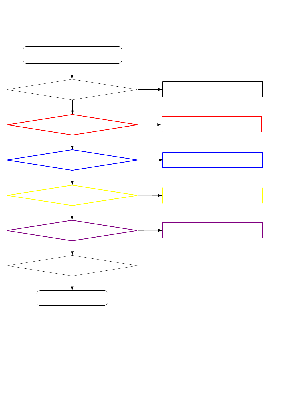
Level 3Repair
Distribution, transmission, or infringement of any content or data from this document without Samsung’s written authorization is strictly prohibited.
Confidential and proprietary-the contents in this service guide subject to change without prior notice.
8-30
8-3-9. BT/WIFI
BT/WiFi is not working
Check BT or WiFi function
ON
No Enable BT or WiFi Function
Yes
END
Check the Voltage on C220 =
1.8V
No Check the U202(crack, open, damaged, etc.)
Yes
Check 37.4MHz Clock at
R200
No Check the OSC201(crack, open, etc.)
Yes
Check the Voltage on L205 =
1.35V
No Resolder or change the L205
Yes
Check the Status of
C221, ANT203
No Resolder or Replace C221, ANT203
Yes
Resolder or Replace U202
Yes
Yes
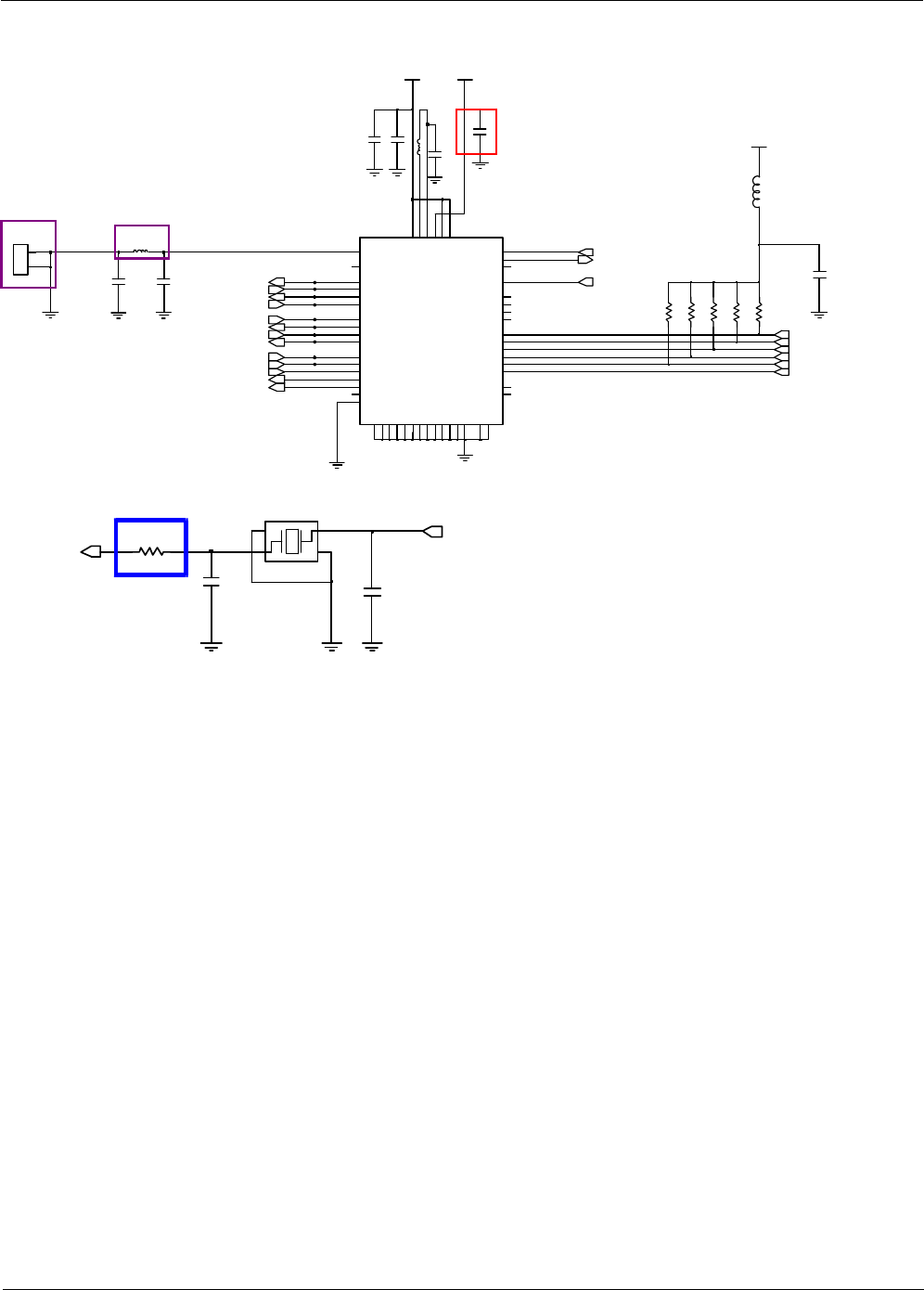
Level 3Repair
Distribution, transmission, or infringement of any content or data from this document without Samsung’s written authorization is strictly prohibited.
Confidential and proprietary-the contents in this service guide subject to change without prior notice.
8-31
V_BAT
GND
GND
P1
P2
BT_HOST_WAKE
I2S_WS P3
P4 BT_WAKE
UART_RTS
P5
P6 UART_RXD
GND
P7
P8
N1 FM_ANT
I2S_DO
N2
N3
I2S_CLK
I2S_DI N4
N5
URAT_CTS
UART_TXD
N6
N7GND
ANT
N8
PCM_CLK
J1
J8GND
K1 PCM_IN
VIO
K8
PCM_OUT
L1
L8 WL_GPIO6
M1GND
GND
M8
E1
VIN_LDO
WL_WAKE
E8
CLK_REG F1
F8
GND
G1
LPO
OSC_OUT
G8
PCM_SYNC
H1
H8
OSC_IN
B5
HSIC_STROBE
SDIO_DATA1 B6
B7
SDIO_CLK
SDIO_DATA0
B8
BT_REG_ON
C1 C8
SDIO_CMD
D1
WL_REG_ON
WL_HOST_WAKE
D8
GND
HSIC_DATA A5
A6
SDIO_DATA2
SDIO_DATA3
A7
A8GND
B1
SR_VLX
GND
B2
B3
VDD_FEM
GND
B4
U202
NC1
2
NC
GND
A1
A2
VBAT
VDD_FEMA3
A4
R206
C269
VCC_1.8V_AP
TP_212
TP_213
C224
ANT203
11
2
2
C222
R209
TP_214
C223
TP_215
C218
C220
TP_201
VCC_1.8V_AP
R205
L211
R208
TP_202
C221
C270
L205
R207
TP216
TP213
TP214
TP215
WLAN_SDIO_CL
K
WLAN_SDIO_CM
D
WLAN_SDIO_D(3
)
WLAN_SDIO_D(2
)
WLAN_SDIO_D(1
)
WLAN_SDIO_D(0
)
BT_WIFI_CLK32K
XTAL_37_4M_OUT
BT_UART_RXD
BT_PCM_SYNC
BT_PCM_CLK
BT_PCM_IN
BT_PCM_OUT
BT_UART_CTS
BT_UART_RTS
WLAN_EN
BT_UART_TXD
BT_WAKE
BT_HOST_WAKE
BT_EN
WLAN_HOST_WAKE
XTAL_37_4M_IN
OSC201
2
43
1
C205
R200
C203
XTAL_37_4M_OUT
X
TAL_37_4M_I
N
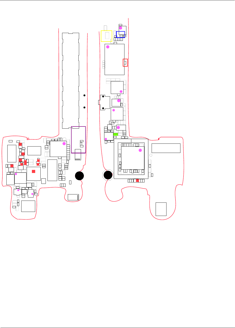
Level 3Repair
Distribution, transmission, or infringement of any content or data from this document without Samsung’s written authorization is strictly prohibited.
Confidential and proprietary-the contents in this service guide subject to change without prior notice.
8-32
ANT200
ANT203
C208
C214
C215
C217
C221
C223
C224
C588
C591
C592
C604C605
C606
C609
C610
C615
C616
C617
C618
C619
C623
C624
C625
C626
C628
C633
C637
C638
C643
C645
C646
C647
C648
C649
C650
C651
C652
C653
C654
C655
C656
C657
C658
C659
C660
C661
C662
C663
C664
C665
C666
C700
C701
C702
C703
C704
C705
C714
C715
C716
C717
C767
C768
C769
C770
CN300
HDC600
HDC601
HEA700
L513
L600
L605
L607
L608
L611
L612
L613
L614
L615
L701
LED500
MIC601
R426
R439
R440
R521
R528
R529
R530
R531
R611
R624
R625
R626
R628
R632
R633R634
R703
R704
R707
TP_606
TP_FLASH_SET
TP_ISP_FLASH
TP_TORCH_SET
U505
U509
U603
U605
U607
U608
U701
U702
U703
V602
ZD600
ZD601
ZD602
ZD603
ZD604
ZD605
ZD606
ZD607
ZD608
BOTHHOLE103
C200
C201
C202
C203
C204
C205
C206
C207
C209
C210
C211
C212
C213
C216
C218
C219
C220
C222
C228
C235C236
C269
C270
C452
C631
C632
C634
C635
C636C640
C642
C644
C706
C709
C710
C711
C737
C738C739
C741
C742
C743
C744
C745
C746
C747
C748
C749
C755
C756
C757
C758
C759
C760
C761
C762
F200
HDC701
L200
L201
L202
L203
L204
L205
L206
L208
L211
L270
L603
L609
L610
L616
L700
L709
MIC602
OSC200
OSC201
R200
R201
R202
R205
R206
R207
R208
R209
R214
R455
R462
R463
R618
R620
R631
R733
R734
R735
R738
R739
R740
SC700
SW600
TA600
TP_SPI_SCLK
TP200
TP203
TP204
TP205
TP206
TP213
TP214
TP215
TP216
TP706
U200
U201
U202
U203
U711
V601
ZD700
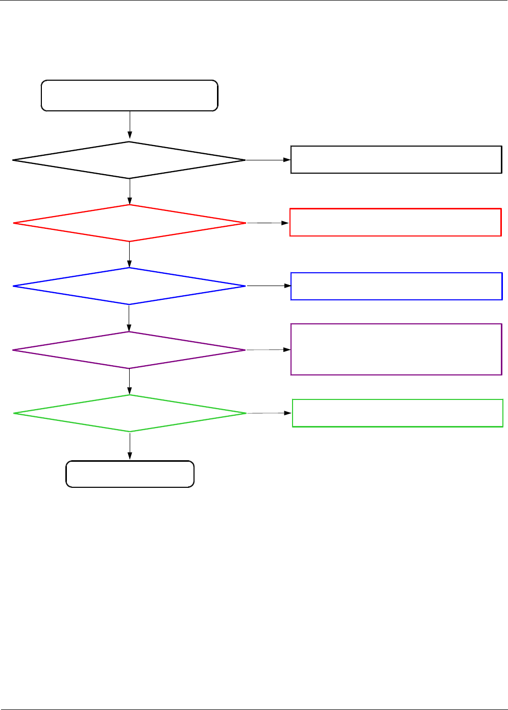
Level 3Repair
Distribution, transmission, or infringement of any content or data from this document without Samsung’s written authorization is strictly prohibited.
Confidential and proprietary-the contents in this service guide subject to change without prior notice.
8-33
8-3-10. GPS
Yes
Enable GPS Function in the setting.
No
Check GPS function ON
Yes
Check solder condition at
C208, C209,C210,C211,L203
No resolder
Yes
CheckOSC200,C200,C201 (short, open, crack, etc.)
No
Check 26MHz Clock at
OSC200
Yes
Check PMIC(U500) &UCP400
(short, open, crack, etc.)
No
Check the voltage on
C206=2.8V &C212 >1.8V
Yes
Yes
END
GPS is not working
Check the Antenna connect
ANT200
1. Resolder or Replace ANT 200
2. Replace SPK Module
No
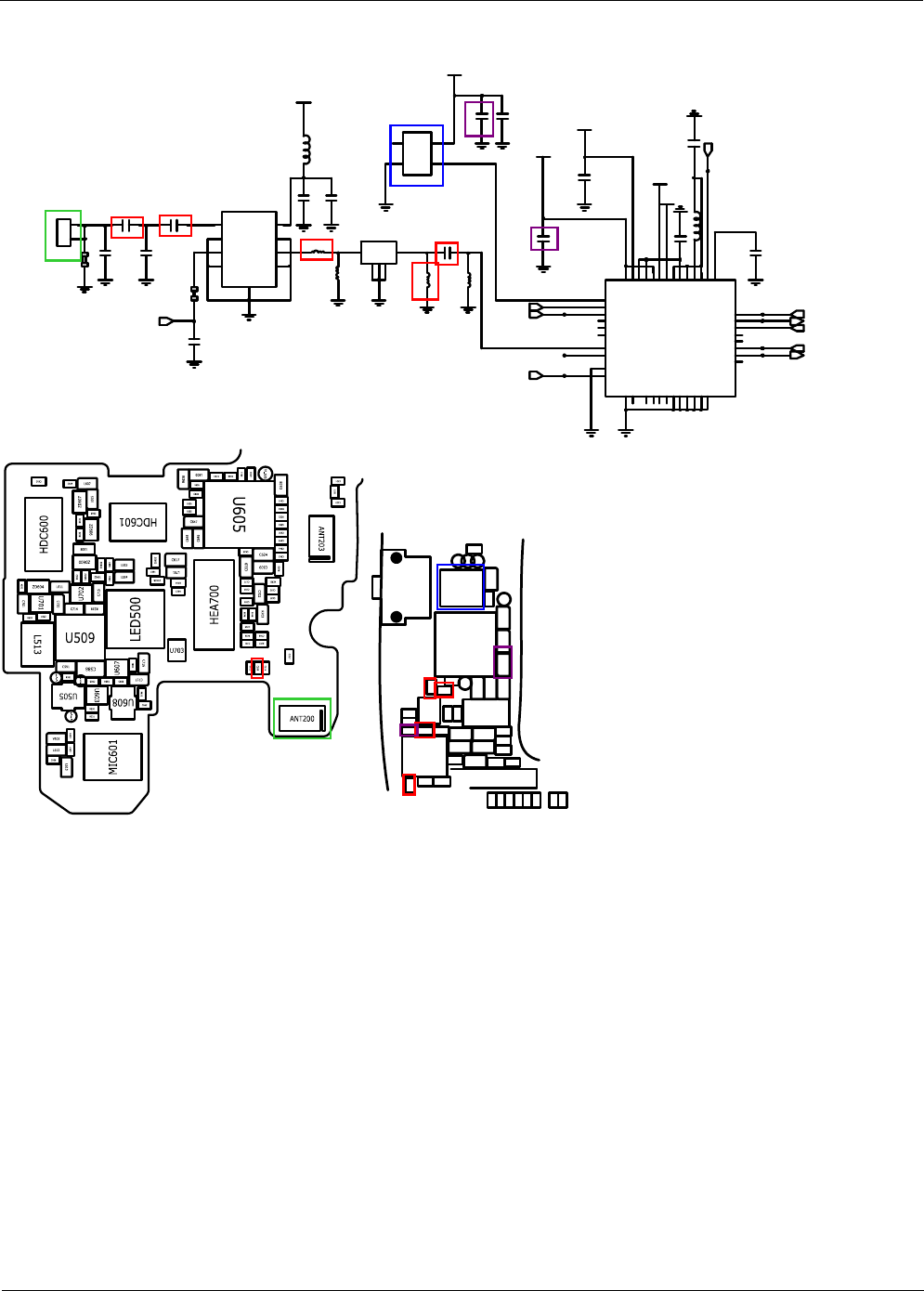
Level 3Repair
Distribution, transmission, or infringement of any content or data from this document without Samsung’s written authorization is strictly prohibited.
Confidential and proprietary-the contents in this service guide subject to change without prior notice.
8-34
C216
C201
R201
C210
TP_GPS_EN
TP202
11
2
2
ANT200
L204
TP200
C204
TP204
C213
V_BAT
TP201
TP203
C206
C212
C208
C202
C214
VDD_AUXO
VCC_2.8V_AP
VCC_1.8V_AP
TP206
C211
VDD_AUXO
TP205
VCC_1.8V_AP
L202
C217
C219
GND
2
GND
1
3
OUTVCC
4
OSC200
C207
RF_IN
1
6
RF_OUTVCTRL
3
8
VDD
2GND
4GND GND 5
GND 7
GND
9
U200
C209
C200
L203
L200
C215
IN 4
OUT
F200
G
2
G
3
G
5
1
GPS_AUXOP
G3
G4
REF_CAP
VDD_BATG5
G6
REGPU
F1
GPS_VSSIF
GPS_VDDLNA
F2
F3
GPS_VDDIF
VDD1P2_GRF
F4
F5
VDD1P2_CORE
VDD_PRE
F6
GPS_RFIP
G1
G2GPS_VSSLNA
LPO_IN
D5
D6
VDDC
NC
E1
E2
GPS_VDDPLL
VDD_AUXOE3
E4
AVSS
VDD_AUXINE5
E6 TM2
C3VSS
SDA2|UARD_RX
C4
C5
C_GPIO_3
SCL2|UART_TX C6
TCXO
D1
NC
D2
VSS
D3
D4VSS
B1
HOST_REQ
LNA_EN B2
B3
UART_nCTS
VDDCB4
B5
UART_nRTS
RST_N
B6
C1NC
NC
C2
1NC
2
NC
CAL_REQ
A1
A2
IF_VALID
GPS_SYNC|PPS_OUT
A3
C_GPIO_2
A4
GPS_CAL
A5
A6
VDDIO
U201
L201
GPS_CLK_26M
GPS_LNA_EN
GPS_LNA_EN
GPS_CLK32K
GPS_UART_CT
S
GPS_UART_RT
S
GPS_UART_RX
D
GPS_UART_TX
D
GPS_nRST
GPS_EN
C200
C201
C202
C204
C206
C207
C209
C210
C211
C212
C213
C216
C219
C452
C631
C632
C636C640
C642
C644
F200
L200
L201
L202
L203
L204
L603
L616
OSC200
R201
R202
R455
R618
R620
R631
SW600
TA600
TP200
TP203
TP204
TP205
TP206
U200
U201
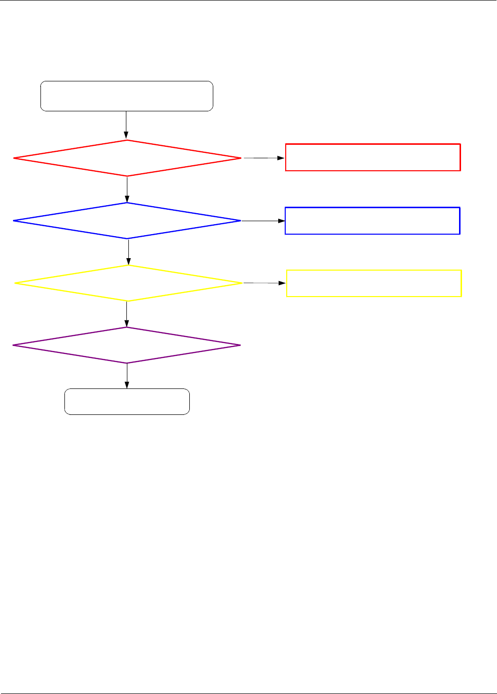
Level 3Repair
Distribution, transmission, or infringement of any content or data from this document without Samsung’s written authorization is strictly prohibited.
Confidential and proprietary-the contents in this service guide subject to change without prior notice.
8-35
8-3-11. FM RADIO
FM Radio is not working
END
Check the Connection of
HDC600
No Connect Earjack Ass'y correctly to HDC600
Yes
Check the Voltage
#10,19(1.8V), 11(2.8V)
No Check C235, C236 (Crack, short, etc)
Yes
Check the Audio Signal at
C649, C650
No Check Audio Codec IC (U605)
Switch IC (U608)
Resold and Replace U203
Yes
Yes
Yes
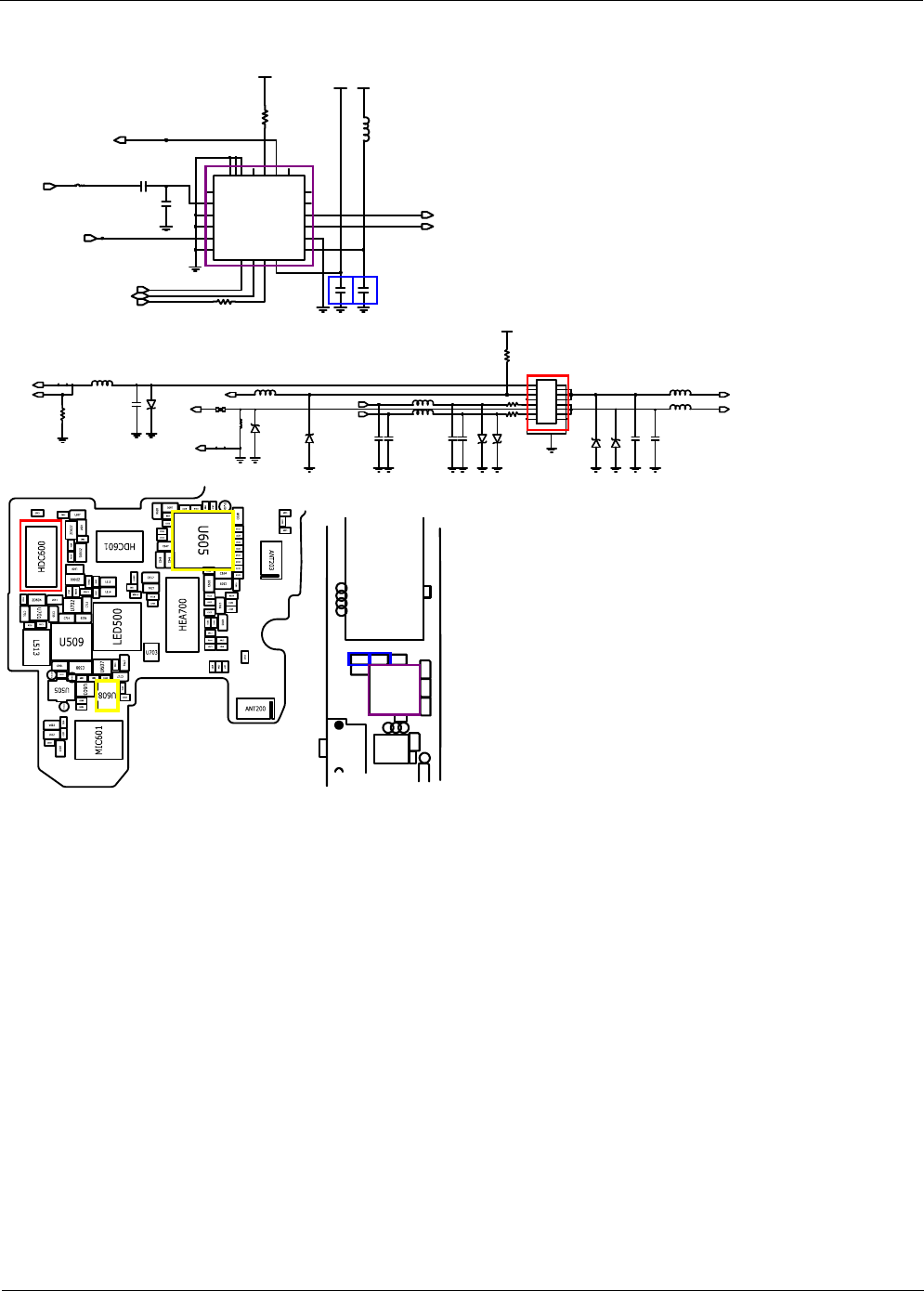
Level 3Repair
Distribution, transmission, or infringement of any content or data from this document without Samsung’s written authorization is strictly prohibited.
Confidential and proprietary-the contents in this service guide subject to change without prior notice.
8-36
C228
1005
VCC_2.8V_APVCC_1.8V_AP
C235
L206
R214
R202
VCC_1.8V_AP
C236
TP212
FM_RST
L270
SEN 116 VA
10
VIO
NC
2223
NC
RCLK
9
3RFGND
13
ROUT
RST
5
7
SCLK
SDIO
8
21
GND
GPO1
19
GPO2|_INT
18 17
GPO3|DCLK
14
LOUT
LPI
4
1NC
20
NC
U203
16
DFS
DOUT 152 FMI
12
GND
L208
FM_INT
FM_RST
FM_RADIO_ANT
FM_CLK32K
FM_SDA_1.8V
FM_SCL_1.8V
RADIO_
R
RADIO_L
ZD601
L614
L616
L615
2
2
3
34
4
5
56
6
7
78
8
9
9
1
1
10
10
11
11 12
12
13 13 14 14
15
15 16 16
HDC600
C655
ZD600
R631
L607
ZD605
C666
VCC_1.8V_AP
R634
C656
L605
ZD607
C665
ZD606
C653
C664
ZD604
R628
C663
R626
ZD602
R633
C654
EAR_DETEAR_ADC_3.5
EAROUT_L
SPK_OUT_L_
N
SPK_OUT_L_
P
FM_RADIO_ANT
EAROUT_R
EAR_MIC_3.5
EAROUT_FB
C200
C201
C220
C228
C235C236
L206
L208L270
OSC200
R202
R214
SW600
TP200
TP203
TP205
TP206
TP213
TP214
TP215
TP216
U202
U203
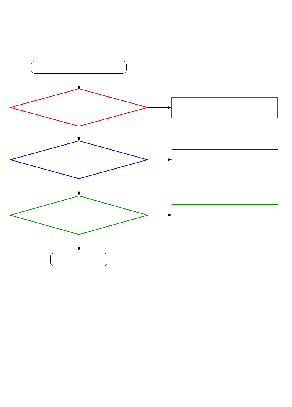
Level 3Repair
Distribution, transmission, or infringement of any content or data from this document without Samsung’s written authorization is strictly prohibited.
Confidential and proprietary-the contents in this service guide subject to change without prior notice.
8-37
8-3-12.Sensor Part
1. Magnetic Sensor
Check the Voltage
C240 =2.8V
C268 =1.8V
Abnormal Magnetic Sensor part
END
No
Yes
Check the Voltage
R434 =1.8V
R435 =1.8V
No
Yes
Magnetic Sensor operate
correctly?
No
Yes
Resolder U204 or heat over U500
Resolder U500 or heat over UCP400
Apply Heat over or Replace U204 using a
Heatgun
Yes
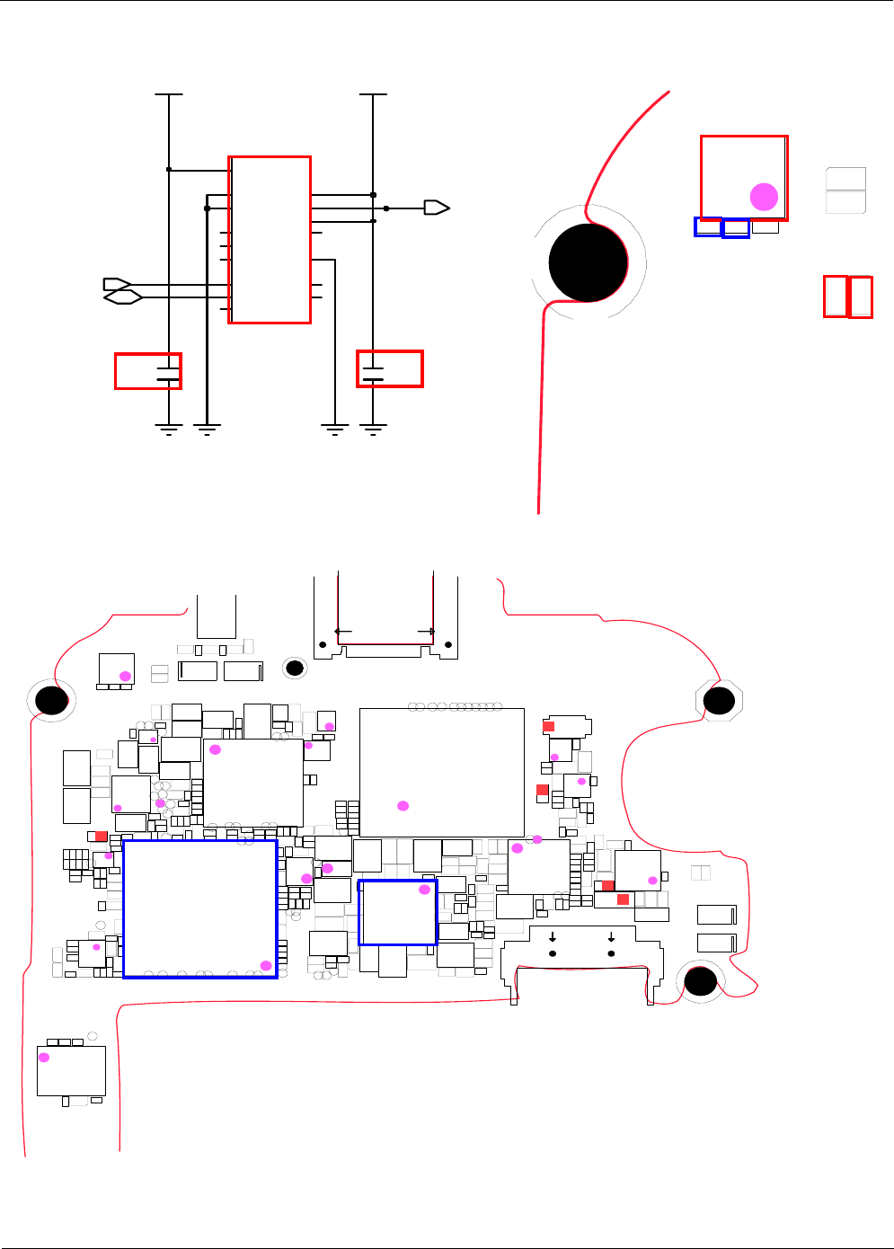
Level 3Repair
Distribution, transmission, or infringement of any content or data from this document without Samsung’s written authorization is strictly prohibited.
Confidential and proprietary-the contents in this service guide subject to change without prior notice.
8-38
Magnetic Sensor
VCC_2.8V_AP
VSS
C1
TST2
C2
DRDY
C3
VID
C4
CAD0
D1
D2
CAD1
SDA|SI
D4
NC
2
TST1
A1
CSB A2
SCL|SK
A3
RSV A4
VDD
B1
TST6
B3
SO
B4
U204
NC 1
C268
VCC_1.8V_AP
C240
TP207
MSENSE_SCL_1.8V
MSENSE_INT
MSENSE_SDA_1.8V
BOTHHOLE104
C240
C268
C597
L517
R434
R435 R534
U204
AP_PMIC_EN
AP_PS_HOLD
BOTHHOLE102
BOTHHOLE104
BOTHHOLE106
BOTHHOLE108
BTC500
C237
C238
C239
C240
C244
C246
C250
C268
C300
C301
C302
C303
C304
C305
C306
C307
C308
C309
C310
C311
C312
C313
C314
C315
C316
C317
C318
C319
C320
C321
C322
C323
C324
C325
C326
C327
C328
C329
C330
C331
C332
C333
C334
C335
C341
C342
C344
C347
C348
C356
C357
C400
C403
C404
C405
C406
C407
C408
C409
C413
C414
C415
C417
C418
C419
C420
C421
C422
C425
C426
C427
C443
C444
C445
C446
C447
C448
C450
C451
C453
C454
C500
C501
C503
C504
C505
C506
C507
C508
C509
C510
C511
C512
C513
C514
C515
C516
C517
C518
C519
C520
C521
C522
C523
C524
C525
C526
C528
C529
C530
C531
C532
C533
C534
C535
C537
C538
C539
C541
C544
C546
C549
C550
C551
C552
C553
C554
C555
C556
C557
C558
C559
C560
C561
C563
C564
C565
C566
C567
C568
C569
C570
C571
C572
C573
C574
C575
C576
C577
C579
C580
C581
C582
C583
C585
C586
C587
C593
C594
C595
C597
C600
C601
C613
C614
C620
C707
C718
C719
C729
C730
C731
C732
C733
C734
C765
C766
C785
D500
D700
F700
FM_RST
IFC700
KEY500
KEY501
L300
L301
L302
L303
L305
L500
L501
L502
L503
L504
L505
L506
L507
L508
L509
L510
L511
L512
L514
L515
L517
L518
L601
L602
L702
L703
L706
L707
MIC600
MOT500
MOT501
OSC400
OSC500
R104
R300
R301
R302
R303
R304
R305
R306
R307
R308
R309
R312
R313
R314
R315
R318
R319
R331
R332
R333
R334
R335
R336
R337
R338
R342
R400
R401
R402
R403
R404
R405
R406
R407
R408
R417R420
R427
R428
R429
R432
R433
R434
R435
R438
R441
R442
R447
R448
R449
R450
R451
R452
R456
R457
R460R461
R464
R465
R468
R469
R470
R471
R473
R474
R475
R476
R483
R500
R501
R502
R503
R504
R505
R507
R512
R513
R515
R516
R517
R518
R519
R526
R532
R533
R534
R708
R709
R717
R741R742
R743
RESET300
TA500
TH300
TH400
TP_AP_D TP_AP_D+
TP_eMMC_EN
TP_TORCH_EN
TP201
TP202
TP207
TP211
TP300
TP301
TP302
TP303
TP304
TP305
TP306
TP307
TP308
TP309
TP310TP311
TP312
TP313
TP314
TP315
TP316
TP317
TP318
TP319
TP320
TP321
TP322
TP324
TP325
TP326
TP327
TP328
TP400
TP401
TP402
TP403
TP501
TP502
TP504
TP505
TP506
TP507
TP508
TP509
TP518
TP519TP708
TP710
U204
U205
U206
U301
U302
U500
U501
U502
U506
U600
U704
U706
U713
U718
U719
UCP300
UCP400
UME300
V600
VIBTONE_PWM
ZD500
ZD502
ZD701
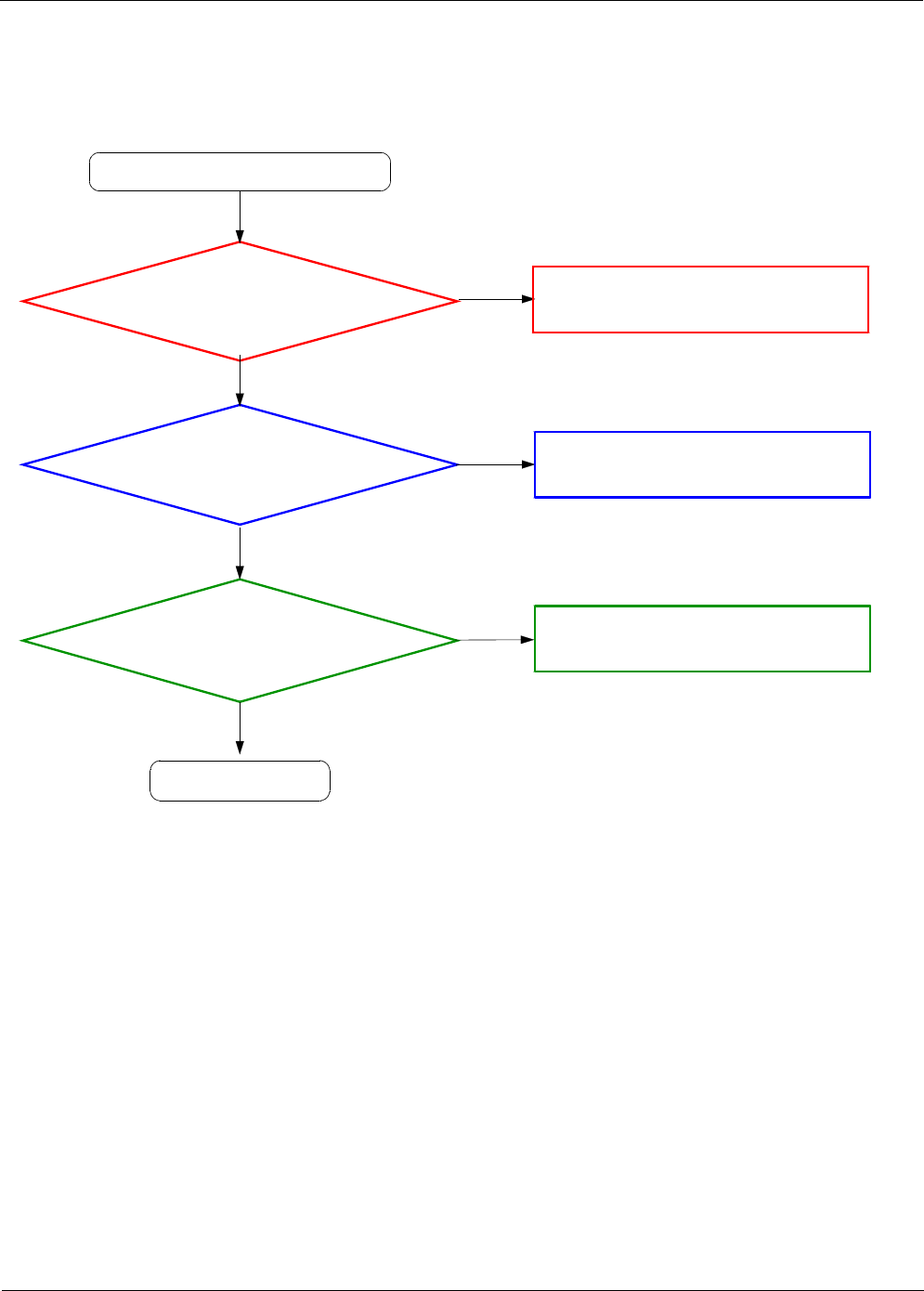
Level 3Repair
Distribution, transmission, or infringement of any content or data from this document without Samsung’s written authorization is strictly prohibited.
Confidential and proprietary-the contents in this service guide subject to change without prior notice.
8-39
2. Acceleration ,Gyro Sensor
Check the Voltage
C238 =2.8V
C239 =2.8V
C237 =1.8V
Abnormal Acceleration,Gyro Sensor part
END
No
Yes
Check the Voltage
R460 =1.8V
R461 =1.8V
No
Yes
Acceleration,Gyro Sensor
operate correctly?
No
Yes
Resolder U205 or heat over U500
Resolder U500 or heat over UCP400
Apply Heat over or Replace U205
using aHeatgun or change PBA
Yes
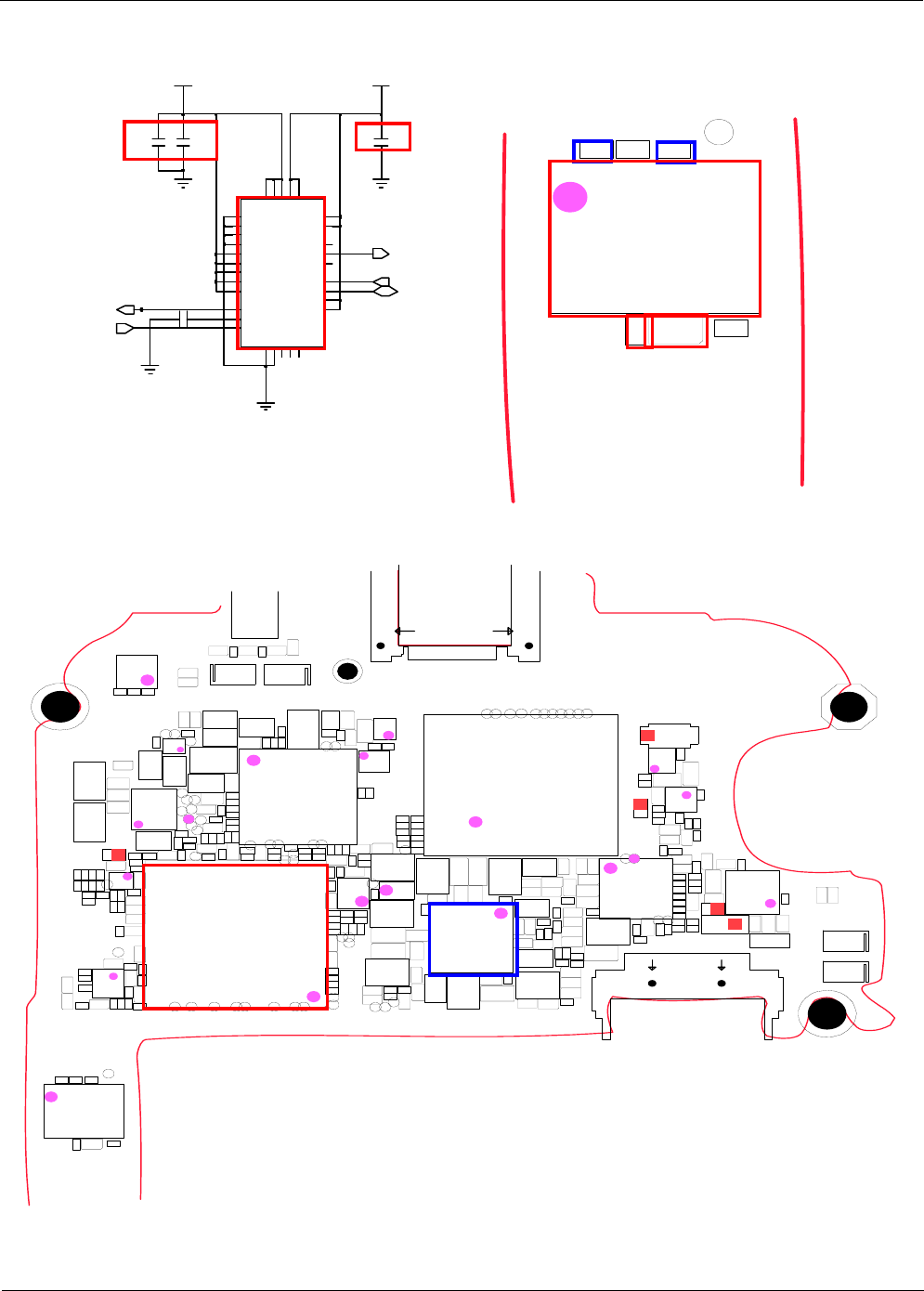
Level 3Repair
Distribution, transmission, or infringement of any content or data from this document without Samsung’s written authorization is strictly prohibited.
Confidential and proprietary-the contents in this service guide subject to change without prior notice.
8-40
6 Axics Sensor
(
GYRO,ACCEL
)
9
VDD21
VDD_IO 25
VDD_IO
RES
4
5RES
SCL_A|G 24
SDA_A|G 28
27
SDO_A
SDO_G 26
7
VDD
VDD
8
31
NC
RES
2
RES
10
11 RES
RES
12
13 RES
RES
14
3RES
17 DRDY_G|INT2_G
1GND
GND
6
INT1_A 20
INT1_G 18
19
INT2_A
29
NC
NC
30
U205
15 CAP
23
CS_A
CS_G 22
DEN_G
16
TP211
C238
VCC_1.8V_AP
C239
VCC_2.8V_AP
C237
C244
ACC_INT
GSENSE_SCL_1.8V
GSENSE_SDA_1.8V
GYRO_DE
GYRO_INT
C237
C238
C239
C244
R460R461
TP211
U205
AP_PMIC_EN
AP_PS_HOLD
BOTHHOLE102
BOTHHOLE104
BOTHHOLE106
BOTHHOLE108
BTC500
C237
C238
C239
C240
C244
C246
C250
C268
C300
C301
C302
C303
C304
C305
C306
C307
C308
C309
C310
C311
C312
C313
C314
C315
C316
C317
C318
C319
C320
C321
C322
C323
C324
C325
C326
C327
C328
C329
C330
C331
C332
C333
C334
C335
C341
C342
C344
C347
C348
C356
C357
C400
C403
C404
C405
C406
C407
C408
C409
C413
C414
C415
C417
C418
C419
C420
C421
C422
C425
C426
C427
C443
C444
C445
C446
C447
C448
C450
C451
C453
C454
C500
C501
C503
C504
C505
C506
C507
C508
C509
C510
C511
C512
C513
C514
C515
C516
C517
C518
C519
C520
C521
C522
C523
C524
C525
C526
C528
C529
C530
C531
C532
C533
C534
C535
C537
C538
C539
C541
C544
C546
C549
C550
C551
C552
C553
C554
C555
C556
C557
C558
C559
C560
C561
C563
C564
C565
C566
C567
C568
C569
C570
C571
C572
C573
C574
C575
C576
C577
C579
C580
C581
C582
C583
C585
C586
C587
C593
C594
C595
C597
C600
C601
C613
C614
C620
C707
C718
C719
C729
C730
C731
C732
C733
C734
C765
C766
C785
D500
D700
F700
FM_RST
IFC700
KEY500
KEY501
L300
L301
L302
L303
L305
L500
L501
L502
L503
L504
L505
L506
L507
L508
L509
L510
L511
L512
L514
L515
L517
L518
L601
L602
L702
L703
L706
L707
MIC600
MOT500
MOT501
OSC400
OSC500
R104
R300
R301
R302
R303
R304
R305
R306
R307
R308
R309
R312
R313
R314
R315
R318
R319
R331
R332
R333
R334
R335
R336
R337
R338
R342
R400
R401
R402
R403
R404
R405
R406
R407
R408
R417R420
R427
R428
R429
R432
R433
R434
R435
R438
R441
R442
R447
R448
R449
R450
R451
R452
R456
R457
R460R461
R464
R465
R468
R469
R470
R471
R473
R474
R475
R476
R483
R500
R501
R502
R503
R504
R505
R507
R512
R513
R515
R516
R517
R518
R519
R526
R532
R533
R534
R708
R709
R717
R741R742
R743
RESET300
TA500
TH300
TH400
TP_AP_D TP_AP_D+
TP_eMMC_EN
TP_TORCH_EN
TP201
TP202
TP207
TP211
TP300
TP301
TP302
TP303
TP304
TP305
TP306
TP307
TP308
TP309
TP310TP311
TP312
TP313
TP314
TP315
TP316
TP317
TP318
TP319
TP320
TP321
TP322
TP324
TP325
TP326
TP327
TP328
TP400
TP401
TP402
TP403
TP501
TP502
TP504
TP505
TP506
TP507
TP508
TP509
TP518
TP519TP708
TP710
U204
U205
U206
U301
U302
U500
U501
U502
U506
U600
U704
U706
U713
U718
U719
UCP300
UCP400
UME300
V600
VIBTONE_PWM
ZD500
ZD502
ZD701
Level 3Repair
Distribution, transmission, or infringement of any content or data from this document without Samsung’s written authorization is strictly prohibited.
Confidential and proprietary-the contents in this service guide subject to change without prior notice.
8-41
3. Barometer Sensor
Check the Voltage
C250 =1.8V
C246 =1.8V
Abnormal Barometer Sensor part
END
No
Yes
Check the Voltage
R432 =1.8V
R433 =1.8V
No
Yes
Barometer Sensor operate
correctly?
No
Yes
Resolder U206 or heat over U500
Resolder U500 or heat over UCP400
Apply Heat over or Replace U206 using a
Heatgun or change PBA
Yes
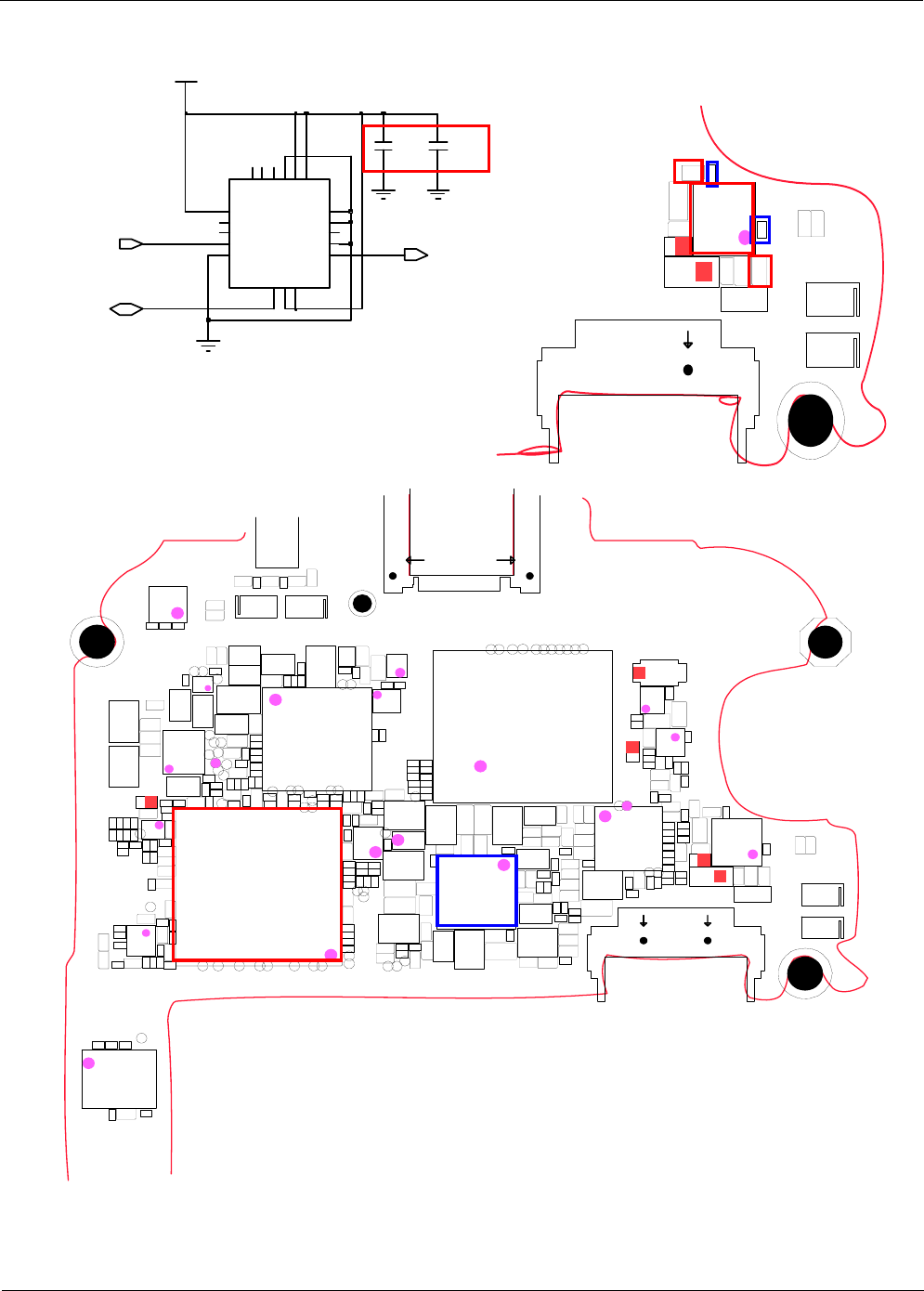
Level 3Repair
Distribution, transmission, or infringement of any content or data from this document without Samsung’s written authorization is strictly prohibited.
Confidential and proprietary-the contents in this service guide subject to change without prior notice.
8-42
Barometer Senso
r
NC19
10
RSVD
RSVD15
4SCL|SPC
6
SDA|SDI|SDO
SDO|SA0
7
14
VDD
VDD_IO
1GND 13
16
GND
INT1 9
INT2 11
2NC
NC
3
NC17
18
NC
U206
8CS
GND
5
12
GND
C246
VCC_1.8V_AP
C250
BARO_INT
BSENSE_SDA_1.8V
BSENSE_SCL_1.8V
BOTHHOLE108
C246
C250
C570
C571
C593
D500
L514
L515
MOT500
MOT501
R432
R433
TA500
U206
ZD500
AP_PMIC_EN
AP_PS_HOLD
BOTHHOLE102
BOTHHOLE104
BOTHHOLE106
BOTHHOLE108
BTC500
C237
C238
C239
C240
C244
C246
C250
C268
C300
C301
C302
C303
C304
C305
C306
C307
C308
C309
C310
C311
C312
C313
C314
C315
C316
C317
C318
C319
C320
C321
C322
C323
C324
C325
C326
C327
C328
C329
C330
C331
C332
C333
C334
C335
C341
C342
C344
C347
C348
C356
C357
C400
C403
C404
C405
C406
C407
C408
C409
C413
C414
C415
C417
C418
C419
C420
C421
C422
C425
C426
C427
C443
C444
C445
C446
C447
C448
C450
C451
C453
C454
C500
C501
C503
C504
C505
C506
C507
C508
C509
C510
C511
C512
C513
C514
C515
C516
C517
C518
C519
C520
C521
C522
C523
C524
C525
C526
C528
C529
C530
C531
C532
C533
C534
C535
C537
C538
C539
C541
C544
C546
C549
C550
C551
C552
C553
C554
C555
C556
C557
C558
C559
C560
C561
C563
C564
C565
C566
C567
C568
C569
C570
C571
C572
C573
C574
C575
C576
C577
C579
C580
C581
C582
C583
C585
C586
C587
C593
C594
C595
C597
C600
C601
C613
C614
C620
C707
C718
C719
C729
C730
C731
C732
C733
C734
C765
C766
C785
D500
D700
F700
FM_RST
IFC700
KEY500
KEY501
L300
L301
L302
L303
L305
L500
L501
L502
L503
L504
L505
L506
L507
L508
L509
L510
L511
L512
L514
L515
L517
L518
L601
L602
L702
L703
L706
L707
MIC600
MOT500
MOT501
OSC400
OSC500
R104
R300
R301
R302
R303
R304
R305
R306
R307
R308
R309
R312
R313
R314
R315
R318
R319
R331
R332
R333
R334
R335
R336
R337
R338
R342
R400
R401
R402
R403
R404
R405
R406
R407
R408
R417R420
R427
R428
R429
R432
R433
R434
R435
R438
R441
R442
R447
R448
R449
R450
R451
R452
R456
R457
R460R461
R464
R465
R468
R469
R470
R471
R473
R474
R475
R476
R483
R500
R501
R502
R503
R504
R505
R507
R512
R513
R515
R516
R517
R518
R519
R526
R532
R533
R534
R708
R709
R717
R741R742
R743
RESET300
TA500
TH300
TH400
TP_AP_D TP_AP_D+
TP_eMMC_EN
TP_TORCH_EN
TP201
TP202
TP207
TP211
TP300
TP301
TP302
TP303
TP304
TP305
TP306
TP307
TP308
TP309
TP310TP311
TP312
TP313
TP314
TP315
TP316
TP317
TP318
TP319
TP320
TP321
TP322
TP324
TP325
TP326
TP327
TP328
TP400
TP401
TP402
TP403
TP501
TP502
TP504
TP505
TP506
TP507
TP508
TP509
TP518
TP519TP708
TP710
U204
U205
U206
U301
U302
U500
U501
U502
U506
U600
U704
U706
U713
U718
U719
UCP300
UCP400
UME300
V600
VIBTONE_PWM
ZD500
ZD502
ZD701

Level 3Repair
Distribution, transmission, or infringement of any content or data from this document without Samsung’s written authorization is strictly prohibited.
Confidential and proprietary-the contents in this service guide subject to change without prior notice.
8-43
4. RGB Sensor
Check the Voltage
R703 =2.8V
C703 =2.8V
Abnormal RGB Sensor part
END
No
Yes
Check the Voltage
R451 =1.8V
R452 =1.8V
No
Yes
Barometer Sensor operate
correctly?
No
Yes
Resolder U703,R703 or heat over U500
Resolder U500 or heat over UCP400
change VT camera assenbly
Yes
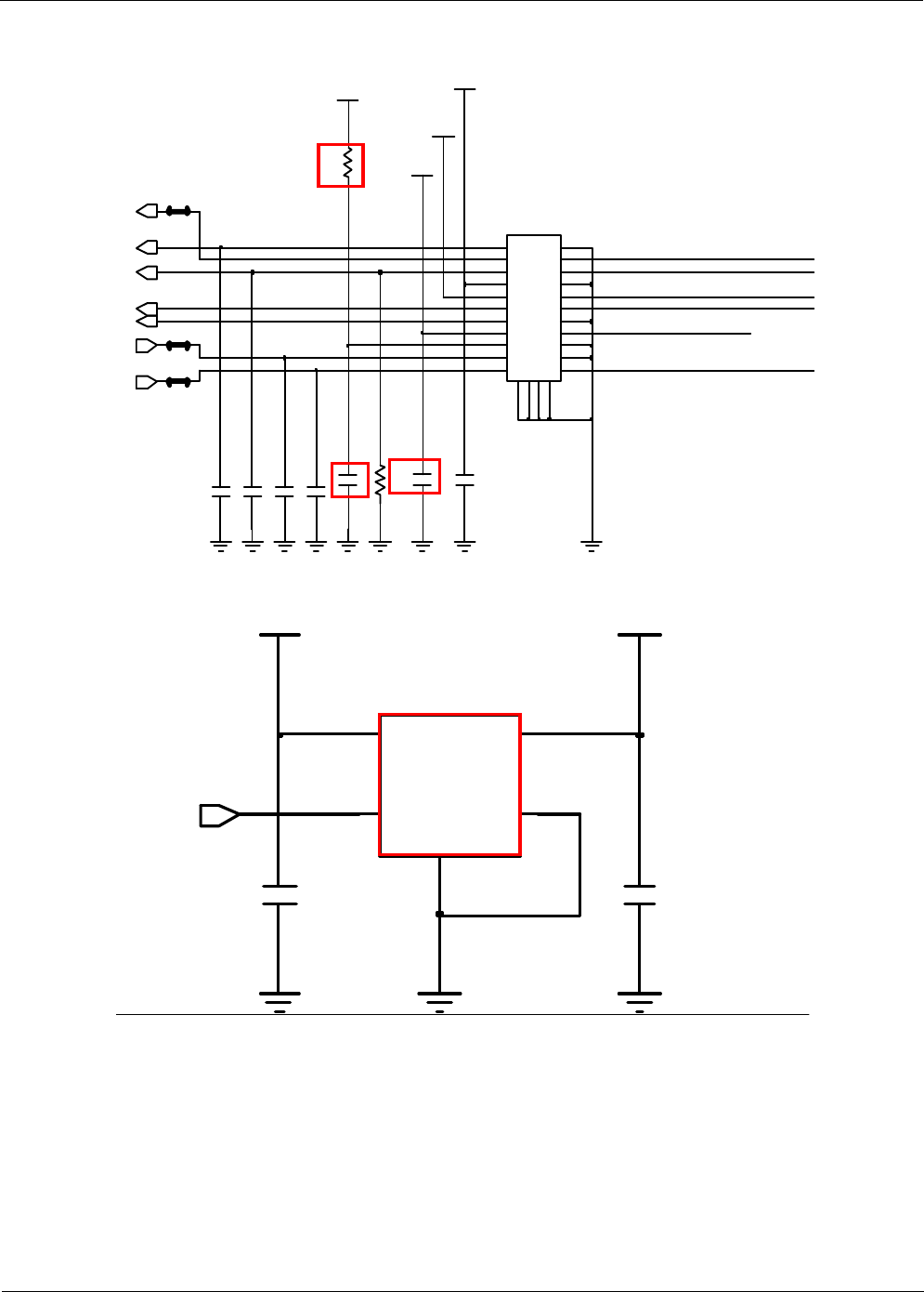
Level 3Repair
Distribution, transmission, or infringement of any content or data from this document without Samsung’s written authorization is strictly prohibited.
Confidential and proprietary-the contents in this service guide subject to change without prior notice.
8-44
C767
R707OPEN
C769
C705
VCC_2.8V_AP
LED_A_2.8V
R703
C770
CAM_SENSOR_A2.8V
C703
26NC
55 6 6
77 8
8
99
NC
23
24NC
NC
25
18 18
1919
22
20
20
21 21 22 22
334
4
10 10
1111 12
12
13 13 14 14
1515 16
16
17 17
HEA700
11
C702
C768
VT_CAM_1.8V
VT_CAM_SDA_1.8V
VT_CAM_SCL_1.8V
RGB_SDA_1.8V
RGB_SCL_1.8V
RGB_INT
VT_CAM_ID
CAM_VT_nRST
V_BAT
C716 C717
U703
3CE
GND
5
GND 2
4VDD 1
VOUT
LED_A_2.8V
CAM_IO_ENRGB_EN
Level 3Repair
Distribution, transmission, or infringement of any content or data from this document without Samsung’s written authorization is strictly prohibited.
Confidential and proprietary-the contents in this service guide subject to change without prior notice.
8-45
8-3-13. NFC
NFC is not working
Check the Battery
(NFC Antenna is in Battery)
No Check the battery
(antenna/contact crack, open, damaged)
Yes
END
Check the Voltage on
NFC_VEN, NFC_IRQ
goes high
No Check the R225, TP210
Yes
Check 27.12MHz Clock on
OSC202 at R217
No Check the OSC202(crack, open, etc.)
Yes
Check the Voltage on C247,
C251 goes high(1.8V)
No Resolder or Replace U207
Yes
Yes
Level 3Repair
Distribution, transmission, or infringement of any content or data from this document without Samsung’s written authorization is strictly prohibited.
Confidential and proprietary-the contents in this service guide subject to change without prior notice.
8-46
Level 3Repair
Distribution, transmission, or infringement of any content or data from this document without Samsung’s written authorization is strictly prohibited.
Confidential and proprietary-the contents in this service guide subject to change without prior notice.
8-47
Level 3Repair
Distribution, transmission, or infringement of any content or data from this document without Samsung’s written authorization is strictly prohibited.
Confidential and proprietary-the contents in this service guide subject to change without prior notice.
8-48
8-3-14. MHL
MHL Does not work
Yes
No
Check if HDMI Adaptor is well connected
Check if HDMI_EN
(U712 PIN 3) goes High
Yes
No
Resolder or change F702
Check the voltage of
C763(1.2V), C753(3.3V),
C754(1.8V)
Yes
Check the MHL Signal of
F702
Replace U708
Yes
No
Check the LDOs(U712, U710)
END
Yes
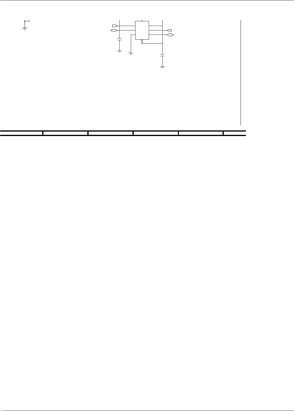
Level 3Repair
Distribution, transmission, or infringement of any content or data from this document without Samsung’s written authorization is strictly prohibited.
Confidential and proprietary-the contents in this service guide subject to change without prior notice.
8-49
MMON_FILTER
74
C752
VCCA1
8
VCCB
2A0
A1
3B0 7
6
B1
4GND
OE
5
C751
MHL_DSCL_1.8V
MHL_DSDA_1.8V MHL_DSCL_3.3V
MHL_DSDA_3.3V
MHL PART
(
Near I/F CON.)
85
9
6
O
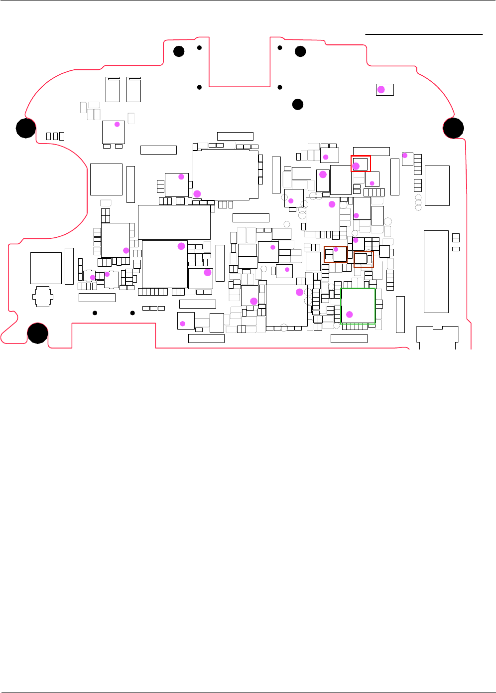
Level 3Repair
Distribution, transmission, or infringement of any content or data from this document without Samsung’s written authorization is strictly prohibited.
Confidential and proprietary-the contents in this service guide subject to change without prior notice.
8-50
ANT102
ANT103
BAT500
C101
C102C104
C107
C108 C109
C110
C112
C113
C114
C115
C116C117
C118
C119
C120
C122
C123
C124
C125
C126
C127
C128
C129
C130
C131
C132C133
C134
C135
C136
C137
C138
C139
C140
C141
C142
C143
C144
C145
C146
C147
C148
C149
C150
C152
C153
C154
C156
C157
C158
C159
C160
C161
C163
C164
C170
C171
C172
C173
C174
C175
C176
C177
C178
C179
C180
C181
C182
C183
C184
C185
C186
C187
C188
C189
C190
C191
C192
C193
C195
C196
C197
C198
C241
C242
C243
C245
C247
C248
C249
C251
C252
C253
C254
C255
C256
8
5
2
C
7
5
2
C
C259
C260
C261
C262
C263
C336
C337
C338
C339
C340
C343
C349
C350
C351
C401
C402
C410
C411
C412
C416
C424
C428
C429
C430
C431
C432
C433
C434
C435
C436
C437
C438
C439
C440
C441
C442
C449
C502
C527
C536
C540
C542
C543
C545
C547
C548
C578
C607
C608
C611
C612
C621
C622
C708
C712
C713
C720
C721
C722
C723
C724
C725
C726
C727
C728
C735
C736
C740
C750
C751
C752
C753
C754
C763
C764
C786
C787
C788
C790
F100
F101
F702
HDC300
HDC702
L102
L103
L104
L105
L106
L107
L108
L109
L110
L111
L112
L113
L114
L115
L116
L117
L118
L119
L120
L121
L122
L124
L125
L126
L127
L128
L129
L130
L131
L132
L133
L209
L210
L704
L705
L708
OSC100
OSC202
Q200
Q201
R101
R102
R105
R106
R107
R108
R109
R110
R111
R112
R113
R114
R115
R116
R117
R217
R218
R219
R220
R222
R224
R225
R310
R311
R320
R321
R322
R323
R324
R325
R326
R327
R328
R329
R330
R339
R340
R341
R410
R411
R412
R413
R414
R415
R416
R418
R419
R421
R430
R431
R436
R437
R443
R444
R445
R446
R453
R454
R458
R459
R466
R467
R472
R482
R511
R612
R614
R616
R622
R700
R701
R702 R705
R706
R716
R718
R719
R720
R721
R722
R723
R724
R725
R726
R727
R728
R729
R730
R731
R732
R744
R745
R746
R747
R748
R749
R750
R751
R752
R753
RFS100
RFS101
RFS102
SC300
SC301
SC302
SC304 SC305
SC306
SC307
SC309
SC310
SC311
SC312
SC313
SC314
SC315
TA700
TH401
TP_100
TP_329
TP_330
TP_331
TP_600
TP_601
TP_602
TP_603TP_604
TP_605
TP_607
TP_GPS_EN
TP208
TP209
TP210
TP323
TP517
TP704
TP705
TP711
U101
U102
U103
U104
U105
U106
U107
U108
U207
U401
U504
U604
U606
U700
U707
U708
U709
U710
U712
U714
U715
V100
V101
ZD300
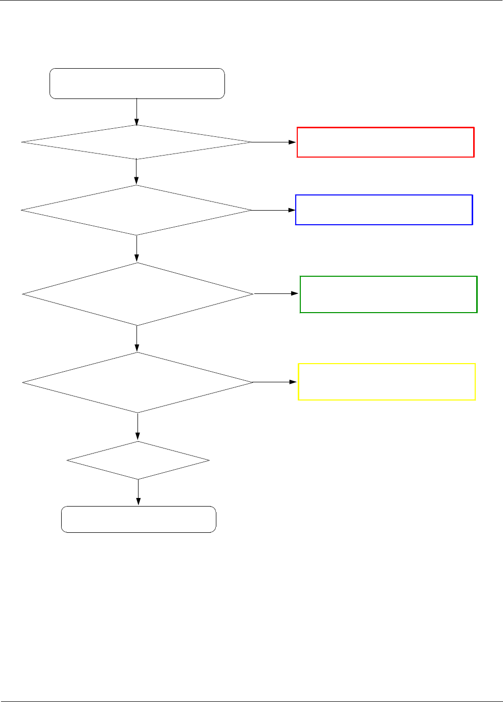
Level 3Repair
Distribution, transmission, or infringement of any content or data from this document without Samsung’s written authorization is strictly prohibited.
Confidential and proprietary-the contents in this service guide subject to change without prior notice.
8-51
8-3-15. LCD
LCD is still off after PWR ON
Yes
No
Reconnect the HDC 702
Check the connection of
HDC 702
Yes
END
No
Resolder or Replace the U707
Check VCC_3.3V_LCD =
3.3V(C549)
Yes
Check VCC_2.2V_LCD =
2.2V(C735)
Yes
Yes
Replace LCD
Module
No
Resolder or Replace the PMIC(U500)
Yes
Check ELVDD_4.6V =
4.6V(C713), ELVSS_-4.9V =
3.0~4.4V(C712)
Resoldering L703, L706
Resoldering U706
No
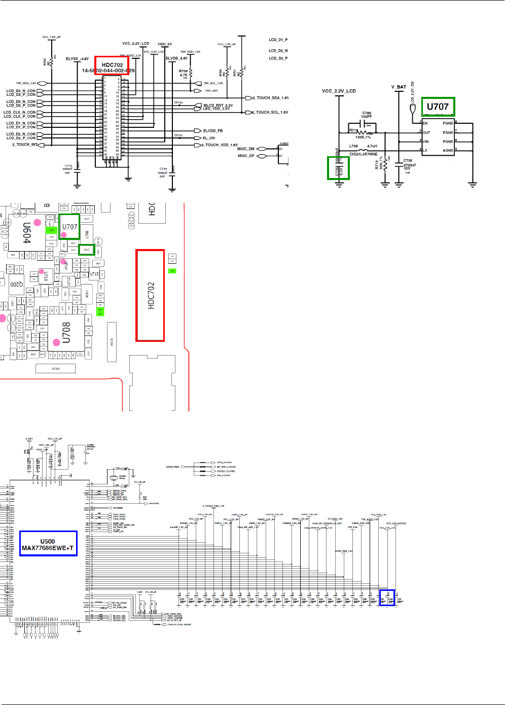
Level 3Repair
Distribution, transmission, or infringement of any content or data from this document without Samsung’s written authorization is strictly prohibited.
Confidential and proprietary-the contents in this service guide subject to change without prior notice.
8-52
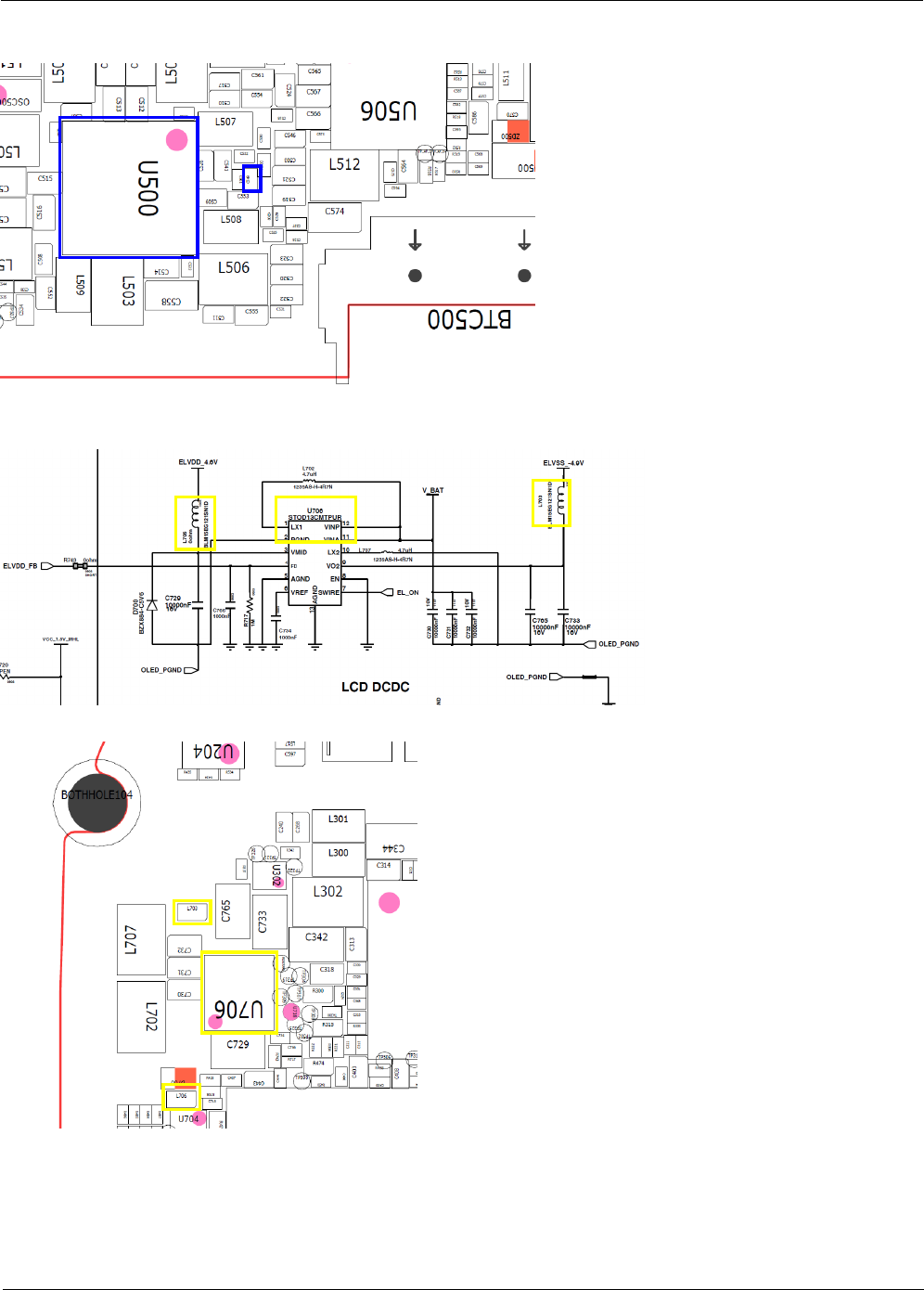
Level 3Repair
Distribution, transmission, or infringement of any content or data from this document without Samsung’s written authorization is strictly prohibited.
Confidential and proprietary-the contents in this service guide subject to change without prior notice.
8-53
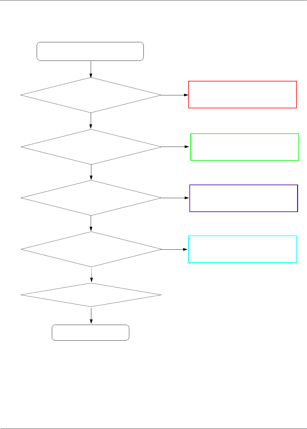
Level 3Repair
Distribution, transmission, or infringement of any content or data from this document without Samsung’s written authorization is strictly prohibited.
Confidential and proprietary-the contents in this service guide subject to change without prior notice.
8-54
8-3-16. TSP
Touch Screen does not work
Yes
No
Reconnect the HDC702
Check TSP Connector on
Main PBA
Yes
END
Yes
No
Reconnect TSP Connector
Check the TSP connector on
LCD Module
Yes
Replace LCD Module
Yes
Check the I2C signal(R466,
R467) and int signal(R706)
Yes
Resolder R466, R467, R706
No
No
U500
TSP_VDD_1.8V(R706,C548)
and TSP_AVDD_3.3V(C547) Resolder or Replace U500
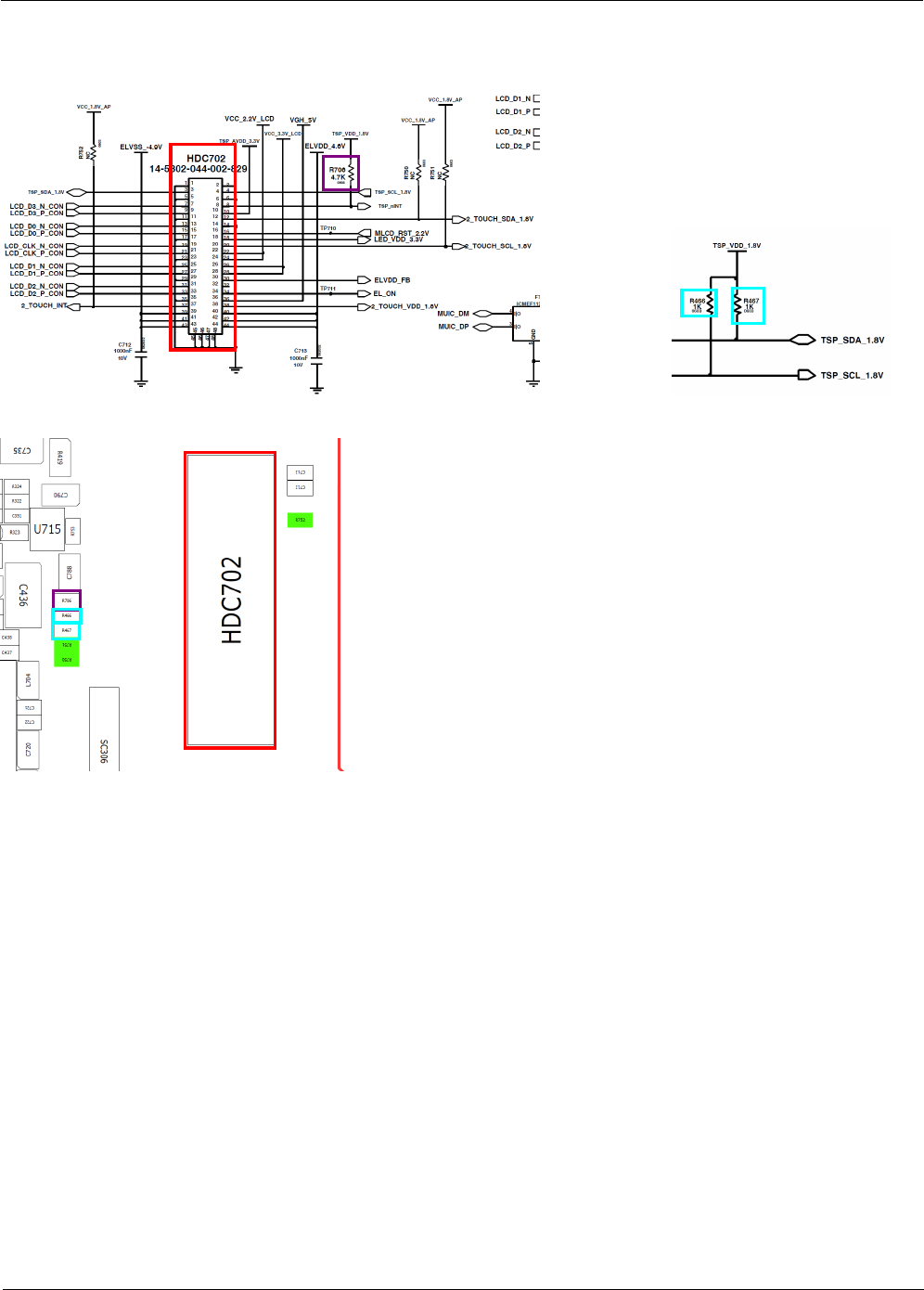
Level 3Repair
Distribution, transmission, or infringement of any content or data from this document without Samsung’s written authorization is strictly prohibited.
Confidential and proprietary-the contents in this service guide subject to change without prior notice.
8-55
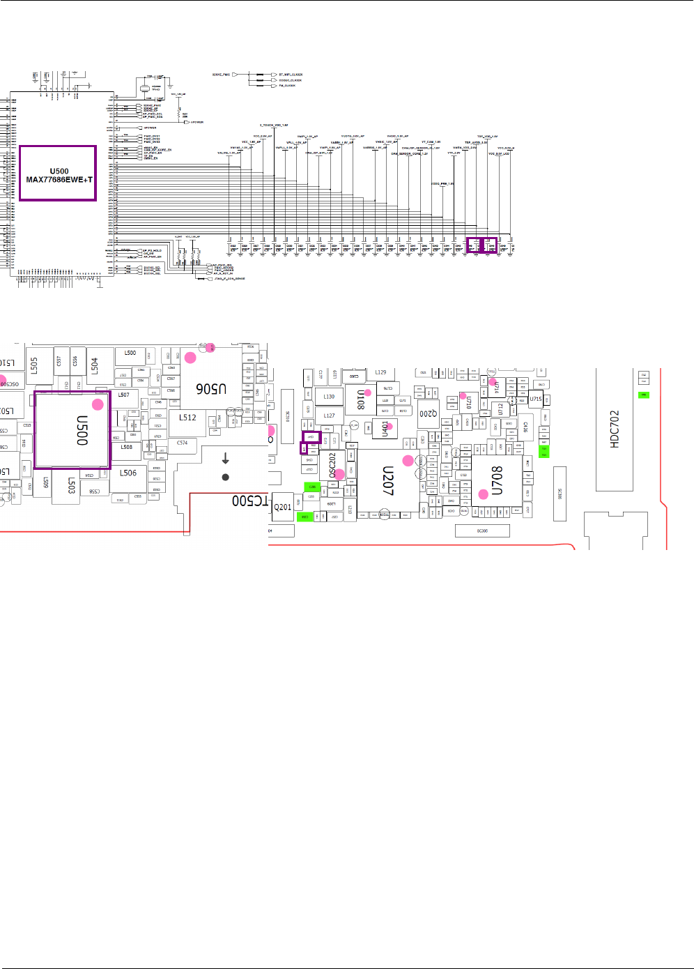
Level 3Repair
Distribution, transmission, or infringement of any content or data from this document without Samsung’s written authorization is strictly prohibited.
Confidential and proprietary-the contents in this service guide subject to change without prior notice.
8-56
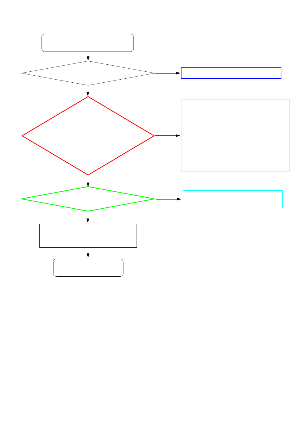
Level 3Repair
Distribution, transmission, or infringement of any content or data from this document without Samsung’s written authorization is strictly prohibited.
Confidential and proprietary-the contents in this service guide subject to change without prior notice.
8-57
8-3-17. 8M CAM
Check the Camera
connector on Main PBA Reconnect the HDC701
No
Check the voltage
C706 =2.8V
C709 =2.8V
C710 =1.8V
C711 =1.2V
C760 =1.2V
C743 =1.2V
Resolder U500, U711, U701, U702
Resolder C706, C709, C710, C711, C760,
C743
No
Yes
Resolder R455
Replace the PBA.
Check R455 is 24MHz
Yes
END
Replace the camera module
"Camera" function does not work
No
Yes
Abnormal
Yes
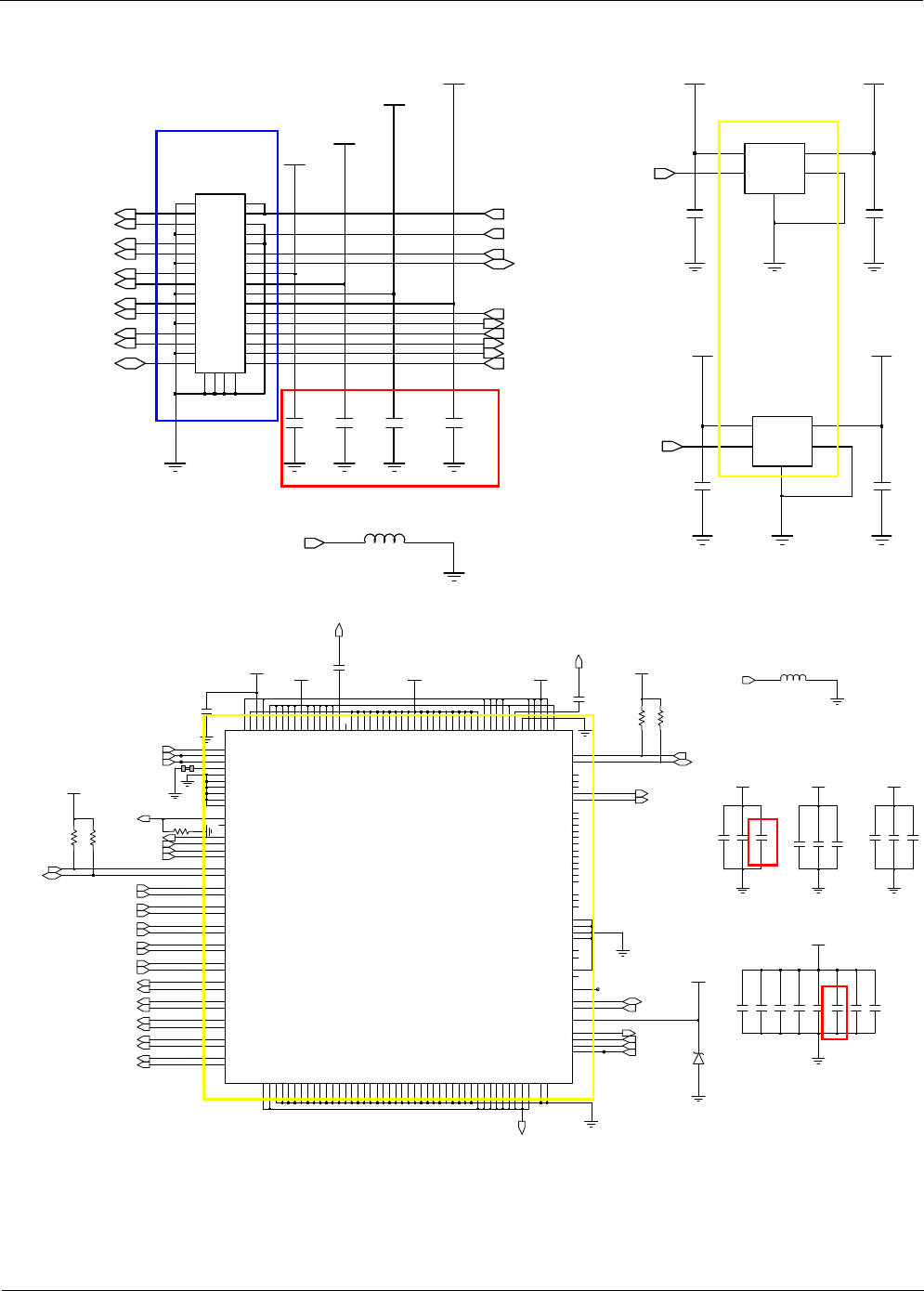
Level 3Repair
Distribution, transmission, or infringement of any content or data from this document without Samsung’s written authorization is strictly prohibited.
Confidential and proprietary-the contents in this service guide subject to change without prior notice.
8-58
GND
2
GND
5
4VIN 1
VOUT
U702
EN
3
V_BAT
C714
CAM_SENSOR_A2.8V
EN
3
GND
2
GND
5
4VIN VOUT 1
U701
C701C700
CAM_AF_2.8V
C715
V_BAT
CAM_AF_EN
CAM_IO_EN
L700
CAM_AF_2.8V
99
NC
35 36
NC
37
NC NC
38
32
32
33 33 34 34
44
5566
77 88
25 25 26
26
27
27 28
28
29
29
33
30
30
31 31
18
19 19
22
20
20
21 21 22 22
23 23 24
24
10
1111 12 12
13
13 14
14
15
15 16
16
17
17 18
HDC701
11
10
CAM_SENSOR_A2.8V
C706
CAM_SENSOR_CORE_1.2V
C709
CAM_ISP_SENSOR_IO_1.8V
C710 C711
8M_CAM_SEN_D0_N
8M_CAM_SEN_D1_P
CIS_SDA_1.8V
8M_CAM_SEN_D1_N
8M_CAM_SEN_D2_P
8M_CAM_SEN_D2_N
8M_CAM_SEN_D3_P
8M_CAM_SEN_D3_N
8M_CAM_SEN_D0_P
CIS_SPI_MISO
CIS_SPI_MOSI
CIS_SPI_SCLK
CIS_SPI_SSN
CIS_SCL_1.8V
CAM_MCLK
8M_CAM_SEN_CLK_P
8M_CAM_SEN_CLK_N
AF_SDA
AF_SCL
CAM_AGND
8M_CIS_RESET
CAM_AGND
C747
CAM_ISP_CORE_1.2V
C742
TP706
C743
C744
R733
C738
CAM_ISP_SENSOR_IO_1.8V
N7 TX_CLKN
N8
TX_DATA2N
N9 TX_DATA3N
N11
GPIO2
N12
VDDIO_HOST
N13
VSSIO_HOST
N2
VDD_OTP
N3
VDDIO_OTP
N4
VDD_REG
N5
TX_DATA0N
N6 TX_DATA1N
M4
REG_VSS25
M5
TX_DATA0P
M6
TX_DATA1P
M7
TX_CLKP
M8
TX_DATA2P
M9
TX_DATA3P
N1
VPP_OTP
N10
GPIO0
L9
M_VDD18
M1VSSIO_HOST
M10
GPIO1
M11
GPIO3
M12
VDD_RPLL
M13
VDD_IPLL
M2
I2CS_ID
M3
UART_TX
L13
EXTCLK
L2
UART_RX
L3
AF_SDA
L4INT_VSS12
L5
M_VDD11L6
M_VDD11L7
M_VDD11
L8
M_VDD11
K6
M_VSS11
K7
M_VSS11
K8
M_VSS11
K9
INT_VDD12
L1
VDDIO_HOST
L10
GPIO4
L11VSS_PLL1
L12
VSS_PLL2
K10
INT_VDD12
K11 STANDBY
K12 REGPD
K13
XSHUTDOWN
K2
VDDIO_HOST
K3
INT_VDD12
K4
INT_VSS12
K5M_VSS11
J3
INT_VDD12
J4INT_VSS12
J5
INT_VSS12
J6
INT_VSS12
J7
M_VREG_0P4V
J8
INT_VSS12J9
INT_VDD12
K1
AF_SCL
H8INT_VSS12
H9
INT_VDD12
J1
VSSIO_HOST
J10VSSIO_HOST
J11
VDDIO_HOST
J12
TEST_EN
J13
PGBYPASS
J2
CIS_XSHUTDOWN
H12 TEST2
H13 TEST3
H2 CIS_SCL
H3
INT_VDD12
H4INT_VSS12
H5
INT_VSS12
H6
INT_VSS12
H7
INT_VSS12
G5
INT_VSS12
G6
INT_VSS12
G7INT_VSS12
G8INT_VSS12
G9
INT_VDD12
H1 CIS_SDA
H10
TEST0
H11
TEST1
G1
CIS_SSN
G10
VSSIO_HOST
G11
VDDIO_HOST
G12
POUT_VSYNC
G13
POUT_PCLK
G2
CIS_SCLK
G3
INT_VDD12
G4
INT_VSS12
F2 CIS_MISO
F3
INT_VDD12
F4
INT_VSS12
F5
INT_VSS12
F6
INT_VSS12
F7INT_VSS12
F8INT_VSS12
F9
INT_VDD12
E7
INT_VDD12
E8
INT_VDD12
E9
INT_VDD12
F1 CIS_MOSI
F10
POUT_HSYNC
F11
POUT_DATA1 F12
POUT_DATA2
F13
POUT_DATA0
VDDIO_HOST
E12
POUT_DATA4
E13
POUT_DATA3
E2
VDDIO_CIS
E3
INT_VDD12
E4
INT_VDD12E5
INT_VDD12E6
INT_VDD12
INT_VDD12
D5S_VSS11
D6S_VSS11
D7S_VSS11
D8
S_VSS11
D9
INT_VDD12
E1VSSIO_CIS
E10
VSSIO_HOST
E11
C9
S_VDD18
D1
VSSIO_CIS
D10
INT_VDD12
D11
POUT_DATA7
D12
POUT_DATA6
D13
POUT_DATA5
D2
VDDIO_CIS
D3
CIS_EXTCLK
D4
C13
POUT_DATA8
C2
VDDIO_CIS
C3
TCK
C4
HOST_SDA
C5
S_VDD11C6
S_VDD11
C7
S_VDD11
C8
S_VDD11
B6 RX_DATA2P
B7
RX_CLKP
B8
RX_DATA1P
B9 RX_DATA0P
C1
VSSIO_CIS
C10VSSIO_HOST
C11
VDDIO_HOST
C12
POUT_DATA9
B10
HOST_SCLK
B11
HOST_MOSI
B12
POUT_DATA10
B13
POUT_DATA11
B2
TDI
B3
RTCK
B4
HOST_SCL
B5
RX_DATA3P
A3VSSIO_HOST
A4
VDDIO_HOST
A5
RX_DATA3N
A6 RX_DATA2N
A7
RX_CLKN
A8
RX_DATA1N
A9 RX_DATA0N
B1
NTRST
1
NC
2
A1
TDO
A10
FSOURCE
A11
HOST_MISO A12
HOST_SSN
A13
MONITOR
A2
TMS
U711
NC
TP708
TP709
C759
CAM_ISP_MIPI_1.2V
C758
CAM_ISP_MIPI_1.2V
C757
C749
CAM_ISP_MIPI_1.2V
TP_SPI_SCLK
CAM_AF_2.8V
C760
C739
C748
C761
C746
ZD700
C756
C745
C741
CAM_ISP_SENSOR_IO_1.8V
R739
R734
CAM_ISP_SENSOR_IO_1.8V
L709
R740
R735
C762
CAM_ISP_SENSOR_IO_1.8V
C755
CAM_ISP_SENSOR_IO_1.8V
C737
R738
CAM_ISP_CORE_1.2V
ISP_FLASH_EN
ISP_FLASH_SET
AGND
AGND
AGND
AGND
8M_CAM_CLK_N
8M_CAM_D2_N
8M_CAM_D3_N
ISP_RESET
CAM_MCLK
AF_SDA
8M_CAM_D0_P
8M_CAM_D1_P
8M_CAM_CLK_P
8M_CAM_D2_P
8M_CAM_D3_P
8M_CAM_D0_N
8M_CAM_D1_N
8M_CAM_SEN_D0_P
8M_CAM_SDA_1.8V
CIS_SPI_MOSI
CIS_SPI_MISO
CIS_SPI_SSN
CIS_SPI_SCLK
CIS_SDA_1.8V
CIS_SCL_1.8V
8M_CIS_RESET
AF_SCL
ISP_STANDBY
CAM_SPI_SSN
8M_CAM_SEN_D3_N
8M_CAM_SEN_D2_N
8M_CAM_SEN_CLK_N
8M_CAM_SEN_D1_N
8M_CAM_SEN_D0_N
CAM_SPI_SCLK
CAM_SPI_MOSI
8M_CAM_SCL_1.8V
8M_CAM_SEN_D3_P
8M_CAM_SEN_D2_P
8M_CAM_SEN_CLK_P
8M_CAM_SEN_D1_P
CAM_SPI_MISO
Level 3Repair
Distribution, transmission, or infringement of any content or data from this document without Samsung’s written authorization is strictly prohibited.
Confidential and proprietary-the contents in this service guide subject to change without prior notice.
8-59
C542
2_TOUCH_VDD_1.8V
VM1M2_1.2V_AP VMEM_VDD_2.8V
C532
CAM_ISP_MIPI_1.2V
C550
VPLL_1.0V_AP
VALIVE_1.0V_AP
C536
VT_CAM_1.8V
C535
VMIPI_1.0V_AP VHSIC_1.8V_AP
VHSIC_1.0V_AP
C525 C534C531
CAM_SENSOR_CORE_1.2V
C548
VTF_2.8V
C547C544C541C538
VCC_1.8V_AP
BATT
XIN
PGND2B
LX2B
INB2B
INB2A
LX2A
INB2B
INB2A
LX2A
NC
PGND2A
INB8
NC
LX9
PGND2A
BUCK8
LX8
INB9
BATT
XOUT
PGND2B
LX2B
NC
32KHCP
VCCP32KH
VCOIN
NC
SNS2N
SNS2P
PGND9
SELB4
SCL
SDA
PGND4B
BUCK2
NC
PGND8
PGND4B
SNS3N
INB3
INB3
LX4B
BUCK9
VCC32KCP
P32KH
32KHZAP
SNS4N
VSETB51
VSETB52
SELB2
SELB3
DVS3
PWRREQ
LX4B
MRSTB2
DVS2
VIO
INB4B
SNS3P
LX3
LX3
INB4B
BUCK3
PGND3
PGND3
INB4A
SNS4P
JIGONB
PWRON
PWRHOLD
BUCK4
ACOKB
RESETB
IRQB
MRSTB1
DVS1
DGND
INB4A
ONOB
OUT24
E8
OUT16
E9
LX4A
AGND2
AGND1
AGND1
LX4A
OUT20 E10
BUCK5
INB5
PGND4A
ENL21
ENL22
OUT26 E5
OUT19 E6
ENL20
OUT15
D4
OUT6
D5
OUT18
D6
OUT23
D7
OUT12
D8
OUT14 D9
PGND4A
OUT25 C7
OUT4
C8
OUT13
C9
LX1
OUT11
D10
BUCK7
LX5
INB1
OUT9 C10
INB7
PGND5
BUCK1
ENB8
OUT7 C4
OUT1
C5
OUT5
C6
ENB9
OUT2
B4
OUT8 B5
OUT17
B6
OUT22
B7
OUT21
B8
OUT10
B9
PGND1
INL6
INL4
INL5
INB6
OUT3 B10
INB7
LX7
BUCK6
INL3
PGND7
NC
LX6
PGND6
INL7
INL1
INL2
U500
NC
NC
NC
VCC_3.0V_MOTOR
C533 C539
CAM_ISP_CORE_1.2V
VMPLL_1.0V_AP
C549C543
VMIPI_1.8V_AP
C551
C526 C540
VCC_2.8V_AP
TSP_AVDD_3.3V
C528 C546
TSP_VDD_1.8V
C545
VUOTG_3.0V_AP
CAM_ISP_SENSOR_IO_1.8V
C527
VCC_3.3V_LCD
C530
VABB1_1.8V_AP
VDDQ_PRE_1.8V
VABB02_1.8V_AP
C537C529
BUCK9_GND
C206
C207
C209
C210
C219
C452
C631
C632
C634
C635
C636C640
C642
C644
C706
C709
C710
C711
C737
C738C739
C741
C742
C743
C744
C745
C746
C747
C748
C749
C755
C756
C757
C758
C759
C760
C761
C762
F200
HDC701
L200
L202
L603
L609
L610
L616
L700
L709
R201
R455
R462
R463
R618
R620
R631
R733
R734
R735
R738
R739
R740
SC700
TA600
TP_SPI_SCLK
TP706
U200
U711
V601
ZD700
Level 3Repair
Distribution, transmission, or infringement of any content or data from this document without Samsung’s written authorization is strictly prohibited.
Confidential and proprietary-the contents in this service guide subject to change without prior notice.
8-60
C208
C214
C215
C217
C588
C591
C592
C604C605
C606
C609
C610
C615
C616
C617
C618
C619
C623
C624
C625
C626
C627
C628
C629
C633
C637
C638
C643
C645
C646
C647
C648
C649
C650
C651
C652
C653
C654
C655
C656
C657
C658
C659
C660
C661
C662
C663
C664
C665
C666
C700
C701
C702
C703
C704
C705
C714
C715
C716
C717
C767
C768
C769
C770
HDC600
HDC601
HEA700
L513
L600
L605
L607
L608
L611
L612
L613
L614
L615
L701
LED500
MIC601
R426
R439
R440
R521
R528
R529
R530
R531
R611
R617
R619
R624
R625
R626
R628
R629
R630
R632
R633R634
R703
R704
R707
TP_606
TP_FLASH_SET
TP_ISP_FLASH
TP_TORCH_SET
U505
U509
U603
U605
U607
U608
U701
U702
U703
V602
ZD600
ZD601
ZD602
ZD603
ZD604
ZD605
ZD606
ZD607
ZD608

Level 3Repair
Distribution, transmission, or infringement of any content or data from this document without Samsung’s written authorization is strictly prohibited.
Confidential and proprietary-the contents in this service guide subject to change without prior notice.
8-61
AP_PS_HOLD
C240
C268
C302
C307
C308
C310
C311
C312
C313
C314
C315
C316
C317
C318
C321
C323
C324
C325
C328
C329
C330
C331
C332
C333
C341
C342
C344
C347
C348
C404
C425
C448
C500
C501
C503
C504
C505
C506
C507
C508
C509
C510
C511
C512
C513
C514
C515
C516
C517
C518
C519
C520
C521
C522
C523
C524
C525
C526
C528
C529
C530
C531
C532
C533
C534
C535
C537
C538
C539
C541
C544
C546
C549
C550
C551
C552
C553
C554
C555
C556
C557
C558
C559
C560
C561 C565
C566
C567
C573
C580
C581
C600
C601
C620
C729
C730
C731
C732
C733
C734
C765
C766
C785
F700
L300
L301
L302
L303
L500
L501
L502
L503
L504
L505
L506
L507
L508
L509
L510
L702
L703
L707
OSC400
OSC500
R104
R300
R302
R303
R304
R305
R306
R307
R308
R309
R315
R318
R319
R331
R332
R333
R334
R337
R342
R438
R447
R448
R465
R468
R474
R483
R500
R501
R504
R505
R717
R741R742
R743
RESET300
TH300
TP_eMMC_EN
TP304
TP307
TP308
TP309
TP310TP311
TP312
TP313
TP314
TP317
TP319
TP320
TP321
TP324
TP325
TP326
TP502
TP504
TP506
TP507
TP508
TP519
U302
U500
U600
U706
U713
U718
UCP300
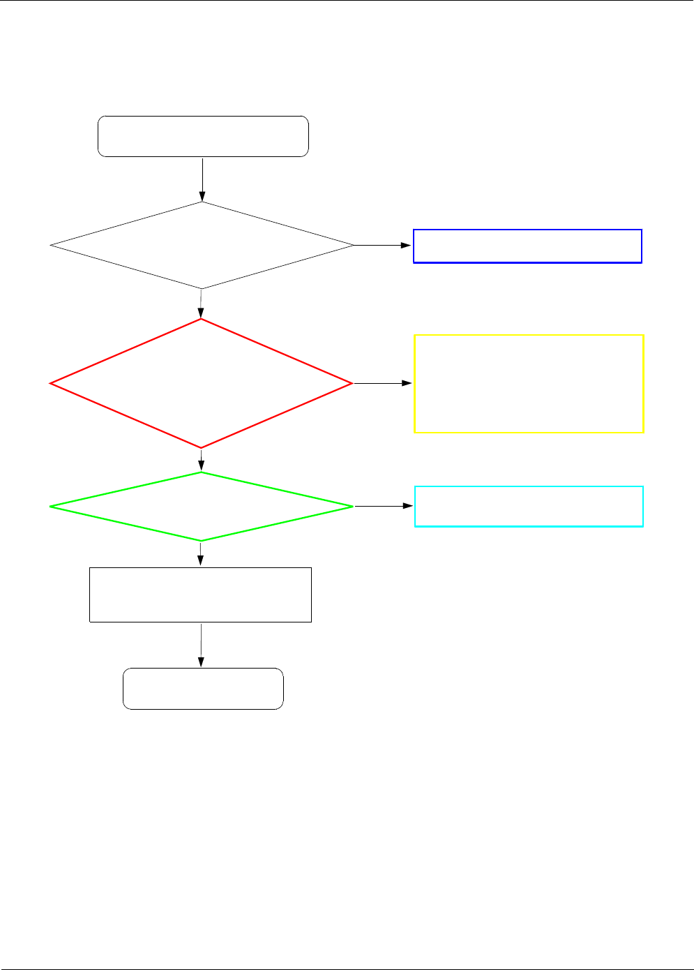
Level 3Repair
Distribution, transmission, or infringement of any content or data from this document without Samsung’s written authorization is strictly prohibited.
Confidential and proprietary-the contents in this service guide subject to change without prior notice.
8-62
8-3-18. 1.9M CAM
Yes
Check the Camera
connector on Main PBA Reconnect the HEA700
No
Check the voltage
C543 =1.8V
C701 =2.8V
No
Yes
Yes
END
Replace the camera module
"Camera" function does not work
No
Yes
Resolder U500, U701
Resolder C542, C701
Check R704 is 24MHz Resolder R704
Replace the PBA.
Abnormal
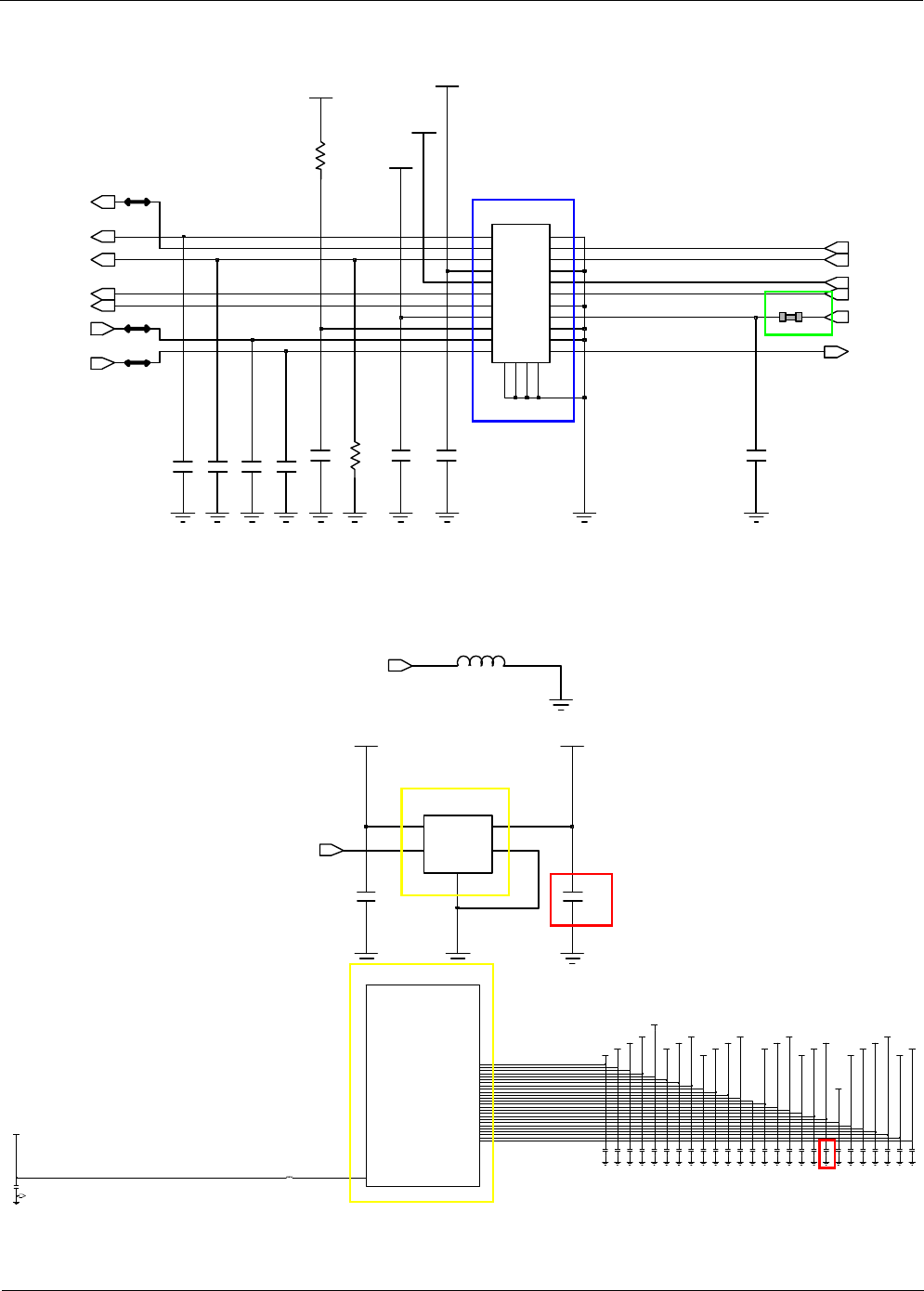
Level 3Repair
Distribution, transmission, or infringement of any content or data from this document without Samsung’s written authorization is strictly prohibited.
Confidential and proprietary-the contents in this service guide subject to change without prior notice.
8-63
L701
VT_CAM_1.8V
V_BAT
R704
C702
88
99
23NC
NC
24
25NC
NC
26
20 20
2121 22
22
33 4
4
55 6
6
77
1313 14
14
15 15 16 16
1717 18
18
19 19
22
HEA700
11
10
10
11 11 12 12
CAM_SENSOR_A2.8V
C703
EN
3
GND
2
GND
5
4VIN VOUT 1
U701
C768
R703
C770
C704
CAM_SENSOR_A2.8V
C701
LED_A_2.8V
C700
C705
VCC_2.8V_AP
C769
R707
C767
VT_CAM_D0_P
VT_CAM_D0_N
VT_CAM_CLK_P
VT_CAM_CLK_N
CAM_IO_EN
VT_CAM_SDA_1.8V
VT_CAM_SCL_1.8V
VTCAM_MCLK
RGB_SDA_1.8V
RGB_SCL_1.8V VT_AGND
RGB_INT
VT_CAM_ID
CAM_VT_nRST
VT_AGND
C542
2_TOUCH_VDD_1.8V
VM1M2_1.2V_AP VMEM_VDD_2.8V
C532
CAM_ISP_MIPI_1.2V
C550
VPLL_1.0V_AP
VALIVE_1.0V_AP
C536
VT_CAM_1.8V
C535
VMIPI_1.0V_AP VHSIC_1.8V_AP
VHSIC_1.0V_AP
C525 C534C531
CAM_SENSOR_CORE_1.2V
C548
VTF_2.8V
C547C544C541C538
VCC_1.8V_AP
BATT
XIN
PGND2B
LX2B
INB2B
INB2A
LX2A
INB2B
INB2A
LX2A
NC
PGND2A
INB8
NC
LX9
PGND2A
BUCK8
LX8
INB9
BATT
XOUT
PGND2B
LX2B
NC
32KHCP
VCCP32KH
VCOIN
NC
SNS2N
SNS2P
PGND9
SELB4
SCL
SDA
PGND4B
BUCK2
NC
PGND8
PGND4B
SNS3N
INB3
INB3
LX4B
BUCK9
VCC32KCP
P32KH
32KHZAP
SNS4N
VSETB51
VSETB52
SELB2
SELB3
DVS3
PWRREQ
LX4B
MRSTB2
DVS2
VIO
INB4B
SNS3P
LX3
LX3
INB4B
BUCK3
PGND3
PGND3
INB4A
SNS4P
JIGONB
PWRON
PWRHOLD
BUCK4
ACOKB
RESETB
IRQB
MRSTB1
DVS1
DGND
INB4A
ONOB
OUT24
E8
OUT16
E9
LX4A
AGND2
AGND1
AGND1
LX4A
OUT20 E10
BUCK5
INB5
PGND4A
ENL21
ENL22
OUT26 E5
OUT19 E6
ENL20
OUT15
D4
OUT6
D5
OUT18
D6
OUT23
D7
OUT12
D8
OUT14 D9
PGND4A
OUT25 C7
OUT4
C8
OUT13
C9
LX1
OUT11
D10
BUCK7
LX5
INB1
OUT9 C10
INB7
PGND5
BUCK1
ENB8
OUT7 C4
OUT1
C5
OUT5
C6
ENB9
OUT2
B4
OUT8 B5
OUT17
B6
OUT22
B7
OUT21
B8
OUT10
B9
PGND1
INL6
INL4
INL5
INB6
OUT3 B10
INB7
LX7
BUCK6
INL3
PGND7
NC
LX6
PGND6
INL7
INL1
INL2
U500
NC
NC
NC
VCC_3.0V_MOTOR
C533 C539
CAM_ISP_CORE_1.2V
VMPLL_1.0V_AP
C549C543
VMIPI_1.8V_AP
C551
C526 C540
VCC_2.8V_AP
TSP_AVDD_3.3V
C528 C546
TSP_VDD_1.8V
C545
VUOTG_3.0V_AP
CAM_ISP_SENSOR_IO_1.8V
C527
VCC_3.3V_LCD
C530
VABB1_1.8V_AP
VDDQ_PRE_1.8V
VABB02_1.8V_AP
C537C529
BUCK9_GND
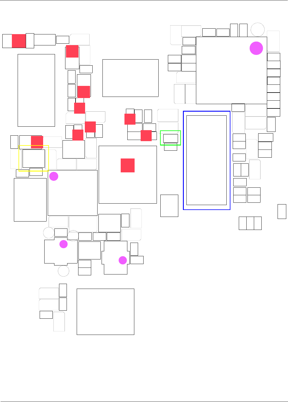
Level 3Repair
Distribution, transmission, or infringement of any content or data from this document without Samsung’s written authorization is strictly prohibited.
Confidential and proprietary-the contents in this service guide subject to change without prior notice.
8-64
C208
C214
C215
C217
C588
C591
C592
C604C605
C606
C609
C610
C615
C616
C617
C618
C619
C623
C624
C625
C626
C627
C628
C629
C633
C637
C638
C643
C645
C646
C647
C648
C649
C650
C651
C652
C653
C654
C655
C656
C657
C658
C659
C660
C661
C662
C663
C664
C665
C666
C700
C701
C702
C703
C704
C705
C714
C715
C716
C717
C767
C768
C769
C770
HDC600
HDC601
HEA700
L513
L600
L605
L607
L608
L611
L612
L613
L614
L615
L701
LED500
MIC601
R426
R439
R440
R521
R528
R529
R530
R531
R611
R617
R619
R624
R625
R626
R628
R629
R630
R632
R633R634
R703
R704
R707
TP_606
TP_FLASH_SET
TP_ISP_FLASH
TP_TORCH_SET
U505
U509
U603
U605
U607
U608
U701
U702
U703
V602
ZD600
ZD601
ZD602
ZD603
ZD604
ZD605
ZD606
ZD607
ZD608
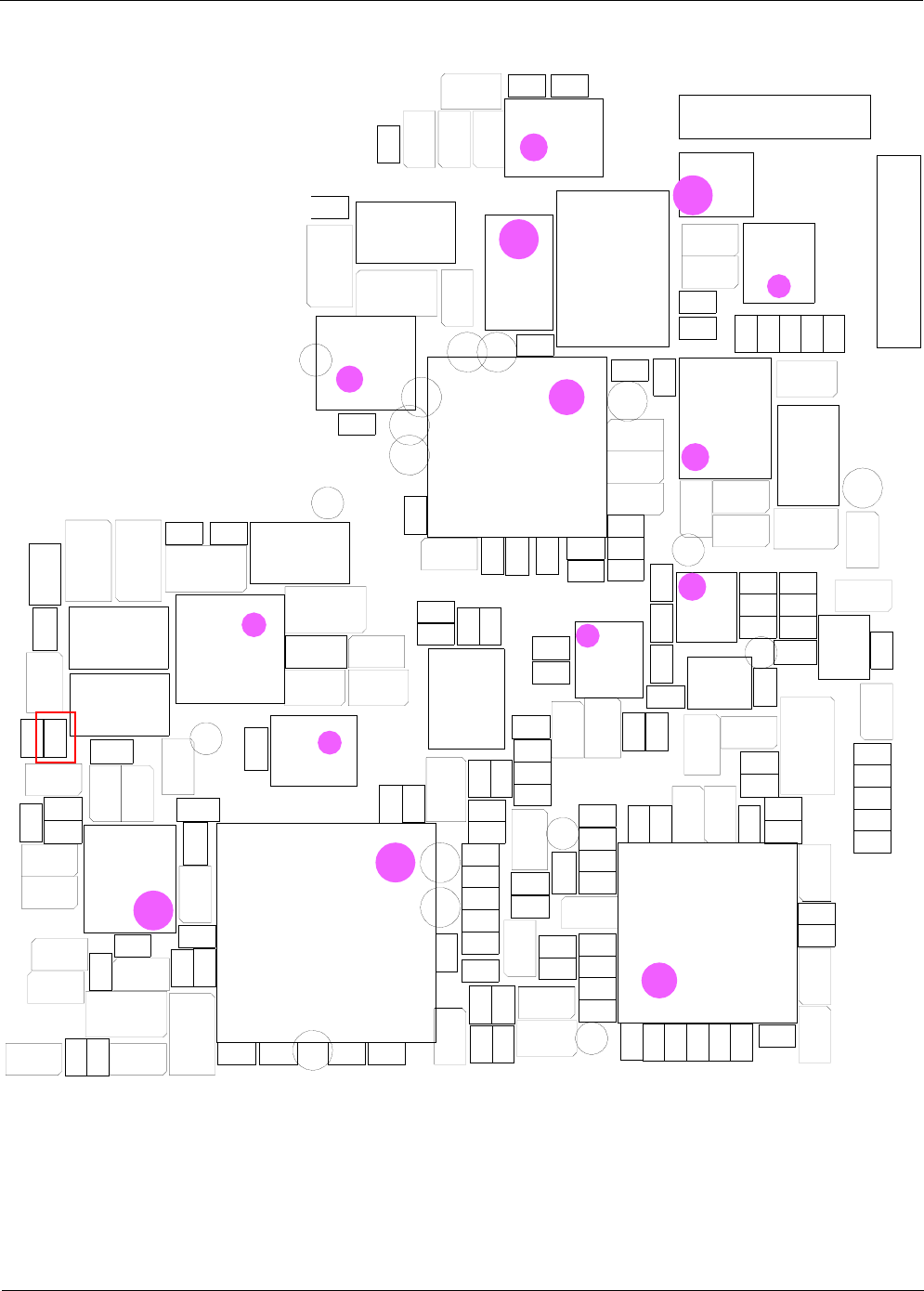
Level 3Repair
Distribution, transmission, or infringement of any content or data from this document without Samsung’s written authorization is strictly prohibited.
Confidential and proprietary-the contents in this service guide subject to change without prior notice.
8-65
BAT500
C113
C114
C119
C158
C159
C160
C170
C171
C172
C173
C174
C175
C176
C177
C197
C241
C242
C243
C245
C247
C248
C249
C251
C252
C253
C254
C255
C256
8
5
2
C
7
5
2
C
C259
C260
C261
C262
C263
C336
C337
C338
C339
C340
C343
C351
C401
C402
C410
C411
C412
C416
C424
C428
C429
C430
C431
C432
C433
C434
C435
C436
C437
C438
C439
C440
C441
C442
C449
C502
C527
C536
C540
C542
C543
C545
C547
C548
C607
C608
C611
C612
C621
C622
C708
C720
C721
C722
C723
C724
C725
C726
C727
C728
C735
C736
C740
C750
C751
C752
C753
C754
C763
C764
C786
C787
C788
C790
F702
L111
L119
L127
L128
L129
L130
L131
L132
L209
L210
L704
L705
L708
OSC202
Q200
R116
R117
R217
R218
R220
R222
R224
R225
R310
R311
R320
R321
R322
R323
R324
R410
R411
R412
R413
R414
R415
R416
R419
R430
R431
R436
R437
R443
R444
R445
R446
R453
R454
R458
R459
R466
R467
R472
R482
R612
R614
R616
R622
R700
R701
R702 R705
R706
R716
R718
R719
R720
R721
R722
R723
R724
R725
R726
R727
R728
R729
R730
R731
R732
R744
R745
R746
R747
R748
R749
R750
R751
R753
SC307
SC309
TA700
TP_100
TP_600
TP_601
TP_602
TP_603TP_604
TP_605
TP_607
TP_GPS_EN
TP208
TP209
TP210
TP323
TP517
TP704
TP705
TP711
U104
U108
U207
U401
U604
U700
U707
U708
U709
U710
U712
U714
U715
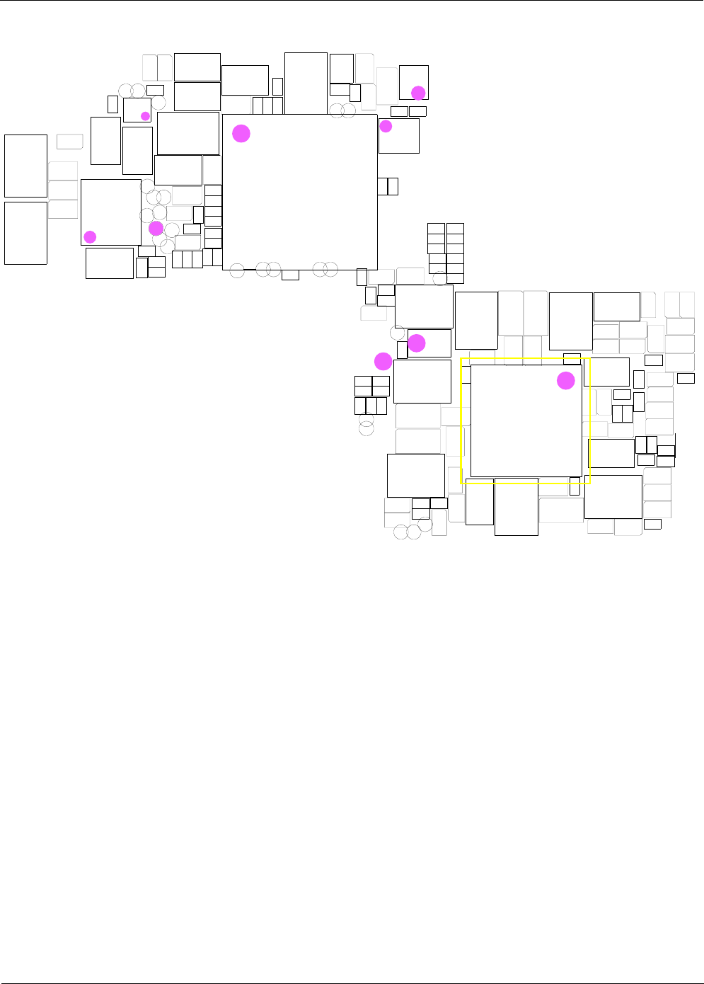
Level 3Repair
Distribution, transmission, or infringement of any content or data from this document without Samsung’s written authorization is strictly prohibited.
Confidential and proprietary-the contents in this service guide subject to change without prior notice.
8-66
AP_PS_HOLD
C240
C268
C302
C307
C308
C310
C311
C312
C313
C314
C315
C316
C317
C318
C321
C323
C324
C325
C328
C329
C330
C331
C332
C333
C341
C342
C344
C347
C348
C404
C425
C448
C500
C501
C503
C504
C505
C506
C507
C508
C509
C510
C511
C512
C513
C514
C515
C516
C517
C518
C519
C520
C521
C522
C523
C524
C525
C526
C528
C529
C530
C531
C532
C533
C534
C535
C537
C538
C539
C541
C544
C546
C549
C550
C551
C552
C553
C554
C555
C556
C557
C558
C559
C560
C561 C565
C566
C567
C573
C580
C581
C600
C601
C620
C729
C730
C731
C732
C733
C734
C765
C766
C785
F700
L300
L301
L302
L303
L500
L501
L502
L503
L504
L505
L506
L507
L508
L509
L510
L702
L703
L707
OSC400
OSC500
R104
R300
R302
R303
R304
R305
R306
R307
R308
R309
R315
R318
R319
R331
R332
R333
R334
R337
R342
R438
R447
R448
R465
R468
R474
R483
R500
R501
R504
R505
R717
R741R742
R743
RESET300
TH300
TP_eMMC_EN
TP304
TP307
TP308
TP309
TP310TP311
TP312
TP313
TP314
TP317
TP319
TP320
TP321
TP324
TP325
TP326
TP502
TP504
TP506
TP507
TP508
TP519
U302
U500
U600
U706
U713
U718
UCP300
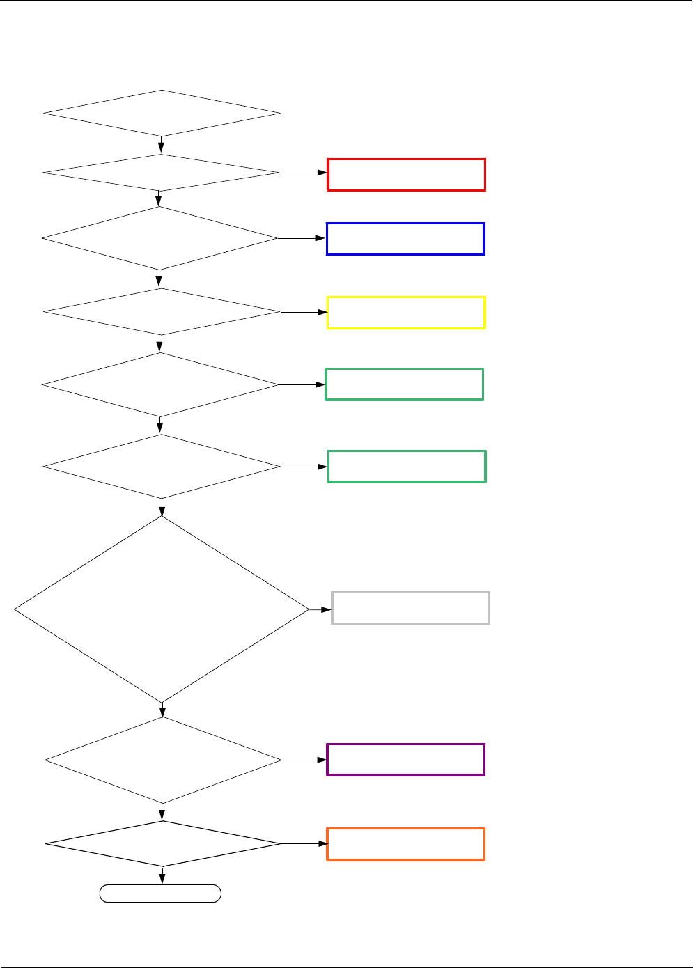
Level 3Repair
Distribution, transmission, or infringement of any content or data from this document without Samsung’s written authorization is strictly prohibited.
Confidential and proprietary-the contents in this service guide subject to change without prior notice.
8-67
Check C117 ≤-65dBm ?
8-3-19. GSM1800 RX
NORMAL CONDITION
catch the channel?
Check the voltage at
{C148= VOUT_CHARGER ?}
&{
C158,C159, C160
=VOUT_CHARGER?}
&{
C147, C172 = 2.85V ?}
&{
C144, C170 = 2.65V ?}
&{
C146, C174 =1.8
V?}
&{
C173, C171, C145 =1.2
V?}
Check the Voltage at
C110 =VBATT ?
Check component
soldering status OK at
F100
CHECK soldered
RFS100, L109, C116, C117
Resolder or change
U103, C110
Resolder or change
F100
Resolder or change
U108
Check the freq. at
OSC100 PIN 1:26
MHz ?
Change or resolder
OSC100
Check C112
≥-65dBm ?
Resolder or change
C112
GSM1800 Receiver is O.K? Resolder or change
UCP300
END
NO
YES
NO
NO
YES
NO
YES
NO
YES
NO
YES
NO
YES
NO
Check F100 PIN 18, 19
≥-65dBm
Resolder or change
F100
NO
YES
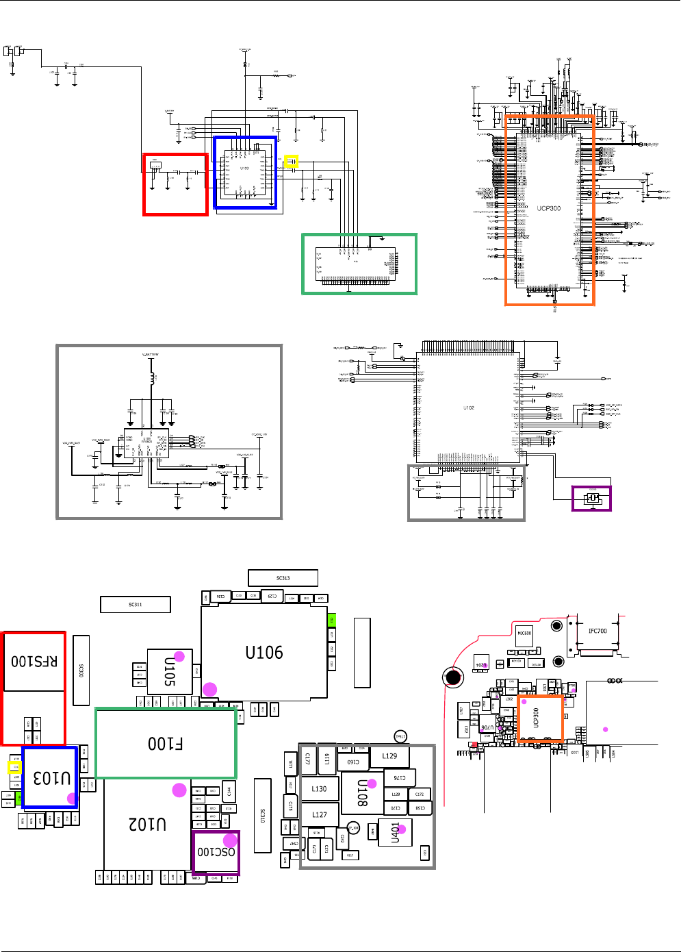
Level 3Repair
Distribution, transmission, or infringement of any content or data from this document without Samsung’s written authorization is strictly prohibited.
Confidential and proprietary-the contents in this service guide subject to change without prior notice.
8-68
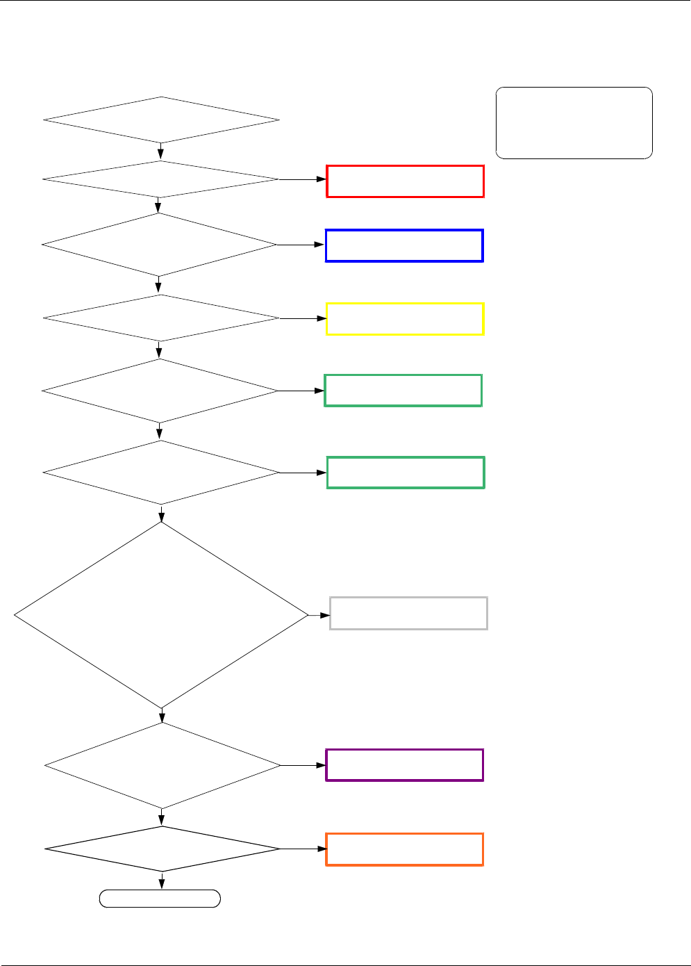
Level 3Repair
Distribution, transmission, or infringement of any content or data from this document without Samsung’s written authorization is strictly prohibited.
Confidential and proprietary-the contents in this service guide subject to change without prior notice.
8-69
Check C117 ≤-65dBm ?
8-3-20. WCDMA Band1 RX
NORMAL CONDITION
catch the channel?
Check the voltage at
{C148= VOUT_CHARGER ?}
&{
C158,C159, C160
=VOUT_CHARGER?}
&{
C147, C172 = 2.85V ?}
&{
C144, C170 = 2.65V ?}
&{
C146, C174 =1.8
V?}
&{
C173, C171, C145 =1.2
V?}
Check the Voltage at
C110 =VBATT
Check component
soldering status OK at
F100
CHECK soldered
RFS100, L109, C116, C117
Resolder or change
U103, C110
Resolder or change
F100
Resolder or change
U108
Check the freq. at
OSC100 PIN 1: 26MHz ?
Change or resolder
OSC100
Check L108, C118
≥-65dBm ?
Resolder or change
L108, C118
WCDMA band1 Receiver is O.K? Resolder or change
UCP300
END
NO
YES
NO
NO
YES
NO
YES
NO
YES
NO
YES
NO
YES
NO
Check F100 PIN 14, 15
≥-65dBm
Resolder or change
F100
NO
YES
CONTINUOUS RX ON
RF INPUT : 10700CH
AMP :-50
dBm
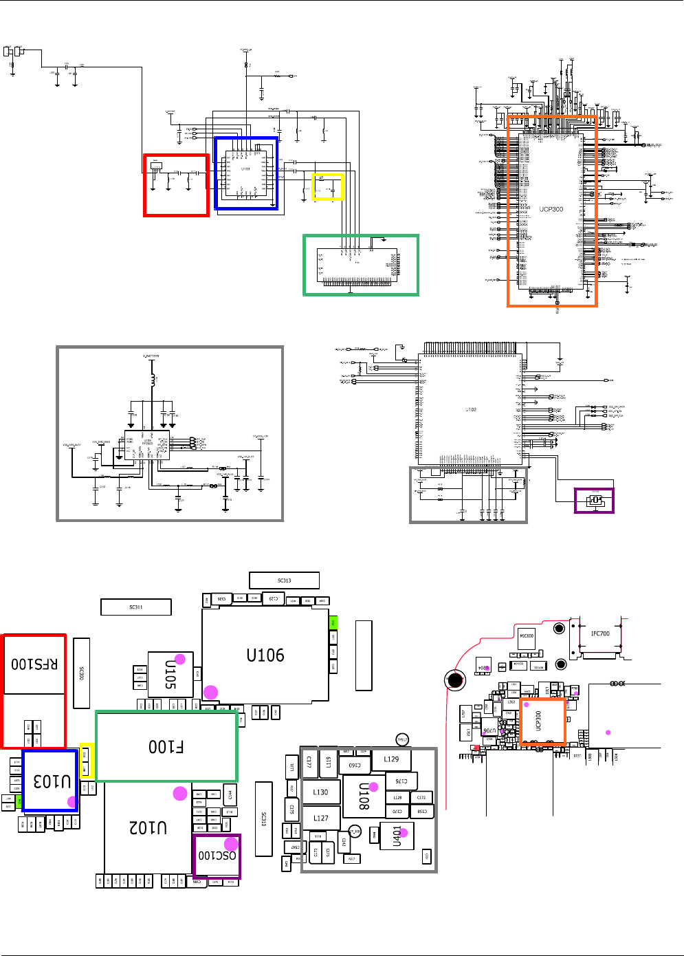
Level 3Repair
Distribution, transmission, or infringement of any content or data from this document without Samsung’s written authorization is strictly prohibited.
Confidential and proprietary-the contents in this service guide subject to change without prior notice.
8-70

Level 3Repair
Distribution, transmission, or infringement of any content or data from this document without Samsung’s written authorization is strictly prohibited.
Confidential and proprietary-the contents in this service guide subject to change without prior notice.
8-71
Check C117 ≤-65dBm ?
8-3-21. WCDMA Band2 /GSM1900 RX
NORMAL CONDITION
catch the channel?
Check the voltage at
{C148= VOUT_CHARGER ?}
&{
C158,C159, C160
=VOUT_CHARGER?}
&{
C147, C172 = 2.85V ?}
&{
C144, C170 = 2.65V ?}
&{
C146, C174 =1.8
V?}
&{
C173, C171, C145 =1.2
V?}
Check the Voltage at
C110 =VBATT ?
Check component
soldering status OK at
F100
CHECK soldered
RFS100, L109, C116, C117
Resolder or change
U103, C110
Resolder or change
F100
Resolder or change
U108
Check the freq. at
OSC100 PIN 1:26
MHz ?
Change or resolder
OSC100
Check L105, L107
≥-65dBm ?
Resolder or change
L105, L107
WCDMA band2/GSM1900
Receiver is O.K?
Resolder or change
UCP300
END
NO
YES
NO
NO
YES
NO
YES
NO
YES
NO
YES
NO
YES
NO
Check F100 PIN 16, 17
≥-65dBm
Resolder or change
F100
NO
YES
CONTINUOUS RX ON
RF INPUT : 9880CH
AMP :-50
dBm
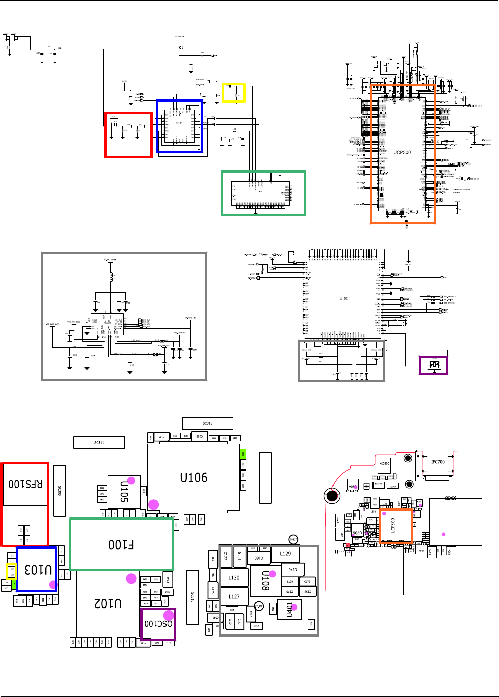
Level 3Repair
Distribution, transmission, or infringement of any content or data from this document without Samsung’s written authorization is strictly prohibited.
Confidential and proprietary-the contents in this service guide subject to change without prior notice.
8-72

Level 3Repair
Distribution, transmission, or infringement of any content or data from this document without Samsung’s written authorization is strictly prohibited.
Confidential and proprietary-the contents in this service guide subject to change without prior notice.
8-73
Check C117 ≤-65dBm ?
8-3-22. WCDMA Band5 /GSM 850 RX
NORMAL CONDITION
catch the channel?
Check the voltage at
{C148= VOUT_CHARGER ?}
&{
C158,C159, C160
=VOUT_CHARGER?}
&{
C147, C172 = 2.85V ?}
&{
C144, C170 = 2.65V ?}
&{
C146, C174 =1.8
V?}
&{
C173, C171, C145 =1.2
V?}
Check the Voltage at
C110 =VBATT ?
Check component
soldering status OK at
F100
CHECK soldered
RFS100, L109, C116, C117
Resolder or change
U103, C110
Resolder or change
F100
Resolder or change
U108
Check the freq. at
OSC100 PIN 1:26
MHz ?
Change or resolder
OSC100
Check C115, L112
≥-65dBm ?
Resolder or change
C115, L112
WCDMA band5/GSM850
Receiver is O.K?
Resolder or change
UCP300
END
NO
YES
NO
NO
YES
NO
YES
NO
YES
NO
YES
NO
YES
NO
Check F100 PIN 20, 21
≥-65dBm
Resolder or change
F100
NO
YES
CONTINUOUS RX ON
RF INPUT : 4408CH
AMP :-50
dBm

Level 3Repair
Distribution, transmission, or infringement of any content or data from this document without Samsung’s written authorization is strictly prohibited.
Confidential and proprietary-the contents in this service guide subject to change without prior notice.
8-74
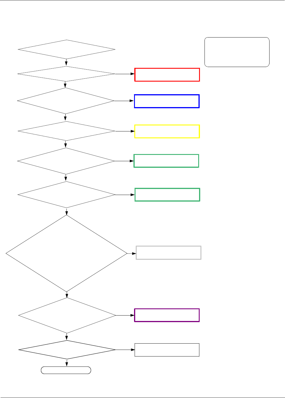
Level 3Repair
Distribution, transmission, or infringement of any content or data from this document without Samsung’s written authorization is strictly prohibited.
Confidential and proprietary-the contents in this service guide subject to change without prior notice.
8-75
Check C117 ≤-65dBm ?
8-3-23. WCDMA Band8 /GSM900 RX
NORMAL CONDITION
catch the channel?
Check the voltage at
{C148= VOUT_CHARGER ?}
&{
C158,C159, C160
=VOUT_CHARGER?}
&{
C147, C172 = 2.85V ?}
&{
C144, C170 = 2.65V ?}
&{
C146, C174 =1.8
V?}
&{
C173, C171, C145 =1.2
V?}
Check the Voltage at
C110 =VBATT ?
Check component
soldering status OK at
F100
CHECK soldered
RFS100, L109, C116, C117
Resolder or change
U103, C110
Resolder or change
F100
Resolder or change
U108
Check the freq. at
OSC100 PIN 1:26
MHz ?
Change or resolder
OSC100
Check L104, L106
≥-65dBm ?
Resolder or change
L104, L106
WCDMA band8/GSM900
Receiver is O.K?
Resolder or change
UCP300
END
NO
YES
NO
NO
YES
NO
YES
NO
YES
NO
YES
NO
YES
NO
Check F100 PIN 22, 23
≥-65dBm
Resolder or change
F100
NO
YES
CONTINUOUS RX ON
RF INPUT : 3013CH
AMP :-50
dBm
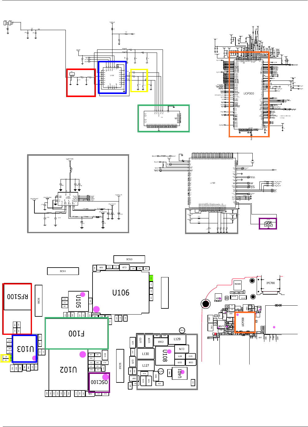
Level 3Repair
Distribution, transmission, or infringement of any content or data from this document without Samsung’s written authorization is strictly prohibited.
Confidential and proprietary-the contents in this service guide subject to change without prior notice.
8-76

Level 3Repair
Distribution, transmission, or infringement of any content or data from this document without Samsung’s written authorization is strictly prohibited.
Confidential and proprietary-the contents in this service guide subject to change without prior notice.
8-77
U103 PIN14 :About
30dBm ?
8-3-24. GSM850/GSM900 TX
Check the Voltage at
C110 =VBATT ?
Check the Voltage at
C125,C129,C132
CHECK soldered
-RFS100, L109, C116, C117,
C191, C101, L103, L102,
ANT103
Resolder or change
U103, C110
Resolder or change
U106,C125,C129,C132
Check C124, C120, L114
:About 30dBm ?
Resolder or change
C124, C120, L114
NO
YES
NO
YES
NO
YES
NO
YES
Check C136
About 0dBm ?
Resolder or change
C136
NO
YES
Check the voltage at
{C148= VOUT_CHARGER ?}
&{
C158,C159, C160
=VOUT_CHARGER?}
&{
C147, C172 = 2.85V ?}
&{
C144, C170 = 2.65V ?}
&{
C146, C174 =1.8
V?}
&{
C173, C171, C145 =1.2
V?}
Resolder or change
U108
Check the freq. at
OSC100 PIN 1:26
MHz ?
Change or resolder
OSC100
GSM850/900 Transmitter is O.K? Resolder or change
UCP300
END
NO
YES
NO
YES
NO
CONTINUOUS TX ON CONDITION
TX POWER IDX1 APPLIED
GSM850 CH : 190
GSM900 CH :62
RBW : 100KHz
VBW : 100KHz
SPAN :10
MHz
REF LEV. :10
dBm
ATT. :20
dB
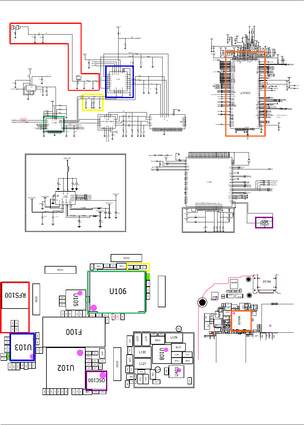
Level 3Repair
Distribution, transmission, or infringement of any content or data from this document without Samsung’s written authorization is strictly prohibited.
Confidential and proprietary-the contents in this service guide subject to change without prior notice.
8-78
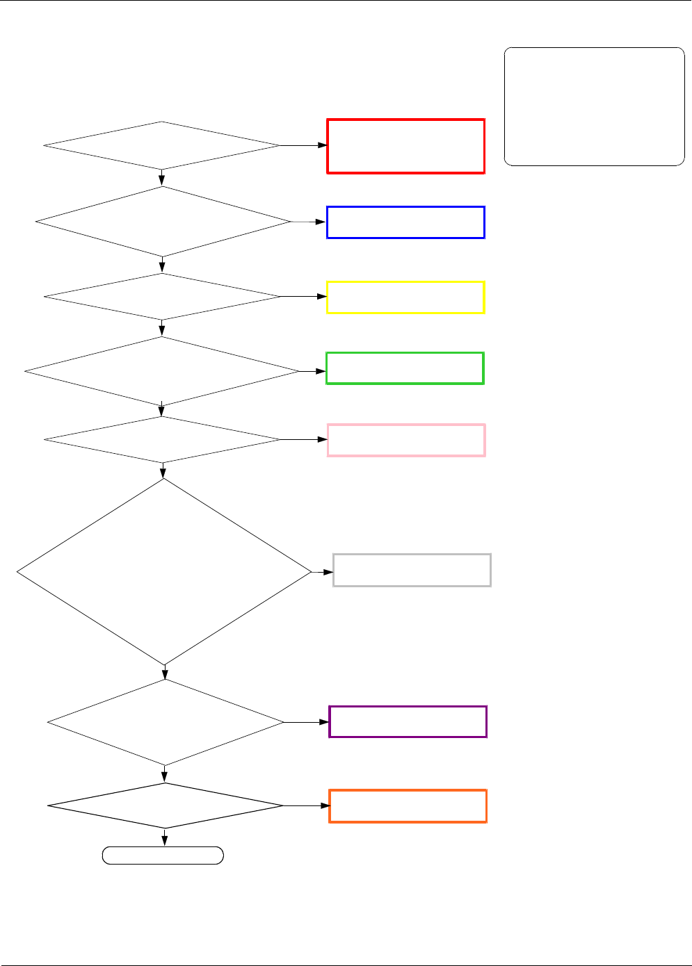
Level 3Repair
Distribution, transmission, or infringement of any content or data from this document without Samsung’s written authorization is strictly prohibited.
Confidential and proprietary-the contents in this service guide subject to change without prior notice.
8-79
U103 PIN14 :About
27dBm ?
8-3-25. DCS/PCS TX
Check the Voltage at
C110 =VBATT ?
Check the Voltage at
C125,C129,C132
CHECK soldered
-RFS100, L109, C116, C117,
C191, C101, L103, L102,
ANT103
Resolder or change
U103, C110
Resolder or change
U106,C125,C129,C132
Check C122, L133, C123
:About 27dBm ?
Resolder or change
C122, L133, C123
NO
YES
NO
YES
YES
NO
NO
YES
Check C137
About -4dBm ?
Resolder or change
C137
NO
YES
Check the voltage at
{C148= VOUT_CHARGER ?}
&{
C158,C159, C160
=VOUT_CHARGER?}
&{
C147, C172 = 2.85V ?}
&{
C144, C170 = 2.65V ?}
&{
C146, C174 =1.8
V?}
&{
C173, C171, C145 =1.2
V?}
Resolder or change
U108
Check the freq. at
OSC100 PIN 1:26
MHz ?
Change or resolder
OSC100
DCS/PCS Transmitter is O.K? Resolder or change
UCP300
END
NO
YES
NO
YES
NO
CONTINUOUS TX ON CONDITION
TX POWER IDX1 APPLIED
DCS CH : 685
PCS CH : 661
RBW : 100KHz
VBW : 100KHz
SPAN :10
MHz
REF LEV. :10
dBm
ATT. :20
dB
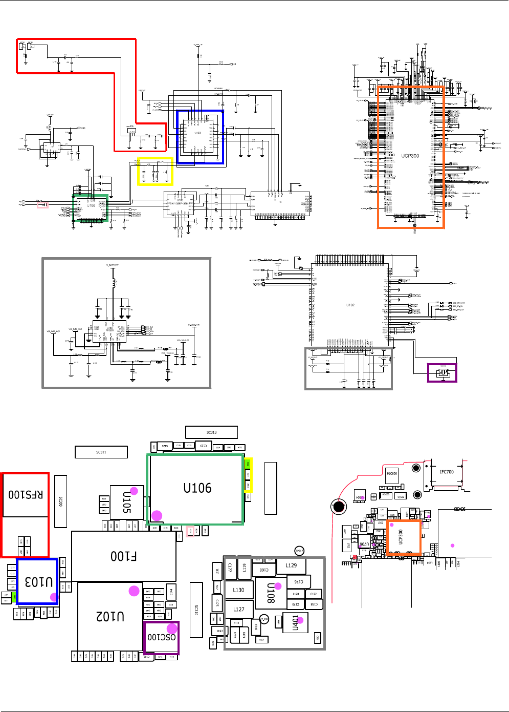
Level 3Repair
Distribution, transmission, or infringement of any content or data from this document without Samsung’s written authorization is strictly prohibited.
Confidential and proprietary-the contents in this service guide subject to change without prior notice.
8-80

Level 3Repair
Distribution, transmission, or infringement of any content or data from this document without Samsung’s written authorization is strictly prohibited.
Confidential and proprietary-the contents in this service guide subject to change without prior notice.
8-81
U103 PIN14
:About 22 dBm ?
8-3-26. WCDMA BAND1 TX
Check the Voltage at
C110 =VBATT ?
Resolder or change
U103, C110
Check L108, C118 :
About 22dBm ?
Resolder or change
L108, C118
NO
YES
NO
YES
NO
CHECK soldered
-RFS100, L109, C116, C117,
C191, C101, L103, L102,
ANT103
YES
Check component
soldering status OK at
F100
Resolder or change
F100
NO
YES
Check C140,C127,L116
About 22dBm ?
Resolder or change
C140,C127,L116
NO
YES
Check the Voltage at C114,
L132 =VOUT_CHARGER?
Resolder or change
C114, L132
NO
YES
Check C137
About 0dBm ?
Resolder or change
C137
YES
Check the voltage at
{C148= VOUT_CHARGER ?}
&{
C158,C159, C160
=VOUT_CHARGER?}
&{
C147, C172 = 2.85V ?}
&{
C144, C170 = 2.65V ?}
&{
C146, C174 =1.8
V?}
&{
C173, C171, C145 =1.2
V?}
Resolder or change
U108
NO
CONTINUOUS TX ON CONDITION
TX POWER DAC:14500 CODE
APPLIED
WCDMA Band1 CH : 20000
RBW : 100KHz
VBW : 100KHz
SPAN :10
MHz
REF LEV. :10
dBm
ATT. :20
dB
YES
Check the U105 PIN2
About 22dbm and C143 =
VOUT_CHARGER?
Resolder or change
U105, C143
YES
NO
NO
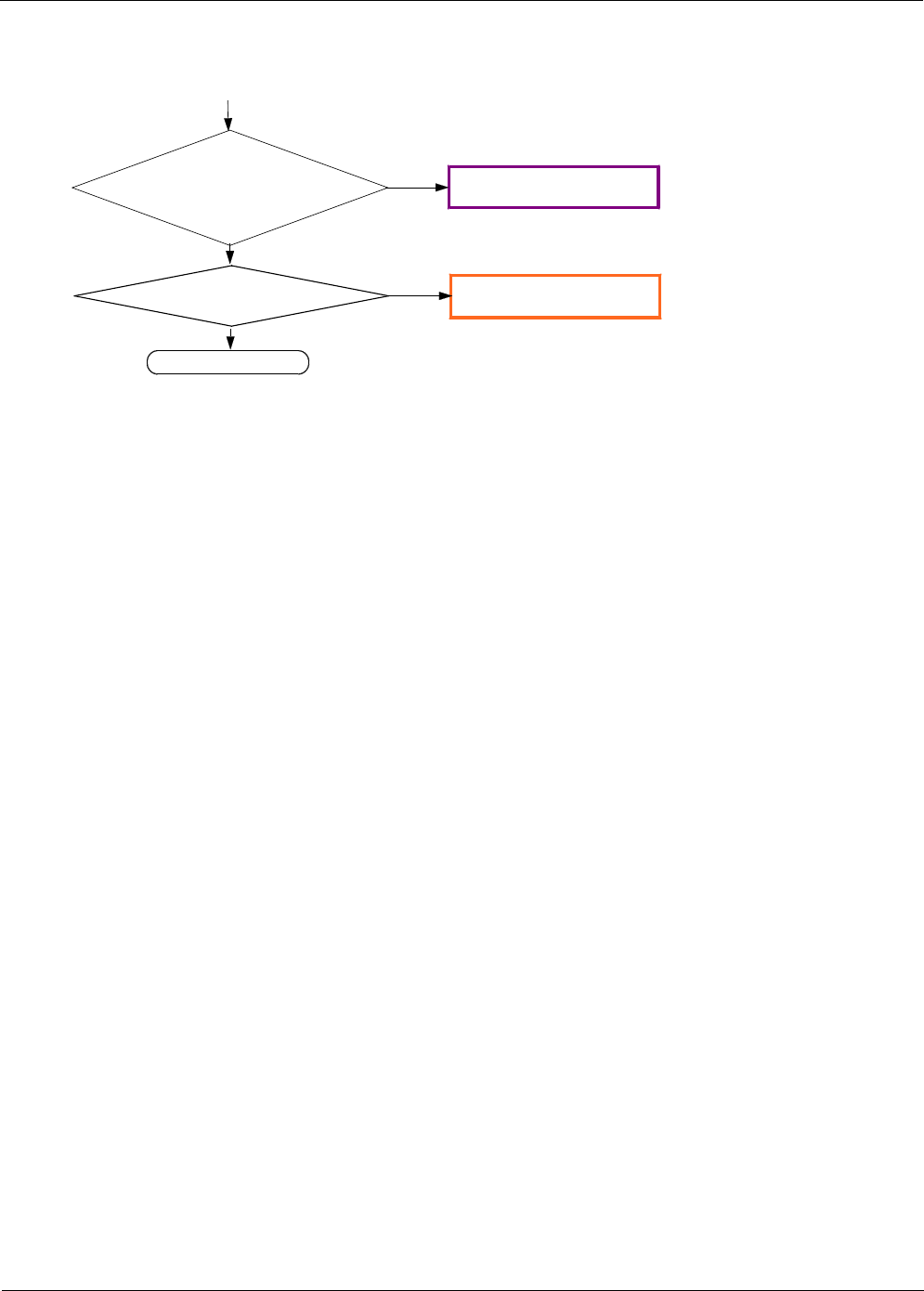
Level 3Repair
Distribution, transmission, or infringement of any content or data from this document without Samsung’s written authorization is strictly prohibited.
Confidential and proprietary-the contents in this service guide subject to change without prior notice.
8-82
WCDMA band1 Transmitter is O.K? Resolder or change
UCP300
END
YES
NO
Check the freq. at
OSC100 PIN 1:26
MHz ?
Change or resolder
OSC100
YES
NO
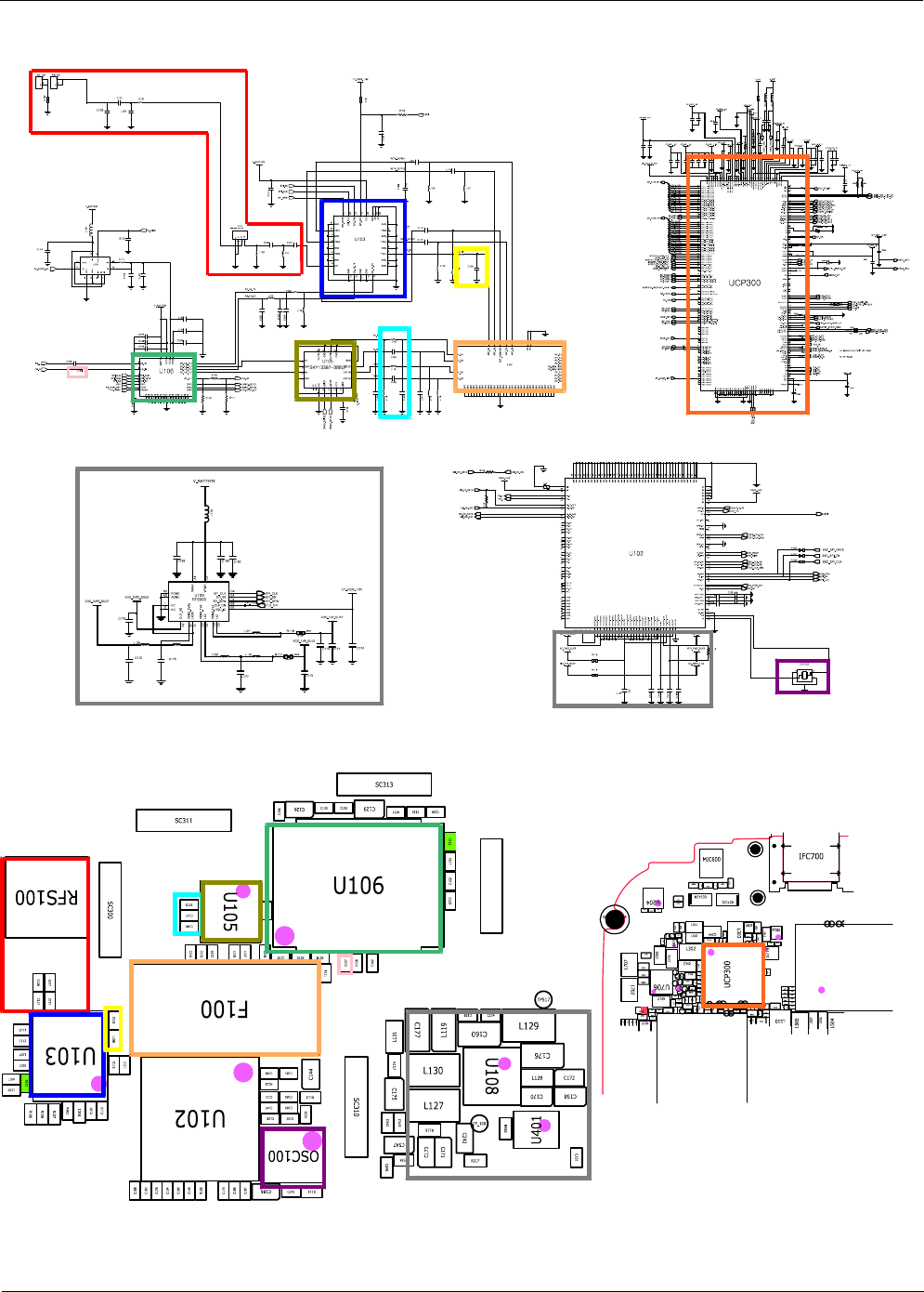
Level 3Repair
Distribution, transmission, or infringement of any content or data from this document without Samsung’s written authorization is strictly prohibited.
Confidential and proprietary-the contents in this service guide subject to change without prior notice.
8-83

Level 3Repair
Distribution, transmission, or infringement of any content or data from this document without Samsung’s written authorization is strictly prohibited.
Confidential and proprietary-the contents in this service guide subject to change without prior notice.
8-84
U103 PIN14
:About 22 dBm ?
8-3-27. WCDMA BAND2 TX
Check the Voltage at
C110 =VBATT ?
Resolder or change
U103, C110
Check L105, L107 :
About 22dBm ?
Resolder or change
L105, L107
NO
YES
NO
YES
NO
CHECK soldered
-RFS100, L109, C116, C117,
C191, C101, L103, L102,
ANT103
YES
Check component
soldering status OK at
F100
Resolder or change
F100
NO
YES
Check C141,C135, C139
About 22dBm ?
Resolder or change
C141,C135, C139
NO
YES
Check the Voltage at C114,
L132 =VOUT_CHARGER?
Resolder or change
C114, L132
NO
YES
Check C137
About 0dBm ?
Resolder or change
C137
YES
Check the voltage at
{C148= VOUT_CHARGER ?}
&{
C158,C159, C160
=VOUT_CHARGER?}
&{
C147, C172 = 2.85V ?}
&{
C144, C170 = 2.65V ?}
&{
C146, C174 =1.8
V?}
&{
C173, C171, C145 =1.2
V?}
Resolder or change
U108
NO
CONTINUOUS TX ON CONDITION
TX POWER DAC:23000 CODE
APPLIED
WCDMA Band2 CH : 9880
RBW : 100KHz
VBW : 100KHz
SPAN :10
MHz
REF LEV. :10
dBm
ATT. :20
dB
YES
Check the U105 PIN2
About 22dbm and C143 =
VOUT_CHARGER?
Resolder or change
U105, C143
YES
NO
NO

Level 3Repair
Distribution, transmission, or infringement of any content or data from this document without Samsung’s written authorization is strictly prohibited.
Confidential and proprietary-the contents in this service guide subject to change without prior notice.
8-85
WCDMA band2 Transmitter is O.K? Resolder or change
UCP300
END
YES
NO
Check the freq. at
OSC100 PIN 1:26
MHz ?
Change or resolder
OSC100
YES
NO
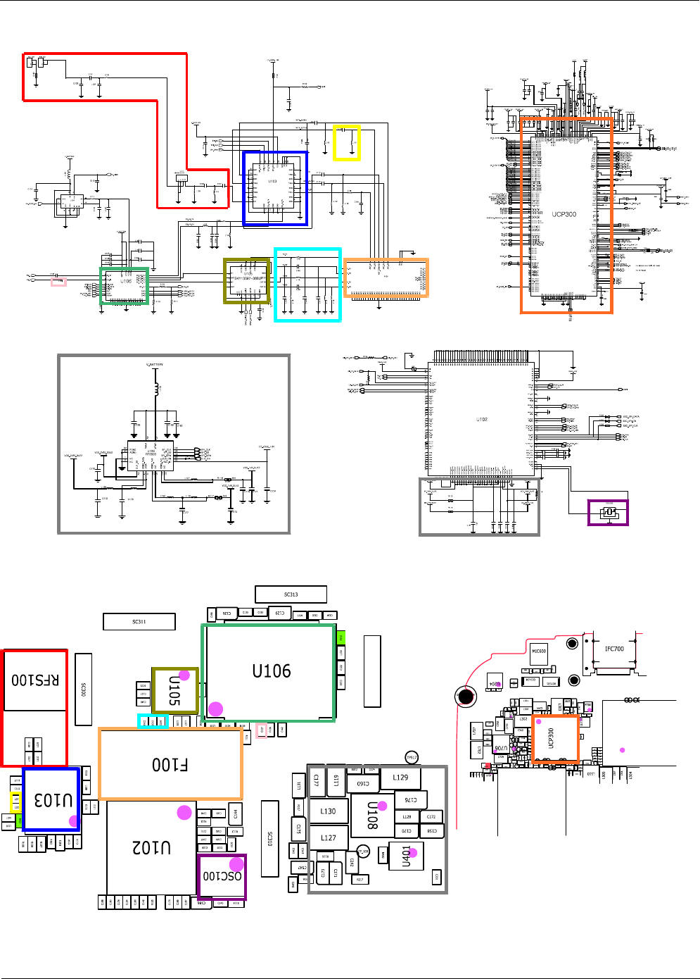
Level 3Repair
Distribution, transmission, or infringement of any content or data from this document without Samsung’s written authorization is strictly prohibited.
Confidential and proprietary-the contents in this service guide subject to change without prior notice.
8-86
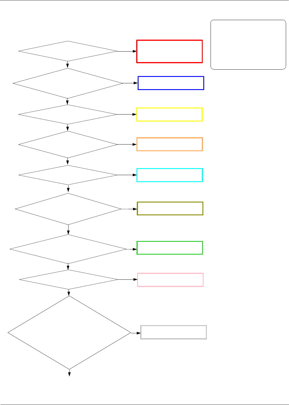
Level 3Repair
Distribution, transmission, or infringement of any content or data from this document without Samsung’s written authorization is strictly prohibited.
Confidential and proprietary-the contents in this service guide subject to change without prior notice.
8-87
U103 PIN14
:About 22 dBm ?
8-3-28. WCDMA BAND5 TX
Check the Voltage at
C110 =VBATT ?
Resolder or change
U103, C110
Check C115, L112 :
About 22dBm ?
Resolder or change
C115, L112
NO
YES
NO
YES
NO
CHECK soldered
-RFS100, L109, C116, C117,
C191, C101, L103, L102,
ANT103
YES
Check component
soldering status OK at
F100
Resolder or change
F100
NO
YES
Check L117,L115,
About 22dBm ?
Resolder or change
L117,L115,
NO
YES
Check the Voltage at C114,
L132 =VOUT_CHARGER?
Resolder or change
C114, L132
NO
YES
Check C136
About 0dBm ?
Resolder or change
C130
YES
Check the voltage at
{C148= VOUT_CHARGER ?}
&{
C158,C159, C160
=VOUT_CHARGER?}
&{
C147, C172 = 2.85V ?}
&{
C144, C170 = 2.65V ?}
&{
C146, C174 =1.8
V?}
&{
C173, C171, C145 =1.2
V?}
Resolder or change
U108
NO
CONTINUOUS TX ON CONDITION
TX POWER DAC: 23000 CODE
APPLIED
WCDMA Band5 CH : 4408
RBW : 100KHz
VBW : 100KHz
SPAN :10
MHz
REF LEV. :10
dBm
ATT. :20
dB
YES
Check the U105 PIN4
About 22dbm and C143 =
VOUT_CHARGER?
Resolder or change
U105, C143
YES
NO
NO

Level 3Repair
Distribution, transmission, or infringement of any content or data from this document without Samsung’s written authorization is strictly prohibited.
Confidential and proprietary-the contents in this service guide subject to change without prior notice.
8-88
WCDMA band2 Transmitter is O.K? Resolder or change
UCP300
END
YES
NO
Check the freq. at
OSC100 PIN 1:26
MHz ?
Change or resolder
OSC100
YES
NO

Level 3Repair
Distribution, transmission, or infringement of any content or data from this document without Samsung’s written authorization is strictly prohibited.
Confidential and proprietary-the contents in this service guide subject to change without prior notice.
8-89
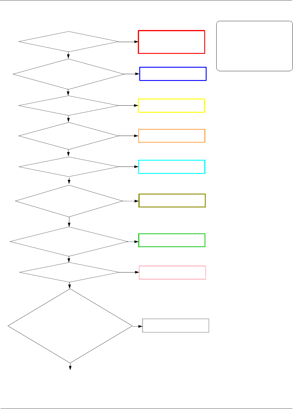
Level 3Repair
Distribution, transmission, or infringement of any content or data from this document without Samsung’s written authorization is strictly prohibited.
Confidential and proprietary-the contents in this service guide subject to change without prior notice.
8-90
U103 PIN14
:About 22 dBm ?
8-3-29. WCDMA BAND8 TX
Check the Voltage at
C110 =VBATT ?
Resolder or change
U103, C110
Check L104, L106 :
About 22dBm ?
Resolder or change
L104, L106
NO
YES
NO
YES
NO
CHECK soldered
-RFS100, L109, C116, C117,
C191, C101, L103, L102,
ANT103
YES
Check component
soldering status OK at
F100
Resolder or change
F100
NO
YES
Check L118,C138
About 22dBm ?
Resolder or change
L118,C138
NO
YES
Check the Voltage at C114,
L132 =VOUT_CHARGER?
Resolder or change
C114, L132
NO
YES
Check C136
About 0dBm ?
Resolder or change
C130
YES
Check the voltage at
{C148= VOUT_CHARGER ?}
&{
C158,C159, C160
=VOUT_CHARGER?}
&{
C147, C172 = 2.85V ?}
&{
C144, C170 = 2.65V ?}
&{
C146, C174 =1.8
V?}
&{
C173, C171, C145 =1.2
V?}
Resolder or change
U108
NO
YES
Check the U105 PIN4
About 22dbm and C143 =
VOUT_CHARGER?
Resolder or change
U105, C143
YES
NO
NO
CONTINUOUS TX ON CONDITION
TX POWER DAC: 23000 CODE
APPLIED
WCDMA Band8 CH : 3013
RBW : 100KHz
VBW : 100KHz
SPAN :10
MHz
REF LEV. :10
dBm
ATT. :20
dB

Level 3Repair
Distribution, transmission, or infringement of any content or data from this document without Samsung’s written authorization is strictly prohibited.
Confidential and proprietary-the contents in this service guide subject to change without prior notice.
8-91
WCDMA band2 Transmitter is O.K? Resolder or change
UCP300
END
YES
NO
Check the freq. at
OSC100 PIN 1:26
MHz ?
Change or resolder
OSC100
YES
NO
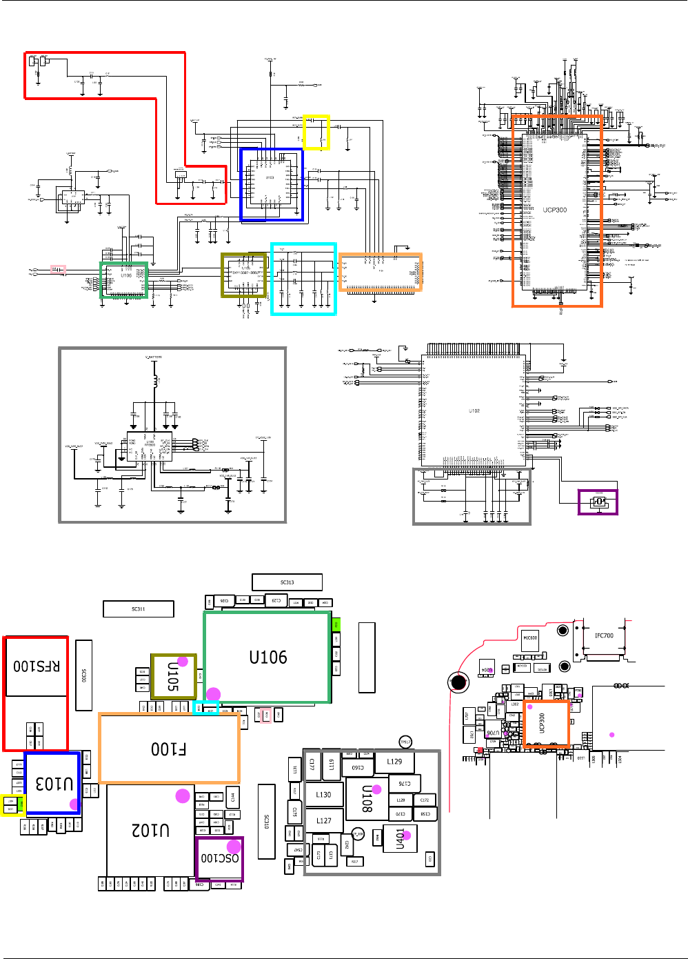
Level 3Repair
Distribution, transmission, or infringement of any content or data from this document without Samsung’s written authorization is strictly prohibited.
Confidential and proprietary-the contents in this service guide subject to change without prior notice.
8-92
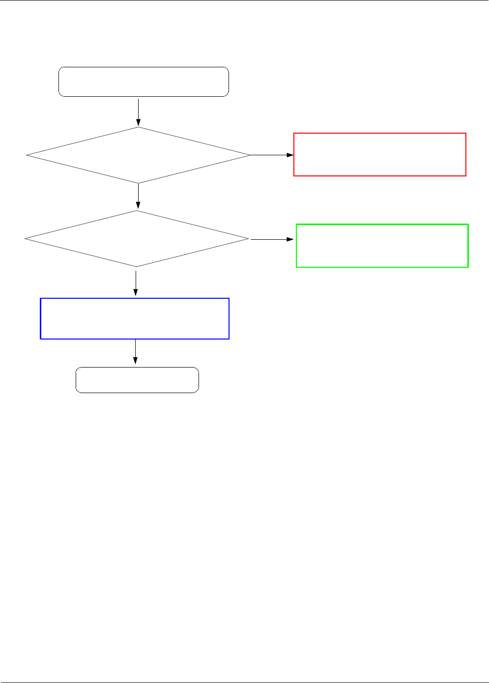
Level 3Repair
Distribution, transmission, or infringement of any content or data from this document without Samsung’s written authorization is strictly prohibited.
Confidential and proprietary-the contents in this service guide subject to change without prior notice.
8-93
8-3-30. OTG
Yes
No Change U506
Check CHG_IN_5V(C565)=5V
Yes
END
Yes
No Check U502
Check V_BUS_5V(C563) =5V
Yes
Change the board
OTG does not work
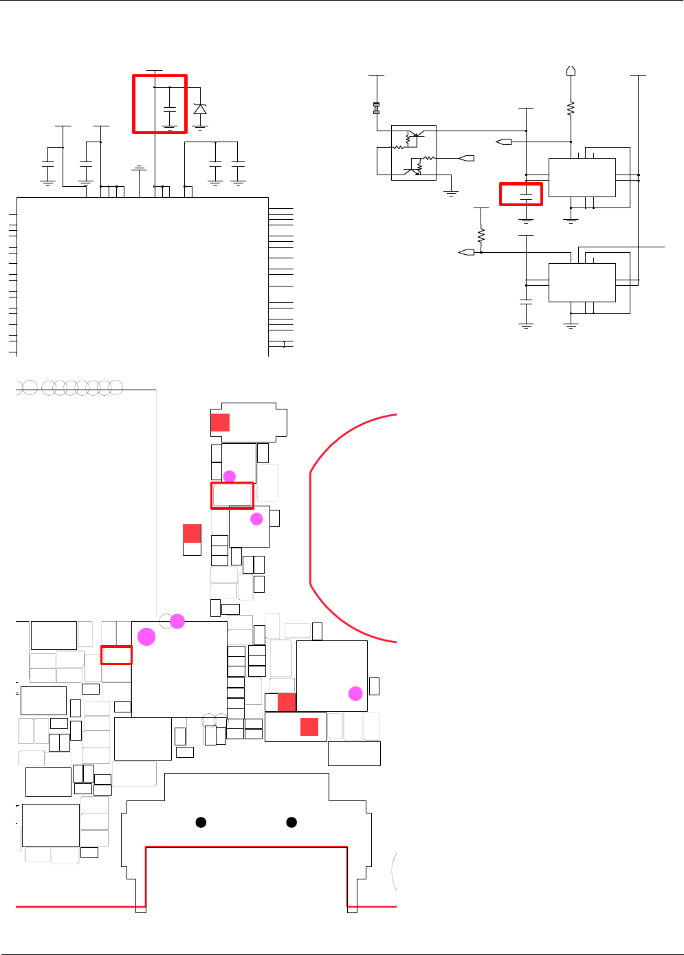
Level 3Repair
Distribution, transmission, or infringement of any content or data from this document without Samsung’s written authorization is strictly prohibited.
Confidential and proprietary-the contents in this service guide subject to change without prior notice.
8-94
ZD502
C565
C594
DP2
K
9
SYS
K
3
SYS
K
4
BATT
K5
BATT
K6
ADP2
K7
DN1
K
8
BAT_SP
3
SYS
4
BATT
J5
BATT
J6
ADN1 J7
MVIO
8
SYS_A
H
5
MVBAT
H7
BAT_SN
2
AUR2
G7
G8
CHGLX
H
1
AVL
H
2
SYS_A
H
4
CHGLX
G
1
BYP
F2
MRST1B
F5
MRST2B
F6
AUT1
F7
UT1
F
8
DETBATB
E
4
E5
AIN E8
VBATTFG E9
BYP
F1
SYS_Q
D
5
SCLFG
D8
ALRT D9
CHGIN
E1
CHGIN
E2
SNS
C8
VBFG C9
CHGIN
D1
THRM
D10
INOKB
D
4
SAFEOUT1 C1
SAFEOUT2
C2
SDA C6
VIO
B10
SCL
B6
VCCTEST
A4
U506
CHG_IN_5V
V_BATTERY
C564
C566
R
5
C567
V_BAT
B2
B1 IN
IN
C1
1
NC
NC
2
B3
OUT
OUT C3
A2
OVLO
U502
ACOK_
A1
EN_
A3
C2
GND
IC
C563
C3
OUT
OVLO
A2
A3
EN_
GND
C2
B2
IC
IN
B1
C1 IN
NC
1
2
NC
OUT B3
U504
A1
ACOK_
U501
2
5
6
3
1
4
V_BUS_5V
WPC_5V
R533
C578
R507
CHG_IN_5V
VCC_1.8V_AP
R511
CHG_IN_5V
TA_ACOK
OTG_EN
WPC_INT
BTC500
C246
C250
C300
C301
C302
C303
C304
C305
C306
C309
C319
C320
C326
C357
C500
C501
C503
C509
C510
C511
C517
C518
C519
C520
C521
C522
C523
C524
C525
C526
C528
C529
C530
C531
C532
C537
C541
C546
C549
C553
C554
C555
C561
C563
C564
C565
C566
C567
C568
C569
C570
C571
C572
C573
C574
C575
C576
C577
C579
C580
C581
C582
C583
C585
C586
C587
C593
C594
C595
C707
D500
L500
L506
L507
L508
L511
L512
R312
R313
R432
R433
R500
R502
R503
R507
R512
R513
R515
R516
R517
R518
R519
R526
R532
R533
TA500
TP_AP_D TP_AP_D+
TP300
TP301
TP302
TP303
TP305
TP316
TP322
TP327
TP328
U206
U501
U502
U506
U719
UME300
ZD500
ZD502
ZD701