Samsung GT M8800 Service Manual. Www.s Manuals.com. Manual R1.0
User Manual: Smartphone Samsung GT-M8800 Pixon - Service manuals and Schematics, Disassembly / Assembly. Free.
Open the PDF directly: View PDF ![]() .
.
Page Count: 75
GSM TELEPHONE
Samsung M8800
1. Safety Precautions
2. Specification
3. Product Function
4. Array course control
5. Exploded View and Parts list
6. MAIN Electrical Parts List
7. Block Diagrams
8. PCB Diagrams
9. Chart of Troubleshooting
10. Reference data
11. Disassembly and Assembly
Instructions
GSM TELEPHONE CONTENTS
This Service Manual is aproperty of Samsung Electronics Co.,Ltd.
Any unauthorized use of Manual can be punished under applicable
International and/or domestic law.
Samsung Electronics Co.,Ltd.
2008. 10. Rev.1.0
ⓒ
Country Web Site
North America service.samsungportal.com
Latin America latin.samsungportal.com
CIS cis.samsungportal.com
Europe europe.samsungportal.com
China china.samsungportal.com
Asia asia.samsungportal.com
Mideast &Africa mea.samsungportal.com
GSPN (Global Service Partner Network)

SAMSUNG Proprietary-Contents may change without notice
2. Specification
2-1
This Document can not be used without Samsung's authorization
EGSM 850 EGSM 900
Phase 2
DCS1800
Phase 1
PCS 1900 WCDMA
Freq.
Band(MHZ)
Uplink/Downlink
824~849
869~894
880~915
925~960
1710~1785
1805~1880
1850~1910
1930~1990
1920~1980
2110~2170
ARFCN range 128~251 1~124 &
975~1023 512~885 512~810 10562~10838
Tx/Rx spacing 45MHz 45MHz 95 MHz 80 MHz 190MHz
Mod. Bit rate/
Bit Period
270.833 kbps
3.692 us
270.833 kbps
3.692 us
270.833 kbps
3.692 us
270.833 kbps
3.692 us 3.84 Mcps/s
Time slot
Period/Frame
Period
576.9 us
4.615 ms
576.9 us
4.615 ms
576.9 us
4.615 ms
576.9 us
4.15 ms 10 ms
Modulation 0.3 GMSK 0.3 GMSK 0.3 GMSK 0.3 GMSK UL :2
BPSK
DL :QPSK
MS Power 33 dBm ~
5dBm
33 dBm ~
5dBm 30dBm~0dBm 30dBm~0dBm
MAX:24
(+1,-3)dBm
MIN :<-50dBm
Power Class 5pcl ~19pcl 5pcl ~19pcl 0pcl ~15
pcl 0pcl ~15
pcl CLASS3
Sensitivity -103 dBm -103 dBm -100dBm -100dBm -106.7 dBm
TDMA Mux 8888-
Cell Radius 35Km 35 Km 2Km --
2-1. GSM850&900/DCS1800/PCS1900/WCDMA2100 General
Specification

SAMSUNG Proprietary-Contents may change without notice
Specification
2-2
This Document can not be used without Samsung's authorization
TX POWER
LEVEL CONTOL
EGSM
850/900
TX POWER
LEVEL CONTOL DCS 1800 TX POWER
LEVEL CONTOL PCS 1900
533±2
dBm 030±3
dBm 030±3
dBm
631±2
dBm 128±3
dBm 128±3
dBm
729±2
dBm 226±3
dBm 226±3
dBm
827±2
dBm 324±3
dBm 324±3
dBm
925±2
dBm 422±3
dBm 422±3
dBm
10 23±2 dBm 520±3
dBm 520±3
dBm
11 21±2 dBm 618±3
dBm 618±3
dBm
12 19±2 dBm 716±3
dBm 716±3
dBm
13 17±2 dBm 814±3
dBm 814±3
dBm
14 15±2 dBm 912±3
dBm 912±3
dBm
15 13±2 dBm 10 10±4 dBm 10 10±4 dBm
16 11±3 dBm 11 8±4 dBm 11 8±4 dBm
17 9±3 dBm 12 6±4 dBm 12 6±4 dBm
18 7±3 dBm 13 4±4 dBm 13 4±4 dBm
19 5±3 dBm 14 2±5 dBm 14 2±5 dBm
15 0±5 dBm 15 0±5 dBm
2-2. GSM TX power class

SAMSUNG Proprietary-Contents may change without notice
3. Product Function
3-1
This Document can not be used without Samsung's authorization
Main Function
-8MCamera /CIF Camera
-LCD -Main:3.2" 240x4000 262K Color TFT
-Video Recording &Messaging
-Music Player(MP3/AAC/AAC+/Enhanced ACC+)
-Multimedia Message Service (MMS)
-Bluetooth Wireless Technology
-E-mail
-Voice recorder
-Java /WAP2.0
-Four-band(850/900/1800/1900MHz), UMTS 2100MHz
-USB 2.0
-FM Radio
-GPS
-HSDPA 7.2

SAMSUNG Proprietary-Contents may change without notice
11.Reference data
11-1
This Document can not be used without Samsung's authorization
Reference Abbreviation
-AAC:Advanced Audio Coding.
-AVC :Advanced Video Coding.
-BER :Bit Error Rate
-BPSK:Binary Phase Shift Keying
-CA :Conditional Access
-CDM :Code Division Multiplexing
-C/I :Carrier to Interference
-DMB :Digital Multimedia Broadcasting
-EN :European Standard
-ES :Elementary Stream
-ETSI:European Telecommunications Standards Institute
-MPEG:Moving Picture Experts Group
-PN :Pseudo-random Noise
-PS :Pilot Symbol
-QPSK:Quadrature Phase Shift Keying
-RS :Reed-Solomon
-SI :Service Information
-TDM :Time Division Multiplexing
-TS :Transport Stream

SAMSUNG Proprietary-Contents may change without notice
1. Safety Precautions
1-2
This Document can not be used without Samsung's authorization
1-1. Repair Precaution
●Repair in Shield Box, during detailed tuning.
Take specially care of tuning or test,
because specipicty of cellular phone is sensitive for surrounding interference(RF noise).
●Be careful to use akind of magnetic object or tool,
because performance of parts is damaged by the influence of manetic force.
●Surely use astandard screwdriver when you disassemble this product,
otherwise screw will be worn away.
●Use athicken twisted wire when you measure level.
Athicken twisted wire has low resistance, therefore error of measurement is few.
●Repair after separate Test Pack and Set because for short danger (for example an
overcurrent and furious flames of parts etc) when you repair board in condition of
connecting Test Pack and tuning on.
●Take specially care of soldering, because Land of PCB is small and weak in heat.
●Surely tune on/off while using AC power plug, because arepair of battery charger is
dangerous when tuning ON/OFF PBA and Connector after disassembing charger.
●Don't use as you pleases after change other material than replacement registered on SEC
System.
Otherwise engineer in charge isn't charged with problem that you don't keep this rules.

SAMSUNG Proprietary-Contents may change without notice
Safety Precautions
1-2
This Document can not be used without Samsung's authorization
1-2. ESD(Electrostatically Sensitive Devices) Precaution
Several semiconductor may be damaged easilly by static electricity. Such parts are called by
ESD(Electrostatically Sensitive Devices), for example IC,BGA chip etc. Read Precaution below.
You can prevent from ESD damage by static electricity.
●Remove static electricity remained your body before you touch semiconductor or parts with
semiconductor. There are ways that you touch an earthed place or wear static electricity
prevention string on wrist.
●Use earthed soldering steel when you connect or disconnect ESD.
●Use soldering removing tool to break static electricity. ,otherwise ESD will be damaged by
static electricity.
●Don't unpack until you set up ESD on product. Because most of ESD are packed by box
and aluminum plate to have conductive power,they are prevented from static electricity.
●You must maintain electric contact between ESD and place due to be set up until ESD is
connected completely to the proper place or acircuit board.
SAMSUNG Proprietary-Contents may change without notice
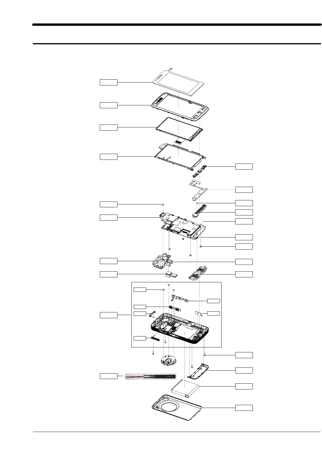
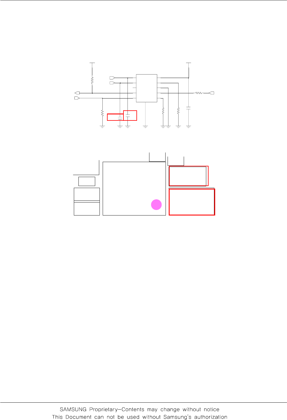
5. Exploded View and Parts List
5-1
This Document can not be used without Samsung's authorization
5-1. Cellular phone Exploded View
QME03
QFR01
QLB01
QLC01
QMP01
QCR32
QSP01
QCA02
QRE01
QST01
QSD01
QIF01
QCR57
QCK02
QCK01
QVO01
QKP01
QBR04
QCR32
QAN02
QCR54
QBA00
QBA01
QSC01
QCA01
QSH01
QMI03
QCR05
QME01

SAMSUNG Proprietary-Contents may change without notice
Exploded View and Parts List
5-2
This Document can not be used without Samsung's authorization
Design LOC Discription SEC CODE
QAN02 INTENNA-GT_M8800 GH42-01779A
QBA00 NPR COVER-BATT GH71-08641A
QBA01 INNER BATTERY PACK-1000MAH,BLK GH43-02974A
QBR04 PMO BRACKET-KEY GH72-49749A
QCA01 ASSY CAMERA-GT_M8800 GH96-03369A
QCA02 CAMERA MODULE-GT_M8800 GH59-06260A
QCR05 SCREW-MACHINE 6001-001478
QCR32 SCREW-MACHINE 6001-001700
QCR54 SCREW-MACHINE 6001-001645
QFR01 ASSY CASE-FRONT GH98-10189A
QKP01 ASSY KEYPAD-(EU/BLACK) GH98-10192A
QLB01 ASSY BRACKET-LCD GH98-10193A
QLC01 ASSY LCD-LCD MODULE ASSY(M8800 GH96-03364A
QME01 KEY FPCB-GT_M8800,FPCB ASS'Y GH59-06339A
QME03 UNIT-TOUCH WINDOW(M8800) GH59-06337A
QMI03 RMO RUBBER-MIC HOLDER GH73-12285A
QMP01 A/S ASSY-PBA MAIN (GT_M8800 SV GH82-03272A
QSC01 PMO COVER-SCREW GH72-50997A
QSH01 ASSY BRACKET-SHIELD CAN GH98-10194A
QSP01 UNIT-MODULE SPEAKER(AUDIO RECE GH59-06318A
QST01ASSY STYLUS PEN-HANDSTRAP GH98-09735A
QRE01 ASSY CASE-REAR GH98-10190A
QCK01 ASSY KEY-CAM GH98-10648B
QCK02 PMO KEY-HOLD GH72-49762A
QCR57 SCREW-MACHINE 6001-002001
QIF01 PMO COVER-IF V2 GH72-50420A
QSD01 PMO COVER-SD V2 GH72-50419A
QVO01 PMO KEY-VOL V2 GH72-50421A
5-2. Cellular phone Parts list
SAMSUNG Proprietary-Contents may change without notice
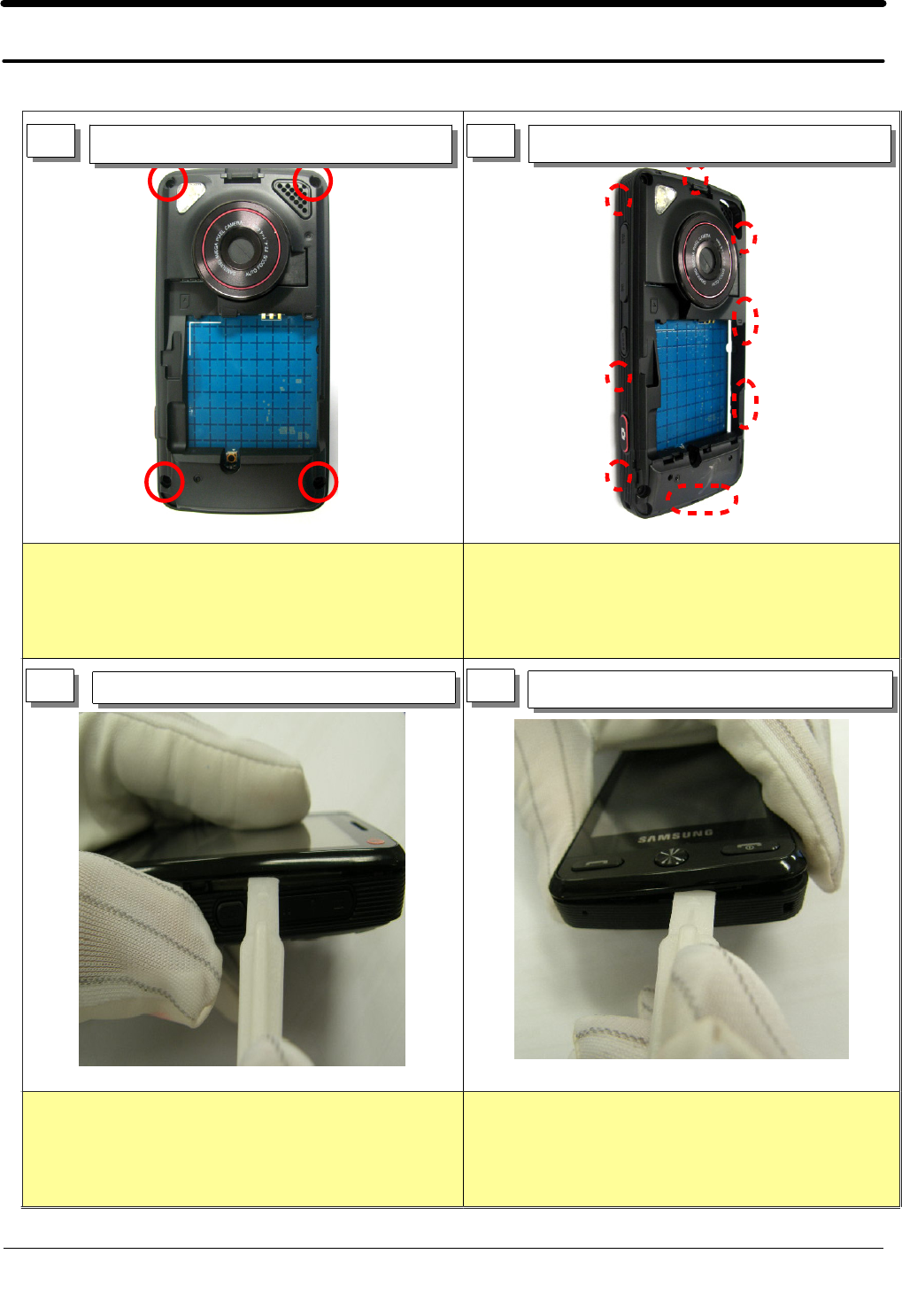
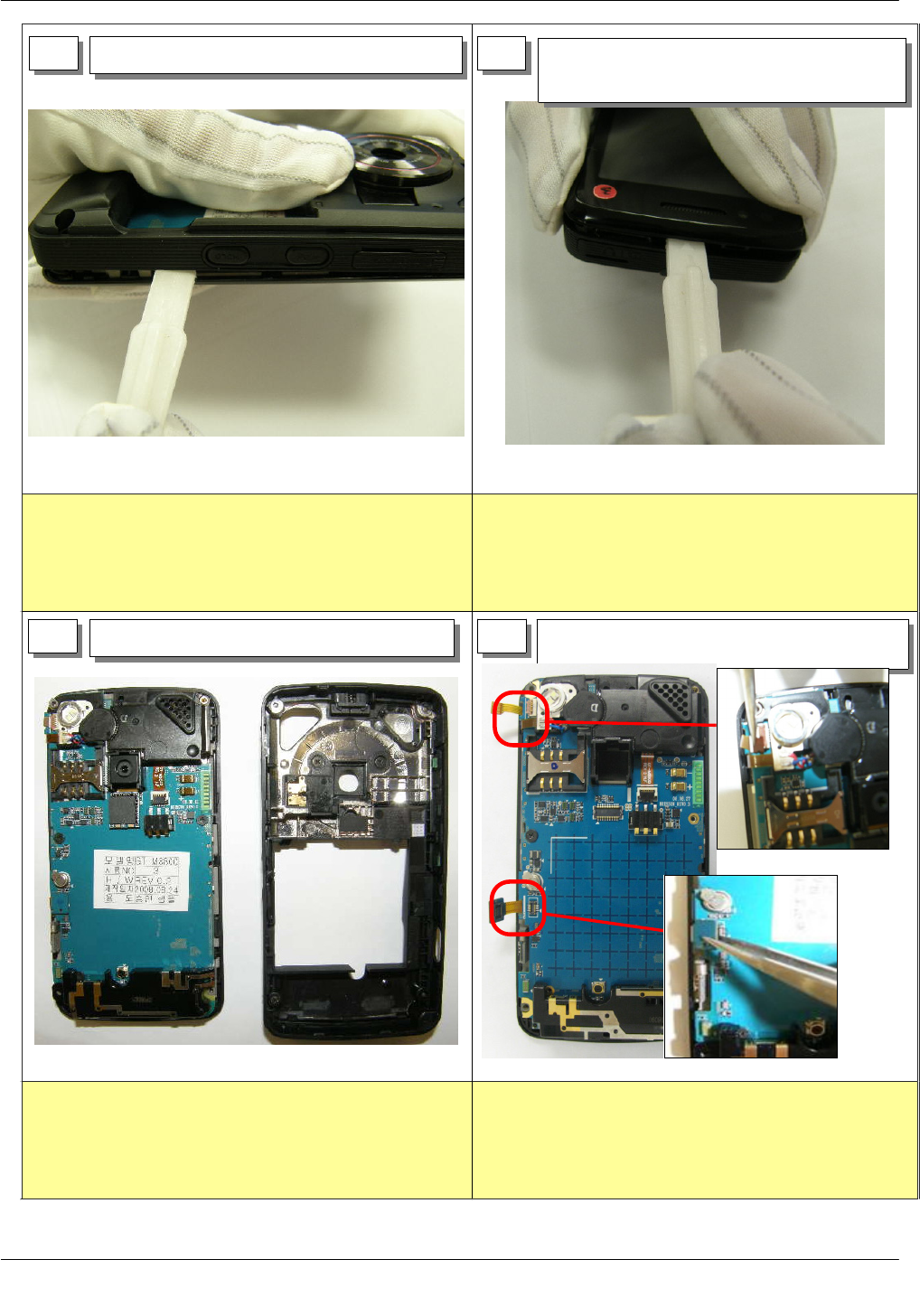
7. Disassembly and Assembly Instructions
7-1
This Document can not be used without Samsung's authorization
1) Be care of Shooting out damage and scratch not to
occur.
1)When you disjoint arear case from right side to left
side, be care of hooks and key hanging.
1) Be care of Shooting out damage and scratch not to
occur..
1) Be care of Shooting out damage and scratch not to
occur..
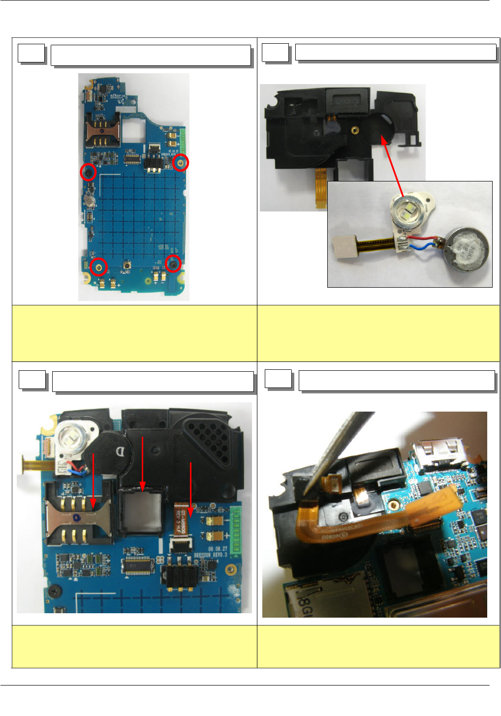
11) Unsrew 4points from the rear case 21)Disjoint hooks
3 4
1) Disjoint arear ase using adisjointing knife. 1) Disjoint arear ase using adisjointing knife.
7-1. Disassembly
SAMSUNG Proprietary-Contents may change without notice
Exploded View and Parts List
7-2
This Document can not be used without Samsung's authorization
1) Be care of Shooting out damage and scratch not to
occur.
1) Be care of Shooting out damage and scratch not to
occur..
1)Be care of damage of connector and FPCB.
5 6
1) Disjoint arear ase using adisjointing knife. 1) Disjoint arear ase using adisjointing
knife.
7 8
1) Disassemble aREAR case. 1) Disassemble aSUB PBA Connector and
TSP FPCB.
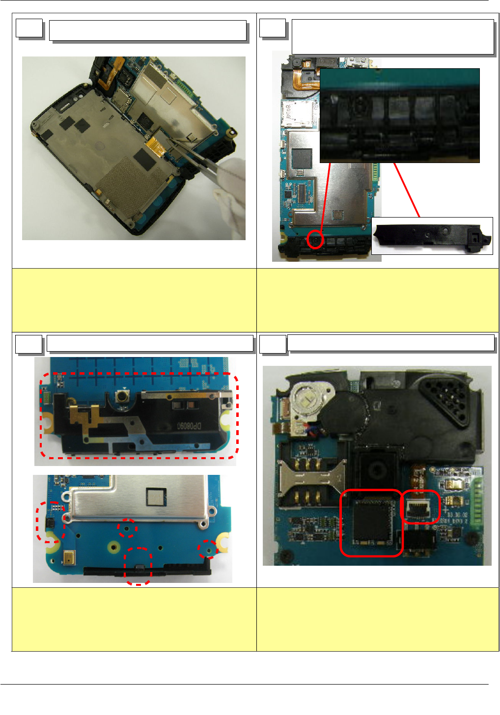
SAMSUNG Proprietary-Contents may change without notice
Exploded View and Parts List
7-3
This Document can not be used without Samsung's authorization
1) Be care of damage of connector and FPCB. 1) When unscrew, be care of Shooting out damage and
scratch not to occur
1) Be care of damage of surrounding components. 1) Be care of damage of connector and FPCB.
910
11 12
1) Disassemble LCD FPCB Connector 1) First unscrew Intenna screw 1point and
disjoint Intenna.
1) Disjoint Intenna. 1) Disassemble connector.
SAMSUNG Proprietary-Contents may change without notice
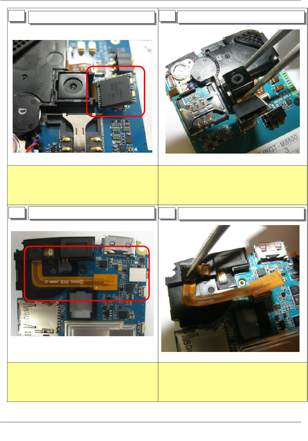
Exploded View and Parts List
7-4
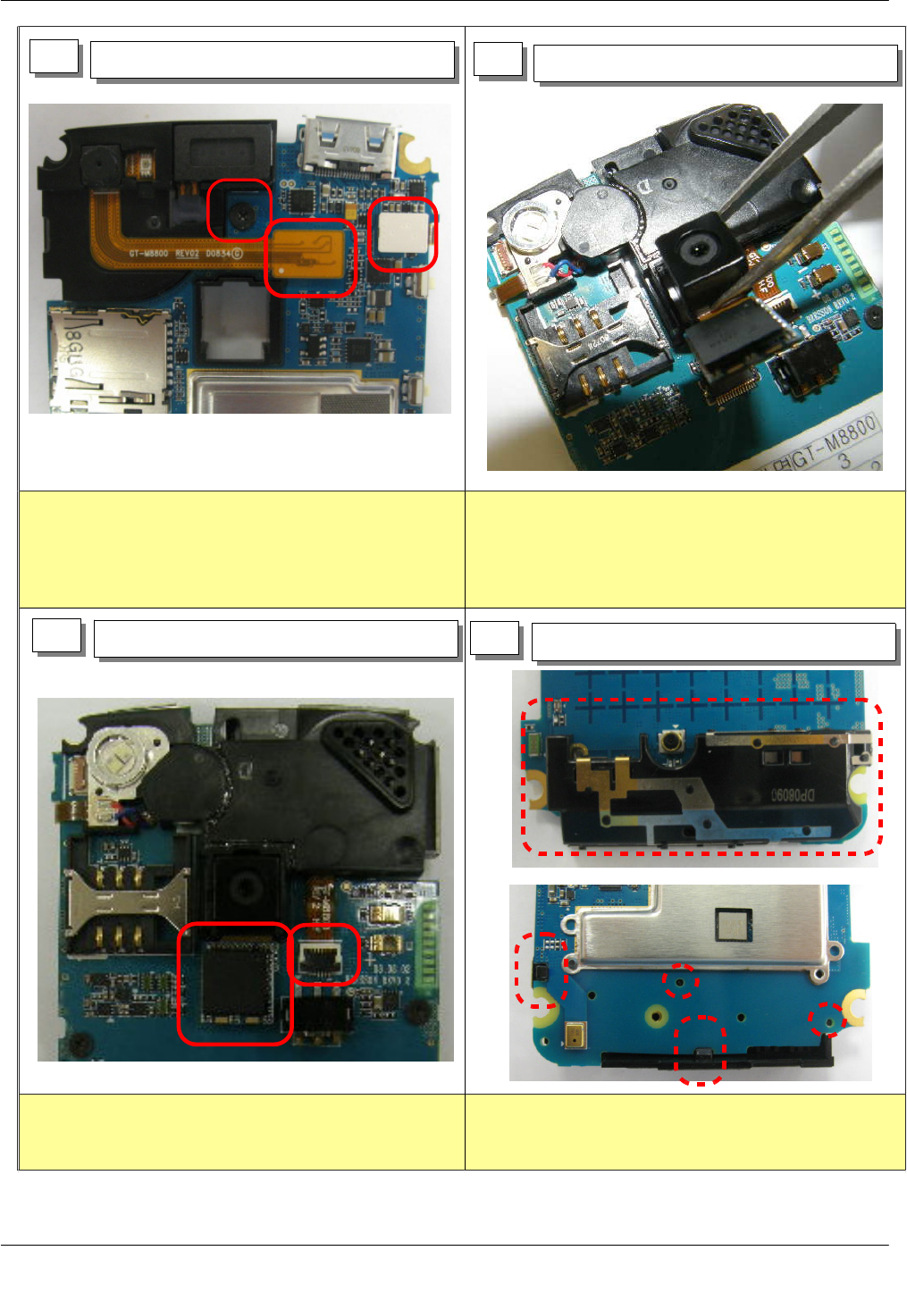
This Document can not be used without Samsung's authorization
1) Be care of damage of connector and FPCB. 1) Be care of shooting out Camera module and scratch
not to accur.
1) When unscrew,be care of damage and scratch not
to accur.
2) Be care of damage of connector and FPCB.
1) Be care of shhoting out Camera module and damage
of FPCB
13 14
15 16
Disjoint camera connector. 1) Disassemble Camera
1) Disjoint Connector and screw 1point 1) Disassemble CIF Camera
SAMSUNG Proprietary-Contents may change without notice
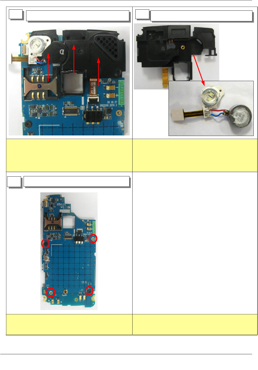
Exploded View and Parts List
7-5
This Document can not be used without Samsung's authorization
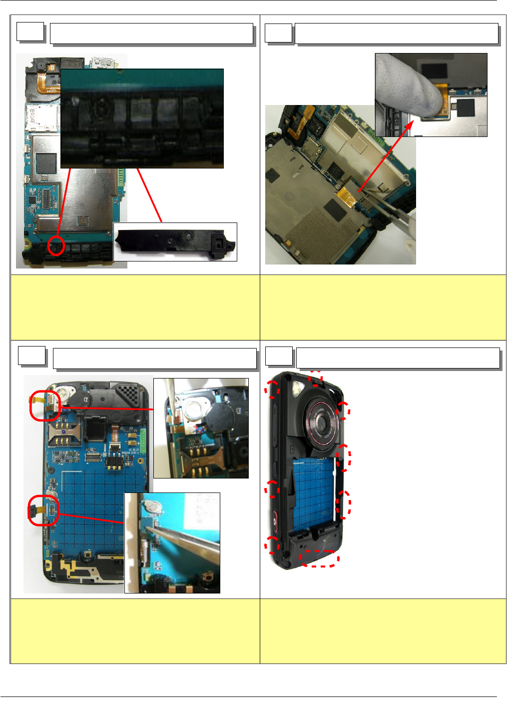
1) Be care of Shooting out damage and scratch not to
occur.
1) Be care of Shooting out damage and scratch not to
occur. .
①
②
③
④
1) Be care of Shooting out damage and scratch not
to occur.
17 18
1) Disassemble speaker bracket 1) Disassemble LED and vibration motor.
1) Unscrew 4point of shieldcan srew.
19
SAMSUNG Proprietary-Contents may change without notice
Exploded View and Parts List
7-6
This Document can not be used without Samsung's authorization
①
②
③
④
1) Be care of Shooting out damage and scratch not to
occur.
2) Screw size :
TORQUE :
1) Be care of Shooting out damage and scratch not to
occur..
1) Be care of Shooting out damage and scratch not to
occur.
1) Be care of shooting out aCamera module and
damage of aFPCB.
2
11) Joint aLED and avibration motor.
34
1) Assemble aspeaker bracket. 1) Jiont aCIF Camera
1) screw 4point of sheildcan.
7-2. Assembly
SAMSUNG Proprietary-Contents may change without notice
Exploded View and Parts List
7-7
This Document can not be used without Samsung's authorization
1) Be care of Shooting out damage and scratch not to
occur.
1) Be care of damage of FPCB.
Check the silkline.
1) Be care of Camera module's damage and scratch
1) Be care of FPCB's damage.
Check the silkline. 1) Be care of damage and scratch.
51) Assemble aConnector and screw 1point 61) joint aCamera
71) joint aConnector 81) Assemble aintenna
SAMSUNG Proprietary-Contents may change without notice
Exploded View and Parts List
7-8
This Document can not be used without Samsung's authorization
1) Be care of damage and scratch
2) Screw size :
TORQUE :
1) Be care of FPCB's damage
1) Be care of connector and FPCB's damage.
1)When you joint arear case from left side to right
side, be care of hooks and key hanging.
2) Screw size :
TORQUE :
91) Jiont Intenna screw 1point 10
11
1) Assemble aLCD FPCB Connector.
1) Joint SUB PBA Connector and TSP FPCB 1) Joint rear's hooks
12
SAMSUNG Proprietary-Contents may change without notice
Exploded View and Parts List
7-9
This Document can not be used without Samsung's authorization
1)Be care of damage and scratch
1) Joint screw 4point of rear.
13
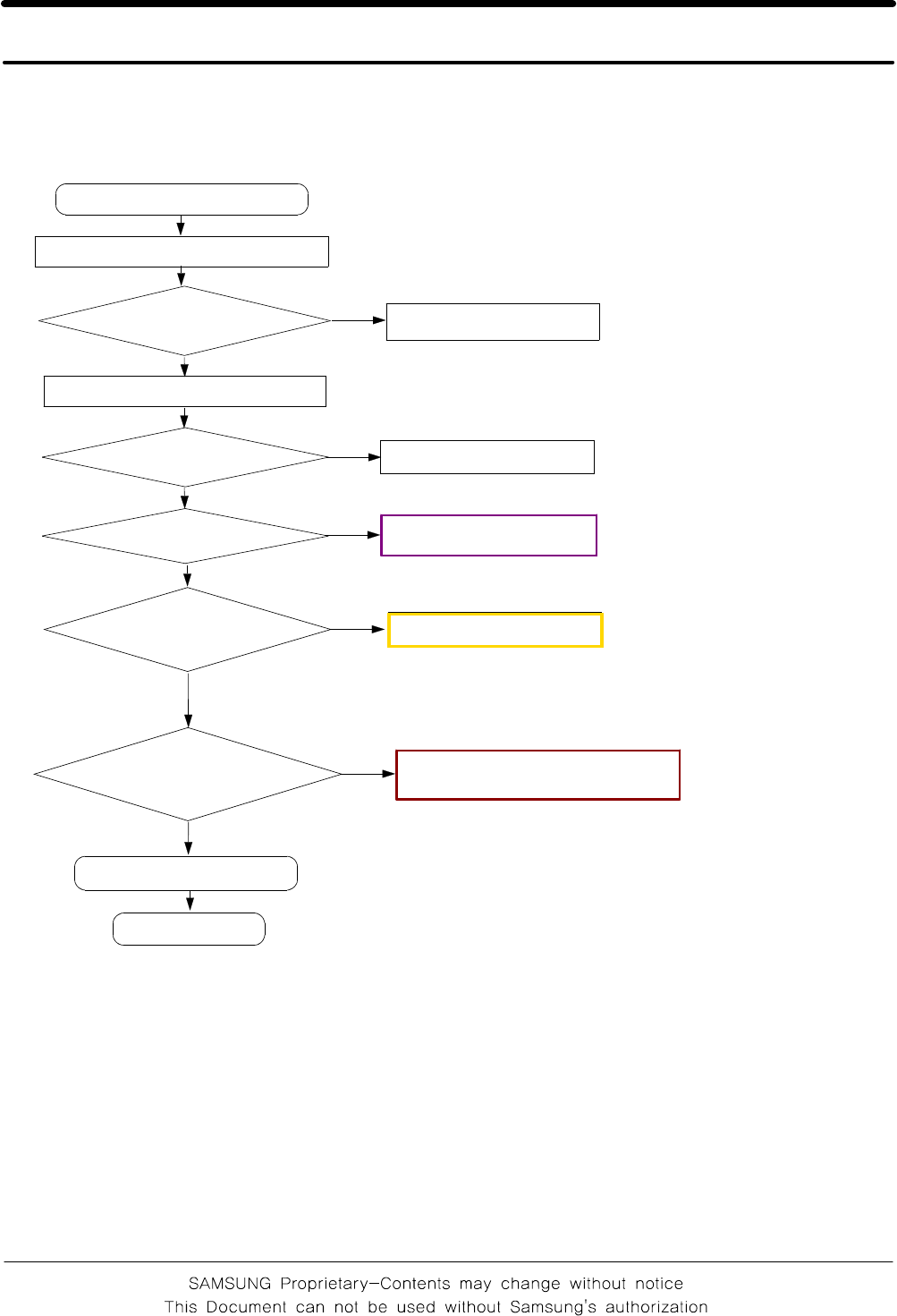
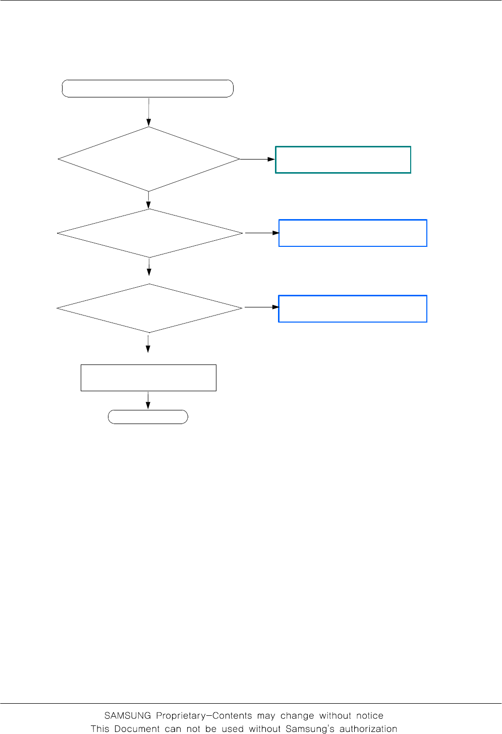
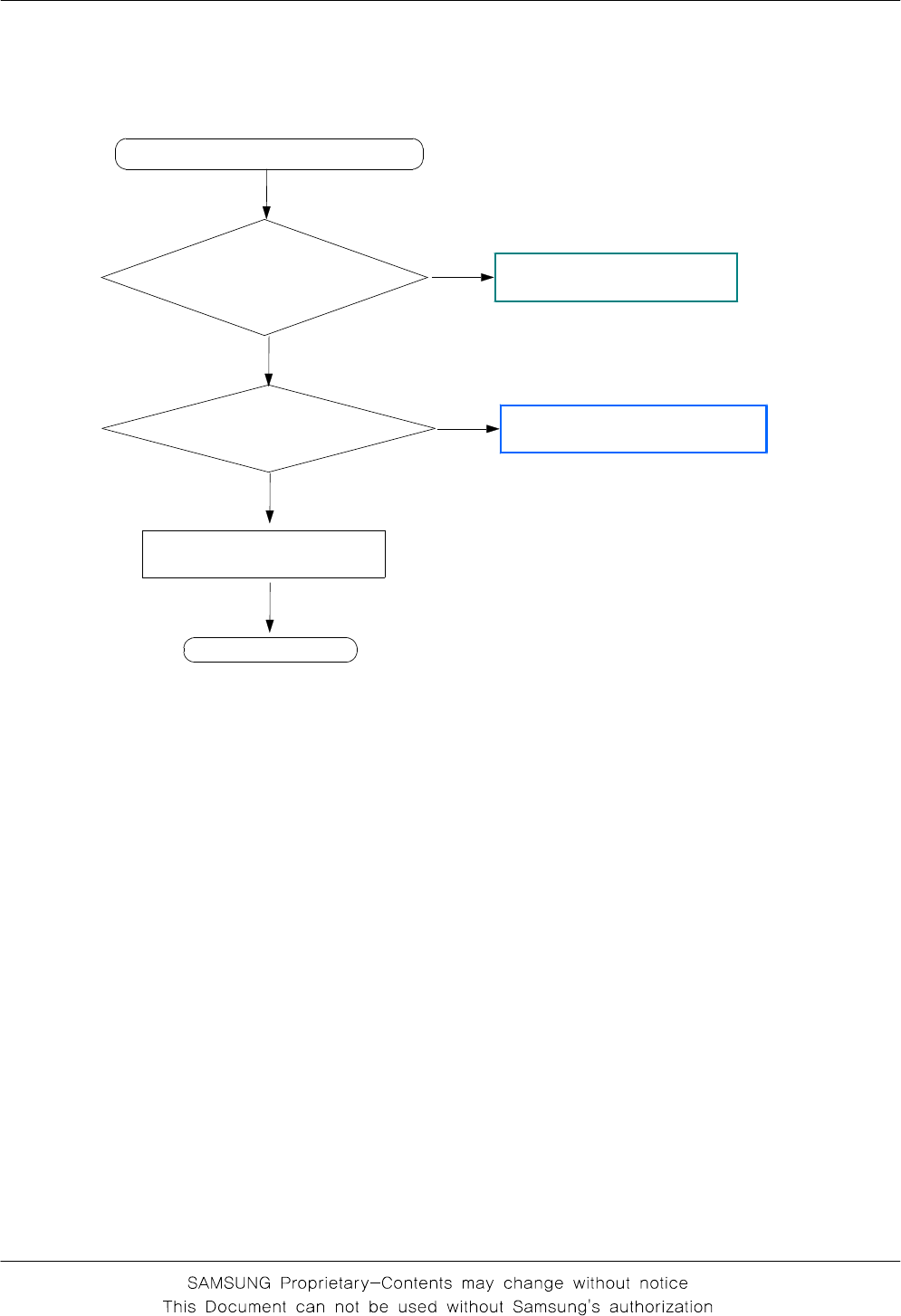
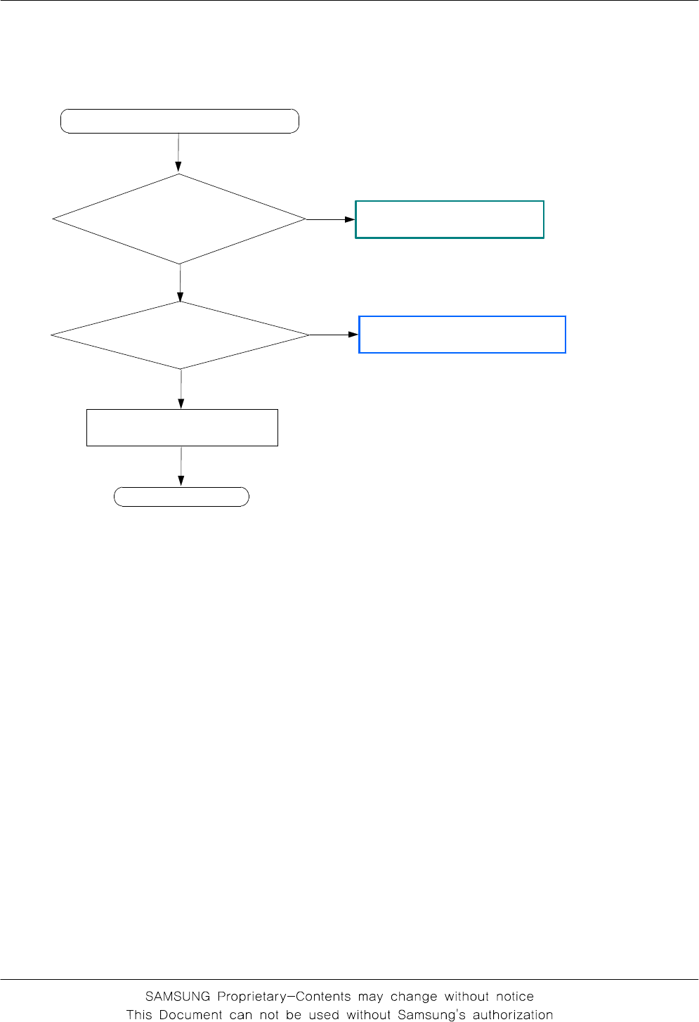
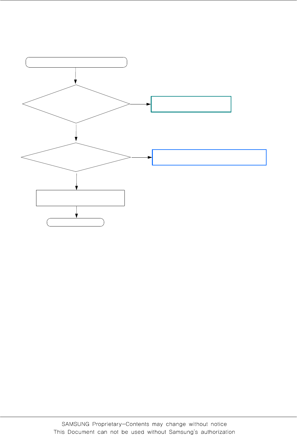
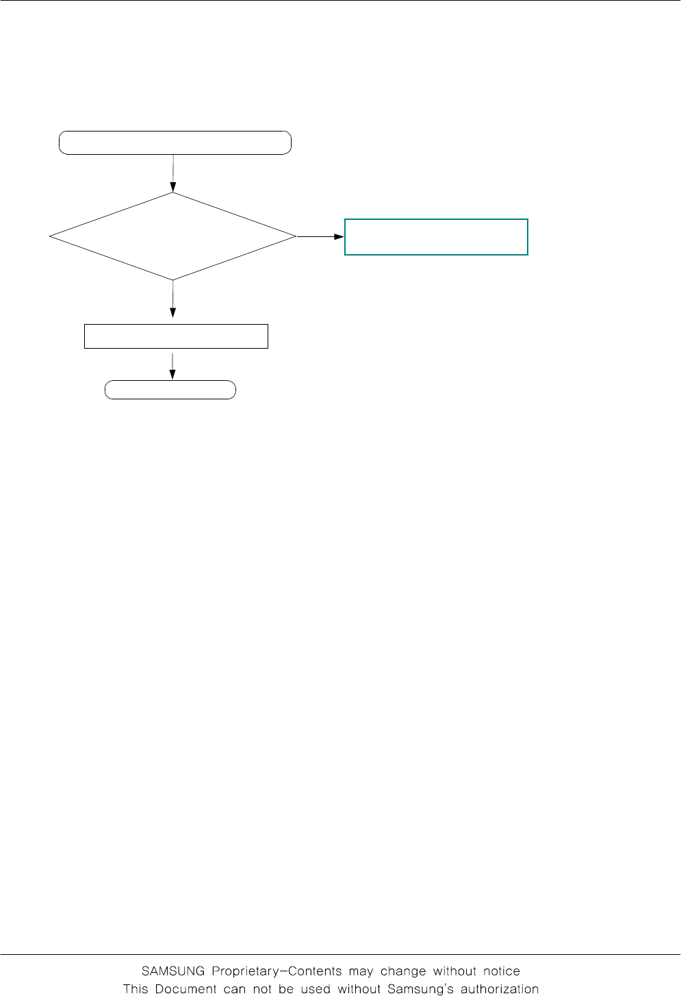
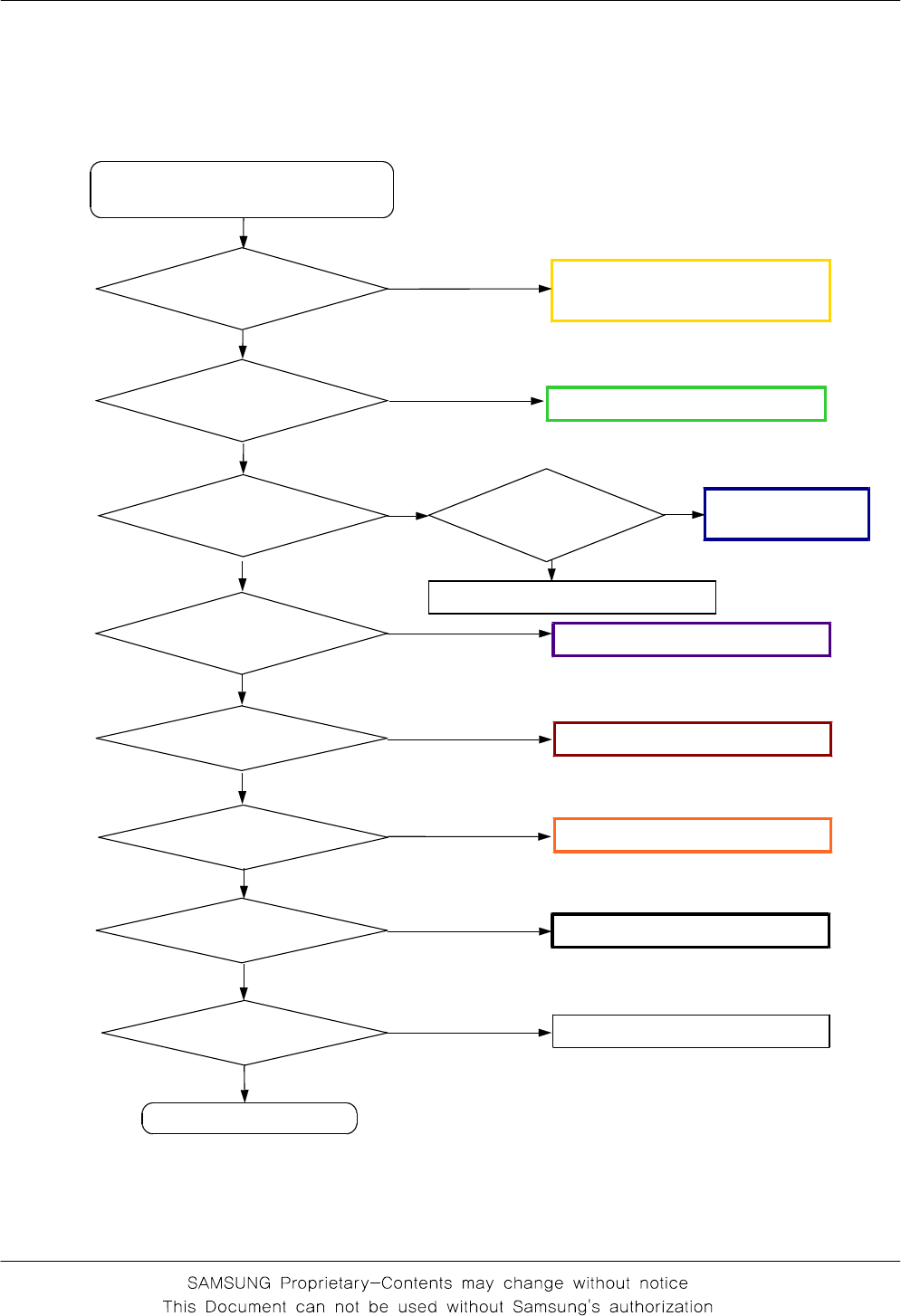
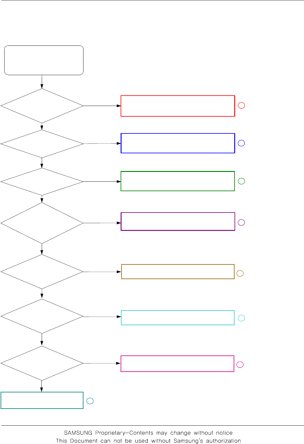
10. Flow Chart of Troubleshooting
10-1
10-1 BASEBAND
10-1-1. Power ON
'Power On' does not work
Voltage >=3.3V
Download again
Charge the Battery
U402 PIN
F10(PS_HOLD)=2.6V
Check the PMIC related to
PS_HOLD
check the PMIC output
voltage (C414, C415,
C417, C418, C419)
check the TCX200
C201=19.2Mhz?
Check the clock generation circuit
(relatedtoTCX200
)
Check the initial operation
END
No
Yes
Yes
Yes
Yes
Yes
Yes
No
No
No
Check the current consumption
Check the Vbat Voltage
Current consumption
>= 100mA
check the PMIC
No
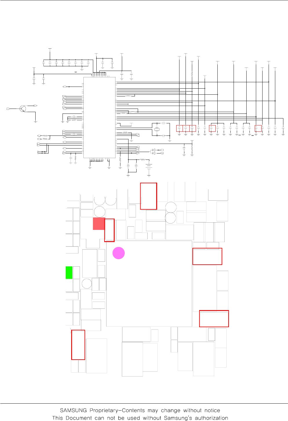
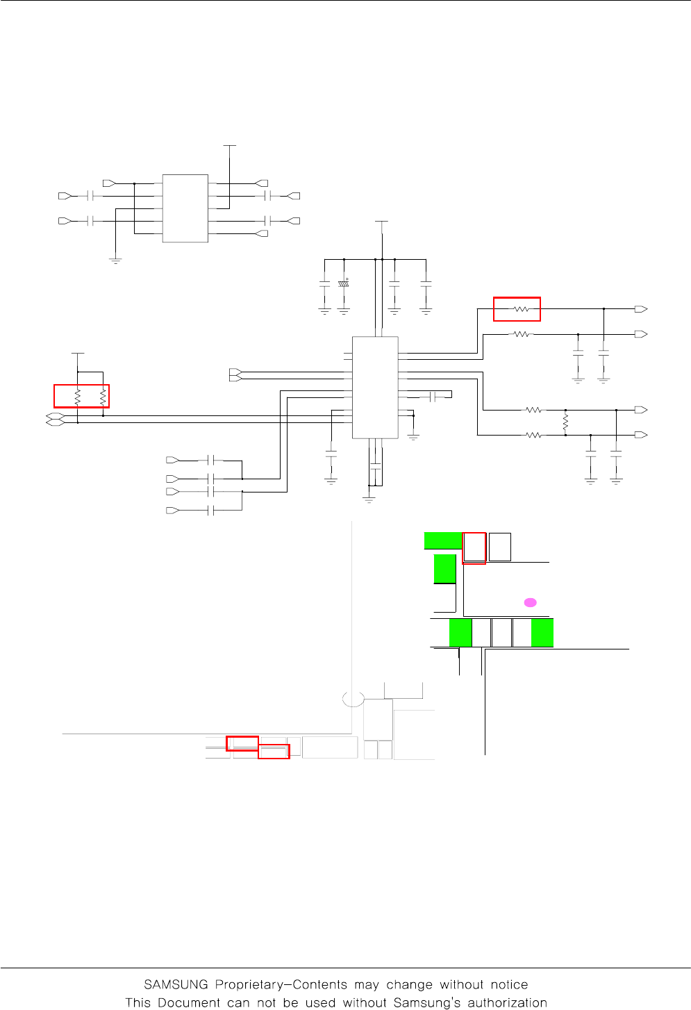
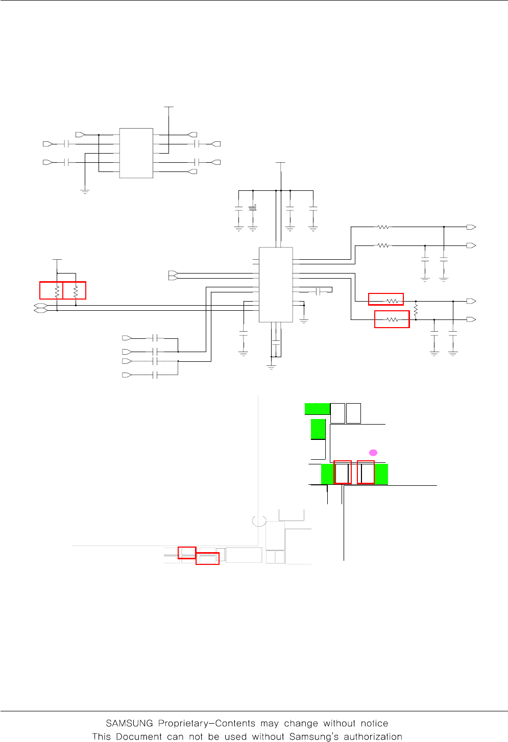
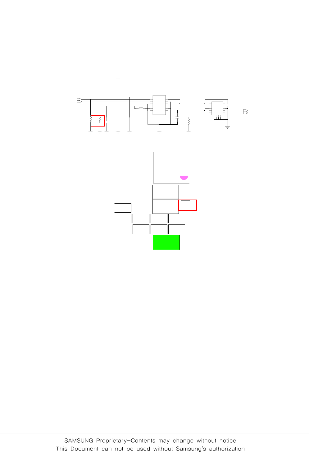
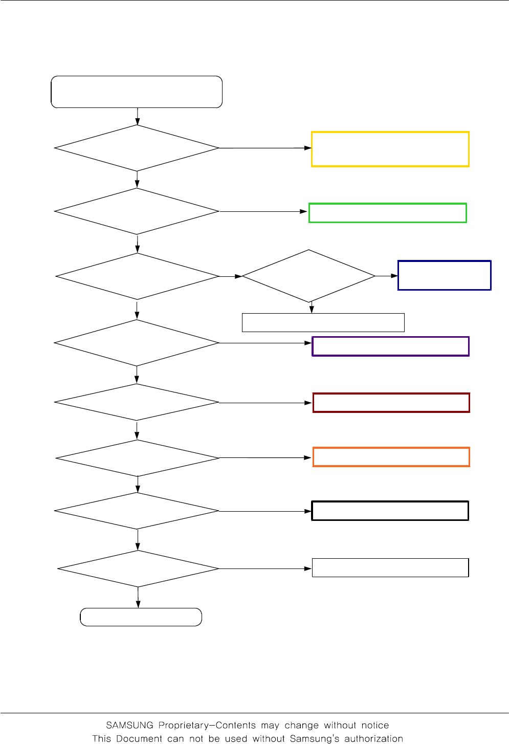
Flow Chart of Troubleshooting
10-2
< Power Management IC >
10V
10V
25V
< JIG Detect >
10V
C453
V_MMC_2.85V
C419
V_FEM_2.7V
VBATT_4.2V
C421
0603
R403
C456
C402
C413
C406
1005
C454 V_BT_2.6V
3
0
6
0
R411
C416
1005
R407
13
2
TR400
L401
C429
0603
C452
C431
V_MSMP_2.6V
VEXT_5V
C428
WPAM_BIAS_2.85V
C433
1005
C457
C422
V_MSMC_1.2V
V_USIM_3.0V
5
L
C
M
S
M
_
D
D
V
L6
VREG_S3
7
L
3
2
S
_
D
D
V
L8
VREG_S2
L9
VREG_MMC
K8
VREG_MSME
K9
SLEEP_CLK
L1 MPP4|LCD_DRV_N
L10
VREG_RUIM
L11
XTAL_IN
L2 KPD_DRV_N
L3 MPP3|VIB_DRV_N
L4
KPD_PWR_N
0
1
K
MI
U
R
_
D
D
V
K11
XTAL_OUT
K2 MPP7|CBLPWR_N
K3 AMUX_OUT
K4
VREG_MSMC K5
VSW_MSMC
K6
VSW_S3
K7
VSW_S2
H6 MPP10|RUIM_CLK
H7 MPP6|RUIM_RST
H8 OPT_2
J1 USB_D_M
J10
VCOIN
J11
VREG_MSMP
J2 USB_D_P K1
HSET_BIAS
7
GD
N
G
G8
SBDT|SSBI
H1 USB_VBUS
H10 TCXO_OUT_1
1
1
H
M
S
M
_
D
D
V
H2 USB_ID
H4 USB_SE0
H5 MPP12|RUIM_IO
F8
SBCK
1
G
V
5
_
G
E
R
V
G10
PON_RESET_N
G11
VREG_MSMA
G2
VREG_USB
G4 USB_DAT
5
GD
N
G
6
GD
N
G
1
F
V
5
_
W
S
V
F10
PS_HOLD
F11 TCXO_OUT_RF
F2 USB_OVP_G
F4 USB_OE_N
5
FD
N
G
6
FD
N
G
7
FD
N
G
E10 REF_GND
E11 TCXO_IN
E2
BAT_FET_N
E4 TCXO_EN_2
5
ED
N
G
6
ED
N
G
7
ED
N
G
E8
SBST
1
1
DC
N
D
D2
ISNS_P
D4 OPT_1
D5 MPP11|RUIM_M_IO
D6 MPP9|RUIM_M_CLK
D7 MPP5|RUIM_M_RST
D8 TCXO_EN_1
1
E
T
A
B
V
B8
VREG_RFUBM
9
B
F
R
_
D
D
V
C1
VCHG
C10
MSM_INT_N
C11 REF_BYP
C2
CHG_CTL_N
D1
ISNS_M
D10 REF_ISET
B10 TCXO_OUT_2
B11
VREG_WLAN
2
B
NI
A
M
_
D
D
V
3
B
P
G
_
D
D
V
B4 MPP8|REF_OUT
B5 SPKR_IN_M
B6 SPKR_IN_P
B7 MPP2|AMUX_IN2
A3
VREG_GP1
4
A
R
K
P
S
_
D
D
V
A5 SPKR_OUT_M
A6 SPKR_OUT_P
A7 MPP1|AMUX_IN1
A8
VREG_RFTX
A9
VREG_RFRX1
B1
VREG_GP3
1C
N
2C
N
A1
VREG_TCXO
A10
VREG_RFRX2
1
1
A
N
A
L
W
_
D
D
V
A2
VREG_GP2
U402
V_RF_2.1V
C404
V_RF_2.1V
VBATT_4.2V
1005
R400
L400
C427
C408
C424C418
V_TCXO_2.85V
C423
C409
C405
C420
TP_AMUX_OUT
21
TP_PM_INT R406
OSC400
3
0
6
0
C425
TP_RFUBM
C400
0603
R408
R424
1005
C430
C432
C438
0603
R402
C426
TP_PS_HOLD
C414
0603
R401
BAT400
2
NEG
1POS
C401
C417
V_MSME_1.8V
V_RF_2.7VVBATT_4.2V
C407
TP_SLEEP_CLK
C415
C412
C437
L402
D400
3
1
2
V_RF_2.7V
C403
V_MSMA_2.6V
USB_VBUS_5V
USB_DM_JTAG
USB_DM_MODEM
USB_DP_MODEM
USB_DP_JTAG
TCXO_FF
JIG_ON
JIG_ON_SW
BT_TCXO_EN
BT_TCXO_OUT
JIG_ON_SW
REF_OUT
AMUX_OUT
USIM_RST
PMIC_SBST
SSBI2_DATA
RESET_N PS_HOLD
BOOT_SW
ON_SW
USB_DAT
USB_OE_N
USB_SEO
CLK19.2M_TCXO
TCXO_EN
CLK19.2M_PM
PM_INT_N
SLEEP_CLK
SIM_IO
SIM_CLK
SIM_RST
USIM_IO
USIM_CLK
C300
C305
C318
C319
C324
5
2
3
C
C330
1
3
3
C7
3
3
C
8
3
3
C
C341
C345
0
5
3
C
3
5
3
C
C354
5
5
3
C
6
5
3
C
7
5
3
C
8
5
3
C
5
6
3
C
C400
C401
2
0
4
C
3
0
4
C
4
0
4
C
5
0
4
C
6
0
4
C
C407
C408
9
0
4
C
C412
3
1
4
C
4
1
4
C
5
1
4
C
6
1
4
C
C417
C418
9
1
0
2
4
C
1
2
4
C
2
2
4
C
3
2
4
C
4
2
4
C
5
2
4
C
6
2
4
C
7
2
4
C
8
2
4
C
C429
0
3
4
C
C431
2
3
4
C
3
3
4
C
C452
C453
C454
C456
C457
1
0
5
C
2
0
5
D400
0
0
4
L
1
0
4
L
2
0
4
L
0
0
4
C
S
O
0
0
3
R
3
1
3
R
3
2
3
R
5
2
3
R
0
0
4
R
1
0
4
R
6
0
4
R
R408
1
1
4
R
R424
3
0
5
R
R504
TP_AMUX_OUT
W
S
_
T
O
O
B
_
P
T
TP_PM_INT
TP_PS_HOLD
TP_RESETOUT_N
TP_RFUBM
N
_
T
S
R
2
0
4
U
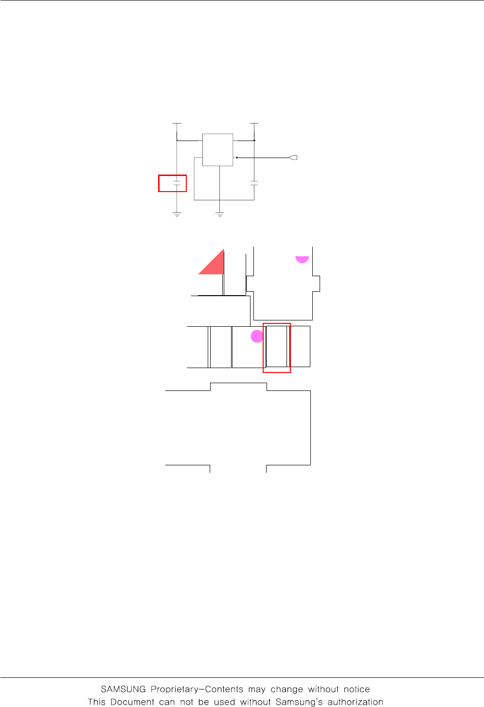
Flow Chart of Troubleshooting
10-3
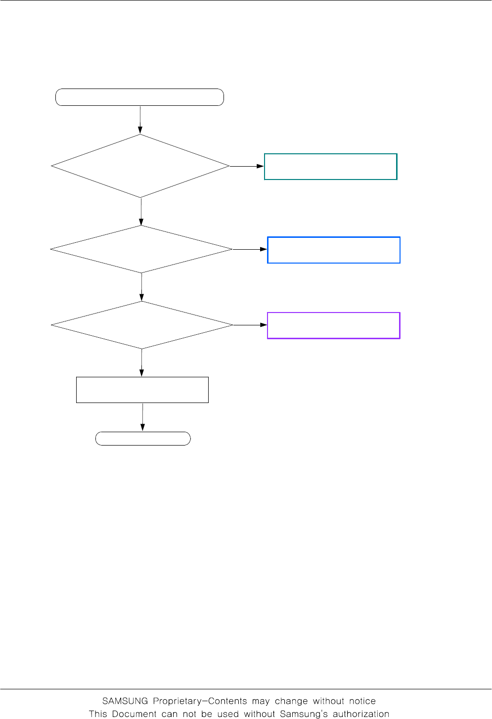
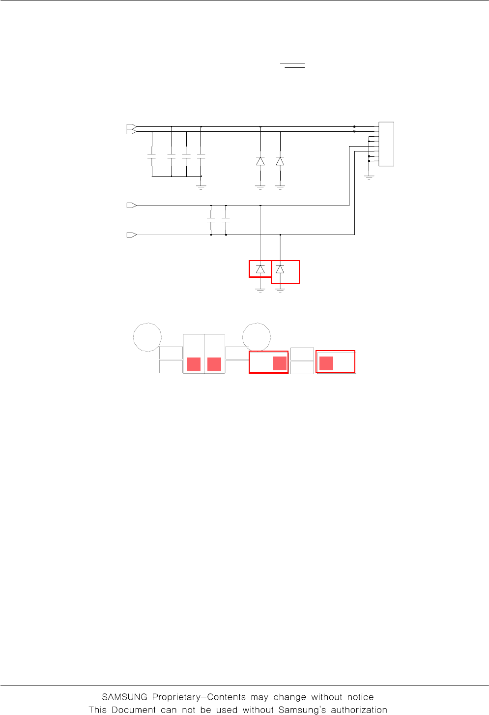
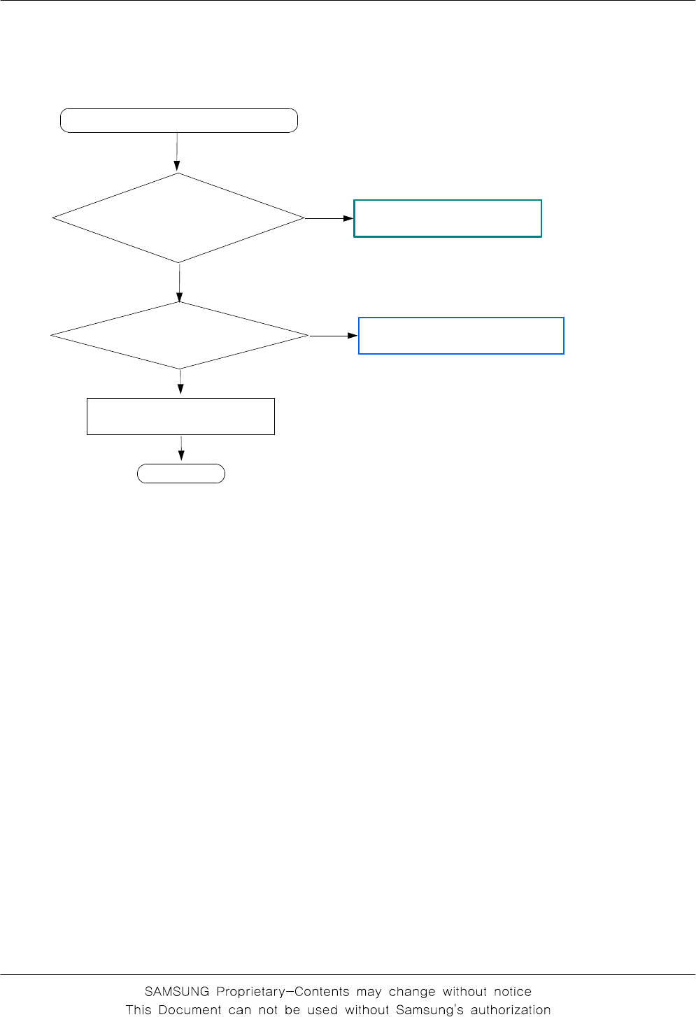
10-1-2. Sim Part
Check the voltage at
pin#1(C442) of SIM400 >=
3.0V ?
"Insert SIM"is displayed on the LCD
Check the SIM connector's
(SIM400) connection to
SIM card
Check the PMIC
Resolder or change SIM400
END
No
Yes
Yes
Yes
Yes
No
No
Is there any signals
pin#2,#3,#4of SIM400 ? Check the PMIC
Check the SIM Card
Flow Chart of Troubleshooting
10-4
< USIM Connector >
C439 C442
V_USIM_3.0V
C441
ZD401
1
2
3
4
5
6
6
G
78
GG
910
G
SIM400
11
22
33 4
4
5
5
6
C443
1005
R413
USIM_IO
USIM_CLK
USIM_RST
C439
1
4
4
C
2
4
4
C
3
4
4
C
R413
SIM400
ZD401
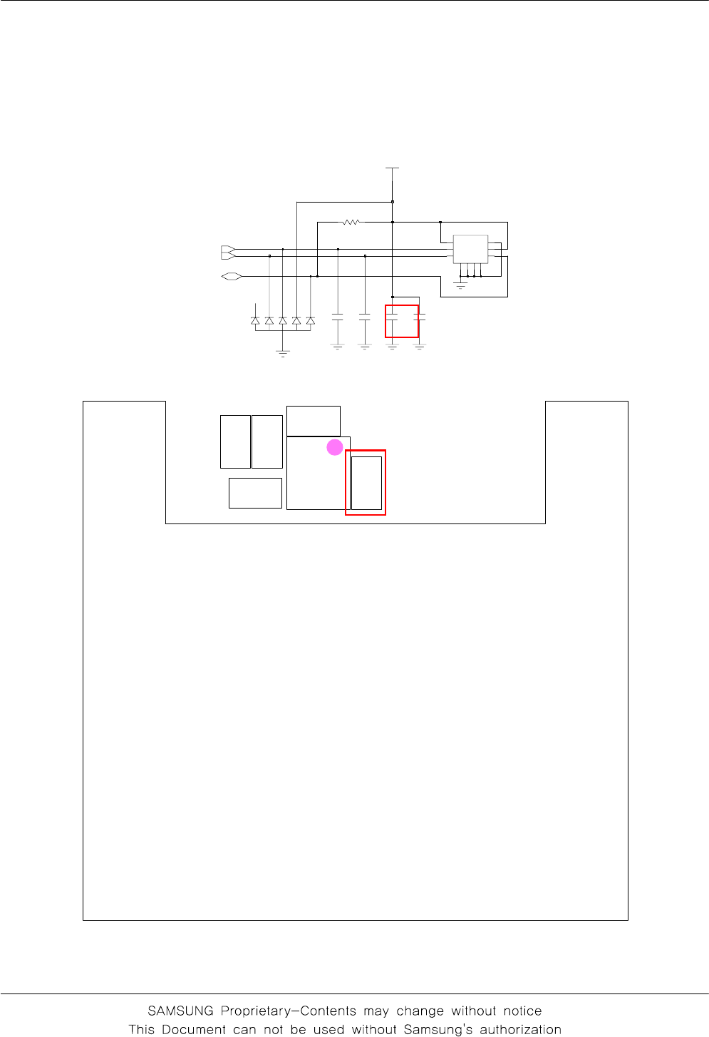
Flow Chart of Troubleshooting
10-5
10-1-3. Charging Part
When U401 is charging,
U401 pin #4 = "L" ?
Abnormal charging part
C434 at USB_5V or
C435 at EXT_5V =5V?
Replace U401
Resolder U402
END
No
Yes
Yes
Yes
Yes
No
No
Check the battery &TA Check the PMIC
Flow Chart of Troubleshooting
10-6
1%
< Charging IC >
C434
_CHG
5_EN
_PPR
3
BAT
1CRDL
GND
11
8
GND
ICDL 9
IMIN 6
2USB
7
USBON
4
U401
10
R409
5
0
0
1
R410
1005
C435
C436
3
0
6
0
R423
R404
3
0
6
0
VBATT_4.2VV_MSME_1.8V
R405
0603
VEXT_5V
CHG_EN_N
CHG_INDICATE USB_VBUS_5V
USB_VBUS
C434
C435
C436
R404
R405
R409
R410
U401
Flow Chart of Troubleshooting
10-7
10-1-4. Microphone Part -PHONE Mic
Is the DC bias voltage on
Normal MIC path at C560
1.8V?
Normal Microphone does not work
Is the assembled status of
Normal mic ok?
Check the path around Noraml MIC bias circuit
Reassemble the Normal mic
END
No
Yes
Yes
Yes
Yes
No
No
Is the Normal Mic path
component soldering status
ok ?Resolder the trouble point
Is Normal microphone ok?
No
Replace the MIC
Flow Chart of Troubleshooting
10-8
C558
R519
2
GND
GND2
3
GND
OUT
4
OUT
POWER
1
POWER
MIC500
GND1
C559
C537
C560
C540
V_MICBIAS_1.8V
REC_MIC1_P
MIC1_N
MIC1_P
C102
6
0
1
C
5
0
1
C
C109
8
5
5
C
9
5
5
C
0
6
5
C
C842
7
0
1
L0
1
1
L
2
1
1
L
L114
L131
9
1
5
R
U100
Flow Chart of Troubleshooting
10-9
10-1-5. Speaker part
Is there any signals at the
pin #B3(R508), #C3(R507)
of U502?
There is no sound from the speaker
Is the Normal Mic path
component soldering status
ok ?
Check the MSM6281
Resolder the trouble point
No
Yes
Yes
Yes
No
Change the speaker module
END
Is there any signals at the
pin #B5(R502) of U502 ?
Yes
Check the U502
No
Flow Chart of Troubleshooting
10-10
< Mono Class-D AMP >
C531
C504
C526 C528
C513C512
C530
R502
V_MSMP_2.6V
R505
C529
C520
VBATT_4.2V
C525
R509
R511
C506
C516
C515
4
VCC 8
V_MSMP_2.6V
1
CB2
5
COM1 10
6
COM2
3GND
9
NC
NC 7
NO1
2
NO2
U504
CB1
C519
C511
R508R507
C527
TA500C505
C524
B4 RXIN-
D4
SCL
C3 SDA
B3
1
B
D
D
V
S
S
V
3
A
INB1
INB2
C1
NC 1
NC 2
B5
OUT+
D5
OUT-
4
C
D
N
G
P
D
D
V
P5
C
RXIN+
B2
A4
C1N
C1P A5
D
N
G
3
D
A2
HPL
HPR A1
INA1
D2
D1 INA2
C2
U502
BIAS
0
1
5
R
AUDIO_N
AUDIO_P
AUDIO_N
AUDIO_P
AUDIO_CTRL
CODEC_SPK_N
CODEC_SPK_P
HPH_L
HPH_R
CODEC_EAR_L
CODEC_EAR_R
RADIO_OUT_L
RADIO_OUT_R
AMP_I2C_SCL
AMP_I2C_SDA
AMP_SPK_P
AMP_SPK_N
EAR_R
EAR_L
4
3
3
C
C335
C351
C352
4
1
4
C
2
2
4
C
3
2
4
C
C454
0
0
4
L
R314R315 R507
R508
TP_AMUX_OUT
2
0
3
C
C303
4
0
5
C
2
1
5
C
C513
5
2
5
C
8
2
5
C
2
0
5
R
5
0
5
R
9
0
5
R
0
1
5
R
1
1
5
R
U502
Flow Chart of Troubleshooting
10-11
10-1-6. Receiver part
Is the assembled status of
speaker module ok?
There is no sound from the receiver
Is there any signals at the
pin #5(ZD500), #6(ZD501)
of SLC500?
Reassemble the speaker module
check the MSM6281 or connector
END
No
Yes
Yes
Yes
No
Change speaker module
Yes
Flow Chart of Troubleshooting
10-12
< Speaker / Receiver CON >
ZD500
ZD502
C542
ZD501
TP_SPK_P
TP_SPK_N
C548 C549 C551
1
2
2
33
44
5
5
66
7NC
NC
8
SLC500
1
ZD503
C541
C550
RCV_N
AMP_SPK_N
AMP_SPK_P
RCV_P
C541
C542
C548 C549
C550 C551
N
_
K
P
S
_
P
T
P
_
K
P
S
_
P
T
ZD500ZD501
2
0
5
D
Z
3
0
5
D
Z
Flow Chart of Troubleshooting
10-13
10-1-7. Ear mic Part -MIC CABLE
Is there any signals at the
pin #A1(R509), #A2(R511)
of U502?
There is no sound from the Ear mic
Is there any signals at the
pin #B3(R508), #C3(R507)
of U502?
CHECK the U502
check the MSM6281
END
No
Yes
Yes
Yes
No
Check the IFC700 or change the Earmic
Flow Chart of Troubleshooting
10-14
< Mono Class-D AMP >
C531
C504
C526 C528
C513C512
C530
R502
V_MSMP_2.6V
R505
C529
C520
VBATT_4.2V
C525
R509
R511
C506
C516
C515
4
VCC 8
V_MSMP_2.6V
1
CB2
5
COM1 10
6
COM2
3GND
9
NC
NC 7
NO1
2
NO2
U504
CB1
C519
C511
R508R507
C527
TA500C505
C524
B4 RXIN-
D4
SCL
C3 SDA
B3
1
B
D
D
V
S
S
V
3
A
INB1
INB2
C1
NC 1
NC 2
B5
OUT+
D5
OUT-
4
C
D
N
G
P
D
D
V
P5
C
RXIN+
B2
A4
C1N
C1P A5
D
N
G
3
D
A2
HPL
HPR A1
INA1
D2
D1 INA2
C2
U502
BIAS
0
1
5
R
AUDIO_N
AUDIO_P
AUDIO_N
AUDIO_P
AUDIO_CTRL
CODEC_SPK_N
CODEC_SPK_P
HPH_L
HPH_R
CODEC_EAR_L
CODEC_EAR_R
RADIO_OUT_L
RADIO_OUT_R
AMP_I2C_SCL
AMP_I2C_SDA
AMP_SPK_P
AMP_SPK_N
EAR_R
EAR_L
4
3
3
C
C335
C351
C352
4
1
4
C
2
2
4
C
3
2
4
C
C454
0
0
4
L
R314R315 R507
R508
TP_AMUX_OUT
2
0
3
C
C303
4
0
5
C
2
1
5
C
C513
5
2
5
C
8
2
5
C
2
0
5
R
5
0
5
R
9
0
5
R
0
1
5
R
1
1
5
R
U502
Flow Chart of Troubleshooting
10-15
10-1-8-1. Camera
Check the camera
connector
Camera does not work
Check the voltage 1.2V of
C611, C612?
Reconnect the Camera FPCB
CHECK the U607
END
No
Yes
Yes
Yes
No
Change the Camera module
Flow Chart of Troubleshooting
10-16
< 8MP Camera Connector >
5
1
6
C
VDD_MCAM_ISP_2.8V
6
1
6
C
6
0
6
C
C605
77 8 8
99
2727 28 28
29 29
33
30
30
44
55 6
6
2
2
20 20
2121 22
22
23 23 24 24
25 25 26
26
12 12
1313 14
14
15 15 16 16
1717 18
18
19 19
HEA601
11
10
10
11 11
3
0
6
D
Z
VDD_MCAM_AF_3.3V
L601
7
0
6
C
8
0
6
C
5
0
6
D
Z
1
0
6
D
Z
2
0
6
D
Z
1
1
6
C
VDD_MCAM_DIGI_1.8V
4
1
6
C
3
1
6
C
VDD_MCAM_CORE_1.2V
9
0
6
C
L600
2
1
6
C
4
0
6
D
Z
VDD_MCAM_ANA_2.8V
0
0
6
D
Z
CAM_VSYNC_F
MCAM_RST_F
CAM_I2C_SDA
CAM_I2C_SCL
0
1
6
C
CAM_DF(4)
CAM_DF(7)
CAM_DF(3)
MV_CAM_PCLK
MCAM_INT_F
CAM_HSYNC_F
CAM_MCLK
CAM_DF(0)
CAM_DF(2)
CAM_DF(1)
CAM_DF(6)
CAM_DF(5)
2
3
5
C
3
3
5
C
4
3
5
C
C607
C608
C609
C610
C611C612
C636
C637
C639
4
4
6
C
5
4
6
C
6
4
6
C
7
4
6
C
C648
9
4
6
C
0
0
6
F
1
0
6
F
2
0
6
F
8
0
6
F
0
0
6
L
R316
2
2
5
R
R627
8
2
6
R
R631
6
3
6
R
R831
D
_
M
A
C
_
P
T
3
0
5
U
0
1
6
U
U619
1
2
6
U
0
0
6
D
Z1
0
6
D
Z2
0
6
D
Z
Flow Chart of Troubleshooting
10-17
10-1-8-2. Camera Flash
Yes
Change the Flash LED &moter module
END
Camera Flash does not work
Check the voltage
pin#3(R611) of U601="H"? Resolder U601
Yes
No
Check the Flash LED &
moter module connector Reconnect the Flash LED &moter module FPCB
No
Yes
Flow Chart of Troubleshooting
10-18
< CAM FLASH LED DRIVER >
R611
C601
C603
8
99
NC
11 12
NCNC
13 14
NC
11
1010
22
3344
5566
778
VBATT_4.2V
HDC600
L602
R612
R610
8
OUT
PGND
7
RSET
14
SW
6
FLEN
312
FLGND
FLINH
10
13
FLOUTA
FLOUTB
11
9
GND
15
D
N
G
5
IN
U601
4
AGND
1
CT
EN|SET
2
C602
MOT_N
MOT_P
CAM_FLASH_MODE
CAM_FLASH_EN
C606
C623
C624
C625
C626 C627
C628
R610
R611
R620
R705
R706
7
0
7
R
Z
Flow Chart of Troubleshooting
10-19
10-1-8-3. Vibration
Vibration does not work
Yes
Check the voltage pin
#1(C618)=3.3V of U603 ?
No
Resolder U603
Yes
Check the Flash LED &
moter module connector Reconnect the Flash LED &moter module FPCB
No
Yes
Change the Flash LED &moter module
END
Flow Chart of Troubleshooting
10-20
< Motor Power - 3.3V >
VBATT_4.2VV_MOT_3.3V
C619
3
CE
D
N
G
5
GND
2
4
VDD
1VOUT
U603
C618
MOTOR_PWR_EN
0
0
2
C
8
1
6
C
9
1
6
C
0
2
6
C
1
2
6
C
HDC600
L200
U603
U604
6
0
7
D
Z
Flow Chart of Troubleshooting
10-21
10-1-8-3. Camera Lens Cover
Camera lens cover does not open
Check the voltage pin
#1(ZD714) of U701 ="
L" ?Resolder U701
Yes
Yes
No
Change the Camera lens cover
END
Flow Chart of Troubleshooting
10-22
< Camera Lens Cover >
C712
5
1
7
D
Z
R712
VBATT_4.2V
3VDD VREF 6
5
VSET
R714
GND
2
9
D
N
G
7
IN1
IN2 8
OUTA
4
1OUTB
U701
4
1
7
D
Z
C713
SHUTTER_OUT_N
SHUTTER_OUT_P
SHUTTER_N
SHUTTER_P
C707
R308
R309
R310
SHUTTER700
SHUTTER701
ZD710
ZD714
ZD715
Flow Chart of Troubleshooting
10-23
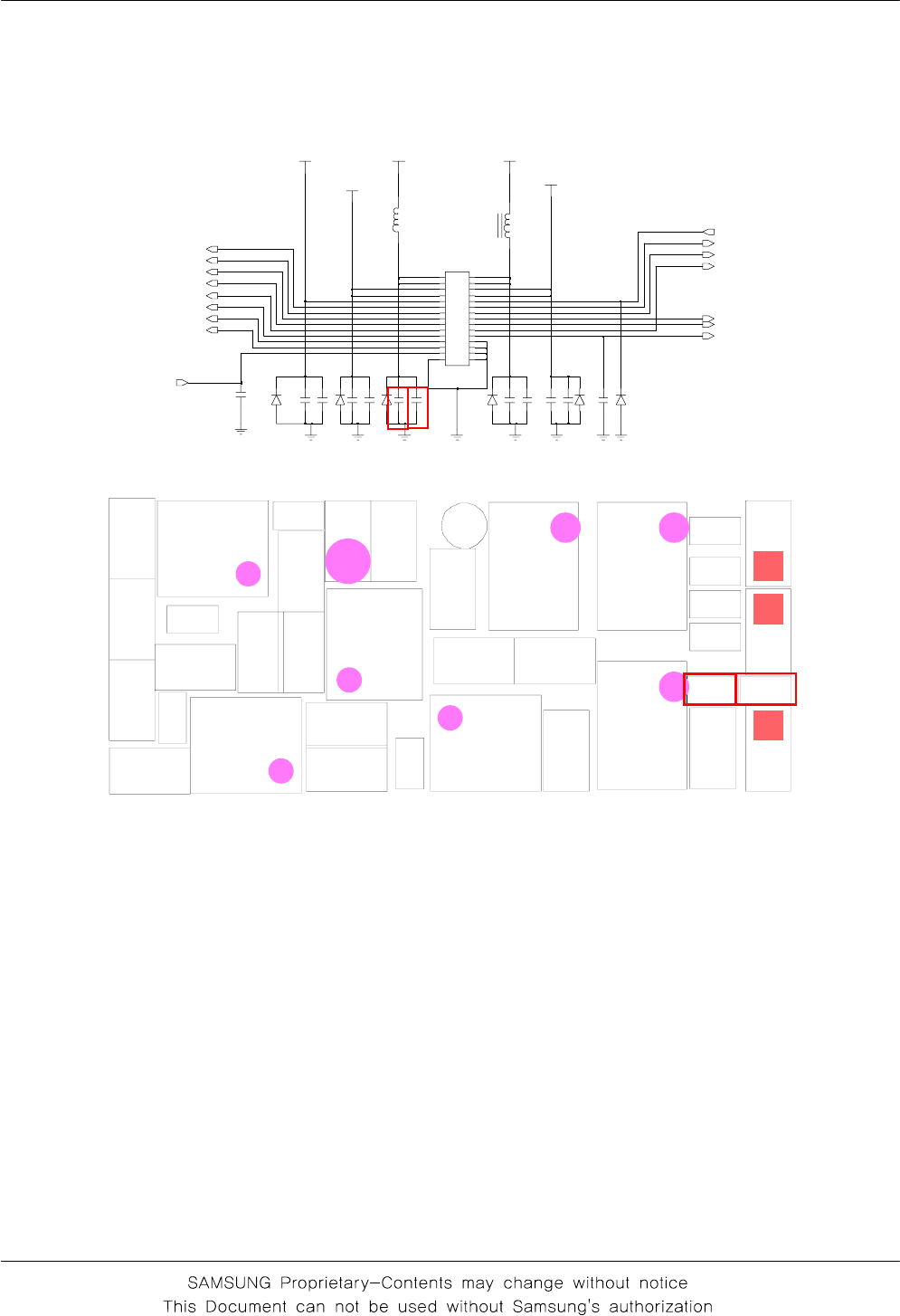
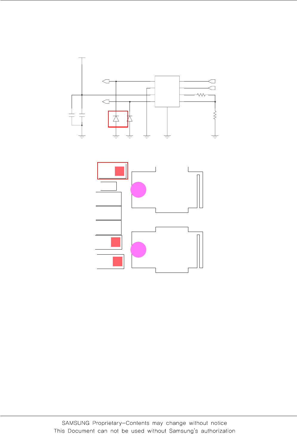
10-1-9. Bluetooth
< BLUETOOTH >
TP_BT_TXD
F200
1
GND1 GND2
3
4IN 2
OUT
L201
L202
C215
C219
TP_BT_INT
C213
V_BT_2.6V
C211
R209
TP_TCXO_EN
V_MSMP_2.6V
R206
C216
TP_BT_RXD
TP_CTS
C218
R210
C220
TP_RST
R208
C221
C222
TP_SLEEP
ANT200
12
C214
J8
HUSB_DN
9
J
O
D
D
V
TP_RTS
9
H
O
D
D
V
1
J
P
FI
D
D
V
J2
VCTRIFP
J3
RES
J4
XTALN J5
XTALP
J6 TM0 J7
HUSB_DP
1
H
O
C
V
D
D
V
2
HS
S
V
3
HS
S
V4
H
O
X
D
D
V
H5 TM2
H6 TM1
H7
GPIO7
H8
PA_CTL|GPIO6
5
FS
S
V
6
FS
S
V
F8 PCM_CLK|SCK
F9
STATUS|GPIO_4
1
G
O
L
D
D
V
2
G
L
L
P
D
D
V
8
G
B
S
U
_
O
D
D
V
G9
XTAL_PD|GPIO5TX_PU_TDD
4
ES
S
V
5
ES
S
V
6
ES
S
V
E8 PCM_IN E9
BT_PRIORITY|TX_REZ|GPIO3
1
FS
S
V
2
FS
S
V
4
FS
S
V
2
DS
S
V
D4
TST1
5
DS
S
V
6
DS
S
V
D8 PCM_SYNC
D9 PCM_OUT
E1
RFION
2
ES
S
V
7
B
C
D
D
V
B8 UART_TXD
B9 UART_RXD
C1
RFIOP
2
CS
S
V
C8 UART_CTS_N
C9 UART_RTS_N
D1
RFTUNE
A8 SDA|TX_PU_TDD
A9 SCL|TX_PU_TDD_N
1
B
F
T
D
D
V
2
B
F
R
D
D
V
B3 VREG_CTL
B4
RST_N
B5
BT_WAKE|GPIO_0 B6
HOST_WAKE|GPIO_1
2C
N
1
A
FI
D
D
V
A2 VREG2
A3 VREG1
4
A
V
3
R
D
D
V
A5
LPOIN
A6
WLAN_ACTIVITY|TX_CONFIRM|GPIO_2
7
A
C
D
D
V
U201
1C
N
C210
C212
TP_BT_WAKE
MSM_PCM_DIN
MSM_PCM_DOUT
BT_WAKE
BT_INT
BT_TCXO_EN
BT_TCXO_OUT
BT_RTS
BT_CTS
BT_UART1_TXD
BT_UART1_RXD
MSM_PCM_SYNC
MSM_PCM_CLK
BT_SLEEP SLEEP_CLK
BT_RST_N
Bluetooth does not work
Yes
Check the voltage
C213=2.6V and C214=2.6V
of U101
No
Resolder U402
Yes
The signal of C219
≥-6dBm Resolder U201
No
Yes
Check the signal of
ANT200 Resolder ANT200
No
Yes
END
Flow Chart of Troubleshooting
10-24
0
0
2
T
N
A
R206
1
2
1
C
C129
5
3
1
C
C193
0
1
2
C
1
1
2
C
2
1
2
C
3
1
2
C
C214
C21 5 C218
9
1
2
C
C220
1
2
2
C
2
2
2
C
L202 R102
3
0
1
R
4
0
1
R
R208
9
0
2
R
T
N
I
_
T
B
_
P
TD
X
R
_
T
B
_
P
T
D
X
T
_
T
B
_
P
T
E
K
A
W
_
T
B
_
P
T
TP_CTS
TP_RSTTP_RTS
P
E
E
L
S
_
P
T
TP_TCXO_EN
U201
Flow Chart of Troubleshooting
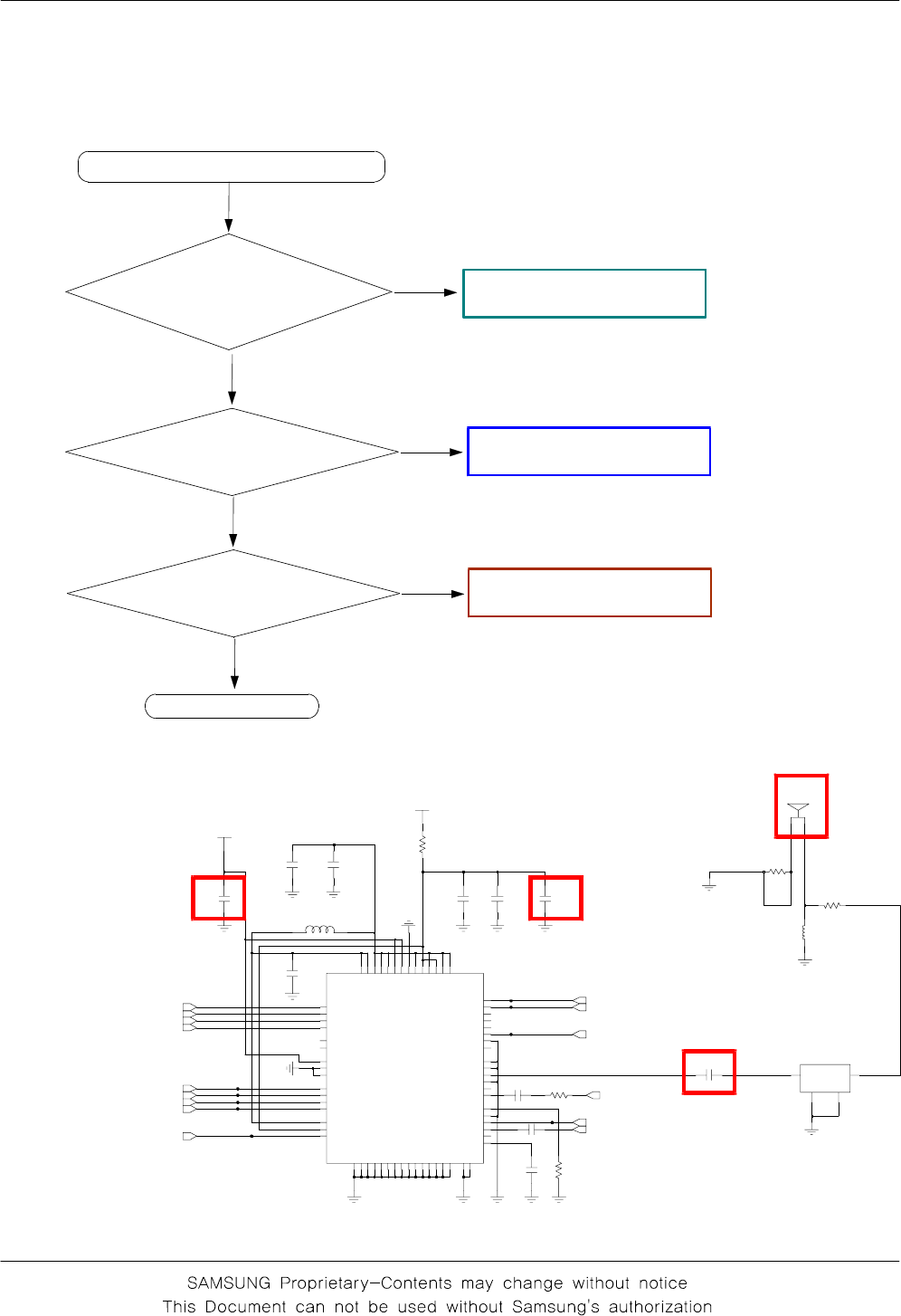
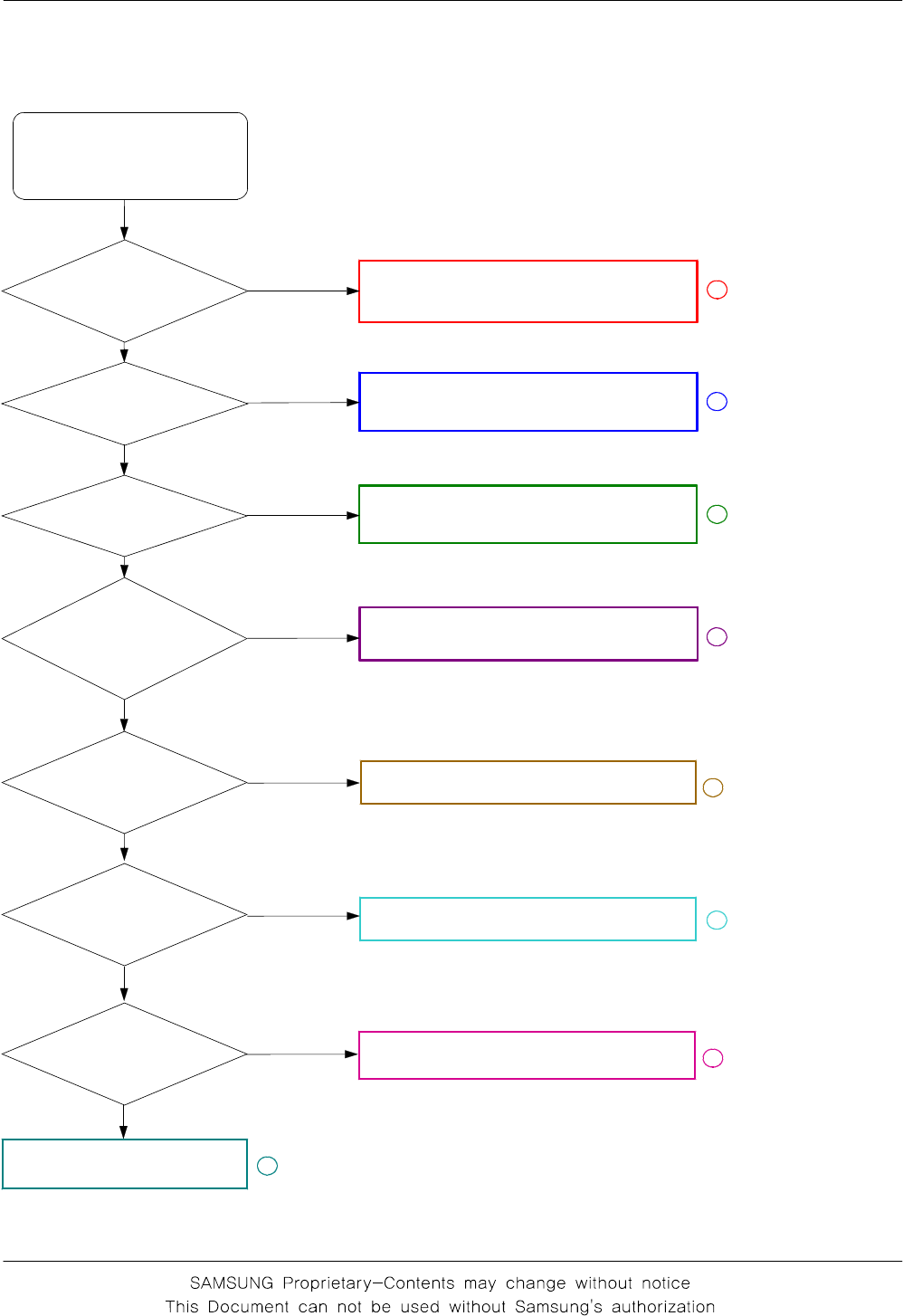
10-25
10-2.RF
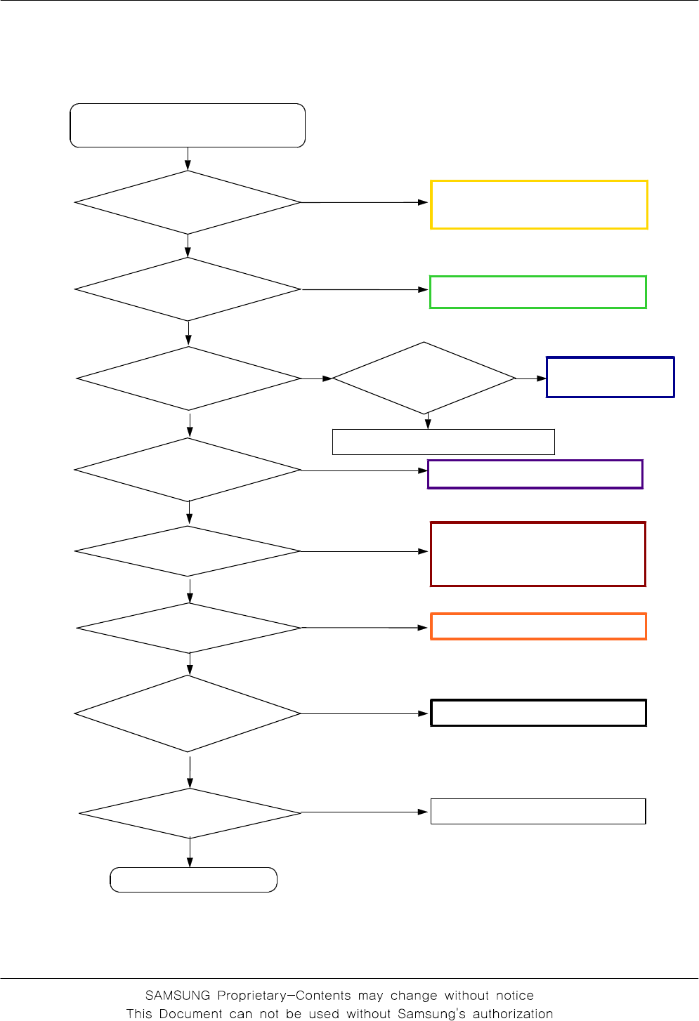
10-2-1. EGSM Rx
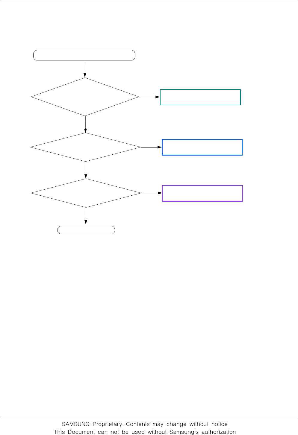
Continuous RX ON
RF Input :62
CH
AMP :-50
dBm
Redownload binary or change UCP300
Check soldered status of
L100, R100, ANT100, ANT_GND100,
C841,C100,L101
YES
NO
Check pin #15,#14
of FEM100: Low
#13 : High ?
⑦
⑥
⑤
④
③
②
①
NO
NO
NO
NO
NO
NO
NO
NO
YES
YES
YES
YES
YES
YES
YES
YES
YES
GSM RX path component
resolder or change
GSM Receiver is O.K?
Check pin #3, #4 of
FEM100 ≥-65dBm
Normal Condition Catch the
channel
Resolder or Change U104
Resolder or Change TCX200
Resolder or change PMIC(U402)
Check soldered status of
C838, C839, L108
Resolder or Change
FEM100
Resolder or Change
RFS100, L105, C104
END
Check the pin #11,12,13,14 of
U104 Vp-p>160mV
Check the pin #2 of
U102 = 19.2Mhz
Check VDDA1 pins of
U104 ≒2.65V
Check pin #48,49 of
U104 ≥-65dBm
Check pin #20 of
FEM100 ≥-65dBm
Flow Chart of Troubleshooting
10-26
10-2-2. GSM850 Rx
Continuous RX ON
RF Input :62
CH
AMP :-50
dBm
Redownload binary or change UCP300
Check soldered status of
L100, R100, ANT100, ANT_GND100,
C841,C100,L101
YES
NO
Check pin #15,#14 and
#13 of FEM100: Low ?
⑦
⑥
⑤
④
③
②
①
NO
NO
NO
NO
NO
NO
NO
NO
YES
YES
YES
YES
YES
YES
YES
YES
YES
GSM RX path component
resolder or change
GSM Receiver is O.K?
Check pin #1, #2 of
FEM100 ≥-65dBm
Normal Condition Catch the
channel
Resolder or Change U104
Resolder or Change TCX200
Resolder or change PMIC(U402)
Check soldered status of
C101, C103, L102
Resolder or Change
FEM100
Resolder or Change
RFS100, L105, C104
END
Check the pin #11,12,13,14 of
U104 Vp-p>160mV
Check the pin #2 of
U102 = 19.2Mhz
Check VDDA1 pins of
U104 ≒2.65V
Check pin #50,51 of
U104 ≥-65dBm
Check pin #20 of
FEM100 ≥-65dBm
Flow Chart of Troubleshooting
10-27
10-2-3. DCS Rx
Continuous RX ON
RF Input :62
CH
AMP :-50
dBm
Redownload binary or change UCP300
Check soldered status of
L100, R100, ANT100, ANT_GND100,
C841,C100,L101
YES
NO
Check pin #15
of FEM100: Low
#14, #13 : High?
⑦
⑥
⑤
④
③
②
①
NO
NO
NO
NO
NO
NO
NO
NO
YES
YES
YES
YES
YES
YES
YES
YES
YES
GSM RX path component
resolder or change
GSM Receiver is O.K?
Check pin #1, #2 of
FEM100 ≥-65dBm
Normal Condition Catch the
channel
Resolder or Change U104
Resolder or Change TCX200
Resolder or change PMIC(U402)
Check soldered status of
L113, L115, L116
Resolder or Change
FEM100
Resolder or Change
RFS100, L105, C104
END
Check the pin #11,12,13,14 of
U104 Vp-p>160mV
Check the pin #2 of
U102 = 19.2Mhz
Check VDDA1 pins of
U104 ≒2.65V
Check pin #46,47 of
U104 ≥-65dBm
Check pin #20 of
FEM100 ≥-65dBm

Flow Chart of Troubleshooting
10-28
10-2-4. PCS Rx
Continuous RX ON
RF Input :62
CH
AMP :-50
dBm
Redownload binary or change UCP300
Check soldered status of
L100, R100, ANT100, ANT_GND100,
C841,C100,L101
YES
NO
Check pin #15, #13
of FEM100: Low
#14: High?
⑦
⑥
⑤
④
③
②
①
NO
NO
NO
NO
NO
NO
NO
NO
YES
YES
YES
YES
YES
YES
YES
YES
YES
GSM RX path component
resolder or change
GSM Receiver is O.K?
Check pin #7, #8 of
FEM100 ≥-65dBm
Normal Condition Catch the
channel
Resolder or Change U104
Resolder or Change TCX200
Resolder or change PMIC(U402)
Check soldered status of
L117, L118, U101
Resolder or Change
FEM100
Resolder or Change
RFS100, L105, C104
END
Check the pin #11,12,13,14 of
U104 Vp-p>160mV
Check the pin #2 of
U102 = 19.2Mhz
Check VDDA1 pins of
U104 ≒2.65V
Check pin #44,45 of
U104 ≥-65dBm
Check pin #20 of
FEM100 ≥-65dBm
Flow Chart of Troubleshooting
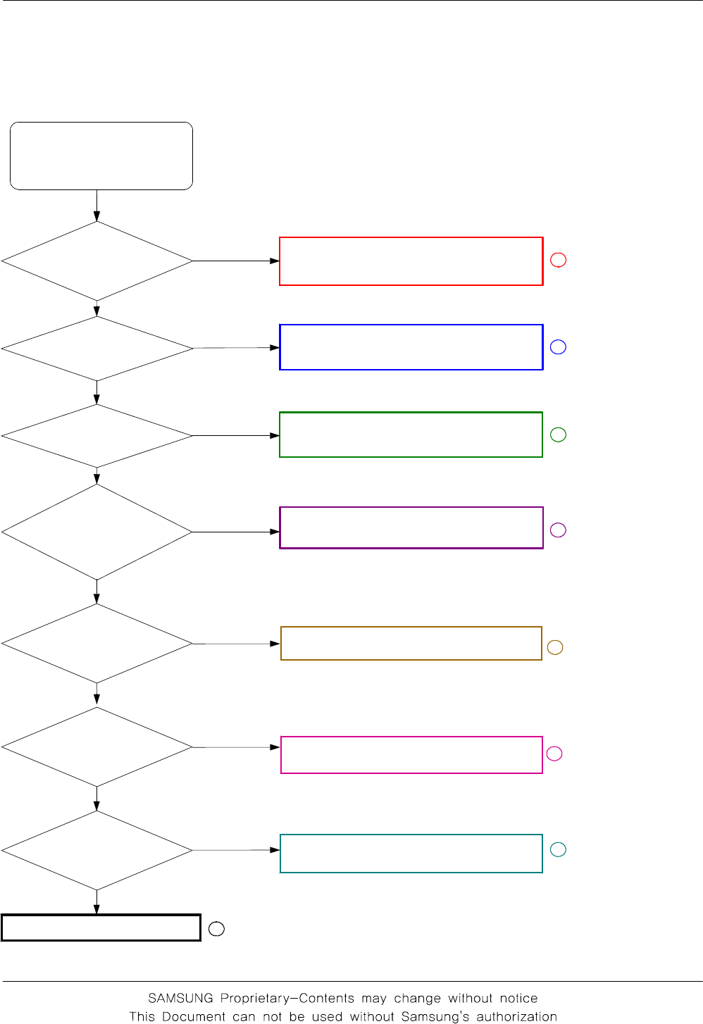
10-29
Tx On
Tx Level :5
PAM100
pin #4 ≥3.4V?
10-2-5. EGSM, GSM850 Tx
Nomal
Condition Catch
The Channel
Check soldered status of
R100, C100, L100, L101,
ANT100, ANT_GND100, C841
No
1
Yes
Resolder or Change
RFS100
RFS100 Pin
#1(c) ≥30dBm 2
Yes
No
FEM100 pin
#20 ≥30dBm ?
Yes Resolder or Change
L105, C104 3
No
FEM100
pin #15,14:High
pin #13 : Low?
Redownload binary or change
UCP300
No
4
Yes
pin #8 PAM100
≥30dBm ?
YES Resolder or change
FEM100 5
NO
6dBm>
PAM100 pin#7
>0dBm? 6
Resolder or change
R102, R103, R104
No
Yes
No
7
Check VBAT
Yes
8
Resolder PAM100 or U104
Flow Chart of Troubleshooting
10-30
10-2-6. DCS, PCS Tx
Tx On
Tx Level :0
PAM100
pin #4 ≥3.4V?
Nomal
Condition Catch
The Channel
Check soldered status of
R100, C100, L100, L101,
ANT100, ANT_GND100, C841
No
1
Yes
Resolder or Change
RFS100
RFS100 Pin
#1(c) ≥28dBm 2
Yes
No
FEM100 pin
#20 ≥28dBm ?
Yes Resolder or Change
L105, C104 3
No
FEM100
pin #15:High
pin#14,#13:Low?
Redownload binary or change
UCP300
No
4
Yes
pin #9 PAM100
≥28dBm ?
YES Resolder or change
FEM100 5
NO
6dBm>
PAM100 pin#1
>0dBm? 6
Resolder or change
R105, R106, R107
No
Yes
No
7
Check VBAT
Yes
8
Resolder PAM100 or U104
Flow Chart of Troubleshooting
10-31
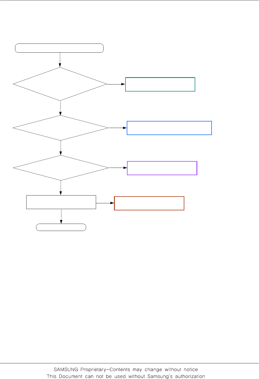
10-2-7. UMTS Rx
RX ON
RF Input : 10700CH
Cell Power :-40
dBm
YES
Normal Condition Catch the
channel
Check soldered status of
L100, R100, ANT100, ANT_GND100,
C841,C100,L101
①
NO
YES
②
Check pin #20 of
FEM100 ≥-50dBm
NO Resolder or Change
RFS100, L105, C104
YES
Check FAM100
pin #14 : Low
pin #15, 13 : High ?
Check pin #16 of
FEM100 ≥-50dBm
YES ③
NO Resolder or Change
FEM100
NO
YES
Redownload binary or change UCP300
Check pin #2(Rx) of
F202 ≥-50dBm ④
NO Check soldered status of
F202
Resolder or change
C171, C172, C191, C166, F101
C164, C173, C174, L129, C165
YES
⑤
NO
Check pin #34 of
U100 ≥-50dBm
YES
Check the pin #2 of
U104 = 19.2Mhz ⑥
NO Resolder or Change TCX200
YES
Check the pin #11,12,13,14 of
U104 Vp-p ≒1.3V?
⑦
NO
Resolder or Change U104
YES
UMTS Receiver is O.K?
NO UMTS RX path component
resolder or change
YES
END
Flow Chart of Troubleshooting
10-32
Tx On
RF Input : 9750CH
Tx Power :24
dBm
10-2-8. UMTS Tx
Nomal
Condition Catch
The Channel
Check soldered status of
L100, R100, ANT100, ANT_GND100,
C841,C100,L101
No
1
Yes
Resolder or Change
RFS100
RFS100 Pin
#1(c) ≥20dBm 2
Yes
No
FEM100 pin #8
≥18dBm ?
Yes Resolder or Change
RFS100, L105, C104 3
No
FEM100
pin #14 : Low
pin #15,13:High?
Redownload binary or change
UCP300
No
4
Yes
FEM100
pin #11 ≥3.4V?
No Check the Battery 5
Yes
F202
pin #3 ≥
18dBm ?
Yes
6
Resolder or change
U200, C211, L205
No
DUF
pin #7 ≥
16dBm ?
Yes 7
Resolder or change DUF100
No
8
Resolder U106
Flow Chart of Troubleshooting
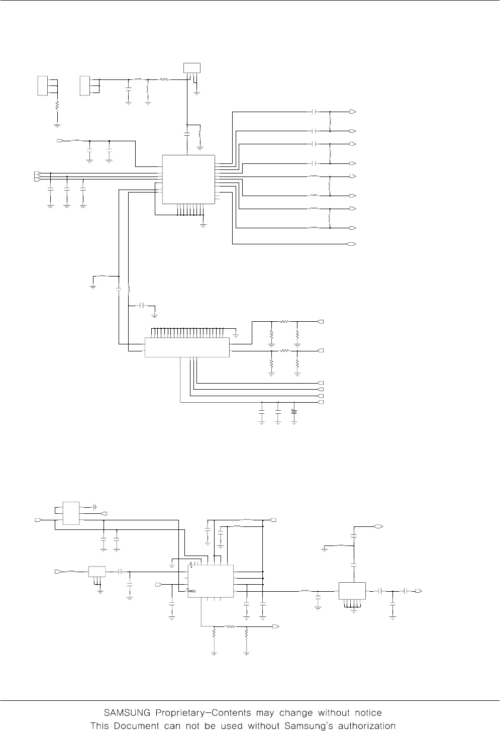
10-33
< FEM >
< GSM PAM >
C101
L115
33
R105
ANT100
1
1
22
C122
C108
C117
L104
L113
L105
C107
0
0
1
R
C116
C100
R102
L120
R103
R106
TA100
R107
U101
L118
R104
C838
C839
C103
C104
L108
C126
L117
L102
C115
L119
L116
C113
T
T
A
B
V
5
D
N
G
6P
M
A
R
V
7
GSM_IN
8GSM_OUT
9DCS|PCS_OUT
D
N
G6
2
D
N
G7
2
D
N
G8
2
D
N
G9
2
D
N
G
3N
E
_
X
T
0
3
D
N
G1
3
D
N
G
4
D
N
G9
1
D
N
G
2L
E
S
_
D
N
A
B
0
2
D
N
G1
2
D
N
G2
2
D
N
G3
2
D
N
G4
2
D
N
G5
2
D
N
G1
1
D
N
G2
1
D
N
G3
1
D
N
G4
1
D
N
G5
1
D
N
G6
1
D
N
G7
1
D
N
G8
1
PAM100
1
DCS|PCS_IN
0
1
L101
UMTS_TRX3
15 VC1
14 VC2
13 VC3
VC4
12
11 VDD
8
1GSM850_RX1
2GSM850_RX2
24 GSM850|900_TX
3GSM900_RX1
GSM900_RX2 4
UMTS_TRX1 16
17UMTS_TRX2 18
GG
26
G
27 28
G
5GSM1800_RX1
GSM1800_RX2 6
GSM1800|1900_TX
22
7
GSM1900_RX1
GSM1900_RX2
20
ANT
G
10
G
9
G
19 21
GG
2325
FEM100
ANT_GND100
11
2
2
3
3
RFS100
2A
C
1
G
3
4G
L100
C114
C841
GSM_PA_PWR_CTL
GSM850_EGSM900_TX
GSM_ANT_SEL2_N
GSM_ANT_SEL1_N
GSM_ANT_SEL0_N
GSM900_RX_P
GSM900_RX_M
GSM_BAND
GSM_PA_EN
VBATT_4.2V
DCS1800_PCS1900_TX
GSM850_RX_M
V_FEM_2.7V
TRX_WCDMA_2100
PCS1900_RX_M
PCS1900_RX_P
DCS1800_RX_P
DCS1800_RX_M
GSM850_RX_P
(BAND1_W2100)
< WCDMA PAM >
R837
C177
C169
OUT 4
F100
2
G
3
G
5
G
IN
1
C161
C191
C180
C156
L124
C146
VCC2 12
S
A
I
B
C
C
V6
1
3VMODE
9
1
C
N
1RF_IN
9
RF_OUT
5
1
1
C
C
V
VCC2 10
3
1
L
2
C
C
V
11
VCC2
5L
P
C
7
1
D
N
G
M
I4
1
NC
2
C
N
6
7C
N
C
N
8
C
N8
1
U106
C172
13
G
G
4
G
68
G
G
9
RX 5
TX
7
DUF100
ANT
2
G
C179
C157
C148
L126
C151
U822
C178
C171
L127
L123
R115
L803
C1
6
3
C2
E1 1
4E2
U105
2
B1
5B2
R116
UMTS2100_TX
PA_RANGE0
VBATT_4.2VWPAM_BIAS_2.85V
PA_ON_W2100
PWR_DET
TRX_WCDMA_2100
UMTS_RX_2100
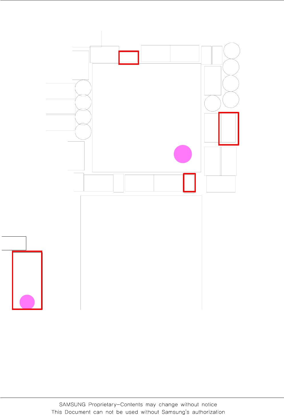
Flow Chart of Troubleshooting
10-34
< RF TRANCEIVER >
10V
10V
C182
C163
C130
VDDA2
8
VTUNE_GPS
9
N
Q
_
X
T5
6
P
Q
_
X
T6
6
F
E
RI
_
C
A
D7
6
S
AI
B
R
_
X
T8
6
G
U
L
S
_
D
N
G9
6
VDDA2
7
C
N0
7
C
N1
7
2
T
U
O
_
F
R
_
B
H8
5
3
T
U
O
_
F
R
_
B
H9
5
VDDA1
6
2
A
D
D
V0
6
2
A
D
D
V1
6
2
A
D
D
V2
6
NI
_
X
T3
6
PI
_
X
T4
6
GCELL_INP 50
GCELL_INN 51
PDET_IN
2
5
1
A
D
D
V3
5
2
A
D
D
V4
5
1
T
U
O
_
F
R
_
B
L5
5
1
T
U
O
_
F
R
_
B
H6
5
2
T
U
O
_
F
R
_
B
L7
5
VDDA2 43
GPCS_INP 44
GPCS_INN 45
DCS_INP 46
DCS_INN 47
EGSM_INP 48
EGSM_INN 49
VTUNE1
5
WPRXSE2 36
VDDA2 37
WPRXSE1 38
WDRXHB2 39
VDDA1
4
WDRXHB1 40
WDRXLB 41
GPS_IN 42
M
NI
_
X
M
_
B
W
9
2
VDDA1
3
P
B
L
X
R
P
W
0
3
M
B
L
X
R
P
W
1
3
P
B
H
X
R
P
W
2
3
M
B
H
X
R
P
W
3
3
T
U
O
_
2
E
S
X
R
P
W
4
3
WPRXSE1_OUT
35
2
A
D
D
V
1
2
1
A
D
D
V
2
2
3
2M
D
D
V
2
E
N
U
T
V
4
2
2
A
D
D
V
5
2
N
O
_
F
R
6
2
2
A
D
D
V
7
2
P
NI
_
X
M
_
B
W
8
2
PRX_IP
14
DRX_QP
15
DRX_QN
16
DRX_IP
17
N
I
_
X
R
D
8
1
C|
N
9
1
TCXO
2
T
D
B
S
0
2
U104
VDDA2
1
VDDA1
10
PRX_QP
11
PRX_QN
12
13 PRX_IN
C121
C185
C193
C147
C124
C142
C136
R110
C165
C194
C139
R111
L125
C133
L129
C153
C187
C118
C135
C132
C145
C184
C190
C188 C186
C175 L130
LL1005-FH3N9S
C155
R113
C154
C164
C183
C192
C141
C119
R112
C120
C137
C152
C149
C158
R114
L122
F101
G
2
G
5
1
IN
OUT
3
OUT
4
R109
C166
C174
C173
C134
C162
C140
C159
C129
C144
C150
C143
C160
C123
C138
C189
C167
C128
C131
C127
V_RF_2.1V
TX_I_MTX_Q_P
V_RF_2.7V
RX_GPS
WCDMA_HB_MIX_IN_M
RX_I_P
RX_I_M
RX_Q_M
RX_Q_P
V_RF_2.1V
V_RF_2.1V
WCDMA_HB_MIX_IN_PWCDMA_HB_MIX_IN_M
WCDMA_HB_MIX_IN_P
V_RF_2.1V
RF_ON_TX_ON
V_RF_2.7V
SSBI_RTR
CLK19.2M_RTR
GPS_RX_I_M
GPS_RX_I_P
GPS_RX_Q_M
GPS_RX_Q_P
V_RF_2.7V
GSM850_RX_M
GSM850_RX_P
GSM900_RX_M
GSM900_RX_P
DCS1800_RX_M
DCS1800_RX_P
PCS1900_RX_M
PCS1900_RX_P
UMTS_RX_2100
DAC_REF
TX_Q_M TX_I_P
V_MSMP_2.6V
PWR_DET
GSM850_EGSM900_TX
DCS1800_PCS1900_TX
UMTS2100_TX
Flow Chart of Troubleshooting
10-35
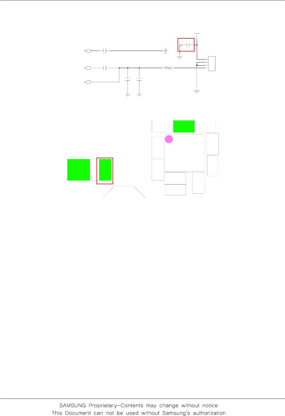
10-2-9. GPS
Type the following keystring
*#4097*4097# ->
select '1'
< LNA_GPS >
U100
1
BI2RFOUT
10
1
1D
N
G
L131
C109
C106
C842 L107
C112
L110
C102
1
1
22
33
ANT101
C110
C111
4
1
1
L
C105
L112
V_RF_2.7V
RX_GPS
GPS_LNA_ON
C102
6
0
1
C
5
0
1
C
C109
C842
7
0
1
L0
1
1
L
2
1
1
L
L114
L131
U100
Catch The
Signal? 1
Check soldered status of
R101,C110,C109,L114,
U100,L107,L110,L112,L131
No
Yes
Redownload Binary
Flow Chart of Troubleshooting
10-36
10-2-10. FM Radio
Connect the MIC Cable and
Turn on the FM Radio
< FM RADIO >
L200
V_MSMP_2.6V
C209
V_MSMP_2.6V
R203
TP_FM_RST
R204
TP_FM_INT
R201
C200 R200
RST
5
K
L
C
S
78
O
I
D
S
6SEN VDD 11
O
I
V
10
LPI
4
NC
1
C
N
20
22
C
N
C
N
23
9
K
L
C
R
RFGND
3
ROUT 13
DOUT 15
FMI
2
GND 12
D
N
G
21 19
1
O
P
G
18
T
N
I
_
|
2
O
P
G
K
L
C
D
|
3
O
P
G
17
LOUT 14
U200
DFS 16
C205
R205
VBATT_4.2V
FM_RST_N
RADIO_OUT_R
SLEEP_CLK
RADIO_OUT_L
FM_INT
FM_I2S_BCLK
FM_I2S_LRCLK
FM_I2S_DOUT
FM_I2C_SDA
FM_I2C_SCL
FM_RADIO_ANT
OK
2
1
No
Check the MIC Cable, Soldered conditions of
C200, L200, U200
Yes
Yes
Check the Soldered conditions of
C318, C319 and Audio Path
No
Sound from
the earphone?
Catch the FM
signal?
Flow Chart of Troubleshooting
10-37
C205
C209
R200
1
0
2
R
3
0
2
R
5
0
2
R
TP_FM_BCLK
TP_FM_INT
TP_FM_LRCLK
T
S
R
_
M
F
_
P
T
K
L
C
_
P
E
E
L
S
_
P
T
U200

SAMSUNG Proprietary-Contents may change without notice
4. Array Course Control
4-1
This Document can not be used without Samsung's authorization
4-1. Software Adjustments
Test Cable (GH39-01160A)
Test Jig (GH99-36900A)
RF Test Cable (GH99-38251A)
RF Test Cable (GH39-00985A)
SAMSUNG Proprietary-Contents may change without notice
Array Course Control
4-2
This Document can not be used without Samsung's authorization
4-2. Software Downloading
4-2-1. Pre-requsite for Download
•Downloader Program(Multiloader V5.50.exe)
•M8800 Mobile Phone
•USB Data Link Cable
•Binary files
4-2-2. S/W Download Process
■Load the binary download program by executing the “Multiloader V5.33.exe”
1. Execute the download SW, Multiloader.exe.
2. Boot the M8800 by pressing 'Power ON Key'+'
CAMERA key'+'
VOLUME DOWN
Key'at the same time.
-if you do properly, you can see the 'DOWMLOAD' in the middle of the screen.
3. Connet the USB data cable to the M8800.
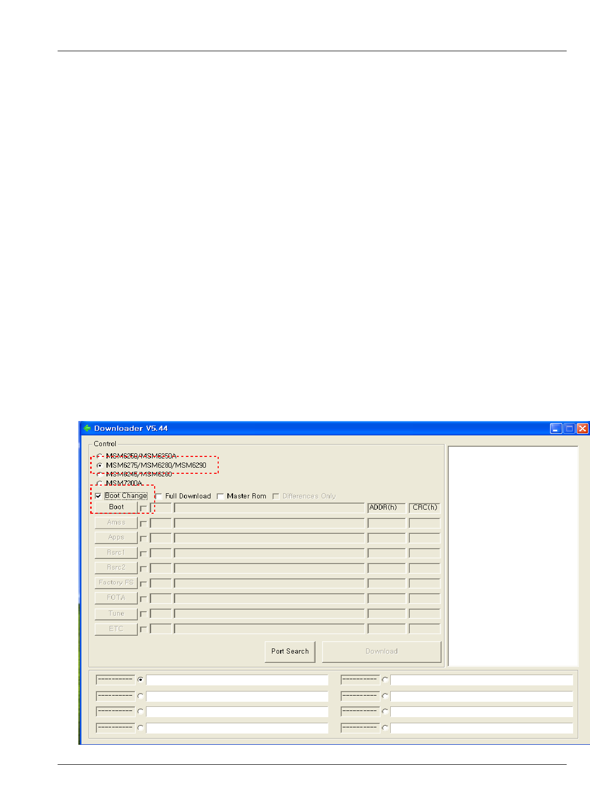
4. Choose MSM6275/MSM6280 and check 'Boot Change', then the 'Boot' button will
be activate
d.
SAMSUNG Proprietary-Contents may change without notice
Array Course Control
4-3
This Document can not be used without Samsung's authorization
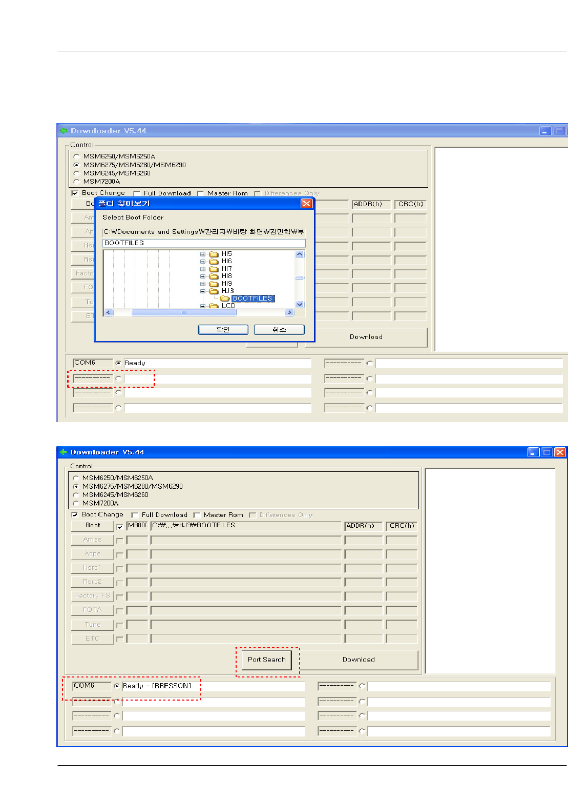
5. Click the 'Boot', then the dialogue box is opened. Select the wanted directory, and
press 'OK'.
6. Select 'Port Search', then 'Port' is activated.
7.Click 'Download', then downloading is executed successively. After 10seconds,
SAMSUNG Proprietary-Contents may change without notice
Array Course Control
4-4
This Document can not be used without Samsung's authorization
M8800 rebooting.
9. Disconnet the USB data cable to the M8800.
10. One more Boot the M8800 by pressing 'Power ON Key'+'
CAMERA key'+
'VOLUME DOWN Key'at the same time.
-if you do properly, you can see the 'DOWMLOAD' in the middle of the screen.
11. Connet the USB data cable to the M8800.
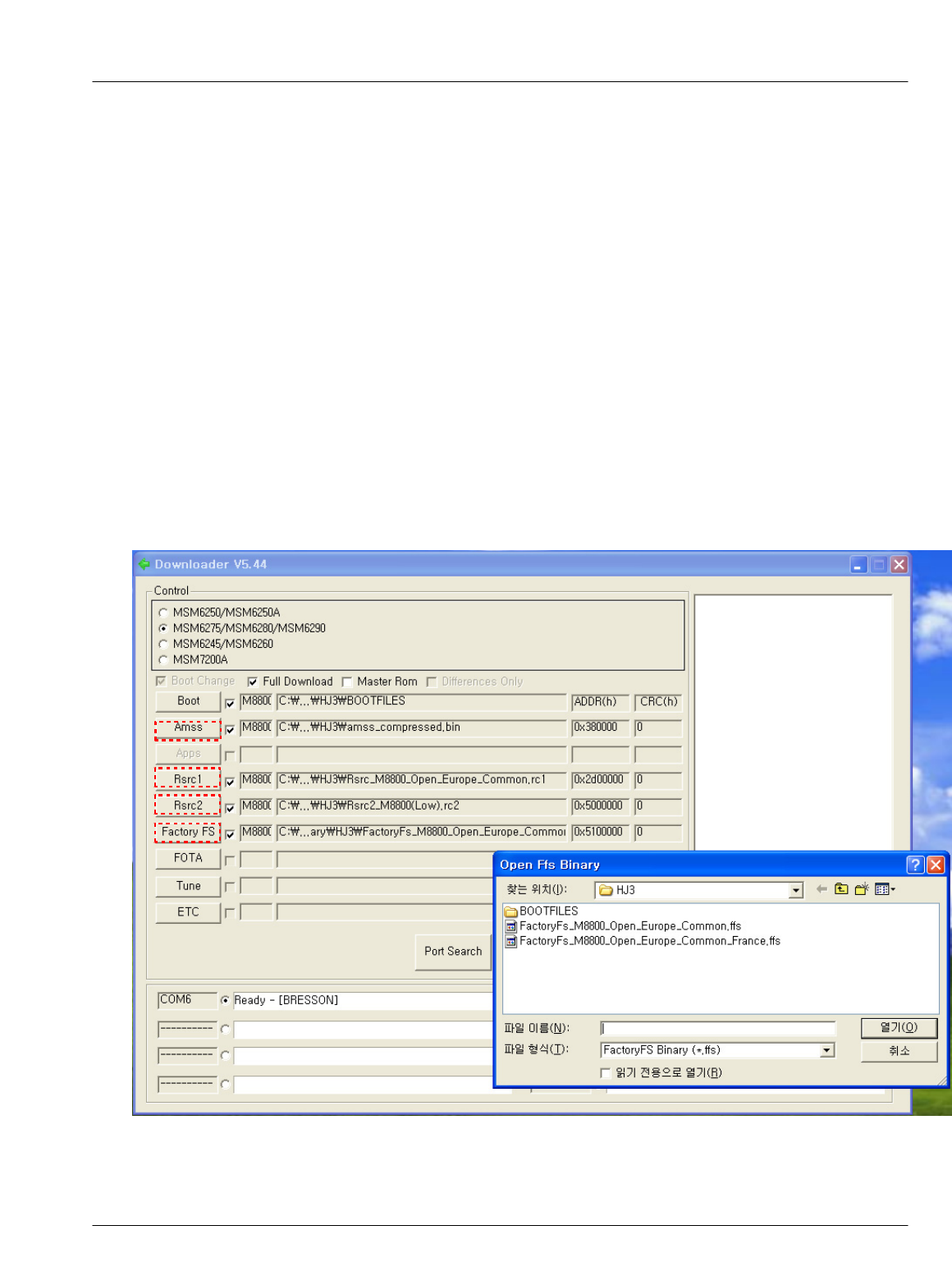
12. Select the 'Boot Change' once more, then 'Boot' button will be inactivated, and the
others('Amss', 'Rsrc1', 'Rsrc2', 'FactoryFS', 'FOTA', and 'ETC') are activated.
-Click 'AMSS', 'Rsrc1', 'Rsrc2', and 'FactoryFS' each, and select wanted files.
SAMSUNG Proprietary-Contents may change without notice
Array Course Control
4-5
This Document can not be used without Samsung's authorization
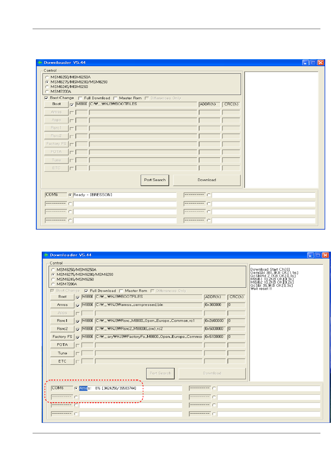
12. Select 'Port Search', then 'Port' is activated.
13.Click 'Download', then downloading is executed successively.If the download is
completed, S/W downloading is finished. (Download time :about 5minutes)
SAMSUNG Proprietary-Contents may change without notice
8. Block Diagrams
8-1
This Document can not be used without Samsung's authorization
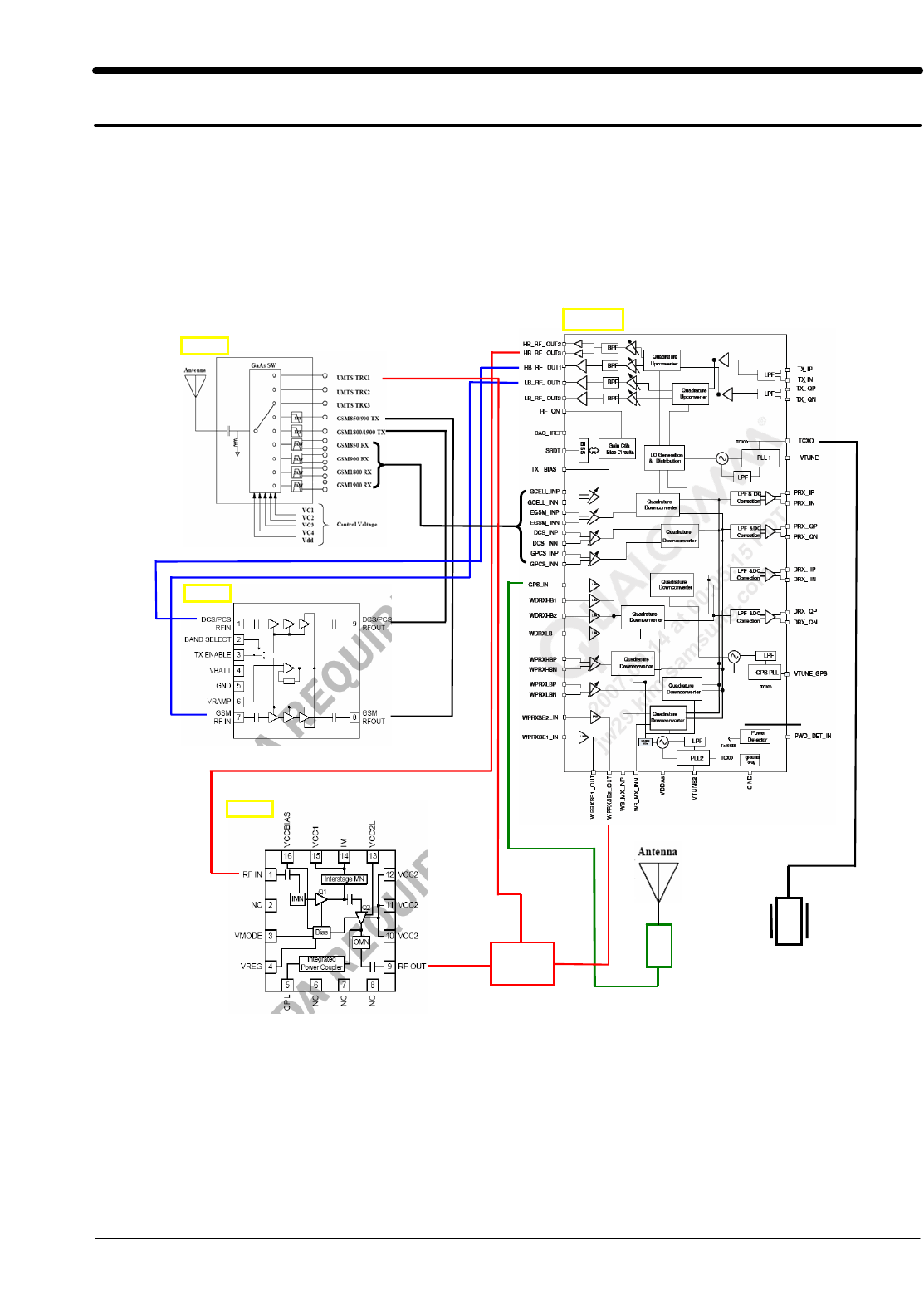
8-1 RF
T
C
X
O
Duplexe
r
GPS
LNA
3G PAM
2G PAM
FEM
TRANSCEIVER
SAMSUNG Proprietary-Contents may change without notice
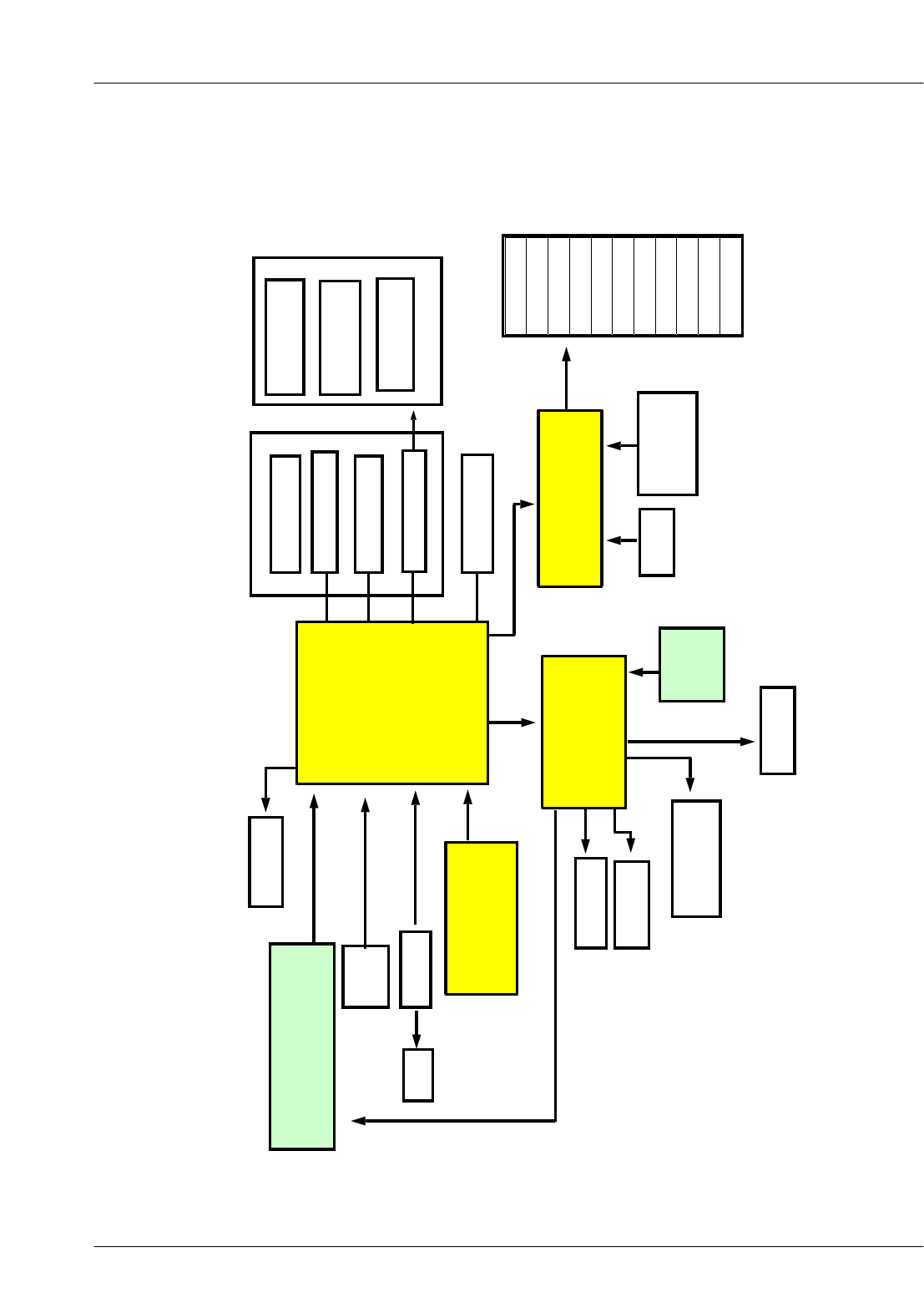
Block Diagrams
8-2
This Document can not be used without Samsung's authorization
2Baseband
MODEM
MSM6281
MEMORY
(KAV00500FM-AFFY)
TOUCH
SCREEN
BLUETOOTH
Li-Ion BATT
(1000 mAh)
PM IC
(PM6658)
RTC_CLK
SIM & T-FLASH
CARD
CAMERA(CIF)
CAMERA(8M)
LCD
BB INTERFACE
Serial DATA I/F
I/O Interface
A/D Interface
RF INTERFACE
Battery Type
Battery
Voltage
Battery Temp
ANT
AUDIO
BLOCK
MULTIMEDIA CHIP
(MV8729)
MV_POWER
BLOCK
V_RF
V_MSMA
V_MSMP
V_MSME
V_MSMC
VPAM_BIAS
V_TCXO
V_BT
V_MMC
V_FEM
V_USB
TV-OUT

SAMSUNG Proprietary-Contents may change without notice
6-1
This Document can not be used without Samsung's authorization
6. MAIN Electrical Parts List
SEC CODE Design LOC Discription
0403-001547 ZD709 DIODE-ZENER
0404-001153 D300 DIODE-SCHOTTKY
0406-001267 ZD704,ZD705,ZD706 DIODE-TVS
0406-001279 D401,D402,D801,D802 DIODE-TVS
0406-001279 D803,D804,ZD500 DIODE-TVS
0406-001279 ZD501,ZD502,ZD503 DIODE-TVS
0406-001279 ZD600,ZD601,ZD602 DIODE-TVS
0406-001279 ZD603,ZD604,ZD605 DIODE-TVS
0406-001279 ZD700,ZD701,ZD707 DIODE-TVS
0406-001279 ZD708,ZD710,ZD711 DIODE-TVS
0406-001279 ZD712,ZD713,ZD714 DIODE-TVS
0406-001279 ZD715 DIODE-TVS
0406-001286 ZD400,ZD401,ZD702 DIODE-TVS
0406-001286 ZD703 DIODE-TVS
0407-001002 D400 IC-ANALOG SWITCH
0504-001113 TR400 TRANSISTOR
0504-001151 U105 IC-ANALOG SWITCH
0801-003013 U300 IC-ANALOG SWITCH
1001-001394 U602,U700,U815,U818 IC-ANALOG SWITCH
1001-001436 U504 IC-ANALOG SWITCH
1001-001447 U302,U600 IC-ANALOG SWITCH
1001-001481 U403 IC-ANALOG SWITCH
1003-002047 U604 IC-DRIVER
1003-002169 U701 IC-DRIVER
1108-000210 UME300 IC-MCP
1201-002733 U502 IC-AUDIO AMP
1201-002774 U100 LNA_GPS
1201-002775 U106 IC-TRANSCEIVER
1201-002778 PAM100 IC-TRANSCEIVER
1203-004422 U811 IC-DC/DC CONVERTER
1203-004518 U401 IC-POWER AMP
1203-004596 U503 IC-DC/DC CONVERTER
1203-004776 U603,U810 IC-DC/DC CONVERTER
1203-004778 U402 IC-POWER SUPERVISOR
1203-004819 U816 IC-DC/DC CONVERTER
1203-004857 U601 IC-DRIVER
1203-004978 U619 IC-DC/DC CONVERTER

SAMSUNG Proprietary-Contents may change without notice
MAIN Electrical Parts List
6-2
This Document can not be used without Samsung's authorization
SEC CODE Design LOC Discription
1203-005069 U400 IC-DC/DC CONVERTER
1203-005250 U610,U621 IC-DC/DC CONVERTER
1203-005403 U800 IC-DC/DC CONVERTER
1203-005478 U607 IC-DC/DC CONVERTER
1203-005479 U615 IC-DRIVER
1203-005485 U620,U821 IC-DC/DC CONVERTER
1203-005487 U801 IC-DC/DC CONVERTER
1204-002924 U200 IC-MULTI REG
1205-003228 U501 IC-MULTI REG
1205-003288 U817 IC-DRIVER
1205-003297 U104 IC-TRANSCEIVER
1205-003419 U201 IC-TRANSCEIVER
1205-003498 UCP300 IC-MODEM
1205-003611 U802 IC-DC/DC CONVERTER
1209-001766 U702 IC-DRIVER
1404-001224 TH300 THERMISTOR-NTC
2007-000137 R200,R201 R-CHIP
2007-000140 R112,R706 R-CHIP
2007-000143 R204,R205,R828,R829 R-CHIP
2007-000144 R407 R-CHIP
2007-000145 R621 R-CHIP
2007-000147 R308 R-CHIP
2007-000148 R712 R-CHIP
2007-000151 R413 R-CHIP
2007-000157 R842 R-CHIP
2007-000161 R310 R-CHIP
2007-000162 R522 R-CHIP
2007-000163 R804 R-CHIP
2007-000164 R619 R-CHIP
2007-000165 R320,R630 R-CHIP
2007-000171 C841,L201,R100,R101 R-CHIP
2007-000171 R206,R210,R316,R424 R-CHIP
2007-000171 R502,R505,R519,R831 R-CHIP
2007-000171 R846,R847 R-CHIP
2007-000172 R111,R208,R632,R633 R-CHIP
2007-000174 R105 R-CHIP
2007-001119 R515,R521 R-CHIP

SAMSUNG Proprietary-Contents may change without notice
MAIN Electrical Parts List
This Document can not be used without Samsung's authorization
6-3
SEC CODE Design LOC Discription
2007-001217 R102 R-CHIP
2007-001285 R114 R-CHIP
2007-001291 R509,R511 R-CHIP
2007-001298 R113 R-CHIP
2007-001305 R106,R107 R-CHIP
2007-001333 R714 R-CHIP
2007-001339 R807 R-CHIP
2007-002797 R203 R-CHIP
2007-003015 R110 R-CHIP
2007-003030 R103,R104 R-CHIP
2007-007092 R510,R709 R-CHIP
2007-007132 R410 R-CHIP
2007-007197 R702,R703,R705,R715 R-CHIP
2007-007197 R716 R-CHIP
2007-007309 R109 R-CHIP
2007-007310 R818 R-CHIP
2007-007314 R409 R-CHIP
2007-007334 R612 R-CHIP
2007-007468 R400 R-CHIP
2007-007528 R517,R520 R-CHIP
2007-007586 R311 R-CHIP
2007-007741 R312 R-CHIP
2007-008040 R837 R-CHIP
2007-008045 R202,R318,R412,R600 R-CHIP
2007-008045 R614,R708,R801,R824 R-CHIP
2007-008045 R840 R-CHIP
2007-008046 R115,R116 R-CHIP
2007-008049 R305 R-CHIP
2007-008052 R507,R508,R626,R711 R-CHIP
2007-008052 R713,U611 R-CHIP
2007-008055 R325,R421,R610,R611 R-CHIP
2007-008055 R817 R-CHIP
2007-008419 R309 R-CHIP
2007-008483 R408 R-CHIP
2007-008486 R404,R405,R411,R414 R-CHIP
2007-008486 R422,R830 R-CHIP
2007-008516 R300,R302,R303,R304 R-CHIP

SAMSUNG Proprietary-Contents may change without notice
MAIN Electrical Parts List
6-4
This Document can not be used without Samsung's authorization
SEC CODE Design LOC Discription
2007-008516 R306,R406,R415,R416 R-CHIP
2007-008516 R417,R419,R423,R627 R-CHIP
2007-008516 R628,R631,R636,R637 R-CHIP
2007-008516 R827,R832 R-CHIP
2007-008542 R319,R620 R-CHIP
2007-008548 R704 R-CHIP
2007-008588 R503,R504,R601,R607 R-CHIP
2007-008686 R812 R-CHIP
2007-008806 R321,R402,R403 R-CHIP
2007-009084 R317,R833 R-CHIP
2007-009111 R707,R815 R-CHIP
2007-009115 R307,R835 R-CHIP
2007-009157 R822 R-CHIP
2007-009158 R209 R-CHIP
2007-009170 R700,R701,R823 R-CHIP
2007-009171 R313,R314,R315,R401 R-CHIP
2007-009408 R326,R327 R-CHIP
2203-000233 C105,C123,C124,C128 C-CER,CHIP
2203-000233 C134,C154,C158,C187 C-CER,CHIP
2203-000233 C189 C-CER,CHIP
2203-000254 C137,C160,C707 C-CER,CHIP
2203-000278 C102,C219,C552,C554 C-CER,CHIP
2203-000330 C413,C432 C-CER,CHIP
2203-000386 C833,C834,C835,C836 C-CER,CHIP
2203-000438 C141,C146,C148,C180 C-CER,CHIP
2203-000438 C200 C-CER,CHIP
2203-000466 C220 C-CER,CHIP
2203-000489 C106 C-CER,CHIP
2203-000627 C127,C136,C142,C143 C-CER,CHIP
2203-000627 C145,C149,C150,C152 C-CER,CHIP
2203-000627 C159,C162,C163,C175 C-CER,CHIP
2203-000627 C188,C812 C-CER,CHIP
2203-000696 C161,C191 C-CER,CHIP
2203-000725 C621 C-CER,CHIP
2203-000812 C104,C108,C113,C114 C-CER,CHIP
2203-000812 C115,C135,C147,C151 C-CER,CHIP
2203-000812 C164,C171,C172,C173 C-CER,CHIP

SAMSUNG Proprietary-Contents may change without notice
MAIN Electrical Parts List
This Document can not be used without Samsung's authorization
6-5
SEC CODE Design LOC Discription
2203-000812 C190,C439,C441,C443 C-CER,CHIP
2203-000812 C553 C-CER,CHIP
2203-000854 C545,C546,C556,C557 C-CER,CHIP
2203-000995 C122 C-CER,CHIP
2203-001383 C177 C-CER,CHIP
2203-001385 C101,C103,C117,C129 C-CER,CHIP
2203-001385 C838,C839 C-CER,CHIP
2203-001405 C205,C511,C515,C516 C-CER,CHIP
2203-001405 C519,C547,C555 C-CER,CHIP
2203-002709 C825 C-CER,CHIP
2203-005234 C100 C-CER,CHIP
2203-005288 C166 C-CER,CHIP
2203-005382 C116 C-CER,CHIP
2203-005552 C109 C-CER,CHIP
2203-005682 C208,C311,C314,C317 C-CER,CHIP
2203-005682 C423,C425,C427,C444 C-CER,CHIP
2203-005682 C446,C447,C448,C451 C-CER,CHIP
2203-005682 C452,C542,C550,C551 C-CER,CHIP
2203-005682 C607,C609,C611,C613 C-CER,CHIP
2203-005682 C615,C623,C625,C627 C-CER,CHIP
2203-005682 C700,C701,C705,U822 C-CER,CHIP
2203-005719 C445,C449 C-CER,CHIP
2203-005725 C133,C144 C-CER,CHIP
2203-005727 C548,C549,C831,C832 C-CER,CHIP
2203-005729 C709,C710,C711 C-CER,CHIP
2203-005732 C118,C119 C-CER,CHIP
2203-005736 C221,C422,C431,C438 C-CER,CHIP
2203-005777 C169 C-CER,CHIP
2203-005806 C201,C203,C211,C301 C-CER,CHIP
2203-005806 C324,C325,C326,C327 C-CER,CHIP
2203-005806 C328,C336,C339,C340 C-CER,CHIP
2203-005806 C341,C342,C346,C351 C-CER,CHIP
2203-005806 C365 C-CER,CHIP
2203-006047 C316 C-CER,CHIP
2203-006048 C442,C537,C538,C540 C-CER,CHIP
2203-006048 C702,C706,C827 C-CER,CHIP
2203-006121 C222 C-CER,CHIP

SAMSUNG Proprietary-Contents may change without notice
MAIN Electrical Parts List
6-6
This Document can not be used without Samsung's authorization
SEC CODE Design LOC Discription
2203-006194 C202,C204,C207,C310 C-CER,CHIP
2203-006194 C313,C329,C330,C331 C-CER,CHIP
2203-006194 C332,C333,C334,C337 C-CER,CHIP
2203-006194 C343,C344,C345,C347 C-CER,CHIP
2203-006194 C349,C350,C355,C357 C-CER,CHIP
2203-006208 C632,C634,C635,C815 C-CER,CHIP
2203-006257 C518,C522,C523,C527 C-CER,CHIP
2203-006257 C529,C530,C531 C-CER,CHIP
2203-006260 C126 C-CER,CHIP
2203-006305 C541 C-CER,CHIP
2203-006307 C435 C-CER,CHIP
2203-006324 C601,C602,C603 C-CER,CHIP
2203-006348 C433,C434,C703 C-CER,CHIP
2203-006361 C712 C-CER,CHIP
2203-006399 C318,C319,C415,C416 C-CER,CHIP
2203-006423 C132,C140,C206,C303 C-CER,CHIP
2203-006423 C304,C305,C306,C308 C-CER,CHIP
2203-006423 C309,C312,C315,C320 C-CER,CHIP
2203-006423 C321,C322,C323,C338 C-CER,CHIP
2203-006423 C348,C352,C353,C354 C-CER,CHIP
2203-006423 C356,C358,C360,C361 C-CER,CHIP
2203-006423 C362,C363,C412,C500 C-CER,CHIP
2203-006423 C503,C608,C610,C612 C-CER,CHIP
2203-006423 C614,C616,C624,C626 C-CER,CHIP
2203-006423 C628,C640,C641,C708 C-CER,CHIP
2203-006423 C713,C715,C800,C803 C-CER,CHIP
2203-006423 C804,C805,C806,C807 C-CER,CHIP
2203-006423 C808,C813,C814,C817 C-CER,CHIP
2203-006423 C818,C819,C820,U806 C-CER,CHIP
2203-006423 U808 C-CER,CHIP
2203-006556 C364 C-CER,CHIP
2203-006562 C410,C411,C436,C450 C-CER,CHIP
2203-006562 C504,C520,C524,C526 C-CER,CHIP
2203-006562 C532,C533,C534,C618 C-CER,CHIP
2203-006562 C619,C620,C629,C636 C-CER,CHIP
2203-006562 C637,C638,C639,C642 C-CER,CHIP
2203-006562 C643,C644,C645,C646 C-CER,CHIP

SAMSUNG Proprietary-Contents may change without notice
MAIN Electrical Parts List
This Document can not be used without Samsung's authorization
6-7
SEC CODE Design LOC Discription
2203-006562 C647,C648,C649,C704 C-CER,CHIP
2203-006562 C826,C829,C830,U613 C-CER,CHIP
2203-006648 C714 C-CER,CHIP
2203-006668 C300 C-CER,CHIP
2203-006681 C107,C120,C121,C130 C-CER,CHIP
2203-006681 C131,C138,C139,C153 C-CER,CHIP
2203-006681 C155,C167,C183,C185 C-CER,CHIP
2203-006681 C186,C193 C-CER,CHIP
2203-006712 C156,C157,C178 C-CER,CHIP
2203-006824 C179,C182,C184,C400 C-CER,CHIP
2203-006824 C414,C417,C418,C419 C-CER,CHIP
2203-006824 C816 C-CER,CHIP
2203-006825 C335,C359 C-CER,CHIP
2203-006838 C457,C801,C802,C821 C-CER,CHIP
2203-006838 C822,C823,C824,C837 C-CER,CHIP
2203-006838 U813 C-CER,CHIP
2203-006839 C209,C213,C214,C401 C-CER,CHIP
2203-006839 C402,C403,C404,C405 C-CER,CHIP
2203-006839 C407,C409,C440,C505 C-CER,CHIP
2203-006839 C506,C600,C617,C809 C-CER,CHIP
2203-006839 C828,C840 C-CER,CHIP
2203-006841 C437,C810,U804 C-CER,CHIP
2203-006872 C210,C212,C215,C218 C-CER,CHIP
2203-006872 C406,C408,C420,C421 C-CER,CHIP
2203-006872 C428,C429,C430,C501 C-CER,CHIP
2203-006872 C502 C-CER,CHIP
2203-006890 U805,U80 C-CER,CHIP
2203-007270 C192,C194,C424,C426 C-CER,CHIP
2203-007270 C453,C456,C633,C811 C-CER,CHIP
2203-007271 C302,C307,C454 C-CER,CHIP
2404-001339 TA802 C-TA,CHIP
2404-001377 TA501 C-TA,CHIP
2404-001381 TA800,TA801 C-TA,CHIP
2404-001496 TA100,TA700,TA701 C-TA,CHIP
2404-001506 TA500 C-TA,CHIP
2703-001178 L112,L803 INDUCTOR-SMD
2703-001231 L801 INDUCTOR-SMD

SAMSUNG Proprietary-Contents may change without notice
MAIN Electrical Parts List
6-8
This Document can not be used without Samsung's authorization
SEC CODE Design LOC Discription
2703-001409 L115,L118 INDUCTOR-SMD
2703-001733 L129 INDUCTOR-SMD
2703-001737 C110 INDUCTOR-SMD
2703-001748 L126 INDUCTOR-SMD
2703-001749 L131 INDUCTOR-SMD
2703-001751 L130 INDUCTOR-SMD
2703-002170 L117,U101 INDUCTOR-SMD
2703-002176 L122 INDUCTOR-SMD
2703-002198 L101,L123,L124 INDUCTOR-SMD
2703-002200 L102,L108 INDUCTOR-SMD
2703-002203 L104 INDUCTOR-SMD
2703-002204 L119 INDUCTOR-SMD
2703-002207 L127 INDUCTOR-SMD
2703-002208 L125 INDUCTOR-SMD
2703-002268 L113,L116 INDUCTOR-SMD
2703-002308 L107 INDUCTOR-SMD
2703-002314 L105 INDUCTOR-SMD
2703-002365 L100 INDUCTOR-SMD
2703-002368 C216,L120 INDUCTOR-SMD
2703-002506 C165,C174 INDUCTOR-SMD
2703-002557 L200 INDUCTOR-SMD
2703-002700 L114 INDUCTOR-SMD
2703-002710 L110 INDUCTOR-SMD
2703-003258 L400,L401,L402 INDUCTOR-SMD
2703-003260 L800 INDUCTOR-SMD
2703-003347 L602,L603 INDUCTOR-SMD
2801-004339 OSC400 CRYSTAL-SMD
2801-004458 OSC800 CRYSTAL-SMD
2809-001280 TCX200 OSCILLATOR-VCTCXO
2901-001353 F600,F601,F602 FILTER-EMI SMD
2901-001498 F607,F700,U608,U609 FILTER-EMI SMD
2901-001498 U616,U617,U618 FILTER-EMI SMD
2901-001498 F100 FILTER-SAW
2904-001658 F101 FILTER-SAW
2904-001702 F200 FILTER-LC
2909-001307 DUF100 DUPLEXER-FBAR
2910-000024 FEM100 FEM

SAMSUNG Proprietary-Contents may change without notice
MAIN Electrical Parts List
This Document can not be used without Samsung's authorization
6-9
SEC CODE Design LOC Discription
2911-000096 MIC500 MICPHONE
3003-001136 F608,L600,L601 BEAD-SMD
3301-001534 L202 BEAD-SMD
3301-001659 L700,L701,L702,L703 BEAD-SMD
3301-001812 TAC700,TAC701,TAC702 SWITCH-TACT
3404-001303 TAC703,TAC704 SWITCH-TACT
3404-001303 RFS100 CONNECTOR-COAXIAL
3705-001503 CN800 CONNECTOR-ZIP
3708-001947 SLC500 CONNECTOR-ZIP
3709-001336 SIM400 CONNECTOR-CARD EDGE
3709-001464 CD400 CONNECTOR-CARD EDGE
3710-002681 IFC700 SOCKET-INTERFACE
3711-005728 HDC602 HEADER-BOARD TO BOARD
3711-005836 HEA601 HEADER-BOARD TO BOARD
3711-006141 HDC603 HEADER-BOARD TO BOARD
3711-006327 HDC600,HEA700 HEADER-BOARD TO BOARD
3711-006803 BTC700 HEADER-BATTERY
4202-001446 ANT200 NPR-ANTENNA CONTACT
4302-001130 BAT400 BATTERY-LI(2ND)
GH13-00066A UCP800 IC-MULTI REG
GH71-08426A ANT100,ANT101,ANT102 NPR-ANTENNA CONTACT
GH71-08426A ANT_GND100 NPR-ANTENNA CONTACT
GH71-08426A SHUTTER700 NPR-ANTENNA CONTACT
GH71-08426A SHUTTER701 NPR-ANTENNA CONTACT
2007-010045 R811 R-CHIP
Please consult the GSPN website (Samsung Portal) for the most recent version of the product's
part list.
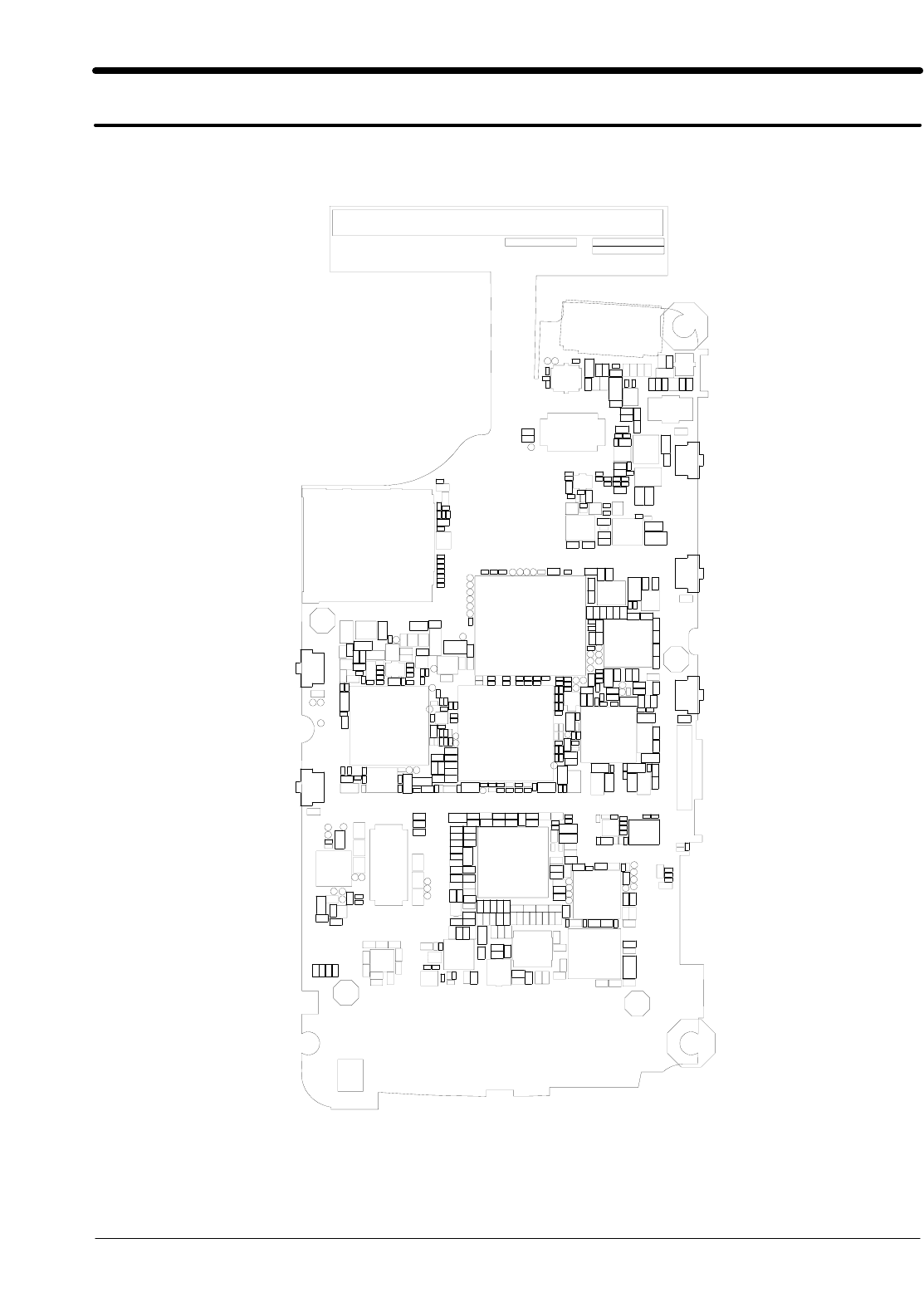
SAMSUNG Proprietary-Contents may change without notice
9. PCB Diagrams
9-1
This Document can not be used without Samsung's authorization
BOTH701
BOTH702
C101
C102
C103
C104
C105 C106
C107
C108
C109
C113
C114
C115
C116
C117
C118
C119
C120
C121
C122
C123
C124
C126
C127
C128
C129
C130
C131
C132
C133
C134
C135
C136
C137
C138C139 C140
C141
C142C143
C144
C145
C146
C147
C148
C149
C150
C151
C152
C153
C154
C155
C156
C157
C158
C159
C160
C161
C162 C163
C164
C165
C166
C167
C169
C171
C172
C173
C174
C175
C177
C178
C179 C180
C182
C183
C184
C185
C186
C187
C188
C189
C190
C191
C192
C193
C194
C200
C201
C202
C203
C204
C206
C207
C208
C210
C211
C212
C213
C214
C215 C218
C219
C220
C221
C222
C300
C301
C302
C303
C304
C305
C306
C307
C308
C309
C310 C311
C312
C313
C314
C315
C316
C317
C318
C319
C320
C321
C322
C323
C324
C325
C326
C327
C328
C329
C330
C331
C332
C333
C334
C335
C336
C337
C338
C339
C340 C341
C342
C343
C344 C345
C346
C347
C348
C349
C350
C351C352
C353
C354
C355
C356
C357
C358
C359 C360
C361
C362
C363
C364
C365
C400
C401
C402
C403
C404
C405
C406
C407
C408
C409
C410 C411
C412
C413
C414
C415
C416
C417
C418
C419
C420
C421
C422
C423
C424
C425
C426
C427
C428
C429
C430
C431
C432
C433
C434
C435
C436
C440
C444
C445
C446
C447
C448
C449
C450
C451
C452
C453
C454
C456
C457
C500
C501
C502
C503
C504
C505
C506
C511
C512
C513
C515 C516
C518
C519
C520
C522
C523
C524
C525
C526
C527
C528
C529C530 C531
C537
C538
C540
C545
C546
C547
C552
C553
C554
C555
C556
C557
C558
C559
C560
C600
C601
C602
C603
C605
C606
C617
C618
C619
C620
C621
C623
C624
C625
C626 C627
C628
C629
C632
C633
C638
C640
C641
C642
C643
C700
C701
C702
C703
C704
C705
C706
C708
C709
C710
C711
C714
C715
C800
C801
C802
C803
C804
C805
C806
C807
C808
C809
C810
C811
C812
C813
C814
C815
C816
C817
C818
C819
C820
C821 C822
C823
C824
C825
C826
C828
C831
C832
C837
C838
C839
C840
C842
CD400
D400
D401
D402
DUF100
F100
F101
F607
FEM100
HDC600
HDC602
HDC603
IFC700
JTAG300
JTAG301
JTAG302JTAG303
JTAG304
L102
L104
L105
L107
L108
L110
L112
L113
L114
L115
L116
L117
L118
L119
L120
L122
L123
L124
L125
L126
L127
L129
L130
L131
L200
L202
L400
L401
L402
L602
L700
L701
L702
L703
L800
L801
L803
MIC500
MV_UART_RX
MV_UART_TX
OSC400
OSC800
PAM100
R102
R103
R104
R105R106 R107
R109
R110 R111
R112
R113
R114
R115
R116
R202
R208
R209
R210
R300
R301
R302
R303
R304
R305
R306
R307
R311
R312
R313
R314R315
R317
R319
R321
R323
R325
R326
R327
R400
R401
R402
R403
R404
R405
R406
R408
R409
R410
R411
R412
R414
R415
R416
R417
R418
R419
R421
R422
R423
R424
R502
R503
R504
R505
R507
R508
R509
R510
R511
R515
R517
R519
R520
R521
R600
R601
R607
R610
R611
R612
R614
R619
R620
R621
R626
R630
R632
R633
R700R701
R702
R703
R704
R705
R706
R707
R708
R709
R711
R713
R715
R716
R801
R804
R807
R811
R812
R815
R817
R818
R822
R823
R824
R827
R830
R832
R833 R835
R837
R840
R846
R847
TA100
TA500
TA50 1
TA700
TA70 1
TA800
TA801
TAC700
TAC701TAC702
TAC703 TAC70 4
TCX20 0
TH300
TP300
TP301
TP30 2
TP30 3
TP304
TP_A800
TP_ACC_I700TP_ACC_I701
TP_AMUX_OUT
TP_BC LK
TP_BL_RST
TP_BL_SCL
TP_BL_SDA
TP_BOOT_SW
TP_BT_INT
TP_BT_RXD
TP_BT_TXD
TP_BT_WAKE
TP_CORE_800
TP_CORE_EN
TP_CTS
TP_D800
TP_DIN
TP_DOUT
TP_FM_DIN
TP_LCD_CABC
TP_LCD_D
TP_LCD_E MI_D
TP_LCD_RS
TP_LCD_VSYNC
TP_LCD_WR
TP_LIGHT_SENSOR
TP_LRCLK
TP_MCL K
TP_MODE300
TP_MODE301
TP_MV_CS
TP_MV_INT
TP_MV_WE
TP_NAND_D300
TP_NAND_OE
TP_N_RDY
TP_ONE800
TP_PM_INT
TP_PS_HOLD
TP_RESETOUT_N
TP_RFUBM
TP_RST
TP_RST_N
TP_RTS
TP_SCL_600
TP_SDRAM_CAS
TP_SDRAM _CS
TP_SDRAM_D300
TP_SDRAM_RAS
TP_SERAM_WE
TP_SLEEP
TP_TCXO_EN
TP_TV_OUT_SEL
TR400
U100
U101
U104
U105
U106
U201
U300
U301
U400
U401
U402
U403
U501
U502
U504
U600
U601
U602
U603
U604
U608
U609
U611
U613
U614
U615
U616
U617
U618
U620
U700
U702
U800
U801
U802 U804
U805
U806
U807
U808
U810
U811
U813
U815
U818
U821
U822
UCP300
UCP800
UME300
ZD400
ZD700
ZD701
ZD702
ZD703
ZD704
ZD705
ZD706
ZD707
ZD708
ZD709
ZD711
ZD712
ZD713
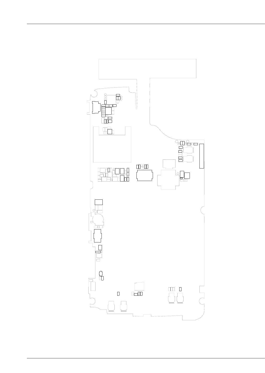
SAMSUNG Proprietary-Contents may change without notice
PCB Diagrams
9-2
This Document can not be used without Samsung's authorization
ANT100
ANT101
ANT102
ANT200
ANT_GND100
BAT400
BTC700
C100
C110
C111
C112
C205
C209
C216
C437
C438
C439
C441
C442
C443
C532 C533
C534
C541
C542
C548 C549
C550 C551
C607
C608
C609
C610
C611C612
C613
C614
C615 C616
C634
C635
C636
C637
C639
C644 C645
C646
C647
C648
C649
C707
C712
C713
C827
C829
C830
C833
C834
C835
C836
C841
CN800
D300
D801
D802
D803
D804
F200
F600
F601
F602
F608
F700
HEA601
HEA700
JTAG800
L100
L101
L201
L600
L601
L603
R100
R101
R200
R201
R203
R204
R205
R206
R308
R309
R310
R316
R318
R320
R407
R413
R522
R627
R628
R631
R636
R637
R712
R714
R828R829
R831
R842
RFS100
SHUTTER700
SHUTTER701
SIM400
SLC500
TA802
TP_CAM_D
TP_FM_BCLK
TP_FM_INT
TP_FM_LRCLK
TP_FM_RST
TP_MOT_PWM
TP_MV_PT_EN
TP_SLEEP_CLK
TP_SPK_N TP_SPK_P
TP_TOUCH_INT
TP_TOUCH_PWR_EN
U200
U302
U503
U607
U610
U619
U621
U701
U816
U817
ZD401
ZD500ZD501
ZD502
ZD503
ZD600ZD601ZD602
ZD603
ZD604
ZD605
ZD710
ZD714
ZD715