Samsung GT P5200 Service Manual. Www.s Manuals.com. Manual
samsung_gt-p5200_service_manual Samsung - Schematics & Service Manuals PDF
User Manual: Tablet Samsung GT-P5200 Galaxy Tab 3 10.1 3G - Service manuals and Schematics, Disassembly / Assembly. Free.
Open the PDF directly: View PDF ![]() .
.
Page Count: 95

1. Safety Precautions
1-1
Confidential and proprietary-the contents in this service guide subject to change without prior notice.
Distribution, transmission, or infringement of any content or data from this document without Samsung’s written authorization is strictly prohibited.
1-1. Repair Precaution
Before attempting any repair or detailed tuning, shield the device from RF noise or static
electricity discharges.
Use only demagnetized tools that are specifically designed for small electronic repairs,
as most electronic parts are sensitive to electromagnetic forces.
Use only high quality screwdrivers when servicing products. Low quality screwdrivers can
easily damage the heads of screws.
Use only conductor wire of the properly gauge and insulation for low resistance, because of
the low margin of error of most testing equipment.
We recommend 22-gauge twisted copper wire.
Hand-soldering is not recommended, because printed circuit boards (PCBs) can be easily
damaged, even with relatively low heat. Never use asoldering iron with apower rating of
more than 100 watts and use only lead-free solder with a melting point below 250°C (482°F).
Prior to disassembling the battery charger for repair, ensure that the AC power is disconnected.
Always use the replacement parts that are registered in the SEC system. Third-party replac
ement parts may not function properly.

Safety Precautions
Distribution, transmission, or infringement of any content or data from this document without Samsung’s written authorization is strictly prohibited.
Confidential and proprietary-the contents in this service guide subject to change without prior notice.
1-2
1-2. ESD(Electrostatically Sensitive Devices) Precaution
Many semiconductors and ESDs in electronic devices are particularly sensitive to static discha
rge and can be easily damaged by it. We recommend protecting these components with cond
uctive anti-static bags when you store or transport them.
Always use an anti-static strap or wristband and remove electrostatic buildup or dissipate
static electricity from your body before repairing ESDs.
Ensure that soldering irons have AC adapter with ground wires and that the ground wires are
properly connected.
Use only desoldering tools with plastic tips to prevent static discharge.
Properly shield the work environment from accidental electrostatic discharge before opening
packages containing ESDs.
The potential for static electricity discharge may be increased in low humidity environments,
such as air-conditioned rooms. Increase the airflow to the working area to decrease the
chance of accidental static electricity discharges.

2. Specification
2-1
Confidential and proprietary-the contents in this service guide subject to change without prior notice.
Distribution, transmission, or infringement of any content or data from this document without Samsung’s written authorization is strictly prohibited.
2-1. GSM General Specification
GSM850 EGSM 900 DCS1800 PCS1900 WCDMA
2100 WCDMA
1900 WCDMA
900 WCMDA
850
Freq.
Band[MHz]
Uplink/
Downlink
824~849
869~894
880~915
925~960
1710~1785
1805~1880
1850~1910
1930~1990
1922~1977
2112~2167
1852~1907
1932~1987
880~915
925~960
824~849
869~894
ARFCN
range 128~251 0~124 &
975~1023 512~885 512~810
UL:
9612~9888
DL:
10562~10838
UL:
9262~9538
DL:
9662~9938
UL:
2712~2863
DL:
2937~3088
UL:
4132~4233
DL:
4357~4458
Tx/Rx
spacing 45MHz 45MHz 95MHz 80MHz 190MHz 80MHz 45MHz 45MHz
Mod. Bit
rate/
Bit Period
270.833kbps
3.692us
270.833kbps
3.692us
270.833kbps
3.692us
270.833kbps
3.692us 3.84Mcps 3.84Mcps 3.84Mcps 3.84Mcps
Time Slot
Period/
Frame
Period
576.9us
4.615ms
576.9us
4.615ms
576.9us
4.615ms
576.9us
4.615ms
FrameLength:
10ms
Slotlength:
0.667ms
FrameLength:
10ms
Slotlength:
0.667ms
FrameLength:
10ms
Slotlength:
0.667ms
FrameLength:
10ms
Slotlength:
0.667ms
Modulation 0.3GMSK 0.3GMSK 0.3GMSK 0.3GMSK QPSKHQPSK QPSKHQPSK QPSKHQPSK QPSKHQPSK
MS Power 33dBm~5dBm 33dBm~5dBm 30dBm~0dBm 30dBm~0dBm 24dBm~
-50dBm 24dBm~
-50dBm 24dBm~
-50dBm 24dBm~
-50dBm
Power
Class 5pcl ~19
pcl 5pcl ~19
pcl 0pcl ~15
pcl 0pcl ~15
pcl 3(max+24dBm) 3(max+24dBm) 3(max+24dBm) 3(max+24dBm)
Sensitivity -102dBm -102dBm -100dBm -100dBm -106.7dBm -106.7dBm -106.7dBm -106.7dBm
TDMA Mux 8 8 8 8 8888
Cell Radius 35Km 35Km 2Km 2Km 2Km 2Km 2Km 2Km
Specification
Distribution, transmission, or infringement of any content or data from this document without Samsung’s written authorization is strictly prohibited.
Confidential and proprietary-the contents in this service guide subject to change without prior notice.
2-2
2-2. GSM Tx Power Class
TX Power
control
level
GSM850
533±2
dBm
631±2
dBm
729±2
dBm
827±2
dBm
925±2
dBm
10 23±2 dBm
11 21±2 dBm
12 19±2 dBm
13 17±2 dBm
14 15±2 dBm
15 13±2 dBm
16 11±3 dBm
17 9±3dBm
18 7±3 dBm
19 5±3 dBm
TX Power
control
level
EGSM900
533±2
dBm
631±2
dBm
729±2
dBm
827±2
dBm
925±2
dBm
10 23±2 dBm
11 21±2 dBm
12 19±2 dBm
13 17±2 dBm
14 15±2 dBm
15 13±2 dBm
16 11±3 dBm
17 9±3dBm
18 7±3 dBm
19 5±3 dBm
TX Power
control
level
DCS1800
030±3
dBm
128±3
dBm
226±3
dBm
324±3
dBm
422±3
dBm
520±3
dBm
618±3
dBm
716±3
dBm
814±3
dBm
912±4
dBm
10 10±4 dBm
11 8±4 dBm
12 6±4 dBm
13 4±4 dBm
14 2±5 dBm
15 0±5 dBm
TX Power
control
level
PCS1900
030±3
dBm
128±3
dBm
226±3
dBm
324±3
dBm
422±3
dBm
520±3
dBm
618±3
dBm
716±3
dBm
814±3
dBm
912±4
dBm
10 10±4 dBm
11 8±4 dBm
12 6±4 dBm
13 4±4 dBm
14 2±5 dBm
15 0±5 dBm

3. Operation Instruction and Installation
3-1
Confidential and proprietary-the contents in this service guide subject to change without prior notice.
Distribution, transmission, or infringement of any content or data from this document without Samsung’s written authorization is strictly prohibited.
Main Function
•Android OS: Jelly Bean
•Main 3MP FF, Sub 1.3FF
• 10.1" WXGA TFT Full Touch (C-Type)
•HSDPA 21.1Mbps /HSUPA 5.76Mbps
•A-GPS /GLONASS/ BT v4.0 +EDR with LE /USB v2.0 /Wi-Fi (802.11 a/b/g/n)/ OTG
•Recording definition: 720p
•Sensors: Accelation, Magnetic, ALS
•Additional :
-1.6
GHz Dual Core CPU

5. MAIN Electrical Parts List
5-1
Confidential and proprietary-the contents in this service guide subject to change without prior notice.
Distribution, transmission, or infringement of any content or data from this document without Samsung’s written authorization is strictly prohibited.
SEC Code Design LOC Description
0403-001870 ZD5005,ZD7000 DIODE-ZENER
0404-001250 D7002 DIODE-SCHOTTKY
0404-001394 D7000 DIODE-SCHOTTKY
0404-001669 D8000 DIODE-SCHOTTKY
0406-001239 D5001 DIODE-TVS
0406-001267 ZD5000,ZD5001,ZD9001 DIODE-TVS
0406-001267 ZD9002,ZD9003,ZD9004 DIODE-TVS
0406-001267 ZD9005,ZD9006 DIODE-TVS
0406-001293 ZD7001,ZD7002 DIODE-TVS
0406-001390 ZD9000 DIODE-TVS
0406-001413 ZD3000,ZD3001,ZD3002 DIODE-TVS
0406-001413 ZD3003,ZD3004,ZD4000 DIODE-TVS
0406-001413 ZD4001,ZD4004,ZD4005 DIODE-TVS
0406-001413 ZD4007,ZD4008,ZD4009 DIODE-TVS
0406-001505 D4000,D4001,ZD4003 DIODE-TVS
0406-001505 ZD4006,ZD5003 DIODE-TVS
0406-001506 ZD5004 DIODE-TVS
0406-001561 ZD5002 DIODE-TVS
0406-001583 ZD5006 DIODE-TVS
0407-001002 D7001 DIODE-ARRAY
0504-001113 TR7001,TR7002 TR-DIGITAL
0504-001171 Q5001 TR-DIGITAL
0505-001995 Q7000 FET-SILICON
0505-002341 Q5000,Q5004,Q9000 FET-SILICON
0505-002384 Q100,Q4000 FET-SILICON
0505-002388 Q5003 FET-SILICON
0505-002720 Q5002 FET-SILICON
0801-003024 U4000 IC-CMOS LOGIC
0801-003079 U6012 IC-CMOS LOGIC
0801-003346 U6002 IC-CMOS LOGIC
0801-003435 U6015 IC-CMOS LOGIC
0801-003437 U3000,U5000,U7007 IC-CMOS LOGIC
0902-003015 UCP6001 IC-MICROPROCESSOR
0904-002738 U8004 IC-GRAPHIC CONT.
1001-001846 U4004 IC-ANALOG MULTIPLEX
1003-002391 U104 IC-LEVEL DRIVER
1006-001552 U6014 IC-BUS TRANSCEIVER
1009-001058 U103 IC-HALL EFFECT S/W
1105-002212 UME3000 IC-RDRAM
1105-002305 UCP6001UP IC-DDR2 SDRAM

Main Electrical Parts List
Distribution, transmission, or infringement of any content or data from this document without Samsung’s written authorization is strictly prohibited.
Confidential and proprietary-the contents in this service guide subject to change without prior notice.
5-2
1107-002239 UME6000 IC-FLASH MEMORY
1201-003400 PAM1000 IC-POWER AMP
1201-003579 U2001 IC-GPS AMP
1202-001123 U4002 IC-VOLTAGE COMP.
1203-002250 U5004,U5007 IC-VOL. DETECTOR
1203-004776 FPC7000,U5008 IC-POSI.FIXED REG.
1203-004818 U6010,U9000 IC-POSI.FIXED REG.
1203-004819 U9002 IC-POSI.FIXED REG.
1203-005512 U5006 IC-POSI.FIXED REG.
1203-005574 U105 IC-POSI.FIXED REG.
1203-005599 U8007 IC-DC/DC CONVERTER
1203-006044 U9004 IC-DC/DC CONVERTER
1203-006115 U9001 IC-POWER SUPERVISOR
1203-006766 U3001,U5001 IC-VOL. DETECTOR
1203-006768 U7001,U8005 IC-DC/DC CONVERTER
1203-006801 U1004 IC-DC/DC CONVERTER
1203-006817 U107 IC-POSI.FIXED REG.
1203-006872 U108 IC-MULTI REG.
1203-006874 U100,U8000 IC-MULTI REG.
1203-006920 U8006 IC-BACKLIGHT DRIVER
1203-007084 U7005 IC-RESET
1203-007142 U6000 IC-DC/DC CONVERTER
1203-007333 U1002 IC-DC/DC CONVERTER
1203-007623 U7003 IC-BATTERY
1203-007702 U8001 IC-DC/DC CONVERTER
1203-007791 U4001,U6016 IC-POSI.FIXED REG.
1203-007842 U8002 IC-POSI.FIXED REG.
1203-007909 U7002 IC-POWER SUPERVISOR
1203-007951 U5005 IC-POWER SUPERVISOR
1204-003387 U109 IC-REMOTE CONTROL
1205-003692 U9006 IC-EXPANDER
1205-004233 U106 IC-TRANSMITTER
1205-004511 UCP3000 IC-MODEM
1205-004513 U5002 IC-SWITCH
1205-004515 U1001 IC-TRANSCEIVER
1205-004548 U8003 IC-TRANSMITTER
1205-004598 U2003 IC-WIFI
1205-004649 U2002 IC-GPS RECEIVER
1205-004803 U9003 IC-COMM. CONTROLLER
1205-004804 U4003 IC-CODEC
1209-002142 U102 IC-SENSOR

Main Electrical Parts List
Distribution, transmission, or infringement of any content or data from this document without Samsung’s written authorization is strictly prohibited.
Confidential and proprietary-the contents in this service guide subject to change without prior notice.
5-3
1209-002153 U101 IC-SENSOR
1209-002221 U1007 IC-SENSOR
1404-001694 TH7001,TH7002 THERMISTOR-NTC
1404-001726 V1000 THERMISTOR-NTC
1404-001728 TH3000 THERMISTOR-NTC
2007-000141 R6088 R-CHIP
2007-000143 R123,R124 R-CHIP
2007-000162 R5010,R5030 R-CHIP
2007-000163 R8009 R-CHIP
2007-000169 R1003 R-CHIP
2007-000170 R8004 R-CHIP
2007-001217 R104,R105,R106,R107 R-CHIP
2007-001217 R109,R110,R111,R112 R-CHIP
2007-001217 R113,R114,R115,R116 R-CHIP
2007-001217 R117,R118,R119,R120 R-CHIP
2007-002796 R7000 R-CHIP
2007-002970 R6016,R6103,R6105 R-CHIP
2007-003010 R1007 R-CHIP
2007-003015 R5025,R5027,R5038 R-CHIP
2007-007107 R3007 R-CHIP
2007-007131 R9014 R-CHIP
2007-007137 R4002 R-CHIP
2007-007142 R5023,R9023 R-CHIP
2007-007307 R6018,R6019 R-CHIP
2007-007318 R1017 R-CHIP
2007-007489 R8001 R-CHIP
2007-007538 R6060 R-CHIP
2007-007590 R9011 R-CHIP
2007-007627 R8011 R-CHIP
2007-0077419 R127,R128,R5013 R-CHIP
2007-007741 R5018,R7020,R7029 R-CHIP
2007-007741 R7031,R7032,R7033 R-CHIP
2007-007741 R9000,R9001,R9002 R-CHIP
2007-007942 R4016,R4017,R4024 R-CHIP
2007-007942 R4027,R4028 R-CHIP
2007-007943 R4025,R4026 R-CHIP
2007-007981 R8000,R9020 R-CHIP
2007-008045 R3005,R4018,R5000 R-CHIP
2007-008045 R5006,R5041,R6021 R-CHIP
2007-008045 R6077,R6109,R7040 R-CHIP
2007-008045 R7041,R9004 R-CHIP

Main Electrical Parts List
Distribution, transmission, or infringement of any content or data from this document without Samsung’s written authorization is strictly prohibited.
Confidential and proprietary-the contents in this service guide subject to change without prior notice.
5-4
2007-008048 R131,R132,R2015 R-CHIP
2007-008052 R125,R133,R134,R3009 R-CHIP
2007-008052 R5014,R6011,R6012 R-CHIP
2007-008052 R6033,R6034,R6107 R-CHIP
2007-008052 R6108 R-CHIP
2007-008055 R3030,R5022,R5043 R-CHIP
2007-008055 R6026,R6058,R6080 R-CHIP
2007-008055 R7036,R7043,R8010 R-CHIP
2007-008055 R9022,R9024,R9025 R-CHIP
2007-0080579 R6104 R-CHIP
2007-008137 R7002,R7003 R-CHIP
2007-008210 R9021 R-CHIP
2007-008298 R6051,R6094 R-CHIP
2007-008312 R4023 R-CHIP
2007-008354 R6055,R8014 R-CHIP
2007-008403 R5044 R-CHIP
2007-008419 R5004,R5007,R5042 R-CHIP
2007-008420 R5028 R-CHIP
2007-008483 R9015,R9016,R9018 R-CHIP
2007-008483 R9019 R-CHIP
2007-008486 R100,R5021 R-CHIP
2007-008516 R121,R126,R2000 R-CHIP
2007-008516 R2002,R2003,R2023 R-CHIP
2007-008516 R2024,R3025,R4011 R-CHIP
2007-008516 R4012,R5001,R5003 R-CHIP
2007-008516 R5008,R5037,R6000 R-CHIP
2007-008516 R6005,R6006,R6007 R-CHIP
2007-008516 R6036,R6038,R7004 R-CHIP
2007-008516 R7025,R9007,R9017 R-CHIP
2007-008531 R1008,R6048 R-CHIP
2007-008588 R1015,R3012,R3013 R-CHIP
2007-008588 R3014,R4004 R-CHIP
2007-008697 R6047 R-CHIP
2007-008721 R7017,R8013 R-CHIP
2007-008774 R9003 R-CHIP
2007-008800 R5005 R-CHIP
2007-008806 R4000,R4019 R-CHIP
2007-008812 R7022 R-CHIP
2007-009084 R108,R122,R4009 R-CHIP
2007-009084 R4010,R5016,R5031 R-CHIP
2007-009084 R5040,R7014,R8003 R-CHIP

Main Electrical Parts List
Distribution, transmission, or infringement of any content or data from this document without Samsung’s written authorization is strictly prohibited.
Confidential and proprietary-the contents in this service guide subject to change without prior notice.
5-5
2007-009111 R6027 R-CHIP
2007-009155 R3006,R3010,R3031 R-CHIP
2007-009155 R5011 R-CHIP
2007-009158 R129,R130 R-CHIP
2007-009168 R8012 R-CHIP
2007-009171 R2007,R2008,R2009 R-CHIP
2007-009171 R2010,R2011,R6039 R-CHIP
2007-009171 R6040,R6041,R6042 R-CHIP
2007-009171 R6043,R6044,R6045 R-CHIP
2007-009171 R6046 R-CHIP
2007-009182 R6086 R-CHIP
2007-009199 R6031 R-CHIP
2007-009208 R4021,R4022 R-CHIP
2007-009212 R4001,R6052,R6053 R-CHIP
2007-009314 R6025 R-CHIP
2007-009315 R3002,R3008 R-CHIP
2007-009323 R7030 R-CHIP
2007-009361 R1001 R-CHIP
2007-009408 R6008,R6009,R6010 R-CHIP
2007-009793 R5009 R-CHIP
2007-009801 R1005,R1006 R-CHIP
2007-009805 R6030 R-CHIP
2007-009920 R6057,R6059 R-CHIP
2007-009954 R7011 R-CHIP
2007-010233 R3016 R-CHIP
2007-010856 R5012 R-CHIP
2203-000233 C1017,C2065 C-CER,CHIP
2203-000254 C1037,C2013,C8014 C-CER,CHIP
2203-000254 C8020,C9044 C-CER,CHIP
2203-000278 C6096,C7061 C-CER,CHIP
2203-000359 C8030 C-CER,CHIP
2203-000386 C134,C135 C-CER,CHIP
2203-000425 C4014,C4015,C4016 C-CER,CHIP
2203-000425 C4017 C-CER,CHIP
2203-000438 C7031 C-CER,CHIP
2203-000489 C8024 C-CER,CHIP
2203-000627 C8006 C-CER,CHIP
2203-000725 C5040 C-CER,CHIP
2203-001239 C4018,C4019 C-CER,CHIP
2203-001383 C1019 C-CER,CHIP
2203-001437 C1020 C-CER,CHIP

Main Electrical Parts List
Distribution, transmission, or infringement of any content or data from this document without Samsung’s written authorization is strictly prohibited.
Confidential and proprietary-the contents in this service guide subject to change without prior notice.
5-6
2203-002687 C7076,C7086 C-CER,CHIP
2203-002709 C107,C8005 C-CER,CHIP
2203-003054 C6095 C-CER,CHIP
2203-005056 C1015 C-CER,CHIP
2203-005682 C1052,C2020,C3039 C-CER,CHIP
2203-005682 C3041,C3042,C5000 C-CER,CHIP
2203-005682 C5001,C5003 C-CER,CHIP
2203-005717 C3047,C7043 C-CER,CHIP
2203-005719 C1055,C1078 C-CER,CHIP
2203-005725 C2002,C2006,C3048 C-CER,CHIP
2203-005725 C7042 C-CER,CHIP
2203-005727 C5025,C5027,C5032 C-CER,CHIP
2203-005729 C1128,C2049,C4002 C-CER,CHIP
2203-005729 C4003,C4010,C4011 C-CER,CHIP
2203-005731 C2050 C-CER,CHIP
2203-005732 C4006,C4007,C4012 C-CER,CHIP
2203-005732 C5002 C-CER,CHIP
2203-005734 C1060,C5021,C7085 C-CER,CHIP
2203-005736 C1053,C2010,C2014 C-CER,CHIP
2203-005777 C2012 C-CER,CHIP
2203-005779 C8022,C8023 C-CER,CHIP
2203-005792 C1051 C-CER,CHIP
2203-005806 C1046,C2008,C2045 C-CER,CHIP
2203-005806 C2056,C4013 C-CER,CHIP
2203-006048 C1028,C8012,C8013 C-CER,CHIP
2203-006048 C8017,C8018,C8019 C-CER,CHIP
2203-006048 C9026 C-CER,CHIP
2203-006121 C126 C-CER,CHIP
2203-006194 C1050,C3001,C3002 C-CER,CHIP
2203-006194 C7002 C-CER,CHIP
2203-006208 C7008,C7009,C7068 C-CER,CHIP
2203-006257 C6094 C-CER,CHIP
2203-006260 C1035,C1044 C-CER,CHIP
2203-006305 C1126,C1127,C2015 C-CER,CHIP
2203-006305 C2016,C2026,C2037 C-CER,CHIP
2203-006305 C2046,C2053,C2057 C-CER,CHIP
2203-006305 C2060,C2063,C2064 C-CER,CHIP
2203-006348 C9014 C-CER,CHIP
2203-006377 C1138,C1139 C-CER,CHIP
2203-006379 C1048 C-CER,CHIP

Main Electrical Parts List
Distribution, transmission, or infringement of any content or data from this document without Samsung’s written authorization is strictly prohibited.
Confidential and proprietary-the contents in this service guide subject to change without prior notice.
5-7
2203-006399 C1021,C1022,C1098 C-CER,CHIP
2203-006399 C131,C4005,C6080 C-CER,CHIP
2203-006399 C6093,C6097,C6098 C-CER,CHIP
2203-006399 C8003,C8026 C-CER,CHIP
2203-006423 C100,C1001,C1002 C-CER,CHIP
2203-006423 C1003,C1004,C1005 C-CER,CHIP
2203-006423 C1010,C1011,C1012 C-CER,CHIP
2203-006423 C102,C1049,C1056 C-CER,CHIP
2203-006423 C1058,C110,C111,C112 C-CER,CHIP
2203-006423 C115,C118,C119,C121 C-CER,CHIP
2203-006423 C123,C128,C129,C136 C-CER,CHIP
2203-006423 C2007,C3000,C3003 C-CER,CHIP
2203-006423 C3004,C3010,C3012 C-CER,CHIP
2203-006423 C3013,C3014,C3016 C-CER,CHIP
2203-006423 C3018,C3019,C3020 C-CER,CHIP
2203-006423 C3021,C3023,C3024 C-CER,CHIP
2203-006423 C3025,C3027,C3028 C-CER,CHIP
2203-006423 C3029,C3032,C3033 C-CER,CHIP
2203-006423 C3034,C3038,C3045 C-CER,CHIP
2203-006423 C5013,C6084,C6087 C-CER,CHIP
2203-006423 C7082,C8037,C9000 C-CER,CHIP
2203-006423 C9001,C9004,C9005 C-CER,CHIP
2203-006423 C9006,C9007,C9008 C-CER,CHIP
2203-006423 C9009,C9010 C-CER,CHIP
2203-006562 C1059,C114,C130 C-CER,CHIP
2203-006562 C4004,C4008,C4009 C-CER,CHIP
2203-006562 C5019,C5020,C5043 C-CER,CHIP
2203-006562 C6079,C6092,C7000 C-CER,CHIP
2203-006562 C7012,C7013,C7030 C-CER,CHIP
2203-006562 C7032,C7033,C7037 C-CER,CHIP
2203-006562 C7041,C7049,C7056 C-CER,CHIP
2203-006562 C7069,C7070,C7073 C-CER,CHIP
2203-006562 C7077,C7078,C8025 C-CER,CHIP
2203-006562 C8038,C8041,C8042 C-CER,CHIP
2203-006562 C9045 C-CER,CHIP
2203-006626 C1143 C-CER,CHIP
2203-006647 C1006,C1007,C1008 C-CER,CHIP

Main Electrical Parts List
Distribution, transmission, or infringement of any content or data from this document without Samsung’s written authorization is strictly prohibited.
Confidential and proprietary-the contents in this service guide subject to change without prior notice.
5-8
2203-006647 C1013 C-CER,CHIP
2203-006668 C125 C-CER,CHIP
2203-006681 C7053,C8033 C-CER,CHIP
2203-006707 C2022,C2029,C2034 C-CER,CHIP
2203-006707 C2047 C-CER,CHIP
2203-006815 C1045,C1047,C5017 C-CER,CHIP
2203-006839 C1057,C1141,C4021 C-CER,CHIP
2203-006839 C5010 C-CER,CHIP
2203-006844 C113,C8034,C8035 C-CER,CHIP
2203-006872 C1009,C1031,C1034 C-CER,CHIP
2203-006872 C1101,C1105,C1125 C-CER,CHIP
2203-006872 C116,C117,C120,C122 C-CER,CHIP
2203-006872 C127,C2003,C4023 C-CER,CHIP
2203-006872 C4038,C4040,C4041 C-CER,CHIP
2203-006872 C6085,C6086,C7074 C-CER,CHIP
2203-006872 C8000,C8002,C8015 C-CER,CHIP
2203-006872 C8021,C9032 C-CER,CHIP
2203-006896 C1023 C-CER,CHIP
2203-006978 C5014,C5018,C5023 C-CER,CHIP
2203-006979 C1000,C1014,C5015 C-CER,CHIP
2203-007133 C9042 C-CER,CHIP
2203-007210 C1089,C3006,C3009 C-CER,CHIP
2203-007210 C3011,C3015,C3017 C-CER,CHIP
2203-007210 C3022,C3026,C3030 C-CER,CHIP
2203-007210 C3031,C3035,C3046 C-CER,CHIP
2203-007240 C5011,C6090,C7001 C-CER,CHIP
2203-007240 C7004,C7005,C7006 C-CER,CHIP
2203-007240 C7007,C7014,C7015 C-CER,CHIP
2203-007240 C7016,C7017,C7018 C-CER,CHIP
2203-007240 C7019,C7045,C7062 C-CER,CHIP
2203-007240 C7063,C7064,C7065 C-CER,CHIP
2203-007240 C7066,C7067,C7071 C-CER,CHIP
2203-007240 C7083,C7084 C-CER,CHIP
2203-007269 C3036,C3037,C5016 C-CER,CHIP
2203-007269 C7075 C-CER,CHIP
2203-007270 C1088,C5031,C7046 C-CER,CHIP

Main Electrical Parts List
Distribution, transmission, or infringement of any content or data from this document without Samsung’s written authorization is strictly prohibited.
Confidential and proprietary-the contents in this service guide subject to change without prior notice.
5-9
2203-007270 C7047,C8027,C8031 C-CER,CHIP
2203-007270 C8032 C-CER,CHIP
2203-007271 C137,C2036,C5041 C-CER,CHIP
2203-007271 C5042,C7003,C7020 C-CER,CHIP
2203-007271 C7029,C7034,C7035 C-CER,CHIP
2203-007271 C7036,C7038,C7039 C-CER,CHIP
2203-007271 C7050,C7051,C7081 C-CER,CHIP
2203-007271 C9011,C9012,C9013 C-CER,CHIP
2203-007271 C9021,C9022,C9023 C-CER,CHIP
2203-007271 C9024,C9025,C9027 C-CER,CHIP
2203-007271 C9029 C-CER,CHIP
2203-007279 C7023,C7048,C7052 C-CER,CHIP
2203-007279 C7054,C7055 C-CER,CHIP
2203-007317 C1092,C1109,C1110 C-CER,CHIP
2203-007317 C1114,C4024,C4025 C-CER,CHIP
2203-007317 C4029,C4035,C5004 C-CER,CHIP
2203-007317 C8001,C8004,C9047 C-CER,CHIP
2203-007385 C101,C103,C108,C109 C-CER,CHIP
2203-007385 C138,C139,C8011 C-CER,CHIP
2203-007391 C1142,C5044,C6000 C-CER,CHIP
2203-007391 C6001,C6002,C6003 C-CER,CHIP
2203-007391 C6004,C6005,C6006 C-CER,CHIP
2203-007391 C6007,C6008,C6009 C-CER,CHIP
2203-007391 C6010,C6011,C6012 C-CER,CHIP
2203-007391 C6013,C6014,C6015 C-CER,CHIP
2203-007391 C6016,C6017,C6018 C-CER,CHIP
2203-007391 C6019,C6020,C6021 C-CER,CHIP
2203-007391 C6022,C6023,C6024 C-CER,CHIP
2203-007391 C6025,C6026,C6027 C-CER,CHIP
2203-007391 C6028,C6029,C6030 C-CER,CHIP
2203-007391 C6031,C6032,C6033 C-CER,CHIP
2203-007391 C6034,C6035,C6036 C-CER,CHIP
2203-007391 C6037,C6038,C6039 C-CER,CHIP
2203-007391 C6040,C6041,C6042 C-CER,CHIP

Main Electrical Parts List
Distribution, transmission, or infringement of any content or data from this document without Samsung’s written authorization is strictly prohibited.
Confidential and proprietary-the contents in this service guide subject to change without prior notice.
5-10
2203-007391 C6043,C6044,C6045 C-CER,CHIP
2203-007391 C6046,C6047,C6048 C-CER,CHIP
2203-007391 C6049,C6050,C6051 C-CER,CHIP
2203-007391 C6052,C6053,C6054 C-CER,CHIP
2203-007391 C6055,C6056,C6057 C-CER,CHIP
2203-007391 C6058,C6059,C6060 C-CER,CHIP
2203-007391 C6061,C6062,C6063 C-CER,CHIP
2203-007391 C6064,C6065,C6066 C-CER,CHIP
2203-007391 C6067,C6068,C6069 C-CER,CHIP
2203-007391 C6070,C6071,C6072 C-CER,CHIP
2203-007391 C6073,C6074,C6075 C-CER,CHIP
2203-007391 C6076,C6077,C6078 C-CER,CHIP
2203-007393 C1039,C1054,C1086 C-CER,CHIP
2203-007393 C124,C132,C133,C2042 C-CER,CHIP
2203-007393 C2043,C2061,C6091 C-CER,CHIP
2203-007393 C7011,C7024,C7025 C-CER,CHIP
2203-007393 C7026,C7027,C7028 C-CER,CHIP
2203-007393 C7040,C7044,C7057 C-CER,CHIP
2203-007393 C7058,C7059,C7060 C-CER,CHIP
2203-007393 C7072,C8010 C-CER,CHIP
2203-007449 C105,C106,C1100 C-CER,CHIP
2203-007449 C1106,C2001,C2005 C-CER,CHIP
2203-007449 C2011,C3049,C3050 C-CER,CHIP
2203-007449 C4000,C4022,C4026 C-CER,CHIP
2203-007449 C4027,C4030,C4031 C-CER,CHIP
2203-007449 C4039,C5009,C5012 C-CER,CHIP
2203-007449 C5022,C5038,C5039 C-CER,CHIP
2203-007449 C6088,C8007,C8008 C-CER,CHIP
2203-007449 C8009,C8036,C9002 C-CER,CHIP
2203-007449 C9003,C9020,C9028 C-CER,CHIP
2203-007449 C9031,C9035,C9036 C-CER,CHIP
2203-007449 C9037,C9039,C9040 C-CER,CHIP
2203-007449 C9041,C9046 C-CER,CHIP
2203-007693 C9043 C-CER,CHIP

Main Electrical Parts List
Distribution, transmission, or infringement of any content or data from this document without Samsung’s written authorization is strictly prohibited.
Confidential and proprietary-the contents in this service guide subject to change without prior notice.
5-11
2203-007775 C4020 C-CER,CHIP
2203-007790 C8029,C8039,C8040 C-CER,CHIP
2203-007795 C1030,C1064,C3005 C-CER,CHIP
2203-007795 C3007,C3008,C5006 C-CER,CHIP
2203-007795 C5007 C-CER,CHIP
2203-007796 C104,C2004,C2009 C-CER,CHIP
2203-007796 C2027,C2028,C2032 C-CER,CHIP
2203-007796 C2058,C4033,C4034 C-CER,CHIP
2203-007796 C4036,C4037,C5008 C-CER,CHIP
2203-007796 C5036,C7010,C8028 C-CER,CHIP
2203-007796 C9019,C9030 C-CER,CHIP
2203-008095 C2031,C2033,C2054 C-CER,CHIP
2203-008097 C2024,C2035,C2039 C-CER,CHIP
2203-008097 C2040,C2041,C2044 C-CER,CHIP
2203-008097 C2059,C2062,C8016 C-CER,CHIP
2203-008097 C9015,C9016,C9017 C-CER,CHIP
2203-008097 C9018 C-CER,CHIP
2203-008126 C5024 C-CER,CHIP
2203-008527 C7079,C7080 C-CER,CHIP
2203-008528 C1140 C-CER,CHIP
2404-001506 C4001,TA7001,TA7002 C-TA,CHIP
2409-001127 TA1000 C-POLYMER ,CHIP
2703-002204 L2004 INDUCTOR-SMD
2703-002267 L1003,L1008 INDUCTOR-SMD
2703-002313 L1000,L1001,L1040 INDUCTOR-SMD
2703-002367 L2000 INDUCTOR-SMD
2703-002596 C1099,C1107 INDUCTOR-SMD
2703-002960 L9005,L9006 INDUCTOR-SMD
2703-003004 L1004 INDUCTOR-SMD
2703-003485 L9004 INDUCTOR-SMD
2703-003498 L6000 INDUCTOR-SMD
2703-003686 L8001 INDUCTOR-SMD
2703-003754 L7011,L9001 INDUCTOR-SMD
2703-003755 L1034,L1036,L1037 INDUCTOR-SMD

Main Electrical Parts List
Distribution, transmission, or infringement of any content or data from this document without Samsung’s written authorization is strictly prohibited.
Confidential and proprietary-the contents in this service guide subject to change without prior notice.
5-12
2703-003869 L3002,L3003 INDUCTOR-SMD
2703-003911 L1002,L7004,L7006 INDUCTOR-SMD
2703-003913 L7005,L8005 INDUCTOR-SMD
2703-004012 R2001 INDUCTOR-SMD
2703-004039 L1011 INDUCTOR-SMD
2703-004230 L5000 INDUCTOR-SMD
2703-004287 L1012 INDUCTOR-SMD
2703-004297 L5001 INDUCTOR-SMD
2703-004299 L1014,L1018 INDUCTOR-SMD
2703-004300 L1007 INDUCTOR-SMD
2703-004301 C1032,L1005 INDUCTOR-SMD
2703-004302 L1017 INDUCTOR-SMD
2703-004338 L2011 INDUCTOR-SMD
2703-004345 L2002 INDUCTOR-SMD
2703-004364 L2014 INDUCTOR-SMD
2703-004365 L1016 INDUCTOR-SMD
2703-004366 L2003 INDUCTOR-SMD
2703-004369 L1015 INDUCTOR-SMD
2703-004530 L8004 INDUCTOR-SMD
2703-004635 L7000,L7001,L7002 INDUCTOR-SMD
2703-004635 L7003,L7007,L7008 INDUCTOR-SMD
2703-004635 L7009,L7010 INDUCTOR-SMD
2703-004697 L4004,L4005,L4009 INDUCTOR-SMD
2703-004697 L4010 INDUCTOR-SMD
2801-004785 OSC100 CRYSTAL-SMD
2801-004836 OSC8000 CRYSTAL-SMD
2801-004931 OSC1000 CRYSTAL-SMD
2801-005165 OSC6000 CRYSTAL-SMD
2801-005167 OSC2002 CRYSTAL-SMD
2801-005254 OSC3000,OSC7000 CRYSTAL-SMD
2805-001098 OSC2001 OSCILLATOR-TCXO
2901-001625 F5000 FILTER-EMI/ESD
2901-001673 F8001 FILTER-EMI SMD
2901-001674 F8000,F8002,F9000 FILTER-EMI SMD

Main Electrical Parts List
Distribution, transmission, or infringement of any content or data from this document without Samsung’s written authorization is strictly prohibited.
Confidential and proprietary-the contents in this service guide subject to change without prior notice.
5-13
2901-001674 F9001 FILTER-EMI SMD
2904-002085 F2001,F2002 FILTER-GPS SAW
2909-001324 F2004 FILTER-LC
2910-000125 F1000 DUPLEXER-SAW
2911-000219 U1000 DUPLEXER-ASM
2911-000257 U2004 DUPLEXER-FEM
2911-000258 U2005 DUPLEXER-FEM
3301-001534 L8000,R2004 BEAD-SMD
3301-001729 L101,L102,L9003 BEAD-SMD
3301-001812 L100 BEAD-SMD
3301-001895 L2001 BEAD-SMD
3301-001901 L9000,L9002 BEAD-SMD
3301-001929 L4011,L4012 BEAD-SMD
3301-001956 L3000,L3001 BEAD-SMD
3301-002037 L8003 BEAD-SMD
3301-002062 L1031 BEAD-SMD
3301-002065 L4000,L4001,L4002 BEAD-SMD
3301-002065 L4003,L4006,L7012 BEAD-SMD
3301-002065 L7013 BEAD-SMD
3301-002078 L4007,L4008 BEAD-SMD
3301-002085 L8002 BEAD-SMD
3301-002236 L1042,L1043 BEAD-SMD
3301-002254 L5004 BEAD-SMD
3705-001731 RFS1000 CONNECTOR-COAXIAL
3708-002183 SLC5000,SLC8000 CONNECTOR-FPC/FFC/PIC
3708-002781 SLC9000 CONNECTOR-FPC/FFC/PIC
3709-001811 CD9000 CONNECTOR-CARD EDGE
3709-001813 SIM3000 CONNECTOR-CARD EDGE
3711-006925 HDC6000,HDC9000 HEADER-BOARD TO BOARD
3711-006925 HDC9001 HEADER-BOARD TO BOARD
3711-007173 HDC3001,HDC4001 HEADER-BOARD TO BOARD
3711-008010 HDC100,HDC4000 HEADER-BOARD TO BOARD
3711-008010 HDC5000 HEADER-BOARD TO BOARD
3711-008347 HDC9002 HEADER-BOARD TO BOARD

Main Electrical Parts List
Distribution, transmission, or infringement of any content or data from this document without Samsung’s written authorization is strictly prohibited.
Confidential and proprietary-the contents in this service guide subject to change without prior notice.
5-14
3711-008421 BTC7000 CONNECTOR-HEADER
3712-001458 ANT1000,ANT1001 CONNECTOR-TERMINAL
3712-001458 ANT2001,ANT2002 CONNECTOR-TERMINAL
4709-001672 F2005 FREQ-DISTRIBUTER
4709-002028 F2003 FREQ-DISTRIBUTER
GH98-27736A SC1000 ASSY COVER-ASSY SHIELD COVER 1
GH98-27737A SC1001 ASSY COVER-ASSY SHIELD COVER 2
GH98-27738A SC1002 ASSY COVER-ASSY SHIELD COVER 3
Please consult the GSPN website (Samsung Portal) for the most recent version of the product's part list.
6. Level 1Repair
6-1
Confidential and proprietary-the contents in this service guide subject to change without prior notice.
Distribution, transmission, or infringement of any content or data from this document without Samsung’s written authorization is strictly prohibited.
6-1. S/W Download
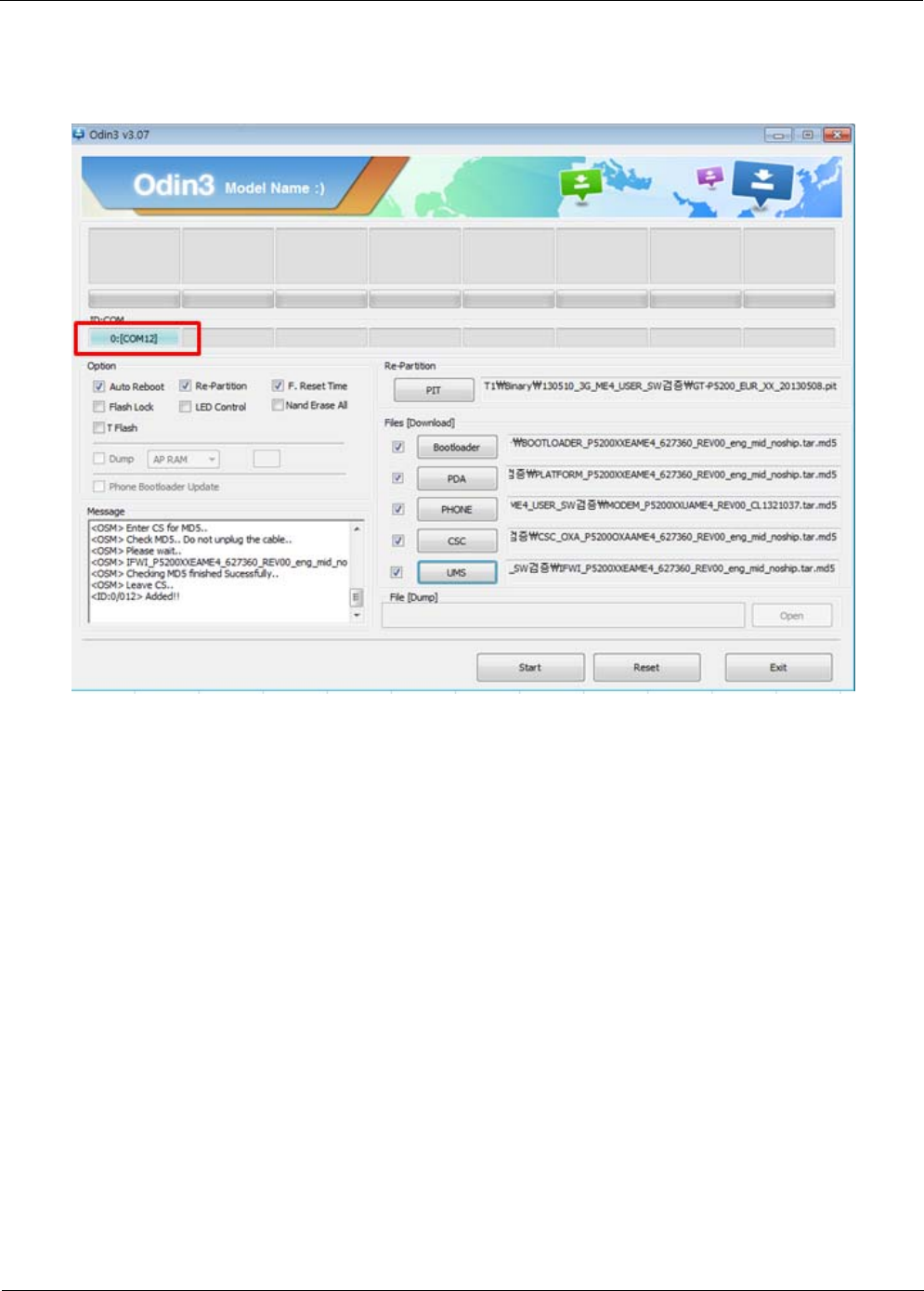
6-1-1. Pre-requisite for S/W Downloading
Downloader Program (Odin3 v3.07.exe)
GT-P5200
Data Link Cable (GH39-01578A)
Binary files
Settings
Data Link Cable
Level 1Repair
Distribution, transmission, or infringement of any content or data from this document without Samsung’s written authorization is strictly prohibited.
Confidential and proprietary-the contents in this service guide subject to change without prior notice.
6-2
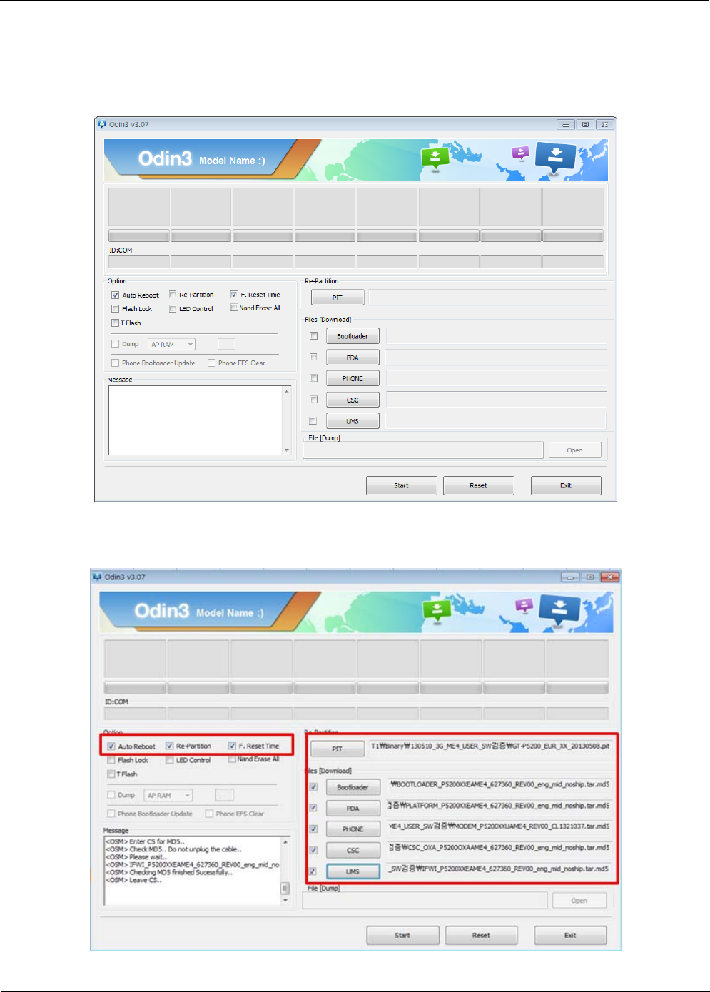
6-1-2. S/W Downloader Program
Load the binary download program by executing the
"Odin3 v3.07.exe" Run this file.
1.Option checking and select files
-Check Auto Reboot and F. Reset Time, then select PIT, Bootloader,
CODE, PHONE, CSC and UMS File.
Level 1Repair
Distribution, transmission, or infringement of any content or data from this document without Samsung’s written authorization is strictly prohibited.
Confidential and proprietary-the contents in this service guide subject to change without prior notice.
6-3
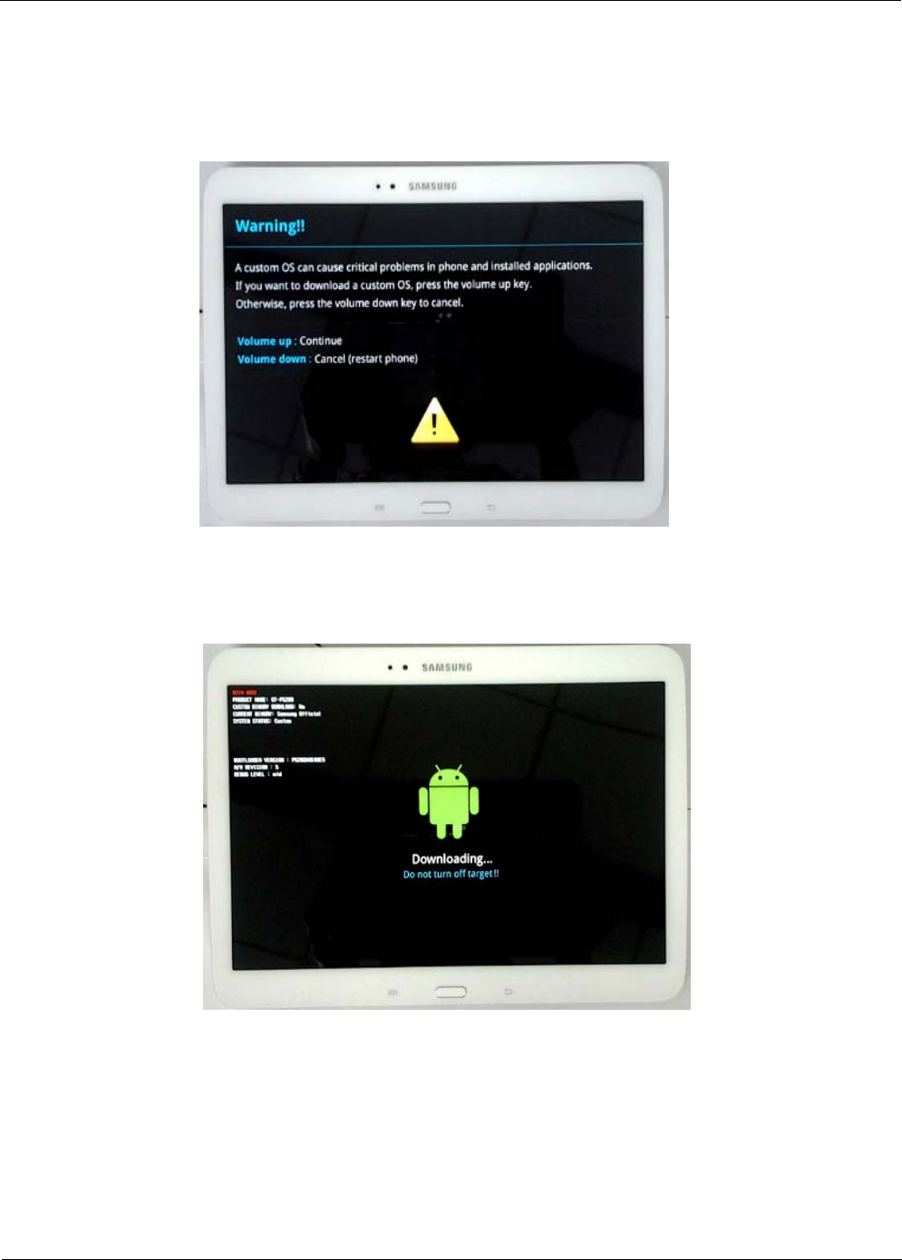
2.Enter Device into Download Mode
-Press volume down button and power key at same time for 5seconds, then you
can see below display.
-Press volume up button to enter device into download mode.
Level 1Repair
Distribution, transmission, or infringement of any content or data from this document without Samsung’s written authorization is strictly prohibited.
Confidential and proprietary-the contents in this service guide subject to change without prior notice.
6-4
3.Connect the Device to PC via Data Cable.
Make sure ID:COM box highlighted blue that the device is connected to the PC.
Level 1Repair
Distribution, transmission, or infringement of any content or data from this document without Samsung’s written authorization is strictly prohibited.
Confidential and proprietary-the contents in this service guide subject to change without prior notice.
6-5
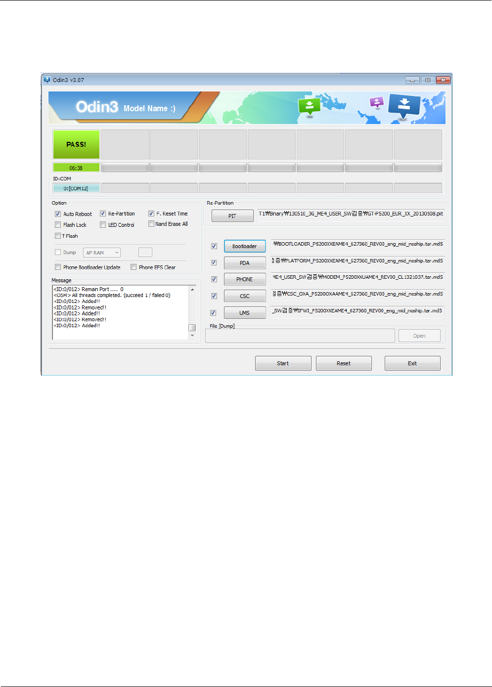
4.Start Downloading PIT, CODE, PHONE and CSC files by clicking Start button.
Then wait for "PASS" to be appear on the screen.
5.Once the device boots up, confirm the downloaded version name and etc. :
*#1234#
Full Reset :
Apps >Settings >Backup and reset >Factory data reset
8. Level 3Repair
8-1
Confidential and proprietary-the contents in this service guide subject to change without prior notice.
Distribution, transmission, or infringement of any content or data from this document without Samsung’s written authorization is strictly prohibited.
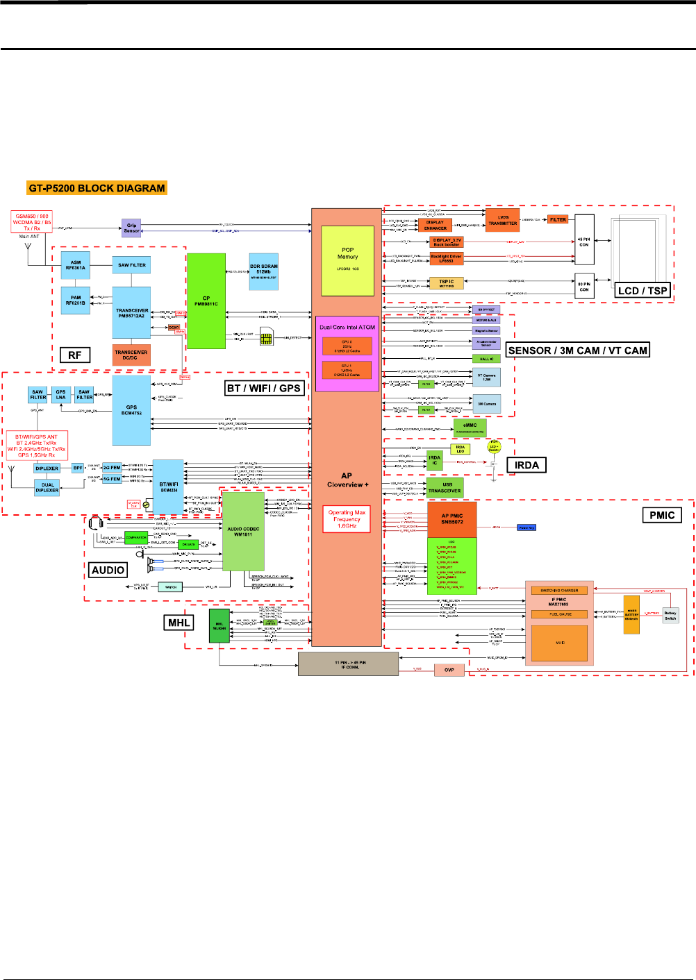
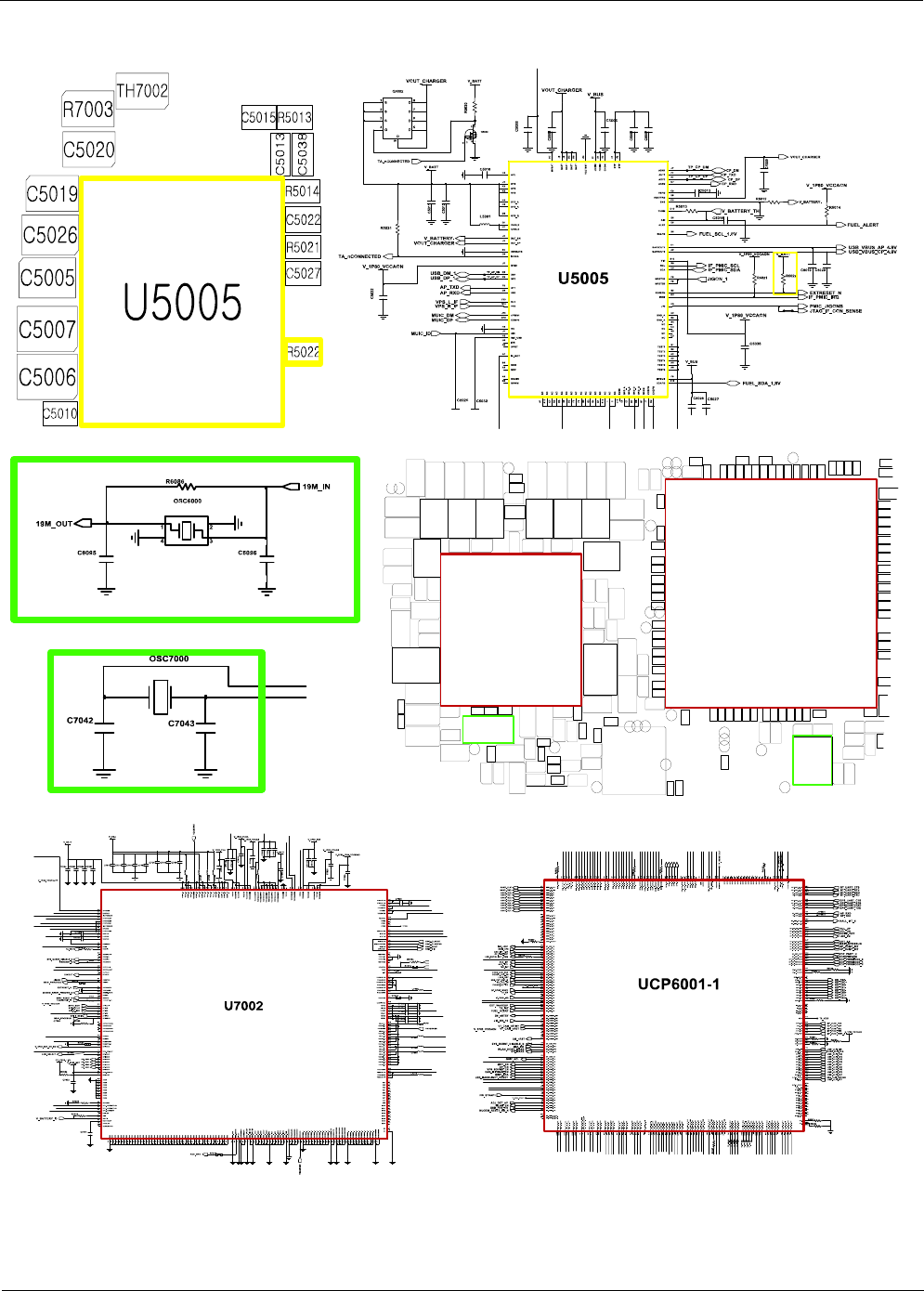
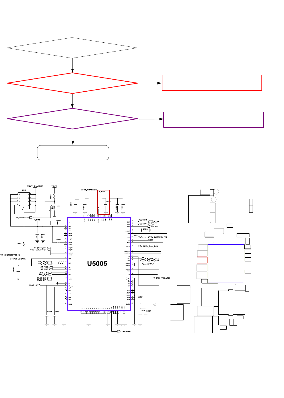
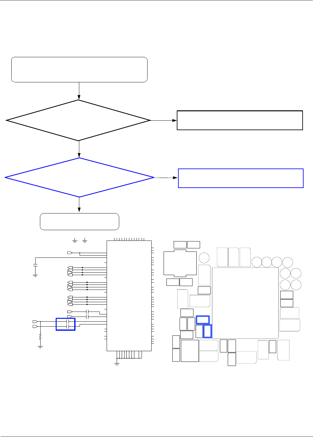
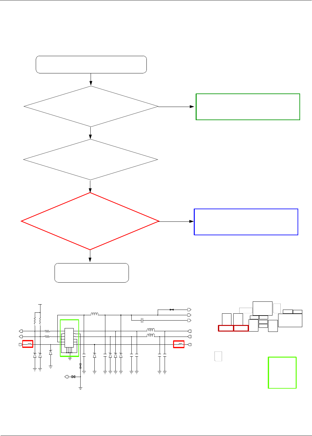
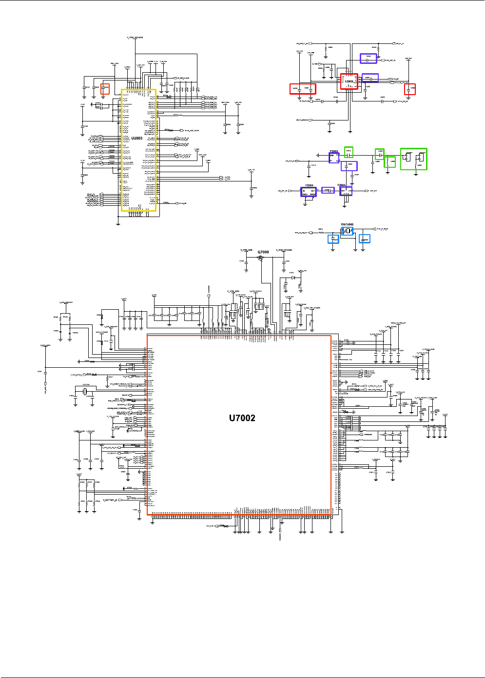
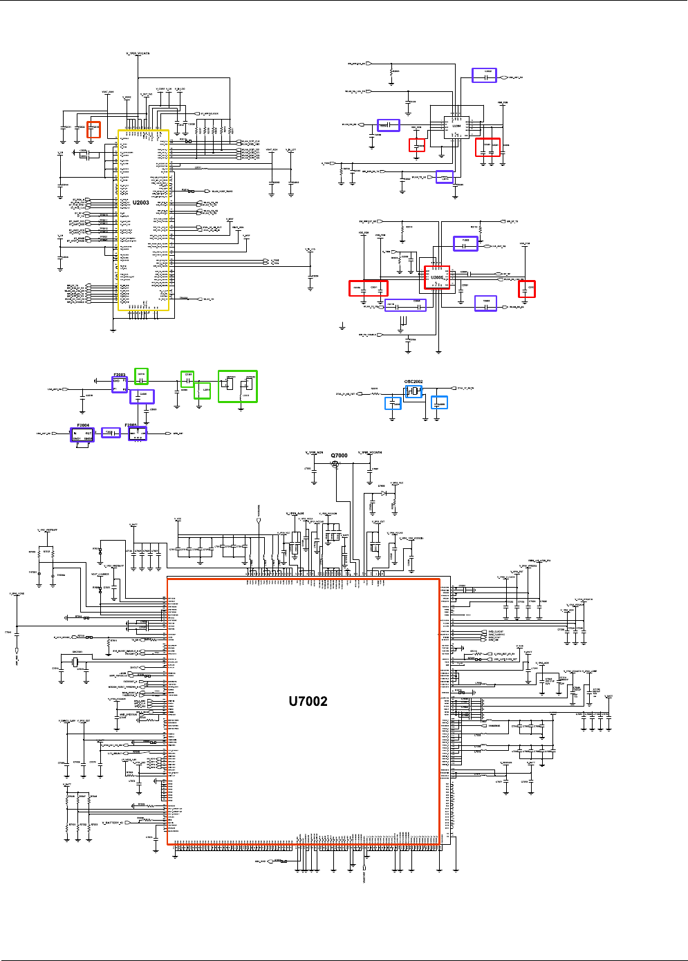
8-1. Block Diagram
Level 3Repair
Distribution, transmission, or infringement of any content or data from this document without Samsung’s written authorization is strictly prohibited.
Confidential and proprietary-the contents in this service guide subject to change without prior notice.
8-2
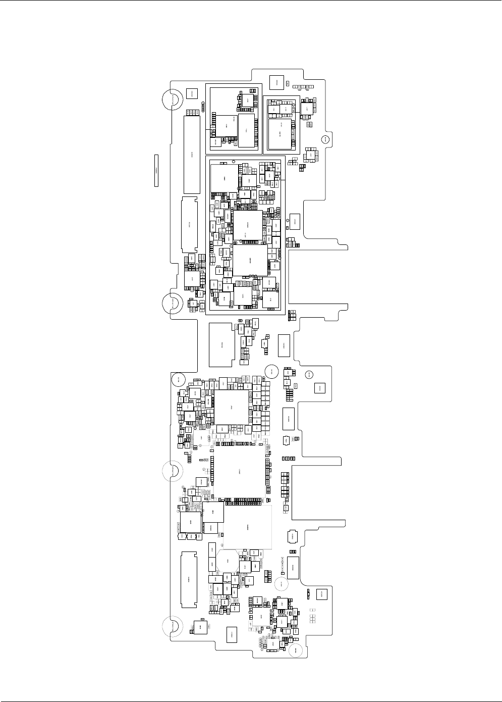
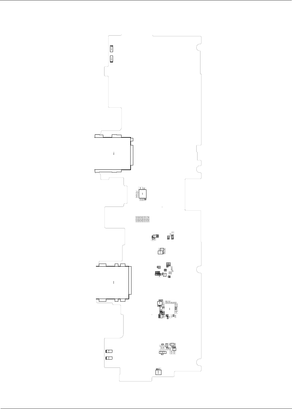
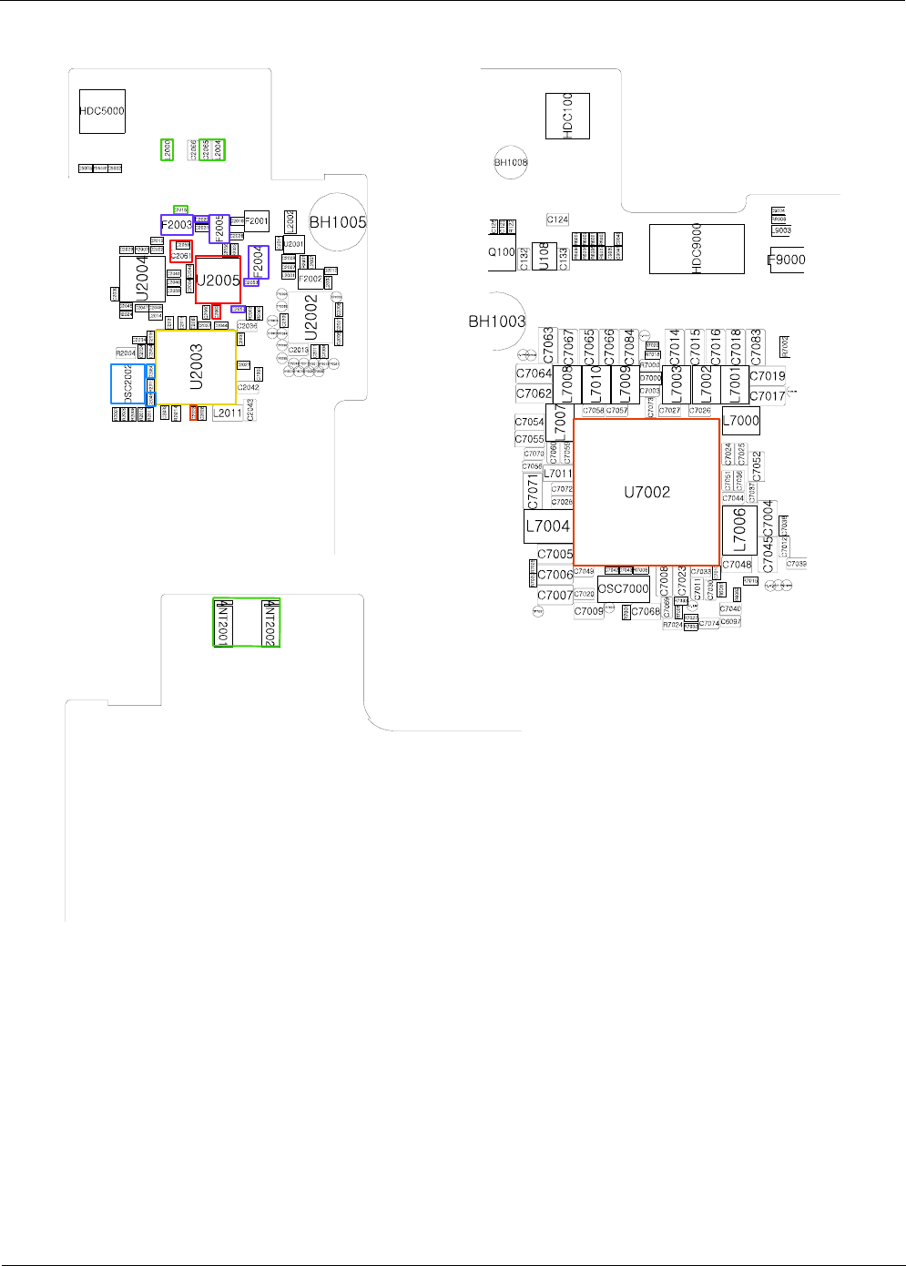
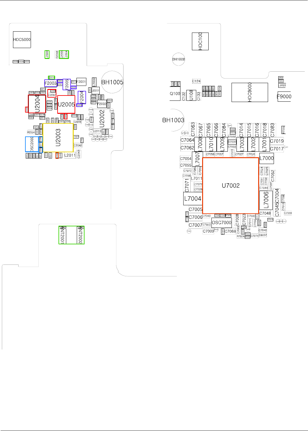
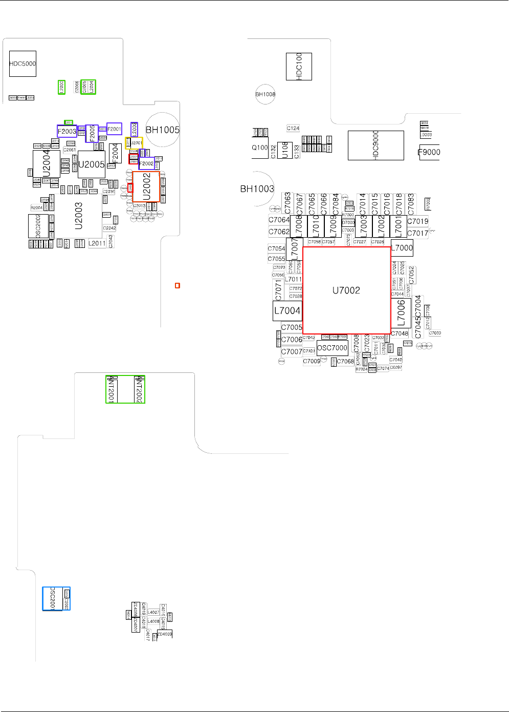
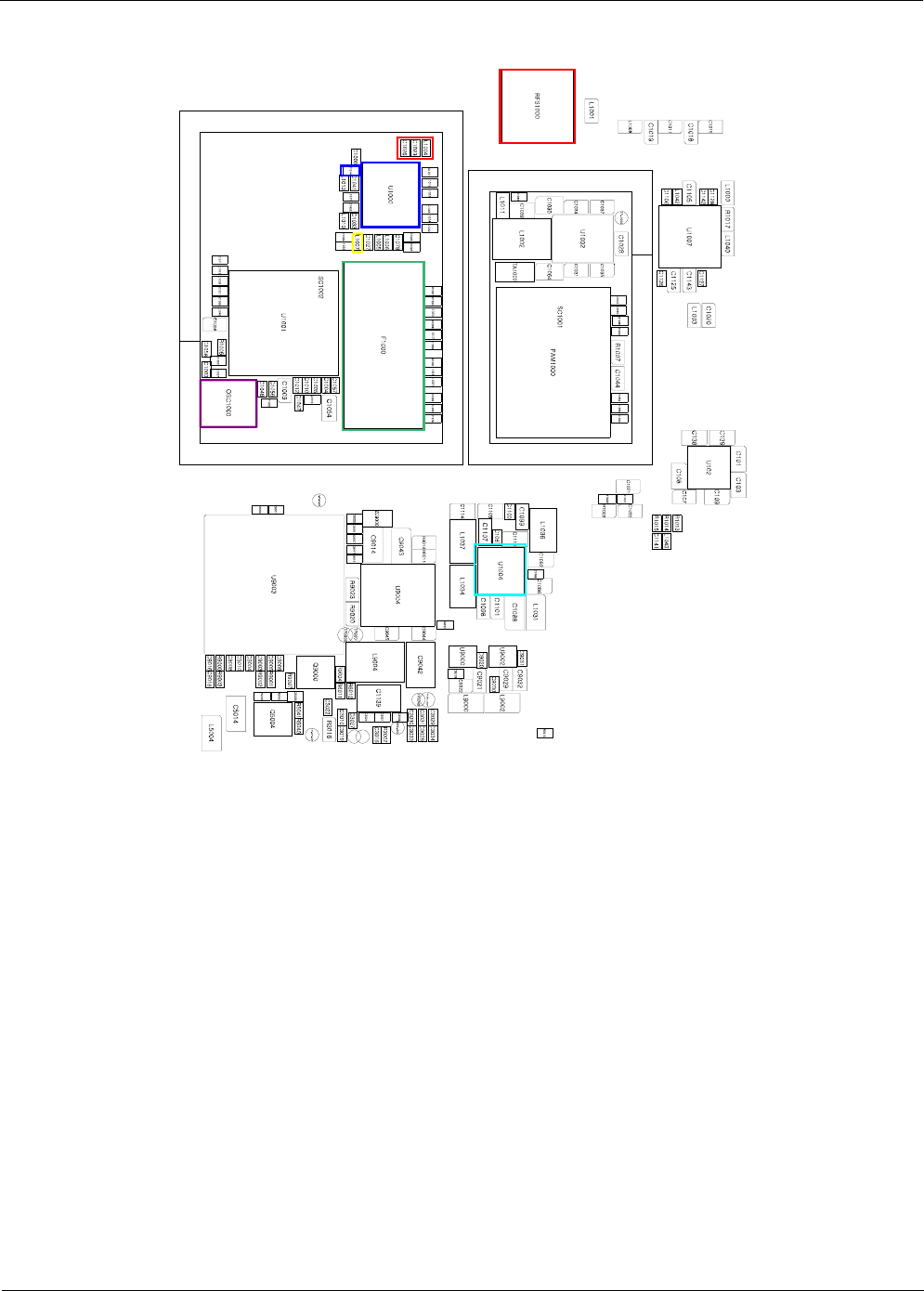
8-2. PCB Diagrams
8-2-1. Top
Level 3Repair
Distribution, transmission, or infringement of any content or data from this document without Samsung’s written authorization is strictly prohibited.
Confidential and proprietary-the contents in this service guide subject to change without prior notice.
8-3
8-2-2. Bottom

Level 3Repair
Distribution, transmission, or infringement of any content or data from this document without Samsung’s written authorization is strictly prohibited.
Confidential and proprietary-the contents in this service guide subject to change without prior notice.
8-4
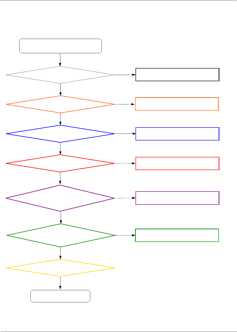
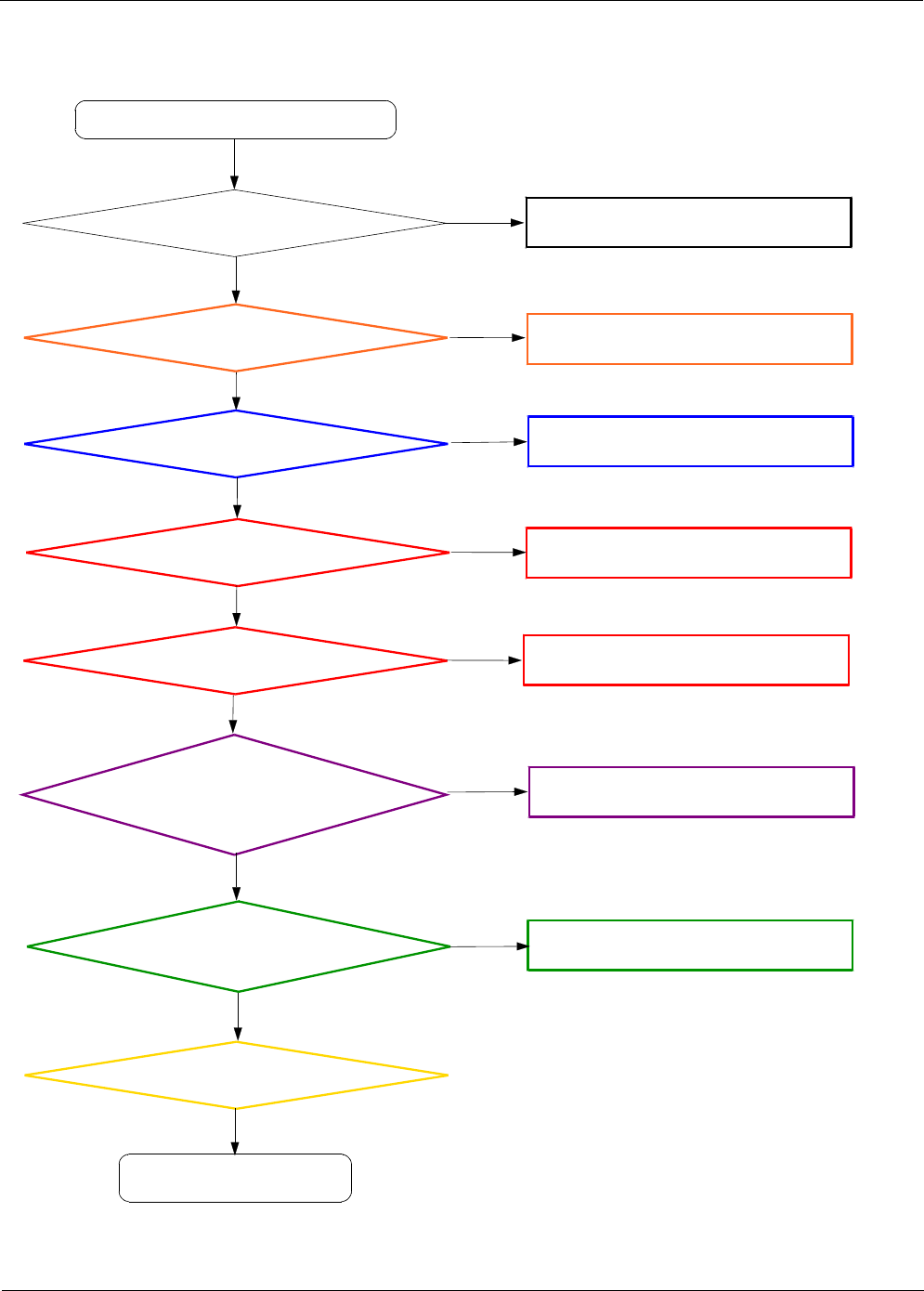
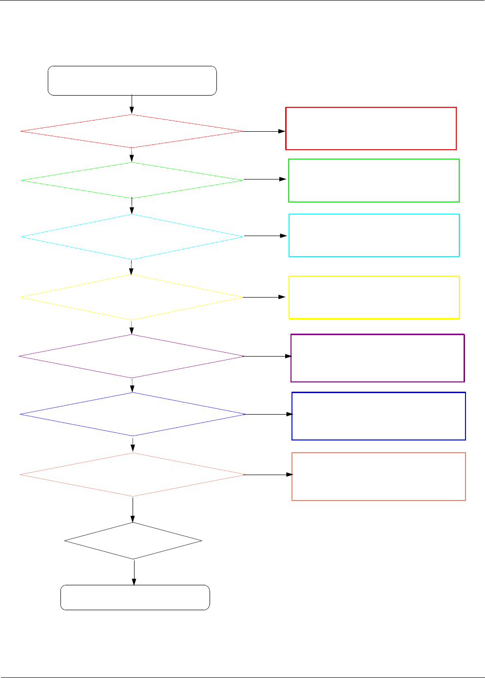
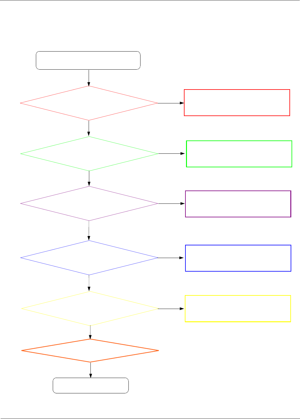
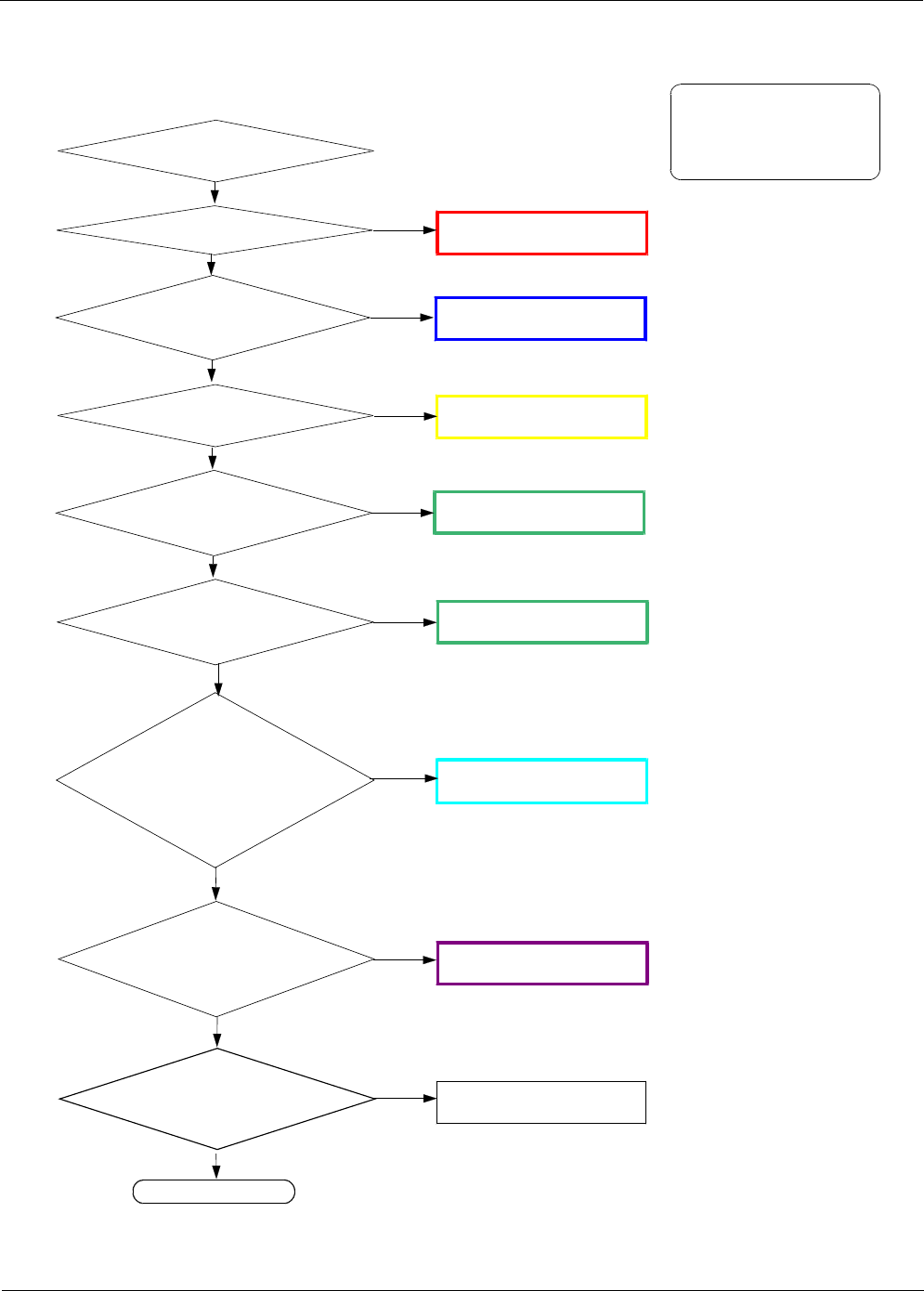
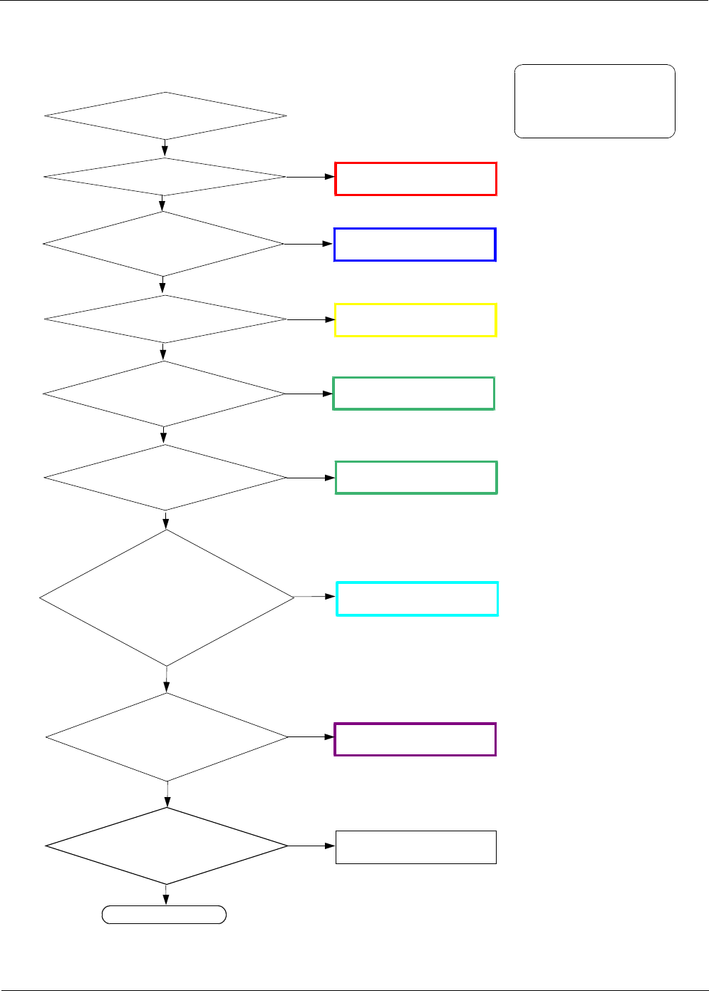
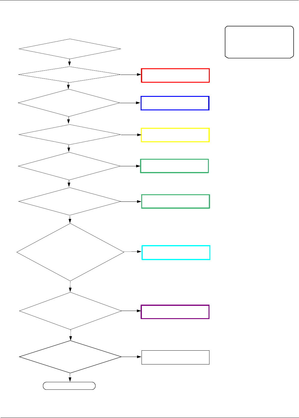
8-3. Flow Chart of Troubleshooting
Equipments
Oscilloscope Digital Multimeter
Power Supply +driver, ESD Safe Tweezer
8960 & Spectrum Analyzer Soldering iron
Level 3Repair
Distribution, transmission, or infringement of any content or data from this document without Samsung’s written authorization is strictly prohibited.
Confidential and proprietary-the contents in this service guide subject to change without prior notice.
8-5
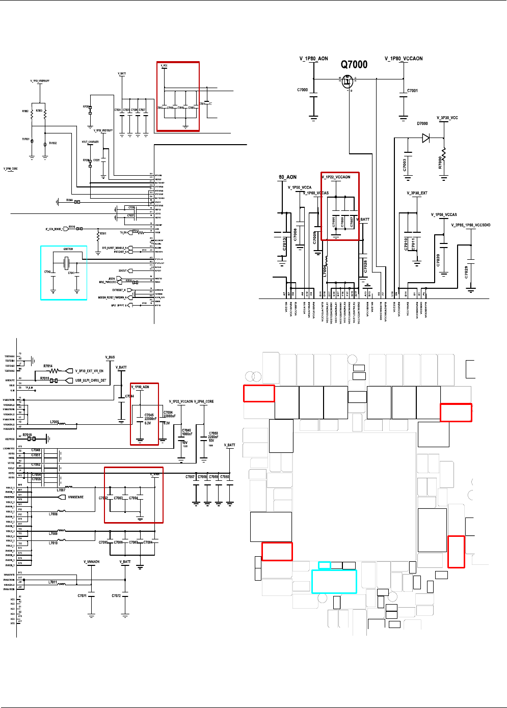
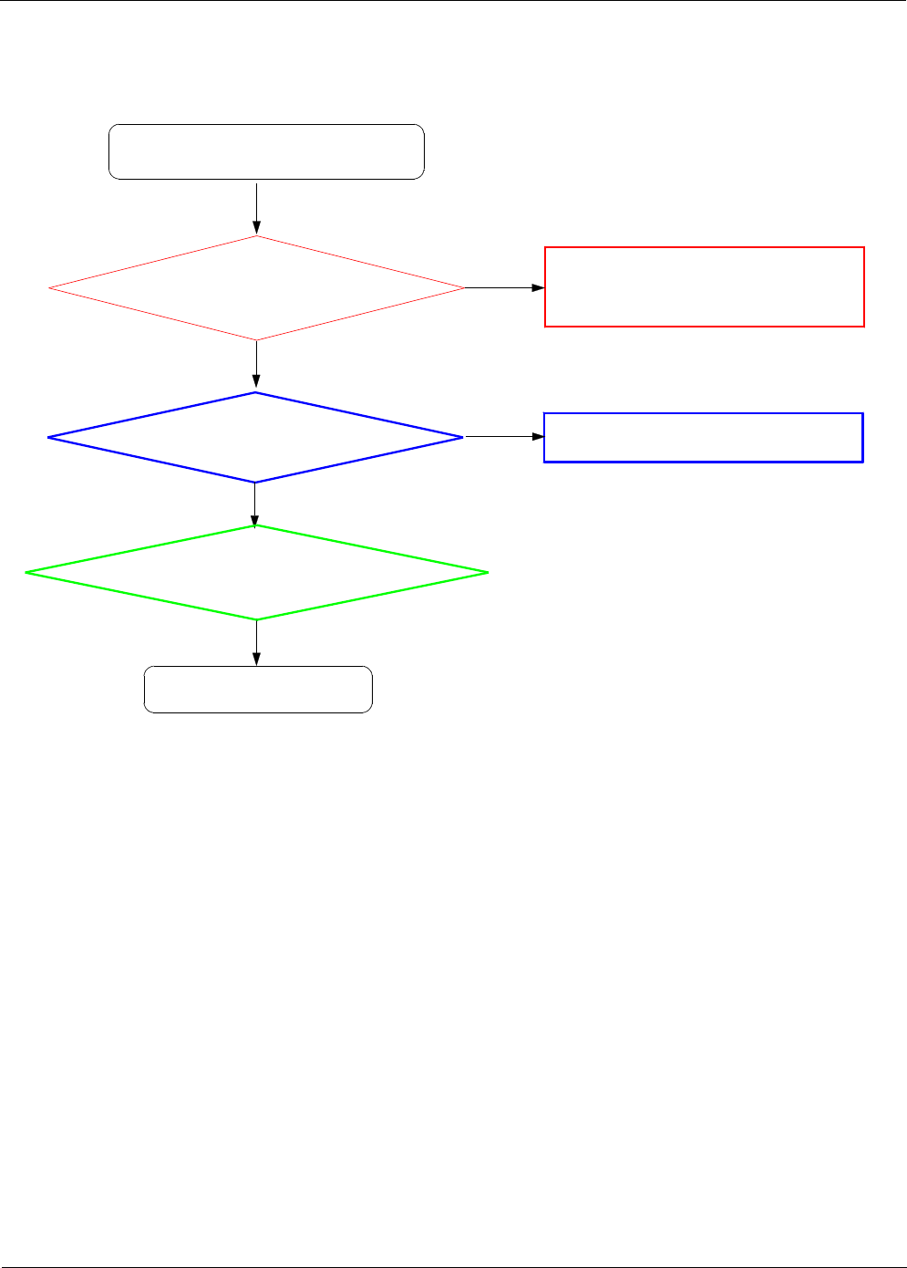
8-3-1. Power On
Check the PWR key-FPCB
(open, etc)
Cell-phone can`t power on.
Change the key-FPCB
And retry to the power-on operation.
END
No
Yes
Check U7002 output voltage
(C7017>0.8V, C7064>0.8V,
C7045≥1.8V, C7005≥1.2V)
If the output voltage is not satisfied with normal
condition, Change the U7002
No
Yes
No
Yes
Check the Battery Voltage.
Is it more than 3.4V? Charging the battery by TA.
check the initial operation
Yes
Abnormal
Check the Clock
OSC7000(C7042)
Is that frequency 32KHz?
Change the OSC7000
If OSC700 does not still work, Change the U7002
This problem is internal oscillator of U7002.
※Test condition (Oscilloscope setting)
:20.0
us.div (time division)
Yes
Change the FRONT ASSY
Power-on the phone and check
the power-on sound.
Sound is ok?
Yes
No
Level 3Repair
Distribution, transmission, or infringement of any content or data from this document without Samsung’s written authorization is strictly prohibited.
Confidential and proprietary-the contents in this service guide subject to change without prior notice.
8-6
C6097
C7000
C7003
C7004
C7005
C7006
C7007
C7008
C7009
C7010
C7011
C7012
C7013
C7014
C7015
C7016
C7017
C7018
C7019
C7020
C7023
C7024
C7025
C7026C7027
C7028
C7030
C7033
C7034
C7036
C7037
C7038
C7039
C7040
C7042C7043
C7044
C7045
C7046
C7048
C7049
C7051
C7052
C7053
C7054
C7055
C7056
C7057C7058
C7059
C7060
C7062
C7063
C7064
C7065
C7066
C7067
C7068
C7069
C7070
C7071
C7072
C7073
C7074
C7083
C7084
D7000
L7000
L7001
L7002
L7003
L7004
L7006
L7007L7008
L7009
L7010
L7011
OSC7000
R6081
R6082
R7000
R7001
R7002
R7006
R7014
R7015
R7018
R7020
R7024
R7025
R7027
R7028
R7030
R7032
R7033
TP7000
TP7005
TP_ILIM
TP_SPI6001
TP_SPI6002
TP_SPI6003
TP_SVID DIN
U7002
Level 3Repair
Distribution, transmission, or infringement of any content or data from this document without Samsung’s written authorization is strictly prohibited.
Confidential and proprietary-the contents in this service guide subject to change without prior notice.
8-7
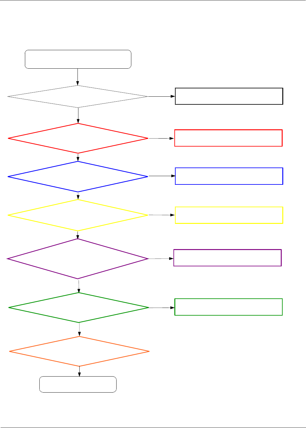
8-3-2. Initial
Initial Failure
END
Check the PMIC Reset
EXTRESET_N(R5022) =
VBATT(High)
Yes
Check the U5005 and R5022 (crack, open, etc.)
Check the oscillator clock waveforms.
32.768KHz :OSC7000(C7042),
24MHz :OSC6000(C6096)
Check the OSC7000, OSC6000 and R6086.
(Crack, open etc.)
Check the output clock waveforms and frequency.
※Test condition (Oscilloscope setting)
:20.0
us.div (time division)
Abnormal
Yes
Normal
No
Re-download SW the cell-phone.
Change UCP6001,U7002
Abnormal
Abnormal
Change PBA
Level 3Repair
Distribution, transmission, or infringement of any content or data from this document without Samsung’s written authorization is strictly prohibited.
Confidential and proprietary-the contents in this service guide subject to change without prior notice.
8-8
C6010
C6011
C6012
C6015
C6016
C6017
C6019
C6023
C6027
C6028
C6029
C6030
C6035
C6036
C6037
C6038
C6039
C6040
C6041
C6042
C6043
C6044
C6045
C6046
C6047
C6048
C6049
C6050
C6051
C6052
C6053
C6054
C6055
C6056
C6057
C6058
C6059
C6060
C6061
C6062
C6063
C6064
C6065
C6066
C6067
C6068
C6069
C6070
C6071
C6072
C6073
C6074
C6075
C6076
C6077
C6078
C6085
C6095C6096
C6097
C7000
C7003
C7004
C7005
C7006
C7007
C7008
C7009
C7010
C7011
C7012
C7013
C7014
C7015
C7016
C7017
C7018
C7019
C7020
C7023
C7024
C7025
C7026C7027
C7028
C7030
C7033
C7034
C7036
C7037
C7038
C7039
C7040
C7042C7043
C7044
C7045
C7046
C7048
C7049
C7051
C7052
C7053
C7054
C7055
C7056
C7057C7058
C7059
C7060
C7062
C7063
C7064
C7065
C7066
C7067
C7068
C7069
C7070
C7071
C7072
C7073
C7074
C7083
C7084
C8000
C8004
C8005
C8006
C8015
C8016
D7000
L7000
L7001
L7002
L7003
L7004
L7006
L7007L7008
L7009
L7010
L7011
L8000
OSC6000
OSC7000
R2012
R6008
R6009
R6010
R6019
R6027
R6030
R6031
R6047
R6051
R6052
R6053
R6057
R6059
R6081
R6082
R6086
R6087
R6089
R6094
R6097
R6099
R7000
R7001
R7002
R7006
R7012
R7014
R7015
R7016
R7018
R7020
R7024
R7025
R7027
R7028
R7030
R7032
R7033
R8001
R9021
TH7001
TP4001
TP4003
TP4013
TP7000
TP7005
TP_AON_085
TP_AP_DM
TP_AP_DP
TP_IERR
TP_ILIM
TP_KSEL_STRAP1
TP_REFCLK
TP_RESETOUT
TP_SPI6000
TP_SPI6001
TP_SPI6002
TP_SPI6003
TP_SPI6004
TP_SPI6005
TP_SPI6006
TP_SPI6007
TP_SVID DIN
TP_SVIDDOUT
TP_ULPI _CLK
TP_ULPI_D6000
U6014
U7002
UCP6001
Level 3Repair
Distribution, transmission, or infringement of any content or data from this document without Samsung’s written authorization is strictly prohibited.
Confidential and proprietary-the contents in this service guide subject to change without prior notice.
8-9
8-3-3. Charging Part
C1138
C127
C128
C134C135
C136
C5004
C5005
C5006
C5007
C5008
C5010
C5011
C5012
C5013
C5015
C5019
C5020
C5022
C5025
C5026
C5027
C5032C5038
C5039
C5040
L5001
OSC100
Q5000
Q5002
Q5003
R133
R134
R5013
R5014
R5021
R5022
R5039
R5044
R7003TH7002
TP101
TP102
U109
U5005
U5006
U5007
TA /USB Insert
Yes
END
Charging Sequence Start
V_BUS =5V
No Check C5005 =5
V,
or may not connected TA /USB
Yes
Battery is Charging? No Resolder or Replace U5005
Yes
Level 3Repair
Distribution, transmission, or infringement of any content or data from this document without Samsung’s written authorization is strictly prohibited.
Confidential and proprietary-the contents in this service guide subject to change without prior notice.
8-10
8-3-4. Microphone Part
C4033
TP4011
C4034
R4020
CPVOUTN
CPCB
K9CPGND
CPCA
CPVDD
K1 BCLK2
JACKDET
K2
K3 GPIO8|DACDAT3
K4 GPIO11|BCLK3
K5DGND
HPOUT2P
HP2GND
H8
ADCLRCLK1|GPIO1
J1
DBVDD2
LRCLK2
J3
J4 GPIO9|ADCDAT3
HPOUT1R
HPOUT1L
CPVOUTP
HPOUT2N
AVDD1
H1 DACDAT1
SCLK
SDA
ADCDAT2
H4
DBVDD3
HPOUT1FB
VREFC
LDO1VDD
F9 MICDET
LRCLK1
G1
DCVDD
BCLK1
G3
G4 DACDAT2
GPIO10|LRCLK3
G5
SPKVDD2
VMIDC
AVDD2
AVDD1
MCLK1
MCLK2
ADDR
ADCDAT1
F4
F7
SPKGND2
SPKOUTRP
SPKMODE
LDO2ENA
D6
D7 IN1LN
IN1LP
D8
D9AGND
DBVDD1
SPKGND1
LINEOUTFB
LINEOUT1N
IN1RP
C7
C8 IN2LN|DMICDAT
IN2LP|VRXN
C9
SPKOUTRN
SPKVDD2
D3
LINEOUT2P
LINEOUT1P
B7 IN2RN
IN2RP|VRXP
B8
B9 IN1RN
SPKOUTRN
C2SPKGND2
SPKOUTRP
C4
LINEOUT2N
MICBIAS2
A8 DMICCLK
MICBIAS1
SPKOUTLN
SPKGND1
B2
SPKOUTLP
SPKOUTLP
NC
1
NC
2
SPKOUTLN
SPKVDD1
SPKVDD1
A4 LDO1ENA
REFGND
U4003
TP4012
TP4007
C4037
C4036
C4027
TP4005
TP4009
TP4010
TP4006
TP4002
TP4004
TP4008
TP4001
TP4003
MAIN_MIC_N
MAIN_MIC_P
EAR_MIC_N
EAR_MIC_P
CODEC_LDO_EN
MM_I2S_DO
MM_I2S_DI
MM_I2S_CLK
SPEECH_PCM_IN
SPEECH_PCM_SYNC
SPEECH_PCM_CLK
SPEECH_PCM_OUT
BT_PCM_OUT
BT_PCM_IN
BT_PCM_SYNC
BT_PCM_CLK
MM_I2S_SYNC
C4003
C4006
C4020
C4021
C4022
C4023
C4024
C4025
C4026
C4027
C4028
C4029
C4030
C4031
C4033
C4034
C4035
C4036
C4037
C4038
C4039
C4040
C4041
C6092
C6093
L4011
L4012
LINEOUT_ON
R4019
R4020
R4021R4022
R6058R6061
TP4002
TP4005
TP4006
TP4007
TP4008
TP4009
TP4011
TP4012
U4003
U4004
U6010
Check USB CONN FPCB
where MIC is placed
for any damage (Tear in
FPCB, etc)
Replace the USB CONN FPCB
No
Yes
Yes
Check microphone function
in voice call speaker mode
or in voice recording mode
Check component soldering
status of C4036,C4037 Resolder or replace C4036,C4037
END
Yes
No
Level 3Repair
Distribution, transmission, or infringement of any content or data from this document without Samsung’s written authorization is strictly prohibited.
Confidential and proprietary-the contents in this service guide subject to change without prior notice.
8-11
8-3-5. Speaker Part
Check the signals on
L4009,L4010(Left SPK)
L4004,L4005(Right SPK)
Check speaker function.
Play MP3 with maximum volume level.
No Replace U4003
END
Yes
Yes
Replace the speaker
module
Yes
Check the connection of
HDC4000(R),HDC4001(L)
Yes
No Reconnect HDC4000(R),HDC4001(L)
R4015
ZD4008
ZD4007
13
14NC
NC
15NC
16
2
33 44
55 6 6
77 88
9
9
NC
HDC4001
11
10 10
11 11 12
12
2
C4016
V_1P80_VCCAON
C4015
R4014
R4012
L4010L4009
ZD4006
ZD4003
C4019C4018
L4007
L4008
C4013
ZD4004
ZD4005
R4009 R4010
L4006
C4017
C4014
ZD4009
R4011
EAR_ADC_3.5
EAR_MIC+
EAR_L_DET
EAR_G_DET
SPK_OUTL_N SPK_OUTL_P
EAROUT_R
EAROUT_L
EAR_MIC-
EAROUT_FB
C4009
HDC4001
L4009L4010
Q4000
R 400 9 R 401 0
R 401 1
R 401 2
R4016
U4002
ZD4003
ZD4004
ZD4005
ZD4006
Level 3Repair
Distribution, transmission, or infringement of any content or data from this document without Samsung’s written authorization is strictly prohibited.
Confidential and proprietary-the contents in this service guide subject to change without prior notice.
8-12
D4001
L4004 L4005
D4000
4
556
6
7NC
NC
8
NC
9
10NC
HDC4000
112
2
334
SPK_OUTR_N
SPK_OUTR_P
BOTHHOLE1002
D4000
D4001
HDC4000
L4004
L4005
C4033
C4024
TP4011
C4034
MAIN_MICBIAS_2.2V
C4041
C4028
C4038
R4020
C4029
C4022
CPVOUTN
CPCB K8
K9CPGND
J8
CPCA
CPVDDJ9
K1 BCLK2
JACKDET
K2
K3 GPIO8|DACDAT3
K4 GPIO11|BCLK3
K5DGND
K7
HPOUT2P
HP2GND
H8
ADCLRCLK1|GPIO1
J1
J2
DBVDD2
LRCLK2
J3
J4 GPIO9|ADCDAT3
J5
HPOUT1R J6
HPOUT1L
CPVOUTP J7
HPOUT2N
AVDD1G9
H1 DACDAT1
SCLK H2
H3
SDA
ADCDAT2
H4
H5
DBVDD3
HPOUT1FB H6
H7
VREFC
LDO1VDDF8
F9 MICDET
LRCLK1
G1
G2
DCVDD
BCLK1
G3
G4 DACDAT2
GPIO10|LRCLK3
G5
G8
SPKVDD2
VMIDC E7
E8
AVDD2
AVDD1E9
F1
MCLK1
MCLK2 F2
F3
ADDR
ADCDAT1
F4
F7
SPKGND2
SPKOUTRP D4
D5
SPKMODE
LDO2ENA
D6
D7 IN1LN
IN1LP
D8
D9AGND
DBVDD1E1
E2
SPKGND1
LINEOUTFB C5
C6
LINEOUT1N
IN1RP
C7
C8 IN2LN|DMICDAT
IN2LP|VRXN
C9
D1
SPKOUTRN
SPKVDD2D2
D3
LINEOUT2P
LINEOUT1P B6
B7 IN2RN
IN2RP|VRXP
B8
B9 IN1RN
SPKOUTRN C1
C2SPKGND2
SPKOUTRP C3
C4
LINEOUT2N
MICBIAS2 A7
A8 DMICCLK
MICBIAS1 A9
B1
SPKOUTLN
SPKGND1
B2
B3
SPKOUTLP
SPKOUTLP B4
B5
NC
1
NC
2
SPKOUTLN A1
A2
SPKVDD1
SPKVDD1A3
A4 LDO1ENA
REFGND A5
A6
U4003
C4040
V_BATT
TP4012
C4035
TP4007
C4037
C4036
V_1P80_VCCAON
C4027
TP4005
C4021
C4030
C4023
C4031
TP4009
TP4010
C4026
TP4006
L4011
L4012
TP4000
TP4002
C4025
TP4004
TP4008
TP4001
TP4003
C4020
MAIN_MIC_N
MAIN_MIC_P
EAR_MIC_N
EAR_MIC_P
CODEC_LDO_EN
EAROUT_L
CODEC_19MHZ
VPS_R
VPS_L
SPK_OUTR_N
SPK_OUTL_N
SPK_OUTR_P
SPK_OUTL_P
MM_I2S_DO
MM_I2S_DI
MM_I2S_CLK
CODEC_CLK32K
EAROUT_FB
EAROUT_R
SPEECH_PCM_IN
CODEC_SCL_1.8V
CODEC_SDA_1.8V
SPEECH_PCM_SYNC
SPEECH_PCM_CLK
SPEECH_PCM_OUT
BT_PCM_OUT
BT_PCM_IN
BT_PCM_SYNC
BT_PCM_CLK
MM_I2S_SYNC
C4003
C4006
C4020
C4021
C4022
C4023
C4024
C4025
C4026
C4027
C4028
C4029
C4030
C4031
C4033
C4034
C4035
C4036
C4037
C4038
C4039
C4040
C4041
C6092
C6093
L4011
L4012
LINEOUT_ON
R4019
R4020
R4021R4022
R6058R6061
TP4002
TP4005
TP4006
TP4007
TP4008
TP4009
TP4011
TP4012
U4003
U4004
U6010
Level 3Repair
Distribution, transmission, or infringement of any content or data from this document without Samsung’s written authorization is strictly prohibited.
Confidential and proprietary-the contents in this service guide subject to change without prior notice.
8-13
8-3-6. BT Part
BT is not working
Check BT function ON No Enable BT Function
Yes
END
Check the Voltage on
C2033= 1.8V
No Check the U7002(crack, open, damaged, etc.)
Yes
Check 37.4 MHz Clock at
C2049, C2050
No Check the OSC2002(crack, open, etc.)
Yes
Check the Voltage on C2059,
C2061, C2062
No Check the U2005(crack, open, damaged, etc.)
Yes
Check the Status of
C2057, C2053, C2026, F2003,
F2004, F2005
No Resolder or replace C2057, C2053, C2026,
F2003, F2004, F2005
Yes
Resolder or Replace U2003
Yes
Yes
Yes
Check the Status of C2015,
C2065, L2000, L2004,
ANT2001, ANT2002
No Resolder or Replace C2015, C2065, L2000,
L2004, ANT2001, ANT2002
Level 3Repair
Distribution, transmission, or infringement of any content or data from this document without Samsung’s written authorization is strictly prohibited.
Confidential and proprietary-the contents in this service guide subject to change without prior notice.
8-14
Level 3Repair
Distribution, transmission, or infringement of any content or data from this document without Samsung’s written authorization is strictly prohibited.
Confidential and proprietary-the contents in this service guide subject to change without prior notice.
8-15
Level 3Repair
Distribution, transmission, or infringement of any content or data from this document without Samsung’s written authorization is strictly prohibited.
Confidential and proprietary-the contents in this service guide subject to change without prior notice.
8-16
8-3-7. WIFI Part
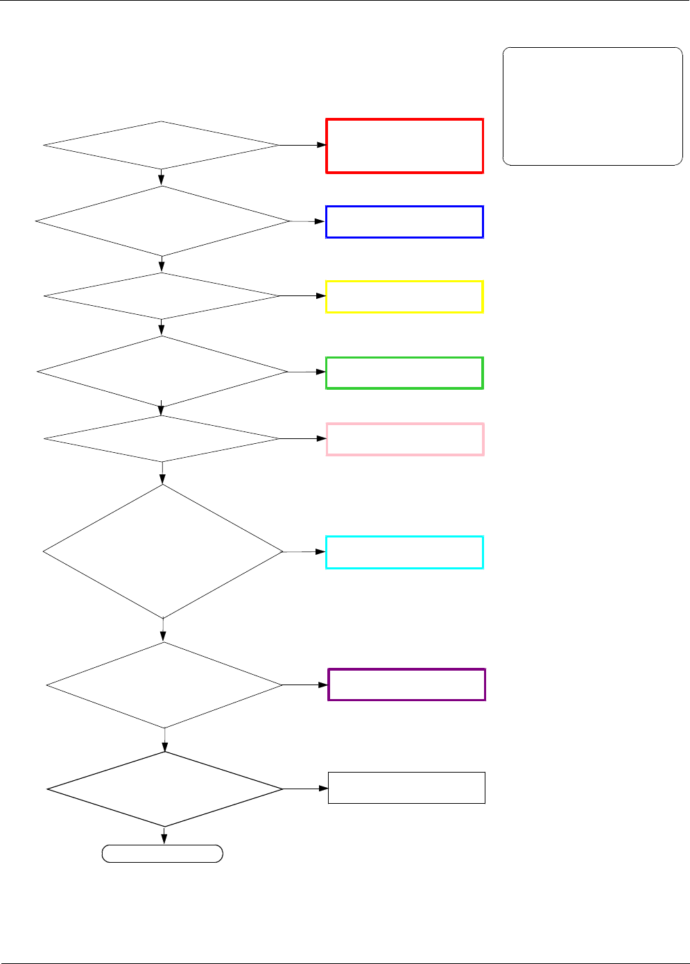
WIFI is not working
Check WIFI function ON No Enable WIFI Function
Yes
END
Check the Voltage on C2033
=1.8V
No Check the U7002(crack, open, damaged, etc.)
Yes
Check 37.4 MHz Clock at
C2049, C2050
No Check the OSC2002(crack, open, etc.)
Yes
Check the Voltage on C2038,
C2040, C2041
No Check the U2004(crack, open, damaged, etc.)
Yes
Check the Status of
C2016, C2022, C2026 C2034,
C2046, C2053, C2063, L2014,
F2003, F2004, F2005
No Resolder or Replace C2016, C2022, C2026
C2034, C2046, C2053, C2063, L2014, F2003,
F2004, F2005
Yes
Resolder or Replace U2003
Yes
Yes
Yes
Check the Status of C2015,
C2065, L2000, L2004,
ANT2001, ANT2002
No Resolder or Replace C2015, C2065, L2000,
L2004, ANT2001, ANT2002
Check the Voltage on C2059,
C2061, C2062
Yes
No Check the U2005(crack, open, damaged, etc.)
Level 3Repair
Distribution, transmission, or infringement of any content or data from this document without Samsung’s written authorization is strictly prohibited.
Confidential and proprietary-the contents in this service guide subject to change without prior notice.
8-17
Level 3Repair
Distribution, transmission, or infringement of any content or data from this document without Samsung’s written authorization is strictly prohibited.
Confidential and proprietary-the contents in this service guide subject to change without prior notice.
8-18
Level 3Repair
Distribution, transmission, or infringement of any content or data from this document without Samsung’s written authorization is strictly prohibited.
Confidential and proprietary-the contents in this service guide subject to change without prior notice.
8-19
8-3-8. GPS Part
GPS is not working
Check GPS function ON No Enable GPS Function
Yes
END
Check the Voltage on C2009
=1.8
V, C2007, L2001 =2.8V
No Check the U7002 (crack, open, damaged,
etc.)
Yes
Check 26MHz Clock at
C2002, C2003
No Check the OSC2001(crack, open, etc.)
Yes
Check the Voltage of
GPS_LNA_EN (at C2014),
No Resolder or change the U2001
Yes
Check the Status of
C2010, C2020 L2002, L2003,
R2001, F2001, F2002, F2003,
F2005
No Resolder or Replace C2010, C2020 L2002,
L2003, R2001, F2001, F2002, F2003, F2005
Yes
Yes
Yes
Check the Status of
C2015, C2065, L2000, L2004,
ANT2001, ANT2002
No Resolder or Replace C2015, C2065, L2000,
L2004, ANT2001, ANT2002
Resolder or Replace U2002
Yes
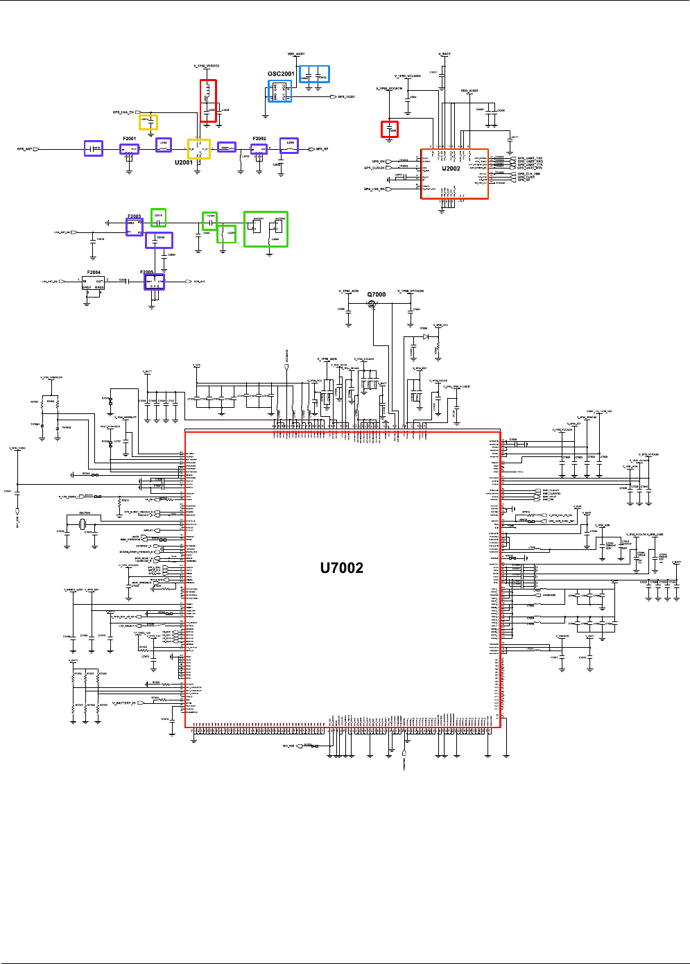
Level 3Repair
Distribution, transmission, or infringement of any content or data from this document without Samsung’s written authorization is strictly prohibited.
Confidential and proprietary-the contents in this service guide subject to change without prior notice.
8-20
Level 3Repair
Distribution, transmission, or infringement of any content or data from this document without Samsung’s written authorization is strictly prohibited.
Confidential and proprietary-the contents in this service guide subject to change without prior notice.
8-21
Level 3Repair
Distribution, transmission, or infringement of any content or data from this document without Samsung’s written authorization is strictly prohibited.
Confidential and proprietary-the contents in this service guide subject to change without prior notice.
8-22
Check F8000, F8001, F8002 Resolder or Replace the F8000, F8001, F8002
Check C8008 =3.3V
C8009 = 1.8V Resolder or Replace the C8008, C8009,
C8013, C8014, C8019, C8020, U8000
Check C8011 =1.1V
C8026 =1.8V Resolder or Replace the C8011, C8026,
U8001, U8002
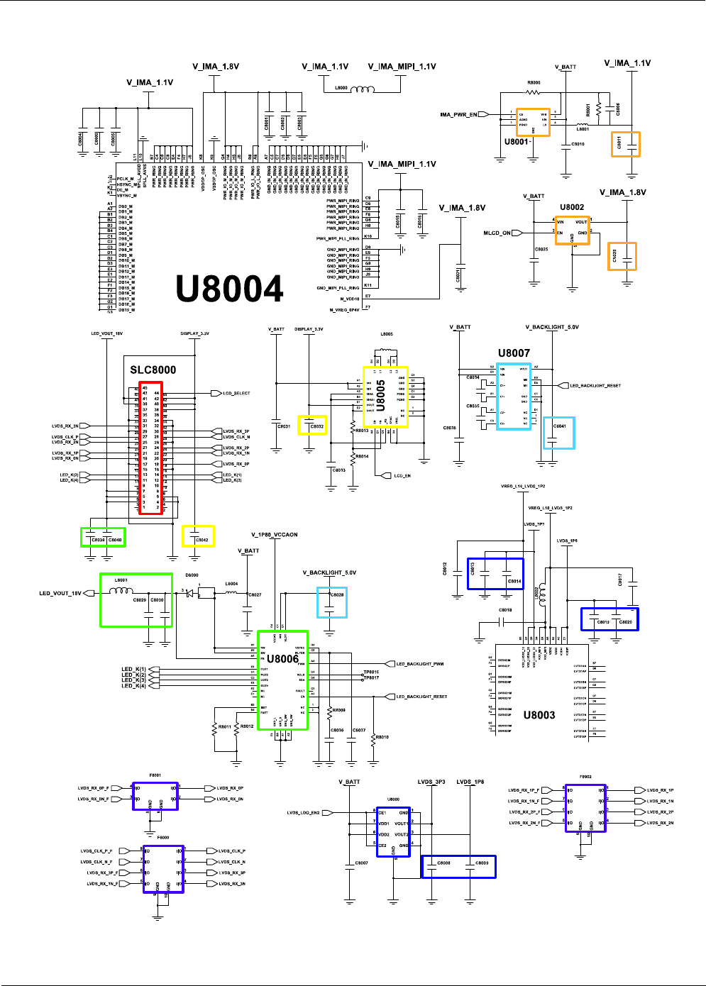
8-3-9. LCD
LCD is still off after PWR ON
Yes
No
Check the connection of
SLC8000
Yes
END
No
Check the C8040
and High(18V)
Yes
Check the Voltage on C8041
=5.0V
Yes
Yes
Replace LCD
Module
No
Yes
Check the Voltage on C8042
=3.3V
No Resolder or Replace the U8007
,C8041, C8028
Check the Backlight Driver IC(U8006)
or Replace the
C8039,C8040,L8003,C8029,C8030
Reconnect the SLC8000
Check the U8005, C8042, C8032 (crack, open,
damaged, etc.)
Yes
No
No
Yes
Yes
No
Level 3Repair
Distribution, transmission, or infringement of any content or data from this document without Samsung’s written authorization is strictly prohibited.
Confidential and proprietary-the contents in this service guide subject to change without prior notice.
8-23
Level 3Repair
Distribution, transmission, or infringement of any content or data from this document without Samsung’s written authorization is strictly prohibited.
Confidential and proprietary-the contents in this service guide subject to change without prior notice.
8-24
Level 3Repair
Distribution, transmission, or infringement of any content or data from this document without Samsung’s written authorization is strictly prohibited.
Confidential and proprietary-the contents in this service guide subject to change without prior notice.
8-25
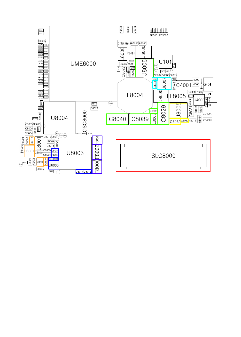
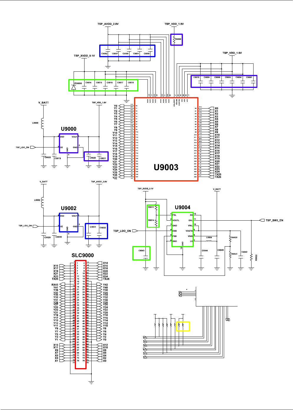
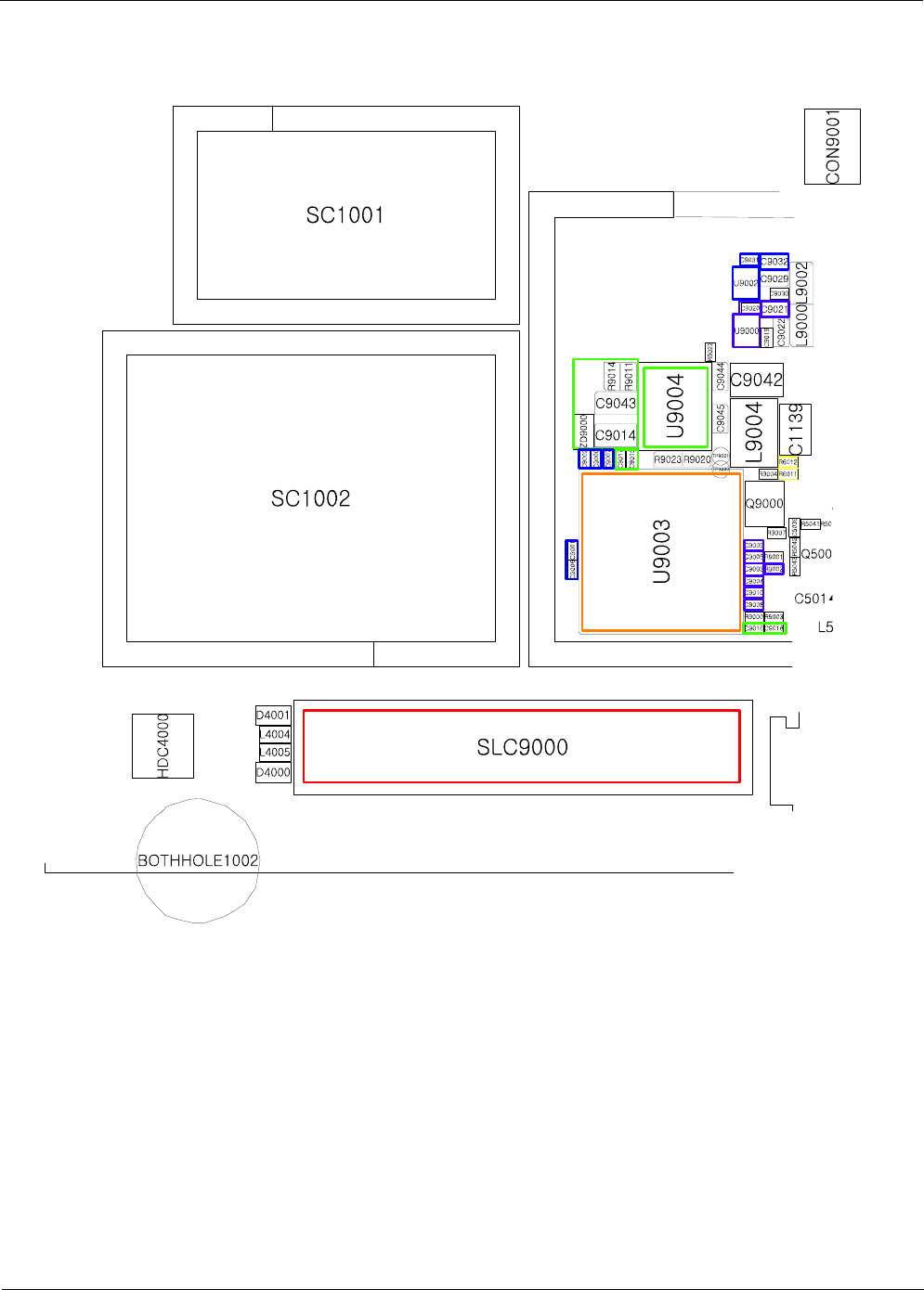
8-3-10. TSP
Yes
No
Reconnect the SLC9000
Check TSP Connector on
Main PBA
Yes
END
Yes
No Resolder or Replace U9004, R9011, R9014,
C9043, C9014, C9015, C9016, C9017, C9018,
ZD9000
Check the Voltage on C9043
=9.1V
Yes
Replace U9003
Yes
Yes
No
Check the Voltage on C9020
=1.8V
Resolder or Replace U9000, C9020, C9021,
C9010, C9009, C9008, C9005, C9004, C9003,
R9002
Check the I2C signal Resolder or Replace R6001, R6012
No
Touch Screen does not work
Yes
No
Check the Voltage on C9031
=2.8V Resolder or Replace U9002, C9031, C9032,
C9002, C9007, C9006, C9001, C9000
Level 3Repair
Distribution, transmission, or infringement of any content or data from this document without Samsung’s written authorization is strictly prohibited.
Confidential and proprietary-the contents in this service guide subject to change without prior notice.
8-26
R6062
TP_KSEL_STRAP1
R6066 R6012
V_1P80_VCCAON
R6067
TSP_VDD_1.8V
R6063 R6011
V_1P22_VCCAON
R6107
GP_CORE_073
K6
GP_CORE_074
J5
GP_CORE_075
J9
GP_I2C_3_SDA_HDMI
H4GP_I2C_3_SCL_HDMI
F8
D28
GP_I2S_0_CLK
D32
GP_CORE_071
GP_I2S_0_FS
GP_CORE_072
C17
B32
GP_EMMC_0_RST_
AV12
GP_I2C_2_SDA
AV26
GP_I2C_1_SCL
AU27
GP_I2C_1_SDA
AT26
GP_I2C_0_SCL
AT28
AN13
GP_I2C_0_SDA
AN27
GP_EMMC_1_RST_
GP_I2C_2_SCL
AM26
GP_I2C_4_SCL
AE5
GP_CORE_082
AE7
GP_I2C_4_SDA
AF4
GP_I2C_5_SCL
AF6
GP_I2C_5_SDA
AD2
R6108
SENSOR_I2C_SDA
CAM_I2C_SCL
CAM_I2C_SDA
I2C9_SCL_DNIE
I2C9_SDA_DNIE
ADJ_DET_AP
MM_I2S_DI
USB_PHY_CS
MM_I2S_CLK
MM_I2S_SYNC
MODEM_RESET_BB_N
WLAN_EN
CODEC_SCL_1.8V
CODEC_SDA_1.8V
TSP_SCL_1.8V
TSP_SDA_1.8V
SENSOR_I2C_SCL
MHL_DSCL_1.2V
MHL_DSDA_1.2V
UCP6001-1
Level 3Repair
Distribution, transmission, or infringement of any content or data from this document without Samsung’s written authorization is strictly prohibited.
Confidential and proprietary-the contents in this service guide subject to change without prior notice.
8-27
Level 3Repair
Distribution, transmission, or infringement of any content or data from this document without Samsung’s written authorization is strictly prohibited.
Confidential and proprietary-the contents in this service guide subject to change without prior notice.
8-28
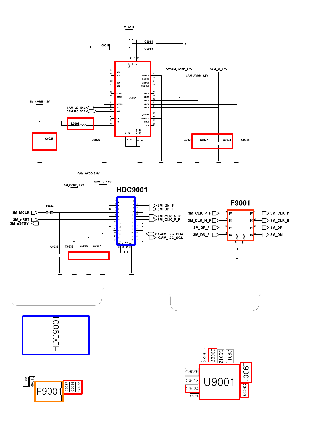
8-3-11. 3M CAM
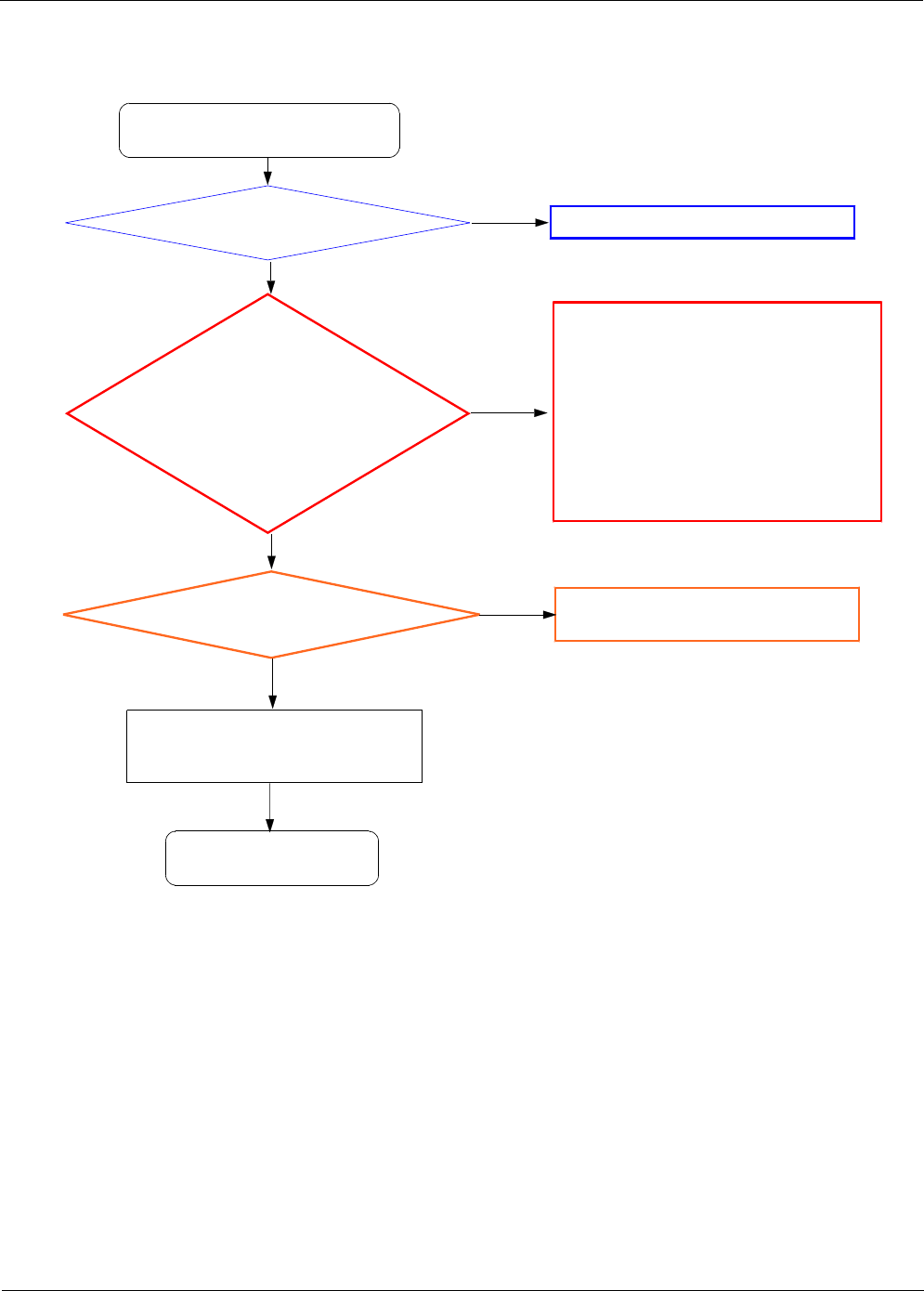
Yes
Check the Camera
connector on Main PBA Reconnect the HDC9001
No
Check the voltage
C9035 =1.2
V?
C9036 =2.8
V?
C9037 =1.8
V?
Resolder C9035, C9025, L9001
Resolder C9036, C9027
Resolder C9037, C9024
Replace the PBA
or Replace U9001
No
Yes
END
Replace the camera module
"Camera" function does not work
Yes
Yes
Check F9001 Resolder F9001
Replace the PBA
No
Yes
Level 3Repair
Distribution, transmission, or infringement of any content or data from this document without Samsung’s written authorization is strictly prohibited.
Confidential and proprietary-the contents in this service guide subject to change without prior notice.
8-29
Level 3Repair
Distribution, transmission, or infringement of any content or data from this document without Samsung’s written authorization is strictly prohibited.
Confidential and proprietary-the contents in this service guide subject to change without prior notice.
8-30
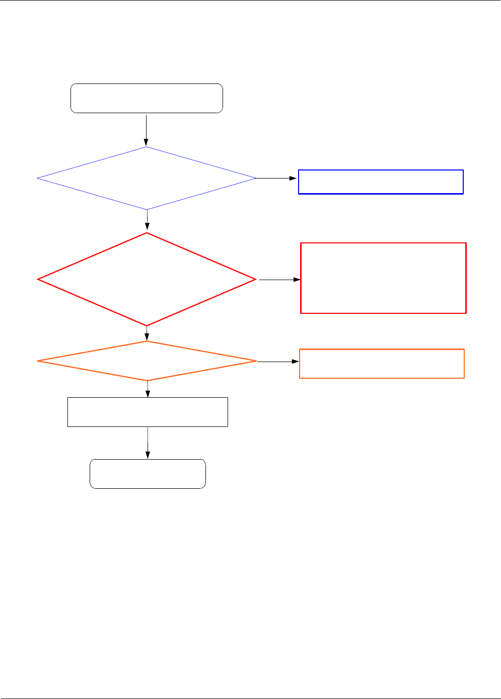
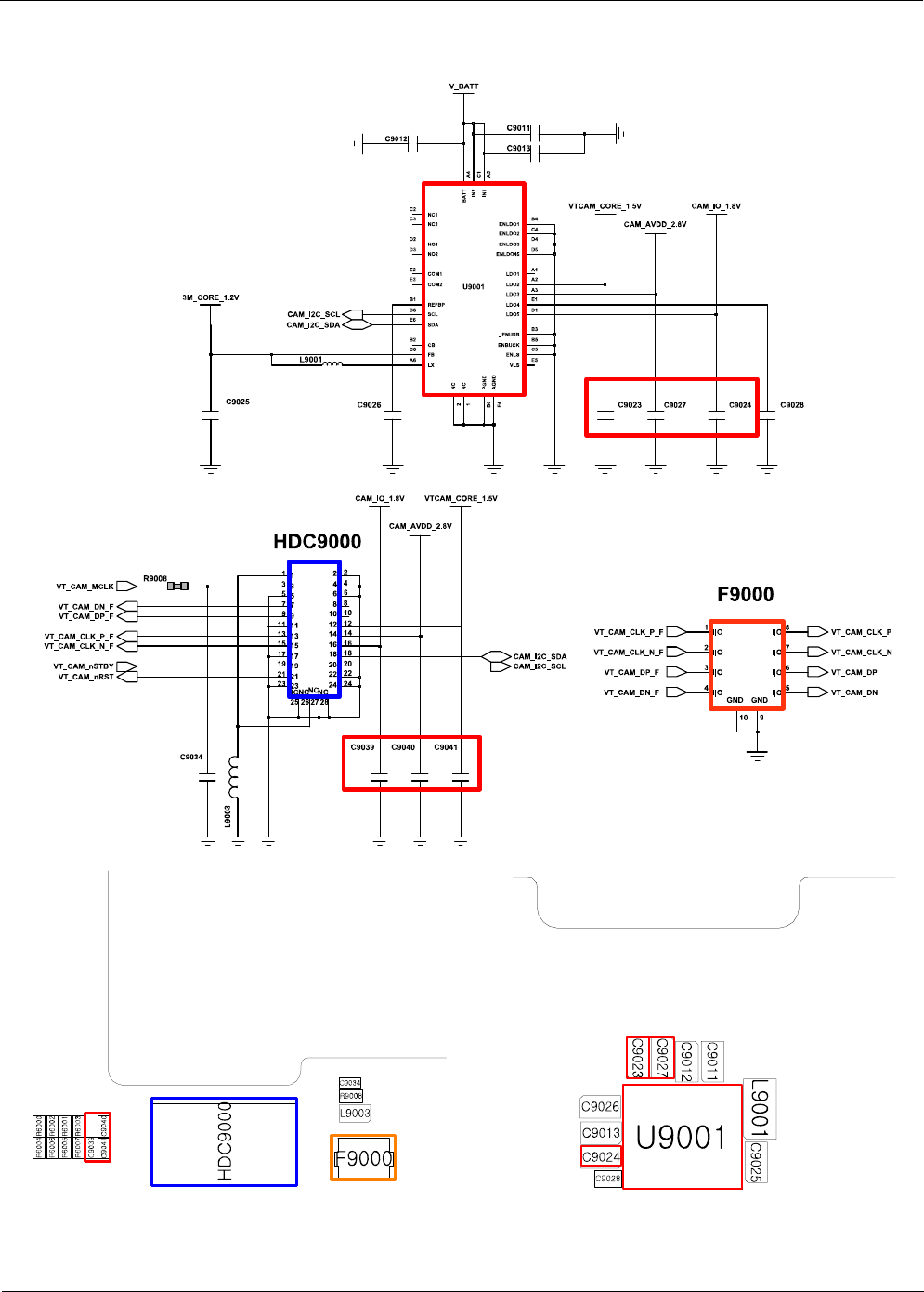
8-3-12. 1.3M CAM
Yes
Check the Camera
connector on Main PBA Reconnect the HDC9000
No
Check the voltage
C9039 =1.8
V?
C9040 =2.8
V?
C9041 =1.5V
No
Yes
END
Replace the camera module
"Camera" function does not work
Yes
Resolder C9039, C9024
Resolder C9040, C9027
Resolder C9041, C9023
Replace the PBA
or Replace U9001
Abnormal
Check F9000
Yes
Resolder F9000
Replace the PBA
No
Level 3Repair
Distribution, transmission, or infringement of any content or data from this document without Samsung’s written authorization is strictly prohibited.
Confidential and proprietary-the contents in this service guide subject to change without prior notice.
8-31
Level 3Repair
Distribution, transmission, or infringement of any content or data from this document without Samsung’s written authorization is strictly prohibited.
Confidential and proprietary-the contents in this service guide subject to change without prior notice.
8-32
8-3-13. OTG
OTG does not work
Yes
No Check the U5005
Check if V_BUS goes 5V
(C5005)
Yes
END
Yes
Check the V_BUS_IN goes
5V
(C5014)
No
Check the U5001
Yes
Replace IF FPCB
Level 3Repair
Distribution, transmission, or infringement of any content or data from this document without Samsung’s written authorization is strictly prohibited.
Confidential and proprietary-the contents in this service guide subject to change without prior notice.
8-33
Level 3Repair
Distribution, transmission, or infringement of any content or data from this document without Samsung’s written authorization is strictly prohibited.
Confidential and proprietary-the contents in this service guide subject to change without prior notice.
8-34
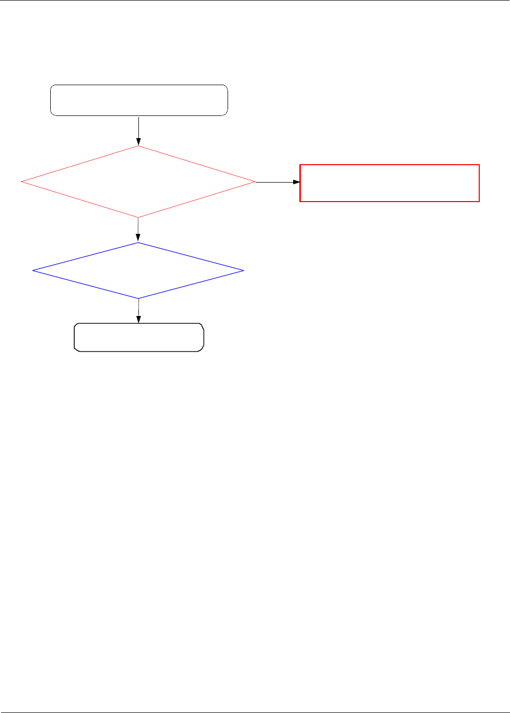
8-3-14. MHL
Yes
No
Check the LDOs(U100, U105)
Check the voltage of
L101(1.2V), C115(3.3V),
L102(1.2V), C122(1.8V),
Replace U106
Yes
END
Yes
MHL Does not work
Level 3Repair
Distribution, transmission, or infringement of any content or data from this document without Samsung’s written authorization is strictly prohibited.
Confidential and proprietary-the contents in this service guide subject to change without prior notice.
8-35
Level 3Repair
Distribution, transmission, or infringement of any content or data from this document without Samsung’s written authorization is strictly prohibited.
Confidential and proprietary-the contents in this service guide subject to change without prior notice.
8-36
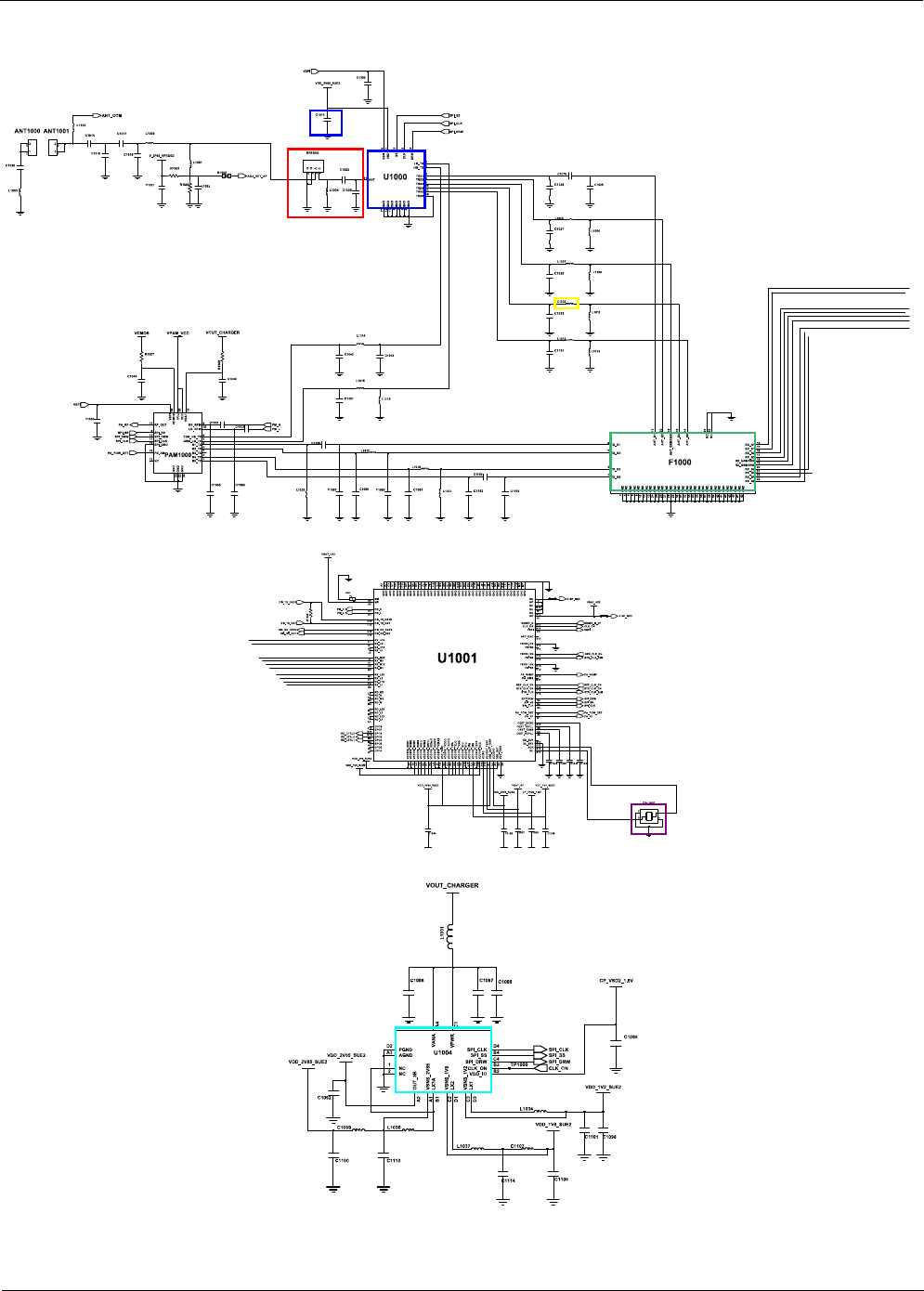
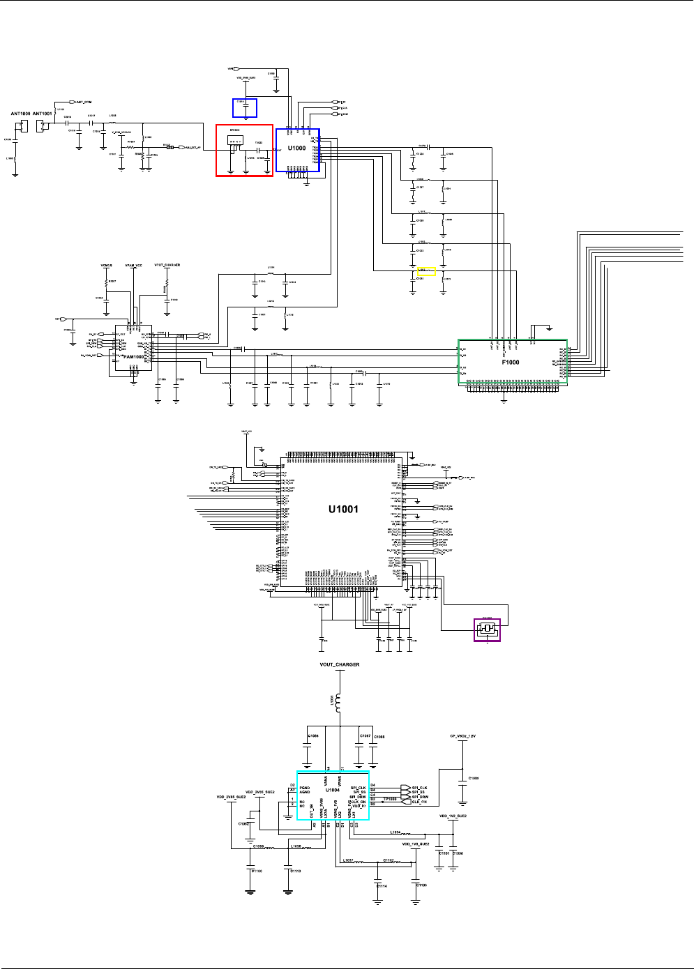
Check C1023 ≤-65dBm ?
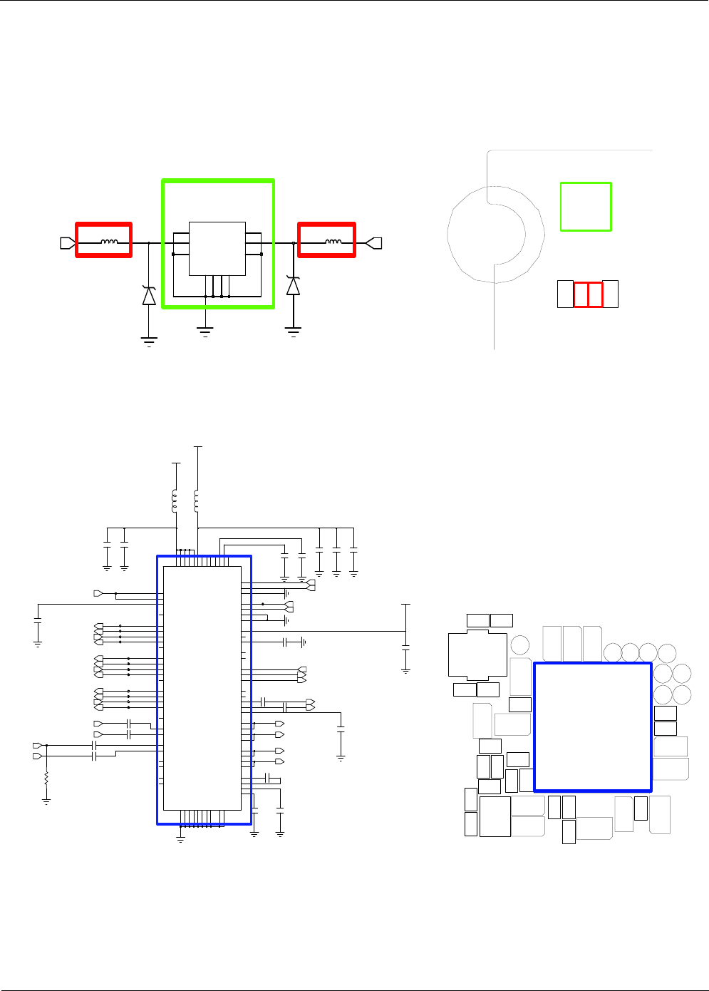
8-3-16. GSM850/ WCDMA Band5 RX
CONTINUO
US RX ON
RF INPUT : 4408CH
AMP :-50
dBm
NORMAL CONDITION
catch the channel?
Check the voltage at
{C1057 =VBAT_RF ?}
&{
C1056 = 2.85V ?}
&{
C1054 = 2.65V ?}
&{
C1058 =1.8
V?}
&{
C1059 =1.2
V?}
Check the Voltage at
C1014 = 2.85V ?
Check component
soldering status OK at
F1000
CHECK soldered
L1004,C1023,C1026,RFS1000
Resolder or change
U1000, C1014
Resolder or change
F1000
Resolder or change
U1004
Check the freq. at
OSC1000 PIN 1or PIN
3:26
MHz ?
Change or resolder
OSC1000
Check C1032
≥-65dBm ?Resolder or change
Check C1032
WCDMA Band5
/GSM 850
Receiver is O.K? Resolder or change
UCP3000
END
NO
YES
NO
NO
YES
NO
YES
NO
YES
NO
YES
NO
YES
NO
Check F1000 PIN 20, 21
≥-65dBm Resolder or change
F1000
NO
YES
Level 3Repair
Distribution, transmission, or infringement of any content or data from this document without Samsung’s written authorization is strictly prohibited.
Confidential and proprietary-the contents in this service guide subject to change without prior notice.
8-37

Level 3Repair
Distribution, transmission, or infringement of any content or data from this document without Samsung’s written authorization is strictly prohibited.
Confidential and proprietary-the contents in this service guide subject to change without prior notice.
8-38
Level 3Repair
Distribution, transmission, or infringement of any content or data from this document without Samsung’s written authorization is strictly prohibited.
Confidential and proprietary-the contents in this service guide subject to change without prior notice.
8-39
Check C1023 ≤-65dBm ?
8-3-17. GSM900/ WCDMA Band8 RX
CONTINUOUS RX ON
RF INPUT : 3013CH
AMP :-50
dBm
NORMAL CONDITION
catch the channel?
Check the voltage at
{C1057 =VBAT_RF ?}
&{
C1056 = 2.85V ?}
&{
C1054 = 2.65V ?}
&{
C1058 =1.8
V?}
&{
C1059 =1.2
V?}
Check the Voltage at
C1014 = 2.85V ?
Check component
soldering status OK at
F1000
CHECK soldered
L1004, C1023, C1026, RFS1000
Resolder or change
U1000, C1014
Resolder or change
F1000
Resolder or change
U1004
Check the freq. at
OSC1000 PIN 1or PIN
3:26
MHz ?
Change or resolder
OSC1000
Check L1012
≥-65dBm ?Resolder or change
Check L1012
WCDMA Band8
/GSM 900
Receiver is O.K?
Resolder or change
UCP3000
END
NO
YES
NO
NO
YES
NO
YES
NO
YES
NO
YES
NO
YES
NO
Check F1000 PIN 22, 23
≥-65dBm Resolder or change
F1000
NO
YES
Level 3Repair
Distribution, transmission, or infringement of any content or data from this document without Samsung’s written authorization is strictly prohibited.
Confidential and proprietary-the contents in this service guide subject to change without prior notice.
8-40

Level 3Repair
Distribution, transmission, or infringement of any content or data from this document without Samsung’s written authorization is strictly prohibited.
Confidential and proprietary-the contents in this service guide subject to change without prior notice.
8-41
Level 3Repair
Distribution, transmission, or infringement of any content or data from this document without Samsung’s written authorization is strictly prohibited.
Confidential and proprietary-the contents in this service guide subject to change without prior notice.
8-42
Check C1023 ≤-65dBm ?
8-3-18. GSM1800 RX
NORMAL CONDITION
catch the channel?
Check the voltage at
{C1057 =VBAT_RF ?}
&{
C1056 = 2.85V ?}
&{
C1054 = 2.65V ?}
&{
C1058 =1.8
V?}
&{
C1059 =1.2
V?}
Check the Voltage at
C1014 = 2.85V ?
Check component
soldering status OK at
F1000
CHECK soldered
L1004, C1023, C1026, RFS1000
Resolder or change
U1000, C1014
Resolder or change
F1000
Resolder or change
U1004
Check the freq. at
OSC1000 PIN 1or PIN
3:26
MHz ?
Change or resolder
OSC1000
Check L1007
≥-65dBm ?Resolder or change
Check L1007
GSM 1800
Receiver is O.K? Resolder or change
UCP3000
END
NO
YES
NO
NO
YES
NO
YES
NO
YES
NO
YES
NO
YES
NO
Check F1000 PIN 18, 19
≥-65dBm Resolder or change
F1000
NO
YES
CONTINUOUS RX ON
RF INPUT : 698CH
AMP : -50dBm

Level 3Repair
Distribution, transmission, or infringement of any content or data from this document without Samsung’s written authorization is strictly prohibited.
Confidential and proprietary-the contents in this service guide subject to change without prior notice.
8-43
Level 3Repair
Distribution, transmission, or infringement of any content or data from this document without Samsung’s written authorization is strictly prohibited.
Confidential and proprietary-the contents in this service guide subject to change without prior notice.
8-44

Level 3Repair
Distribution, transmission, or infringement of any content or data from this document without Samsung’s written authorization is strictly prohibited.
Confidential and proprietary-the contents in this service guide subject to change without prior notice.
8-45
Check C1023 ≤-65dBm ?
8-3-19. GSM1900/ WCDMA Band2 RX
NORMAL CONDITION
catch the channel?
Check the voltage at
{C1057 =VBAT_RF ?}
&{
C1056 = 2.85V ?}
&{
C1054 = 2.65V ?}
&{
C1058 =1.8
V?}
&{
C1059 =1.2
V?}
Check the Voltage at
C1014 = 2.85V ?
Check component
soldering status OK at
F1000
CHECK soldered
L1004, C1023, C1026, RFS1000
Resolder or change
U1000, C1014
Resolder or change
F1000
Resolder or change
U1004
Check the freq. at
OSC1000 PIN 1or PIN
3:26
MHz ?
Change or resolder
OSC1000
Check L1005
≥-65dBm ?Resolder or change
Check L1005
WCDMA Band2
/GSM1900
Receiver is O.K?
Resolder or change
UCP3000
END
NO
YES
NO
NO
YES
NO
YES
NO
YES
NO
YES
NO
YES
NO
Check F1000 PIN 16, 17
≥-65dBm Resolder or change
F1000
NO
YES
CONTINUOUS RX ON
RF INPUT : 9880CH
AMP :-50
dBm

Level 3Repair
Distribution, transmission, or infringement of any content or data from this document without Samsung’s written authorization is strictly prohibited.
Confidential and proprietary-the contents in this service guide subject to change without prior notice.
8-46

Level 3Repair
Distribution, transmission, or infringement of any content or data from this document without Samsung’s written authorization is strictly prohibited.
Confidential and proprietary-the contents in this service guide subject to change without prior notice.
8-47

Level 3Repair
Distribution, transmission, or infringement of any content or data from this document without Samsung’s written authorization is strictly prohibited.
Confidential and proprietary-the contents in this service guide subject to change without prior notice.
8-48
Check C1023 ≤-65dBm ?
8-3-20. WCDMA Band1 RX
NORMAL CONDITION
catch the channel?
Check the voltage at
{C1057 =VBAT_RF ?}
&{
C1056 = 2.85V ?}
&{
C1054 = 2.65V ?}
&{
C1058 =1.8
V?}
&{
C1059 =1.2
V?}
Check the Voltage at
C1014 = 2.85V ?
Check component
soldering status OK at
F1000
CHECK soldered
L1004, C1023, C1026, RFS1000
Resolder or change
U1000, C1014
Resolder or change
F1000
Resolder or change
U1004
Check the freq. at
OSC1000 PIN 1or PIN
3:26
MHz ?
Change or resolder
OSC1000
Check C1078
≥-65dBm ?Resolder or change
Check C1078
WCDMA Band1
Receiver is O.K? Resolder or change
UCP3000
END
NO
YES
NO
NO
YES
NO
YES
NO
YES
NO
YES
NO
YES
NO
Check F1000 PIN 14, 15
≥-65dBm Resolder or change
F1000
NO
YES
CONTINUOUS RX ON
RF INPUT : 10700CH
AMP :-50
dBm

Level 3Repair
Distribution, transmission, or infringement of any content or data from this document without Samsung’s written authorization is strictly prohibited.
Confidential and proprietary-the contents in this service guide subject to change without prior notice.
8-49

Level 3Repair
Distribution, transmission, or infringement of any content or data from this document without Samsung’s written authorization is strictly prohibited.
Confidential and proprietary-the contents in this service guide subject to change without prior notice.
8-50
Level 3Repair
Distribution, transmission, or infringement of any content or data from this document without Samsung’s written authorization is strictly prohibited.
Confidential and proprietary-the contents in this service guide subject to change without prior notice.
8-51
U1000 PIN11 :About
30dBm ?
8-3-21. GSM850/ GSM900 TX
Check the Voltage at
C1014 = 2.85V ?
Check the Voltage at
C1049 =VOUT_CHARGER?
CHECK soldered
L1004, C1023, C1026, RFS1000
Resolder or change
U1000, C1014
Resolder or change
PAM1000, C1049
Check L1015, C1051 :
About 30dBm ?Resolder or change
L1015, C1051
YES
NO
NO
YES
YES
NO
NO
YES
Check C1053 :
About 0dBm ?Resolder or change
C1053
YES
YES
Check the voltage at
{C1057 =VBAT_RF ?}
&{
C1056 = 2.85V ?}
&{
C1054 = 2.65V ?}
&{
C1058 =1.8
V?}
&{
C1059 =1.2
V?}
Resolder or change
U1004
Check the freq. at
OSC1000 PIN 1or PIN
3:26
MHz ?
Change or resolder
OSC1000
GSM850/900
Transmitter is O.K? Resolder or change
UCP3000
END
NO
YES
NO
YES
NO
CONTINOUS TX ON CONDITION
TX POWER DAC:14500 CODE
APPLIED
GSM850 CH : 190
GSM900 CH :62
RBW : 100KHz
VBW : 100KHz
SPAN :10
MHz
REF LEV. :10
dBm
ATT. :20
dB
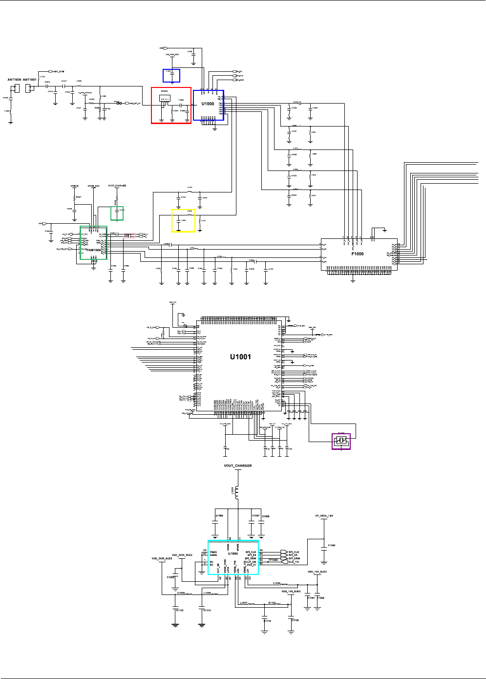
Level 3Repair
Distribution, transmission, or infringement of any content or data from this document without Samsung’s written authorization is strictly prohibited.
Confidential and proprietary-the contents in this service guide subject to change without prior notice.
8-52
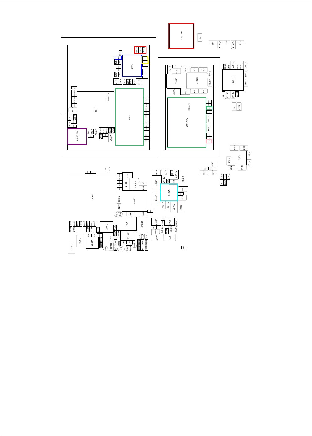
Level 3Repair
Distribution, transmission, or infringement of any content or data from this document without Samsung’s written authorization is strictly prohibited.
Confidential and proprietary-the contents in this service guide subject to change without prior notice.
8-53

Level 3Repair
Distribution, transmission, or infringement of any content or data from this document without Samsung’s written authorization is strictly prohibited.
Confidential and proprietary-the contents in this service guide subject to change without prior notice.
8-54
U1000 PIN11 :About
30dBm ?
8-3-22. GSM1800/ GSM1900 TX
Check the Voltage at
C1014 = 2.85V ?
Check the Voltage at
C1049 =VOUT_CHARGER?
CHECK soldered
L1004, C1023, C1026, RFS1000
Resolder or change
U1000, C1014
Resolder or change
PAM1000, C1049
Check L1015, C1051 :
About 30dBm ?Resolder or change
L1014, C1042
YES
NO
NO
YES
YES
NO
NO
YES
Check C1052 :
About 0dBm ?Resolder or change
C1052
YES
YES
Check the voltage at
{C1057 =VBAT_RF ?}
&{
C1056 = 2.85V ?}
&{
C1054 = 2.65V ?}
&{
C1058 =1.8
V?}
&{
C1059 =1.2
V?}
Resolder or change
U1004
Check the freq. at
OSC1000 PIN 1or PIN
3:26
MHz ?
Change or resolder
OSC1000
GSM1800/1900
Transmitter is O.K? Resolder or change
UCP3000
END
NO
YES
NO
YES
NO
CONTINOUS TX ON CONDITION
TX POWER DAC:14500 CODE
APPLIED
DCS CH : 685
PCS CH : 661
RBW : 100KHz
VBW : 100KHz
SPAN :10
MHz
REF LEV. :10
dBm
ATT. :20
dB
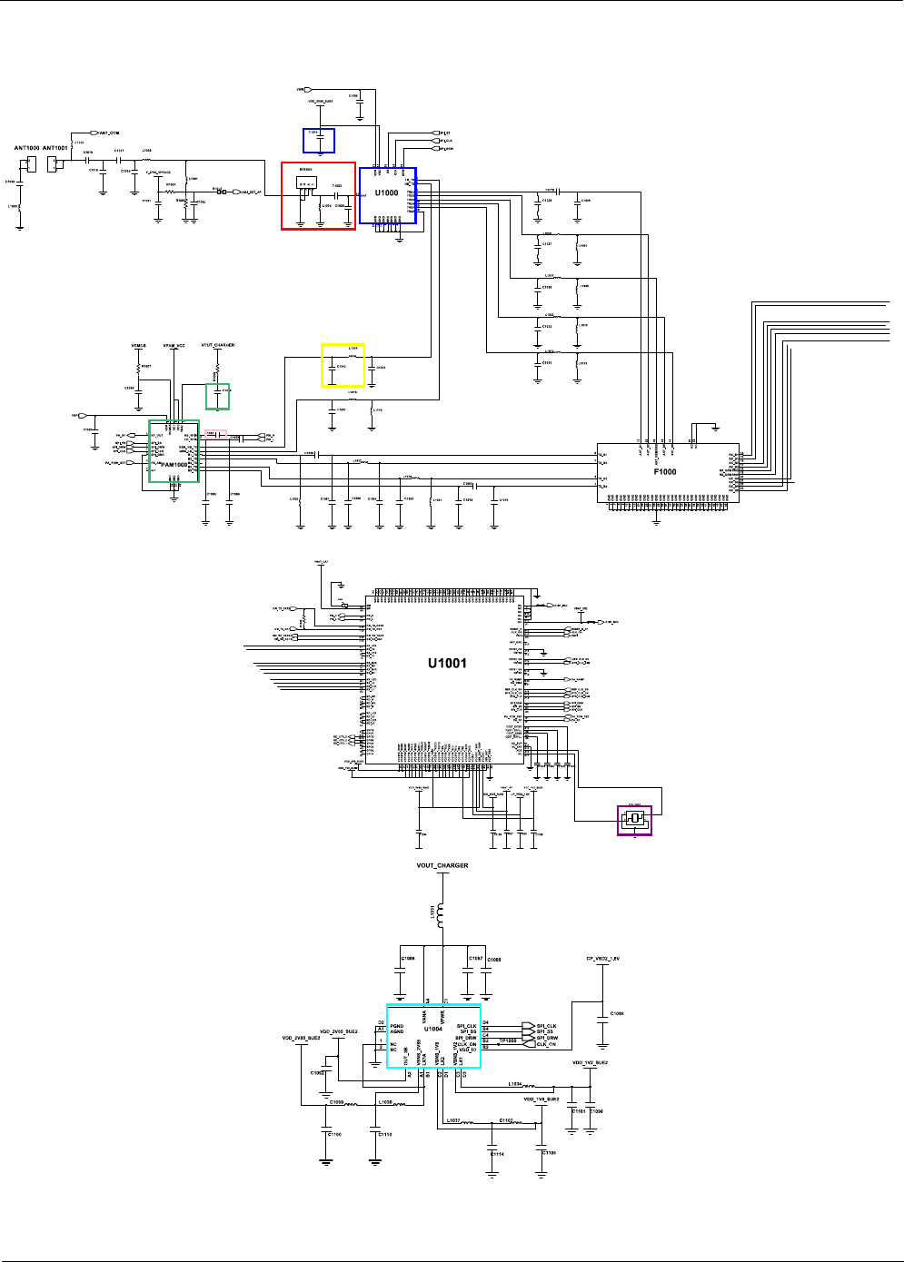
Level 3Repair
Distribution, transmission, or infringement of any content or data from this document without Samsung’s written authorization is strictly prohibited.
Confidential and proprietary-the contents in this service guide subject to change without prior notice.
8-55
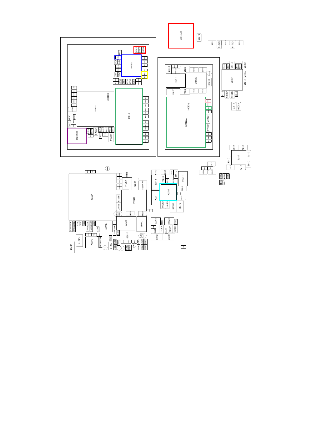
Level 3Repair
Distribution, transmission, or infringement of any content or data from this document without Samsung’s written authorization is strictly prohibited.
Confidential and proprietary-the contents in this service guide subject to change without prior notice.
8-56
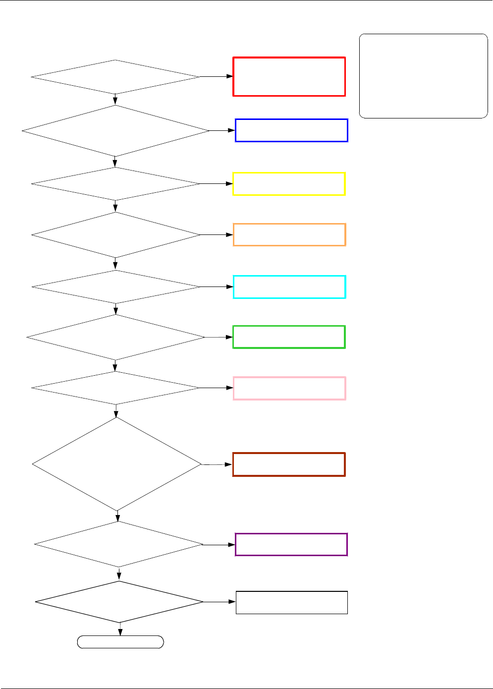
Level 3Repair
Distribution, transmission, or infringement of any content or data from this document without Samsung’s written authorization is strictly prohibited.
Confidential and proprietary-the contents in this service guide subject to change without prior notice.
8-57
U1000 PIN11 :About
30dBm ?
8-3-23. WCDMA BAND1 TX
Check the Voltage at
C1014 = 2.85V ?
Resolder or change
U1000, C1014
Check C1078 :
About 22dBm ?Resolder or change
C1078
YES
NO
NO
YES
YES
CHECK soldered
L1004, C1023, C1026, RFS1000
NO
Check component
soldering status OK at
F1000
Resolder or change
F1000
NO
YES
Check C1055, L1020:
About 22dBm ?Resolder or change
C1055, L1020
YES
NO
CONTINOUS TX ON CONDITION
TX POWER DAC:14500 CODE
APPLIED
WCDMA Band1 CH : 10700
RBW : 100KHz
VBW : 100KHz
SPAN :10
MHz
REF LEV. :10
dBm
ATT. :20
dB
Check the Voltage at
C1049 =
VOUT_CHARGER?
Resolder or change
PAM1000, C1049
NO
YES
Check C1052:
About 0dBm ?Resolder or change
C1052
YES
YES
Check the voltage at
{C1057 =VBAT_RF ?}
&{
C1056 = 2.85V ?}
&{
C1054 = 2.65V ?}
&{
C1058 =1.8
V?}
&{
C1059 =1.2
V?}
Resolder or change
U1004
Check the freq. at
OSC1000 PIN 1or PIN
3:26
MHz ?
Change or resolder
OSC1000
WCDMA BAND1
Transmitter is O.K? Resolder or change
UCP3000
END
NO
YES
NO
YES
NO
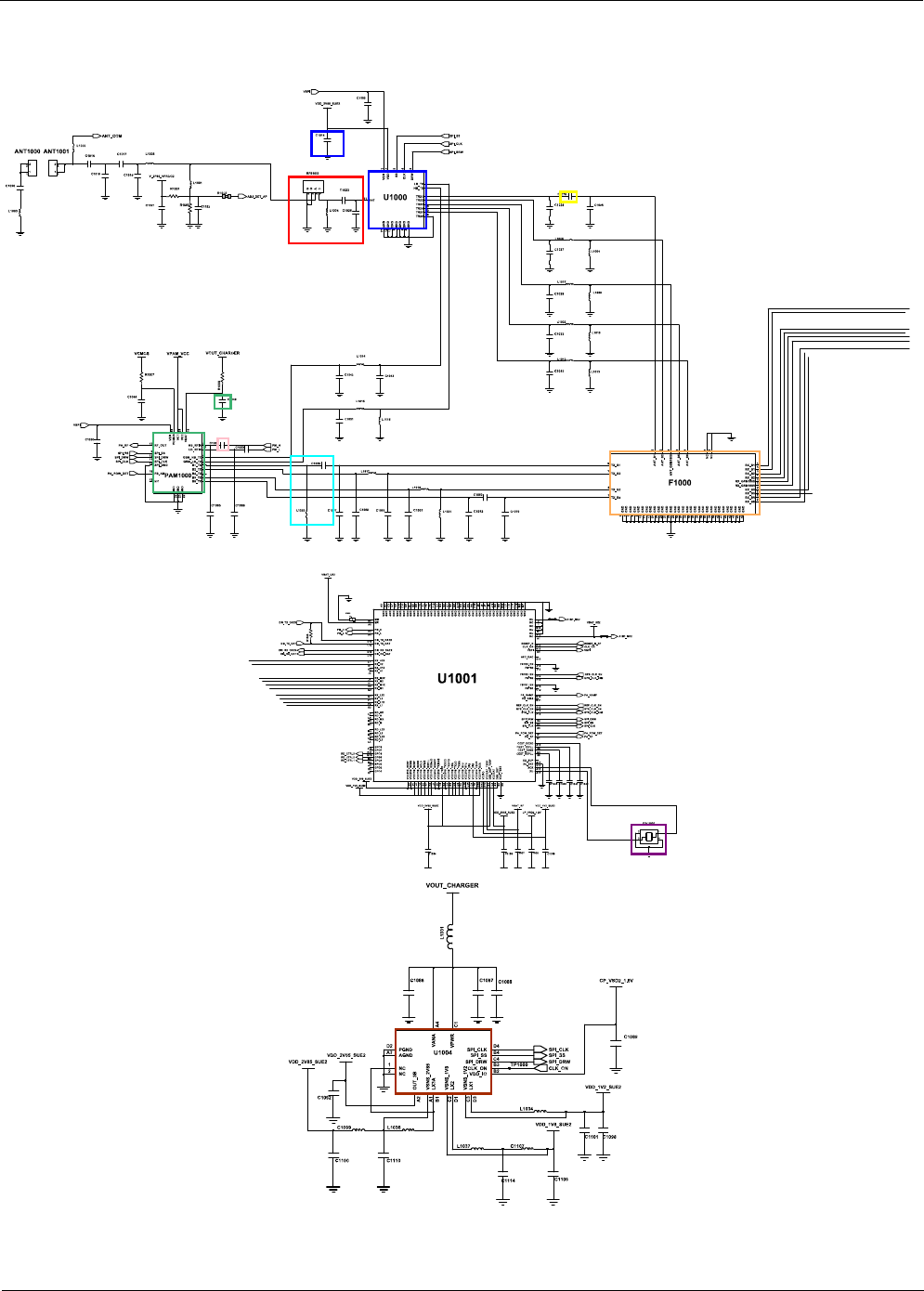
Level 3Repair
Distribution, transmission, or infringement of any content or data from this document without Samsung’s written authorization is strictly prohibited.
Confidential and proprietary-the contents in this service guide subject to change without prior notice.
8-58
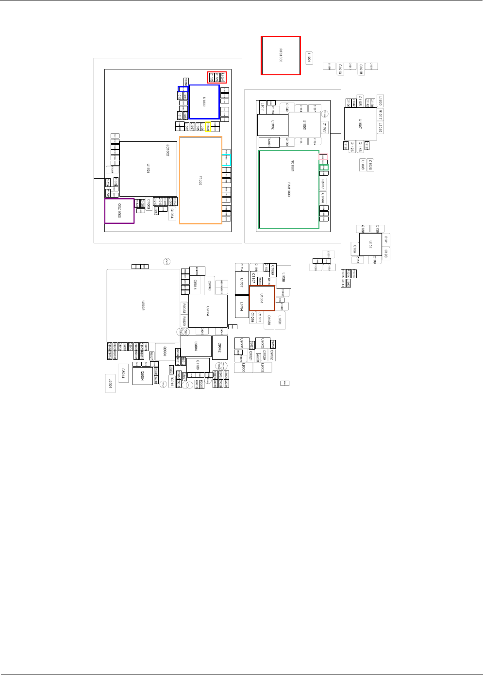
Level 3Repair
Distribution, transmission, or infringement of any content or data from this document without Samsung’s written authorization is strictly prohibited.
Confidential and proprietary-the contents in this service guide subject to change without prior notice.
8-59

Level 3Repair
Distribution, transmission, or infringement of any content or data from this document without Samsung’s written authorization is strictly prohibited.
Confidential and proprietary-the contents in this service guide subject to change without prior notice.
8-60
U1000 PIN11 :About
30dBm ?
8-3-24. WCDMA BAND2 TX
Check the Voltage at
C1014 = 2.85V ?
Resolder or change
U1000, C1014
Check L1005 :
About 22dBm ?Resolder or change
L1005
YES
NO
NO
YES
YES
CHECK soldered
L1004, C1023, C1026, RFS1000
NO
Check component
soldering status OK at
F1000
Resolder or change
F1000
NO
YES
Check C1068, L1017:
About 22dBm ?Resolder or change
C1068, L1017:
YES
NO
Check the Voltage at
C1049 =
VOUT_CHARGER?
Resolder or change
PAM1000, C1049
NO
YES
Check C1052:
About 0dBm ?Resolder or change
C1052
YES
YES
Check the voltage at
{C1057 =VBAT_RF ?}
&{
C1056 = 2.85V ?}
&{
C1054 = 2.65V ?}
&{
C1058 =1.8
V?}
&{
C1059 =1.2
V?}
Resolder or change
U1004
Check the freq. at
OSC1000 PIN 1or PIN
3:26
MHz ?
Change or resolder
OSC1000
WCDMA BAND2
Transmitter is O.K? Resolder or change
UCP3000
END
NO
YES
NO
YES
NO
CONTINOUS TX ON CONDITION
TX POWER DAC:14500 CODE
APPLIED
WCDMA Band2 CH : 9880
RBW : 100KHz
VBW : 100KHz
SPAN :10
MHz
REF LEV. :10
dBm
ATT. :20
dB
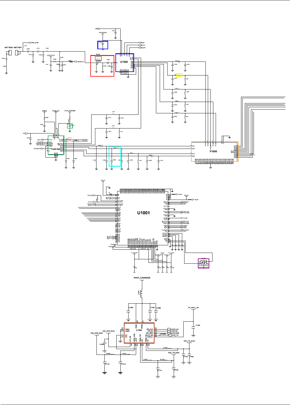
Level 3Repair
Distribution, transmission, or infringement of any content or data from this document without Samsung’s written authorization is strictly prohibited.
Confidential and proprietary-the contents in this service guide subject to change without prior notice.
8-61
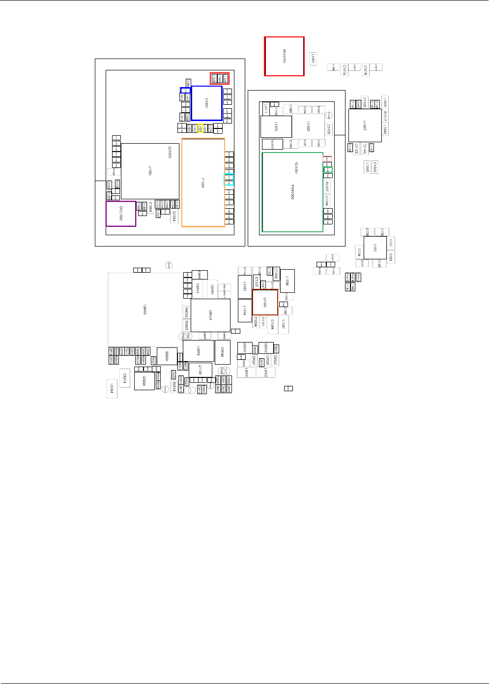
Level 3Repair
Distribution, transmission, or infringement of any content or data from this document without Samsung’s written authorization is strictly prohibited.
Confidential and proprietary-the contents in this service guide subject to change without prior notice.
8-62
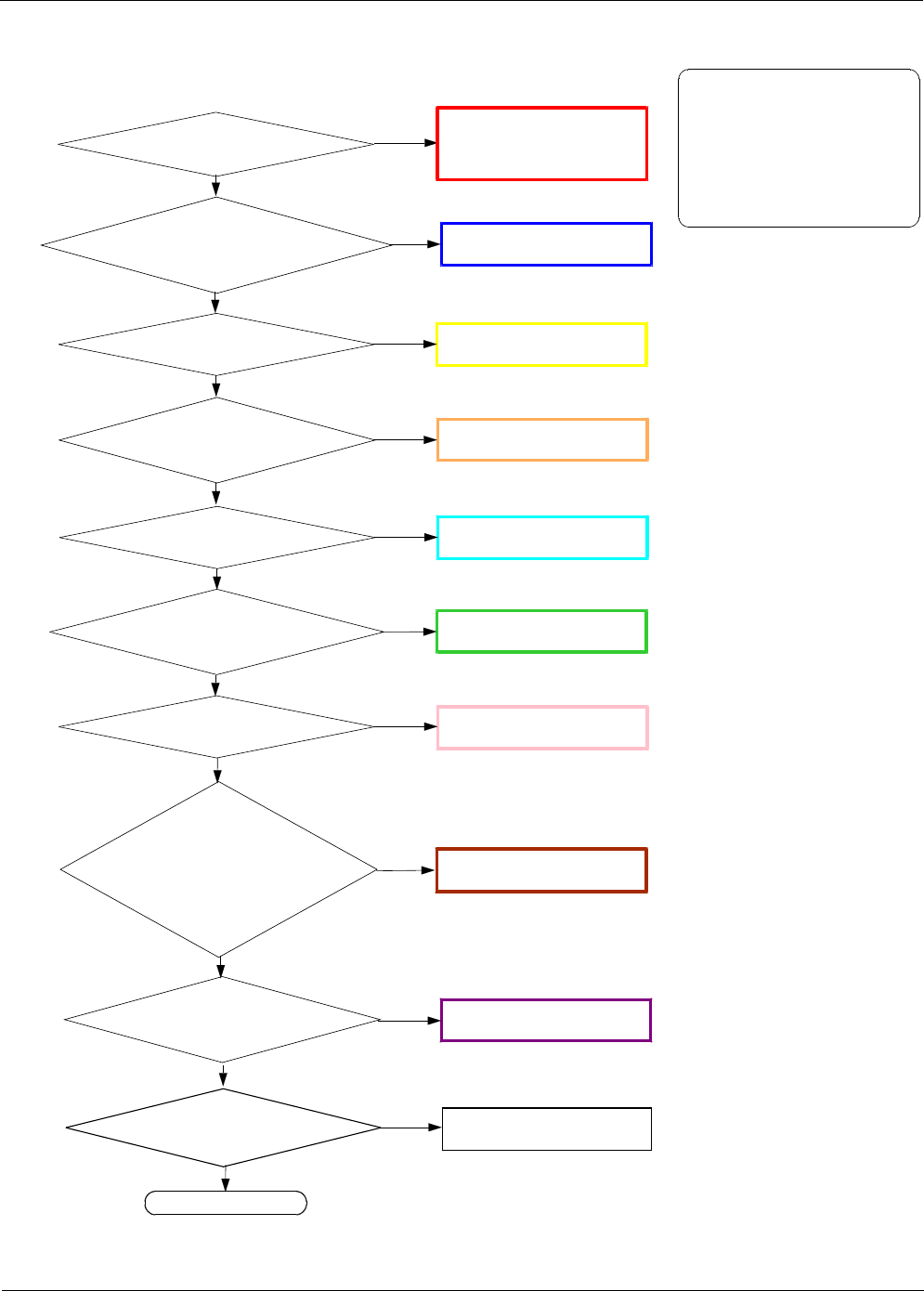
Level 3Repair
Distribution, transmission, or infringement of any content or data from this document without Samsung’s written authorization is strictly prohibited.
Confidential and proprietary-the contents in this service guide subject to change without prior notice.
8-63
U1000 PIN11 :About
30dBm ?
8-3-25. WCDMA BAND5 TX
Check the Voltage at
C1014 = 2.85V ?
Resolder or change
U1000, C1014
Check C1032:
About 22dBm ?Resolder or change
C1032
YES
NO
NO
YES
YES
CHECK soldered
L1004, C1023, C1026, RFS1000
NO
Check component
soldering status OK at
F1000
Resolder or change
F1000
NO
YES
Check C1061, L1018:
About 22dBm ?Resolder or change
C1061, L1018
YES
NO
Check the Voltage at
C1049 =
VOUT_CHARGER?
Resolder or change
PAM1000, C1049
NO
YES
Check C1053:
About 0dBm ?Resolder or change
C1053
YES
YES
Check the voltage at
{C1057 =VBAT_RF ?}
&{
C1056 = 2.85V ?}
&{
C1054 = 2.65V ?}
&{
C1058 =1.8
V?}
&{
C1059 =1.2
V?}
Resolder or change
U1004
Check the freq. at
OSC1000 PIN 1or PIN
3:26
MHz ?
Change or resolder
OSC1000
WCDMA BAND5
Transmitter is O.K? Resolder or change
UCP3000
END
NO
YES
NO
YES
NO
CONTINOUS TX ON CONDITION
TX POWER DAC:14500 CODE
APPLIED
WCDMA Band5 CH : 4408
RBW : 100KHz
VBW : 100KHz
SPAN :10
MHz
REF LEV. :10
dBm
ATT. :20
dB
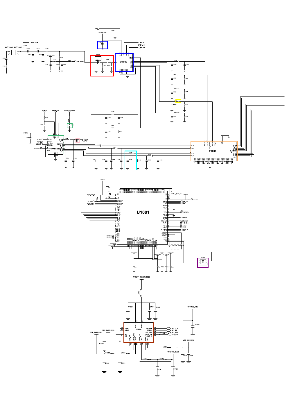
Level 3Repair
Distribution, transmission, or infringement of any content or data from this document without Samsung’s written authorization is strictly prohibited.
Confidential and proprietary-the contents in this service guide subject to change without prior notice.
8-64

Level 3Repair
Distribution, transmission, or infringement of any content or data from this document without Samsung’s written authorization is strictly prohibited.
Confidential and proprietary-the contents in this service guide subject to change without prior notice.
8-65
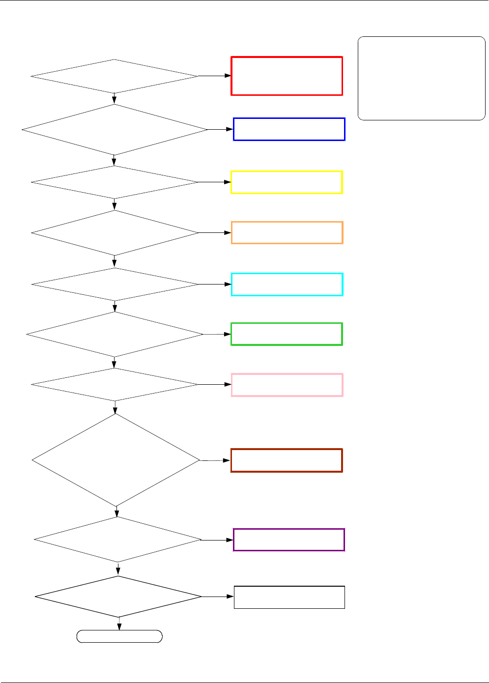
Level 3Repair
Distribution, transmission, or infringement of any content or data from this document without Samsung’s written authorization is strictly prohibited.
Confidential and proprietary-the contents in this service guide subject to change without prior notice.
8-66
U1000 PIN11 :About
30dBm ?
8-3-26. WCDMA BAND8 TX
Check the Voltage at
C1014 = 2.85V ?
Resolder or change
U1000, C1014
Check L1012:
About 22dBm ?Resolder or change
L1012
YES
NO
NO
YES
YES
CHECK soldered
L1004, C1023, C1026, RFS1000
NO
Check component
soldering status OK at
F1000
Resolder or change
F1000
NO
YES
Check C1062, C1060:
About 22dBm ?Resolder or change
C1062, C1060
YES
NO
Check the Voltage at
C1049 =
VOUT_CHARGER?
Resolder or change
PAM1000, C1049
NO
YES
Check C1053:
About 0dBm ?Resolder or change
C1053
YES
YES
Check the voltage at
{C1057 =VBAT_RF ?}
&{
C1056 = 2.85V ?}
&{
C1054 = 2.65V ?}
&{
C1058 =1.8
V?}
&{
C1059 =1.2
V?}
Resolder or change
U1004
Check the freq. at
OSC1000 PIN 1or PIN
3:26
MHz ?
Change or resolder
OSC1000
WCDMA BAND5
Transmitter is O.K? Resolder or change
UCP3000
END
NO
YES
NO
YES
NO
CONTINOUS TX ON CONDITION
TX POWER DAC:14500 CODE
APPLIED
WCDMA Band8 CH : 3013
RBW : 100KHz
VBW : 100KHz
SPAN :10
MHz
REF LEV. :10
dBm
ATT. :20
dB
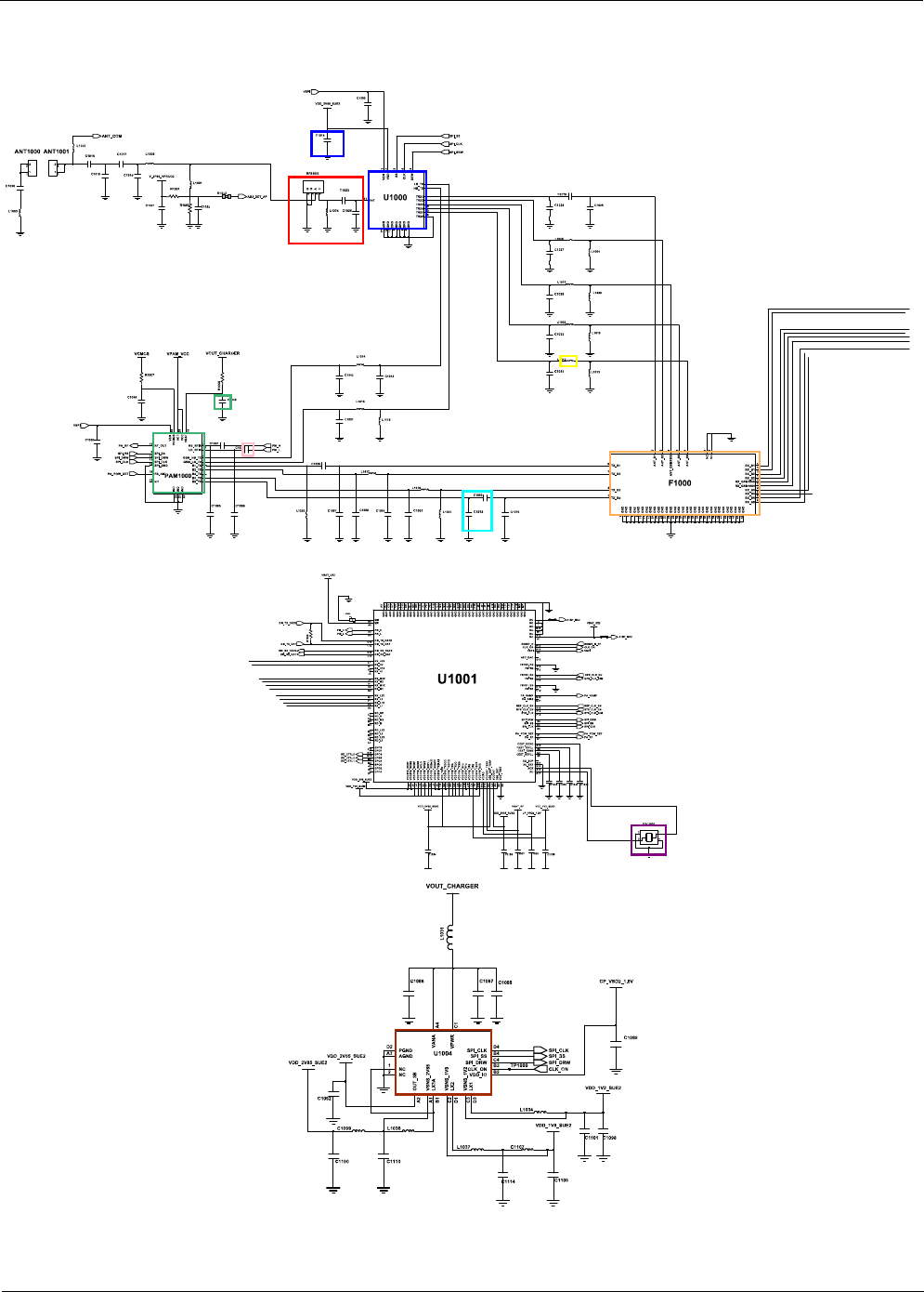
Level 3Repair
Distribution, transmission, or infringement of any content or data from this document without Samsung’s written authorization is strictly prohibited.
Confidential and proprietary-the contents in this service guide subject to change without prior notice.
8-67
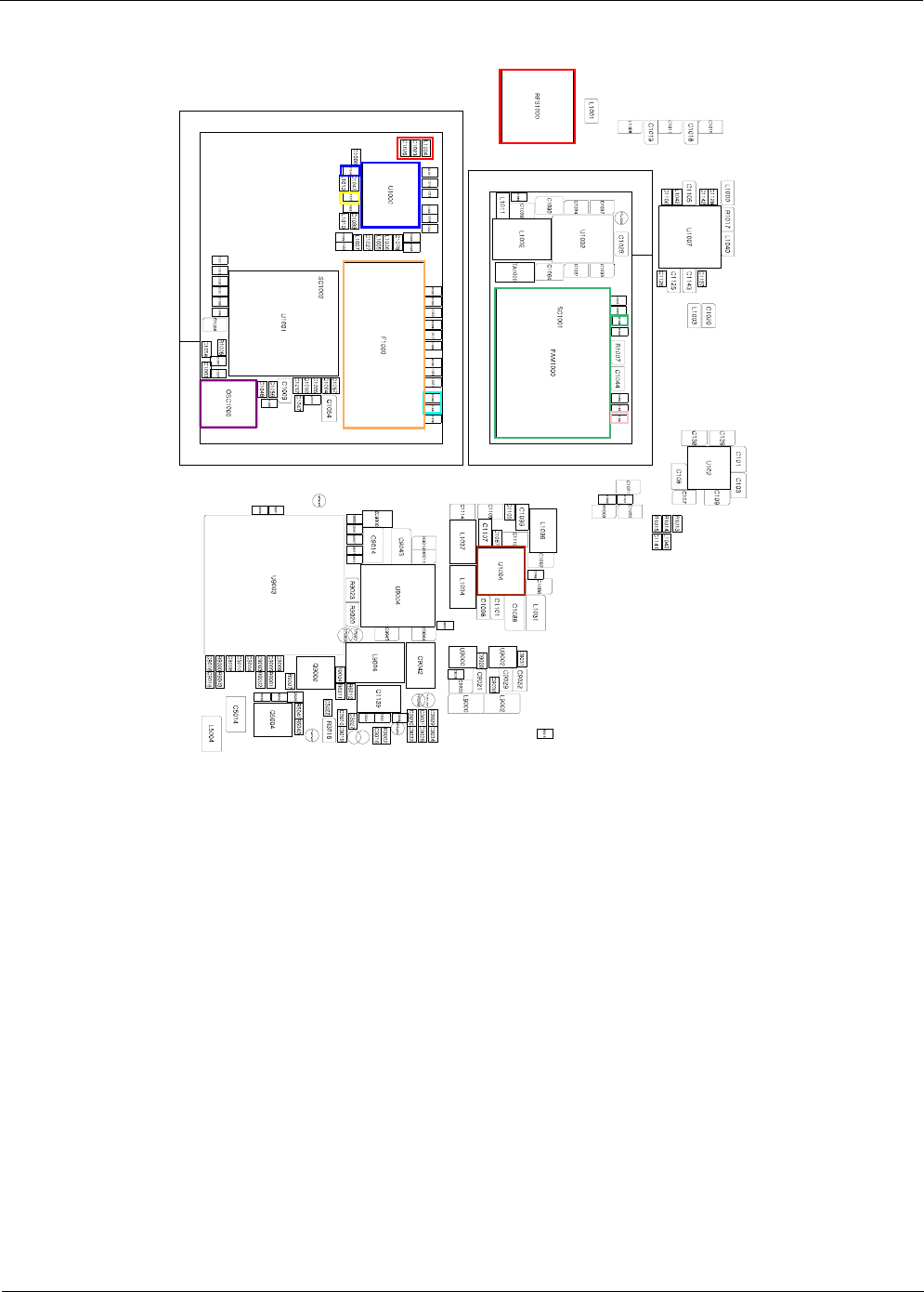
Level 3Repair
Distribution, transmission, or infringement of any content or data from this document without Samsung’s written authorization is strictly prohibited.
Confidential and proprietary-the contents in this service guide subject to change without prior notice.
8-68
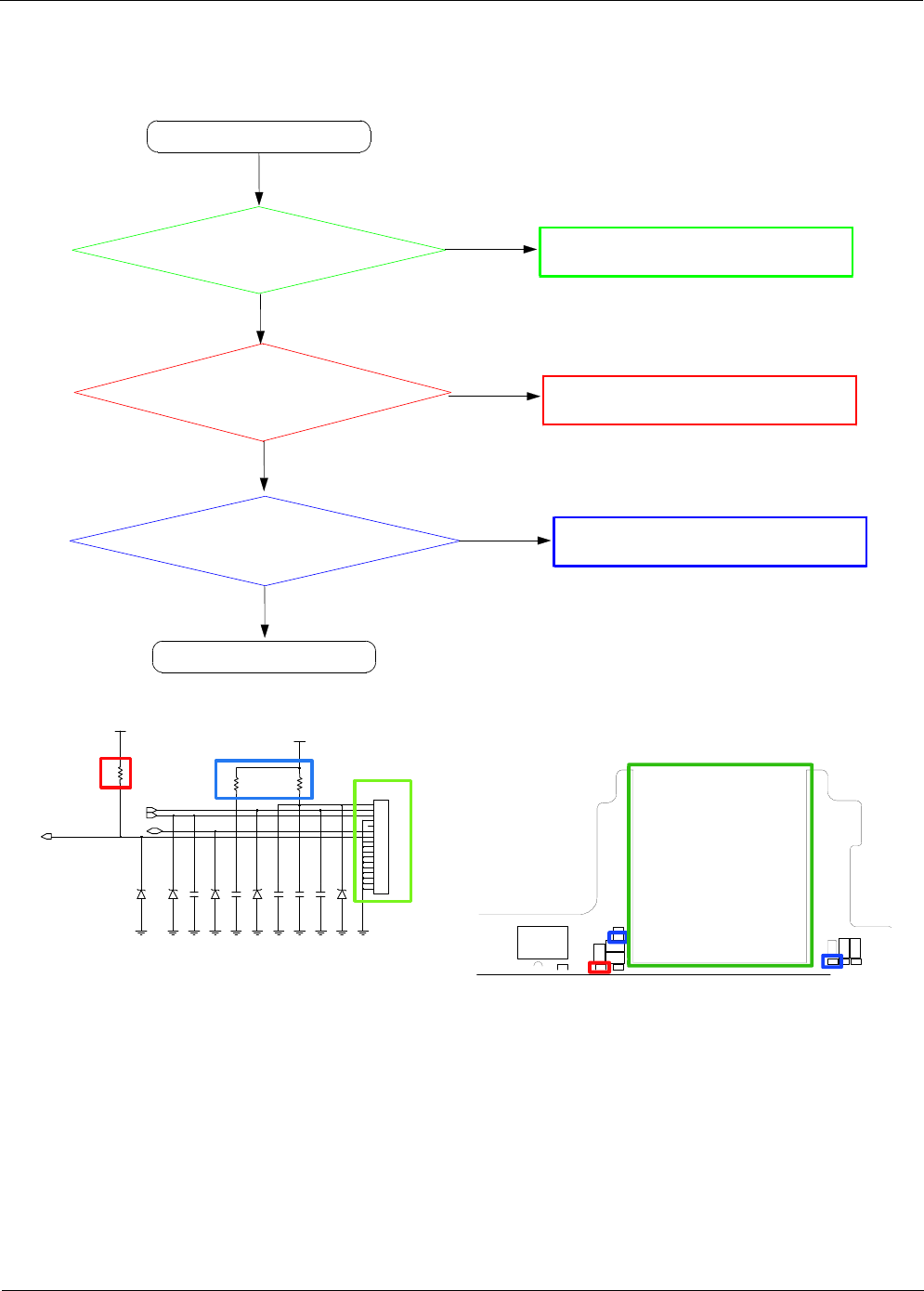
Level 3Repair
Distribution, transmission, or infringement of any content or data from this document without Samsung’s written authorization is strictly prohibited.
Confidential and proprietary-the contents in this service guide subject to change without prior notice.
8-69
8-3-27. Sim Part
R3009
C3038
R3010
C3042
C3039
C3041
ZD3000
NC3
6
7NC4
NC5
8
NC6
9
10 NC7
NC8
11
C5 C5
C6
C6
C7 C7
1CD
COM
4GND
2
3NC1
5NC2
SIM3000
C1 C1
C2
C2
C3 C3
R3008
CP_VSIM_3.0V
CP_VSD2_1.8V
ZD3002
ZD3001
ZD3004
C3040
ZD3003
SIM_IO
SIM_CLK
SIM_RST
SIM_DETECT_CP
Check the Voltage of SIM
(R3008,R3009 :3.0
V)
Insert SIM card
Check the Pin Soldering
of SIM3000
Yes
Yes
Yes
No
END
Check the Voltage of
detection PIN
(R3010 :1.8
V)
Resoldering and recheck
Change to the new SIM card
Check the voltage from CP.
Unless power, Change the PBA
Yes
No
No
C3038
C3039
C3040
C3041
C3042
HDC3001
R3008
R3009
R3010R3025
TP3019
ZD3000
ZD3001 ZD3002
ZD3003
ZD3004

9. Reference Abbreviate
9-1
Confidential and proprietary-the contents in this service guide subject to change without prior notice.
Distribution, transmission, or infringement of any content or data from this document without Samsung’s written authorization is strictly prohibited.
Reference Abbreviate
―AAC:Advanced Audio Coding.
―AVC :Advanced Video Coding.
―BER :Bit Error Rate
―BPSK:Binary Phase Shift Keying
―CA :Conditional Access
―CDM :Code Division Multiplexing
―C/I :Carrier to Interference
―DMB :Digital Multimedia Broadcasting
―EN :European Standard
―ES :Elementary Stream
―ETSI:European Telecommunications Standards Institute
―MPEG:Moving Picture Experts Group
―PN :Pseudo-random Noise
―PS :Pilot Symbol
―QPSK:Quadrature Phase Shift Keying
―RS :Reed-Solomon
―SI :Service Information
―TDM :Time Division Multiplexing
―TS :Transport Stream