Samsung GT S5230 Service Manual. Www.s Manuals.com. Manual
User Manual: Smartphone Samsung GT-S5230 - Service manuals and Schematics, Disassembly / Assembly. Free.
Open the PDF directly: View PDF ![]() .
.
Page Count: 51
GSM TELEPHONE
GT-S5230
1. Safety Precautions
2. Specification
3. Product Function
4. Array course control
5. Exploded View and Parts list
6. MAIN Electrical Parts List
7. Disassembly and Assembly
Instructions
8. Block Diagrams
9. PCB Diagrams
10. Chart of Troubleshooting
11. Reference data
GSM TELEPHONE CONTENTS
This Service Manual is aproperty of Samsung Electronics Co.,Ltd.
Any unauthorized use of Manual can be punished under applicable
International and/or domestic law.
Samsung Electronics Co.,Ltd.
2009. 04. Rev.1.0
ⓒ
Country Web Site
North America service.samsungportal.com
Latin America latin.samsungportal.com
CIS cis.samsungportal.com
Europe europe.samsungportal.com
China china.samsungportal.com
Asia asia.samsungportal.com
Mideast &Africa mea.samsungportal.com
GSPN (Global Service Partner Network)
SAMSUNG Proprietary-Contents may change without notice
5. Exploded View and Parts List
5-1
This Document can not be used without Samsung's authorization
5-1. Cellular phone Exploded View
QRE01
QCK01
QCK02
QCR91
QBA00
QKP01
QMP02
QLB01
QAN02
QCB01
QMP01
QSH01
QFR01
QME03
QLC01
QLC03
QCA01
QMO01
QSP01
QVK01
QAN03
QSH02
QVO01
QCR60
QIF01
2. Specification
2-1
2-1. GSM General Specification
GSM900
Phase 1
GSM850
Phase 1
DCS1800
Phase 1 PCS1900
Freq.
Band[MHz]
Uplink/Downlink
880~915
925~960
824.2~848.8
869.2~893.8
1710~1785
1805~1880
1850~1910
1930~1990
ARFCN range 0~124 &
975~1023 128~251 512~885 512~810
Tx/Rx spacing 45MHz 45MHz 95MHz 80MHz
Mod. Bit rate/
Bit Period
270.833kbps
3.692us
270.833kbps
3.692us
270.833kbps
3.692us
270.833kbps
3.692us
Time Slot
Period/Frame
Period
576.9us
4.615ms
576.9us
4.615ms
576.9us
4.615ms
576.9us
4.615ms
Modulation 0.3GMSK 0.3GMSK 0.3GMSK 0.3GMSK
MS Power 33dBm~5dBm 33dBm~5dBm 30dBm~0dBm 30dBm~0dBm
Power Class 5pcl ~ 19pcl 5pcl ~ 19pcl 0pcl ~15
pcl 0pcl ~15
pcl
Sensitivity -102dBm -102dBm -100dBm -100dBm
TDMA Mux 8 888
Cell Radius 35Km 35Km 2Km -
Speclflcation
2-2
TX Power
control level
GSM850
GSM900
533±3
dBm
631±3
dBm
729±3
dBm
827±3
dBm
925±3
dBm
10 23±3 dBm
11 21±3 dBm
12 19±3 dBm
13 17±3 dBm
14 15±3 dBm
15 13±3 dBm
16 11±5 dBm
17 9±5 dBm
18 7±5 dBm
19 5±5 dBm
TX Power
control level DCS1800
030±3
dBm
128±3
dBm
226±3
dBm
324±3
dBm
422±3
dBm
520±3
dBm
618±3
dBm
716±3
dBm
814±3
dBm
912±4
dBm
10 10±4 dBm
11 8±4dBm
12 6±4 dBm
13 4±4 dBm
14 2±5 dBm
15 0±5 dBm
TX Power
control level PCS1900
030±3
dBm
128±3
dBm
226±3
dBm
324±3
dBm
422±3
dBm
520±3
dBm
618±3
dBm
716±3
dBm
814±3
dBm
912±4
dBm
10 10±4 dBm
11 8±4dBm
12 6±4 dBm
13 4±4 dBm
14 2±5 dBm
15 0±5 dBm
2-2. GSM Tx Power Class
Speclflcation
2-3
TX Power
control level
GSM900
GSM850
827±3
dBm
925±3
dBm
10 23±3 dBm
11 21±3 dBm
12 19±3 dBm
13 17±3 dBm
14 15±3 dBm
15 13±3 dBm
16 11±5 dBm
17 9±5 dBm
18 7±5 dBm
19 5±5 dBm
TX Power
control level DCS1800
2 26±3 dBm
3 24±3 dBm
4 22±3 dBm
5 20±3 dBm
6 18±3 dBm
7 16±3 dBm
8 12±3 dBm
9 10±3 dBm
10 14±3 dBm
11 12±4 dBm
12 10±4 dBm
13 8±4dBm
14 6±4 dBm
15 4±4 dBm
2-3. GSM EDGE TX power class
TX Power
control level PCS1900
226±3
dBm
324±3
dBm
422±3
dBm
520±3
dBm
618±3
dBm
716±3
dBm
812±3
dBm
910±3
dBm
10 14±3 dBm
11 12±4 dBm
12 10±4 dBm
13 8±4dBm
14 6±4 dBm
15 4±4 dBm
Only in Master

SAMSUNG Proprietary-Contents may change without notice
3. Operation Instruction and Installation
3-1
This Document can not be used without Samsung's authorization
Main Function
-3.2Mega Pixel Camera
-3.0"WQVGA 262K TFT TOUCH SCREEN
-"
TOUCH WIZ" Full Touch UI
-BlueTooth V2.1+EDR
-USB 2.0
-SMS/MMS/EMS (OMA v1.2 )
-MP3/AMR/AAC/AAC+/e-AAC+/WMA
-Quad Band(EGSM900/DCS,PCS,EDGE)
-MicroSD Card Support
-External Memory
-FM Radio Support,Radio Data System
-Full Internet Browsing
-Accelerometer rotation
-Face Detection &Smile Shot
SAMSUNG Proprietary-Contents may change without notice
4. Array course control
4-1
This Document can not be used without Samsung's authorization
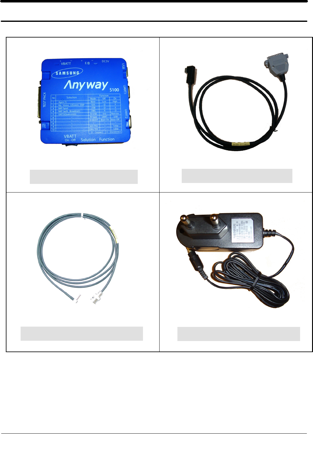
4-1. Software Adjustments
Test Cable (GH39-01160A)
Test Jig (GH99-36900A)
RF Test Cable (GH39-00985A) Adapter (GH99-38251A)

SAMSUNG Proprietary-Contents may change without notice
Array course control
4-2
This Document can not be used without Samsung's authorization
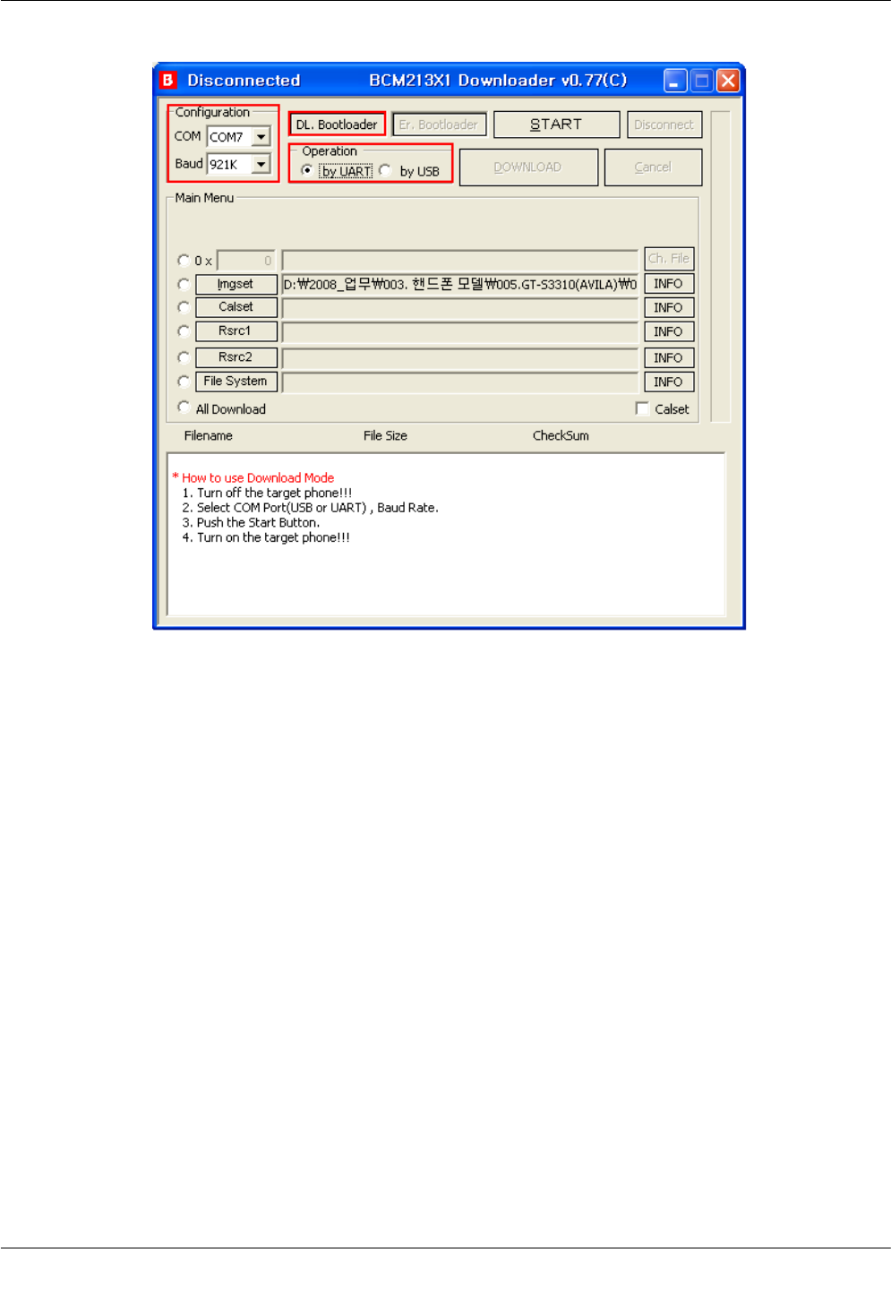
4-2. Software Downloading
4-2-1. Pre-requsite for Downloading
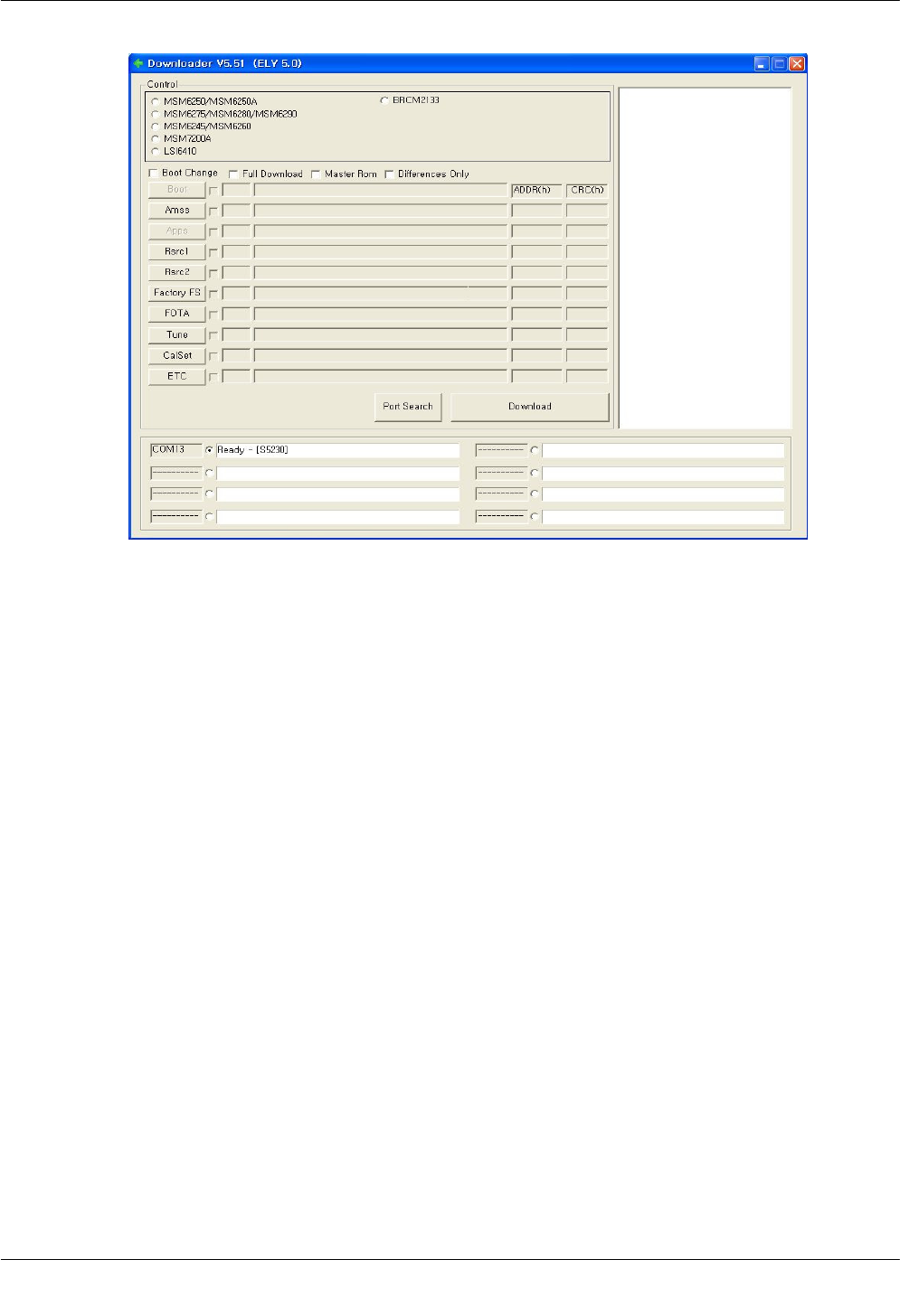
•Downloader Program(BCM213x1 Downloader v0.xx(D))
•Downloader Program(Downloader V5.51 (ELY x.0))
•GT-S5230 Mobile Phone
•Data Cable
•BOOT file, BIN file,RC1 file, RC2 file, FFS file, Calset file
4-2-2. S/W Downloader Program
■Load the binary download program by executing the
"BCM213x1 Downloader v0.xx(C) "
1.Select the connected serial port and the rate of speed.
2.Select the check box, Connect cable to phone after Click DL.Bootloader Button.
SAMSUNG Proprietary-Contents may change without notice
Array course control
4-3
This Document can not be used without Samsung's authorization
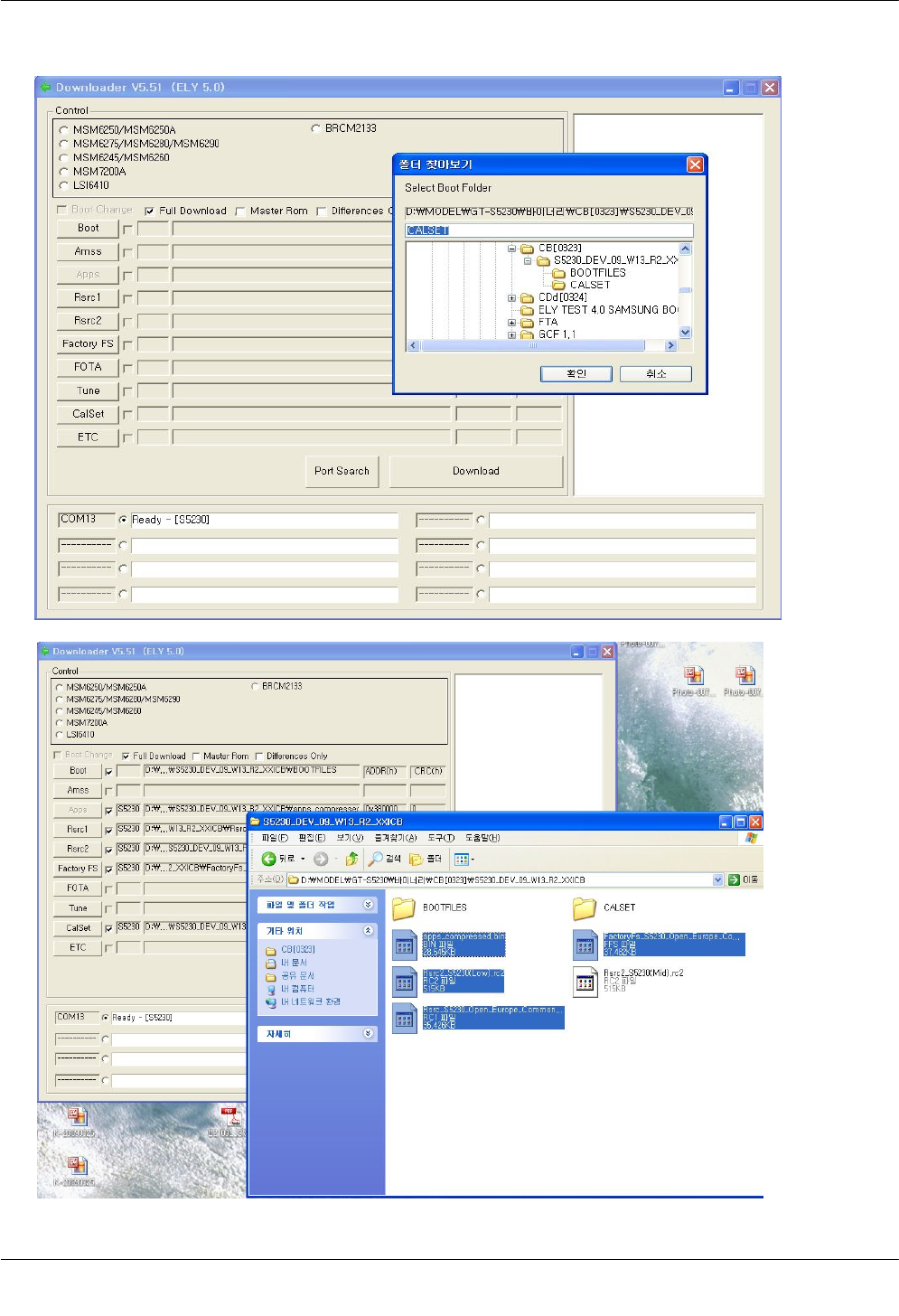
3.Execute the Downloader V5.51 (ELY x.0),When Complete DL.Bootloader.
Click the "Port Search" button.
SAMSUNG Proprietary-Contents may change without notice
Array course control
4-4
This Document can not be used without Samsung's authorization
4.Check the "Full Download". and
Select the file(s) what you want to download
-click 'Boot' to select aBoot folder.
-drag in Bin, Rc1, Rc2, Ffs files
-click 'calset' to select aCalset folder.
SAMSUNG Proprietary-Contents may change without notice
Array course control
4-5
This Document can not be used without Samsung's authorization
SAMSUNG Proprietary-Contents may change without notice
Array course control
4-6
This Document can not be used without Samsung's authorization
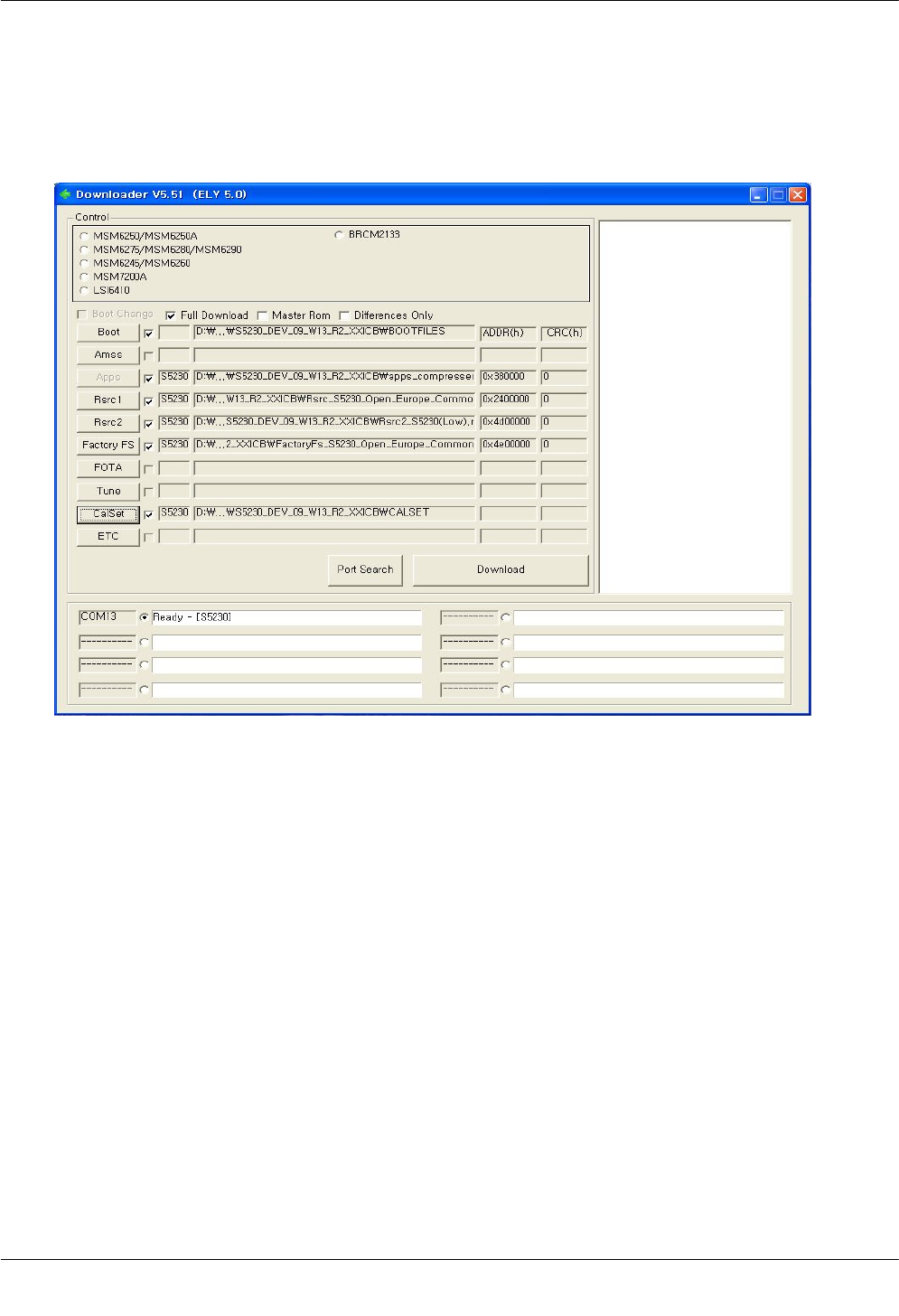
5.Check the All Download &Calset ,Click the Download Botton,
6.Confirm the downloaded version name and etc. :
*#1234#
Full Reset :
*0206*3855#

SAMSUNG Proprietary-Contents may change without notice
10.Reference data
10-1
This Document can not be used without Samsung's authorization
10-1. Reference Abbreviate
AAC:Advanced Audio Coding.
AVC :Advanced Video Coding.
BER :Bit Error Rate
BPSK:Binary Phase Shift Keying
CA :Conditional Access
CDM :Code Division Multiplexing
C/I :Carrier to Interference
DMB :Digital Multimedia Broadcasting
EN :European Standard
ES :Elementary Stream
ETSI:European Telecommunications Standards Institute
MPEG:Moving Picture Experts Group
PN :Pseudo-random Noise
PS :Pilot Symbol
QPSK:Quadrature Phase Shift Keying
RS :Reed-Solomon
SI :Service Information
TDM :Time Division Multiplexing
TS :Transport Stream

SAMSUNG Proprietary-Contents may change without notice
1. Safety Precautions
1-2
This Document can not be used without Samsung's authorization
1-1. Repair Precaution
●Repair in Shield Box, during detailed tuning.
Take specially care of tuning or test,
because specipicty of cellular phone is sensitive for surrounding interference(RF noise).
●Be careful to use akind of magnetic object or tool,
because performance of parts is damaged by the influence of manetic force.
●Surely use astandard screwdriver when you disassemble this product,
otherwise screw will be worn away.
●Use athicken twisted wire when you measure level.
Athicken twisted wire has low resistance, therefore error of measurement is few.
●Repair after separate Test Pack and Set because for short danger (for example an
overcurrent and furious flames of parts etc) when you repair board in condition of
connecting Test Pack and tuning on.
●Take specially care of soldering, because Land of PCB is small and weak in heat.
●Surely tune on/off while using AC power plug, because arepair of battery charger is
dangerous when tuning ON/OFF PBA and Connector after disassembing charger.
●Don't use as you pleases after change other material than replacement registered on SEC
System.
Otherwise engineer in charge isn't charged with problem that you don't keep this rules.

SAMSUNG Proprietary-Contents may change without notice
Safety Precautions
1-2
This Document can not be used without Samsung's authorization
1-2. ESD(Electrostatically Sensitive Devices) Precaution
Several semiconductor may be damaged easilly by static electricity. Such parts are called by
ESD(Electrostatically Sensitive Devices), for example IC,BGA chip etc. Read Precaution below.
You can prevent from ESD damage by static electricity.
●Remove static electricity remained your body before you touch semiconductor or parts with
semiconductor. There are ways that you touch an earthed place or wear static electricity
prevention string on wrist.
●Use earthed soldering steel when you connect or disconnect ESD.
●Use soldering removing tool to break static electricity. ,otherwise ESD will be damaged by
static electricity.
●Don't unpack until you set up ESD on product. Because most of ESD are packed by box
and aluminum plate to have conductive power,they are prevented from static electricity.
●You must maintain electric contact between ESD and place due to be set up until ESD is
connected completely to the proper place or acircuit board.

SAMSUNG Proprietary-Contents may change without notice
6. MAIN Electrical Parts List
6-1
This Document can not be used without Samsung's authorization
SEC CODE Design LOC Description
D301 0403-001749 DIODE-ZENER;PZU5.6B
ZD101,ZD102,ZD103 0404-001504 DIODE-SCHOTTKY;JDH2S01FS
ZD104 0404-001504 DIODE-SCHOTTKY;JDH2S01FS
D100 0406-001286 DIODE-TVS;PESD5V0L5UV
D101,D102,D303,D304 0406-001288 DIODE-TVS;PESD5V0S1UL
ZD301,ZD302 0406-001288 DIODE-TVS;PESD5V0S1UL
Q300 0502-001322 TR-POWER;PBSS301PD
U304 0801-003026 IC;NC7WZ86L8X
U200 0801-003130 IC;NC7SV17L6X
UME200 1108-000269 MEMORY;K522H1HACA-A060
U305 1201-002494 IC;TPA6201A1DRBR
PAM100 1201-002773 IC;SKY77344
U103 1201-002864 IC;MAX9877AERP-T
U301 1203-004604 IC;AAT3169IFO
U303 1203-005485 IC;MIC5365-3.0YMT
U300 1203-005562 IC;BCM59035C1IFB5G
U302 1203-005580 IC;MIC5365-1.8YMT
U104 1204-003026 IC;SI4709-B-GMR
U307 1205-003288 IC;TSC2007IYZGR
U106 1205-003754 IC;BCM2070B0KUBXG
UCP200 1205-003760 IC;BCM21332IFBG
U306 1209-001817 IC;BMA020
VR200 1404-001221 THERMISTOR;NCP15WB473J04RC
R210,R307 2007-000138 R-CHIP;RC1005J101CS
R113,R207 2007-000140 R-CHIP;RC1005J102CS
R204,R205 2007-000141 R-CHIP;RC1005J222CS
R208,R313,R314 2007-000143 R-CHIP;RC1005J472CS
R128,R209,R211,R212 2007-000144 R-CHIP;RC1005J512CS
R213 2007-000144 R-CHIP;RC1005J512CS
R138 2007-000151 R-CHIP;RC1005J153CS
R126,R127,R129,R130 2007-000157 R-CHIP;RC1005J473CS
R121,R122,R132,R140 2007-000162 R-CHIP;RC1005J104CS
R142,R223,R301 2007-000162 R-CHIP;RC1005J104CS
R124 2007-000165 R-CHIP;RC1005J204CS
R109,R115,R117 2007-000171 R-CHIP;WR0402X000JT
R137 2007-000172 R-CHIP;RC1005J100CS

SAMSUNG Proprietary-Contents may change without notice
Main Electrical Parts List
6-2
This Document can not be used without Samsung's authorization
R111 2007-001301 R-CHIP;MCR01MZP5J680
R219,U311 2007-001319 R-CHIP;RC1005J122CS
R136 2007-001333 R-CHIP;MCR01MZP5J183
R125,R131 2007-002796 R-CHIP;MCR01MZP5J511
R118,R119 2007-003010 R-CHIP;RC1005J200CS
R206 2007-003014 R-CHIP;TSR16GJ244V
R105 2007-003018 R-CHIP;RMC16S-430J-TP
R304 2007-007100 R-CHIP;RK73K1ETP106J
R306,R312 2007-007107 R-CHIP;RC1005F1003CS
R310,R311 2007-007156 R-CHIP;RC1005J1ROCS
R114,R116 2007-007189 R-CHIP;TSR16GJ9R1V
R200 2007-007193 R-CHIP;TSR16GJ5R1V
R217 2007-007312 R-CHIP;MCR01MZP5F2002
R222 2007-007315 R-CHIP;MCR01MZP5F3901
R308,R309 2007-007489 R-CHIP;RK73H1ETP1503F
R123,R133,R134,R143 2007-007528 R-CHIP;RK73H1ETP1501F
R201,R202 2007-007981 R-CHIP;ERJ2RKF1803X
R305 2007-008275 R-CHIP;MCR01MZP5F303
R203 2007-008401 R-CHIP;RC1005F754CS
R302 2007-010071 R-CHIP;MCR10EZHFLR100
C179,C235 2203-000233 C-CERAMIC,CHIP;GRP1555C1H101J
C152,C157,C159,C315 2203-000254 C-CERAMIC,CHIP;GRP155R71C103K
C340 2203-000254 C-CERAMIC,CHIP;GRP155R71C103K
C151,C158 2203-000278 C-CERAMIC,CHIP;GRP1555C1H100D
C143,C148,C149,C153 2203-000386 C-CERAMIC,CHIP;GRP1555C1H150J
C154,C165,C167,C170 2203-000386 C-CERAMIC,CHIP;GRP1555C1H150J
C124,C218,C316,C317 2203-000425 C-CERAMIC,CHIP;GRP1555C1H180J
C130,C155,C168,C233 2203-000438 C-CERAMIC,CHIP;GRP155R71H102K
C166 2203-000466 C-CERAMIC,CHIP;GRP1555C1H1R0C
C338,C342 2203-000489 C-CERAMIC,CHIP;GRP155R71H222K
C227 2203-000679 C-CERAMIC,CHIP;GRP1555C1H270J
C116,C122,C127,C142 2203-000812 C-CERAMIC,CHIP;GRP1555C1H330J
C161 2203-000812 C-CERAMIC,CHIP;GRP1555C1H330J
C232 2203-000854 C-CERAMIC,CHIP;GRP1555C1H390J
C204,C215,C229 2203-000995 C-CERAMIC,CHIP;GRP1555C1H470J
C146,C147 2203-001072 C-CERAMIC,CHIP;GRP1555C1H560JD01E
C223 2203-001101 C-CERAMIC,CHIP;GRP155R71E682KA01E

SAMSUNG Proprietary-Contents may change without notice
Main Electrical Parts List
6-3
This Document can not be used without Samsung's authorization
C178,C180 2203-001153 C-CERAMIC,CHIP;GRP1555C1H680J
C128 2203-001221 C-CERAMIC,CHIP;GRP155R71H821KD01E
C119 2203-002668 C-CERAMIC,CHIP;C1005CG1H0R5BT
C343,C344 2203-003054 C-CERAMIC,CHIP;GRP1555C1H9R0C
C117 2203-005056 C-CERAMIC,CHIP;GRP1555C1H6R8CZ01E
R112 2203-005288 C-CERAMIC,CHIP;GRP1555C1H1R0BZ01E
C132 2203-005344 C-CERAMIC,CHIP;GRM155R71E223KA61D
C123,C144,C160,C163 2203-005482 C-CERAMIC,CHIP;GRP155R61A104KA01E
C171,C226,C236 2203-005482 C-CERAMIC,CHIP;GRP155R61A104KA01E
C131,C133,C174,C201 2203-006048 C-CERAMIC,CHIP;GRM155R71A104K
C202,C207,C209,C210 2203-006048 C-CERAMIC,CHIP;GRM155R71A104K
C211,C212,C213,C216 2203-006048 C-CERAMIC,CHIP;GRM155R71A104K
C336 2203-006048 C-CERAMIC,CHIP;GRM155R71A104K
C162,C320,C334 2203-006208 C-CERAMIC,CHIP;CM105X5R475M06AT
C134,C135,C136,C137 2203-006260 C-CERAMIC,CHIP;GRM155R61A224KE19E
C139,C140 2203-006260 C-CERAMIC,CHIP;GRM155R61A224KE19E
C304 2203-006324 C-CERAMIC,CHIP;GRM188R61A225KE19D
C310 2203-006348 C-CERAMIC,CHIP;CV105X5R105K25AT
C138,C141,C145,C172 2203-006399 C-CERAMIC,CHIP;GRM155R60J105KE19D
C175,C206,C208,C214 2203-006399 C-CERAMIC,CHIP;GRM155R60J105KE19D
C217,C230,C231,C305 2203-006399 C-CERAMIC,CHIP;GRM155R60J105KE19D
C309,C311,C313,C328 2203-006399 C-CERAMIC,CHIP;GRM155R60J105KE19D
C339,C341,C345,C346 2203-006399 C-CERAMIC,CHIP;GRM155R60J105KE19D
C347,C348,C349,C350 2203-006399 C-CERAMIC,CHIP;GRM155R60J105KE19D
C351 2203-006399 C-CERAMIC,CHIP;GRM155R60J105KE19D
C300,C301,C303,C312 2203-006562 C-CERAMIC,CHIP;CV05X5R105K10AH
C314,C323 2203-006562 C-CERAMIC,CHIP;CV05X5R105K10AH
C150,C164,C203,C205 2203-006872 C-CERAMIC,CHIP;GRM155R60J225ME15D
C219,C220,C222,C224 2203-006872 C-CERAMIC,CHIP;GRM155R60J225ME15D
C307,C308,C319,C321 2203-006872 C-CERAMIC,CHIP;GRM155R60J225ME15D
C322,C324,C325,C326 2203-006872 C-CERAMIC,CHIP;GRM155R60J225ME15D
C329,C332,C333,C352 2203-006872 C-CERAMIC,CHIP;GRM155R60J225ME15D
C327,C330 2203-006890 C-CERAMIC,CHIP;CV105X5R106M06AT
TA301 2404-001339 C-TA,CHIP;TEESVJ1A475M8R
TA102 2404-001377 C-TA,CHIP;F980J226MMA
TA100,TA101,TA300 2404-001381 C-TA,CHIP;F981A106MMA
TA302 2404-001430 C-TA,CHIP;TCSHL1A106MRAR

SAMSUNG Proprietary-Contents may change without notice
Main Electrical Parts List
6-4
This Document can not be used without Samsung's authorization
L109,L113 2703-001729 INDUCTOR-SMD;LL1005-FH1N8S
L119,L123 2703-001748 INDUCTOR-SMD;LL1005-FH5N6S
L132,L133 2703-002201 INDUCTOR-SMD;CIH05T33NJNC
C112,L104,L107 2703-002203 INDUCTOR-SMD;CIH05T15NJNC
C118 2703-002204 INDUCTOR-SMD;CIH05T22NJNC
L115,L117 2703-002206 INDUCTOR-SMD;CIH05T39NJNC
L103,L108,L110,L112 2703-002208 INDUCTOR-SMD;CIH05T2N2SNC
L101 2703-002267 INDUCTOR-SMD;CIH05T4N7SNC
L105 2703-002314 INDUCTOR-SMD;CIH05T47NJNC
L120,L122 2703-002551 INDUCTOR-SMD;LQW15AN33NH00D
L114,L118 2703-003145 INDUCTOR-SMD;LQW15AN5N1B00D
L134 2703-003476 INDUCTOR-SMD;LQG15HSR27J02D
L300,L301 2703-003545 INDUCTOR-SMD;LQM2MPN2R2NG0
OSC300 2801-004373 CRYSTAL-UNIT;CC7V-T1A
OSC200 2801-004815 CRYSTAL-UNIT;FCX05-LFHF
F301,F302,F303 2901-001451 FILTER-EMI SMD;ICVE10054E250R500FR
F101 2901-001544 FILTER-EMI SMD;AMLV-14S-03Q-012-300F
F100 2909-001312 FILTER-DUPLEXER;LCB10B2450K3
U100 2911-000123 FILTER;LMSP43NA-794
L125,L126 3301-001438 CORE-FERRITE BEAD;BLM15BB750SN1D
L136,L200,L201 3301-001659 CORE-FERRITE BEAD;BLM15AG601SN1
L127,L129 3301-001729 CORE-FERRITE BEAD;BLM15AG102SN1D
L302,L303 3301-001756 CORE-FERRITE BEAD;BLM15HG102SN1D
L128,L131 3301-001812 CORE-FERRITE BEAD;BLM15HD102SN1
L124 3301-001970 CORE-FERRITE BEAD;BLM15BA330SN1
RFS100 3705-001448 CONNECTOR-COAXIAL;20369-001E
RFS101 3705-001503 CONNECTOR-COAXIAL;KMS-560
CN300 3708-002211 CONNECTOR-FPC/FFC/PIC;FF12-21A-R12BN-D3
CD100 3709-001465 CONNECTOR-CARD EDGE;NDTF-6S8M-311
IFC100 3710-002681 CONNECTOR-SOCKET;HY20-AB0360
HEA301 3711-006028 CONNECTOR-HEADER;14-5805-040-000-829
BTC300 3711-006924 CONNECTOR-HEADER;2005-03-242
BAT300 4302-001181 BATTERY;ML414RU2-TT36-TP1
SAMSUNG Proprietary-Contents may change without notice
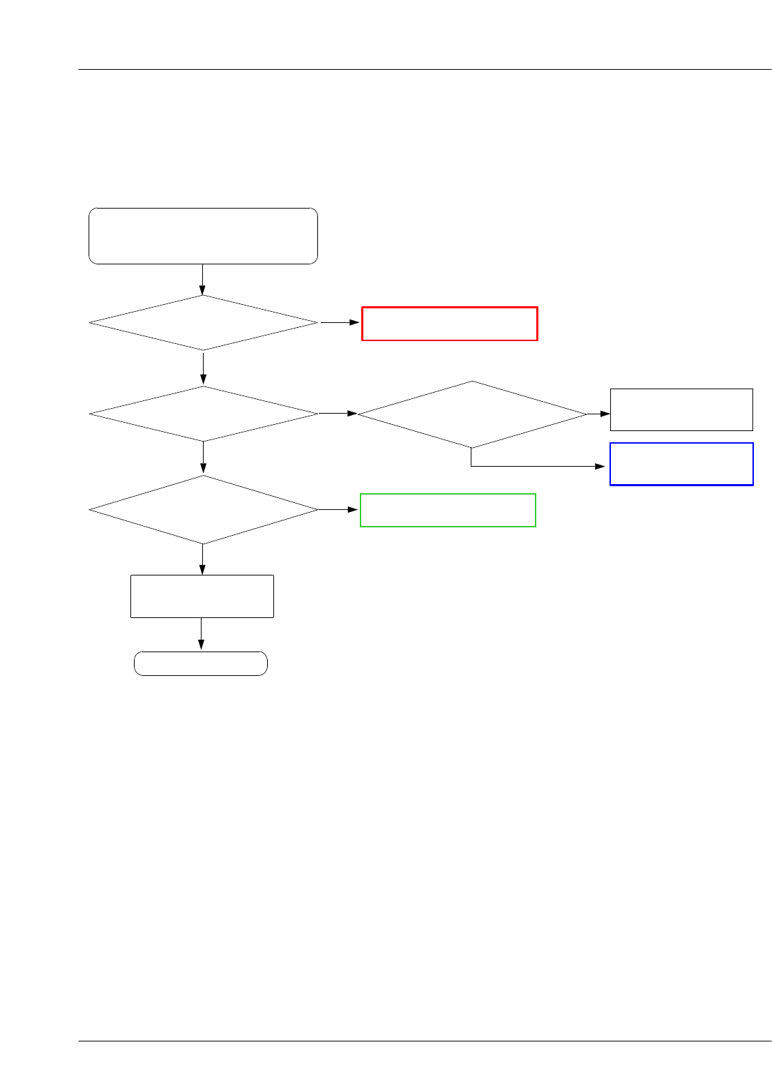
9. Flow Chart of Troubleshooting
This Document can not be used without Samsung's authorization
9-1
9-1. Power On
Check the current consumption
more than 100mA
'Power On 'does not work
Yes
Yes
No
Download again
Check the VBAT
more than 3.3V
No
Check the Battery
Yes
Check the related circuit
No
C300(VBAT)=3.0
V?
Yes
①
Check the U300
No
Check the MEM_1.8V of U300
is more than 1.8V
1.8V
Yes
Check U300
3.0V_DIG =3.0V
3.0V_ANLG =3.0V
1.2V_ANLG =1.2V
②
No
Check the U300 and C352, C319, C333
Yes
③
Yes
Yes
Check the clock 32KHz_DIGIT
No
Check CLK32K
Freq =32
KHz
Check the initial operation
END
SAMSUNG Proprietary-Contents may change without notice
This Document can not be used without Samsung's authorization
Flow Chart of Troubleshooting
9-2
UMP
1005
643C
213C
4L
1ODLCHV 5L
2ODLCHV
6L
1ODLSMV 7L
2ODLSMV
8L
1ODLXUAV 9L
2ODLXUAV
K7
VMSBAT
K8
VAXBAT
9K SAIB_CTN
1L
DNGRSCV
L10
BAT_PRSNT
11L DNG_PBFER
2L
LRSCV
3L
ODLOIV
1K
TABRSCV
01K DNG_CTN
11K PBFER 2K
BFRSCV
K3
VIVCC
K4
VHBAT1K5
VHBAT2
K6AVSS
J2AVSS
3J 2DELMWP
4J
SNS_
1
ODL
C
H
V5J
SNS_2ODLCHV
J6AVSS
J7AVSS
CTN
8J
9J 2TSETANA
H5AVSS
H6AVSS
H7AVSS
H8AVSS
9H 1TSETANA
1J
\YKNOP
J10
PDRIVE
11J
TABBV
G8
G9AVSS
1H 23KLC
01H
PCC
H11
VCHGR
2H TUO_DI
H3
VOFFBUS\
AVSS
H4
G10
VMBAT_SNS
11G
BFBV
2G 2TATS
3G 2OIPG
G4AVSS
G5AVSS
G6AVSS
G7AVSS
AVSS
F3VSSC
F4AVSS
F5AVSS
F6AVSS
F7AVSS
F8AVSS
9F NI_DI
1G 1TATS
E6AVSS
E7AVSS
E8AVSS
E9AVSS
F1
VDDO
F10
RSENSE
11F
1SUBTSBV
2F \NDHSGTO|1OIPG
D9AVSS
1E
RGHCSIDV
01E
1WSBV 11E
2WSBV
2E ADS
3E LCS
E4AVSS
E5AVSS
11D
2SUBTSBV
2D \TESER
3D \TNI
D4AVSS
D5AVSS
D6AVSS
D7AVSS
D8AVSS
4C 0TSETGID
C5AVSS
C6AVSS
C7AVSS
C8AVSS
9C 2CP
1D ILATX
01D DNGU
B7
VABAT
B8
VLCLDOB9
VLSBAT
1C OLATX
C10AVSS
11C \DCA
C2AVSS
3C 1TSETGID
1B
TABRSOIV
01B
CN
11B 1SNSGF
2B
BFRSOIV
3B
2ODLVLV
4B
1ODLVLV
B5AVSS
B6
VRFBAT
2A
LRSOIV
3A 1DELMWP
VLVVDDA4
A5
VRFLDO1A6
VRFLDO2
7A
2ODLAV
8A
1ODLAV
9A
ODLMISV
1
CN 2
CN
1A
DNGRSOIV
01A 1CP
11A 2SNSGF
003U
103L
623C
303PT
323C
103PT
403C
5001
113C
5001
013C
123C
313C
303C
803C
823C813C713C
1005
203PT
1
003TAB
2
003L
703C
Fn0022
5001
103C
5001
203C
5
4C
6
E
4
003Q
3
B
1
1C
2
2C
3C
923C
303R
5001
K1
513C
543C
1005
403PT
613C913C
01003R
423C
1005
003CSO
003PT
903C
403R
723C413C
1.0203R
003AT
223C523C
003C
023C
TABV
TABV
EROCV_V2.1
MEM_V8.1
NI_CD
QER_KLC
TESER_BB
T
ABV
CP
K23KLC
TED_CCA
QRI_UMP
ADS
LCS
BIV
_
V2.3
THGIL_YEK_V2.3
GLNA_V0.3
1PMA_V0.3
DS_V0.3
GTOBSU_V5.2
FRV_V7.2
FRV_
V3.1
OXCV_V3.1
SUBV
YEKNOP
GID_V0.3
CCVMIS
MARVN_BSU_V3.3
DCL_V9.2
OI_MAC_V8.2
GLNA_V2.1
PUKCAB
2
C
2
C
C237
2
C
C300
C301
C302
C303
C304
6
0
3
C
C307
C309
C310
C311
C312
C313
C314
C315
C316
C317
C318
C319
C320
C321
C322
2
3
C
5
2
3
C
C326
C327
C328
9
2
3
C
C345
C346
3
4
C
0
0
5
C
L300
1
0
3
L
OSC300
R205
R206
R218
R300
R302
3
0
3
R
R304
1
R
2
1
4
R
0
0
3
A
T
6
2
2
P
T
TP300
1
0
3
P
T
TP302
TP303
4
0
3
P
T
TP400
0
0
3
U
SAMSUNG Proprietary-Contents may change without notice
Flow Chart of Troubleshooting
This Document can not be used without Samsung's authorization
9-3
9-2. Initial
Initial Failure
Yes
U300 pin D2 (RESET/)="
H"?
(check the test point) No
Check the circuit related to reset
Yes
Check the 16bit data signal
&memory CE
END
Yes
SAMSUNG Proprietary-Contents may change without notice
This Document can not be used without Samsung's authorization
Flow Chart of Troubleshooting
9-4
)DNAN kcolB egraL(YROMEM
)MARDD bM215 + DNAN bG1(
MEM_V8.1
122PT
322PT
012PT
402PT
702PT
UND 2P
UND 9P
VSSD
N4
VSSN
N5
VCCQNN6
VCCNN7
VSSN
N8
CN 9N
1P
UND
UND 01P
6M N11OI
N31OI
7M
N5
1
OI
8M
D4A
9M
UND 1N
UND 01N
CN 2N
D51QD
3N
6L N3OI
N5OI
7L
N7OI
8L
D5A
9L
VDDDM2
D31QD
3M
D
41QD
4M
N9OI
5M
6K N01OI
N21OI
7K
N41OI
8K
D6A
9K
VSSQD
L2
D11QD
3L
D21QD
4L
N1OI
5L
6J N2OI
N4OI
7J
N6OI
8J
D7A
9J
VDDQDK2
D9QD
3K
D01QD
4K
N8OI
5K
CN 6H
D8A
7H
D9A
8H
D11A
9H
VSSQD
J2
DSQDU 3J
D8QD
4J
N0OI
5J
CN 6G
7G D21A
DEKC 8G
VDDDG9
VDDDH2
DMDU 3H
DKC 4H
CN 5H
CN 6F
DSAC 7F
8F
DEW_
VSSD
F9
VSSD
G2
DM
D
L3G
DKC_ 4G
CN 5G
NB|R 6E
DSAR 7E
CN 8E
9E
DSC
VDDQDF2
DSQDL 3F
D7QD
4F
NPW 5F
NEW_ 6D
D0AB
7D
D1AB
8D
9D D01A
VSSQD
E2
D6QD
3E D5QD
4E
NER_ 5E
NEC 6C
D0A
7C
D1A
8C
9C D2A
VDDQDD2
D4QD
3D D3QD
4D
NELA 5D
VCCNB6
CN 7B
D
3
A
8B
CN 9B
VSSD
C2
D2QD
3C D1QD
4C
NELC 5C
UND 2A
UND 9A
UND 1B
UND 01B
CN 2
B
D0QD
3B
VDDDB4
VSSN
B5
002EMU
CN 1
CN 2
01A
UND
512PT412PT
022PT
212PT
802PT
932C
1005
042C
1005
912PT
812PT
302PT
902R
602PT
902PT
MEM_V8.1
222PT
712PT
502PT
612PT
312PT
)0(QDD
)51:0(QDD
)11(QDD
)01(QDD
)9(QDD
)8(QDD
)7(QDD
)6(QDD
)5(QD
D
)4(QDD
)3(QDD
)2(QDD
)1(QDD
)5(QDAF
)4(QDAF
)3(QDAF
)2(QDAF
)1(QDAF
)0(QDAF
)51:0(QDAF )51(QDD
)41(QDD
)31(QDD
)21
(QDD
)21:0(AD
)51(QDAF
)41(QDAF
)31(QDAF
)21(QDAF
)11(QDAF
)01(QDAF
)9(QDAF
)8(QDAF
)7(QDAF
)6(QDAF
)01(AD
)9(AD
)8
(AD
)7(AD
)6(AD
)5(AD
)4(AD
)3(AD
)2(AD
)1(
A
D
)0(AD
)21(AD
)11(AD
ELA_DNAN
NSACD
NSARD
YDRN
NECDNAN
EKCD
ELC_DNAN
ECRDD
PWF
NEO
NEWD
NEW
1SQDD
1MQDD
0SQDD
0MQDD
1ABD
0ABD
NKLCD
KLCD
9
3
2
C
0
4
2
C
C241
C242
C243
OSC200R210
1
1
2
R
2
1
2
R
3
1
2
R
4
1
2
R
R215
3
0
2
P
T
4
0
2
P
T
TP206TP207
TP208
0
1
2
P
T
1
1
2
P
T
2
1
2
P
T
4
1
2
P
T
TP216
8
1
2
P
T
TP220
TP222
TP223
TP224
TP227
8
2
2
P
T
TP504
0
0
2
U
0
0
2
E
M
U
SAMSUNG Proprietary-Contents may change without notice
Flow Chart of Troubleshooting
This Document can not be used without Samsung's authorization
9-5
9-3. Charging Part
Yes
Resolder or replace U300
Check the circuit related to
AUX_ON signal
Check the circuit related to
V_EXT_CHARGE
Yes
No
Check the U300 pin K11
≒1.25V
Yes
No
TP304 pin (ACC_DET)
="
L"?
Yes
No
END
Abnormal charging part
Check the U300 pin H11
>5.0V
SAMSUNG Proprietary-Contents may change without notice
This Document can not be used without Samsung's authorization
Flow Chart of Troubleshooting
9-6
UMP
1005
643C
213C
4L
1ODLCHV 5L
2ODLCHV
6L
1ODLSMV 7L
2ODLSMV
8L
1ODLXUAV 9L
2ODLXUAV
K7
VMSBAT
K8
VAXBAT
9K SAIB_CTN
1L
DNGRSCV
L10
BAT_PRSNT
11L DNG_PBFER
2L
LRSCV
3L
ODLOIV
1K
TABRSCV
01K DNG_CTN
11K PBFER 2K
BFRSCV
K3
VIVCC
K4
VHBAT1K5
VHBAT2
K6AVSS
J2AVSS
3J 2DELMWP
4J
SNS_
1
ODL
C
H
V5J
SNS_2ODLCHV
J6AVSS
J7AVSS
CTN
8J
9J 2TSETANA
H5AVSS
H6AVSS
H7AVSS
H8AVSS
9H 1TSETANA
1J
\YKNOP
J10
PDRIVE
11J
TABBV
G8
G9AVSS
1H 23KLC
01H
PCC
H11
VCHGR
2H TUO_DI
H3
VOFFBUS\
AVSS
H4
G10
VMBAT_SNS
11G
BFBV
2G 2TATS
3G 2OIPG
G4AVSS
G5AVSS
G6AVSS
G7AVSS
AVSS
F3VSSC
F4AVSS
F5AVSS
F6AVSS
F7AVSS
F8AVSS
9F NI_DI
1G 1TATS
E6AVSS
E7AVSS
E8AVSS
E9AVSS
F1
VDDO
F10
RSENSE
11F
1SUBTSBV
2F \NDHSGTO|1OIPG
D9AVSS
1E
RGHCSIDV
01E
1WSBV 11E
2WSBV
2E ADS
3E LCS
E4AVSS
E5AVSS
11D
2SUBTSBV
2D \TESER
3D \TNI
D4AVSS
D5AVSS
D6AVSS
D7AVSS
D8AVSS
4C 0TSETGID
C5AVSS
C6AVSS
C7AVSS
C8AVSS
9C 2CP
1D ILATX
01D DNGU
B7
VABAT
B8
VLCLDOB9
VLSBAT
1C OLATX
C10AVSS
11C \DCA
C2AVSS
3C 1TSETGID
1B
TABRSOIV
01B
CN
11B 1SNSGF
2B
BFRSOIV
3B
2ODLVLV
4B
1ODLVLV
B5AVSS
B6
VRFBAT
2A
LRSOIV
3A 1DELMWP
VLVVDDA4
A5
VRFLDO1A6
VRFLDO2
7A
2ODLAV
8A
1ODLAV
9A
ODLMISV
1
CN 2
CN
1A
DNGRSOIV
01A 1CP
11A 2SNSGF
003U
103L
623C
303PT
323C
103PT
403C
5001
113C
5001
013C
123C
313C
303C
803C
823C813C713C
1005
203PT
1
003TAB
2
003L
703C
Fn0022
5001
103C
5001
203C
5
4C
6
E
4
003Q
3
B
1
1C
2
2C
3C
923C
303R
5001
K1
513C
543C
1005
403PT
613C913C
01003R
423C
1005
003CSO
003PT
903C
403R
723C413C
1.0203R
003AT
223C523C
003C
023C
TABV
TABV
EROCV_V2.1
MEM_V8.1
NI_CD
QER_KLC
TESER_BB
T
ABV
CP
K23KLC
TED_CCA
QRI_UMP
ADS
LCS
BIV
_
V2.3
THGIL_YEK_V2.3
GLNA_V0.3
1PMA_V0.3
DS_V0.3
GTOBSU_V5.2
FRV_V7.2
FRV_
V3.1
OXCV_V3.1
SUBV
YEKNOP
GID_V0.3
CCVMIS
MARVN_BSU_V3.3
DCL_V9.2
OI_MAC_V8.2
GLNA_V2.1
PUKCAB
2
C
2
C
C237
2
C
C300
C301
C302
C303
C304
6
0
3
C
C307
C309
C310
C311
C312
C313
C314
C315
C316
C317
C318
C319
C320
C321
C322
2
3
C
5
2
3
C
C326
C327
C328
9
2
3
C
C345
C346
3
4
C
0
0
5
C
L300
1
0
3
L
OSC300
R205
R206
R218
R300
R302
3
0
3
R
R304
1
R
2
1
4
R
0
0
3
A
T
6
2
2
P
T
TP300
1
0
3
P
T
TP302
TP303
4
0
3
P
T
TP400
0
0
3
U
SAMSUNG Proprietary-Contents may change without notice
Flow Chart of Troubleshooting
This Document can not be used without Samsung's authorization
9-7
9-4. Sim Part
Phone can't access SIM Card
Yes
①
Check the SIMVCC =3.0V
No
Check the circuit related to R316, C172
Yes
②
Check the SIM connector's
connector's to SIM card resolder or change CD100
No
③
Yes
Check the related circuit of CD100
No
Check the circuit around CD100
input circuitry
Yes
END
SAMSUNG Proprietary-Contents may change without notice
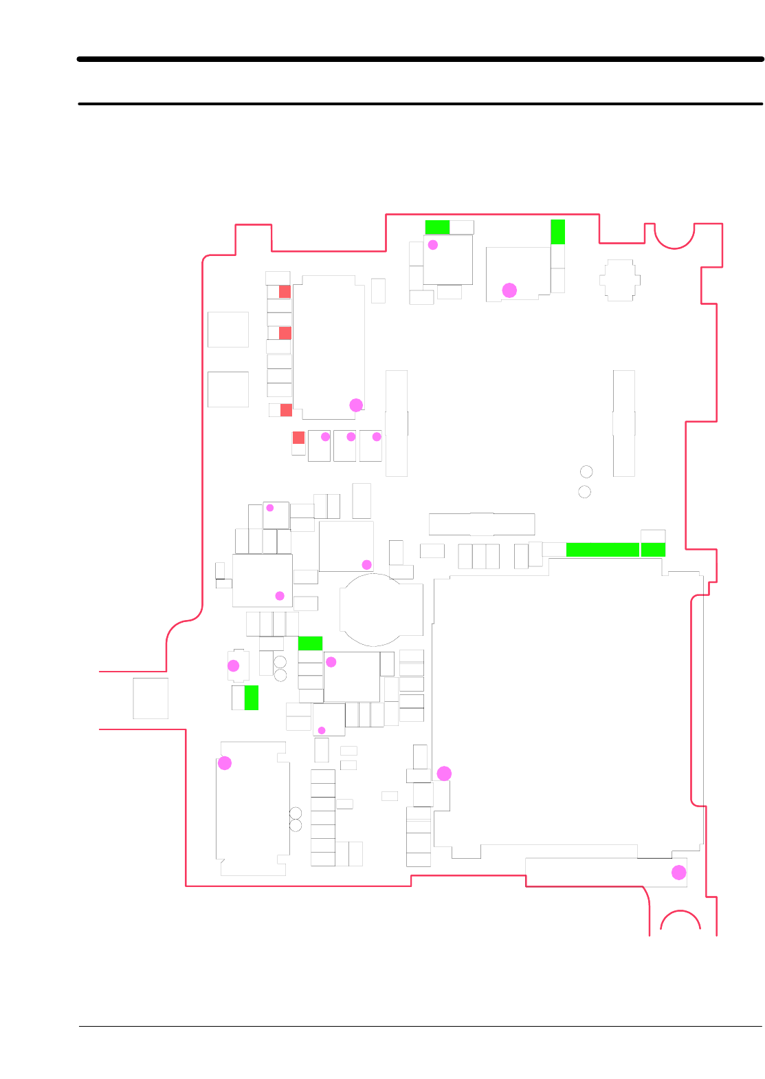
This Document can not be used without Samsung's authorization
Flow Chart of Troubleshooting
9-8
R
OTCENNOCMIS
433C
333C
1005
633C
1005
733C
CCVMIS
1005
213R
533C
61
G
5
66
77
88
99 G
3141
GG
51
11
0101
1111
2121
22
433 4
5
003MIS
OIMIS
KLCMIS
TSRMIS
C102
3
3
3
C
4
3
3
C
C335
C336
C337
C423 R222
2
1
3
R
SIM300
ZD400
SAMSUNG Proprietary-Contents may change without notice
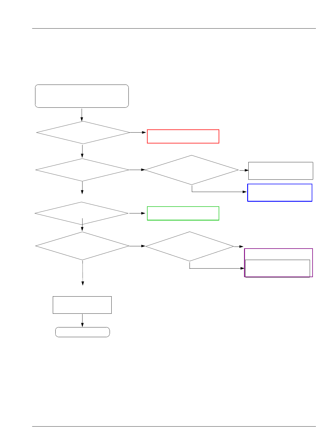
Flow Chart of Troubleshooting
This Document can not be used without Samsung's authorization
9-9
9-5. Microphone Part
Microphone does not work
Yes
Resolder MIC
Check the connection
from MIC
No
Check the circuit related to R142
Check the JACK_IN =
3.0V ?
Yes
Check the path from Main IC to MIC
Check the circuit
from UCP200to MIC
No
Yes
Replace the MIC
Check the MIC No
Yes
END
SAMSUNG Proprietary-Contents may change without notice
This Document can not be used without Samsung's authorization
Flow Chart of Troubleshooting
9-10
4
5
6
004D
1
2
3
11NI
2NI
2
33NI
44NI
5
1TUO
2TUO
6
7
3TUO
8
4TUO
004F
DNG
901
DNG
CN 22
CN 32
42
CN
CN 52
62
CN
72
CN
3
3
44
5
5
66
7
7
88
9
9
12
CN
41 41
51
51
61 61
71
71
81 81
91
91
22
02 02
0
04CFI
1
1
01 01
11
11
21 21
31 31
004DZ
5001
514R
204AT GID_V0.3
524C
1NS201DH51MLB504L
TABV
1NS201DH51MLB404L
624C
5001
324C
004PT
NI_CD
1005
134C
704R
GID_V0.3
GID_V0.3
234C
114R
0
1
5001
214R
334C
1005
314R
1005
824C
1005
414R
HCTIWS_RAE
SUBV
NI_KCAJ
5001
614R
J_XT_ATRAU
J_XR_ATRAU
J_TED_CCA
+D
-D
L_KPSRAE
R_KPSRAE
XT_ATRAU
XR_ATRAU
TED_CCA
TNA_MF
2
0
2
C
8
1
2
C
5
3
2
C
C237
3
3
4
C
0
0
4
F
0
0
4
C
F
I
0
0
2
L
R205
R206
7
0
4
R
1
1
4
R
2
1
4
R
R413
R414
R415
R416
2
0
4
A
T
SAMSUNG Proprietary-Contents may change without notice
Flow Chart of Troubleshooting
This Document can not be used without Samsung's authorization
9-11
9-6. Speaker Part(Melody)
Speaker does not work
Is the terminal of speaker
OK? check the specker
No
Yes
No
Resolder SPK_P (R117) &SPK_N
(R115)
Check the
SPK_P &SPK_N
"HIGH"
Yes
①
Yes
②
Change speaker
Is speaker OK?
END
No
No
Yes
Check the output circuit of
U103(Audio AMP) Change or resolder around U103
SAMSUNG Proprietary-Contents may change without notice
This Document can not be used without Samsung's authorization
Flow Chart of Troubleshooting
9-12
004C
T
A
B
V
314C
004AT
1005
814C
1005
804C
V01704C
5001
V01604C
5001
104R
004R
1005
224C
3B
B1
VDD
A3VSS
2
+TUO 5B
-TUO 5D
PGND
C4
C5
PVDD
4B +NIXR
4D -NIXR
3C LCS
ADS
D3
LPH 2A
1A
RPH
2D 1ANI
2ANI
1D
1BNI
2C
1C 2BNI
1
CN
CN
004MAP
2B SAIB
4A
N1C 5A
P1C
GND
404C
5001
414C
304C 304R
114C214C
504C
014C904C
5001
204R
5001
ADS
LCS
TUOR_MF
TUOL_MF
N_PMA
R_RAE
L_RAE
L_KPSRAE
P_KPS
N_KPS
R_KPSRAE
P_PMA 204C
2
3
3
C
8
3
3
C
C339
C340
0
0
4
C
2
0
4
C
3
0
4
C
4
0
4
C
5
0
4
C
6
0
4
C
7
0
4
C
8
0
4
C
9
0
4
C
0
1
4
C
1
1
4
C
2
1
4
C
C413
C414
8
1
4
C
2
2
4
C
C501
C502
3
0
5
C
4
0
5
C
1
0
5
D
D505
PAM400
3
1
3
R
R400
R401
2
0
4
R
3
0
4
R
3
0
5
R
4
0
5
R
5
0
5
R
0
0
4
A
T
2
0
3
U
0
0
5
V
SAMSUNG Proprietary-Contents may change without notice
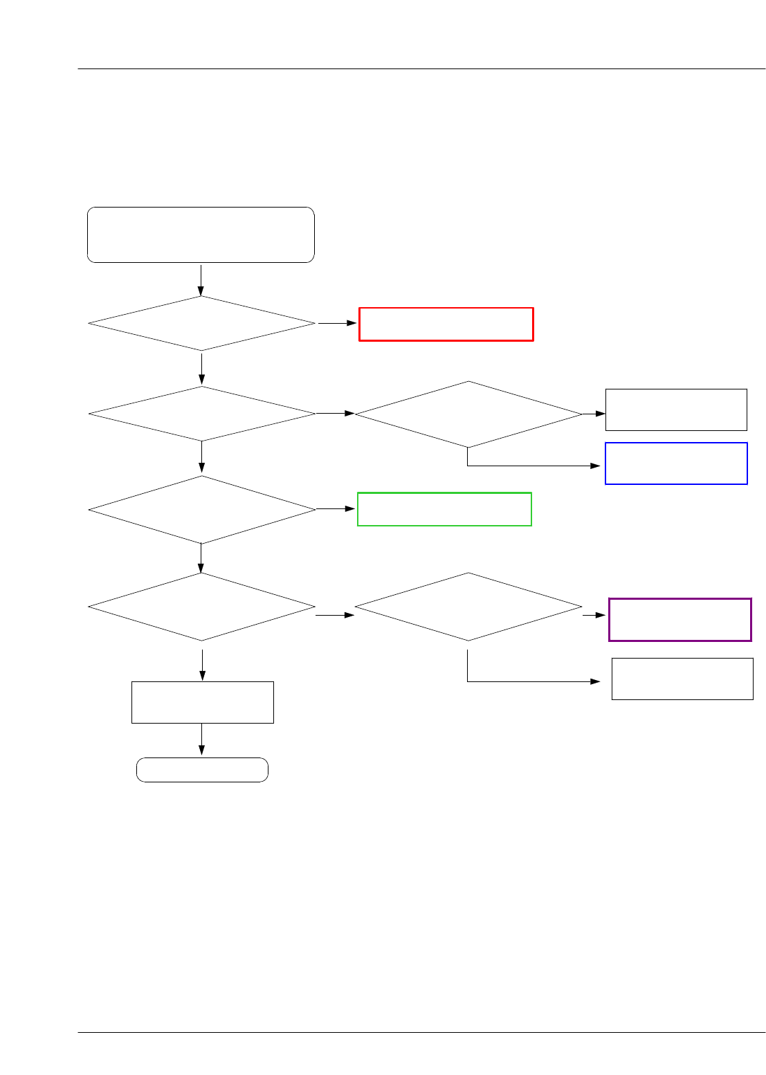
Flow Chart of Troubleshooting
This Document can not be used without Samsung's authorization
9-13
9-7. Key Data Input
ROTCENNOC YEK
YEK EMULOV
105D205D
1005
V501
V500
1005
305D
005C
605R
505R
33
44
005KV
1
1
22
4
5
5
6
6
77
88
9
9
51 51
61 61
71
71
81
81
91 91
2
2
02 02
33
4
005CDH
1
1
01
01
11 11
21 21
31
31
41
41
THGIL_YEK_V2.3
405D
00
5D
16543
)0(WOR_YEK
)2(WOR_YEK
)4(WOR_YEK
)3(LOC_YEK
)0(LOC_YEK
)1(LOC_YEK
)2(LOC_YEK
YEKNO
P
)2(WOR_YEK
)4(LOC_YE
K
N_NI_CIM
P_NI_CIM
)3(LOC_YEK)0(WOR_YEK
)1(WOR_YEK
)3(WOR_YEK
Check Initial Operation
Yes
When one of the keys is
pushed,
is it displayed on LCD?
Check the Dome sheet &Key Pad
No
Yes
When one of the keys is
pushed,
KBIO signal is OK?
Replace the Key PBA
No
Yes
END
SAMSUNG Proprietary-Contents may change without notice
This Document can not be used without Samsung's authorization
Flow Chart of Troubleshooting
9-14
9-8. Camera part
"Camera" function does not work
Yes
Check the Camera
connector on PBA
Reconnect the camera module
No
Yes
Is there another problem?
Yes
Replace the camera
module
END
SAMSUNG Proprietary-Contents may change without notice
Flow Chart of Troubleshooting
This Document can not be used without Samsung's authorization
9-15
9-9. Radio part
OID
A
RMF
301C
201R
VIO
01
RCLK
9
DNGFR
3
TUOR 31
TSR
5
SCLK
87
SDIO
6DDVNES 11
81
GPO2|_INT
GPO3|DCLK
71
TUOL 41
IPL
4
CN
1
NC
02
22
NC
NC
32
SFD 61
TUOD 51
IMF
2
DNG 21
GND
12 91
GPO1
001U
001PT
GID_V0.3
401C
GID_V0.3
201PT
20
1
C
ADS
LCS
TSR_MF
TUOR_MF
TUOL_MF
KCSS_S2I
QRI_MF
TNA_MF
SWSS_S2I
K23KLC
ODS
S_S2I
Radio does not work
①
Yes
Resolder C142
and Check PMU part
No
C132 ≥3.0V
Yes
②
L134, C130 is OK?
(When U104 operate)
No Resolder L134,C130
and check U104
Yes
Check signal
related to U104
Yes
END
SAMSUNG Proprietary-Contents may change without notice
This Document can not be used without Samsung's authorization
Flow Chart of Troubleshooting
9-16
9-10. GSM Receiver
RX ON
Cell Power :-60
dBm
U100 Pin17≥
-65dBm
①
Yes
Resolder U100,L105, C116
No
Yes
No
Check MODULE100
pin10,pin16 = L
U100 VC1, VC2
≥-68dBm
Check ANT Switch
control circuit
No
②
Yes Resolder U100
Yes
③
U100
pin 13 ≥-70dBm
pin 5,6 ≥-70dBm
Resolder L114,L116,L118
No
Yes
Check UCP200
END
SAMSUNG Proprietary-Contents may change without notice
Flow Chart of Troubleshooting
This Document can not be used without Samsung's authorization
9-17
9-11. DCS Receiver
Yes
No
Resolder L109, L113, L110,
L112
U100
pin 13 ≥-70dBm
pin 5,6 ≥-70dBm
Yes Resolder U100
Yes
No Check ANT Switch
control circuit
Check U100
pin10,pin16 = L
No
Yes
No Resolder U100,L105, C116
Yes
U100 Pin17≥-
65dBm
RX ON
Cell Power :-60
dBm
①
U100 VCV1, VC2
≥-68dBm
②
③
Check UCP200
END

SAMSUNG Proprietary-Contents may change without notice
This Document can not be used without Samsung's authorization
Flow Chart of Troubleshooting
9-18
9-12. PCS Receiver
RX ON
Cell Power :-60
dBm
①
Yes
U100 Pin17≥-
65dBm
No Resolder U100,L105, C116
Yes
Check ANT Switch
control circuit
U100 VC1, VC2
≥-68dBm
Check U100
pin10,pin16 = L
No No
②
Resolder U100
Yes
③
U100
pin 13 ≥-70dBm
pin 5,6 ≥-70dBm
Yes
No
Resolder L106, L103, L108
Check UCP200
END
SAMSUNG Proprietary-Contents may change without notice
Flow Chart of Troubleshooting
This Document can not be used without Samsung's authorization
9-19
9-13. GSM850 Receiver
RX ON
Cell Power :-60
dBm
①
Yes
U100 Pin17≥-
65dBm
No Resolder U100,L105, C116
Yes
Check ANT Switch
control circuit
U100 VC1, VC2
≥-68dBm
Check U100
pin10,pin16 = L
No No
②
Resolder U100
Yes
③
U100
pin 13 ≥-70dBm
pin 5,6 ≥-70dBm
Yes
No
Resolder L119, L123, L120,
C126
Check UCP200
END
SAMSUNG Proprietary-Contents may change without notice
This Document can not be used without Samsung's authorization
Flow Chart of Troubleshooting
9-20
MEF
/
TN
A
0
01R
001L
L109
501L
101R
411L
911L
101C
801L
421C
711L
611L
211L
G
3
4
G
001SFR
2A
C
1
321C
301L
L111
501C
601C
XR_009MSG
6
19NC
20NC
1CV 01
2CV 61
XR_0081MSG
4
11
XT_0091|0081MSGXR_0091MSG
1
XR_0091MSG
2
7XR_058MSG
XR_058MSG
8
31
XT_009|058MSG
5XR_00
9MSG
001F
17
ANT
GND
9
12GND
GND
14
15GND
GND
18
3XR_0081MSG
001C
511L
701L
101L
401L
201L
1
NIFR
811L
001CFR
3
G
G42 G
311L
601L
011L
021L
1CV
2CV
XT_MSG
XT_SCPD
A_XR058MSG
B_XR058MSG
B_XR009MSG
A_XR009MSG
B_XRSCD
A_XRSCD
B
_XRSC
P
A_XRSCP
C100
C101
C105
C106
C107
9
0
1
C
C110
3
1
1
C
C114
8
1
1
C
3
2
1
C
C124
5
2
1
C
0
0
1
F
L100
L101
2
0
1
L
3
0
1
L
L104
L105
L106
L107
L108
L109
0
1
1
L
L111
L112
L113
L114
5
1
1
L
L116
L117
L118
9
1
1
L
L120
1
2
1
L
2
2
1
L
PAM100
1
0
1
R
0
0
1
R
R103
6
0
1
R
7
0
1
R
3
1
1
R
0
0
1
S
F
R
0
0
1
C
S
1
0
1
C
S
2
0
1
C
S
SC103
SC104
TA100
TP107 TP108
SAMSUNG Proprietary-Contents may change without notice
Flow Chart of Troubleshooting
This Document can not be used without Samsung's authorization
9-21
9-14. GSM850/900 Transmitter
①
②
④
Check VBAT or PAM
control signal
No
Change or Resolder U100
Yes
U100 Pin17≥
-65dBm
TX ON (5Level)
Check U100
pin10 = H (2.6V),
Pin16=L
U100 pin13
≥-30dBm
PAM100 pin5
≥-4dBm
Check ANT Switch
control circuit
Yes
Check PAM100 pin
1,2,3,20, VBAT OK?
Yes
Yes
Yes
Yes
No
No
No
No
Yes
Resolder U100,L105, C116
PAM100 pin13
≥-30dBm
③
No Resolder or Change C117, C119,
C118
Resolder or Change PAM100
Check UCP200
END
SAMSUNG Proprietary-Contents may change without notice
This Document can not be used without Samsung's authorization
Flow Chart of Troubleshooting
9-22
9-15. DCS/PCS Transmitter
④
TX ON (5Level)
①
Yes
U100 Pin17≥
-65dBm
No Resolder U100,L105, C116
Yes
Check ANT Switch
control circuit
U100 pin11
≥-30dBm
Check U100
pin10 =H (2.6V)
pin16 = L
No No
②
Change or Resolder U100
Yes
③
PAM100 pin15
≥-30dBm
Yes
No
Resolder or Change C124, C125,
C126
Yes
Check PAM100 pin 1,
2,3,20, VBAT OK?
PAM100 pin3
≥-4dBm No Resolder or Change
PAM100
No
Check VBAT or PAM
control signal
Check UCP200
Yes
END
SAMSUNG Proprietary-Contents may change without notice
Flow Chart of Troubleshooting
This Document can not be used without Samsung's authorization
9-23
001R
901C
001L
L109
601R
501L
001AT
101R
801PT
411L
701R
911L
101C
801L
421C
711L
611L
211L
701PT
G
3
4G
001SFR
2A
C
1
321C
121L
301L
L111
501C
601C
XR_009MSG
6
19NC
20NC
1CV 01
2CV 61
XR_0081MSG
4
11
XT_0091|0081MSGXR_0091MSG
1
XR_0091MSG
2
7XR_058MSG
XR_058MSG
8
31
XT_009|058MSG
5XR_00
9MSG
001F
17
ANT
GND
9
12GND
GND
14
15GND
GND
18
3XR_0081MSG
TABV
001C
511L
701L
101L
521C
311R
221L
401L
201L
311C
811C
701C
011C
411C
1
NIFR
811L
001CFR
3
G
G42 G
301R
311L
601L
VBATT117
VBATT218
TEDV 91
PMARV 3
10GND
11GND
12GND
14GND
16GND
NI_MSG
5TUO_MSG 31
02
EDOM
4NI_SCP|SCD 51
TUO_SCP|SCD
2NE
6GND
GND
21
GND
7
8GND
GND
9
001MAP
SB
1
01
1L
021L
BL_AP
1CV
BH_AP
2CV
NE_XT
EDOMV
CADXUA
X
T_SCPD
XT_MSG
LES_DNAB
XT_MSG
XT_SCPD
A_XR058MSG
B_XR058MSG
B_XR009MSG
A_XR009MSG
B_XRSCD
A_XRSCD
B_XRSCP
A_XRSCP

SAMSUNG Proprietary-Contents may change without notice
This Document can not be used without Samsung's authorization
Flow Chart of Troubleshooting
9-24
C100
C101
C105
C106
C107
9
0
1
C
C110
3
1
1
C
C114
8
1
1
C
3
2
1
C
C124
5
2
1
C
0
0
1
F
L100
L101
2
0
1
L
3
0
1
L
L104
L105
L106
L107
L108
L109
0
1
1
L
L111
L112
L113
L114
5
1
1
L
L116
L117
L118
9
1
1
L
L120
1
2
1
L
2
2
1
L
PAM100
1
0
1
R
0
0
1
R
R103
6
0
1
R
7
0
1
R
3
1
1
R
0
0
1
S
F
R
0
0
1
C
S
1
0
1
C
S
2
0
1
C
S
SC103
SC104
TA100
TP107 TP108
SAMSUNG Proprietary-Contents may change without notice
Flow Chart of Troubleshooting
This Document can not be used without Samsung's authorization
9-25
9-18 Bluetooth part
Bluetooth connection disable
Yes
Check BT function ON Enable BT function
No
Yes
Check the voltage of U300
is around 3.0V
No
Check U300 and change
Check 26KHz Clock on
BT100 (J5)
Yes
Check OSC116
No
Yes
Check the assembled
status of ANT100
No
Resolder of change ANT100
Yes
Exchange No
Check UCP200
Yes
END
SAMSUNG Proprietary-Contents may change without notice
This Document can not be used without Samsung's authorization
Flow Chart of Troubleshooting
9-26
0
0
1
T
N
A
BT_PWR_ON
T
S
R
_
T
B
0
0
1
T
B
7
1
1
C
C119
0
2
1
C
C122
C506
C508
1
0
1
F
L125
L126
L127
0
1
1
R
1
1
1
R
TP103
TP104
TP105
6
0
1
P
T
S
T
R
B
U
7J
PD_BSUH
ND_BSUH 8J
J9
VDDO
8H
6OIPG|LTC_AP
H9
VDDO
J1
VDDIFP
2J
PFIRTCV
3J
SER
4J
NLATX 5J
PLATX
6J 0MT
9G
DDT_UP_XT5OIPG|DP_LATX
H1
VDDVCO
H2VSS
H3VSSH4
VDDXO
5H 2MT
6H 1MT
7H
7OIPG
F4VSS
F5VSS
F6VSS
KCS|KLC_MCP
8F
9F
4_OIPG|SUTATS
G1
VDDLO
G2
VDDPLL
G8
VDDO_USB
E2VSS
E4VSS
E5VSS
E6VSS
8E NI_MCP 9E
3OIPG|ZER_XT|YTIROIRP_TB
F1VSS
F2VSS
1D
ENUTFR
D2VSS
4D
1TST
D5VSS
D6VSS
8D CNYS_MCP
9D TUO_MCP
1E
NOIFR
6B
1_OIPG|EKAW_TSOH
B7
VDDC
8B DXT_TRAU
9B DXR_TRAU
POIFR 1C
C2VSS
8C N_STC_TRAU
9C N_STR_TRAU
A7
VDDC
8A DDT_UP_XT|ADS
9A N_DDT_UP_XT|LCS
B1
VDDTF
VDDRFB2
3B LTC_GERV
4B
N_TSR
5B
0_OIPG|EKAW_TB
1NC
2NC
A1
VDDIF
2A 2GERV
3A 1GERV
A4
VDDR3V
5A
NIOPL
6A
2_OIPG|MRIFNOC_XT|YTIVITCA_NALW
XTBU
001TB
211C 321L
401PT
1GERV
GID_V0.3
GID_V0.3
621L
221C
7
21L
NO_RWP
_TB
EKAW_TSOH
711C
011R
501PT
121C
EKAW_TB
GID_V0.3
911C
5
21L
211R
L128
STRBU
MEM_V8.1
C126
921L
511C
801C
021C
611C
NI
4TUO 2
101F
1DNG
1
2DNG
3
TSR_TB
301PT
111R
601PT
111C
432
001TNA
1
STCBU
XRBU
STRBU
K23KLC
KLC_TB
QER_KLC
XTBU
KLC_MCP
NI_MCP
TUO_MCP
CNYS_MCP
RWP_TB
TESER_TB
EKAW_TB
EKAW_TSOH
SAMSUNG Proprietary-Contents may change without notice
7. Block Diagrams
7-1
This Document can not be used without Samsung's authorization
BBCCMM2211333322
(12X12mm FBGA)
GSM/ GPRS/ EDGE, Class33
Integrated RF Transceiver
ARM9 (208MHz)
USB2.0(480Mbps)
UARTs(3.6Mbps)
3.2M camera
H.263,H264,WMV9,MPEG4
MP3,AAC,AAC+,eAAC,WMA
64 Poly MIDI
SPK AMP(400m W)
HEADSET AMP(100mW)
I2S,SPI,PCM
USIM Interface
BBlluueettooootthh ((BBCCMM22004466))
V2.0+EDR HCI
VVoolluummee KKeeyy
TSP
(Touch Screen Panel)
Touch IC(TSC2007)
MMeemmoorryy ((SSEECC))
NAND(2Gbit)
DDRAM(1Gbit)
LARGE BLOCK
SSIIMM CCaarrdd
1.8V/3. 0V Support
PPMMUU ((BBCCMM5599003355))
15ch LDO
2ch Step down DC/DC
I2C Interface / R TC
Charger (USB/ TA)
MMoottoorr
RRFF BBlloocckk
SK Y 77344(PAM)
LMSP43NA-794(FEM)
INTENNA
CCaammeerraa MMoodduullee((쿠쿠스스코코엘엘비비이이))
3MM
LLSSII SSeennssoorr ((11//44” ))
TT--FFllaasshh CCaarrdd ((44BBiitt))
EExxtteerrnnaall IIOO IInntteerrffaaccee
USB 2.0 / UART1
AAuuddiioo AAMMPP
(MAX9877)
33AAXXIISS
SSEENNSSOORREERR
FFMM RRaaddiioo
SI4705 (I2S IF, RDS)
HHeeaaddsseett
SSPPEEAAKKEERR
LLCCDD ((AAMM LLCCDD))
400*240,WQVGA,( 3.0” )
16M Color, TFT
BB & RF PART (ONE CHIP MODULE)
SAMSUNG Proprietary-Contents may change without notice
8. PCB Diagrams
8-1
This Document can not be used without Samsung's authorization
8-1. Top
BAT300
D
A
P
_
T
N
A
_
T
B
3
1
1
C
2
1
1
C
C129
0
3
1
C
C131
C132
0
5
1
C
1
5
1
C
C152
7
5
1
C
8
5
1
C
9
5
1
C
C164
6
6
1
C
9
6
1
C
C172
C173
C175
C176C177
9
7
1
C
C181
2
0
2
C
3
0
2
C
3
1
2
C
C222
3
2
2
C
4
2
2
C
7
2
2
C
C232
3
3
2
C
0
0
3
C
C301
3
0
3
C
4
0
3
C
C311
C312
C313
C314
C318
C338
C339
C340
1
4
3
C
2
4
3
C
C343
C344
C345
C346
C347
9
4
3
C
C350
C353
C354
0
0
1
D
C
0
0
3
N
C
D101
D102
0
0
1
F
1
0
3
F
2
0
3
F
3
0
3
F
1
0
3
A
E
H
1
0
1
L
4
2
1
L
L132
L133
L134
6
3
1
L
L302
L303
MASTER_JTAG_PAD
MOT_PAD
R106
R107
R108
R110
R121
2
2
1
R
4
2
1
R
R126
R127
8
2
1
R
R129
R130
5
3
1
R
R136
8
3
1
R
R144
4
0
2
R
5
0
2
R
0
1
2
R
3
2
2
R
R301
R306
R307
8
0
3
R
R309
R310
R311
2
1
3
R
0
0
1
S
F
R
RFS101
2
0
1
C
S
SC103
6
0
1
C
S
SPK_PAD
TP102
TP103
TP104
TP108
1
0
2
P
T
4
0
3
P
T
U104
U106
0
0
2
U
U301
2
0
3
U
U303
U304
5
0
3
U
ZD301
2
0
3
D
Z
SAMSUNG Proprietary-Contents may change without notice
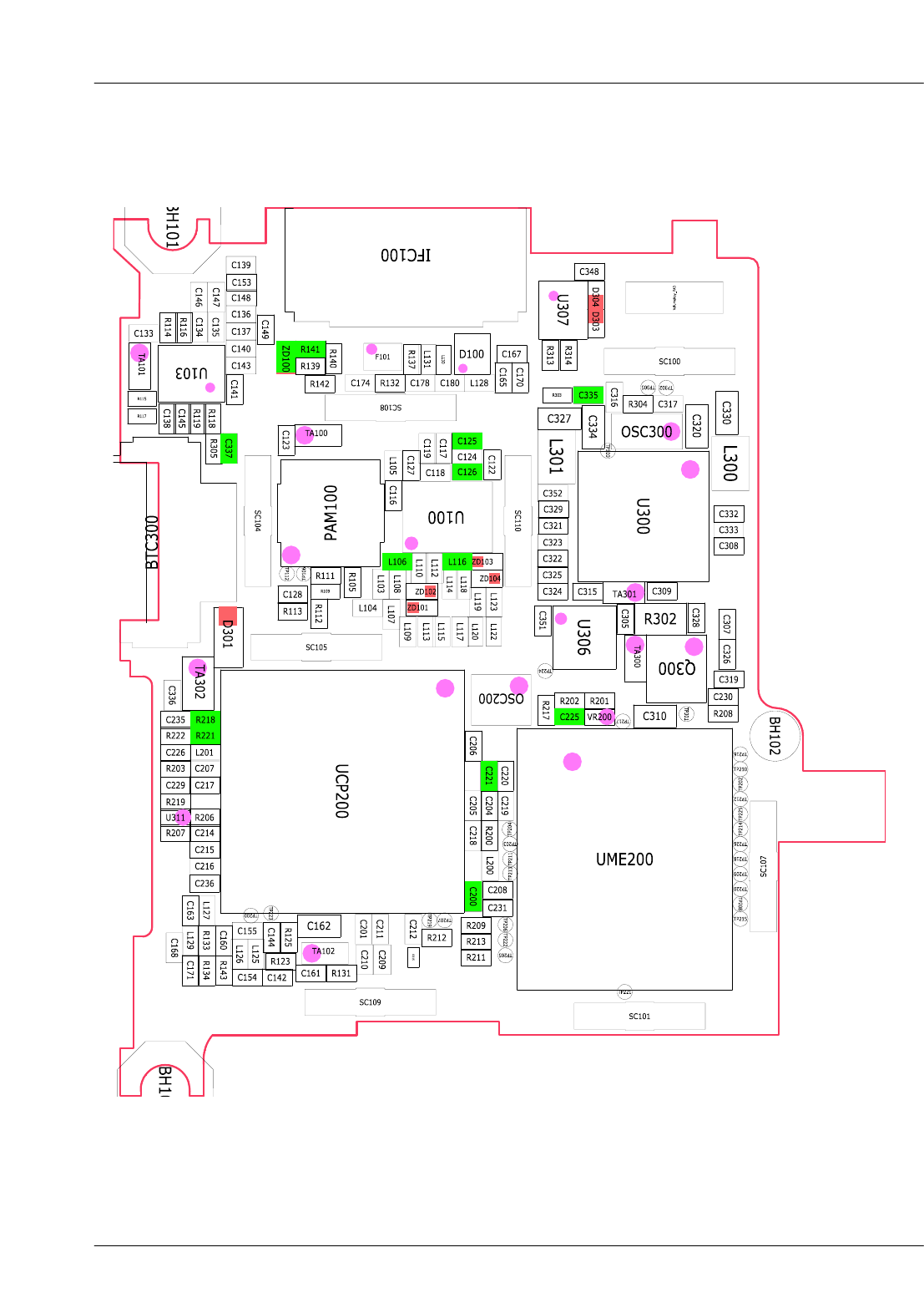
PCB Diagrams
8-2
This Document can not be used without Samsung's authorization
8-2. Bottom

- This Document can not be used without Samsung's authorization -
5-2. Cellular phone Parts list : GT-S5230DIAXEZ
Design LOC
Description
SEC CODE
QAN02
INTENNA-MAIN (GT-S5230)
GH42-02003A
QAN03
INTENNA-BT (GT-S5230)
GH42-02041A
QBC00
ASSY COVER-BATTERY EU
GH98-13721C
QCA01
ASSY CAMERA-3M MODULE(GT-S5230)
GH96-03801A
QCB01
CBF COAXIAL CABLE-SCH-W450
GH39-01027A
QCK01
PMO KEY-CAMERA EVA
GH72-54573A
QCK02
PMO KEY-HOLD
GH72-54583C
QCR101
SCREW-MACHINE
6001-002005
QCR91
SCREW-MACHINE
6001-002260
QFR01
ASSY CASE-FRONT
GH98-11970C
QIF01
PMO COVER-IF
GH72-54582C
QKP01
ASSY KEYPAD-(EU/SWEET PINK)
GH98-11972C
QLB01
ASSY BRACKET-LCD
GH98-12528A
QLC01
ELA MODULE-3.0" WQVGA GT-S5230 TFT ASSY
GH96-03865A
QLC03
ASSY ETC-LCD FPCB(GT-S5230)
GH59-07300A
QME03
TOUCH/PANEL-GT_S5230(EU S/PNK)
GH59-07302C
QMO01
MOTOR DC-SCHC250
GH31-00323A
QMP01
A/S ASSY-PBA MAIN(GT-S5230 SVC)
GH82-03617A
QMP02
KEY FPCB-SUB KEY PBA(GT-S5230)
GH59-07301A
QRE01
ASSY CASE-REAR
GH98-11971C
QSH01
ASSY COVER-SHIELD CAN TOP
GH98-13258A
QSH02
ICT SHIELD-CAN BTM
GH70-04837A
QSP01
MODULE-SPEAKER (GT-S5230)
GH59-07536A
QVK01
KEY FPCB-VOLUME KEY(GT-S5230)
GH59-07298A
QVO01
PMO KEY-VOLUME
GH72-54584C