Samsung GT S5660 Service Manual. Www.s Manuals.com. Manual R1.0
User Manual: Smartphone Samsung GT-S5660 - Service manuals and Schematics, Disassembly / Assembly. Free.
Open the PDF directly: View PDF ![]() .
.
Page Count: 87
GSM TELEPHONE
GT-S5660
1. Safety Precautions
2. Specification
3. Product Function
4. Exploded View and Parts list
5. MAIN Electrical Parts List
6. Level 1Repair
7. Disassembly and Assembly
Instructions
8. Chart of Troubleshooting
9. Reference data
Notice :
All functionality, features, specifications and other
product information provided in this document inclu
ding, but not limited to, the benefits, design, pricing,
components, performance, availability, and capabiliti
-es of the product are subject to change without
notice or obligation. Samsung reserves the right to
make changes to this document and the product
described herein, at anytime, without obligation on
Samsung to provide notification of such change.
GSM TELEPHONE CONTENTS

This Service Manual is aproperty of Samsung Electronics Co.,Ltd.
Any unauthorized use of Manual can be punished under applicable
International and/or domestic law.
Samsung Electronics Co.,Ltd.
2011. 02. Rev.1.0
ⓒ
2. Specification
2-1
2-1. GSM General Specification
GSM850
Phase 1
EGSM 900
Phase 2
DCS1800
Phase 1 PCS1900 WCDMA
2100 WCDMA900
Freq.
Band[MHz]
Uplink/Downlin
k
824~849
869~894
880~915
925~960
1710~1785
1805~1880
1850~1910
1930~1990
1922~1977
2112~2167
880~915
925~960
ARFCN range 128~251 0~124 &
975~1023 512~885 512~810
UL:9612~98
88DL:10562
~10838
UL:2712~28
63,DL:2937
~3088
Tx/Rx spacing 45MHz 45MHz 95MHz 80MHz 190MHz 45MHz
Mod. Bit rate/
Bit Period
270.833kbp
s
3.692us
270.833kbp
s
3.692us
270.833kbp
s
3.692us
270.833kbp
s
3.692us
3.84Mcps 3.84Mcps
Time Slot
Period/Frame
Period
576.9us
4.615ms
576.9us
4.615ms
576.9us
4.615ms
576.9us
4.615ms
FrameLengt
h:
10ms
Slotlength:
0.667ms
FrameLengt
h:
10ms
Slotlength:
0.667ms
Modulation 0.3GMSK 0.3GMSK 0.3GMSK 0.3GMSK QPSKHQPS
K
QPSKHQPS
K
MS Power 33dBm~5dB
m
33dBm~5dB
m
30dBm~0dB
m
30dBm~0dB
m
24dBm~-
50dBm
24dBm~-
50dBm
Power Class 5pcl ~
19pcl 5pcl ~19
pcl 0pcl ~15
pcl 0pcl ~15
pcl 3(max+24dB
m)
3(max+24dB
m)
Sensitivity -102dBm -102dBm -100dBm -100dBm -106.7dBm -106.7dBm
TDMA Mux 8 8 8 8 88
Cell Radius 35Km 35Km 2Km 2Km 2Km 2Km
Specification
2-2
2-2. GSM Tx Power Class
TX Power
control
level
GSM850
533±2
dBm
631±2
dBm
729±2
dBm
827±2
dBm
925±2
dBm
10 23±2 dBm
11 21±2 dBm
12 19±2 dBm
13 17±2 dBm
14 15±2 dBm
15 13±2 dBm
16 11±3 dBm
17 9±3dBm
18 7±3 dBm
19 5±3 dBm
TX Power
control
level
EGSM900
533±2
dBm
631±2
dBm
729±2
dBm
827±2
dBm
925±2
dBm
10 23±2 dBm
11 21±2 dBm
12 19±2 dBm
13 17±2 dBm
14 15±2 dBm
15 13±2 dBm
16 11±3 dBm
17 9±3dBm
18 7±3 dBm
19 5±3 dBm
TX Power
control
level
DCS1800
030±3
dBm
128±3
dBm
226±3
dBm
324±3
dBm
422±3
dBm
520±3
dBm
618±3
dBm
716±3
dBm
814±3
dBm
912±4
dBm
10 10±4 dBm
11 8±4 dBm
12 6±4 dBm
13 4±4 dBm
14 2±5 dBm
15 0±5 dBm
TX Power
control
level
PCS1900
030±3
dBm
128±3
dBm
226±3
dBm
324±3
dBm
422±3
dBm
520±3
dBm
618±3
dBm
716±3
dBm
814±3
dBm
912±4
dBm
10 10±4 dBm
11 8±4 dBm
12 6±4 dBm
13 4±4 dBm
14 2±5 dBm
15 0±5 dBm

SAMSUNG Proprietary-Contents may change without notice
3. Operation Instruction and Installation
3-1
This Document can not be used without Samsung's authorization
Main Function
•Quad Band EGSM850/900/DCS/PCS (EDGE/GPRS), UMTS 900/2100MHz
•HSDPA 7.2 Mbps
•3.2”
HVGA TFT Full Touch (c-type )
•Music player, Voice Recorder
•GPS /BT v2.1 /USB v2.0 /WiFi (802.11 b/n/g)
•3M
Camera
•FM Radio Receiver
•Sensors: Accelerometer, Compass, Proximity
•Improve TouchWiz 3.0 Light for Android(Multiple SNS(Facebook, Myspace, Twitter),Multiple
IM(Parling: AOL, G-talk))
•Android Froyo OS
•SMS/MMS/Email
SAMSUNG Proprietary-Contents may change without notice
6. Level 1Repair
6-1
This Document can not be used without Samsung's authorization
6-1. Software Download
6-1-1. Pre-requisite for Download
ㆍDownloader Program (Odin Multi Downloader v4.42)
ㆍGT-S5660 Mobile Phone
ㆍData Cable
ㆍJIG BOX (GH99-36900A)
ㆍRF Test Cable (GH39-00985A)
ㆍJIG Cable (GH39-01160A)
ㆍAdapter (GH99-38251A)
ㆍBinary files
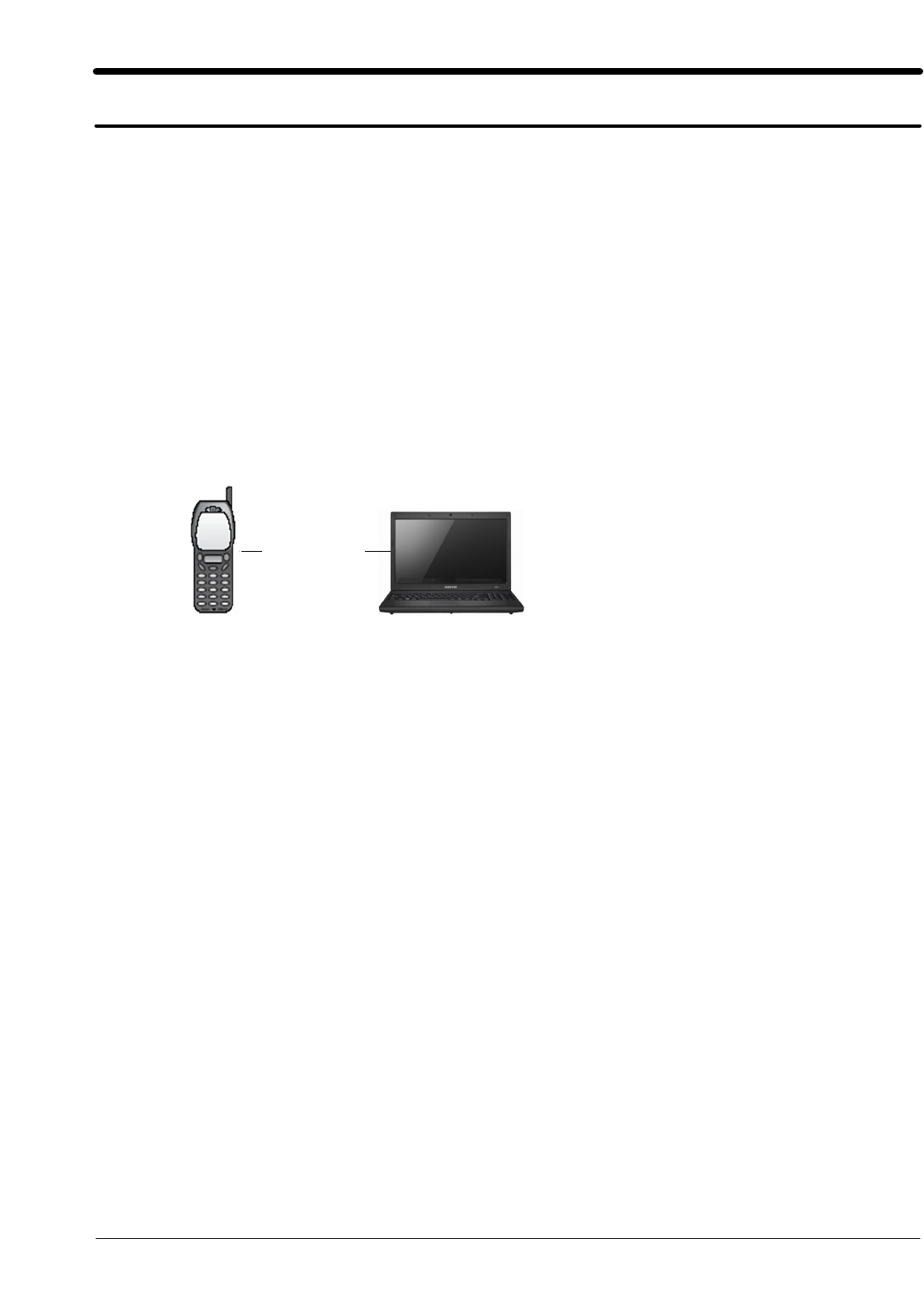
-Diagram of Connection:
PC
Mobile Phone(with Battery)
Data Cable
SAMSUNG Proprietary-Contents may change without notice
Level 1Repair
6-2
This Document can not be used without Samsung's authorization
6-1-2. S/W Download Process
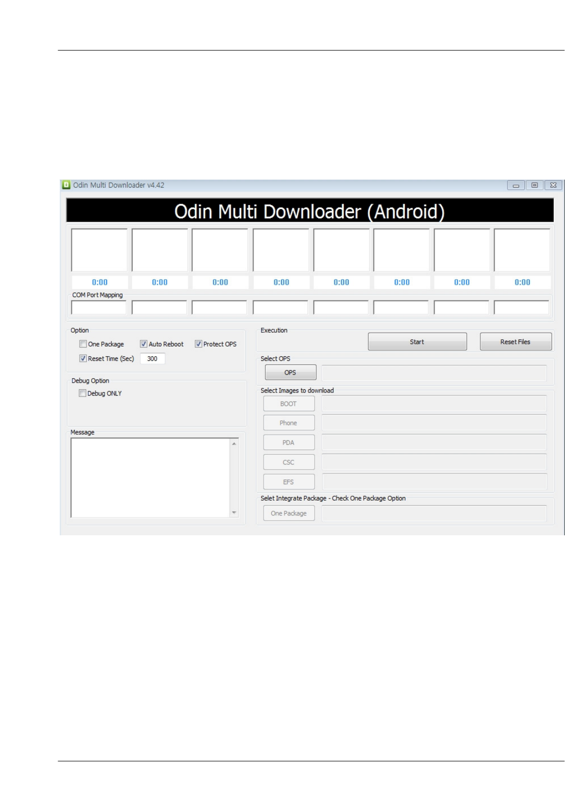
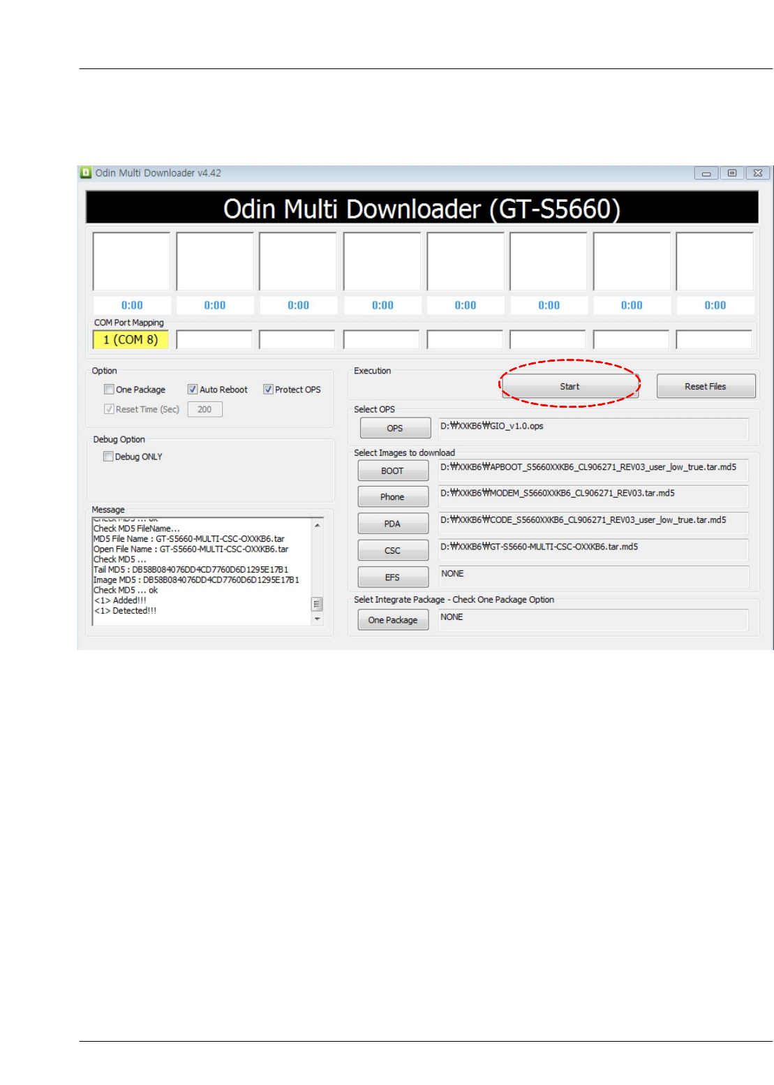
1. Load the binary download program by executing the "Odin Multi Downloader v4.42"
SAMSUNG Proprietary-Contents may change without notice
Level 1Repair
6-3
This Document can not be used without Samsung's authorization
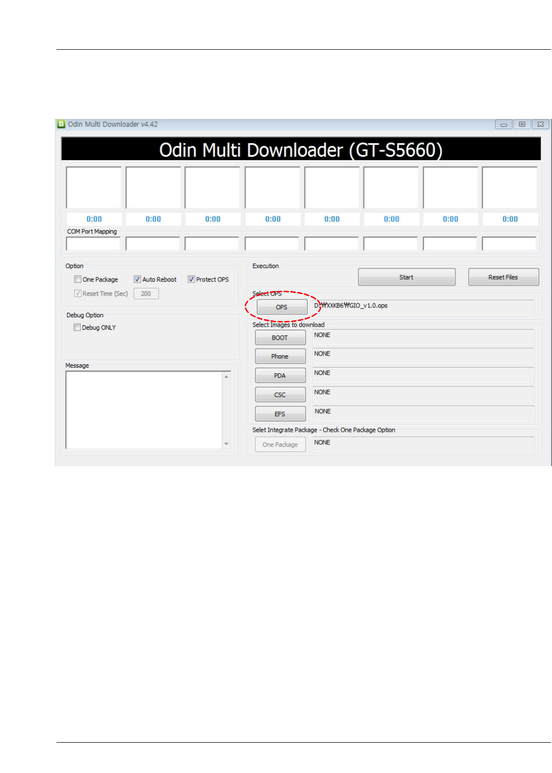
2Select OPS file (Gio_v1.0.ops) from the folder that you saved the binary files.
SAMSUNG Proprietary-Contents may change without notice
Level 1Repair
6-4
This Document can not be used without Samsung's authorization
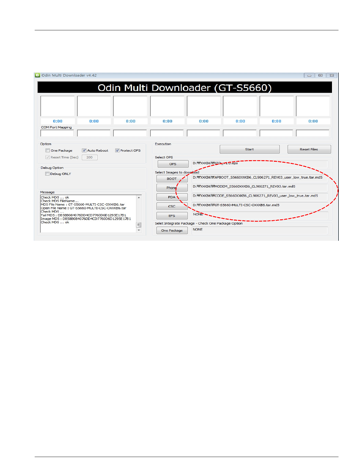
3. Load the file of Bootloader, Amss, PDA, CSC files from the folder that you saved the binary
files.
SAMSUNG Proprietary-Contents may change without notice
Level 1Repair
6-5
This Document can not be used without Samsung's authorization
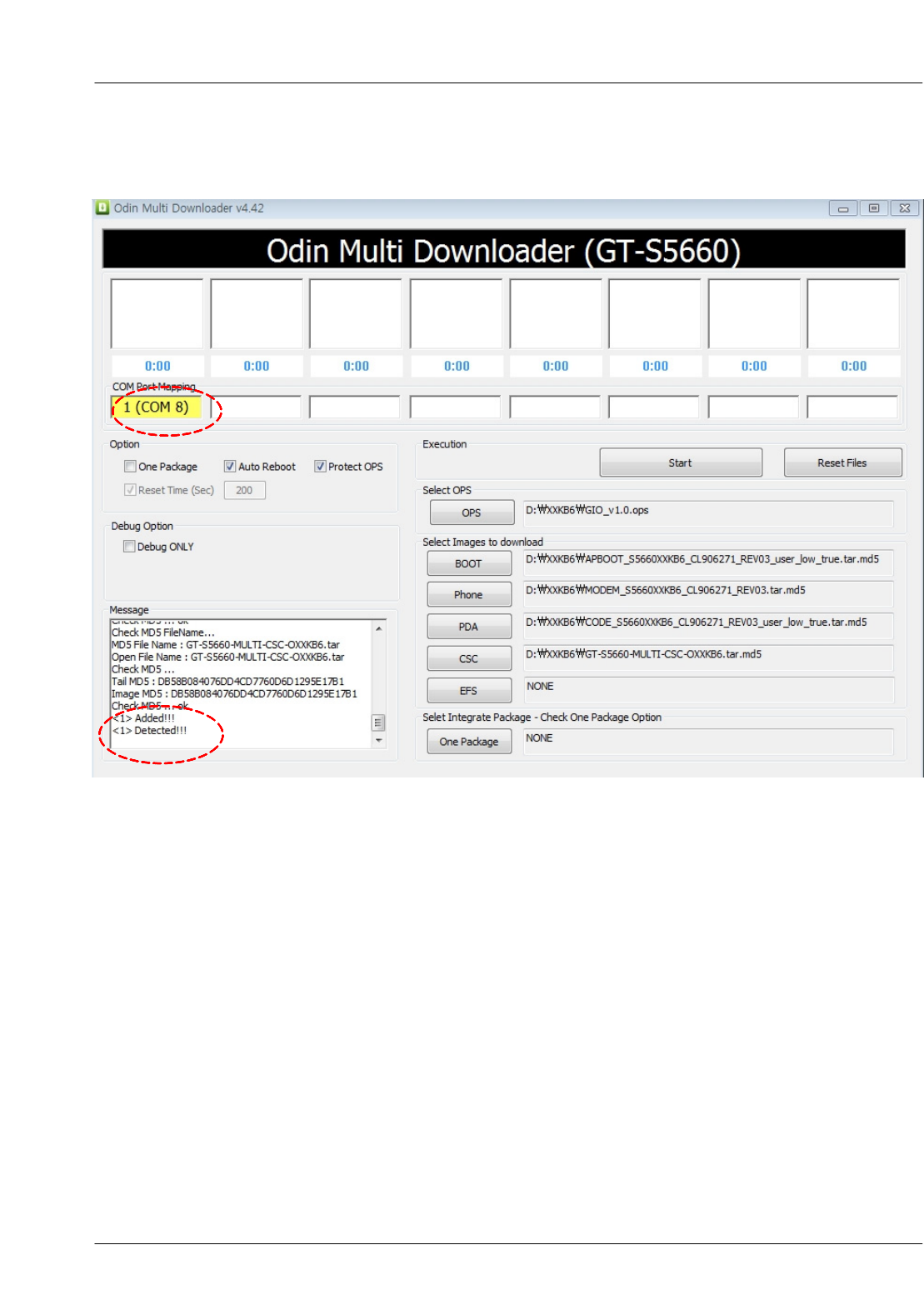
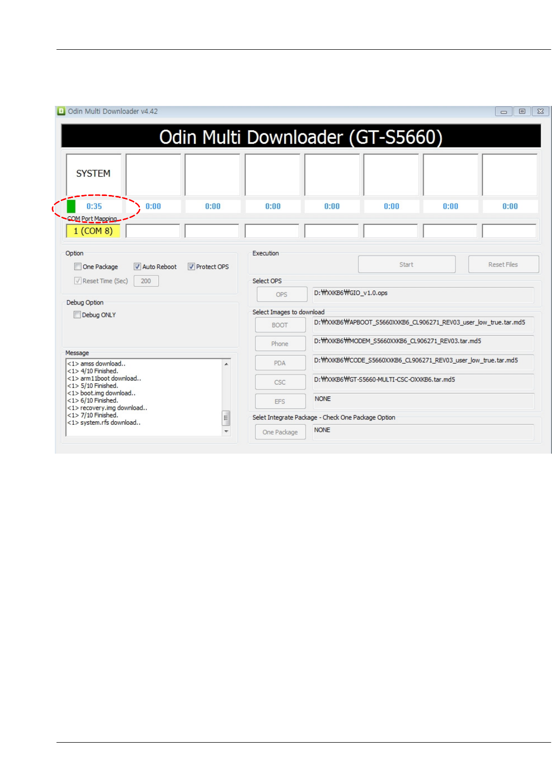
4. COM Port Mapping change to yellow colour when the phone with download mode is
connected to PC by data cable.
cf. You have to set the phone as adownload mode by pressing Middle Key(OK Key) +
Power key and Volume Down Key simultaneously before connecting to PC .
Then, the port would be searched.
SAMSUNG Proprietary-Contents may change without notice
Level 1Repair
6-6
This Document can not be used without Samsung's authorization
5. Click the Start button when the Port searched.
SAMSUNG Proprietary-Contents may change without notice
Level 1Repair
6-7
This Document can not be used without Samsung's authorization
It will start to download.
SAMSUNG Proprietary-Contents may change without notice
Level 1Repair
6-8
This Document can not be used without Samsung's authorization
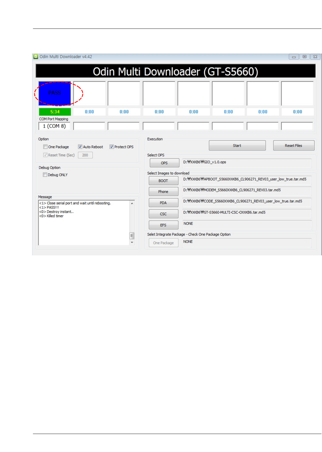
6. When downloading is finished successfully, there is a"
PASS"message.
7. Confirm the downloaded version name and etc. :
*#1234#

SAMSUNG Proprietary-Contents may change without notice
9. Reference Abbreviate
This Document can not be used without Samsung's authorization
9-1
Reference Abbreviate
―AAC:Advanced Audio Coding.
―AVC :Advanced Video Coding.
―BER :Bit Error Rate
―BPSK:Binary Phase Shift Keying
―CA :Conditional Access
―CDM :Code Division Multiplexing
―C/I :Carrier to Interference
―DMB :Digital Multimedia Broadcasting
―EN :European Standard
―ES :Elementary Stream
―ETSI:European Telecommunications Standards Institute
―MPEG:Moving Picture Experts Group
―PN :Pseudo-random Noise
―PS :Pilot Symbol
―QPSK:Quadrature Phase Shift Keying
―RS :Reed-Solomon
―SI :Service Information
―TDM :Time Division Multiplexing
―TS :Transport Stream

SAMSUNG Proprietary-Contents may change without notice
1. Safety Precautions
1-1
This Document can not be used without Samsung's authorization
1-1. Repair Precaution
―Repair in Shield Box, during detailed tuning. Take specially care of tuning or test, because
specipicty of cellular phone is sensitive for surrounding interference(RF noise).
―Be careful to use akind of magnetic object or tool, because performance of parts is damaged by
the influence of magnetic force.
―Surely use astandard screwdriver when you disassemble this product, otherwise screw will be
worn away.
―Use athicken twisted wire when you measure level.
Athicken twisted wire has low resistance, therefore error of measurement is few.
―Repair after separate Test Pack and Set because for short danger (for example an overcurrent
and furious flames of parts etc) when you repair board in condition of connecting Test Pack and
tuning on.
―Take specially care of soldering, because Land of PCB is small and weak in heat.
―Surely tune on/off while using AC power plug, because arepair of battery charger is dangerous
when tuning ON/OFF PBA and Connector after disassembling charger.
―Don't use as you pleases after change other material than replacement registered on SEC System.
Otherwise engineer in charge isn't charged with problem that you don't keep this rules.

SAMSUNG Proprietary-Contents may change without notice
Safety Precautions
1-2
This Document can not be used without Samsung's authorization
1-2. ESD(Electrostatically Sensitive Devices) Precaution
Several semiconductor may be damaged easily by static electricity. Such parts are called by ESD
(Electrostatically Sensitive Devices), for example IC,BGA chip etc. Read Precaution below.
You can prevent from ESD damage by static electricity.
―Remove static electricity remained your body before you touch semiconductor or parts with
semiconductor. There are ways that you touch an earthed place or wear static electricity prevention
string on wrist.
―Use earthed soldering steel when you connect or disconnect ESD.
―Use soldering removing tool to break static electricity. ,otherwise ESD will be damaged by static
electricity.
―Don't unpack until you set up ESD on product. Because most of ESD are packed by box and
aluminum plate to have conductive power,they are prevented from static electricity.
―You must maintain electric contact between ESD and place due to be set up until ESD is
connected completely to the proper place or acircuit board.
SAMSUNG Proprietary-Contents may change without notice
4. Exploded View and Parts List
4-1
This Document can not be used without Samsung's authorization
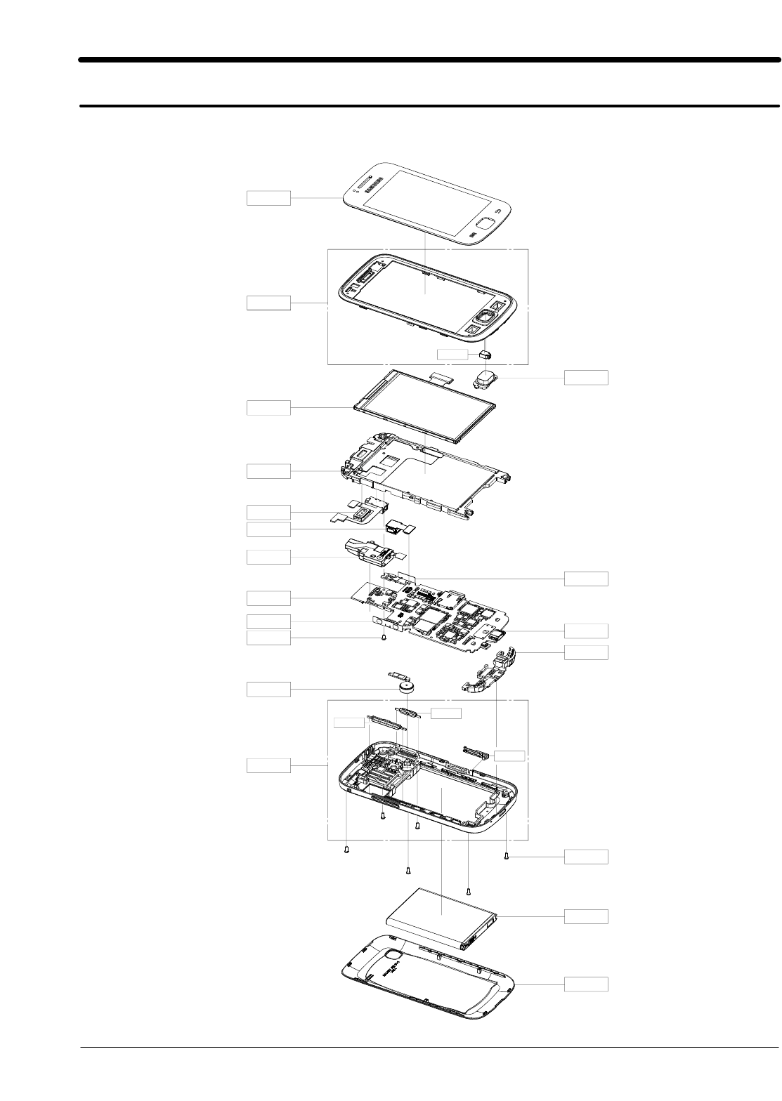
4-1. Cellular phone Exploded View
QFR01
QRE01
QLC01
QLB01
QCA01
QVK01
QCR12
QSP01
QMO01
QMP01
QAR01
QME03
QCK01
QKP01
QVK02
QME01
QAN02
QCR67
QBC00
QBA01
QSD01
QVO01
QMI03
SAMSUNG Proprietary-Contents may change without notice
Exploded View and Parts List
4-2
This Document can not be used without Samsung's authorization
Design LOC Description SEC CODE
QCR12 SCREW-MACHINE 6001-001530
QCR67 SCREW-MACHINE 6001-002083
QMO01 MOTOR DC-GT_S5660 GH31-00533A
QAN02 INTENNA-MAIN(GT_S5660) GH42-02961A
QBA01 INNER BATTERY PACK-EB494358VU,GT-S5830,L GH43-03504A
QVK02 KEY FPCB-POWER KEY(GT_S5660) GH59-10888A
QVK01 KEY FPCB-VOLUME KEY(GT_S5660) GH59-10889A
QME01 DOME SHEET-GT_S5660 GH59-10897A
QME03 TOUCH/PANEL-GT_S5660 GH59-10911A
QSP01 MODULE-SPK(GT_S5660) GH59-10913A
QAR01 MODULE-RCV+SENSOR(GT_S5660) GH59-10920A
QKP01 PMO KEY-HOME GH72-63203A
QMP01 A/S ASSY-PBA MAIN(COMM)GT_S5660 GH82-05634A
QLC01 ASSY LCD-3.2" HVGA GT_S5660 GH96-05097A
QCA01 ASSY CAMERA-3M(GT_S5660) GH96-05106A
QBC00 ASSY COVER-BATT GH98-19585A
QLB01 ASSY BRACKET-LCD GH98-19588A
QFR01 ASSY CASE-FRONT GH98-19583A
QMI03 ASSY COVER-MIC HOLDER GH98-19587A
QRE01 ASSY CASE-REAR GH98-19584A
QVO01 PMO KEY-VOLUME GH72-63171A
QCK01 PMO KEY-POWER GH72-63172A
QSD01 PMO COVER-MICRO SD GH72-63174A
4-2. Cellular phone Parts list

SAMSUNG Proprietary-Contents may change without notice
5. MAIN Electrical Parts List
5-1
This Document can not be used without Samsung's authorization
SEC CODE DESIGN LOC Description
0403-001870 D600 TDZ5V6J
0404-001646 ZD509 PMEG4005EJ
0406-001267 ZD507,ZD508 RCLAMP0521P
0406-001361 ZD503 PESD5V0U5BV
0406-001369 ZD601 RCLAMP3654P.TCT
0406-001375 ZD504 UCLAMP0501T
0406-001413 ZD505,ZD506 PESD5V0F1BL
0406-001459 ZD500,ZD501,ZD502 RD1301B
0406-001459 ZD602 RD1301B
0407-001002 D400,D500 DAN222TL
0504-001138 Q601 DTA114EM
0505-001325 Q500 2SK3019
0505-002341 Q600 SI1013X-T1-GE3
0601-002846 LED500,LED501 19-217UTD/S759/TR8
0801-003265 U300 74AUP1G74GM
0801-003383 U301 74LVC1G00GM
1001-001645 U601 FSA9280AUMX
1108-000411 UME300 KAT007012C-BRTT
1201-003057 PAM101 RF7201
1201-003168 U200 SFMG1M0Q001
1201-003192 PAM100 SKY77544-51
1202-001068 U506 TC75S56FE
1203-004818 U600 RP103K181D-TR
1203-006159 U102 AAT2146IJS-0.6-T1
1203-006346 U500 FT8010MPX
1203-006732 U400 MAX8899GEWZ-T
1203-006760 U505 KTD259EHD-TR
1205-003297 U103 RTR6285
1205-004076 U202 AR6003G-AC2B-R
1205-004113 U201 BCM20780C0KUBG
1205-004180 UCP300 MSM7227-1-SCREEN
1209-002023 U504 BMA222
1209-002030 U503 MMC3280MS
1404-001221 TH300 NCP15WB473J04RC
2007-000137 R325 RC1005J202CS
2007-000138 R103,R120,R121,R322 RC1005J101CS

SAMSUNG Proprietary-Contents may change without notice
Main Electrical Parts List
5-2
This Document can not be used without Samsung's authorization
SEC CODE DESIGN LOC Description
2007-000138 R326 RC1005J101CS
2007-000140 R118,R303,R510 RC1005J102CS
2007-000141 R304,R305,R306,R307 RC1005J222CS
2007-000141 R311,R312,R313,R314 RC1005J222CS
2007-000141 R607 RC1005J222CS
2007-000143 R620 RC1005J472CS
2007-000144 R400 RC1005J512CS
2007-000148 R308,R502,R509,R600 RC1005J103CS
2007-000148 R618 RC1005J103CS
2007-000149 R610 RC1005J123CS
2007-000152 R621,R622 RC1005J203CS
2007-000153 R508 RC1005J223CS
2007-000160 R506 RC1005J683CS
2007-000162 R302,R315,R319,R324 RC1005J104CS
2007-000162 R327,R410,R507,R521 RC1005J104CS
2007-000170 R528 RC1005J105CS
2007-000172 R516 RC1005J100CS
2007-000758 R505 RC1005J334CS
2007-001119 R512 RC1005J681CS
2007-001291 R405,R406 RC1005J300CS
2007-001292 R330 RC1005J330CS
2007-001298 R329,R401 RC1005J510CS
2007-001301 R119,R500,R501 MCR01MZP5J680
2007-001339 R612 RC1005J184CS
2007-007107 R407 RC1005F1003CS
2007-007132 R204 RC1005F153CS
2007-007139 R309,R310,R523 MCR01MZP5F4702
2007-007309 R117 MCR01MZP5F1202
2007-007334 R402,R517 RC1005F2003CS
2007-007468 R116,R409 RK73H1ETP1213F
2007-007480 R408 RK73H1ETP1303F
2007-007528 R513 RK73H1ETP1501F
2007-007573 R403 RK73H1ETP3303F
2007-008044 R106 MCR006MZPJ680
2007-008045 R126,R127,R611 ERJ1GEJ101C
2007-008055 R300,R338 ERJ1GENJ104X

SAMSUNG Proprietary-Contents may change without notice
Main Electrical Parts List
5-3
This Document can not be used without Samsung's authorization
SEC CODE DESIGN LOC Description
2007-008057 R128,R129 MCR006YZPJ151
2007-008298 R301 RC1005F49R9CS
2007-008483 R613,R614,R615,R616 RMC1/20473JPA
2007-008483 R617 RMC1/20473JPA
2007-008502 R114 RC1005F4993CS
2007-008531 R320 MCR006MZPJ0100
2007-008766 R323 ERJ2RKF6041X
2007-008812 R404 RC1005F2153CS
2007-009115 R104 RC0603J240CS
2007-009155 R619 MCR006YZPJ474
2007-009794 R205 RK73H1HTTC6191F
2203-000233 C113,C149,C177,C188 GRP1555C1H101J
2203-000233 C190,C197,C212,C213 GRP1555C1H101J
2203-000233 C235,C435 GRP1555C1H101J
2203-000254 C111,C117,C171,C204 GRP155R71C103K
2203-000278 C151,C200,C203,C209 GRP1555C1H100D
2203-000278 C228,C511 GRP1555C1H100D
2203-000359 C518,C524 GRP1555C1H151JD01E
2203-000386 C528 GRP1555C1H150J
2203-000425 C433,C434 GRP1555C1H180J
2203-000438 C102,C112,C173,C216 GRP155R71H102K
2203-000489 C139,C140,C328 GRP155R71H222K
2203-000585 C428 GRP155R71H221KD01E
2203-000627 C164,C170,C187 GRM1555C1H220J
2203-000696 C321 GRP1555C1H2R0C
2203-000812 C103,C114,C142,C163 GRP1555C1H330J
2203-000812 C208,C211,C323,C513 GRP1555C1H330J
2203-000812 C617 GRP1555C1H330J
2203-000995 C329,C330,C429,C514 GRP1555C1H470J
2203-000995 C618,C636,U502 GRP1555C1H470J
2203-001017 C179,C182 GRP1555C1H4R0C
2203-001033 C191 GRP155R71E562KD01E
2203-001072 C245 GRP1555C1H560JD01E
2203-001153 C150,C153 GRP1555C1H680J
2203-001385 C116,C135,C137 GRP1555C1H1R5CZ01E
2203-001405 C406,C407 04023G223ZAT2A

SAMSUNG Proprietary-Contents may change without notice
Main Electrical Parts List
5-4
This Document can not be used without Samsung's authorization
SEC CODE DESIGN LOC Description
2203-002668 C120,C128 C1005CG1H0R5BT
2203-005057 C136,C512 GRP1555C1H8R2CZ01E
2203-005249 C526,C607 GRM188R71H104K
2203-005382 C181,C232,C234 GRP1555C1H6R0BZ01E
2203-005480 C324 GRP155R71A333KA01E
2203-005483 C503,C504 GRP155R61A683KA01E
2203-005682 C125,C126,C133,C134 GRP0335C1E330JD01E
2203-005682 C156,C158 GRP0335C1E330JD01E
2203-005725 C193 GRP0335C1E220JD01E
2203-005736 C194 GRP0335C1E101JD01E
2203-005806 C122 GRP033R71C102KD01E
2203-006048 C101,C162,C169,C186 GRM155R71A104K
2203-006048 C205,C206,C210,C222 GRM155R71A104K
2203-006048 C224,C225,C227,C230 GRM155R71A104K
2203-006048 C231,C240,C300,C301 GRM155R71A104K
2203-006048 C303,C306,C308,C309 GRM155R71A104K
2203-006048 C311,C312,C313,C314 GRM155R71A104K
2203-006048 C315,C318,C322,C325 GRM155R71A104K
2203-006048 C326,C327,C331,C332 GRM155R71A104K
2203-006048 C436,C437,C442,C443 GRM155R71A104K
2203-006048 C501,C507,C517,C520 GRM155R71A104K
2203-006048 C522,C523,C525 GRM155R71A104K
2203-006123 C217 GRM0335C1E5R6CD01D
2203-006137 C506 CL05B223KONC
2203-006187 C127,C129 GRM0335C1E3R9B
2203-006201 C239 GRM188R60J225KE01D
2203-006208 C159,C500,C615 CM105X5R475M06AT
2203-006260 C400 GRM155R61A224KE19E
2203-006348 C619 CV105X5R105K25AT
2203-006399 C201,C202,C214,C215 GRM155R60J105KE19D
2203-006399 C221,C302,C304,C305 GRM155R60J105KE19D
2203-006399 C307,C317,C319,C320 GRM155R60J105KE19D
2203-006399 C408,C409,C416,C417 GRM155R60J105KE19D
2203-006399 C418,C419,C423,C424 GRM155R60J105KE19D
2203-006399 C425,C426,C427,C430 GRM155R60J105KE19D
2203-006399 C432,C445,C502,C508 GRM155R60J105KE19D

SAMSUNG Proprietary-Contents may change without notice
Main Electrical Parts List
5-5
This Document can not be used without Samsung's authorization
SEC CODE DESIGN LOC Description
2203-006399 C509,C603,C604,C605 GRM155R60J105KE19D
2203-006399 C606,C608,C609,C610 GRM155R60J105KE19D
2203-006399 C623,C627,C633 GRM155R60J105KE19D
2203-006423 C183 GRM33X5R104K6.3
2203-006562 C431,C444 CV05X5R105K10AH
2203-006707 C123,C124 GRM0335C1E4R7C
2203-006824 C141,C160,C401,C402 CV105X5R475K10AT
2203-006824 C403,C404,C405,C420 CV105X5R475K10AT
2203-006824 C438,C439,C440,C441 CV105X5R475K10AT
2203-006824 C614 CV105X5R475K10AT
2203-006842 C233 CL05C471JB5NNNC
2203-006846 C130,C132 ECJZEC1E2R0B
2203-006979 C185 CL03B103KP3NNNC
2203-007240 C310,C316,C505 CL10A226MQ8NRNE
2203-007271 C207,C220,C223,C226 CL05A225KP5NSNC
2203-007271 C229,C238,C244,C410 CL05A225KP5NSNC
2203-007271 C411,C412,C413,C414 CL05A225KP5NSNC
2203-007271 C415,C422,C625,C626 CL05A225KP5NSNC
2203-007279 C118,C527 CV105X5R106M10AT
2203-007317 C184,C421 CV05X5R475M06AH
2203-007701 C521,C616 QV105X5R106M10AT
2404-001506 TA400 C-TA,CHIP;TCTP1A476M8R-D
2703-001729 L116 LL1005-FH1N8S
2703-001747 L131,L140 LL1005-FH4N7S
2703-002176 L117 CIH05T2N7SNC
2703-002198 L121,L203 CIH05T10NJNC
2703-002200 L111 CIH05T18NJNC
2703-002203 L101 CIH05T15NJNC
2703-002205 L120,L202 CIH05T3N9KNC
2703-002208 L118,L119,L130 CIH05T2N2SNC
2703-002268 L122 CIH05T8N2JNC
2703-002269 L207 CIH05T56NJNC
2703-002281 L106 CIH05T5N6SNC
2703-002308 L500 CIH05T68NJNC
2703-002314 L133,L506 CIH05T47NJNC
2703-002365 L113,L205 CIH05T1N2SNC
SAMSUNG Proprietary-Contents may change without notice
Main Electrical Parts List
5-6
This Document can not be used without Samsung's authorization
SEC CODE DESIGN LOC Description
2703-002369 L105 CIH05T1N5SNC
2703-002544 L132 LQW15AN8N2H00D
2703-002842 L136 LLV0603-F2N2S
2703-002861 L507 LPF3010T-100M
2703-002958 L109 CIH03T56NJNC
2703-003685 L123 CIG21L4R7MNE
2703-003686 L400,L401,L402,L403 CIG21L2R2MNE
2703-003915 L103,L104 CML0306-5N6-JNH
2703-004030 L107,L108,L110 LQP03TN22NJ02D
2801-004909 OSC400 EXS00A-MU00031
2801-005045 OSC200 CXC6X260000GHVRE00
2809-001366 OSC100 1XTV19200AEB
2901-001525 F600,F601,F602,F603 ICVE10184E150R101FR
2901-001525 F604,F605,F606 ICVE10184E150R101FR
2901-001650 F607 ICMEF212P121MFR
2904-001658 F103 SFDG50AQ101
2904-001702 F105 SFHG40YQ101
2904-001869 F101 B9504
2904-001881 F100 SFRG42PY002
2910-000099 DUF101 SFXG50PD502
2910-000117 DUF100 SAYRJ897MCA0B0A
2911-000162 F200 D6105
3003-001136 MIC500 SPU0410HR5H
3301-001438 L204 BLM15BB750SN1D
3301-001659 L200,L201 BLM15AG601SN1
3301-001729 L512 BLM15AG102SN1D
3301-001756 L100,L602,L603 BLM15HG102SN1D
3301-001789 L601 BLM15EG121SN1D
3301-001885 L501,L502,L503,L504 BLM15HD182SN1D
3301-001885 L505,L510,L513 BLM15HD182SN1D
3301-002037 L508,L509 BLM18KG601SN1
3705-001731 RFS100 KMS-560-002-BEF
3709-001575 CD600 SCHA4B0301
3709-001668 SIM600 5000-6P-2.7XB
3711-006483 HEA600 14-5802-054-202-829
3711-006615 SPK500 AXT610124AW1

SAMSUNG Proprietary-Contents may change without notice
Main Electrical Parts List
5-7
This Document can not be used without Samsung's authorization
SEC CODE DESIGN LOC Description
3711-006923 HEA501 14-5802-016-002-829
3711-006925 HEA601 BM10B(0.8)-24DP-0.4V
3711-007650 BTC600 202-03050-00341
3712-001348 ANT100,ANT101,ANT200 HJ-ICT-05Y
3712-001348 ANT201,MOT500,MOT501 HJ-ICT-05Y
3722-002867 IFC600 HY07-AB0770
Please consult the GSPN website (Samsung Portal) for the most recent version of the product's
part list.
SAMSUNG Proprietary-Contents may change without notice
7. Level 2Repair
7-2
This Document can not be used without Samsung's authorization
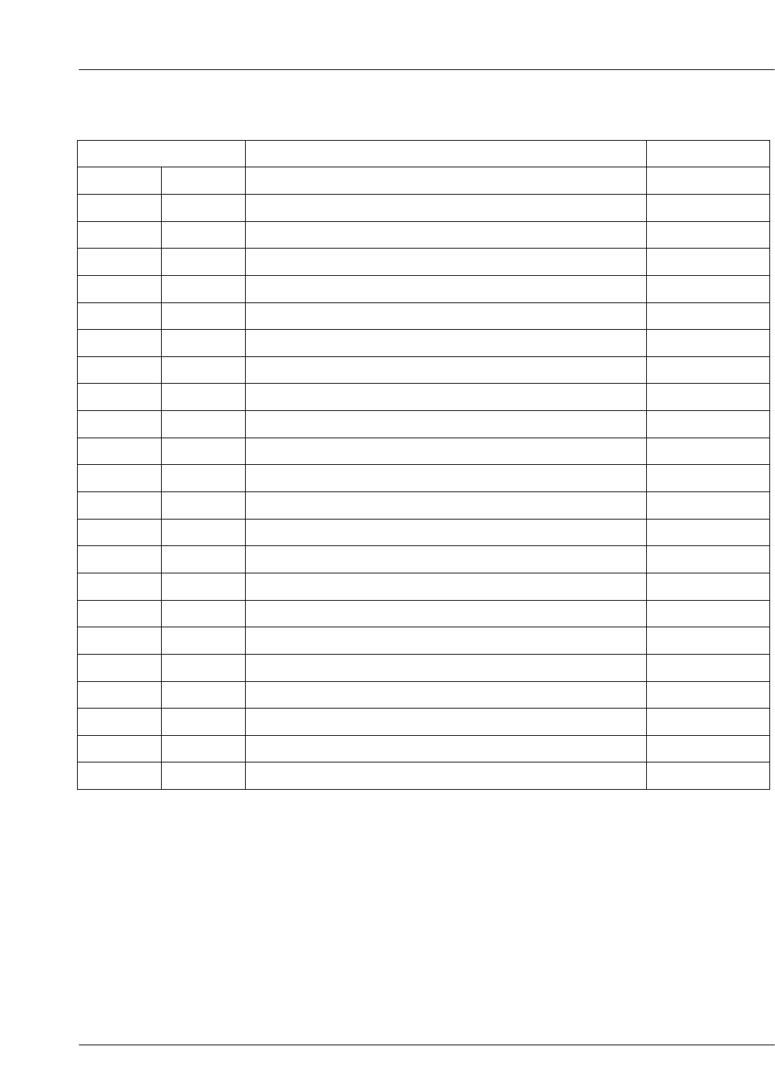
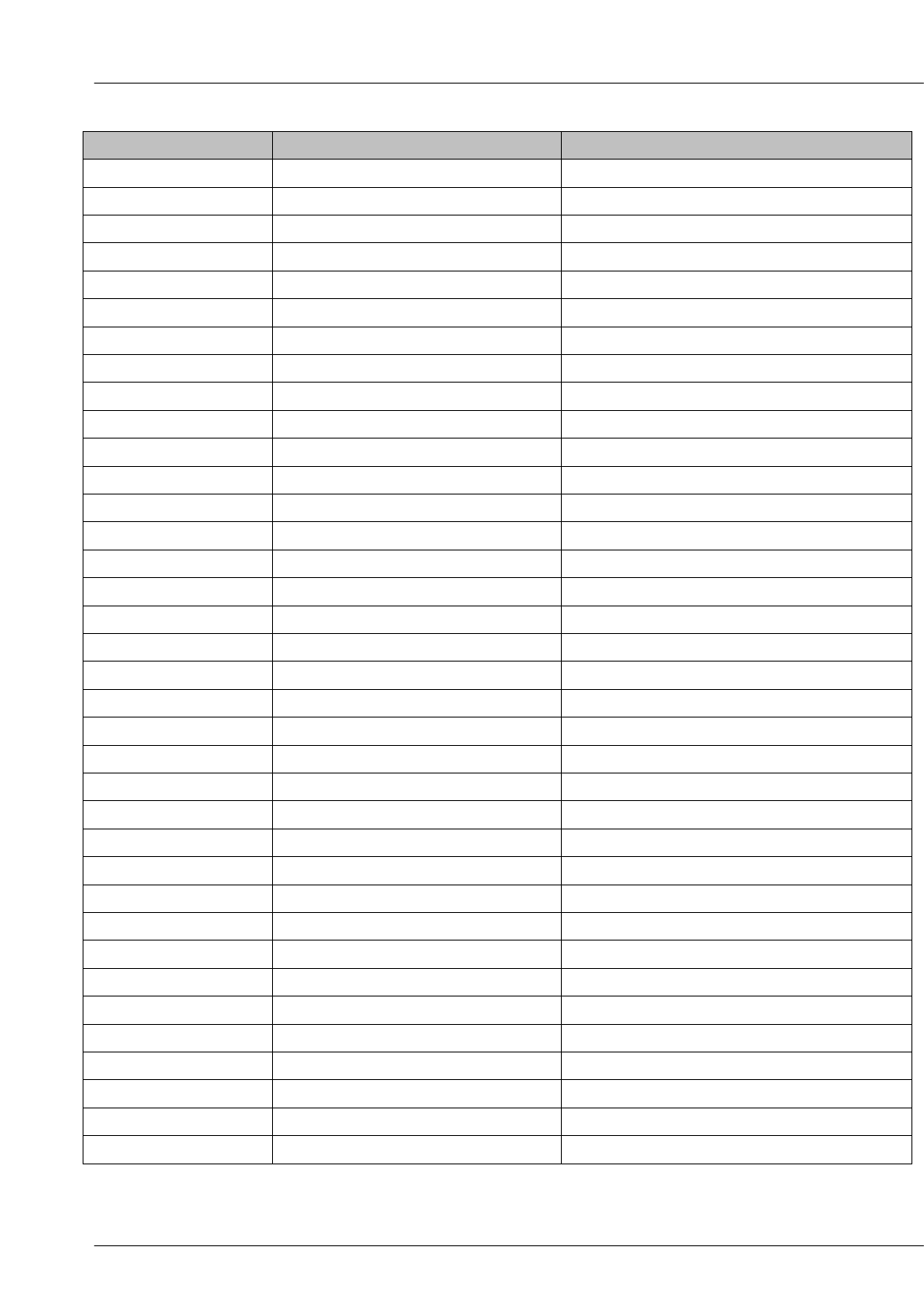
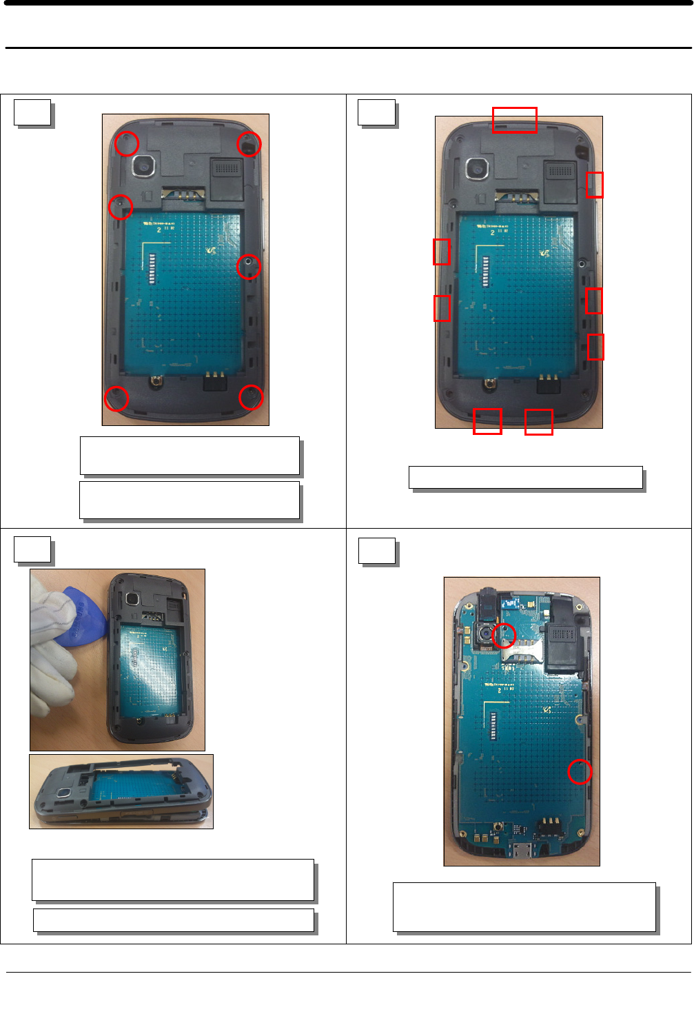
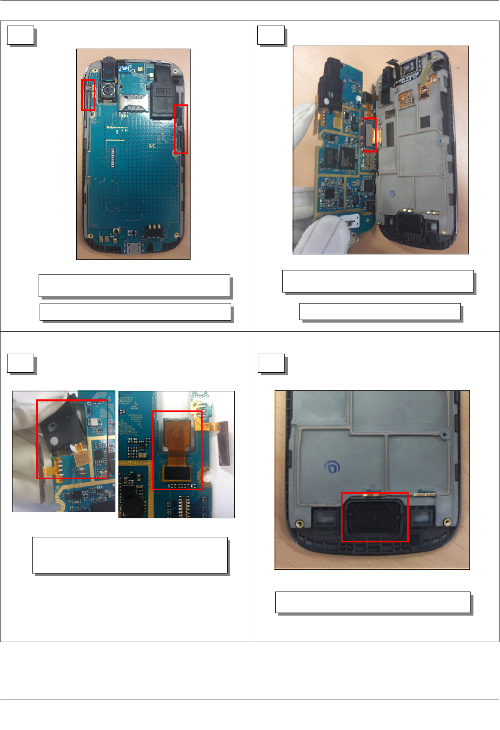
7-1. Disassembly
2
34
Release the screws at 2points.
1.0±0.1 kgf.cm
Release the screws at 6points.
1.0±0.1 kgf.cm
DO NOT MAKE SCRATCH ON
THE REAR.
1
Disjoint hook 8points at the rear
Disjoint using adecompositive tool at the side
of the rear.
DO NOT MAKE SCRATCH ON TEH REAR.
SAMSUNG Proprietary-Contents may change without notice
7. Level 2Repair
7-2
This Document can not be used without Samsung's authorization
5 6
7 8
Tear off the both FPCBs
Separate the earjack module and the
camera module.
Be careful not to rip up the FPCBs.
Separate the PBA and the Front.
Be careful not to damage the FPCB.
Separate the Homekey and the front.
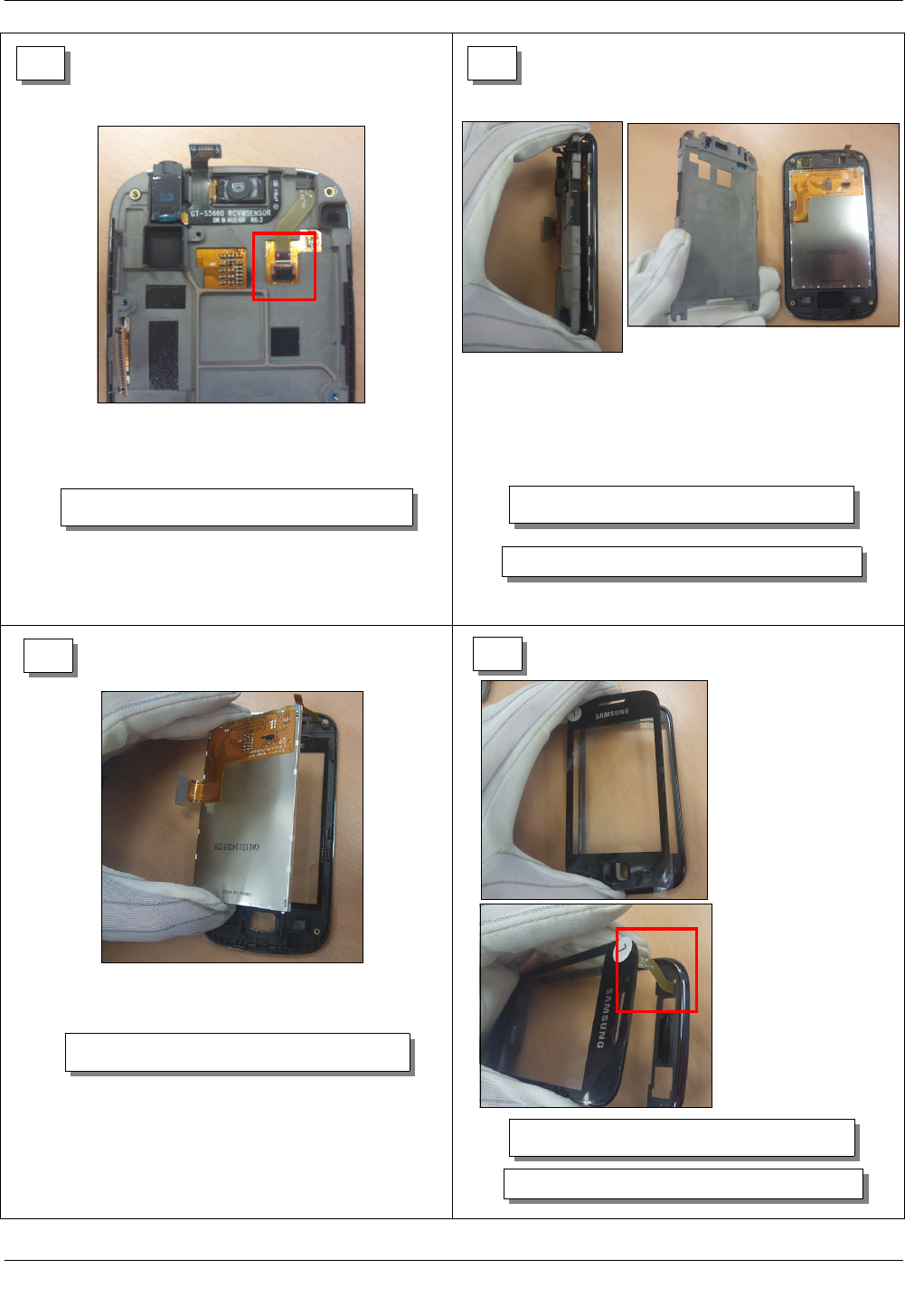
SAMSUNG Proprietary-Contents may change without notice
7. Level 2Repair
7-3
This Document can not be used without Samsung's authorization
910
11
Separate the braket and the front.
12
Be careful not to damage the LCD FPCB
Separate the TSP FPCB and the connector.
Separate the TSP and the front.
Separate the LCD and the front.
Be careful not to damage the TPS FPCB.
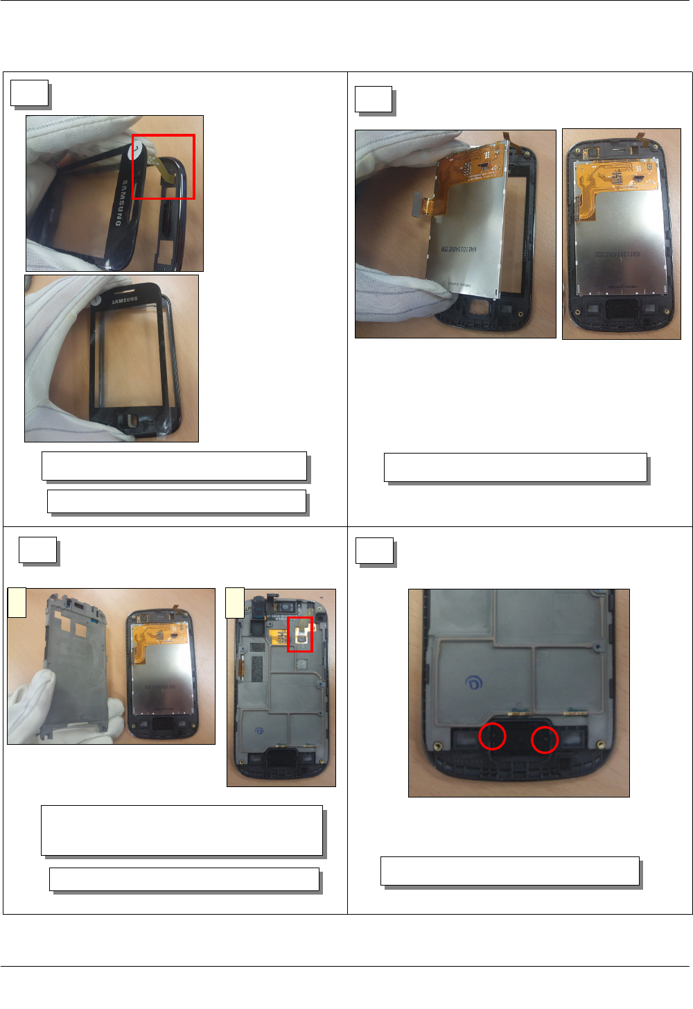
SAMSUNG Proprietary-Contents may change without notice
7. Level 2Repair
7-4
This Document can not be used without Samsung's authorization
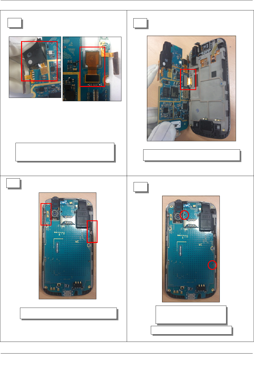
7-2. Assembly
1
4
3
2
Be careful not to tear up the TSP FPCB.
1. Assemble the braket and the front.
2. Insert the TSP FPCB into the connector.
Be careful to damage the LCD FPCB.
Assemble the LCD and the front.
Assemble the TSP and the front.
12
Insert the TSP FPCB into the connector.
SAMSUNG Proprietary-Contents may change without notice
7. Level 2Repair
7-5
This Document can not be used without Samsung's authorization
7
6
8
5
Assemble the earjack module and the
camera module. Connect the PBA and the LCD connector.
Attach the both FPCBs on the braket. Screw up at 2points.
1.0±0.1 kgf.cm
Be careful not to damage the PBA.
SAMSUNG Proprietary-Contents may change without notice
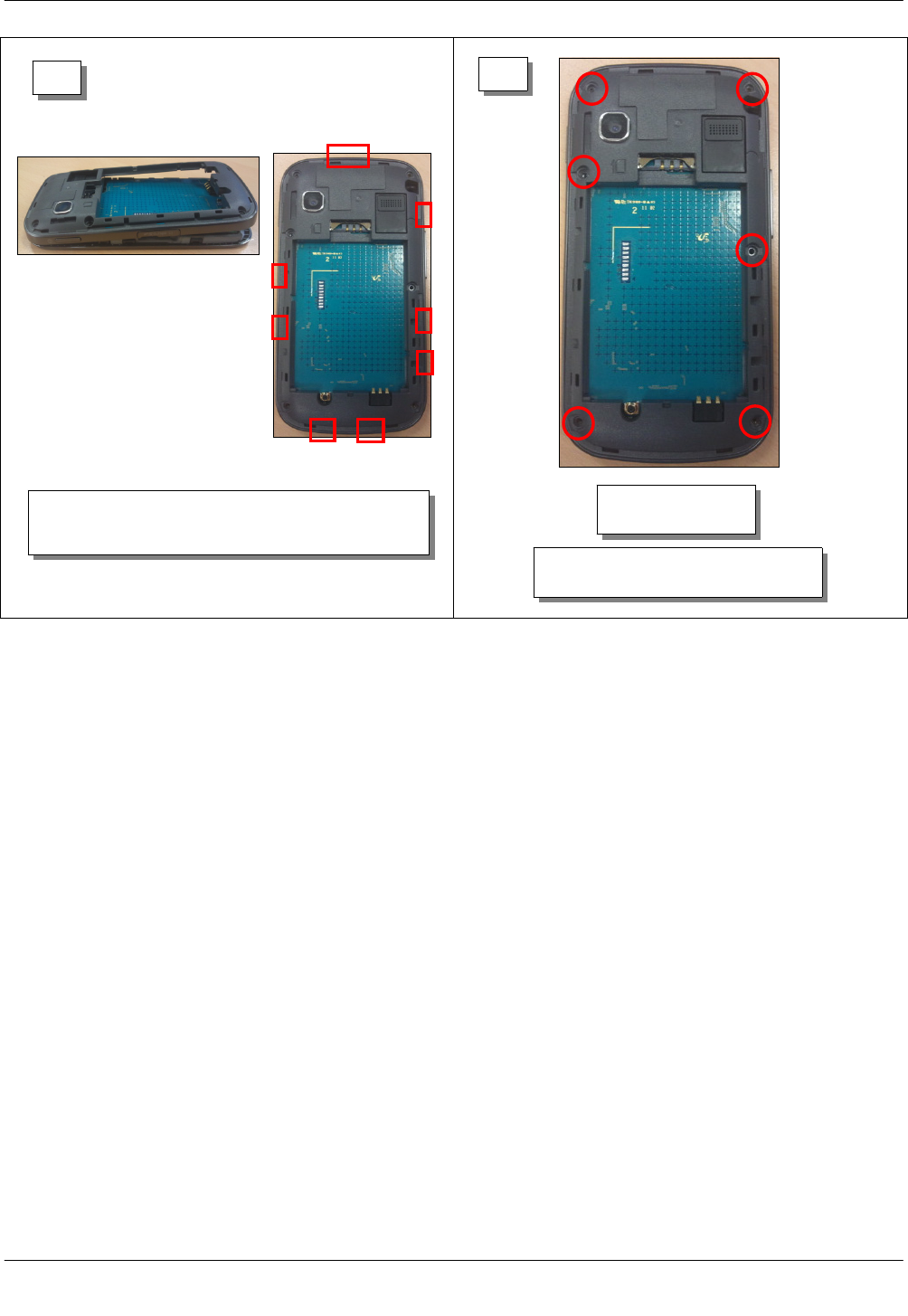
7. Level 2Repair
7-6
This Document can not be used without Samsung's authorization
9
1. Assemble the Rear and the Front ass'y.
2. Hook at the 8points.
10
Screw at 6points.
1.0±0.1 kgf.cm
DO NOT MAKE SCRATCH ON
THE REAR.
SAMSUNG Proprietary-Contents may change without notice
8. Level 3Repair
8-1
This Document can not be used without Samsung's authorization
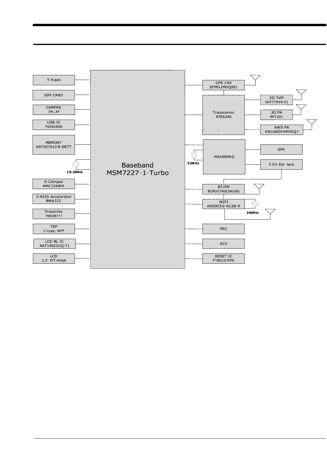
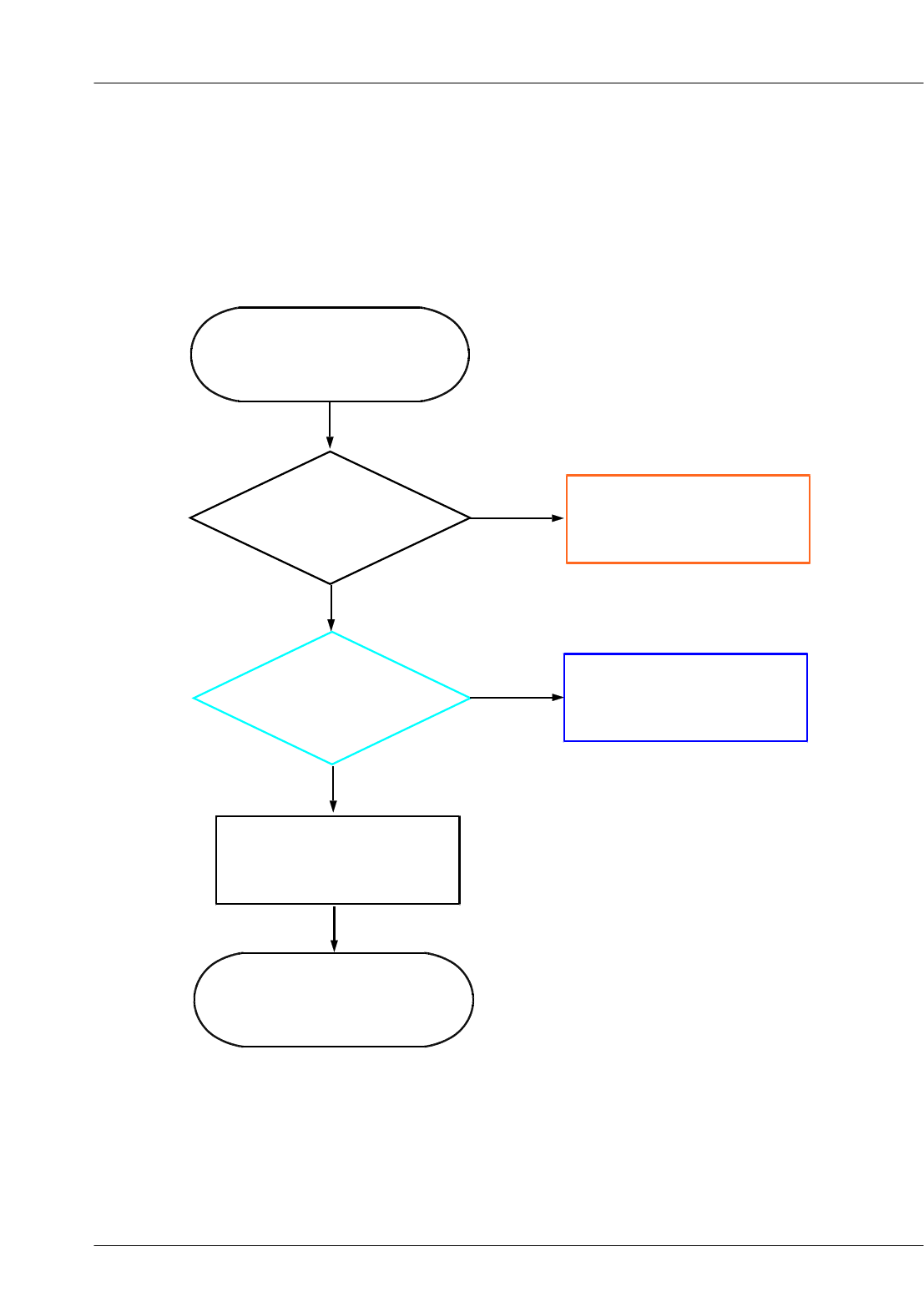
8-1.Block Diagram
SAMSUNG Proprietary-Contents may change without notice
Level 3Repair
8-2
This Document can not be used without Samsung's authorization
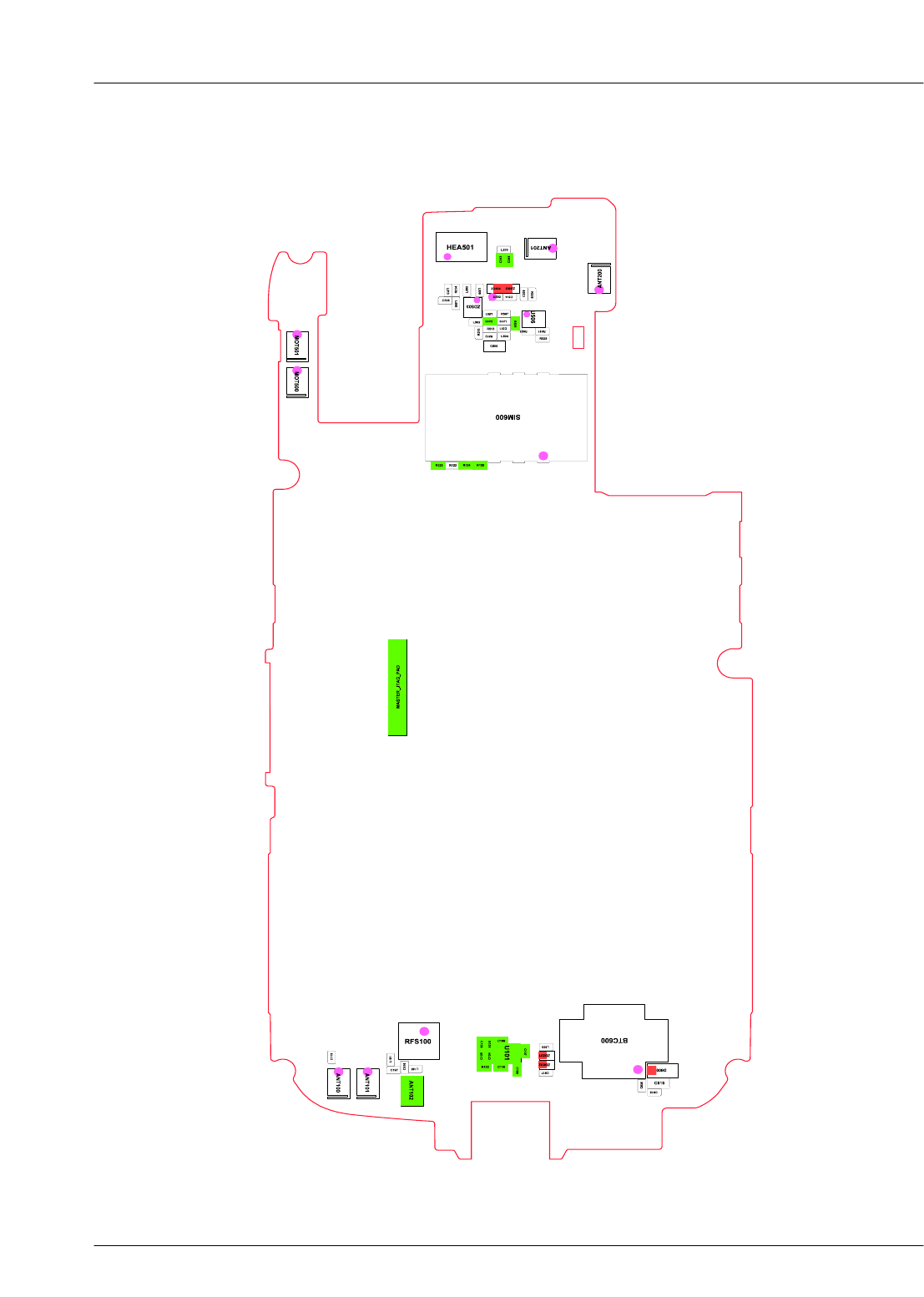
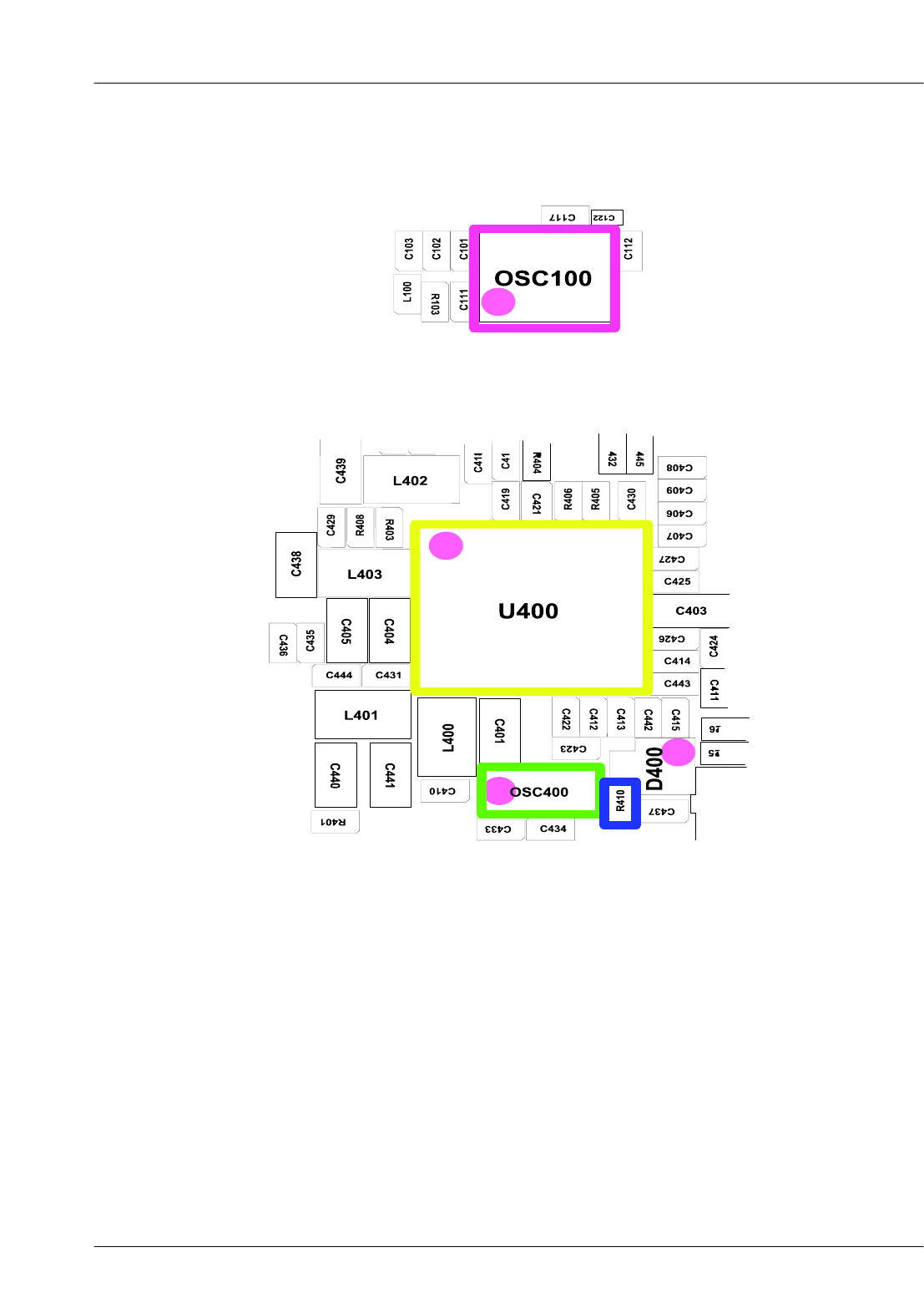
8-2. PCB Diagrams
8-2-1. Top
SAMSUNG Proprietary-Contents may change without notice
Level 3Repair
8-3
This Document can not be used without Samsung's authorization
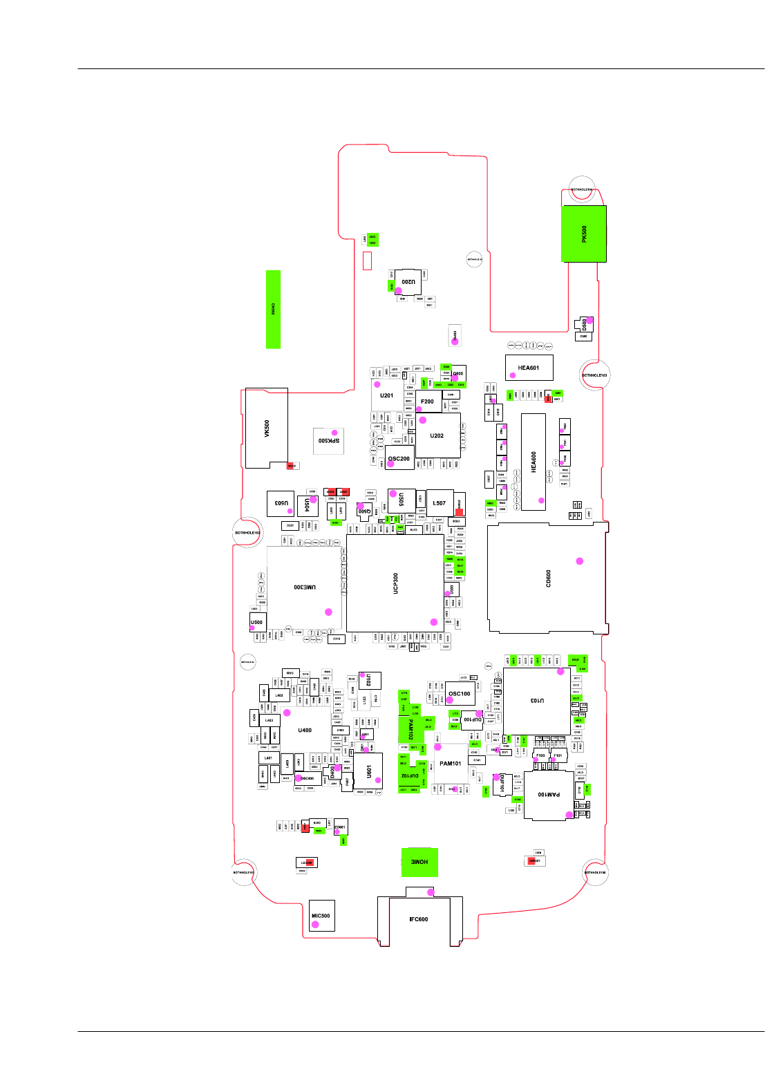
8-2-1. Bottom
SAMSUNG Proprietary-Contents may change without notice
Level 3Repair
8-4
This Document can not be used without Samsung's authorization
8-3. LOGIC
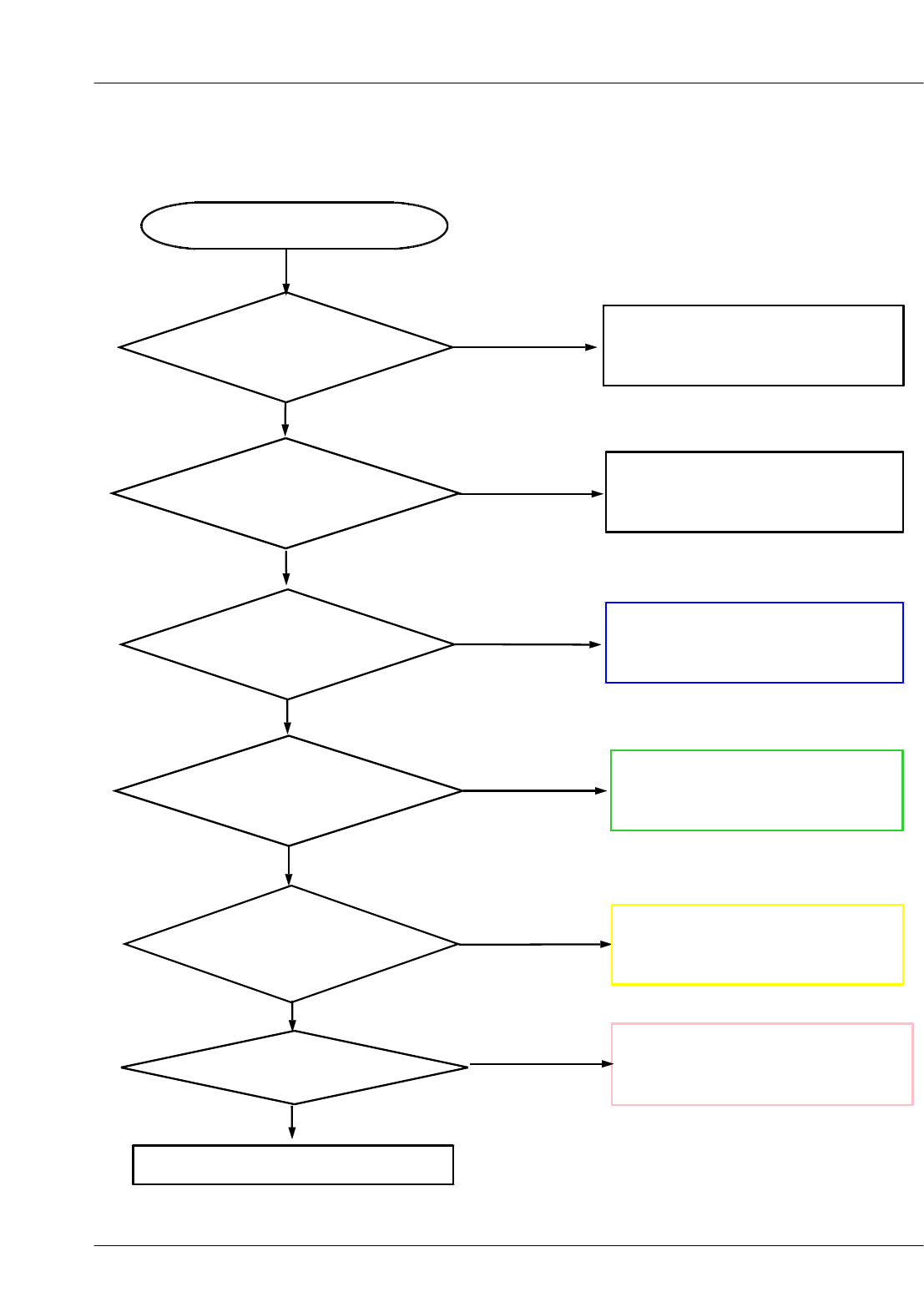
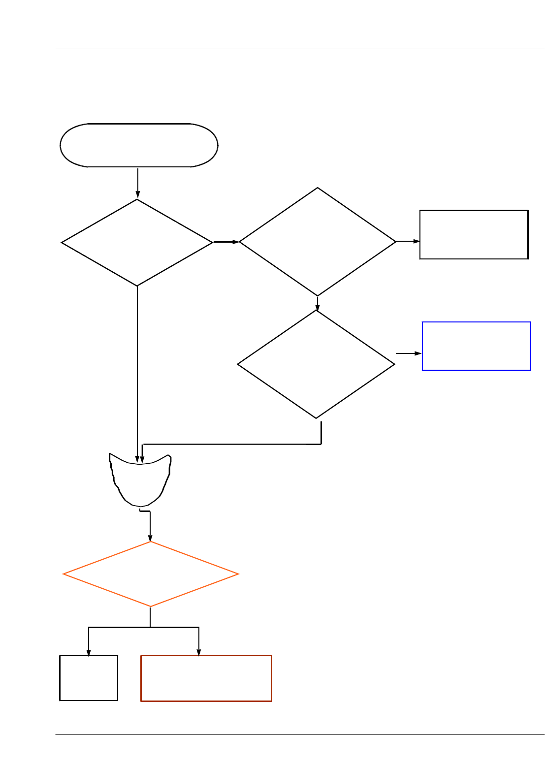
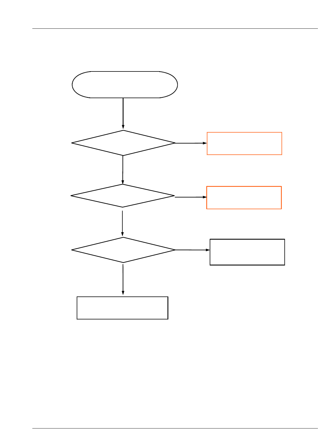
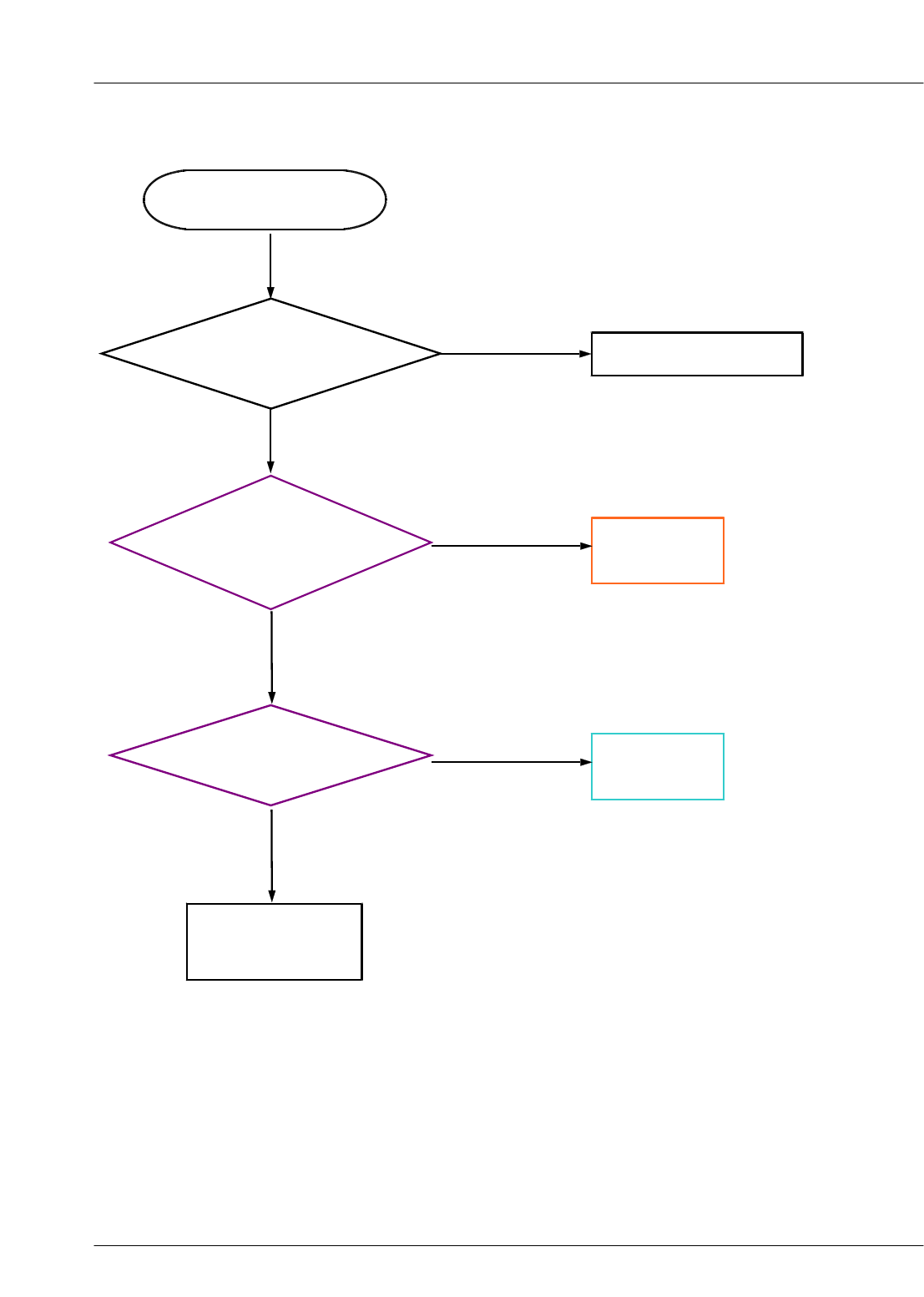
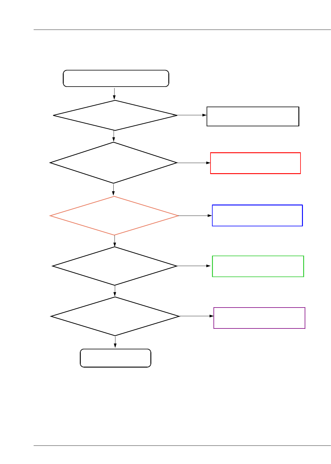
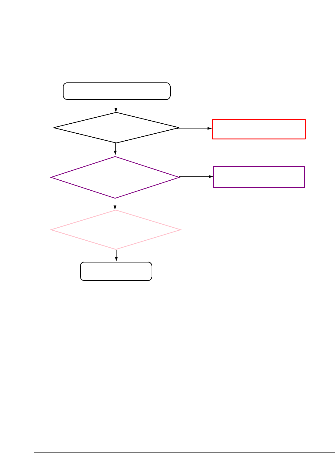
8-3-1. Power On
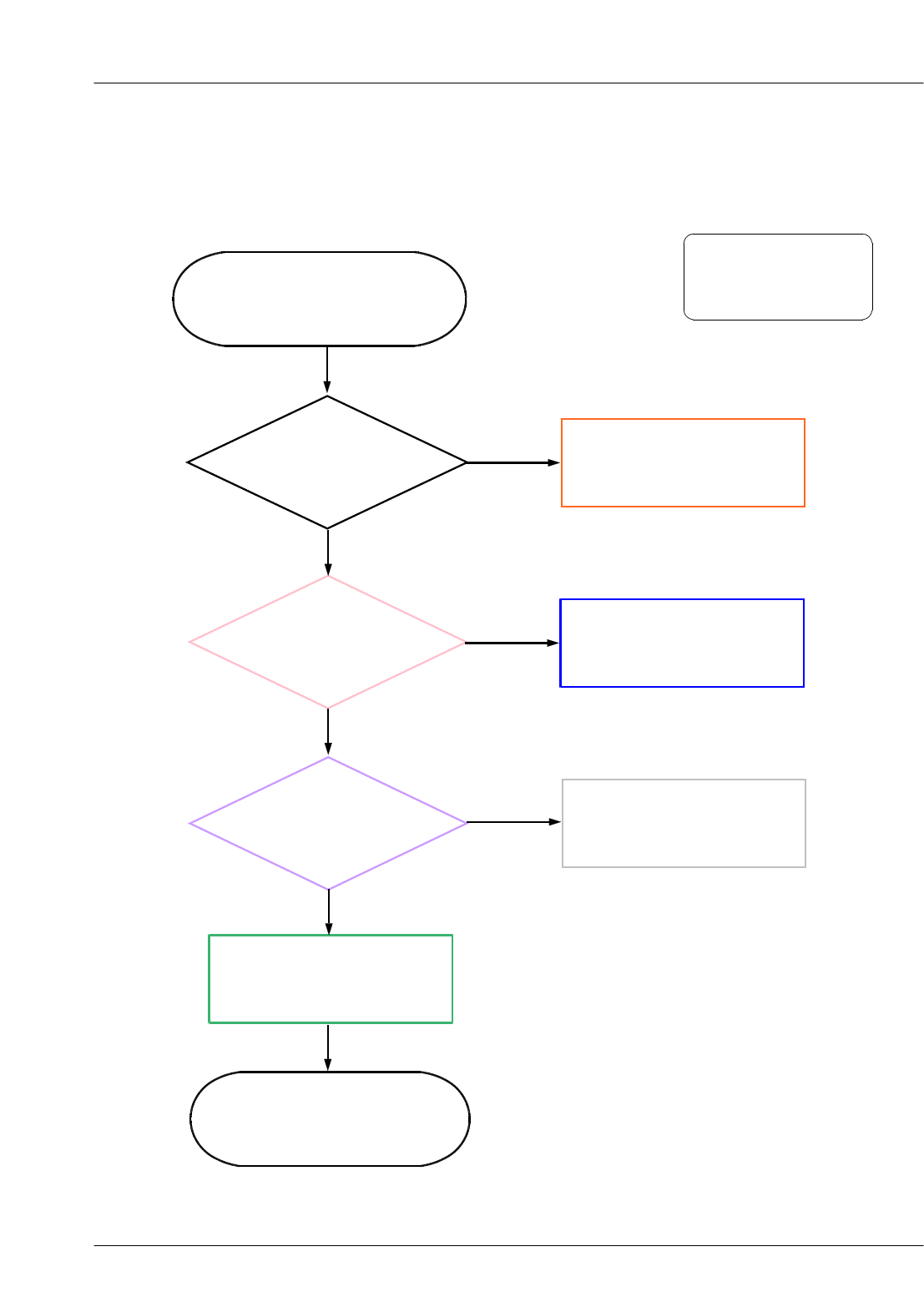
Power switch on
NG
Check the current
consumption
>= 100mA?
Download
NO
Check the U400
Check the clock
C117 =19.2
Mhz ?
Check the initial operation
Check the clock generation circuit
Resolder OSC400
Check the PMIC
relatedtoPS_HOLD
Change the battery
Yes
Yes
Yes
Yes
NO
NO
C441(VREG_MSMC1)=1.2V?
C440(VREG_MSMC2)=1.2V?
C439(VREG_MSME)=1.8V?
C410(VREG_MSMP)=2.6V?
C411(VREG_MSMA)=2.6V?
Yes
NO
Check the clock at
OSC400 =32
KHz ?
NO
Check the R410_T
P_PS_HOLD pin P
S_HOLD =2.6
V?
NO
Check the battery
voltage
>= 3.45?
Yes
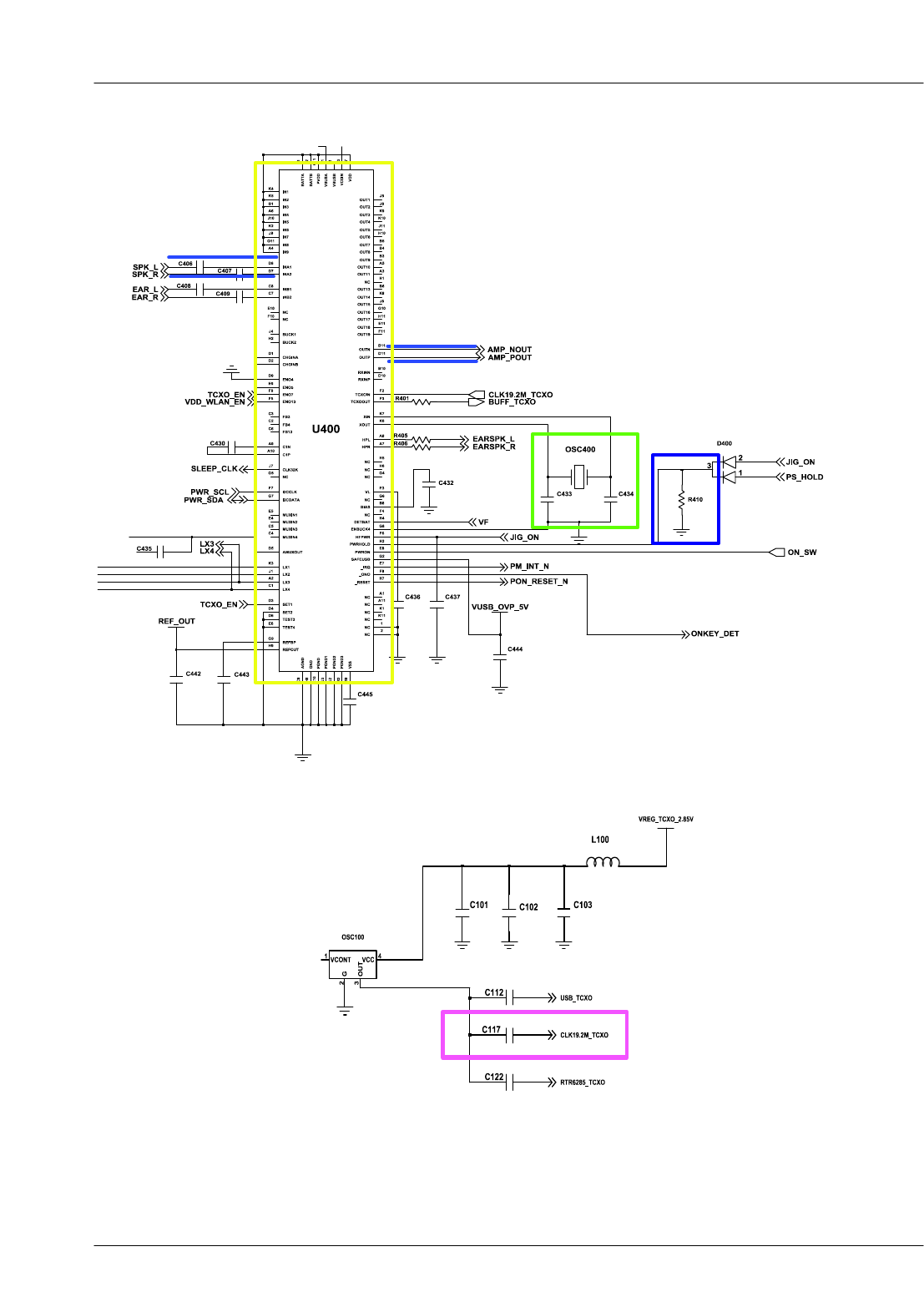
SAMSUNG Proprietary-Contents may change without notice
Level 3Repair
8-5
This Document can not be used without Samsung's authorization
SAMSUNG Proprietary-Contents may change without notice
Level 3Repair
8-6
This Document can not be used without Samsung's authorization
SAMSUNG Proprietary-Contents may change without notice
Level 3Repair
8-7
This Document can not be used without Samsung's authorization
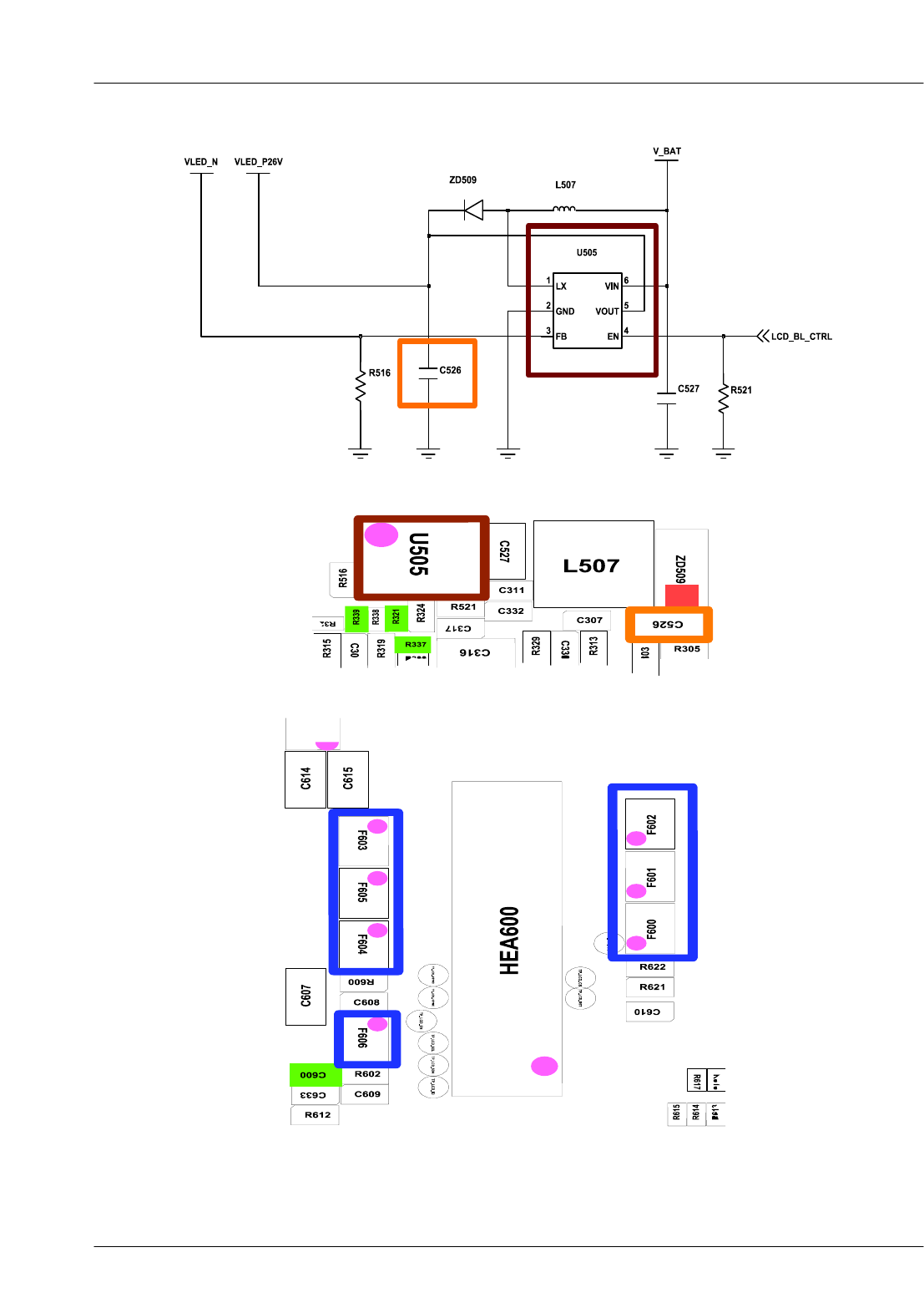
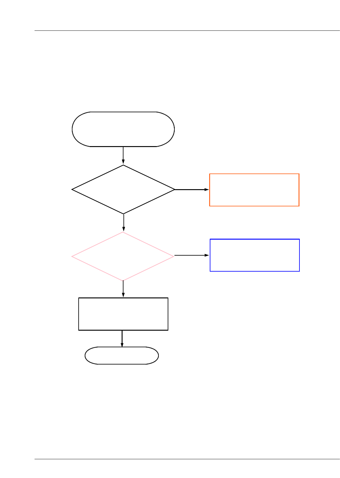
8-3-2. LCD Working
Power Switch On
LCD FPCB
connector is co
rrectly connecti
ned?
Replace U505 &Check
neighboring circuits
Yes
NO
Yes
LCD
Replace
C526
LED_P_26V=26V?
F600, F601, F602,
F603, F604, F605,
F606 Resolder
F600, F601,
F602, F603,
F604, F605,
F606 Correctly
mounted?
NO
correctly connect
NO
LCD Display
On?
Yes
Yes
NO
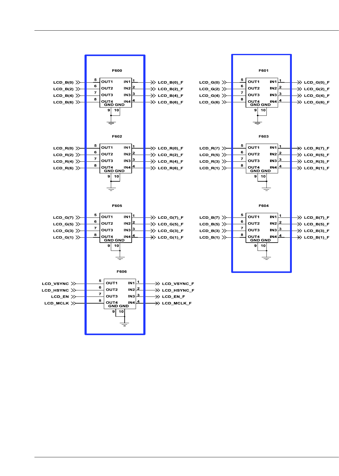
SAMSUNG Proprietary-Contents may change without notice
Level 3Repair
8-8
This Document can not be used without Samsung's authorization
SAMSUNG Proprietary-Contents may change without notice
Level 3Repair
8-9
This Document can not be used without Samsung's authorization
SAMSUNG Proprietary-Contents may change without notice
Level 3Repair
8-10
This Document can not be used without Samsung's authorization
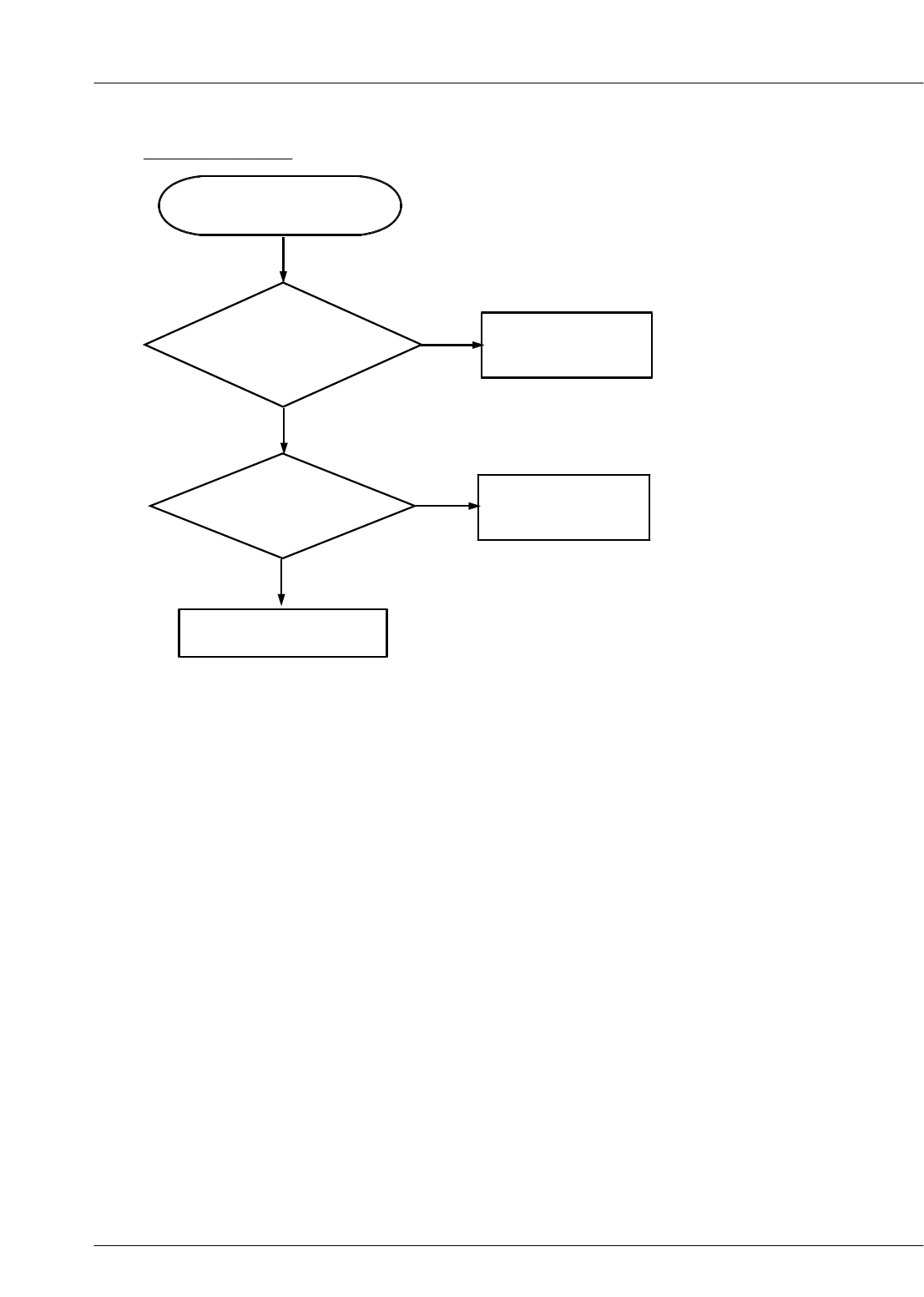
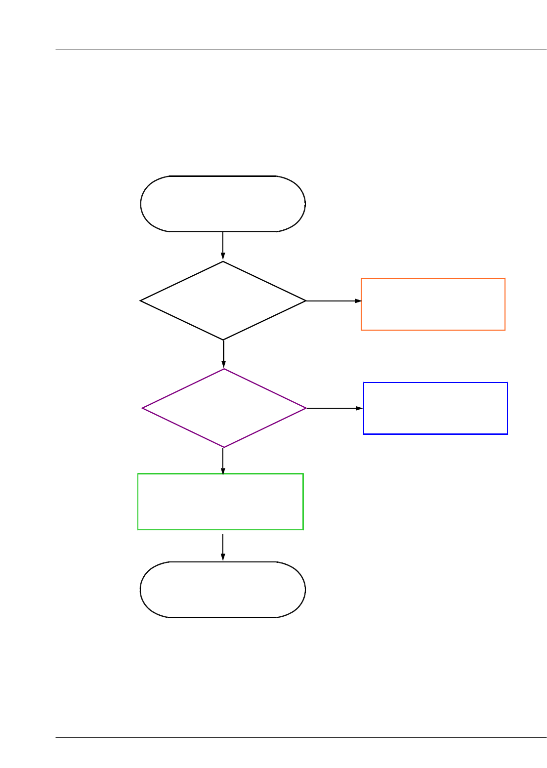
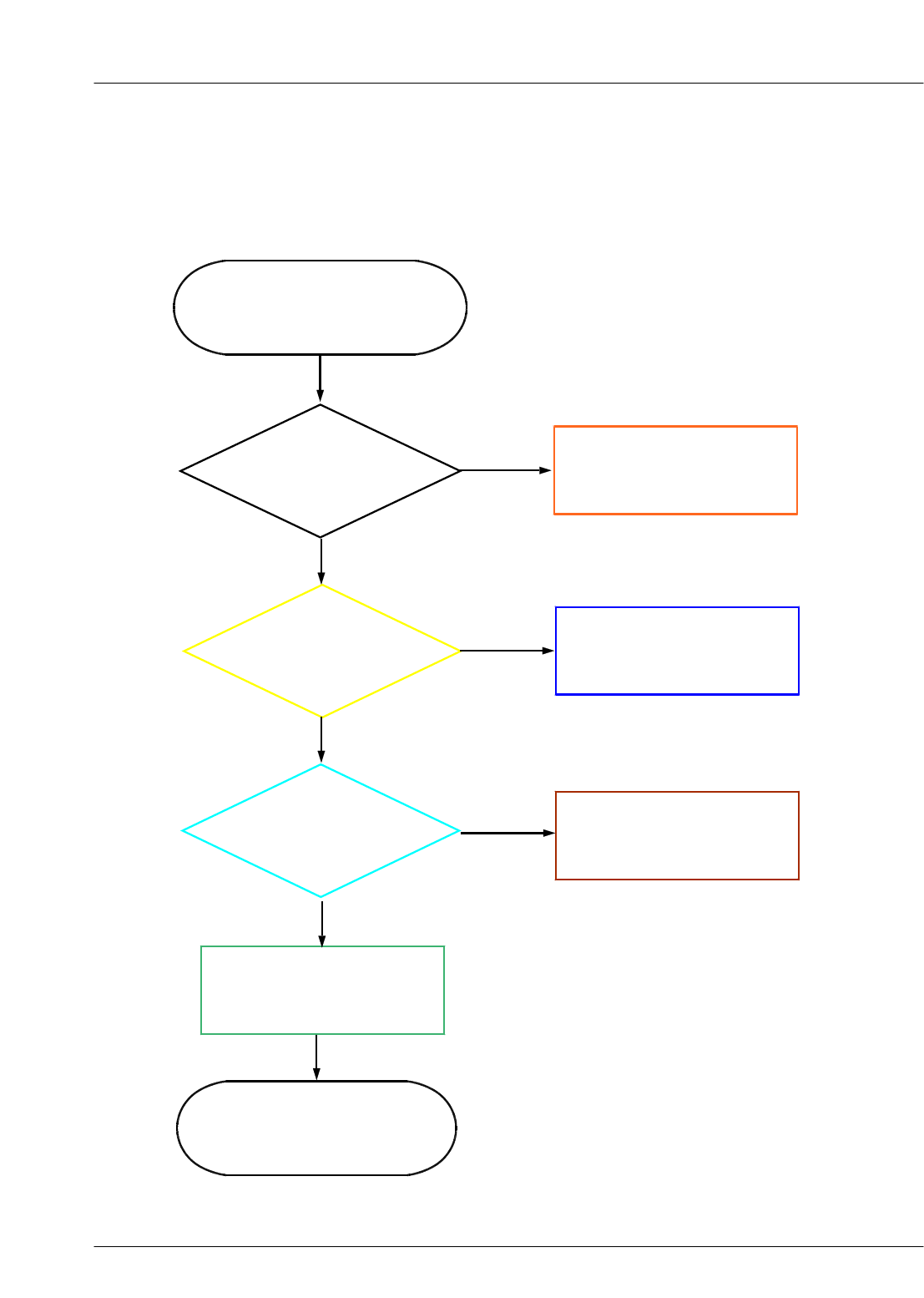
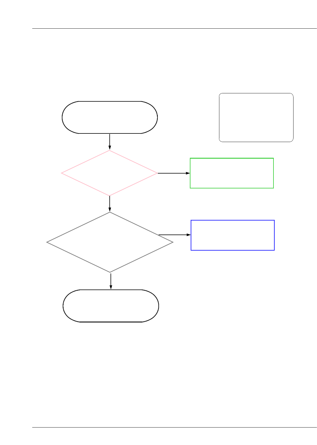
8-3-3. TSP
Operate TSP
NG
Check
TSP Connecting Reconnecting TSP
NO
YES
Change TSP Module
No Problem? Change main PBA
NO
END
SAMSUNG Proprietary-Contents may change without notice
Level 3Repair
8-11
This Document can not be used without Samsung's authorization
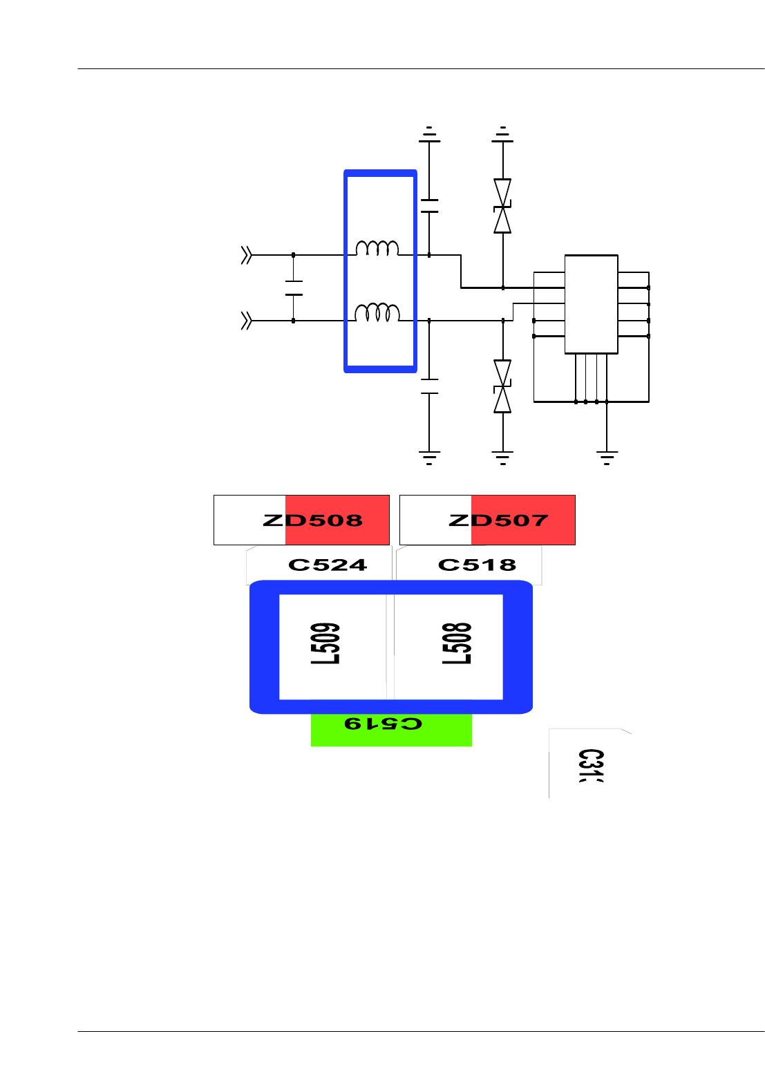
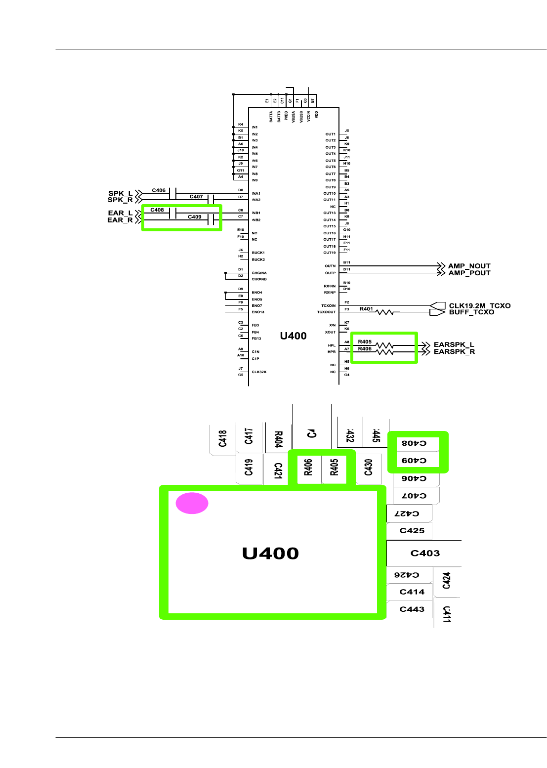
8-3-3. Audio Working
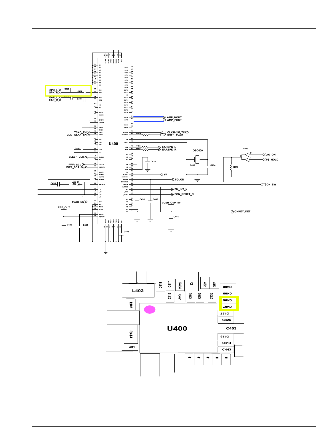
-Speaker Working
7
Operate speaker
NG
Check
Speaker
Connector
Resolder
NO
YES
Speaker break
down?
YES
Change Speaker
NO
Signal on in
L508, L509?
Resolder
L508,L509
SPK ASSY
YES
NO
Signal on in
C406, C407?
Resolder
C406, C407
Replace U400
YES
NO
Change main PBA
SAMSUNG Proprietary-Contents may change without notice
Level 3Repair
8-12
This Document can not be used without Samsung's authorization
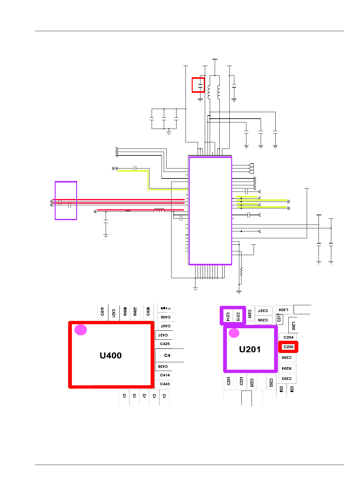
C518
99
11
NC NC
12 13
NCNC
14
10 10
22
33 4 4
55 6 6
77 8 8
SPK500
11
ZD507
ZD508
L509
C524
C519
L508
AMP_POUT
AMP_NOUT
SAMSUNG Proprietary-Contents may change without notice
Level 3Repair
8-13
This Document can not be used without Samsung's authorization
SAMSUNG Proprietary-Contents may change without notice
Level 3Repair
8-14
This Document can not be used without Samsung's authorization
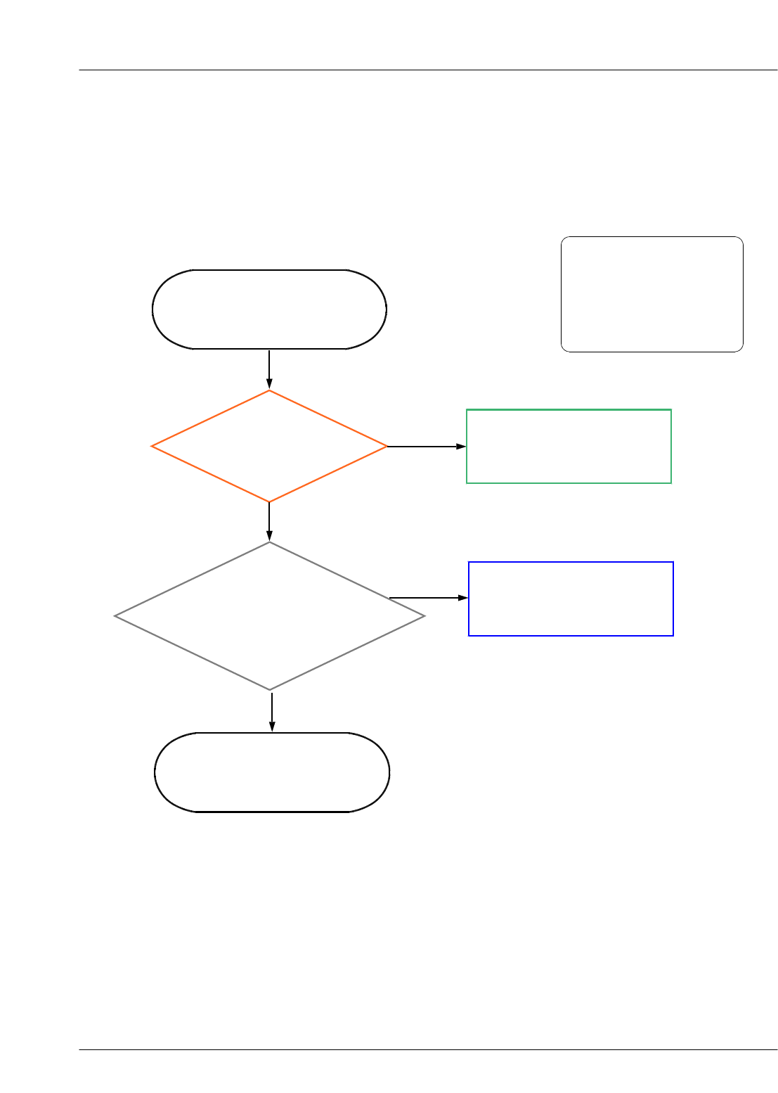
-Receiver Working
Operate Receiver
NG
Check
Receiver
Connector
Resolder
NO
YES
Receiver break
down?
YES
Change Receiver
NO
Change main PBA
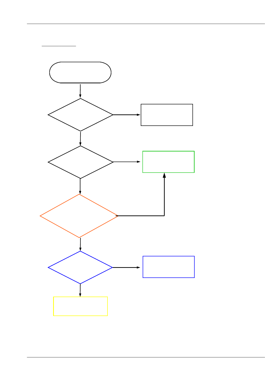
SAMSUNG Proprietary-Contents may change without notice
Level 3Repair
8-15
This Document can not be used without Samsung's authorization
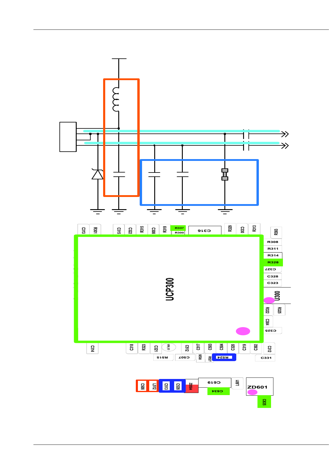
-MIC Working
Operate MIC
NG
Pollute
MIC Hole?
YES Clean up
MIC hole
NO
Check Voltage
of L512, C508
L512 &C508's
Voltage
NO
NO
YES
YES
Change main PBA
Signal on in
C503, C504 ?Change UCP300
YES
NO
Signal on in
C513, C528,
R524 ?
Resoldering
C513, C528
R524
SAMSUNG Proprietary-Contents may change without notice
Level 3Repair
8-16
This Document can not be used without Samsung's authorization
C513
C528
L512
C508
ZD504
OUT
4
OUT
POWER
1
POWER
MIC500
2
GND
3
GND
VMIC_BIAS_1.8V
C503
SHORT
R524
C504
MIC_P
MIC_N
SAMSUNG Proprietary-Contents may change without notice
Level 3Repair
8-17
This Document can not be used without Samsung's authorization
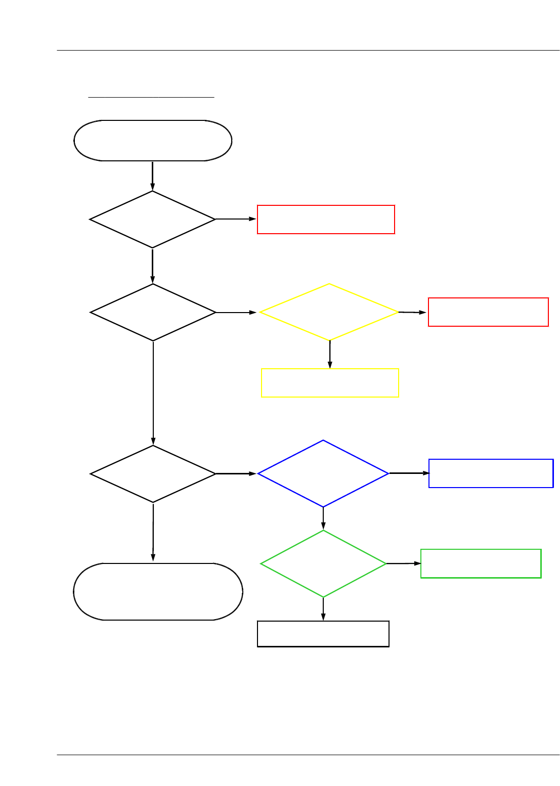
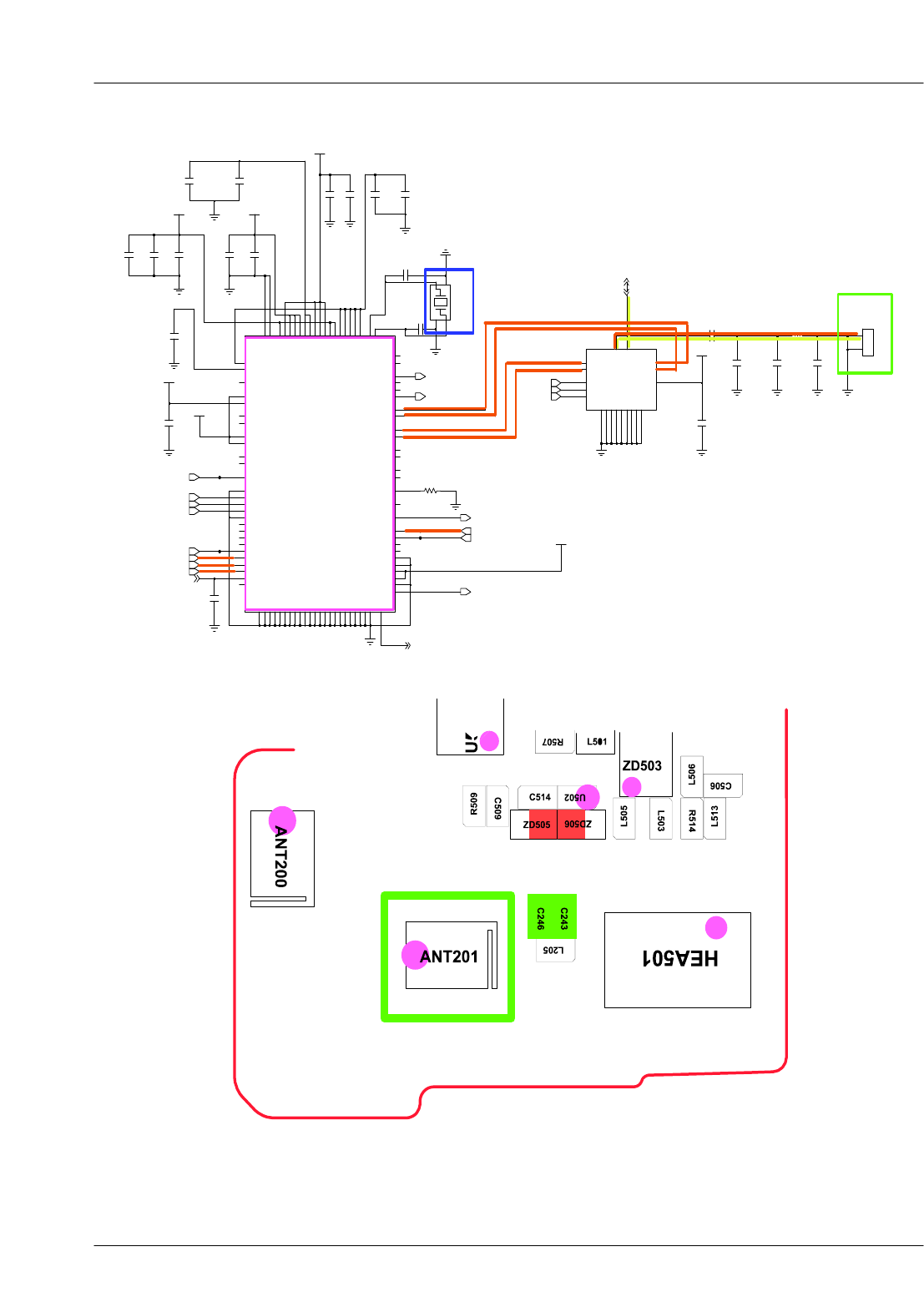
Stereo Headset Working
Hands-free stereo
headset
NG
YES
Check U506Button NG?
NO
Check
L501
MIC NG?
NO
YES
Check U506
YES
Resolder L501
NO
Signal on
in ZD503?
SPK NG? Check L503, L505,
YES
YES
NO
NO
Signal on
in C408
C409?
YES Check R405, R406,
U400
The End NO
Change Main PBA
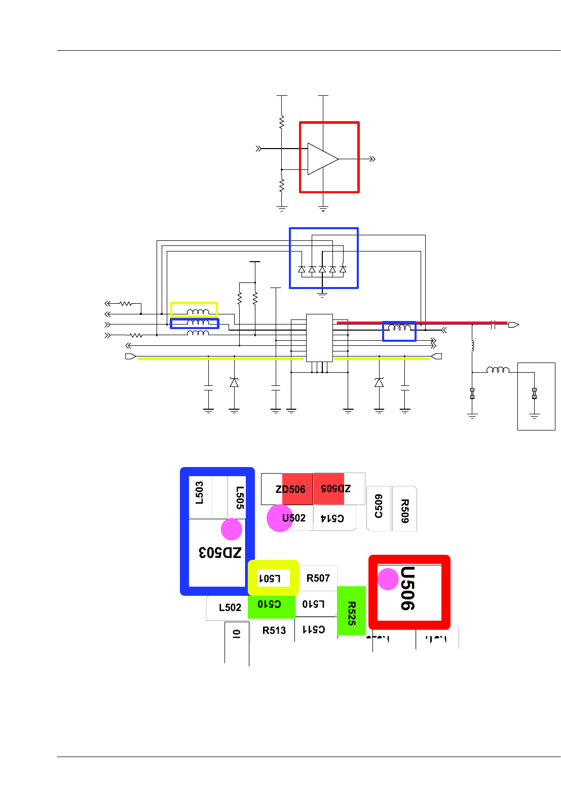
SAMSUNG Proprietary-Contents may change without notice
Level 3Repair
8-18
This Document can not be used without Samsung's authorization
GND CLOSE TO PMU ANALOG GND
6
ZD503
1
2
3
4
5
ZD506
R514
SHORT
R515
SHORT
L506
NC
19
20NC
44
55 66
77 88
99
NC
17
18NC
11 11 12 12
13
13 14 14
15 15 16
16
22
33
HEA501
11
10 10
L513
L501
VREG_MSMP_2.6V
R528
R510
R507
L502
L505
C506
VLCD_3.0V
R509
L503
ZD505
C514
U502
C509
EARSPK_L
EAR_MIC
EARSPK_R
3PI_ADC
FM_ANT
JACK_INT_N
PROXI_INT
RCV_P
RCV_N
I2C_SDA
I2C_SCL
R517
VREG_MSMP_2.6V
R523
VREG_MSMP_2.6V
2
1
3
5
4
U506
EAR_MIC
EAR_SWITCH
SAMSUNG Proprietary-Contents may change without notice
Level 3Repair
8-19
This Document can not be used without Samsung's authorization
SAMSUNG Proprietary-Contents may change without notice
Level 3Repair
8-20
This Document can not be used without Samsung's authorization
8-3-5. KEY Working
-Volume KEY
Press Volume Key
NG
Check the V/K
Soldering State
It is OK ?
YES
Resoldering the V/K FPCB
NO
Check the V/K
FPCB STATE
It is OK ?Change V/K FPCB
NO
YES
Change main PBA
SAMSUNG Proprietary-Contents may change without notice
Level 3Repair
8-21
This Document can not be used without Samsung's authorization
-Sub Key
Press Power Key,
Other Sub Key
Power (END)
Key NG?
Yes
Pressing
power key,
ZD502 =High?
Yes
Check 8-3-1 Section
NO
Check the Soldering State.
Change PWR KEY FPCB
NO
Home Key
NG?
Change Domesheet
Change Main PBA
Yes
NO
The End
Menu&Back Key
NG? Change TSP
Yes
NO
SAMSUNG Proprietary-Contents may change without notice
Level 3Repair
8-22
This Document can not be used without Samsung's authorization
V_BAT
PK500
11
2
2
33
ZD502
ON_SW
SAMSUNG Proprietary-Contents may change without notice
Level 3Repair
8-23
This Document can not be used without Samsung's authorization
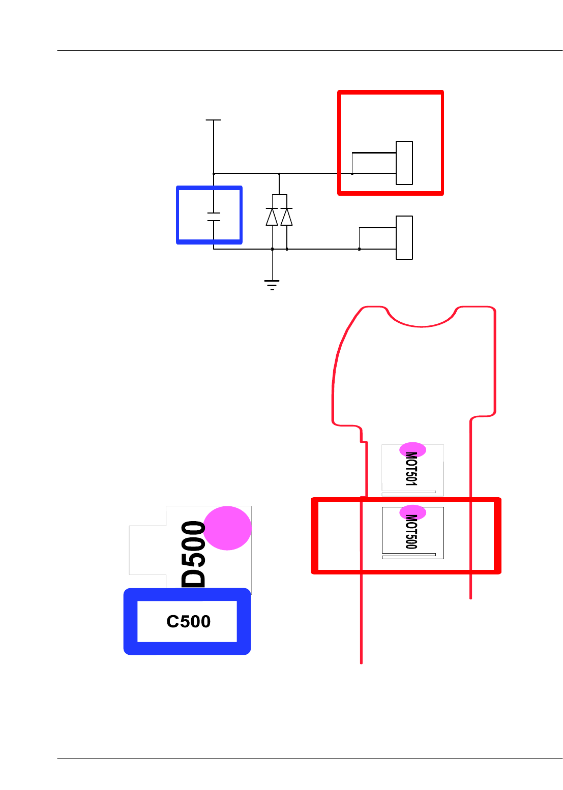
8-3-6. Vibrator Working
Operate Vibrator
NO
Check
Vibrator Clip
Resolder Vibrator Clip
NO
Yes
VREG_VIB_3.3V
(C500) =3.3V?
Check PMIC (U400)
Change Main PBA
No
Yes
MOT500 PAD
High?
Change Vibrator
Yes
NO
Change Main PBA
SAMSUNG Proprietary-Contents may change without notice
Level 3Repair
8-24
This Document can not be used without Samsung's authorization
3
1
2
D500
VREG_VIB_3.3V
C500
2
2
2
MOT501
11
MOT500
11
2
SAMSUNG Proprietary-Contents may change without notice
Level 3Repair
8-25
This Document can not be used without Samsung's authorization
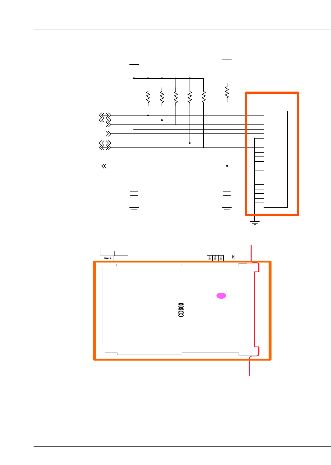
8-3-7. T-Flash Card Working
Insert &Operate
microSD card
NG
YES
CD600
break down ?Change CD600
NO
YES
Change CD600
12thPin of CD600
=High ?
NO
4thPin of CD600
=3.0V? Check U400(PMIC)
NO
YES
Change Main PBA
SAMSUNG Proprietary-Contents may change without notice
Level 3Repair
8-26
This Document can not be used without Samsung's authorization
R616
VREG_USIM_3.0V
6
15 NC
NC
16
NC
17
18 NC
19 NC
NC
20
VDD
4
VSS
7DAT0
DAT1
8
1DAT2
DAT3|CD
2
9GND
10 GND
13 NC
NC
14
CD600
CD
12
5CLK
3CMD
11 COMMON
R612
R615 R617
C627 C633
R613
VREG_TFLASH_2.85V
R614
MICROSD_CMD
MICROSD_DATA(0)
MICROSD_DATA(1)
MICROSD_DATA(2)
MICROSD_DATA(3)
nTF_DETECT
MICROSD_CLK
SAMSUNG Proprietary-Contents may change without notice
Level 3Repair
8-27
This Document can not be used without Samsung's authorization
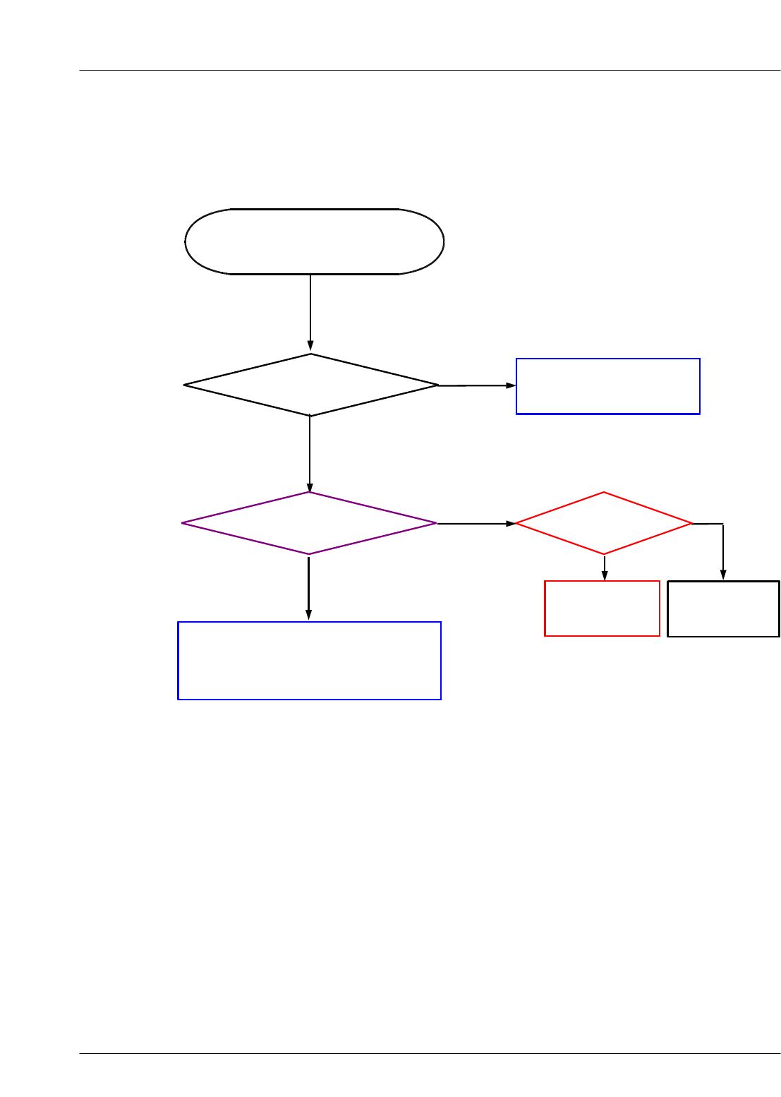
8-3-8. SIM Card Working
Resolder
Q600
Change
U400(PMIC)
Yes
Check
Q600
SIM Connector
Break down?
NO
Change SIM600
YES
No
Yes
R610
=3.0V
NG
Check SIM600
&Neighboring Circuits
Insert &Operate
SIM card
SAMSUNG Proprietary-Contents may change without notice
Level 3Repair
8-28
This Document can not be used without Samsung's authorization
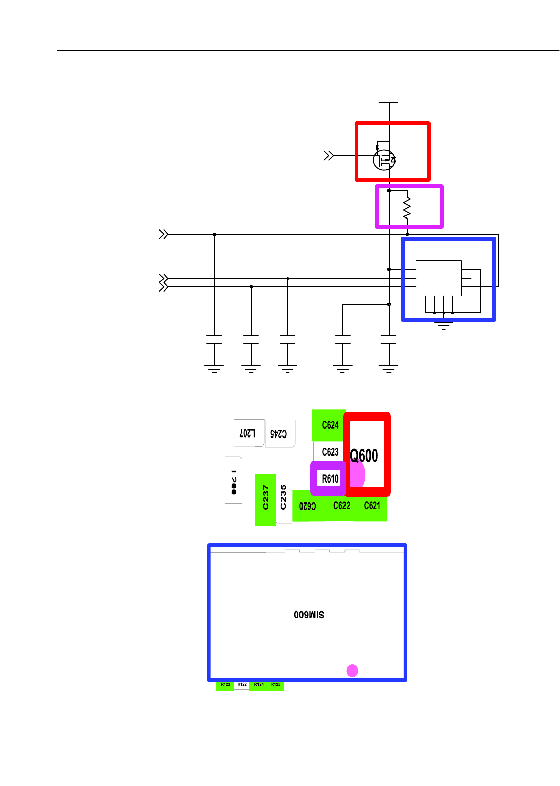
C624
S2
Q600
D3
G
1
VREG_USIM_3.0V
C623
C621
R610
C620 C622
7
GG
89
GG
10
SIM600
11
22
33 4
4
55
6
6
SIM_DATA
SIM_CLK
SIM_RST
UIM_FET_PWR_CTL
SAMSUNG Proprietary-Contents may change without notice
Level 3Repair
8-29
This Document can not be used without Samsung's authorization
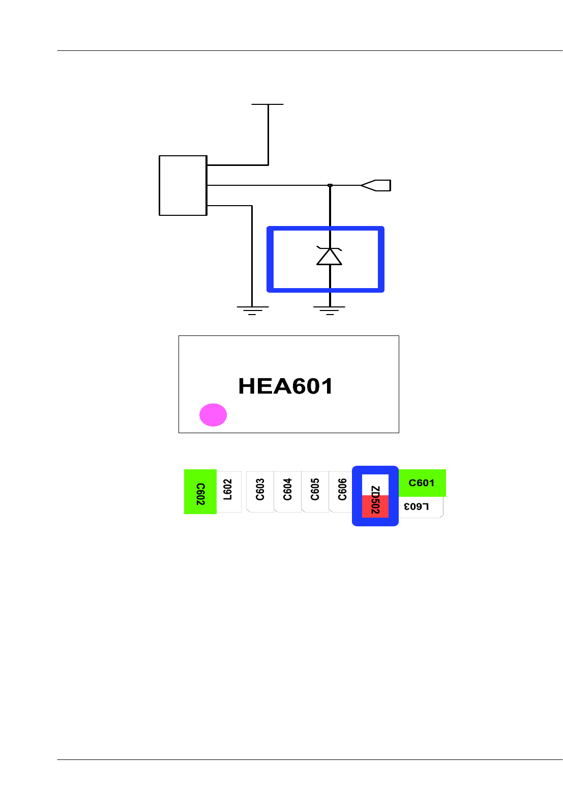
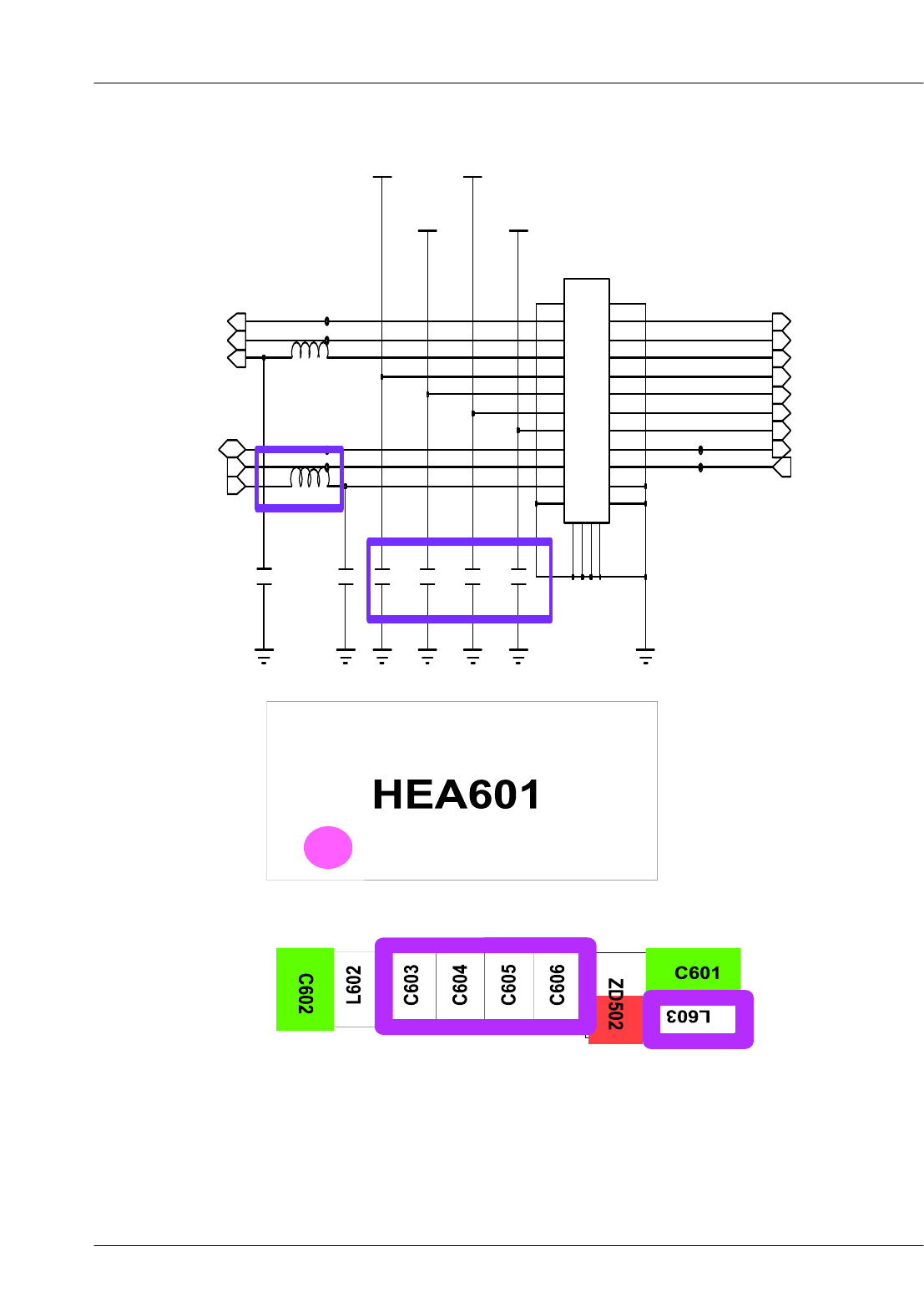
8-3-9 CAMERA Working
Operate CAMERA
NG
Camera FPCB con
nector is correctly
connecting?
correctly connect
NO
Yes
C603 =3.0
V,
C604 =1.8V
C605 =2.8V
C606 =2.8V
Change
U400(PMIC)
NO
Yes
CAMERA
Replace
L603 =24MHz ?Change
UCP300
Yes
SAMSUNG Proprietary-Contents may change without notice
Level 3Repair
8-30
This Document can not be used without Samsung's authorization
VCAMIO_2.8V
TP_CAM_SDA
VCAMAF_3.0V
C603
TP_CAM_RESETTP_CAM_SCL
C605
VCAMA_2.8VVCAMC_1.8V
C601
TP_CAM_D(0)
C606
L603
L602
NC
25 26
NC
27
NC
NC
28
C604
24
3
34
4
556
6
7
78
8
99
17 18 18
19
19
22
20
20
21 21 22 22
23
23 24
1
10 10
11
11 12
12
13 13 14 14
15
15 16
16
17
HEA601
1
TP_VSYNC
TP_HSYNC
C602
CAM_SCL
CAM_SDA
CAM_MCLK
CAM_D(3)
CAM_RESET
CAM_HSYNC
CAM_VSYNC
CAM_PCLK
CAM_D(6)
CAM_D(5)
CAM_D(4)
CAM_D(7)
CAM_D(2)
CAM_D(1)
CAM_D(0)
SAMSUNG Proprietary-Contents may change without notice
Level 3Repair
8-31
This Document can not be used without Samsung's authorization
SAMSUNG Proprietary-Contents may change without notice
Level 3Repair
8-32
This Document can not be used without Samsung's authorization
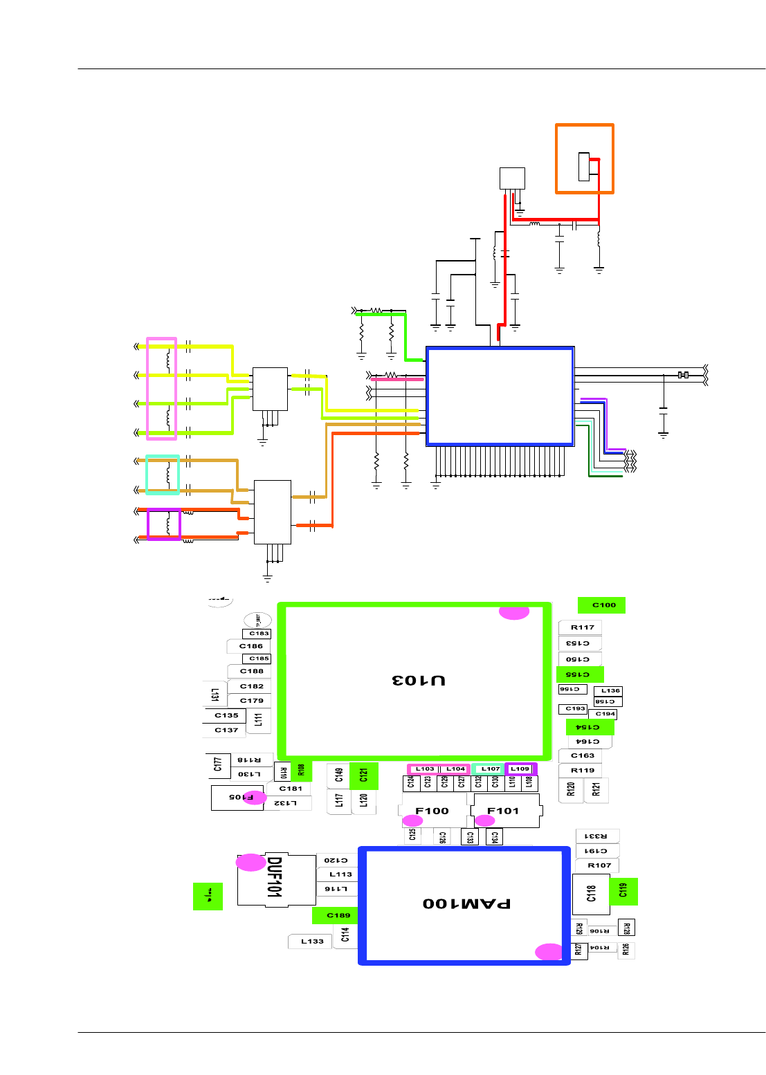
8-4-1. GSM850 RX
**If you check the tx chain,
Check the not only RF Device but also resistor, inductor and capacitor.
Resolder U103 or Change
Check Antenna contact
The End
Yes
Yes
Check L109 =-55
dBm ?
No
Replace PAM100
Yes
Normal condition
Catch the channel?
No
Yes
Continuous Rx ON
RF Input : 190 CH
Amplitude :-50
dBm
SAMSUNG Proprietary-Contents may change without notice
Level 3Repair
8-33
This Document can not be used without Samsung's authorization
8-4-2. GSM900 RX
**If you check the tx chain,
Check the not only RF Device but also resistor, inductor and capacitor.
Continuous Rx ON
RF Input :62CH
Amplitude :-50
dBm
The End
Check L107 >= -55 dBm?
Normal Condition
Catch the channel?
Yes
Yes
Yes
No
No
Check Antenna Contact
Resolder U103 or Change
Replace PAM100
SAMSUNG Proprietary-Contents may change without notice
Level 3Repair
8-34
This Document can not be used without Samsung's authorization
8-4-3. DCS/PCS RX
**If you check the tx chain,
Check the not only RF Device but also resistor, inductor and capacitor.
Check L103, L104
>= -55 dBm?
Continous Rx ON
RF Input :698CH
Amplitude :-50
dBm
The End
Normal Condition
Catch the channel?
Yes
Yes
Yes
No
No
Check Antenna Contact
Resolder U103 or Change
Replace PAM100
SAMSUNG Proprietary-Contents may change without notice
Level 3Repair
8-35
This Document can not be used without Samsung's authorization
C116
IN2 4
OUT1
8
OUT1
9
OUT2
6
7OUT2
G
2
3G
5G
10G
1
IN1
F101
C119
R126
R106
C191
L140
C197
R127
L103
L104
L108
C127
C129
R129
C123
L110
5G
G
10
1
IN1
IN2 4
OUT1
8
9OUT1
OUT2
6
7OUT2
F100
2G
G
3
C134
C133
L107
V_BAT
WCDMA2 16
WCDMA3 17
8
_TXEN
14 RX1
RX2
13
12 RX3
RX4
11
10
TEMP
4
VAPC
VBATT5
WCDMA1 15
22G
23G
24G
G
25
26G
HB_IN
1
LB_IN
3
MODE 9
G
39
G
40
G
41
42G
G
43
44G
20G
G
21
G
32
33G
34G
G
35
36G
G
19
G
37
38G
BS1
7
BS2
6
2G
27G
G
28
G
29
30G
G
31
PAM100
ANT18
R128
ANT101
1
1
22
C118
G
RFS100
2A
1C
G
3
4
L101
C130
C125
SHORT
R107
L133
R104
C189
C132
C126
C124
L109
C114
RFOUT_G850_EGSM
ANT_SEL(0)
ANT_SEL(3)
ANT_SEL(2)
ANT_SEL(1)
GSM_PA_RAMP+
TRX_AWS
TRX_WCDMA900
RFOUT_DCS_PCS
RX_EGSM900_N
RX_EGSM900_P
RX_DCS1800_N
RX_DCS1800_P
RX_PCS1900_N
RX_PCS1900_P
TRX_WCDMA2100
RX_GSM850_N
RX_GSM850_P
SAMSUNG Proprietary-Contents may change without notice
Level 3Repair
8-36
This Document can not be used without Samsung's authorization
8-4-4. WCDMA Band1 RX
**If you check the tx chain,
Check the not only RF Device but also resistor, inductor and capacitor.
Continous Rx ON
RF Input : 10700CH
Amplitude :-50
dBm
The End
Check L113 =-65dBm?
Normal Condition
Catch the channel?
Yes
Yes
Yes
No
No
Check Antenna Contact
Resolder U103 or Change
Replace PAM100
Check L117= -65 dBm? Replace DUF101
No
Yes
SAMSUNG Proprietary-Contents may change without notice
Level 3Repair
8-37
This Document can not be used without Samsung's authorization
8-4-5. WCDMA Band8 RX
**If you check the tx chain,
Check the not only RF Device but also resistor, inductor and capacitor.
The End
Check L105 =-65dBm?
Normal Condition
Catch the channel?
Yes
Yes
Yes
No
No
Check Antenna Contact
Resolder U103 or Change
Replace PAM100
Check C135 =-65dBm? Replace DUF100
No
Yes
Continous Rx ON
RF Input : 3013CH
Amplitude :-50
dBm
CONTINUOUS RX ON
RF INPUT : 3013CH
AMP :-50
dBm
SAMSUNG Proprietary-Contents may change without notice
Level 3Repair
8-38
This Document can not be used without Samsung's authorization
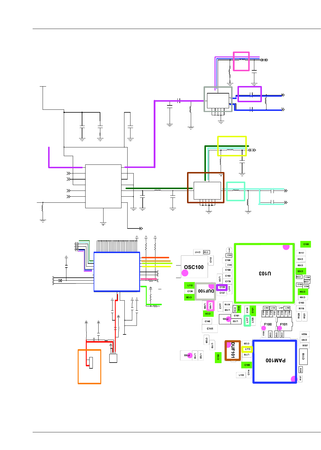
L113
C137
C149
C138
C121
L117
57
G
G
8
G
9
1
RXTX
3
L121
DUF101
6
ANT
G
24
G
G
C135
C136
3VMODE1
1RFIN_B8
RFOUT_B1 10
RFOUT_B8 14
VBAT
4
VCC 12
VEN_B1
6
5VEN_B8
VMODE0
2
CPL 8
GND 9
GND 11
GND 13
GND
15
7RFIN_B1
PAM101
C139
L112
C120
L119
C141
L120
L111
L105
C128 C152
L116
L106
GG
45
G
7
G
G
9
1
RX
8
RX
3TX
DUF100
ANT
6
2
C140
C131
RTR_W1900_RX
TRX_WCDMA900
WCDMA_RXP_900
WCDMA_RXM_900
CPL
PA_ON_W900
PA_ON_W2100
TRX_WCDMA2100
RTR_W2100_RX
PA_R1
PA_R0
C116
C119
R106
C191
L140
C197
R127
R129
V_BAT
WCDMA2 16
WCDMA3 17
8
_TXEN
14 RX1
RX2
13
12 RX3
RX4
11
10
TEMP
4
VAPC
VBATT
5
WCDMA1 15
22
G23
G24
G
G25
26
G
HB_IN
1
LB_IN
3
MODE 9
G39
G40
G41
42
G
G43
44
G
20
G
G21
G32
33
G34
G
G35
36
G
G19
G37
38
G
BS1
7
BS2
6
2
G
27
G
G28
G29
30
G
G31
PAM100
ANT
18
R128
ANT101
1
1
22
C118
G
RFS100
2
A1
C
G3
4
L101
SHORT
R107
L133
R104
C189
C114
ANT_SEL(0)
ANT_SEL(3)
ANT_SEL(2)
ANT_SEL(1)
GSM_PA_RAMP+
TRX_AWS
TRX_WCDMA900
TRX_WCDMA2100
SAMSUNG Proprietary-Contents may change without notice
Level 3Repair
8-39
This Document can not be used without Samsung's authorization
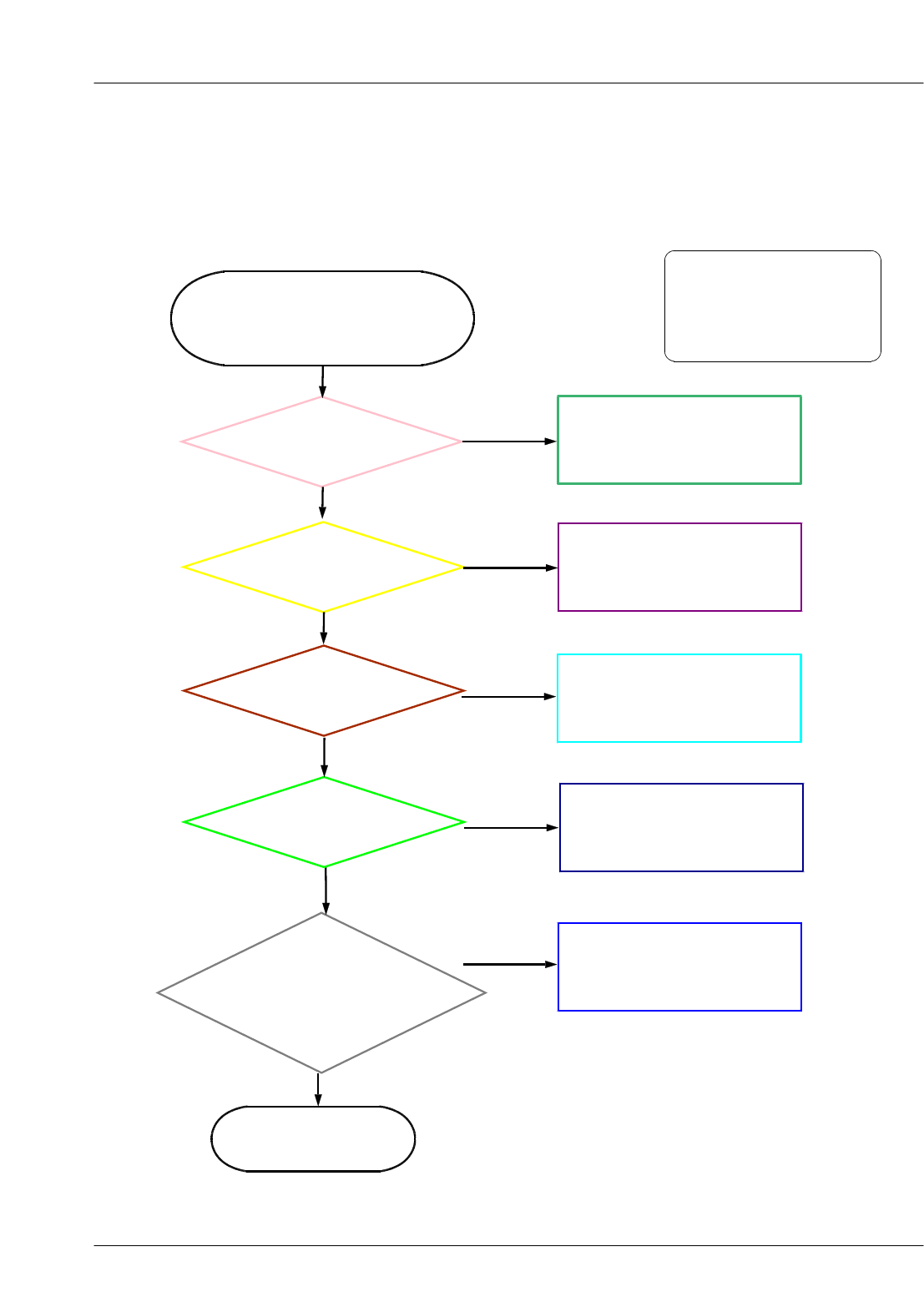
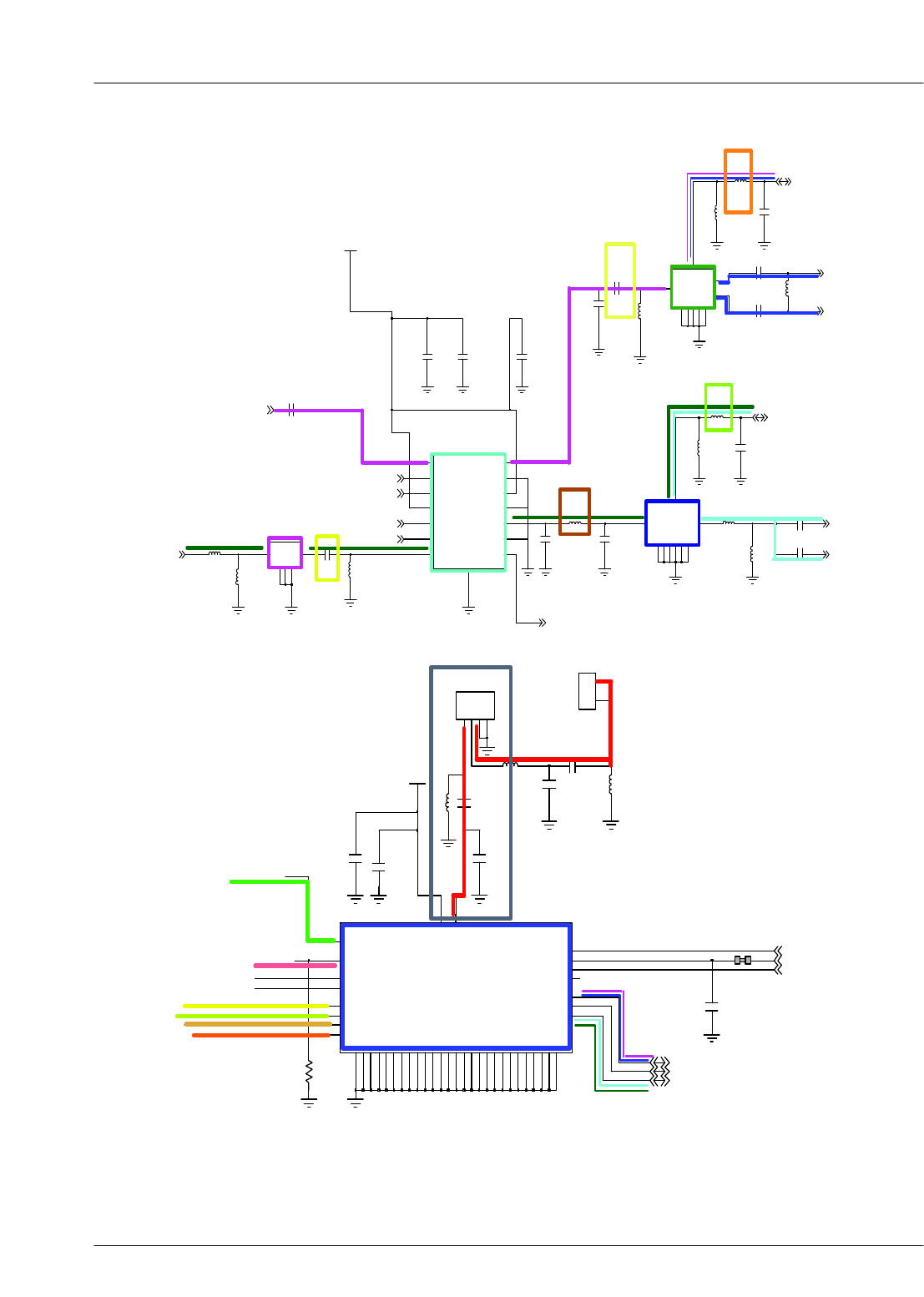
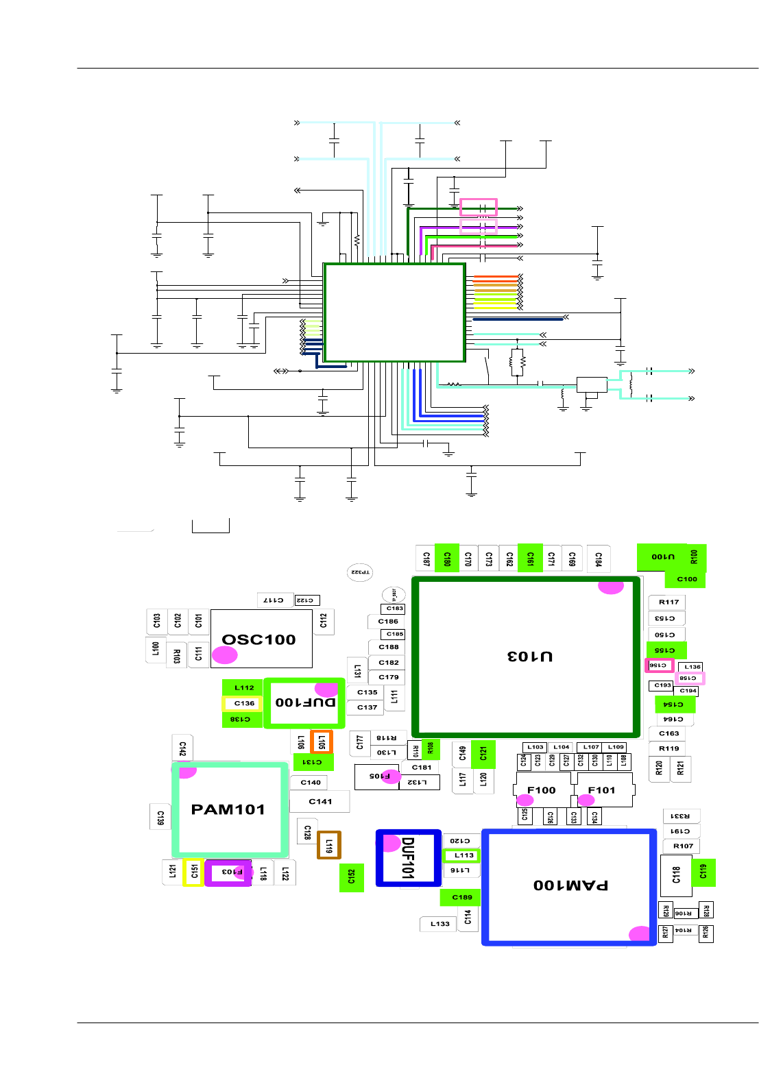
8-4-6. GSM850/900 TX
**If you check the tx chain,
Check the not only RF Device but also resistor, inductor and capacitor.
Check R106 >= 13dBm?
Check PAM100 PIN26
OUTPUT(RF CONN.)
With HP8960 >= 33dBm?
The End
Yes
Replace PAM100
No
Tx ON (Level :5)
Battery voltage:3.8V
Yes
Yes
No
Check The U103
CONTINOUS TX ON CONDITION
TX POWER DAC:14500 CODE
APPLIED
GSM850 CH : 190
GSM900 CH :62
RBW : 100KHz
VBW : 100KHz
SPAN :10
MHz
REF LEV. :10
dBm
ATT. :20
dB
SAMSUNG Proprietary-Contents may change without notice
Level 3Repair
8-40
This Document can not be used without Samsung's authorization
8-4-7. DCS/PCS TX
**If you check the tx chain,
Check the not only RF Device but also resistor, inductor and capacitor.
CONTINOUS TX ON CONDITION
TX POWER DAC:14500 CODE
APPLIED
DCS CH : 698
PCS CH : 661
RBW : 100KHz
VBW : 100KHz
SPAN :10
MHz
REF LEV. :10
dBm
ATT. :20
dB
Tx ON (Level :5)
Battery voltage:3.8V
The End
Check R105 >= 11dBm?
Yes
Yes
Yes
No
Check PAM100 PIN26
OUTPUT(RF CONN.)
With HP8960 >= 30dBm?
Check The U103
Replace PAM100
No
SAMSUNG Proprietary-Contents may change without notice
Level 3Repair
8-41
This Document can not be used without Samsung's authorization
C116
IN2 4
OUT1
8
OUT1
9
OUT2
6
7OUT2
G
2
3G
5G
10G
1
IN1
F101
C119
R126
R106
C191
L140
C197
R127
L103
L104
L108
C127
C129
R129
C123
L110
5G
G
10
1
IN1
IN2 4
OUT1
8
9OUT1
OUT2
6
7OUT2
F100
2G
G
3
C134
C133
L107
V_BAT
WCDMA2 16
WCDMA3 17
8
_TXEN
14 RX1
RX2
13
12 RX3
RX4
11
10
TEMP
4
VAPC
VBATT5
WCDMA1 15
22G
23G
24G
G
25
26G
HB_IN
1
LB_IN
3
MODE 9
G
39
G
40
G
41
42G
G
43
44G
20G
G
21
G
32
33G
34G
G
35
36G
G
19
G
37
38G
BS1
7
BS2
6
2G
27G
G
28
G
29
30G
G
31
PAM100
ANT18
R128
ANT101
1
1
22
C118
G
RFS100
2A
1C
G
3
4
L101
C130
C125
SHORT
R107
L133
R104
C189
C132
C126
C124
L109
C114
RFOUT_G850_EGSM
ANT_SEL(0)
ANT_SEL(3)
ANT_SEL(2)
ANT_SEL(1)
GSM_PA_RAMP+
TRX_AWS
TRX_WCDMA900
RFOUT_DCS_PCS
RX_EGSM900_N
RX_EGSM900_P
RX_DCS1800_N
RX_DCS1800_P
RX_PCS1900_N
RX_PCS1900_P
TRX_WCDMA2100
RX_GSM850_N
RX_GSM850_P
SAMSUNG Proprietary-Contents may change without notice
Level 3Repair
8-42
This Document can not be used without Samsung's authorization
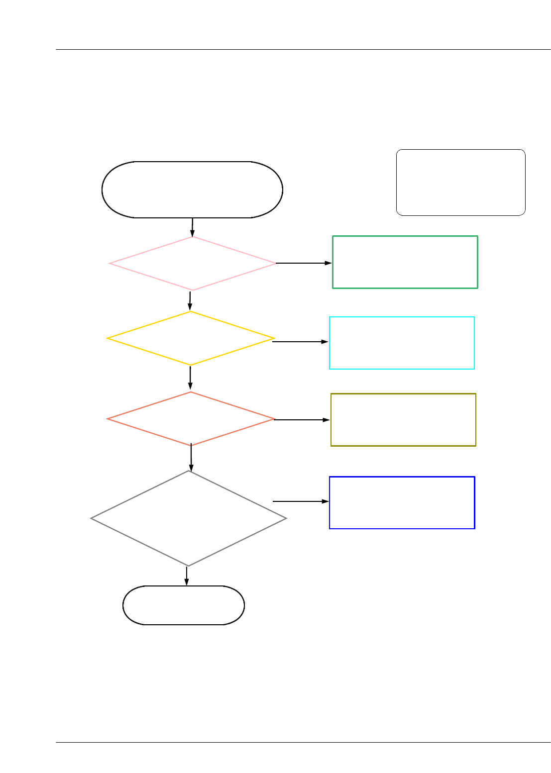
8-4-8. WCDMA Band1 TX
**If you check the tx chain,
Check the not only RF Device but also resistor, inductor and capacitor.
Tx ON
Battery Voltage: 3.8V
CONTINOUS TX ON CONDITION
TX POWER DAC:120 CODE APPLIED
CH : 10700
RBW : 100KHz
VBW : 100KHz
SPAN :10
MHz
REF LEV. :10
dBm
ATT. :20
dB
The End
Check PAM100 PIN26
OUTPUT(RF CONN.)
With HP8960 >= 23dBm?
Yes
Check L119 =26dBm?
Check C156 =8dBm ?
Check C151 =5dBm?
Yes
Yes
Yes
No
No
Check the U103
Replace PAM100
Replace PAM101
No
No
No
Replace F103
Replace DUF101
Yes
Yes
Check L113 =24dBm?
SAMSUNG Proprietary-Contents may change without notice
Level 3Repair
8-43
This Document can not be used without Samsung's authorization
8-4-9. WCDMA Band8 TX
**If you check the tx chain,
Check the not only RF Device but also resistor, inductor and capacitor.
Tx ON
Battery Voltage: 3.8V
Check PAM100 PIN26
OUTPUT(RF CONN.)
With HP8960 >= 23dBm?
The End
Check C158 =8dBm ?
Yes
Yes
No
Check the U103
Replace PAM100
Replace U102
Check C136 =26dBm?
No
No
No
Replace DUF100
Yes
Yes
Yes
CONTINOUS TX ON CONDITION
TX POWER DAC:120 CODE APPLIED
CH : 3013
RBW : 100KHz
VBW : 100KHz
SPAN :10
MHz
REF LEV. :10
dBm
ATT. :20
dB
Check L105= 26 dBm?
SAMSUNG Proprietary-Contents may change without notice
Level 3Repair
8-44
This Document can not be used without Samsung's authorization
C151
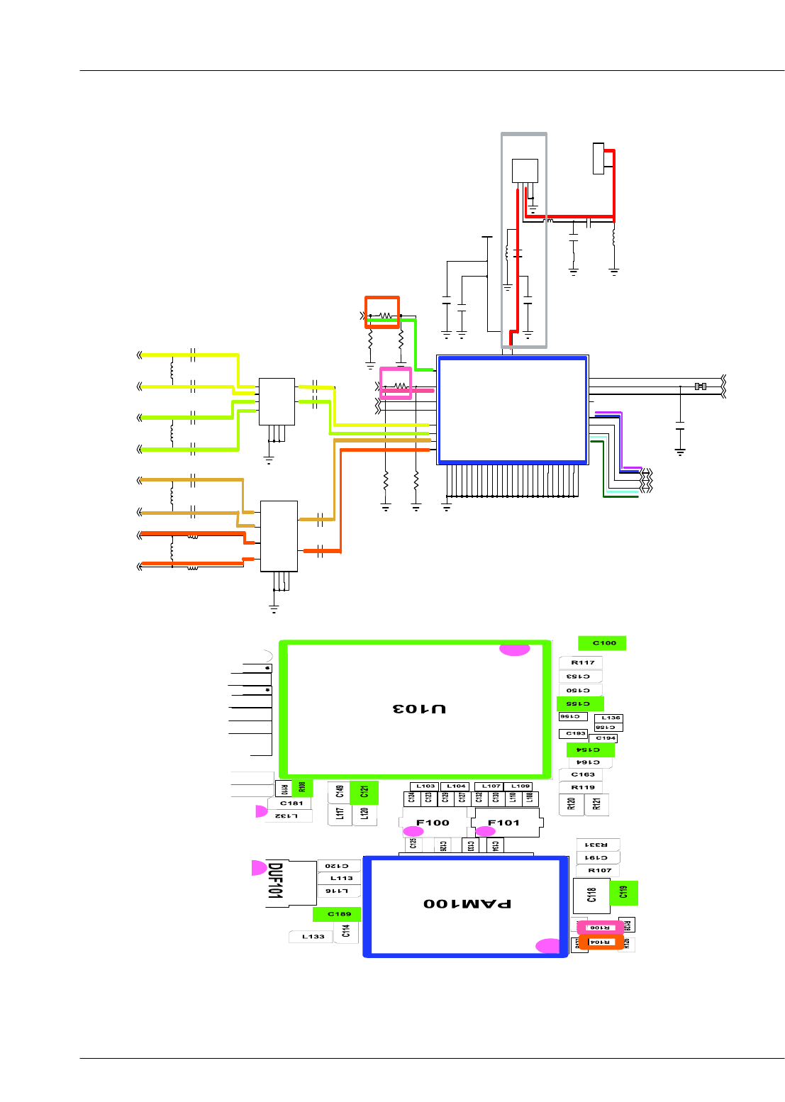
L113
C137
C149
C142
L118
C138
C121
L117
57
G
G
8
G
9
1
RXTX
3
L121
DUF101
6
ANT
G
24
G
G
IN OUT 4
F103
2
GG
3
G
5
1
C135
C136
3VMODE1
1RFIN_B8
RFOUT_B1 10
RFOUT_B8 14
VBAT
4
VCC 12
VEN_B1
6
5VEN_B8
VMODE0
2
CPL 8
GND 9
GND 11
GND 13
GND
15
7RFIN_B1
V_BAT_3GPA_3.0V
PAM101
C139
L112
C120
L119
L122
C141
L120
L111
L105
C128 C152
L116
L106
GG
45
G
7
G
G
9
1
RX
8
RX
3TX
DUF100
ANT
6
2
C140
C131
RTR_W1900_RXRFOUT_W2100
TRX_WCDMA900
WCDMA_RXP_900
WCDMA_RXM_900
RFOUT_W900
CPL
PA_ON_W900
PA_ON_W2100
TRX_WCDMA2100
RTR_W2100_RX
PA_R1
PA_R0
C116
C119
C191
L140
C197
R129
V_BAT
WCDMA2 16
WCDMA3 17
8
_TXEN
14 RX1
RX2
13
12 RX3
RX4
11
10
TEMP
4
VAPC
VBATT5
WCDMA1 15
22G
23G
24G
G
25
26G
HB_IN
1
LB_IN
3
MODE 9
G
39
G
40
G
41
42G
G
43
44G
20G
G
21
G
32
33G
34G
G
35
36G
G
19
G
37
38G
BS1
7
BS2
6
2G
27G
G
28
G
29
30G
G
31
PAM100
ANT18
ANT101
1
1
22
C118
G
RFS100
2A
1C
G
3
4
L101
SHORT
R107
L133
C189
C114
ANT_SEL(0)
ANT_SEL(1)
GSM_PA_RAMP+
TRX_AWS
TRX_WCDMA900
TRX_WCDMA2100
SAMSUNG Proprietary-Contents may change without notice
Level 3Repair
8-45
This Document can not be used without Samsung's authorization
C161
C186
C177
VREG_PA_2.1V
C183
VREG_PA_2.1V
L136
VREG_PA_2.1V
C150
C180 VREG_PA_2.1V
C187
C170
L132
C182
R118
C155
C188
C156
C173
VREG_RFRX1_2.7V
TP_SBDT
OUT 3
4OUT
F105
2
G
5
G
1IN
C162
C184
VREG_PA_2.1V
VREG_RFRX1_2.7V
C154
VREG_RFRX1_2.7V
VREG_PA_2.1V
C163
70
NC
71
NC
8VDDA2
9VTUNE_GPS
SHORT
R110
63
TX_IN
64
TX_IP
65
TX_QN
TX_QP66
DAC_IREF67
68
TX_RBIAS
69
GND_SLUG
VDDA2
7
56
HB_RF_OUT1
57
LB_RF_OUT2
58
HB_RF_OUT2
HB_RF_OUT3
59
VDDA1
6
60
VDDA2
61
VDDA2
62
VDDA2
49
EGSM_INN
5VTUNE1
50
GCELL_INP
51
GCELL_INN
PDET_IN
52
53
VDDA1
54
VDDA2
55
LB_RF_OUT1
41
WDRXLB
42
GPS_IN
43
VDDA2
44
GPCS_INP
GPCS_INN 45
46
DCS_INP
47
DCS_INN
48
EGSM_INP
34WPRXSE2_OUT
35
WPRXSE1_OUT
36
WPRXSE2
37
VDDA2
38
WPRXSE1
39
WDRXHB2
4VDDA1
40
WDRXHB1
27VDDA2
28
WB_MX_INP
29WB_MX_INM
3VDDA1
30WPRXLBP
31
WPRXLBM
32WPRXHBP
33WPRXHBM
2TCXO
20
SBDT
21VDDA2
22VDDA1
VDDM
23
24VTUNE2
25VDDA2
26RF_ON
12 PRX_QN
13 PRX_IN
14 PRX_IP
15 DRX_QP
DRX_QN
16
17 DRX_IP
DRX_IN
18
N|C
19
VREG_PA_2.1V
U103
1VDDA2
VDDA1
10
11 PRX_QP
R117
C171
R108
OPEN
C185
C164
VREG_RFRX1_2.7V
L131
VREG_MSMP_2.6V
C153
C181
C179
C194
C193
L130
C169
C158
RFOUT_AWS
RFOUT_DCS_PCS
RFOUT_G850_EGSM
RTR_W1900_RX
RX1_I_P
RX1_Q_N
RX1_Q_P
RX_I_P
RX_I_N
RX_Q_N
RX_Q_P
TX_I_N
RX_GSM850_N
RX_GSM850_P
RX_EGSM900_N
RX_EGSM900_P
RX_DCS1800_N
RX_DCS1800_P
RX_PCS1900_N
RX_PCS1900_P
RX_GPS
RTR_W2100_RX
WCDMA_RXM_900
WCDMA_RXP_900
WCDMA_RXM_2100
WCDMA_RXP_2100
TX_ON
SSBDT_RTR6285
RTR6285_TCXO
RX1_I_N
RFOUT_W900
WCDMA_RXP_2100
WCDMA_RXM_2100
RFOUT_W2100
PWR_DET
DAC_REF
TX_Q_P
TX_Q_N TX_I_P
AWS_RXP
AWS_RXM
SAMSUNG Proprietary-Contents may change without notice
Level 3Repair
8-46
This Document can not be used without Samsung's authorization
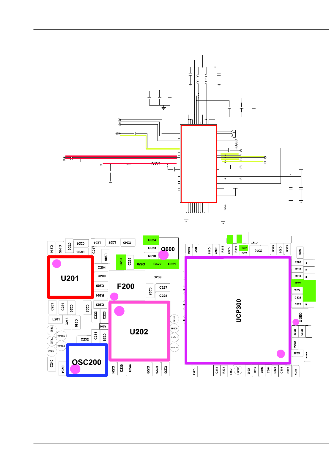
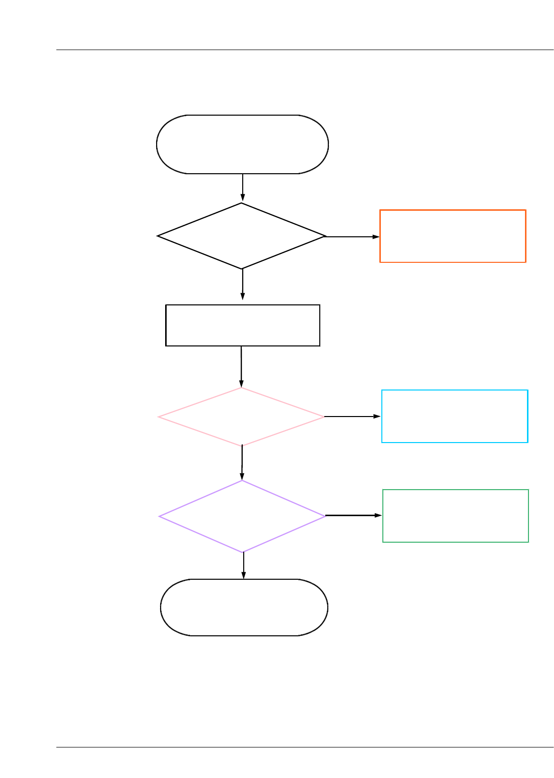
8-4-10. BLUETOOTH
Bluetooth connection disable
Yes
Check BT function ON Enable BT function
No
Yes
Check the voltage of U201
is around 3.0V
No
Check U201 and change
Check 26KHz Clock on
U202 (H6)
Yes
Check OSC200
No
Yes
Check the assembled
status of ANT201
No
Exchange ANT201
Yes
Exchange
No
Check UCP300
Yes
END
SAMSUNG Proprietary-Contents may change without notice
Level 3Repair
8-47
This Document can not be used without Samsung's authorization
C214
C209
C207
XIN
VSS
H7
H8
BT_VDDPX
XOUT
VSS
G7
BT_VDDRFG8
GPIO2
H1
GPIO0
H2
VBATH3
VREG H4
VREGHV
H5
H6
TM0
RES
F7
VSS
F8
VDDOG1
GPIO1
G2
VDDCG3
LPO_CLK
G4
VREG_CTL G5
G6
COEX_OUT0
VSS
E7
BT_RFP
E8
PCM_IN
F1
PCM_SYNC
F2
COEX_IN
F3
SPARE
F4
VSS
F5
F6
VSS
BT_VDDIF D7
BT_VDDTFD8
PCM_CLK E1
PCM_OUT E2
COEX_OUT1
E3
I2S_CLK
E4
I2S_WS
E5
E6
TM3
FM_VDDRFC7
FM_LNA2
C8
VDDCD1
UART_RXD
D2
SDA|I2C_DA
D3 SCL|I2C_CK
D4
I2S_DO
D5
D6
VSS
VSS
B7
FM_RXN
B8
UART_TXD
C1
VSS
C2
UART_CTS_N
C3
VSS
C4
TM2
C5
C6
SPARE
SPARE
A7
FM_RXP
A8
UART_RTS_N
B1
GPIO5
B2
FM_AOUT_L
B3
FM_AOUT_R
B4
SPARE
B5
B6
NC
1
NC
2
GPIO6|FM_IRQ
A1
TCXO_MODE
A2
SPARE
A3
SPARE
A4
FM_VDDAUDIO A5
A6
U201
TP205
TP202
C203
VREG_BT_2.6V
VREG_MSMP_2.6V
C216
1%
R204
C215
C206
C221
C213
C245
V_BT_1.2V
C202
VREG_MSMP_2.6V
VREG_BT_2.6V
V_BT_1.2V
L200
L207
TP204
TP201
C220
VREG_MSMP_2.6VV_BT_1.2V
TP203
C205
L204
C201
C200
C217
L201
FM_ANT
C204
BT_CLK
BT_PRIORITY
WLAN_ACTIVE
BT_ACTIVEBT_RF_TRX
BT_WAKE
BT_HOST_WAKE
FM_LOUT
FM_ROUT
BT_UART_RXD
BT_UART_TXD
SLEEP_CLK
BT_PCM_CLK
BT_PCM_DOUT
BT_PCM_DIN
BT_PCM_SYNC
BT_PWR
BT_CLK_REQ
BT_UART_CTS
BT_UART_RTS
SAMSUNG Proprietary-Contents may change without notice
Level 3Repair
8-48
This Document can not be used without Samsung's authorization
C230
TP210
TP211
C246
1
1
22
VWLAN_3.3V
ANT201
VREG_MSMP_2.6V
C229
C224
TP209
C237
C235
GPIO_3
L5
L6 GPIO_4
PAREG_BASE
L7
PAREG_VDD33_OUT
L8
SWREG_OUT
L9
VWLAN_3.3V
L205
VBATTERY_42
K8 VBATTERY_42
K9
GPIO_24
L1
SWREG_OUT
L10
VREG
L11
GPIO_25
L2
GPIO_23
L3
GPIO_1
L4
CHIP_PWD
K10
DREG_OUT
K11
VDD18_XTALK2
DVDD_SOC1K3
K4 GPIO_0
GPIO_2
K5
PM_MODE
K6
PM_ENABLE
K7
GND
H6
GND
H7
GND
H8
XTALIJ1
DVDD_SDIO J10
SREG_OUT
J11
VDD33_ANTJ2
XTAL0K1
GND
G7
GND
G8
XPABIAS5 H1
GPIO_10
H10 GPIO_9
H11
ANTE H2
DVDD12H4
DVDD12H5
DVDD12F8
XPABIAS2 G1
GPIO_12
G10 GPIO_11
G11
ANTB G2
GND
G4GND
G5
GND
G6
ANTC F1
GPIO_14 F10
GPIO_13 F11
ANTA F2
GND
F4
GND
F5
GND
F6
GND
F7
GPIO_6
E10 GPIO_5
E11
VDD18_BBE2
GND
E4
GND
E5
GND
E6
GND
E7
DVDD12E8
GPIO_7
D11
VDD18_SYNTHD2
GND
D4
GND
D5GND
D6
GND
D7
DVDD12D8
ANTD E1
GPIO_22 B8
GPIO_20 B9
VDD12_BBC1
DVDD_SOC2C10
GPIO_15 C11
VDD12_SYNTHC2
BIASREF D1
GPIO_8
D10
GPIO_17 B10
GPIO_16 B11
VDD18_RFB2
GND
B3
GND
B4
VDD33_PAB5
VDD33_PAB6
GND
B7
RF5INP A3
RF5INN A4
RF2OUTP A5
RF2OUTN A6
RF5OUTP A7
RF5OUTN A8
GPIO_19 A9
BT_RX_OUT B1
NC1
NC2
RF2INP A1
GPIO_21 A10
GPIO_18 A11
RF2INN A2
TP_WLAN_RST
U202
C223
VWLAN_1.8V
C238
C239
VWLAN_3.3V
C243
C225
C222
C231
OSC200
2
4
3
1
C226
C232
C240
C228
R205
16
1VC3
18
19GND
2RXA
RXB
3TXA 5
6
TXB
TX_BIAS 89 VC1
VC2
BT
GND
4
7GND
GND
10
11GND
GND
13
GND
14
15GND
GND
F200
ANT12
17
C234
VWLAN_1.8V
C233
C244
C227
VREG_MSMP_2.6V
BT_RF_TRX
ANT_SEL_C
ANT_SEL_B
ANT_SEL_E
BT_CLK_REQ
BT_CLK
WLAN_ACTIVE
BT_PRIORITY
ANT_SEL_C
ANT_SEL_B
ANT_SEL_E
BT_ACTIVE
WLAN_SD_DATA(0)
WLAN_SD_DATA(1)
WLAN_SD_DATA(2)
WLAN_SD_DATA(3)
WLAN_SD_CMD
WLAN_HOST_WAKE
WLAN_SD_CLK
WLAN_RESET_N
SAMSUNG Proprietary-Contents may change without notice
Level 3Repair
8-49
This Document can not be used without Samsung's authorization
8-4-11. FM RADIO
Radio does not work
Yes
Check C200
and Check U400
No
C200 ≥2.8V
Yes
C214, 214 is OK?
(When U201 operate)
No
Resolder C214,C215
and check U201
Yes
Check signal
related to U201
Yes
END
SAMSUNG Proprietary-Contents may change without notice
Level 3Repair
8-50
This Document can not be used without Samsung's authorization
C214
C209
C207
XIN
VSS
H7
H8
BT_VDDPX
XOUT
VSS
G7
BT_VDDRFG8
GPIO2
H1
GPIO0
H2
VBATH3
VREG H4
VREGHV
H5
H6
TM0
RES
F7
VSS
F8
VDDOG1
GPIO1
G2
VDDCG3
LPO_CLK
G4
VREG_CTL G5
G6
COEX_OUT0
VSS
E7
BT_RFP
E8
PCM_IN
F1
PCM_SYNC
F2
COEX_IN
F3
SPARE
F4
VSS
F5
F6
VSS
BT_VDDIF D7
BT_VDDTFD8
PCM_CLK E1
PCM_OUT E2
COEX_OUT1
E3
I2S_CLK
E4
I2S_WS
E5
E6
TM3
FM_VDDRFC7
FM_LNA2
C8
VDDCD1
UART_RXD
D2
SDA|I2C_DA
D3 SCL|I2C_CK
D4
I2S_DO
D5
D6
VSS
VSS
B7
FM_RXN
B8
UART_TXD
C1
VSS
C2
UART_CTS_N
C3
VSS
C4
TM2
C5
C6
SPARE
SPARE
A7
FM_RXP
A8
UART_RTS_N
B1
GPIO5
B2
FM_AOUT_L
B3
FM_AOUT_R
B4
SPARE
B5
B6
NC
1
NC
2
GPIO6|FM_IRQ
A1
TCXO_MODE
A2
SPARE
A3
SPARE
A4
FM_VDDAUDIO A5
A6
U201
TP205
TP202
C203
VREG_BT_2.6V
VREG_MSMP_2.6V
C216
1%
R204
C215
C206
C221
C213
C245
V_BT_1.2V
C202
VREG_MSMP_2.6V
VREG_BT_2.6V
V_BT_1.2V
L200
L207
TP204
TP201
C220
VREG_MSMP_2.6VV_BT_1.2V
TP203
C205
L204
C201
C200
C217
L201
FM_ANT
C204
BT_CLK
BT_PRIORITY
WLAN_ACTIVE
BT_ACTIVEBT_RF_TRX
BT_WAKE
BT_HOST_WAKE
FM_LOUT
FM_ROUT
BT_UART_RXD
BT_UART_TXD
SLEEP_CLK
BT_PCM_CLK
BT_PCM_DOUT
BT_PCM_DIN
BT_PCM_SYNC
BT_PWR
BT_CLK_REQ
BT_UART_CTS
BT_UART_RTS
SAMSUNG Proprietary-Contents may change without notice
Level 3Repair
8-51
This Document can not be used without Samsung's authorization
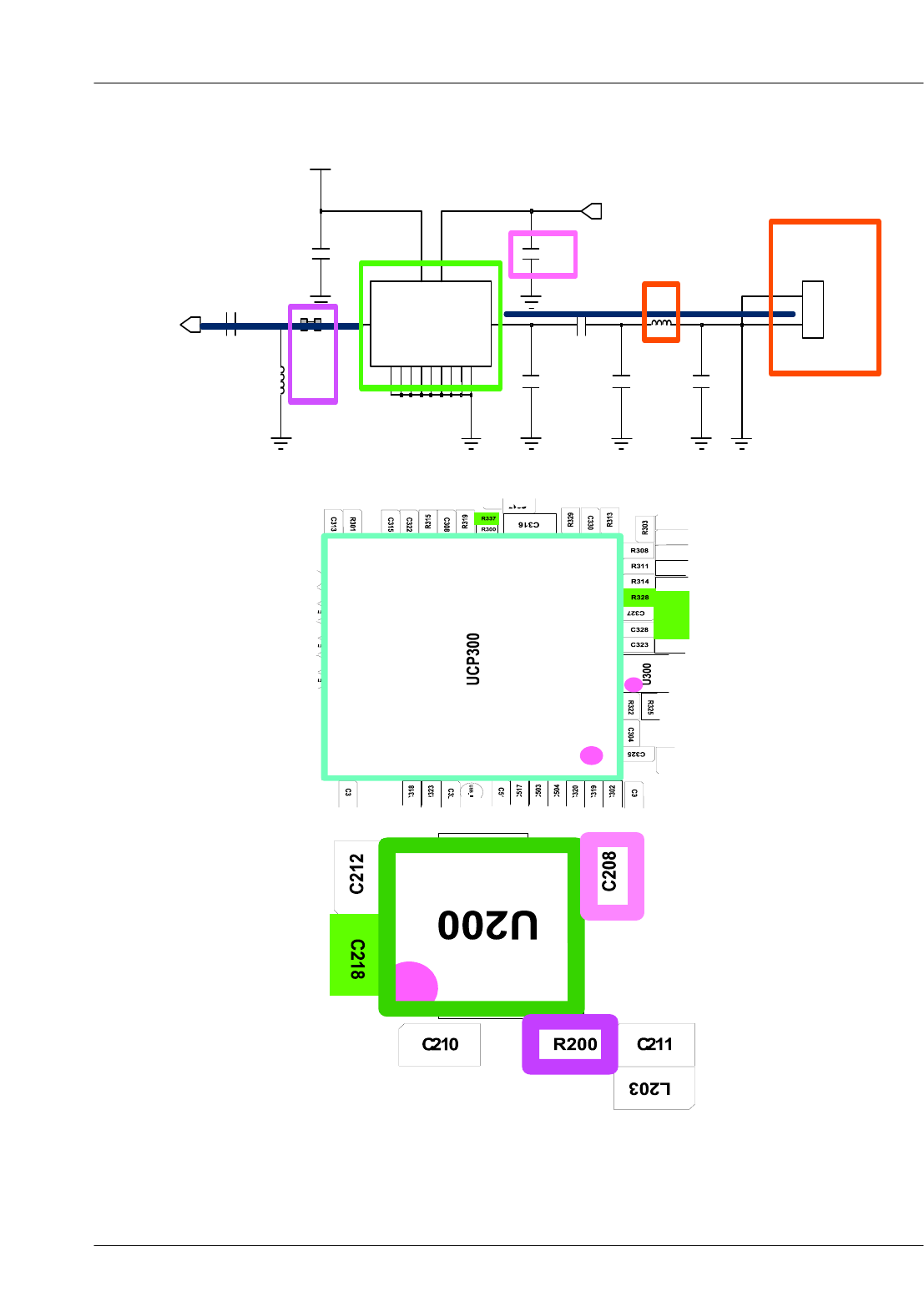
8-4-12. GPS
Operate GPS
Yes
No
Replace UCP300
Check C208 =High ?
Yes
No Replace U200
Check R200 >= -53dBm?
Yes
The End
Check ANT200, L202 Abnormal
Resolder ANT200, L202
Normal
GPS Signal Input: -50dBm
@L207
SAMSUNG Proprietary-Contents may change without notice
Level 3Repair
8-52
This Document can not be used without Samsung's authorization
11
2
2
ANT200
C211
VREG_RFRX1_2.7V
C210
C218
L202
G
7
G
9
G
11
G
13
2
RFINRFOUT
10
8
VCTL
12
VDD
G
1
G
34
G
G
56
G
U200
C242
C208
R200
SHORT
L203
C212
C241
RX_GPS
GPS_LNA_ON
SAMSUNG Proprietary-Contents may change without notice
Level 3Repair
8-53
This Document can not be used without Samsung's authorization
8-5. Service Schematics
-NC Point(Top View)
●:NC
UME300
123456789
10 11 12 13 14
A○○●○○○○○○○○○○○
B○○○●○○○○○○○○○○
C○●○○○○○○○○○○○○
D○○○○ ○○○
E○○○ ○●●○●● ○○○
F○○○ ○ ● ○○○
G○○○ ○ ● ○○○
H○○○ ○ ○ ○○○
J○○○ ○ ○ ○○○
K○○○ ○○○○○○ ○○○
L○○○ ○○○
M○○●○○○○○○○○○○○
N○○○○○○○○○○○○○○
P○○○○○○○○○○○○○○
U400
123456789
10 11
A●○○○○○○○○○●
B○○○○○○○○○○○
C○○○○○○○○○○○
D○○○○○○○○○○○
E○○○○○○○○○●○
F○○○●○○○○○●○
G○○○●●●○○○○○
H●○○○●●○○○○○
J○○○○○○○○○○○
K●○○○○○○○○○●
SAMSUNG Proprietary-Contents may change without notice
Level 3Repair
8-54
This Document can not be used without Samsung's authorization
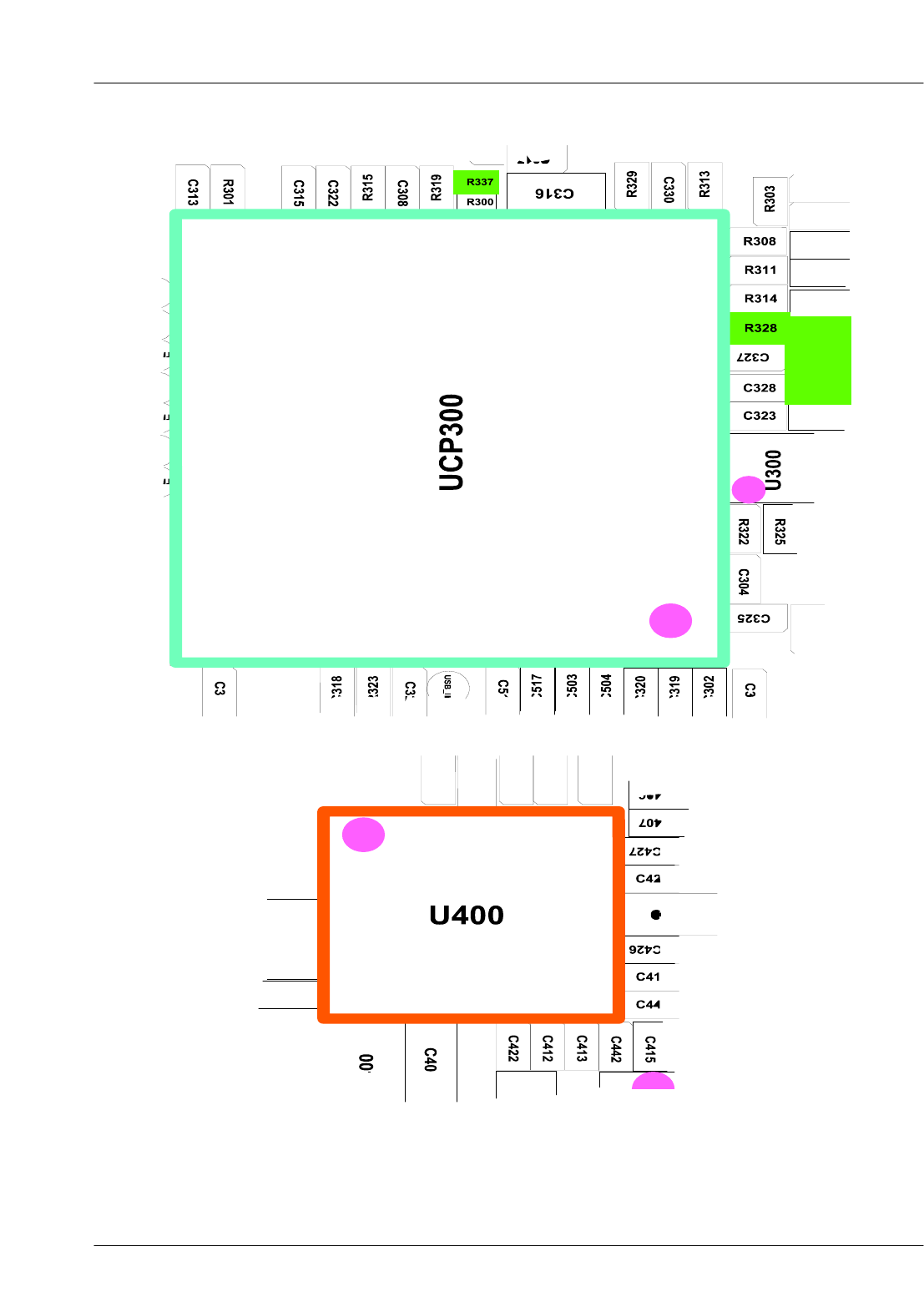
UCP300
1 2 3 4 5 6 7 8 9 10 11 12 13 14 15 16 17 18 19 20 21 22 23 24 25 26 27 28
A●●●●●●●●●●●●●●●●●●●●●●●●●●● A
B●○○○○○○○○○○○○○○○○○○○○○○○○○● B
C●○○○○○○○○○○○○○○○○○○○○○○○○○● C
D●○○ ○○● D
E●○○ ○○○○○○○○○○○○○○○○○○○ ○○● E
F●○○ ○○○○○○○○○○○○○○○○○○○ ○○● F
G●○○ ○○ ○○ ○○● G
H●○○ ○○ ○○○○○○○○○○○○○ ○○ ○○● H
J●○○ ○○ ○○○○○○○○○○○○○ ○○ ○○● J
K●○○○○○○ ○○○○○○●
K
L●○○○○○○ ○○○○○○○○○○○○●
L
M●○○ ○○ ○○ ○○○○○○○ ○○ ○○ ○○● M
N●○○ ○○ ○○ ○○○○○○○ ○○ ○○ ○○● N
P●○○ ○○ ○○ ○○○○○○○ ○○ ○○ ○○● P
R●○○ ○○ ○○ ○○○○○○○ ○○ ○○ ○○● R
T●○○ ○○ ○○ ○○○○○○○ ○○ ○○ ○○● T
U●○○ ○○ ○○ ○○○○○○○ ○○ ○○ ○○● U
V●○○○○○○ ○○○○○○●
V
W●○○ ○○ ○○○○○○○○○○○○○ ○○ ○○●W
Y●○○ ○○ ○○○○○○○○○○○○○ ○○ ○○● Y
AA ●○○ ○○ ○○ ○○●
AA
AB ●○○ ○○○○○○○○○○○○○○○○○○○ ○○●
AB
AC ●○○ ○○○○○○○○○○○○○○○○○○○ ○○●
AC
AD ●○○ ○○●
AD
AE ●○○○○○○○○○○○○○○○○○○○○○○○○○●
AE
AF ●○○○○○○○○○○○○○○○○○○○○○○○○○●
AF
AG ●●●●●●●●●●●●●●●●●●●●●●●●●●●
AG
1 2 3 4 5 6 7 8 9 10 11 12 13 14 15 16 17 18 19 20 21 22 23 24 25 26 27
SAMSUNG Proprietary-Contents may change without notice
Level 3Repair
8-55
This Document can not be used without Samsung's authorization
U202
123456789
10 11
A○○○○○○○○○○○
B●○○○○○○○○○○
C○○ ○○
D○○ ○○○○○ ○○
E○○ ○○○○○ ○○
F○○ ○○○○○ ○○
G○○ ○○○○○ ○○
H○○ ○○○○○ ○○
J○○ ○○
K○○○○○○○○○○○
L○○○○○○○○○○○