Samsung SGH C260 Service Manual. Www.s Manuals.com. Manual R1.0
User Manual: Phone Samsung SGH-C260 - Service manuals and Schematics, Disassembly / Assembly. Free.
Open the PDF directly: View PDF ![]() .
.
Page Count: 58
GSM TELEPHONE
SGH-C260
GSM TELEPHONE CONTENTS
1. Specification
2. Exploded View and Parts list
3. Chart of Troubleshooting
4. Array course control
5. Block Diagrams
6. PCB Diagrams
7. MAIN Electrical Parts List
8. Reference data
9. Safety Precautions
10. Product Function

Contents
1. Specification
1-1. GSM General Specification .......................................................................................1-1
1-2. GSM TX power class ...............................................................................................1-2
2. Exploded View and Parts list
2-1. Cellular phone Exploded View ..................................................................................2-1
2-2. Cellular phone Parts list ............................................................................................2-2
2-3. Disassembly ...............................................................................................................2-9
2-4. Assembly ..................................................................................................................2-11
3. Chart of Troubleshooting
3-1. Baseband ............................................................................................................3-1
3-1-1. Power ON .....................................................................................................3-1
3-1-2. System Initial ................................................................................................3-5
3-1-3. SIM Part .......................................................................................................3-8
3-1-4. Charging Part .............................................................................................3-10
3-1-5. Microphone Part .........................................................................................3-12
3-1-6. Speaker Part ..............................................................................................3-15
3-1-7. Camera Part ..............................................................................................3-18
3-1-8. LCD .............................................................................................................3-21
3-2. RF ......................................................................................................................3-13
3-2-1. EGSM Rx ...................................................................................................3-23
3-2-2. DCS Rx ......................................................................................................3-24
3-2-3. PCS Rx ......................................................................................................3-25
3-2-4. EGSM Tx ...................................................................................................3-27
3-2-4. DCS & PCS Tx .........................................................................................3-28
3-2-6. BLUETOOTH ..............................................................................................3-30

Contents
4. Array course control
4-1. Downloading Binary Files ......................................................................................4-2
4-2. Pre-requsite for Downloading ................................................................................4-2
4-3. S/W Downloader Program .....................................................................................4-3
5. Block Diagrams
6. PCB Diagrams
7. MAIN Electrical Parts List
8. Reference data
8-1. Reference Abbreviate ..............................................................................................8-1
9. Safety Precautions
9-1. Repair Precaution ......................................................................................................9-1
9-2. ESD(Electrostaically Sensitive Devices) Precaution ................................................9-2
10. Product Function
1. Specification
1-1
1-1. GSM General Specification
GSM 900 DCS1800
Freq. Band[MHz]
Uplink/Downlink
880~915
925~960
1710~1785
1805~1880
ARFCN range 0~124
& 975~1023 512~885
Tx/Rx spacing 45MHz 95MHz
Mod. Bit rate/
Bit Period
GPRS 270.833Kbps
3.692us
270.833Kbps
3.692us
EDGE 812.5Kbps
3.692us
812.5Kbps
3.692us
Time Slot Period/Frame Period 576.9us
4.615ms
576.9us
4.615ms
Modulation
GPRS 0.3GMSK 0.3GMSK
EDGE 8PSK 8PSK
MS Power
GPRS 33dBm~5dBm 30dBm~0dBm
EDGE 27~5dBm 26~0dBm
Power Level
GPRS 5pcl~19pcl 0pcl~15pcl
EDGE 8~19(class E2) 2~15(class E2)
Sensitivity -102dBm -100dBm
TDMA Mux 8 8
Cell Radius 35Km 2Km
Speclflcation
1-2
1-2. GSM Tx Power Class
TX Power
control level GSM900
5 33±2dBm
6 31±3dBm
7 29±3dBm
8 27±3dBm
9 25±3dBm
10 23±3dBm
11 21±3dBm
12 19±3dBm
13 17±3dBm
14 15±3dBm
15 13±3dBm
16 11±5dBm
17 9±5dBm
18 7±5dBm
19 5±5dBm
TX Power
control
level DCS1800
0 30±2dBm
1 28±3dBm
2 26±3dBm
3 24±3dBm
4 22±3dBm
5 20±3dBm
6 18±3dBm
7 16±3dBm
8 14±3dBm
9 12±4dBm
10 10±4dBm
11 8±4dBm
12 6±4dBm
13 4±4dBm
14 2±5dBm
15 0±5dBm
SAMSUNG Proprietary-Contents may change without notice
2. Exploded View and Parts List
2-1
This Document can not be used without Samsung's authorization
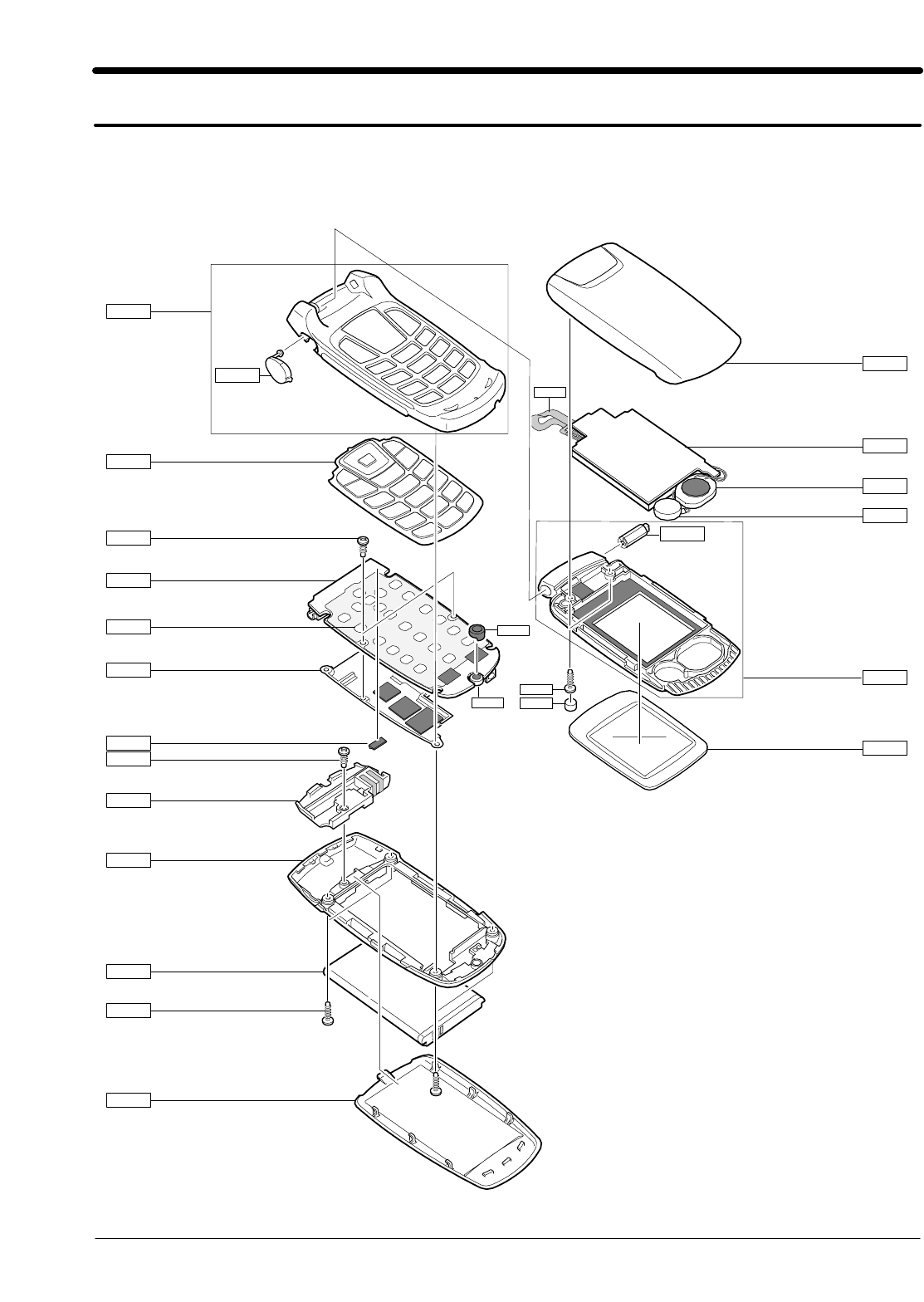
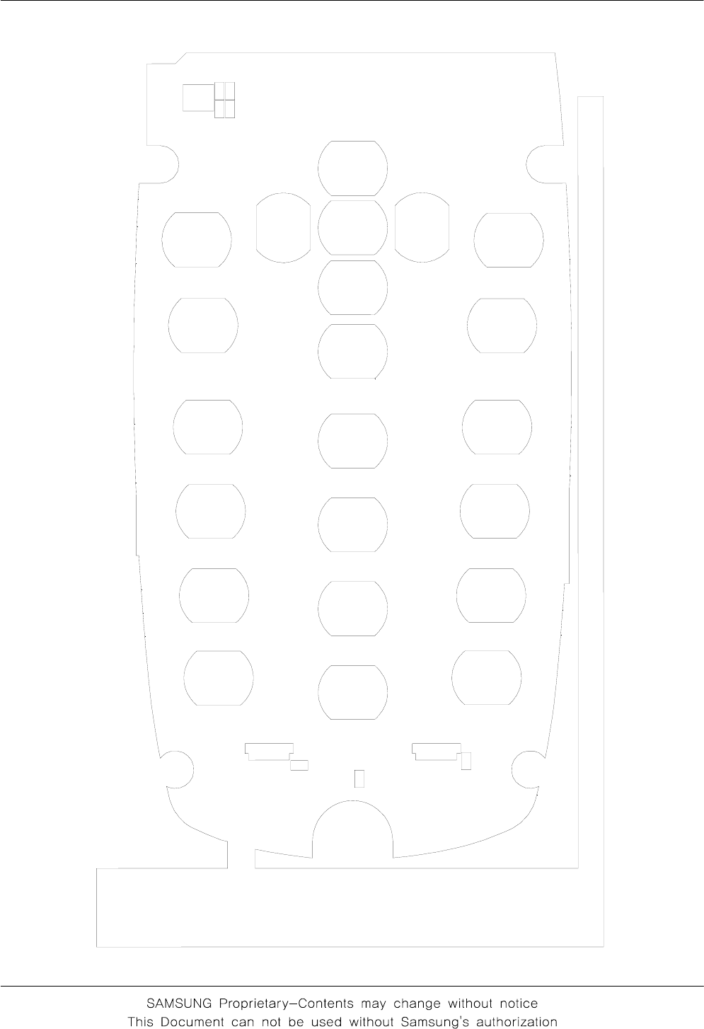
2-1. Cellular phone Exploded View
QFR01
QRF03
QKP01
QMP01
QFU01
QLC01
QHI01
QFL01
QSP01
QMO01
QMW02
QCR12
QME01
QSH01
QCR12
QAN02
QRE01
QBA01
QCR06
QBA01
QCR12
QSC05
QME03
QMI01
QMI03
QAN05
SAMSUNG Proprietary-Contents may change without notice
Main Electrical Parts List
2-2
This Document can not be used without Samsung's authorization
Design LOC Discription SEC CODE
QAN02 INTENNA-SGHC260 GH42-01102A
QAN05 ASSY MEC-INTENNA CONTACT GH75-08168A
QBA00 PMO-CASE BATTERY GH72-36766A
QBA01 INNER BATTERY PACK-750MAH,BLK, GH43-02483A
QCR06 SCREW-MACHINE 6001-001155
QCR12 SCREW-MACHINE 6001-001530
QCR12 SCREW-MACHINE 6001-001530
QCR12 SCREW-MACHINE 6001-001530
QFU01 ASSY CASE-UPPER GH98-03405A
QKP01 ASSY KEYPAD-(XEN/ZR) GH98-03772A
QLC01 LCD-LCD MODULE GH07-01056A
QME01 UNIT-SGHC260 METAL DOME(MAIN) GH59-04084A
QME03 UNIT-SGHC260 CON TO CON GH59-04070A
QMI01 MICROPHONE-ASSY-6.25MM GH30-00177F
QMI03 RMO-MIC HOLDER GH73-05342A
QMO01 MOTOR DC-SGHC260 GH31-00308A
QMP01 PBA MAIN-SGHC260 GH92-03328A
QMW02 PMO-COVER MAIN WINDOW GH72-36767A
QRE01 ASSY CASE-REAR GH98-03406A
QSC05 RMO-COVER FOLDER SCREW GH73-09088A
QSH01 ASSY CASE-SHIELD CAN GH98-03407A
QSP01 SPEAKER 3001-002094
QFR01 ASSY CASE-FRONT GH98-03403A
QRF03 PMO-CASE EAR GH72-36761A
QFL01 ASSY CASE-LOWER GH98-03404A
QHI01 ASSY MEC-HINGE GH75-08452A
2-2. Cellular phone Parts list
SAMSUNG Proprietary-Contents may change without notice
Main Electrical Parts List
2-3
This Document can not be used without Samsung's authorization
Discription SEC CODE
BAG PE 6902-000297
ADAPTOR-SGHC140 DC JACK(EU_B GH44-01597A
LABEL(R)-WATER SOAK GH68-09361A
LABEL(R)-WATER SOAK GH68-09361A
MANUAL USERS-EU PORTUGUESE GH68-13784A
MANUAL USERS-EU ENGLISH GH68-13785A
LABEL(R)-MAIN(EU) GH68-13956A
BOX(P)-UNIT MAIN (EU) GH69-05051A
RMO-RUBBER CSP GH73-08597A
RMO-COVER DUMMY HOLE GH73-08828A
MPR-INSU TAPE GH74-17540A
MPR-VINYL BOHO LCD WIN GH74-20912A
MPR-TAPE MAIN WINDOW GH74-29604A
MPR-TAPE DOPARO LED GH74-30219A
MPR-VINYL BOHO WINDOW JIG GH74-30221A
MPR-SPONGE GH74-30223A
MPR-SPONGE GH74-30638A
MPR-INSU TAPE GH74-30658A
SAMSUNG Proprietary-Contents may change without notice
Main Electrical Parts List
2-4
This Document can not be used without Samsung's authorization
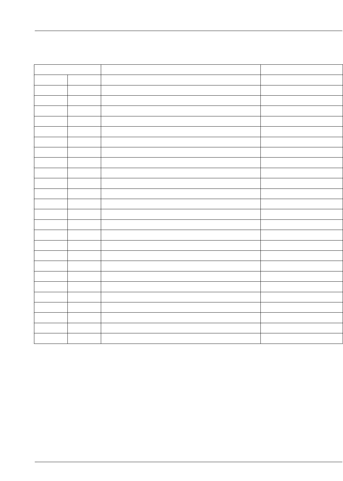
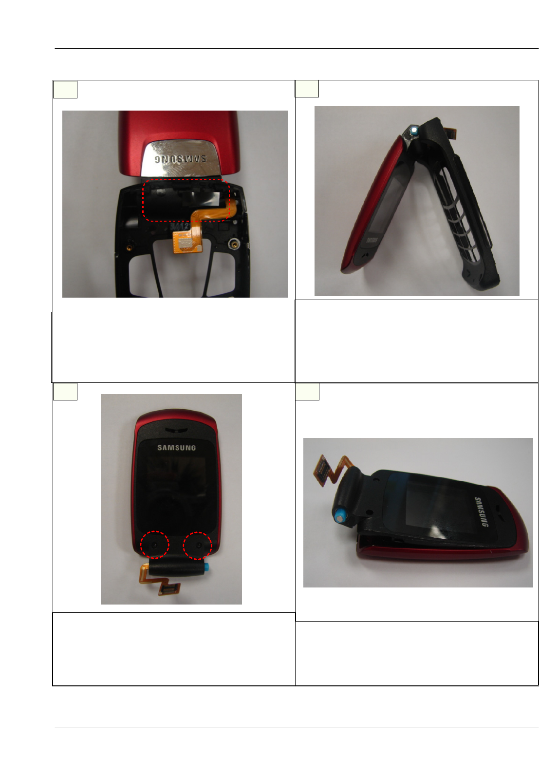
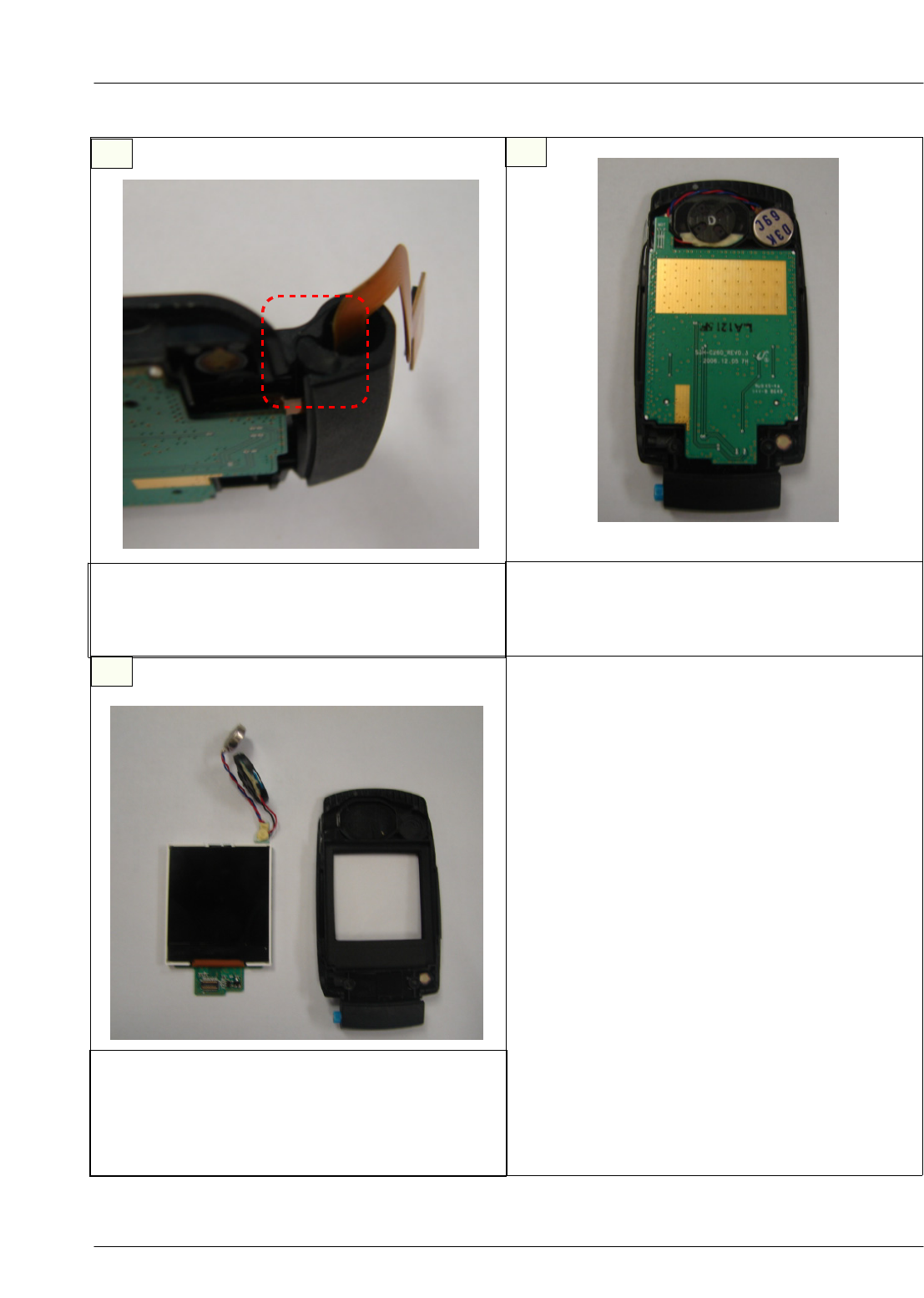
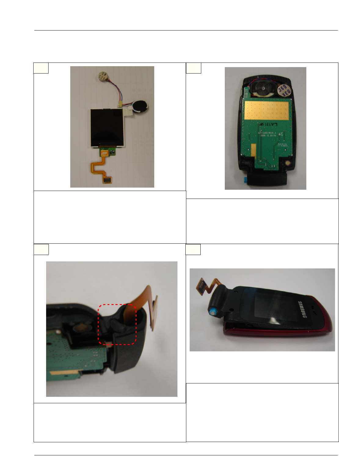
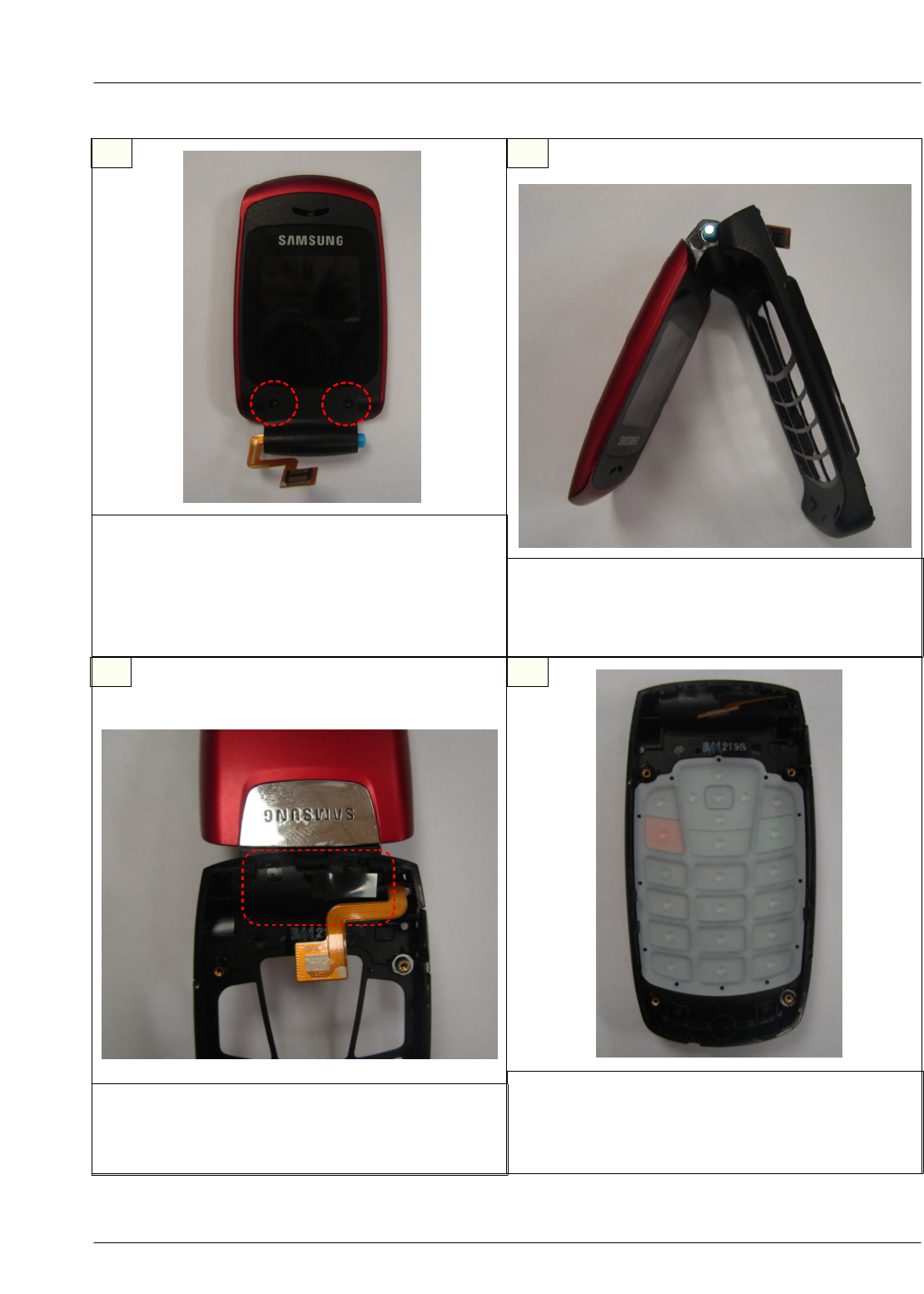
2-3. Disassembly
1
3
2
4
1) Lift up the lockers in the bottom of set.
※caution
1) Be careful not to make scratch and molding
damage!
1) Twist the REAR off the set carefully.
※caution
1) Be careful not to make scratch and molding
damage!
1) Unscrew the REAR.(4 points)
※caution
1) Be careful not to make scratch and molding da
mage!
1) Lift up the lockers in the center of set.
※caution
1) Be careful not to make scratch and molding
damage!
2) Remove the lockers in the center by all means.
SAMSUNG Proprietary-Contents may change without notice
Main Electrical Parts List
2-5
This Document can not be used without Samsung's authorization
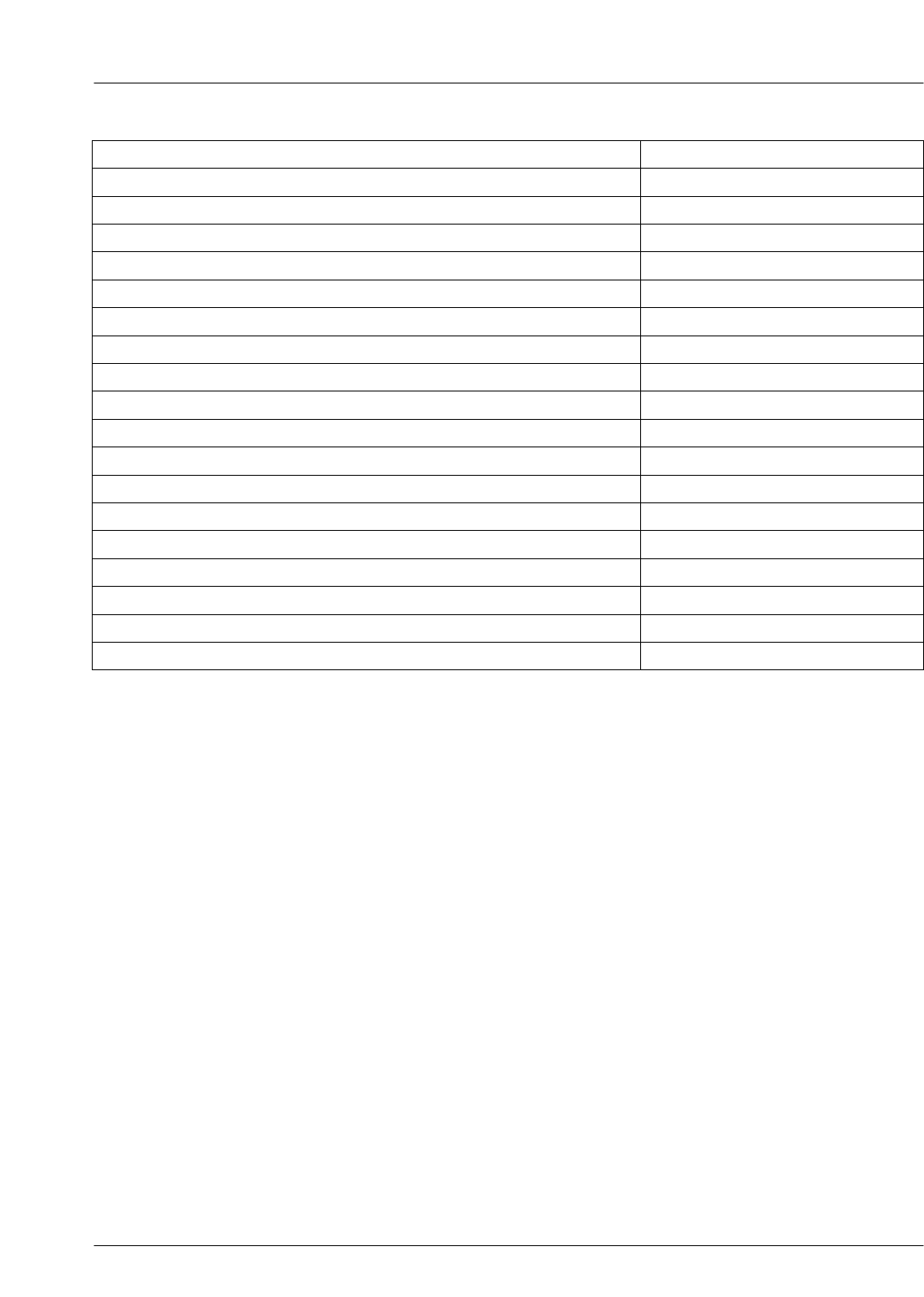
56
1) Remove the CON TO CON.
※caution
1) Be careful not to make scratch and molding
damage!
2) Be careful not to damage the CON TO CON .
1) Remove the PBA placed at the FRONT.
※caution
1) Be careful not to make scratch and molding
damage!
2) Be careful not to damage the CON TO CON .
78
1) Unscrew the SHIELD-CAN.(2 points)
※caution
1) Be careful not to make scratch and molding
damage!
1) Remove the KEY-PAD placed at the Front.
※caution
1) Be careful not to make scratch and molding
damage!
SAMSUNG Proprietary-Contents may change without notice
Main Electrical Parts List
2-6
This Document can not be used without Samsung's authorization
910
1) Remove the tape.
※caution
1) Be careful not to make scratch and molding
damage!
2) Be careful not to damage the CON TO CON .
1)Seperate the FRONT from the FOLDER
assembled.
※caution
1) Be careful not to make scratch and molding
damage!
2) Be careful not to damage the CON TO CON .
11 12
1) Remove the screw caps and unscrew the
LOWER. (2points)
※caution
1) Be careful not to make scratch and molding
damage!
1) Lift up the bottom of LOWER removing the
lockers with a tool.
※caution
1) Be careful not to make scratch and molding
damage!
SAMSUNG Proprietary-Contents may change without notice
Main Electrical Parts List
2-7
This Document can not be used without Samsung's authorization
13 14
1) Take the rubber out.
※caution
1) Be careful not to make scratch and molding
damage!
1) Remove the LCD F-PCB.
※caution
1) Be careful not to make scratch and molding
damage!
15
1) Remove the LCD carefully so that the nonwoven
on speaker and motor is not damaged.
※caution
1) Be careful not to make scratch and molding
damage!
SAMSUNG Proprietary-Contents may change without notice
Main Electrical Parts List
2-8
This Document can not be used without Samsung's authorization
1
3
2
4
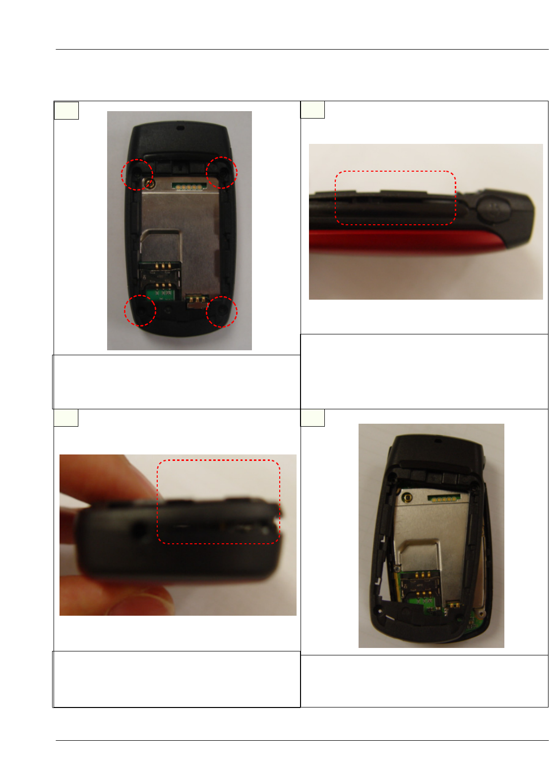
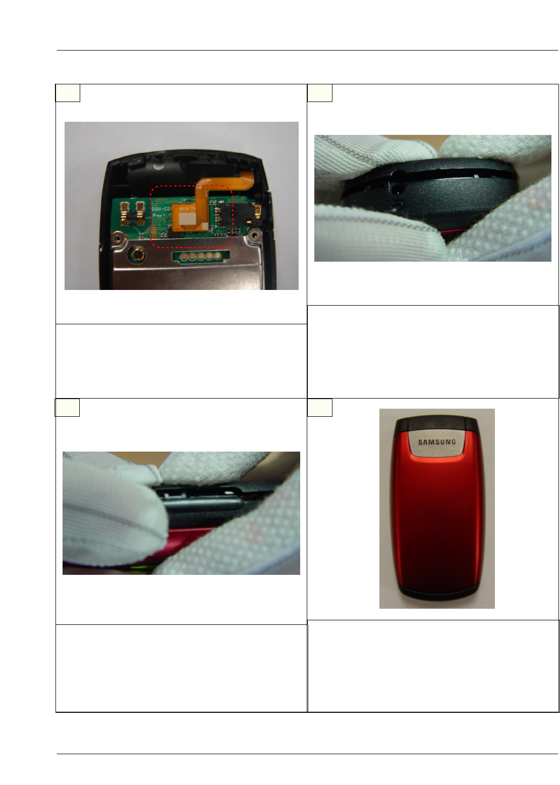
1) Place the MIC as the picture below
※caution
1) Be careful not to make scratch and molding
damage! TORQE (1.0 ± 0.1 Kgf·Cm)
1) Put the MIC COVER and CREW
2) Attach KEYPAD
3) Press the KEYPAD not to be detached
※caution
1) Be careful not to make scratch and molding
damage!
2-4. Assembly
1)Put the CON TO CON on the LCD Module
it clicks.
※caution
1) Be careful not to make scratch and molding
damage!
2) Be careful not to damage the LCD Module.
1) Put the LCD Module into place as shown .
2) Put the speaker and motor into place.
※caution
1) Be careful not to make scratch and molding
damage!
SAMSUNG Proprietary-Contents may change without notice
Main Electrical Parts List
2-9
This Document can not be used without Samsung's authorization
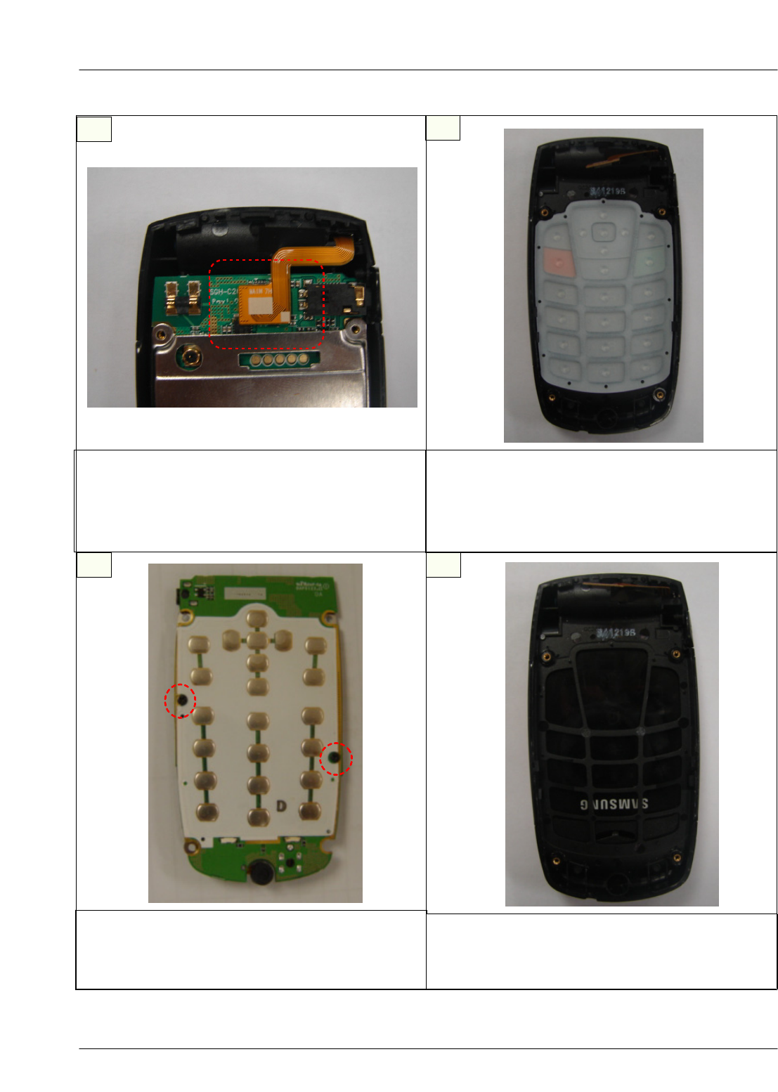
1) Put one side of the FOLDER into the FRONT
firstly,do the other side pressing the hinge.
※caution
1)Be careful not to damage the F-PCB.
56
1) Fasten 2 screws.
2) Put the screw caps on the FOLDER.
※caution
1) Be careful not to make scratch and molding
damage!
TORQE (1.0 ± 0.1 Kgf·Cm)
1) Place the KEY-PAD into the FRONT.
※caution
1) Be careful not to make scratch and molding
damage!
7 8
1) Put a tape on.
※caution
1) Be careful not to damage the wire on the
speaker due to PBA.
SAMSUNG Proprietary-Contents may change without notice
Main Electrical Parts List
2-10
This Document can not be used without Samsung's authorization
1) Press the bottom of REAR down until it
clicks.
※caution
1) Be careful not to make scratch and molding
damage!
2) Be careful not to damage the locker.
910
1) As shown,put the CON TO CON on PBA.
※caution
1) Be careful not to make scratch and molding
damage!
2) Press the CON TO CON down firmly.
1) Press the top down until the lockers click
grasping with your fingers carefully.
※caution
1) Be careful not to make scratch and molding
damage!
2) Be careful not to damage the locker.
11 12
1) Press the both sides of the REAR using
the lockers.
※caution
1) Be careful not to make scratch and molding
damage!
2) Be careful not to damage the locker.
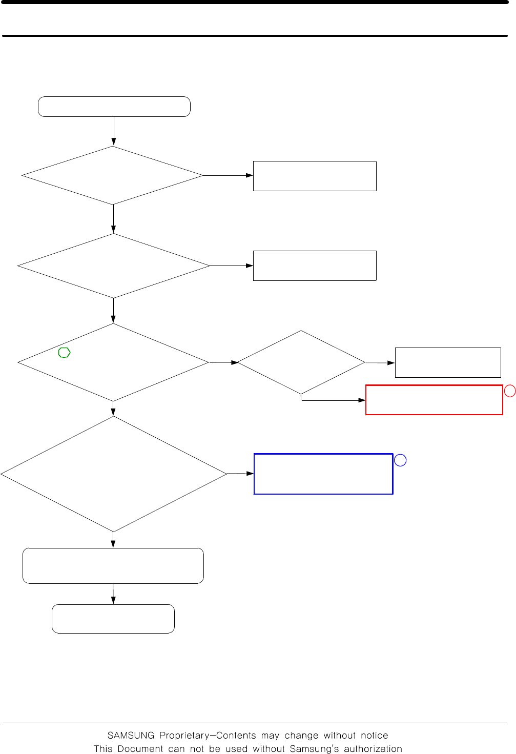
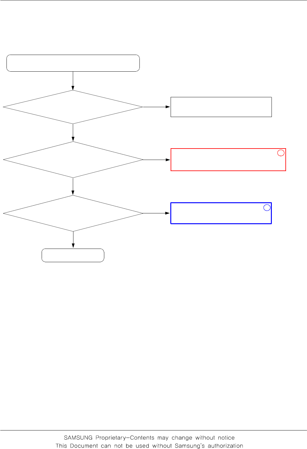
3. Flow Chart of Troubleshooting
3-1
3-1. Baseband
3-1-1. Power ON
check the current
consumption
>= 100mA Download again
'Power ON' does not work
No
Yes
Yes
END
Yes
Check the Initial Operation
Yes
Charge the battery
No
Check the Voltage
of the Battery
>= 3.3V
Check"Power On"Key
No
Check the pin
C152,C153,C155 of
UCP107 is >= 2.8V
>=2.8V
Check "Power
On"
key?
No
check UCD107 and C153
Yes 1
Check the clock signal
atpin#3ofOSC101
Freq=26Mhz
Vrms >=300mV
No Check the clock generation
circuit OSC101
Yes
2
3
Flow Chart of Troubleshooting
3-2
C119 25V
R102
C150
C189
R195
C151
VBAT
VCCD_2.9V
C121
C132
C147
C183
C125
C145
25V
VLDO1
5
1
VLDO2
6
1
VLDO3
90
1
C
F
A
V8
1
4
1
VBAT
4I
B
B
_
C
C
V
4
2
Q
B
B
_
C
C
V
1E
F
_
C
C
V
7
1
F
E
R
_
C
C
V
2
1
VCC_TXVCO
VDD
3
1
RX850B
1
3
RX900
0
3
RX900B
9
2
K
L
C
S
6
5
A
T
A
D
S
7N
E
S
TXOP_HI
1
1
TXOP_LO
B
Q
0
2
N
I
F
E
R
B
N
I
F
E
R9
1
P
O
_
F
E
R1
2
RX1800
7
2
8
2
RX1800B
RX1900
5
2
6
2
RX1900B
RX850
2
3
3
3
GND
I
2
B
I
3
C
N
8
C
N
4
3
5
3C
N
3
2
Q
2
2
UCD101
C146
R143
VRF_2.9V
2
GND1
GND2
4
HOT
1
3
HOT
C124
OSC101
C184
C123
RTXIP
RTXIN
RTXQP
RTXQN26M_OUT
DCS_LNA_IN_N
DCS_LNA_IN_P
GSM_LNA_IN_N
GSM_LNA_IN_P
SERCLK
SERDAT
SERLE
GSM_PAM_IN
DPCS_PAM_IN
AFC
Flow Chart of Troubleshooting
3-3
100NF
10V
C180
C153
C170
VCCA_2.9V
VBAT
C172
VCCB_2.9V
VBAT
VRF_2.9V
VCCD_2.9V
VRTC_3V
C173
TP2
C171
1
2
M300
C174
Q103
13
2
VCCD_2.9V
C155
VCCA_2.9V
C152
VCCD_2.9V
R157
VREF A10
N
G
E
R
V
4
1
R
P
G
E
R
V
3
1
M
VRTC H11
VSIM K12
1
S
S
V5
G
2
S
S
V4
K
3
S
S
V2
R
4
S
S
V6
P
M
C
V
X
V
3
1
R
Q
A
N
E
O
X
1
D
A12
VL4S_B B11
VL5S_A D10
C9
VL5S_B
VLDO_1 G11
VLDO_2 J12
VLDO_3 A13
VLDO_4 B12
VLDO_5 B10
VLDO_6 A14
VLDO_7 C12
5
D
D
V0
1
C
7
6
D
D
V3
1
B
B
D
D
V6
A
D
D
D
V1
1
N
V
D
D
V1
1
L
1
O
I
_
D
D
V5
N
2
O
I
_
D
D
V4
J
L
T
C
O
_
D
D
V4
C
VEXT E14
VIB_DRV F15
VL4S_A
P
X
T
7
E
UP_CLK N9
UP_IO P10
UP_RST R10
VACC F14
VBAT E13
1
D
D
V3
J
VDD12 J13
2
D
D
V3
M
3
D
D
V6
N
VDD34 C11
7
C
SCLK_PSC L8
M7
SDI_PSC
SDO_PSC N7
SERCK
C2
C1 SERDA
B1 SERLE1
SERLE2
A2
SIM_CLK K14
SIM_IO J11
SIM_RST K11
RESETN_CSP
O
_
T
E
S
E
R
9
K
RING_DRV F13
9
LD
V
S
R
0
1
N2
D
V
S
R
RTC_ALMN H10
K
L
C
_
C
T
R
4
N
RWN
L2
N
I
X
T
X
R
6
D
P
I
X
T
X
R
7
D
N
Q
X
T
X
R
6
C
P
Q
X
T
X
R
OCTL4
A4
G6 OCTL5
OCTL6
B3
A3 OCTL7
F
U
B
_
1
W
S
P
7
L
P
E
E
K
_
R
W
P
9
M
N
1
W
S
_
R
W
P
5
1
C
2
W
S
_
R
W
P
4
1
C
1
F
E
R
A
R
6
B
2
F
E
R
A
R
5
B
R3
5
1
N
NC
E5
D15
NC3
E6 NC4
1
5
C
N
6
C
N2
7
C
N
5
P
3
1
D
8
C
N
E10
NC9
C5 OCTL1
OCTL2
F5
4
B
1
C
S
P
_
D
N
G5
1
B
2
C
S
P
_
D
N
G5
1
K
Q
R
T
N
I
0
1
L
L3 I|O
LED1_DRV G13
LED2_DRV G12
C
M
6
R
N
N
I
C
I
M
4
1
M
P
N
I
C
I
M
4
1
N
N
T
U
O
C
I
M
5
1
P
P
T
U
O
C
I
M
2
S
D
N
G8
F
3
S
D
N
G9
F
4
S
D
N
G0
1
F
5
S
D
N
G7
G
6
S
D
N
G8
G
7
S
D
N
G9
G
8
S
D
N
G0
1
G
9
S
D
N
G6
H
V
D
N
G3
1
P
R
U
C
H
_
D
N
G1
1
F
L
T
C
O
_
D
N
G
D
D
N
G0
1
M
Q
D
N
G8
E
1
S
D
N
G7
F
0
1
S
D
N
G7
H
1
1
S
D
N
G8
H
9
H
2
1
S
D
N
G
3
1
S
D
N
G7
J
4
1
S
D
N
G8
J
5
1
S
D
N
G9
J
6
1
S
D
N
G0
1
J
7
1
S
D
N
G0
1
K
DB2
K3
J5 DB3
DB4
J6
DB5
H5
DB6
G3
DB7
G4
DB8
F4
DB9
F1
R
T
N
I
D
3
P
B
D
N
G6
F
I
D
I
A
D
6
L
O
D
I
A
D
6
M
N
R
I
A
D
4
P
DB0
K1
K2 DB1
DB10
F2
DB11
F3
DB12
E2
DB13
E3
DB14
D3
DB15
D2
2
1
R
N
N
I
X
U
A
4
1
L
P
N
I
X
U
A
5
1
M
N
T
U
O
X
U
A
3
1
L
P
T
U
O
X
U
A
3
1
K
CH_BDRV E11
CH_ISEN F12
CH_RES D14
E9
CREF
K8
CSN_PSC
K
C
I
A
D
4
R
L5
N1 AB3
AB4
N2
M2 AB5
AB6
M1
K7 AB7
AB8
K5
C
F
A
9
D
N
A
T
U
O
A
2
1
N
P
A
T
U
O
A
1
1
P
N
B
T
U
O
A
2
1
P
P
B
T
U
O
A
UCD107
AB0
K6
P1 AB1
AB2
C175
C179
C162
C168
VCCD_1.8V
C182
VIB_DRV
PWR_KEEP
BAND_SEL1
SIM_CLK
UP_SDO
UP_SCLK
UP_CS
VREF
RTCALARM
UP_SDI
SIMCLK
SIMDATA
SIMRST
SIM_RST
SIM_IO
VSIM
N
O
_
G
I
J
P
N
I
C
I
M
N
N
I
C
I
M
P
T
U
O
C
I
M
N
T
U
O
C
I
M
P
N
I
X
U
A
P
T
U
O
X
U
A
VIB_EN
N
N
I
X
U
A
N
T
U
O
X
U
A
KEY_COL(2)
KEY_ROW(0)
INTRQ
RST
T
N
I
_
P
S
D
C
P
A
V
P
I
X
T
R
N
I
X
T
R
P
Q
X
T
R
N
Q
X
T
R
P
A
T
U
O
A
N
A
T
U
O
A
P
B
T
U
O
A
N
B
T
U
O
A
K
2
3
_
K
L
C
C
M
_
M
3
1
K
L
C
N
O
_
R
W
P
DSP_AB(6)
DSP_AB(5)
DSP_AB(4)
DSP_AB(3)
DSP_AB(2)
DSP_AB(1)
DSP_AB(0)
DSP_IO
DSP_RWN
FLASH_RESET
SERLE
SERDAT
SERCLK
TX_EN
VMOD_EN
C
F
A
DSP_DB(13)
DSP_DB(12)
DSP_DB(11)
DSP_DB(10)
DSP_DB(9)
DSP_DB(8)
DSP_DB(7)
DSP_DB(6)
DSP_DB(5)
DSP_DB(4)
DSP_DB(3)
DSP_DB(2)
DSP_DB(1)
DSP_DB(0)
DSP_AB(0:8)
DSP_AB(8)
DSP_AB(7)
KEY_BL1
DSP_DB(0:15)
DSP_DB(15)
DSP_DB(14)
Flow Chart of Troubleshooting
3-4
3
②
Flow Chart of Troubleshooting
3-5
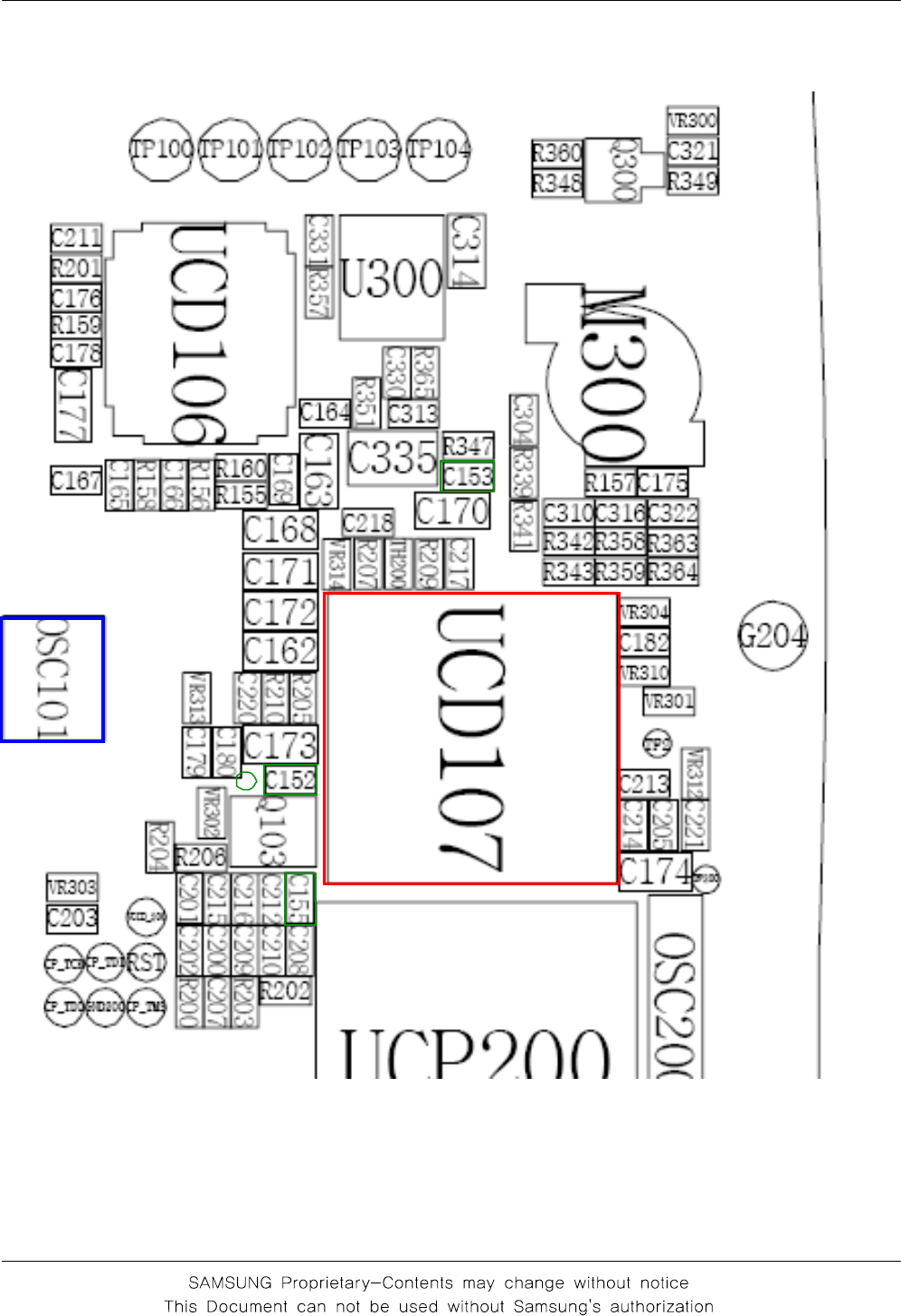
3-1-2. Initial
Initial Failure
check R200 : LOW? Check UCP200
No
Yes
Yes
END
Yes
Check the Initial Operation
Yes
Check R131, C127
No
check C127 or R131
is 13Mhz?
Check the clock signal
at pin #3 of OSC101
Freq=26Mhz?
No check OSC101
1
Check C168(VCCD_2.9V),
C173(VCCD_1.8V) of
UCP107 "High" when the
phone is boot on?
No Check UCD107
Yes
2
3
4
Flow Chart of Troubleshooting
3-6
3
2
4
1
2
C120
R133
2
1
1
L
C185
VCC
8
2_CLR
_PR
1
_Q 5
U103
7
CK
6
D
4
GND
3Q
VRF_2.9V
R190
C133
C134
C127
F104
C129
R189
R131
26M_OUT
CLK13M_YMU
CLK13M_MC
CLK13M_TR
Flow Chart of Troubleshooting
3-7
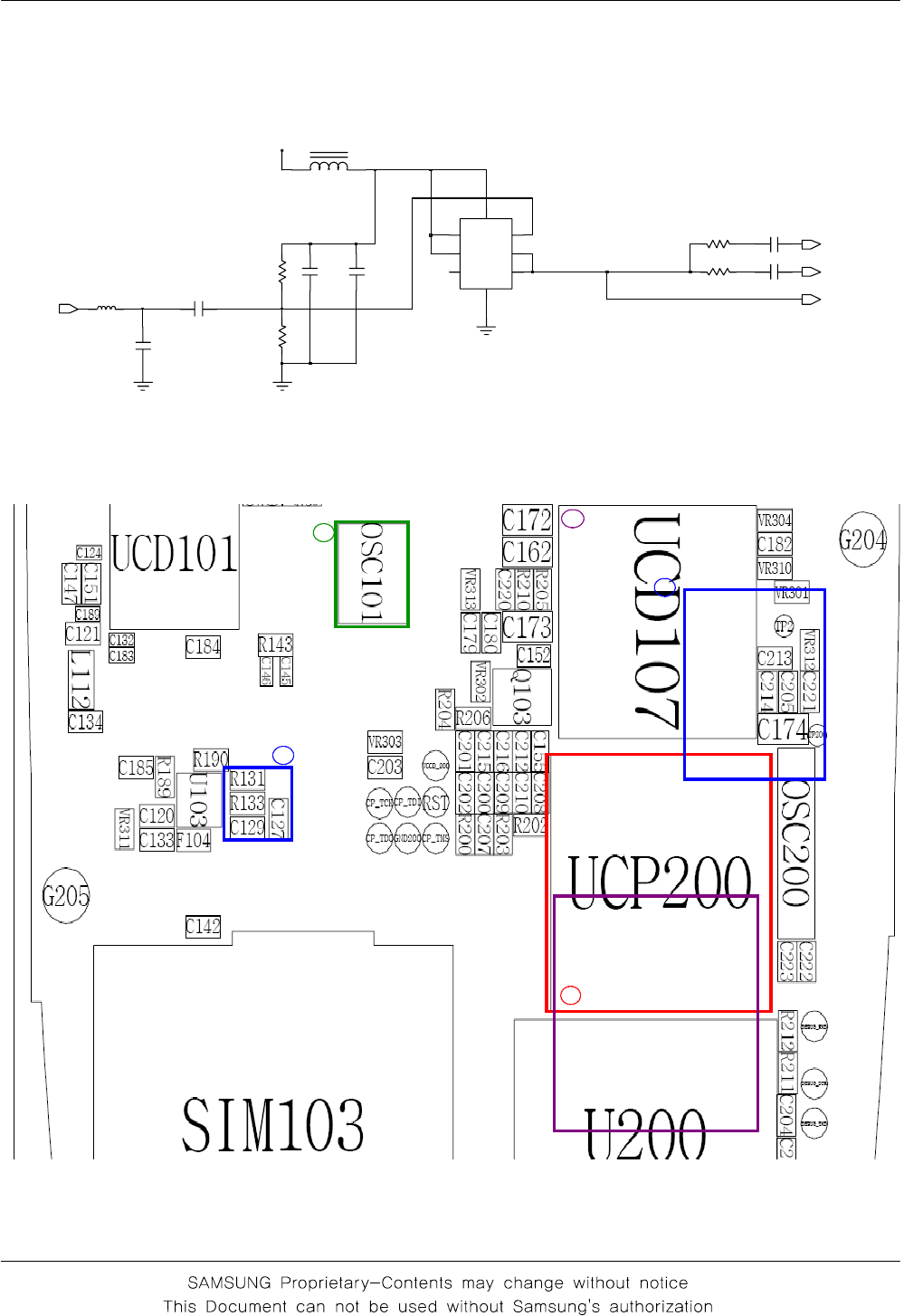
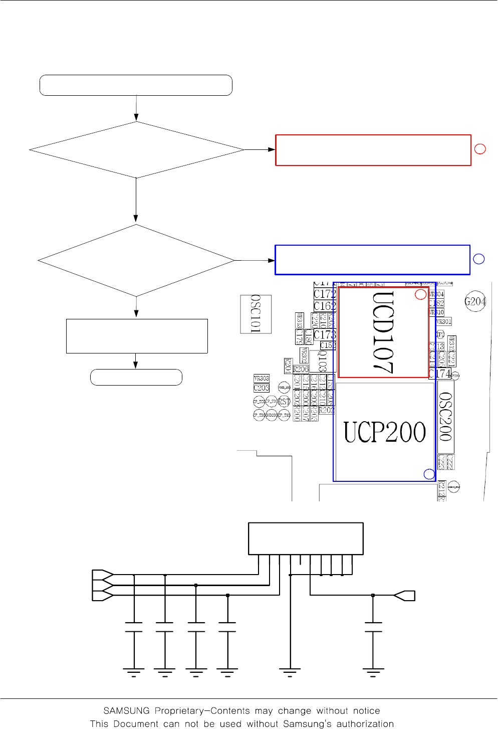
3-1-3. Sim Part
"Insert SIM" is displayed on the LCD
Is there any signal pin
#2,3 of SIM103?
Check the UCD107
Check the UCP107 & UCD200
END
No
Yes
No
Yes
1
2
Check the SIM Card
The voltage is 2.8V
at the pin#1 of SIM103
1
2
C140 C141C138 C139
C
C
V
2
P
P
V
5
3K
L
C
4D
N
G
6O
/
I
7C
N
C
N
8
C
N
9
0
1C
N
1C
C
V
SIM103
C142
SIM_RST
VSIM
SIM_CLK SIM_IO
Flow Chart of Troubleshooting
3-8
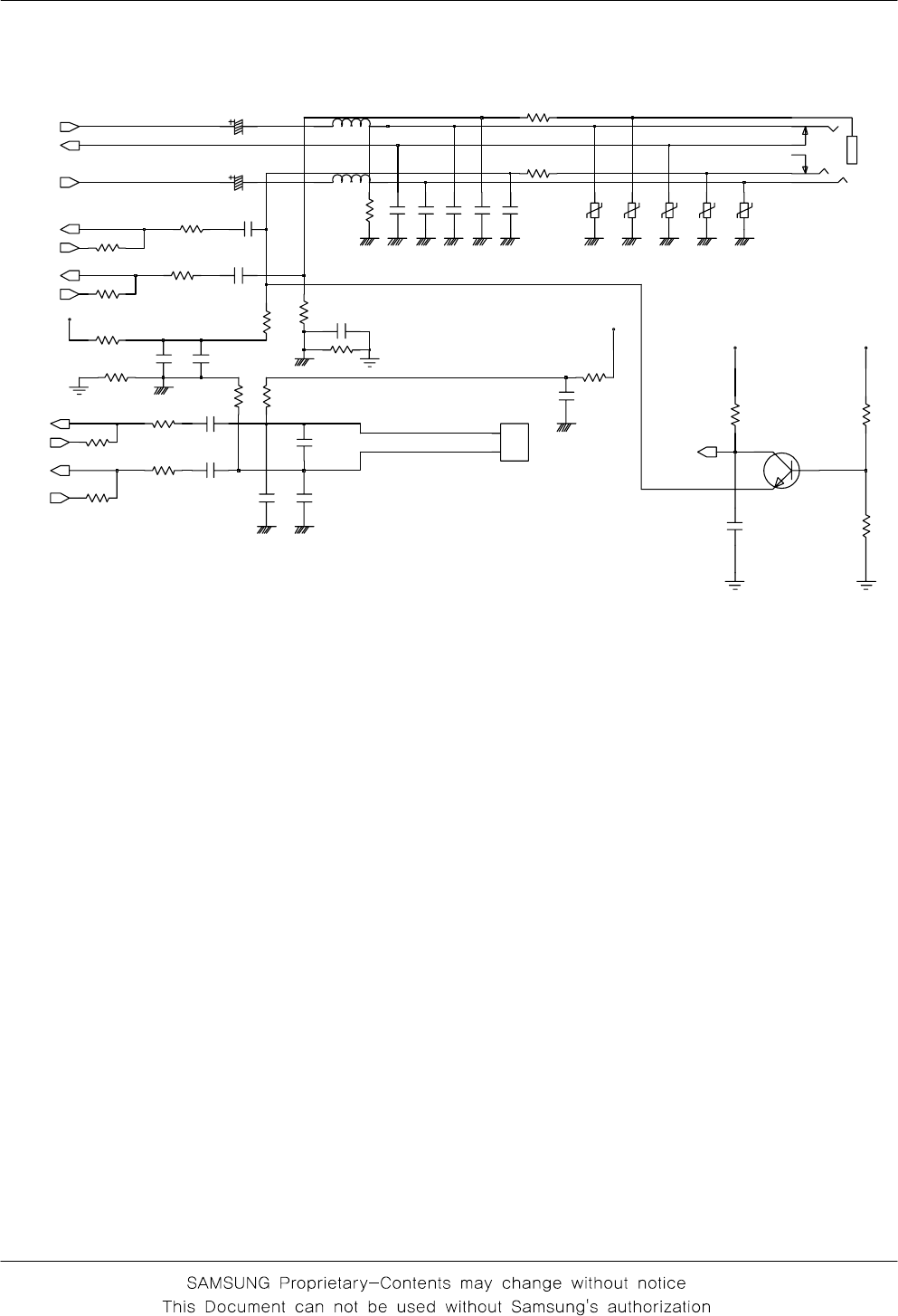
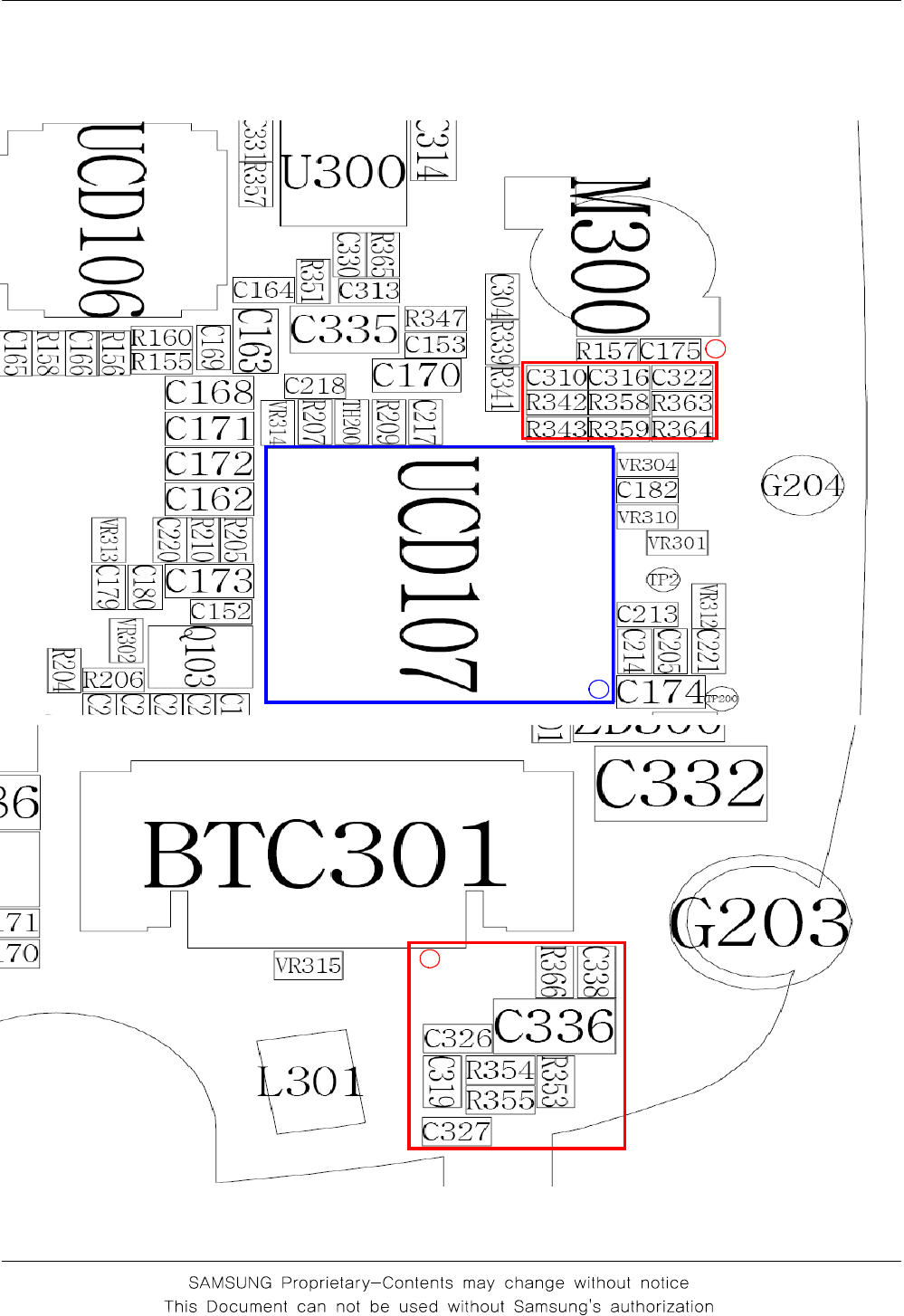
3-1-4.Microphone Part
* Call with Sim before testing.
Check the soldered status
of microphone
MicroPhone does not work
Resolder microphone
END
No
Yes
Yes
Check the reference
voltage on mic path
C336 ≒2.0V
Yes
Check and resolder or change
R353, R355, C336, C327, C326,
C316,C322, R358, R363, R359, R364
No
Is microphone OK?
Yes
Check UCD107
No
1
2
Flow Chart of Troubleshooting
3-9
VCCD_2.9V
R364
R341
R347
C319
C334
C305
R335
6
1
3
R
V
C313
R359
R345
L304
C336
VCCA_2.9V
C308
C321
R349
R352
C333
C322
C310
R342
R355
VCCA_2.9V
8
1
3
R
V
R348
R344
7
1
3
R
V
R363
Q300
2
3
1
C335
R354
C309
0
2
3
R
V
9
1
3
R
V
VCCA_2.9V
R353
C327
R337
R343
EAR300
1
2
3
4
5
6
C307
C316
C304
R360
C306
L303
R358
C326
C311
L301
1
1
2
2
R340
R339
R351
EAR_SWITCH
AUXOUTP
AUXINP
MICOUTP
MICINP
JACK_IN
AOUTBP
AOUTBN
MICINN
MICOUTN
AUXINN
AUXOUTN
Flow Chart of Troubleshooting
3-10
2
1
1
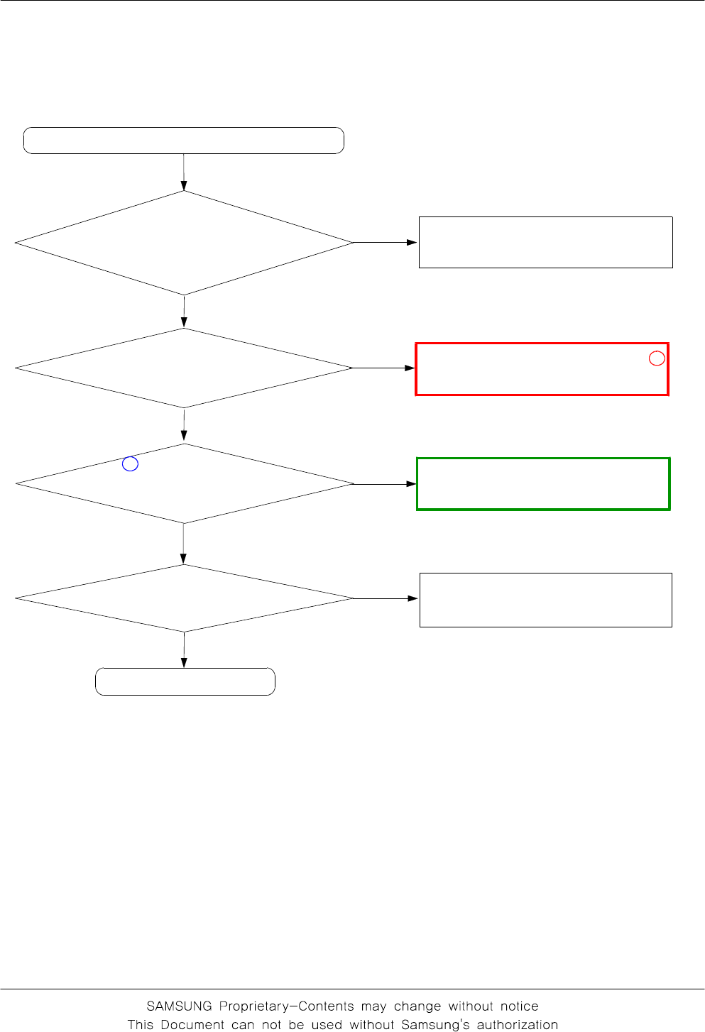
Flow Chart of Troubleshooting
3-11
Check connection of LCD and PBA
3-1-5. Speaker Part
No
Yes
Check the Speaker
Are the any signals at the
pin #3, 9 of U300?
No
Check toh solder status of
speaker
(on the upper folder)
is it OK?
There is no sound from speaker
Are there any signal at the
C169, R365, R357?
Replace the Speaker
Check the UCD107
END
No
Yes
1
Yes
③
No
Yes
2
Are there any signal at the
pin #3, 5 of HEA200?
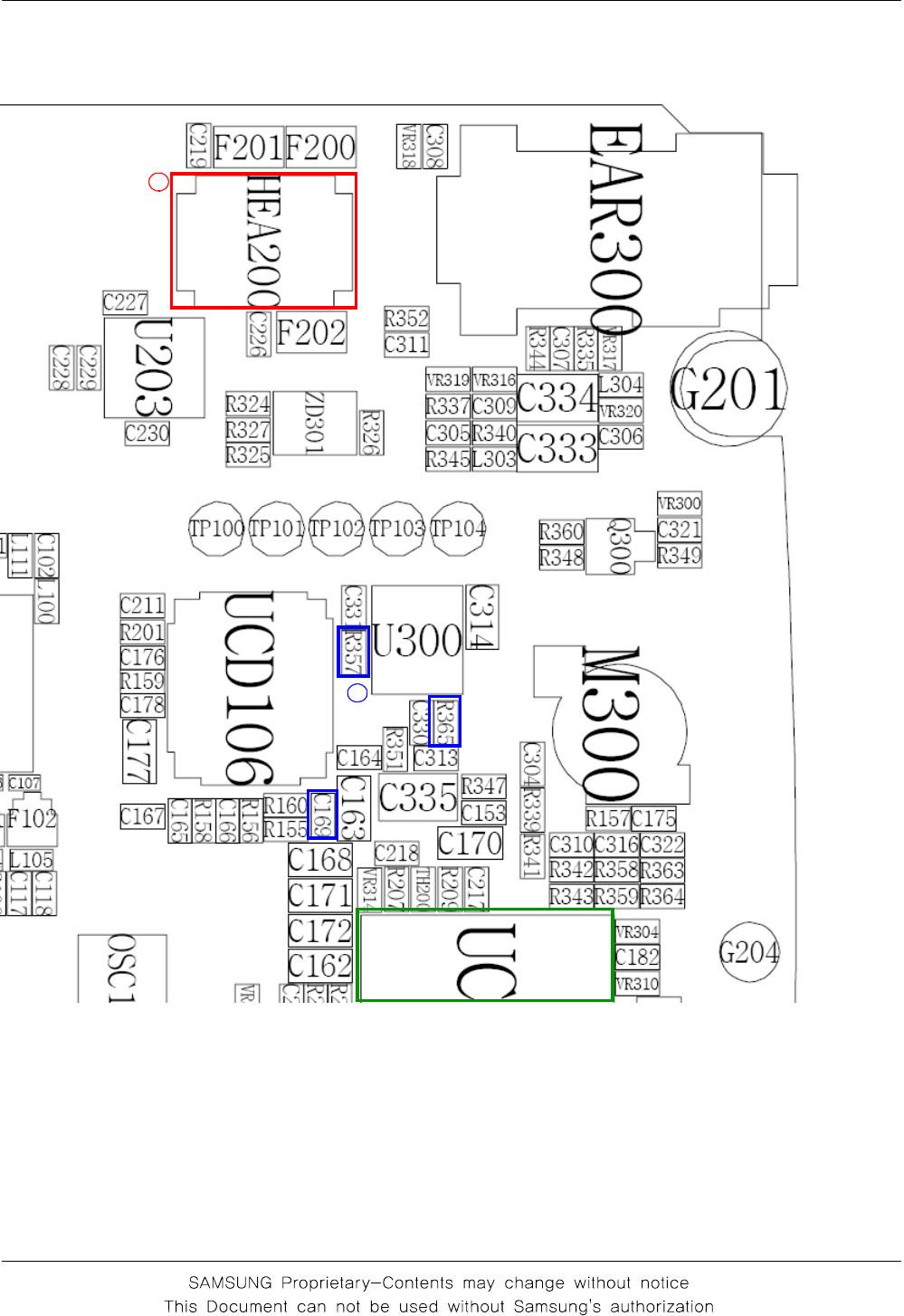
Flow Chart of Troubleshooting
3-12
2
1
③
③
Flow Chart of Troubleshooting
3-13
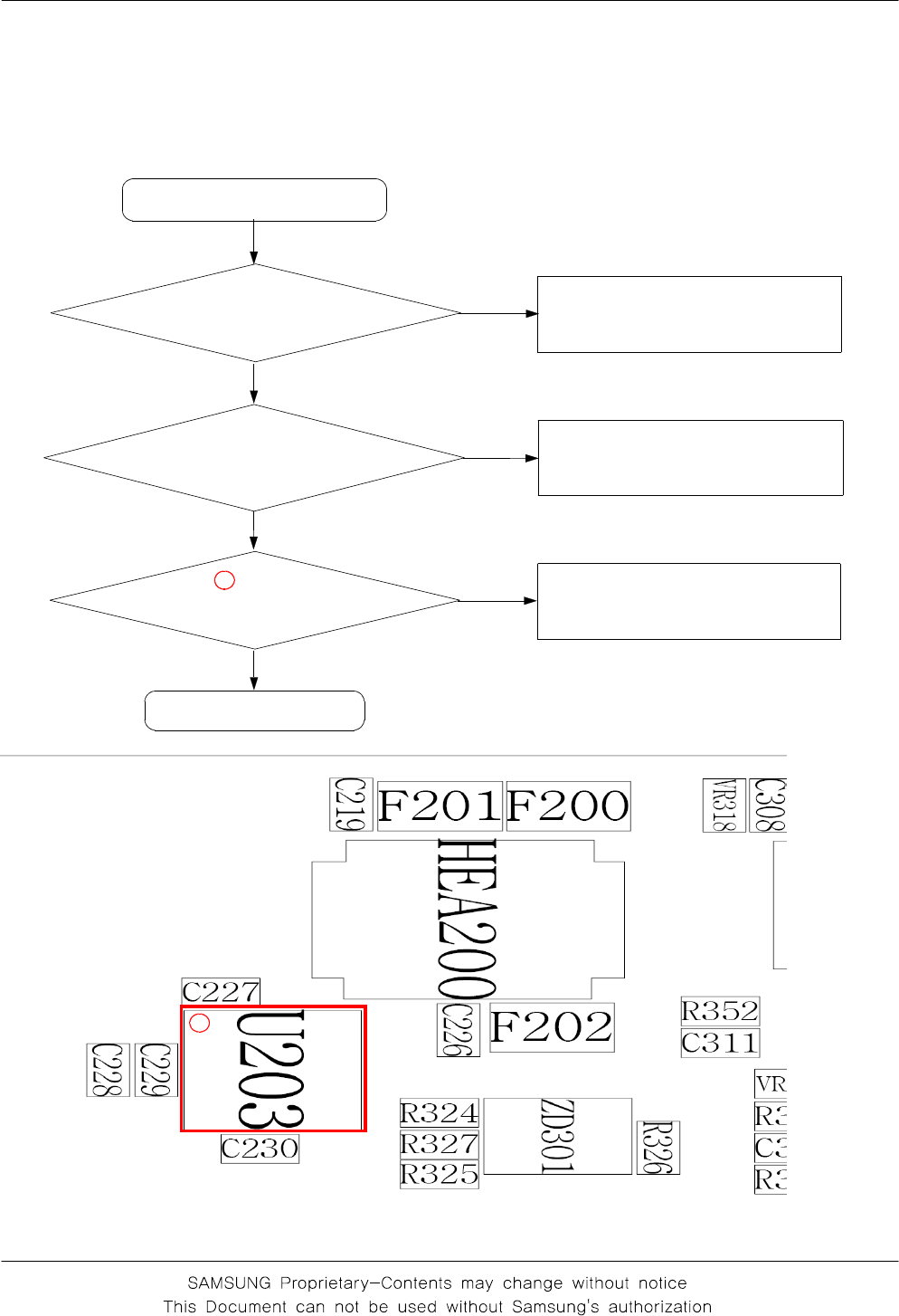
3-1-6. LCD backlight
Backlight ON "TIME"
mode in the menu?
Backlight does not work
Check conecting between
PBA and LCD conector
Select backlight "15 sec" mode
or other
Check FPCB
Check UCP200
No
Yes
No
Check pin #8 of U203
is high? Check the LCD
Yes
Yes
No
1
1
Flow Chart of Troubleshooting
3-14
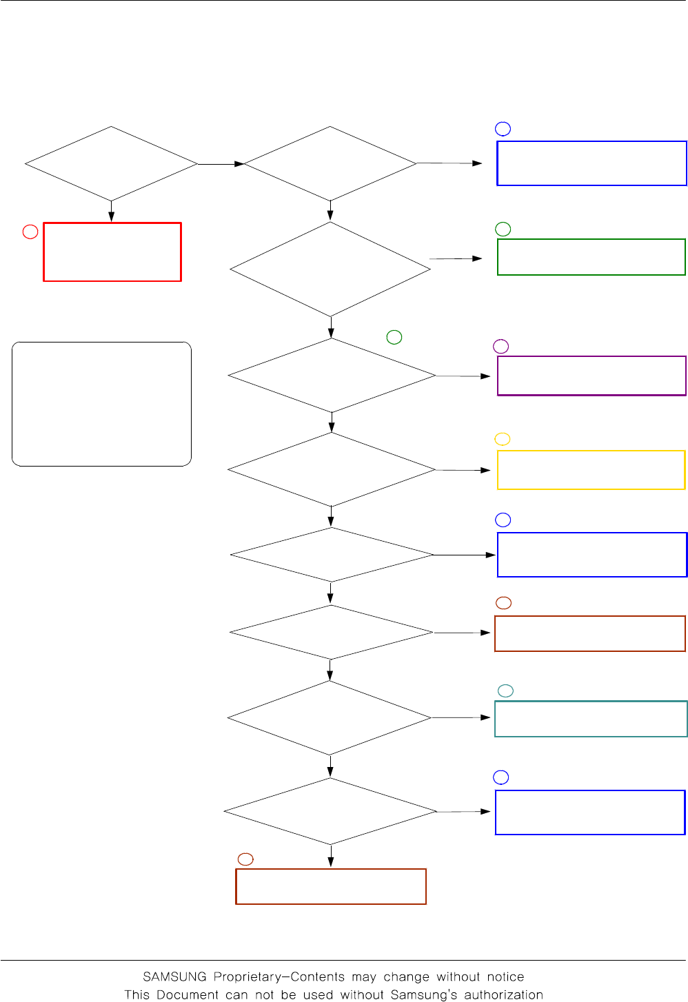
3-2. RF
3-2-1. GSM Rx
Normal condition
catch the channel ?
Check U304
pin #11 ≥-65
dbm ?
Check UCD101
pin #29,30
≥-65dBm ?
Yes
No
No
Check U304
pin #17 ≥-65
dbm ?
Yes
No
Yes
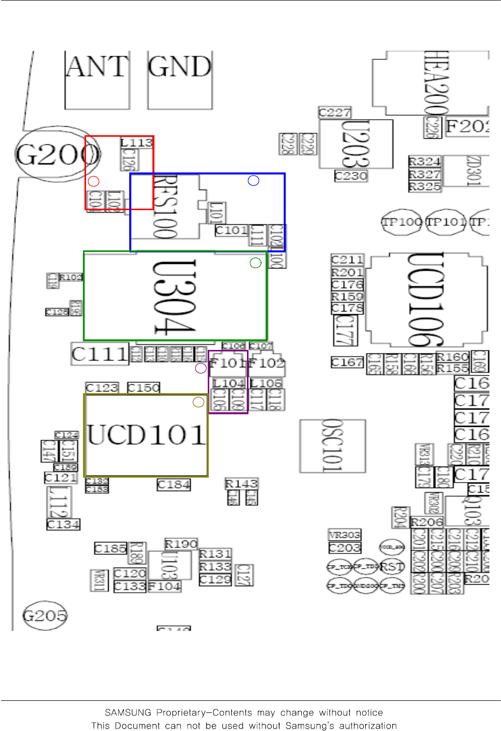
Check ANT, C126, L102
Check and resolder or change
RFS100, C101, L111, L100, L101, C102
Resolder or change
U304
Check and resolder or change
F101, C105, C109, L104
Resolder or change
UCP200
CONTINOUS RX ON
RF INPUT : 62CH
AMP : -50dbm
Check UCD101
pin#13 = 2.9V?
Yes
Resolder or change
UCD101
Yes
No
No
1
2
3
4
5
Flow Chart of Troubleshooting
3-15
C119 25V
R102
C150
C189
R195
C151
VBAT
VCCD_2.9V
C121
C132
C147
C183
C125
C145
25V
VLDO1
5
1
VLDO2
6
1
VLDO3
90
1
C
F
A
V8
1
4
1
VBAT
4I
B
B
_
C
C
V
4
2
Q
B
B
_
C
C
V
1E
F
_
C
C
V
7
1
F
E
R
_
C
C
V
2
1
VCC_TXVCO
VDD
3
1
RX850B
1
3
RX900
0
3
RX900B
9
2
K
L
C
S
6
5
A
T
A
D
S
7N
E
S
TXOP_HI
1
1
TXOP_LO
B
Q
0
2
N
I
F
E
R
B
N
I
F
E
R9
1
P
O
_
F
E
R1
2
RX1800
7
2
8
2
RX1800B
RX1900
5
2
6
2
RX1900B
RX850
2
3
3
3
GND
I
2
B
I
3
C
N
8
C
N
4
3
5
3C
N
3
2
Q
2
2
UCD101
C146
R143
VRF_2.9V
2
GND1
GND2
4
HOT
1
3
HOT
C124
OSC101
C184
C123
RTXIP
RTXIN
RTXQP
RTXQN26M_OUT
DCS_LNA_IN_N
DCS_LNA_IN_P
GSM_LNA_IN_N
GSM_LNA_IN_P
SERCLK
SERDAT
SERLE
GSM_PAM_IN
DPCS_PAM_IN
AFC
Flow Chart of Troubleshooting
3-16
12
3
4
5
Flow Chart of Troubleshooting
3-17
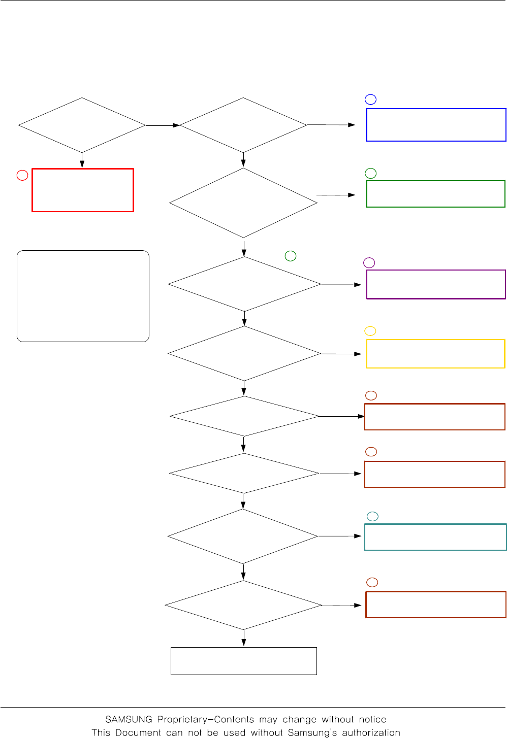
3-2-2. DCS Rx
Normal condition
catch the channel ?
Check U304
pin #1112
≥-65
dbm ?
Check UCD101
pin #27, 28
≥-65dBm ?
Yes
No
No
Check U304
pin#6 ≥-65 dbm ?
Yes
No
Yes
Check ANT, C126, L102
Check and resolder or change
RFS100, C101, L111, L100, L101, L102
Resolder or change
U304
Check and resolder or change
F102, C107, C117, L105, C118
Resolder or change
UCP200
CONTINOUS RX ON
RF INPUT : 698CH
AMP : -50dbm
Check UCD101
pin #13 = 2.9V?
Yes
Check and resolder or change
UCD101
Yes
No
No
1
2
3
4
5
Flow Chart of Troubleshooting
3-18
3-2-3. GSM Tx
Check U304
pin #4 is
about 2.8?
Check and change
RFS100, C101,
L111,L100
Yes
No
CONTINUS TX ON CONDITION
TX POWER DAC : 554 CODE
APPLIED
CH : 62ch
RBW : 100KHz
VBW : 100KHz
SPAN : 10MHz
REF LEV : 10dBm
ATT : 20dB
Yes
No
Yes
UCD101 pin #14
is 3.7V ?
No
Yes
UCD101 pin #2
is 1.8V ?
No
Yes
UCD101 pin #21
is about 26mHz?
No
Yes
UCD101 pin #20
is about 26mHz?
Yes
No
1
3
UCD101 pin #17
is 2.9V ?
No
Yes
No
Check U304
pin #17 is
about 4~5dbm? :
2.8V ?
Check U304
pin #11 is
about 2~3dbm?
Check UCD101
pin #10 is
about 4~5dbm?
No
Yes
Check and resolder or change
UCD101
Check and resolder or change
U304
Check and change
Battery, UCD107
Check UCD107
2
5
6
Check OSC101
7
Check and resolder or change
C119, R102
4
3
Check and resolder or change
UCD101
2
Check and resolder or change
UCD101
2
Check UCD107
6

Flow Chart of Troubleshooting
3-19
2
3
4
6
1
7
Flow Chart of Troubleshooting
3-20
3-2-4. DCS Tx
CONTINUS TX ON CONDITION
TX POWER DAC : 560 CODE
APPLIED
CH : 698CH(DCS), 660CH(PCS)
RBW : 100KHz
VBW : 100KHz
SPAN : 10MHz
REF LEV : 10dBm
ATT : 20dB
Check U304
pin #4 is
about 2.8?
Check and change
RFS100, C101,
L111,L100
Yes
No
Yes
No
Yes
UCD101 pin #14
is 3.7V ?
No
Yes
UCD101 pin #2
is 1.8V ?
No
Yes
UCD101 pin #21
is about 26mHz?
No
Check and resolder or change
UCD107
Yes
UCD101 pin #20
is about 26mHz?
Yes
No
1
3
UCD101 pin #17
is 2.9V ?
No
Yes
No
Check U304
pin #19 is
about 4~5dbm? :
2.8V ?
Check U304
pin #11 is
about 2~3dbm?
Check UCD101
pin #11 is
about 4~5dbm?
No
Yes
Check and resolder or change
UCD101
Check and resolder or change
U304
Check and change
Battery, UCD107
Check UCD100
2
5
6
Check UCD101
6
Check OSC101
7
Check and resolder or change
C119, R102
4
3
Check UCD101
6
Flow Chart of Troubleshooting
3-21
2
3
4
6
1
7
SAMSUNG Proprietary-Contents may change without notice
4. Array course control
4-1
This Document can not be used without Samsung's authorization
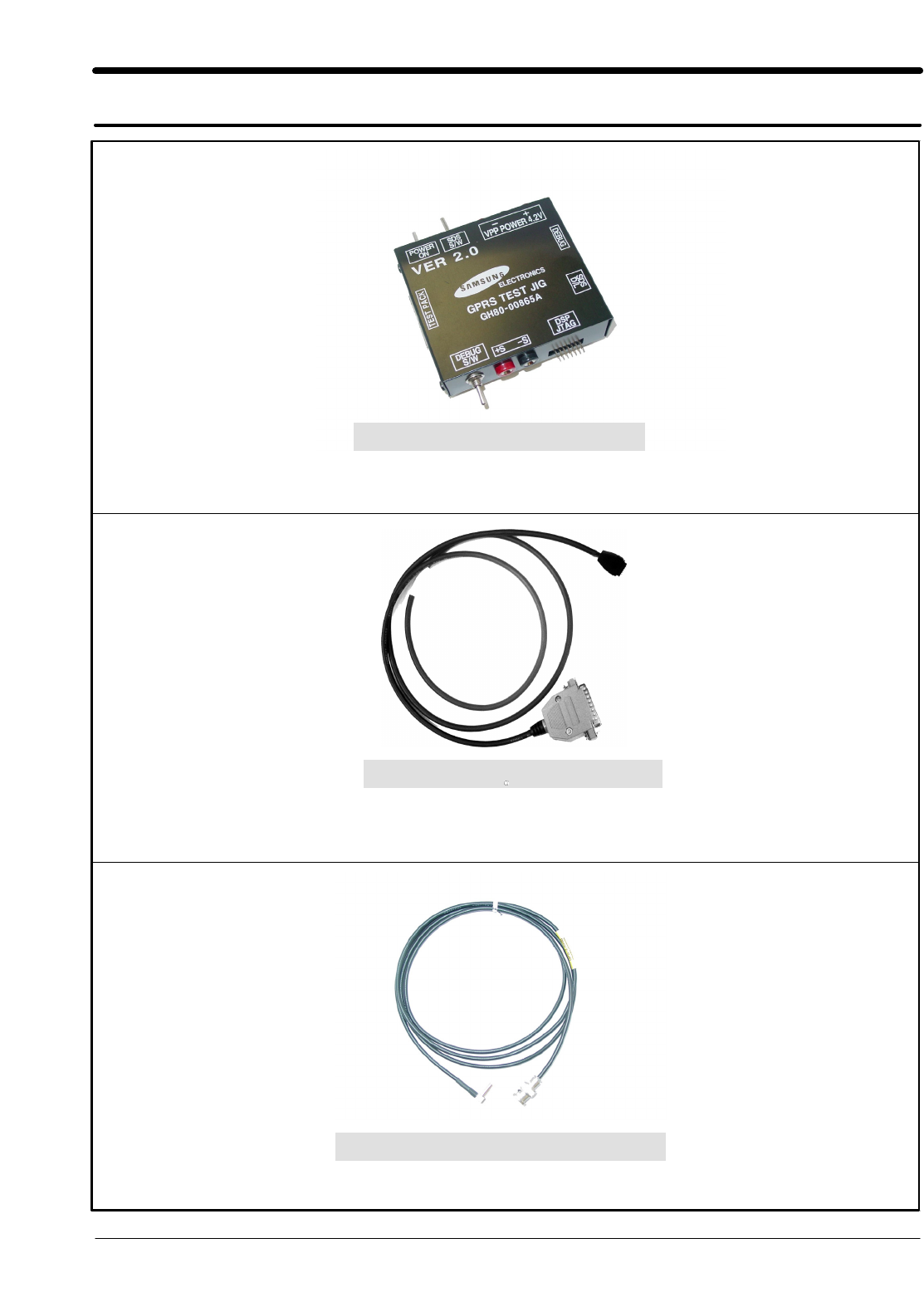
Test Jig (GH80-00865A)
Test Cable (GH39-00127A)
RF Test Cable (GH39-00397A)

SAMSUNG Proprietary-Contents may change without notice
Array course control
4-2
This Document can not be used without Samsung's authorization
Software Downloading
4-1. Downloading Binary Files
• Three binary files for downloading C260.
– C260XXYY.s3 : Main source code binary.
4-2. Pre-requsite for Downloading
• Downloader Program(OptiFlash.exe)
• C260 Mobile Phone
• Data Cable
• Binary files
SAMSUNG Proprietary-Contents may change without notice
Array course control
4-3
This Document can not be used without Samsung's authorization
4-3. S/W Downloader Program
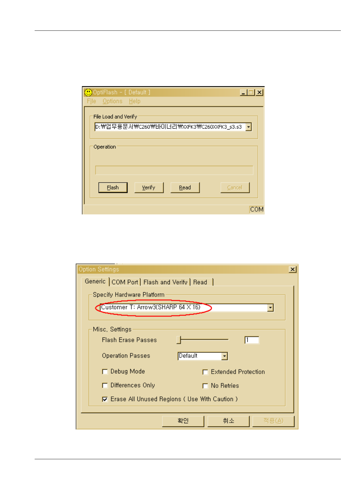
1. Load the binary download program by executing the “OptiFlash.exe”
2. Select the “Options” -> “Settings” -> “Generic” -> “Specify hardware platform”.
Choose hardware platform for the downloader file setting.
Set the everything else as the default values which are shown below
SAMSUNG Proprietary-Contents may change without notice
Array course control
4-4
This Document can not be used without Samsung's authorization
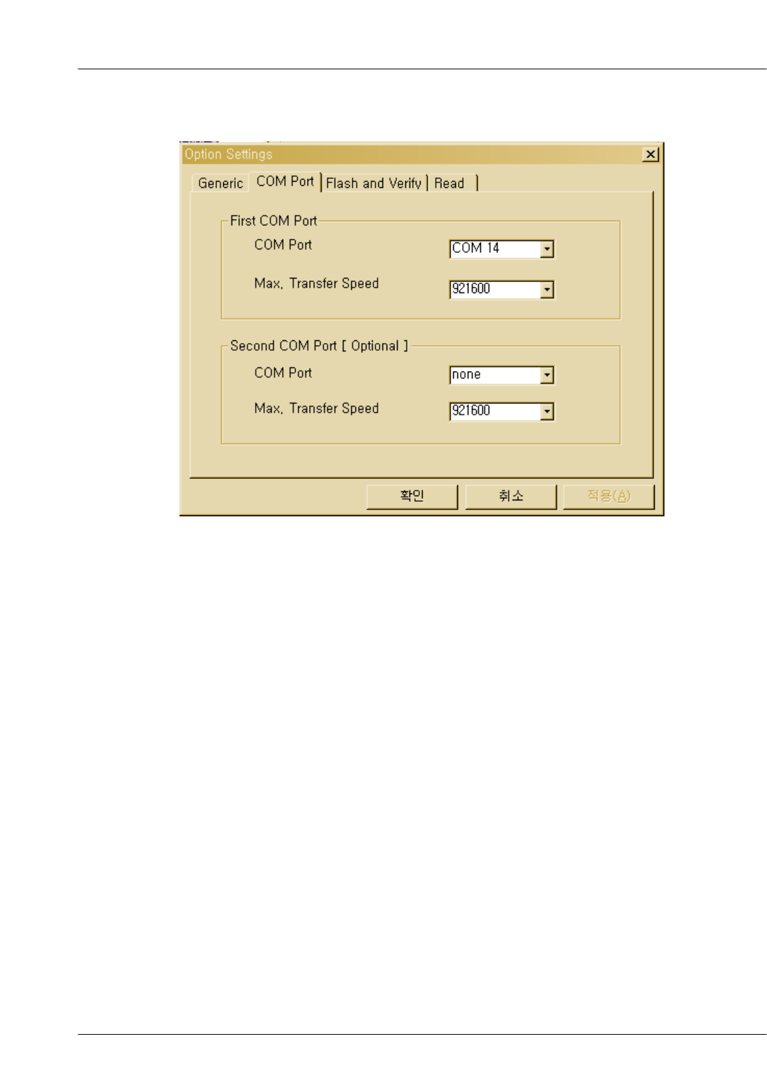
3. Select the COM port when the download cable is connected
Up to twelve ports are supported. Additionally you can select the
maximum transfer speed OptiFlash will use to communicate with
the phone. However, OptiFlash will use a slower speed if either the
PC’s or the phone’s serial hardware is incapable of handling the
selected speed
SAMSUNG Proprietary-Contents may change without notice
Array course control
4-5
This Document can not be used without Samsung's authorization
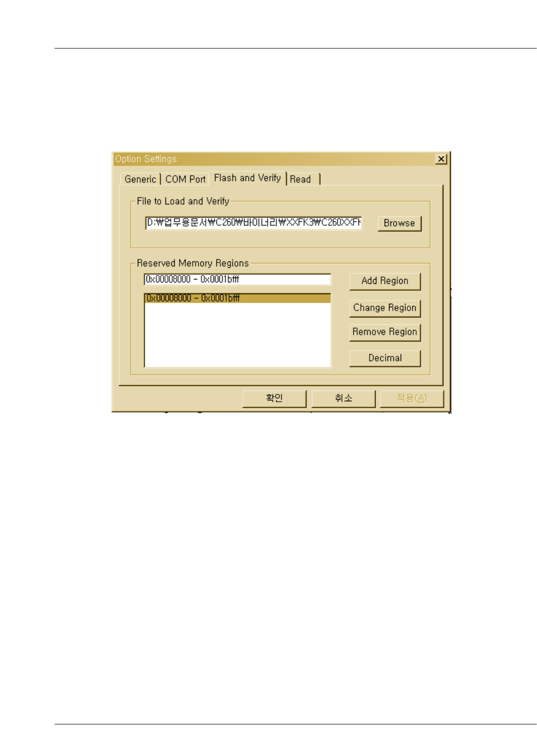
4. Select the“Flash&Verify” -> “Browse”
Set the directory path and choose the latest s/w binary, for example “
C260XXYY.s3”, for the downloader binary setting.
Make sure that not to change the reserved memory
regions.
In case of C140 the reserved memory regions are :
-0x00008000 – 0x0001bfff
SAMSUNG Proprietary-Contents may change without notice
Array course control
4-6
This Document can not be used without Samsung's authorization
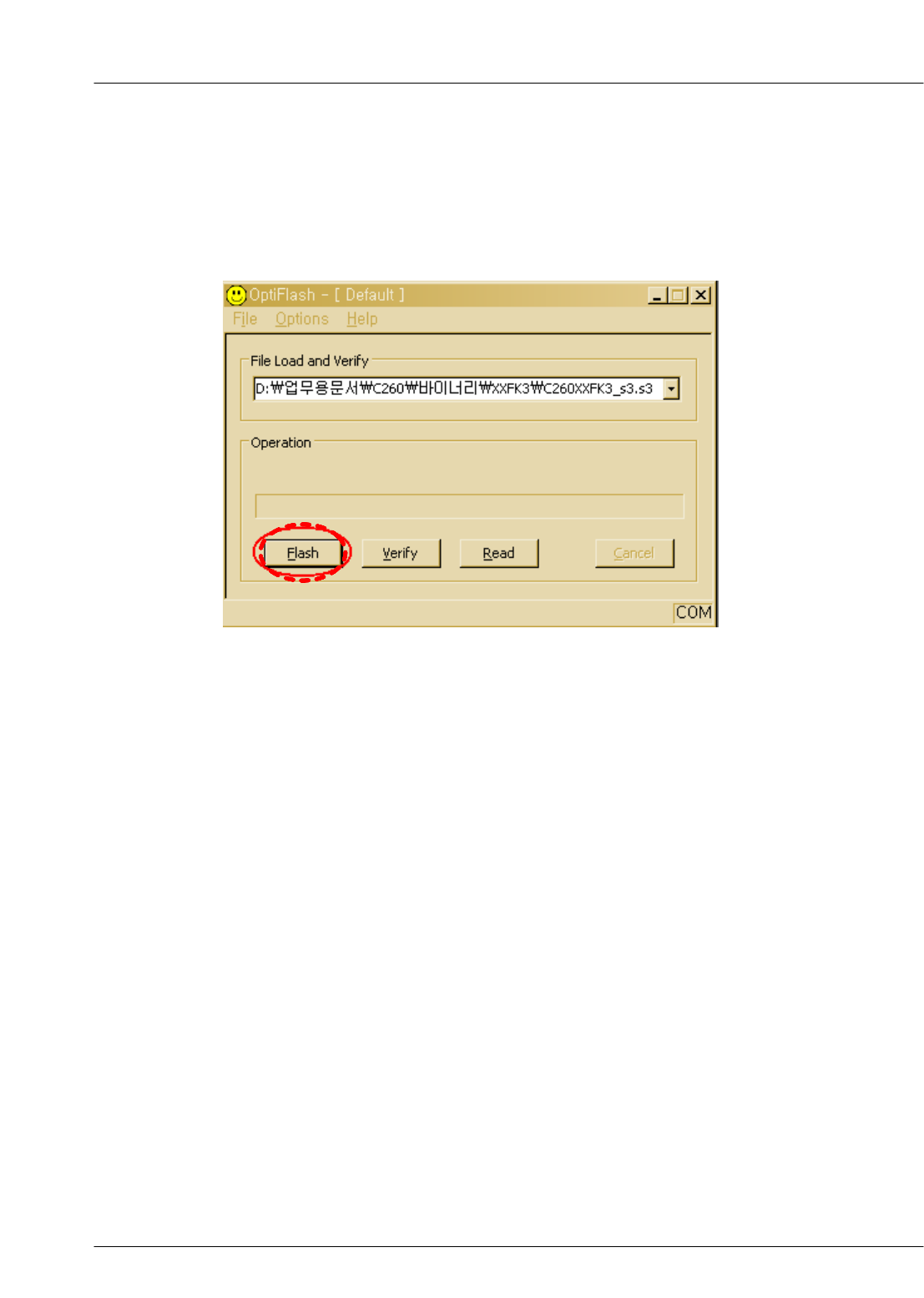
5. Click “OK” button then press “Flash”.
(Before pressing ‘Flash’ button, push the button ‘*’and ‘END’ at the same time.Then
press ‘Flash’.)
Downloader will upload the binary file as below for the downloading.
6. When downloading is finished successfully, there is a “All is well” message.
7. After finishing downloading, Certain memory resets should be done to guarantee the
normal performance.
8. Confirm the downloaded version name and etc. :
*#1111#
Full Reset :
*2767*3855#
SAMSUNG Proprietary-Contents may change without notice
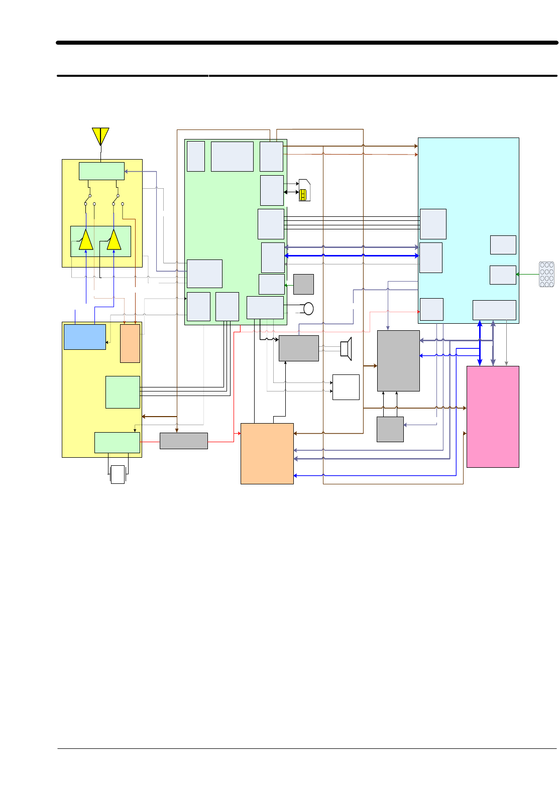
5. Block Diagrams
5-1
This Document can not be used without Samsung's authorization
T X R X
Serial
Interface
Xtal Oscillation
+ tunning
Trident
CSP2200B
VAPC
NC7SV74L8X
Key
UART
Core I/F &
Memor y I / F
System
Clock
DSP
I/F
789
456
123
* 0 #
ADC
Input
A[0:8]
D[0:15]
Control
3 bit
Key_Col[0: 4]
Key_Row[0: 4]
A(1:22)
D(0: 15) Cont rol
Core VCC
MIC
Antenna
SKY77518
Diplexer
26
MHz
GSM_TX
DCS_TX
GSM_RX
CLK26M
AFC
DCS_RX
RTXQ
RTXI
VMOD_EN
Band_Sel
TX_EN
RF
I/Q
DSP
I/F
RF Bl ock
Ctrl
Key
B/L
PM
Block
ADC
Block
Audio
I/F
RF
Serial
VSIM
SIM_RST
SIM_CLK
SIM_DATA
SIM
I/F
Serial
interface
Serial
interface
LRS18CK
BAT &
Charging
YMU
ISL8484IRZ
AOUTAP
D(0)~D(7)
A(0)
AOUTB
MSPK+-
control
SPK1P
SPK1N
EARPHONE
AOUTBP&N
AUXOUTP&N
LCD
Control
control
RT9364
PQW
LED+ LED-
control
A(2)
VRF VCCD_2. 9
CLK13M
VCCD_2.9
VCCD_1. 8
AD6548XCPZ
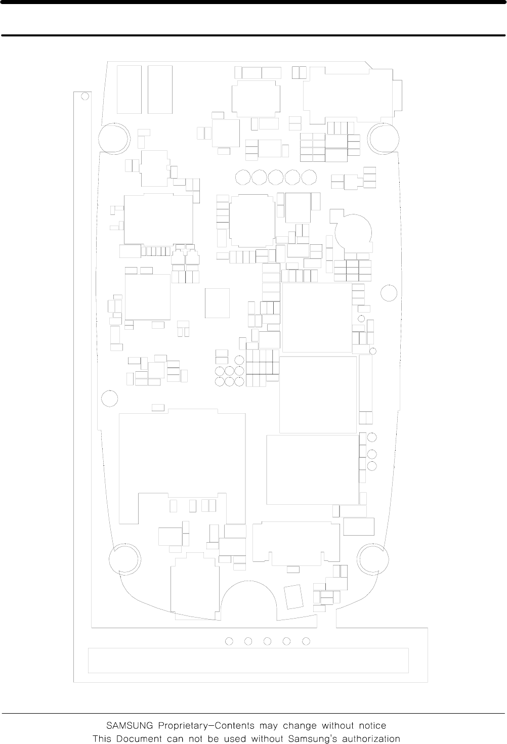
6. PCB Diagrams
6-1
ANT
BTC301
CN200
CP_TCK
CP_TDI
CP_TDO CP_TMS
1
0
3
J
C
D
DEBUG_DT R
DEBUG_RX D
DEBUG_TX D
0
0
3
R
A
E
F101F102
F104
F200F201
F202
G200 G201
G202 G203
G204
G205
GND
GND200
0
0
2
A
E
H
JIG
0
0
3
M
1
0
1
C
S
O
0
0
2
C
S
O
3
0
1
Q
0
0
3
Q
0
0
1
S
F
R
RST
RXD
SIM103
0
0
2
H
T
TP100 TP101 TP102 TP103 TP104
TP2
TP200
TXD
3
0
1
U
5
0
1
U
9
0
1
U
U200
U202
3
0
2
U
U204
U300
4
0
3
U
UCD101
6
0
1
D
C
U
7
0
1
D
C
U
UCP200
VBAT
VCCD_200
VR300
VR301
2
0
3
R
V
VR303
VR304
9
0
3
R
V
VR310
1
1
3
R
V
2
1
3
R
V
3
1
3
R
V
4
1
3
R
V
VR315
VR316
7
1
3
R
V
8
1
3
R
V
VR319
VR320
ZD300
1
0
3
D
Z
PCB Diagrams
6-2
*0
123
456
789
CLEAR
DOWN
I
LED301
LED302
T
F
E
L
MENU
PWR
T
H
G
I
R
SEND
SHARP
STO
1
0
2
U
UP
2
0
3
D
Z
SAMSUNG Proprietary-Contents may change without notice
7-1
This Document can not be used without Samsung's authorization
7. MAIN Electrical Parts List
SEC CODE Design LOC Discription STATUS
0403-001547 ZD300 DIODE-ZENER SA
0406-001083 ZD301 DIODE-TVS SA
0406-001267 ZD100 DIODE-TVS SA
0501-000225 TR300 TR-SMALL SIGNAL SA
0504-000168 TR100 TR-DIGITAL SA
0601-002160 LED301 LED SA
0601-002160 LED302 LED SA
0801-002529 U109 IC-CMOS LOGIC SA
0801-003013 U103 IC-CMOS LOGIC SA
1001-001371 U300 IC-ANALOG SWITCH SA
1009-001020 U201 IC-HALL EFFECT S/W SA
1108-000095 UME200 IC-MCP SA
1201-002490 PAM100 IC-POWER AMP SA
1203-003663 U105 IC-BATTERY SA
1203-003897 UCD107 IC-POWER SUPERVISOR SA
1203-004051 U203 IC-DC/DC CONVERTER SA
1204-001811 UCD106 IC-MELODY SA
1205-003098 UCD101 IC-TRANSCEIVER SA
1404-001165 TH200 THERMISTOR-NTC SA
1405-001082 VR300 VARISTOR SA
1405-001082 VR301 VARISTOR SA
1405-001082 VR302 VARISTOR SA
1405-001082 VR303 VARISTOR SA
1405-001082 VR304 VARISTOR SA
1405-001082 VR309 VARISTOR SA
1405-001082 VR310 VARISTOR SA
1405-001082 VR311 VARISTOR SA
1405-001082 VR312 VARISTOR SA
1405-001082 VR313 VARISTOR SA
1405-001082 VR314 VARISTOR SA
1405-001082 VR315 VARISTOR SA
1405-001082 VR316 VARISTOR SA
1405-001082 VR317 VARISTOR SA
1405-001082 VR318 VARISTOR SA
1405-001082 VR319 VARISTOR SA
1405-001082 VR320 VARISTOR SA
1405-001108 VR307 VARISTOR SA

SAMSUNG Proprietary-Contents may change without notice
Exploded View and Parts List
7-2
This Document can not be used without Samsung's authorization
SEC CODE Design LOC Discription STATUS
2007-000140 R324 R-CHIP SA
2007-000140 R325 R-CHIP SA
2007-000140 R326 R-CHIP SA
2007-000140 R344 R-CHIP SA
2007-000148 R118 R-CHIP SA
2007-000148 R143 R-CHIP SA
2007-000148 R339 R-CHIP SA
2007-000148 R342 R-CHIP SA
2007-000148 R358 R-CHIP SA
2007-000148 R363 R-CHIP SA
2007-000157 R188 R-CHIP SA
2007-000157 R202 R-CHIP SA
2007-000157 R349 R-CHIP SA
2007-000161 R341 R-CHIP SA
2007-000161 R343 R-CHIP SA
2007-000161 R359 R-CHIP SA
2007-000161 R364 R-CHIP SA
2007-000162 R117 R-CHIP SA
2007-000162 R172 R-CHIP SA
2007-000162 R182 R-CHIP SA
2007-000162 R203 R-CHIP SA
2007-000162 R208 R-CHIP SA
2007-000164 R155 R-CHIP SA
2007-000170 R189 R-CHIP SA
2007-000170 R190 R-CHIP SA
2007-000171 R213 R-CHIP SA
2007-000171 R335 R-CHIP SA
2007-000171 R337 R-CHIP SA
2007-000171 R351 R-CHIP SA
2007-000171 R366 R-CHIP SA
2007-000172 R200 R-CHIP SA
2007-000172 R201 R-CHIP SA
2007-000173 R357 R-CHIP SA
2007-000173 R365 R-CHIP SA
2007-000242 R340 R-CHIP SA
2007-000242 R354 R-CHIP SA
2007-000242 R355 R-CHIP SA

SAMSUNG Proprietary-Contents may change without notice
Exploded View and Parts List
7-3
This Document can not be used without Samsung's authorization
SEC CODE Design LOC Discription STATUS
2007-000566 R211 R-CHIP SA
2007-000566 R212 R-CHIP SA
2007-000566 R327 R-CHIP SA
2007-000775 R156 R-CHIP SA
2007-000775 R158 R-CHIP SA
2007-000831 R348 R-CHIP SA
2007-001119 R347 R-CHIP SA
2007-001119 R353 R-CHIP SA
2007-001288 R367 R-CHIP SA
2007-001288 R368 R-CHIP SA
2007-001308 R133 R-CHIP SA
2007-001323 R345 R-CHIP SA
2007-001325 R159 R-CHIP SA
2007-001335 R360 R-CHIP SA
2007-001339 R183 R-CHIP SA
2007-002797 R131 R-CHIP SA
2007-003112 R301 R-CHIP SA
2007-003112 R302 R-CHIP SA
2007-007107 R207 R-CHIP SA
2007-007314 R209 R-CHIP SA
2007-007573 R205 R-CHIP SA
2007-007573 R210 R-CHIP SA
2007-007861 R160 R-CHIP SA
2007-008043 R102 R-CHIP SA
2007-008137 R170 R-CHIP SA
2007-008806 R195 R-CHIP SA
2007-009160 R171 R-CHIP SA
2203-000233 C106 C-CER,CHIP SA
2203-000233 C107 C-CER,CHIP SA
2203-000233 C110 C-CER,CHIP SA
2203-000233 C175 C-CER,CHIP SA
2203-000233 C190 C-CER,CHIP SA
2203-000233 C221 C-CER,CHIP SA
2203-000233 C306 C-CER,CHIP SA
2203-000233 C309 C-CER,CHIP SA
2203-000254 C146 C-CER,CHIP SA
2203-000254 C147 C-CER,CHIP SA

SAMSUNG Proprietary-Contents may change without notice
Exploded View and Parts List
7-4
This Document can not be used without Samsung's authorization
SEC CODE Design LOC Discription STATUS
2203-000254 C152 C-CER,CHIP SA
2203-000254 C153 C-CER,CHIP SA
2203-000254 C165 C-CER,CHIP SA
2203-000254 C200 C-CER,CHIP SA
2203-000254 C207 C-CER,CHIP SA
2203-000254 C208 C-CER,CHIP SA
2203-000254 C209 C-CER,CHIP SA
2203-000254 C211 C-CER,CHIP SA
2203-000254 C213 C-CER,CHIP SA
2203-000254 C215 C-CER,CHIP SA
2203-000254 C217 C-CER,CHIP SA
2203-000278 C319 C-CER,CHIP SA
2203-000330 C222 C-CER,CHIP SA
2203-000330 C223 C-CER,CHIP SA
2203-000386 C127 C-CER,CHIP SA
2203-000386 C326 C-CER,CHIP SA
2203-000386 C327 C-CER,CHIP SA
2203-000386 C338 C-CER,CHIP SA
2203-000425 C101 C-CER,CHIP SA
2203-000438 C176 C-CER,CHIP SA
2203-000438 C185 C-CER,CHIP SA
2203-000627 C134 C-CER,CHIP SNA
2203-000654 C166 C-CER,CHIP SA
2203-000679 C202 C-CER,CHIP SA
2203-000714 C169 C-CER,CHIP SA
2203-000812 C113 C-CER,CHIP SA
2203-000812 C115 C-CER,CHIP SA
2203-000812 C116 C-CER,CHIP SA
2203-000812 C120 C-CER,CHIP SA
2203-000812 C311 C-CER,CHIP SA
2203-000854 C105 C-CER,CHIP SA
2203-000854 C109 C-CER,CHIP SA
2203-000854 C132 C-CER,CHIP SA
2203-000854 C145 C-CER,CHIP SA
2203-000854 C184 C-CER,CHIP SA
2203-000854 C330 C-CER,CHIP SA
2203-000854 C331 C-CER,CHIP SA

SAMSUNG Proprietary-Contents may change without notice
Exploded View and Parts List
7-5
This Document can not be used without Samsung's authorization
SEC CODE Design LOC Discription STATUS
2203-000940 C138 C-CER,CHIP SA
2203-000995 C140 C-CER,CHIP SA
2203-000995 C141 C-CER,CHIP SA
2203-000995 C142 C-CER,CHIP SA
2203-000995 C225 C-CER,CHIP SA
2203-000995 C305 C-CER,CHIP SA
2203-000995 C307 C-CER,CHIP SA
2203-001072 C321 C-CER,CHIP SA
2203-001383 C108 C-CER,CHIP SA
2203-001405 C218 C-CER,CHIP SA
2203-001412 C129 C-CER,CHIP SA
2203-005057 C117 C-CER,CHIP SA
2203-005057 C118 C-CER,CHIP SA
2203-005065 C168 C-CER,CHIP SA
2203-005065 C170 C-CER,CHIP SA
2203-005065 C171 C-CER,CHIP SA
2203-005065 C173 C-CER,CHIP SA
2203-005234 C102 C-CER,CHIP SA
2203-005249 C188 C-CER,CHIP SA
2203-005482 C112 C-CER,CHIP SA
2203-005482 C124 C-CER,CHIP SA
2203-005482 C139 C-CER,CHIP SA
2203-005482 C150 C-CER,CHIP SA
2203-005482 C155 C-CER,CHIP SA
2203-005482 C164 C-CER,CHIP SA
2203-005482 C167 C-CER,CHIP SA
2203-005482 C178 C-CER,CHIP SA
2203-005482 C180 C-CER,CHIP SA
2203-005482 C183 C-CER,CHIP SA
2203-005482 C189 C-CER,CHIP SA
2203-005482 C201 C-CER,CHIP SA
2203-005482 C204 C-CER,CHIP SA
2203-005482 C205 C-CER,CHIP SA
2203-005482 C206 C-CER,CHIP SA
2203-005482 C212 C-CER,CHIP SA
2203-005482 C214 C-CER,CHIP SA
2203-005482 C219 C-CER,CHIP SA

SAMSUNG Proprietary-Contents may change without notice
Exploded View and Parts List
7-6
This Document can not be used without Samsung's authorization
SEC CODE Design LOC Discription STATUS
2203-005482 C220 C-CER,CHIP SA
2203-005482 C224 C-CER,CHIP SA
2203-005482 C301 C-CER,CHIP SA
2203-005482 C316 C-CER,CHIP SA
2203-005482 C322 C-CER,CHIP SA
2203-005682 C125 C-CER,CHIP SA
2203-006047 C123 C-CER,CHIP SA
2203-006048 C133 C-CER,CHIP SA
2203-006137 C179 C-CER,CHIP SA
2203-006137 C203 C-CER,CHIP SA
2203-006137 C308 C-CER,CHIP SA
2203-006257 C313 C-CER,CHIP SA
2203-006260 C121 C-CER,CHIP SA
2203-006260 C210 C-CER,CHIP SA
2203-006260 C216 C-CER,CHIP SA
2203-006324 C162 C-CER,CHIP SA
2203-006361 C111 C-CER,CHIP SA
2203-006361 C186 C-CER,CHIP SA
2203-006361 C335 C-CER,CHIP SA
2203-006556 C119 C-CER,CHIP SA
2203-006562 C182 C-CER,CHIP SA
2203-006562 C227 C-CER,CHIP SA
2203-006562 C228 C-CER,CHIP SA
2203-006562 C229 C-CER,CHIP SA
2203-006626 C151 C-CER,CHIP SA
2203-006626 C226 C-CER,CHIP SA
2203-006626 C230 C-CER,CHIP SA
2203-006626 C304 C-CER,CHIP SA
2203-006626 C310 C-CER,CHIP SA
2203-006708 C163 C-CER,CHIP SA
2203-006708 C172 C-CER,CHIP SA
2203-006708 C174 C-CER,CHIP SA
2203-006708 C177 C-CER,CHIP SA
2203-006824 C314 C-CER,CHIP SA
2203-006978 C339 C-CER,CHIP SA
2404-001352 TA303 C-TA,CHIP SA
2404-001393 TA301 C-TA,CHIP SA

SAMSUNG Proprietary-Contents may change without notice
Exploded View and Parts List
7-7
This Document can not be used without Samsung's authorization
SEC CODE Design LOC Discription STATUS
2404-001393 TA302 C-TA,CHIP SA
2404-001406 TA300 C-TA,CHIP SA
2703-001236 L112 INDUCTOR-SMD SA
2703-001737 L100 INDUCTOR-SMD SA
2703-001737 L111 INDUCTOR-SMD SA
2703-001752 L101 INDUCTOR-SMD SA
2703-002205 L103 INDUCTOR-SMD SA
2703-002484 L105 INDUCTOR-SMD SA
2703-002593 L104 INDUCTOR-SMD SA
2801-003856 OSC200 CRYSTAL-SMD SA
2801-004587 OSC101 CRYSTAL-SMD SA
2901-001296 F200 FILTER-EMI SMD SA
2901-001296 F201 FILTER-EMI SMD SA
2901-001296 F202 FILTER-EMI SMD SA
2904-001592 F101 FILTER-SAW SA
2904-001599 F102 FILTER-SAW SA
3301-001342 L110 BEAD-SMD SA
3301-001342 L200 BEAD-SMD SA
3705-001358 RFS100 CONNECTOR-COAXIAL SA
3709-001384 SIM103 CONNECTOR-CARD EDGE SA
3711-005954 HDC200 HEADER-BOARD TO BOARD SA
3711-006228 BTC301 HEADER-BATTERY SA
3722-002067 EAR300 JACK-EAR PHONE SA
3722-002433 DCJ301 JACK-DC POWER SA
GH09-00039A UCP200 IC MICOM SA
GH71-04813A ANT NPR-ANTENNA CONTACT SA
GH71-04813A GND NPR-ANTENNA CONTACT SA

SAMSUNG Proprietary-Contents may change without notice
8. Reference data
8-1
This Document can not be used without Samsung's authorization
8-1. Reference Abbreviate
AAC: Advanced Audio Coding.
AVC : Advanced Video Coding.
BER :BitErrorRate
BPSK: Binary Phase Shift Keying
CA : Conditional Access
CDM : Code Division Multiplexing
C/I : Carrier to Interference
DMB : Digital Multimedia Broadcasting
EN : European Standard
ES : Elementary Stream
ETSI: European Telecommunications Standards Institute
MPEG: Moving Picture Experts Group
PN : Pseudo-random Noise
PS :PilotSymbol
QPSK: Quadrature Phase Shift Keying
RS : Reed-Solomon
SI : Service Information
TDM : Time Division Multiplexing
TS : Transport Stream

SAMSUNG Proprietary-Contents may change without notice
9. Safety Precautions
9-1
This Document can not be used without Samsung's authorization
9-1. Repair Precaution
●Repair in Shield Box, during detailed tuning.
Take specially care of tuning or test,
because specipicty of cellular phone is sensitive for surrounding interference(RF noise).
●Be careful to use a kind of magnetic object or tool,
because performance of parts is damaged by the influence of manetic force.
●Surely use a standard screwdriver when you disassemble this product,
otherwise screw will be worn away.
●Use a thicken twisted wire when you measure level.
A thicken twisted wire has low resistance, therefore error of measurement is few.
●Repair after separate Test Pack and Set because for short danger (for example an
overcurrent and furious flames of parts etc) when you repair board in condition of
connecting Test Pack and tuning on.
●Take specially care of soldering, because Land of PCB is small and weak in heat.
●Surely tune on/off while using AC power plug, because a repair of battery charger is
dangerous when tuning ON/OFF PBA and Connector after disassembing charger.
●Don't use as you pleases after change other material than replacement registered on SEC
System. Otherwise engineer in charge isn't charged with problem that you don't keep this
rules.

SAMSUNG Proprietary-Contents may change without notice
Safety Precautions
9-2
This Document can not be used without Samsung's authorization
9-2. ESD(Electrostatically Sensitive Devices) Precaution
Several semiconductor may be damaged easilly by static electricity. Such parts are called by
ESD(Electrostatically Sensitive Devices), for example IC,BGA chip etc. Read Precaution below.
You can prevent from ESD damage by static electricity.
●Remove static electricity remained your body before you touch semiconductor or parts with
semiconductor. There are ways that you touch an earthed place or wear static electricity
prevention string on wrist.
●Use earthed soldering steel when you connect or disconnect ESD.
●Use soldering removing tool to break static electricity. , otherwise ESD will be damaged by
static electricity.
●Don't unpack until you set up ESD on product. Because most of ESD are packed by box
and aluminum plate to have conductive power,they are prevented from static electricity.
●You must maintain electric contact between ESD and place due to be set up until ESD is
connected completely to the proper place or a circuit board.

SAMSUNG Proprietary-Contents may change without notice
10. Product Function
10-1
This Document can not be used without Samsung's authorization
Main Function
- Network services
- Read SMS messages
-Voicemail
- Broadcast message
- Web browser
- Access media files
- Funbox memory status
- Calendar, Calculator, Task list, Voice memo, etc...
- Speed dial
- SDN (Service Dialling Numbers)

This Service Manual is a property of Samsung Electronics Co.,Ltd.
Any unauthorized use of Manual can be punished under applicable
International and/or domestic law.
Samsung Electronics Co.,Ltd.
2007. 02. Rev.1.0
ⓒ