Samsung SGH E420 Service Manual. Www.s Manuals.com. Manual R1.0
User Manual: Phone Samsung SGH-E420 - Service manuals and Schematics, Disassembly / Assembly. Free.
Open the PDF directly: View PDF ![]() .
.
Page Count: 69
GSM TELEPHONE
SGH-E420
GSM TELEPHONE CONTENTS
1. Safety Precautions
2. Specification
3. Product Function
4. Array course control
5. Exploded View/Disassembly
and Assembly Instructions
6. MAIN Electrical Parts List
7. Block Diagrams
8. PCB Diagrams
9. Flow Chart of Troubleshooting
10. Reference data

CONTENTS
1. Safety Precautions
1-1. Repair Precaution......................................................................................................1-1
1-2. ESD(Electrostatically Sensitive Devices) Precaution...............................................1-2
2. Specification
2-1. GSM General Specification.......................................................................................2-1
2-2. GSM Tx Power Class...............................................................................................2-2
3. Product Function
4. Array course control
4-1. Software Adjustments................................................................................................4-1
4-2. Software Downloading...............................................................................................4-2
5. Exploded View/Disassembly & Assembly Instructions
5-1. Cellular phone Exploded View..................................................................................5-1
5-2. Cellular phone Parts list............................................................................................5-2
5-3. Disassembly & Assembly Instructions......................................................................5-4
6. MAIN Electrical Parts List
7. Block Diagrams
8. PCB Diagrams

CONTENTS
9. Flow Chart of Troubleshooting
9-1. Pown on.....................................................................................................................9-1
9-2. Initial...........................................................................................................................9-3
9-3. Charging Part.............................................................................................................9-6
9-4. SIM Part.....................................................................................................................9-8
9-5. Microphone Part.......................................................................................................9-10
9-6. Speaker Part............................................................................................................9-12
9-7. Key Data Input........................................................................................................9-14
9-8. Receiver Part...........................................................................................................9-15
9-9. LCD Part..................................................................................................................9-16
9-10. Key Back Light......................................................................................................9-18
9-11. Camera Part...........................................................................................................9-19
9-12. GSM Receiver........................................................................................................9-21
9-13. GSM Transmitter....................................................................................................9-22
9-14. DCS Receiver........................................................................................................9-23
9-15. DCS Transmitter....................................................................................................9-24
9-16. PCS Receiver.........................................................................................................9-25
9-17. PCS Transmitter.....................................................................................................9-23
10. Reference data

SAMSUNG Proprietary-Contents may change without notice
1. Safety Precautions
1-1
This Document can not be used without Samsung's authorization
1-1. Repair Precaution
● Repair in Shield Box, during detailed tuning.
Take specially care of tuning or test,
because specipicty of cellular phone is sensitive for surrounding interference(RF noise).
● Be careful to use a kind of magnetic object or tool,
because performance of parts is damaged by the influence of magnetic force.
● Surely use a standard screwdriver when you disassemble this product,
otherwise screw will be worn away.
● Use a thicken twisted wire when you measure level.
A thicken twisted wire has low resistance, therefore error of measurement is few.
● Repair after separate Test Pack and Set because for short danger (for example an
overcurrent and furious flames of parts etc) when you repair board in condition of
connecting Test Pack and tuning on.
● Take specially care of soldering, because Land of PCB is small and weak in heat.
● Surely tune on/off while using AC power plug, because a repair of battery charger is
dangerous when tuning ON/OFF PBA and Connector after disassembling charger.
● Don't use as you pleases after change other material than replacement registered on
SEC System.
Otherwise engineer in charge isn't charged with problem that you don't keep this rules.

SAMSUNG Proprietary-Contents may change without notice
Safety Precautions
1-2
This Document can not be used without Samsung's authorization
1-2. ESD(Electrostatically Sensitive Devices) Precaution
Several semiconductor may be damaged easily by static electricity. Such parts are called by ESD
(Electrostatically Sensitive Devices), for example IC,BGA chip etc. Read Precaution below.
You can prevent from ESD damage by static electricity.
● Remove static electricity remained your body before you touch semiconductor or parts with
semiconductor. There are ways that you touch an earthed place or wear static electricity
prevention string on wrist.
● Use earthed soldering steel when you connect or disconnect ESD.
● Use soldering removing tool to break static electricity. , otherwise ESD will be damaged by
static electricity.
● Don't unpack until you set up ESD on product. Because most of ESD are packed by box and
aluminum
plate to have conductive power,they are prevented from static electricity.
● You must maintain electric contact between ESD and place due to be set up until ESD is
connected
completely to the proper place or a circuit board.
2. Specification
2-1
2-1. GSM General Specification
GSM900
Phase 1
EGSM 900
Phase 2
DCS1800
Phase 1 PCS1900
Freq.
Band[MHz]
Uplink/Downlink
890~915
935~960
880~915
925~960
1710~1785
1805~1880
1850~1910
1930~1990
ARFCN range 1~124 0~124 &
975~1023 512~885 512~810
Tx/Rx spacing 45MHz 45MHz 95MHz 80MHz
Mod. Bit rate/
Bit Period
270.833kbps
3.692us
270.833kbps
3.692us
270.833kbps
3.692us
270.833kbps
3.692us
Time Slot
Period/Frame
Period
576.9us
4.615ms
576.9us
4.615ms
576.9us
4.615ms
576.9us
4.615ms
Modulation 0.3GMSK 0.3GMSK 0.3GMSK 0.3GMSK
MS Power 33dBm~5dBm 33dBm~5dBm 30dBm~0dBm 30dBm~0dBm
Power Class 5pcl ~ 19pcl 5pcl ~ 19pcl 0pcl ~ 15pcl 0pcl ~ 15pcl
Sensitivity -102dBm -102dBm -100dBm -100dBm
TDMA Mux 888 8
Cell Radius 35Km 35Km 2Km -
Speclflcation
2-2
TX Power
control level
GSM900
533±2dBm
631±2dBm
729±2dBm
827±2dBm
925±2dBm
10 23±2 dBm
11 21±2 dBm
12 19±2 dBm
13 17±2 dBm
14 15±2 dBm
15 13±2 dBm
16 11±3 dBm
17 9±3dBm
18 7±3 dBm
19 5±3 dBm
TX Power
control level
DCS1800
030±3dBm
128±3dBm
226±3dBm
324±3dBm
422±3dBm
520±3dBm
618±3dBm
716±3dBm
814±3dBm
912±4dBm
10 10±4 dBm
11 8±4dBm
12 6±4 dBm
13 4±4 dBm
14 2±5 dBm
15 0±5 dBm
TX Power
control level
PCS1800
030±3dBm
128±3dBm
226±3dBm
324±3dBm
422±3dBm
520±3dBm
618±3dBm
716±3dBm
814±3dBm
912±4dBm
10 10±4 dBm
11 8±4dBm
12 6±4 dBm
13 4±4 dBm
14 2±5 dBm
15 0±5 dBm
2-2. GSM Tx Power Class

SAMSUNG Proprietary-Contents may change without notice
3. Product Function
3-1
This Document can not be used without Samsung's authorization
Main Function
-VGA Camera
-65536 Color OLED Main Screen (128×160)
65536 Color OLED Sub Screen (96×96)
-SMS/EMS/MMS Message Service
-WAP Http support
-J2ME JAVA (MIDP 2.0/CLDC 1.1)
-Speaker phone
-40 Poly Melody
-vCard, vCalendar
-E-mail Client
-Tri-band(900/1800/1900MHz)

SAMSUNG Proprietary-Contents may change without notice
Product Function
3-2
This Document can not be used without Samsung's authorization
SAMSUNG Proprietary-Contents may change without notice
4. Array course control
4-1
This Document can not be used without Samsung's authorization
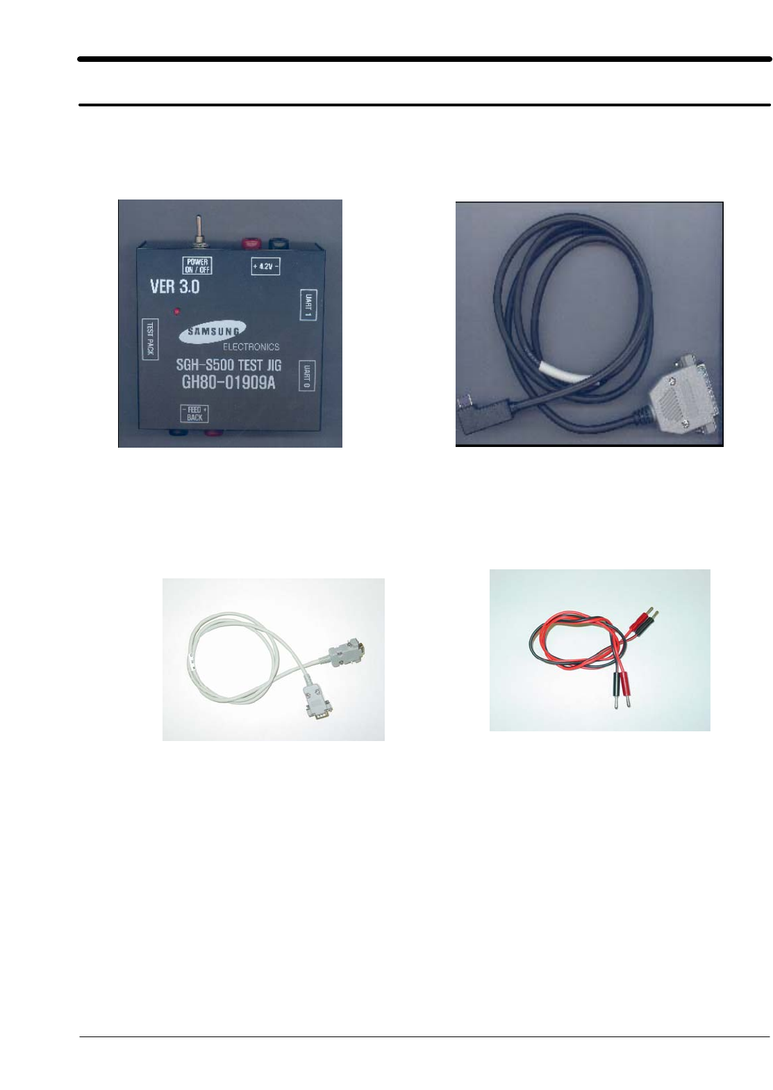
4-1. Software Adjustments
Test Jig (GH80-01909A)Test Jig (GH80-01909A) Test Cable (SGH-E420 VER2)Test Cable (SGH-E420 VER2)
Power Supply CableSerial Cable(CSA LL64151-A)
SAMSUNG Proprietary-Contents may change without notice
Array course control
4-2
This Document can not be used without Samsung's authorization
4-2. Software Downloading
4-2-1. Pre-requsite for Downloading
• Downloader Program(Lily Downloader 2.0.exe)
• E420 Mobile Phone
• Data Cable
• Binary file, TFS file
4-2-2. S/W Downloader Program
■Load the binary download program by executing the
“Lily Downloader 2.0.exe”
1. Select the connected serial port and therateofspeed
2. Select the check box, the mode you want to download.
- if the binary file wanted, check only 'BIN'
- if the tfs file wanted, check only 'TFS'
- if all the files wanted, check 'BIN+TFS'
12
SAMSUNG Proprietary-Contents may change without notice
Array course control
4-3
This Document can not be used without Samsung's authorization
3. Select the file(s) what you want to download

SAMSUNG Proprietary-Contents may change without notice
Array course control
4-4
This Document can not be used without Samsung's authorization
SAMSUNG Proprietary-Contents may change without notice
5-1
This Document can not be used without Samsung's authorization
5. Exploded View/Disassembly&Assembly Instructions
5-1. Cellular phone Exploded View
QFU01
QME15
QLB01
QFR01
QRF03
QCA01
QLC01 QMO01
QVK01
QFL01
QCR26
QSC01
QSP01
QHI01
QKP01
QME01
QCA02
QMI01
QCR12
QAN02
QCK01
QRE01
QMI03
QCR05
QBA01
QBA00
QAN05
QVO01
QRF01
QMP01
SAMSUNG Proprietary-Contents may change without notice
Exploded View/Disassembly&Assembly Instructions
5-2
This Document can not be used without Samsung's authorization
5-2. Cellular phone Parts list
Design LOC Description Sec Code
QAN02 INTENNA-SGHE420 GH42-01018A
QAN05 ASSY MEC-INTENNA CONTACT GH75-08168A
QBA00 PMO-COVER BATTERY GH72-33285A
QBA01 INNER BATTERY PACK-750MAH,BLK, GH43-02483A
QCA01 UNIT-CAMERA MODULE GH59-03566A
QCA02 UNIT-CAMERA KEY GH59-03606A
QCK01 PMO-CAMERA KEY GH72-33287A
QCR05 SCREW-MACHINE 6001-001478
QCR12 SCREW-MACHINE 6001-001530
QCR26 SCREW-MACHINE 6001-001850
QFU01 ASSY CASE-FOLDER UPPER GH98-01842A
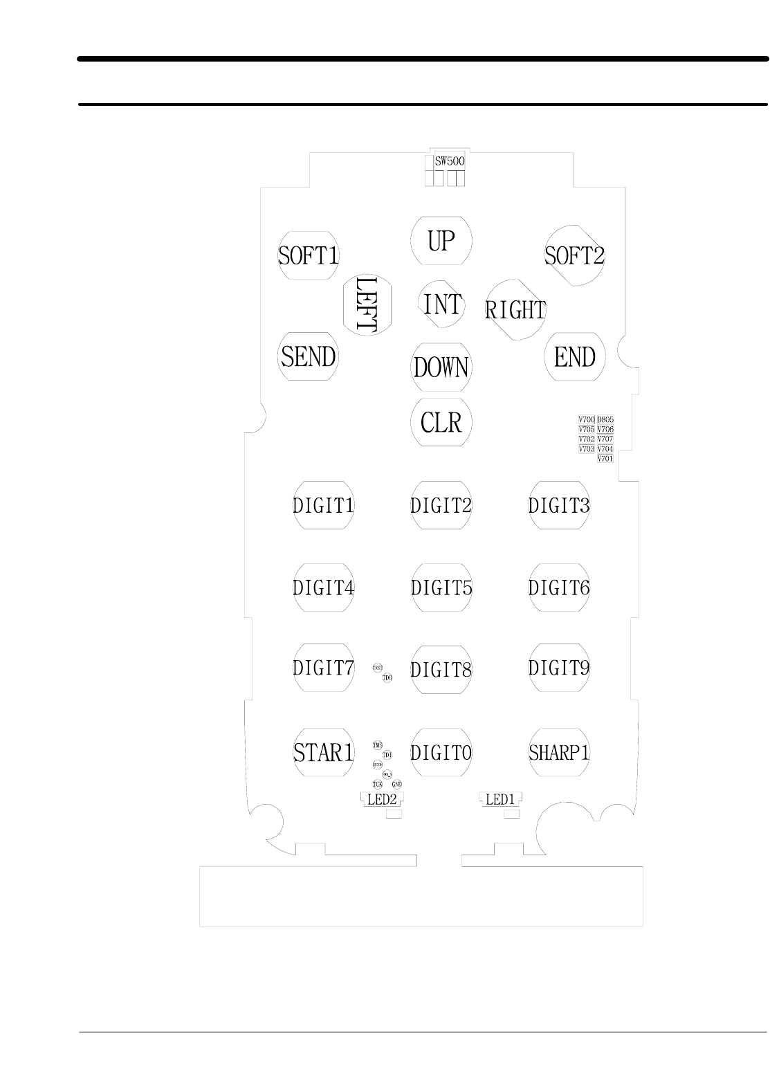
QKP01 ASSY KEYPAD-(SER/UWA) GH98-02645A
QLB01 ASSY BRACKET-LCD GH98-01846A
QME01 UNIT-METAL DOME GH59-03605A
QME15 ELA ETC-EL SHEET(PNK) GH96-02356A
QMI01 MICROPHONE-ASSY-SGHE420 GH30-00311A
QMO01 MOTOR DC-SGHE420 GH31-00198C
QMP01 PBA MAIN-SGHE420 GH92-03133A
QRF01 RMO-COVER RF GH73-08169A
QSC01 RMO-COVER SCREW GH73-08170A
QSP01 SPEAKER 3001-002064
QVK01 UNIT-VOLUME KEY GH59-03595A
QVO01 PMO-VOLUME KEY GH72-33286A
QFR01 ASSY CASE-FRONT GH98-01844A
QRF03 PMO-COVER EAR GH72-33281A
QFL01 ASSY CASE-FOLDER LOWER GH98-01843A
QHI01 ASSY MEC-HINGE(CAN TYPE) GH75-04662A
QLC01 LCD-M/S SGH-E420 GH07-01014A
QMW01 AS-LCD WINDOW SVC GH81-06126A
QRE01 ASSY CASE-REAR GH98-01845A
QMI03 RMO-RUBBER MIC GH73-08187A
SAMSUNG Proprietary-Contents may change without notice
Exploded View/Disassembly&Assembly Instructions
5-3
This Document can not be used without Samsung's authorization
Description Sec Code
BAG PE 6902-000634
ADAPTOR-SGHE690,SIL,EU,A_TYPE GH44-01361B
LABEL(P)-WATER SOAK GH68-02026A
LABEL(P)-WATER SOAK GH68-02026A
MANUAL-SFC GH68-04336A
LABEL(P)-BARCODE RUSSIA GH68-08494A
MANUAL USERS-EU RUSSIAN GH68-12319A
LABEL(R)-MAIN(SER) GH68-12806A
BOX-UNIT(SER) GH69-04579A
CUSHION-CASE(EU) GH69-04581A
MPR-INSU TAPE GH74-18047A
MPR-TAPE MIC GH74-25834A
MPR-GASKET LCD CONN GH74-25836A
MPR-VINYL BOHO F/LOWER GH74-26366A
MPR-VINYL BOHO F/UPPER 2DN GH74-26368A
MPR-TAPE,9.1X3.1XT0.06,3M1361 GH74-26419A
MPR-INSULATION TAPE,11.2X7.5XT GH74-26425A
MPR-INSU TAPE EL CONN GH74-27032A
MPR-TAPE MAIN LCD GH74-27500A
MPR-SPONGE LCD GH74-27688A
MPR-INSU TAPE GH74-28027A
MPR-VINYL BOHO MAIN GH74-29305A
MPR-VINYL BOHO REAR BATT GH74-29981A
AS-MAIN LCD SVC GH81-05969A
AS-SUB LCD SVC GH81-05970A
AS-LCD PCB SVC GH81-05971A
AS-WINDOW TAPE SVC GH81-06097A
SAMSUNG Proprietary-Contents may change without notice
Exploded View/Disassembly&Assembly Instructions
5-4
This Document can not be used without Samsung's authorization
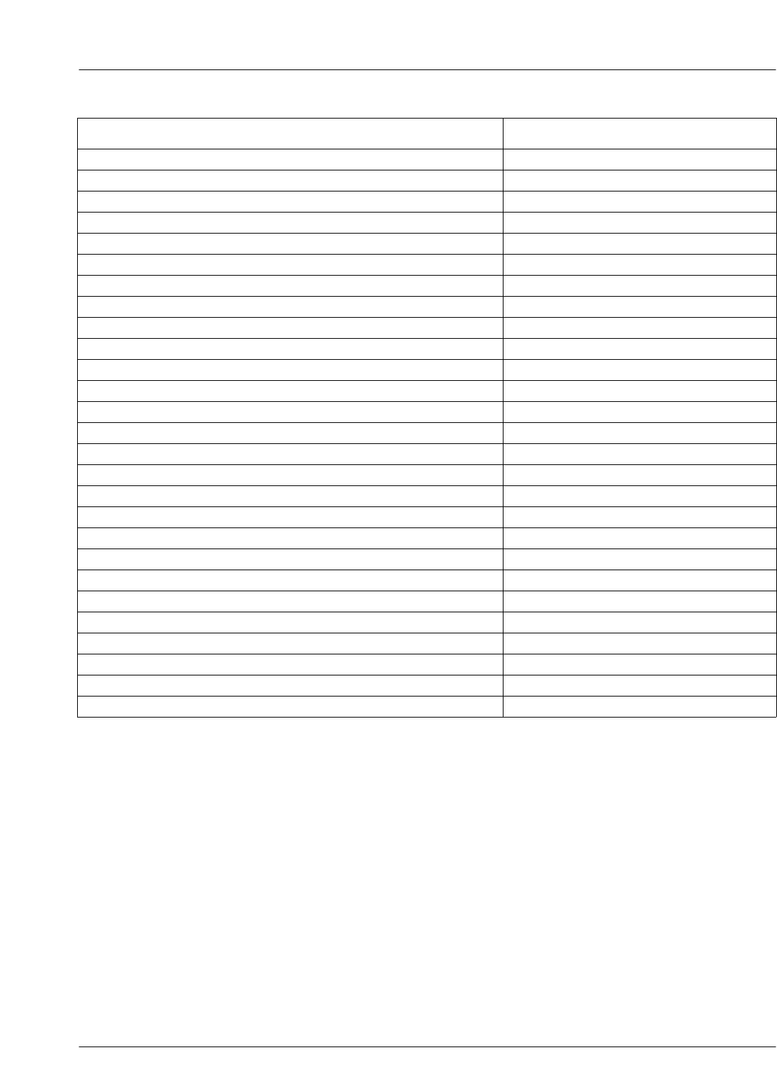
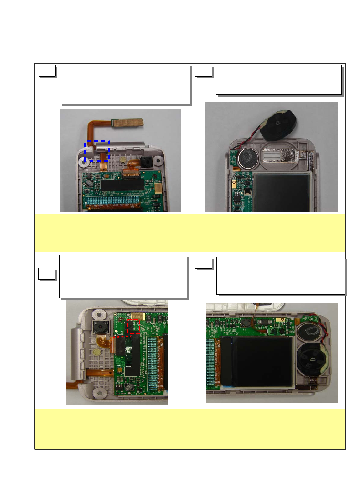
5-3. Disassembly and Assembly Instructions
―Disassembly
SAMSUNG Proprietary-Contents may change without notice
Exploded View/Disassembly&Assembly Instructions
5-5
This Document can not be used without Samsung's authorization
SAMSUNG Proprietary-Contents may change without notice
Exploded View/Disassembly&Assembly Instructions
5-6
This Document can not be used without Samsung's authorization
1)
SAMSUNG Proprietary-Contents may change without notice
Exploded View/Disassembly&Assembly Instructions
5-7
This Document can not be used without Samsung's authorization
When inserting the camera module,
When inserting the motor and the speaker, it pays
attention in WIRE control.
1) When attaching the TAPE, be careful not to
damage camera FPCB at pincette.
When attaching an insulation TAPE, be careful
not to cover the LCD.
―Assembly
SAMSUNG Proprietary-Contents may change without notice
Exploded View/Disassembly&Assembly Instructions
5-8
This Document can not be used without Samsung's authorization
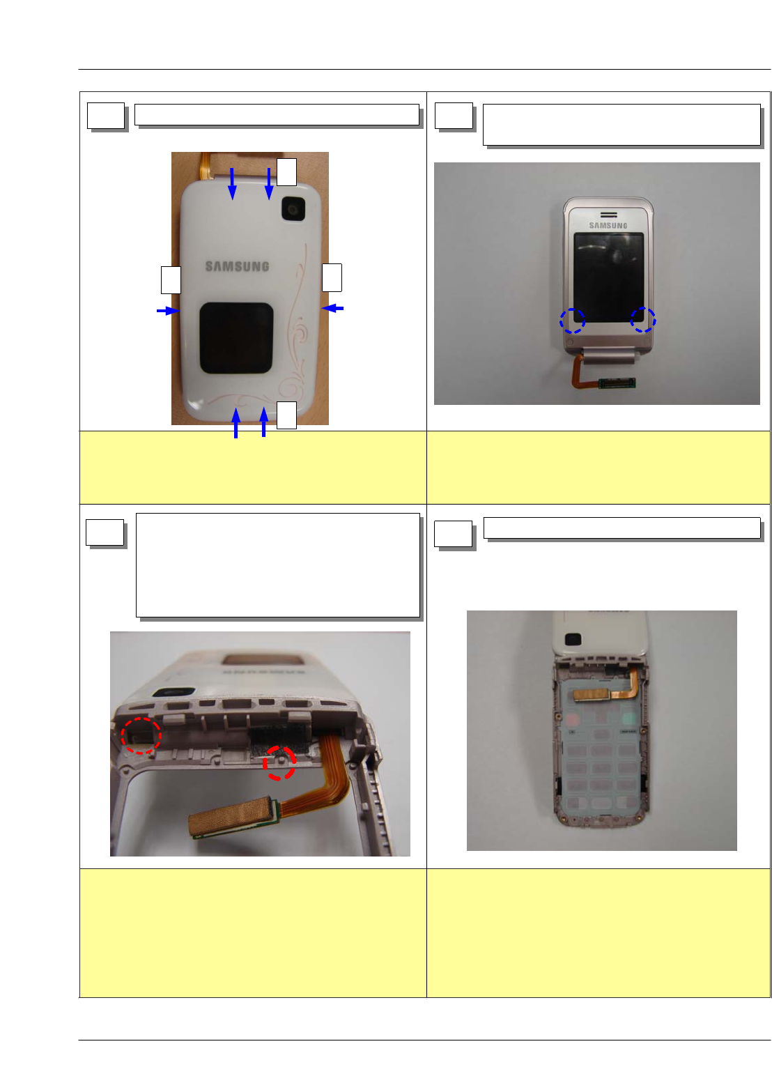
When attaching the dust prevention TAPE, be careful
not to cover the keypad groove.
SAMSUNG Proprietary-Contents may change without notice
Exploded View/Disassembly&Assembly Instructions
5-9
This Document can not be used without Samsung's authorization
When contracting the LCD CONNECTOR, in order
for the sound to be born "tightly", it contracts with
thumb.

SAMSUNG Proprietary-Contents may change without notice
Exploded View/Disassembly&Assembly Instructions
5-10
This Document can not be used without Samsung's authorization

SAMSUNG Proprietary-Contents may change without notice
6. MAIN Electrical Parts List
6-1
This Document can not be used without Samsung's authorization
Design LOC Description SEC Code STATUS
ANT200 NPR-ANTENNA CONTACT GH71-05666A SA
ANT201 NPR-ANTENNA CONTACT GH71-05666A SA
BAT500 BATTERY-LI(2ND) 4302-001130 SA
BTC600 HEADER-BATTERY 3711-006219 SA
C100 C-CER,CHIP 2203-005482 SA
C101 C-CER,CHIP 2203-000233 SA
C102 C-CER,CHIP 2203-000233 SA
C103 C-CER,CHIP 2203-005138 SA
C104 C-CER,CHIP 2203-005482 SA
C105 C-CER,CHIP 2203-002525 SA
C106 C-CER,CHIP 2203-000838 SA
C107 C-CER,CHIP 2203-006961 SA
C108 C-CER,CHIP 2203-005482 SA
C109 C-CER,CHIP 2203-005057 SA
C110 C-CER,CHIP 2203-005057 SA
C111 C-CER,CHIP 2203-005482 SA
C112 C-CER,CHIP 2203-000254 SA
C113 C-CER,CHIP 2203-005481 SA
C114 C-CER,CHIP 2203-005480 SA
C115 C-CER,CHIP 2203-000233 SA
C116 C-CER,CHIP 2203-000233 SA
C117 C-CER,CHIP 2203-006562 SA
C118 C-CER,CHIP 2203-000438 SA
C119 C-CER,CHIP 2203-005482 SA
C120 C-CER,CHIP 2203-005057 SA
C121 C-CER,CHIP 2203-000254 SA
C122 C-CER,CHIP 2203-006562 SA
C123 C-CER,CHIP 2203-000585 SA
C124 C-CER,CHIP 2203-000585 SA
C125 C-CER,CHIP 2203-000233 SA
C126 C-CER,CHIP 2203-000609 SA
C127 C-CER,CHIP 2203-000585 SA
C128 C-CER,CHIP 2203-000679 SA
C129 C-CER,CHIP 2203-000585 SA
C130 C-CER,CHIP 2203-000679 SA
C131 C-CER,CHIP 2203-000585 SA
C201 C-CER,CHIP 2203-005482 SA
C202 C-CER,CHIP 2203-000311 SA
C203 C-CER,CHIP 2203-000585 SA
C204 C-TA,CHIP 2404-001474 SA
C205 C-CER,CHIP 2203-005482 SA
C206 C-CER,CHIP 2203-006190 SA
C207 C-CER,CHIP 2203-006190 SA
C208 C-CER,CHIP 2203-005234 SA
C209 C-CER,CHIP 2203-000812 SA
C210 C-CER,CHIP 2203-001385 SA
C212 C-CER,CHIP 2203-000233 SA
C213 C-CER,CHIP 2203-000233 SA
C219 INDUCTOR-SMD 2703-002208 SA
C300 C-CER,CHIP 2203-005061 SA
C301 C-CER,CHIP 2203-005061 SA
C302 C-CER,CHIP 2203-005061 SA
C303 C-CER,CHIP 2203-005061 SA

SAMSUNG Proprietary-Contents may change without notice
Main Electrical Parts List
6-2
This Document can not be used without Samsung's authorization
Design LOC Description SEC Code STATUS
C304 C-CER,CHIP 2203-000254 SA
C305 C-CER,CHIP 2203-005061 SA
C306 C-CER,CHIP 2203-005061 SA
C307 C-CER,CHIP 2203-000254 SA
C308 C-CER,CHIP 2203-000254 SA
C309 C-CER,CHIP 2203-005482 SA
C310 C-CER,CHIP 2203-005482 SA
C311 C-CER,CHIP 2203-000854 SA
C312 C-CER,CHIP 2203-000679 SA
C314 C-CER,CHIP 2203-005482 SA
C317 C-CER,CHIP 2203-005482 SA
C319 C-CER,CHIP 2203-000679 SA
C320 C-CER,CHIP 2203-000679 SA
C321 C-CER,CHIP 2203-000679 SA
C322 C-CER,CHIP 2203-000679 SA
C323 C-CER,CHIP 2203-000679 SA
C400 C-CER,CHIP 2203-006562 SA
C401 C-CER,CHIP 2203-005061 SA
C403 C-CER,CHIP 2203-005061 SA
C404 C-CER,CHIP 2203-005061 SA
C405 C-CER,CHIP 2203-000643 SA
C407 C-CER,CHIP 2203-005482 SA
C409 C-CER,CHIP 2203-006562 SA
C410 C-CER,CHIP 2203-006562 SA
C411 C-CER,CHIP 2203-005061 SA
C500 C-CER,CHIP 2203-006208 SA
C501 C-CER,CHIP 2203-005482 SA
C502 C-CER,CHIP 2203-006825 SA
C503 C-CER,CHIP 2203-005482 SA
C504 C-CER,CHIP 2203-005482 SA
C505 C-CER,CHIP 2203-005482 SA
C506 C-CER,CHIP 2203-006208 SA
C507 C-CER,CHIP 2203-005395 SA
C508 C-CER,CHIP 2203-000386 SA
C509 C-TA,CHIP 2404-001225 SA
C510 C-CER,CHIP 2203-005482 SA
C511 C-CER,CHIP 2203-000627 SNA
C512 C-CER,CHIP 2203-006257 SA
C513 C-CER,CHIP 2203-000189 SA
C514 C-CER,CHIP 2203-000627 SNA
C515 C-CER,CHIP 2203-006208 SA
C516 C-CER,CHIP 2203-000885 SA
C517 C-CER,CHIP 2203-006208 SA
C518 C-CER,CHIP 2203-006208 SA
C519 C-CER,CHIP 2203-006824 SA
C520 C-TA,CHIP 2404-001225 SA
C521 C-TA,CHIP 2404-001225 SA
C522 C-CER,CHIP 2203-005482 SA
C523 C-CER,CHIP 2203-005482 SA
C524 C-CER,CHIP 2203-005482 SA
C525 C-CER,CHIP 2203-006208 SA
C526 C-CER,CHIP 2203-005061 SA
C527 C-CER,CHIP 2203-002443 SA

SAMSUNG Proprietary-Contents may change without notice
Main Electrical Parts List
6-3
This Document can not be used without Samsung's authorization
Design LOC Description SEC Code STATUS
C529 C-CER,CHIP 2203-006562 SA
C530 C-CER,CHIP 2203-006348 SA
C531 C-CER,CHIP 2203-006208 SA
C532 C-CER,CHIP 2203-006208 SA
C533 C-CER,CHIP 2203-006208 SA
C534 C-CER,CHIP 2203-006208 SA
C535 C-CER,CHIP 2203-000679 SA
C538 C-CER,CHIP 2203-006348 SA
C540 C-CER,CHIP 2203-006562 SA
C541 C-CER,CHIP 2203-006257 SA
C542 C-TA,CHIP 2404-001381 SA
C600 C-CER,CHIP 2203-005061 SA
C602 C-CER,CHIP 2203-000854 SA
C603 C-CER,CHIP 2203-005061 SA
C604 C-TA,CHIP 2404-001377 SA
C605 C-CER,CHIP 2203-000679 SA
C606 C-CER,CHIP 2203-005061 SA
C607 C-CER,CHIP 2203-000386 SA
C609 C-CER,CHIP 2203-000812 SA
C610 C-CER,CHIP 2203-005061 SA
C611 C-CER,CHIP 2203-000679 SA
C612 C-CER,CHIP 2203-000425 SA
C615 C-CER,CHIP 2203-000425 SA
C616 C-CER,CHIP 2203-006562 SA
C617 C-CER,CHIP 2203-005482 SA
C620 C-CER,CHIP 2203-005061 SA
C700 C-CER,CHIP 2203-000812 SA
C701 C-CER,CHIP 2203-005683 SA
C702 C-CER,CHIP 2203-005683 SA
C703 C-CER,CHIP 2203-005683 SA
C704 C-CER,CHIP 2203-005683 SA
C705 C-CER,CHIP 2203-005683 SA
C706 C-CER,CHIP 2203-005683 SA
C707 C-CER,CHIP 2203-005683 SA
C708 C-CER,CHIP 2203-005683 SA
C709 C-CER,CHIP 2203-000812 SA
C710 C-CER,CHIP 2203-005683 SA
C711 C-CER,CHIP 2203-005683 SA
C712 C-CER,CHIP 2203-005683 SA
C713 C-CER,CHIP 2203-005683 SA
C714 C-CER,CHIP 2203-005683 SA
C715 C-CER,CHIP 2203-005683 SA
C716 C-CER,CHIP 2203-000278 SA
C717 C-CER,CHIP 2203-005482 SA
C718 C-CER,CHIP 2203-005482 SA
C719 C-CER,CHIP 2203-000812 SA
C720 C-CER,CHIP 2203-000812 SA
C800 C-CER,CHIP 2203-000854 SA
C801 C-CER,CHIP 2203-006562 SA
C802 C-CER,CHIP 2203-000233 SA
C803 C-CER,CHIP 2203-000679 SA
C804 C-CER,CHIP 2203-005482 SA
C805 C-CER,CHIP 2203-005482 SA

SAMSUNG Proprietary-Contents may change without notice
Main Electrical Parts List
6-4
This Document can not be used without Samsung's authorization
Design LOC Description SEC Code STATUS
C806 C-CER,CHIP 2203-005482 SA
C807 C-CER,CHIP 2203-000438 SA
C808 C-CER,CHIP 2203-000725 SA
C809 C-CER,CHIP 2203-000812 SA
C810 C-CER,CHIP 2203-000812 SA
C811 C-CER,CHIP 2203-006260 SA
C812 C-TA,CHIP 2404-001381 SA
C813 C-CER,CHIP 2203-005482 SA
C814 C-CER,CHIP 2203-001221 SA
C815 C-CER,CHIP 2203-006048 SA
D600 DIODE-SCHOTTKY 0404-001172 SA
D610 DIODE-TVS 0406-001231 SA
D611 DIODE-TVS 0406-001231 SA
D612 DIODE-TVS 0406-001231 SA
D800 DIODE-TVS 0406-001231 SA
D801 DIODE-TVS 0406-001231 SA
D802 DIODE-TVS 0406-001231 SA
D803 DIODE-TVS 0406-001231 SA
D804 DIODE-TVS 0406-001231 SA
D805 DIODE-TVS 0406-001235 SA
F201 FILTER-EMI SMD 2901-001254 SA
F700 FILTER-EMI SMD 2901-001286 SA
F701 FILTER-EMI SMD 2901-001286 SA
F702 FILTER-EMI SMD 2901-001286 SA
F703 FILTER-EMI SMD 2901-001286 SA
F704 FILTER-EMI SMD 2901-001286 SA
IFC600 SOCKET-INTERFACE 3710-002442 SA
L100 INDUCTOR-SMD 2703-002201 SA
L101 INDUCTOR-SMD 2703-002176 SA
L103 INDUCTOR-SMD 2703-002176 SA
L105 INDUCTOR-SMD 2703-002208 SA
L106 INDUCTOR-SMD 2703-002208 SA
L107 INDUCTOR-SMD 2703-002208 SA
L108 INDUCTOR-SMD 2703-002208 SA
L201 R-CHIP 2007-000171 SA
L208 INDUCTOR-SMD 2703-002313 SA
L210 R-CHIP 2007-000171 SA
L213 INDUCTOR-SMD 2703-002176 SA
L216 C-CER,CHIP 2203-005158 SA
L500 BEAD-SMD 3301-001105 SA
L501 BEAD-SMD 3301-001729 SA
L600 BEAD-SMD 3301-001438 SA
L601 BEAD-SMD 3301-001438 SA
L602 BEAD-SMD 3301-001438 SA
L603 BEAD-SMD 3301-001438 SA
LED1 LED 0601-002268 SA
LED2 LED 0601-002268 SA
MODULE200 DUPLEXER-FEM 2911-000044 SA
OSC100 OSCILLATOR-VCO 2806-001329 SA
OSC101 OSCILLATOR-VCTCXO 2809-001307 SA
Q800 FET-SILICON 0505-002088 SA
R100 R-CHIP 2007-007148 SA
R101 R-CHIP 2007-000141 SA

SAMSUNG Proprietary-Contents may change without notice
Main Electrical Parts List
6-5
This Document can not be used without Samsung's authorization
Design LOC Description SEC Code STATUS
R102 R-CHIP 2007-000171 SA
R103 R-CHIP 2007-007311 SA
R104 R-CHIP 2007-000566 SA
R105 R-CHIP 2007-000174 SA
R106 R-CHIP 2007-000148 SA
R107 R-CHIP 2007-000566 SA
R108 R-CHIP 2007-001305 SA
R109 R-CHIP 2007-003030 SA
R110 R-CHIP 2007-000982 SA
R111 R-CHIP 2007-000138 SA
R112 R-CHIP 2007-000138 SA
R113 R-CHIP 2007-000982 SA
R114 R-CHIP 2007-000982 SA
R115 R-CHIP 2007-000982 SA
R201 R-CHIP 2007-000171 SA
R202 R-CHIP 2007-000145 SA
R204 R-CHIP 2007-000171 SA
R205 R-CHIP 2007-000171 SA
R206 R-CHIP 2007-000171 SA
R207 R-CHIP 2007-000162 SA
R208 R-CHIP 2007-000162 SA
R210 R-CHIP 2007-000171 SA
R212 INDUCTOR-SMD 2703-002208 SA
R300 R-CHIP 2007-000174 SA
R301 R-CHIP 2007-000171 SA
R302 R-CHIP 2007-000162 SA
R306 R-CHIP 2007-007107 SA
R307 R-CHIP 2007-000162 SA
R308 R-CHIP 2007-000162 SA
R312 R-CHIP 2007-000171 SA
R313 R-CHIP 2007-000141 SA
R314 R-CHIP 2007-000141 SA
R315 R-CHIP 2007-000162 SA
R316 R-CHIP 2007-000143 SA
R318 R-CHIP 2007-007107 SA
R319 R-CHIP 2007-007142 SA
R320 R-CHIP 2007-007142 SA
R323 R-CHIP 2007-000171 SA
R400 R-CHIP 2007-000162 SA
R401 R-CHIP 2007-000162 SA
R403 R-CHIP 2007-000162 SA
R404 R-CHIP 2007-000162 SA
R405 R-CHIP 2007-000162 SA
R406 R-CHIP 2007-000162 SA
R407 R-CHIP 2007-000162 SA
R408 R-CHIP 2007-000162 SA
R409 R-CHIP 2007-000171 SA
R410 R-CHIP 2007-000171 SA
R411 R-CHIP 2007-000171 SA
R412 R-CHIP 2007-000171 SA
R413 R-CHIP 2007-007141 SA
R500 R-CHIP 2007-000148 SA
R501 R-CHIP 2007-007573 SA

SAMSUNG Proprietary-Contents may change without notice
Main Electrical Parts List
6-6
This Document can not be used without Samsung's authorization
Design LOC Description SEC Code STATUS
R502 R-CHIP 2007-007334 SA
R503 R-CHIP 2007-000162 SA
R504 R-CHIP 2007-007100 SA
R505 R-CHIP 2007-000162 SA
R508 R-CHIP 2007-000171 SA
R509 R-CHIP 2007-000157 SA
R510 R-CHIP 2007-001292 SA
R511 R-CHIP 2007-001292 SA
R512 R-CHIP 2007-000171 SA
R513 R-CHIP 2007-000162 SA
R514 R-CHIP 2007-007489 SA
R515 R-CHIP 2007-007311 SA
R602 R-CHIP 2007-000148 SA
R603 R-CHIP 2007-000171 SA
R605 R-CHIP 2007-000140 SA
R606 R-CHIP 2007-000140 SA
R607 R-CHIP 2007-002796 SA
R608 R-CHIP 2007-002796 SA
R609 R-CHIP 2007-000140 SA
R610 R-CHIP 2007-000140 SA
R612 R-CHIP 2007-000148 SA
R614 R-CHIP 2007-008531 SA
R615 R-CHIP 2007-008531 SA
R616 R-CHIP 2007-007306 SA
R617 R-CHIP 2007-007306 SA
R618 R-CHIP 2007-007107 SA
R620 R-CHIP 2007-000162 SA
R621 R-CHIP 2007-000171 SA
R622 R-CHIP 2007-000171 SA
R623 R-CHIP 2007-000168 SA
R624 R-CHIP 2007-001339 SA
R625 R-CHIP 2007-000171 SA
R626 R-CHIP 2007-001339 SA
R627 R-CHIP 2007-001339 SA
R628 R-CHIP 2007-008531 SA
R629 R-CHIP 2007-000171 SA
R630 R-CHIP 2007-008531 SA
R631 R-CHIP 2007-007573 SA
R632 R-CHIP 2007-007529 SA
R633 R-CHIP 2007-007107 SA
R634 R-CHIP 2007-000166 SA
R710 R-CHIP 2007-000143 SA
R711 R-CHIP 2007-000143 SA
R712 R-CHIP 2007-000171 SA
R713 R-CHIP 2007-000171 SA
R800 R-CHIP 2007-000138 SA
R801 R-CHIP 2007-000138 SA
R802 R-CHIP 2007-000138 SA
R803 R-CHIP 2007-000171 SA
R804 R-CHIP 2007-000171 SA
R805 R-CHIP 2007-000162 SA
R806 R-CHIP 2007-001303 SA
R807 R-CHIP 2007-007013 SA
SAMSUNG Proprietary-Contents may change without notice
Main Electrical Parts List
6-7
This Document can not be used without Samsung's authorization
Design LOC Description SEC Code STATUS
R808 R-CHIP 2007-003013 SA
R809 R-CHIP 2007-007308 SA
R810 R-CHIP 2007-007014 SA
R811 R-CHIP 2007-000831 SA
R812 R-CHIP 2007-000171 SA
R813 R-CHIP 2007-001325 SA
R814 R-CHIP 2007-000171 SA
R815 R-CHIP 2007-000172 SA
R816 R-CHIP 2007-000172 SA
R817 R-CHIP 2007-001339 SA
RFS201 CONNECTOR-COAXIAL 3705-001358 SA
SIM500 CONNECTOR-CARD EDGE 3709-001400 SA
SOC700 HEADER-BOARD TO BOARD 3711-005918 SA
SW500 IC-HALL EFFECT S/W 1009-001018 SA
TH300 THERMISTOR-NTC 1404-001221 SA
U100 IC-TRANSCEIVER 1205-002327 SA
U200 IC-POWER AMP 1201-002218 SA
U401 IC ASIC-SGHX670 GH13-00036A SA
U402 FET-SILICON 0505-001923 SA
U403 FET-SILICON 0505-002088 SA
U500 IC-CONTROLLER 1205-002350 SA
U503 IC-POSI.FIXED REG. 1203-003787 SA
U505 IC-BATTERY 1203-003663 SA
U600 IC-ANALOG MULTIPLEX 1001-001345 SA
U601 IC-ANALOG SWITCH 1001-001362 SA
U602 IC-VOLTAGE COMP. 1202-001068 SA
U603 FILTER-EMI/ESD 2901-001349 SA
U605 TR-DIGITAL 0504-001100 SA
U800 IC-MELODY 1204-002690 SA
U801 IC-CMOS LOGIC 0801-003025 SA
UCP300 IC-COMM. CONTROLLER 1205-003065 SA
UME400 IC-MCP 1108-000059 SA
V700 DIODE-TVS 0406-001235 SA
V701 DIODE-TVS 0406-001235 SA
V702 DIODE-TVS 0406-001235 SA
V703 DIODE-TVS 0406-001235 SA
V704 DIODE-TVS 0406-001235 SA
V705 DIODE-TVS 0406-001235 SA
V706 DIODE-TVS 0406-001235 SA
V707 DIODE-TVS 0406-001235 SA
V708 VARISTOR 1405-001082 SA
X500 CRYSTAL-SMD 2801-004373 SA
ZD600 DIODE-TVS 0406-001231 SA
ZD601 DIODE-TVS 0406-001231 SA
ZD602 DIODE-TVS 0406-001197 SA
ZD603 DIODE-ZENER 0403-001547 SA
ZD604 DIODE-TVS 0406-001201 SA

SAMSUNG Proprietary-Contents may change without notice
Main Electrical Parts List
6-8
This Document can not be used without Samsung's authorization
SAMSUNG Proprietary-Contents may change without notice
7-1
This Document can not be used without Samsung's authorization
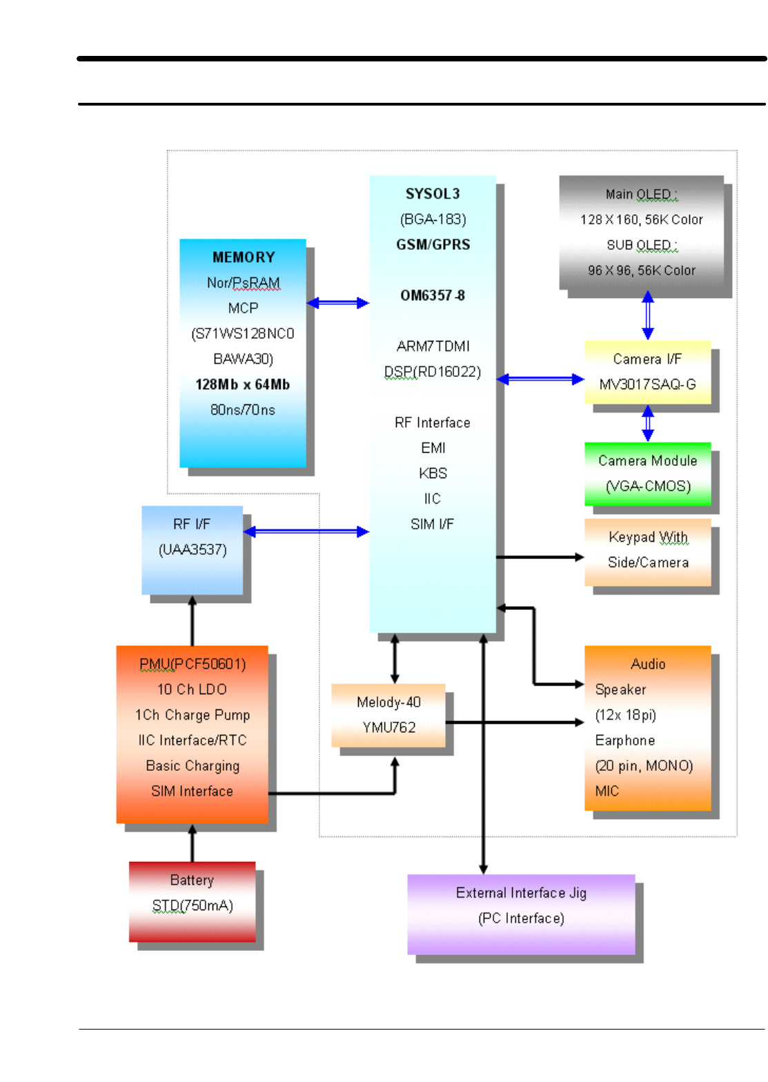
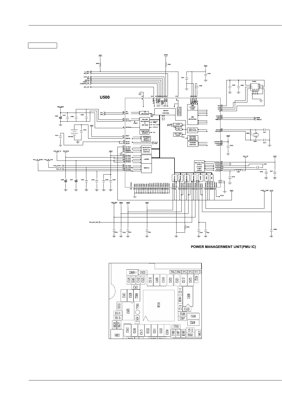
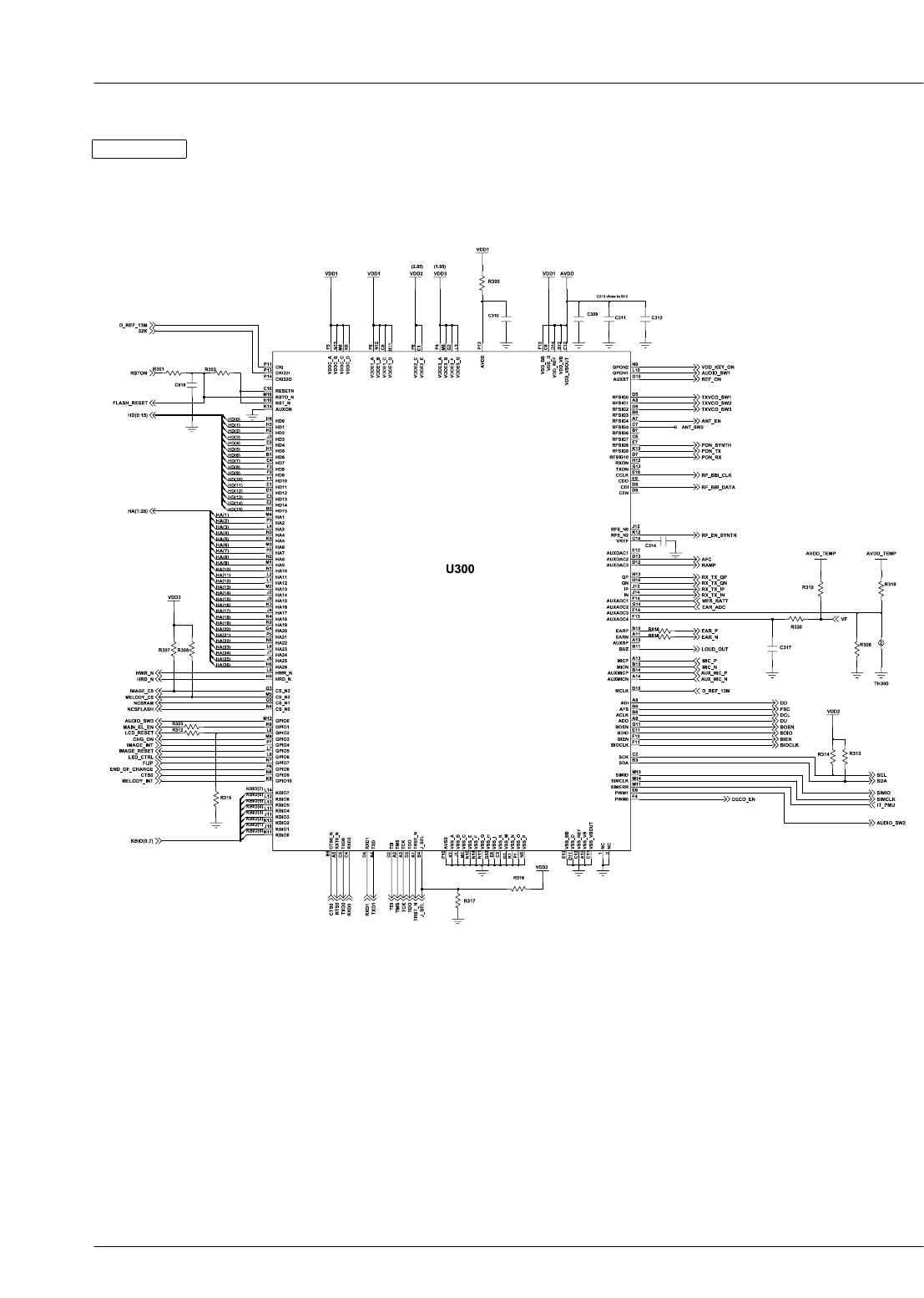
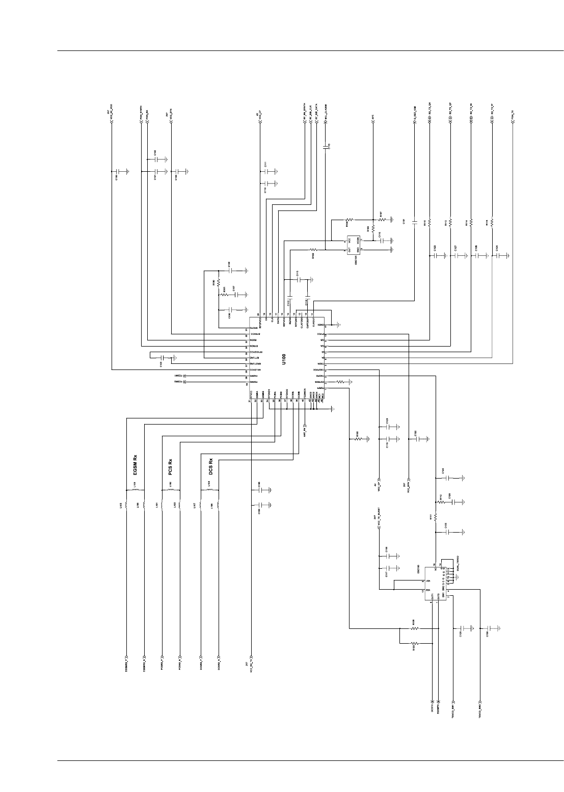
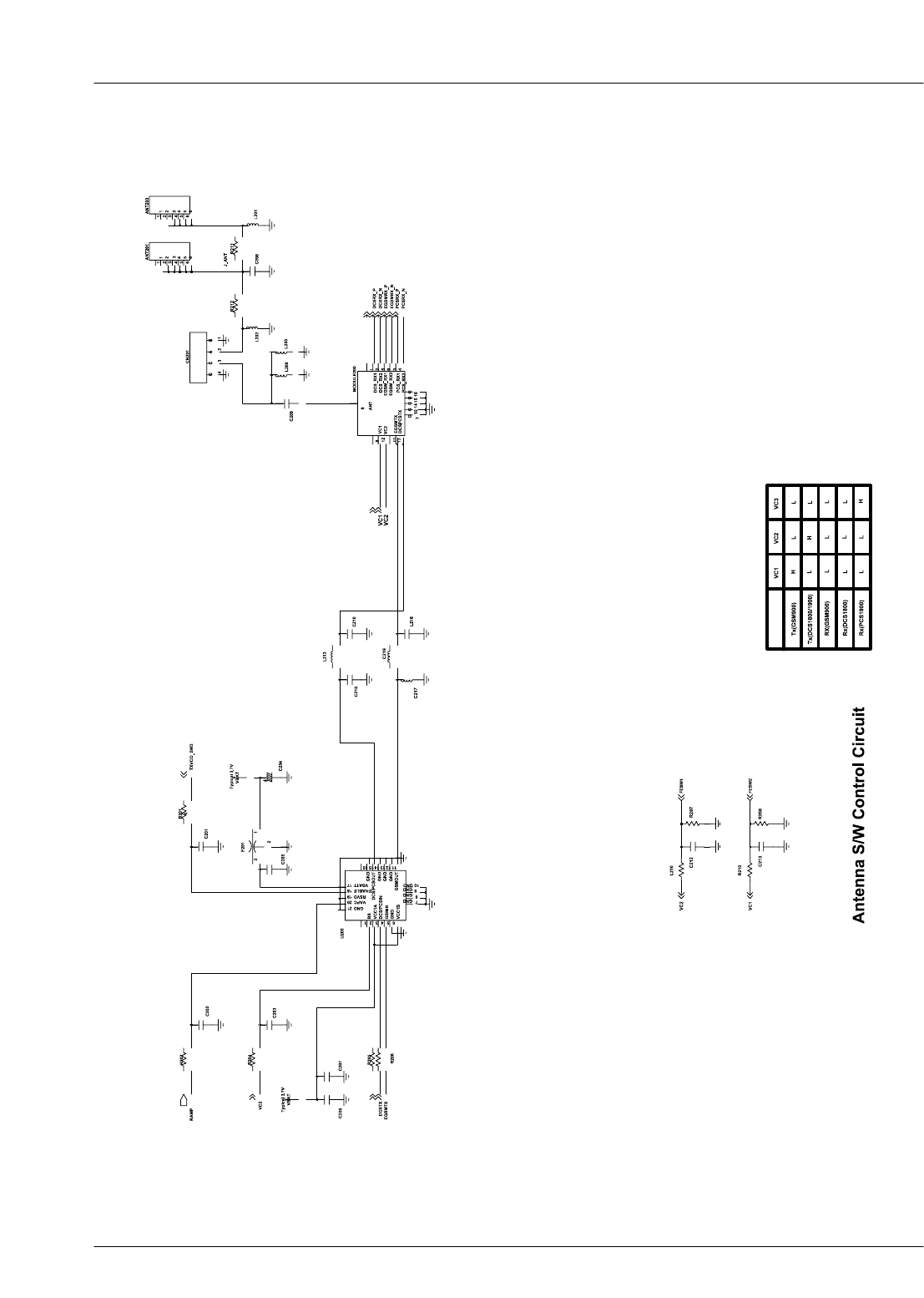
7. Block Diagrams

SAMSUNG Proprietary-Contents may change without notice
Block Diagrams
7-2
This Document can not be used without Samsung's authorization
SAMSUNG Proprietary-Contents may change without notice
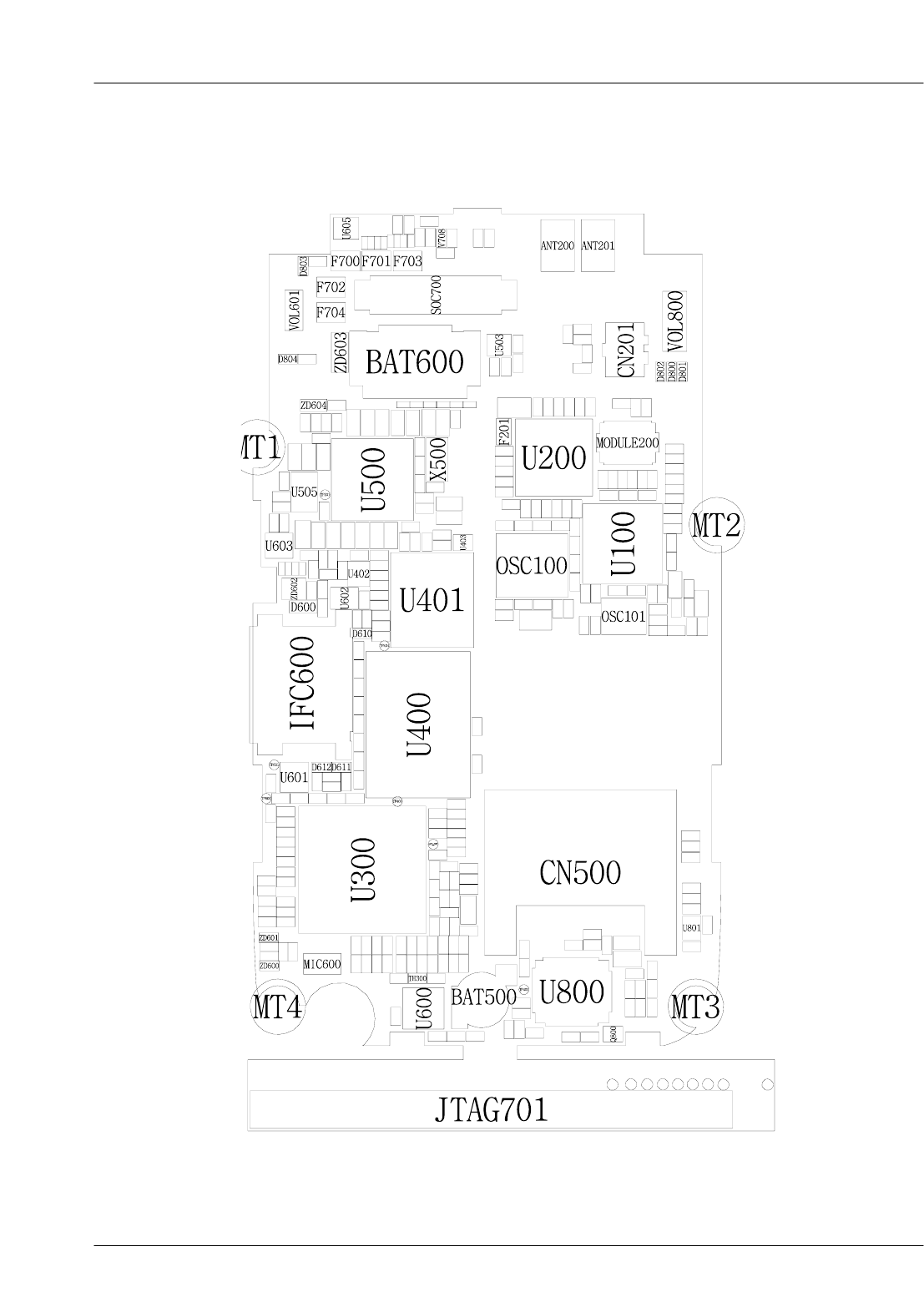
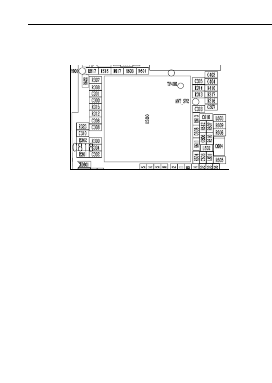
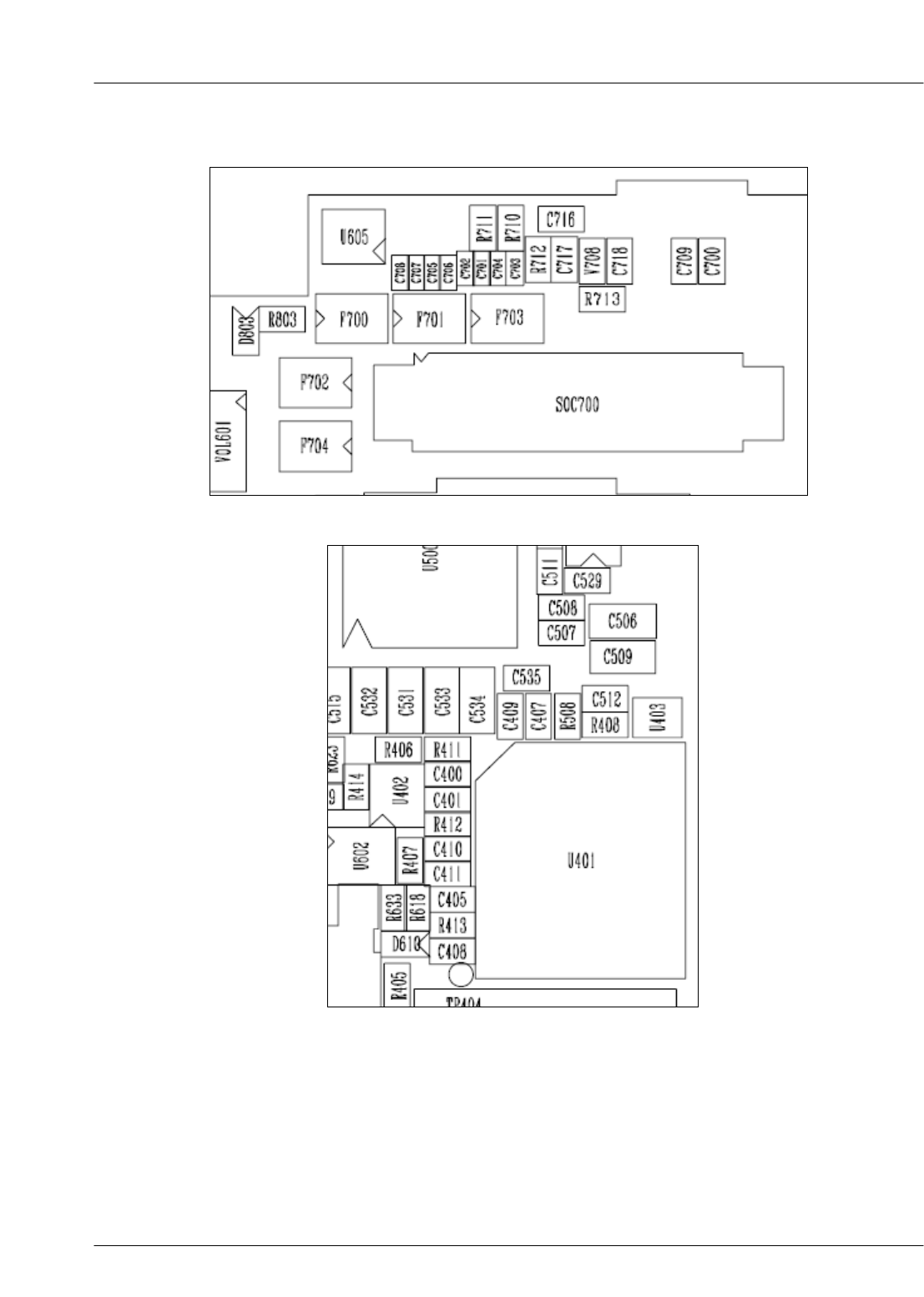
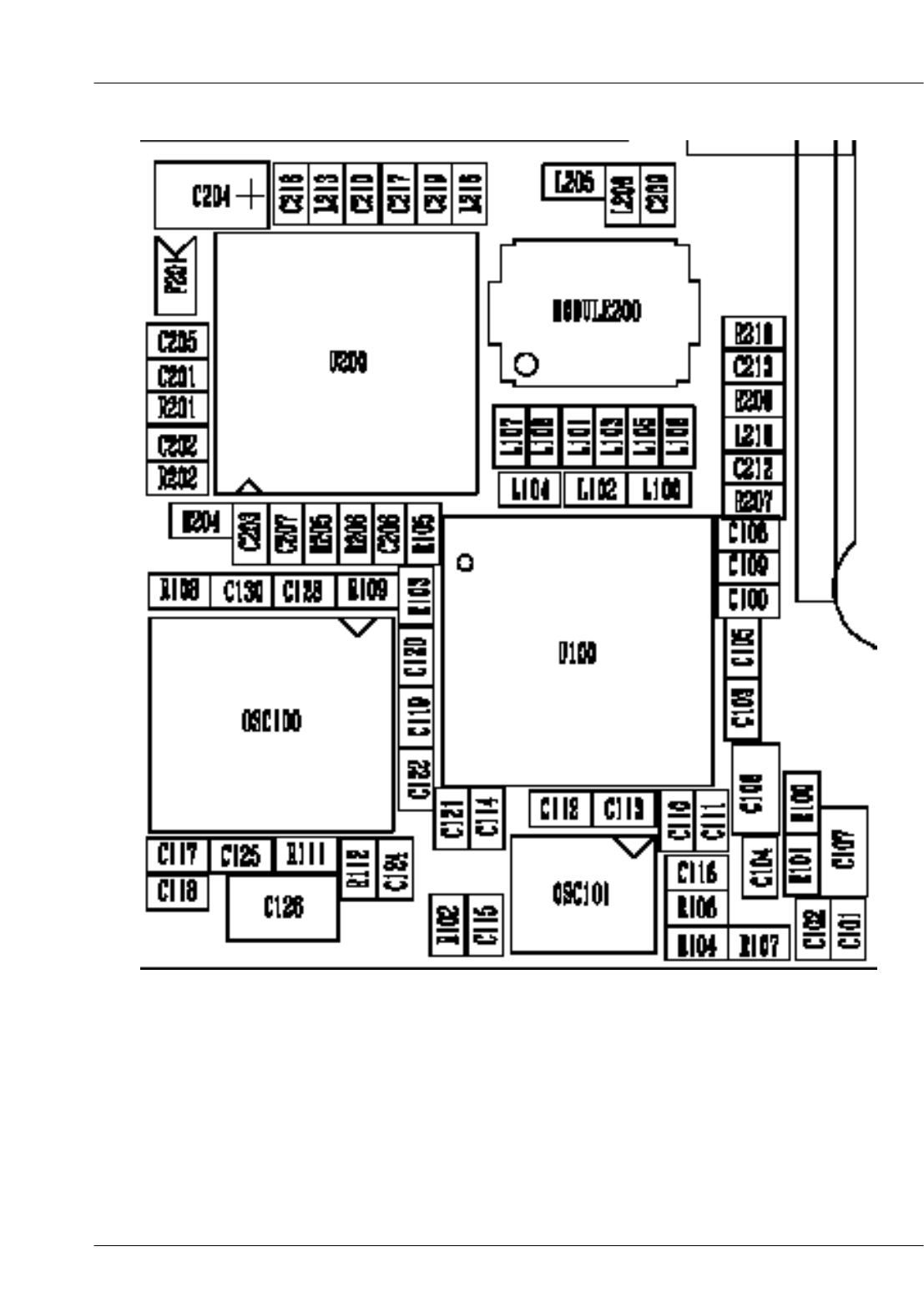
8. PCB Diagrams
8-1
This Document can not be used without Samsung's authorization
Top
SAMSUNG Proprietary-Contents may change without notice
PCB Diagrams
8-2
This Document can not be used without Samsung's authorization
Bottom
SAMSUNG Proprietary-Contents may change without notice
9. Flow Chart of Troubleshooting
This Document can not be used without Samsung's authorization
9-1
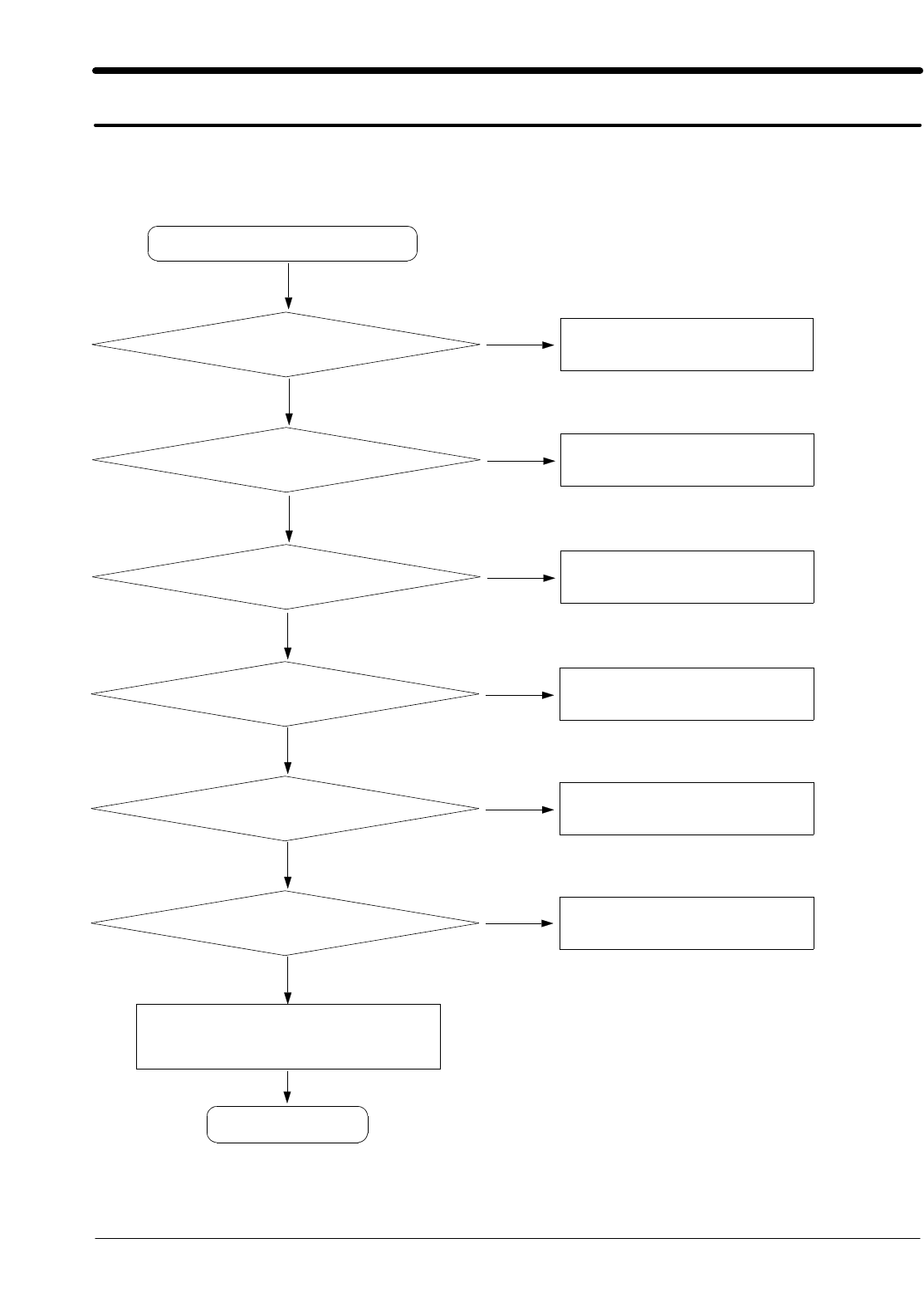
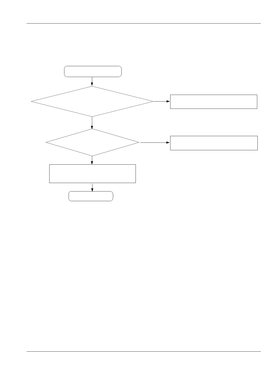
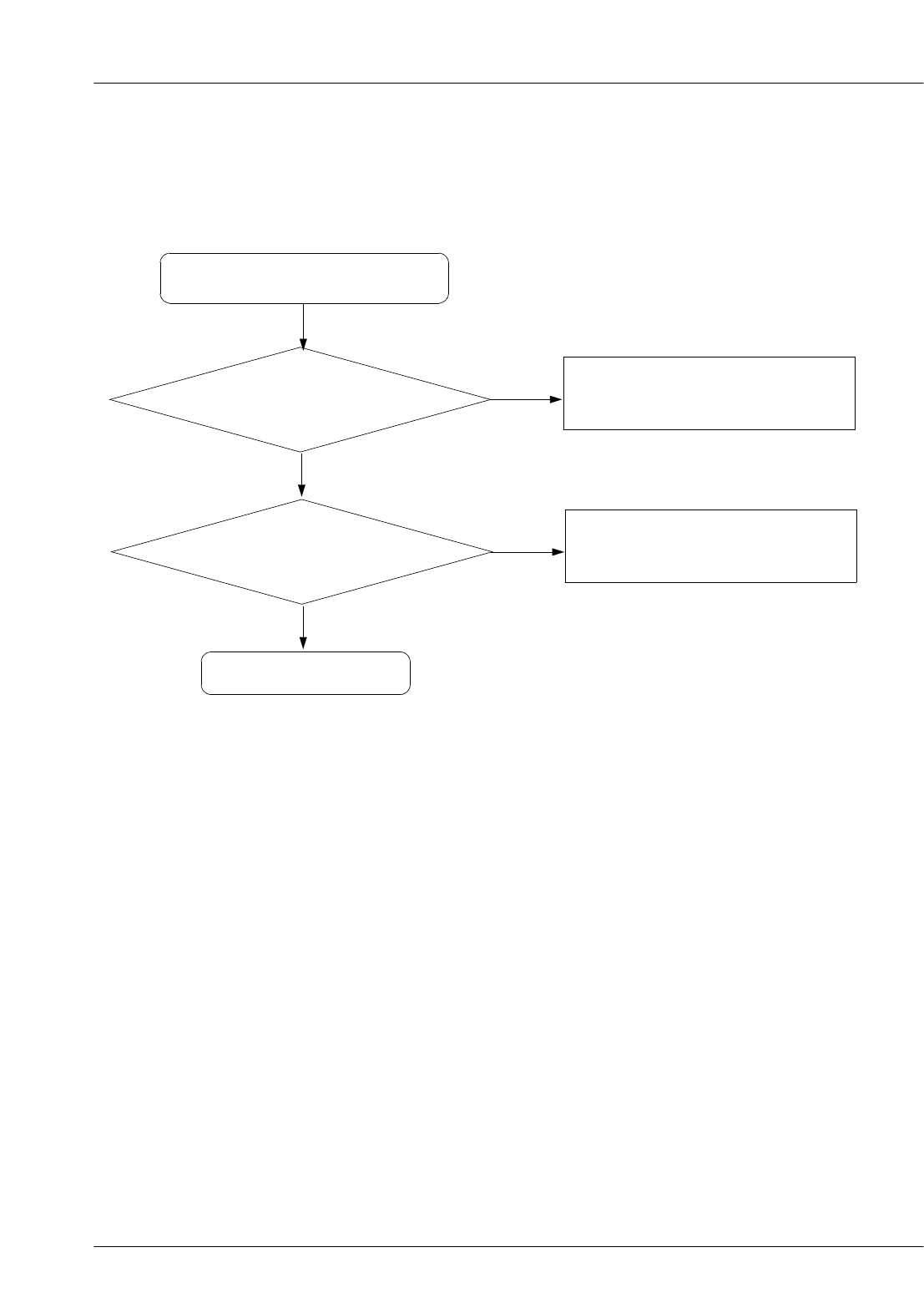
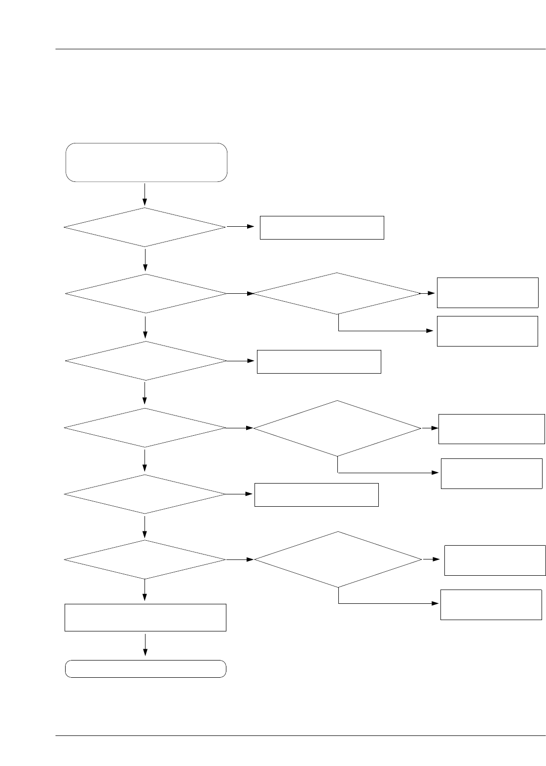
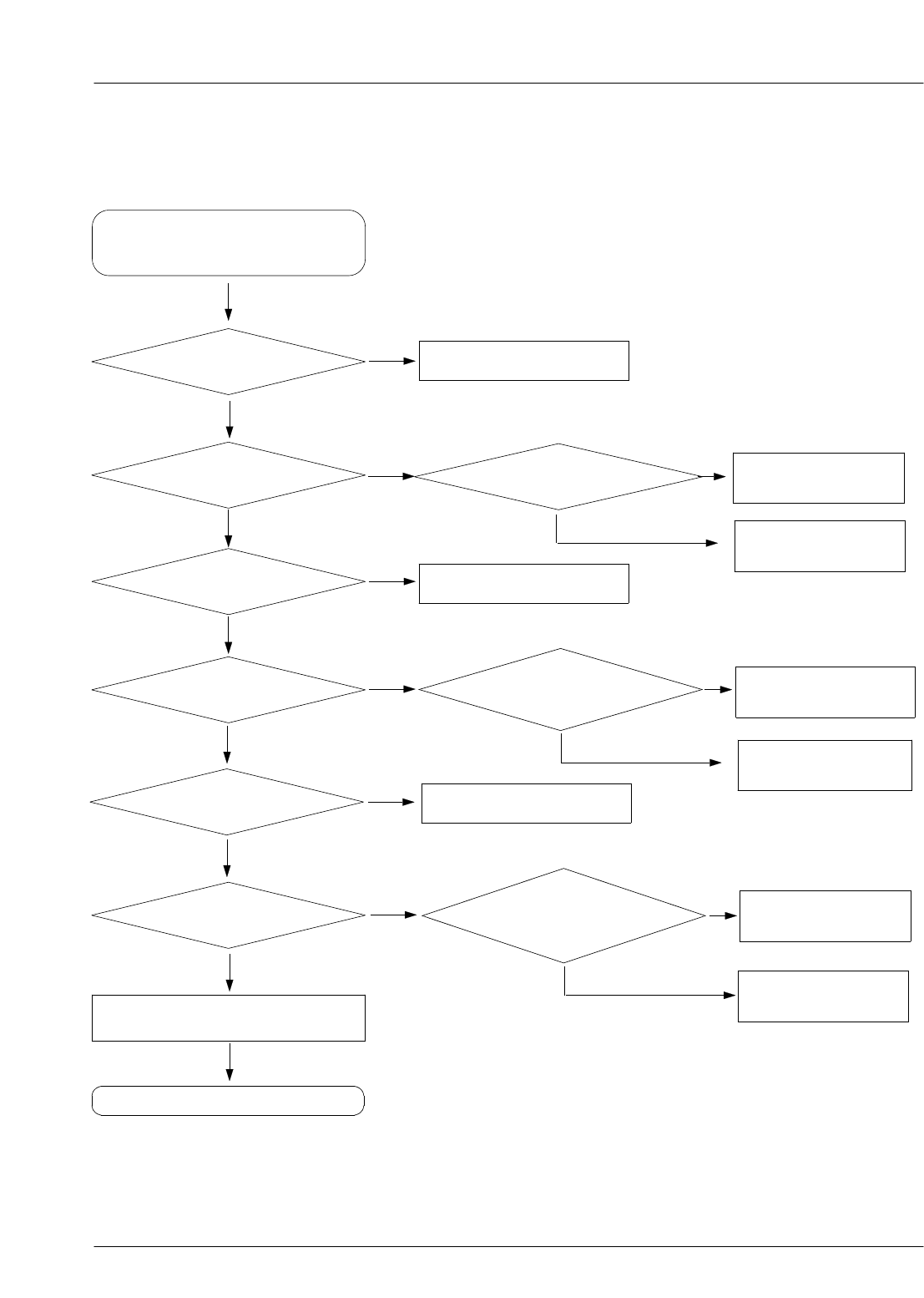
9-1. Power On
Check the Battery Voltage
is more than 3.4V
' Power On ' does not work
Change the Battery
END
No
Yes
C512 = 2.7V? Check the PMU related to the ISUP
No
Yes
Check the Clock at
R504=32KHZ Resolder X500
No
Yes
C532 (VDD1) = "H"? Check the VDD1 circuit
No
Yes
C531(VDD2) & C533(VDD3)
= 2.85V? Check the VDD2,VDD3 circuit
No
Yes
Check for the clock at C121
=13MHz
Check the clock generation circuit
(related to U100)
No
Yes
Check the initial operation
Yes
Yes
SAMSUNG Proprietary-Contents may change without notice
This Document can not be used without Samsung's authorization
Flow Chart of Troubleshooting
9-2
Power On
SAMSUNG Proprietary-Contents may change without notice
Flow Chart of Troubleshooting
This Document can not be used without Samsung's authorization
9-3
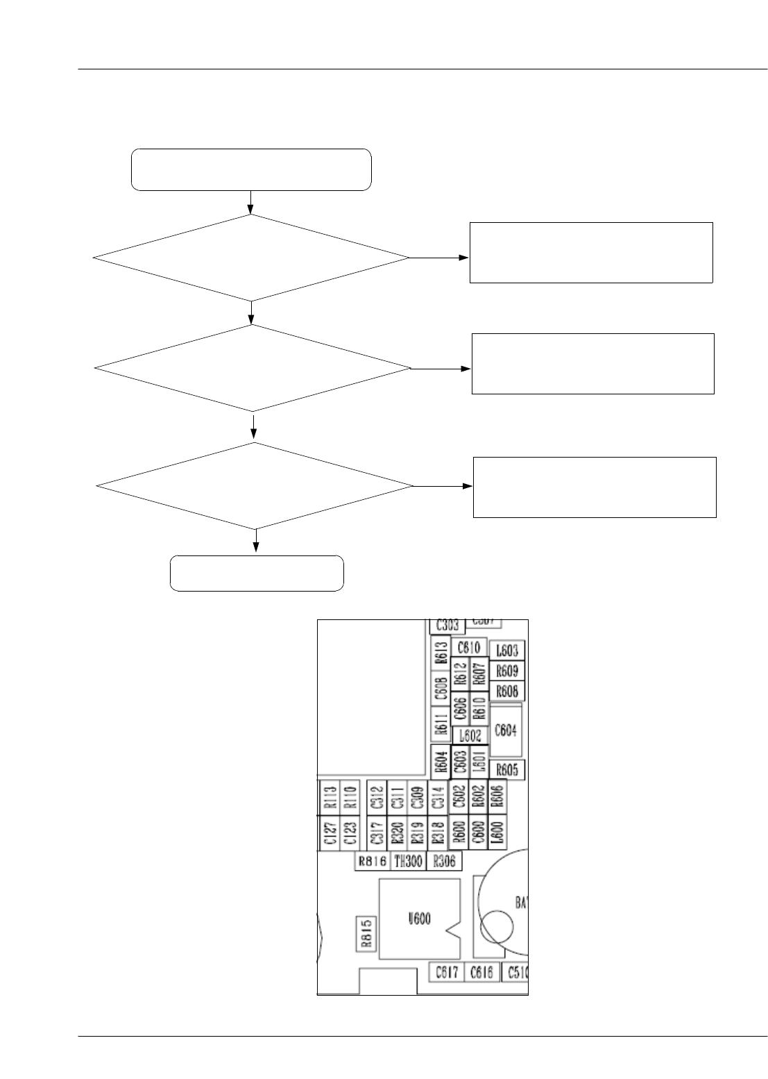
9-2. Initial
R302 (RSTON) ="H"?
Initial Failure
Check the circuit related to reset
END
No
Yes
Is U400 Pin
(memory CE) OK?
Yes
Yes
No
Check the U400
Check the circuit around
LCD & U400 (Short or not solder)
Yes
SAMSUNG Proprietary-Contents may change without notice
This Document can not be used without Samsung's authorization
Flow Chart of Troubleshooting
9-4
Initial
SAMSUNG Proprietary-Contents may change without notice
Flow Chart of Troubleshooting
This Document can not be used without Samsung's authorization
9-5
SAMSUNG Proprietary-Contents may change without notice
This Document can not be used without Samsung's authorization
Flow Chart of Troubleshooting
9-6
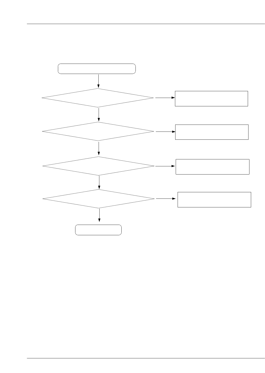
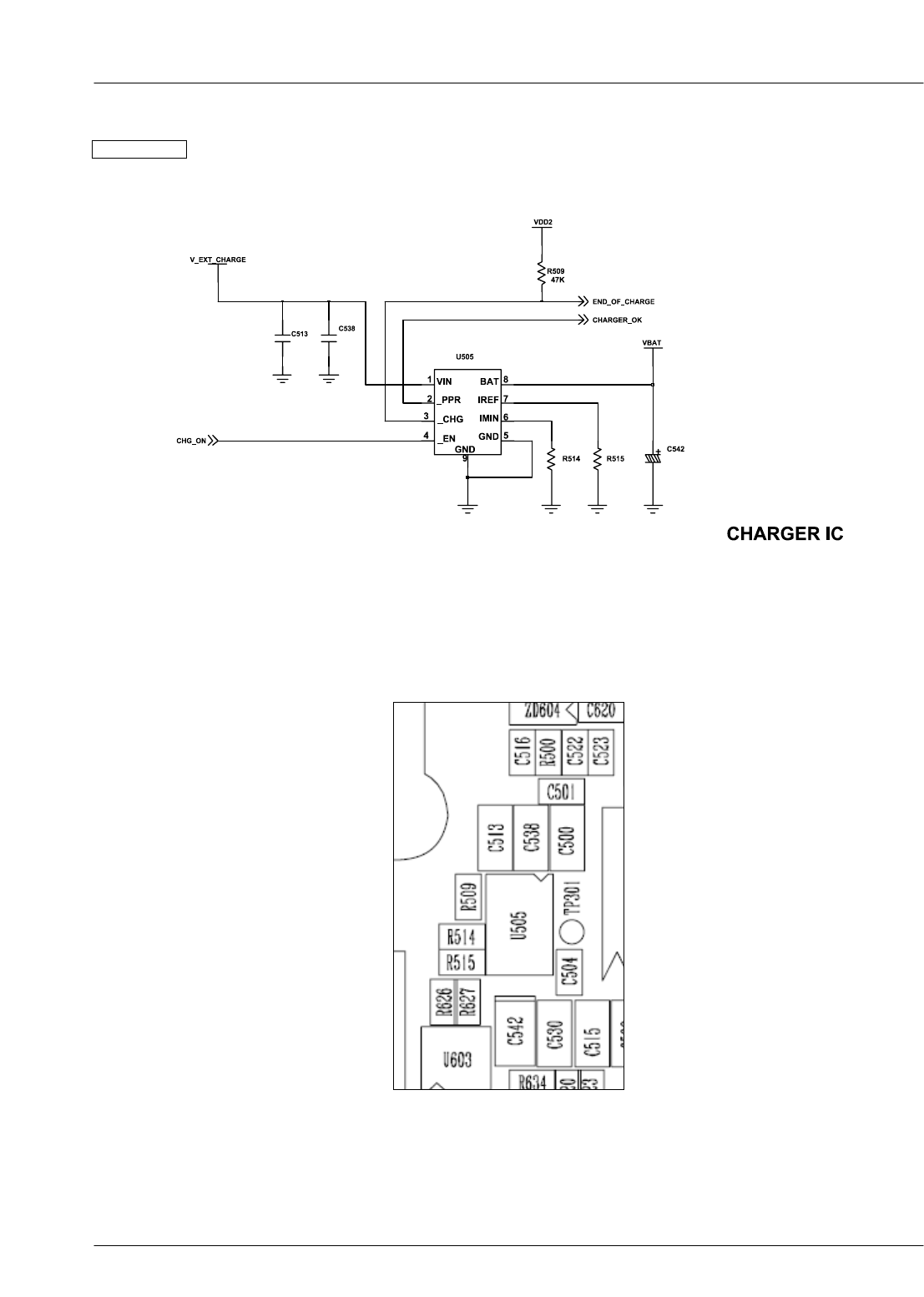
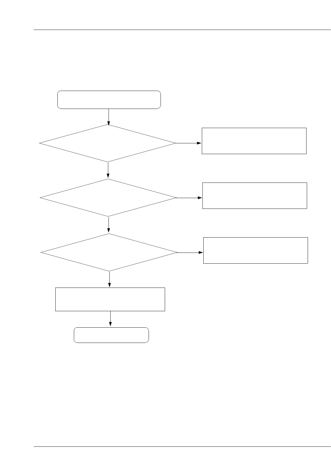
9-3. Charging Part
Check the U505 pin 1
>4.9V
Abnormal charging part
END
No
Yes
U505 pin 7 = "H"?
No
Yes
Check the U505 pin8
≒4.2V
No
Yes
Check the the circuit related to
+DCVOLT
Resolder or replace U505
Check the circuit related to
CHG_ON signal
Yes
U505 pin 4 = "L"?
Yes
No
Resolder or replace U505
SAMSUNG Proprietary-Contents may change without notice
Flow Chart of Troubleshooting
This Document can not be used without Samsung's authorization
9-7
Charging
SAMSUNG Proprietary-Contents may change without notice
This Document can not be used without Samsung's authorization
Flow Chart of Troubleshooting
9-8
9-4. Sim Part
CN500 pin 1,5 = "H"?
Phone can't access SIM Card
Check the sim charge pump
Check the SIM Card
END
No
Yes
Yes
Yes
No
Check the 32k OSC
After Power ON,
Check SIMCLK Signal on CN500
pin3 in a few second
Yes
No
Replace PBA
After SIM card insert,
CN500 pin 2 = "H(SIM_RST)"?
Yes
SAMSUNG Proprietary-Contents may change without notice
Flow Chart of Troubleshooting
This Document can not be used without Samsung's authorization
9-9
SAMSUNG Proprietary-Contents may change without notice
This Document can not be used without Samsung's authorization
Flow Chart of Troubleshooting
9-10
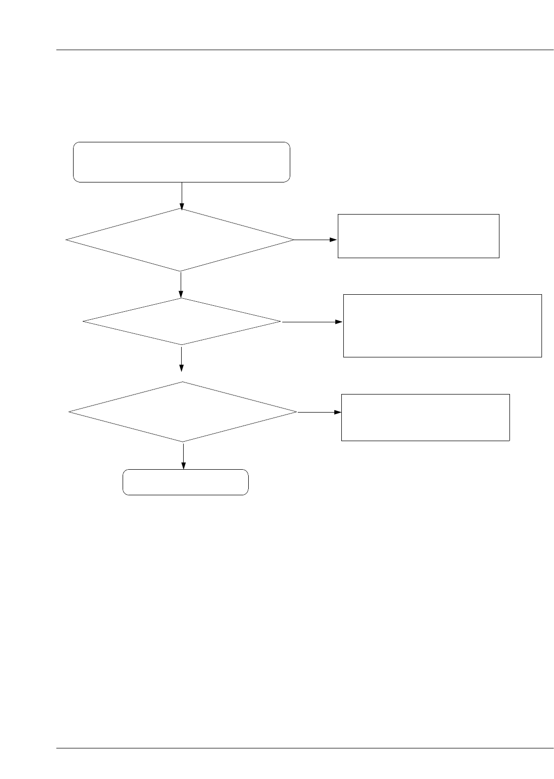
9-5. Microphone Part
Check the connection
from MIC
Check the circuit
from U300 to MIC
Resolder MIC
Resolder the R605, R606, R609, R610, L602,
L603, C606 and C610
END
No
Yes
Yes
Yes
Yes
No
Check the MIC
No
Replace the MIC
Microphone does not work
SAMSUNG Proprietary-Contents may change without notice
Flow Chart of Troubleshooting
This Document can not be used without Samsung's authorization
9-11
Microphone
SAMSUNG Proprietary-Contents may change without notice
This Document can not be used without Samsung's authorization
Flow Chart of Troubleshooting
9-12
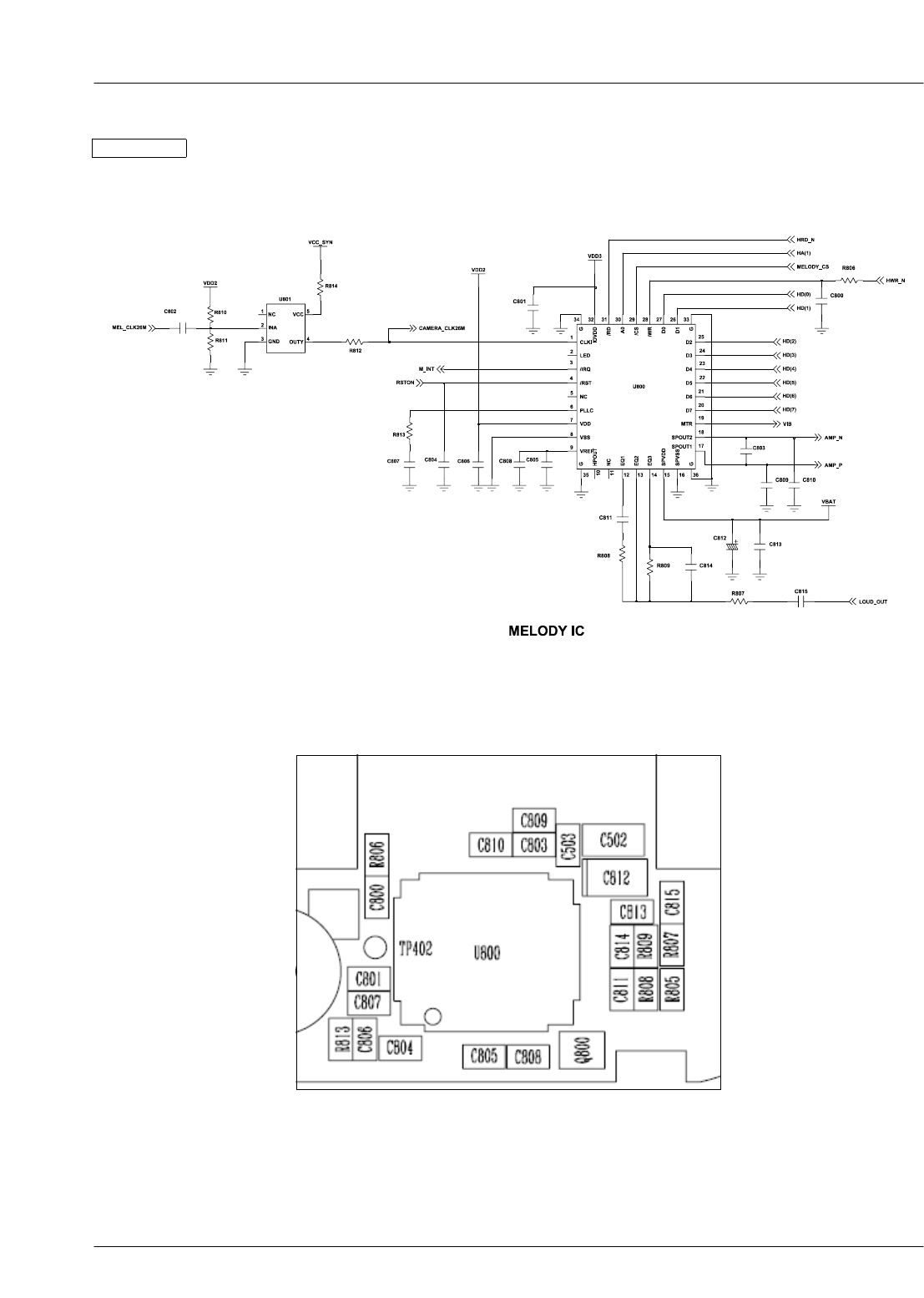
9-6. Speaker Part(Melody)
U801 pin 5 = 2.85V?
Speaker does not work
Check the Clock signal at
pin1(CLKI) of
U800(13MHz)
Check the clock generation circuit
(related to OSC101 and U800)
END
No
Yes
No
Resolder or replace U801
C809 & C810 Around
U800 ≒ 1.8V?
(When U800 operate)
Resolder U800
Yes
No
is Speaker Contact in
proper position? Check the speaker Contact
Yes
No
Is Speaker working?
No
Yes
Change the Speaker
Yes
Yes
SAMSUNG Proprietary-Contents may change without notice
Flow Chart of Troubleshooting
This Document can not be used without Samsung's authorization
9-13
Speaker
SAMSUNG Proprietary-Contents may change without notice
This Document can not be used without Samsung's authorization
Flow Chart of Troubleshooting
9-14
9-7. Key Data Input
When one of the keys is
pushed,
is it displayed on LCD?
Check the Dome sheet & Key rubber
END
No
Yes
Yes
Check Initial Operation
When one of the keys is
pushed,
KBIO signal is OK?
Replace the PBA
No
Yes
SAMSUNG Proprietary-Contents may change without notice
Flow Chart of Troubleshooting
This Document can not be used without Samsung's authorization
9-15
9-8. Receiver Part
U600 pin11 = L during
call established?
Ceck U600
END
No
Yes
Yes
Receiver does not work
Is Receiver working? Replace the Receiver
No
Yes
No
Resolder or replace U600
Yes
U600 pin 4, 16 = 1.5?
SAMSUNG Proprietary-Contents may change without notice
This Document can not be used without Samsung's authorization
Flow Chart of Troubleshooting
9-16
9-9. LCD Part (for Color Main )
Is LCD Contrast set on high
level in the Menu?
Set LCD Contrast on high level
END
No
Yes
Yes
LCD does not work
SOC700 pin 29, 30 = 2.8V? Resolder LCD module
No
Yes
F703pin3,4,5,6isOK? Check the U401
No
Yes
Yes
Replace the LCD Module
SAMSUNG Proprietary-Contents may change without notice
Flow Chart of Troubleshooting
This Document can not be used without Samsung's authorization
9-17
SAMSUNG Proprietary-Contents may change without notice
This Document can not be used without Samsung's authorization
Flow Chart of Troubleshooting
9-18
9-10. Key Back Light
C530 = "H"? Check the PMU related to "VDD_KEY"
END
No
Yes
Key Backlight does not work
Yes
SAMSUNG Proprietary-Contents may change without notice
Flow Chart of Troubleshooting
This Document can not be used without Samsung's authorization
9-19
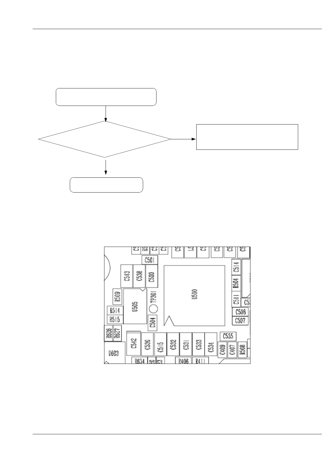
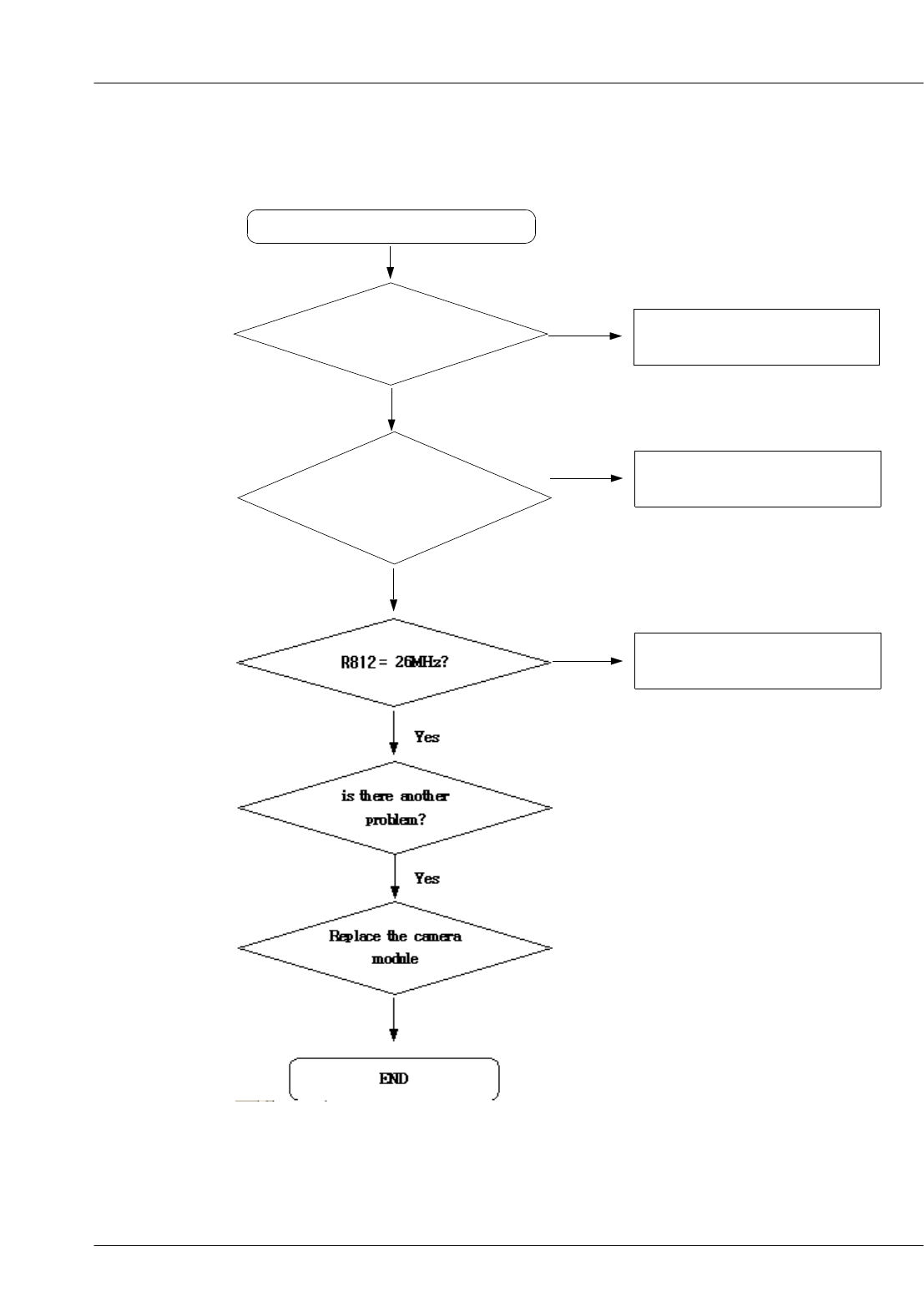
9-11. Camera part
Reconnect the camera module
No
Yes
Camera function does not work
Yes
Check the Camera
connector on PCB
HDC700 C718
=2.8V?
Yes
Resolder U401
No
Check U801(pin2, pin4) related to
26MHz and R812
No
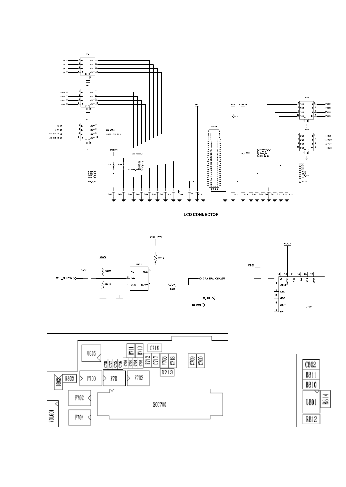
SAMSUNG Proprietary-Contents may change without notice
This Document can not be used without Samsung's authorization
Flow Chart of Troubleshooting
9-20
SAMSUNG Proprietary-Contents may change without notice
Flow Chart of Troubleshooting
This Document can not be used without Samsung's authorization
9-21
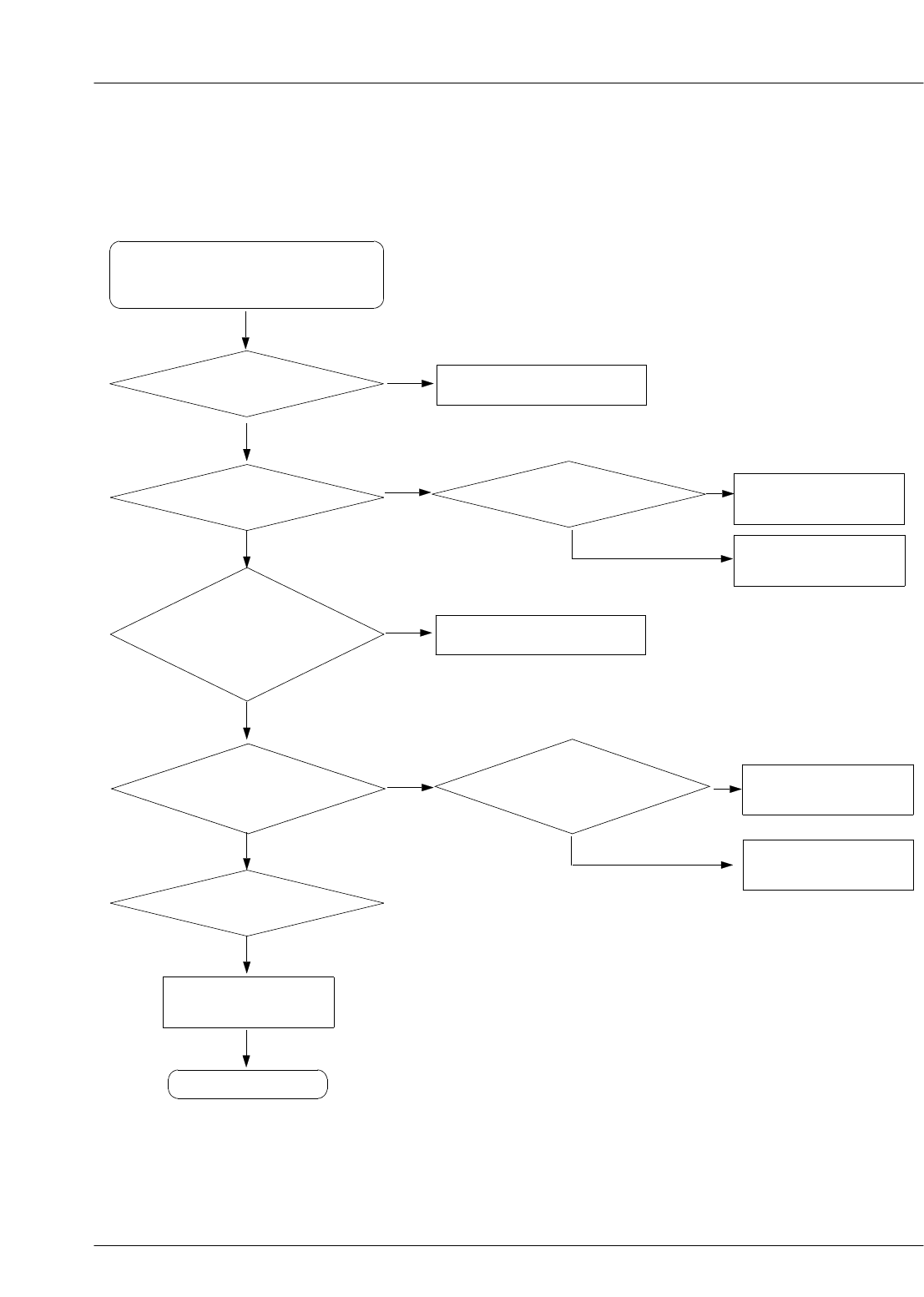
9-12. GSM Receiver
MODULE200 Pin8
>= -65dBm Resolder CN201, C209
END
No
Yes
RX ON
RF input : CH center freq
Amp : -50dBm
Check MODULE200
pin9=L,pin12=L
MODULE200 pin5,6
>= -65dBm
U100
pin32 >= -70dBm
pin33 >= -70dBm
U100pin6,7,8,9
>= 1V
Check ANT Switch
control circuit
Resolder MODULE200
Resolder C101, L105, L106
Check U100
pin10,22,28 >=2.7V
pin20 >=4.0V
Check & Resolder
RF PMU Part
Check &Resolder
U100, RF26MHz part,
R100, R101
R110,R113,R114,
R115 >= 1V
Yes
Yes
Yes
Yes
Yes
Yes
Yes
No
No
No No
No
Check U300
SAMSUNG Proprietary-Contents may change without notice
This Document can not be used without Samsung's authorization
Flow Chart of Troubleshooting
9-22
9-13. GSM Transmitter
TX ON (5Level)
MODULE200 Pin8
>= 20dBm
Yes
Resolder CN201, C209
No
Check MODULE200
pin9=H,pin12=L
Change
or Resolder MODULE200
MODULE200 Pin11
>= 20dBm
YesYes
No No Check ANT Switch
control circuit
Yes
Resolder C217, C219, L216
MODULE200 Pin11
>= 20dBm
Check U200
+VBATT(pin17) OK?
No
Resolder or change U200
or check PAM control
signal
Yes
Yes
MODULE200 Pin11
>= 3dBm
No
Check +VBATT
No
OSC100 pin1
>= 6Bm Resolder R206
Yes
No
Check & Resolder
RF PSU part
Check U100
pin4 >= 4.0V
pin22, 28 >= 2.7V
U100Pin6,7,8,9
>= 500mV
Yes Yes
No
Resolder U100
or check Txcpo(R112)
No
Check U300
END
SAMSUNG Proprietary-Contents may change without notice
Flow Chart of Troubleshooting
This Document can not be used without Samsung's authorization
9-23
9-14. DCS Receiver
RX ON
RF input : CH center freq
Amp : -50dBm
MODULE200 Pin8
>= -65dBm
MODULE200 Pin1,2
>= -65dBm
U100Pin38>=-70dBm
Pin39>=-70dBm
U100pin6,7,8,9
>= 1V
Yes
Yes
No
Resolder CN201, C209
No
Yes
No
Resolder MODULE200
Check ANT Switch
control circuit
Check MODULE200
pin9=L,pin12=L
Yes
Yes
Resolder L107, L108, L104
No
Check U100
pin22,28 >= 2.7V
pin4 >= 4.0V
Check & Resolder
RF PSU Part
No No
Check & Resolder
U100, RF26MHz part
R100, R101
Yes
Yes
R110,R113,R114,
R115 >= 1V
Yes
Check U300
END
SAMSUNG Proprietary-Contents may change without notice
This Document can not be used without Samsung's authorization
Flow Chart of Troubleshooting
9-24
9-15. DCS Transmitter
TX ON (0Level)
Resolder C219, L216, C217
Check ANT Switch
control circuit
Change
or Resolder MODULE200
Yes
Resolder CN201, C209
END
Check U300
U100Pin6,7,8,9
>= 500mV
OSC100 pin5
>= 6Bm
U200 Pin3
>= 3dBm
U200 Pin15
>= 20dBm
MODULE200 Pin13
>= 20dBm
>= 20dBm
MODULE200 Pin8
>= 20dBm
No
Check MODULE200
pin9=L,pin12=H
YesYes
No
No
Yes
No
Check U200
+VBATT(pin17) OK?
Yes
Yes Resolder or change U200
or check PAM control
signal
No
No
Check +VBATT
Yes
Resolder R205
No
Check U100
pin4 >= 4.0V
pin22, 28 >= 2.7V
YesYes Check & Resolder
RF PSU part
No
No
Resolder U100
or check Txcpo(R112)
SAMSUNG Proprietary-Contents may change without notice
Flow Chart of Troubleshooting
This Document can not be used without Samsung's authorization
9-25
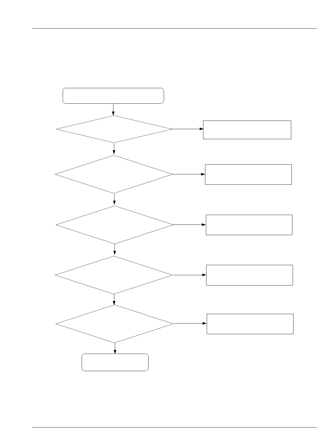
9-16. PCS Receiver
RX ON
RF input : CH center freq
Amp : -50dBm
Check ANT Switch
control circuit
Change
or Resolder MODULE200
Resolder CN201, C209
MODULE200 pin3,4
>= -65dBm
MODULE200 Pin8
>= -65dBm
Yes
No
Yes
Check MODULE200
pin9=L,pin12=L
No
No
Yes
Yes
U100 Pin35,36
>= -70dBm
No
Resolder L101, L103, L102
Yes
Check U100
pin4 >= 4.0V
pin22, 28 >= 2.7V
U100 Pin 6,7,8,9
>= 1V
No Check & Resolder
RF PSU part
Check & Resolder
U100, RF 26MHz part,
R100, R101
R110,R113,R114,
R115 >= 1V
Yes
Check U300
END
SAMSUNG Proprietary-Contents may change without notice
This Document can not be used without Samsung's authorization
Flow Chart of Troubleshooting
9-26
9-17. PCS Transmitter
TX ON (0Level)
Resolder U100
or check Txcpo(R112)
Check & Resolder
RF PSU part
Check U100
pin4 >= 4.0V
pin22, 28 >= 2.7V
Resolder R205
Check +VBATT
Check U200
+VBATT(pin17) OK?
Resolder or change U200
or check PAM control
signal
Resolder C219, L216, C217
Check ANT Switch
control circuit
Change
or Resolder MODULE200
Yes
Resolder CN201, C209
END
Check U300
U100Pin6,7,8,9
>= 500mV
OSC100 pin5
>= 6Bm
U200 Pin3
>= 3dBm
U200 Pin15
>= 20dBm
MODULE200 Pin13
>= 20dBm
MODULE200 Pin8
>= 20dBm
No
Check MODULE200
pin9=L,pin12=H
Yes
Yes
No
No
Yes
No
Yes
Yes
NoNo
Yes
No
YesYes
No
No
SAMSUNG Proprietary-Contents may change without notice
Flow Chart of Troubleshooting
This Document can not be used without Samsung's authorization
9-27
SAMSUNG Proprietary-Contents may change without notice
This Document can not be used without Samsung's authorization
Flow Chart of Troubleshooting
9-28
SAMSUNG Proprietary-Contents may change without notice
Flow Chart of Troubleshooting
This Document can not be used without Samsung's authorization
9-29

SAMSUNG Proprietary-Contents may change without notice
This Document can not be used without Samsung's authorization
Flow Chart of Troubleshooting
9-30

SAMSUNG Proprietary-Contents may change without notice
10. Reference data
10-1
This Document can not be used without Samsung's authorization
Reference Abbreviate
―AAC: Advanced Audio Coding.
―AVC : Advanced Video Coding.
―BER : Bit Error Rate
―BPSK: Binary Phase Shift Keying
―CA : Conditional Access
―CDM : Code Division Multiplexing
―C/I : Carrier to Interference
―DMB : Digital Multimedia Broadcasting
―EN : European Standard
―ES : Elementary Stream
―ETSI: European Telecommunications Standards Institute
―MPEG: Moving Picture Experts Group
―PN : Pseudo-random Noise
―PS : Pilot Symbol
―QPSK: Quadrature Phase Shift Keying
―RS : Reed-Solomon
―SI : Service Information
―TDM : Time Division Multiplexing
―TS : Transport Stream

SAMSUNG Proprietary-Contents may change without notice
Reference data
10-2
This Document can not be used without Samsung's authorization

ⓒ
This Service Manual is a property of Samsung Electronics Co.,Ltd.
Any unauthorized use of Manual can be punished under applicable
International and/or domestic law.
Samsung Electronics Co.,Ltd.
2006. 12 Rev.1.0