Samsung SGH X530 Service Manual. Www.s Manuals.com. Manual R1.0
User Manual: Phone Samsung SGH-X530 - Service manuals and Schematics, Disassembly / Assembly. Free.
Open the PDF directly: View PDF ![]() .
.
Page Count: 56
GSM TELEPHONE
SGH-X530
GSM TELEPHONE CONTENTS
1. Safety Precautions
2. Specification
3. Product Function
4. Array course control
5. Exploded View and Parts list
6. MAIN Electrical Parts List
7. Block Diagrams
8. PCB Diagrams
9. Flow Chart of Troubleshooting
10. Reference data

Contents
1. Safety Precautions
1-1. Repair Precaution ...........................................................................1-1
1-2. ESD(Electrostatically Sensitive Devices) Precaution ...........................1-2
2. Specification
2-1. GSM General Specification ..............................................................2-1
2-2. GSM TX power Level ......................................................................2-2
3. Product Function
4. Array course control
4-1. Downloading Binary Files .............................................................4-2
4-2. Pre-requsite for Downloading .......................................................4-2
4-3. S/W Downloader Program ............................................................4-3
5. Exploded View and Parts list
5-1. Cellular phone Exploded View ......................................................5-1
5-2. Cellular phone Parts list ..............................................................5-2
5-3. Disassembly ...............................................................................5-4
5-4. Assembly ...................................................................................5-6
6. MAIN Electrical Parts List
7. Block Diagrams
8. PCB Diagrams

Contents
9. Flow Chart of Troubleshooting
9-1. Baseband ................................................................................9-1
9-1-1. Power ON ..........................................................................9-1
9-1-2. Initial ................................................................................9-4
9-1-3. SIM Part .............................................................................9-6
9-1-4. Microphone Part .................................................................9-7
9-1-5. Speaker Part_1(MP3, SPEAKER PHONE) ................................9-8
9-1-6. Speaker Part_2(RECEIVER) ................................................9-10
9-1-7. Charging Part ...................................................................9-11
9-2. RF .........................................................................................9-13
9-2-1. EGSM RX .........................................................................9-13
9-2-2. DCS RX ...........................................................................9-15
9-2-3. PCS RX ............................................................................9-16
9-2-4. EGSM TX .........................................................................9-17
9-2-5. DCS TX ...........................................................................9-18
9-2-6. PCS TX ............................................................................9-19
10. Reference data

SAMSUNG Proprietary-Contents may change without notice
1. Safety Precautions
1-1
This Document can not be used without Samsung's authorization
1-1. Repair Precaution
●Repair in Shield Box, during detailed tuning.
Take specially care of tuning or test,
because specipicty of cellular phone is sensitive for surrounding interference(RF noise).
●Be careful to use a kind of magnetic object or tool,
because performance of parts is damaged by the influence of manetic force.
●Surely use a standard screwdriver when you disassemble this product,
otherwise screw will be worn away.
●Use a thicken twisted wire when you measure level.
A thicken twisted wire has low resistance, therefore error of measurement is few.
●Repair after separate Test Pack and Set because for short danger (for example an
overcurrent and furious flames of parts etc) when you repair board in condition of
connecting Test Pack and tuning on.
●Take specially care of soldering, because Land of PCB is small and weak in heat.
●Surely tune on/off while using AC power plug, because a repair of battery charger is
dangerous when tuning ON/OFF PBA and Connector after disassembing charger.
●Don't use as you pleases after change other material than replacement registered on SEC
System.
Otherwise engineer in charge isn't charged with problem that you don't keep this rules.

SAMSUNG Proprietary-Contents may change without notice
Safety Precautions
1-2
This Document can not be used without Samsung's authorization
1-2. ESD(Electrostatically Sensitive Devices) Precaution
Several semiconductor may be damaged easilly by static electricity. Such parts are called by
ESD(Electrostatically Sensitive Devices), for example IC,BGA chip etc. Read Precaution below.
You can prevent from ESD damage by static electricity.
●Remove static electricity remained your body before you touch semiconductor or parts with
semiconductor. There are ways that you touch an earthed place or wear static electricity
prevention string on wrist.
●Use earthed soldering steel when you connect or disconnect ESD.
●Use soldering removing tool to break static electricity. , otherwise ESD will be damaged by
static electricity.
●Don't unpack until you set up ESD on product. Because most of ESD are packed by box
and aluminum plate to have conductive power,they are prevented from static electricity.
●You must maintain electric contact between ESD and place due to be set up until ESD is
connected completely to the proper place or a circuit board.
2. Specification
2-1
2-1. GSM General Specification
GSM900
Phase 1
EGSM 900
Phase 2
DCS1800
Phase 1 PCS1900
Freq. Band[MHz]
Uplink/Downlink
890~915
935~960
880~915
925~960
1710~1785
1805~1880
1850~1910
1930~1990
ARFCN range 1~124 0~124 &
975~1023 512~885 512~810
Tx/Rxspacing 45MHz 45MHz 95MHz 80MHz
Mod. Bit rate/
Bit Period
270.833 kbps
3.692 us
270.833 kbps
3.692 us
270.833 kbps
3.692 us
270.833 kbps
3.692 us
Time Slot
Period/Frame Period
576.9 us
4.615 ms
576.9 us
4.615 ms
576.9 us
4.615 ms
576.9 us
4.615 ms
Modulation 0.3GMSK 0.3 GMSK 0.3 GMSK 0.3 GMSK
MS Power 33 dBm~13 dBm 33 dBm~5 dBm 30 dBm~0 dBm 30 dBm~0 dBm
Power Class 5 pcl ~ 15 pcl 5 pcl ~ 19 pcl 0 pcl ~ 15 pcl 0 pcl ~ 15 pcl
Sensitivity -102 dBm -102 dBm -100 dBm -100 dBm
TDMA Mux 8 8 8 8
Cell Radius 35 Km 35 Km 2 Km -
Speclflcation
2-2
2-2. GSM Tx Power Class
TX Power
control level GSM900
5 33±2 dBm
6 31±2 dBm
7 29±2 dBm
8 27±2 dBm
9 25±2 dBm
10 23±2 dBm
11 21±2 dBm
12 19±2 dBm
13 17±2 dBm
14 15±2 dBm
15 13±2 dBm
16 11±3 dBm
17 9±3 dBm
18 7±3 dBm
19 5±3 dBm
TX Power
control level DCS1800
0 30±3 dBm
1 28±3 dBm
2 26±3 dBm
3 24±3 dBm
4 22±3 dBm
5 20±3 dBm
6 18±3 dBm
7 16±3 dBm
8 14±3 dBm
9 12±4 dBm
10 10±4 dBm
11 8±4 dBm
12 6±4 dBm
13 4±4 dBm
14 2±5 dBm
15 0±5 dBm
TX Power
control level PCS1900
0 30±3 dBm
1 28±3 dBm
2 26±3 dBm
3 24±3 dBm
4 22±3 dBm
5 20±3 dBm
6 18±3 dBm
7 16±3 dBm
8 14±3 dBm
9 12±4 dBm
10 10±4 dBm
11 8±4 dBm
12 6±4 dBm
13 4±4 dBm
14 2±5 dBm
15 0±5 dBm

SAMSUNG Proprietary-Contents may change without notice
3. Product Function
3-1
This Document can not be used without Samsung's authorization
Main Function
- Speed dial
- SDN(Service Dialling Numbers)
-Networkservices
- Read SMS or MMS message
-Voicemail
- SOS messages
SAMSUNG Proprietary-Contents may change without notice
4. Array course control
4-1
This Document can not be used without Samsung's authorization
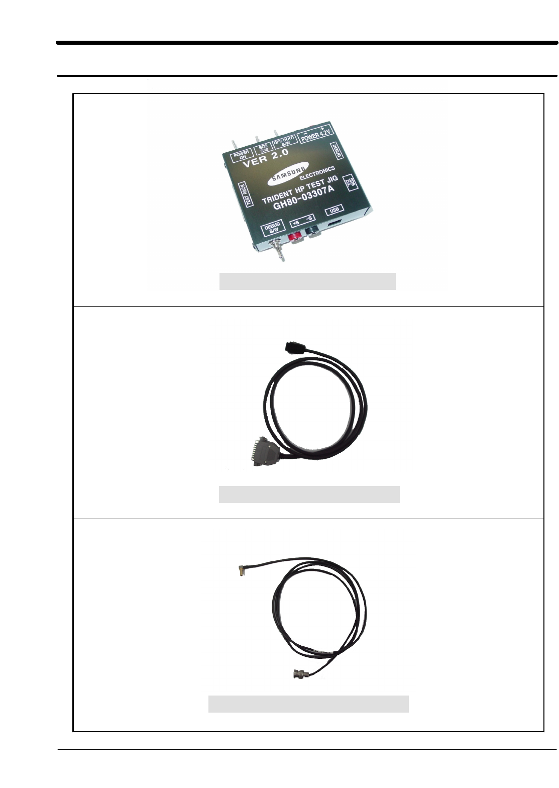
Test Jig (GH80-03307A)
Test Cable (GH39-00127A)
RF Test Cable (GH39-00283A)

SAMSUNG Proprietary-Contents may change without notice
Array course control
4-2
This Document can not be used without Samsung's authorization
4-1. Downloading Binary Files (1)
•Swift Model firmware is composed of 2 files
–*.s3 : Main source code binary.
4-2. Prerequisite
•Downloader program(Optiflash.exe)
•X530 Moblie Phone
•Data Cable
•Binary Files
SAMSUNG Proprietary-Contents may change without notice
Array course control
4-3
This Document can not be used without Samsung's authorization
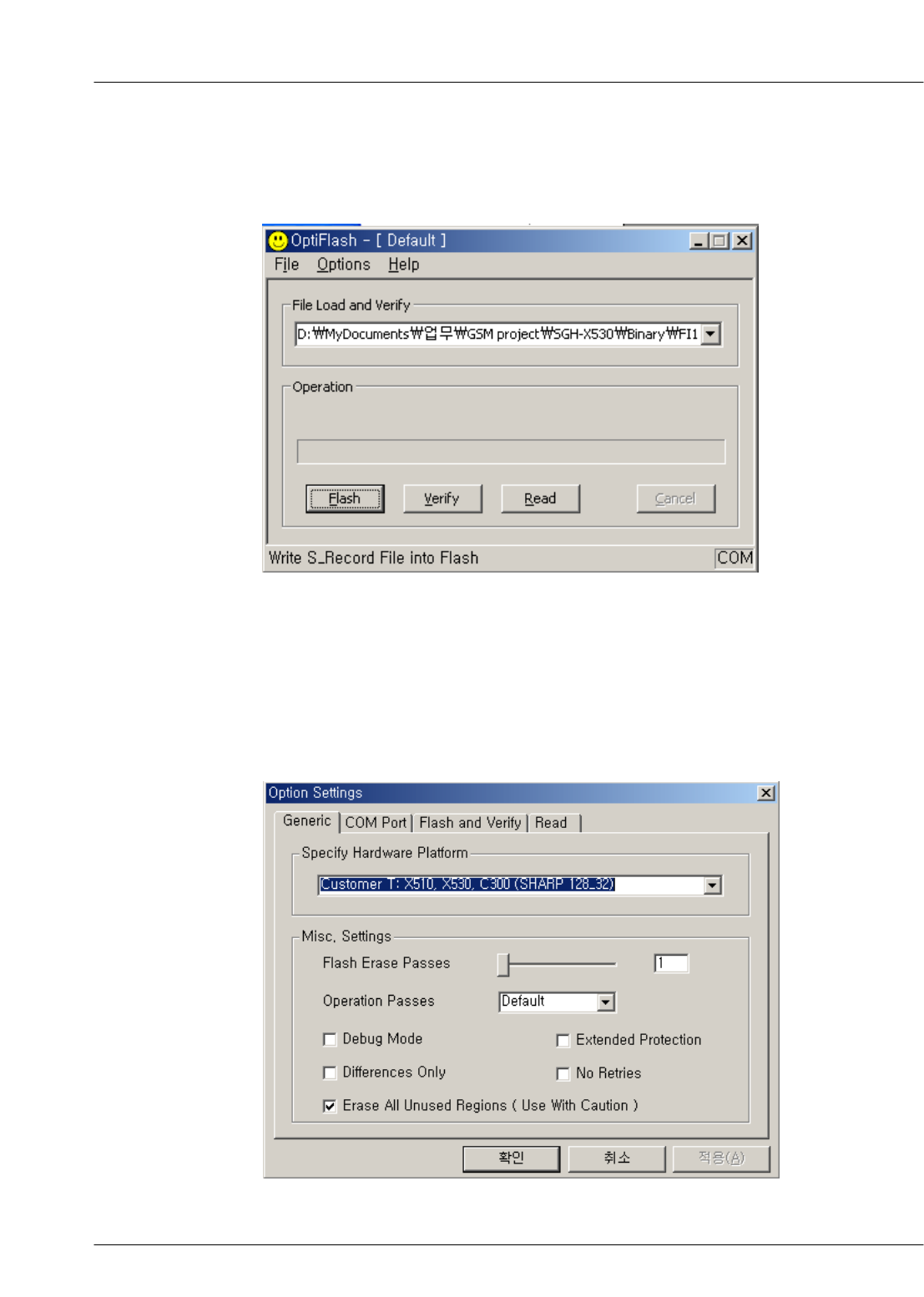
4-3. S/W Downloader Program
1. Load the binary download program by execution the "OptiFlash.exe"
2. Select the“Options” -> “Settings” -> “Generic” -> “Specify hardware platform”.
Choose hardware platform for the downloader file setting.
Set the everything else as the default values which are shown below
SAMSUNG Proprietary-Contents may change without notice
Array course control
4-4
This Document can not be used without Samsung's authorization
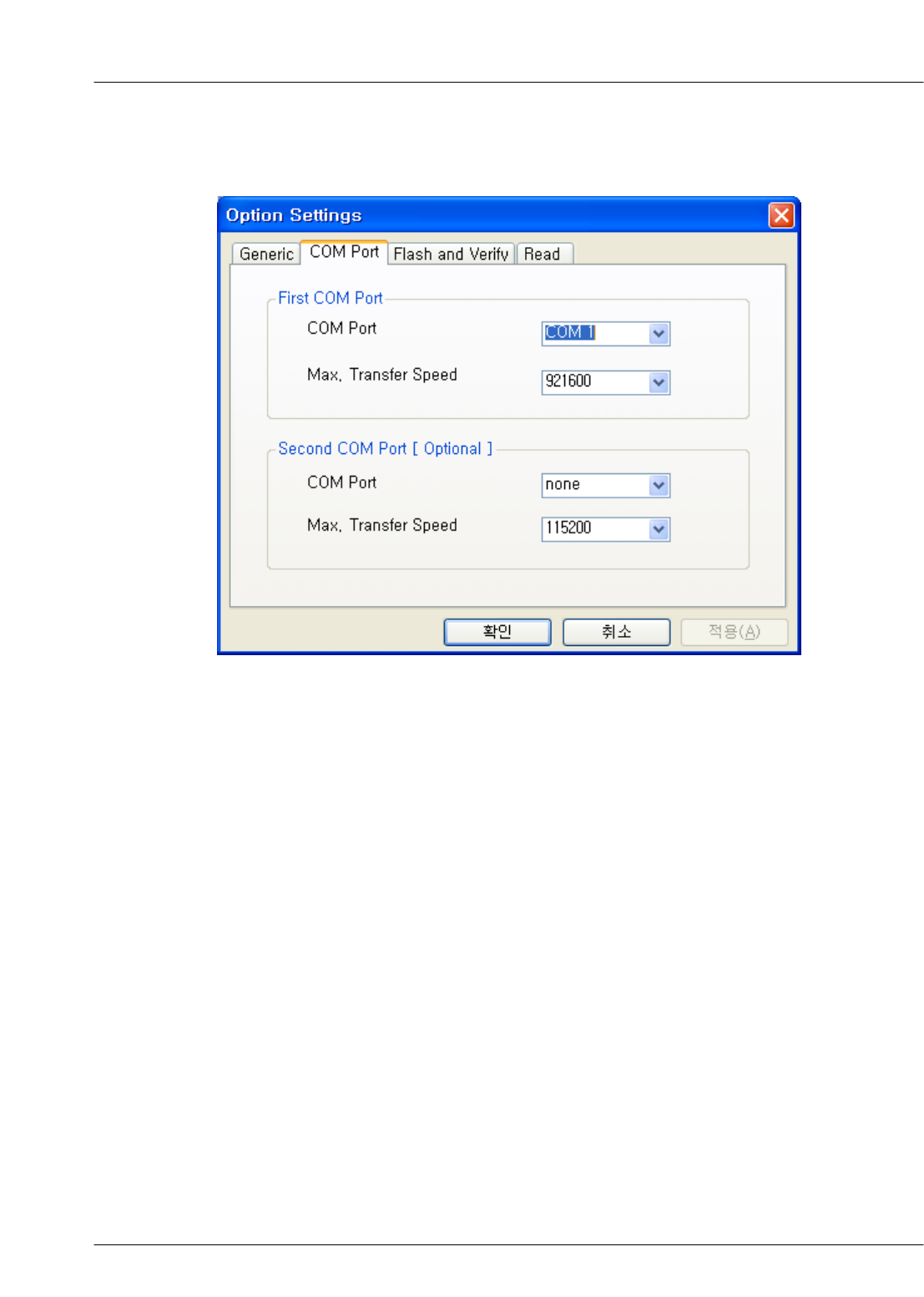
3. Select the COM port where the download cable is connected
Only COM1 is supported. Additionally you can select the maximum transfer speed
OptiFlash will use to communicate with the phone. However, Optiflash will use a slower
speed if either the PC’s or the phone’s serial hardware is incapable of handling the
selected speed.
SAMSUNG Proprietary-Contents may change without notice
Array course control
4-5
This Document can not be used without Samsung's authorization
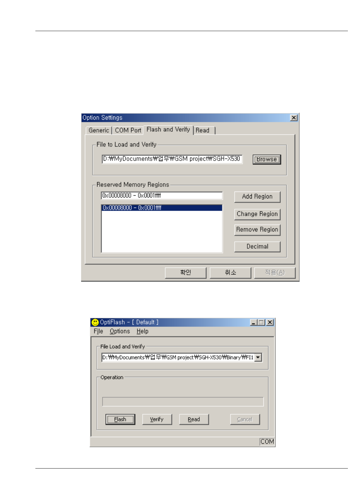
4. Select the “Flash&Verify” -> “Browse”
Set the directory path and choose the latest S/W binary, for example
"gsmstack.s3", for the downloader binary setting.
And Check "Reserved Memory Regions" - 0x00008000 - 0x0001ffff
5. 1st. Press “Flash”.
SAMSUNG Proprietary-Contents may change without notice
Array course control
4-6
This Document can not be used without Samsung's authorization
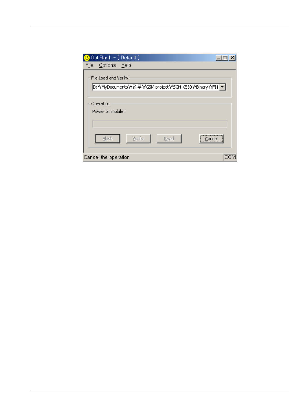
2nd. Turn on Power of mobile
6. When downloading is finished successfully, there is a “All is well” message.
7. After finishing downloading, Certain memory resets should be done to guarantee the
normal performance.
8. Confirm the downloaded version name by key-string(*#1234#)
Memory reset will be done by pressing the following key-strings.
Full Reset :“
*2767*3855#” will reboot the phone automatically.
SAMSUNG Proprietary-Contents may change without notice
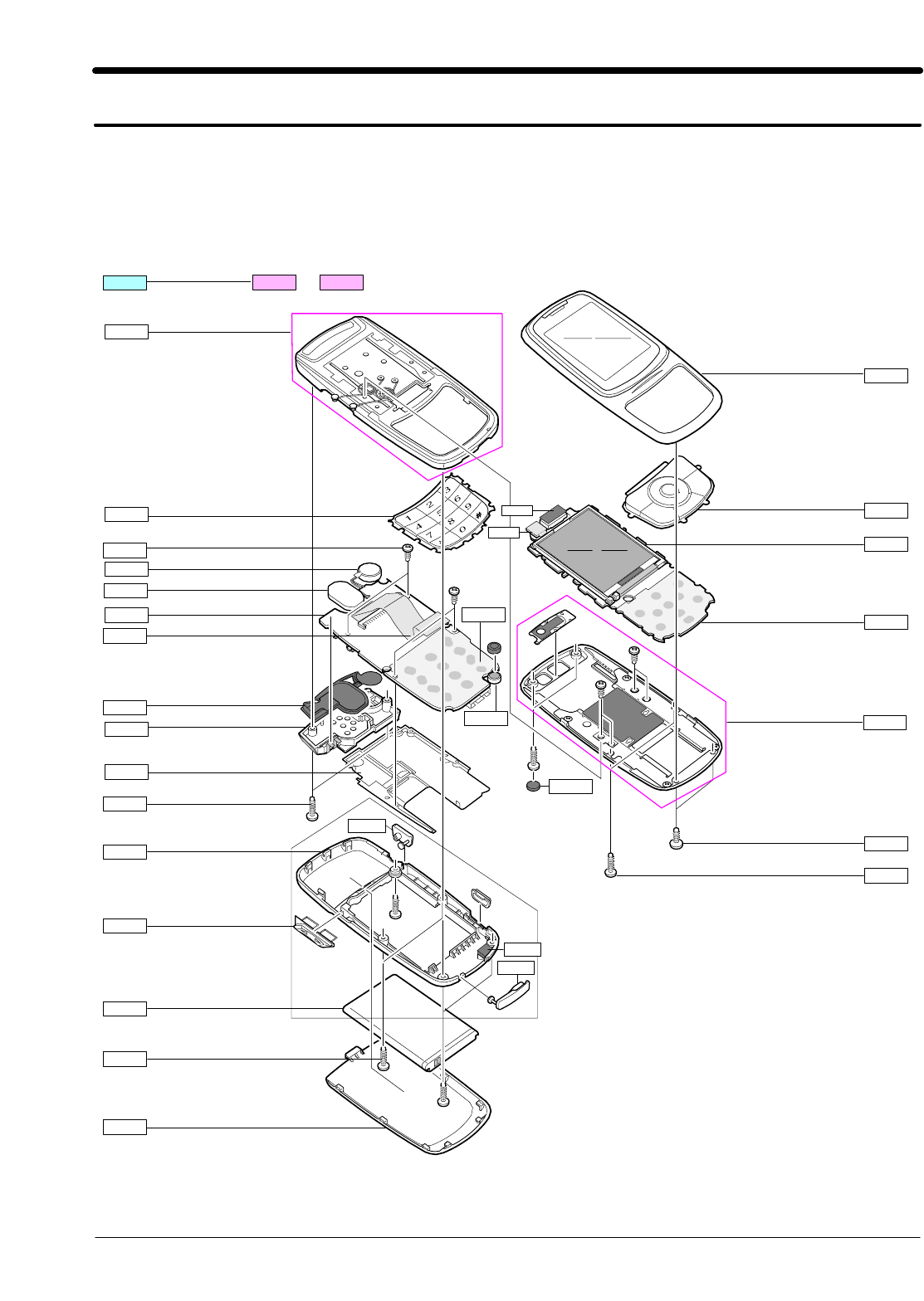
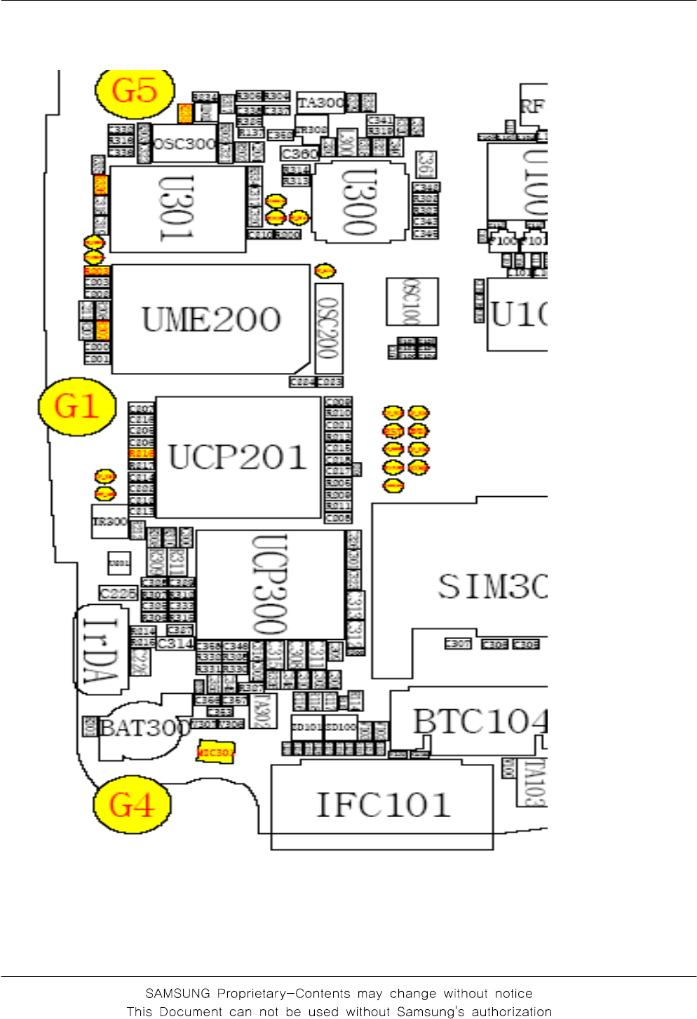
5. Exploded View and Parts List
5-1
This Document can not be used without Samsung's authorization
5-1. Cellular phone Exploded View
QFR01
QKP01
QMP01
QAN02
QSH01
QRE01
QBA00
QFU01
QKP02
QME02
QFL01
QMO01
QSP01
QCR54
QVO01
QBA01
QRF03
QIF01
QLC01
QCA01
QAU01
QPC01
QCR49
QCR04
QCR05
QAN05
QCR17
QME01
QFR01 QFL01
+
QHI01
QMI01
QSC01
QMI03

SAMSUNG Proprietary-Contents may change without notice
Exploded View and Parts List
5-2
This Document can not be used without Samsung's authorization
5-2. Cellular phone Parts list
Design LOC Discription SEC CODE
QAN02 INTENNA-SGHX530 GH42-00995A
QAN05 ASSY RUBBER-INTENNA GH98-02741A
QAU01 AUDIO-RECEIVER 3009-001243
QBA00 PMO-COVER BATT GH72-34196A
QBA01 INNER BATTERY PACK-800MAH,MAIN GH43-02589A
QCA01 UNIT-CAMERA GH59-03701A
QCR04 SCREW-MACHINE 6001-001479
QCR05 SCREW-MACHINE 6001-001478
QCR17 SCREW-MACHINE 6001-001460
QCR49 SCREW-MACHINE 6001-001823
QCR54 SCREW-MACHINE 6001-001645
QFU01 ASSY COVER-SLIDE UPPER GH98-02234A
QKP01 ASSY KEYPAD-MAIN(OPEN/BRN) GH98-02239A
QKP02 ASSY KEYPAD-SUB(OPEN/BRN) GH98-02238A
QLC01 ELA UNIT-SGHX530 LCD MODULE GH96-02314A
QME01 UNIT-DOME SHEET (MAIN KEY) GH59-03675A
QME02 UNIT-DOME SHEET (NAVI KEY) GH59-03682A
QMI01 MICROPHONE-ASSY-SGHX530 GH30-00320A
QMO01 MOTOR DC-SPHV8400 GH31-00187A
QMP01 PBA MAIN-SGHX530S (PBA MAIN) GH92-03125A
QPC01 MEA-SLIDE FPCB KIT GH97-06774A
QSC01 RMO-RUBBER SCREW GH73-08015A
QSH03 ASSY BRACKET-SHIELD REAR GH98-02241A
QSP01 SPEAKER 3001-002075
QVO01 PMO-KEY VOLUME GH72-34195A
QHI01 ASSY HINGE GH98-02235A
QFL01 ASSY COVER-SLIDE LOWER GH98-02236A
QFR01 ASSY COVER-FRONT GH98-02237A
QRE01 ASSY COVER-REAR GH98-02240A
QIF01 PMO-COVER IF GH72-34193A
QMI03 RMO-RUBBER MIC GH73-08289A
QRF03 PMO-COVER EAR JACK GH72-34192A

SAMSUNG Proprietary-Contents may change without notice
Exploded View and Parts List
5-3
This Document can not be used without Samsung's authorization
Discription SEC CODE
BAG PE 6902-000297
ADAPTOR-SCHN391 HUTCHSON GH44-00745A
UNIT-EARPHONE GH59-01694A
LABEL(P)-IMEI GH68-01335D
LABEL(P)-WATER SOAK GH68-02026A
LABEL(P)-WATER SOAK GH68-02026A
MANUAL USERS-EU ENGLISH GH68-12661A
LABEL(R)-MAIN((XSA) GH68-13025D
BOX(P)-UNIT MAIN(SEA_2) GH69-04689K
RMO-RUBBER MIC HOLDER GH73-08016A
RMO-RUBBER BGA A GH73-08526A
RMO-RUBBER BGA B GH73-08527A
RMO-RUBBER BGA C GH73-08528A
RMO-RUBBER BGA D GH73-08529A
MPR-REMOVE TAPE LCD GH74-13804A
MPR-TAPE LCD SHORT GH74-19768A
MPR-GASKET LCD SIDE GH74-24930A
MPR-VINYL BOHO CAMERA LENS GH74-25648A
MPR-TAPE GH74-26727A
MPR-TAPE GH74-26727A
MPR-SPONGE CAM GH74-28219A
MPR-INSU TAPE GH74-28241A
MPR-INSU TAPE LCD PCB GH74-28645A
MPR-INSU TAPE MAIN PCB GH74-28646A
MPR-TAPE ELEC ESD GH74-28649A
MPR-VINYL BOHO WINDOW GH74-28851A
MPR-TAPE BGA B GH74-28856A
MPR-TAPE MAIN FPCB HOLD GH74-28942A
MPR-SPONGE PCB GH74-28944A
MPR-ELEC TAPE PCB A GH74-28946A
MPR-VINYL BOHO FRONT GH74-29101A
SAMSUNG Proprietary-Contents may change without notice
Exploded View and Parts List
5-4
This Document can not be used without Samsung's authorization
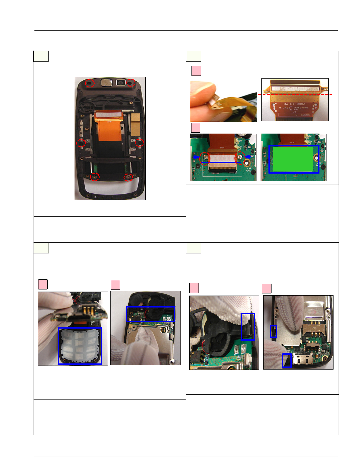
5-3. Disassembly
1
43
2
1) Disjoint REAR's lower locker and remove REAR
case just like a picture below.
※caution
1) Be careful for scratch
1)Disjoint the REAR Screw of 5 Points.
※caution
1) Be careful for scratch
1) Disjoint VOL KEY with tweezers.
2) Disjoint an INTENNA SCREW.
3) Disjoint an INTENNA SCREW.
4) Remove an INTENA.
5) Disjoint SPEAKER RUBBER, MOTOR and
SPEAKER with tweezers
※caution
1) Be careful for the damage on the WIRE or
RUBBER.
1) Remove the green tape on the FPCB
2) Disjoint the FPCB by DESOLDERING.
※caution
1) Be careful for the FPCB's crack
①
⑤②
③
④
SAMSUNG Proprietary-Contents may change without notice
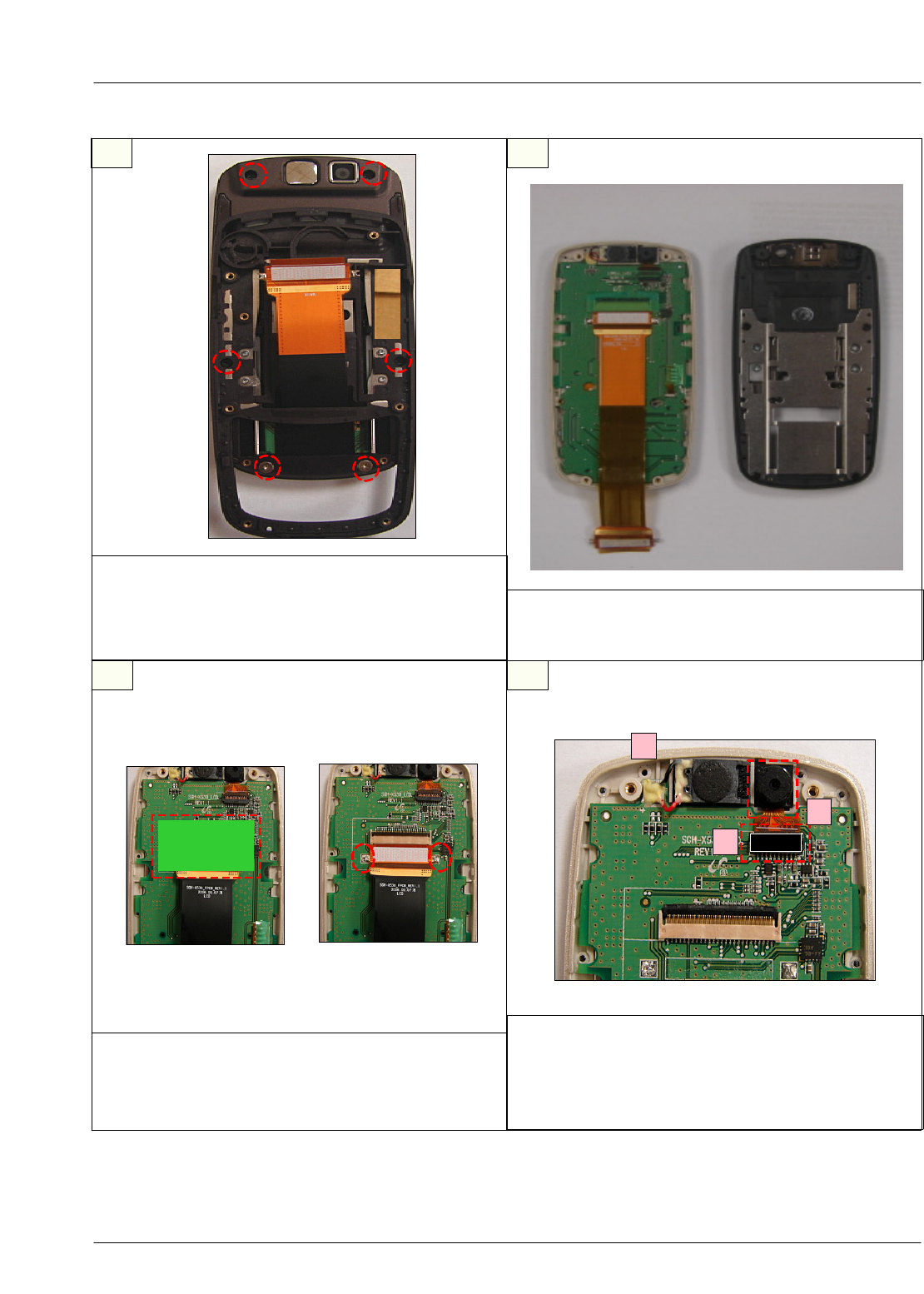
Exploded View and Parts List
5-5
This Document can not be used without Samsung's authorization
5
87
6
1) Remove the green tape from the FPCB
2) Disjoint the FPCB with DESOLDERING.
※caution
1) Be careful for the FPCB's crack
1),2) First, Remove the Black tape, and then
disjoint the CAM from connector.
3) Take off the receiver from the Upper plastic.
※caution
1) Be careful for the Cammera's crack.
1) Disjoin 6 screws.
※caution
1) Be careful for scratch
2) Using the '+' screw driver.
1) Disjoint HINGE ASSY like the picture below.
※caution
1) Be careful FPCB's crumpling.
①
③
②
SAMSUNG Proprietary-Contents may change without notice
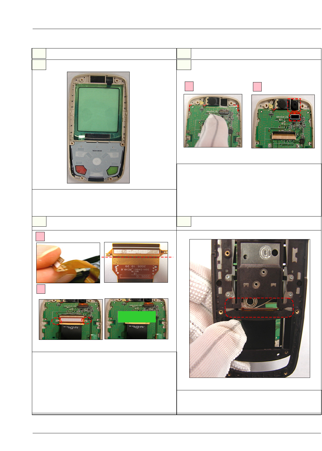
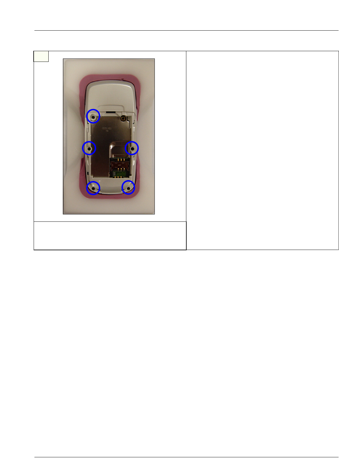
Exploded View and Parts List
5-6
This Document can not be used without Samsung's authorization
1
43
2
1) Fold the FPCB like the picture below.
2) Insert the LCD FPCB to the CONNECTOR,
SOLDERING 2 points and then put the green
TAPE.
※caution
1) Be careful for scratch
2) Be careful for the FPCB's crack
1) Insert the MAIN FPCB like the picture below.
※caution
1) Be careful for the FPCB's crack
1) Put the NAVI key like the picture below.
※caution
1) Put the hole of NAVY key to UPPER
1) Put the receiver and the SUB PBA.
2) Insert the CAMERA, and then put up the
SPONGE along the edge of connector
※caution
1) Check the fabrication status of RCV & CAM
2) Be careful for the CAM FPCB's crack.
①
②
②
①
②
56
SAMSUNG Proprietary-Contents may change without notice
Exploded View and Parts List
5-7
This Document can not be used without Samsung's authorization
5
87
6
1) Joint the 6 screws with the slide stopping JIG.
※caution
1) Fix the slide tightly.
1) Fold the FPCB like the picture below.
2) Insert the LCD FPCB to the CONNECTOR
along the SILK LINE, SOLDERING 2 points and
then put the green TAPE.
※caution
1) Be careful for the FPCB's crack
1) Put the NAVY key like the picture below.
2) Put the PBA first, and then MOT, SPK.
※caution
1) Be careful the wire.
1)InserttheSPKRUBBERlikethepicturebelow.
2)Lock the PBA on the left side HOOK and then
put the MIC.
※caution
1) Be careful the rubber's folding.
①
②
①②①②
SAMSUNG Proprietary-Contents may change without notice
Exploded View and Parts List
5-8
This Document can not be used without Samsung's authorization
9
1211
10
1)Joint the 2 screws with the screw JIG.
※caution
1) Be careful for the damage to INTENNA pattern.
1) Soldering the Intenna pads.
※caution
1) Be careful for the damage of plastic.
1) Insert the VOL KEY.
※caution
1) Be careful for the damage of plastic.
1) Joint the lower REAR plastic first.
2) Push the upper REAR plastic like the picture
below until hearing the locking sound.
※caution
1) Be careful for the damage of plastic.
②
①
SAMSUNG Proprietary-Contents may change without notice
Exploded View and Parts List
5-9
This Document can not be used without Samsung's authorization
13
1) Joint 5 screws with the prop.
※caution
1) Be careful for the damage of plastic.

SAMSUNG Proprietary-Contents may change without notice
6. MAIN Electrical Parts List
6-1
This Document can not be used without Samsung's authorization
SEC CODE Design LOC Discription SEC CODE
0401-001141 D300 DIODE-SWITCHING SA
0403-001547 D101 DIODE-ZENER SA
0406-001197 ZD100 DIODE-TVS SA
0406-001197 ZD101 DIODE-TVS SA
0406-001197 ZD301 DIODE-TVS SA
0406-001201 ZD302 DIODE-TVS SA
0406-001260 D200 DIODE-TVS SA
0501-000225 TR302 TR-SMALL SIGNAL SA
0504-000168 TR300 TR-DIGITAL SA
0601-001819 LED200 LED SA
0601-001819 LED201 LED SA
0601-001819 LED202 LED SA
0601-001819 LED203 LED SA
0601-001819 LED204 LED SA
0601-001819 LED205 LED SA
0601-001819 LED206 LED SA
0601-001819 LED207 LED SA
0601-001819 LED208 LED SA
0601-001819 LED209 LED SA
0601-001819 LED210 LED SA
0601-001819 LED211 LED SA
0604-001306 IRDA PHOTO-IRDA SA
0801-002529 U104 IC-CMOS LOGIC SA
1009-001027 U200 IC-HALL EFFECT S/W SA
1108-000010 UME200 IC-MCP SA
1201-002278 U100 IC-POWER AMP SA
1203-003304 UCP300 IC-POWER SUPERVISOR SA
1203-003663 U103 IC-BATTERY SA
1204-001811 U300 IC-MELODY SA
1205-003116 U101 IC-TRANSCEIVER SA
1209-001712 U201 IC-SENSOR SA
1405-001082 V100 VARISTOR SA
1405-001082 V102 VARISTOR SA
1405-001082 V103 VARISTOR SA
1405-001082 V205 VARISTOR SA
1405-001082 V206 VARISTOR SA
1405-001082 V306 VARISTOR SA

SAMSUNG Proprietary-Contents may change without notice
Main Electrical Parts List
6-2
This Document can not be used without Samsung's authorization
SEC CODE Design LOC Discription SEC CODE
1405-001082 V307 VARISTOR SA
1405-001082 V308 VARISTOR SA
1405-001082 V309 VARISTOR SA
1405-001082 V310 VARISTOR SA
1405-001177 V101 VARISTOR SA
1405-001177 V200 VARISTOR SA
1405-001177 V201 VARISTOR SA
1405-001177 V202 VARISTOR SA
1405-001177 V203 VARISTOR SA
1405-001177 V204 VARISTOR SA
1405-001177 V207 VARISTOR SA
1405-001177 V208 VARISTOR SA
1405-001177 V209 VARISTOR SA
1405-001177 V210 VARISTOR SA
2007-000070 R335 R-CHIP SA
2007-000140 R120 R-CHIP SA
2007-000140 R316 R-CHIP SA
2007-000144 R301 R-CHIP SA
2007-000148 R307 R-CHIP SA
2007-000148 R312 R-CHIP SA
2007-000148 R330 R-CHIP SA
2007-000148 R331 R-CHIP SA
2007-000157 R205 R-CHIP SA
2007-000157 R209 R-CHIP SA
2007-000160 R320 R-CHIP SA
2007-000161 R306 R-CHIP SA
2007-000161 R315 R-CHIP SA
2007-000162 R112 R-CHIP SA
2007-000162 R119 R-CHIP SA
2007-000162 R211 R-CHIP SA
2007-000164 R206 R-CHIP SA
2007-000164 R318 R-CHIP SA
2007-000168 R325 R-CHIP SA
2007-000170 R212 R-CHIP SA
2007-000170 R303 R-CHIP SA
2007-000171 R313 R-CHIP SA
2007-000171 R314 R-CHIP SA

SAMSUNG Proprietary-Contents may change without notice
Main Electrical Parts List
6-3
This Document can not be used without Samsung's authorization
SEC CODE Design LOC Discription SEC CODE
2007-000172 R111 R-CHIP SA
2007-000172 R200 R-CHIP SA
2007-000172 R201 R-CHIP SA
2007-000566 R114 R-CHIP SA
2007-000566 R116 R-CHIP SA
2007-000566 R117 R-CHIP SA
2007-000566 R118 R-CHIP SA
2007-000775 R319 R-CHIP SA
2007-000775 R321 R-CHIP SA
2007-000775 R322 R-CHIP SA
2007-000831 R113 R-CHIP SA
2007-000831 R324 R-CHIP SA
2007-001119 R304 R-CHIP SA
2007-001119 R326 R-CHIP SA
2007-001284 R215 R-CHIP SA
2007-001290 R302 R-CHIP SA
2007-001320 R305 R-CHIP SA
2007-001320 R327 R-CHIP SA
2007-001323 R317 R-CHIP SA
2007-001325 R323 R-CHIP SA
2007-001335 R234 R-CHIP SA
2007-002965 R308 R-CHIP SA
2007-002965 R310 R-CHIP SA
2007-003023 R235 R-CHIP SA
2007-007014 R329 R-CHIP SA
2007-007468 R328 R-CHIP SA
2007-007468 R332 R-CHIP SA
2007-007573 R210 R-CHIP SA
2007-007573 R213 R-CHIP SA
2007-008045 R103 R-CHIP SA
2007-008137 R121 R-CHIP SA
2007-008419 R122 R-CHIP SA
2007-008419 R124 R-CHIP SA
2007-008419 R125 R-CHIP SA
2007-008419 R126 R-CHIP SA
2007-008419 R127 R-CHIP SA
2007-008419 R128 R-CHIP SA

SAMSUNG Proprietary-Contents may change without notice
Main Electrical Parts List
6-4
This Document can not be used without Samsung's authorization
SEC CODE Design LOC Discription SEC CODE
2007-008419 R129 R-CHIP SA
2007-008419 R130 R-CHIP SA
2007-008419 R131 R-CHIP SA
2007-008419 R132 R-CHIP SA
2007-008419 R133 R-CHIP SA
2007-008419 R134 R-CHIP SA
2007-008483 R136 R-CHIP SA
2007-008486 R115 R-CHIP SA
2007-008516 R106 R-CHIP SA
2007-008516 R107 R-CHIP SA
2007-008531 R104 R-CHIP SA
2007-008548 R100 R-CHIP SA
2007-008587 R101 R-CHIP SA
2007-008590 R333 R-CHIP SNA
2007-009111 R219 R-CHIP SA
2007-009111 R220 R-CHIP SA
2007-009111 R223 R-CHIP SA
2007-009111 R224 R-CHIP SA
2007-009111 R225 R-CHIP SA
2007-009111 R227 R-CHIP SA
2007-009111 R228 R-CHIP SA
2007-009111 R229 R-CHIP SA
2007-009111 R230 R-CHIP SA
2007-009111 R231 R-CHIP SA
2007-009111 R232 R-CHIP SA
2007-009111 R233 R-CHIP SA
2007-009160 R123 R-CHIP SA
2007-009315 R204 R-CHIP SA
2007-009315 R300 R-CHIP SA
2203-000233 C222 C-CER,CHIP SA
2203-000233 C316 C-CER,CHIP SA
2203-000254 C204 C-CER,CHIP SA
2203-000254 C205 C-CER,CHIP SA
2203-000254 C206 C-CER,CHIP SA
2203-000254 C207 C-CER,CHIP SA
2203-000254 C209 C-CER,CHIP SA
2203-000254 C210 C-CER,CHIP SA

SAMSUNG Proprietary-Contents may change without notice
Main Electrical Parts List
6-5
This Document can not be used without Samsung's authorization
SEC CODE Design LOC Discription SEC CODE
2203-000254 C211 C-CER,CHIP SA
2203-000254 C218 C-CER,CHIP SA
2203-000254 C301 C-CER,CHIP SA
2203-000254 C302 C-CER,CHIP SA
2203-000254 C334 C-CER,CHIP SA
2203-000254 C340 C-CER,CHIP SA
2203-000254 C359 C-CER,CHIP SA
2203-000278 C353 C-CER,CHIP SA
2203-000311 C341 C-CER,CHIP SA
2203-000330 C223 C-CER,CHIP SA
2203-000330 C224 C-CER,CHIP SA
2203-000359 C356 C-CER,CHIP SA
2203-000359 C357 C-CER,CHIP SA
2203-000425 C321 C-CER,CHIP SA
2203-000425 C322 C-CER,CHIP SA
2203-000438 C343 C-CER,CHIP SA
2203-000679 C217 C-CER,CHIP SA
2203-000812 C305 C-CER,CHIP SA
2203-000812 C306 C-CER,CHIP SA
2203-000812 C332 C-CER,CHIP SA
2203-000940 C303 C-CER,CHIP SA
2203-000940 C325 C-CER,CHIP SA
2203-000940 C333 C-CER,CHIP SA
2203-000940 C346 C-CER,CHIP SA
2203-000940 C358 C-CER,CHIP SA
2203-000995 C307 C-CER,CHIP SA
2203-000995 C336 C-CER,CHIP SA
2203-000995 C339 C-CER,CHIP SA
2203-001072 C352 C-CER,CHIP SA
2203-002668 C164 C-CER,CHIP SA
2203-005344 C216 C-CER,CHIP SA
2203-005344 C323 C-CER,CHIP SA
2203-005344 C337 C-CER,CHIP SA
2203-005395 C163 C-CER,CHIP SA
2203-005482 C335 C-CER,CHIP SA
2203-005482 C338 C-CER,CHIP SA
2203-005682 C102 C-CER,CHIP SA

SAMSUNG Proprietary-Contents may change without notice
Main Electrical Parts List
6-6
This Document can not be used without Samsung's authorization
SEC CODE Design LOC Discription SEC CODE
2203-005682 C104 C-CER,CHIP SA
2203-005682 C125 C-CER,CHIP SA
2203-005682 C127 C-CER,CHIP SA
2203-005682 C128 C-CER,CHIP SA
2203-005682 C129 C-CER,CHIP SA
2203-005731 C103 C-CER,CHIP SA
2203-005736 C105 C-CER,CHIP SA
2203-005736 C112 C-CER,CHIP SA
2203-005736 C115 C-CER,CHIP SA
2203-005736 C126 C-CER,CHIP SA
2203-005777 C101 C-CER,CHIP SA
2203-005777 C106 C-CER,CHIP SA
2203-005777 C111 C-CER,CHIP SA
2203-005777 C113 C-CER,CHIP SA
2203-005819 C311 C-CER,CHIP SA
2203-005819 C312 C-CER,CHIP SA
2203-005819 C313 C-CER,CHIP SA
2203-005819 C314 C-CER,CHIP SA
2203-005819 C315 C-CER,CHIP SA
2203-006048 C148 C-CER,CHIP SA
2203-006048 C200 C-CER,CHIP SA
2203-006048 C201 C-CER,CHIP SA
2203-006048 C202 C-CER,CHIP SA
2203-006048 C203 C-CER,CHIP SA
2203-006048 C208 C-CER,CHIP SA
2203-006048 C214 C-CER,CHIP SA
2203-006048 C215 C-CER,CHIP SA
2203-006048 C221 C-CER,CHIP SA
2203-006048 C300 C-CER,CHIP SA
2203-006048 C317 C-CER,CHIP SA
2203-006048 C319 C-CER,CHIP SA
2203-006048 C324 C-CER,CHIP SA
2203-006048 C326 C-CER,CHIP SA
2203-006048 C330 C-CER,CHIP SA
2203-006048 C342 C-CER,CHIP SA
2203-006048 C345 C-CER,CHIP SA
2203-006048 C349 C-CER,CHIP SA

SAMSUNG Proprietary-Contents may change without notice
Main Electrical Parts List
6-7
This Document can not be used without Samsung's authorization
SEC CODE Design LOC Discription SEC CODE
2203-006048 C351 C-CER,CHIP SA
2203-006048 C355 C-CER,CHIP SA
2203-006194 C107 C-CER,CHIP SA
2203-006194 C108 C-CER,CHIP SA
2203-006194 C116 C-CER,CHIP SA
2203-006194 C121 C-CER,CHIP SA
2203-006257 C304 C-CER,CHIP SA
2203-006257 C310 C-CER,CHIP SA
2203-006257 C348 C-CER,CHIP SA
2203-006260 C212 C-CER,CHIP SA
2203-006260 C213 C-CER,CHIP SA
2203-006305 C137 C-CER,CHIP SA
2203-006318 C114 C-CER,CHIP SA
2203-006318 C117 C-CER,CHIP SA
2203-006324 C308 C-CER,CHIP SA
2203-006324 C350 C-CER,CHIP SA
2203-006377 C130 C-CER,CHIP SA
2203-006410 C110 C-CER,CHIP SA
2203-006423 C118 C-CER,CHIP SA
2203-006423 C120 C-CER,CHIP SA
2203-006423 C122 C-CER,CHIP SA
2203-006423 C123 C-CER,CHIP SA
2203-006423 C219 C-CER,CHIP SA
2203-006423 C220 C-CER,CHIP SA
2203-006556 C100 C-CER,CHIP SA
2203-006556 C109 C-CER,CHIP SA
2203-006556 C133 C-CER,CHIP SA
2203-006556 C134 C-CER,CHIP SA
2203-006556 C135 C-CER,CHIP SA
2203-006556 C136 C-CER,CHIP SA
2203-006556 C157 C-CER,CHIP SA
2203-006556 C158 C-CER,CHIP SA
2203-006556 C159 C-CER,CHIP SA
2203-006556 C160 C-CER,CHIP SA
2203-006556 C161 C-CER,CHIP SA
2203-006556 C162 C-CER,CHIP SA
2203-006562 C143 C-CER,CHIP SA

SAMSUNG Proprietary-Contents may change without notice
Main Electrical Parts List
6-8
This Document can not be used without Samsung's authorization
SEC CODE Design LOC Discription SEC CODE
2203-006562 C144 C-CER,CHIP SA
2203-006562 C309 C-CER,CHIP SA
2203-006562 C318 C-CER,CHIP SA
2203-006562 C320 C-CER,CHIP SA
2203-006562 C327 C-CER,CHIP SA
2203-006626 C328 C-CER,CHIP SA
2203-006626 C329 C-CER,CHIP SA
2203-006648 C119 C-CER,CHIP SA
2203-006681 C146 C-CER,CHIP SA
2203-006824 C225 C-CER,CHIP SA
2203-006824 C226 C-CER,CHIP SA
2203-006824 C354 C-CER,CHIP SA
2203-006824 C360 C-CER,CHIP SA
2203-006824 C361 C-CER,CHIP SA
2404-001225 TA303 C-TA,CHIP SA
2404-001225 TA304 C-TA,CHIP SA
2404-001374 TA102 C-TA,CHIP SA
2404-001406 TA103 C-TA,CHIP SA
2404-001414 TA300 C-TA,CHIP SA
2404-001414 TA302 C-TA,CHIP SA
2703-001513 L301 INDUCTOR-SMD SA
2703-001513 L302 INDUCTOR-SMD SA
2703-001513 L303 INDUCTOR-SMD SA
2703-001513 L304 INDUCTOR-SMD SA
2703-002313 L106 INDUCTOR-SMD SA
2703-002485 L101 INDUCTOR-SMD SA
2703-002544 L109 INDUCTOR-SMD SA
2703-002558 L110 INDUCTOR-SMD SA
2703-002597 L108 INDUCTOR-SMD SA
2703-002858 L103 INDUCTOR-SMD SA
2703-002858 L104 INDUCTOR-SMD SA
2801-003856 OSC200 CRYSTAL-SMD SA
2801-004455 OSC100 CRYSTAL-SMD SA
2801-004573 OSC300 CRYSTAL-SMD SA
2904-001592 F100 FILTER-SAW SA
2904-001599 F101 FILTER-SAW SA
2904-001600 F102 FILTER-SAW SA
SAMSUNG Proprietary-Contents may change without notice
Main Electrical Parts List
6-9
This Document can not be used without Samsung's authorization
SEC CODE Design LOC Discription SEC CODE
3301-001208 L300 BEAD-SMD SA
3301-001729 L200 BEAD-SMD SA
3404-001152 TAC1 SWITCH-TACT SA
3404-001152 TAC2 SWITCH-TACT SA
3705-001358 RFS601 CONNECTOR-COAXIAL SA
3708-002278 CN103 CONNECTOR-FPC/FFC/PIC SA
3709-001384 SIM300 CONNECTOR-CARD EDGE SA
3710-001611 IFC101 CONNECTOR-INTERFACE SA
3711-006228 BTC104 HEADER-BATTERY SA
3722-002067 EAR300 JACK-EAR PHONE SA
4302-001130 BAT300 BATTERY-LI(2ND) SA
GH09-00036A UCP201 IC MICOM-SGHX480 SA
GH13-00036A U301 IC ASIC-SGHX670 SA
SAMSUNG Proprietary-Contents may change without notice
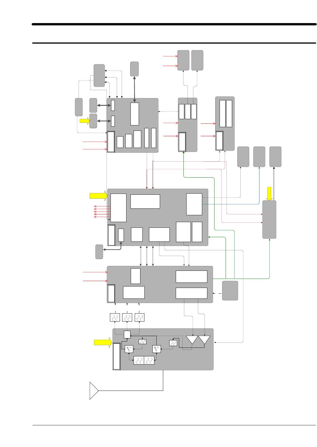
7. Block Diagrams
7-1
This Document can not be used without Samsung's authorization
TQM6M4002
G
S
M
D
P
C
S
SI4208
LNA
IN
M/N
RF-BB
IF
PAM
IF
RF
IF
Synth
esizer
GSM
DCS
PCS
OSC26M
26M_RF
CSP2200
SIM IF
SIM
POWER
MANAGEMENT
Drivers
RF IF
RF Block
Enable
DAI
SER_CTRL
TXI_I/O
TXQ_I/O
TX_EN,TXPWR
TX_BAND_SEL
AUDIO
IF
DSP
IF
YAMAHA
Sound Generator
Trident 2
MCI
Power
DSP
mem. IF
Serial ctrl
System Clk
MCU IF
Keypad IF
RTCIrDA
IrDA
Tx,Rx
En
X-tal
32.768
Charging
IC
Interface
Connector
18Pin
Keypad
KB_COL[0:4]
KB_ROW[0:4]
LCD
Module
MV3017
Memory
128Mbits Flash
32Mbits RAM
CAM
Module
CAM_Y[0:7]
LCD IF
CAM IF
LCD_D[0:7]
Speaker
Ear Phone
DEBUG
SDS
DLC_DET SDS_TXD
SDS_RXD
A[1:23]
D[0:15]
CLK13M_MC
CLK13M_TR
CLK13M_YMU
JIG ON
Charging
Current
VBAT
VBAT
VBAT
VCCD_1.8V
VCCD_2.9V
VRF_2.9V
VCCB_2.9V
VCCA_2.9V
VRF_2.9V
VCCD_2.9V
VCCD_2.9V
VCCD_1.8V
VCCD
_2.9V
VCCD
_1.8V
VCCD
_2.9V
VCCD
_1.8V
VCCD
_2.9V
VCCD
_1.8V
VBAT
GSM Tx
DPCX Tx
AFC
RX_EN
Receiver
SAMSUNG Proprietary-Contents may change without notice
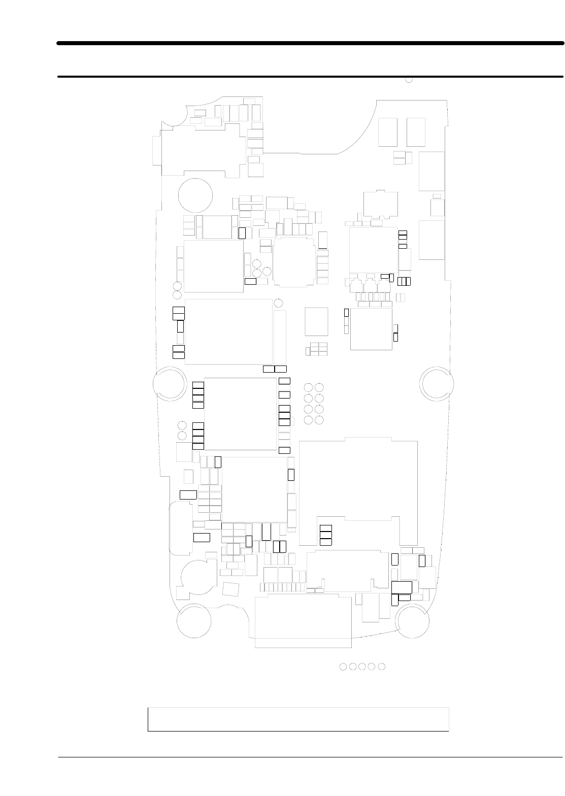
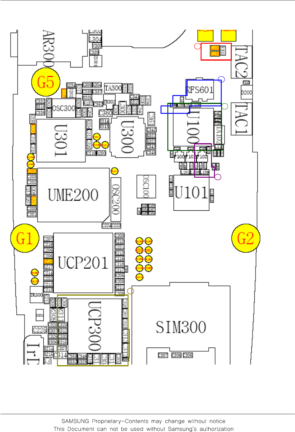
8. PCB Diagrams
8-1
This Document can not be used without Samsung's authorization
ANT_GND
BAT300
BTC104
CN100
CP_CSRAM
CP_TCK CP_TDI
CP_TDO
CP_TMS
1
0
1
D
D200
0
0
3
D
DSP_INT
0
0
3
R
A
E
F100F101F102
FEEDING
G1 G2
G3
G4
G5
GND1
IFC101
A
D
r
I
MIC301
0
0
1
C
S
O
0
0
2
C
S
O
OSC300
RFS601
RST
SIM300
2
0
1
A
T
3
0
1
A
T
TA300
2
0
3
A
T
3
0
3
A
T
4
0
3
A
T
1
C
A
T
2
C
A
T
TP100TP101TP102
TP103
TP104
TP105
TP_A(1)
TP_CP_OEN
TP_CP_WEN
TP_CSROM1
TP_D(1)
TP_INTRQ
TP_MV3017_ CS
TR300
TR302
0
0
1
U
U101
U103
U104
U201
0
0
3
U
1
0
3
U
UCP201
0
0
3
P
C
U
UME200
0
0
1
V
2
0
1
V
3
0
1
V
V210
V306V307
V308
V309
V310
VCORE
ZD100ZD101
1
0
3
D
Z
SAMSUNG Proprietary-Contents may change without notice
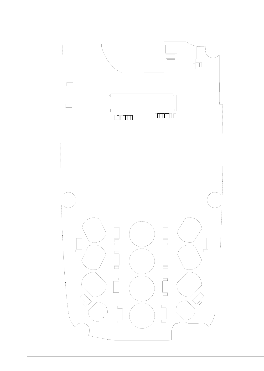
PCB Diagrams
8-2
This Document can not be used without Samsung's authorization
0
1
2
3
4
5
6
7
8
9
CN103
0
0
2
D
E
L
1
0
2
D
E
L
2
0
2
D
E
L
3
0
2
D
E
L
4
0
2
D
E
L
5
0
2
D
E
L6
0
2
D
E
L
7
0
2
D
E
L
LED208
9
0
2
D
E
L
LED210
1
1
2
D
E
L
MOT
SHARP
K
P
S
STAR
0
0
2
U
1
0
1
V
V200
V201
V202
V203
V204
V205
V206
V207 V208
9
0
2
V
ZD302
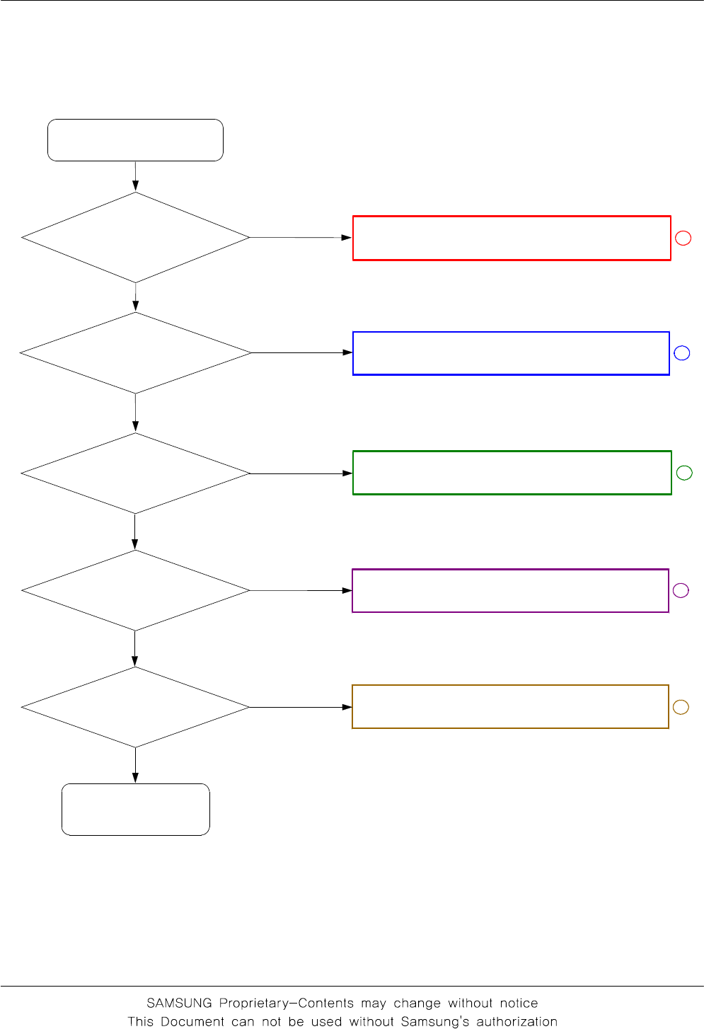
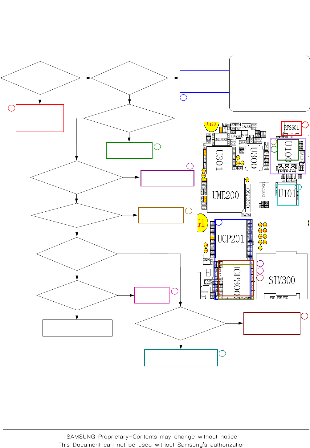
9. Flow Chart of Troubleshooting
9-1
9-1. Baseband
9-1-1. Power ON
check the current
consumption
>= 100mA Download again
'Power ON' does not work
No
Yes
Yes
END
Yes
Check the Initial Operation
Yes
Charge the battery
No
Check the Voltage
of the Battery
>= 3.3V
Download again
No
Check the pin C311,
C312, C314, C315
is
>=2.8V
Check
"Power On
with jig box"
No
check 'END KEY' of keypad
Yes 1
Checktheclocksignalat
pin #4 of OSC100
Freq=26Mhz,
Vrms >=300mV
No Check the clock generation
circuit OSC100
Yes
2
Flow Chart of Troubleshooting
9-2
C314
VLDO_5
A14
VLDO_6
C12
VLDO_7
H11
VRTC
K12
VSIM
F15
VIB_DRV
A12
VL4S_A
B11
VL4S_B
D10
VL5S_A
VL5S_B C9
G11
VLDO_1
J12
VLDO_2
A13
VLDO_3
B12
VLDO_4
B10
J11
SIM_IO K11
SIM_RST
N9
UP_CLK
P10
UP_IO
R10
UP_RST
F14
VACC
L8
SCLK_PSC
SDI_PSC M7
N7
SDO_PSC
K14
SIM_CLK
F13
RING_DRV
LED1_DRV
G12
LED2_DRV G13
CSN_PSC K8
BAT300
RB414_IV02N
1
2
VCCB_2.9V
C309 C313
VCCD_2.9V
C315C311
VRF_2.9V VCCD_1.8V
C316
VCCA_2.9V
C312
VRTC_3V
C310
R301
BAND_SEL1
BAND_SEL2
UP_SCLK
UP_CS
SIMCLK
SIMDATA
SIMRST
SIM_RST
SIM_IO
VSIM
SIM_CLK
UP_SDO
UP_SDI
KEY_BL1
KEY_BL2
MOT
Flow Chart of Troubleshooting
9-3
9-1-2. Initial
Initial Failure
check the pin
RSTB of UCP201
is LOW?
Check UCP201
No
Yes
Yes
END
Yes
Check the Initial Operation
Yes
Check
R101, C105
No
check the pin CKI
of UCP201 is
13Mhz?
Check the clock signal
at pin #3 of OSC100
Freq=26Mhz?
No check OSC100
1
Check the pin #9 of U101
is HIGH and pin #11,
#13 is 2.9V?
No Check U101
Yes
2
3
4
Flow Chart of Troubleshooting
9-4
IOBIT[2]/VEC[3]/EROMHI
IOBIT[1]/VEC[4]/PLLTOA
CKO/IACK/ERAMHI
F
E
R
V
X0
1
F
A
S
S
V0
1
E
L
L
P
D
_
S
S
V5
1
E
8
D
C
T
R
V
E
D
D
V2
U
E
D
D
V8
P
E
D
D
V5
1
U
6
1
U
E
D
D
V
E
D
D
V6
1
N
6
1
E
E
D
D
V
E
D
D
V7
1
E
6
1
G
L
L
P
D
_
D
D
V
D
D
V6
1
R
D
D
V7
1
R
D
D
V5
A
6
1
C
D
D
V
1
1
C
A
D
D
V
E
D
D
V1
B
4
1
B
E
D
D
V
1
M
E
D
D
V
TDO F12
TMS G12
TRST F15
2
E
D
D
V
D
D
V1
G
1
R
D
D
V
D
D
V4
R
3
1
T
D
D
V
K11
L12
B
T
S
R2
1
C
U5
RWN
TCK H13
H12
TDI
M6
DB#8 P7
N7
DB#9
INT#0 N4
R12
IO7
N8
DB#10
DB#11 M8
U11
DB#12
DB#13 T11
DB#14 R11
P10
DB#15
R14
AB#6
T14
AB#7
AB#8 T17
I
K
C7
1
F
G15
UCP201
AB#0 U13
M10
AB#1
AB#2 R13
AB#3 N11
P11
AB#4
AB#5 P12
VCCD_2.9V
C216C215
VCCD_2.9V VRTC_3V
R204
DSP_INT
VCORE
C218
C217
VCCD_1.8V
VCCD_1.8V
CHG_OFF
TR_RST
VREF
DSP_IO
DSP_RWN
DSP_INT
TR_RST
CLK13M_TR
DSP_AB(8:0)
DSP_AB(7)
DSP_AB(6)
DSP_AB(5)
DSP_AB(4)
DSP_AB(3)
DSP_AB(2)
DSP_AB(1)
DSP_AB(0)
DSP_AB(8)
DSP_DB(15:0)
DSP_DB(7)
DSP_DB(8)
DSP_DB(9)
DSP_DB(10)
DSP_DB(11)
DSP_DB(12)
DSP_DB(13)
DSP_DB(14)
DSP_DB(15)
OSC100
2
43
1
C120C118 C119
R106
VRF_2.9VVCCD_2.9V
XOUT
8
1
L
A
T
X
31
2
L
A
T
X
30
9
N
D
P
_
T
E
S
E
R
_
10 12
D
D
V
13
D
D
V
28
D
D
V
29
D
D
V
O
I
V
11
V
I
D
X
2632
N
E
X
25
E
D
O
M
X
22
RFIEN
21
RFIEP
18
RFIPN
17
RFIPP
16
H
O
F
R
L
O
F
R
15
1SCLK
3SDIO
33
D
N
G
C
N
3435
C
N
24
RFIAN
23
RFIAP
20
RFIDN
19
RFIDP
U101
C
F
A
27
BIN
6
7BIP
4BQN
5BQP
D
N
G
14
R103
C116
C104
C105
C108
R101
R100
C107
C102
C100
CLK13M_TR
CLK13M_MC
CLK13M_YMU
RTX_IN
RTX_IP
XOENA
GSM_LNA_IN_N
GSM_LNA_IN_P
DCS_LNA_IN_N
RF_EN
DPCS_PAM_IN
GSM_PAM_IN
AFC
SERDAT
RTX_QN
RTX_QP
SERCLK
SERLE
PCS_LNA_IN_P
PCS_LNA_IN_N
DCS_LNA_IN_P
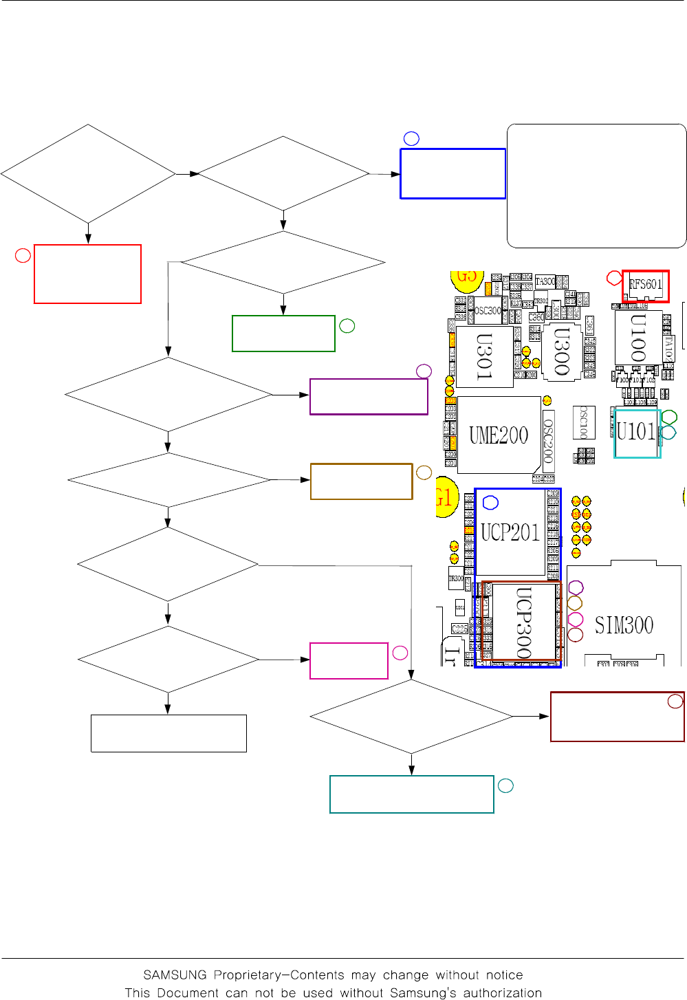
Flow Chart of Troubleshooting
9-5
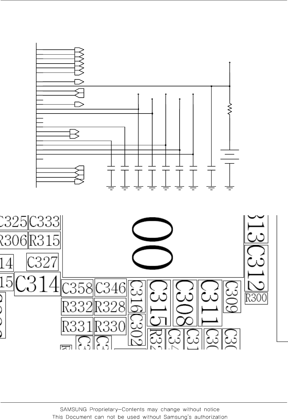
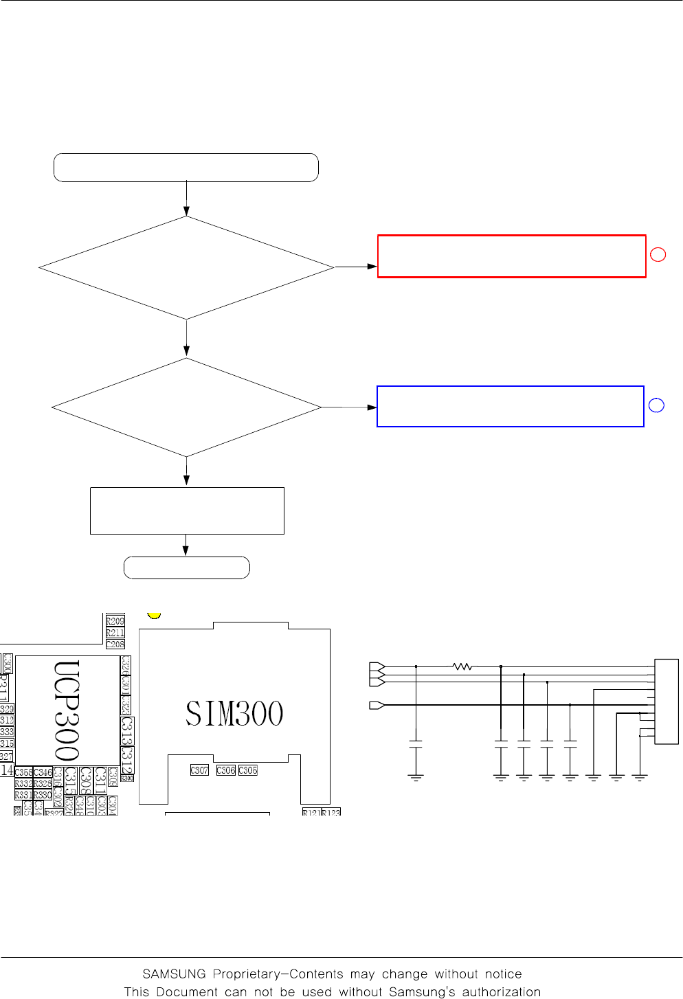
9-1-3. Sim Part
"Insert SIM" is displayed on the LCD
Is there any signal
pin #2,3,4 of
SIM300?
Check the UCP300
Check the UCP201 & UCP300
END
No
Yes
No
Yes
1
2
Check the SIM Card
The voltage is 2.8V
at the pin#1 of
C304 C307C306C303
R300
C305
NC
NC
10
VCC
1
2VCC
5VPP
SIM300
CLK
3
GND
4
I/O
6
NC
7
8NC
9
SIM_RST
VSIM
SIM_CLK
SIM_IO
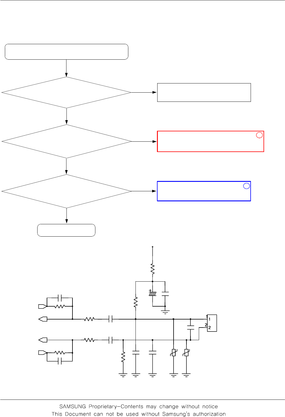
Flow Chart of Troubleshooting
9-6
9-1-4.Microphone Part * Call with Sim before testing.
Check the soldered
status of microphone
MicroPhone does not work
Resolder microphone
END
No
Yes
Yes
Check the reference
voltage on mic path
R326 ≒2.0V
Yes
Check
C346,R328,R332,C358,R330,R331,C349,
C355,C348,R327,R333
No
Is microphone OK?
Yes
Check UCP300
No
1
2
C349
R330
V306
R333
R331
C355
R326
C356
R332
R328
R327
C358
C357
C346
VCCA_2.9
V
C348
TA302
C353
V307
MIC301
MICOUTP
MICINN
MICOUTN
MICINP
Flow Chart of Troubleshooting
9-7
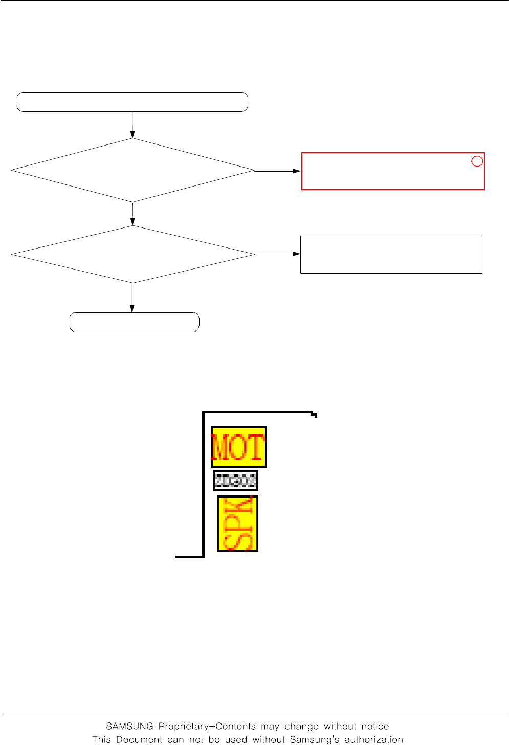
Flow Chart of Troubleshooting
9-8
9-1-5. Speaker Part
Check the connection
status at speaker pad
There is no sound from speaker
Are there any signal at
the speaker pad?
reconnect speaker
Replace the speaker module
END
No
Yes
YES
NO
1
Flow Chart of Troubleshooting
9-9
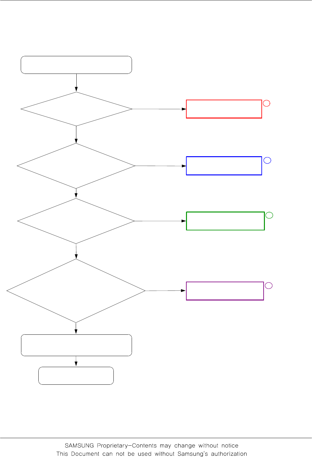
9-1-6. LCD backlight
Backlight ON "TIME"
mode in the menu?
Backlight does not work
Check conecting
between PBA and LCD
conector
Select backlight "15 sec" mode
Check FPCB
END
No
Yes
No
Check the U102 on the LCD PCB
Yes
Yes
Flow Chart of Troubleshooting
9-10
9-2. RF
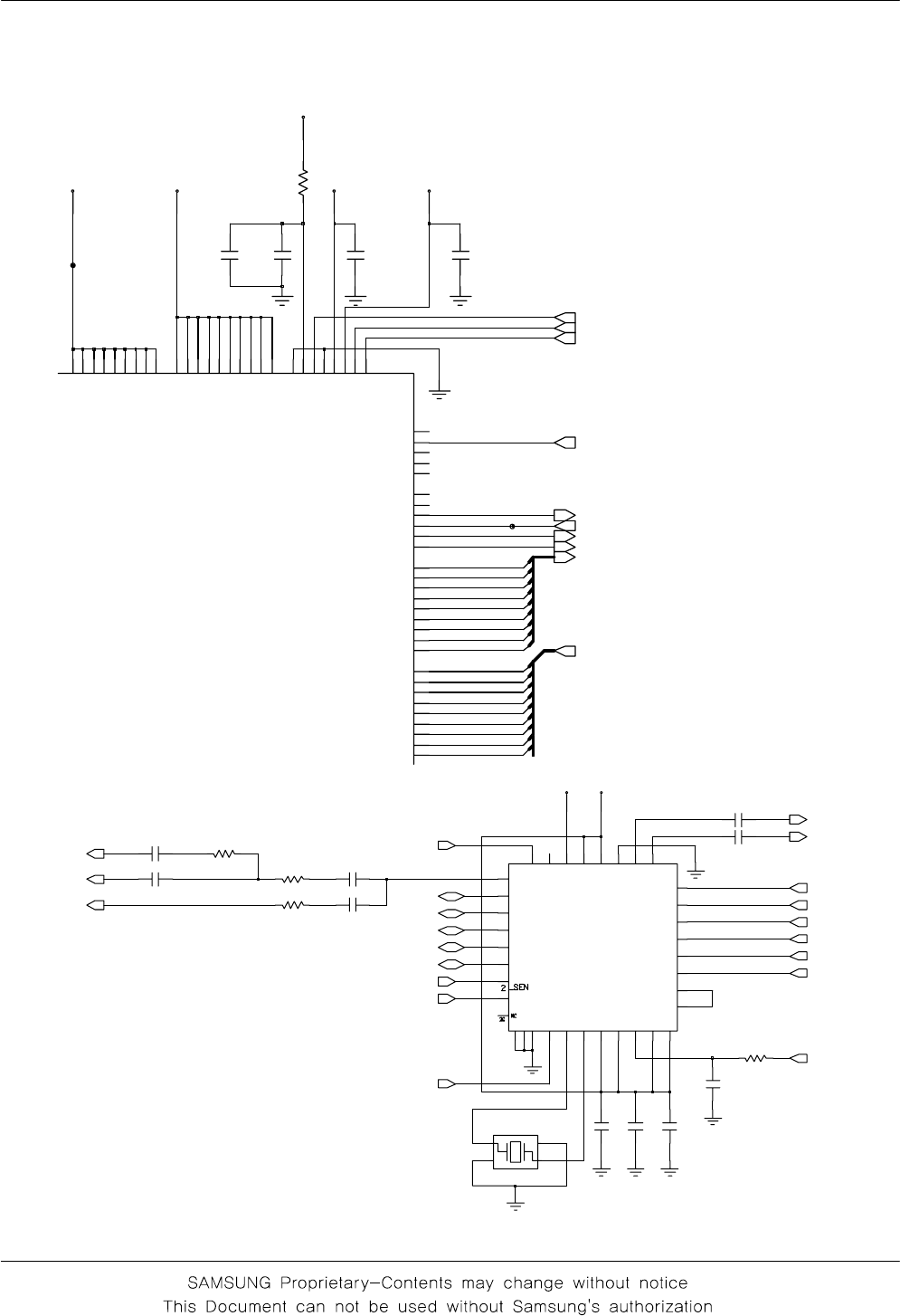
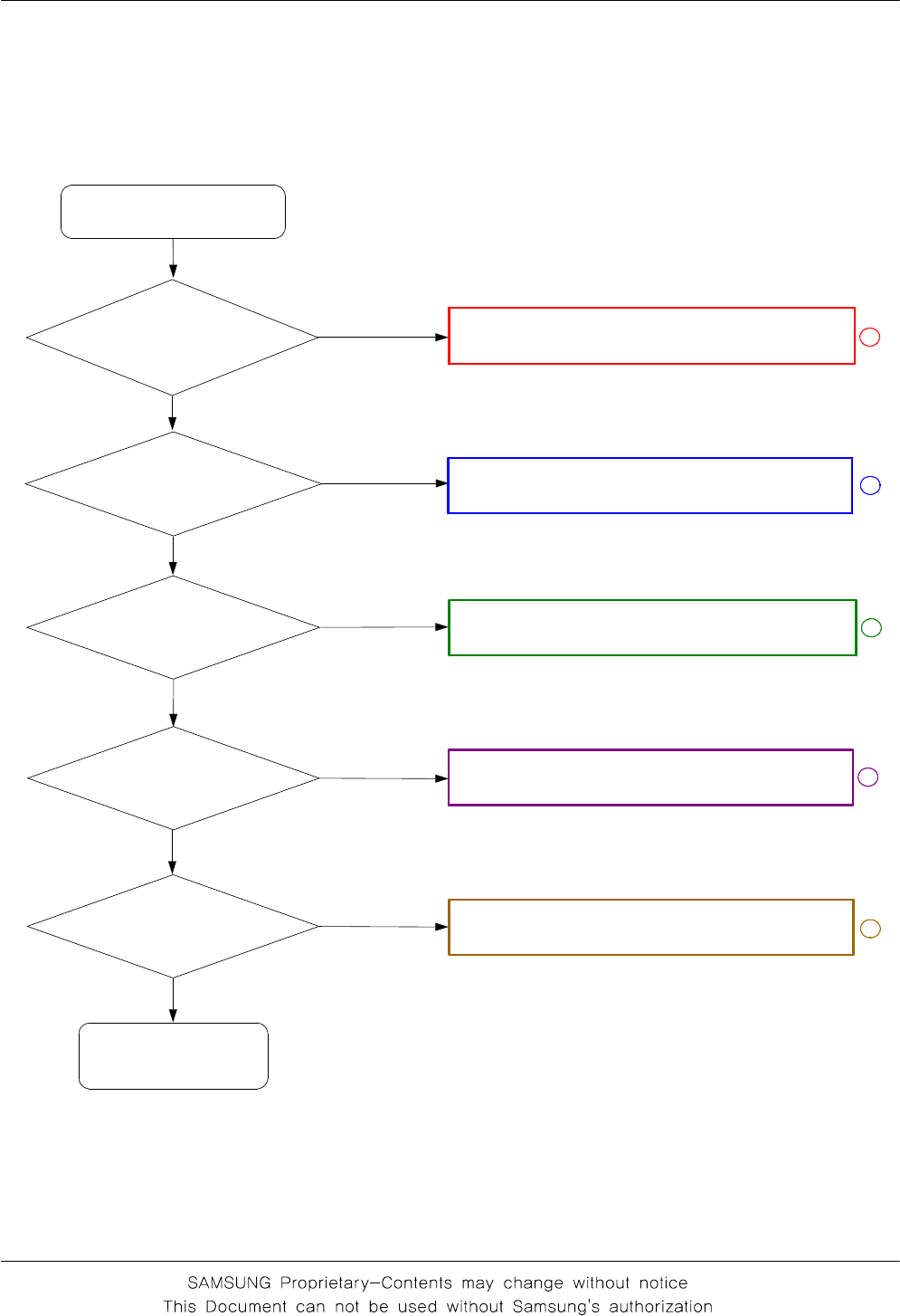
9-2-1. GSM Rx
Normal condition
catch the
channel ?
Check U100
pin 12 ≥-65
dbm ?
Check U101
pin 21,22 ≥-
65dBm ?
Yes
No
No
Check U100
pin 16 ≥-65
dbm ?
Yes
No
Yes
Check ANT, R102, R105, R135
Resolder or change
RFS601, C110,L106,L103,L104
Resolder or change
U100
Resolder or change
F100,C101,C106,L101
Resolder or change
UCP201
CONTINOUS RX ON
RF INPUT : 62CH
AMP : -50dbm
Check U101
pin 13 = 2.9V
Yes
Resolder or change
UCP300
Yes
No
No
1
2
3
4
5
Flow Chart of Troubleshooting
9-11
1
2
3
4
5
Flow Chart of Troubleshooting
9-12
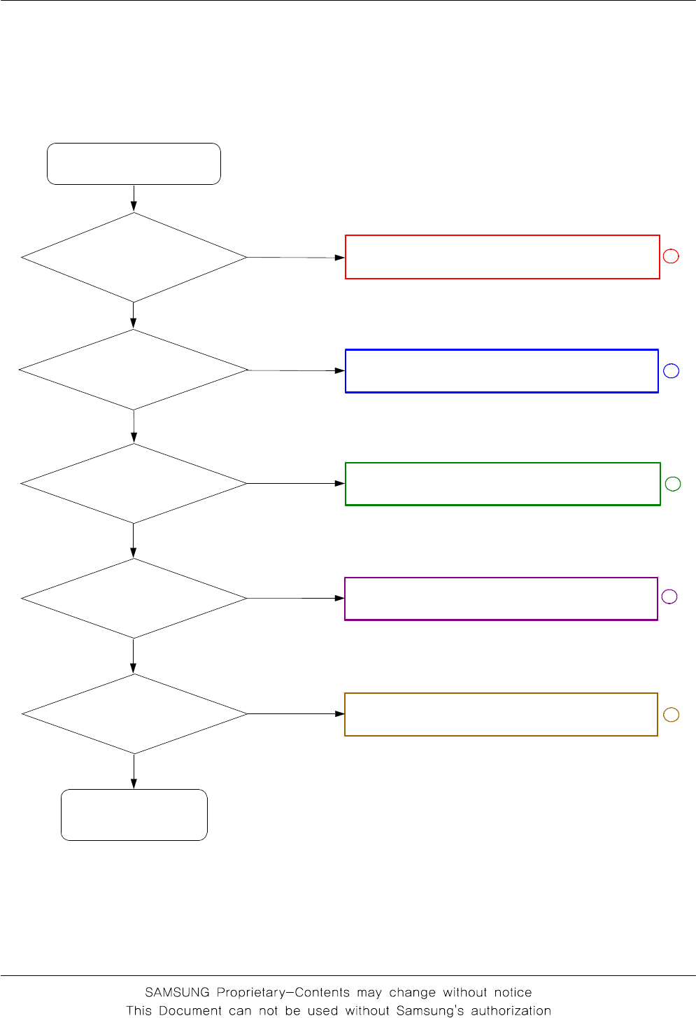
9-2-2. DCS Rx
Normal condition
catch the
channel ?
Check U100
pin 12 ≥-65
dbm ?
Check U101
pin 19,20 ≥-
65dBm ?
Yes
No
No
Check U100
pin 18 ≥-65
dbm ?
Yes
No
Yes
Check ANT, R102, R105, R135
Resolder or change
RFS601, C110,L106,L103,L104
Resolder or change
U100
Resolder or change
F101,C111,C113,L108
Resolder or change
UCP201
CONTINOUS RX ON
RF INPUT : 698CH
AMP : -50dbm
Check U101
pin 13 = 2.9V
Yes
Resolder or change
UCP300
Yes
No
No
1
2
3
4
5
Flow Chart of Troubleshooting
9-13
1
2
3
4
5
Flow Chart of Troubleshooting
9-14
9-2-3. PCS Rx
Normal condition
catch the
channel ?
Check U100
pin 12 ≥-65
dbm ?
Check U101
pin 17,18 ≥-
65dBm ?
Yes
No
No
Check U100
pin 20 ≥-65
dbm ?
Yes
No
Yes
Check ANT, R102, R105, R135
Resolder or change
RFS601, C110,L106,L103,L104
Resolder or change
U100
Resolder or change
F102,C114,C117,L109
Resolder or change
UCP201
CONTINOUS RX ON
RF INPUT : 660CH
AMP : -50dbm
Check U101
pin 13 = 2.9V
Yes
Resolder or change
UCP300
Yes
No
No
1
2
3
4
5
Flow Chart of Troubleshooting
9-15
1
2
3
4
5
Flow Chart of Troubleshooting
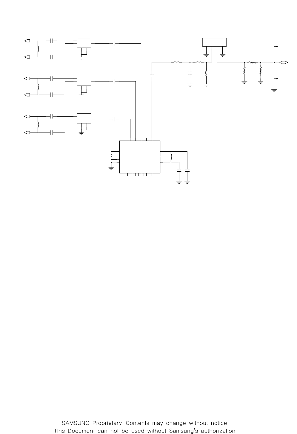
9-16
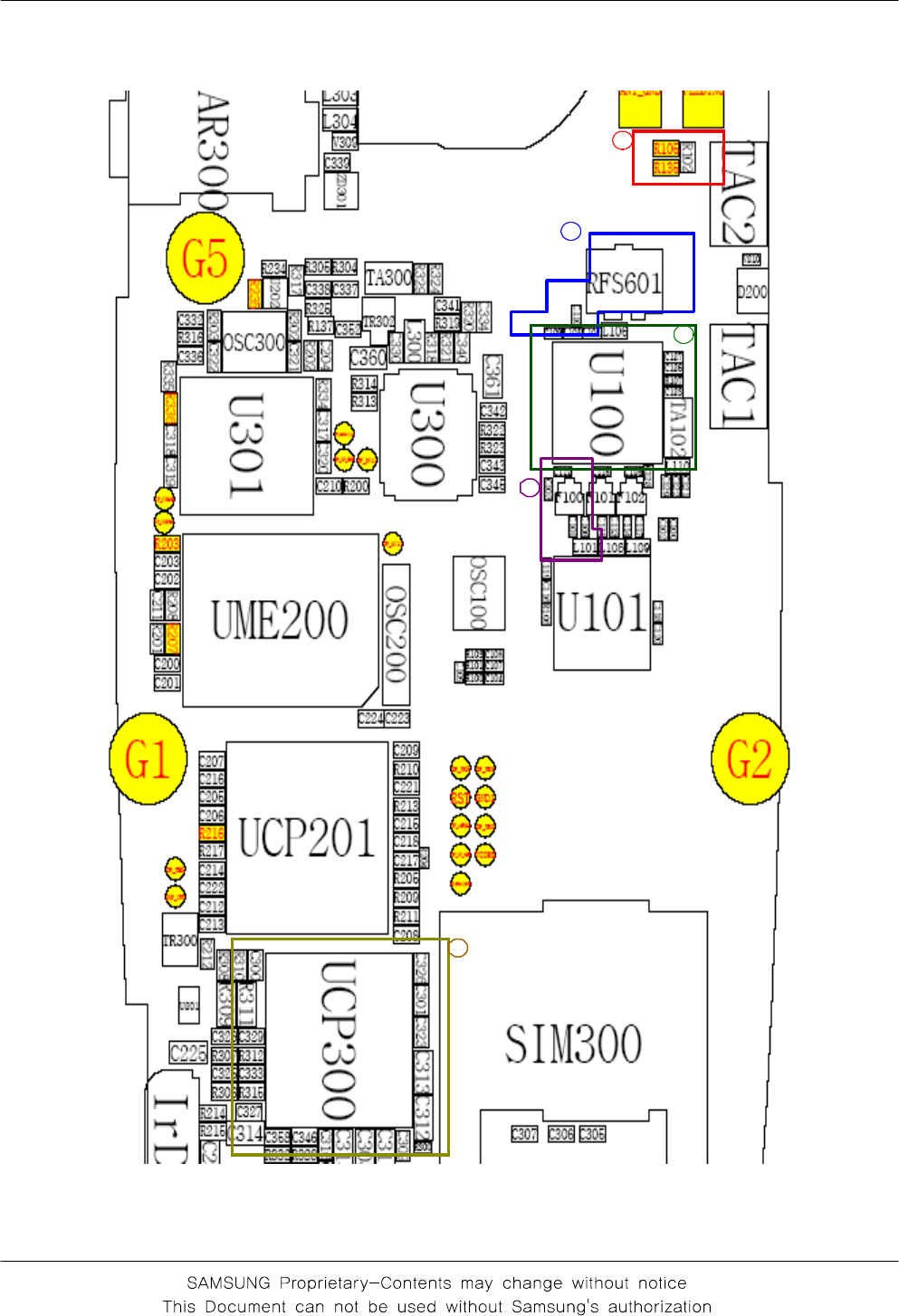
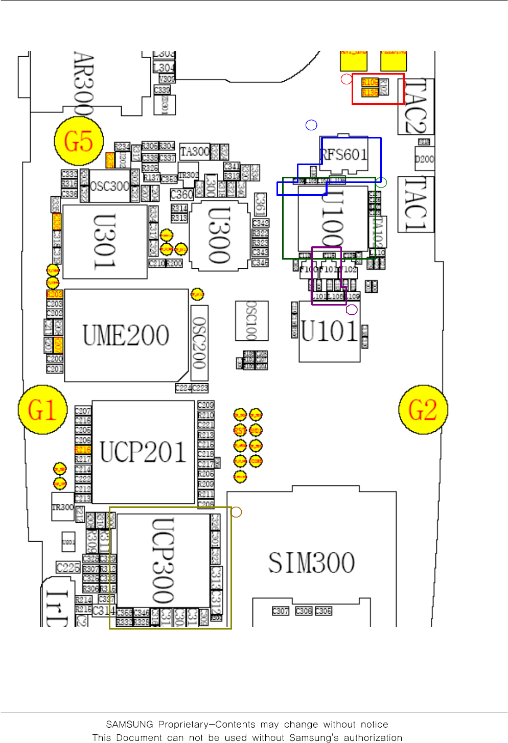
L106
L109
N
E
_
D
O
M
V
8P
M
A
R
V
6X
T
V
3
X
R
4
1
4
X
R
2
V1
7T
T
A
B
V
41
S
B
V
52
S
B
V
0
1
VCC1
3
VCC2
9
GND1
15 GND2
17 GND3
19 GND4
21 GND5
1
1N
I
X
T
0
0
9
|
0
5
8
M
S
G
0
2
1
X
R
8
1
2
X
R
6
1
U100
2
1
T
N
A
1N
I
S
C
P
|
S
C
D
13
ANT_GND
FEEDING
L104
R105
C117
C114
L101
C106
C110
R135
C121
L103
C122
G
2
G
5
1
IN
OUT
3
4OUT
F101
1
IN
OUT
3
OUT
4
23
C
1
GND
4
GND
F102
G
2
G
5
RFS601
A
R102
L108
C113
C111
L110
C101
C109
3
4OUT
F100
G
2
G
5
1
IN
OUT
C103
C115
C112
ANT
GSM_LNA_IN_P
GSM_LNA_IN_N
PCS_LNA_IN_P
PCS_LNA_IN_N
DCS_LNA_IN_P
DCS_LNA_IN_N
Flow Chart of Troubleshooting
9-17
9-2-4. GSM Tx
Check U101
pin 15 : about
2~3 dbm?
Check U101
pin 6 : 2.8V ?
Check and
change
RFS601,
R102,L103
Yes
Check and
change
UCP201,UCP300
No
CONTINUS TX ON CONDITION
TX POWER DAC : 554 CODE
APPLIED
CH : 62ch
RBW : 100KHz
VBW : 100KHz
SPAN : 10MHz
REF LEV : 10dBm
ATT : 20dB
U100 pin 11 :
about 4~5dbm?
Yes
No
Yes
U100 pin 7 :
3.7V ?
U101
check & change
No Battery, UCP300
check & change
Yes
U100 pin 8 :
1.2V ?
No UCP300 check
Yes
U100 pin 6 :
3V ?
No UCP300
check
U101 pin 12,13,
28,29 : 2.9V ?
U100
change or resolder
UCP300
change or resolder
No
Yes
U101
change or resolder
Yes
U100 pin 12
:
about -5dbm?
No
Yes
No
1
2
3
4
5
6
7
8
1
3
2
4
5
6
7
8
Flow Chart of Troubleshooting
9-18
9-2-5. DCS/PCS Tx
CONTINUS TX ON CONDITION
TX POWER DAC : 560 CODE
APPLIED
CH : 698CH(DCS),
660CH(PCS)
RBW : 100KHz
VBW : 100KHz
SPAN : 10MHz
REF LEV : 10dBm
ATT : 20dB
Check U101
pin 6 : 2.8V ?
U100 pin 1 :
about 4~5dbm?
No
Check U100
pin 16 : about
2~3 dbm?
No Check and
change
UCP201,UCP300
Yes
No
Yes
Check and
change
RFS601,
R102,L103
Yes
U100
check & change
No Battery, UCP300
check & change
Yes
No U100 check
Yes
No
Yes
No UCP300
check
Yes
U100
change or resolder
U100 pin 12,13,
28,29 : 2.9V ?
No UCP300
change or resolder
Yes
U101
change or resolder
U100 pin 7 :
3.7V ?
U100 pin 8 :
1.2V ?
U100 pin 12
:
about -5dbm?
U100 pin 6 :
3V ?
1
2
3
4
5
6
7
8
1
3
2
4
5
6
7
8

SAMSUNG Proprietary-Contents may change without notice
10. Reference data
10-1
This Document can not be used without Samsung's authorization
10-1. Reference Abbreviate
AAC: Advanced Audio Coding.
AVC : Advanced Video Coding.
BER :BitErrorRate
BPSK: Binary Phase Shift Keying
CA :ConditionalAccess
CDM : Code Division Multiplexing
C/I : Carrier to Interference
DMB : Digital Multimedia Broadcasting
EN : European Standard
ES : Elementary Stream
ETSI: European Telecommunications Standards Institute
MPEG: Moving Picture Experts Group
PN : Pseudo-random Noise
PS : Pilot Symbol
QPSK: Quadrature Phase Shift Keying
RS : Reed-Solomon
SI : Service Information
TDM : Time Division Multiplexing
TS : Transport Stream

This Service Manual is a property of Samsung Electronics Co.,Ltd.
Any unauthorized use of Manual can be punished under applicable
International and/or domestic law.
Samsung Electronics Co.,Ltd.
2006. 11. Rev.1.0
ⓒ