Samsung SGH X540 Service Manual. Www.s Manuals.com. Manual R1.0
User Manual: Samsung SGH-X540 - Service manuals and Schematics, Disassembly / Assembly. Free.
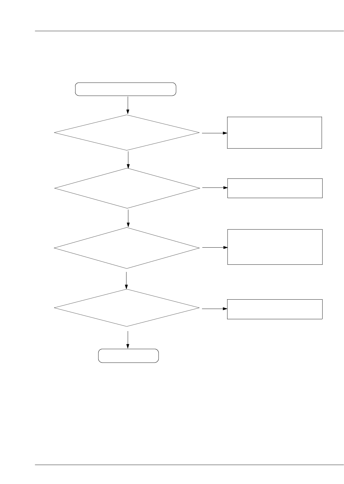
Open the PDF directly: View PDF ![]() .
.
Page Count: 69
GSM TELEPHONE
SGH-X540
GSM TELEPHONE CONTENTS
1. Safety Precautions
2. Specification
3. Product Function
4. Array course control
5. Exploded View/Disassembly
and Assembly Instructions
6. MAIN Electrical Parts List
7. Block Diagrams
8. PCB Diagrams
9. Flow Chart of Troubleshooting
10. Reference data

CONTENTS
1. Safety Precautions
1-1. Repair Precaution......................................................................................................1-1
1-2. ESD(Electrostatically Sensitive Devices) Precaution...............................................1-2
2. Specification
2-1. GSM General Specification.......................................................................................2-1
2-2. GSM TX power Level...............................................................................................2-2
3. Product Function
4. Array course control
4-1. Software Adjustments................................................................................................4-1
4-2. Software Downloading...............................................................................................4-2
5. Exploded View and Parts list
5-1. Cellular phone Exploded View..................................................................................5-1
5-2. Cellular phone Part list.............................................................................................5-2
5-3. Disassembly & Assembly Instructions......................................................................5-4
6. MAIN Electrical Parts List
7. Block Diagrams
7-1. RF Solution Block Diagram......................................................................................7-1
7-2. Base Band Solution Block Diagram.........................................................................7-2
8. PCB Diagrams

CONTENTS
9. Flow Chart of Troubleshooting
9-1. Power On..................................................................................................................9-1
9-2. Initial ..........................................................................................................................9-3
9-3. Charging Part ...........................................................................................................9-5
9-4. SIM Part....................................................................................................................9-7
9-5. Microphone Part.........................................................................................................9-9
9-6. Speaker Part(Melody).............................................................................................9-11
9-7. Key Data Input.......................................................................................................9-13
9-8. Receiver Part..........................................................................................................9-14
9-9. Back Light(for Color Main LCD)............................................................................9-15
9-10. Key Back Light.....................................................................................................9-17
9-11. Camera Part..........................................................................................................9-18
9-12. GSM Receiver.......................................................................................................9-20
9-13. GSM Transmitter...................................................................................................9-21
9-14. DCS Receiver.......................................................................................................9-22
9-15. DCS Transmitter...................................................................................................9-23
9-16. PCS Receiver ......................................................................................................9-24
9-17. PCS Transmitter...................................................................................................9-25
10. Reference data

SAMSUNG Proprietary-Contents may change without notice
1. Safety Precautions
1-1
This Document can not be used without Samsung's authorization
1-1. Repair Precaution
―Repair in Shield Box, during detailed tuning. Take specially care of tuning or test, because
specipicty of cellular phone is sensitive for surrounding interference(RF noise).
―Be careful to use a kind of magnetic object or tool, because performance of parts is damaged by
the influence of magnetic force.
―Surely use a standard screwdriver when you disassemble this product, otherwise screw will be
worn away.
―Use a thicken twisted wire when you measure level. A thicken twisted wire has low resistance,
therefore error of measurement is few.
―Repair after separate Test Pack and Set because for short danger (for example an overcurrent
and furious flames of parts etc) when you repair board in condition of connecting Test Pack and
tuning on.
―Take specially care of soldering, because Land of PCB is small and weak in heat.
―Surely tune on/off while using AC power plug, because a repair of battery charger is dangerous
when tuning ON/OFF PBA and Connector after disassembling charger.
―Don't use as you pleases after change other material than replacement registered on SEC System.
Otherwise engineer in charge isn't charged with problem that you don't keep this rules.

SAMSUNG Proprietary-Contents may change without notice
Safety Precautions
1-2
This Document can not be used without Samsung's authorization
1-2. ESD(Electrostatically Sensitive Devices) Precaution
Several semiconductor may be damaged easily by static electricity. Such parts are called by ESD
(Electrostatically Sensitive Devices), for example IC,BGA chip etc. Read Precaution below.
You can prevent from ESD damage by static electricity.
―Remove static electricity remained your body before you touch semiconductor or parts with
semiconductor. There are ways that you touch an earthed place or wear static electricity prevention
string on wrist.
―Use earthed soldering steel when you connect or disconnect ESD.
―Use soldering removing tool to break static electricity. , otherwise ESD will be damaged by static
electricity.
―Don't unpack until you set up ESD on product. Because most of ESD are packed by box and
aluminum plate to have conductive power,they are prevented from static electricity.
―You must maintain electric contact between ESD and place due to be set up until ESD is
connected completely to the proper place or a circuit board.
2. Specification
2-1
2-1. GSM General Specification
GSM900
Phase 1 EGSM 900
Phase 2 DCS1800
Phase 1 PCS1900
Freq.
Band[MHz]
Uplink/Downlink
890~915
935~960
880~915
925~960
1710~1785
1805~1880
1850~1910
1930~1990
ARFCN range 1~124 0~124 &
975~1023 512~885 512~810
Tx/Rx spacing 45MHz 45MHz 95MHz 80MHz
Mod. Bit rate/
Bit Period
270.833kbps
3.692us
270.833kbps
3.692us
270.833kbps
3.692us
270.833kbps
3.692us
Time Slot
Period/Frame
Period
576.9us
4.615ms
576.9us
4.615ms
576.9us
4.615ms
576.9us
4.615ms
Modulation 0.3GMSK 0.3GMSK 0.3GMSK 0.3GMSK
MS Power 33dBm~5dBm 33dBm~5dBm 30dBm~0dBm 30dBm~0dBm
Power Class 5pcl ~ 19pcl 5pcl ~ 19pcl 0pcl ~ 15pcl 0pcl ~ 15pcl
Sensitivity -102dBm -102dBm -100dBm -100dBm
TDMA Mux 8 8 8 8
Cell Radius 35Km 35Km 2Km -
Speclflcation
2-2
2-2. GSM Tx Power Class
TX Power
control level GSM900
533±2dBm
631±2dBm
729±2dBm
827±2dBm
925±2dBm
10 23±2 dBm
11 21±2 dBm
12 19±2 dBm
13 17±2 dBm
14 15±2 dBm
15 13±2 dBm
16 11±3 dBm
17 9±3dBm
18 7±3 dBm
19 5±3 dBm
TX Power
control level DCS1800
030±3dBm
128±3dBm
226±3dBm
324±3dBm
422±3dBm
520±3dBm
618±3dBm
716±3dBm
814±3dBm
912±4dBm
10 10±4 dBm
11 8±4dBm
12 6±4 dBm
13 4±4 dBm
14 2±5 dBm
15 0±5 dBm
TX Power
control level PCS1800
0 30±3 dBm
1 28±3 dBm
2 26±3 dBm
3 24±3 dBm
4 22±3 dBm
5 20±3 dBm
6 18±3 dBm
7 16±3 dBm
8 14±3 dBm
9 12±4 dBm
10 10±4 dBm
11 8±4dBm
12 6±4 dBm
13 4±4 dBm
14 2±5 dBm
15 0±5 dBm

SAMSUNG Proprietary-Contents may change without notice
3. Product Function
3-1
This Document can not be used without Samsung's authorization
Main Function
―SMS/EMS/MMS Message Service
―WAP HTTP support
―J2ME JAVA (MIDP 2.0/CLDC 1.1)
―Speaker phone
―16 Poly Melody
―vCard, vCalendar
―E-mail client
―FM Radio
―B/T Headset

SAMSUNG Proprietary-Contents may change without notice
Product Function
3-2
This Document can not be used without Samsung's authorization
SAMSUNG Proprietary-Contents may change without notice
4. Array course control
4-1
This Document can not be used without Samsung's authorization
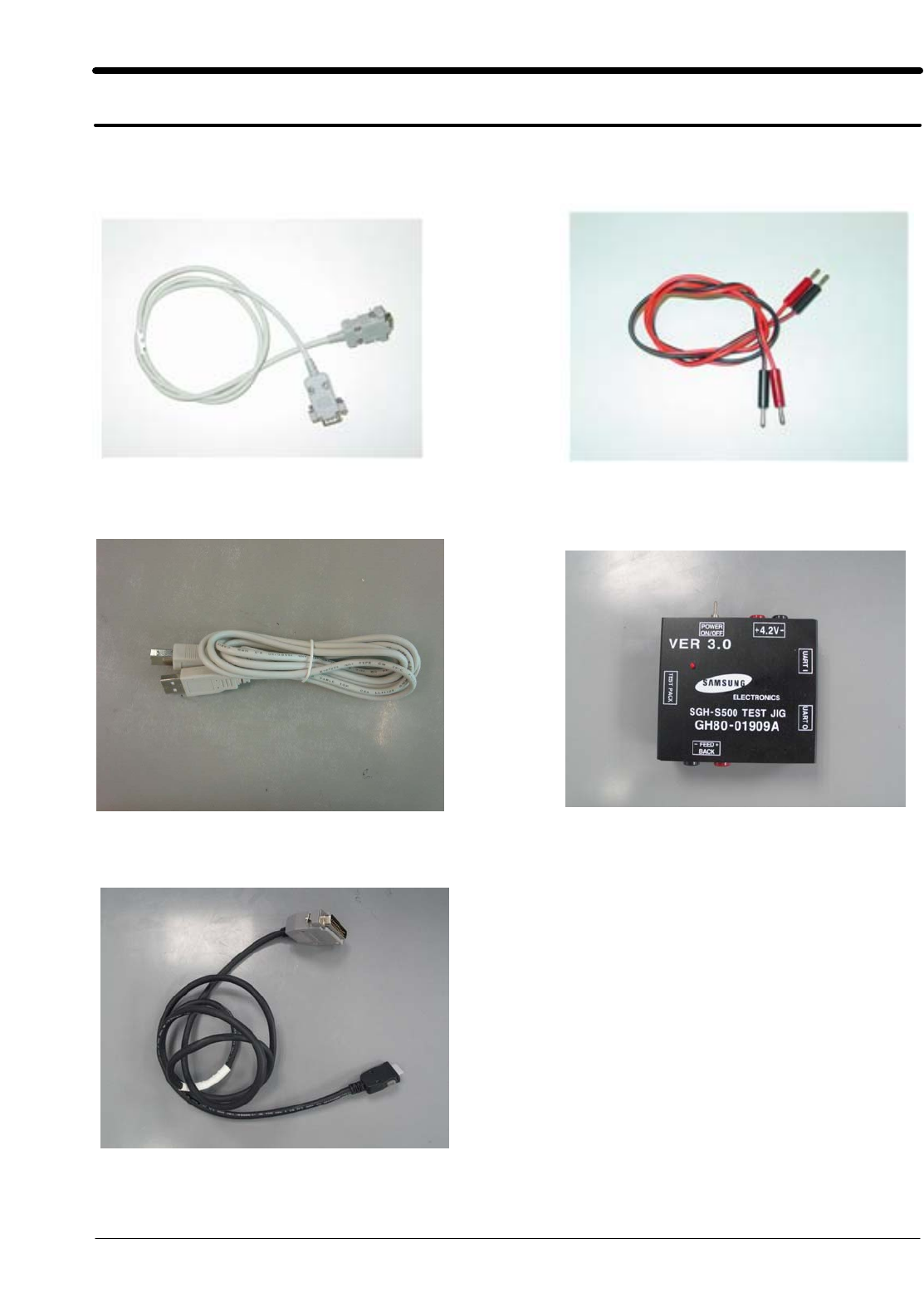
4-1. Software Adjustments
Serial Cable(CSA LL64151-A) Power Cable
USB DATA CABLE (CSA LL11105 AWM) JIG BOX (GH80-01909A)
JIG CABLE (GH39-00217A)
SAMSUNG Proprietary-Contents may change without notice
Array course control
4-2
This Document can not be used without Samsung's authorization
4-2. Software Downloading
4-2-1. Pre-requsite for Downloading
• Downloader Program(Klaus_Downloader_V2.0.exe)
• X540 Mobile Phone
• Data Cable
• Binary file, TFS file
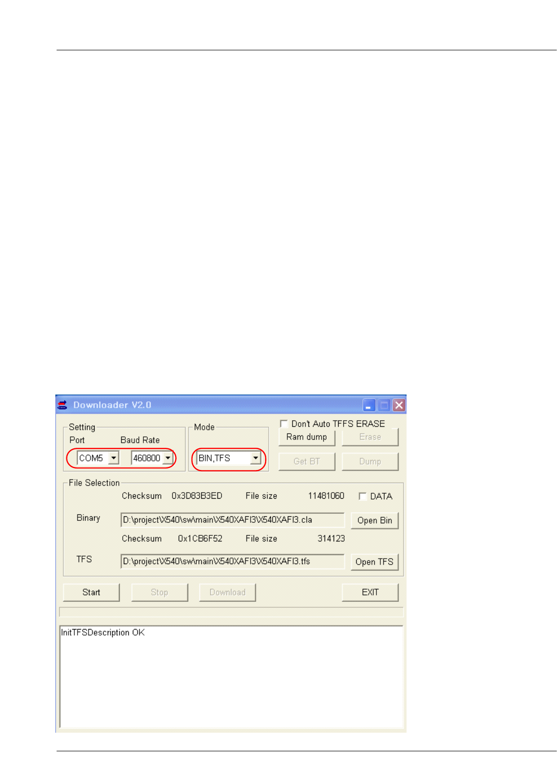
4-2-2. S/W Downloader Program
■Load the binary download program by executing the
“Klaus_Downloader_V2.0.exe”
1. Select the connected serial port and the rate of speed
2. Select the check box, the mode you want to download.
- if the binary file wanted, check only 'BIN'
- if the tfs file wanted, check only 'TFS'
- if all the files wanted, check 'BIN+TFS'
1
SAMSUNG Proprietary-Contents may change without notice
Array course control
4-3
This Document can not be used without Samsung's authorization
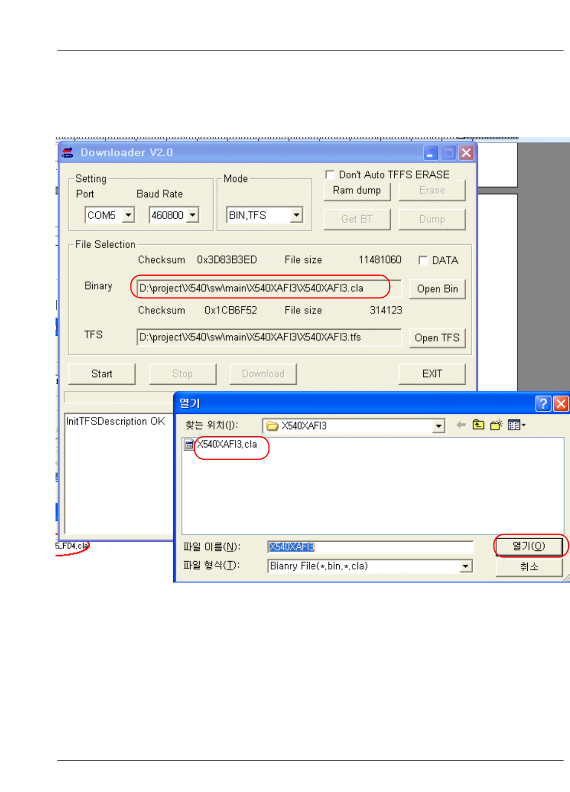
3. Select the file(s) what you want to download

SAMSUNG Proprietary-Contents may change without notice
Array course control
4-4
This Document can not be used without Samsung's authorization
SAMSUNG Proprietary-Contents may change without notice
5. Exploded View/Disassembly&Assembly Instructions
5-1
This Document can not be used without Samsung's authorization
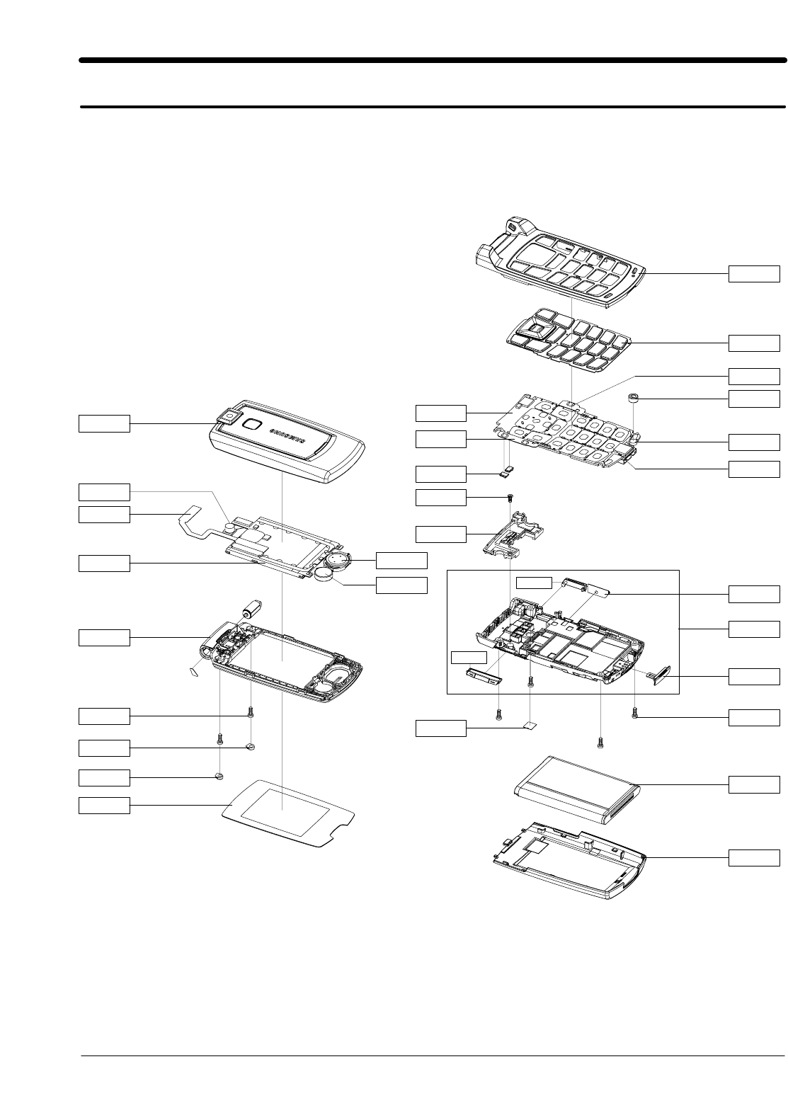
5-1. Cellular phone Exploded View
QFU01
QAN05
QCR12
QAN02
QRF01
QMP01
QVK01
QSP01
QFR01
QKP01
QMI03
QMI01
QME01
QRE01
QVO01
QRF03 QCK01
QIF01
QCR05
QBA01
QBA00
QCA02
QMO01
QME03
QLC01
QFL01
QSC07
QSC05
QMW01
QCR05
QCA01
SAMSUNG Proprietary-Contents may change without notice
Exploded View/Disassembly&Assembly Instructions
5-2
This Document can not be used without Samsung's authorization
Design LOC Description SEC CODE
QAN02 INTENNA-SGHX540 GH42-01034A
QAN05 ASSY RUBBER-INTENNA GH98-02857A
QBA00 PMO-COVER BATT V2 GH72-35034A
QBA01 INNER BATTERY PACK-750MAH,BLK, GH43-02483A
QCA01 UNIT-SGHX540 CAMERA MODULE GH59-03655A
QCA02 UNIT-CAMERA KEY GH59-03643A
QCK01 PMO-CAMERA KEY V3 GH72-35488A
QCR05 SCREW-MACHINE 6001-001478
QCR05 SCREW-MACHINE 6001-001478
QCR12 SCREW-MACHINE 6001-001530
QFL01 ASSY CASE-FOLDER LOWER GH98-02385A
QFR01 ASSY CASE-FRONT GH98-02384A
QFU01 ASSY CASE-FOLDER UPPER GH98-02386A
QIF01 PMO-COVER IF GH72-34482A
QKP01 ASSY KEYPAD-(SER/GRY) GH98-03159A
QLC01 ELA ETC-SGHX540 LCD MODULE GH96-02269A
QME01 UNIT-METAL DOME GH59-03659A
QME03 PCB-CON TO CON GH41-01475A
QMI01 MICROPHONE-ASSY-SGHX540 GH30-00319A
QMI03 RMO-MIC HOLDER GH73-05342A
QMO01 MOTOR DC-SGHX540 GH31-00119B
QMP01 PBA MAIN-SGHX540 GH92-03230A
QMW01 ASSY COVER-MAIN LCD GH98-02388A
QRF01 MPR-TAPE GH74-26974A
QSC05 RMO-RUBBER SCREW CAP L GH73-08137A
QSC07 RMO-RUBBER SCREW CAP R GH73-08138A
QSP01 SPEAKER 3001-002072
QVK01 UNIT-VOLUME KEY GH59-03660A
QRE01 ASSY CASE-REAR GH98-02387A
QVO01 PMO-VOL KEY V3 GH72-35489A
QRF03 PMO-COVER EAR V3 GH72-35490A
5-2. Cellular phone Parts list
SAMSUNG Proprietary-Contents may change without notice
Exploded View/Disassembly&Assembly Instructions
5-3
This Document can not be used without Samsung's authorization
Description SEC CODE
BAG PE 6902-000634
ADAPTOR-SGHD500 TA GH44-01451A
UNIT-EARPHONE(10P,SIL) GH59-03757B
LABEL(P)-WATER SOAK GH68-02026A
LABEL(P)-WATER SOAK GH68-02026A
MANUAL-SFC GH68-04336A
LABEL(P)-BARCODE RUSSIA GH68-08494A
MANUAL USERS-EU RUSSIAN GH68-12674A
LABEL(R)-MAIN(SER) GH68-12845A
BOX-UNIT(SER) GH69-04608A
CUSHION-CASE(EU) GH69-04932A
MPR-REMOVE TAPE LCD GH74-13804A
MPR-INSU TAPE GH74-15070A
MPR-BOHO VINYL LCD CONN GH74-15350A
MPR-TAPE LED GH74-17926A
MPR-INSU TAPE GH74-21312A
MPR-SPONGE LCD GH74-26952A
MPR-TAPE FPCB HOLE GH74-26973A
MPR-VINYL BOHO MAIN WINDOW GH74-26977A
MPR-INSU TAPE GH74-27176A
MPR-TAPE GH74-27509A
MPR-INSU TAPE GH74-27512A
MPR-INSU TAPE GH74-28085A
MPR-INSU TAPE GH74-28241A
MPR-TAPE GH74-28519A
MPR-INSU TAPE GH74-28609A
MPR-TAPE FPCB GH74-30174A
MPR-TAPE NAVI KEY GH74-30365A
MPR-TAPE ZTC BOARD GH74-30366A
MPR-TAPE LCD ELEC GH74-30367A
MPR-TAPE CAMERA CONN GH74-30368A
MPR-TAPE LOWER GH74-30369A
MPR-INSU TAPE YMU GH74-30370A
SAMSUNG Proprietary-Contents may change without notice
Exploded View/Disassembly&Assembly Instructions
5-4
This Document can not be used without Samsung's authorization
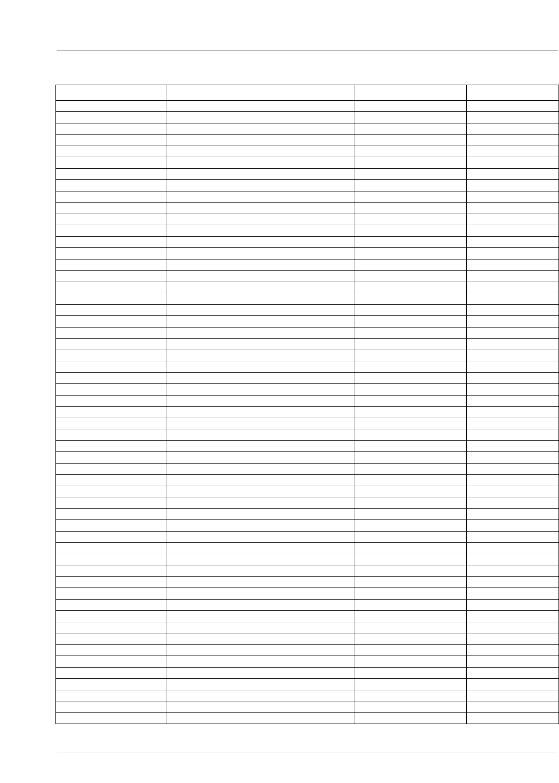
1) Handle with care. No scratch. 1) Handle with care. No scratch
2) Check no bending the board and front/rear cover.
1) Handle with care. No scratch
2) Check no bending the board and front/rear cover.
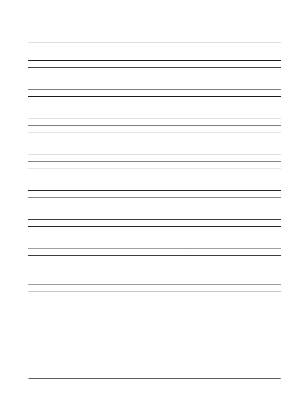
5-3. Disassembly and Assembly Instructions
―Disassembly
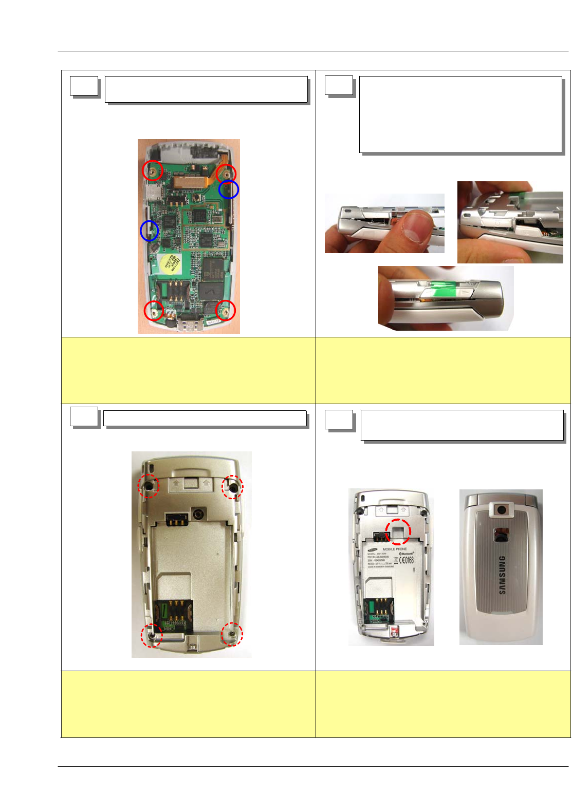
1) Release and remove the screws(4 point)
11) Press the Rear Camera Hook side with
the dismantle tool to release the locker
2
1) Press the opposite side with the
dismantle tool to release the locker.
2) Open the rear cover.
31) Realeae the camera key and the volume
key.
4
-Please use dismantle tool
to open
-REAR case is too soft to be
broken
SAMSUNG Proprietary-Contents may change without notice
Exploded View/Disassembly&Assembly Instructions
5-5
This Document can not be used without Samsung's authorization
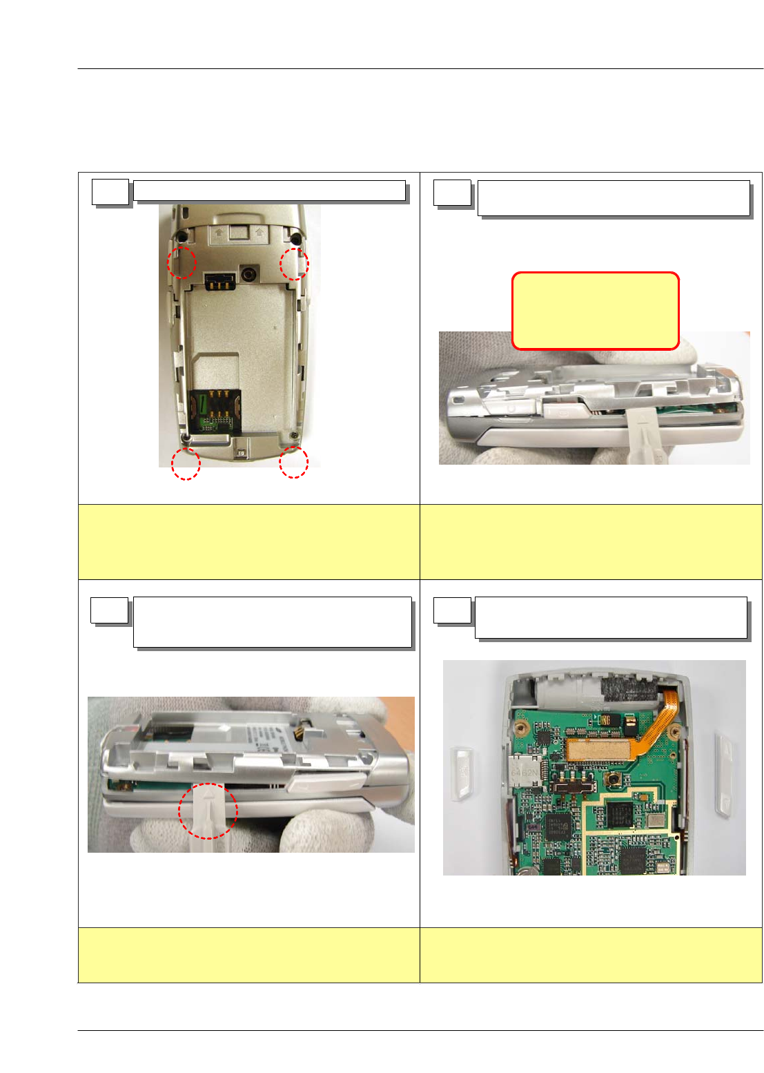
51) Release the LCD connector.
1) Check the FPCB crack and connector damage. 1) Check the PBA's damage.
71) Release the keypad in the FRONT.
8
1)Remove the tape for preventing light
emission.
1) After separate the CAMERA F-PCB and
VOLUME F-PCB, release the PBA.
6
SAMSUNG Proprietary-Contents may change without notice
Exploded View/Disassembly&Assembly Instructions
5-6
This Document can not be used without Samsung's authorization
10 1) Release the F-PCB from the front side.
1) Care with torn of F-PCB. 1) Care with F-PCB crack and CONNECTOR damage.
2) Care with torn of F-PCB..
1) Handle with care. No scratch
2) Check no bending the board and front/rear cover.
1) Handle with care. No scratch
2) Check no bending the board and front/rear cover.
1)Press the hinge side with the dismantle
tool to release the locker.
9
1) Press the side with the dismantle
tool to release the locker.
11 1) Press the opposite side with the
dismantle tool to release the locker.
2) Separate holding REAR.
12
SAMSUNG Proprietary-Contents may change without notice
Exploded View/Disassembly&Assembly Instructions
5-7
This Document can not be used without Samsung's authorization
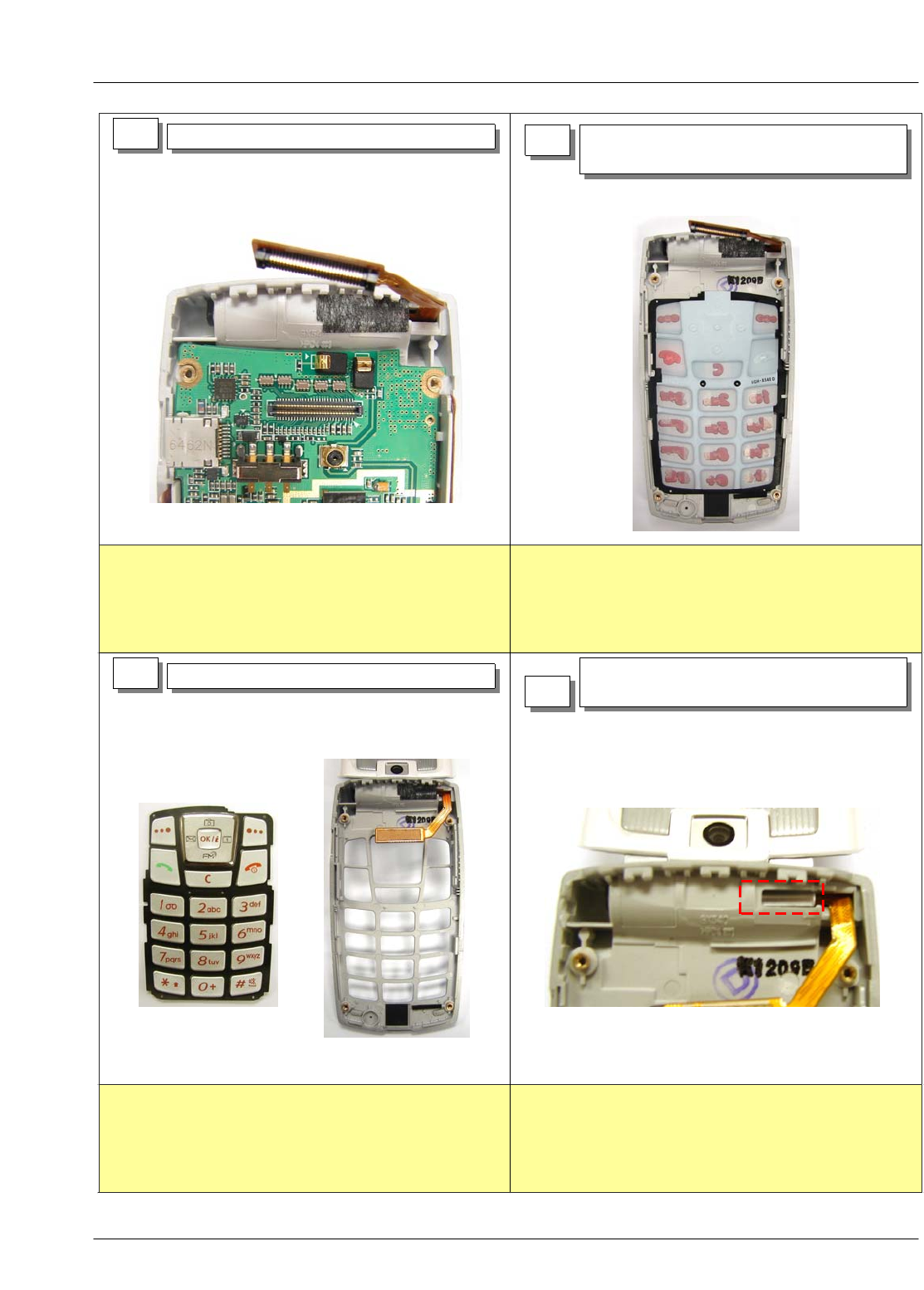
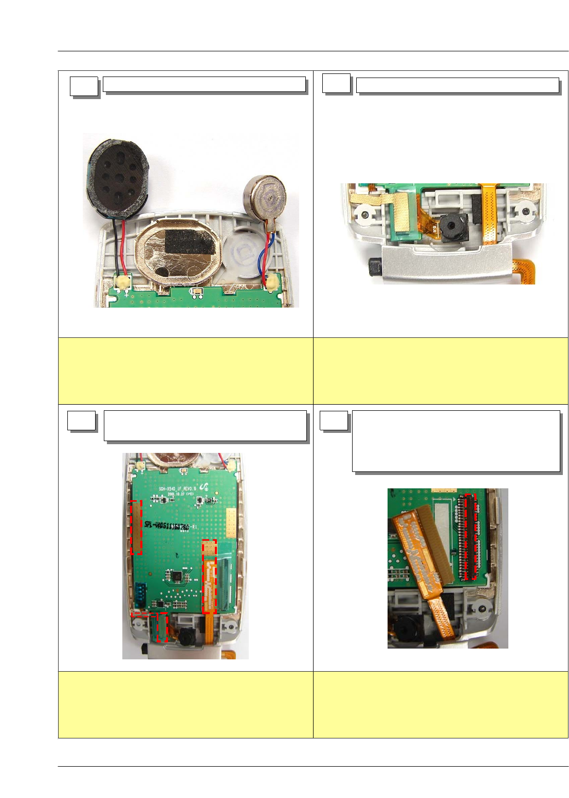
14 1) Remove CAMERA MODULE from FOLDER.
1) Care with disconnecting of WIRE and soldering. 1) Care with torn of F-PCB.
1) Check correctly attaching Shielding tape. 1) Slowly separate for no damage to LCD.
1) Remove SPEAKER and MOTOR from FOLDER.
13
1) Remove all shield tape on the LCD
MODULE.
15 1) Remove the insulate tape on the LCD
CONNECTOR.
2) Hold up LOCKER of LCD CONNECTOR,
separate LCD CONNECTOR.
16
SAMSUNG Proprietary-Contents may change without notice
Exploded View/Disassembly&Assembly Instructions
5-8
This Document can not be used without Samsung's authorization
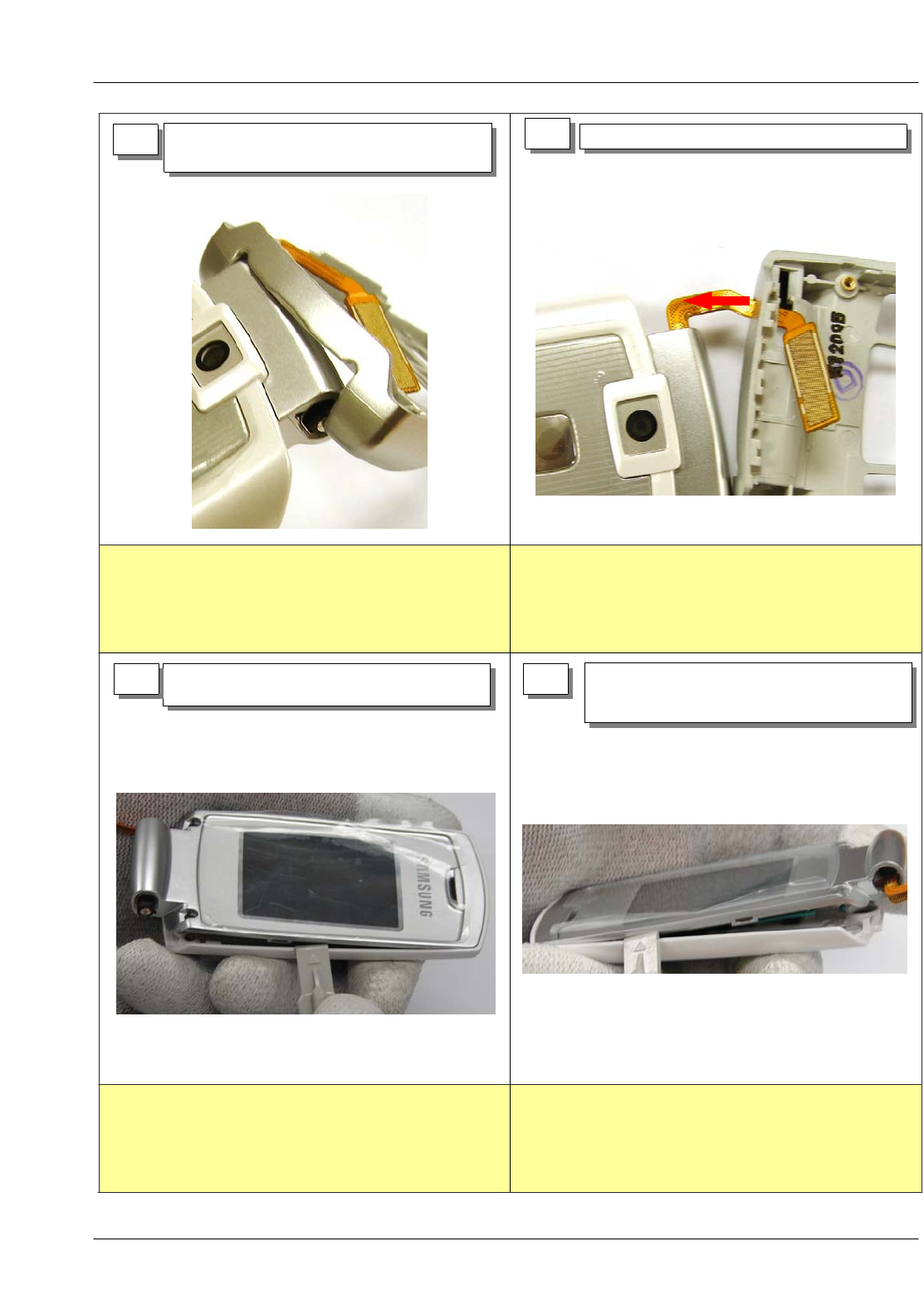
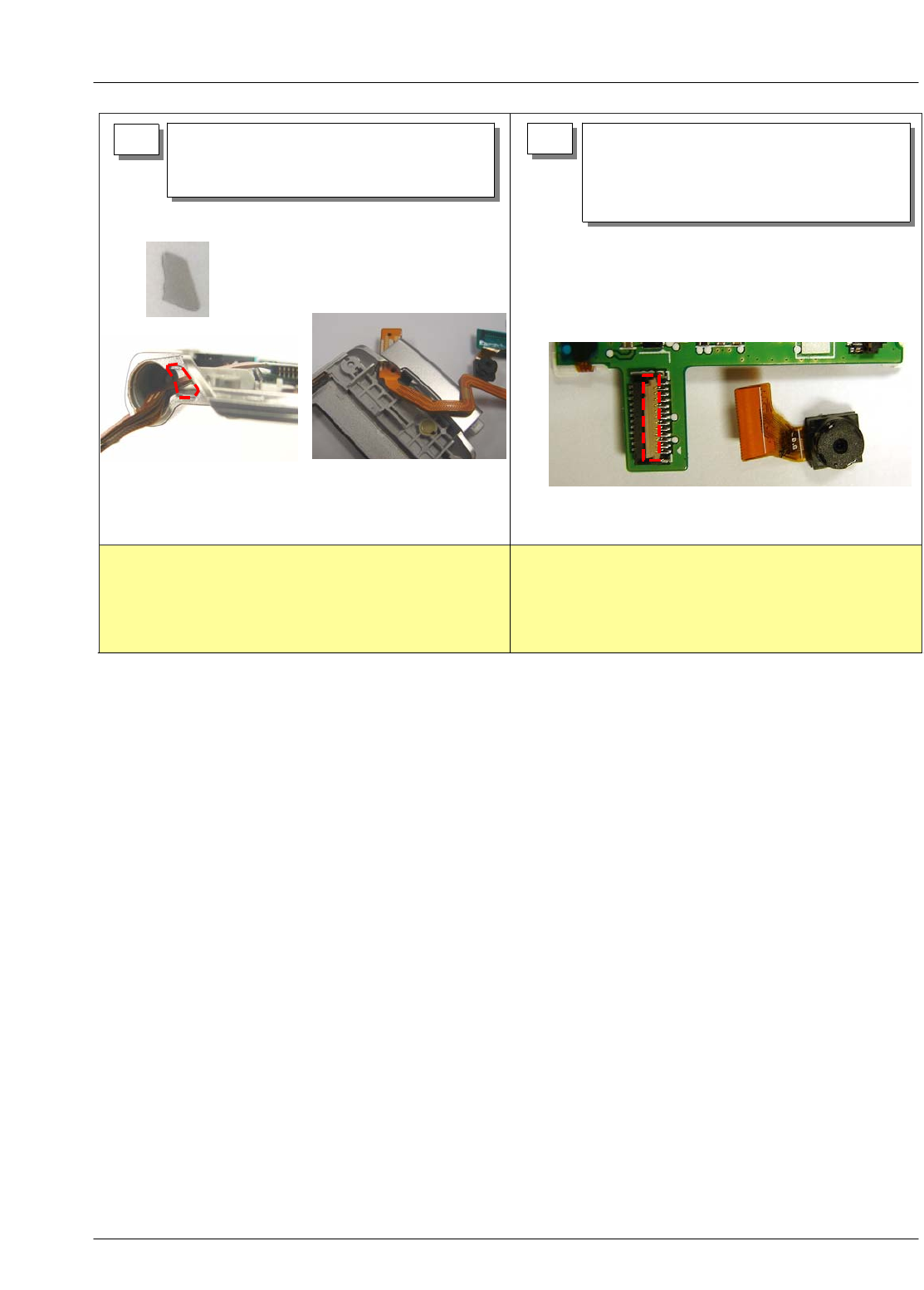
1) Care with torn of F-PCB. 1) Care with torn of F-PCB.
2) Slowly separate for no damage to CAMERA.
1) Release the F-PCB HOLE SHEET.
2) Release LCD MODULE from FOLDER side.
3) Remove LCD CONNECTOR through HINGE.
17 1) Remove all SHIELD TAPE on the PBA.
2) Remove insulation tape of CAMERA F-PCB
CONNECTOR side.
3) Hold LOCKER and separate CAMERA MODULE
18
SAMSUNG Proprietary-Contents may change without notice
Exploded View/Disassembly&Assembly Instructions
5-9
This Document can not be used without Samsung's authorization
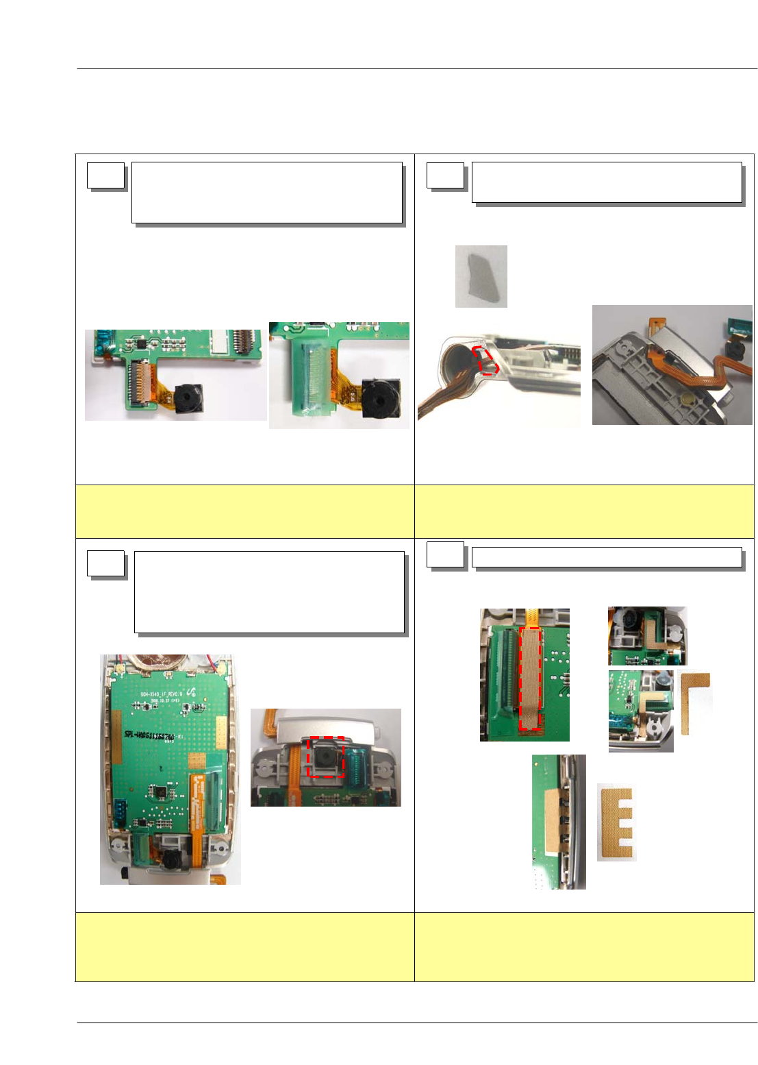
1) Check correctly attaching insulating tape..1) Care with torn of F-PCB.
41) Attach SHIELD TAPE making meet standard
1) Check correctly inserting Camera Module..
2) Care with torn of F-PCB. 1) Check correctly attaching tape.
―Assembly
1) Insert CAMERA F-PCB into connector
putting SILK line.
2) Attach insulating tape on CONNECTOR.
11) Through LCD CONNECTOR into Hinge.
2) Hold F-PCB HOLE SHEET.
2
31) Attach the LCD module to the Folder.
2) Combine LCD CONNECTOR, attach
insulating tape for preventing unfasten.
3) Insert Camera.
SAMSUNG Proprietary-Contents may change without notice
Exploded View/Disassembly&Assembly Instructions
5-10
This Document can not be used without Samsung's authorization
1) Care with disconnecting of WIRE and soldering.
2) Check correctly attaching them. 1) Check there is no gap between Upper and Lower case
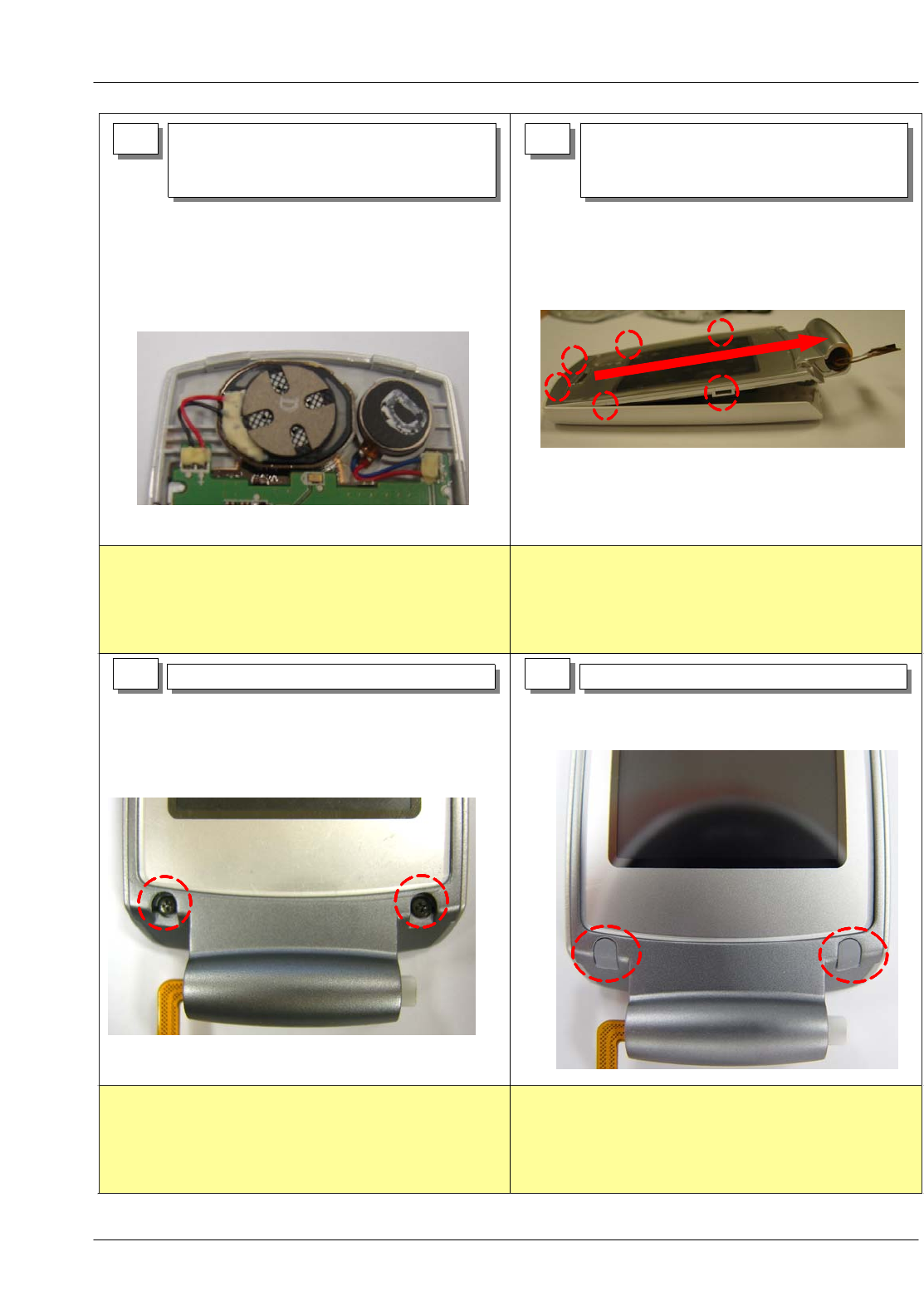
71) Tighten the SCREWS (2 POINT) 81) Put the SCREW CAPS
1) Check correctly attaching Screw cap.
1) Insert the SPEAKER and MOTOR.
2) Keep in order WIRE not to do interfere
structure and PBA.
51) Put UPPER to LOWER(Left of picture)
2) Press and hold both sides to arrow
direction and hang on LOCKER.
6

SAMSUNG Proprietary-Contents may change without notice
Exploded View/Disassembly&Assembly Instructions
5-11
This Document can not be used without Samsung's authorization
10 1) Hold FOLDER and FRONT's HINGE.
1) Care with torn of F-PCB.
1) After holding Hinge, open and close Folder for
'click' sound.(One time)
2) Check allophone when folder open and close.
3) Care with torn of F-PCB.
12 1) Attach a KEY PAD to the Front cover
1) Check correctly attaching.
2) Check the torn. 1) Check key pad correct.
1) Go through LCD CONNECOR into FRONT HOLE
9
1) Attach preventing light emission tape
through FRONT into LCD Connector
11
SAMSUNG Proprietary-Contents may change without notice
Exploded View/Disassembly&Assembly Instructions
5-12
This Document can not be used without Samsung's authorization
1) Check the correct.
1) Check there is no gap between Front and rear case
2) Check the direction of PBA.
3) After insert KEY, check tension.
15 1) Tighten the REAR SCREWS (4 POINT)
1) Place MAIN PBA as below picture with
caring the Bosses and the Holders.
13 1) Insert REAR to FONT ASS'Y.
2) Insert CAMERA KEY, VOLUME KEY at
correct place.
3) Put the Rear cover with pressing.
14
1) Attach RF SHEET.
2) Check the structure.
16

SAMSUNG Proprietary-Contents may change without notice
6. MAIN Electrical Parts List
6-1
This Document can not be used without Samsung's authorization
Design LOC Description SEC Code STATUS
ANT200 NPR-ANTENNA CONTACT GH71-05666A SA
ANT201 NPR-ANTENNA CONTACT GH71-05666A SA
ANT600 ANTENNA-CHIP 4202-001239 SA
BAT500 BATTERY-LI(2ND) 4302-001130 SA
BAT700 HEADER-BATTERY 3711-006250 SA
C100 C-CER,CHIP 2203-000812 SA
C101 C-CER,CHIP 2203-000278 SA
C102 C-CER,CHIP 2203-000854 SA
C103 C-CER,CHIP 2203-000812 SA
C104 C-CER,CHIP 2203-001607 SA
C105 C-CER,CHIP 2203-001397 SA
C106 C-CER,CHIP 2203-000854 SA
C108 C-CER,CHIP 2203-000278 SA
C110 C-CER,CHIP 2203-006048 SA
C112 C-CER,CHIP 2203-000278 SA
C114 INDUCTOR-SMD 2703-002208 SA
C115 C-CER,CHIP 2203-000233 SA
C116 INDUCTOR-SMD 2703-002208 SA
C117 C-CER,CHIP 2203-000233 SA
C118 C-CER,CHIP 2203-006562 SA
C120 C-CER,CHIP 2203-005446 SA
C121 C-CER,CHIP 2203-001153 SA
C122 C-CER,CHIP 2203-000854 SA
C125 C-CER,CHIP 2203-001153 SA
C126 C-CER,CHIP 2203-000233 SA
C127 C-CER,CHIP 2203-005281 SA
C128 C-CER,CHIP 2203-000278 SA
C129 C-CER,CHIP 2203-000854 SA
C130 C-CER,CHIP 2203-005234 SA
C131 C-CER,CHIP 2203-000679 SA
C132 C-CER,CHIP 2203-000254 SA
C133 C-CER,CHIP 2203-000278 SA
C137 C-CER,CHIP 2203-000679 SA
C138 C-CER,CHIP 2203-005234 SA
C139 C-CER,CHIP 2203-000278 SA
C140 C-CER,CHIP 2203-005395 SA
C142 C-CER,CHIP 2203-000995 SA
C143 C-CER,CHIP 2203-000995 SA
C201 C-CER,CHIP 2203-000812 SA
C202 C-CER,CHIP 2203-006048 SA
C204 C-CER,CHIP 2203-006048 SA
C207 C-CER,CHIP 2203-000278 SA
C208 C-CER,CHIP 2203-000278 SA
C210 C-CER,CHIP 2203-005659 SA
C211 C-CER,CHIP 2203-000585 SA
C212 C-CER,CHIP 2203-006048 SA
C213 C-CER,CHIP 2203-006048 SA
C214 C-CER,CHIP 2203-000696 SA
C215 C-CER,CHIP 2203-005446 SA
C216 C-CER,CHIP 2203-000870 SA
C300 C-CER,CHIP 2203-002709 SA
C301 C-CER,CHIP 2203-002709 SA
C302 C-CER,CHIP 2203-002709 SA
C303 C-CER,CHIP 2203-002709 SA
C304 C-CER,CHIP 2203-000254 SA

SAMSUNG Proprietary-Contents may change without notice
Main Electrical Parts List
6-2
This Document can not be used without Samsung's authorization
Design LOC Description SEC Code STATUS
C305 C-CER,CHIP 2203-002709 SA
C306 C-CER,CHIP 2203-002709 SA
C307 C-CER,CHIP 2203-000254 SA
C308 C-CER,CHIP 2203-000254 SA
C309 C-CER,CHIP 2203-005482 SA
C310 C-CER,CHIP 2203-005482 SA
C311 C-CER,CHIP 2203-000854 SA
C312 C-CER,CHIP 2203-000679 SA
C314 C-CER,CHIP 2203-005482 SA
C315 C-CER,CHIP 2203-006562 SA
C316 C-CER,CHIP 2203-006562 SA
C317 C-CER,CHIP 2203-005482 SA
C400 C-CER,CHIP 2203-002709 SA
C401 C-CER,CHIP 2203-002709 SA
C402 C-CER,CHIP 2203-000643 SA
C403 C-CER,CHIP 2203-005482 SA
C404 C-CER,CHIP 2203-002709 SA
C406 C-CER,CHIP 2203-006562 SA
C407 C-CER,CHIP 2203-006562 SA
C408 C-CER,CHIP 2203-006562 SA
C410 C-CER,CHIP 2203-002709 SA
C500 C-CER,CHIP 2203-006562 SA
C501 C-CER,CHIP 2203-006257 SA
C502 C-CER,CHIP 2203-000627 SNA
C503 C-CER,CHIP 2203-000854 SA
C506 C-CER,CHIP 2203-000233 SA
C507 C-TA,CHIP 2404-001381 SA
C508 C-CER,CHIP 2203-000812 SA
C509 C-CER,CHIP 2203-006208 SA
C510 C-CER,CHIP 2203-006562 SA
C511 C-CER,CHIP 2203-006208 SA
C512 C-CER,CHIP 2203-006257 SA
C513 C-CER,CHIP 2203-006257 SA
C515 C-CER,CHIP 2203-006825 SA
C516 C-CER,CHIP 2203-005482 SA
C519 C-CER,CHIP 2203-006208 SA
C520 C-CER,CHIP 2203-006208 SA
C521 C-CER,CHIP 2203-006257 SA
C522 C-CER,CHIP 2203-006257 SA
C523 C-CER,CHIP 2203-000627 SNA
C524 C-CER,CHIP 2203-005482 SA
C525 C-CER,CHIP 2203-006257 SA
C600 C-CER,CHIP 2203-005482 SA
C602 C-CER,CHIP 2203-006562 SA
C603 C-CER,CHIP 2203-005057 SA
C604 C-CER,CHIP 2203-005057 SA
C605 C-CER,CHIP 2203-002709 SA
C607 C-CER,CHIP 2203-000628 SA
C608 C-CER,CHIP 2203-002709 SA
C609 C-CER,CHIP 2203-005057 SA
C610 C-CER,CHIP 2203-006562 SA
C611 C-CER,CHIP 2203-002709 SA
C612 C-CER,CHIP 2203-002443 SA
C613 C-CER,CHIP 2203-006348 SA
C614 C-CER,CHIP 2203-006681 SA

SAMSUNG Proprietary-Contents may change without notice
Main Electrical Parts List
6-3
This Document can not be used without Samsung's authorization
Design LOC Description SEC Code STATUS
C700 C-CER,CHIP 2203-002709 SA
C701 C-CER,CHIP 2203-001153 SA
C702 C-CER,CHIP 2203-002709 SA
C703 C-CER,CHIP 2203-002709 SA
C704 C-CER,CHIP 2203-000330 SA
C705 C-CER,CHIP 2203-002709 SA
C707 C-CER,CHIP 2203-001153 SA
C708 C-CER,CHIP 2203-002709 SA
C709 C-CER,CHIP 2203-000330 SA
C710 C-CER,CHIP 2203-006562 SA
C711 C-CER,CHIP 2203-006562 SA
C712 C-CER,CHIP 2203-005482 SA
C713 C-CER,CHIP 2203-000278 SA
C714 C-CER,CHIP 2203-000278 SA
C715 C-CER,CHIP 2203-000386 SA
C716 C-CER,CHIP 2203-000425 SA
C717 C-CER,CHIP 2203-000386 SA
C718 C-CER,CHIP 2203-001153 SA
C720 C-CER,CHIP 2203-001153 SA
C721 C-CER,CHIP 2203-000679 SA
C722 C-CER,CHIP 2203-000679 SA
C724 C-CER,CHIP 2203-000643 SA
C800 C-CER,CHIP 2203-000278 SA
C801 C-CER,CHIP 2203-005482 SA
C802 C-CER,CHIP 2203-005482 SA
C803 C-CER,CHIP 2203-005683 SA
C804 C-CER,CHIP 2203-005683 SA
C805 C-CER,CHIP 2203-005683 SA
C806 C-CER,CHIP 2203-005683 SA
C807 C-CER,CHIP 2203-005683 SA
C808 C-CER,CHIP 2203-005683 SA
C809 C-CER,CHIP 2203-005683 SA
C810 C-CER,CHIP 2203-005683 SA
C811 C-CER,CHIP 2203-005683 SA
C812 C-CER,CHIP 2203-005683 SA
C813 C-CER,CHIP 2203-005683 SA
C814 C-CER,CHIP 2203-005683 SA
C815 C-CER,CHIP 2203-005683 SA
C816 C-CER,CHIP 2203-005683 SA
C817 C-CER,CHIP 2203-000812 SA
C818 C-CER,CHIP 2203-000812 SA
C900 C-CER,CHIP 2203-000854 SA
C901 C-CER,CHIP 2203-006562 SA
C902 C-CER,CHIP 2203-000233 SA
C904 C-CER,CHIP 2203-000679 SA
C905 C-CER,CHIP 2203-005482 SA
C906 C-CER,CHIP 2203-005482 SA
C907 C-CER,CHIP 2203-005482 SA
C908 C-CER,CHIP 2203-000438 SA
C909 C-CER,CHIP 2203-000725 SA
C910 C-CER,CHIP 2203-000812 SA
C911 C-CER,CHIP 2203-000812 SA
C912 C-CER,CHIP 2203-006260 SA
C913 C-TA,CHIP 2404-001381 SA
C914 C-CER,CHIP 2203-005482 SA

SAMSUNG Proprietary-Contents may change without notice
Main Electrical Parts List
6-4
This Document can not be used without Samsung's authorization
Design LOC Description SEC Code STATUS
C915 C-CER,CHIP 2203-000138 SA
C916 C-TA,CHIP 2404-001240 SA
C917 C-CER,CHIP 2203-005482 SA
C918 C-CER,CHIP 2203-006260 SA
C919 C-CER,CHIP 2203-000233 SA
C920 C-CER,CHIP 2203-006260 SA
C921 C-CER,CHIP 2203-006260 SA
C922 C-CER,CHIP 2203-006260 SA
C923 C-CER,CHIP 2203-000254 SA
C924 C-CER,CHIP 2203-000254 SA
C925 C-CER,CHIP 2203-000386 SA
C926 C-CER,CHIP 2203-000386 SA
C927 C-TA,CHIP 2404-001226 SA
C928 C-CER,CHIP 2203-005482 SA
C929 C-CER,CHIP 2203-006137 SA
C930 C-CER,CHIP 2203-006137 SA
D400 C-CER,CHIP 2203-000254 SA
D700 DIODE-TVS 0406-001150 SA
D703 DIODE-TVS 0406-001231 SA
D704 DIODE-TVS 0406-001231 SA
D705 DIODE-TVS 0406-001231 SA
D706 DIODE-TVS 0406-001231 SA
D707 DIODE-TVS 0406-001231 SA
D708 DIODE-TVS 0406-001231 SA
D709 DIODE-TVS 0406-001231 SA
D710 DIODE-TVS 0406-001231 SA
D711 DIODE-TVS 0406-001231 SA
D712 DIODE-TVS 0406-001231 SA
D713 DIODE-TVS 0406-001231 SA
D714 DIODE-TVS 0406-001197 SA
EAR700 JACK-EAR PHONE 3722-002010 SA
F702 FILTER-EMI/ESD 2901-001348 SA
F800 FILTER-EMI SMD 2901-001286 SA
F801 FILTER-EMI SMD 2901-001286 SA
F802 FILTER-EMI SMD 2901-001286 SA
F803 FILTER-EMI SMD 2901-001286 SA
F804 FILTER-EMI SMD 2901-001286 SA
HEA800 HEADER-BOARD TO BOARD 3711-005918 SA
IFC700 CONNECTOR-INTERFACE 3710-001611 SA
L100 INDUCTOR-SMD 2703-002200 SA
L101 INDUCTOR-SMD 2703-002313 SA
L104 INDUCTOR-SMD 2703-002314 SA
L105 INDUCTOR-SMD 2703-002309 SA
L106 INDUCTOR-SMD 2703-002203 SA
L107 INDUCTOR-SMD 2703-001733 SA
L108 INDUCTOR-SMD 2703-002314 SA
L109 INDUCTOR-SMD 2703-002309 SA
L110 INDUCTOR-SMD 2703-002203 SA
L111 INDUCTOR-SMD 2703-002204 SA
L112 INDUCTOR-SMD 2703-002206 SA
L113 INDUCTOR-SMD 2703-002268 SA
L114 INDUCTOR-SMD 2703-002267 SA
L115 INDUCTOR-SMD 2703-002199 SA
L116 INDUCTOR-SMD 2703-002206 SA
L117 INDUCTOR-SMD 2703-002268 SA

SAMSUNG Proprietary-Contents may change without notice
Main Electrical Parts List
6-5
This Document can not be used without Samsung's authorization
Design LOC Description SEC Code STATUS
L118 INDUCTOR-SMD 2703-002369 SA
L119 INDUCTOR-SMD 2703-002369 SA
L204 INDUCTOR-SMD 2703-002314 SA
L205 INDUCTOR-SMD 2703-002313 SA
L206 INDUCTOR-SMD 2703-002313 SA
L207 INDUCTOR-SMD 2703-002313 SA
L210 INDUCTOR-SMD 2703-002170 SA
L600 BEAD-SMD 3301-001729 SA
L700 BEAD-SMD 3301-001885 SA
L701 BEAD-SMD 3301-001885 SA
L702 BEAD-SMD 3301-001876 SA
L703 BEAD-SMD 3301-001876 SA
L704 BEAD-SMD 3301-001876 SA
L705 INDUCTOR-SMD 2703-001513 SA
LED700 LED 0601-002258 SA
LED701 LED 0601-002258 SA
LED702 LED 0601-002258 SA
LED703 LED 0601-002258 SA
LED704 LED 0601-002258 SA
LED705 LED 0601-002258 SA
LED706 LED 0601-002258 SA
LED707 LED 0601-002258 SA
LED708 LED 0601-002258 SA
LED709 LED 0601-002258 SA
LED710 LED 0601-002258 SA
LED711 LED 0601-002258 SA
LED712 LED 0601-002258 SA
LED713 LED 0601-002258 SA
LED714 LED 0601-002258 SA
LED715 LED 0601-002258 SA
LED716 LED 0601-002258 SA
OSC101 OSCILLATOR-VCTCXO 2809-001307 SA
Q400 FET-SILICON 0505-002088 SA
Q900 FET-SILICON 0505-002088 SA
R100 INDUCTOR-SMD 2703-002313 SA
R101 R-CHIP 2007-000982 SA
R102 R-CHIP 2007-000171 SA
R103 R-CHIP 2007-007316 SA
R105 R-CHIP 2007-009323 SA
R106 R-CHIP 2007-003001 SA
R108 R-CHIP 2007-008516 SA
R110 R-CHIP 2007-000932 SA
R111 R-CHIP 2007-000932 SA
R112 R-CHIP 2007-009323 SA
R113 R-CHIP 2007-000171 SA
R117 R-CHIP 2007-000143 SA
R118 R-CHIP 2007-000171 SA
R119 R-CHIP 2007-000143 SA
R120 R-CHIP 2007-000143 SA
R121 R-CHIP 2007-000143 SA
R200 C-CER,CHIP 2203-005446 SA
R201 R-CHIP 2007-000171 SA
R202 R-CHIP 2007-000147 SA
R205 R-CHIP 2007-000171 SA
R300 R-CHIP 2007-000174 SA

SAMSUNG Proprietary-Contents may change without notice
Main Electrical Parts List
6-6
This Document can not be used without Samsung's authorization
Design LOC Description SEC Code STATUS
R301 R-CHIP 2007-000171 SA
R302 R-CHIP 2007-000162 SA
R303 R-CHIP 2007-007107 SA
R304 R-CHIP 2007-007107 SA
R305 R-CHIP 2007-007107 SA
R306 R-CHIP 2007-007142 SA
R307 R-CHIP 2007-007142 SA
R308 R-CHIP 2007-007107 SA
R309 R-CHIP 2007-000162 SA
R310 R-CHIP 2007-000162 SA
R311 R-CHIP 2007-007001 SA
R312 R-CHIP 2007-000171 SA
R313 R-CHIP 2007-000141 SA
R314 R-CHIP 2007-000141 SA
R315 R-CHIP 2007-000162 SA
R316 R-CHIP 2007-000162 SA
R317 R-CHIP 2007-000143 SA
R324 R-CHIP 2007-000171 SA
R325 R-CHIP 2007-000162 SA
R400 R-CHIP 2007-000171 SA
R401 R-CHIP 2007-000171 SA
R402 R-CHIP 2007-000171 SA
R403 R-CHIP 2007-000162 SA
R404 R-CHIP 2007-000162 SA
R406 R-CHIP 2007-007141 SA
R407 R-CHIP 2007-000162 SA
R408 R-CHIP 2007-000162 SA
R409 R-CHIP 2007-000171 SA
R410 R-CHIP 2007-000162 SA
R411 R-CHIP 2007-000162 SA
R412 R-CHIP 2007-000162 SA
R413 R-CHIP 2007-000162 SA
R414 R-CHIP 2007-000171 SA
R500 R-CHIP 2007-000171 SA
R501 R-CHIP 2007-000162 SA
R502 R-CHIP 2007-007100 SA
R503 R-CHIP 2007-000171 SA
R504 R-CHIP 2007-000171 SA
R505 R-CHIP 2007-000162 SA
R508 R-CHIP 2007-001339 SA
R509 R-CHIP 2007-000758 SA
R510 R-CHIP 2007-000162 SA
R511 R-CHIP 2007-000171 SA
R512 R-CHIP 2007-000166 SA
R513 R-CHIP 2007-003000 SA
R601 R-CHIP 2007-000171 SA
R602 R-CHIP 2007-007334 SA
R603 R-CHIP 2007-008542 SA
R604 R-CHIP 2007-008542 SA
R607 R-CHIP 2007-008542 SA
R608 R-CHIP 2007-009233 SA
R611 R-CHIP 2007-000171 SA
R619 R-CHIP 2007-000157 SA
R620 R-CHIP 2007-008542 SA
R621 R-CHIP 2007-008542 SA

SAMSUNG Proprietary-Contents may change without notice
Main Electrical Parts List
6-7
This Document can not be used without Samsung's authorization
Design LOC Description SEC Code STATUS
R622 R-CHIP 2007-000171 SA
R624 R-CHIP 2007-008542 SA
R625 R-CHIP 2007-008542 SA
R626 R-CHIP 2007-000140 SA
R627 R-CHIP 2007-000140 SA
R628 R-CHIP 2007-007489 SA
R629 R-CHIP 2007-007311 SA
R631 R-CHIP 2007-000162 SA
R632 R-CHIP 2007-007573 SA
R633 R-CHIP 2007-000162 SA
R700 R-CHIP 2007-000162 SA
R701 R-CHIP 2007-000162 SA
R702 R-CHIP 2007-008531 SA
R703 R-CHIP 2007-008531 SA
R705 BEAD-SMD 3301-001885 SA
R706 R-CHIP 2007-000148 SA
R707 BEAD-SMD 3301-001885 SA
R708 R-CHIP 2007-008531 SA
R710 R-CHIP 2007-000140 SA
R711 R-CHIP 2007-000140 SA
R712 R-CHIP 2007-008531 SA
R713 R-CHIP 2007-002796 SA
R714 R-CHIP 2007-008531 SA
R715 R-CHIP 2007-008531 SA
R716 R-CHIP 2007-002796 SA
R717 R-CHIP 2007-000140 SA
R718 R-CHIP 2007-000140 SA
R719 C-CER,CHIP 2203-000278 SA
R720 R-CHIP 2007-000148 SA
R721 C-CER,CHIP 2203-000278 SA
R722 R-CHIP 2007-007009 SA
R723 R-CHIP 2007-007009 SA
R724 R-CHIP 2007-000173 SA
R725 R-CHIP 2007-007009 SA
R726 R-CHIP 2007-000173 SA
R727 R-CHIP 2007-007009 SA
R728 R-CHIP 2007-000173 SA
R729 R-CHIP 2007-007009 SA
R730 R-CHIP 2007-007009 SA
R731 R-CHIP 2007-007009 SA
R732 R-CHIP 2007-007009 SA
R733 R-CHIP 2007-007009 SA
R734 R-CHIP 2007-007009 SA
R735 R-CHIP 2007-007009 SA
R736 R-CHIP 2007-000173 SA
R737 R-CHIP 2007-000173 SA
R738 R-CHIP 2007-000173 SA
R739 R-CHIP 2007-007573 SA
R740 R-CHIP 2007-000138 SA
R741 R-CHIP 2007-007529 SA
R742 R-CHIP 2007-000138 SA
R743 R-CHIP 2007-000138 SA
R744 R-CHIP 2007-007107 SA
R745 R-CHIP 2007-001339 SA
R746 R-CHIP 2007-000171 SA
SAMSUNG Proprietary-Contents may change without notice
Main Electrical Parts List
6-8
This Document can not be used without Samsung's authorization
Design LOC Description SEC Code STATUS
R747 R-CHIP 2007-000171 SA
R748 R-CHIP 2007-001317 SA
R749 R-CHIP 2007-007107 SA
R750 R-CHIP 2007-000162 SA
R751 R-CHIP 2007-000162 SA
R752 R-CHIP 2007-000162 SA
R753 R-CHIP 2007-000162 SA
R800 R-CHIP 2007-000171 SA
R809 R-CHIP 2007-007136 SA
R810 R-CHIP 2007-007136 SA
R812 R-CHIP 2007-008419 SA
R900 R-CHIP 2007-001303 SA
R901 R-CHIP 2007-007014 SA
R902 R-CHIP 2007-007014 SA
R903 R-CHIP 2007-000172 SA
R904 R-CHIP 2007-001325 SA
R905 R-CHIP 2007-000162 SA
R906 R-CHIP 2007-007137 SA
R907 R-CHIP 2007-007470 SA
R908 R-CHIP 2007-000171 SA
R909 R-CHIP 2007-000162 SA
R910 R-CHIP 2007-000172 SA
R911 R-CHIP 2007-000172 SA
R912 R-CHIP 2007-000171 SA
R913 R-CHIP 2007-000171 SA
RFS200 CONNECTOR-COAXIAL 3705-001358 SA
SIM500 CONNECTOR-CARD EDGE 3709-001400 SA
SW600 IC-HALL EFFECT S/W 1009-001018 SA
TA200 C-TA,CHIP 2404-001474 SA
TA600 C-TA,CHIP 2404-001381 SA
TA700 C-TA,CHIP 2404-001377 SA
TH300 THERMISTOR-NTC 1404-001221 SA
TR700 TR-DIGITAL 0504-001100 SA
U100 IC-TRANSCEIVER 1205-002689 SA
U200 IC-POWER AMP 1201-002425 SA
U201 DUPLEXER-FEM 2911-000044 SA
U301 IC-CMOS LOGIC 0801-002529 SA
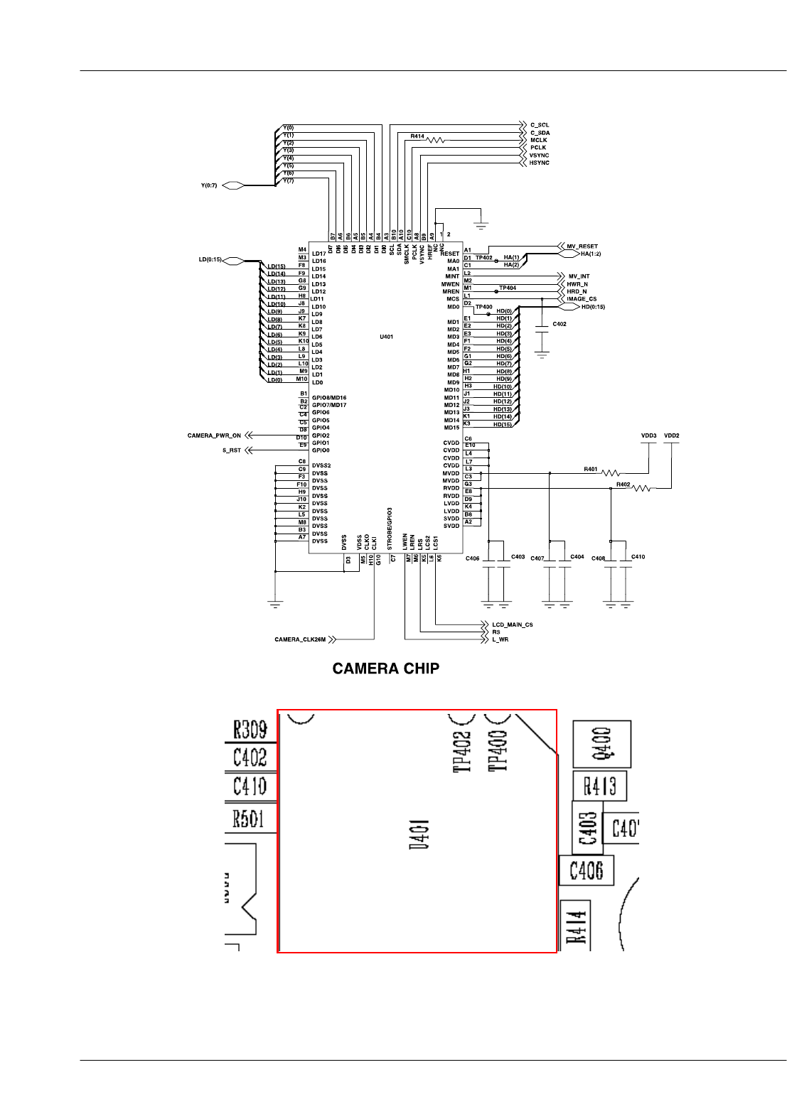
U401 IC ASIC-SGHE420 GH13-00042A SA
U402 FET-SILICON 0505-001923 SA
U500 IC-POWER SUPERVISOR 1203-003882 SA
U501 IC-POSI.FIXED REG. 1203-003787 SA
U502 IC-CMOS LOGIC 0801-002507 SA
U600 BLUETOOTH MODULE 4709-001496 SA
U602 IC-BATTERY 1203-003663 SA
U605 IC-CMOS LOGIC 0801-003076 SA
U606 IC-CMOS LOGIC 0801-003076 SA
U700 IC-POSI.FIXED REG. 1203-003531 SA
U701 IC-VOLTAGE COMP. 1202-001068 SA
U702 IC-ANALOG SWITCH 1001-001410 SA
U900 IC-CMOS LOGIC 0801-003025 SA
U901 IC-MELODY 1204-001811 SA
U902 IC-TUNER 1204-002700 SA
U903 IC-AUDIO AMP 1201-002356 SA
UCP300 IC-COMM. CONTROLLER 1205-003065 SA
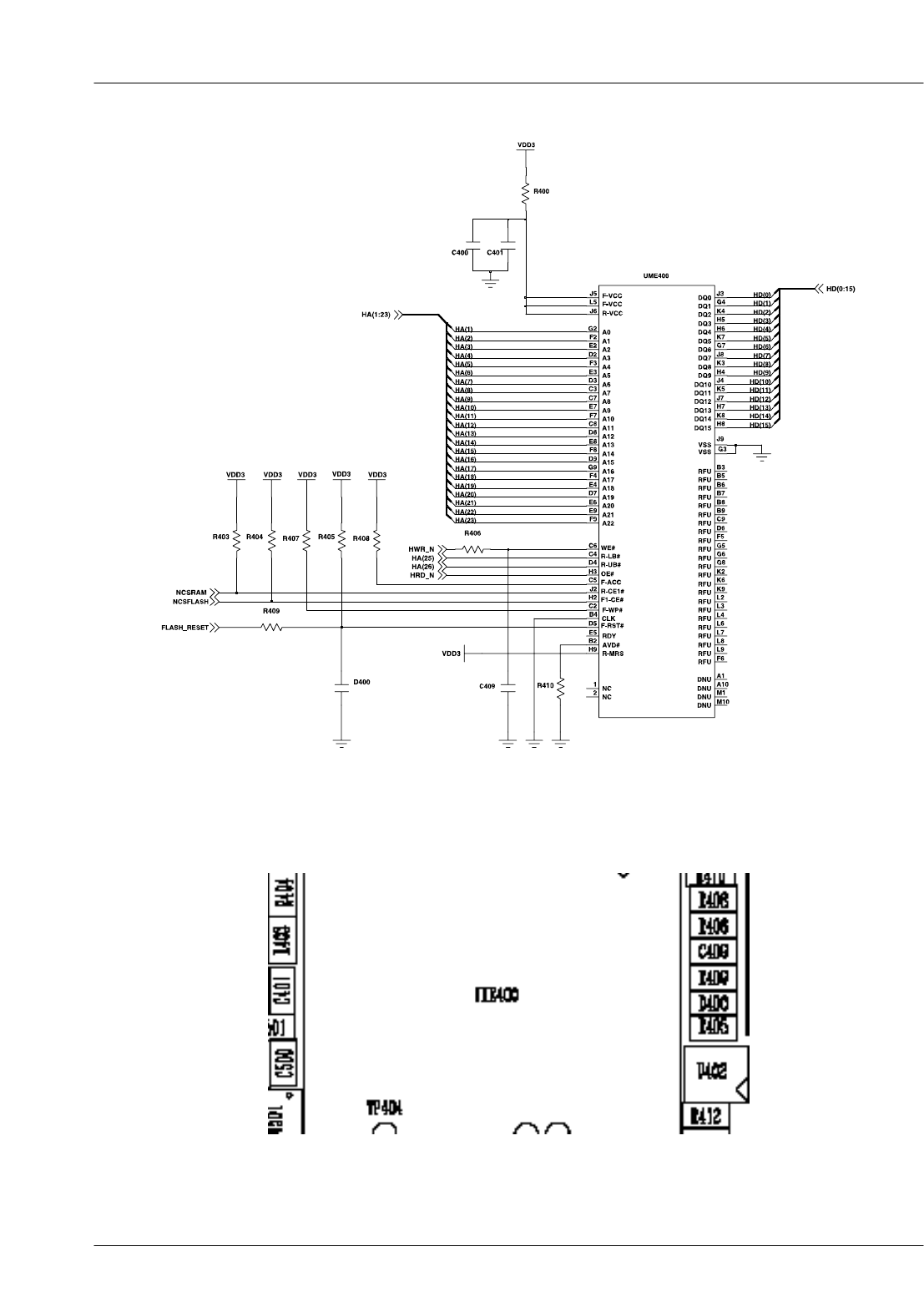
UME400 IC-MCP 1108-000059 SA
SAMSUNG Proprietary-Contents may change without notice
Main Electrical Parts List
6-9
This Document can not be used without Samsung's authorization
Design LOC Description SEC Code STATUS
V500 VARISTOR 1405-001082 SA
V800 VARISTOR 1405-001082 SA
V801 VARISTOR 1405-001082 SA
V802 VARISTOR 1405-001082 SA
V803 DIODE-TVS 0406-001231 SA
V804 DIODE-TVS 0406-001231 SA
V805 VARISTOR 1405-001082 SA
V806 DIODE-TVS 0406-001231 SA
V807 DIODE-TVS 0406-001231 SA
V808 VARISTOR 1405-001082 SA
X500 CRYSTAL-SMD 2801-004373 SA
ZD700 DIODE-ZENER 0403-001547 SA

SAMSUNG Proprietary-Contents may change without notice
Main Electrical Parts List
6-10
This Document can not be used without Samsung's authorization
SAMSUNG Proprietary-Contents may change without notice
This Document can not be used without Samsung's authorization
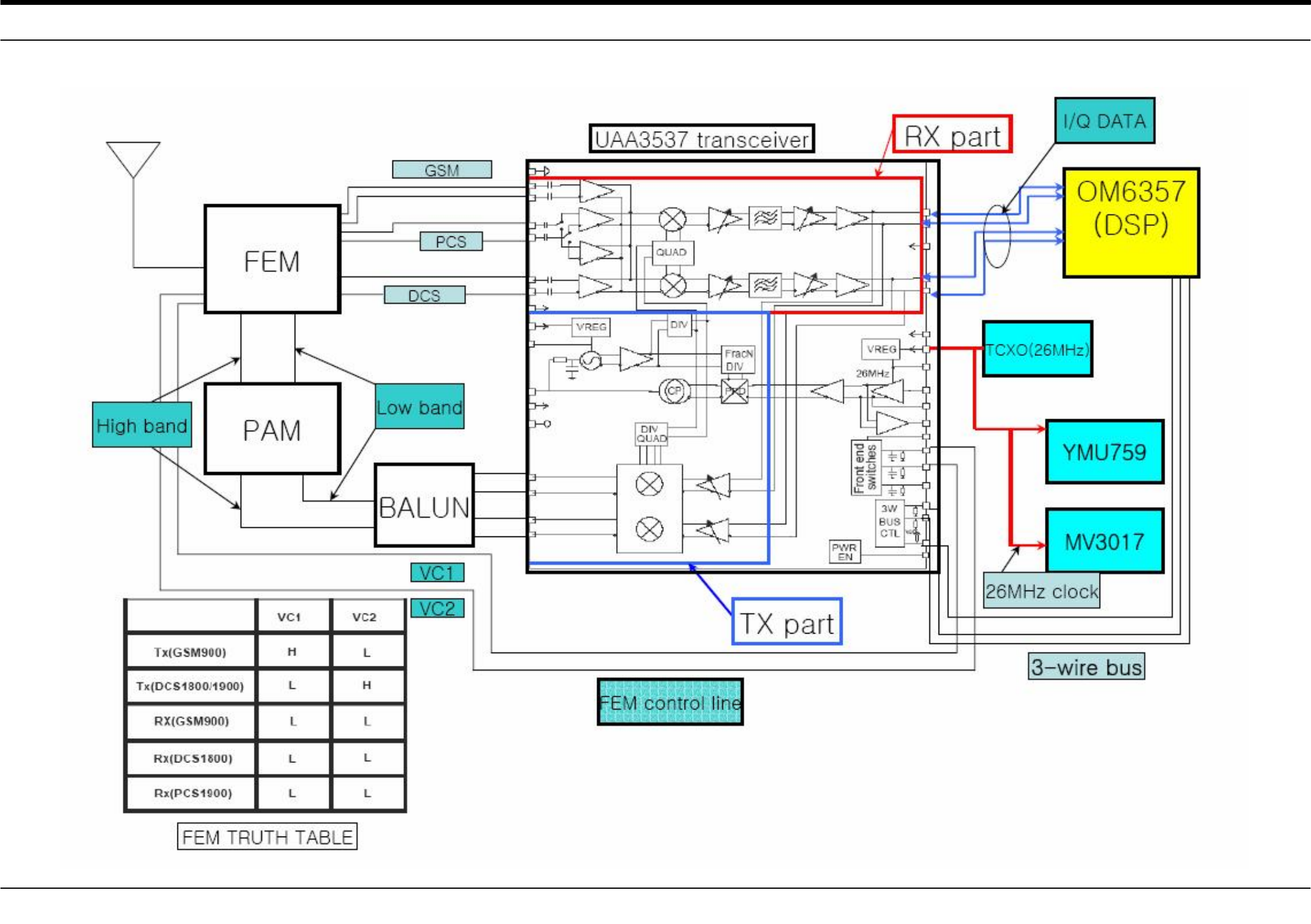
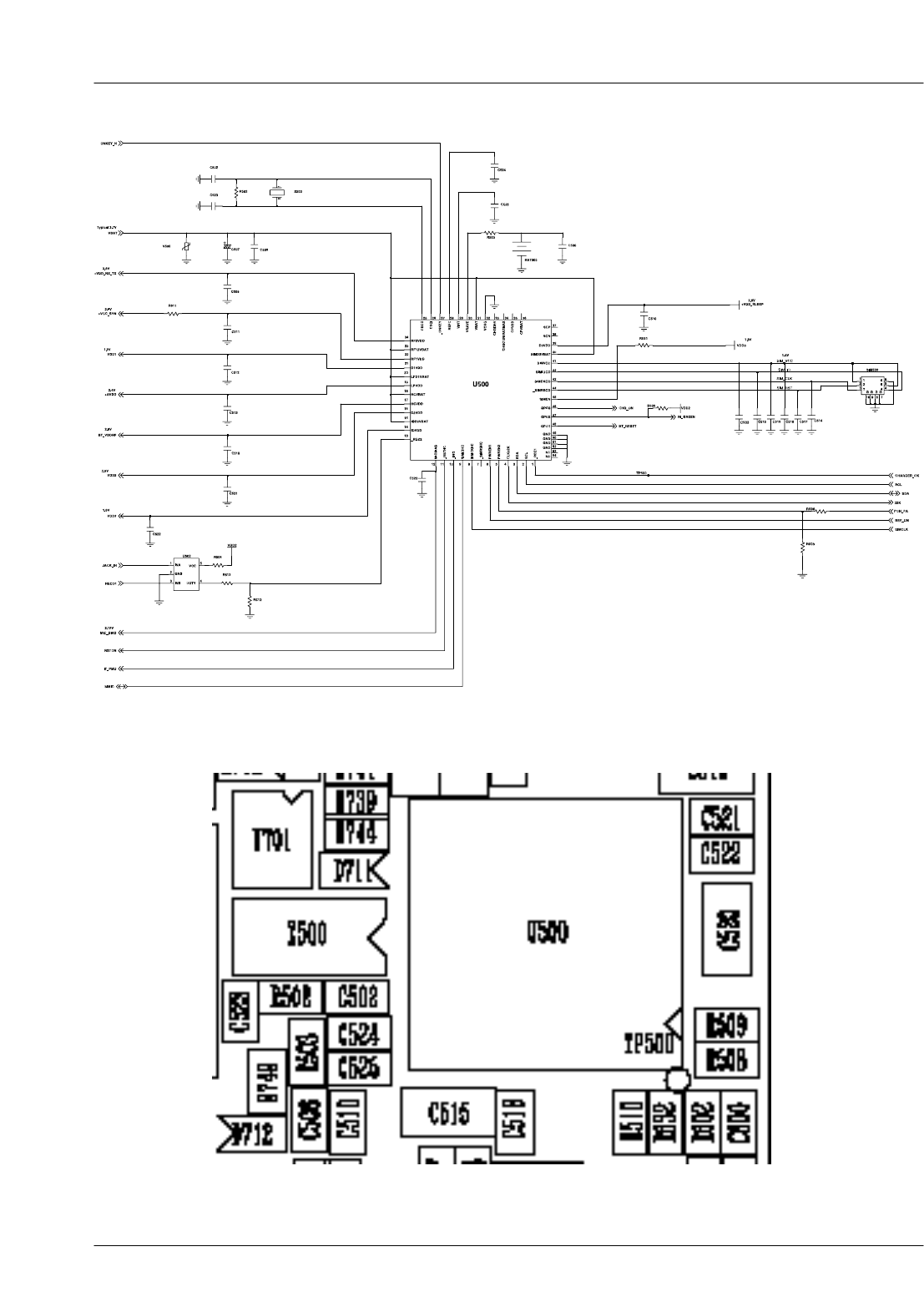
7. Block Diagrams
7-1
7-1. RF Solution Block Diagram
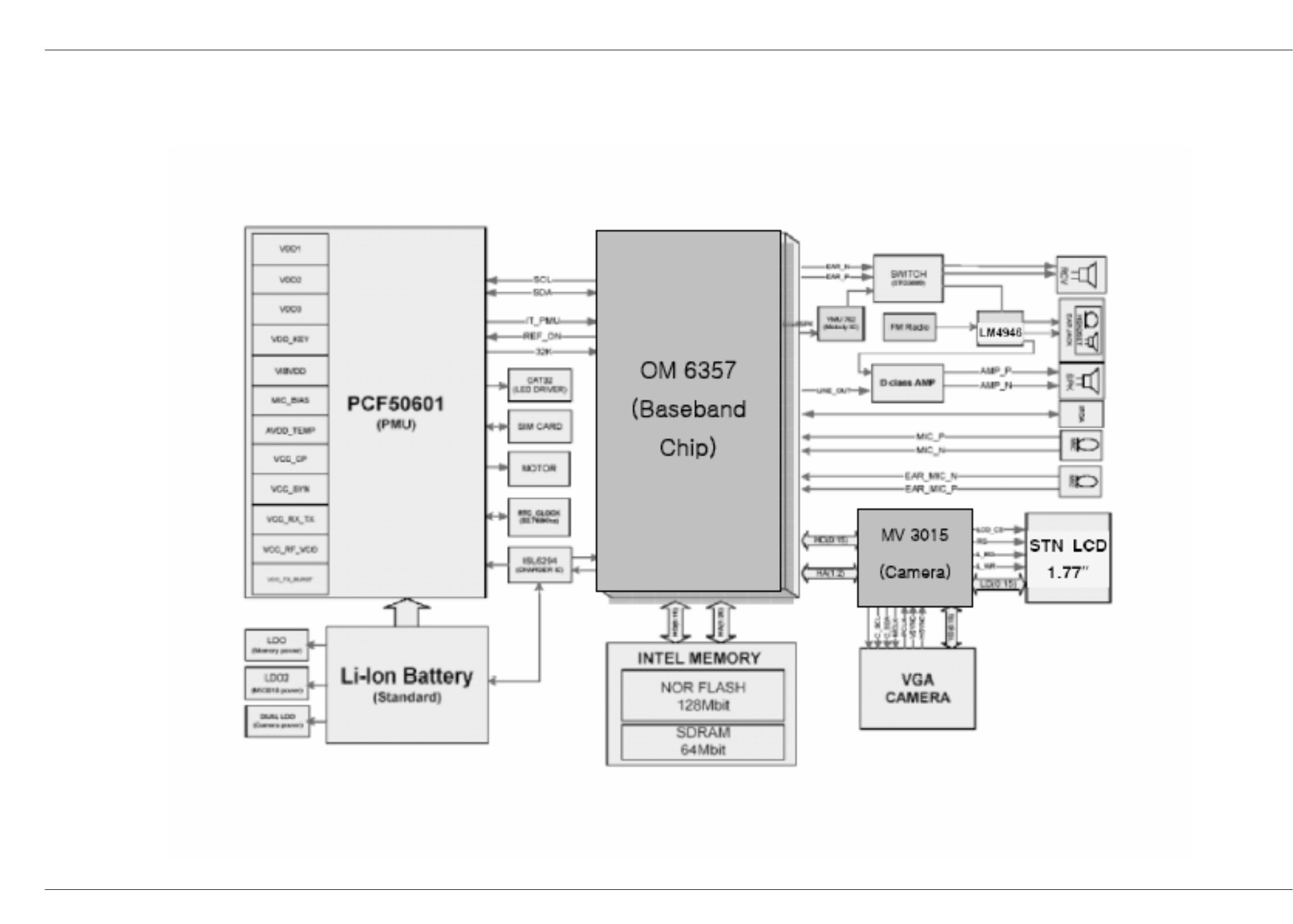
SAMSUNG Proprietary-Contents may change without notice
Block Diagrams
This Document can not be used without Samsung's authorization
7-2
7-2. Base Band Solution Block Diagram
SAMSUNG Proprietary-Contents may change without notice
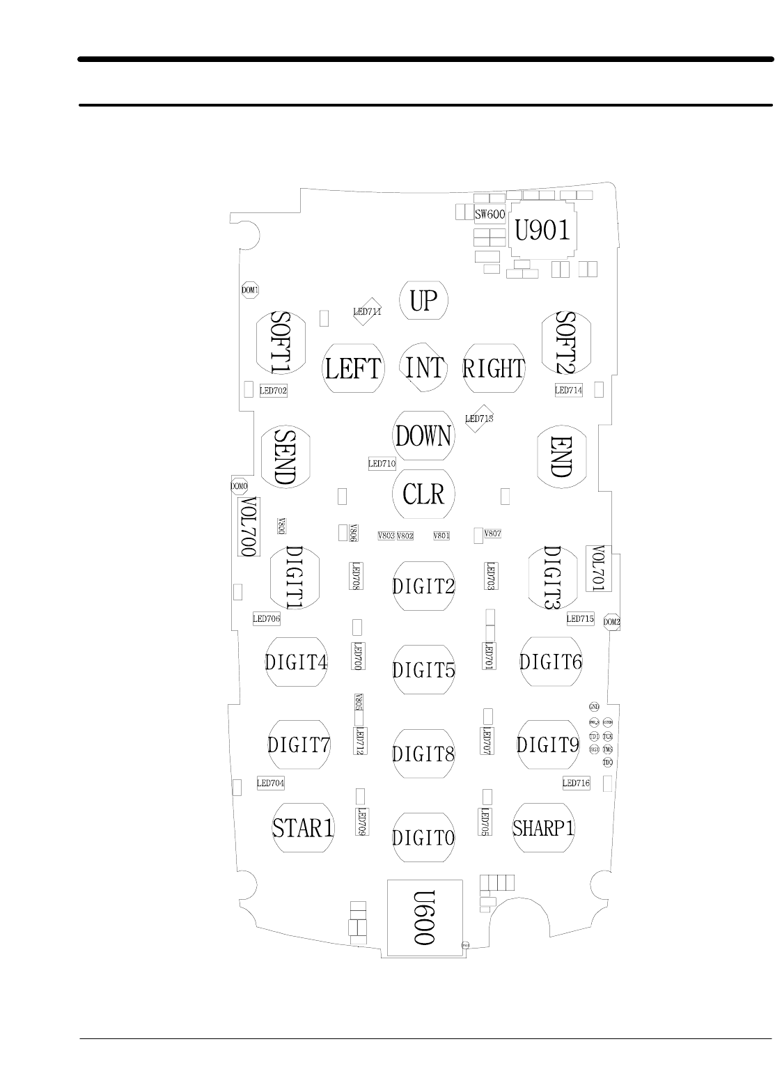
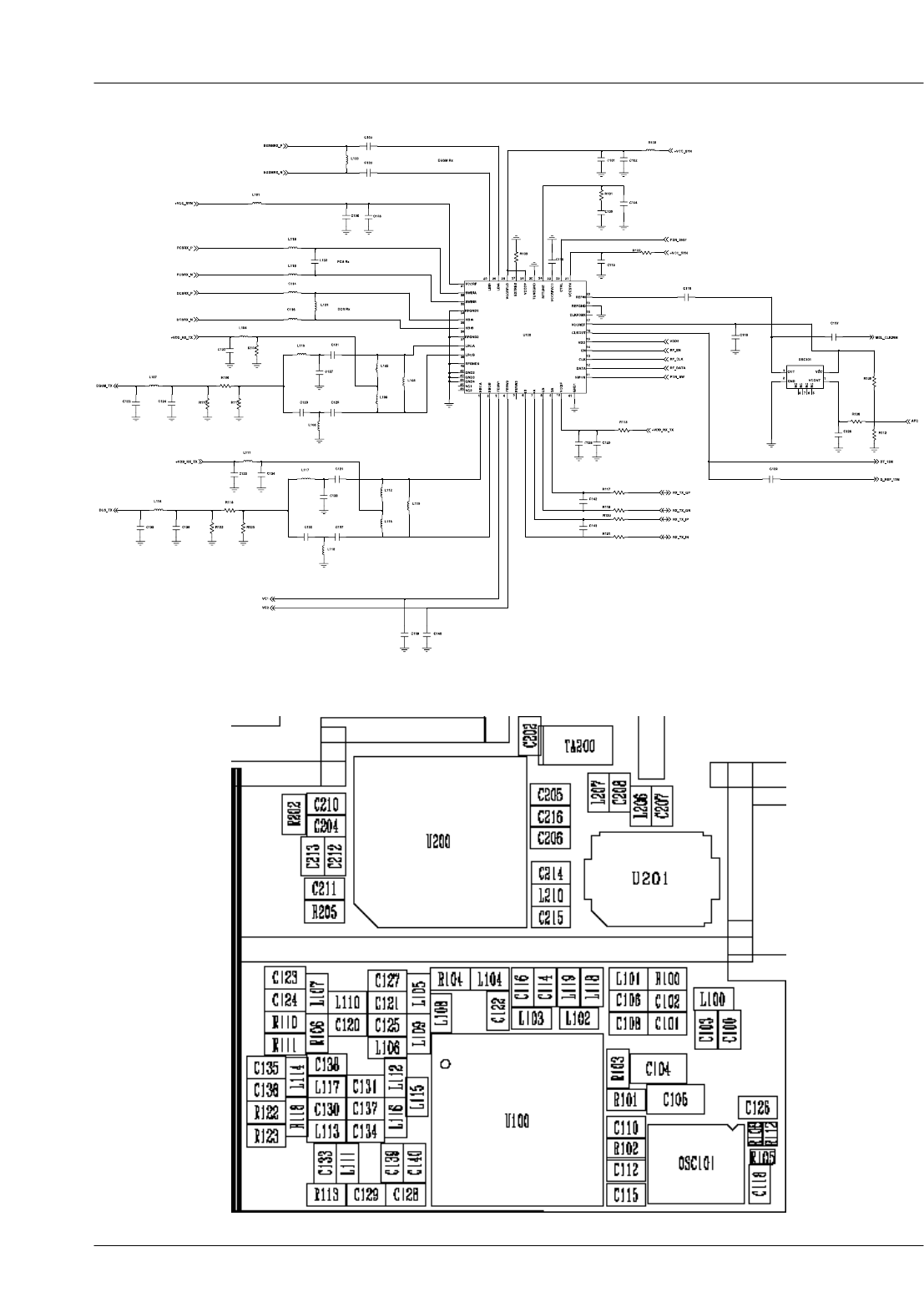
8. PCB Diagrams
8-1
This Document can not be used without Samsung's authorization
Top
SAMSUNG Proprietary-Contents may change without notice
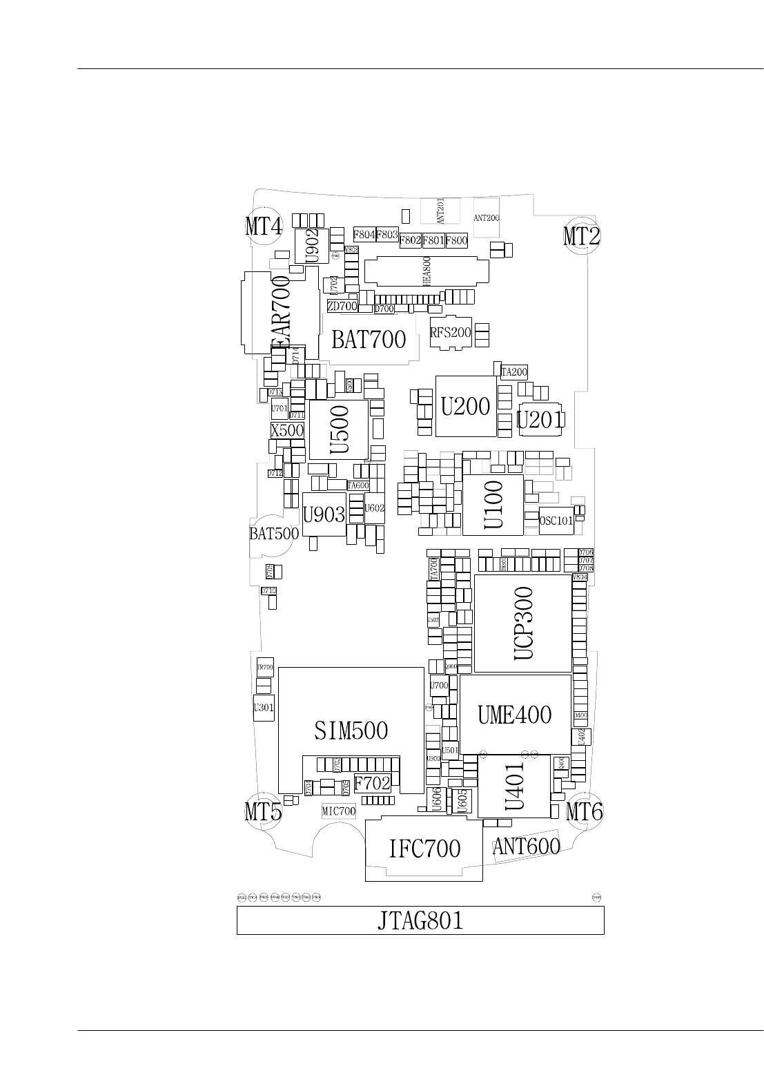
PCB Diagrams
8-2
This Document can not be used without Samsung's authorization
Top
SAMSUNG Proprietary-Contents may change without notice
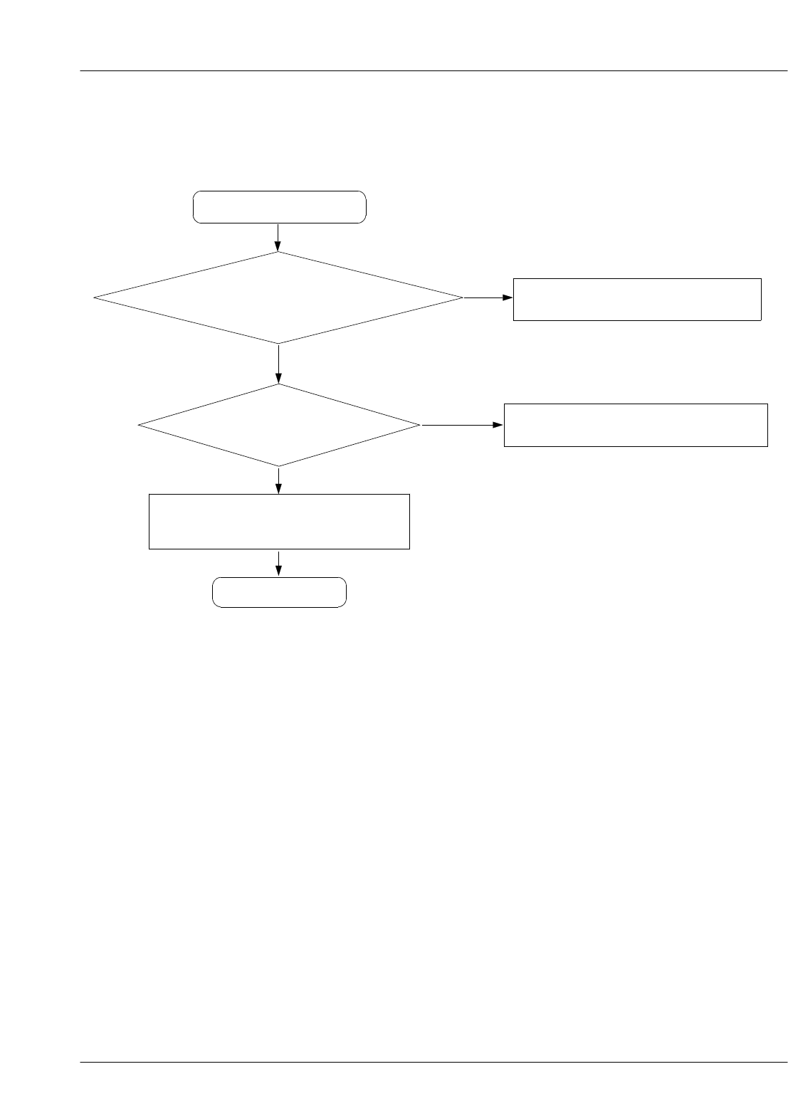
9. Flow Chart of Troubleshooting
This Document can not be used without Samsung's authorization
9-1
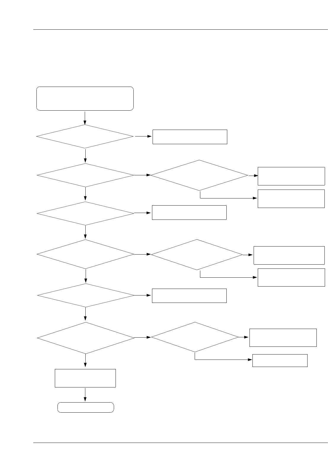
9-1. Power On
Yes
Yes
Check the initial operation
Yes
No Check the clock generation circuit
(related to U101)
Check for the clock at C319
=26MHz
Yes
No
Check the +VDD_GSM_CORE circuit
C401(+VDD_GSM_CORE)
=1.9V?
Yes
No
Check the related circuit
TA425(+VDD_IO_LOW) &
C424(+VDD_IO_HIGH) = "H"?
Yes
No
Resolder OSC400
Check the Clock at
R401=32KHZ
Yes
No
Check the PMU related to VINTC408(VINT) = 2.7V?
Yes
No
END
Change the Battery
' Power On ' does not work
Check the Battery Voltage
is more than 3.4V
SAMSUNG Proprietary-Contents may change without notice
This Document can not be used without Samsung's authorization
Flow Chart of Troubleshooting
9-2
SAMSUNG Proprietary-Contents may change without notice
Flow Chart of Troubleshooting
This Document can not be used without Samsung's authorization
9-3
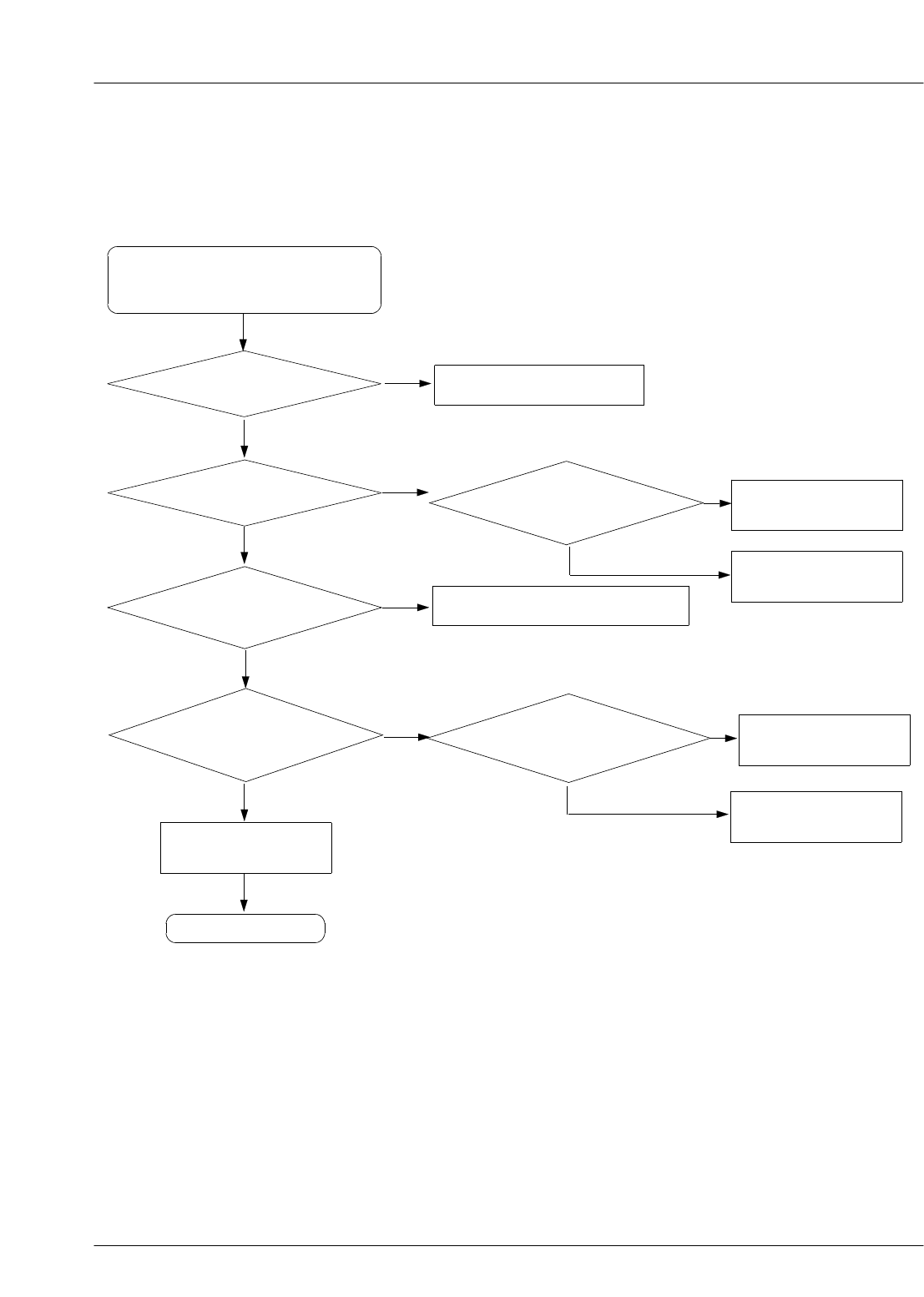
9-2. Initial
U200 pin 2 (RSTON) ="H"?
Initial Failure
Check the circuit related to reset
END
No
Yes
Is U302 pin 4
OK?
Yes
Yes
No
Check the U302
Check the 16bit data signal
&memoryCE
Yes
SAMSUNG Proprietary-Contents may change without notice
This Document can not be used without Samsung's authorization
Flow Chart of Troubleshooting
9-4
SAMSUNG Proprietary-Contents may change without notice
Flow Chart of Troubleshooting
This Document can not be used without Samsung's authorization
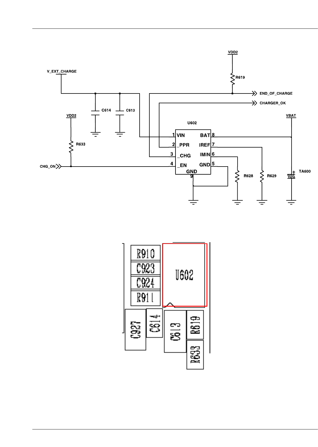
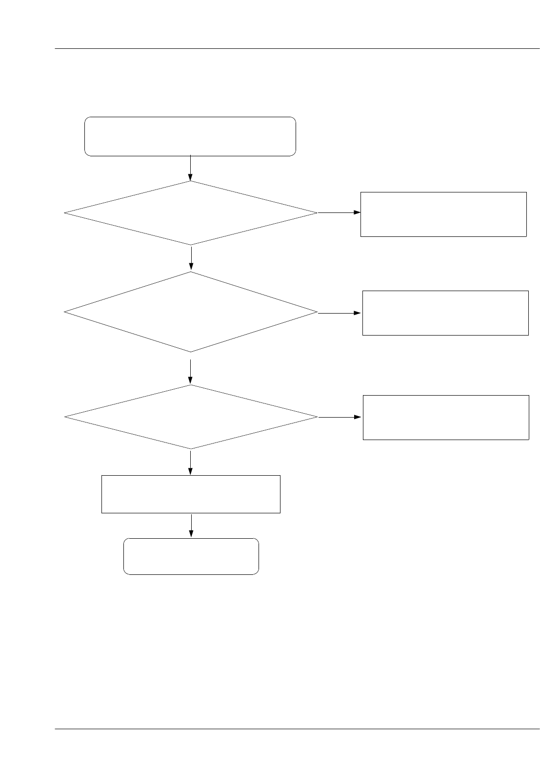
9-5
9-3. Charging Part
Yes
Resolder or replace U503
Check the circuit related to
AUX_ON signal
Resolder or replace U503
Check the circuit related to
V_EXT_CHARGE
Yes
No
Check the U500 pin 10
≒4.2V
Yes
No
U500 pin 3 = "L"?
Yes
No
U500 pin 5 = "L"?
Yes
No
END
Abnormal charging part
Check the U500 pin 1
>4.9V
Yes
Resolder or replace U503
Check the circuit related to
AUX_ON signal
Resolder or replace U503
Check the circuit related to
V_EXT_CHARGE
Yes
No
Yes
No
Yes
No
Yes
No
END
Abnormal charging part
SAMSUNG Proprietary-Contents may change without notice
This Document can not be used without Samsung's authorization
Flow Chart of Troubleshooting
9-6
SAMSUNG Proprietary-Contents may change without notice
Flow Chart of Troubleshooting
This Document can not be used without Samsung's authorization
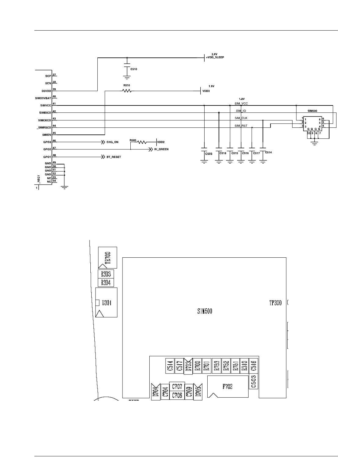
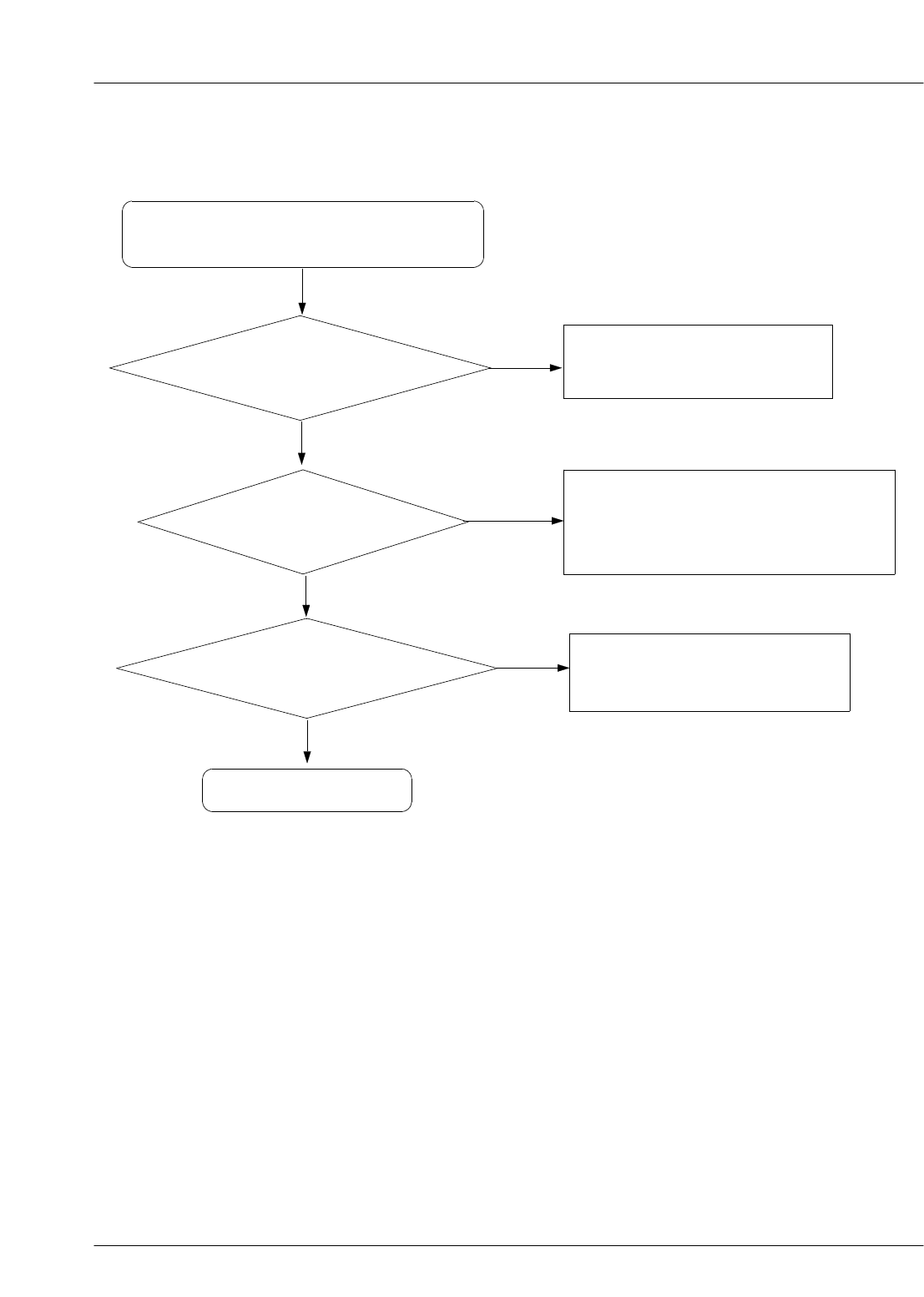
9-7
9-4. Sim Part
SIM400 pin 1,5 = "H"?
Phone can't access SIM Card
Check the sim charge pump
Check the SIM Card
END
No
Yes
Yes
Yes
No
Check the Clock
After Power ON,
Check SIMCLK Signal on
pin3 of SIM400 in a few second
Yes
No
Replace PBA
After SIM card insert,
SIM400 pin 2 = "H(SIM_RST)"?
Yes
SAMSUNG Proprietary-Contents may change without notice
This Document can not be used without Samsung's authorization
Flow Chart of Troubleshooting
9-8
SAMSUNG Proprietary-Contents may change without notice
Flow Chart of Troubleshooting
This Document can not be used without Samsung's authorization
9-9
9-5. Microphone Part
Check the connection
from MIC
Check the circuit
from UCP201 to MIC
Resolder MIC
Resolder the C605, C611, R602, R604
R605, U600
END
No
Yes
Yes
Yes
Yes
No
Check the MIC No
Replace the MIC
Microphone does not work
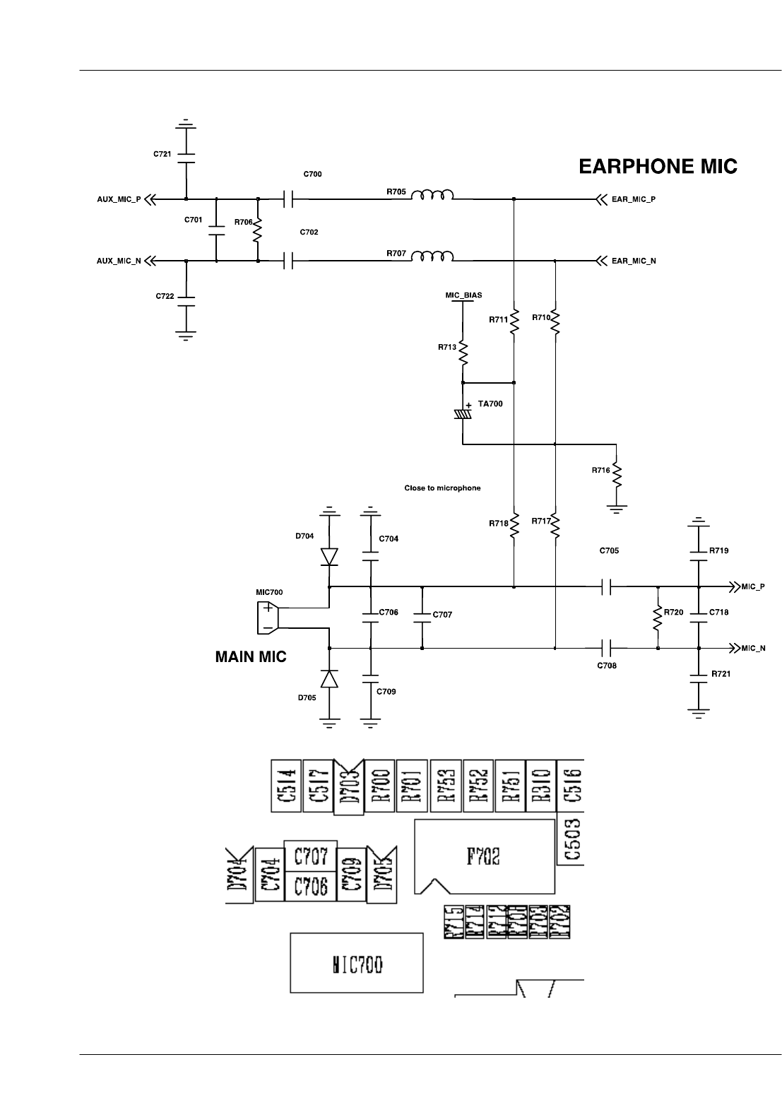
SAMSUNG Proprietary-Contents may change without notice
This Document can not be used without Samsung's authorization
Flow Chart of Troubleshooting
9-10
SAMSUNG Proprietary-Contents may change without notice
Flow Chart of Troubleshooting
This Document can not be used without Samsung's authorization
9-11
9-6. Speaker Part(Melody)
U304 pin 6 = 2.9V?
Speaker does not work
Check the Clock signal at
Pin 4 of U304 (26MHz)
Check the clock generation circuit
(related to U301 and U303)
No
Yes
No
Resolder or replace U304
Yes
U301 pin 17,18 ≒ 1.8V?
(When U301 operate) Resolder U301
No
Yes
END
Yes
Is Speaker working? Change the Speaker
No
Yes
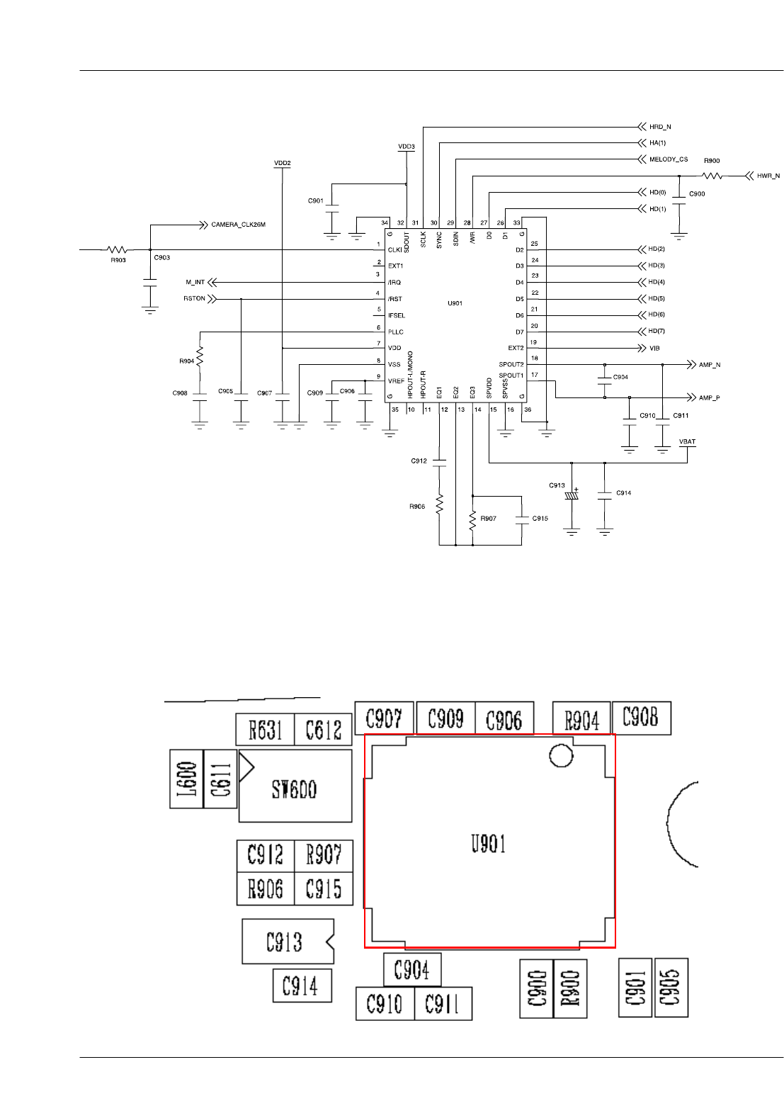
SAMSUNG Proprietary-Contents may change without notice
This Document can not be used without Samsung's authorization
Flow Chart of Troubleshooting
9-12
SAMSUNG Proprietary-Contents may change without notice
Flow Chart of Troubleshooting
This Document can not be used without Samsung's authorization
9-13
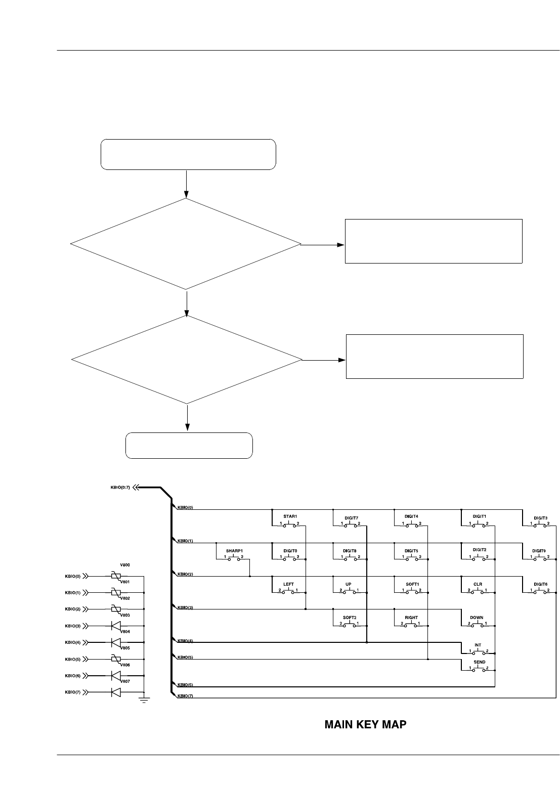
9-7. Key Data Input
When one of the keys is
pushed,
is it displayed on LCD?
Check the Dome sheet & Key Pad
END
No
Yes
Yes
Check Initial Operation
When one of the keys is
pushed,
KBIO signal is OK?
Replace the PBA
No
Yes
SAMSUNG Proprietary-Contents may change without notice
This Document can not be used without Samsung's authorization
Flow Chart of Troubleshooting
9-14
9-8. Receiver Part
Is Receiver working? Resolder UCP201 or change PBA
END
No
Yes
Yes
Receiver does not work
No
Replace the Receiver
Yes
Is Receiver working?
SAMSUNG Proprietary-Contents may change without notice
Flow Chart of Troubleshooting
This Document can not be used without Samsung's authorization
9-15
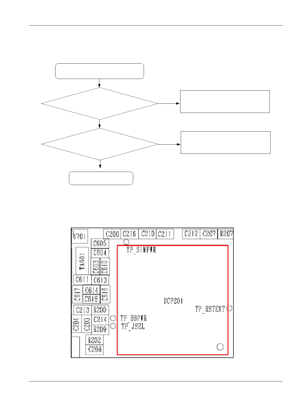
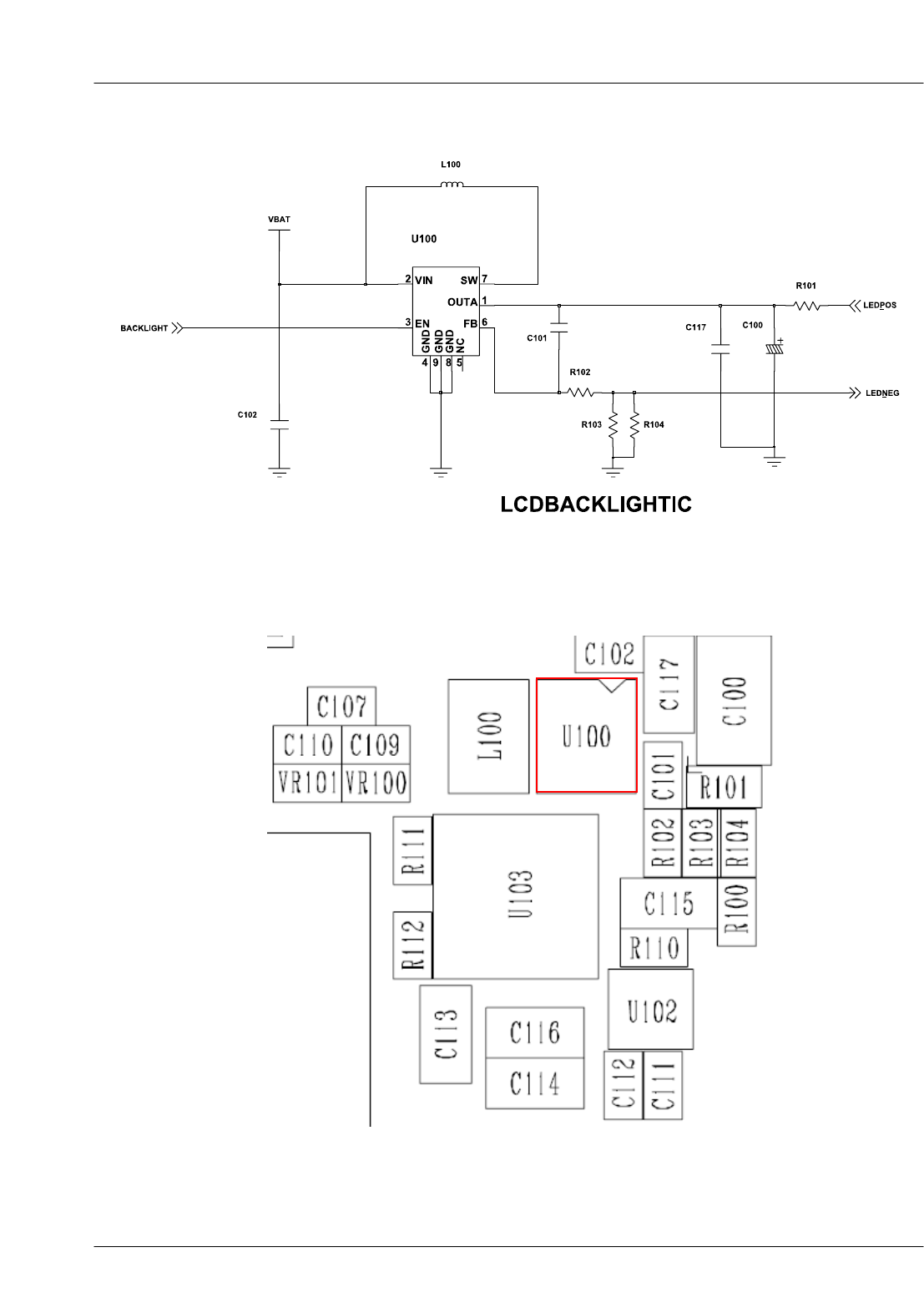
9-9. Back Light (for Color Main LCD)
Is LCD Contrast set on high
level in the Menu?
Set LCD Contrast on high level
END
No
Yes
Yes
Backlight does not work
U100(SUB PCB) PIN 3 = H ?
Check the inserting condition of slide FPCB
Resolder UCP201 or change PBA
No
Yes
U100PIN1=7V? Check the U100 & the related circuit
No
Yes
Yes
Replace the LCD Module
SAMSUNG Proprietary-Contents may change without notice
This Document can not be used without Samsung's authorization
Flow Chart of Troubleshooting
9-16
SAMSUNG Proprietary-Contents may change without notice
Flow Chart of Troubleshooting
This Document can not be used without Samsung's authorization
9-17
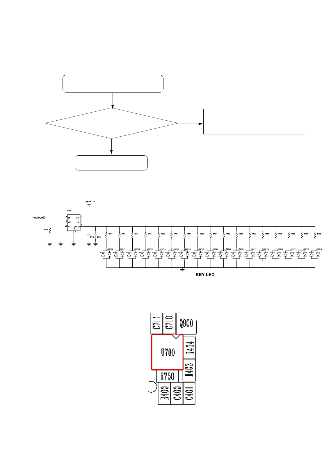
9-10. Key Back Light
U700 pin1 = H ? Check the UCP201 related to
"KEY_LED_ON"
END
No
Yes
Yes
Main Key LED does not work
SAMSUNG Proprietary-Contents may change without notice
This Document can not be used without Samsung's authorization
Flow Chart of Troubleshooting
9-18
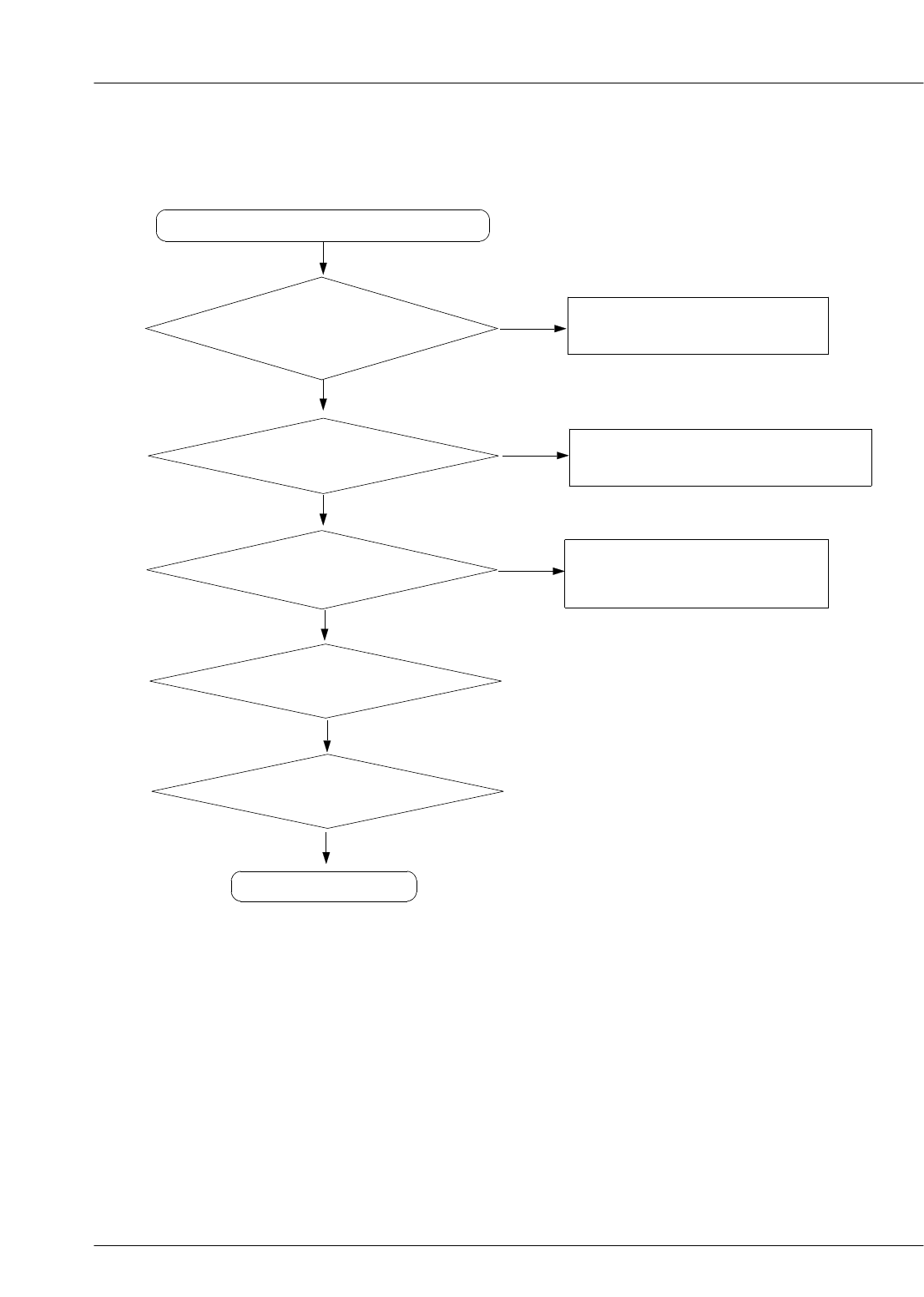
9-11. Camera part
"Camera" function does not work
Yes
No
Reconnect the camera module
Check the Camera
connector on
SUB PCB board
Yes
SLC700 pin 41 = H ?
No Check the inserting condition of slide FPCB
Reconnect SLC700
Yes
C319 =26MHz?
No
Check U304(pin2, pin4) related to
26Mhz and R317
Yes
Is there another problem?
END
Replace the camera
module
Yes
SAMSUNG Proprietary-Contents may change without notice
Flow Chart of Troubleshooting
This Document can not be used without Samsung's authorization
9-19
SAMSUNG Proprietary-Contents may change without notice
This Document can not be used without Samsung's authorization
Flow Chart of Troubleshooting
9-20
9-12. GSM Receiver
RX ON
RF input : CH center freq : +67.7kHz
Amp : -50dBm
Yes
F100 Pin8
>= -65dBm
No
Resolder RFS100,C101
Yes
Check ANT Switch
control circuit
F100 5,6
>= -68dBm Check F100
pin10,pin12 = L
No
No
Yes
Yes Resolder F100
No
Resolder C104, C108, L103
U101
pin 29 >= -70dBm
pin 30 >= -70dBm
Yes
No
U101 pin 23,26,31
>=2.8V
U101 pin 7,8,9,10
>= 1V
No Check & Resolder
U101, R125
RF26MHz, RF PSU Part
YesYes
Resolder U101
Check UCP201
END

SAMSUNG Proprietary-Contents may change without notice
Flow Chart of Troubleshooting
This Document can not be used without Samsung's authorization
9-21
9-13. GSM Transmitter
U101 pin 23,26,31
>=2.8V
Yes Resolder U101
Check UCP201
END
No
No
No
No
No
No
No
No
No
Yes
Yes
Yes
Yes
Yes
Yes
Yes
Yes
Check & Resolder RFLO
signal, RF13MHz,
RF PSU Part
Check +VBAT or PAM
control signal
Resolder or Change F101
Check F101, OK?
Yes
U101 pin 7,8,9,10
>= 1V
Resolder R110,R111,R112
Resolder or Change PAM100
Check ANT Switch
control circuit
Change or Resolder
L107,C125,C124
PAM100 pin12
<= -11dBm
PAM100 pin 38<=
-15dB
PAM100 pin16
>= 18dBm
F100 pin11
>= 18dBm
Check F100
pin10 = H (2.6V),
12 = L
TX ON (5Level)
Resolder RFS100,C101
F100 Pin8
>= 20dBm
SAMSUNG Proprietary-Contents may change without notice
This Document can not be used without Samsung's authorization
Flow Chart of Troubleshooting
9-22
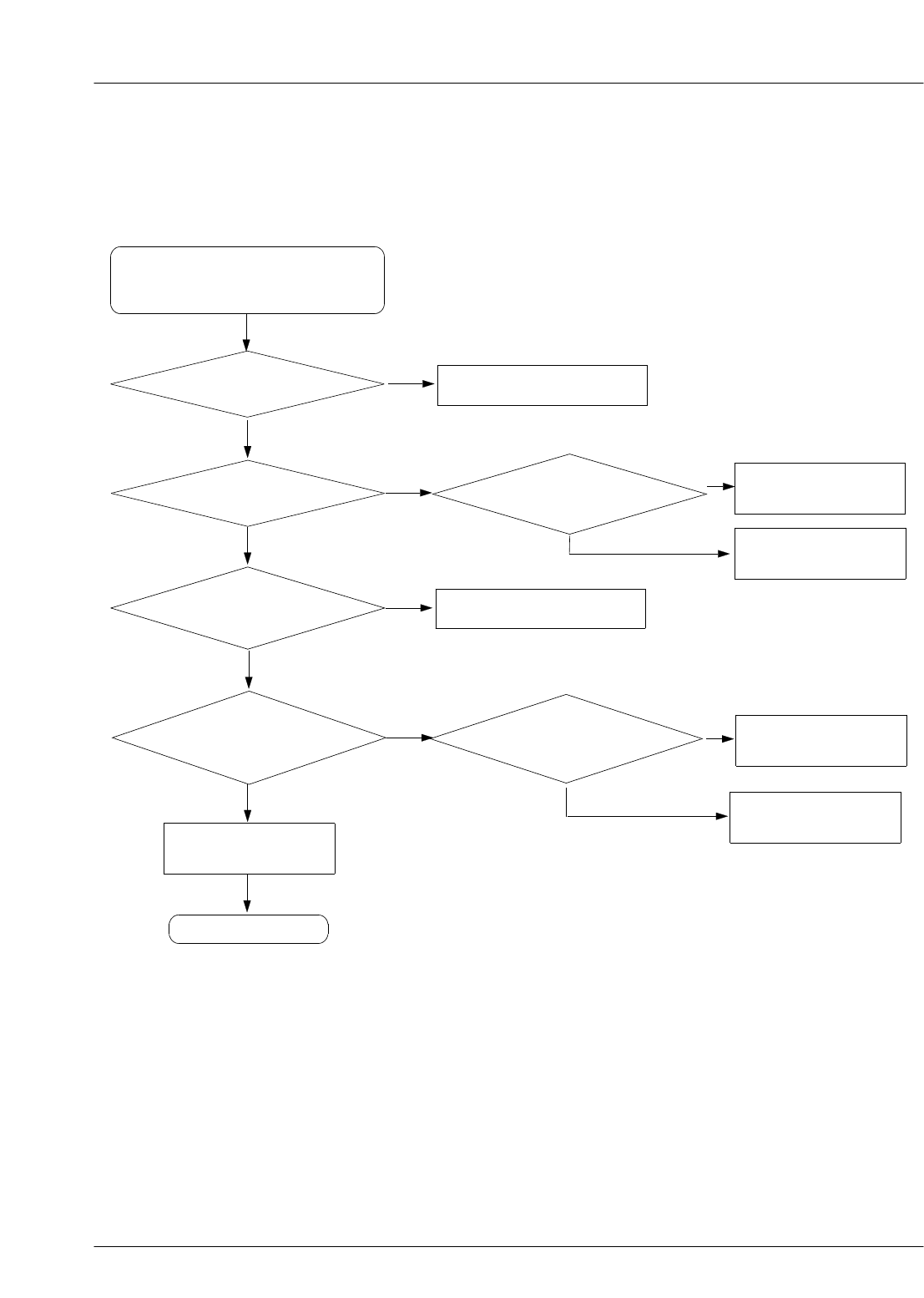
9-14. DCS Receiver
Check F100
pin10,pin12 = L
Check UCP201
No
No
No
No
No
Yes
YesYes
Yes
Yes
Yes
Resolder U101
Check & Resolder
U100, R113
RF26MHz, RF PSU Part
U101 pin 23,26,31
>=2.8V
Resolder C117, C118, L106
Resolder F100
Check ANT Switch
control circuit
U101
pin 35 >= -70dBm
pin 36 >= -70dBm
U101 pin 7,8,9,10
>= 1V
F100 1,2
>= -68dBm
RX ON
RF input : CH center freq : +67.7kHz
Amp : -50dBm
Yes
No
END
Resolder RFS100,C101
F100 Pin8
>= -65dBm
SAMSUNG Proprietary-Contents may change without notice
Flow Chart of Troubleshooting
This Document can not be used without Samsung's authorization
9-23
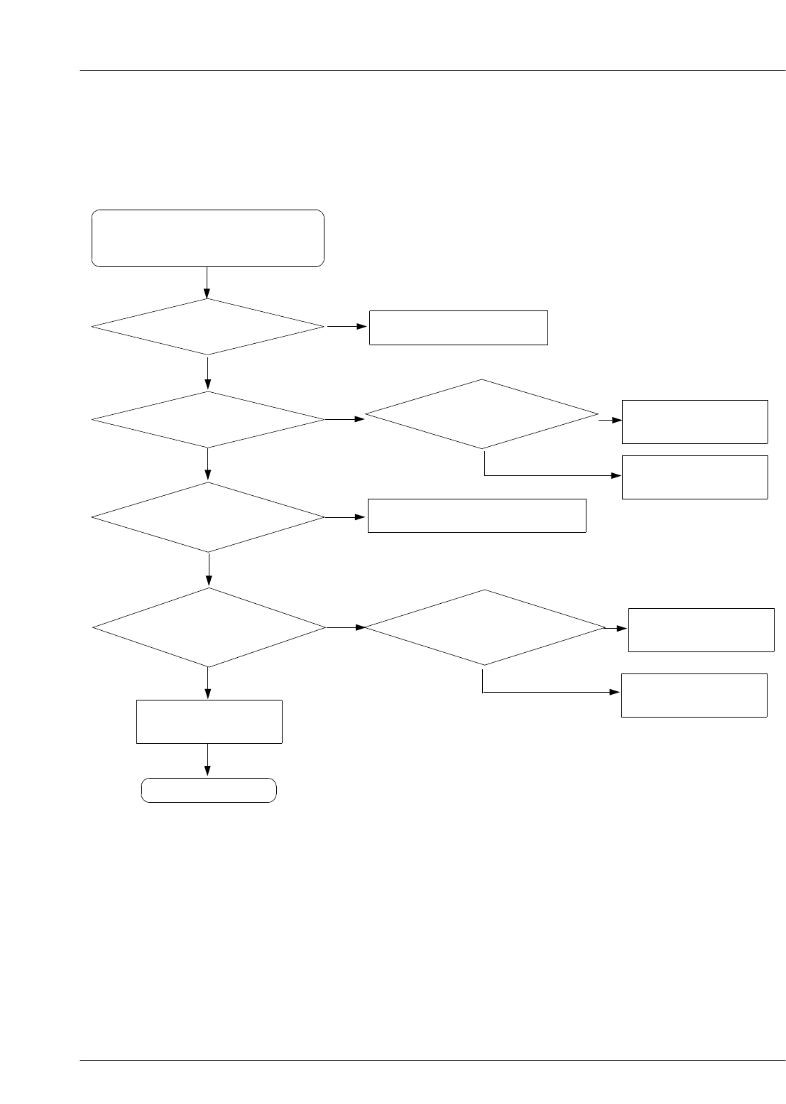
9-15. DCS Transmitter
U101 pin 23,26,31
>=2.8V
Yes Resolder U101
Check UCP201
END
No
No
No
No
No
No
No
No
No
Yes
Yes
Yes
Yes
Yes
Yes
Yes
Yes
Check & Resolder RFLO
signal, RF13MHz,
RF PSU Part
Check +VBAT or PAM
control signal
Resolder or Change F101
Check F101, OK?
Yes
U101 pin 7,8,9,10
>= 1V
Resolder R116, R117, R118
Resolder or Change PAM100
Check ANT Switch
control circuit
Change or Resolder
L104,C134,R124
PAM100 pin4
<= -11dBm
PAM100 pin 2<=
-15dB
PAM100 pin18
>= 18dBm
F100 pin13
>= 18dBm
Check F100
pin12 = H (2.6V),
10 = L
TX ON (5Level)
Resolder RFS100,C101
F100 Pin8
>= 20dBm
SAMSUNG Proprietary-Contents may change without notice
This Document can not be used without Samsung's authorization
Flow Chart of Troubleshooting
9-24
9-16. PCS Receiver
RX ON
RF input : CH center freq : +67.7kHz
Amp : -50dBm
Yes
F100 Pin8
>= -65dBm
No
Resolder RFS100,C101
Yes
F100 3,4
>= -68dBm Check F100
pin10,pin12 = L
No
No
Check ANT Switch
control circuit
Yes
Yes
Resolder F100
U101
pin 32 >= -70dBm
pin 33 >= -70dBm
No
Resolder C112, C116, L105
Yes
U101 pin 23,26,31
>=2.8V
101 pin 7,8,9,10
>= 1V
No
No Check & Resolder
U100, R113
RF26MHz, RF PSU Part
YesYes
Resolder U101
Check UCP201
END

SAMSUNG Proprietary-Contents may change without notice
Flow Chart of Troubleshooting
This Document can not be used without Samsung's authorization
9-25
9-17. PCS Transmitter
TX ON (5Level)
Yes
F100 Pin8
>= 20dBm
No Resolder RFS100,C101
Yes
F100 pin13
>= 18dBm
Check F100
pin12 = H (2.6V),
10 = L
No
No Check ANT Switch
control circuit
Yes Change or Resolder
L104,C134,R124
Yes
PAM100 pin18
>= 18dBm
No Resolder or Change PAM100
Yes
Check F101, OK?
PAM100 pin4
<= -11dBm
No
No
Resolder or Change F101
Check +VBAT or PAM
control signal
Yes
Yes
No
U101 pin1
<= -15dBm Resolder R103, R104, R105
Yes
U101 pin 23,26,31
>=2.8V
U101 pin 7,8,9,10
>= 1V
No
No Check & Resolder RFLO
signal, RF13MHz,
RF PSU Part
Resolder U101
Yes
Yes
Check UCP201
END
SAMSUNG Proprietary-Contents may change without notice
This Document can not be used without Samsung's authorization
Flow Chart of Troubleshooting
9-26

SAMSUNG Proprietary-Contents may change without notice
10. Reference data
10-1
This Document can not be used without Samsung's authorization
Reference Abbreviate
―AAC: Advanced Audio Coding.
―AVC : Advanced Video Coding.
―BER : Bit Error Rate
―BPSK: Binary Phase Shift Keying
―CA : Conditional Access
―CDM : Code Division Multiplexing
―C/I : Carrier to Interference
―DMB : Digital Multimedia Broadcasting
―EN : European Standard
―ES : Elementary Stream
―ETSI: European Telecommunications Standards Institute
―MPEG: Moving Picture Experts Group
―PN : Pseudo-random Noise
―PS :PilotSymbol
―QPSK: Quadrature Phase Shift Keying
―RS : Reed-Solomon
―SI : Service Information
―TDM : Time Division Multiplexing
―TS : Transport Stream

SAMSUNG Proprietary-Contents may change without notice
Reference data
10-2
This Document can not be used without Samsung's authorization

This Service Manual is a property of Samsung Electronics Co.,Ltd.
Any unauthorized use of Manual can be punished under applicable
International and/or domestic law.
Samsung Electronics Co.,Ltd.
2007. 01. Rev.1.0
ⓒ

