Samsung SGH ZV30 Service Manual. Www.s Manuals.com. Manual
User Manual: Phone Samsung SGH-ZV30 - Service manuals and Schematics, Disassembly / Assembly. Free.
Open the PDF directly: View PDF ![]() .
.
Page Count: 55
SGH-ZV30
UMTS TELEPHONE CONTENTS
1. Specification
2. Circuit Description
3. Exploded Views and Parts List
4. Electrical Parts List
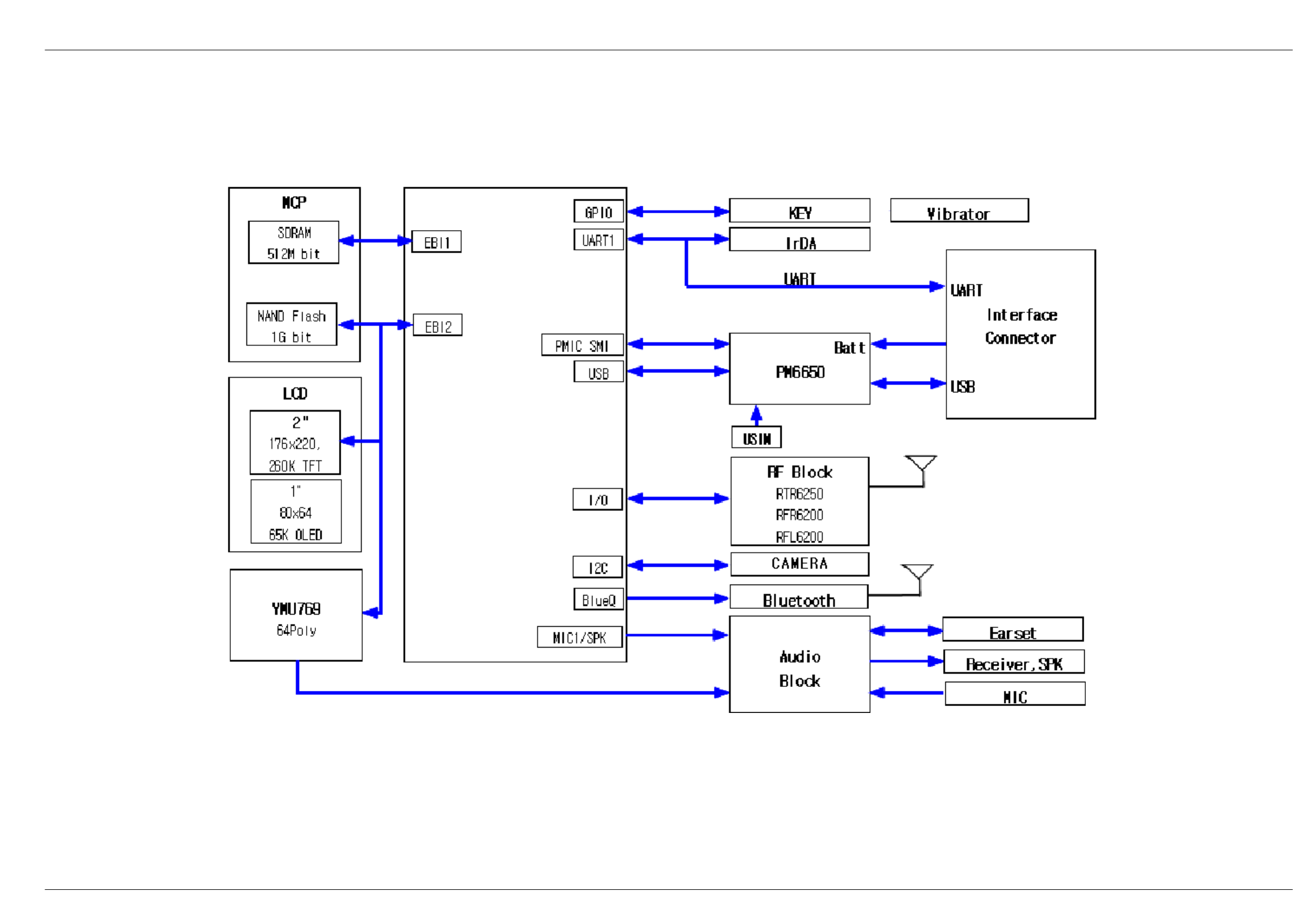
5. Block Diagrams
6. PCB Diagrams
7. Flow Chart of Troubleshooting
UMTS TELEPHONE

Samsung Electronics Co.,Ltd. September. 2005
Printed in Korea.
Code No.: GH68-08450A
BASIC.
This Service Manual is a property of Samsung Electronics Co.,Ltd.
Any unauthorized use of Manual can be punished under applicable
International and/or domestic law.
ⓒ
SAMSUNG Proprietary-Contents may change without notice
1. Specification
This Document can not be used without Samsung's authorization
1-1
EGSM 900 DCS1800 PCS1900 W-CDMA
Freq.
Band[MHz]
Uplink/Downlink
880~915
925~960
1710~1785
1805~1880
1850~1910
1930~1990
1920~1980
2110~2170
ARFCN range 0~124 &
975~1023 512~885 512~810 UL:9612~9888
DL:10562~10838
Tx/Rx spacing 45MHz 95MHz 80MHz 190MHz
Mod. Bit rate/
Bit Period
270.833kbps
3.692us
270.833kbps
3.692us
270.833kbps
3.692us
3.84Mcps
Time Slot
Period/Frame
Period
576.9us
4.615ms
576.9us
4.615ms
576.9us
4.615ms
Frame length : 10ms
Slot length : 0.667ms
Modulation 0.3GMSK 0.3GMSK 0.3GMSK QPSK
HQPSK
MS Power 33dBm~5dBm 30dBm~0dBm 30dBm~0dBm 24dBm ~ - 50dBm
Power Class 4
(max +33dBm)
1
(max +30dBm)
1
(max +30dBm)
3
(max +24dBm)
Sensitivity -102dBm -100dBm -100dBm -106.7dBm
TDMA Mux 8 8 8
Cell Radius 35Km 2Km 2Km 2Km
1-1. GSM General Specification
SAMSUNG Proprietary-Contents may change without notice
This Document can not be used without Samsung's authorization
Specification
1-2
TX Power
control level PCS1900
030±3dBm
128±3dBm
226±3dBm
324±3dBm
422±3dBm
520±3dBm
618±3dBm
716±3dBm
814±3dBm
912±4dBm
10 10±4 dBm
11 8±4dBm
12 6±4 dBm
13 4±4 dBm
14 2±5 dBm
15 0±5 dBm
TX Power
control level GSM900
533±2dBm
631±2dBm
729±2dBm
827±2dBm
925±2dBm
10 23±2 dBm
11 21±2 dBm
12 19±2 dBm
13 17±2 dBm
14 15±2 dBm
15 13±2 dBm
16 11±3 dBm
17 9±3dBm
18 7±3 dBm
19 5±3 dBm
TX Power
control level DCS1800
030±3dBm
128±3dBm
226±3dBm
324±3dBm
422±3dBm
520±3dBm
618±3dBm
716±3dBm
814±3dBm
912±4dBm
10 10±4 dBm
11 8±4dBm
12 6±4 dBm
13 4±4 dBm
14 2±5 dBm
15 0±5 dBm
1-2. GSM TX power class

SAMSUNG Proprietary-Contents may change without notice
2. Circuit Description
This Document can not be used without Samsung's authorization
2-1
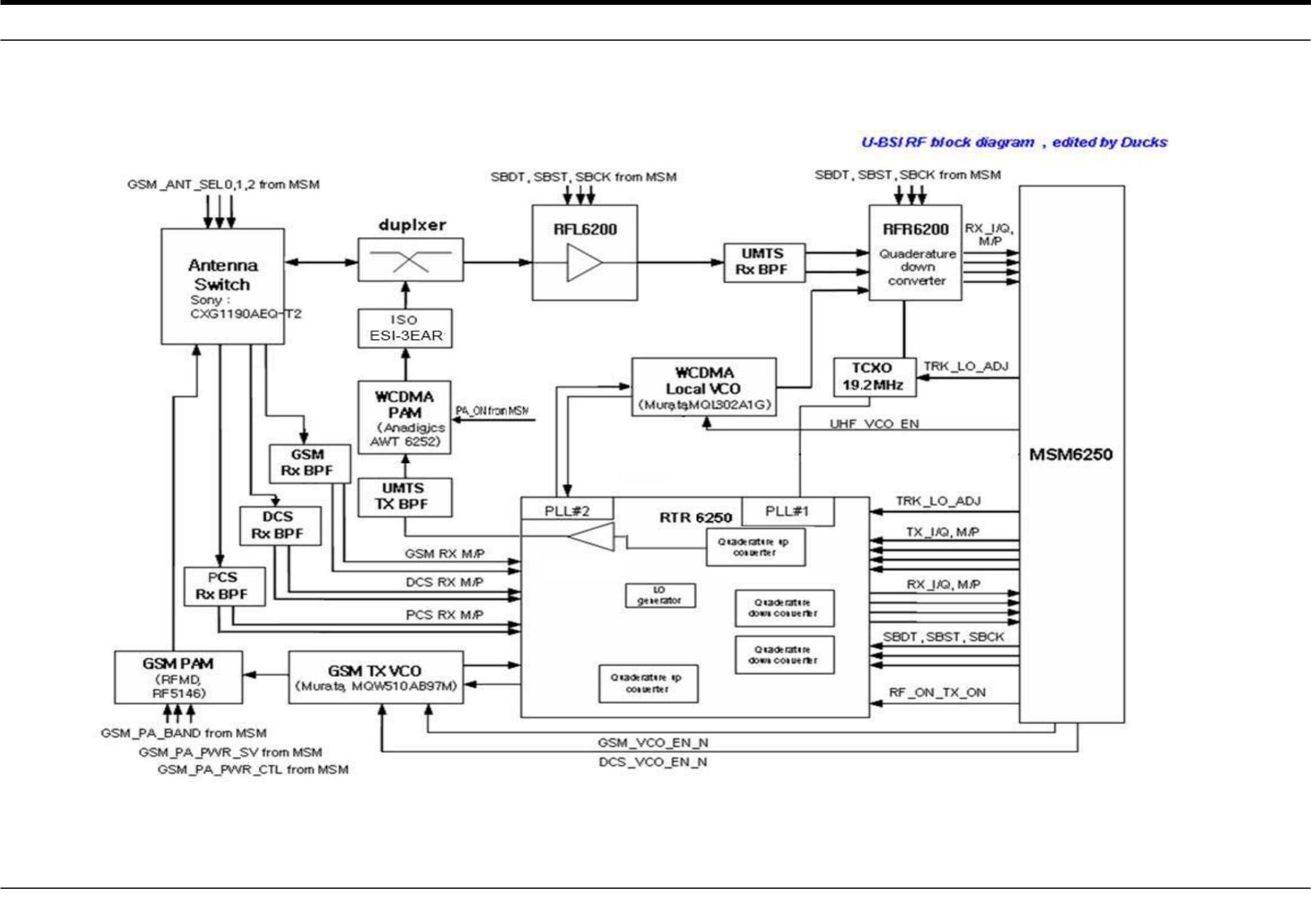
2-1. SGH-ZV30 RF Circuit Description
- Antenna Switch Module (U106)
The antenna switch module allows multiple operating bands and modes to share the same antenna. A common
antenna connects to one of five paths: 1) UMTS-2100 Rx/Tx, 2) EGSM-900 Rx, 3) EGSM-900 Tx, 4) DCS-1800
Rx, and 5) DCS-1800 Tx. 6) PCS-1900 Tx, 7) PCS-1900 Rx, UMTS operation requires simultaneous reception and
transmission.
-Filter
To convert Electromagnetic Field Wave to Acoustic Wave and then pass the specific frequency band.
- GSM Rx FILTER (F100) : For filtering the frequency band between 925 ~ 960 MHz.
- DCS Rx FILTER (F101) : For filtering the frequency band 1805 and 1880 MHz.
- PCS Rx FILTER (F102) : For filtering the frequency band 1930 and 1990 MHz.
- WCDMA Rx FILTER (F201) : For filtering the frequency band 2110 and 2170 MHz.
- WCDMA Tx FILTER (F202) : For filtering the frequency band 1920 and 1980 MHz.
- VCTCXO (OSC201)
To generate the 19.2MHz reference clock to drive the logic and RF.
- Duplexer (F204)
A duplexer splits a single operating band into receive and transmit paths.
- UMTS PAM (U202)
This is a key component in the transmitter chain and must complement the RTR6250 IC precisely; jointly they
dominate the UMTS transmitter performance characteristics. Parameters such as gain, output power level, ACLR,
harmonics, Rx-band noise, and power supply current are critical.
- GSM/DCS/PCS PAM (U105)
The PAM is a key component in any transmitter chain and must complement the rest of the transmitter
precisely.For GSM, DCS, PCS operation, the closed-loop transmit power control functions add even more
requirements relative to the UMTS PA. In addition to gain control and switching requirements, the usual RF
parameters such as gain, output power level, several output spectrum requirements, and power supply current are
critical..

SAMSUNG Proprietary-Contents may change without notice
This Document can not be used without Samsung's authorization
Circuit Description
2-2
- GSM/DCS/PCS l Tx VCO (OSC101)
The Tx VCO outputs for EGSM, DCS, PCS drive a resistive network that splits the active signal into two signals:
1) the input to the active PAM / this is the low loss path, and 2) the OPLL feedback signal.
- RF VCO (OSC202)
The single-band UHF VCO is a key component within its phase-locked loop; VCO performance directly impacts
PLL and transceiver performance. UMTS Rx LO signal is generated from this VCO's output.
- RFL6200 (U201)
The RFL6200 includes an LNA circuit optimized for UMTS-2100 operation. The LNA is separated from all other
receive functions contained within the RFR6200 receiver IC to improve mixer LO to RF isolation a critical
parameter in the Zero-IF architecture.
- RFR6200 (U203)
The RFR6200 provides the Zero-IF receiver signal path, from RF to analog baseband, for UMTS-2100 applications.
The RFR6200 accepts its UMTS input signal from the handset RF front-end design. The UMTS input is configured
differentially to optimize second-order inter-modulation and common mode rejection performance, and implements
MSM-controlled gain adjustments to extend the receiver dynamic range.
- RTR6250 (U104)
The RTR6250 supports multi-band, multi-mode phones with two receiver signal paths and three transmitter signal
paths:
1) Receiver paths
- EGSM-900
- DCS-1800
-PCS-1900
2) Transmitter paths
- EGSM-900 (using OPLL technique)
- DCS-1800 (using OPLL technique)
-PCS-1900
- UMTS-2100
Numerous secondary functions are integrated on-chip as well:

SAMSUNG Proprietary-Contents may change without notice
Circuit Description
This Document can not be used without Samsung's authorization
2-3
2-2. Baseband Circuit description of SGH-ZV30
2-2-1. PM6650
- Power Management
Ten low-dropout regulators designed specifically for GSM applications power the terminal and help ensure
optimal system performance and long battery life. It provides LDOs support for 1.375V, 1.8V, 2.6V,
2.85V,3.3V.IC-level interfaces include the three-line serial bus interface(SBI) used by the MSM6250 device to
control and status the PM6650 IC.
- TCXO Controller and Buffers
The PM6650 IC includes circuits for controlling the TCXO warm-up and buffering its signal for distribution
throughout the handset. Performance specifications are presented below.
2-2-2. Connector
- LCD Connector
LCD is consisted of main LCD(color 262K TFT LCD) and small LCD(OLED color 65K LCD). Chip select
signals in the U302, MAIN_LCD_CSB can enable main LCD and SUB_LCD_CSB can enable small
LCD.Dimming signal enables white LED of main LCD and Dimming Control. C_Main_LCD_RESETB signal
initiates the reset process of the main LCD. C_SUB_LCD_RESETB signal initiates the Reset process of the
small LCD. 16-bit data lines(D2(0)~D(15)) transfers data and commands to LCD. Data and commands use
"C_A2(1)" signal. If this signal is high, Inputs to LCD are commands. If it is low, Inputs to LCD are data.
The signal which informs the input or output state to LCD, is required. But this system is not necessary this
signal. Power signals for LCD are "VBATT and VREG_MSMP". "EAR1OP" and "EAR1ON" are used for audio
speaker. And "MOTOR_EN" from U302 enables the motor.
-Key
This is consisted of key interface pins among U302, KEY_N(0:4). These signals compose the matrix.Result of
matrix informs the key status to key interface in the U302. Power on/off key is seperated from the matrix.
The key LED use the "VBATT" supply voltage. "KEY_LED_ON" signal enables LEDs with current control.
"HALL_SW" informs the status of folder (open or closed) to the. This uses the hall effect IC, EM1681
- EMI ESD Filter
This system uses the EMI ESD filter, GMF05LC to protect noise from IF CONNECTOR part.
- IF connector
It is 24-pin connector. They are designed to use VBATT, CF, UART1_TX, UART1_RX, UART1_RFR,
UART1_CTS, JIG_ON, RTCK, TCK, TDI, TDO, TMS and GND. They connected to power supply
IC,microprocessor and signal processor IC.
2-2-3. Audio
EAR1OP and EAR1ON from U302 are connected to the main Receiver. MIC1P and MIC1N are connected to
the main MIC. And MIC2P and MIC2N are connected to the Earphone. YMU769 has a built-in amplifier, and
thus, is an ideal device for outputting sounds that are used by mobile phones in addition to game sounds and
ringing melodies that are replayed by a synthesizer.

SAMSUNG Proprietary-Contents may change without notice
This Document can not be used without Samsung's authorization
Circuit Description
2-4
The synthesizer section adopts "stereophonic hybrid synthesizer system" that are given advantages of both FM
synthesizers and Wave Table synthesizers to allow simultaneous generation of up to 32 FM voices and 32
Wave Table voices. Furthermore, YMU769 has a built-in hardware sequencer that helps to realize complex play
without heavily loading the host CPU. And this device also has a built-in circuit for controlling vibrators and
LEDs synchronizing with play of music. The consumed electric current can be stopped to the minimum by
power down mode when not operating. The hardware sequence built in this device allows playing of the
complex music without giving excessive load to the CPU of the portable telephones. Moreover, the registers of
the FM synthesizer can be operated directly for real time sound generation, allowing, for example, utilization of
various sound effects when using the game software installed in the portable telephone.
2-2-4. Memory
The signals in the MSM6250 enable two memories. They use two volt supply voltage, VREG_MSME and
VREG_MSMP from the PM6650. This system uses SEC's memory, KBE00F005M-F411. It is consisted of 1G
bits flash NAND memory and 512M bits SDRAM memory. It has 16 bit data line, D1[0~15] which is connected
to MSM6250.It has 22 bit address lines, A[1~22]. ROM_CS and RAM_CS signals is chip select.
2-2-5. Camera
The camera module consists of 1.3 Mega pixel. The Mega camera is a highly integrated CMOS color image
sensor implemented by Hynix CMOS sensor process realizing high sensitivity and wide dynamic range. Total
pixel array size is 1298H x 982V, and 1280H x 960V pixels are active.
2-2-6. IRDA
This system uses IRDA module, HSDL_3208, Agilent's. This has signals, "IRDA_EN"(enable signal),
"RXD0"(Input data) and "TXD0"(output data). These signals are connected to U302(MSN6250). It uses two
power signals. "VREG_MSMP" is used for circuit and "VBATT" is used for LED.
2-2-7. TransFlash Card (External Memory Card)
Memory Module has eight exposed contacts on one side. The host is connected to the module using a
dedicated eight-pin connector. Measuring just 11mm by 15mm and 1mm thick, Two-thirds the size of a SIM
module, TransFlash is even smaller than many embedded memory devices.
SAMSUNG Proprietary-Contents may change without notice
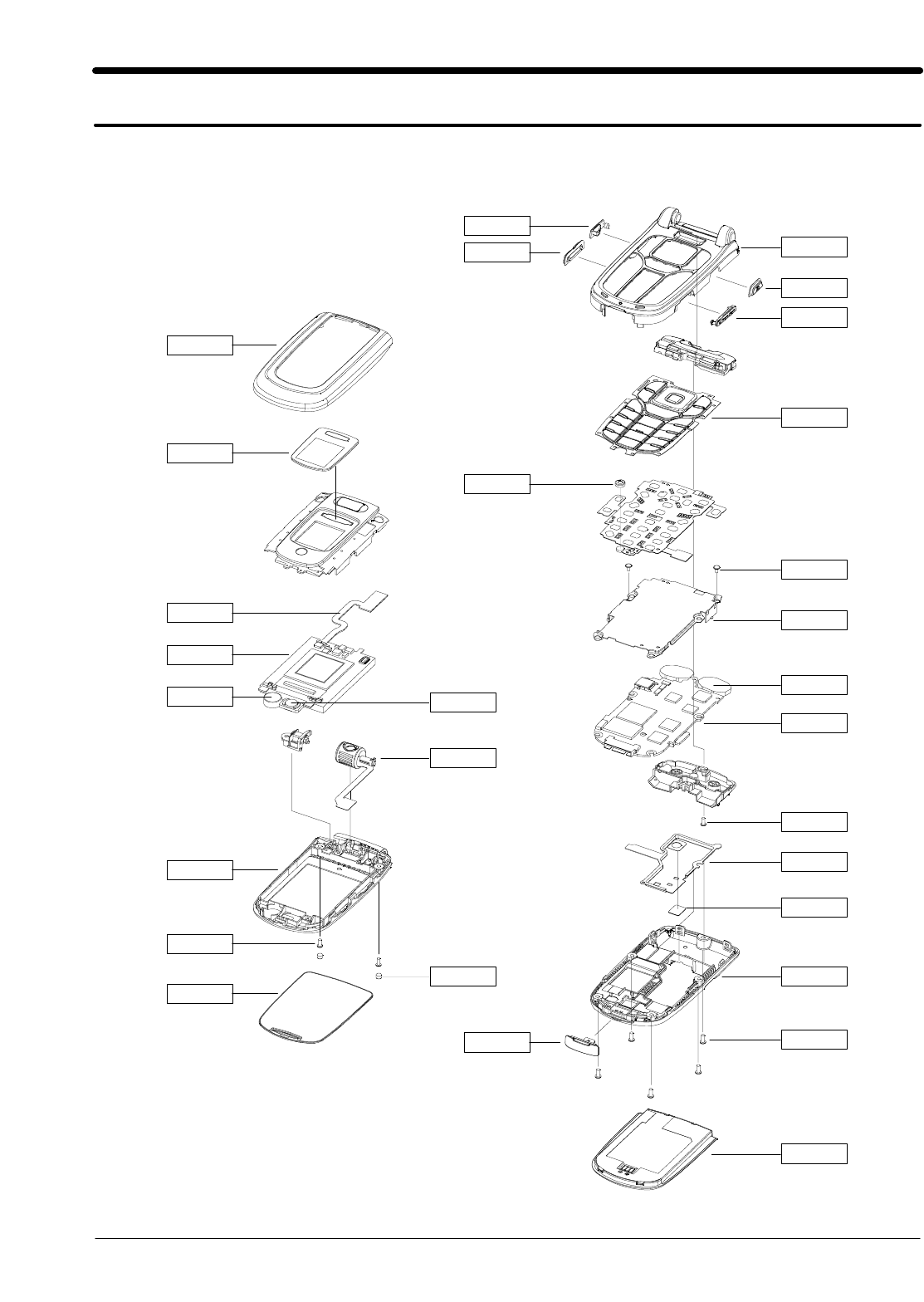
3. Exploded View and Parts List
3-1
This Document can not be used without Samsung's authorization
3-1. Exploded View
QFU01
QRF03
QVO01
QMI03
QIF01
QWD01
QLC01
QMO01 QAR01
QFL01
QMW01
QME03
QCA01
QFR01
QCK01
QCW04
QKP01
QFR02
QCR12
QME06
QMP01
QCR04
QRE02
QRF01
QRE01
QCR11
QBA01
QSC12
QCR16
SAMSUNG Proprietary-Contents may change without notice
Exploded view and Part List
3-2
This Document can not be used without Samsung's authorization
3-2. Parts List
Location No Description Sec Code
QAR01 ㅤAUDIO-RECEIVER;32ohm,110dB±2dB,11x7 3009-001132
QBA01 ㅤBATTERY-1000MAH,SIL,ENG,M;BST474ASB, GH43-01990A
QCA01 ㅤUNIT-CAMERA;SGH-ZV30,MOMFA331U1A,-,E GH59-02281A
QCK01 ㅤMEC-CAMERA KEY;SGH-ZV30,VODAFON,PC,- GH75-06987A
QCR04 ㅤSCREW-MACHINE;PH,+,-,M1.4,L4,ZPC(BLK 6001-001479
QCR11 ㅤSCREW-MACHINE;PH,+,M1.7,L4,ZPC(BLK), 6001-001654
QCR12 ㅤSCREW-MACHINE;PH,+,M1.4,L2.5,ZPC(BLK 6001-001530
QCR16 ㅤSCREW-MACHINE;PH,+,-,M1.7,L4.5,ZPC(B 6001-001878
QFL01 ㅤMEC-FOLDER LOWER;SGH-ZV30,VODAFON,PC GH75-06980A
QFR02 ㅤMEC-FRONT SHIELD CAN;SGH-ZV30,VODAFO GH75-06983A
QFU01 ㅤMEC-FOLDER UPPER;SGH-ZV30,VODAFON,PC GH75-06979A
QIF01 ㅤPMO-IF COVER V2;SGH-ZV30,PC+URETHANE GH72-25828A
QKP01 ㅤMEC-KEYPAD(VOD/D_GRY);SGH-ZV30,VODAF GH75-06982A
QLC01 ㅤLCD-SGHZV30 MODULE;UF-17E101-A,SGH-Z GH07-00754A
QME03 ㅤUNIT-FPCB;SGH-ZV30,KBSGHZV30KM,-,OMN GH59-02284A
QME06 ㅤUNIT-SPK MODULE;SGH-ZV30,SS-SGH-ZV30 GH59-02356A
QMO01 ㅤMOTOR DC-SGHZV30;DMJBRK94B,SGH-ZV30, GH31-00177A
QMP01 ㅤPBA MAIN-SGHZV30;SGH-ZV30,VODAFONE,G GH92-02152A
QMW01 ㅤMEC-MAIN WINDOW;SGH-ZV30,VOD,PC,-,-, GH75-07462A
QRE01 ㅤMEC-REAR COVER;SGH-ZV30,VODAFON,PC,- GH75-06985A
QRE02 ㅤMEC-REAR SHIELD CAN;SGH-ZV30,VODAFON GH75-06984A
QRF01 ㅤMPR-SHEET REAR SHIELD CA;SGH-ZV30,PC GH74-15903A
QSC12 ㅤRMO-FOLDER SCREW;SGH-ZV30,SI RUBBER, GH73-05042A
QVO01 ㅤMEC-VOLUME KEY;SGH-ZV30,VODAFON,PC,- GH75-06986A
QWD01 ㅤPCT-SUB WINDOW;SGH-ZV30,ACRYL,SIL,-, GH72-25186A
QFR01 ㅤMEC-FRONT COVER;SGH-ZV30,VODAFON,PC, GH75-06981A
ㅤQCW04 PMO-TRANS FLASH COVER;SGH-ZV30,PC,D/ GH72-21805A
ㅤQMI03 RMO-RUBBER MIC;SGH-ZV30,205C,5XT2.35 GH73-04677A
ㅤQRF03 PMO-EAR JACK COVER;SGH-ZV30,PC+URETH GH72-21806A

SAMSUNG Proprietary-Contents may change without notice
Exploded view and Part List
3-3
This Document can not be used without Samsung's authorization
Description Sec Code
BAG PE;LDPE,T0.05,W80,L180,TRP,-,- 6902-000634
CBF INTERFACE-PC DATA CABLE;SGH-Z110 GH39-00326A
CHARGER-TCH;TCH137ESE,SGH-X910,AC/DC GH44-00701A
S/W CD-PC STUDIO VODAFONE;SGH-ZV30,S GH46-00168A
UNIT-EARPHONE;SGH-Z107,EM-SS650E-ST, GH59-01713A
LABEL(P)-WATER SOAK;COMM,NORGE,100G, GH68-02026A
MANUAL-WEEE CARD;COMM,SEC,ENGLISH,UN GH68-07013A
LABEL(R)-MAIN;SGH-ZV30,EU,MAT,0.05,4 GH68-07055A
MANUAL-USER;SGH-ZV30,MAN,GERMAN,GERM GH68-07773A
MANUAL-QSG;SGH-ZV30,VD2,GERMAN,GERM, GH68-08167A
CUSHION-CASE LOWER(VOD);SGH-Z105,PUL GH69-02177A
BOX(P)-MENUAL BOX(UMTS);SGH-Z107V,SI GH69-02540C
CUSHION-CASE(UPPER);SGH-Z300,PULP,T0 GH69-02837A
BOX(P)-SGHZV30(UMTS);SGH-ZV30,SC350+ GH69-03235A
IPR-LOCKER SPRING;SCH-750,STS304,-,T GH70-10633A
PMO-BATTERY LOCKER;SGH-ZV30,PC,GRY,- GH72-24503A
MPR-BOHO VNYL CONN V2;SGH-E316,#950, GH74-11112A
MPR-BOHO VINYL TOP F/U;SGH-ZV30,3M 4 GH74-14662A
MPR-BOHO VINYL F/LOWER;SGH-ZV30,3M 4 GH74-14663A
MPR-NON WOVEN FRONT LCD;SGH-ZV30,NON GH74-15896A
MPR-MIC PC SHEET;SGH-ZV30,PC SHEET+T GH74-15897A
MPR-TAPE ALUMINIUM;SGH-ZV30,AL TAPE, GH74-16493A
MPR-GASKET GOLD L;SGH-ZV30,CFPWX290, GH74-16494A
MPR-GASKET GOLD R;SGH-ZV30,CFPWX290, GH74-16495A
MPR-TAPE LCD INSULATION2;SGH-ZV30,3M GH74-16497A
MPR-BOHO VINYL UPPER;SGH-ZV30,PBC,38 GH74-17233A
MPR-SPONGE EAR COVER;SGH-ZV30,SRS PO GH74-17968A
MEC-HANGER;SGH-E710,KORA,-,-,ME/SIL, GH75-03673B
SAMSUNG Proprietary-Contents may change without notice
Exploded view and Part List
3-4
This Document can not be used without Samsung's authorization
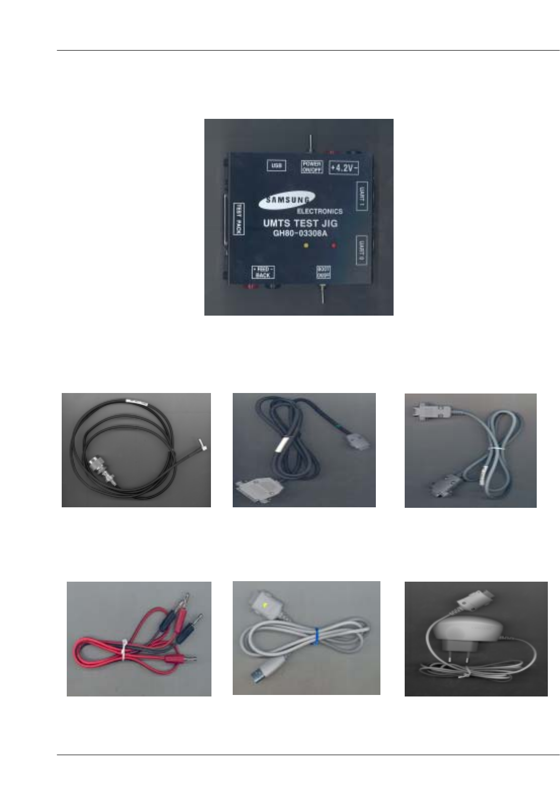
3-3. Test Jig (GH80-03308A)
3-3-1. RF Test Cable
(GH39-00283A)
3-3-2. Test Cable
(GH39-00337E)
3-3-3. Serial Cable
3-3-4. Power Supply Cable 3-3-5. DATA CABLE
(GH39-00326A)
3-3-6. TC
(GH44-00701A)

SAMSUNG Proprietary-Contents may change without notice
4. Electrical Parts List
4-1
This Document can not be used without Samsung's authorization
Design LOC Description SEC CODE
AN401 ;ACS2450FBAVI 4202-001062
C101,C110,C112,C114 C-CERAMIC,CHIP 2203-000812
C102,C104,C252,C408 C-CERAMIC,CHIP 2203-000679
C103,C107,C129,C137 C-CERAMIC,CHIP 2203-000438
C105,C111,C113,C120 C-CERAMIC,CHIP 2203-005482
C108,C130,C136,C171 C-CERAMIC,CHIP 2203-000254
C115,C116,C117,C119 C-CERAMIC,CHIP 2203-000812
C118,C125,C133,C601 C-CERAMIC,CHIP 2203-000854
C121,C124,C131,C146 C-CERAMIC,CHIP 2203-000812
C122,C126,C132,C134 C-CERAMIC,CHIP 2203-000233
C123,C204 C-CERAMIC,CHIP 2203-000885
C127,C135,C154,C159 C-CERAMIC,CHIP 2203-000995
C128,C141,C142,C150 C-CERAMIC,CHIP 2203-005482
C138 C-FILM,CHIP 2301-001512
C139 C-CERAMIC,CHIP 2203-005446
C140 C-CERAMIC,CHIP 2203-002668
C143,C253 C-CERAMIC,CHIP 2203-000836
C147,C245,C257,C413 C-CERAMIC,CHIP 2203-006208
C148,C153,C162,C168 C-CERAMIC,CHIP 2203-000438
C149,C164,C169,C259 C-CERAMIC,CHIP 2203-000386
C151,C163,C229,C251 C-CERAMIC,CHIP 2203-000812
C152,C156,C157,C207 C-CERAMIC,CHIP 2203-005482
C155,C328,C329,C417 C-CERAMIC,CHIP 2203-006093
C158 C-CERAMIC,CHIP 2203-000311
C160,C457 C-TA,CHIP 2404-001274
C161 C-FILM,CHIP 2301-001515
C165 C-CERAMIC,CHIP 2203-005503
C166 C-CERAMIC,CHIP 2203-002443
C167,C221 C-CERAMIC,CHIP 2203-005234
C170,C201,C202,C209 C-CERAMIC,CHIP 2203-000233
C205 C-CERAMIC,CHIP 2203-006324
C208,C210,C214,C248 C-CERAMIC,CHIP 2203-000330
C211,C685 C-CERAMIC,CHIP 2203-000995
C212 C-CERAMIC,CHIP 2203-001178
C222 C-CERAMIC,CHIP 2203-001383
C224,C228,C234,C244 C-CERAMIC,CHIP 2203-000233
C225,C233,C238,C240 C-CERAMIC,CHIP 2203-005482
C231,C232,C235,C239 C-CERAMIC,CHIP 2203-000254
C236,C242 C-CERAMIC,CHIP 2203-005288
C237,C241,C256,C407 C-CERAMIC,CHIP 2203-000438
C243,C246,C249,C258 C-CERAMIC,CHIP 2203-005482
C247,C250,C262,C404 C-CERAMIC,CHIP 2203-000233
C254 C-CERAMIC,CHIP 2203-000585
C255 C-FILM,CHIP 2301-001214
C260,C261,C684 C-CERAMIC,CHIP 2203-005050
C263 C-CERAMIC,CHIP 2203-000330
C301,C303,C304,C305 C-CERAMIC,CHIP 2203-005482
C302,C310 C-CERAMIC,CHIP 2203-006091
C306,C307,C308,C309 C-CERAMIC,CHIP 2203-005482
C311,C312,C313,C314 C-CERAMIC,CHIP 2203-005482

SAMSUNG Proprietary-Contents may change without notice
Electrical Parts List
4-2
This Document can not be used without Samsung's authorization
Design LOC Description SEC CODE
C315,C316,C317,C318 C-CERAMIC,CHIP 2203-005482
C319,C320,C321,C322 C-CERAMIC,CHIP 2203-005482
C323,C324,C325,C326 C-CERAMIC,CHIP 2203-005482
C333,C334,C335,C336 C-CERAMIC,CHIP 2203-005482
C337,C338,C339,C340 C-CERAMIC,CHIP 2203-005482
C341,C342 C-CERAMIC,CHIP 2203-000550
C343 C-CERAMIC,CHIP 2203-000489
C344 C-CERAMIC,CHIP 2203-005480
C345 C-CERAMIC,CHIP 2203-000254
C346,C402,C406,C409 C-CERAMIC,CHIP 2203-005482
C347,C501,C638,C647 C-TA,CHIP 2404-001225
C348 C-CERAMIC,CHIP 2203-005395
C401,C481 C-CERAMIC,CHIP 2203-006053
C405 C-CERAMIC,CHIP 2203-000628
C410,C414,C416,C419 C-CERAMIC,CHIP 2203-005482
C415,C422,C423,C431 C-CERAMIC,CHIP 2203-006208
C418,C420,C425,C426 C-CERAMIC,CHIP 2203-006201
C421,C427,C430,C432 C-CERAMIC,CHIP 2203-000278
C424,C440,C442,C458 C-CERAMIC,CHIP 2203-005482
C428,C429,C462 C-CERAMIC,CHIP 2203-006201
C433,C467,C472,C475 C-CERAMIC,CHIP 2203-006093
C434,C603,C604,C606 C-CERAMIC,CHIP 2203-000278
C441 C-CERAMIC,CHIP 2203-001153
C443,C444,C605,C683 C-CERAMIC,CHIP 2203-000812
C446,C449,C450,C451 C-CERAMIC,CHIP 2203-000438
C447,C448 C-CERAMIC,CHIP 2203-006208
C452,C453,C454,C466 C-CERAMIC,CHIP 2203-000438
C460,C461 C-TA,CHIP 2404-001281
C463,C502,C503 C-TA,CHIP 2404-001105
C464 C-CERAMIC,CHIP 2203-002494
C470,C471,C504,C512 C-CERAMIC,CHIP 2203-005482
C473,C474 C-CERAMIC,CHIP 2203-005138
C478,C505,C649 C-TA,CHIP 2404-001339
C479,C506,C650,C693 C-CERAMIC,CHIP 2203-005061
C482,C508,C509,C510 C-CERAMIC,CHIP 2203-006093
C483,C507,C517,C518 C-CERAMIC,CHIP 2203-000233
C511,C615,C622,C670 C-CERAMIC,CHIP 2203-006093
C513,C514,C633,C634 C-CERAMIC,CHIP 2203-005482
C602,C607,C608,C629 C-CERAMIC,CHIP 2203-000854
C609,C613 C-TA,CHIP 2404-001366
C614,C621,C681 C-CERAMIC,CHIP 2203-006137
C616,C617 C-TA,CHIP 2404-001352
C618 C-CERAMIC,CHIP 2203-000233
C630 C-CERAMIC,CHIP 2203-000438
C632,C635,C636,C678 C-CERAMIC,CHIP 2203-000854
C637,C640,C671,C690 C-CERAMIC,CHIP 2203-005482
C639,C691 C-TA,CHIP 2404-001394
C641,C642,C643,C644 C-CERAMIC,CHIP 2203-005481
C645,C646 C-CERAMIC,CHIP 2203-000654
C648,C692 C-TA,CHIP 2404-001225

SAMSUNG Proprietary-Contents may change without notice
Electrical Parts List
4-3
This Document can not be used without Samsung's authorization
Design LOC Description SEC CODE
C679,C682,C686,C687 C-CERAMIC,CHIP 2203-000278
C680 C-CERAMIC,CHIP 2203-000854
C688 C-CERAMIC,CHIP 2203-000278
C689 C-CERAMIC,CHIP 2203-006093
C694 C-CERAMIC,CHIP 2203-005061
C695,C696 C-CERAMIC,CHIP 2203-006190
C697,C698 C-CERAMIC,CHIP 2203-000812
CN101 CONNECTOR-COAXIAL3705-001358
CN401 CONNECTOR-CARDEDGE3709-001269
CN402 CONNECTOR-SOCKET 3710-002120
CN404 CONNECTOR-HEADER 3711-005781
CN504 CONNECTOR-CARDEDGE3709-001344
CN505 ;14-5602-060-000-829 3711-005367
CN601 JACK-PHONE3722-002181
CN603,CN604 CONNECTOR-SOCKET 3710-001105
D400 DIODE-SCHOTTKY 0404-001093
D401 DIODE-ARRAY 0407-001002
F100 FILTER-SAW 2904-001550
F101 FILTER-SAW 2904-001570
F102 FILTER-SAW 2904-001571
F201 FILTER-SAW 2904-001439
F202 FILTER-SAW 2904-001438
F203 RF-MODULE 4709-001370
F204 FILTER 2910-000004
HEA501 CONNECTOR-HEADER 3711-005643
L101 INDUCTOR-SMD2703-002201
L102,L121,L124 INDUCTOR-SMD2703-002155
L103,L106,L112,L119 INDUCTOR-SMD2703-002198
L104,L204,L213 INDUCTOR-SMD2703-002267
L105 INDUCTOR-SMD2703-002200
L108,L114,L115,L120 INDUCTOR-SMD2703-002819
L109,L111,L116,L118 INDUCTOR-SMD2703-002208
L110,L117,L203 INDUCTOR-SMD2703-002205
L113,L208,L211,L212 CORE-FERRITEBEAD3301-001756
L122 INDUCTOR-SMD2703-002170
L123 INDUCTOR-SMD2703-002369
L201 INDUCTOR-SMD2703-002314
L202 INDUCTOR-SMD2703-002198
L205 INDUCTOR-SMD2703-002268
L206 INDUCTOR-SMD2703-001750
L207 INDUCTOR-SMD2703-002206
L209,L210 INDUCTOR-SMD2703-002368
L214 CORE-FERRITEBEAD3301-001120
L215 INDUCTOR-SMD2703-001749
L301,L302,L303,L305 R-CHIP 2007-000171
L402,L403 INDUCTOR-SMD2703-002782
L404 INDUCTOR-SMD2703-000300
L405,L501,L502,L503 CORE-FERRITEBEAD3301-001534
L602,L603,L605,L604 INDUCTOR-SMD2703-001595
LED401 PHOTO-IRDA 0604-001261

SAMSUNG Proprietary-Contents may change without notice
Electrical Parts List
4-4
This Document can not be used without Samsung's authorization
Design LOC Description SEC CODE
OSC101 OSCILLATOR-VCO 2806-001360
OSC201 OSCILLATOR-VCTCXO2809-001280
OSC202 ;MQL302A1G71 2806-001367
OSC301 RESONATOR-CERAMIC2802-001182
Q403,Q404 TR-DIGITAL0504-000168
Q405 TR-DIGITAL0504-001050
R101,R312,R323 R-CHIP 2007-000171
R102,R211 R-CHIP 2007-007491
R105,R106,R129,R130 R-CHIP 2007-000138
R107 INDUCTOR-SMD2703-001180
R108,R109,R111,R112 R-CHIP 2007-000140
R115,R118,R642,R643 R-CHIP 2007-000172
R116 R-CHIP 2007-007316
R117 R-CHIP 2007-000145
R119,R133,R134 R-CHIP 2007-001217
R120,R121,R635,R636 R-CHIP 2007-003001
R122 R-CHIP 2007-000174
R123,R124,R125,R126 R-CHIP 2007-001307
R127,R128 R-CHIP 2007-001301
R131 R-CHIP 2007-000147
R132,R402 R-CHIP 2007-007142
R135,R204,R207,R214 R-CHIP 2007-000138
R201,R210,R212 R-CHIP 2007-007314
R202 R-CHIP 2007-000173
R205 R-CHIP 2007-007318
R206 R-CHIP 2007-007470
R208 R-CHIP 2007-008263
R209,R314 R-CHIP 2007-000137
R213 R-CHIP 2007-000163
R215,R405 R-CHIP 2007-001298
R216,R221,R313,R325 R-CHIP 2007-000140
R218,R411,R503,R504 R-CHIP 2007-000143
R220 R-CHIP 2007-007310
R222 R-CHIP 2007-001284
R301,R304,R311,R315 R-CHIP 2007-000148
R302,R303,R602 R-CHIP 2007-001339
R308 R-CHIP 2007-000636
R309 R-CHIP 2007-000157
R316,R317,R318,R319 R-CHIP 2007-000148
R321,R326,R327,R508 R-CHIP 2007-000148
R324,R416,R435,R436 R-CHIP 2007-000171
R403,R414,R417,R443 R-CHIP 2007-000140
R406 R-CHIP 2007-007468
R408,R623,R624,R625 R-CHIP 2007-007132
R409 R-CHIP 2007-009117
R410 R-CHIP 2007-007095
R413 R-CHIP 2007-000153
R415,R419,R420,R421 R-CHIP 2007-008542
R423,R424 R-CHIP 2007-008542
R432 R-CHIP 2007-000162
SAMSUNG Proprietary-Contents may change without notice
Electrical Parts List
4-5
This Document can not be used without Samsung's authorization
Design LOC Description SEC CODE
R437,R438 R-CHIP 2007-007199
R439 R-CHIP 2007-007107
R445,R454,R631,R632 R-CHIP 2007-000171
R447,R448,R449,R450 R-CHIP 2007-008437
R452,R453 R-CHIP 2007-003112
R459 R-CHIP 2007-000146
R460 R-CHIP 2007-007592
R509,R511,R630,R641 R-CHIP 2007-000148
R510 R-CHIP 2007-000166
R605 R-CHIP 2007-008055
R607,R608,R611,R612 R-CHIP 2007-007317
R616 R-CHIP 2007-001325
R626 R-CHIP 2007-007132
R627,R628 R-CHIP 2007-007139
R633,R634,R639,R640 R-CHIP 2007-000171
R637,R638 R-CHIP 2007-003001
TH201 THERMISTOR 1404-001221
U104 IC1205-002645
U105 IC1201-002174
U106 IC1205-002724
U201 IC1201-001984
U202 ;AWT6252M7P8 1201-002196
U203 IC1205-002297
U204 TR-DIGITAL0504-001060
U301 ;KBE00F005M-F411 1108-000005
U302 IC1205-002527
U401 IC1203-003335
U402 DIODE-ARRAY 0407-001038
U403 RF-MODULE 4709-001352
U407 DIODE-TVS0406-001200
U408 BATTERY 4302-001177
U409 IC1203-002785
U411 ;AAT4280-3 1205-002767
U413 IC1001-001248
U414 IC 1203-003728
U415 FET-SILICON0505-001889
U502 ;MIC2211-GKYML 1203-003785
U506,U507,U511 ;ECLAMP2378P 2901-001348
U512,U513,U514,U516 VARISTOR1405-001161
U601 IC1001-001261
U602 IC1203-002860
U603 IC1204-002316
U604,U605 IC1001-001265
V501,V502,V503,V504 VARISTOR 1405-001082
V505,V506,V507,V508 VARISTOR 1405-001082
V509,V510,V511,V512 VARISTOR 1405-001082
V601,V602,V603,V604 VARISTOR 1405-001082
XTAL401 CRYSTAL-UNIT 2801-004373
ZD402,ZD407 DIODE-TVS0406-001197
ZD405 DIODE-ZENER 0403-001547

SAMSUNG Proprietary-Contents may change without notice
Electrical Parts List
4-6
This Document can not be used without Samsung's authorization
Design LOC Description SEC CODE
ZD408 DIODE-ZENER 0403-001387
ZD501 DIODE-TVS0406-001215
ZD504,ZD505,ZD506 DIODE-TVS0406-001201
ZD507,ZD508,ZD509 DIODE-TVS0406-001201
ZD602,ZD603,ZD604 DIODE-TVS0406-001201
ZD605,ZD606,ZD607 DIODE-TVS0406-001201
SAMSUNG Proprietary-Contents may change without notice
This Document can not be used without Samsung's authorization
5. Block Diagrams
5-1
5-1. RF Solution Block Diagram
SAMSUNG Proprietary-Contents may change without notice
Block Diagrams
This Document can not be used without Samsung's authorization
5-2
5-2. Base Band Solution Block Diagram
SAMSUNG Proprietary-Contents may change without notice
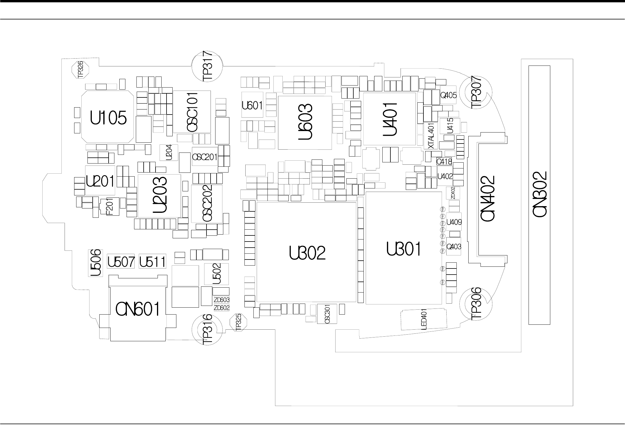
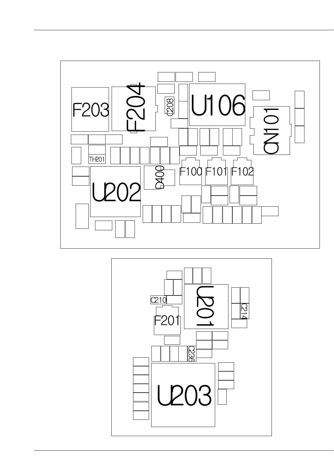
6. PCB Diagrams
6-1
This Document can not be used without Samsung's authorization
6-1. PCB Top Diagram
SAMSUNG Proprietary-Contents may change without notice
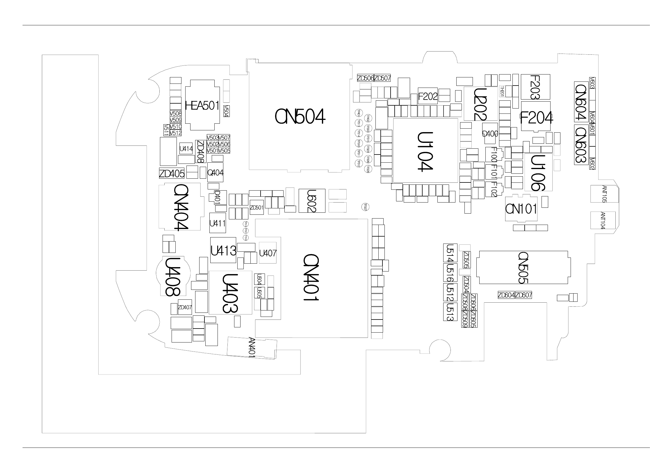
PCB Diagrams
6-2
This Document can not be used without Samsung's authorization
6-2. PCB Bottom Diagram
SAMSUNG Proprietary-Contents may change without notice
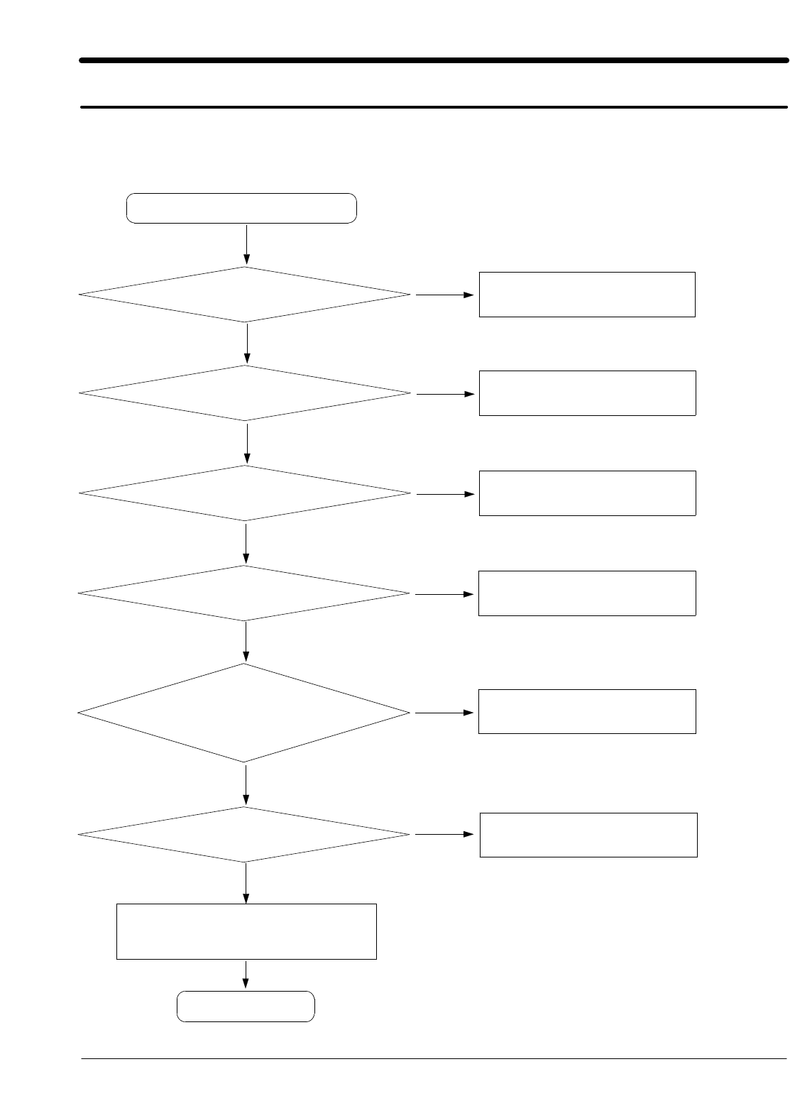
7. Flow Chart of Troubleshooting
This Document can not be used without Samsung's authorization
7-1
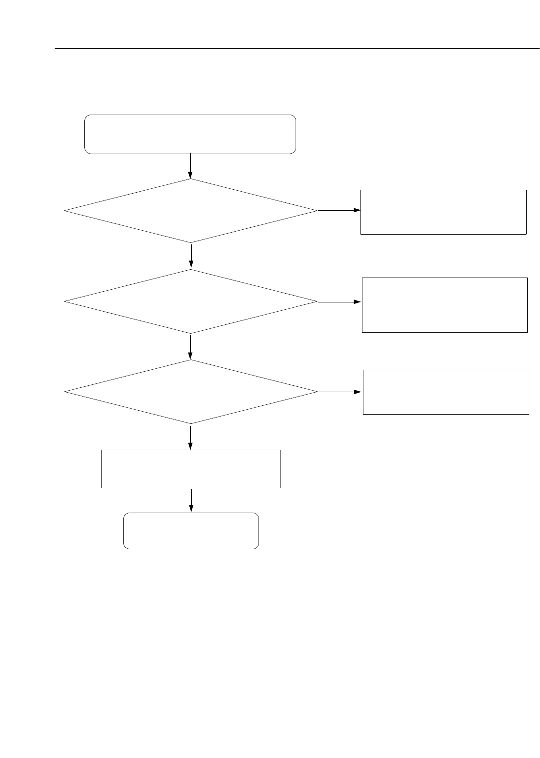
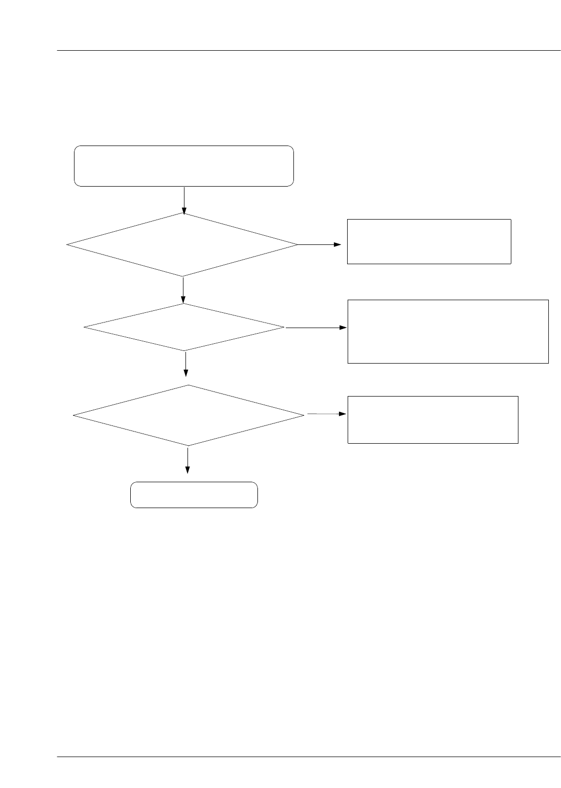
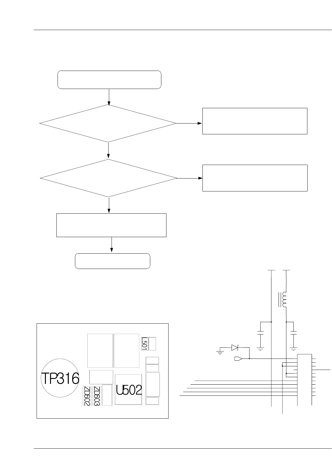
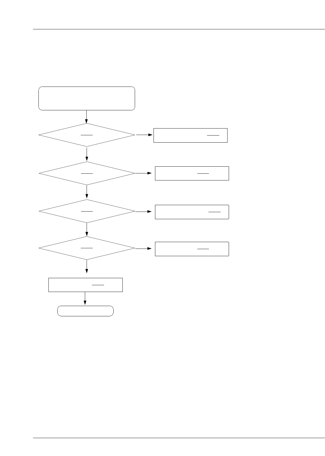
7-1. Power On
Yes
Yes
Check the initial operation
Yes
No Check the clock generation circuit
(related to OSC201)
Check for the clock at
C407= 19.2MHz
Yes
No Check the PMIC
C415(VREG_MSME) = 1.8V?
C421(VREG_MSMP) = 2.6V?
C423(VREG_MSMA) = 2.6V?
C433(VREG_TCXO) = 2.85V?
Yes
No Check the PMIC
C413(VREG_MSMC) =
1.375V?
Yes
No Resolder XTAL401
Check the Clock at
XTAL401=32.768KHZ
Yes
No Check the PMIC related to PS_HOLD
U401 pin57(PS_HOLD)
=2.6V?
Yes
No
END
Change the Battery
' Power On ' does not work
Check the Battery Voltage
is more than 3.3V
SAMSUNG Proprietary-Contents may change without notice
This Document can not be used without Samsung's authorization
Flow Chart of Troubleshooting
7-2
Power On
_2.85V
3.3V, 150mA
VREG_MSMP
VREG_TCXO
3.3V, 50mA
VREG_USIM
VREG_MSMA
KEY_LED_ON
VREG_RFRX
VREG_MSME
VREG_USB
VREG_RFTX
* GND to Pin62
VREG_MMC
2.6V, 300mA
2.85V, 150mA
3V, 300mA
<POWER>
_2.85V _2.6V
_3.05V
1.375V, 500mA
_2.85V
2.85V, 150mA
2.85V, 50mA
VREG_MOTOR
_5V
_2.8V
VREG_BT 2.8V, 150mA
_1.375V
_1.8V
_3.3V
< Power Management IC >
VREG_MSMC
2.85V, 50mA
5V
VREG_SYNT
MEL_VCC
2.6V, 300mA
3.05V, 150mA
2.85V, 150mA
_2.85V _2.85V
1.8V, 500mA
_2.85V
_2.6V
2.85V, 150mA
R406
CC7V-T1A
XTAL401
C433
C441
R409
C434
S4
C421
1D
D
2D5
6
D
G
3
C409
U415
C432
C417
VREG_USB
R405
U408
21
VREG_MSMC
V_IN
C444
C428C426
VREG_USIM
R402
C402
C470
R412
C473
R413 C453C454
C440
VREG_MMC
VREG_RFRX
D401
3
1
2
C401
C451
V_IN
C410
C423
VREG_MSMP
C427
R411
C415
V_IN
C447
VREG_USIM
C425
64
VREG_WLAN
14
VSW_5V
31
VSW_MSMC
37
VSW_MSME
27
VSW_PA
44 XTAL_IN
46 XTAL_OUT
28
VREG_PA
69
VREG_RFRX1
67
VREG_RFRX2
VREG_RFTX 73
42
VREG_RUIM
81
VREG_SYNT
84
VREG_TCXO
10
VREG_USB
65
VDD_WLAN
VIB_DRV_N 25
12
VREG_5V
VREG_MMC 39
56
VREG_MSMA
32
VREG_MSMC
36
VREG_MSME
50
VREG_MSMP
83
VDD_MAIN
52
VDD_MSM
VDD_MSMC 33
VDD_MSME 35
29
VDD_PA
VDD_RF 71
VDD_RUIM 41
77
VDD_SPKR
USB_D_P
18
USB_ID
11
USB_OE_N
13
USB_SE0
19
16 USB_VBUS
48 VBACKUP
6VBAT
2VCHG
60 VCOIN
VDD_ANA 54
SPKR_IN_M
76
SPKR_IN_P
SPKR_OUT_M 79
75
SPKR_OUT_P
55 TCXO_EN
58 TCXO_IN
TCXO_OUT
53
15 USB_CTL_N
17 USB_DAT
20 USB_D_M
26
34 RUIM_M_CLK
30 RUIM_M_IO
40 RUIM_M_RST
43 RUIM_RST
SBCK
49
47 SBDT
51 SBST
45 SLEEP_CLK
74
SPKR_BYP
78
NC
NC87
PON_RESET_N
9
57 PS_HOLD
63
REF_BYP 62
REF_GND
61
REF_ISET
80 REF_OUT
RUIM_CLK
38
RUIM_IO
8
85
GND
21
GP1_DRV_N
5ISNS_M
3ISNS_P
KPDPWR_N
24
23
KPD_DRV_N
LCD_DRV_N 22
MSM_INT_N
59
86
U401
ADC_BYP
1
70 AMUX_IN1
72 AMUX_IN2
82 AMUX_OUT
7BAT_FET_N
68 CBL0PWR_N
CBL1PWR_N
66
4CHG_CTL_N
FLSH_DRV_N
VREG_MSMA
R440
C406
3
ON/_OFF
2
OUT
R438
U411
GND 4
IN 1
5IN
6IN
7IN
IN
8
R408
C443
Q403
1
3
2
VBATT
VREG_SYNTVREG_RFTX
C407
R435
C481
C474
C424
C413
R437
C472
Q404
1
3
2
C471
C446
TP401
C430
C442
C422C418
C414
R403
7
88
9
GG
10
G
11
12
G
1
1
22
3
34
4
5
5
66
7
R439
CN401
C452
VREG_MSME
C431
R458
V_IN
VREG_TCXO
390R410
R436
FLAG34
GATE
2GND
1IN 6
NC
NC 5
VREG_BT
U414
C420
KEY_LED_ON
GND
4
3NC
OUT 1
VDD 2
U409
C419
TP402
C405
C429
C448
C416
C404
C408
C411
C475
L402
L403
C450
U407
6
CLOCK
2
GND
1
IO
5NC
SIM34
VCC
C449
C439
AMUX_OUT
USB_VBUS
PS_HOLD
HFK_DETECT
KEY_PRESSED
USIM_RST
USIM_CLK
USIM_IO
JIG_ON
JIG_DETECT
JIG_ON
JIG_DETECT
ON_SW
TCXO
TCXO_EN
TCXO_OUT
RESET_N
USB_SEO
USB_OE_N
SIM_RST
SIM_IO
PM_INT_N
REF_OUT
SIM_CLK
PMIC_SBCK
PMIC_SBDT
PMIC_SBST
SLEEP_XTAL_IN
USB_DAT
USB_D_P
USB_D_MPS_HOLD
SAMSUNG Proprietary-Contents may change without notice
Flow Chart of Troubleshooting
This Document can not be used without Samsung's authorization
7-3
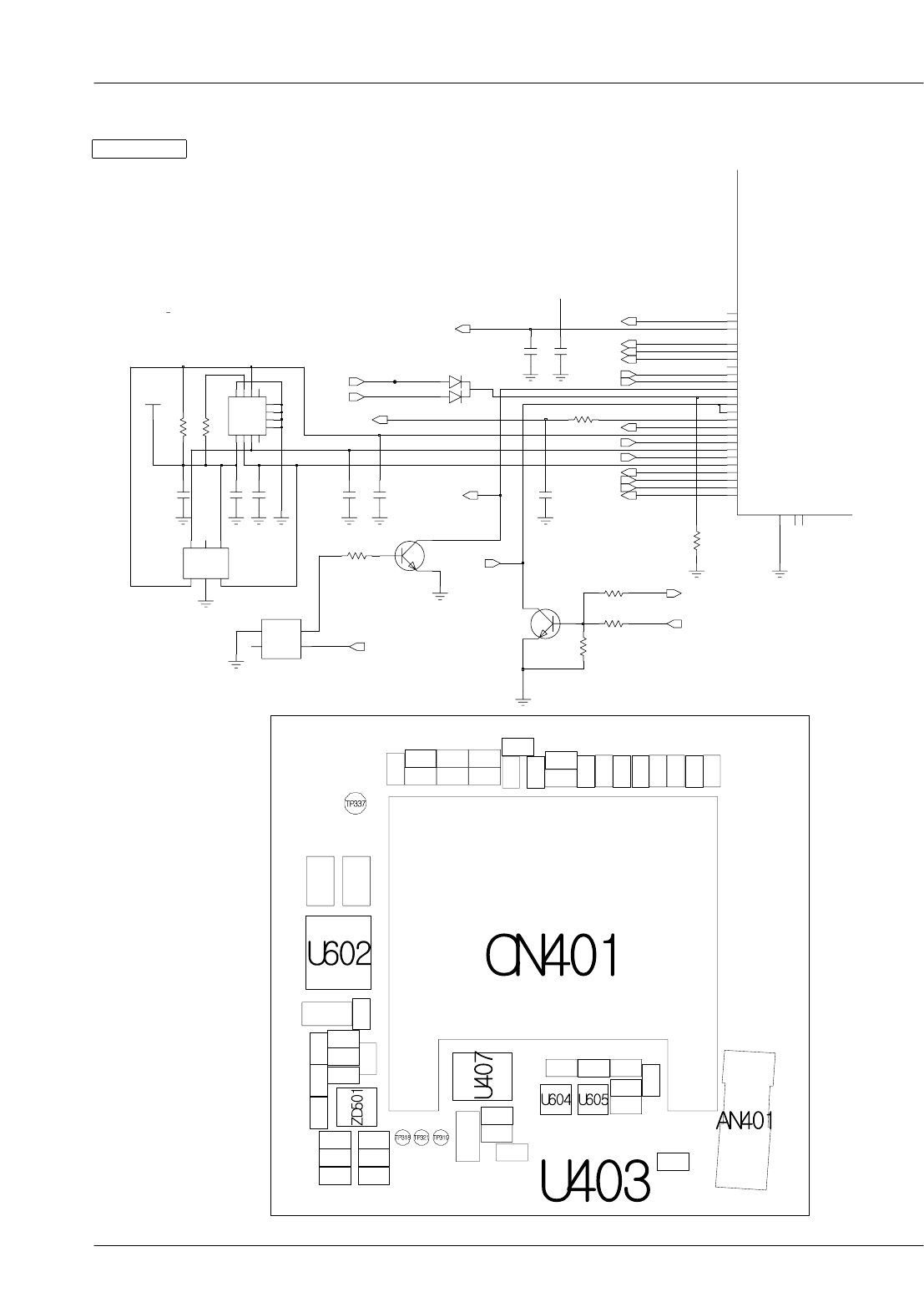
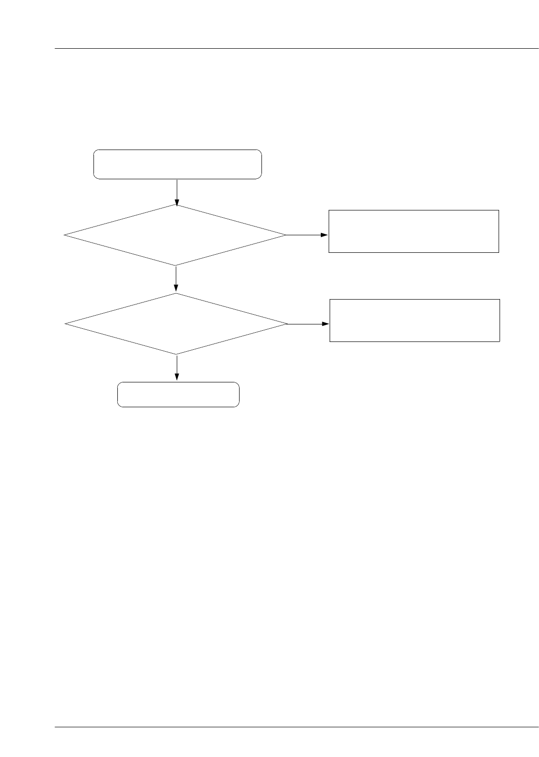
7-2. Initial
Check the LCD RESET Circuit
No
Yes
Yes
CN505 pin 37, 38(LCD
RESET) is 'H' Level?
Yes
No
END
Check the PMIC
Initial Failure
RESET_N(TP337) IS 'H'?
SAMSUNG Proprietary-Contents may change without notice
This Document can not be used without Samsung's authorization
Flow Chart of Troubleshooting
7-4
_2.6V
TP329
R308
WDOG_EN_1
AE17
AF17 WDOG_EN_2
A18 TCXO
L19 RINGER
F14 RESIN_N
RESOUT_N
F12
MODE1_1
AA25
MODE1_2
AA26
MODE2_1
U25
U26 MODE_2
MODE0
Y23
AE21 BOOT_MODE_1
AF21 BOOT_MODE_2
A1_3M8
M4
A1_4
N11
A1_5
N8
A1_6
A1_7N6
N2
A1_8
N1
A1_9
L4
A1_2
A1-11P2
A1_1L1
P1
A1_10
P6
A1_12
TP337
VREG_MSMP
TP303
R309
RESET_N
W_DOG
TMODE1
TMODE0
CAM_EN1
RESOUT2_N
TMODE2
SAMSUNG Proprietary-Contents may change without notice
Flow Chart of Troubleshooting
This Document can not be used without Samsung's authorization
7-5
_2.6V
_2.6V
_2.6V
_3.3V
ZD508
uClamp0501H
R503
ZD505
VREG_MSMP
VBATT
uClamp0501H
ZD509
9OUT 8
IN
16 OUT
OUT
15
14 OUT
OUT
13
OUT
12
11 OUT
OUT
10
GND
17
1
IN
IN 2
3
IN
IN 4
IN 5
6
IN
IN 7
U507
C511
C509
OUT
OUT
13
OUT
12
11 OUT
OUT
10
9OUT
C508
IN
IN 4
IN 5
6
IN
IN 7
8
IN
16 OUT
OUT
15
14
U511
GND
17
1
IN
IN 2
3
L502
VREG_MSMP
ZD504
MEGA_2.5
VREG_MOTOR
VREG_MSMP
U513
U512
U516
R504
L501
88
99
55
55 56
56
57
57 58
58
59
59
66
60
60
77
48
48
49
49
55
50
50
51
51 52
52
53
53 54
54
40 40
41
41 42
42
43
43 44
44
45
45 46
46
47
47
33 33 34 34
35 35 36 36
37 37 38 38
39 39
44
26
26
27
27 28
28
29
29
33
30 30
31 31 32 32
19 19
22
20 20
21 21 22 22
23 23 24 24
25
25
11 11 12 12
13 13 14 14
15 15 16 16
17 17 18 18
CN505
11
10 10
C510
13
OUT
12
OUT
OUT 11
10
OUT
OUT 9
4IN
5IN
IN
6
7IN
IN
8
OUT 16
15
OUT
OUT 14
U506
17
GND
IN
1
2IN
IN
3
MEGA_1.8
U514
FLASH_ON
LCD_HALL_SW
C_WE2_N
C_WE2_N WE2_N
C_SUB_LCD_RESETB
C_SUB_LCD_CSB
C_A2(1)
CAM_D(6)
CAM_D(0)
CAM_MCLK
CAM_D(2)
CAM_D(4)
CAM_D(5)
CAM_D(7)
D2(7)
EAR1ON_CON
C_SUB_LED_EN
CAM_RESETB
I2C_SDA
CAM_VSYNC
CAM_HSYNC
I2C_SCL
CAM_PCLK
MEGA_SLEEP
C_MAIN_LCD_CSB
A2(1)
WHITE_LED_EN
MAIN_LCD_RESETB
SUB_LCD_RESETB
SUB_LED_EN
SUB_LCD_CSB
MAIN_LCD_CSB
CAM_D(3)
CAM_D(1)
D2(0)
D2(2)
D2(4)
D2(6)
D2(8)
D2(10)
D2(12)
D2(14)
C_A2(1)
C_WHITE_LED_EN
C_MAIN_LCD_RESETB
C_SUB_LCD_RESETB
C_SUB_LED_EN
C_SUB_LCD_CSB
D2(1)
D2(3)
D2(5)
D2(9)
D2(11)
D2(13)
D2(15)
C_WHITE_LED_EN
C_MAIN_LCD_RESETB
C_MAIN_LCD_CSB
EAR1OP_CON
SAMSUNG Proprietary-Contents may change without notice
This Document can not be used without Samsung's authorization
Flow Chart of Troubleshooting
7-6
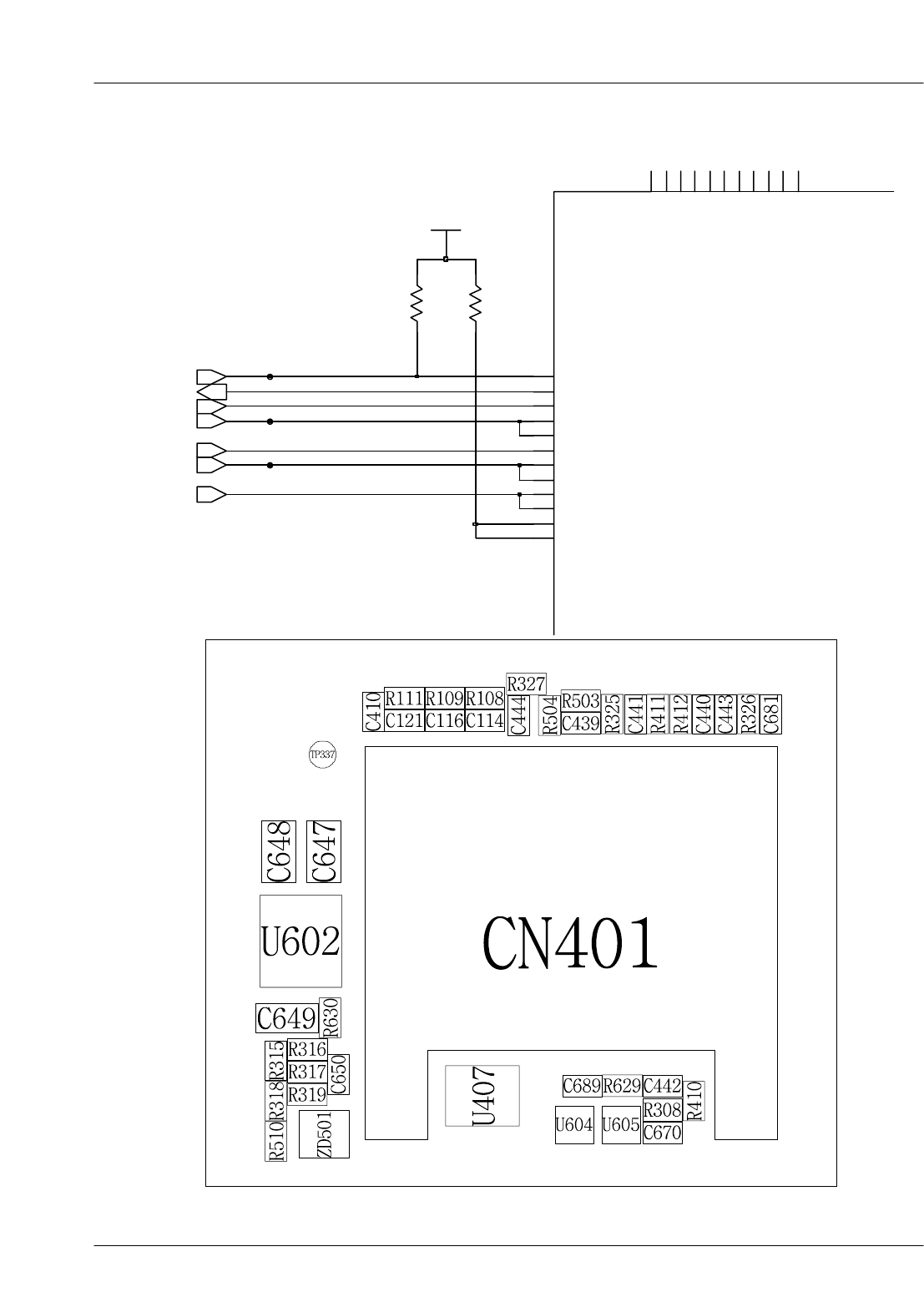
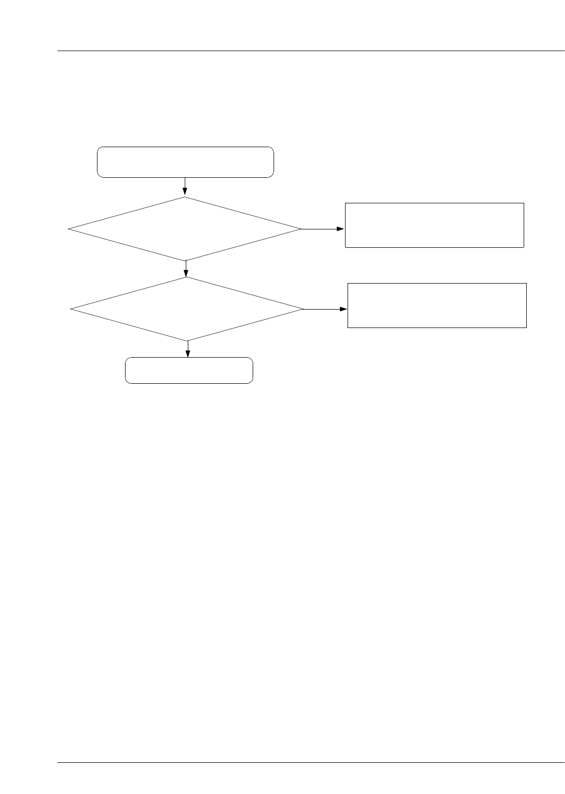
7-3. SIM Part
Yes
After SIM card insert,
CN401 pin 2 = "H(USIM_RST)"? Replace PBA
No
Yes
After Power ON,
Check SIM_CLK Signal on
CN401 pin3 in a few second
It is 3.84MHz?
Check the 32.768KHz OSC(XTAL 401)
&
19.2Mhz(OSC201)
No
Yes
Yes
Yes
No
END
Check the SIM Card
Check the SIM POWER
Phone can't access SIM Card
CN401 pin 1 = "H"?
SAMSUNG Proprietary-Contents may change without notice
Flow Chart of Troubleshooting
This Document can not be used without Samsung's authorization
7-7
SIM
5V
VDD_MSME
VDD_RUIM
VDD_SPKR
VDD_WLAN
VIB_DRV_N
19
VDD_ANA
VDD_MAIN
VDD_MSM
VDD_MSMC
SPKR_OUT_P
17 USB_DAT
20 USB_D_M
USB_D_P
18
USB_ID
11
USB_OE_N
13
USB_SE0
43 RUIM_RST
SBCK
49
47 SBDT
51 SBST
SPKR_BYP
SPKR_IN_M
SPKR_IN_P
SPKR_OUT_M
PS_HOLD
REF_BYP
REF_GND
REF_ISET
80 REF_OUT
RUIM_CLK
38
RUIM_IO
26
34 RUIM_M_CLK
30 RUIM_M_IO
40 RUIM_M_RST
KPDPWR_N
24
KPD_DRV_N
LCD_DRV_N
MSM_INT_N
59
86NC
NC
87
PON_RESET_N
9
57
72 AMUX_IN2
82 AMUX_OUT
68 CBL0PWR_N
CBL1PWR_N
66
FLSH_DRV_N
85GND
GP1_DRV_N
R440
C411
1
2
D401
3
C442
100NF
GG
10
G
1112
G
1
2
2
33
4455
6
6
77
8
8
9
R439
CN401
PC-D8-A3-H2.4-S
1
R408
C443
1
3
2
Q403
TP402
R412
R413
Q404
1
3
2
C440
390R410
C441
R409
C410
VREG_USIM
C444
R411
C439
5
NC
SIM
34VCC
U407
6
CLOCK
2GND
1IO
VDD 2
U409
GND
4
3NC
OUT 1
AMUX_OUT
HFK_DETECT
KEY_PRESSED
USIM_RST
USIM_CLK
USIM_IO
JIG_ON
JIG_DETECT
JIG_DETECT
ON_SW
RESET_N
USB_SEO
USB_OE_N
SIM_RST
SIM_IO
PM_INT_N
REF_OUT
SIM_CLK
PMIC_SBCK
PMIC_SBDT
PMIC_SBST
USB_DAT
USB_D_P
USB_D_MPS_HOLD
SAMSUNG Proprietary-Contents may change without notice
This Document can not be used without Samsung's authorization
Flow Chart of Troubleshooting
7-8
7-4. Speaker Part(Melody)
Yes
Yes
Change the Speaker
Yes
No
Is Speaker working?
No
Yes
Check the circuit related to
"SPOUT1/SPOUT2" signal
U603 pin 14,23
≒ Battery Volt ?
No
Yes
Resolder U302
U603 pin 3 ≒ 2.6V?
(When U302 operate)
Resolder or replace U602
No
Yes
No
END
Check the clock generation circuit
(related to U401 and U603)
Check the Clock signal
at Pin 2 of U603
(19.2MHz)
Speaker does not work
U603 pin28,29 = 3.0V?
SAMSUNG Proprietary-Contents may change without notice
Flow Chart of Troubleshooting
This Document can not be used without Samsung's authorization
7-9
Speaker
5.6V
_3V
5.6V
C645
C639
R628
C635
V602
C642
C638
39PF
C629
R624
C690
L602
L604
C691
R626
R625
MEL_VCC
CN604-2
24-8005-002-000-867
2
24-8005-002-000-867
CN604-1
1
L605
L603
VBATT
CN603-2
2
CN603-1
24-8005-002-000-867
1
24-8005-002-000-867
V603
C643
R623
C641
C637
C646
C671
C630
C644
VSS
7
_CS
47
_IRQ 35
_RD
1
_RST
3
48
_WR
23
SPVDD-R
13
SPVSS-L
24
SPVSS-R
TESTI
4
VDD
6
VDD 28
VREF
8
VSS
44
PIO1 33
PIO2 32
PLLC
5
SPOUT1-L
11 SPOUT1-R 26
SPOUT2-L
10 SPOUT2-R 27
14
SPVDD-L
LED 31
MTR 30
NC
9
NC
12 NC 25
50
NC
51
NC
PIO0 34
21
EQ2-R
15
EQ3-L
22
EQ3-R
GND
49
18
HPOUT-L/MONO
19
HPOUT-R
IOVDD
45
IOVDD 29
D3
40
D4
39
D5
38
D6
37
D7 36
17
EQ1-L
20
EQ1-R
16
EQ2-L
U603
A0
46
CLKI
2
D0
43 42
D1
D2
41
MEL_VCC
C633
C692
R616
39PF
C636
R627
C640
V601
V604
C632
SPK_TP2
SPK_TP1
YAMAHA_EARJACK_L
YAMAHA_EARJACK_R
HPH_L HPH_R
MELODY_CSB
MELODY_IRQ
OE2_N
MELODY_RESETB
WE2_N
D2(0:7)
D2(1)
D2(0)
D2(2)
D2(3)
D2(4)
D2(5)
D2(6)
A2(1)
TCXO_OUT
D2(7)
SAMSUNG Proprietary-Contents may change without notice
This Document can not be used without Samsung's authorization
Flow Chart of Troubleshooting
7-10
7-5. Microphone Part
Microphone does not work
Replace the MIC
Check the MIC
No
Yes
Yes
Yes
Yes
No
END
Resolder the R607, R608, R631, R632, R633,
R634, C614, C615, C621 and C622
Resolder MIC
Check the circuit
from U302 to MIC
Check the connection
from MIC
No
SAMSUNG Proprietary-Contents may change without notice
Flow Chart of Troubleshooting
This Document can not be used without Samsung's authorization
7-11
Microphone
C684
R634
R633
C621
R632
C610
C616
C614
C693 C617
C687
C685
C624
R611
C686C612
C694
C615
C622
C623
R608
MICBIAS
C688
R612
R631
C682
MICBIAS
C683
R607
C618
EARMIC_P MIC2P
MIC2N
MICP_CON
MICN_CON
MIC1P
MIC1N
EARMIC_N
SAMSUNG Proprietary-Contents may change without notice
This Document can not be used without Samsung's authorization
Flow Chart of Troubleshooting
7-12
7-6. Key Data Input
Yes
No
Replace the PBA
When one of the keys is
pushed,
KEY_IO signal is OK?
Check Initial Operation
Yes
Yes
No
END
Check the Dome sheet & Key Pad
When one of the keys is
pushed,
is it displayed on LCD?
SAMSUNG Proprietary-Contents may change without notice
Flow Chart of Troubleshooting
This Document can not be used without Samsung's authorization
7-13
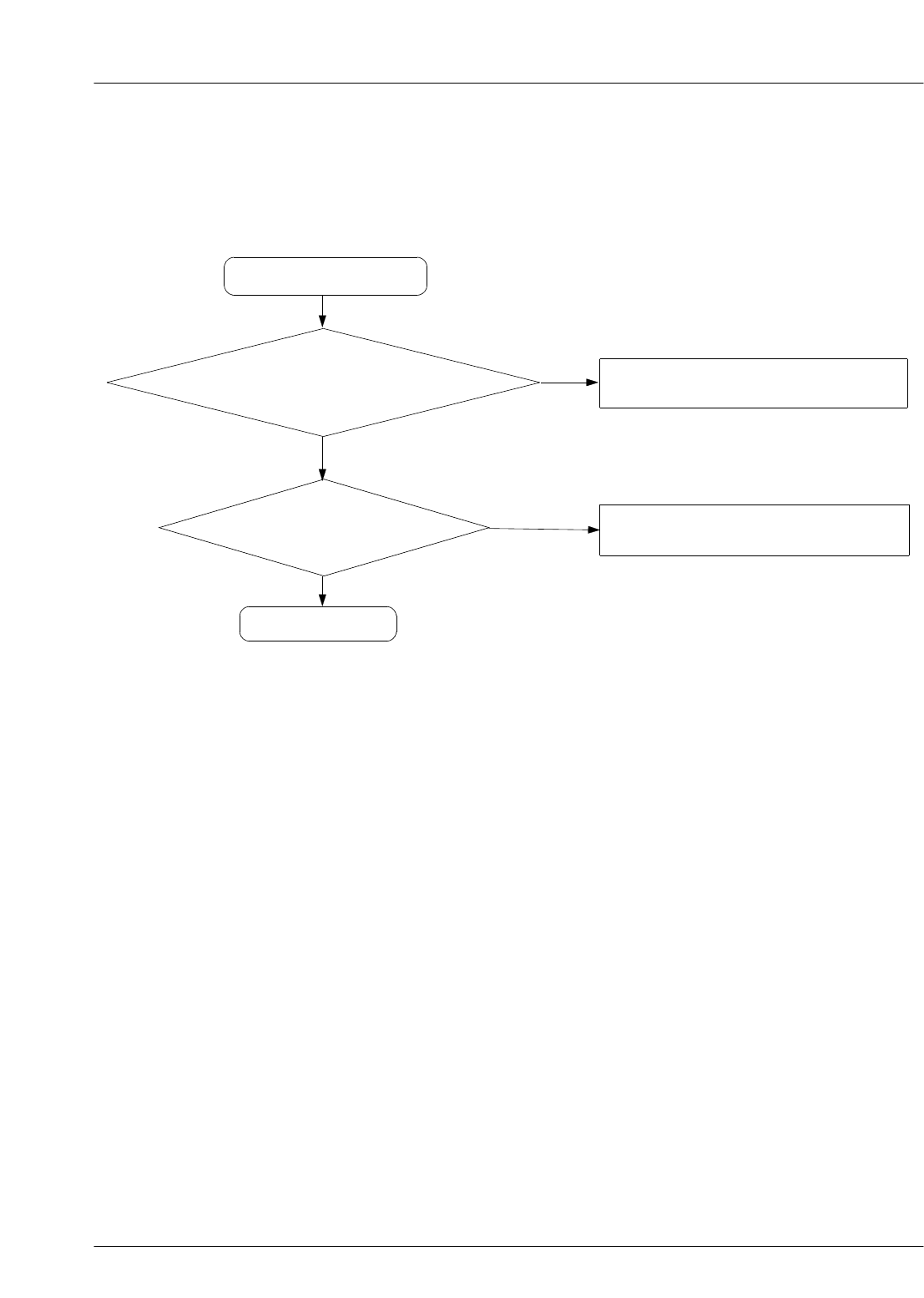
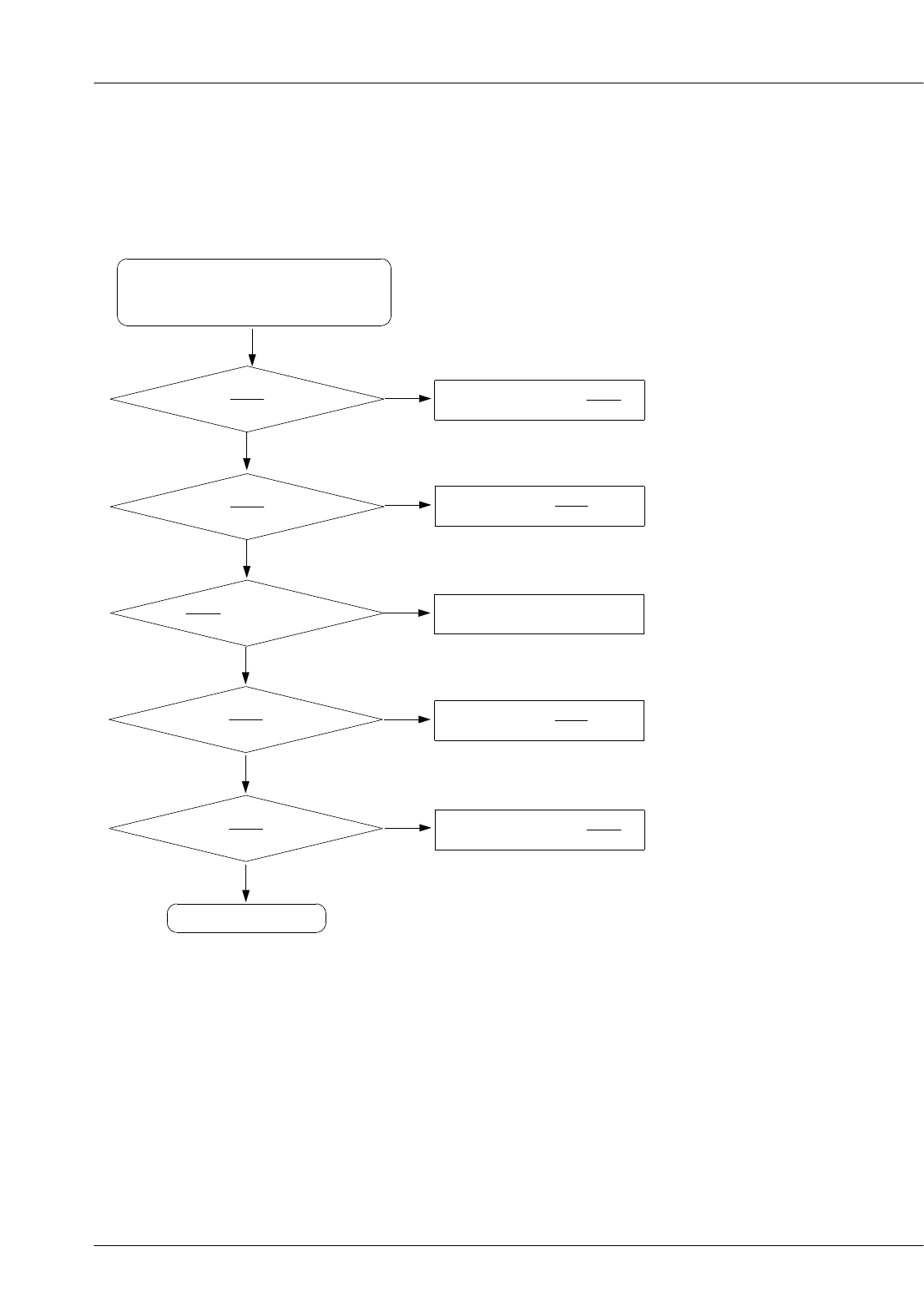
7-7. Receiver Part
Receiver does not work
Check the soldering of the
speaker wire
Yes
Modify the speaker wire soldering
No
Yes
No
Replace the Receiver
Is Receiver working?
Yes
END
SAMSUNG Proprietary-Contents may change without notice
This Document can not be used without Samsung's authorization
Flow Chart of Troubleshooting
7-14
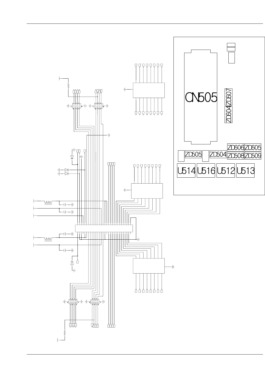
7-8. Back Light (for Color Main LCD)
Replace the LCD Module
Yes
Yes
No
Replace or Resolder L501
L501 ≥ 3.3V
Backlight does not work
Yes
Yes
No
END
Set BACKLIGHT on AlwaysON
Is BACKLIGHT set
AlwaysON in the Menu?
VBATT
C511
ZD504
MEGA_2.5
L501
88
99
66
77
55
443 3
19 19
22
20 20
21 21 22 22
23 23 24 24
11 11 12 12
13 13 14 14
15 15 16 16
17 17 18 18
CN505
11
10 10
C510
EAR1OP_CON
SAMSUNG Proprietary-Contents may change without notice
Flow Chart of Troubleshooting
This Document can not be used without Samsung's authorization
7-15
7-9. Key Back Light
Yes
Replace The PBA Module
No
HEA501 pin 20
Voltage = "3.05"?
Key Backlight does not work
Yes
Yes
No
END
Set BACKLIGHT on AlwaysON
Is BACKLIGHT set
AlwaysON in the Menu?
Replace Key_FPCB
Yes
SAMSUNG Proprietary-Contents may change without notice
This Document can not be used without Samsung's authorization
Flow Chart of Troubleshooting
7-16
7-10. Camera part
Yes
Replace the camera
module
END
Is there another problem?
Yes
Replace U302
No
U513(pin7) = 24MHz
Yes
Check the voltage of U401 & U502
No
CN505 pin28 = 1.8V?
CN505 pin27 = 2.6V?
Yes
Check the Camera
connector on LCD module Connect the camera module
No
Yes
"Camera" function does not work
SAMSUNG Proprietary-Contents may change without notice
Flow Chart of Troubleshooting
This Document can not be used without Samsung's authorization
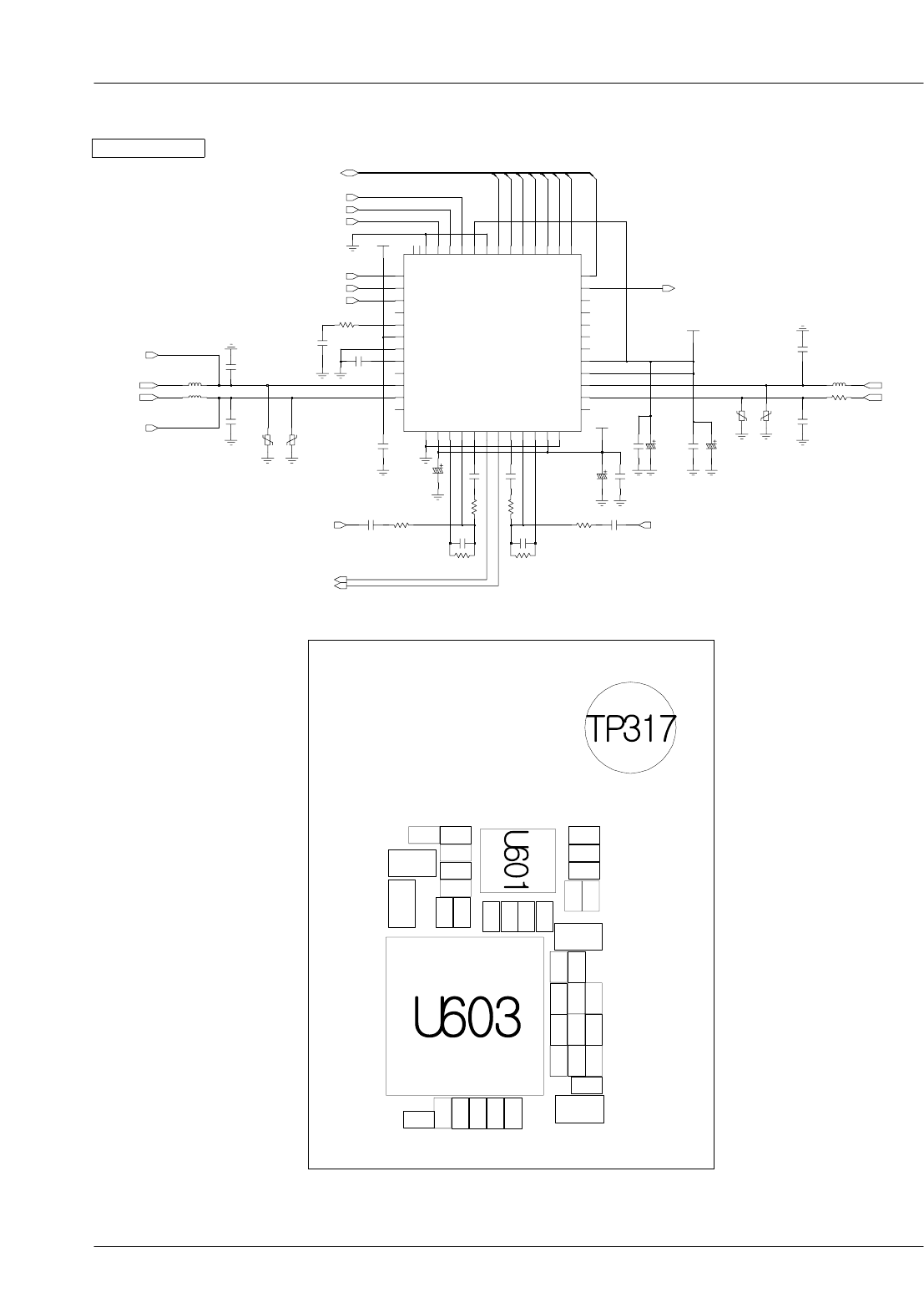
7-17
U513
CAM_MCLK
CAM_RESETB
I2C_SDA
CAM_VSYNC
SAMSUNG Proprietary-Contents may change without notice
This Document can not be used without Samsung's authorization
Flow Chart of Troubleshooting
7-18
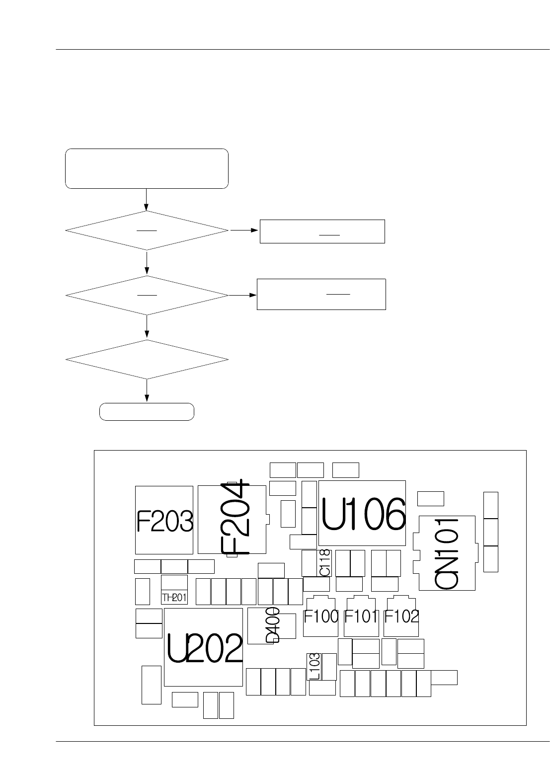
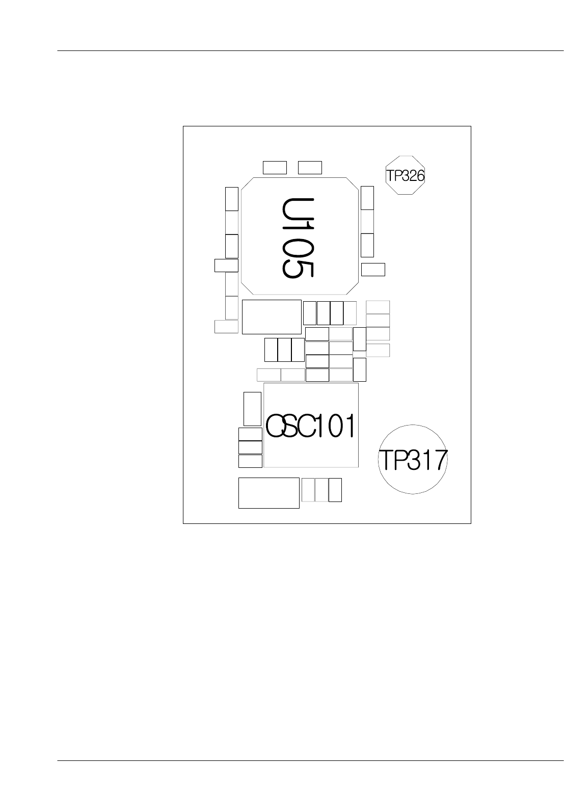
7-11. GSM Receiver
RX ON
RF input : CH center freq +67.7kHz
Amp : -50dBm
Yes
No Resolder U106(ASM)
C118
>= -60dBm
Yes
L103
>= -65dBm Resolder F100
(GSM SAW)
No
Yes
Resolder U104
(RTR6250)
Yes
END
SAMSUNG Proprietary-Contents may change without notice
Flow Chart of Troubleshooting
This Document can not be used without Samsung's authorization
7-19
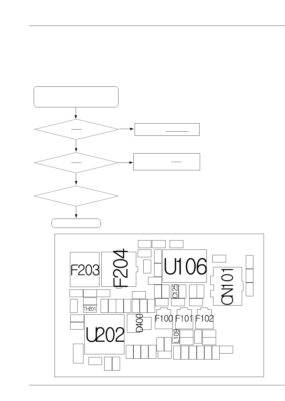
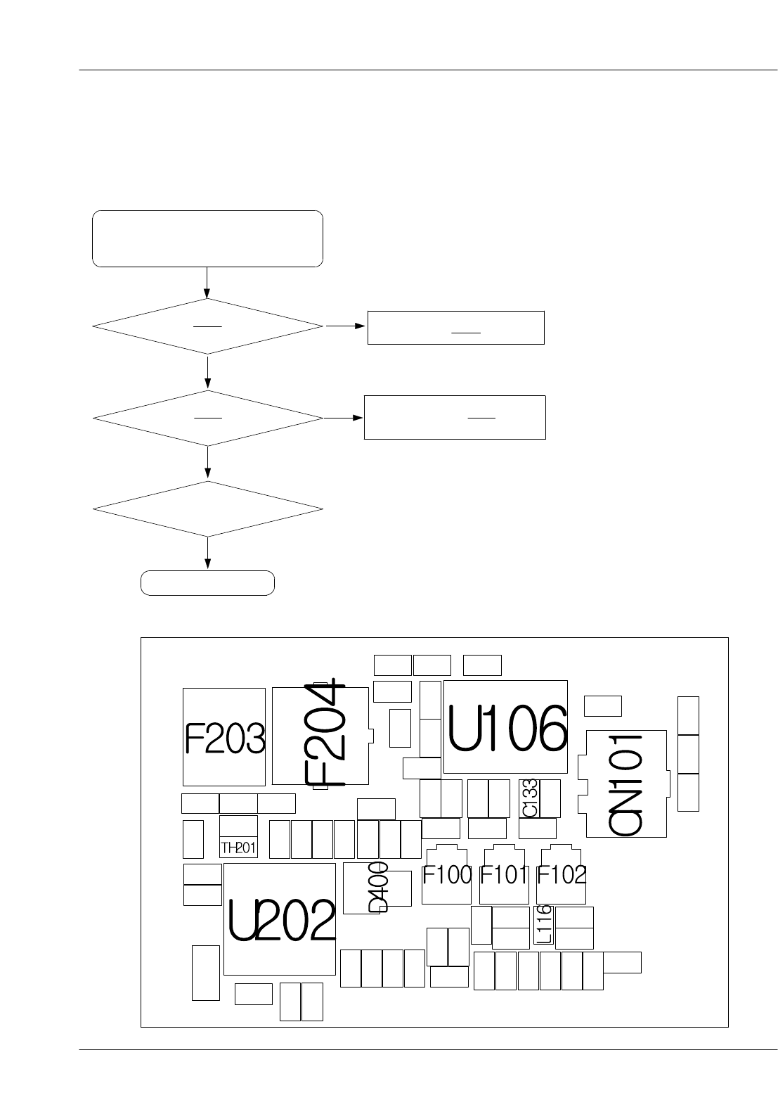
7-12. GSM Transmitter
Yes
Check U302
(MSM6250)
END
No
No
No
No
Yes
Yes
Yes
Yes
Resolder U106
(ASM)
Resolder U105(PAM)
U106(ASM)
pin22
>= 23dBm
U105(PAM) pin6
>= 26dBm
OSC101(TXVCO)
pin1
>= 2dBm Resolder OSC101
(TXVCO)
TX ON (5 Level)
Resolder U105
(PAM)
U105(PAM) Pin45
>= 1V
SAMSUNG Proprietary-Contents may change without notice
This Document can not be used without Samsung's authorization
Flow Chart of Troubleshooting
7-20
SAMSUNG Proprietary-Contents may change without notice
Flow Chart of Troubleshooting
This Document can not be used without Samsung's authorization
7-21
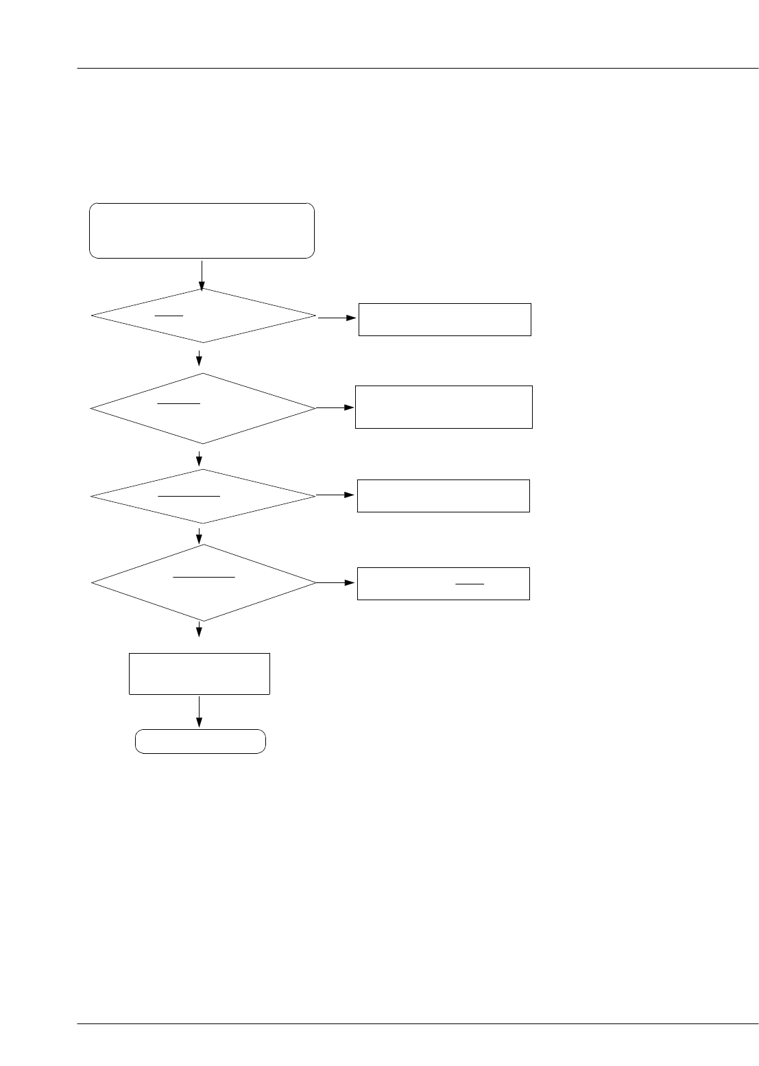
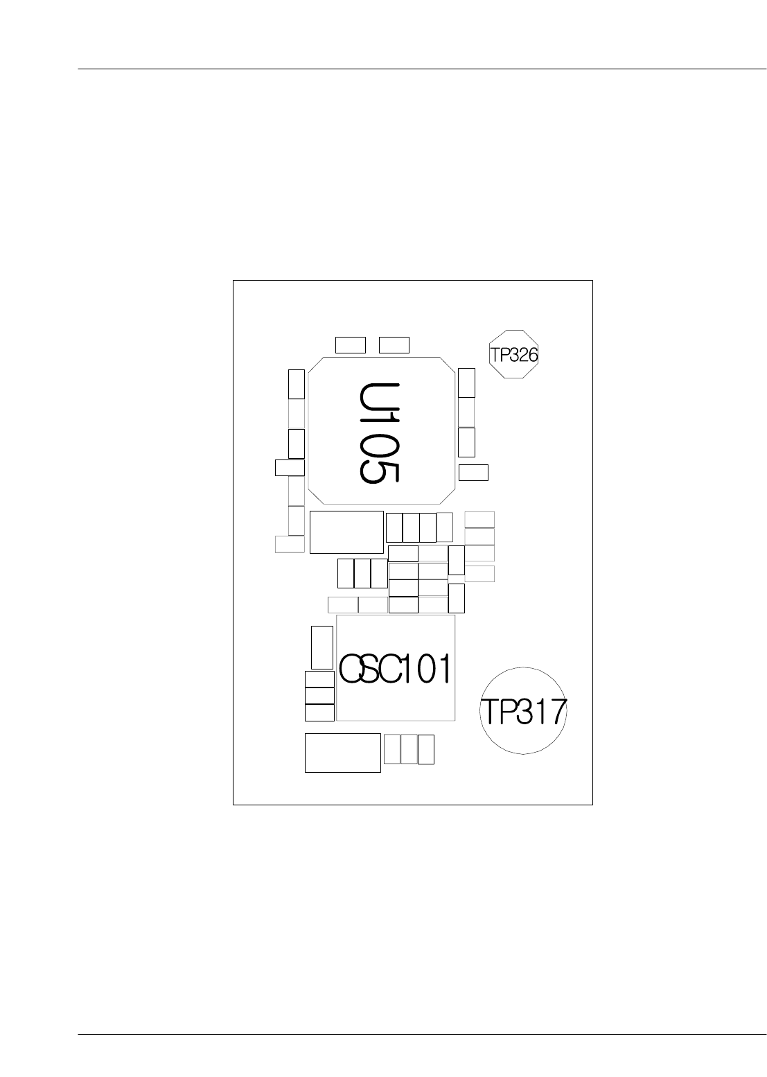
7-13. DCS Receiver
No
Yes
Yes
Yes
Resolder U104
(RTR6250)
L109
>= -65dBm Resolder F101
(DCS SAW)
RX ON
RF input : CH center freq +67.7kHz
Amp : -50dBm
Yes
No
END
Resolder U106(ASM)
C125
>= -60dBm

SAMSUNG Proprietary-Contents may change without notice
This Document can not be used without Samsung's authorization
Flow Chart of Troubleshooting
7-22
7-14. DCS Transmitter
Yes
Check U302
(MSM6250)
END
No
No
No
No
Yes
Yes
Yes
Yes
Resolder U106
(ASM)
Resolder U105(PAM)
U106(ASM)
pin22
>= 20dBm
U105(PAM) pin31
>= 23dBm
OSC101(TXVCO)
pin5
>= 2dBm
Resolder OSC101
(TXVCO)
TX ON (0 Level)
Resolder U105
(PAM)
U105(PAM) Pin45
>= 1V
SAMSUNG Proprietary-Contents may change without notice
Flow Chart of Troubleshooting
This Document can not be used without Samsung's authorization
7-23
SAMSUNG Proprietary-Contents may change without notice
This Document can not be used without Samsung's authorization
Flow Chart of Troubleshooting
7-24
7-15. PCS Receiver
No
Yes
Yes
Yes
Resolder U104
(RTR6250)
L116
>= -65dBm Resolder F102
(PCS SAW)
RX ON
RF input : CH center freq +67.7kHz
Amp : -50dBm
Yes
No
END
Resolder U106(ASM)
C133
>= -60dBm
SAMSUNG Proprietary-Contents may change without notice
Flow Chart of Troubleshooting
This Document can not be used without Samsung's authorization
7-25
7-16. PCS Transmitter
Yes
Check U302
(MSM6250)
END
No
No
No
No
Yes
Yes
Yes
Yes
Resolder U106
(ASM)
Resolder U105(PAM)
U106(ASM)
pin22
>= 20dBm
U105(PAM) pin31
>= 23dBm
OSC101(TXVCO)
pin5
>= 2dBm Resolder OSC101
(TXVCO)
TX ON (0 Level)
Resolder U105
(PAM)
U105(PAM) Pin45
>= 1V
SAMSUNG Proprietary-Contents may change without notice
This Document can not be used without Samsung's authorization
Flow Chart of Troubleshooting
7-26
SAMSUNG Proprietary-Contents may change without notice
Flow Chart of Troubleshooting
This Document can not be used without Samsung's authorization
7-27
7-17. WCDMA Receiver
Yes
Resolder U203
(RFR6250)
END
Resolder F201
(WRX SAW)
No
Yes
C236
>= -60dBm
Check & Resolder U201
(RFL6200)
No
Resolder F204
(DPLX)
No
Yes
Yes
C210
>= -55dBm
C214
>= -65dBm
Yes
No Check & Resolder U106
(ASM)
C208
>= -60dBm
Yes
RX ON
RF input : CH center freq
Amp : -50dBm
SAMSUNG Proprietary-Contents may change without notice
This Document can not be used without Samsung's authorization
Flow Chart of Troubleshooting
7-28
SAMSUNG Proprietary-Contents may change without notice
Flow Chart of Troubleshooting
This Document can not be used without Samsung's authorization
7-29
7-18. WCDMA Transmitter
Yes
No Check & Resolder U106
(ASM)
C101
>= 19dBm
Yes
Check & Resolder U104
(RTR6250)
No Resolder F204
(DPLX)
END
No
No
No
Yes
Yes
Yes
Yes
C208
>= 19dBm
Check & Resolder U202
(WPAM)
Resolder F202
(WTX SAW)
U202(WPAM) pin8
>= 20dBm
C211
>= -7dBm
C212
>= -7Bm
TX ON (PDM for 23dBm)
SAMSUNG Proprietary-Contents may change without notice
This Document can not be used without Samsung's authorization
Flow Chart of Troubleshooting
7-30
SAMSUNG Proprietary-Contents may change without notice
Flow Chart of Troubleshooting
This Document can not be used without Samsung's authorization
7-31
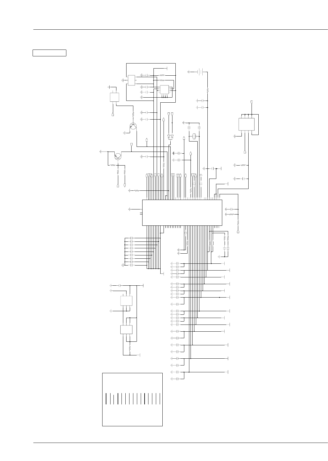
Transmitter
_2.85V
_2.85V
_2.85V
_2.85V
_2.6V
_2.85V
_2.85V
_2.85V
_2.85V
_2.85V
_2.85V
C141
R123
C121
R116
R134
C162
L110
C154
R104R103
F100
2
GG
5
IN
1
3
OUT
4
OUT
C131
C165
R117
C101
33PF
C142
L120
C136
C128
C107
L121
L119
ANT104
R118
R111
C167
R105
C160
C123
C157
R127
C126
R102
C144
C103
C163
C124
L115
L108
C112
C135
R128
L105
L102
C104
C117
C127
R106
L104C118
C114
R124
R130
L112
C151
C113
R112
C145
L113
C137
C120
L106
L103
R120
R121
C166
C146
C108
L123
IN
1
3
OUT
4
OUT
R107
F101
B7852
2
GG
5
C153
C129
R135
R109
C110
L114
C116
ANT105
L107
C138
R129
C155
R133
C105
C171
C147
C119
R132
L101
C115
L122
C133
CN101
A2
3
C
1
G
4
G
G
25
G
1IN
OUT 3
4
OUT
KMS-512
B7851
F102
RX1
52
RX2
3
RX3
RX4
4
20
TRX
TX1 13
TX2 11
25 VDD
31
8
NC
NC
91 0
NC
NC
1415
NC
NC7
16
NC
1718
NC
GND
21
GND
23
24 GND
30 GND
32 GND
NC
7
NC
29
NC
22
ANT
26 CTL-A
CTL-B
27
28 CTL-C
1
GND
GND
6
12
GND
19
GND
R122
U106
C143
C159
C125
C111
L124
R126
R101
C149
R131
R125
C140
C152
C164
L109
C148
VDDA9
43
VDDM
8
VTUNE_REF
C139
VDDA17
5
VDDA2
7
VDDA3
10
VDDA4
15
VDDA5
23
VDDA6
26
VDDA7
27
VDDA8
31
VDDA1
36
VDDA10
39
VDDA11
41
VDDA12
48 VDDA13
50 VDDA14
52 VDDA15
54 VDDA16
56 TX_QN
16
TX_QP
42
TX_VCO_FB
53 UMTS1900_OUT
51 UMTS2100_OUT
55 UMTS800_OUT
49 VCONTROL
9
VCO_TUNE
4
R_BIAS
44 SBCK
45 SBDT
46 SBST
6
TCXO
19
TX_IN
18
TX_IP
40
TX_MOD_CP
17
NC1
59 NC2
47 RF_ON
14
RX_IN
13
RX_IP
12
RX_QN
11
RX_QP
32
RX_VCO_IN
33
GSM1800_INN
35
GSM1800_INP
24
GSM1900_INN
25
GSM1900_INP
21
GSM850_INN
22
GSM850_INP
38
GSM900_INN
37
GSM900_INP
58
CP1
30
CP2
1
CP_HOLD1
29
CP_HOLD2
20
DAC_REF
3
FAQ1
28
FAQ2
57 GND
34
U104
2
VRAMP
45
C102
VCC1DCS/PCS
39
46
VCC1GSM
35
VCC2DCS/PCS
2
VCC2GSM
21
VCC3DCS/PCS
VCC3GSM
18 19
VCCOUT
20
VCCOUT
NC
10
11 NC
NC
12
13
NC
14
NC
41
TXENABLE
42
VBATT
VBATT
43
3NC
29
NC
33
NC
38
NC
NC 36
NC
44
8NC
9NC
17
NC
NC
22 23
NC
24
NC
25
NC
26
NC
27
NC
28
NC
GND
4950
GND
51
GND
GSM850/900IN
48
6GSM850/900OUT
1NC
15
NC
16
NC
53 GND
54 GND
47
GND1GSM
GND
5
GND
7
30
GND
32
GND
34
GND
U105
BANDSEL
40 37
DCS/PCSIN
31
DCS/PCSOUT
4GND
52
GND
R119
L117
C161
L111
C132
L118
R115
C168
C130
1NF
G
13
OUT1
5
OUT2
1
2
SW1 SW2
4
8
VB1
VB2
12
10
VC
3
G
6
GG
7
G
119
GG14
R108
OSC101
C150
C156
C169
C158
C134
C170
C122
L116
GSM_ANT_SEL1_N
GSM_ANT_SEL0_N
ANT
TCXOVREG_SYNT
PCS_RXM
PCS_RXM
PCS_RXP
PCS_RXP
VBATT
UMTS_TXRF
RX_VCO
VREG_MSMP
MOD_CP
GSM_ANT_SEL2_N
UMTS_ANT
VREG_RFRX
TXVCO
GSM_RXM
DCS_RXP
VREG_RTR
TX_QP
TX_IP
TX_QM
TX_IM
RF_ON_TX_ON
GSM_BAND
GSM_PA_PWR_SV
SBST
TX_AGC_ADJ
VREG_RFTX
VREG_RTR
RX_QP
RX_IP
VREG_RTR
FAQ2
VREG_SYNT
CP2
GSM_RXM
GSM_RXP
DAC_REF
DCS_RXM
GSM_RXP
RX_IM
RX_QM
VREG_RTR
VREG_RTR
SBCK
SBDT
TXVCO DCS_VCO_EN_N
GSM_VCO_EN_N
VREG_RFTX
MOD_CP
DCS_RXP
DCS_RXM
GSM_PA_PWR_CTL
SAMSUNG Proprietary-Contents may change without notice
This Document can not be used without Samsung's authorization
Flow Chart of Troubleshooting
7-32
_2.85V
_2.85V
_2.85V
_2.6V
_2.85V
_2.85V
_2.85V
_2.85V
_2.85V
_2.85V
_2.6V
4
VCC
VCON
1
R207
OSC201
GND
2
OUT
3
C259
R209
15PF
R211
C219
100PF
C247
R206
C242
C224
C250
C201
C228
R212
C261
1.8PF
L208
L209
R214
R220
L215
8.2K,1%
C209
R215
C235
TH201
C225
C244
C232
R201
C236
BLM15HG102SN1D
L212
C239
R205
R204
C229
L207
C227
C218
4.7nH
L204
4.7K
R218
4.7nF
C263
1NF
C256
C255
C238
4.7nH
L213
C221
L211
R213
C207
E2
C234C233
2
B1B2
5
C1
6
3
C2
E1 1
4
C222
U204
100NF
C258
C208
C240
R222 4.7
C205
R208
C214
C241
27
VDDA6
29
VDDA7
VDDA8
39
23
VDDM
25
26
SBDT
SBST 24
28
TCXO
UMTS_INM
8
UMTS_INP
6
4VDDA1
14
VDDA2
17
VDDA3
VDDA4
18
VDDA5
20
LO_INM
15 16
LO_INP
19
LO_OUT
NC1
4546
NC2
RX_IM 30
31
RX_IP
RX_QM
33
RX_QP
34
R_BIAS
38
SBCK
GND12
GND13
4344
GND14
3GND2
GND3
5
7GND4
9GND5
GND6
11
GND7
13
GND8 22
GND9
32
2DNC1
10 DNC2
DNC3
12
21
DNC4
DNC5
36
DNC6
37
DNC7
40
GND1
1
GND10
35
GND11
4142
L203
U203
C212
C249
VBATT
C248
1.8PF
C260
C202
C252
IN
5OUT 2
1
G1 G2
34
G3 G4
6
L202
F203
L210
1K
R221
C243
VREG_SYNT
VREG_RFTX
G
G
2
OUT 1
SW 35 VC
7VCC
VREG_TCXO
OSC202
MQL302A1G71
8
G
6
G
4
C254
220PF
C251
33PF
GND2
IN
1OUT 2
L201
DG50LE0
F202
3
GND1
4
8
1VCC 10
VCC
4VMODE
5VREF
R210
GND
3
GND 9
GND 7
6
GND
GND
11
2RFIN
RFOUT
OUT 3
4
OUT
U202
F201
B7728
2
GG
5
IN
1
C257
4.7UF
C206
C204
C231
R202
C246
100NF
C253
390PF
C237
L206
3
2
1
C217
D400
10
SBDT
SBST
8
3UMTS_BIAS
UMTS_IN
4
11
UMTS_OUT
VDDA
15
VDDM 9
14
GND
GND
1718
GND
19
GND
21
NC
NC
22 16
R_BIAS
7
SBCK
2DNC
GND
1
GND
20
GND
5
6
GND
GND 12
13
GND
RFL6200
U201
F204
3
ANT
4
GND
2RX
TX 1
L214
C245
C211
NC
C216
R216 1K
C210
L205
C262
HDET
TCXO
VREG_SYNT
VREG_RFTX
PA_ON
PA_THERM
UHF_VCO_EN
RX_VCO
CP2
FAQ2
PA_RANGE0
VREG_RFRX
UMTS_RXP
UMTS_RXM
TRK_LO_ADJ
UMTS_TXRF
UMTS_ANT
VREG_RFRX
VREG_RFRX
VREG_MSMP
UMTS_RXP
UMTS_RXM
SBCK
SBDT
SBST
VREG_RFRX
VREG_MSMP
SBDT
SBCK
SBST
TCXO
RX_IP
RX_IM
RX_QM
RX_QP

