SG6859 Datasheet. Www.s Manuals.com. R1.2.1 Fairchild
User Manual: Marking of electronic components, SMD Codes AA, AA**, AA***, AA-, AA-**, AA-***, AA=***, AAA, AAA***, AAC, AAD, AAE, AAE**, AAF, AAFI, AAG, AAH**, AAHC, AAHO, AAI**, AAIK, AAJ**, AAJ***, AAJF*, AAJI, AAJJ, AAL***, AAM***, AAN***, AANC, AAP, AAQ, AAR, AAS, AASQ, AASR, AAT***, AATJ, AATK, AATL, AATM, AAU, AAU**, AAW, AAX, Aa. Datasheets 2N7002T, 2SD1757K, 74AHC1G00GW, AME8804AEEY, BCW60A, BCX51, BD48E23G, BD48K23G, BL3406B-1.0V, BL9641, LR9641, MAX1736EUT41-T, MAX1736EUT42-T, MAX2644, MAX4335EXT-T, MAX4336EXT
Open the PDF directly: View PDF ![]() .
.
Page Count: 14
Product Specification
Low Cost Green-Mode PWM Controller for Flyback Converters SG6859
© System General Corp. - 1 - www.sg.com.tw • www.fairchildsemi.com
Version 1.2.1(IAO33.0067.B2) September 28,2007
FEATURES
Green-Mode PWM
Supports the “Blue Angel” Standard
Low Start-up Current (9uA)
Low Operating Current (3mA)
Leading-Edge Blanking
Constant Output Power Limit
Universal Input
Built-in Synchronized Slope Compensation
Current Mode Operation
Cycle-by-cycle Current Limiting
Under Voltage Lockout (UVLO)
Programmable PWM Frequency with Frequency
Hopping
VDD Over Voltage Protection (Auto Restart)
Gate Output Voltage Clamped at 17V
Low Cost
Few External Components Required
Small SOT-26 and Dip 8 Packages
APPLICATIONS
General-purpose switching mode power supplies and
flyback power converters, such as
Battery chargers for cellular phones, cordless
phones, PDAs, digital cameras, and power tools
Power adapters for ink jet printers, video game
consoles, and portable audio players
Open-frame SMPS for TV/DVD standby and other
auxiliary supplies, home appliances, and consumer
electronics
Replacements for linear transformers and RCC
SMPS
PC 5V standby power.
DESCRIPTION
This highly integrated PWM controller provides
several special enhancements designed to meet the low
standby-power needs of low-power SMPS. To minimize
standby power consumption, the proprietary green-mode
function provides off-time modulation to linearly
decrease the switching frequency under light-load
conditions. This green-mode function enables the power
supply to easily meet even the strictest power
conservation requirements.
The BiCMOS fabrication process enables reducing
the start-up current to 9uA, and the operating current to
3mA. To further improve power conservation, a large
start-up resistance can be used. Built-in synchronized
slope compensation ensures the stability of peak current
mode control. Proprietary internal compensation provides
a constant output power limit over a universal AC input
range (90VAC to 264VAC). Pulse-by-pulse current limiting
ensures safe operation even during short-circuits.
To protect the external power MOSFET from being
damaged by supply over voltage, the SG6859’s output
driver is clamped at 17V. SG6859 controllers can be used
to improve the performance and reduce the production
cost of power supplies. The SG6859 is the best choice for
replacing linear and RCC-mode power adapters. It is
available in 8-pin DIP and 6-pin SOT-26 packages.
TYPICAL APPLICATION
SG6859
Product Specification
Low Cost Green-Mode PWM Controller for Flyback Converters SG6859
© System General Corp. - 2 - www.sg.com.tw • www.fairchildsemi.com
Version 1.2.1(IAO33.0067.B2) September 28, 2007
MARKING DIAGRAMS PIN CONFIGURATION
ORDERING INFORMATION
Part Number Pb-Free Package
SG6859TZ 6-Pin SOT-26
SG6859DZ 8-Pin DIP-8
PIN DESCRIPTIONS
Pin No.
Name DIP-8(SOT-26) Type Function
GATE 1 / (6) Driver Output The totem-pole output driver for driving the power MOSFET.
VDD 2 / (5) Supply Power supply.
NC 3 NC pin.
SENSE 4 / (4) Analog Input
Current sense. This pin senses the voltage across a resistor. When the voltage
reaches the internal threshold, PWM output is disabled. This activates
over-current protection. This pin also provides current amplitude information for
current-mode control.
RI 5 / (3) Analog
Input/Output
A resistor connected from the RI pin to ground will generate a constant current
source for the SG6859. This current is used to charge an internal capacitor, to
determine the switching frequency. Increasing the resistance will reduce the
amplitude of the current source and reduce the switching frequency. A 95kΩ
resistor Ri results in a 50uA constant current Ii and a 70kHz switching frequency.
NC 6 NC pin.
FB 7 / (2) Analog Input
Feedback. The FB pin provides the output voltage regulation signal. It provides
feedback to the internal PWM comparator, so that the PWM comparator can
control the duty cycle.
GND 8 / (1) Supply Ground.
AAJ: SG6859
M: Mask Version
W: Week code A~Z=W1~W26
A~Z=W27~W52
: Lead Free Package
SOT-26
GND
FB
RI
GATE
VDD
SENSE
T: D=DIP
P: Z =Lead Free
Null=Regular Package
XXXXXXXX: Wafer Lot
Y: Year; WW: Week
V: Assembly Location
DIP-8
RI
NC
FB
GND
SENSE
N
C
VDD
GATE
AAJMW
XXXXXXXXYWWV
SG6859TP
Product Specification
Low Cost Green-Mode PWM Controller for Flyback Converters SG6859
© System General Corp. - 3 - www.sg.com.tw • www.fairchildsemi.com
Version 1.2.1(IAO33.0067.B2) September 28, 2007
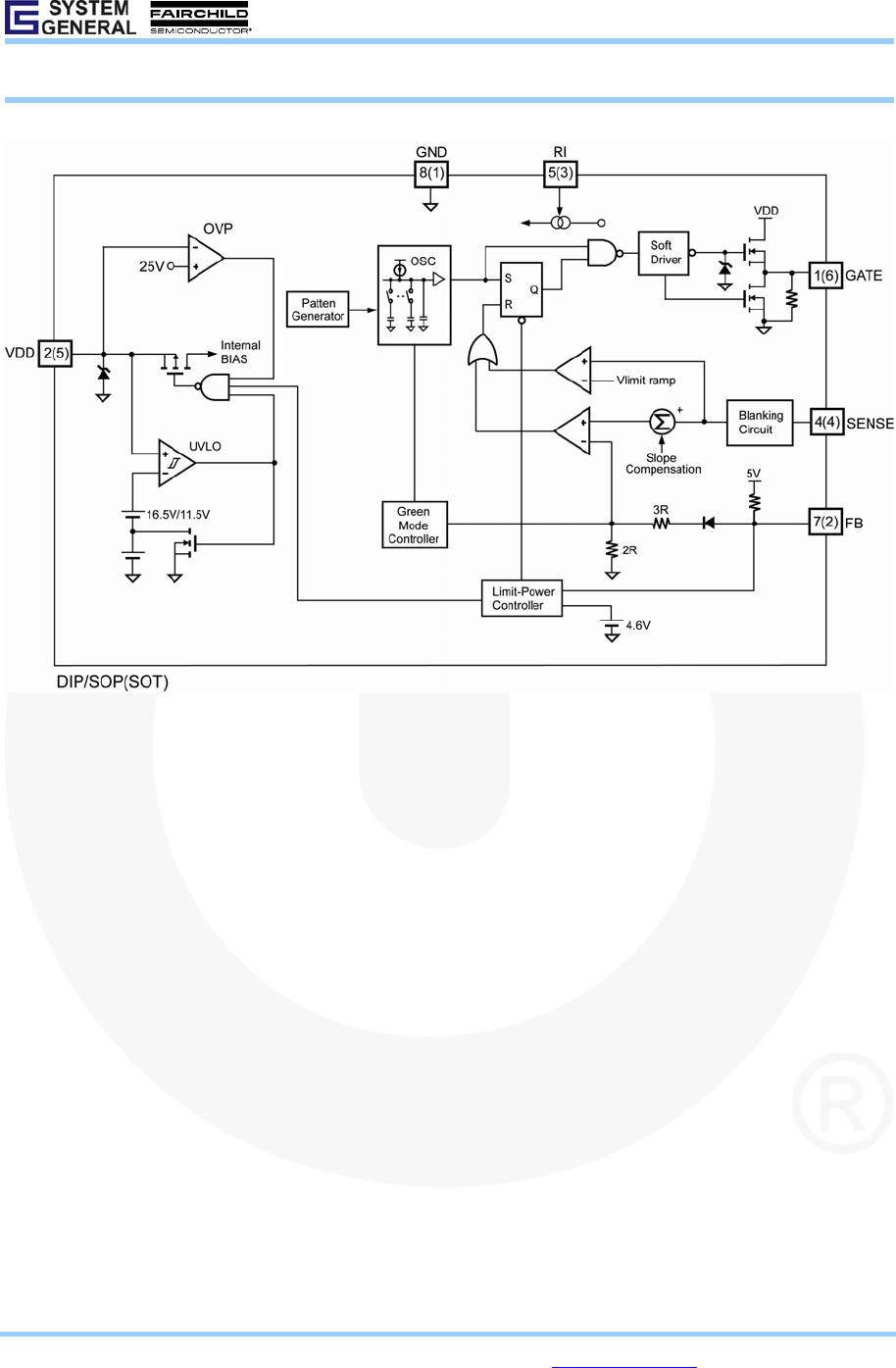
BLOCK DIAGRAM
Product Specification
Low Cost Green-Mode PWM Controller for Flyback Converters SG6859
© System General Corp. - 4 - www.sg.com.tw • www.fairchildsemi.com
Version 1.2.1(IAO33.0067.B2) September 28, 2007
ABSOLUTE MAXIMUM RATINGS
Symbol Parameter Value Unit
VVDD DC Supply Voltage * 30 V
VFB Input Voltage to FB Pin -0.3 to 7 V
VSENCE Input Voltage to Sense Pin -0.3 to 7 V
TJ Operating Junction Temperature 150 °C
SOT 208.4 °C/W
RθJA Thermal Resistance (Junction to Air) DIP 82.5 °C/W
TSTG Storage Temperature Range -55 to +150 °C
TL Lead Temperature (Wave soldering or IR, 10 seconds) 260 °C
VESD-HBM ESD Capability, HBM Model 3.5 kV
VESD-MM ESD Capability, Machine Model 200 V
* All voltage values, except differential voltages, are given with respect to GND pin.
* Stresses beyond those listed under "absolute maximum ratings" may cause permanent damage to the device.
RECOMMENDED OPERATING CONDITIONS
Symbol Parameter Value Unit
VDD DC Supply Voltage ≦22 V
TA Operating Ambient Temperature -20 to +85 °C
* For proper operation.
ELECTRICAL CHARACTERISTICS (VDD = 15V; TA = 25°C)
VDD Section
Symbol Parameter Test Condition Min. Typ. Max. Unit
VDD-OP Continuously Operation Voltage 22 V
VDD-ON Turn-On Threshold Voltage 15.5 16.5 17.5 V
VDD-OFF Turn-Off Threshold Voltage 10.5 11.5 12.5 V
IDD-ST Startup Current VDD=VDD-ON – 0.1V 9 15 µA
IDD-OP Operating Supply Current VDD=15V,
GATE with 1nF to GND 3 3.5 mA
VDD-OVP VDD Over-voltage-protection level (Auto Restart) 24 25 26 V
tD-VDDOVP VDD Over-voltage-protection Debounce (Auto Restart) 125 µs
VDD-G OFF VDD Low-threshold Voltage to Exit
Green-off Mode V
DD-OFF + 1 V

Product Specification
Low Cost Green-Mode PWM Controller for Flyback Converters SG6859
© System General Corp. - 5 - www.sg.com.tw • www.fairchildsemi.com
Version 1.2.1(IAO33.0067.B2) September 28, 2007
Feedback Input Section
Symbol Parameter Test Condition Min. Typ. Max. Unit
ZFB Input Impedance 5 KΩ
VFB-OPEN FB Output High Voltage 5 V
VFB-OL FB Open-loop Trigger Level 4.3 4.6 4.9 V
tD-OLP The delay time of FB pin Open Loop Protection 56 ms
VFB-N Green-Mode Entry FB Voltage 2.6 2.85 3.1 V
VFB-G Green-Mode Ending FB Voltage 2.20 V
SG Green-Mode Modulation Slope RI=95KΩ 40 75 100 Hz/mV
Current Sense Section
Symbol Parameter Test Condition Min. Typ. Max. Unit
ZSENSE Input Impedance 10 KΩ
tPD Delay to Output 40 55 100 ns
VSTHFL Flat Threshold Voltage for Current Limit 0.91 0.96 1.01 V
VSTHVA Valley Threshold Voltage for Current Limit 0.75 0.80 0.85 V
tLEB Leading-Edge Blanking Time 250 300 350 ns
DCYSAW Duty Cycle of SAW Limit 40 %
Oscillator Section
Symbol Parameter Test Condition Min. Typ. Max. Unit
Center Frequency 65 70 75
FOSC Normal PWM Frequency Hopping Range RI=95KΩ ±4.9 KHz
THOP Hopping Period RI=95KΩ 3.7 ms
FOSC-G Green-Mode Frequency RI=95KΩ 22 KHz
FDV Frequency Variation versus VDD Deviation VDD=13.5 to 22V 0 0.02 2 %
FDT Frequency Variation versus Temp. Deviation TA=-20 to 85°C 2 %
Output Section
Symbol Parameter Test Condition Min. Typ. Max. Unit
DCYMAX Maximum Duty Cycle 70 75 80 %
VGATE-L Output Voltage Low VDD=15V, Io=20mA 1.5 V
VGATE-H Output Voltage High VDD=13.5V, Io=20mA 8 V
tr Rising Time VDD=15V, CL=1nF 150 ns
tf Falling Time VDD=15V, CL=1nF 55 ns
VGATE-CLAMP Output Clamp Voltage VDD=22V 16 17 18 V
Product Specification
Low Cost Green-Mode PWM Controller for Flyback Converters SG6859
© System General Corp. - 6 - www.sg.com.tw • www.fairchildsemi.com
Version 1.2.1(IAO33.0067.B2) September 28, 2007
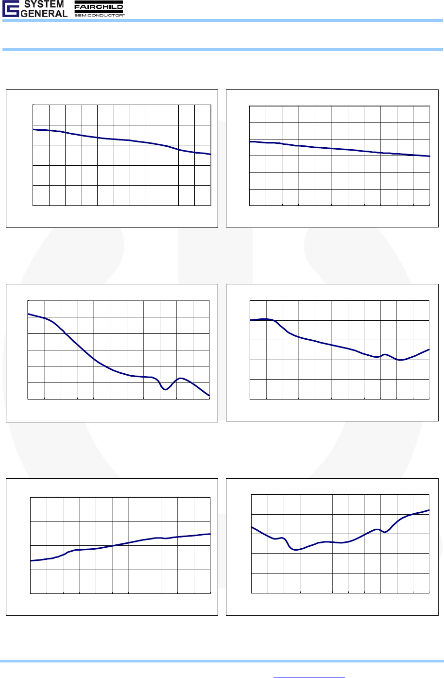
TYPICAL CHARACTERISTICS
Turn-On Threshold Voltage (V
DD-ON
) vs Temperature
16.0
16.2
16.4
16.6
16.8
17.0
-40 -25 -10 5 20 35 50 65 80 95 110 125
Temperature (℃)
V
DD-ON
(V)
Turn-Off Threshold Voltage (V
DD-OFF
) vs Temperature
8
9
10
11
12
13
14
-40 -25 -10 5 20 35 50 65 80 95 110 125
Temperature (℃)
V
DD-OFF
(V)
Startup Current (I
DD-ST
) vs Temperature
0.2
0.4
0.6
0.8
1.0
1.2
1.4
-40 -25 -10 5 20 35 50 65 80 95 110 125
Temperature (℃)
I
DD-ST
(uA)
Operating Supply Current (I
DD-OP
) vs Temperature
2.0
2.2
2.4
2.6
2.8
3.0
-40 -25 -10 5 20 35 50 65 80 95 110 125
Temperature (℃)
I
DD-OP
(mA)
Normal PWM Frequency (F
OSC
) vs Temperature
70.0
70.5
71.0
71.5
72.0
-40 -25 -10 5 20 35 50 65 80 95 110 125
Temperature (℃)
F
OSC
(Khz)
Maximum Duty Cycle (DCY
MAX
) vs Temperature
74.0
74.2
74.4
74.6
74.8
75.0
-40-25-10 5 203550658095110125
Temperature (℃)
DCY
MAX
(%)
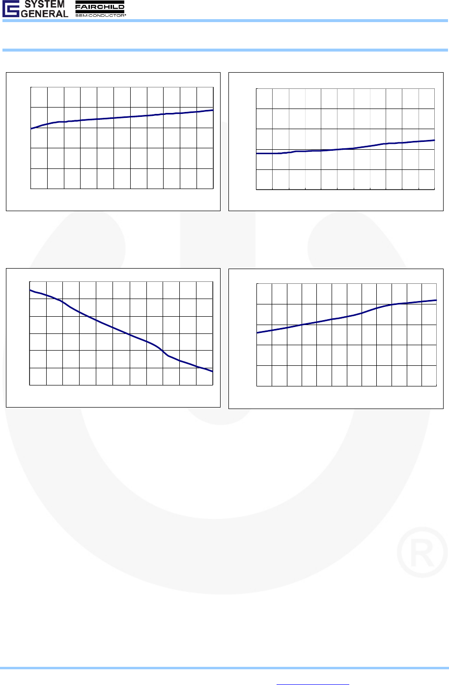
Product Specification
Low Cost Green-Mode PWM Controller for Flyback Converters SG6859
© System General Corp. - 7 - www.sg.com.tw • www.fairchildsemi.com
Version 1.2.1(IAO33.0067.B2) September 28, 2007
Green-Mode Entry FB Voltage (V
FB-N
) vs Temperature
2.2
2.4
2.6
2.8
3.0
3.2
-40 -25 -10 5 20 35 50 65 80 95 110 125
Temperature (℃)
V
FB-N
(V)
Green-Mode Ending FB Voltage (V
FB-G
) vs Temperature
2.20
2.22
2.24
2.26
2.28
2.30
-40 -25 -10 5 20 35 50 65 80 95 110 125
Temperature (℃)
V
FB-G
(V)
Leading-Edge Blanking Time (t
LEB
) vs Temperature
280
290
300
310
320
330
340
-40 -25 -10 5 20 35 50 65 80 95 110 125
Temperature (℃)
t
LEB
(ns)
Operating Supply Current vs VDD voltage
1.0
1.5
2.0
2.5
3.0
3.5
12 13 14 15 16 17 18 19 20 21 22 23 24
VDD (V)
IDD-OP (mA
)

Product Specification
Low Cost Green-Mode PWM Controller for Flyback Converters SG6859
© System General Corp. - 8 - www.sg.com.tw • www.fairchildsemi.com
Version 1.2.1(IAO33.0067.B2) September 28, 2007
OPERATION DESCRIPTION
SG6859 devices integrate many useful designs into
one controller for low-power switch-mode power supplies.
The following descriptions highlight some of the features
of the SG6859 series.
Start-up Current
The start-up current is only 9uA. Low start-up
current allows a start-up resistor with a high resistance
and a low-wattage to supply the start-up power for the
controller. A 1.5 MΩ, 0.25W, start-up resistor and a
10uF/25V VDD hold-up capacitor would be sufficient for
an AC-to-DC power adapter with a wide input range
(100VAC to 240VAC).
Operating Current
The operating current has been reduced to 3mA. The
low operating current results in higher efficiency and
reduces the VDD hold-up capacitance requirement.
Green-Mode Operation
The proprietary green-mode function provides
off-time modulation to linearly decrease the switching
frequency under light-load conditions. On-time is limited
to provide stronger protection against brownouts and
other abnormal conditions. The feedback current, which is
sampled from the voltage feedback loop, is taken as the
reference. Once the feedback current exceeds the
threshold current, the switching frequency starts to
decrease. This green-mode function dramatically reduces
power consumption under light-load and zero-load
conditions. Power supplies using the SG6859 can easily
meet even the strictest regulations regarding standby
power consumption.
Oscillator Operation
A resistor connected from the RI pin to ground will
generate a constant current source for the SG6859. This
current is used to charge an internal capacitor. The
charge-time determines the internal clock speed and the
switching frequency. Increasing the resistance will reduce
the amplitude of the input current and reduce the
switching frequency. A 95kΩ resistor Ri results in a 50uA
constant current Ii and a 70kHz switching frequency. The
relationship between Ri and the switching frequency is:
)(kHz
)(kR
6650
I
PWM
fΩ
=
Leading-Edge Blanking
Each time the power MOSFET is switched on, a
turn-on spike will inevitably occur at the sense-resistor.
To avoid premature termination of the switching pulse, a
320nsec leading edge blanking time is built in.
Conventional RC filtering can therefore be omitted.
During this blanking period, the current-limit comparator
is disabled and it cannot switch off the gate driver.
Constant Output Power Limit
When the SENSE voltage across the sense resistor Rs
reaches the threshold voltage (around 0.96V), the output
GATE drive will be turned off following a short
propagation delay tPD.
This propagation delay will introduce an additional
current proportional to tPD*Vin/Lp. The propagation delay
is nearly constant regardless of the input line voltage VIN.
Higher input line voltages will result in larger additional
currents. At high input line voltages, the output power
limit will be higher than at low input line voltages.
To compensate for this output power limit variation
across a wide AC input range, the threshold voltage is
adjusted by adding a positive ramp.
This ramp signal rises from 0.80V to 0.96V, and then
flattens out at 0.96V. A smaller threshold voltage forces
the output GATE drive to terminate earlier.
This reduces the total PWM turn-on time and makes
the output power equal to that of low line input. This
proprietary internal compensation ensures a constant
output power limit for a wide AC input voltage range
(90VAC to 264VAC).
Under Voltage Lockout (UVLO)
The turn-on and turn-off thresholds of the SG6859
are fixed internally at 16.5V/11.5V. During start-up, the
hold-up capacitor must be charged to 16.5V through the
start-up resistor, so that the SG6859 will be enabled. The
hold-up capacitor will continue to supply VDD until power
can be delivered from the auxiliary winding of the main
transformer. VDD must not drop below 11.5V during this
start-up process. This UVLO hysteresis window ensures
that hold-up capacitor will be adequate to supply VDD
during start-up.

Product Specification
Low Cost Green-Mode PWM Controller for Flyback Converters SG6859
© System General Corp. - 9 - www.sg.com.tw • www.fairchildsemi.com
Version 1.2.1(IAO33.0067.B2) September 28, 2007
Gate Output
The SG6859 BiCMOS output stage is a fast totem
pole gate driver. Cross conduction has been avoided to
minimize heat dissipation, increase efficiency, and
enhance reliability. The output driver is clamped by an
internal 17V Zener diode in order to protect power
MOSFET transistors against undesired over-voltage gate
signals.
Built-in Slope Compensation
The sensed voltage across the current sense resistor
is used for current mode control and pulse-by-pulse
current limiting. Built-in slope compensation will
improve stability and prevent sub-harmonic oscillations
due to peak-current mode control. The SG6859 has a
synchronized, positively-sloped ramp built-in at each
switching cycle. The slope of the ramp is:
.)(max
36.0
Duty
Duty×
Noise Immunity
Noise from the current sense or the control signal can
cause significant pulse width jitter, particularly in
continuous-conduction mode. While slope compensation
helps alleviate these problems, further precautions should
still be taken. Good placement and layout practices should
be followed. Avoiding long PCB traces and component
leads, locating compensation and filter components near
the SG6859, and increasing the power MOS gate
resistance is advised.
Product Specification
Low Cost Green-Mode PWM Controller for Flyback Converters SG6859
© System General Corp. - 10 - www.sg.com.tw • www.fairchildsemi.com
Version 1.2.1(IAO33.0067.B2) September 28, 2007
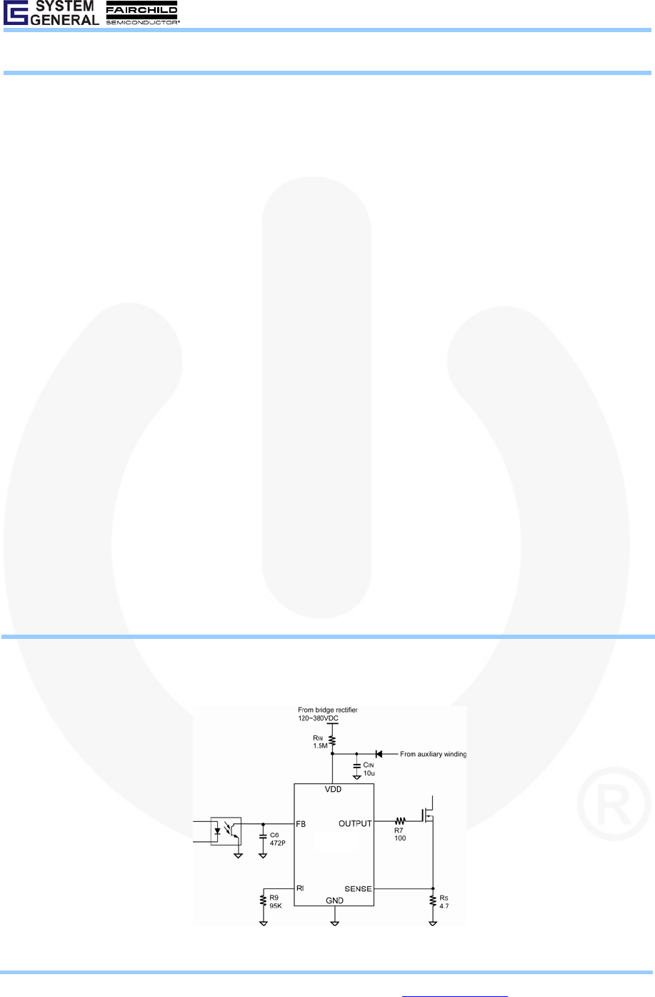
REFERENCE CIRCUIT
F1
R7
R6
R3
R1
R5 R4
R9
R10
R11
R13
R12
R14
R8
R2
C3
C7
CY1 C10
C1
CX1
C2
C9
C4
C8
C6
1 2
L1
10
5
73,4
1,2
8
9
T1
2 1
D1
1
23
Q1
GND
1
FB
2
RI
3SENSE 4
VDD 5
GATE 6
U1
21
D2
12
3 4
U2
2 1
D4
2 1
D5
1 2
L2
2 3
1
U3
1
4
3
2
BD1
VO
GND
L
N
R15
C11
BOM
Reference Component Reference Component
BD1 BD 1A/500V L2 10uH 6mm
CX1 (Optional) XC 0.1uF Q1 MOSFET 1A/600V
CY1 (Optional) YC 102P/400V (Y1) R1,R2 R 750KΩ 1206
C1 CC 103P/500V R3,R4 R 47KΩ 1206
C2 EC 10µF/400V 105°C R5 R 47Ω 1206
C3 CC 102P/500V R6 R 4.7Ω 1206
C4 EC 10µ/50V R7 R 100Ω 0805
C6 CC 472P 0805 R8 R 10Ω 1206
C7 (Optional) CC 102P/100V 1206 R9 R 100KΩ 0805
C8 EC 470µ/10V 105°C R10 (Optional) R 10Ω 1206
C9 EC 220µ/10V 105°C R11 R 100Ω 1/8W
C10 CC 222P 0805 R12 R 33KΩ 0805
C11 N.C. R13 R 33KΩ 1/8W
D1 Diode FRI07 R14 R 4.7KΩ 0805
D2 Diode FR102 R15 R 0Ω 0805
D4 Diode SB360 T1 EE-16
D5 (Optional) ZD 6.8V 0.5W U1 IC SG6859
F1 R 1Ω/0.5W U2 PC817
L1 20mH 6*8mm U3 TL431
Product Specification
Low Cost Green-Mode PWM Controller for Flyback Converters SG6859
© System General Corp. - 11 - www.sg.com.tw • www.fairchildsemi.com
Version 1.2.1(IAO33.0067.B2) September 28, 2007
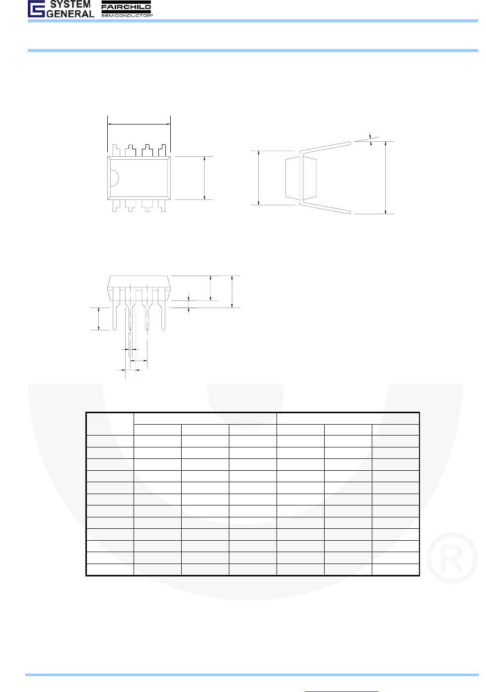
PACKAGE INFORMATION
8 PINS - DIP (D)
41
85
D
E1
EeB
A1
A2
A
b
b1
L
e
¢X
Θ
Dimensions
Millimeters Inches
Symbol Min. Typ. Max. Min. Typ. Max.
A 5.334 0.210
A1 0.381 0.015
A2 3.175 3.302 3.429 0.125 0.130 0.135
b 1.524 0.060
b1 0.457 0.018
D 9.017 9.271 10.160 0.355 0.365 0.400
E 7.620 0.300
E1 6.223 6.350 6.477 0.245 0.250 0.255
e 2.540 0.100
L 2.921 3.302 3.810 0.115 0.130 0.150
eB 8.509 9.017 9.525 0.335 0.355 0.375
θ˚ 0˚ 7˚ 15˚ 0˚ 7˚ 15˚
Product Specification
Low Cost Green-Mode PWM Controller for Flyback Converters SG6859
© System General Corp. - 12 - www.sg.com.tw • www.fairchildsemi.com
Version 1.2.1(IAO33.0067.B2) September 28, 2007
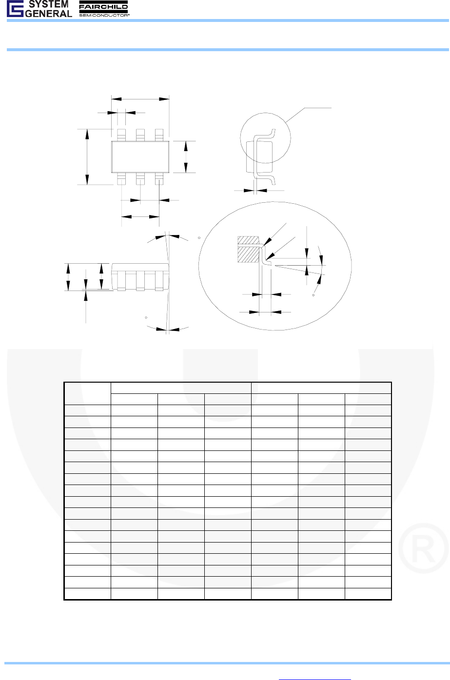
6 PINS - SOT (T)
13
64
E
e1
E1
e
D
b
A2
A1
A
θ
θ
R1
R
L2
L1
L
θ
Detail A
Detail A
c
1
1
Dimensions
Millimeters Inches
Symbol Min. Typ. Max. Min. Typ. Max.
A 1.45 0.057
A1 0.15 0.006
A2 0.90 1.15 1.30 0.036 0.045 0.051
b 0.30 0.50 0.011 0.020
c 0.08 0.22 0.003 0.009
D 2.90 0.114
E 2.80 0.110
E1 1.60 0.063
e 0.95 0.037
e1 1.90 0.075
L 0.30 0.45 0.60 0.020 0.018 0.024
L1 0.60 0.024
L2 0.25 0.010
R 0.10 0.004
R1 0.10 0.25 0.004 0.010
θ° 0° 4° 8° 0° 4° 8°
θ1° 5° 10° 15° 5° 10° 15°
Product Specification
Low Cost Green-Mode PWM Controller for Flyback Converters SG6859
© System General Corp. - 13 - www.sg.com.tw • www.fairchildsemi.com
Version 1.2.1(IAO33.0067.B2) September 28, 2007