Service Manual C45 M50 MT50 Siemens C45, M50, Repair Ation Level 2.5e
User Manual: Service manuals, Schematics Mobile Phones Siemens. Free.
Open the PDF directly: View PDF ![]() .
.
Page Count: 46

V1.0 Page 1 of 46 ICM MP CCQ ST
C45, M50 AND MT50 Company Confidential © Copyright Siemens AG 05/02
C45 / M50 / MT50
Level 2.5e
Repair Documentation
V 1.0

V1.0 Page 2 of 46 ICM MP CCQ ST
C45, M50 AND MT50 Company Confidential © Copyright Siemens AG 05/02
Table of Contents:
1 LIST OF AVAILABLE LEVEL 2,5E PARTS C45, M50 + MT50.........4
2 REQUIRED EQUIPMENT FOR LEVEL 2,5E......................................................5
3 REQUIRED SOFTWARE FOR LEVEL 2,5E C45, M50 AND MT50....................5
4 RADIO PART....................................................................................................6
4.1 Power Supply RF-Part....................................................................................7
4.2 Frequency generation.....................................................................................9
4.2.1 Synthesizer: The discrete VCXO (26MHz)...........................................................................9
4.2.2 Synthesizer: LO1................................................................................................................11
4.2.3 Synthesizer: LO2................................................................................................................13
4.2.4 Synthesizer: PLL................................................................................................................14
4.3 Antenna switch (electrical/mechanical)......................................................15
4.4 Receivers.......................................................................................................17
4.4.1 Receiver: GSM900/1800 –Filter to Demodulator...............................................................17
4.4.2 IC Overview........................................................................................................................19
4.5 Transmitter....................................................................................................20
4.5.1 Transmitter: Modulator and Up-conversion Loop...............................................................20
4.5.2 Transmitter: Power Amplifier..............................................................................................21
5 POWER SUPPLY..............................................................................................22
5.1 Overview and Voltages.................................................................................22
5.2 Power Supply ASIC.......................................................................................23
5.3 Battery and Charging....................................................................................26
5.3.1 Battery................................................................................................................................26
5.3.2 Charging Concept..............................................................................................................26
6 LOGIC PART.....................................................................................................28
6.1 Overview Logic/control...............................................................................28
6.2 EGOLD (PMB6850) V2.x...............................................................................30
6.3 EGAIM inside the EGOLD+...........................................................................31
6.3.1 Tasks of the EGAIM inside the EGOLD+...........................................................................32
6.4 Real Time Clock (integrated in the EGOLD+).............................................35
6.5 SRAM.............................................................................................................36

V1.0 Page 3 of 46 ICM MP CCQ ST
C45, M50 AND MT50 Company Confidential © Copyright Siemens AG 05/02
6.6 FLASH............................................................................................................37
7 ACOUSTICS......................................................................................................38
7.1 General...........................................................................................................38
7.2 Vibra...............................................................................................................39
7.3 Microphone and Loudspeaker (Ringer).....................................................40
7.3.1 Loudspeaker......................................................................................................................40
7.3.2 Microphone........................................................................................................................40
7.3.3 Loudspeaker/Ringer...........................................................................................................41
8 ILLUMINATION:................................................................................................42
8.1 Illumination....................................................................................................42
9 SIM-CARD AND CONNECTORS......................................................................43
9.1 SIM-Card........................................................................................................43
9.2 Display connector.........................................................................................44
9.3 I/O-Connector................................................................................................45
9.4 Battery Connector.........................................................................................46
V1.0 Page 4 of 46 ICM MP CCQ ST
C45, M50 AND MT50 Company Confidential © Copyright Siemens AG 05/02
1 List of available level 2,5e parts
C45, M50 + MT50
ID-No Type Name, Location Part-No.
D100 IC Egold+ L36810-G6132-D670
D361 IC ASIC L36145-J4682-Y29
D800 IC Transceiver IC L36820-L6081-D670
D920 IC PA_Comperator L36820-L6084-D670
N386 IC
Volt.Regulator_ZUB
L36820-C6161-D670
N840 IC
Volt.Regulator_RF
L36810-C6065-D670
R959 Resistor Temp_Resistor L36120-F4223-H
L366 Diode Diode_AF L36840-D3084-D670
V342
Transistor Tran._Charge L36830-C1104-D670
V344
Diode Diode_Charge L36840-D5061-D670
V442
Transistor Tran._SW_Vibra L36830-C1097-D670
V850
Transistor Tran._VCO_Switch L36820-C6047-D670
V880
Transistor Tran._Sw_Diplexer L36820-C6047-D670
V881
Transistor Tran._Sw_Diplexer L36820-C6047-D670
V920
Diode Feedback_Diode L36840-D5049-D670
V922
Transistor Tran._PA_Control L36840-C4009-D670
V950
Transistor Tran._26MHz_Ampl. L36840-C4049-D670
V951
Diode Capa_Diode L36840-D61-D670
Z100 Quartz Quarz/Egold L36145-F102-Y8
Z850
VCO
1LO_VCO L36145-G100-Y93
Z851 Filter Filter_BALUN L36145-K260-Y31
Z880 IC Ant_Switch_Diplexer L36145-K280-Y181
Z890
VCO
Transmitter_VCO L36145-G100-Y92
Z900 IC Power_Amplifier L36851-Z2002-A45
Z950 Quartz Oszillator_26MHz L36145-F260-Y16

V1.0 Page 5 of 46 ICM MP CCQ ST
C45, M50 AND MT50 Company Confidential © Copyright Siemens AG 05/02
2 Required Equipment for Level 2,5e
- GSM-Tester (CMU200 or 4400S incl. Options)
- PC-incl. Monitor, Keyboard and Mouse
- Bootadapter 2000/2002 (L36880-N9241-A200)
- Troubleshooting Frame C45 (F30032-P135-A1)
- Power Supply
- Spectrum Analyser
- Active RF-Probe incl. Power Supply
- Oscilloscope incl. Probe
- RF-Connector (N<>SMA(f))
- Power Supply Cables
- Dongle (F30032-P28-A1)
- BGA Soldering equipment
Reference: Equipment recommendation V1.0 (downloadable from the technical support page)
3 Required Software for Level 2,5e C45, M50
AND MT50
- Windows NT Version4
- Winsui version1.22 or higher
- Windows software for GSM-Tester ( Cats(Acterna) or CMU-GO(Rohde&Schwarz) )
- Software for reference oscillator adjustment
- Internet unblocking solution

V1.0 Page 6 of 46 ICM MP CCQ ST
C45, M50 AND MT50 Company Confidential © Copyright Siemens AG 05/02
4 Radio Part
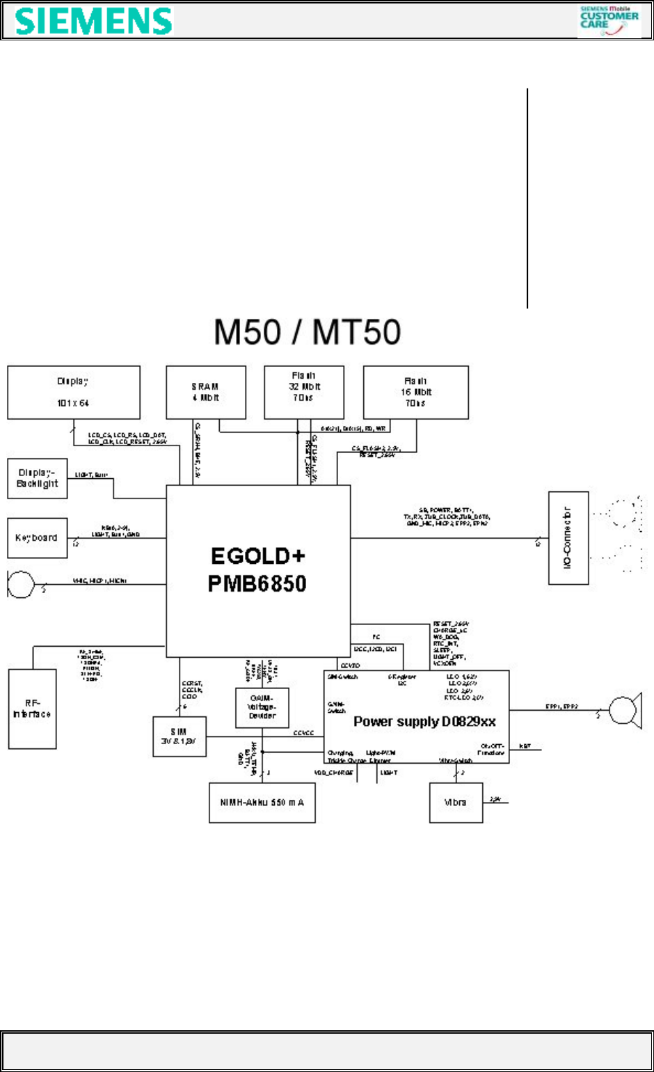
The radio part of the C45, M50 AND MT50 consists of a Hitachi RF chip-set.
The radio part is designed for Dual Band operation, covering EGSM900 as well
as GSM 1800 frequencies, and can be divided into 4 Blocks.
- Power supply for RF-Part
- Transmitter
- Receiver
- Synthesizer,
The RF-Part has it´s own power supply realised by a voltage regulator
which is directly connected to the battery. The voltages for the logic part are
generated by the Power-Supply ASIC
The transmitter part converts the I/Q base band signals supplied by the
logic (EGOLD+) into RF-signals with characteristics as defined in the
GSM recommendation (www.etsi.org) After amplification by a power
Amplifier the signal is radiated via the internal or external antenna.
The receiver part converts the received GMSK signal supplied by the
antenna into IQ base band signals which can then be further processed by
the logic (EGOLD+).
The synthesizer generates the required frequencies for the transmitter and
Receiver. A 26MHz oscillator is acting as a reference frequency.
Restrictions:
- The mobile phone can never transmit and receive in both bands simultaneously.
- Only the monitor time slot can be selected independently of the frequency band.
- Transmitter and receiver can of course never operated simultaneously.
V1.0 Page 7 of 46 ICM MP CCQ ST
C45, M50 AND MT50 Company Confidential © Copyright Siemens AG 05/02
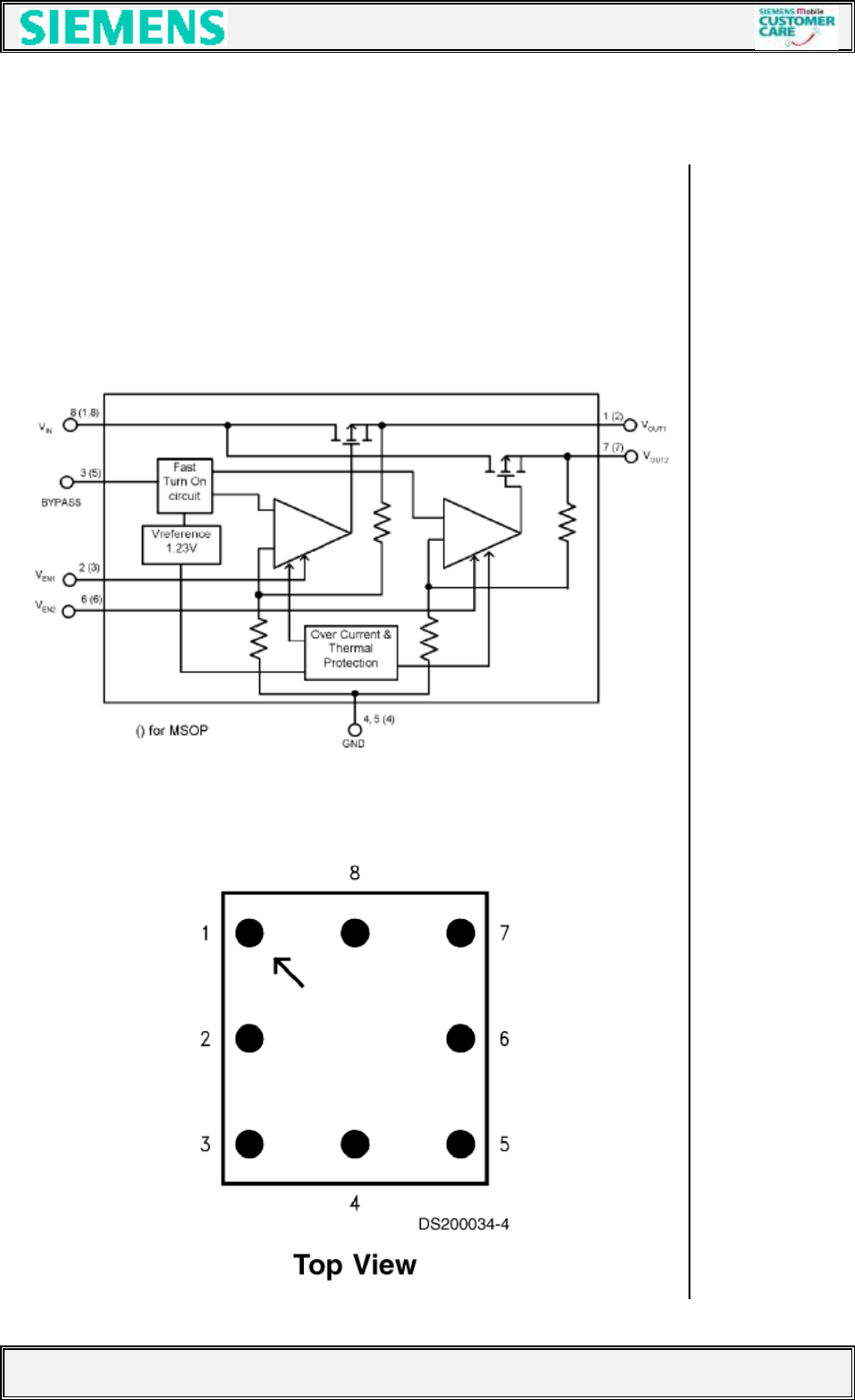
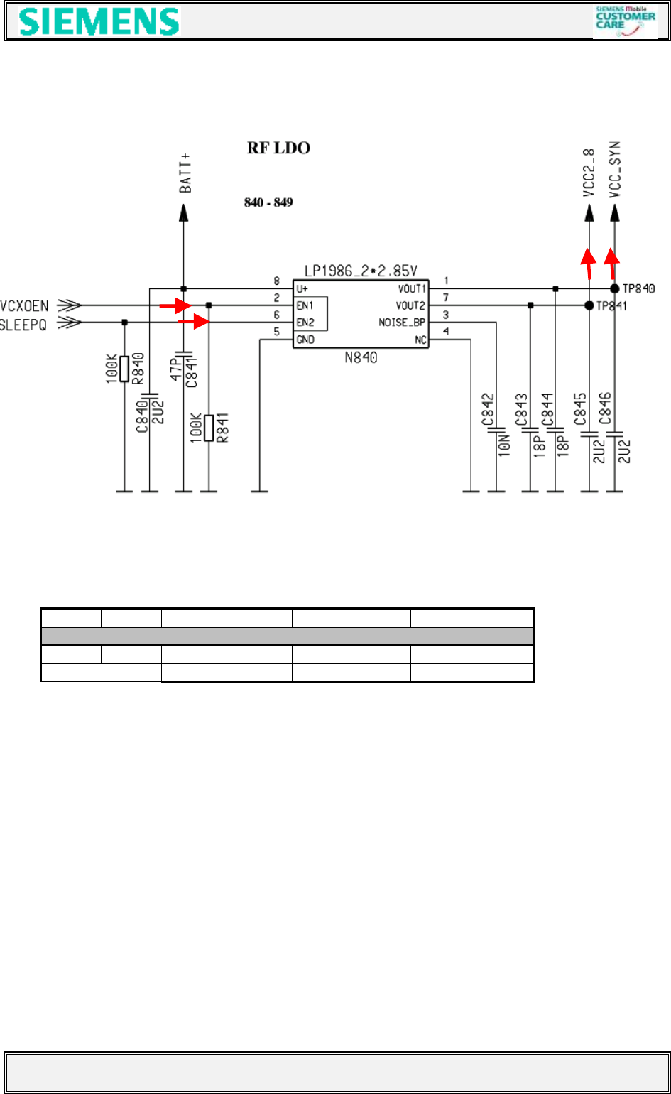
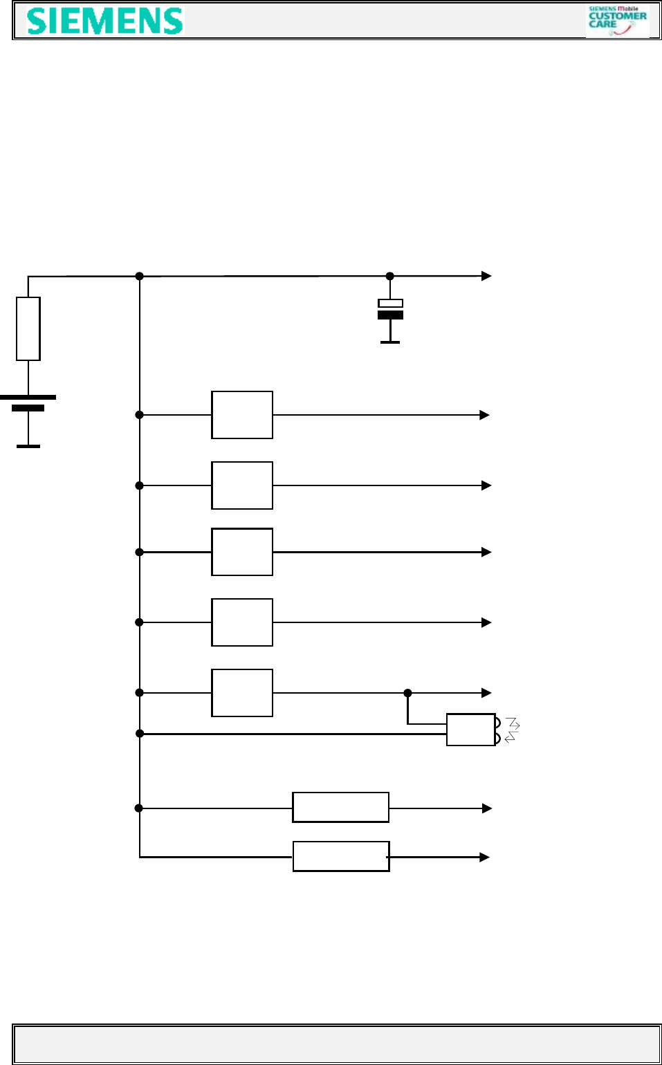
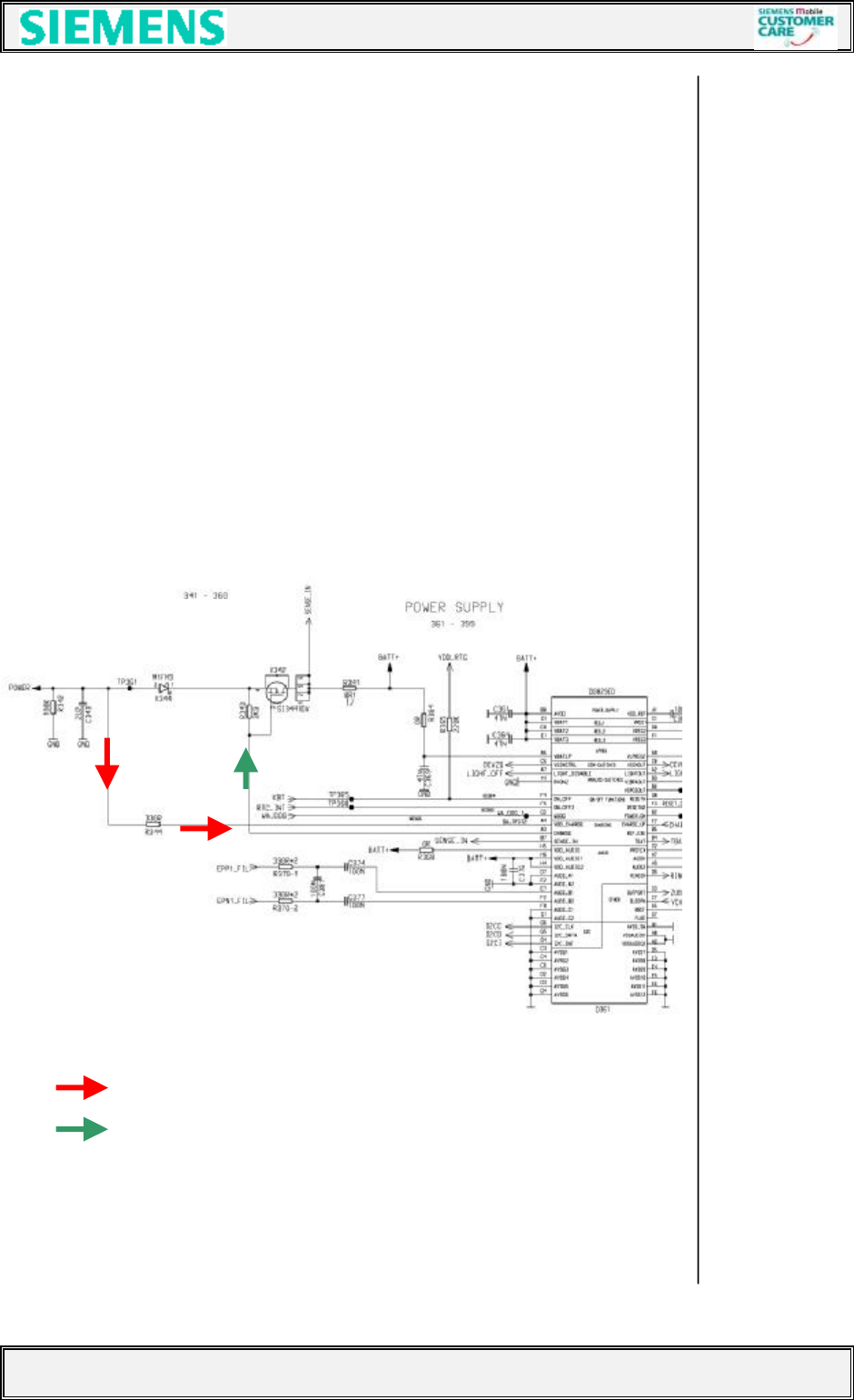
4.1 Power Supply RF-Part
A directly to Batt+ connected voltage regulator, with a nominal output voltage
of 2.8V is used, to perform the required “RF-Voltages” named VCC2_8 and
VCC_SYN.
The voltage regulator is activated as well as deactivated via SLEEPQ and
VCXOEN provided by the EGOLD+
The temporary deactivation is used to extend the stand by time.
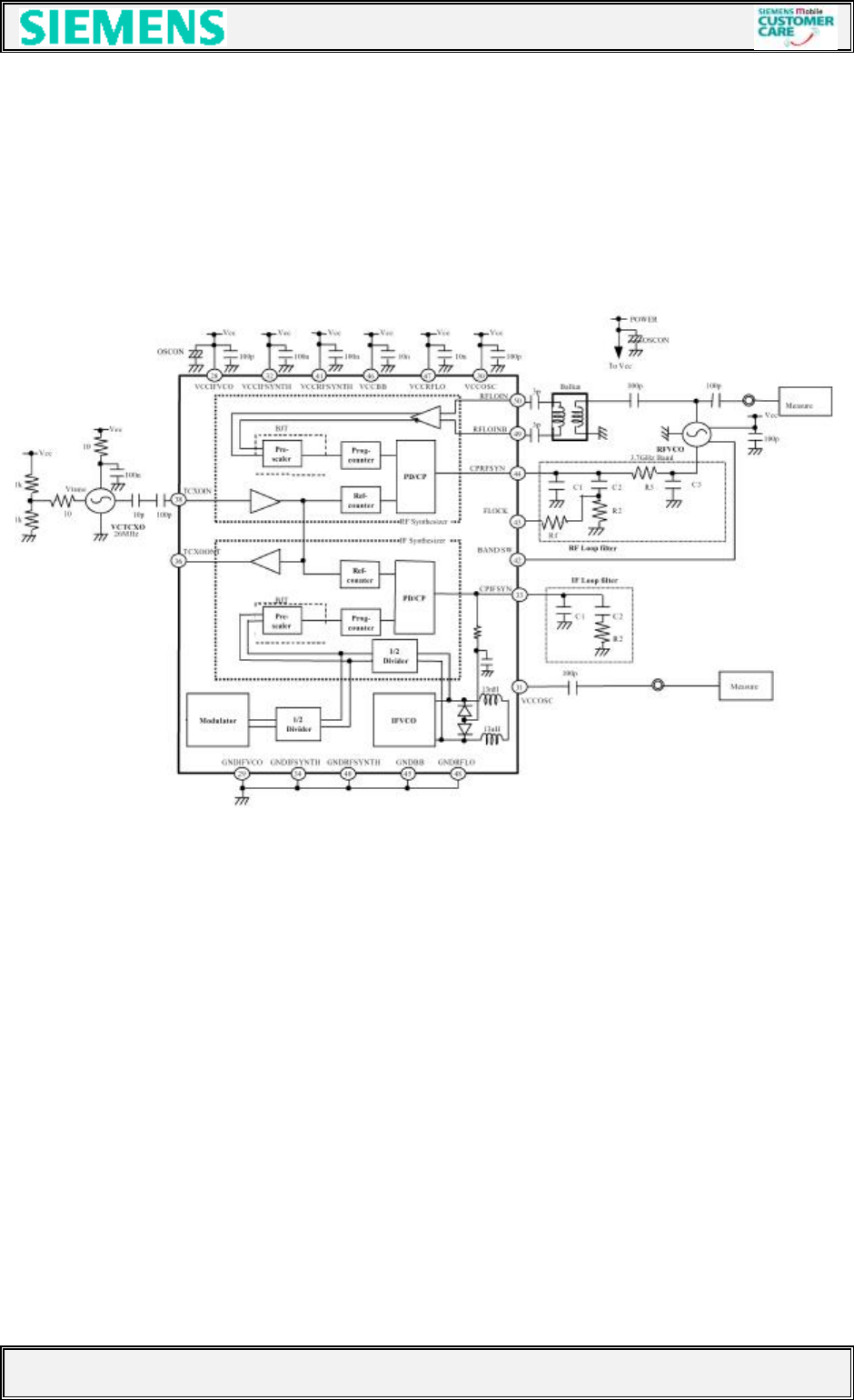
Blockdiagram
PIN-OUT
V1.0 Page 8 of 46 ICM MP CCQ ST
C45, M50 AND MT50 Company Confidential © Copyright Siemens AG 05/02
Circuit diagram
Type Part No.
Signal Source Output
Hitachi N840 Pin 6 SleepQ EGOLD+ L11 Pin 7 VCC2_8
Pin 2 VCXOEN EGOLD+ P7 Pin 1 VCC_SYN
V1.0 Page 9 of 46 ICM MP CCQ ST
C45, M50 AND MT50 Company Confidential © Copyright Siemens AG 05/02
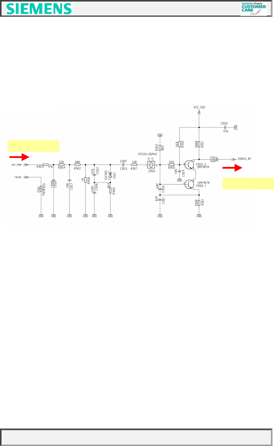
4.2 Frequency generation
4.2.1 Synthesizer: The discrete VCXO (26MHz)
M46 mobile is using a reference frequency of 26MHz for the Hitachi chip set.
The generation of the 26MHz signal is done via a discrete “Colpitts” VCXO .
This oscillator consists mainly of:
A 26MHz crystal Z950
An oscillator switch V950
A capacity diode V951
TP 951 after dividing by two
The oscillator output signal is directly connected to the BRIGHT IC (pin 38) to be
used as reference frequency inside the Bright and to be divided by 2.
This so gained signal SIN13MHZ_BB is used from the EGOLD+(functional M14).
To compensate frequency drifts (e.g. caused by temperature) the oscillator
frequency is controlled by the (AFC_PNM) signal, generated through the internal
EGOLD+ (D100 (functional R3)) PLL via the capacity diode V951.
Reference is the base station frequency.
To compensate a temperature caused frequency drift, the temperature-depending
resistor R959 is placed near the VCXO to measure the temperature. The
measurement result TVCXO is reported to the EGOLD+(baseband L4) via R136 as
the signal TENV.
The required voltage VCC_OSC is provided by the N840 (VCC_SYN) through
R863 and R861
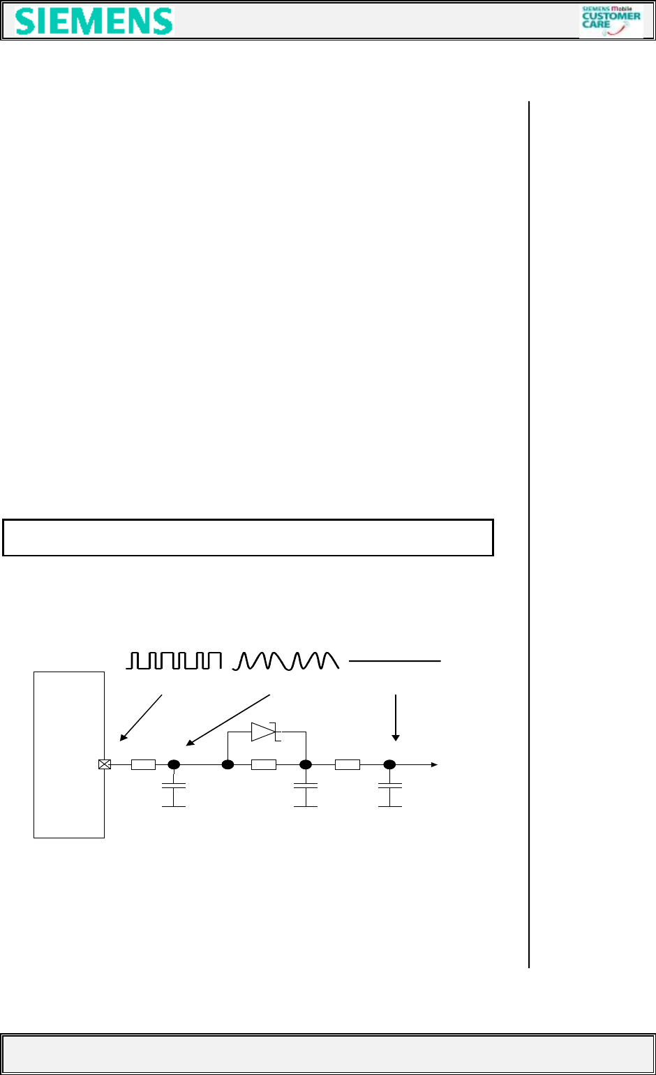
Waveform of the AFC_PNM signal from EGOLD+ to Oscillator
EGOLD+
V1.3
GND GND
47K
R615
AFC
Signalform
C110
C616
100N
100N
AFC_PNM
GND
C600
10N
R600
V602
BAS170W
1
2
3
1 2 3
30K 22K
R106
V1.0 Page 10 of 46 ICM MP CCQ ST
C45, M50 AND MT50 Company Confidential © Copyright Siemens AG 05/02
Circuit diagram
from EGOLD
EGOLDEGO
LD+
to Bright IC
V1.0 Page 11 of 46 ICM MP CCQ ST
C45, M50 AND MT50 Company Confidential © Copyright Siemens AG 05/02
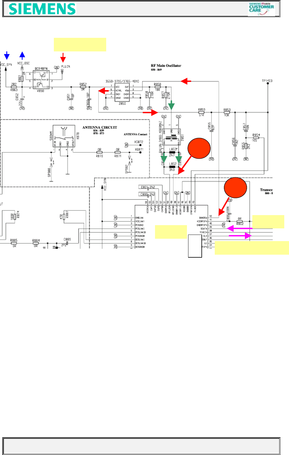
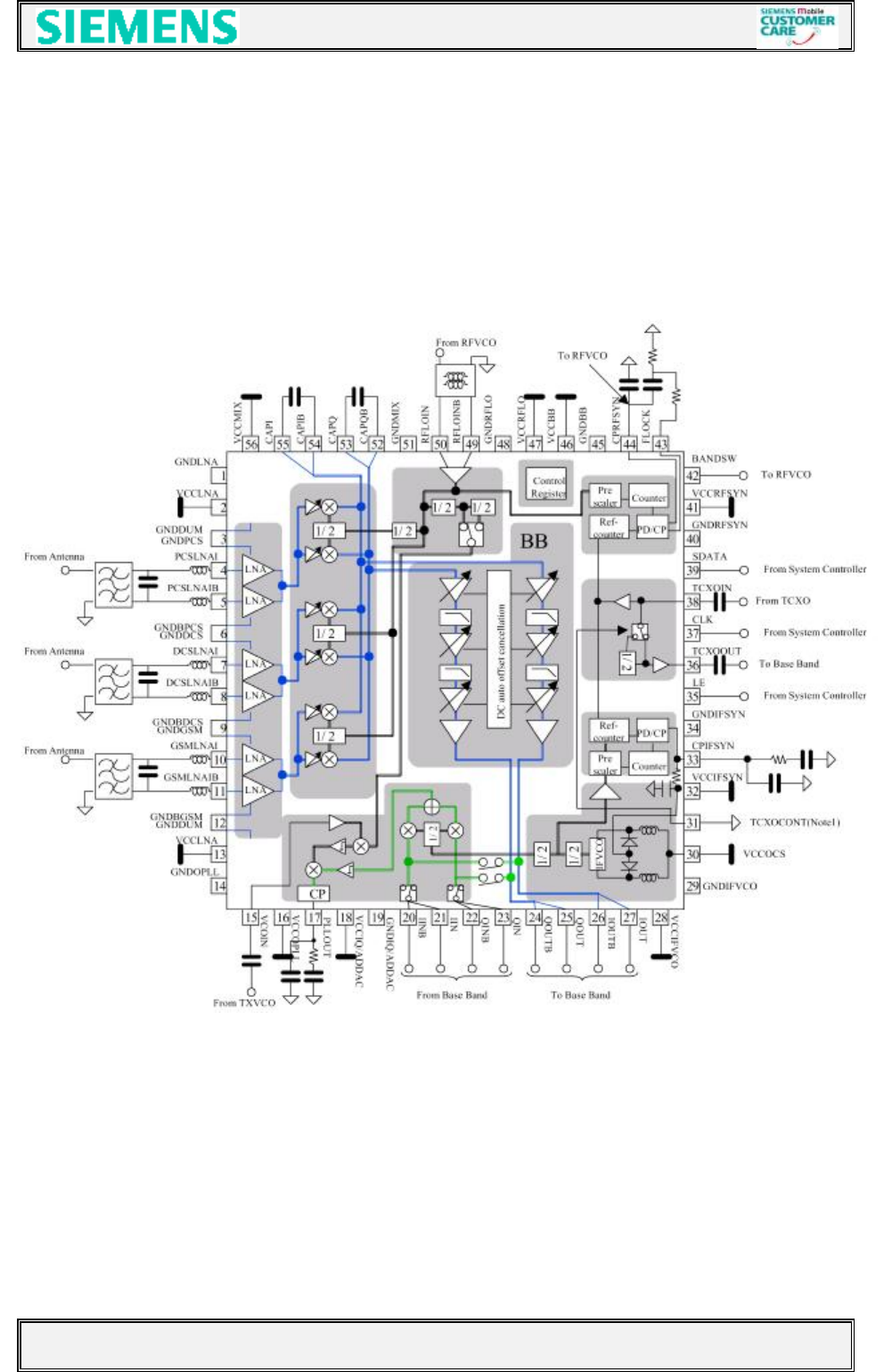
4.2.2 Synthesizer: LO1
The first local oscillator is needed to generate frequencies which enable the
transceiver IC to mix an “IF” and to perform the channel selection in the TX part.
To do so, a control voltage for the LO1 is used. Gained by a comparator
(located inside the Transceiver -IC).
This control voltage is a result of the comparison of the divided LO1 and a reference
Signal. The division ratio of the dividers is programmed by the EGOLD+, according
to the network channel requirements.
The first local oscillator (LO1) is part of the PLL which consists of the comparator
inside the Bright (D800), a loop filter and the VCO (Z850) module.
This LO1 circuit generates frequencies from:
3610-3760 MHz for GSM900
3700-3840 MHz for GSM1800
(The VCO can be switched via the signal VSW (Pin 3) to generate frequencies for
GSM900 and GSM1800)
RX IF = no IF required TX IF-GSM900 = 45…46MHz
TX IF-GSM1800 = 90…92MHz
Formula to calculate the frequencies:
1st LO freq. RX EGSM = Ch. * 4
PCN = Ch. * 2
The VCO (Z850) is switched on by the EGOLD+ signal PLLON (TDMA-Timer J12)
via V850 and therefore supplied with VCC_SYN. The VCO guarantees by using the
control voltage at pin5 a coverage of the GSM900 and GSM1800 band.
The channel programming of the PLL happens via the EGOLD+ signals SYGCCL,
SYGCDT, SYNSTR (RF Control K14, K15, M15).
The required voltage VCC_SYN is provided by the N840
V1.0 Page 12 of 46 ICM MP CCQ ST
C45, M50 AND MT50 Company Confidential © Copyright Siemens AG 05/02
Circuit diagram
4221
4222
13MHz to EGOLD
1
:
2
from EGOLD+
26MHz
Bright
V1.0 Page 13 of 46 ICM MP CCQ ST
C45, M50 AND MT50 Company Confidential © Copyright Siemens AG 05/02
4.2.3 Synthesizer: LO2
The second local oscillator (LO2) consists of a PLL and a VCO which are
integrated in Bright IV and a second order loopfilter which is realized external.
Due to the direct conversion receiver architecture, the LO2 is only used for
transmit-operation. To avoid inband-spurious in the transmit-signal, the
LO2-frequency assignment is not fixed for the whole band.
Before the LO2-signal gets to the modulator it is divided by 8 for GSM900 and by 4
for GSM1800. So the resulting
TX-IF frequencies are 45…46 MHz. GSM900
TX-IF frequencies are 90…92 MHz. GSM1800
2nd LO freq. = 360…368 MHz divided by 8 = 45…46 MHz,
divided by 4 = 90…92 MHz
The LO2 PLL and power-up of the VCO is controlled via the tree-wire-bus of
Bright IV+.(EGOLD+ signals SYGCCL, SYGCDT, SYNSTR (RF Control K14, K15, M15))
The required voltage VCC_SYN is provided by the N840
Circuit diagram
Loop-filter LO2
V1.0 Page 14 of 46 ICM MP CCQ ST
C45, M50 AND MT50 Company Confidential © Copyright Siemens AG 05/02
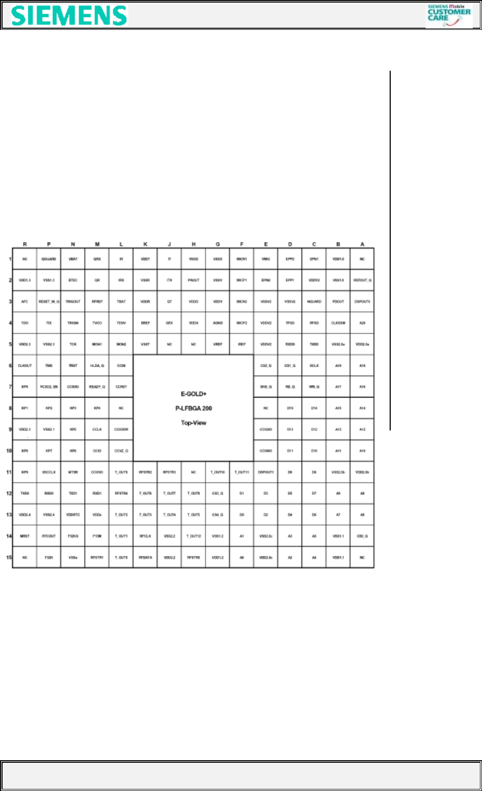
4.2.4 Synthesizer: PLL
PLL as a part of the BRIGHT IC
Blockdiagram
V1.0 Page 15 of 46 ICM MP CCQ ST
C45, M50 AND MT50 Company Confidential © Copyright Siemens AG 05/02
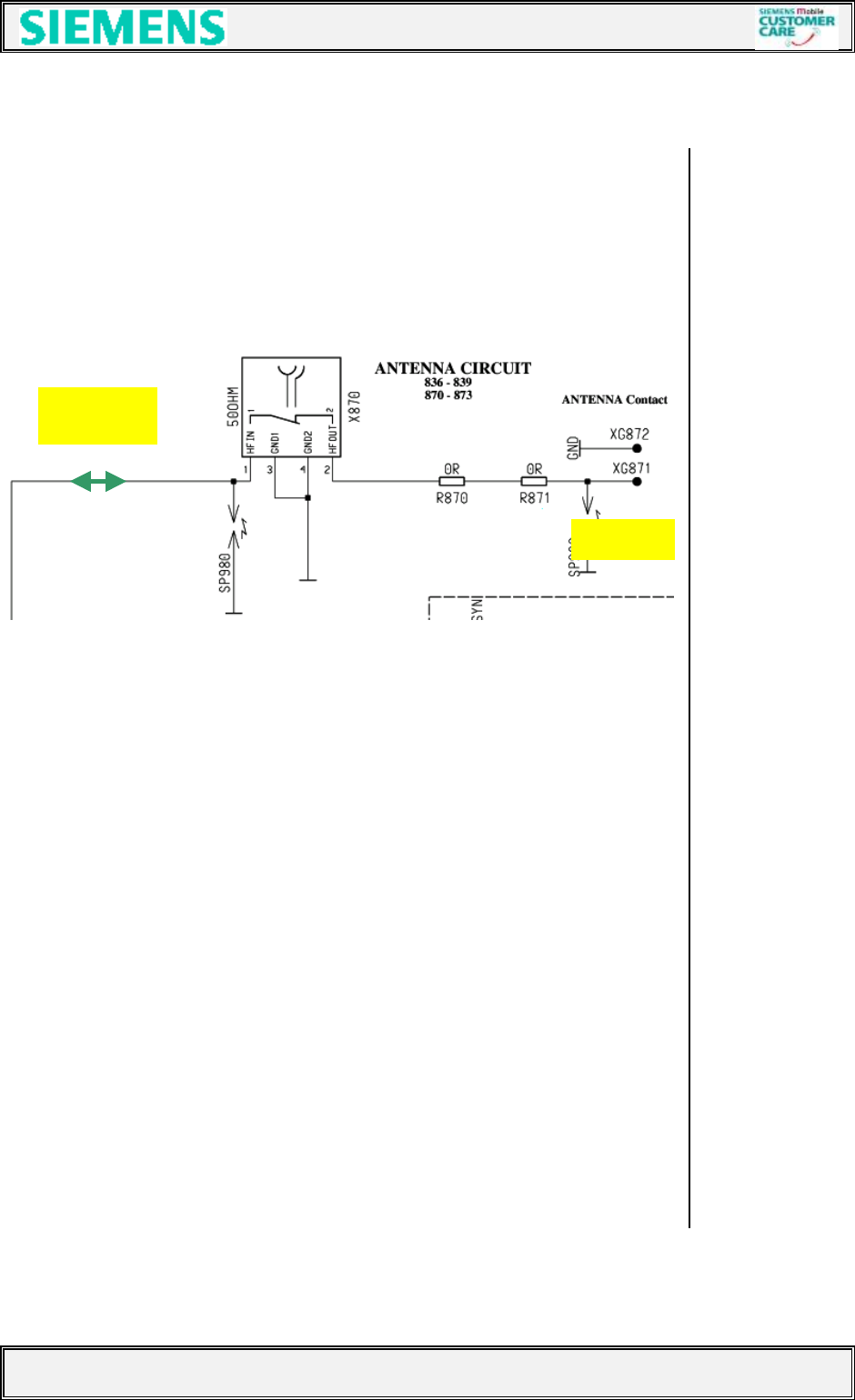
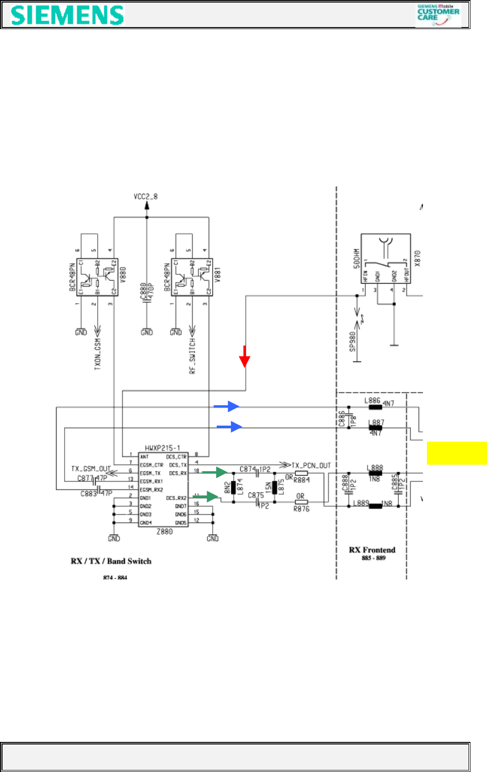
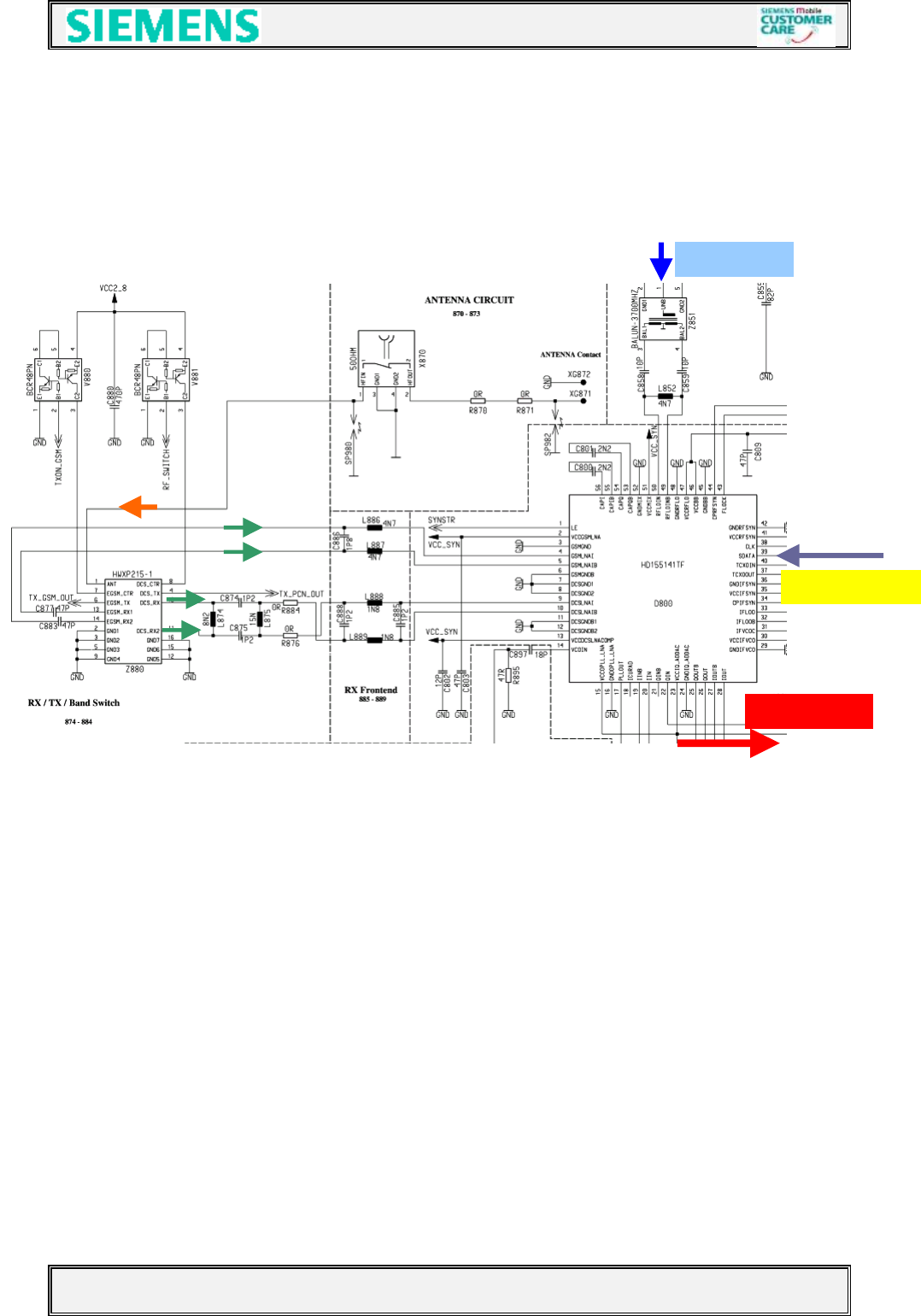
4.3 Antenna switch (electrical/mechanical)
Internal/External <> GSM1900/PCS <> Receiver/Transmitter
The M46 mobile has two antenna switches.
a) The mechanical antenna switch for the differentiation
between the internal and external antenna
Internal
to / from
diplexer
V1.0 Page 16 of 46 ICM MP CCQ ST
C45, M50 AND MT50 Company Confidential © Copyright Siemens AG 05/02
b) The electrical antenna switch, for the differentiation between the receiving
and transmitting signals.
To activate the correct settings of this diplexer, some logical switches and
switching signals are required. (V880, V881)
Bright
V1.0 Page 17 of 46 ICM MP CCQ ST
C45, M50 AND MT50 Company Confidential © Copyright Siemens AG 05/02
4.4 Receivers
4.4.1 Receiver: GSM900/1800 –Filter to Demodulator
From the antenna switch, up to the demodulator the received signal passes the
following blocks to get the demodulated baseband signals for the EGOLD+:
Filter >>>>>>>> LNA >>>>>>>> Demodulator>>>>>>>> PGC
Z880 Bright Bright Bright
Filter: The GSM900 and GSM 1800 filters are located inside the frontend module.
The Filter are centered to a frequency of 942,5MHz for GSM900 and 1847,5MHz
for GSM1800. The symmetrical filter output is matched via LC-Combinations to
the LNA input of the BRIGHT (D800)
LNA: The LNA´s is located inside the BRIGHT and is able to perform an
amplification/attenuation from ~ 20dB. The LNA is can be switched in HIGH and
LOW mode and is controlled by the Bright.
Demodulator: The Bright IC performs a direct demodulation of the received
GSM1900 Signals. To do so the LO1 is required.
The channel depending frequencies for 1900MHz band are divided by´2 for
internally.
PGC: After demodulation the “I” and “Q” signals are amplified by the internal
PGC-Amplifier whereby the “I” and the “Q” path are amplified independently
From each other. The performance of this PGC is 80dB (-22 up to 58dB),
switchable in steps of 2dB. The control is realised through the EGOLD+
signals (SYGCCL, SYGCDT, SYNSTR).
After passing an internal switch, the signals are ready for further processing
through EGOLD+
The required voltage VCC_SYN is provided by the N840
V1.0 Page 18 of 46 ICM MP CCQ ST
C45, M50 AND MT50 Company Confidential © Copyright Siemens AG 05/02
from LO1
to EGOLD+
progr. signals
V1.0 Page 19 of 46 ICM MP CCQ ST
C45, M50 AND MT50 Company Confidential © Copyright Siemens AG 05/02
4.4.2 IC Overview
IC Overview
BRIGHT IV
V1.0 Page 20 of 46 ICM MP CCQ ST
C45, M50 AND MT50 Company Confidential © Copyright Siemens AG 05/02
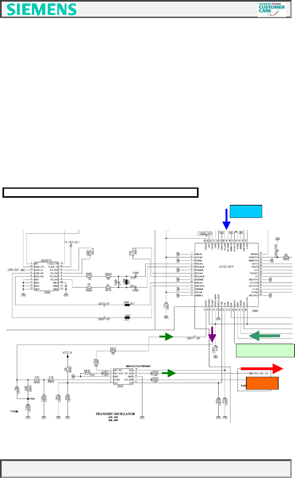
4.5 Transmitter
4.5.1 Transmitter: Modulator and Up-conversion Loop
The modulation is also based on the principle of the
“up-conversion modulation phase locked loop” and is accomplished via the
BRIGHT IC(D800). The internal TX IF-LO provides the quadratic modulator with the
TX IF frequencies (79…81 MHz) by generating 632…648 MHz frequencies,
which are divided by 8.
This so generated IF GMSK RF signal is compared in a phase detector with the
down mixed GMSK RF output from the TX-VCO (Z890).
To get the comparison signal PCN_PA_IN signal appearing at Pin 10 of the (Z890)
is mixed with the LO1 signal (divided by 2).
The output (PLLOUT) signal of the phase detector passes a discrete loop filter
realised by capacitors and resistors to set the TXVCO to required frequency.
The large loop band width (~1,5MHz) guarantees that the regulating process is
considerably quicker than the changes in the modulation signal.
The required voltage VCC_SYN and VCC2_8 is provided by the N840
to PA
from EGOLD+
LO1
V1.0 Page 21 of 46 ICM MP CCQ ST
C45, M50 AND MT50 Company Confidential © Copyright Siemens AG 05/02
4.5.2 Transmitter: Power Amplifier
The output signal (PCN_PA_IN) from the TX-VCO are led to the power amplifier
(Z900) passing a matching circuit. The PA is a “two in one” PA (GSM part not used)
and, is connected directly to Batt+.
After amplification, a part of the output signal (TX_PCN_OUT) is decoupled via a
directional coupler. The other part runs through the antenna switch (Z880) and the
antenna connector (X870) to the Antenna. The decoupled part is equalised by the
detector diode (V920) and used from the (N920) to get a PA control voltage by
comparing this voltage with the PA_RAMP signal provided from the
EGOLD+ (GAIM/BASEBAND H2).
The (N920) is activated through the signal TXONPA and TXON1.
The required voltage BATT+ is provided by the battery.
The required voltage VCC2_8 is provided by N840.
Blockdiagram of LML361 (PA control IC9
Vdd
Vdd
Vss
Vdd
Vdd
Vss
Vdd
Vss
Comp 2
Comp1
Out B
Out A
Vss
Vdd
BS PA_ON
Gnd
TC
Ramp
Vr
Vf
Vhome
V1.0 Page 22 of 46 ICM MP CCQ ST
C45, M50 AND MT50 Company Confidential © Copyright Siemens AG 05/02
5 Power Supply
5.1 Overview and Voltages
Ri
Linear-
Regler
[ASIC]
Linear-
Regler
[ASIC]
Linearregler
Linearregler
IrDA
LED
2,0 A
peak
current 150 µF
2,9V +-3%
2,65V +-3%
140mA max.
100mA max.
2,8V +- 3,5%
2,8V +- 3,5%
75 mA max.
145 mA max.
35 mA(pk), 7 mA(avg)
80 mA
EGOLD Core
Magnetischer Ringer
Flash, SRAM, SIM,
Light, Soundchip,
Vibra-motor, Altimeter
EGAIM,
EGOLD Portpins,
LCD controller
Powercontrol-ASIC,
TXVCO
Transceiver IC,
VCXO
Leerlaufspannung:
3,2V..4,2V
NiMH
PA
+Treiber
+Regelung
Linear-
Regler
[ASIC]
2,07V (1,92V) +- 3%
VDDRTC
Linear-
Regler
[ASIC]
2,0V +-5%
140mA max.
Audio-
Amplifier
[ASIC]

V1.0 Page 23 of 46 ICM MP CCQ ST
C45, M50 AND MT50 Company Confidential © Copyright Siemens AG 05/02
Overview of HW Structure
All power supply functions of the mobile phone, except the RF-Part, are carried out
by the power supply ASIC (D361)
General:
The pin POWER of the I/O-Connector is used for charging the battery.
For accessories, which provide a variable charging current, the current will
be set via a pin SB (current byte) (e.g. S25 chargers corresponding to
Car Kits etc.).
- The S45/ME45 power supply is unregulated and cannot be controlled by
the SB signal.
- The SB signal is used to distinguish between various chargers.
The following restrictions must be considered:
- The phone cannot be operated without battery.
- The phone will be damaged if the battery is inserted the wrong way
- In the charging branch a fuse element is inserted against over current.
5.2 Power Supply ASIC
The power supply ASIC (D361) contains the following functions:
- Control of “Switch On” of the mobile phone via the ON/OFF switch.
- Recognition of external chargers connected on POWER.
- Control of “Switch On” of the mobile phone via the ON/OFF1 (RTC)
- Watchdog monitoring
- Control of mobile phone “SWITCH OFF” via WATCHDOG_µP connection.
- “Switch off “of mobile phone in the case of overvoltage at battery connection.
- Generation of RESET signal for EGOLD+ and Flash
- Voltage generation via “Linear regulator 2.90 V “
- Voltage generation via “Linear regulator 2.65 V “
- Voltage generation via “Linear regulator 2.07 V “
- Battery charge support: interrupted if there is an over-temperature
- Software-controlled switching of voltage supply for the accessories
- Light switching
- Voltage generation for “SIM-CARD”
- VIBRA switching
- Ringer tone switching
- Audio switching
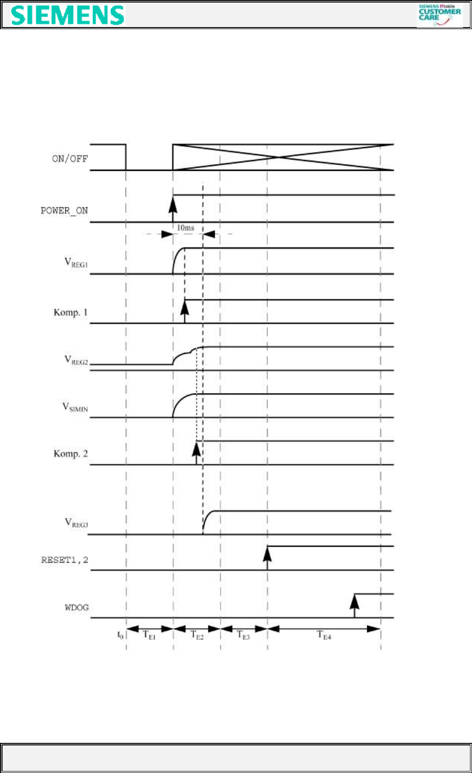
Switch “ON” sequence
- Falling edge recognition KB7, or RTC_INT
- Generation of the “2,07; 2,65; 2,9” voltages
- Generation of the “RESET_2,0V and RESET_2,65V”
- 32,768 KHz oscillator
- Generation of the “Watch Dog” signal through the EGOLD+
after “POWER_ON”
- 26MHz oscillator
V1.0 Page 24 of 46 ICM MP CCQ ST
C45, M50 AND MT50 Company Confidential © Copyright Siemens AG 05/02
“Switch-On” timing
V1.0 Page 25 of 46 ICM MP CCQ ST
C45, M50 AND MT50 Company Confidential © Copyright Siemens AG 05/02
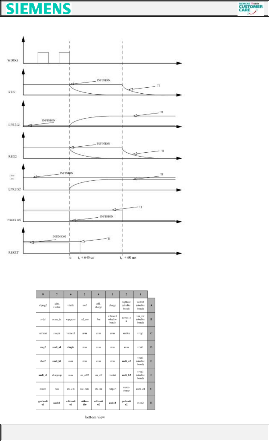
“Switch-Off” timing
“PIN-OUT” ASIC D361
V1.0 Page 26 of 46 ICM MP CCQ ST
C45, M50 AND MT50 Company Confidential © Copyright Siemens AG 05/02
5.3 Battery and Charging
5.3.1 Battery
A Li-Ion battery with a nominal capacity of 840mAh is used for the S/ME45 series
and a NiMH battery with a nominal capacity of 550mAh for the C45. M50 and MT50
are delivered out with a Li-Ion battery of 650 mAh. A temperature sensor
(22kΩ at 25°C) is integrated to monitor the battery temperature.
Battery connector:
5.3.2 Charging Concept
The battery is charged in the unit itself. The hardware and software is designed for
Li-Ion or NiMH with 4.2V technology.
The battery will be charged as long as the GAIM part of the EGOLD+ measures
changes in the values of the battery voltages during the charging process.
There are two ways to charge the battery:
Normal charging also called “fast charging”
Trickle charging
Normal Charging
As soon as the phone is connected to an external charger, charging starts. The
customer can see this via the “Charge” symbol in the display
Charging is enabled via a FET-Switch (V342) in the phone. This FET-Switch activates
the circuit form the external charger to the battery. The EGOLD+ takes over the
steering of this switch depending on the charge level of the battery, whereby a
disable function in the ASIC (D361) hardware can override/interrupt the charging in
the case of overvoltage of the battery (only in case of NEC batteries).
The charging software is able to charge the battery with an input current within the
range of 350-600mA. If the FET-Switch is switched off, no charging current will flow
into the battery (exception is trickle charging, see below).
For controlling the charging process it is necessary to measure the ambient (phone)
temperature and the battery voltage.
V1.0 Page 27 of 46 ICM MP CCQ ST
C45, M50 AND MT50 Company Confidential © Copyright Siemens AG 05/02
For temperature detection, a NTC resistor (22kΩ at 25°) is assembled in the
battery pack. Via the pin 2 of the battery connector connected to the
EGOLD+ (GAIM L3) is carrying out the measurement.
The voltage is measured from the GAIM-part of the EGOLD+ (see description
In chapter 7)
Trickle charge
If the phone has not been used for a longish time (longer than approx. 1 month), the
battery could be totally self-discharged. (battery voltage less then 3,2V), so that
it is not possible to charge the battery via the normal charging circuit. In this case
only trickle charge is possible.
The STV-ASIC (D361) controls the charging circuit himself.
- Battery voltage below 2,8 Volt charging current 20mA.
- Battery voltage below 3,2 Volt charging current 50mA.
- Battery voltage over 3,2 Volt “Normal charging”.
Power supply for the ASIC (D361) in this mode is the external charger.
(VDD_CHARGE)
The switch into normal charging mode, is done automatically if the required voltage
is reached.
Trickle Charging Power Supply
“Normal/Trickle” charging activation
!! Attention!!
- a charger voltage >15V can destroy resistors or capacitors in the charging path
- a charger voltage >20V can destroy the MOS-FET switch transistor in the
charging path.
V1.0 Page 28 of 46 ICM MP CCQ ST
C45, M50 AND MT50 Company Confidential © Copyright Siemens AG 05/02
6 Logic Part
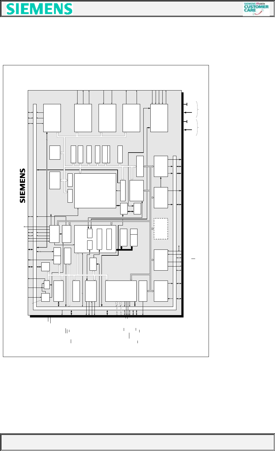
6.1 Overview Logic/control
Overview to the HW structure
The hardware in the M50 / MT50 can be split up into two function groups:
At first there is the baseband chipset with its periphery comprising the EGOLD+,
Flash and power supply ASIC. This function group is basis for all equipment variants.
V1.0 Page 29 of 46 ICM MP CCQ ST
C45, M50 AND MT50 Company Confidential © Copyright Siemens AG 05/02
The logic part of the M50 consists of:
The EGOLD+
Hardware µC-part
Software µC-part
Software SP (Signal Processor) part Equaliser
EGAIM inside the EGOLD+
RTC (Real Time Clock)
V1.0 Page 30 of 46 ICM MP CCQ ST
C45, M50 AND MT50 Company Confidential © Copyright Siemens AG 05/02
6.2 EGOLD (PMB6850) V2.x
P ROM
48k x 16
P RAM
5k x 16
Y RAM
2k x 16
X ROM
18k x 16
X RAM
6k x 16
PRAM
1k x 16
Bus
Interface
Unit Shared Memory
Dual Port 512 x 16
Keypad
Interface GSM
TDMA Timer
TAP Controller
JTAG
Boundary Scan
GMSK Modulator
Voiceband Filters
RX and TX
Baseband Filter
A51/52
Cipher
Unit
SIM card
Interface
High Speed
(F=512, D=8/16)
32 kHz
13 MHz / 32 kHz
52 MHz
Dual Port RAM
1k x 16
Interrupt Controller
OCEM
E-GOLD Architecture
SRAM
xk x 16 (x = 0...64)
DSP Timer2
X-Bus
PD-Bus
Interleaving
2 x 28 x 116 x 1
PROM
1k x 16
Boot
Block
Company confidential
De-Interleaving 12k x 4
16 bit write access
4/16 bit read access
DSP Serial
Communication
Interface
Enhanced Handsfree / DAI
3 39
2 MHz (to GAIM)
RTC
External
Bus & Port
Controller
AFC Unit
Pulse-Carry Mod.
Interrupt
Extension 60
Power
Management DSP Timer1DSP Timer1
OAK+ DSP
ž Interleaving / De-Interleaving
ž Speech Decoding (FR, HR, EFR)
ž Speech Coding (FR, HR, EFR)
ž Level Measurement
ž Channel Decoding (FR, HR, EFR)
ž Channel Coding (FR, HR, EFR)
ž Equalization
ž Encryption / Decryption
ž Voice Memo / Voice Dialing
Viterbi
HW
Accelerator
ID Register
SSC
SPI
compatible
ASC0
Autobaud
Detect ASC1
8
523
2
5
Multicore
Debug Support
SEIB
CAPCOM
2 x 8 bit
16
RF Control
45
8 16
3
5
GPT1/GPT2
Watchdog
8
CS(4:0)2
Interrupt Controller
READY#
NMI#
HOLD#
HLDA#
CLKOUT
RSTOUT#
Osc.
32.768 kHz
Enable Signals to
X- and PD-Bus
Peripherals
requires ext. crystal
and special bondout
OCDS DPEC
MCU
C166CBC
Clock Generation
Peripheral Enable
Generator
A(20:0) 21 24
64 to MCU &
Clock Generation Unit
6
16 bit I/O Ports
H. Meschede, HL AS CR CE,
Audio & Speech
TMS
TCK
TDO
TDI
VBIN
VBOUT
DACI
DACQ
BPDM2
BPDM1
TRST
VCLK
F13M
CLKANA
VDDRTC
TXD0 / - / PE.4
RXD0 / - / PE.3
TXDD / TXD1 / PF.6
TFSD / T2IN / PF.10
SCLK / T6EUD / PF.8
RFSD / - / PF.9
RXDD / RXD1 / PF.7
VDDa
VSSa
VCXO_EN / - / PE.8
CLKSXM / A21 / PF.5
MRST / - / PE.7
MTSR / - / PE.6
SSCCLK / - / PE.5
F32K
RTCOUT
PDOUT / A23 / PF.4
TXD1 / CC04IO / PE.0
RXD1 / EX1IN & T5EUD /
PE.1
DSPOUT0 / A22 / PF.3
D(7:0)
AFC
READY / WAKEUP / PC.1
CC02IO / - / HOLD & DSPOUT1 / PF.0
CC01IO / NMI & DSPOUT2 / PE.2
HLDA / CC03IO & DSPIN0 & T2IN / PC.3
T5IN / T2EUD & T3IN / PC.4
CC06IO / A21 & EX7IN / PF.11
CLKOUT / CC05IO / PC.0
DSPOUT1 / A22 / PF.1
MON1
MON2
TRIGIN
TRIGOUT
CS2 / CC02IO / PF.12
CS3 / EX4IN & DSPIN0 & T4EUD / PF.13
CS4 / DSPOUT2 / PF.14
RD
WR
CC00IO / T3OUT / PC.2
CS0
CS1
RESET_IN
D8 / CC20IO / PA.8
D9 / CC16IO / PA.9
D10 / - / PA.10
D11 / - / PA.11
D12 / EX5IN / PA.12
D13 / T7IN / PA.13
D14 / CC22IO / PA.14
D15 / CC18IO / PA.15
BHE / CC00IO / PF.15
RSTOUT / EX6IN & T3EUD / PF.2
VDD2.(4:1)
VDD2.0x, x=a,b,c
VSS2.(4:1)
VSS2.0x, x=a,b,c
I/O Driver
VDD1.(2:0)
VSS1.(2:0)
Core
GAIMDATA
GAIMSTR
GAIMCLK
RFSTR1
RFSTR0
RFDATA
RFCLK
RFSTR4 / EX2IN / PD.2
RFSTR3 / CC18IO / PD.1
RFSTR2 / CC07IO / PD.0
T_OUT12 / A23 / PD.11
T_OUT11 / CC19IO / PD.10
T_OUT10 / EX1IN & DSPIN1 / PD.9
T_OUT9 / T7IN & EX3IN / PD.8
T_OUT8 / CC23IO / PD.7
T_OUT7/ CAPIN / PD.6
T_OUT6 / T4IN / PD.5
T_OUT5 / CC17IO / PD.4
T_OUT4 / DSPIN0 / PD.3
CCIN
KP9 / CC18IO / PB.9
KP8 / CC22IO / PB.8
KP7 / T7IN / PB.7
KP6 / EX5IN / PB.6
T_OUT3
T_OUT2
T_OUT1
T_OUT0
GAIMRXON
KP5 / - / PB.5
KP4 / - / PB.4
KP3 / CC16IO / PB.3
KP2 / CC20IO / PB.2
KP1 / CC06IO / PB.1
KP0 / T2EUD & EX0IN / PB.0
CCRST
CCLK
CCIO
CCIOSW / T6OUT & T0IN
& T6IN / PB.11
CCVZ / - / PB.10
V1.0 Page 31 of 46 ICM MP CCQ ST
C45, M50 AND MT50 Company Confidential © Copyright Siemens AG 05/02
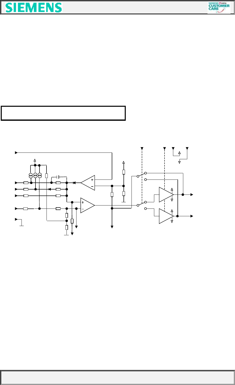
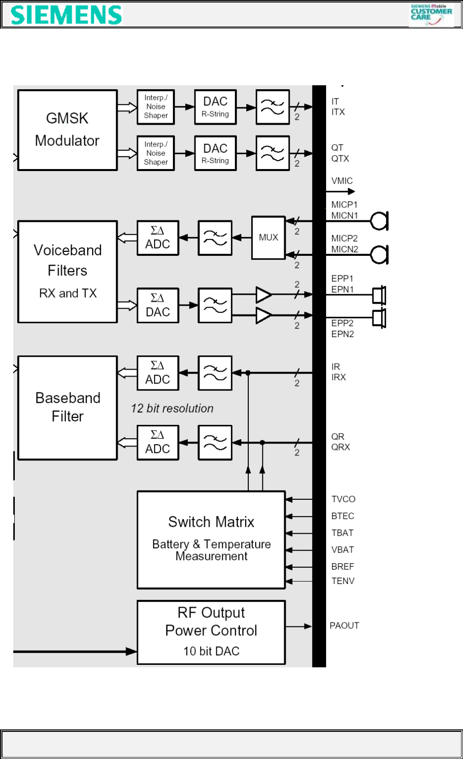
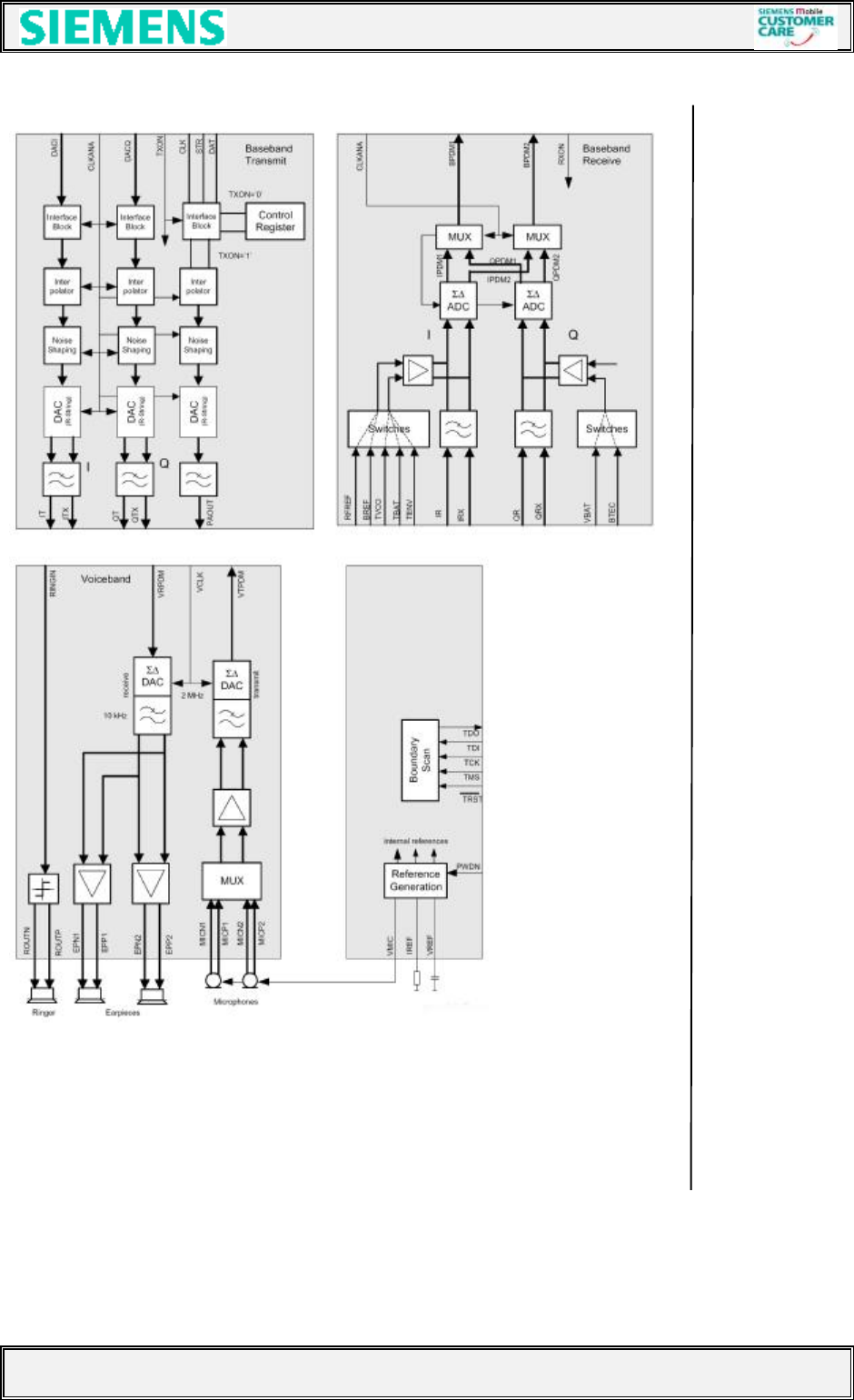
6.3 EGAIM inside the EGOLD+
V1.0 Page 32 of 46 ICM MP CCQ ST
C45, M50 AND MT50 Company Confidential © Copyright Siemens AG 05/02
EGAIM inside the EGOLD+
6.3.1 Tasks of the EGAIM inside the EGOLD+
- Measurement of Battery and Ambient temperature
- Measurement of Battery Voltage
- A/D conversion of MIC-Path signals incl. coding
- D/A conversion of EP-Path signals incl. decoding
- Generating of the PA-Control Signal “PA_Ramp”
V1.0 Page 33 of 46 ICM MP CCQ ST
C45, M50 AND MT50 Company Confidential © Copyright Siemens AG 05/02
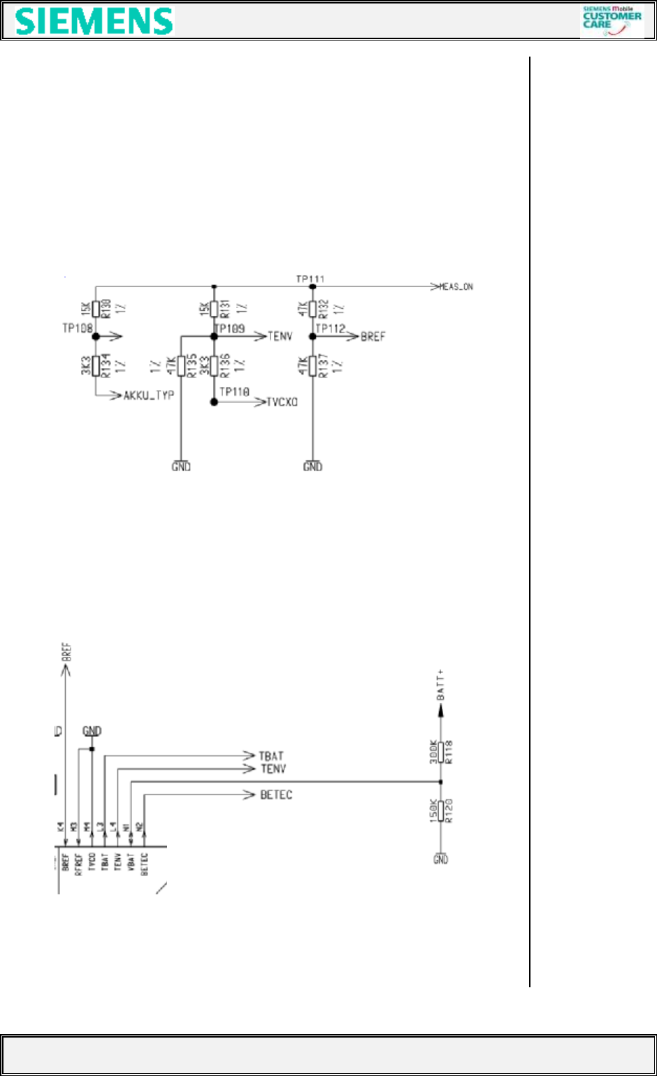
Measurement of Battery and Ambient Temperature
The temperature is measured as a voltage equivalent of the temperature on the
voltage dividers R131,R136,R135 for the ambient temperature by the EGAIM.
The battery temperature is measured directly at (l3) of the EGOLD+. For this,
the integrated Σ∆ converter of the EGAIM of the RX-I base band branch is used.
This Σ∆ converter compares the voltage of TBAT and TENV internally with a
reference voltage BREF.
Via an analog multiplexer, either the RX-I base band signal, or the TBAT signal
and the TENV signal can be switched to the input of the converter.
The signal MEAS_ON from the EGOLD+(GSM TDMA-TIMER G11) activates the
measurement and is used to generate to BREF by the help of R137,R132
Measurement of the Battery Voltage
The measurement of the battery voltage is done in the Q-branch of the EGAIM.
for this BATT+ is connected via a voltage divider R118, R120 to the EGOLD+
(GAIM N2) (Input limitation 1.33V to 5.91V) .An analog multiplexer does the
switching between the baseband signal processing and the voltage
measurement.
V1.0 Page 34 of 46 ICM MP CCQ ST
C45, M50 AND MT50 Company Confidential © Copyright Siemens AG 05/02
A/D conversion of MIC-Path signals incl. coding
The Microphone signals (MICN2, MIpN2, MICP1, MICN1) arrive at
the voiceband part of the EGAIM. For further operations the signals will
be converted into digital information, filtered, coded and finally formed
into the GMSK-Signal by the internal GMSK-Modulator.
This so generated signals (MOD_A, MOD_AX, MOD_B, MOD_BX) are
given to the SMARI IC / Bright IC in the transmitter path.
D/A conversion of EP-Path signals incl. decoding
Arriving at the Baseband-Part the demodulated signals (MOD_A, MOD_AX,
MOD_B, MOD_BX ) will be filtered and A/D converted. In the voiceband part
after decoding (with help of the uC part) and filtering the signals will be D/A
converted amplified and given as (EPP1, EPN1, EPP2, EPN2) to the internal
earpiece or the external loudspeaker.
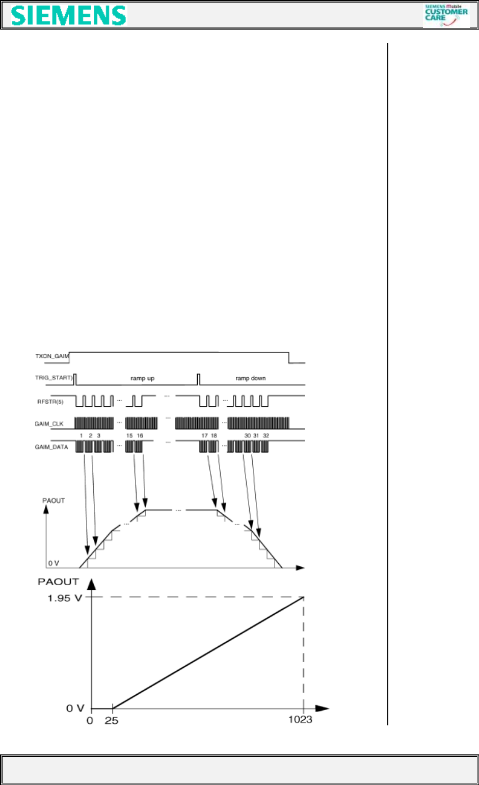
Generation of the PA Control Signal (PA_RAMP)
The RF output power amplifier needs an analog ramp up/down control voltage.
For this the system interface on EGOLD+ generates 10 bit digital values which
have to be transferred serially to the power ramping path. After loading into an
10 bit latch the control value will be converted into the corresponding analog
voltage with a maximum of ~2V
Key-Value
V1.0 Page 35 of 46 ICM MP CCQ ST
C45, M50 AND MT50 Company Confidential © Copyright Siemens AG 05/02
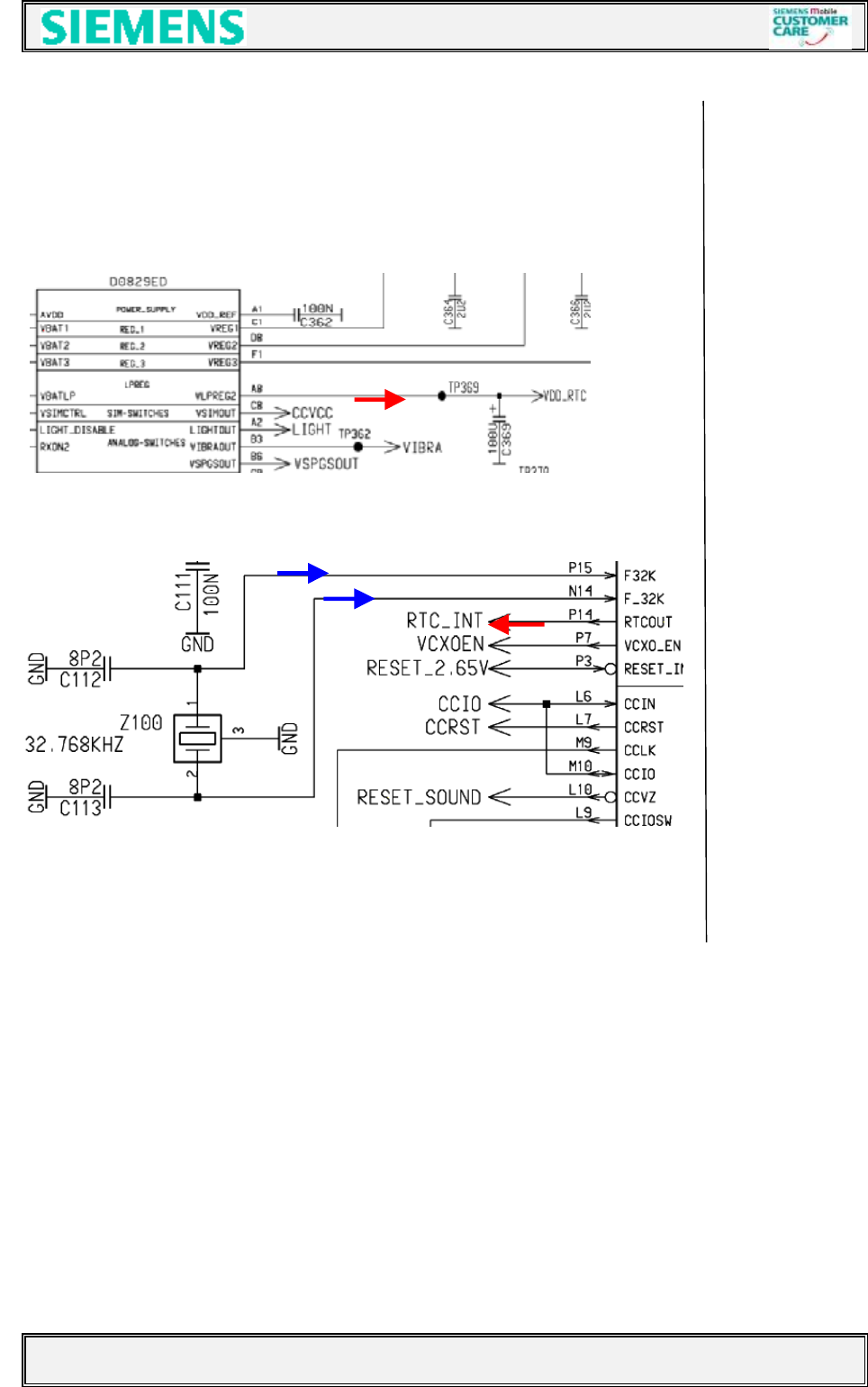
6.4 Real Time Clock (integrated in the EGOLD+)
The real time clock is powered via its own voltage regulator inside the ASIC (D361)
directly from the battery. The so gained voltage VDD_RTC is buffered by a capacitor
(C369) to keep the data (e.g. clock) in the internal RAM during a battery change for
at least 30 seconds.
An alarm function is also integrated which allows to switch the phone on and off.
via RTC_INT
The reference oscillator for the RTC is (Z100)
V1.0 Page 36 of 46 ICM MP CCQ ST
C45, M50 AND MT50 Company Confidential © Copyright Siemens AG 05/02
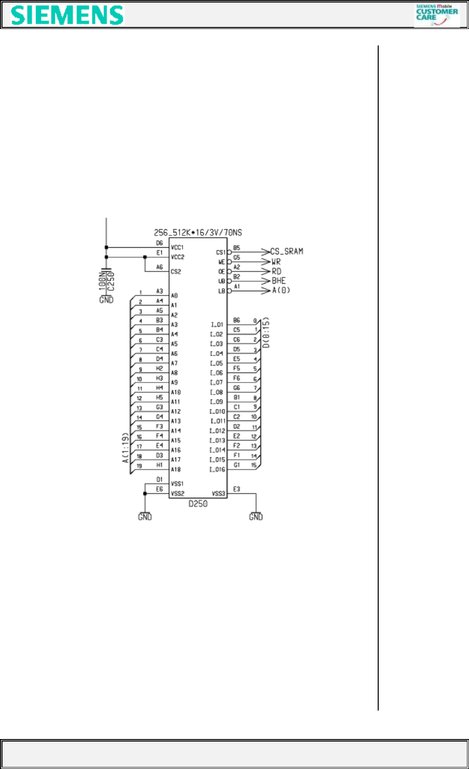
6.5 SRAM
Memory for volatile data.
Memory Size: 4Mbit
Data Bus: 16Bit
Access Time: 70ns
The SRAM (D250) is provided with 2.07V from the ASIC (D361) . It is used
from the EGOLD+ to store temporally data.
The communication is controlled and activated from the EGOLD+.
V1.0 Page 37 of 46 ICM MP CCQ ST
C45, M50 AND MT50 Company Confidential © Copyright Siemens AG 05/02
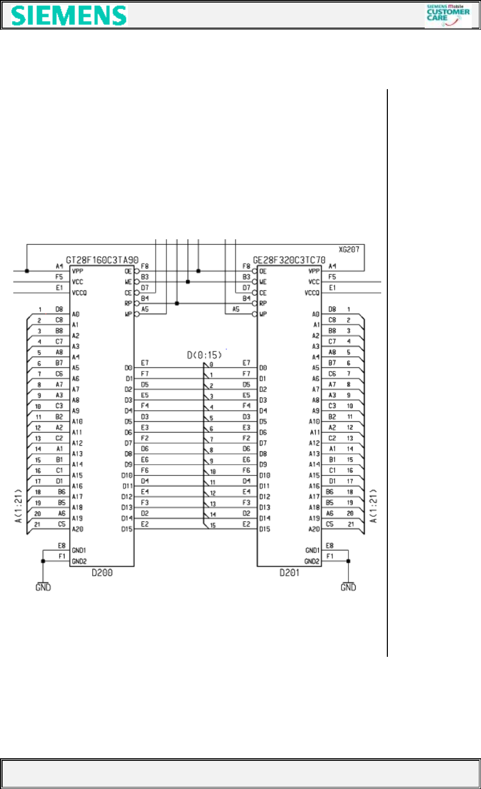
6.6 FLASH
Non-volatile but erasable and re-programmable (software update) program
memory (Flash) for the EGOLD and for saving user data (menu settings),
linguistic data (voice memo) and mobile phone matching data.
There is a serial number on the flash which cannot be forged.
Memory Size: 48 Mbit (32 Mbit + 16 Mbit)
Data Bus: 16 Bit
Access Time: 70ns (32 Mbit)
90ns (16Mbit)
Boot Block: Top
V1.0 Page 38 of 46 ICM MP CCQ ST
C45, M50 AND MT50 Company Confidential © Copyright Siemens AG 05/02
7 Acoustics
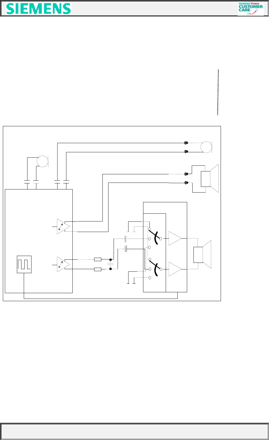
7.1 General
The Electro-Acoustic components are: a) The Vibra
b) The Microphone
c) The Loudspeaker/Ringer
Schalke Asic
MUX
PWM (50% duty cycle)
EPN2
EPP2
EPN1
EPP1
PMB6850
EGold+
16Ω
AUDO N
AUDO P
I/O-connector
A1
A2
B1
B2
C1
C2
RINGIN
32Ω
Headset
MICP2
MICN2
MICP1
MICN1
Internal
speaker
Internal
microphone
M46: Audio-concept
V1.0 Page 39 of 46 ICM MP CCQ ST
C45, M50 AND MT50 Company Confidential © Copyright Siemens AG 05/02
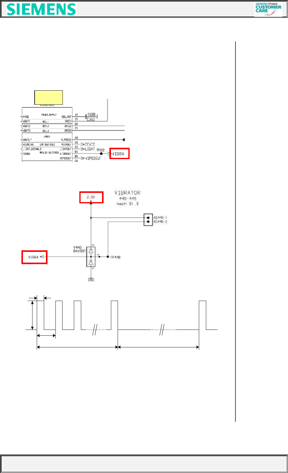
7.2 Vibra
The vibrator is assembled in the lower case shell. The electrical connection is
carried out via spring contacts The Vibra is driven and controlled from the
power supply ASIC (pin B3)via the signal VIBRA
The vibrator is directly connected to the ASIC´s 2,9V. The diode V440 is used to
protect the circuit against over voltage and switching spikes.
3,6V..4,2V
15,5..20,3µs
50µs
0,5s0,5s
Vibra-Timing
D361
V1.0 Page 40 of 46 ICM MP CCQ ST
C45, M50 AND MT50 Company Confidential © Copyright Siemens AG 05/02
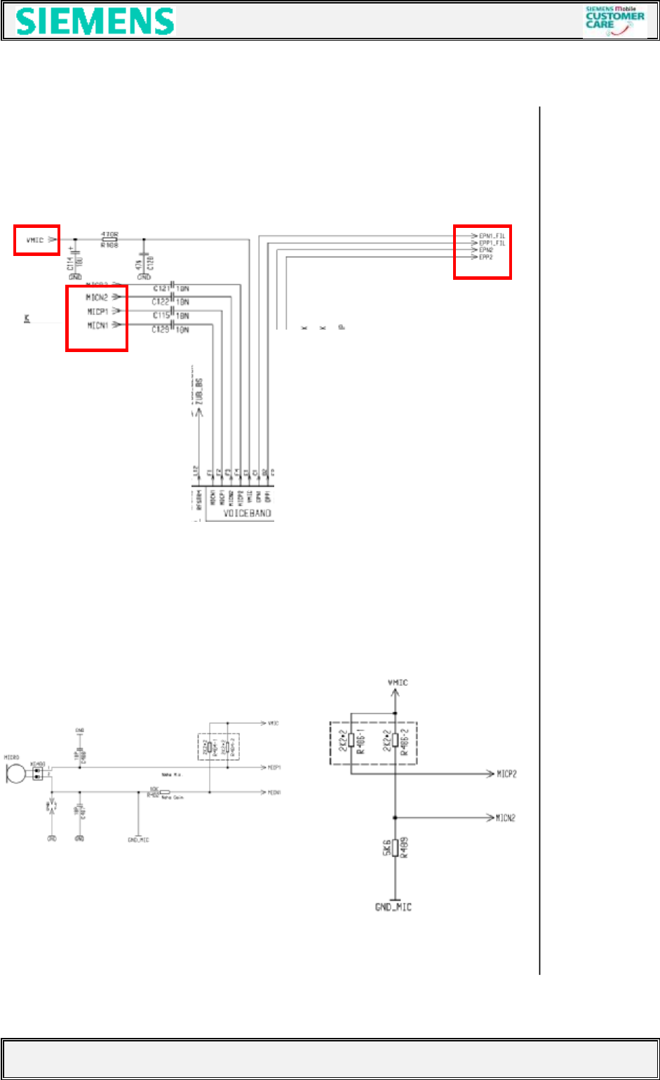
7.3 Microphone and Loudspeaker (Ringer)
7.3.1 Loudspeaker
Loudspeaker (EPP1_FIL, EPN1_FIL, EPP2, EPN2) and Microphone (MIC2, MICN2-
MICP1, MICN1) are connected directly to the Voiceband-Part of EGOLD+
7.3.2 Microphone
Both Microphones are directly connected to the EGOLD+.(Voiceband F1-F4) via the
signals MICN1, MICP1 (Internal Microphone )and MICN2, MICP2
(External Microphone/Headset). Power supply for the Microphone is
VMIC (Voiceband E1)
V1.0 Page 41 of 46 ICM MP CCQ ST
C45, M50 AND MT50 Company Confidential © Copyright Siemens AG 05/02
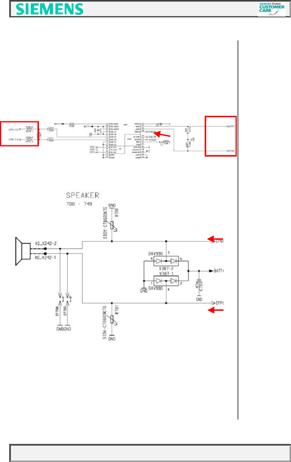
7.3.3 Loudspeaker/Ringer
The internal Loudspeaker (Earpiece) is connected to the voiceband part of the
EGOLD+ (VOICEBAND D1,E2) via the mono audio amplifier inside the ASIC (D361).
Input EPN1_FIL - EPP1_FIL Output to earpiece EPN1 - EPP1
The ringing tones are generated with the loudspeaker too. To activate the ringer, the
signal RINGIN from the EGOLD+ (Miscellaneous,E9) is used
V1.0 Page 42 of 46 ICM MP CCQ ST
C45, M50 AND MT50 Company Confidential © Copyright Siemens AG 05/02
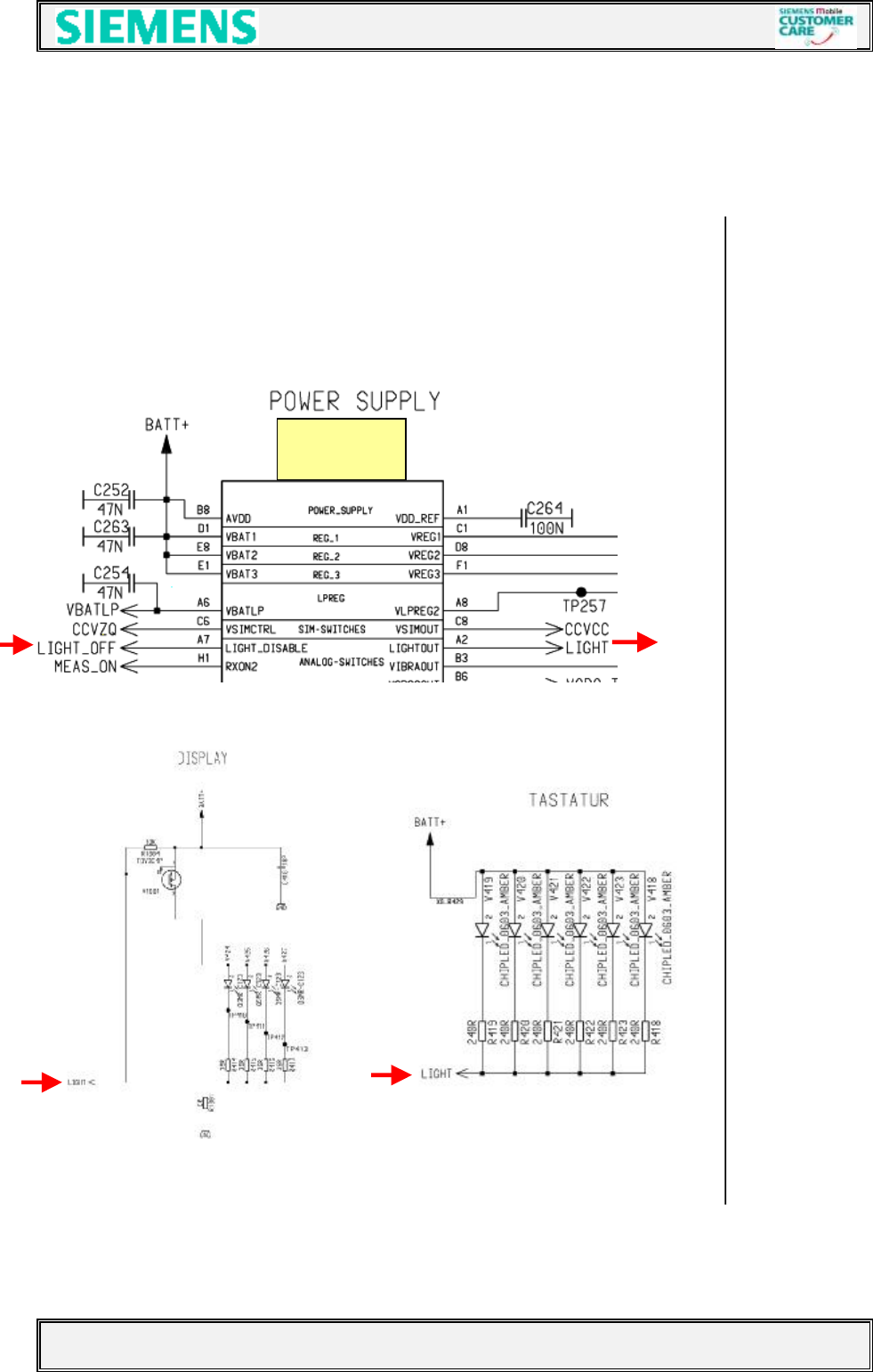
8 Illumination:
8.1 Illumination
The Light is switched via an analogue switch inside the ASIC (D361). It is controlled
from the EGOLD+ (TDMA-TIMER,L15) with the signal LIGHT_OFF. Output is the
signal LIGHT, which is connected via the MMI connector X550 to the keypad LED´s.
and directly to display backlight section
D361
V1.0 Page 43 of 46 ICM MP CCQ ST
C45, M50 AND MT50 Company Confidential © Copyright Siemens AG 05/02
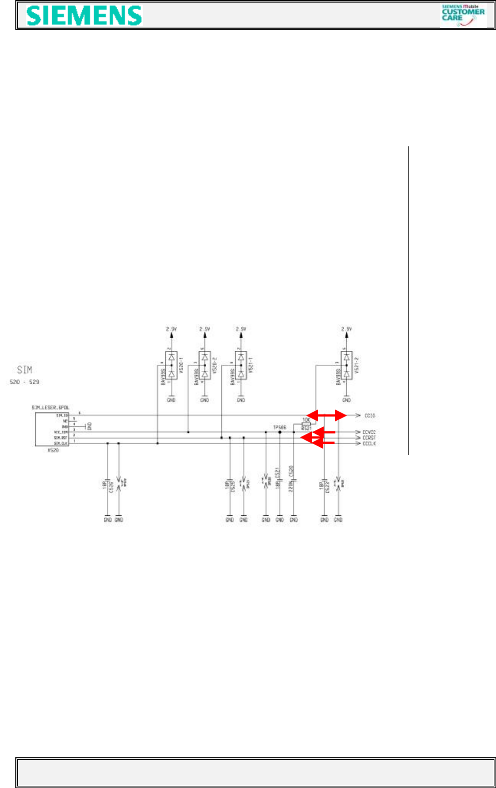
9 SIM-CARD and Connectors
9.1 SIM-Card
The SIM-CARD is supplied via X520 at pin3 with CCVCC (2,9V) The CCVCC is a
ASIC (D361) switched 2,9V voltage, activated by CCVZQ from the
EGOLD+(Address-Data G13)
If no SIM-CARD is connected, or if there is no response (CCIO) from the SIM-CARD,
the EGOLD+ tries 3 times to connect the SIM-CARD. After this time the EGOLD+
stops trying. That means, if the EGOLD+ is losing the connection while normal
operation of the mobile phone, the mobile must be switched off and on again.
The communication between the EGOLD+ and the SIM-CARD is done via the CCIO
X520 pin6 by using CCCLK as a clock signal.
The diodes V520/521 are used to protect signal lines versus switching peaks.
V1.0 Page 44 of 46 ICM MP CCQ ST
C45, M50 AND MT50 Company Confidential © Copyright Siemens AG 05/02
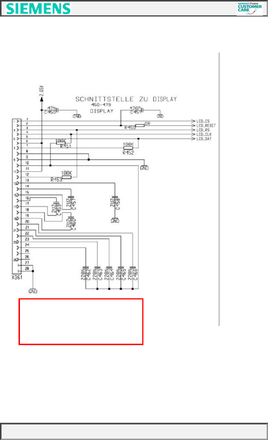
9.2 Display connector
The display is provided with 2,65V from the ASIC (D361). The communication with
the EGOLD+ by the LCD-Signals, directly connected to the EGOLD+
LCD_CS SIM L9
LCD_RESET Miscellaneous N7
LCD_RS Serial-Interface R14
LCD_CLK Serial-Interface P11
LCD_DAT Serial-Interface N11
V1.0 Page 45 of 46 ICM MP CCQ ST
C45, M50 AND MT50 Company Confidential © Copyright Siemens AG 05/02
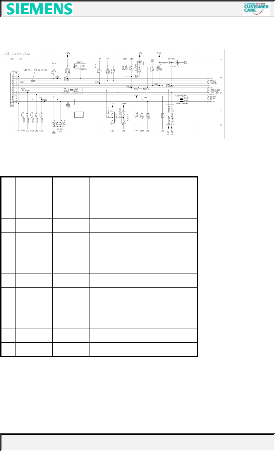
9.3 I/O-Connector
Pin Name IN/OUT Notes
1 GND
2 SB O Control line for external power supply
3 POWER I Power input from external power supply
4 FBatt+ O Voltage for external accessories.
5 TX O Serial interface
6 RX I Serial interface
7 ZUB_CLK I/O Clock line for accessory bus
Use as DTC In data operation
8 ZUB_DATA I/O Data line for accessory bus.
Use as CTS in data operation
9 GND_MIC For external microphone
10 MICP2 I External microphone
11 EPP2 O
For external loudspeaker
12 EPN2 O For external loudspeaker
V1.0 Page 46 of 46 ICM MP CCQ ST
C45, M50 AND MT50 Company Confidential © Copyright Siemens AG 05/02
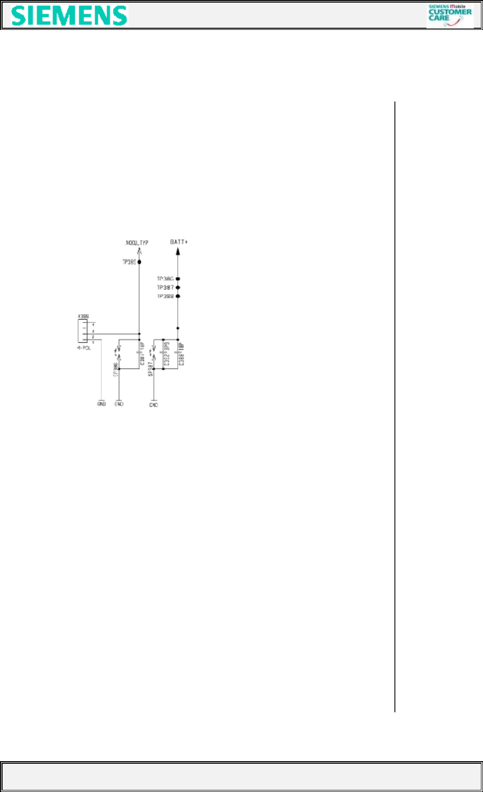
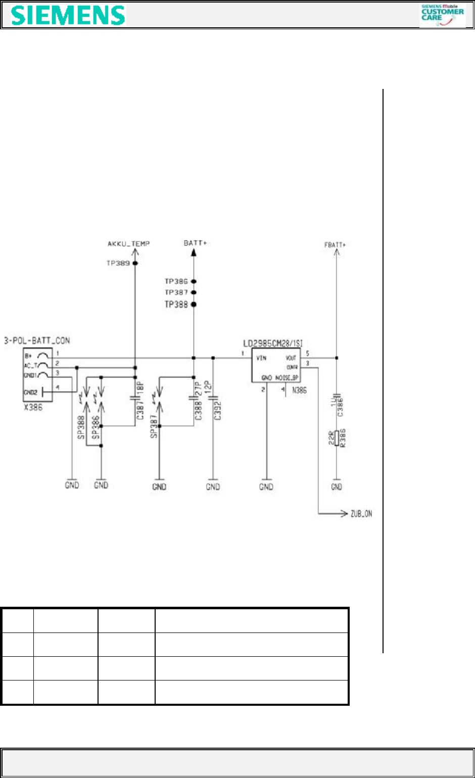
9.4 Battery Connector
The battery is connected via the battery connector (X386) to the battery contacts
on the RF-Board.
Directly connected to battery, there is a voltage regulator (N386). This regulator
Is used to provide the external accessories with the required voltage.
To extend STAND-BY time, the regulator is switched on with the signal ZUB_On
only if accessories are recognised.
Responsible for the ZUB_ON signal is the ASIC (D361).
Pin Name IN/OUT Notes
1 Batt+ I/O Battery voltage
2 Akku_Temp O Temperature control of the battery pack.
3 GND
