A35/36/40 Siemens C75 Service Repair Ation Level 2.5e
User Manual: Service manuals, Schematics Mobile Phones Siemens. Free.
Open the PDF directly: View PDF ![]() .
.
Page Count: 37
Company Confidential s Com
Copyright 2005© Siemens AG
Page 1 of 37
Service Repair Documentation
Level 2.5e – C75 Release 1.0
Service Repair Documentation
Level 2.5e – C75
Release Date Department Notes to change
1.0 05.08.2005 ICM MP CCQ GRM T New document
Company Confidential s Com
Copyright 2005© Siemens AG
Page 2 of 37
Service Repair Documentation
Level 2.5e – C75 Release 1.0
Table of Contents:
1 List of available level 2,5e parts C75 4
2 Required Equipment for Level 2,5e 5
3 Required Software for Level 2,5e 5
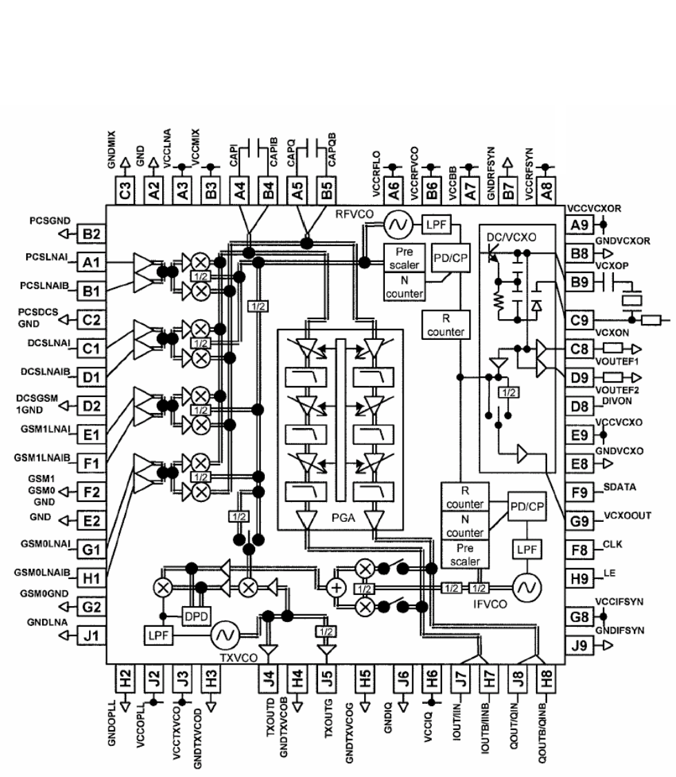
4 Radio Part 6
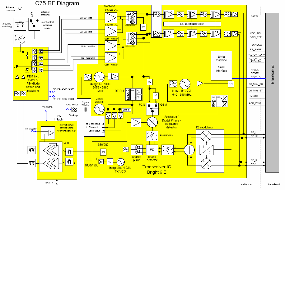
4.1 BLOCK DIAGRAM RF PART 7
4.2 POWER SUPPLY RF-PART 7
4.3 FREQUENCY GENERATION 8
4.4 RECEIVER 11
4.5 TRANSMITTER 12
4.6 BRIGHT IC OVERVIEW 13
4.7 ANTENNA SWITCH (ELECTRICAL/MECHANICAL) 15
4.8 TRANSMITTER: POWER AMPLIFIER 17
5 Logic / Control 18
5.1 OVERVIEW HARDWARE STRUCTURE C75 18
5.2 SGOLDLITE 18
5.2.1 Digital Baseband 18
5.2.2 SDRAM 22
5.2.3 FLASH 23
5.2.4 SIM 23
5.2.5 Vibration Motor 23
5.2.6 Camera 23
5.2.7 Display 23
5.2.8 Camera, Display ASIC 24
6 IRDA 24
7 Power Supply 25
7.1 ASIC MOZART / TWIGO4 25
7.1.1 Battery 25
7.1.2 Charging Concept 25
8 Illumination 28
9 Interfaces 29
9.1 MICROPHONE (XG1901) 29
9.2 LOUDSPEAKER (XG1702-XG1703) 30
9.3 BATTERY (X1400) 30
Company Confidential s Com
Copyright 2005© Siemens AG
Page 3 of 37
Service Repair Documentation
Level 2.5e – C75 Release 1.0
9.4 CAMERA SOCKET (X3651) 31
9.5 IRDA (V2650) 32
9.6 INTERFACE SIM MODULE 32
9.7 IO CONNECTOR WITH ESD PROTECTION 33
9.8 VIBRATION MOTOR (XG2100) 36
9.9 DISPLAY 36
9.10 BOARD TO BOARD CONNECTOR 37
Company Confidential s Com
Copyright 2005© Siemens AG
Page 4 of 37
Service Repair Documentation
Level 2.5e – C75 Release 1.0
1 List of available level 2,5e parts C75
(according to Component Matrix V1.06 - check C-market for updates)
Product RF
Chipset ID Order Number Description CM
C75 HIT C1329 L36344-F1225-M12 CAPACITOR 2*2U2 (Cap-Type7)
C75 HIT C1330 L36344-F1225-M12 CAPACITOR 2*2U2 (Cap-Type7)
C75 HIT C1332 L36344-F1225-M12 CAPACITOR 2*2U2 (Cap-Type7)
C75 HIT C1363 L36377-F6225-M CAPACITOR 2U2 (Cap-Type4)
C75 HIT D1000 L50610-G6196-D670 IC SGOLDLITE PMB8875 V1X PB-FREE
C75 HIT D1300
L50645-J4683-Y22 IC ASIC D1094ED-MOZART+ TWIGO4+
C75 HIT D3601 L50620-U6053-D670 IC CAMERA INTERFACE S1D13716B02 PB FREE
C75 HIT D902
L50645-K80-Y308 IC FEM MURATA GSM900 1800 1900 (Fem-Type6)
C75 HIT D903 L50620-L6170-D670 IC TRANCEIVER HD155165BP PB Free
C75 HIT L1300 L36140-F2100-Y6 COIL 0603 (Co-Type4)
C75 HIT L1301 L36151-F5103-M3 COIL 10U (Co-Type1)
C75 HIT L1302 L36151-F5472-M1 COIL 4U7 (Co-Type3)
C75 HIT L1303 L50640-F100-Y10 COIL 1206 (Co-Type5)
C75 HIT L1318 L36140-F2100-Y6 COIL 0603 (Co-Type4)
C75 HIT L1331 L36140-F2100-Y6 COIL 0603 (Co-Type4)
C75 HIT N1501 L36810-B6132-D670 IC LOGIC DUAL BUS SWITCH US8
C75 HIT N3600 L506810-C6153-D670 IC ANA RE 2.9V USMD5 PB FREE
C75 HIT N901 L50651-Z2002-A82 IC MODUL PA PF0814 (PA-Type2)
C75 HIT R955 L36120-F4223-H RESISTOR TEMP 22K (Res-Type7)
C75 HIT V1305 L36830-C1107-D670 TRANSISTOR SI5933 (Tra-Type2)
C75 HIT V1400 L36840-D66-D670 DIODE BAV99T (Di-Type5)
C75 HIT V1500 L36840-C4057-D670 TRANSISTOR EMD12 EMT6 (Tra-Type8)
C75 HIT V1605 L36840-D3088-D670 DIODE SC89 (Di-Type2)
C75 HIT V2100 L50640-D5084-D670 DIODE RB548W (Di-Type8)
C75 HIT V2302 L36840-C4014-D670 TRANSISTOR BC847BS BC846S (Tra-Type7)
C75 HIT V2821 L36830-C1112-D670 TRANSISTOR SI1902 (Tra-Type4)
C75 HIT V950 L36840-D61-D670 DIODE 1SV305 (Di-Type4)
C75 HIT Z1000 L50645-F102-Y40 QUARZ 32,768KHZ (Q-Type4)
C75 HIT Z1500 L50620-L6151-D670 FILTER EMI (Fi-Type5) PB Free
C75 HIT Z950 L36145-F260-Y17 QUARZ 26MHZ (Q-Type4)

Company Confidential s Com
Copyright 2005© Siemens AG
Page 5 of 37
Service Repair Documentation
Level 2.5e – C75 Release 1.0
2 Required Equipment for Level 2,5e
- GSM-Tester (CMU200 or 4400S incl. Options)
- PC-incl. Monitor, Keyboard and Mouse
- Bootadapter 2000/2002 (L36880-N9241-A200)
- Adapter cable for Bootadapter due to new Lumberg connector (F30032-P226-A1)
- Troubleshooting Frame A62/A65(C75/A75) (F30032-P405-A1)
- Power Supply
- Spectrum Analyser
- Active RF-Probe incl. Power Supply
- Oscilloscope incl. Probe
- RF-Connector (N<>SMA(f))
- Power Supply Cables
- Dongle (F30032-P28-A1) if USB-Dongle is used a special driver for NT is required
- BGA Soldering equipment
Reference: Equipment recommendation V1.6
(downloadable from the technical support page)
3 Required Software for Level 2,5e
- Windows XP
- X-Focus version XX or higher
- GRT Version 3 or higher
- Internet unblocking solution (JPICS)
Company Confidential s Com
Copyright 2005© Siemens AG
Page 6 of 37
Service Repair Documentation
Level 2.5e – C75 Release 1.0
4 Radio Part
The radio part is realizes the conversion of the GMSK-HF-signals from the antenna to the
baseband and vice versa.
In the receiving direction, the signals are split in the I- and Q-component and led to the D/A-
converter of the logic part. In the transmission direction, the GMSK-signal is generated in an
Up Conversion Modulation Phase Locked Loop by modulation of the I- and Q-signals which
were generated in the logic part. After that the signals are amplified in the power amplifier.
Transmitter and Receiver are never active at the same time. Simultaneous receiving in the
EGSM900 and GSM1800 band is impossible. Simultaneous transmission in the EGSM900
and GSM1800 band is impossible, too. However the monitoring band (monitoring timeslot) in
the TDMA-frame can be chosen independently of the receiving respectively the transmitting
band (RX- and TX timeslot of the band).
The RF-part is dimensioned for triple band operation (EGSM900, DCS1800, PCS19000)
supporting GPRS functionality up to multiclass 10.
The RF-circuit consists of the following components:
• Hitachi Bright 6E chip set (HD155165BP) with the following functionality:
o PLL for local oscillator LO1 and LO2 and TxVCO
o Integrated local oscillators LO1, LO2
o Integrated TxVCO
o Direct conversion receiver including LNA, DC-mixer, channel filtering and
PGC-amplifier
o 26 MHz reference oscillator
• Transmitter power amplifier with integrated power control circuitry
• Frontend-Module including RX-/TX-switch and EGSM900 / DCS1800 / PCS 1900
receiver SAW-filters
• Quartz and passive circuitry of the 26MHz VCXO reference oscillator
Company Confidential s Com
Copyright 2005© Siemens AG
Page 7 of 37
Service Repair Documentation
Level 2.5e – C75 Release 1.0
4.1 Block diagram RF part
4.2 Power Supply RF-Part
The voltage regulator for the RF-part is located inside the ASIC D1300. It generates the
required 2,8V “RF-Voltages” named VDD_RF1 and VDD_RF2. VDD_RF2 is passed via a 0Ω
resistor and renamed as VDD_BRIGHT as operating voltage for the BRIGHT. The voltage
regulator is activated as well as deactivated via VCXOEN_UC (Functional F23) provided by the
SGOLDlite. The temporary deactivation is used to extend the stand by time.
Company Confidential s Com
Copyright 2005© Siemens AG
Page 8 of 37
Service Repair Documentation
Level 2.5e – C75 Release 1.0
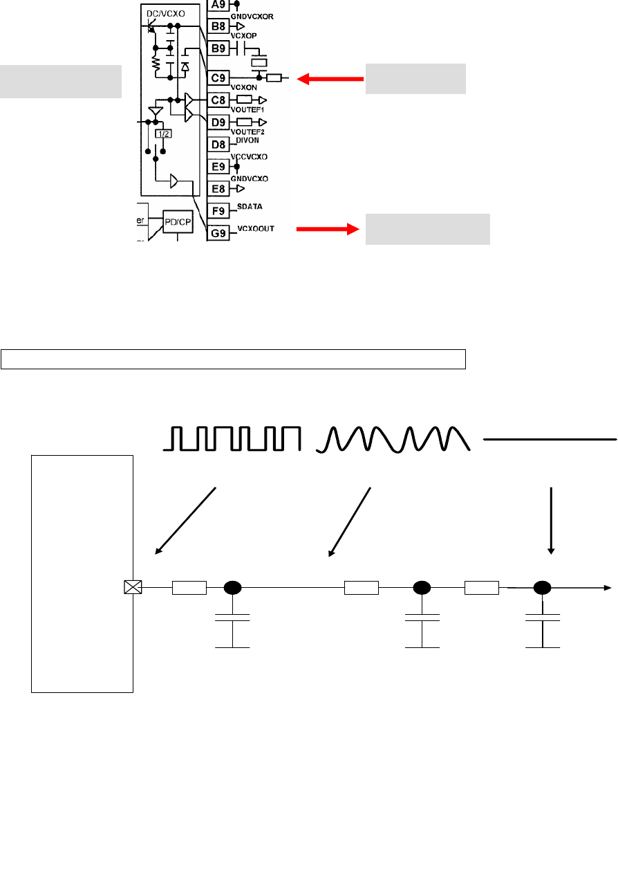
4.3 Frequency generation
The C75 mobile is using a reference frequency of 26MHz. The generation of the 26MHz
signal is done via a VCO (Z950). TP (test point) of the 26MHz signal is the TP 820
The oscillator output signal 26MHz_RF is directly connected to the BRIGHT IC (ball B9) to be
used as reference frequency inside the Bright (PLL). The signal leaves the Bright IC as
RF_SIN26M (ball G9) to be further used from the SGOLDlite (D1000 (Functional AE15)).
VCXO Out
SGOLDlite In
Bright 6E
To compensate frequency drifts (e.g. caused by temperature) the oscillator frequency is
controlled by the (RF_AFC) signal, generated through the internal SGOLDlite (D1000 (A10))
PLL. Reference for the “EGOLD-PLL” is the base station frequency received via the
Frequency Correction Burst.
The required voltage VDD_RF2 is provided by the ASCI D1300
Waveform of the AFC_PNM signal from SGOLDlite to Oscillator
SGOLDlite
GND GND
R2
RF_AFC
Signalform
C1
C2
AFC_PNM
GND
C3
R3
1 2 3
1 2 3
R1
Company Confidential s Com
Copyright 2005© Siemens AG
Page 9 of 37
Service Repair Documentation
Level 2.5e – C75 Release 1.0
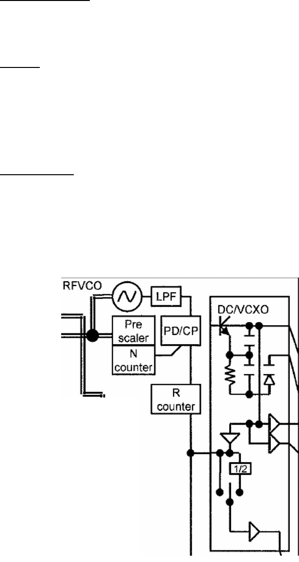
Synthesizer: LO1
First local oscillator (LO1) consists of a PLL and VCO inside Bright (D903) and an internal
loop filter
RF PLL
The frequency-step is 400 kHz in GSM1800 mode and 800kHz in EGSM900 mode due to the
internal divider by two for GSM1800 and divider by four for EGSM900. To achieve the
required settling-time in GPRS operation, the PLL can operate in fastlock-mode a certain
period after programming to ensure a fast settling. After this the loopfilter and currents are
switched into normal-mode to get the necessary phasenoise-performance. The PLL is
controlled via the tree-wire-bus of Bright VI E.
RFVCO (LO1)
The first local oscillator is needed to generate frequencies which enable the transceiver IC to
demodulate the receiver signal and to perform the channel selection in the TX part. The VCO
module is switched on with the signal PLLON. The full oscillation range is divided into 256
sub-bands To do so, a control voltage for the LO1 is used, gained by a comparator. This
control voltage is a result of the comparison of the divided LO1 and the 26MHz reference
Signal. The division ratio of the dividers is programmed by the SGOLDlite, according to the
network channel requirements.
Company Confidential s Com
Copyright 2005© Siemens AG
Page 10 of 37
Service Repair Documentation
Level 2.5e – C75 Release 1.0
Matrix to calculate the TX and RX frequencies C75:
Band RX / TX Channels RF frequencies LO1 frequency IF freq.
EGSM 900 Receive: 0..124 935,0 - 959,8 MHz LO1 = 4*RF
EGSM 900 Transmit: 0..124 890,0 - 914,8 MHz LO1 = 4*(RF+IF) 80,0 MHz
EGSM 900 Receive: 975..1023 925,2 - 934,8 MHz LO1 = 4*RF
EGSM 900 Transmit: 975..1023 880,2 - 889,8 MHz LO1 = 4*(RF+IF) 82,0 MHz
GSM 1800 Receive: 512..661 1805,2 - 1835,0 MHz LO1 = 2*RF
GSM 1800 Transmit: 512..661 1710,2 - 1740,0 MHz LO1 = 2*(RF+IF) 80,0 MHz
GSM 1800 Receive: 661..885 1835,0 - 1879,8 MHz LO1 = 2*RF
GSM 1800 Transmit: 661..885 1740,0 - 1784,8 MHz LO1 = 2*(RF+IF) 82,0 MHz
GSM 1900 Receive: 512..810 1930,2 - 1989,8 MHz LO1 = 2*RF
GSM 1900 Transmit: 512..810 1850,2 - 1909,8 MHz LO1 = 2*(RF+IF) 80,0 MHz
Synthesizer: LO2
The second local oscillator (LO2) consists of a PLL and VCO inside Bright (D903) and an
internal loop filter. Due to the direct conversion receiver architecture, the LO2 is only used for
transmit-operation. The LO2 covers a frequency range of at least 16 MHz (640MHz –
656MHz).
Before the LO2-signal gets to the modulator it is divided by 8. So the resulting TX-IF
frequencies are 80/82 MHz (dependent on the channel and band). The LO2 PLL and power-
up of the VCO is controlled via the tree-wire-bus of Bright (SGOLDlite signals RF_DAT;
RF_CLK; RF_STR). To ensure the frequency stability, the 640MHz VCO signal is compared
by the phase detector of the 2nd PLL with the 26Mhz reference signal. The resulting control
signal passes the external loop filter and is used to control the 640/656MHz VCO.
The required voltage VDD_BRIGHT is provided by the ASIC D1300
Company Confidential s Com
Copyright 2005© Siemens AG
Page 11 of 37
Service Repair Documentation
Level 2.5e – C75 Release 1.0
4.4 Receiver
Receiver: Filter to Demodulator
The band filters are located inside the frontend module (D902). The filters are centred to the
band frequencies. The symmetrical filter output is matched to the LNA input of the Bright .The
Bright 6E incorporates three RF LNAs for GSM850/EGSM900, GSM1800 and GSM1900
operation. The LNA/mixer can be switched in High- and Low-mode to perform an
amplification of ~ 20dB. For the “High Gain“ state the mixers are optimised to conversion gain
and noise figure, in the “Low Gain“ state the mixers are optimised to large-signal behavior for
operation at a high input level. The Bright performs a direct conversion mixers which are IQ-
demodulators. For the demodulation of the received GSM signals the LO1 is required. The
channel depending LO1 frequencies for 1800MHz/1900MHz bands are divided by 2 and by 4
for 850MHG/900MHz band. Furthermore the IC includes a programmable gain baseband
amplifier PGA (90 dB range, 2dB steps) with automatic DC-offset calibration. LNA and PGA
are controlled via SGOLDlite signals RF_DAT; RF_CLK; RF_STR (RF CTRL B10, C8, B12). The
channel-filtering is realized inside the chip with a three stage baseband filter for both IQ
chains. Only two capacitors which are part of the first passive RC-filters are external. The
second and third filters are active filters and are fully integrated. The IQ receive signals are
fed into the A/D converters in the EGAIM part of SGOLDlite. The post-switched logic
measures the level of the demodulated baseband signal and regulates the level to a defined
value by varying the PGA amplification and switching the appropriate LNA gains.
From the antenna switch, up to the demodulator the received signal passes the following
blocks to get the demodulated baseband signals for the SGOLDlite:
Demodulator PGC
LNA
Filter
D903 Bright(D903)
The required voltage VDD_BRIGHT is provided by the ASIC D1300

Company Confidential s Com
Copyright 2005© Siemens AG
Page 12 of 37
Service Repair Documentation
Level 2.5e – C75 Release 1.0
4.5 Transmitter
Transmitter: Modulator and Up-conversion Loop
The generation of the GMSK-modulated signal in Bright (D903) is based on the principle of
up conversion modulation phase locked loop. The incoming IQ-signals from the baseband
are mixed with the divided LO2-signal. The modulator is followed by a lowpass filter (corner
frequency ~80 MHz) which is necessary to attenuate RF harmonics generated by the
modulator. A similar filter is used in the feedback-path of the down conversion mixer.
With help of an offset PLL the IF-signal becomes the modulated signal at the final transmit
frequency. Therefore the GMSK modulated rf-signal at the output of the TX-VCOs is mixed
with the divided LO1-signal to a IF-signal and sent to the phase detector. The I/Q modulated
signal with a center frequency of the intermediate frequency is send to the phase detector as
well.
The output signal of the phase detector controls the TxVCO and is processed by a loop filter
whose components are external to the Bright. The TxVCO which is realized inside the Bright
chip generates the GSMK modulated frequency.
TxVCO
Filter PD
Modulator
Bright(D903)
The required voltage VDD_BRIGHT is provided by the ASIC D1300
Company Confidential s Com
Copyright 2005© Siemens AG
Page 13 of 37
Service Repair Documentation
Level 2.5e – C75 Release 1.0
4.6 Bright IC Overview
BRIGHT 6E
IC Overview
Company Confidential s Com
Copyright 2005© Siemens AG
Page 14 of 37
Service Repair Documentation
Level 2.5e – C75 Release 1.0
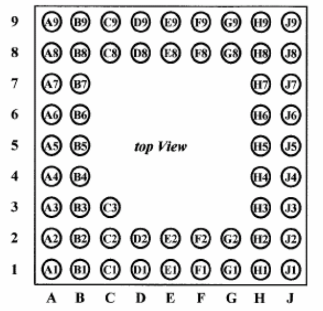
IC top view (ball overview)
Company Confidential s Com
Copyright 2005© Siemens AG
Page 15 of 37
Service Repair Documentation
Level 2.5e – C75 Release 1.0
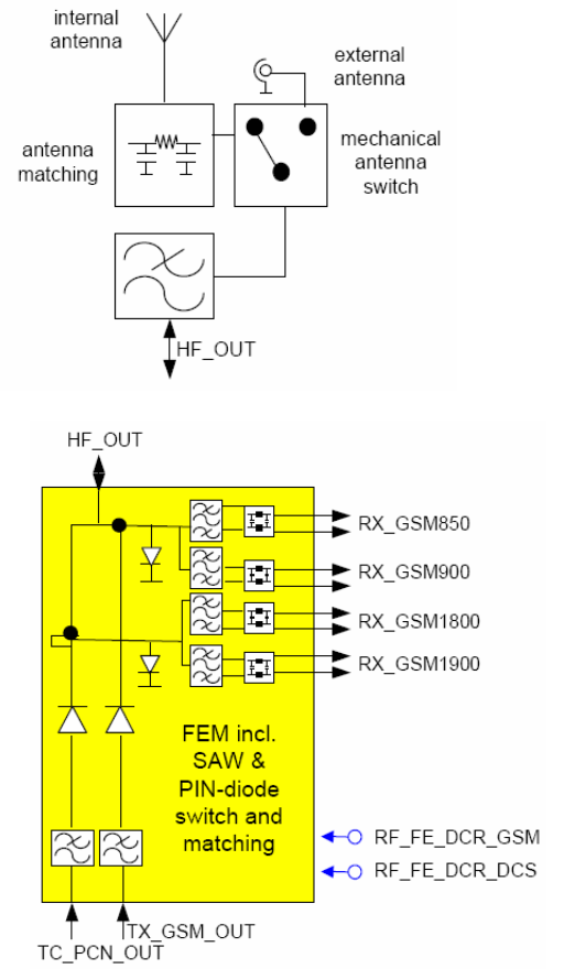
4.7 Antenna switch (electrical/mechanical)
Internal/External <> Receiver/Transmitter
The C75 mobile have two antenna switches.
a) The mechanical antenna switch for the differentiation between the internal and
external antenna.
b) The electrical antenna switch, for the differentiation between the receiving and
transmitting signals.
To activate the correct tx pathes of this diplexer, the SGOLDlite signals RF_FE_DTR_GSM
and RF_FE_DTR_DCS are required.
Internal/External antenna switch
The electrical antenna switch
Company Confidential s Com
Copyright 2005© Siemens AG
Page 16 of 37
Service Repair Documentation
Level 2.5e – C75 Release 1.0
Top View :
Switching Matrix:
select mode Vsw 1 Vsw 2
GSM900/DCS1800/PCS1900 RX Low Low
EGSM TX high Low
DCS1800/PCS1900 TX Low High
Pin assignment:
1 Antenna 15 EGSM900 RX1
2 GND 16 EGSM900 RX2
3 Vsw2 (DCS1800/PCS1900 TX control) 17 DCS1800 RX1
4 GND 18 DCS1800 RX2
5 DCS1800/PCS1900 TX 19 PCS1900 RX1
6 GND 20 PCS1900 RX2
7 GND 21 GND
8 GND 22 GND
9 GND 23 GND
10 GND 24 GND
11 GND 25 GND
12 GND 26 Vsw1 (EGSM900 TX control)
13 GND 27 EGSM900 TX
14 28 GND
Company Confidential s Com
Copyright 2005© Siemens AG
Page 17 of 37
Service Repair Documentation
Level 2.5e – C75 Release 1.0
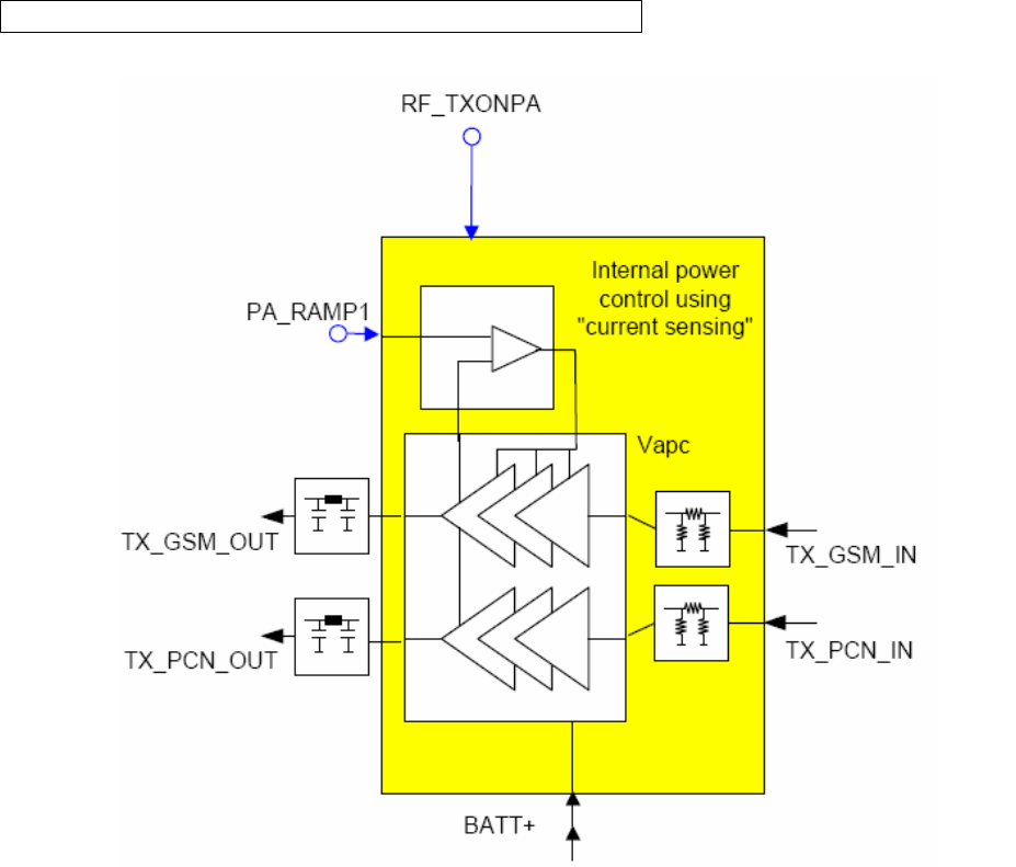
4.8 Transmitter: Power Amplifier
The output signals (PCN_PA_IN , and GSM_PA_IN) from the TxVCO are led to the power
amplifier. The power amplifier is a PA-module N901 from Hitachi. It contains two separate 3-
stage amplifier chains GSM850/EGSM900 and GSM1800/GSM1900 operation. It is possible
to control the output-power of both bands via one VAPC-port. The appropriate amplifier chain
is activated by a logic signal RF_BAND_SW (TDMA Timer A10) which is provided by the SGOLDlite.
To ensure that the output power and burst-timing fulfills the GSM-specification, an internal
power control circuitry is use. The power detect circuit consists of a sensing transistor which
operates at the same current as the third RF-transistor. The current is a measure of the
output power of the PA. This signal is square-root converted and converted into a voltage by
means of a simple resistor. It is then compared with the RF_RAMP1 (Analoq Interface L24) signal.
The N901 is activated through the signal RF_TXONPA (TDMA Timer A17).
The required voltage BATT+ is provided by the battery.
Company Confidential s Com
Copyright 2005© Siemens AG
Page 18 of 37
Service Repair Documentation
Level 2.5e – C75 Release 1.0
5 Logic / Control
5.1 Overview Hardware Structure C75
5.2 SGOLDLITE
5.2.1 Digital Baseband
Baseband Processor SGOLDlite (PMB8875)
S-GOLDliteTM is a GSM single chip mixed signal baseband IC containing all analog and
digital functionality of a cellular radio. The integrated circuit contains a ARM926EJ-S CPU
and a TEAKLite DSP core. The ARM926EJ-S is a powerful standard controller and
particularly suited for wireless systems. It is supported by a wide range of tools and
application SW. The TEAKLite is an established DSP core for wireless applications with
approved firmware for GSM signal processing. The package is a P-LFBGA-345 (264
functional pins + 81 thermical balls).
Company Confidential s Com
Copyright 2005© Siemens AG
Page 19 of 37
Service Repair Documentation
Level 2.5e – C75 Release 1.0
Supported Standards
• GSM speech FR, HR, EFR and AMR-NB
• GSM data 2.4kbit/s, 4.8kbit/s, 9.6kbits, and 14.4kbit/s
• HSCSD class 10
• GPRS class 12
Processing cores
• ARM926EJ-S 32-bit processor core with operating frequency up to 125 MHz for
controller functions
• TEAKLite DSP core with operating frequency 104 MHz.
ARM-Memory
• 8 kByte Boot ROM on the AHB
• 96 kByte SRAM on the AHB, flexibly usable as program or data RAM
• 8 kByte Cache for Program (internal)
• 8 kByte tightly coupled memory for Program (internal)
• 8 kByte Cache for Data (internal)
• 8 kByte tightly coupled memory for Data (internal)
TEAKLite-Memory
• 80 kwords Program ROM
• 4 kwords Program RAM
• 48 kwords Data ROM
• 27 kwords Data RAM
Shared Memory Blocks
• 1.5 kwords Shared RAM (dual ported) between controller system and TEAKLite.
Functional Hardware blocks
• CPU and DSP Timers
• Programmable PLL with additional phase shifters for system clock generation
• GSM Timer Module that off-loads the CPU from radio channel timing
• GMSK Modulator according to GSM-standard 05.04 (5/2000)
• Hardware accelerators for equalizer and channel decoding
• Advanced static and dynamic power management features including TDMA-Frame
synchronous low-power mode and enhanced CPU modes (idle and sleep modes)
Company Confidential s Com
Copyright 2005© Siemens AG
Page 20 of 37
Service Repair Documentation
Level 2.5e – C75 Release 1.0
•
Interfaces and Features
• Keypad Interface for scanning keypads up to 6 rows and 4 columns
• Pulse Number Modulation output for Automatic Frequency Correction (AFC)
• Serial RF Control Interface; support of direct conversion RF
• 2 USARTs with autobaud detection and hardware flow control
• IrDA Controller integrated in USART0 (with IrDA support up to 115.2 kbps)
• 1 Serial Synchronous SPI compatible interfaces in the controller domain
• 1 Serial Synchronous SPI compatible interface in the TEAKLite domain
• I2C-bus interface (e.g. connection to S/M-Power)
• 2 bidirectional and one unidirectional I2S interface accessible from the TEAKLite
• USB V1.1 mini host interface for full speed devices with up to 5 interfaces and 10
endpoints configurable supporting also USB on-the-go functionality
• ISO 7816 compatible SIM card interface
• Enhanced digital (phase linearity, adj/ co-channel interference) baseband filters,
including analog prefilters and high resolution analog-to-digital converters.
• Separate analog-to-digital converter for various general purpose measurements like
battery voltage, battery, VCXO and environmental temperature, battery technology,
transmission power, offset, onchip temperature, etc.
• Ringer support for highly oversampled PDM/PWM input signals for more versatility in
ringer tone generation
• RF power ramping functions
• DAI Interface according to GSM 11.10 is implemented via dedicated I2S mode
• 26 MHz master clock input
• External memory interface:
– 1.8V interface
– Data bus: 16 bit non-multiplexed and multiplexed, 32 bit multiplexed
– Supports synchronous devices (SDRAMs and Flash Memory) up to 62.4 MHz
– For each of the 4 address regions 128 MByte with 32-bit access or 64 MByte with a
16-bit access are addressable
– Supports asynchronous devices (i.e. SRAM, display) including write buffer for
cache line write
• Port logic for external port signals
• Comprehensive static and dynamic Power Management
– Various frequency options during operation mode
– 32 kHz clock in standby mode
– Sleep control in standby mode
– RAMs and ROMs in power save mode during standby mode
– Additional leakage current reduction in standby mode possible by switching off the
power for the TEAKLite subsystem.
Company Confidential s Com
Copyright 2005© Siemens AG
Page 21 of 37
Service Repair Documentation
Level 2.5e – C75 Release 1.0
–
Baseband receive path
In the receiver path the antenna input signal is converted to the base band, filtered, and
amplified to target level by the RF transceiver chipset. The resulting differential I and Q
baseband signals are fed into the S-GOLDliteTM. The A-to-D converter generates two 6.5
Mbit/s data streams. The decimation and narrowband channel filtering is done by a digital
baseband filter for each path. The DSP performs for GMSK, the complex baseband signal
equalization with soft-output recovery and the channel decoding supported by a Viterbi
hardware accelerator. The recovered digital speech data is fed into the speech decoder
(D1300). The S-GOLDliteTM supports fullrate, halfrate, enhanced fullrate and adaptive
multirate speech codec algorithms.
Baseband transmit path
In the transmit direction the microphone signal is amplified and A-to-D converted by the
D1300. The prefiltered and A-to-D converted voice signal passes a digital decimation filter.
Speech and channel encoding (including voice activity detection, VAD, and discontinuous
transmission, DTX) as well as digital GMSK modulation is carried out by the S-GOLDliteTM.
The digital I and Q baseband components of the GMSK modulated signals (48-times
oversampled with 13 MSamples/s) are D-to-A converted. The analog differential baseband
signals are fed into the RF transceiver chipset. The RF transceiver modulates the baseband
signal using a GMSK modulator. Finally, an RF power module amplifies the RF transmit
signal to the required power level. The S-GOLDliteTM controller software controls the gain of
the power amplifier by predefined ramping curves (16 words, 11 bit). The S-GOLDliteTM
communicates with the RF chip set via a serial data interface.
The following algorithms and a task scheduler are implemented on the DSP:
Algorithms running on the DSP:
• scanning of channels, i.e, measurement of the field strengths of neighbouring base
stations
• detection and evaluation of Frequency Correction Bursts
• equalisation of GMSK Normal Bursts and Synchronisation Bursts with bit-by-bit soft-
output
• Synch burst channel decoder
• channel encoding and soft-decision decoding for fullrate, enhanced-fullrate and
adaptive multirate speech, and control channels as well as RACH, PRACH
• channel encoding for GPRS coding schemes (CS1-CS4) as well as USF detection
algorithms for the Medium Access Control (MAC) software layer
• fullrate, enhanced fullrate and adaptive multirate speech encoding and decoding
• support for fullrate (F9.6, F4.8, and F2.4) data channels
• mandatory sub-functions like – discontinuous transmission, – voice activity detection,
VAD – background noise calculation
• generation of tone and side tone
• hands-free functions (acoustic echo cancellation, noise-reduction)
• support for voice memo
Company Confidential s Com
Copyright 2005© Siemens AG
Page 22 of 37
Service Repair Documentation
Level 2.5e – C75 Release 1.0
• support for voice dialling
• handling of vocoder and voice-paths for type approval testing
• ADPCM encoder (8 kHz sampling frequency), cannot run in parallel to a speech codec
• ADPCM decoder (8 kHz and 16 kHz sampling frequency), cannot run in parallel to a
speech codec
Scheduler functions on the DSP:
The scheduler is based on an operating system. It is basically triggered by interrupts
generated by hardware peripherals or commands from the micro-controller.
communication between DSP and micro-controller
• fully automatic handling of speech channels
• semi-automatic handling of control channels
• support of the GSM ciphering algorithm (A51, A52, A53) in combination with the
hardware accelerator.
• support for General Packet Radio Services (GPRS) with up to 4 Rx and 1Tx or 3 Rx
and 2 Tx (Class 10 mobile).
• monitoring of paging blocks for packet switched and circuit switched services
simultaneously GPRS MS in Class-B mode of operation
• MMS support
• loop-back functions (according to GSM 11.10)
Real Time Clock
The real time clock (degree of accuracy 150ppm) is powered via a separate voltage regulator
inside the ASIC. Via a capacitor, data is kept in the internal RAM during a battery change for
at least 30 seconds. An alarm function is also integrated with which it is possible to switch the
phone on and off.
Measurement of Battery voltage, Battery Type and Ambient Temperature
The voltage equivalent of the temperature and battery code on the voltage separator will be
calculated as the difference against a reference voltage of the S-GOLDlite. Inside the S-
GOLDlite are some analog to digital converters. These are used to measure the battery
voltage, battery code resistor and the ambient temperature.
Timing of the Battery Voltage Measurement
Unless the battery is being charged, the measurement shall be made in the TX time slot.
During charging it will be done after the TX time slot.
5.2.2 SDRAM
Memory for volatile data. SDRAM= synchronous High data rate Dynamic RAM
Memory Size: 64 Mbit
Data Bus: 16 Bit
Frequency: 105 MHz
Power supply: 1.8 V
Company Confidential s Com
Copyright 2005© Siemens AG
Page 23 of 37
Service Repair Documentation
Level 2.5e – C75 Release 1.0
5.2.3 FLASH
Non-volatile but deletable and re-programmable (software update) program memory for the
S-GOLDlite and for saving e.g. user data (menu settings), voice band data (voice memo),
mobile phone matching data, images etc.. There is a serial number on the flash which cannot
be changed.
Memory Size 256 Mbit (32 MByte)
Data Bus: 16 Bit
Access Time: Initial access: 85 ns
Synchronous Burst Mode: 54 MHz
5.2.4 SIM
SIM cards with supply voltages of 1.8V and 3V are supported. 1.8V cards are supplied with
3V.
5.2.5 Vibration Motor
The vibration motor is mounted in the lower case. The electrical connection to the PCB is
realised with pressure contacts.
5.2.6 Camera
The camera module uses a colour sensor with a full VGA (640x480) resolution in landscape
orientation. The module will deliver an 8Bit output signal which will be pre-processed by the
EPSON S1D13716 graphic engine chip. Various settings like brightness, image stabilization,
white balance can be done by using the I2C interface.
The camera is realised as a platform socket solution camera and uses same connector and
same interface as X75 1.3-Megapixel-Cameras.
5.2.7 Display
In the mobile phone a display module with an intelligent graphic Liquid Crystal Display (LCD)
is used. The display module consists of the following parts and features
- an Active Matrix Liquid Crystal Display Panel, 1.8”, 132x176 dots, 262k colours
- a display controller mounted on the display
- a light guide with 4 white LED’s
-a FPC with all passive components
- an electrical interface 10-pin spring connector

Company Confidential s Com
Copyright 2005© Siemens AG
Page 24 of 37
Service Repair Documentation
Level 2.5e – C75 Release 1.0
All displays need a supply voltage of VDD_2.9 = 2.90 V. Four white side-shooter LEDs for
illumination are mounted on the module FPC. The current for the LEDs is limited to max. 18
mA by a current sink on the mobile phone PCB. All four LEDs are in serial. The voltage for
the 3 LEDs is VBoost
For data transmission an 4-wire serial interface with a maximum transfer-rate of 13 Mbit/s is
used.
5.2.8 Camera, Display ASIC
For the interface between S-GOLDlite, camera and display a graphics engine chip called
S1D13716 from Epson is used. By using the SSC interface the S-GOLDlite communicates
with this graphic engine chip. The Camera ASIC has a second SSC interface to adapt the
display. Over an I2C interface, provided by the S1D13716, the camera-module can be
initialised; the picture-data output of the camera goes over a parallel 8-bit interface
There are three modes available:
a) Bypass mode:
In this mode the S1D13716 is transparent regarding the display. The S-GOLDlite
communicates “directly” with the display.
b) Camera View Mode:
In this mode the S1D13716 transfers the picture – data from the camera directly to
the display. A resizing and compressing engine is available to reduce the data
amount to the display. So the preview can be done without using the SGOD
performance.
c) Camera Capture Mode:
In this mode the picture – data from the camera is sent to the SGOLD. There are resizing and
compressing engines available to reduce the data-stream to the SGOLD-lite
6 IRDA
A Low-Power infrared data interface is supporting transmission rates up to 115.2kbps (Slow
IrDA). As a Low-Power-Device, the infrared data interface has a transmission range of at
least:
• 20cm to other Low-Power-Devices and
• 30cm to Standard-Devices
It is not possible to use the Bluetooth and the IRDA interface at the same time.
Company Confidential s Com
Copyright 2005© Siemens AG
Page 25 of 37
Service Repair Documentation
Level 2.5e – C75 Release 1.0
7 Power Supply
7.1 ASIC Mozart / Twigo4
The power supply ASIC will contain the following functions:
• Powerdown-Mode
• Sleep Mode
• Trickle Charge Mode
• Power on Reset
• Digital state machine to control switch on and supervise the uC with a
watchdog
• 17 Voltage regulators
• 2 internal DC/DC converters (Step-up and Step-down converter)
• Low power voltage regulator
• Additional output ports
• Voltage supervision
• Temperature supervision with external and internal sensor
• Battery charge control
• TWI Interface (I2C interface)
• Bandgap reference
• High performance audio quality
• Audio multiplexer for selection of audio input
• Audio amplifier stereo/mono
• 16 bit Sigma/Delta DAC with Clock recovery and I2S Interface
7.1.1 Battery
As a standard battery a LiIon battery with a nominal capacity of 780mAh@0.2CA* and GSM
capacity** of min. 750mAh will be provided.
* battery will be discharged with 20% of capacity rate till 2.75V; e.g. R65, 0.2x750mA=150mA
** battery will be discharged with 2A(0.6ms)+0.25A(0.4ms) till 3.2V.
7.1.2 Charging Concept
7.1.2.1 General
The battery is charged in the phone. The hardware and software is designed for LiIon with
4.2V technology. Charging is started as soon as the phone is connected to an external
charger. If the phone is not switched on, then charging shall take place in the background
(the customer can see this via the “Charge” symbol in the display). During normal use the
phone is being charged (restrictions: see below). Charging is enabled via a PMOS switch in
the phone. This PMOS switch closes the circuit for the external charger to the battery. The
processor takes over the control of this switch depending on the charge level of the battery,
whereby a disable function in the ASIC hardware can override/interrupt the charging in the
case of over voltage of the battery
Company Confidential s Com
Copyright 2005© Siemens AG
Page 26 of 37
Service Repair Documentation
Level 2.5e – C75 Release 1.0
For controlling the charging process it is necessary to measure the ambient (phone)
temperature and the battery voltage. The temperature sensor will be an NTC resistor with a
nominal resistance of 22kΩ at 25°C. The determination of the temperature is achieved via a
voltage measurement on a voltage divider in which one component is the NTC. Charging is
ongoing as long the temperature is within the range +5°C to 45°C. The maximal charge time
will be 2 hours (Imax=750mA).
7.1.2.2 Measurement of Battery voltage, Battery Type and Ambient Temperature
The voltage equivalent of the temperature and battery code on the voltage separator will be
calculated as the difference against a reference voltage of the S-GOLDlite. Inside the S-
GOLDlite are some analog to digital converters. These are used to measure the battery
voltage, battery code resistor and the ambient temperature.
7.1.2.3 Timing of the Battery Voltage Measurement
Unless the battery is being charged, the measurement shall be made in the TX time slot.
During charging it will be done after the TX time slot.
7.1.2.4 Recognition of the Battery Type
The different batteries will be encoded by different resistors within the battery pack itself.
7.1.2.5 Charging Characteristic of Lithium-Ion Cells
LiIon batteries are charged with a U/I characteristic, i.e. the charging current is regulated in
relation to the battery voltage until a minimal charging current has been achieved. The
maximum charging current is given by the connected charger. The battery voltage may not
exceed 4.2V ±50mV average. During the charging pulse current the voltage may reach 4.3V.
The temperature range in which charging of the phone may be performed is in the ranges
from 0...50°C. Outside this range no charging takes place, the battery only supplies current.
7.1.2.6 Trickle Charging
The ASIC is able to charge the battery at voltages below 3.2V without any support from the
charge SW. The current will by measured indirectly via the voltage drop over a shunt resistor
and linearly regulated inside the ASIC by means of the external FET. The current level during
trickle charge for voltages <2.8V is in a range of 20-50mA and in a range of 50-100mA for
voltages up to 3.2V. To limit the power dissipation of the dual charge FET the trickle charging
is stopped in case the output voltage of the charger exceeds 10 Volt. The maximum trickle
time is limited to 1 hour. As soon as the battery voltage reaches 3.2 V the ASIC will switch on
the phone automatically and normal charging will be initiated by software.
7.1.2.7 Normal Charging (Fast charge)
For battery voltages above 3.2 Volt and normal ambient temperature between 0 and 50°C the
battery can be charged with a charge current up to 1C. This charging mode is SW controlled
and starts if an accessory (charger) is detected with a supply voltage above 6.4 Volt by the
ASIC ASIC. The level of charge current is only limited by the charger.
Company Confidential s Com
Copyright 2005© Siemens AG
Page 27 of 37
Service Repair Documentation
Level 2.5e – C75 Release 1.0
7.1.2.8 USB Charging
The ASIC can support USB charging when USB charging is integrated in the charging
software. If charge voltage is in the range 4.4V to 5.25 V USB charging is ongoing. During
USB charging only limited charging is possible. Charge current is limited to 75, 150, 300 or
400 mA.
7.1.2.9 Audio multiplexer
The digital audio information from/to the DSP inside the SGOLD are delivered via the I2S
interface, the 26MHz from the RF part. The internal AD and DA converter are connected to
microphone and loudspeaker.
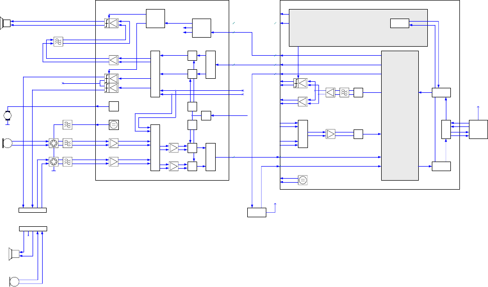
DSP
MCU
I/O-Connector
MIC2
Mozart / Twigo 4
MONO1_OUT
MICBIAS
I²C / TWI
SSC
MONO2_OUT
Vibra PWM
RINGIN
MONO1_LP_OUT
MONO2_LP_OUT
MONO1_IN
MONO2_IN
HP
SPK
STEREO1_OUT
STEREO1_OUT
PHANTOM_BUFF_OUT
MUX
MIC1
LINE2
LINE1
I²S
MUX
I²S
MICE2
MICE1
HP
MIC
HP
MICE
M
I²S
Control
...
26MHz
DAC
ADC
PLL
DIV
DIV
I²S_1
EP2
MIC1
MIC2
RINGIN
I²S_1
MUX
VMIC
NB
ADC
Decoder
Encoder
I²C / TWI
SSC
EP1
LP Filter
SGold lite
KEY-CLICK
&Ringing
I²S_2
I²S_2
NB
DAC
BB
GSM RF
GSM
BB & RF
Bluetooth
Voice
Recording
DAC
ADC
I/O-Connector
Mono Headset
I²S
HP
MICBIAS
7.1.2.10 Interface
The ASIC has two serial control interfaces and one serial audio interface. With the serial
interfaces, all functions of the ASIC can be controlled. For time critical commands ( all audio
functions incl. Vibra) the SSC is used.
TWI interface
TWI ( two wire interface) is an I2C 2 wire interface with the signals Clock (I2C_CLK) data line
(I2C_DAT) and the interrupt (PM_INT).

Company Confidential s Com
Copyright 2005© Siemens AG
Page 28 of 37
Service Repair Documentation
Level 2.5e – C75 Release 1.0
SSC interface
The SSC interface enables high-speed synchronous data transfer between SGOLD and
ASIC.
The interface consist of: clock signal (PM_SSC_SCLK), master transmit slave receive
(PM_SSC_MTSR), master receive slave transmit (PM_SSC_MTSR) and the select line
(PM_SSC_CS)
IS2 interface
The audio interface is a bidirectional serial interface, TX and RX part are independent. The
IS2 interface consist of a three wire connection for each direction. The three lines are clock
(CLK), the serial data line (DAC or ADC) and the word select line (WAO). Clock and word
select line is used for RX and TX together in SL65. (PM_I2S_DAC for RX and PM_I2S_ADC
for TX)
7.1.2.11 LDO`S
LDO´s: Voltage Current Name voltage domains
REG 1 2,9V 0...140mA 2.9V Display, Epson Camera-Chip, SGOLD
REG 2a 1,5V 0...300mA 1.5V_UC SGOLD
REG 2b 1,5V 0...100mA 1.5V_DSP SGOLD
REG 3 2,65V 0...140mA 2.65V SGOLD, Hall-Sensor, Epson Camera-Chip,
USB Switch
MEM REG1 1,8V 0...250mA 1.8V_MEM1 SGOLD, Display, SDRAM
MEM REG2 1,8V 0...150mA 1.8V_MEM2 Flash Memory, Camera-ASIC
AUDIO REG 2,9V 0...190mA VAUDREGA PMU ASIC
RF REG1 2,7V 0...150mA VDD_RF1 RF-Part (Hitachi Bright V)
AFC REG 2,65V 0...2mA VDD_AFC SGOLD
LP_REG 2,0V 0...2mA VDD_RTC SGOLD
SIM REG 2,9V 0...70mA VDD_SIM SIM
USB REG 3,1V 0...40mA VDD_USB SGOLD, USB Protection
VIBRA 2,8V
0...140mA VDD_VIBRA VIBRA
8 Illumination
a) Keyboard
The Keyboard will be realized via a separate PCB which will be connected to the main PCB
via board-to-board connector with 12 interconnections. The illumination of the keypad will be
done via 6 high-brightness LEDs (colour: white, type: top-shooter, driven by 5 mA / LED).
b) Display
The 4 serial LEDs for the display are supplied by one constant current source, to ensure the
same brigthness and colour of the white backlight.
Company Confidential s Com
Copyright 2005© Siemens AG
Page 29 of 37
Service Repair Documentation
Level 2.5e – C75 Release 1.0
9 Interfaces
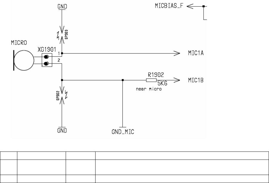
9.1 Microphone (XG1901)
in Name IN/OUT Remarks
1 MIC1A O Microphone power supply. The same line carries the low
frequency speech signal.
2 MIC1B GND_MIC
Company Confidential s Com
Copyright 2005© Siemens AG
Page 30 of 37
Service Repair Documentation
Level 2.5e – C75 Release 1.0
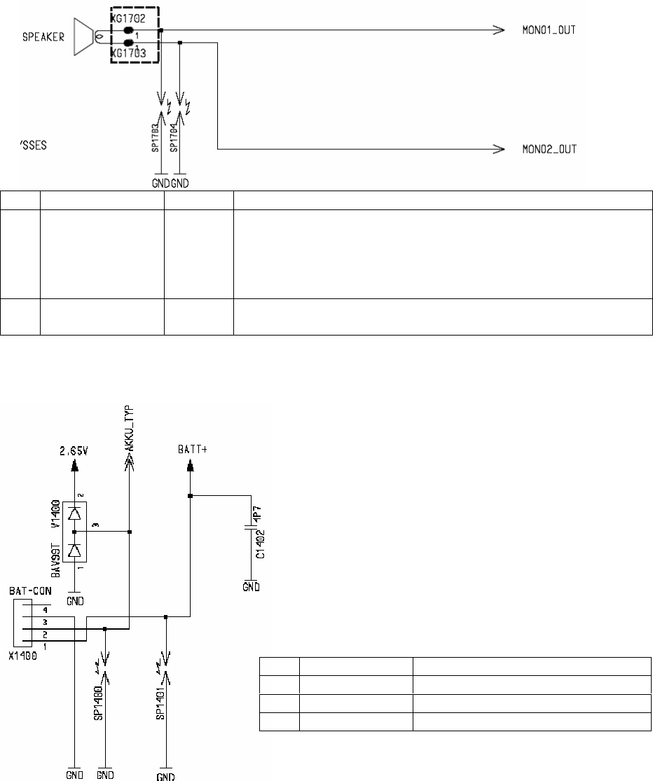
9.2 Loudspeaker (XG1702-XG1703)
Pin Name IN/OUT Remarks
1 MONO1_OUT O 1st connection to the internal earpiece. Earpiece can be
switched off in the case of accessory operation. EPP1
builds together with EPN1 the differential output to drive the
multifunctional “earpiece” (earpiece, ringer, handsfree
function).
2 MONO2_OUT O 2nd connection to the internal earpiece. Earpiece can be
switched off in the case of accessory operation.
9.3 Battery (X1400)
Pin Name Remarks
1 BATT+ Positive battery pole
2 AKKU_TYP Recognition of battery/supplier
3 GND Ground
Company Confidential s Com
Copyright 2005© Siemens AG
Page 31 of 37
Service Repair Documentation
Level 2.5e – C75 Release 1.0
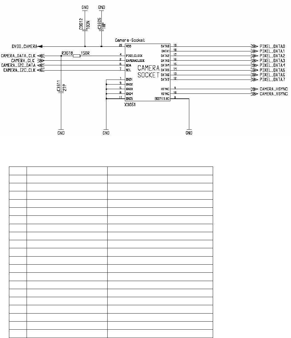
9.4 Camera Socket (X3651)
Pin Name Remarks
1 GND Ground
2 CAMERA_CLK Camera clock signal
3 GND Ground
4 CAMERA_DATA_CLK Camera data line
5 GND Ground
6 CAMERA_I2C_DATA I2C bus data line
7 CAMERA_I2C_CLK I2C bus clock signal
8 GND Ground
9 CAMERA_HSYCN Horizontal synchronisation line
10 CAMERA_VSYCN Vertikal synchronisation line
11 GND Ground
12 PIXEL_DATA7 Pixel data line
13 PIXEL_DATA6 Pixel data line
14 PIXEL_DATA5 Pixel data line
15 PIXEL_DATA4 Pixel data line
16 PIXEL_DATA3 Pixel data line
17 PIXEL_DATA2 Pixel data line
18 PIXEL_DATA1 Pixel data line
19 PIXEL_DATA0 Pixel data line
20 DVDD_CAMERA Voltage supply for camera
Company Confidential s Com
Copyright 2005© Siemens AG
Page 32 of 37
Service Repair Documentation
Level 2.5e – C75 Release 1.0
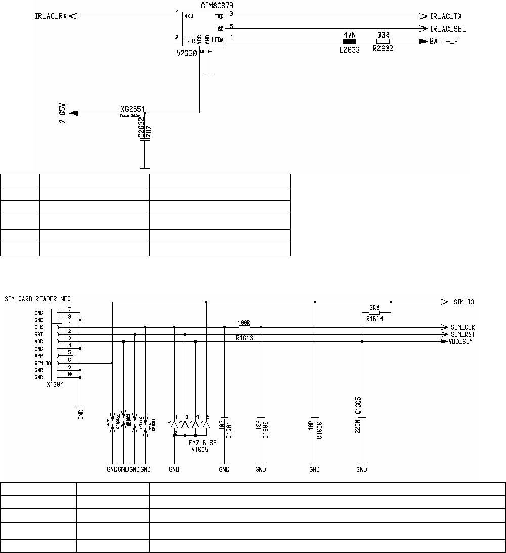
9.5 IRDA (V2650)
Pin Name Remarks
1 BATT+O IRDA operating voltage
2
3 IR_BT_RX RX data line
4 IR_BT_TX TX data line
5 IR_SEL IRDA Select
9.6 Interface SIM Module
Pin Name IN/OUT Remarks
SIM_CLK O Pulse for chipcard. The SIM is controlled directly from the SGOLD.
SIM_RST O Reset for chipcard
SIM_IO I/O Data pin for chipcard
VDD_SIM O Switchable power supply for chipcard;
Company Confidential s Com
Copyright 2005© Siemens AG
Page 33 of 37
Service Repair Documentation
Level 2.5e – C75 Release 1.0
9.7 IO Connector with ESD protection
IO Connector – New Slim Lumberg
Pin Name IN/OUT Notes
1 POWER I/O POWER is needed for charging batteries and for supplying
the accessories. If accessories are supplied by mobile, talk-
time and standby-time from telephone are reduced.
Therefore it has to be respected on an as low as possible
power consumption in the accessories.
2 GND
3 TX O Serial interface
4 RX I Serial interface
5 CTS I/O Data-line for accessory-bus
Use as CTS in data operation.
6 RTS I/O Use as RTS in data-operation.
7 DCD I/O Clock-line for accessory-bus.
Use as DTC in data-operation.
8 STEREO1_OUT Analog O driving ext. left speaker to PHANTOM_BUF_OUT with mono-
headset STEREO1_OUT and STEREO2_OUT differential
mode
9
10 STEREO2_OUT Analog O driving ext. right to PHANTOM_BUF_OUT with mono-
headset STEREO1_OUT and STEREO2_OUT differential
mode
11 GND_MIC Analog I for ext. microphone
12 MICEA_AC Analog I External microphone
Company Confidential s Com
Copyright 2005© Siemens AG
Page 34 of 37
Service Repair Documentation
Level 2.5e – C75 Release 1.0
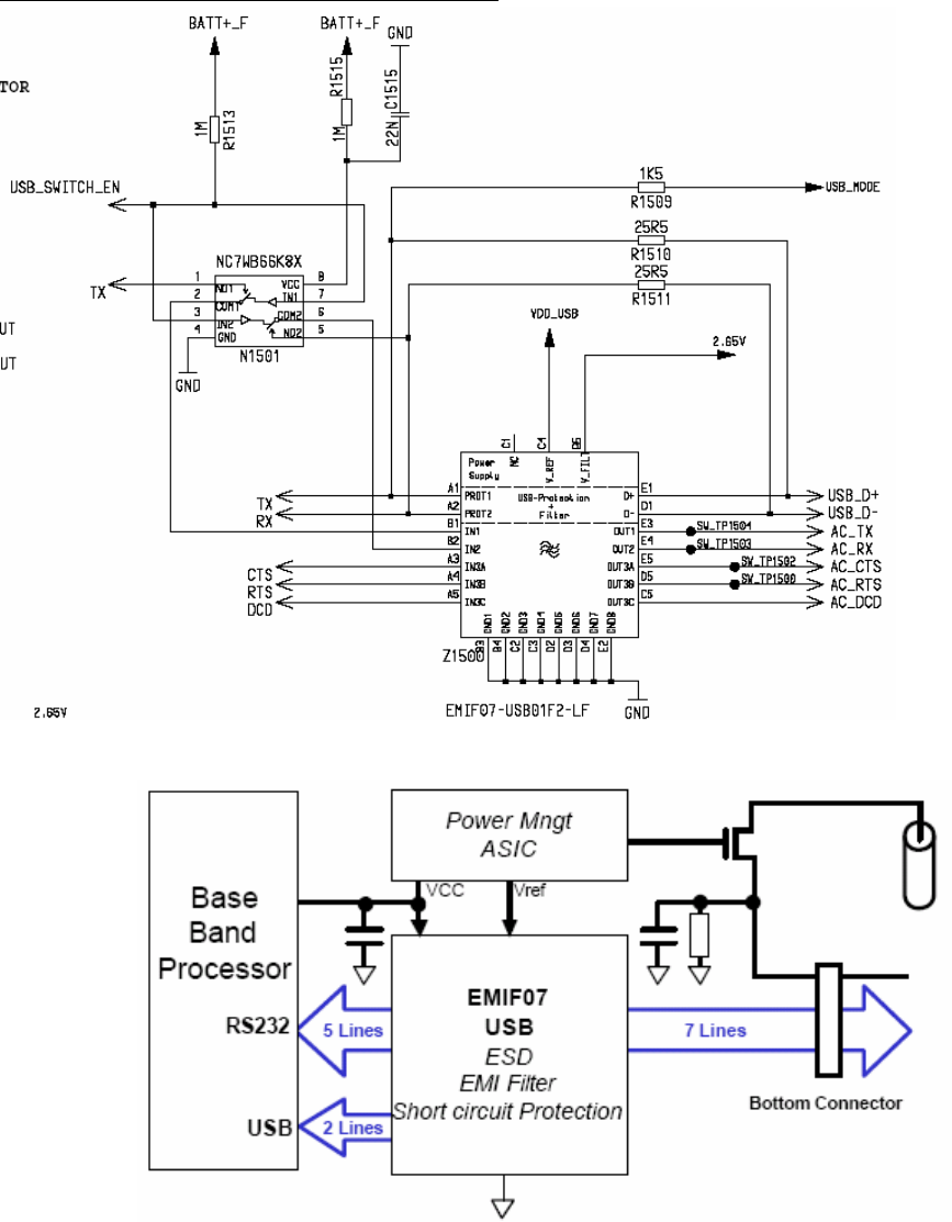
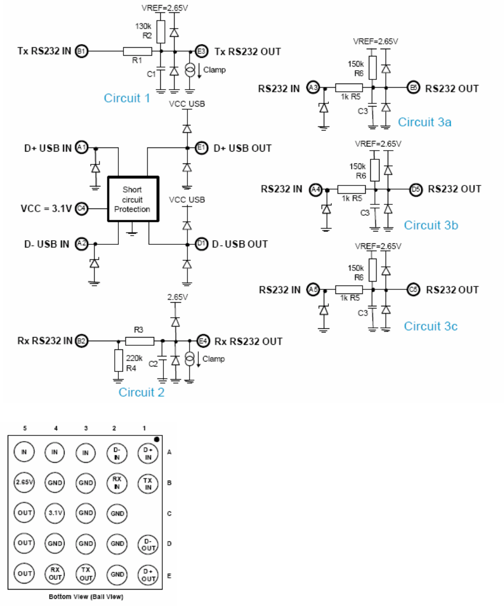
ESD Protection with EMI filter and USB Switch
Application schematic
Company Confidential s Com
Copyright 2005© Siemens AG
Page 35 of 37
Service Repair Documentation
Level 2.5e – C75 Release 1.0
Internal schematic
The Z1500 is a 5-channel filter with over-voltage and ESD
Protection array which is designed to provide filtering of
undesired RF signals in the 800-4000MHz frequency band
Additionally the Z1500 contains diodes to protect
downstream components from Electrostatic Discharge
(ESD) voltages
Company Confidential s Com
Copyright 2005© Siemens AG
Page 36 of 37
Service Repair Documentation
Level 2.5e – C75 Release 1.0
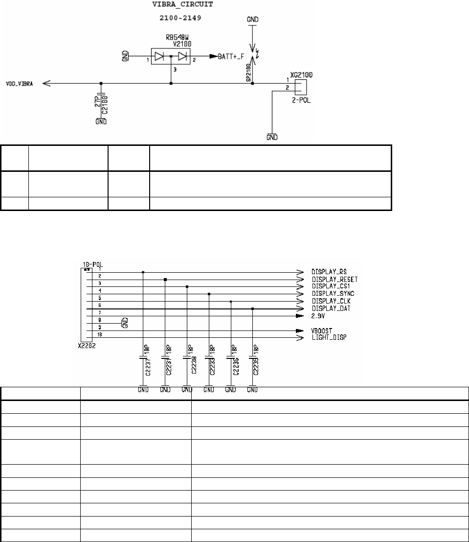
9.8 Vibration Motor (XG2100)
Pin Name IN/OU
T Remarks
1 VDD_VIBRA Vbatt will be switched by PWM-signal with
internal FET to VDD_Vibra in Asic
2 GND
9.9 DISPLAY
Pin Number Pin Name Description
1 DISPLAY_RS Control / display data flag
2 DISPLAY _RESET Reset (low active)
3 DISPLAY _CS1 Chip select main display (low active)
4 DISPLAY _SYNC Tearing pin (synchronization of display refresh and data
transmission)
5 DISPLAY_CLK Serial Clock
6 DISPLAY _DAT Serial Data
7 2.9V Power supply VDD1
8 GND Power supply GND
9 VBOOST Anode LED
10 LIGHT_DISP Cathode LED
Company Confidential s Com
Copyright 2005© Siemens AG
Page 37 of 37
Service Repair Documentation
Level 2.5e – C75 Release 1.0
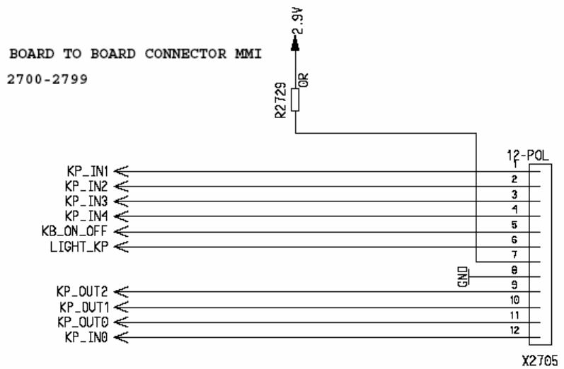
9.10 Board to Board Connector
The keyboard is connected via an inter board connector (X2705).
The lines KPOUT0 – KPOUT2 and KPIN0 – KPIN4 are connected with the SGOLDLITE.
KB_ON_OFF is used for the ON/OFF switch.
