AN 31 Op Amp Circuit Collection (Rev. B) 140 B Snla140b
User Manual: 140 B
Open the PDF directly: View PDF ![]() .
.
Page Count: 52

Application Report
SNLA140B–May 2004–Revised May 2013
AN-31 Op Amp Circuit Collection
.....................................................................................................................................................
ABSTRACT
This application report provides basic circuits of the Texas Instruments op amp collection.
Contents
1 Introduction .................................................................................................................. 4
2 Basic Circuits ................................................................................................................ 4
3 Signal Generation ......................................................................................................... 15
4 Signal Processing ......................................................................................................... 25
List of Figures
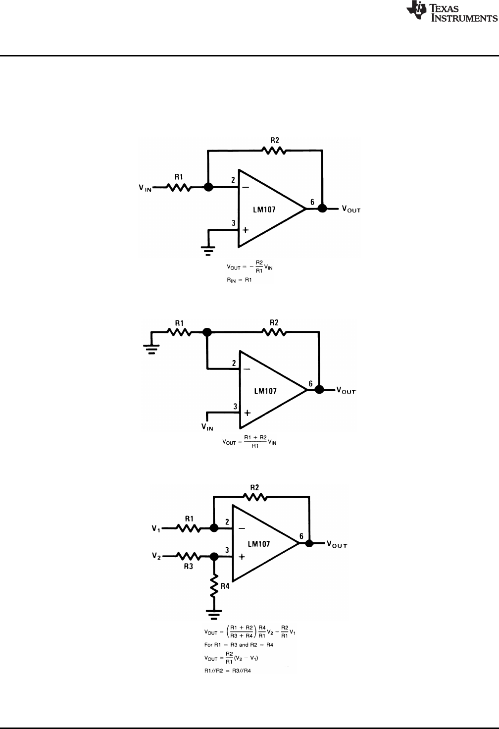
1 Inverting Amplifier........................................................................................................... 4
2 Non-Inverting Amplifier ..................................................................................................... 4
3 Difference Amplifier......................................................................................................... 4
4 Inverting Summing Amplifier............................................................................................... 5
5 Non-Inverting Summing Amplifier......................................................................................... 5
6 Inverting Amplifier with High Input Impedance.......................................................................... 5
7 Fast Inverting Amplifier with High Input Impedance.................................................................... 6
8 Non-Inverting AC Amplifier ................................................................................................ 6
9 Practical Differentiator...................................................................................................... 7
10 Integrator..................................................................................................................... 7
11 Fast Integrator............................................................................................................... 8
12 Current to Voltage Converter.............................................................................................. 8
13 Circuit for Operating the LM101 Without a Negative Supply.......................................................... 9
14 Circuit for Generating the Second Positive Voltage .................................................................... 9
15 Neutralizing Input Capacitance to Optimize Response Time ......................................................... 9
16 Integrator with Bias Current Compensation............................................................................ 10
17 Voltage Comparator for Driving DTL or TTL Integrated Circuits .................................................... 10
18 Threshold Detector for Photodiodes .................................................................................... 11
19 Double-Ended Limit Detector ............................................................................................ 11
20 Multiple Aperture Window Discriminator................................................................................ 12
21 Offset Voltage Adjustment for Inverting Amplifiers Using Any Type of Feedback Element ..................... 13
22 Offset Voltage Adjustment for Non-Inverting Amplifiers Using Any Type of Feedback Element ............... 13
23 Offset Voltage Adjustment for Voltage Followers ..................................................................... 13
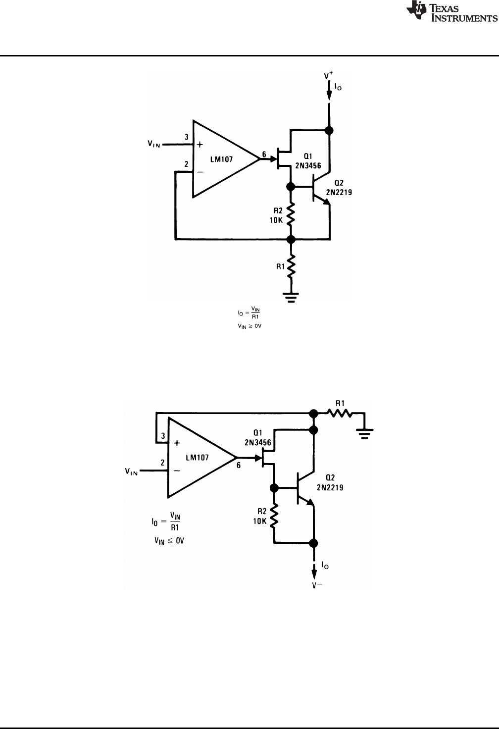
24 Offset Voltage Adjustment for Differential Amplifiers ................................................................. 14
25 Offset Voltage Adjustment for Inverting Amplifiers Using 10 kΩSource Resistance or Less................... 14
26 Low Frequency Sine Wave Generator with Quadrature Output..................................................... 15
27 High Frequency Sine Wave Generator with Quadrature Output .................................................... 16
28 Free-Running Multivibrator ............................................................................................... 16
29 Wein Bridge Sine Wave Oscillator ...................................................................................... 17
30 Function Generator........................................................................................................ 17
All trademarks are the property of their respective owners.
1
SNLA140B–May 2004–Revised May 2013 AN-31 Op Amp Circuit Collection
Submit Documentation Feedback Copyright © 2004–2013, Texas Instruments Incorporated

www.ti.com
31 Pulse Width Modulator.................................................................................................... 18
32 Bilateral Current Source .................................................................................................. 18
33 Bilateral Current Source .................................................................................................. 19
34 Wein Bridge Oscillator with FET Amplitude Stabilization ............................................................ 20
35 Low Power Supply for Integrated Circuit Testing ..................................................................... 21
36 Positive Voltage Reference .............................................................................................. 22
37 Positive Voltage Reference .............................................................................................. 22
38 Negative Voltage Reference ............................................................................................. 23
39 Negative Voltage Reference ............................................................................................. 23
40 Precision Current Sink .................................................................................................... 24
41 Precision Current Source................................................................................................. 24
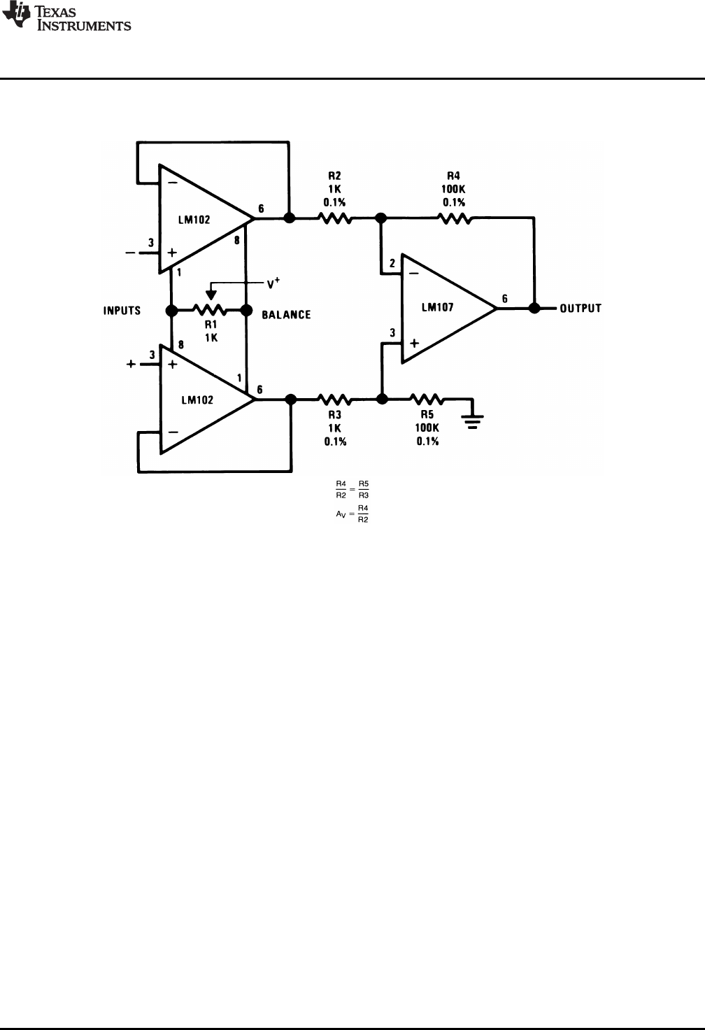
42 Differential-Input Instrumentation Amplifier ............................................................................ 25
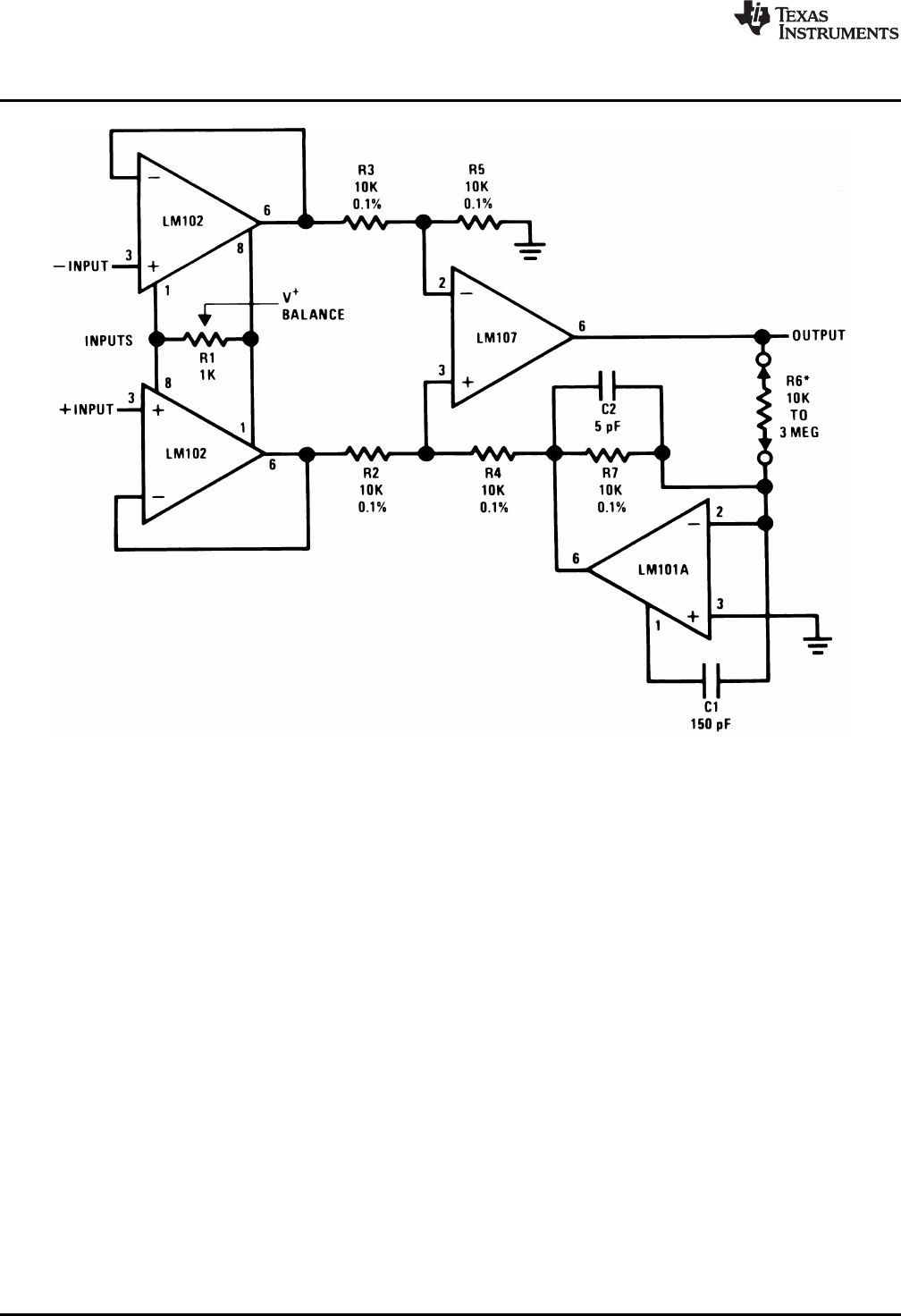
43 Variable Gain, Differential-Input Instrumentation Amplifier .......................................................... 26
44 Instrumentation Amplifier with ±100 Volt Common Mode Range ................................................... 27
45 Instrumentation Amplifier with ±10 Volt Common Mode Range..................................................... 28
46 High Input Impedance Instrumentation Amplifier...................................................................... 29
47 Bridge Amplifier with Low Noise Compensation....................................................................... 29
48 Bridge Amplifier............................................................................................................ 30
49 Precision Diode ............................................................................................................ 30
50 Precision Clamp ........................................................................................................... 31
51 Fast Half Wave Rectifier.................................................................................................. 31
52 Precision AC to DC Converter........................................................................................... 32
53 Low Drift Peak Detector .................................................................................................. 32
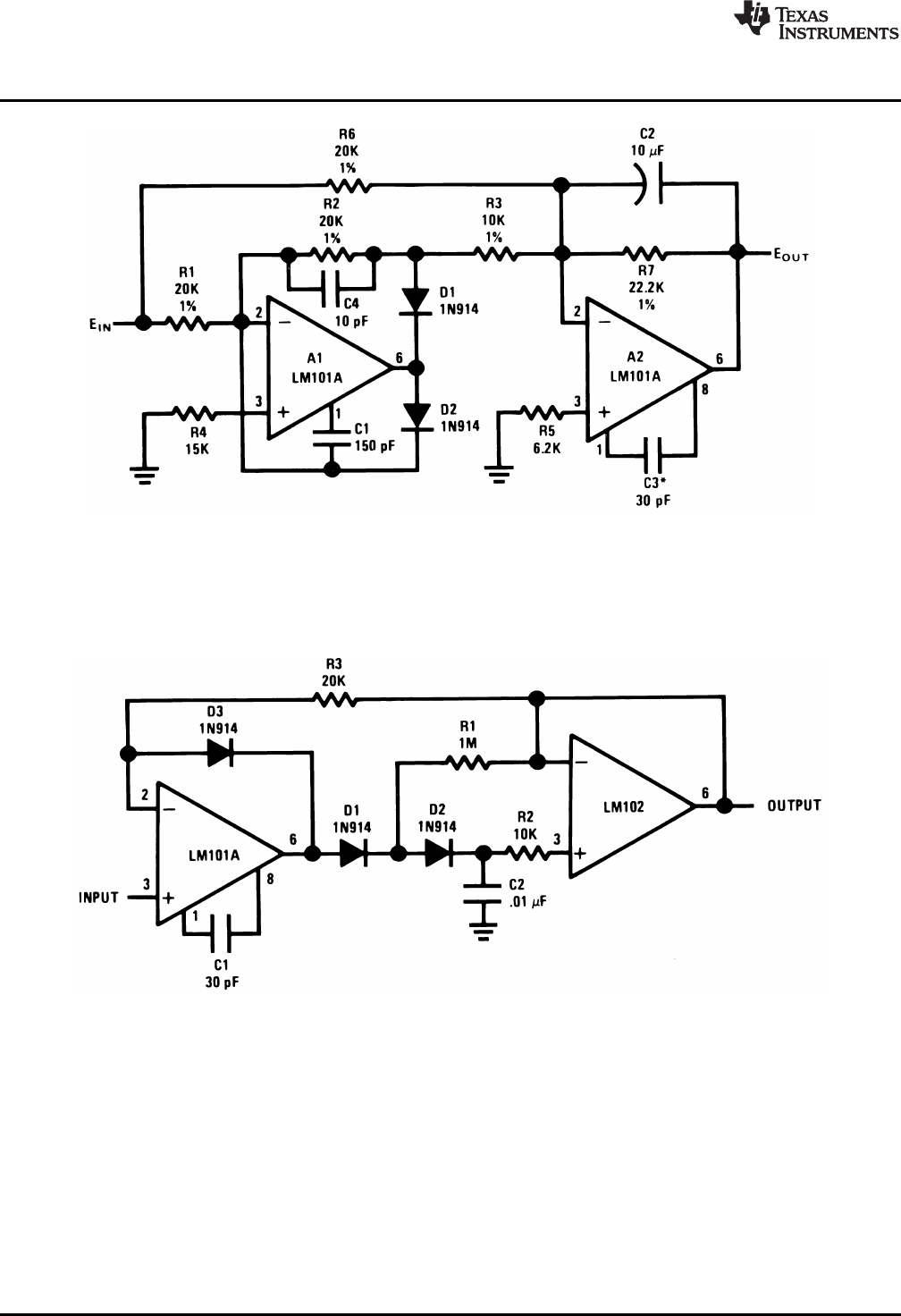
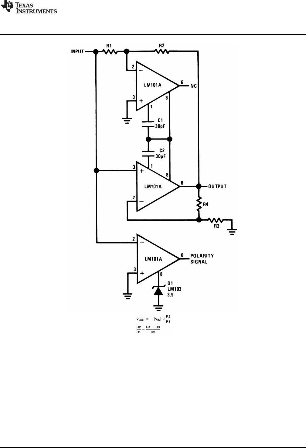
54 Absolute Value Amplifier with Polarity Detector ....................................................................... 33
55 Sample and Hold .......................................................................................................... 34
56 Sample and Hold .......................................................................................................... 34
57 Low Drift Integrator........................................................................................................ 35
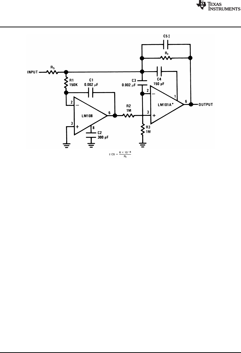
58 Fast†Summing Amplifier with Low Input Current ..................................................................... 36
59 Fast Integrator with Low Input Current ................................................................................. 37
60 Adjustable Q Notch Filter................................................................................................. 38
61 Easily Tuned Notch Filter................................................................................................. 39
62 Tuned Circuit............................................................................................................... 39
63 Two-Stage Tuned Circuit ................................................................................................. 40
64 Negative Capacitance Multiplier......................................................................................... 40
65 Variable Capacitance Multiplier.......................................................................................... 41
66 Simulated Inductor ........................................................................................................ 41
67 Capacitance Multiplier .................................................................................................... 42
68 High Pass Active Filter.................................................................................................... 42
69 Low Pass Active Filter .................................................................................................... 43
70 Nonlinear Operational Amplifier with Temperature Compensated Breakpoints................................... 43
71 Current Monitor ............................................................................................................ 44
72 Saturating Servo Preamplifier with Rate Feedback................................................................... 44
73 Power Booster ............................................................................................................. 45
74 Analog Multiplier ........................................................................................................... 45
75 Long Interval Timer........................................................................................................ 46
76 Fast Zero Crossing Detector............................................................................................. 46
77 Amplifier for Piezoelectric Transducer .................................................................................. 47
78 Temperature Probe........................................................................................................ 47
79 Photodiode Amplifier ...................................................................................................... 48
2AN-31 Op Amp Circuit Collection SNLA140B–May 2004–Revised May 2013
Submit Documentation Feedback
Copyright © 2004–2013, Texas Instruments Incorporated

www.ti.com
80 Photodiode Amplifier ...................................................................................................... 48
81 High Input Impedance AC Follower..................................................................................... 48
82 Temperature Compensated Logarithmic Converter................................................................... 49
83 Root Extractor.............................................................................................................. 49
84 Multiplier/Divider ........................................................................................................... 50
85 Cube Generator............................................................................................................ 50
86 Fast Log Generator ....................................................................................................... 51
87 Anti-Log Generator ........................................................................................................ 51
3
SNLA140B–May 2004–Revised May 2013 AN-31 Op Amp Circuit Collection
Submit Documentation Feedback Copyright © 2004–2013, Texas Instruments Incorporated
Introduction
www.ti.com
1 Introduction
Texas Instruments recommends replacing 2N2920 and 2N3728 matched pairs with LM394 in all
application circuits.
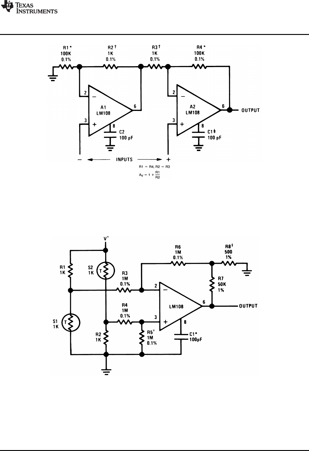
2 Basic Circuits
Figure 1. Inverting Amplifier
Figure 2. Non-Inverting Amplifier
For minimum offset error due to input bias current.
Figure 3. Difference Amplifier
4AN-31 Op Amp Circuit Collection SNLA140B–May 2004–Revised May 2013
Submit Documentation Feedback
Copyright © 2004–2013, Texas Instruments Incorporated

www.ti.com
Basic Circuits
R5 = R1//R2//R3//R4
For minimum offset error due to input bias current/
Figure 4. Inverting Summing Amplifier
* RS= 1k for 1% accuracy
Figure 5. Non-Inverting Summing Amplifier
* Source Impedance less than 100k gives less than 1% gain error.
Figure 6. Inverting Amplifier with High Input Impedance
5
SNLA140B–May 2004–Revised May 2013 AN-31 Op Amp Circuit Collection
Submit Documentation Feedback Copyright © 2004–2013, Texas Instruments Incorporated
www.ti.com
Basic Circuits
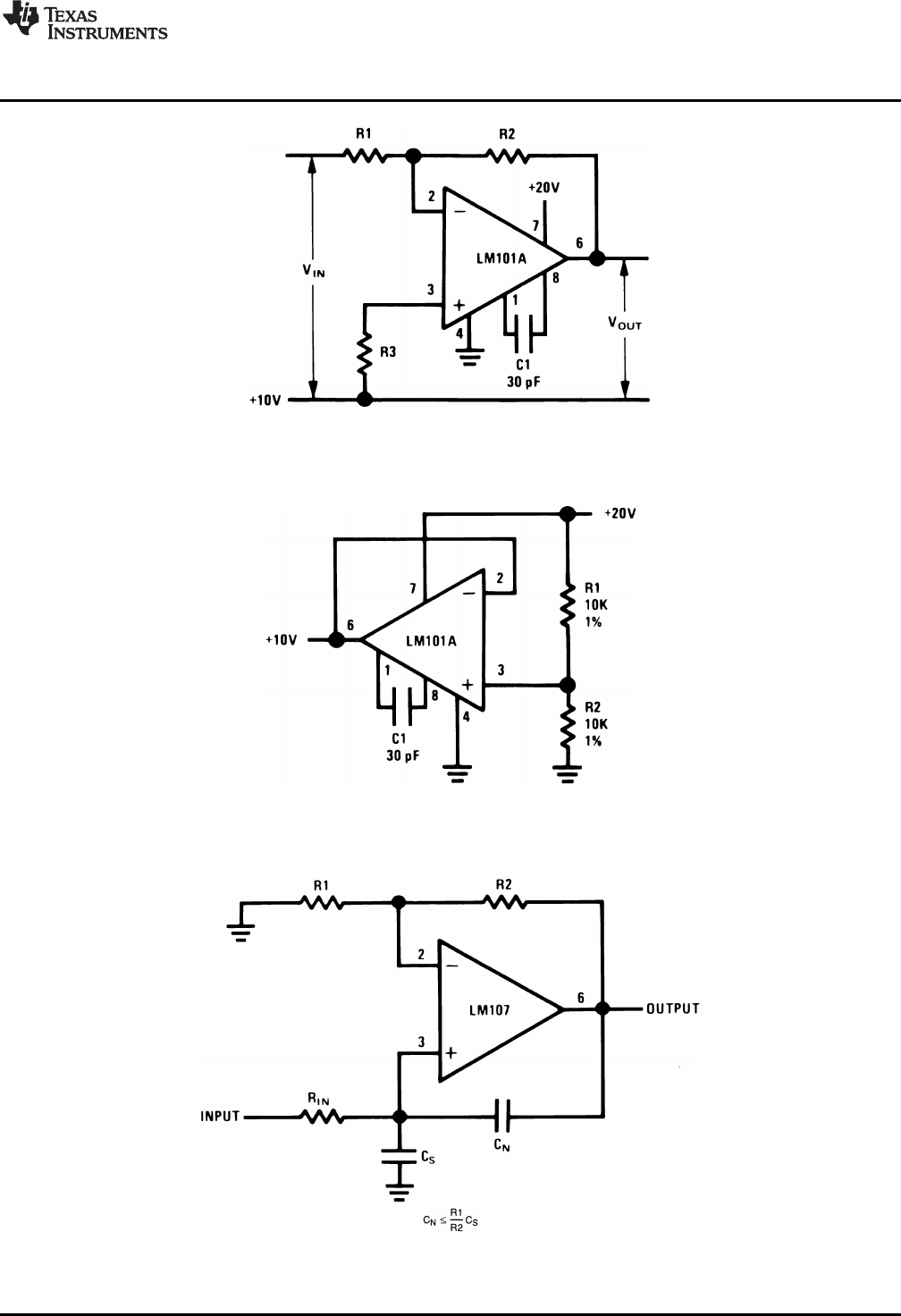
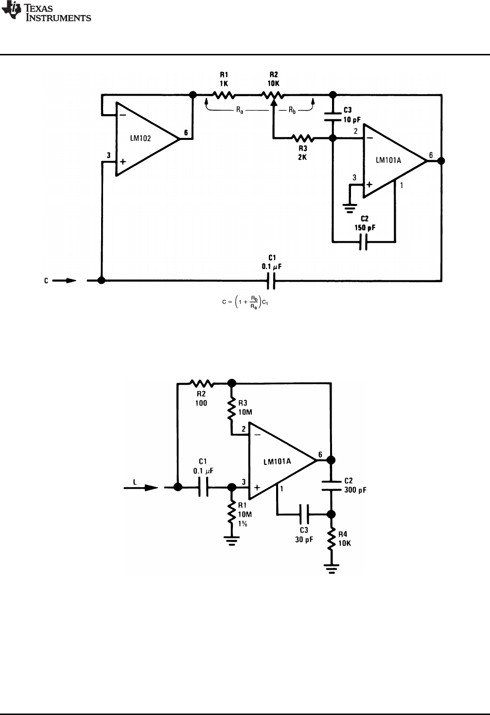
Figure 13. Circuit for Operating the LM101 Without a Negative Supply
Figure 14. Circuit for Generating the Second Positive Voltage
Figure 15. Neutralizing Input Capacitance to Optimize Response Time
9
SNLA140B–May 2004–Revised May 2013 AN-31 Op Amp Circuit Collection
Submit Documentation Feedback Copyright © 2004–2013, Texas Instruments Incorporated
Basic Circuits
www.ti.com
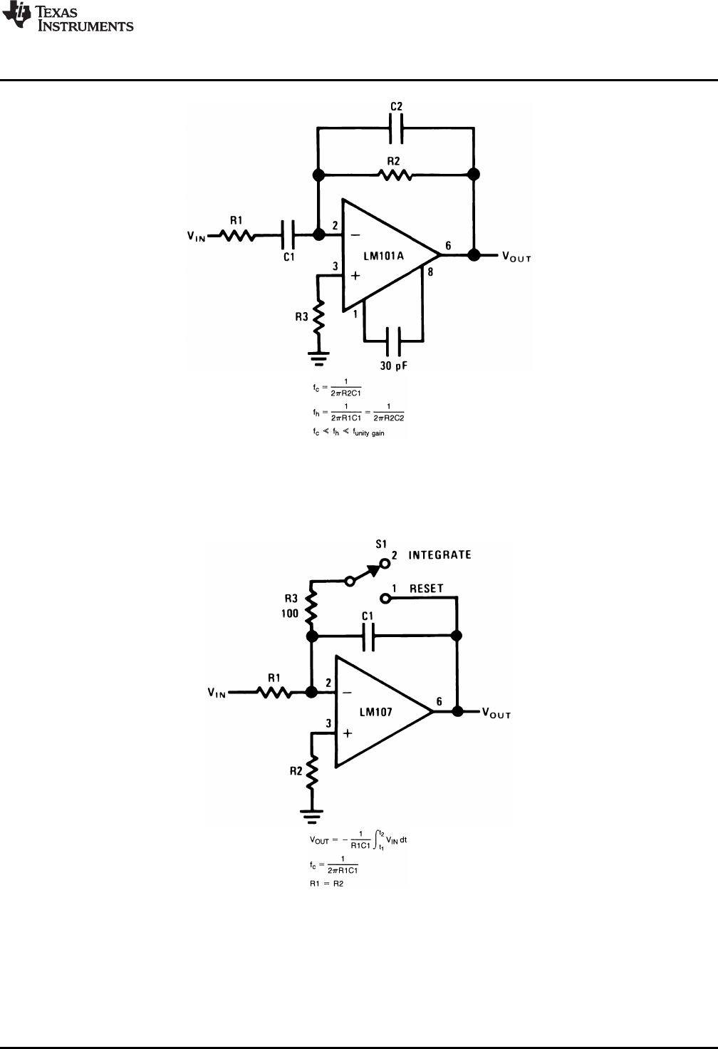
* Adjust for zero integrator drift.
Current drift typically 0.1 n/A°C over −55°C to 125°C temperature range.
Figure 16. Integrator with Bias Current Compensation
Figure 17. Voltage Comparator for Driving DTL or TTL Integrated Circuits
10 AN-31 Op Amp Circuit Collection SNLA140B–May 2004–Revised May 2013
Submit Documentation Feedback
Copyright © 2004–2013, Texas Instruments Incorporated
www.ti.com
Basic Circuits
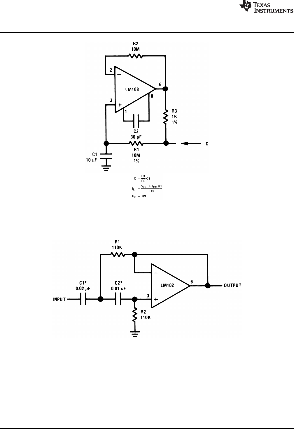
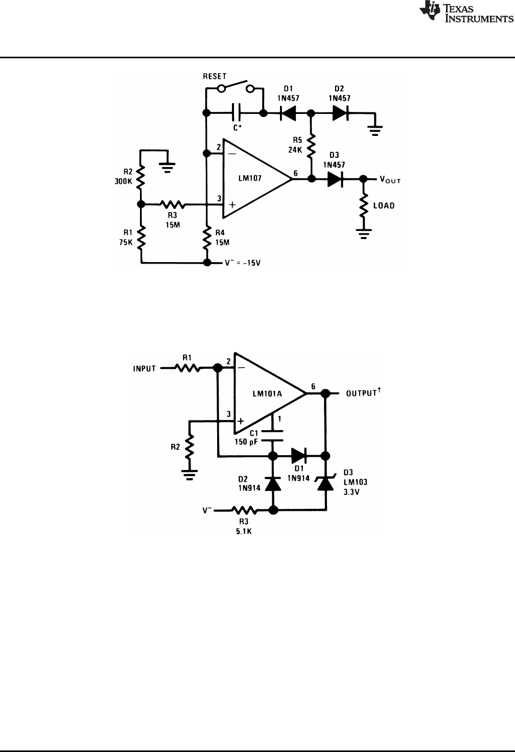
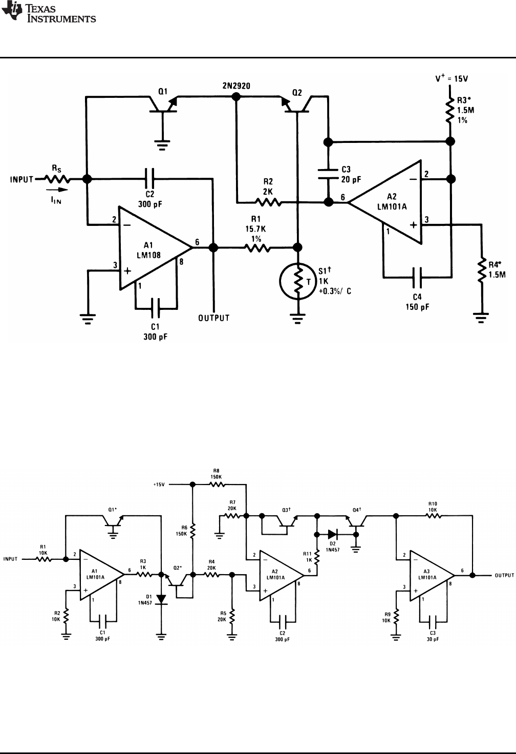
Figure 18. Threshold Detector for Photodiodes
VOUT = 4.6V for VLT ≤VIN ≤VUT
VOUT = 0V for VIN < VLT or VIN > VUT
Figure 19. Double-Ended Limit Detector
11
SNLA140B–May 2004–Revised May 2013 AN-31 Op Amp Circuit Collection
Submit Documentation Feedback Copyright © 2004–2013, Texas Instruments Incorporated

www.ti.com
Basic Circuits
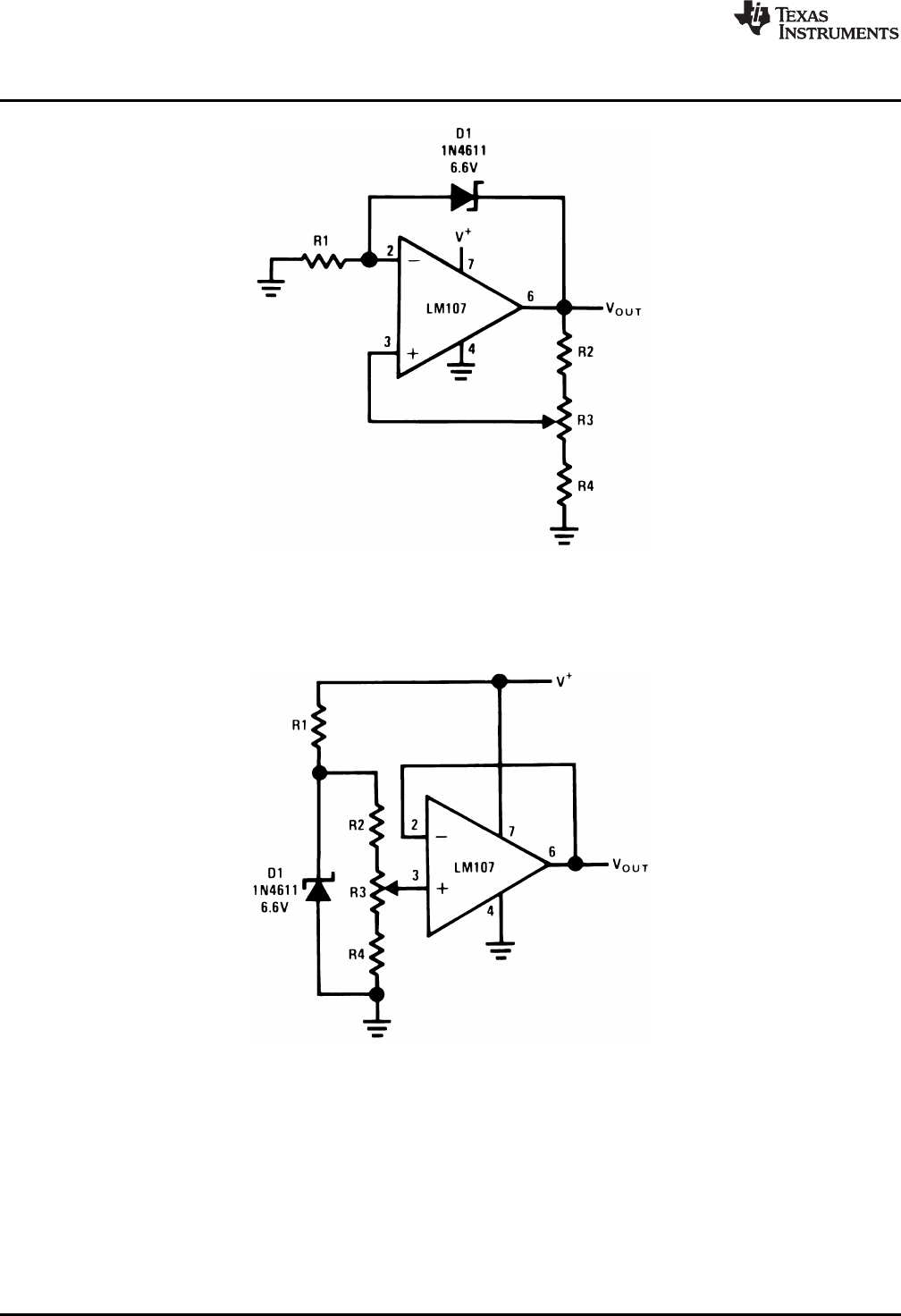
Figure 21. Offset Voltage Adjustment for Inverting Amplifiers Using Any Type of Feedback Element
Figure 22. Offset Voltage Adjustment for Non-Inverting Amplifiers Using Any Type of Feedback Element
Figure 23. Offset Voltage Adjustment for Voltage Followers
13
SNLA140B–May 2004–Revised May 2013 AN-31 Op Amp Circuit Collection
Submit Documentation Feedback Copyright © 2004–2013, Texas Instruments Incorporated
Basic Circuits
www.ti.com
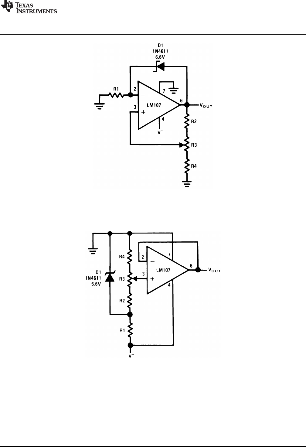
Figure 24. Offset Voltage Adjustment for Differential Amplifiers
Figure 25. Offset Voltage Adjustment for Inverting Amplifiers Using 10 kΩSource Resistance or Less
14 AN-31 Op Amp Circuit Collection SNLA140B–May 2004–Revised May 2013
Submit Documentation Feedback
Copyright © 2004–2013, Texas Instruments Incorporated

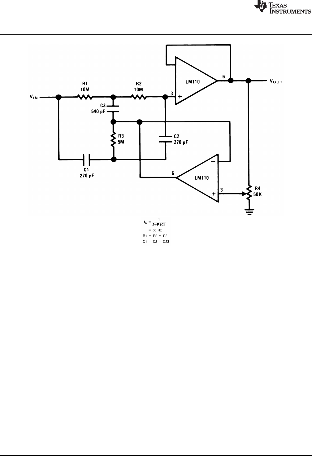
Signal Generation
www.ti.com
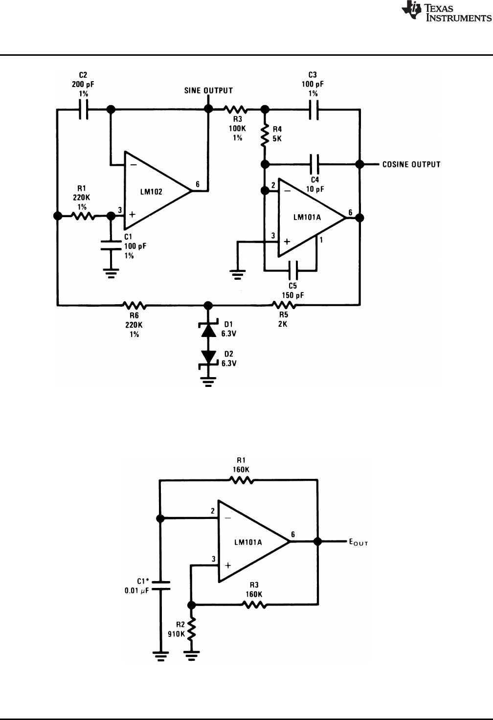
Figure 27. High Frequency Sine Wave Generator with Quadrature Output
* Chosen for oscillation at 100 Hz
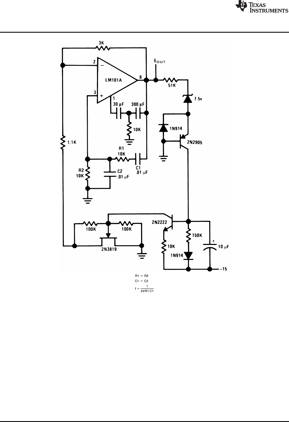
Figure 28. Free-Running Multivibrator
16 AN-31 Op Amp Circuit Collection SNLA140B–May 2004–Revised May 2013
Submit Documentation Feedback
Copyright © 2004–2013, Texas Instruments Incorporated

www.ti.com
Signal Processing
*† Matching Determines CMRR
‡ May be deleted to maximize bandwidth
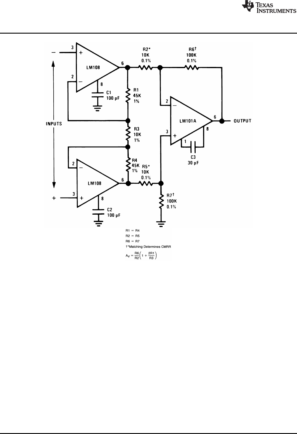
Figure 46. High Input Impedance Instrumentation Amplifier
* Reduces feed through of power supply noise by 20 dB and makes supply bypassing unnecessary.
† Trim for best common mode rejection
‡ Gain adjust
Figure 47. Bridge Amplifier with Low Noise Compensation
29
SNLA140B–May 2004–Revised May 2013 AN-31 Op Amp Circuit Collection
Submit Documentation Feedback Copyright © 2004–2013, Texas Instruments Incorporated
www.ti.com
Signal Processing
* EREF must have a source impedance of less than 200Ωif D2 is used.
Figure 50. Precision Clamp
Figure 51. Fast Half Wave Rectifier
31
SNLA140B–May 2004–Revised May 2013 AN-31 Op Amp Circuit Collection
Submit Documentation Feedback Copyright © 2004–2013, Texas Instruments Incorporated
Signal Processing
www.ti.com
* Feedforward compensation can be used to make a fast full wave rectifier without a filter.
Figure 52. Precision AC to DC Converter
Figure 53. Low Drift Peak Detector
32 AN-31 Op Amp Circuit Collection SNLA140B–May 2004–Revised May 2013
Submit Documentation Feedback
Copyright © 2004–2013, Texas Instruments Incorporated
Signal Processing
www.ti.com
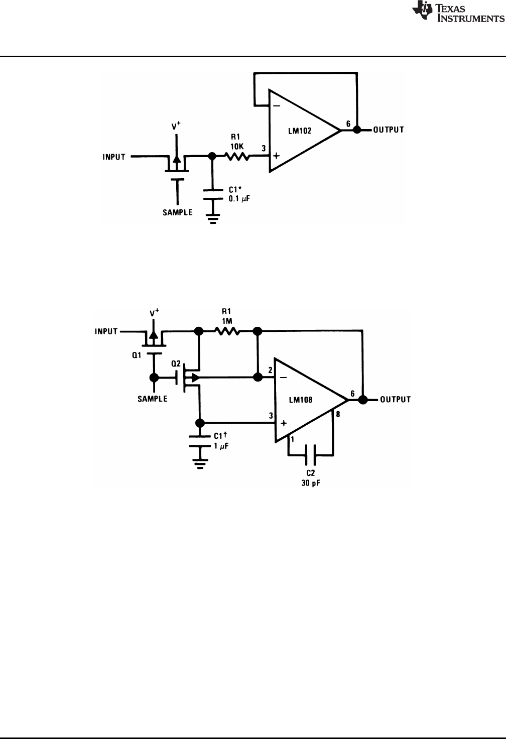
* Polycarbonate-dielectric capacitor
Figure 55. Sample and Hold
* Worst case drift less than 2.5 mV/sec
† Teflon, Polyethylene or Polycarbonate Dielectric Capacitor
Figure 56. Sample and Hold
34 AN-31 Op Amp Circuit Collection SNLA140B–May 2004–Revised May 2013
Submit Documentation Feedback
Copyright © 2004–2013, Texas Instruments Incorporated
www.ti.com
Signal Processing
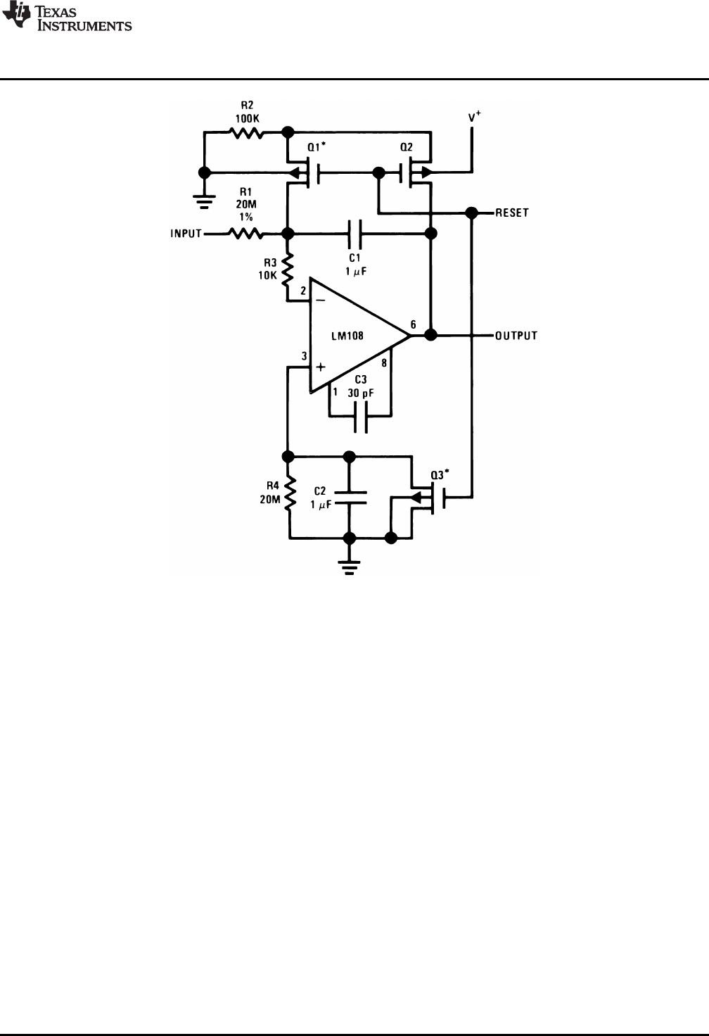
* Q1 and Q3 should not have internal gate-protection diodes.
Worst case drift less than 500 μV/sec over −55°C to +125°C.
Figure 57. Low Drift Integrator
35
SNLA140B–May 2004–Revised May 2013 AN-31 Op Amp Circuit Collection
Submit Documentation Feedback Copyright © 2004–2013, Texas Instruments Incorporated
Signal Processing
www.ti.com
* In addition to increasing speed, the LM101A raises high and low frequency gain, increases output drive capability
and eliminates thermal feedback.
† Power Bandwidth: 250 kHz
Small Signal Bandwidth: 3.5 MHz
Slew Rate: 10V/μs
Figure 58. Fast†Summing Amplifier with Low Input Current
36 AN-31 Op Amp Circuit Collection SNLA140B–May 2004–Revised May 2013
Submit Documentation Feedback
Copyright © 2004–2013, Texas Instruments Incorporated

Signal Processing
www.ti.com
Figure 67. Capacitance Multiplier
* Values are for 100 Hz cutoff. Use metalized polycarbonate capacitors for good temperature stability.
Figure 68. High Pass Active Filter
42 AN-31 Op Amp Circuit Collection SNLA140B–May 2004–Revised May 2013
Submit Documentation Feedback
Copyright © 2004–2013, Texas Instruments Incorporated
www.ti.com
Signal Processing
* Values are for 10 kHz cutoff. Use silvered mica capacitors for good temperature stability.
Figure 69. Low Pass Active Filter
Figure 70. Nonlinear Operational Amplifier with Temperature Compensated Breakpoints
43
SNLA140B–May 2004–Revised May 2013 AN-31 Op Amp Circuit Collection
Submit Documentation Feedback Copyright © 2004–2013, Texas Instruments Incorporated
Signal Processing
www.ti.com
* Low leakage −0.017 μF per second delay
Figure 75. Long Interval Timer
Propagation delay approximately 200 ns
† DTL or TTL fanout of three.
Minimize stray capacitance
Pin 8
Figure 76. Fast Zero Crossing Detector
46 AN-31 Op Amp Circuit Collection SNLA140B–May 2004–Revised May 2013
Submit Documentation Feedback
Copyright © 2004–2013, Texas Instruments Incorporated
www.ti.com
Signal Processing
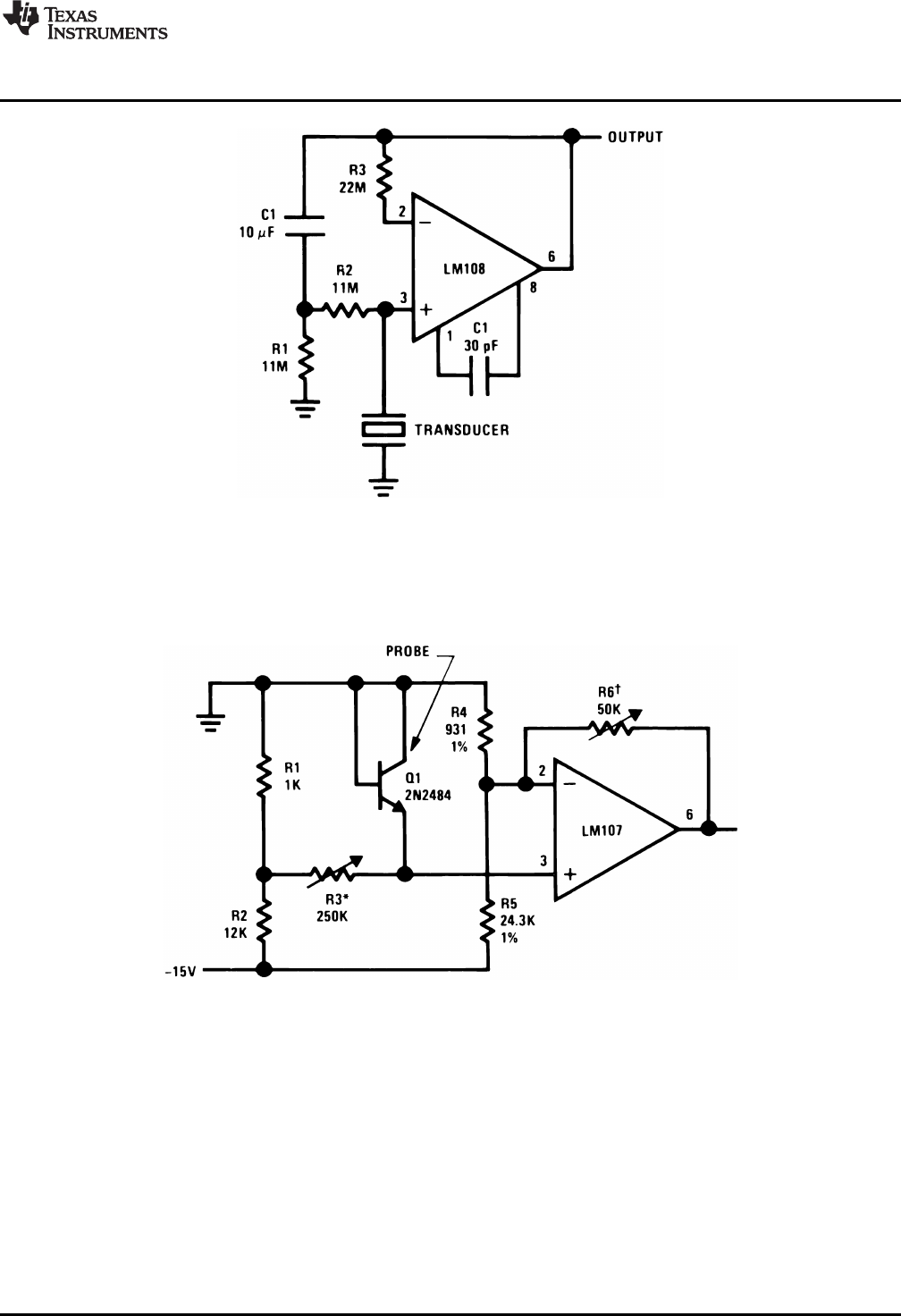
Low frequency cutoff = R1 C1
Figure 77. Amplifier for Piezoelectric Transducer
* Set for 0V at 0°C
† Adjust for 100 mV/°C
Figure 78. Temperature Probe
47
SNLA140B–May 2004–Revised May 2013 AN-31 Op Amp Circuit Collection
Submit Documentation Feedback Copyright © 2004–2013, Texas Instruments Incorporated
Signal Processing
www.ti.com
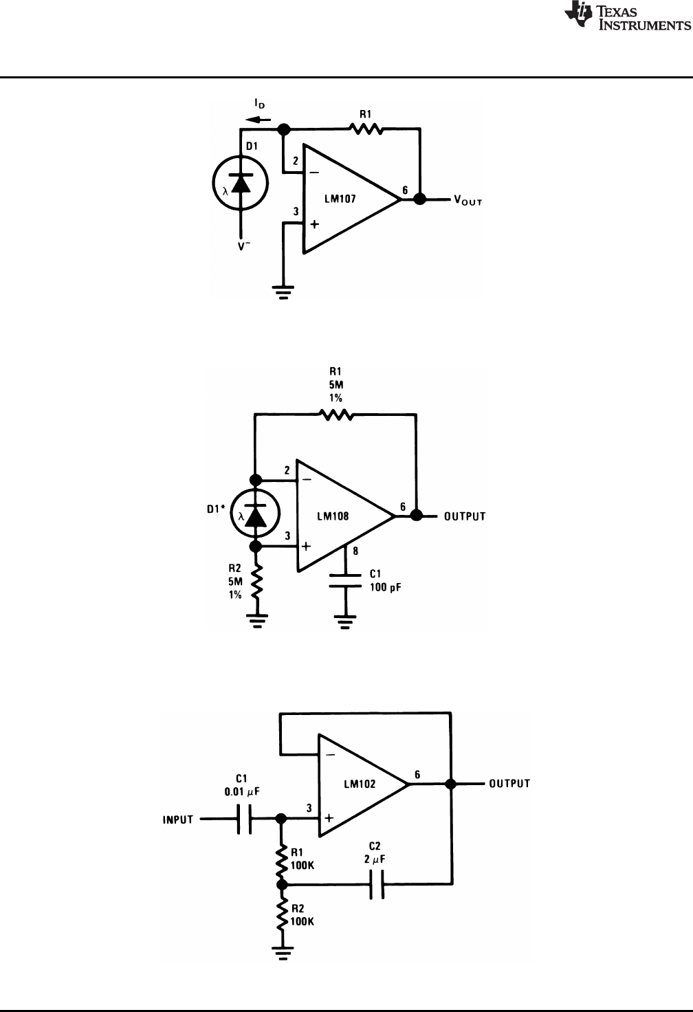
VOUT = R1 ID
Figure 79. Photodiode Amplifier
VOUT = 10 V/μA
*Operating photodiode with less than 3 mV across it eliminates leakage currents.
Figure 80. Photodiode Amplifier
Figure 81. High Input Impedance AC Follower
48 AN-31 Op Amp Circuit Collection SNLA140B–May 2004–Revised May 2013
Submit Documentation Feedback
Copyright © 2004–2013, Texas Instruments Incorporated
www.ti.com
Signal Processing
10 nA < IIN < 1 mA
Sensitivity is 1V per decade
† 1 kΩ(±1%) at 25°C, +3500 ppm/°C.
Available from Vishay Ultronix, Grand Junction, CO, Q81 Series.
* Determines current for zero crossing on output: 10 μA as shown.
Figure 82. Temperature Compensated Logarithmic Converter
*† 2N3728 matched pairs
Figure 83. Root Extractor
49
SNLA140B–May 2004–Revised May 2013 AN-31 Op Amp Circuit Collection
Submit Documentation Feedback Copyright © 2004–2013, Texas Instruments Incorporated

www.ti.com
Signal Processing
† 1 kΩ(±1%) at 25°C, +3500 ppm/°C.
Available from Vishay Ultronix, Grand Junction, CO, Q81 Series.
Figure 86. Fast Log Generator
† 1 kΩ(±1%) at 25°C, +3500 ppm/°C.
Available from Vishay Ultronix, Grand Junction, CO, Q81 Series.
Figure 87. Anti-Log Generator
51
SNLA140B–May 2004–Revised May 2013 AN-31 Op Amp Circuit Collection
Submit Documentation Feedback Copyright © 2004–2013, Texas Instruments Incorporated

IMPORTANT NOTICE
Texas Instruments Incorporated and its subsidiaries (TI) reserve the right to make corrections, enhancements, improvements and other
changes to its semiconductor products and services per JESD46, latest issue, and to discontinue any product or service per JESD48, latest
issue. Buyers should obtain the latest relevant information before placing orders and should verify that such information is current and
complete. All semiconductor products (also referred to herein as “components”) are sold subject to TI’s terms and conditions of sale
supplied at the time of order acknowledgment.
TI warrants performance of its components to the specifications applicable at the time of sale, in accordance with the warranty in TI’s terms
and conditions of sale of semiconductor products. Testing and other quality control techniques are used to the extent TI deems necessary
to support this warranty. Except where mandated by applicable law, testing of all parameters of each component is not necessarily
performed.
TI assumes no liability for applications assistance or the design of Buyers’ products. Buyers are responsible for their products and
applications using TI components. To minimize the risks associated with Buyers’ products and applications, Buyers should provide
adequate design and operating safeguards.
TI does not warrant or represent that any license, either express or implied, is granted under any patent right, copyright, mask work right, or
other intellectual property right relating to any combination, machine, or process in which TI components or services are used. Information
published by TI regarding third-party products or services does not constitute a license to use such products or services or a warranty or
endorsement thereof. Use of such information may require a license from a third party under the patents or other intellectual property of the
third party, or a license from TI under the patents or other intellectual property of TI.
Reproduction of significant portions of TI information in TI data books or data sheets is permissible only if reproduction is without alteration
and is accompanied by all associated warranties, conditions, limitations, and notices. TI is not responsible or liable for such altered
documentation. Information of third parties may be subject to additional restrictions.
Resale of TI components or services with statements different from or beyond the parameters stated by TI for that component or service
voids all express and any implied warranties for the associated TI component or service and is an unfair and deceptive business practice.
TI is not responsible or liable for any such statements.
Buyer acknowledges and agrees that it is solely responsible for compliance with all legal, regulatory and safety-related requirements
concerning its products, and any use of TI components in its applications, notwithstanding any applications-related information or support
that may be provided by TI. Buyer represents and agrees that it has all the necessary expertise to create and implement safeguards which
anticipate dangerous consequences of failures, monitor failures and their consequences, lessen the likelihood of failures that might cause
harm and take appropriate remedial actions. Buyer will fully indemnify TI and its representatives against any damages arising out of the use
of any TI components in safety-critical applications.
In some cases, TI components may be promoted specifically to facilitate safety-related applications. With such components, TI’s goal is to
help enable customers to design and create their own end-product solutions that meet applicable functional safety standards and
requirements. Nonetheless, such components are subject to these terms.
No TI components are authorized for use in FDA Class III (or similar life-critical medical equipment) unless authorized officers of the parties
have executed a special agreement specifically governing such use.
Only those TI components which TI has specifically designated as military grade or “enhanced plastic” are designed and intended for use in
military/aerospace applications or environments. Buyer acknowledges and agrees that any military or aerospace use of TI components
which have not been so designated is solely at the Buyer's risk, and that Buyer is solely responsible for compliance with all legal and
regulatory requirements in connection with such use.
TI has specifically designated certain components as meeting ISO/TS16949 requirements, mainly for automotive use. In any case of use of
non-designated products, TI will not be responsible for any failure to meet ISO/TS16949.
Products Applications
Audio www.ti.com/audio Automotive and Transportation www.ti.com/automotive
Amplifiers amplifier.ti.com Communications and Telecom www.ti.com/communications
Data Converters dataconverter.ti.com Computers and Peripherals www.ti.com/computers
DLP® Products www.dlp.com Consumer Electronics www.ti.com/consumer-apps
DSP dsp.ti.com Energy and Lighting www.ti.com/energy
Clocks and Timers www.ti.com/clocks Industrial www.ti.com/industrial
Interface interface.ti.com Medical www.ti.com/medical
Logic logic.ti.com Security www.ti.com/security
Power Mgmt power.ti.com Space, Avionics and Defense www.ti.com/space-avionics-defense
Microcontrollers microcontroller.ti.com Video and Imaging www.ti.com/video
RFID www.ti-rfid.com
OMAP Applications Processors www.ti.com/omap TI E2E Community e2e.ti.com
Wireless Connectivity www.ti.com/wirelessconnectivity
Mailing Address: Texas Instruments, Post Office Box 655303, Dallas, Texas 75265
Copyright © 2013, Texas Instruments Incorporated
