MZ R90/R91 Sony_MZ R90_service_manual Sony R90 Service Manual
User Manual: sony_MZ-R90_service_manual
Open the PDF directly: View PDF ![]() .
.
Page Count: 50
SERVICE MANUAL
PORTABLE MINIDISC RECORDER
US Model
Canadian Model
Australian Model
Chinese Model
MZ-R90
AEP Model
UK Model
E Model
Tourist Model
MZ-R90/R91
SPECIFICATIONS
MZ-R90/R91
US and foreign patents licensed from Dolby
Laboratories Licensing Corporation.
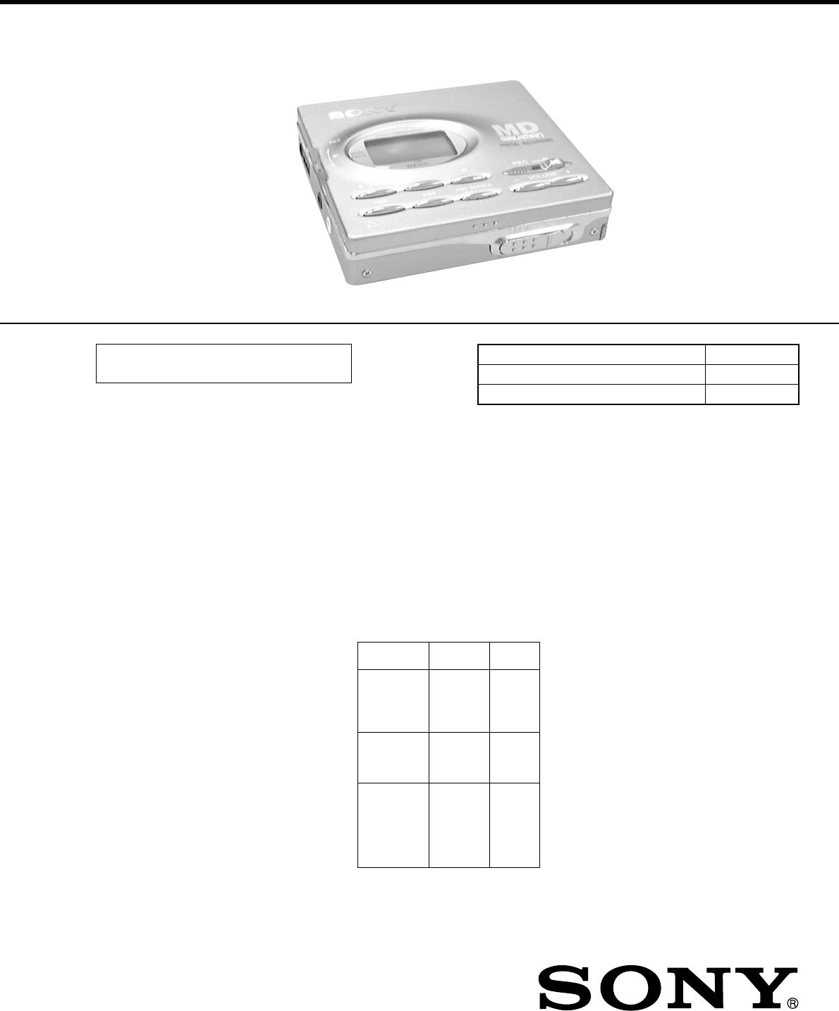
Photo: MZ-R91 (Blue type)
System
Audio playing system
MiniDisc digital audio system
Laser diode properties
Material: GaAlAs
Wavelength: λ= 790 nm
Emission duration: continuous
Laser output: less than 44.6 µW
(This output is the value measured at a distance
of 200 mm from the lens surface on the optical
pick-upblockwith7mmaperture.)
Recording and playback time
Maximum 80 minutes (MDW-80, stereo
recording)
Maximum 160 minutes (MDW-80, monaural
recording)
Maximum 74 minutes (MDW-74, stereo
recording)
Maximum 148 minutes (MDW-74, monaural
recording)
Revolutions
400 rpm to 1,800 rpm (CLV)
Error correction
Advanced Cross Interleave Reed Solomon
Code (ACIRC)
Sampling frequency
44.1 kHz
Sampling rate converter
Input: 32 kHz/44.1 kHz/48 kHz
Coding
Adaptive TRansform Acoustic Coding
(ATRAC)
Modulation system
EFM (Eight to Fourteen Modulation)
Number of channels
2 stereo channels
1 monaural channel
Frequency response
20 to 20,000 Hz ±3dB
Wo w and Fl ut ter
Below measurable limit
Inputs
Microphone: stereo mini-jack, 0.35–1.38 mV
Line in: stereo mini-jack, 69–194 mV
Optical (Digital) in: optical (digital) mini-jack
Outputs
i/LINE OUT*: stereo mini-jack
Headphones: maximum output level 5 mV +
5mV, load impedance 16 ohm
LINE OUT: 194 mV, load impedance 10
kilohm
*Thei/LINE OUT jack connects either
headphones or a line cable.
General
Power requirements
Sony AC Power Adaptor (supplied) connected
at the DC IN 3 V jack:
220–230 V AC, 50/60 Hz (European model)
120 V AC, 50 Hz (Canadian model)
100–240 V AC, 50/60 Hz (Other models)
Nickel metal hydride rechargeable battery NH-
14WM (supplied)
LR6 (size AA) alkaline battery (not supplied)
Battery operation time
Dimensions
MZ-R90
Approx. 78.9 ×17.3 ×72.0 mm (w/h/d)
(3
1
/
8
×
11
/
16
×2
7
/
8
in.)
MZ-R91
Approx. 78.9 ×18.0 ×72.0 mm (w/h/d)
(3
1
/
8
×
23
/
32
×2
7
/
8
in.)
Mass
MZ-R90
Approx. 105 g (3.7 oz) the recorder only
Approx. 148 g (5.2 oz) incl. a recordable MD,
and NH-14WM nickel metal hydride
rechargeable battery
MZ-R91
Approx. 110 g (3.8 oz) the recorder only
Approx. 153 g (5.4 oz) incl. a recordable MD,
and NH-14WM nickel metal hydride
rechargeable battery
Supplied accessories
AC power adaptor (1)
Headphones with a remote control (1) (RM-MZ2S)
NH-14WM nickel metal hydride rechargeable
battery (1)
Dry battery case (1)
Rechargeable battery carrying case (1)
Carrying pouch (1)
A
Design and specifications are subject to
change without notice.
C plug adaptor (1)
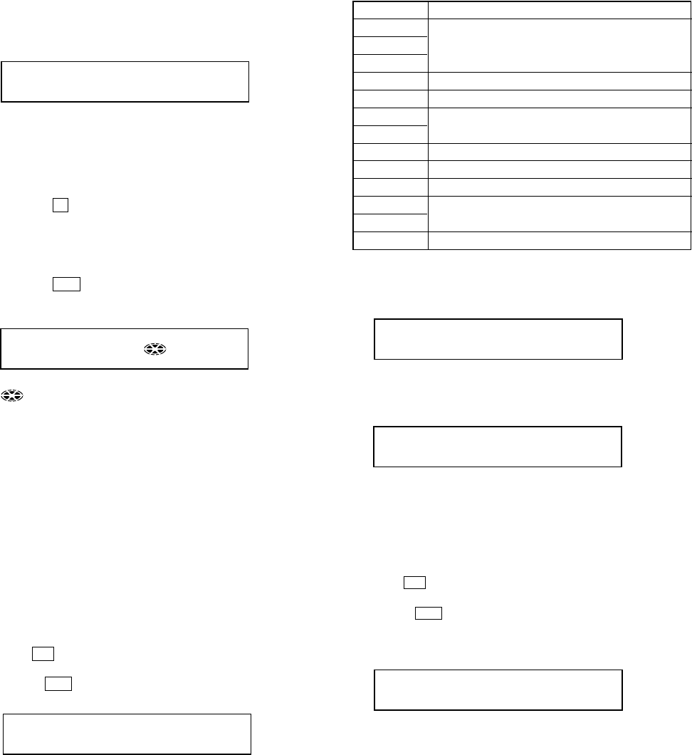
Battery life1)
Batteries Recording
2) Playback
NH-14WM
nickel metal
hydride
rechargeable
battery
Approx.
6.5 hours Approx.
12 hours
LR6 (SG)
(size AA)
Sony alkaline
dry battery
Approx.
4 hours Approx.
16.5
hours
NH-14WM
nickel metal
hydride
rechargeable
battery
+ One LR6
(SG) (size AA)
Approx.
14.5 hours Approx.
29 hour
1)
The battery life may be shorter due to
operating conditions and the temperature of
the location.
2)
When you record, use a fully charged
rechargeable battery.
Model Name Using Similar Mechanism NEW
Mechanism Type MT-MZR90-165
Optical Pick-up Name LCX-2R
Ver 1.3 2000. 07
With SUPPLIMENT-1
(9-927-187-83)

– 2 –
TABLE OF CONTENTS
1. SERVICING NOTES ............................................... 3
2. GENERAL ................................................................... 4
3. DISASSEMBLY ......................................................... 5
4. TEST MODE.............................................................. 11
5. ELECTRICAL ADJUSTMENTS......................... 18
6. DIAGRAMS
6-1. Block Diagram –SERVO Section–................................. 23
6-2. Block Diagram –A/D, D/A CONVERTER,
AUDIO Section –............................................................ 25
6-3. Block Diagram –KEY CONTROL/DISPLAY/
POWER SUPPLY Section –........................................... 27
6-4. Printed Wiring Board ...................................................... 30
6-5. Schematic Diagram ......................................................... 33
6-6. IC Pin Function Description ........................................... 46
7. EXPLODED VIEWS ................................................ 53
8. ELECTRICAL PARTS LIST ............................... 57
Flexible Circuit Board Repairing
•Keep the temperature of the soldering iron around 270 ˚C dur-
ing repairing.
•Do not touch the soldering iron on the same conductor of the
circuit board (within 3 times).
•Be careful not to apply force on the conductor when soldering
or unsoldering.
Notes on chip component replacement
•Never reuse a disconnected chip component.
•Notice that the minus side of a tantalum capacitor may be dam-
aged by heat.
CAUTION
Use of controls or adjustments or performance of procedures
other than those specified herein may result in hazardous ra-
diation exposure.
ATTENTION AU COMPOSANT AYANT RAPPORT
À LA SÉCURITÉ!
LES COMPOSANTS IDENTIFIÉS PAR UNE MARQUE 0
SUR LES DIAGRAMMES SCHÉMATIQUES ET LA LISTE
DES PIÈCES SONT CRITIQUES POUR LA SÉCURITÉ
DE FONCTIONNEMENT. NE REMPLACER CES COM-
POSANTS QUE PAR DES PIÈCES SONY DONT LES
NUMÉROS SONT DONNÉS DANS CE MANUEL OU
DANS LES SUPPLÉMENTS PUBLIÉS PAR SONY.
SAFETY-RELATED COMPONENT WARNING!!
COMPONENTS IDENTIFIED BY MARK 0 OR DOTTED
LINE WITH MARK 0 ON THE SCHEMATIC DIAGRAMS
AND IN THE PARTS LIST ARE CRITICAL TO SAFE
OPERATION. REPLACE THESE COMPONENTS WITH
SONY PARTS WHOSE PART NUMBERS APPEAR AS
SHOWN IN THIS MANUAL OR IN SUPPLEMENTS PUB-
LISHED BY SONY.
– 3 –
NOTES ON HANDLING THE OPTICAL PICK-UP
BLOCK OR BASE UNIT
The laser diode in the optical pick-up block may suffer electro-
static break-down because of the potential difference generated
by the charged electrostatic load, etc. on clothing and the human
body.
During repair, pay attention to electrostatic break-down and also
use the procedure in the printed matter which is included in the
repair parts.
The flexible board is easily damaged and should be handled with
care.
NOTES ON LASER DIODE EMISSION CHECK
Never look into the laser diode emission from right above when
checking it for adjustment. It is feared that you will lose your sight.
NOTES ON HANDLING THE OPTICAL PICK-UP BLOCK
(LCX-2R)
The laser diode in the optical pick-up block may suffer electro-
static break-down easily. When handling it, perform soldering
bridge to the laser-tap on the flexible board. Also perform mea-
sures against electrostatic break-down sufficiently before the op-
eration. The flexible board is easily damaged and should be handled
with care.
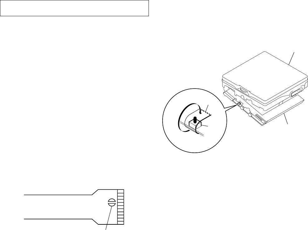
laser-tap
OPTICAL PICK-UP FLEXIBLE BOARD
SECTION 1
SERVICING NOTES
• When repairing this device with the power on, if you remove
the MAIN board or open the upper panel assy, this device stops
working.
In this case, you can work without the device stopping by fas-
tening the hook of the open/close detect switch (S801) with tape.
• This set is designed to perform automatic adjustment for each
adjustment and write its value to EEPROM. Therefore, when
EEPROM (IC802) has been replaced in service, be sure to per-
form automatic adjustment and write resultant values to the new
EEPROM.
(Refer to Section 5 Electrical Adjustment. (page 18))
• Replacement of CXD2660GA (IC502) and CXR701080-013GA
(IC801) used in this set requires a special tool. Therefore, they
cannot be replaced.
tape
S801 MAIN board
upper panel assy
– 4 –
SECTION 2
GENERAL
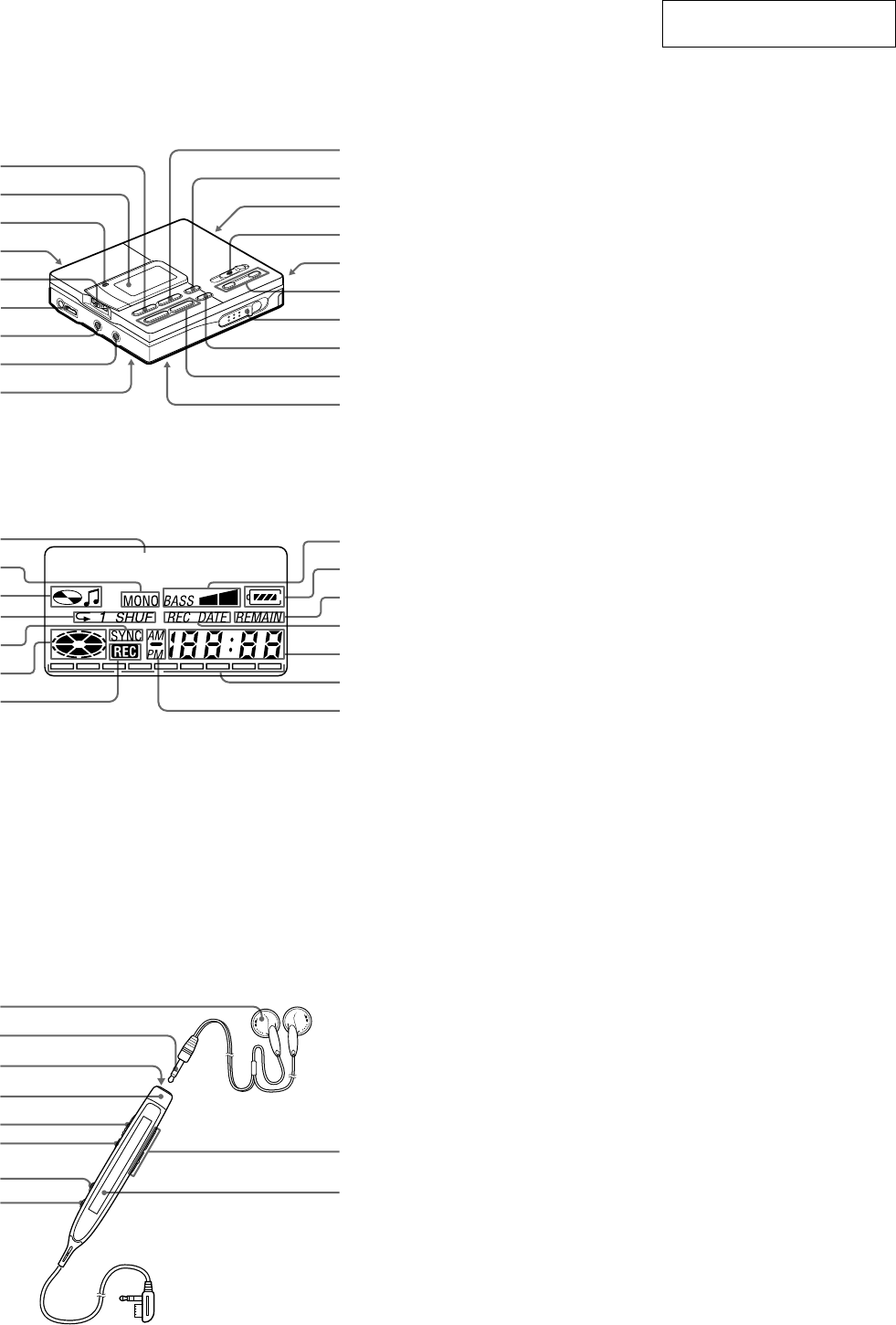
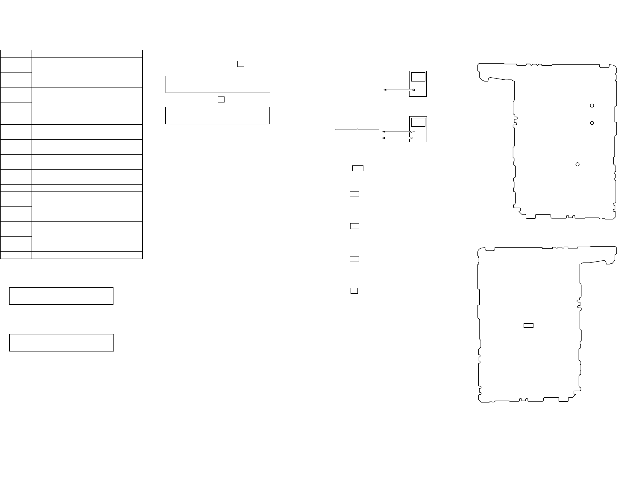
• LOCATION OF CONTROLS
– The recorder –
1
2
3
5
4
6
7
8
9
qd
0
qa
qs
qf
qg
ql
qh
qj
qk
1
9
2
3
4
5
6
7
80
1
3
2
6
7
0
8
9
qa
qs
qd
qf
5
4
1x (stop) /CHARGE button
2Display window
3REC indicator
4DC IN 3V jack
5Jog lever
6i/LINE OUT (headphones/line out) jack
7MIC (PLUG IN POWER) jack
8LINE IN (OPTICAL) jack
9HOLD switch
Slide to lock the controls of the recorder.
0N (play) button
qa X (pause) button
qs T MARK (track mark) button
qd REC (record) switch
qf Battery compartment
qg VOL (volume) +/– buttons
qh OPEN switch
qj END SEARCH button
qk ./> (search/AMS) buttons
ql SYNCHRO REC (synchro-recording)
ON/OFF switch
1Character information display
Displays the disc and track name*,
date, error messages, track numbers,
etc.
* Disc and track names appear only
with MDs that have been
electronically labeled.
2MONO(monaural) indication
3Disc name/track name indications
Appears when labeling disc or track
respectively.
4Play mode indication
Shows the play mode of the MD.
F (all repeat): All tracks play
repeatedly.
F 1(single repeat): One track plays
repeatedly.
F SHUF(shuffle repeat): Tracks will
be repeated in random
order.
5SYNC (synchro-recording) indication
Lights up while synchro-recording.
6Disc indication
Shows that the disc is rotating for
recording, playing or editing an MD.
7REC indication
Lights up while recording. Flashes
when standing by for recording.
– The headphones with a remote control (RM-MZ2S) –
8Mega bass indication
9Battery indication
Shows approximate battery condition.
While charging the rechargeable
battery, this indication shows the
charging condition.
0REMAIN (remaining time/tracks)
indication
Lights up along with the remaining
time of the track, remaining time of the
MD, or remaining number of tracks.
qa REC DATE (recorded/current date)
indication
Lights up along with the date and time
the MD was recorded. When only
“DATE” lights up, the current date
and time are displayed.
qs Time display
Shows the elapsed time of the track
being recorded or played.
qd Level meter
Shows the level of the MD being
played or recorded.
qf AM/PM indication
Lights up along with the time
indication in the 12-hour system.
1Headphones
Can be replaced with optional headphones.
2Stereo mini plug
3x (stop) button
4Control
To play, press the control towards
N•> during stop. Press the
control towards N•> during play
to search the beginning of the
succeeding track; hold in this position
to fast-forward. Press towards .
during play to search the beginning of
the preceeding track; hold in this
position to rewind.
5HOLD switch
Slide to lock the controls of the remote
control.
6X (pause) button
7PLAY MODE button
8DISPLAY button
9VOL (volume) +/– buttons
When the AVLS is set to on, you
cannot increase the volume to the
maximum. To increase the volume
above the limited level, set the AVLS
to off using the jog lever.
0Display window
– The display window of the recorder –
This section is extracted from
instruction manual.
– 5 –
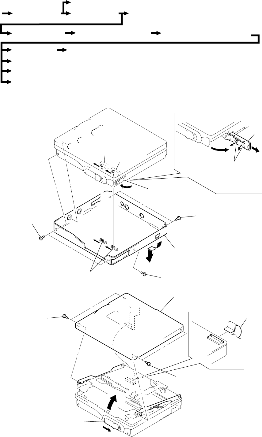
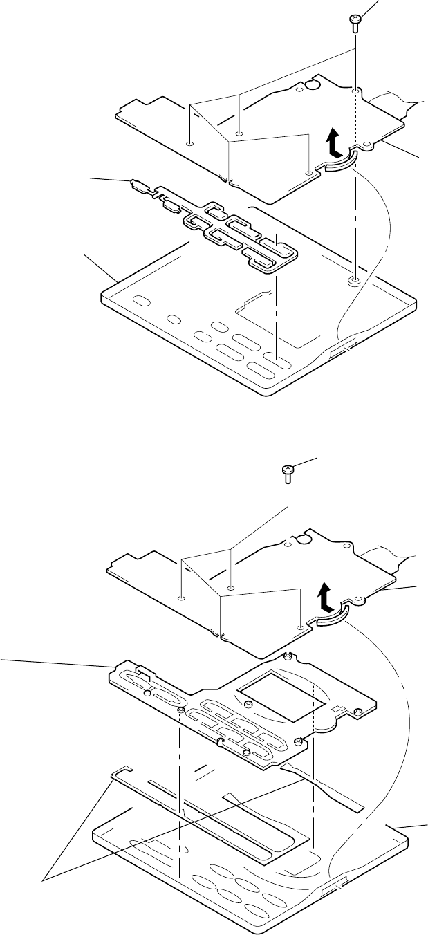
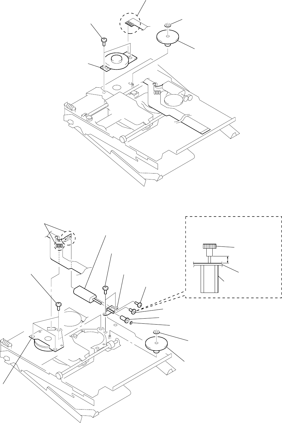
PANEL ASSY, BOTTOM
Note: Follow the disassembly procedure in the numerical order given.
SECTION 3
DISASSEMBLY
• This set can be disassembled in the order shown below.
Upper Panel Section
Main Board, “Case Assy, Battery”
LCD Module, “Button, Control”, “Service Assy, Upper Panel” (R90/R91)
Main Board, “Case Assy, Battery” “Chassis Assy, Set”,
MD Mechanism Deck (MT-MZR90-165)
Panel Assy, Bottom
Set
Belt Assy, Ornamental
Service Assy, OP
Motor Flexible Board
Motor, DC (Sled) (M602)
“Motor, DC SSM-01C14A (Spindle) (M601)”, “Motor, DC (Over Write Head Up/Down) (M603)”
Holder Assy
4two screws
(1.4)
1flexible boar
d
(CN801)
5upper panel section
4two screws
(1.4)
2knob (open)
3
UPPER PANEL SECTION
Note: On installation of bottom
panel assy, adjust the posi-
tion of both two switches
(S804, S807) and two
knobs (hold).
S807
S804
4Close the
battery terminal (plus).
5two screws
(1.4)
1Open the
battery case lid.
3battery case li
d
6Remove the bottom panel assy
in the direction of arrow A.
A
5two screws
(1.4)
knob (hold) 5screw (1.4)
2two claws
– 6 –
•MZ-R91
1five screws
(1.4)
2LCD modul
e
3control button
4upper panel service assy
1five tapping screws
(1.7)
2LCD module
5upper panel service ass
y
3control button
4adhesive sheet
(control button)
Note: The control buttons are stuck with
strong adhesive sheets.
As the control buttons are very fragile,
do not peel them off forcibly.
Note: Also replace the adhesive sheets (control button),
when replacing the control buttons and upper panel
service assy.
LCD MODULE, “BUTTON, CONTROL”, “SERVICE ASSY, UPPER PANEL”
•MZ-R90
– 7 –
)
)
)
)
@
@
^
6Remove the ornamental belt assy
in the direction of arrow C.2Open toward the direction B
to disengage two bosses
and convex portions pointed
with *.
1Pull toward the direction A
to disengage two bosses .
Note: As the ornamental belt assy
is very fragile, do not give an
excessive force to the entire
assy when removing it.
C
B
A
A
B
3three bosses
4knob (open)
2Open toward the direction B
to disengage two bosses
and convex portions pointed
with *.
boss boss
boss
boss
5two bosses
BELT ASSY, ORNAMENTAL
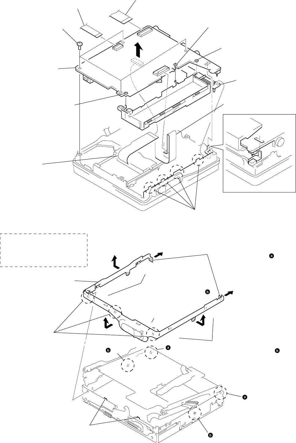
MAIN BOARD, “CASE ASSY, BATTERY”
3four toothed lock screws
(M1.4)
2flexible board (over write head)
(CN601)
2flexible board (LCD module)
(CN801)
Note: Before removing the flexible board
from CN501, be sure to solder the
flexible board.
(Refer to servicing notes (NOTES ON
HANDLING THE OPTICAL PICK-UP
BLOCK (LCX-2R)) page 3.)
1Remove the solder of
battery terminal (minus).
1Remove the solder of joint.
8batter case assy
7four bosses
2motor flexible board
(CN602)
5flexible board
(optical pick-up)
(CN501)
1Remove the solder of
battery terminal (plus).
6main board
4
– 8 –
2boss
3MD mechanism deck
(MT-MZR90-165)
2boss
4tension spring (arm)
5set chassis ass
y
1screw (1.4)
1screw (1.4)
8bearing
5screw
4rack spring
3precision pan screw
(M1.4)
1washer (0.8 - 2.5)
2gear (SA)
5screw
7Pull off the lead screw.
6
B
A
9Opening the over write head
toward the direction A, remove th
e
OP Service assy toward
the direction B.
Note: Do not open the entire assy
forcibly, when opening
the over write head.
over write head section
“CHASSIS ASSY, SET”, MD MECHANISM DECK (MT-MZR90-165)
SERVICE ASSY, OP
– 9 –
1Remove two solders of
DC motor (over write head up/down) (M603).
1Remove four solders of
DC motor (sled) (M602).
1Remove four solders of
DC motor (spindle) (M601).
DC motor (sled)
circular hole
3motor flexible board
2adhesive sheet
Note: Align a circular hole in the stripping paper
with a circular hole in the DC motor (sled),
when mounting the motor
flexible board.
5Remove the holder assy in the
direction of arrow C.
1Open the holder assy.
A
B
3
C
2Push the convex portion
toward the direction B and
open the holder assy toward
the direction A to erect uprightly.
4boss
HOLDER ASSY
MOTOR FLEXIBLE BOARD
– 10 –
4two precision pan screws
(M1.4)
5DC motor (sled) (M602)
1Remove four solders of
motor flexible board.
2washer (0.8 - 2.5)
3gear (SA)
1Remove six solders of
motor flexible board.
4three precision pan screws
(M1.4)
qa DC motor (over write head up/down)
(M603)
6two precision pan screws
(M1.4)
qs gear chassis assy
9screw
(M1.2 × 1.5)
0gear (HA)
8gear (HB)
7washer (0.8 - 2.5)
2washer (0.8 - 2.5)
3gear (HC)
5DC motor
(spindle)
(M601)
DC motor
(over write head up/down)
(M603)
gear chassis assy
gear (HA)
2.65 mm
Note: Press-fit the gear (HA) up to the
position of the DC motor (over write
head up/down) (M603) as shown
below.
MOTOR, DC (SLED) (M602)
“MOTOR, DC SSM-01C14A (SPINDLE) (M601)”,
“MOTOR, DC (OVER WRITE HEAD UP/DOWN) (M603)”
– 11 –
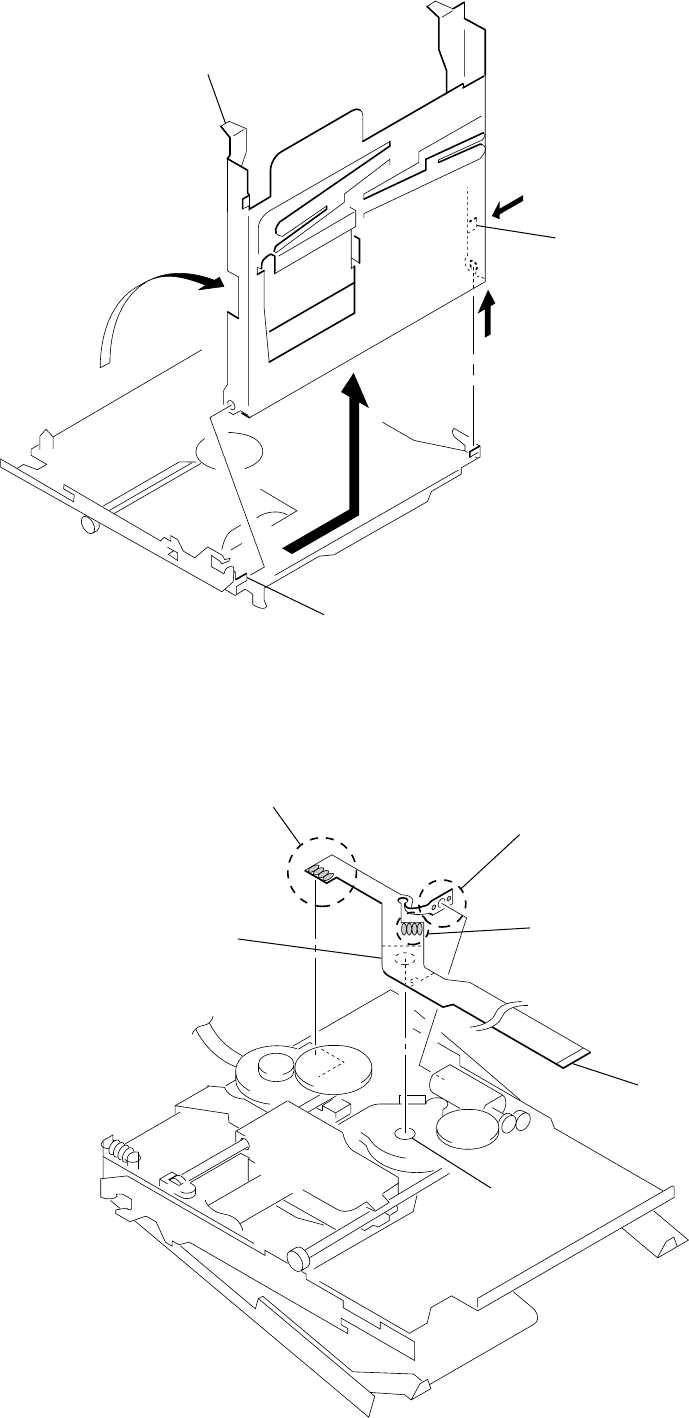
SECTION 4
TEST MODE
[Outline]
• This set provides the Overall adjustment mode (Assy mode) that
allows CD and MO disc to be automatically adjusted when in
the test mode. In this overall adjustment mode, the protect switch
is detected to judge the disc, CD or MO, and each adjustment is
automatically executed in order. If a fault is found, the system
displays its location. Also, the manual mode allows each indi-
vidual adjustment to be automatically adjusted.
• The keys in the description refer to the keys on both set and
remote commander unless otherwise specified. Though LCD
display shows the LCD of the remote commander, same con-
tents are also displayed on the LCD of the set.
[Setting Method of Test Mode]
There are two different methods to set the test mode:
1Short BP801 (TEST) on the MAIN board with a solder bridge
(connect pin y; of IC801 to the ground). Then, turn on the
power.
– MAIN BOARD (Conductor Side) –
2In the normal mode, turn on the HOLD switch on the set. While
pressing the Nkey on the set, press the following set keys
in the following order:
>t>t.t.t>t.t
> t.tXtX
[Operation in Setting the Test Mode]
• When the test mode becomes active, first the display check mode
is selected. (Press xkey once, when the display check mode
is not active.)
• Other mode can be selected from the display check mode.
• When the test mode is set, the LCD repeats the following dis-
play.
LCD display
•When the Xkey is pressed and hold down, the display at that
time is held so that display can be checked.
[Releasing the Test Mode]
For test mode set with the method 1:
Turn off the power and open the solder bridge on BP801 (TEST)
on the MAIN board.
Note: Remove the solders completely. Remaining could be shorted with
the chassis, etc.
For test mode set with the method 2:
Turn off the power.
Note: If electrical adjustment (see page 18) has not been finished com-
pletely, always start in the test mode. (The set cannot start in nor-
mal mode.)
Microprocessor
version
display
All off
All lit xxxxxxxxx
V0.000
888
001
F1SHUF
REC
BP801
Short: Test Mode
Open: Normal Mode
)(
– 12 –
[Configuration of Test Mode]
[Manual Mode]
Mode to adjust or check the operation of the set by function.
Normally, the adjustment in this mode is not executed.
• Transition method in Manual Mode
1. Setting the test mode. (See page 11)
2. Press the >or [VOL +] key activates the manual mode
where the LCD display as shown below.
3. The optical pick-up moves outward or inward while
the >or .key is pressed for several seconds respec-
tively.
4. Each test item is assigned with a 3-digit mode number;
100th place is a major item, 10th place is a medium item, and
unit place is a minor item.
[Manual Mode]
[Servo Mode]
[Audio Mode]
[Power Mode]
[OP Alignment Mode]
[Overall Adjustment Mode]
[Self-Diagnosis Display Mode]
Press the
>
or [VOL +] key
[Key Check Mode]
[Test Mode $Display Check Mode%]
Press the
x
key
Press the
x
key
Press the
x
key
Press the
x
key
Press the
.
or [VOL --] key
Press the
N
or [REC] key on the set
Move up the jog key on the set or
press the [DISPLAY] key
on the remote commander
Press the [T MARK] or [DISPLAY] key
on the remote commander for several seconds.
Quit the key check or open the upper panel
[Sound Skip Check Result Display Mode]
LCD display
Manual
000
[VOL +]
key:100th place of mode number
increase.
[VOL --]
key:100th place of mode number
decrease.
[Major item switching]
[VOL +]
key:10th place of mode number
increase.
[VOL --]
key:10th place of mode number
decrease.
[VOL +]
key:Increases the
adjusted value
[VOL --]
key:Decreases the
adjusted value
[Medium item switching]
N
key
x
key
[Minor item switching]
[Adjusted value variation]
X
key: When adjusted value is
changed:
Adjusted value is written.
When adjusted value is
not changed:
That item is adjusted
automatically.
[Adjusted value write]
N
key
N
key: Unit place of mode number
increase.
x
key
– 13 –
5. The display changes a shown below each time the jog key on
the set is turned up or [DISPLAY] key on the remote com-
mander is pressed.
However in the power mode (mode number 700’s), only the
power adjustment value is displayed.
6. Quit the manual mode, and press xkey to return to the test
mode (display check mode).
AD 85
731
• Power Supply Adjusted Value
LCD display
mode number
fixed display
adjusted value
[Overall Adjustment Mode]
Mode to adjust the servo automatically in all items.
Normally, automatic adjustment is executed in this mode at the
repair.
Adjust the CD first, when performing adjustment.
•Configuration of overall adjustment
For further information, refer to the Section 5 Electrical Adjust-
ment. (See page 18)
• Address & Adjusted Value Display
LCD display
• Jitter Value & Adjusted Value Display
LCD display
• Block Error Value & Adjusted Value Display
LCD display
• ADIP Error Value & Adjusted Value Display
LCD display
• Item Title Display
LCD display
C68S01
011
063B01
011
059A01
011
LrefPw 01
011
0FFJ01
011
mode number
address
adjusted value
mode number
jitter value
adjusted value
mode number
block error value
adjusted value
mode number
ADIP error value
adjusted value
adjusted value
mode number
item title
> key . key
> key
Title
display
CD overall
adjusting
CD overall
adjustment
OK
MO overall
adjusting
MO overall
adjustment
OK
CD overall
adjustment
NG
MO overall
adjustment
NG
N key
protect switch ON
All item
OK
protect switch OFF
NG item exists
or x key
NG item exists
or x key
x key
x key
x key
x key
[Test mode $display check mode%]
– 14 –
[Sound Skip Check Result Display Mode]
This set can display and check the error count occurring during
record and play.
• Setting method of Sound Skip Check Result Display
Mode
1. Setting the test mode. (See page 11)
2. Press the Nor [REC] key on the set activates the sound skip
check result display mode where the LCD displays as shown
below.
If microprocessor version is 1.20
When Nkey is pressed:
When [REC] key on the set is pressed:
If microprocessor version is 1.30 or later
When Nor [REC] key on the set is pressed:
3. When Nkey is pressed, the total of error count is displayed
on the LCD, and each time the >key is pressed, the error
count descents one by one as shown below. Also,
when .key is pressed, the error count ascends by one. If
[REC] key on the set is pressed, the error count during record
is displayed.
**
: Sound skip check items counter (hexadecimal)
######
: 6-digit address (hexadecimal) where a sound skipped
last
LCD display
Stat**
000
LCD display
Rtry**
000
Total of play system error count
Total of record system error count
LCD display
P**R**
000
Total of play system error count
Total of record system
error count
######
000
EIB **
000
Stat**
000
BEmp**
000
If microprocessor version is
1.20.
Stat**
000
Adrs**
000
BEmp**
000
######
000
P**R**
000
EIB **
000
If microprocessor version is
1.30 or later.
4. When [REC] key on the set is pressed, the total of error count
is displayed on the LCD, and each time the >key is
pressed, the error count descents one by one as shown below.
Also, when .key is pressed, the error count ascends by
one. If Nkey is pressed, the error count during play is dis-
played.
**
: Sound skip check items counter (hexadecimal)
######
: 6-digit address (hexadecimal) where a sound skipped
last
Error code
Cause of error Description of error
EIB Sound error correction error
Playback Stat Decorder status error
Adrs Cannot access the address
BEmp Buffer becomes empty
BOvr Buffer becomes full and sounds are
dumped
Recording BFul Buffer capacity lowers and data are
forcibly written
Rtry Retry count over
5. Quit the sound skip check result display mode, and press
the xkey to return to the test mode (display check mode).
Bful**
000
Rtry**
000
######
000
P**R**
000
BOvr**
000
BOvr**
000
Bful**
000
Rtry**
000
######
000
If microprocessor version is
1.20.
If microprocessor version is
1.30 or later.
– 15 –
[Self-Diagnosis Display Mode]
•This set uses the self-diagnosis system in which if an error oc-
curs in recording/playback mode, the error is detected by the
model control and power control blocks of the microprocessor
and information on the cause is stored as history in EEPROM.
By viewing this history in test mode, it helps you to analyze a
fault and determine its location.
Total recording time has been recorded as optical pick-up using
time, and it is compared with the total recording time in the
self-diagnosis display mode to find when an error occurred.
Clear both total recording time and the time in self-diagnosis
display mode, when the optical pick-up was replaced.
1. Setting the test mode. (See page 11)
2. Move up the jog key on the set or press the [DISPLAY] key on
the remote commander activates the self-diagnosis display mode
where the LCD display as shown below.
3. Then, each time >key is pressed, LCD display descends
by one as shown below. Also, the LCD display ascends by one
when . key is pressed.
4. Quit the self-diagnosis display mode, and press the xkey to
return to the test mode (display check mode).
LCD display
** : Self-Diagnosis Data
1st0**
000
history code
1st0**
000
1st1**
000
1st2**
000
N 0**
000
N 1**
000
N 2**
000
N-10**
000
N-11**
000
N-12**
000
N-20**
000
N-21**
000
N-22**
000
R ####
000
1
1
– 16 –
• Description of Indication History
History code number Description
1st0 The first error
1st1 Total recording time when 1st0 was generated (Higher rank byte)
1st2 Total recording time when 1st0 was generated (Lower rank byte)
N 0 The last error
N 1 Total recording time when N 0 was generated (Higher rank byte)
N 2 Total recording time when N 0 was generated (Lower rank byte)
N-10 One error before the last.
N-11 Total recording time when N-10 was generated (Higher rank byte)
N-12 Total recording time when N-10 was generated (Lower rank byte)
N-20 Two errors before the last.
N-21 Total recording time when N-20 was generated (Higher rank byte)
N-22 Total recording time when N-20 was generated (Lower rank byte)
REC Total recording time *
• Description of Error Indication Codes
[Clearing Self-Diagnosis Data and Total Recording Time]
1. Setting the test mode. (See page 11.)
2. Move up the jog key on the set or press the [DISPLAY] key on the remote commander activates the self-diagnosis display mode.
3. Press the Xkey or [REC] key on the set during display of self-diagnosis data when clearing the self-diagnosis data, or during display of
total recording time when clearing the total recording time. Thus, “ClrOK?” will be displayed on the LCD, and press the same key again,
and when self-diagnosis data is cleared “ErrCLR” is displayed and the data is cleared. Also when total recording time is cleared, “ ReeT
O” is displayed and it is cleared.
* Total recording time
Total recording time is recorded in
minutes. It is recorded in hexadecimal
format and up to 65,535 min. can be
counted. It returns to “0000h” when
recorder goes beyond this limit.
Problem Indication code Meaning of code Description
No error 00 No error
01 Illegal access target address Attempt to access an abnormal address
was specified
Servo error 02 High temperture High temperture
03 Focus error Forcus could not be applied
04 Spindle error Abnormal lotation of disc
21 Initial low battery Abnormal voltage at initialization
Power error 22 Low battery Momentary interruption detected
23 Low battery NI Momentary interruption detected (NiMH)
24 Low battery AM Momentary interruption detected (AM)

– 17 –
[Key Check Mode]
This set can check if the set and remote commander function nor-
mally.
•Setting Method of Key Check Mode
1. Setting the test mode. (See page 11)
2. Press the [T MARK] or [DISPLAY] key on the remote com-
mander for several seconds activates the key check mode where
all segments of LCD turn OFF. (At the last two digits of DOT
section, AD value of remote commander key line is displayed
in hexadecimal)
3. When each key is pressed, it is displayed on the LCD, imply-
ing that it was successfully checked as shown below. How-
ever, for the slide switch on the set, it is not checked unless it
is reciprocated.
* The key pressed to enter the key check mode was already
checked at that time.
Set key
Key Indication
NPLAY
>FF
.FR
XPAUSE
VOL + VOL +
VOL –VOL –
xSTOP
REC REC
END SEARCH END S
Jog (up) JOG+
Jog (down) JOG–
Jog (push) PUSH
T MARK T MARK
HOLD (hold) HLDon
HOLD (off) HLDoff
SYNCHRO REC (on) SYCon
SYNCHRO REC (off) SYCoff
Remote commander key
Key Indication
N/>rPLAY
.rFR
XrPAUSE
VOL + rVOL +
VOL –rVOL –
xrSTOP
PLAYMODE rPMODE
DISPLAY rDISP
4. The test mode (display check mode) is automatically activated
when all keys on the set and remote commander were checked
(see above). Also, the test mode (display check mode) gets
back if opening the upper panel during a key check.

– 18 –
SECTION 5
ELECTRICAL ADJUSTMENTS
[Outline]
• In this set, automatic adjustment of CD and MO can be per-
formed by entering the test mode. (See page 11)
However, before starting automatic adjustment, the memory
clear, power adjustment and temperature adjustment must be
performed in the manual mode.
• The keys in the description refer to the keys on both set and
remote commander unless otherwise specified.
Though LCD display shows the LCD of the remote commander,
same contents are also displayed on the LCD of the set.
[Precautions for Adjustment]
1. Adjustment must be done in the test mode only.
After adjusting, release the test mode.
2. Use the following tools and measuring instruments.
• Test CD disc TDYS-1
(Part No. : 4-963-646-01)
Available SONY CD disc
• Recorded MO disc PTDM-1
(Part No. : J-2501-054-A)
Available SONY MO disc (recorded)
• Laser power meter LPM-8001
(Part No. : J-2501-046-A)
• Digital voltmeter
3. Unless specified otherwise, supply DC 3V from the DC IN 3V
jack.
4. Switch position
HOLD switch ................ OFF
[Adjustment Sequence]
Adjustment must be done with the following steps.
1. NV Reset (Memory clear)
r
2. Power Supply Manual Adjustment Manual Mode
r
3. Temperature correction
r
4. CD Overall Adjustment
rOverall Mode
5. MO Overall Adjustment
[NV Reset]
• Setting method of NV reset
1. Select the manual mode of test mode, and set mode num-
ber 021NV Reset.
2. Press the Xkey.
3. Press the Xkey once more.
rNV reset (after several seconds)
4. Quit the manual mode, and activate the test mode.
[Power Supply Manual Adjustment]
• Adjustment sequence
Adjustment must be done with the following steps.
1. VC PWM Duty (L) adjustment (mode number: 762)
r
2. VREM PWM Duty (H) adjustment (mode number: 763)
r
3. VREM PWM Duty (L) adjsutment (mode number: 764)
r
4. VC PWM Duty (H) adjustment (mode number: 765)
r
5. VREM PWM Duty (H) adjustment (mode number: 766)
r
6. VREM PWM Duty (L) adjustment (mode number: 767)
LCD display
ResNV
021
LCD display
ResOK?
021
LCD display
Res***
021
Reset!
021
– 19 –
• Adjustment method of VC PWM Duty (L)
(mode number: 762)
1. Select the manual mode of the test mode, and set the mode
number 762. (See page 12)
2. Connect a digital voltmeter to the TP915 (VC) on the MAIN
board, and adjust [VOL +] key (voltage up) or [VOL --] key
(voltage down) so that the voltage becomes 2.5 ± 0.02 V.
Proceed to the next step without pressing Xkey if voltage is
already adjusted.
3. Press the Xkey to write the adjusted value.
• Adjustment method of VREM PWM Duty (H)
(mode number: 763)
1. Select the manual mode of the test mode, and set the mode
number 763. (See page 12)
2. Connect a digital voltmeter to the TP914 (VR) on the MAIN
board, and adjust [VOL +] key (voltage up) or [VOL --] key
(voltage down) so that the voltage becomes 2.75 ± 0.02 V.
Proceed to the next step without pressing Xkey if voltage is
already adjusted.
3. Press the Xkey to write the adjusted value.
• Adjustment method of VREM PWM Duty (L)
(mode number: 764)
1. Select the manual mode of the test mode, and set the mode
number 764. (See page 12)
2. Connect a digital voltmeter to the TP914 (VR) on the MAIN
board, and adjust [VOL +] key (voltage up) or [VOL --] key
(voltage down) so that the voltage becomes 2.5 ± 0.02 V.
Proceed to the next step without pressing Xkey if voltage is
already adjusted.
3. Press the Xkey to write the adjusted value.
VclPWM
762
LCD display
digital
voltmeter
MAIN board
TP915 (VC)
TP5105 (GND)
VrhVcl
763
LCD display
digital
voltmeter
MAIN board
TP914 (VC)
TP5105 (GND)
VrlVcl
764
LCD display
digital
voltmeter
MAIN board
TP914 (VC)
TP5105 (GND)
• Adjustment method of VC PWM Duty (H)
(mode number: 765)
1. Select the manual mode of the test mode, and set the mode
number 765. (See page 12)
2. Connect a digital voltmeter to the TP915 (VC) on the MAIN
board, and adjust [VOL +] key (voltage up) or [VOL --] key
(voltage down) so that the voltage becomes 2.75 ± 0.02 V.
Proceed to the next step without pressing Xkey if voltage is
already adjusted.
3. Press the Xkey to write the adjusted value.
• Adjustment method of VREM PWM Duty (H)
(mode number: 766)
1. Select the manual mode of the test mode, and set the mode
number 766. (See page 12)
2. Connect a digital voltmeter to the TP914 (VR) on the MAIN
board, and adjust [VOL +] key (voltage up) or [VOL --] key
(voltage down) so that the voltage becomes 2.75 ± 0.02 V.
Proceed to the next step without pressing Xkey if voltage is
already adjusted.
3. Press the Xkey to write the adjusted value.
• Adjustment method of VREM PWM Duty (L)
(mode number: 767)
1. Select the manual mode of the test mode, and set the mode
number 767. (See page 12)
2. Connect a digital voltmeter to the TP914 (VR) on the MAIN
board, and adjust [VOL +] key (voltage up) or [VOL --] key
(voltage down) so that the voltage becomes 2.5 ± 0.02 V.
Proceed to the next step without pressing Xkey if voltage is
already adjusted.
3. Press the Xkey to write the adjusted value.
VchPWM
765
LCD display
digital
voltmeter
MAIN board
TP915 (VC)
TP5105 (GND)
VrhVch
766
LCD display
digital
voltmeter
MAIN board
TP914 (VC)
TP5105 (GND)
VrlVch
767
LCD display
digital
voltmeter
MAIN board
TP914 (VC)
TP5105 (GND)
– 20 –
[Temperature Correction]
• Adjustment Method of temperature correction
1. Select the manual mode of test mode, and set the mode num-
ber 014. (See page 12)
2. Measure the ambient temperature.
3. Adjust with [VOL +], [VOL --] key so that the adjusted value
(hexadecimal value) becomes the ambient temperature.
(Initial value: 14h = 20 °C, Adjusting range: 80h to 7fh (–128
°C to +127 °C)
4. Press the Xkey to write the adjusted value.
[Overall Adjustment Mode]
• Adjustment Method of Overall Adjustment Mode
1. Setting the test mode. (See page 11)
2. Press the .or [VOL --] key activates the overall adjust-
ment mode where the LCD display as shown below.
3. Insert the CD test disc TDYS-1 (Parts No.4-963-646-01) or
an available SONY CD disc.
4. Press Nkey. The system discriminates between CD and MO
and performs automatic adjustment for CD.
Also, if .key is pressed, CD is adjusted automatically.
SetTmp
014
LCD display
LCD display
ASSY**
000
: (DISC MARK) When power adjustment “H” finished;
Outward ON
When power adjustment “L” finished;
Inward ON
Power supply is not yet adjusted unless both outward
and inward disc marks are ON.
Note: Disc mark is displayed on the remote commander
LCD only.
** : Left side = MO auto adjustment information
F : Auto adjustment finished
1 : Manual adjustment remains
0 : Not adjusted yet
Right side = CD auto adjustment information
F : CD auto adjustment finished
1 : Manual adjustment remains (not auto adjustment
)
0 : Not adjusted yet
LCD display
CD RUN
%%%
%%%: Manual mode number being executed
LCD display
CD OK
341
LCD display
###: Overall adjustment. NG mode number
### NG
LCD display
%%%: Manual mode number being executed
MO RUN
%%%
•CD Automatic Adjustment item
Mode No. Description
312
313 CD electrical offset adjustment
314
328 CD TWPP gain adjustment
321 CD tracking error gain adjustment
323 CD tracking error offset adjustment
332
336 CD ABCD level adjustment
344 CD focus gain adjustment
345 CD tracking gain adjustment
521 CD two-axis sensibility adjustment
522
341 CD focus bias adjustment
5. If the result of automatic adjustment is OK, the following dis-
play appears in the LCD:
6. If the result of automatic adjustment is NG, the following dis-
play appears in the LCD:
7. If NG, set the manual mode. Perform automatic adjustment
for the items not accepted. (See page 12)
8. If CD adjustment is OK, insert an available SONY MO disc
(recorded).
At this time, be sure to turn OFF the disc protect switch.
9. Press Nkey. The system discriminates between CD and MO
and performs automatic adjustment for the MO disc.
Also, if >key is pressed, MO is adjusted automatically.
However, when CD adjustment is not finished, “SetCD!” is
blinking on the LCD and MO adjustment is not executed.
– 21 –
[Laser Power Check]
Connection :
Check Method :
1. Select the manual mode of test mode, and set the laser power
adjusting mode. (mode number 010)
2. Press the .key continuously until the optical pick-up
moves to the most inward track.
3. Open the cover and set the laser power meter on the objective
lens of the optical pick-up.
4. Press the Nkey, and set the laser MO read adjustment mode.
(mode number 011)
5. Check that the laser power meter reading is 0.81 ± 0.08 mW.
6. Check that the voltage both ends of resitor R1005 at this time
is below 44 mV.
7. Press the Nkey, and set the laser CD read adjustment
mode. (mode number 012)
8. Check that the laser power meter reading is 0.97 ± 0.10 mW.
9. Check that the voltage both ends of resitor R1005 at this time
is below 44 mV.
10. Press the Nkey, and set the laser MO write adjustment mode.
(mode number 013)
11. Check that the laser power meter reading is 4.95 ± 0.50 mW.
12. Check that the voltage both ends of resister R1005 at this time
is below 80 mV.
13. Press the xkey.
14. Release the test mode.
digital voltmeter
MAIN board
laser
power meter
Optical pick-up
objective lens
Both ends of R1005
Connecting Location:
– MAIN BOARD (Component Side) –
TP914
(VR)
TP915
(VC)
TP5105
(GND)
– MAIN BOARD (Conductor Side) –
(+) (–)
R1005
10. If the result of automatic adjustment is OK, the following dis-
play appears in the LCD:
11. If the result of automatic adjustment is NG, the following dis-
play appears in the LCD:
12. If NG, set the manual mode. Perform automatic adjustment
for the items not accepted. (See page 12)
13. To clear the data in overall adjustment mode, set the manual
mode and change the mode number 021 (Res NV) to reset the
NV. (See page 12)
LCD display
MO OK
141
Resume
043
LCD display
ResClr
043
LCD display
### NG
###: Overall adjustment. NG mode number
•MO Automatic Adjustment item
Mode No. Description
112
113 MO electrical offset adjustment
114
118
221 Lower reflection CD tracking error gain adjustment
223 Lower reflection CD tracking error offset adjustment
232
236 Lower reflection CD ABCD level adjustment
244 Lower reflection CD focus gain adjustment
245 Lower reflection CD tracking gain adjustment
121 MO tracking error gain adjustment
122 MO tracking error offset adjustment
134 MO TWPP gain adjustment
131 MO double speed read TWPP offset adjustment
132
136 MO ABCD level adjustment
144 MO focus gain adjustment
145 MO tracking gain adjustment
434 MO write TWPP gain adjustment
431 MO write TWPP offset adjustment
432
436 MO write ABCD level adjustment
445 MO write tracking gain adjustment
411 MO normal speed read TWPP offset adjustment
412
448 32 cluster full recording
141 MO focus bias adjustment
14. When both CD and MO overall adjustments are OK, set the
manual mode and clear the clock data.
For the microprocessor version 1.20 or later, set the mode num-
ber 043 (Resume), and press the Xkey.
rPress the Xkey, historical data clear
Note: In step 10, set the clock data to 99Y11M11D11H11M00S,
and in step 14, do not set the clock.
– 22 –
MZ-R90/R91
– 23 – – 24 –
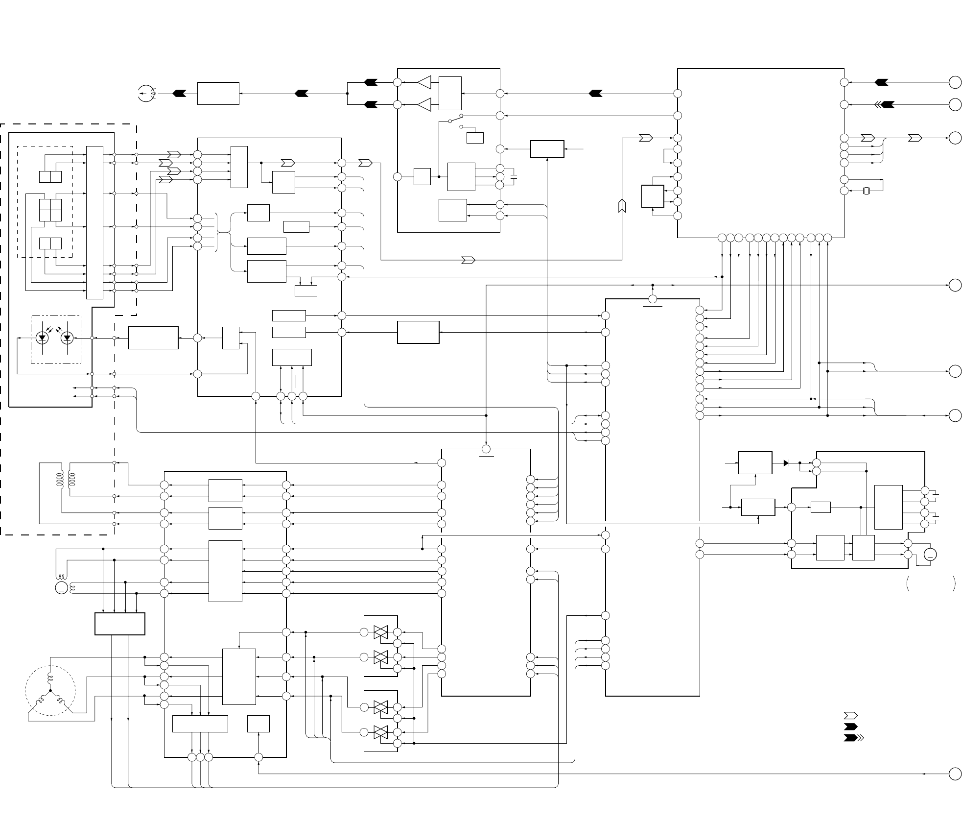
SECTION 6
DIAGRAMS
6-1. BLOCK DIAGRAM – SERVO Section –
WV
U
OVER WRITE HEAD DRIVE
IC603
DIGITAL SIGNAL PROCESSOR,
EFM/ACIRC ENCODER/DECODER,
SHOCK PROOF MEMORY CONTROLLER,
ATRAC ENCODER/DECODER,
16M BIT D-RAM
IC502 (1/2)
RF AMP, FOCUS/TRACKING ERROR AMP
IC501
FOCUS/TRACKING COIL DRIVE,
SPINDLE/SLED MOTOR DRIVE
IC601
SPINDLE SERVO DRIVE
SWITCH
IC504, 505
DIGITAL SERVO
SIGNAL
PROCESSOR
IC502 (2/2)
05
D
(Page 25)
F
(Page 25)
G
(Page 27)
OE
• SIGNAL PATH
: REC (ANALOG IN)
: PLAY (ANALOG OUT)
: REC (DIGITAL IN)
VMC
VMAB
VC
IN2
IN1
OUTB
C2H
C2L
C1H
C1L
OUTA
D603
X501
22.5792MHz
ADDT
DIN1
RESET
A
(Page 25)
ANALOG REC
OFTRK
MODE2
MODE1
EFMO
SLCU
SLD MON 1
TFDR
TRDR
FFDR
FRDR
SLDU
SLDV
SLVS
SLDW
SLCW
IC504
IC505
M602
(SLED)
M601
(SPINDLE)
FI3
RI3
FO3
RO3
FO1
RO1
OVER WRITE
HEAD B+
HB
EFM
CK
C1L
VGH
C1H
HA
COSC
TE
OFTRK
RF
PEAK
BOTM
ABCD
FE
B
A
D
C
JX
JY
IY
IX
PD-O
PD-NI
JX
JY
B
A
IY
IX
LD-A
MON
PD S0
PD S1
D
C
DETECTOR
OVER WRITE
HEAD DRIVE
Q601, 602
B+ SWITCH
Q603, 604
VC B+
BATT B+
FILTER
HR601
OVER WRITE HEAD
MNT2
MODE3
CPWO
CPVO
SLCU
SLCV
SPCW
SPCV
SPCU
SPDL PWM
CLV U
CLV V
CLV W
CPUO
MODE1
MODE2
SBUS
SCK
DATA
CLK
PD-I
8
7
14
5
6
12
11
3
2
13
1
31
30
20
19
41
33
DADT
DADT, XBCK,
LRCK, FS256
42
XBCK 45
LRCK 43
FS256
OSCO
OSCI
46
10
2
FS4
RFI
84
85
86
99
87
96
12
2 1
7
21
22
FI1
RI1
16
15
FI2 14
RI2 13
PWM24 25
FI4 23
RI4 24
SPVS
SPDU
SPDV
128
129
127
124
110
APCREF
106
123
113
103
102
109
111
112
133
138
SLCV 139
SPCU 130
SPCV 131
SPCW 132
134
141
135
140
SPDW
30
7
5
FO2
11
RO2
9
FO4
26
RO4
28
32
17
16
18
19
21
22
23
VIN 24
23 24 25
19
29
28
33
78
FILI
81
PCO
80
CLTV
83
FILO
82
4
FOK
MNT1
51
3
XSHOCK
MNT3
52
5
SQSY
DQSY
54
14
DQSY
SQSY
53
13
XINT
XINT
55
16
TX
SENS
6
11
XLAT
XLAT
8
8
SENSE
TX
5
XCS DSP 9
SI0 11
SO0 12
SCK0
HD CON 2
HD CON 1
13
17
DIN0
SRDT
6
SWDT
7
SCLK
SRDT
SRDT, SWDT,
SCLK
SWDT
SCLK
E
(Page 27)
SWDT, SCLK
SWDT
SCLK
32
ASYO
74
ASYI
75
14
10
11
41
ADFG
TE
15
RECP
PEAK
BOTM
ABCD
FE
ADFG
21
42
1
26
10
11
8
9
14
12
6
5
20
18
JX JY
I-V
AMP
IX IY
CB
DA
TRK+
TRK–
FCS+
FCS–
LD
PD
LASER DIODE
AUTOMATIC
POWER CONTROL
Q1001
SLED VOLTAGE
MONITOR
IC604
LOW-PASS
FILTER SWITCH
Q501
RF
AMP
ABCD
AMP
TON
PEAK/
BOTM
EFM
LOGIC
SAW.
GEN.
CHARGE
PUMP
OVER WRITE HEAD
UP/DOWM MOTOR DRIVE
IC602
SYSTEM CONTROLLER
IC801 (1/3)
LVDET CHARGE
PUMP
MOTOR
DRIVE
CONTROL
LOGIC
CONTROL
LOGIC
OSC
FOCUS
ERROR AMP
ADIP
S-MON 43
WPPLPF 3
S-MONITOR
TPP/WPP
SERIAL
INTERFACE
TRACKING
COIL DRIVE
FOCUS
COIL DRIVE
SLED
MOTOR
DRIVE
PWMI 3
UI 2
VI 1
WI
OE
48
1734 35 36
UO
46 CPUI
40
CPVI
39
CPWI
38
VO
44
WO
42
SPINDLE
MOTOR
DRIVE
SPINDLE VOLTAGE
MONITOR BIAS
APC
TRACKING
ERROR AMP
XRST
XRST
68
XIC RST
B
(Page 25)
C
(Page 25)
DIGITAL REC
2-AXIS
DEVICE
OPTICAL PICK-UP BLOCK
(LCX-2R)
(FOCUS)
(TRACKING)
M
56
3
21
7
56
3
35
WRPWR
7
PD S0
36
REC WBL SW
57
S MON
79
PD S1
38
MODE1
27
MODE2
SSB DATA
SSB CLK
28
MODE3
29
SPDL START SW
49
SPDL PWM
67
CLV U
24
CLV V
25
CLV W
26
B+ SWITCH
Q605
DC/DC
CONVERTER
IC605, Q607
MM
M603
OVER WRITE
HEAD UP/DOWM
MZ-R90/R91
– 25 – – 26 – – 27 – – 28 –
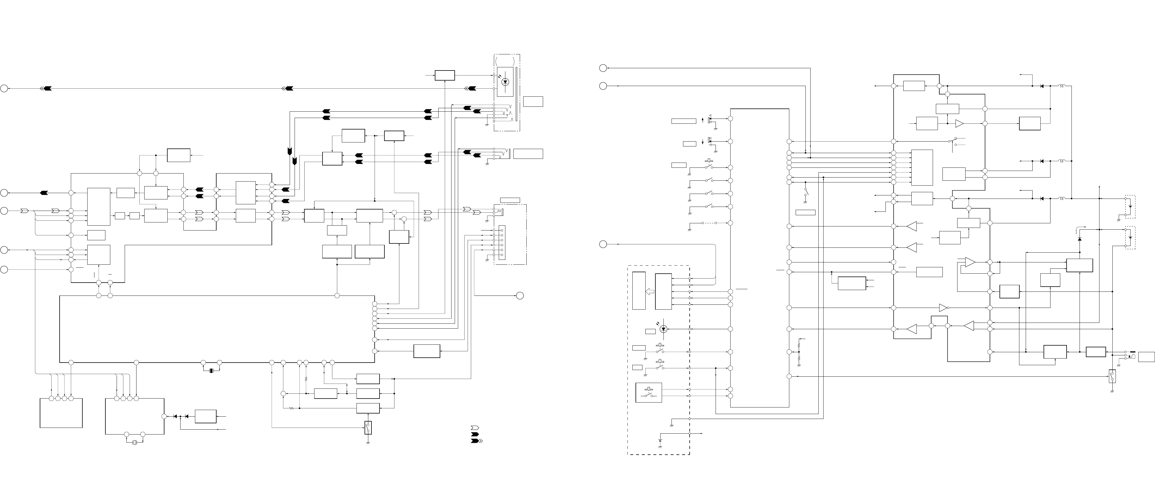
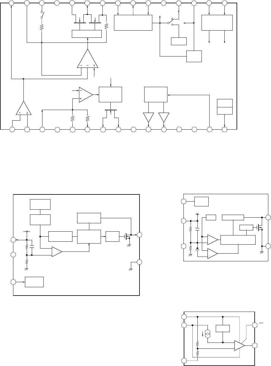
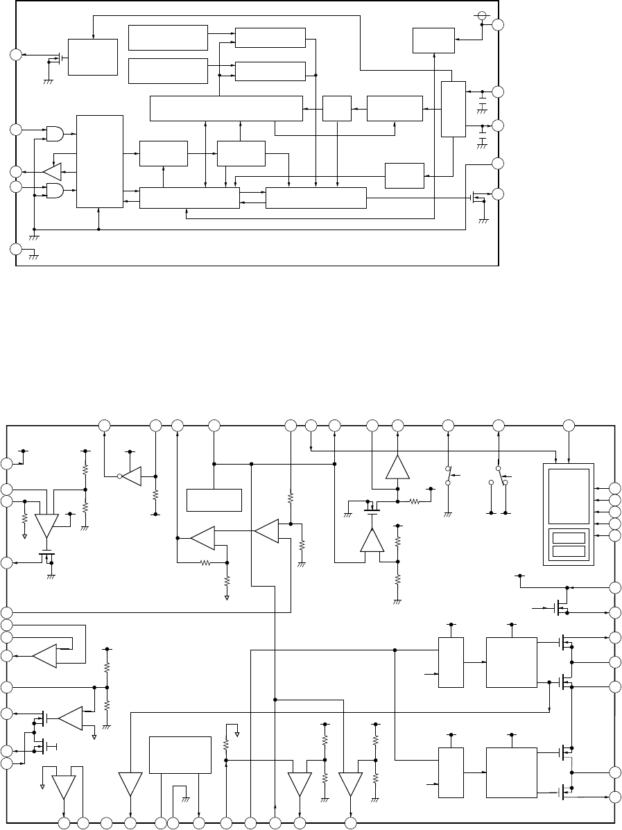
6-2. BLOCK DIAGRAM – A/D, D/A CONVERTER, AUDIO Section – 6-3. BLOCK DIAGRAM – KEY CONTROL/DISPLAY/POWER SUPPLY Section –
A/D, D/A CONVERTER
IC301
EEPROM
IC802
05
D
(Page 24)
F
(Page 24)
• SIGNAL PATH
: REC (ANALOG IN)
: PLAY (ANALOG OUT)
: REC (DIGITAL IN)
RESET
A
(Page 24) ANALOG REC
VR B+
VC B+
VC B+
B+ SWITCH
Q305, 306
B+ SWITCH
Q302
LINE AMP
IC302
LINE AMP
IC303
LINE OUT
ON/OFF SWITCH
Q101, 201
MUTING
Q101, 201
MUTING
CONTROL SWITCH
Q308
LINE OUT ON/OFF
CONTROL SWITCH
Q307, 309
CD TEXT COPY
DEETCT
Q801
LEVEL SHIFT
Q802, 803
LEVEL SHIFT
Q805
LEVEL SHIFT
Q806
+2.5V
REGULATOR
IC304
+2.5V
REGULATOR
IC305
BEEP TONE
BUFFER
Q301, 303
DADT
DADT, XBCK,
LRCK, FS256
6
XBCK 3
LRCK 2
FS256 1
SRDT, SWDT,
SCLK SWDT
SCLK
SRDT
SWDT
SCLK
SRDT
H
(Page 27)
RMC KEY
HIGH-PASS
FILTER
DPGA DBB D/A
CONVERTER
A/D
CONVERTER
AUDIO
INTERFACE
CONTROLLER
CONTROL
REGISTER
INTERFACE
CLOCK
DIVIDER
B
(Page 24)
C
(Page 24)
DIGITAL REC
LEVEL SHIFT
Q804
SUB
TRACTION
LOW-PASS
FILTER
BATT B+
BACK-UP BATT B+
D804 D801
VDD
X802
32.768kHz
TSB CLOCK
SWITCHING
Q807
RMC DTCK
RVCC
DTCK
CDWM 2V
CDWM DATA
KEY-R
RGND
VC B+
LIN1ADCL
ADCR
LOUT1
ROUT1
PGAL
PGAR
OPGAL
OPGAR
STDI
4STDO
BCLK
LRCK
MCLK
18 CDTI
16 CCLK
17 CDTO
15 62
61
DO
DI
SK
XCS XCS NV
VRAD
SO1
TSB CLKCTL
SI1
BEEP
XHP STBY
XCS ADA
2
9 8
10
4 3 2 1
38
VRDA
35
19
TSB SLV ON 34
7170
SCK1
72
TSB EDGE
41
TSB SLV CTL
48
23
18
MUTE
56
LIN2 53
RIN1 55
RIN2 52
LOUT2 37
ROUT2 36
33
32
47
43
34
31
48
42
110
XPD ADA
111
119
REAL TIME CLOCK
IC804
SWDT
SCLK
SRDT
SDO
SDI
OSCIN
OSCOUT
X801
16.9344MHz
46 45
EXTAL
XTAL
SCK2
CS-RTC CS RTC
3 4 2 7
101
117
OPT DET 113
XOPT CONT 116
XJACK DET 114
XMIC DET 115
XRST
PD
(LINE IN JACK)
+
+
OPTICAL
RECEIVER
J304
i/LINE OUT
J301
LINE IN
(OPTICAL)
J303
MIC
(PLUG IN POWER)
+
XCS
DC/DC
CONVERTER
IC803, Q809
SYSTEM CONTROLLER
IC801 (2/3)
POWER CONTROL
IC901
05
LINE FILTER
LF901
+2.5V
REGULATOR
IC902
H
(Page 26)
RMC KEY
STEP-UP
DC/DC
CONVERTER
SWITCHING
REGULATOR
SWITCHING
REGULATOR
SWITCHING
REGULATOR
STEP-UP
PRE DRIVER
& PWM
SYSTEM
CONTROL
SWITCHING
REGULATOR
Q904
REGULATOR
S802
OPEN .
S807
SYNCHRO REC
J901
DC IN 3V
!
GROUND LINE
SWITCHING
Q902
CHARGE ON
SWITCH
Q901 (1/2), 905
CHARGE
CONTROL
Q906
CHARGE
CONTROL
Q901 (2/2)
POWER OFF
RESET SWITCH
Q808
LCD
DRIVER
LCD
SYSTEM CONTROLLER
IC801 (3/3)
G
(Page 24)
OE
E
(Page 24)
SWDT, SCLK
BAT1
LITHIUM
BATTERY
(FOR BACK UP)
BACK UP BATT B+
SWDT
SCLK
SDO
SCK
RST
CS
STB LCD STB
XCS LCD
VR B+
BP801
(TEST)
S806
(PROTECT DETECT)
SYNC REC
BATT B+
VC B+
RF1 VC
VBAKN
RMC KEY
FFCLR
SLEEP
REG CTL PWM
WK DET
HALF LOCK SW
VSTB
XWK3
FFCLR
SLEEP
CLK
XWK2
XWK1
XWK4
VB
VC
XRST
RF1
STEP-UP
PRE DRIVER
& PWM
RESET SIGNAL
GENEARTOR
RF2
VCIN
VC
VROUT
VCON
VLD
VREG
VR
VG B+
MOTOR/COIL DRIVE
(IC601) B+
OVER WRITE HEAD
DRIVE CIRCUIT B+
VR B+
VLD B+
LASER APC CIRCUIT B+
VC B+
RF AMP (IC501), DSP (IC502),
MOTOR/COIL DRIVE (IC601),
OVER WRITE HEAD DRIVE (IC603),
SYSTEM CONTROLLER (IC801),
REMOTE CONTROL CIRCUIT B+
VREG B+
DSP (IC502) B+
(FOR INTERNAL LOGIC)
VG
L2
SWVG
D901 L902
CHG
MON
COMPARATOR
& BUFFER
CHGB
SERON
RF3
BATT B+
MOTOR/COIL DRIVE (IC601),
OVER WRITE HEAD UP/DOWN
MOTOR DRIVE (IC602) B+
CHARGE
(BATTERY CASE)
VB RF5
INM5
RS
CHGSW
VB
INP3 BATM
D907
22
21
20
89
1
24
38
33
37
36
43
34
35
32
85
78
39
40
64
83
84
VC PWM 66
XCHG 59
SERON 58
16
26
L1
PWMVC
28
25
29
3130
19
17
846
47
15
XRST
XRST 43 40
7
48
5
DCIN 1
44
2
4
12
11
10
3
+
+
–
RECHARGEABLE
BATTERY
(NICKEL-METAL)
NH-14WM 1.2V
B UP BATT
SWITCH & LCD MODULE UNIT
DRY BATTERY
SIZE “AA”
(IEC DESIGNATION R6)
1PC. 1.5V
+
–
+
–
RF2 VR
23
VRM PWM 65
CHG MON 81
GND SW
VRM MON
42
+
–
D905 L904
D906 L905
ON
OFF
S804
HOLD
S803
T MARK
REC
XHOLD SW
73
T.MARK
56
PROTECT
3
OFF
HOLD
S901
(BATTERY IN DETECT) XGUN ON
14
S801
(OPEN/CLOSE DETECT) OPEN CLOSW SW
50
XTEST
60
REC LED REC LED
69
PAUSE PAUSE PAUSE KEY
4
REC REC REC KEY
88
SET KEY 1
86
SET KEY 2
87
SET KEY 1
SET KEY 2
XWK1
LCD RST
MZ-R90/R91
– 29 – – 30 – – 31 – – 32 –
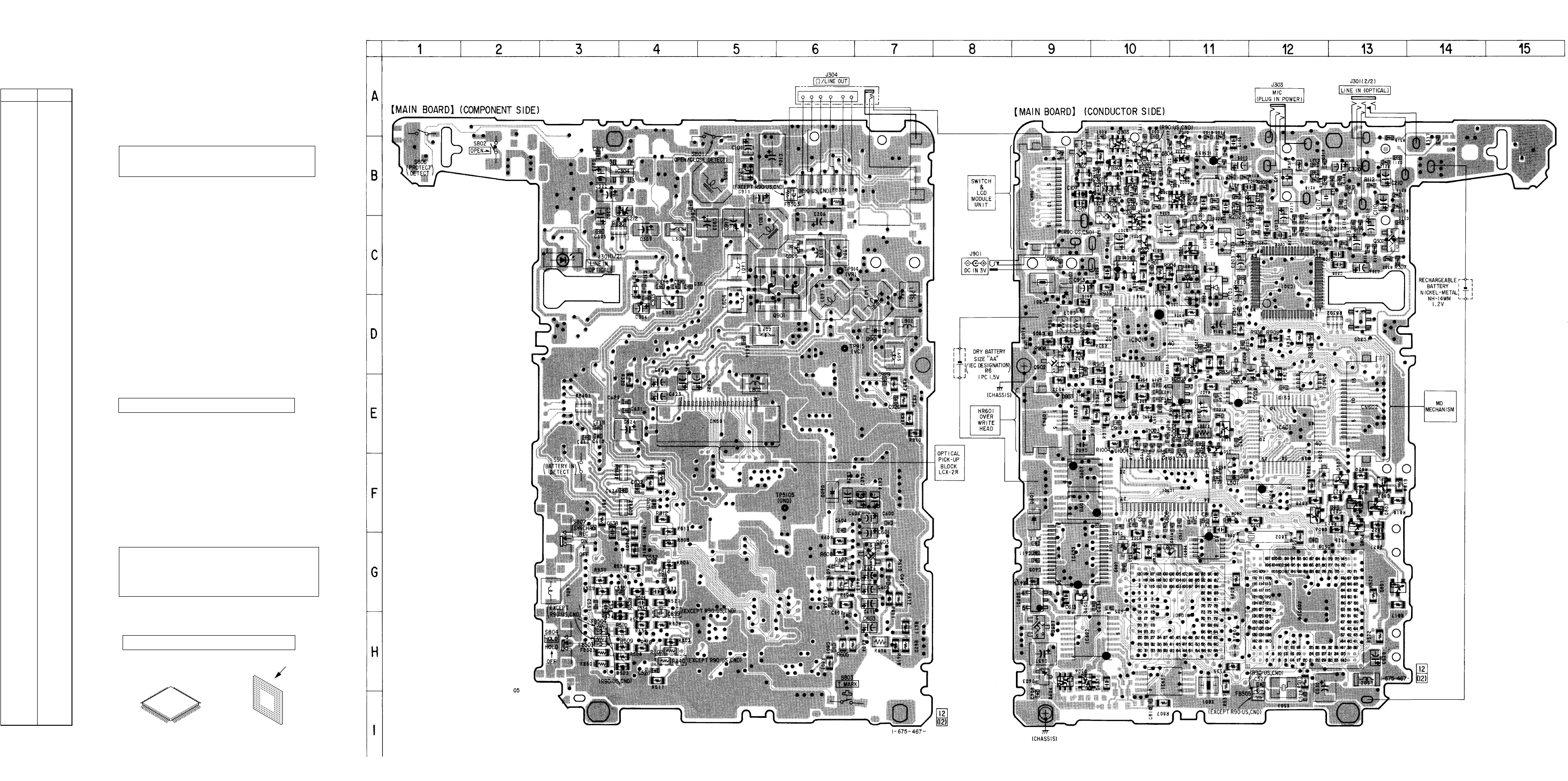
6-4. PRINTED WIRING BOARD
• Semiconductor
Location
Ref. No. Location
D301 B-10
D302 B-9
D303 C-4
D304 B-10
D501 G-10
D600 F-6
D601 F-9
D602 G-6
D603 H-9
D801 E-12
D802 F-12
D803 D-11
D804 F-11
D901 D-7
D902 C-9
D903 E-9
D905 C-11
D906 C-11
D907 D-11
IC301 C-12
IC302 C-13
IC303 B-11
IC304 B-4
IC305 D-13
IC501 F-10
IC502 G-12
IC504 E-11
IC505 E-12
IC601 E-12
IC602 H-9
IC603 G-9
IC604 F-12
IC605 G-9
IC801 H-11
IC802 H-10
IC803 E-11
IC804 G-11
IC901 D-10
IC902 C-10
Q101 B-9
Q102 B-11
Q201 C-10
Q202 B-11
Q301 B-10
Q302 C-13
Q303 B-10
Q305 C-11
Q306 H-9
Q307 C-10
Q308 B-11
Q309 B-10
Q501 E-11
Q601 F-9
Q602 F-9
Q603 G-7
Q604 H-9
Q605 G-9
Q607 H-9
Q801 G-13
Q802 F-13
Q803 F-13
Q804 F-13
Q805 F-13
Q806 F-12
Q807 F-13
Q809 D-11
Q901 C-6
Q902 D-9
Q904 C-11
Q905 C-6
Q906 C-10
Q1001 E-11
• Main board is four-layer printed board.
However, the patterns of layers 2 and 3 have not been in-
cluded in this diagrams.
* IC502 and IC801 are not replaceable
• Lead Layouts
surfac
e
Lead layout of conventional IC CSP (chip size package)
Note on Printed Wiring Board:
•X: parts extracted from the component side.
•Y: parts extracted from the conductor side.
•x: parts mounted on the conductor side.
•z: Through hole.
•b: Pattern from the side which enables seeing.
(The other layers' patterns are not indicated.)
Caution:
Pattern face side: Parts on the pattern face side seen from
(Conductor Side) the pattern face are indicated.
Parts face side: Parts on the parts face side seen from
(Component Side) the parts face are indicated.
Note on Schematic Diagram:
• All capacitors are in µF unless otherwise noted. pF: µµF
50 WV or less are not indicated except for electrolytics
and tantalums.
• All resistors are in Ω and 1/4 W or less unless otherwise
specified.
• % : indicates tolerance.
•f: internal component.
•C: panel designation.
•A: B+ Line.
• Power voltage is dc 3 V and fed with regulated dc power
supply from external power voltage jack.
• Voltages and waveforms are dc with respect to ground
under no-signal conditions.
no mark : PLAYBACK
( ) : RECORD
∗: Impossible to measure
• Voltages are taken with a VOM (Input impedance 10 MΩ).
Voltage variations may be noted due to normal produc-
tion tolerances.
• Waveforms are taken with a oscilloscope.
Voltage variations may be noted due to normal produc-
tion tolerances.
• Circled numbers refer to waveforms.
• Signal path.
E: PLAYBACK (ANALOG OUT)
j: PLAYBACK (ANALOG IN)
l: RECORD (DEGITAL IN)
• Abbreviation
CND : Canadian model
FR : French model
HK : Hong Kong model
JEW : Tourist model
Note: The components identified by mark 0 or dotted line
with mark 0 are critical for safety.
Replace only with part number specified.
* IC502 and IC801 are not replaceable
• The voltage and waveform of CSP (chip size package) can-
not be measured, because its lead layout is different form
that of conventional IC.
Ver 1.2 2000. 02
MZ-R90/R91
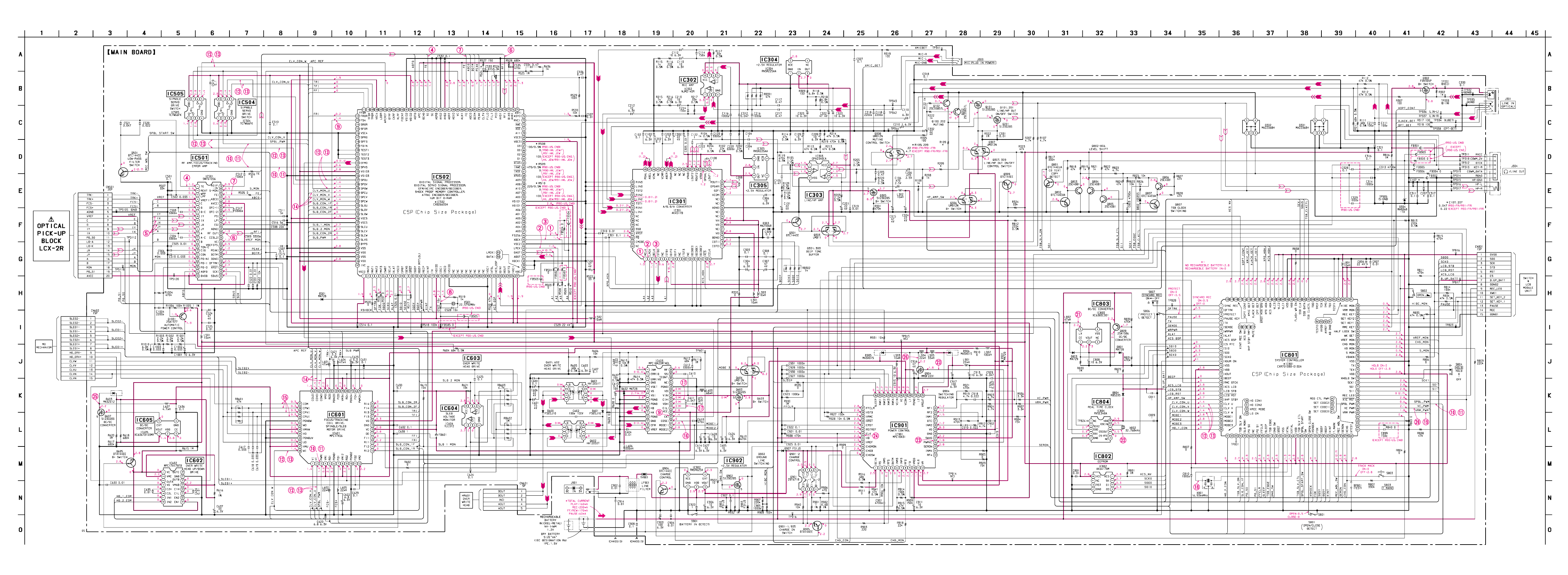
– 33 – – 34 – – 35 – – 36 – – 37 –
6-5. SCHEMATIC DIAGRAM • See page 38 for Waveforms. • See page 41 for IC Block Diagrams.
– 39 – – 40 – – 41 – – 42 –
• IC Block Diagrams
IC301 AK4517BVQ-L
1
495051525354555657
48
58596061626364
2423221817 2928272625212019 323130
2
3
4
5
6
7
8
LRCK
BCLK
SDTO
NC
SDTI
DIF0
DIF1
MCLK CLOCK
DIVIDER
HPF
DPGA DBB D/A
CONVERTER
AUDIO
INTERFACE
CONTROLLER
12
13
14
15
16
DCODE0
DCODE1
DCODE2
9
10
11
NC
TST3
NC
CS (SCK)
CCLK (SSI)
DGND
VD
NC
CDTO
CDTI (SSO)
VB
VA
NC
NC
AGND
NC
NC
VCOM
DZF
OPGAR
ROUT1
CONTROL
REGISTER
INTERFACE
46
45
44
VCML
47 ADCL
IPGAL
NC
VCMR
43 ADCR
42 IPGAR
41 NC
40 NC
39 NC
38 VRAD
37 LOUT2
36 ROUT2
35 VRDA
34 OPGAL
33 LOUT1
A/D
CONVERTER
NC
NC
NC
SSB
NC
CMODE
LIN1
RIN1
TST1
LIN2
RIN2
TST2
LIN3
RIN3
RST
PD
IC304, 305 RN5RZ25AA-TR
1
2
34
5
+
–
VREF
CE
NC
VOUT
VDD
GND
CURRENT
LIMIT
IC501 SN761056ADBT
TE
VREF11
C
D
D-C
WPPLPF
REXT 2
3
4
5
6
7
1
ADIPIN
44
ADIP TEMP
S-MONITOR
PEAK/BOTM
POWER
SUPPLY
T-ON
AUTOMATIC
POWER CONTRL
FOCUS
ERROR
AMP
TPP/WPP
TRACKING
ERROR
AMP
8
IY
9
IX
10
JX
11
JY
18
PD-NI
17
CDN
16
CIG
15
TON-C
14
13
B
12
A
A-C
19
PD-I
20
PD-O
21
ADFG
22
DVDD
39 OFC-C1
40 AVCC
38 OFC-C2
37 PS
36
35
34
33
32
31
30
29
28
27
26
LP
EQ
AGND
RF
CCSL2
VC
VREF075
PEAK
BOTM
DGND
OFTRK
XRST
SCK
SBUS
25
24
23
S-MON
43
FE
42
ABCD
41
DWBPF
DW
AWBPF
MIJ
MALFA
D-C
A-C
VREF075
CSLO
AW
PK/BTM
TWPP
TE
ADIP
TON BOTM
TON PEAK
AW+DW
CSL
TON
NPP
I+J
A+B+C+D
SERIAL
INTERFACE
RF
AMP
ABCD
AMP
1IC301 1 (MCLK), IC502 rh (FS256)
1 V/DIV, 50 ns/DIV
2.7 Vp-p
88.5 ns
2.8 Vp-p
22.7 µs
1.2 Vp-p
354 ns
Approx.
396 mVp-p
Approx.
540 mVp-p
Approx.
1.4 Vp-p
Approx.
416 mVp-p
1.3 Vp-p
44.3 ns
2.7 Vp-p
5.7 µs
2.8 Vp-p
5.3 µs
2.8 Vp-p
11.4 µs
2.8 Vp-p
11.1 ms
2.8 Vp-p
20 ms
2.8 Vp-p
11.8 ms
1.3 Vp-p
11.5 µs
1.6 Vp-p
5.7 µs
4.8 Vp-p
5.7 µs
2.2 Vp-p
59.1 ns
508 mVp-p
11.3 µs
1.2 Vp-p
30.5 µs
112 mVp-p
7.4 µs
203 mVp-p
11.3 µs
2.7 Vp-p
7.6 µs
• Waveforms
2IC301 2 (LRCK), IC502 rd (LRCK)
1 V/DIV, 10 µs/DIV
3IC301 3 (BCLK), IC502 rg (XBCK)
400 mV/DIV, 200 ns/DIV
4IC501 1 (TE), IC502 oh (TE)
(PLAY Mode)
200 mV/DIV, 1 µs/DIV
5IC501 8, 9, 0, qa (IY, IX, JX,JY)
(PLAY Mode)
200 mV/DIV, 500 ns/DIV
6IC501 ed (RF), IC502 uk (RFI) (PLAY Mode)
400 mV/DIV, 1 µs/DIV
7IC501 rs (FE), IC502 ij (FE) (PLAY Mode)
200 mV/DIV, 1 µs/DIV
8IC502 w; (OSCO)
400 mV/DIV, 20 ns/DIV
9IC502 <zzc (FS4), IC603 ql (CK)
1 V/DIV, 2 µs/DIV
0IC502 <zxv (SPVS), IC504 1, 2
IC601 3 (PWMI), IC801 yj (SPDL PWM)
(PLAY Mode)
1 V/DIV, 2 µs/DIV
qa IC502 <zxv (SPVS), IC504 1, 2
IC601 3 (PWMI), IC801 yj (SPDL PWM)
(REC Mode)
1 V/DIV, 5 µs/DIV
qs IC502 <zxm , <zx, , <zx. (SPDU, SPDV, SPDW)
IC504 5, 6, IC505 1, 2, 5, 6
IC601 1, 2, rk (VI, UI, WI)
IC801 wf, wg, wh (CLV U, CLV V, CLV W)
(PLAY Mode)
1 V/DIV, 5 ms/DIV
qd IC502 <zxm , <zx, , <zx. (SPDU, SPDV, SPDW)
IC504 5, 6, IC505 1, 2, 5, 6
IC601 1, 2, rk (VI, UI, WI)
IC801 wf, wg, wh (CLV U, CLV V, CLV W)
(REC Mode)
1 V/DIV, 10 ms/DIV
qf IC502 <zc/ , <zcz , <zcx (SPCU, SPCV, SPCW)
IC601 ef, eg, eh (COWO, COVO, COUO)
1 V/DIV, 5 ms/DIV
qg IC601 ej, ek, el, r; (COM,
CPWI, CPVI, CPUI)
400 mV/DIV, 5 µs/DIV
qh IC603 qk (COSC) (REC Mode)
400 mV/DIV, 5 µs/DIV
qj IC603 wa, wd (CIH, CIL) (REC Mode)
2 V/DIV, 2 µs/DIV
qk IC801 rg (XTAL)
1 V/DIV, 20 ns/DIV
ql IC801 yg (VRM PWM)
100 mV/DIV, 5 µs/DIV
w; IC801 yh (VC PWM)
40 mV/DIV, 5 µs/DIV
wa IC803 5 (LX)
50 mV/DIV, 5 µs/DIV
ws IC804 8 (OSCOUT)
500 mV/DIV, 20 µs/DIV
wf IC901 rd (CLK)
1 V/DIV, 2 µs/DIV
wd IC901 qh (PWMVC), Q904 (Gate)
5 V/DIV, 2 µs/DIV
8.8 Vp-p
7.8 µs
wg Q607 (Drain)
50 mV/DIV, 5 µs/DIV
wh Q904 (Drain)
1 V/DIV, 5 µs/DIV
114 mVp-p
8.6
µ
s
3.5 Vp-p
7.6 µs
– 38 –
– 43 –
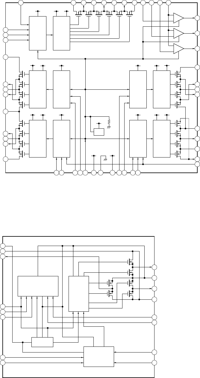
IC601 MPC17A56FTA
IC602 MPC17A17XDTBR2
+
–
+
–
242322212019
VC VG
1
2
3
4
5
6
7
8
3PHASE
CONTROL
PRE
DRIVER
48
VC
VC VC
PRE
DRIVER
H-BRIDGE
CONTROL
VC
H-BRIDGE
CONTROL
VG
47 46 45 44 43 42 41 39 38 37
+
–
40
36
35
34
VC
PRE
DRIVER
VG
9
10
11
12
33
32
31
30
VC
VC
PRE
DRIVER
H-BRIDGE
CONTROL
VC
H-BRIDGE
CONTROL
VG
VC
PRE
DRIVER
VG
28
29
26
25
27
14 15 16 1713
BIAS
VC ROE
VG
18
VC
VI
UI
PWM
VM1
RO1
PGND1
FO1
VM12
RO2
PGND2
FO2
VM2
RI2
FI2
RI1
FI1
OE
VC
GND
VG
FI3
RI3
FI4
RI4
PWM24
FO4
PGND4
RO4
VM34
FO3
PGND3
RO3
VM3
CPWO
CPVO
CPUO
COM
CPWI
CPVI
CPUI
GNDW
WO
VMVW
VO
GNDUV
UO
VMU
WI
OUTA
VMC
VC
3
2
1
C2L
C2H
VG
6
5
IN2
IN1
8
7
4
C1L
C1H
11
EN2
10
EN1
9
VMAB
OUTB
GND
OUTC
13
14
15
16
12
LVDET
CONTROL
LOGIC
CHARGE
PUMP LEVEL
SHIFTER
PREDRIVER
– 44 –
IC603 MPC18A20MTAEL
21
22
23
24
25
26
2728
29
30 16
17
18
19
20
235
4678910
111 12 13 14 15
CONTROL
LOGIC
CHARGE PUMP
SAW
GEN
SAW
CLK
OSC
EFM
LOGIC
BIAS
VREF
PRE
DRIVER
VREF
COMP
COMP
+
PRE DRIVER
SAW
CLK
EN ENB
OP
RF
SS
DTC
NC
PGNDLG
VB
VIN
C1H
VGH
C1L
VCC
CK
COSC
MODE 1
MODE 2
INM
ERRID
ERRIV
GND
VSET
VG
VGI
PGNDG
PGNDB
HB
HA
PGNDA
GND
EFM
VERF
IC605 XC6367B103MR
VDD
VOUT
CE
GND
EXT
1
2
3
5
4
VLX
LIMITER
PWM/PFM
CONTROL
OSC 100kHz
BUFFER
PHASE
COMPARATOR
REFERENCE
VOLTAGE
CHIP
ENABLE
SLOW
START
+
–
VDD
IC803 XC6383C301MR
IC902 RN5RG25AA-TR
+
–
1
3
5
4
2VREF
GND
VDD
VOUT
CE
EXT
1
2
3
CHIP
ENABLE
+
–
+
–
VREF
2STEP PFM CONTROL
OSC 100/180kHz
VLX LIMITER 5
4
VDD
CE
VOUT
NC VSS
LX
BUFFER
– 45 –
IC804 RV5C348A-E2
IC901 MPC18A31FTA
1
2
3
4
5
10
9
8
7
6
VDD
OSC IN
OSC OUT
CE
/INTR
32K OUT
SCLK
SO
SI
VSS
ALARM W REGISTER
(WEEK,MIN,HOUR)
ALARM D REGISTER
(MIN,HOUR)
32KHz
OUTPUT
CONTROL
TIME COUNTER
(SEC,MIN,HOUR,WEEK,DAY,MONTH,YEAR)
SHIFT REGISTER INTERRUPT CONTROL
VOLTAGE
DETECT
DIVIDER
CORRECTION
DIV OSC
COMPARATOR W
COMPARATOR D
ADDRESS
REGISTER
ADDRESS
DECORDER
OSC
DETECT
I/O
CONTROL
DCIN
DCIN VB
RS
INM5
2
3
RF5 4
INP3 7
RF3 8
1
CHGSW
48
DCIN
DCIN
VC
+
–
+
–
+
–
++–
+
–
VC
VG
VC
VC
VC
VBVC
FB
VREG
9
10
VR 12
VREG
RF4
VC
VR
INM3 6
BATM 5
VLD 11
CHGB
CHGMON
VREF
47 46
VB
CLK
44 43
RSTREF
42
CRST
41
XRST
40
VRMC
39
VBTB
3845
FFCLR
37
SYSTEM
CONTROL
SAW
OSC2
+–
+–+
–
BANDGAP
REFERENCE
STEP-UP
DC/DC
CONVERTER
STEP-UP
PRE DRIVER
36 SLEEP
35 XWK1
34 XWK2
33 XWK3
32 XWK4
XRST
29 VCON
28 L1
27 PGND
FFCLR
RF4
INM4
SERON
PWMVC
13 14 15 16
SWVG
17
GND
18
VG
19
INM2
20
DTC
21
INM1
22
RF2
23
+–
RF1
24
30 VC
31 VCIN
VG
VC
RF1
RF2
STEP-UP
PRE DRIVER 26 L2
25 VROUT
PWM
PWM

– 46 –
6-6. IC PIN FUNCTION DESCRIPTION
• MAIN BOARD IC501 SN761056ADBT (RF AMP, FOCUS/TRACKING ERROR AMP)
Pin No. Pin Name I/O Description
1 TE O Tracking error signal output to the CXD2660GA (IC502)
2 REXT — Connected to the external resistor for the ADIP amplifier control
3 WPPLPF —Connected to the external capacitor for low-pass filter of the TPP/WPP
4 VREF11 O Reference voltage output terminal (+1.1V)
5 C I Signal input from the optical pick-up detector (C)
6 D I Signal input from the optical pick-up detector (D)
7 D-C I Signal input from the optical pick-up detector (D) (AC input)
8 IY I I-V converted RF signal IY input from the optical pick-up block detector
9 IX I I-V converted RF signal IX input from the optical pick-up block detector
10 JX I I-V converted RF signal JX input from the optical pick-up block detector
11 JY I I-V converted RF signal JY input from the optical pick-up block detector
12 A I Signal input from the optical pick-up detector (A)
13 A-C I Signal input from the optical pick-up detector (A) (AC input)
14 B I Signal input from the optical pick-up detector (B)
15 TON-C —Connected to the external capacitor for the TON hold
16 CIG —Connected to the external capacitor for low-pass filter of the NPP divider denominator
17 CDN —Connected to the external capacitor for low-pass filter of the CSL divider denominator
18 PD-NI I Light amount monitor input terminal (non-invert input)
19 PD-I I Light amount monitor input terminal (invert input)
20 PD-O O Light amount monitor output terminal
21 ADFG O ADIP duplex FM signal (22.05 kHz ± 1 kHz) output to the CXD2660GA (IC502)
22 DVDD —Power supply terminal (+2.4V) (digital system)
23 SBUS I/O Two-way SSB serial data bus with the system controller (IC801)
24 SCK I SSB serial clock signal input from the system controller (IC801)
25 XRST I Reset signal input from the system controller (IC801) “L”: reset
26 OFTRK I Off track signal input from the CXD2660GA (IC502)
27 DGND —Ground terminal (digital system)
28 BOTM O Light amount signal (RF/ABCD) bottom hold output to the CXD2660GA (IC502)
29 PEAK O Light amount signal (RF/ABCD) peak hold output to the CXD2660GA (IC502)
30 VREF075 —Connected to the external capacitor for the internal reference voltage
31 VC O Middle point voltage (+1.2V) generation output terminal
32 CCSL2 —Connected to the external capacitor for low-pass filter of the TPP/WPP
33 RF OUT O Playback EFM RF signal output to the CXD2660GA (IC502)
34 AGND —Ground terminal (analog system)
35 EQ —Connected to the external capacitor for the RF equalizer
36 LP —Connected to the external capacitor for the RF equalizer
37 PS —Connected to the external capacitor for the RF equalizer
38 OFC-2 —Connected to the external capacitor for the RF AC coupling
39 OFC-1 —Connected to the external capacitor for the RF AC coupling
40 AVCC —Power supply terminal (+2.4V) (analog system)
41 ABCD O Light amount signal (ABCD) output to the CXD2660GA (IC502)
42 FE O Focus error signal output to the CXD2660GA (IC502)
43 S-MON O Servo signal monitor output to the system controller (IC801)
44 ADIP-IN I ADIP duplex FM signal (22.05 kHz ± 1 kHz) input terminal Not used

– 47 –
• MAIN BOARD IC502 CXD2660GA
Pin No. Pin Name I/O Description
1 VDC0 —Power supply terminal (+1.8V) (for internal logic)
2 MNT0 I/O Not used (open)
3 MNT1 O Recording shock detect signal output to the system controller (IC801)
4 MNT2 O Off track signal output to the SN761056ADBT (IC501) and system controller (IC801)
5 MNT3 O Focus OK signal output to the system controller (IC801)
“H”: is output when focus is on (“L”: NG)
6 SWDT I Serial data input from the system controller (IC801)
7 SCLK I (S) Serial clock signal input from the system controller (IC801)
8 XLAT I (S) Serial data latch pulse input from the system controller (IC801)
9 VSC0 —Ground terminal (for internal logic)
10 SRDT O (3) Serial data output to the system controller (IC801)
11 SENS O (3) Internal status (SENSE) output to the system controller (IC801)
12 XRST I (S) Reset signal input from the system controller (IC801) “L”: reset
13 SQSY O Subcode Q sync (SCOR) output the system controller (IC801)
“L” is output every 13.3 msec Almost all, “H” is output
14 DQSY
(MTFLGL) ODigital In U-bit CD format subcode Q sync (SCOR) output to the system controller (IC801)
“L” is output every 13.3 msec Almost all, “H” is output
15 RECP I Laser power selection signal input from the system controller (IC801)
“L”: playback mode, “H”: recording mode
16 XINT O Interrupt status output to the system controller (IC801)
17 TX I Recording data output enable signal input from the system controller (IC801)
Writing data transmission timing input
18 VDIO0 —Power supply terminal (+2.4V) (for I/O)
19 OSCI I System clock (512Fs=22.5792 MHz) input terminal
20 OSCO O System clock (512Fs=22.5792 MHz) output terminal
21 VSIO0 —Ground terminal (for I/O)
22 to 29 NC —Not used (open)
30 VSC1 —Ground terminal (for internal logic)
31 XTSL I Input terminal for the system clock frequency setting
“L”: 45.1584 MHz, “H”: 22.5792 MHz (fixed at “H” in this set)
32 XCS_DSP I Chip select signal input from the system controller (IC801)
33 DIN1 I Digital audio signal input terminal when recording mode
34 DOUT O Digital audio signal output terminal when playback mode Not used (open)
35 DT72 O Not used (open)
36, 37 VDC1, VDC2 —Power supply terminal (+1.8V) (for internal logic)
38 DATAI I Serial data input terminal Not used (fixed at “L”)
39 LRCKI I L/R sampling clock signal (44.1 kHz) input terminal
“L”: Rch, “H”: Lch Not used (fixed at “L”)
40 XBCKI I Serial input/output data bit clock signal (2.8224 MHz) input terminal Not used (fixed at “L”)
41 ADDT I Recording data signal input from the A/D, D/A converter (IC301)
42 DADT O Playback data signal output to the A/D, D/A converter (IC301)
43 LRCK O L/R sampling clock signal (44.1 kHz) output to the A/D, D/A converter (IC301)
44 VSC2 —Ground terminal (for internal logic)
45 XBCK O Serial input/output data bit clock signal (2.8224 MHz) out put to the A/D, D/A converter (IC301)
* I (S) stands for schmitt input, I (A) for analog input, O (3) for 3-state output, and O (A) for analog output in the column I/O
(DIGITAL SIGNAL PROCESSOR, DIGITAL SERVO SIGNAL PROCESSOR, EFM/ACIRC ENCODER/DECODER,
SHOCK PROOF MEMORY CONTROLLER, ATRAC ENCODER/DECODER, 16M BIT D-RAM)

– 48 –
Pin No. Pin Name I/O Description
46 FS256 O Clock signal (11.2896 MHz) output to the A/D, D/A converter (IC301) (X' tal system)
47 to 52 A03, A04, A02,
A05, A01, A06 O Address signal output to the external D-RAM Not used (open)
53 VDIO1 —Power supply terminal (+2.4V) (for I/O)
54 VSIO1 —Ground terminal (for I/O)
55 to 59 A00, A07, A10.
A08, A09 O Address signal output to the external D-RAM Not used (open)
60 XRAS O Row address strobe signal output to the external D-RAM “L” active Not used (open)
61 IXOE O Output enable signal output terminal for internal D-RAM “L” active Not used (open)
62 IXWE O Data write enable signal output terminal for internal D-RAM “L” active Not used (open)
63 XCAS O Column address strobe signal output to the external D-RAM “L” active Not used (open)
64 to 67 D1, D2, D0, D3 I/O Two-way data bus with the external D-RAM Not used (open)
68 VDC3 —Power supply terminal (+1.8V) (for internal logic)
69 VSC3 —Ground terminal (for internal logic)
70 A11 O Address signal output to the external D-RAM Not used (open)
71 XOE O Output enable signal output to the external D-RAM “L” active Not used (open)
72 XWE O Data write enable signal output to the external D-RAM “L” active Not used (open)
73 MVCI I (S) Digital in PLL oscillation input from the external VCO Not used (fixed at “L”)
74 ASYO O (A) Playback EFM full-swing output terminal
75 ASYI I (A) Playback EFM asymmetry comparator voltage input terminal
76 AVD1 —Power supply terminal (+2.4V) (analog system)
77 BIAS I (A) Playback EFM asymmetry circuit constant current input terminal
78 RFI I (A) Playback EFM RF signal input from the SN761056ADBT (IC501)
79 AVS1 —Ground terminal (analog system)
80 PCO O (3) Phase comparison output for master clock of the recording/playback EFM master PLL
81 FILI I (A) Filter input for master clock of the recording/playback EFM master PLL
82 FILO O (A) Filter output for master clock of the recording/playback EFM master PLL
83 CLTV I (A) Internal VCO control voltage input of the recording/playback EFM master PLL
84 PEAK I (A) Light amount signal (RF/ABCD) peak hold input from the SN761056ADBT (IC501)
85 BOTM I (A) Light amount signal (RF/ABCD) bottom hold input from the SN761056ADBT (IC501)
86 ABCD I (A) Light amount signal (ABCD) input from the SN761056ADBT (IC501)
87 FE I (A) Focus error signal input from the SN761056ADBT (IC501)
88 AUX1 I (A) Auxiliary signal (I3 signal/temperature signal) input terminal Not used (fixed at “H”)
89 VC I (A) Middle point voltage (+1.2V) input terminal
90 ADIO O (A) Monitor output of the A/D converter input signal Not used (open)
91 ADRT I (A) A/D converter operational range upper limit voltage input terminal (fixed at “H” in this set)
92 AVD2 —Power supply terminal (+2.4V) (analog system)
93 AVS2 —Ground terminal (analog system)
94 ADRB I (A) A/D converter operational range lower limit voltage input terminal (fixed at “L” in this set)
95 SE I (A) Sled error signal input terminal Not used (fixed at “L”)
96 TE I (A) Tracking error signal input from the SN761056ADBT (IC501)
97 DCHG I (A) Connected to the +2.4V power supply
98 APC I (A) Error signal input for the laser automatic power control Not used (fixed at “H”)
99 ADFG I (A) ADIP duplex FM signal (22.05 kHz ± 1 kHz) input from the SN761056ADBT (IC501)
100 VDIO2 —Power supply terminal (+2.4V) (for I/O)
101 VSIO2 —Ground terminal (for I/O)
102 F0CNT O Filter f0 control signal output terminal Not used (open)
* I (S) stands for schmitt input, I (A) for analog input, O (3) for 3-state output, and O (A) for analog output in the column I/O

– 49 –
Pin No. Pin Name I/O Description
103 XLRF O Serial latch signal output terminal Not used (open)
104 CKRF O Serial clock signal output terminal Not used (open)
105 DTRF O Writing data output terminal Not used (open)
106 APCREF O Control signal output to the reference voltage generator circuit for the laser automatic power
control
107 LDDR O PWM signal output for the laser automatic power control Not used (open)
108 VDC4 —Power supply terminal (+1.8V) (for internal logic)
109 TRDR O Tracking servo drive PWM signal (–) output to the MPC17A56FTA (IC601)
110 TFDR O Tracking servo drive PWM signal (+) output to the MPC17A56FTA (IC601)
111 FFDR O Focus servo drive PWM signal (+) output to the MPC17A56FTA (IC601)
112 FRDR O Focus servo drive PWM signal (–) output to the MPC17A56FTA (IC601)
113 FS4 O Clock signal (176.4 kHz) output to the MPC18A20MTAEL (IC603) (X' tal system)
114 SRDR O Sled servo drive PWM signal (–) output terminal Not used (open)
115 SFDR O Sled servo drive PWM signal (+) output terminal Not used (open)
116 VSC4 —Ground terminal (for internal logic)
117 SPRD O Spindle servo drive PWM signal (–) output terminal Not used (open)
118 SPFD O Spindle servo drive PWM signal (+) output terminal Not used (open)
119 FGIN I FG signal input terminal for spindle servo Not used (open)
120 to 12
2
TEST1 to TEST3 I Input terminal for the test (normally : fixed at “L”)
123 EFMO O EFM signal output when recording mode to the MPC18A20MTAEL (IC603)
124 SPVS O Spindle servo drive voltage control signal output to the MPC17A56FTA (IC601)
125 VDIO3 —Power supply terminal (+2.4V) (for I/O)
126 VSIO3 —Ground terminal (for I/O)
127 SPDU O Spindle servo (U) drive signal output to the MPC17A56FTA (IC601)
128 SPDV O Spindle servo (V) drive signal output to the MPC17A56FTA (IC601)
129 SPDW O Spindle servo (W) drive signal output to the MPC17A56FTA (IC601)
130 SPCU I Spindle servo (U) timing signal input from the MPC17A56FTA (IC601)
131 SPCV I Spindle servo (V) timing signal input from the MPC17A56FTA (IC601)
132 SPCW I Spindle servo (W) timing signal input from the MPC17A56FTA (IC601)
133 SLDU O Sled servo (1+) drive signal output to the MPC17A56FTA (IC601)
134 SLDV O Sled servo (1–) drive signal output to the MPC17A56FTA (IC601)
135 SLDW O Sled servo (2+) drive signal output to the MPC17A56FTA (IC601)
136 VDC5 —Power supply terminal (+1.8V) (for internal logic)
137 VSC5 —Ground terminal (for internal logic)
138 SLCU I Sled servo (1) timing signal input from the MPC17A56FTA (IC601)
139 SLCV I Sled servo (2) timing signal input from the MPC17A56FTA (IC601)
140 SLCW O Sled servo (2–) timing signal output to the MPC17A56FTA (IC601)
141 SLVS O Sled servo voltage control signal output to the MPC17A56FTA (IC601)
142 BYPS O By-pass transistor control signal output to the MPC17A56FTA (IC601)
143 VSS —Ground terminal (for internal 16M bit D-RAM)
144 VDD —Power supply terminal (+2.4V) (for internal 16M bit D-RAM)
145 VSS —Ground terminal (for internal 16M bit D-RAM)
146 VDD —Power supply terminal (+2.4V) (for internal 16M bit D-RAM)
147 IVC O Output terminal for the test Not used (open)

– 50 –
• MAIN BOARD IC801 CXR701080-013GA (MASTER CONTROLLER)
Pin No. Pin Name I/O Description
1SYNC REC ISYNCHRO REC switch (S801) input terminal “L”: off, “H”: on
2OFTRK IOff track signal input from the CXD2660GA (IC502)
3PROTECT IRec-proof claw detect input from the protect detect switch (S806)
“L”: recording possible , “H”: protect
4PAUSE KEY ISet pause key input terminal
5TX ORecording data output enable signal output to the CXD2660GA (IC502)
Writing data transmission timing output
6 SENSE I Internal status (SENSE) input from the CXD2660GA (IC502)
7WRPWR OLaser power select signal output to the CXD2660GA (IC502)
“L”: playback mode , “H”: recording mode
8XLAT OSerial data latch pulse output to the CXD2660GA (IC502)
9 XCS DSP O Chip select signal output to the CXD2660GA (IC502)
10 CS RTC OChip select signal output to the real time clock (IC804)
11 SI0 ISerial data input from the A/D, D/A converter (IC301), CXD2660GA (IC502), EEPROM
(IC802), real time clock (IC804) and switch & liquid crystal display module unit
12 SO0 O Serial data output to the A/D, D/A converter (IC301), CXD2660GA (IC502), EEPROM (IC802),
real time clock (IC804) and switch & liquid crystal display module unit
13 SCK0 O Serial clock signal output to the A/D, D/A converter (IC301), CXD2660GA (IC502), EEPROM
(IC802), real time clock (IC804) and switch & liquid crystal display module unit
14 XGUM ON I Rechargeable battery pack detection switch (S901) input terminal
“L”: rechargeable battery pack in
15 VSS —Ground terminal
16 VDD —Power supply terminal (+2.4V)
17 XOUT ONot used (open)
18 BEEP OBeep sound control signal input terminal
19 RMC DTCK I/O TSB serial communication data input/output terminal for remote commander with headphone
20 XCS LCD OChip select signal output to the liquid crystal display
21 LCD STB OStrobe signal output to the liquid crystal display
22 LCD RST OReset control signal output to the liquid crystal display
23 XHP STBY O Standby on/off control signal output to the line/headphone amplifier (IC303)
“L”: standby mode, “H”: amplifier on
24 CLV U OSpindle servo (U) drive signal output to the MPC17A56FTAF (IC601)
25 CLV V OSpindle servo (V) drive signal output to the MPC17A56FTAF (IC601)
26 CLV W OSpindle servo (W) drive signal output to the MPC17A56FTAF (IC601)
27 MODE1 O Power supply control signal output for over write head drive to the MPC18A20MTAEL (IC603)
28 MODE2 OPower supply control signal output for over write head drive to the MPC18A20MTAEL (IC603)
29 MODE3 OPower supply control signal output terminal for over write head drive
30 HD CON 1 OOver write head control signal output to the MPC17A17DTB (IC602)
31 HD CON 2 OOver write head control signal output to the MPC17A17DTB (IC602)
32 XREC MODE ONot used (open)
33 LD ON O Laser diode on/off control signal output terminal “L”: laser off, “H”: laser on Not used (open)
34 TSB SLV ON ITSB slave detect signal input terminal
35 SLD MON 1 ISled servo timing signal input from the MPC17A56FTA (IC601)
36 PD S0 OPD IC mode switching signal output to the optical pick-up block
37 REG CTL CLK O Synchronizing external clock signal output terminal Not used (open)
38 PD S1 OPD IC mode switching signal output to the optical pick-up block

– 51 –
Pin No. Pin Name I/O Description
39 FFCLR OInput latch output for starting signal to the MPC18A31FTA (IC901)
40 SLEEP OSystem sleep control signal output to the MPC18A31FTA (IC901) “H”: sleep on
41 TSB EDGE ITSB slave edge detect signal input terminal
42 GND SW O Ground line switching signal output terminal
43 XRST ISystem reset signal input from the MPC18A31FTA (IC901) “L”: reset
For several hundreds msec. after the power supply rises, “L” is input, then it changes to “H”
44 VSS —Ground terminal
45 XTAL O Main system clock output terminal (16.9344 MHz)
46 EXTAL I Main system clock input terminal (16.9344 MHz)
47 VDD —Power supply terminal (+2.4V)
48 TSB SLV CTL I/O Two-way control signal bus with TSB slave circuit
49 SPDL START
SW O Spindle servo start switching signal output to the analog switch (IC504, 505)
50 OPEN CLOSE
SW IUpper panel open/close detect switch (S801) input terminal (A/D input)
“L”: upper panel close, “H”: upper panel open
51 XSHOCK I Recording shock detect signal input from the CXD2660GA (IC502)
52 FOK IFocus OK signal input from the CXD2660GA (IC502) “H”: is input when focus is on (“L”: NG)
53 SQSY ISubcode Q sync (SCOR) input from the CXD2660GA (IC502)
“L” is input every 13.3 msec Almost all, “H” is input
54 DQSY IDigital In U-bit CD format subcode Q sync (SCOR) input from the CXD2660GA (IC502)
“L” is input every 13.3 msec Almost all, “H” is input
55 XINT IInterrupt status input from the CXD2660GA (IC502)
56 T.MARK I T MARK switch (S803) input terminal
57 REC WBL SW OStable control signal is output when recording
58 SERON OSeries power supply control signal output to the MPC18A31FTA (IC901)
59 XCHG O Charge control signal output to the MPC18A31FTA (IC901)
60 XTEST ISetting terminal for the test mode “L”: test mode, normally: fixed at “H”
61 SET CODE0 IDestination setting terminal Fixed at “L” in this set
62 SET CODE1 IDestination setting terminal Fixed at “L” in this set (US, canadian model: Not used (open))
63 SET CODE2 IDestination setting terminal Fixed at “L” in this set (US, canadian model: Not used (open))
64 REG CTL PWM OSynchronizing external clock signal output to the MPC18A31FTA (IC901)
65 VRM PWM OVREM power supply voltage control PWM signal output to the MPC18A31FTA (IC901)
66 VC PWM OSystem power supply voltage control PWM signal output to the MPC18A31FTA (IC901)
67 SPDL PWM OSpindle servo drive voltage control PWM signal output to the MPC17A56FTA (IC601)
68 XIC RST O Reset signal output to the A/D, D/A converter (IC301), SN761056ADBT (IC501) and
CXD2660GA (IC502) “L”: reset
69 REC LED OREC LED drive signal output terminal “H”: LED on
70 SI1 I Joint text data input from the remote commander with headphone
71 SO1 O Joint text data output to the remote commander with headphone
72 SCK1 OJoint data communication clock output to the remote commander with headphone
73 XHOLD SW IHOLD switch (S804) input terminal “L”: hold on, “H”: hold off
74 VDD —Power supply terminal (+2.4V)
75 TEX I Sub system clock input terminal Not used (open)
76 TX O Sub system clock output terminal Not used (open)
77 VSS —Ground terminal
78 VBKAN I Sub power supply input terminal
79 S MON I Servo signal monitor input from the SN761056ADBT (IC501) (A/D input)

– 52 –
Pin No. Pin Name I/O Description
80 VB MON I Un-regulator power supply voltage monitor input terminal (A/D input)
81 CHG MON I Rechargeable battery voltage monitor input from the MPC18A31FTA (IC901) (A/D input)
82 VREF MON I Reference voltage monitor input from the SN761056ADBT (IC501) (A/D input)
83 WK DET I Set key starting detect signal input terminal (A/D input)
84 HALF LOCK
SW IOpen knob detect switch (S802) input terminal “L”: normal position, “H”: open knob slid
85 RMC KEY I Remote commander with headphone key input terminal (A/D input)
86 SET KEY 1 I Set key input terminal (A/D input) (x, >, .,VOL +/– keys input)
87 SET KEY 2 I Set key input terminal (A/D input) (B, jog, END SEARCH keys input)
88 REC KEY I REC key input terminal
89 VRM MON I VREM voltage monitor input terminal (A/D input)
90 HIDC MON I HI-DC voltage monitor input terminal (A/D input)
91 AD GND —Ground terminal (for A/D converter)
92 AVREF I Input terminal for power supply voltage adjustment reference voltage (+2.4V) (for A/D converter)
93 AVDD —Power supply terminal (+2.4V) (for A/D converter)
94 TEST0 I Input terminal for the test (normally: fixed at “L”)
95 TEST1 I Input terminal for the test (normally: fixed at “L”)
96 TDI I Input terminal for JTAG Not used (open)
97 TMS I Input terminal for JTAG Not used (open)
98 TCK I Input terminal for JTAG Not used (open)
99 TRST I Input terminal for JTAG Not used (open)
100 TDO O Output terminal for JTAG Not used (open)
101 TSB CLKCTL O TSB clock control signal output terminal
102 SSB DATA I/O Two-way SSB serial data bus with the SN761056ADBT (IC501)
103 SSB CLK O SSB serial clock signal output to the SN761056ADBT (IC501)
104 FLASH WR EN —Not used (fixed at “H”)
105 VDD —Power supply terminal (+2.4V)
106 VSS —Ground terminal
107 to 109 VLC1 to VLC3 —Power supply terminal for the liquid crystal display (+2.4V)
110 XCS ADA O Chip select signal output to the A/D, D/A converter (IC301)
111 XPD ADA O Power supply control signal output to the A/D, D/A converter (IC301)
112
XRST MTR DRV
O Reset signal output terminal “L”: reset Not used (open)
113 OPT DET I DIN plug detect signal input terminal
114 XJACK DET I LINE IN plug detect signal input terminal
115 XMIC DET I MIC plug detect signal input terminal
116 XOPT CONT O Power supply control signal output to the DIN plug laser diode
117 MUTE O Analog muting on/off control signal output terminal “L”: muting off, “H”: muting on
118 XHP STBY TMP O Power supply control signal output to the headphone amplifier Not used (open)
119 XCS NV O Chip select signal output to the EEPROM (IC802)
120 XINT REC SW O Not used (open)
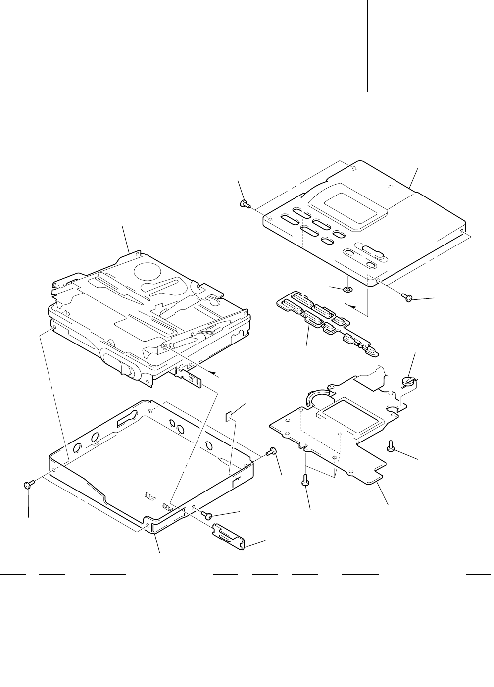
– 53 –
(1) PANEL SECTION (MZ-R90)
SECTION 7
EXPLODED VIEWS
Les composants identifiés par une
marque 0 sont critiquens pour la
sécurité.
Ne les remplacer que par une pièce
portant le numéro spécifié.
The components identified by
mark 0 or dotted line with mark
0 are critical for safety.
Replace only with part number
specified.
• Items marked “*” are not stocked since they
are seldom required for routine service. Some
delay should be anticipated when ordering
these items.
• The mechanical parts with no reference num-
ber in the exploded views are not supplied.
• Accessories and packing materials are given
in the last of the electrical parts list.
NOTE:
• -XX and -X mean standardized parts, so they
may have some difference from the original
one.
• Color Indication of Appearance Parts
Example:
KNOB, BALANCE (WHITE) . . . (RED)
↑↑
Parts Color Cabinet's Color
Ref. No. Part No. Description Remark Ref. No. Part No. Description Remark
1 4-223-077-01 LID, BATTERY CASE (SILVER)
1 4-223-077-11 LID, BATTERY CASE (BLACK) (HK, CH, JEW)
1 4-223-077-51 LID, BATTERY CASE (BLUE) (US)
2 X-3378-689-1 PANEL (R90L) ASSY, BOTTOM (BLUE) (US)
2 X-4952-045-1 PANEL (S) ASSY, BOTTOM (SILVER)
2 X-4952-048-1 PANEL (B) ASSY, BOTTOM (BLACK)
(HK, CH, JEW)
3 4-218-229-09 SCREW (1.4), MI (SILVER)
3 4-218-229-11 SCREW (1.4), MI (BLACK) (HK, CH, JEW)
3 4-218-229-13 SCREW (1.4), MI (BLACK) (CND)
4 X-3378-556-1 SERVICE ASSY, UPPER PANEL (S) (SILVER)
4 X-3378-557-1 SERVICE ASSY, UPPER PANEL (B) (BLACK)
4 X-3378-989-1 SERVICE ASSY, UPPER PANEL (L) (BLUE)
5 4-223-103-01 BUTTON, CONTROL (SILVER)
5 4-223-103-11 BUTTON, CONTROL (BLACK) (HK, CH, JEW)
6 1-756-028-11 BATTERY
7 1-803-759-11 LCD MODULE
8 3-044-057-01 SHEET (BATTERY CASE)
9 3-048-299-01 WASHER (LCD)
• Abbreviation
AUS : Australian model
CH : Chinese model
CND : Canadian model
FR : French model
HK : Hong Kong model
JEW : Tourist model
3
2
1
33
3
8
7
3
6
3
4
3
chassis section
5
9
Ver 1.3 2000. 07
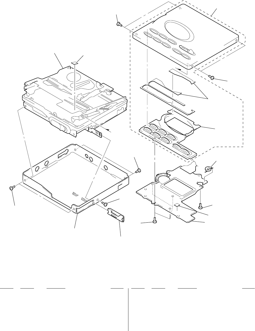
– 54 –
Ref. No. Part No. Description Remark Ref. No. Part No. Description Remark
(2) PANEL SECTION (MZ-R91)
51 4-223-077-21 LID, BATTERY CASE (BLUE)
51 4-223-077-31 LID, BATTERY CASE (RED)
51 4-223-077-41 LID, BATTERY CASE (WHITE)
52 X-4952-184-1 PANEL (L) ASSY, BOTTOM (BLUE)
52 X-4952-186-1 PANEL (R) ASSY, BOTTOM (RED)
52 X-4952-188-1 PANEL (W) ASSY, BOTTOM (WHITE)
53 4-218-229-09 SCREW (1.4), MI
54 X-3378-553-1 SERVICE ASSY, UPPER PANEL (L) (BLUE)
54 X-3378-554-1 SERVICE ASSY, UPPER PANEL (R) (RED)
54 X-3378-555-1 SERVICE ASSY, UPPER PANEL (W) (WHITE)
57 1-756-028-11 BATTERY
58 1-803-759-11 LCD MODULE
59 4-984-017-01 SCREW (1.7), TAPPING
60 3-044-057-01 SHEET (BATTERY CASE)
53 54
53
57
59
58
60
59
51
53
52
53
53
chassis section
not supplied
not supplied
60
Ver 1.3 2000. 07
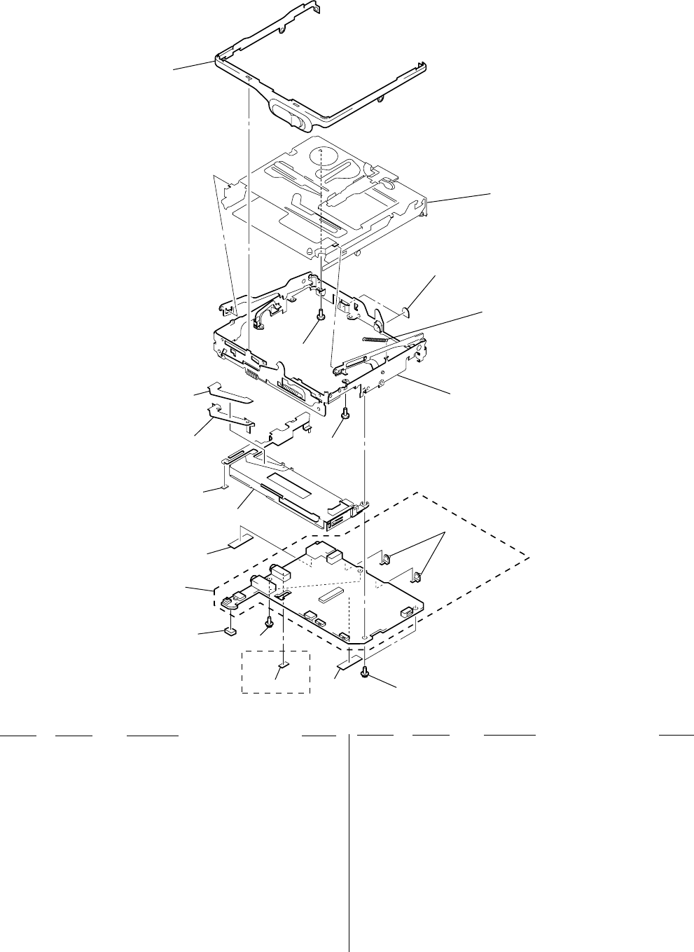
– 55 –
(3) CHASSIS SECTION
Ref. No. Part No. Description Remark Ref. No. Part No. Description Remark
101 X-4952-044-1 BELT ASSY (S), ORNAMENTAL (SILVER)
(R90/R91)
101 X-4952-337-1 BELT (B) ASSY, ORNAMENTAL (BLACK)
(R90: BLACK)
102 4-223-076-01 SHEET (TERMINAL), INSULATING
103 4-223-083-01 SPRING (ARM), TENSION
104 X-4952-042-1 CHASSIS ASSY, SET
105 4-218-233-05 SCREW (1.4), MI
106 X-4952-043-1 CASE ASSY, BATTERY
107 A-3323-361-A MAIN BOARD, COMPLETE
(R90: AEP, UK, E, AUS, CH/R91: AEP, UK)
107 A-3323-374-A MAIN BOARD, COMPLETE (R90: FR/R91: FR)
107 A-3323-491-A MAIN BOARD, COMPLETE
(R90: HK, JEW/R91: HK, JEW)
107 A-3323-493-A MAIN BOARD, COMPLETE (R90: US, CND)
108 4-223-110-01 TERMINAL (3)
109 3-335-797-91 SCREW (M1.4), TOOTHED LOCK
110 3-042-741-01 SHEET (FLEXIBLE) (R90/R91: HK, JEW)
111 3-044-312-01 SHEET (PC BOARD) (2)
112 3-043-283-01 JOINT (R90: US, E, AUS, CH/
R91: EXCEPT HK, JEW)
112 3-043-283-02 JOINT (R90: EXCEPT US, E, AUS CH/
R91: HK, JEW)
113 3-043-530-01 SHEET (JOINT), INSULATING
(R90: EXCEPT CA/R91)
114 3-049-215-01 SHEET (PRO)
101
MT-MZR90-165
not supplied
102
103
104
105
105
106
114
112
113
107
111 109
110
110
109
108
R91
Ver 1.3 2000. 07
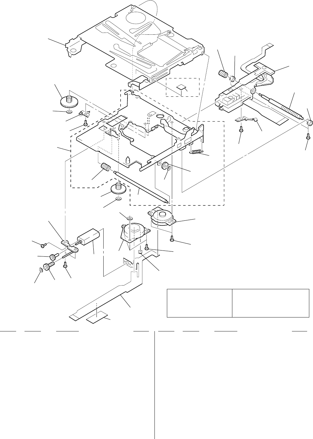
– 56 –
165 166
177
167
168
169
167
170
153
171
172
173
154
159
M602
152
153
175
M601
151
176
M603
152
155
154
156
157
158
162
152
163
154
164
154 174
160
161
R91
(4) MD-MECHANISM DECK SECTION
(MT-MZR90-165)
Ref. No. Part No. Description Remark Ref. No. Part No. Description Remark
151 1-675-466-11 MOTOR FLEXIBLE BOARD
152 4-963-883-42 SCREW (M1.4), PRECISION PAN
153 4-963-883-31 SCREW (M1.4), PRECISION PAN
154 3-338-645-31 WASHER (0.8-2.5)
155 4-222-214-11 GEAR (HB)
156 4-222-217-01 GEAR (HA)
157 4-224-885-01 SCREW (M1.2X1.5)
158 X-4951-918-1 CHASSIS ASSY, GEAR
159 4-222-223-01 SHAFT, SUB
160 4-222-215-01 GEAR (HC)
161 4-222-218-01 GEAR (HD)
162 X-4951-920-1 CHASSIS ASSY
163 4-222-206-01 SPRING, THRUST
164 4-222-216-01 GEAR (SA)
165 X-4951-919-1 HOLDER ASSY
166 4-222-208-01 GEAR (SB)
167 4-222-204-01 BEARING
0168 X-4952-386-1 SERVICE ASSY, OP
169 4-222-203-01 SCREW, LEAD
170 3-349-825-21 SCREW
171 4-222-205-01 SPRING, RACK
172 4-222-222-01 GEAR (RACK)
173 4-222-226-01 SPRING (EJECT), TENSION
174 4-997-677-11 WASHER
175 3-043-428-01 SHEET (CLV)
176 3-222-363-01 SPACER (FLEXIBLE)
M601 8-835-666-01 MOTOR, DC SSM-01C14A (SPINDLE)
(WITH TURN TABLE)
M602 1-763-399-11 MOTOR, DC (SLED) (WITH GEAR)
M603 1-763-400-11 MOTOR, DC (OVER WRITE HEAD UP/DOWN)
The components identified by
mark 0 or dotted line with
mark 0 are critical for safety.
Replace only with part num-
ber specified.
Les composants identifiés par une
marque 0 sont critiques pour la
sécurité.
Ne les remplacer que par une pièce
portant le numéro spécifié.
Ver 1.3 2000. 07

– 57 –
SECTION 8
ELECTRICAL PARTS LIST
Ref. No. Part No. Description Remark Ref. No. Part No. Description Remark
A-3323-361-A MAIN BOARD, COMPLETE
(R90: AEP, UK, E, AUS, CH/R91: AEP, UK)
A-3323-374-A MAIN BOARD, COMPLETE (R90: FR/R91: FR)
A-3323-491-A MAIN BOARD, COMPLETE
(R90: HK, JEW/R91: HK, JEW)
A-3323-493-A MAIN BOARD, COMPLETE (R90: US, CND)
*********************
4-223-110-01 TERMINAL (3)
< CAPACITOR >
C101 1-125-984-21 TANTALUM CHIP 22uF 20% 4V
C102 1-107-820-11 CERAMIC CHIP 0.1uF 16V
C103 1-131-734-21 TANTALUM CHIP 4.7uF 20% 6.3V
C104 1-125-837-11 CERAMIC CHIP 1uF 10% 6.3V
C105 1-117-863-11 CERAMIC CHIP 0.47uF 10% 6.3V
C106 1-131-727-91 TANTALUM CHIP 470uF 20% 2.5V
C107 1-115-467-11 CERAMIC CHIP 0.22uF 10% 10V
(EXCEPT R90: FR/R91: FR)
C107 1-165-176-11 CERAMIC CHIP 0.047uF 16V
(R90: FR/R91: FR)
C108 1-125-837-11 CERAMIC CHIP 1uF 10% 6.3V
C109 1-117-919-11 TANTALUM CHIP 10uF 20% 6.3V
C110 1-135-337-11 TANTALUM CHIP 1uF 20% 6.3V
C111 1-164-874-11 CERAMIC CHIP 100PF 5% 16V
C112 1-117-919-11 TANTALUM CHIP 10uF 20% 6.3V
C113 1-117-919-11 TANTALUM CHIP 10uF 20% 6.3V
C114 1-164-878-11 CERAMIC CHIP 150PF 5% 16V
C116 1-164-937-11 CERAMIC CHIP 0.001uF 10% 16V
C117 1-125-985-91 CERAMIC CHIP 0.47uF 10% 25V
C118 1-164-939-11 CERAMIC CHIP 0.0022uF 10% 16V
C120 1-164-940-11 CERAMIC CHIP 0.0033uF 10% 16V
C122 1-125-837-11 CERAMIC CHIP 1uF 10% 6.3V
C201 1-125-984-21 TANTALUM CHIP 22uF 20% 4V
C202 1-107-820-11 CERAMIC CHIP 0.1uF 16V
C203 1-131-734-21 TANTALUM CHIP 4.7uF 20% 6.3V
C204 1-125-837-11 CERAMIC CHIP 1uF 10% 6.3V
C205 1-117-863-11 CERAMIC CHIP 0.47uF 10% 6.3V
C206 1-131-727-91 TANTALUM CHIP 470uF 20% 2.5V
C207 1-115-467-11 CERAMIC CHIP 0.22uF 10% 10V
(EXCEPT R90: FR/R91: FR)
C207 1-165-176-11 CERAMIC CHIP 0.047uF 16V
(R90: FR/R91: FR)
C208 1-125-837-11 CERAMIC CHIP 1uF 10% 6.3V
C209 1-117-919-11 TANTALUM CHIP 10uF 20% 6.3V
NOTE:
• Due to standardization, replacements in the
parts list may be different from the parts speci-
fied in the diagrams or the components used
on the set.
• -XX and -X mean standardized parts, so they
may have some difference from the original
one.
• RESISTORS
All resistors are in ohms.
METAL: Metal-film resistor.
METAL OXIDE: Metal oxide-film resistor.
F: nonflammable
• Items marked “*” are not stocked since they
are seldom required for routine service.
Some delay should be anticipated when order-
ing these items.
• SEMICONDUCTORS
In each case, u: µ, for example:
uA. . : µA. . uPA. . : µPA. .
uPB. . : µPB. . uPC. . : µPC. .
uPD. . : µPD. .
• CAPACITORS
uF: µF
• COILS
uH: µH
Les composants identifiés par une
marque 0 sont critiquens pour la
sécurité.
Ne les remplacer que par une pièce
portant le numéro spécifié.
The components identified by
mark 0 or dotted line with mark
0 are critical for safety.
Replace only with part number
specified.
When indicating parts by reference
number, please include the board.
• Abbreviation
AUS : Australian model
CH : Chinese model
CND : Canadian model
FR : French model
HK : Hong Kong model
JEW : Tourist model
C210 1-135-337-11 TANTALUM CHIP 1uF 20% 6.3V
C211 1-164-874-11 CERAMIC CHIP 100PF 5% 16V
C212 1-117-919-11 TANTALUM CHIP 10uF 20% 6.3V
C213 1-117-919-11 TANTALUM CHIP 10uF 20% 6.3V
C214 1-164-878-11 CERAMIC CHIP 150PF 5% 16V
C216 1-164-937-11 CERAMIC CHIP 0.001uF 10% 16V
C217 1-125-985-91 CERAMIC CHIP 0.47uF 10% 25V
C218 1-164-939-11 CERAMIC CHIP 0.0022uF 10% 16V
C220 1-164-940-11 CERAMIC CHIP 0.0033uF 10% 16V
C222 1-125-837-11 CERAMIC CHIP 1uF 10% 6.3V
C301 1-107-820-11 CERAMIC CHIP 0.1uF 16V
C302 1-127-895-11 TANTALUM CHIP 22uF 20% 4V
C303 1-107-820-11 CERAMIC CHIP 0.1uF 16V
C304 1-117-919-11 TANTALUM CHIP 10uF 20% 6.3V
C305 1-164-943-11 CERAMIC CHIP 0.01uF 10% 16V
C306 1-117-919-11 TANTALUM CHIP 10uF 20% 6.3V
C307 1-131-862-91 TANTALUM CHIP 47uF 20% 4V
C308 1-107-820-11 CERAMIC CHIP 0.1uF 16V
C309 1-125-777-11 CERAMIC CHIP 0.1uF 10% 10V
C310 1-164-943-11 CERAMIC CHIP 0.01uF 10% 16V
C311 1-125-777-11 CERAMIC CHIP 0.1uF 10% 10V
C312 1-164-949-11 CERAMIC CHIP 0.047uF 16V
C313 1-164-941-11 CERAMIC CHIP 0.0047uF 10% 16V
C314 1-164-937-11 CERAMIC CHIP 0.001uF 10% 16V
C315 1-131-725-91 TANTALUM CHIP 47uF 20% 4V
C316 1-125-777-11 CERAMIC CHIP 0.1uF 10% 10V
C317 1-125-777-11 CERAMIC CHIP 0.1uF 10% 10V
C318 1-125-777-11 CERAMIC CHIP 0.1uF 10% 10V
C319 1-164-943-11 CERAMIC CHIP 0.01uF 10% 16V
C320 1-117-919-11 TANTALUM CHIP 10uF 20% 6.3V
C321 1-125-777-11 CERAMIC CHIP 0.1uF 10% 10V
C322 1-131-862-91 TANTALUM CHIP 47uF 20% 4V
C323 1-117-919-11 TANTALUM CHIP 10uF 20% 6.3V
C324 1-127-895-11 TANTALUM CHIP 22uF 20% 4V
C327 1-125-777-11 CERAMIC CHIP 0.1uF 10% 10V
C328 1-125-777-11 CERAMIC CHIP 0.1uF 10% 10V
(R90: US, CND)
C329 1-164-937-11 CERAMIC CHIP 0.001uF 10% 16V
(R90: US, CND)
C330 1-107-820-11 CERAMIC CHIP 0.1uF 16V
C331 1-164-943-11 CERAMIC CHIP 0.01uF 10% 16V
C332 1-127-895-11 TANTALUM CHIP 22uF 20% 4V
C501 1-125-777-11 CERAMIC CHIP 0.1uF 10% 10V
MAIN

– 58 –
Ref. No. Part No. Description Remark Ref. No. Part No. Description Remark
C502 1-127-772-81 CERAMIC CHIP 33000PF 10% 10V
C503 1-164-940-11 CERAMIC CHIP 0.0033uF 10% 16V
C504 1-164-940-11 CERAMIC CHIP 0.0033uF 10% 16V
C505 1-164-943-11 CERAMIC CHIP 0.01uF 10% 16V
C506 1-127-772-81 CERAMIC CHIP 33000PF 10% 10V
C507 1-125-777-11 CERAMIC CHIP 0.1uF 10% 10V
C508 1-164-858-11 CERAMIC CHIP 22PF 5% 16V
C509 1-164-940-11 CERAMIC CHIP 0.0033uF 10% 16V
C510 1-125-777-11 CERAMIC CHIP 0.1uF 10% 10V
C511 1-164-845-11 CERAMIC CHIP 5PF 0.25PF 16V
C512 1-164-938-11 CERAMIC CHIP 0.0015uF 10% 16V
C513 1-127-772-81 CERAMIC CHIP 33000PF 10% 10V
C514 1-125-777-11 CERAMIC CHIP 0.1uF 10% 10V
C515 1-125-777-11 CERAMIC CHIP 0.1uF 10% 10V
C516 1-164-845-11 CERAMIC CHIP 5PF 0.25PF 16V
C517 1-164-940-11 CERAMIC CHIP 0.0033uF 10% 16V
C519 1-125-777-11 CERAMIC CHIP 0.1uF 10% 10V
C520 1-107-819-11 CERAMIC CHIP 0.022uF 10% 16V
C521 1-119-923-81 CERAMIC CHIP 0.047uF 10% 10V
C522 1-164-943-11 CERAMIC CHIP 0.01uF 10% 16V
C524 1-131-725-91 TANTALUM CHIP 47uF 20% 4V
C525 1-164-943-11 CERAMIC CHIP 0.01uF 10% 16V
C526 1-164-943-11 CERAMIC CHIP 0.01uF 10% 16V
C527 1-164-850-11 CERAMIC CHIP 10PF 0.50PF 16V
C528 1-164-850-11 CERAMIC CHIP 10PF 0.50PF 16V
C529 1-127-895-11 TANTALUM CHIP 22uF 20% 4V
C530 1-131-725-91 TANTALUM CHIP 47uF 20% 4V
C531 1-164-943-11 CERAMIC CHIP 0.01uF 10% 16V
C532 1-125-777-11 CERAMIC CHIP 0.1uF 10% 10V
C533 1-164-245-11 CERAMIC CHIP 0.015uF 10% 25V
C534 1-117-863-11 CERAMIC CHIP 0.47uF 10% 6.3V
C535 1-164-935-11 CERAMIC CHIP 470PF 10% 16V
C536 1-117-863-11 CERAMIC CHIP 0.47uF 10% 6.3V
C537 1-164-943-11 CERAMIC CHIP 0.01uF 10% 16V
C600 1-125-777-11 CERAMIC CHIP 0.1uF 10% 10V
C601 1-131-623-91 TANTALUM CHIP 15uF 20% 4V
C602 1-109-813-11 CAP, CHIP 100PF 5% 100V
C603 1-135-337-11 TANTALUM CHIP 1uF 20% 6.3V
C604 1-164-943-11 CERAMIC CHIP 0.01uF 10% 16V
C605 1-117-919-11 TANTALUM CHIP 10uF 20% 6.3V
C606 1-127-895-11 TANTALUM CHIP 22uF 20% 4V
C607 1-107-820-11 CERAMIC CHIP 0.1uF 16V
C608 1-107-819-11 CERAMIC CHIP 0.022uF 10% 16V
C609 1-119-923-81 CERAMIC CHIP 0.047uF 10% 10V
C610 1-164-935-11 CERAMIC CHIP 470PF 10% 16V
C611 1-119-923-81 CERAMIC CHIP 0.047uF 10% 10V
C612 1-164-940-11 CERAMIC CHIP 0.0033uF 10% 16V
C613 1-125-837-11 CERAMIC CHIP 1uF 10% 6.3V
C614 1-117-919-11 TANTALUM CHIP 10uF 20% 6.3V
C615 1-135-379-91 TANTALUM CHIP 3.3uF 20% 10V
C617 1-127-772-81 CERAMIC CHIP 33000PF 10% 10V
C618 1-127-772-81 CERAMIC CHIP 33000PF 10% 10V
C619 1-127-772-81 CERAMIC CHIP 33000PF 10% 10V
C620 1-131-621-91 TANTALUM CHIP 6.8uF 20% 6.3V
C621 1-127-578-91 TANTALUM CHIP 3.3uF 20% 6.3V
C622 1-131-621-91 TANTALUM CHIP 6.8uF 20% 6.3V
C623 1-127-578-91 TANTALUM CHIP 3.3uF 20% 6.3V
C624 1-125-777-11 CERAMIC CHIP 0.1uF 10% 10V
C625 1-125-777-11 CERAMIC CHIP 0.1uF 10% 10V
C626 1-117-919-11 TANTALUM CHIP 10uF 20% 6.3V
C627 1-117-919-11 TANTALUM CHIP 10uF 20% 6.3V
C628 1-117-919-11 TANTALUM CHIP 10uF 20% 6.3V
C629 1-125-777-11 CERAMIC CHIP 0.1uF 10% 10V
C630 1-125-777-11 CERAMIC CHIP 0.1uF 10% 10V
C631 1-125-777-11 CERAMIC CHIP 0.1uF 10% 10V
C632 1-125-777-11 CERAMIC CHIP 0.1uF 10% 10V
C633 1-162-970-11 CERAMIC CHIP 0.01uF 10% 25V
C634 1-164-943-11 CERAMIC CHIP 0.01uF 10% 16V
C635 1-164-943-11 CERAMIC CHIP 0.01uF 10% 16V
C636 1-125-777-11 CERAMIC CHIP 0.1uF 10% 10V
C637 1-131-726-91 TANTALUM CHIP 33uF 20% 6.3V
C638 1-125-837-11 CERAMIC CHIP 1uF 10% 6.3V
C801 1-164-943-11 CERAMIC CHIP 0.01uF 10% 16V
C803 1-164-941-11 CERAMIC CHIP 0.0047uF 10% 16V
C804 1-164-858-11 CERAMIC CHIP 22PF 5% 16V
C806 1-127-895-11 TANTALUM CHIP 22uF 20% 4V
C807 1-164-943-11 CERAMIC CHIP 0.01uF 10% 16V
C808 1-117-919-11 TANTALUM CHIP 10uF 20% 6.3V
C809 1-125-837-11 CERAMIC CHIP 1uF 10% 6.3V
C810 1-164-937-11 CERAMIC CHIP 0.001uF 10% 16V
C811 1-125-837-11 CERAMIC CHIP 1uF 10% 6.3V
C899 1-164-217-11 CERAMIC CHIP 150PF 5% 50V
(EXCEPT R90: US, CND)
C901 1-164-941-11 CERAMIC CHIP 0.0047uF 10% 16V
C902 1-164-943-11 CERAMIC CHIP 0.01uF 10% 16V
C903 1-128-964-91 TANTALUM CHIP 100uF 20% 6.3V
C904 1-164-943-11 CERAMIC CHIP 0.01uF 10% 16V
C905 1-164-937-11 CERAMIC CHIP 0.001uF 10% 16V
C906 1-117-919-11 TANTALUM CHIP 10uF 20% 6.3V
C907 1-125-777-11 CERAMIC CHIP 0.1uF 10% 10V
C908 1-125-777-11 CERAMIC CHIP 0.1uF 10% 10V
C910 1-107-819-11 CERAMIC CHIP 0.022uF 10% 16V
C911 1-117-919-11 TANTALUM CHIP 10uF 20% 6.3V
C913 1-117-919-11 TANTALUM CHIP 10uF 20% 6.3V
C914 1-164-943-11 CERAMIC CHIP 0.01uF 10% 16V
C915 1-125-840-91 TANTALUM 10uF 20% 6.3V
C916 1-131-725-91 TANTALUM CHIP 47uF 20% 4V
C917 1-128-964-91 TANTALUM CHIP 100uF 20% 6.3V
C918 1-107-819-11 CERAMIC CHIP 0.022uF 10% 16V
C919 1-109-982-11 CERAMIC CHIP 1uF 10% 10V
C920 1-125-837-11 CERAMIC CHIP 1uF 10% 6.3V
C921 1-164-943-11 CERAMIC CHIP 0.01uF 10% 16V
C922 1-125-777-11 CERAMIC CHIP 0.1uF 10% 10V
C923 1-164-937-11 CERAMIC CHIP 0.001uF 10% 16V
C925 1-164-943-11 CERAMIC CHIP 0.01uF 10% 16V
C926 1-119-923-81 CERAMIC CHIP 0.047uF 10% 10V
C927 1-164-937-11 CERAMIC CHIP 0.001uF 10% 16V
C928 1-164-937-11 CERAMIC CHIP 0.001uF 10% 16V
C929 1-119-923-81 CERAMIC CHIP 0.047uF 10% 10V
C930 1-164-937-11 CERAMIC CHIP 0.001uF 10% 16V
C931 1-164-937-11 CERAMIC CHIP 0.001uF 10% 16V
C932 1-109-982-11 CERAMIC CHIP 1uF 10% 10V
C1001 1-125-840-91 TANTALUM 10uF 20% 6.3V
C1002 1-127-772-81 CERAMIC CHIP 33000PF 10% 10V
C1003 1-127-772-81 CERAMIC CHIP 33000PF 10% 10V
MAIN

– 59 –
Ref. No. Part No. Description Remark Ref. No. Part No. Description Remark
C1004 1-164-939-11 CERAMIC CHIP 0.0022uF 10% 16V
< CONNECTOR >
*CN501 1-778-168-11 CONNECTOR, FFC/FPC (ZIF) 20P
*CN601 1-793-510-21 CONNECTOR, FPC (ZIF) 5P
*CN602 1-793-511-21 CONNECTOR, FPC (ZIF) 15P
*CN801 1-793-511-21 CONNECTOR, FPC (ZIF) 15P
< DIODE >
D301 8-719-077-43 DIODE MAZZ068H01S0
D302 8-719-077-43 DIODE MAZZ068H01S0
D303 8-719-056-54 DIODE MAZS068008SO
D304 8-719-017-58 DIODE MA8068-TX
D501 8-719-421-27 DIODE MA728-TX
D600 8-719-072-10 DIODE FS05J10-TP
D601 8-719-072-10 DIODE FS05J10-TP
D602 8-719-421-27 DIODE MA728-TX
D603 8-719-067-36 DIODE MA3ZD1200LS0
D801 8-719-421-27 DIODE MA728-TX
D802 8-719-988-61 DIODE 1SS355TE-17
D803 8-719-420-51 DIODE MA729-TX
D804 8-719-069-29 DIODE RB520S-30TE61
D901 8-719-420-51 DIODE MA729-TX
D902 8-719-072-26 DIODE FS1J3-TP
D903 8-719-072-26 DIODE FS1J3-TP
D905 8-719-074-74 DIODE MA3XD15001S0
D906 8-719-074-74 DIODE MA3XD15001S0
D907 8-719-072-26 DIODE FS1J3-TP
< FERRITE BEAD/RESISTOR >
FB301 1-500-329-21 FERRITE BEAD INDUCTOR
FB302 1-500-329-21 FERRITE BEAD INDUCTOR
FB303 1-216-864-11 METAL CHIP 0 5% 1/16W
(EXCEPT R90: US, CND)
FB303 1-414-228-11 FERRITE BEAD INDUCTOR (R90: US, CND)
FB304 1-216-864-11 METAL CHIP 0 5% 1/16W
FB305 1-500-329-21 FERRITE BEAD INDUCTOR
FB306 1-500-329-21 FERRITE BEAD INDUCTOR
FB501 1-216-864-11 METAL CHIP 0 5% 1/16W
FB502 1-216-864-11 METAL CHIP 0 5% 1/16W
FB503 1-216-864-11 METAL CHIP 0 5% 1/16W
(EXCEPT R90: US, CND)
FB503 1-414-760-21 FERRITE, EMI (SMD) (R90: US, CND)
FB504 1-216-864-11 METAL CHIP 0 5% 1/16W
(EXCEPT R90: US, CND)
FB504 1-414-229-11 FERRITE BEAD INDUCTOR (R90: US, CND)
FB505 1-216-864-11 METAL CHIP 0 5% 1/16W
(EXCEPT R90: US, CND)
FB505 1-500-329-21 FERRITE BEAD INDUCTOR (R90: US, CND)
FB601 1-500-329-21 FERRITE BEAD INDUCTOR
< IC >
IC301 8-759-641-92 IC AK4517BVQ-L
IC302 8-759-572-38 IC NJM2140R
IC303 8-759-641-90 IC OPA2340EA
IC304 8-759-559-91 IC RN5RZ25AA-TR
IC305 8-759-559-91 IC RN5RZ25AA-TR
IC501 8-759-682-68 IC SN761056CDBT
@ IC502 8-752-397-66 IC CXD2660GA
IC504 8-759-647-75 IC TC7W66FK (TE85R)
IC505 8-759-647-75 IC TC7W66FK (TE85R)
IC601 8-759-678-83 IC MPC17A56FTAEB
IC602 8-759-642-58 IC MPC17A17XDTBR2
IC603 8-759-642-59 IC MPC18A20MTAEL
IC604 8-759-358-40 IC TLC372CPWR
IC605 8-759-586-58 IC XC6367B103MR
@ IC801 8-752-914-73 IC CXR701080-013GA
IC802 8-759-593-47 IC AK6417AM-E2
IC803 8-759-641-93 IC XC6383C301MR
IC804 8-759-641-91 IC RV5C348A-E2
IC901 8-759-678-82 IC MPC18A31FTAEB
IC902 8-759-652-23 IC RN5RG25AA-TR
< JACK >
J301 1-793-619-21 JACK (LINE IN (OPTICAL))
J303 1-793-620-21 JACK (MIC (PLIG IN POWER)
J304 1-793-509-11 JACK (i/LINE OUT)
J901 1-785-383-11 JACK, DC (POLARITY UNIFIED TYPE)
(DC IN 3V)
< COIL >
L301 1-469-535-21 INDUCTOR 10uH
L302 1-469-535-21 INDUCTOR 10uH
L303 1-469-535-21 INDUCTOR 10uH
L501 1-469-535-21 INDUCTOR 10uH
L502 1-469-535-21 INDUCTOR 10uH
L601 1-410-389-31 INDUCTOR CHIP 47uH
L602 1-469-422-21 INDUCTOR 22uH
L603 1-419-258-21 COIL, CHOKE 68uH
L604 1-410-389-31 INDUCTOR CHIP 47uH
L605 1-469-422-21 INDUCTOR 22uH
L606 1-414-407-41 INDUCTOR 330uH
L607 1-419-441-21 INDUCTOR 4.7uH
L801 1-469-535-21 INDUCTOR 10uH
L802 1-410-389-31 INDUCTOR CHIP 47uH
L901 1-414-400-41 INDUCTOR 22uH
L902 1-469-426-21 INDUCTOR 100uH
L903 1-469-367-21 INDUCTOR 10uH
L904 1-419-257-21 COIL, CHOKE 22uH
L905 1-419-407-21 COIL, CHOKE 33uH
< LINE FILTER >
LF901 1-416-405-21 FILTER, CHIP EMI (COMMON MODE)
< TRANSISTOR >
Q101 8-729-044-58 FET SI2304DS-T1
Q102 8-729-050-32 TRANSISTOR 2SC5585TL
Q201 8-729-044-58 FET SI2304DS-T1
Q202 8-729-050-32 TRANSISTOR 2SC5585TL
Q301 8-729-928-81 TRANSISTOR DTC144EE-TL
Q302 8-729-046-49 FET FDV304P
Q303 8-729-929-99 TRANSISTOR UMB11-TN
Q305 8-729-046-45 FET SI2302DS-T1
Q306 8-729-047-48 TRANSISTOR UMD12N-TR
Q307 8-729-047-48 TRANSISTOR UMD12N-TR
Q308 8-729-047-48 TRANSISTOR UMD12N-TR
@ Replacement of CXD2660GA (IC502) and
CXR701080-013GA (IC801) used in this set require
a special tool. Therefore, they cannot be replaced.
MAIN
Ver 1.3 2000. 07

– 60 –
Ref. No. Part No. Description Remark Ref. No. Part No. Description Remark
MAIN
Q309 8-729-928-81 TRANSISTOR DTC144EE-TL
Q501 8-729-928-81 TRANSISTOR DTC144EE-TL
Q601 8-729-046-43 FET HAT2051T-EL
Q602 8-729-046-42 FET HAT2050T-EL
Q603 8-729-046-45 FET SI2302DS-T1
Q604 8-729-047-48 TRANSISTOR UMD12N-TR
Q605 8-729-928-27 TRANSISTOR DTA144EE-TL
Q607 8-729-046-45 FET SI2302DS-T1
Q801 8-729-029-14 TRANSISTOR DTC144EUA-T106
Q802 8-729-029-14 TRANSISTOR DTC144EUA-T106
Q803 8-729-905-35 TRANSISTOR 2SC4081T106R
Q804 8-729-905-35 TRANSISTOR 2SC4081T106R
Q805 8-729-905-35 TRANSISTOR 2SC4081T106R
Q806 8-729-905-35 TRANSISTOR 2SC4081T106R
Q807 8-729-029-14 TRANSISTOR DTC144EUA-T106
Q809 8-729-230-60 TRANSISTOR 2SA1586YG-TE85L
Q901 8-729-046-44 TRANSISTOR ZDT6718TA
Q902 8-729-046-45 FET SI2302DS-T1
Q904 8-729-043-46 FET MMBF2201NT1
Q905 8-729-928-27 TRANSISTOR DTA144EE-TL
Q906 8-729-928-81 TRANSISTOR DTC144EE-TL
Q1001 8-729-922-10 TRANSISTOR 2SA1577-T106-QR
< RESISTOR >
R102 1-208-715-11 METAL CHIP 22K 0.5% 1/16W
R103 1-208-691-11 METAL CHIP 2.2K 0.5% 1/16W
R104 1-208-683-11 METAL CHIP 1K 0.5% 1/16W
R105 1-208-687-11 METAL CHIP 1.5K 0.5% 1/16W
R107 1-218-961-11 RES, CHIP 4.7K 5% 1/16W
R108 1-218-953-11 RES, CHIP 1K 5% 1/16W
R109 1-216-793-11 RES, CHIP 4.7 5% 1/16W
(EXCEPT R90: FR/R91: FR)
R109 1-216-801-11 RES, CHIP 22 5% 1/16W
(R90: FR/R91: FR)
R111 1-208-931-11 METAL CHIP 68K 0.5% 1/16W
R112 1-208-927-11 METAL CHIP 47K 0.5% 1/16W
R113 1-208-927-11 METAL CHIP 47K 0.5% 1/16W
R114 1-208-927-11 METAL CHIP 47K 0.5% 1/16W
R115 1-208-683-11 METAL CHIP 1K 0.5% 1/16W
R116 1-218-945-11 METAL CHIP 220 0.5% 1/16W
R117 1-208-719-11 METAL CHIP 33K 0.5% 1/16W
R118 1-208-703-11 METAL CHIP 6.8K 0.5% 1/16W
R119 1-218-985-11 METAL CHIP 470K 0.5% 1/16W
R120 1-218-849-11 METAL CHIP 3.3K 0.5% 1/16W
R122 1-218-953-11 RES, CHIP 1K 5% 1/16W
R202 1-208-715-11 METAL CHIP 22K 0.5% 1/16W
R203 1-208-691-11 METAL CHIP 2.2K 0.5% 1/16W
R204 1-208-683-11 METAL CHIP 1K 0.5% 1/16W
R205 1-208-687-11 METAL CHIP 1.5K 0.5% 1/16W
R207 1-218-961-11 RES, CHIP 4.7K 5% 1/16W
R208 1-218-953-11 RES, CHIP 1K 5% 1/16W
R209 1-216-793-11 RES, CHIP 4.7 5% 1/16W
(EXCEPT R90: FR/R91: FR)
R209 1-216-801-11 RES, CHIP 22 5% 1/16W
(R90: FR/R91: FR)
R211 1-208-931-11 METAL CHIP 68K 0.5% 1/16W
R212 1-208-927-11 METAL CHIP 47K 0.5% 1/16W
R213 1-208-927-11 METAL CHIP 47K 0.5% 1/16W
R214 1-208-927-11 METAL CHIP 47K 0.5% 1/16W
R215 1-208-683-11 METAL CHIP 1K 0.5% 1/16W
R216 1-218-945-11 METAL CHIP 220 0.5% 1/16W
R217 1-208-719-11 METAL CHIP 33K 0.5% 1/16W
R218 1-208-703-11 METAL CHIP 6.8K 0.5% 1/16W
R219 1-218-985-11 METAL CHIP 470K 0.5% 1/16W
R220 1-218-849-11 METAL CHIP 3.3K 0.5% 1/16W
R222 1-218-953-11 RES, CHIP 1K 5% 1/16W
R301 1-218-985-11 RES, CHIP 470K 5% 1/16W
R302 1-218-953-11 RES, CHIP 1K 5% 1/16W
R303 1-216-864-11 METAL CHIP 0 5% 1/16W
R304 1-216-864-11 METAL CHIP 0 5% 1/16W
R305 1-218-941-11 RES, CHIP 100 5% 1/16W
R307 1-218-941-11 RES, CHIP 100 5% 1/16W
R309 1-218-941-11 RES, CHIP 100 5% 1/16W
R317 1-218-941-11 RES, CHIP 100 5% 1/16W
R318 1-218-941-11 RES, CHIP 100 5% 1/16W
R319 1-218-941-11 RES, CHIP 100 5% 1/16W
R320 1-216-864-11 METAL CHIP 0 5% 1/16W
R322 1-218-989-11 RES, CHIP 1M 5% 1/16W
R323 1-218-973-11 RES, CHIP 47K 5% 1/16W
R324 1-218-971-11 RES, CHIP 33K 5% 1/16W
R502 1-216-833-11 RES, CHIP 10K 5% 1/16W
R503 1-216-864-11 METAL CHIP 0 5% 1/16W
R505 1-216-864-11 METAL CHIP 0 5% 1/16W
R506 1-216-864-11 METAL CHIP 0 5% 1/16W
R507 1-218-971-11 RES, CHIP 33K 5% 1/16W
R508 1-216-809-11 RES, CHIP 100 5% 1/16W
(EXCEPT R90: US,CND, HK, JEW/
R91: HK, JEW)
R508 1-216-864-11 METAL CHIP 0 5% 1/16W
(R90: HK, JEW/R91: HK, JEW)
R508 1-218-823-11 METAL CHIP 100 0.5% 1/16W
(R90: US, CND)
R509 1-216-809-11 RES, CHIP 100 5% 1/16W
(EXCEPT R90: US,CND, HK, JEW/
R91: HK, JEW)
R509 1-216-864-11 METAL CHIP 0 5% 1/16W
(R90: HK, JEW/R91: HK, JEW)
R509 1-218-839-11 METAL CHIP 470 0.5% 1/16W
(R90: US, CND)
R510 1-216-809-11 RES, CHIP 100 5% 1/16W
(EXCEPT R90: US,CND, HK, JEW/
R91: HK, JEW)
R510 1-216-864-11 METAL CHIP 0 5% 1/16W
(R90: HK, JEW/R91: HK, JEW)
R510 1-218-831-11 METAL CHIP 220 0.5% 1/16W
(R90: US, CND)
R517 1-216-864-11 METAL CHIP 0 5% 1/16W
R518 1-216-845-11 METAL CHIP 100K 5% 1/16W
R519 1-216-821-11 METAL CHIP 1K 5% 1/16W
R520 1-216-841-11 METAL CHIP 47K 5% 1/16W
R522 1-216-803-11 METAL CHIP 33 5% 1/16W
R524 1-216-821-11 METAL CHIP 1K 5% 1/16W
R525 1-216-857-11 METAL CHIP 1M 5% 1/16W
R526 1-216-827-11 METAL CHIP 3.3K 5% 1/16W
R527 1-216-811-11 METAL CHIP 150 5% 1/16W
R528 1-216-855-11 METAL CHIP 680K 5% 1/16W
R529 1-216-845-11 METAL CHIP 100K 5% 1/16W
R530 1-216-833-11 RES, CHIP 10K 5% 1/16W

– 61 –
Ref. No. Part No. Description Remark Ref. No. Part No. Description Remark
MAIN
R535 1-216-864-11 METAL CHIP 0 5% 1/16W
R536 1-216-864-11 METAL CHIP 0 5% 1/16W
R537 1-216-864-11 METAL CHIP 0 5% 1/16W
R602 1-216-864-11 METAL CHIP 0 5% 1/16W
R604 1-218-891-11 METAL CHIP 68K 0.5% 1/16W
R605 1-218-891-11 METAL CHIP 68K 0.5% 1/16W
R606 1-216-833-11 RES, CHIP 10K 5% 1/16W
R607 1-218-871-11 METAL CHIP 10K 0.5% 1/16W
R608 1-216-864-11 METAL CHIP 0 5% 1/16W
R609 1-216-864-11 METAL CHIP 0 5% 1/16W
R610 1-216-853-11 METAL CHIP 470K 5% 1/16W
R611 1-216-857-11 METAL CHIP 1M 5% 1/16W
R612 1-216-843-11 METAL CHIP 68K 5% 1/16W
R613 1-218-871-11 METAL CHIP 10K 0.5% 1/16W
R615 1-216-857-11 METAL CHIP 1M 5% 1/16W
R616 1-219-724-11 METAL CHIP 1 1% 1/4W
R617 1-216-855-11 METAL CHIP 680K 5% 1/16W
R618 1-216-855-11 METAL CHIP 680K 5% 1/16W
R619 1-216-833-11 RES, CHIP 10K 5% 1/16W
R620 1-216-857-11 METAL CHIP 1M 5% 1/16W
R621 1-216-833-11 RES, CHIP 10K 5% 1/16W
R636 1-216-821-11 METAL CHIP 1K 5% 1/16W
R801 1-216-857-11 METAL CHIP 1M 5% 1/16W
R802 1-216-851-11 METAL CHIP 330K 5% 1/16W
R803 1-216-864-11 METAL CHIP 0 5% 1/16W
R804 1-216-864-11 METAL CHIP 0 5% 1/16W
R805 1-216-864-11 METAL CHIP 0 5% 1/16W
(EXCEPT R90 : US, CND)
R806 1-216-864-11 METAL CHIP 0 5% 1/16W
R807 1-216-864-11 METAL CHIP 0 5% 1/16W
R808 1-216-841-11 METAL CHIP 47K 5% 1/16W
R809 1-216-849-11 METAL CHIP 220K 5% 1/16W
R810 1-218-977-11 RES, CHIP 100K 5% 1/16W
R811 1-216-853-11 METAL CHIP 470K 5% 1/16W
R812 1-218-903-11 METAL CHIP 220K 0.5% 1/16W
R813 1-218-903-11 METAL CHIP 220K 0.5% 1/16W
R814 1-216-845-11 METAL CHIP 100K 5% 1/16W
R815 1-216-853-11 METAL CHIP 470K 5% 1/16W
R816 1-218-989-11 METAL CHIP 1M 0.5% 1/16W
R817 1-216-851-11 METAL CHIP 330K 5% 1/16W
R818 1-216-841-11 METAL CHIP 47K 5% 1/16W
R819 1-216-821-11 METAL CHIP 1K 5% 1/16W
R820 1-216-829-11 METAL CHIP 4.7K 5% 1/16W
R821 1-216-821-11 METAL CHIP 1K 5% 1/16W
R822 1-216-841-11 METAL CHIP 47K 5% 1/16W
R823 1-216-833-11 RES, CHIP 10K 5% 1/16W
R824 1-216-841-11 METAL CHIP 47K 5% 1/16W
R825 1-216-833-11 RES, CHIP 10K 5% 1/16W
R826 1-216-821-11 METAL CHIP 1K 5% 1/16W
R827 1-216-841-11 METAL CHIP 47K 5% 1/16W
R828 1-216-841-11 METAL CHIP 47K 5% 1/16W
R829 1-216-864-11 METAL CHIP 0 5% 1/16W
R830 1-216-853-11 METAL CHIP 470K 5% 1/16W
R831 1-216-853-11 METAL CHIP 470K 5% 1/16W
R833 1-216-857-11 METAL CHIP 1M 5% 1/16W
R834 1-218-887-11 METAL CHIP 47K 0.5% 1/16W
R835 1-218-887-11 METAL CHIP 47K 0.5% 1/16W
R838 1-216-864-11 METAL CHIP 0 5% 1/16W
R840 1-216-864-11 METAL CHIP 0 5% 1/16W
(EXCEPT R90: US, CND)
R901 1-219-724-11 METAL CHIP 1 1% 1/4W
R902 1-242-996-91 METAL CHIP 0.68 1% 1/4W
R903 1-216-813-11 METAL CHIP 220 5% 1/16W
R904 1-216-833-11 RES, CHIP 10K 5% 1/16W
R905 1-216-864-11 METAL CHIP 0 5% 1/16W
R906 1-216-817-11 METAL CHIP 470 5% 1/16W
R907 1-216-849-11 METAL CHIP 220K 5% 1/16W
R908 1-216-845-11 METAL CHIP 100K 5% 1/16W
R909 1-216-864-11 METAL CHIP 0 5% 1/16W
R910 1-216-864-11 METAL CHIP 0 5% 1/16W
R911 1-216-864-11 METAL CHIP 0 5% 1/16W
R912 1-216-829-11 METAL CHIP 4.7K 5% 1/16W
R913 1-216-853-11 METAL CHIP 470K 5% 1/16W
R914 1-218-899-11 RES, CHIP 150K 0.5% 1/16W
R915 1-218-887-11 RES, CHIP 47K 0.5% 1/16W
R916 1-208-931-11 RES, CHIP 68K 0.5% 1/16W
R918 1-216-837-11 METAL CHIP 22K 5% 1/16W
R919 1-216-829-11 METAL CHIP 4.7K 5% 1/16W
R921 1-216-853-11 METAL CHIP 470K 5% 1/16W
R922 1-216-797-11 METAL CHIP 10 5% 1/16W
R923 1-216-829-11 METAL CHIP 4.7K 5% 1/16W
R924 1-216-829-11 METAL CHIP 4.7K 5% 1/16W
R927 1-216-847-11 METAL CHIP 150K 5% 1/16W
R928 1-218-871-11 METAL CHIP 10K 0.5% 1/16W
R929 1-216-835-11 METAL CHIP 15K 5% 1/16W
R930 1-216-857-11 METAL CHIP 1M 5% 1/16W
R931 1-216-833-11 RES, CHIP 10K 5% 1/16W
R932 1-216-857-11 METAL CHIP 1M 5% 1/16W
R934 1-216-835-11 METAL CHIP 15K 5% 1/16W
R935 1-216-864-11 METAL CHIP 0 5% 1/16W
R936 1-216-827-11 METAL CHIP 3.3K 5% 1/16W
R937 1-216-827-11 METAL CHIP 3.3K 5% 1/16W
R938 1-216-853-11 METAL CHIP 470K 5% 1/16W
R939 1-216-847-11 METAL CHIP 150K 5% 1/16W
R940 1-216-833-11 RES, CHIP 10K 5% 1/16W
R941 1-208-927-11 RES, CHIP 47K 0.5% 1/16W
R1001 1-218-855-11 METAL CHIP 2.2K 0.5% 1/16W
R1002 1-218-855-11 METAL CHIP 2.2K 0.5% 1/16W
R1003 1-218-855-11 METAL CHIP 2.2K 0.5% 1/16W
R1004 1-216-853-11 METAL CHIP 470K 5% 1/16W
R1005 1-219-724-11 METAL CHIP 1 1% 1/4W
R1006 1-218-977-11 RES, CHIP 100K 5% 1/16W
R1010 1-218-867-11 METAL CHIP 6.8K 0.5% 1/16W
< COMPOSITION CIRCUIT BLOCK >
RB301 1-233-971-11 RES, NETWORK (CHIP TYPE) 47K
RB302 1-233-961-11 RES, NETWORK (CHIP TYPE) 1K
RB601 1-233-965-11 RES, NETWORK (CHIP TYPE) 4.7K
RB602 1-233-979-11 RES, NETWORK (CHIP TYPE) 1M
RB603 1-233-965-11 RES, NETWORK (CHIP TYPE) 4.7K
< SWITCH >
S801 1-762-805-21 SWITCH, PUSH (1KEY)
(OPEN/CLOSE DETECT)
S802 1-762-947-12 SWITCH, PUSH (1KEY) (OPEN .)
S803 1-771-248-11 SWITCH, TACTILE (T MARK)

– 62 –
Ref. No. Part No. Description Remark Ref. No. Part No. Description Remark
Sony Corporation
Personal Audio Division Company
9-927-187-12 2000B0586-1
Printed in Japan C 2000. 2
Published by General Engineering Dept.
S804 1-771-770-21 SWITCH, SLIDE (HOLD)
S806 1-771-860-21 SWITCH, PUSH (PROTECT DETECT)
S807 1-771-770-21 SWITCH, SLIDE (SYNCHRO REC)
S901 1-771-806-21 SWITCH, PUSH (1KEY) (BATTERY IN DETECT)
< THERMISTOR >
TH901 1-803-795-21 THERMISTOR, POSITIVE
< VIBRATOR >
X501 1-781-574-21 VIBRATOR, CRYSTAL (22.5792MHz)
X801 1-781-575-21 VIBRATOR, CERAMIC (19.9344MHz)
X802 1-781-525-21 VIBRATOR, CRYSTAL (32.768kHz)
**************************************************************
MISCELLANEOUS
**************
6 1-756-028-11 BATTERY
7 1-803-759-11 LCD MODULE
57 1-756-028-11 BATTERY
58 1-803-759-11 LCD MODULE
151 1-675-466-11 MOTOR FLEXIBLE BOARD
0168 X-4952-386-1 SERVICE ASSY, OP
M601 8-835-666-01 MOTOR, DC SSM-01C14A (SPINDLE)
(WITH TURN TABLE)
M602 1-763-399-11 MOTOR, DC (SLED) (WITH GEAR)
M603 1-763-400-11 MOTOR, DC (OVER WRITE HEAD UP/DOWN)
************************************************************
ACCESSORIES & PACKING MATERIALS
*********************************
01-418-028-11 ADAPTOR, AC (AC-MZR55)
(R90: E, JEW/R91: JEW)
01-418-049-11 ADAPTOR, AC (AC-MZR55)
(R90: UK, HK/R91: UK, HK)
01-418-275-11 ADAPTOR, AC (AC-MZR55) (R90: US, CND)
01-418-276-11 ADAPTOR, AC (AC-MZR55)
(R90: AEP, FR/R91: AEP, FR)
01-418-277-11 ADAPTOR, AC (AC-MZR55) (R90: AUS)
1-418-493-11 REMOTECONTROL UNIT (RM-MZ2S) (BLACK)
(R90: US, HK, CH, JEW)
1-418-493-51 REMOTECONTROL UNIT (RM-MZ2S) (SILVER)
(EXCEPT R90: US/R91)
1-418-493-61 REMOTECONTROL UNIT (RM-MZ2S) (CLEAR)
(R91)
01-418-784-11 ADAPTOR (AC-MZR70), AC (R90: CH)
01-569-007-11 ADAPTOR, CONVERSION 2P
(R90: CH, JEW/R91: JEW)
1-756-023-11 CASE, BATTERY (for SIZE R6 (AA) BATTERY)
1-756-036-11 BATTERY, NICKEL HYDROGEN (NH-14WM)
1-779-504-11 CONNECTOR, OPTICAL
(EXCEPT R90: HK CH, JEW/R91: HK, JEW)
1-779-504-51 CONNECTOR, OPTICAL
(R90: HK, CH, JEW/R91: HK, JEW)
3-043-060-01 CASE, CHARGE (C/D)
3-045-575-01 CASE, CARRYING
3-867-571-11 MANUAL, INSTRUCTION (ENGLISH, SPANISH,
PORTUGUESE, SWEDISH, FINNISH, RUSSIAN)
(R90: AEP, UK, E, HK, JEW/
R91: AEP, UK, HK, JEW)
The components identified by
mark 0 or dotted line with
mark 0 are critical for safety.
Replace only with part num-
ber specified.
Les composants identifiés par une
marque 0 sont critiques pour la
sécurité.
Ne les remplacer que par une pièce
portant le numéro spécifié.
MZ-R90/R91
MAIN
3-867-571-21 MANUAL, INSTRUCTION (ENGLISH)
(R90: US, AUS, CH)
3-867-571-31 MANUAL, INSTRUCTION (ENGLISH, FRENCH,
GERMAN, DUTCH, ITALIAN) (R90: CND,
AEP, FR/R91: AEP, FR)
3-867-571-41 MANUAL, INSTRUCTION (JAPANESE,
CHINESE, KOREAN) (R90: E, HK,
JEW/R91: HK, JEW)
3-867-571-51 MANUAL, INSTRUCTION (CHINESE) (R90: CH)
8-953-278-90 HEADPHONE MDR-A34SP (R90: US)
8-953-304-90 RECEIVER MDR-E805SP (EXCEPT R90: US)

– 2 –
1. Addition of Korean Model
Korean Model has been added.
This is the same as Hong Kong model which is not described in this supplement-1.
Refer to MZ-R90/R91 original service manual (9-927-187-S) for other information.
• EXPLODED VIEWS
Page Hong Kong Model Korean Model
Ref. No. Part No. Description Remark
107 A-3323-292-A MAIN BOARD, COMPLETE
(R90: KR/R91: KR)
Ref. No. Part No. Description Remark
107 A-3323-491-A MAIN BOARD, COMPLETE
(R90: HK, JEW/R91: HK, JEW)
55
Page Hong Kong Model Korean Model
Ref. No. Part No. Description Remark
A-3323-292-A MAIN BOARD, COMPLETE
(R90: KR/R91: KR)
R805 1-216-864-11 METAL CHIP 0 5% 1/16W
(R90: KR/R91: KR)
ACCESSORIES & PACKING MATERIALS
*******************************
(Korean model has no AC adaptors.)
3-867-571-01 MANUAL, INSTRUCTION
(JAPANESE, KOREAN) (R90: KR/R91: KR)
Ref. No. Part No. Description Remark
A-3323-491-A MAIN BOARD, COMPLETE
(R90: HK, JEW/R91: HK, JEW)
C899 1-164-217-11 CERAMIC CHIP 150PF 5% 50V
(EXCEPT R90: US, CND)
ACCESSORIES & PACKING MATERIALS
*******************************
01-418-049-11 ADAPTOR, AC (AC-MZR55)
(R90: UK, HK/R91: UK, HK)
57
• ELECTRICAL PARTS LIST
• Abbreviation
CND : Canadian model
HK : Hong Kong model
JEW : Tourist model
KR : Korean model
58
62
The components identified by
mark 0 or dotted line with
mark 0 are critical for safety.
Replace only with part num-
ber specified.
Les composants identifiés par une
marque 0 sont critiques pour la
sécurité.
Ne les remplacer que par une pièce
portant le numéro spécifié.
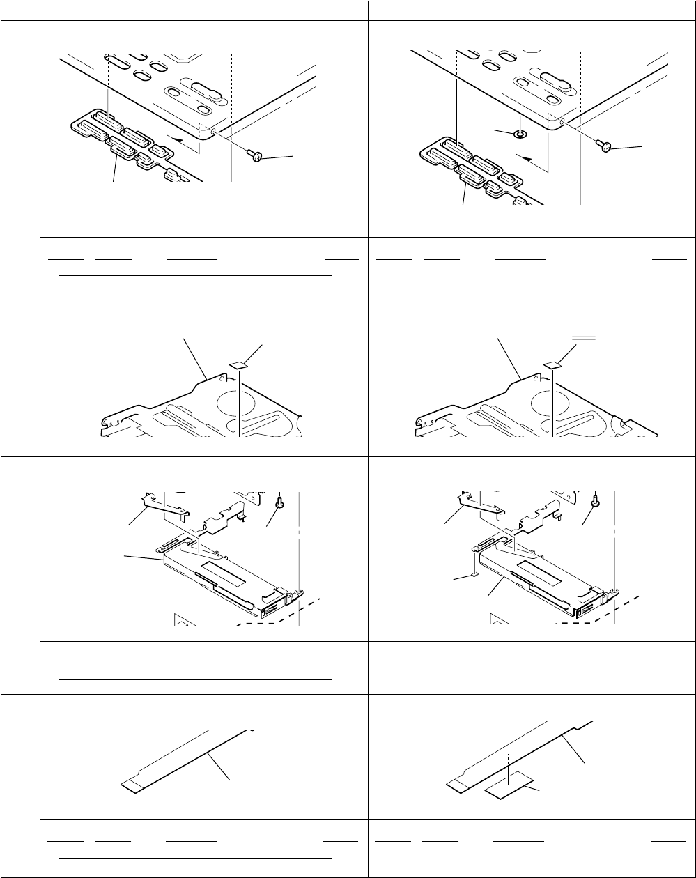
– 3 –
2. Correction
EXPLODED VIEWS
! : Indicates changed portion.
Page INCORRECT CORRECT
54
Ref. No. Part No. Description Remark
9 3-048-299-01 WASHER (LCD)
Ref. No. Part No. Description Remark
53
3
9
3
%
Ref. No. Part No. Description Remark
114 3-049-215-01 SHEET (PRO)
Ref. No. Part No. Description Remark
chassis section
61
chassis section
61
60
55
105
106
112
105
106
114
112
@
#
56
151
151
176
Ref. No. Part No. Description Remark
176 3-222-363-01 SPACER (FLEXIBLE)
Ref. No. Part No. Description Remark
@

– 4 –
•ELECTRICAL PARTS LIST
Page INCORRECT CORRCT
Ref. No. Part No. Description Remark
IC501 8-759-682-68 IC SN761056CDBT
IC601 8-759-678-83 IC MPC17A56FTAEB
IC901 8-759-678-82 IC MPC18A31FTAEB
Q101 8-729-044-58 FET SI2304DS-T1
Q201 8-729-044-58 FET SI2304DS-T1
Ref. No. Part No. Description Remark
IC501 8-759-661-14 IC SN761056ADBT
IC601 8-759-642-14 IC MPC17A56FTA
IC901 8-759-642-13 IC MPC18A31FTA
Q101 8-729-046-45 FET SI2302DS-T1
Q201 8-729-046-45 FET SI2302DS-T1
59
Sony Corporation
Audio Entertainment Group
9-927-187-83 2000G0573-1
Printed in Japan C 2000. 7
Published by PE General Engineering Dept.
MZ-R90/R91
