STB5NK50Z, STD5NK50Z, STP5NK50Z Datasheet. Www.s Manuals.com. Stp5nk50z, Stp5nk50zfp St
User Manual: Marking of electronic components, SMD Codes D5, D5*, D5***, D5.1, D5.6, D50, D51, D52, D53, D54, D55, D56, D57, D58, D59, D5NK50Z. Datasheets AZ23B10-G, AZ23B11-G, AZ23B12-G, AZ23B13-G, AZ23B15-G, AZ23B6V2-G, AZ23B6V8-G, AZ23B7V5-G, AZ23B8V2-G, AZ23B9V1-G, AZ23C10-G, AZ23C11-G, AZ23C12-G, AZ23C13-G, AZ23C15-G, AZ23C6V2-G, AZ23C6V8-G, AZ23C7V5-G, AZ23C8V2-G, AZ23C9V1-G, BC847BM, BZX384-C5V1, EMD5, MMBD4148CC, MMSZ5230, OPA2350EA, RT8010PQW, STD5NK50Z-1, STD5NK50ZT4, Si2325DS, TZT5V1AW, TZT5V6AW, UMD5N.
Open the PDF directly: View PDF ![]() .
.
Page Count: 18
1/17June 2004
STB5NK50Z/-1 - STD5NK50Z/-1
STP5NK50Z - STP5NK50ZFP
N-CHANNEL 500V - 1.22Ω - 4.4A TO-220/FP-D/IPAK-D2/I2PAK
Zener-Protected SuperMESH™MOSFET
Table 1: General Features
■TYPICAL RDS(on) = 1.22 Ω
■EXTREMELY HIGH dv/dt CAPABILITY
■IMPROVED ESD CAPABILITY
■100% AVALANCHE RATED
■GATE CHARGE MINIMIZED
■VERY LOW INTRINSIC CAPACITANCES
■VERY GOOD MANUFACTURING
REPEATIBILITY
DESCRIPTION
The SuperMESH™ series is obtained through an
extreme optimization of ST’s well established
stripbased PowerMESH™ layout. In addition to
pushing on-resistance significantly down, special
care is taken to ensure a very good dv/dt capability
for the most demanding applications. Such series
complements ST full range of high voltage MOS-
FETs including revolutionary MDmesh™ products.
APPLICATIONS
■HIGH CURRENT, HIGH SPEED SWITCHING
■IDEAL FOR OFF-LINE POWER SUPPLIES,
ADAPTORS AND PFC
■LIGHTING
Table 2: Order Codes
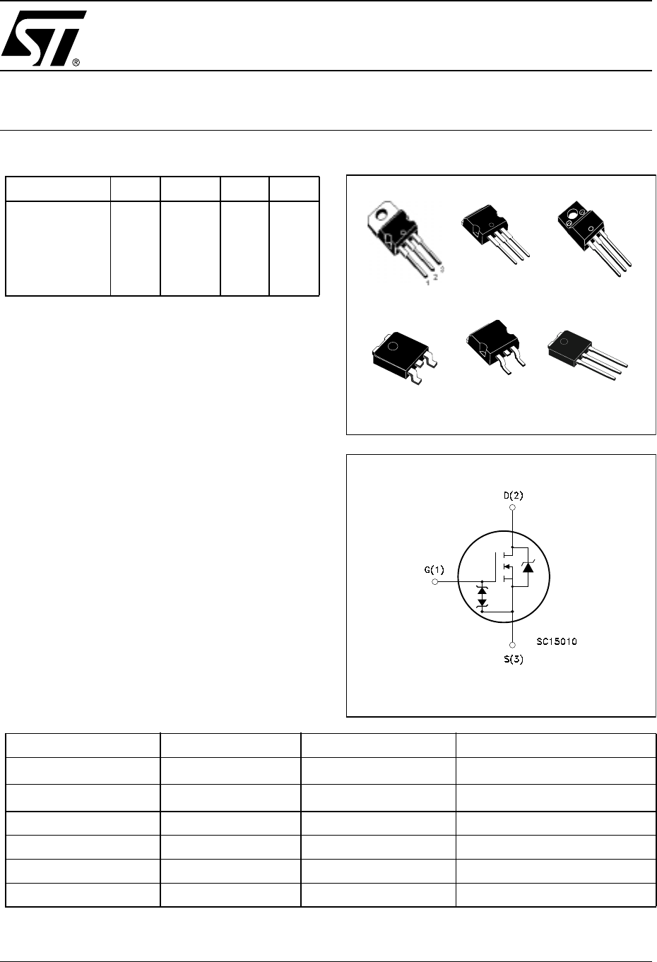
Figure 1: Package
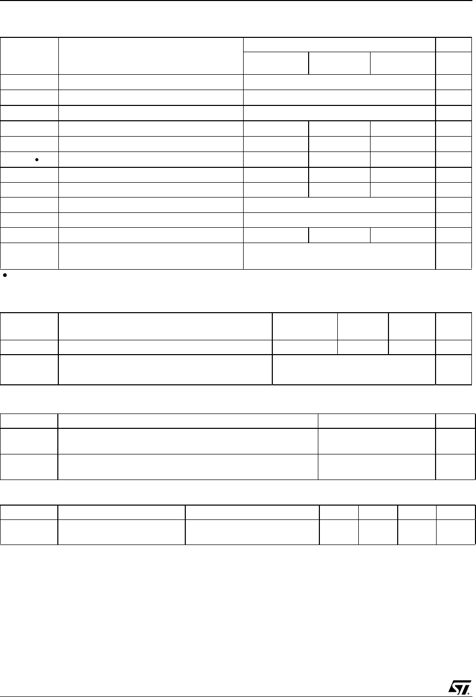
Figure 2: Internal Schematic Diagram
TYPE VDSS RDS(on) IDPw
STB5NK50Z
STB5NK50Z-1
STD5NK50Z
STD5NK50Z-1
STP5K50Z
STP5K50ZFP
500 V
500 V
500 V
500 V
500 V
500 V
< 1.5 Ω
< 1.5 Ω
< 1.5 Ω
< 1.5 Ω
< 1.5 Ω
< 1.5 Ω
4.4 A
4.4 A
4.4 A
4.4 A
4.4 A
4.4 A
70 W
70 W
70 W
70 W
70 W
25 W TO-220FP
123
1
3
DPAK
3
2
1
IPAK
123
I2PAK
TO-220
13
D2PAK
SALES TYPE MARKING PACKAGE PACKAGING
STB5NK50ZT4 B5NK50Z D2PAK TAPE & REEL
STB5NK50Z-1 B5NK50Z I2PAK TUBE
STD5NK50ZT4 D5NK50Z DPAK TAPE & REEL
STD5NK50Z-1 D5NK50Z IPAK TUBE
STP5NK50Z P5NK50Z TO-220 TUBE
STP5NK50ZFP P5NK50ZFP TO-220FP TUBE
Rev. 4
STB5NK50Z/-1 - STD5NK50Z/-1 - STP5NK50Z - STP5NK50ZFP
2/17
Table 3: Absolute Maximum ratings
() Pulse width limited by safe operating area
(1) ISD ≤4.4A, di/dt ≤200A/µs, VDD ≤ V(BR)DSS, Tj ≤ TJMAX.
(*) Limited only by maximum temperature allowed
Table 4: Thermal Data
Table 5: Avalanche Characteristics
Table 6: Gate-Source Zener Diode
PROTECTION FEATURES OF GATE-TO-SOURCE ZENER DIODES
The built-in back-to-back Zener diodes have specifically been designed to enhance not only the device’s
ESD capability, but also to make them safely absorb possible voltage transients that may occasionally be
applied from gate to source. In this respect the Zener voltage is appropriate to achieve an efficient and
cost-effective intervention to protect the device’s integrity. These integrated Zener diodes thus avoid the
usage of external components.
Symbol Parameter Value Unit
STP5NK50Z
STB5NK50Z/-1 STP5NK50ZFP STD5NK50Z
STD5NK50Z-1
VDS Drain-source Voltage (VGS = 0) 500 V
VDGR Drain-gate Voltage (RGS = 20 kΩ)500 V
VGS Gate- source Voltage ± 30 V
IDDrain Current (continuous) at TC = 25°C4.4 4.4 (*) 4.4 A
IDDrain Current (continuous) at TC = 100°C2.7 2.7 (*) 2.7 A
IDM ( ) Drain Current (pulsed) 17.6 17.6 (*) 17.6 A
PTOT Total Dissipation at TC = 25°C70 25 70 W
Derating Factor 0.56 0.2 0.56 W/°C
VESD(G-S) Gate source ESD(HBM-C=100pF, R=1.5KΩ) 3000 V
dv/dt (1) Peak Diode Recovery voltage slope 4.5 V/ns
VISO Insulation Withstand Voltage (DC) - 2500 - V
Tj
Tstg
Operating Junction Temperature
Storage Temperature -55 to 150
-55 to 150 °C
°C
TO-220
I2PAK/D2PAK TO-220FP DPAK
Rthj-case Thermal Resistance Junction-case Max 1.78 5 1.78 °C/W
Rthj-amb Thermal Resistance Junction-ambient Max 62.5 °C/W
TlMaximum Lead Temperature For Soldering Purpose 300 °C
Symbol Parameter Max Value Unit
IAR Avalanche Current, Repetitive or Not-Repetitive
(pulse width limited by Tj max) 4.4 A
EAS Single Pulse Avalanche Energy
(starting Tj = 25 °C, ID = IAR, VDD = 50 V) 130 mJ
Symbol Parameter Test Conditions Min. Typ. Max. Unit
BVGSO Gate-Source Breakdown
Voltage Igs=± 1mA (Open Drain) 30 V
3/17
STB5NK50Z/-1 - STD5NK50Z/-1 - STP5NK50Z - STP5NK50ZFP
ELECTRICAL CHARACTERISTICS (TCASE =25°C UNLESS OTHERWISE SPECIFIED)
Table 7: On /Off
Table 8: Dynamic
Table 9: Source Drain Diode
(1) Pulsed: Pulse duration = 300 µs, duty cycle 1.5 %.
(2) Pulse width limited by safe operating area.
(3) Coss eq. is defined as a constant equivalent capacitance giving the same charging time as Coss when VDS increases from 0 to 80% VDSS.
Symbol Parameter Test Conditions Min. Typ. Max. Unit
V(BR)DSS Drain-source Breakdown
Voltage ID = 1 mA, VGS = 0 500 V
IDSS Zero Gate Voltage
Drain Current (VGS = 0) VDS = Max Rating
VDS = Max Rating, TC = 125°C 1
50 µA
µA
IGSS Gate-body Leakage
Current (VDS = 0) VGS = ± 20 V ± 10 µA
VGS(th) Gate Threshold Voltage VDS = VGS, ID = 50 µA 3 3.75 4.5 V
RDS(on Static Drain-source On
Resistance VGS = 10 V, ID = 2.2 A 1.22 1.5 Ω
Symbol Parameter Test Conditions Min. Typ. Max. Unit
gfs (1) Forward Transconductance VDS = 15 V , ID = 2.2 A 3.1 S
Ciss
Coss
Crss
Input Capacitance
Output Capacitance
Reverse Transfer
Capacitance
VDS = 25 V, f = 1 MHz, VGS = 0 535
75
17
pF
pF
pF
COSS eq (3).Equivalent Output
Capacitance VGS = 0 V, VDS = 0 to 400 V 45 pF
td(on)
tr
td(off)
tf
Turn-on Delay Time
Rise Time
Turn-off-Delay Time
Fall Time
VDD = 250 V, ID = 2.2 A,
RG = 4.7 Ω, VGS = 10 V
(see Figure 19)
15
10
32
15
ns
ns
ns
ns
Qg
Qgs
Qgd
Total Gate Charge
Gate-Source Charge
Gate-Drain Charge
VDD = 400 V, ID = 4.4 A,
VGS = 10 V
(see Figure 22)
20
4
10
28 nC
nC
nC
Symbol Parameter Test Conditions Min. Typ. Max. Unit
ISD
ISDM (2) Source-drain Current
Source-drain Current (pulsed) 4.4
17.6 A
A
VSD (1) Forward On Voltage ISD = 4.4 A, VGS = 0 1.6 V
trr
Qrr
IRRM
Reverse Recovery Time
Reverse Recovery Charge
Reverse Recovery Current
ISD = 4.4 A, di/dt = 100 A/µs
VDD = 30V, Tj = 150°C
(see Figure 20)
310
1425
9.2
ns
nC
A
STB5NK50Z/-1 - STD5NK50Z/-1 - STP5NK50Z - STP5NK50ZFP
4/17
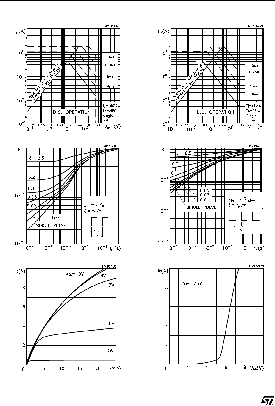
Figure 3: Safe Operating Area For DPAK/IPAK/
D2PAK/I2PAK/TO-220
Figure 4: Thermal Impedance For DPAK/IPAK/
D2PAK/I2PAK/TO-220
Figure 5: Output Characteristics
Figure 6: Safe Operating Area For TO-220FP
Figure 7: Thermal Impedance For TO-220FP
Figure 8: Transfer Characteristics
5/17
STB5NK50Z/-1 - STD5NK50Z/-1 - STP5NK50Z - STP5NK50ZFP
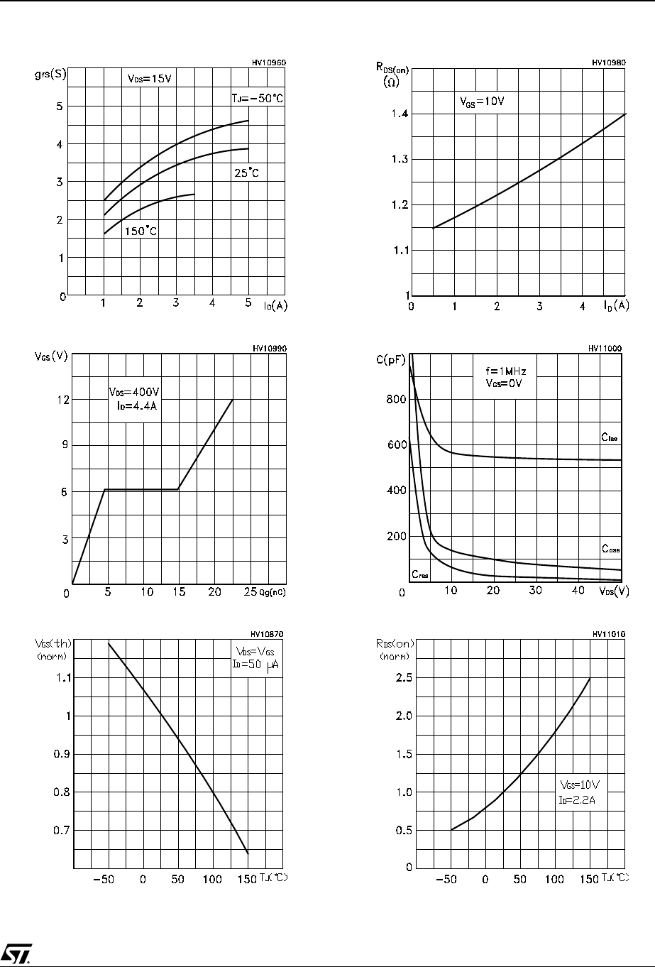
Figure 9: Transconductance
Figure 10: Gate Charge vs Gate-source Voltage
Figure 11: Normalized Gate Threshold Voltage
vs Temperature
Figure 12: Static Drain-Source On Resistance
Figure 13: Capacitance Variations
Figure 14: Normalized On Resistance vs Tem-
perature
STB5NK50Z/-1 - STD5NK50Z/-1 - STP5NK50Z - STP5NK50ZFP
6/17
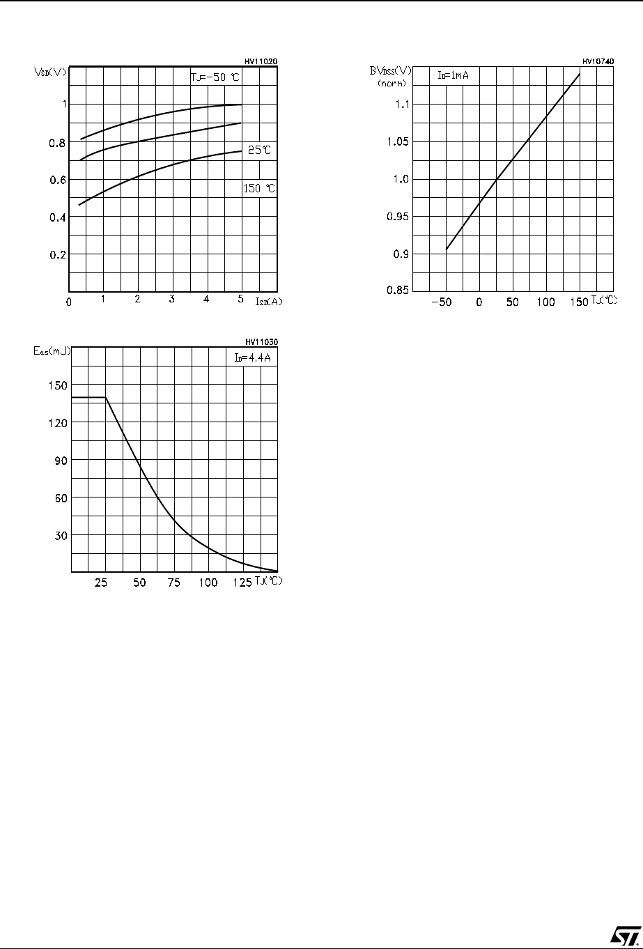
Figure 15: Source-Drain Forward Characteris-
tics
Figure 16: Maximum Avalanche Energy vs
Temperature
Figure 17: Normalized BVDSS vs Temperature
7/17
STB5NK50Z/-1 - STD5NK50Z/-1 - STP5NK50Z - STP5NK50ZFP
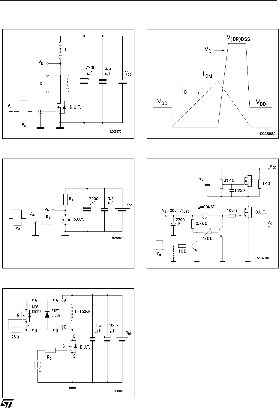
Figure 18: Unclamped Inductive Load Test Cir-
cuit
Figure 19: Switching Times Test Circuit For
Resistive Load
Figure 20: Test Circuit For Inductive Load
Switching and Diode Recovery Times
Figure 21: Unclamped Inductive Wafeform
Figure 22: Gate Charge Test Circuit
STB5NK50Z/-1 - STD5NK50Z/-1 - STP5NK50Z - STP5NK50ZFP
8/17
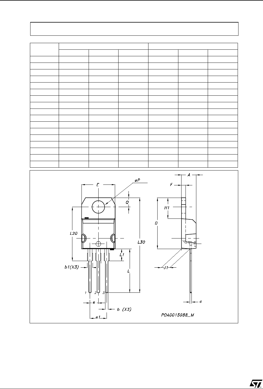
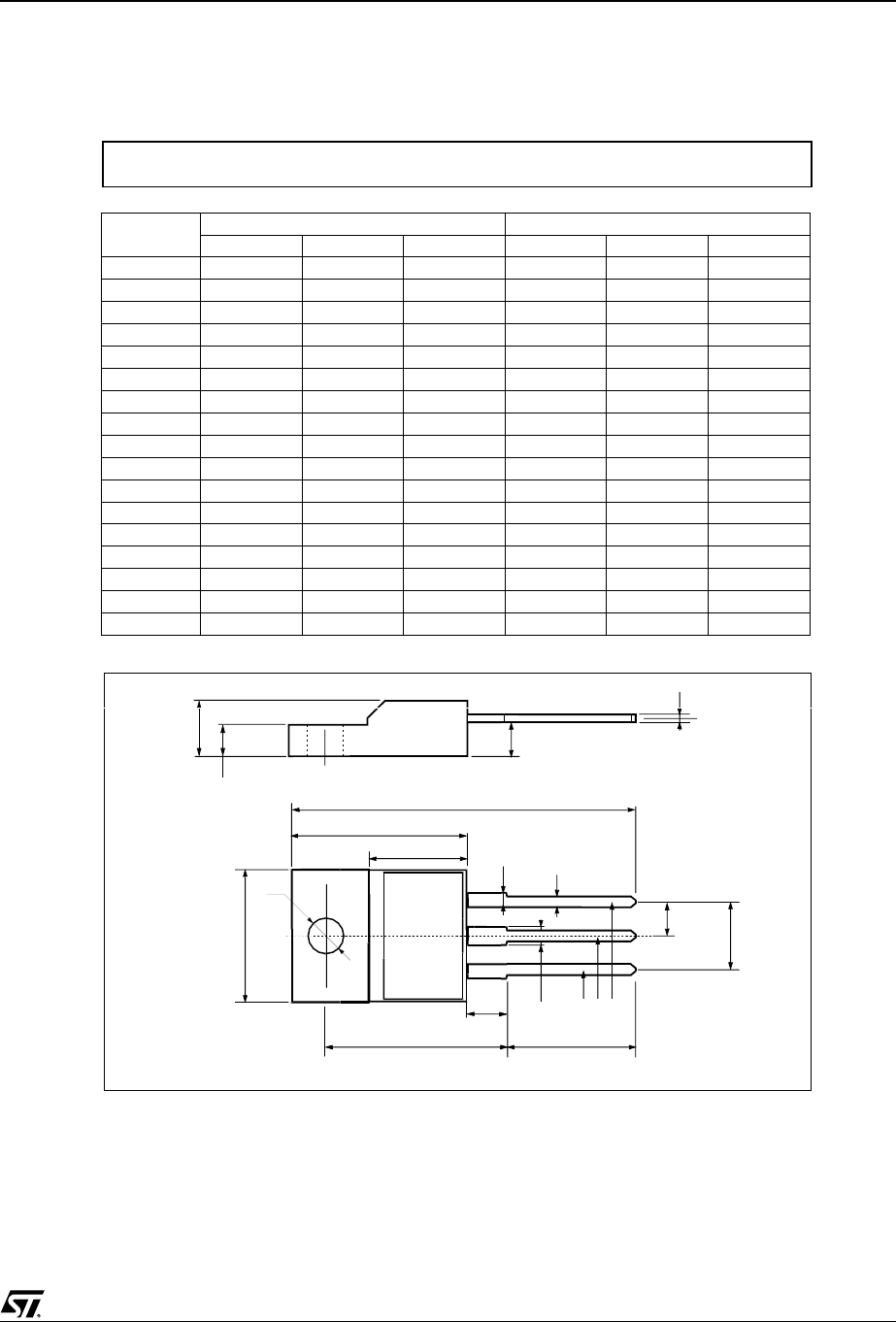
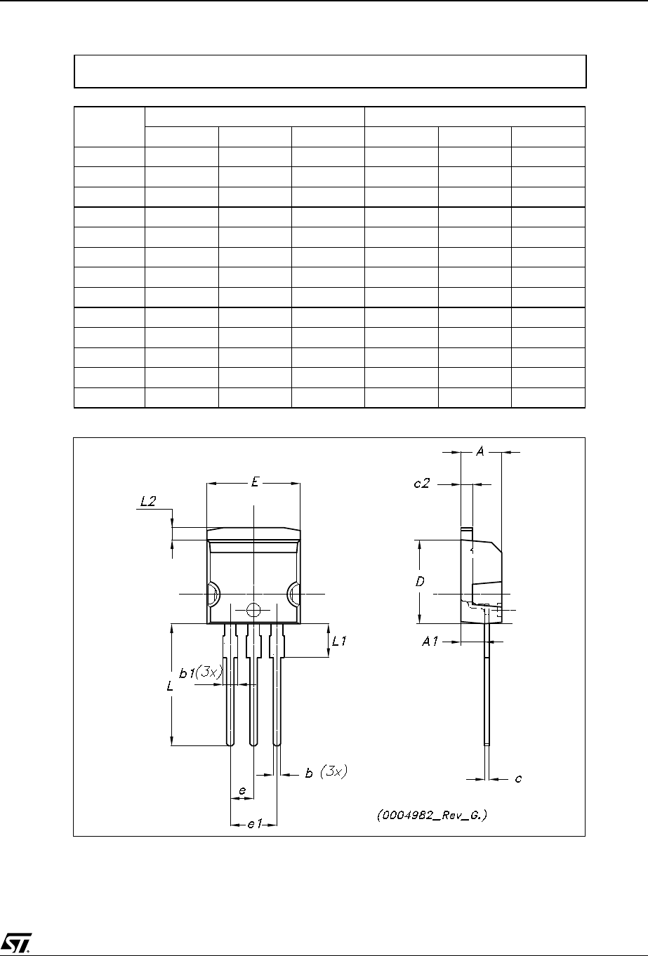
DIM. mm. inch
MIN. TYP MAX. MIN. TYP. MAX.
A 4.40 4.60 0.173 0.181
b 0.61 0.88 0.024 0.034
b1 1.15 1.70 0.045 0.066
c 0.49 0.70 0.019 0.027
D 15.25 15.75 0.60 0.620
E 10 10.40 0.393 0.409
e 2.40 2.70 0.094 0.106
e1 4.95 5.15 0.194 0.202
F 1.23 1.32 0.048 0.052
H1 6.20 6.60 0.244 0.256
J1 2.40 2.72 0.094 0.107
L 13 14 0.511 0.551
L1 3.50 3.93 0.137 0.154
L20 16.40 0.645
L30 28.90 1.137
øP 3.75 3.85 0.147 0.151
Q 2.65 2.95 0.104 0.116
TO-220 MECHANICAL DATA
9/17
STB5NK50Z/-1 - STD5NK50Z/-1 - STP5NK50Z - STP5NK50ZFP
L2
A
B
D
E
H
G
L6
F
L3
G1
123
F2
F1
L7
L4
L5
DIM. mm. inch
MIN. TYP MAX. MIN. TYP. MAX.
A 4.4 4.6 0.173 0.181
B 2.5 2.7 0.098 0.106
D 2.5 2.75 0.098 0.108
E 0.45 0.7 0.017 0.027
F 0.75 1 0.030 0.039
F1 1.15 1.7 0.045 0.067
F2 1.15 1.7 0.045 0.067
G 4.95 5.2 0.195 0.204
G1 2.4 2.7 0.094 0.106
H 10 10.4 0.393 0.409
L2 16 0.630
L3 28.6 30.6 1.126 1.204
L4 9.8 10.6 .0385 0.417
L5 2.9 3.6 0.114 0.141
L6 15.9 16.4 0.626 0.645
L7 9 9.3 0.354 0.366
Ø3 3.2 0.118 0.126
TO-220FP MECHANICAL DATA
STB5NK50Z/-1 - STD5NK50Z/-1 - STP5NK50Z - STP5NK50ZFP
10/17
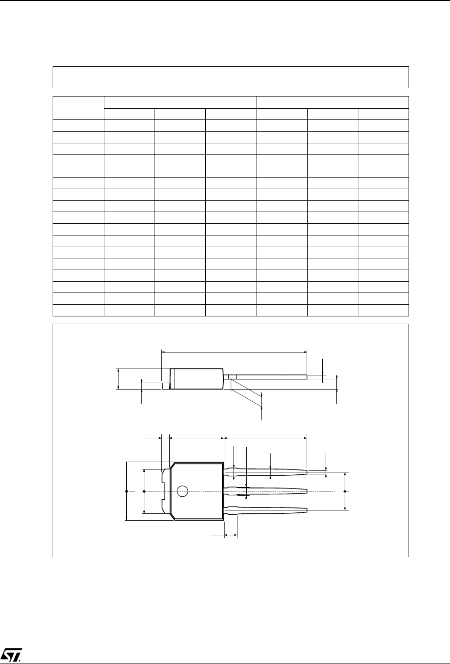
DIM. mm inch
MIN. TYP. MAX. MIN. TYP. MAX.
A 2.20 2.40 0.087 0.094
A1 0.90 1.10 0.035 0.043
A2 0.03 0.23 0.001 0.009
B 0.64 0.90 0.025 0.035
B2 5.20 5.40 0.204 0.213
C 0.45 0.60 0.018 0.024
C2 0.48 0.60 0.019 0.024
D 6.00 6.20 0.236 0.244
E 6.40 6.60 0.252 0.260
G 4.40 4.60 0.173 0.181
H 9.35 10.10 0.368 0.398
L2 0.8 0.031
L4 0.60 1.00 0.024 0.039
V2 0
o
8
o
0
o
0
o
P032P_B
TO-252 (DPAK) MECHANICAL DATA
11/17
STB5NK50Z/-1 - STD5NK50Z/-1 - STP5NK50Z - STP5NK50ZFP
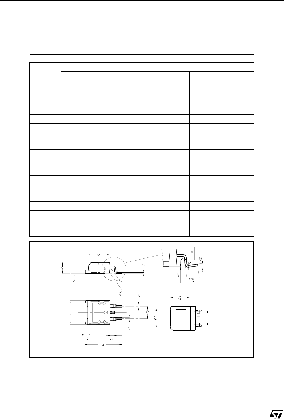
DIM. mm inch
MIN. TYP. MAX. MIN. TYP. MAX.
A 2.2 2.4 0.086 0.094
A1 0.9 1.1 0.035 0.043
A3 0.7 1.3 0.027 0.051
B 0.64 0.9 0.025 0.031
B2 5.2 5.4 0.204 0.212
B3 0.85 0.033
B5 0.3 0.012
B6 0.95 0.037
C 0.45 0.6 0.017 0.023
C2 0.48 0.6 0.019 0.023
D 6 6.2 0.236 0.244
E 6.4 6.6 0.252 0.260
G 4.4 4.6 0.173 0.181
H 15.9 16.3 0.626 0.641
L 9 9.4 0.354 0.370
L1 0.8 1.2 0.031 0.047
L2 0.8 1 0.031 0.039
A
C2
C
A3
H
A1
DL
L2
L1
1 3
= =
B3
B
B6
B2
E
G
= =
= =
B5
2
TO-251 (IPAK) MECHANICAL DATA
0068771-E
STB5NK50Z/-1 - STD5NK50Z/-1 - STP5NK50Z - STP5NK50ZFP
12/17
TO-247 MECHANICAL DATA
1
DIM. mm. inch
MIN. TYP MAX. MIN. TYP. MAX.
A 4.4 4.6 0.173 0.181
A1 2.49 2.69 0.098 0.106
A2 0.03 0.23 0.001 0.009
B 0.7 0.93 0.027 0.036
B2 1.14 1.7 0.044 0.067
C 0.45 0.6 0.017 0.023
C2 1.23 1.36 0.048 0.053
D 8.95 9.35 0.352 0.368
D1 8 0.315
E 10 10.4 0.393
E1 8.5 0.334
G 4.88 5.28 0.192 0.208
L 15 15.85 0.590 0.625
L2 1.27 1.4 0.050 0.055
L3 1.4 1.75 0.055 0.068
M 2.4 3.2 0.094 0.126
R0.4 0.015
V2 0º4º
D
2
PAK MECHANICAL DATA
3
13/17
STB5NK50Z/-1 - STD5NK50Z/-1 - STP5NK50Z - STP5NK50ZFP
DIM. mm. inch
MIN. TYP MAX. MIN. TYP. MAX.
A 4.40 4.60 0.173 0.181
A1 2.40 2.72 0.094 0.107
b 0.61 0.88 0.024 0.034
b1 1.14 1.70 0.044 0.066
c 0.49 0.70 0.019 0.027
c2 1.23 1.32 0.048 0.052
D 8.95 9.35 0.352 0.368
e 2.40 2.70 0.094 0.106
e1 4.95 5.15 0.194 0.202
E 10 10.40 0.393 0.410
L 13 14 0.511 0.551
L1 3.50 3.93 0.137 0.154
L2 1.27 1.40 0.050 0.055
TO-262 (I
2
PAK) MECHANICAL DATA
STB5NK50Z/-1 - STD5NK50Z/-1 - STP5NK50Z - STP5NK50ZFP
14/17
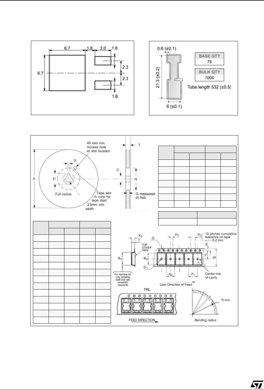
TAPE AND REEL SHIPMENT (suffix ”T4”)*
TUBE SHIPMENT (no suffix)*
DPAK FOOTPRINT
* on sales type
DIM. mm inch
MIN. MAX. MIN. MAX.
A 330 12.992
B1.5 0.059
C 12.8 13.2 0.504 0.520
D20.2 0.795
G 16.4 18.4 0.645 0.724
N50 1.968
T 22.4 0.881
BASE QTY BULK QTY
2500 2500
REEL MECHANICAL DATA
DIM. mm inch
MIN. MAX. MIN. MAX.
A0 6.8 7 0.267 0.275
B0 10.4 10.6 0.409 0.417
B1 12.1 0.476
D1.5 1.6 0.059 0.063
D1 1.5 0.059
E1.65 1.85 0.065 0.073
F 7.4 7.6 0.291 0.299
K0 2.55 2.75 0.100 0.108
P0 3.9 4.1 0.153 0.161
P1 7.9 8.1 0.311 0.319
P2 1.9 2.1 0.075 0.082
R40 1.574
W 15.7 16.3 0.618 0.641
TAPE MECHANICAL DATA
All dimensions
are in millimeters
All dimensions are in millimeters
15/17
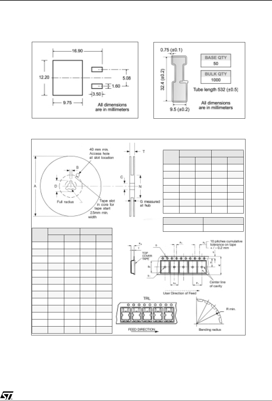
STB5NK50Z/-1 - STD5NK50Z/-1 - STP5NK50Z - STP5NK50ZFP
TAPE AND REEL SHIPMENT (suffix ”T4”)*
TUBE SHIPMENT (no suffix)*
D2PAK FOOTPRINT
* on sales type
DIM. mm inch
MIN. MAX. MIN. MAX.
A 330 12.992
B1.5 0.059
C 12.8 13.2 0.504 0.520
D20.2 0795
G 24.4 26.4 0.960 1.039
N100 3.937
T 30.4 1.197
BASE QTY BULK QTY
1000 1000
REEL MECHANICAL DATA
DIM. mm inch
MIN. MAX. MIN. MAX.
A0 10.5 10.7 0.413 0.421
B0 15.7 15.9 0.618 0.626
D 1.5 1.6 0.059 0.063
D1 1.59 1.61 0.062 0.063
E 1.65 1.85 0.065 0.073
F11.4 11.6 0.449 0.456
K0 4.8 5.0 0.189 0.197
P0 3.9 4.1 0.153 0.161
P1 11.9 12.1 0.468 0.476
P2 1.9 2.1 0.075 0.082
R 50 1.574
T 0.25 0.35 0.0098 0.0137
W23.7 24.3 0.933 0.956
TAPE MECHANICAL DATA

STB5NK50Z/-1 - STD5NK50Z/-1 - STP5NK50Z - STP5NK50ZFP
16/17
Table 10: Revision History
Date Revision Description of Changes
16-June-2004 1 D2PAK Included. New Stylesheet.

17/17
STB5NK50Z/-1 - STD5NK50Z/-1 - STP5NK50Z - STP5NK50ZFP
Information furnished is believed to be accurate and reliable. However, STMicroelectronics assumes no responsibility for the
consequences of use of such information nor for any infringement of patents or other rights of third parties which may result from
its use. No license is granted by implication or otherwise under any patent or patent rights of STMicroelectronics. Specifications
mentioned in this publication are subject to change without notice. This publication supersedes and replaces all information
previously supplied. STMicroelectronics products are not authorized for use as critical components in life support devices or
systems without express written approval of STMicroelectronics.
The ST logo is a registered trademark of STMicroelectronics
All other names are the property of their respective owners
© 2004 STMicroelectronics - All Rights Reserved
STMicroelectronics GROUP OF COMPANIES
Australia - Belgium - Brazil - Canada - China - Czech Republic - Finland - France - Germany - Hong Kong - India - Israel - Italy - Japan -
Malaysia - Malta - Morocco - Singapore - Spain - Sweden - Switzerland - United Kingdom - United States.