STM32F405/415, STM32F407/417, STM32F427/437 And STM32F429/439 Advanced ARM® Based 32 Bit MCUs Stm32f429xx Reference Manual
stm32f407xx_reference_manual
User Manual:
Open the PDF directly: View PDF ![]() .
.
Page Count: 1718 [warning: Documents this large are best viewed by clicking the View PDF Link!]
- 1 Documentation conventions
- 2 Memory and bus architecture
- 3 Embedded Flash memory interface
- 3.1 Introduction
- 3.2 Main features
- 3.3 Embedded Flash memory in STM32F405xx/07xx and STM32F415xx/17xx
- 3.4 Embedded Flash memory in STM32F42xxx and STM32F43xxx
- Table 6. Flash module - 2 Mbyte dual bank organization (STM32F42xxx and STM32F43xxx)
- Table 7. 1 Mbyte Flash memory single bank vs dual bank organization (STM32F42xxx and STM32F43xxx)
- Table 8. 1 Mbyte single bank Flash memory organization (STM32F42xxx and STM32F43xxx)
- Table 9. 1 Mbyte dual bank Flash memory organization (STM32F42xxx and STM32F43xxx)
- 3.5 Read interface
- 3.6 Erase and program operations
- 3.7 Option bytes
- 3.8 One-time programmable bytes
- 3.9 Flash interface registers
- 3.9.1 Flash access control register (FLASH_ACR) for STM32F405xx/07xx and STM32F415xx/17xx
- 3.9.2 Flash access control register (FLASH_ACR) for STM32F42xxx and STM32F43xxx
- 3.9.3 Flash key register (FLASH_KEYR)
- 3.9.4 Flash option key register (FLASH_OPTKEYR)
- 3.9.5 Flash status register (FLASH_SR) for STM32F405xx/07xx and STM32F415xx/17xx
- 3.9.6 Flash status register (FLASH_SR) for STM32F42xxx and STM32F43xxx
- 3.9.7 Flash control register (FLASH_CR) for STM32F405xx/07xx and STM32F415xx/17xx
- 3.9.8 Flash control register (FLASH_CR) for STM32F42xxx and STM32F43xxx
- 3.9.9 Flash option control register (FLASH_OPTCR) for STM32F405xx/07xx and STM32F415xx/17xx
- 3.9.10 Flash option control register (FLASH_OPTCR) for STM32F42xxx and STM32F43xxx
- 3.9.11 Flash option control register (FLASH_OPTCR1) for STM32F42xxx and STM32F43xxx
- 3.9.12 Flash interface register map
- 4 CRC calculation unit
- 5 Power controller (PWR)
- 5.1 Power supplies
- 5.2 Power supply supervisor
- 5.3 Low-power modes
- Entering low-power mode
- Exiting low-power mode
- 5.3.1 Slowing down system clocks
- 5.3.2 Peripheral clock gating
- 5.3.3 Sleep mode
- 5.3.4 Stop mode (STM32F405xx/07xx and STM32F415xx/17xx)
- 5.3.5 Stop mode (STM32F42xxx and STM32F43xxx)
- 5.3.6 Standby mode
- 5.3.7 Programming the RTC alternate functions to wake up the device from the Stop and Standby modes
- 5.4 Power control registers (STM32F405xx/07xx and STM32F415xx/17xx)
- 5.5 Power control registers (STM32F42xxx and STM32F43xxx)
- 5.6 PWR register map
- 6 Reset and clock control for STM32F42xxx and STM32F43xxx (RCC)
- 6.1 Reset
- 6.2 Clocks
- 6.3 RCC registers
- 6.3.1 RCC clock control register (RCC_CR)
- 6.3.2 RCC PLL configuration register (RCC_PLLCFGR)
- 6.3.3 RCC clock configuration register (RCC_CFGR)
- 6.3.4 RCC clock interrupt register (RCC_CIR)
- 6.3.5 RCC AHB1 peripheral reset register (RCC_AHB1RSTR)
- 6.3.6 RCC AHB2 peripheral reset register (RCC_AHB2RSTR)
- 6.3.7 RCC AHB3 peripheral reset register (RCC_AHB3RSTR)
- 6.3.8 RCC APB1 peripheral reset register (RCC_APB1RSTR)
- 6.3.9 RCC APB2 peripheral reset register (RCC_APB2RSTR)
- 6.3.10 RCC AHB1 peripheral clock register (RCC_AHB1ENR)
- 6.3.11 RCC AHB2 peripheral clock enable register (RCC_AHB2ENR)
- 6.3.12 RCC AHB3 peripheral clock enable register (RCC_AHB3ENR)
- 6.3.13 RCC APB1 peripheral clock enable register (RCC_APB1ENR)
- 6.3.14 RCC APB2 peripheral clock enable register (RCC_APB2ENR)
- 6.3.15 RCC AHB1 peripheral clock enable in low power mode register (RCC_AHB1LPENR)
- 6.3.16 RCC AHB2 peripheral clock enable in low power mode register (RCC_AHB2LPENR)
- 6.3.17 RCC AHB3 peripheral clock enable in low power mode register (RCC_AHB3LPENR)
- 6.3.18 RCC APB1 peripheral clock enable in low power mode register (RCC_APB1LPENR)
- 6.3.19 RCC APB2 peripheral clock enabled in low power mode register (RCC_APB2LPENR)
- 6.3.20 RCC Backup domain control register (RCC_BDCR)
- 6.3.21 RCC clock control & status register (RCC_CSR)
- 6.3.22 RCC spread spectrum clock generation register (RCC_SSCGR)
- 6.3.23 RCC PLLI2S configuration register (RCC_PLLI2SCFGR)
- 6.3.24 RCC PLL configuration register (RCC_PLLSAICFGR)
- 6.3.25 RCC Dedicated Clock Configuration Register (RCC_DCKCFGR)
- 6.3.26 RCC register map
- 7 Reset and clock control for STM32F405xx/07xx and STM32F415xx/17xx(RCC)
- 7.1 Reset
- 7.2 Clocks
- 7.3 RCC registers
- 7.3.1 RCC clock control register (RCC_CR)
- 7.3.2 RCC PLL configuration register (RCC_PLLCFGR)
- 7.3.3 RCC clock configuration register (RCC_CFGR)
- 7.3.4 RCC clock interrupt register (RCC_CIR)
- 7.3.5 RCC AHB1 peripheral reset register (RCC_AHB1RSTR)
- 7.3.6 RCC AHB2 peripheral reset register (RCC_AHB2RSTR)
- 7.3.7 RCC AHB3 peripheral reset register (RCC_AHB3RSTR)
- 7.3.8 RCC APB1 peripheral reset register (RCC_APB1RSTR)
- 7.3.9 RCC APB2 peripheral reset register (RCC_APB2RSTR)
- 7.3.10 RCC AHB1 peripheral clock enable register (RCC_AHB1ENR)
- 7.3.11 RCC AHB2 peripheral clock enable register (RCC_AHB2ENR)
- 7.3.12 RCC AHB3 peripheral clock enable register (RCC_AHB3ENR)
- 7.3.13 RCC APB1 peripheral clock enable register (RCC_APB1ENR)
- 7.3.14 RCC APB2 peripheral clock enable register (RCC_APB2ENR)
- 7.3.15 RCC APB2 peripheral clock enable register(RCC_APB2ENR)
- 7.3.16 RCC AHB1 peripheral clock enable in low power mode register (RCC_AHB1LPENR)
- 7.3.17 RCC AHB2 peripheral clock enable in low power mode register (RCC_AHB2LPENR)
- 7.3.18 RCC AHB3 peripheral clock enable in low power mode register (RCC_AHB3LPENR)
- 7.3.19 RCC APB1 peripheral clock enable in low power mode register (RCC_APB1LPENR)
- 7.3.20 RCC APB2 peripheral clock enabled in low power mode register (RCC_APB2LPENR)
- 7.3.21 RCC Backup domain control register (RCC_BDCR)
- 7.3.22 RCC clock control & status register (RCC_CSR)
- 7.3.23 RCC spread spectrum clock generation register (RCC_SSCGR)
- 7.3.24 RCC PLLI2S configuration register (RCC_PLLI2SCFGR)
- 7.3.25 RCC register map
- 8 General-purpose I/Os (GPIO)
- 8.1 GPIO introduction
- 8.2 GPIO main features
- 8.3 GPIO functional description
- Table 35. Port bit configuration table
- 8.3.1 General-purpose I/O (GPIO)
- 8.3.2 I/O pin multiplexer and mapping
- 8.3.3 I/O port control registers
- 8.3.4 I/O port data registers
- 8.3.5 I/O data bitwise handling
- 8.3.6 GPIO locking mechanism
- 8.3.7 I/O alternate function input/output
- 8.3.8 External interrupt/wakeup lines
- 8.3.9 Input configuration
- 8.3.10 Output configuration
- 8.3.11 Alternate function configuration
- 8.3.12 Analog configuration
- 8.3.13 Using the OSC32_IN/OSC32_OUT pins as GPIO PC14/PC15 port pins
- 8.3.14 Using the OSC_IN/OSC_OUT pins as GPIO PH0/PH1 port pins
- 8.3.15 Selection of RTC_AF1 and RTC_AF2 alternate functions
- 8.4 GPIO registers
- 8.4.1 GPIO port mode register (GPIOx_MODER) (x = A..I/J/K)
- 8.4.2 GPIO port output type register (GPIOx_OTYPER) (x = A..I/J/K)
- 8.4.3 GPIO port output speed register (GPIOx_OSPEEDR) (x = A..I/J/K)
- 8.4.4 GPIO port pull-up/pull-down register (GPIOx_PUPDR) (x = A..I/J/K)
- 8.4.5 GPIO port input data register (GPIOx_IDR) (x = A..I/J/K)
- 8.4.6 GPIO port output data register (GPIOx_ODR) (x = A..I/J/K)
- 8.4.7 GPIO port bit set/reset register (GPIOx_BSRR) (x = A..I/J/K)
- 8.4.8 GPIO port configuration lock register (GPIOx_LCKR) (x = A..I/J/K)
- 8.4.9 GPIO alternate function low register (GPIOx_AFRL) (x = A..I/J/K)
- 8.4.10 GPIO alternate function high register (GPIOx_AFRH) (x = A..I/J)
- 8.4.11 GPIO register map
- 9 System configuration controller (SYSCFG)
- 9.1 I/O compensation cell
- 9.2 SYSCFG registers for STM32F405xx/07xx and STM32F415xx/17xx
- 9.2.1 SYSCFG memory remap register (SYSCFG_MEMRMP)
- 9.2.2 SYSCFG peripheral mode configuration register (SYSCFG_PMC)
- 9.2.3 SYSCFG external interrupt configuration register 1 (SYSCFG_EXTICR1)
- 9.2.4 SYSCFG external interrupt configuration register 2 (SYSCFG_EXTICR2)
- 9.2.5 SYSCFG external interrupt configuration register 3 (SYSCFG_EXTICR3)
- 9.2.6 SYSCFG external interrupt configuration register 4 (SYSCFG_EXTICR4)
- 9.2.7 Compensation cell control register (SYSCFG_CMPCR)
- 9.2.8 SYSCFG register maps for STM32F405xx/07xx and STM32F415xx/17xx
- 9.3 SYSCFG registers for STM32F42xxx and STM32F43xxx
- 9.3.1 SYSCFG memory remap register (SYSCFG_MEMRMP)
- 9.3.2 SYSCFG peripheral mode configuration register (SYSCFG_PMC)
- 9.3.3 SYSCFG external interrupt configuration register 1 (SYSCFG_EXTICR1)
- 9.3.4 SYSCFG external interrupt configuration register 2 (SYSCFG_EXTICR2)
- 9.3.5 SYSCFG external interrupt configuration register 3 (SYSCFG_EXTICR3)
- 9.3.6 SYSCFG external interrupt configuration register 4 (SYSCFG_EXTICR4)
- 9.3.7 Compensation cell control register (SYSCFG_CMPCR)
- 9.3.8 SYSCFG register maps for STM32F42xxx and STM32F43xxx
- 10 DMA controller (DMA)
- 10.1 DMA introduction
- 10.2 DMA main features
- 10.3 DMA functional description
- 10.3.1 General description
- 10.3.2 DMA transactions
- 10.3.3 Channel selection
- 10.3.4 Arbiter
- 10.3.5 DMA streams
- 10.3.6 Source, destination and transfer modes
- 10.3.7 Pointer incrementation
- 10.3.8 Circular mode
- 10.3.9 Double buffer mode
- 10.3.10 Programmable data width, packing/unpacking, endianess
- 10.3.11 Single and burst transfers
- 10.3.12 FIFO
- 10.3.13 DMA transfer completion
- 10.3.14 DMA transfer suspension
- 10.3.15 Flow controller
- 10.3.16 Summary of the possible DMA configurations
- 10.3.17 Stream configuration procedure
- 10.3.18 Error management
- 10.4 DMA interrupts
- 10.5 DMA registers
- 10.5.1 DMA low interrupt status register (DMA_LISR)
- 10.5.2 DMA high interrupt status register (DMA_HISR)
- 10.5.3 DMA low interrupt flag clear register (DMA_LIFCR)
- 10.5.4 DMA high interrupt flag clear register (DMA_HIFCR)
- 10.5.5 DMA stream x configuration register (DMA_SxCR) (x = 0..7)
- 10.5.6 DMA stream x number of data register (DMA_SxNDTR) (x = 0..7)
- 10.5.7 DMA stream x peripheral address register (DMA_SxPAR) (x = 0..7)
- 10.5.8 DMA stream x memory 0 address register (DMA_SxM0AR) (x = 0..7)
- 10.5.9 DMA stream x memory 1 address register (DMA_SxM1AR) (x = 0..7)
- 10.5.10 DMA stream x FIFO control register (DMA_SxFCR) (x = 0..7)
- 10.5.11 DMA register map
- 11 Chrom-Art Accelerator™ controller (DMA2D)
- 11.1 DMA2D introduction
- 11.2 DMA2D main features
- 11.3 DMA2D functional description
- 11.3.1 General description
- 11.3.2 DMA2D control
- 11.3.3 DMA2D foreground and background FIFOs
- 11.3.4 DMA2D foreground and background pixel format converter (PFC)
- 11.3.5 DMA2D foreground and background CLUT interface
- 11.3.6 DMA2D blender
- 11.3.7 DMA2D output PFC
- 11.3.8 DMA2D output FIFO
- 11.3.9 DMA2D AHB master port timer
- 11.3.10 DMA2D transactions
- 11.3.11 DMA2D configuration
- 11.3.12 DMA2D transfer control (start, suspend, abort and completion)
- 11.3.13 Watermark
- 11.3.14 Error management
- 11.3.15 AHB dead time
- 11.4 DMA2D interrupts
- 11.5 DMA2D registers
- 11.5.1 DMA2D control register (DMA2D_CR)
- 11.5.2 DMA2D Interrupt Status Register (DMA2D_ISR)
- 11.5.3 DMA2D interrupt flag clear register (DMA2D_IFCR)
- 11.5.4 DMA2D foreground memory address register (DMA2D_FGMAR)
- 11.5.5 DMA2D foreground offset register (DMA2D_FGOR)
- 11.5.6 DMA2D background memory address register (DMA2D_BGMAR)
- 11.5.7 DMA2D background offset register (DMA2D_BGOR)
- 11.5.8 DMA2D foreground PFC control register (DMA2D_FGPFCCR)
- 11.5.9 DMA2D foreground color register (DMA2D_FGCOLR)
- 11.5.10 DMA2D background PFC control register (DMA2D_BGPFCCR)
- 11.5.11 DMA2D background color register (DMA2D_BGCOLR)
- 11.5.12 DMA2D foreground CLUT memory address register (DMA2D_FGCMAR)
- 11.5.13 DMA2D background CLUT memory address register (DMA2D_BGCMAR)
- 11.5.14 DMA2D output PFC control register (DMA2D_OPFCCR)
- 11.5.15 DMA2D output color register (DMA2D_OCOLR)
- 11.5.16 DMA2D output memory address register (DMA2D_OMAR)
- 11.5.17 DMA2D output offset register (DMA2D_OOR)
- 11.5.18 DMA2D number of line register (DMA2D_NLR)
- 11.5.19 DMA2D line watermark register (DMA2D_LWR)
- 11.5.20 DMA2D AHB master timer configuration register (DMA2D_AMTCR)
- 11.5.21 DMA2D register map
- 12 Interrupts and events
- 12.1 Nested vectored interrupt controller (NVIC)
- 12.2 External interrupt/event controller (EXTI)
- 12.3 EXTI registers
- 13 Analog-to-digital converter (ADC)
- 13.1 ADC introduction
- 13.2 ADC main features
- 13.3 ADC functional description
- 13.4 Data alignment
- 13.5 Channel-wise programmable sampling time
- 13.6 Conversion on external trigger and trigger polarity
- 13.7 Fast conversion mode
- 13.8 Data management
- 13.9 Multi ADC mode
- 13.10 Temperature sensor
- 13.11 Battery charge monitoring
- 13.12 ADC interrupts
- 13.13 ADC registers
- 13.13.1 ADC status register (ADC_SR)
- 13.13.2 ADC control register 1 (ADC_CR1)
- 13.13.3 ADC control register 2 (ADC_CR2)
- 13.13.4 ADC sample time register 1 (ADC_SMPR1)
- 13.13.5 ADC sample time register 2 (ADC_SMPR2)
- 13.13.6 ADC injected channel data offset register x (ADC_JOFRx) (x=1..4)
- 13.13.7 ADC watchdog higher threshold register (ADC_HTR)
- 13.13.8 ADC watchdog lower threshold register (ADC_LTR)
- 13.13.9 ADC regular sequence register 1 (ADC_SQR1)
- 13.13.10 ADC regular sequence register 2 (ADC_SQR2)
- 13.13.11 ADC regular sequence register 3 (ADC_SQR3)
- 13.13.12 ADC injected sequence register (ADC_JSQR)
- 13.13.13 ADC injected data register x (ADC_JDRx) (x= 1..4)
- 13.13.14 ADC regular data register (ADC_DR)
- 13.13.15 ADC Common status register (ADC_CSR)
- 13.13.16 ADC common control register (ADC_CCR)
- 13.13.17 ADC common regular data register for dual and triple modes (ADC_CDR)
- 13.13.18 ADC register map
- 14 Digital-to-analog converter (DAC)
- 14.1 DAC introduction
- 14.2 DAC main features
- 14.3 DAC functional description
- 14.4 Dual DAC channel conversion
- 14.4.1 Independent trigger without wave generation
- 14.4.2 Independent trigger with single LFSR generation
- 14.4.3 Independent trigger with different LFSR generation
- 14.4.4 Independent trigger with single triangle generation
- 14.4.5 Independent trigger with different triangle generation
- 14.4.6 Simultaneous software start
- 14.4.7 Simultaneous trigger without wave generation
- 14.4.8 Simultaneous trigger with single LFSR generation
- 14.4.9 Simultaneous trigger with different LFSR generation
- 14.4.10 Simultaneous trigger with single triangle generation
- 14.4.11 Simultaneous trigger with different triangle generation
- 14.5 DAC registers
- 14.5.1 DAC control register (DAC_CR)
- 14.5.2 DAC software trigger register (DAC_SWTRIGR)
- 14.5.3 DAC channel1 12-bit right-aligned data holding register (DAC_DHR12R1)
- 14.5.4 DAC channel1 12-bit left aligned data holding register (DAC_DHR12L1)
- 14.5.5 DAC channel1 8-bit right aligned data holding register (DAC_DHR8R1)
- 14.5.6 DAC channel2 12-bit right aligned data holding register (DAC_DHR12R2)
- 14.5.7 DAC channel2 12-bit left aligned data holding register (DAC_DHR12L2)
- 14.5.8 DAC channel2 8-bit right-aligned data holding register (DAC_DHR8R2)
- 14.5.9 Dual DAC 12-bit right-aligned data holding register (DAC_DHR12RD)
- 14.5.10 DUAL DAC 12-bit left aligned data holding register (DAC_DHR12LD)
- 14.5.11 DUAL DAC 8-bit right aligned data holding register (DAC_DHR8RD)
- 14.5.12 DAC channel1 data output register (DAC_DOR1)
- 14.5.13 DAC channel2 data output register (DAC_DOR2)
- 14.5.14 DAC status register (DAC_SR)
- 14.5.15 DAC register map
- 15 Digital camera interface (DCMI)
- 15.1 DCMI introduction
- 15.2 DCMI main features
- 15.3 DCMI pins
- 15.4 DCMI clocks
- 15.5 DCMI functional overview
- 15.6 Data format description
- 15.7 DCMI interrupts
- 15.8 DCMI register description
- 15.8.1 DCMI control register 1 (DCMI_CR)
- 15.8.2 DCMI status register (DCMI_SR)
- 15.8.3 DCMI raw interrupt status register (DCMI_RIS)
- 15.8.4 DCMI interrupt enable register (DCMI_IER)
- 15.8.5 DCMI masked interrupt status register (DCMI_MIS)
- 15.8.6 DCMI interrupt clear register (DCMI_ICR)
- 15.8.7 DCMI embedded synchronization code register (DCMI_ESCR)
- 15.8.8 DCMI embedded synchronization unmask register (DCMI_ESUR)
- 15.8.9 DCMI crop window start (DCMI_CWSTRT)
- 15.8.10 DCMI crop window size (DCMI_CWSIZE)
- 15.8.11 DCMI data register (DCMI_DR)
- 15.8.12 DCMI register map
- 16 LCD-TFT Controller (LTDC)
- 16.1 Introduction
- 16.2 LTDC main features
- 16.3 LTDC functional description
- 16.4 LTDC programmable parameters
- 16.5 LTDC interrupts
- 16.6 LTDC programming procedure
- 16.7 LTDC registers
- 16.7.1 LTDC Synchronization Size Configuration Register (LTDC_SSCR)
- 16.7.2 LTDC Back Porch Configuration Register (LTDC_BPCR)
- 16.7.3 LTDC Active Width Configuration Register (LTDC_AWCR)
- 16.7.4 LTDC Total Width Configuration Register (LTDC_TWCR)
- 16.7.5 LTDC Global Control Register (LTDC_GCR)
- 16.7.6 LTDC Shadow Reload Configuration Register (LTDC_SRCR)
- 16.7.7 LTDC Background Color Configuration Register (LTDC_BCCR)
- 16.7.8 LTDC Interrupt Enable Register (LTDC_IER)
- 16.7.9 LTDC Interrupt Status Register (LTDC_ISR)
- 16.7.10 LTDC Interrupt Clear Register (LTDC_ICR)
- 16.7.11 LTDC Line Interrupt Position Configuration Register (LTDC_LIPCR)
- 16.7.12 LTDC Current Position Status Register (LTDC_CPSR)
- 16.7.13 LTDC Current Display Status Register (LTDC_CDSR)
- 16.7.14 LTDC Layerx Control Register (LTDC_LxCR) (where x=1..2)
- 16.7.15 LTDC Layerx Window Horizontal Position Configuration Register (LTDC_LxWHPCR) (where x=1..2)
- 16.7.16 LTDC Layerx Window Vertical Position Configuration Register (LTDC_LxWVPCR) (where x=1..2)
- 16.7.17 LTDC Layerx Color Keying Configuration Register (LTDC_LxCKCR) (where x=1..2)
- 16.7.18 LTDC Layerx Pixel Format Configuration Register (LTDC_LxPFCR) (where x=1..2)
- 16.7.19 LTDC Layerx Constant Alpha Configuration Register (LTDC_LxCACR) (where x=1..2)
- 16.7.20 LTDC Layerx Default Color Configuration Register (LTDC_LxDCCR) (where x=1..2)
- 16.7.21 LTDC Layerx Blending Factors Configuration Register (LTDC_LxBFCR) (where x=1..2)
- 16.7.22 LTDC Layerx Color Frame Buffer Address Register (LTDC_LxCFBAR) (where x=1..2)
- 16.7.23 LTDC Layerx Color Frame Buffer Length Register (LTDC_LxCFBLR) (where x=1..2)
- 16.7.24 LTDC Layerx ColorFrame Buffer Line Number Register (LTDC_LxCFBLNR) (where x=1..2)
- 16.7.25 LTDC Layerx CLUT Write Register (LTDC_LxCLUTWR) (where x=1..2)
- 16.7.26 LTDC register map
- 17 Advanced-control timers (TIM1&TIM8)
- 17.1 TIM1&TIM8 introduction
- 17.2 TIM1&TIM8 main features
- 17.3 TIM1&TIM8 functional description
- 17.3.1 Time-base unit
- 17.3.2 Counter modes
- 17.3.3 Repetition counter
- 17.3.4 Clock selection
- 17.3.5 Capture/compare channels
- 17.3.6 Input capture mode
- 17.3.7 PWM input mode
- 17.3.8 Forced output mode
- 17.3.9 Output compare mode
- 17.3.10 PWM mode
- 17.3.11 Complementary outputs and dead-time insertion
- 17.3.12 Using the break function
- 17.3.13 Clearing the OCxREF signal on an external event
- 17.3.14 6-step PWM generation
- 17.3.15 One-pulse mode
- 17.3.16 Encoder interface mode
- 17.3.17 Timer input XOR function
- 17.3.18 Interfacing with Hall sensors
- 17.3.19 TIMx and external trigger synchronization
- 17.3.20 Timer synchronization
- 17.3.21 Debug mode
- 17.4 TIM1&TIM8 registers
- 17.4.1 TIM1&TIM8 control register 1 (TIMx_CR1)
- 17.4.2 TIM1&TIM8 control register 2 (TIMx_CR2)
- 17.4.3 TIM1&TIM8 slave mode control register (TIMx_SMCR)
- 17.4.4 TIM1&TIM8 DMA/interrupt enable register (TIMx_DIER)
- 17.4.5 TIM1&TIM8 status register (TIMx_SR)
- 17.4.6 TIM1&TIM8 event generation register (TIMx_EGR)
- 17.4.7 TIM1&TIM8 capture/compare mode register 1 (TIMx_CCMR1)
- 17.4.8 TIM1&TIM8 capture/compare mode register 2 (TIMx_CCMR2)
- 17.4.9 TIM1&TIM8 capture/compare enable register (TIMx_CCER)
- 17.4.10 TIM1&TIM8 counter (TIMx_CNT)
- 17.4.11 TIM1&TIM8 prescaler (TIMx_PSC)
- 17.4.12 TIM1&TIM8 auto-reload register (TIMx_ARR)
- 17.4.13 TIM1&TIM8 repetition counter register (TIMx_RCR)
- 17.4.14 TIM1&TIM8 capture/compare register 1 (TIMx_CCR1)
- 17.4.15 TIM1&TIM8 capture/compare register 2 (TIMx_CCR2)
- 17.4.16 TIM1&TIM8 capture/compare register 3 (TIMx_CCR3)
- 17.4.17 TIM1&TIM8 capture/compare register 4 (TIMx_CCR4)
- 17.4.18 TIM1&TIM8 break and dead-time register (TIMx_BDTR)
- 17.4.19 TIM1&TIM8 DMA control register (TIMx_DCR)
- 17.4.20 TIM1&TIM8 DMA address for full transfer (TIMx_DMAR)
- 17.4.21 TIM1&TIM8 register map
- 18 General-purpose timers (TIM2 to TIM5)
- 18.1 TIM2 to TIM5 introduction
- 18.2 TIM2 to TIM5 main features
- 18.3 TIM2 to TIM5 functional description
- 18.3.1 Time-base unit
- 18.3.2 Counter modes
- 18.3.3 Clock selection
- 18.3.4 Capture/compare channels
- 18.3.5 Input capture mode
- 18.3.6 PWM input mode
- 18.3.7 Forced output mode
- 18.3.8 Output compare mode
- 18.3.9 PWM mode
- 18.3.10 One-pulse mode
- 18.3.11 Clearing the OCxREF signal on an external event
- 18.3.12 Encoder interface mode
- 18.3.13 Timer input XOR function
- 18.3.14 Timers and external trigger synchronization
- 18.3.15 Timer synchronization
- 18.3.16 Debug mode
- 18.4 TIM2 to TIM5 registers
- 18.4.1 TIMx control register 1 (TIMx_CR1)
- 18.4.2 TIMx control register 2 (TIMx_CR2)
- 18.4.3 TIMx slave mode control register (TIMx_SMCR)
- 18.4.4 TIMx DMA/Interrupt enable register (TIMx_DIER)
- 18.4.5 TIMx status register (TIMx_SR)
- 18.4.6 TIMx event generation register (TIMx_EGR)
- 18.4.7 TIMx capture/compare mode register 1 (TIMx_CCMR1)
- 18.4.8 TIMx capture/compare mode register 2 (TIMx_CCMR2)
- 18.4.9 TIMx capture/compare enable register (TIMx_CCER)
- 18.4.10 TIMx counter (TIMx_CNT)
- 18.4.11 TIMx prescaler (TIMx_PSC)
- 18.4.12 TIMx auto-reload register (TIMx_ARR)
- 18.4.13 TIMx capture/compare register 1 (TIMx_CCR1)
- 18.4.14 TIMx capture/compare register 2 (TIMx_CCR2)
- 18.4.15 TIMx capture/compare register 3 (TIMx_CCR3)
- 18.4.16 TIMx capture/compare register 4 (TIMx_CCR4)
- 18.4.17 TIMx DMA control register (TIMx_DCR)
- 18.4.18 TIMx DMA address for full transfer (TIMx_DMAR)
- 18.4.19 TIM2 option register (TIM2_OR)
- 18.4.20 TIM5 option register (TIM5_OR)
- 18.4.21 TIMx register map
- 19 General-purpose timers (TIM9 to TIM14)
- 19.1 TIM9 to TIM14 introduction
- 19.2 TIM9 to TIM14 main features
- 19.3 TIM9 to TIM14 functional description
- 19.3.1 Time-base unit
- 19.3.2 Counter modes
- 19.3.3 Clock selection
- 19.3.4 Capture/compare channels
- 19.3.5 Input capture mode
- 19.3.6 PWM input mode (only for TIM9/12)
- 19.3.7 Forced output mode
- 19.3.8 Output compare mode
- 19.3.9 PWM mode
- 19.3.10 One-pulse mode
- 19.3.11 TIM9/12 external trigger synchronization
- 19.3.12 Timer synchronization (TIM9/12)
- 19.3.13 Debug mode
- 19.4 TIM9 and TIM12 registers
- 19.4.1 TIM9/12 control register 1 (TIMx_CR1)
- 19.4.2 TIM9/12 slave mode control register (TIMx_SMCR)
- 19.4.3 TIM9/12 Interrupt enable register (TIMx_DIER)
- 19.4.4 TIM9/12 status register (TIMx_SR)
- 19.4.5 TIM9/12 event generation register (TIMx_EGR)
- 19.4.6 TIM9/12 capture/compare mode register 1 (TIMx_CCMR1)
- 19.4.7 TIM9/12 capture/compare enable register (TIMx_CCER)
- 19.4.8 TIM9/12 counter (TIMx_CNT)
- 19.4.9 TIM9/12 prescaler (TIMx_PSC)
- 19.4.10 TIM9/12 auto-reload register (TIMx_ARR)
- 19.4.11 TIM9/12 capture/compare register 1 (TIMx_CCR1)
- 19.4.12 TIM9/12 capture/compare register 2 (TIMx_CCR2)
- 19.4.13 TIM9/12 register map
- 19.5 TIM10/11/13/14 registers
- 19.5.1 TIM10/11/13/14 control register 1 (TIMx_CR1)
- 19.5.2 TIM10/11/13/14 Interrupt enable register (TIMx_DIER)
- 19.5.3 TIM10/11/13/14 status register (TIMx_SR)
- 19.5.4 TIM10/11/13/14 event generation register (TIMx_EGR)
- 19.5.5 TIM10/11/13/14 capture/compare mode register 1 (TIMx_CCMR1)
- 19.5.6 TIM10/11/13/14 capture/compare enable register (TIMx_CCER)
- 19.5.7 TIM10/11/13/14 counter (TIMx_CNT)
- 19.5.8 TIM10/11/13/14 prescaler (TIMx_PSC)
- 19.5.9 TIM10/11/13/14 auto-reload register (TIMx_ARR)
- 19.5.10 TIM10/11/13/14 capture/compare register 1 (TIMx_CCR1)
- 19.5.11 TIM11 option register 1 (TIM11_OR)
- 19.5.12 TIM10/11/13/14 register map
- 20 Basic timers (TIM6&TIM7)
- 20.1 TIM6&TIM7 introduction
- 20.2 TIM6&TIM7 main features
- 20.3 TIM6&TIM7 functional description
- 20.4 TIM6&TIM7 registers
- 20.4.1 TIM6&TIM7 control register 1 (TIMx_CR1)
- 20.4.2 TIM6&TIM7 control register 2 (TIMx_CR2)
- 20.4.3 TIM6&TIM7 DMA/Interrupt enable register (TIMx_DIER)
- 20.4.4 TIM6&TIM7 status register (TIMx_SR)
- 20.4.5 TIM6&TIM7 event generation register (TIMx_EGR)
- 20.4.6 TIM6&TIM7 counter (TIMx_CNT)
- 20.4.7 TIM6&TIM7 prescaler (TIMx_PSC)
- 20.4.8 TIM6&TIM7 auto-reload register (TIMx_ARR)
- 20.4.9 TIM6&TIM7 register map
- 21 Independent watchdog (IWDG)
- 22 Window watchdog (WWDG)
- 23 Cryptographic processor (CRYP)
- 23.1 CRYP introduction
- 23.2 CRYP main features
- 23.3 CRYP functional description
- 23.4 CRYP interrupts
- 23.5 CRYP DMA interface
- 23.6 CRYP registers
- 23.6.1 CRYP control register (CRYP_CR) for STM32F415/417xx
- 23.6.2 CRYP control register (CRYP_CR) for STM32F415/417xx
- 23.6.3 CRYP status register (CRYP_SR)
- 23.6.4 CRYP data input register (CRYP_DIN)
- 23.6.5 CRYP data output register (CRYP_DOUT)
- 23.6.6 CRYP DMA control register (CRYP_DMACR)
- 23.6.7 CRYP interrupt mask set/clear register (CRYP_IMSCR)
- 23.6.8 CRYP raw interrupt status register (CRYP_RISR)
- 23.6.9 CRYP masked interrupt status register (CRYP_MISR)
- 23.6.10 CRYP key registers (CRYP_K0...3(L/R)R)
- 23.6.11 CRYP initialization vector registers (CRYP_IV0...1(L/R)R)
- 23.6.12 CRYP context swap registers (CRYP_CSGCMCCM0..7R and CRYP_CSGCM0..7R) for STM32F42xxx and STM32F43xxx
- 23.6.13 CRYP register map
- 24 Random number generator (RNG)
- 25 Hash processor (HASH)
- 25.1 HASH introduction
- 25.2 HASH main features
- 25.3 HASH functional description
- 25.4 HASH registers
- 25.4.1 HASH control register (HASH_CR) for STM32F415/417xx
- 25.4.2 HASH control register (HASH_CR) for STM32F43xxx
- 25.4.3 HASH data input register (HASH_DIN)
- 25.4.4 HASH start register (HASH_STR)
- 25.4.5 HASH digest registers (HASH_HR0..4/5/6/7)
- 25.4.6 HASH interrupt enable register (HASH_IMR)
- 25.4.7 HASH status register (HASH_SR)
- 25.4.8 HASH context swap registers (HASH_CSRx)
- 25.4.9 HASH register map
- 26 Real-time clock (RTC)
- 26.1 Introduction
- 26.2 RTC main features
- 26.3 RTC functional description
- 26.3.1 Clock and prescalers
- 26.3.2 Real-time clock and calendar
- 26.3.3 Programmable alarms
- 26.3.4 Periodic auto-wakeup
- 26.3.5 RTC initialization and configuration
- 26.3.6 Reading the calendar
- 26.3.7 Resetting the RTC
- 26.3.8 RTC synchronization
- 26.3.9 RTC reference clock detection
- 26.3.10 RTC coarse digital calibration
- 26.3.11 RTC smooth digital calibration
- 26.3.12 Timestamp function
- 26.3.13 Tamper detection
- 26.3.14 Calibration clock output
- 26.3.15 Alarm output
- 26.4 RTC and low-power modes
- 26.5 RTC interrupts
- 26.6 RTC registers
- 26.6.1 RTC time register (RTC_TR)
- 26.6.2 RTC date register (RTC_DR)
- 26.6.3 RTC control register (RTC_CR)
- 26.6.4 RTC initialization and status register (RTC_ISR)
- 26.6.5 RTC prescaler register (RTC_PRER)
- 26.6.6 RTC wakeup timer register (RTC_WUTR)
- 26.6.7 RTC calibration register (RTC_CALIBR)
- 26.6.8 RTC alarm A register (RTC_ALRMAR)
- 26.6.9 RTC alarm B register (RTC_ALRMBR)
- 26.6.10 RTC write protection register (RTC_WPR)
- 26.6.11 RTC sub second register (RTC_SSR)
- 26.6.12 RTC shift control register (RTC_SHIFTR)
- 26.6.13 RTC time stamp time register (RTC_TSTR)
- 26.6.14 RTC time stamp date register (RTC_TSDR)
- 26.6.15 RTC timestamp sub second register (RTC_TSSSR)
- 26.6.16 RTC calibration register (RTC_CALR)
- 26.6.17 RTC tamper and alternate function configuration register (RTC_TAFCR)
- 26.6.18 RTC alarm A sub second register (RTC_ALRMASSR)
- 26.6.19 RTC alarm B sub second register (RTC_ALRMBSSR)
- 26.6.20 RTC backup registers (RTC_BKPxR)
- 26.6.21 RTC register map
- 27 Inter-integrated circuit (I2C) interface
- 27.1 I2C introduction
- 27.2 I2C main features
- 27.3 I2C functional description
- 27.4 I2C interrupts
- 27.5 I2C debug mode
- 27.6 I2C registers
- 27.6.1 I2C Control register 1 (I2C_CR1)
- 27.6.2 I2C Control register 2 (I2C_CR2)
- 27.6.3 I2C Own address register 1 (I2C_OAR1)
- 27.6.4 I2C Own address register 2 (I2C_OAR2)
- 27.6.5 I2C Data register (I2C_DR)
- 27.6.6 I2C Status register 1 (I2C_SR1)
- 27.6.7 I2C Status register 2 (I2C_SR2)
- 27.6.8 I2C Clock control register (I2C_CCR)
- 27.6.9 I2C TRISE register (I2C_TRISE)
- 27.6.10 I2C FLTR register (I2C_FLTR)
- 27.6.11 I2C register map
- 28 Serial peripheral interface (SPI)
- 28.1 SPI introduction
- 28.2 SPI and I2S main features
- 28.3 SPI functional description
- 28.3.1 General description
- 28.3.2 Configuring the SPI in slave mode
- 28.3.3 Configuring the SPI in master mode
- 28.3.4 Configuring the SPI for half-duplex communication
- 28.3.5 Data transmission and reception procedures
- Rx and Tx buffers
- Start sequence in slave mode
- Handling data transmission and reception
- Transmit-only procedure (BIDIMODE=0 RXONLY=0)
- Bidirectional transmit procedure (BIDIMODE=1 and BIDIOE=1)
- Unidirectional receive-only procedure (BIDIMODE=0 and RXONLY=1)
- Bidirectional receive procedure (BIDIMODE=1 and BIDIOE=0)
- Continuous and discontinuous transfers
- 28.3.6 CRC calculation
- 28.3.7 Status flags
- 28.3.8 Disabling the SPI
- In master or slave full-duplex mode (BIDIMODE=0, RXONLY=0)
- In master or slave unidirectional transmit-only mode (BIDIMODE=0, RXONLY=0) or bidirectional transmit mode (BIDIMODE=1, BIDIOE=1)
- In master unidirectional receive-only mode (MSTR=1, BIDIMODE=0, RXONLY=1) or bidirectional receive mode (MSTR=1, BIDIMODE=1, BIDIOE=0)
- In slave receive-only mode (MSTR=0, BIDIMODE=0, RXONLY=1) or bidirectional receive mode (MSTR=0, BIDIMODE=1, BIDOE=0)
- 28.3.9 SPI communication using DMA (direct memory addressing)
- 28.3.10 Error flags
- 28.3.11 SPI interrupts
- 28.4 I2S functional description
- 28.5 SPI and I2S registers
- 28.5.1 SPI control register 1 (SPI_CR1) (not used in I2S mode)
- 28.5.2 SPI control register 2 (SPI_CR2)
- 28.5.3 SPI status register (SPI_SR)
- 28.5.4 SPI data register (SPI_DR)
- 28.5.5 SPI CRC polynomial register (SPI_CRCPR) (not used in I2S mode)
- 28.5.6 SPI RX CRC register (SPI_RXCRCR) (not used in I2S mode)
- 28.5.7 SPI TX CRC register (SPI_TXCRCR) (not used in I2S mode)
- 28.5.8 SPI_I2S configuration register (SPI_I2SCFGR)
- 28.5.9 SPI_I2S prescaler register (SPI_I2SPR)
- 28.5.10 SPI register map
- 29 Serial audio interface (SAI)
- 29.1 Introduction
- 29.2 Main features
- 29.3 Functional block diagram
- 29.4 Main SAI modes
- 29.5 SAI synchronization mode
- 29.6 Audio data size
- 29.7 Frame synchronization
- 29.8 Slot configuration
- 29.9 SAI clock generator
- 29.10 Internal FIFOs
- 29.11 AC’97 link controller
- 29.12 Specific features
- 29.13 Error flags
- 29.14 Interrupt sources
- 29.15 Disabling the SAI
- 29.16 SAI DMA interface
- 29.17 SAI registers
- 29.17.1 SAI xConfiguration register 1 (SAI_xCR1) where x is A or B
- 29.17.2 SAI xConfiguration register 2 (SAI_xCR2) where x is A or B
- 29.17.3 SAI xFrame configuration register (SAI_XFRCR) where x is A or B
- 29.17.4 SAI xSlot register (SAI_xSLOTR) where x is A or B
- 29.17.5 SAI xInterrupt mask register2(SAI_xIM) where x is A or B
- 29.17.6 SAI xStatus register (SAI_xSR) where x is A or B
- 29.17.7 SAI xClear flag register (SAI_xCLRFR) where X is A or B
- 29.17.8 SAI xData register (SAI_xDR) where x is A or B
- 29.17.9 SAI register map
- 30 Universal synchronous asynchronous receiver transmitter (USART)
- 30.1 USART introduction
- 30.2 USART main features
- 30.3 USART functional description
- 30.3.1 USART character description
- 30.3.2 Transmitter
- 30.3.3 Receiver
- 30.3.4 Fractional baud rate generation
- How to derive USARTDIV from USART_BRR register values when OVER8=0
- How to derive USARTDIV from USART_BRR register values when OVER8=1
- Table 133. Error calculation for programmed baud rates at fPCLK = 8 MHz or fPCLK = 12 MHz, oversampling by 16
- Table 134. Error calculation for programmed baud rates at fPCLK = 8 MHz or fPCLK =12 MHz, oversampling by 8
- Table 135. Error calculation for programmed baud rates at fPCLK = 16 MHz or fPCLK = 24 MHz, oversampling by 16
- Table 136. Error calculation for programmed baud rates at fPCLK = 16 MHz or fPCLK = 24 MHz, oversampling by 8
- Table 137. Error calculation for programmed baud rates at fPCLK = 8 MHz or fPCLK = 16 MHz, oversampling by 16
- Table 138. Error calculation for programmed baud rates at fPCLK = 8 MHz or fPCLK = 16 MHz, oversampling by 8
- Table 139. Error calculation for programmed baud rates at fPCLK = 30 MHz or fPCLK = 60 MHz, oversampling by 16
- Table 140. Error calculation for programmed baud rates at fPCLK = 30 MHz or fPCLK = 60 MHz, oversampling by 8
- Table 141. Error calculation for programmed baud rates at fPCLK = 42 MHz or fPCLK = 84 Hz, oversampling by 16
- Table 142. Error calculation for programmed baud rates at fPCLK = 42 MHz or fPCLK = 84 MHz, oversampling by 8
- 30.3.5 USART receiver tolerance to clock deviation
- 30.3.6 Multiprocessor communication
- 30.3.7 Parity control
- 30.3.8 LIN (local interconnection network) mode
- 30.3.9 USART synchronous mode
- 30.3.10 Single-wire half-duplex communication
- 30.3.11 Smartcard
- 30.3.12 IrDA SIR ENDEC block
- 30.3.13 Continuous communication using DMA
- 30.3.14 Hardware flow control
- 30.4 USART interrupts
- 30.5 USART mode configuration
- 30.6 USART registers
- 31 Secure digital input/output interface (SDIO)
- 31.1 SDIO main features
- 31.2 SDIO bus topology
- 31.3 SDIO functional description
- 31.4 Card functional description
- 31.4.1 Card identification mode
- 31.4.2 Card reset
- 31.4.3 Operating voltage range validation
- 31.4.4 Card identification process
- 31.4.5 Block write
- 31.4.6 Block read
- 31.4.7 Stream access, stream write and stream read (MultiMediaCard only)
- 31.4.8 Erase: group erase and sector erase
- 31.4.9 Wide bus selection or deselection
- 31.4.10 Protection management
- 31.4.11 Card status register
- 31.4.12 SD status register
- 31.4.13 SD I/O mode
- 31.4.14 Commands and responses
- 31.5 Response formats
- 31.6 SDIO I/O card-specific operations
- 31.7 CE-ATA specific operations
- 31.8 HW flow control
- 31.9 SDIO registers
- 31.9.1 SDIO power control register (SDIO_POWER)
- 31.9.2 SDI clock control register (SDIO_CLKCR)
- 31.9.3 SDIO argument register (SDIO_ARG)
- 31.9.4 SDIO command register (SDIO_CMD)
- 31.9.5 SDIO command response register (SDIO_RESPCMD)
- 31.9.6 SDIO response 1..4 register (SDIO_RESPx)
- 31.9.7 SDIO data timer register (SDIO_DTIMER)
- 31.9.8 SDIO data length register (SDIO_DLEN)
- 31.9.9 SDIO data control register (SDIO_DCTRL)
- 31.9.10 SDIO data counter register (SDIO_DCOUNT)
- 31.9.11 SDIO status register (SDIO_STA)
- 31.9.12 SDIO interrupt clear register (SDIO_ICR)
- 31.9.13 SDIO mask register (SDIO_MASK)
- 31.9.14 SDIO FIFO counter register (SDIO_FIFOCNT)
- 31.9.15 SDIO data FIFO register (SDIO_FIFO)
- 31.9.16 SDIO register map
- 32 Controller area network (bxCAN)
- 32.1 bxCAN introduction
- 32.2 bxCAN main features
- 32.3 bxCAN general description
- 32.4 bxCAN operating modes
- 32.5 Test mode
- 32.6 Debug mode
- 32.7 bxCAN functional description
- 32.8 bxCAN interrupts
- 32.9 CAN registers
- 32.9.1 Register access protection
- 32.9.2 CAN control and status registers
- 32.9.3 CAN mailbox registers
- CAN TX mailbox identifier register (CAN_TIxR) (x=0..2)
- CAN mailbox data length control and time stamp register (CAN_TDTxR) (x=0..2)
- CAN mailbox data low register (CAN_TDLxR) (x=0..2)
- CAN mailbox data high register (CAN_TDHxR) (x=0..2)
- CAN receive FIFO mailbox identifier register (CAN_RIxR) (x=0..1)
- CAN receive FIFO mailbox data length control and time stamp register (CAN_RDTxR) (x=0..1)
- CAN receive FIFO mailbox data low register (CAN_RDLxR) (x=0..1)
- CAN receive FIFO mailbox data high register (CAN_RDHxR) (x=0..1)
- 32.9.4 CAN filter registers
- 32.9.5 bxCAN register map
- 33 Ethernet (ETH): media access control (MAC) with DMA controller
- 33.1 Ethernet introduction
- 33.2 Ethernet main features
- 33.3 Ethernet pins
- 33.4 Ethernet functional description: SMI, MII and RMII
- 33.5 Ethernet functional description: MAC 802.3
- 33.5.1 MAC 802.3 frame format
- 33.5.2 MAC frame transmission
- 33.5.3 MAC frame reception
- 33.5.4 MAC interrupts
- 33.5.5 MAC filtering
- 33.5.6 MAC loopback mode
- 33.5.7 MAC management counters: MMC
- 33.5.8 Power management: PMT
- 33.5.9 Precision time protocol (IEEE1588 PTP)
- Reference timing source
- Transmission of frames with the PTP feature
- Reception of frames with the PTP feature
- System Time correction methods
- Programming steps for system time generation initialization
- Programming steps for system time update in the Coarse correction method
- Programming steps for system time update in the Fine correction method
- PTP trigger internal connection with TIM2
- PTP pulse-per-second output signal
- 33.6 Ethernet functional description: DMA controller operation
- 33.7 Ethernet interrupts
- 33.8 Ethernet register descriptions
- 33.8.1 MAC register description
- Ethernet MAC configuration register (ETH_MACCR)
- Ethernet MAC frame filter register (ETH_MACFFR)
- Ethernet MAC hash table high register (ETH_MACHTHR)
- Ethernet MAC hash table low register (ETH_MACHTLR)
- Ethernet MAC MII address register (ETH_MACMIIAR)
- Ethernet MAC MII data register (ETH_MACMIIDR)
- Ethernet MAC flow control register (ETH_MACFCR)
- Ethernet MAC VLAN tag register (ETH_MACVLANTR)
- Ethernet MAC remote wakeup frame filter register (ETH_MACRWUFFR)
- Ethernet MAC PMT control and status register (ETH_MACPMTCSR)
- Ethernet MAC debug register (ETH_MACDBGR)
- Ethernet MAC interrupt status register (ETH_MACSR)
- Ethernet MAC interrupt mask register (ETH_MACIMR)
- Ethernet MAC address 0 high register (ETH_MACA0HR)
- Ethernet MAC address 0 low register (ETH_MACA0LR)
- Ethernet MAC address 1 high register (ETH_MACA1HR)
- Ethernet MAC address1 low register (ETH_MACA1LR)
- Ethernet MAC address 2 high register (ETH_MACA2HR)
- Ethernet MAC address 2 low register (ETH_MACA2LR)
- Ethernet MAC address 3 high register (ETH_MACA3HR)
- Ethernet MAC address 3 low register (ETH_MACA3LR)
- 33.8.2 MMC register description
- Ethernet MMC control register (ETH_MMCCR)
- Ethernet MMC receive interrupt register (ETH_MMCRIR)
- Ethernet MMC transmit interrupt register (ETH_MMCTIR)
- Ethernet MMC receive interrupt mask register (ETH_MMCRIMR)
- Ethernet MMC transmit interrupt mask register (ETH_MMCTIMR)
- Ethernet MMC transmitted good frames after a single collision counter register (ETH_MMCTGFSCCR)
- Ethernet MMC transmitted good frames after more than a single collision counter register (ETH_MMCTGFMSCCR)
- Ethernet MMC transmitted good frames counter register (ETH_MMCTGFCR)
- Ethernet MMC received frames with CRC error counter register (ETH_MMCRFCECR)
- Ethernet MMC received frames with alignment error counter register (ETH_MMCRFAECR)
- MMC received good unicast frames counter register (ETH_MMCRGUFCR)
- 33.8.3 IEEE 1588 time stamp registers
- Ethernet PTP time stamp control register (ETH_PTPTSCR)
- Ethernet PTP subsecond increment register (ETH_PTPSSIR)
- Ethernet PTP time stamp high register (ETH_PTPTSHR)
- Ethernet PTP time stamp low register (ETH_PTPTSLR)
- Ethernet PTP time stamp high update register (ETH_PTPTSHUR)
- Ethernet PTP time stamp low update register (ETH_PTPTSLUR)
- Ethernet PTP time stamp addend register (ETH_PTPTSAR)
- Ethernet PTP target time high register (ETH_PTPTTHR)
- Ethernet PTP target time low register (ETH_PTPTTLR)
- Ethernet PTP time stamp status register (ETH_PTPTSSR)
- Ethernet PTP PPS control register (ETH_PTPPPSCR)
- 33.8.4 DMA register description
- Ethernet DMA bus mode register (ETH_DMABMR)
- Ethernet DMA transmit poll demand register (ETH_DMATPDR)
- EHERNET DMA receive poll demand register (ETH_DMARPDR)
- Ethernet DMA receive descriptor list address register (ETH_DMARDLAR)
- Ethernet DMA transmit descriptor list address register (ETH_DMATDLAR)
- Ethernet DMA status register (ETH_DMASR)
- Ethernet DMA operation mode register (ETH_DMAOMR)
- Ethernet DMA interrupt enable register (ETH_DMAIER)
- Ethernet DMA missed frame and buffer overflow counter register (ETH_DMAMFBOCR)
- Ethernet DMA receive status watchdog timer register (ETH_DMARSWTR)
- Ethernet DMA current host transmit descriptor register (ETH_DMACHTDR)
- Ethernet DMA current host receive descriptor register (ETH_DMACHRDR)
- Ethernet DMA current host transmit buffer address register (ETH_DMACHTBAR)
- Ethernet DMA current host receive buffer address register (ETH_DMACHRBAR)
- 33.8.5 Ethernet register maps
- 33.8.1 MAC register description
- 34 USB on-the-go full-speed (OTG_FS)
- 34.1 OTG_FS introduction
- 34.2 OTG_FS main features
- 34.3 OTG_FS functional description
- 34.4 OTG dual role device (DRD)
- 34.5 USB peripheral
- 34.6 USB host
- 34.7 SOF trigger
- 34.8 Power options
- 34.9 Dynamic update of the OTG_FS_HFIR register
- 34.10 USB data FIFOs
- 34.11 Peripheral FIFO architecture
- 34.12 Host FIFO architecture
- 34.13 FIFO RAM allocation
- 34.14 USB system performance
- 34.15 OTG_FS interrupts
- 34.16 OTG_FS control and status registers
- 34.16.1 CSR memory map
- 34.16.2 OTG_FS global registers
- OTG_FS control and status register (OTG_FS_GOTGCTL)
- OTG_FS interrupt register (OTG_FS_GOTGINT)
- OTG_FS AHB configuration register (OTG_FS_GAHBCFG)
- OTG_FS USB configuration register (OTG_FS_GUSBCFG)
- OTG_FS reset register (OTG_FS_GRSTCTL)
- OTG_FS core interrupt register (OTG_FS_GINTSTS)
- OTG_FS interrupt mask register (OTG_FS_GINTMSK)
- OTG_FS Receive status debug read/OTG status read and pop registers (OTG_FS_GRXSTSR/OTG_FS_GRXSTSP)
- OTG_FS Receive FIFO size register (OTG_FS_GRXFSIZ)
- OTG_FS Host non-periodic transmit FIFO size register (OTG_FS_HNPTXFSIZ)/Endpoint 0 Transmit FIFO size (OTG_FS_DIEPTXF0)
- OTG_FS non-periodic transmit FIFO/queue status register (OTG_FS_HNPTXSTS)
- OTG_FS general core configuration register (OTG_FS_GCCFG)
- OTG_FS core ID register (OTG_FS_CID)
- OTG_FS Host periodic transmit FIFO size register (OTG_FS_HPTXFSIZ)
- OTG_FS device IN endpoint transmit FIFO size register (OTG_FS_DIEPTXFx) (x = 1..3, where x is the FIFO_number)
- 34.16.3 Host-mode registers
- OTG_FS Host configuration register (OTG_FS_HCFG)
- OTG_FS Host frame interval register (OTG_FS_HFIR)
- OTG_FS Host frame number/frame time remaining register (OTG_FS_HFNUM)
- OTG_FS_Host periodic transmit FIFO/queue status register (OTG_FS_HPTXSTS)
- OTG_FS Host all channels interrupt register (OTG_FS_HAINT)
- OTG_FS Host all channels interrupt mask register (OTG_FS_HAINTMSK)
- OTG_FS Host port control and status register (OTG_FS_HPRT)
- OTG_FS Host channel-x characteristics register (OTG_FS_HCCHARx) (x = 0..7, where x = Channel_number)
- OTG_FS Host channel-x interrupt register (OTG_FS_HCINTx) (x = 0..7, where x = Channel_number)
- OTG_FS Host channel-x interrupt mask register (OTG_FS_HCINTMSKx) (x = 0..7, where x = Channel_number)
- OTG_FS Host channel-x transfer size register (OTG_FS_HCTSIZx) (x = 0..7, where x = Channel_number)
- 34.16.4 Device-mode registers
- OTG_FS device configuration register (OTG_FS_DCFG)
- OTG_FS device control register (OTG_FS_DCTL)
- OTG_FS device status register (OTG_FS_DSTS)
- OTG_FS device IN endpoint common interrupt mask register (OTG_FS_DIEPMSK)
- OTG_FS device OUT endpoint common interrupt mask register (OTG_FS_DOEPMSK)
- OTG_FS device all endpoints interrupt register (OTG_FS_DAINT)
- OTG_FS all endpoints interrupt mask register (OTG_FS_DAINTMSK)
- OTG_FS device VBUS discharge time register (OTG_FS_DVBUSDIS)
- OTG_FS device VBUS pulsing time register (OTG_FS_DVBUSPULSE)
- OTG_FS device IN endpoint FIFO empty interrupt mask register: (OTG_FS_DIEPEMPMSK)
- OTG_FS device control IN endpoint 0 control register (OTG_FS_DIEPCTL0)
- OTG device endpoint-x control register (OTG_FS_DIEPCTLx) (x = 1..3, where x = Endpoint_number)
- OTG_FS device control OUT endpoint 0 control register (OTG_FS_DOEPCTL0)
- OTG_FS device endpoint-x control register (OTG_FS_DOEPCTLx) (x = 1..3, where x = Endpoint_number)
- OTG_FS device endpoint-x interrupt register (OTG_FS_DIEPINTx) (x = 0..3, where x = Endpoint_number)
- OTG_FS device endpoint-x interrupt register (OTG_FS_DOEPINTx) (x = 0..3, where x = Endpoint_number)
- OTG_FS device IN endpoint 0 transfer size register (OTG_FS_DIEPTSIZ0)
- OTG_FS device OUT endpoint 0 transfer size register (OTG_FS_DOEPTSIZ0)
- OTG_FS device endpoint-x transfer size register (OTG_FS_DIEPTSIZx) (x = 1..3, where x = Endpoint_number)
- OTG_FS device IN endpoint transmit FIFO status register (OTG_FS_DTXFSTSx) (x = 0..3, where x = Endpoint_number)
- OTG_FS device OUT endpoint-x transfer size register (OTG_FS_DOEPTSIZx) (x = 1..3, where x = Endpoint_number)
- 34.16.5 OTG_FS power and clock gating control register (OTG_FS_PCGCCTL)
- 34.16.6 OTG_FS register map
- 34.17 OTG_FS programming model
- 35 USB on-the-go high-speed (OTG_HS)
- 35.1 OTG_HS introduction
- 35.2 OTG_HS main features
- 35.3 OTG_HS functional description
- 35.4 OTG dual-role device
- 35.5 USB functional description in peripheral mode
- 35.6 USB functional description on host mode
- 35.7 SOF trigger
- 35.8 USB_HS power modes
- 35.9 Dynamic update of the OTG_HS_HFIR register
- 35.10 FIFO RAM allocation
- 35.11 OTG_HS interrupts
- 35.12 OTG_HS control and status registers
- 35.12.1 CSR memory map
- 35.12.2 OTG_HS global registers
- OTG_HS control and status register (OTG_HS_GOTGCTL)
- OTG_HS interrupt register (OTG_HS_GOTGINT)
- OTG_HS AHB configuration register (OTG_HS_GAHBCFG)
- OTG_HS USB configuration register (OTG_HS_GUSBCFG)
- OTG_HS reset register (OTG_HS_GRSTCTL)
- OTG_HS core interrupt register (OTG_HS_GINTSTS)
- OTG_HS interrupt mask register (OTG_HS_GINTMSK)
- OTG_HS Receive status debug read/OTG status read and pop registers (OTG_HS_GRXSTSR/OTG_HS_GRXSTSP)
- OTG_HS Receive FIFO size register (OTG_HS_GRXFSIZ)
- OTG_HS nonperiodic transmit FIFO size/Endpoint 0 transmit FIFO size register (OTG_HS_GNPTXFSIZ/OTG_HS_TX0FSIZ)
- OTG_HS nonperiodic transmit FIFO/queue status register (OTG_HS_GNPTXSTS)
- OTG_HS I2C access register (OTG_HS_GI2CCTL)
- OTG_HS general core configuration register (OTG_HS_GCCFG)
- OTG_HS core ID register (OTG_HS_CID)
- OTG_HS Host periodic transmit FIFO size register (OTG_HS_HPTXFSIZ)
- OTG_HS device IN endpoint transmit FIFO size register (OTG_HS_DIEPTXFx) (x = 1..7, where x is the FIFO_number)
- 35.12.3 Host-mode registers
- OTG_HS host configuration register (OTG_HS_HCFG)
- OTG_HS Host frame interval register (OTG_HS_HFIR)
- OTG_HS host frame number/frame time remaining register (OTG_HS_HFNUM)
- OTG_HS_Host periodic transmit FIFO/queue status register (OTG_HS_HPTXSTS)
- OTG_HS Host all channels interrupt register (OTG_HS_HAINT)
- OTG_HS host all channels interrupt mask register (OTG_HS_HAINTMSK)
- OTG_HS host port control and status register (OTG_HS_HPRT)
- OTG_HS host channel-x characteristics register (OTG_HS_HCCHARx) (x = 0..11, where x = Channel_number)
- OTG_HS host channel-x split control register (OTG_HS_HCSPLTx) (x = 0..11, where x = Channel_number)
- OTG_HS host channel-x interrupt register (OTG_HS_HCINTx) (x = 0..11, where x = Channel_number)
- OTG_HS host channel-x interrupt mask register (OTG_HS_HCINTMSKx) (x = 0..11, where x = Channel_number)
- OTG_HS host channel-x transfer size register (OTG_HS_HCTSIZx) (x = 0..11, where x = Channel_number)
- OTG_HS host channel-x DMA address register (OTG_HS_HCDMAx) (x = 0..11, where x = Channel_number)
- 35.12.4 Device-mode registers
- OTG_HS device configuration register (OTG_HS_DCFG)
- OTG_HS device control register (OTG_HS_DCTL)
- OTG_HS device status register (OTG_HS_DSTS)
- OTG_HS device IN endpoint common interrupt mask register (OTG_HS_DIEPMSK)
- OTG_HS device OUT endpoint common interrupt mask register (OTG_HS_DOEPMSK)
- OTG_HS device all endpoints interrupt register (OTG_HS_DAINT)
- OTG_HS all endpoints interrupt mask register (OTG_HS_DAINTMSK)
- OTG_HS device VBUS discharge time register (OTG_HS_DVBUSDIS)
- OTG_HS device VBUS pulsing time register (OTG_HS_DVBUSPULSE)
- OTG_HS Device threshold control register (OTG_HS_DTHRCTL)
- OTG_HS device IN endpoint FIFO empty interrupt mask register: (OTG_HS_DIEPEMPMSK)
- OTG_HS device each endpoint interrupt register (OTG_HS_DEACHINT)
- OTG_HS device each endpoint interrupt register mask (OTG_HS_DEACHINTMSK)
- OTG_HS device each in endpoint-1 interrupt register (OTG_HS_DIEPEACHMSK1)
- OTG_HS device each OUT endpoint-1 interrupt register (OTG_HS_DOEPEACHMSK1)
- OTG device endpoint-x control register (OTG_HS_DIEPCTLx) (x = 0..7, where x = Endpoint_number)
- OTG_HS device control OUT endpoint 0 control register (OTG_HS_DOEPCTL0)
- OTG_HS device endpoint-x control register (OTG_HS_DOEPCTLx) (x = 1..3, where x = Endpoint_number)
- OTG_HS device endpoint-x interrupt register (OTG_HS_DIEPINTx) (x = 0..7, where x = Endpoint_number)
- OTG_HS device endpoint-x interrupt register (OTG_HS_DOEPINTx) (x = 0..7, where x = Endpoint_number)
- OTG_HS device IN endpoint 0 transfer size register (OTG_HS_DIEPTSIZ0)
- OTG_HS device OUT endpoint 0 transfer size register (OTG_HS_DOEPTSIZ0)
- OTG_HS device endpoint-x transfer size register (OTG_HS_DIEPTSIZx) (x = 1..3, where x = Endpoint_number)
- OTG_HS device IN endpoint transmit FIFO status register (OTG_HS_DTXFSTSx) (x = 0..5, where x = Endpoint_number)
- OTG_HS device endpoint-x transfer size register (OTG_HS_DOEPTSIZx) (x = 1..5, where x = Endpoint_number)
- OTG_HS device endpoint-x DMA address register (OTG_HS_DIEPDMAx / OTG_HS_DOEPDMAx) (x = 1..5, where x = Endpoint_number)
- 35.12.5 OTG_HS power and clock gating control register (OTG_HS_PCGCCTL)
- 35.12.6 OTG_HS register map
- 35.13 OTG_HS programming model
- 36 Flexible static memory controller (FSMC)
- 36.1 FSMC main features
- 36.2 Block diagram
- 36.3 AHB interface
- 36.4 External device address mapping
- 36.5 NOR Flash/PSRAM controller
- Table 215. Programmable NOR/PSRAM access parameters
- 36.5.1 External memory interface signals
- 36.5.2 Supported memories and transactions
- 36.5.3 General timing rules
- 36.5.4 NOR Flash/PSRAM controller asynchronous transactions
- Asynchronous static memories (NOR Flash memory, PSRAM, SRAM)
- Mode 1 - SRAM/PSRAM (CRAM)
- Mode A - SRAM/PSRAM (CRAM) OE toggling
- Mode 2/B - NOR Flash
- Mode C - NOR Flash - OE toggling
- Mode D - asynchronous access with extended address
- Muxed mode - multiplexed asynchronous access to NOR Flash memory
- WAIT management in asynchronous accesses
- 36.5.5 Synchronous transactions
- 36.5.6 NOR/PSRAM control registers
- 36.6 NAND Flash/PC Card controller
- Table 241. Programmable NAND/PC Card access parameters
- 36.6.1 External memory interface signals
- 36.6.2 NAND Flash / PC Card supported memories and transactions
- 36.6.3 Timing diagrams for NAND and PC Card
- 36.6.4 NAND Flash operations
- 36.6.5 NAND Flash pre-wait functionality
- 36.6.6 Computation of the error correction code (ECC) in NAND Flash memory
- 36.6.7 PC Card/CompactFlash operations
- 36.6.8 NAND Flash/PC Card control registers
- PC Card/NAND Flash control registers 2..4 (FSMC_PCR2..4)
- FIFO status and interrupt register 2..4 (FSMC_SR2..4)
- Common memory space timing register 2..4 (FSMC_PMEM2..4)
- Attribute memory space timing registers 2..4 (FSMC_PATT2..4)
- I/O space timing register 4 (FSMC_PIO4)
- ECC result registers 2/3 (FSMC_ECCR2/3)
- 36.6.9 FSMC register map
- 37 Flexible memory controller (FMC)
- 37.1 FMC main features
- 37.2 Block diagram
- 37.3 AHB interface
- 37.4 External device address mapping
- 37.5 NOR Flash/PSRAM controller
- Table 258. Programmable NOR/PSRAM access parameters
- 37.5.1 External memory interface signals
- 37.5.2 Supported memories and transactions
- 37.5.3 General timing rules
- 37.5.4 NOR Flash/PSRAM controller asynchronous transactions
- Asynchronous static memories (NOR Flash, PSRAM, SRAM)
- Mode 1 - SRAM/PSRAM (CRAM)
- Mode A - SRAM/PSRAM (CRAM) OE toggling
- Mode 2/B - NOR Flash
- Mode C - NOR Flash - OE toggling
- Mode D - asynchronous access with extended address
- Muxed mode - multiplexed asynchronous access to NOR Flash memory
- WAIT management in asynchronous accesses
- 37.5.5 Synchronous transactions
- 37.5.6 NOR/PSRAM controller registers
- 37.6 NAND Flash/PC Card controller
- Table 284. Programmable NAND Flash/PC Card access parameters
- 37.6.1 External memory interface signals
- 37.6.2 NAND Flash / PC Card supported memories and transactions
- 37.6.3 Timing diagrams for NAND Flash memory and PC Card
- 37.6.4 NAND Flash operations
- 37.6.5 NAND Flash prewait functionality
- 37.6.6 Computation of the error correction code (ECC) in NAND Flash memory
- 37.6.7 PC Card/CompactFlash operations
- 37.6.8 NAND Flash/PC Card controller registers
- 37.7 SDRAM controller
- 37.8 FMC register map
- 38 Debug support (DBG)
- 38.1 Overview
- 38.2 Reference ARM® documentation
- 38.3 SWJ debug port (serial wire and JTAG)
- 38.4 Pinout and debug port pins
- 38.5 STM32F4xx JTAG TAP connection
- 38.6 ID codes and locking mechanism
- 38.7 JTAG debug port
- 38.8 SW debug port
- 38.9 AHB-AP (AHB access port) - valid for both JTAG-DP and SW-DP
- 38.10 Core debug
- 38.11 Capability of the debugger host to connect under system reset
- 38.12 FPB (Flash patch breakpoint)
- 38.13 DWT (data watchpoint trigger)
- 38.14 ITM (instrumentation trace macrocell)
- 38.15 ETM (Embedded trace macrocell)
- 38.16 MCU debug component (DBGMCU)
- 38.17 TPIU (trace port interface unit)
- 38.17.1 Introduction
- 38.17.2 TRACE pin assignment
- 38.17.3 TPUI formatter
- 38.17.4 TPUI frame synchronization packets
- 38.17.5 Transmission of the synchronization frame packet
- 38.17.6 Synchronous mode
- 38.17.7 Asynchronous mode
- 38.17.8 TRACECLKIN connection inside the STM32F4xx
- 38.17.9 TPIU registers
- 38.17.10 Example of configuration
- 38.18 DBG register map
- 39 Device electronic signature
- Revision history

March 2015 DocID018909 Rev 9 1/1718
1
RM0090
Reference manual
STM32F405/415, STM32F407/417, STM32F427/437 and
STM32F429/439 advanced ARM®-based 32-bit MCUs
Introduction
This reference manual targets application developers. It provides complete information on
how to use the STM32F405xx/07xx, STM32F415xx/17xx, STM32F42xxx and
STM32F43xxx microcontroller memory and peripherals.
The STM32F405xx/07xx, STM32F415xx/17xx, STM32F42xxx and STM32F43xxx constitute
a family of microcontrollers with different memory sizes, packages and peripherals.
For ordering information, mechanical and electrical device characteristics please refer to the
datasheets.
For information on the ARM Cortex®-M4 with FPU core, please refer to the Cortex®-M4 with
FPU Technical Reference Manual.
Related documents
Available from STMicroelectronics web site (http://www.st.com):
•STM32F40x and STM32F41x datasheets
•STM32F42x and STM32F43x datasheets
•For information on the ARM Cortex®-M4 with FPU, refer to the STM32F3xx/F4xxx
Cortex®-M4 with FPU programming manual (PM0214).
www.st.com

Contents RM0090
2/1718 DocID018909 Rev 9
Contents
1 Documentation conventions . . . . . . . . . . . . . . . . . . . . . . . . . . . . . . . . . 57
1.1 List of abbreviations for registers . . . . . . . . . . . . . . . . . . . . . . . . . . . . . . . 57
1.2 Glossary . . . . . . . . . . . . . . . . . . . . . . . . . . . . . . . . . . . . . . . . . . . . . . . . . . 58
1.3 Peripheral availability . . . . . . . . . . . . . . . . . . . . . . . . . . . . . . . . . . . . . . . . 58
2 Memory and bus architecture . . . . . . . . . . . . . . . . . . . . . . . . . . . . . . . . 59
2.1 System architecture . . . . . . . . . . . . . . . . . . . . . . . . . . . . . . . . . . . . . . . . . 59
2.1.1 I-bus . . . . . . . . . . . . . . . . . . . . . . . . . . . . . . . . . . . . . . . . . . . . . . . . . . . . 62
2.1.2 D-bus . . . . . . . . . . . . . . . . . . . . . . . . . . . . . . . . . . . . . . . . . . . . . . . . . . . 62
2.1.3 S-bus . . . . . . . . . . . . . . . . . . . . . . . . . . . . . . . . . . . . . . . . . . . . . . . . . . . 62
2.1.4 DMA memory bus . . . . . . . . . . . . . . . . . . . . . . . . . . . . . . . . . . . . . . . . . 62
2.1.5 DMA peripheral bus . . . . . . . . . . . . . . . . . . . . . . . . . . . . . . . . . . . . . . . . 63
2.1.6 Ethernet DMA bus . . . . . . . . . . . . . . . . . . . . . . . . . . . . . . . . . . . . . . . . . 63
2.1.7 USB OTG HS DMA bus . . . . . . . . . . . . . . . . . . . . . . . . . . . . . . . . . . . . . 63
2.1.8 LCD-TFT controller DMA bus . . . . . . . . . . . . . . . . . . . . . . . . . . . . . . . . 63
2.1.9 DMA2D bus . . . . . . . . . . . . . . . . . . . . . . . . . . . . . . . . . . . . . . . . . . . . . . 63
2.1.10 BusMatrix . . . . . . . . . . . . . . . . . . . . . . . . . . . . . . . . . . . . . . . . . . . . . . . . 63
2.1.11 AHB/APB bridges (APB) . . . . . . . . . . . . . . . . . . . . . . . . . . . . . . . . . . . . 63
2.2 Memory organization . . . . . . . . . . . . . . . . . . . . . . . . . . . . . . . . . . . . . . . . 64
2.3 Memory map . . . . . . . . . . . . . . . . . . . . . . . . . . . . . . . . . . . . . . . . . . . . . . 64
2.3.1 Embedded SRAM . . . . . . . . . . . . . . . . . . . . . . . . . . . . . . . . . . . . . . . . . 68
2.3.2 Flash memory overview . . . . . . . . . . . . . . . . . . . . . . . . . . . . . . . . . . . . . 68
2.3.3 Bit banding . . . . . . . . . . . . . . . . . . . . . . . . . . . . . . . . . . . . . . . . . . . . . . . 68
2.4 Boot configuration . . . . . . . . . . . . . . . . . . . . . . . . . . . . . . . . . . . . . . . . . . 69
3 Embedded Flash memory interface . . . . . . . . . . . . . . . . . . . . . . . . . . . . 73
3.1 Introduction . . . . . . . . . . . . . . . . . . . . . . . . . . . . . . . . . . . . . . . . . . . . . . . 73
3.2 Main features . . . . . . . . . . . . . . . . . . . . . . . . . . . . . . . . . . . . . . . . . . . . . . 73
3.3 Embedded Flash memory in
STM32F405xx/07xx and STM32F415xx/17xx . . . . . . . . . . . . . . . . . . . . . 74
3.4 Embedded Flash memory in STM32F42xxx and STM32F43xxx . . . . . . . 76
3.5 Read interface . . . . . . . . . . . . . . . . . . . . . . . . . . . . . . . . . . . . . . . . . . . . . 80
3.5.1 Relation between CPU clock frequency and Flash memory read time . 80

DocID018909 Rev 9 3/1718
RM0090 Contents
39
3.5.2 Adaptive real-time memory accelerator (ART Accelerator™) . . . . . . . . 82
3.6 Erase and program operations . . . . . . . . . . . . . . . . . . . . . . . . . . . . . . . . . 84
3.6.1 Unlocking the Flash control register . . . . . . . . . . . . . . . . . . . . . . . . . . . 84
3.6.2 Program/erase parallelism . . . . . . . . . . . . . . . . . . . . . . . . . . . . . . . . . . . 85
3.6.3 Erase . . . . . . . . . . . . . . . . . . . . . . . . . . . . . . . . . . . . . . . . . . . . . . . . . . . 85
3.6.4 Programming . . . . . . . . . . . . . . . . . . . . . . . . . . . . . . . . . . . . . . . . . . . . . 86
3.6.5 Read-while-write (RWW) . . . . . . . . . . . . . . . . . . . . . . . . . . . . . . . . . . . . 87
3.6.6 Interrupts . . . . . . . . . . . . . . . . . . . . . . . . . . . . . . . . . . . . . . . . . . . . . . . . 88
3.7 Option bytes . . . . . . . . . . . . . . . . . . . . . . . . . . . . . . . . . . . . . . . . . . . . . . . 88
3.7.1 Description of user option bytes . . . . . . . . . . . . . . . . . . . . . . . . . . . . . . 88
3.7.2 Programming user option bytes . . . . . . . . . . . . . . . . . . . . . . . . . . . . . . . 92
3.7.3 Read protection (RDP) . . . . . . . . . . . . . . . . . . . . . . . . . . . . . . . . . . . . . 93
3.7.4 Write protections . . . . . . . . . . . . . . . . . . . . . . . . . . . . . . . . . . . . . . . . . . 94
3.7.5 Proprietary code readout protection (PCROP) . . . . . . . . . . . . . . . . . . . 95
3.8 One-time programmable bytes . . . . . . . . . . . . . . . . . . . . . . . . . . . . . . . . . 96
3.9 Flash interface registers . . . . . . . . . . . . . . . . . . . . . . . . . . . . . . . . . . . . . . 98
3.9.1 Flash access control register (FLASH_ACR)
for STM32F405xx/07xx and STM32F415xx/17xx . . . . . . . . . . . . . . . . . 98
3.9.2 Flash access control register (FLASH_ACR)
for STM32F42xxx and STM32F43xxx . . . . . . . . . . . . . . . . . . . . . . . . . . 99
3.9.3 Flash key register (FLASH_KEYR) . . . . . . . . . . . . . . . . . . . . . . . . . . . 100
3.9.4 Flash option key register (FLASH_OPTKEYR) . . . . . . . . . . . . . . . . . . 100
3.9.5 Flash status register (FLASH_SR) for
STM32F405xx/07xx and STM32F415xx/17xx . . . . . . . . . . . . . . . . . . . 101
3.9.6 Flash status register (FLASH_SR) for
STM32F42xxx and STM32F43xxx . . . . . . . . . . . . . . . . . . . . . . . . . . . 102
3.9.7 Flash control register (FLASH_CR) for
STM32F405xx/07xx and STM32F415xx/17xx . . . . . . . . . . . . . . . . . . . 103
3.9.8 Flash control register (FLASH_CR) for
STM32F42xxx and STM32F43xxx . . . . . . . . . . . . . . . . . . . . . . . . . . . 105
3.9.9 Flash option control register (FLASH_OPTCR) for
STM32F405xx/07xx and STM32F415xx/17xx . . . . . . . . . . . . . . . . . . . 106
3.9.10 Flash option control register (FLASH_OPTCR)
for STM32F42xxx and STM32F43xxx . . . . . . . . . . . . . . . . . . . . . . . . . 108
3.9.11 Flash option control register (FLASH_OPTCR1)
for STM32F42xxx and STM32F43xxx . . . . . . . . . . . . . . . . . . . . . . . . . 110
3.9.12 Flash interface register map . . . . . . . . . . . . . . . . . . . . . . . . . . . . . . . . 111
4 CRC calculation unit . . . . . . . . . . . . . . . . . . . . . . . . . . . . . . . . . . . . . . . 113

Contents RM0090
4/1718 DocID018909 Rev 9
4.1 CRC introduction . . . . . . . . . . . . . . . . . . . . . . . . . . . . . . . . . . . . . . . . . . .113
4.2 CRC main features . . . . . . . . . . . . . . . . . . . . . . . . . . . . . . . . . . . . . . . . . .113
4.3 CRC functional description . . . . . . . . . . . . . . . . . . . . . . . . . . . . . . . . . . . .114
4.4 CRC registers . . . . . . . . . . . . . . . . . . . . . . . . . . . . . . . . . . . . . . . . . . . . . .114
4.4.1 Data register (CRC_DR) . . . . . . . . . . . . . . . . . . . . . . . . . . . . . . . . . . . 114
4.4.2 Independent data register (CRC_IDR) . . . . . . . . . . . . . . . . . . . . . . . . 114
4.4.3 Control register (CRC_CR) . . . . . . . . . . . . . . . . . . . . . . . . . . . . . . . . . 115
4.4.4 CRC register map . . . . . . . . . . . . . . . . . . . . . . . . . . . . . . . . . . . . . . . . 115
5 Power controller (PWR) . . . . . . . . . . . . . . . . . . . . . . . . . . . . . . . . . . . . 116
5.1 Power supplies . . . . . . . . . . . . . . . . . . . . . . . . . . . . . . . . . . . . . . . . . . . . .116
5.1.1 Independent A/D converter supply and reference voltage . . . . . . . . . . 117
5.1.2 Battery backup domain . . . . . . . . . . . . . . . . . . . . . . . . . . . . . . . . . . . . 118
5.1.3 Voltage regulator for STM32F405xx/07xx and STM32F415xx/17xx . . 120
5.1.4 Voltage regulator for STM32F42xxx and STM32F43xxx . . . . . . . . . . . 121
5.2 Power supply supervisor . . . . . . . . . . . . . . . . . . . . . . . . . . . . . . . . . . . . 124
5.2.1 Power-on reset (POR)/power-down reset (PDR) . . . . . . . . . . . . . . . . . 124
5.2.2 Brownout reset (BOR) . . . . . . . . . . . . . . . . . . . . . . . . . . . . . . . . . . . . . 125
5.2.3 Programmable voltage detector (PVD) . . . . . . . . . . . . . . . . . . . . . . . . 125
5.3 Low-power modes . . . . . . . . . . . . . . . . . . . . . . . . . . . . . . . . . . . . . . . . . 126
5.3.1 Slowing down system clocks . . . . . . . . . . . . . . . . . . . . . . . . . . . . . . . . 128
5.3.2 Peripheral clock gating . . . . . . . . . . . . . . . . . . . . . . . . . . . . . . . . . . . . 129
5.3.3 Sleep mode . . . . . . . . . . . . . . . . . . . . . . . . . . . . . . . . . . . . . . . . . . . . . 129
5.3.4 Stop mode (STM32F405xx/07xx and STM32F415xx/17xx) . . . . . . . . 130
5.3.5 Stop mode (STM32F42xxx and STM32F43xxx) . . . . . . . . . . . . . . . . . 133
5.3.6 Standby mode . . . . . . . . . . . . . . . . . . . . . . . . . . . . . . . . . . . . . . . . . . . 136
5.3.7 Programming the RTC alternate functions to wake up the device from
the Stop and Standby modes . . . . . . . . . . . . . . . . . . . . . . . . . . . . . . . . 138
5.4 Power control registers (STM32F405xx/07xx and STM32F415xx/17xx) 141
5.4.1 PWR power control register (PWR_CR)
for STM32F405xx/07xx and STM32F415xx/17xx . . . . . . . . . . . . . . . . 141
5.4.2 PWR power control/status register (PWR_CSR)
for STM32F405xx/07xx and STM32F415xx/17xx . . . . . . . . . . . . . . . . 142
5.5 Power control registers (STM32F42xxx and STM32F43xxx) . . . . . . . . . 144
5.5.1 PWR power control register (PWR_CR)
for STM32F42xxx and STM32F43xxx . . . . . . . . . . . . . . . . . . . . . . . . . 144
5.5.2 PWR power control/status register (PWR_CSR)
for STM32F42xxx and STM32F43xxx . . . . . . . . . . . . . . . . . . . . . . . . . 147

DocID018909 Rev 9 5/1718
RM0090 Contents
39
5.6 PWR register map . . . . . . . . . . . . . . . . . . . . . . . . . . . . . . . . . . . . . . . . . 149
6 Reset and clock control for
STM32F42xxx and STM32F43xxx (RCC) . . . . . . . . . . . . . . . . . . . . . . . 150
6.1 Reset . . . . . . . . . . . . . . . . . . . . . . . . . . . . . . . . . . . . . . . . . . . . . . . . . . . 150
6.1.1 System reset . . . . . . . . . . . . . . . . . . . . . . . . . . . . . . . . . . . . . . . . . . . . 150
6.1.2 Power reset . . . . . . . . . . . . . . . . . . . . . . . . . . . . . . . . . . . . . . . . . . . . . 150
6.1.3 Backup domain reset . . . . . . . . . . . . . . . . . . . . . . . . . . . . . . . . . . . . . . 151
6.2 Clocks . . . . . . . . . . . . . . . . . . . . . . . . . . . . . . . . . . . . . . . . . . . . . . . . . . . 151
6.2.1 HSE clock . . . . . . . . . . . . . . . . . . . . . . . . . . . . . . . . . . . . . . . . . . . . . . 154
6.2.2 HSI clock . . . . . . . . . . . . . . . . . . . . . . . . . . . . . . . . . . . . . . . . . . . . . . . 155
6.2.3 PLL configuration . . . . . . . . . . . . . . . . . . . . . . . . . . . . . . . . . . . . . . . . . 155
6.2.4 LSE clock . . . . . . . . . . . . . . . . . . . . . . . . . . . . . . . . . . . . . . . . . . . . . . . 156
6.2.5 LSI clock . . . . . . . . . . . . . . . . . . . . . . . . . . . . . . . . . . . . . . . . . . . . . . . 156
6.2.6 System clock (SYSCLK) selection . . . . . . . . . . . . . . . . . . . . . . . . . . . . 156
6.2.7 Clock security system (CSS) . . . . . . . . . . . . . . . . . . . . . . . . . . . . . . . . 157
6.2.8 RTC/AWU clock . . . . . . . . . . . . . . . . . . . . . . . . . . . . . . . . . . . . . . . . . . 157
6.2.9 Watchdog clock . . . . . . . . . . . . . . . . . . . . . . . . . . . . . . . . . . . . . . . . . . 158
6.2.10 Clock-out capability . . . . . . . . . . . . . . . . . . . . . . . . . . . . . . . . . . . . . . . 158
6.2.11 Internal/external clock measurement using TIM5/TIM11 . . . . . . . . . . . 158
6.3 RCC registers . . . . . . . . . . . . . . . . . . . . . . . . . . . . . . . . . . . . . . . . . . . . . 161
6.3.1 RCC clock control register (RCC_CR) . . . . . . . . . . . . . . . . . . . . . . . . . 161
6.3.2 RCC PLL configuration register (RCC_PLLCFGR) . . . . . . . . . . . . . . . 163
6.3.3 RCC clock configuration register (RCC_CFGR) . . . . . . . . . . . . . . . . . 165
6.3.4 RCC clock interrupt register (RCC_CIR) . . . . . . . . . . . . . . . . . . . . . . . 167
6.3.5 RCC AHB1 peripheral reset register (RCC_AHB1RSTR) . . . . . . . . . . 170
6.3.6 RCC AHB2 peripheral reset register (RCC_AHB2RSTR) . . . . . . . . . . 173
6.3.7 RCC AHB3 peripheral reset register (RCC_AHB3RSTR) . . . . . . . . . . 174
6.3.8 RCC APB1 peripheral reset register (RCC_APB1RSTR) . . . . . . . . . . 174
6.3.9 RCC APB2 peripheral reset register (RCC_APB2RSTR) . . . . . . . . . . 178
6.3.10 RCC AHB1 peripheral clock register (RCC_AHB1ENR) . . . . . . . . . . . 180
6.3.11 RCC AHB2 peripheral clock enable register (RCC_AHB2ENR) . . . . . 182
6.3.12 RCC AHB3 peripheral clock enable register (RCC_AHB3ENR) . . . . . 183
6.3.13 RCC APB1 peripheral clock enable register (RCC_APB1ENR) . . . . . 183
6.3.14 RCC APB2 peripheral clock enable register (RCC_APB2ENR) . . . . . 187
6.3.15 RCC AHB1 peripheral clock enable in low power mode register
(RCC_AHB1LPENR) . . . . . . . . . . . . . . . . . . . . . . . . . . . . . . . . . . . . . . 189

Contents RM0090
6/1718 DocID018909 Rev 9
6.3.16 RCC AHB2 peripheral clock enable in low power mode register
(RCC_AHB2LPENR) . . . . . . . . . . . . . . . . . . . . . . . . . . . . . . . . . . . . . . 192
6.3.17 RCC AHB3 peripheral clock enable in low power mode register
(RCC_AHB3LPENR) . . . . . . . . . . . . . . . . . . . . . . . . . . . . . . . . . . . . . . 193
6.3.18 RCC APB1 peripheral clock enable in low power mode register
(RCC_APB1LPENR) . . . . . . . . . . . . . . . . . . . . . . . . . . . . . . . . . . . . . . 193
6.3.19 RCC APB2 peripheral clock enabled in low power mode register
(RCC_APB2LPENR) . . . . . . . . . . . . . . . . . . . . . . . . . . . . . . . . . . . . . . 197
6.3.20 RCC Backup domain control register (RCC_BDCR) . . . . . . . . . . . . . . 199
6.3.21 RCC clock control & status register (RCC_CSR) . . . . . . . . . . . . . . . . 200
6.3.22 RCC spread spectrum clock generation register (RCC_SSCGR) . . . . 202
6.3.23 RCC PLLI2S configuration register (RCC_PLLI2SCFGR) . . . . . . . . . 203
6.3.24 RCC PLL configuration register (RCC_PLLSAICFGR) . . . . . . . . . . . . 205
6.3.25 RCC Dedicated Clock Configuration Register (RCC_DCKCFGR) . . . 206
6.3.26 RCC register map . . . . . . . . . . . . . . . . . . . . . . . . . . . . . . . . . . . . . . . . 209
7 Reset and clock control for
STM32F405xx/07xx and STM32F415xx/17xx(RCC) . . . . . . . . . . . . . . 212
7.1 Reset . . . . . . . . . . . . . . . . . . . . . . . . . . . . . . . . . . . . . . . . . . . . . . . . . . . 212
7.1.1 System reset . . . . . . . . . . . . . . . . . . . . . . . . . . . . . . . . . . . . . . . . . . . . 212
7.1.2 Power reset . . . . . . . . . . . . . . . . . . . . . . . . . . . . . . . . . . . . . . . . . . . . . 213
7.1.3 Backup domain reset . . . . . . . . . . . . . . . . . . . . . . . . . . . . . . . . . . . . . . 213
7.2 Clocks . . . . . . . . . . . . . . . . . . . . . . . . . . . . . . . . . . . . . . . . . . . . . . . . . . . 214
7.2.1 HSE clock . . . . . . . . . . . . . . . . . . . . . . . . . . . . . . . . . . . . . . . . . . . . . . 216
7.2.2 HSI clock . . . . . . . . . . . . . . . . . . . . . . . . . . . . . . . . . . . . . . . . . . . . . . . 217
7.2.3 PLL configuration . . . . . . . . . . . . . . . . . . . . . . . . . . . . . . . . . . . . . . . . . 218
7.2.4 LSE clock . . . . . . . . . . . . . . . . . . . . . . . . . . . . . . . . . . . . . . . . . . . . . . . 218
7.2.5 LSI clock . . . . . . . . . . . . . . . . . . . . . . . . . . . . . . . . . . . . . . . . . . . . . . . 219
7.2.6 System clock (SYSCLK) selection . . . . . . . . . . . . . . . . . . . . . . . . . . . . 219
7.2.7 Clock security system (CSS) . . . . . . . . . . . . . . . . . . . . . . . . . . . . . . . . 219
7.2.8 RTC/AWU clock . . . . . . . . . . . . . . . . . . . . . . . . . . . . . . . . . . . . . . . . . . 220
7.2.9 Watchdog clock . . . . . . . . . . . . . . . . . . . . . . . . . . . . . . . . . . . . . . . . . . 220
7.2.10 Clock-out capability . . . . . . . . . . . . . . . . . . . . . . . . . . . . . . . . . . . . . . . 221
7.2.11 Internal/external clock measurement using TIM5/TIM11 . . . . . . . . . . . 221
7.3 RCC registers . . . . . . . . . . . . . . . . . . . . . . . . . . . . . . . . . . . . . . . . . . . . . 223
7.3.1 RCC clock control register (RCC_CR) . . . . . . . . . . . . . . . . . . . . . . . . . 223
7.3.2 RCC PLL configuration register (RCC_PLLCFGR) . . . . . . . . . . . . . . . 225
7.3.3 RCC clock configuration register (RCC_CFGR) . . . . . . . . . . . . . . . . . 227

DocID018909 Rev 9 7/1718
RM0090 Contents
39
7.3.4 RCC clock interrupt register (RCC_CIR) . . . . . . . . . . . . . . . . . . . . . . . 229
7.3.5 RCC AHB1 peripheral reset register (RCC_AHB1RSTR) . . . . . . . . . . 232
7.3.6 RCC AHB2 peripheral reset register (RCC_AHB2RSTR) . . . . . . . . . . 235
7.3.7 RCC AHB3 peripheral reset register (RCC_AHB3RSTR) . . . . . . . . . . 236
7.3.8 RCC APB1 peripheral reset register (RCC_APB1RSTR) . . . . . . . . . . 236
7.3.9 RCC APB2 peripheral reset register (RCC_APB2RSTR) . . . . . . . . . . 239
7.3.10 RCC AHB1 peripheral clock enable register (RCC_AHB1ENR) . . . . . 241
7.3.11 RCC AHB2 peripheral clock enable register (RCC_AHB2ENR) . . . . . 243
7.3.12 RCC AHB3 peripheral clock enable register (RCC_AHB3ENR) . . . . . 244
7.3.13 RCC APB1 peripheral clock enable register
(RCC_APB1ENR) . . . . . . . . . . . . . . . . . . . . . . . . . . . . . . . . . . . . . . . . 244
7.3.14 RCC APB2 peripheral clock enable register (RCC_APB2ENR) . . . . . 247
7.3.15 RCC APB2 peripheral clock enable register(RCC_APB2ENR) . . . . . . 249
7.3.16 RCC AHB1 peripheral clock enable in low power mode register
(RCC_AHB1LPENR) . . . . . . . . . . . . . . . . . . . . . . . . . . . . . . . . . . . . . . 251
7.3.17 RCC AHB2 peripheral clock enable in low power mode register
(RCC_AHB2LPENR) . . . . . . . . . . . . . . . . . . . . . . . . . . . . . . . . . . . . . . 253
7.3.18 RCC AHB3 peripheral clock enable in low power mode register
(RCC_AHB3LPENR) . . . . . . . . . . . . . . . . . . . . . . . . . . . . . . . . . . . . . . 254
7.3.19 RCC APB1 peripheral clock enable in low power mode register
(RCC_APB1LPENR) . . . . . . . . . . . . . . . . . . . . . . . . . . . . . . . . . . . . . . 255
7.3.20 RCC APB2 peripheral clock enabled in low power mode
register (RCC_APB2LPENR) . . . . . . . . . . . . . . . . . . . . . . . . . . . . . . . 258
7.3.21 RCC Backup domain control register (RCC_BDCR) . . . . . . . . . . . . . . 260
7.3.22 RCC clock control & status register (RCC_CSR) . . . . . . . . . . . . . . . . 261
7.3.23 RCC spread spectrum clock generation register (RCC_SSCGR) . . . . 263
7.3.24 RCC PLLI2S configuration register (RCC_PLLI2SCFGR) . . . . . . . . . 264
7.3.25 RCC register map . . . . . . . . . . . . . . . . . . . . . . . . . . . . . . . . . . . . . . . . 266
8 General-purpose I/Os (GPIO) . . . . . . . . . . . . . . . . . . . . . . . . . . . . . . . . 268
8.1 GPIO introduction . . . . . . . . . . . . . . . . . . . . . . . . . . . . . . . . . . . . . . . . . . 268
8.2 GPIO main features . . . . . . . . . . . . . . . . . . . . . . . . . . . . . . . . . . . . . . . . 268
8.3 GPIO functional description . . . . . . . . . . . . . . . . . . . . . . . . . . . . . . . . . . 268
8.3.1 General-purpose I/O (GPIO) . . . . . . . . . . . . . . . . . . . . . . . . . . . . . . . . 270
8.3.2 I/O pin multiplexer and mapping . . . . . . . . . . . . . . . . . . . . . . . . . . . . . 271
8.3.3 I/O port control registers . . . . . . . . . . . . . . . . . . . . . . . . . . . . . . . . . . . 275
8.3.4 I/O port data registers . . . . . . . . . . . . . . . . . . . . . . . . . . . . . . . . . . . . . 275
8.3.5 I/O data bitwise handling . . . . . . . . . . . . . . . . . . . . . . . . . . . . . . . . . . . 275
8.3.6 GPIO locking mechanism . . . . . . . . . . . . . . . . . . . . . . . . . . . . . . . . . . 275

Contents RM0090
8/1718 DocID018909 Rev 9
8.3.7 I/O alternate function input/output . . . . . . . . . . . . . . . . . . . . . . . . . . . . 276
8.3.8 External interrupt/wakeup lines . . . . . . . . . . . . . . . . . . . . . . . . . . . . . . 276
8.3.9 Input configuration . . . . . . . . . . . . . . . . . . . . . . . . . . . . . . . . . . . . . . . . 276
8.3.10 Output configuration . . . . . . . . . . . . . . . . . . . . . . . . . . . . . . . . . . . . . . 277
8.3.11 Alternate function configuration . . . . . . . . . . . . . . . . . . . . . . . . . . . . . . 278
8.3.12 Analog configuration . . . . . . . . . . . . . . . . . . . . . . . . . . . . . . . . . . . . . . 279
8.3.13 Using the OSC32_IN/OSC32_OUT pins as GPIO PC14/PC15
port pins . . . . . . . . . . . . . . . . . . . . . . . . . . . . . . . . . . . . . . . . . . . . . . . . 279
8.3.14 Using the OSC_IN/OSC_OUT pins as GPIO PH0/PH1 port pins . . . . 279
8.3.15 Selection of RTC_AF1 and RTC_AF2 alternate functions . . . . . . . . . . 280
8.4 GPIO registers . . . . . . . . . . . . . . . . . . . . . . . . . . . . . . . . . . . . . . . . . . . . 281
8.4.1 GPIO port mode register (GPIOx_MODER) (x = A..I/J/K) . . . . . . . . . . 281
8.4.2 GPIO port output type register (GPIOx_OTYPER)
(x = A..I/J/K) . . . . . . . . . . . . . . . . . . . . . . . . . . . . . . . . . . . . . . . . . . . . . 282
8.4.3 GPIO port output speed register (GPIOx_OSPEEDR)
(x = A..I/J/K) . . . . . . . . . . . . . . . . . . . . . . . . . . . . . . . . . . . . . . . . . . . . . 282
8.4.4 GPIO port pull-up/pull-down register (GPIOx_PUPDR)
(x = A..I/J/K) . . . . . . . . . . . . . . . . . . . . . . . . . . . . . . . . . . . . . . . . . . . . . 283
8.4.5 GPIO port input data register (GPIOx_IDR) (x = A..I/J/K) . . . . . . . . . . 283
8.4.6 GPIO port output data register (GPIOx_ODR) (x = A..I/J/K) . . . . . . . . 284
8.4.7 GPIO port bit set/reset register (GPIOx_BSRR) (x = A..I/J/K) . . . . . . . 284
8.4.8 GPIO port configuration lock register (GPIOx_LCKR)
(x = A..I/J/K) . . . . . . . . . . . . . . . . . . . . . . . . . . . . . . . . . . . . . . . . . . . . . 285
8.4.9 GPIO alternate function low register (GPIOx_AFRL) (x = A..I/J/K) . . . 286
8.4.10 GPIO alternate function high register (GPIOx_AFRH)
(x = A..I/J) . . . . . . . . . . . . . . . . . . . . . . . . . . . . . . . . . . . . . . . . . . . . . . 286
8.4.11 GPIO register map . . . . . . . . . . . . . . . . . . . . . . . . . . . . . . . . . . . . . . . . 287
9 System configuration controller (SYSCFG) . . . . . . . . . . . . . . . . . . . . 289
9.1 I/O compensation cell . . . . . . . . . . . . . . . . . . . . . . . . . . . . . . . . . . . . . . . 289
9.2 SYSCFG registers for STM32F405xx/07xx and STM32F415xx/17xx . . 289
9.2.1 SYSCFG memory remap register (SYSCFG_MEMRMP) . . . . . . . . . . 289
9.2.2 SYSCFG peripheral mode configuration register (SYSCFG_PMC) . . 290
9.2.3 SYSCFG external interrupt configuration register 1
(SYSCFG_EXTICR1) . . . . . . . . . . . . . . . . . . . . . . . . . . . . . . . . . . . . . 290
9.2.4 SYSCFG external interrupt configuration register 2
(SYSCFG_EXTICR2) . . . . . . . . . . . . . . . . . . . . . . . . . . . . . . . . . . . . . 291
9.2.5 SYSCFG external interrupt configuration register 3
(SYSCFG_EXTICR3) . . . . . . . . . . . . . . . . . . . . . . . . . . . . . . . . . . . . . 292

DocID018909 Rev 9 9/1718
RM0090 Contents
39
9.2.6 SYSCFG external interrupt configuration register 4
(SYSCFG_EXTICR4) . . . . . . . . . . . . . . . . . . . . . . . . . . . . . . . . . . . . . 292
9.2.7 Compensation cell control register (SYSCFG_CMPCR) . . . . . . . . . . . 293
9.2.8 SYSCFG register maps for
STM32F405xx/07xx and STM32F415xx/17xx . . . . . . . . . . . . . . . . . . . 294
9.3 SYSCFG registers for STM32F42xxx and STM32F43xxx . . . . . . . . . . . 294
9.3.1 SYSCFG memory remap register (SYSCFG_MEMRMP) . . . . . . . . . . 294
9.3.2 SYSCFG peripheral mode configuration register (SYSCFG_PMC) . . 296
9.3.3 SYSCFG external interrupt configuration register 1
(SYSCFG_EXTICR1) . . . . . . . . . . . . . . . . . . . . . . . . . . . . . . . . . . . . . 297
9.3.4 SYSCFG external interrupt configuration register 2
(SYSCFG_EXTICR2) . . . . . . . . . . . . . . . . . . . . . . . . . . . . . . . . . . . . . 298
9.3.5 SYSCFG external interrupt configuration register 3
(SYSCFG_EXTICR3) . . . . . . . . . . . . . . . . . . . . . . . . . . . . . . . . . . . . . 298
9.3.6 SYSCFG external interrupt configuration register 4
(SYSCFG_EXTICR4) . . . . . . . . . . . . . . . . . . . . . . . . . . . . . . . . . . . . . 299
9.3.7 Compensation cell control register (SYSCFG_CMPCR) . . . . . . . . . . . 300
9.3.8 SYSCFG register maps for STM32F42xxx and STM32F43xxx . . . . . . 301
10 DMA controller (DMA) . . . . . . . . . . . . . . . . . . . . . . . . . . . . . . . . . . . . . . 302
10.1 DMA introduction . . . . . . . . . . . . . . . . . . . . . . . . . . . . . . . . . . . . . . . . . . 302
10.2 DMA main features . . . . . . . . . . . . . . . . . . . . . . . . . . . . . . . . . . . . . . . . . 302
10.3 DMA functional description . . . . . . . . . . . . . . . . . . . . . . . . . . . . . . . . . . . 304
10.3.1 General description . . . . . . . . . . . . . . . . . . . . . . . . . . . . . . . . . . . . . . . 304
10.3.2 DMA transactions . . . . . . . . . . . . . . . . . . . . . . . . . . . . . . . . . . . . . . . . 306
10.3.3 Channel selection . . . . . . . . . . . . . . . . . . . . . . . . . . . . . . . . . . . . . . . . 307
10.3.4 Arbiter . . . . . . . . . . . . . . . . . . . . . . . . . . . . . . . . . . . . . . . . . . . . . . . . . 308
10.3.5 DMA streams . . . . . . . . . . . . . . . . . . . . . . . . . . . . . . . . . . . . . . . . . . . . 309
10.3.6 Source, destination and transfer modes . . . . . . . . . . . . . . . . . . . . . . . 309
10.3.7 Pointer incrementation . . . . . . . . . . . . . . . . . . . . . . . . . . . . . . . . . . . . . 312
10.3.8 Circular mode . . . . . . . . . . . . . . . . . . . . . . . . . . . . . . . . . . . . . . . . . . . 313
10.3.9 Double buffer mode . . . . . . . . . . . . . . . . . . . . . . . . . . . . . . . . . . . . . . . 313
10.3.10 Programmable data width, packing/unpacking, endianess . . . . . . . . . 314
10.3.11 Single and burst transfers . . . . . . . . . . . . . . . . . . . . . . . . . . . . . . . . . . 316
10.3.12 FIFO . . . . . . . . . . . . . . . . . . . . . . . . . . . . . . . . . . . . . . . . . . . . . . . . . . . 317
10.3.13 DMA transfer completion . . . . . . . . . . . . . . . . . . . . . . . . . . . . . . . . . . . 319
10.3.14 DMA transfer suspension . . . . . . . . . . . . . . . . . . . . . . . . . . . . . . . . . . 320
10.3.15 Flow controller . . . . . . . . . . . . . . . . . . . . . . . . . . . . . . . . . . . . . . . . . . . 321

Contents RM0090
10/1718 DocID018909 Rev 9
10.3.16 Summary of the possible DMA configurations . . . . . . . . . . . . . . . . . . . 322
10.3.17 Stream configuration procedure . . . . . . . . . . . . . . . . . . . . . . . . . . . . . . 322
10.3.18 Error management . . . . . . . . . . . . . . . . . . . . . . . . . . . . . . . . . . . . . . . . 323
10.4 DMA interrupts . . . . . . . . . . . . . . . . . . . . . . . . . . . . . . . . . . . . . . . . . . . . 324
10.5 DMA registers . . . . . . . . . . . . . . . . . . . . . . . . . . . . . . . . . . . . . . . . . . . . . 325
10.5.1 DMA low interrupt status register (DMA_LISR) . . . . . . . . . . . . . . . . . . 325
10.5.2 DMA high interrupt status register (DMA_HISR) . . . . . . . . . . . . . . . . . 326
10.5.3 DMA low interrupt flag clear register (DMA_LIFCR) . . . . . . . . . . . . . . 327
10.5.4 DMA high interrupt flag clear register (DMA_HIFCR) . . . . . . . . . . . . . 327
10.5.5 DMA stream x configuration register (DMA_SxCR) (x = 0..7) . . . . . . . 328
10.5.6 DMA stream x number of data register (DMA_SxNDTR) (x = 0..7) . . . 331
10.5.7 DMA stream x peripheral address register (DMA_SxPAR) (x = 0..7) . 332
10.5.8 DMA stream x memory 0 address register (DMA_SxM0AR) (x = 0..7) 332
10.5.9 DMA stream x memory 1 address register (DMA_SxM1AR) (x = 0..7) 332
10.5.10 DMA stream x FIFO control register (DMA_SxFCR) (x = 0..7) . . . . . . 333
10.5.11 DMA register map . . . . . . . . . . . . . . . . . . . . . . . . . . . . . . . . . . . . . . . . 335
11 Chrom-Art Accelerator™ controller (DMA2D) . . . . . . . . . . . . . . . . . . 339
11.1 DMA2D introduction . . . . . . . . . . . . . . . . . . . . . . . . . . . . . . . . . . . . . . . . 339
11.2 DMA2D main features . . . . . . . . . . . . . . . . . . . . . . . . . . . . . . . . . . . . . . 340
11.3 DMA2D functional description . . . . . . . . . . . . . . . . . . . . . . . . . . . . . . . . 340
11.3.1 General description . . . . . . . . . . . . . . . . . . . . . . . . . . . . . . . . . . . . . . . 340
11.3.2 DMA2D control . . . . . . . . . . . . . . . . . . . . . . . . . . . . . . . . . . . . . . . . . . 341
11.3.3 DMA2D foreground and background FIFOs . . . . . . . . . . . . . . . . . . . . 341
11.3.4 DMA2D foreground and background pixel format converter (PFC) . . . 342
11.3.5 DMA2D foreground and background CLUT interface . . . . . . . . . . . . . 344
11.3.6 DMA2D blender . . . . . . . . . . . . . . . . . . . . . . . . . . . . . . . . . . . . . . . . . . 345
11.3.7 DMA2D output PFC . . . . . . . . . . . . . . . . . . . . . . . . . . . . . . . . . . . . . . . 345
11.3.8 DMA2D output FIFO . . . . . . . . . . . . . . . . . . . . . . . . . . . . . . . . . . . . . . 346
11.3.9 DMA2D AHB master port timer . . . . . . . . . . . . . . . . . . . . . . . . . . . . . . 346
11.3.10 DMA2D transactions . . . . . . . . . . . . . . . . . . . . . . . . . . . . . . . . . . . . . . 347
11.3.11 DMA2D configuration . . . . . . . . . . . . . . . . . . . . . . . . . . . . . . . . . . . . . . 347
11.3.12 DMA2D transfer control (start, suspend, abort and completion) . . . . . 350
11.3.13 Watermark . . . . . . . . . . . . . . . . . . . . . . . . . . . . . . . . . . . . . . . . . . . . . . 351
11.3.14 Error management . . . . . . . . . . . . . . . . . . . . . . . . . . . . . . . . . . . . . . . . 351
11.3.15 AHB dead time . . . . . . . . . . . . . . . . . . . . . . . . . . . . . . . . . . . . . . . . . . . 351

DocID018909 Rev 9 11/1718
RM0090 Contents
39
11.4 DMA2D interrupts . . . . . . . . . . . . . . . . . . . . . . . . . . . . . . . . . . . . . . . . . . 351
11.5 DMA2D registers . . . . . . . . . . . . . . . . . . . . . . . . . . . . . . . . . . . . . . . . . . 352
11.5.1 DMA2D control register (DMA2D_CR) . . . . . . . . . . . . . . . . . . . . . . . . 352
11.5.2 DMA2D Interrupt Status Register (DMA2D_ISR) . . . . . . . . . . . . . . . . 354
11.5.3 DMA2D interrupt flag clear register (DMA2D_IFCR) . . . . . . . . . . . . . . 355
11.5.4 DMA2D foreground memory address register (DMA2D_FGMAR) . . . 356
11.5.5 DMA2D foreground offset register (DMA2D_FGOR) . . . . . . . . . . . . . . 356
11.5.6 DMA2D background memory address register (DMA2D_BGMAR) . . 357
11.5.7 DMA2D background offset register (DMA2D_BGOR) . . . . . . . . . . . . . 357
11.5.8 DMA2D foreground PFC control register (DMA2D_FGPFCCR) . . . . . 357
11.5.9 DMA2D foreground color register (DMA2D_FGCOLR) . . . . . . . . . . . . 360
11.5.10 DMA2D background PFC control register (DMA2D_BGPFCCR) . . . . 361
11.5.11 DMA2D background color register (DMA2D_BGCOLR) . . . . . . . . . . . 363
11.5.12 DMA2D foreground CLUT memory address register
(DMA2D_FGCMAR) . . . . . . . . . . . . . . . . . . . . . . . . . . . . . . . . . . . . . . 363
11.5.13 DMA2D background CLUT memory address register
(DMA2D_BGCMAR) . . . . . . . . . . . . . . . . . . . . . . . . . . . . . . . . . . . . . . 364
11.5.14 DMA2D output PFC control register (DMA2D_OPFCCR) . . . . . . . . . . 364
11.5.15 DMA2D output color register (DMA2D_OCOLR) . . . . . . . . . . . . . . . . . 365
11.5.16 DMA2D output memory address register (DMA2D_OMAR) . . . . . . . . 366
11.5.17 DMA2D output offset register (DMA2D_OOR) . . . . . . . . . . . . . . . . . . 367
11.5.18 DMA2D number of line register (DMA2D_NLR) . . . . . . . . . . . . . . . . . 367
11.5.19 DMA2D line watermark register (DMA2D_LWR) . . . . . . . . . . . . . . . . . 368
11.5.20 DMA2D AHB master timer configuration register (DMA2D_AMTCR) . 368
11.5.21 DMA2D register map . . . . . . . . . . . . . . . . . . . . . . . . . . . . . . . . . . . . . . 369
12 Interrupts and events . . . . . . . . . . . . . . . . . . . . . . . . . . . . . . . . . . . . . . 371
12.1 Nested vectored interrupt controller (NVIC) . . . . . . . . . . . . . . . . . . . . . . 371
12.1.1 NVIC features . . . . . . . . . . . . . . . . . . . . . . . . . . . . . . . . . . . . . . . . . . . 371
12.1.2 SysTick calibration value register . . . . . . . . . . . . . . . . . . . . . . . . . . . . 371
12.1.3 Interrupt and exception vectors . . . . . . . . . . . . . . . . . . . . . . . . . . . . . . 371
12.2 External interrupt/event controller (EXTI) . . . . . . . . . . . . . . . . . . . . . . . . 371
12.2.1 EXTI main features . . . . . . . . . . . . . . . . . . . . . . . . . . . . . . . . . . . . . . . 379
12.2.2 EXTI block diagram . . . . . . . . . . . . . . . . . . . . . . . . . . . . . . . . . . . . . . . 380
12.2.3 Wakeup event management . . . . . . . . . . . . . . . . . . . . . . . . . . . . . . . . 380
12.2.4 Functional description . . . . . . . . . . . . . . . . . . . . . . . . . . . . . . . . . . . . . 380
12.2.5 External interrupt/event line mapping . . . . . . . . . . . . . . . . . . . . . . . . . 382

Contents RM0090
12/1718 DocID018909 Rev 9
12.3 EXTI registers . . . . . . . . . . . . . . . . . . . . . . . . . . . . . . . . . . . . . . . . . . . . . 384
12.3.1 Interrupt mask register (EXTI_IMR) . . . . . . . . . . . . . . . . . . . . . . . . . . . 384
12.3.2 Event mask register (EXTI_EMR) . . . . . . . . . . . . . . . . . . . . . . . . . . . . 384
12.3.3 Rising trigger selection register (EXTI_RTSR) . . . . . . . . . . . . . . . . . . 385
12.3.4 Falling trigger selection register (EXTI_FTSR) . . . . . . . . . . . . . . . . . . 385
12.3.5 Software interrupt event register (EXTI_SWIER) . . . . . . . . . . . . . . . . 386
12.3.6 Pending register (EXTI_PR) . . . . . . . . . . . . . . . . . . . . . . . . . . . . . . . . 386
12.3.7 EXTI register map . . . . . . . . . . . . . . . . . . . . . . . . . . . . . . . . . . . . . . . . 387
13 Analog-to-digital converter (ADC) . . . . . . . . . . . . . . . . . . . . . . . . . . . . 388
13.1 ADC introduction . . . . . . . . . . . . . . . . . . . . . . . . . . . . . . . . . . . . . . . . . . 388
13.2 ADC main features . . . . . . . . . . . . . . . . . . . . . . . . . . . . . . . . . . . . . . . . . 388
13.3 ADC functional description . . . . . . . . . . . . . . . . . . . . . . . . . . . . . . . . . . . 389
13.3.1 ADC on-off control . . . . . . . . . . . . . . . . . . . . . . . . . . . . . . . . . . . . . . . . 391
13.3.2 ADC clock . . . . . . . . . . . . . . . . . . . . . . . . . . . . . . . . . . . . . . . . . . . . . . 391
13.3.3 Channel selection . . . . . . . . . . . . . . . . . . . . . . . . . . . . . . . . . . . . . . . . 391
13.3.4 Single conversion mode . . . . . . . . . . . . . . . . . . . . . . . . . . . . . . . . . . . 392
13.3.5 Continuous conversion mode . . . . . . . . . . . . . . . . . . . . . . . . . . . . . . . 393
13.3.6 Timing diagram . . . . . . . . . . . . . . . . . . . . . . . . . . . . . . . . . . . . . . . . . . 393
13.3.7 Analog watchdog . . . . . . . . . . . . . . . . . . . . . . . . . . . . . . . . . . . . . . . . . 393
13.3.8 Scan mode . . . . . . . . . . . . . . . . . . . . . . . . . . . . . . . . . . . . . . . . . . . . . . 394
13.3.9 Injected channel management . . . . . . . . . . . . . . . . . . . . . . . . . . . . . . . 395
13.3.10 Discontinuous mode . . . . . . . . . . . . . . . . . . . . . . . . . . . . . . . . . . . . . . 396
13.4 Data alignment . . . . . . . . . . . . . . . . . . . . . . . . . . . . . . . . . . . . . . . . . . . . 397
13.5 Channel-wise programmable sampling time . . . . . . . . . . . . . . . . . . . . . 398
13.6 Conversion on external trigger and trigger polarity . . . . . . . . . . . . . . . . 398
13.7 Fast conversion mode . . . . . . . . . . . . . . . . . . . . . . . . . . . . . . . . . . . . . . 400
13.8 Data management . . . . . . . . . . . . . . . . . . . . . . . . . . . . . . . . . . . . . . . . . 401
13.8.1 Using the DMA . . . . . . . . . . . . . . . . . . . . . . . . . . . . . . . . . . . . . . . . . . . 401
13.8.2 Managing a sequence of conversions without using the DMA . . . . . . 401
13.8.3 Conversions without DMA and without overrun detection . . . . . . . . . . 402
13.9 Multi ADC mode . . . . . . . . . . . . . . . . . . . . . . . . . . . . . . . . . . . . . . . . . . . 402
13.9.1 Injected simultaneous mode . . . . . . . . . . . . . . . . . . . . . . . . . . . . . . . . 405
13.9.2 Regular simultaneous mode . . . . . . . . . . . . . . . . . . . . . . . . . . . . . . . . 406
13.9.3 Interleaved mode . . . . . . . . . . . . . . . . . . . . . . . . . . . . . . . . . . . . . . . . . 408
13.9.4 Alternate trigger mode . . . . . . . . . . . . . . . . . . . . . . . . . . . . . . . . . . . . . 409

DocID018909 Rev 9 13/1718
RM0090 Contents
39
13.9.5 Combined regular/injected simultaneous mode . . . . . . . . . . . . . . . . . . 411
13.9.6 Combined regular simultaneous + alternate trigger mode . . . . . . . . . . 412
13.10 Temperature sensor . . . . . . . . . . . . . . . . . . . . . . . . . . . . . . . . . . . . . . . . 413
13.11 Battery charge monitoring . . . . . . . . . . . . . . . . . . . . . . . . . . . . . . . . . . . 415
13.12 ADC interrupts . . . . . . . . . . . . . . . . . . . . . . . . . . . . . . . . . . . . . . . . . . . . 415
13.13 ADC registers . . . . . . . . . . . . . . . . . . . . . . . . . . . . . . . . . . . . . . . . . . . . . 416
13.13.1 ADC status register (ADC_SR) . . . . . . . . . . . . . . . . . . . . . . . . . . . . . . 416
13.13.2 ADC control register 1 (ADC_CR1) . . . . . . . . . . . . . . . . . . . . . . . . . . . 417
13.13.3 ADC control register 2 (ADC_CR2) . . . . . . . . . . . . . . . . . . . . . . . . . . . 419
13.13.4 ADC sample time register 1 (ADC_SMPR1) . . . . . . . . . . . . . . . . . . . . 421
13.13.5 ADC sample time register 2 (ADC_SMPR2) . . . . . . . . . . . . . . . . . . . . 421
13.13.6 ADC injected channel data offset register x (ADC_JOFRx) (x=1..4) . . 422
13.13.7 ADC watchdog higher threshold register (ADC_HTR) . . . . . . . . . . . . . 422
13.13.8 ADC watchdog lower threshold register (ADC_LTR) . . . . . . . . . . . . . . 423
13.13.9 ADC regular sequence register 1 (ADC_SQR1) . . . . . . . . . . . . . . . . . 423
13.13.10 ADC regular sequence register 2 (ADC_SQR2) . . . . . . . . . . . . . . . . . 424
13.13.11 ADC regular sequence register 3 (ADC_SQR3) . . . . . . . . . . . . . . . . . 424
13.13.12 ADC injected sequence register (ADC_JSQR) . . . . . . . . . . . . . . . . . . 425
13.13.13 ADC injected data register x (ADC_JDRx) (x= 1..4) . . . . . . . . . . . . . . 425
13.13.14 ADC regular data register (ADC_DR) . . . . . . . . . . . . . . . . . . . . . . . . . 426
13.13.15 ADC Common status register (ADC_CSR) . . . . . . . . . . . . . . . . . . . . . 426
13.13.16 ADC common control register (ADC_CCR) . . . . . . . . . . . . . . . . . . . . . 427
13.13.17 ADC common regular data register for dual and triple modes
(ADC_CDR) . . . . . . . . . . . . . . . . . . . . . . . . . . . . . . . . . . . . . . . . . . . . . 430
13.13.18 ADC register map . . . . . . . . . . . . . . . . . . . . . . . . . . . . . . . . . . . . . . . . 430
14 Digital-to-analog converter (DAC) . . . . . . . . . . . . . . . . . . . . . . . . . . . . 433
14.1 DAC introduction . . . . . . . . . . . . . . . . . . . . . . . . . . . . . . . . . . . . . . . . . . 433
14.2 DAC main features . . . . . . . . . . . . . . . . . . . . . . . . . . . . . . . . . . . . . . . . . 433
14.3 DAC functional description . . . . . . . . . . . . . . . . . . . . . . . . . . . . . . . . . . . 435
14.3.1 DAC channel enable . . . . . . . . . . . . . . . . . . . . . . . . . . . . . . . . . . . . . . 435
14.3.2 DAC output buffer enable . . . . . . . . . . . . . . . . . . . . . . . . . . . . . . . . . . 435
14.3.3 DAC data format . . . . . . . . . . . . . . . . . . . . . . . . . . . . . . . . . . . . . . . . . 435
14.3.4 DAC conversion . . . . . . . . . . . . . . . . . . . . . . . . . . . . . . . . . . . . . . . . . . 436
14.3.5 DAC output voltage . . . . . . . . . . . . . . . . . . . . . . . . . . . . . . . . . . . . . . . 437
14.3.6 DAC trigger selection . . . . . . . . . . . . . . . . . . . . . . . . . . . . . . . . . . . . . . 437
14.3.7 DMA request . . . . . . . . . . . . . . . . . . . . . . . . . . . . . . . . . . . . . . . . . . . . 438

Contents RM0090
14/1718 DocID018909 Rev 9
14.3.8 Noise generation . . . . . . . . . . . . . . . . . . . . . . . . . . . . . . . . . . . . . . . . . 438
14.3.9 Triangle-wave generation . . . . . . . . . . . . . . . . . . . . . . . . . . . . . . . . . . 439
14.4 Dual DAC channel conversion . . . . . . . . . . . . . . . . . . . . . . . . . . . . . . . . 440
14.4.1 Independent trigger without wave generation . . . . . . . . . . . . . . . . . . . 440
14.4.2 Independent trigger with single LFSR generation . . . . . . . . . . . . . . . . 441
14.4.3 Independent trigger with different LFSR generation . . . . . . . . . . . . . . 441
14.4.4 Independent trigger with single triangle generation . . . . . . . . . . . . . . . 442
14.4.5 Independent trigger with different triangle generation . . . . . . . . . . . . . 442
14.4.6 Simultaneous software start . . . . . . . . . . . . . . . . . . . . . . . . . . . . . . . . . 442
14.4.7 Simultaneous trigger without wave generation . . . . . . . . . . . . . . . . . . 443
14.4.8 Simultaneous trigger with single LFSR generation . . . . . . . . . . . . . . . 443
14.4.9 Simultaneous trigger with different LFSR generation . . . . . . . . . . . . . 443
14.4.10 Simultaneous trigger with single triangle generation . . . . . . . . . . . . . . 444
14.4.11 Simultaneous trigger with different triangle generation . . . . . . . . . . . . 444
14.5 DAC registers . . . . . . . . . . . . . . . . . . . . . . . . . . . . . . . . . . . . . . . . . . . . . 445
14.5.1 DAC control register (DAC_CR) . . . . . . . . . . . . . . . . . . . . . . . . . . . . . 445
14.5.2 DAC software trigger register (DAC_SWTRIGR) . . . . . . . . . . . . . . . . . 448
14.5.3 DAC channel1 12-bit right-aligned data holding register
(DAC_DHR12R1) . . . . . . . . . . . . . . . . . . . . . . . . . . . . . . . . . . . . . . . . 448
14.5.4 DAC channel1 12-bit left aligned data holding register
(DAC_DHR12L1) . . . . . . . . . . . . . . . . . . . . . . . . . . . . . . . . . . . . . . . . . 449
14.5.5 DAC channel1 8-bit right aligned data holding register
(DAC_DHR8R1) . . . . . . . . . . . . . . . . . . . . . . . . . . . . . . . . . . . . . . . . . 449
14.5.6 DAC channel2 12-bit right aligned data holding register
(DAC_DHR12R2) . . . . . . . . . . . . . . . . . . . . . . . . . . . . . . . . . . . . . . . . 450
14.5.7 DAC channel2 12-bit left aligned data holding register
(DAC_DHR12L2) . . . . . . . . . . . . . . . . . . . . . . . . . . . . . . . . . . . . . . . . . 450
14.5.8 DAC channel2 8-bit right-aligned data holding register
(DAC_DHR8R2) . . . . . . . . . . . . . . . . . . . . . . . . . . . . . . . . . . . . . . . . . 450
14.5.9 Dual DAC 12-bit right-aligned data holding register
(DAC_DHR12RD) . . . . . . . . . . . . . . . . . . . . . . . . . . . . . . . . . . . . . . . . 451
14.5.10 DUAL DAC 12-bit left aligned data holding register
(DAC_DHR12LD) . . . . . . . . . . . . . . . . . . . . . . . . . . . . . . . . . . . . . . . . 451
14.5.11 DUAL DAC 8-bit right aligned data holding register
(DAC_DHR8RD) . . . . . . . . . . . . . . . . . . . . . . . . . . . . . . . . . . . . . . . . . 452
14.5.12 DAC channel1 data output register (DAC_DOR1) . . . . . . . . . . . . . . . . 452
14.5.13 DAC channel2 data output register (DAC_DOR2) . . . . . . . . . . . . . . . . 452
14.5.14 DAC status register (DAC_SR) . . . . . . . . . . . . . . . . . . . . . . . . . . . . . . 453
14.5.15 DAC register map . . . . . . . . . . . . . . . . . . . . . . . . . . . . . . . . . . . . . . . . 453

DocID018909 Rev 9 15/1718
RM0090 Contents
39
15 Digital camera interface (DCMI) . . . . . . . . . . . . . . . . . . . . . . . . . . . . . . 455
15.1 DCMI introduction . . . . . . . . . . . . . . . . . . . . . . . . . . . . . . . . . . . . . . . . . . 455
15.2 DCMI main features . . . . . . . . . . . . . . . . . . . . . . . . . . . . . . . . . . . . . . . . 455
15.3 DCMI pins . . . . . . . . . . . . . . . . . . . . . . . . . . . . . . . . . . . . . . . . . . . . . . . . 455
15.4 DCMI clocks . . . . . . . . . . . . . . . . . . . . . . . . . . . . . . . . . . . . . . . . . . . . . . 455
15.5 DCMI functional overview . . . . . . . . . . . . . . . . . . . . . . . . . . . . . . . . . . . . 456
15.5.1 DMA interface . . . . . . . . . . . . . . . . . . . . . . . . . . . . . . . . . . . . . . . . . . . 457
15.5.2 DCMI physical interface . . . . . . . . . . . . . . . . . . . . . . . . . . . . . . . . . . . . 457
15.5.3 Synchronization . . . . . . . . . . . . . . . . . . . . . . . . . . . . . . . . . . . . . . . . . . 459
15.5.4 Capture modes . . . . . . . . . . . . . . . . . . . . . . . . . . . . . . . . . . . . . . . . . . 461
15.5.5 Crop feature . . . . . . . . . . . . . . . . . . . . . . . . . . . . . . . . . . . . . . . . . . . . . 462
15.5.6 JPEG format . . . . . . . . . . . . . . . . . . . . . . . . . . . . . . . . . . . . . . . . . . . . 463
15.5.7 FIFO . . . . . . . . . . . . . . . . . . . . . . . . . . . . . . . . . . . . . . . . . . . . . . . . . . . 463
15.6 Data format description . . . . . . . . . . . . . . . . . . . . . . . . . . . . . . . . . . . . . 464
15.6.1 Data formats . . . . . . . . . . . . . . . . . . . . . . . . . . . . . . . . . . . . . . . . . . . . 464
15.6.2 Monochrome format . . . . . . . . . . . . . . . . . . . . . . . . . . . . . . . . . . . . . . . 464
15.6.3 RGB format . . . . . . . . . . . . . . . . . . . . . . . . . . . . . . . . . . . . . . . . . . . . . 464
15.6.4 YCbCr format . . . . . . . . . . . . . . . . . . . . . . . . . . . . . . . . . . . . . . . . . . . . 465
15.7 DCMI interrupts . . . . . . . . . . . . . . . . . . . . . . . . . . . . . . . . . . . . . . . . . . . 465
15.8 DCMI register description . . . . . . . . . . . . . . . . . . . . . . . . . . . . . . . . . . . . 466
15.8.1 DCMI control register 1 (DCMI_CR) . . . . . . . . . . . . . . . . . . . . . . . . . . 466
15.8.2 DCMI status register (DCMI_SR) . . . . . . . . . . . . . . . . . . . . . . . . . . . . 468
15.8.3 DCMI raw interrupt status register (DCMI_RIS) . . . . . . . . . . . . . . . . . . 469
15.8.4 DCMI interrupt enable register (DCMI_IER) . . . . . . . . . . . . . . . . . . . . 470
15.8.5 DCMI masked interrupt status register (DCMI_MIS) . . . . . . . . . . . . . . 471
15.8.6 DCMI interrupt clear register (DCMI_ICR) . . . . . . . . . . . . . . . . . . . . . . 472
15.8.7 DCMI embedded synchronization code register (DCMI_ESCR) . . . . . 473
15.8.8 DCMI embedded synchronization unmask register (DCMI_ESUR) . . 474
15.8.9 DCMI crop window start (DCMI_CWSTRT) . . . . . . . . . . . . . . . . . . . . . 475
15.8.10 DCMI crop window size (DCMI_CWSIZE) . . . . . . . . . . . . . . . . . . . . . . 475
15.8.11 DCMI data register (DCMI_DR) . . . . . . . . . . . . . . . . . . . . . . . . . . . . . . 476
15.8.12 DCMI register map . . . . . . . . . . . . . . . . . . . . . . . . . . . . . . . . . . . . . . . . 476
16 LCD-TFT Controller (LTDC) . . . . . . . . . . . . . . . . . . . . . . . . . . . . . . . . . 478
16.1 Introduction . . . . . . . . . . . . . . . . . . . . . . . . . . . . . . . . . . . . . . . . . . . . . . 478
16.2 LTDC main features . . . . . . . . . . . . . . . . . . . . . . . . . . . . . . . . . . . . . . . . 478

Contents RM0090
16/1718 DocID018909 Rev 9
16.3 LTDC functional description . . . . . . . . . . . . . . . . . . . . . . . . . . . . . . . . . . 479
16.3.1 LTDC block diagram . . . . . . . . . . . . . . . . . . . . . . . . . . . . . . . . . . . . . . 479
16.3.2 LTDC reset and clocks . . . . . . . . . . . . . . . . . . . . . . . . . . . . . . . . . . . . . 479
16.3.3 LCD-TFT pins and signal interface . . . . . . . . . . . . . . . . . . . . . . . . . . . 480
16.4 LTDC programmable parameters . . . . . . . . . . . . . . . . . . . . . . . . . . . . . . 480
16.4.1 LTDC Global configuration parameters . . . . . . . . . . . . . . . . . . . . . . . . 480
16.4.2 Layer programmable parameters . . . . . . . . . . . . . . . . . . . . . . . . . . . . 483
16.5 LTDC interrupts . . . . . . . . . . . . . . . . . . . . . . . . . . . . . . . . . . . . . . . . . . . 487
16.6 LTDC programming procedure . . . . . . . . . . . . . . . . . . . . . . . . . . . . . . . . 488
16.7 LTDC registers . . . . . . . . . . . . . . . . . . . . . . . . . . . . . . . . . . . . . . . . . . . . 489
16.7.1 LTDC Synchronization Size Configuration Register (LTDC_SSCR) . . 489
16.7.2 LTDC Back Porch Configuration Register (LTDC_BPCR) . . . . . . . . . . 489
16.7.3 LTDC Active Width Configuration Register (LTDC_AWCR) . . . . . . . . . 490
16.7.4 LTDC Total Width Configuration Register (LTDC_TWCR) . . . . . . . . . . 491
16.7.5 LTDC Global Control Register (LTDC_GCR) . . . . . . . . . . . . . . . . . . . . 491
16.7.6 LTDC Shadow Reload Configuration Register (LTDC_SRCR) . . . . . . 493
16.7.7 LTDC Background Color Configuration Register (LTDC_BCCR) . . . . 493
16.7.8 LTDC Interrupt Enable Register (LTDC_IER) . . . . . . . . . . . . . . . . . . . 494
16.7.9 LTDC Interrupt Status Register (LTDC_ISR) . . . . . . . . . . . . . . . . . . . . 495
16.7.10 LTDC Interrupt Clear Register (LTDC_ICR) . . . . . . . . . . . . . . . . . . . . . 495
16.7.11 LTDC Line Interrupt Position Configuration Register (LTDC_LIPCR) . 496
16.7.12 LTDC Current Position Status Register (LTDC_CPSR) . . . . . . . . . . . . 496
16.7.13 LTDC Current Display Status Register (LTDC_CDSR) . . . . . . . . . . . . 497
16.7.14 LTDC Layerx Control Register (LTDC_LxCR) (where x=1..2) . . . . . . . 498
16.7.15 LTDC Layerx Window Horizontal Position Configuration Register
(LTDC_LxWHPCR) (where x=1..2) . . . . . . . . . . . . . . . . . . . . . . . . . . . 498
16.7.16 LTDC Layerx Window Vertical Position Configuration Register
(LTDC_LxWVPCR) (where x=1..2) . . . . . . . . . . . . . . . . . . . . . . . . . . . 499
16.7.17 LTDC Layerx Color Keying Configuration Register (LTDC_LxCKCR)
(where x=1..2) . . . . . . . . . . . . . . . . . . . . . . . . . . . . . . . . . . . . . . . . . . . 500
16.7.18 LTDC Layerx Pixel Format Configuration Register (LTDC_LxPFCR)
(where x=1..2) . . . . . . . . . . . . . . . . . . . . . . . . . . . . . . . . . . . . . . . . . . . 501
16.7.19 LTDC Layerx Constant Alpha Configuration Register (LTDC_LxCACR)
(where x=1..2) . . . . . . . . . . . . . . . . . . . . . . . . . . . . . . . . . . . . . . . . . . . 501
16.7.20 LTDC Layerx Default Color Configuration Register (LTDC_LxDCCR)
(where x=1..2) . . . . . . . . . . . . . . . . . . . . . . . . . . . . . . . . . . . . . . . . . . . 502
16.7.21 LTDC Layerx Blending Factors Configuration Register (LTDC_LxBFCR)
(where x=1..2) . . . . . . . . . . . . . . . . . . . . . . . . . . . . . . . . . . . . . . . . . . . 503

DocID018909 Rev 9 17/1718
RM0090 Contents
39
16.7.22 LTDC Layerx Color Frame Buffer Address Register (LTDC_LxCFBAR)
(where x=1..2) . . . . . . . . . . . . . . . . . . . . . . . . . . . . . . . . . . . . . . . . . . . 504
16.7.23 LTDC Layerx Color Frame Buffer Length Register (LTDC_LxCFBLR)
(where x=1..2) . . . . . . . . . . . . . . . . . . . . . . . . . . . . . . . . . . . . . . . . . . . 504
16.7.24 LTDC Layerx ColorFrame Buffer Line Number Register
(LTDC_LxCFBLNR) (where x=1..2) . . . . . . . . . . . . . . . . . . . . . . . . . . . 505
16.7.25 LTDC Layerx CLUT Write Register (LTDC_LxCLUTWR)
(where x=1..2) . . . . . . . . . . . . . . . . . . . . . . . . . . . . . . . . . . . . . . . . . . . 506
16.7.26 LTDC register map . . . . . . . . . . . . . . . . . . . . . . . . . . . . . . . . . . . . . . . . 507
17 Advanced-control timers (TIM1&TIM8) . . . . . . . . . . . . . . . . . . . . . . . . 510
17.1 TIM1&TIM8 introduction . . . . . . . . . . . . . . . . . . . . . . . . . . . . . . . . . . . . . 510
17.2 TIM1&TIM8 main features . . . . . . . . . . . . . . . . . . . . . . . . . . . . . . . . . . . .511
17.3 TIM1&TIM8 functional description . . . . . . . . . . . . . . . . . . . . . . . . . . . . . 513
17.3.1 Time-base unit . . . . . . . . . . . . . . . . . . . . . . . . . . . . . . . . . . . . . . . . . . . 513
17.3.2 Counter modes . . . . . . . . . . . . . . . . . . . . . . . . . . . . . . . . . . . . . . . . . . 514
17.3.3 Repetition counter . . . . . . . . . . . . . . . . . . . . . . . . . . . . . . . . . . . . . . . . 522
17.3.4 Clock selection . . . . . . . . . . . . . . . . . . . . . . . . . . . . . . . . . . . . . . . . . . . 524
17.3.5 Capture/compare channels . . . . . . . . . . . . . . . . . . . . . . . . . . . . . . . . . 526
17.3.6 Input capture mode . . . . . . . . . . . . . . . . . . . . . . . . . . . . . . . . . . . . . . . 528
17.3.7 PWM input mode . . . . . . . . . . . . . . . . . . . . . . . . . . . . . . . . . . . . . . . . . 529
17.3.8 Forced output mode . . . . . . . . . . . . . . . . . . . . . . . . . . . . . . . . . . . . . . . 530
17.3.9 Output compare mode . . . . . . . . . . . . . . . . . . . . . . . . . . . . . . . . . . . . . 531
17.3.10 PWM mode . . . . . . . . . . . . . . . . . . . . . . . . . . . . . . . . . . . . . . . . . . . . . 532
17.3.11 Complementary outputs and dead-time insertion . . . . . . . . . . . . . . . . 535
17.3.12 Using the break function . . . . . . . . . . . . . . . . . . . . . . . . . . . . . . . . . . . 536
17.3.13 Clearing the OCxREF signal on an external event . . . . . . . . . . . . . . . 539
17.3.14 6-step PWM generation . . . . . . . . . . . . . . . . . . . . . . . . . . . . . . . . . . . . 540
17.3.15 One-pulse mode . . . . . . . . . . . . . . . . . . . . . . . . . . . . . . . . . . . . . . . . . 541
17.3.16 Encoder interface mode . . . . . . . . . . . . . . . . . . . . . . . . . . . . . . . . . . . . 542
17.3.17 Timer input XOR function . . . . . . . . . . . . . . . . . . . . . . . . . . . . . . . . . . . 544
17.3.18 Interfacing with Hall sensors . . . . . . . . . . . . . . . . . . . . . . . . . . . . . . . . 545
17.3.19 TIMx and external trigger synchronization . . . . . . . . . . . . . . . . . . . . . . 547
17.3.20 Timer synchronization . . . . . . . . . . . . . . . . . . . . . . . . . . . . . . . . . . . . . 550
17.3.21 Debug mode . . . . . . . . . . . . . . . . . . . . . . . . . . . . . . . . . . . . . . . . . . . . 550
17.4 TIM1&TIM8 registers . . . . . . . . . . . . . . . . . . . . . . . . . . . . . . . . . . . . . . . 551
17.4.1 TIM1&TIM8 control register 1 (TIMx_CR1) . . . . . . . . . . . . . . . . . . . . . 551
17.4.2 TIM1&TIM8 control register 2 (TIMx_CR2) . . . . . . . . . . . . . . . . . . . . . 552

Contents RM0090
18/1718 DocID018909 Rev 9
17.4.3 TIM1&TIM8 slave mode control register (TIMx_SMCR) . . . . . . . . . . . 554
17.4.4 TIM1&TIM8 DMA/interrupt enable register (TIMx_DIER) . . . . . . . . . . 556
17.4.5 TIM1&TIM8 status register (TIMx_SR) . . . . . . . . . . . . . . . . . . . . . . . . 558
17.4.6 TIM1&TIM8 event generation register (TIMx_EGR) . . . . . . . . . . . . . . 559
17.4.7 TIM1&TIM8 capture/compare mode register 1 (TIMx_CCMR1) . . . . . 561
17.4.8 TIM1&TIM8 capture/compare mode register 2 (TIMx_CCMR2) . . . . . 564
17.4.9 TIM1&TIM8 capture/compare enable register (TIMx_CCER) . . . . . . . 565
17.4.10 TIM1&TIM8 counter (TIMx_CNT) . . . . . . . . . . . . . . . . . . . . . . . . . . . . 569
17.4.11 TIM1&TIM8 prescaler (TIMx_PSC) . . . . . . . . . . . . . . . . . . . . . . . . . . . 569
17.4.12 TIM1&TIM8 auto-reload register (TIMx_ARR) . . . . . . . . . . . . . . . . . . . 569
17.4.13 TIM1&TIM8 repetition counter register (TIMx_RCR) . . . . . . . . . . . . . . 570
17.4.14 TIM1&TIM8 capture/compare register 1 (TIMx_CCR1) . . . . . . . . . . . . 570
17.4.15 TIM1&TIM8 capture/compare register 2 (TIMx_CCR2) . . . . . . . . . . . . 571
17.4.16 TIM1&TIM8 capture/compare register 3 (TIMx_CCR3) . . . . . . . . . . . . 571
17.4.17 TIM1&TIM8 capture/compare register 4 (TIMx_CCR4) . . . . . . . . . . . . 572
17.4.18 TIM1&TIM8 break and dead-time register (TIMx_BDTR) . . . . . . . . . . 572
17.4.19 TIM1&TIM8 DMA control register (TIMx_DCR) . . . . . . . . . . . . . . . . . . 574
17.4.20 TIM1&TIM8 DMA address for full transfer (TIMx_DMAR) . . . . . . . . . . 575
17.4.21 TIM1&TIM8 register map . . . . . . . . . . . . . . . . . . . . . . . . . . . . . . . . . . . 576
18 General-purpose timers (TIM2 to TIM5) . . . . . . . . . . . . . . . . . . . . . . . . 578
18.1 TIM2 to TIM5 introduction . . . . . . . . . . . . . . . . . . . . . . . . . . . . . . . . . . . 578
18.2 TIM2 to TIM5 main features . . . . . . . . . . . . . . . . . . . . . . . . . . . . . . . . . . 578
18.3 TIM2 to TIM5 functional description . . . . . . . . . . . . . . . . . . . . . . . . . . . . 579
18.3.1 Time-base unit . . . . . . . . . . . . . . . . . . . . . . . . . . . . . . . . . . . . . . . . . . . 579
18.3.2 Counter modes . . . . . . . . . . . . . . . . . . . . . . . . . . . . . . . . . . . . . . . . . . 581
18.3.3 Clock selection . . . . . . . . . . . . . . . . . . . . . . . . . . . . . . . . . . . . . . . . . . . 589
18.3.4 Capture/compare channels . . . . . . . . . . . . . . . . . . . . . . . . . . . . . . . . . 592
18.3.5 Input capture mode . . . . . . . . . . . . . . . . . . . . . . . . . . . . . . . . . . . . . . . 594
18.3.6 PWM input mode . . . . . . . . . . . . . . . . . . . . . . . . . . . . . . . . . . . . . . . . . 595
18.3.7 Forced output mode . . . . . . . . . . . . . . . . . . . . . . . . . . . . . . . . . . . . . . . 595
18.3.8 Output compare mode . . . . . . . . . . . . . . . . . . . . . . . . . . . . . . . . . . . . . 596
18.3.9 PWM mode . . . . . . . . . . . . . . . . . . . . . . . . . . . . . . . . . . . . . . . . . . . . . 597
18.3.10 One-pulse mode . . . . . . . . . . . . . . . . . . . . . . . . . . . . . . . . . . . . . . . . . 600
18.3.11 Clearing the OCxREF signal on an external event . . . . . . . . . . . . . . . 601
18.3.12 Encoder interface mode . . . . . . . . . . . . . . . . . . . . . . . . . . . . . . . . . . . . 602
18.3.13 Timer input XOR function . . . . . . . . . . . . . . . . . . . . . . . . . . . . . . . . . . . 604

DocID018909 Rev 9 19/1718
RM0090 Contents
39
18.3.14 Timers and external trigger synchronization . . . . . . . . . . . . . . . . . . . . 604
18.3.15 Timer synchronization . . . . . . . . . . . . . . . . . . . . . . . . . . . . . . . . . . . . . 607
18.3.16 Debug mode . . . . . . . . . . . . . . . . . . . . . . . . . . . . . . . . . . . . . . . . . . . . 612
18.4 TIM2 to TIM5 registers . . . . . . . . . . . . . . . . . . . . . . . . . . . . . . . . . . . . . . 613
18.4.1 TIMx control register 1 (TIMx_CR1) . . . . . . . . . . . . . . . . . . . . . . . . . . 613
18.4.2 TIMx control register 2 (TIMx_CR2) . . . . . . . . . . . . . . . . . . . . . . . . . . 615
18.4.3 TIMx slave mode control register (TIMx_SMCR) . . . . . . . . . . . . . . . . . 616
18.4.4 TIMx DMA/Interrupt enable register (TIMx_DIER) . . . . . . . . . . . . . . . . 618
18.4.5 TIMx status register (TIMx_SR) . . . . . . . . . . . . . . . . . . . . . . . . . . . . . . 619
18.4.6 TIMx event generation register (TIMx_EGR) . . . . . . . . . . . . . . . . . . . . 621
18.4.7 TIMx capture/compare mode register 1 (TIMx_CCMR1) . . . . . . . . . . . 622
18.4.8 TIMx capture/compare mode register 2 (TIMx_CCMR2) . . . . . . . . . . . 625
18.4.9 TIMx capture/compare enable register (TIMx_CCER) . . . . . . . . . . . . . 626
18.4.10 TIMx counter (TIMx_CNT) . . . . . . . . . . . . . . . . . . . . . . . . . . . . . . . . . . 628
18.4.11 TIMx prescaler (TIMx_PSC) . . . . . . . . . . . . . . . . . . . . . . . . . . . . . . . . 628
18.4.12 TIMx auto-reload register (TIMx_ARR) . . . . . . . . . . . . . . . . . . . . . . . . 628
18.4.13 TIMx capture/compare register 1 (TIMx_CCR1) . . . . . . . . . . . . . . . . . 629
18.4.14 TIMx capture/compare register 2 (TIMx_CCR2) . . . . . . . . . . . . . . . . . 629
18.4.15 TIMx capture/compare register 3 (TIMx_CCR3) . . . . . . . . . . . . . . . . . 630
18.4.16 TIMx capture/compare register 4 (TIMx_CCR4) . . . . . . . . . . . . . . . . . 630
18.4.17 TIMx DMA control register (TIMx_DCR) . . . . . . . . . . . . . . . . . . . . . . . 631
18.4.18 TIMx DMA address for full transfer (TIMx_DMAR) . . . . . . . . . . . . . . . 631
18.4.19 TIM2 option register (TIM2_OR) . . . . . . . . . . . . . . . . . . . . . . . . . . . . . 632
18.4.20 TIM5 option register (TIM5_OR) . . . . . . . . . . . . . . . . . . . . . . . . . . . . . 633
18.4.21 TIMx register map . . . . . . . . . . . . . . . . . . . . . . . . . . . . . . . . . . . . . . . . 634
19 General-purpose timers (TIM9 to TIM14) . . . . . . . . . . . . . . . . . . . . . . . 636
19.1 TIM9 to TIM14 introduction . . . . . . . . . . . . . . . . . . . . . . . . . . . . . . . . . . 636
19.2 TIM9 to TIM14 main features . . . . . . . . . . . . . . . . . . . . . . . . . . . . . . . . . 636
19.2.1 TIM9/TIM12 main features . . . . . . . . . . . . . . . . . . . . . . . . . . . . . . . . . . 636
19.2.2 TIM10/TIM11 and TIM13/TIM14 main features . . . . . . . . . . . . . . . . . . 637
19.3 TIM9 to TIM14 functional description . . . . . . . . . . . . . . . . . . . . . . . . . . . 639
19.3.1 Time-base unit . . . . . . . . . . . . . . . . . . . . . . . . . . . . . . . . . . . . . . . . . . . 639
19.3.2 Counter modes . . . . . . . . . . . . . . . . . . . . . . . . . . . . . . . . . . . . . . . . . . 640
19.3.3 Clock selection . . . . . . . . . . . . . . . . . . . . . . . . . . . . . . . . . . . . . . . . . . . 643
19.3.4 Capture/compare channels . . . . . . . . . . . . . . . . . . . . . . . . . . . . . . . . . 645
19.3.5 Input capture mode . . . . . . . . . . . . . . . . . . . . . . . . . . . . . . . . . . . . . . . 646

Contents RM0090
20/1718 DocID018909 Rev 9
19.3.6 PWM input mode (only for TIM9/12) . . . . . . . . . . . . . . . . . . . . . . . . . . 647
19.3.7 Forced output mode . . . . . . . . . . . . . . . . . . . . . . . . . . . . . . . . . . . . . . . 648
19.3.8 Output compare mode . . . . . . . . . . . . . . . . . . . . . . . . . . . . . . . . . . . . . 649
19.3.9 PWM mode . . . . . . . . . . . . . . . . . . . . . . . . . . . . . . . . . . . . . . . . . . . . . 650
19.3.10 One-pulse mode . . . . . . . . . . . . . . . . . . . . . . . . . . . . . . . . . . . . . . . . . 651
19.3.11 TIM9/12 external trigger synchronization . . . . . . . . . . . . . . . . . . . . . . . 652
19.3.12 Timer synchronization (TIM9/12) . . . . . . . . . . . . . . . . . . . . . . . . . . . . . 655
19.3.13 Debug mode . . . . . . . . . . . . . . . . . . . . . . . . . . . . . . . . . . . . . . . . . . . . 655
19.4 TIM9 and TIM12 registers . . . . . . . . . . . . . . . . . . . . . . . . . . . . . . . . . . . 655
19.4.1 TIM9/12 control register 1 (TIMx_CR1) . . . . . . . . . . . . . . . . . . . . . . . . 655
19.4.2 TIM9/12 slave mode control register (TIMx_SMCR) . . . . . . . . . . . . . . 657
19.4.3 TIM9/12 Interrupt enable register (TIMx_DIER) . . . . . . . . . . . . . . . . . 658
19.4.4 TIM9/12 status register (TIMx_SR) . . . . . . . . . . . . . . . . . . . . . . . . . . . 659
19.4.5 TIM9/12 event generation register (TIMx_EGR) . . . . . . . . . . . . . . . . . 660
19.4.6 TIM9/12 capture/compare mode register 1 (TIMx_CCMR1) . . . . . . . . 662
19.4.7 TIM9/12 capture/compare enable register (TIMx_CCER) . . . . . . . . . . 665
19.4.8 TIM9/12 counter (TIMx_CNT) . . . . . . . . . . . . . . . . . . . . . . . . . . . . . . . 666
19.4.9 TIM9/12 prescaler (TIMx_PSC) . . . . . . . . . . . . . . . . . . . . . . . . . . . . . . 666
19.4.10 TIM9/12 auto-reload register (TIMx_ARR) . . . . . . . . . . . . . . . . . . . . . 666
19.4.11 TIM9/12 capture/compare register 1 (TIMx_CCR1) . . . . . . . . . . . . . . . 667
19.4.12 TIM9/12 capture/compare register 2 (TIMx_CCR2) . . . . . . . . . . . . . . . 667
19.4.13 TIM9/12 register map . . . . . . . . . . . . . . . . . . . . . . . . . . . . . . . . . . . . . . 668
19.5 TIM10/11/13/14 registers . . . . . . . . . . . . . . . . . . . . . . . . . . . . . . . . . . . . 670
19.5.1 TIM10/11/13/14 control register 1 (TIMx_CR1) . . . . . . . . . . . . . . . . . . 670
19.5.2 TIM10/11/13/14 Interrupt enable register (TIMx_DIER) . . . . . . . . . . . . 671
19.5.3 TIM10/11/13/14 status register (TIMx_SR) . . . . . . . . . . . . . . . . . . . . . 671
19.5.4 TIM10/11/13/14 event generation register (TIMx_EGR) . . . . . . . . . . . 672
19.5.5 TIM10/11/13/14 capture/compare mode register 1
(TIMx_CCMR1) . . . . . . . . . . . . . . . . . . . . . . . . . . . . . . . . . . . . . . . . . . 673
19.5.6 TIM10/11/13/14 capture/compare enable register
(TIMx_CCER) . . . . . . . . . . . . . . . . . . . . . . . . . . . . . . . . . . . . . . . . . . . 676
19.5.7 TIM10/11/13/14 counter (TIMx_CNT) . . . . . . . . . . . . . . . . . . . . . . . . . 677
19.5.8 TIM10/11/13/14 prescaler (TIMx_PSC) . . . . . . . . . . . . . . . . . . . . . . . . 677
19.5.9 TIM10/11/13/14 auto-reload register (TIMx_ARR) . . . . . . . . . . . . . . . . 677
19.5.10 TIM10/11/13/14 capture/compare register 1 (TIMx_CCR1) . . . . . . . . . 678
19.5.11 TIM11 option register 1 (TIM11_OR) . . . . . . . . . . . . . . . . . . . . . . . . . . 678
19.5.12 TIM10/11/13/14 register map . . . . . . . . . . . . . . . . . . . . . . . . . . . . . . . . 679

DocID018909 Rev 9 21/1718
RM0090 Contents
39
20 Basic timers (TIM6&TIM7) . . . . . . . . . . . . . . . . . . . . . . . . . . . . . . . . . . . 681
20.1 TIM6&TIM7 introduction . . . . . . . . . . . . . . . . . . . . . . . . . . . . . . . . . . . . . 681
20.2 TIM6&TIM7 main features . . . . . . . . . . . . . . . . . . . . . . . . . . . . . . . . . . . 681
20.3 TIM6&TIM7 functional description . . . . . . . . . . . . . . . . . . . . . . . . . . . . . 682
20.3.1 Time-base unit . . . . . . . . . . . . . . . . . . . . . . . . . . . . . . . . . . . . . . . . . . . 682
20.3.2 Counting mode . . . . . . . . . . . . . . . . . . . . . . . . . . . . . . . . . . . . . . . . . . 683
20.3.3 Clock source . . . . . . . . . . . . . . . . . . . . . . . . . . . . . . . . . . . . . . . . . . . . 686
20.3.4 Debug mode . . . . . . . . . . . . . . . . . . . . . . . . . . . . . . . . . . . . . . . . . . . . 686
20.4 TIM6&TIM7 registers . . . . . . . . . . . . . . . . . . . . . . . . . . . . . . . . . . . . . . . 687
20.4.1 TIM6&TIM7 control register 1 (TIMx_CR1) . . . . . . . . . . . . . . . . . . . . . 687
20.4.2 TIM6&TIM7 control register 2 (TIMx_CR2) . . . . . . . . . . . . . . . . . . . . . 688
20.4.3 TIM6&TIM7 DMA/Interrupt enable register (TIMx_DIER) . . . . . . . . . . 688
20.4.4 TIM6&TIM7 status register (TIMx_SR) . . . . . . . . . . . . . . . . . . . . . . . . 689
20.4.5 TIM6&TIM7 event generation register (TIMx_EGR) . . . . . . . . . . . . . . 689
20.4.6 TIM6&TIM7 counter (TIMx_CNT) . . . . . . . . . . . . . . . . . . . . . . . . . . . . 689
20.4.7 TIM6&TIM7 prescaler (TIMx_PSC) . . . . . . . . . . . . . . . . . . . . . . . . . . . 690
20.4.8 TIM6&TIM7 auto-reload register (TIMx_ARR) . . . . . . . . . . . . . . . . . . . 690
20.4.9 TIM6&TIM7 register map . . . . . . . . . . . . . . . . . . . . . . . . . . . . . . . . . . . 691
21 Independent watchdog (IWDG) . . . . . . . . . . . . . . . . . . . . . . . . . . . . . . 692
21.1 IWDG introduction . . . . . . . . . . . . . . . . . . . . . . . . . . . . . . . . . . . . . . . . . 692
21.2 IWDG main features . . . . . . . . . . . . . . . . . . . . . . . . . . . . . . . . . . . . . . . . 692
21.3 IWDG functional description . . . . . . . . . . . . . . . . . . . . . . . . . . . . . . . . . . 692
21.3.1 Hardware watchdog . . . . . . . . . . . . . . . . . . . . . . . . . . . . . . . . . . . . . . . 692
21.3.2 Register access protection . . . . . . . . . . . . . . . . . . . . . . . . . . . . . . . . . 692
21.3.3 Debug mode . . . . . . . . . . . . . . . . . . . . . . . . . . . . . . . . . . . . . . . . . . . . 693
21.4 IWDG registers . . . . . . . . . . . . . . . . . . . . . . . . . . . . . . . . . . . . . . . . . . . . 694
21.4.1 Key register (IWDG_KR) . . . . . . . . . . . . . . . . . . . . . . . . . . . . . . . . . . . 694
21.4.2 Prescaler register (IWDG_PR) . . . . . . . . . . . . . . . . . . . . . . . . . . . . . . 695
21.4.3 Reload register (IWDG_RLR) . . . . . . . . . . . . . . . . . . . . . . . . . . . . . . . 695
21.4.4 Status register (IWDG_SR) . . . . . . . . . . . . . . . . . . . . . . . . . . . . . . . . . 696
21.4.5 IWDG register map . . . . . . . . . . . . . . . . . . . . . . . . . . . . . . . . . . . . . . . 697
22 Window watchdog (WWDG) . . . . . . . . . . . . . . . . . . . . . . . . . . . . . . . . . 698
22.1 WWDG introduction . . . . . . . . . . . . . . . . . . . . . . . . . . . . . . . . . . . . . . . . 698
22.2 WWDG main features . . . . . . . . . . . . . . . . . . . . . . . . . . . . . . . . . . . . . . 698

Contents RM0090
22/1718 DocID018909 Rev 9
22.3 WWDG functional description . . . . . . . . . . . . . . . . . . . . . . . . . . . . . . . . 698
22.4 How to program the watchdog timeout . . . . . . . . . . . . . . . . . . . . . . . . . . 700
22.5 Debug mode . . . . . . . . . . . . . . . . . . . . . . . . . . . . . . . . . . . . . . . . . . . . . . 701
22.6 WWDG registers . . . . . . . . . . . . . . . . . . . . . . . . . . . . . . . . . . . . . . . . . . 702
22.6.1 Control register (WWDG_CR) . . . . . . . . . . . . . . . . . . . . . . . . . . . . . . . 702
22.6.2 Configuration register (WWDG_CFR) . . . . . . . . . . . . . . . . . . . . . . . . . 703
22.6.3 Status register (WWDG_SR) . . . . . . . . . . . . . . . . . . . . . . . . . . . . . . . . 703
22.6.4 WWDG register map . . . . . . . . . . . . . . . . . . . . . . . . . . . . . . . . . . . . . . 704
23 Cryptographic processor (CRYP) . . . . . . . . . . . . . . . . . . . . . . . . . . . . 705
23.1 CRYP introduction . . . . . . . . . . . . . . . . . . . . . . . . . . . . . . . . . . . . . . . . . 705
23.2 CRYP main features . . . . . . . . . . . . . . . . . . . . . . . . . . . . . . . . . . . . . . . . 705
23.3 CRYP functional description . . . . . . . . . . . . . . . . . . . . . . . . . . . . . . . . . . 707
23.3.1 DES/TDES cryptographic core . . . . . . . . . . . . . . . . . . . . . . . . . . . . . . 708
23.3.2 AES cryptographic core . . . . . . . . . . . . . . . . . . . . . . . . . . . . . . . . . . . . 713
23.3.3 Data type . . . . . . . . . . . . . . . . . . . . . . . . . . . . . . . . . . . . . . . . . . . . . . . 724
23.3.4 Initialization vectors - CRYP_IV0...1(L/R) . . . . . . . . . . . . . . . . . . . . . . 727
23.3.5 CRYP busy state . . . . . . . . . . . . . . . . . . . . . . . . . . . . . . . . . . . . . . . . . 728
23.3.6 Procedure to perform an encryption or a decryption . . . . . . . . . . . . . . 729
23.3.7 Context swapping . . . . . . . . . . . . . . . . . . . . . . . . . . . . . . . . . . . . . . . . 730
23.4 CRYP interrupts . . . . . . . . . . . . . . . . . . . . . . . . . . . . . . . . . . . . . . . . . . . 732
23.5 CRYP DMA interface . . . . . . . . . . . . . . . . . . . . . . . . . . . . . . . . . . . . . . . 733
23.6 CRYP registers . . . . . . . . . . . . . . . . . . . . . . . . . . . . . . . . . . . . . . . . . . . . 733
23.6.1 CRYP control register (CRYP_CR) for STM32F415/417xx . . . . . . . . . 733
23.6.2 CRYP control register (CRYP_CR) for STM32F415/417xx . . . . . . . . . 735
23.6.3 CRYP status register (CRYP_SR) . . . . . . . . . . . . . . . . . . . . . . . . . . . . 738
23.6.4 CRYP data input register (CRYP_DIN) . . . . . . . . . . . . . . . . . . . . . . . . 739
23.6.5 CRYP data output register (CRYP_DOUT) . . . . . . . . . . . . . . . . . . . . . 740
23.6.6 CRYP DMA control register (CRYP_DMACR) . . . . . . . . . . . . . . . . . . . 741
23.6.7 CRYP interrupt mask set/clear register (CRYP_IMSCR) . . . . . . . . . . . 741
23.6.8 CRYP raw interrupt status register (CRYP_RISR) . . . . . . . . . . . . . . . 742
23.6.9 CRYP masked interrupt status register (CRYP_MISR) . . . . . . . . . . . . 742
23.6.10 CRYP key registers (CRYP_K0...3(L/R)R) . . . . . . . . . . . . . . . . . . . . . 743
23.6.11 CRYP initialization vector registers (CRYP_IV0...1(L/R)R) . . . . . . . . . 745
23.6.12 CRYP context swap registers (CRYP_CSGCMCCM0..7R and
CRYP_CSGCM0..7R) for STM32F42xxx and STM32F43xxx . . . . . . . 747

DocID018909 Rev 9 23/1718
RM0090 Contents
39
23.6.13 CRYP register map . . . . . . . . . . . . . . . . . . . . . . . . . . . . . . . . . . . . . . . 748
24 Random number generator (RNG) . . . . . . . . . . . . . . . . . . . . . . . . . . . . 752
24.1 RNG introduction . . . . . . . . . . . . . . . . . . . . . . . . . . . . . . . . . . . . . . . . . . 752
24.2 RNG main features . . . . . . . . . . . . . . . . . . . . . . . . . . . . . . . . . . . . . . . . . 752
24.3 RNG functional description . . . . . . . . . . . . . . . . . . . . . . . . . . . . . . . . . . . 752
24.3.1 Operation . . . . . . . . . . . . . . . . . . . . . . . . . . . . . . . . . . . . . . . . . . . . . . . 753
24.3.2 Error management . . . . . . . . . . . . . . . . . . . . . . . . . . . . . . . . . . . . . . . . 753
24.4 RNG registers . . . . . . . . . . . . . . . . . . . . . . . . . . . . . . . . . . . . . . . . . . . . . 753
24.4.1 RNG control register (RNG_CR) . . . . . . . . . . . . . . . . . . . . . . . . . . . . . 754
24.4.2 RNG status register (RNG_SR) . . . . . . . . . . . . . . . . . . . . . . . . . . . . . . 754
24.4.3 RNG data register (RNG_DR) . . . . . . . . . . . . . . . . . . . . . . . . . . . . . . . 755
24.4.4 RNG register map . . . . . . . . . . . . . . . . . . . . . . . . . . . . . . . . . . . . . . . . 756
25 Hash processor (HASH) . . . . . . . . . . . . . . . . . . . . . . . . . . . . . . . . . . . . 757
25.1 HASH introduction . . . . . . . . . . . . . . . . . . . . . . . . . . . . . . . . . . . . . . . . . 757
25.2 HASH main features . . . . . . . . . . . . . . . . . . . . . . . . . . . . . . . . . . . . . . . . 757
25.3 HASH functional description . . . . . . . . . . . . . . . . . . . . . . . . . . . . . . . . . . 758
25.3.1 Duration of the processing . . . . . . . . . . . . . . . . . . . . . . . . . . . . . . . . . . 760
25.3.2 Data type . . . . . . . . . . . . . . . . . . . . . . . . . . . . . . . . . . . . . . . . . . . . . . . 760
25.3.3 Message digest computing . . . . . . . . . . . . . . . . . . . . . . . . . . . . . . . . . 762
25.3.4 Message padding . . . . . . . . . . . . . . . . . . . . . . . . . . . . . . . . . . . . . . . . 763
25.3.5 Hash operation . . . . . . . . . . . . . . . . . . . . . . . . . . . . . . . . . . . . . . . . . . 764
25.3.6 HMAC operation . . . . . . . . . . . . . . . . . . . . . . . . . . . . . . . . . . . . . . . . . 764
25.3.7 Context swapping . . . . . . . . . . . . . . . . . . . . . . . . . . . . . . . . . . . . . . . . 765
25.3.8 HASH interrupt . . . . . . . . . . . . . . . . . . . . . . . . . . . . . . . . . . . . . . . . . . . 767
25.4 HASH registers . . . . . . . . . . . . . . . . . . . . . . . . . . . . . . . . . . . . . . . . . . . . 767
25.4.1 HASH control register (HASH_CR) for STM32F415/417xx . . . . . . . . . 767
25.4.2 HASH control register (HASH_CR) for STM32F43xxx . . . . . . . . . . . . 770
25.4.3 HASH data input register (HASH_DIN) . . . . . . . . . . . . . . . . . . . . . . . . 773
25.4.4 HASH start register (HASH_STR) . . . . . . . . . . . . . . . . . . . . . . . . . . . . 774
25.4.5 HASH digest registers (HASH_HR0..4/5/6/7) . . . . . . . . . . . . . . . . . . . 775
25.4.6 HASH interrupt enable register (HASH_IMR) . . . . . . . . . . . . . . . . . . . 777
25.4.7 HASH status register (HASH_SR) . . . . . . . . . . . . . . . . . . . . . . . . . . . . 778
25.4.8 HASH context swap registers (HASH_CSRx) . . . . . . . . . . . . . . . . . . . 779
25.4.9 HASH register map . . . . . . . . . . . . . . . . . . . . . . . . . . . . . . . . . . . . . . . 780

Contents RM0090
24/1718 DocID018909 Rev 9
26 Real-time clock (RTC) . . . . . . . . . . . . . . . . . . . . . . . . . . . . . . . . . . . . . . 783
26.1 Introduction . . . . . . . . . . . . . . . . . . . . . . . . . . . . . . . . . . . . . . . . . . . . . . 783
26.2 RTC main features . . . . . . . . . . . . . . . . . . . . . . . . . . . . . . . . . . . . . . . . . 784
26.3 RTC functional description . . . . . . . . . . . . . . . . . . . . . . . . . . . . . . . . . . . 785
26.3.1 Clock and prescalers . . . . . . . . . . . . . . . . . . . . . . . . . . . . . . . . . . . . . . 785
26.3.2 Real-time clock and calendar . . . . . . . . . . . . . . . . . . . . . . . . . . . . . . . 786
26.3.3 Programmable alarms . . . . . . . . . . . . . . . . . . . . . . . . . . . . . . . . . . . . . 786
26.3.4 Periodic auto-wakeup . . . . . . . . . . . . . . . . . . . . . . . . . . . . . . . . . . . . . 787
26.3.5 RTC initialization and configuration . . . . . . . . . . . . . . . . . . . . . . . . . . . 788
26.3.6 Reading the calendar . . . . . . . . . . . . . . . . . . . . . . . . . . . . . . . . . . . . . . 789
26.3.7 Resetting the RTC . . . . . . . . . . . . . . . . . . . . . . . . . . . . . . . . . . . . . . . . 790
26.3.8 RTC synchronization . . . . . . . . . . . . . . . . . . . . . . . . . . . . . . . . . . . . . 791
26.3.9 RTC reference clock detection . . . . . . . . . . . . . . . . . . . . . . . . . . . . . . 791
26.3.10 RTC coarse digital calibration . . . . . . . . . . . . . . . . . . . . . . . . . . . . . . . 792
26.3.11 RTC smooth digital calibration . . . . . . . . . . . . . . . . . . . . . . . . . . . . . . 793
26.3.12 Timestamp function . . . . . . . . . . . . . . . . . . . . . . . . . . . . . . . . . . . . . . . 795
26.3.13 Tamper detection . . . . . . . . . . . . . . . . . . . . . . . . . . . . . . . . . . . . . . . . . 796
26.3.14 Calibration clock output . . . . . . . . . . . . . . . . . . . . . . . . . . . . . . . . . . . . 797
26.3.15 Alarm output . . . . . . . . . . . . . . . . . . . . . . . . . . . . . . . . . . . . . . . . . . . . 798
26.4 RTC and low-power modes . . . . . . . . . . . . . . . . . . . . . . . . . . . . . . . . . . 798
26.5 RTC interrupts . . . . . . . . . . . . . . . . . . . . . . . . . . . . . . . . . . . . . . . . . . . . 799
26.6 RTC registers . . . . . . . . . . . . . . . . . . . . . . . . . . . . . . . . . . . . . . . . . . . . . 800
26.6.1 RTC time register (RTC_TR) . . . . . . . . . . . . . . . . . . . . . . . . . . . . . . . . 800
26.6.2 RTC date register (RTC_DR) . . . . . . . . . . . . . . . . . . . . . . . . . . . . . . . . 801
26.6.3 RTC control register (RTC_CR) . . . . . . . . . . . . . . . . . . . . . . . . . . . . . . 802
26.6.4 RTC initialization and status register (RTC_ISR) . . . . . . . . . . . . . . . . . 804
26.6.5 RTC prescaler register (RTC_PRER) . . . . . . . . . . . . . . . . . . . . . . . . . 807
26.6.6 RTC wakeup timer register (RTC_WUTR) . . . . . . . . . . . . . . . . . . . . . . 807
26.6.7 RTC calibration register (RTC_CALIBR) . . . . . . . . . . . . . . . . . . . . . . . 808
26.6.8 RTC alarm A register (RTC_ALRMAR) . . . . . . . . . . . . . . . . . . . . . . . . 809
26.6.9 RTC alarm B register (RTC_ALRMBR) . . . . . . . . . . . . . . . . . . . . . . . . 810
26.6.10 RTC write protection register (RTC_WPR) . . . . . . . . . . . . . . . . . . . . . 811
26.6.11 RTC sub second register (RTC_SSR) . . . . . . . . . . . . . . . . . . . . . . . . . 811
26.6.12 RTC shift control register (RTC_SHIFTR) . . . . . . . . . . . . . . . . . . . . . . 812
26.6.13 RTC time stamp time register (RTC_TSTR) . . . . . . . . . . . . . . . . . . . . 812
26.6.14 RTC time stamp date register (RTC_TSDR) . . . . . . . . . . . . . . . . . . . . 813

DocID018909 Rev 9 25/1718
RM0090 Contents
39
26.6.15 RTC timestamp sub second register (RTC_TSSSR) . . . . . . . . . . . . . . 814
26.6.16 RTC calibration register (RTC_CALR) . . . . . . . . . . . . . . . . . . . . . . . . . 814
26.6.17 RTC tamper and alternate function configuration register
(RTC_TAFCR) . . . . . . . . . . . . . . . . . . . . . . . . . . . . . . . . . . . . . . . . . . . 816
26.6.18 RTC alarm A sub second register (RTC_ALRMASSR) . . . . . . . . . . . . 818
26.6.19 RTC alarm B sub second register (RTC_ALRMBSSR) . . . . . . . . . . . . 819
26.6.20 RTC backup registers (RTC_BKPxR) . . . . . . . . . . . . . . . . . . . . . . . . . 820
26.6.21 RTC register map . . . . . . . . . . . . . . . . . . . . . . . . . . . . . . . . . . . . . . . . 820
27 Inter-integrated circuit (I2C) interface . . . . . . . . . . . . . . . . . . . . . . . . . 823
27.1 I2C introduction . . . . . . . . . . . . . . . . . . . . . . . . . . . . . . . . . . . . . . . . . . . . 823
27.2 I2C main features . . . . . . . . . . . . . . . . . . . . . . . . . . . . . . . . . . . . . . . . . . 824
27.3 I2C functional description . . . . . . . . . . . . . . . . . . . . . . . . . . . . . . . . . . . . 825
27.3.1 Mode selection . . . . . . . . . . . . . . . . . . . . . . . . . . . . . . . . . . . . . . . . . . . 825
27.3.2 I2C slave mode . . . . . . . . . . . . . . . . . . . . . . . . . . . . . . . . . . . . . . . . . . 827
27.3.3 I2C master mode . . . . . . . . . . . . . . . . . . . . . . . . . . . . . . . . . . . . . . . . . 830
27.3.4 Error conditions . . . . . . . . . . . . . . . . . . . . . . . . . . . . . . . . . . . . . . . . . . 836
27.3.5 Programmable noise filter . . . . . . . . . . . . . . . . . . . . . . . . . . . . . . . . . . 837
27.3.6 SDA/SCL line control . . . . . . . . . . . . . . . . . . . . . . . . . . . . . . . . . . . . . . 838
27.3.7 SMBus . . . . . . . . . . . . . . . . . . . . . . . . . . . . . . . . . . . . . . . . . . . . . . . . . 838
27.3.8 DMA requests . . . . . . . . . . . . . . . . . . . . . . . . . . . . . . . . . . . . . . . . . . . 841
27.3.9 Packet error checking . . . . . . . . . . . . . . . . . . . . . . . . . . . . . . . . . . . . . 842
27.4 I2C interrupts . . . . . . . . . . . . . . . . . . . . . . . . . . . . . . . . . . . . . . . . . . . . . 843
27.5 I2C debug mode . . . . . . . . . . . . . . . . . . . . . . . . . . . . . . . . . . . . . . . . . . . 845
27.6 I2C registers . . . . . . . . . . . . . . . . . . . . . . . . . . . . . . . . . . . . . . . . . . . . . . 845
27.6.1 I2C Control register 1 (I2C_CR1) . . . . . . . . . . . . . . . . . . . . . . . . . . . . . 845
27.6.2 I2C Control register 2 (I2C_CR2) . . . . . . . . . . . . . . . . . . . . . . . . . . . . . 847
27.6.3 I2C Own address register 1 (I2C_OAR1) . . . . . . . . . . . . . . . . . . . . . . . 849
27.6.4 I2C Own address register 2 (I2C_OAR2) . . . . . . . . . . . . . . . . . . . . . . . 849
27.6.5 I2C Data register (I2C_DR) . . . . . . . . . . . . . . . . . . . . . . . . . . . . . . . . . 850
27.6.6 I2C Status register 1 (I2C_SR1) . . . . . . . . . . . . . . . . . . . . . . . . . . . . . . 850
27.6.7 I2C Status register 2 (I2C_SR2) . . . . . . . . . . . . . . . . . . . . . . . . . . . . . . 854
27.6.8 I2C Clock control register (I2C_CCR) . . . . . . . . . . . . . . . . . . . . . . . . . 855
27.6.9 I2C TRISE register (I2C_TRISE) . . . . . . . . . . . . . . . . . . . . . . . . . . . . . 856
27.6.10 I2C FLTR register (I2C_FLTR) . . . . . . . . . . . . . . . . . . . . . . . . . . . . . . . 857
27.6.11 I2C register map . . . . . . . . . . . . . . . . . . . . . . . . . . . . . . . . . . . . . . . . . 858

Contents RM0090
26/1718 DocID018909 Rev 9
28 Serial peripheral interface (SPI) . . . . . . . . . . . . . . . . . . . . . . . . . . . . . . 859
28.1 SPI introduction . . . . . . . . . . . . . . . . . . . . . . . . . . . . . . . . . . . . . . . . . . . 859
28.2 SPI and I2S main features . . . . . . . . . . . . . . . . . . . . . . . . . . . . . . . . . . . 860
28.2.1 SPI features . . . . . . . . . . . . . . . . . . . . . . . . . . . . . . . . . . . . . . . . . . . . . 860
28.2.2 I2S features . . . . . . . . . . . . . . . . . . . . . . . . . . . . . . . . . . . . . . . . . . . . . 861
28.3 SPI functional description . . . . . . . . . . . . . . . . . . . . . . . . . . . . . . . . . . . . 862
28.3.1 General description . . . . . . . . . . . . . . . . . . . . . . . . . . . . . . . . . . . . . . . 862
28.3.2 Configuring the SPI in slave mode . . . . . . . . . . . . . . . . . . . . . . . . . . . 865
28.3.3 Configuring the SPI in master mode . . . . . . . . . . . . . . . . . . . . . . . . . . 868
28.3.4 Configuring the SPI for half-duplex communication . . . . . . . . . . . . . . . 870
28.3.5 Data transmission and reception procedures . . . . . . . . . . . . . . . . . . . 870
28.3.6 CRC calculation . . . . . . . . . . . . . . . . . . . . . . . . . . . . . . . . . . . . . . . . . . 877
28.3.7 Status flags . . . . . . . . . . . . . . . . . . . . . . . . . . . . . . . . . . . . . . . . . . . . . 879
28.3.8 Disabling the SPI . . . . . . . . . . . . . . . . . . . . . . . . . . . . . . . . . . . . . . . . . 880
28.3.9 SPI communication using DMA (direct memory addressing) . . . . . . . 881
28.3.10 Error flags . . . . . . . . . . . . . . . . . . . . . . . . . . . . . . . . . . . . . . . . . . . . . . 883
28.3.11 SPI interrupts . . . . . . . . . . . . . . . . . . . . . . . . . . . . . . . . . . . . . . . . . . . . 884
28.4 I2S functional description . . . . . . . . . . . . . . . . . . . . . . . . . . . . . . . . . . . . 885
28.4.1 I2S general description . . . . . . . . . . . . . . . . . . . . . . . . . . . . . . . . . . . . 885
28.4.2 I2S full duplex . . . . . . . . . . . . . . . . . . . . . . . . . . . . . . . . . . . . . . . . . . . 886
28.4.3 Supported audio protocols . . . . . . . . . . . . . . . . . . . . . . . . . . . . . . . . . . 887
28.4.4 Clock generator . . . . . . . . . . . . . . . . . . . . . . . . . . . . . . . . . . . . . . . . . . 894
28.4.5 I2S master mode . . . . . . . . . . . . . . . . . . . . . . . . . . . . . . . . . . . . . . . . . 896
28.4.6 I2S slave mode . . . . . . . . . . . . . . . . . . . . . . . . . . . . . . . . . . . . . . . . . . 898
28.4.7 Status flags . . . . . . . . . . . . . . . . . . . . . . . . . . . . . . . . . . . . . . . . . . . . . 900
28.4.8 Error flags . . . . . . . . . . . . . . . . . . . . . . . . . . . . . . . . . . . . . . . . . . . . . . 901
28.4.9 I2S interrupts . . . . . . . . . . . . . . . . . . . . . . . . . . . . . . . . . . . . . . . . . . . . 902
28.4.10 DMA features . . . . . . . . . . . . . . . . . . . . . . . . . . . . . . . . . . . . . . . . . . . . 902
28.5 SPI and I2S registers . . . . . . . . . . . . . . . . . . . . . . . . . . . . . . . . . . . . . . . 903
28.5.1 SPI control register 1 (SPI_CR1) (not used in I2S mode) . . . . . . . . . . 903
28.5.2 SPI control register 2 (SPI_CR2) . . . . . . . . . . . . . . . . . . . . . . . . . . . . . 905
28.5.3 SPI status register (SPI_SR) . . . . . . . . . . . . . . . . . . . . . . . . . . . . . . . . 906
28.5.4 SPI data register (SPI_DR) . . . . . . . . . . . . . . . . . . . . . . . . . . . . . . . . . 907
28.5.5 SPI CRC polynomial register (SPI_CRCPR) (not used in I2S
mode) . . . . . . . . . . . . . . . . . . . . . . . . . . . . . . . . . . . . . . . . . . . . . . . . . . 908
28.5.6 SPI RX CRC register (SPI_RXCRCR) (not used in I2S mode) . . . . . . 908
28.5.7 SPI TX CRC register (SPI_TXCRCR) (not used in I2S mode) . . . . . . 908

DocID018909 Rev 9 27/1718
RM0090 Contents
39
28.5.8 SPI_I2S configuration register (SPI_I2SCFGR) . . . . . . . . . . . . . . . . . . 909
28.5.9 SPI_I2S prescaler register (SPI_I2SPR) . . . . . . . . . . . . . . . . . . . . . . . 910
28.5.10 SPI register map . . . . . . . . . . . . . . . . . . . . . . . . . . . . . . . . . . . . . . . . . 912
29 Serial audio interface (SAI) . . . . . . . . . . . . . . . . . . . . . . . . . . . . . . . . . . 913
29.1 Introduction . . . . . . . . . . . . . . . . . . . . . . . . . . . . . . . . . . . . . . . . . . . . . . 913
29.2 Main features . . . . . . . . . . . . . . . . . . . . . . . . . . . . . . . . . . . . . . . . . . . . . 914
29.3 Functional block diagram . . . . . . . . . . . . . . . . . . . . . . . . . . . . . . . . . . . . 915
29.4 Main SAI modes . . . . . . . . . . . . . . . . . . . . . . . . . . . . . . . . . . . . . . . . . . . 916
29.5 SAI synchronization mode . . . . . . . . . . . . . . . . . . . . . . . . . . . . . . . . . . . 917
29.6 Audio data size . . . . . . . . . . . . . . . . . . . . . . . . . . . . . . . . . . . . . . . . . . . . 917
29.7 Frame synchronization . . . . . . . . . . . . . . . . . . . . . . . . . . . . . . . . . . . . . . 917
29.7.1 Frame length . . . . . . . . . . . . . . . . . . . . . . . . . . . . . . . . . . . . . . . . . . . . 918
29.7.2 Frame synchronization polarity . . . . . . . . . . . . . . . . . . . . . . . . . . . . . . 918
29.7.3 Frame synchronization active level length . . . . . . . . . . . . . . . . . . . . . . 919
29.7.4 Frame synchronization offset . . . . . . . . . . . . . . . . . . . . . . . . . . . . . . . . 919
29.7.5 FS signal role . . . . . . . . . . . . . . . . . . . . . . . . . . . . . . . . . . . . . . . . . . . . 919
29.8 Slot configuration . . . . . . . . . . . . . . . . . . . . . . . . . . . . . . . . . . . . . . . . . . 920
29.9 SAI clock generator . . . . . . . . . . . . . . . . . . . . . . . . . . . . . . . . . . . . . . . . 922
29.10 Internal FIFOs . . . . . . . . . . . . . . . . . . . . . . . . . . . . . . . . . . . . . . . . . . . . 923
29.11 AC’97 link controller . . . . . . . . . . . . . . . . . . . . . . . . . . . . . . . . . . . . . . . . 926
29.12 Specific features . . . . . . . . . . . . . . . . . . . . . . . . . . . . . . . . . . . . . . . . . . . 927
29.12.1 Mute mode . . . . . . . . . . . . . . . . . . . . . . . . . . . . . . . . . . . . . . . . . . . . . . 927
29.12.2 MONO/STEREO function . . . . . . . . . . . . . . . . . . . . . . . . . . . . . . . . . . 927
29.12.3 Companding mode . . . . . . . . . . . . . . . . . . . . . . . . . . . . . . . . . . . . . . . 928
29.12.4 Output data line management on an inactive slot . . . . . . . . . . . . . . . . 929
29.13 Error flags . . . . . . . . . . . . . . . . . . . . . . . . . . . . . . . . . . . . . . . . . . . . . . . . 931
29.13.1 FIFO overrun/underrun (OVRUDR) . . . . . . . . . . . . . . . . . . . . . . . . . . . 931
29.13.2 Anticipated frame synchronisation detection (AFSDET) . . . . . . . . . . . 933
29.13.3 Late frame synchronization detection . . . . . . . . . . . . . . . . . . . . . . . . . 933
29.13.4 Codec not ready (CNRDY AC’97) . . . . . . . . . . . . . . . . . . . . . . . . . . . . 934
29.13.5 Wrong clock configuration in master mode (with NODIV = 0) . . . . . . . 934
29.14 Interrupt sources . . . . . . . . . . . . . . . . . . . . . . . . . . . . . . . . . . . . . . . . . . 935
29.15 Disabling the SAI . . . . . . . . . . . . . . . . . . . . . . . . . . . . . . . . . . . . . . . . . . 935
29.16 SAI DMA interface . . . . . . . . . . . . . . . . . . . . . . . . . . . . . . . . . . . . . . . . . 936

Contents RM0090
28/1718 DocID018909 Rev 9
29.17 SAI registers . . . . . . . . . . . . . . . . . . . . . . . . . . . . . . . . . . . . . . . . . . . . . . 937
29.17.1 SAI xConfiguration register 1 (SAI_xCR1) where x is A or B . . . . . . . 937
29.17.2 SAI xConfiguration register 2 (SAI_xCR2) where x is A or B . . . . . . . 940
29.17.3 SAI xFrame configuration register (SAI_XFRCR) where x is A or B . . 942
29.17.4 SAI xSlot register (SAI_xSLOTR) where x is A or B . . . . . . . . . . . . . . 944
29.17.5 SAI xInterrupt mask register2(SAI_xIM) where x is A or B . . . . . . . . . 945
29.17.6 SAI xStatus register (SAI_xSR) where x is A or B . . . . . . . . . . . . . . . . 947
29.17.7 SAI xClear flag register (SAI_xCLRFR) where X is A or B . . . . . . . . . 949
29.17.8 SAI xData register (SAI_xDR) where x is A or B . . . . . . . . . . . . . . . . . 950
29.17.9 SAI register map . . . . . . . . . . . . . . . . . . . . . . . . . . . . . . . . . . . . . . . . . 950
30 Universal synchronous asynchronous receiver
transmitter (USART) . . . . . . . . . . . . . . . . . . . . . . . . . . . . . . . . . . . . . . . 952
30.1 USART introduction . . . . . . . . . . . . . . . . . . . . . . . . . . . . . . . . . . . . . . . . 952
30.2 USART main features . . . . . . . . . . . . . . . . . . . . . . . . . . . . . . . . . . . . . . 953
30.3 USART functional description . . . . . . . . . . . . . . . . . . . . . . . . . . . . . . . . 954
30.3.1 USART character description . . . . . . . . . . . . . . . . . . . . . . . . . . . . . . . 956
30.3.2 Transmitter . . . . . . . . . . . . . . . . . . . . . . . . . . . . . . . . . . . . . . . . . . . . . . 957
30.3.3 Receiver . . . . . . . . . . . . . . . . . . . . . . . . . . . . . . . . . . . . . . . . . . . . . . . . 960
30.3.4 Fractional baud rate generation . . . . . . . . . . . . . . . . . . . . . . . . . . . . . . 965
30.3.5 USART receiver tolerance to clock deviation . . . . . . . . . . . . . . . . . . . . 975
30.3.6 Multiprocessor communication . . . . . . . . . . . . . . . . . . . . . . . . . . . . . . 975
30.3.7 Parity control . . . . . . . . . . . . . . . . . . . . . . . . . . . . . . . . . . . . . . . . . . . . 977
30.3.8 LIN (local interconnection network) mode . . . . . . . . . . . . . . . . . . . . . . 978
30.3.9 USART synchronous mode . . . . . . . . . . . . . . . . . . . . . . . . . . . . . . . . . 980
30.3.10 Single-wire half-duplex communication . . . . . . . . . . . . . . . . . . . . . . . . 982
30.3.11 Smartcard . . . . . . . . . . . . . . . . . . . . . . . . . . . . . . . . . . . . . . . . . . . . . . 983
30.3.12 IrDA SIR ENDEC block . . . . . . . . . . . . . . . . . . . . . . . . . . . . . . . . . . . . 985
30.3.13 Continuous communication using DMA . . . . . . . . . . . . . . . . . . . . . . . . 987
30.3.14 Hardware flow control . . . . . . . . . . . . . . . . . . . . . . . . . . . . . . . . . . . . . 989
30.4 USART interrupts . . . . . . . . . . . . . . . . . . . . . . . . . . . . . . . . . . . . . . . . . . 991
30.5 USART mode configuration . . . . . . . . . . . . . . . . . . . . . . . . . . . . . . . . . . 992
30.6 USART registers . . . . . . . . . . . . . . . . . . . . . . . . . . . . . . . . . . . . . . . . . . 992
30.6.1 Status register (USART_SR) . . . . . . . . . . . . . . . . . . . . . . . . . . . . . . . . 992
30.6.2 Data register (USART_DR) . . . . . . . . . . . . . . . . . . . . . . . . . . . . . . . . . 995
30.6.3 Baud rate register (USART_BRR) . . . . . . . . . . . . . . . . . . . . . . . . . . . . 995
30.6.4 Control register 1 (USART_CR1) . . . . . . . . . . . . . . . . . . . . . . . . . . . . . 995

DocID018909 Rev 9 29/1718
RM0090 Contents
39
30.6.5 Control register 2 (USART_CR2) . . . . . . . . . . . . . . . . . . . . . . . . . . . . . 998
30.6.6 Control register 3 (USART_CR3) . . . . . . . . . . . . . . . . . . . . . . . . . . . . . 999
30.6.7 Guard time and prescaler register (USART_GTPR) . . . . . . . . . . . . . 1002
30.6.8 USART register map . . . . . . . . . . . . . . . . . . . . . . . . . . . . . . . . . . . . . 1003
31 Secure digital input/output interface (SDIO) . . . . . . . . . . . . . . . . . . . 1004
31.1 SDIO main features . . . . . . . . . . . . . . . . . . . . . . . . . . . . . . . . . . . . . . . 1004
31.2 SDIO bus topology . . . . . . . . . . . . . . . . . . . . . . . . . . . . . . . . . . . . . . . . 1004
31.3 SDIO functional description . . . . . . . . . . . . . . . . . . . . . . . . . . . . . . . . . 1007
31.3.1 SDIO adapter . . . . . . . . . . . . . . . . . . . . . . . . . . . . . . . . . . . . . . . . . . . 1008
31.3.2 SDIO APB2 interface . . . . . . . . . . . . . . . . . . . . . . . . . . . . . . . . . . . . . 1018
31.4 Card functional description . . . . . . . . . . . . . . . . . . . . . . . . . . . . . . . . . . 1019
31.4.1 Card identification mode . . . . . . . . . . . . . . . . . . . . . . . . . . . . . . . . . . 1019
31.4.2 Card reset . . . . . . . . . . . . . . . . . . . . . . . . . . . . . . . . . . . . . . . . . . . . . 1019
31.4.3 Operating voltage range validation . . . . . . . . . . . . . . . . . . . . . . . . . . 1019
31.4.4 Card identification process . . . . . . . . . . . . . . . . . . . . . . . . . . . . . . . . 1020
31.4.5 Block write . . . . . . . . . . . . . . . . . . . . . . . . . . . . . . . . . . . . . . . . . . . . . 1021
31.4.6 Block read . . . . . . . . . . . . . . . . . . . . . . . . . . . . . . . . . . . . . . . . . . . . . 1022
31.4.7 Stream access, stream write and stream read
(MultiMediaCard only) . . . . . . . . . . . . . . . . . . . . . . . . . . . . . . . . . . . . 1022
31.4.8 Erase: group erase and sector erase . . . . . . . . . . . . . . . . . . . . . . . . 1023
31.4.9 Wide bus selection or deselection . . . . . . . . . . . . . . . . . . . . . . . . . . . 1024
31.4.10 Protection management . . . . . . . . . . . . . . . . . . . . . . . . . . . . . . . . . . . 1024
31.4.11 Card status register . . . . . . . . . . . . . . . . . . . . . . . . . . . . . . . . . . . . . . 1027
31.4.12 SD status register . . . . . . . . . . . . . . . . . . . . . . . . . . . . . . . . . . . . . . . 1030
31.4.13 SD I/O mode . . . . . . . . . . . . . . . . . . . . . . . . . . . . . . . . . . . . . . . . . . . 1034
31.4.14 Commands and responses . . . . . . . . . . . . . . . . . . . . . . . . . . . . . . . . 1035
31.5 Response formats . . . . . . . . . . . . . . . . . . . . . . . . . . . . . . . . . . . . . . . . 1039
31.5.1 R1 (normal response command) . . . . . . . . . . . . . . . . . . . . . . . . . . . . 1039
31.5.2 R1b . . . . . . . . . . . . . . . . . . . . . . . . . . . . . . . . . . . . . . . . . . . . . . . . . . 1039
31.5.3 R2 (CID, CSD register) . . . . . . . . . . . . . . . . . . . . . . . . . . . . . . . . . . . 1039
31.5.4 R3 (OCR register) . . . . . . . . . . . . . . . . . . . . . . . . . . . . . . . . . . . . . . . 1040
31.5.5 R4 (Fast I/O) . . . . . . . . . . . . . . . . . . . . . . . . . . . . . . . . . . . . . . . . . . . 1040
31.5.6 R4b . . . . . . . . . . . . . . . . . . . . . . . . . . . . . . . . . . . . . . . . . . . . . . . . . . 1041
31.5.7 R5 (interrupt request) . . . . . . . . . . . . . . . . . . . . . . . . . . . . . . . . . . . . . 1041
31.5.8 R6 . . . . . . . . . . . . . . . . . . . . . . . . . . . . . . . . . . . . . . . . . . . . . . . . . . . 1042
31.6 SDIO I/O card-specific operations . . . . . . . . . . . . . . . . . . . . . . . . . . . . 1042

Contents RM0090
30/1718 DocID018909 Rev 9
31.6.1 SDIO I/O read wait operation by SDIO_D2 signalling . . . . . . . . . . . . 1042
31.6.2 SDIO read wait operation by stopping SDIO_CK . . . . . . . . . . . . . . . 1043
31.6.3 SDIO suspend/resume operation . . . . . . . . . . . . . . . . . . . . . . . . . . . 1043
31.6.4 SDIO interrupts . . . . . . . . . . . . . . . . . . . . . . . . . . . . . . . . . . . . . . . . . 1043
31.7 CE-ATA specific operations . . . . . . . . . . . . . . . . . . . . . . . . . . . . . . . . . 1043
31.7.1 Command completion signal disable . . . . . . . . . . . . . . . . . . . . . . . . . 1043
31.7.2 Command completion signal enable . . . . . . . . . . . . . . . . . . . . . . . . . 1044
31.7.3 CE-ATA interrupt . . . . . . . . . . . . . . . . . . . . . . . . . . . . . . . . . . . . . . . . 1044
31.7.4 Aborting CMD61 . . . . . . . . . . . . . . . . . . . . . . . . . . . . . . . . . . . . . . . . 1044
31.8 HW flow control . . . . . . . . . . . . . . . . . . . . . . . . . . . . . . . . . . . . . . . . . . 1044
31.9 SDIO registers . . . . . . . . . . . . . . . . . . . . . . . . . . . . . . . . . . . . . . . . . . . 1044
31.9.1 SDIO power control register (SDIO_POWER) . . . . . . . . . . . . . . . . . . 1044
31.9.2 SDI clock control register (SDIO_CLKCR) . . . . . . . . . . . . . . . . . . . . 1045
31.9.3 SDIO argument register (SDIO_ARG) . . . . . . . . . . . . . . . . . . . . . . . . 1046
31.9.4 SDIO command register (SDIO_CMD) . . . . . . . . . . . . . . . . . . . . . . . 1047
31.9.5 SDIO command response register (SDIO_RESPCMD) . . . . . . . . . . 1048
31.9.6 SDIO response 1..4 register (SDIO_RESPx) . . . . . . . . . . . . . . . . . . 1048
31.9.7 SDIO data timer register (SDIO_DTIMER) . . . . . . . . . . . . . . . . . . . . 1049
31.9.8 SDIO data length register (SDIO_DLEN) . . . . . . . . . . . . . . . . . . . . . 1049
31.9.9 SDIO data control register (SDIO_DCTRL) . . . . . . . . . . . . . . . . . . . . 1050
31.9.10 SDIO data counter register (SDIO_DCOUNT) . . . . . . . . . . . . . . . . . . 1051
31.9.11 SDIO status register (SDIO_STA) . . . . . . . . . . . . . . . . . . . . . . . . . . . 1052
31.9.12 SDIO interrupt clear register (SDIO_ICR) . . . . . . . . . . . . . . . . . . . . . 1053
31.9.13 SDIO mask register (SDIO_MASK) . . . . . . . . . . . . . . . . . . . . . . . . . . 1055
31.9.14 SDIO FIFO counter register (SDIO_FIFOCNT) . . . . . . . . . . . . . . . . . 1057
31.9.15 SDIO data FIFO register (SDIO_FIFO) . . . . . . . . . . . . . . . . . . . . . . . 1058
31.9.16 SDIO register map . . . . . . . . . . . . . . . . . . . . . . . . . . . . . . . . . . . . . . . 1058
32 Controller area network (bxCAN) . . . . . . . . . . . . . . . . . . . . . . . . . . . . 1060
32.1 bxCAN introduction . . . . . . . . . . . . . . . . . . . . . . . . . . . . . . . . . . . . . . . 1060
32.2 bxCAN main features . . . . . . . . . . . . . . . . . . . . . . . . . . . . . . . . . . . . . . 1060
32.3 bxCAN general description . . . . . . . . . . . . . . . . . . . . . . . . . . . . . . . . . . 1061
32.3.1 CAN 2.0B active core . . . . . . . . . . . . . . . . . . . . . . . . . . . . . . . . . . . . 1061
32.3.2 Control, status and configuration registers . . . . . . . . . . . . . . . . . . . . 1062
32.3.3 Tx mailboxes . . . . . . . . . . . . . . . . . . . . . . . . . . . . . . . . . . . . . . . . . . . 1062
32.3.4 Acceptance filters . . . . . . . . . . . . . . . . . . . . . . . . . . . . . . . . . . . . . . . 1062

DocID018909 Rev 9 31/1718
RM0090 Contents
39
32.4 bxCAN operating modes . . . . . . . . . . . . . . . . . . . . . . . . . . . . . . . . . . . 1063
32.4.1 Initialization mode . . . . . . . . . . . . . . . . . . . . . . . . . . . . . . . . . . . . . . . 1064
32.4.2 Normal mode . . . . . . . . . . . . . . . . . . . . . . . . . . . . . . . . . . . . . . . . . . . 1064
32.4.3 Sleep mode (low power) . . . . . . . . . . . . . . . . . . . . . . . . . . . . . . . . . . 1064
32.5 Test mode . . . . . . . . . . . . . . . . . . . . . . . . . . . . . . . . . . . . . . . . . . . . . . . 1065
32.5.1 Silent mode . . . . . . . . . . . . . . . . . . . . . . . . . . . . . . . . . . . . . . . . . . . . 1065
32.5.2 Loop back mode . . . . . . . . . . . . . . . . . . . . . . . . . . . . . . . . . . . . . . . . 1066
32.5.3 Loop back combined with silent mode . . . . . . . . . . . . . . . . . . . . . . . . 1066
32.6 Debug mode . . . . . . . . . . . . . . . . . . . . . . . . . . . . . . . . . . . . . . . . . . . . . 1067
32.7 bxCAN functional description . . . . . . . . . . . . . . . . . . . . . . . . . . . . . . . . 1067
32.7.1 Transmission handling . . . . . . . . . . . . . . . . . . . . . . . . . . . . . . . . . . . . 1067
32.7.2 Time triggered communication mode . . . . . . . . . . . . . . . . . . . . . . . . . 1069
32.7.3 Reception handling . . . . . . . . . . . . . . . . . . . . . . . . . . . . . . . . . . . . . . 1069
32.7.4 Identifier filtering . . . . . . . . . . . . . . . . . . . . . . . . . . . . . . . . . . . . . . . . 1070
32.7.5 Message storage . . . . . . . . . . . . . . . . . . . . . . . . . . . . . . . . . . . . . . . . 1074
32.7.6 Error management . . . . . . . . . . . . . . . . . . . . . . . . . . . . . . . . . . . . . . . 1076
32.7.7 Bit timing . . . . . . . . . . . . . . . . . . . . . . . . . . . . . . . . . . . . . . . . . . . . . . 1076
32.8 bxCAN interrupts . . . . . . . . . . . . . . . . . . . . . . . . . . . . . . . . . . . . . . . . . 1078
32.9 CAN registers . . . . . . . . . . . . . . . . . . . . . . . . . . . . . . . . . . . . . . . . . . . . 1080
32.9.1 Register access protection . . . . . . . . . . . . . . . . . . . . . . . . . . . . . . . . 1080
32.9.2 CAN control and status registers . . . . . . . . . . . . . . . . . . . . . . . . . . . . 1080
32.9.3 CAN mailbox registers . . . . . . . . . . . . . . . . . . . . . . . . . . . . . . . . . . . . 1090
32.9.4 CAN filter registers . . . . . . . . . . . . . . . . . . . . . . . . . . . . . . . . . . . . . . . 1097
32.9.5 bxCAN register map . . . . . . . . . . . . . . . . . . . . . . . . . . . . . . . . . . . . . 1101
33 Ethernet (ETH): media access control (MAC) with
DMA controller . . . . . . . . . . . . . . . . . . . . . . . . . . . . . . . . . . . . . . . . . . . 1105
33.1 Ethernet introduction . . . . . . . . . . . . . . . . . . . . . . . . . . . . . . . . . . . . . . .1105
33.2 Ethernet main features . . . . . . . . . . . . . . . . . . . . . . . . . . . . . . . . . . . . . .1105
33.2.1 MAC core features . . . . . . . . . . . . . . . . . . . . . . . . . . . . . . . . . . . . . . . 1106
33.2.2 DMA features . . . . . . . . . . . . . . . . . . . . . . . . . . . . . . . . . . . . . . . . . . . 1107
33.2.3 PTP features . . . . . . . . . . . . . . . . . . . . . . . . . . . . . . . . . . . . . . . . . . . 1107
33.3 Ethernet pins . . . . . . . . . . . . . . . . . . . . . . . . . . . . . . . . . . . . . . . . . . . . .1108
33.4 Ethernet functional description: SMI, MII and RMII . . . . . . . . . . . . . . . .1109
33.4.1 Station management interface: SMI . . . . . . . . . . . . . . . . . . . . . . . . . . 1109
33.4.2 Media-independent interface: MII . . . . . . . . . . . . . . . . . . . . . . . . . . . 1112

Contents RM0090
32/1718 DocID018909 Rev 9
33.4.3 Reduced media-independent interface: RMII . . . . . . . . . . . . . . . . . . 1115
33.4.4 MII/RMII selection . . . . . . . . . . . . . . . . . . . . . . . . . . . . . . . . . . . . . . . 1116
33.5 Ethernet functional description: MAC 802.3 . . . . . . . . . . . . . . . . . . . . . .1117
33.5.1 MAC 802.3 frame format . . . . . . . . . . . . . . . . . . . . . . . . . . . . . . . . . . 1117
33.5.2 MAC frame transmission . . . . . . . . . . . . . . . . . . . . . . . . . . . . . . . . . . 1121
33.5.3 MAC frame reception . . . . . . . . . . . . . . . . . . . . . . . . . . . . . . . . . . . . . 1128
33.5.4 MAC interrupts . . . . . . . . . . . . . . . . . . . . . . . . . . . . . . . . . . . . . . . . . . 1133
33.5.5 MAC filtering . . . . . . . . . . . . . . . . . . . . . . . . . . . . . . . . . . . . . . . . . . . 1134
33.5.6 MAC loopback mode . . . . . . . . . . . . . . . . . . . . . . . . . . . . . . . . . . . . . 1137
33.5.7 MAC management counters: MMC . . . . . . . . . . . . . . . . . . . . . . . . . . 1137
33.5.8 Power management: PMT . . . . . . . . . . . . . . . . . . . . . . . . . . . . . . . . . 1138
33.5.9 Precision time protocol (IEEE1588 PTP) . . . . . . . . . . . . . . . . . . . . . . 1141
33.6 Ethernet functional description: DMA controller operation . . . . . . . . . . .1147
33.6.1 Initialization of a transfer using DMA . . . . . . . . . . . . . . . . . . . . . . . . . 1148
33.6.2 Host bus burst access . . . . . . . . . . . . . . . . . . . . . . . . . . . . . . . . . . . . 1148
33.6.3 Host data buffer alignment . . . . . . . . . . . . . . . . . . . . . . . . . . . . . . . . . 1149
33.6.4 Buffer size calculations . . . . . . . . . . . . . . . . . . . . . . . . . . . . . . . . . . . 1149
33.6.5 DMA arbiter . . . . . . . . . . . . . . . . . . . . . . . . . . . . . . . . . . . . . . . . . . . . 1150
33.6.6 Error response to DMA . . . . . . . . . . . . . . . . . . . . . . . . . . . . . . . . . . . 1150
33.6.7 Tx DMA configuration . . . . . . . . . . . . . . . . . . . . . . . . . . . . . . . . . . . . 1150
33.6.8 Rx DMA configuration . . . . . . . . . . . . . . . . . . . . . . . . . . . . . . . . . . . . 1162
33.6.9 DMA interrupts . . . . . . . . . . . . . . . . . . . . . . . . . . . . . . . . . . . . . . . . . . 1173
33.7 Ethernet interrupts . . . . . . . . . . . . . . . . . . . . . . . . . . . . . . . . . . . . . . . . .1174
33.8 Ethernet register descriptions . . . . . . . . . . . . . . . . . . . . . . . . . . . . . . . . .1175
33.8.1 MAC register description . . . . . . . . . . . . . . . . . . . . . . . . . . . . . . . . . . 1175
33.8.2 MMC register description . . . . . . . . . . . . . . . . . . . . . . . . . . . . . . . . . . 1194
33.8.3 IEEE 1588 time stamp registers . . . . . . . . . . . . . . . . . . . . . . . . . . . . 1199
33.8.4 DMA register description . . . . . . . . . . . . . . . . . . . . . . . . . . . . . . . . . . 1207
33.8.5 Ethernet register maps . . . . . . . . . . . . . . . . . . . . . . . . . . . . . . . . . . . 1221
34 USB on-the-go full-speed (OTG_FS) . . . . . . . . . . . . . . . . . . . . . . . . . 1225
34.1 OTG_FS introduction . . . . . . . . . . . . . . . . . . . . . . . . . . . . . . . . . . . . . . 1225
34.2 OTG_FS main features . . . . . . . . . . . . . . . . . . . . . . . . . . . . . . . . . . . . 1225
34.2.1 General features . . . . . . . . . . . . . . . . . . . . . . . . . . . . . . . . . . . . . . . . 1226
34.2.2 Host-mode features . . . . . . . . . . . . . . . . . . . . . . . . . . . . . . . . . . . . . . 1226
34.2.3 Peripheral-mode features . . . . . . . . . . . . . . . . . . . . . . . . . . . . . . . . . 1227

DocID018909 Rev 9 33/1718
RM0090 Contents
39
34.3 OTG_FS functional description . . . . . . . . . . . . . . . . . . . . . . . . . . . . . . 1227
34.3.1 OTG full-speed core . . . . . . . . . . . . . . . . . . . . . . . . . . . . . . . . . . . . . 1227
34.3.2 Full-speed OTG PHY . . . . . . . . . . . . . . . . . . . . . . . . . . . . . . . . . . . . . 1228
34.4 OTG dual role device (DRD) . . . . . . . . . . . . . . . . . . . . . . . . . . . . . . . . 1229
34.4.1 ID line detection . . . . . . . . . . . . . . . . . . . . . . . . . . . . . . . . . . . . . . . . . 1229
34.4.2 HNP dual role device . . . . . . . . . . . . . . . . . . . . . . . . . . . . . . . . . . . . . 1229
34.4.3 SRP dual role device . . . . . . . . . . . . . . . . . . . . . . . . . . . . . . . . . . . . . 1230
34.5 USB peripheral . . . . . . . . . . . . . . . . . . . . . . . . . . . . . . . . . . . . . . . . . . . 1230
34.5.1 SRP-capable peripheral . . . . . . . . . . . . . . . . . . . . . . . . . . . . . . . . . . . 1231
34.5.2 Peripheral states . . . . . . . . . . . . . . . . . . . . . . . . . . . . . . . . . . . . . . . . 1231
34.5.3 Peripheral endpoints . . . . . . . . . . . . . . . . . . . . . . . . . . . . . . . . . . . . . 1232
34.6 USB host . . . . . . . . . . . . . . . . . . . . . . . . . . . . . . . . . . . . . . . . . . . . . . . 1234
34.6.1 SRP-capable host . . . . . . . . . . . . . . . . . . . . . . . . . . . . . . . . . . . . . . . 1235
34.6.2 USB host states . . . . . . . . . . . . . . . . . . . . . . . . . . . . . . . . . . . . . . . . . 1235
34.6.3 Host channels . . . . . . . . . . . . . . . . . . . . . . . . . . . . . . . . . . . . . . . . . . 1237
34.6.4 Host scheduler . . . . . . . . . . . . . . . . . . . . . . . . . . . . . . . . . . . . . . . . . . 1238
34.7 SOF trigger . . . . . . . . . . . . . . . . . . . . . . . . . . . . . . . . . . . . . . . . . . . . . . 1239
34.7.1 Host SOFs . . . . . . . . . . . . . . . . . . . . . . . . . . . . . . . . . . . . . . . . . . . . . 1239
34.7.2 Peripheral SOFs . . . . . . . . . . . . . . . . . . . . . . . . . . . . . . . . . . . . . . . . 1240
34.8 Power options . . . . . . . . . . . . . . . . . . . . . . . . . . . . . . . . . . . . . . . . . . . . 1240
34.9 Dynamic update of the OTG_FS_HFIR register . . . . . . . . . . . . . . . . . . 1241
34.10 USB data FIFOs . . . . . . . . . . . . . . . . . . . . . . . . . . . . . . . . . . . . . . . . . . 1242
34.11 Peripheral FIFO architecture . . . . . . . . . . . . . . . . . . . . . . . . . . . . . . . . 1242
34.11.1 Peripheral Rx FIFO . . . . . . . . . . . . . . . . . . . . . . . . . . . . . . . . . . . . . . 1242
34.11.2 Peripheral Tx FIFOs . . . . . . . . . . . . . . . . . . . . . . . . . . . . . . . . . . . . . 1243
34.12 Host FIFO architecture . . . . . . . . . . . . . . . . . . . . . . . . . . . . . . . . . . . . . 1243
34.12.1 Host Rx FIFO . . . . . . . . . . . . . . . . . . . . . . . . . . . . . . . . . . . . . . . . . . . 1243
34.12.2 Host Tx FIFOs . . . . . . . . . . . . . . . . . . . . . . . . . . . . . . . . . . . . . . . . . . 1244
34.13 FIFO RAM allocation . . . . . . . . . . . . . . . . . . . . . . . . . . . . . . . . . . . . . . 1244
34.13.1 Device mode . . . . . . . . . . . . . . . . . . . . . . . . . . . . . . . . . . . . . . . . . . . 1244
34.13.2 Host mode . . . . . . . . . . . . . . . . . . . . . . . . . . . . . . . . . . . . . . . . . . . . . 1245
34.14 USB system performance . . . . . . . . . . . . . . . . . . . . . . . . . . . . . . . . . . 1245
34.15 OTG_FS interrupts . . . . . . . . . . . . . . . . . . . . . . . . . . . . . . . . . . . . . . . . 1246
34.16 OTG_FS control and status registers . . . . . . . . . . . . . . . . . . . . . . . . . . 1247
34.16.1 CSR memory map . . . . . . . . . . . . . . . . . . . . . . . . . . . . . . . . . . . . . . . 1248

Contents RM0090
34/1718 DocID018909 Rev 9
34.16.2 OTG_FS global registers . . . . . . . . . . . . . . . . . . . . . . . . . . . . . . . . . . 1253
34.16.3 Host-mode registers . . . . . . . . . . . . . . . . . . . . . . . . . . . . . . . . . . . . . 1275
34.16.4 Device-mode registers . . . . . . . . . . . . . . . . . . . . . . . . . . . . . . . . . . . . 1285
34.16.5 OTG_FS power and clock gating control register
(OTG_FS_PCGCCTL) . . . . . . . . . . . . . . . . . . . . . . . . . . . . . . . . . . . . 1307
34.16.6 OTG_FS register map . . . . . . . . . . . . . . . . . . . . . . . . . . . . . . . . . . . . 1308
34.17 OTG_FS programming model . . . . . . . . . . . . . . . . . . . . . . . . . . . . . . . 1317
34.17.1 Core initialization . . . . . . . . . . . . . . . . . . . . . . . . . . . . . . . . . . . . . . . . 1317
34.17.2 Host initialization . . . . . . . . . . . . . . . . . . . . . . . . . . . . . . . . . . . . . . . . 1318
34.17.3 Device initialization . . . . . . . . . . . . . . . . . . . . . . . . . . . . . . . . . . . . . . 1318
34.17.4 Host programming model . . . . . . . . . . . . . . . . . . . . . . . . . . . . . . . . . 1319
34.17.5 Device programming model . . . . . . . . . . . . . . . . . . . . . . . . . . . . . . . . 1335
34.17.6 Operational model . . . . . . . . . . . . . . . . . . . . . . . . . . . . . . . . . . . . . . . 1337
34.17.7 Worst case response time . . . . . . . . . . . . . . . . . . . . . . . . . . . . . . . . . 1355
34.17.8 OTG programming model . . . . . . . . . . . . . . . . . . . . . . . . . . . . . . . . . 1357
35 USB on-the-go high-speed (OTG_HS) . . . . . . . . . . . . . . . . . . . . . . . . 1363
35.1 OTG_HS introduction . . . . . . . . . . . . . . . . . . . . . . . . . . . . . . . . . . . . . . 1363
35.2 OTG_HS main features . . . . . . . . . . . . . . . . . . . . . . . . . . . . . . . . . . . . 1363
35.2.1 General features . . . . . . . . . . . . . . . . . . . . . . . . . . . . . . . . . . . . . . . . 1364
35.2.2 Host-mode features . . . . . . . . . . . . . . . . . . . . . . . . . . . . . . . . . . . . . . 1365
35.2.3 Peripheral-mode features . . . . . . . . . . . . . . . . . . . . . . . . . . . . . . . . . 1365
35.3 OTG_HS functional description . . . . . . . . . . . . . . . . . . . . . . . . . . . . . . 1365
35.3.1 High-speed OTG PHY . . . . . . . . . . . . . . . . . . . . . . . . . . . . . . . . . . . . 1366
35.3.2 External Full-speed OTG PHY using the I2C interface . . . . . . . . . . . 1366
35.3.3 Embedded Full-speed OTG PHY . . . . . . . . . . . . . . . . . . . . . . . . . . . 1366
35.4 OTG dual-role device . . . . . . . . . . . . . . . . . . . . . . . . . . . . . . . . . . . . . . 1367
35.4.1 ID line detection . . . . . . . . . . . . . . . . . . . . . . . . . . . . . . . . . . . . . . . . . 1367
35.4.2 HNP dual role device . . . . . . . . . . . . . . . . . . . . . . . . . . . . . . . . . . . . . 1367
35.4.3 SRP dual-role device . . . . . . . . . . . . . . . . . . . . . . . . . . . . . . . . . . . . . 1367
35.5 USB functional description in peripheral mode . . . . . . . . . . . . . . . . . . 1368
35.5.1 SRP-capable peripheral . . . . . . . . . . . . . . . . . . . . . . . . . . . . . . . . . . . 1368
35.5.2 Peripheral states . . . . . . . . . . . . . . . . . . . . . . . . . . . . . . . . . . . . . . . . 1368
35.5.3 Peripheral endpoints . . . . . . . . . . . . . . . . . . . . . . . . . . . . . . . . . . . . . 1369
35.6 USB functional description on host mode . . . . . . . . . . . . . . . . . . . . . . 1372
35.6.1 SRP-capable host . . . . . . . . . . . . . . . . . . . . . . . . . . . . . . . . . . . . . . . 1372
35.6.2 USB host states . . . . . . . . . . . . . . . . . . . . . . . . . . . . . . . . . . . . . . . . . 1372

DocID018909 Rev 9 35/1718
RM0090 Contents
39
35.6.3 Host channels . . . . . . . . . . . . . . . . . . . . . . . . . . . . . . . . . . . . . . . . . . 1374
35.6.4 Host scheduler . . . . . . . . . . . . . . . . . . . . . . . . . . . . . . . . . . . . . . . . . . 1375
35.7 SOF trigger . . . . . . . . . . . . . . . . . . . . . . . . . . . . . . . . . . . . . . . . . . . . . . 1376
35.7.1 Host SOFs . . . . . . . . . . . . . . . . . . . . . . . . . . . . . . . . . . . . . . . . . . . . . 1376
35.7.2 Peripheral SOFs . . . . . . . . . . . . . . . . . . . . . . . . . . . . . . . . . . . . . . . . 1377
35.8 USB_HS power modes . . . . . . . . . . . . . . . . . . . . . . . . . . . . . . . . . . . . 1378
35.9 Dynamic update of the OTG_HS_HFIR register . . . . . . . . . . . . . . . . . 1378
35.10 FIFO RAM allocation . . . . . . . . . . . . . . . . . . . . . . . . . . . . . . . . . . . . . . 1379
35.10.1 Peripheral mode . . . . . . . . . . . . . . . . . . . . . . . . . . . . . . . . . . . . . . . . 1379
35.10.2 Host mode . . . . . . . . . . . . . . . . . . . . . . . . . . . . . . . . . . . . . . . . . . . . . 1379
35.11 OTG_HS interrupts . . . . . . . . . . . . . . . . . . . . . . . . . . . . . . . . . . . . . . . . 1380
35.12 OTG_HS control and status registers . . . . . . . . . . . . . . . . . . . . . . . . . 1381
35.12.1 CSR memory map . . . . . . . . . . . . . . . . . . . . . . . . . . . . . . . . . . . . . . . 1382
35.12.2 OTG_HS global registers . . . . . . . . . . . . . . . . . . . . . . . . . . . . . . . . . . 1387
35.12.3 Host-mode registers . . . . . . . . . . . . . . . . . . . . . . . . . . . . . . . . . . . . . 1412
35.12.4 Device-mode registers . . . . . . . . . . . . . . . . . . . . . . . . . . . . . . . . . . . . 1424
35.12.5 OTG_HS power and clock gating control register
(OTG_HS_PCGCCTL) . . . . . . . . . . . . . . . . . . . . . . . . . . . . . . . . . . . 1452
35.12.6 OTG_HS register map . . . . . . . . . . . . . . . . . . . . . . . . . . . . . . . . . . . . 1452
35.13 OTG_HS programming model . . . . . . . . . . . . . . . . . . . . . . . . . . . . . . . 1467
35.13.1 Core initialization . . . . . . . . . . . . . . . . . . . . . . . . . . . . . . . . . . . . . . . . 1467
35.13.2 Host initialization . . . . . . . . . . . . . . . . . . . . . . . . . . . . . . . . . . . . . . . . 1468
35.13.3 Device initialization . . . . . . . . . . . . . . . . . . . . . . . . . . . . . . . . . . . . . . 1469
35.13.4 DMA mode . . . . . . . . . . . . . . . . . . . . . . . . . . . . . . . . . . . . . . . . . . . . . 1469
35.13.5 Host programming model . . . . . . . . . . . . . . . . . . . . . . . . . . . . . . . . . 1469
35.13.6 Device programming model . . . . . . . . . . . . . . . . . . . . . . . . . . . . . . . . 1496
35.13.7 Operational model . . . . . . . . . . . . . . . . . . . . . . . . . . . . . . . . . . . . . . . 1498
35.13.8 Worst case response time . . . . . . . . . . . . . . . . . . . . . . . . . . . . . . . . . 1516
35.13.9 OTG programming model . . . . . . . . . . . . . . . . . . . . . . . . . . . . . . . . . 1518
36 Flexible static memory controller (FSMC) . . . . . . . . . . . . . . . . . . . . 1524
36.1 FSMC main features . . . . . . . . . . . . . . . . . . . . . . . . . . . . . . . . . . . . . . 1524
36.2 Block diagram . . . . . . . . . . . . . . . . . . . . . . . . . . . . . . . . . . . . . . . . . . . . 1525
36.3 AHB interface . . . . . . . . . . . . . . . . . . . . . . . . . . . . . . . . . . . . . . . . . . . . 1525
36.3.1 Supported memories and transactions . . . . . . . . . . . . . . . . . . . . . . . 1526
36.4 External device address mapping . . . . . . . . . . . . . . . . . . . . . . . . . . . . 1527

Contents RM0090
36/1718 DocID018909 Rev 9
36.4.1 NOR/PSRAM address mapping . . . . . . . . . . . . . . . . . . . . . . . . . . . . 1527
36.4.2 NAND/PC Card address mapping . . . . . . . . . . . . . . . . . . . . . . . . . . . 1528
36.5 NOR Flash/PSRAM controller . . . . . . . . . . . . . . . . . . . . . . . . . . . . . . . 1529
36.5.1 External memory interface signals . . . . . . . . . . . . . . . . . . . . . . . . . . . 1530
36.5.2 Supported memories and transactions . . . . . . . . . . . . . . . . . . . . . . . 1532
36.5.3 General timing rules . . . . . . . . . . . . . . . . . . . . . . . . . . . . . . . . . . . . . . 1533
36.5.4 NOR Flash/PSRAM controller asynchronous transactions . . . . . . . . 1534
36.5.5 Synchronous transactions . . . . . . . . . . . . . . . . . . . . . . . . . . . . . . . . . 1552
36.5.6 NOR/PSRAM control registers . . . . . . . . . . . . . . . . . . . . . . . . . . . . . 1558
36.6 NAND Flash/PC Card controller . . . . . . . . . . . . . . . . . . . . . . . . . . . . . . 1564
36.6.1 External memory interface signals . . . . . . . . . . . . . . . . . . . . . . . . . . . 1565
36.6.2 NAND Flash / PC Card supported memories and transactions . . . . . 1567
36.6.3 Timing diagrams for NAND and PC Card . . . . . . . . . . . . . . . . . . . . . 1567
36.6.4 NAND Flash operations . . . . . . . . . . . . . . . . . . . . . . . . . . . . . . . . . . . 1568
36.6.5 NAND Flash pre-wait functionality . . . . . . . . . . . . . . . . . . . . . . . . . . . 1569
36.6.6 Computation of the error correction code (ECC)
in NAND Flash memory . . . . . . . . . . . . . . . . . . . . . . . . . . . . . . . . . . . 1570
36.6.7 PC Card/CompactFlash operations . . . . . . . . . . . . . . . . . . . . . . . . . . 1571
36.6.8 NAND Flash/PC Card control registers . . . . . . . . . . . . . . . . . . . . . . . 1573
36.6.9 FSMC register map . . . . . . . . . . . . . . . . . . . . . . . . . . . . . . . . . . . . . . 1580
37 Flexible memory controller (FMC) . . . . . . . . . . . . . . . . . . . . . . . . . . . 1582
37.1 FMC main features . . . . . . . . . . . . . . . . . . . . . . . . . . . . . . . . . . . . . . . . 1582
37.2 Block diagram . . . . . . . . . . . . . . . . . . . . . . . . . . . . . . . . . . . . . . . . . . . . 1583
37.3 AHB interface . . . . . . . . . . . . . . . . . . . . . . . . . . . . . . . . . . . . . . . . . . . . 1584
37.3.1 Supported memories and transactions . . . . . . . . . . . . . . . . . . . . . . . 1585
37.4 External device address mapping . . . . . . . . . . . . . . . . . . . . . . . . . . . . 1586
37.4.1 NOR/PSRAM address mapping . . . . . . . . . . . . . . . . . . . . . . . . . . . . 1587
37.4.2 NAND Flash memory/PC Card address mapping . . . . . . . . . . . . . . . 1588
37.4.3 SDRAM address mapping . . . . . . . . . . . . . . . . . . . . . . . . . . . . . . . . . 1589
37.5 NOR Flash/PSRAM controller . . . . . . . . . . . . . . . . . . . . . . . . . . . . . . . 1592
37.5.1 External memory interface signals . . . . . . . . . . . . . . . . . . . . . . . . . . . 1594
37.5.2 Supported memories and transactions . . . . . . . . . . . . . . . . . . . . . . . 1596
37.5.3 General timing rules . . . . . . . . . . . . . . . . . . . . . . . . . . . . . . . . . . . . . . 1597
37.5.4 NOR Flash/PSRAM controller asynchronous transactions . . . . . . . . 1597
37.5.5 Synchronous transactions . . . . . . . . . . . . . . . . . . . . . . . . . . . . . . . . . 1614
37.5.6 NOR/PSRAM controller registers . . . . . . . . . . . . . . . . . . . . . . . . . . . 1620

DocID018909 Rev 9 37/1718
RM0090 Contents
39
37.6 NAND Flash/PC Card controller . . . . . . . . . . . . . . . . . . . . . . . . . . . . . . 1626
37.6.1 External memory interface signals . . . . . . . . . . . . . . . . . . . . . . . . . . . 1627
37.6.2 NAND Flash / PC Card supported memories and transactions . . . . . 1629
37.6.3 Timing diagrams for NAND Flash memory and PC Card . . . . . . . . . 1629
37.6.4 NAND Flash operations . . . . . . . . . . . . . . . . . . . . . . . . . . . . . . . . . . . 1630
37.6.5 NAND Flash prewait functionality . . . . . . . . . . . . . . . . . . . . . . . . . . . 1631
37.6.6 Computation of the error correction code (ECC)
in NAND Flash memory . . . . . . . . . . . . . . . . . . . . . . . . . . . . . . . . . . . 1632
37.6.7 PC Card/CompactFlash operations . . . . . . . . . . . . . . . . . . . . . . . . . . 1633
37.6.8 NAND Flash/PC Card controller registers . . . . . . . . . . . . . . . . . . . . . 1635
37.7 SDRAM controller . . . . . . . . . . . . . . . . . . . . . . . . . . . . . . . . . . . . . . . . . 1642
37.7.1 SDRAM controller main features . . . . . . . . . . . . . . . . . . . . . . . . . . . . 1642
37.7.2 SDRAM External memory interface signals . . . . . . . . . . . . . . . . . . . . 1642
37.7.3 SDRAM controller functional description . . . . . . . . . . . . . . . . . . . . . . 1643
37.7.4 Low power modes . . . . . . . . . . . . . . . . . . . . . . . . . . . . . . . . . . . . . . . 1649
37.7.5 SDRAM controller registers . . . . . . . . . . . . . . . . . . . . . . . . . . . . . . . . 1652
37.8 FMC register map . . . . . . . . . . . . . . . . . . . . . . . . . . . . . . . . . . . . . . . . . 1659
38 Debug support (DBG) . . . . . . . . . . . . . . . . . . . . . . . . . . . . . . . . . . . . . 1661
38.1 Overview . . . . . . . . . . . . . . . . . . . . . . . . . . . . . . . . . . . . . . . . . . . . . . . 1661
38.2 Reference ARM® documentation . . . . . . . . . . . . . . . . . . . . . . . . . . . . . 1662
38.3 SWJ debug port (serial wire and JTAG) . . . . . . . . . . . . . . . . . . . . . . . . 1662
38.3.1 Mechanism to select the JTAG-DP or the SW-DP . . . . . . . . . . . . . . . 1663
38.4 Pinout and debug port pins . . . . . . . . . . . . . . . . . . . . . . . . . . . . . . . . . 1663
38.4.1 SWJ debug port pins . . . . . . . . . . . . . . . . . . . . . . . . . . . . . . . . . . . . . 1664
38.4.2 Flexible SWJ-DP pin assignment . . . . . . . . . . . . . . . . . . . . . . . . . . . 1664
38.4.3 Internal pull-up and pull-down on JTAG pins . . . . . . . . . . . . . . . . . . . 1665
38.4.4 Using serial wire and releasing the unused debug pins as GPIOs . . 1666
38.5 STM32F4xx JTAG TAP connection . . . . . . . . . . . . . . . . . . . . . . . . . . . 1666
38.6 ID codes and locking mechanism . . . . . . . . . . . . . . . . . . . . . . . . . . . . . 1668
38.6.1 MCU device ID code . . . . . . . . . . . . . . . . . . . . . . . . . . . . . . . . . . . . . 1668
38.6.2 Boundary scan TAP . . . . . . . . . . . . . . . . . . . . . . . . . . . . . . . . . . . . . . 1669
38.6.3 Cortex®-M4 with FPU TAP . . . . . . . . . . . . . . . . . . . . . . . . . . . . . . . . . 1669
38.6.4 Cortex®-M4 with FPU JEDEC-106 ID code . . . . . . . . . . . . . . . . . . . . 1669
38.7 JTAG debug port . . . . . . . . . . . . . . . . . . . . . . . . . . . . . . . . . . . . . . . . . 1669
38.8 SW debug port . . . . . . . . . . . . . . . . . . . . . . . . . . . . . . . . . . . . . . . . . . . 1671

Contents RM0090
38/1718 DocID018909 Rev 9
38.8.1 SW protocol introduction . . . . . . . . . . . . . . . . . . . . . . . . . . . . . . . . . . 1671
38.8.2 SW protocol sequence . . . . . . . . . . . . . . . . . . . . . . . . . . . . . . . . . . . . 1671
38.8.3 SW-DP state machine (reset, idle states, ID code) . . . . . . . . . . . . . . 1672
38.8.4 DP and AP read/write accesses . . . . . . . . . . . . . . . . . . . . . . . . . . . . 1673
38.8.5 SW-DP registers . . . . . . . . . . . . . . . . . . . . . . . . . . . . . . . . . . . . . . . . 1673
38.8.6 SW-AP registers . . . . . . . . . . . . . . . . . . . . . . . . . . . . . . . . . . . . . . . . 1674
38.9 AHB-AP (AHB access port) - valid for both JTAG-DP
and SW-DP . . . . . . . . . . . . . . . . . . . . . . . . . . . . . . . . . . . . . . . . . . . . . 1674
38.10 Core debug . . . . . . . . . . . . . . . . . . . . . . . . . . . . . . . . . . . . . . . . . . . . . 1676
38.11 Capability of the debugger host to connect under system reset . . . . . 1677
38.12 FPB (Flash patch breakpoint) . . . . . . . . . . . . . . . . . . . . . . . . . . . . . . . . 1677
38.13 DWT (data watchpoint trigger) . . . . . . . . . . . . . . . . . . . . . . . . . . . . . . . 1678
38.14 ITM (instrumentation trace macrocell) . . . . . . . . . . . . . . . . . . . . . . . . . 1678
38.14.1 General description . . . . . . . . . . . . . . . . . . . . . . . . . . . . . . . . . . . . . . 1678
38.14.2 Time stamp packets, synchronization and overflow packets . . . . . . . 1678
38.15 ETM (Embedded trace macrocell) . . . . . . . . . . . . . . . . . . . . . . . . . . . . 1680
38.15.1 General description . . . . . . . . . . . . . . . . . . . . . . . . . . . . . . . . . . . . . . 1680
38.15.2 Signal protocol, packet types . . . . . . . . . . . . . . . . . . . . . . . . . . . . . . . 1680
38.15.3 Main ETM registers . . . . . . . . . . . . . . . . . . . . . . . . . . . . . . . . . . . . . . 1680
38.15.4 Configuration example . . . . . . . . . . . . . . . . . . . . . . . . . . . . . . . . . . . . 1681
38.16 MCU debug component (DBGMCU) . . . . . . . . . . . . . . . . . . . . . . . . . . 1681
38.16.1 Debug support for low-power modes . . . . . . . . . . . . . . . . . . . . . . . . . 1681
38.16.2 Debug support for timers, watchdog, bxCAN and I2C . . . . . . . . . . . . 1682
38.16.3 Debug MCU configuration register . . . . . . . . . . . . . . . . . . . . . . . . . . 1682
38.16.4 Debug MCU APB1 freeze register (DBGMCU_APB1_FZ) . . . . . . . . 1683
38.16.5 Debug MCU APB2 Freeze register (DBGMCU_APB2_FZ) . . . . . . . . 1685
38.17 TPIU (trace port interface unit) . . . . . . . . . . . . . . . . . . . . . . . . . . . . . . . 1686
38.17.1 Introduction . . . . . . . . . . . . . . . . . . . . . . . . . . . . . . . . . . . . . . . . . . . . 1686
38.17.2 TRACE pin assignment . . . . . . . . . . . . . . . . . . . . . . . . . . . . . . . . . . . 1687
38.17.3 TPUI formatter . . . . . . . . . . . . . . . . . . . . . . . . . . . . . . . . . . . . . . . . . . 1688
38.17.4 TPUI frame synchronization packets . . . . . . . . . . . . . . . . . . . . . . . . . 1689
38.17.5 Transmission of the synchronization frame packet . . . . . . . . . . . . . . 1689
38.17.6 Synchronous mode . . . . . . . . . . . . . . . . . . . . . . . . . . . . . . . . . . . . . . 1689
38.17.7 Asynchronous mode . . . . . . . . . . . . . . . . . . . . . . . . . . . . . . . . . . . . . 1690
38.17.8 TRACECLKIN connection inside the STM32F4xx . . . . . . . . . . . . . . . 1690
38.17.9 TPIU registers . . . . . . . . . . . . . . . . . . . . . . . . . . . . . . . . . . . . . . . . . . 1690

DocID018909 Rev 9 39/1718
RM0090 Contents
39
38.17.10 Example of configuration . . . . . . . . . . . . . . . . . . . . . . . . . . . . . . . . . . 1691
38.18 DBG register map . . . . . . . . . . . . . . . . . . . . . . . . . . . . . . . . . . . . . . . . . 1691
39 Device electronic signature . . . . . . . . . . . . . . . . . . . . . . . . . . . . . . . . 1693
39.1 Unique device ID register (96 bits) . . . . . . . . . . . . . . . . . . . . . . . . . . . . 1693
39.2 Flash size . . . . . . . . . . . . . . . . . . . . . . . . . . . . . . . . . . . . . . . . . . . . . . . 1694
Revision history . . . . . . . . . . . . . . . . . . . . . . . . . . . . . . . . . . . . . . . . . . . . . . . . . . 1695

List of tables RM0090
40/1718 DocID018909 Rev 9
List of tables
Table 1. STM32F4xx register boundary addresses . . . . . . . . . . . . . . . . . . . . . . . . . . . . . . . . . . . . . 64
Table 2. Boot modes. . . . . . . . . . . . . . . . . . . . . . . . . . . . . . . . . . . . . . . . . . . . . . . . . . . . . . . . . . . . . 69
Table 3. Memory mapping vs. Boot mode/physical remap
in STM32F405xx/07xx and STM32F415xx/17xx . . . . . . . . . . . . . . . . . . . . . . . . . . . . . . . . 71
Table 4. Memory mapping vs. Boot mode/physical remap
in STM32F42xxx and STM32F43xxx . . . . . . . . . . . . . . . . . . . . . . . . . . . . . . . . . . . . . . . . . 72
Table 5. Flash module organization (STM32F40x and STM32F41x) . . . . . . . . . . . . . . . . . . . . . . . . 75
Table 6. Flash module - 2 Mbyte dual bank organization (STM32F42xxx and STM32F43xxx) . . . . 77
Table 7. 1 Mbyte Flash memory single bank vs dual bank organization
(STM32F42xxx and STM32F43xxx) . . . . . . . . . . . . . . . . . . . . . . . . . . . . . . . . . . . . . . . . . 78
Table 8. 1 Mbyte single bank Flash memory organization
(STM32F42xxx and STM32F43xxx) . . . . . . . . . . . . . . . . . . . . . . . . . . . . . . . . . . . . . . . . . . 78
Table 9. 1 Mbyte dual bank Flash memory organization (STM32F42xxx and STM32F43xxx) . . . . 79
Table 10. Number of wait states according to CPU clock (HCLK) frequency
(STM32F405xx/07xx and STM32F415xx/17xx) . . . . . . . . . . . . . . . . . . . . . . . . . . . . . . . . . 80
Table 11. Number of wait states according to CPU clock (HCLK) frequency
(STM32F42xxx and STM32F43xxx) . . . . . . . . . . . . . . . . . . . . . . . . . . . . . . . . . . . . . . . . . 81
Table 12. Program/erase parallelism . . . . . . . . . . . . . . . . . . . . . . . . . . . . . . . . . . . . . . . . . . . . . . . . . 85
Table 13. Flash interrupt request . . . . . . . . . . . . . . . . . . . . . . . . . . . . . . . . . . . . . . . . . . . . . . . . . . . . 88
Table 14. Option byte organization . . . . . . . . . . . . . . . . . . . . . . . . . . . . . . . . . . . . . . . . . . . . . . . . . . . 88
Table 15. Description of the option bytes (STM32F405xx/07xx and STM32F415xx/17xx) . . . . . . . . 89
Table 16. Description of the option bytes
(STM32F42xxx and STM32F43xxx) . . . . . . . . . . . . . . . . . . . . . . . . . . . . . . . . . . . . . . . . . . 90
Table 17. Access versus read protection level . . . . . . . . . . . . . . . . . . . . . . . . . . . . . . . . . . . . . . . . . . 94
Table 18. OTP area organization . . . . . . . . . . . . . . . . . . . . . . . . . . . . . . . . . . . . . . . . . . . . . . . . . . . . 96
Table 19. Flash register map and reset values
(STM32F405xx/07xx and STM32F415xx/17xx) . . . . . . . . . . . . . . . . . . . . . . . . . . . . . . . . 111
Table 20. Flash register map and reset values (STM32F42xxx and STM32F43xxx) . . . . . . . . . . . . 111
Table 21. CRC calculation unit register map and reset values. . . . . . . . . . . . . . . . . . . . . . . . . . . . . 115
Table 22. Voltage regulator configuration mode versus device operating mode . . . . . . . . . . . . . . . 122
Table 23. Low-power mode summary . . . . . . . . . . . . . . . . . . . . . . . . . . . . . . . . . . . . . . . . . . . . . . . 128
Table 24. Sleep-now entry and exit . . . . . . . . . . . . . . . . . . . . . . . . . . . . . . . . . . . . . . . . . . . . . . . . . 129
Table 25. Sleep-on-exit entry and exit . . . . . . . . . . . . . . . . . . . . . . . . . . . . . . . . . . . . . . . . . . . . . . . 130
Table 26. Stop operating modes
(STM32F405xx/07xx and STM32F415xx/17xx) . . . . . . . . . . . . . . . . . . . . . . . . . . . . . . . . 131
Table 27. Stop mode entry and exit (for STM32F405xx/07xx and STM32F415xx/17xx) . . . . . . . . . 132
Table 28. Stop operating modes (STM32F42xxx and STM32F43xxx) . . . . . . . . . . . . . . . . . . . . . . . 134
Table 29. Stop mode entry and exit (STM32F42xxx and STM32F43xxx) . . . . . . . . . . . . . . . . . . . . 136
Table 30. Standby mode entry and exit . . . . . . . . . . . . . . . . . . . . . . . . . . . . . . . . . . . . . . . . . . . . . . 137
Table 31. PWR - register map and reset values for STM32F405xx/07xx and STM32F415xx/17xx. 149
Table 32. PWR - register map and reset values for STM32F42xxx and STM32F43xxx . . . . . . . . . 149
Table 33. RCC register map and reset values for STM32F42xxx and STM32F43xxx . . . . . . . . . . . 209
Table 34. RCC register map and reset values . . . . . . . . . . . . . . . . . . . . . . . . . . . . . . . . . . . . . . . . . 266
Table 35. Port bit configuration table . . . . . . . . . . . . . . . . . . . . . . . . . . . . . . . . . . . . . . . . . . . . . . . . 269
Table 36. Flexible SWJ-DP pin assignment . . . . . . . . . . . . . . . . . . . . . . . . . . . . . . . . . . . . . . . . . . . 272
Table 37. RTC_AF1 pin . . . . . . . . . . . . . . . . . . . . . . . . . . . . . . . . . . . . . . . . . . . . . . . . . . . . . . . . . . 280
Table 38. RTC_AF2 pin . . . . . . . . . . . . . . . . . . . . . . . . . . . . . . . . . . . . . . . . . . . . . . . . . . . . . . . . . . 281
Table 39. GPIO register map and reset values . . . . . . . . . . . . . . . . . . . . . . . . . . . . . . . . . . . . . . . . 287

DocID018909 Rev 9 41/1718
RM0090 List of tables
46
Table 40. SYSCFG register map and reset values (STM32F405xx/07xx and STM32F415xx/17xx) 294
Table 41. SYSCFG register map and reset values (STM32F42xxx and STM32F43xxx) . . . . . . . . . 301
Table 42. DMA1 request mapping . . . . . . . . . . . . . . . . . . . . . . . . . . . . . . . . . . . . . . . . . . . . . . . . . . 307
Table 43. DMA2 request mapping . . . . . . . . . . . . . . . . . . . . . . . . . . . . . . . . . . . . . . . . . . . . . . . . . . 308
Table 44. Source and destination address . . . . . . . . . . . . . . . . . . . . . . . . . . . . . . . . . . . . . . . . . . . . 309
Table 45. Source and destination address registers in Double buffer mode (DBM=1). . . . . . . . . . . 314
Table 46. Packing/unpacking & endian behavior (bit PINC = MINC = 1) . . . . . . . . . . . . . . . . . . . . . 315
Table 47. Restriction on NDT versus PSIZE and MSIZE . . . . . . . . . . . . . . . . . . . . . . . . . . . . . . . . . 316
Table 48. FIFO threshold configurations . . . . . . . . . . . . . . . . . . . . . . . . . . . . . . . . . . . . . . . . . . . . . 318
Table 49. Possible DMA configurations . . . . . . . . . . . . . . . . . . . . . . . . . . . . . . . . . . . . . . . . . . . . . . 322
Table 50. DMA interrupt requests . . . . . . . . . . . . . . . . . . . . . . . . . . . . . . . . . . . . . . . . . . . . . . . . . . . 324
Table 51. DMA register map and reset values . . . . . . . . . . . . . . . . . . . . . . . . . . . . . . . . . . . . . . . . . 335
Table 52. Supported color mode in input . . . . . . . . . . . . . . . . . . . . . . . . . . . . . . . . . . . . . . . . . . . . . 342
Table 53. Data order in memory . . . . . . . . . . . . . . . . . . . . . . . . . . . . . . . . . . . . . . . . . . . . . . . . . . . . 343
Table 54. Alpha mode configuration . . . . . . . . . . . . . . . . . . . . . . . . . . . . . . . . . . . . . . . . . . . . . . . . . 344
Table 55. Supported CLUT color mode . . . . . . . . . . . . . . . . . . . . . . . . . . . . . . . . . . . . . . . . . . . . . . 345
Table 56. CLUT data order in memory . . . . . . . . . . . . . . . . . . . . . . . . . . . . . . . . . . . . . . . . . . . . . . . 345
Table 57. Supported color mode in output . . . . . . . . . . . . . . . . . . . . . . . . . . . . . . . . . . . . . . . . . . . . 346
Table 58. Data order in memory . . . . . . . . . . . . . . . . . . . . . . . . . . . . . . . . . . . . . . . . . . . . . . . . . . . . 346
Table 59. DMA2D interrupt requests . . . . . . . . . . . . . . . . . . . . . . . . . . . . . . . . . . . . . . . . . . . . . . . . 351
Table 60. DMA2D register map and reset values . . . . . . . . . . . . . . . . . . . . . . . . . . . . . . . . . . . . . . . 369
Table 61. Vector table for STM32F405xx/07xx and STM32F415xx/17xx. . . . . . . . . . . . . . . . . . . . . 372
Table 62. Vector table for STM32F42xxx and STM32F43xxx . . . . . . . . . . . . . . . . . . . . . . . . . . . . . 375
Table 63. External interrupt/event controller register map and reset values. . . . . . . . . . . . . . . . . . . 387
Table 64. External interrupt/event controller register map and reset values. . . . . . . . . . . . . . . . . . . 387
Table 65. ADC pins. . . . . . . . . . . . . . . . . . . . . . . . . . . . . . . . . . . . . . . . . . . . . . . . . . . . . . . . . . . . . . 391
Table 66. Analog watchdog channel selection . . . . . . . . . . . . . . . . . . . . . . . . . . . . . . . . . . . . . . . . . 394
Table 67. Configuring the trigger polarity . . . . . . . . . . . . . . . . . . . . . . . . . . . . . . . . . . . . . . . . . . . . . 398
Table 68. External trigger for regular channels. . . . . . . . . . . . . . . . . . . . . . . . . . . . . . . . . . . . . . . . . 399
Table 69. External trigger for injected channels . . . . . . . . . . . . . . . . . . . . . . . . . . . . . . . . . . . . . . . . 400
Table 70. ADC interrupts . . . . . . . . . . . . . . . . . . . . . . . . . . . . . . . . . . . . . . . . . . . . . . . . . . . . . . . . . 415
Table 71. ADC global register map. . . . . . . . . . . . . . . . . . . . . . . . . . . . . . . . . . . . . . . . . . . . . . . . . . 430
Table 72. ADC register map and reset values for each ADC . . . . . . . . . . . . . . . . . . . . . . . . . . . . . . 431
Table 73. ADC register map and reset values (common ADC registers) . . . . . . . . . . . . . . . . . . . . . 432
Table 74. DAC pins. . . . . . . . . . . . . . . . . . . . . . . . . . . . . . . . . . . . . . . . . . . . . . . . . . . . . . . . . . . . . . 434
Table 75. External triggers . . . . . . . . . . . . . . . . . . . . . . . . . . . . . . . . . . . . . . . . . . . . . . . . . . . . . . . . 437
Table 76. DAC register map . . . . . . . . . . . . . . . . . . . . . . . . . . . . . . . . . . . . . . . . . . . . . . . . . . . . . . . 453
Table 77. DCMI pins . . . . . . . . . . . . . . . . . . . . . . . . . . . . . . . . . . . . . . . . . . . . . . . . . . . . . . . . . . . . . 455
Table 78. DCMI signals . . . . . . . . . . . . . . . . . . . . . . . . . . . . . . . . . . . . . . . . . . . . . . . . . . . . . . . . . . 457
Table 79. Positioning of captured data bytes in 32-bit words (8-bit width) . . . . . . . . . . . . . . . . . . . . 458
Table 80. Positioning of captured data bytes in 32-bit words (10-bit width) . . . . . . . . . . . . . . . . . . . 458
Table 81. Positioning of captured data bytes in 32-bit words (12-bit width) . . . . . . . . . . . . . . . . . . . 458
Table 82. Positioning of captured data bytes in 32-bit words (14-bit width) . . . . . . . . . . . . . . . . . . . 459
Table 83. Data storage in monochrome progressive video format . . . . . . . . . . . . . . . . . . . . . . . . . . 464
Table 84. Data storage in RGB progressive video format . . . . . . . . . . . . . . . . . . . . . . . . . . . . . . . . 465
Table 85. Data storage in YCbCr progressive video format . . . . . . . . . . . . . . . . . . . . . . . . . . . . . . . 465
Table 86. DCMI interrupts. . . . . . . . . . . . . . . . . . . . . . . . . . . . . . . . . . . . . . . . . . . . . . . . . . . . . . . . . 465
Table 87. DCMI register map and reset values . . . . . . . . . . . . . . . . . . . . . . . . . . . . . . . . . . . . . . . . 476
Table 88. LCD-TFT pins and signal interface . . . . . . . . . . . . . . . . . . . . . . . . . . . . . . . . . . . . . . . . . . 480
Table 89. Pixel Data mapping versus Color Format . . . . . . . . . . . . . . . . . . . . . . . . . . . . . . . . . . . . . 484
Table 90. LTDC interrupt requests . . . . . . . . . . . . . . . . . . . . . . . . . . . . . . . . . . . . . . . . . . . . . . . . . . 488
Table 91. LTDC register map and reset values . . . . . . . . . . . . . . . . . . . . . . . . . . . . . . . . . . . . . . . . 507

List of tables RM0090
42/1718 DocID018909 Rev 9
Table 92. Counting direction versus encoder signals . . . . . . . . . . . . . . . . . . . . . . . . . . . . . . . . . . . . 543
Table 93. TIMx Internal trigger connection . . . . . . . . . . . . . . . . . . . . . . . . . . . . . . . . . . . . . . . . . . . . 556
Table 94. Output control bits for complementary OCx and OCxN channels with
break feature. . . . . . . . . . . . . . . . . . . . . . . . . . . . . . . . . . . . . . . . . . . . . . . . . . . . . . . . . . . 568
Table 95. TIM1&TIM8 register map and reset values. . . . . . . . . . . . . . . . . . . . . . . . . . . . . . . . . . . . 576
Table 96. Counting direction versus encoder signals . . . . . . . . . . . . . . . . . . . . . . . . . . . . . . . . . . . . 603
Table 97. TIMx internal trigger connection . . . . . . . . . . . . . . . . . . . . . . . . . . . . . . . . . . . . . . . . . . . . 618
Table 98. Output control bit for standard OCx channels. . . . . . . . . . . . . . . . . . . . . . . . . . . . . . . . . . 627
Table 99. TIM2 to TIM5 register map and reset values . . . . . . . . . . . . . . . . . . . . . . . . . . . . . . . . . . 634
Table 100. TIMx internal trigger connection . . . . . . . . . . . . . . . . . . . . . . . . . . . . . . . . . . . . . . . . . . . . 658
Table 101. Output control bit for standard OCx channels. . . . . . . . . . . . . . . . . . . . . . . . . . . . . . . . . . 666
Table 102. TIM9/12 register map and reset values . . . . . . . . . . . . . . . . . . . . . . . . . . . . . . . . . . . . . . 668
Table 103. Output control bit for standard OCx channels. . . . . . . . . . . . . . . . . . . . . . . . . . . . . . . . . . 676
Table 104. TIM10/11/13/14 register map and reset values . . . . . . . . . . . . . . . . . . . . . . . . . . . . . . . . 679
Table 105. TIM6&TIM7 register map and reset values. . . . . . . . . . . . . . . . . . . . . . . . . . . . . . . . . . . . 691
Table 106. Min/max IWDG timeout period at 32 kHz (LSI). . . . . . . . . . . . . . . . . . . . . . . . . . . . . . . . . 693
Table 107. IWDG register map and reset values . . . . . . . . . . . . . . . . . . . . . . . . . . . . . . . . . . . . . . . . 697
Table 108. Timeout values at 30 MHz (fPCLK1). . . . . . . . . . . . . . . . . . . . . . . . . . . . . . . . . . . . . . . . . . 701
Table 109. WWDG register map and reset values . . . . . . . . . . . . . . . . . . . . . . . . . . . . . . . . . . . . . . . 704
Table 110. Number of cycles required to process each 128-bit block
(STM32F415/417xx) . . . . . . . . . . . . . . . . . . . . . . . . . . . . . . . . . . . . . . . . . . . . . . . . . . . . . 705
Table 111. Number of cycles required to process each 128-bit block
(STM32F43xxx) . . . . . . . . . . . . . . . . . . . . . . . . . . . . . . . . . . . . . . . . . . . . . . . . . . . . . . . . 705
Table 112. Data types. . . . . . . . . . . . . . . . . . . . . . . . . . . . . . . . . . . . . . . . . . . . . . . . . . . . . . . . . . . . . 725
Table 113. CRYP register map and reset values for STM32F415/417xx. . . . . . . . . . . . . . . . . . . . . . 748
Table 114. CRYP register map and reset values for STM32F43xxx . . . . . . . . . . . . . . . . . . . . . . . . . 749
Table 115. RNG register map and reset map . . . . . . . . . . . . . . . . . . . . . . . . . . . . . . . . . . . . . . . . . . . 756
Table 116. HASH register map and reset values on STM32F415/417xx . . . . . . . . . . . . . . . . . . . . . . 780
Table 117. HASH register map and reset values on STM32F43xxx . . . . . . . . . . . . . . . . . . . . . . . . . 781
Table 118. Effect of low-power modes on RTC . . . . . . . . . . . . . . . . . . . . . . . . . . . . . . . . . . . . . . . . . 798
Table 119. Interrupt control bits . . . . . . . . . . . . . . . . . . . . . . . . . . . . . . . . . . . . . . . . . . . . . . . . . . . . . 799
Table 120. RTC register map and reset values . . . . . . . . . . . . . . . . . . . . . . . . . . . . . . . . . . . . . . . . . 820
Table 121. Maximum DNF[3:0] value to be compliant with Thd:dat(max) . . . . . . . . . . . . . . . . . . . . . 837
Table 122. SMBus vs. I2C . . . . . . . . . . . . . . . . . . . . . . . . . . . . . . . . . . . . . . . . . . . . . . . . . . . . . . . . . 839
Table 123. I2C Interrupt requests . . . . . . . . . . . . . . . . . . . . . . . . . . . . . . . . . . . . . . . . . . . . . . . . . . . . 843
Table 124. I2C register map and reset values . . . . . . . . . . . . . . . . . . . . . . . . . . . . . . . . . . . . . . . . . . 858
Table 125. SPI interrupt requests . . . . . . . . . . . . . . . . . . . . . . . . . . . . . . . . . . . . . . . . . . . . . . . . . . . . 884
Table 126. Audio frequency precision (for PLLM VCO = 1 MHz or 2 MHz) . . . . . . . . . . . . . . . . . . . . 896
Table 127. I2S interrupt requests . . . . . . . . . . . . . . . . . . . . . . . . . . . . . . . . . . . . . . . . . . . . . . . . . . . . 902
Table 128. SPI register map and reset values . . . . . . . . . . . . . . . . . . . . . . . . . . . . . . . . . . . . . . . . . . 912
Table 129. Example of possible audio frequency sampling range . . . . . . . . . . . . . . . . . . . . . . . . . . . 923
Table 130. Interrupt sources. . . . . . . . . . . . . . . . . . . . . . . . . . . . . . . . . . . . . . . . . . . . . . . . . . . . . . . . 935
Table 131. SAI register map and reset values . . . . . . . . . . . . . . . . . . . . . . . . . . . . . . . . . . . . . . . . . . 950
Table 132. Noise detection from sampled data . . . . . . . . . . . . . . . . . . . . . . . . . . . . . . . . . . . . . . . . . 963
Table 133. Error calculation for programmed baud rates at fPCLK = 8 MHz or fPCLK = 12 MHz,
oversampling by 16. . . . . . . . . . . . . . . . . . . . . . . . . . . . . . . . . . . . . . . . . . . . . . . . . . . . . . 966
Table 134. Error calculation for programmed baud rates at fPCLK = 8 MHz or fPCLK =12 MHz,
oversampling by 8. . . . . . . . . . . . . . . . . . . . . . . . . . . . . . . . . . . . . . . . . . . . . . . . . . . . . . . 967
Table 135. Error calculation for programmed baud rates at fPCLK = 16 MHz or fPCLK = 24 MHz,
oversampling by 16. . . . . . . . . . . . . . . . . . . . . . . . . . . . . . . . . . . . . . . . . . . . . . . . . . . . . . 968
Table 136. Error calculation for programmed baud rates at fPCLK = 16 MHz or fPCLK = 24 MHz,
oversampling by 8. . . . . . . . . . . . . . . . . . . . . . . . . . . . . . . . . . . . . . . . . . . . . . . . . . . . . . . 969

DocID018909 Rev 9 43/1718
RM0090 List of tables
46
Table 137. Error calculation for programmed baud rates at fPCLK = 8 MHz or fPCLK = 16 MHz,
oversampling by 16. . . . . . . . . . . . . . . . . . . . . . . . . . . . . . . . . . . . . . . . . . . . . . . . . . . . . . 969
Table 138. Error calculation for programmed baud rates at fPCLK = 8 MHz or fPCLK = 16 MHz,
oversampling by 8. . . . . . . . . . . . . . . . . . . . . . . . . . . . . . . . . . . . . . . . . . . . . . . . . . . . . . . 970
Table 139. Error calculation for programmed baud rates at fPCLK = 30 MHz or fPCLK = 60 MHz,
oversampling by 16. . . . . . . . . . . . . . . . . . . . . . . . . . . . . . . . . . . . . . . . . . . . . . . . . . . . . . 971
Table 140. Error calculation for programmed baud rates at fPCLK = 30 MHz or fPCLK = 60 MHz,
oversampling by 8 . . . . . . . . . . . . . . . . . . . . . . . . . . . . . . . . . . . . . . . . . . . . . . . . . . . . . . 972
Table 141. Error calculation for programmed baud rates at fPCLK = 42 MHz or fPCLK = 84 Hz,
oversampling by 16. . . . . . . . . . . . . . . . . . . . . . . . . . . . . . . . . . . . . . . . . . . . . . . . . . . . . . 973
Table 142. Error calculation for programmed baud rates at fPCLK = 42 MHz or fPCLK = 84 MHz,
oversampling by 8. . . . . . . . . . . . . . . . . . . . . . . . . . . . . . . . . . . . . . . . . . . . . . . . . . . . . . . 974
Table 143. USART receiver’s tolerance when DIV fraction is 0 . . . . . . . . . . . . . . . . . . . . . . . . . . . . . 975
Table 144. USART receiver tolerance when DIV_Fraction is different from 0 . . . . . . . . . . . . . . . . . . 975
Table 145. Frame formats . . . . . . . . . . . . . . . . . . . . . . . . . . . . . . . . . . . . . . . . . . . . . . . . . . . . . . . . . 977
Table 146. USART interrupt requests. . . . . . . . . . . . . . . . . . . . . . . . . . . . . . . . . . . . . . . . . . . . . . . . . 991
Table 147. USART mode configuration . . . . . . . . . . . . . . . . . . . . . . . . . . . . . . . . . . . . . . . . . . . . . . . 992
Table 148. USART register map and reset values . . . . . . . . . . . . . . . . . . . . . . . . . . . . . . . . . . . . . . 1003
Table 149. SDIO I/O definitions . . . . . . . . . . . . . . . . . . . . . . . . . . . . . . . . . . . . . . . . . . . . . . . . . . . . 1008
Table 150. Command format . . . . . . . . . . . . . . . . . . . . . . . . . . . . . . . . . . . . . . . . . . . . . . . . . . . . . . 1012
Table 151. Short response format . . . . . . . . . . . . . . . . . . . . . . . . . . . . . . . . . . . . . . . . . . . . . . . . . . 1013
Table 152. Long response format . . . . . . . . . . . . . . . . . . . . . . . . . . . . . . . . . . . . . . . . . . . . . . . . . . . 1013
Table 153. Command path status flags . . . . . . . . . . . . . . . . . . . . . . . . . . . . . . . . . . . . . . . . . . . . . . 1013
Table 154. Data token format . . . . . . . . . . . . . . . . . . . . . . . . . . . . . . . . . . . . . . . . . . . . . . . . . . . . . . 1016
Table 155. Transmit FIFO status flags . . . . . . . . . . . . . . . . . . . . . . . . . . . . . . . . . . . . . . . . . . . . . . . 1017
Table 156. Receive FIFO status flags . . . . . . . . . . . . . . . . . . . . . . . . . . . . . . . . . . . . . . . . . . . . . . . 1018
Table 157. Card status . . . . . . . . . . . . . . . . . . . . . . . . . . . . . . . . . . . . . . . . . . . . . . . . . . . . . . . . . . . 1028
Table 158. SD status . . . . . . . . . . . . . . . . . . . . . . . . . . . . . . . . . . . . . . . . . . . . . . . . . . . . . . . . . . . . 1031
Table 159. Speed class code field . . . . . . . . . . . . . . . . . . . . . . . . . . . . . . . . . . . . . . . . . . . . . . . . . . 1032
Table 160. Performance move field . . . . . . . . . . . . . . . . . . . . . . . . . . . . . . . . . . . . . . . . . . . . . . . . . 1032
Table 161. AU_SIZE field . . . . . . . . . . . . . . . . . . . . . . . . . . . . . . . . . . . . . . . . . . . . . . . . . . . . . . . . . 1033
Table 162. Maximum AU size . . . . . . . . . . . . . . . . . . . . . . . . . . . . . . . . . . . . . . . . . . . . . . . . . . . . . . 1033
Table 163. Erase size field . . . . . . . . . . . . . . . . . . . . . . . . . . . . . . . . . . . . . . . . . . . . . . . . . . . . . . . . 1033
Table 164. Erase timeout field . . . . . . . . . . . . . . . . . . . . . . . . . . . . . . . . . . . . . . . . . . . . . . . . . . . . . 1034
Table 165. Erase offset field . . . . . . . . . . . . . . . . . . . . . . . . . . . . . . . . . . . . . . . . . . . . . . . . . . . . . . . 1034
Table 166. Block-oriented write commands . . . . . . . . . . . . . . . . . . . . . . . . . . . . . . . . . . . . . . . . . . . 1036
Table 167. Block-oriented write protection commands. . . . . . . . . . . . . . . . . . . . . . . . . . . . . . . . . . . 1037
Table 168. Erase commands . . . . . . . . . . . . . . . . . . . . . . . . . . . . . . . . . . . . . . . . . . . . . . . . . . . . . . 1037
Table 169. I/O mode commands . . . . . . . . . . . . . . . . . . . . . . . . . . . . . . . . . . . . . . . . . . . . . . . . . . . 1038
Table 170. Lock card . . . . . . . . . . . . . . . . . . . . . . . . . . . . . . . . . . . . . . . . . . . . . . . . . . . . . . . . . . . . 1038
Table 171. Application-specific commands . . . . . . . . . . . . . . . . . . . . . . . . . . . . . . . . . . . . . . . . . . . 1038
Table 172. R1 response . . . . . . . . . . . . . . . . . . . . . . . . . . . . . . . . . . . . . . . . . . . . . . . . . . . . . . . . . . 1039
Table 173. R2 response . . . . . . . . . . . . . . . . . . . . . . . . . . . . . . . . . . . . . . . . . . . . . . . . . . . . . . . . . . 1040
Table 174. R3 response . . . . . . . . . . . . . . . . . . . . . . . . . . . . . . . . . . . . . . . . . . . . . . . . . . . . . . . . . . 1040
Table 175. R4 response . . . . . . . . . . . . . . . . . . . . . . . . . . . . . . . . . . . . . . . . . . . . . . . . . . . . . . . . . . 1040
Table 176. R4b response . . . . . . . . . . . . . . . . . . . . . . . . . . . . . . . . . . . . . . . . . . . . . . . . . . . . . . . . . 1041
Table 177. R5 response . . . . . . . . . . . . . . . . . . . . . . . . . . . . . . . . . . . . . . . . . . . . . . . . . . . . . . . . . . 1041
Table 178. R6 response . . . . . . . . . . . . . . . . . . . . . . . . . . . . . . . . . . . . . . . . . . . . . . . . . . . . . . . . . . 1042
Table 179. Response type and SDIO_RESPx registers. . . . . . . . . . . . . . . . . . . . . . . . . . . . . . . . . . 1048
Table 180. SDIO register map . . . . . . . . . . . . . . . . . . . . . . . . . . . . . . . . . . . . . . . . . . . . . . . . . . . . . 1058
Table 181. Transmit mailbox mapping . . . . . . . . . . . . . . . . . . . . . . . . . . . . . . . . . . . . . . . . . . . . . . . 1075
Table 182. Receive mailbox mapping. . . . . . . . . . . . . . . . . . . . . . . . . . . . . . . . . . . . . . . . . . . . . . . . 1075

List of tables RM0090
44/1718 DocID018909 Rev 9
Table 183. bxCAN register map and reset values . . . . . . . . . . . . . . . . . . . . . . . . . . . . . . . . . . . . . . 1101
Table 184. Alternate function mapping . . . . . . . . . . . . . . . . . . . . . . . . . . . . . . . . . . . . . . . . . . . . . . . 1108
Table 185. Management frame format . . . . . . . . . . . . . . . . . . . . . . . . . . . . . . . . . . . . . . . . . . . . . . . 1110
Table 186. Clock range. . . . . . . . . . . . . . . . . . . . . . . . . . . . . . . . . . . . . . . . . . . . . . . . . . . . . . . . . . . 1112
Table 187. TX interface signal encoding . . . . . . . . . . . . . . . . . . . . . . . . . . . . . . . . . . . . . . . . . . . . . 1114
Table 188. RX interface signal encoding . . . . . . . . . . . . . . . . . . . . . . . . . . . . . . . . . . . . . . . . . . . . . 1114
Table 189. Frame statuses . . . . . . . . . . . . . . . . . . . . . . . . . . . . . . . . . . . . . . . . . . . . . . . . . . . . . . . . 1130
Table 190. Destination address filtering . . . . . . . . . . . . . . . . . . . . . . . . . . . . . . . . . . . . . . . . . . . . . . 1136
Table 191. Source address filtering . . . . . . . . . . . . . . . . . . . . . . . . . . . . . . . . . . . . . . . . . . . . . . . . . 1137
Table 192. Receive descriptor 0 - encoding for bits 7, 5 and 0 (normal descriptor
format only, EDFE=0) . . . . . . . . . . . . . . . . . . . . . . . . . . . . . . . . . . . . . . . . . . . . . . . . . . . 1168
Table 193. Time stamp snapshot dependency on registers bits . . . . . . . . . . . . . . . . . . . . . . . . . . . 1201
Table 194. Ethernet register map and reset values . . . . . . . . . . . . . . . . . . . . . . . . . . . . . . . . . . . . . 1221
Table 195. Core global control and status registers (CSRs). . . . . . . . . . . . . . . . . . . . . . . . . . . . . . . 1249
Table 196. Host-mode control and status registers (CSRs) . . . . . . . . . . . . . . . . . . . . . . . . . . . . . . . 1250
Table 197. Device-mode control and status registers . . . . . . . . . . . . . . . . . . . . . . . . . . . . . . . . . . . 1251
Table 198. Data FIFO (DFIFO) access register map . . . . . . . . . . . . . . . . . . . . . . . . . . . . . . . . . . . . 1253
Table 199. Power and clock gating control and status registers . . . . . . . . . . . . . . . . . . . . . . . . . . . 1253
Table 200. TRDT values . . . . . . . . . . . . . . . . . . . . . . . . . . . . . . . . . . . . . . . . . . . . . . . . . . . . . . . . . . 1259
Table 201. Minimum duration for soft disconnect . . . . . . . . . . . . . . . . . . . . . . . . . . . . . . . . . . . . . . . 1287
Table 202. OTG_FS register map and reset values . . . . . . . . . . . . . . . . . . . . . . . . . . . . . . . . . . . . . 1308
Table 203. Core global control and status registers (CSRs). . . . . . . . . . . . . . . . . . . . . . . . . . . . . . . 1383
Table 204. Host-mode control and status registers (CSRs) . . . . . . . . . . . . . . . . . . . . . . . . . . . . . . . 1384
Table 205. Device-mode control and status registers . . . . . . . . . . . . . . . . . . . . . . . . . . . . . . . . . . . 1385
Table 206. Data FIFO (DFIFO) access register map . . . . . . . . . . . . . . . . . . . . . . . . . . . . . . . . . . . . 1387
Table 207. Power and clock gating control and status registers . . . . . . . . . . . . . . . . . . . . . . . . . . . 1387
Table 208. TRDT values . . . . . . . . . . . . . . . . . . . . . . . . . . . . . . . . . . . . . . . . . . . . . . . . . . . . . . . . . . 1394
Table 209. Minimum duration for soft disconnect . . . . . . . . . . . . . . . . . . . . . . . . . . . . . . . . . . . . . . . 1427
Table 210. OTG_HS register map and reset values. . . . . . . . . . . . . . . . . . . . . . . . . . . . . . . . . . . . . 1452
Table 211. NOR/PSRAM bank selection . . . . . . . . . . . . . . . . . . . . . . . . . . . . . . . . . . . . . . . . . . . . . 1527
Table 212. External memory address . . . . . . . . . . . . . . . . . . . . . . . . . . . . . . . . . . . . . . . . . . . . . . . . 1528
Table 213. Memory mapping and timing registers . . . . . . . . . . . . . . . . . . . . . . . . . . . . . . . . . . . . . . 1528
Table 214. NAND bank selections . . . . . . . . . . . . . . . . . . . . . . . . . . . . . . . . . . . . . . . . . . . . . . . . . . 1529
Table 215. Programmable NOR/PSRAM access parameters . . . . . . . . . . . . . . . . . . . . . . . . . . . . . 1530
Table 216. Nonmultiplexed I/O NOR Flash . . . . . . . . . . . . . . . . . . . . . . . . . . . . . . . . . . . . . . . . . . . 1530
Table 217. Multiplexed I/O NOR Flash . . . . . . . . . . . . . . . . . . . . . . . . . . . . . . . . . . . . . . . . . . . . . . . 1531
Table 218. Nonmultiplexed I/Os PSRAM/SRAM . . . . . . . . . . . . . . . . . . . . . . . . . . . . . . . . . . . . . . . 1531
Table 219. Multiplexed I/O PSRAM . . . . . . . . . . . . . . . . . . . . . . . . . . . . . . . . . . . . . . . . . . . . . . . . . 1531
Table 220. NOR Flash/PSRAM controller: example of supported memories
and transactions . . . . . . . . . . . . . . . . . . . . . . . . . . . . . . . . . . . . . . . . . . . . . . . . . . . . . . . 1532
Table 221. FSMC_BCRx bit fields . . . . . . . . . . . . . . . . . . . . . . . . . . . . . . . . . . . . . . . . . . . . . . . . . . 1535
Table 222. FSMC_BTRx bit fields . . . . . . . . . . . . . . . . . . . . . . . . . . . . . . . . . . . . . . . . . . . . . . . . . . 1536
Table 223. FSMC_BCRx bit fields . . . . . . . . . . . . . . . . . . . . . . . . . . . . . . . . . . . . . . . . . . . . . . . . . . 1538
Table 224. FSMC_BTRx bit fields . . . . . . . . . . . . . . . . . . . . . . . . . . . . . . . . . . . . . . . . . . . . . . . . . . 1538
Table 225. FSMC_BWTRx bit fields . . . . . . . . . . . . . . . . . . . . . . . . . . . . . . . . . . . . . . . . . . . . . . . . . 1539
Table 226. FSMC_BCRx bit fields . . . . . . . . . . . . . . . . . . . . . . . . . . . . . . . . . . . . . . . . . . . . . . . . . . 1541
Table 227. FSMC_BTRx bit fields . . . . . . . . . . . . . . . . . . . . . . . . . . . . . . . . . . . . . . . . . . . . . . . . . . 1541
Table 228. FSMC_BWTRx bit fields . . . . . . . . . . . . . . . . . . . . . . . . . . . . . . . . . . . . . . . . . . . . . . . . . 1542
Table 229. FSMC_BCRx bit fields . . . . . . . . . . . . . . . . . . . . . . . . . . . . . . . . . . . . . . . . . . . . . . . . . . 1543
Table 230. FSMC_BTRx bit fields . . . . . . . . . . . . . . . . . . . . . . . . . . . . . . . . . . . . . . . . . . . . . . . . . . 1544
Table 231. FSMC_BWTRx bit fields . . . . . . . . . . . . . . . . . . . . . . . . . . . . . . . . . . . . . . . . . . . . . . . . . 1544
Table 232. FSMC_BCRx bit fields . . . . . . . . . . . . . . . . . . . . . . . . . . . . . . . . . . . . . . . . . . . . . . . . . . 1546

DocID018909 Rev 9 45/1718
RM0090 List of tables
46
Table 233. FSMC_BTRx bit fields . . . . . . . . . . . . . . . . . . . . . . . . . . . . . . . . . . . . . . . . . . . . . . . . . . 1546
Table 234. FSMC_BWTRx bit fields . . . . . . . . . . . . . . . . . . . . . . . . . . . . . . . . . . . . . . . . . . . . . . . . . 1547
Table 235. FSMC_BCRx bit fields . . . . . . . . . . . . . . . . . . . . . . . . . . . . . . . . . . . . . . . . . . . . . . . . . . 1548
Table 236. FSMC_BTRx bit fields . . . . . . . . . . . . . . . . . . . . . . . . . . . . . . . . . . . . . . . . . . . . . . . . . . 1549
Table 237. FSMC_BCRx bit fields . . . . . . . . . . . . . . . . . . . . . . . . . . . . . . . . . . . . . . . . . . . . . . . . . . 1554
Table 238. FSMC_BTRx bit fields . . . . . . . . . . . . . . . . . . . . . . . . . . . . . . . . . . . . . . . . . . . . . . . . . . 1555
Table 239. FSMC_BCRx bit fields . . . . . . . . . . . . . . . . . . . . . . . . . . . . . . . . . . . . . . . . . . . . . . . . . . 1556
Table 240. FSMC_BTRx bit fields . . . . . . . . . . . . . . . . . . . . . . . . . . . . . . . . . . . . . . . . . . . . . . . . . . 1557
Table 241. Programmable NAND/PC Card access parameters. . . . . . . . . . . . . . . . . . . . . . . . . . . . 1565
Table 242. 8-bit NAND Flash . . . . . . . . . . . . . . . . . . . . . . . . . . . . . . . . . . . . . . . . . . . . . . . . . . . . . . 1565
Table 243. 16-bit NAND Flash . . . . . . . . . . . . . . . . . . . . . . . . . . . . . . . . . . . . . . . . . . . . . . . . . . . . . 1566
Table 244. 16-bit PC Card . . . . . . . . . . . . . . . . . . . . . . . . . . . . . . . . . . . . . . . . . . . . . . . . . . . . . . . . 1566
Table 245. Supported memories and transactions . . . . . . . . . . . . . . . . . . . . . . . . . . . . . . . . . . . . . . 1567
Table 246. 16-bit PC-Card signals and access type. . . . . . . . . . . . . . . . . . . . . . . . . . . . . . . . . . . . . 1572
Table 247. ECC result relevant bits . . . . . . . . . . . . . . . . . . . . . . . . . . . . . . . . . . . . . . . . . . . . . . . . . 1579
Table 248. FSMC register map. . . . . . . . . . . . . . . . . . . . . . . . . . . . . . . . . . . . . . . . . . . . . . . . . . . . . 1580
Table 249. NOR/PSRAM bank selection . . . . . . . . . . . . . . . . . . . . . . . . . . . . . . . . . . . . . . . . . . . . . 1587
Table 250. NOR/PSRAM External memory address . . . . . . . . . . . . . . . . . . . . . . . . . . . . . . . . . . . . 1588
Table 251. NAND/PC Card memory mapping and timing registers . . . . . . . . . . . . . . . . . . . . . . . . . 1588
Table 252. NAND bank selection . . . . . . . . . . . . . . . . . . . . . . . . . . . . . . . . . . . . . . . . . . . . . . . . . . . 1589
Table 253. SDRAM bank selection . . . . . . . . . . . . . . . . . . . . . . . . . . . . . . . . . . . . . . . . . . . . . . . . . . 1589
Table 254. SDRAM address mapping . . . . . . . . . . . . . . . . . . . . . . . . . . . . . . . . . . . . . . . . . . . . . . . 1589
Table 255. SDRAM address mapping with 8-bit data bus width. . . . . . . . . . . . . . . . . . . . . . . . . . . . 1590
Table 256. SDRAM address mapping with 16-bit data bus width. . . . . . . . . . . . . . . . . . . . . . . . . . . 1591
Table 257. SDRAM address mapping with 32-bit data bus width. . . . . . . . . . . . . . . . . . . . . . . . . . . 1591
Table 258. Programmable NOR/PSRAM access parameters . . . . . . . . . . . . . . . . . . . . . . . . . . . . . 1593
Table 259. Non-multiplexed I/O NOR Flash memory . . . . . . . . . . . . . . . . . . . . . . . . . . . . . . . . . . . . 1594
Table 260. 16-bit multiplexed I/O NOR Flash memory . . . . . . . . . . . . . . . . . . . . . . . . . . . . . . . . . . . 1594
Table 261. Non-multiplexed I/Os PSRAM/SRAM . . . . . . . . . . . . . . . . . . . . . . . . . . . . . . . . . . . . . . . 1595
Table 262. 16-Bit multiplexed I/O PSRAM . . . . . . . . . . . . . . . . . . . . . . . . . . . . . . . . . . . . . . . . . . . . 1595
Table 263. NOR Flash/PSRAM: Example of supported memories and transactions . . . . . . . . . . . . 1596
Table 264. FMC_BCRx bit fields . . . . . . . . . . . . . . . . . . . . . . . . . . . . . . . . . . . . . . . . . . . . . . . . . . . 1599
Table 265. FMC_BTRx bit fields. . . . . . . . . . . . . . . . . . . . . . . . . . . . . . . . . . . . . . . . . . . . . . . . . . . . 1599
Table 266. FMC_BCRx bit fields . . . . . . . . . . . . . . . . . . . . . . . . . . . . . . . . . . . . . . . . . . . . . . . . . . . 1601
Table 267. FMC_BTRx bit fields. . . . . . . . . . . . . . . . . . . . . . . . . . . . . . . . . . . . . . . . . . . . . . . . . . . . 1602
Table 268. FMC_BWTRx bit fields . . . . . . . . . . . . . . . . . . . . . . . . . . . . . . . . . . . . . . . . . . . . . . . . . . 1602
Table 269. FMC_BCRx bit fields . . . . . . . . . . . . . . . . . . . . . . . . . . . . . . . . . . . . . . . . . . . . . . . . . . . 1604
Table 270. FMC_BTRx bit fields. . . . . . . . . . . . . . . . . . . . . . . . . . . . . . . . . . . . . . . . . . . . . . . . . . . . 1605
Table 271. FMC_BWTRx bit fields . . . . . . . . . . . . . . . . . . . . . . . . . . . . . . . . . . . . . . . . . . . . . . . . . . 1605
Table 272. FMC_BCRx bit fields . . . . . . . . . . . . . . . . . . . . . . . . . . . . . . . . . . . . . . . . . . . . . . . . . . . 1607
Table 273. FMC_BTRx bit fields. . . . . . . . . . . . . . . . . . . . . . . . . . . . . . . . . . . . . . . . . . . . . . . . . . . . 1607
Table 274. FMC_BWTRx bit fields . . . . . . . . . . . . . . . . . . . . . . . . . . . . . . . . . . . . . . . . . . . . . . . . . . 1608
Table 275. FMC_BCRx bit fields . . . . . . . . . . . . . . . . . . . . . . . . . . . . . . . . . . . . . . . . . . . . . . . . . . . 1609
Table 276. FMC_BTRx bit fields. . . . . . . . . . . . . . . . . . . . . . . . . . . . . . . . . . . . . . . . . . . . . . . . . . . . 1610
Table 277. FMC_BWTRx bit fields . . . . . . . . . . . . . . . . . . . . . . . . . . . . . . . . . . . . . . . . . . . . . . . . . . 1610
Table 278. FMC_BCRx bit fields . . . . . . . . . . . . . . . . . . . . . . . . . . . . . . . . . . . . . . . . . . . . . . . . . . . 1612
Table 279. FMC_BTRx bit fields. . . . . . . . . . . . . . . . . . . . . . . . . . . . . . . . . . . . . . . . . . . . . . . . . . . . 1612
Table 280. FMC_BCRx bit fields . . . . . . . . . . . . . . . . . . . . . . . . . . . . . . . . . . . . . . . . . . . . . . . . . . . 1617
Table 281. FMC_BTRx bit fields. . . . . . . . . . . . . . . . . . . . . . . . . . . . . . . . . . . . . . . . . . . . . . . . . . . . 1617
Table 282. FMC_BCRx bit fields . . . . . . . . . . . . . . . . . . . . . . . . . . . . . . . . . . . . . . . . . . . . . . . . . . . 1618
Table 283. FMC_BTRx bit fields. . . . . . . . . . . . . . . . . . . . . . . . . . . . . . . . . . . . . . . . . . . . . . . . . . . . 1619
Table 284. Programmable NAND Flash/PC Card access parameters . . . . . . . . . . . . . . . . . . . . . . . 1627

List of tables RM0090
46/1718 DocID018909 Rev 9
Table 285. 8-bit NAND Flash . . . . . . . . . . . . . . . . . . . . . . . . . . . . . . . . . . . . . . . . . . . . . . . . . . . . . . 1627
Table 286. 16-bit NAND Flash . . . . . . . . . . . . . . . . . . . . . . . . . . . . . . . . . . . . . . . . . . . . . . . . . . . . . 1628
Table 287. 16-bit PC Card . . . . . . . . . . . . . . . . . . . . . . . . . . . . . . . . . . . . . . . . . . . . . . . . . . . . . . . . 1628
Table 288. Supported memories and transactions . . . . . . . . . . . . . . . . . . . . . . . . . . . . . . . . . . . . . . 1629
Table 289. 16-bit PC-Card signals and access type. . . . . . . . . . . . . . . . . . . . . . . . . . . . . . . . . . . . . 1634
Table 290. ECC result relevant bits . . . . . . . . . . . . . . . . . . . . . . . . . . . . . . . . . . . . . . . . . . . . . . . . . 1641
Table 291. SDRAM signals. . . . . . . . . . . . . . . . . . . . . . . . . . . . . . . . . . . . . . . . . . . . . . . . . . . . . . . . 1642
Table 292. FMC register map . . . . . . . . . . . . . . . . . . . . . . . . . . . . . . . . . . . . . . . . . . . . . . . . . . . . . . 1659
Table 293. SWJ debug port pins . . . . . . . . . . . . . . . . . . . . . . . . . . . . . . . . . . . . . . . . . . . . . . . . . . . 1664
Table 294. Flexible SWJ-DP pin assignment . . . . . . . . . . . . . . . . . . . . . . . . . . . . . . . . . . . . . . . . . . 1664
Table 295. JTAG debug port data registers . . . . . . . . . . . . . . . . . . . . . . . . . . . . . . . . . . . . . . . . . . . 1669
Table 296. 32-bit debug port registers addressed through the shifted value A[3:2] . . . . . . . . . . . . . 1670
Table 297. Packet request (8-bits) . . . . . . . . . . . . . . . . . . . . . . . . . . . . . . . . . . . . . . . . . . . . . . . . . . 1671
Table 298. ACK response (3 bits). . . . . . . . . . . . . . . . . . . . . . . . . . . . . . . . . . . . . . . . . . . . . . . . . . . 1672
Table 299. DATA transfer (33 bits) . . . . . . . . . . . . . . . . . . . . . . . . . . . . . . . . . . . . . . . . . . . . . . . . . . 1672
Table 300. SW-DP registers . . . . . . . . . . . . . . . . . . . . . . . . . . . . . . . . . . . . . . . . . . . . . . . . . . . . . . . 1673
Table 301. Cortex®-M4 with FPU AHB-AP registers . . . . . . . . . . . . . . . . . . . . . . . . . . . . . . . . . . . . 1675
Table 302. Core debug registers . . . . . . . . . . . . . . . . . . . . . . . . . . . . . . . . . . . . . . . . . . . . . . . . . . . 1676
Table 303. Main ITM registers . . . . . . . . . . . . . . . . . . . . . . . . . . . . . . . . . . . . . . . . . . . . . . . . . . . . . 1679
Table 304. Main ETM registers. . . . . . . . . . . . . . . . . . . . . . . . . . . . . . . . . . . . . . . . . . . . . . . . . . . . . 1680
Table 305. Asynchronous TRACE pin assignment. . . . . . . . . . . . . . . . . . . . . . . . . . . . . . . . . . . . . . 1687
Table 306. Synchronous TRACE pin assignment . . . . . . . . . . . . . . . . . . . . . . . . . . . . . . . . . . . . . . 1687
Table 307. Flexible TRACE pin assignment . . . . . . . . . . . . . . . . . . . . . . . . . . . . . . . . . . . . . . . . . . . 1688
Table 308. Important TPIU registers. . . . . . . . . . . . . . . . . . . . . . . . . . . . . . . . . . . . . . . . . . . . . . . . . 1690
Table 309. DBG register map and reset values . . . . . . . . . . . . . . . . . . . . . . . . . . . . . . . . . . . . . . . . 1691
Table 310. Document revision history . . . . . . . . . . . . . . . . . . . . . . . . . . . . . . . . . . . . . . . . . . . . . . . 1695

DocID018909 Rev 9 47/1718
RM0090 List of figures
56
List of figures
Figure 1. System architecture for STM32F405xx/07xx and STM32F415xx/17xx devices. . . . . . . . . 60
Figure 2. System architecture for STM32F42xxx and STM32F43xxx devices . . . . . . . . . . . . . . . . . 62
Figure 3. Flash memory interface connection inside system architecture
(STM32F405xx/07xx and STM32F415xx/17xx) . . . . . . . . . . . . . . . . . . . . . . . . . . . . . . . . 73
Figure 4. Flash memory interface connection inside system architecture
(STM32F42xxx and STM32F43xxx) . . . . . . . . . . . . . . . . . . . . . . . . . . . . . . . . . . . . . . . . . . 74
Figure 5. Sequential 32-bit instruction execution . . . . . . . . . . . . . . . . . . . . . . . . . . . . . . . . . . . . . . . . 83
Figure 6. RDP levels . . . . . . . . . . . . . . . . . . . . . . . . . . . . . . . . . . . . . . . . . . . . . . . . . . . . . . . . . . . . . 94
Figure 7. PCROP levels . . . . . . . . . . . . . . . . . . . . . . . . . . . . . . . . . . . . . . . . . . . . . . . . . . . . . . . . . . . 96
Figure 8. CRC calculation unit block diagram . . . . . . . . . . . . . . . . . . . . . . . . . . . . . . . . . . . . . . . . . 113
Figure 9. Power supply overview for STM32F405xx/07xx and STM32F415xx/17xx . . . . . . . . . . . . 116
Figure 10. Power supply overview for STM32F42xxx and STM32F43xxx. . . . . . . . . . . . . . . . . . . . . 117
Figure 11. Backup domain . . . . . . . . . . . . . . . . . . . . . . . . . . . . . . . . . . . . . . . . . . . . . . . . . . . . . . . . . 120
Figure 12. Power-on reset/power-down reset waveform . . . . . . . . . . . . . . . . . . . . . . . . . . . . . . . . . . 124
Figure 13. BOR thresholds . . . . . . . . . . . . . . . . . . . . . . . . . . . . . . . . . . . . . . . . . . . . . . . . . . . . . . . . 125
Figure 14. PVD thresholds . . . . . . . . . . . . . . . . . . . . . . . . . . . . . . . . . . . . . . . . . . . . . . . . . . . . . . . . . 126
Figure 15. Simplified diagram of the reset circuit. . . . . . . . . . . . . . . . . . . . . . . . . . . . . . . . . . . . . . . . 151
Figure 16. Clock tree . . . . . . . . . . . . . . . . . . . . . . . . . . . . . . . . . . . . . . . . . . . . . . . . . . . . . . . . . . . . . 152
Figure 17. HSE/ LSE clock sources. . . . . . . . . . . . . . . . . . . . . . . . . . . . . . . . . . . . . . . . . . . . . . . . . . 154
Figure 18. Frequency measurement with TIM5 in Input capture mode . . . . . . . . . . . . . . . . . . . . . . . 159
Figure 19. Frequency measurement with TIM11 in Input capture mode . . . . . . . . . . . . . . . . . . . . . . 160
Figure 20. Simplified diagram of the reset circuit. . . . . . . . . . . . . . . . . . . . . . . . . . . . . . . . . . . . . . . . 213
Figure 21. Clock tree . . . . . . . . . . . . . . . . . . . . . . . . . . . . . . . . . . . . . . . . . . . . . . . . . . . . . . . . . . . . . 215
Figure 22. HSE/ LSE clock sources. . . . . . . . . . . . . . . . . . . . . . . . . . . . . . . . . . . . . . . . . . . . . . . . . . 217
Figure 23. Frequency measurement with TIM5 in Input capture mode . . . . . . . . . . . . . . . . . . . . . . . 222
Figure 24. Frequency measurement with TIM11 in Input capture mode . . . . . . . . . . . . . . . . . . . . . . 222
Figure 25. Basic structure of a five-volt tolerant I/O port bit . . . . . . . . . . . . . . . . . . . . . . . . . . . . . . . . 269
Figure 26. Selecting an alternate function on STM32F405xx/07xx and STM32F415xx/17xx . . . . 273
Figure 27. Selecting an alternate function on STM32F42xxx and STM32F43xxx . . . . . . . . . . . . . . 274
Figure 28. Input floating/pull up/pull down configurations . . . . . . . . . . . . . . . . . . . . . . . . . . . . . . . . . 277
Figure 29. Output configuration . . . . . . . . . . . . . . . . . . . . . . . . . . . . . . . . . . . . . . . . . . . . . . . . . . . . . 278
Figure 30. Alternate function configuration . . . . . . . . . . . . . . . . . . . . . . . . . . . . . . . . . . . . . . . . . . . . 278
Figure 31. High impedance-analog configuration . . . . . . . . . . . . . . . . . . . . . . . . . . . . . . . . . . . . . . . 279
Figure 32. DMA block diagram . . . . . . . . . . . . . . . . . . . . . . . . . . . . . . . . . . . . . . . . . . . . . . . . . . . . . 304
Figure 33. System implementation of the two DMA controllers
(STM32F405xx/07xx and STM32F415xx/17xx ) . . . . . . . . . . . . . . . . . . . . . . . . . . . . . . . 305
Figure 34. System implementation of the two DMA controllers (STM32F42xxx and STM32F43xxx) 306
Figure 35. Channel selection . . . . . . . . . . . . . . . . . . . . . . . . . . . . . . . . . . . . . . . . . . . . . . . . . . . . . . . 307
Figure 36. Peripheral-to-memory mode . . . . . . . . . . . . . . . . . . . . . . . . . . . . . . . . . . . . . . . . . . . . . . . 310
Figure 37. Memory-to-peripheral mode . . . . . . . . . . . . . . . . . . . . . . . . . . . . . . . . . . . . . . . . . . . . . . . 311
Figure 38. Memory-to-memory mode . . . . . . . . . . . . . . . . . . . . . . . . . . . . . . . . . . . . . . . . . . . . . . . . 312
Figure 39. FIFO structure. . . . . . . . . . . . . . . . . . . . . . . . . . . . . . . . . . . . . . . . . . . . . . . . . . . . . . . . . . 317
Figure 40. DMA2D block diagram . . . . . . . . . . . . . . . . . . . . . . . . . . . . . . . . . . . . . . . . . . . . . . . . . . . 341
Figure 41. External interrupt/event controller block diagram . . . . . . . . . . . . . . . . . . . . . . . . . . . . . . . 380
Figure 42. External interrupt/event GPIO mapping (STM32F405xx/07xx and STM32F415xx/17xx). 382
Figure 43. External interrupt/event GPIO mapping (STM32F42xxx and STM32F43xxx) . . . . . . . . . 383
Figure 44. Single ADC block diagram . . . . . . . . . . . . . . . . . . . . . . . . . . . . . . . . . . . . . . . . . . . . . . . . 390
Figure 45. Timing diagram . . . . . . . . . . . . . . . . . . . . . . . . . . . . . . . . . . . . . . . . . . . . . . . . . . . . . . . . 393

List of figures RM0090
48/1718 DocID018909 Rev 9
Figure 46. Analog watchdog’s guarded area . . . . . . . . . . . . . . . . . . . . . . . . . . . . . . . . . . . . . . . . . . . 394
Figure 47. Injected conversion latency . . . . . . . . . . . . . . . . . . . . . . . . . . . . . . . . . . . . . . . . . . . . . . . 395
Figure 48. Right alignment of 12-bit data . . . . . . . . . . . . . . . . . . . . . . . . . . . . . . . . . . . . . . . . . . . . . . 397
Figure 49. Left alignment of 12-bit data . . . . . . . . . . . . . . . . . . . . . . . . . . . . . . . . . . . . . . . . . . . . . . . 397
Figure 50. Left alignment of 6-bit data . . . . . . . . . . . . . . . . . . . . . . . . . . . . . . . . . . . . . . . . . . . . . . . . 397
Figure 51. Multi ADC block diagram(1). . . . . . . . . . . . . . . . . . . . . . . . . . . . . . . . . . . . . . . . . . . . . . . . 403
Figure 52. Injected simultaneous mode on 4 channels: dual ADC mode . . . . . . . . . . . . . . . . . . . . . 406
Figure 53. Injected simultaneous mode on 4 channels: triple ADC mode . . . . . . . . . . . . . . . . . . . . . 406
Figure 54. Regular simultaneous mode on 16 channels: dual ADC mode . . . . . . . . . . . . . . . . . . . . 407
Figure 55. Regular simultaneous mode on 16 channels: triple ADC mode . . . . . . . . . . . . . . . . . . . . 407
Figure 56. Interleaved mode on 1 channel in continuous conversion mode: dual ADC mode. . . . . . 408
Figure 57. Interleaved mode on 1 channel in continuous conversion mode: triple ADC mode . . . . . 409
Figure 58. Alternate trigger: injected group of each ADC . . . . . . . . . . . . . . . . . . . . . . . . . . . . . . . . . 410
Figure 59. Alternate trigger: 4 injected channels (each ADC) in discontinuous mode . . . . . . . . . . . . 411
Figure 60. Alternate trigger: injected group of each ADC . . . . . . . . . . . . . . . . . . . . . . . . . . . . . . . . . 411
Figure 61. Alternate + regular simultaneous . . . . . . . . . . . . . . . . . . . . . . . . . . . . . . . . . . . . . . . . . . . 412
Figure 62. Case of trigger occurring during injected conversion . . . . . . . . . . . . . . . . . . . . . . . . . . . . 413
Figure 63. Temperature sensor and VREFINT channel block diagram . . . . . . . . . . . . . . . . . . . . . . 414
Figure 64. DAC channel block diagram . . . . . . . . . . . . . . . . . . . . . . . . . . . . . . . . . . . . . . . . . . . . . . 434
Figure 65. Data registers in single DAC channel mode . . . . . . . . . . . . . . . . . . . . . . . . . . . . . . . . . . . 436
Figure 66. Data registers in dual DAC channel mode . . . . . . . . . . . . . . . . . . . . . . . . . . . . . . . . . . . . 436
Figure 67. Timing diagram for conversion with trigger disabled TEN = 0 . . . . . . . . . . . . . . . . . . . . . 437
Figure 68. DAC LFSR register calculation algorithm . . . . . . . . . . . . . . . . . . . . . . . . . . . . . . . . . . . . . 439
Figure 69. DAC conversion (SW trigger enabled) with LFSR wave generation. . . . . . . . . . . . . . . . . 439
Figure 70. DAC triangle wave generation . . . . . . . . . . . . . . . . . . . . . . . . . . . . . . . . . . . . . . . . . . . . . 440
Figure 71. DAC conversion (SW trigger enabled) with triangle wave generation . . . . . . . . . . . . . . . 440
Figure 72. DCMI block diagram . . . . . . . . . . . . . . . . . . . . . . . . . . . . . . . . . . . . . . . . . . . . . . . . . . . . . 456
Figure 73. Top-level block diagram . . . . . . . . . . . . . . . . . . . . . . . . . . . . . . . . . . . . . . . . . . . . . . . . . . 456
Figure 74. DCMI signal waveforms . . . . . . . . . . . . . . . . . . . . . . . . . . . . . . . . . . . . . . . . . . . . . . . . . . 457
Figure 75. Timing diagram . . . . . . . . . . . . . . . . . . . . . . . . . . . . . . . . . . . . . . . . . . . . . . . . . . . . . . . . . 459
Figure 76. Frame capture waveforms in Snapshot mode . . . . . . . . . . . . . . . . . . . . . . . . . . . . . . . . . 461
Figure 77. Frame capture waveforms in continuous grab mode . . . . . . . . . . . . . . . . . . . . . . . . . . . . 462
Figure 78. Coordinates and size of the window after cropping . . . . . . . . . . . . . . . . . . . . . . . . . . . . . 462
Figure 79. Data capture waveforms . . . . . . . . . . . . . . . . . . . . . . . . . . . . . . . . . . . . . . . . . . . . . . . . . . 463
Figure 80. Pixel raster scan order . . . . . . . . . . . . . . . . . . . . . . . . . . . . . . . . . . . . . . . . . . . . . . . . . . . 464
Figure 81. LTDC block diagram . . . . . . . . . . . . . . . . . . . . . . . . . . . . . . . . . . . . . . . . . . . . . . . . . . . . . 479
Figure 82. LCD-TFT Synchronous timings . . . . . . . . . . . . . . . . . . . . . . . . . . . . . . . . . . . . . . . . . . . . 481
Figure 83. Layer window programmable parameters: . . . . . . . . . . . . . . . . . . . . . . . . . . . . . . . . . . . . 483
Figure 84. Blending two layers with background . . . . . . . . . . . . . . . . . . . . . . . . . . . . . . . . . . . . . . . . 486
Figure 85. Interrupt events . . . . . . . . . . . . . . . . . . . . . . . . . . . . . . . . . . . . . . . . . . . . . . . . . . . . . . . . . 487
Figure 86. Advanced-control timer block diagram . . . . . . . . . . . . . . . . . . . . . . . . . . . . . . . . . . . . . . . 512
Figure 87. Counter timing diagram with prescaler division change from 1 to 2 . . . . . . . . . . . . . . . . . 514
Figure 88. Counter timing diagram with prescaler division change from 1 to 4 . . . . . . . . . . . . . . . . . 514
Figure 89. Counter timing diagram, internal clock divided by 1 . . . . . . . . . . . . . . . . . . . . . . . . . . . . . 515
Figure 90. Counter timing diagram, internal clock divided by 2 . . . . . . . . . . . . . . . . . . . . . . . . . . . . . 515
Figure 91. Counter timing diagram, internal clock divided by 4 . . . . . . . . . . . . . . . . . . . . . . . . . . . . . 516
Figure 92. Counter timing diagram, internal clock divided by N. . . . . . . . . . . . . . . . . . . . . . . . . . . . . 516
Figure 93. Counter timing diagram, update event when ARPE=0 (TIMx_ARR not preloaded) . . . . . 516
Figure 94. Counter timing diagram, update event when ARPE=1
(TIMx_ARR preloaded) . . . . . . . . . . . . . . . . . . . . . . . . . . . . . . . . . . . . . . . . . . . . . . . . . . . 517
Figure 95. Counter timing diagram, internal clock divided by 1 . . . . . . . . . . . . . . . . . . . . . . . . . . . . . 518
Figure 96. Counter timing diagram, internal clock divided by 2 . . . . . . . . . . . . . . . . . . . . . . . . . . . . . 518

DocID018909 Rev 9 49/1718
RM0090 List of figures
56
Figure 97. Counter timing diagram, internal clock divided by 4 . . . . . . . . . . . . . . . . . . . . . . . . . . . . . 518
Figure 98. Counter timing diagram, internal clock divided by N. . . . . . . . . . . . . . . . . . . . . . . . . . . . . 519
Figure 99. Counter timing diagram, update event when repetition counter
is not used . . . . . . . . . . . . . . . . . . . . . . . . . . . . . . . . . . . . . . . . . . . . . . . . . . . . . . . . . . . . 519
Figure 100. Counter timing diagram, internal clock divided by 1, TIMx_ARR = 0x6 . . . . . . . . . . . . . . 520
Figure 101. Counter timing diagram, internal clock divided by 2 . . . . . . . . . . . . . . . . . . . . . . . . . . . . . 521
Figure 102. Counter timing diagram, internal clock divided by 4, TIMx_ARR=0x36 . . . . . . . . . . . . . . 521
Figure 103. Counter timing diagram, internal clock divided by N. . . . . . . . . . . . . . . . . . . . . . . . . . . . . 521
Figure 104. Counter timing diagram, update event with ARPE=1 (counter underflow) . . . . . . . . . . . . 522
Figure 105. Counter timing diagram, Update event with ARPE=1 (counter overflow) . . . . . . . . . . . . . 522
Figure 106. Update rate examples depending on mode and TIMx_RCR register settings . . . . . . . . . 523
Figure 107. Control circuit in normal mode, internal clock divided by 1 . . . . . . . . . . . . . . . . . . . . . . . . 524
Figure 108. TI2 external clock connection example. . . . . . . . . . . . . . . . . . . . . . . . . . . . . . . . . . . . . . . 524
Figure 109. Control circuit in external clock mode 1 . . . . . . . . . . . . . . . . . . . . . . . . . . . . . . . . . . . . . . 525
Figure 110. External trigger input block . . . . . . . . . . . . . . . . . . . . . . . . . . . . . . . . . . . . . . . . . . . . . . . . 526
Figure 111. Control circuit in external clock mode 2 . . . . . . . . . . . . . . . . . . . . . . . . . . . . . . . . . . . . . . 526
Figure 112. Capture/compare channel (example: channel 1 input stage) . . . . . . . . . . . . . . . . . . . . . . 527
Figure 113. Capture/compare channel 1 main circuit . . . . . . . . . . . . . . . . . . . . . . . . . . . . . . . . . . . . . 527
Figure 114. Output stage of capture/compare channel (channel 1 to 3) . . . . . . . . . . . . . . . . . . . . . . . 528
Figure 115. Output stage of capture/compare channel (channel 4). . . . . . . . . . . . . . . . . . . . . . . . . . . 528
Figure 116. PWM input mode timing . . . . . . . . . . . . . . . . . . . . . . . . . . . . . . . . . . . . . . . . . . . . . . . . . . 530
Figure 117. Output compare mode, toggle on OC1. . . . . . . . . . . . . . . . . . . . . . . . . . . . . . . . . . . . . . . 532
Figure 118. Edge-aligned PWM waveforms (ARR=8) . . . . . . . . . . . . . . . . . . . . . . . . . . . . . . . . . . . . . 533
Figure 119. Center-aligned PWM waveforms (ARR=8) . . . . . . . . . . . . . . . . . . . . . . . . . . . . . . . . . . . . 534
Figure 120. Complementary output with dead-time insertion. . . . . . . . . . . . . . . . . . . . . . . . . . . . . . . . 535
Figure 121. Dead-time waveforms with delay greater than the negative pulse. . . . . . . . . . . . . . . . . . 535
Figure 122. Dead-time waveforms with delay greater than the positive pulse. . . . . . . . . . . . . . . . . . . 536
Figure 123. Output behavior in response to a break.. . . . . . . . . . . . . . . . . . . . . . . . . . . . . . . . . . . . . . 538
Figure 124. Clearing TIMx OCxREF . . . . . . . . . . . . . . . . . . . . . . . . . . . . . . . . . . . . . . . . . . . . . . . . . . 539
Figure 125. 6-step generation, COM example (OSSR=1) . . . . . . . . . . . . . . . . . . . . . . . . . . . . . . . . . . 540
Figure 126. Example of one pulse mode. . . . . . . . . . . . . . . . . . . . . . . . . . . . . . . . . . . . . . . . . . . . . . . 541
Figure 127. Example of counter operation in encoder interface mode. . . . . . . . . . . . . . . . . . . . . . . . . 544
Figure 128. Example of encoder interface mode with TI1FP1 polarity inverted. . . . . . . . . . . . . . . . . . 544
Figure 129. Example of hall sensor interface. . . . . . . . . . . . . . . . . . . . . . . . . . . . . . . . . . . . . . . . . . . . 546
Figure 130. Control circuit in reset mode . . . . . . . . . . . . . . . . . . . . . . . . . . . . . . . . . . . . . . . . . . . . . . . 547
Figure 131. Control circuit in gated mode . . . . . . . . . . . . . . . . . . . . . . . . . . . . . . . . . . . . . . . . . . . . . . 548
Figure 132. Control circuit in trigger mode. . . . . . . . . . . . . . . . . . . . . . . . . . . . . . . . . . . . . . . . . . . . . . 549
Figure 133. Control circuit in external clock mode 2 + trigger mode . . . . . . . . . . . . . . . . . . . . . . . . . . 550
Figure 134. General-purpose timer block diagram . . . . . . . . . . . . . . . . . . . . . . . . . . . . . . . . . . . . . . . 579
Figure 135. Counter timing diagram with prescaler division change from 1 to 2 . . . . . . . . . . . . . . . . . 580
Figure 136. Counter timing diagram with prescaler division change from 1 to 4 . . . . . . . . . . . . . . . . . 581
Figure 137. Counter timing diagram, internal clock divided by 1 . . . . . . . . . . . . . . . . . . . . . . . . . . . . . 582
Figure 138. Counter timing diagram, internal clock divided by 2 . . . . . . . . . . . . . . . . . . . . . . . . . . . . . 582
Figure 139. Counter timing diagram, internal clock divided by 4 . . . . . . . . . . . . . . . . . . . . . . . . . . . . . 582
Figure 140. Counter timing diagram, internal clock divided by N. . . . . . . . . . . . . . . . . . . . . . . . . . . . . 583
Figure 141. Counter timing diagram, Update event when ARPE=0 (TIMx_ARR not preloaded). . . . . 583
Figure 142. Counter timing diagram, Update event when ARPE=1 (TIMx_ARR preloaded). . . . . . . . 584
Figure 143. Counter timing diagram, internal clock divided by 1 . . . . . . . . . . . . . . . . . . . . . . . . . . . . . 585
Figure 144. Counter timing diagram, internal clock divided by 2 . . . . . . . . . . . . . . . . . . . . . . . . . . . . . 585
Figure 145. Counter timing diagram, internal clock divided by 4 . . . . . . . . . . . . . . . . . . . . . . . . . . . . . 585
Figure 146. Counter timing diagram, internal clock divided by N. . . . . . . . . . . . . . . . . . . . . . . . . . . . . 586
Figure 147. Counter timing diagram, Update event . . . . . . . . . . . . . . . . . . . . . . . . . . . . . . . . . . . . . . . 586

List of figures RM0090
50/1718 DocID018909 Rev 9
Figure 148. Counter timing diagram, internal clock divided by 1, TIMx_ARR=0x6 . . . . . . . . . . . . . . . 587
Figure 149. Counter timing diagram, internal clock divided by 2 . . . . . . . . . . . . . . . . . . . . . . . . . . . . . 588
Figure 150. Counter timing diagram, internal clock divided by 4, TIMx_ARR=0x36 . . . . . . . . . . . . . . 588
Figure 151. Counter timing diagram, internal clock divided by N. . . . . . . . . . . . . . . . . . . . . . . . . . . . . 588
Figure 152. Counter timing diagram, Update event with ARPE=1 (counter underflow). . . . . . . . . . . . 589
Figure 153. Counter timing diagram, Update event with ARPE=1 (counter overflow) . . . . . . . . . . . . . 589
Figure 154. Control circuit in normal mode, internal clock divided by 1 . . . . . . . . . . . . . . . . . . . . . . . . 590
Figure 155. TI2 external clock connection example. . . . . . . . . . . . . . . . . . . . . . . . . . . . . . . . . . . . . . . 590
Figure 156. Control circuit in external clock mode 1 . . . . . . . . . . . . . . . . . . . . . . . . . . . . . . . . . . . . . . 591
Figure 157. External trigger input block . . . . . . . . . . . . . . . . . . . . . . . . . . . . . . . . . . . . . . . . . . . . . . . . 591
Figure 158. Control circuit in external clock mode 2 . . . . . . . . . . . . . . . . . . . . . . . . . . . . . . . . . . . . . . 592
Figure 159. Capture/compare channel (example: channel 1 input stage) . . . . . . . . . . . . . . . . . . . . . . 592
Figure 160. Capture/compare channel 1 main circuit . . . . . . . . . . . . . . . . . . . . . . . . . . . . . . . . . . . . . 593
Figure 161. Output stage of capture/compare channel (channel 1). . . . . . . . . . . . . . . . . . . . . . . . . . . 593
Figure 162. PWM input mode timing . . . . . . . . . . . . . . . . . . . . . . . . . . . . . . . . . . . . . . . . . . . . . . . . . . 595
Figure 163. Output compare mode, toggle on OC1 . . . . . . . . . . . . . . . . . . . . . . . . . . . . . . . . . . . . . . . 597
Figure 164. Edge-aligned PWM waveforms (ARR=8) . . . . . . . . . . . . . . . . . . . . . . . . . . . . . . . . . . . . . 598
Figure 165. Center-aligned PWM waveforms (ARR=8) . . . . . . . . . . . . . . . . . . . . . . . . . . . . . . . . . . . . 599
Figure 166. Example of one-pulse mode . . . . . . . . . . . . . . . . . . . . . . . . . . . . . . . . . . . . . . . . . . . . . . . 600
Figure 167. Clearing TIMx OCxREF . . . . . . . . . . . . . . . . . . . . . . . . . . . . . . . . . . . . . . . . . . . . . . . . . . 602
Figure 168. Example of counter operation in encoder interface mode . . . . . . . . . . . . . . . . . . . . . . . . 603
Figure 169. Example of encoder interface mode with TI1FP1 polarity inverted . . . . . . . . . . . . . . . . . 604
Figure 170. Control circuit in reset mode . . . . . . . . . . . . . . . . . . . . . . . . . . . . . . . . . . . . . . . . . . . . . . . 605
Figure 171. Control circuit in gated mode . . . . . . . . . . . . . . . . . . . . . . . . . . . . . . . . . . . . . . . . . . . . . . 606
Figure 172. Control circuit in trigger mode. . . . . . . . . . . . . . . . . . . . . . . . . . . . . . . . . . . . . . . . . . . . . . 606
Figure 173. Control circuit in external clock mode 2 + trigger mode . . . . . . . . . . . . . . . . . . . . . . . . . . 607
Figure 174. Master/Slave timer example . . . . . . . . . . . . . . . . . . . . . . . . . . . . . . . . . . . . . . . . . . . . . . . 608
Figure 175. Gating timer 2 with OC1REF of timer 1 . . . . . . . . . . . . . . . . . . . . . . . . . . . . . . . . . . . . . . 609
Figure 176. Gating timer 2 with Enable of timer 1 . . . . . . . . . . . . . . . . . . . . . . . . . . . . . . . . . . . . . . . . 610
Figure 177. Triggering timer 2 with update of timer 1 . . . . . . . . . . . . . . . . . . . . . . . . . . . . . . . . . . . . . 610
Figure 178. Triggering timer 2 with Enable of timer 1 . . . . . . . . . . . . . . . . . . . . . . . . . . . . . . . . . . . . . 611
Figure 179. Triggering timer 1 and 2 with timer 1 TI1 input . . . . . . . . . . . . . . . . . . . . . . . . . . . . . . . . . 612
Figure 180. General-purpose timer block diagram (TIM9 and TIM12) . . . . . . . . . . . . . . . . . . . . . . . . 637
Figure 181. General-purpose timer block diagram (TIM10/11/13/14) . . . . . . . . . . . . . . . . . . . . . . . . 638
Figure 182. Counter timing diagram with prescaler division change from 1 to 2 . . . . . . . . . . . . . . . . . 640
Figure 183. Counter timing diagram with prescaler division change from 1 to 4 . . . . . . . . . . . . . . . . . 640
Figure 184. Counter timing diagram, internal clock divided by 1 . . . . . . . . . . . . . . . . . . . . . . . . . . . . . 641
Figure 185. Counter timing diagram, internal clock divided by 2 . . . . . . . . . . . . . . . . . . . . . . . . . . . . . 641
Figure 186. Counter timing diagram, internal clock divided by 4 . . . . . . . . . . . . . . . . . . . . . . . . . . . . . 642
Figure 187. Counter timing diagram, internal clock divided by N. . . . . . . . . . . . . . . . . . . . . . . . . . . . . 642
Figure 188. Counter timing diagram, update event when ARPE=0 (TIMx_ARR not
preloaded). . . . . . . . . . . . . . . . . . . . . . . . . . . . . . . . . . . . . . . . . . . . . . . . . . . . . . . . . . . . . 642
Figure 189. Counter timing diagram, update event when ARPE=1 (TIMx_ARR
preloaded). . . . . . . . . . . . . . . . . . . . . . . . . . . . . . . . . . . . . . . . . . . . . . . . . . . . . . . . . . . . . 643
Figure 190. Control circuit in normal mode, internal clock divided by 1 . . . . . . . . . . . . . . . . . . . . . . . . 644
Figure 191. TI2 external clock connection example. . . . . . . . . . . . . . . . . . . . . . . . . . . . . . . . . . . . . . . 644
Figure 192. Control circuit in external clock mode 1 . . . . . . . . . . . . . . . . . . . . . . . . . . . . . . . . . . . . . . 645
Figure 193. Capture/compare channel (example: channel 1 input stage) . . . . . . . . . . . . . . . . . . . . . . 645
Figure 194. Capture/compare channel 1 main circuit . . . . . . . . . . . . . . . . . . . . . . . . . . . . . . . . . . . . . 646
Figure 195. Output stage of capture/compare channel (channel 1). . . . . . . . . . . . . . . . . . . . . . . . . . . 646
Figure 196. PWM input mode timing . . . . . . . . . . . . . . . . . . . . . . . . . . . . . . . . . . . . . . . . . . . . . . . . . . 648
Figure 197. Output compare mode, toggle on OC1. . . . . . . . . . . . . . . . . . . . . . . . . . . . . . . . . . . . . . . 650

DocID018909 Rev 9 51/1718
RM0090 List of figures
56
Figure 198. Edge-aligned PWM waveforms (ARR=8) . . . . . . . . . . . . . . . . . . . . . . . . . . . . . . . . . . . . . 651
Figure 199. Example of one pulse mode. . . . . . . . . . . . . . . . . . . . . . . . . . . . . . . . . . . . . . . . . . . . . . . 651
Figure 200. Control circuit in reset mode . . . . . . . . . . . . . . . . . . . . . . . . . . . . . . . . . . . . . . . . . . . . . . . 653
Figure 201. Control circuit in gated mode . . . . . . . . . . . . . . . . . . . . . . . . . . . . . . . . . . . . . . . . . . . . . . 654
Figure 202. Control circuit in trigger mode. . . . . . . . . . . . . . . . . . . . . . . . . . . . . . . . . . . . . . . . . . . . . . 654
Figure 203. Basic timer block diagram. . . . . . . . . . . . . . . . . . . . . . . . . . . . . . . . . . . . . . . . . . . . . . . . . 681
Figure 204. Counter timing diagram with prescaler division change from 1 to 2 . . . . . . . . . . . . . . . . . 683
Figure 205. Counter timing diagram with prescaler division change from 1 to 4 . . . . . . . . . . . . . . . . . 683
Figure 206. Counter timing diagram, internal clock divided by 1 . . . . . . . . . . . . . . . . . . . . . . . . . . . . . 684
Figure 207. Counter timing diagram, internal clock divided by 2 . . . . . . . . . . . . . . . . . . . . . . . . . . . . . 684
Figure 208. Counter timing diagram, internal clock divided by 4 . . . . . . . . . . . . . . . . . . . . . . . . . . . . . 685
Figure 209. Counter timing diagram, internal clock divided by N. . . . . . . . . . . . . . . . . . . . . . . . . . . . . 685
Figure 210. Counter timing diagram, update event when ARPE = 0 (TIMx_ARR not
preloaded). . . . . . . . . . . . . . . . . . . . . . . . . . . . . . . . . . . . . . . . . . . . . . . . . . . . . . . . . . . . . 685
Figure 211. Counter timing diagram, update event when ARPE=1 (TIMx_ARR
preloaded). . . . . . . . . . . . . . . . . . . . . . . . . . . . . . . . . . . . . . . . . . . . . . . . . . . . . . . . . . . . . 686
Figure 212. Control circuit in normal mode, internal clock divided by 1 . . . . . . . . . . . . . . . . . . . . . . . . 686
Figure 213. Independent watchdog block diagram . . . . . . . . . . . . . . . . . . . . . . . . . . . . . . . . . . . . . . . 693
Figure 214. Watchdog block diagram . . . . . . . . . . . . . . . . . . . . . . . . . . . . . . . . . . . . . . . . . . . . . . . . . 699
Figure 215. Window watchdog timing diagram . . . . . . . . . . . . . . . . . . . . . . . . . . . . . . . . . . . . . . . . . . 700
Figure 216. Block diagram (STM32F415/417xx) . . . . . . . . . . . . . . . . . . . . . . . . . . . . . . . . . . . . . . . . . 707
Figure 217. Block diagram (STM32F43xxx) . . . . . . . . . . . . . . . . . . . . . . . . . . . . . . . . . . . . . . . . . . . . 708
Figure 218. DES/TDES-ECB mode encryption . . . . . . . . . . . . . . . . . . . . . . . . . . . . . . . . . . . . . . . . . . 710
Figure 219. DES/TDES-ECB mode decryption . . . . . . . . . . . . . . . . . . . . . . . . . . . . . . . . . . . . . . . . . . 710
Figure 220. DES/TDES-CBC mode encryption . . . . . . . . . . . . . . . . . . . . . . . . . . . . . . . . . . . . . . . . . . 712
Figure 221. DES/TDES-CBC mode decryption . . . . . . . . . . . . . . . . . . . . . . . . . . . . . . . . . . . . . . . . . . 713
Figure 222. AES-ECB mode encryption . . . . . . . . . . . . . . . . . . . . . . . . . . . . . . . . . . . . . . . . . . . . . . . 714
Figure 223. AES-ECB mode decryption . . . . . . . . . . . . . . . . . . . . . . . . . . . . . . . . . . . . . . . . . . . . . . . 715
Figure 224. AES-CBC mode encryption . . . . . . . . . . . . . . . . . . . . . . . . . . . . . . . . . . . . . . . . . . . . . . . 716
Figure 225. AES-CBC mode decryption . . . . . . . . . . . . . . . . . . . . . . . . . . . . . . . . . . . . . . . . . . . . . . . 717
Figure 226. AES-CTR mode encryption . . . . . . . . . . . . . . . . . . . . . . . . . . . . . . . . . . . . . . . . . . . . . . . 718
Figure 227. AES-CTR mode decryption . . . . . . . . . . . . . . . . . . . . . . . . . . . . . . . . . . . . . . . . . . . . . . . 719
Figure 228. Initial counter block structure for the Counter mode . . . . . . . . . . . . . . . . . . . . . . . . . . . . . 719
Figure 229. 64-bit block construction according to DATATYPE . . . . . . . . . . . . . . . . . . . . . . . . . . . . . 726
Figure 230. Initialization vectors use in the TDES-CBC encryption . . . . . . . . . . . . . . . . . . . . . . . . . . . 728
Figure 231. CRYP interrupt mapping diagram . . . . . . . . . . . . . . . . . . . . . . . . . . . . . . . . . . . . . . . . . . . 733
Figure 232. Block diagram . . . . . . . . . . . . . . . . . . . . . . . . . . . . . . . . . . . . . . . . . . . . . . . . . . . . . . . . . . 752
Figure 233. Block diagram for STM32F415/417xx . . . . . . . . . . . . . . . . . . . . . . . . . . . . . . . . . . . . . . . 758
Figure 234. Block diagram for STM32F43xxx . . . . . . . . . . . . . . . . . . . . . . . . . . . . . . . . . . . . . . . . . . . 759
Figure 235. Bit, byte and half-word swapping . . . . . . . . . . . . . . . . . . . . . . . . . . . . . . . . . . . . . . . . . . . 761
Figure 236. HASH interrupt mapping diagram . . . . . . . . . . . . . . . . . . . . . . . . . . . . . . . . . . . . . . . . . . . 767
Figure 237. RTC block diagram . . . . . . . . . . . . . . . . . . . . . . . . . . . . . . . . . . . . . . . . . . . . . . . . . . . . . 785
Figure 238. I2C bus protocol . . . . . . . . . . . . . . . . . . . . . . . . . . . . . . . . . . . . . . . . . . . . . . . . . . . . . . . . 825
Figure 239. I2C block diagram for STM32F40x/41x . . . . . . . . . . . . . . . . . . . . . . . . . . . . . . . . . . . . . . 826
Figure 240. I2C block diagram for STM32F42x/43x . . . . . . . . . . . . . . . . . . . . . . . . . . . . . . . . . . . . . . 827
Figure 241. Transfer sequence diagram for slave transmitter . . . . . . . . . . . . . . . . . . . . . . . . . . . . . . . 829
Figure 242. Transfer sequence diagram for slave receiver . . . . . . . . . . . . . . . . . . . . . . . . . . . . . . . . . 830
Figure 243. Transfer sequence diagram for master transmitter. . . . . . . . . . . . . . . . . . . . . . . . . . . . . . 833
Figure 244. Transfer sequence diagram for master receiver . . . . . . . . . . . . . . . . . . . . . . . . . . . . . . . 835
Figure 245. I2C interrupt mapping diagram . . . . . . . . . . . . . . . . . . . . . . . . . . . . . . . . . . . . . . . . . . . . 844
Figure 246. SPI block diagram. . . . . . . . . . . . . . . . . . . . . . . . . . . . . . . . . . . . . . . . . . . . . . . . . . . . . . . 862
Figure 247. Single master/ single slave application. . . . . . . . . . . . . . . . . . . . . . . . . . . . . . . . . . . . . . . 863

List of figures RM0090
52/1718 DocID018909 Rev 9
Figure 248. Data clock timing diagram . . . . . . . . . . . . . . . . . . . . . . . . . . . . . . . . . . . . . . . . . . . . . . . . 865
Figure 249. TI mode - Slave mode, single transfer . . . . . . . . . . . . . . . . . . . . . . . . . . . . . . . . . . . . . . . 867
Figure 250. TI mode - Slave mode, continuous transfer . . . . . . . . . . . . . . . . . . . . . . . . . . . . . . . . . . . 867
Figure 251. TI mode - master mode, single transfer . . . . . . . . . . . . . . . . . . . . . . . . . . . . . . . . . . . . . . 869
Figure 252. TI mode - master mode, continuous transfer . . . . . . . . . . . . . . . . . . . . . . . . . . . . . . . . . . 869
Figure 253. TXE/RXNE/BSY behavior in Master / full-duplex mode (BIDIMODE=0 and
RXONLY=0) in the case of continuous transfers . . . . . . . . . . . . . . . . . . . . . . . . . . . . . . . 873
Figure 254. TXE/RXNE/BSY behavior in Slave / full-duplex mode (BIDIMODE=0,
RXONLY=0) in the case of continuous transfers . . . . . . . . . . . . . . . . . . . . . . . . . . . . . . . 873
Figure 255. TXE/BSY behavior in Master transmit-only mode (BIDIMODE=0 and RXONLY=0) in
case of continuous transfers . . . . . . . . . . . . . . . . . . . . . . . . . . . . . . . . . . . . . . . . . . . . . . . 874
Figure 256. TXE/BSY in Slave transmit-only mode (BIDIMODE=0 and RXONLY=0) in the case of
continuous transfers . . . . . . . . . . . . . . . . . . . . . . . . . . . . . . . . . . . . . . . . . . . . . . . . . . . . . 875
Figure 257. RXNE behavior in receive-only mode (BIDIRMODE=0 and RXONLY=1) in the case of
continuous transfers . . . . . . . . . . . . . . . . . . . . . . . . . . . . . . . . . . . . . . . . . . . . . . . . . . . . . 876
Figure 258. TXE/BSY behavior when transmitting (BIDIRMODE=0 and RXONLY=0) in the case of
discontinuous transfers . . . . . . . . . . . . . . . . . . . . . . . . . . . . . . . . . . . . . . . . . . . . . . . . . . . 877
Figure 259. Transmission using DMA . . . . . . . . . . . . . . . . . . . . . . . . . . . . . . . . . . . . . . . . . . . . . . . . . 882
Figure 260. Reception using DMA . . . . . . . . . . . . . . . . . . . . . . . . . . . . . . . . . . . . . . . . . . . . . . . . . . . . 882
Figure 261. TI mode frame format error detection . . . . . . . . . . . . . . . . . . . . . . . . . . . . . . . . . . . . . . . . 884
Figure 262. I2S block diagram . . . . . . . . . . . . . . . . . . . . . . . . . . . . . . . . . . . . . . . . . . . . . . . . . . . . . . . 885
Figure 263. I2S full duplex block diagram . . . . . . . . . . . . . . . . . . . . . . . . . . . . . . . . . . . . . . . . . . . . . . 887
Figure 264. I2S Philips protocol waveforms (16/32-bit full accuracy, CPOL = 0). . . . . . . . . . . . . . . . . 888
Figure 265. I2S Philips standard waveforms (24-bit frame with CPOL = 0) . . . . . . . . . . . . . . . . . . . . . 888
Figure 266. Transmitting 0x8EAA33 . . . . . . . . . . . . . . . . . . . . . . . . . . . . . . . . . . . . . . . . . . . . . . . . . . 889
Figure 267. Receiving 0x8EAA33 . . . . . . . . . . . . . . . . . . . . . . . . . . . . . . . . . . . . . . . . . . . . . . . . . . . . 889
Figure 268. I2S Philips standard (16-bit extended to 32-bit packet frame with CPOL = 0) . . . . . . . . . 889
Figure 269. Example . . . . . . . . . . . . . . . . . . . . . . . . . . . . . . . . . . . . . . . . . . . . . . . . . . . . . . . . . . . . . . 890
Figure 270. MSB Justified 16-bit or 32-bit full-accuracy length with CPOL = 0 . . . . . . . . . . . . . . . . . . 890
Figure 271. MSB Justified 24-bit frame length with CPOL = 0. . . . . . . . . . . . . . . . . . . . . . . . . . . . . . . 891
Figure 272. MSB Justified 16-bit extended to 32-bit packet frame with CPOL = 0 . . . . . . . . . . . . . . . 891
Figure 273. LSB justified 16-bit or 32-bit full-accuracy with CPOL = 0 . . . . . . . . . . . . . . . . . . . . . . . . 891
Figure 274. LSB Justified 24-bit frame length with CPOL = 0 . . . . . . . . . . . . . . . . . . . . . . . . . . . . . . . 892
Figure 275. Operations required to transmit 0x3478AE. . . . . . . . . . . . . . . . . . . . . . . . . . . . . . . . . . . . 892
Figure 276. Operations required to receive 0x3478AE . . . . . . . . . . . . . . . . . . . . . . . . . . . . . . . . . . . . 892
Figure 277. LSB justified 16-bit extended to 32-bit packet frame with CPOL = 0 . . . . . . . . . . . . . . . . 893
Figure 278. Example of LSB justified 16-bit extended to 32-bit packet frame . . . . . . . . . . . . . . . . . . . 893
Figure 279. PCM standard waveforms (16-bit) . . . . . . . . . . . . . . . . . . . . . . . . . . . . . . . . . . . . . . . . . . 894
Figure 280. PCM standard waveforms (16-bit extended to 32-bit packet frame). . . . . . . . . . . . . . . . . 894
Figure 281. Audio sampling frequency definition . . . . . . . . . . . . . . . . . . . . . . . . . . . . . . . . . . . . . . . . . 895
Figure 282. I2S clock generator architecture . . . . . . . . . . . . . . . . . . . . . . . . . . . . . . . . . . . . . . . . . . . . 895
Figure 283. Functional block diagram . . . . . . . . . . . . . . . . . . . . . . . . . . . . . . . . . . . . . . . . . . . . . . . . . 915
Figure 284. Audio frame . . . . . . . . . . . . . . . . . . . . . . . . . . . . . . . . . . . . . . . . . . . . . . . . . . . . . . . . . . . 917
Figure 285. FS role is start of frame + channel side identification (FSDEF = TRIS = 1) . . . . . . . . . . . 920
Figure 286. FS role is start of frame (FSDEF = 0) . . . . . . . . . . . . . . . . . . . . . . . . . . . . . . . . . . . . . . . . 920
Figure 287. Slot size configuration with FBOFF = 0 in SAI_xSLOTR . . . . . . . . . . . . . . . . . . . . . . . . . 921
Figure 288. First bit offset . . . . . . . . . . . . . . . . . . . . . . . . . . . . . . . . . . . . . . . . . . . . . . . . . . . . . . . . . . 921
Figure 289. Audio block clock generator overview . . . . . . . . . . . . . . . . . . . . . . . . . . . . . . . . . . . . . . . 922
Figure 290. AC’97 audio frame . . . . . . . . . . . . . . . . . . . . . . . . . . . . . . . . . . . . . . . . . . . . . . . . . . . . . . 926
Figure 291. Data companding hardware in an audio block in the SAI . . . . . . . . . . . . . . . . . . . . . . . . . 928
Figure 292. Tristate strategy on SD output line on an inactive slot . . . . . . . . . . . . . . . . . . . . . . . . . . . 930
Figure 293. Tristate on output data line in a protocol like I2S . . . . . . . . . . . . . . . . . . . . . . . . . . . . . . . 931

DocID018909 Rev 9 53/1718
RM0090 List of figures
56
Figure 294. Overrun detection error. . . . . . . . . . . . . . . . . . . . . . . . . . . . . . . . . . . . . . . . . . . . . . . . . . . 932
Figure 295. FIFO underrun event . . . . . . . . . . . . . . . . . . . . . . . . . . . . . . . . . . . . . . . . . . . . . . . . . . . . 933
Figure 296. USART block diagram . . . . . . . . . . . . . . . . . . . . . . . . . . . . . . . . . . . . . . . . . . . . . . . . . . . 955
Figure 297. Word length programming . . . . . . . . . . . . . . . . . . . . . . . . . . . . . . . . . . . . . . . . . . . . . . . . 956
Figure 298. Configurable stop bits . . . . . . . . . . . . . . . . . . . . . . . . . . . . . . . . . . . . . . . . . . . . . . . . . . . . 958
Figure 299. TC/TXE behavior when transmitting . . . . . . . . . . . . . . . . . . . . . . . . . . . . . . . . . . . . . . . . . 959
Figure 300. Start bit detection when oversampling by 16 or 8. . . . . . . . . . . . . . . . . . . . . . . . . . . . . . . 960
Figure 301. Data sampling when oversampling by 16 . . . . . . . . . . . . . . . . . . . . . . . . . . . . . . . . . . . . . 963
Figure 302. Data sampling when oversampling by 8 . . . . . . . . . . . . . . . . . . . . . . . . . . . . . . . . . . . . . . 963
Figure 303. Mute mode using Idle line detection . . . . . . . . . . . . . . . . . . . . . . . . . . . . . . . . . . . . . . . . . 976
Figure 304. Mute mode using address mark detection . . . . . . . . . . . . . . . . . . . . . . . . . . . . . . . . . . . . 977
Figure 305. Break detection in LIN mode (11-bit break length - LBDL bit is set) . . . . . . . . . . . . . . . . . 979
Figure 306. Break detection in LIN mode vs. Framing error detection. . . . . . . . . . . . . . . . . . . . . . . . . 980
Figure 307. USART example of synchronous transmission. . . . . . . . . . . . . . . . . . . . . . . . . . . . . . . . . 981
Figure 308. USART data clock timing diagram (M=0) . . . . . . . . . . . . . . . . . . . . . . . . . . . . . . . . . . . . . 981
Figure 309. USART data clock timing diagram (M=1) . . . . . . . . . . . . . . . . . . . . . . . . . . . . . . . . . . . . . 982
Figure 310. RX data setup/hold time . . . . . . . . . . . . . . . . . . . . . . . . . . . . . . . . . . . . . . . . . . . . . . . . . . 982
Figure 311. ISO 7816-3 asynchronous protocol . . . . . . . . . . . . . . . . . . . . . . . . . . . . . . . . . . . . . . . . . 983
Figure 312. Parity error detection using the 1.5 stop bits . . . . . . . . . . . . . . . . . . . . . . . . . . . . . . . . . . 984
Figure 313. IrDA SIR ENDEC- block diagram . . . . . . . . . . . . . . . . . . . . . . . . . . . . . . . . . . . . . . . . . . . 986
Figure 314. IrDA data modulation (3/16) -Normal mode . . . . . . . . . . . . . . . . . . . . . . . . . . . . . . . . . . . 986
Figure 315. Transmission using DMA . . . . . . . . . . . . . . . . . . . . . . . . . . . . . . . . . . . . . . . . . . . . . . . . . 988
Figure 316. Reception using DMA . . . . . . . . . . . . . . . . . . . . . . . . . . . . . . . . . . . . . . . . . . . . . . . . . . . . 989
Figure 317. Hardware flow control between 2 USARTs . . . . . . . . . . . . . . . . . . . . . . . . . . . . . . . . . . . 989
Figure 318. RTS flow control . . . . . . . . . . . . . . . . . . . . . . . . . . . . . . . . . . . . . . . . . . . . . . . . . . . . . . . . 990
Figure 319. CTS flow control . . . . . . . . . . . . . . . . . . . . . . . . . . . . . . . . . . . . . . . . . . . . . . . . . . . . . . . . 990
Figure 320. USART interrupt mapping diagram . . . . . . . . . . . . . . . . . . . . . . . . . . . . . . . . . . . . . . . . . 991
Figure 321. SDIO “no response” and “no data” operations . . . . . . . . . . . . . . . . . . . . . . . . . . . . . . . . 1005
Figure 322. SDIO (multiple) block read operation . . . . . . . . . . . . . . . . . . . . . . . . . . . . . . . . . . . . . . . 1005
Figure 323. SDIO (multiple) block write operation . . . . . . . . . . . . . . . . . . . . . . . . . . . . . . . . . . . . . . . 1006
Figure 324. SDIO sequential read operation . . . . . . . . . . . . . . . . . . . . . . . . . . . . . . . . . . . . . . . . . . . 1006
Figure 325. SDIO sequential write operation . . . . . . . . . . . . . . . . . . . . . . . . . . . . . . . . . . . . . . . . . . . 1006
Figure 326. SDIO block diagram . . . . . . . . . . . . . . . . . . . . . . . . . . . . . . . . . . . . . . . . . . . . . . . . . . . . 1007
Figure 327. SDIO adapter . . . . . . . . . . . . . . . . . . . . . . . . . . . . . . . . . . . . . . . . . . . . . . . . . . . . . . . . . 1008
Figure 328. Control unit . . . . . . . . . . . . . . . . . . . . . . . . . . . . . . . . . . . . . . . . . . . . . . . . . . . . . . . . . . . 1009
Figure 329. SDIO adapter command path . . . . . . . . . . . . . . . . . . . . . . . . . . . . . . . . . . . . . . . . . . . . . 1010
Figure 330. Command path state machine (CPSM) . . . . . . . . . . . . . . . . . . . . . . . . . . . . . . . . . . . . . 1011
Figure 331. SDIO command transfer . . . . . . . . . . . . . . . . . . . . . . . . . . . . . . . . . . . . . . . . . . . . . . . . . 1012
Figure 332. Data path . . . . . . . . . . . . . . . . . . . . . . . . . . . . . . . . . . . . . . . . . . . . . . . . . . . . . . . . . . . . 1014
Figure 333. Data path state machine (DPSM) . . . . . . . . . . . . . . . . . . . . . . . . . . . . . . . . . . . . . . . . . . 1015
Figure 334. CAN network topology . . . . . . . . . . . . . . . . . . . . . . . . . . . . . . . . . . . . . . . . . . . . . . . . . . 1061
Figure 335. Dual CAN block diagram . . . . . . . . . . . . . . . . . . . . . . . . . . . . . . . . . . . . . . . . . . . . . . . . 1063
Figure 336. bxCAN operating modes. . . . . . . . . . . . . . . . . . . . . . . . . . . . . . . . . . . . . . . . . . . . . . . . . 1065
Figure 337. bxCAN in silent mode . . . . . . . . . . . . . . . . . . . . . . . . . . . . . . . . . . . . . . . . . . . . . . . . . . . 1066
Figure 338. bxCAN in loop back mode . . . . . . . . . . . . . . . . . . . . . . . . . . . . . . . . . . . . . . . . . . . . . . . 1066
Figure 339. bxCAN in combined mode . . . . . . . . . . . . . . . . . . . . . . . . . . . . . . . . . . . . . . . . . . . . . . . 1067
Figure 340. Transmit mailbox states . . . . . . . . . . . . . . . . . . . . . . . . . . . . . . . . . . . . . . . . . . . . . . . . . 1068
Figure 341. Receive FIFO states . . . . . . . . . . . . . . . . . . . . . . . . . . . . . . . . . . . . . . . . . . . . . . . . . . . . 1069
Figure 342. Filter bank scale configuration - register organization . . . . . . . . . . . . . . . . . . . . . . . . . . 1072
Figure 343. Example of filter numbering . . . . . . . . . . . . . . . . . . . . . . . . . . . . . . . . . . . . . . . . . . . . . . 1073
Figure 344. Filtering mechanism - example. . . . . . . . . . . . . . . . . . . . . . . . . . . . . . . . . . . . . . . . . . . . 1074
Figure 345. CAN error state diagram. . . . . . . . . . . . . . . . . . . . . . . . . . . . . . . . . . . . . . . . . . . . . . . . . 1075

List of figures RM0090
54/1718 DocID018909 Rev 9
Figure 346. Bit timing . . . . . . . . . . . . . . . . . . . . . . . . . . . . . . . . . . . . . . . . . . . . . . . . . . . . . . . . . . . . . 1077
Figure 347. CAN frames . . . . . . . . . . . . . . . . . . . . . . . . . . . . . . . . . . . . . . . . . . . . . . . . . . . . . . . . . . 1078
Figure 348. Event flags and interrupt generation . . . . . . . . . . . . . . . . . . . . . . . . . . . . . . . . . . . . . . . . 1079
Figure 349. RX and TX mailboxes . . . . . . . . . . . . . . . . . . . . . . . . . . . . . . . . . . . . . . . . . . . . . . . . . . . 1090
Figure 350. ETH block diagram . . . . . . . . . . . . . . . . . . . . . . . . . . . . . . . . . . . . . . . . . . . . . . . . . . . . . 1109
Figure 351. SMI interface signals . . . . . . . . . . . . . . . . . . . . . . . . . . . . . . . . . . . . . . . . . . . . . . . . . . . 1110
Figure 352. MDIO timing and frame structure - Write cycle. . . . . . . . . . . . . . . . . . . . . . . . . . . . . . . . 1111
Figure 353. MDIO timing and frame structure - Read cycle. . . . . . . . . . . . . . . . . . . . . . . . . . . . . . . . 1112
Figure 354. Media independent interface signals . . . . . . . . . . . . . . . . . . . . . . . . . . . . . . . . . . . . . . . 1113
Figure 355. MII clock sources . . . . . . . . . . . . . . . . . . . . . . . . . . . . . . . . . . . . . . . . . . . . . . . . . . . . . . 1115
Figure 356. Reduced media-independent interface signals. . . . . . . . . . . . . . . . . . . . . . . . . . . . . . . . 1115
Figure 357. RMII clock sources . . . . . . . . . . . . . . . . . . . . . . . . . . . . . . . . . . . . . . . . . . . . . . . . . . . . . 1116
Figure 358. Clock scheme . . . . . . . . . . . . . . . . . . . . . . . . . . . . . . . . . . . . . . . . . . . . . . . . . . . . . . . . . 1116
Figure 359. Address field format . . . . . . . . . . . . . . . . . . . . . . . . . . . . . . . . . . . . . . . . . . . . . . . . . . . . 1118
Figure 360. MAC frame format . . . . . . . . . . . . . . . . . . . . . . . . . . . . . . . . . . . . . . . . . . . . . . . . . . . . . 1120
Figure 361. Tagged MAC frame format . . . . . . . . . . . . . . . . . . . . . . . . . . . . . . . . . . . . . . . . . . . . . . . 1120
Figure 362. Transmission bit order . . . . . . . . . . . . . . . . . . . . . . . . . . . . . . . . . . . . . . . . . . . . . . . . . . 1127
Figure 363. Transmission with no collision . . . . . . . . . . . . . . . . . . . . . . . . . . . . . . . . . . . . . . . . . . . . 1127
Figure 364. Transmission with collision . . . . . . . . . . . . . . . . . . . . . . . . . . . . . . . . . . . . . . . . . . . . . . . 1128
Figure 365. Frame transmission in MMI and RMII modes . . . . . . . . . . . . . . . . . . . . . . . . . . . . . . . . . 1128
Figure 366. Receive bit order. . . . . . . . . . . . . . . . . . . . . . . . . . . . . . . . . . . . . . . . . . . . . . . . . . . . . . . 1132
Figure 367. Reception with no error. . . . . . . . . . . . . . . . . . . . . . . . . . . . . . . . . . . . . . . . . . . . . . . . . . 1133
Figure 368. Reception with errors . . . . . . . . . . . . . . . . . . . . . . . . . . . . . . . . . . . . . . . . . . . . . . . . . . . 1133
Figure 369. Reception with false carrier indication . . . . . . . . . . . . . . . . . . . . . . . . . . . . . . . . . . . . . . 1133
Figure 370. MAC core interrupt masking scheme . . . . . . . . . . . . . . . . . . . . . . . . . . . . . . . . . . . . . . . 1134
Figure 371. Wakeup frame filter register . . . . . . . . . . . . . . . . . . . . . . . . . . . . . . . . . . . . . . . . . . . . . . 1139
Figure 372. Networked time synchronization. . . . . . . . . . . . . . . . . . . . . . . . . . . . . . . . . . . . . . . . . . . 1142
Figure 373. System time update using the Fine correction method. . . . . . . . . . . . . . . . . . . . . . . . . . 1144
Figure 374. PTP trigger output to TIM2 ITR1 connection . . . . . . . . . . . . . . . . . . . . . . . . . . . . . . . . . 1146
Figure 375. PPS output . . . . . . . . . . . . . . . . . . . . . . . . . . . . . . . . . . . . . . . . . . . . . . . . . . . . . . . . . . . 1147
Figure 376. Descriptor ring and chain structure . . . . . . . . . . . . . . . . . . . . . . . . . . . . . . . . . . . . . . . . . 1148
Figure 377. TxDMA operation in Default mode . . . . . . . . . . . . . . . . . . . . . . . . . . . . . . . . . . . . . . . . . 1152
Figure 378. TxDMA operation in OSF mode . . . . . . . . . . . . . . . . . . . . . . . . . . . . . . . . . . . . . . . . . . . 1154
Figure 379. Normal transmit descriptor . . . . . . . . . . . . . . . . . . . . . . . . . . . . . . . . . . . . . . . . . . . . . . . 1155
Figure 380. Enhanced transmit descriptor . . . . . . . . . . . . . . . . . . . . . . . . . . . . . . . . . . . . . . . . . . . . . 1161
Figure 381. Receive DMA operation . . . . . . . . . . . . . . . . . . . . . . . . . . . . . . . . . . . . . . . . . . . . . . . . . 1163
Figure 382. Normal Rx DMA descriptor structure . . . . . . . . . . . . . . . . . . . . . . . . . . . . . . . . . . . . . . . 1165
Figure 383. Enhanced receive descriptor field format with IEEE1588 time stamp enabled. . . . . . . . 1171
Figure 384. Interrupt scheme . . . . . . . . . . . . . . . . . . . . . . . . . . . . . . . . . . . . . . . . . . . . . . . . . . . . . . . 1174
Figure 385. Ethernet MAC remote wakeup frame filter register (ETH_MACRWUFFR). . . . . . . . . . . 1184
Figure 386. OTG full-speed block diagram . . . . . . . . . . . . . . . . . . . . . . . . . . . . . . . . . . . . . . . . . . . . 1227
Figure 387. OTG A-B device connection . . . . . . . . . . . . . . . . . . . . . . . . . . . . . . . . . . . . . . . . . . . . . . 1229
Figure 388. USB peripheral-only connection . . . . . . . . . . . . . . . . . . . . . . . . . . . . . . . . . . . . . . . . . . . 1231
Figure 389. USB host-only connection . . . . . . . . . . . . . . . . . . . . . . . . . . . . . . . . . . . . . . . . . . . . . . . 1235
Figure 390. SOF connectivity. . . . . . . . . . . . . . . . . . . . . . . . . . . . . . . . . . . . . . . . . . . . . . . . . . . . . . . 1239
Figure 391. Updating OTG_FS_HFIR dynamically . . . . . . . . . . . . . . . . . . . . . . . . . . . . . . . . . . . . . . 1241
Figure 392. Device-mode FIFO address mapping and AHB FIFO access mapping . . . . . . . . . . . . . 1242
Figure 393. Host-mode FIFO address mapping and AHB FIFO access mapping . . . . . . . . . . . . . . . 1243
Figure 394. Interrupt hierarchy. . . . . . . . . . . . . . . . . . . . . . . . . . . . . . . . . . . . . . . . . . . . . . . . . . . . . . 1247
Figure 395. CSR memory map . . . . . . . . . . . . . . . . . . . . . . . . . . . . . . . . . . . . . . . . . . . . . . . . . . . . . 1249
Figure 396. Transmit FIFO write task . . . . . . . . . . . . . . . . . . . . . . . . . . . . . . . . . . . . . . . . . . . . . . . . 1320
Figure 397. Receive FIFO read task . . . . . . . . . . . . . . . . . . . . . . . . . . . . . . . . . . . . . . . . . . . . . . . . . 1321

DocID018909 Rev 9 55/1718
RM0090 List of figures
56
Figure 398. Normal bulk/control OUT/SETUP and bulk/control IN transactions . . . . . . . . . . . . . . . . 1322
Figure 399. Bulk/control IN transactions . . . . . . . . . . . . . . . . . . . . . . . . . . . . . . . . . . . . . . . . . . . . . . 1325
Figure 400. Normal interrupt OUT/IN transactions . . . . . . . . . . . . . . . . . . . . . . . . . . . . . . . . . . . . . . 1327
Figure 401. Normal isochronous OUT/IN transactions . . . . . . . . . . . . . . . . . . . . . . . . . . . . . . . . . . . 1332
Figure 402. Receive FIFO packet read . . . . . . . . . . . . . . . . . . . . . . . . . . . . . . . . . . . . . . . . . . . . . . . 1338
Figure 403. Processing a SETUP packet . . . . . . . . . . . . . . . . . . . . . . . . . . . . . . . . . . . . . . . . . . . . . 1340
Figure 404. Bulk OUT transaction . . . . . . . . . . . . . . . . . . . . . . . . . . . . . . . . . . . . . . . . . . . . . . . . . . . 1346
Figure 405. TRDT max timing case . . . . . . . . . . . . . . . . . . . . . . . . . . . . . . . . . . . . . . . . . . . . . . . . . . 1356
Figure 406. A-device SRP . . . . . . . . . . . . . . . . . . . . . . . . . . . . . . . . . . . . . . . . . . . . . . . . . . . . . . . . . 1357
Figure 407. B-device SRP . . . . . . . . . . . . . . . . . . . . . . . . . . . . . . . . . . . . . . . . . . . . . . . . . . . . . . . . . 1358
Figure 408. A-device HNP . . . . . . . . . . . . . . . . . . . . . . . . . . . . . . . . . . . . . . . . . . . . . . . . . . . . . . . . . 1359
Figure 409. B-device HNP . . . . . . . . . . . . . . . . . . . . . . . . . . . . . . . . . . . . . . . . . . . . . . . . . . . . . . . . . 1361
Figure 410. USB OTG interface block diagram . . . . . . . . . . . . . . . . . . . . . . . . . . . . . . . . . . . . . . . . . 1366
Figure 411. Updating OTG_HS_HFIR dynamically . . . . . . . . . . . . . . . . . . . . . . . . . . . . . . . . . . . . . . 1379
Figure 412. Interrupt hierarchy. . . . . . . . . . . . . . . . . . . . . . . . . . . . . . . . . . . . . . . . . . . . . . . . . . . . . . 1381
Figure 413. CSR memory map . . . . . . . . . . . . . . . . . . . . . . . . . . . . . . . . . . . . . . . . . . . . . . . . . . . . . 1383
Figure 414. Transmit FIFO write task . . . . . . . . . . . . . . . . . . . . . . . . . . . . . . . . . . . . . . . . . . . . . . . . 1472
Figure 415. Receive FIFO read task . . . . . . . . . . . . . . . . . . . . . . . . . . . . . . . . . . . . . . . . . . . . . . . . . 1473
Figure 416. Normal bulk/control OUT/SETUP and bulk/control IN transactions - DMA
mode. . . . . . . . . . . . . . . . . . . . . . . . . . . . . . . . . . . . . . . . . . . . . . . . . . . . . . . . . . . . . . . . 1474
Figure 417. Normal bulk/control OUT/SETUP and bulk/control IN transactions - Slave
mode. . . . . . . . . . . . . . . . . . . . . . . . . . . . . . . . . . . . . . . . . . . . . . . . . . . . . . . . . . . . . . . . 1475
Figure 418. Bulk/control IN transactions - DMA mode . . . . . . . . . . . . . . . . . . . . . . . . . . . . . . . . . . . . 1478
Figure 419. Bulk/control IN transactions - Slave mode . . . . . . . . . . . . . . . . . . . . . . . . . . . . . . . . . . . 1479
Figure 420. Normal interrupt OUT/IN transactions - DMA mode . . . . . . . . . . . . . . . . . . . . . . . . . . . . 1481
Figure 421. Normal interrupt OUT/IN transactions - Slave mode . . . . . . . . . . . . . . . . . . . . . . . . . . . 1482
Figure 422. Normal isochronous OUT/IN transactions - DMA mode . . . . . . . . . . . . . . . . . . . . . . . . . 1487
Figure 423. Normal isochronous OUT/IN transactions - Slave mode . . . . . . . . . . . . . . . . . . . . . . . . 1488
Figure 424. Receive FIFO packet read in slave mode. . . . . . . . . . . . . . . . . . . . . . . . . . . . . . . . . . . . 1499
Figure 425. Processing a SETUP packet . . . . . . . . . . . . . . . . . . . . . . . . . . . . . . . . . . . . . . . . . . . . . 1501
Figure 426. Slave mode bulk OUT transaction . . . . . . . . . . . . . . . . . . . . . . . . . . . . . . . . . . . . . . . . . 1508
Figure 427. TRDT max timing case . . . . . . . . . . . . . . . . . . . . . . . . . . . . . . . . . . . . . . . . . . . . . . . . . . 1517
Figure 428. A-device SRP . . . . . . . . . . . . . . . . . . . . . . . . . . . . . . . . . . . . . . . . . . . . . . . . . . . . . . . . . 1518
Figure 429. B-device SRP . . . . . . . . . . . . . . . . . . . . . . . . . . . . . . . . . . . . . . . . . . . . . . . . . . . . . . . . . 1519
Figure 430. A-device HNP . . . . . . . . . . . . . . . . . . . . . . . . . . . . . . . . . . . . . . . . . . . . . . . . . . . . . . . . . 1520
Figure 431. B-device HNP . . . . . . . . . . . . . . . . . . . . . . . . . . . . . . . . . . . . . . . . . . . . . . . . . . . . . . . . . 1522
Figure 432. FSMC block diagram . . . . . . . . . . . . . . . . . . . . . . . . . . . . . . . . . . . . . . . . . . . . . . . . . . . 1525
Figure 433. FSMC memory banks . . . . . . . . . . . . . . . . . . . . . . . . . . . . . . . . . . . . . . . . . . . . . . . . . . 1527
Figure 434. Mode1 read accesses. . . . . . . . . . . . . . . . . . . . . . . . . . . . . . . . . . . . . . . . . . . . . . . . . . . 1534
Figure 435. Mode1 write accesses . . . . . . . . . . . . . . . . . . . . . . . . . . . . . . . . . . . . . . . . . . . . . . . . . . 1535
Figure 436. ModeA read accesses . . . . . . . . . . . . . . . . . . . . . . . . . . . . . . . . . . . . . . . . . . . . . . . . . . 1537
Figure 437. ModeA write accesses . . . . . . . . . . . . . . . . . . . . . . . . . . . . . . . . . . . . . . . . . . . . . . . . . . 1537
Figure 438. Mode2 and mode B read accesses . . . . . . . . . . . . . . . . . . . . . . . . . . . . . . . . . . . . . . . . 1539
Figure 439. Mode2 write accesses . . . . . . . . . . . . . . . . . . . . . . . . . . . . . . . . . . . . . . . . . . . . . . . . . . 1540
Figure 440. Mode B write accesses . . . . . . . . . . . . . . . . . . . . . . . . . . . . . . . . . . . . . . . . . . . . . . . . . . 1540
Figure 441. Mode C read accesses . . . . . . . . . . . . . . . . . . . . . . . . . . . . . . . . . . . . . . . . . . . . . . . . . 1542
Figure 442. Mode C write accesses . . . . . . . . . . . . . . . . . . . . . . . . . . . . . . . . . . . . . . . . . . . . . . . . . 1543
Figure 443. Mode D read accesses . . . . . . . . . . . . . . . . . . . . . . . . . . . . . . . . . . . . . . . . . . . . . . . . . . 1545
Figure 444. Mode D write accesses. . . . . . . . . . . . . . . . . . . . . . . . . . . . . . . . . . . . . . . . . . . . . . . . . . 1545
Figure 445. Multiplexed read accesses . . . . . . . . . . . . . . . . . . . . . . . . . . . . . . . . . . . . . . . . . . . . . . . 1547
Figure 446. Multiplexed write accesses . . . . . . . . . . . . . . . . . . . . . . . . . . . . . . . . . . . . . . . . . . . . . . . 1548
Figure 447. Asynchronous wait during a read access . . . . . . . . . . . . . . . . . . . . . . . . . . . . . . . . . . . 1550

List of figures RM0090
56/1718 DocID018909 Rev 9
Figure 448. Asynchronous wait during a write access. . . . . . . . . . . . . . . . . . . . . . . . . . . . . . . . . . . . 1551
Figure 449. Wait configurations . . . . . . . . . . . . . . . . . . . . . . . . . . . . . . . . . . . . . . . . . . . . . . . . . . . . . 1553
Figure 450. Synchronous multiplexed read mode - NOR, PSRAM (CRAM) . . . . . . . . . . . . . . . . . . . 1554
Figure 451. Synchronous multiplexed write mode - PSRAM (CRAM) . . . . . . . . . . . . . . . . . . . . . . . . 1556
Figure 452. NAND/PC Card controller timing for common memory access . . . . . . . . . . . . . . . . . . . 1568
Figure 453. Access to non ‘CE don’t care’ NAND-Flash . . . . . . . . . . . . . . . . . . . . . . . . . . . . . . . . . . 1569
Figure 454. FMC block diagram. . . . . . . . . . . . . . . . . . . . . . . . . . . . . . . . . . . . . . . . . . . . . . . . . . . . . 1584
Figure 455. FMC memory banks . . . . . . . . . . . . . . . . . . . . . . . . . . . . . . . . . . . . . . . . . . . . . . . . . . . 1587
Figure 456. Mode1 read access waveforms . . . . . . . . . . . . . . . . . . . . . . . . . . . . . . . . . . . . . . . . . . . 1598
Figure 457. Mode1 write access waveforms . . . . . . . . . . . . . . . . . . . . . . . . . . . . . . . . . . . . . . . . . . . 1598
Figure 458. ModeA read access waveforms . . . . . . . . . . . . . . . . . . . . . . . . . . . . . . . . . . . . . . . . . . . 1600
Figure 459. ModeA write access waveforms . . . . . . . . . . . . . . . . . . . . . . . . . . . . . . . . . . . . . . . . . . . 1601
Figure 460. Mode2 and mode B read access waveforms . . . . . . . . . . . . . . . . . . . . . . . . . . . . . . . . . 1603
Figure 461. Mode2 write access waveforms . . . . . . . . . . . . . . . . . . . . . . . . . . . . . . . . . . . . . . . . . . . 1603
Figure 462. ModeB write access waveforms . . . . . . . . . . . . . . . . . . . . . . . . . . . . . . . . . . . . . . . . . . . 1604
Figure 463. ModeC read access waveforms . . . . . . . . . . . . . . . . . . . . . . . . . . . . . . . . . . . . . . . . . . . 1606
Figure 464. ModeC write access waveforms . . . . . . . . . . . . . . . . . . . . . . . . . . . . . . . . . . . . . . . . . . . 1606
Figure 465. ModeD read access waveforms . . . . . . . . . . . . . . . . . . . . . . . . . . . . . . . . . . . . . . . . . . . 1608
Figure 466. ModeD write access waveforms . . . . . . . . . . . . . . . . . . . . . . . . . . . . . . . . . . . . . . . . . . . 1609
Figure 467. Muxed read access waveforms . . . . . . . . . . . . . . . . . . . . . . . . . . . . . . . . . . . . . . . . . . . 1611
Figure 468. Muxed write access waveforms . . . . . . . . . . . . . . . . . . . . . . . . . . . . . . . . . . . . . . . . . . . 1611
Figure 469. Asynchronous wait during a read access waveforms. . . . . . . . . . . . . . . . . . . . . . . . . . . 1613
Figure 470. Asynchronous wait during a write access waveforms. . . . . . . . . . . . . . . . . . . . . . . . . . . 1614
Figure 471. Wait configuration waveforms. . . . . . . . . . . . . . . . . . . . . . . . . . . . . . . . . . . . . . . . . . . . . 1616
Figure 472. Synchronous multiplexed read mode waveforms - NOR, PSRAM (CRAM) . . . . . . . . . . 1616
Figure 473. Synchronous multiplexed write mode waveforms - PSRAM (CRAM). . . . . . . . . . . . . . . 1618
Figure 474. NAND Flash/PC Card controller waveforms for common memory access. . . . . . . . . . . 1630
Figure 475. Access to non ‘CE don’t care’ NAND-Flash . . . . . . . . . . . . . . . . . . . . . . . . . . . . . . . . . . 1631
Figure 476. Burst write SDRAM access waveforms . . . . . . . . . . . . . . . . . . . . . . . . . . . . . . . . . . . . . 1644
Figure 477. Burst read SDRAM access . . . . . . . . . . . . . . . . . . . . . . . . . . . . . . . . . . . . . . . . . . . . . . . 1645
Figure 478. Logic diagram of Read access with RBURST bit set (CAS=2, RPIPE=0) . . . . . . . . . . . 1646
Figure 479. Read access crossing row boundary . . . . . . . . . . . . . . . . . . . . . . . . . . . . . . . . . . . . . . . 1648
Figure 480. Write access crossing row boundary . . . . . . . . . . . . . . . . . . . . . . . . . . . . . . . . . . . . . . . 1648
Figure 481. Self-refresh mode . . . . . . . . . . . . . . . . . . . . . . . . . . . . . . . . . . . . . . . . . . . . . . . . . . . . . . 1651
Figure 482. Power-down mode . . . . . . . . . . . . . . . . . . . . . . . . . . . . . . . . . . . . . . . . . . . . . . . . . . . . . 1652
Figure 483. Block diagram of STM32 MCU and Cortex®-M4 with FPU-level
debug support. . . . . . . . . . . . . . . . . . . . . . . . . . . . . . . . . . . . . . . . . . . . . . . . . . . . . . . . . 1661
Figure 484. SWJ debug port . . . . . . . . . . . . . . . . . . . . . . . . . . . . . . . . . . . . . . . . . . . . . . . . . . . . . . . 1663
Figure 485. JTAG TAP connections . . . . . . . . . . . . . . . . . . . . . . . . . . . . . . . . . . . . . . . . . . . . . . . . . 1667
Figure 486. TPIU block diagram . . . . . . . . . . . . . . . . . . . . . . . . . . . . . . . . . . . . . . . . . . . . . . . . . . . . 1686

DocID018909 Rev 9 57/1718
RM0090 Documentation conventions
112
1 Documentation conventions
1.1 List of abbreviations for registers
The following abbreviations are used in register descriptions:
read/write (rw) Software can read and write to these bits.
read-only (r) Software can only read these bits.
write-only (w) Software can only write to this bit. Reading the bit returns the reset
value.
read/clear (rc_w1) Software can read as well as clear this bit by writing 1. Writing ‘0’ has
no effect on the bit value.
read/clear (rc_w0) Software can read as well as clear this bit by writing 0. Writing ‘1’ has
no effect on the bit value.
read/clear by read
(rc_r)
Software can read this bit. Reading this bit automatically clears it to ‘0’.
Writing ‘0’ has no effect on the bit value.
read/set (rs) Software can read as well as set this bit. Writing ‘0’ has no effect on the
bit value.
read-only write
trigger (rt_w)
Software can read this bit. Writing ‘0’ or ‘1’ triggers an event but has no
effect on the bit value.
toggle (t) Software can only toggle this bit by writing ‘1’. Writing ‘0’ has no effect.
Reserved (Res.) Reserved bit, must be kept at reset value.

Documentation conventions RM0090
58/1718 DocID018909 Rev 9
1.2 Glossary
This section gives a brief definition of acronyms and abbreviations used in this document:
•The CPU core integrates two debug ports:
– JTAG debug port (JTAG-DP) provides a 5-pin standard interface based on the
Joint Test Action Group (JTAG) protocol.
– SWD debug port (SWD-DP) provides a 2-pin (clock and data) interface based on
the Serial Wire Debug (SWD) protocol.
For both the JTAG and SWD protocols, please refer to the Cortex®-M4 with FPU
Technical Reference Manual
•Word: data/instruction of 32-bit length.
•Half word: data/instruction of 16-bit length.
•Byte: data of 8-bit length.
•Double word: data of 64-bit length.
•IAP (in-application programming): IAP is the ability to reprogram the Flash memory of a
microcontroller while the user program is running.
•ICP (in-circuit programming): ICP is the ability to program the Flash memory of a
microcontroller using the JTAG protocol, the SWD protocol or the bootloader while the
device is mounted on the user application board.
•I-Code: this bus connects the Instruction bus of the CPU core to the Flash instruction
interface. Prefetch is performed on this bus.
•D-Code: this bus connects the D-Code bus (literal load and debug access) of the CPU
to the Flash data interface.
•Option bytes: product configuration bits stored in the Flash memory.
•OBL: option byte loader.
•AHB: advanced high-performance bus.
•CPU: refers to the Cortex®-M4 with FPU core.
1.3 Peripheral availability
For peripheral availability and number across all STM32F405xx/07xx and
STM32F415xx/17xx sales types, please refer to the STM32F405xx/07xx and
STM32F415xx/17xx datasheets.
For peripheral availability and number across all STM32F42xxx and STM32F43xxx sales
types, please refer to the STM32F42xxx and STM32F43xxx datasheets.

DocID018909 Rev 9 59/1718
RM0090 Memory and bus architecture
112
2 Memory and bus architecture
2.1 System architecture
In STM32F405xx/07xx and STM32F415xx/17xx, the main system consists of 32-bit
multilayer AHB bus matrix that interconnects:
The main system consists of 32-bit multilayer AHB bus matrix that interconnects:
•Eight masters:
–Cortex
®-M4 with FPU core I-bus, D-bus and S-bus
– DMA1 memory bus
– DMA2 memory bus
– DMA2 peripheral bus
– Ethernet DMA bus
– USB OTG HS DMA bus
•Seven slaves:
– Internal Flash memory ICode bus
– Internal Flash memory DCode bus
– Main internal SRAM1 (112 KB)
– Auxiliary internal SRAM2 (16 KB)
– AHB1 peripherals including AHB to APB bridges and APB peripherals
– AHB2 peripherals
–FSMC
The bus matrix provides access from a master to a slave, enabling concurrent access and
efficient operation even when several high-speed peripherals work simultaneously. The 64-
Kbyte CCM (core coupled memory) data RAM is not part of the bus matrix and can be
accessed only through the CPU. This architecture is shown in Figure 1.
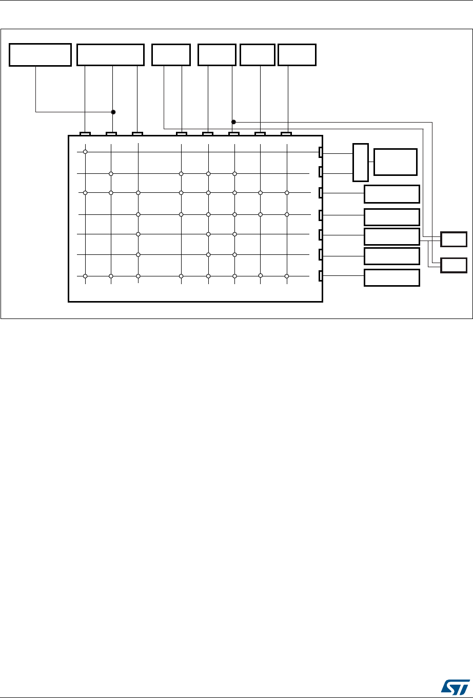
Memory and bus architecture RM0090
60/1718 DocID018909 Rev 9
Figure 1. System architecture for STM32F405xx/07xx and STM32F415xx/17xx devices
!2-
#ORTEX-
'0
$-!
'0
$-!
-!#
%THERNET
53"/4'
(3
"USMATRIX3
)#/$%
$#/$%
!##%,
&LASH
MEMORY
32!-
+BYTE
32!-
+BYTE
!("
PERIPHERALS
!("
&3-#
3TATIC-EM#TL
)BUS
$BUS
3BUS
$-!?0)
$-!?-%-
$-!?-%-
$-!?0
%4(%2.%4?-
53"?(3?-
AID
##-DATA2!-
+BYTE
!0"
!0"
PERIPHERALS

DocID018909 Rev 9 61/1718
RM0090 Memory and bus architecture
112
In the STM32F42xx and STM32F43xx devices, the main system consists of 32-bit multilayer
AHB bus matrix that interconnects:
•Ten masters:
–Cortex
®-M4 with FPU core I-bus, D-bus and S-bus
– DMA1 memory bus
– DMA2 memory bus
– DMA2 peripheral bus
– Ethernet DMA bus
– USB OTG HS DMA bus
– LCD Controller DMA-bus
– DMA2D (Chrom-Art Accelerator™) memory bus
•Eight slaves:
– Internal Flash memory ICode bus
– Internal Flash memory DCode bus
– Main internal SRAM1 (112 KB)
– Auxiliary internal SRAM2 (16 KB)
– Auxiliary internal SRAM3 (64 KB)
– AHB1peripherals including AHB to APB bridges and APB peripherals
– AHB2 peripherals
–FMC
The bus matrix provides access from a master to a slave, enabling concurrent access and
efficient operation even when several high-speed peripherals work simultaneously. The 64-
Kbyte CCM (core coupled memory) data RAM is not part of the bus matrix and can be
accessed only through the CPU. This architecture is shown in Figure 2.
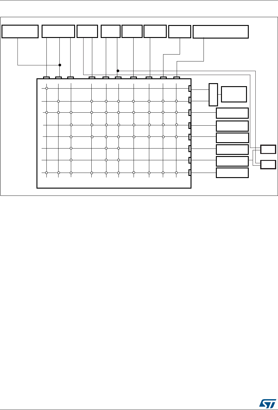
Memory and bus architecture RM0090
62/1718 DocID018909 Rev 9
Figure 2. System architecture for STM32F42xxx and STM32F43xxx devices
2.1.1 I-bus
This bus connects the Instruction bus of the Cortex®-M4 with FPU core to the BusMatrix.
This bus is used by the core to fetch instructions. The target of this bus is a memory
containing code (internal Flash memory/SRAM or external memories through the
FSMC/FMC).
2.1.2 D-bus
This bus connects the databus of the Cortex®-M4 with FPU to the 64-Kbyte CCM data RAM
to the BusMatrix. This bus is used by the core for literal load and debug access. The target
of this bus is a memory containing code or data (internal Flash memory or external
memories through the FSMC/FMC).
2.1.3 S-bus
This bus connects the system bus of the Cortex®-M4 with FPU core to a BusMatrix. This
bus is used to access data located in a peripheral or in SRAM. Instructions may also be
fetch on this bus (less efficient than ICode). The targets of this bus are the internal SRAM1,
SRAM2 and SRAM3, the AHB1 peripherals including the APB peripherals, the AHB2
peripherals and the external memories through the FSMC/FMC.
2.1.4 DMA memory bus
This bus connects the DMA memory bus master interface to the BusMatrix. It is used by the
DMA to perform transfer to/from memories. The targets of this bus are data memories:
$50
&RUWH[0
*3
'0$
*3
'0$
0$&
(WKHUQHW
86%27*
+6
%XVPDWUL[6
,&2'(
'&2'(
$&&(/
)ODVK
PHPRU\
65$0
.E\WH
65$0
.E\WH
$+%
SHULSKHUDOV
$+%
SHULSKHUDOV
)0&H[WHUQDO
0HP&WO
,EXV
'EXV
6EXV
'0$B3,
'0$B0(0
'0$B0(0
'0$B3
(7+(51(7B0
86%B+6B0
-36
&&0GDWD5$0
.E\WH
$3%
$3%
65$0
.E\WH
/&'7)7 &KURP$57$FFHOHUDWRU
'0$'
/&'7)7B0
'0$'

DocID018909 Rev 9 63/1718
RM0090 Memory and bus architecture
112
internal SRAMs (SRAM1, SRAM2 and SRAM3) and external memories through the
FSMC/FMC.
2.1.5 DMA peripheral bus
This bus connects the DMA peripheral master bus interface to the BusMatrix. This bus is
used by the DMA to access AHB peripherals or to perform memory-to-memory transfers.
The targets of this bus are the AHB and APB peripherals plus data memories: internal
SRAMs (SRAM1, SRAM2 and SRAM3) and external memories through the FSMC/FMC.
2.1.6 Ethernet DMA bus
This bus connects the Ethernet DMA master interface to the BusMatrix. This bus is used by
the Ethernet DMA to load/store data to a memory. The targets of this bus are data
memories: internal SRAMs (SRAM1, SRAM2, SRAM3), internal Flash memory, and
external memories through the FSMC/FMC.
2.1.7 USB OTG HS DMA bus
This bus connects the USB OTG HS DMA master interface to the BusMatrix. This bus is
used by the USB OTG DMA to load/store data to a memory. The targets of this bus are data
memories: internal SRAMs (SRAM1, SRAM2, SRAM3), internal Flash memory, and
external memories through the FSMC/FMC.
2.1.8 LCD-TFT controller DMA bus
This bus connects the LCD controller DMA master interface to the BusMatrix. It is used by
the LCD-TFT DMA to load/store data to a memory. The targets of this bus are data
memories: internal SRAMs (SRAM1, SRAM2, SRAM3), external memories through FMC,
and internal Flash memory.
2.1.9 DMA2D bus
This bus connect the DMA2D master interface to the BusMatrix. This bus is used by the
DMA2D graphic Accelerator to load/store data to a memory. The targets of this bus are data
memories: internal SRAMs (SRAM1, SRAM2, SRAM3), external memories through FMC,
and internal Flash memory.
2.1.10 BusMatrix
The BusMatrix manages the access arbitration between masters. The arbitration uses a
round-robin algorithm.
2.1.11 AHB/APB bridges (APB)
The two AHB/APB bridges, APB1 and APB2, provide full synchronous connections between
the AHB and the two APB buses, allowing flexible selection of the peripheral frequency.
Refer to the device datasheets for more details on APB1 and APB2 maximum frequencies,
and to Table 1 for the address mapping of AHB and APB peripherals.
After each device reset, all peripheral clocks are disabled (except for the SRAM and Flash
memory interface). Before using a peripheral you have to enable its clock in the
RCC_AHBxENR or RCC_APBxENR register.

Memory and bus architecture RM0090
64/1718 DocID018909 Rev 9
Note: When a 16- or an 8-bit access is performed on an APB register, the access is transformed
into a 32-bit access: the bridge duplicates the 16- or 8-bit data to feed the 32-bit vector.
2.2 Memory organization
Program memory, data memory, registers and I/O ports are organized within the same linear
4 Gbyte address space.
The bytes are coded in memory in little endian format. The lowest numbered byte in a word
is considered the word’s least significant byte and the highest numbered byte, the word’s
most significant.
For the detailed mapping of peripheral registers, please refer to the related chapters.
The addressable memory space is divided into 8 main blocks, each of 512 MB.
All the memory areas that are not allocated to on-chip memories and peripherals are
considered “Reserved”). Refer to the memory map figure in the product datasheet.
2.3 Memory map
See the datasheet corresponding to your device for a comprehensive diagram of the
memory map. Table 1 gives the boundary addresses of the peripherals available in all
STM32F4xx devices.
Table 1. STM32F4xx register boundary addresses
Boundary address Peripheral Bus Register map
0xA000 0000 - 0xA000 0FFF
FSMC control register
(STM32F405xx/07xx
and
STM32F415xx/17xx)/
FMC control register
(STM32F42xxx and
STM32F43xxx)
AHB3 Section 36.6.9: FSMC register map on page 1580
Section 37.8: FMC register map on page 1659
0x5006 0800 - 0x5006 0BFF RNG
AHB2
Section 24.4.4: RNG register map on page 756
0x5006 0400 - 0x5006 07FF HASH Section 25.4.9: HASH register map on page 780
0x5006 0000 - 0x5006 03FF CRYP Section 23.6.13: CRYP register map on page 748
0x5005 0000 - 0x5005 03FF DCMI Section 15.8.12: DCMI register map on page 476
0x5000 0000 - 0x5003 FFFF USB OTG FS Section 34.16.6: OTG_FS register map on
page 1308

DocID018909 Rev 9 65/1718
RM0090 Memory and bus architecture
112
0x4004 0000 - 0x4007 FFFF USB OTG HS
AHB1
Section 35.12.6: OTG_HS register map on
page 1452
0x4002 B000 - 0x4002 BBFF DMA2D Section 11.5: DMA2D registers on page 352
0x4002 8000 - 0x4002 93FF ETHERNET MAC Section 33.8.5: Ethernet register maps on
page 1221
0x4002 6400 - 0x4002 67FF DMA2
Section 10.5.11: DMA register map on page 335
0x4002 6000 - 0x4002 63FF DMA1
0x4002 4000 - 0x4002 4FFF BKPSRAM
0x4002 3C00 - 0x4002 3FFF Flash interface
register Section 3.9: Flash interface registers
0x4002 3800 - 0x4002 3BFF RCC Section 7.3.25: RCC register map on page 266
0x4002 3000 - 0x4002 33FF CRC Section 4.4.4: CRC register map on page 115
0x4002 2800 - 0x4002 2BFF GPIOK
Section 8.4.11: GPIO register map on page 287
0x4002 2400 - 0x4002 27FF GPIOJ
0x4002 2000 - 0x4002 23FF GPIOI
Section 8.4.11: GPIO register map on page 287
0x4002 1C00 - 0x4002 1FFF GPIOH
0x4002 1800 - 0x4002 1BFF GPIOG
0x4002 1400 - 0x4002 17FF GPIOF
0x4002 1000 - 0x4002 13FF GPIOE
0x4002 0C00 - 0x4002 0FFF GPIOD
0x4002 0800 - 0x4002 0BFF GPIOC
0x4002 0400 - 0x4002 07FF GPIOB
0x4002 0000 - 0x4002 03FF GPIOA
0x4001 6800 - 0x4001 6BFF LCD-TFT
APB2
Section 16.7.26: LTDC register map on page 507
0x4001 5800 - 0x4001 5BFF SAI1 Section 29.17.9: SAI register map on page 950
0x4001 5400 - 0x4001 57FF SPI6
APB2 Section 28.5.10: SPI register map on page 912
0x4001 5000 - 0x4001 53FF SPI5
0x4001 4800 - 0x4001 4BFF TIM11
APB2
Section 19.5.12: TIM10/11/13/14 register map on
page 679
0x4001 4400 - 0x4001 47FF TIM10
0x4001 4000 - 0x4001 43FF TIM9 Section 19.4.13: TIM9/12 register map on
page 668
0x4001 3C00 - 0x4001 3FFF EXTI Section 12.3.7: EXTI register map on page 387
0x4001 3800 - 0x4001 3BFF SYSCFG
Section 9.2.8: SYSCFG register maps for
STM32F405xx/07xx and STM32F415xx/17xx on
page 294 and Section 9.3.8: SYSCFG register
maps for STM32F42xxx and STM32F43xxx on
page 301
0x4001 3400 - 0x4001 37FF SPI4 APB2 Section 28.5.10: SPI register map on page 912
Table 1. STM32F4xx register boundary addresses (continued)
Boundary address Peripheral Bus Register map

Memory and bus architecture RM0090
66/1718 DocID018909 Rev 9
0x4001 3000 - 0x4001 33FF SPI1
APB2
Section 28.5.10: SPI register map on page 912
0x4001 2C00 - 0x4001 2FFF SDIO Section 31.9.16: SDIO register map on page 1058
0x4001 2000 - 0x4001 23FF ADC1 - ADC2 - ADC3 Section 13.13.18: ADC register map on page 430
0x4001 1400 - 0x4001 17FF USART6
Section 30.6.8: USART register map on page 1003
0x4001 1000 - 0x4001 13FF USART1
0x4001 0400 - 0x4001 07FF TIM8 Section 17.4.21: TIM1&TIM8 register map on
page 576
0x4001 0000 - 0x4001 03FF TIM1
0x4000 7C00 - 0x4000 7FFF UART8
APB1 Section 30.6.8: USART register map on page 1003
0x4000 7800 - 0x4000 7BFF UART7
Table 1. STM32F4xx register boundary addresses (continued)
Boundary address Peripheral Bus Register map

DocID018909 Rev 9 67/1718
RM0090 Memory and bus architecture
112
0x4000 7400 - 0x4000 77FF DAC
APB1
Section 14.5.15: DAC register map on page 453
0x4000 7000 - 0x4000 73FF PWR Section 5.6: PWR register map on page 149
0x4000 6800 - 0x4000 6BFF CAN2
Section 32.9.5: bxCAN register map on page 1101
0x4000 6400 - 0x4000 67FF CAN1
0x4000 5C00 - 0x4000 5FFF I2C3
Section 27.6.11: I2C register map on page 8580x4000 5800 - 0x4000 5BFF I2C2
0x4000 5400 - 0x4000 57FF I2C1
0x4000 5000 - 0x4000 53FF UART5
Section 30.6.8: USART register map on page 1003
0x4000 4C00 - 0x4000 4FFF UART4
0x4000 4800 - 0x4000 4BFF USART3
0x4000 4400 - 0x4000 47FF USART2
0x4000 4000 - 0x4000 43FF I2S3ext
Section 28.5.10: SPI register map on page 912
0x4000 3C00 - 0x4000 3FFF SPI3 / I2S3
0x4000 3800 - 0x4000 3BFF SPI2 / I2S2
0x4000 3400 - 0x4000 37FF I2S2ext
0x4000 3000 - 0x4000 33FF IWDG Section 21.4.5: IWDG register map on page 697
0x4000 2C00 - 0x4000 2FFF WWDG Section 22.6.4: WWDG register map on page 704
0x4000 2800 - 0x4000 2BFF RTC & BKP Registers Section 26.6.21: RTC register map on page 820
0x4000 2000 - 0x4000 23FF TIM14 Section 19.5.12: TIM10/11/13/14 register map on
page 679
0x4000 1C00 - 0x4000 1FFF TIM13
0x4000 1800 - 0x4000 1BFF TIM12 Section 19.4.13: TIM9/12 register map on
page 668
0x4000 1400 - 0x4000 17FF TIM7 Section 20.4.9: TIM6&TIM7 register map on
page 691
0x4000 1000 - 0x4000 13FF TIM6
0x4000 0C00 - 0x4000 0FFF TIM5
Section 18.4.21: TIMx register map on page 634
0x4000 0800 - 0x4000 0BFF TIM4
0x4000 0400 - 0x4000 07FF TIM3
0x4000 0000 - 0x4000 03FF TIM2
Table 1. STM32F4xx register boundary addresses (continued)
Boundary address Peripheral Bus Register map

Memory and bus architecture RM0090
68/1718 DocID018909 Rev 9
2.3.1 Embedded SRAM
The STM32F405xx/07xx and STM32F415xx/17xx feature 4 Kbytes of backup SRAM (see
Section 5.1.2: Battery backup domain) plus 192 Kbytes of system SRAM.
The STM32F42xxx and STM32F43xxx feature 4 Kbytes of backup SRAM (see
Section 5.1.2: Battery backup domain) plus 256 Kbytes of system SRAM.
The embedded SRAM can be accessed as bytes, half-words (16 bits) or full words (32 bits).
Read and write operations are performed at CPU speed with 0 wait state. The embedded
SRAM is divided into up to three blocks:
•SRAM1 and SRAM2 mapped at address 0x2000 0000 and accessible by all AHB
masters.
•SRAM3 (available on STM32F42xxx and STM32F43xxx) mapped at address
0x2002 0000 and accessible by all AHB masters.
•CCM (core coupled memory) mapped at address 0x1000 0000 and accessible only by
the CPU through the D-bus.
The AHB masters support concurrent SRAM accesses (from the Ethernet or the USB OTG
HS): for instance, the Ethernet MAC can read/write from/to SRAM2 while the CPU is
reading/writing from/to SRAM1 or SRAM3.
The CPU can access the SRAM1, SRAM2, and SRAM3 through the System Bus or through
the I-Code/D-Code buses when boot from SRAM is selected or when physical remap is
selected (Section 9.2.1: SYSCFG memory remap register (SYSCFG_MEMRMP) in the
SYSCFG controller). To get the max performance on SRAM execution, physical remap
should be selected (boot or software selection).
2.3.2 Flash memory overview
The Flash memory interface manages CPU AHB I-Code and D-Code accesses to the Flash
memory. It implements the erase and program Flash memory operations and the read and
write protection mechanisms. It accelerates code execution with a system of instruction
prefetch and cache lines.
The Flash memory is organized as follows:
•A main memory block divided into sectors.
•System memory from which the device boots in System memory boot mode
•512 OTP (one-time programmable) bytes for user data.
•Option bytes to configure read and write protection, BOR level, watchdog
software/hardware and reset when the device is in Standby or Stop mode.
Refer to Section 3: Embedded Flash memory interface for more details.
2.3.3 Bit banding
The Cortex®-M4 with FPU memory map includes two bit-band regions. These regions map
each word in an alias region of memory to a bit in a bit-band region of memory. Writing to a
word in the alias region has the same effect as a read-modify-write operation on the
targeted bit in the bit-band region.
In the STM32F4xx devices both the peripheral registers and the SRAM are mapped to a bit-
band region, so that single bit-band write and read operations are allowed. The operations

DocID018909 Rev 9 69/1718
RM0090 Memory and bus architecture
112
are only available for Cortex®-M4 with FPU accesses, and not from other bus masters (e.g.
DMA).
A mapping formula shows how to reference each word in the alias region to a corresponding
bit in the bit-band region. The mapping formula is:
bit_word_addr = bit_band_base + (byte_offset x 32) + (bit_number × 4)
where:
–bit_word_addr is the address of the word in the alias memory region that maps to
the targeted bit
–bit_band_base is the starting address of the alias region
–byte_offset is the number of the byte in the bit-band region that contains the
targeted bit
–bit_number is the bit position (0-7) of the targeted bit
Example
The following example shows how to map bit 2 of the byte located at SRAM address
0x20000300 to the alias region:
0x22006008 = 0x22000000 + (0x300*32) + (2*4)
Writing to address 0x22006008 has the same effect as a read-modify-write operation on bit
2 of the byte at SRAM address 0x20000300.
Reading address 0x22006008 returns the value (0x01 or 0x00) of bit 2 of the byte at SRAM
address 0x20000300 (0x01: bit set; 0x00: bit reset).
For more information on bit-banding, please refer to the Cortex®-M4 with FPU programming
manual (see Related documents on page 1).
2.4 Boot configuration
Due to its fixed memory map, the code area starts from address 0x0000 0000 (accessed
through the ICode/DCode buses) while the data area (SRAM) starts from address
0x2000 0000 (accessed through the system bus). The Cortex®-M4 with FPU CPU always
fetches the reset vector on the ICode bus, which implies to have the boot space available
only in the code area (typically, Flash memory). STM32F4xx microcontrollers implement a
special mechanism to be able to boot from other memories (like the internal SRAM).
In the STM32F4xx, three different boot modes can be selected through the BOOT[1:0] pins
as shown in Table 2.
Table 2. Boot modes
Boot mode selection pins
Boot mode Aliasing
BOOT1 BOOT0
x 0 Main Flash memory Main Flash memory is selected as the boot space
0 1 System memory System memory is selected as the boot space
1 1 Embedded SRAM Embedded SRAM is selected as the boot space

Memory and bus architecture RM0090
70/1718 DocID018909 Rev 9
The values on the BOOT pins are latched on the 4th rising edge of SYSCLK after a reset. It
is up to the user to set the BOOT1 and BOOT0 pins after reset to select the required boot
mode.
BOOT0 is a dedicated pin while BOOT1 is shared with a GPIO pin. Once BOOT1 has been
sampled, the corresponding GPIO pin is free and can be used for other purposes.
The BOOT pins are also resampled when the device exits the Standby mode. Consequently,
they must be kept in the required Boot mode configuration when the device is in the Standby
mode. After this startup delay is over, the CPU fetches the top-of-stack value from address
0x0000 0000, then starts code execution from the boot memory starting from 0x0000 0004.
Note: When the device boots from SRAM, in the application initialization code, you have to
relocate the vector table in SRAM using the NVIC exception table and the offset register.
In STM32F42xxx and STM32F43xxx devices, when booting from the main Flash memory,
the application software can either boot from bank 1 or from bank 2. By default, boot from
bank 1 is selected.
To select boot from Flash memory bank 2, set the BFB2 bit in the user option bytes. When
this bit is set and the boot pins are in the boot from main Flash memory configuration, the
device boots from system memory, and the boot loader jumps to execute the user
application programmed in Flash memory bank 2. For further details, please refer to
AN2606.
Note: When booting from bank 2, in the applications initialization code, relocate the vector table to
bank 2 base address. (0x0808 0000) using the NVIC exception table and offset register.

DocID018909 Rev 9 71/1718
RM0090 Memory and bus architecture
112
Embedded bootloader
The embedded bootloader mode is used to reprogram the Flash memory using one of the
following serial interfaces:
•USART1 (PA9/PA10)
•USART3 (PB10/11 and PC10/11)
•CAN2 (PB5/13)
•USB OTG FS (PA11/12) in Device mode (DFU: device firmware upgrade).
The USART peripherals operate at the internal 16 MHz oscillator (HSI) frequency, while the
CAN and USB OTG FS require an external clock (HSE) multiple of 1 MHz (ranging from 4 to
26 MHz).
The embedded bootloader code is located in system memory. It is programmed by ST
during production. For additional information, refer to application note AN2606.
Physical remap in STM32F405xx/07xx and STM32F415xx/17xx
Once the boot pins are selected, the application software can modify the memory
accessible in the code area (in this way the code can be executed through the ICode bus in
place of the System bus). This modification is performed by programming the Section 9.2.1:
SYSCFG memory remap register (SYSCFG_MEMRMP) in the SYSCFG controller.
The following memories can thus be remapped:
•Main Flash memory
•System memory
•Embedded SRAM1 (112 KB)
•FSMC bank 1 (NOR/PSRAM 1 and 2)
Table 3. Memory mapping vs. Boot mode/physical remap
in STM32F405xx/07xx and STM32F415xx/17xx
Addresses Boot/Remap in
main Flash memory
Boot/Remap in
embedded SRAM
Boot/Remap in
System memory Remap in FSMC
0x2001 C000 - 0x2001 FFFF SRAM2 (16 KB) SRAM2 (16 KB) SRAM2 (16 KB) SRAM2 (16 KB)
0x2000 0000 - 0x2001 BFFF SRAM1 (112 KB) SRAM1 (112 KB) SRAM1 (112 KB) SRAM1 (112 KB)
0x1FFF 0000 - 0x1FFF 77FF System memory System memory System memory System memory
0x0810 0000 - 0x0FFF FFFF Reserved Reserved Reserved Reserved
0x0800 0000 - 0x080F FFFF Flash memory Flash memory Flash memory Flash memory
0x0400 0000 - 0x07FF FFFF Reserved Reserved Reserved
FSMC bank 1
NOR/PSRAM 2
(128 MB Aliased)
0x0000 0000 -
0x000F FFFF(1)(2) Flash (1 MB) Aliased SRAM1 (112 KB)
Aliased
System memory
(30 KB) Aliased
FSMC bank 1
NOR/PSRAM 1
(128 MB Aliased)
1. When the FSMC is remapped at address 0x0000 0000, only the first two regions of bank 1 memory controller (bank 1
NOR/PSRAM 1 and NOR/PSRAM 2) can be remapped. In remap mode, the CPU can access the external memory via
ICode bus instead of System bus which boosts up the performance.
2. Even when aliased in the boot memory space, the related memory is still accessible at its original memory space.

Memory and bus architecture RM0090
72/1718 DocID018909 Rev 9
Physical remap in STM32F42xxx and STM32F43xxx
Once the boot pins are selected, the application software can modify the memory
accessible in the code area (in this way the code can be executed through the ICode bus in
place of the System bus). This modification is performed by programming the Section 9.2.1:
SYSCFG memory remap register (SYSCFG_MEMRMP) in the SYSCFG controller.
The following memories can thus be remapped:
•Main Flash memory
•System memory
•Embedded SRAM1 (112 KB)
•FMC bank 1 (NOR/PSRAM 1 and 2)
•FMC SDRAM bank 1
Table 4. Memory mapping vs. Boot mode/physical remap
in STM32F42xxx and STM32F43xxx
Addresses Boot/Remap in
main Flash memory
Boot/Remap in
embedded SRAM
Boot/Remap in
System memory Remap in FMC
0x2002 0000 - 0x2002 FFFF SRAM3 (64 KB) SRAM3 (64 KB) SRAM3 (64 KB) SRAM3 (64 KB)
0x2001 C000 - 0x2001 FFFF SRAM2 (16 KB) SRAM2 (16 KB) SRAM2 (16 KB) SRAM2 (16 KB)
0x2000 0000 - 0x2001 BFFF SRAM1 (112 KB) SRAM1 (112 KB) SRAM1 (112 KB) SRAM1 (112 KB)
0x1FFF 0000 - 0x1FFF 77FF System memory System memory System memory System memory
0x0810 0000 - 0x0FFF FFFF Reserved Reserved Reserved Reserved
0x0800 0000 - 0x081F FFFF Flash memory Flash memory Flash memory Flash memory
0x0400 0000 - 0x07FF FFFF Reserved Reserved Reserved
FMC bank 1
NOR/PSRAM 2
(128 MB Aliased)
0x0000 0000 -
0x001F FFFF(1)(2) Flash (2 MB) Aliased SRAM1 (112 KB)
Aliased
System memory
(30 KB) Aliased
FMC bank 1
NOR/PSRAM 1
(128 MB Aliased)
or FMC SDRAM
bank 1 (128 MB
Aliased)
1. When the FMC is remapped at address 0x0000 0000, only the first two regions of bank 1 memory controller (bank 1
NOR/PSRAM 1 and NOR/PSRAM 2) or SDRAM bank 1 can be remapped. In remap mode, the CPU can access the
external memory via ICode bus instead of System bus which boosts up the performance.
2. Even when aliased in the boot memory space, the related memory is still accessible at its original memory space.
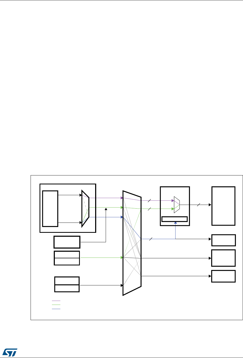
DocID018909 Rev 9 73/1718
RM0090 Embedded Flash memory interface
112
3 Embedded Flash memory interface
3.1 Introduction
The Flash memory interface manages CPU AHB I-Code and D-Code accesses to the Flash
memory. It implements the erase and program Flash memory operations and the read and
write protection mechanisms.
The Flash memory interface accelerates code execution with a system of instruction
prefetch and cache lines.
3.2 Main features
•Flash memory read operations
•Flash memory program/erase operations
•Read / write protections
•Prefetch on I-Code
•64 cache lines of 128 bits on I-Code
•8 cache lines of 128 bits on D-Code
Figure 3 shows the Flash memory interface connection inside the system architecture.
Figure 3. Flash memory interface connection inside system architecture
(STM32F405xx/07xx and STM32F415xx/17xx)
#ORTEX
CORE
%THERNET
53"(3
$-!
$-!
$CODEBUS
)#ODEBUS
#ORTEX-WITH&05
)#ODE
$#ODE
3BU S
!("
PERIPH
&LASH
MEMORY
&LASHINTERFACE
32!-AND
%XTERNAL
MEMORIES
!("
PERIPH
&,)4®ISTERS
!("
BIT
INSTRUCTION
BUS
!CCESSTOINSTRUCTIONIN&LASHMEMORY
!CCESSTODATAANDLITERALPOOLIN&LASHMEMORY
&,)4®ISTERACCESS
-36
##-DATA
2!-
!("
BIT
DATABUS
!("
BIT
SYSTEMBUS
&LASH
MEMORY
BUS
BITS
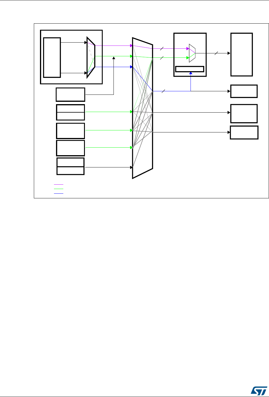
Embedded Flash memory interface RM0090
74/1718 DocID018909 Rev 9
Figure 4. Flash memory interface connection inside system architecture
(STM32F42xxx and STM32F43xxx)
3.3 Embedded Flash memory in
STM32F405xx/07xx and STM32F415xx/17xx
The Flash memory has the following main features:
•Capacity up to 1 Mbyte
•128 bits wide data read
•Byte, half-word, word and double word write
•Sector and mass erase
•Memory organization
The Flash memory is organized as follows:
– A main memory block divided into 4 sectors of 16 Kbytes, 1 sector of 64 Kbytes,
and 7 sectors of 128 Kbytes
– System memory from which the device boots in System memory boot mode
– 512 OTP (one-time programmable) bytes for user data
The OTP area contains 16 additional bytes used to lock the corresponding OTP
data block.
– Option bytes to configure read and write protection, BOR level, watchdog
software/hardware and reset when the device is in Standby or Stop mode.
•Low-power modes (for details refer to the Power control (PWR) section of the reference
manual)
#ORTEX
CORE
%THERNET
53"(3
$-!
$-!
$CODEBUS
)#ODEBUS
#ORTEX-WITH&05
)#ODE
$#ODE
3BU S
!("
PERIPH
&LASH
MEMORY
&LASHINTERFACE
32!-AND
EXTERNAL
MEMORIES
!("
PERIPH
&,)4®ISTERS
!("
BIT
INSTRUCTION
BUS
!CCESSTOINSTRUCTIONIN&LASHMEMORY
!CCESSTODATAANDLITERALPOOLIN&LASHMEMORY
&,)4®ISTERACCESS
-36
##-DATA
2!-
!("
BIT
DATABUS
!("
BIT
SYSTEMBUS
&LASH
MEMORY
BUS
BITS
$-!$
,#$4&4
DocID018909 Rev 9 75/1718
RM0090 Embedded Flash memory interface
112
Table 5. Flash module organization (STM32F40x and STM32F41x)
Block Name Block base addresses Size
Main memory
Sector 0 0x0800 0000 - 0x0800 3FFF 16 Kbytes
Sector 1 0x0800 4000 - 0x0800 7FFF 16 Kbytes
Sector 2 0x0800 8000 - 0x0800 BFFF 16 Kbytes
Sector 3 0x0800 C000 - 0x0800 FFFF 16 Kbytes
Sector 4 0x0801 0000 - 0x0801 FFFF 64 Kbytes
Sector 5 0x0802 0000 - 0x0803 FFFF 128 Kbytes
Sector 6 0x0804 0000 - 0x0805 FFFF 128 Kbytes
.
.
.
.
.
.
.
.
.
Sector 11 0x080E 0000 - 0x080F FFFF 128 Kbytes
System memory 0x1FFF 0000 - 0x1FFF 77FF 30 Kbytes
OTP area 0x1FFF 7800 - 0x1FFF 7A0F 528 bytes
Option bytes 0x1FFF C000 - 0x1FFF C00F 16 bytes

Embedded Flash memory interface RM0090
76/1718 DocID018909 Rev 9
3.4 Embedded Flash memory in STM32F42xxx and
STM32F43xxx
The Flash memory has the following main features:
•Capacity up to 2 Mbyte with dual bank architecture supporting read-while-write
capability (RWW)
•128 bits wide data read
•Byte, half-word, word and double word write
•Sector, bank, and mass erase (both banks)
•Dual bank memory organization
The Flash memory is organized as follows:
– For each bank, a main memory block (1 Mbyte) divided into 4 sectors of 16
Kbytes, 1 sector of 64 Kbytes, and 7 sectors of 128 Kbytes
– System memory from which the device boots in System memory boot mode
– 512 OTP (one-time programmable) bytes for user data
The OTP area contains 16 additional bytes used to lock the corresponding OTP
data block.
– Option bytes to configure read and write protection, BOR level, watchdog, dual
bank boot mode, dual bank feature, software/hardware and reset when the device
is in Standby or Stop mode.
•Dual bank organization on 1 Mbyte devices
The dual bank feature on 1 Mbyte devices is enabled by setting the DB1M option bit.
To obtain a dual bank Flash memory, the last 512 Kbytes of the single bank (sectors
[8:11]) are re-structured in the same way as the first 512 Kbytes.
The sector numbering of dual bank memory organization is different from the single
bank: the single bank memory contains 12 sectors whereas the dual bank memory
contains 16 sectors (see Table 7: 1 Mbyte Flash memory single bank vs dual bank
organization (STM32F42xxx and STM32F43xxx)).
For erase operation, the right sector numbering must be considered according the
DB1M option bit.
– When the DB1M bit is reset, the erase operation must be performed on the default
sector number.
– When the DB1M bit is set, to perform an erase operation on bank 2, the sector
number must be programmed (sector number from 12 to 19). Refer to FLASH_CR
register for SNB (Sector number) configuration.
Refer to Table 8: 1 Mbyte single bank Flash memory organization (STM32F42xxx and
STM32F43xxx) and Table 9: 1 Mbyte dual bank Flash memory organization (STM32F42xxx
and STM32F43xxx) for details on 1 Mbyte single bank and 1 Mbyte dual bank
organizations.

DocID018909 Rev 9 77/1718
RM0090 Embedded Flash memory interface
112
Table 6. Flash module - 2 Mbyte dual bank organization (STM32F42xxx and STM32F43xxx)
Block Bank Name Block base addresses Size
Main memory
Bank 1
Sector 0 0x0800 0000 - 0x0800 3FFF 16 Kbytes
Sector 1 0x0800 4000 - 0x0800 7FFF 16 Kbytes
Sector 2 0x0800 8000 - 0x0800 BFFF 16 Kbytes
Sector 3 0x0800 C000 - 0x0800 FFFF 16 Kbyte
Sector 4 0x0801 0000 - 0x0801 FFFF 64 Kbytes
Sector 5 0x0802 0000 - 0x0803 FFFF 128 Kbytes
Sector 6 0x0804 0000 - 0x0805 FFFF 128 Kbytes
- - -
- - -
- - -
Sector 11 0x080E 0000 - 0x080F FFFF 128 Kbytes
Bank 2
Sector 12 0x0810 0000 - 0x0810 3FFF 16 Kbytes
Sector 13 0x0810 4000 - 0x0810 7FFF 16 Kbytes
Sector 14 0x0810 8000 - 0x0810 BFFF 16 Kbytes
Sector 15 0x0810 C000 - 0x0810 FFFF 16 Kbytes
Sector 16 0x0811 0000 - 0x0811 FFFF 64 Kbytes
Sector 17 0x0812 0000 - 0x0813 FFFF 128 Kbytes
Sector 18 0x0814 0000 - 0x0815 FFFF 128 Kbytes
- -
- -
- -
Sector 23 0x081E 0000 - 0x081F FFFF 128 Kbytes
System memory 0x1FFF 0000 - 0x1FFF 77FF 30 Kbytes
OTP 0x1FFF 7800 - 0x1FFF 7A0F 528 bytes
Option bytes
Bank 1 0x1FFF C000 - 0x1FFF C00F 16 bytes
Bank 2 0x1FFE C000 - 0x1FFE C00F 16 bytes
Embedded Flash memory interface RM0090
78/1718 DocID018909 Rev 9
Table 7. 1 Mbyte Flash memory single bank vs dual bank organization
(STM32F42xxx and STM32F43xxx)
1 Mbyte single bank Flash memory (default) 1 Mbyte dual bank Flash memory
DB1M=0 DB1M=1
Main memory Sector number Sector size Main memory Sector number Sector size
1MB
Sector 0 16 Kbytes
Bank 1
512KB
Sector 0 16 Kbytes
Sector 1 16 Kbytes Sector 1 16 Kbytes
Sector 2 16 Kbytes Sector 2 16 Kbytes
Sector 3 16 Kbytes Sector 3 16 Kbytes
Sector 4 64 Kbytes Sector 4 64 Kbytes
Sector 5 128 Kbytes Sector 5 128 Kbytes
Sector 6 128 Kbytes Sector 6 128 Kbytes
Sector 7 128 Kbytes Sector 7 128 Kbytes
Sector 8 128 Kbytes
Bank 2
512KB
Sector 12 16 Kbytes
Sector 9 128 Kbytes Sector 13 16 Kbytes
Sector 10 128 Kbytes Sector 14 16 Kbytes
Sector 11 128 Kbytes Sector 15 16 Kbytes
-- Sector 16 64 Kbytes
-- Sector 17 128 Kbytes
-- Sector 18 128 Kbytes
-- Sector 19 128 Kbytes
Table 8. 1 Mbyte single bank Flash memory organization
(STM32F42xxx and STM32F43xxx)
Block Bank Name Block base addresses Size
Main memory Single bank
Sector 0 0x0800 0000 - 0x0800 3FFF 16 Kbytes
Sector 1 0x0800 4000 - 0x0800 7FFF 16 Kbytes
Sector 2 0x0800 8000 - 0x0800 BFFF 16 Kbytes
Sector 3 0x0800 C000 - 0x0800 FFFF 16 Kbytes
Sector 4 0x0801 0000 - 0x0801 FFFF 64 Kbytes
Sector 5 0x0802 0000 - 0x0803 FFFF 128 Kbytes
Sector 6 0x0804 0000 - 0x0805 FFFF 128 Kbytes
Sector 7 0x0806 0000 - 0x0807 FFFF 128 Kbytes
Sector 8 0x0808 0000 - 0x0809 FFFF 128 Kbytes
Sector 9 0x080A 0000 - 0x080B FFFF 128 Kbytes
Sector 10 0x080C 0000 - 0x080D FFFF 128 Kbytes
Sector 11 0x080E 0000 - 0x080F FFFF 128 Kbytes
DocID018909 Rev 9 79/1718
RM0090 Embedded Flash memory interface
112
System memory 0x1FFF 0000 - 0x1FFFF 77FF 30 Kbytes
OTP 0x1FFF 7800 - 0x1FFF 7A0F 528 bytes
Option bytes
0x1FFF C000 - 0x1FFF C00F 16 bytes
0x1FFE C000 - 0x1FFE C00F 16 bytes
Table 8. 1 Mbyte single bank Flash memory organization
(STM32F42xxx and STM32F43xxx) (continued)
Block Bank Name Block base addresses Size
Table 9. 1 Mbyte dual bank Flash memory organization (STM32F42xxx and STM32F43xxx)
Block Name Block base addresses Size
Main memory
Bank 1
Sector 0 0x0800 0000 - 0x0800 3FFF 16 Kbytes
Sector 1 0x0800 4000 - 0x0800 7FFF 16 Kbytes
Sector 2 0x0800 8000 - 0x0800 BFFF 16 Kbytes
Sector 3 0x0800 C000 - 0x0800 FFFF 16 Kbyte
Sector 4 0x0801 0000 - 0x0801 FFFF 64 Kbytes
Sector 5 0x0802 0000 - 0x0803 FFFF 128 Kbytes
Sector 6 0x0804 0000 - 0x0805 FFFF 128 Kbytes
Sector 7 0x0806 0000 - 0x0807 FFFF 128 Kbytes
Bank 2
Sector 12 0x0808 0000 - 0x0808 3FFF 16 Kbytes
Sector 13 0x0808 4000 - 0x0808 7FFF 16 Kbytes
Sector 14 0x0808 0000 - 0x0808 BFFF 16 Kbytes
Sector 15 0x0808 C000 - 0x0808 FFFF 16 Kbytes
Sector 16 0x0809 0000 - 0x0809 FFFF 64 Kbytes
Sector 17 0x080A 0000 - 0x080B FFFF 128 Kbytes
Sector 18 0x080C 0000 - 0x080D FFFF 128 Kbytes
Sector 19 0x080E 0000 - 0x080F FFFF 16 Kbytes
System memory 0x1FFF 0000 - 0x1FFF 77FF 30 Kbytes
OTP 0x1FFF 7800 - 0x1FFF 7A0F 528 bytes
Option bytes
Bank 1 0x1FFF C000 - 0x1FFF C00F 16 bytes
Bank 2 0x1FFE C000 - 0x1FFE C007 16 bytes

Embedded Flash memory interface RM0090
80/1718 DocID018909 Rev 9
3.5 Read interface
3.5.1 Relation between CPU clock frequency and Flash memory read time
To correctly read data from Flash memory, the number of wait states (LATENCY) must be
correctly programmed in the Flash access control register (FLASH_ACR) according to the
frequency of the CPU clock (HCLK) and the supply voltage of the device.
The prefetch buffer must be disabled when the supply voltage is below 2.1 V. The
correspondence between wait states and CPU clock frequency is given in Table 10 and
Table 11.
Note: On STM32F405xx/07xx and STM32F415xx/17xx devices:
- when VOS = '0', the maximum value of fHCLK = 144 MHz.
- when VOS = '1', the maximum value of fHCLK = 168 MHz.
On STM32F42xxx and STM32F43xxx devices:
- when VOS[1:0] = '0x01', the maximum value of fHCLK is 120 MHz.
- when VOS[1:0] = '0x10', the maximum value of fHCLK is 144 MHz. It can be extended to
168 MHz by activating the over-drive mode.
- when VOS[1:0] = '0x11, the maximum value of fHCLK is 168 MHz. It can be extended to
180 MHz by activating the over-drive mode.
- The over-drive mode is not available when VDD ranges from 1.8 to 2.1 V.
Refer to Section 5.1.4: Voltage regulator for STM32F42xxx and STM32F43xxx for details on
how to activate the over-drive mode.
Table 10. Number of wait states according to CPU clock (HCLK) frequency
(STM32F405xx/07xx and STM32F415xx/17xx)
Wait states (WS)
(LATENCY)
HCLK (MHz)
Voltage range
2.7 V - 3.6 V
Voltage range
2.4 V - 2.7 V
Voltage range
2.1 V - 2.4 V
Voltage range
1.8 V - 2.1 V
Prefetch OFF
0 WS (1 CPU cycle) 0 < HCLK≤ 30 0 < HCLK ≤ 24 0 < HCLK ≤ 22 0 < HCLK ≤ 20
1 WS (2 CPU cycles) 30 < HCLK ≤ 60 24 < HCLK≤ 48 22 < HCLK ≤ 44 20 <HCLK ≤ 40
2 WS (3 CPU cycles) 60 < HCLK ≤ 90 48 < HCLK≤ 72 44 < HCLK≤ 66 40 < HCLK≤ 60
3 WS (4 CPU cycles) 90 < HCLK ≤ 120 72 < HCLK≤ 96 66 < HCLK ≤ 88 60 < HCLK≤ 80
4 WS (5 CPU cycles) 120 < HCLK ≤ 150 96 < HCLK≤ 120 88 < HCLK≤ 110 80 < HCLK≤ 100
5 WS (6 CPU cycles) 150 < HCLK ≤ 168 120 < HCLK ≤ 144 110 < HCLK≤ 132 100 < HCLK≤ 120
6 WS (7 CPU cycles) 144 < HCLK ≤ 168 132 < HCLK≤ 154 120 < HCLK≤ 140
7 WS (8 CPU cycles) 154 < HCLK ≤ 168 140 < HCLK≤ 160

DocID018909 Rev 9 81/1718
RM0090 Embedded Flash memory interface
112
After reset, the CPU clock frequency is 16 MHz and 0 wait state (WS) is configured in the
FLASH_ACR register.
It is highly recommended to use the following software sequences to tune the number of
wait states needed to access the Flash memory with the CPU frequency.
Increasing the CPU frequency
1. Program the new number of wait states to the LATENCY bits in the FLASH_ACR
register
2. Check that the new number of wait states is taken into account to access the Flash
memory by reading the FLASH_ACR register
3. Modify the CPU clock source by writing the SW bits in the RCC_CFGR register
4. If needed, modify the CPU clock prescaler by writing the HPRE bits in RCC_CFGR
5. Check that the new CPU clock source or/and the new CPU clock prescaler value is/are
taken into account by reading the clock source status (SWS bits) or/and the AHB
prescaler value (HPRE bits), respectively, in the RCC_CFGR register.
Decreasing the CPU frequency
1. Modify the CPU clock source by writing the SW bits in the RCC_CFGR register
2. If needed, modify the CPU clock prescaler by writing the HPRE bits in RCC_CFGR
3. Check that the new CPU clock source or/and the new CPU clock prescaler value is/are
taken into account by reading the clock source status (SWS bits) or/and the AHB
prescaler value (HPRE bits), respectively, in the RCC_CFGR register
4. Program the new number of wait states to the LATENCY bits in FLASH_ACR
5. Check that the new number of wait states is used to access the Flash memory by
reading the FLASH_ACR register
Table 11. Number of wait states according to CPU clock (HCLK) frequency
(STM32F42xxx and STM32F43xxx)
Wait states (WS)
(LATENCY)
HCLK (MHz)
Voltage range
2.7 V - 3.6 V
Voltage range
2.4 V - 2.7 V
Voltage range
2.1 V - 2.4 V
Voltage range
1.8 V - 2.1 V
Prefetch OFF
0 WS (1 CPU cycle) 0 <HCLK≤ 30 0 <HCLK ≤ 24 0 <HCLK ≤ 22 0 < HCLK ≤ 20
1 WS (2 CPU cycles) 30 <HCLK ≤ 60 24 < HCLK≤ 48 22 <HCLK ≤ 44 20 <HCLK ≤ 40
2 WS (3 CPU cycles) 60 <HCLK ≤ 90 48 < HCLK≤ 72 44 < HCLK≤ 66 40 < HCLK≤ 60
3 WS (4 CPU cycles) 90 <HCLK ≤ 120 72 < HCLK≤ 96 66 <HCLK ≤ 88 60 < HCLK≤ 80
4 WS (5 CPU cycles) 120 <HCLK ≤ 150 96 < HCLK≤ 120 88 < HCLK≤ 110 80 < HCLK≤ 100
5 WS (6 CPU cycles) 150 <HCLK ≤ 180 120 <HCLK ≤ 144 110 < HCLK≤ 132 100 < HCLK≤ 120
6 WS (7 CPU cycles) 144 <HCLK ≤ 168 132 < HCLK≤ 154 120 < HCLK≤ 140
7 WS (8 CPU cycles) 168 <HCLK ≤ 180 154 <HCLK ≤ 176 140 < HCLK≤ 160
8 WS (9 CPU cycles) 176 <HCLK ≤ 180 160 < HCLK≤ 168

Embedded Flash memory interface RM0090
82/1718 DocID018909 Rev 9
Note: A change in CPU clock configuration or wait state (WS) configuration may not be effective
straight away. To make sure that the current CPU clock frequency is the one you have
configured, you can check the AHB prescaler factor and clock source status values. To
make sure that the number of WS you have programmed is effective, you can read the
FLASH_ACR register.
3.5.2 Adaptive real-time memory accelerator (ART Accelerator™)
The proprietary Adaptive real-time (ART) memory accelerator is optimized for STM32
industry-standard ARM® Cortex®-M4 with FPU processors. It balances the inherent
performance advantage of the ARM® Cortex®-M4 with FPU over Flash memory
technologies, which normally requires the processor to wait for the Flash memory at higher
operating frequencies.
To release the processor full performance, the accelerator implements an instruction
prefetch queue and branch cache which increases program execution speed from the 128-
bit Flash memory. Based on CoreMark benchmark, the performance achieved thanks to the
ART accelerator is equivalent to 0 wait state program execution from Flash memory at a
CPU frequency up to 180 MHz.
Instruction prefetch
Each Flash memory read operation provides 128 bits from either four instructions of 32 bits
or 8 instructions of 16 bits according to the program launched. So, in case of sequential
code, at least four CPU cycles are needed to execute the previous read instruction line.
Prefetch on the I-Code bus can be used to read the next sequential instruction line from the
Flash memory while the current instruction line is being requested by the CPU. Prefetch is
enabled by setting the PRFTEN bit in the FLASH_ACR register. This feature is useful if at
least one wait state is needed to access the Flash memory.
Figure 5 shows the execution of sequential 32-bit instructions with and without prefetch
when 3 WSs are needed to access the Flash memory.
DocID018909 Rev 9 83/1718
RM0090 Embedded Flash memory interface
112
Figure 5. Sequential 32-bit instruction execution
When the code is not sequential (branch), the instruction may not be present in the currently
used instruction line or in the prefetched instruction line. In this case (miss), the penalty in
terms of number of cycles is at least equal to the number of wait states.
&
&
&
&
$
$
$
$
%
%
%
%
&
&
&
&
$
$
$
%
%
2EADINS 'IVESINS 2EADINS 'IVESINS
INS
FETCH INS
FETCH INS
FETCH INS
FETCH INS
FETCH INS
FETCH INS
FETCH INS
FETCH
7!)4
7!)4
$%
&
&
&
&
$
$
$
%
%
&
&
&
&
$
$
$
%
%
7AITDATA
%
2EADINS 'IVESINS 'IVESINS
2EADINS 2EADINS
INS INS
FETCH INS INS
7ITHOUTPREFETCH
7ITHPREFETCH
&$%
#ORTEX-PIPELINE
!("PROTOCOL
ADDRESSREQUESTED
&&ETCHSTAGE
$$ECODESTAGE
%%XECUTESTAGE
INS
FETCH INS
FETCH INS
FETCH FETCH FETCH FETCH INS
FETCH
-36

Embedded Flash memory interface RM0090
84/1718 DocID018909 Rev 9
Instruction cache memory
To limit the time lost due to jumps, it is possible to retain 64 lines of 128 bits in an instruction
cache memory. This feature can be enabled by setting the instruction cache enable (ICEN)
bit in the FLASH_ACR register. Each time a miss occurs (requested data not present in the
currently used instruction line, in the prefetched instruction line or in the instruction cache
memory), the line read is copied into the instruction cache memory. If some data contained
in the instruction cache memory are requested by the CPU, they are provided without
inserting any delay. Once all the instruction cache memory lines have been filled, the LRU
(least recently used) policy is used to determine the line to replace in the instruction memory
cache. This feature is particularly useful in case of code containing loops.
Data management
Literal pools are fetched from Flash memory through the D-Code bus during the execution
stage of the CPU pipeline. The CPU pipeline is consequently stalled until the requested
literal pool is provided. To limit the time lost due to literal pools, accesses through the AHB
databus D-Code have priority over accesses through the AHB instruction bus I-Code.
If some literal pools are frequently used, the data cache memory can be enabled by setting
the data cache enable (DCEN) bit in the FLASH_ACR register. This feature works like the
instruction cache memory, but the retained data size is limited to 8 rows of 128 bits.
Note: Data in user configuration sector are not cacheable.
3.6 Erase and program operations
For any Flash memory program operation (erase or program), the CPU clock frequency
(HCLK) must be at least 1 MHz. The contents of the Flash memory are not guaranteed if a
device reset occurs during a Flash memory operation.
Any attempt to read the Flash memory on STM32F4xx while it is being written or erased,
causes the bus to stall. Read operations are processed correctly once the program
operation has completed. This means that code or data fetches cannot be performed while
a write/erase operation is ongoing.
On STM32F42xxx and STM32F43xxx devices, two banks are available allowing read
operation from one bank while a write/erase operation is performed to the other bank.
3.6.1 Unlocking the Flash control register
After reset, write is not allowed in the Flash control register (FLASH_CR) to protect the
Flash memory against possible unwanted operations due, for example, to electric
disturbances. The following sequence is used to unlock this register:
1. Write KEY1 = 0x45670123 in the Flash key register (FLASH_KEYR)
2. Write KEY2 = 0xCDEF89AB in the Flash key register (FLASH_KEYR)
Any wrong sequence will return a bus error and lock up the FLASH_CR register until the
next reset.
The FLASH_CR register can be locked again by software by setting the LOCK bit in the
FLASH_CR register.

DocID018909 Rev 9 85/1718
RM0090 Embedded Flash memory interface
112
Note: The FLASH_CR register is not accessible in write mode when the BSY bit in the FLASH_SR
register is set. Any attempt to write to it with the BSY bit set will cause the AHB bus to stall
until the BSY bit is cleared.
3.6.2 Program/erase parallelism
The Parallelism size is configured through the PSIZE field in the FLASH_CR register. It
represents the number of bytes to be programmed each time a write operation occurs to the
Flash memory. PSIZE is limited by the supply voltage and by whether the external VPP
supply is used or not. It must therefore be correctly configured in the FLASH_CR register
before any programming/erasing operation.
A Flash memory erase operation can only be performed by sector, bank or for the whole
Flash memory (mass erase). The erase time depends on PSIZE programmed value. For
more details on the erase time, refer to the electrical characteristics section of the device
datasheet.
Table 12 provides the correct PSIZE values.
Note: Any program or erase operation started with inconsistent program parallelism/voltage range
settings may lead to unpredicted results. Even if a subsequent read operation indicates that
the logical value was effectively written to the memory, this value may not be retained.
To use VPP
, an external high-voltage supply (between 8 and 9 V) must be applied to the VPP
pad. The external supply must be able to sustain this voltage range even if the DC
consumption exceeds 10 mA. It is advised to limit the use of VPP to initial programming on
the factory line. The VPP supply must not be applied for more than an hour, otherwise the
Flash memory might be damaged.
3.6.3 Erase
The Flash memory erase operation can be performed at sector level or on the whole Flash
memory (Mass Erase). Mass Erase does not affect the OTP sector or the configuration
sector.
Sector Erase
To erase a sector, follow the procedure below:
1. Check that no Flash memory operation is ongoing by checking the BSY bit in the
FLASH_SR register
2. Set the SER bit and select the sector out of the 12 sectors (for STM32F405xx/07xx and
STM32F415xx/17xx) and out of 24 (for STM32F42xxx and STM32F43xxx) in the main
memory block you wish to erase (SNB) in the FLASH_CR register
3. Set the STRT bit in the FLASH_CR register
4. Wait for the BSY bit to be cleared
Table 12. Program/erase parallelism
Voltage range 2.7 - 3.6 V
with External VPP
Voltage range
2.7 - 3.6 V
Voltage range
2.4 - 2.7 V
Voltage range
2.1 - 2.4 V
Voltage range
1.8 V - 2.1 V
Parallelism size x64 x32 x16 x8
PSIZE(1:0)11100100

Embedded Flash memory interface RM0090
86/1718 DocID018909 Rev 9
Bank erase in STM32F42xxx and STM32F43xxx devices
To erase bank 1 or bank 2, follow the procedure below:
1. Check that no Flash memory operation is ongoing by checking the BSY bit in the
FLASH_SR register
2. Set MER or MER1 bit accordingly in the FLASH_CR register
3. Set the STRT bit in the FLASH_CR register
4. Wait for the BSY bit to be reset.
Mass Erase
To perform Mass Erase, the following sequence is recommended:
1. Check that no Flash memory operation is ongoing by checking the BSY bit in the
FLASH_SR register
2. Set the MER bit in the FLASH_CR register (on STM32F405xx/07xx and
STM32F415xx/17xx devices)
3. Set both the MER and MER1 bits in the FLASH_CR register (on STM32F42xxx and
STM32F43xxx devices).
4. Set the STRT bit in the FLASH_CR register
5. Wait for the BSY bit to be cleared
Note: If MERx and SER bits are both set in the FLASH_CR register, mass erase is performed.
If both MERx and SER bits are reset and the STRT bit is set, an unpredictable behavior may
occur without generating any error flag. This condition should be forbidden.
3.6.4 Programming
Standard programming
The Flash memory programming sequence is as follows:
1. Check that no main Flash memory operation is ongoing by checking the BSY bit in the
FLASH_SR register.
2. Set the PG bit in the FLASH_CR register
3. Perform the data write operation(s) to the desired memory address (inside main
memory block or OTP area):
– Byte access in case of x8 parallelism
– Half-word access in case of x16 parallelism
– Word access in case of x32 parallelism
– Double word access in case of x64 parallelism
4. Wait for the BSY bit to be cleared.
Note: Successive write operations are possible without the need of an erase operation when
changing bits from ‘1’ to ‘0’. Writing ‘1’ requires a Flash memory erase operation.
If an erase and a program operation are requested simultaneously, the erase operation is
performed first.

DocID018909 Rev 9 87/1718
RM0090 Embedded Flash memory interface
112
Programming errors
It is not allowed to program data to the Flash memory that would cross the 128-bit row
boundary. In such a case, the write operation is not performed and a program alignment
error flag (PGAERR) is set in the FLASH_SR register.
The write access type (byte, half-word, word or double word) must correspond to the type of
parallelism chosen (x8, x16, x32 or x64). If not, the write operation is not performed and a
program parallelism error flag (PGPERR) is set in the FLASH_SR register.
If the standard programming sequence is not respected (for example, if there is an attempt
to write to a Flash memory address when the PG bit is not set), the operation is aborted and
a program sequence error flag (PGSERR) is set in the FLASH_SR register.
Programming and caches
If a Flash memory write access concerns some data in the data cache, the Flash write
access modifies the data in the Flash memory and the data in the cache.
If an erase operation in Flash memory also concerns data in the data or instruction cache,
you have to make sure that these data are rewritten before they are accessed during code
execution. If this cannot be done safely, it is recommended to flush the caches by setting the
DCRST and ICRST bits in the FLASH_CR register.
Note: The I/D cache should be flushed only when it is disabled (I/DCEN = 0).
3.6.5 Read-while-write (RWW)
In STM32F42xxx and STM32F43xxx devices, the Flash memory is divided into two banks
allowing read-while-write operations. This feature allows to perform a read operation from
one bank while an erase or program operation is performed to the other bank.
Note: Write-while-write operations are not allowed. As an exampled, It is not possible to perform
an erase operation on one bank while programming the other one.
Read from bank 1 while erasing bank 2
While executing a program code from bank 1, it is possible to perform an erase operation on
bank 2 (and vice versa). Follow the procedure below:
1. Check that no Flash memory operation is ongoing by checking the BSY bit in the
FLASH_SR register (BSY is active when erase/program operation is on going to
bank 1 or bank 2)
2. Set MER or MER1 bit in the FLASH_CR register
3. Set the STRT bit in the FLASH_CR register
4. Wait for the BSY bit to be reset (or use the EOP interrupt).
Read from bank 1 while programming bank 2
While executing a program code (over the I-Code bus) from bank 1,it is possible to perform
an program operation to the bank 2 (and vice versa). Follow the procedure below:
Embedded Flash memory interface RM0090
88/1718 DocID018909 Rev 9
1. Check that no Flash memory operation is ongoing by checking the BSY bit in the
FLASH_SR register (BSY is active when erase/program operation is on going on bank
1 or bank 2)
2. Set the PG bit in the FLASH_CR register
3. Perform the data write operation(s) to the desired memory address inside main
memory block or OTP area
4. Wait for the BSY bit to be reset.
3.6.6 Interrupts
Setting the end of operation interrupt enable bit (EOPIE) in the FLASH_CR register enables
interrupt generation when an erase or program operation ends, that is when the busy bit
(BSY) in the FLASH_SR register is cleared (operation completed, correctly or not). In this
case, the end of operation (EOP) bit in the FLASH_SR register is set.
If an error occurs during a program, an erase, or a read operation request, one of the
following error flags is set in the FLASH_SR register:
•PGAERR, PGPERR, PGSERR (Program error flags)
•WRPERR (Protection error flag)
•RDERR (Read protection error flag) for STM32F42xxx and STM32F43xxx devices
only.
In this case, if the error interrupt enable bit (ERRIE) is set in the FLASH_SR register, an
interrupt is generated and the operation error bit (OPERR) is set in the FLASH_SR register.
Note: If several successive errors are detected (for example, in case of DMA transfer to the Flash
memory), the error flags cannot be cleared until the end of the successive write requests.
3.7 Option bytes
3.7.1 Description of user option bytes
The option bytes are configured by the end user depending on the application requirements.
Table 14 shows the organization of these bytes inside the user configuration sector.
Table 13. Flash interrupt request
Interrupt event Event flag Enable control bit
End of operation EOP EOPIE
Write protection error WRPERR ERRIE
Programming error PGAERR, PGPERR, PGSERR ERRIE
Read protection error RDERR ERRIE
Table 14. Option byte organization
Address [63:16] [15:0]
0x1FFF C000 Reserved ROP & user option bytes (RDP & USER)
0x1FFF C008 Reserved SPRMOD and Write protection nWRP bits for
sectors 0 to 11

DocID018909 Rev 9 89/1718
RM0090 Embedded Flash memory interface
112
0x1FFE C000 Reserved Reserved
0x1FFE C008 Reserved SPRMOD and Write protection nWRP bits for
sectors 12 to 23
Table 15. Description of the option bytes (STM32F405xx/07xx and
STM32F415xx/17xx)
Option bytes (word, address 0x1FFF C000)
RDP: Read protection option byte.
The read protection is used to protect the software code stored in Flash memory.
Bits 15:8
0xAA: Level 0, no protection
0xCC: Level 2, chip protection (debug and boot from RAM features disabled)
Others: Level 1, read protection of memories (debug features limited)
USER: User option byte
This byte is used to configure the following features:
– Select the watchdog event: Hardware or software
– Reset event when entering the Stop mode
– Reset event when entering the Standby mode
Bit 7
nRST_STDBY
0: Reset generated when entering the Standby mode
1: No reset generated
Bit 6
nRST_STOP
0: Reset generated when entering the Stop mode
1: No reset generated
Bit 5
WDG_SW
0: Hardware independent watchdog
1: Software independent watchdog
Bit 4 0x1: Not used
Bits 3:2
BOR_LEV: BOR reset Level
These bits contain the supply level threshold that activates/releases the reset.
They can be written to program a new BOR level value into Flash memory.
00: BOR Level 3 (VBOR3), brownout threshold level 3
01: BOR Level 2 (VBOR2), brownout threshold level 2
10: BOR Level 1 (VBOR1), brownout threshold level 1
11: BOR off, POR/PDR reset threshold level is applied
Note: For full details on BOR characteristics, refer to the “Electrical characteristics”
section of the product datasheet.
Bits 1:0 0x1: Not used
Table 14. Option byte organization (continued)
Address [63:16] [15:0]

Embedded Flash memory interface RM0090
90/1718 DocID018909 Rev 9
Option bytes (word, address 0x1FFF C008)
Bits 15:12 0xF: Not used
nWRP: Flash memory write protection option bytes
Sectors 0 to 11 can be write protected.
Bits 11:0
nWRPi
0: Write protection active on selected sector
1: Write protection not active on selected sector
Table 16. Description of the option bytes
(STM32F42xxx and STM32F43xxx)
Option bytes (word, address 0x1FFF C000)
RDP: Read protection option byte.
The read protection is used to protect the software code stored in Flash memory.
Bit 15:8
0xAA: Level 0, no protection
0xCC: Level 2, chip protection (debug and boot from RAM features
disabled)
Others: Level 1, read protection of memories (debug features limited)
USER: User option byte
This byte is used to configure the following features:
Select the watchdog event: Hardware or software
Reset event when entering the Stop mode
Reset event when entering the Standby mode
Bit 7
nRST_STDBY
0: Reset generated when entering the Standby mode
1: No reset generated
Bit 6
nRST_STOP
0: Reset generated when entering the Stop mode
1: No reset generated
Bit 5
WDG_SW
0: Hardware independent watchdog
1: Software independent watchdog
Bit 4
BFB2: Dual bank boot
0: Boot from Flash memory bank 1 or system memory depending on boot pin
state (Default).
1: Boot always from system memory (Dual bank boot mode).
Table 15. Description of the option bytes (STM32F405xx/07xx and
STM32F415xx/17xx) (continued)

DocID018909 Rev 9 91/1718
RM0090 Embedded Flash memory interface
112
Bits 3:2
BOR_LEV: BOR reset Level
These bits contain the supply level threshold that activates/releases the reset.
They can be written to program a new BOR level value into Flash memory.
00: BOR Level 3 (VBOR3), brownout threshold level 3
01: BOR Level 2 (VBOR2), brownout threshold level 2
10: BOR Level 1 (VBOR1), brownout threshold level 1
11: BOR off, POR/PDR reset threshold level is applied
Note: For full details on BOR characteristics, refer to the “Electrical
characteristics” section of the product datasheet.
Bits 1:0 0x1: Not used
Option bytes (word, address 0x1FFF C008)
Bit 15
SPRMOD: Selection of protection mode of nWPRi bits
0: nWPRi bits used for sector i write protection (Default)
1: nWPRi bits used for sector i PCROP protection (Sector)
Bit 14
DB1M: Dual bank 1 Mbyte Flash memory devices
0: 1 Mbyte single Flash memory (contiguous addresses in bank 1)
1: 1 Mbyte dual bank Flash memory. The Flash memory is organized as two banks
of 512 Kbytes each (see Table 7: 1 Mbyte Flash memory single bank vs dual bank
organization (STM32F42xxx and STM32F43xxx) and Table 9: 1 Mbyte dual bank
Flash memory organization (STM32F42xxx and STM32F43xxx)). To perform an
erase operation, the right sector must be programmed (see Table 7 for information
on the sector numbering scheme).
Bits 13:12 0x2: not used
nWRP: Flash memory write protection option bytes for bank 1. Sectors 0 to 11 can be write
protected.
Bits 11:0
nWRPi:
If SPRMOD is reset (default value):
0: Write protection active on sector i.
1: Write protection not active on sector i.
If SPRMOD is set (active):
0: PCROP protection not active on sector i.
1: PCROP protection active on sector i.
Option bytes (word, address 0x1FFE C000)
Bit 15:0 0xFFFF: not used
Table 16. Description of the option bytes
(STM32F42xxx and STM32F43xxx) (continued)

Embedded Flash memory interface RM0090
92/1718 DocID018909 Rev 9
3.7.2 Programming user option bytes
To run any operation on this sector, the option lock bit (OPTLOCK) in the Flash option
control register (FLASH_OPTCR) must be cleared. To be allowed to clear this bit, you have
to perform the following sequence:
1. Write OPTKEY1 = 0x0819 2A3B in the Flash option key register (FLASH_OPTKEYR)
2. Write OPTKEY2 = 0x4C5D 6E7F in the Flash option key register (FLASH_OPTKEYR)
The user option bytes can be protected against unwanted erase/program operations by
setting the OPTLOCK bit by software.
Modifying user option bytes on STM32F405xx/07xx and STM32F415xx/17xx
To modify the user option value, follow the sequence below:
1. Check that no Flash memory operation is ongoing by checking the BSY bit in the
FLASH_SR register
2. Write the desired option value in the FLASH_OPTCR register.
3. Set the option start bit (OPTSTRT) in the FLASH_OPTCR register
4. Wait for the BSY bit to be cleared.
Note: The value of an option is automatically modified by first erasing the user configuration sector
and then programming all the option bytes with the values contained in the FLASH_OPTCR
register.
Modifying user option bytes on STM32F42xxx and STM32F43xxx
The user option bytes for bank 1 and bank 2 cannot be modified independently. They must
be updated concurrently.
To modify the user option byte value, follow the sequence below:
1. Check that no Flash memory operation is ongoing by checking the BSY bit in the
FLASH_SR register
2. Write the bank 2 option byte value in the FLASH_OPTCR1 register
3. Write the bank 1 option byte value in the FLASH_OPTCR register.
4. Set the option start bit (OPTSTRT) in the FLASH_OPTCR register
5. Wait for the BSY bit to be cleared
Option bytes (word, address 0x1FFE C008)
Bit 15:12 0xF: not used
nWRP: Flash memory write protection option bytes for bank 2. Sectors 12 to 23 can be write
protected.
Bits 11: 0
nWRPi:
If SPRMOD is reset (default value):
0: Write protection active on sector i.
1: Write protection not active on sector i.
If SPRMOD is set (active):
0: PCROP protection not active on sector i.
1: PCROP protection active on sector i.
Table 16. Description of the option bytes
(STM32F42xxx and STM32F43xxx) (continued)

DocID018909 Rev 9 93/1718
RM0090 Embedded Flash memory interface
112
Note: The value of an option byte is automatically modified by first erasing the user configuration
sector (bank 1 and 2) and then programming all the option bytes with the values contained
in the FLASH_OPTCR and FLASH_OPTCR1 registers.
3.7.3 Read protection (RDP)
The user area in the Flash memory can be protected against read operations by an
entrusted code. Three read protection levels are defined:
•Level 0: no read protection
When the read protection level is set to Level 0 by writing 0xAA into the read protection
option byte (RDP), all read/write operations (if no write protection is set) from/to the
Flash memory or the backup SRAM are possible in all boot configurations (Flash user
boot, debug or boot from RAM).
•Level 1: read protection enabled
It is the default read protection level after option byte erase. The read protection Level
1 is activated by writing any value (except for 0xAA and 0xCC used to set Level 0 and
Level 2, respectively) into the RDP option byte. When the read protection Level 1 is set:
– No access (read, erase, program) to Flash memory or backup SRAM can be
performed while the debug feature is connected or while booting from RAM or
system memory bootloader. A bus error is generated in case of read request.
– When booting from Flash memory, accesses (read, erase, program) to Flash
memory and backup SRAM from user code are allowed.
When Level 1 is active, programming the protection option byte (RDP) to Level 0
causes the Flash memory and the backup SRAM to be mass-erased. As a result the
user code area is cleared before the read protection is removed. The mass erase only
erases the user code area. The other option bytes including write protections remain
unchanged from before the mass-erase operation. The OTP area is not affected by
mass erase and remains unchanged. Mass erase is performed only when Level 1 is
active and Level 0 requested. When the protection level is increased (0->1, 1->2, 0->2)
there is no mass erase.
•Level 2: debug/chip read protection disabled
The read protection Level 2 is activated by writing 0xCC to the RDP option byte. When
the read protection Level 2 is set:
– All protections provided by Level 1 are active.
– Booting from RAM or system memory bootloader is no more allowed.
– JTAG, SWV (single-wire viewer), ETM, and boundary scan are disabled.
– User option bytes can no longer be changed.
– When booting from Flash memory, accesses (read, erase and program) to Flash
memory and backup SRAM from user code are allowed.
Memory read protection Level 2 is an irreversible operation. When Level 2 is activated,
the level of protection cannot be decreased to Level 0 or Level 1.
Note: The JTAG port is permanently disabled when Level 2 is active (acting as a JTAG fuse). As a
consequence, boundary scan cannot be performed. STMicroelectronics is not able to
perform analysis on defective parts on which the Level 2 protection has been set.
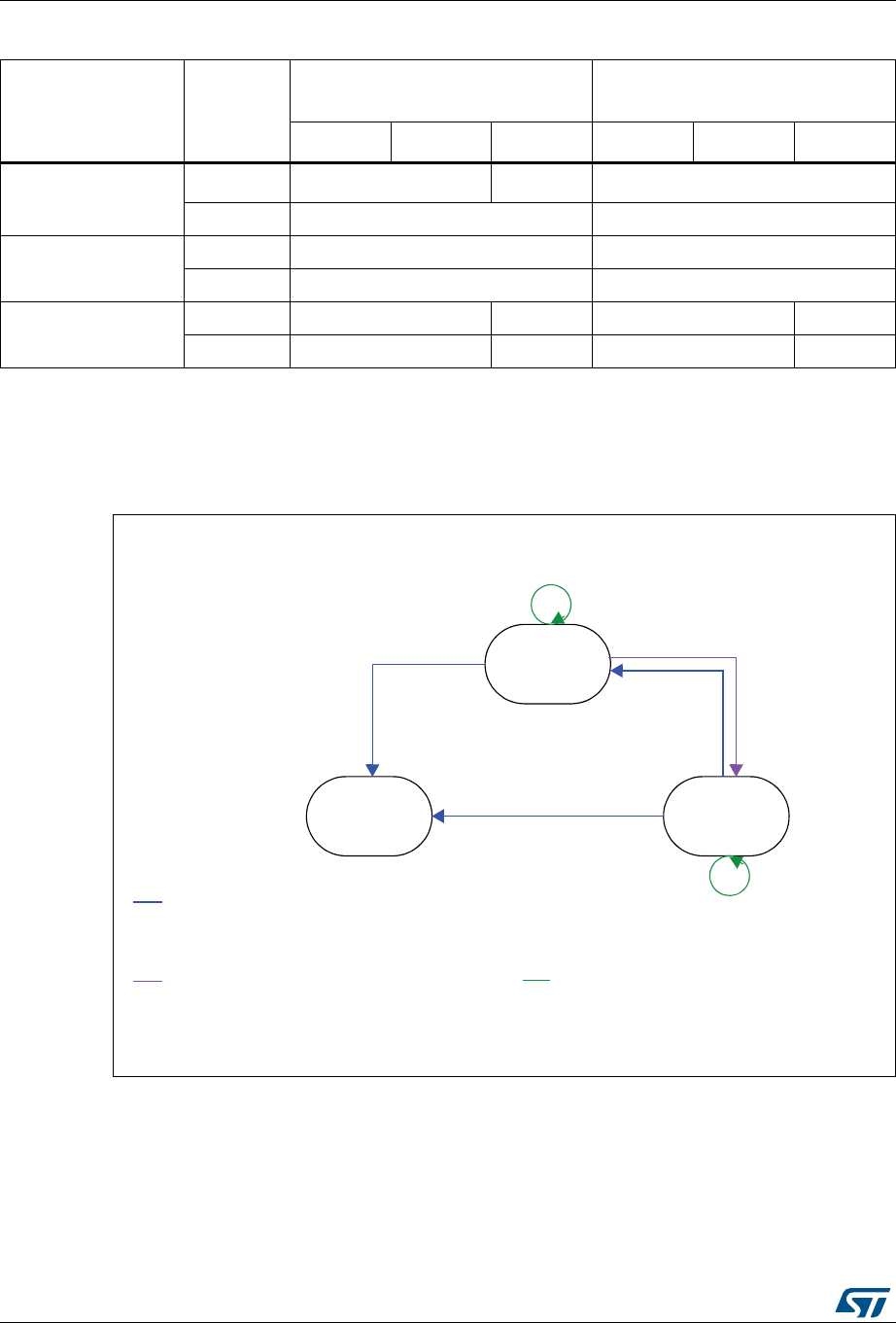
Embedded Flash memory interface RM0090
94/1718 DocID018909 Rev 9
--
Figure 6 shows how to go from one RDP level to another.
Figure 6. RDP levels
3.7.4 Write protections
Up to 24 user sectors in Flash memory can be protected against unwanted write operations
due to loss of program counter contexts. When the non-write protection nWRPi bit (0 ≤i≤11)
in the FLASH_OPTCR or FLASH_OPTCR1 registers is low, the corresponding sector
Table 17. Access versus read protection level
Memory area Protection
Level
Debug features, Boot from RAM or
from System memory bootloader Booting from Flash memory
Read Write Erase Read Write Erase
Main Flash Memory
and Backup SRAM
Level 1 NO NO(1) YES
Level 2 NO YES
Option Bytes
Level 1 YES YES
Level 2 NO NO
OTP
Level 1 NO NA YES NA
Level 2 NO NA YES NA
1. The main Flash memory and backup SRAM are only erased when the RDP changes from level 1 to 0. The OTP area
remains unchanged.
,EVEL
LEVE,LEVE,
H!!0$2H##0$2
2$0!!H
2$0##H
DEFAULT
/PTIONSWRITE2$0LEVELINCREASEINCLUDES
/PTIONSERASE
.EWOPTIONSPROGRAM
/PTIONSWRITE2$0LEVELDECREASEINCLUDES
-ASSERASE
/PTIONSERASE
.EWOPTIONSPROGRAM
/PTIONSWRITE2$0LEVELIDENTICALINCLUDES
/PTIONSERASE
.EWOPTIONSPROGRAM
2$0!!H
/THERSOPTIONSMODIFIED
2$0!!H##H
/THERSOPTIONSMODIFIED
7RITEOPTIONS
INCLUDING
2$0!!H
7RITEOPTIONS
INCLUDING
2$0##H
7RITEOPTIONS
INCLUDING
2$0##H
7RITEOPTIONSINCLUDING
2$0##H!!H
AI

DocID018909 Rev 9 95/1718
RM0090 Embedded Flash memory interface
112
cannot be erased or programmed. Consequently, a mass erase cannot be performed if one
of the sectors is write-protected.
If an erase/program operation to a write-protected part of the Flash memory is attempted
(sector protected by write protection bit, OTP part locked or part of the Flash memory that
can never be written like the ICP), the write protection error flag (WRPERR) is set in the
FLASH_SR register.
On STM32F42xxx and STM32F43xxx devices, when the PCROP mode is set, the active
level of nWRPi is high, and the corresponding sector i is write protected when nWRPi is
high. A PCROP sector is automatically write protected.
Note: When the memory read protection level is selected (RDP level = 1), it is not possible to
program or erase Flash memory sector i if the CPU debug features are connected (JTAG or
single wire) or boot code is being executed from RAM, even if nWRPi = 1.
Write protection error flag
If an erase/program operation to a write protected area of the Flash memory is performed,
the Write Protection Error flag (WRPERR) is set in the FLASH_SR register.
If an erase operation is requested, the WRPERR bit is set when:
•Mass, bank, sector erase are configured (MER or MER/MER1 and SER = 1)
•A sector erase is requested and the Sector Number SNB field is not valid
•A mass erase is requested while at least one of the user sector is write protected by
option bit (MER or MER/MER1 = 1 and nWRPi = 0 with 0 ≤ i ≤ 11 bits in the
FLASH_OPTCRx register
•A sector erase is requested on a write protected sector. (SER = 1, SNB = i and
nWRPi = 0 with 0 ≤ i ≤ 11 bits in the FLASH_OPTCRx register)
•The Flash memory is readout protected and an intrusion is detected.
If a program operation is requested, the WRPERR bit is set when:
•A write operation is performed on system memory or on the reserved part of the user
specific sector.
•A write operation is performed to the user configuration sector
•A write operation is performed on a sector write protected by option bit.
•A write operation is requested on an OTP area which is already locked
•The Flash memory is read protected and an intrusion is detected.
3.7.5 Proprietary code readout protection (PCROP)
The proprietary readout protection (PCROP) is available only on STM32F42xxx and
STM32F43xxx devices.
Flash memory user sectors (0 to 23) can be protected against D-bus read accesses by
using the proprietary readout protection (PCROP).
The PCROP protection is selected as follows, through the SPRMOD option bit in the
FLASH_CR register:
•SPRMOD = 0: nWRPi control the write protection of respective user sectors
•SPRMOD = 1: nWRPi control the read and write protection (PCROP) of respective
user sectors.
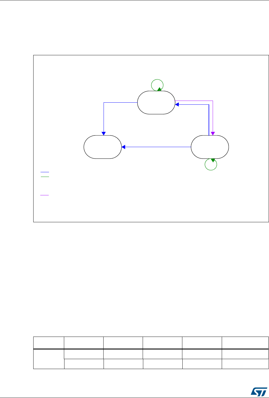
Embedded Flash memory interface RM0090
96/1718 DocID018909 Rev 9
When a sector is readout protected (PCROP mode activated), it can only be accessed for
code fetch through ICODE Bus on Flash interface:
•Any read access performed through the D-bus triggers a RDERR flag error.
•Any program/erase operation on a PCROPed sector triggers a WRPERR flag error.
Figure 7. PCROP levels
The deactivation of the SPRMOD and/or the unprotection of PCROPed user sectors can
only occur when, at the same time, the RDP level changes from 1 to 0. If this condition is not
respected, the user option byte modification is cancelled and the write error WRPERR flag
is set. The modification of the users option bytes (BOR_LEV, RST_STDBY, ..) is allowed
since none of the active nWRPi bits is reset and SPRMOD is kept active.
Note: The active value of nWRPi bits is inverted when PCROP mode is active (SPRMOD =1).
If SPRMOD = 1 and nWRPi =1, then user sector i of bank 1, respectively bank 2 is
read/write protected (PCROP).
3.8 One-time programmable bytes
Table 18 shows the organization of the one-time programmable (OTP) part of the OTP area.
,EVEL
,EVEL
2$0X##
2$0X!!
2$0X##
DEFAULT
5SEROPTIONSECTORERASE
0ROGRAMNEWOPTIONS
'LOBALMASSERASE
5SEROPTIONSECTIONERASE
0ROGRAMNEWOPTIONS
7RITEOPTIONS
30-/$ACTIVE
ANDVALIDN720I
.ORESTRICTIONON
7RITEOPTIONS
7RITEOPTIONS
30-/$ACTIVE
ANDVALIDN720I
,EVEL
2$0X!!
7RITEOPTIONS
30-/$ACTIVE
ANDVALIDN720I
7RITEOPTIONS
30-/$ACTIVE
ANDVALIDN720I 7RITEOPTIONS
30-/$ACTIVE
ANDVALIDN720I
6ALIDN720IMEANSTHATNONEOFTHEN720BITSSETCANBERESETTRANSITIONFROMTO
-36
Table 18. OTP area organization
Block [128:96] [95:64] [63:32] [31:0] Address byte 0
0
OTP0 OTP0 OTP0 OTP0 0x1FFF 7800
OTP0 OTP0 OTP0 OTP0 0x1FFF 7810

DocID018909 Rev 9 97/1718
RM0090 Embedded Flash memory interface
112
The OTP area is divided into 16 OTP data blocks of 32 bytes and one lock OTP block of 16
bytes. The OTP data and lock blocks cannot be erased. The lock block contains 16 bytes
LOCKBi (0 ≤ i ≤ 15) to lock the corresponding OTP data block (blocks 0 to 15). Each OTP
data block can be programmed until the value 0x00 is programmed in the corresponding
OTP lock byte. The lock bytes must only contain 0x00 and 0xFF values, otherwise the OTP
bytes might not be taken into account correctly.
1
OTP1 OTP1 OTP1 OTP1 0x1FFF 7820
OTP1 OTP1 OTP1 OTP1 0x1FFF 7830
.
.
.
.
.
.
.
.
.
15
OTP15 OTP15 OTP15 OTP15 0x1FFF 79E0
OTP15 OTP15 OTP15 OTP15 0x1FFF 79F0
Lock block LOCKB15 ...
LOCKB12
LOCKB11 ...
LOCKB8
LOCKB7 ...
LOCKB4
LOCKB3 ...
LOCKB0 0x1FFF 7A00
Table 18. OTP area organization (continued)
Block [128:96] [95:64] [63:32] [31:0] Address byte 0

Embedded Flash memory interface RM0090
98/1718 DocID018909 Rev 9
3.9 Flash interface registers
3.9.1 Flash access control register (FLASH_ACR)
for STM32F405xx/07xx and STM32F415xx/17xx
The Flash access control register is used to enable/disable the acceleration features and
control the Flash memory access time according to CPU frequency.
Address offset: 0x00
Reset value: 0x0000 0000
Access: no wait state, word, half-word and byte access
31 30 29 28 27 26 25 24 23 22 21 20 19 18 17 16
Reserved
15 14 13 12 11 10 9 8 7 6 5 4 3 2 1 0
Reserved DCRST ICRST DCEN ICEN PRFTEN Reserved LATENCY
rwwrwrw rw rwrwrw
Bits 31:13 Reserved, must be kept cleared.
Bit 12 DCRST: Data cache reset
0: Data cache is not reset
1: Data cache is reset
This bit can be written only when the D cache is disabled.
Bit 11 ICRST: Instruction cache reset
0: Instruction cache is not reset
1: Instruction cache is reset
This bit can be written only when the I cache is disabled.
Bit 10 DCEN: Data cache enable
0: Data cache is disabled
1: Data cache is enabled
Bit 9 ICEN: Instruction cache enable
0: Instruction cache is disabled
1: Instruction cache is enabled
Bit 8 PRFTEN: Prefetch enable
0: Prefetch is disabled
1: Prefetch is enabled
Bits 7:3 Reserved, must be kept cleared.
Bits 2:0 LATENCY: Latency
These bits represent the ratio of the CPU clock period to the Flash memory access time.
000: Zero wait state
001: One wait state
010: Two wait states
011: Three wait states
100: Four wait states
101: Five wait states
110: Six wait states
111: Seven wait states

DocID018909 Rev 9 99/1718
RM0090 Embedded Flash memory interface
112
3.9.2 Flash access control register (FLASH_ACR)
for STM32F42xxx and STM32F43xxx
The Flash access control register is used to enable/disable the acceleration features and
control the Flash memory access time according to CPU frequency.
Address offset: 0x00
Reset value: 0x0000 0000
Access: no wait state, word, half-word and byte access
31 30 29 28 27 26 25 24 23 22 21 20 19 18 17 16
Reserved
15 14 13 12 11 10 9 8 7 6 5 4 3 2 1 0
Reserved DCRST ICRST DCEN ICEN PRFTEN Reserved LATENCY
rwwrwrw rw rwrwrwrw
Bits 31:11 Reserved, must be kept cleared.
Bit 12 DCRST: Data cache reset
0: Data cache is not reset
1: Data cache is reset
This bit can be written only when the D cache is disabled.
Bit 11 ICRST: Instruction cache reset
0: Instruction cache is not reset
1: Instruction cache is reset
This bit can be written only when the I cache is disabled.
Bit 10 DCEN: Data cache enable
0: Data cache is disabled
1: Data cache is enabled
Bit 9 ICEN: Instruction cache enable
0: Instruction cache is disabled
1: Instruction cache is enabled
Bit 8 PRFTEN: Prefetch enable
0: Prefetch is disabled
1: Prefetch is enabled
Bits 7:4 Reserved, must be kept cleared.
Bits 3:0 LATENCY: Latency
These bits represent the ratio of the CPU clock period to the Flash memory access time.
0000: Zero wait state
0001: One wait state
0010: Two wait states
...
1110: Fourteen wait states
1111: Fifteen wait states
Embedded Flash memory interface RM0090
100/1718 DocID018909 Rev 9
3.9.3 Flash key register (FLASH_KEYR)
The Flash key register is used to allow access to the Flash control register and so, to allow
program and erase operations.
Address offset: 0x04
Reset value: 0x0000 0000
Access: no wait state, word access
3.9.4 Flash option key register (FLASH_OPTKEYR)
The Flash option key register is used to allow program and erase operations in the user
configuration sector.
Address offset: 0x08
Reset value: 0x0000 0000
Access: no wait state, word access
31 30 29 28 27 26 25 24 23 22 21 20 19 18 17 16
KEY[31:16]
wwwwww w w w w w w w w w w
1514131211109876543210
KEY[15:0]
wwwwww w w w w w w w w w w
Bits 31:0 FKEYR: FPEC key
The following values must be programmed consecutively to unlock the FLASH_CR register
and allow programming/erasing it:
a) KEY1 = 0x45670123
b) KEY2 = 0xCDEF89AB
31 30 29 28 27 26 25 24 23 22 21 20 19 18 17 16
OPTKEYR[31:16
wwwwww w w w w w ww w w w
15 14 13 12 11 10 9 8 7 6 5 4 3 2 1 0
OPTKEYR[15:0]
wwwwww w w w w w ww w w w
Bits 31:0 OPTKEYR: Option byte key
The following values must be programmed consecutively to unlock the FLASH_OPTCR
register and allow programming it:
a) OPTKEY1 = 0x08192A3B
b) OPTKEY2 = 0x4C5D6E7F

DocID018909 Rev 9 101/1718
RM0090 Embedded Flash memory interface
112
3.9.5 Flash status register (FLASH_SR) for
STM32F405xx/07xx and STM32F415xx/17xx
The Flash status register gives information on ongoing program and erase operations.
Address offset: 0x0C
Reset value: 0x0000 0000
Access: no wait state, word, half-word and byte access
31 30 29 28 27 26 25 24 23 22 21 20 19 18 17 16
Reserved
BSY
r
15 14 13 12 11 10 9 8 7 6 5 4 3 2 1 0
Reserved
PGSERR PGPERR PGAERR WRPERR
Reserved
OPERR EOP
rc_w1 rc_w1 rc_w1 rc_w1 rc_w1 rc_w1
Bits 31:17 Reserved, must be kept cleared.
Bit 16 BSY: Busy
This bit indicates that a Flash memory operation is in progress. It is set at the beginning of a
Flash memory operation and cleared when the operation finishes or an error occurs.
0: no Flash memory operation ongoing
1: Flash memory operation ongoing
Bits 15:8 Reserved, must be kept cleared.
Bit 7 PGSERR: Programming sequence error
Set by hardware when a write access to the Flash memory is performed by the code while
the control register has not been correctly configured.
Cleared by writing 1.
Bit 6 PGPERR: Programming parallelism error
Set by hardware when the size of the access (byte, half-word, word, double word) during the
program sequence does not correspond to the parallelism configuration PSIZE (x8, x16,
x32, x64).
Cleared by writing 1.
Bit 5 PGAERR: Programming alignment error
Set by hardware when the data to program cannot be contained in the same 128-bit Flash
memory row.
Cleared by writing 1.
Bit 4 WRPERR: Write protection error
Set by hardware when an address to be erased/programmed belongs to a write-protected
part of the Flash memory.
Cleared by writing 1.

Embedded Flash memory interface RM0090
102/1718 DocID018909 Rev 9
3.9.6 Flash status register (FLASH_SR) for
STM32F42xxx and STM32F43xxx
The Flash status register gives information on ongoing program and erase operations.
Address offset: 0x0C
Reset value: 0x0000 0000
Access: no wait state, word, half-word and byte access
Bits 3:2 Reserved, must be kept cleared.
Bit 1 OPERR: Operation error
Set by hardware when a flash operation (programming / erase /read) request is detected and
can not be run because of parallelism, alignment, or write protection error. This bit is set only
if error interrupts are enabled (ERRIE = 1).
Bit 0 EOP: End of operation
Set by hardware when one or more Flash memory operations (program/erase) has/have
completed successfully. It is set only if the end of operation interrupts are enabled (EOPIE =
1).
Cleared by writing a 1.
31 30 29 28 27 26 25 24 23 22 21 20 19 18 17 16
Reserved BSY
r
15 14 13 12 11 10 9 8 7 6 5 4 3 2 1 0
Reserved RDERR PGSERR PGPERR PGAERR WRPERR Reserved OPERR EOP
rc_w1 rc_w1 rc_w1 rc_w1 rc_w1 rc_w1 rc_w1
Bits 31:17 Reserved, must be kept cleared.
Bit 16 BSY: Busy
This bit indicates that a Flash memory operation is in progress to/from one bank. It is set at the
beginning of a Flash memory operation and cleared when the operation finishes or an error
occurs.
0: no Flash memory operation ongoing
1: Flash memory operation ongoing
Bits 15:9 Reserved, must be kept cleared.
Bit 8 RDERR: Proprietary readout protection (PCROP) error
Set by hardware when a read access through the D-bus is performed to an address
belonging to a proprietary readout protected Flash sector.
Cleared by writing 1.
Bit 7 PGSERR: Programming sequence error
Set by hardware when a write access to the Flash memory is performed by the code while
the control register has not been correctly configured.
Cleared by writing 1.

DocID018909 Rev 9 103/1718
RM0090 Embedded Flash memory interface
112
3.9.7 Flash control register (FLASH_CR) for
STM32F405xx/07xx and STM32F415xx/17xx
The Flash control register is used to configure and start Flash memory operations.
Address offset: 0x10
Reset value: 0x8000 0000
Access: no wait state when no Flash memory operation is ongoing, word, half-word and
byte access.
Bit 6 PGPERR: Programming parallelism error
Set by hardware when the size of the access (byte, half-word, word, double word) during the
program sequence does not correspond to the parallelism configuration PSIZE (x8, x16,
x32, x64).
Cleared by writing 1.
Bit 5 PGAERR: Programming alignment error
Set by hardware when the data to program cannot be contained in the same 128-bit Flash
memory row.
Cleared by writing 1.
Bit 4 WRPERR: Write protection error
Set by hardware when an address to be erased/programmed belongs to a write-protected
part of the Flash memory.
Cleared by writing 1.
Bits 3:2 Reserved, must be kept cleared.
Bit 1 OPERR: Operation error
Set by hardware when a flash operation (programming/erase/read) request is detected and
can not be run because of parallelism, alignment, write or read (PCROP) protection error.
This bit is set only if error interrupts are enabled (ERRIE = 1).
Bit 0 EOP: End of operation
Set by hardware when one or more Flash memory operations (program/erase) has/have
completed successfully. It is set only if the end of operation interrupts are enabled (EOPIE =
1).
Cleared by writing a 1.
31 30 29 28 27 26 25 24 23 22 21 20 19 18 17 16
LOCK
Reserved
ERRIE EOPIE
Reserved
STRT
rs rw rw rs
15 14 13 12 11 10 9 8 7 6 5 4 3 2 1 0
Reserved
PSIZE[1:0]
Res.
SNB[3:0] MER SER PG
rw rw rw rw rw rw rw rw rw

Embedded Flash memory interface RM0090
104/1718 DocID018909 Rev 9
Bit 31 LOCK: Lock
Write to 1 only. When it is set, this bit indicates that the FLASH_CR register is locked. It is
cleared by hardware after detecting the unlock sequence.
In the event of an unsuccessful unlock operation, this bit remains set until the next reset.
Bits 30:26 Reserved, must be kept cleared.
Bit 25 ERRIE: Error interrupt enable
This bit enables the interrupt generation when the OPERR bit in the FLASH_SR register is
set to 1.
0: Error interrupt generation disabled
1: Error interrupt generation enabled
Bit 24 EOPIE: End of operation interrupt enable
This bit enables the interrupt generation when the EOP bit in the FLASH_SR register goes
to 1.
0: Interrupt generation disabled
1: Interrupt generation enabled
Bits 23:17 Reserved, must be kept cleared.
Bit 16 STRT: Start
This bit triggers an erase operation when set. It is set only by software and cleared when the
BSY bit is cleared.
Bits 15:10 Reserved, must be kept cleared.
Bits 9:8 PSIZE: Program size
These bits select the program parallelism.
00 program x8
01 program x16
10 program x32
11 program x64
Bit 7 Reserved, must be kept cleared.
Bits 6:3 SNB: Sector number
These bits select the sector to erase.
0000 sector 0
0001 sector 1
...
1011 sector 11
Others not allowed
Bit 2 MER: Mass Erase
Erase activated for all user sectors.
Bit 1 SER: Sector Erase
Sector Erase activated.
Bit 0 PG: Programming
Flash programming activated.

DocID018909 Rev 9 105/1718
RM0090 Embedded Flash memory interface
112
3.9.8 Flash control register (FLASH_CR) for
STM32F42xxx and STM32F43xxx
The Flash control register is used to configure and start Flash memory operations.
Address offset: 0x10
Reset value: 0x8000 0000
Access: no wait state when no Flash memory operation is ongoing, word, half-word and
byte access.
31 30 29 28 27 26 25 24 23 22 21 20 19 18 17 16
LOCK Reserved
ERRI
EEOPIE Reserved STRT
rs rw rw rs
15 14 13 12 11 10 9 8 7 6 5 4 3 2 1 0
MER1 Reserved PSIZE[1:0] SNB[4:0] MER SER PG
rw rw rw rw rw rw rw rw rw rw rw
Bit 31 LOCK: Lock
Write to 1 only. When it is set, this bit indicates that the FLASH_CR register is locked. It is
cleared by hardware after detecting the unlock sequence.
In the event of an unsuccessful unlock operation, this bit remains set until the next reset.
Bits 30:26 Reserved, must be kept cleared.
Bit 25 ERRIE: Error interrupt enable
This bit enables the interrupt generation when the OPERR bit in the FLASH_SR register is
set to 1.
0: Error interrupt generation disabled
1: Error interrupt generation enabled
Bit 24 EOPIE: End of operation interrupt enable
This bit enables the interrupt generation when the EOP bit in the FLASH_SR register goes
to 1.
0: Interrupt generation disabled
1: Interrupt generation enabled
Bits 23:17 Reserved, must be kept cleared.
Bit 16 STRT: Start
This bit triggers an erase operation when set. It is set only by software and cleared when the
BSY bit is cleared.
Bit 15 MER1: Mass Erase of bank 2 sectors
Erase activated for bank 2 user sectors 12 to 23.
Bits 14:10 Reserved, must be kept cleared.
Bits 9:8 PSIZE: Program size
These bits select the program parallelism.
00 program x8
01 program x16
10 program x32
11 program x64

Embedded Flash memory interface RM0090
106/1718 DocID018909 Rev 9
3.9.9 Flash option control register (FLASH_OPTCR) for
STM32F405xx/07xx and STM32F415xx/17xx
The FLASH_OPTCR register is used to modify the user option bytes.
Address offset: 0x14
Reset value: 0x0FFF AAED. The option bits are loaded with values from Flash memory at
reset release.
Access: no wait state when no Flash memory operation is ongoing, word, half-word and
byte access.
Bits 7:3 SNB: Sector number
These bits select the sector to erase.
0000: sector 0
0001: sector 1
...
01011: sector 11
01100: not allowed
01101: not allowed
01110: not allowed
01111: not allowed
10000: section 12
10001: section 13
...
11011 sector 23
11100: not allowed
11101: not allowed
11110: not allowed
11111: not allowed
Bit 2 MER: Mass Erase of bank 1 sectors
Erase activated of bank 1 sectors.
Bit 1 SER: Sector Erase
Sector Erase activated.
Bit 0 PG: Programming
Flash programming activated.
31 30 29 28 27 26 25 24 23 22 21 20 19 18 17 16
Reserved nWRP[11:0]
rw rw rw rw rw rw rw rw rw rw rw rw
15 14 13 12 11 10 9 8 7 6 5 4 3 2 1 0
RDP[7:0] nRST_
STDBY
nRST_
STOP
WDG_
SW Reserv
ed
BOR_LEV OPTST
RT
OPTLO
CK
rw rw rw rw rw rw rw rw rw rw rw rw rw rs rs

DocID018909 Rev 9 107/1718
RM0090 Embedded Flash memory interface
112
Bits 31:28 Reserved, must be kept cleared.
Bits 27:16 nWRP[7:6]: Not write protect
These bits contain the value of the write-protection option bytes after reset. They can be
written to program a new write protect value into Flash memory.
0: Write protection active on selected sector
1: Write protection inactive on selected sector
Bits 15:8 RDP: Read protect
These bits contain the value of the read-protection option level after reset. They can be
written to program a new read protection value into Flash memory.
0xAA: Level 0, read protection not active
0xCC: Level 2, chip read protection active
Others: Level 1, read protection of memories active
Bits 7:5 USER: User option bytes
These bits contain the value of the user option byte after reset. They can be written to
program a new user option byte value into Flash memory.
Bit 7: nRST_STDBY
Bit 6: nRST_STOP
Bit 5: WDG_SW
Note: When changing the WDG mode from hardware to software or from software to
hardware, a system reset is required to make the change effective.
Bit 4 Reserved, must be kept cleared. Always read as “0”.
Bits 3:2 BOR_LEV: BOR reset Level
These bits contain the supply level threshold that activates/releases the reset. They can be
written to program a new BOR level. By default, BOR is off. When the supply voltage (VDD)
drops below the selected BOR level, a device reset is generated.
00: BOR Level 3 (VBOR3), brownout threshold level 3
01: BOR Level 2 (VBOR2), brownout threshold level 2
10: BOR Level 1 (VBOR1), brownout threshold level 1
11: BOR off, POR/PDR reset threshold level is applied
Note: For full details about BOR characteristics, refer to the “Electrical characteristics” section
in the device datasheet.
Bit 1 OPTSTRT: Option start
This bit triggers a user option operation when set. It is set only by software and cleared when
the BSY bit is cleared.
Bit 0 OPTLOCK: Option lock
Write to 1 only. When this bit is set, it indicates that the FLASH_OPTCR register is locked.
This bit is cleared by hardware after detecting the unlock sequence.
In the event of an unsuccessful unlock operation, this bit remains set until the next reset.

Embedded Flash memory interface RM0090
108/1718 DocID018909 Rev 9
3.9.10 Flash option control register (FLASH_OPTCR)
for STM32F42xxx and STM32F43xxx
The FLASH_OPTCR register is used to modify the user option bytes.
Address offset: 0x14
Reset value: 0x0FFF AAED. The option bits are loaded with values from Flash memory at
reset release.
Access: no wait state when no Flash memory operation is ongoing, word, half-word and
byte access.
31 30 29 28 27 26 25 24 23 22 21 20 19 18 17 16
SPR
MOD DB1M
Reserved
nWRP[11:0]
rw rw rw rw rw rw rw rw rw rw rw rw rw rw
1514131211109876543210
RDP[7:0] nRST_
STDBY
nRST_
STOP
WDG_
SW BFB2 BOR_LEV OPTST
RT
OPTLO
CK
rw rw rw rw rw rw rw rw rw rw rw rw rw rw rs rs
Bit 31 SPRMOD: Selection of protection mode for nWPRi bits
0: PCROP disabled. nWPRi bits used for Write protection on sector i.
1: PCROP enabled. nWPRi bits used for PCROP protection on sector i
Bit 30 DB1M: Dual-bank on 1 Mbyte Flash memory devices
0: 1 Mbyte single bank Flash memory (contiguous addresses in bank1)
1: 1 Mbyte dual bank Flash memory. The Flash memory is organized as two banks of
512 Kbytes each (see Table 7: 1 Mbyte Flash memory single bank vs dual bank organization
(STM32F42xxx and STM32F43xxx) and Table 9: 1 Mbyte dual bank Flash memory
organization (STM32F42xxx and STM32F43xxx)). To perform an erase operation, the right
sector must be programmed (see Table 7 for information on the sector numbering scheme).
Note: If DB1M is set and an erase operation is performed on Bank 2 while the default sector
number is selected (as an example, sector 8 is configured instead of sector 12), the
erase operation on Bank 2 sector is not performed.
Bits 29:28 Reserved, must be kept cleared.
Bits 27:16 nWRP: Not write protect
These bits contain the value of the write-protection and read-protection (PCROP) option
bytes for sectors 0 to 11 after reset. They can be written to program a new write-protect or
PCROP value into Flash memory.
If SPRMOD is reset:
0: Write protection active on sector i
1: Write protection not active on sector i
If SPRMOD is set:
0: PCROP protection not active on sector i
1: PCROP protection active on sector i
Bits 15:8 RDP: Read protect
These bits contain the value of the read-protection option level after reset. They can be
written to program a new read protection value into Flash memory.
0xAA: Level 0, read protection not active
0xCC: Level 2, chip read protection active
Others: Level 1, read protection of memories active

DocID018909 Rev 9 109/1718
RM0090 Embedded Flash memory interface
112
Bits 7:5 USER: User option bytes
These bits contain the value of the user option byte after reset. They can be written to
program a new user option byte value into Flash memory.
Bit 7: nRST_STDBY
Bit 6: nRST_STOP
Bit 5: WDG_SW
Note: When changing the WDG mode from hardware to software or from software to
hardware, a system reset is required to make the change effective.
Bit 4 BFB2: Dual-bank Boot option byte
0: Dual-bank boot disabled. Boot can be performed either from Flash memory bank 1 or from
system memory depending on boot pin state (default)
1: Dual-bank boot enabled. Boot is always performed from system memory.
Note: For STM32F42xx and STM32F43xx 1 MB part numbers, this option bit is reserved and
must be kept cleared.
Bits 3:2 BOR_LEV: BOR reset Level
These bits contain the supply level threshold that activates/releases the reset. They can be
written to program a new BOR level. By default, BOR is off. When the supply voltage (VDD)
drops below the selected BOR level, a device reset is generated.
00: BOR Level 3 (VBOR3), brownout threshold level 3
01: BOR Level 2 (VBOR2), brownout threshold level 2
10: BOR Level 1 (VBOR1), brownout threshold level 1
11: BOR off, POR/PDR reset threshold level is applied
Note: For full details on BOR characteristics, refer to the “Electrical characteristics” section of
the product datasheet.
Bit 1 OPTSTRT: Option start
This bit triggers a user option operation when set. It is set only by software and cleared when
the BSY bit is cleared.
Bit 0 OPTLOCK: Option lock
Write to 1 only. When this bit is set, it indicates that the FLASH_OPTCR register is locked.
This bit is cleared by hardware after detecting the unlock sequence.
In the event of an unsuccessful unlock operation, this bit remains set until the next reset.

Embedded Flash memory interface RM0090
110/1718 DocID018909 Rev 9
3.9.11 Flash option control register (FLASH_OPTCR1)
for STM32F42xxx and STM32F43xxx
This register is available only on STM32F42xxx and STM32F43xxx.
The FLASH_OPTCR1 register is used to modify the user option bytes for bank 2.
Address offset: 0x18
Reset value: 0x0FFF 0000. The option bits are loaded with values from Flash memory at
reset release.
Access: no wait state when no Flash memory operation is ongoing, word, half-word and
byte access.
31 30 29 28 27 26 25 24 23 22 21 20 19 18 17 16
Reserved
nWRP[11:0]
rw rw rw rw rw rw rw rw rw rw rw rw
15 14 13 12 11 10 9 8 7 6 5 4 3 2 1 0
Reserved
Bits 31:28 Reserved, must be kept cleared.
Bits 27:16 nWRP: Not write protect
These bits contain the value of the write-protection and read-protection (PCROP) option
bytes for sectors 0 to 11 after reset. They can be written to program a new write-protect or
PCROP value into Flash memory.
If SPRMOD is reset (default value):
0: Write protection active on sector i.
1: Write protection not active on sector i.
If SPRMOD is set:
0: PCROP protection not active on sector i.
1: PCROP protection active on sector i.
Bits 15:0 Reserved, must be kept cleared.
DocID018909 Rev 9 111/1718
RM0090 Embedded Flash memory interface
112
3.9.12 Flash interface register map
Table 19. Flash register map and reset values
(STM32F405xx/07xx and STM32F415xx/17xx)
Offset Register
31
30
29
28
27
26
25
24
23
22
21
20
19
18
17
16
15
14
13
12
11
10
9
8
7
6
5
4
3
2
1
0
0x00 FLASH_ACR Reserved
DCRST
ICRST
DCEN
ICEN
PRFTEN
Reserved LATENCY
Reset value 00000 0 0 0
0x04
FLASH_KEY
RKEY[31:16] KEY[15:0]
Reset value 000000000000000000000000000000 0 0
0x08
FLASH_OPT
KEYR OPTKEYR[31:16] OPTKEYR[15:0]
Reset value 000000000000000000000000000000 0 0
0x0C FLASH_SR Reserved
BSY
Reserved
PGSERR
PGPERR
PGAERR
WRPERR
Reserved
OPERR
EOP
Reset value 0 0 0 0 0 0 0
0x10 FLASH_CR
LOCK
Reserved
EOPIE
Reserved
STRT
Reserved
PSIZ
E[1:0
]
Reserved
SNB[3:0]
MER
SER
PG
Reset value 1 0 0 0 0 0 0 0 0 0 0
0x14
FLASH_OPT
CR Reserved nWRP[11:0] RDP[7:0]
nRST_STDBY
nRST_STOP
WDG_SW
Reserved
BOR_LEV
OPTSTRT
OPTLOCK
Reset value 11111111111110101010111 11 0 1
Table 20. Flash register map and reset values (STM32F42xxx and STM32F43xxx)
Offset Register
31
30
29
28
27
26
25
24
23
22
21
20
19
18
17
16
15
14
13
12
11
10
9
8
7
6
5
4
3
2
1
0
0x00
FLASH_ACR
Reserved
DCRST
ICRST
DCEN
ICEN
PRFTEN
Reserved
LATENCY
Reset value 00000 0 0 0 0
0x04
FLASH_KEYR KEY[31:16] KEY[15:0]
Reset value 00000000000000000000000000000 0 0 0
0x08
FLASH_
OPTKEYR OPTKEYR[31:16] OPTKEYR[15:0]
Reset value 00000000000000000000000000000 0 0 0
Embedded Flash memory interface RM0090
112/1718 DocID018909 Rev 9
0x0C
FLASH_SR
Reserved
BSY
Reserved
RDERR
PGSERR
PGPERR
PGAERR
WRPERR
Reserved
OPERR
EOP
Reset value 0 00000 0 0
0x10
FLASH_CR
LOCK
Reserved
EOPIE
Reserved
STRT
MER1
Reserved
PSIZE[1:0]
SNB[4:0]
MER
SER
PG
Reset value 1 0 00 00000000 0 0
0x14
FLASH_OPTCR
SPRMOD
DB1M
Reserved
nWRP[11:0] RDP[7:0]
nRST_STDBY
nRST_STOP
WDG_SW
BFB2
BOR_LEV
OPTSTRT
OPTLOCK
Reset value 00 1111111111111010101011101 1 0 1
0x18
FLASH_
OPTCR1
Reserved
nWRP[11:0]
Reserved
Reset value 111111111111
Table 20. Flash register map and reset values (STM32F42xxx and STM32F43xxx) (continued)
Offset Register
31
30
29
28
27
26
25
24
23
22
21
20
19
18
17
16
15
14
13
12
11
10
9
8
7
6
5
4
3
2
1
0
DocID018909 Rev 9 113/1718
RM0090 CRC calculation unit
115
4 CRC calculation unit
This section applies to the whole STM32F4xx family, unless otherwise specified.
4.1 CRC introduction
The CRC (cyclic redundancy check) calculation unit is used to get a CRC code from a 32-bit
data word and a fixed generator polynomial.
Among other applications, CRC-based techniques are used to verify data transmission or
storage integrity. In the scope of the EN/IEC 60335-1 standard, they offer a means of
verifying the Flash memory integrity. The CRC calculation unit helps compute a signature of
the software during runtime, to be compared with a reference signature generated at link-
time and stored at a given memory location.
4.2 CRC main features
•Uses CRC-32 (Ethernet) polynomial: 0x4C11DB7
–X
32 + X26 + X23 + X22 + X16 + X12 + X11 + X10 +X8 + X7 + X5 + X4 + X2+ X +1
•Single input/output 32-bit data register
•CRC computation done in 4 AHB clock cycles (HCLK)
•General-purpose 8-bit register (can be used for temporary storage)
The block diagram is shown in Figure 8.
Figure 8. CRC calculation unit block diagram
$+%EXV
ELWUHDGDFFHVV
'DWDUHJLVWHURXWSXW
&5&FRPSXWDWLRQSRO\QRPLDO[&'%
ELWZULWHDFFHVV
'DWDUHJLVWHULQSXW
DL

CRC calculation unit RM0090
114/1718 DocID018909 Rev 9
4.3 CRC functional description
The CRC calculation unit mainly consists of a single 32-bit data register, which:
•is used as an input register to enter new data in the CRC calculator (when writing into
the register)
•holds the result of the previous CRC calculation (when reading the register)
Each write operation into the data register creates a combination of the previous CRC value
and the new one (CRC computation is done on the whole 32-bit data word, and not byte per
byte).
The write operation is stalled until the end of the CRC computation, thus allowing back-to-
back write accesses or consecutive write and read accesses.
The CRC calculator can be reset to 0xFFFF FFFF with the RESET control bit in the
CRC_CR register. This operation does not affect the contents of the CRC_IDR register.
4.4 CRC registers
The CRC calculation unit contains two data registers and a control register.The peripheral
The CRC registers have to be accessed by words (32 bits).
4.4.1 Data register (CRC_DR)
Address offset: 0x00
Reset value: 0xFFFF FFFF
4.4.2 Independent data register (CRC_IDR)
Address offset: 0x04
Reset value: 0x0000 0000
31 30 29 28 27 26 25 24 23 22 21 20 19 18 17 16
DR [31:16]
rw rw rw rw rw rw rw rw rw rw rw rw rw rw rw rw
1514131211109876543210
DR [15:0]
rw rw rw rw rw rw rw rw rw rw rw rw rw rw rw rw
Bits 31:0 Data register bits
Used as an input register when writing new data into the CRC calculator.
Holds the previous CRC calculation result when it is read.
31 30 29 28 27 26 25 24 23 22 21 20 19 18 17 16
Reserved
1514131211109876543210
Reserved IDR[7:0]
rw rw rw rw rw rw rw rw
DocID018909 Rev 9 115/1718
RM0090 CRC calculation unit
115
4.4.3 Control register (CRC_CR)
Address offset: 0x08
Reset value: 0x0000 0000
4.4.4 CRC register map
The following table provides the CRC register map and reset values.
Bits 31:8 Reserved, must be kept at reset value.
Bits 7:0 General-purpose 8-bit data register bits
Can be used as a temporary storage location for one byte.
This register is not affected by CRC resets generated by the RESET bit in the CRC_CR
register.
31 30 29 28 27 26 25 24 23 22 21 20 19 18 17 16
Reserved
1514131211109876543210
Reserved
RESET
w
Bits 31:1 Reserved, must be kept at reset value.
Bit 0 RESET bit
Resets the CRC calculation unit and sets the data register to 0xFFFF FFFF.
This bit can only be set, it is automatically cleared by hardware.
Table 21. CRC calculation unit register map and reset values
Offset Register 31-24 23-16 15-8 7 6 5 4 3 2 1 0
0x00
CRC_DR Data register
Reset
value 0xFFFF FFFF
0x04
CRC_IDR
Reserved
Independent data register
Reset
value 0x00
0x08
CRC_CR
Reserved
RESET
Reset
value 0
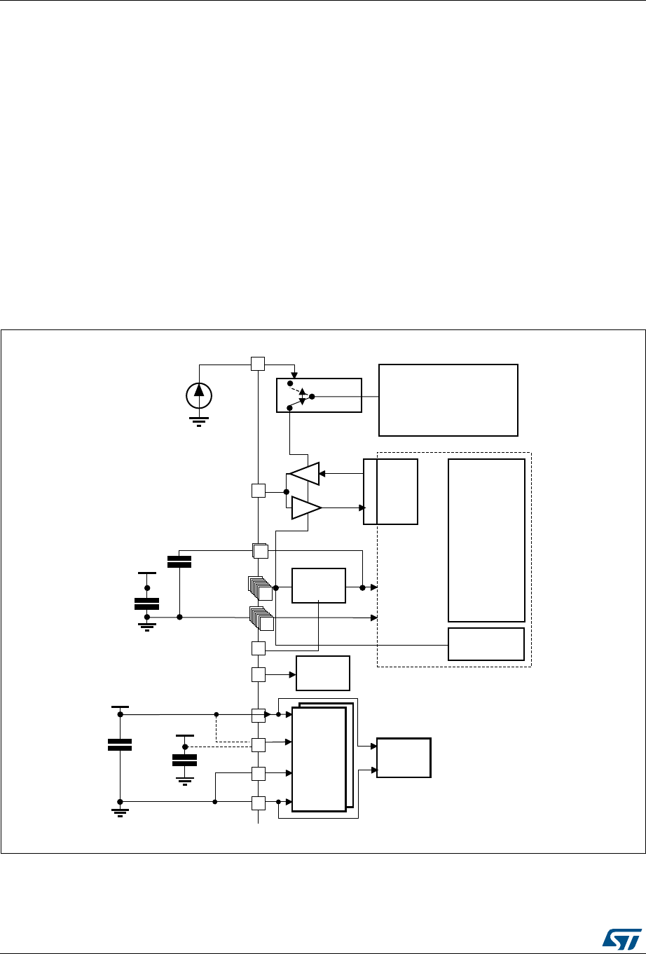
Power controller (PWR) RM0090
116/1718 DocID018909 Rev 9
5 Power controller (PWR)
This section applies to the whole STM32F4xx family, unless otherwise specified.
5.1 Power supplies
The device requires a 1.8 to 3.6 V operating voltage supply (VDD). An embedded linear
voltage regulator is used to supply the internal 1.2 V digital power.
The real-time clock (RTC), the RTC backup registers, and the backup SRAM (BKP SRAM)
can be powered from the VBAT voltage when the main VDD supply is powered off.
Note: Depending on the operating power supply range, some peripheral may be used with limited
functionality and performance. For more details refer to section "General operating
conditions" in STM32F4xx datasheets.
Figure 9. Power supply overview for STM32F405xx/07xx and STM32F415xx/17xx
1. VDDA and VSSA must be connected to VDD and VSS, respectively.
069
%DFNXSFLUFXLWU\
26&.57&
:DNHXSORJLF
%DFNXSUHJLVWHUV
EDFNXS5$0
.HUQHOORJLF
&38GLJLWDO
5$0
$QDORJ
5&V
3//
3RZHU
VZLWFK
9%$7
*3,2V
287
,1
îQ)
î)
9%$7
WR9
9ROWDJH
UHJXODWRU
9''$
$'&
/HYHOVKLIWHU
,2
/RJLF
9''
Q)
)
)ODVKPHPRU\
9&$3B
9&$3B
î)
%<3$66B5(*
3'5B21 5HVHW
FRQWUROOHU
9''
966
9''
95()
95()
966$
95()
Q)
)
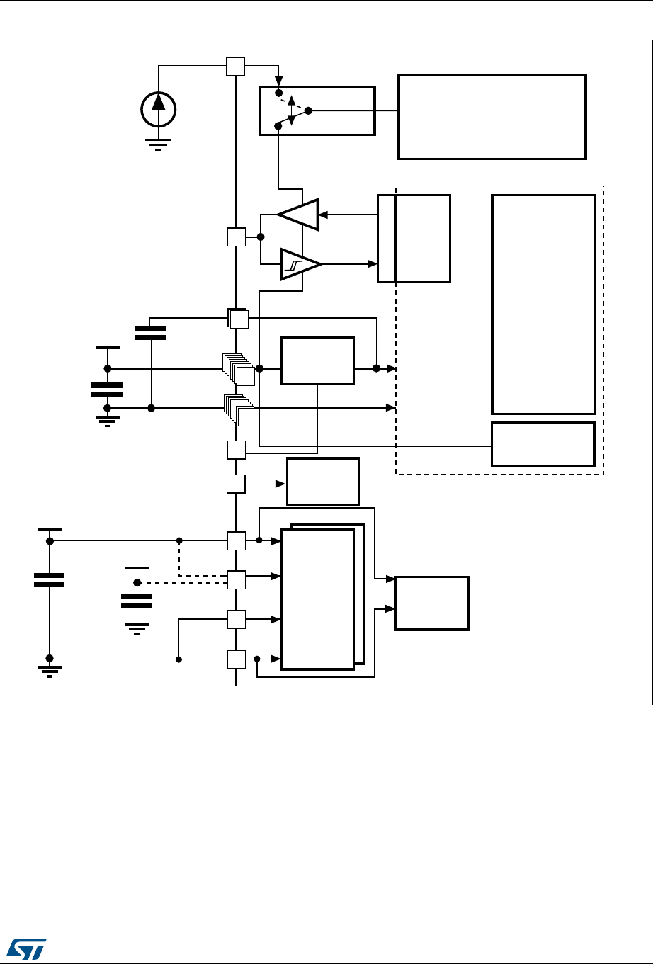
DocID018909 Rev 9 117/1718
RM0090 Power controller (PWR)
149
Figure 10. Power supply overview for STM32F42xxx and STM32F43xxx
1. VDDA and VSSA must be connected to VDD and VSS, respectively.
5.1.1 Independent A/D converter supply and reference voltage
To improve conversion accuracy, the ADC has an independent power supply which can be
separately filtered and shielded from noise on the PCB.
•The ADC voltage supply input is available on a separate VDDA pin.
•An isolated supply ground connection is provided on pin VSSA.
To ensure a better accuracy of low voltage inputs, the user can connect a separate external
reference voltage ADC input on VREF
. The voltage on VREF ranges from 1.8 V to VDDA.
-36
6$$
!NALOG
2#S0,,
0OWERSWITCH
6"!4
'0)/S
/54
). +ERNELLOGIC
#05
DIGITAL
2!-
"ACKUPCIRCUITRY
/3#+24#
"ACKUPREGISTERS
BACKUP2!-
7AKEUPLOGIC
§N&
§&
6"!4
TO6
6OLTAGE
REGULATOR
633
6$$!
62%&
62%&
633!
!$#
,EVELSHIFTER
)/
,OGIC
6$$
&
62%&
N&
&
6$$
&LASHMEMORY
6#!0?
6#!0?
§&
"90!33?2%'
0$2?/. 2ESET
CONTROLLER
N&

Power controller (PWR) RM0090
118/1718 DocID018909 Rev 9
5.1.2 Battery backup domain
Backup domain description
To retain the content of the RTC backup registers, backup SRAM, and supply the RTC when
VDD is turned off, VBAT pin can be connected to an optional standby voltage supplied by a
battery or by another source.
To allow the RTC to operate even when the main digital supply (VDD) is turned off, the VBAT
pin powers the following blocks:
•The RTC
•The LSE oscillator
•The backup SRAM when the low-power backup regulator is enabled
•PC13 to PC15 I/Os, plus PI8 I/O (when available)
The switch to the VBAT supply is controlled by the power-down reset embedded in the Reset
block.
Warning: During tRSTTEMPO (temporization at VDD startup) or after a PDR
is detected, the power switch between VBAT and VDD remains
connected to VBAT
.
During the startup phase, if VDD is established in less than
tRSTTEMPO (Refer to the datasheet for the value of tRSTTEMPO)
and VDD > VBAT + 0.6 V, a current may be injected into VBAT
through an internal diode connected between VDD and the
power switch (VBAT).
If the power supply/battery connected to the VBAT pin cannot
support this current injection, it is strongly recommended to
connect an external low-drop diode between this power
supply and the VBAT pin.
If no external battery is used in the application, it is recommended to connect the VBAT pin to
VDD with a 100 nF external decoupling ceramic capacitor in parallel.
When the backup domain is supplied by VDD (analog switch connected to VDD), the
following functions are available:
•PC14 and PC15 can be used as either GPIO or LSE pins
•PC13 can be used as a GPIOas the RTC_AF1 pin (refer to Table 37: RTC_AF1 pin for
more details about this pin configuration)
Note: Due to the fact that the switch only sinks a limited amount of current (3 mA), the use of PI8
and PC13 to PC15 GPIOs in output mode is restricted: the speed has to be limited to 2 MHz
with a maximum load of 30 pF and these I/Os must not be used as a current source (e.g. to
drive an LED).

DocID018909 Rev 9 119/1718
RM0090 Power controller (PWR)
149
When the backup domain is supplied by VBAT (analog switch connected to VBAT because
VDD is not present), the following functions are available:
•PC14 and PC15 can be used as LSE pins only
•PC13 can be used as the RTC_AF1 pin (refer to Table 37: RTC_AF1 pin for more
details about this pin configuration)
•PI8 can be used as RTC_AF2
Backup domain access
After reset, the backup domain (RTC registers, RTC backup register and backup SRAM) is
protected against possible unwanted write accesses. To enable access to the backup
domain, proceed as follows:
•Access to the RTC and RTC backup registers
1. Enable the power interface clock by setting the PWREN bits in the RCC_APB1ENR
register (see Section 7.3.13 and Section 6.3.13)
2. Set the DBP bit in the Section 5.4.1 and PWR power control register (PWR_CR) for
STM32F42xxx and STM32F43xxx to enable access to the backup domain
3. Select the RTC clock source: see Section 6.2.8: RTC/AWU clock
4. Enable the RTC clock by programming the RTCEN [15] bit in the Section 6.3.17: RCC
Backup domain control register (RCC_BDCR)
•Access to the backup SRAM
1. Enable the power interface clock by setting the PWREN bits in the RCC_APB1ENR
register (see Section 7.3.13 and Section 6.3.13 for STM32F405xx/07xx and
STM32F415xx/17xx and STM32F42xxx and STM32F43xxx, respectively)
2. Set the DBP bit in the PWR power control register (PWR_CR) for STM32F405xx/07xx
and STM32F415xx/17xx and PWR power control register (PWR_CR) for
STM32F42xxx and STM32F43xxx to enable access to the backup domain
3. Enable the backup SRAM clock by setting BKPSRAMEN bit in the RCC AHB1
peripheral clock enable register (RCC_AHB1ENR)RCC AHB1 peripheral clock enable
register (RCC_AHB1ENR).
RTC and RTC backup registers
The real-time clock (RTC) is an independent BCD timer/counter. The RTC provides a time-
of-day clock/calendar, two programmable alarm interrupts, and a periodic programmable
wakeup flag with interrupt capability. The RTC contains 20 backup data registers (80 bytes)
which are reset when a tamper detection event occurs. For more details refer to Section 26:
Real-time clock (RTC).
Backup SRAM
The backup domain includes 4 Kbytes of backup SRAM addressed in 32-bit, 16-bit or 8-bit
mode. Its content is retained even in Standby or VBAT mode when the low-power backup
regulator is enabled. It can be considered as an internal EEPROM when VBAT is always
present.
When the backup domain is supplied by VDD (analog switch connected to VDD), the backup
SRAM is powered from VDD which replaces the VBAT power supply to save battery life.
When the backup domain is supplied by VBAT (analog switch connected to VBAT because
VDD is not present), the backup SRAM is powered by a dedicated low-power regulator. This
regulator can be ON or OFF depending whether the application needs the backup SRAM
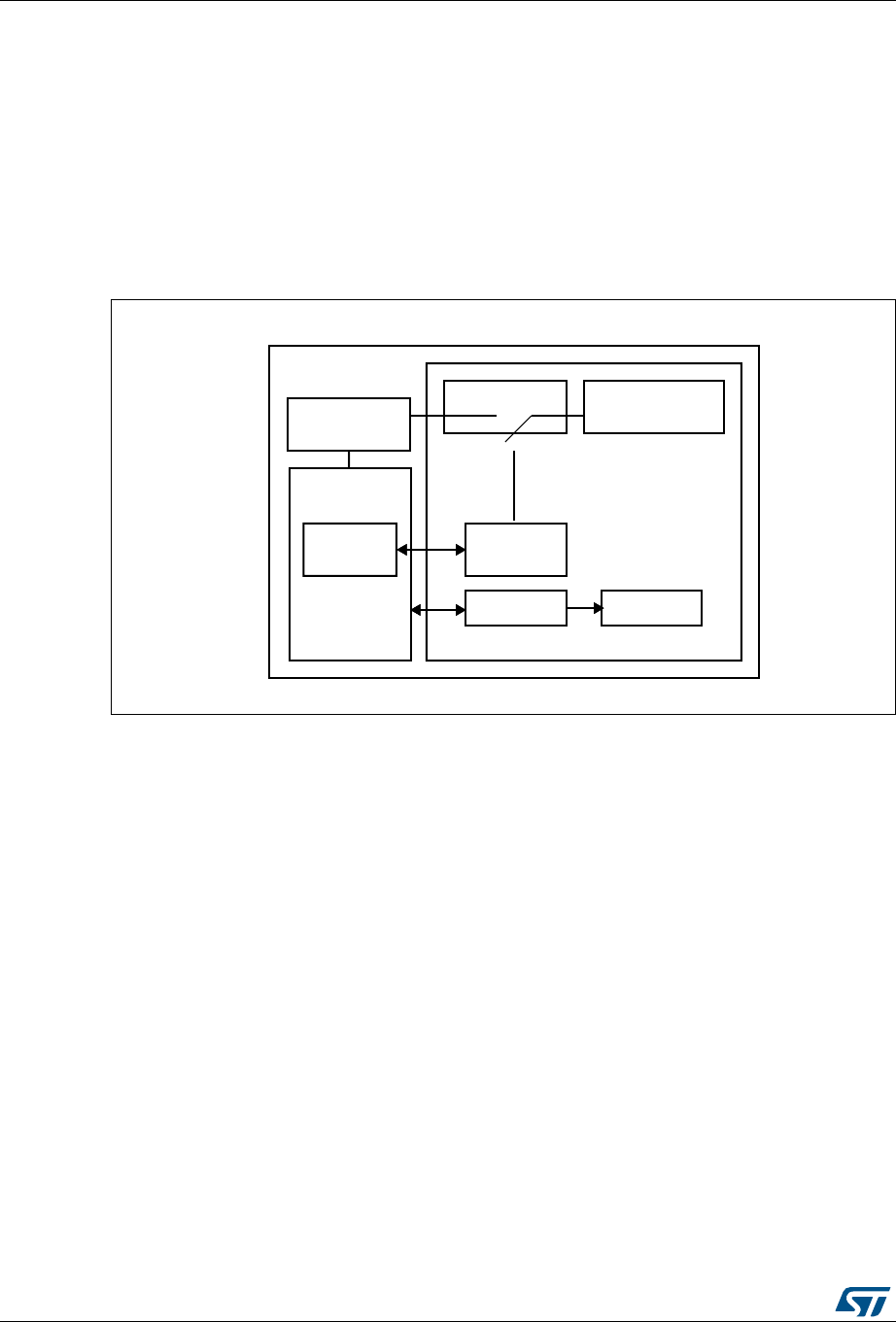
Power controller (PWR) RM0090
120/1718 DocID018909 Rev 9
function in Standby and VBAT modes or not. The power-down of this regulator is controlled
by a dedicated bit, the BRE control bit of the PWR_CSR register (see Section 5.4.2: PWR
power control/status register (PWR_CSR) for STM32F405xx/07xx and
STM32F415xx/17xx).
The backup SRAM is not mass erased by an tamper event. When the Flash memory is read
protected, the backup SRAM is also read protected to prevent confidential data, such as
cryptographic private key, from being accessed. When the protection level change from
level 1 to level 0 is requested, the backup SRAM content is erased. Refer to Section 3.7.3:
Read protection (RDP).
Figure 11. Backup domain
5.1.3 Voltage regulator for STM32F405xx/07xx and STM32F415xx/17xx
An embedded linear voltage regulator supplies all the digital circuitries except for the backup
domain and the Standby circuitry. The regulator output voltage is around 1.2 V.
This voltage regulator requires one or two external capacitors to be connected to one or two
dedicated pins, VCAP_1 and VCAP_2 available in all packages. Specific pins must be
connected either to VSS or VDD to activate or deactivate the voltage regulator. These pins
depend on the package.
When activated by software, the voltage regulator is always enabled after Reset. It works in
three different modes depending on the application modes.
•In Run mode, the regulator supplies full power to the 1.2 V domain (core, memories
and digital peripherals). In this mode, the regulator output voltage (around 1.2 V) can
be scaled by software to different voltage values:
Scale 1 or scale 2 can be configured on the fly through VOS (bit 15 of the
PWR_CR register).
The voltage scaling allows optimizing the power consumption when the device is
clocked below the maximum system frequency.
•In Stop mode, the main regulator or the low-power regulator supplies to the 1.2 V
domain, thus preserving the content of registers and internal SRAM. The voltage
069
9ROWDJHUHJXODWRU
!9
9GRPDLQ
%DFNXS65$0
LQWHUIDFH
3RZHUVZLWFK /3YROWDJHUHJXODWRU
!9
%DFNXS65$0
9
57& /6(+]
%DFNXSGRPDLQ

DocID018909 Rev 9 121/1718
RM0090 Power controller (PWR)
149
regulator can be put either in main regulator mode (MR) or in low-power mode (LPR).
The programmed voltage scale remains the same during Stop mode:
The programmed voltage scale remains the same during Stop mode (see
Section 5.4.1: PWR power control register (PWR_CR) for STM32F405xx/07xx
and STM32F415xx/17xx).
•In Standby mode, the regulator is powered down. The content of the registers and
SRAM are lost except for the Standby circuitry and the backup domain.
Note: For more details, refer to the voltage regulator section in the STM32F405xx/07xx and
STM32F415xx/17xx datasheets.
5.1.4 Voltage regulator for STM32F42xxx and STM32F43xxx
An embedded linear voltage regulator supplies all the digital circuitries except for the backup
domain and the Standby circuitry. The regulator output voltage is around 1.2 V.
This voltage regulator requires two external capacitors to be connected to two dedicated
pins, VCAP_1 and VCAP_2 available in all packages. Specific pins must be connected either to
VSS or VDD to activate or deactivate the voltage regulator. These pins depend on the
package.
When activated by software, the voltage regulator is always enabled after Reset. It works in
three different modes depending on the application modes (Run, Stop, or Standby mode).
•In Run mode, the main regulator supplies full power to the 1.2 V domain (core,
memories and digital peripherals). In this mode, the regulator output voltage (around
1.2 V) can be scaled by software to different voltage values (scale 1, scale 2, and scale
3 can be configured through VOS[1:0] bits of the PWR_CR register). The scale can be
modified only when the PLL is OFF and the HSI or HSE clock source is selected as
system clock source. The new value programmed is active only when the PLL is ON.
When the PLL is OFF, the voltage scale 3 is automatically selected.
The voltage scaling allows optimizing the power consumption when the device is
clocked below the maximum system frequency. After exit from Stop mode, the voltage
scale 3 is automatically selected.(see Section 5.4.1: PWR power control register

Power controller (PWR) RM0090
122/1718 DocID018909 Rev 9
(PWR_CR) for STM32F405xx/07xx and STM32F415xx/17xx.
2 operating modes are available:
–Normal mode: The CPU and core logic operate at maximum frequency at a given
voltage scaling (scale 1, scale 2 or scale 3)
–Over-drive mode: This mode allows the CPU and the core logic to operate at a
higher frequency than the normal mode for the voltage scaling scale 1 and scale
2.
•In Stop mode: the main regulator or low-power regulator supplies a low-power voltage
to the 1.2V domain, thus preserving the content of registers and internal SRAM.
The voltage regulator can be put either in main regulator mode (MR) or in low-power
mode (LPR). Both modes can be configured by software as follows:
–Normal mode: the 1.2 V domain is preserved in nominal leakage mode. It is the
default mode when the main regulator (MR) or the low-power regulator (LPR) is
enabled.
– Low voltage mode.
–Under-drive mode: the 1.2 V domain is preserved in reduced leakage mode. This
mode is only available when the main regulator or the low-power regulator is in
low voltage mode (see Table 22).
•In Standby mode: the regulator is powered down. The content of the registers and
SRAM are lost except for the Standby circuitry and the backup domain.
Note: Over-drive and under-drive mode are not available when the regulator is bypassed.
For more details, refer to the voltage regulator section in the STM32F42xxx and
STM32F43xxx datasheets.
Table 22. Voltage regulator configuration mode versus device operating mode(1)
1. ‘-’ means that the corresponding configuration is not available.
Voltage regulator
configuration Run mode Sleep mode Stop mode Standby mode
Normal mode MR MR MR or LPR -
Low-voltage mode - - MR or LPR -
Over-drive
mode(2)
2. The over-drive mode is not available when VDD = 1.8 to 2.1 V.
MR MR - -
Under-drive mode - - MR or LPR -
Power-down
mode ---Yes

DocID018909 Rev 9 123/1718
RM0090 Power controller (PWR)
149
Entering Over-drive mode
It is recommended to enter Over-drive mode when the application is not running critical
tasks and when the system clock source is either HSI or HSE. To optimize the configuration
time, enable the Over-drive mode during the PLL lock phase.
To enter Over-drive mode, follow the sequence below:
1. Select HSI or HSE as system clock.
2. Configure RCC_PLLCFGR register and set PLLON bit of RCC_CR register.
3. Set ODEN bit of PWR_CR register to enable the Over-drive mode and wait for the
ODRDY flag to be set in the PWR_CSR register.
4. Set the ODSW bit in the PWR_CR register to switch the voltage regulator from Normal
mode to Over-drive mode. The System will be stalled during the switch but the PLL
clock system will be still running during locking phase.
5. Wait for the ODSWRDY flag in the PWR_CSR to be set.
6. Select the required Flash latency as well as AHB and APB prescalers.
7. Wait for PLL lock.
8. Switch the system clock to the PLL.
9. Enable the peripherals that are not generated by the System PLL (I2S clock, LCD-TFT
clock, SAI1 clock, USB_48MHz clock....).
Note: The PLLI2S and PLLSAI can be configured at the same time as the system PLL.
During the Over-drive switch activation, no peripheral clocks should be enabled. The
peripheral clocks must be enabled once the Over-drive mode is activated.
Entering Stop mode disables the Over-drive mode, as well as the PLL. The application
software has to configure again the Over-drive mode and the PLL after exiting from Stop
mode.
Exiting from Over-drive mode
It is recommended to exit from Over-drive mode when the application is not running critical
tasks and when the system clock source is either HSI or HSE.There are two sequences that
allow exiting from over-drive mode:
•By resetting simultaneously the ODEN and ODSW bits bit in the PWR_CR register
(sequence 1)
•By resetting first the ODSW bit to switch the voltage regulator to Normal mode and then
resetting the ODEN bit to disable the Over-drive mode (sequence 2).
Example of sequence 1:
1. Select HSI or HSE as system clock source.
2. Disable the peripheral clocks that are not generated by the System PLL (I2S clock,
LCD-TFT clock, SAI1 clock, USB_48MHz clock,....)
3. Reset simultaneously the ODEN and the ODSW bits in the PWR_CR register to switch
back the voltage regulator to Normal mode and disable the Over-drive mode.
4. Wait for the ODWRDY flag of PWR_CSR to be reset.
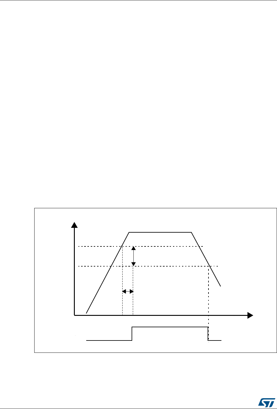
Power controller (PWR) RM0090
124/1718 DocID018909 Rev 9
Example of sequence 2:
1. Select HSI or HSE as system clock source.
2. Disable the peripheral clocks that are not generated by the System PLL (I2S clock,
LCD-TFT clock, SAI1 clock, USB_48MHz clock,....).
3. Reset the ODSW bit in the PWR_CR register to switch back the voltage regulator to
Normal mode. The system clock is stalled during voltage switching.
4. Wait for the ODWRDY flag of PWR_CSR to be reset.
5. Reset the ODEN bit in the PWR_CR register to disable the Over-drive mode.
Note: During step 3, the ODEN bit remains set and the Over-drive mode is still enabled but not
active (ODSW bit is reset). If the ODEN bit is reset instead, the Over-drive mode is disabled
and the voltage regulator is switched back to the initial voltage.
5.2 Power supply supervisor
5.2.1 Power-on reset (POR)/power-down reset (PDR)
The device has an integrated POR/PDR circuitry that allows proper operation starting
from 1.8 V.
The device remains in Reset mode when VDD/VDDA is below a specified threshold,
VPOR/PDR, without the need for an external reset circuit. For more details concerning the
power on/power-down reset threshold, refer to the electrical characteristics of the
datasheet.
Figure 12. Power-on reset/power-down reset waveform
6$$6$$!
M6
HYSTERESIS
0$2
0$2
-36
2ESET
4EMPORIZATION
T2344%-0/
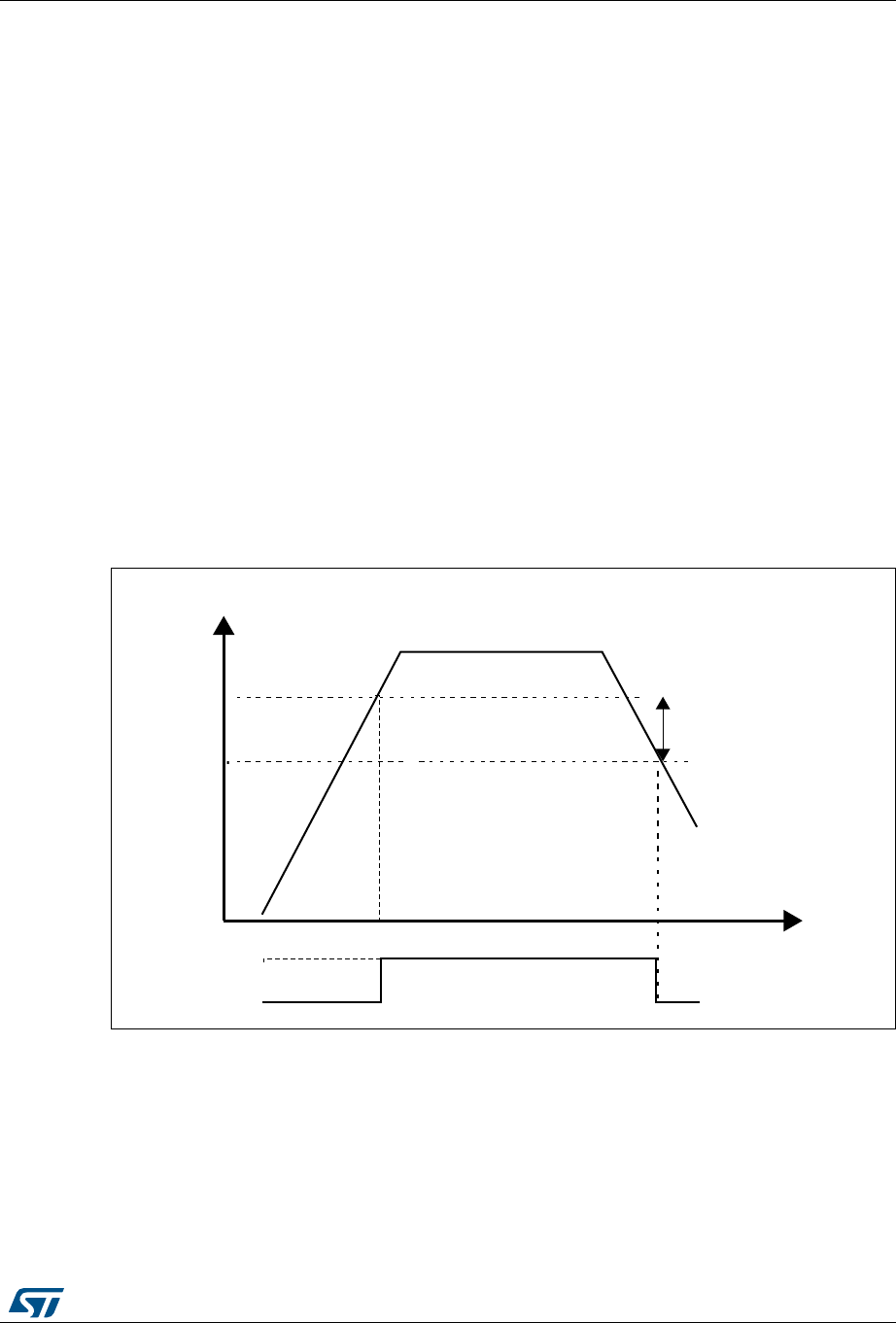
DocID018909 Rev 9 125/1718
RM0090 Power controller (PWR)
149
5.2.2 Brownout reset (BOR)
During power on, the Brownout reset (BOR) keeps the device under reset until the supply
voltage reaches the specified VBOR threshold.
VBOR is configured through device option bytes. By default, BOR is off. 3 programmable
VBOR threshold levels can be selected:
•BOR Level 3 (VBOR3). Brownout threshold level 3.
•BOR Level 2 (VBOR2). Brownout threshold level 2.
•BOR Level 1 (VBOR1). Brownout threshold level 1.
Note: For full details about BOR characteristics, refer to the "Electrical characteristics" section in
the device datasheet.
When the supply voltage (VDD) drops below the selected VBOR threshold, a device reset is
generated.
The BOR can be disabled by programming the device option bytes. In this case, the
power-on and power-down is then monitored by the POR/ PDR (see Section 5.2.1: Power-
on reset (POR)/power-down reset (PDR)).
The BOR threshold hysteresis is ~100 mV (between the rising and the falling edge of the
supply voltage).
Figure 13. BOR thresholds
5.2.3 Programmable voltage detector (PVD)
You can use the PVD to monitor the VDD power supply by comparing it to a threshold
selected by the PLS[2:0] bits in the PWR power control register (PWR_CR) for
STM32F405xx/07xx and STM32F415xx/17xx and PWR power control register (PWR_CR)
for STM32F42xxx and STM32F43xxx.
The PVD is enabled by setting the PVDE bit.
-36
6$$6$$!
M6
HYSTERESIS
"/2THRESHOLD
2ESET
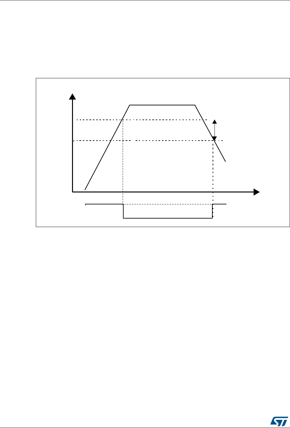
Power controller (PWR) RM0090
126/1718 DocID018909 Rev 9
A PVDO flag is available, in the PWR power control/status register (PWR_CSR) for
STM32F405xx/07xx and STM32F415xx/17xx, to indicate if VDD is higher or lower than the
PVD threshold. This event is internally connected to the EXTI line16 and can generate an
interrupt if enabled through the EXTI registers. The PVD output interrupt can be generated
when VDD drops below the PVD threshold and/or when VDD rises above the PVD threshold
depending on EXTI line16 rising/falling edge configuration. As an example the service
routine could perform emergency shutdown tasks.
Figure 14. PVD thresholds
5.3 Low-power modes
By default, the microcontroller is in Run mode after a system or a power-on reset. In Run
mode the CPU is clocked by HCLK and the program code is executed. Several low-power
modes are available to save power when the CPU does not need to be kept running, for
example when waiting for an external event. It is up to the user to select the mode that gives
the best compromise between low-power consumption, short startup time and available
wakeup sources.
The devices feature three low-power modes:
•Sleep mode (Cortex®-M4 with FPU core stopped, peripherals kept running)
•Stop mode (all clocks are stopped)
•Standby mode (1.2 V domain powered off)
In addition, the power consumption in Run mode can be reduce by one of the following
means:
•Slowing down the system clocks
•Gating the clocks to the APBx and AHBx peripherals when they are unused.
069
9''
P9
K\VWHUHVLV
39'WKUHVKROG
39'RXWSXW

DocID018909 Rev 9 127/1718
RM0090 Power controller (PWR)
149
Entering low-power mode
Low-power modes are entered by the MCU by executing the WFI (Wait For Interrupt), or
WFE (Wait for Event) instructions, or when the SLEEPONEXIT bit in the Cortex®-M4 with
FPU System Control register is set on Return from ISR.
Exiting low-power mode
The MCU exits from Sleep and Stop modes low-power mode depending on the way the low-
power mode was entered:
•If the WFI instruction or Return from ISR was used to enter the low-power mode, any
peripheral interrupt acknowledged by the NVIC can wake up the device.
•If the WFE instruction is used to enter the low-power mode, the MCU exits the low-
power mode as soon as an event occurs. The wakeup event can be generated either
by:
– NVIC IRQ interrupt:
When SEVONPEND = 0 in the Cortex®-M4 with FPU System Control register: by
enabling an interrupt in the peripheral control register and in the NVIC. When the
MCU resumes from WFE, the peripheral interrupt pending bit and the NVIC
peripheral IRQ channel pending bit (in the NVIC interrupt clear pending register)
have to be cleared. Only NVIC interrupts with sufficient priority will wakeup and
interrupt the MCU.
When SEVONPEND = 1 in the Cortex®-M4 with FPU System Control register: by
enabling an interrupt in the peripheral control register and optionally in the NVIC.
When the MCU resumes from WFE, the peripheral interrupt pending bit and when
enabled the NVIC peripheral IRQ channel pending bit (in the NVIC interrupt clear
pending register) have to be cleared. All NVIC interrupts will wakeup the MCU,
even the disabled ones.Only enabled NVIC interrupts with sufficient priority will
wakeup and interrupt the MCU.
–Event
This is done by configuring a EXTI line in event mode. When the CPU resumes
from WFE, it is not necessary to clear the EXTI peripheral interrupt pending bit or
the NVIC IRQ channel pending bit as the pending bits corresponding to the event
line is not set. It may be necessary to clear the interrupt flag in the peripheral.
The MCU exits from Standby low-power mode through an external reset (NRST pin), an
IWDG reset, a rising edge on one of the enabled WKUPx pins or a RTC event occurs (see
Figure 237: RTC block diagram).
After waking up from Standby mode, program execution restarts in the same way as after a
Reset (boot pin sampling, option bytes loading, reset vector is fetched, etc.).

Power controller (PWR) RM0090
128/1718 DocID018909 Rev 9
Only enabled NVIC interrupts with sufficient priority will wakeup and interrupt the
MCU.
5.3.1 Slowing down system clocks
In Run mode the speed of the system clocks (SYSCLK, HCLK, PCLK1, PCLK2) can be
reduced by programming the prescaler registers. These prescalers can also be used to slow
down peripherals before entering Sleep mode.
For more details refer to Section 6.3.3: RCC clock configuration register (RCC_CFGR).
Table 23. Low-power mode summary
Mode name Entry Wakeup Effect on 1.2 V
domain clocks
Effect on
VDD
domain
clocks
Voltage regulator
Sleep
(Sleep now or
Sleep-on-
exit)
WFI or Return
from ISR Any interrupt CPU CLK OFF
no effect on other
clocks or analog
clock sources
None ON
WFE Wakeup event
Stop
PDDS and LPDS
bits +
SLEEPDEEP bit
+ WFI, Return
from ISR or WFE
Any EXTI line (configured
in the EXTI registers,
internal and external lines)
All 1.2 V domain
clocks OFF
HSI and
HSE
oscillator
s OFF
ON or in low- power
mode (depends on
PWR power control
register (PWR_CR)
for
STM32F405xx/07x
x and
STM32F415xx/17x
x and PWR power
control register
(PWR_CR) for
STM32F405xx/07x
x and
STM32F415xx/17x
xPWR power
control register
(PWR_CR) for
STM32F42xxx and
STM32F43xxx
Standby
PDDS bit +
SLEEPDEEP bit
+ WFI, Return
from ISR or WFE
WKUP pin rising edge,
RTC alarm (Alarm A or
Alarm B), RTC Wakeup
event, RTC tamper
events, RTC time stamp
event, external reset in
NRST pin, IWDG reset
OFF

DocID018909 Rev 9 129/1718
RM0090 Power controller (PWR)
149
5.3.2 Peripheral clock gating
In Run mode, the HCLKx and PCLKx for individual peripherals and memories can be
stopped at any time to reduce power consumption.
To further reduce power consumption in Sleep mode the peripheral clocks can be disabled
prior to executing the WFI or WFE instructions.
Peripheral clock gating is controlled by the AHB1 peripheral clock enable register
(RCC_AHB1ENR), AHB2 peripheral clock enable register (RCC_AHB2ENR), AHB3
peripheral clock enable register (RCC_AHB3ENR) (see Section 6.3.9: RCC AHB1
peripheral clock enable register (RCC_AHB1ENR), Section 6.3.10: RCC AHB2 peripheral
clock enable register (RCC_AHB2ENR), Section 7.3.12: RCC AHB3 peripheral clock
enable register (RCC_AHB3ENR) for STM32F405xx/07xx and STM32F415xx/17xx, and
Section 6.3.10: RCC AHB1 peripheral clock register (RCC_AHB1ENR), Section 6.3.11:
RCC AHB2 peripheral clock enable register (RCC_AHB2ENR), and Section 6.3.12: RCC
AHB3 peripheral clock enable register (RCC_AHB3ENR) for STM32F42xxx and
STM32F43xxx).
Disabling the peripherals clocks in Sleep mode can be performed automatically by resetting
the corresponding bit in RCC_AHBxLPENR and RCC_APBxLPENR registers.
5.3.3 Sleep mode
Entering Sleep mode
The Sleep mode is entered according to Section : Entering low-power mode, when the
SLEEPDEEP bit in the Cortex®-M4 with FPU System Control register is cleared.
Refer to Table 24 and Table 25 for details on how to enter Sleep mode.
Exiting Sleep mode
The Sleep mode is exited according to Section : Exiting low-power mode.
Refer to Table 24 and Table 25 for more details on how to exit Sleep mode.
Table 24. Sleep-now entry and exit
Sleep-now mode Description
Mode entry
WFI (Wait for Interrupt) or WFE (Wait for Event) while:
– SLEEPDEEP = 0
Refer to the Cortex®-M4 with FPU System Control register.
On Return from ISR while:
– SLEEPDEEP = 0 and
– SLEEPONEXIT = 1
Refer to the Cortex®-M4 with FPU System Control register.

Power controller (PWR) RM0090
130/1718 DocID018909 Rev 9
5.3.4 Stop mode (STM32F405xx/07xx and STM32F415xx/17xx)
The Stop mode is based on the Cortex®-M4 with FPU deepsleep mode combined with
peripheral clock gating. The voltage regulator can be configured either in normal or low-
power mode. In Stop mode, all clocks in the 1.2 V domain are stopped, the PLLs, the HSI
and the HSE RC oscillators are disabled. Internal SRAM and register contents are
preserved.
By setting the FPDS bit in the PWR_CR register, the Flash memory also enters power-down
mode when the device enters Stop mode. When the Flash memory is in power-down mode,
an additional startup delay is incurred when waking up from Stop mode (see Table 26: Stop
operating modes (STM32F405xx/07xx and STM32F415xx/17xx) and Section 5.4.1: PWR
power control register (PWR_CR) for STM32F405xx/07xx and STM32F415xx/17xx).
Mode exit
If WFI or Return from ISR was used for entry:
Interrupt: Refer to Table 61: Vector table for STM32F405xx/07xx and
STM32F415xx/17xx and Table 62: Vector table for STM32F42xxx and
STM32F43xxx
If WFE was used for entry and SEVONPEND = 0
Wakeup event: Refer to Section 12.2.3: Wakeup event management
f WFE was used for entry and SEVONPEND = 1
Interrupt even when disabled in NVIC: refer to Table 61: Vector table for
STM32F405xx/07xx and STM32F415xx/17xx and Table 62: Vector table
for STM32F42xxx and STM32F43xxx or Wakeup event (see
Section 12.2.3: Wakeup event management).
Wakeup latency None
Table 25. Sleep-on-exit entry and exit
Sleep-on-exit Description
Mode entry
WFI (Wait for Interrupt) or WFE (Wait for Event) while:
– SLEEPDEEP = 0
Refer to the Cortex®-M4 with FPU System Control register.
On Return from ISR while:
– SLEEPDEEP = 0 and
– SLEEPONEXIT = 1
Refer to the Cortex®-M4 with FPU System Control register.
Mode exit
Interrupt: refer to Table 61: Vector table for STM32F405xx/07xx and
STM32F415xx/17xx and Table 62: Vector table for STM32F42xxx and
STM32F43xxx
Wakeup latency None
Table 24. Sleep-now entry and exit (continued)
Sleep-now mode Description

DocID018909 Rev 9 131/1718
RM0090 Power controller (PWR)
149
Entering Stop mode (for STM32F405xx/07xx and STM32F415xx/17xx)
The Stop mode is entered according to Section : Entering low-power mode, when the
SLEEPDEEP bit in the Cortex®-M4 with FPU System Control register is set.
Refer to Table 27 for details on how to enter the Stop mode.
To further reduce power consumption in Stop mode, the internal voltage regulator can be put
in low-power mode. This is configured by the LPDS bit of the PWR power control register
(PWR_CR) for STM32F405xx/07xx and STM32F415xx/17xx and PWR power control
register (PWR_CR) for STM32F42xxx and STM32F43xxx.
If Flash memory programming is ongoing, the Stop mode entry is delayed until the memory
access is finished.
If an access to the APB domain is ongoing, The Stop mode entry is delayed until the APB
access is finished.
In Stop mode, the following features can be selected by programming individual control bits:
•Independent watchdog (IWDG): the IWDG is started by writing to its Key register or by
hardware option. Once started it cannot be stopped except by a Reset. See
Section 21.3 in Section 21: Independent watchdog (IWDG).
•Real-time clock (RTC): this is configured by the RTCEN bit in the Section 6.3.17: RCC
Backup domain control register (RCC_BDCR)
•Internal RC oscillator (LSI RC): this is configured by the LSION bit in the
Section 6.3.18: RCC clock control & status register (RCC_CSR).
•External 32.768 kHz oscillator (LSE OSC): this is configured by the LSEON bit in the
Section 6.3.17: RCC Backup domain control register (RCC_BDCR).
The ADC or DAC can also consume power during the Stop mode, unless they aredisabled
before entering it. To disable them, the ADON bit in the ADC_CR2 register and the ENx bit
in the DAC_CR register must both be written to 0.
Table 26. Stop operating modes
(STM32F405xx/07xx and STM32F415xx/17xx)
Stop mode LPDS bit FPDS bit Wake-up latency
STOP MR
(Main regulator) 0 0 HSI RC startup time
STOP MR-FPD 0 1
HSI RC startup time +
Flash wakeup time from Power Down
mode
STOP LP 1 0 HSI RC startup time +
regulator wakeup time from LP mode
STOP LP-FPD 1 1
HSI RC startup time +
Flash wakeup time from Power Down
mode +
regulator wakeup time from LP mode

Power controller (PWR) RM0090
132/1718 DocID018909 Rev 9
Note: If the application needs to disable the external clock before entering Stop mode, the HSEON
bit must first be disabled and the system clock switched to HSI.
Otherwise, if the HSEON bit is kept enabled while the external clock (external oscillator) can
be removed before entering stop mode, the clock security system (CSS) feature must be
enabled to detect any external oscillator failure and avoid a malfunction behavior when
entering stop mode.
Exiting Stop mode (for STM32F405xx/07xx and STM32F415xx/17xx)
The Stop mode is exited according to Section : Exiting low-power mode.
Refer to Table 27 for more details on how to exit Stop mode.
When exiting Stop mode by issuing an interrupt or a wakeup event, the HSI RC oscillator is
selected as system clock.
When the voltage regulator operates in low-power mode, an additional startup delay is
incurred when waking up from Stop mode. By keeping the internal regulator ON during Stop
mode, the consumption is higher although the startup time is reduced.
Table 27. Stop mode entry and exit (for STM32F405xx/07xx and STM32F415xx/17xx)
Stop mode Description
Mode entry
WFI (Wait for Interrupt) or WFE (Wait for Event) while:
– SLEEPDEEP bit is set in Cortex®-M4 with FPU System Control register
– PDDS bit is cleared in Power Control register (PWR_CR)
– Select the voltage regulator mode by configuring LPDS bit in PWR_CR.
On Return from ISR:
– SLEEPDEEP bit is set in Cortex®-M4 with FPU System Control register
– SLEEPONEXIT = 1
– PDDS bit is cleared in Power Control register (PWR_CR)
Note: To enter Stop mode, all EXTI Line pending bits (in Pending register
(EXTI_PR)), all peripheral interrupts pending bits, the RTC Alarm
(Alarm A and Alarm B), RTC wakeup, RTC tamper, and RTC time
stamp flags, must be reset. Otherwise, the Stop mode entry
procedure is ignored and program execution continues.

DocID018909 Rev 9 133/1718
RM0090 Power controller (PWR)
149
5.3.5 Stop mode (STM32F42xxx and STM32F43xxx)
The Stop mode is based on the Cortex®-M4 with FPU deepsleep mode combined with
peripheral clock gating. The voltage regulator can be configured either in normal or low-
power mode. In Stop mode, all clocks in the 1.2 V domain are stopped, the PLLs, the HSI
and the HSE RC oscillators are disabled. Internal SRAM and register contents are
preserved.
In Stop mode, the power consumption can be further reduced by using additional settings in
the PWR_CR register. However this will induce an additional startup delay when waking up
from Stop mode (see Table 28).
Mode exit
If WFI or Return from ISR was used for entry:
Any EXTI lines configured in Interrupt mode (the corresponding EXTI
Interrupt vector must be enabled in the NVIC). The interrupt source can
be external interrupts or peripherals with wakeup capability. Refer to
Table 61: Vector table for STM32F405xx/07xx and STM32F415xx/17xx
on page 372 and Table 62: Vector table for STM32F42xxx and
STM32F43xxx.
If WFE was used for entry and SEVONPEND = 0
Any EXTI lines configured in event mode. Refer to Section 12.2.3:
Wakeup event management on page 380.
If WFE was used for entry and SEVONPEND = 1:
– Any EXTI lines configured in Interrupt mode (even if the corresponding
EXTI Interrupt vector is disabled in the NVIC). The interrupt source can
be an external interrupt or a peripheral with wakeup capability. Refer to
Table 61: Vector table for STM32F405xx/07xx and STM32F415xx/17xx
on page 372 and Table 62: Vector table for STM32F42xxx and
STM32F43xxx.
– Wakeup event: refer to Section 12.2.3: Wakeup event management on
page 380.
Wakeup latency Table 26: Stop operating modes (STM32F405xx/07xx and
STM32F415xx/17xx)
Table 27. Stop mode entry and exit (for STM32F405xx/07xx and STM32F415xx/17xx)
Stop mode Description

Power controller (PWR) RM0090
134/1718 DocID018909 Rev 9
Entering Stop mode (STM32F42xxx and STM32F43xxx)
The Stop mode is entered according to Section : Entering low-power mode, when the
SLEEPDEEP bit in the Cortex®-M4 with FPU System Control register is set.
Refer to Table 29 for details on how to enter the Stop mode.
When the microcontroller enters in Stop mode, the voltage scale 3 is automatically selected.
To further reduce power consumption in Stop mode, the internal voltage regulator can be put
in low-power or low voltage mode. This is configured by the LPDS, MRUDS, LPUDS and
UDEN bits of the PWR power control register (PWR_CR) for STM32F405xx/07xx and
STM32F415xx/17xx.
If Flash memory programming is ongoing, the Stop mode entry is delayed until the memory
access is finished.
If an access to the APB domain is ongoing, The Stop mode entry is delayed until the APB
access is finished.
If the Over-drive mode was enabled before entering Stop mode, it is automatically disabled
during when the Stop mode is activated.
Table 28. Stop operating modes (STM32F42xxx and STM32F43xxx)
Voltage Regulator Mode UDEN[1:0]
bits
MRUDS
bit
LPUDS
bit
LPDS
bit
FPDS
bit Wakeup latency
Normal
mode
STOP MR
(Main Regulator) - 0 - 0 0 HSI RC startup time
STOP MR- FPD - 0 - 0 1
HSI RC startup time +
Flash wakeup time from power-
down mode
STOP LP - 0 0 1 0
HSI RC startup time +
regulator wakeup time from LP
mode
STOP LP-FPD - - 0 1 1
HSI RC startup time +
Flash wakeup time from power-
down mode +
regulator wakeup time from LP
mode
Under-
drive
Mode
STOP UMR-
FPD 3 1 - 0 -
HSI RC startup time +
Flash wakeup time from power-
down mode +
Main regulator wakeup time from
under-drive mode + Core logic to
nominal mode
STOP ULP-FPD 3 - 1 1 -
HSI RC startup time +
Flash wakeup time from power-
down mode +
regulator wakeup time from LP
under-drive mode + Core logic to
nominal mode

DocID018909 Rev 9 135/1718
RM0090 Power controller (PWR)
149
In Stop mode, the following features can be selected by programming individual control bits:
•Independent watchdog (IWDG): the IWDG is started by writing to its Key register or by
hardware option. Once started it cannot be stopped except by a Reset. See
Section 21.3 in Section 21: Independent watchdog (IWDG).
•Real-time clock (RTC): this is configured by the RTCEN bit in the RCC Backup domain
control register (RCC_BDCR)
•Internal RC oscillator (LSI RC): this is configured by the LSION bit in the RCC clock
control & status register (RCC_CSR).
•External 32.768 kHz oscillator (LSE OSC): this is configured by the LSEON bit in the
RCC Backup domain control register (RCC_BDCR).
The ADC or DAC can also consume power during the Stop mode, unless they are disabled
before entering it. To disable them, the ADON bit in the ADC_CR2 register and the ENx bit
in the DAC_CR register must both be written to 0.
Note: Before entering Stop mode, it is recommended to enable the clock security system (CSS)
feature to prevent external oscillator (HSE) failure from impacting the internal MCU
behavior.
Exiting Stop mode (STM32F42xxx and STM32F43xxx)
The Stop mode is exited according to Section : Exiting low-power mode.
Refer to Table 29 for more details on how to exit Stop mode.
When exiting Stop mode by issuing an interrupt or a wakeup event, the HSI RC oscillator is
selected as system clock.
If the Under-drive mode was enabled, it is automatically disabled after exiting Stop mode.
When the voltage regulator operates in low-power or low voltage mode, an additional
startup delay is incurred when waking up from Stop mode. By keeping the internal regulator
ON during Stop mode, the consumption is higher although the startup time is reduced.
When the voltage regulator operates in Under-drive mode, an additional startup delay is
induced when waking up from Stop mode.

Power controller (PWR) RM0090
136/1718 DocID018909 Rev 9
5.3.6 Standby mode
The Standby mode allows to achieve the lowest power consumption. It is based on the
Cortex®-M4 with FPU deepsleep mode, with the voltage regulator disabled. The 1.2 V
domain is consequently powered off. The PLLs, the HSI oscillator and the HSE oscillator are
also switched off. SRAM and register contents are lost except for registers in the backup
domain (RTC registers, RTC backup register and backup SRAM), and Standby circuitry (see
Figure 9).
Table 29. Stop mode entry and exit (STM32F42xxx and STM32F43xxx)
Stop mode Description
Mode entry
WFI (Wait for Interrupt) or WFE (Wait for Event) while:
– SLEEPDEEP bit is set in Cortex®-M4 with FPU System Control register
– PDDS bit is cleared in Power Control register (PWR_CR)
– Select the voltage regulator mode by configuring LPDS, MRUDS, LPUDS
and UDEN bits in PWR_CR (see Table 28: Stop operating modes
(STM32F42xxx and STM32F43xxx)).
On Return from ISR while:
– SLEEPDEEP bit is set in Cortex®-M4 with FPU System Control register
and
– SLEEPONEXIT = 1 and
– PDDS is cleared in PWR_CR1:
Note: To enter Stop mode, all EXTI Line pending bits (in Pending register
(EXTI_PR)), all peripheral interrupts pending bits, the RTC Alarm
(Alarm A and Alarm B), RTC wakeup, RTC tamper, and RTC time
stamp flags, must be reset. Otherwise, the Stop mode entry
procedure is ignored and program execution continues.
Mode exit
If WFI or Return from ISR was used for entry:
All EXTI lines configured in Interrupt mode (the corresponding EXTI
Interrupt vector must be enabled in the NVIC). The interrupt source can
be external interrupts or peripherals with wakeup capability. Refer to
Table 61: Vector table for STM32F405xx/07xx and STM32F415xx/17xx
on page 372.
If WFE was used for entry and SEVONPEND = 0:
All EXTI Lines configured in event mode. Refer to Section 12.2.3:
Wakeup event management on page 380
If WFE was used for entry and SEVONPEND = 1:
– Any EXTI lines configured in Interrupt mode (even if the corresponding
EXTI Interrupt vector is disabled in the NVIC). The interrupt source can
be external interrupts or peripherals with wakeup capability. Refer to
Table 61: Vector table for STM32F405xx/07xx and STM32F415xx/17xx
on page 372 and Table 62: Vector table for STM32F42xxx and
STM32F43xxx.
– Wakeup event: refer to Section 12.2.3: Wakeup event management on
page 380.
Wakeup latency Refer to Table 28: Stop operating modes (STM32F42xxx and
STM32F43xxx)

DocID018909 Rev 9 137/1718
RM0090 Power controller (PWR)
149
Entering Standby mode
The Standby mode is entered according to Section : Entering low-power mode, when the
SLEEPDEEP bit in the Cortex®-M4 with FPU System Control register is set.
Refer to Table 30 for more details on how to enter Standby mode.
In Standby mode, the following features can be selected by programming individual control
bits:
•Independent watchdog (IWDG): the IWDG is started by writing to its Key register or by
hardware option. Once started it cannot be stopped except by a reset. See
Section 21.3 in Section 21: Independent watchdog (IWDG).
•Real-time clock (RTC): this is configured by the RTCEN bit in the backup domain
control register (RCC_BDCR)
•Internal RC oscillator (LSI RC): this is configured by the LSION bit in the Control/status
register (RCC_CSR).
•External 32.768 kHz oscillator (LSE OSC): this is configured by the LSEON bit in the
backup domain control register (RCC_BDCR)
Exiting Standby mode
The Standby mode is exited according to Section : Exiting low-power mode. The SBF status
flag in PWR_CR (see Section 5.4.2: PWR power control/status register (PWR_CSR) for
STM32F405xx/07xx and STM32F415xx/17xx) indicates that the MCU was in Standby
mode. All registers are reset after wakeup from Standby except for PWR_CR.
Refer to Table 30 for more details on how to exit Standby mode.
Table 30. Standby mode entry and exit
Standby mode Description
Mode entry
WFI (Wait for Interrupt) or WFE (Wait for Event) while:
– SLEEPDEEP is set in Cortex®-M4 with FPU System Control register
– PDDS bit is set in Power Control register (PWR_CR)
– WUF bit is cleared in Power Control/Status register (PWR_CR)
– the RTC flag corresponding to the chosen wakeup source (RTC Alarm A,
RTC Alarm B, RTC wakeup, Tamper or Timestamp flags) is cleared
On return from ISR while:
– SLEEPDEEP bit is set in Cortex®-M4 with FPU System Control register
and
– SLEEPONEXIT = 1 and
– PDDS bit is set in Power Control register (PWR_CR) and
– WUF bit is cleared in Power Control/Status register (PWR_SR)
Mode exit WKUP pin rising edge, RTC alarm (Alarm A and Alarm B), RTC wakeup,
tamper event, time stamp event, external reset in NRST pin, IWDG reset.
Wakeup latency Reset phase.

Power controller (PWR) RM0090
138/1718 DocID018909 Rev 9
I/O states in Standby mode
In Standby mode, all I/O pins are high impedance except for:
•Reset pad (still available)
•RTC_AF1 pin (PC13) if configured for tamper, time stamp, RTC Alarm out, or RTC
clock calibration out
•WKUP pin (PA0), if enabled
Debug mode
By default, the debug connection is lost if the application puts the MCU in Stop or Standby
mode while the debug features are used. This is due to the fact that the Cortex®-M4 with
FPU core is no longer clocked.
However, by setting some configuration bits in the DBGMCU_CR register, the software can
be debugged even when using the low-power modes extensively. For more details, refer to
Section 38.16.1: Debug support for low-power modes.
5.3.7 Programming the RTC alternate functions to wake up the device from
the Stop and Standby modes
The MCU can be woken up from a low-power mode by an RTC alternate function.
The RTC alternate functions are the RTC alarms (Alarm A and Alarm B), RTC wakeup, RTC
tamper event detection and RTC time stamp event detection.
These RTC alternate functions can wake up the system from the Stop and Standby low-
power modes.
The system can also wake up from low-power modes without depending on an external
interrupt (Auto-wakeup mode), by using the RTC alarm or the RTC wakeup events.
The RTC provides a programmable time base for waking up from the Stop or Standby mode
at regular intervals.
For this purpose, two of the three alternate RTC clock sources can be selected by
programming the RTCSEL[1:0] bits in the Section 6.3.17: RCC Backup domain control
register (RCC_BDCR):
•Low-power 32.768 kHz external crystal oscillator (LSE OSC)
This clock source provides a precise time base with a very low-power consumption
(additional consumption of less than 1 µA under typical conditions)
•Low-power internal RC oscillator (LSI RC)
This clock source has the advantage of saving the cost of the 32.768 kHz crystal. This
internal RC oscillator is designed to use minimum power.

DocID018909 Rev 9 139/1718
RM0090 Power controller (PWR)
149
RTC alternate functions to wake up the device from the Stop mode
•To wake up the device from the Stop mode with an RTC alarm event, it is necessary to:
a) Configure the EXTI Line 17 to be sensitive to rising edges (Interrupt or Event
modes)
b) Enable the RTC Alarm Interrupt in the RTC_CR register
c) Configure the RTC to generate the RTC alarm
•To wake up the device from the Stop mode with an RTC tamper or time stamp event, it
is necessary to:
a) Configure the EXTI Line 21 to be sensitive to rising edges (Interrupt or Event
modes)
b) Enable the RTC time stamp Interrupt in the RTC_CR register or the RTC tamper
interrupt in the RTC_TAFCR register
c) Configure the RTC to detect the tamper or time stamp event
•To wake up the device from the Stop mode with an RTC wakeup event, it is necessary
to:
a) Configure the EXTI Line 22 to be sensitive to rising edges (Interrupt or Event
modes)
b) Enable the RTC wakeup interrupt in the RTC_CR register
c) Configure the RTC to generate the RTC Wakeup event
RTC alternate functions to wake up the device from the Standby mode
•To wake up the device from the Standby mode with an RTC alarm event, it is necessary
to:
a) Enable the RTC alarm interrupt in the RTC_CR register
b) Configure the RTC to generate the RTC alarm
•To wake up the device from the Standby mode with an RTC tamper or time stamp
event, it is necessary to:
a) Enable the RTC time stamp interrupt in the RTC_CR register or the RTC tamper
interrupt in the RTC_TAFCR register
b) Configure the RTC to detect the tamper or time stamp event
•To wake up the device from the Standby mode with an RTC wakeup event, it is
necessary to:
a) Enable the RTC wakeup interrupt in the RTC_CR register
b) Configure the RTC to generate the RTC wakeup event

Power controller (PWR) RM0090
140/1718 DocID018909 Rev 9
Safe RTC alternate function wakeup flag clearing sequence
If the selected RTC alternate function is set before the PWR wakeup flag (WUTF) is cleared,
it will not be detected on the next event as detection is made once on the rising edge.
To avoid bouncing on the pins onto which the RTC alternate functions are mapped, and exit
correctly from the Stop and Standby modes, it is recommended to follow the sequence
below before entering the Standby mode:
•When using RTC alarm to wake up the device from the low-power modes:
a) Disable the RTC alarm interrupt (ALRAIE or ALRBIE bits in the RTC_CR register)
b) Clear the RTC alarm (ALRAF/ALRBF) flag
c) Clear the PWR Wakeup (WUF) flag
d) Enable the RTC alarm interrupt
e) Re-enter the low-power mode
•When using RTC wakeup to wake up the device from the low-power modes:
a) Disable the RTC Wakeup interrupt (WUTIE bit in the RTC_CR register)
b) Clear the RTC Wakeup (WUTF) flag
c) Clear the PWR Wakeup (WUF) flag
d) Enable the RTC Wakeup interrupt
e) Re-enter the low-power mode
•When using RTC tamper to wake up the device from the low-power modes:
a) Disable the RTC tamper interrupt (TAMPIE bit in the RTC_TAFCR register)
b) Clear the Tamper (TAMP1F/TSF) flag
c) Clear the PWR Wakeup (WUF) flag
d) Enable the RTC tamper interrupt
e) Re-enter the low-power mode
•When using RTC time stamp to wake up the device from the low-power modes:
a) Disable the RTC time stamp interrupt (TSIE bit in RTC_CR)
b) Clear the RTC time stamp (TSF) flag
c) Clear the PWR Wakeup (WUF) flag
d) Enable the RTC TimeStamp interrupt
e) Re-enter the low-power mode

DocID018909 Rev 9 141/1718
RM0090 Power controller (PWR)
149
5.4 Power control registers (STM32F405xx/07xx and
STM32F415xx/17xx)
5.4.1 PWR power control register (PWR_CR)
for STM32F405xx/07xx and STM32F415xx/17xx
Address offset: 0x00
Reset value: 0x0000 4000 (reset by wakeup from Standby mode)
31 30 29 28 27 26 25 24 23 22 21 20 19 18 17 16
Reserved
1514131211109876543210
Res. VOS Reserved FPDS DBP PLS[2:0] PVDE CSBF CWUF PDDS LPDS
rw rw rw rw rw rw rw w w rw rw
Bits 31:15 Reserved, must be kept at reset value.
Bit 14 VOS: Regulator voltage scaling output selection
This bit controls the main internal voltage regulator output voltage to achieve a trade-off
between performance and power consumption when the device does not operate at the
maximum frequency.
0: Scale 2 mode
1: Scale 1 mode (default value at reset)
Bits 13:10 Reserved, must be kept at reset value.
Bit 9 FPDS: Flash power-down in Stop mode
When set, the Flash memory enters power-down mode when the device enters Stop mode.
This allows to achieve a lower consumption in stop mode but a longer restart time.
0: Flash memory not in power-down when the device is in Stop mode
1: Flash memory in power-down when the device is in Stop mode
Bit 8 DBP: Disable backup domain write protection
In reset state, the RCC_BDCR register, the RTC registers (including the backup registers),
and the BRE bit of the PWR_CSR register, are protected against parasitic write access. This
bit must be set to enable write access to these registers.
0: Access to RTC and RTC Backup registers and backup SRAM disabled
1: Access to RTC and RTC Backup registers and backup SRAM enabled
Bits 7:5 PLS[2:0]: PVD level selection
These bits are written by software to select the voltage threshold detected by the Power
Voltage Detector
000: 2.0 V
001: 2.1 V
010: 2.3 V
011: 2.5 V
100: 2.6 V
101: 2.7 V
110: 2.8 V
111: 2.9 V
Note: Refer to the electrical characteristics of the datasheet for more details.

Power controller (PWR) RM0090
142/1718 DocID018909 Rev 9
5.4.2 PWR power control/status register (PWR_CSR)
for STM32F405xx/07xx and STM32F415xx/17xx
Address offset: 0x04
Reset value: 0x0000 0000 (not reset by wakeup from Standby mode)
Additional APB cycles are needed to read this register versus a standard APB read.
Bit 4 PVDE: Power voltage detector enable
This bit is set and cleared by software.
0: PVD disabled
1: PVD enabled
Bit 3 CSBF: Clear standby flag
This bit is always read as 0.
0: No effect
1: Clear the SBF Standby Flag (write).
Bit 2 CWUF: Clear wakeup flag
This bit is always read as 0.
0: No effect
1: Clear the WUF Wakeup Flag after 2 System clock cycles
Bit 1 PDDS: Power-down deepsleep
This bit is set and cleared by software. It works together with the LPDS bit.
0: Enter Stop mode when the CPU enters deepsleep. The regulator status depends on the
LPDS bit.
1: Enter Standby mode when the CPU enters deepsleep.
Bit 0 LPDS: Low-power deepsleep
This bit is set and cleared by software. It works together with the PDDS bit.
0: Voltage regulator on during Stop mode
1: Voltage regulator in low-power mode during Stop mode
31 30 29 28 27 26 25 24 23 22 21 20 19 18 17 16
Reserved
1514131211109876543210
Res
VOS
RDY Reserved
BRE EWUP
Reserved
BRR PVDO SBF WUF
r rwrw rrrr
Bits 31:15 Reserved, must be kept at reset value.
Bit 14 VOSRDY: Regulator voltage scaling output selection ready bit
0: Not ready
1: Ready

DocID018909 Rev 9 143/1718
RM0090 Power controller (PWR)
149
Bits 13:10 Reserved, must be kept at reset value.
Bit 9 BRE: Backup regulator enable
When set, the Backup regulator (used to maintain backup SRAM content in Standby and
VBAT modes) is enabled. If BRE is reset, the backup regulator is switched off. The backup
SRAM can still be used but its content will be lost in the Standby and VBAT modes. Once set,
the application must wait that the Backup Regulator Ready flag (BRR) is set to indicate that
the data written into the RAM will be maintained in the Standby and VBAT modes.
0: Backup regulator disabled
1: Backup regulator enabled
Note: This bit is not reset when the device wakes up from Standby mode, by a system reset,
or by a power reset.
Bit 8 EWUP: Enable WKUP pin
This bit is set and cleared by software.
0: WKUP pin is used for general purpose I/O. An event on the WKUP pin does not wakeup
the device from Standby mode.
1: WKUP pin is used for wakeup from Standby mode and forced in input pull down
configuration (rising edge on WKUP pin wakes-up the system from Standby mode).
Note: This bit is reset by a system reset.
Bits 7:4 Reserved, must be kept at reset value.
Bit 3 BRR: Backup regulator ready
Set by hardware to indicate that the Backup Regulator is ready.
0: Backup Regulator not ready
1: Backup Regulator ready
Note: This bit is not reset when the device wakes up from Standby mode or by a system reset
or power reset.
Bit 2 PVDO: PVD output
This bit is set and cleared by hardware. It is valid only if PVD is enabled by the PVDE bit.
0: VDD is higher than the PVD threshold selected with the PLS[2:0] bits.
1: VDD is lower than the PVD threshold selected with the PLS[2:0] bits.
Note: The PVD is stopped by Standby mode. For this reason, this bit is equal to 0 after
Standby or reset until the PVDE bit is set.
Bit 1 SBF: Standby flag
This bit is set by hardware and cleared only by a POR/PDR (power-on reset/power-down
reset) or by setting the CSBF bit in the PWR_CR register.
0: Device has not been in Standby mode
1: Device has been in Standby mode
Bit 0 WUF: Wakeup flag
This bit is set by hardware and cleared either by a system reset or by setting the CWUF bit in
the PWR_CR register.
0: No wakeup event occurred
1: A wakeup event was received from the WKUP pin or from the RTC alarm (Alarm A or
Alarm B), RTC Tamper event, RTC TimeStamp event or RTC Wakeup).
Note: An additional wakeup event is detected if the WKUP pin is enabled (by setting the
EWUP bit) when the WKUP pin level is already high.

Power controller (PWR) RM0090
144/1718 DocID018909 Rev 9
5.5 Power control registers (STM32F42xxx and STM32F43xxx)
5.5.1 PWR power control register (PWR_CR)
for STM32F42xxx and STM32F43xxx
Address offset: 0x00
Reset value: 0x0000 C000 (reset by wakeup from Standby mode)
31 30 29 28 27 26 25 24 23 22 21 20 19 18 17 16
Reserved UDEN[1:0] ODSWE
NODEN
rw rw rw rw
15 14 13 12 11 10 9 8 7 6 5 4 3 2 1 0
VOS[1:0] ADCDC1 Res. MRUDS LPUDS FPDS DBP PLS[2:0] PVDE CSBF CWUF PDDS LPDS
rw rw rw rw rw rw rw rw rw rw rw rc_w1 rc_w1 rw rw
Bits 31:20 Reserved, must be kept at reset value.
Bits 19:18 UDEN[1:0]: Under-drive enable in stop mode
These bits are set by software. They allow to achieve a lower power consumption in Stop
mode but with a longer wakeup time.
When set, the digital area has less leakage consumption when the device enters Stop mode.
00: Under-drive disable
01: Reserved
10: Reserved
11:Under-drive enable
Bit 17 ODSWEN: Over-drive switching enabled.
This bit is set by software. It is cleared automatically by hardware after exiting from Stop
mode or when the ODEN bit is reset. When set, It is used to switch to Over-drive mode.
To set or reset the ODSWEN bit, the HSI or HSE must be selected as system clock.
The ODSWEN bit must only be set when the ODRDY flag is set to switch to Over-drive
mode.
0: Over-drive switching disabled
1: Over-drive switching enabled
Note: On any over-drive switch (enabled or disabled), the system clock will be stalled during
the internal voltage set up.
Bit 16 ODEN: Over-drive enable
This bit is set by software. It is cleared automatically by hardware after exiting from Stop
mode. It is used to enabled the Over-drive mode in order to reach a higher frequency.
To set or reset the ODEN bit, the HSI or HSE must be selected as system clock. When the
ODEN bit is set, the application must first wait for the Over-drive ready flag (ODRDY) to be
set before setting the ODSWEN bit.
0: Over-drive disabled
1: Over-drive enabled

DocID018909 Rev 9 145/1718
RM0090 Power controller (PWR)
149
Bits 15:14 VOS[1:0]: Regulator voltage scaling output selection
These bits control the main internal voltage regulator output voltage to achieve a trade-off
between performance and power consumption when the device does not operate at the
maximum frequency (refer to the STM32F42xx and STM32F43xx datasheets for more
details).
These bits can be modified only when the PLL is OFF. The new value programmed is active
only when the PLL is ON. When the PLL is OFF, the voltage scale 3 is automatically
selected.
00: Reserved (Scale 3 mode selected)
01: Scale 3 mode
10: Scale 2 mode
11: Scale 1 mode (reset value)
Bit 13 ADCDC1:
0: No effect.
1: Refer to AN4073 for details on how to use this bit.
Note: This bit can only be set when operating at supply voltage range 2.7 to 3.6V and when
the Prefetch is OFF.
Bit 12 Reserved, must be kept at reset value.
Bit 11 MRUDS: Main regulator in deepsleep under-drive mode
This bit is set and cleared by software.
0: Main regulator ON when the device is in Stop mode
1: Main Regulator in under-drive mode and Flash memory in power-down when the device is
in Stop under-drive mode.
Bit 10 LPUDS: Low-power regulator in deepsleep under-drive mode
This bit is set and cleared by software.
0: Low-power regulator ON if LPDS bit is set when the device is in Stop mode
1: Low-power regulator in under-drive mode if LPDS bit is set and Flash memory in power-
down when the device is in Stop under-drive mode.
Bit 9 FPDS: Flash power-down in Stop mode
When set, the Flash memory enters power-down mode when the device enters Stop mode.
This allows to achieve a lower consumption in stop mode but a longer restart time.
0: Flash memory not in power-down when the device is in Stop mode
1: Flash memory in power-down when the device is in Stop mode
Bit 8 DBP: Disable backup domain write protection
In reset state, the RCC_BDCR register, the RTC registers (including the backup registers),
and the BRE bit of the PWR_CSR register, are protected against parasitic write access. This
bit must be set to enable write access to these registers.
0: Access to RTC and RTC Backup registers and backup SRAM disabled
1: Access to RTC and RTC Backup registers and backup SRAM enabled

Power controller (PWR) RM0090
146/1718 DocID018909 Rev 9
Bits 7:5 PLS[2:0]: PVD level selection
These bits are written by software to select the voltage threshold detected by the Power
Voltage Detector
000: 2.0 V
001: 2.1 V
010: 2.3 V
011: 2.5 V
100: 2.6 V
101: 2.7 V
110: 2.8 V
111: 2.9 V
Note: Refer to the electrical characteristics of the datasheet for more details.
Bit 4 PVDE: Power voltage detector enable
This bit is set and cleared by software.
0: PVD disabled
1: PVD enabled
Bit 3 CSBF: Clear standby flag
This bit is always read as 0.
0: No effect
1: Clear the SBF Standby Flag (write).
Bit 2 CWUF: Clear wakeup flag
This bit is always read as 0.
0: No effect
1: Clear the WUF Wakeup Flag after 2 System clock cycles
Bit 1 PDDS: Power-down deepsleep
This bit is set and cleared by software. It works together with the LPDS bit.
0: Enter Stop mode when the CPU enters deepsleep. The regulator status depends on the
LPDS bit.
1: Enter Standby mode when the CPU enters deepsleep.
Bit 0 LPDS: Low-power deepsleep
This bit is set and cleared by software. It works together with the PDDS bit.
0:Main voltage regulator ON during Stop mode
1: Low-power voltage regulator ON during Stop mode

DocID018909 Rev 9 147/1718
RM0090 Power controller (PWR)
149
5.5.2 PWR power control/status register (PWR_CSR)
for STM32F42xxx and STM32F43xxx
Address offset: 0x04
Reset value: 0x0000 0000 (not reset by wakeup from Standby mode)
Additional APB cycles are needed to read this register versus a standard APB read.
31 30 29 28 27 26 25 24 23 22 21 20 19 18 17 16
Reserved UDRDY[1:0] ODSWRDY ODRDY
rc_w1 rc_w1 r r
15 14 13 12 11 10 9 8 7 6 5 4 3 2 1 0
Res
VOS
RDY Reserved BRE EWUP Reserved. BRR PVDO SBF WUF
rrwrwrrrr
Bits 31:20 Reserved, must be kept at reset value.
Bits 19:18 UDRDY[1:0]: Under-drive ready flag
These bits are set by hardware when the Under-drive mode is enabled in Stop mode and
cleared by programming them to 1.
00: Under-drive is disabled
01: Reserved
10: Reserved
11:Under-drive mode is activated in Stop mode.
Bit 17 ODSWRDY: Over-drive mode switching ready
0: Over-drive mode is not active.
1: Over-drive mode is active on digital area on 1.2 V domain
Bit 16 ODRDY: Over-drive mode ready
0: Over-drive mode not ready.
1: Over-drive mode ready
Bit 14 VOSRDY: Regulator voltage scaling output selection ready bit
0: Not ready
1: Ready
Bits 13:10 Reserved, must be kept at reset value.
Bit 9 BRE: Backup regulator enable
When set, the Backup regulator (used to maintain backup SRAM content in Standby and
VBAT modes) is enabled. If BRE is reset, the backup regulator is switched off. The backup
SRAM can still be used but its content will be lost in the Standby and VBAT modes. Once set,
the application must wait that the Backup Regulator Ready flag (BRR) is set to indicate that
the data written into the RAM will be maintained in the Standby and VBAT modes.
0: Backup regulator disabled
1: Backup regulator enabled
Note: This bit is not reset when the device wakes up from Standby mode, by a system reset,
or by a power reset.

Power controller (PWR) RM0090
148/1718 DocID018909 Rev 9
Bit 8 EWUP: Enable WKUP pin
This bit is set and cleared by software.
0: WKUP pin is used for general purpose I/O. An event on the WKUP pin does not wakeup
the device from Standby mode.
1: WKUP pin is used for wakeup from Standby mode and forced in input pull down
configuration (rising edge on WKUP pin wakes-up the system from Standby mode).
Note: This bit is reset by a system reset.
Bits 7:4 Reserved, must be kept at reset value.
Bit 3 BRR: Backup regulator ready
Set by hardware to indicate that the Backup Regulator is ready.
0: Backup Regulator not ready
1: Backup Regulator ready
Note: This bit is not reset when the device wakes up from Standby mode or by a system reset
or power reset.
Bit 2 PVDO: PVD output
This bit is set and cleared by hardware. It is valid only if PVD is enabled by the PVDE bit.
0: VDD is higher than the PVD threshold selected with the PLS[2:0] bits.
1: VDD is lower than the PVD threshold selected with the PLS[2:0] bits.
Note: The PVD is stopped by Standby mode. For this reason, this bit is equal to 0 after
Standby or reset until the PVDE bit is set.
Bit 1 SBF: Standby flag
This bit is set by hardware and cleared only by a POR/PDR (power-on reset/power-down
reset) or by setting the CSBF bit in the PWR power control register (PWR_CR) for
STM32F405xx/07xx and STM32F415xx/17xx
0: Device has not been in Standby mode
1: Device has been in Standby mode
Bit 0 WUF: Wakeup flag
This bit is set by hardware and cleared either by a system reset or by setting the CWUF bit in
the PWR_CR register.
0: No wakeup event occurred
1: A wakeup event was received from the WKUP pin or from the RTC alarm (Alarm A or
Alarm B), RTC Tamper event, RTC TimeStamp event or RTC Wakeup).
Note: An additional wakeup event is detected if the WKUP pin is enabled (by setting the
EWUP bit) when the WKUP pin level is already high.
DocID018909 Rev 9 149/1718
RM0090 Power controller (PWR)
149
5.6 PWR register map
The following table summarizes the PWR registers.
Refer to Table 1 on page 64for the register boundary addresses.
Table 31. PWR - register map and reset values for STM32F405xx/07xx and STM32F415xx/17xx
Offset Register
31
30
29
28
27
26
25
24
23
22
21
20
19
18
17
16
15
14
13
12
11
10
9
8
7
6
5
4
3
2
1
0
0x000 PWR_CR Reserved
VOS
Reserved
FPDS
DBP
PLS[2:0]
PVDE
CSBF
CWUF
PDDS
LPDS
Reset value 1 0000000000
0x004 PWR_CSR Reserved
VOSRDY
Reserved
BRE
EWUP
Reserved
BRR
PVDO
SBF
WUF
Reset value 0 00 0000
Table 32. PWR - register map and reset values for STM32F42xxx and STM32F43xxx
Offset Register
31
30
29
28
27
26
25
24
23
22
21
20
19
18
17
16
15
14
13
12
11
10
9
8
7
6
5
4
3
2
1
0
0x000 PWR_CR Reserved
UDEN[1:0]
ODSWEN
ODEN
VOS[1:0]
ADCDC1
Reserved
MRUDS
LPUDS
FPDS
DBP
PLS[2:0]
PVDE
CSBF
CWUF
PDDS
LPDS
Reset value 1111110 110000000000
0x004 PWR_CSR Reserved
UDRDY[1:0]
ODSWRDY
ODRDY
Reserved
VOSRDY
Reserved
BRE
EWUP
Reserved
BRR
PVDO
SBF
WUF
Reset value 0000 0 00 0000

Reset and clock control for STM32F42xxx and STM32F43xxx (RCC) RM0090
150/1718 DocID018909 Rev 9
6 Reset and clock control for
STM32F42xxx and STM32F43xxx (RCC)
6.1 Reset
There are three types of reset, defined as system Reset, power Reset and backup domain
Reset.
6.1.1 System reset
A system reset sets all registers to their reset values except the reset flags in the clock
controller CSR register and the registers in the Backup domain (see Figure 4).
A system reset is generated when one of the following events occurs:
1. A low level on the NRST pin (external reset)
2. Window watchdog end of count condition (WWDG reset)
3. Independent watchdog end of count condition (IWDG reset)
4. A software reset (SW reset) (see Software reset)
5. Low-power management reset (see Low-power management reset)
Software reset
The reset source can be identified by checking the reset flags in the RCC clock control &
status register (RCC_CSR).
The SYSRESETREQ bit in Cortex®-M4 with FPU Application Interrupt and Reset Control
Register must be set to force a software reset on the device. Refer to the Cortex®-M4 with
FPU technical reference manual for more details.
Low-power management reset
There are two ways of generating a low-power management reset:
1. Reset generated when entering the Standby mode:
This type of reset is enabled by resetting the nRST_STDBY bit in the user option bytes.
In this case, whenever a Standby mode entry sequence is successfully executed, the
device is reset instead of entering the Standby mode.
2. Reset when entering the Stop mode:
This type of reset is enabled by resetting the nRST_STOP bit in the user option bytes.
In this case, whenever a Stop mode entry sequence is successfully executed, the
device is reset instead of entering the Stop mode.
6.1.2 Power reset
A power reset is generated when one of the following events occurs:
1. Power-on/power-down reset (POR/PDR reset) or brownout (BOR) reset
2. When exiting the Standby mode
A power reset sets all registers to their reset values except the Backup domain (see
Figure 4)
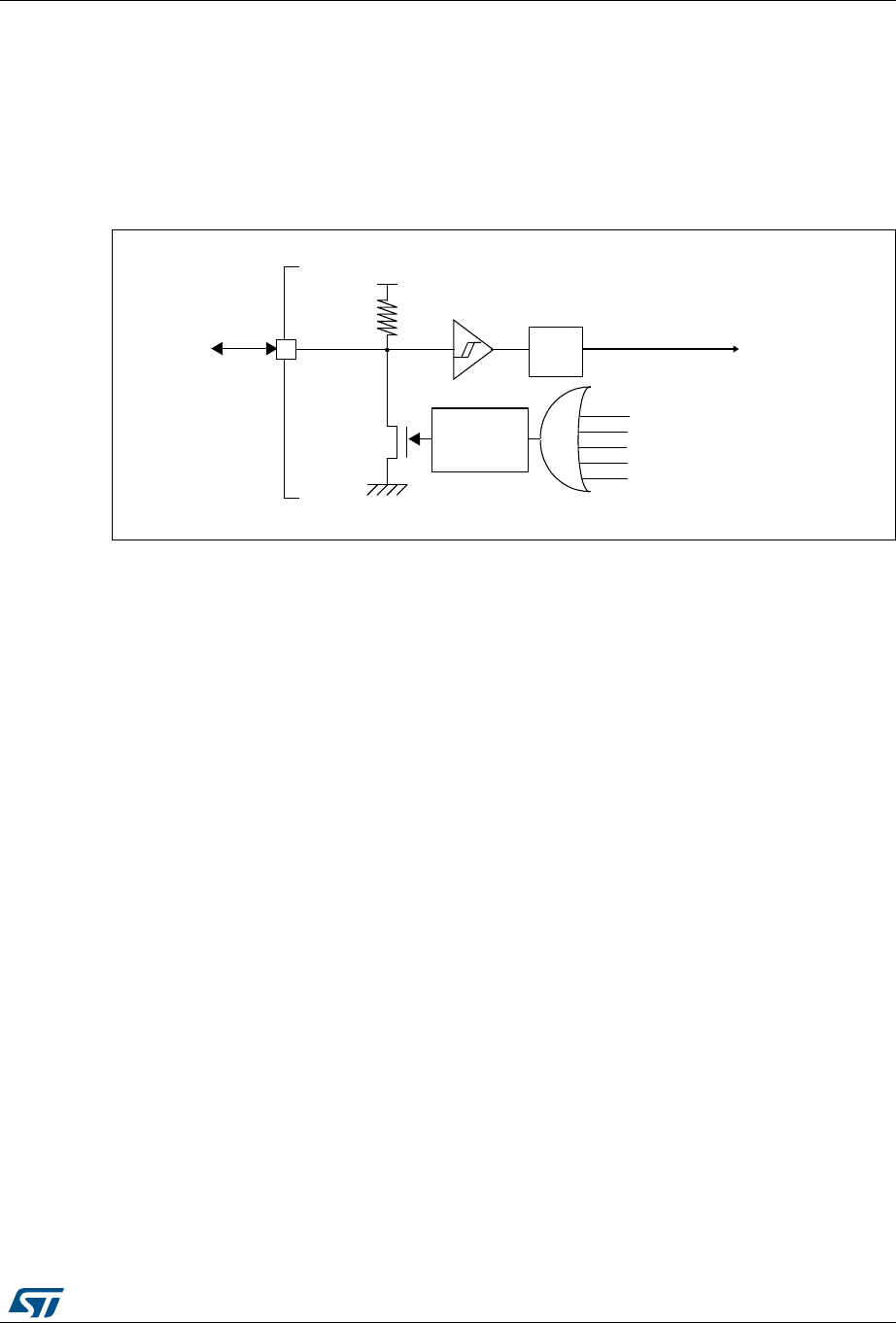
DocID018909 Rev 9 151/1718
RM0090 Reset and clock control for STM32F42xxx and STM32F43xxx (RCC)
211
These sources act on the NRST pin and it is always kept low during the delay phase. The
RESET service routine vector is fixed at address 0x0000_0004 in the memory map.
The system reset signal provided to the device is output on the NRST pin. The pulse
generator guarantees a minimum reset pulse duration of 20 µs for each internal reset
source. In case of an external reset, the reset pulse is generated while the NRST pin is
asserted low.
Figure 15. Simplified diagram of the reset circuit
The Backup domain has two specific resets that affect only the Backup domain (see
Figure 4).
6.1.3 Backup domain reset
The backup domain reset sets all RTC registers and the RCC_BDCR register to their reset
values. The BKPSRAM is not affected by this reset. The only way of resetting the
BKPSRAM is through the Flash interface by requesting a protection level change from 1 to
0.
A backup domain reset is generated when one of the following events occurs:
1. Software reset, triggered by setting the BDRST bit in the RCC Backup domain control
register (RCC_BDCR).
2. VDD or VBAT power on, if both supplies have previously been powered off.
6.2 Clocks
Three different clock sources can be used to drive the system clock (SYSCLK):
•HSI oscillator clock
•HSE oscillator clock
•Main PLL (PLL) clock
The devices have the two following secondary clock sources:
•32 kHz low-speed internal RC (LSI RC) which drives the independent watchdog and,
optionally, the RTC used for Auto-wakeup from the Stop/Standby mode.
•32.768 kHz low-speed external crystal (LSE crystal) which optionally drives the RTC
clock (RTCCLK)
1567
5
38
9
''
9
''$
::'*UHVHW
,:'*UHVHW
3XOVH
JHQHUDWRU 3RZHUUHVHW
([WHUQDO
UHVHW
PLQV
6\VWHPUHVHW
)LOWHU
6RIWZDUHUHVHW
/RZSRZHUPDQDJHPHQWUHVHW
DLF
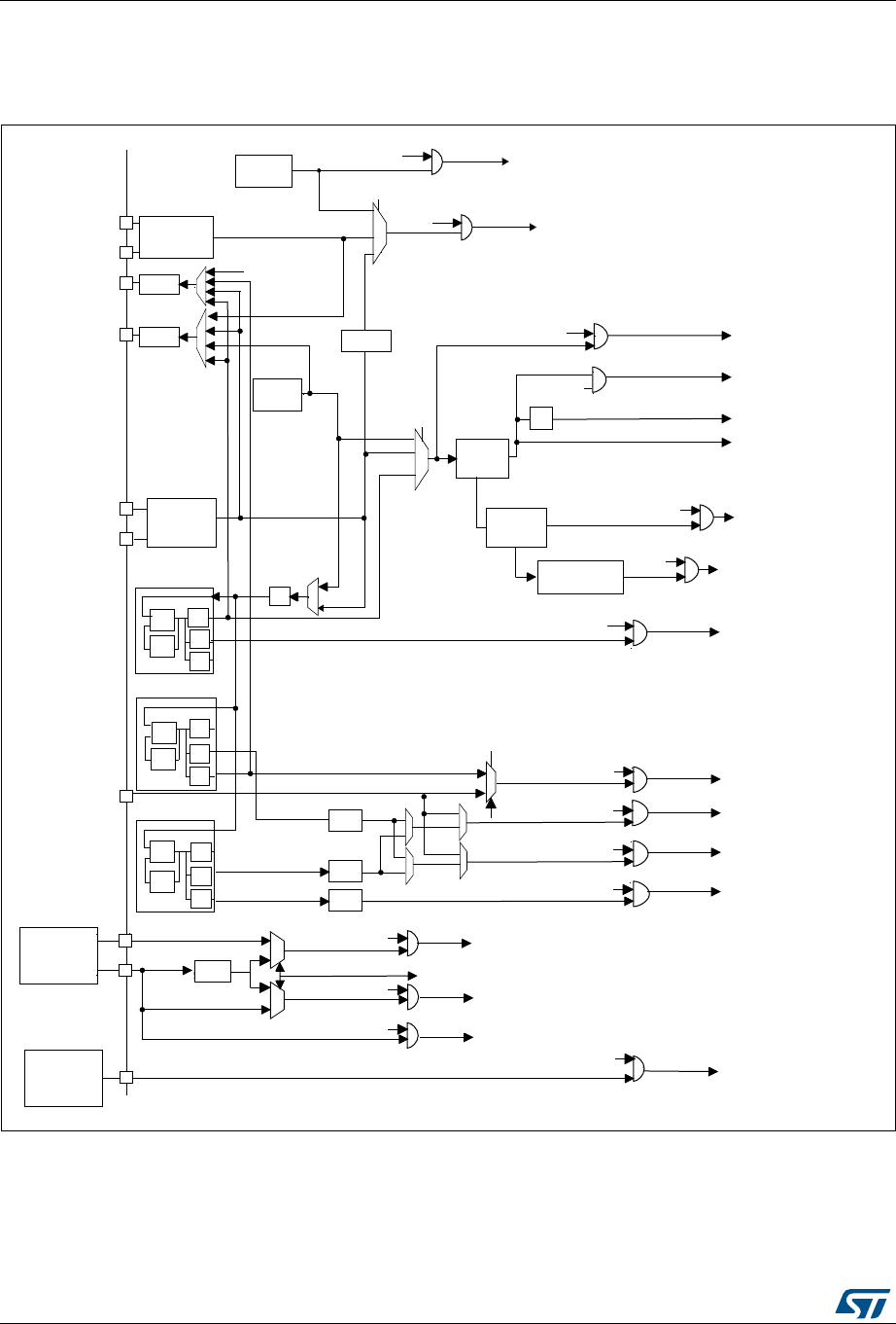
Reset and clock control for STM32F42xxx and STM32F43xxx (RCC) RM0090
152/1718 DocID018909 Rev 9
Each clock source can be switched on or off independently when it is not used, to optimize
power consumption.
Figure 16. Clock tree
1. For full details about the internal and external clock source characteristics, refer to the Electrical characteristics section in
the device datasheet.
2. When TIMPRE bit of the RCC_DCKCFGR register is reset, if APBx prescaler is 1, then TIMxCLK = PCLKx, otherwise
TIMxCLK = 2x PCLKx.
3. When TIMPRE bit in the RCC_DCKCFGR register is set, if APBx prescaler is 1,2 or 4, then TIMxCLK = HCLK, otherwise
TIMxCLK = 4x PCLKx.
069
3//
0,,B50,,B6(/LQ6<6&)*B30&WR(WKHUQHW0$&
/6(
(7+B0,,B7;B&/.B0,,
27*B+6B6&/
3//,6&/.
)&/.&RUWH[
IUHHUXQQLQJFORFN
$3%[SHULSKHUDOFORFNV
0+]
FORFNV
86%+6
8/3,FORFN
(WKHUQHW
373FORFN
0&2
0&2
(7+B0,,B5;B&/.B0,
,
26&B,1
26&B287
7R,QGHSHQGHQW
ZDWFKGRJ
/6(
/6,
WR57&
57&&/.
57&6(/>@
,:'*&/.
26&B,1
26&B287
3//&/.
+6,
+6,
+6(
6:
6<6&/.
0+]
PD[
+&/.
WR$+%EXVFRUH
PHPRU\DQG'0$
0+]PD[
WR&RUWH[6\VWHPWLPHU
&ORFN
HQDEOH
3//&.
,6FORFNV
$+%
35(6&
0$&50,,&/.
0$&7;&/.
0$&5;&/.
:DWFKGRJ
HQDEOH
57&
HQDEOH
3HULSKHUDO
FORFNHQDEOH
WR
3//,6
6<6&/.
([WFORFN
,665&
+6(B57&
+6(
,6B&.,1
3+<(WKHUQHW
WR0+]
86%3+<
WR0+]
3//6$,
3//6$,&/.
3///&'&/.
3//6$,&/. 6$,B$FORFN
6$,B%FORFN
/&'7)7
FORFN
/6,5&
N+]
/6(26&
N+]
WR
WR
0+]
+6,5&
0+]
+6(26&
9&2
[1
3
4
5
0
9&2
[1
3
4
5
',9
',9
',9
9&2
[1
3
4
5
3HULSKHUDO
FORFNHQDEOH
3HULSKHUDO
FORFNHQDEOH
3HULSKHUDO
FORFNHQDEOH
3HULSKHUDO
FORFNHQDEOH
3HULSKHUDO
FORFNHQDEOH
3HULSKHUDO
FORFNHQDEOH
3HULSKHUDO
FORFNHQDEOH
3HULSKHUDO
FORFNHQDEOH
3HULSKHUDO
FORFNHQDEOH
$3%[
35(6&
$3%[WLPHUFORFNV
LI$3%[SUHVF
[HOVH[
3HULSKHUDOFORFN
HQDEOH
3HULSKHUDOFORFN
HQDEOH

DocID018909 Rev 9 153/1718
RM0090 Reset and clock control for STM32F42xxx and STM32F43xxx (RCC)
211
The clock controller provides a high degree of flexibility to the application in the choice of the
external crystal or the oscillator to run the core and peripherals at the highest frequency
and, guarantee the appropriate frequency for peripherals that need a specific clock like
Ethernet, USB OTG FS and HS, I2S, SAI, LTDC, and SDIO.
Several prescalers are used to configure the AHB frequency, the high-speed APB (APB2)
and the low-speed APB (APB1) domains. The maximum frequency of the AHB domain is
180 MHz. The maximum allowed frequency of the high-speed APB2 domain is 90 MHz. The
maximum allowed frequency of the low-speed APB1 domain is 45 MHz
All peripheral clocks are derived from the system clock (SYSCLK) except for:
•The USB OTG FS clock (48 MHz), the random analog generator (RNG) clock
(≤48 MHz) and the SDIO clock (≤ 48 MHz) which are coming from a specific output of
PLL (PLL48CLK)
•I2S clock
To achieve high-quality audio performance, the I2S clock can be derived either from a
specific PLL (PLLI2S) or from an external clock mapped on the I2S_CKIN pin. For
more information about I2S clock frequency and precision, refer to Section 28.4.4:
Clock generator.
•SAI1 clock
The SAI1 clock is generated from a specific PLL (PLLSAI or PLLI2S) or from an
external clock mapped on the I2S_CKIN pin.
The PLLSAI can be used as clock source for SAI1 peripheral in case the PLLI2S is
programmed to achieve another audio sampling frequency (49.152 MHz or
11.2896 MHz), and the application requires both frequencies at the same time.
•LTDC clock
The LTDC clock is generated from a specific PLL (PLLSAI).
•The USB OTG HS (60 MHz) clock which is provided from the external PHY
•The Ethernet MAC clocks (TX, RX and RMII) which are provided from the external
PHY. For further information on the Ethernet configuration, please refer to
Section 33.4.4: MII/RMII selection in the Ethernet peripheral description. When the
Ethernet is used, the AHB clock frequency must be at least 25 MHz.
The RCC feeds the external clock of the Cortex System Timer (SysTick) with the AHB clock
(HCLK) divided by 8. The SysTick can work either with this clock or with the Cortex clock
(HCLK), configurable in the SysTick control and status register.
The timer clock frequencies for STM32F42xxx and STM32F43xxx are automatically set by
hardware. There are two cases depending on the value of TIMPRE bit in RCC_CFGR
register:
•If TIMPRE bit in RCC_DKCFGR register is reset:
If the APB prescaler is configured to a division factor of 1, the timer clock frequencies
(TIMxCLK) are set to PCLKx. Otherwise, the timer clock frequencies are twice the
frequency of the APB domain to which the timers are connected: TIMxCLK = 2xPCLKx.
•If TIMPRE bit in RCC_DKCFGR register is set:
If the APB prescaler is configured to a division factor of 1, 2 or 4, the timer clock
frequencies (TIMxCLK) are set to HCLK. Otherwise, the timer clock frequencies is four
times the frequency of the APB domain to which the timers are connected: TIMxCLK =
4xPCLKx.
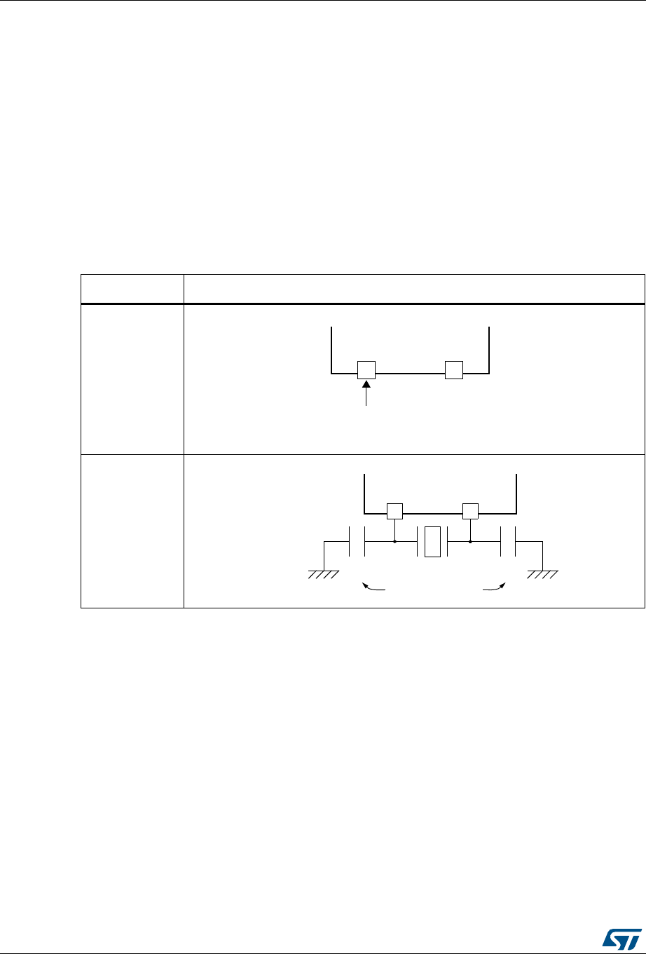
Reset and clock control for STM32F42xxx and STM32F43xxx (RCC) RM0090
154/1718 DocID018909 Rev 9
FCLK acts as Cortex®-M4 with FPU free-running clock. For more details, refer to the
Cortex®-M4 with FPU technical reference manual.
6.2.1 HSE clock
The high speed external clock signal (HSE) can be generated from two possible clock
sources:
•HSE external crystal/ceramic resonator
•HSE external user clock
The resonator and the load capacitors have to be placed as close as possible to the
oscillator pins in order to minimize output distortion and startup stabilization time. The
loading capacitance values must be adjusted according to the selected oscillator.
External source (HSE bypass)
In this mode, an external clock source must be provided. You select this mode by setting the
HSEBYP and HSEON bits in the RCC clock control register (RCC_CR). The external clock
signal (square, sinus or triangle) with ~50% duty cycle has to drive the OSC_IN pin while the
OSC_OUT pin should be left HI-Z. See Figure 17.
External crystal/ceramic resonator (HSE crystal)
The HSE has the advantage of producing a very accurate rate on the main clock.
The associated hardware configuration is shown in Figure 17. Refer to the electrical
characteristics section of the datasheet for more details.
The HSERDY flag in the RCC clock control register (RCC_CR) indicates if the high-speed
external oscillator is stable or not. At startup, the clock is not released until this bit is set by
hardware. An interrupt can be generated if enabled in the RCC clock interrupt register
(RCC_CIR).
Figure 17. HSE/ LSE clock sources
Hardware configuration
External clock
Crystal/ceramic
resonators
OSC_OUT
External
source
(HI-Z)
OSC_IN OSC_OUT
Load
capacitors
CL2
CL1

DocID018909 Rev 9 155/1718
RM0090 Reset and clock control for STM32F42xxx and STM32F43xxx (RCC)
211
The HSE Crystal can be switched on and off using the HSEON bit in the RCC clock control
register (RCC_CR).
6.2.2 HSI clock
The HSI clock signal is generated from an internal 16 MHz RC oscillator and can be used
directly as a system clock, or used as PLL input.
The HSI RC oscillator has the advantage of providing a clock source at low cost (no external
components). It also has a faster startup time than the HSE crystal oscillator however, even
with calibration the frequency is less accurate than an external crystal oscillator or ceramic
resonator.
Calibration
RC oscillator frequencies can vary from one chip to another due to manufacturing process
variations, this is why each device is factory calibrated by ST for 1% accuracy at TA= 25 °C.
After reset, the factory calibration value is loaded in the HSICAL[7:0] bits in the RCC clock
control register (RCC_CR).
If the application is subject to voltage or temperature variations this may affect the RC
oscillator speed. You can trim the HSI frequency in the application using the HSITRIM[4:0]
bits in the RCC clock control register (RCC_CR).
The HSIRDY flag in the RCC clock control register (RCC_CR) indicates if the HSI RC is
stable or not. At startup, the HSI RC output clock is not released until this bit is set by
hardware.
The HSI RC can be switched on and off using the HSION bit in the RCC clock control
register (RCC_CR).
The HSI signal can also be used as a backup source (Auxiliary clock) if the HSE crystal
oscillator fails. Refer to Section 6.2.7: Clock security system (CSS) on page 157.
6.2.3 PLL configuration
The STM32F4xx devices feature three PLLs:
•A main PLL (PLL) clocked by the HSE or HSI oscillator and featuring two different
output clocks:
– The first output is used to generate the high speed system clock (up to 180 MHz)
– The second output is used to generate the clock for the USB OTG FS (48 MHz),
the random analog generator (≤ 48 MHz) and the SDIO (≤ 48 MHz).
•Two dedicated PLLs (PLLI2S and PLLSAI) used to generate an accurate clock to
achieve high-quality audio performance on the I2S and SAI1 interfaces. PLLSAI is also
used for the LCD-TFT clock.
Since the main-PLL configuration parameters cannot be changed once PLL is enabled, it is
recommended to configure PLL before enabling it (selection of the HSI or HSE oscillator as
PLL clock source, and configuration of division factors M, N, P, and Q).
The PLLI2S and PLLSAI use the same input clock as PLL (PLLM[5:0] and PLLSRC bits are
common to both PLLs). However, the PLLI2S and PLLSAI have dedicated enable/disable
and division factors (N and R) configuration bits. Once the PLLI2S and PLLSAI are enabled,
the configuration parameters cannot be changed.

Reset and clock control for STM32F42xxx and STM32F43xxx (RCC) RM0090
156/1718 DocID018909 Rev 9
The three PLLs are disabled by hardware when entering Stop and Standby modes, or when
an HSE failure occurs when HSE or PLL (clocked by HSE) are used as system clock. RCC
PLL configuration register (RCC_PLLCFGR),RCC clock configuration register
(RCC_CFGR), and RCC Dedicated Clock Configuration Register (RCC_DCKCFGR) can be
used to configure PLL, PLLI2S, and PLLSAI.
6.2.4 LSE clock
The LSE clock is generated from a 32.768 kHz low-speed external crystal or ceramic
resonator. It has the advantage providing a low-power but highly accurate clock source to
the real-time clock peripheral (RTC) for clock/calendar or other timing functions.
The LSE oscillator is switched on and off using the LSEON bit in RCC Backup domain
control register (RCC_BDCR).
The LSERDY flag in the RCC Backup domain control register (RCC_BDCR) indicates if the
LSE crystal is stable or not. At startup, the LSE crystal output clock signal is not released
until this bit is set by hardware. An interrupt can be generated if enabled in the RCC clock
interrupt register (RCC_CIR).
External source (LSE bypass)
In this mode, an external clock source must be provided. It must have a frequency up to
1 MHz. You select this mode by setting the LSEBYP and LSEON bits in the RCC Backup
domain control register (RCC_BDCR). The external clock signal (square, sinus or triangle)
with ~50% duty cycle has to drive the OSC32_IN pin while the OSC32_OUT pin should be
left HI-Z. See Figure 17.
6.2.5 LSI clock
The LSI RC acts as an low-power clock source that can be kept running in Stop and
Standby mode for the independent watchdog (IWDG) and Auto-wakeup unit (AWU). The
clock frequency is around 32 kHz. For more details, refer to the electrical characteristics
section of the datasheets.
The LSI RC can be switched on and off using the LSION bit in the RCC clock control &
status register (RCC_CSR).
The LSIRDY flag in the RCC clock control & status register (RCC_CSR) indicates if the low-
speed internal oscillator is stable or not. At startup, the clock is not released until this bit is
set by hardware. An interrupt can be generated if enabled in the RCC clock interrupt register
(RCC_CIR).
6.2.6 System clock (SYSCLK) selection
After a system reset, the HSI oscillator is selected as the system clock. When a clock source
is used directly or through PLL as the system clock, it is not possible to stop it.
A switch from one clock source to another occurs only if the target clock source is ready
(clock stable after startup delay or PLL locked). If a clock source that is not yet ready is
selected, the switch occurs when the clock source is ready. Status bits in the RCC clock
control register (RCC_CR) indicate which clock(s) is (are) ready and which clock is currently
used as the system clock.

DocID018909 Rev 9 157/1718
RM0090 Reset and clock control for STM32F42xxx and STM32F43xxx (RCC)
211
6.2.7 Clock security system (CSS)
The clock security system can be activated by software. In this case, the clock detector is
enabled after the HSE oscillator startup delay, and disabled when this oscillator is stopped.
If a failure is detected on the HSE clock, this oscillator is automatically disabled, a clock
failure event is sent to the break inputs of advanced-control timers TIM1 and TIM8, and an
interrupt is generated to inform the software about the failure (clock security system
interrupt CSSI), allowing the MCU to perform rescue operations. The CSSI is linked to the
Cortex®-M4 with FPU NMI (non-maskable interrupt) exception vector.
Note: When the CSS is enabled, if the HSE clock happens to fail, the CSS generates an interrupt,
which causes the automatic generation of an NMI. The NMI is executed indefinitely unless
the CSS interrupt pending bit is cleared. As a consequence, the application has to clear the
CSS interrupt in the NMI ISR by setting the CSSC bit in the Clock interrupt register
(RCC_CIR).
If the HSE oscillator is used directly or indirectly as the system clock (indirectly meaning that
it is directly used as PLL input clock, and that PLL clock is the system clock) and a failure is
detected, then the system clock switches to the HSI oscillator and the HSE oscillator is
disabled.
If the HSE oscillator clock was the clock source of PLL used as the system clock when the
failure occurred, PLL is also disabled. In this case, if the PLLI2S was enabled, it is also
disabled when the HSE fails.
6.2.8 RTC/AWU clock
Once the RTCCLK clock source has been selected, the only possible way of modifying the
selection is to reset the power domain.
The RTCCLK clock source can be either the HSE 1 MHz (HSE divided by a programmable
prescaler), the LSE or the LSI clock. This is selected by programming the RTCSEL[1:0] bits
in the RCC Backup domain control register (RCC_BDCR) and the RTCPRE[4:0] bits in RCC
clock configuration register (RCC_CFGR). This selection cannot be modified without
resetting the Backup domain.
If the LSE is selected as the RTC clock, the RTC will work normally if the backup or the
system supply disappears. If the LSI is selected as the AWU clock, the AWU state is not
guaranteed if the system supply disappears. If the HSE oscillator divided by a value
between 2 and 31 is used as the RTC clock, the RTC state is not guaranteed if the backup
or the system supply disappears.
The LSE clock is in the Backup domain, whereas the HSE and LSI clocks are not. As a
consequence:
•If LSE is selected as the RTC clock:
– The RTC continues to work even if the VDD supply is switched off, provided the
VBAT supply is maintained.
•If LSI is selected as the Auto-wakeup unit (AWU) clock:
– The AWU state is not guaranteed if the VDD supply is powered off. Refer to
Section 6.2.5: LSI clock on page 156 for more details on LSI calibration.
•If the HSE clock is used as the RTC clock:
– The RTC state is not guaranteed if the VDD supply is powered off or if the internal
voltage regulator is powered off (removing power from the 1.2 V domain).

Reset and clock control for STM32F42xxx and STM32F43xxx (RCC) RM0090
158/1718 DocID018909 Rev 9
Note: To read the RTC calendar register when the APB1 clock frequency is less than seven times
the RTC clock frequency (fAPB1 < 7xfRTCLCK), the software must read the calendar time and
date registers twice. The data are correct if the second read access to RTC_TR gives the
same result than the first one. Otherwise a third read access must be performed.
6.2.9 Watchdog clock
If the independent watchdog (IWDG) is started by either hardware option or software
access, the LSI oscillator is forced ON and cannot be disabled. After the LSI oscillator
temporization, the clock is provided to the IWDG.
6.2.10 Clock-out capability
Two microcontroller clock output (MCO) pins are available:
•MCO1
You can output four different clock sources onto the MCO1 pin (PA8) using the
configurable prescaler (from 1 to 5):
–HSI clock
– LSE clock
– HSE clock
– PLL clock
The desired clock source is selected using the MCO1PRE[2:0] and MCO1[1:0] bits in
the RCC clock configuration register (RCC_CFGR).
•MCO2
You can output four different clock sources onto the MCO2 pin (PC9) using the
configurable prescaler (from 1 to 5):
– HSE clock
– PLL clock
– System clock (SYSCLK)
– PLLI2S clock
The desired clock source is selected using the MCO2PRE[2:0] and MCO2 bits in the
RCC clock configuration register (RCC_CFGR).
For the different MCO pins, the corresponding GPIO port has to be programmed in alternate
function mode.
The selected clock to output onto MCO must not exceed 100 MHz (the maximum I/O
speed).
6.2.11 Internal/external clock measurement using TIM5/TIM11
It is possible to indirectly measure the frequencies of all on-board clock source generators
by means of the input capture of TIM5 channel4 and TIM11 channel1 as shown in Figure 18
and Figure 18.
Internal/external clock measurement using TIM5 channel4
TIM5 has an input multiplexer which allows choosing whether the input capture is triggered
by the I/O or by an internal clock. This selection is performed through the TI4_RMP [1:0] bits
in the TIM5_OR register.
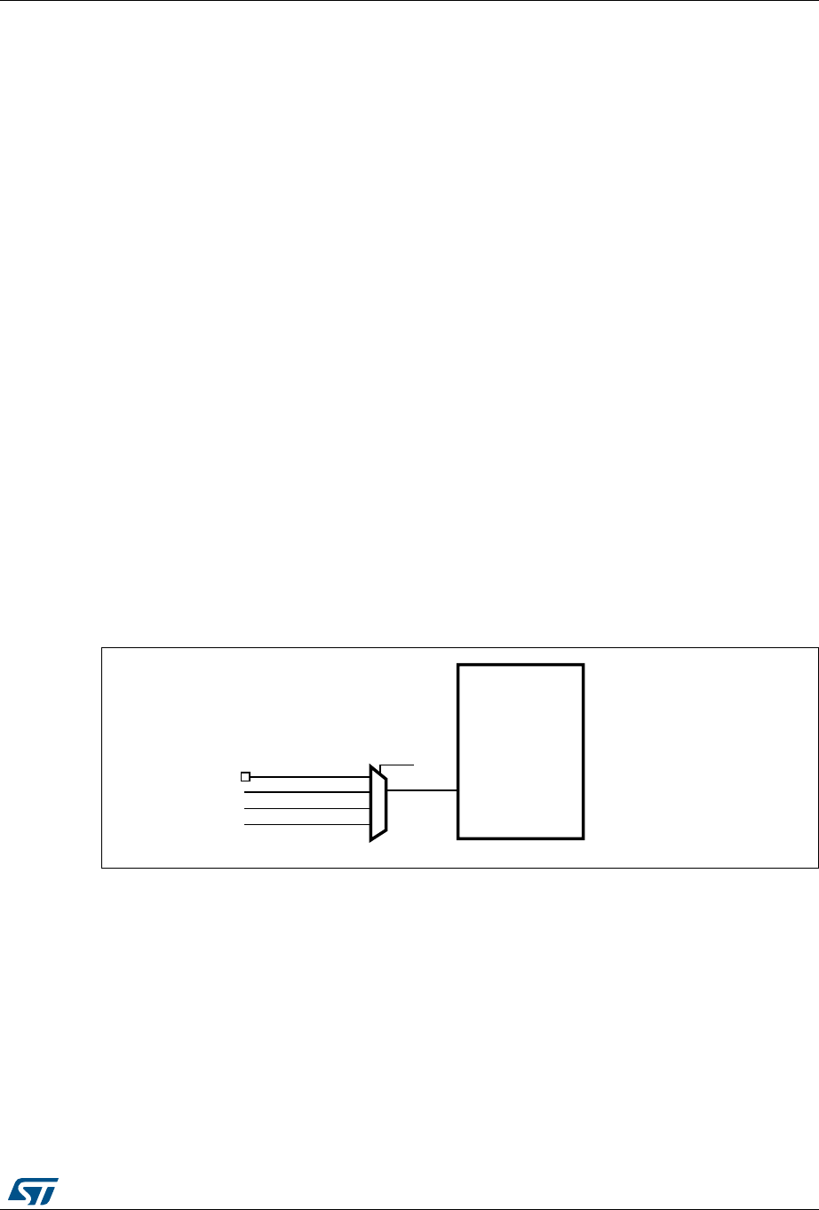
DocID018909 Rev 9 159/1718
RM0090 Reset and clock control for STM32F42xxx and STM32F43xxx (RCC)
211
The primary purpose of having the LSE connected to the channel4 input capture is to be
able to precisely measure the HSI (this requires to have the HSI used as the system clock
source). The number of HSI clock counts between consecutive edges of the LSE signal
provides a measurement of the internal clock period. Taking advantage of the high precision
of LSE crystals (typically a few tens of ppm) we can determine the internal clock frequency
with the same resolution, and trim the source to compensate for manufacturing-process
and/or temperature- and voltage-related frequency deviations.
The HSI oscillator has dedicated, user-accessible calibration bits for this purpose.
The basic concept consists in providing a relative measurement (e.g. HSI/LSE ratio): the
precision is therefore tightly linked to the ratio between the two clock sources. The greater
the ratio, the better the measurement.
It is also possible to measure the LSI frequency: this is useful for applications that do not
have a crystal. The ultralow-power LSI oscillator has a large manufacturing process
deviation: by measuring it versus the HSI clock source, it is possible to determine its
frequency with the precision of the HSI. The measured value can be used to have more
accurate RTC time base timeouts (when LSI is used as the RTC clock source) and/or an
IWDG timeout with an acceptable accuracy.
Use the following procedure to measure the LSI frequency:
1. Enable the TIM5 timer and configure channel4 in Input capture mode.
2. This bit is set the TI4_RMP bits in the TIM5_OR register to 0x01 to connect the LSI
clock internally to TIM5 channel4 input capture for calibration purposes.
3. Measure the LSI clock frequency using the TIM5 capture/compare 4 event or interrupt.
4. Use the measured LSI frequency to update the prescaler of the RTC depending on the
desired time base and/or to compute the IWDG timeout.
Figure 18. Frequency measurement with TIM5 in Input capture mode
Internal/external clock measurement using TIM11 channel1
TIM11 has an input multiplexer which allows choosing whether the input capture is triggered
by the I/O or by an internal clock. This selection is performed through TI1_RMP [1:0] bits in
the TIM11_OR register. The HSE_RTC clock (HSE divided by a programmable prescaler) is
connected to channel 1 input capture to have a rough indication of the external crystal
frequency. This requires that the HSI is the system clock source. This can be useful for
instance to ensure compliance with the IEC 60730/IEC 61335 standards which require to be
able to determine harmonic or subharmonic frequencies (–50/+100% deviations).
4)-
4)
4)?2-0;=
'0)/
24#?7AKE5P?)4
,3%
,3)
AI6

Reset and clock control for STM32F42xxx and STM32F43xxx (RCC) RM0090
160/1718 DocID018909 Rev 9
Figure 19. Frequency measurement with TIM11 in Input capture mode
4)-
4)
4)?2-0;=
'0)/
(3%?24#-(Z
AI

DocID018909 Rev 9 161/1718
RM0090 Reset and clock control for STM32F42xxx and STM32F43xxx (RCC)
211
6.3 RCC registers
Refer to Section 1.1: List of abbreviations for registers for a list of abbreviations used in
register descriptions.
6.3.1 RCC clock control register (RCC_CR)
Address offset: 0x00
Reset value: 0x0000 XX83 where X is undefined.
Access: no wait state, word, half-word and byte access
31 30 29 28 27 26 25 24 23 22 21 20 19 18 17 16
Reserved
PLLSAI
RDY
PLLSAI
ON
PLLI2S
RDY
PLLI2S
ON
PLLRD
YPLLON
Reserved
CSS
ON
HSE
BYP
HSE
RDY
HSE
ON
rrwrrwr rw rwrw r rw
15 14 13 12 11 10 9 8 7 6 5 4 3 2 1 0
HSICAL[7:0] HSITRIM[4:0] Res.
HSI
RDY HSION
rrrrrr r rrwrwrwrwrw rrw
Bits 31:28 Reserved, must be kept at reset value.
Bit 29 PLLSAIRDY: PLLSAI clock ready flag
Set by hardware to indicate that the PLLSAI is locked.
0: PLLSAI unlocked
1: PLLSAI locked
Bit 28 PLLISAION: PLLSAI enable
Set and cleared by software to enable PLLSAI.
Cleared by hardware when entering Stop or Standby mode.
0: PLLSAI OFF
1: PLLSAI ON
Bit 27 PLLI2SRDY: PLLI2S clock ready flag
Set by hardware to indicate that the PLLI2S is locked.
0: PLLI2S unlocked
1: PLLI2S locked
Bit 26 PLLI2SON: PLLI2S enable
Set and cleared by software to enable PLLI2S.
Cleared by hardware when entering Stop or Standby mode.
0: PLLI2S OFF
1: PLLI2S ON
Bit 25 PLLRDY: Main PLL (PLL) clock ready flag
Set by hardware to indicate that PLL is locked.
0: PLL unlocked
1: PLL locked
Bit 24 PLLON: Main PLL (PLL) enable
Set and cleared by software to enable PLL.
Cleared by hardware when entering Stop or Standby mode. This bit cannot be reset if PLL
clock is used as the system clock.
0: PLL OFF
1: PLL ON

Reset and clock control for STM32F42xxx and STM32F43xxx (RCC) RM0090
162/1718 DocID018909 Rev 9
Bits 23:20 Reserved, must be kept at reset value.
Bit 19 CSSON: Clock security system enable
Set and cleared by software to enable the clock security system. When CSSON is set, the
clock detector is enabled by hardware when the HSE oscillator is ready, and disabled by
hardware if an oscillator failure is detected.
0: Clock security system OFF (Clock detector OFF)
1: Clock security system ON (Clock detector ON if HSE oscillator is stable, OFF if not)
Bit 18 HSEBYP: HSE clock bypass
Set and cleared by software to bypass the oscillator with an external clock. The external
clock must be enabled with the HSEON bit, to be used by the device.
The HSEBYP bit can be written only if the HSE oscillator is disabled.
0: HSE oscillator not bypassed
1: HSE oscillator bypassed with an external clock
Bit 17 HSERDY: HSE clock ready flag
Set by hardware to indicate that the HSE oscillator is stable. After the HSEON bit is cleared,
HSERDY goes low after 6 HSE oscillator clock cycles.
0: HSE oscillator not ready
1: HSE oscillator ready
Bit 16 HSEON: HSE clock enable
Set and cleared by software.
Cleared by hardware to stop the HSE oscillator when entering Stop or Standby mode. This
bit cannot be reset if the HSE oscillator is used directly or indirectly as the system clock.
0: HSE oscillator OFF
1: HSE oscillator ON
Bits 15:8 HSICAL[7:0]: Internal high-speed clock calibration
These bits are initialized automatically at startup.
Bits 7:3 HSITRIM[4:0]: Internal high-speed clock trimming
These bits provide an additional user-programmable trimming value that is added to the
HSICAL[7:0] bits. It can be programmed to adjust to variations in voltage and temperature
that influence the frequency of the internal HSI RC.
Bit 2 Reserved, must be kept at reset value.
Bit 1 HSIRDY: Internal high-speed clock ready flag
Set by hardware to indicate that the HSI oscillator is stable. After the HSION bit is cleared,
HSIRDY goes low after 6 HSI clock cycles.
0: HSI oscillator not ready
1: HSI oscillator ready
Bit 0 HSION: Internal high-speed clock enable
Set and cleared by software.
Set by hardware to force the HSI oscillator ON when leaving the Stop or Standby mode or in
case of a failure of the HSE oscillator used directly or indirectly as the system clock. This bit
cannot be cleared if the HSI is used directly or indirectly as the system clock.
0: HSI oscillator OFF
1: HSI oscillator ON

DocID018909 Rev 9 163/1718
RM0090 Reset and clock control for STM32F42xxx and STM32F43xxx (RCC)
211
6.3.2 RCC PLL configuration register (RCC_PLLCFGR)
Address offset: 0x04
Reset value: 0x2400 3010
Access: no wait state, word, half-word and byte access.
This register is used to configure the PLL clock outputs according to the formulas:
•f(VCO clock) = f(PLL clock input) × (PLLN / PLLM)
•f(PLL general clock output) = f(VCO clock) / PLLP
•f(USB OTG FS, SDIO, RNG clock output) = f(VCO clock) / PLLQ
31 30 29 28 27 26 25 24 23 22 21 20 19 18 17 16
Reserved PLLQ3 PLLQ2 PLLQ1 PLLQ0 Reserv
ed
PLLSR
CReserved PLLP1 PLLP0
rw rw rw rw rw rw rw
15 14 13 12 11 10 9 8 7 6 5 4 3 2 1 0
Reserv
ed
PLLN PLLM5 PLLM4 PLLM3 PLLM2 PLLM1 PLLM0
rw rw rw rw rw rw rw rw rw rw rw rw rw rw rw
Bits 31:28 Reserved, must be kept at reset value.
Bits 27:24 PLLQ: Main PLL (PLL) division factor for USB OTG FS, SDIO and random number generator
clocks
Set and cleared by software to control the frequency of USB OTG FS clock, the random
number generator clock and the SDIO clock. These bits should be written only if PLL is
disabled.
Caution: The USB OTG FS requires a 48 MHz clock to work correctly. The SDIO and the
random number generator need a frequency lower than or equal to 48 MHz to work
correctly.
USB OTG FS clock frequency = VCO frequency / PLLQ with 2 ≤ PLLQ ≤ 15
0000: PLLQ = 0, wrong configuration
0001: PLLQ = 1, wrong configuration
0010: PLLQ = 2
0011: PLLQ = 3
0100: PLLQ = 4
...
1111: PLLQ = 15
Bit 23 Reserved, must be kept at reset value.
Bit 22 PLLSRC: Main PLL(PLL) and audio PLL (PLLI2S) entry clock source
Set and cleared by software to select PLL and PLLI2S clock source. This bit can be written
only when PLL and PLLI2S are disabled.
0: HSI clock selected as PLL and PLLI2S clock entry
1: HSE oscillator clock selected as PLL and PLLI2S clock entry
Bits 21:18 Reserved, must be kept at reset value.

Reset and clock control for STM32F42xxx and STM32F43xxx (RCC) RM0090
164/1718 DocID018909 Rev 9
Bits 17:16 PLLP: Main PLL (PLL) division factor for main system clock
Set and cleared by software to control the frequency of the general PLL output clock. These
bits can be written only if PLL is disabled.
Caution: The software has to set these bits correctly not to exceed 180 MHz on this domain.
PLL output clock frequency = VCO frequency / PLLP with PLLP = 2, 4, 6, or 8
00: PLLP = 2
01: PLLP = 4
10: PLLP = 6
11: PLLP = 8
Bits 14:6 PLLN: Main PLL (PLL) multiplication factor for VCO
Set and cleared by software to control the multiplication factor of the VCO. These bits can
be written only when PLL is disabled. Only half-word and word accesses are allowed to
write these bits.
Caution: The software has to set these bits correctly to ensure that the VCO output
frequency is between 192 and 432 MHz. Below an example of PLLN bitfield
forbidden values for PLL input equal to FPLL_IN = 1 MHz:
VCO output frequency = VCO input frequency × PLLN with 192 ≤ PLLN ≤ 432
000000000: PLLN = 0, wrong configuration
000000001: PLLN = 1, wrong configuration
...
011000000: PLLN = 192
...
110110000: PLLN = 432
110110001: PLLN = 433, wrong configuration
...
111111111: PLLN = 511, wrong configuration
Bits 5:0 PLLM: Division factor for the main PLL (PLL) and audio PLL (PLLI2S) input clock
Set and cleared by software to divide the PLL and PLLI2S input clock before the VCO.
These bits can be written only when the PLL and PLLI2S are disabled.
Caution: The software has to set these bits correctly to ensure that the VCO input frequency
ranges from 1 to 2 MHz. It is recommended to select a frequency of 2 MHz to limit
PLL jitter.
VCO input frequency = PLL input clock frequency / PLLM with 2 ≤ PLLM ≤ 63
000000: PLLM = 0, wrong configuration
000001: PLLM = 1, wrong configuration
000010: PLLM = 2
000011: PLLM = 3
000100: PLLM = 4
...
111110: PLLM = 62
111111: PLLM = 63

DocID018909 Rev 9 165/1718
RM0090 Reset and clock control for STM32F42xxx and STM32F43xxx (RCC)
211
6.3.3 RCC clock configuration register (RCC_CFGR)
Address offset: 0x08
Reset value: 0x0000 0000
Access: 0 ≤ wait state ≤ 2, word, half-word and byte access
1 or 2 wait states inserted only if the access occurs during a clock source switch.
31 30 29 28 27 26 25 24 23 22 21 20 19 18 17 16
MCO2 MCO2 PRE[2:0] MCO1 PRE[2:0] I2SSC
RMCO1 RTCPRE[4:0]
rw rw rw rw rw rw rw rw rw rw rw rw rw rw
15 14 13 12 11 10 9 8 7 6 5 4 3 2 1 0
PPRE2[2:0] PPRE1[2:0]
Reserved
HPRE[3:0] SWS1 SWS0 SW1 SW0
rw rw rw rw rw rw rw rw rw rw r r rw rw
Bits 31:30 MCO2[1:0]: Microcontroller clock output 2
Set and cleared by software. Clock source selection may generate glitches on MCO2. It is
highly recommended to configure these bits only after reset before enabling the external
oscillators and the PLLs.
00: System clock (SYSCLK) selected
01: PLLI2S clock selected
10: HSE oscillator clock selected
11: PLL clock selected
Bits 27:29 MCO2PRE: MCO2 prescaler
Set and cleared by software to configure the prescaler of the MCO2. Modification of this
prescaler may generate glitches on MCO2. It is highly recommended to change this
prescaler only after reset before enabling the external oscillators and the PLLs.
0xx: no division
100: division by 2
101: division by 3
110: division by 4
111: division by 5
Bits 24:26 MCO1PRE: MCO1 prescaler
Set and cleared by software to configure the prescaler of the MCO1. Modification of this
prescaler may generate glitches on MCO1. It is highly recommended to change this
prescaler only after reset before enabling the external oscillators and the PLL.
0xx: no division
100: division by 2
101: division by 3
110: division by 4
111: division by 5
Bit 23 I2SSRC: I2S clock selection
Set and cleared by software. This bit allows to select the I2S clock source between the
PLLI2S clock and the external clock. It is highly recommended to change this bit only after
reset and before enabling the I2S module.
0: PLLI2S clock used as I2S clock source
1: External clock mapped on the I2S_CKIN pin used as I2S clock source

Reset and clock control for STM32F42xxx and STM32F43xxx (RCC) RM0090
166/1718 DocID018909 Rev 9
Bits 22:21 MCO1: Microcontroller clock output 1
Set and cleared by software. Clock source selection may generate glitches on MCO1. It is
highly recommended to configure these bits only after reset before enabling the external
oscillators and PLL.
00: HSI clock selected
01: LSE oscillator selected
10: HSE oscillator clock selected
11: PLL clock selected
Bits 20:16 RTCPRE: HSE division factor for RTC clock
Set and cleared by software to divide the HSE clock input clock to generate a 1 MHz clock
for RTC.
Caution: The software has to set these bits correctly to ensure that the clock supplied to the
RTC is 1 MHz. These bits must be configured if needed before selecting the RTC
clock source.
00000: no clock
00001: no clock
00010: HSE/2
00011: HSE/3
00100: HSE/4
...
11110: HSE/30
11111: HSE/31
Bits 15:13 PPRE2: APB high-speed prescaler (APB2)
Set and cleared by software to control APB high-speed clock division factor.
Caution: The software has to set these bits correctly not to exceed 90 MHz on this domain.
The clocks are divided with the new prescaler factor from 1 to 16 AHB cycles after
PPRE2 write.
0xx: AHB clock not divided
100: AHB clock divided by 2
101: AHB clock divided by 4
110: AHB clock divided by 8
111: AHB clock divided by 16
Bits 12:10 PPRE1: APB Low speed prescaler (APB1)
Set and cleared by software to control APB low-speed clock division factor.
Caution: The software has to set these bits correctly not to exceed 45 MHz on this domain.
The clocks are divided with the new prescaler factor from 1 to 16 AHB cycles after
PPRE1 write.
0xx: AHB clock not divided
100: AHB clock divided by 2
101: AHB clock divided by 4
110: AHB clock divided by 8
111: AHB clock divided by 16
Bits 9:8 Reserved, must be kept at reset value.

DocID018909 Rev 9 167/1718
RM0090 Reset and clock control for STM32F42xxx and STM32F43xxx (RCC)
211
6.3.4 RCC clock interrupt register (RCC_CIR)
Address offset: 0x0C
Reset value: 0x0000 0000
Access: no wait state, word, half-word and byte access
Bits 7:4 HPRE: AHB prescaler
Set and cleared by software to control AHB clock division factor.
Caution: The clocks are divided with the new prescaler factor from 1 to 16 AHB cycles after
HPRE write.
Caution: The AHB clock frequency must be at least 25 MHz when the Ethernet is used.
0xxx: system clock not divided
1000: system clock divided by 2
1001: system clock divided by 4
1010: system clock divided by 8
1011: system clock divided by 16
1100: system clock divided by 64
1101: system clock divided by 128
1110: system clock divided by 256
1111: system clock divided by 512
Bits 3:2 SWS: System clock switch status
Set and cleared by hardware to indicate which clock source is used as the system clock.
00: HSI oscillator used as the system clock
01: HSE oscillator used as the system clock
10: PLL used as the system clock
11: not applicable
Bits 1:0 SW: System clock switch
Set and cleared by software to select the system clock source.
Set by hardware to force the HSI selection when leaving the Stop or Standby mode or in
case of failure of the HSE oscillator used directly or indirectly as the system clock.
00: HSI oscillator selected as system clock
01: HSE oscillator selected as system clock
10: PLL selected as system clock
11: not allowed
31 30 29 28 27 26 25 24 23 22 21 20 19 18 17 16
Reserved CSSC PLLSAI
RDYC
PLLI2S
RDYC
PLL
RDYC
HSE
RDYC
HSI
RDYC
LSE
RDYC
LSI
RDYC
ww w www w w
15 14 13 12 11 10 9 8 7 6 5 4 3 2 1 0
Reserv
ed
PLLSAI
RDYIE
PLLI2S
RDYIE
PLL
RDYIE
HSE
RDYIE
HSI
RDYIE
LSE
RDYIE
LSI
RDYIE CSSF PLLSAI
RDYF
PLLI2S
RDYF
PLL
RDYF
HSE
RDYF
HSI
RDYF
LSE
RDYF
LSI
RDYF
rw rw rw rw rw rw rw r r r r r r r r

Reset and clock control for STM32F42xxx and STM32F43xxx (RCC) RM0090
168/1718 DocID018909 Rev 9
Bits 31:24 Reserved, must be kept at reset value.
Bit 23 CSSC: Clock security system interrupt clear
This bit is set by software to clear the CSSF flag.
0: No effect
1: Clear CSSF flag
Bit 22 PLLSAIRDYC: PLLSAI Ready Interrupt Clear
This bit is set by software to clear PLLSAIRDYF flag. It is reset by hardware when the
PLLSAIRDYF is cleared.
0: PLLSAIRDYF not cleared
1: PLLSAIRDYF cleared
Bit 21 PLLI2SRDYC: PLLI2S ready interrupt clear
This bit is set by software to clear the PLLI2SRDYF flag.
0: No effect
1: PLLI2SRDYF cleared
Bit 20 PLLRDYC: Main PLL(PLL) ready interrupt clear
This bit is set by software to clear the PLLRDYF flag.
0: No effect
1: PLLRDYF cleared
Bit 19 HSERDYC: HSE ready interrupt clear
This bit is set by software to clear the HSERDYF flag.
0: No effect
1: HSERDYF cleared
Bit 18 HSIRDYC: HSI ready interrupt clear
This bit is set software to clear the HSIRDYF flag.
0: No effect
1: HSIRDYF cleared
Bit 17 LSERDYC: LSE ready interrupt clear
This bit is set by software to clear the LSERDYF flag.
0: No effect
1: LSERDYF cleared
Bit 16 LSIRDYC: LSI ready interrupt clear
This bit is set by software to clear the LSIRDYF flag.
0: No effect
1: LSIRDYF cleared
Bit 15 Reserved, must be kept at reset value.
Bit 14 PLLSAIRDYIE: PLLSAI Ready Interrupt Enable
This bit is set and reset by software to enable/disable interrupt caused by PLLSAI lock.
0: PLLSAI lock interrupt disabled
1: PLLSAI lock interrupt enabled
Bit 13 PLLI2SRDYIE: PLLI2S ready interrupt enable
This bit is set and cleared by software to enable/disable interrupt caused by PLLI2S lock.
0: PLLI2S lock interrupt disabled
1: PLLI2S lock interrupt enabled

DocID018909 Rev 9 169/1718
RM0090 Reset and clock control for STM32F42xxx and STM32F43xxx (RCC)
211
Bit 12 PLLRDYIE: Main PLL (PLL) ready interrupt enable
This bit is set and cleared by software to enable/disable interrupt caused by PLL lock.
0: PLL lock interrupt disabled
1: PLL lock interrupt enabled
Bit 11 HSERDYIE: HSE ready interrupt enable
This bit is set and cleared by software to enable/disable interrupt caused by the HSE
oscillator stabilization.
0: HSE ready interrupt disabled
1: HSE ready interrupt enabled
Bit 10 HSIRDYIE: HSI ready interrupt enable
This bit is set and cleared by software to enable/disable interrupt caused by the HSI
oscillator stabilization.
0: HSI ready interrupt disabled
1: HSI ready interrupt enabled
Bit 9 LSERDYIE: LSE ready interrupt enable
This bit is set and cleared by software to enable/disable interrupt caused by the LSE
oscillator stabilization.
0: LSE ready interrupt disabled
1: LSE ready interrupt enabled
Bit 8 LSIRDYIE: LSI ready interrupt enable
This bit is set and cleared by software to enable/disable interrupt caused by LSI oscillator
stabilization.
0: LSI ready interrupt disabled
1: LSI ready interrupt enabled
Bit 7 CSSF: Clock security system interrupt flag
This bit is set by hardware when a failure is detected in the HSE oscillator.
It is cleared by software by setting the CSSC bit.
0: No clock security interrupt caused by HSE clock failure
1: Clock security interrupt caused by HSE clock failure
Bit 6 PLLSAIRDYF: PLLSAI Ready Interrupt flag
This bit is set by hardware when the PLLSAI is locked and PLLSAIRDYDIE is set.
It is cleared by software by setting the PLLSAIRDYC bit.
0: No clock ready interrupt caused by PLLSAI lock
1: Clock ready interrupt caused by PLLSAI lock
Bit 5 PLLI2SRDYF: PLLI2S ready interrupt flag
This bit is set by hardware when the PLLI2S is locked and PLLI2SRDYDIE is set.
It is cleared by software by setting the PLLRI2SDYC bit.
0: No clock ready interrupt caused by PLLI2S lock
1: Clock ready interrupt caused by PLLI2S lock
Bit 4 PLLRDYF: Main PLL (PLL) ready interrupt flag
This bit is set by hardware when PLL is locked and PLLRDYDIE is set.
It is cleared by software setting the PLLRDYC bit.
0: No clock ready interrupt caused by PLL lock
1: Clock ready interrupt caused by PLL lock

Reset and clock control for STM32F42xxx and STM32F43xxx (RCC) RM0090
170/1718 DocID018909 Rev 9
6.3.5 RCC AHB1 peripheral reset register (RCC_AHB1RSTR)
Address offset: 0x10
Reset value: 0x0000 0000
Access: no wait state, word, half-word and byte access.
Bit 3 HSERDYF: HSE ready interrupt flag
This bit is set by hardware when External High Speed clock becomes stable and
HSERDYDIE is set.
It is cleared by software by setting the HSERDYC bit.
0: No clock ready interrupt caused by the HSE oscillator
1: Clock ready interrupt caused by the HSE oscillator
Bit 2 HSIRDYF: HSI ready interrupt flag
This bit is set by hardware when the Internal High Speed clock becomes stable and
HSIRDYDIE is set.
It is cleared by software by setting the HSIRDYC bit.
0: No clock ready interrupt caused by the HSI oscillator
1: Clock ready interrupt caused by the HSI oscillator
Bit 1 LSERDYF: LSE ready interrupt flag
This bit is set by hardware when the External Low Speed clock becomes stable and
LSERDYDIE is set.
It is cleared by software by setting the LSERDYC bit.
0: No clock ready interrupt caused by the LSE oscillator
1: Clock ready interrupt caused by the LSE oscillator
Bit 0 LSIRDYF: LSI ready interrupt flag
This bit is set by hardware when the internal low speed clock becomes stable and
LSIRDYDIE is set.
It is cleared by software by setting the LSIRDYC bit.
0: No clock ready interrupt caused by the LSI oscillator
1: Clock ready interrupt caused by the LSI oscillator
31 30 29 28 27 26 25 24 23 22 21 20 19 18 17 16
Reserved
OTGH
S
RST Reserved
ETHMAC
RST Res.
DMA2D
RST
DMA2
RST
DMA1
RST Reserved
rw rw rw rw rw
15 14 13 12 11 10 9 8 7 6 5 4 3 2 1 0
Reserved
CRCR
ST Res.
GPIOK
RST
GPIOJ
RST
GPIOI
RST
GPIOH
RST
GPIOGG
RST
GPIOF
RST
GPIOE
RST
GPIOD
RST
GPIOC
RST
GPIOB
RST
GPIOA
RST
rw rw rw rw rw rw rw rw rw rw rw rw
Bits 31:30 Reserved, must be kept at reset value.
Bit 29 OTGHSRST: USB OTG HS module reset
This bit is set and cleared by software.
0: does not reset the USB OTG HS module
1: resets the USB OTG HS module
Bits 28:26 Reserved, must be kept at reset value.

DocID018909 Rev 9 171/1718
RM0090 Reset and clock control for STM32F42xxx and STM32F43xxx (RCC)
211
Bit 25 ETHMACRST: Ethernet MAC reset
This bit is set and cleared by software.
0: does not reset Ethernet MAC
1: resets Ethernet MAC
Bit 24 Reserved, must be kept at reset value.
Bit 23 DMA2DRST: DMA2D reset
This bit is set and reset by software.
0: does not reset DMA2D
1: resets DMA2D
Bit 22 DMA2RST: DMA2 reset
This bit is set and cleared by software.
0: does not reset DMA2
1: resets DMA2
Bit 21 DMA1RST: DMA2 reset
This bit is set and cleared by software.
0: does not reset DMA2
1: resets DMA2
Bits 20:13 Reserved, must be kept at reset value.
Bit 12 CRCRST: CRC reset
This bit is set and cleared by software.
0: does not reset CRC
1: resets CRC
Bit 11 Reserved, must be kept at reset value.
Bit 10 GPIOKRST: IO port K reset
This bit is set and cleared by software.
0: does not reset IO port K
1: resets IO port K
Bit 9 GPIOJRST: IO port J reset
This bit is set and cleared by software.
0: does not reset IO port J
1: resets IO port J
Bit 8 GPIOIRST: IO port I reset
This bit is set and cleared by software.
0: does not reset IO port I
1: resets IO port I
Bit 7 GPIOHRST: IO port H reset
This bit is set and cleared by software.
0: does not reset IO port H
1: resets IO port H
Bit 6 GPIOGRST: IO port G reset
This bit is set and cleared by software.
0: does not reset IO port G
1: resets IO port G

Reset and clock control for STM32F42xxx and STM32F43xxx (RCC) RM0090
172/1718 DocID018909 Rev 9
Bit 5 GPIOFRST: IO port F reset
This bit is set and cleared by software.
0: does not reset IO port F
1: resets IO port F
Bit 4 GPIOERST: IO port E reset
This bit is set and cleared by software.
0: does not reset IO port E
1: resets IO port E
Bit 3 GPIODRST: IO port D reset
This bit is set and cleared by software.
0: does not reset IO port D
1: resets IO port D
Bit 2 GPIOCRST: IO port C reset
This bit is set and cleared by software.
0: does not reset IO port C
1: resets IO port C
Bit 1 GPIOBRST: IO port B reset
This bit is set and cleared by software.
0: does not reset IO port B
1:resets IO port B
Bit 0 GPIOARST: IO port A reset
This bit is set and cleared by software.
0: does not reset IO port A
1: resets IO port A

DocID018909 Rev 9 173/1718
RM0090 Reset and clock control for STM32F42xxx and STM32F43xxx (RCC)
211
6.3.6 RCC AHB2 peripheral reset register (RCC_AHB2RSTR)
Address offset: 0x14
Reset value: 0x0000 0000
Access: no wait state, word, half-word and byte access
31 30 29 28 27 26 25 24 23 22 21 20 19 18 17 16
Reserved
15 14 13 12 11 10 9 8 7 6 5 4 3 2 1 0
Reserved
OTGFS
RST
RNG
RST
HASH
RST
CRYP
RST Reserved
DCMI
RST
rw rw rw rw rw
Bits 31:8 Reserved, must be kept at reset value.
Bit 7 OTGFSRST: USB OTG FS module reset
Set and cleared by software.
0: does not reset the USB OTG FS module
1: resets the USB OTG FS module
Bit 6 RNGRST: Random number generator module reset
Set and cleared by software.
0: does not reset the random number generator module
1: resets the random number generator module
Bit 5 HASHRST: Hash module reset
Set and cleared by software.
0: does not reset the HASH module
1: resets the HASH module
Bit 4 CRYPRST: Cryptographic module reset
Set and cleared by software.
0: does not reset the cryptographic module
1: resets the cryptographic module
Bits 3:1 Reserved, must be kept at reset value.
Bit 0 DCMIRST: Camera interface reset
Set and cleared by software.
0: does not reset the Camera interface
1: resets the Camera interface

Reset and clock control for STM32F42xxx and STM32F43xxx (RCC) RM0090
174/1718 DocID018909 Rev 9
6.3.7 RCC AHB3 peripheral reset register (RCC_AHB3RSTR)
Address offset: 0x18
Reset value: 0x0000 0000
Access: no wait state, word, half-word and byte access.
6.3.8 RCC APB1 peripheral reset register (RCC_APB1RSTR)
Address offset: 0x20
Reset value: 0x0000 0000
Access: no wait state, word, half-word and byte access.
31 30 29 28 27 26 25 24 23 22 21 20 19 18 17 16
Reserved
1514131211109 8 765432 1 0
Reserved
FMCRST
rw
Bits 31:1 Reserved, must be kept at reset value.
Bit 0 FMCRST: Flexible memory controller module reset
Set and cleared by software.
0: does not reset the FMC module
1: resets the FMC module
31 30 29 28 27 26 25 24 23 22 21 20 19 18 17 16
UART8R
ST
UART7R
ST DACRST PWR
RST Reser-
ved
CAN2
RST
CAN1
RST Reser-
ved
I2C3
RST
I2C2
RST
I2C1
RST
UART5
RST
UART4
RST
UART3
RST
UART2
RST Reser-
ved
rw rw rw rw rw rw rw rw rw rw rw rw
1514131211109876543210
SPI3
RST
SPI2
RST Reserved
WWDG
RST Reserved
TIM14
RST
TIM13
RST
TIM12
RST
TIM7
RST
TIM6
RST
TIM5
RST
TIM4
RST
TIM3
RST
TIM2
RST
rw rw rw rw rw rw rw rw rw rw rw rw

DocID018909 Rev 9 175/1718
RM0090 Reset and clock control for STM32F42xxx and STM32F43xxx (RCC)
211
Bit 31 UART8RST: UART8 reset
Set and cleared by software.
0: does not reset UART8
1: resets UART8
Bit 30 UART7RST: UART7 reset
Set and cleared by software.
0: does not reset UART7
1: resets UART7
Bit 29 DACRST: DAC reset
Set and cleared by software.
0: does not reset the DAC interface
1: resets the DAC interface
Bit 28 PWRRST: Power interface reset
Set and cleared by software.
0: does not reset the power interface
1: resets the power interface
Bit 27 Reserved, must be kept at reset value.
Bit 26 CAN2RST: CAN2 reset
Set and cleared by software.
0: does not reset CAN2
1: resets CAN2
Bit 25 CAN1RST: CAN1 reset
Set and cleared by software.
0: does not reset CAN1
1: resets CAN1
Bit 24 Reserved, must be kept at reset value.
Bit 23 I2C3RST: I2C3 reset
Set and cleared by software.
0: does not reset I2C3
1: resets I2C3
Bit 22 I2C2RST: I2C2 reset
Set and cleared by software.
0: does not reset I2C2
1: resets I2C2
Bit 21 I2C1RST: I2C1 reset
Set and cleared by software.
0: does not reset I2C1
1: resets I2C1
Bit 20 UART5RST: UART5 reset
Set and cleared by software.
0: does not reset UART5
1: resets UART5
Bit 19 UART4RST: USART4 reset
Set and cleared by software.
0: does not reset UART4
1: resets UART4

Reset and clock control for STM32F42xxx and STM32F43xxx (RCC) RM0090
176/1718 DocID018909 Rev 9
Bit 18 USART3RST: USART3 reset
Set and cleared by software.
0: does not reset USART3
1: resets USART3
Bit 17 USART2RST: USART2 reset
Set and cleared by software.
0: does not reset USART2
1: resets USART2
Bit 16 Reserved, must be kept at reset value.
Bit 15 SPI3RST: SPI3 reset
Set and cleared by software.
0: does not reset SPI3
1: resets SPI3
Bit 14 SPI2RST: SPI2 reset
Set and cleared by software.
0: does not reset SPI2
1: resets SPI2
Bits 13:12 Reserved, must be kept at reset value.
Bit 11 WWDGRST: Window watchdog reset
Set and cleared by software.
0: does not reset the window watchdog
1: resets the window watchdog
Bits 10:9 Reserved, must be kept at reset value.
Bit 8 TIM14RST: TIM14 reset
Set and cleared by software.
0: does not reset TIM14
1: resets TIM14
Bit 7 TIM13RST: TIM13 reset
Set and cleared by software.
0: does not reset TIM13
1: resets TIM13
Bit 6 TIM12RST: TIM12 reset
Set and cleared by software.
0: does not reset TIM12
1: resets TIM12
Bit 5 TIM7RST: TIM7 reset
Set and cleared by software.
0: does not reset TIM7
1: resets TIM7
Bit 4 TIM6RST: TIM6 reset
Set and cleared by software.
0: does not reset TIM6
1: resets TIM6

DocID018909 Rev 9 177/1718
RM0090 Reset and clock control for STM32F42xxx and STM32F43xxx (RCC)
211
Bit 3 TIM5RST: TIM5 reset
Set and cleared by software.
0: does not reset TIM5
1: resets TIM5
Bit 2 TIM4RST: TIM4 reset
Set and cleared by software.
0: does not reset TIM4
1: resets TIM4
Bit 1 TIM3RST: TIM3 reset
Set and cleared by software.
0: does not reset TIM3
1: resets TIM3
Bit 0 TIM2RST: TIM2 reset
Set and cleared by software.
0: does not reset TIM2
1: resets TIM2

Reset and clock control for STM32F42xxx and STM32F43xxx (RCC) RM0090
178/1718 DocID018909 Rev 9
6.3.9 RCC APB2 peripheral reset register (RCC_APB2RSTR)
Address offset: 0x24
Reset value: 0x0000 0000
Access: no wait state, word, half-word and byte access.
31 30 29 28 27 26 25 24 23 22 21 20 19 18 17 16
Reserved
LTD
CRST Reserved
SAI1
RST
SPI6
RST
SPI5
RST Res.
TIM11
RST
TIM10
RST
TIM9
RST
rw rw rw rw rw rw rw
15 14 13 12 11 10 9 8 7 6 5 4 3 2 1 0
Reser-
ved
SYSCF
G RST
SPI4
RST
SPI1
RST
SDIO
RST Reserved
ADC
RST Reserved
USART
6
RST
USART
1
RST Reserved
TIM8
RST
TIM1
RST
rw rw rw rw rw rw rw rw rw
Bits 31:27 Reserved, must be kept at reset value.
Bit 26 LTDCRST: LTDC reset
This bit is set and reset by software.
0: does not reset LCD-TFT
1: resets LCD-TFT
Bits 27:23 Reserved, must be kept at reset value.
Bit 22 SAI1RST: SAI1 reset
This bit is set and reset by software.
0: does not reset SAI1
1: resets SAI1
Bit 21 SPI6RST: SPI6 reset
This bit is set and cleared by software.
0: does not reset SPI6
1: resets SPI6
Bit 20 SPI5RST: SPI5 reset
This bit is set and cleared by software.
0: does not reset SPI5
1: resets SPI5
Bit 19 Reserved, must be kept at reset value.
Bit 18 TIM11RST: TIM11 reset
This bit is set and cleared by software.
0: does not reset TIM11
1: resets TIM14
Bit 17 TIM10RST: TIM10 reset
This bit is set and cleared by software.
0: does not reset TIM10
1: resets TIM10
Bit 16 TIM9RST: TIM9 reset
This bit is set and cleared by software.
0: does not reset TIM9
1: resets TIM9

DocID018909 Rev 9 179/1718
RM0090 Reset and clock control for STM32F42xxx and STM32F43xxx (RCC)
211
Bit 15 Reserved, must be kept at reset value.
Bit 14 SYSCFGRST: System configuration controller reset
This bit is set and cleared by software.
0: does not reset the System configuration controller
1: resets the System configuration controller
Bit 13 SPI4RST: SPI4 reset
This bit is set and cleared by software.
0: does not reset SPI4
1: resets SPI4
Bit 12 SPI1RST: SPI1 reset
This bit is set and cleared by software.
0: does not reset SPI1
1: resets SPI1
Bit 11 SDIORST: SDIO reset
This bit is set and cleared by software.
0: does not reset the SDIO module
1: resets the SDIO module
Bits 10:9 Reserved, must be kept at reset value.
Bit 8 ADCRST: ADC interface reset (common to all ADCs)
This bit is set and cleared by software.
0: does not reset the ADC interface
1: resets the ADC interface
Bits 7:6 Reserved, must be kept at reset value.
Bit 5 USART6RST: USART6 reset
This bit is set and cleared by software.
0: does not reset USART6
1: resets USART6
Bit 4 USART1RST: USART1 reset
This bit is set and cleared by software.
0: does not reset USART1
1: resets USART1
Bits 3:2 Reserved, must be kept at reset value.
Bit 1 TIM8RST: TIM8 reset
This bit is set and cleared by software.
0: does not reset TIM8
1: resets TIM8
Bit 0 TIM1RST: TIM1 reset
This bit is set and cleared by software.
0: does not reset TIM1
1: resets TIM1

Reset and clock control for STM32F42xxx and STM32F43xxx (RCC) RM0090
180/1718 DocID018909 Rev 9
6.3.10 RCC AHB1 peripheral clock register (RCC_AHB1ENR)
Address offset: 0x30
Reset value: 0x0010 0000
Access: no wait state, word, half-word and byte access.
31 30 29 28 27 26 25 24 23 22 21 20 19 18 17 16
Reser-
ved
OTGH
S
ULPIE
N
OTGH
SEN
ETHM
ACPTP
EN
ETHM
ACRXE
N
ETHM
ACTXE
N
ETHMA
CEN Res.
DMA2D
EN
DMA2E
N
DMA1E
N
CCMDAT
ARAMEN Res. BKPSR
AMEN Reserved
rw rw rw rw rw rw rw rw rw rw
15 14 13 12 11 10 9 8 7 6 5 4 3 2 1 0
Reserved
CRCE
NRes.
GPIOK
EN
GPIOJ
EN
GPIOIE
N
GPIOH
EN
GPIOG
EN
GPIOFE
NGPIOEEN GPIOD
EN
GPIOC
EN
GPIO
BEN
GPIO
AEN
rw rw rw rw rw rw rw rw rw rw rw rw
Bit 31 Reserved, must be kept at reset value.
Bit 30 OTGHSULPIEN: USB OTG HSULPI clock enable
This bit is set and cleared by software.
0: USB OTG HS ULPI clock disabled
1: USB OTG HS ULPI clock enabled
Bit 29 OTGHSEN: USB OTG HS clock enable
This bit is set and cleared by software.
0: USB OTG HS clock disabled
1: USB OTG HS clock enabled
Bit 28 ETHMACPTPEN: Ethernet PTP clock enable
This bit is set and cleared by software.
0: Ethernet PTP clock disabled
1: Ethernet PTP clock enabled
Bit 27 ETHMACRXEN: Ethernet Reception clock enable
This bit is set and cleared by software.
0: Ethernet Reception clock disabled
1: Ethernet Reception clock enabled
Bit 26 ETHMACTXEN: Ethernet Transmission clock enable
This bit is set and cleared by software.
0: Ethernet Transmission clock disabled
1: Ethernet Transmission clock enabled
Bit 25 ETHMACEN: Ethernet MAC clock enable
This bit is set and cleared by software.
0: Ethernet MAC clock disabled
1: Ethernet MAC clock enabled
Bit 24 Reserved, must be kept at reset value.
Bit 23 DMA2DEN: DMA2D clock enable
This bit is set and cleared by software.
0: DMA2D clock disabled
1: DMA2D clock enabled

DocID018909 Rev 9 181/1718
RM0090 Reset and clock control for STM32F42xxx and STM32F43xxx (RCC)
211
Bit 22 DMA2EN: DMA2 clock enable
This bit is set and cleared by software.
0: DMA2 clock disabled
1: DMA2 clock enabled
Bit 21 DMA1EN: DMA1 clock enable
This bit is set and cleared by software.
0: DMA1 clock disabled
1: DMA1 clock enabled
Bit 20 CCMDATARAMEN: CCM data RAM clock enable
This bit is set and cleared by software.
0: CCM data RAM clock disabled
1: CCM data RAM clock enabled
Bit 19 Reserved, must be kept at reset value.
Bit 18 BKPSRAMEN: Backup SRAM interface clock enable
This bit is set and cleared by software.
0: Backup SRAM interface clock disabled
1: Backup SRAM interface clock enabled
Bits 17:13 Reserved, must be kept at reset value.
Bit 12 CRCEN: CRC clock enable
This bit is set and cleared by software.
0: CRC clock disabled
1: CRC clock enabled
Bit 11 Reserved, must be kept at reset value.
Bit 10 GPIOKEN: IO port K clock enable
This bit is set and cleared by software.
0: IO port K clock disabled
1: IO port K clock enabled
Bit 9 GPIOJEN: IO port J clock enable
This bit is set and cleared by software.
0: IO port J clock disabled
1: IO port J clock enabled
Bit 8 GPIOIEN: IO port I clock enable
This bit is set and cleared by software.
0: IO port I clock disabled
1: IO port I clock enabled
Bit 7 GPIOHEN: IO port H clock enable
This bit is set and cleared by software.
0: IO port H clock disabled
1: IO port H clock enabled
Bit 6 GPIOGEN: IO port G clock enable
This bit is set and cleared by software.
0: IO port G clock disabled
1: IO port G clock enabled

Reset and clock control for STM32F42xxx and STM32F43xxx (RCC) RM0090
182/1718 DocID018909 Rev 9
6.3.11 RCC AHB2 peripheral clock enable register (RCC_AHB2ENR)
Address offset: 0x34
Reset value: 0x0000 0000
Access: no wait state, word, half-word and byte access.
Bit 5 GPIOFEN: IO port F clock enable
This bit is set and cleared by software.
0: IO port F clock disabled
1: IO port F clock enabled
Bit 4 GPIOEEN: IO port E clock enable
This bit is set and cleared by software.
0: IO port E clock disabled
1: IO port E clock enabled
Bit 3 GPIODEN: IO port D clock enable
This bit is set and cleared by software.
0: IO port D clock disabled
1: IO port D clock enabled
Bit 2 GPIOCEN: IO port C clock enable
This bit is set and cleared by software.
0: IO port C clock disabled
1: IO port C clock enabled
Bit 1 GPIOBEN: IO port B clock enable
This bit is set and cleared by software.
0: IO port B clock disabled
1: IO port B clock enabled
Bit 0 GPIOAEN: IO port A clock enable
This bit is set and cleared by software.
0: IO port A clock disabled
1: IO port A clock enabled
31 30 29 28 27 26 25 24 23 22 21 20 19 18 17 16
Reserved
15 14 13 12 11 10 9 8 7 6 5 4 3 2 1 0
Reserved
OTGFS
EN
RNG
EN
HASH
EN
CRYP
EN Reserved
DCMI
EN
rw rw rw rw rw
Bits 31:8 Reserved, must be kept at reset value.
Bit 7 OTGFSEN: USB OTG FS clock enable
This bit is set and cleared by software.
0: USB OTG FS clock disabled
1: USB OTG FS clock enabled
Bit 6 RNGEN: Random number generator clock enable
This bit is set and cleared by software.
0: Random number generator clock disabled
1: Random number generator clock enabled

DocID018909 Rev 9 183/1718
RM0090 Reset and clock control for STM32F42xxx and STM32F43xxx (RCC)
211
6.3.12 RCC AHB3 peripheral clock enable register (RCC_AHB3ENR)
Address offset: 0x38
Reset value: 0x0000 0000
Access: no wait state, word, half-word and byte access.
6.3.13 RCC APB1 peripheral clock enable register (RCC_APB1ENR)
Address offset: 0x40
Reset value: 0x0000 0000
Access: no wait state, word, half-word and byte access.
Bit 5 HASHEN: Hash modules clock enable
This bit is set and cleared by software.
0: Hash modules clock disabled
1: Hash modules clock enabled
Bit 4 CRYPEN: Cryptographic modules clock enable
This bit is set and cleared by software.
0: cryptographic module clock disabled
1: cryptographic module clock enabled
Bits 3:1 Reserved, must be kept at reset value.
Bit 0 DCMIEN: Camera interface enable
This bit is set and cleared by software.
0: Camera interface clock disabled
1: Camera interface clock enabled
31 30 29 28 27 26 25 24 23 22 21 20 19 18 17 16
Reserved
15 14 13 12 11 10 9 8 7 6 5 4 3 2 1 0
Reserved FMCEN
rw
Bits 31:1 Reserved, must be kept at reset value.
Bit 0 FMCEN: Flexible memory controller module clock enable
This bit is set and cleared by software.
0: FMC module clock disabled
1: FMC module clock enabled
31 30 29 28 27 26 25 24 23 22 21 20 19 18 17 16
UART8
EN
UART7
EN
DAC
EN
PWR
EN Reser-
ved
CAN2
EN
CAN1
EN Reser-
ved
I2C3
EN
I2C2
EN
I2C1
EN
UART5
EN
UART4
EN
USART
3
EN
USART
2
EN Reser-
ved
rw rw rw rw rw rw rw rw rw rw rw rw rw
15 14 13 12 11 10 9 8 7 6 5 4 3 2 1 0
SPI3
EN
SPI2
EN Reserved
WWDG
EN Reserved
TIM14
EN
TIM13
EN
TIM12
EN
TIM7
EN
TIM6
EN
TIM5
EN
TIM4
EN
TIM3
EN
TIM2
EN
rw rw rw rw rw rw rw rw rw rw rw rw

Reset and clock control for STM32F42xxx and STM32F43xxx (RCC) RM0090
184/1718 DocID018909 Rev 9
Bit 31 UART8EN: UART8 clock enable
This bit is set and cleared by software.
0: UART8 clock disabled
1: UART8 clock enabled
Bit 30 UART7EN: UART7 clock enable
This bit is set and cleared by software.
0: UART7 clock disabled
1: UART7 clock enabled
Bit 29 DACEN: DAC interface clock enable
This bit is set and cleared by software.
0: DAC interface clock disabled
1: DAC interface clock enable
Bit 28 PWREN: Power interface clock enable
This bit is set and cleared by software.
0: Power interface clock disabled
1: Power interface clock enable
Bit 27 Reserved, must be kept at reset value.
Bit 26 CAN2EN: CAN 2 clock enable
This bit is set and cleared by software.
0: CAN 2 clock disabled
1: CAN 2 clock enabled
Bit 25 CAN1EN: CAN 1 clock enable
This bit is set and cleared by software.
0: CAN 1 clock disabled
1: CAN 1 clock enabled
Bit 24 Reserved, must be kept at reset value.
Bit 23 I2C3EN: I2C3 clock enable
This bit is set and cleared by software.
0: I2C3 clock disabled
1: I2C3 clock enabled
Bit 22 I2C2EN: I2C2 clock enable
This bit is set and cleared by software.
0: I2C2 clock disabled
1: I2C2 clock enabled
Bit 21 I2C1EN: I2C1 clock enable
This bit is set and cleared by software.
0: I2C1 clock disabled
1: I2C1 clock enabled
Bit 20 UART5EN: UART5 clock enable
This bit is set and cleared by software.
0: UART5 clock disabled
1: UART5 clock enabled
Bit 19 UART4EN: UART4 clock enable
This bit is set and cleared by software.
0: UART4 clock disabled
1: UART4 clock enabled

DocID018909 Rev 9 185/1718
RM0090 Reset and clock control for STM32F42xxx and STM32F43xxx (RCC)
211
Bit 18 USART3EN: USART3 clock enable
This bit is set and cleared by software.
0: USART3 clock disabled
1: USART3 clock enabled
Bit 17 USART2EN: USART2 clock enable
This bit is set and cleared by software.
0: USART2 clock disabled
1: USART2 clock enabled
Bit 16 Reserved, must be kept at reset value.
Bit 15 SPI3EN: SPI3 clock enable
This bit is set and cleared by software.
0: SPI3 clock disabled
1: SPI3 clock enabled
Bit 14 SPI2EN: SPI2 clock enable
This bit is set and cleared by software.
0: SPI2 clock disabled
1: SPI2 clock enabled
Bits 13:12 Reserved, must be kept at reset value.
Bit 11 WWDGEN: Window watchdog clock enable
This bit is set and cleared by software.
0: Window watchdog clock disabled
1: Window watchdog clock enabled
Bit 10:9 Reserved, must be kept at reset value.
Bit 8 TIM14EN: TIM14 clock enable
This bit is set and cleared by software.
0: TIM14 clock disabled
1: TIM14 clock enabled
Bit 7 TIM13EN: TIM13 clock enable
This bit is set and cleared by software.
0: TIM13 clock disabled
1: TIM13 clock enabled
Bit 6 TIM12EN: TIM12 clock enable
This bit is set and cleared by software.
0: TIM12 clock disabled
1: TIM12 clock enabled
Bit 5 TIM7EN: TIM7 clock enable
This bit is set and cleared by software.
0: TIM7 clock disabled
1: TIM7 clock enabled
Bit 4 TIM6EN: TIM6 clock enable
This bit is set and cleared by software.
0: TIM6 clock disabled
1: TIM6 clock enabled

Reset and clock control for STM32F42xxx and STM32F43xxx (RCC) RM0090
186/1718 DocID018909 Rev 9
Bit 3 TIM5EN: TIM5 clock enable
This bit is set and cleared by software.
0: TIM5 clock disabled
1: TIM5 clock enabled
Bit 2 TIM4EN: TIM4 clock enable
This bit is set and cleared by software.
0: TIM4 clock disabled
1: TIM4 clock enabled
Bit 1 TIM3EN: TIM3 clock enable
This bit is set and cleared by software.
0: TIM3 clock disabled
1: TIM3 clock enabled
Bit 0 TIM2EN: TIM2 clock enable
This bit is set and cleared by software.
0: TIM2 clock disabled
1: TIM2 clock enabled

DocID018909 Rev 9 187/1718
RM0090 Reset and clock control for STM32F42xxx and STM32F43xxx (RCC)
211
6.3.14 RCC APB2 peripheral clock enable register (RCC_APB2ENR)
Address offset: 0x44
Reset value: 0x0000 0000
Access: no wait state, word, half-word and byte access.
31 30 29 28 27 26 25 24 23 22 21 20 19 18 17 16
Reserved
LTDC
EN Reserved SAI1EN SPI6EN SPI5EN Res.
TIM11
EN
TIM10
EN
TIM9
EN
rw rw rw rw rw rw rw
15 14 13 12 11 10 9 8 7 6 5 4 3 2 1 0
Reser-
ved
SYSCF
G EN
SPI4E
N
SPI1
EN
SDIO
EN
ADC3
EN
ADC2
EN
ADC1
EN Reserved
USART
6
EN
USART
1
EN Reserved
TIM8
EN
TIM1
EN
rw rw rw rw rw rw rw rw rw rw rw
Bits 31:27 Reserved, must be kept at reset value.
Bit 26 LTDCEN: LTDC clock enable
This bit is set and cleared by software.
0: LTDC clock disabled
1: LTDC clock enabled
Bits 27: 23 Reserved, must be kept at reset value.
Bit 22 SAI1EN: SAI1 clock enable
This bit is set and cleared by software.
0: SAI1 clock disabled
1: SAI1 clock enabled
Bit 21 SPI6EN: SPI6 clock enable
This bit is set and cleared by software.
0: SPI6 clock disabled
1: SPI6 clock enabled
Bit 20 SPI5EN: SPI5 clock enable
This bit is set and cleared by software.
0: SPI5 clock disabled
1: SPI5 clock enabled
Bit 18 TIM11EN: TIM11 clock enable
This bit is set and cleared by software.
0: TIM11 clock disabled
1: TIM11 clock enabled
Bit 17 TIM10EN: TIM10 clock enable
This bit is set and cleared by software.
0: TIM10 clock disabled
1: TIM10 clock enabled
Bit 16 TIM9EN: TIM9 clock enable
This bit is set and cleared by software.
0: TIM9 clock disabled
1: TIM9 clock enabled
Bit 15 Reserved, must be kept at reset value.

Reset and clock control for STM32F42xxx and STM32F43xxx (RCC) RM0090
188/1718 DocID018909 Rev 9
Bit 14 SYSCFGEN: System configuration controller clock enable
This bit is set and cleared by software.
0: System configuration controller clock disabled
1: System configuration controller clock enabled
Bit 13 SPI4EN: SPI4 clock enable
This bit is set and cleared by software.
0: SPI4 clock disabled
1: SPI4 clock enabled
Bit 12 SPI1EN: SPI1 clock enable
This bit is set and cleared by software.
0: SPI1 clock disabled
1: SPI1 clock enabled
Bit 11 SDIOEN: SDIO clock enable
This bit is set and cleared by software.
0: SDIO module clock disabled
1: SDIO module clock enabled
Bit 10 ADC3EN: ADC3 clock enable
This bit is set and cleared by software.
0: ADC3 clock disabled
1: ADC3 clock disabled
Bit 9 ADC2EN: ADC2 clock enable
This bit is set and cleared by software.
0: ADC2 clock disabled
1: ADC2 clock disabled
Bit 8 ADC1EN: ADC1 clock enable
This bit is set and cleared by software.
0: ADC1 clock disabled
1: ADC1 clock disabled
Bits 7:6 Reserved, must be kept at reset value.
Bit 5 USART6EN: USART6 clock enable
This bit is set and cleared by software.
0: USART6 clock disabled
1: USART6 clock enabled
Bit 4 USART1EN: USART1 clock enable
This bit is set and cleared by software.
0: USART1 clock disabled
1: USART1 clock enabled
Bits 3:2 Reserved, must be kept at reset value.
Bit 1 TIM8EN: TIM8 clock enable
This bit is set and cleared by software.
0: TIM8 clock disabled
1: TIM8 clock enabled
Bit 0 TIM1EN: TIM1 clock enable
This bit is set and cleared by software.
0: TIM1 clock disabled
1: TIM1 clock enabled

DocID018909 Rev 9 189/1718
RM0090 Reset and clock control for STM32F42xxx and STM32F43xxx (RCC)
211
6.3.15 RCC AHB1 peripheral clock enable in low power mode register
(RCC_AHB1LPENR)
Address offset: 0x50
Reset value: 0x7EEF 97FF
Access: no wait state, word, half-word and byte access.
31 30 29 28 27 26 25 24 23 22 21 20 19 18 17 16
Res.
OTGHS
ULPILPE
N
OTGH
S
LPEN
ETHPT
P
LPEN
ETHRX
LPEN
ETHTX
LPEN
ETHMA
C
LPEN Res.
DMA2D
LPEN
DMA2
LPEN
DMA1
LPEN Res.
SRAM3
LPEN
BKPSRA
M
LPEN
SRAM
2
LPEN
SRAM
1
LPEN
rw rw rw rw rw rw rw rw rw rw rw rw rw
15 14 13 12 11 10 9 8 7 6 5 4 3 2 1 0
FLITF
LPEN Reserved
CRC
LPEN Res.
GPIOK
LPEN
GPIOIJ
LPEN
GPIOI
LPEN
GPIOH
LPEN
GPIOG
G
LPEN
GPIO
F
LPEN
GPIOE
LPEN
GPIOD
LPEN
GPIOC
LPEN
GPIOB
LPEN
GPIOA
LPEN
rw rw rw rw rw rw rw rw rw rw rw rw rw
Bit 31 Reserved, must be kept at reset value.
Bit 30 OTGHSULPILPEN: USB OTG HS ULPI clock enable during Sleep mode
This bit is set and cleared by software.
0: USB OTG HS ULPI clock disabled during Sleep mode
1: USB OTG HS ULPI clock enabled during Sleep mode
Bit 29 OTGHSLPEN: USB OTG HS clock enable during Sleep mode
This bit is set and cleared by software.
0: USB OTG HS clock disabled during Sleep mode
1: USB OTG HS clock enabled during Sleep mode
Bit 28 ETHMACPTPLPEN: Ethernet PTP clock enable during Sleep mode
This bit is set and cleared by software.
0: Ethernet PTP clock disabled during Sleep mode
1: Ethernet PTP clock enabled during Sleep mode
Bit 27 ETHMACRXLPEN: Ethernet reception clock enable during Sleep mode
This bit is set and cleared by software.
0: Ethernet reception clock disabled during Sleep mode
1: Ethernet reception clock enabled during Sleep mode
Bit 26 ETHMACTXLPEN: Ethernet transmission clock enable during Sleep mode
This bit is set and cleared by software.
0: Ethernet transmission clock disabled during sleep mode
1: Ethernet transmission clock enabled during sleep mode
Bit 25 ETHMACLPEN: Ethernet MAC clock enable during Sleep mode
This bit is set and cleared by software.
0: Ethernet MAC clock disabled during Sleep mode
1: Ethernet MAC clock enabled during Sleep mode
Bit 24 Reserved, must be kept at reset value.
Bit 23 DMA2DLPEN: DMA2D clock enable during Sleep mode
This bit is set and cleared by software.
0: DMA2D clock disabled during Sleep mode
1: DMA2D clock enabled during Sleep mode

Reset and clock control for STM32F42xxx and STM32F43xxx (RCC) RM0090
190/1718 DocID018909 Rev 9
Bit 22 DMA2LPEN: DMA2 clock enable during Sleep mode
This bit is set and cleared by software.
0: DMA2 clock disabled during Sleep mode
1: DMA2 clock enabled during Sleep mode
Bit 21 DMA1LPEN: DMA1 clock enable during Sleep mode
This bit is set and cleared by software.
0: DMA1 clock disabled during Sleep mode
1: DMA1 clock enabled during Sleep mode
Bit 20 Reserved, must be kept at reset value.
Bit 19 SRAM3LPEN: SRAM3 interface clock enable during Sleep mode
This bit is set and cleared by software.
0: SRAM3 interface clock disabled during Sleep mode
1: SRAM3 interface clock enabled during Sleep mode
Bit 18 BKPSRAMLPEN: Backup SRAM interface clock enable during Sleep mode
This bit is set and cleared by software.
0: Backup SRAM interface clock disabled during Sleep mode
1: Backup SRAM interface clock enabled during Sleep mode
Bit 17 SRAM2LPEN: SRAM2 interface clock enable during Sleep mode
This bit is set and cleared by software.
0: SRAM2 interface clock disabled during Sleep mode
1: SRAM2 interface clock enabled during Sleep mode
Bit 16 SRAM1LPEN: SRAM1 interface clock enable during Sleep mode
This bit is set and cleared by software.
0: SRAM1 interface clock disabled during Sleep mode
1: SRAM1 interface clock enabled during Sleep mode
Bit 15 FLITFLPEN: Flash interface clock enable during Sleep mode
This bit is set and cleared by software.
0: Flash interface clock disabled during Sleep mode
1: Flash interface clock enabled during Sleep mode
Bits 14:13 Reserved, must be kept at reset value.
Bit 12 CRCLPEN: CRC clock enable during Sleep mode
This bit is set and cleared by software.
0: CRC clock disabled during Sleep mode
1: CRC clock enabled during Sleep mode
Bit 11 Reserved, must be kept at reset value.
Bit 10 GPIOKLPEN: IO port K clock enable during Sleep mode
This bit is set and cleared by software.
0: IO port K clock disabled during Sleep mode
1: IO port K clock enabled during Sleep mode
Bit 9 GPIOJLPEN: IO port J clock enable during Sleep mode
This bit is set and cleared by software.
0: IO port J clock disabled during Sleep mode
1: IO port J clock enabled during Sleep mode

DocID018909 Rev 9 191/1718
RM0090 Reset and clock control for STM32F42xxx and STM32F43xxx (RCC)
211
Bit 8 GPIOILPEN: IO port I clock enable during Sleep mode
This bit is set and cleared by software.
0: IO port I clock disabled during Sleep mode
1: IO port I clock enabled during Sleep mode
Bit 7 GPIOHLPEN: IO port H clock enable during Sleep mode
This bit is set and cleared by software.
0: IO port H clock disabled during Sleep mode
1: IO port H clock enabled during Sleep mode
Bits 6 GPIOGLPEN: IO port G clock enable during Sleep mode
This bit is set and cleared by software.
0: IO port G clock disabled during Sleep mode
1: IO port G clock enabled during Sleep mode
Bit 5 GPIOFLPEN: IO port F clock enable during Sleep mode
This bit is set and cleared by software.
0: IO port F clock disabled during Sleep mode
1: IO port F clock enabled during Sleep mode
Bit 4 GPIOELPEN: IO port E clock enable during Sleep mode
Set and cleared by software.
0: IO port E clock disabled during Sleep mode
1: IO port E clock enabled during Sleep mode
Bit 3 GPIODLPEN: IO port D clock enable during Sleep mode
This bit is set and cleared by software.
0: IO port D clock disabled during Sleep mode
1: IO port D clock enabled during Sleep mode
Bit 2 GPIOCLPEN: IO port C clock enable during Sleep mode
This bit is set and cleared by software.
0: IO port C clock disabled during Sleep mode
1: IO port C clock enabled during Sleep mode
Bit 1 GPIOBLPEN: IO port B clock enable during Sleep mode
This bit is set and cleared by software.
0: IO port B clock disabled during Sleep mode
1: IO port B clock enabled during Sleep mode
Bit 0 GPIOALPEN: IO port A clock enable during sleep mode
This bit is set and cleared by software.
0: IO port A clock disabled during Sleep mode
1: IO port A clock enabled during Sleep mode

Reset and clock control for STM32F42xxx and STM32F43xxx (RCC) RM0090
192/1718 DocID018909 Rev 9
6.3.16 RCC AHB2 peripheral clock enable in low power mode register
(RCC_AHB2LPENR)
Address offset: 0x54
Reset value: 0x0000 00F1
Access: no wait state, word, half-word and byte access.
31 30 29 28 27 26 25 24 23 22 21 20 19 18 17 16
Reserved
15 14 13 12 11 10 9 8 7 6 5 4 3 2 1 0
Reserved
OTGFS
LPEN
RNG
LPEN
HASH
LPEN
CRYP
LPEN Reserved
DCMI
LPEN
rw rw rw rw rw
Bits 31:8 Reserved, must be kept at reset value.
Bit 7 OTGFSLPEN: USB OTG FS clock enable during Sleep mode
This bit is set and cleared by software.
0: USB OTG FS clock disabled during Sleep mode
1: USB OTG FS clock enabled during Sleep mode
Bit 6 RNGLPEN: Random number generator clock enable during Sleep mode
This bit is set and cleared by software.
0: Random number generator clock disabled during Sleep mode
1: Random number generator clock enabled during Sleep mode
Bit 5 HASHLPEN: Hash modules clock enable during Sleep mode
This bit is set and cleared by software.
0: Hash modules clock disabled during Sleep mode
1: Hash modules clock enabled during Sleep mode
Bit 4 CRYPLPEN: Cryptography modules clock enable during Sleep mode
This bit is set and cleared by software.
0: cryptography modules clock disabled during Sleep mode
1: cryptography modules clock enabled during Sleep mode
Bits 3:1 Reserved, must be kept at reset value.
Bit 0 DCMILPEN: Camera interface enable during Sleep mode
This bit is set and cleared by software.
0: Camera interface clock disabled during Sleep mode
1: Camera interface clock enabled during Sleep mode

DocID018909 Rev 9 193/1718
RM0090 Reset and clock control for STM32F42xxx and STM32F43xxx (RCC)
211
6.3.17 RCC AHB3 peripheral clock enable in low power mode register
(RCC_AHB3LPENR)
Address offset: 0x58
Reset value: 0x0000 0001
Access: no wait state, word, half-word and byte access.
6.3.18 RCC APB1 peripheral clock enable in low power mode register
(RCC_APB1LPENR)
Address offset: 0x60
Reset value: 0xF6FE C9FF
Access: no wait state, word, half-word and byte access.
31 30 29 28 27 26 25 24 23 22 21 20 19 18 17 16
Reserved
15 14 13 12 11 10 9 8 7 6 5 4 3 2 1 0
Reserved
FMC
LPEN
rw
Bits 31:1Reserved, must be kept at reset value.
Bit 0
FMCLPEN: Flexible memory controller module clock enable during Sleep mode
This bit is set and cleared by software.
0: FMC module clock disabled during Sleep mode
1: FMC module clock enabled during Sleep mode
31 30 29 28 27 26 25 24 23 22 21 20 19 18 17 16
UART8
LPEN
UART7
LPEN
DAC
LPEN
PWR
LPEN
RESER
VED
CAN2
LPEN
CAN1
LPEN Reser-
ved
I2C3
LPEN
I2C2
LPEN
I2C1
LPEN
UART5
LPEN
UART4
LPEN
USART
3
LPEN
USART
2
LPEN Reser-
ved
rw rw rw rw rw rw rw rw rw rw rw rw rw
15 14 13 12 11 10 9 8 7 6 5 4 3 2 1 0
SPI3
LPEN
SPI2
LPEN Reserved
WWDG
LPEN Reserved
TIM14
LPEN
TIM13
LPEN
TIM12
LPEN
TIM7
LPEN
TIM6
LPEN
TIM5
LPEN
TIM4
LPEN
TIM3
LPEN
TIM2
LPEN
rw rw rw rw rw rw rw rw rw rw rw rw

Reset and clock control for STM32F42xxx and STM32F43xxx (RCC) RM0090
194/1718 DocID018909 Rev 9
Bit 31 UART8LPEN: UART8 clock enable during Sleep mode
This bit is set and cleared by software.
0: UART8 clock disabled during Sleep mode
1: UART8 clock enabled during Sleep mode
Bit 30 UART7LPEN: UART7 clock enable during Sleep mode
This bit is set and cleared by software.
0: UART7 clock disabled during Sleep mode
1: UART7 clock enabled during Sleep mode
Bit 29 DACLPEN: DAC interface clock enable during Sleep mode
This bit is set and cleared by software.
0: DAC interface clock disabled during Sleep mode
1: DAC interface clock enabled during Sleep mode
Bit 28 PWRLPEN: Power interface clock enable during Sleep mode
This bit is set and cleared by software.
0: Power interface clock disabled during Sleep mode
1: Power interface clock enabled during Sleep mode
Bit 27 Reserved, must be kept at reset value.
Bit 26 CAN2LPEN: CAN 2 clock enable during Sleep mode
This bit is set and cleared by software.
0: CAN 2 clock disabled during sleep mode
1: CAN 2 clock enabled during sleep mode
Bit 25 CAN1LPEN: CAN 1 clock enable during Sleep mode
This bit is set and cleared by software.
0: CAN 1 clock disabled during Sleep mode
1: CAN 1 clock enabled during Sleep mode
Bit 24 Reserved, must be kept at reset value.
Bit 23 I2C3LPEN: I2C3 clock enable during Sleep mode
This bit is set and cleared by software.
0: I2C3 clock disabled during Sleep mode
1: I2C3 clock enabled during Sleep mode
Bit 22 I2C2LPEN: I2C2 clock enable during Sleep mode
This bit is set and cleared by software.
0: I2C2 clock disabled during Sleep mode
1: I2C2 clock enabled during Sleep mode
Bit 21 I2C1LPEN: I2C1 clock enable during Sleep mode
This bit is set and cleared by software.
0: I2C1 clock disabled during Sleep mode
1: I2C1 clock enabled during Sleep mode
Bit 20 UART5LPEN: UART5 clock enable during Sleep mode
This bit is set and cleared by software.
0: UART5 clock disabled during Sleep mode
1: UART5 clock enabled during Sleep mode
Bit 19 UART4LPEN: UART4 clock enable during Sleep mode
This bit is set and cleared by software.
0: UART4 clock disabled during Sleep mode
1: UART4 clock enabled during Sleep mode

DocID018909 Rev 9 195/1718
RM0090 Reset and clock control for STM32F42xxx and STM32F43xxx (RCC)
211
Bit 18 USART3LPEN: USART3 clock enable during Sleep mode
This bit is set and cleared by software.
0: USART3 clock disabled during Sleep mode
1: USART3 clock enabled during Sleep mode
Bit 17 USART2LPEN: USART2 clock enable during Sleep mode
This bit is set and cleared by software.
0: USART2 clock disabled during Sleep mode
1: USART2 clock enabled during Sleep mode
Bit 16 Reserved, must be kept at reset value.
Bit 15 SPI3LPEN: SPI3 clock enable during Sleep mode
This bit is set and cleared by software.
0: SPI3 clock disabled during Sleep mode
1: SPI3 clock enabled during Sleep mode
Bit 14 SPI2LPEN: SPI2 clock enable during Sleep mode
This bit is set and cleared by software.
0: SPI2 clock disabled during Sleep mode
1: SPI2 clock enabled during Sleep mode
Bits 13:12 Reserved, must be kept at reset value.
Bit 11 WWDGLPEN: Window watchdog clock enable during Sleep mode
This bit is set and cleared by software.
0: Window watchdog clock disabled during sleep mode
1: Window watchdog clock enabled during sleep mode
Bits 10:9 Reserved, must be kept at reset value.
Bit 8 TIM14LPEN: TIM14 clock enable during Sleep mode
This bit is set and cleared by software.
0: TIM14 clock disabled during Sleep mode
1: TIM14 clock enabled during Sleep mode
Bit 7 TIM13LPEN: TIM13 clock enable during Sleep mode
This bit is set and cleared by software.
0: TIM13 clock disabled during Sleep mode
1: TIM13 clock enabled during Sleep mode
Bit 6 TIM12LPEN: TIM12 clock enable during Sleep mode
This bit is set and cleared by software.
0: TIM12 clock disabled during Sleep mode
1: TIM12 clock enabled during Sleep mode
Bit 5 TIM7LPEN: TIM7 clock enable during Sleep mode
This bit is set and cleared by software.
0: TIM7 clock disabled during Sleep mode
1: TIM7 clock enabled during Sleep mode
Bit 4 TIM6LPEN: TIM6 clock enable during Sleep mode
This bit is set and cleared by software.
0: TIM6 clock disabled during Sleep mode
1: TIM6 clock enabled during Sleep mode

Reset and clock control for STM32F42xxx and STM32F43xxx (RCC) RM0090
196/1718 DocID018909 Rev 9
Bit 3 TIM5LPEN: TIM5 clock enable during Sleep mode
This bit is set and cleared by software.
0: TIM5 clock disabled during Sleep mode
1: TIM5 clock enabled during Sleep mode
Bit 2 TIM4LPEN: TIM4 clock enable during Sleep mode
This bit is set and cleared by software.
0: TIM4 clock disabled during Sleep mode
1: TIM4 clock enabled during Sleep mode
Bit 1 TIM3LPEN: TIM3 clock enable during Sleep mode
This bit is set and cleared by software.
0: TIM3 clock disabled during Sleep mode
1: TIM3 clock enabled during Sleep mode
Bit 0 TIM2LPEN: TIM2 clock enable during Sleep mode
This bit is set and cleared by software.
0: TIM2 clock disabled during Sleep mode
1: TIM2 clock enabled during Sleep mode

DocID018909 Rev 9 197/1718
RM0090 Reset and clock control for STM32F42xxx and STM32F43xxx (RCC)
211
6.3.19 RCC APB2 peripheral clock enabled in low power mode register
(RCC_APB2LPENR)
Address offset: 0x64
Reset value: 0x0x0477 7F33
Access: no wait state, word, half-word and byte access.
31 30 29 28 27 26 25 24 23 22 21 20 19 18 17 16
Reserved
LTDC
LPEN Reserved
SAI1
LPEN
SPI6
LPEN
SPI5
LPEN Reser-
ved
TIM11
LPEN
TIM10
LPEN
TIM9
LPEN
rw rw rw rw rw rw rw
15 14 13 12 11 10 9 8 7 6 5 4 3 2 1 0
Reser-
ved
SYSC
FG
LPEN
SPI4
LPEN
SPI1
LPEN
SDIO
LPEN
ADC3
LPEN
ADC2
LPEN
ADC1
LPEN Reserved
USART
6
LPEN
USART
1
LPEN Reserved
TIM8
LPEN
TIM1
LPEN
rw rw rw rw rw rw rw rw rw rw rw
Bits 31:27 Reserved, must be kept at reset value.
Bit 26 LTDCLPEN: LTDC clock enable during Sleep mode
This bit is set and cleared by software.
0: LTDC clock disabled during Sleep mode
1: LTDC clock enabled during Sleep mode
Bits 25:23 Reserved, must be kept at reset value.
Bit 22 SAI1LPEN: SAI1 clock enable during Sleep mode
This bit is set and cleared by software.
0: SAI1 clock disabled during Sleep mode
1: SAI1 clock enabled during Sleep mode
Bit 21 SPI6LPEN: SPI6 clock enable during Sleep mode
This bit is set and cleared by software.
0: SPI6 clock disabled during Sleep mode
1: SPI6 clock enabled during Sleep mode
Bit 20 SPI5LPEN: SPI5 clock enable during Sleep mode
This bit is set and cleared by software.
0: SPI5 clock disabled during Sleep mode
1: SPI5 clock enabled during Sleep mode
Bit 19 Reserved, must be kept at reset value.
Bit 18 TIM11LPEN: TIM11 clock enable during Sleep mode
This bit is set and cleared by software.
0: TIM11 clock disabled during Sleep mode
1: TIM11 clock enabled during Sleep mode
Bit 17 TIM10LPEN: TIM10 clock enable during Sleep mode
This bit is set and cleared by software.
0: TIM10 clock disabled during Sleep mode
1: TIM10 clock enabled during Sleep mode

Reset and clock control for STM32F42xxx and STM32F43xxx (RCC) RM0090
198/1718 DocID018909 Rev 9
Bit 16 TIM9LPEN: TIM9 clock enable during sleep mode
This bit is set and cleared by software.
0: TIM9 clock disabled during Sleep mode
1: TIM9 clock enabled during Sleep mode
Bit 15 Reserved, must be kept at reset value.
Bit 14 SYSCFGLPEN: System configuration controller clock enable during Sleep mode
This bit is set and cleared by software.
0: System configuration controller clock disabled during Sleep mode
1: System configuration controller clock enabled during Sleep mode
Bit 13 SPI4LPEN: SPI4 clock enable during Sleep mode
This bit is set and cleared by software.
0: SPI4 clock disabled during Sleep mode
1: SPI4 clock enabled during Sleep mode
Bit 12 SPI1LPEN: SPI1 clock enable during Sleep mode
This bit is set and cleared by software.
0: SPI1 clock disabled during Sleep mode
1: SPI1 clock enabled during Sleep mode
Bit 11 SDIOLPEN: SDIO clock enable during Sleep mode
This bit is set and cleared by software.
0: SDIO module clock disabled during Sleep mode
1: SDIO module clock enabled during Sleep mode
Bit 10 ADC3LPEN: ADC 3 clock enable during Sleep mode
This bit is set and cleared by software.
0: ADC 3 clock disabled during Sleep mode
1: ADC 3 clock disabled during Sleep mode
Bit 9 ADC2LPEN: ADC2 clock enable during Sleep mode
This bit is set and cleared by software.
0: ADC2 clock disabled during Sleep mode
1: ADC2 clock disabled during Sleep mode
Bit 8 ADC1LPEN: ADC1 clock enable during Sleep mode
This bit is set and cleared by software.
0: ADC1 clock disabled during Sleep mode
1: ADC1 clock disabled during Sleep mode
Bits 7:6 Reserved, must be kept at reset value.
Bit 5 USART6LPEN: USART6 clock enable during Sleep mode
This bit is set and cleared by software.
0: USART6 clock disabled during Sleep mode
1: USART6 clock enabled during Sleep mode
Bit 4 USART1LPEN: USART1 clock enable during Sleep mode
This bit is set and cleared by software.
0: USART1 clock disabled during Sleep mode
1: USART1 clock enabled during Sleep mode

DocID018909 Rev 9 199/1718
RM0090 Reset and clock control for STM32F42xxx and STM32F43xxx (RCC)
211
6.3.20 RCC Backup domain control register (RCC_BDCR)
Address offset: 0x70
Reset value: 0x0000 0000, reset by Backup domain reset.
Access: 0 ≤ wait state ≤ 3, word, half-word and byte access
Wait states are inserted in case of successive accesses to this register.
The LSEON, LSEBYP, RTCSEL and RTCEN bits in the RCC Backup domain control
register (RCC_BDCR) are in the Backup domain. As a result, after Reset, these bits are
write-protected and the DBP bit in the PWR power control register (PWR_CR) for
STM32F42xxx and STM32F43xxx has to be set before these can be modified. Refer to
Section 6.1.1: System reset on page 150 for further information. These bits are only reset
after a Backup domain Reset (see Section 6.1.3: Backup domain reset). Any internal or
external Reset will not have any effect on these bits.
Bits 3:2 Reserved, must be kept at reset value.
Bit 1 TIM8LPEN: TIM8 clock enable during Sleep mode
This bit is set and cleared by software.
0: TIM8 clock disabled during Sleep mode
1: TIM8 clock enabled during Sleep mode
Bit 0 TIM1LPEN: TIM1 clock enable during Sleep mode
This bit is set and cleared by software.
0: TIM1 clock disabled during Sleep mode
1: TIM1 clock enabled during Sleep mode
31 30 29 28 27 26 25 24 23 22 21 20 19 18 17 16
Reserved
BDRST
rw
15 14 13 12 11 10 9 8 7 6 5 4 3 2 1 0
RTCEN Reserved RTCSEL[1:0] Reserved
LSEBY
P
LSERD
YLSEON
rw rw rw rw r rw
Bits 31:17 Reserved, must be kept at reset value.
Bit 16 BDRST: Backup domain software reset
This bit is set and cleared by software.
0: Reset not activated
1: Resets the entire Backup domain
Note: The BKPSRAM is not affected by this reset, the only way of resetting the BKPSRAM is
through the Flash interface when a protection level change from level 1 to level 0 is
requested.
Bit 15 RTCEN: RTC clock enable
This bit is set and cleared by software.
0: RTC clock disabled
1: RTC clock enabled
Bits 14:10 Reserved, must be kept at reset value.

Reset and clock control for STM32F42xxx and STM32F43xxx (RCC) RM0090
200/1718 DocID018909 Rev 9
6.3.21 RCC clock control & status register (RCC_CSR)
Address offset: 0x74
Reset value: 0x0E00 0000, reset by system reset, except reset flags by power reset only.
Access: 0 ≤ wait state ≤ 3, word, half-word and byte access
Wait states are inserted in case of successive accesses to this register.
Bits 9:8 RTCSEL[1:0]: RTC clock source selection
These bits are set by software to select the clock source for the RTC. Once the RTC clock
source has been selected, it cannot be changed anymore unless the Backup domain is
reset. The BDRST bit can be used to reset them.
00: No clock
01: LSE oscillator clock used as the RTC clock
10: LSI oscillator clock used as the RTC clock
11: HSE oscillator clock divided by a programmable prescaler (selection through the
RTCPRE[4:0] bits in the RCC clock configuration register (RCC_CFGR)) used as the RTC
clock
Bits 7:3 Reserved, must be kept at reset value.
Bit 2 LSEBYP: External low-speed oscillator bypass
This bit is set and cleared by software to bypass the oscillator. This bit can be written only
when the LSE clock is disabled.
0: LSE oscillator not bypassed
1: LSE oscillator bypassed
Bit 1 LSERDY: External low-speed oscillator ready
This bit is set and cleared by hardware to indicate when the external 32 kHz oscillator is
stable. After the LSEON bit is cleared, LSERDY goes low after 6 external low-speed
oscillator clock cycles.
0: LSE clock not ready
1: LSE clock ready
Bit 0 LSEON: External low-speed oscillator enable
This bit is set and cleared by software.
0: LSE clock OFF
1: LSE clock ON
31 30 29 28 27 26 25 24 23 22 21 20 19 18 17 16
LPWR
RSTF
WWDG
RSTF
IWDG
RSTF
SFT
RSTF
POR
RSTF
PIN
RSTF
BORRS
TF RMVF Reserved
rrrrrr rrt_w
15 14 13 12 11 10 9 8 7 6 5 4 3 2 1 0
Reserved LSIRDY LSION
rrw

DocID018909 Rev 9 201/1718
RM0090 Reset and clock control for STM32F42xxx and STM32F43xxx (RCC)
211
Bit 31 LPWRRSTF: Low-power reset flag
This bit is set by hardware when a Low-power management reset occurs.
Cleared by writing to the RMVF bit.
0: No Low-power management reset occurred
1: Low-power management reset occurred
For further information on Low-power management reset, refer to Low-power management
reset.
Bit 30 WWDGRSTF: Window watchdog reset flag
This bit is set by hardware when a window watchdog reset occurs.
Cleared by writing to the RMVF bit.
0: No window watchdog reset occurred
1: Window watchdog reset occurred
Bit 29 IWDGRSTF: Independent watchdog reset flag
This bit is set by hardware when an independent watchdog reset from VDD domain occurs.
Cleared by writing to the RMVF bit.
0: No watchdog reset occurred
1: Watchdog reset occurred
Bit 28 SFTRSTF: Software reset flag
This bit is set by hardware when a software reset occurs.
Cleared by writing to the RMVF bit.
0: No software reset occurred
1: Software reset occurred
Bit 27 PORRSTF: POR/PDR reset flag
This bit is set by hardware when a POR/PDR reset occurs.
Cleared by writing to the RMVF bit.
0: No POR/PDR reset occurred
1: POR/PDR reset occurred
Bit 26 PINRSTF: PIN reset flag
This bit is set by hardware when a reset from the NRST pin occurs.
Cleared by writing to the RMVF bit.
0: No reset from NRST pin occurred
1: Reset from NRST pin occurred
Bit 25 BORRSTF: BOR reset flag
Cleared by software by writing the RMVF bit.
This bit is set by hardware when a POR/PDR or BOR reset occurs.
0: No POR/PDR or BOR reset occurred
1: POR/PDR or BOR reset occurred
Bit 24 RMVF: Remove reset flag
This bit is set by software to clear the reset flags.
0: No effect
1: Clear the reset flags

Reset and clock control for STM32F42xxx and STM32F43xxx (RCC) RM0090
202/1718 DocID018909 Rev 9
6.3.22 RCC spread spectrum clock generation register (RCC_SSCGR)
Address offset: 0x80
Reset value: 0x0000 0000
Access: no wait state, word, half-word and byte access.
The spread spectrum clock generation is available only for the main PLL.
The RCC_SSCGR register must be written either before the main PLL is enabled or after
the main PLL disabled.
Note: For full details about PLL spread spectrum clock generation (SSCG) characteristics, refer to
the “Electrical characteristics” section in your device datasheet.
Bits 23:2 Reserved, must be kept at reset value.
Bit 1 LSIRDY: Internal low-speed oscillator ready
This bit is set and cleared by hardware to indicate when the internal RC 40 kHz oscillator is
stable. After the LSION bit is cleared, LSIRDY goes low after 3 LSI clock cycles.
0: LSI RC oscillator not ready
1: LSI RC oscillator ready
Bit 0 LSION: Internal low-speed oscillator enable
This bit is set and cleared by software.
0: LSI RC oscillator OFF
1: LSI RC oscillator ON
31 30 29 28 27 26 25 24 23 22 21 20 19 18 17 16
SSCG
EN
SPR
EAD
SEL Reserved INCSTEP
rw rw rw rw rw rw rw rw rw rw rw rw rw
1514131211109 8 765432 1 0
INCSTEP MODPER
rw rw rw rw rw rw rw rw rw rw rw rw rw rw rw rw
Bit 31 SSCGEN: Spread spectrum modulation enable
This bit is set and cleared by software.
0: Spread spectrum modulation DISABLE. (To write after clearing CR[24]=PLLON bit)
1: Spread spectrum modulation ENABLE. (To write before setting CR[24]=PLLON bit)
Bit 30 SPREADSEL: Spread Select
This bit is set and cleared by software.
To write before to set CR[24]=PLLON bit.
0: Center spread
1: Down spread

DocID018909 Rev 9 203/1718
RM0090 Reset and clock control for STM32F42xxx and STM32F43xxx (RCC)
211
6.3.23 RCC PLLI2S configuration register (RCC_PLLI2SCFGR)
Address offset: 0x84
Reset value: 0x2400 3000
Access: no wait state, word, half-word and byte access.
This register is used to configure the PLLI2S clock outputs according to the formulas:
f(VCO clock) = f(PLLI2S clock input) × (PLLI2SN / PLLM)
f(PLL I2S clock output) = f(VCO clock) / PLLI2SR
Bits 29:28 Reserved, must be kept at reset value.
Bits 27:13 INCSTEP: Incrementation step
These bits are set and cleared by software. To write before setting CR[24]=PLLON bit.
Configuration input for modulation profile amplitude.
Bits 12:0 MODPER: Modulation period
These bits are set and cleared by software. To write before setting CR[24]=PLLON bit.
Configuration input for modulation profile period.
31 30 29 28 27 26 25 24 23 22 21 20 19 18 17 16
Reserv
ed
PLLI2S
R2
PLLI2S
R1
PLLI2S
R0 PLLI2SQ
Reserved
rw rw rw rw rw rw rw
15 14 13 12 11 10 9 8 7 6 5 4 3 2 1 0
Reserv
ed
PLLI2SN
8
PLLI2SN
7
PLLI2SN
6
PLLI2SN
5
PLLI2SN
4
PLLI2SN
3
PLLI2SN
2
PLLI2SN
1
PLLI2SN
0Reserved
rw rw rw rw rw rw rw rw rw

Reset and clock control for STM32F42xxx and STM32F43xxx (RCC) RM0090
204/1718 DocID018909 Rev 9
Bit 31 Reserved, must be kept at reset value.
Bits 30:28 PLLI2SR: PLLI2S division factor for I2S clocks
These bits are set and cleared by software to control the I2S clock frequency. These bits
should be written only if the PLLI2S is disabled. The factor must be chosen in accordance
with the prescaler values inside the I2S peripherals, to reach 0.3% error when using
standard crystals and 0% error with audio crystals. For more information about I2S clock
frequency and precision, refer to Section 28.4.4: Clock generator in the I2S chapter.
Caution: The I2Ss requires a frequency lower than or equal to 192 MHz to work correctly.
I2S clock frequency = VCO frequency / PLLR with 2 ≤ PLLR ≤ 7
000: PLLR = 0, wrong configuration
001: PLLR = 1, wrong configuration
010: PLLR = 2
...
111: PLLR = 7
Bits 27:24 PLLI2SQ: PLLI2S division factor for SAI1 clock
These bits are set and cleared by software to control the SAI1 clock frequency.
They should be written when the PLLI2S is disabled.
SAI1 clock frequency = VCO frequency / PLLI2SQ with 2 <= PLLI2SIQ <= 15
0000: PLLI2SQ = 0, wrong configuration
0001: PLLI2SQ = 1, wrong configuration
0010: PLLI2SQ = 2
0011: PLLI2SQ = 3
0100: PLLI2SQ = 4
0101: PLLI2SQ = 5
...
1111: PLLI2SQ = 15
Bits 23:15 Reserved, must be kept at reset value.
Bits 14:6 PLLI2SN: PLLI2S multiplication factor for VCO
These bits are set and cleared by software to control the multiplication factor of the VCO.
These bits can be written only when the PLLI2S is disabled. Only half-word and word
accesses are allowed to write these bits.
Caution: The software has to set these bits correctly to ensure that the VCO output
frequency is between 192 and 432 MHz.
VCO output frequency = VCO input frequency × PLLI2SN with 192 ≤ PLLI2SN ≤ 432
000000000: PLLI2SN = 0, wrong configuration
000000001: PLLI2SN = 1, wrong configuration
...
011000000: PLLI2SN = 192
011000001: PLLI2SN = 193
011000010: PLLI2SN = 194
...
110110000: PLLI2SN = 432
110110000: PLLI2SN = 433, wrong configuration
...
111111111: PLLI2SN = 511, wrong configuration
Bits 5:0 Reserved, must be kept at reset value.

DocID018909 Rev 9 205/1718
RM0090 Reset and clock control for STM32F42xxx and STM32F43xxx (RCC)
211
6.3.24 RCC PLL configuration register (RCC_PLLSAICFGR)
Address offset: 0x88
Reset value: 0x2400 3000
Access: no wait state, word, half-word and byte access.
This register is used to configure the PLLSAI clock outputs according to the formulas:
•f(VCO clock) = f(PLLSAI clock input) × (PLLSAIN / PLLM)
•f(PLLSAI1 clock output) = f(VCO clock) / PLLSAIQ
•f(PLL LCD clock output) = f(VCO clock) / PLLSAIR
31 30 29 28 27 26 25 24 23 22 21 20 19 18 17 16
Reserved PLLSAIR PLLSAIQ Reserved
rw rw rw rw rw rw rw
1514131211109 8 765432 1 0
Reserved PLLSAIN Reserved
rw rw rw rw rw rw rw rw rw
Bit 31 Reserved, must be kept at reset value.
Bits 30:28 PLLSAIR: PLLSAI division factor for LCD clock
Set and reset by software to control the LCD clock frequency.
These bits should be written when the PLLSAI is disabled.
LCD clock frequency = VCO frequency / PLLSAIR with 2 ≤ PLLSAIR ≤ 7
000: PLLSAIR = 0, wrong configuration
001: PLLSAIR = 1, wrong configuration
010: PLLSAIR = 2
...
111: PLLSAIR = 7
Bits 27:24 PLLSAIQ: PLLSAI division factor for SAI1 clock
Set and reset by software to control the frequency of SAI1 clock.
These bits should be written when the PLLSAI is disabled.
SAI1 clock frequency = VCO frequency / PLLSAIQ with 2 ≤ PLLSAIQ ≤15
0000: PLLSAIQ = 0, wrong configuration
0001: PLLSAIQ = 1, wrong configuration
...
0010: PLLSAIQ = 2
0011: PLLSAIQ = 3
0100: PLLSAIQ = 4
0101: PLLSAIQ = 5
...
1111: PLLSAIQ = 15

Reset and clock control for STM32F42xxx and STM32F43xxx (RCC) RM0090
206/1718 DocID018909 Rev 9
6.3.25 RCC Dedicated Clock Configuration Register (RCC_DCKCFGR)
Address offset: 0x8C
Reset value: 0x0000 0000
Access: no wait state, word, half-word and byte access.
The RCC_DCKCFGR register allows to configure the timer clock prescalers and the PLLSAI
and PLLI2S output clock dividers for SAI1 and LTDC peripherals according to the following
formula:
f(PLLSAIDIVQ clock output) = f(PLLSAI_Q) / PLLSAIDIVQ
f(PLLSAIDIVR clock output) = f(PLLSAI_R) / PLLSAIDIVR
f(PLLI2SDIVQ clock output) = f(PLLI2S_Q) / PLLI2SDIVQ
Bits 23:15 Reserved, must be kept at reset value.
Bits 14:6 PLLSAIN: PLLSAI division factor for VCO
Set and reset by software to control the multiplication factor of the VCO.
These bits should be written when the PLLSAI is disabled.
Only half-word and word accesses are allowed to write these bits.
VCO output frequency = VCO input frequency x PLLSAIN with 49 ≤ PLLSAIN ≤ 432
000000000: PLLSAIN = 0, wrong configuration
000000001: PLLSAIN = 1, wrong configuration
......
000110000: PLLSAIN = 48, wrong configuration
000110001: PLLSAIN = 49
...
011000000: PLLSAIN = 192
011000001: PLLSAIN = 193
...
110110000: PLLSAIN = 432
110110000: PLLSAIN = 433, wrong configuration
...
111111111: PLLSAIN = 511, wrong configuration
Bits 5:0 Reserved, must be kept at reset value
31 30 29 28 27 26 25 24 23 22 21 20 19 18 17 16
Reserved
TIMPRE SAI1BSRC SAI1ASRC
Reserved
PLLSAIDIVR
rw rw rw rw rw rw rw
15 14 13 12 11 10 9 8 7 6 5 4 3 2 1 0
Reserved
PLLSAIDIVQ
Reserved
PLLIS2DIVQ
rw rw rw rw rw rw rw rw rw rw

DocID018909 Rev 9 207/1718
RM0090 Reset and clock control for STM32F42xxx and STM32F43xxx (RCC)
211
Bits 31:25 Reserved, must be kept at reset value.
Bit 24 TIMPRE: Timers clocks prescalers selection
This bit is set and reset by software to control the clock frequency of all the timers connected
to APB1 and APB2 domain.
0: If the APB prescaler (PPRE1, PPRE2 in the RCC_CFGR register) is configured to a
division factor of 1, TIMxCLK = PCLKx. Otherwise, the timer clock frequencies are set to
twice to the frequency of the APB domain to which the timers are connected:
TIMxCLK = 2xPCLKx.
1:If the APB prescaler (PPRE1, PPRE2 in the RCC_CFGR register) is configured to a
division factor of 1, 2 or 4, TIMxCLK = HCLK. Otherwise, the timer clock frequencies are set
to four times to the frequency of the APB domain to which the timers are connected:
TIMxCLK = 4xPCLKx.
Bits 23:22 SAI1BSRC: SAI1-B clock source selection
These bits are set and cleared by software to control the SAI1-B clock frequency.
They should be written when the PLLSAI and PLLI2S are disabled.
00: SAI1-B clock frequency = f(PLLSAI_Q) / PLLSAIDIVQ
01: SAI1-B clock frequency = f(PLLI2S_Q) / PLLI2SDIVQ
10: SAI1-B clock frequency = Alternate function input frequency
11: wrong configuration
Bits 21:20 SAI1ASRC: SAI1-A clock source selection
These bits are set and cleared by software to control the SAI1-A clock frequency.
They should be written when the PLLSAI and PLLI2S are disabled.
00: SAI1-A clock frequency = f(PLLSAI_Q) / PLLSAIDIVQ
01: SAI1-A clock frequency = f(PLLI2S_Q) / PLLI2SDIVQ
10: SAI1-A clock frequency = Alternate function input frequency
11: wrong configuration
Bits 19: 18 Reserved, must be kept at reset value.
Bits 17:16 PLLSAIDIVR: division factor for LCD_CLK
These bits are set and cleared by software to control the frequency of LCD_CLK.
They should be written only if PLLSAI is disabled.
LCD_CLK frequency = f(PLLSAI_R) / PLLSAIDIVR with 2 ≤ PLLSAIDIVR ≤ 16
00: PLLSAIDIVR = /2
01: PLLSAIDIVR = /4
10: PLLSAIDIVR = /8
11: PLLSAIDIVR = /16
Bits 15: 13 Reserved, must be kept at reset value.

Reset and clock control for STM32F42xxx and STM32F43xxx (RCC) RM0090
208/1718 DocID018909 Rev 9
Bits 12:8 PLLSAIDIVQ: PLLSAI division factor for SAI1 clock
These bits are set and reset by software to control the SAI1 clock frequency.
They should be written only if PLLSAI is disabled.
SAI1 clock frequency = f(PLLSAI_Q) / PLLSAIDIVQ with 1 ≤ PLLSAIDIVQ ≤ 31
00000: PLLSAIDIVQ = /1
00001: PLLSAIDIVQ = /2
00010: PLLSAIDIVQ = /3
00011: PLLSAIDIVQ = /4
00100: PLLSAIDIVQ = /5
...
11111: PLLSAIDIVQ = /32
Bits 7:5 Reserved, must be kept at reset value.
Bits 4:0 PLLI2SDIVQ: PLLI2S division factor for SAI1 clock
These bits are set and reset by software to control the SAI1 clock frequency.
They should be written only if PLLI2S is disabled.
SAI1 clock frequency = f(PLLI2S_Q) / PLLI2SDIVQ with 1 <= PLLI2SDIVQ <= 31
00000: PLLI2SDIVQ = /1
00001: PLLI2SDIVQ = /2
00010: PLLI2SDIVQ = /3
00011: PLLI2SDIVQ = /4
00100: PLLI2SDIVQ = /5
...
11111: PLLI2SDIVQ = /32
DocID018909 Rev 9 209/1718
RM0090 Reset and clock control for STM32F42xxx and STM32F43xxx (RCC)
211
6.3.26 RCC register map
Table 33 gives the register map and reset values.
Table 33. RCC register map and reset values for STM32F42xxx and STM32F43xxx
Addr.
offset
Register
name
31
30
29
28
27
26
25
24
23
22
21
20
19
18
17
16
15
14
13
12
11
10
9
8
7
6
5
4
3
2
1
0
0x00 RCC_CR
Reserved
PLL SAIRDY
PLL SAION
PLL I2SRDY
PLL I2SON
PLL RDY
PLL ON
Reserved
CSSON
HSEBYP
HSERDY
HSEON
HSICAL 7
HSICAL 6
HSICAL 5
HSICAL 4
HSICAL 3
HSICAL 2
HSICAL 1
HSICAL 0
HSITRIM 4
HSITRIM 3
HSITRIM 2
HSITRIM 1
HSITRIM 0
Reserved
HSIRDY
HSION
0x04 RCC_PLLCFG
RReserved
PLLQ 3
PLLQ 2
PLLQ 1
PLLQ 0
Reserved
PLLSRC
Reserved
PLLP 1
PLLP 0
Reserved
PLLN 8
PLLN 7
PLLN 6
PLLN 5
PLLN 4
PLLN 3
PLLN 2
PLLN 1
PLLN 0
PLLM 5
PLLM 4
PLLM 3
PLLM 2
PLLM 1
PLLM 0
0x08 RCC_CFGR
MCO2 1
MCO2 0
MCO2PRE2
MCO2PRE1
MCO2PRE0
MCO1PRE2
MCO1PRE1
MCO1PRE0
I2SSRC
MCO1 1
MCO1 0
RTCPRE 4
RTCPRE 3
RTCPRE 2
RTCPRE 1
RTCPRE 0
PPRE2 2
PPRE2 1
PPRE2 0
PPRE1 2
PPRE1 1
PPRE1 0
Reserved
HPRE 3
HPRE 2
HPRE 1
HPRE 0
SWS 1
SWS 0
SW 1
SW 0
0x0C RCC_CIR Reserved
CSSC
PLLSAIRDYC
PLLI2SRDYC
PLLRDYC
HSERDYC
HSIRDYC
LSERDYC
LSIRDYC
Reserved
PLLSAIRDYIE
PLLI2SRDYIE
PLLRDYIE
HSERDYIE
HSIRDYIE
LSERDYIE
LSIRDYIE
CSSF
PLLSAIRDYF
PLLI2SRDYF
PLLRDYF
HSERDYF
HSIRDYF
LSERDYF
LSIRDYF
0x10 RCC_AHB1RS
TR
Reserved
OTGHSRST
Reserved
ETHMACRST
Reserved
DMA2DRST
DMA2RST
DMA1RST
Reserved
CRCRST
Reserved
GPIOKRST
GPIOJRST
GPIOIRST
GPIOHRST
GPIOGRST
GPIOFRST
GPIOERST
GPIODRST
GPIOCRST
GPIOBRST
GPIOARST
0x14 RCC_AHB2RS
TR Reserved
OTGFSRST
RNGRST
HSAHRST
CRYPRST
Reserved
DCMIRST
0x18 RCC_AHB3RS
TR Reserved
FMCRST
0x1C Reserved Reserved
0x20 RCC_APB1RS
TR
UART8RST
UART7RST
DACRST
PWRRST
Reserved
CAN2RST
CAN1RST
Reserved
I2C3RST
I2C2RST
I2C1RST
UART5RST
UART4RST
UART3RST
UART2RST
Reserved
SPI3RST
SPI2RST
Reserved
WWDGRST
Reserved
TIM14RST
TIM13RST
TIM12RST
TIM7RST
TIM6RST
TIM5RST
TIM4RST
TIM3RST
TIM2RST
0x24 RCC_APB2RS
TR Reserved
LTDCRST
Reserved
SAI1RST
SPI6RST
SPI5RST
Reserved
TIM11RST
TIM10RST
TIM9RST
Reserved
SYSCFGRST
SP45RST
SPI1RST
SDIORST
Reserved
ADCRST
Reserved
USART6RST
USART1RST
Reserved
TIM8RST
TIM1RST
0x28 Reserved Reserved
0x2C Reserved Reserved
0x30 RCC_
AHB1ENR
Reserved
OTGHSULPIEN
OTGHSEN
ETHMACPTPEN
ETHMACRXEN
ETHMACTXEN
ETHMACEN
Reserved
DMA2DEN
DMA2EN
DMA1EN
CCMDATARAMEN
Reserved
BKPSRAMEN
Reserved
CRCEN
Reserved
GPIOKEN
GPIOJEN
GPIOIEN
GPIOHEN
GPIOGEN
GPIOFEN
GPIOEEN
GPIODEN
GPIOCEN
GPIOBEN
GPIOAEN
0x34 RCC_
AHB2ENR Reserved
OTGFSEN
RNGEN
HASHEN
CRYPEN
Reserved
DCMIEN
0x38 RCC_
AHB3ENR Reserved
FMCEN
0x3C Reserved Reserved
Reset and clock control for STM32F42xxx and STM32F43xxx (RCC) RM0090
210/1718 DocID018909 Rev 9
0x40 RCC_
APB1ENR
UART8EN
UART7EN
DACEN
PWREN
Reserved
CAN2EN
CAN1EN
Reserved
I2C3EN
I2C2EN
I2C1EN
UART5EN
UART4EN
USART3EN
USART2EN
Reserved
SPI3EN
SPI2EN
Reserved
WWDGEN
Reserved
TIM14EN
TIM13EN
TIM12EN
TIM7EN
TIM6EN
TIM5EN
TIM4EN
TIM3EN
TIM2EN
0x44 RCC_
APB2ENR Reserved
LTDCEN
Reserved
SAI1EN
SPI6EN
SPI5EN
Reserved
TIM11EN
TIM10EN
TIM9EN
Reserved
SYSCFGEN
SPI4EN
SPI1EN
SDIOEN
ADC3EN
ADC2EN
ADC1EN
Reserved
USART6EN
USART1EN
Reserved
TIM8EN
TIM1EN
0x48 Reserved Reserved
0x4C Reserved Reserved
0x50 RCC_AHB1LP
ENR
Reserved
OTGHSULPILPEN
OTGHSLPEN
ETHMACPTPLPEN
ETHMACRXLPEN
ETHMACTXLPEN
ETHMACLPEN
Reserved
DMA2DLPEN
DMA2LPEN
DMA1LPEN
Reserved
SRAM3LPEN
BKPSRAMLPEN
SRAM2LPEN
SRAM1LPEN
FLITFLPEN
Reserved
CRCLPEN
Reserved
GPIOKLPEN
GPIOJLPEN
GPIOILPEN
GPIOHLPEN
GPIOGLPEN
GPIOFLPEN
GPIOELPEN
GPIODLPEN
GPIOCLPEN
GPIOBLPEN
GPIOALPEN
0x54 RCC_AHB2LP
ENR Reserved
OTGFSLPEN
RNGLPEN
HASHLPEN
CRYPLPEN
Reserved
DCMILPEN
0x58 RCC_AHB3LP
ENR Reserved
FMCLPEN
0x5C Reserved Reserved
0x60 RCC_APB1LP
ENR
UART8LPEN
UART7LPEN
DACLPEN
PWRLPEN
Reserved
CAN2LPEN
CAN1LPEN
Reserved
I2C3LPEN
I2C2LPEN
I2C1LPEN
UART5LPEN
UART4LPEN
USART3LPEN
USART2LPEN
Reserved
SPI3LPEN
SPI2LPEN
Reserved
WWDGLPEN
Reserved
TIM14LPEN
TIM13LPEN
TIM12LPEN
TIM7LPEN
TIM6LPEN
TIM5LPEN
TIM4LPEN
TIM3LPEN
TIM2LPEN
0x64 RCC_APB2LP
ENR Reserved
LTDCLPEN
Reserved
SAI1LPEN
SPI6LPEN
SPI5LPEN
Reserved
TIM11LPEN
TIM10LPEN
TIM9LPEN
Reserved
SYSCFGLPEN
SPI4LPEN
SPI1LPEN
SDIOLPEN
ADC3LPEN
ADC2LPEN
ADC1LPEN
Reserved
USART6LPEN
USART1LPEN
Reserved
TIM8LPEN
TIM1LPEN
0x68 Reserved Reserved
0x6C Reserved Reserved
0x70 RCC_BDCR Reserved
BDRST
RTCEN
Reserved
RTCSEL 1
RTCSEL 0
Reserved
LSEBYP
LSERDY
LSEON
0x74 RCC_CSR
LPWRRSTF
WWDGRSTF
WDGRSTF
SFTRSTF
PORRSTF
PADRSTF
BORRSTF
RMVF
Reserved
LSIRDY
LSION
0x78 Reserved Reserved
0x7C Reserved Reserved
0x80 RCC_SSCGR
SSCGEN
SPREADSEL
Reserved
INCSTEP MODPER
0x84 RCC_PLLI2SC
FGR
Reserved
PLLI2SRx PLLI2SQ Reserved PLLI2SNx Reserved
Table 33. RCC register map and reset values for STM32F42xxx and STM32F43xxx (continued)
Addr.
offset
Register
name
31
30
29
28
27
26
25
24
23
22
21
20
19
18
17
16
15
14
13
12
11
10
9
8
7
6
5
4
3
2
1
0

DocID018909 Rev 9 211/1718
RM0090 Reset and clock control for STM32F42xxx and STM32F43xxx (RCC)
211
Refer to Table 1 on page 64 for the register boundary addresses.
0x88 RCC_PLLSAI
CFGR
PLLSAIR
PLLSAIQ
Reserved
PLLSAIN
Reserved
0x8C RCC_DCKCF
GR Reserved
TIMPRE
SAI1BSCR
SAI1ASCR
Reserved
PLLSAIDIVR
Reserved PLLSAIDIVQ Reserved PLLI2SDIVQ
Table 33. RCC register map and reset values for STM32F42xxx and STM32F43xxx (continued)
Addr.
offset
Register
name
31
30
29
28
27
26
25
24
23
22
21
20
19
18
17
16
15
14
13
12
11
10
9
8
7
6
5
4
3
2
1
0

Reset and clock control for STM32F405xx/07xx and STM32F415xx/17xx(RCC) RM0090
212/1718 DocID018909 Rev 9
7 Reset and clock control for
STM32F405xx/07xx and STM32F415xx/17xx(RCC)
7.1 Reset
There are three types of reset, defined as system Reset, power Reset and backup domain
Reset.
7.1.1 System reset
A system reset sets all registers to their reset values except the reset flags in the clock
controller CSR register and the registers in the Backup domain (see Figure 4).
A system reset is generated when one of the following events occurs:
1. A low level on the NRST pin (external reset)
2. Window watchdog end of count condition (WWDG reset)
3. Independent watchdog end of count condition (IWDG reset)
4. A software reset (SW reset) (see Software reset)
5. Low-power management reset (see Low-power management reset)
Software reset
The reset source can be identified by checking the reset flags in the RCC clock control &
status register (RCC_CSR).
The SYSRESETREQ bit in Cortex®-M4 with FPU Application Interrupt and Reset Control
Register must be set to force a software reset on the device. Refer to the Cortex®-M4 with
FPU technical reference manual for more details.
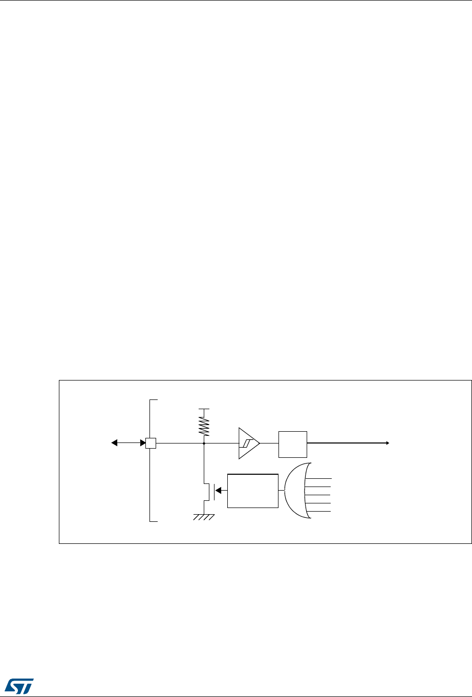
DocID018909 Rev 9 213/1718
RM0090 Reset and clock control for STM32F405xx/07xx and STM32F415xx/17xx(RCC)
267
Low-power management reset
There are two ways of generating a low-power management reset:
1. Reset generated when entering the Standby mode:
This type of reset is enabled by resetting the nRST_STDBY bit in the user option bytes.
In this case, whenever a Standby mode entry sequence is successfully executed, the
device is reset instead of entering the Standby mode.
2. Reset when entering the Stop mode:
This type of reset is enabled by resetting the nRST_STOP bit in the user option bytes.
In this case, whenever a Stop mode entry sequence is successfully executed, the
device is reset instead of entering the Stop mode.
7.1.2 Power reset
A power reset is generated when one of the following events occurs:
1. Power-on/power-down reset (POR/PDR reset) or brownout (BOR) reset
2. When exiting the Standby mode
A power reset sets all registers to their reset values except the Backup domain (see
Figure 4)
These sources act on the NRST pin and it is always kept low during the delay phase. The
RESET service routine vector is fixed at address 0x0000_0004 in the memory map.
The system reset signal provided to the device is output on the NRST pin. The pulse
generator guarantees a minimum reset pulse duration of 20 µs for each internal reset
source. In case of an external reset, the reset pulse is generated while the NRST pin is
asserted low.
Figure 20. Simplified diagram of the reset circuit
The Backup domain has two specific resets that affect only the Backup domain (see
Figure 4).
7.1.3 Backup domain reset
The backup domain reset sets all RTC registers and the RCC_BDCR register to their reset
values. The BKPSRAM is not affected by this reset. The only way of resetting the
BKPSRAM is through the Flash interface by requesting a protection level change from 1 to
0.
1567
5
38
9
''
9
''$
::'*UHVHW
,:'*UHVHW
3XOVH
JHQHUDWRU 3RZHUUHVHW
([WHUQDO
UHVHW
PLQV
6\VWHPUHVHW
)LOWHU
6RIWZDUHUHVHW
/RZSRZHUPDQDJHPHQWUHVHW
DLF

Reset and clock control for STM32F405xx/07xx and STM32F415xx/17xx(RCC) RM0090
214/1718 DocID018909 Rev 9
A backup domain reset is generated when one of the following events occurs:
1. Software reset, triggered by setting the BDRST bit in the RCC Backup domain control
register (RCC_BDCR).
2. VDD or VBAT power on, if both supplies have previously been powered off.
7.2 Clocks
Three different clock sources can be used to drive the system clock (SYSCLK):
•HSI oscillator clock
•HSE oscillator clock
•Main PLL (PLL) clock
The devices have the two following secondary clock sources:
•32 kHz low-speed internal RC (LSI RC) which drives the independent watchdog and,
optionally, the RTC used for Auto-wakeup from the Stop/Standby mode.
•32.768 kHz low-speed external crystal (LSE crystal) which optionally drives the RTC
clock (RTCCLK)
Each clock source can be switched on or off independently when it is not used, to optimize
power consumption.
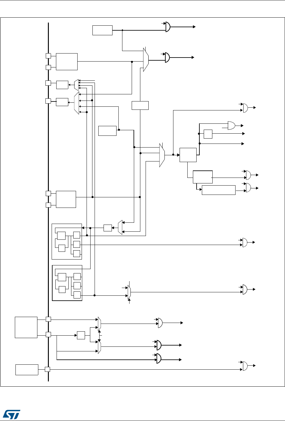
DocID018909 Rev 9 215/1718
RM0090 Reset and clock control for STM32F405xx/07xx and STM32F415xx/17xx(RCC)
267
Figure 21. Clock tree
1. For full details about the internal and external clock source characteristics, refer to the Electrical characteristics section in
the device datasheet.
0,,
6#/
X.
0
1
2
-
TO
0(9%THERNET
TO-(Z
53"0(9
TO-(Z
-))?2-))?3%,IN393#&'?0-#
-))
-))
!("
02%3#
!0"X
02%3#
IF!0"XPRESC X
ELSE X
,3%
%4(?-))?48?#,+
/4'?(3?3#,
0,,)3#,+
&#,+#ORTEX
FREERUNNINGCLOCK
!0"X
PERIPHERAL
CLOCKS
!0"X
TIMER
CLOCKS
-(Z
CLOCKS
53"(3
5,0)CLOCK
%THERNET
040CLOCK
-#/
0ERIPHERAL
CLOCKENABLE
TO
-#/
AIC
%4(?-))?28?#,+
/3#?).
/3#?/54
,3%/3#
K(Z
,3)2#
K(Z
TOINDEPENDENTWATCHDOG
,3%
,3)
TO24#
24##,+
24#3%,;=
)7$'#,+
(3%/3#
-(Z
/3#?).
/3#?/54
(3)2#
-(Z
0,,#,+
(3)
(3)
(3% -(Z
37
393#,+
MAX
(#,+
TO!("BUSCORE
MEMORYAND$-!
-(ZMAX
TO#ORTEX3YSTEM
#LOCK
%NABLE
0ERIPHERAL
CLOCKENABLE
0,,#+
)3CLOCKS
0ERIPHERAL
CLOCKENABLE
0ERIPHERAL
CLOCKENABLE
-!#2-))#,+
-!#48#,+
-!#28#,+
TO%THERNET-!#
0ERIPHERAL
CLOCKENABLE
0ERIPHERAL
CLOCKENABLE
TIMER
7ATCHDOG
ENABLE
24#
ENABLE
0ERIPHERAL
CLOCKENABLE
0ERIPHERAL
CLOCKENABLE
0ERIPHERAL
CLOCKENABLE
TO
0,,)3
6#/
X.
0
1
2
393#,+
%XTCLOCK
)3?#+).
)332#
(3%?24#
(3%

Reset and clock control for STM32F405xx/07xx and STM32F415xx/17xx(RCC) RM0090
216/1718 DocID018909 Rev 9
The clock controller provides a high degree of flexibility to the application in the choice of the
external crystal or the oscillator to run the core and peripherals at the highest frequency
and, guarantee the appropriate frequency for peripherals that need a specific clock like
Ethernet, USB OTG FS and HS, I2S and SDIO.
Several prescalers are used to configure the AHB frequency, the high-speed APB (APB2)
and the low-speed APB (APB1) domains. The maximum frequency of the AHB domain is
168 MHz. The maximum allowed frequency of the high-speed APB2 domain is 84 MHz. The
maximum allowed frequency of the low-speed APB1 domain is 42 MHz
All peripheral clocks are derived from the system clock (SYSCLK) except for:
•The USB OTG FS clock (48 MHz), the random analog generator (RNG) clock
(≤48 MHz) and the SDIO clock (≤ 48 MHz) which are coming from a specific output of
PLL (PLL48CLK)
•The I2S clock
To achieve high-quality audio performance, the I2S clock can be derived either from a
specific PLL (PLLI2S) or from an external clock mapped on the I2S_CKIN pin. For
more information about I2S clock frequency and precision, refer to Section 28.4.4:
Clock generator.
•The USB OTG HS (60 MHz) clock which is provided from the external PHY
•The Ethernet MAC clocks (TX, RX and RMII) which are provided from the external
PHY. For further information on the Ethernet configuration, please refer to
Section 33.4.4: MII/RMII selection in the Ethernet peripheral description. When the
Ethernet is used, the AHB clock frequency must be at least 25 MHz.
The RCC feeds the external clock of the Cortex System Timer (SysTick) with the AHB clock
(HCLK) divided by 8. The SysTick can work either with this clock or with the Cortex clock
(HCLK), configurable in the SysTick control and status register.
The timer clock frequencies are automatically set by hardware. There are two cases:
1. If the APB prescaler is 1, the timer clock frequencies are set to the same frequency as
that of the APB domain to which the timers are connected.
2. Otherwise, they are set to twice (×2) the frequency of the APB domain to which the
timers are connected.
FCLK acts as Cortex®-M4 with FPU free-running clock. For more details, refer to the
Cortex®-M4 with FPU technical reference manual.
7.2.1 HSE clock
The high speed external clock signal (HSE) can be generated from two possible clock
sources:
•HSE external crystal/ceramic resonator
•HSE external user clock
The resonator and the load capacitors have to be placed as close as possible to the
oscillator pins in order to minimize output distortion and startup stabilization time. The
loading capacitance values must be adjusted according to the selected oscillator.
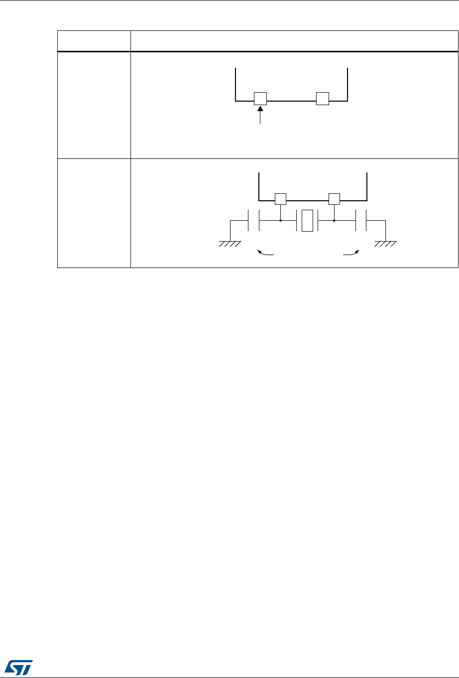
DocID018909 Rev 9 217/1718
RM0090 Reset and clock control for STM32F405xx/07xx and STM32F415xx/17xx(RCC)
267
External source (HSE bypass)
In this mode, an external clock source must be provided. You select this mode by setting the
HSEBYP and HSEON bits in the RCC clock control register (RCC_CR). The external clock
signal (square, sinus or triangle) with ~50% duty cycle has to drive the OSC_IN pin while the
OSC_OUT pin should be left HI-Z. See Figure 22.
External crystal/ceramic resonator (HSE crystal)
The HSE has the advantage of producing a very accurate rate on the main clock.
The associated hardware configuration is shown in Figure 22. Refer to the electrical
characteristics section of the datasheet for more details.
The HSERDY flag in the RCC clock control register (RCC_CR) indicates if the high-speed
external oscillator is stable or not. At startup, the clock is not released until this bit is set by
hardware. An interrupt can be generated if enabled in the RCC clock interrupt register
(RCC_CIR).
The HSE Crystal can be switched on and off using the HSEON bit in the RCC clock control
register (RCC_CR).
7.2.2 HSI clock
The HSI clock signal is generated from an internal 16 MHz RC oscillator and can be used
directly as a system clock, or used as PLL input.
The HSI RC oscillator has the advantage of providing a clock source at low cost (no external
components). It also has a faster startup time than the HSE crystal oscillator however, even
with calibration the frequency is less accurate than an external crystal oscillator or ceramic
resonator.
Figure 22. HSE/ LSE clock sources
Hardware configuration
External clock
Crystal/ceramic
resonators
OSC_OUT
External
source
(HI-Z)
OSC_IN OSC_OUT
Load
capacitors
CL2
CL1

Reset and clock control for STM32F405xx/07xx and STM32F415xx/17xx(RCC) RM0090
218/1718 DocID018909 Rev 9
Calibration
RC oscillator frequencies can vary from one chip to another due to manufacturing process
variations, this is why each device is factory calibrated by ST for 1% accuracy at TA= 25 °C.
After reset, the factory calibration value is loaded in the HSICAL[7:0] bits in the RCC clock
control register (RCC_CR).
If the application is subject to voltage or temperature variations this may affect the RC
oscillator speed. You can trim the HSI frequency in the application using the HSITRIM[4:0]
bits in the RCC clock control register (RCC_CR).
The HSIRDY flag in the RCC clock control register (RCC_CR) indicates if the HSI RC is
stable or not. At startup, the HSI RC output clock is not released until this bit is set by
hardware.
The HSI RC can be switched on and off using the HSION bit in the RCC clock control
register (RCC_CR).
The HSI signal can also be used as a backup source (Auxiliary clock) if the HSE crystal
oscillator fails. Refer to Section 7.2.7: Clock security system (CSS) on page 219.
7.2.3 PLL configuration
The STM32F4xx devices feature two PLLs:
•A main PLL (PLL) clocked by the HSE or HSI oscillator and featuring two different
output clocks:
– The first output is used to generate the high speed system clock (up to 168 MHz)
– The second output is used to generate the clock for the USB OTG FS (48 MHz),
the random analog generator (≤48 MHz) and the SDIO (≤ 48 MHz).
•A dedicated PLL (PLLI2S) used to generate an accurate clock to achieve high-quality
audio performance on the I2S interface.
Since the main-PLL configuration parameters cannot be changed once PLL is enabled, it is
recommended to configure PLL before enabling it (selection of the HSI or HSE oscillator as
PLL clock source, and configuration of division factors M, N, P, and Q).
The PLLI2S uses the same input clock as PLL (PLLM[5:0] and PLLSRC bits are common to
both PLLs). However, the PLLI2S has dedicated enable/disable and division factors (N and
R) configuration bits. Once the PLLI2S is enabled, the configuration parameters cannot be
changed.
The two PLLs are disabled by hardware when entering Stop and Standby modes, or when
an HSE failure occurs when HSE or PLL (clocked by HSE) are used as system clock. RCC
PLL configuration register (RCC_PLLCFGR) and RCC clock configuration register
(RCC_CFGR) can be used to configure PLL and PLLI2S, respectively.
7.2.4 LSE clock
The LSE clock is generated from a 32.768 kHz low-speed external crystal or ceramic
resonator. It has the advantage providing a low-power but highly accurate clock source to
the real-time clock peripheral (RTC) for clock/calendar or other timing functions.
The LSE oscillator is switched on and off using the LSEON bit in RCC Backup domain
control register (RCC_BDCR).

DocID018909 Rev 9 219/1718
RM0090 Reset and clock control for STM32F405xx/07xx and STM32F415xx/17xx(RCC)
267
The LSERDY flag in the RCC Backup domain control register (RCC_BDCR) indicates if the
LSE crystal is stable or not. At startup, the LSE crystal output clock signal is not released
until this bit is set by hardware. An interrupt can be generated if enabled in the RCC clock
interrupt register (RCC_CIR).
External source (LSE bypass)
In this mode, an external clock source must be provided. It must have a frequency up to
1 MHz. You select this mode by setting the LSEBYP and LSEON bits in the RCC Backup
domain control register (RCC_BDCR). The external clock signal (square, sinus or triangle)
with ~50% duty cycle has to drive the OSC32_IN pin while the OSC32_OUT pin should be
left HI-Z. See Figure 22.
7.2.5 LSI clock
The LSI RC acts as an low-power clock source that can be kept running in Stop and
Standby mode for the independent watchdog (IWDG) and Auto-wakeup unit (AWU). The
clock frequency is around 32 kHz. For more details, refer to the electrical characteristics
section of the datasheets.
The LSI RC can be switched on and off using the LSION bit in the RCC clock control &
status register (RCC_CSR).
The LSIRDY flag in the RCC clock control & status register (RCC_CSR) indicates if the low-
speed internal oscillator is stable or not. At startup, the clock is not released until this bit is
set by hardware. An interrupt can be generated if enabled in the RCC clock interrupt register
(RCC_CIR).
7.2.6 System clock (SYSCLK) selection
After a system reset, the HSI oscillator is selected as the system clock. When a clock source
is used directly or through PLL as the system clock, it is not possible to stop it.
A switch from one clock source to another occurs only if the target clock source is ready
(clock stable after startup delay or PLL locked). If a clock source that is not yet ready is
selected, the switch occurs when the clock source is ready. Status bits in the RCC clock
control register (RCC_CR) indicate which clock(s) is (are) ready and which clock is currently
used as the system clock.
7.2.7 Clock security system (CSS)
The clock security system can be activated by software. In this case, the clock detector is
enabled after the HSE oscillator startup delay, and disabled when this oscillator is stopped.
If a failure is detected on the HSE clock, this oscillator is automatically disabled, a clock
failure event is sent to the break inputs of advanced-control timers TIM1 and TIM8, and an
interrupt is generated to inform the software about the failure (clock security system
interrupt CSSI), allowing the MCU to perform rescue operations. The CSSI is linked to the
Cortex®-M4 with FPU NMI (non-maskable interrupt) exception vector.
Note: When the CSS is enabled, if the HSE clock happens to fail, the CSS generates an interrupt,
which causes the automatic generation of an NMI. The NMI is executed indefinitely unless
the CSS interrupt pending bit is cleared. As a consequence, the application has to clear the
CSS interrupt in the NMI ISR by setting the CSSC bit in the Clock interrupt register
(RCC_CIR).

Reset and clock control for STM32F405xx/07xx and STM32F415xx/17xx(RCC) RM0090
220/1718 DocID018909 Rev 9
If the HSE oscillator is used directly or indirectly as the system clock (indirectly meaning that
it is directly used as PLL input clock, and that PLL clock is the system clock) and a failure is
detected, then the system clock switches to the HSI oscillator and the HSE oscillator is
disabled.
If the HSE oscillator clock was the clock source of PLL used as the system clock when the
failure occurred, PLL is also disabled. In this case, if the PLLI2S was enabled, it is also
disabled when the HSE fails.
7.2.8 RTC/AWU clock
Once the RTCCLK clock source has been selected, the only possible way of modifying the
selection is to reset the power domain.
The RTCCLK clock source can be either the HSE 1 MHz (HSE divided by a programmable
prescaler), the LSE or the LSI clock. This is selected by programming the RTCSEL[1:0] bits
in the RCC Backup domain control register (RCC_BDCR) and the RTCPRE[4:0] bits in RCC
clock configuration register (RCC_CFGR). This selection cannot be modified without
resetting the Backup domain.
If the LSE is selected as the RTC clock, the RTC will work normally if the backup or the
system supply disappears. If the LSI is selected as the AWU clock, the AWU state is not
guaranteed if the system supply disappears. If the HSE oscillator divided by a value
between 2 and 31 is used as the RTC clock, the RTC state is not guaranteed if the backup
or the system supply disappears.
The LSE clock is in the Backup domain, whereas the HSE and LSI clocks are not. As a
consequence:
•If LSE is selected as the RTC clock:
– The RTC continues to work even if the VDD supply is switched off, provided the
VBAT supply is maintained.
•If LSI is selected as the Auto-wakeup unit (AWU) clock:
– The AWU state is not guaranteed if the VDD supply is powered off. Refer to
Section 7.2.5: LSI clock on page 219 for more details on LSI calibration.
•If the HSE clock is used as the RTC clock:
– The RTC state is not guaranteed if the VDD supply is powered off or if the internal
voltage regulator is powered off (removing power from the 1.2 V domain).
Note: To read the RTC calendar register when the APB1 clock frequency is less than seven times
the RTC clock frequency (fAPB1 < 7xfRTCLCK), the software must read the calendar time and
date registers twice. The data are correct if the second read access to RTC_TR gives the
same result than the first one. Otherwise a third read access must be performed.
7.2.9 Watchdog clock
If the independent watchdog (IWDG) is started by either hardware option or software
access, the LSI oscillator is forced ON and cannot be disabled. After the LSI oscillator
temporization, the clock is provided to the IWDG.

DocID018909 Rev 9 221/1718
RM0090 Reset and clock control for STM32F405xx/07xx and STM32F415xx/17xx(RCC)
267
7.2.10 Clock-out capability
Two microcontroller clock output (MCO) pins are available:
•MCO1
You can output four different clock sources onto the MCO1 pin (PA8) using the
configurable prescaler (from 1 to 5):
–HSI clock
– LSE clock
– HSE clock
– PLL clock
The desired clock source is selected using the MCO1PRE[2:0] and MCO1[1:0] bits in
the RCC clock configuration register (RCC_CFGR).
•MCO2
You can output four different clock sources onto the MCO2 pin (PC9) using the
configurable prescaler (from 1 to 5):
– HSE clock
– PLL clock
– System clock (SYSCLK)
– PLLI2S clock
The desired clock source is selected using the MCO2PRE[2:0] and MCO2 bits in the
RCC clock configuration register (RCC_CFGR).
For the different MCO pins, the corresponding GPIO port has to be programmed in alternate
function mode.
The selected clock to output onto MCO must not exceed 100 MHz (the maximum I/O
speed).
7.2.11 Internal/external clock measurement using TIM5/TIM11
It is possible to indirectly measure the frequencies of all on-board clock source generators
by means of the input capture of TIM5 channel4 and TIM11 channel1 as shown in Figure 23
and Figure 23.
Internal/external clock measurement using TIM5 channel4
TIM5 has an input multiplexer which allows choosing whether the input capture is triggered
by the I/O or by an internal clock. This selection is performed through the TI4_RMP [1:0] bits
in the TIM5_OR register.
The primary purpose of having the LSE connected to the channel4 input capture is to be
able to precisely measure the HSI (this requires to have the HSI used as the system clock
source). The number of HSI clock counts between consecutive edges of the LSE signal
provides a measurement of the internal clock period. Taking advantage of the high precision
of LSE crystals (typically a few tens of ppm) we can determine the internal clock frequency
with the same resolution, and trim the source to compensate for manufacturing-process
and/or temperature- and voltage-related frequency deviations.
The HSI oscillator has dedicated, user-accessible calibration bits for this purpose.
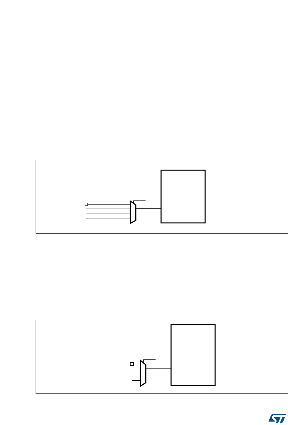
Reset and clock control for STM32F405xx/07xx and STM32F415xx/17xx(RCC) RM0090
222/1718 DocID018909 Rev 9
The basic concept consists in providing a relative measurement (e.g. HSI/LSE ratio): the
precision is therefore tightly linked to the ratio between the two clock sources. The greater
the ratio, the better the measurement.
It is also possible to measure the LSI frequency: this is useful for applications that do not
have a crystal. The ultralow-power LSI oscillator has a large manufacturing process
deviation: by measuring it versus the HSI clock source, it is possible to determine its
frequency with the precision of the HSI. The measured value can be used to have more
accurate RTC time base timeouts (when LSI is used as the RTC clock source) and/or an
IWDG timeout with an acceptable accuracy.
Use the following procedure to measure the LSI frequency:
1. Enable the TIM5 timer and configure channel4 in Input capture mode.
2. Set the TI4_RMP bits in the TIM5_OR register to 0x01 to connect the LSI clock
internally to TIM5 channel4 input capture for calibration purposes.
3. Measure the LSI clock frequency using the TIM5 capture/compare 4 event or interrupt.
4. Use the measured LSI frequency to update the prescaler of the RTC depending on the
desired time base and/or to compute the IWDG timeout.
Figure 23. Frequency measurement with TIM5 in Input capture mode
Internal/external clock measurement using TIM11 channel1
TIM11 has an input multiplexer which allows choosing whether the input capture is triggered
by the I/O or by an internal clock. This selection is performed through TI1_RMP [1:0] bits in
the TIM11_OR register. The HSE_RTC clock (HSE divided by a programmable prescaler) is
connected to channel 1 input capture to have a rough indication of the external crystal
frequency. This requires that the HSI is the system clock source. This can be useful for
instance to ensure compliance with the IEC 60730/IEC 61335 standards which require to be
able to determine harmonic or subharmonic frequencies (–50/+100% deviations).
Figure 24. Frequency measurement with TIM11 in Input capture mode
4)-
4)
4)?2-0;=
'0)/
24#?7AKE5P?)4
,3%
,3)
AI6
4)-
4)
4)?2-0;=
'0)/
(3%?24#-(Z
AI

DocID018909 Rev 9 223/1718
RM0090 Reset and clock control for STM32F405xx/07xx and STM32F415xx/17xx(RCC)
267
7.3 RCC registers
Refer to Section 1.1: List of abbreviations for registers for a list of abbreviations used in
register descriptions.
7.3.1 RCC clock control register (RCC_CR)
Address offset: 0x00
Reset value: 0x0000 XX83 where X is undefined.
Access: no wait state, word, half-word and byte access
31 30 29 28 27 26 25 24 23 22 21 20 19 18 17 16
Reserved
PLLI2S
RDY
PLLI2S
ON
PLLRD
YPLLON Reserved
CSS
ON
HSE
BYP
HSE
RDY
HSE
ON
r rw r rw rw rw r rw
15 14 13 12 11 10 9 8 7 6 5 4 3 2 1 0
HSICAL[7:0] HSITRIM[4:0] Res.
HSI
RDY HSION
rrrrrr r rrwrwrwrwrw rrw
Bits 31:28 Reserved, must be kept at reset value.
Bit 27 PLLI2SRDY: PLLI2S clock ready flag
Set by hardware to indicate that the PLLI2S is locked.
0: PLLI2S unlocked
1: PLLI2S locked
Bit 26 PLLI2SON: PLLI2S enable
Set and cleared by software to enable PLLI2S.
Cleared by hardware when entering Stop or Standby mode.
0: PLLI2S OFF
1: PLLI2S ON
Bit 25 PLLRDY: Main PLL (PLL) clock ready flag
Set by hardware to indicate that PLL is locked.
0: PLL unlocked
1: PLL locked
Bit 24 PLLON: Main PLL (PLL) enable
Set and cleared by software to enable PLL.
Cleared by hardware when entering Stop or Standby mode. This bit cannot be reset if PLL
clock is used as the system clock.
0: PLL OFF
1: PLL ON
Bits 23:20 Reserved, must be kept at reset value.
Bit 19 CSSON: Clock security system enable
Set and cleared by software to enable the clock security system. When CSSON is set, the
clock detector is enabled by hardware when the HSE oscillator is ready, and disabled by
hardware if an oscillator failure is detected.
0: Clock security system OFF (Clock detector OFF)
1: Clock security system ON (Clock detector ON if HSE oscillator is stable, OFF if not)

Reset and clock control for STM32F405xx/07xx and STM32F415xx/17xx(RCC) RM0090
224/1718 DocID018909 Rev 9
Bit 18 HSEBYP: HSE clock bypass
Set and cleared by software to bypass the oscillator with an external clock. The external
clock must be enabled with the HSEON bit, to be used by the device.
The HSEBYP bit can be written only if the HSE oscillator is disabled.
0: HSE oscillator not bypassed
1: HSE oscillator bypassed with an external clock
Bit 17 HSERDY: HSE clock ready flag
Set by hardware to indicate that the HSE oscillator is stable. After the HSEON bit is cleared,
HSERDY goes low after 6 HSE oscillator clock cycles.
0: HSE oscillator not ready
1: HSE oscillator ready
Bit 16 HSEON: HSE clock enable
Set and cleared by software.
Cleared by hardware to stop the HSE oscillator when entering Stop or Standby mode. This
bit cannot be reset if the HSE oscillator is used directly or indirectly as the system clock.
0: HSE oscillator OFF
1: HSE oscillator ON
Bits 15:8 HSICAL[7:0]: Internal high-speed clock calibration
These bits are initialized automatically at startup.
Bits 7:3 HSITRIM[4:0]: Internal high-speed clock trimming
These bits provide an additional user-programmable trimming value that is added to the
HSICAL[7:0] bits. It can be programmed to adjust to variations in voltage and temperature
that influence the frequency of the internal HSI RC.
Bit 2 Reserved, must be kept at reset value.
Bit 1 HSIRDY: Internal high-speed clock ready flag
Set by hardware to indicate that the HSI oscillator is stable. After the HSION bit is cleared,
HSIRDY goes low after 6 HSI clock cycles.
0: HSI oscillator not ready
1: HSI oscillator ready
Bit 0 HSION: Internal high-speed clock enable
Set and cleared by software.
Set by hardware to force the HSI oscillator ON when leaving the Stop or Standby mode or in
case of a failure of the HSE oscillator used directly or indirectly as the system clock. This bit
cannot be cleared if the HSI is used directly or indirectly as the system clock.
0: HSI oscillator OFF
1: HSI oscillator ON

DocID018909 Rev 9 225/1718
RM0090 Reset and clock control for STM32F405xx/07xx and STM32F415xx/17xx(RCC)
267
7.3.2 RCC PLL configuration register (RCC_PLLCFGR)
Address offset: 0x04
Reset value: 0x2400 3010
Access: no wait state, word, half-word and byte access.
This register is used to configure the PLL clock outputs according to the formulas:
•f(VCO clock) = f(PLL clock input) × (PLLN / PLLM)
•f(PLL general clock output) = f(VCO clock) / PLLP
•f(USB OTG FS, SDIO, RNG clock output) = f(VCO clock) / PLLQ
31 30 29 28 27 26 25 24 23 22 21 20 19 18 17 16
Reserved PLLQ3 PLLQ2 PLLQ1 PLLQ0 Reserv
ed
PLLSR
CReserved PLLP1 PLLP0
rw rw rw rw rw rw rw
15 14 13 12 11 10 9 8 7 6 5 4 3 2 1 0
Reserv
ed
PLLN PLLM5 PLLM4 PLLM3 PLLM2 PLLM1 PLLM0
rw rw rw rw rw rw rw rw rw rw rw rw rw rw rw
Bits 31:28 Reserved, must be kept at reset value.
Bits 27:24 PLLQ: Main PLL (PLL) division factor for USB OTG FS, SDIO and random number generator
clocks
Set and cleared by software to control the frequency of USB OTG FS clock, the random
number generator clock and the SDIO clock. These bits should be written only if PLL is
disabled.
Caution: The USB OTG FS requires a 48 MHz clock to work correctly. The SDIO and the
random number generator need a frequency lower than or equal to 48 MHz to work
correctly.
USB OTG FS clock frequency = VCO frequency / PLLQ with 2 ≤ PLLQ ≤ 15
0000: PLLQ = 0, wrong configuration
0001: PLLQ = 1, wrong configuration
0010: PLLQ = 2
0011: PLLQ = 3
0100: PLLQ = 4
...
1111: PLLQ = 15
Bit 23 Reserved, must be kept at reset value.
Bit 22 PLLSRC: Main PLL(PLL) and audio PLL (PLLI2S) entry clock source
Set and cleared by software to select PLL and PLLI2S clock source. This bit can be written
only when PLL and PLLI2S are disabled.
0: HSI clock selected as PLL and PLLI2S clock entry
1: HSE oscillator clock selected as PLL and PLLI2S clock entry
Bits 21:18 Reserved, must be kept at reset value.

Reset and clock control for STM32F405xx/07xx and STM32F415xx/17xx(RCC) RM0090
226/1718 DocID018909 Rev 9
Bits 17:16 PLLP: Main PLL (PLL) division factor for main system clock
Set and cleared by software to control the frequency of the general PLL output clock. These
bits can be written only if PLL is disabled.
Caution: The software has to set these bits correctly not to exceed 168 MHz on this domain.
PLL output clock frequency = VCO frequency / PLLP with PLLP = 2, 4, 6, or 8
00: PLLP = 2
01: PLLP = 4
10: PLLP = 6
11: PLLP = 8
Bits 14:6 PLLN: Main PLL (PLL) multiplication factor for VCO
Set and cleared by software to control the multiplication factor of the VCO. These bits can
be written only when PLL is disabled. Only half-word and word accesses are allowed to
write these bits.
Caution: The software has to set these bits correctly to ensure that the VCO output
frequency is between 192 and 432 MHz.
VCO output frequency = VCO input frequency × PLLN with 192 ≤ PLLN ≤ 432
000000000: PLLN = 0, wrong configuration
000000001: PLLN = 1, wrong configuration
...
011000000: PLLN = 192
...
110110000: PLLN = 432
110110001: PLLN = 433, wrong configuration
...
111111111: PLLN = 511, wrong configuration
Bits 5:0 PLLM: Division factor for the main PLL (PLL) and audio PLL (PLLI2S) input clock
Set and cleared by software to divide the PLL and PLLI2S input clock before the VCO.
These bits can be written only when the PLL and PLLI2S are disabled.
Caution: The software has to set these bits correctly to ensure that the VCO input frequency
ranges from 1 to 2 MHz. It is recommended to select a frequency of 2 MHz to limit
PLL jitter.
VCO input frequency = PLL input clock frequency / PLLM with 2 ≤ PLLM ≤ 63
000000: PLLM = 0, wrong configuration
000001: PLLM = 1, wrong configuration
000010: PLLM = 2
000011: PLLM = 3
000100: PLLM = 4
...
111110: PLLM = 62
111111: PLLM = 63

DocID018909 Rev 9 227/1718
RM0090 Reset and clock control for STM32F405xx/07xx and STM32F415xx/17xx(RCC)
267
7.3.3 RCC clock configuration register (RCC_CFGR)
Address offset: 0x08
Reset value: 0x0000 0000
Access: 0 ≤ wait state ≤ 2, word, half-word and byte access
1 or 2 wait states inserted only if the access occurs during a clock source switch.
31 30 29 28 27 26 25 24 23 22 21 20 19 18 17 16
MCO2 MCO2 PRE[2:0] MCO1 PRE[2:0] I2SSC
RMCO1 RTCPRE[4:0]
rw rw rw rw rw rw rw rw rw rw rw rw rw rw
15 14 13 12 11 10 9 8 7 6 5 4 3 2 1 0
PPRE2[2:0] PPRE1[2:0]
Reserved
HPRE[3:0] SWS1 SWS0 SW1 SW0
rw rw rw rw rw rw rw rw rw rw r r rw rw
Bits 31:30 MCO2[1:0]: Microcontroller clock output 2
Set and cleared by software. Clock source selection may generate glitches on MCO2. It is
highly recommended to configure these bits only after reset before enabling the external
oscillators and the PLLs.
00: System clock (SYSCLK) selected
01: PLLI2S clock selected
10: HSE oscillator clock selected
11: PLL clock selected
Bits 27:29 MCO2PRE: MCO2 prescaler
Set and cleared by software to configure the prescaler of the MCO2. Modification of this
prescaler may generate glitches on MCO2. It is highly recommended to change this
prescaler only after reset before enabling the external oscillators and the PLLs.
0xx: no division
100: division by 2
101: division by 3
110: division by 4
111: division by 5
Bits 24:26 MCO1PRE: MCO1 prescaler
Set and cleared by software to configure the prescaler of the MCO1. Modification of this
prescaler may generate glitches on MCO1. It is highly recommended to change this
prescaler only after reset before enabling the external oscillators and the PLL.
0xx: no division
100: division by 2
101: division by 3
110: division by 4
111: division by 5
Bit 23 I2SSRC: I2S clock selection
Set and cleared by software. This bit allows to select the I2S clock source between the
PLLI2S clock and the external clock. It is highly recommended to change this bit only after
reset and before enabling the I2S module.
0: PLLI2S clock used as I2S clock source
1: External clock mapped on the I2S_CKIN pin used as I2S clock source

Reset and clock control for STM32F405xx/07xx and STM32F415xx/17xx(RCC) RM0090
228/1718 DocID018909 Rev 9
Bits 22:21 MCO1: Microcontroller clock output 1
Set and cleared by software. Clock source selection may generate glitches on MCO1. It is
highly recommended to configure these bits only after reset before enabling the external
oscillators and PLL.
00: HSI clock selected
01: LSE oscillator selected
10: HSE oscillator clock selected
11: PLL clock selected
Bits 20:16 RTCPRE: HSE division factor for RTC clock
Set and cleared by software to divide the HSE clock input clock to generate a 1 MHz clock
for RTC.
Caution: The software has to set these bits correctly to ensure that the clock supplied to the
RTC is 1 MHz. These bits must be configured if needed before selecting the RTC
clock source.
00000: no clock
00001: no clock
00010: HSE/2
00011: HSE/3
00100: HSE/4
...
11110: HSE/30
11111: HSE/31
Bits 15:13 PPRE2: APB high-speed prescaler (APB2)
Set and cleared by software to control APB high-speed clock division factor.
Caution: The software has to set these bits correctly not to exceed 84 MHz on this domain.
The clocks are divided with the new prescaler factor from 1 to 16 AHB cycles after
PPRE2 write.
0xx: AHB clock not divided
100: AHB clock divided by 2
101: AHB clock divided by 4
110: AHB clock divided by 8
111: AHB clock divided by 16
Bits 12:10 PPRE1: APB Low speed prescaler (APB1)
Set and cleared by software to control APB low-speed clock division factor.
Caution: The software has to set these bits correctly not to exceed 42 MHz on this domain.
The clocks are divided with the new prescaler factor from 1 to 16 AHB cycles after
PPRE1 write.
0xx: AHB clock not divided
100: AHB clock divided by 2
101: AHB clock divided by 4
110: AHB clock divided by 8
111: AHB clock divided by 16
Bits 9:8 Reserved, must be kept at reset value.

DocID018909 Rev 9 229/1718
RM0090 Reset and clock control for STM32F405xx/07xx and STM32F415xx/17xx(RCC)
267
7.3.4 RCC clock interrupt register (RCC_CIR)
Address offset: 0x0C
Reset value: 0x0000 0000
Access: no wait state, word, half-word and byte access
Bits 7:4 HPRE: AHB prescaler
Set and cleared by software to control AHB clock division factor.
Caution: The clocks are divided with the new prescaler factor from 1 to 16 AHB cycles after
HPRE write.
Caution: The AHB clock frequency must be at least 25 MHz when the Ethernet is used.
0xxx: system clock not divided
1000: system clock divided by 2
1001: system clock divided by 4
1010: system clock divided by 8
1011: system clock divided by 16
1100: system clock divided by 64
1101: system clock divided by 128
1110: system clock divided by 256
1111: system clock divided by 512
Bits 3:2 SWS: System clock switch status
Set and cleared by hardware to indicate which clock source is used as the system clock.
00: HSI oscillator used as the system clock
01: HSE oscillator used as the system clock
10: PLL used as the system clock
11: not applicable
Bits 1:0 SW: System clock switch
Set and cleared by software to select the system clock source.
Set by hardware to force the HSI selection when leaving the Stop or Standby mode or in
case of failure of the HSE oscillator used directly or indirectly as the system clock.
00: HSI oscillator selected as system clock
01: HSE oscillator selected as system clock
10: PLL selected as system clock
11: not allowed
31 30 29 28 27 26 25 24 23 22 21 20 19 18 17 16
Reserved CSSC Reserv
ed
PLLI2S
RDYC
PLL
RDYC
HSE
RDYC
HSI
RDYC
LSE
RDYC
LSI
RDYC
wwwwwww
15 14 13 12 11 10 9 8 7 6 5 4 3 2 1 0
Reserved
PLLI2S
RDYIE
PLL
RDYIE
HSE
RDYIE
HSI
RDYIE
LSE
RDYIE
LSI
RDYIE CSSF Reserv
ed
PLLI2S
RDYF
PLL
RDYF
HSE
RDYF
HSI
RDYF
LSE
RDYF
LSI
RDYF
rw rw rw rw rw rw r r r r r r r

Reset and clock control for STM32F405xx/07xx and STM32F415xx/17xx(RCC) RM0090
230/1718 DocID018909 Rev 9
Bits 31:24 Reserved, must be kept at reset value.
Bit 23 CSSC: Clock security system interrupt clear
This bit is set by software to clear the CSSF flag.
0: No effect
1: Clear CSSF flag
Bits 22 Reserved, must be kept at reset value.
Bit 21 PLLI2SRDYC: PLLI2S ready interrupt clear
This bit is set by software to clear the PLLI2SRDYF flag.
0: No effect
1: PLLI2SRDYF cleared
Bit 20 PLLRDYC: Main PLL(PLL) ready interrupt clear
This bit is set by software to clear the PLLRDYF flag.
0: No effect
1: PLLRDYF cleared
Bit 19 HSERDYC: HSE ready interrupt clear
This bit is set by software to clear the HSERDYF flag.
0: No effect
1: HSERDYF cleared
Bit 18 HSIRDYC: HSI ready interrupt clear
This bit is set software to clear the HSIRDYF flag.
0: No effect
1: HSIRDYF cleared
Bit 17 LSERDYC: LSE ready interrupt clear
This bit is set by software to clear the LSERDYF flag.
0: No effect
1: LSERDYF cleared
Bit 16 LSIRDYC: LSI ready interrupt clear
This bit is set by software to clear the LSIRDYF flag.
0: No effect
1: LSIRDYF cleared
Bits 15:12 Reserved, must be kept at reset value.
Bit 13 PLLI2SRDYIE: PLLI2S ready interrupt enable
Set and cleared by software to enable/disable interrupt caused by PLLI2S lock.
0: PLLI2S lock interrupt disabled
1: PLLI2S lock interrupt enabled
Bit 12 PLLRDYIE: Main PLL (PLL) ready interrupt enable
Set and cleared by software to enable/disable interrupt caused by PLL lock.
0: PLL lock interrupt disabled
1: PLL lock interrupt enabled
Bit 11 HSERDYIE: HSE ready interrupt enable
Set and cleared by software to enable/disable interrupt caused by the HSE oscillator
stabilization.
0: HSE ready interrupt disabled
1: HSE ready interrupt enabled

DocID018909 Rev 9 231/1718
RM0090 Reset and clock control for STM32F405xx/07xx and STM32F415xx/17xx(RCC)
267
Bit 10 HSIRDYIE: HSI ready interrupt enable
Set and cleared by software to enable/disable interrupt caused by the HSI oscillator
stabilization.
0: HSI ready interrupt disabled
1: HSI ready interrupt enabled
Bit 9 LSERDYIE: LSE ready interrupt enable
Set and cleared by software to enable/disable interrupt caused by the LSE oscillator
stabilization.
0: LSE ready interrupt disabled
1: LSE ready interrupt enabled
Bit 8 LSIRDYIE: LSI ready interrupt enable
Set and cleared by software to enable/disable interrupt caused by LSI oscillator
stabilization.
0: LSI ready interrupt disabled
1: LSI ready interrupt enabled
Bit 7 CSSF: Clock security system interrupt flag
Set by hardware when a failure is detected in the HSE oscillator.
Cleared by software setting the CSSC bit.
0: No clock security interrupt caused by HSE clock failure
1: Clock security interrupt caused by HSE clock failure
Bits 6 Reserved, must be kept at reset value.
Bit 5 PLLI2SRDYF: PLLI2S ready interrupt flag
Set by hardware when the PLLI2S locks and PLLI2SRDYDIE is set.
Cleared by software setting the PLLRI2SDYC bit.
0: No clock ready interrupt caused by PLLI2S lock
1: Clock ready interrupt caused by PLLI2S lock
Bit 4 PLLRDYF: Main PLL (PLL) ready interrupt flag
Set by hardware when PLL locks and PLLRDYDIE is set.
Cleared by software setting the PLLRDYC bit.
0: No clock ready interrupt caused by PLL lock
1: Clock ready interrupt caused by PLL lock
Bit 3 HSERDYF: HSE ready interrupt flag
Set by hardware when External High Speed clock becomes stable and HSERDYDIE is set.
Cleared by software setting the HSERDYC bit.
0: No clock ready interrupt caused by the HSE oscillator
1: Clock ready interrupt caused by the HSE oscillator

Reset and clock control for STM32F405xx/07xx and STM32F415xx/17xx(RCC) RM0090
232/1718 DocID018909 Rev 9
7.3.5 RCC AHB1 peripheral reset register (RCC_AHB1RSTR)
Address offset: 0x10
Reset value: 0x0000 0000
Access: no wait state, word, half-word and byte access.
Bit 2 HSIRDYF: HSI ready interrupt flag
Set by hardware when the Internal High Speed clock becomes stable and HSIRDYDIE is
set.
Cleared by software setting the HSIRDYC bit.
0: No clock ready interrupt caused by the HSI oscillator
1: Clock ready interrupt caused by the HSI oscillator
Bit 1 LSERDYF: LSE ready interrupt flag
Set by hardware when the External Low Speed clock becomes stable and LSERDYDIE is
set.
Cleared by software setting the LSERDYC bit.
0: No clock ready interrupt caused by the LSE oscillator
1: Clock ready interrupt caused by the LSE oscillator
Bit 0 LSIRDYF: LSI ready interrupt flag
Set by hardware when the internal low speed clock becomes stable and LSIRDYDIE is set.
Cleared by software setting the LSIRDYC bit.
0: No clock ready interrupt caused by the LSI oscillator
1: Clock ready interrupt caused by the LSI oscillator
31 30 29 28 27 26 25 24 23 22 21 20 19 18 17 16
Reserved
OTGH
S
RST Reserved
ETHMAC
RST Reserved
DMA2
RST
DMA1
RST Reserved
rw rw rw rw
15 14 13 12 11 10 9 8 7 6 5 4 3 2 1 0
Reserved
CRCR
ST Reserved
GPIOI
RST
GPIOH
RST
GPIOGG
RST
GPIOF
RST
GPIOE
RST
GPIOD
RST
GPIOC
RST
GPIOB
RST
GPIOA
RST
rw rw rw rw rw rw rw rw rw rw
Bits 31:30 Reserved, must be kept at reset value.
Bit 29 OTGHSRST: USB OTG HS module reset
Set and cleared by software.
0: does not reset the USB OTG HS module
1: resets the USB OTG HS module
Bits 28:26 Reserved, must be kept at reset value.
Bit 25 ETHMACRST: Ethernet MAC reset
Set and cleared by software.
0: does not reset Ethernet MAC
1: resets Ethernet MAC
Bits 24:23 Reserved, must be kept at reset value.

DocID018909 Rev 9 233/1718
RM0090 Reset and clock control for STM32F405xx/07xx and STM32F415xx/17xx(RCC)
267
Bit 22 DMA2RST: DMA2 reset
Set and cleared by software.
0: does not reset DMA2
1: resets DMA2
Bit 21 DMA1RST: DMA1 reset
Set and cleared by software.
0: does not reset DMA1
1: resets DMA1
Bits 20:13 Reserved, must be kept at reset value.
Bit 12 CRCRST: CRC reset
Set and cleared by software.
0: does not reset CRC
1: resets CRC
Bits 11:9 Reserved, must be kept at reset value.
Bit 8 GPIOIRST: IO port I reset
Set and cleared by software.
0: does not reset IO port I
1: resets IO port I
Bit 7 GPIOHRST: IO port H reset
Set and cleared by software.
0: does not reset IO port H
1: resets IO port H
Bits 6 GPIOGRST: IO port G reset
Set and cleared by software.
0: does not reset IO port G
1: resets IO port G
Bit 5 GPIOFRST: IO port F reset
Set and cleared by software.
0: does not reset IO port F
1: resets IO port F
Bit 4 GPIOERST: IO port E reset
Set and cleared by software.
0: does not reset IO port E
1: resets IO port E
Bit 3 GPIODRST: IO port D reset
Set and cleared by software.
0: does not reset IO port D
1: resets IO port D

Reset and clock control for STM32F405xx/07xx and STM32F415xx/17xx(RCC) RM0090
234/1718 DocID018909 Rev 9
Bit 2 GPIOCRST: IO port C reset
Set and cleared by software.
0: does not reset IO port C
1: resets IO port C
Bit 1 GPIOBRST: IO port B reset
Set and cleared by software.
0: does not reset IO port B
1:resets IO port B
Bit 0 GPIOARST: IO port A reset
Set and cleared by software.
0: does not reset IO port A
1: resets IO port A

DocID018909 Rev 9 235/1718
RM0090 Reset and clock control for STM32F405xx/07xx and STM32F415xx/17xx(RCC)
267
7.3.6 RCC AHB2 peripheral reset register (RCC_AHB2RSTR)
Address offset: 0x14
Reset value: 0x0000 0000
Access: no wait state, word, half-word and byte access
31 30 29 28 27 26 25 24 23 22 21 20 19 18 17 16
Reserved
15 14 13 12 11 10 9 8 7 6 5 4 3 2 1 0
Reserved
OTGFS
RST
RNG
RST
HASH
RST
CRYP
RST Reserved
DCMI
RST
rw rw rw rw rw
Bits 31:8 Reserved, must be kept at reset value.
Bit 7 OTGFSRST: USB OTG FS module reset
Set and cleared by software.
0: does not reset the USB OTG FS module
1: resets the USB OTG FS module
Bit 6 RNGRST: Random number generator module reset
Set and cleared by software.
0: does not reset the random number generator module
1: resets the random number generator module
Bit 5 HASHRST: Hash module reset
Set and cleared by software.
0: does not reset the HASH module
1: resets the HASH module
Bit 4 CRYPRST: Cryptographic module reset
Set and cleared by software.
0: does not reset the cryptographic module
1: resets the cryptographic module
Bits 3:1 Reserved, must be kept at reset value.
Bit 0 DCMIRST: Camera interface reset
Set and cleared by software.
0: does not reset the Camera interface
1: resets the Camera interface

Reset and clock control for STM32F405xx/07xx and STM32F415xx/17xx(RCC) RM0090
236/1718 DocID018909 Rev 9
7.3.7 RCC AHB3 peripheral reset register (RCC_AHB3RSTR)
Address offset: 0x18
Reset value: 0x0000 0000
Access: no wait state, word, half-word and byte access.
7.3.8 RCC APB1 peripheral reset register (RCC_APB1RSTR)
Address offset: 0x20
Reset value: 0x0000 0000
Access: no wait state, word, half-word and byte access.
31 30 29 28 27 26 25 24 23 22 21 20 19 18 17 16
Reserved
1514131211109 8 765432 1 0
Reserved
FSMCRST
rw
Bits 31:1 Reserved, must be kept at reset value.
Bit 0 FSMCRST: Flexible static memory controller module reset
Set and cleared by software.
0: does not reset the FSMC module
1: resets the FSMC module
31 30 29 28 27 26 25 24 23 22 21 20 19 18 17 16
Reserved
DACRST PWR
RST Reser-
ved
CAN2
RST
CAN1
RST Reser-
ved
I2C3
RST
I2C2
RST
I2C1
RST
UART5
RST
UART4
RST
UART3
RST
UART2
RST Reser-
ved
rw rw rw rw rw rw rw rw rw rw
1514131211109876543210
SPI3
RST
SPI2
RST Reserved
WWDG
RST Reserved
TIM14
RST
TIM13
RST
TIM12
RST
TIM7
RST
TIM6
RST
TIM5
RST
TIM4
RST
TIM3
RST
TIM2
RST
rw rw rw rw rw rw rw rw rw rw rw rw
Bits 31:30 Reserved, must be kept at reset value.
Bit 29 DACRST: DAC reset
Set and cleared by software.
0: does not reset the DAC interface
1: resets the DAC interface
Bit 28 PWRRST: Power interface reset
Set and cleared by software.
0: does not reset the power interface
1: resets the power interface
Bit 27 Reserved, must be kept at reset value.

DocID018909 Rev 9 237/1718
RM0090 Reset and clock control for STM32F405xx/07xx and STM32F415xx/17xx(RCC)
267
Bit 26 CAN2RST: CAN2 reset
Set and cleared by software.
0: does not reset CAN2
1: resets CAN2
Bit 25 CAN1RST: CAN1 reset
Set and cleared by software.
0: does not reset CAN1
1: resets CAN1
Bit 24 Reserved, must be kept at reset value.
Bit 23 I2C3RST: I2C3 reset
Set and cleared by software.
0: does not reset I2C3
1: resets I2C3
Bit 22 I2C2RST: I2C2 reset
Set and cleared by software.
0: does not reset I2C2
1: resets I2C2
Bit 21 I2C1RST: I2C1 reset
Set and cleared by software.
0: does not reset I2C1
1: resets I2C1
Bit 20 UART5RST: UART5 reset
Set and cleared by software.
0: does not reset UART5
1: resets UART5
Bit 19 UART4RST: USART4 reset
Set and cleared by software.
0: does not reset UART4
1: resets UART4
Bit 18 USART3RST: USART3 reset
Set and cleared by software.
0: does not reset USART3
1: resets USART3
Bit 17 USART2RST: USART2 reset
Set and cleared by software.
0: does not reset USART2
1: resets USART2
Bit 16 Reserved, must be kept at reset value.
Bit 15 SPI3RST: SPI3 reset
Set and cleared by software.
0: does not reset SPI3
1: resets SPI3
Bit 14 SPI2RST: SPI2 reset
Set and cleared by software.
0: does not reset SPI2
1: resets SPI2

Reset and clock control for STM32F405xx/07xx and STM32F415xx/17xx(RCC) RM0090
238/1718 DocID018909 Rev 9
Bits 13:12 Reserved, must be kept at reset value.
Bit 11 WWDGRST: Window watchdog reset
Set and cleared by software.
0: does not reset the window watchdog
1: resets the window watchdog
Bits 10:9 Reserved, must be kept at reset value.
Bit 8 TIM14RST: TIM14 reset
Set and cleared by software.
0: does not reset TIM14
1: resets TIM14
Bit 7 TIM13RST: TIM13 reset
Set and cleared by software.
0: does not reset TIM13
1: resets TIM13
Bit 6 TIM12RST: TIM12 reset
Set and cleared by software.
0: does not reset TIM12
1: resets TIM12
Bit 5 TIM7RST: TIM7 reset
Set and cleared by software.
0: does not reset TIM7
1: resets TIM7
Bit 4 TIM6RST: TIM6 reset
Set and cleared by software.
0: does not reset TIM6
1: resets TIM6
Bit 3 TIM5RST: TIM5 reset
Set and cleared by software.
0: does not reset TIM5
1: resets TIM5
Bit 2 TIM4RST: TIM4 reset
Set and cleared by software.
0: does not reset TIM4
1: resets TIM4
Bit 1 TIM3RST: TIM3 reset
Set and cleared by software.
0: does not reset TIM3
1: resets TIM3
Bit 0 TIM2RST: TIM2 reset
Set and cleared by software.
0: does not reset TIM2
1: resets TIM2

DocID018909 Rev 9 239/1718
RM0090 Reset and clock control for STM32F405xx/07xx and STM32F415xx/17xx(RCC)
267
7.3.9 RCC APB2 peripheral reset register (RCC_APB2RSTR)
Address offset: 0x24
Reset value: 0x0000 0000
Access: no wait state, word, half-word and byte access.
31 30 29 28 27 26 25 24 23 22 21 20 19 18 17 16
Reserved
TIM11
RST
TIM10
RST
TIM9
RST
rw rw rw
15 14 13 12 11 10 9 8 7 6 5 4 3 2 1 0
Reser-
ved
SYSCF
G RST Reser-
ved
SPI1
RST
SDIO
RST Reserved
ADC
RST Reserved
USART
6
RST
USART
1
RST Reserved
TIM8
RST
TIM1
RST
rw rw rw rw rw rw rw rw
Bits 31:19 Reserved, must be kept at reset value.
Bit 18 TIM11RST: TIM11 reset
Set and cleared by software.
0: does not reset TIM11
1: resets TIM14
Bit 17 TIM10RST: TIM10 reset
Set and cleared by software.
0: does not reset TIM10
1: resets TIM10
Bit 16 TIM9RST: TIM9 reset
Set and cleared by software.
0: does not reset TIM9
1: resets TIM9
Bit 15 Reserved, must be kept at reset value.
Bit 14 SYSCFGRST: System configuration controller reset
Set and cleared by software.
0: does not reset the System configuration controller
1: resets the System configuration controller
Bit 13 Reserved, must be kept at reset value.
Bit 12 SPI1RST: SPI1 reset
Set and cleared by software.
0: does not reset SPI1
1: resets SPI1
Bit 11 SDIORST: SDIO reset
Set and cleared by software.
0: does not reset the SDIO module
1: resets the SDIO module
Bits 10:9 Reserved, must be kept at reset value.

Reset and clock control for STM32F405xx/07xx and STM32F415xx/17xx(RCC) RM0090
240/1718 DocID018909 Rev 9
Bit 8 ADCRST: ADC interface reset (common to all ADCs)
Set and cleared by software.
0: does not reset the ADC interface
1: resets the ADC interface
Bits 7:6 Reserved, must be kept at reset value.
Bit 5 USART6RST: USART6 reset
Set and cleared by software.
0: does not reset USART6
1: resets USART6
Bit 4 USART1RST: USART1 reset
Set and cleared by software.
0: does not reset USART1
1: resets USART1
Bits 3:2 Reserved, must be kept at reset value.
Bit 1 TIM8RST: TIM8 reset
Set and cleared by software.
0: does not reset TIM8
1: resets TIM8
Bit 0 TIM1RST: TIM1 reset
Set and cleared by software.
0: does not reset TIM1
1: resets TIM1

DocID018909 Rev 9 241/1718
RM0090 Reset and clock control for STM32F405xx/07xx and STM32F415xx/17xx(RCC)
267
7.3.10 RCC AHB1 peripheral clock enable register (RCC_AHB1ENR)
Address offset: 0x30
Reset value: 0x0010 0000
Access: no wait state, word, half-word and byte access.
31 30 29 28 27 26 25 24 23 22 21 20 19 18 17 16
Reser-
ved
OTGH
S
ULPIE
N
OTGH
SEN
ETHM
ACPTP
EN
ETHM
ACRXE
N
ETHM
ACTXE
N
ETHMA
CEN Reserved
DMA2E
N
DMA1E
N
CCMDAT
ARAMEN Res. BKPSR
AMEN Reserved
rw rw rw rw rw rw rw rw rw
15 14 13 12 11 10 9 8 7 6 5 4 3 2 1 0
Reserved
CRCE
NReserved
GPIOIE
N
GPIOH
EN
GPIOG
EN
GPIOFE
NGPIOEEN GPIOD
EN
GPIOC
EN
GPIO
BEN
GPIO
AEN
rw rw rw rw rw rw rw rw rw rw
Bit 31 Reserved, must be kept at reset value.
Bit 30 OTGHSULPIEN: USB OTG HSULPI clock enable
Set and cleared by software.
0: USB OTG HS ULPI clock disabled
1: USB OTG HS ULPI clock enabled
Bit 29 OTGHSEN: USB OTG HS clock enable
Set and cleared by software.
0: USB OTG HS clock disabled
1: USB OTG HS clock enabled
Bit 28 ETHMACPTPEN: Ethernet PTP clock enable
Set and cleared by software.
0: Ethernet PTP clock disabled
1: Ethernet PTP clock enabled
Bit 27 ETHMACRXEN: Ethernet Reception clock enable
Set and cleared by software.
0: Ethernet Reception clock disabled
1: Ethernet Reception clock enabled
Bit 26 ETHMACTXEN: Ethernet Transmission clock enable
Set and cleared by software.
0: Ethernet Transmission clock disabled
1: Ethernet Transmission clock enabled
Bit 25 ETHMACEN: Ethernet MAC clock enable
Set and cleared by software.
0: Ethernet MAC clock disabled
1: Ethernet MAC clock enabled
Bits 24:23 Reserved, must be kept at reset value.
Bit 22 DMA2EN: DMA2 clock enable
Set and cleared by software.
0: DMA2 clock disabled
1: DMA2 clock enabled

Reset and clock control for STM32F405xx/07xx and STM32F415xx/17xx(RCC) RM0090
242/1718 DocID018909 Rev 9
Bit 21 DMA1EN: DMA1 clock enable
Set and cleared by software.
0: DMA1 clock disabled
1: DMA1 clock enabled
Bit 20 CCMDATARAMEN: CCM data RAM clock enable
Set and cleared by software.
0: CCM data RAM clock disabled
1: CCM data RAM clock enabled
Bit 19 Reserved, must be kept at reset value.
Bit 18 BKPSRAMEN: Backup SRAM interface clock enable
Set and cleared by software.
0: Backup SRAM interface clock disabled
1: Backup SRAM interface clock enabled
Bits 17:13 Reserved, must be kept at reset value.
Bit 12 CRCEN: CRC clock enable
Set and cleared by software.
0: CRC clock disabled
1: CRC clock enabled
Bits 11:9 Reserved, must be kept at reset value.
Bit 8 GPIOIEN: IO port I clock enable
Set and cleared by software.
0: IO port I clock disabled
1: IO port I clock enabled
Bit 7 GPIOHEN: IO port H clock enable
Set and cleared by software.
0: IO port H clock disabled
1: IO port H clock enabled
Bit 6 GPIOGEN: IO port G clock enable
Set and cleared by software.
0: IO port G clock disabled
1: IO port G clock enabled
Bit 5 GPIOFEN: IO port F clock enable
Set and cleared by software.
0: IO port F clock disabled
1: IO port F clock enabled
Bit 4 GPIOEEN: IO port E clock enable
Set and cleared by software.
0: IO port E clock disabled
1: IO port E clock enabled
Bit 3 GPIODEN: IO port D clock enable
Set and cleared by software.
0: IO port D clock disabled
1: IO port D clock enabled

DocID018909 Rev 9 243/1718
RM0090 Reset and clock control for STM32F405xx/07xx and STM32F415xx/17xx(RCC)
267
7.3.11 RCC AHB2 peripheral clock enable register (RCC_AHB2ENR)
Address offset: 0x34
Reset value: 0x0000 0000
Access: no wait state, word, half-word and byte access.
Bit 2 GPIOCEN: IO port C clock enable
Set and cleared by software.
0: IO port C clock disabled
1: IO port C clock enabled
Bit 1 GPIOBEN: IO port B clock enable
Set and cleared by software.
0: IO port B clock disabled
1: IO port B clock enabled
Bit 0 GPIOAEN: IO port A clock enable
Set and cleared by software.
0: IO port A clock disabled
1: IO port A clock enabled
31 30 29 28 27 26 25 24 23 22 21 20 19 18 17 16
Reserved
15 14 13 12 11 10 9 8 7 6 5 4 3 2 1 0
Reserved
OTGFS
EN
RNG
EN
HASH
EN
CRYP
EN Reserved
DCMI
EN
rw rw rw rw rw
Bits 31:8 Reserved, must be kept at reset value.
Bit 7 OTGFSEN: USB OTG FS clock enable
Set and cleared by software.
0: USB OTG FS clock disabled
1: USB OTG FS clock enabled
Bit 6 RNGEN: Random number generator clock enable
Set and cleared by software.
0: Random number generator clock disabled
1: Random number generator clock enabled
Bit 5 HASHEN: Hash modules clock enable
Set and cleared by software.
0: Hash modules clock disabled
1: Hash modules clock enabled
Reset and clock control for STM32F405xx/07xx and STM32F415xx/17xx(RCC) RM0090
244/1718 DocID018909 Rev 9
7.3.12 RCC AHB3 peripheral clock enable register (RCC_AHB3ENR)
Address offset: 0x38
Reset value: 0x0000 0000
Access: no wait state, word, half-word and byte access.
7.3.13 RCC APB1 peripheral clock enable register
(RCC_APB1ENR)
Address offset: 0x40
Reset value: 0x0000 0000
Access: no wait state, word, half-word and byte access.
Bit 4 CRYPEN: Cryptographic modules clock enable
Set and cleared by software.
0: cryptographic module clock disabled
1: cryptographic module clock enabled
Bits 3:1 Reserved, must be kept at reset value.
Bit 0 DCMIEN: Camera interface enable
Set and cleared by software.
0: Camera interface clock disabled
1: Camera interface clock enabled
31 30 29 28 27 26 25 24 23 22 21 20 19 18 17 16
Reserved
15 14 13 12 11 10 9 8 7 6 5 4 3 2 1 0
Reserved FSMCEN
rw
Bits 31:1 Reserved, must be kept at reset value.
Bit 0 FSMCEN: Flexible static memory controller module clock enable
Set and cleared by software.
0: FSMC module clock disabled
1: FSMC module clock enabled
31 30 29 28 27 26 25 24 23 22 21 20 19 18 17 16
Reserved
DAC
EN
PWR
EN Reser-
ved
CAN2
EN
CAN1
EN Reser-
ved
I2C3
EN
I2C2
EN
I2C1
EN
UART5
EN
UART4
EN
USART
3
EN
USART
2
EN Reser-
ved
rw rw rw rw rw rw rw rw rw rw rw
15 14 13 12 11 10 9 8 7 6 5 4 3 2 1 0
SPI3
EN
SPI2
EN Reserved
WWDG
EN Reserved
TIM14
EN
TIM13
EN
TIM12
EN
TIM7
EN
TIM6
EN
TIM5
EN
TIM4
EN
TIM3
EN
TIM2
EN
rw rw rw rw rw rw rw rw rw rw rw rw

DocID018909 Rev 9 245/1718
RM0090 Reset and clock control for STM32F405xx/07xx and STM32F415xx/17xx(RCC)
267
Bits 31:30 Reserved, must be kept at reset value.
Bit 29 DACEN: DAC interface clock enable
Set and cleared by software.
0: DAC interface clock disabled
1: DAC interface clock enable
Bit 28 PWREN: Power interface clock enable
Set and cleared by software.
0: Power interface clock disabled
1: Power interface clock enable
Bit 27 Reserved, must be kept at reset value.
Bit 26 CAN2EN: CAN 2 clock enable
Set and cleared by software.
0: CAN 2 clock disabled
1: CAN 2 clock enabled
Bit 25 CAN1EN: CAN 1 clock enable
Set and cleared by software.
0: CAN 1 clock disabled
1: CAN 1 clock enabled
Bit 24 Reserved, must be kept at reset value.
Bit 23 I2C3EN: I2C3 clock enable
Set and cleared by software.
0: I2C3 clock disabled
1: I2C3 clock enabled
Bit 22 I2C2EN: I2C2 clock enable
Set and cleared by software.
0: I2C2 clock disabled
1: I2C2 clock enabled
Bit 21 I2C1EN: I2C1 clock enable
Set and cleared by software.
0: I2C1 clock disabled
1: I2C1 clock enabled
Bit 20 UART5EN: UART5 clock enable
Set and cleared by software.
0: UART5 clock disabled
1: UART5 clock enabled
Bit 19 UART4EN: UART4 clock enable
Set and cleared by software.
0: UART4 clock disabled
1: UART4 clock enabled
Bit 18 USART3EN: USART3 clock enable
Set and cleared by software.
0: USART3 clock disabled
1: USART3 clock enabled

Reset and clock control for STM32F405xx/07xx and STM32F415xx/17xx(RCC) RM0090
246/1718 DocID018909 Rev 9
Bit 17 USART2EN: USART2 clock enable
Set and cleared by software.
0: USART2 clock disabled
1: USART2 clock enabled
Bit 16 Reserved, must be kept at reset value.
Bit 15 SPI3EN: SPI3 clock enable
Set and cleared by software.
0: SPI3 clock disabled
1: SPI3 clock enabled
Bit 14 SPI2EN: SPI2 clock enable
Set and cleared by software.
0: SPI2 clock disabled
1: SPI2 clock enabled
Bits 13:12 Reserved, must be kept at reset value.
Bit 11 WWDGEN: Window watchdog clock enable
Set and cleared by software.
0: Window watchdog clock disabled
1: Window watchdog clock enabled
Bits 10:9 Reserved, must be kept at reset value.
Bit 8 TIM14EN: TIM14 clock enable
Set and cleared by software.
0: TIM14 clock disabled
1: TIM14 clock enabled
Bit 7 TIM13EN: TIM13 clock enable
Set and cleared by software.
0: TIM13 clock disabled
1: TIM13 clock enabled
Bit 6 TIM12EN: TIM12 clock enable
Set and cleared by software.
0: TIM12 clock disabled
1: TIM12 clock enabled
Bit 5 TIM7EN: TIM7 clock enable
Set and cleared by software.
0: TIM7 clock disabled
1: TIM7 clock enabled
Bit 4 TIM6EN: TIM6 clock enable
Set and cleared by software.
0: TIM6 clock disabled
1: TIM6 clock enabled
Bit 3 TIM5EN: TIM5 clock enable
Set and cleared by software.
0: TIM5 clock disabled
1: TIM5 clock enabled

DocID018909 Rev 9 247/1718
RM0090 Reset and clock control for STM32F405xx/07xx and STM32F415xx/17xx(RCC)
267
7.3.14 RCC APB2 peripheral clock enable register (RCC_APB2ENR)
Address offset: 0x44
Reset value: 0x0000 0000
Access: no wait state, word, half-word and byte access.
Bit 2 TIM4EN: TIM4 clock enable
Set and cleared by software.
0: TIM4 clock disabled
1: TIM4 clock enabled
Bit 1 TIM3EN: TIM3 clock enable
Set and cleared by software.
0: TIM3 clock disabled
1: TIM3 clock enabled
Bit 0 TIM2EN: TIM2 clock enable
Set and cleared by software.
0: TIM2 clock disabled
1: TIM2 clock enabled
31 30 29 28 27 26 25 24 23 22 21 20 19 18 17 16
Reserved
TIM11
EN
TIM10
EN
TIM9
EN
rw rw rw
15 14 13 12 11 10 9 8 7 6 5 4 3 2 1 0
Reser-
ved
SYSCF
G EN Reser-
ved
SPI1
EN
SDIO
EN
ADC3
EN
ADC2
EN
ADC1
EN Reserved
USART
6
EN
USART
1
EN Reserved
TIM8
EN
TIM1
EN
rw rw rw rw rw rw rw rw rw rw
Bits 31:19 Reserved, must be kept at reset value.
Bit 18 TIM11EN: TIM11 clock enable
Set and cleared by software.
0: TIM11 clock disabled
1: TIM11 clock enabled
Bit 17 TIM10EN: TIM10 clock enable
Set and cleared by software.
0: TIM10 clock disabled
1: TIM10 clock enabled
Bit 16 TIM9EN: TIM9 clock enable
Set and cleared by software.
0: TIM9 clock disabled
1: TIM9 clock enabled
Bit 15 Reserved, must be kept at reset value.

Reset and clock control for STM32F405xx/07xx and STM32F415xx/17xx(RCC) RM0090
248/1718 DocID018909 Rev 9
Bit 14 SYSCFGEN: System configuration controller clock enable
Set and cleared by software.
0: System configuration controller clock disabled
1: System configuration controller clock enabled
Bit 13 Reserved, must be kept at reset value.
Bit 12 SPI1EN: SPI1 clock enable
Set and cleared by software.
0: SPI1 clock disabled
1: SPI1 clock enabled
Bit 11 SDIOEN: SDIO clock enable
Set and cleared by software.
0: SDIO module clock disabled
1: SDIO module clock enabled
Bit 10 ADC3EN: ADC3 clock enable
Set and cleared by software.
0: ADC3 clock disabled
1: ADC3 clock disabled
Bit 9 ADC2EN: ADC2 clock enable
Set and cleared by software.
0: ADC2 clock disabled
1: ADC2 clock disabled
Bit 8 ADC1EN: ADC1 clock enable
Set and cleared by software.
0: ADC1 clock disabled
1: ADC1 clock disabled
Bits 7:6 Reserved, must be kept at reset value.
Bit 5 USART6EN: USART6 clock enable
Set and cleared by software.
0: USART6 clock disabled
1: USART6 clock enabled
Bit 4 USART1EN: USART1 clock enable
Set and cleared by software.
0: USART1 clock disabled
1: USART1 clock enabled
Bits 3:2 Reserved, must be kept at reset value.
Bit 1 TIM8EN: TIM8 clock enable
Set and cleared by software.
0: TIM8 clock disabled
1: TIM8 clock enabled
Bit 0 TIM1EN: TIM1 clock enable
Set and cleared by software.
0: TIM1 clock disabled
1: TIM1 clock enabled

DocID018909 Rev 9 249/1718
RM0090 Reset and clock control for STM32F405xx/07xx and STM32F415xx/17xx(RCC)
267
7.3.15 RCC APB2 peripheral clock enable register(RCC_APB2ENR)
Address offset: 0x44
Reset value: 0x0000 0000
Access: no wait state, word, half-word and byte access.
31 30 29 28 27 26 25 24 23 22 21 20 19 18 17 16
Reserved SPI6EN SPI5EN Res.
TIM11
EN
TIM10
EN
TIM9
EN
rw rw rw rw rw
15 14 13 12 11 10 9 8 7 6 5 4 3 2 1 0
Reser-
ved
SYSCF
G EN
SPI4E
N
SPI1
EN
SDIO
EN
ADC3
EN
ADC2
EN
ADC1
EN Reserved
USART
6
EN
USART
1
EN Reserved
TIM8
EN
TIM1
EN
rw rw rw rw rw rw rw rw rw rw rw
Bits 31:22 Reserved, must be kept at reset value.
Bit 21 SPI6EN: SPI6 clock enable
Set and cleared by software.
0: SPI6 clock disabled
1: SPI6 clock enabled
Bit 20 SPI5EN: SPI5 clock enable
Set and cleared by software.
0: SPI5 clock disabled
1: SPI5 clock enabled
Bit 19 Reserved, must be kept at reset value.
Bit 18 TIM11EN: TIM11 clock enable
Set and cleared by software.
0: TIM11 clock disabled
1: TIM11 clock enabled
Bit 17 TIM10EN: TIM10 clock enable
Set and cleared by software.
0: TIM10 clock disabled
1: TIM10 clock enabled
Bit 16 TIM9EN: TIM9 clock enable
Set and cleared by software.
0: TIM9 clock disabled
1: TIM9 clock enabled
Bit 15 Reserved, must be kept at reset value.
Bit 14 SYSCFGEN: System configuration controller clock enable
Set and cleared by software.
0: System configuration controller clock disabled
1: System configuration controller clock enabled
Bit 13 SPI4EN: SPI4 clock enable
Set and cleared by software.
0: SPI4 clock disabled
1: SPI4 clock enabled

Reset and clock control for STM32F405xx/07xx and STM32F415xx/17xx(RCC) RM0090
250/1718 DocID018909 Rev 9
Bit 12 SPI1EN: SPI1 clock enable
Set and cleared by software.
0: SPI1 clock disabled
1: SPI1 clock enabled
Bit 11 SDIOEN: SDIO clock enable
Set and cleared by software.
0: SDIO module clock disabled
1: SDIO module clock enabled
Bit 10 ADC3EN: ADC3 clock enable
Set and cleared by software.
0: ADC3 clock disabled
1: ADC3 clock disabled
Bit 9 ADC2EN: ADC2 clock enable
Set and cleared by software.
0: ADC2 clock disabled
1: ADC2 clock disabled
Bit 8 ADC1EN: ADC1 clock enable
Set and cleared by software.
0: ADC1 clock disabled
1: ADC1 clock disabled
Bits 7:6 Reserved, must be kept at reset value.
Bit 5 USART6EN: USART6 clock enable
Set and cleared by software.
0: USART6 clock disabled
1: USART6 clock enabled
Bit 4 USART1EN: USART1 clock enable
Set and cleared by software.
0: USART1 clock disabled
1: USART1 clock enabled
Bits 3:2 Reserved, must be kept at reset value.
Bit 1 TIM8EN: TIM8 clock enable
Set and cleared by software.
0: TIM8 clock disabled
1: TIM8 clock enabled
Bit 0 TIM1EN: TIM1 clock enable
Set and cleared by software.
0: TIM1 clock disabled
1: TIM1 clock enabled

DocID018909 Rev 9 251/1718
RM0090 Reset and clock control for STM32F405xx/07xx and STM32F415xx/17xx(RCC)
267
7.3.16 RCC AHB1 peripheral clock enable in low power mode register
(RCC_AHB1LPENR)
Address offset: 0x50
Reset value: 0x7E67 91FF
Access: no wait state, word, half-word and byte access.
31 30 29 28 27 26 25 24 23 22 21 20 19 18 17 16
Reser
-ved
OTGHS
ULPILPE
N
OTGH
S
LPEN
ETHPT
P
LPEN
ETHRX
LPEN
ETHTX
LPEN
ETHMA
C
LPEN Reserved
DMA2
LPEN
DMA1
LPEN Reserved
BKPSRA
M
LPEN
SRAM
2
LPEN
SRAM
1
LPEN
rw rw rw rw rw rw rw rw rw rw rw
15 14 13 12 11 10 9 8 7 6 5 4 3 2 1 0
FLITF
LPEN Reserved
CRC
LPEN Reserved
GPIOI
LPEN
GPIOH
LPEN
GPIOG
G
LPEN
GPIO
F
LPEN
GPIOE
LPEN
GPIOD
LPEN
GPIOC
LPEN
GPIOB
LPEN
GPIOA
LPEN
rw rw rw rw rw rw rw rw rw rw rw
Bit 31 Reserved, must be kept at reset value.
Bit 30 OTGHSULPILPEN: USB OTG HS ULPI clock enable during Sleep mode
Set and cleared by software.
0: USB OTG HS ULPI clock disabled during Sleep mode
1: USB OTG HS ULPI clock enabled during Sleep mode
Bit 29 OTGHSLPEN: USB OTG HS clock enable during Sleep mode
Set and cleared by software.
0: USB OTG HS clock disabled during Sleep mode
1: USB OTG HS clock enabled during Sleep mode
Bit 28 ETHMACPTPLPEN: Ethernet PTP clock enable during Sleep mode
Set and cleared by software.
0: Ethernet PTP clock disabled during Sleep mode
1: Ethernet PTP clock enabled during Sleep mode
Bit 27 ETHMACRXLPEN: Ethernet reception clock enable during Sleep mode
Set and cleared by software.
0: Ethernet reception clock disabled during Sleep mode
1: Ethernet reception clock enabled during Sleep mode
Bit 26 ETHMACTXLPEN: Ethernet transmission clock enable during Sleep mode
Set and cleared by software.
0: Ethernet transmission clock disabled during sleep mode
1: Ethernet transmission clock enabled during sleep mode
Bit 25 ETHMACLPEN: Ethernet MAC clock enable during Sleep mode
Set and cleared by software.
0: Ethernet MAC clock disabled during Sleep mode
1: Ethernet MAC clock enabled during Sleep mode
Bits 24:23 Reserved, must be kept at reset value.
Bit 22 DMA2LPEN: DMA2 clock enable during Sleep mode
Set and cleared by software.
0: DMA2 clock disabled during Sleep mode
1: DMA2 clock enabled during Sleep mode

Reset and clock control for STM32F405xx/07xx and STM32F415xx/17xx(RCC) RM0090
252/1718 DocID018909 Rev 9
Bit 21 DMA1LPEN: DMA1 clock enable during Sleep mode
Set and cleared by software.
0: DMA1 clock disabled during Sleep mode
1: DMA1 clock enabled during Sleep mode
Bits 20:19 Reserved, must be kept at reset value.
Bit 18 BKPSRAMLPEN: Backup SRAM interface clock enable during Sleep mode
Set and cleared by software.
0: Backup SRAM interface clock disabled during Sleep mode
1: Backup SRAM interface clock enabled during Sleep mode
Bit 17 SRAM2LPEN: SRAM 2 interface clock enable during Sleep mode
Set and cleared by software.
0: SRAM 2 interface clock disabled during Sleep mode
1: SRAM 2 interface clock enabled during Sleep mode
Bit 16 SRAM1LPEN: SRAM 1interface clock enable during Sleep mode
Set and cleared by software.
0: SRAM 1 interface clock disabled during Sleep mode
1: SRAM 1 interface clock enabled during Sleep mode
Bit 15 FLITFLPEN: Flash interface clock enable during Sleep mode
Set and cleared by software.
0: Flash interface clock disabled during Sleep mode
1: Flash interface clock enabled during Sleep mode
Bits 14:13 Reserved, must be kept at reset value.
Bit 12 CRCLPEN: CRC clock enable during Sleep mode
Set and cleared by software.
0: CRC clock disabled during Sleep mode
1: CRC clock enabled during Sleep mode
Bits 11:9 Reserved, must be kept at reset value.
Bit 8 GPIOILPEN: IO port I clock enable during Sleep mode
Set and cleared by software.
0: IO port I clock disabled during Sleep mode
1: IO port I clock enabled during Sleep mode
Bit 7 GPIOHLPEN: IO port H clock enable during Sleep mode
Set and cleared by software.
0: IO port H clock disabled during Sleep mode
1: IO port H clock enabled during Sleep mode
Bits 6 GPIOGLPEN: IO port G clock enable during Sleep mode
Set and cleared by software.
0: IO port G clock disabled during Sleep mode
1: IO port G clock enabled during Sleep mode
Bit 5 GPIOFLPEN: IO port F clock enable during Sleep mode
Set and cleared by software.
0: IO port F clock disabled during Sleep mode
1: IO port F clock enabled during Sleep mode

DocID018909 Rev 9 253/1718
RM0090 Reset and clock control for STM32F405xx/07xx and STM32F415xx/17xx(RCC)
267
7.3.17 RCC AHB2 peripheral clock enable in low power mode register
(RCC_AHB2LPENR)
Address offset: 0x54
Reset value: 0x0000 00F1
Access: no wait state, word, half-word and byte access.
Bit 4 GPIOELPEN: IO port E clock enable during Sleep mode
Set and cleared by software.
0: IO port E clock disabled during Sleep mode
1: IO port E clock enabled during Sleep mode
Bit 3 GPIODLPEN: IO port D clock enable during Sleep mode
Set and cleared by software.
0: IO port D clock disabled during Sleep mode
1: IO port D clock enabled during Sleep mode
Bit 2 GPIOCLPEN: IO port C clock enable during Sleep mode
Set and cleared by software.
0: IO port C clock disabled during Sleep mode
1: IO port C clock enabled during Sleep mode
Bit 1 GPIOBLPEN: IO port B clock enable during Sleep mode
Set and cleared by software.
0: IO port B clock disabled during Sleep mode
1: IO port B clock enabled during Sleep mode
Bit 0 GPIOALPEN: IO port A clock enable during sleep mode
Set and cleared by software.
0: IO port A clock disabled during Sleep mode
1: IO port A clock enabled during Sleep mode
31 30 29 28 27 26 25 24 23 22 21 20 19 18 17 16
Reserved
15 14 13 12 11 10 9 8 7 6 5 4 3 2 1 0
Reserved
OTGFS
LPEN
RNG
LPEN
HASH
LPEN
CRYP
LPEN Reserved
DCMI
LPEN
rw rw rw rw rw
Bits 31:8 Reserved, must be kept at reset value.
Bit 7 OTGFSLPEN: USB OTG FS clock enable during Sleep mode
Set and cleared by software.
0: USB OTG FS clock disabled during Sleep mode
1: USB OTG FS clock enabled during Sleep mode
Bit 6 RNGLPEN: Random number generator clock enable during Sleep mode
Set and cleared by software.
0: Random number generator clock disabled during Sleep mode
1: Random number generator clock enabled during Sleep mode

Reset and clock control for STM32F405xx/07xx and STM32F415xx/17xx(RCC) RM0090
254/1718 DocID018909 Rev 9
7.3.18 RCC AHB3 peripheral clock enable in low power mode register
(RCC_AHB3LPENR)
Address offset: 0x58
Reset value: 0x0000 0001
Access: no wait state, word, half-word and byte access.
Bit 5 HASHLPEN: Hash modules clock enable during Sleep mode
Set and cleared by software.
0: Hash modules clock disabled during Sleep mode
1: Hash modules clock enabled during Sleep mode
Bit 4 CRYPLPEN: Cryptography modules clock enable during Sleep mode
Set and cleared by software.
0: cryptography modules clock disabled during Sleep mode
1: cryptography modules clock enabled during Sleep mode
Bits 3:1 Reserved, must be kept at reset value.
Bit 0 DCMILPEN: Camera interface enable during Sleep mode
Set and cleared by software.
0: Camera interface clock disabled during Sleep mode
1: Camera interface clock enabled during Sleep mode
31 30 29 28 27 26 25 24 23 22 21 20 19 18 17 16
Reserved
15 14 13 12 11 10 9 8 7 6 5 4 3 2 1 0
Reserved
FSMC
LPEN
rw
Bits 31:1Reserved, must be kept at reset value.
Bit 0
FSMCLPEN: Flexible static memory controller module clock enable during Sleep mode
Set and cleared by software.
0: FSMC module clock disabled during Sleep mode
1: FSMC module clock enabled during Sleep mode

DocID018909 Rev 9 255/1718
RM0090 Reset and clock control for STM32F405xx/07xx and STM32F415xx/17xx(RCC)
267
7.3.19 RCC APB1 peripheral clock enable in low power mode register
(RCC_APB1LPENR)
Address offset: 0x60
Reset value: 0x36FE C9FF
Access: no wait state, word, half-word and byte access.
31 30 29 28 27 26 25 24 23 22 21 20 19 18 17 16
Reserved
DAC
LPEN
PWR
LPEN
RESER
VED
CAN2
LPEN
CAN1
LPEN Reser-
ved
I2C3
LPEN
I2C2
LPEN
I2C1
LPEN
UART5
LPEN
UART4
LPEN
USART
3
LPEN
USART
2
LPEN Reser-
ved
rw rw rw rw rw rw rw rw rw rw rw
15 14 13 12 11 10 9 8 7 6 5 4 3 2 1 0
SPI3
LPEN
SPI2
LPEN Reserved
WWDG
LPEN Reserved
TIM14
LPEN
TIM13
LPEN
TIM12
LPEN
TIM7
LPEN
TIM6
LPEN
TIM5
LPEN
TIM4
LPEN
TIM3
LPEN
TIM2
LPEN
rw rw rw rw rw rw rw rw rw rw rw rw
Bits 31:30 Reserved, must be kept at reset value.
Bit 29 DACLPEN: DAC interface clock enable during Sleep mode
Set and cleared by software.
0: DAC interface clock disabled during Sleep mode
1: DAC interface clock enabled during Sleep mode
Bit 28 PWRLPEN: Power interface clock enable during Sleep mode
Set and cleared by software.
0: Power interface clock disabled during Sleep mode
1: Power interface clock enabled during Sleep mode
Bit 27 Reserved, must be kept at reset value.
Bit 26 CAN2LPEN: CAN 2 clock enable during Sleep mode
Set and cleared by software.
0: CAN 2 clock disabled during sleep mode
1: CAN 2 clock enabled during sleep mode
Bit 25 CAN1LPEN: CAN 1 clock enable during Sleep mode
Set and cleared by software.
0: CAN 1 clock disabled during Sleep mode
1: CAN 1 clock enabled during Sleep mode
Bit 24 Reserved, must be kept at reset value.
Bit 23 I2C3LPEN: I2C3 clock enable during Sleep mode
Set and cleared by software.
0: I2C3 clock disabled during Sleep mode
1: I2C3 clock enabled during Sleep mode
Bit 22 I2C2LPEN: I2C2 clock enable during Sleep mode
Set and cleared by software.
0: I2C2 clock disabled during Sleep mode
1: I2C2 clock enabled during Sleep mode

Reset and clock control for STM32F405xx/07xx and STM32F415xx/17xx(RCC) RM0090
256/1718 DocID018909 Rev 9
Bit 21 I2C1LPEN: I2C1 clock enable during Sleep mode
Set and cleared by software.
0: I2C1 clock disabled during Sleep mode
1: I2C1 clock enabled during Sleep mode
Bit 20 UART5LPEN: UART5 clock enable during Sleep mode
Set and cleared by software.
0: UART5 clock disabled during Sleep mode
1: UART5 clock enabled during Sleep mode
Bit 19 UART4LPEN: UART4 clock enable during Sleep mode
Set and cleared by software.
0: UART4 clock disabled during Sleep mode
1: UART4 clock enabled during Sleep mode
Bit 18 USART3LPEN: USART3 clock enable during Sleep mode
Set and cleared by software.
0: USART3 clock disabled during Sleep mode
1: USART3 clock enabled during Sleep mode
Bit 17 USART2LPEN: USART2 clock enable during Sleep mode
Set and cleared by software.
0: USART2 clock disabled during Sleep mode
1: USART2 clock enabled during Sleep mode
Bit 16 Reserved, must be kept at reset value.
Bit 15 SPI3LPEN: SPI3 clock enable during Sleep mode
Set and cleared by software.
0: SPI3 clock disabled during Sleep mode
1: SPI3 clock enabled during Sleep mode
Bit 14 SPI2LPEN: SPI2 clock enable during Sleep mode
Set and cleared by software.
0: SPI2 clock disabled during Sleep mode
1: SPI2 clock enabled during Sleep mode
Bits 13:12 Reserved, must be kept at reset value.
Bit 11 WWDGLPEN: Window watchdog clock enable during Sleep mode
Set and cleared by software.
0: Window watchdog clock disabled during sleep mode
1: Window watchdog clock enabled during sleep mode
Bits 10:9 Reserved, must be kept at reset value.
Bit 8 TIM14LPEN: TIM14 clock enable during Sleep mode
Set and cleared by software.
0: TIM14 clock disabled during Sleep mode
1: TIM14 clock enabled during Sleep mode
Bit 7 TIM13LPEN: TIM13 clock enable during Sleep mode
Set and cleared by software.
0: TIM13 clock disabled during Sleep mode
1: TIM13 clock enabled during Sleep mode

DocID018909 Rev 9 257/1718
RM0090 Reset and clock control for STM32F405xx/07xx and STM32F415xx/17xx(RCC)
267
Bit 6 TIM12LPEN: TIM12 clock enable during Sleep mode
Set and cleared by software.
0: TIM12 clock disabled during Sleep mode
1: TIM12 clock enabled during Sleep mode
Bit 5 TIM7LPEN: TIM7 clock enable during Sleep mode
Set and cleared by software.
0: TIM7 clock disabled during Sleep mode
1: TIM7 clock enabled during Sleep mode
Bit 4 TIM6LPEN: TIM6 clock enable during Sleep mode
Set and cleared by software.
0: TIM6 clock disabled during Sleep mode
1: TIM6 clock enabled during Sleep mode
Bit 3 TIM5LPEN: TIM5 clock enable during Sleep mode
Set and cleared by software.
0: TIM5 clock disabled during Sleep mode
1: TIM5 clock enabled during Sleep mode
Bit 2 TIM4LPEN: TIM4 clock enable during Sleep mode
Set and cleared by software.
0: TIM4 clock disabled during Sleep mode
1: TIM4 clock enabled during Sleep mode
Bit 1 TIM3LPEN: TIM3 clock enable during Sleep mode
Set and cleared by software.
0: TIM3 clock disabled during Sleep mode
1: TIM3 clock enabled during Sleep mode
Bit 0 TIM2LPEN: TIM2 clock enable during Sleep mode
Set and cleared by software.
0: TIM2 clock disabled during Sleep mode
1: TIM2 clock enabled during Sleep mode

Reset and clock control for STM32F405xx/07xx and STM32F415xx/17xx(RCC) RM0090
258/1718 DocID018909 Rev 9
7.3.20 RCC APB2 peripheral clock enabled in low power mode
register (RCC_APB2LPENR)
Address offset: 0x64
Reset value: 0x0407 5F33
Access: no wait state, word, half-word and byte access.
31 30 29 28 27 26 25 24 23 22 21 20 19 18 17 16
Reserved
TIM11
LPEN
TIM10
LPEN
TIM9
LPEN
rw rw rw
15 14 13 12 11 10 9 8 7 6 5 4 3 2 1 0
Reser-
ved
SYSC
FG
LPEN Reser-
ved
SPI1
LPEN
SDIO
LPEN
ADC3
LPEN
ADC2
LPEN
ADC1
LPEN Reserved
USART
6
LPEN
USART
1
LPEN Reserved
TIM8
LPEN
TIM1
LPEN
rw rw rw rw rw rw rw rw rw rw
Bits 31:19 Reserved, must be kept at reset value.
Bit 18 TIM11LPEN: TIM11 clock enable during Sleep mode
Set and cleared by software.
0: TIM11 clock disabled during Sleep mode
1: TIM11 clock enabled during Sleep mode
Bit 17 TIM10LPEN: TIM10 clock enable during Sleep mode
Set and cleared by software.
0: TIM10 clock disabled during Sleep mode
1: TIM10 clock enabled during Sleep mode
Bit 16 TIM9LPEN: TIM9 clock enable during sleep mode
Set and cleared by software.
0: TIM9 clock disabled during Sleep mode
1: TIM9 clock enabled during Sleep mode
Bit 15 Reserved, must be kept at reset value.
Bit 14 SYSCFGLPEN: System configuration controller clock enable during Sleep mode
Set and cleared by software.
0: System configuration controller clock disabled during Sleep mode
1: System configuration controller clock enabled during Sleep mode
Bit 13 Reserved, must be kept at reset value.
Bit 12 SPI1LPEN: SPI1 clock enable during Sleep mode
Set and cleared by software.
0: SPI1 clock disabled during Sleep mode
1: SPI1 clock enabled during Sleep mode
Bit 11 SDIOLPEN: SDIO clock enable during Sleep mode
Set and cleared by software.
0: SDIO module clock disabled during Sleep mode
1: SDIO module clock enabled during Sleep mode

DocID018909 Rev 9 259/1718
RM0090 Reset and clock control for STM32F405xx/07xx and STM32F415xx/17xx(RCC)
267
Bit 10 ADC3LPEN: ADC 3 clock enable during Sleep mode
Set and cleared by software.
0: ADC 3 clock disabled during Sleep mode
1: ADC 3 clock disabled during Sleep mode
Bit 9 ADC2LPEN: ADC2 clock enable during Sleep mode
Set and cleared by software.
0: ADC2 clock disabled during Sleep mode
1: ADC2 clock disabled during Sleep mode
Bit 8 ADC1LPEN: ADC1 clock enable during Sleep mode
Set and cleared by software.
0: ADC1 clock disabled during Sleep mode
1: ADC1 clock disabled during Sleep mode
Bits 7:6 Reserved, must be kept at reset value.
Bit 5 USART6LPEN: USART6 clock enable during Sleep mode
Set and cleared by software.
0: USART6 clock disabled during Sleep mode
1: USART6 clock enabled during Sleep mode
Bit 4 USART1LPEN: USART1 clock enable during Sleep mode
Set and cleared by software.
0: USART1 clock disabled during Sleep mode
1: USART1 clock enabled during Sleep mode
Bits 3:2 Reserved, must be kept at reset value.
Bit 1 TIM8LPEN: TIM8 clock enable during Sleep mode
Set and cleared by software.
0: TIM8 clock disabled during Sleep mode
1: TIM8 clock enabled during Sleep mode
Bit 0 TIM1LPEN: TIM1 clock enable during Sleep mode
Set and cleared by software.
0: TIM1 clock disabled during Sleep mode
1: TIM1 clock enabled during Sleep mode

Reset and clock control for STM32F405xx/07xx and STM32F415xx/17xx(RCC) RM0090
260/1718 DocID018909 Rev 9
7.3.21 RCC Backup domain control register (RCC_BDCR)
Address offset: 0x70
Reset value: 0x0000 0000, reset by Backup domain reset.
Access: 0 ≤ wait state ≤ 3, word, half-word and byte access
Wait states are inserted in case of successive accesses to this register.
The LSEON, LSEBYP, RTCSEL and RTCEN bits in the RCC Backup domain control
register (RCC_BDCR) are in the Backup domain. As a result, after Reset, these bits are
write-protected and the DBP bit in the PWR power control register (PWR_CR) for
STM32F405xx/07xx and STM32F415xx/17xx has to be set before these can be modified.
Refer to Section 7.1.1: System reset on page 212 for further information. These bits are only
reset after a Backup domain Reset (see Section 7.1.3: Backup domain reset). Any internal
or external Reset will not have any effect on these bits.
31 30 29 28 27 26 25 24 23 22 21 20 19 18 17 16
Reserved BDRST
rw
15 14 13 12 11 10 9 8 7 6 5 4 3 2 1 0
RTCEN Reserved RTCSEL[1:0] Reserved
LSEBY
P
LSERD
YLSEON
rw rw rw rw r rw
Bits 31:17 Reserved, must be kept at reset value.
Bit 16 BDRST: Backup domain software reset
Set and cleared by software.
0: Reset not activated
1: Resets the entire Backup domain
Note: The BKPSRAM is not affected by this reset, the only way of resetting the BKPSRAM is
through the Flash interface when a protection level change from level 1 to level 0 is
requested.
Bit 15 RTCEN: RTC clock enable
Set and cleared by software.
0: RTC clock disabled
1: RTC clock enabled
Bits 14:10 Reserved, must be kept at reset value.
Bits 9:8 RTCSEL[1:0]: RTC clock source selection
Set by software to select the clock source for the RTC. Once the RTC clock source has been
selected, it cannot be changed anymore unless the Backup domain is reset. The BDRST bit
can be used to reset them.
00: No clock
01: LSE oscillator clock used as the RTC clock
10: LSI oscillator clock used as the RTC clock
11: HSE oscillator clock divided by a programmable prescaler (selection through the
RTCPRE[4:0] bits in the RCC clock configuration register (RCC_CFGR)) used as the RTC
clock
Bits 7:3 Reserved, must be kept at reset value.

DocID018909 Rev 9 261/1718
RM0090 Reset and clock control for STM32F405xx/07xx and STM32F415xx/17xx(RCC)
267
7.3.22 RCC clock control & status register (RCC_CSR)
Address offset: 0x74
Reset value: 0x0E00 0000, reset by system reset, except reset flags by power reset only.
Access: 0 ≤ wait state ≤ 3, word, half-word and byte access
Wait states are inserted in case of successive accesses to this register.
Bit 2 LSEBYP: External low-speed oscillator bypass
Set and cleared by software to bypass the oscillator. This bit can be written only when the
LSE clock is disabled.
0: LSE oscillator not bypassed
1: LSE oscillator bypassed
Bit 1 LSERDY: External low-speed oscillator ready
Set and cleared by hardware to indicate when the external 32 kHz oscillator is stable. After
the LSEON bit is cleared, LSERDY goes low after 6 external low-speed oscillator clock
cycles.
0: LSE clock not ready
1: LSE clock ready
Bit 0 LSEON: External low-speed oscillator enable
Set and cleared by software.
0: LSE clock OFF
1: LSE clock ON
31 30 29 28 27 26 25 24 23 22 21 20 19 18 17 16
LPWR
RSTF
WWDG
RSTF
IWDG
RSTF
SFT
RSTF
POR
RSTF
PIN
RSTF
BORRS
TF RMVF
Reserved
rrrrrr rrt_w
15 14 13 12 11 10 9 8 7 6 5 4 3 2 1 0
Reserved
LSIRDY LSION
rrw
Bit 31 LPWRRSTF: Low-power reset flag
Set by hardware when a Low-power management reset occurs.
Cleared by writing to the RMVF bit.
0: No Low-power management reset occurred
1: Low-power management reset occurred
For further information on Low-power management reset, refer to Low-power management
reset.
Bit 30 WWDGRSTF: Window watchdog reset flag
Set by hardware when a window watchdog reset occurs.
Cleared by writing to the RMVF bit.
0: No window watchdog reset occurred
1: Window watchdog reset occurred
Bit 29 IWDGRSTF: Independent watchdog reset flag
Set by hardware when an independent watchdog reset from VDD domain occurs.
Cleared by writing to the RMVF bit.
0: No watchdog reset occurred
1: Watchdog reset occurred

Reset and clock control for STM32F405xx/07xx and STM32F415xx/17xx(RCC) RM0090
262/1718 DocID018909 Rev 9
Bit 28 SFTRSTF: Software reset flag
Set by hardware when a software reset occurs.
Cleared by writing to the RMVF bit.
0: No software reset occurred
1: Software reset occurred
Bit 27 PORRSTF: POR/PDR reset flag
Set by hardware when a POR/PDR reset occurs.
Cleared by writing to the RMVF bit.
0: No POR/PDR reset occurred
1: POR/PDR reset occurred
Bit 26 PINRSTF: PIN reset flag
Set by hardware when a reset from the NRST pin occurs.
Cleared by writing to the RMVF bit.
0: No reset from NRST pin occurred
1: Reset from NRST pin occurred
Bit 25 BORRSTF: BOR reset flag
Cleared by software by writing the RMVF bit.
Set by hardware when a POR/PDR or BOR reset occurs.
0: No POR/PDR or BOR reset occurred
1: POR/PDR or BOR reset occurred
Bit 24 RMVF: Remove reset flag
Set by software to clear the reset flags.
0: No effect
1: Clear the reset flags
Bits 23:2 Reserved, must be kept at reset value.
Bit 1 LSIRDY: Internal low-speed oscillator ready
Set and cleared by hardware to indicate when the internal RC 40 kHz oscillator is stable.
After the LSION bit is cleared, LSIRDY goes low after 3 LSI clock cycles.
0: LSI RC oscillator not ready
1: LSI RC oscillator ready
Bit 0 LSION: Internal low-speed oscillator enable
Set and cleared by software.
0: LSI RC oscillator OFF
1: LSI RC oscillator ON

DocID018909 Rev 9 263/1718
RM0090 Reset and clock control for STM32F405xx/07xx and STM32F415xx/17xx(RCC)
267
7.3.23 RCC spread spectrum clock generation register (RCC_SSCGR)
Address offset: 0x80
Reset value: 0x0000 0000
Access: no wait state, word, half-word and byte access.
The spread spectrum clock generation is available only for the main PLL.
The RCC_SSCGR register must be written either before the main PLL is enabled or after
the main PLL disabled.
Note: For full details about PLL spread spectrum clock generation (SSCG) characteristics, refer to
the “Electrical characteristics” section in your device datasheet.
31 30 29 28 27 26 25 24 23 22 21 20 19 18 17 16
SSCG
EN
SPR
EAD
SEL Reserved INCSTEP
rw rw rw rw rw rw rw rw rw rw rw rw rw
1514131211109 8 765432 1 0
INCSTEP MODPER
rw rw rw rw rw rw rw rw rw rw rw rw rw rw rw rw
Bit 31 SSCGEN: Spread spectrum modulation enable
Set and cleared by software.
0: Spread spectrum modulation DISABLE. (To write after clearing CR[24]=PLLON bit)
1: Spread spectrum modulation ENABLE. (To write before setting CR[24]=PLLON bit)
Bit 30 SPREADSEL: Spread Select
Set and cleared by software.
To write before to set CR[24]=PLLON bit.
0: Center spread
1: Down spread
Bits 29:28 Reserved, must be kept at reset value.
Bits 27:13 INCSTEP: Incrementation step
Set and cleared by software. To write before setting CR[24]=PLLON bit.
Configuration input for modulation profile amplitude.
Bits 12:0 MODPER: Modulation period
Set and cleared by software. To write before setting CR[24]=PLLON bit.
Configuration input for modulation profile period.

Reset and clock control for STM32F405xx/07xx and STM32F415xx/17xx(RCC) RM0090
264/1718 DocID018909 Rev 9
7.3.24 RCC PLLI2S configuration register (RCC_PLLI2SCFGR)
Address offset: 0x84
Reset value: 0x2000 3000
Access: no wait state, word, half-word and byte access.
This register is used to configure the PLLI2S clock outputs according to the formulas:
•f(VCO clock) = f(PLLI2S clock input) × (PLLI2SN / PLLM)
•f(PLL I2S clock output) = f(VCO clock) / PLLI2SR
31 30 29 28 27 26 25 24 23 22 21 20 19 18 17 16
Reserv
ed
PLLI2S
R2
PLLI2S
R1
PLLI2S
R0 Reserved
rw rw rw
15 14 13 12 11 10 9 8 7 6 5 4 3 2 1 0
Reserv
ed
PLLI2SN
8
PLLI2SN
7
PLLI2SN
6
PLLI2SN
5
PLLI2SN
4
PLLI2SN
3
PLLI2SN
2
PLLI2SN
1
PLLI2SN
0Reserved
rw rw rw rw rw rw rw rw rw
Bit 31 Reserved, must be kept at reset value.
Bits 30:28 PLLI2SR: PLLI2S division factor for I2S clocks
Set and cleared by software to control the I2S clock frequency. These bits should be written
only if the PLLI2S is disabled. The factor must be chosen in accordance with the prescaler
values inside the I2S peripherals, to reach 0.3% error when using standard crystals and 0%
error with audio crystals. For more information about I2S clock frequency and precision,
refer to Section 28.4.4: Clock generator in the I2S chapter.
Caution: The I2Ss requires a frequency lower than or equal to 192 MHz to work correctly.
I2S clock frequency = VCO frequency / PLLR with 2 ≤ PLLR ≤ 7
000: PLLR = 0, wrong configuration
001: PLLR = 1, wrong configuration
010: PLLR = 2
...
111: PLLR = 7

DocID018909 Rev 9 265/1718
RM0090 Reset and clock control for STM32F405xx/07xx and STM32F415xx/17xx(RCC)
267
Bits 27:15 Reserved, must be kept at reset value.
Bits 14:6 PLLI2SN: PLLI2S multiplication factor for VCO
Set and cleared by software to control the multiplication factor of the VCO. These bits can
be written only when the PLLI2S is disabled. Only half-word and word accesses are allowed
to write these bits.
Caution: The software has to set these bits correctly to ensure that the VCO output
frequency is between 192 and 432 MHz.
VCO output frequency = VCO input frequency × PLLI2SN with 192 ≤ PLLI2SN ≤ 432
000000000: PLLI2SN = 0, wrong configuration
000000001: PLLI2SN = 1, wrong configuration
...
011000000: PLLI2SN = 192
011000001: PLLI2SN = 193
011000010: PLLI2SN = 194
...
110110000: PLLI2SN = 432
110110000: PLLI2SN = 433, wrong configuration
...
111111111: PLLI2SN = 511, wrong configuration
Bits 5:0 Reserved, must be kept at reset value.
Reset and clock control for STM32F405xx/07xx and STM32F415xx/17xx(RCC) RM0090
266/1718 DocID018909 Rev 9
7.3.25 RCC register map
Table 34 gives the register map and reset values.
Table 34. RCC register map and reset values
Addr.
offset
Register
name
31
30
29
28
27
26
25
24
23
22
21
20
19
18
17
16
15
14
13
12
11
10
9
8
7
6
5
4
3
2
1
0
0x00 RCC_CR Reserved
PLL I2SRDY
PLL I2SON
PLL RDY
PLL ON
Reserved
CSSON
HSEBYP
HSERDY
HSEON
HSICAL 7
HSICAL 6
HSICAL 5
HSICAL 4
HSICAL 3
HSICAL 2
HSICAL 1
HSICAL 0
HSITRIM 4
HSITRIM 3
HSITRIM 2
HSITRIM 1
HSITRIM 0
Reserved
HSIRDY
HSION
0x04 RCC_
PLLCFGR Reserved
PLLQ 3
PLLQ 2
PLLQ 1
PLLQ 0
Reserved
PLLSRC
Reserved
PLLP 1
PLLP 0
Reserved
PLLN 8
PLLN 7
PLLN 6
PLLN 5
PLLN 4
PLLN 3
PLLN 2
PLLN 1
PLLN 0
PLLM 5
PLLM 4
PLLM 3
PLLM 2
PLLM 1
PLLM 0
0x08 RCC_CFGR
MCO2 1
MCO2 0
MCO2PRE2
MCO2PRE1
MCO2PRE0
MCO1PRE2
MCO1PRE1
MCO1PRE0
I2SSRC
MCO1 1
MCO1 0
RTCPRE 4
RTCPRE 3
RTCPRE 2
RTCPRE 1
RTCPRE 0
PPRE2 2
PPRE2 1
PPRE2 0
PPRE1 2
PPRE1 1
PPRE1 0
Reserved
HPRE 3
HPRE 2
HPRE 1
HPRE 0
SWS 1
SWS 0
SW 1
SW 0
0x0C RCC_CIR Reserved
CSSC
Reserved
PLLI2SRDYC
PLLRDYC
HSERDYC
HSIRDYC
LSERDYC
LSIRDYC
Reserved
PLLI2SRDYIE
PLLRDYIE
HSERDYIE
HSIRDYIE
LSERDYIE
LSIRDYIE
CSSF
Reserved
PLLI2SRDYF
PLLRDYF
HSERDYF
HSIRDYF
LSERDYF
LSIRDYF
0x10 RCC_
AHB1RSTR
Reserved
OTGHSRST
Reserved
ETHMACRST
Reserved
DMA2RST
DMA1RST
Reserved
CRCRST
Reserved
GPIOIRST
GPIOHRST
GPIOGRST
GPIOFRST
GPIOERST
GPIODRST
GPIOCRST
GPIOBRST
GPIOARST
0x14 RCC_
AHB2RSTR Reserved
OTGFSRST
RNGRST
HSAHRST
CRYPRST
Reserved
DCMIRST
0x18 RCC_
AHB3RSTR Reserved
FSMCRST
0x1C Reserved Reserved
0x20 RCC_
APB1RSTR
Reserved
DACRST
PWRRST
Reserved
CAN2RST
CAN1RST
Reserved
I2C3RST
I2C2RST
I2C1RST
UART5RST
UART4RST
UART3RST
UART2RST
Reserved
SPI3RST
SPI2RST
Reserved
WWDGRST
Reserved
TIM14RST
TIM13RST
TIM12RST
TIM7RST
TIM6RST
TIM5RST
TIM4RST
TIM3RST
TIM2RST
0x24 RCC_
APB2RSTR Reserved
TIM11RST
TIM10RST
TIM9RST
Reserved
SYSCFGRST
Reserved
SPI1RST
SDIORST
Reserved
ADCRST
Reserved
USART6RST
USART1RST
Reserved
TIM8RST
TIM1RST
0x28 Reserved Reserved
0x2C Reserved Reserved
0x30 RCC_
AHB1ENR
Reserved
OTGHSULPIEN
OTGHSEN
ETHMACPTPEN
ETHMACRXEN
ETHMACTXEN
ETHMACEN
Reserved
DMA2EN
DMA1EN
CCMDATARAMEN
Reserved
BKPSRAMEN
Reserved
CRCEN
Reserved
GPIOIEN
GPIOHEN
GPIOGEN
GPIOFEN
GPIOEEN
GPIODEN
GPIOCEN
GPIOBEN
GPIOAEN
0x34 RCC_
AHB2ENR Reserved
OTGFSEN
RNGEN
HASHEN
CRYPEN
Reserved
DCMIEN
0x38 RCC_
AHB3ENR Reserved
FSMCEN
0x3C Reserved Reserved
DocID018909 Rev 9 267/1718
RM0090 Reset and clock control for STM32F405xx/07xx and STM32F415xx/17xx(RCC)
267
Refer to Table 1 on page 64 for the register boundary addresses.
0x40 RCC_
APB1ENR
Reserved
DACEN
PWREN
Reserved
CAN2EN
CAN1EN
Reserved
I2C3EN
I2C2EN
I2C1EN
UART5EN
UART4EN
USART3EN
USART2EN
Reserved
SPI3EN
SPI2EN
Reserved
WWDGEN
Reserved
TIM14EN
TIM13EN
TIM12EN
TIM7EN
TIM6EN
TIM5EN
TIM4EN
TIM3EN
TIM2EN
0x44 RCC_
APB2ENR Reserved
TIM11EN
TIM10EN
TIM9EN
Reserved
SYSCFGEN
Reserved
SPI1EN
SDIOEN
ADC3EN
ADC2EN
ADC1EN
Reserved
USART6EN
USART1EN
Reserved
TIM8EN
TIM1EN
0x48 Reserved Reserved
0x4C Reserved Reserved
0x50 RCC_AHB1LP
ENR
Reserved
OTGHSULPILPEN
OTGHSLPEN
ETHMACPTPLPEN
ETHMACRXLPEN
ETHMACTXLPEN
ETHMACLPEN
Reserved
DMA2LPEN
DMA1LPEN
Reserved
BKPSRAMLPEN
SRAM2LPEN
SRAM1LPEN
FLITFLPEN
Reserved
CRCLPEN
Reserved
GPIOILPEN
GPIOHLPEN
GPIOGLPEN
GPIOFLPEN
GPIOELPEN
GPIODLPEN
GPIOCLPEN
GPIOBLPEN
GPIOALPEN
0x54 RCC_AHB2LP
ENR Reserved
OTGFSLPEN
RNGLPEN
HASHLPEN
CRYPLPEN
Reserved
DCMILPEN
0x58 RCC_AHB3LP
ENR Reserved
FSMCLPEN
0x5C Reserved Reserved
0x60 RCC_APB1LP
ENR
Reserved
DACLPEN
PWRLPEN
Reserved
CAN2LPEN
CAN1LPEN
Reserved
I2C3LPEN
I2C2LPEN
I2C1LPEN
UART5LPEN
UART4LPEN
USART3LPEN
USART2LPEN
Reserved
SPI3LPEN
SPI2LPEN
Reserved
WWDGLPEN
Reserved
TIM14LPEN
TIM13LPEN
TIM12LPEN
TIM7LPEN
TIM6LPEN
TIM5LPEN
TIM4LPEN
TIM3LPEN
TIM2LPEN
0x64 RCC_APB2LP
ENR Reserved
TIM11LPEN
TIM10LPEN
TIM9LPEN
Reserved
SYSCFGLPEN
Reserved
SPI1LPEN
SDIOLPEN
ADC3LPEN
ADC2LPEN
ADC1LPEN
Reserved
USART6LPEN
USART1LPEN
Reserved
TIM8LPEN
TIM1LPEN
0x68 Reserved Reserved
0x6C Reserved Reserved
0x70 RCC_BDCR Reserved
BDRST
RTCEN
Reserved
RTCSEL 1
RTCSEL 0
Reserved
LSEBYP
LSERDY
LSEON
0x74 RCC_CSR
LPWRRSTF
WWDGRSTF
WDGRSTF
SFTRSTF
PORRSTF
PADRSTF
BORRSTF
RMVF
Reserved
LSIRDY
LSION
0x78 Reserved Reserved
0x7C Reserved Reserved
0x80 RCC_SSCGR
SSCGEN
SPREADSEL
Reserved
INCSTEP MODPER
0x84 RCC_PLLI2SC
FGR
Reserved
PLLI2SRx Reserved PLLI2SNx Reserved
Table 34. RCC register map and reset values (continued)
Addr.
offset
Register
name
31
30
29
28
27
26
25
24
23
22
21
20
19
18
17
16
15
14
13
12
11
10
9
8
7
6
5
4
3
2
1
0

General-purpose I/Os (GPIO) RM0090
268/1718 DocID018909 Rev 9
8 General-purpose I/Os (GPIO)
This section applies to the whole STM32F4xx family, unless otherwise specified.
8.1 GPIO introduction
Each general-purpose I/O port has four 32-bit configuration registers (GPIOx_MODER,
GPIOx_OTYPER, GPIOx_OSPEEDR and GPIOx_PUPDR), two 32-bit data registers
(GPIOx_IDR and GPIOx_ODR), a 32-bit set/reset register (GPIOx_BSRR), a 32-bit locking
register (GPIOx_LCKR) and two 32-bit alternate function selection register (GPIOx_AFRH
and GPIOx_AFRL).
8.2 GPIO main features
•Up to 16 I/Os under control
•Output states: push-pull or open drain + pull-up/down
•Output data from output data register (GPIOx_ODR) or peripheral (alternate function
output)
•Speed selection for each I/O
•Input states: floating, pull-up/down, analog
•Input data to input data register (GPIOx_IDR) or peripheral (alternate function input)
•Bit set and reset register (GPIOx_BSRR) for bitwise write access to GPIOx_ODR
•Locking mechanism (GPIOx_LCKR) provided to freeze the I/O configuration
•Analog function
•Alternate function input/output selection registers (at most 16 AFs per I/O)
•Fast toggle capable of changing every two clock cycles
•Highly flexible pin multiplexing allows the use of I/O pins as GPIOs or as one of several
peripheral functions
8.3 GPIO functional description
Subject to the specific hardware characteristics of each I/O port listed in the datasheet, each
port bit of the general-purpose I/O (GPIO) ports can be individually configured by software in
several modes:
•Input floating
•Input pull-up
•Input-pull-down
•Analog
•Output open-drain with pull-up or pull-down capability
•Output push-pull with pull-up or pull-down capability
•Alternate function push-pull with pull-up or pull-down capability
•Alternate function open-drain with pull-up or pull-down capability
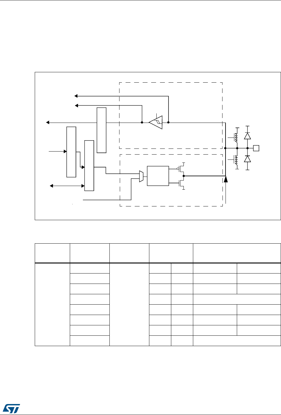
DocID018909 Rev 9 269/1718
RM0090 General-purpose I/Os (GPIO)
288
Each I/O port bit is freely programmable, however the I/O port registers have to be
accessed as 32-bit words, half-words or bytes. The purpose of the GPIOx_BSRR register is
to allow atomic read/modify accesses to any of the GPIO registers. In this way, there is no
risk of an IRQ occurring between the read and the modify access.
Figure 25 shows the basic structure of a 5 V tolerant I/O port bit. Table 39 gives the possible
port bit configurations.
Figure 25. Basic structure of a five-volt tolerant I/O port bit
1. VDD_FT is a potential specific to five-volt tolerant I/Os and different from VDD.
Table 35. Port bit configuration table(1)
MODER(i)
[1:0] OTYPER(i) OSPEEDR(i)
[B:A]
PUPDR(i)
[1:0] I/O configuration
01
0
SPEED
[B:A]
0 0 GP output PP
0 0 1 GP output PP + PU
0 1 0 GP output PP + PD
0 1 1 Reserved
1 0 0 GP output OD
1 0 1 GP output OD + PU
1 1 0 GP output OD + PD
1 1 1 Reserved (GP output OD)
!LTERNATEFUNCTIONOUTPUT
!LTERNATEFUNCTIONINPUT
0USHPULL
OPENDRAINOR
DISABLED
/UTPUTDATAREGISTER
2EADWRITE
&ROMONCHIP
PERIPHERAL
4OONCHIP
PERIPHERAL
/UTPUT
CONTROL
!NALOG
ONOFF 0ULL
0ULL
ONOFF
)/PIN
6$$
6$$
633
633
44,3CHMITT
TRIGGER
633
6$$?&4
0ROTECTION
DIODE
0ROTECTION
DIODE
ONOFF
)NPUTDRIVER
/UTPUTDRIVER
DOWN
UP
0-/3
.-/3
2EAD
"ITSETRESETREGISTERS
7RITE
!NALOG
)NPUTDATAREGISTER
AIB

General-purpose I/Os (GPIO) RM0090
270/1718 DocID018909 Rev 9
8.3.1 General-purpose I/O (GPIO)
During and just after reset, the alternate functions are not active and the I/O ports are
configured in input floating mode.
The debug pins are in AF pull-up/pull-down after reset:
•PA15: JTDI in pull-up
•PA14: JTCK/SWCLK in pull-down
•PA13: JTMS/SWDAT in pull-up
•PB4: NJTRST in pull-up
•PB3: JTDO in floating state
When the pin is configured as output, the value written to the output data register
(GPIOx_ODR) is output on the I/O pin. It is possible to use the output driver in push-pull
mode or open-drain mode (only the N-MOS is activated when 0 is output).
The input data register (GPIOx_IDR) captures the data present on the I/O pin at every AHB1
clock cycle.
All GPIO pins have weak internal pull-up and pull-down resistors, which can be activated or
not depending on the value in the GPIOx_PUPDR register.
10
0
SPEED
[B:A]
0 0 AF PP
0 0 1 AF PP + PU
0 1 0 AF PP + PD
0 1 1 Reserved
100AFOD
101AFOD + PU
110AFOD + PD
1 1 1 Reserved
00
x x x 0 0 Input Floating
x x x 0 1 Input PU
x x x 1 0 Input PD
x x x 1 1 Reserved (input floating)
11
x x x 0 0 Input/output Analog
xxx01
Reservedxxx10
xxx11
1. GP = general-purpose, PP = push-pull, PU = pull-up, PD = pull-down, OD = open-drain, AF = alternate
function.
Table 35. Port bit configuration table(1) (continued)
MODER(i)
[1:0] OTYPER(i) OSPEEDR(i)
[B:A]
PUPDR(i)
[1:0] I/O configuration

DocID018909 Rev 9 271/1718
RM0090 General-purpose I/Os (GPIO)
288
8.3.2 I/O pin multiplexer and mapping
The microcontroller I/O pins are connected to onboard peripherals/modules through a
multiplexer that allows only one peripheral’s alternate function (AF) connected to an I/O pin
at a time. In this way, there can be no conflict between peripherals sharing the same I/O pin.
Each I/O pin has a multiplexer with sixteen alternate function inputs (AF0 to AF15) that can
be configured through the GPIOx_AFRL (for pin 0 to 7) and GPIOx_AFRH (for pin 8 to 15)
registers:
•After reset all I/Os are connected to the system’s alternate function 0 (AF0)
•The peripherals’ alternate functions are mapped from AF1 to AF13
•Cortex®-M4 with FPU EVENTOUT is mapped on AF15
This structure is shown in Figure 26 below.
In addition to this flexible I/O multiplexing architecture, each peripheral has alternate
functions mapped onto different I/O pins to optimize the number of peripherals available in
smaller packages.
To use an I/O in a given configuration, proceed as follows:
•System function
Connect the I/O to AF0 and configure it depending on the function used:
– JTAG/SWD, after each device reset these pins are assigned as dedicated pins
immediately usable by the debugger host (not controlled by the GPIO controller)
– RTC_REFIN: this pin should be configured in Input floating mode
– MCO1 and MCO2: these pins have to be configured in alternate function mode.
Note: You can disable some or all of the JTAG/SWD pins and so release the associated pins for
GPIO usage.
For more details please refer to Section 7.2.10: Clock-out capability and Section 6.2.10:
Clock-out capability.

General-purpose I/Os (GPIO) RM0090
272/1718 DocID018909 Rev 9
•GPIO
Configure the desired I/O as output or input in the GPIOx_MODER register.
•Peripheral alternate function
For the ADC and DAC, configure the desired I/O as analog in the GPIOx_MODER
register.
For other peripherals:
– Configure the desired I/O as an alternate function in the GPIOx_MODER register
– Select the type, pull-up/pull-down and output speed via the GPIOx_OTYPER,
GPIOx_PUPDR and GPIOx_OSPEEDER registers, respectively
– Connect the I/O to the desired AFx in the GPIOx_AFRL or GPIOx_AFRH register
•EVENTOUT
Configure the I/O pin used to output the Cortex®-M4 with FPU EVENTOUT signal by
connecting it to AF15
Note: EVENTOUT is not mapped onto the following I/O pins: PC13, PC14, PC15, PH0, PH1 and
PI8.
Please refer to the “Alternate function mapping” table in the datasheets for the detailed
mapping of the system and peripherals’ alternate function I/O pins.
Table 36. Flexible SWJ-DP pin assignment
Available debug ports
SWJ I/O pin assigned
PA13 /
JTMS/
SWDIO
PA14 /
JTCK/
SWCLK
PA15 /
JTDI
PB3 /
JTDO
PB4/
NJTRST
Full SWJ (JTAG-DP + SW-DP) - Reset state X X X X X
Full SWJ (JTAG-DP + SW-DP) but without
NJTRST XXXX
JTAG-DP Disabled and SW-DP Enabled X X
JTAG-DP Disabled and SW-DP Disabled Released
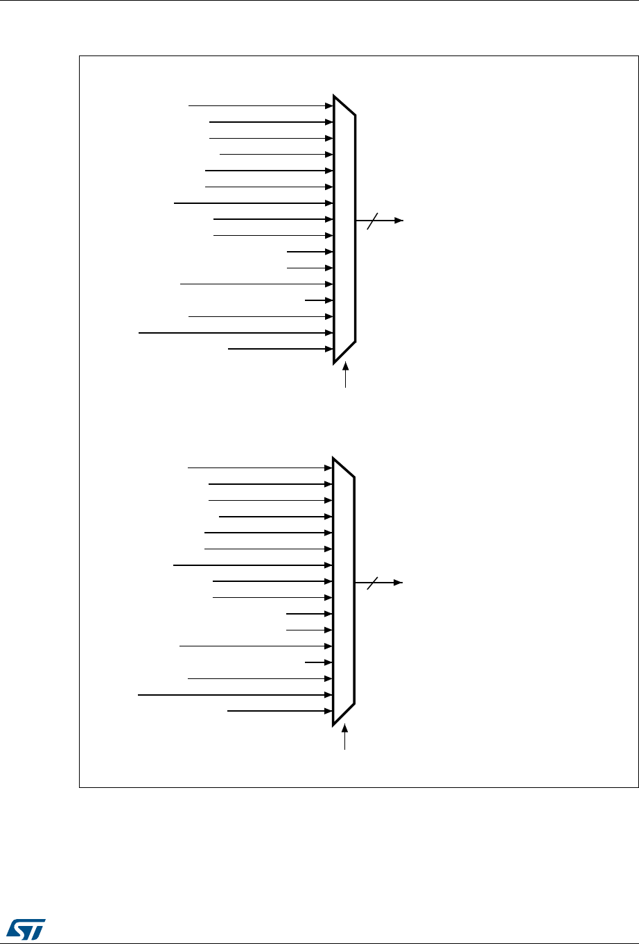
DocID018909 Rev 9 273/1718
RM0090 General-purpose I/Os (GPIO)
288
Figure 26. Selecting an alternate function on STM32F405xx/07xx and
STM32F415xx/17xx
1. Configured in FS.
DL
)RUSLQVWRWKH*3,2[B$)5/>@UHJLVWHUVHOHFWVWKHGHGLFDWHGDOWHUQDWHIXQFWLRQ
$)V\VWHP
$)7,07,0
$)7,0
$)7,0
$),&
$)63,63,
$)63,
$)86$57
$)86$57
$)&$1&$17,0
$)27*B)627*B+6
$)(7+
$))60&6',227*B+6
$)'&0,
$)
$)(9(17287
3LQ[[
$)5/>@
)RUSLQVWRWKH*3,2[B$)5+>@UHJLVWHUVHOHFWVWKHGHGLFDWHGDOWHUQDWHIXQFWLRQ
$)V\VWHP
$)7,07,0
$)7,0
$)7,0
$),&
$)63,63,
$)63,
$)86$57
$)86$57
$)&$1&$17,0
$)27*B)627*B+6
$)(7+
$))60&6',227*B+6
$)'&0,
$)
$)(9(17287
3LQ[[
$)5+>@
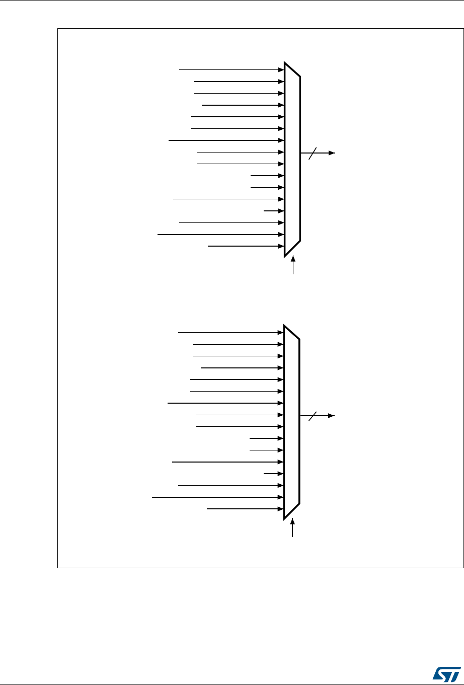
General-purpose I/Os (GPIO) RM0090
274/1718 DocID018909 Rev 9
Figure 27. Selecting an alternate function on STM32F42xxx and STM32F43xxx
1. Configured in FS.
-36
&ORPINSTOTHE'0)/X?!&2,;=REGISTERSELECTSTHEDEDICATEDALTERNATEFUNCTION
!&SYSTEM
!&4)-4)-
!&4)-
!&4)-
!&)#
!&30)
!&30)3!)
!&53!24
!&53!24
!&#!.#!.,4$#4)-
!&/4'?&3/4'?(3
!&%4(
!&&-#3$)//4'?(3
!&$#-)
!&,4$#
!&%6%.4/54
0INXX
!&2,;=
&ORPINSTOTHE'0)/X?!&2(;=REGISTERSELECTSTHEDEDICATEDALTERNATEFUNCTION
!&SYSTEM
!&4)-4)-
!&4)-
!&4)-
!&)#
!&30)
!&30)3!)
!&53!24
!&53!24
!&#!.#!.4)-
!&/4'?&3/4'?(3
!&%4(
!&&-#3$)//4'?(3
!&$#-)
!&,4$#
!&%6%.4/54
0INXX
!&2(;=

DocID018909 Rev 9 275/1718
RM0090 General-purpose I/Os (GPIO)
288
8.3.3 I/O port control registers
Each of the GPIOs has four 32-bit memory-mapped control registers (GPIOx_MODER,
GPIOx_OTYPER, GPIOx_OSPEEDR, GPIOx_PUPDR) to configure up to 16 I/Os.
The GPIOx_MODER register is used to select the I/O direction (input, output, AF, analog).
The GPIOx_OTYPER and GPIOx_OSPEEDR registers are used to select the output type
(push-pull or open-drain) and speed (the I/O speed pins are directly connected to the
corresponding GPIOx_OSPEEDR register bits whatever the I/O direction). The
GPIOx_PUPDR register is used to select the pull-up/pull-down whatever the I/O direction.
8.3.4 I/O port data registers
Each GPIO has two 16-bit memory-mapped data registers: input and output data registers
(GPIOx_IDR and GPIOx_ODR). GPIOx_ODR stores the data to be output, it is read/write
accessible. The data input through the I/O are stored into the input data register
(GPIOx_IDR), a read-only register.
See Section 8.4.5: GPIO port input data register (GPIOx_IDR) (x = A..I/J/K) and
Section 8.4.6: GPIO port output data register (GPIOx_ODR) (x = A..I/J/K) for the register
descriptions.
8.3.5 I/O data bitwise handling
The bit set reset register (GPIOx_BSRR) is a 32-bit register which allows the application to
set and reset each individual bit in the output data register (GPIOx_ODR). The bit set reset
register has twice the size of GPIOx_ODR.
To each bit in GPIOx_ODR, correspond two control bits in GPIOx_BSRR: BSRR(i) and
BSRR(i+SIZE). When written to 1, bit BSRR(i) sets the corresponding ODR(i) bit. When
written to 1, bit BSRR(i+SIZE) resets the ODR(i) corresponding bit.
Writing any bit to 0 in GPIOx_BSRR does not have any effect on the corresponding bit in
GPIOx_ODR. If there is an attempt to both set and reset a bit in GPIOx_BSRR, the set
action takes priority.
Using the GPIOx_BSRR register to change the values of individual bits in GPIOx_ODR is a
“one-shot” effect that does not lock the GPIOx_ODR bits. The GPIOx_ODR bits can always
be accessed directly. The GPIOx_BSRR register provides a way of performing atomic
bitwise handling.
There is no need for the software to disable interrupts when programming the GPIOx_ODR
at bit level: it is possible to modify one or more bits in a single atomic AHB1 write access.
8.3.6 GPIO locking mechanism
It is possible to freeze the GPIO control registers by applying a specific write sequence to
the GPIOx_LCKR register. The frozen registers are GPIOx_MODER, GPIOx_OTYPER,
GPIOx_OSPEEDR, GPIOx_PUPDR, GPIOx_AFRL and GPIOx_AFRH.
To write the GPIOx_LCKR register, a specific write / read sequence has to be applied. When
the right LOCK sequence is applied to bit 16 in this register, the value of LCKR[15:0] is used
to lock the configuration of the I/Os (during the write sequence the LCKR[15:0] value must
be the same). When the LOCK sequence has been applied to a port bit, the value of the port
bit can no longer be modified until the next reset. Each GPIOx_LCKR bit freezes the

General-purpose I/Os (GPIO) RM0090
276/1718 DocID018909 Rev 9
corresponding bit in the control registers (GPIOx_MODER, GPIOx_OTYPER,
GPIOx_OSPEEDR, GPIOx_PUPDR, GPIOx_AFRL and GPIOx_AFRH).
The LOCK sequence (refer to Section 8.4.8: GPIO port configuration lock register
(GPIOx_LCKR) (x = A..I/J/K)) can only be performed using a word (32-bit long) access to
the GPIOx_LCKR register due to the fact that GPIOx_LCKR bit 16 has to be set at the same
time as the [15:0] bits.
For more details please refer to LCKR register description in Section 8.4.8: GPIO port
configuration lock register (GPIOx_LCKR) (x = A..I/J/K).
8.3.7 I/O alternate function input/output
Two registers are provided to select one out of the sixteen alternate function inputs/outputs
available for each I/O. With these registers, you can connect an alternate function to some
other pin as required by your application.
This means that a number of possible peripheral functions are multiplexed on each GPIO
using the GPIOx_AFRL and GPIOx_AFRH alternate function registers. The application can
thus select any one of the possible functions for each I/O. The AF selection signal being
common to the alternate function input and alternate function output, a single channel is
selected for the alternate function input/output of one I/O.
To know which functions are multiplexed on each GPIO pin, refer to the datasheets.
Note: The application is allowed to select one of the possible peripheral functions for each I/O at a
time.
8.3.8 External interrupt/wakeup lines
All ports have external interrupt capability. To use external interrupt lines, the port must be
configured in input mode, refer to Section 12.2: External interrupt/event controller (EXTI)
and Section 12.2.3: Wakeup event management.
8.3.9 Input configuration
When the I/O port is programmed as Input:
•the output buffer is disabled
•the Schmitt trigger input is activated
•the pull-up and pull-down resistors are activated depending on the value in the
GPIOx_PUPDR register
•The data present on the I/O pin are sampled into the input data register every AHB1
clock cycle
•A read access to the input data register provides the I/O State
Figure 28 shows the input configuration of the I/O port bit.
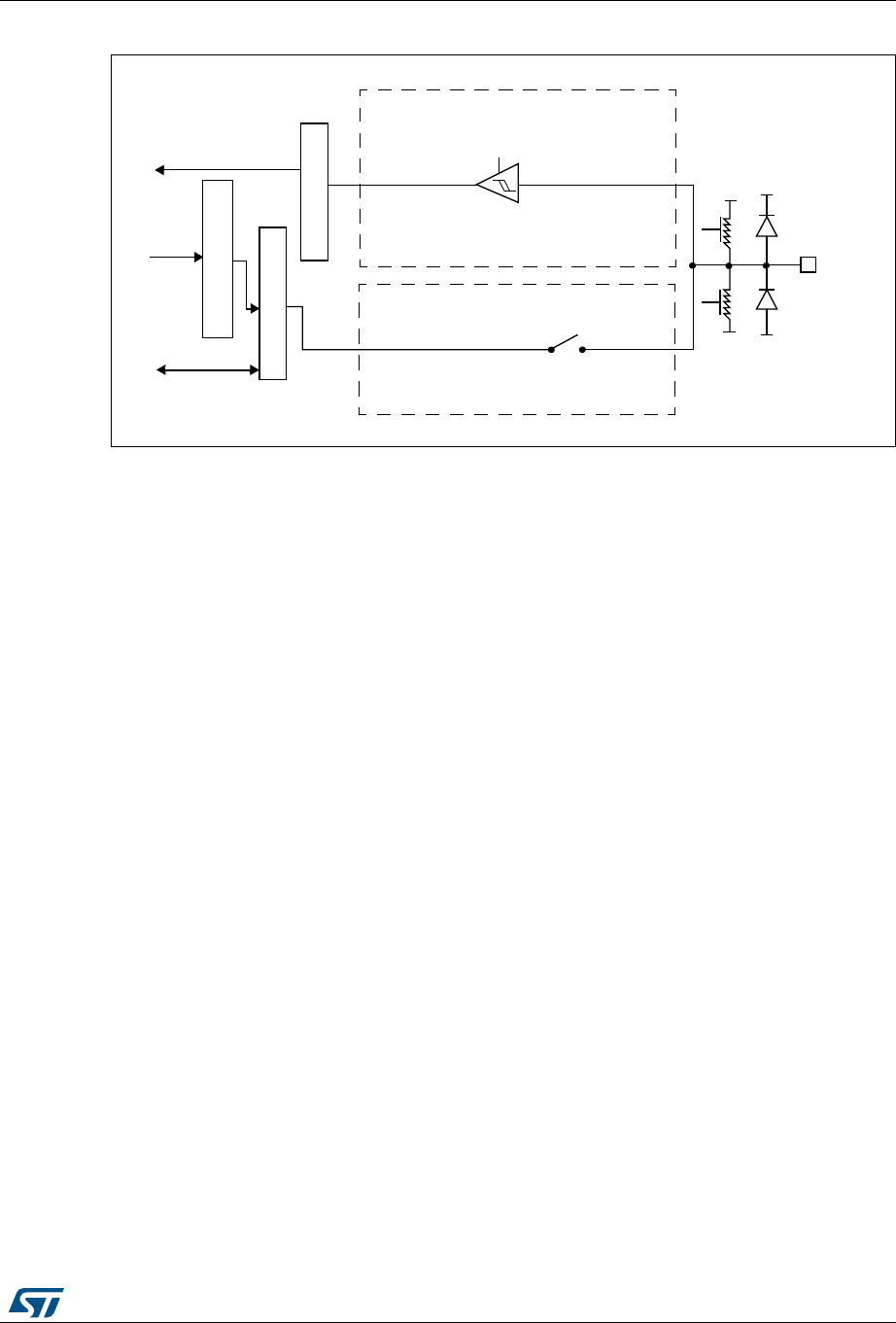
DocID018909 Rev 9 277/1718
RM0090 General-purpose I/Os (GPIO)
288
Figure 28. Input floating/pull up/pull down configurations
8.3.10 Output configuration
When the I/O port is programmed as output:
•The output buffer is enabled:
– Open drain mode: A “0” in the Output register activates the N-MOS whereas a “1”
in the Output register leaves the port in Hi-Z (the P-MOS is never activated)
– Push-pull mode: A “0” in the Output register activates the N-MOS whereas a “1” in
the Output register activates the P-MOS
•The Schmitt trigger input is activated
•The weak pull-up and pull-down resistors are activated or not depending on the value
in the GPIOx_PUPDR register
•The data present on the I/O pin are sampled into the input data register every AHB1
clock cycle
•A read access to the input data register gets the I/O state
•A read access to the output data register gets the last written value
Figure 29 shows the output configuration of the I/O port bit.
ONOFF
PULL
PULL
ONOFF )/PIN
6$$
633
44,3CHMITT
TRIGGER
633
6$$
PROTECTION
DIODE
PROTECTION
DIODE
ON
INPUTDRIVER
OUTPUTDRIVER
DOWN
UP
)NPUTDATAREGISTER
/UTPUTDATAREGISTER
2EADWRITE
2EAD
"ITSETRESETREGISTERS
7RITE
AIB
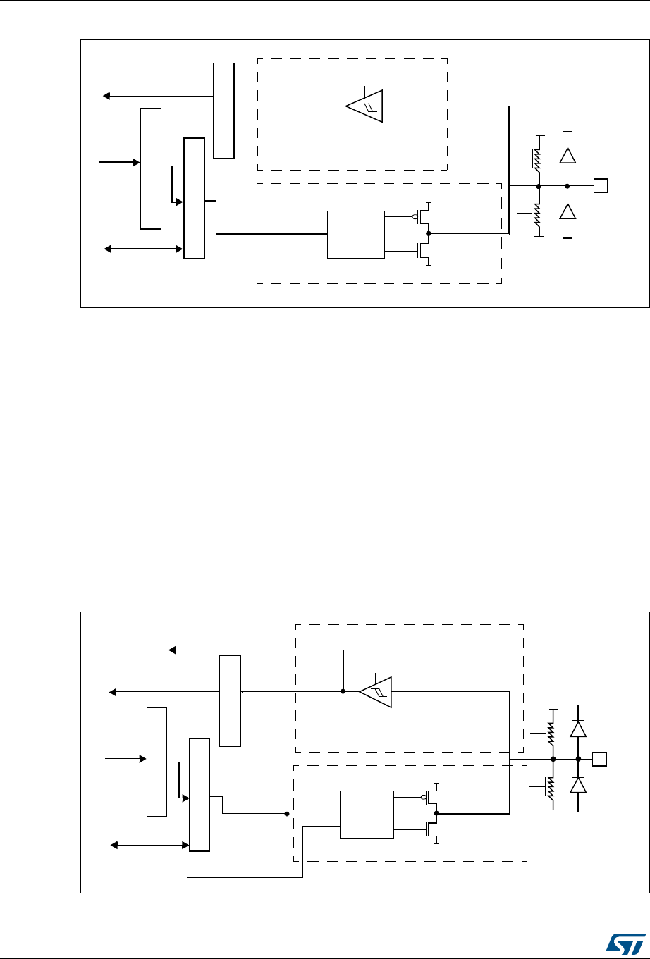
General-purpose I/Os (GPIO) RM0090
278/1718 DocID018909 Rev 9
Figure 29. Output configuration
8.3.11 Alternate function configuration
When the I/O port is programmed as alternate function:
•The output buffer can be configured as open-drain or push-pull
•The output buffer is driven by the signal coming from the peripheral (transmitter enable
and data)
•The Schmitt trigger input is activated
•The weak pull-up and pull-down resistors are activated or not depending on the value
in the GPIOx_PUPDR register
•The data present on the I/O pin are sampled into the input data register every AHB1
clock cycle
•A read access to the input data register gets the I/O state
Figure 30 shows the Alternate function configuration of the I/O port bit.
Figure 30. Alternate function configuration
0USHPULLOR
/PENDRAIN
/UTPUT
CONTROL
6
$$
6
33
44,3CHMITT
TRIGGER
ON
)NPUTDRIVER
/UTPUTDRIVER
0-/3
.-/3
)NPUTDATAREGISTER
/UTPUTDATAREGISTER
2EADWRITE
2EAD
"ITSETRESETREGISTERS
7RITE
ONOFF
PULL
PULL
ONOFF
6
$$
6
33
6
33
6
$$
PROTECTION
DIODE
PROTECTION
DIODE
DOWN
UP )/PIN
AIB
!LTERNATEFUNCTIONOUTPUT
!LTERNATEFUNCTIONINPUT
PUSHPULLOR
OPENDRAIN
&ROMONCHIP
PERIPHERAL
4OONCHIP
PERIPHERAL
/UTPUT
CONTROL
6$$
633
44,3CHMITT
TRIGGER
ON
)NPUTDRIVER
/UTPUTDRIVER
0-/3
.-/3
)NPUTDATAREGISTER
/UTPUTDATAREGISTER
2EADWRITE
2EAD
"ITSETRESETREGISTERS
7RITE
ONOFF
ONOFF
6$$
633 633
6$$
PROTECTION
DIODE
PROTECTION
DIODE
0ULL
0ULL
)/PIN
DOWN
UP
AIB
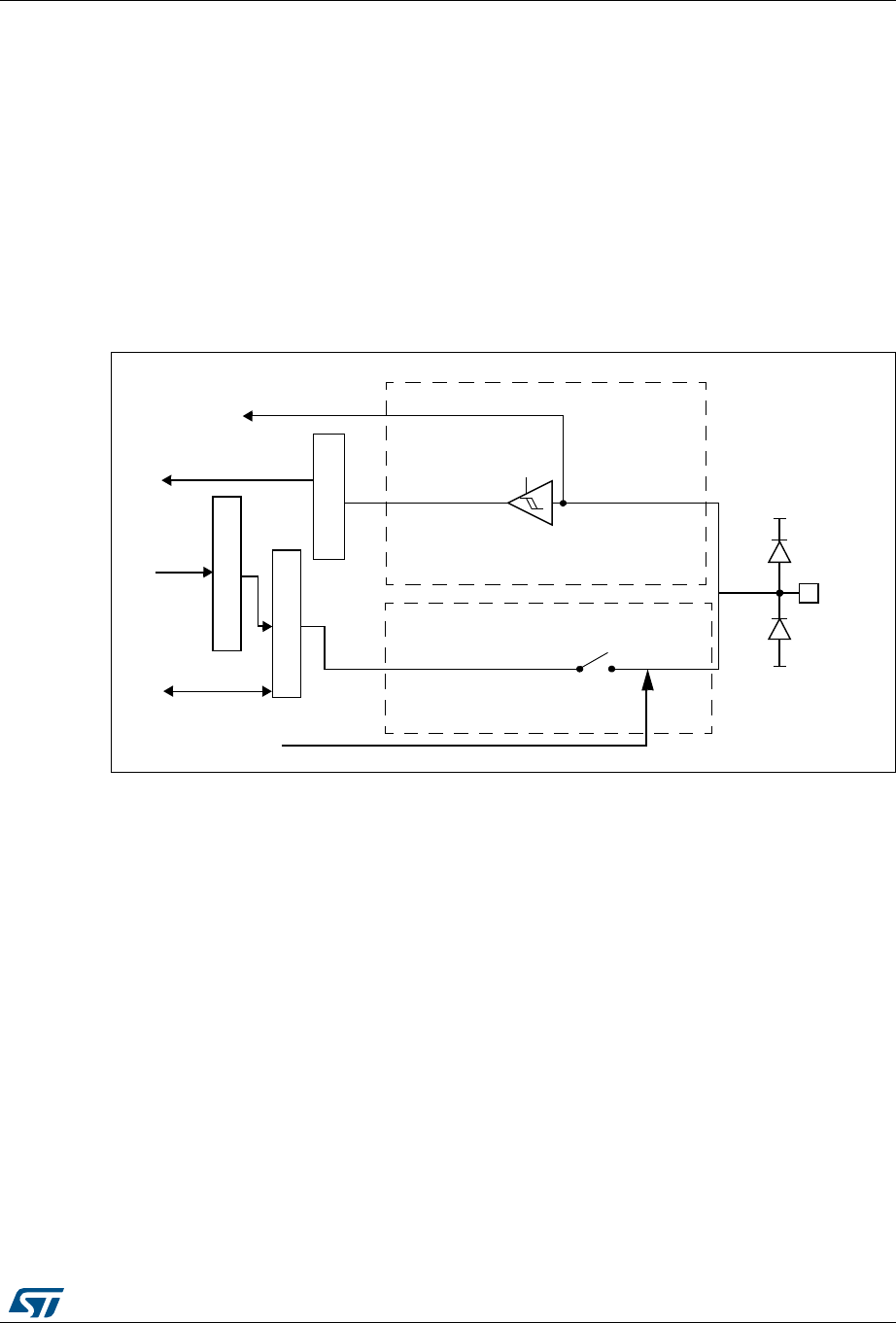
DocID018909 Rev 9 279/1718
RM0090 General-purpose I/Os (GPIO)
288
8.3.12 Analog configuration
When the I/O port is programmed as analog configuration:
•The output buffer is disabled
•The Schmitt trigger input is deactivated, providing zero consumption for every analog
value of the I/O pin. The output of the Schmitt trigger is forced to a constant value (0).
•The weak pull-up and pull-down resistors are disabled
•Read access to the input data register gets the value “0”
Note: In the analog configuration, the I/O pins cannot be 5 Volt tolerant.
Figure 31 shows the high-impedance, analog-input configuration of the I/O port bit.
Figure 31. High impedance-analog configuration
8.3.13 Using the OSC32_IN/OSC32_OUT pins as GPIO PC14/PC15
port pins
The LSE oscillator pins OSC32_IN and OSC32_OUT can be used as general-purpose
PC14 and PC15 I/Os, respectively, when the LSE oscillator is off. The PC14 and PC15 I/Os
are only configured as LSE oscillator pins OSC32_IN and OSC32_OUT when the LSE
oscillator is ON. This is done by setting the LSEON bit in the RCC_BDCR register. The LSE
has priority over the GPIO function.
Note: The PC14/PC15 GPIO functionality is lost when the 1.2 V domain is powered off (by the
device entering the standby mode) or when the backup domain is supplied by VBAT (VDD no
more supplied). In this case the I/Os are set in analog input mode.
8.3.14 Using the OSC_IN/OSC_OUT pins as GPIO PH0/PH1 port pins
The HSE oscillator pins OSC_IN/OSC_OUT can be used as general-purpose PH0/PH1
I/Os, respectively, when the HSE oscillator is OFF. (after reset, the HSE oscillator is off). The
PH0/PH1 I/Os are only configured as OSC_IN/OSC_OUT HSE oscillator pins when the
HSE oscillator is ON. This is done by setting the HSEON bit in the RCC_CR register. The
HSE has priority over the GPIO function.
&ROMONCHIP
PERIPHERAL
4OONCHIP
PERIPHERAL
!NALOG
TRIGGER
OFF
)NPUTDRIVER
)NPUTDATAREGISTER
/UTPUTDATAREGISTER
2EADWRITE
2EAD
"ITSETRESETREGISTERS
7RITE
!NALOG
6
33
6
$$
PROTECTION
DIODE
PROTECTION
DIODE
)/PIN
AI
44,3CHMITT

General-purpose I/Os (GPIO) RM0090
280/1718 DocID018909 Rev 9
8.3.15 Selection of RTC_AF1 and RTC_AF2 alternate functions
The STM32F4xx feature two GPIO pins RTC_AF1 and RTC_AF2 that can be used for the
detection of a tamper or time stamp event, or RTC_ALARM, or RTC_CALIB RTC outputs.
•The RTC_AF1 (PC13) can be used for the following purposes:
RTC_ALARM output: this output can be RTC Alarm A, RTC Alarm B or RTC Wakeup
depending on the OSEL[1:0] bits in the RTC_CR register
•RTC_CALIB output: this feature is enabled by setting the COE[23] in the RTC_CR
register
•RTC_TAMP1: tamper event detection
•RTC_TS: time stamp event detection
The RTC_AF2 (PI8) can be used for the following purposes:
•RTC_TAMP1: tamper event detection
•RTC_TAMP2: tamper event detection
•RTC_TS: time stamp event detection
The selection of the corresponding pin is performed through the RTC_TAFCR register as
follows:
•TAMP1INSEL is used to select which pin is used as the RTC_TAMP1 tamper input
•TSINSEL is used to select which pin is used as the RTC_TS time stamp input
•ALARMOUTTYPE is used to select whether the RTC_ALARM is output in push-pull or
open-drain mode
The output mechanism follows the priority order listed in Table 37 and Table 38.
Table 37. RTC_AF1 pin(1)
Pin
configuration
and function
RTC_ALARM
enabled
RTC_CALIB
enabled
Tamper
enabled
Time
stamp
enabled
TAMP1INSEL
TAMPER1
pin selection
TSINSEL
TIMESTAMP
pin
selection
ALARMOUTTYPE
RTC_ALARM
configuration
Alarm out
output OD 1Don’t care
Don’t
care
Don’t
care Don’t care Don’t care 0
Alarm out
output PP 1Don’t care
Don’t
care
Don’t
care Don’t care Don’t care 1
Calibration
out output PP 01
Don’t
care
Don’t
care Don’t care Don’t care Don’t care
TAMPER1
input floating 0 0 1 0 0 Don’t care Don’t care
TIMESTAMP
and
TAMPER1
input floating
0 0 1 1 0 0 Don’t care
TIMESTAMP
input floating 0 0 0 1 Don’t care 0 Don’t care
Standard
GPIO 0 0 0 0 Don’t care Don’t care Don’t care
1. OD: open drain; PP: push-pull.

DocID018909 Rev 9 281/1718
RM0090 General-purpose I/Os (GPIO)
288
8.4 GPIO registers
This section gives a detailed description of the GPIO registers.
For a summary of register bits, register address offsets and reset values, refer to Table 39 .
The GPIO registers can be accessed by byte (8 bits), half-words (16 bits) or words (32 bits).
8.4.1 GPIO port mode register (GPIOx_MODER) (x = A..I/J/K)
Address offset: 0x00
Reset values:
•0xA800 0000 for port A
•0x0000 0280 for port B
•0x0000 0000 for other ports
Table 38. RTC_AF2 pin
Pin configuration and function Tamper
enabled
Time
stamp
enabled
TAMP1INSEL
TAMPER1
pin selection
TSINSEL
TIMESTAMP
pin
selection
ALARMOUTTYPE
RTC_ALARM
configuration
TAMPER1 input floating 1 0 1 Don’t care Don’t care
TIMESTAMP and TAMPER1 input
floating 11 1 1 Don’t care
TIMESTAMP input floating 0 1 Don’t care 1 Don’t care
Standard GPIO 0 0 Don’t care Don’t care Don’t care
31 30 29 28 27 26 25 24 23 22 21 20 19 18 17 16
MODER15[1:0] MODER14[1:0] MODER13[1:0] MODER12[1:0] MODER11[1:0] MODER10[1:0] MODER9[1:0] MODER8[1:0]
rw rw rw rw rw rw rw rw rw rw rw rw rw rw rw rw
1514131211109876543210
MODER7[1:0] MODER6[1:0] MODER5[1:0] MODER4[1:0] MODER3[1:0] MODER2[1:0] MODER1[1:0] MODER0[1:0]
rw rw rw rw rw rw rw rw rw rw rw rw rw rw rw rw
Bits 2y:2y+1 MODERy[1:0]: Port x configuration bits (y = 0..15)
These bits are written by software to configure the I/O direction mode.
00: Input (reset state)
01: General purpose output mode
10: Alternate function mode
11: Analog mode
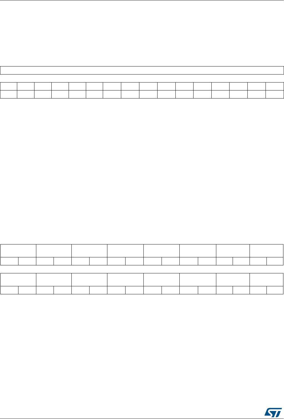
General-purpose I/Os (GPIO) RM0090
282/1718 DocID018909 Rev 9
8.4.2 GPIO port output type register (GPIOx_OTYPER)
(x = A..I/J/K)
Address offset: 0x04
Reset value: 0x0000 0000
8.4.3 GPIO port output speed register (GPIOx_OSPEEDR)
(x = A..I/J/K)
Address offset: 0x08
Reset values:
•0x0C00 0000 for port A
•0x0000 00C0 for port B
•0x0000 0000 for other ports
31 30 29 28 27 26 25 24 23 22 21 20 19 18 17 16
Reserved
1514131211109876543210
OT15 OT14 OT13 OT12 OT11 OT10 OT9 OT8 OT7 OT6 OT5 OT4 OT3 OT2 OT1 OT0
rw rw rw rw rw rw rw rw rw rw rw rw rw rw rw rw
Bits 31:16 Reserved, must be kept at reset value.
Bits 15:0 OTy: Port x configuration bits (y = 0..15)
These bits are written by software to configure the output type of the I/O port.
0: Output push-pull (reset state)
1: Output open-drain
31 30 29 28 27 26 25 24 23 22 21 20 19 18 17 16
OSPEEDR15
[1:0]
OSPEEDR14
[1:0]
OSPEEDR13
[1:0]
OSPEEDR12
[1:0]
OSPEEDR11
[1:0]
OSPEEDR10
[1:0]
OSPEEDR9
[1:0]
OSPEEDR8
[1:0]
rw rw rw rw rw rw rw rw rw rw rw rw rw rw rw rw
15 14 13 12 11 10 9 8 7 6 5 4 3 2 1 0
OSPEEDR7[1:0] OSPEEDR6[1:0] OSPEEDR5[1:0] OSPEEDR4[1:0] OSPEEDR3[1:0] OSPEEDR2[1:0] OSPEEDR1
[1:0]
OSPEEDR0
1:0]
rw rw rw rw rw rw rw rw rw rw rw rw rw rw rw rw
Bits 2y:2y+1 OSPEEDRy[1:0]: Port x configuration bits (y = 0..15)
These bits are written by software to configure the I/O output speed.
00: Low speed
01: Medium speed
10: Fast speed
11: High speed
Note: Refer to the product datasheets for the values of OSPEEDRy bits versus VDD
range and external load.

DocID018909 Rev 9 283/1718
RM0090 General-purpose I/Os (GPIO)
288
8.4.4 GPIO port pull-up/pull-down register (GPIOx_PUPDR)
(x = A..I/J/K)
Address offset: 0x0C
Reset values:
•0x6400 0000 for port A
•0x0000 0100 for port B
•0x0000 0000 for other ports
8.4.5 GPIO port input data register (GPIOx_IDR) (x = A..I/J/K)
Address offset: 0x10
Reset value: 0x0000 XXXX (where X means undefined)
31 30 29 28 27 26 25 24 23 22 21 20 19 18 17 16
PUPDR15[1:0] PUPDR14[1:0] PUPDR13[1:0] PUPDR12[1:0] PUPDR11[1:0] PUPDR10[1:0] PUPDR9[1:0] PUPDR8[1:0]
rw rw rw rw rw rw rw rw rw rw rw rw rw rw rw rw
1514131211109876543210
PUPDR7[1:0] PUPDR6[1:0] PUPDR5[1:0] PUPDR4[1:0] PUPDR3[1:0] PUPDR2[1:0] PUPDR1[1:0] PUPDR0[1:0]
rw rw rw rw rw rw rw rw rw rw rw rw rw rw rw rw
Bits 2y:2y+1 PUPDRy[1:0]: Port x configuration bits (y = 0..15)
These bits are written by software to configure the I/O pull-up or pull-down
00: No pull-up, pull-down
01: Pull-up
10: Pull-down
11: Reserved
31 30 29 28 27 26 25 24 23 22 21 20 19 18 17 16
Reserved
1514131211109876543210
IDR15 IDR14 IDR13 IDR12 IDR11 IDR10 IDR9 IDR8 IDR7 IDR6 IDR5 IDR4 IDR3 IDR2 IDR1 IDR0
rrrrrr r r r r rrrrrr
Bits 31:16 Reserved, must be kept at reset value.
Bits 15:0 IDRy: Port input data (y = 0..15)
These bits are read-only and can be accessed in word mode only. They contain the input
value of the corresponding I/O port.

General-purpose I/Os (GPIO) RM0090
284/1718 DocID018909 Rev 9
8.4.6 GPIO port output data register (GPIOx_ODR) (x = A..I/J/K)
Address offset: 0x14
Reset value: 0x0000 0000
8.4.7 GPIO port bit set/reset register (GPIOx_BSRR) (x = A..I/J/K)
Address offset: 0x18
Reset value: 0x0000 0000
31 30 29 28 27 26 25 24 23 22 21 20 19 18 17 16
Reserved
1514131211109876543210
ODR15 ODR14 ODR13 ODR12 ODR11 ODR10 ODR9 ODR8 ODR7 ODR6 ODR5 ODR4 ODR3 ODR2 ODR1 ODR0
rw rw rw rw rw rw rw rw rw rw rw rw rw rw rw rw
Bits 31:16 Reserved, must be kept at reset value.
Bits 15:0 ODRy: Port output data (y = 0..15)
These bits can be read and written by software.
Note: For atomic bit set/reset, the ODR bits can be individually set and reset by writing to the
GPIOx_BSRR register (x = A..I/J/K).
31 30 29 28 27 26 25 24 23 22 21 20 19 18 17 16
BR15 BR14 BR13 BR12 BR11 BR10 BR9 BR8 BR7 BR6 BR5 BR4 BR3 BR2 BR1 BR0
wwwwwwwwwwwwwwww
1514131211109876543210
BS15 BS14 BS13 BS12 BS11 BS10 BS9 BS8 BS7 BS6 BS5 BS4 BS3 BS2 BS1 BS0
wwwwwwwwwwwwwwww
Bits 31:16 BRy: Port x reset bit y (y = 0..15)
These bits are write-only and can be accessed in word, half-word or byte mode. A read to
these bits returns the value 0x0000.
0: No action on the corresponding ODRx bit
1: Resets the corresponding ODRx bit
Note: If both BSx and BRx are set, BSx has priority.
Bits 15:0 BSy: Port x set bit y (y= 0..15)
These bits are write-only and can be accessed in word, half-word or byte mode. A read to
these bits returns the value 0x0000.
0: No action on the corresponding ODRx bit
1: Sets the corresponding ODRx bit

DocID018909 Rev 9 285/1718
RM0090 General-purpose I/Os (GPIO)
288
8.4.8 GPIO port configuration lock register (GPIOx_LCKR)
(x = A..I/J/K)
This register is used to lock the configuration of the port bits when a correct write sequence
is applied to bit 16 (LCKK). The value of bits [15:0] is used to lock the configuration of the
GPIO. During the write sequence, the value of LCKR[15:0] must not change. When the
LOCK sequence has been applied on a port bit, the value of this port bit can no longer be
modified until the next reset.
Note: A specific write sequence is used to write to the GPIOx_LCKR register. Only word access
(32-bit long) is allowed during this write sequence.
Each lock bit freezes a specific configuration register (control and alternate function
registers).
Address offset: 0x1C
Reset value: 0x0000 0000
Access: 32-bit word only, read/write register
31 30 29 28 27 26 25 24 23 22 21 20 19 18 17 16
Reserved
LCKK
rw
15 14 13 12 11 10 9 8 7 6 5 4 3 2 1 0
LCK15 LCK14 LCK13 LCK12 LCK11 LCK10 LCK9 LCK8 LCK7 LCK6 LCK5 LCK4 LCK3 LCK2 LCK1 LCK0
rw rw rw rw rw rw rw rw rw rw rw rw rw rw rw rw
Bits 31:17 Reserved, must be kept at reset value.
Bit 16 LCKK[16]: Lock key
This bit can be read any time. It can only be modified using the lock key write sequence.
0: Port configuration lock key not active
1: Port configuration lock key active. The GPIOx_LCKR register is locked until an MCU reset
occurs.
LOCK key write sequence:
WR LCKR[16] = ‘1’ + LCKR[15:0]
WR LCKR[16] = ‘0’ + LCKR[15:0]
WR LCKR[16] = ‘1’ + LCKR[15:0]
RD LCKR
RD LCKR[16] = ‘1’ (this read operation is optional but it confirms that the lock is active)
Note: During the LOCK key write sequence, the value of LCK[15:0] must not change.
Any error in the lock sequence aborts the lock.
After the first lock sequence on any bit of the port, any read access on the LCKK bit will
return ‘1’ until the next CPU reset.
Bits 15:0 LCKy: Port x lock bit y (y= 0..15)
These bits are read/write but can only be written when the LCKK bit is ‘0.
0: Port configuration not locked
1: Port configuration locked

General-purpose I/Os (GPIO) RM0090
286/1718 DocID018909 Rev 9
8.4.9 GPIO alternate function low register (GPIOx_AFRL) (x = A..I/J/K)
Address offset: 0x20
Reset value: 0x0000 0000
8.4.10 GPIO alternate function high register (GPIOx_AFRH)
(x = A..I/J)
Address offset: 0x24
Reset value: 0x0000 0000
31 30 29 28 27 26 25 24 23 22 21 20 19 18 17 16
AFRL7[3:0] AFRL6[3:0] AFRL5[3:0] AFRL4[3:0]
rw rw rw rw rw rw rw rw rw rw rw rw rw rw rw rw
1514131211109876543210
AFRL3[3:0] AFRL2[3:0] AFRL1[3:0] AFRL0[3:0]
rw rw rw rw rw rw rw rw rw rw rw rw rw rw rw rw
Bits 31:0 AFRLy: Alternate function selection for port x bit y (y = 0..7)
These bits are written by software to configure alternate function I/Os
AFRLy selection:
0000: AF0
0001: AF1
0010: AF2
0011: AF3
0100: AF4
0101: AF5
0110: AF6
0111: AF7
1000: AF8
1001: AF9
1010: AF10
1011: AF11
1100: AF12
1101: AF13
1110: AF14
1111: AF15
31 30 29 28 27 26 25 24 23 22 21 20 19 18 17 16
AFRH15[3:0] AFRH14[3:0] AFRH13[3:0] AFRH12[3:0]
rw rw rw rw rw rw rw rw rw rw rw rw rw rw rw rw
1514131211109876543210
AFRH11[3:0] AFRH10[3:0] AFRH9[3:0] AFRH8[3:0]
rw rw rw rw rw rw rw rw rw rw rw rw rw rw rw rw
Bits 31:0 AFRHy: Alternate function selection for port x bit y (y = 8..15)
These bits are written by software to configure alternate function I/Os
AFRHy selection:
0000: AF0
0001: AF1
0010: AF2
0011: AF3
0100: AF4
0101: AF5
0110: AF6
0111: AF7
1000: AF8
1001: AF9
1010: AF10
1011: AF11
1100: AF12
1101: AF13
1110: AF14
1111: AF15
DocID018909 Rev 9 287/1718
RM0090 General-purpose I/Os (GPIO)
288
8.4.11 GPIO register map
The following table gives the GPIO register map and the reset values.
Table 39. GPIO register map and reset values
Offset Register
31
30
29
28
27
26
25
24
23
22
21
20
19
18
17
16
15
14
13
12
11
10
9
8
7
6
5
4
3
2
1
0
0x00
GPIOA_
MODER
MODER15[1:0]
MODER14[1:0]
MODER13[1:0]
MODER12[1:0]
MODER11[1:0]
MODER10[1:0]
MODER9[1:0]
MODER8[1:0]
MODER7[1:0]
MODER6[1:0]
MODER5[1:0]
MODER4[1:0]
MODER3[1:0]
MODER2[1:0]
MODER1[1:0]
MODER0[1:0]
Reset value 10101000000000000000000000000000
0x00
GPIOB_
MODER
MODER15[1:0]
MODER14[1:0]
MODER13[1:0]
MODER12[1:0]
MODER11[1:0]
MODER10[1:0]
MODER9[1:0]
MODER8[1:0]
MODER7[1:0]
MODER6[1:0]
MODER5[1:0]
MODER4[1:0]
MODER3[1:0]
MODER2[1:0]
MODER1[1:0]
MODER0[1:0]
Reset value 00000000000000000000001010000000
0x00
GPIOx_MODER
(where x =
C..I/J/K)
MODER15[1:0]
MODER14[1:0]
MODER13[1:0]
MODER12[1:0]
MODER11[1:0]
MODER10[1:0]
MODER9[1:0]
MODER8[1:0]
MODER7[1:0]
MODER6[1:0]
MODER5[1:0]
MODER4[1:0]
MODER3[1:0]
MODER2[1:0]
MODER1[1:0]
MODER0[1:0]
Reset value 00000000000000000000000000000000
0x04
GPIOx_
OTYPER
(where x =
A..I/J/K)
Reserved
OT15
OT14
OT13
OT12
OT11
OT10
OT9
OT8
OT7
OT6
OT5
OT4
OT3
OT2
OT1
OT0
Reset value 0000000000000000
0x08
GPIOx_
OSPEEDER
(where x =
A..I/J/K except
B)
OSPEEDR15[1:0]
OSPEEDR14[1:0]
OSPEEDR13[1:0]
OSPEEDR12[1:0]
OSPEEDR11[1:0]
OSPEEDR10[1:0]
OSPEEDR9[1:0]
OSPEEDR8[1:0]
OSPEEDR7[1:0]
OSPEEDR6[1:0]
OSPEEDR5[1:0]
OSPEEDR4[1:0]
OSPEEDR3[1:0]
OSPEEDR2[1:0]
OSPEEDR1[1:0]
OSPEEDR0[1:0]
Reset value 00000000000000000000000000000000
0x08
GPIOB_
OSPEEDER
OSPEEDR15[1:0]
OSPEEDR14[1:0]
OSPEEDR13[1:0]
OSPEEDR12[1:0]
OSPEEDR11[1:0]
OSPEEDR10[1:0]
OSPEEDR9[1:0]
OSPEEDR8[1:0]
OSPEEDR7[1:0]
OSPEEDR6[1:0]
OSPEEDR5[1:0]
OSPEEDR4[1:0]
OSPEEDR3[1:0]
OSPEEDR2[1:0]
OSPEEDR1[1:0]
OSPEEDR0[1:0]
Reset value 00000000000000000000000011000000
0x0C GPIOA_PUPDR
PUPDR15[1:0]
PUPDR14[1:0]
PUPDR13[1:0]
PUPDR12[1:0]
PUPDR11[1:0]
PUPDR10[1:0]
PUPDR9[1:0]
PUPDR8[1:0]
PUPDR7[1:0]
PUPDR6[1:0]
PUPDR5[1:0]
PUPDR4[1:0]
PUPDR3[1:0]
PUPDR2[1:0]
PUPDR1[1:0]
PUPDR0[1:0]
Reset value 01100100000000000000000000000000
0x0C GPIOB_PUPDR
PUPDR15[1:0]
PUPDR14[1:0]
PUPDR13[1:0]
PUPDR12[1:0]
PUPDR11[1:0]
PUPDR10[1:0]
PUPDR9[1:0]
PUPDR8[1:0]
PUPDR7[1:0]
PUPDR6[1:0]
PUPDR5[1:0]
PUPDR4[1:0]
PUPDR3[1:0]
PUPDR2[1:0]
PUPDR1[1:0]
PUPDR0[1:0]
Reset value 00000000000000000000000100000000
General-purpose I/Os (GPIO) RM0090
288/1718 DocID018909 Rev 9
Refer to Table 1 on page 64 for the register boundary addresses.
0x0C
GPIOx_PUPDR
(where x =
C..I/J/K)
PUPDR15[1:0]
PUPDR14[1:0]
PUPDR13[1:0]
PUPDR12[1:0]
PUPDR11[1:0]
PUPDR10[1:0]
PUPDR9[1:0]
PUPDR8[1:0]
PUPDR7[1:0]
PUPDR6[1:0]
PUPDR5[1:0]
PUPDR4[1:0]
PUPDR3[1:0]
PUPDR2[1:0]
PUPDR1[1:0]
PUPDR0[1:0]
Reset value 00000000000000000000000000000000
0x10
GPIOx_IDR
(where x =
A..I/J/K) Reserved
IDR15
IDR14
IDR13
IDR12
IDR11
IDR10
IDR9
IDR8
IDR7
IDR6
IDR5
IDR4
IDR3
IDR2
IDR1
IDR0
Reset value xxxxxxxxxxxxxxxx
0x14
GPIOx_ODR
(where x =
A..I/J/K) Reserved
ODR15
ODR14
ODR13
ODR12
ODR11
ODR10
ODR9
ODR8
ODR7
ODR6
ODR5
ODR4
ODR3
ODR2
ODR1
ODR0
Reset value 0000000000000000
0x18
GPIOx_BSRR
(where x =
A..I/J/K)
BR15
BR14
BR13
BR12
BR11
BR10
BR9
BR8
BR7
BR6
BR5
BR4
BR3
BR2
BR1
BR0
BS15
BS14
BS13
BS12
BS11
BS10
BS9
BS8
BS7
BS6
BS5
BS4
BS3
BS2
BS1
BS0
Reset value 00000000000000000000000000000000
0x1C
GPIOx_LCKR
(where x =
A..I/J/K) Reserved
LCKK
LCK15
LCK14
LCK13
LCK12
LCK11
LCK10
LCK9
LCK8
LCK7
LCK6
LCK5
LCK4
LCK3
LCK2
LCK1
LCK0
Reset value 00000000000000000
0x20
GPIOx_AFRL
(where x =
A..I/J/K)
AFRL7[3:0] AFRL6[3:0] AFRL5[3:0] AFRL4[3:0] AFRL3[3:0] AFRL2[3:0] AFRL1[3:0] AFRL0[3:0]
Reset value 00000000000000000000000000000000
0x24
GPIOx_AFRH
(where x =
A..I/J)
AFRH15[3:0] AFRH14[3:0] AFRH13[3:0] AFRH12[3:0] AFRH11[3:0] AFRH10[3:0] AFRH9[3:0] AFRH8[3:0]
Reset value 00000000000000000000000000000000
Table 39. GPIO register map and reset values (continued)
Offset Register
31
30
29
28
27
26
25
24
23
22
21
20
19
18
17
16
15
14
13
12
11
10
9
8
7
6
5
4
3
2
1
0

DocID018909 Rev 9 289/1718
RM0090 System configuration controller (SYSCFG)
301
9 System configuration controller (SYSCFG)
The system configuration controller is mainly used to remap the memory accessible in the
code area, select the Ethernet PHY interface and manage the external interrupt line
connection to the GPIOs.
This section applies to the whole STM32F4xx family, unless otherwise specified.
9.1 I/O compensation cell
By default the I/O compensation cell is not used. However when the I/O output buffer speed
is configured in 50 MHz or 100 MHz mode, it is recommended to use the compensation cell
for slew rate control on I/O tf(IO)out)/tr(IO)out commutation to reduce the I/O noise on power
supply.
When the compensation cell is enabled, a READY flag is set to indicate that the
compensation cell is ready and can be used. The I/O compensation cell can be used only
when the supply voltage ranges from 2.4 to 3.6 V.
9.2 SYSCFG registers for STM32F405xx/07xx and
STM32F415xx/17xx
9.2.1 SYSCFG memory remap register (SYSCFG_MEMRMP)
This register is used for specific configurations on memory remap:
•Two bits are used to configure the type of memory accessible at address 0x0000 0000.
These bits are used to select the physical remap by software and so, bypass the BOOT
pins.
•After reset these bits take the value selected by the BOOT pins. When booting from
main Flash memory with BOOT pins set to 10 [(BOOT1,BOOT0) = (1,0)] this register
takes the value 0x00.
When the FSMC is remapped at address 0x0000 0000, only the first two regions of Bank 1
memory controller (Bank1 NOR/PSRAM 1 and NOR/PSRAM 2) can be remapped. In remap
mode, the CPU can access the external memory via ICode bus instead of System bus
which boosts up the performance.
Address offset: 0x00
Reset value: 0x0000 000X (X is the memory mode selected by the BOOT pins)
)
31 30 29 28 27 26 25 24 23 22 21 20 19 18 17 16
Reserved
1514131211109876543210
Reserved
MEM_MODE
rw rw

System configuration controller (SYSCFG) RM0090
290/1718 DocID018909 Rev 9
9.2.2 SYSCFG peripheral mode configuration register (SYSCFG_PMC)
Address offset: 0x04
Reset value: 0x0000 0000
9.2.3 SYSCFG external interrupt configuration register 1
(SYSCFG_EXTICR1)
Address offset: 0x08
Reset value: 0x0000 0000
Bits 31:2 Reserved, must be kept at reset value.
Bits 1:0 MEM_MODE: Memory mapping selection
Set and cleared by software. This bit controls the memory internal mapping at
address 0x0000 0000. After reset these bits take the value selected by the Boot
pins (except for FSMC).
00: Main Flash memory mapped at 0x0000 0000
01: System Flash memory mapped at 0x0000 0000
10: FSMC Bank1 (NOR/PSRAM 1 and 2) mapped at 0x0000 0000
11: Embedded SRAM (SRAM1) mapped at 0x0000 0000
Note: Refer to Section 2.3: Memory map for details about the memory mapping at
address 0x0000 0000.
31 30 29 28 27 26 25 24 23 22 21 20 19 18 17 16
Reserved
MII_RMII
_SEL Reserved
rw
15 14 13 12 11 10 9 8 7 6 5 4 3 2 1 0
Reserved
Bits 31:24 Reserved, must be kept at reset value.
Bit 23 MII_RMII_SEL: Ethernet PHY interface selection
Set and Cleared by software.These bits control the PHY interface for the
Ethernet MAC.
0: MII interface is selected
1: RMII PHY interface is selected
Note: This configuration must be done while the MAC is under reset and before
enabling the MAC clocks.
Bits 22:0 Reserved, must be kept at reset value.
31 30 29 28 27 26 25 24 23 22 21 20 19 18 17 16
Reserved
1514131211109876543210
EXTI3[3:0] EXTI2[3:0] EXTI1[3:0] EXTI0[3:0]
rw rw rw rw rw rw rw rw rw rw rw rw rw rw rw rw

DocID018909 Rev 9 291/1718
RM0090 System configuration controller (SYSCFG)
301
9.2.4 SYSCFG external interrupt configuration register 2
(SYSCFG_EXTICR2)
Address offset: 0x0C
Reset value: 0x0000 0000
Bits 31:16 Reserved, must be kept at reset value.
Bits 15:0 EXTIx[3:0]: EXTI x configuration (x = 0 to 3)
These bits are written by software to select the source input for the EXTIx
external interrupt.
0000: PA[x] pin
0001: PB[x] pin
0010: PC[x] pin
0011: PD[x] pin
0100: PE[x] pin
0101: PF[x] pin
0110: PG[x] pin
0111: PH[x] pin
1000: PI[x] pin
31 30 29 28 27 26 25 24 23 22 21 20 19 18 17 16
Reserved
1514131211109876543210
EXTI7[3:0] EXTI6[3:0] EXTI5[3:0] EXTI4[3:0]
rw rw rw rw rw rw rw rw rw rw rw rw rw rw rw rw
Bits 31:16 Reserved, must be kept at reset value.
Bits 15:0 EXTIx[3:0]: EXTI x configuration (x = 4 to 7)
These bits are written by software to select the source input for the EXTIx
external interrupt.
0000: PA[x] pin
0001: PB[x] pin
0010: PC[x] pin
0011: PD[x] pin
0100: PE[x] pin
0101: PF[x] pin
0110: PG[x] pin
0111: PH[x] pin
1000: PI[x] pin
System configuration controller (SYSCFG) RM0090
292/1718 DocID018909 Rev 9
9.2.5 SYSCFG external interrupt configuration register 3
(SYSCFG_EXTICR3)
Address offset: 0x10
Reset value: 0x0000 0000
9.2.6 SYSCFG external interrupt configuration register 4
(SYSCFG_EXTICR4)
Address offset: 0x14
Reset value: 0x0000 0000
31 30 29 28 27 26 25 24 23 22 21 20 19 18 17 16
Reserved
1514131211109876543210
EXTI11[3:0] EXTI10[3:0] EXTI9[3:0] EXTI8[3:0]
rw rw rw rw rw rw rw rw rw rw rw rw rw rw rw rw
Bits 31:16 Reserved, must be kept at reset value.
Bits 15:0 EXTIx[3:0]: EXTI x configuration (x = 8 to 11)
These bits are written by software to select the source input for the EXTIx external
interrupt.
0000: PA[x] pin
0001: PB[x] pin
0010: PC[x] pin
0011: PD[x] pin
0100: PE[x] pin
0101: PF[x] pin
0110: PG[x] pin
0111: PH[x] pin
1000: PI[x] pin
31 30 29 28 27 26 25 24 23 22 21 20 19 18 17 16
Reserved
1514131211109876543210
EXTI15[3:0] EXTI14[3:0] EXTI13[3:0] EXTI12[3:0]
rw rw rw rw rw rw rw rw rw rw rw rw rw rw rw rw

DocID018909 Rev 9 293/1718
RM0090 System configuration controller (SYSCFG)
301
9.2.7 Compensation cell control register (SYSCFG_CMPCR)
Address offset: 0x20
Reset value: 0x0000 0000
Bits 31:16 Reserved, must be kept at reset value.
Bits 15:0 EXTIx[3:0]: EXTI x configuration (x = 12 to 15)
These bits are written by software to select the source input for the EXTIx external
interrupt.
0000: PA[x] pin
0001: PB[x] pin
0010: PC[x] pin
0011: PD[x] pin
0100: PE[x] pin
0101: PF[x] pin
0110: PG[x] pin
0111: PH[x] pin
Note: PI[15:12] are not used.
31 30 29 28 27 26 25 24 23 22 21 20 19 18 17 16
Reserved
1514131211109 8 7 654321 0
Reserved
READY
Reserved CMP_PD
rrw
Bits 31:9 Reserved, must be kept at reset value.
Bit 8 READY: Compensation cell ready flag
0: I/O compensation cell not ready
1: O compensation cell ready
Bits 7:2 Reserved, must be kept at reset value.
Bit 0 CMP_PD: Compensation cell power-down
0: I/O compensation cell power-down mode
1: I/O compensation cell enabled
System configuration controller (SYSCFG) RM0090
294/1718 DocID018909 Rev 9
9.2.8 SYSCFG register maps for
STM32F405xx/07xx and STM32F415xx/17xx
The following table gives the SYSCFG register map and the reset values.
Refer to Table 1 on page 64 for the register boundary addresses.
9.3 SYSCFG registers for STM32F42xxx and STM32F43xxx
9.3.1 SYSCFG memory remap register (SYSCFG_MEMRMP)
This register is used for specific configurations on memory remap:
•Three bits are used to configure the type of memory accessible at address
0x0000 0000. These bits are used to select the physical remap by software and so,
bypass the BOOT pins.
•After reset these bits take the value selected by the BOOT pins. When booting from
main Flash memory with BOOT pins set to 10 [(BOOT1,BOOT0) = (1,0)] this register
takes the value 0x00.
•Other bits are used to swap FMC SDRAM Bank 1/2 with FMC Bank 3/4 and configure
the Flash Bank 1/2 mapping
Table 40. SYSCFG register map and reset values (STM32F405xx/07xx and STM32F415xx/17xx)
Offset Register
31
30
29
28
27
26
25
24
23
22
21
20
19
18
17
16
15
14
13
12
11
10
9
8
7
6
5
4
3
2
1
0
0x00
SYSCFG_
MEMRMP Reserved
MEM_MODE
Reset value xx
0x04 SYSCFG_PMC Reserved
MII_RMII_SEL
Reserved Reserved
Reset value 0
0x08 SYSCFG_EXTICR1 Reserved EXTI3[3:0] EXTI2[3:0] EXTI1[3:0] EXTI0[3:0]
Reset value 0000000000000000
0x0C SYSCFG_EXTICR2 Reserved EXTI7[3:0] EXTI6[3:0] EXTI5[3:0] EXTI4[3:0]
Reset value 0000000000000000
0x10 SYSCFG_EXTICR3 Reserved EXTI11[3:0] EXTI10[3:0] EXTI9[3:0] EXTI8[3:0]
Reset value 0000000000000000
0x14 SYSCFG_EXTICR4 Reserved EXTI15[3:0] EXTI14[3:0] EXTI13[3:0] EXTI12[3:0]
Reset value 0000000000000000
0x20 SYSCFG_CMPCR Reserved
READY
Reserved
CMP_PD
Reset value 00

DocID018909 Rev 9 295/1718
RM0090 System configuration controller (SYSCFG)
301
There are two possible FMC remap at address 0x0000 0000:
•FMC Bank 1 (NOR/PSRAM 1 and 2) remap:
Only the first two regions of Bank 1 memory controller (Bank1 NOR/PSRAM 1 and
NOR/PSRAM 2) can be remapped.
•FMC SDRAM Bank 1 remap.
In remap mode at address 0x0000 0000, the CPU can access the external memory via
ICode bus instead of System bus which boosts up the performance.
Address offset: 0x00
Reset value: 0x0000 000X (X is the memory mode selected by the BOOT pins)
Note: Booting from NOR Flash memory or SDRAM is not allowed. The regions can only be
mapped at 0x0000 0000 through software remap.
)
31 30 29 28 27 26 25 24 23 22 21 20 19 18 17 16
Reserved
1514131211109876543210
Reserved
SWP_FMC
Res.
FB_
MODE Reserved MEM_MODE[2:0]
rw rw rw rw rw rw
Bits 31:12 Reserved, must be kept at reset value.
Bits 11:10 SWP_FMC: FMC memory mapping swap
Set and cleared by software. These bits are used to swap the FMC SDRAM
Bank 1/2 and FMC Bank 3/4 (SDRAM Bank 1/2 and NAND Bank 2/PCCARD
Bank) in order to enable the code execution from SDRAM Banks without a
physical remapping at 0x0000 0000 address.
00: No FMC memory mapping swap
01: SDRAM banks and NAND Bank 2/PCCARD mapping are swapped. SDRAM
Bank 1 and 2 are mapped at NAND Bank 2 (0x8000 0000) and PCCARD Bank
(0x9000 0000) address, respectively. NAND Bank 2 and PCCARD Bank are
mapped at 0xC000 0000 and 0xD000 0000, respectively.
10: Reserved
11: Reserved
Bit 9 Reserved, must be kept at reset value.

System configuration controller (SYSCFG) RM0090
296/1718 DocID018909 Rev 9
9.3.2 SYSCFG peripheral mode configuration register (SYSCFG_PMC)
Address offset: 0x04
Reset value: 0x0000 0000
Bit 8 FB_MODE: Flash Bank mode selection
Set and cleared by software. This bit controls the Flash Bank 1/2 mapping.
0: Flash Bank 1 is mapped at 0x0800 0000 (and aliased at 0x0000 0000) and
Flash Bank 2 is mapped at 0x0810 0000 (and aliased at 0x0010 0000)
1: Flash Bank 2 is mapped at 0x0800 0000 (and aliased at 0x0000 0000) and
Flash Bank 1 is mapped at 0x0810 0000 (and aliased at 0x0010 0000)
Bits 7:3 Reserved, must be kept at reset value.
Bits 2:0 MEM_MODE: Memory mapping selection
Set and cleared by software. This bit controls the memory internal mapping at
address 0x0000 0000. After reset these bits take the value selected by the Boot
pins (except for FMC).
000: Main Flash memory mapped at 0x0000 0000
001: System Flash memory mapped at 0x0000 0000
010: FMC Bank1 (NOR/PSRAM 1 and 2) mapped at 0x0000 0000
011: Embedded SRAM (SRAM1) mapped at 0x0000 0000
100: FMC/SDRAM Bank 1 mapped at 0x0000 0000
Other configurations are reserved
Note: Refer to Section 2.3: Memory map for details about the memory mapping at
address 0x0000 0000.
31 30 29 28 27 26 25 24 23 22 21 20 19 18 17 16
Reserved
MII_RMII
_SEL Reserved ADCxDC2
rw rw rw rw
15 14 13 12 11 10 9 8 7 6 5 4 3 2 1 0
Reserved
Bits 31:24 Reserved, must be kept at reset value.
Bit 23 MII_RMII_SEL: Ethernet PHY interface selection
Set and Cleared by software.These bits control the PHY interface for the
Ethernet MAC.
0: MII interface is selected
1: RMII PHY interface is selected
Note: This configuration must be done while the MAC is under reset and before
enabling the MAC clocks.
DocID018909 Rev 9 297/1718
RM0090 System configuration controller (SYSCFG)
301
9.3.3 SYSCFG external interrupt configuration register 1
(SYSCFG_EXTICR1)
Address offset: 0x08
Reset value: 0x0000 0000
Bits 22:19 Reserved, must be kept at reset value.
Bits 18:16 ADCxDC2:
0: No effect.
1: Refer to AN4073 on how to use this bit.
Note: These bits can be set only if the following conditions are met:
- ADC clock higher or equal to 30 MHz.
- Only one ADCxDC2 bit must be selected if ADC conversions do not start
at the same time and the sampling times differ.
- These bits must not be set when the ADCDC1 bit is set in PWR_CR
register.
Bits 15:0 Reserved, must be kept at reset value.
31 30 29 28 27 26 25 24 23 22 21 20 19 18 17 16
Reserved
1514131211109876543210
EXTI3[3:0] EXTI2[3:0] EXTI1[3:0] EXTI0[3:0]
rw rw rw rw rw rw rw rw rw rw rw rw rw rw rw rw
Bits 31:16 Reserved, must be kept at reset value.
Bits 15:0 EXTIx[3:0]: EXTI x configuration (x = 0 to 3)
These bits are written by software to select the source input for the EXTIx
external interrupt.
0000: PA[x] pin
0001: PB[x] pin
0010: PC[x] pin
0011: PD[x] pin
0100: PE[x] pin
0101: PF[x] pin
0110: PG[x] pin
0111: PH[x] pin
1000: PI[x] pin
1001: PJ[x] pin
1010: PK[x] pin

System configuration controller (SYSCFG) RM0090
298/1718 DocID018909 Rev 9
9.3.4 SYSCFG external interrupt configuration register 2
(SYSCFG_EXTICR2)
Address offset: 0x0C
Reset value: 0x0000 0000
9.3.5 SYSCFG external interrupt configuration register 3
(SYSCFG_EXTICR3)
Address offset: 0x10
Reset value: 0x0000 0000
31 30 29 28 27 26 25 24 23 22 21 20 19 18 17 16
Reserved
1514131211109876543210
EXTI7[3:0] EXTI6[3:0] EXTI5[3:0] EXTI4[3:0]
rw rw rw rw rw rw rw rw rw rw rw rw rw rw rw rw
Bits 31:16 Reserved, must be kept at reset value.
Bits 15:0 EXTIx[3:0]: EXTI x configuration (x = 4 to 7)
These bits are written by software to select the source input for the EXTIx
external interrupt.
0000: PA[x] pin
0001: PB[x] pin
0010: PC[x] pin
0011: PD[x] pin
0100: PE[x] pin
0101: PF[x] pin
0110: PG[x] pin
0111: PH[x] pin
1000: PI[x] pin
1001: PJ[x] pin
1010: PK[x] pin
31 30 29 28 27 26 25 24 23 22 21 20 19 18 17 16
Reserved
1514131211109876543210
EXTI11[3:0] EXTI10[3:0] EXTI9[3:0] EXTI8[3:0]
rw rw rw rw rw rw rw rw rw rw rw rw rw rw rw rw

DocID018909 Rev 9 299/1718
RM0090 System configuration controller (SYSCFG)
301
9.3.6 SYSCFG external interrupt configuration register 4
(SYSCFG_EXTICR4)
Address offset: 0x14
Reset value: 0x0000 0000
Bits 31:16 Reserved, must be kept at reset value.
Bits 15:0 EXTIx[3:0]: EXTI x configuration (x = 8 to 11)
These bits are written by software to select the source input for the EXTIx
external interrupt.
0000: PA[x] pin
0001: PB[x] pin
0010: PC[x] pin
0011: PD[x] pin
0100: PE[x] pin
0101: PF[x] pin
0110: PG[x] pin
0111: PH[x] pin
1000: PI[x] pin
1001: PJ[x] pin
Note: PK[11:8] are not used.
31 30 29 28 27 26 25 24 23 22 21 20 19 18 17 16
Reserved
1514131211109876543210
EXTI15[3:0] EXTI14[3:0] EXTI13[3:0] EXTI12[3:0]
rw rw rw rw rw rw rw rw rw rw rw rw rw rw rw rw
Bits 31:16 Reserved, must be kept at reset value.
Bits 15:0 EXTIx[3:0]: EXTI x configuration (x = 12 to 15)
These bits are written by software to select the source input for the EXTIx external
interrupt.
0000: PA[x] pin
0001: PB[x] pin
0010: PC[x] pin
0011: PD[x] pin
0100: PE[x] pin
0101: PF[x] pin
0110: PG[x] pin
0111: PH[x] pin
1000: PI[x] pin
1001: PJ[x] pin
Note: PK[15:12] are not used.

System configuration controller (SYSCFG) RM0090
300/1718 DocID018909 Rev 9
9.3.7 Compensation cell control register (SYSCFG_CMPCR)
Address offset: 0x20
Reset value: 0x0000 0000
31 30 29 28 27 26 25 24 23 22 21 20 19 18 17 16
Reserved
1514131211109 8 7 654321 0
Reserved
READY
Reserved
CMP_PD
rrw
Bits 31:9 Reserved, must be kept at reset value.
Bit 8 READY: Compensation cell ready flag
0: I/O compensation cell not ready
1: O compensation cell ready
Bits 7:2 Reserved, must be kept at reset value.
Bit 0 CMP_PD: Compensation cell power-down
0: I/O compensation cell power-down mode
1: I/O compensation cell enabled
DocID018909 Rev 9 301/1718
RM0090 System configuration controller (SYSCFG)
301
9.3.8 SYSCFG register maps for STM32F42xxx and STM32F43xxx
The following table gives the SYSCFG register map and the reset values.
Refer to Table 1 on page 64 for the register boundary addresses.
Table 41. SYSCFG register map and reset values (STM32F42xxx and STM32F43xxx)
Offset Register
31
30
29
28
27
26
25
24
23
22
21
20
19
18
17
16
15
14
13
12
11
10
9
8
7
6
5
4
3
2
1
0
0x00
SYSCFG_
MEMRMP Reserved
SWP_FMC
Reserved
FB_MODE
Reserved
MEM_
MODE
Reset value 00 0 xxx
0x04 SYSCFG_PMC Reserved
MII_RMII_SEL
Reserved
ADC3DC2
ADC2DC2
ADC1DC2
Reserved
Reset value 0 0 0 0
0x08 SYSCFG_EXTICR1 Reserved EXTI3[3:0] EXTI2[3:0] EXTI1[3:0] EXTI0[3:0]
Reset value 0000000000000000
0x0C SYSCFG_EXTICR2 Reserved EXTI7[3:0] EXTI6[3:0] EXTI5[3:0] EXTI4[3:0]
Reset value 0000000000000000
0x10 SYSCFG_EXTICR3 Reserved EXTI11[3:0] EXTI10[3:0] EXTI9[3:0] EXTI8[3:0]
Reset value 0000000000000000
0x14 SYSCFG_EXTICR4 Reserved EXTI15[3:0] EXTI14[3:0] EXTI13[3:0] EXTI12[3:0]
Reset value 0000000000000000
0x20 SYSCFG_CMPCR Reserved
READY
Reserved
CMP_PD
Reset value 00

DMA controller (DMA) RM0090
302/1718 DocID018909 Rev 9
10 DMA controller (DMA)
This section applies to the whole STM32F4xx family, unless otherwise specified.
10.1 DMA introduction
Direct memory access (DMA) is used in order to provide high-speed data transfer between
peripherals and memory and between memory and memory. Data can be quickly moved by
DMA without any CPU action. This keeps CPU resources free for other operations.
The DMA controller combines a powerful dual AHB master bus architecture with
independent FIFO to optimize the bandwidth of the system, based on a complex bus matrix
architecture.
The two DMA controllers have 16 streams in total (8 for each controller), each dedicated to
managing memory access requests from one or more peripherals. Each stream can have
up to 8 channels (requests) in total. And each has an arbiter for handling the priority
between DMA requests.
10.2 DMA main features
The main DMA features are:
•Dual AHB master bus architecture, one dedicated to memory accesses and one
dedicated to peripheral accesses
•AHB slave programming interface supporting only 32-bit accesses
•8 streams for each DMA controller, up to 8 channels (requests) per stream
•Four-word depth 32 first-in, first-out memory buffers (FIFOs) per stream, that can be
used in FIFO mode or direct mode:
– FIFO mode: with threshold level software selectable between 1/4, 1/2 or 3/4 of the
FIFO size
– Direct mode
Each DMA request immediately initiates a transfer from/to the memory. When it is
configured in direct mode (FIFO disabled), to transfer data in memory-to-
peripheral mode, the DMA preloads only one data from the memory to the internal

DocID018909 Rev 9 303/1718
RM0090 DMA controller (DMA)
338
FIFO to ensure an immediate data transfer as soon as a DMA request is triggered
by a peripheral.
•Each stream can be configured by hardware to be:
– a regular channel that supports peripheral-to-memory, memory-to-peripheral and
memory-to-memory transfers
– a double buffer channel that also supports double buffering on the memory side
•Each of the 8 streams are connected to dedicated hardware DMA channels (requests)
•Priorities between DMA stream requests are software-programmable (4 levels
consisting of very high, high, medium, low) or hardware in case of equality (request 0
has priority over request 1, etc.)
•Each stream also supports software trigger for memory-to-memory transfers (only
available for the DMA2 controller)
•Each stream request can be selected among up to 8 possible channel requests. This
selection is software-configurable and allows several peripherals to initiate DMA
requests
•The number of data items to be transferred can be managed either by the DMA
controller or by the peripheral:
– DMA flow controller: the number of data items to be transferred is software-
programmable from 1 to 65535
– Peripheral flow controller: the number of data items to be transferred is unknown
and controlled by the source or the destination peripheral that signals the end of
the transfer by hardware
•Independent source and destination transfer width (byte, half-word, word): when the
data widths of the source and destination are not equal, the DMA automatically
packs/unpacks the necessary transfers to optimize the bandwidth. This feature is only
available in FIFO mode
•Incrementing or nonincrementing addressing for source and destination
•Supports incremental burst transfers of 4, 8 or 16 beats. The size of the burst is
software-configurable, usually equal to half the FIFO size of the peripheral
•Each stream supports circular buffer management
•5 event flags (DMA Half Transfer, DMA Transfer complete, DMA Transfer Error, DMA
FIFO Error, Direct Mode Error) logically ORed together in a single interrupt request for
each stream
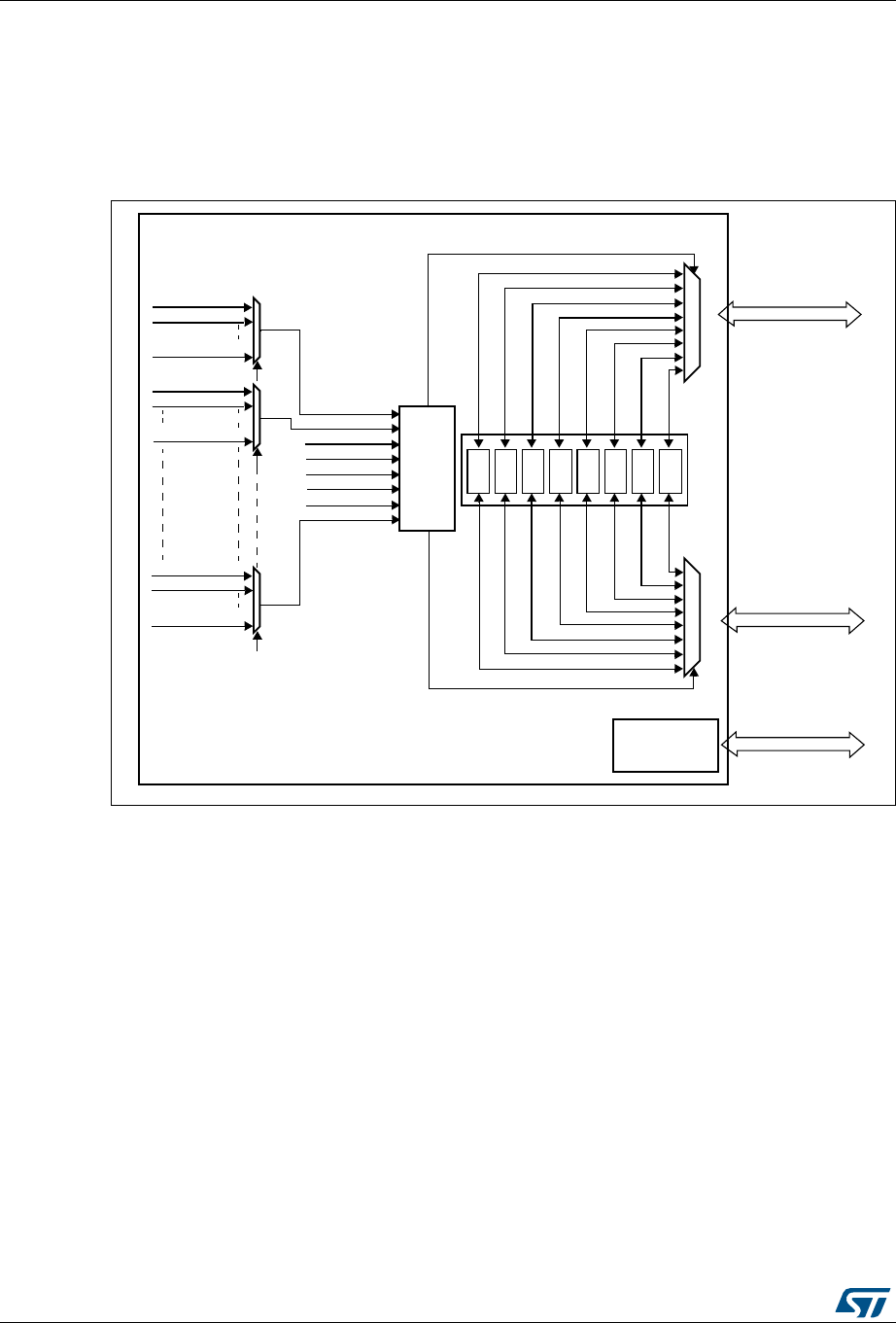
DMA controller (DMA) RM0090
304/1718 DocID018909 Rev 9
10.3 DMA functional description
10.3.1 General description
Figure 32 shows the block diagram of a DMA.
Figure 32. DMA block diagram
The DMA controller performs direct memory transfer: as an AHB master, it can take the
control of the AHB bus matrix to initiate AHB transactions.
It can carry out the following transactions:
•peripheral-to-memory
•memory-to-peripheral
•memory-to-memory
The DMA controller provides two AHB master ports: the AHB memory port, intended to be
connected to memories and the AHB peripheral port, intended to be connected to
peripherals. However, to allow memory-to-memory transfers, the AHB peripheral port must
also have access to the memories.
The AHB slave port is used to program the DMA controller (it supports only 32-bit
accesses).
See Figure 33 and Figure 34 for the implementation of the system of two DMA controllers.
AHB master
Memory port
FIFO
AHB master
Peripheral port
STREAM 0
FIFO STREAM 1
STREAM 0
STREAM 1
FIFO STREAM 2STREAM 2
FIFO STREAM 7
STREAM 7
REQ_STREAM0
REQ_STR0_CH0
REQ_STR0_CH1
DMA controller
FIFO STREAM 3STREAM 3
FIFO STREAM 4STREAM 4
FIFO STREAM 5STREAM 5
FIFO STREAM 6STREAM 6
Arbiter
REQ_STREAM1
REQ_STREAM2
REQ_STREAM3
REQ_STREAM4
REQ_STREAM5
REQ_STREAM6
REQ_STREAM7
REQ_STR0_CH7
REQ_STR1_CH0
REQ_STR1_CH1
REQ_STR1_CH7
REQ_STR7_CH0
REQ_STR7_CH1
REQ_STR7_CH7
AHB slave
programming
interface
Programming port
Channel
selection
ai15945
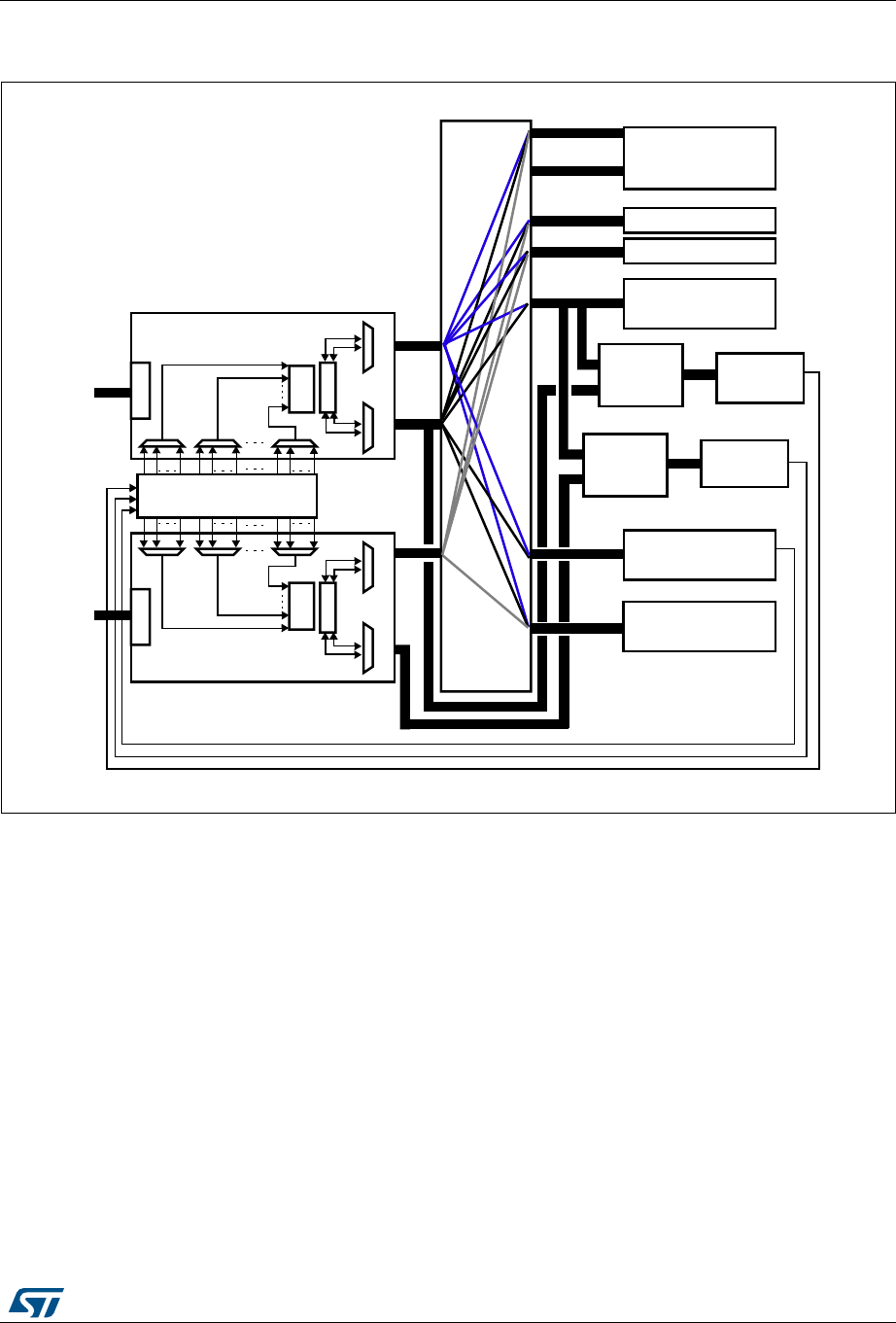
DocID018909 Rev 9 305/1718
RM0090 DMA controller (DMA)
338
Figure 33. System implementation of the two DMA controllers
(STM32F405xx/07xx and STM32F415xx/17xx )
1. The DMA1 controller AHB peripheral port is not connected to the bus matrix like DMA2 controller. As a result, only DMA2
streams are able to perform memory-to-memory transfers.
-36
$-!CONTROLLER
!("PERIPH
!RBITER
!("MEMORY
&)&/
$-!CONTROLLER
!("MEMORY
"USMATRIX
!("
!RBITER
!("PERIPH
-!00).'
&)&/
%XTERNALMEMORY
&LASH
MEMORY
+"32!-
!("PERIPHERALS
MULTILAYER
!("!0"
BRIDGE
DUAL!("
!0" !0"
!("!0"
BRIDGE
DUAL!("
!0" !0"
PERIPHERALS
!("SLAVE!("SLAVE
PORTPORTPORTPORT
CONTROLLER&3-#
$-!REQUEST
PERIPHERALS
+"32!-
!("PERIPHERALS
4O!("
PERIPHERALS
4O!("
PERIPHERALS
$#/$%
)#/$%
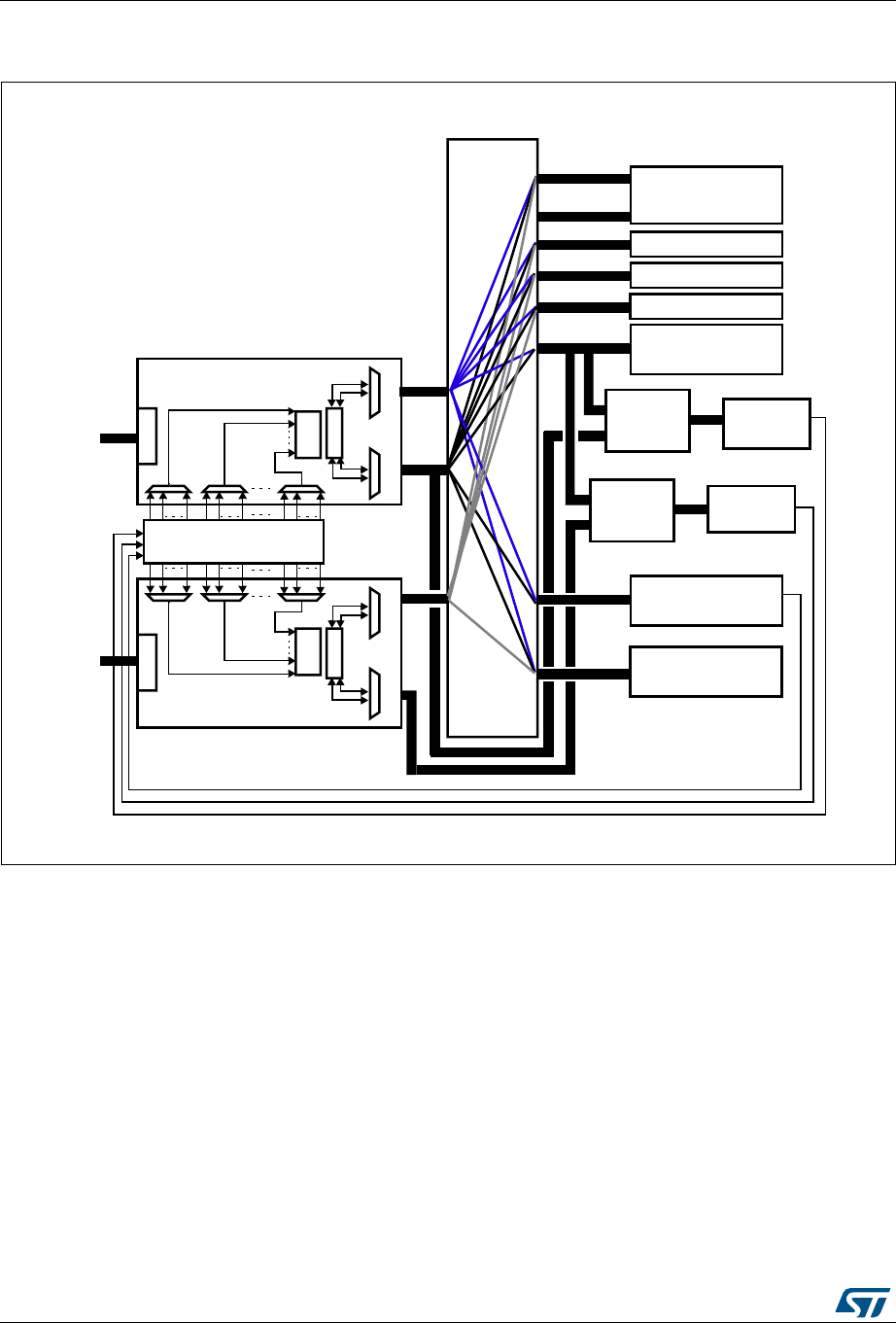
DMA controller (DMA) RM0090
306/1718 DocID018909 Rev 9
Figure 34. System implementation of the two DMA controllers (STM32F42xxx and
STM32F43xxx)
1. The DMA1 controller AHB peripheral port is not connected to the bus matrix like in the case of the DMA2
controller, thus only DMA2 streams are able to perform memory-to-memory transfers.
10.3.2 DMA transactions
A DMA transaction consists of a sequence of a given number of data transfers. The number
of data items to be transferred and their width (8-bit, 16-bit or 32-bit) are software-
programmable.
Each DMA transfer consists of three operations:
•A loading from the peripheral data register or a location in memory, addressed through
the DMA_SxPAR or DMA_SxM0AR register
•A storage of the data loaded to the peripheral data register or a location in memory
addressed through the DMA_SxPAR or DMA_SxM0AR register
•A post-decrement of the DMA_SxNDTR register, which contains the number of
transactions that still have to be performed
-36
$-!CONTROLLER
!("PERIPH
!RBITER
!("MEMORY
&)&/
$-!CONTROLLER
!("MEMORY
"US-ATRIX
!("MULTILAYER
!RBITER
!("PERIPH
-!00).'
&)&/
%XTERNALMEMORY
&LASH
MEMORY
+"32!-
!("PERIPHERALS
!("!0"
BRIDGE
DUAL!("
!0" !0"
!("!0"
BRIDGE
DUAL!("
!0" !0"
PERIPHERALS
!("SLAVE!("SLAVE
PORTPORTPORTPORT
CONTROLLER&-#
$-!REQUEST
PERIPHERALS
+"32!-
!("PERIPHERALS
4O!("
PERIPHERALS
4O!("
PERIPHERALS
$#/$%
)#/$%
+"32!-
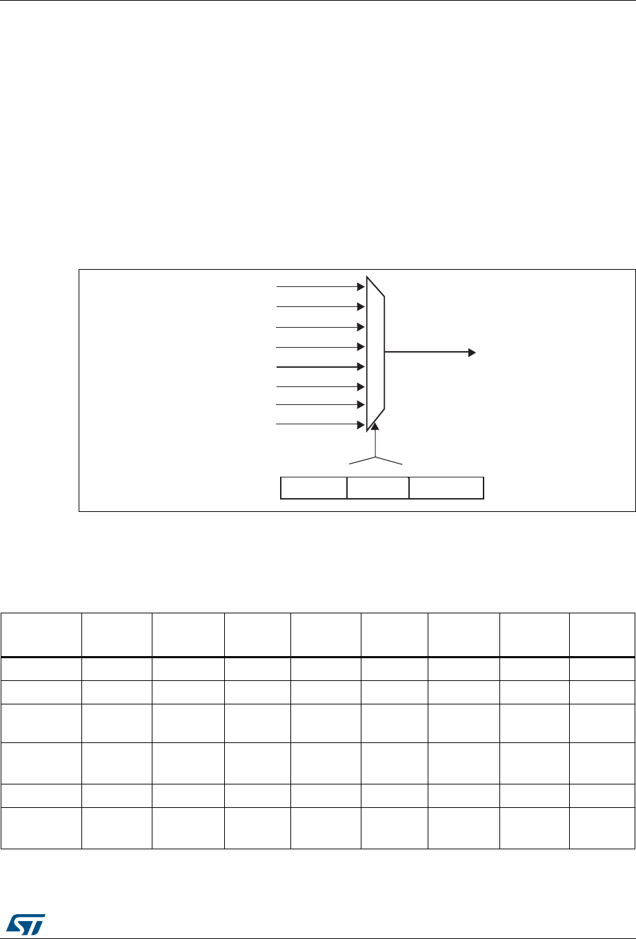
DocID018909 Rev 9 307/1718
RM0090 DMA controller (DMA)
338
After an event, the peripheral sends a request signal to the DMA controller. The DMA
controller serves the request depending on the channel priorities. As soon as the DMA
controller accesses the peripheral, an Acknowledge signal is sent to the peripheral by the
DMA controller. The peripheral releases its request as soon as it gets the Acknowledge
signal from the DMA controller. Once the request has been deasserted by the peripheral,
the DMA controller releases the Acknowledge signal. If there are more requests, the
peripheral can initiate the next transaction.
10.3.3 Channel selection
Each stream is associated with a DMA request that can be selected out of 8 possible
channel requests. The selection is controlled by the CHSEL[2:0] bits in the DMA_SxCR
register.
Figure 35. Channel selection
The 8 requests from the peripherals (TIM, ADC, SPI, I2C, etc.) are independently connected
to each channel and their connection depends on the product implementation.
Table 42 and Table 43 give examples of DMA request mappings.
REQ_STREAMx
REQ_STRx_CH7
REQ_STRx_CH6
REQ_STRx_CH5
REQ_STRx_CH4
REQ_STRx_CH3
REQ_STRx_CH2
REQ_STRx_CH1
REQ_STRx_CH0
CHSEL[2:0]
312927 0
DMA_SxCR
ai15947
Table 42. DMA1 request mapping
Peripheral
requests Stream 0 Stream 1 Stream 2 Stream 3 Stream 4 Stream 5 Stream 6 Stream 7
Channel 0 SPI3_RX SPI3_RX SPI2_RX SPI2_TX SPI3_TX SPI3_TX
Channel 1 I2C1_RX TIM7_UP TIM7_UP I2C1_RX I2C1_TX I2C1_TX
Channel 2 TIM4_CH1 I2S3_EXT_
RX TIM4_CH2 I2S2_EXT_
TX
I2S3_EXT_
TX TIM4_UP TIM4_CH3
Channel 3 I2S3_EXT_
RX
TIM2_UP
TIM2_CH3
I2C3_RX I2S2_EXT_
RX I2C3_TX TIM2_CH1 TIM2_CH2
TIM2_CH4
TIM2_UP
TIM2_CH4
Channel 4 UART5_RX USART3_RX UART4_RX USART3_TX UART4_TX USART2_RX USART2_TX UART5_TX
Channel 5 UART8_TX(1) UART7_TX(1) TIM3_CH4
TIM3_UP UART7_RX(1) TIM3_CH1
TIM3_TRIG TIM3_CH2 UART8_RX(1) TIM3_CH3

DMA controller (DMA) RM0090
308/1718 DocID018909 Rev 9
10.3.4 Arbiter
An arbiter manages the 8 DMA stream requests based on their priority for each of the two
AHB master ports (memory and peripheral ports) and launches the peripheral/memory
access sequences.
Priorities are managed in two stages:
•Software: each stream priority can be configured in the DMA_SxCR register. There are
four levels:
– Very high priority
– High priority
– Medium priority
– Low priority
•Hardware: If two requests have the same software priority level, the stream with the
lower number takes priority over the stream with the higher number. For example,
Stream 2 takes priority over Stream 4.
Channel 6 TIM5_CH3
TIM5_UP
TIM5_CH4
TIM5_TRIG TIM5_CH1 TIM5_CH4
TIM5_TRIG TIM5_CH2 TIM5_UP
Channel 7 TIM6_UP I2C2_RX I2C2_RX USART3_TX DAC1 DAC2 I2C2_TX
1. These requests are available on STM32F42xxx and STM32F43xxx only.
Table 42. DMA1 request mapping (continued)
Peripheral
requests Stream 0 Stream 1 Stream 2 Stream 3 Stream 4 Stream 5 Stream 6 Stream 7
Table 43. DMA2 request mapping
Peripheral
requests Stream 0 Stream 1 Stream 2 Stream 3 Stream 4 Stream 5 Stream 6 Stream 7
Channel 0 ADC1 SAI1_A(1)
TIM8_CH1
TIM8_CH2
TIM8_CH3
SAI1_A(1) ADC1 SAI1_B(1)
TIM1_CH1
TIM1_CH2
TIM1_CH3
Channel 1 DCMI ADC2 ADC2 SAI1_B(1) SPI6_TX(1) SPI6_RX(1) DCMI
Channel 2 ADC3 ADC3 SPI5_RX(1) SPI5_TX(1) CRYP_OUT CRYP_IN HASH_IN
Channel 3 SPI1_RX SPI1_RX SPI1_TX SPI1_TX
Channel 4 SPI4_RX(1) SPI4_TX(1) USART1_RX SDIO USART1_RX SDIO USART1_TX
Channel 5 USART6_RX USART6_RX SPI4_RX(1) SPI4_TX(1) USART6_TX USART6_TX
Channel 6 TIM1_TRIG TIM1_CH1 TIM1_CH2 TIM1_CH1
TIM1_CH4
TIM1_TRIG
TIM1_COM
TIM1_UP TIM1_CH3
Channel 7 TIM8_UP TIM8_CH1 TIM8_CH2 TIM8_CH3 SPI5_RX(1) SPI5_TX(1)
TIM8_CH4
TIM8_TRIG
TIM8_COM
1. These requests are available on STM32F42xxx and STM32F43xxx.
DocID018909 Rev 9 309/1718
RM0090 DMA controller (DMA)
338
10.3.5 DMA streams
Each of the 8 DMA controller streams provides a unidirectional transfer link between a
source and a destination.
Each stream can be configured to perform:
•Regular type transactions: memory-to-peripherals, peripherals-to-memory or memory-
to-memory transfers
•Double-buffer type transactions: double buffer transfers using two memory pointers for
the memory (while the DMA is reading/writing from/to a buffer, the application can
write/read to/from the other buffer).
The amount of data to be transferred (up to 65535) is programmable and related to the
source width of the peripheral that requests the DMA transfer connected to the peripheral
AHB port. The register that contains the amount of data items to be transferred is
decremented after each transaction.
10.3.6 Source, destination and transfer modes
Both source and destination transfers can address peripherals and memories in the entire
4 GB area, at addresses comprised between 0x0000 0000 and 0xFFFF FFFF.
The direction is configured using the DIR[1:0] bits in the DMA_SxCR register and offers
three possibilities: memory-to-peripheral, peripheral-to-memory or memory-to-memory
transfers. Table 44 describes the corresponding source and destination addresses.
When the data width (programmed in the PSIZE or MSIZE bits in the DMA_SxCR register)
is a half-word or a word, respectively, the peripheral or memory address written into the
DMA_SxPAR or DMA_SxM0AR/M1AR registers has to be aligned on a word or half-word
address boundary, respectively.
Peripheral-to-memory mode
Figure 36 describes this mode.
When this mode is enabled (by setting the bit EN in the DMA_SxCR register), each time a
peripheral request occurs, the stream initiates a transfer from the source to fill the FIFO.
When the threshold level of the FIFO is reached, the contents of the FIFO are drained and
stored into the destination.
The transfer stops once the DMA_SxNDTR register reaches zero, when the peripheral
requests the end of transfers (in case of a peripheral flow controller) or when the EN bit in
the DMA_SxCR register is cleared by software.
Table 44. Source and destination address
Bits DIR[1:0] of the
DMA_SxCR register Direction Source address Destination address
00 Peripheral-to-memory DMA_SxPAR DMA_SxM0AR
01 Memory-to-peripheral DMA_SxM0AR DMA_SxPAR
10 Memory-to-memory DMA_SxPAR DMA_SxM0AR
11 reserved - -
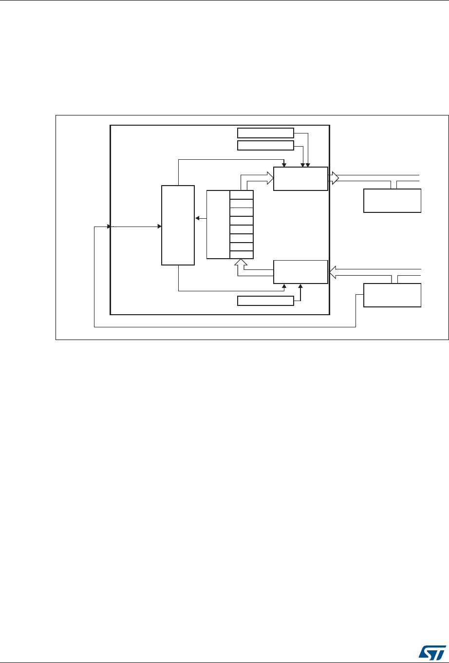
DMA controller (DMA) RM0090
310/1718 DocID018909 Rev 9
In direct mode (when the DMDIS value in the DMA_SxFCR register is ‘0’), the threshold
level of the FIFO is not used: after each single data transfer from the peripheral to the FIFO,
the corresponding data are immediately drained and stored into the destination.
The stream has access to the AHB source or destination port only if the arbitration of the
corresponding stream is won. This arbitration is performed using the priority defined for
each stream using the PL[1:0] bits in the DMA_SxCR register.
Figure 36. Peripheral-to-memory mode
1. For double-buffer mode.
Memory-to-peripheral mode
Figure 37 describes this mode.
When this mode is enabled (by setting the EN bit in the DMA_SxCR register), the stream
immediately initiates transfers from the source to entirely fill the FIFO.
Each time a peripheral request occurs, the contents of the FIFO are drained and stored into
the destination. When the level of the FIFO is lower than or equal to the predefined
threshold level, the FIFO is fully reloaded with data from the memory.
The transfer stops once the DMA_SxNDTR register reaches zero, when the peripheral
requests the end of transfers (in case of a peripheral flow controller) or when the EN bit in
the DMA_SxCR register is cleared by software.
In direct mode (when the DMDIS value in the DMA_SxFCR register is '0'), the threshold
level of the FIFO is not used. Once the stream is enabled, the DMA preloads the first data to
transfer into an internal FIFO. As soon as the peripheral requests a data transfer, the DMA
transfers the preloaded value into the configured destination. It then reloads again the
empty internal FIFO with the next data to be transfer. The preloaded data size corresponds
to the value of the PSIZE bitfield in the DMA_SxCR register.
The stream has access to the AHB source or destination port only if the arbitration of the
corresponding stream is won. This arbitration is performed using the priority defined for
each stream using the PL[1:0] bits in the DMA_SxCR register.
Memory bus
Peripheral bus
REQ_STREAMx Arbiter
DMA_SxM1AR(1)
FIFO
AHB memory
port
AHB peripheral
port
DMA_SxPAR
FIFO
level
DMA controller DMA_SxM0AR
destination
source
peripheral
Memory
Peripheral DMA request
ai15948
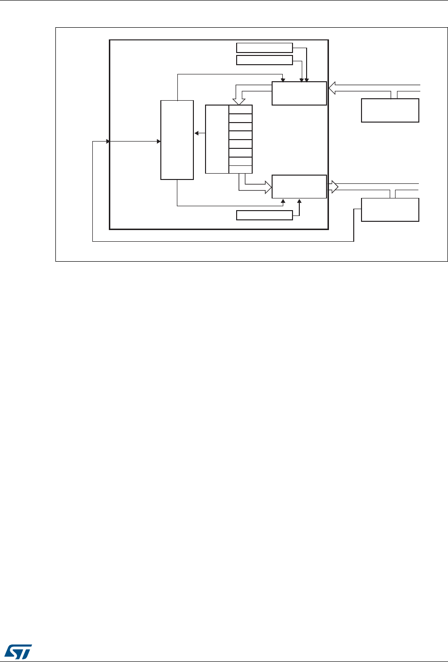
DocID018909 Rev 9 311/1718
RM0090 DMA controller (DMA)
338
Figure 37. Memory-to-peripheral mode
1. For double-buffer mode.
Memory-to-memory mode
The DMA channels can also work without being triggered by a request from a peripheral.
This is the memory-to-memory mode, described in Figure 38.
When the stream is enabled by setting the Enable bit (EN) in the DMA_SxCR register, the
stream immediately starts to fill the FIFO up to the threshold level. When the threshold level
is reached, the FIFO contents are drained and stored into the destination.
The transfer stops once the DMA_SxNDTR register reaches zero or when the EN bit in the
DMA_SxCR register is cleared by software.
The stream has access to the AHB source or destination port only if the arbitration of the
corresponding stream is won. This arbitration is performed using the priority defined for
each stream using the PL[1:0] bits in the DMA_SxCR register.
Note: When memory-to-memory mode is used, the Circular and direct modes are not allowed.
Only the DMA2 controller is able to perform memory-to-memory transfers.
Peripheral bus
Memory bus
REQ_STREAMx Arbiter
DMA_SxM1AR
(1)
FIFO
AHB memory
port
AHB peripheral
port
DMA_SxPAR
FIFO
level
DMA controller
DMA_SxM0AR
source
destination
Peripheral
Memory
Peripheral DMA request
ai15949
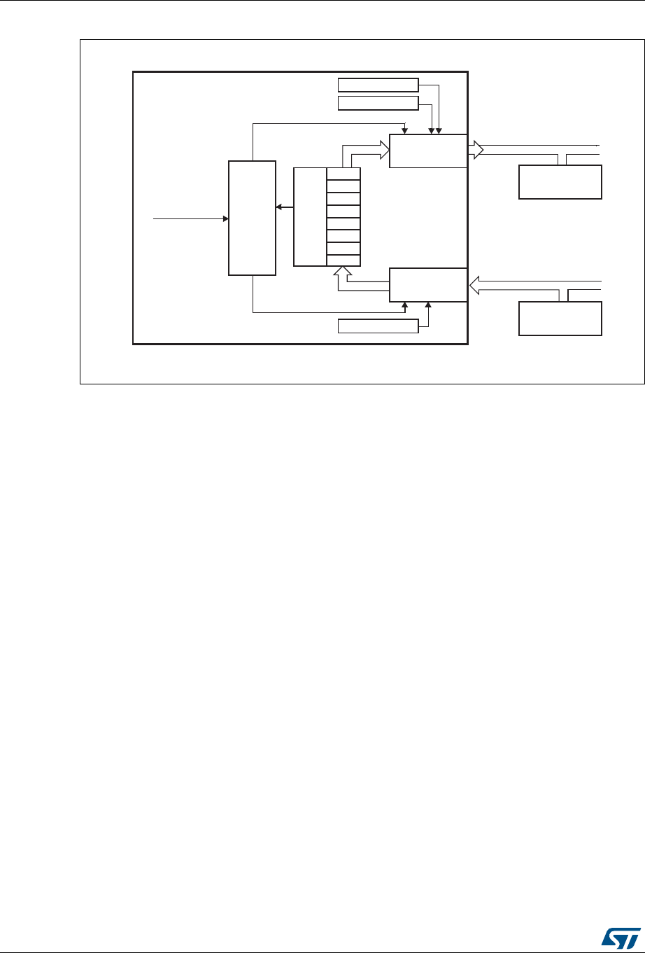
DMA controller (DMA) RM0090
312/1718 DocID018909 Rev 9
Figure 38. Memory-to-memory mode
1. For double-buffer mode.
10.3.7 Pointer incrementation
Peripheral and memory pointers can optionally be automatically post-incremented or kept
constant after each transfer depending on the PINC and MINC bits in the DMA_SxCR
register.
Disabling the Increment mode is useful when the peripheral source or destination data are
accessed through a single register.
If the Increment mode is enabled, the address of the next transfer will be the address of the
previous one incremented by 1 (for bytes), 2 (for half-words) or 4 (for words) depending on
the data width programmed in the PSIZE or MSIZE bits in the DMA_SxCR register.
In order to optimize the packing operation, it is possible to fix the increment offset size for
the peripheral address whatever the size of the data transferred on the AHB peripheral port.
The PINCOS bit in the DMA_SxCR register is used to align the increment offset size with
the data size on the peripheral AHB port, or on a 32-bit address (the address is then
incremented by 4). The PINCOS bit has an impact on the AHB peripheral port only.
If PINCOS bit is set, the address of the next transfer is the address of the previous one
incremented by 4 (automatically aligned on a 32-bit address) whatever the PSIZE value.
The AHB memory port, however, is not impacted by this operation.
Memory bus
Peripheral bus
Stream enable
Arbiter
DMA_SxM1AR(1)
FIFO
AHB memory
port
AHB peripheral
port
DMA_SxPAR
FIFO
level
DMA controller DMA_SxM0AR
destination
source
Memory 1
Memory 2
FIFO
ai15950

DocID018909 Rev 9 313/1718
RM0090 DMA controller (DMA)
338
10.3.8 Circular mode
The Circular mode is available to handle circular buffers and continuous data flows (e.g.
ADC scan mode). This feature can be enabled using the CIRC bit in the DMA_SxCR
register.
When the circular mode is activated, the number of data items to be transferred is
automatically reloaded with the initial value programmed during the stream configuration
phase, and the DMA requests continue to be served.
Note: In the circular mode, it is mandatory to respect the following rule in case of a burst mode
configured for memory:
DMA_SxNDTR = Multiple of ((Mburst beat) × (Msize)/(Psize)), where:
–(Mburst beat) = 4, 8 or 16 (depending on the MBURST bits in the DMA_SxCR
register)
–((Msize)/(Psize)) = 1, 2, 4, 1/2 or 1/4 (Msize and Psize represent the MSIZE and
PSIZE bits in the DMA_SxCR register. They are byte dependent)
–DMA_SxNDTR = Number of data items to transfer on the AHB peripheral port
For example: Mburst beat = 8 (INCR8), MSIZE = ‘00’ (byte) and PSIZE = ‘01’ (half-word), in
this case: DMA_SxNDTR must be a multiple of (8 × 1/2 = 4).
If this formula is not respected, the DMA behavior and data integrity are not guaranteed.
NDTR must also be a multiple of the Peripheral burst size multiplied by the peripheral data
size, otherwise this could result in a bad DMA behavior.
10.3.9 Double buffer mode
This mode is available for all the DMA1 and DMA2 streams.
The Double buffer mode is enabled by setting the DBM bit in the DMA_SxCR register.
A double-buffer stream works as a regular (single buffer) stream with the difference that it
has two memory pointers. When the Double buffer mode is enabled, the Circular mode is
automatically enabled (CIRC bit in DMA_SxCR is don’t care) and at each end of transaction,
the memory pointers are swapped.
In this mode, the DMA controller swaps from one memory target to another at each end of
transaction. This allows the software to process one memory area while the second memory
area is being filled/used by the DMA transfer. The double-buffer stream can work in both
directions (the memory can be either the source or the destination) as described in
Table 45: Source and destination address registers in Double buffer mode (DBM=1).
Note: In Double buffer mode, it is possible to update the base address for the AHB memory port
on-the-fly (DMA_SxM0AR or DMA_SxM1AR) when the stream is enabled, by respecting the
following conditions:
•When the CT bit is ‘0’ in the DMA_SxCR register, the DMA_SxM1AR register can be
written. Attempting to write to this register while CT = '1' sets an error flag (TEIF) and
the stream is automatically disabled.
•When the CT bit is ‘1’ in the DMA_SxCR register, the DMA_SxM0AR register can be
written. Attempting to write to this register while CT = '0', sets an error flag (TEIF) and
the stream is automatically disabled.
To avoid any error condition, it is advised to change the base address as soon as the TCIF
flag is asserted because, at this point, the targeted memory must have changed from

DMA controller (DMA) RM0090
314/1718 DocID018909 Rev 9
memory 0 to 1 (or from 1 to 0) depending on the value of CT in the DMA_SxCR register in
accordance with one of the two above conditions.
For all the other modes (except the Double buffer mode), the memory address registers are
write-protected as soon as the stream is enabled.
10.3.10 Programmable data width, packing/unpacking, endianess
The number of data items to be transferred has to be programmed into DMA_SxNDTR
(number of data items to transfer bit, NDT) before enabling the stream (except when the
flow controller is the peripheral, PFCTRL bit in DMA_SxCR is set).
When using the internal FIFO, the data widths of the source and destination data are
programmable through the PSIZE and MSIZE bits in the DMA_SxCR register (can be 8-,
16- or 32-bit).
When PSIZE and MSIZE are not equal:
•The data width of the number of data items to transfer, configured in the DMA_SxNDTR
register is equal to the width of the peripheral bus (configured by the PSIZE bits in the
DMA_SxCR register). For instance, in case of peripheral-to-memory, memory-to-
peripheral or memory-to-memory transfers and if the PSIZE[1:0] bits are configured for
half-word, the number of bytes to be transferred is equal to 2 × NDT.
•The DMA controller only copes with little-endian addressing for both source and
destination. This is described in Table 46: Packing/unpacking & endian behavior (bit
PINC = MINC = 1).
This packing/unpacking procedure may present a risk of data corruption when the operation
is interrupted before the data are completely packed/unpacked. So, to ensure data
coherence, the stream may be configured to generate burst transfers: in this case, each
group of transfers belonging to a burst are indivisible (refer to Section 10.3.11: Single and
burst transfers).
In direct mode (DMDIS = 0 in the DMA_SxFCR register), the packing/unpacking of data is
not possible. In this case, it is not allowed to have different source and destination transfer
data widths: both are equal and defined by the PSIZE bits in the DMA_SxCR MSIZE bits are
don’t care).
Table 45. Source and destination address registers in Double buffer mode (DBM=1)
Bits DIR[1:0] of the
DMA_SxCR register Direction Source address Destination address
00 Peripheral-to-memory DMA_SxPAR DMA_SxM0AR /
DMA_SxM1AR
01 Memory-to-peripheral DMA_SxM0AR /
DMA_SxM1AR DMA_SxPAR
10 Not allowed(1)
1. When the Double buffer mode is enabled, the Circular mode is automatically enabled. Since the memory-
to-memory mode is not compatible with the Circular mode, when the Double buffer mode is enabled, it is
not allowed to configure the memory-to-memory mode.
11 Reserved - -

DocID018909 Rev 9 315/1718
RM0090 DMA controller (DMA)
338
Note: Peripheral port may be the source or the destination (it could also be the memory source in
the case of memory-to-memory transfer).
PSIZE, MSIZE and NDT[15:0] have to be configured so as to ensure that the last transfer
will not be incomplete. This can occur when the data width of the peripheral port (PSIZE
bits) is lower than the data width of the memory port (MSIZE bits). This constraint is
summarized in Table 47.
Table 46. Packing/unpacking & endian behavior (bit PINC = MINC = 1)
AHB
memory
port
width
AHB
peripheral
port width
Number
of data
items to
transfer
(NDT)
Memory
transfer
number
Memory port
address / byte
lane
Peripher
al
transfer
number
Peripheral port address / byte lane
PINCOS = 1 PINCOS = 0
88 4
1
2
3
4
0x0 / B0[7:0]
0x1 / B1[7:0]
0x2 / B2[7:0]
0x3 / B3[7:0]
1
2
3
4
0x0 / B0[7:0]
0x4 / B1[7:0]
0x8 / B2[7:0]
0xC / B3[7:0]
0x0 / B0[7:0]
0x1 / B1[7:0]
0x2 / B2[7:0]
0x3 / B3[7:0]
816 2
1
2
3
4
0x0 / B0[7:0]
0x1 / B1[7:0]
0x2 / B2[7:0]
0x3 / B3[7:0]
1
2
0x0 / B1|B0[15:0]
0x4 / B3|B2[15:0]
0x0 / B1|B0[15:0]
0x2 / B3|B2[15:0]
832 1
1
2
3
4
0x0 / B0[7:0]
0x1 / B1[7:0]
0x2 / B2[7:0]
0x3 / B3[7:0]
10x0 / B3|B2|B1|B0[31:0] 0x0 / B3|B2|B1|B0[31:0]
16 8 4
1
2
0x0 / B1|B0[15:0]
0x2 / B3|B2[15:0]
1
2
3
4
0x0 / B0[7:0]
0x4 / B1[7:0]
0x8 / B2[7:0]
0xC / B3[7:0]
0x0 / B0[7:0]
0x1 / B1[7:0]
0x2 / B2[7:0]
0x3 / B3[7:0]
16 16 2
1
2
0x0 / B1|B0[15:0]
0x2 / B1|B0[15:0]
1
2
0x0 / B1|B0[15:0]
0x4 / B3|B2[15:0]
0x0 / B1|B0[15:0]
0x2 / B3|B2[15:0]
16 32 1
1
2
0x0 / B1|B0[15:0]
0x2 / B3|B2[15:0]
10x0 / B3|B2|B1|B0[31:0] 0x0 / B3|B2|B1|B0[31:0]
32 8 4
10x0 / B3|B2|B1|B0[31:0] 1
2
3
4
0x0 / B0[7:0]
0x4 / B1[7:0]
0x8 / B2[7:0]
0xC / B3[7:0]
0x0 / B0[7:0]
0x1 / B1[7:0]
0x2 / B2[7:0]
0x3 / B3[7:0]
32 16 2 10x0 /B3|B2|B1|B0[31:0] 1
2
0x0 / B1|B0[15:0]
0x4 / B3|B2[15:0]
0x0 / B1|B0[15:0]
0x2 / B3|B2[15:0]
32 32 1 1 0x0 /B3|B2|B1|B0 [31:0] 1 0x0 /B3|B2|B1|B0 [31:0] 0x0 / B3|B2|B1|B0[31:0]

DMA controller (DMA) RM0090
316/1718 DocID018909 Rev 9
10.3.11 Single and burst transfers
The DMA controller can generate single transfers or incremental burst transfers of 4, 8 or 16
beats.
The size of the burst is configured by software independently for the two AHB ports by using
the MBURST[1:0] and PBURST[1:0] bits in the DMA_SxCR register.
The burst size indicates the number of beats in the burst, not the number of bytes
transferred.
To ensure data coherence, each group of transfers that form a burst are indivisible: AHB
transfers are locked and the arbiter of the AHB bus matrix does not degrant the DMA master
during the sequence of the burst transfer.
Depending on the single or burst configuration, each DMA request initiates a different
number of transfers on the AHB peripheral port:
•When the AHB peripheral port is configured for single transfers, each DMA request
generates a data transfer of a byte, half-word or word depending on the PSIZE[1:0] bits
in the DMA_SxCR register
•When the AHB peripheral port is configured for burst transfers, each DMA request
generates 4,8 or 16 beats of byte, half word or word transfers depending on the
PBURST[1:0] and PSIZE[1:0] bits in the DMA_SxCR register.
The same as above has to be considered for the AHB memory port considering the
MBURST and MSIZE bits.
In direct mode, the stream can only generate single transfers and the MBURST[1:0] and
PBURST[1:0] bits are forced by hardware.
The address pointers (DMA_SxPAR or DMA_SxM0AR registers) must be chosen so as to
ensure that all transfers within a burst block are aligned on the address boundary equal to
the size of the transfer.
The burst configuration has to be selected in order to respect the AHB protocol, where
bursts must not cross the 1 KB address boundary because the minimum address space that
can be allocated to a single slave is 1 KB. This means that the 1 KB address boundary
should not be crossed by a burst block transfer, otherwise an AHB error would be
generated, that is not reported by the DMA registers.
Table 47. Restriction on NDT versus PSIZE and MSIZE
PSIZE[1:0] of DMA_SxCR MSIZE[1:0] of DMA_SxCR NDT[15:0] of DMA_SxNDTR
00 (8-bit) 01 (16-bit) must be a multiple of 2
00 (8-bit) 10 (32-bit) must be a multiple of 4
01 (16-bit) 10 (32-bit) must be a multiple of 2
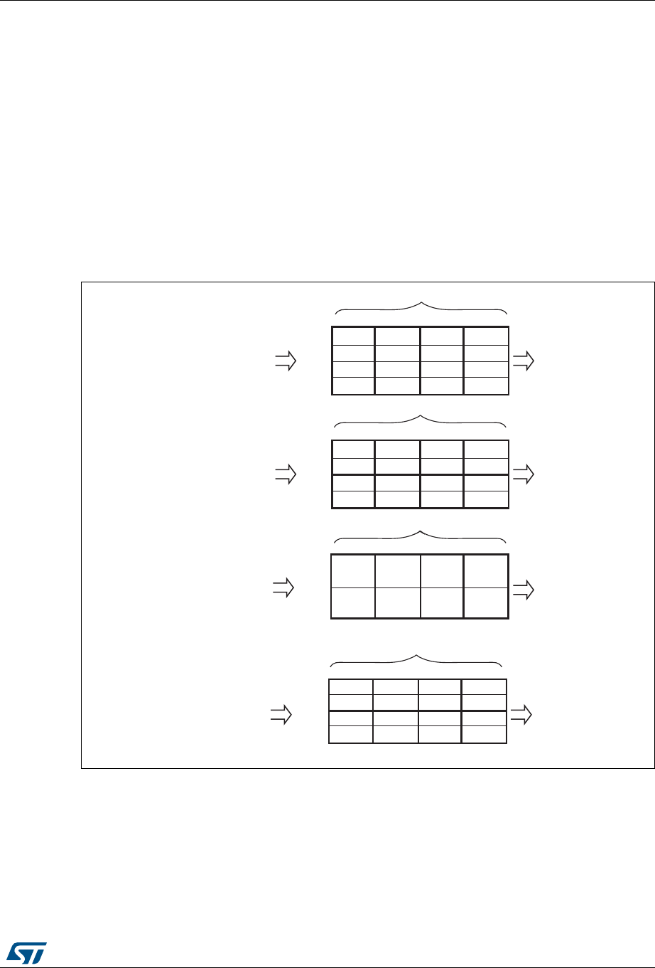
DocID018909 Rev 9 317/1718
RM0090 DMA controller (DMA)
338
10.3.12 FIFO
FIFO structure
The FIFO is used to temporarily store data coming from the source before transmitting them
to the destination.
Each stream has an independent 4-word FIFO and the threshold level is software-
configurable between 1/4, 1/2, 3/4 or full.
To enable the use of the FIFO threshold level, the direct mode must be disabled by setting
the DMDIS bit in the DMA_SxFCR register.
The structure of the FIFO differs depending on the source and destination data widths, and
is described in Figure 39: FIFO structure.
Figure 39. FIFO structure
FIFO threshold and burst configuration
Caution is required when choosing the FIFO threshold (bits FTH[1:0] of the DMA_SxFCR
register) and the size of the memory burst (MBURST[1:0] of the DMA_SxCR register): The
content pointed by the FIFO threshold must exactly match to an integer number of memory
burst transfers. If this is not in the case, a FIFO error (flag FEIFx of the DMA_HISR or
DMA_LISR register) will be generated when the stream is enabled, then the stream will be
Source: byte
4 words
byte lane 0
byte lane 1
byte lane 2
byte lane 3
1/4 1/2 3/4 FullEmpty
B0
B1
B2
B3
B4
B5
B6
B7
B8
B9
B10
B 11
B12
B13
B14
B15
Destination: word
Source: byte Destination: half-word
4 words
byte lane 0
byte lane 1
byte lane 2
byte lane 3
1/4 1/2 3/4 FullEmpty
B0
B1
B2
B3
B4
B5
B6
B7
B8
B9
B10
B 11
B12
B13
B14
B15
W0W1W2W3
H0
H1
H2
H3
H4
H5
H6
H7
Source: half-word Destination: word
4 words
byte lane 0
byte lane 1
byte lane 2
byte lane 3
1/4 1/2 3/4 FullEmpty
H0
W0W1W2W3
H1
H2
H3
H4
H5
H6
H7
B15 B14 B13 B12 B11 B10 B9 B8 B7 B6 B5 B4 B3 B2 B1 B0
B15 B14 B13 B12 B11 B10 B9 B8 B7 B6 B5 B4 B3 B2 B1 B0
H7 H6 H5 H4 H3 H2 H1 H0
H7, H6, H5, H4, H3, H2, H1, H0
W3, W2, W1, W0
W3, W2, W1, W0
Source: half-word
4-words
byte lane 0
byte lane 1
byte lane 2
byte lane 3
1/4 1/2 3/4 FullEmpty
Destination: byte
H7 H6 H5 H4 H3 H2 H1 H0
B0
B1
B2
B3
B4
B5
B6
B7
B8
B9
B10
B 11
B12
B13
B14
B15
H0
H1
H2
H3
H4
H5
H6
H7
B15 B14 B13 B12 B11 B10 B9 B8
B7 B6 B5 B4 B3 B2 B1 B0
ai15951

DMA controller (DMA) RM0090
318/1718 DocID018909 Rev 9
automatically disabled. The allowed and forbidden configurations are described in the
Table 48: FIFO threshold configurations.
In all cases, the burst size multiplied by the data size must not exceed the FIFO size (data
size can be: 1 (byte), 2 (half-word) or 4 (word)).
Incomplete Burst transfer at the end of a DMA transfer may happen if one of the following
conditions occurs:
•For the AHB peripheral port configuration: the total number of data items (set in the
DMA_SxNDTR register) is not a multiple of the burst size multiplied by the data size
•For the AHB memory port configuration: the number of remaining data items in the
FIFO to be transferred to the memory is not a multiple of the burst size multiplied by the
data size
In such cases, the remaining data to be transferred will be managed in single mode by the
DMA, even if a burst transaction was requested during the DMA stream configuration.
Note: When burst transfers are requested on the peripheral AHB port and the FIFO is used
(DMDIS = 1 in the DMA_SxCR register), it is mandatory to respect the following rule to
avoid permanent underrun or overrun conditions, depending on the DMA stream direction:
If (PBURST × PSIZE) = FIFO_SIZE (4 words), FIFO_Threshold = 3/4 is forbidden with
PSIZE = 1, 2 or 4 and PBURST = 4, 8 or 16.
This rule ensures that enough FIFO space at a time will be free to serve the request from
the peripheral.
FIFO flush
The FIFO can be flushed when the stream is disabled by resetting the EN bit in the
DMA_SxCR register and when the stream is configured to manage peripheral-to-memory or
memory-to-memory transfers: If some data are still present in the FIFO when the stream is
disabled, the DMA controller continues transferring the remaining data to the destination
Table 48. FIFO threshold configurations
MSIZE FIFO level MBURST = INCR4 MBURST = INCR8 MBURST = INCR16
Byte
1/4 1 burst of 4 beats forbidden
forbidden1/2 2 bursts of 4 beats 1 burst of 8 beats
3/4 3 bursts of 4 beats forbidden
Full 4 bursts of 4 beats 2 bursts of 8 beats 1 burst of 16 beats
Half-word
1/4 forbidden
forbidden
forbidden
1/2 1 burst of 4 beats
3/4 forbidden
Full 2 bursts of 4 beats 1 burst of 8 beats
Word
1/4
forbidden
forbidden
1/2
3/4
Full 1 burst of 4 beats

DocID018909 Rev 9 319/1718
RM0090 DMA controller (DMA)
338
(even though stream is effectively disabled). When this flush is completed, the transfer
complete status bit (TCIFx) in the DMA_LISR or DMA_HISR register is set.
The remaining data counter DMA_SxNDTR keeps the value in this case to indicate how
many data items are currently available in the destination memory.
Note that during the FIFO flush operation, if the number of remaining data items in the FIFO
to be transferred to memory (in bytes) is less than the memory data width (for example 2
bytes in FIFO while MSIZE is configured to word), data will be sent with the data width set in
the MSIZE bit in the DMA_SxCR register. This means that memory will be written with an
undesired value. The software may read the DMA_SxNDTR register to determine the
memory area that contains the good data (start address and last address).
If the number of remaining data items in the FIFO is lower than a burst size (if the MBURST
bits in DMA_SxCR register are set to configure the stream to manage burst on the AHB
memory port), single transactions will be generated to complete the FIFO flush.
Direct mode
By default, the FIFO operates in direct mode (DMDIS bit in the DMA_SxFCR is reset) and
the FIFO threshold level is not used. This mode is useful when the system requires an
immediate and single transfer to or from the memory after each DMA request.
When the DMA is configured in direct mode (FIFO disabled), to transfer data in memory-to-
peripheral mode, the DMA preloads one data from the memory to the internal FIFO to
ensure an immediate data transfer as soon as a DMA request is triggered by a peripheral.
To avoid saturating the FIFO, it is recommended to configure the corresponding stream with
a high priority.
This mode is restricted to transfers where:
•The source and destination transfer widths are equal and both defined by the
PSIZE[1:0] bits in DMA_SxCR (MSIZE[1:0] bits are don’t care)
•Burst transfers are not possible (PBURST[1:0] and MBURST[1:0] bits in DMA_SxCR
are don’t care)
Direct mode must not be used when implementing memory-to-memory transfers.
10.3.13 DMA transfer completion
Different events can generate an end of transfer by setting the TCIFx bit in the DMA_LISR
or DMA_HISR status register:
•In DMA flow controller mode:
– The DMA_SxNDTR counter has reached zero in the memory-to-peripheral mode
– The stream is disabled before the end of transfer (by clearing the EN bit in the
DMA_SxCR register) and (when transfers are peripheral-to-memory or memory-

DMA controller (DMA) RM0090
320/1718 DocID018909 Rev 9
to-memory) all the remaining data have been flushed from the FIFO into the
memory
•In Peripheral flow controller mode:
– The last external burst or single request has been generated from the peripheral
and (when the DMA is operating in peripheral-to-memory mode) the remaining
data have been transferred from the FIFO into the memory
– The stream is disabled by software, and (when the DMA is operating in peripheral-
to-memory mode) the remaining data have been transferred from the FIFO into
the memory
Note: The transfer completion is dependent on the remaining data in FIFO to be transferred into
memory only in the case of peripheral-to-memory mode. This condition is not applicable in
memory-to-peripheral mode.
If the stream is configured in noncircular mode, after the end of the transfer (that is when the
number of data to be transferred reaches zero), the DMA is stopped (EN bit in DMA_SxCR
register is cleared by Hardware) and no DMA request is served unless the software
reprograms the stream and re-enables it (by setting the EN bit in the DMA_SxCR register).
10.3.14 DMA transfer suspension
At any time, a DMA transfer can be suspended to be restarted later on or to be definitively
disabled before the end of the DMA transfer.
There are two cases:
•The stream disables the transfer with no later-on restart from the point where it was
stopped. There is no particular action to do, except to clear the EN bit in the
DMA_SxCR register to disable the stream. The stream may take time to be disabled
(ongoing transfer is completed first). The transfer complete interrupt flag (TCIF in the
DMA_LISR or DMA_HISR register) is set in order to indicate the end of transfer. The
value of the EN bit in DMA_SxCR is now ‘0’ to confirm the stream interruption. The
DMA_SxNDTR register contains the number of remaining data items at the moment
when the stream was stopped so that the software can determine how many data items
have been transferred before the stream was interrupted.
•The stream suspends the transfer before the number of remaining data items to be
transferred in the DMA_SxNDTR register reaches 0. The aim is to restart the transfer
later by re-enabling the stream. In order to restart from the point where the transfer was
stopped, the software has to read the DMA_SxNDTR register after disabling the stream
by writing the EN bit in DMA_SxCR register (and then checking that it is at ‘0’) to know
the number of data items already collected. Then:
– The peripheral and/or memory addresses have to be updated in order to adjust
the address pointers
– The SxNDTR register has to be updated with the remaining number of data items
to be transferred (the value read when the stream was disabled)
– The stream may then be re-enabled to restart the transfer from the point it was
stopped
Note: Note that a Transfer complete interrupt flag (TCIF in DMA_LISR or DMA_HISR) is set to
indicate the end of transfer due to the stream interruption.

DocID018909 Rev 9 321/1718
RM0090 DMA controller (DMA)
338
10.3.15 Flow controller
The entity that controls the number of data to be transferred is known as the flow controller.
This flow controller is configured independently for each stream using the PFCTRL bit in the
DMA_SxCR register.
The flow controller can be:
•The DMA controller: in this case, the number of data items to be transferred is
programmed by software into the DMA_SxNDTR register before the DMA stream is
enabled.
•The peripheral source or destination: this is the case when the number of data items to
be transferred is unknown. The peripheral indicates by hardware to the DMA controller
when the last data are being transferred. This feature is only supported for peripherals
which are able to signal the end of the transfer, that is:
–SDIO
When the peripheral flow controller is used for a given stream, the value written into the
DMA_SxNDTR has no effect on the DMA transfer. Actually, whatever the value written, it will
be forced by hardware to 0xFFFF as soon as the stream is enabled, to respect the following
schemes:
•Anticipated stream interruption: EN bit in DMA_SxCR register is reset to 0 by the
software to stop the stream before the last data hardware signal (single or burst) is sent
by the peripheral. In such a case, the stream is switched off and the FIFO flush is
triggered in the case of a peripheral-to-memory DMA transfer. The TCIFx flag of the
corresponding stream is set in the status register to indicate the DMA completion. To
know the number of data items transferred during the DMA transfer, read the
DMA_SxNDTR register and apply the following formula:
– Number_of_data_transferred = 0xFFFF – DMA_SxNDTR
•Normal stream interruption due to the reception of a last data hardware signal: the
stream is automatically interrupted when the peripheral requests the last transfer
(single or burst) and when this transfer is complete. the TCIFx flag of the corresponding
stream is set in the status register to indicate the DMA transfer completion. To know the
number of data items transferred, read the DMA_SxNDTR register and apply the same
formula as above.
•The DMA_SxNDTR register reaches 0: the TCIFx flag of the corresponding stream is
set in the status register to indicate the forced DMA transfer completion. The stream is
automatically switched off even though the last data hardware signal (single or burst)
has not been yet asserted. The already transferred data will not be lost. This means
that a maximum of 65535 data items can be managed by the DMA in a single
transaction, even in peripheral flow control mode.
Note: When configured in memory-to-memory mode, the DMA is always the flow controller and
the PFCTRL bit is forced to 0 by hardware.
The Circular mode is forbidden in the peripheral flow controller mode.

DMA controller (DMA) RM0090
322/1718 DocID018909 Rev 9
10.3.16 Summary of the possible DMA configurations
Table 49 summarizes the different possible DMA configurations.
10.3.17 Stream configuration procedure
The following sequence should be followed to configure a DMA stream x (where x is the
stream number):
1. If the stream is enabled, disable it by resetting the EN bit in the DMA_SxCR register,
then read this bit in order to confirm that there is no ongoing stream operation. Writing
this bit to 0 is not immediately effective since it is actually written to 0 once all the
current transfers have finished. When the EN bit is read as 0, this means that the
stream is ready to be configured. It is therefore necessary to wait for the EN bit to be
cleared before starting any stream configuration. All the stream dedicated bits set in the
status register (DMA_LISR and DMA_HISR) from the previous data block DMA
transfer should be cleared before the stream can be re-enabled.
2. Set the peripheral port register address in the DMA_SxPAR register. The data will be
moved from/ to this address to/ from the peripheral port after the peripheral event.
3. Set the memory address in the DMA_SxMA0R register (and in the DMA_SxMA1R
register in the case of a double buffer mode). The data will be written to or read from
this memory after the peripheral event.
4. Configure the total number of data items to be transferred in the DMA_SxNDTR
register. After each peripheral event or each beat of the burst, this value is
decremented.
5. Select the DMA channel (request) using CHSEL[2:0] in the DMA_SxCR register.
6. If the peripheral is intended to be the flow controller and if it supports this feature, set
the PFCTRL bit in the DMA_SxCR register.
7. Configure the stream priority using the PL[1:0] bits in the DMA_SxCR register.
8. Configure the FIFO usage (enable or disable, threshold in transmission and reception)
9. Configure the data transfer direction, peripheral and memory incremented/fixed mode,
single or burst transactions, peripheral and memory data widths, Circular mode,
Table 49. Possible DMA configurations
DMA transfer
mode Source Destination Flow
controller
Circular
mode
Transfer
type
Direct
mode
Double
buffer mode
Peripheral-to-
memory
AHB
peripheral port
AHB
memory port
DMA possible
single possible
possible
burst forbidden
Peripheral forbidden
single possible
forbidden
burst forbidden
Memory-to-
peripheral
AHB
memory port
AHB
peripheral port
DMA possible
single possible
possible
burst forbidden
Peripheral forbidden
single possible
forbidden
burst forbidden
Memory-to-
memory
AHB
peripheral port
AHB
memory port DMA only forbidden
single
forbidden forbidden
burst

DocID018909 Rev 9 323/1718
RM0090 DMA controller (DMA)
338
Double buffer mode and interrupts after half and/or full transfer, and/or errors in the
DMA_SxCR register.
10. Activate the stream by setting the EN bit in the DMA_SxCR register.
As soon as the stream is enabled, it can serve any DMA request from the peripheral
connected to the stream.
Once half the data have been transferred on the AHB destination port, the half-transfer flag
(HTIF) is set and an interrupt is generated if the half-transfer interrupt enable bit (HTIE) is
set. At the end of the transfer, the transfer complete flag (TCIF) is set and an interrupt is
generated if the transfer complete interrupt enable bit (TCIE) is set.
Warning: To switch off a peripheral connected to a DMA stream
request, it is mandatory to, first, switch off the DMA stream to
which the peripheral is connected, then to wait for EN bit = 0.
Only then can the peripheral be safely disabled.
10.3.18 Error management
The DMA controller can detect the following errors:
•Transfer error: the transfer error interrupt flag (TEIFx) is set when:
– A bus error occurs during a DMA read or a write access
– A write access is requested by software on a memory address register in Double
buffer mode whereas the stream is enabled and the current target memory is the
one impacted by the write into the memory address register (refer to
Section 10.3.9: Double buffer mode)
•FIFO error: the FIFO error interrupt flag (FEIFx) is set if:
– A FIFO underrun condition is detected
– A FIFO overrun condition is detected (no detection in memory-to-memory mode
because requests and transfers are internally managed by the DMA)
– The stream is enabled while the FIFO threshold level is not compatible with the
size of the memory burst (refer to Table 48: FIFO threshold configurations)
•Direct mode error: the direct mode error interrupt flag (DMEIFx) can only be set in the
peripheral-to-memory mode while operating in direct mode and when the MINC bit in
the DMA_SxCR register is cleared. This flag is set when a DMA request occurs while
the previous data have not yet been fully transferred into the memory (because the
memory bus was not granted). In this case, the flag indicates that 2 data items were be
transferred successively to the same destination address, which could be an issue if
the destination is not able to manage this situation
In direct mode, the FIFO error flag can also be set under the following conditions:
•In the peripheral-to-memory mode, the FIFO can be saturated (overrun) if the memory
bus is not granted for several peripheral requests
•In the memory-to-peripheral mode, an underrun condition may occur if the memory bus
has not been granted before a peripheral request occurs
If the TEIFx or the FEIFx flag is set due to incompatibility between burst size and FIFO
threshold level, the faulty stream is automatically disabled through a hardware clear of its
EN bit in the corresponding stream configuration register (DMA_SxCR).

DMA controller (DMA) RM0090
324/1718 DocID018909 Rev 9
If the DMEIFx or the FEIFx flag is set due to an overrun or underrun condition, the faulty
stream is not automatically disabled and it is up to the software to disable or not the stream
by resetting the EN bit in the DMA_SxCR register. This is because there is no data loss
when this kind of errors occur.
When the stream's error interrupt flag (TEIF, FEIF, DMEIF) in the DMA_LISR or DMA_HISR
register is set, an interrupt is generated if the corresponding interrupt enable bit (TEIE,
FEIE, DMIE) in the DMA_SxCR or DMA_SxFCR register is set.
Note: When a FIFO overrun or underrun condition occurs, the data are not lost because the
peripheral request is not acknowledged by the stream until the overrun or underrun
condition is cleared. If this acknowledge takes too much time, the peripheral itself may
detect an overrun or underrun condition of its internal buffer and data might be lost.
10.4 DMA interrupts
For each DMA stream, an interrupt can be produced on the following events:
•Half-transfer reached
•Transfer complete
•Transfer error
•Fifo error (overrun, underrun or FIFO level error)
•Direct mode error
Separate interrupt enable control bits are available for flexibility as shown in Table 50.
Note: Before setting an Enable control bit to ‘1’, the corresponding event flag should be cleared,
otherwise an interrupt is immediately generated.
Table 50. DMA interrupt requests
Interrupt event Event flag Enable control bit
Half-transfer HTIF HTIE
Transfer complete TCIF TCIE
Transfer error TEIF TEIE
FIFO overrun/underrun FEIF FEIE
Direct mode error DMEIF DMEIE

DocID018909 Rev 9 325/1718
RM0090 DMA controller (DMA)
338
10.5 DMA registers
The DMA registers have to be accessed by words (32 bits).
10.5.1 DMA low interrupt status register (DMA_LISR)
Address offset: 0x00
Reset value: 0x0000 0000
31 30 29 28 27 26 25 24 23 22 21 20 19 18 17 16
Reserved TCIF3 HTIF3 TEIF3 DMEIF3 Reserv
ed
FEIF3 TCIF2 HTIF2 TEIF2 DMEIF2 Reserv
ed
FEIF2
rrrrrr r r r r r r r r
15 14 13 12 11 10 9 8 7 6 5 4 3 2 1 0
Reserved TCIF1 HTIF1 TEIF1 DMEIF1 Reserv
ed
FEIF1 TCIF0 HTIF0 TEIF0 DMEIF0 Reserv
ed
FEIF0
rrrrrr r r r r r r r r
Bits 31:28, 15:12 Reserved, must be kept at reset value.
Bits 27, 21, 11, 5 TCIFx: Stream x transfer complete interrupt flag (x = 3..0)
This bit is set by hardware. It is cleared by software writing 1 to the corresponding bit in the
DMA_LIFCR register.
0: No transfer complete event on stream x
1: A transfer complete event occurred on stream x
Bits 26, 20, 10, 4 HTIFx: Stream x half transfer interrupt flag (x=3..0)
This bit is set by hardware. It is cleared by software writing 1 to the corresponding bit in the
DMA_LIFCR register.
0: No half transfer event on stream x
1: A half transfer event occurred on stream x
Bits 25, 19, 9, 3 TEIFx: Stream x transfer error interrupt flag (x=3..0)
This bit is set by hardware. It is cleared by software writing 1 to the corresponding bit in the
DMA_LIFCR register.
0: No transfer error on stream x
1: A transfer error occurred on stream x
Bits 24, 18, 8, 2 DMEIFx: Stream x direct mode error interrupt flag (x=3..0)
This bit is set by hardware. It is cleared by software writing 1 to the corresponding bit in the
DMA_LIFCR register.
0: No Direct Mode Error on stream x
1: A Direct Mode Error occurred on stream x
Bits 23, 17, 7, 1 Reserved, must be kept at reset value.
Bits 22, 16, 6, 0 FEIFx: Stream x FIFO error interrupt flag (x=3..0)
This bit is set by hardware. It is cleared by software writing 1 to the corresponding bit in the
DMA_LIFCR register.
0: No FIFO Error event on stream x
1: A FIFO Error event occurred on stream x

DMA controller (DMA) RM0090
326/1718 DocID018909 Rev 9
10.5.2 DMA high interrupt status register (DMA_HISR)
Address offset: 0x04
Reset value: 0x0000 0000
31 30 29 28 27 26 25 24 23 22 21 20 19 18 17 16
Reserved TCIF7 HTIF7 TEIF7 DMEIF7 Reserv
ed
FEIF7 TCIF6 HTIF6 TEIF6 DMEIF6 Reserv
ed
FEIF6
rr r r r r r r r r
15 14 13 12 11 10 9 8 7 6 5 4 3 2 1 0
Reserved TCIF5 HTIF5 TEIF5 DMEIF5 Reserv
ed
FEIF5 TCIF4 HTIF4 TEIF4 DMEIF4 Reserv
ed
FEIF4
rr r r r r r r r r
Bits 31:28, 15:12 Reserved, must be kept at reset value.
Bits 27, 21, 11, 5 TCIFx: Stream x transfer complete interrupt flag (x=7..4)
This bit is set by hardware. It is cleared by software writing 1 to the corresponding bit in the
DMA_HIFCR register.
0: No transfer complete event on stream x
1: A transfer complete event occurred on stream x
Bits 26, 20, 10, 4 HTIFx: Stream x half transfer interrupt flag (x=7..4)
This bit is set by hardware. It is cleared by software writing 1 to the corresponding bit in the
DMA_HIFCR register.
0: No half transfer event on stream x
1: A half transfer event occurred on stream x
Bits 25, 19, 9, 3 TEIFx: Stream x transfer error interrupt flag (x=7..4)
This bit is set by hardware. It is cleared by software writing 1 to the corresponding bit in the
DMA_HIFCR register.
0: No transfer error on stream x
1: A transfer error occurred on stream x
Bits 24, 18, 8, 2 DMEIFx: Stream x direct mode error interrupt flag (x=7..4)
This bit is set by hardware. It is cleared by software writing 1 to the corresponding bit in the
DMA_HIFCR register.
0: No Direct mode error on stream x
1: A Direct mode error occurred on stream x
Bits 23, 17, 7, 1 Reserved, must be kept at reset value.
Bits 22, 16, 6, 0 FEIFx: Stream x FIFO error interrupt flag (x=7..4)
This bit is set by hardware. It is cleared by software writing 1 to the corresponding bit in the
DMA_HIFCR register.
0: No FIFO error event on stream x
1: A FIFO error event occurred on stream x

DocID018909 Rev 9 327/1718
RM0090 DMA controller (DMA)
338
10.5.3 DMA low interrupt flag clear register (DMA_LIFCR)
Address offset: 0x08
Reset value: 0x0000 0000
10.5.4 DMA high interrupt flag clear register (DMA_HIFCR)
Address offset: 0x0C
Reset value: 0x0000 0000
31 30 29 28 27 26 25 24 23 22 21 20 19 18 17 16
Reserved CTCIF3 CHTIF3 CTEIF3 CDMEIF3 Reserved CFEIF3 CTCIF2 CHTIF2 CTEIF2 CDMEIF2 Reserved CFEIF2
www w w w w w w w
15 14 13 12 11 10 9 8 7 6 5 4 3 2 1 0
Reserved CTCIF1 CHTIF1 CTEIF1 CDMEIF1 Reserved CFEIF1 CTCIF0 CHTIF0 CTEIF0 CDMEIF0 Reserved CFEIF0
www w w w w w w w
Bits 31:28, 15:12 Reserved, must be kept at reset value.
Bits 27, 21, 11, 5 CTCIFx: Stream x clear transfer complete interrupt flag (x = 3..0)
Writing 1 to this bit clears the corresponding TCIFx flag in the DMA_LISR register
Bits 26, 20, 10, 4 CHTIFx: Stream x clear half transfer interrupt flag (x = 3..0)
Writing 1 to this bit clears the corresponding HTIFx flag in the DMA_LISR register
Bits 25, 19, 9, 3 CTEIFx: Stream x clear transfer error interrupt flag (x = 3..0)
Writing 1 to this bit clears the corresponding TEIFx flag in the DMA_LISR register
Bits 24, 18, 8, 2 CDMEIFx: Stream x clear direct mode error interrupt flag (x = 3..0)
Writing 1 to this bit clears the corresponding DMEIFx flag in the DMA_LISR register
Bits 23, 17, 7, 1 Reserved, must be kept at reset value.
Bits 22, 16, 6, 0 CFEIFx: Stream x clear FIFO error interrupt flag (x = 3..0)
Writing 1 to this bit clears the corresponding CFEIFx flag in the DMA_LISR register
31 30 29 28 27 26 25 24 23 22 21 20 19 18 17 16
Reserved CTCIF7 CHTIF7 CTEIF7 CDMEIF7 Reserved CFEIF7 CTCIF6 CHTIF6 CTEIF6 CDMEIF6 Reserved CFEIF6
www w w w w w w w
15 14 13 12 11 10 9 8 7 6 5 4 3 2 1 0
Reserved CTCIF5 CHTIF5 CTEIF5 CDMEIF5 Reserved CFEIF5 CTCIF4 CHTIF4 CTEIF4 CDMEIF4 Reserved CFEIF4
www w w w w w w w
Bits 31:28, 15:12 Reserved, must be kept at reset value.
Bits 27, 21, 11, 5 CTCIFx: Stream x clear transfer complete interrupt flag (x = 7..4)
Writing 1 to this bit clears the corresponding TCIFx flag in the DMA_HISR register
Bits 26, 20, 10, 4 CHTIFx: Stream x clear half transfer interrupt flag (x = 7..4)
Writing 1 to this bit clears the corresponding HTIFx flag in the DMA_HISR register
Bits 25, 19, 9, 3 CTEIFx: Stream x clear transfer error interrupt flag (x = 7..4)
Writing 1 to this bit clears the corresponding TEIFx flag in the DMA_HISR register

DMA controller (DMA) RM0090
328/1718 DocID018909 Rev 9
10.5.5 DMA stream x configuration register (DMA_SxCR) (x = 0..7)
This register is used to configure the concerned stream.
Address offset: 0x10 + 0x18 × stream number
Reset value: 0x0000 0000
Bits 24, 18, 8, 2 CDMEIFx: Stream x clear direct mode error interrupt flag (x = 7..4)
Writing 1 to this bit clears the corresponding DMEIFx flag in the DMA_HISR register
Bits 23, 17, 7, 1 Reserved, must be kept at reset value.
Bits 22, 16, 6, 0 CFEIFx: Stream x clear FIFO error interrupt flag (x = 7..4)
Writing 1 to this bit clears the corresponding CFEIFx flag in the DMA_HISR register
31 30 29 28 27 26 25 24 23 22 21 20 19 18 17 16
Reserved
CHSEL[3:0] MBURST [1:0] PBURST[1:0] Reserv
ed
CT DBM or
reserved PL[1:0]
rw rw rw rw rw rw rw rw rw or r rw rw
15 14 13 12 11 10 9 8 7 6 5 4 3 2 1 0
PINCOS MSIZE[1:0] PSIZE[1:0] MINC PINC CIRC DIR[1:0] PFCTRL TCIE HTIE TEIE DMEIE EN
rw rw rw rw rw rw rw rw rw rw rw rw rw rw rw rw
Bits 31:28 Reserved, must be kept at reset value.
Bits 27:25 CHSEL[2:0]: Channel selection
These bits are set and cleared by software.
000: channel 0 selected
001: channel 1 selected
010: channel 2 selected
011: channel 3 selected
100: channel 4 selected
101: channel 5 selected
110: channel 6 selected
111: channel 7 selected
These bits are protected and can be written only if EN is ‘0’
Bits 24:23 MBURST: Memory burst transfer configuration
These bits are set and cleared by software.
00: single transfer
01: INCR4 (incremental burst of 4 beats)
10: INCR8 (incremental burst of 8 beats)
11: INCR16 (incremental burst of 16 beats)
These bits are protected and can be written only if EN is ‘0’
In direct mode, these bits are forced to 0x0 by hardware as soon as bit EN= '1'.
Bits 22:21 PBURST[1:0]: Peripheral burst transfer configuration
These bits are set and cleared by software.
00: single transfer
01: INCR4 (incremental burst of 4 beats)
10: INCR8 (incremental burst of 8 beats)
11: INCR16 (incremental burst of 16 beats)
These bits are protected and can be written only if EN is ‘0’
In direct mode, these bits are forced to 0x0 by hardware.

DocID018909 Rev 9 329/1718
RM0090 DMA controller (DMA)
338
Bit 20 Reserved, must be kept at reset value.
Bit 19 CT: Current target (only in double buffer mode)
This bits is set and cleared by hardware. It can also be written by software.
0: The current target memory is Memory 0 (addressed by the DMA_SxM0AR pointer)
1: The current target memory is Memory 1 (addressed by the DMA_SxM1AR pointer)
This bit can be written only if EN is ‘0’ to indicate the target memory area of the first transfer.
Once the stream is enabled, this bit operates as a status flag indicating which memory area
is the current target.
Bit 18 DBM: Double buffer mode
This bits is set and cleared by software.
0: No buffer switching at the end of transfer
1: Memory target switched at the end of the DMA transfer
This bit is protected and can be written only if EN is ‘0’.
Bits 17:16 PL[1:0]: Priority level
These bits are set and cleared by software.
00: Low
01: Medium
10: High
11: Very high
These bits are protected and can be written only if EN is ‘0’.
Bit 15 PINCOS: Peripheral increment offset size
This bit is set and cleared by software
0: The offset size for the peripheral address calculation is linked to the PSIZE
1: The offset size for the peripheral address calculation is fixed to 4 (32-bit alignment).
This bit has no meaning if bit PINC = '0'.
This bit is protected and can be written only if EN = '0'.
This bit is forced low by hardware when the stream is enabled (bit EN = '1') if the direct
mode is selected or if PBURST are different from “00”.
Bits 14:13 MSIZE[1:0]: Memory data size
These bits are set and cleared by software.
00: byte (8-bit)
01: half-word (16-bit)
10: word (32-bit)
11: reserved
These bits are protected and can be written only if EN is ‘0’.
In direct mode, MSIZE is forced by hardware to the same value as PSIZE as soon as bit EN
= '1'.
Bits 12:11 PSIZE[1:0]: Peripheral data size
These bits are set and cleared by software.
00: Byte (8-bit)
01: Half-word (16-bit)
10: Word (32-bit)
11: reserved
These bits are protected and can be written only if EN is ‘0’
Bit 10 MINC: Memory increment mode
This bit is set and cleared by software.
0: Memory address pointer is fixed
1: Memory address pointer is incremented after each data transfer (increment is done
according to MSIZE)
This bit is protected and can be written only if EN is ‘0’.

DMA controller (DMA) RM0090
330/1718 DocID018909 Rev 9
Bit 9 PINC: Peripheral increment mode
This bit is set and cleared by software.
0: Peripheral address pointer is fixed
1: Peripheral address pointer is incremented after each data transfer (increment is done
according to PSIZE)
This bit is protected and can be written only if EN is ‘0’.
Bit 8 CIRC: Circular mode
This bit is set and cleared by software and can be cleared by hardware.
0: Circular mode disabled
1: Circular mode enabled
When the peripheral is the flow controller (bit PFCTRL=1) and the stream is enabled (bit
EN=1), then this bit is automatically forced by hardware to 0.
It is automatically forced by hardware to 1 if the DBM bit is set, as soon as the stream is
enabled (bit EN ='1').
Bits 7:6 DIR[1:0]: Data transfer direction
These bits are set and cleared by software.
00: Peripheral-to-memory
01: Memory-to-peripheral
10: Memory-to-memory
11: reserved
These bits are protected and can be written only if EN is ‘0’.
Bit 5 PFCTRL: Peripheral flow controller
This bit is set and cleared by software.
0: The DMA is the flow controller
1: The peripheral is the flow controller
This bit is protected and can be written only if EN is ‘0’.
When the memory-to-memory mode is selected (bits DIR[1:0]=10), then this bit is
automatically forced to 0 by hardware.
Bit 4 TCIE: Transfer complete interrupt enable
This bit is set and cleared by software.
0: TC interrupt disabled
1: TC interrupt enabled
Bit 3 HTIE: Half transfer interrupt enable
This bit is set and cleared by software.
0: HT interrupt disabled
1: HT interrupt enabled
Bit 2 TEIE: Transfer error interrupt enable
This bit is set and cleared by software.
0: TE interrupt disabled
1: TE interrupt enabled
Bit 1 DMEIE: Direct mode error interrupt enable
This bit is set and cleared by software.
0: DME interrupt disabled
1: DME interrupt enabled

DocID018909 Rev 9 331/1718
RM0090 DMA controller (DMA)
338
10.5.6 DMA stream x number of data register (DMA_SxNDTR) (x = 0..7)
Address offset: 0x14 + 0x18 × stream number
Reset value: 0x0000 0000
Bit 0 EN: Stream enable / flag stream ready when read low
This bit is set and cleared by software.
0: Stream disabled
1: Stream enabled
This bit may be cleared by hardware:
– on a DMA end of transfer (stream ready to be configured)
– if a transfer error occurs on the AHB master buses
– when the FIFO threshold on memory AHB port is not compatible with the size of the
burst
When this bit is read as 0, the software is allowed to program the Configuration and FIFO
bits registers. It is forbidden to write these registers when the EN bit is read as 1.
Note: Before setting EN bit to '1' to start a new transfer, the event flags corresponding to the
stream in DMA_LISR or DMA_HISR register must be cleared.
31 30 29 28 27 26 25 24 23 22 21 20 19 18 17 16
Reserved
15 14 13 12 11 10 9 8 7 6 5 4 3 2 1 0
NDT[15:0]
rw rw rw rw rw rw rw rw rw rw rw rw rw rw rw rw
Bits 31:16 Reserved, must be kept at reset value.
Bits 15:0 NDT[15:0]: Number of data items to transfer
Number of data items to be transferred (0 up to 65535). This register can be written only
when the stream is disabled. When the stream is enabled, this register is read-only,
indicating the remaining data items to be transmitted. This register decrements after each
DMA transfer.
Once the transfer has completed, this register can either stay at zero (when the stream is in
normal mode) or be reloaded automatically with the previously programmed value in the
following cases:
– when the stream is configured in Circular mode.
– when the stream is enabled again by setting EN bit to '1'
If the value of this register is zero, no transaction can be served even if the stream is
enabled.
DMA controller (DMA) RM0090
332/1718 DocID018909 Rev 9
10.5.7 DMA stream x peripheral address register (DMA_SxPAR) (x = 0..7)
Address offset: 0x18 + 0x18 × stream number
Reset value: 0x0000 0000
10.5.8 DMA stream x memory 0 address register (DMA_SxM0AR) (x = 0..7)
Address offset: 0x1C + 0x18 × stream number
Reset value: 0x0000 0000
10.5.9 DMA stream x memory 1 address register (DMA_SxM1AR) (x = 0..7)
Address offset: 0x20 + 0x18 × stream number
Reset value: 0x0000 0000
31 30 29 28 27 26 25 24 23 22 21 20 19 18 17 16
PAR[31:16]
rw rw rw rw rw rw rw rw rw rw rw rw rw rw rw rw
15 14 13 12 11 10 9 8 7 6 5 4 3 2 1 0
PAR[15:0]
rw rw rw rw rw rw rw rw rw rw rw rw rw rw rw rw
Bits 31:0 PAR[31:0]: Peripheral address
Base address of the peripheral data register from/to which the data will be read/written.
These bits are write-protected and can be written only when bit EN = '0' in the DMA_SxCR register.
31 30 29 28 27 26 25 24 23 22 21 20 19 18 17 16
M0A[31:16]
rw rw rw rw rw rw rw rw rw rw rw rw rw rw rw rw
15 14 13 12 11 10 9 8 7 6 5 4 3 2 1 0
M0A[15:0]
rw rw rw rw rw rw rw rw rw rw rw rw rw rw rw rw
Bits 31:0 M0A[31:0]: Memory 0 address
Base address of Memory area 0 from/to which the data will be read/written.
These bits are write-protected. They can be written only if:
– the stream is disabled (bit EN= '0' in the DMA_SxCR register) or
– the stream is enabled (EN=’1’ in DMA_SxCR register) and bit CT = '1' in the
DMA_SxCR register (in Double buffer mode).
31 30 29 28 27 26 25 24 23 22 21 20 19 18 17 16
M1A[31:16]
rw rw rw rw rw rw rw rw rw rw rw rw rw rw rw rw
15 14 13 12 11 10 9 8 7 6 5 4 3 2 1 0
M1A[15:0]
rw rw rw rw rw rw rw rw rw rw rw rw rw rw rw rw

DocID018909 Rev 9 333/1718
RM0090 DMA controller (DMA)
338
10.5.10 DMA stream x FIFO control register (DMA_SxFCR) (x = 0..7)
Address offset: 0x24 + 0x24 × stream number
Reset value: 0x0000 0021
Bits 31:0 M1A[31:0]: Memory 1 address (used in case of Double buffer mode)
Base address of Memory area 1 from/to which the data will be read/written.
This register is used only for the Double buffer mode.
These bits are write-protected. They can be written only if:
– the stream is disabled (bit EN= '0' in the DMA_SxCR register) or
– the stream is enabled (EN=’1’ in DMA_SxCR register) and bit CT = '0' in the
DMA_SxCR register.
31 30 29 28 27 26 25 24 23 22 21 20 19 18 17 16
Reserved
15 14 13 12 11 10 9 8 7 6 5 4 3 2 1 0
Reserved FEIE Reser
ved
FS[2:0] DMDIS FTH[1:0]
rw r r r rw rw rw
Bits 31:8 Reserved, must be kept at reset value.
Bit 7 FEIE: FIFO error interrupt enable
This bit is set and cleared by software.
0: FE interrupt disabled
1: FE interrupt enabled
Bit 6 Reserved, must be kept at reset value.

DMA controller (DMA) RM0090
334/1718 DocID018909 Rev 9
Bits 5:3 FS[2:0]: FIFO status
These bits are read-only.
000: 0 < fifo_level < 1/4
001: 1/4 ≤ fifo_level < 1/2
010: 1/2 ≤ fifo_level < 3/4
011: 3/4 ≤ fifo_level < full
100: FIFO is empty
101: FIFO is full
others: no meaning
These bits are not relevant in the direct mode (DMDIS bit is zero).
Bit 2 DMDIS: Direct mode disable
This bit is set and cleared by software. It can be set by hardware.
0: Direct mode enabled
1: Direct mode disabled
This bit is protected and can be written only if EN is ‘0’.
This bit is set by hardware if the memory-to-memory mode is selected (DIR bit in
DMA_SxCR are “10”) and the EN bit in the DMA_SxCR register is ‘1’ because the direct
mode is not allowed in the memory-to-memory configuration.
Bits 1:0 FTH[1:0]: FIFO threshold selection
These bits are set and cleared by software.
00: 1/4 full FIFO
01: 1/2 full FIFO
10: 3/4 full FIFO
11: full FIFO
These bits are not used in the direct mode when the DMIS value is zero.
These bits are protected and can be written only if EN is ‘0’.
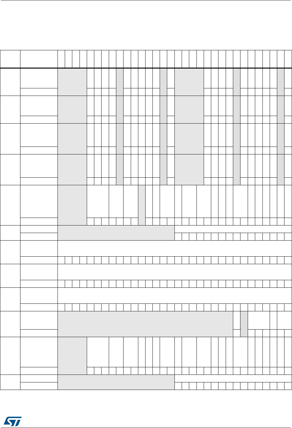
DocID018909 Rev 9 335/1718
RM0090 DMA controller (DMA)
338
10.5.11 DMA register map
Table 51 summarizes the DMA registers.
Table 51. DMA register map and reset values
Offset Register
31
30
29
28
27
26
25
24
23
22
21
20
19
18
17
16
15
14
13
12
11
10
9
8
7
6
5
4
3
2
1
0
0x0000 DMA_LISR Reserved
TCIF3
HTIF3
TEIF3
DMEIF3
Reserved
FEIF3
TCIF2
HTIF2
TEIF2
DMEIF2
Reserved
FEIF2
Reserved
TCIF1
HTIF1
TEIF1
DMEIF1
Reserved
FEIF1
TCIF0
HTIF0
TEIF0
DMEIF0
Reserved
FEIF0
Reset value 0000 00000 0 0000 00000 0
0x0004 DMA_HISR Reserved
TCIF7
HTIF7
TEIF7
DMEIF7
Reserved
FEIF7
TCIF6
HTIF6
TEIF6
DMEIF6
Reserved
FEIF6
Reserved
TCIF5
HTIF5
TEIF5
DMEIF5
Reserved
FEIF5
TCIF4
HTIF4
TEIF4
DMEIF4
Reserved
FEIF4
Reset value 0000 00000 0 0000 00000 0
0x0008 DMA_LIFCR Reserved
CTCIF3
CHTIF3
TEIF3
CDMEIF3
Reserved
CFEIF3
CTCIF2
CHTIF2
CTEIF2
CDMEIF2
Reserved
CFEIF2
Reserved
CTCIF1
CHTIF1
CTEIF1
CDMEIF1
Reserved
CFEIF1
CTCIF0
CHTIF0
CTEIF0
CDMEIF0
Reserved
CFEIF0
Reset value 0000 00000 0 0000 00000 0
0x000C DMA_HIFCR Reserved
CTCIF7
CHTIF7
CTEIF7
CDMEIF7
Reserved
CFEIF7
CTCIF6
CHTIF6
CTEIF6
CDMEIF6
Reserved
CFEIF6
Reserved
CTCIF5
CHTIF5
CTEIF5
CDMEIF5
Reserved
CFEIF5
CTCIF4
CHTIF4
CTEIF4
CDMEIF4
Reserved
CFEIF4
Reset value 0000 00000 0 0000 00000 0
0x0010 DMA_S0CR Reserved
CHSEL[2:0]
MBURST[1:0]
PBURST[1:0]
Reserved
CT
DBM
PL[1:0]
PINCOS
MSIZE[1:0]
PSIZE[1:0]
MINC
PINC
CIRC
DIR[1:0]
PFCTRL
TCIE
HTIE
TEIE
DMEIE
EN
Reset value 0000000 00000000000000000000
0x0014 DMA_S0NDTR Reserved NDT[15:.]
Reset value 0000000000000000
0x0018 DMA_S0PAR PA[31:0]
Reset value 00000000000000000000000000000000
0x001C DMA_S0M0AR M0A[31:0]
Reset value 00000000000000000000000000000000
0x0020 DMA_S0M1AR M1A[31:0]
Reset value 00000000000000000000000000000000
0x0024 DMA_S0FCR Reserved
FEIE
Reserved
FS[2:0]
DMDIS
FTH
[1:0]
Reset value 0 100001
0x0028 DMA_S1CR Reserved
CHSEL
[2:0]
MBURST[1:]
PBURST[1:0]
ACK
CT
DBM
PL[1:0]
PINCOS
MSIZE[1:0]
PSIZE[1:0]
MINC
PINC
CIRC
DIR[1:0]
PFCTRL
TCIE
HTIE
TEIE
DMEIE
EN
Reset value 0000000000000000000000000000
0x002C DMA_S1NDTR Reserved NDT[15:.]
Reset value 0000000000000000
DMA controller (DMA) RM0090
336/1718 DocID018909 Rev 9
0x0030 DMA_S1PAR PA[31:0]
Reset value 00000000000000000000000000000000
0x0034 DMA_S1M0AR M0A[31:0]
Reset value 00000000000000000000000000000000
0x0038 DMA_S1M1AR M1A[31:0]
Reset value 00000000000000000000000000000000
0x003C DMA_S1FCR Reserved
FEIE
Reserved
FS[2:0]
DMDIS
FTH
[1:0]
Reset value 0 100001
0x0040 DMA_S2CR Reserved
CHSEL
[2:0]
MBURST[1:0]
PBURST[1:0]
ACK
CT
DBM
PL[1:0]
PINCOS
MSIZE[1:0]
PSIZE[1:0]
MINC
PINC
CIRC
DIR
[1:0]
PFCTRL
TCIE
HTIE
TEIE
DMEIE
EN
Reset value 0000000000000000000000000000
0x0044 DMA_S2NDTR Reserved NDT[15:.]
Reset value 0000000000000000
0x0048 DMA_S2PAR PA[31:0]
Reset value 00000000000000000000000000000000
0x004C DMA_S2M0AR M0A[31:0]
Reset value 00000000000000000000000000000000
0x0050 DMA_S2M1AR M1A[31:0]
Reset value 00000000000000000000000000000000
0x0054 DMA_S2FCR Reserved
FEIE
Reserved
FS[2:0]
DMDIS
FTH
[1:0]
Reset value 0 100001
0x0058 DMA_S3CR Reserved
CHSEL[2:0]
MBURST[1:0]
PBURST[1:0]
ACK
CT
DBM
PL[1:0]
PINCOS
MSIZE[1:0]
PSIZE[1:0]
MINC
PINC
CIRC
DIR[1:0]
PFCTRL
TCIE
HTIE
TEIE
DMEIE
EN
Reset value 0000000000000000000000000000
0x005C DMA_S3NDTR Reserved NDT[15:.]
Reset value 0000000000000000
0x0060 DMA_S3PAR PA[31:0]
Reset value 00000000000000000000000000000000
0x0064 DMA_S3M0AR M0A[31:0]
Reset value 00000000000000000000000000000000
Table 51. DMA register map and reset values (continued)
Offset Register
31
30
29
28
27
26
25
24
23
22
21
20
19
18
17
16
15
14
13
12
11
10
9
8
7
6
5
4
3
2
1
0
DocID018909 Rev 9 337/1718
RM0090 DMA controller (DMA)
338
0x0068 DMA_S3M1AR M1A[31:0]
Reset value 00000000000000000000000000000000
0x006C DMA_S3FCR Reserved
FEIE
Reserved
FS[2:0]
DMDIS
FTH
[1:0]
Reset value 0 100001
0x0070 DMA_S4CRReserved
CHSEL[2:0]
MBURST[1:0]
PBURST[1:0]
ACK
CT
DBM
PL[1:0]
PINCOS
MSIZE[1:0]
PSIZE[1:0]
MINC
PINC
CIRC
DIR
[1:0]
PFCTRL
TCIE
HTIE
TEIE
DMEIE
EN
Reset value 0000000000000000000000000000
0x0074 DMA_S4NDTR Reserved NDT[15:.]
Reset value 0000000000000000
0x0078 DMA_S4PAR PA[31:0]
Reset value 00000000000000000000000000000000
0x007C DMA_S4M0AR M0A[31:0]
Reset value 00000000000000000000000000000000
0x0080 DMA_S4M1AR M1A[31:0]
Reset value 00000000000000000000000000000000
0x0084 DMA_S4FCR Reserved
FEIE
Reserved
FS[2:0]
DMDIS
FTH
[1:0]
Reset value 0 100001
0x0088 DMA_S5CR Reserved
CHSEL[2:0]
MBURST[1:0]
PBURST[1:0]
ACK
CT
DBM
PL[1:0]
PINCOS
MSIZE[1:0]
PSIZE[1:0]
MINC
PINC
CIRC
DIR[1:0]
PFCTRL
TCIE
HTIE
TEIE
DMEIE
EN
Reset value 0000000000000000000000000000
0x008C DMA_S5NDTR Reserved NDT[15:.]
Reset value 0000000000000000
0x0090 DMA_S5PAR PA[31:0]
Reset value 00000000000000000000000000000000
0x0094 DMA_S5M0AR M0A[31:0]
Reset value 00000000000000000000000000000000
0x0098 DMA_S5M1AR M1A[31:0]
Reset value 00000000000000000000000000000000
0x009C DMA_S5FCR Reserved
FEIE
Reserved
FS[2:0]
DMDIS
FTH
[1:0]
Reset value 0 100001
0x00A0 DMA_S6CR Reserved
CHSEL[2:0]
MBURST[1:0]
PBURST[1:0]
ACK
CT
DBM
PL[1:0]
PINCOS
MSIZE[1:0]
PSIZE[1:0]
MINC
PINC
CIRC
DIR[1:0]
PFCTRL
TCIE
HTIE
TEIE
DMEIE
EN
Reset value 0000000000000000000000000000
0x00A4 DMA_S6NDTR Reserved NDT[15:.]
Reset value 0000000000000000
0x00A8 DMA_S6PAR PA[31:0]
Reset value 00000000000000000000000000000000
Table 51. DMA register map and reset values (continued)
Offset Register
31
30
29
28
27
26
25
24
23
22
21
20
19
18
17
16
15
14
13
12
11
10
9
8
7
6
5
4
3
2
1
0
DMA controller (DMA) RM0090
338/1718 DocID018909 Rev 9
Refer to Table 1 on page 64 for the register boundary addresses.
0x00AC DMA_S6M0AR M0A[31:0]
Reset value 00000000000000000000000000000000
0x00B0 DMA_S6M1AR M1A[31:0]
Reset value 00000000000000000000000000000000
0x00B4 DMA_S6FCR Reserved
FEIE
Reserved
FS[2:0]
DMDIS
FTH
[1:0]
Reset value 0 100001
0x00B8 DMA_S7CR Reserved
CHSEL[2:0]
MBURST[1:0]
PBURST[1:0]
ACK
CT
DBM
PL[1:0]
PINCOS
MSIZE[1:0]
PSIZE[1:0]
MINC
PINC
CIRC
DIR[1:0]
PFCTRL
TCIE
HTIE
TEIE
DMEIE
EN
Reset value 000000000000 000000000000000
0x00BC DMA_S7NDTR Reserved NDT[15:.]
Reset value 0000000000000000
0x00C0 DMA_S7PAR PA[31:0]
Reset value 00000000000000000000000000000000
0x00C4 DMA_S7M0AR M0A[31:0]
Reset value 00000000000000000000000000000000
0x00C8 DMA_S7M1AR M1A[31:0]
Reset value 00000000000000000000000000000000
0x00CC DMA_S7FCR Reserved
FEIE
Reserved
FS[2:0]
DMDIS
FTH
[1:0]
Reset value 0 100001
Table 51. DMA register map and reset values (continued)
Offset Register
31
30
29
28
27
26
25
24
23
22
21
20
19
18
17
16
15
14
13
12
11
10
9
8
7
6
5
4
3
2
1
0

DocID018909 Rev 9 339/1718
RM0090 Chrom-Art Accelerator™ controller (DMA2D)
370
11 Chrom-Art Accelerator™ controller (DMA2D)
11.1 DMA2D introduction
The Chrom-Art Accelerator™ (DMA2D) is a specialized DMA dedicated to image
manipulation. It can perform the following operations:
•Filling a part or the whole of a destination image with a specific color
•Copying a part or the whole of a source image into a part or the whole of a destination
image
•Copying a part or the whole of a source image into a part or the whole of a destination
image with a pixel format conversion
•Blending a part and/or two complete source images with different pixel format and copy
the result into a part or the whole of a destination image with a different color format.
All the classical color coding schemes are supported from 4-bit up to 32-bit per pixel with
indexed or direct color mode. The DMA2D has its own dedicated memories for CLUTs (color
look-up tables).

Chrom-Art Accelerator™ controller (DMA2D) RM0090
340/1718 DocID018909 Rev 9
11.2 DMA2D main features
The main DMA2D features are:
•Single AHB master bus architecture.
•AHB slave programming interface supporting 8/16/32-bit accesses (except for CLUT
accesses which are 32-bit).
•User programmable working area size
•User programmable offset for sources and destination areas
•User programmable sources and destination addresses on the whole memory space
•Up to 2 sources with blending operation
•Alpha value can be modified (source value, fixed value or modulated value)
•User programmable source and destination color format
•Up to 11 color formats supported from 4-bit up to 32-bit per pixel with indirect or direct
color coding
•2 internal memories for CLUT storage in indirect color mode
•Automatic CLUT loading or CLUT programming via the CPU
•User programmable CLUT size
•Internal timer to control AHB bandwidth
•4 operating modes: register-to-memory, memory-to-memory, memory-to-memory with
pixel format conversion, and memory-to-memory with pixel format conversion and
blending
•Area filling with a fixed color
•Copy from an area to another
•Copy with pixel format conversion between source and destination images
•Copy from two sources with independent color format and blending
•Abort and suspend of DMA2D operations
•Watermark interrupt on a user programmable destination line
•Interrupt generation on bus error or access conflict
•Interrupt generation on process completion
11.3 DMA2D functional description
11.3.1 General description
The DMA2D controller performs direct memory transfer. As an AHB master, it can take the
control of the AHB bus matrix to initiate AHB transactions.
The DMA2D can operate in the following modes:
•Register-to-memory
•Memory-to-memory
•Memory-to-memory with Pixel Format Conversion
•Memory-to-memory with Pixel Format Conversion and Blending
The AHB slave port is used to program the DMA2D controller.
The block diagram of the DMA2D is shown in Figure 40: DMA2D block diagram.
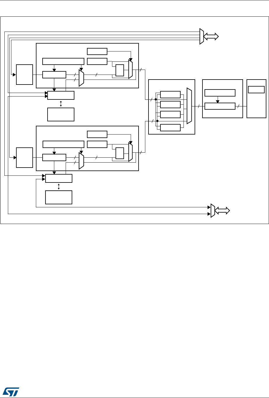
DocID018909 Rev 9 341/1718
RM0090 Chrom-Art Accelerator™ controller (DMA2D)
370
Figure 40. DMA2D block diagram
11.3.2 DMA2D control
The DMA2D controller is configured through the DMA2D Control Register (DMA2D_CR)
which allows selecting:
The user application can perform the following operations:
•Select the operating mode
•Enable/disable the DMA2D interrupt
•Start/suspend/abort ongoing data transfers
11.3.3 DMA2D foreground and background FIFOs
The DMA2D foreground (FG) FG FIFO and background (BG) FIFO fetch the input data to
be copied and/or processed.
The FIFOs fetch the pixels according to the color format defined in their respective pixel
format converter (PFC).
-36
"'0&#
!("3,!6%
!("-!34%2
XBIT
2!-
#,54ITF
XBIT
2!-
#,54ITF
%XPANDER%XPANDER
2'"
D
#OLORMODE
8
BITD
DMODE
D
"'
&)&/
&'0&#
%XPANDER%XPANDER
2'"
D
#OLORMODE
8
BITD
DMODE
D
&'
&)&/
",%.$%2
D
2ED
'REEN
"LUE
/540&#
#OLORMODE
#ONVERTER
/54
&)&/
#OLOR

Chrom-Art Accelerator™ controller (DMA2D) RM0090
342/1718 DocID018909 Rev 9
They are programmed through a set of control registers:
•DMA2D foreground memory address register (DMA2D_FGMAR)
•DMA2D foreground offset register (DMA2D_FGOR)
•DMA2D background memory address register (DMA2D_BGMAR)
•DMA2D background offset register (DMA2D_BGBOR)
•DMA2D number of lines register (number of lines and pixel per lines) (DMA2D_NLR)
When the DMA2D operates in register-to-memory mode, none of the FIFOs is activated.
When the DMA2D operates in memory-to-memory mode (no pixel format conversion nor
blending operation), only the FG FIFO is activated and acts as a buffer.
When the DMA2D operates in memory-to-memory operation with pixel format conversion
(no blending operation), the BG FIFO is not activated.
11.3.4 DMA2D foreground and background pixel format converter (PFC)
DMA2D foreground pixel format converter (PFC) and background pixel format converter
perform the pixel format conversion to generate a 32-bit per pixel value. The PFC can also
modify the alpha channel.
The first stage of the converter converts the color format. The original color format of the
foreground pixel and background pixels are configured through the CM[3:0] bits of the
DMA2D_FGPFCCR and DMA2D_BGPFCCR, respectively.
The supported input formats are given in Table 52: Supported color mode in input.
Table 52. Supported color mode in input
CM[3:0] Color mode
0000 ARGB8888
0001 RGB888
0010 RGB565
0011 ARGB1555
0100 ARGB4444
0101 L8
0110 AL44
0111 AL88
1000 L4
1001 A8
1010 A4

DocID018909 Rev 9 343/1718
RM0090 Chrom-Art Accelerator™ controller (DMA2D)
370
The color format are coded as follows:
•Alpha value field: transparency
0xFF value corresponds to an opaque pixel and 0x00 to a transparent one.
•R field for Red
•G field for Green
•B field for Blue
•L field: luminance
This field is the index to a CLUT to retrieve the three/four RGB/ARGB components.
If the original format was direct color mode, then the extension to 8-bit per channel is
performed by copying the MSBs into the LSBs. This ensures a perfect linearity of the
conversion.
If the original format does not include an alpha channel, the alpha value is automatically set
to 0xFF (opaque).
If the original format is indirect color mode, a CLUT is required and each pixel format
converter is associated with a 256 entry 32-bit CLUT.
For the specific alpha mode A4 and A8, no color information is stored nor indexed. The color
to be used for the image generation is fixed and is defined in the DMA2D_FGCOLR for
foreground pixels and in the DMA2D_BGCOLR register for background pixels.
The order of the fields in the system memory is defined in Table 53: Data order in memory.
The 24-bit RGB888 aligned on 32-bit is supported through the ARGB8888 mode.
Once the 32-bit value is generated, the alpha channel can be modified according to the
AM[1:0] field of the DMA2D_FGPFCCR/DMA2D_BGPFCCR registers as shown in
Table 54: Alpha mode configuration.
Table 53. Data order in memory
Color Mode @ + 3@ + 2@ + 1@ + 0
ARGB8888 A0[7:0] R0[7:0] G0[7:0] B0[7:0]
RGB888
B1[7:0] R0[7:0] G0[7:0] B0[7:0]
G2[7:0] B2[7:0] R1[7:0] G1[7:0]
R3[7:0] G3[7:0] B3[7:0] R2[7:0]
RGB565 R1[4:0]G1[5:3] G1[2:0]B1[4:0] R0[4:0]G0[5:3] G0[2:0]B0[4:0]
ARGB1555 A1[0]R1[4:0]G1[4:3] G1[2:0]B1[4:0] A0[0]R0[4:0]G0[4:3] G0[2:0]B0[4:0]
ARGB4444 A1[3:0]R1[3:0] G1[3:0]B1[3:0] A0[3:0]R0[3:0] G0[3:0]B0[3:0]
L8 L3[7:0] L2[7:0] L1[7:0] L0[7:0]
AL44 A3[3:0]L3[3:0] A2[3:0]L2[3:0] A1[3:0]L1[3:0] A0[3:0]L0[3:0]
AL88 A1[7:0] L1[7:0] A0[7:0] L0[7:0]
L4 L7[3:0]L6[3:0] L5[3:0]L4[3:0] L3[3:0]L2[3:0] L1[3:0]L0[3:0]
A8 A3[7:0] A2[7:0] A1[7:0] A0[7:0]
A4 A7[3:0]A6[3:0] A5[3:0]A4[3:0] A3[3:0]A2[3:0] A1[3:0]A0[3:0]

Chrom-Art Accelerator™ controller (DMA2D) RM0090
344/1718 DocID018909 Rev 9
The alpha channel can be:
•kept as it is (no modification),
•replaced by the ALPHA[7:0] value of DMA2D_FGPFCCR/DMA2D_BGPFCCR,
•or replaced by the original alpha value multiplied by the ALPHA[7:0] value of
DMA2D_FGPFCCR/DMA2D_BGPFCCR divided by 255.
11.3.5 DMA2D foreground and background CLUT interface
The CLUT interface manages the CLUT memory access and the automatic loading of the
CLUT.
Three kinds of accesses are possible:
•CLUT read by the PFC during pixel format conversion operation
•CLUT accessed through the AHB slave port when the CPU is reading or writing data
into the CLUT
•CLUT written through the AHB master port when an automatic loading of the CLUT is
performed
The CLUT memory loading can be done in two different ways:
•Automatic loading
The following sequence should be followed to load the CLUT:
a) Program the CLUT address into the DMA2D_FGCMAR register (foreground
CLUT) or DMA2D_BGCMAR register (background CLUT)
b) Program the CLUT size in the CS[7:0] field of the DMA2D_FGPFCCR register
(foreground CLUT) or DMA2D_BGPFCCR register (background CLUT).
c) Set the START bit of the DMA2D_FGPFCCR register (foreground CLUT) or
DMA2D_BGPFCCR register (background CLUT) to start the transfer. During this
automatic loading process, the CLUT is not accessible by the CPU. If a conflict
occurs, a CLUT access error interrupt is raised assuming CAEIE is set to ‘1’ in
DMA2D_CR.
•Manual loading
The application has to program the CLUT manually through the DMA2D AHB slave
port to which the local CLUT memory is mapped.The foreground CLUT is located at
address offset 0x0400 and the background CLUT at address offset 0x0800.
The CLUT format can be 24 or 32 bits. It is configured through the CCM bit of the
DMA2D_FGPFCCR register (foreground CLUT) or DMA2D_BGPFCCR register
(background CLUT) as shown in Table 55: Supported CLUT color mode.
Table 54. Alpha mode configuration
AM[1:0] Alpha mode
00 No modification
01 Replaced by value in DMA2D_xxPFCCR
10 Replaced by original value multiplied by the value in DMA2D_xxPFCCR / 255
11 Reserved

DocID018909 Rev 9 345/1718
RM0090 Chrom-Art Accelerator™ controller (DMA2D)
370
The way the CLUT data are organized in the system memory is specified in Table 56: CLUT
data order in memory.
11.3.6 DMA2D blender
The DMA2D blender blends the source pixels by pair to compute the resulting pixel.
The blending is performed according to the following equation:
No configuration register is required by the blender. The blender usage depends on the
DMA2D operating mode defined in MODE[1:0] field of the DMA2D_CR register.
11.3.7 DMA2D output PFC
The output PFC performs the pixel format conversion from 32 bits to the output format
defined in the CM[2:0] field of the DMA2D output pixel format converter configuration
register (DMA2D_OPFCCR).
The supported output formats are given in Table 57: Supported color mode in output
Table 55. Supported CLUT color mode
CCM CLUT color mode
0 32-bit ARGB8888
124-bit RGB888
Table 56. CLUT data order in memory
CLUT Color Mode @ + 3 @ + 2 @ + 1 @ + 0
ARGB8888 A0[7:0] R0[7:0] G0[7:0] B0[7:0]
RGB888
B1[7:0] R0[7:0] G0[7:0] B0[7:0]
G2[7:0] B2[7:0] R1[7:0] G1[7:0]
R3[7:0] G3[7:0] B3[7:0] R2[7:0]
COUT =
with αMult =
CFG.αFG + CBG.αBG - CBG.αMult
αOUT
255
αFG . αBG
with C = R or G or B
αOUT = αFG + αBG - αMult
Division is rounded to the nearest lower integer
Chrom-Art Accelerator™ controller (DMA2D) RM0090
346/1718 DocID018909 Rev 9
11.3.8 DMA2D output FIFO
The output FIFO programs the pixels according to the color format defined in the output
PFC.
The destination area is defined through a set of control registers:
•DMA2D output memory address register (DMA2D_OMAR)
•DMA2D output offset register (DMA2D_OOR)
•DMA2D number of lines register (number of lines and pixel per lines) (DMA2D_NLR)
If the DMA2D operates in register-to-memory mode, the configured output rectangle is filled
by the color specified in the DMA2D output color register (DMA2D_OCOLR) which contains
a fixed 32-bit, 24-bit or 16-bit value. The format is selected by the CM[2:0] field of the
DMA2D_OPFCCR register.
The data are stored into the memory in the order defined in Table 58: Data order in memory
The RGB888 aligned on 32-bit is supported through the ARGB8888 mode.
11.3.9 DMA2D AHB master port timer
An 8-bit timer is embedded into the AHB master port to provide an optional limitation of the
bandwidth on the crossbar.
This timer is clocked by the AHB clock and counts a dead time between two consecutive
accesses. This limits the bandwidth usage.
Table 57. Supported color mode in output
CM[2:0] Color mode
000 ARGB8888
001 RGB888
010 RGB565
011 ARGB1555
100 ARGB4444
Table 58. Data order in memory
Color Mode @ + 3@ + 2@ + 1@ + 0
ARGB8888 A0[7:0] R0[7:0] G0[7:0] B0[7:0]
RGB888
B1[7:0] R0[7:0] G0[7:0] B0[7:0]
G2[7:0] B2[7:0] R1[7:0] G1[7:0]
R3[7:0] G3[7:0] B3[7:0] R2[7:0]
RGB565 R1[4:0]G1[5:3] G1[2:0]B1[4:0] R0[4:0]G0[5:3] G0[2:0]B0[4:0]
ARGB1555 A1[0]R1[4:0]G1[4:3] G1[2:0]B1[4:0] A0[0]R0[4:0]G0[4:3] G0[2:0]B0[4:0]
ARGB4444 A1[3:0]R1[3:0] G1[3:0]B1[3:0] A0[3:0]R0[3:0] G0[3:0]B0[3:0]

DocID018909 Rev 9 347/1718
RM0090 Chrom-Art Accelerator™ controller (DMA2D)
370
The timer enabling and the dead time value are configured through the AHB master port
timer configuration register (DMA2D_AMPTCR).
11.3.10 DMA2D transactions
DMA2D transactions consist of a sequence of a given number of data transfers. The
number of data and the width can be programmed by software.
Each DMA2D data transfer is composed of up to 4 steps:
1. Data loading from the memory location pointed by the DMA2D_FGMAR register and
pixel format conversion as defined in DMA2D_FGCR.
2. Data loading from a memory location pointed by the DMA2D_BGMAR register and
pixel format conversion as defined in DMA2D_BGCR.
3. Blending of all retrieved pixels according to the alpha channels resulting of the PFC
operation on alpha values.
4. Pixel format conversion of the resulting pixels according to the DMA2D_OCR register
and programming of the data to the memory location addressed through the
DMA2D_OMAR register.
11.3.11 DMA2D configuration
Both source and destination data transfers can target peripherals and memories in the
whole 4 Gbyte memory area, at addresses ranging between 0x0000 0000 and
0xFFFF FFFF.
The DMA2D can operate in any of the four following modes selected through MODE[1:0]
bits of the DMA2D_CR register:
•Register-to-memory
•Memory-to-memory
•Memory-to-memory with PFC
•Memory-to-memory with PFC and blending
Register-to-memory
The register-to-memory mode is used to fill a user defined area with a predefined color.
The color format is set in the DMA2D_OPFCCR.
The DMA2D does not perform any data fetching from any source. It just writes the color
defined in the DMA2D_OCOLR register to the area located at the address pointed by the
DMA2D_OMAR and defined in the DMA2D_NLR and DMA2D_OOR.
Memory-to-memory
In memory-to-memory mode, the DMA2D does not perform any graphical data
transformation. The foreground input FIFO acts as a buffer and the data are transferred
from the source memory location defined in DMA2D_FGMAR to the destination memory
location pointed by DMA2D_OMAR.
The color mode programmed in the CM[3:0] bits of the DMA2D_FGPFCCR register defines
the number of bits per pixel for both input and output.

Chrom-Art Accelerator™ controller (DMA2D) RM0090
348/1718 DocID018909 Rev 9
The size of the area to be transferred is defined by the DMA2D_NLR and DMA2D_FGOR
registers for the source, and by DMA2D_NLR and DMA2D_OOR registers for the
destination.
Memory-to-memory with PFC
In this mode, the DMA2D performs a pixel format conversion of the source data and stores
them in the destination memory location.
The size of the areas to be transferred are defined by the DMA2D_NLR and DMA2D_FGOR
registers for the source, and by DMA2D_NLR and DMA2D_OOR registers for the
destination.
Data are fetched from the location defined in the DMA2D_FGMAR register and processed
by the foreground PFC. The original pixel format is configured through the
DMA2D_FGPFCCR register.
If the original pixel format is direct color mode, then the color channels are all expanded to 8
bits.
If the pixel format is indirect color mode, the associated CLUT has to be loaded into the
CLUT memory.
The CLUT loading can be done automatically by following the sequence below:
1. Set the CLUT address into the DMA2D_FGCMAR.
2. Set the CLUT size in the CS[7:0] bits of the DMA2D_FGPFCCR register.
3. Set the CLUT format (24 or 32 bits) in the CCM bit of the DMA2D_FGPFCCR register.
4. Start the CLUT loading by setting the START bit of the DMA2D_FGPFCCR register.
Once the CLUT loading is complete, the CTCIF flag of the DMA2D_IFR register is raised,
and an interrupt is generated if the CTCIE bit is set in DMA2D_CR. The automatic CLUT
loading process can not work in parallel with classical DMA2D transfers.
The CLUT can also be filled by the CPU or by any other master through the APB port. The
access to the CLUT is not possible when a DMA2D transfer is ongoing and uses the CLUT
(indirect color format).
In parallel to the color conversion process, the alpha value can be added or changed
depending on the value programmed in the DMA2D_FGPFCCR register. If the original
image does not have an alpha channel, a default alpha value of 0xFF is automatically added
to obtain a fully opaque pixel. The alpha value can be modified according to the AM[1:0] bits
of the DMA2D_FGPFCCR register:
•It can be unchanged.
•It can be replaced by the value defined in the ALPHA[7:0] value of the
DMA2D_FGPFCCR register.
•It can be replaced by the original value multiplied by the ALPHA[7:0] value of the
DMA2D_FGPFCCR register divided by 255.
The resulting 32-bit data are encoded by the OUT PFC into the format specified by the
CM[2:0] field of the DMA2D_OPFCCR register. The output pixel format cannot be the
indirect mode since no CLUT generation process is supported.
The processed data are written into the destination memory location pointed by
DMA2D_OMAR.

DocID018909 Rev 9 349/1718
RM0090 Chrom-Art Accelerator™ controller (DMA2D)
370
Memory-to-memory with PFC and blending
In this mode, 2 sources are fetched in the foreground FIFO and background FIFO from the
memory locations defined by DMA2D_FGMAR and DMA2D_BGMAR.
The two pixel format converters have to be configured as described in the memory-to-
memory mode. Their configurations can be different as each pixel format converter are
independent and have their own CLUT memory.
Once each pixel has been converted into 32 bits by their respective PFCs, they are blended
according to the equation below:
The resulting 32-bit pixel value is encoded by the output PFC according to the specified
output format, and the data are written into the destination memory location pointed by
DMA2D_OMAR.
Configuration error detection
The DMA2D checks that the configuration is correct before any transfer. The configuration
error interrupt flag is set by hardware when a wrong configuration is detected when a new
transfer/automatic loading starts. An interrupt is then generated if the CEIE bit of the
DMA2D_CR is set.
COUT =
with αMult =
CFG.αFG + CBG.αBG - CBG.αMult
αOUT
255
αFG . αBG
with C = R or G or B
αOUT = αFG + αBG - αMult
Division are rounded to the nearest lower integer

Chrom-Art Accelerator™ controller (DMA2D) RM0090
350/1718 DocID018909 Rev 9
The wrong configurations that can be detected are listed below:
•Foreground CLUT automatic loading: MA bits of DMA2D_FGCMAR not aligned with
CCM of DMA2D_FGPFCCR.
•Background CLUT automatic loading: MA of DMA2D_BGCMAR not aligned with CCM
of DMA2D_BGPFCCR
•Memory transfer (except in register-to-memory mode): MA of DMA2D_FGMAR not
aligned with CM of DMA2D_FGPFCCR
•Memory transfer (except in register-to-memory mode): CM in DMA2D_FGPFCCR are
invalid
•Memory transfer (except in register-to-memory mode): PL bits of DMA2D_NLR odd
while CM of DMA2D_FGPFCCR is A4 or L4
•Memory transfer (except in register-to-memory mode): LO bits in DMA2D_FGOR odd
while CM of DMA2D_FGPFCCR is A4 or L4
•Memory transfer (only in blending mode): MA bits in DMA2D_BGMAR are not aligned
with the CM of DMA2D_BGPFCCR
•Memory transfer: CM of DMA2D_BGPFCCR invalid (only in blending mode)
•Memory transfer (only in blending mode): PL bits of DMA2D_NLR odd while CM of
DMA2D_BGPFCCR is A4 or L4
•Memory transfer (only in blending mode): LO bits of DMA2D_BGOR odd while CM of
DMA2D_BGPFCCR is A4 or L4
•Memory transfer (except in memory to memory mode): MA bits in DMA2D_OMAR are
not aligned with CM bits in DMA2D_OPFCCR.
•Memory transfer (except in memory to memory mode): CM bits in DMA2D_OPFCCR
invalid
•Memory transfer: NL bits in DMA2D_NLR = 0
•Memory transfer: PL bits in DMA2D_NLR = 0
11.3.12 DMA2D transfer control (start, suspend, abort and completion)
Once the DMA2D is configured, the transfer can be launched by setting the START bit of the
DMA2D_CR register. Once the transfer is completed, the START bit is automatically reset
and the TCIF flag of the DMA2D_ISR register is raised. An interrupt can be generated if the
TCIE bit of the DMA2D_CR is set.
The user application can suspend the DMA2D at any time by setting the SUSP bit of the
DMA2D_CR register. The transaction can then be aborted by setting the ABORT bit of the
DMA2D_CR register or can be restarted by resetting the SUSP bit of the DMA2D_CR
register.
The user application can abort at any time an ongoing transaction by setting the ABORT bit
of the DMA2D_CR register. In this case, the TCIF flag is not raised.
Automatic CLUT transfers can also be aborted or suspended by using their own START bits
in the DMA2D_FGPFCCR and DDM12D1_BGPFCCR registers.

DocID018909 Rev 9 351/1718
RM0090 Chrom-Art Accelerator™ controller (DMA2D)
370
11.3.13 Watermark
A watermark can be programmed to generate an interrupt when the last pixel of a given line
has been written to the destination memory area.
The line number is defined in the LW[15:0] field of the DMA2D_LWR register.
When the last pixel of this line has been transferred, the TWIF flag of the DMA2D_ISR
register is raised and an interrupt is generated if the TWIE bit of the DMA2D_CR is set.
11.3.14 Error management
Two kind of errors can be triggered:
•AHB master port errors signalled by the TEIF flag of the DMA2D_ISR register.
•Conflicts caused by CLUT access (CPU trying to access the CLUT while a CLUT
loading or a DMA2D transfer is ongoing) signalled by the CAEIF flag of the
DMA2D_ISR register.
Both flags are associated to their own interrupt enable flag in the DMA2D_CR register to
generate an interrupt if need be (TEIE and CAEIE).
11.3.15 AHB dead time
To limit the AHB bandwidth usage, a dead time between two consecutive AHB accesses
can be programmed.
This feature can be enabled by setting the EN bit in the DMA2D_AMTCR register.
The dead time value is stored in the DT[7:0] field of the DMA2D_AMTCR register. This
value represents the guaranteed minimum number of cycles between two consecutive
transactions on the AHB bus.
The update of the dead time value while the DMA2D is running will be taken into account for
the next AHB transfer.
11.4 DMA2D interrupts
An interrupt can be generated on the following events:
•Configuration error
•CLUT transfer complete
•CLUT access error
•Transfer watermark reached
•Transfer complete
•Transfer error
Separate interrupt enable bits are available for flexibility.
Table 59. DMA2D interrupt requests
Interrupt event Event flag Enable control bit
Configuration error CEIF CEIE
CLUT transfer complete CTCIF CTCIE
Chrom-Art Accelerator™ controller (DMA2D) RM0090
352/1718 DocID018909 Rev 9
11.5 DMA2D registers
11.5.1 DMA2D control register (DMA2D_CR)
Address offset: 0x0000
Reset value: 0x0000 0000
CLUT access error CAEIF CAEIE
Transfer watermark TWF TWIE
Transfer complete TCIF TCIE
Transfer error TEIF TEIE
Table 59. DMA2D interrupt requests (continued)
Interrupt event Event flag Enable control bit
31 30 29 28 27 26 25 24 23 22 21 20 19 18 17 16
Reserved MODE
15 14 13 12 11 10 9 8 7 6 5 4 3 2 1 0
Reserved CEIE CTCIE CAEIE TWIE TCIE TEIE Reserved ABORT SUSP START
rw rw rw rw rw rw rs rw rs
Bits 31:18 Reserved, must be kept at reset value
Bits 17:16 MODE: DMA2D mode
This bit is set and cleared by software. It cannot be modified while a transfer is ongoing.
00: Memory-to-memory (FG fetch only)
01: Memory-to-memory with PFC (FG fetch only with FG PFC active)
10: Memory-to-memory with blending (FG and BG fetch with PFC and blending)
11: Register-to-memory (no FG nor BG, only output stage active)
Bits 15:14 Reserved, must be kept at reset value
Bit 13 CEIE: Configuration Error Interrupt Enable
This bit is set and cleared by software.
0: CE interrupt disable
1: CE interrupt enable
Bit 12 CTCIE: CLUT transfer complete interrupt enable
This bit is set and cleared by software.
0: CTC interrupt disable
1: CTC interrupt enable
Bit 11 CAEIE: CLUT access error interrupt enable
This bit is set and cleared by software.
0: CAE interrupt disable
1: CAE interrupt enable

DocID018909 Rev 9 353/1718
RM0090 Chrom-Art Accelerator™ controller (DMA2D)
370
Bit 10 TWIE: Transfer watermark interrupt enable
This bit is set and cleared by software.
0: TW interrupt disable
1: TW interrupt enable
Bit 9 TCIE: Transfer complete interrupt enable
This bit is set and cleared by software.
0: TC interrupt disable
1: TC interrupt enable
Bit 8 TEIE: Transfer error interrupt enable
This bit is set and cleared by software.
0: TE interrupt disable
1: TE interrupt enable
Bits 7:3 Reserved, must be kept at reset value
Bit 2 ABORT: Abort
This bit can be used to abort the current transfer. This bit is set by software and is
automatically reset by hardware when the START bit is reset.
0: No transfer abort requested
1: Transfer abort requested
Bit 1 SUSP: Suspend
This bit can be used to suspend the current transfer. This bit is set and reset by
software. It is automatically reset by hardware when the START bit is reset.
0: Transfer not suspended
1: Transfer suspended
Bit 0 START: Start
This bit can be used to launch the DMA2D according to the parameters loaded in the
various configuration registers. This bit is automatically reset by the following events:
– At the end of the transfer
– When the data transfer is aborted by the user application by setting the ABORT
bit in DMA2D_CR
– When a data transfer error occurs
– When the data transfer has not started due to a configuration error or another
transfer operation already ongoing (automatic CLUT loading).

Chrom-Art Accelerator™ controller (DMA2D) RM0090
354/1718 DocID018909 Rev 9
11.5.2 DMA2D Interrupt Status Register (DMA2D_ISR)
Address offset: 0x0004
Reset value: 0x0000 0000
31 30 29 28 27 26 25 24 23 22 21 20 19 18 17 16
Reserved
15 14 13 12 11 10 9 8 7 6 5 4 3 2 1 0
Reserved
CEIF CTCIF CAEIF TWIF TCIF TEIF
rrrrrr
Bits 31:6 Reserved, must be kept at reset value
Bit 5 CEIF: Configuration error interrupt flag
This bit is set when the START bit of DMA2D_CR, DMA2DFGPFCCR or
DMA2D_BGPFCCR is set and a wrong configuration has been programmed.
Bit 4 CTCIF: CLUT transfer complete interrupt flag
This bit is set when the CLUT copy from a system memory area to the internal DMA2D
memory is complete.
Bit 3 CAEIF: CLUT access error interrupt flag
This bit is set when the CPU accesses the CLUT while the CLUT is being automatically
copied from a system memory to the internal DMA2D.
Bit 2 TWIF: Transfer watermark interrupt flag
This bit is set when the last pixel of the watermarked line has been transferred.
Bit 1 TCIF: Transfer complete interrupt flag
This bit is set when a DMA2D transfer operation is complete (data transfer only).
Bit 0 TEIF: Transfer error interrupt flag
This bit is set when an error occurs during a DMA transfer (data transfer or automatic
CLUT loading).

DocID018909 Rev 9 355/1718
RM0090 Chrom-Art Accelerator™ controller (DMA2D)
370
11.5.3 DMA2D interrupt flag clear register (DMA2D_IFCR)
Address offset: 0x0008
Reset value: 0x0000 0000
31 30 29 28 27 26 25 24 23 22 21 20 19 18 17 16
Reserved
15 14 13 12 11 10 9 8 7 6 5 4 3 2 1 0
Reserved
CCEIF CCTCIF CAECIF CTWIF CTCIF CTEIF
rc_w1 rc_w1 rc_w1 rc_w1 rc_w1 rc_w1
Bits 31:6 Reserved, must be kept at reset value
Bit 5 CCEIF: Clear configuration error interrupt flag
Programming this bit to 1 clears the CEIF flag in the DMA2D_ISR register
Bit 4 CCTCIF: Clear CLUT transfer complete interrupt flag
Programming this bit to 1 clears the CTCIF flag in the DMA2D_ISR register
Bit 3 CAECIF: Clear CLUT access error interrupt flag
Programming this bit to 1 clears the CAEIF flag in the DMA2D_ISR register
Bit 2 CTWIF: Clear transfer watermark interrupt flag
Programming this bit to 1 clears the TWIF flag in the DMA2D_ISR register
Bit 1 CTCIF: Clear transfer complete interrupt flag
Programming this bit to 1 clears the TCIF flag in the DMA2D_ISR register
Bit 0 CTEIF: Clear Transfer error interrupt flag
Programming this bit to 1 clears the TEIF flag in the DMA2D_ISR register
Chrom-Art Accelerator™ controller (DMA2D) RM0090
356/1718 DocID018909 Rev 9
11.5.4 DMA2D foreground memory address register (DMA2D_FGMAR)
Address offset: 0x000C
Reset value: 0x0000 0000
11.5.5 DMA2D foreground offset register (DMA2D_FGOR)
Address offset: 0x0010
Reset value: 0x0000 0000
31 30 29 28 27 26 25 24 23 22 21 20 19 18 17 16
MA[31:16]
rw rw rw rw rw rw rw rw rw rw rw rw rw rw rw rw
15 14 13 12 11 10 9 8 7 6 5 4 3 2 1 0
MA[15:0]
rw rw rw rw rw rw rw rw rw rw rw rw rw rw rw rw
Bits 31:0 MA[31: 0]: Memory address
Address of the data used for the foreground image. This register can only be written
when data transfers are disabled. Once the data transfer has started, this register is
read-only.
The address alignment must match the image format selected e.g. a 32-bit per pixel
format must be 32-bit aligned, a 16-bit per pixel format must be 16-bit aligned and a 4-
bit per pixel format must be 8-bit aligned.
31 30 29 28 27 26 25 24 23 22 21 20 19 18 17 16
Reserved
15 14 13 12 11 10 9 8 7 6 5 4 3 2 1 0
Reserved LO[13:0]
rw rw rw rw rw rw rw rw rw rw rw rw rw rw
Bits 31:14 Reserved, must be kept at reset value
Bits 13:0 LO[13: 0]: Line offset
Line offset used for the foreground expressed in pixel. This value is used to generate
the address. It is added at the end of each line to determine the starting address of the
next line.
These bits can only be written when data transfers are disabled. Once a data transfer
has started, they become read-only.
If the image format is 4-bit per pixel, the line offset must be even.
DocID018909 Rev 9 357/1718
RM0090 Chrom-Art Accelerator™ controller (DMA2D)
370
11.5.6 DMA2D background memory address register (DMA2D_BGMAR)
Address offset: 0x0014
Reset value: 0x0000 0000
11.5.7 DMA2D background offset register (DMA2D_BGOR)
Address offset: 0x0018
Reset value: 0x0000 0000
11.5.8 DMA2D foreground PFC control register (DMA2D_FGPFCCR)
Address offset: 0x001C
Reset value: 0x0000 0000
31 30 29 28 27 26 25 24 23 22 21 20 19 18 17 16
MA[31:16]
rw rw rw rw rw rw rw rw rw rw rw rw rw rw rw rw
15 14 13 12 11 10 9 8 7 6 5 4 3 2 1 0
MA[15:0]
rw rw rw rw rw rw rw rw rw rw rw rw rw rw rw rw
Bits 31: 0 MA[31: 0]: Memory address
Address of the data used for the background image. This register can only be written
when data transfers are disabled. Once a data transfer has started, this register is read-
only.
The address alignment must match the image format selected e.g. a 32-bit per pixel
format must be 32-bit aligned, a 16-bit per pixel format must be 16-bit aligned and a 4-
bit per pixel format must be 8-bit aligned.
31 30 29 28 27 26 25 24 23 22 21 20 19 18 17 16
Reserved
15 14 13 12 11 10 9 8 7 6 5 4 3 2 1 0
Reserved LO[13:0]
rw rw rw rw rw rw rw rw rw rw rw rw rw rw
Bits 31:14 Reserved, must be kept at reset value
Bits 13:0 LO[13: 0]: Line offset
Line offset used for the background image (expressed in pixel). This value is used for
the address generation. It is added at the end of each line to determine the starting
address of the next line.
These bits can only be written when data transfers are disabled. Once data transfer has
started, they become read-only.
If the image format is 4-bit per pixel, the line offset must be even.

Chrom-Art Accelerator™ controller (DMA2D) RM0090
358/1718 DocID018909 Rev 9
31 30 29 28 27 26 25 24 23 22 21 20 19 18 17 16
ALPHA[7:0] Reserved AM[1:0]
rw rw rw rw rw rw rw rw rw rw
15 14 13 12 11 10 9 8 7 6 5 4 3 2 1 0
CS[7:0] Reserved START CCM CM[3:0]
rw rw rw rw rw rw rw rw rc_w1 rw rw rw rw rw
Bits 31:24 ALPHA[7: 0]: Alpha value
These bits define a fixed alpha channel value which can replace the original alpha value
or be multiplied by the original alpha value according to the alpha mode selected
through the AM[1:0] bits.
These bits can only be written when data transfers are disabled. Once a transfer has
started, they become read-only.
Bits 23:18 Reserved, must be kept at reset value
Bits 17:16 AM[1: 0]: Alpha mode
These bits select the alpha channel value to be used for the foreground image. They
can only be written data the transfer are disabled. Once the transfer has started, they
become read-only.
00: No modification of the foreground image alpha channel value
01: Replace original foreground image alpha channel value by ALPHA[7: 0]
10: Replace original foreground image alpha channel value by ALPHA[7:0] multiplied
with original alpha channel value
other configurations are meaningless
Bits 15:8 CS[7: 0]: CLUT size
These bits define the size of the CLUT used for the foreground image. Once the CLUT
transfer has started, this field is read-only.
The number of CLUT entries is equal to CS[7:0] + 1.
Bits 7:6 Reserved, must be kept at reset value

DocID018909 Rev 9 359/1718
RM0090 Chrom-Art Accelerator™ controller (DMA2D)
370
Bit 5 START: Start
This bit can be set to start the automatic loading of the CLUT. It is automatically reset:
– at the end of the transfer
– when the transfer is aborted by the user application by setting the ABORT bit in
DMA2D_CR
– when a transfer error occurs
– when the transfer has not started due to a configuration error or another
transfer operation already ongoing (data transfer or automatic background
CLUT transfer).
Bit 4 CCM: CLUT color mode
This bit defines the color format of the CLUT. It can only be written when the transfer is
disabled. Once the CLUT transfer has started, this bit is read-only.
0: ARGB8888
1: RGB888
others: meaningless
Bits 3:0 CM[3: 0]: Color mode
These bits defines the color format of the foreground image. They can only be written
when data transfers are disabled. Once the transfer has started, they are read-only.
0000: ARGB8888
0001: RGB888
0010: RGB565
0011: ARGB1555
0100: ARGB4444
0101: L8
0110: AL44
0111: AL88
1000: L4
1001: A8
1010: A4
others: meaningless

Chrom-Art Accelerator™ controller (DMA2D) RM0090
360/1718 DocID018909 Rev 9
11.5.9 DMA2D foreground color register (DMA2D_FGCOLR)
Address offset: 0x0020
Reset value: 0x0000 0000
31 30 29 28 27 26 25 24 23 22 21 20 19 18 17 16
Reserved RED[7:0]
rw rw rw rw rw rw rw rw
15 14 13 12 11 10 9 8 7 6 5 4 3 2 1 0
GREEN[7:0] BLUE[7:0]
rw rw rw rw rw rw rw rw rw rw rw rw rw rw rw rw
Bits 31:24 Reserved, must be kept at reset value
Bits 23:16 RED[7: 0]: Red Value
These bits defines the red value for the A4 or A8 mode of the foreground image. They
can only be written when data transfers are disabled. Once the transfer has started,
they are read-only.
Bits 15:8 GREEN[7: 0]: Green Value
These bits defines the green value for the A4 or A8 mode of the foreground image. They
can only be written when data transfers are disabled. Once the transfer has started,
They are read-only.
Bits 7:0 BLUE[7: 0]: Blue Value
These bits defines the blue value for the A4 or A8 mode of the foreground image. They
can only be written when data transfers are disabled. Once the transfer has started,
They are read-only.

DocID018909 Rev 9 361/1718
RM0090 Chrom-Art Accelerator™ controller (DMA2D)
370
11.5.10 DMA2D background PFC control register (DMA2D_BGPFCCR)
Address offset: 0x0024
Reset value: 0x0000 0000
31 30 29 28 27 26 25 24 23 22 21 20 19 18 17 16
ALPHA[7:0] Reserved AM[1:0]
rw rw rw rw rw rw rw rw rw rw
15 14 13 12 11 10 9 8 7 6 5 4 3 2 1 0
CS[7:0] Reserved START CCM CM[3:0]
rw rw rw rw rw rw rw rw rc_w1 rw rw rw rw rw
Bits 31:24 ALPHA[7: 0]: Alpha value
These bits define a fixed alpha channel value which can replace the original alpha value
or be multiplied with the original alpha value according to the alpha mode selected with
bits AM[1: 0]. These bits can only be written when data transfers are disabled. Once the
transfer has started, they are read-only.
Bits 23:18 Reserved, must be kept at reset value
Bits 17:16 AM[1: 0]: Alpha mode
These bits define which alpha channel value to be used for the background image.
These bits can only be written when data transfers are disabled. Once the transfer has
started, they are read-only.
00: No modification of the foreground image alpha channel value
01: Replace original background image alpha channel value by ALPHA[7: 0]
10: Replace original background image alpha channel value by ALPHA[7:0] multiplied
with original alpha channel value
others: meaningless
Bits 15:8 CS[7: 0]: CLUT size
These bits define the size of the CLUT used for the BG. Once the CLUT transfer has
started, this field is read-only.
The number of CLUT entries is equal to CS[7:0] + 1.
Bits 7:6 Reserved, must be kept at reset value

Chrom-Art Accelerator™ controller (DMA2D) RM0090
362/1718 DocID018909 Rev 9
Bit 5 START: Start
This bit is set to start the automatic loading of the CLUT. This bit is automatically reset:
– at the end of the transfer
– when the transfer is aborted by the user application by setting the ABORT bit in
the DMA2D_CR
– when a transfer error occurs
– when the transfer has not started due to a configuration error or another
transfer operation already on going (data transfer or automatic BackGround
CLUT transfer).
Bit 4 CCM: CLUT Color mode
These bits define the color format of the CLUT. This register can only be written when
the transfer is disabled. Once the CLUT transfer has started, this bit is read-only.
0: ARGB8888
1: RGB888
others: meaningless
Bits 3:0 CM[3: 0]: Color mode
These bits define the color format of the foreground image. These bits can only be
written when data transfers are disabled. Once the transfer has started, they are read-
only.
0000: ARGB8888
0001: RGB888
0010: RGB565
0011: ARGB1555
0100: ARGB4444
0101: L8
0110: AL44
0111: AL88
1000: L4
1001: A8
1010: A4
others: meaningless
DocID018909 Rev 9 363/1718
RM0090 Chrom-Art Accelerator™ controller (DMA2D)
370
11.5.11 DMA2D background color register (DMA2D_BGCOLR)
Address offset: 0x0028
Reset value: 0x0000 0000
11.5.12 DMA2D foreground CLUT memory address register
(DMA2D_FGCMAR)
Address offset: 0x002C
Reset value: 0x0000 0000
31 30 29 28 27 26 25 24 23 22 21 20 19 18 17 16
Reserved RED[7:0]
rw rw rw rw rw rw rw rw
15 14 13 12 11 10 9 8 7 6 5 4 3 2 1 0
GREEN[7:0] BLUE[7:0]
rw rw rw rw rw rw rw rw rw rw rw rw rw rw rw rw
Bits 31:24 Reserved, must be kept at reset value
Bits 23:16 RED[7: 0]: Red Value
These bits define the red value for the A4 or A8 mode of the background. These bits
can only be written when data transfers are disabled. Once the transfer has started,
they are read-only.
Bits 15:8 GREEN[7: 0]: Green Value
These bits define the green value for the A4 or A8 mode of the background. These bits
can only be written when data transfers are disabled. Once the transfer has started,
they are read-only.
Bits 7:0 BLUE[7: 0]: Blue Value
These bits define the blue value for the A4 or A8 mode of the background. These bits
can only be written when data transfers are disabled. Once the transfer has started,
they are read-only.
31 30 29 28 27 26 25 24 23 22 21 20 19 18 17 16
MA[31:16]
rw rw rw rw rw rw rw rw rw rw rw rw rw rw rw rw
15 14 13 12 11 10 9 8 7 6 5 4 3 2 1 0
MA[15:0]
rw rw rw rw rw rw rw rw rw rw rw rw rw rw rw rw
Bits 31: 0 MA[31: 0]: Memory Address
Address of the data used for the CLUT address dedicated to the foreground image. This
register can only be written when no transfer is ongoing. Once the CLUT transfer has
started, this register is read-only.
If the foreground CLUT format is 32-bit, the address must be 32-bit aligned.
Chrom-Art Accelerator™ controller (DMA2D) RM0090
364/1718 DocID018909 Rev 9
11.5.13 DMA2D background CLUT memory address register
(DMA2D_BGCMAR)
Address offset: 0x0030
Reset value: 0x0000 0000
11.5.14 DMA2D output PFC control register (DMA2D_OPFCCR)
Address offset: 0x0034
Reset value: 0x0000 0000
31 30 29 28 27 26 25 24 23 22 21 20 19 18 17 16
MA[31:16]
rw rw rw rw rw rw rw rw rw rw rw rw rw rw rw rw
15 14 13 12 11 10 9 8 7 6 5 4 3 2 1 0
MA[15:0]
rw rw rw rw rw rw rw rw rw rw rw rw rw rw rw rw
Bits 31: 0 MA[31: 0]: Memory address
Address of the data used for the CLUT address dedicated to the background image.
This register can only be written when no transfer is on going. Once the CLUT transfer
has started, this register is read-only.
If the background CLUT format is 32-bit, the address must be 32-bit aligned.
31 30 29 28 27 26 25 24 23 22 21 20 19 18 17 16
Reserved
15 14 13 12 11 10 9 8 7 6 5 4 3 2 1 0
Reserved CM[2:0]
rw rw rw
Bits 31: 3 Reserved, must be kept at reset value
Bits 2: 0 CM[2: 0]: Color mode
These bits define the color format of the output image. These bits can only be written
when data transfers are disabled. Once the transfer has started, they are read-only.
000: ARGB8888
001: RGB888
010: RGB565
011: ARGB1555
100: ARGB4444
others: meaningless

DocID018909 Rev 9 365/1718
RM0090 Chrom-Art Accelerator™ controller (DMA2D)
370
11.5.15 DMA2D output color register (DMA2D_OCOLR)
Address offset: 0x0038
Reset value: 0x0000 0000
31 30 29 28 27 26 25 24 23 22 21 20 19 18 17 16
ALPHA[7:0] RED[7:0]
rw rw rw rw rw rw rw rw rw rw rw rw rw rw rw rw
15 14 13 12 11 10 9 8 7 6 5 4 3 2 1 0
GREEN[7:0] BLUE[7:0]
RED[4:0] GREEN[5:0] BLUE[4:0]
A RED[4:0] GREEN[4:0] BLUE[4:0]
ALPHA[3:0] RED[3:0] GREEN[3:0] BLUE[3:0]
rw rw rw rw rw rw rw rw rw rw rw rw rw rw rw rw
Bits 31:24 ALPHA[7: 0]: Alpha Channel Value
These bits define the alpha channel of the output color. These bits can only be written
when data transfers are disabled. Once the transfer has started, they are read-only.
Bits 23:16 RED[7: 0]: Red Value
These bits define the red value of the output image. These bits can only be written when
data transfers are disabled. Once the transfer has started, they are read-only.
Bits 15:8 GREEN[7: 0]: Green Value
These bits define the green value of the output image. These bits can only be written
when data transfers are disabled. Once the transfer has started, they are read-only.
Bits 7:0 BLUE[7: 0]: Blue Value
These bits define the blue value of the output image. These bits can only be written
when data transfers are disabled. Once the transfer has started, they are read-only.

Chrom-Art Accelerator™ controller (DMA2D) RM0090
366/1718 DocID018909 Rev 9
11.5.16 DMA2D output memory address register (DMA2D_OMAR)
Address offset: 0x003C
Reset value: 0x0000 0000
31 30 29 28 27 26 25 24 23 22 21 20 19 18 17 16
MA[31:16]
rw rw rw rw rw rw rw rw rw rw rw rw rw rw rw rw
15 14 13 12 11 10 9 8 7 6 5 4 3 2 1 0
MA[15:0]
rw rw rw rw rw rw rw rw rw rw rw rw rw rw rw rw
Bits 31: 0 MA[31: 0]: Memory Address
Address of the data used for the output FIFO. These bits can only be written when data
transfers are disabled. Once the transfer has started, they are read-only.
The address alignment must match the image format selected e.g. a 32-bit per pixel
format must be 32-bit aligned and a 16-bit per pixel format must be 16-bit aligned.

DocID018909 Rev 9 367/1718
RM0090 Chrom-Art Accelerator™ controller (DMA2D)
370
11.5.17 DMA2D output offset register (DMA2D_OOR)
Address offset: 0x0040
Reset value: 0x0000 0000
11.5.18 DMA2D number of line register (DMA2D_NLR)
Address offset: 0x0044
Reset value: 0x0000 0000
31 30 29 28 27 26 25 24 23 22 21 20 19 18 17 16
Reserved
15 14 13 12 11 10 9 8 7 6 5 4 3 2 1 0
Reserved
LO[13:0]
rw rw rw rw rw rw rw rw rw rw rw rw rw rw
Bits 31:14 Reserved, must be kept at reset value
Bits 13:0 LO[13: 0]: Line Offset
Line offset used for the output (expressed in pixels). This value is used for the address
generation. It is added at the end of each line to determine the starting address of the
next line. These bits can only be written when data transfers are disabled. Once the
transfer has started, they are read-only.
31 30 29 28 27 26 25 24 23 22 21 20 19 18 17 16
Reserved PL[13:0]
rw rw rw rw rw rw rw rw rw rw rw rw rw rw
15 14 13 12 11 10 9 8 7 6 5 4 3 2 1 0
NL[15:0]
rw rw rw rw rw rw rw rw rw rw rw rw rw rw rw rw
Bits 31:30 Reserved, must be kept at reset value
Bits 29:16 PL[13: 0]: Pixel per lines
Number of pixels per lines of the area to be transferred. These bits can only be written
when data transfers are disabled. Once the transfer has started, they are read-only.
If any of the input image format is 4-bit per pixel, pixel per lines must be even.
Bits 15:0 NL[15: 0]: Number of lines
Number of lines of the area to be transferred. These bits can only be written when data
transfers are disabled. Once the transfer has started, they are read-only.
Chrom-Art Accelerator™ controller (DMA2D) RM0090
368/1718 DocID018909 Rev 9
11.5.19 DMA2D line watermark register (DMA2D_LWR)
Address offset: 0x0048
Reset value: 0x0000 0000
11.5.20 DMA2D AHB master timer configuration register (DMA2D_AMTCR)
Address offset: 0x004C
Reset value: 0x0000 0000
31 30 29 28 27 26 25 24 23 22 21 20 19 18 17 16
Reserved
15 14 13 12 11 10 9 8 7 6 5 4 3 2 1 0
LW[15:0]
rw rw rw rw rw rw rw rw rw rw rw rw rw rw rw rw
Bits 31:16 Reserved, must be kept at reset value
Bits 15:0 LW[15:0]: Line watermark
These bits allow to configure the line watermark for interrupt generation.
An interrupt is raised when the last pixel of the watermarked line has been transferred.
These bits can only be written when data transfers are disabled. Once the transfer has
started, they are read-only.
31 30 29 28 27 26 25 24 23 22 21 20 19 18 17 16
Reserved
15 14 13 12 11 10 9 8 7 6 5 4 3 2 1 0
DT[7:0] Reserved EN
rw rw rw rw rw rw rw rw rw
Bits 31:16 Reserved
Bits 15:8 DT[7: 0]: Dead Time
Dead time value in the AHB clock cycle inserted between two consecutive accesses on
the AHB master port. These bits represent the minimum guaranteed number of cycles
between two consecutive AHB accesses.
Bits 7:1 Reserved
Bit 0 EN: Enable
Enables the dead time functionality.
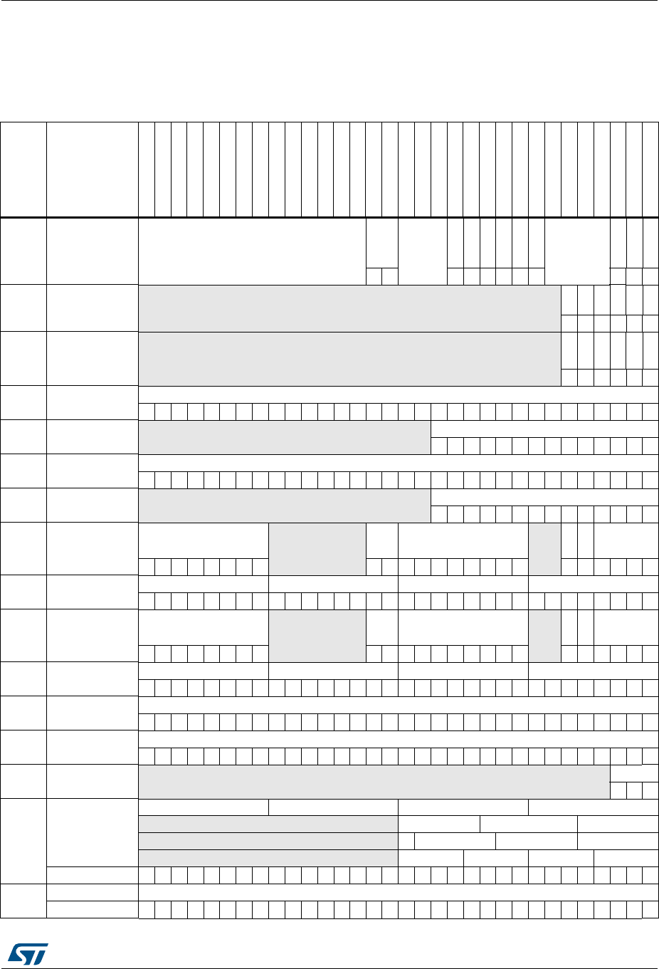
DocID018909 Rev 9 369/1718
RM0090 Chrom-Art Accelerator™ controller (DMA2D)
370
11.5.21 DMA2D register map
The following table summarizes the DMA2D registers. Refer to Table 1 on page 64 for the
DMA2D register base address.
Table 60. DMA2D register map and reset values
Offset Register
31
30
29
28
27
26
25
24
23
22
21
20
19
18
17
16
15
14
13
12
11
10
9
8
7
6
5
4
3
2
1
0
0x0000 DMA2D_CR Reserved
MODE[1:0]
Reserved
CEIE
CTCIE
CAEIE
TWIE
TCIE
TEIE
Reserved
ABORT
SUSP
START
Reset value 00 000000 000
0x0004 DMA2D_ISR Reserved
CEIF
CTCIF
CAEIF
TWIF
TCIF
TEIF
Reset value 000000
0x0008 DMA2D_IFCR Reserved
CCEIF
CCTCIF
CAECIF
CTWIF
CTCIF
CTEIF
Reset value 000000
0x000C DMA2D_FGMAR MA[31:0]
Reset value 00000000000000000000000000000000
0x0010 DMA2D_FGOR Reserved LO[13:0]
Reset value 00000000000000
0x0014 DMA2D_BGMAR MA[31:0]
Reset value 00000000000000000000000000000000
0x0018 DMA2D_BGOR Reserved LO[13:0]
Reset value 00000000000000
0x001C DMA2D_FGPFCCR ALPHA[7:0] Reserved
AM[1:0]
CS[7:0] Res
START
CCM
CM[3:0]
Reset value 00000000 0000000000 000000
0x0020 DMA2D_FGCOLR APLHA[7:0] RED[7:0] GREEN[7:0] BLUE[7:0]
Reset value 00000000000000000000000000000000
0x0024 DMA2D_BGPFCCR ALPHA[7:0] Reserved
AM[1:0]
CS[7:0] Res
START
CCM
CM[3:0]
Reset value 00000000 0000000000 000000
0x0028 DMA2D_BGCOLR APLHA[7:0] RED[7:0] GREEN[7:0] BLUE[7:0]
Reset value 00000000000000000000000000000000
0x002C DMA2D_FGCMAR MA[31:0]
Reset value 00000000000000000000000000000000
0x0030 DMA2D_BGCMAR MA[31:0]
Reset value 00000000000000000000000000000000
0x0034 DMA2D_OPFCCR Reserved CM[2:0]
Reset value 000
0x0038 DMA2D_OCOLR
APLHA[7:0] RED[7:0] GREEN[7:0] BLUE[7:0]
Reserved RED[4:0] GREEN[6:0] BLUE[4:0]
Reserved A RED[4:0] GREEN[4:0] BLUE[4:0]
Reserved ALPHA[3:0] RED[3:0] GREEN[3:0] BLUE[3:0]
Reset value 00000000000000000000000000000000
0x003C DMA2D_OMAR MA[31:0]
Reset value 00000000000000000000000000000000
Chrom-Art Accelerator™ controller (DMA2D) RM0090
370/1718 DocID018909 Rev 9
0x0040 DMA2D_OOR Reserved LO[13:0]
Reset value 00000000000000
0x0044 DMA2D_NLR Res PL[13:0] NL[15:0]
Reset value 000000000000000000000000000000
0x0048 DMA2D_LWR Reserved LW[15:0]
Reset value 0000000000000000
0x004C DMA2D_AMTCR Reserved DT[7:0] Reserved
EN
Reset value 00000000 0
0x0050-
Ox03FF Reserved
0x0400-
0x07FF
DMA2D_FGCLUT APLHA[7:0][255:0] RED[7:0][255:0] GREEN[7:0][255:0] BLUE[7:0][255:0]
Reset value XXXXXXXXXXXXXXXXXXXXXXXXXXXXXXXX
0x0800-
0x0BFF
DMA2D_BGCLUT APLHA[7:0][255:0] RED[7:0][255:0] GREEN[7:0][255:0] BLUE[7:0][255:0]
Reset value XXXXXXXXXXXXXXXXXXXXXXXXXXXXXXXX
Table 60. DMA2D register map and reset values (continued)
Offset Register
31
30
29
28
27
26
25
24
23
22
21
20
19
18
17
16
15
14
13
12
11
10
9
8
7
6
5
4
3
2
1
0

DocID018909 Rev 9 371/1718
RM0090 Interrupts and events
387
12 Interrupts and events
This Section applies to the whole STM32F4xx family, unless otherwise specified.
12.1 Nested vectored interrupt controller (NVIC)
12.1.1 NVIC features
The nested vector interrupt controller NVIC includes the following features:
•82 maskable interrupt channels for STM32F405xx/07xx and STM32F415xx/17xx, and
up to 91 maskable interrupt channels for STM32F42xxx and STM32F43xxx (not
including the 16 interrupt lines of Cortex®-M4 with FPU)
•16 programmable priority levels (4 bits of interrupt priority are used)
•low-latency exception and interrupt handling
•power management control
•implementation of system control registers
The NVIC and the processor core interface are closely coupled, which enables low latency
interrupt processing and efficient processing of late arriving interrupts.
All interrupts including the core exceptions are managed by the NVIC. For more information
on exceptions and NVIC programming, refer to programming manual PM0214.
12.1.2 SysTick calibration value register
The SysTick calibration value is fixed to 18750, which gives a reference time base of 1 ms
with the SysTick clock set to 18.75 MHz (HCLK/8, with HCLK set to 150 MHz).
12.1.3 Interrupt and exception vectors
See Table 62 and Table 62, for the vector table for the STM32F405xx/07xx and
STM32F415xx/17xx and STM32F42xxx and STM32F43xxx devices.
12.2 External interrupt/event controller (EXTI)
The external interrupt/event controller consists of up to 23 edge detectors for generating
event/interrupt requests. Each input line can be independently configured to select the type
(interrupt or event) and the corresponding trigger event (rising or falling or both). Each line
can also masked independently. A pending register maintains the status line of the interrupt
requests.

Interrupts and events RM0090
372/1718 DocID018909 Rev 9
Table 61. Vector table for STM32F405xx/07xx and STM32F415xx/17xx
Position
Priority
Type of
priority Acronym Description Address
- - - Reserved 0x0000 0000
-3 fixed Reset Reset 0x0000 0004
-2 fixed NMI
Non maskable interrupt. The RCC
Clock Security System (CSS) is linked
to the NMI vector.
0x0000 0008
-1 fixed HardFault All class of fault 0x0000 000C
0 settable MemManage Memory management 0x0000 0010
1 settable BusFault Pre-fetch fault, memory access fault 0x0000 0014
2 settable UsageFault Undefined instruction or illegal state 0x0000 0018
- - - Reserved 0x0000 001C - 0x0000
002B
3 settable SVCall System service call via SWI
instruction 0x0000 002C
4 settable Debug Monitor Debug Monitor 0x0000 0030
- - - Reserved 0x0000 0034
5 settable PendSV Pendable request for system service 0x0000 0038
6 settable SysTick System tick timer 0x0000 003C
0 7 settable WWDG Window Watchdog interrupt 0x0000 0040
1 8 settable PVD PVD through EXTI line detection
interrupt 0x0000 0044
2 9 settable TAMP_STAMP Tamper and TimeStamp interrupts
through the EXTI line 0x0000 0048
3 10 settable RTC_WKUP RTC Wakeup interrupt through the
EXTI line 0x0000 004C
4 11 settable FLASH Flash global interrupt 0x0000 0050
5 12 settable RCC RCC global interrupt 0x0000 0054
6 13 settable EXTI0 EXTI Line0 interrupt 0x0000 0058
7 14 settable EXTI1 EXTI Line1 interrupt 0x0000 005C
8 15 settable EXTI2 EXTI Line2 interrupt 0x0000 0060
9 16 settable EXTI3 EXTI Line3 interrupt 0x0000 0064
10 17 settable EXTI4 EXTI Line4 interrupt 0x0000 0068
11 18 settable DMA1_Stream0 DMA1 Stream0 global interrupt 0x0000 006C

DocID018909 Rev 9 373/1718
RM0090 Interrupts and events
387
12 19 settable DMA1_Stream1 DMA1 Stream1 global interrupt 0x0000 0070
13 20 settable DMA1_Stream2 DMA1 Stream2 global interrupt 0x0000 0074
14 21 settable DMA1_Stream3 DMA1 Stream3 global interrupt 0x0000 0078
15 22 settable DMA1_Stream4 DMA1 Stream4 global interrupt 0x0000 007C
16 23 settable DMA1_Stream5 DMA1 Stream5 global interrupt 0x0000 0080
17 24 settable DMA1_Stream6 DMA1 Stream6 global interrupt 0x0000 0084
18 25 settable ADC ADC1, ADC2 and ADC3 global
interrupts 0x0000 0088
19 26 settable CAN1_TX CAN1 TX interrupts 0x0000 008C
20 27 settable CAN1_RX0 CAN1 RX0 interrupts 0x0000 0090
21 28 settable CAN1_RX1 CAN1 RX1 interrupt 0x0000 0094
22 29 settable CAN1_SCE CAN1 SCE interrupt 0x0000 0098
23 30 settable EXTI9_5 EXTI Line[9:5] interrupts 0x0000 009C
24 31 settable TIM1_BRK_TIM9 TIM1 Break interrupt and TIM9 global
interrupt 0x0000 00A0
25 32 settable TIM1_UP_TIM10 TIM1 Update interrupt and TIM10
global interrupt 0x0000 00A4
26 33 settable TIM1_TRG_COM_TIM11 TIM1 Trigger and Commutation
interrupts and TIM11 global interrupt 0x0000 00A8
27 34 settable TIM1_CC TIM1 Capture Compare interrupt 0x0000 00AC
28 35 settable TIM2 TIM2 global interrupt 0x0000 00B0
29 36 settable TIM3 TIM3 global interrupt 0x0000 00B4
30 37 settable TIM4 TIM4 global interrupt 0x0000 00B8
31 38 settable I2C1_EV I2C1 event interrupt 0x0000 00BC
32 39 settable I2C1_ER I2C1 error interrupt 0x0000 00C0
33 40 settable I2C2_EV I2C2 event interrupt 0x0000 00C4
34 41 settable I2C2_ER I2C2 error interrupt 0x0000 00C8
35 42 settable SPI1 SPI1 global interrupt 0x0000 00CC
36 43 settable SPI2 SPI2 global interrupt 0x0000 00D0
37 44 settable USART1 USART1 global interrupt 0x0000 00D4
38 45 settable USART2 USART2 global interrupt 0x0000 00D8
39 46 settable USART3 USART3 global interrupt 0x0000 00DC
Table 61. Vector table for STM32F405xx/07xx and STM32F415xx/17xx (continued)
Position
Priority
Type of
priority Acronym Description Address

Interrupts and events RM0090
374/1718 DocID018909 Rev 9
40 47 settable EXTI15_10 EXTI Line[15:10] interrupts 0x0000 00E0
41 48 settable RTC_Alarm RTC Alarms (A and B) through EXTI
line interrupt 0x0000 00E4
42 49 settable OTG_FS WKUP USB On-The-Go FS Wakeup through
EXTI line interrupt 0x0000 00E8
43 50 settable TIM8_BRK_TIM12 TIM8 Break interrupt and TIM12
global interrupt 0x0000 00EC
44 51 settable TIM8_UP_TIM13 TIM8 Update interrupt and TIM13
global interrupt 0x0000 00F0
45 52 settable TIM8_TRG_COM_TIM14 TIM8 Trigger and Commutation
interrupts and TIM14 global interrupt 0x0000 00F4
46 53 settable TIM8_CC TIM8 Capture Compare interrupt 0x0000 00F8
47 54 settable DMA1_Stream7 DMA1 Stream7 global interrupt 0x0000 00FC
48 55 settable FSMC FSMC global interrupt 0x0000 0100
49 56 settable SDIO SDIO global interrupt 0x0000 0104
50 57 settable TIM5 TIM5 global interrupt 0x0000 0108
51 58 settable SPI3 SPI3 global interrupt 0x0000 010C
52 59 settable UART4 UART4 global interrupt 0x0000 0110
53 60 settable UART5 UART5 global interrupt 0x0000 0114
54 61 settable TIM6_DAC
TIM6 global interrupt,
DAC1 and DAC2 underrun error
interrupts
0x0000 0118
55 62 settable TIM7 TIM7 global interrupt 0x0000 011C
56 63 settable DMA2_Stream0 DMA2 Stream0 global interrupt 0x0000 0120
57 64 settable DMA2_Stream1 DMA2 Stream1 global interrupt 0x0000 0124
58 65 settable DMA2_Stream2 DMA2 Stream2 global interrupt 0x0000 0128
59 66 settable DMA2_Stream3 DMA2 Stream3 global interrupt 0x0000 012C
60 67 settable DMA2_Stream4 DMA2 Stream4 global interrupt 0x0000 0130
61 68 settable ETH Ethernet global interrupt 0x0000 0134
62 69 settable ETH_WKUP Ethernet Wakeup through EXTI line
interrupt 0x0000 0138
63 70 settable CAN2_TX CAN2 TX interrupts 0x0000 013C
64 71 settable CAN2_RX0 CAN2 RX0 interrupts 0x0000 0140
Table 61. Vector table for STM32F405xx/07xx and STM32F415xx/17xx (continued)
Position
Priority
Type of
priority Acronym Description Address

DocID018909 Rev 9 375/1718
RM0090 Interrupts and events
387
65 72 settable CAN2_RX1 CAN2 RX1 interrupt 0x0000 0144
66 73 settable CAN2_SCE CAN2 SCE interrupt 0x0000 0148
67 74 settable OTG_FS USB On The Go FS global interrupt 0x0000 014C
68 75 settable DMA2_Stream5 DMA2 Stream5 global interrupt 0x0000 0150
69 76 settable DMA2_Stream6 DMA2 Stream6 global interrupt 0x0000 0154
70 77 settable DMA2_Stream7 DMA2 Stream7 global interrupt 0x0000 0158
71 78 settable USART6 USART6 global interrupt 0x0000 015C
72 79 settable I2C3_EV I2C3 event interrupt 0x0000 0160
73 80 settable I2C3_ER I2C3 error interrupt 0x0000 0164
74 81 settable OTG_HS_EP1_OUT USB On The Go HS End Point 1 Out
global interrupt 0x0000 0168
75 82 settable OTG_HS_EP1_IN USB On The Go HS End Point 1 In
global interrupt 0x0000 016C
76 83 settable OTG_HS_WKUP USB On The Go HS Wakeup through
EXTI interrupt 0x0000 0170
77 84 settable OTG_HS USB On The Go HS global interrupt 0x0000 0174
78 85 settable DCMI DCMI global interrupt 0x0000 0178
79 86 settable CRYP CRYP crypto global interrupt 0x0000 017C
80 87 settable HASH_RNG Hash and Rng global interrupt 0x0000 0180
81 88 settable FPU FPU global interrupt 0x0000 0184
Table 61. Vector table for STM32F405xx/07xx and STM32F415xx/17xx (continued)
Position
Priority
Type of
priority Acronym Description Address
Table 62. Vector table for STM32F42xxx and STM32F43xxx
Position
Priority
Type of
priority Acronym Description Address
- - - Reserved 0x0000 0000
-3 fixed Reset Reset 0x0000 0004
-2 fixed NMI Non maskable interrupt, Clock Security
System 0x0000 0008

Interrupts and events RM0090
376/1718 DocID018909 Rev 9
-1 fixed HardFault All class of fault 0x0000 000C
0 settable MemManage Memory management 0x0000 0010
1 settable BusFault Pre-fetch fault, memory access fault 0x0000 0014
2settable UsageFault Undefined instruction or illegal state 0x0000 0018
- - - Reserved 0x0000 001C -
0x0000 002B
3settable SVCall System Service call via SWI instruction 0x0000 002C
4settable Debug Monitor Debug Monitor 0x0000 0030
- - Reserved 0x0000 0034
5settable PendSV Pendable request for system service 0x0000 0038
6settable Systick System tick timer 0x0000 003C
0 7 settable WWDG Window Watchdog interrupt 0x0000 0040
1 8 settable PVD PVD through EXTI line detection interrupt 0x0000 0044
2 9 settable TAMP_STAMP Tamper and TimeStamp interrupts through
the EXTI line 0x0000 0048
3 10 settable RTC_WKUP RTC Wakeup interrupt through the EXTI
line 0x0000 004C
4 11 settable FLASH Flash global interrupt 0x0000 0050
5 12 settable RCC RCC global interrupt 0x0000 0054
6 13 settable EXTI0 EXTI Line0 interrupt 0x0000 0058
7 14 settable EXTI1 EXTI Line1 interrupt 0x0000 005C
8 15 settable EXTI2 EXTI Line2 interrupt 0x0000 0060
9 16 settable EXTI3 EXTI Line3 interrupt 0x0000 0064
10 17 settable EXTI4 EXTI Line4 interrupt 0x0000 0068
11 18 settable DMA1_Stream0 DMA1 Stream0 global interrupt 0x0000 006C
12 19 settable DMA1_Stream1 DMA1 Stream1 global interrupt 0x0000 0070
13 20 settable DMA1_Stream2 DMA1 Stream2 global interrupt 0x0000 0074
14 21 settable DMA1_Stream3 DMA1 Stream3 global interrupt 0x0000 0078
15 22 settable DMA1_Stream4 DMA1 Stream4 global interrupt 0x0000 007C
16 23 settable DMA1_Stream5 DMA1 Stream5 global interrupt 0x0000 0080
17 24 settable DMA1_Stream6 DMA1 Stream6 global interrupt 0x0000 0084
Table 62. Vector table for STM32F42xxx and STM32F43xxx (continued)
Position
Priority
Type of
priority Acronym Description Address

DocID018909 Rev 9 377/1718
RM0090 Interrupts and events
387
18 25 settable ADC ADC1, ADC2 and ADC3 global interrupts 0x0000 0088
19 26 settable CAN1_TX CAN1 TX interrupts 0x0000 008C
20 27 settable CAN1_RX0 CAN1 RX0 interrupts 0x0000 0090
21 28 settable CAN1_RX1 CAN1 RX1 interrupt 0x0000 0094
22 29 settable CAN1_SCE CAN1 SCE interrupt 0x0000 0098
23 30 settable EXTI9_5 EXTI Line[9:5] interrupts 0x0000 009C
24 31 settable TIM1_BRK_TIM9 TIM1 Break interrupt and TIM9 global
interrupt 0x0000 00A0
25 32 settable TIM1_UP_TIM10 TIM1 Update interrupt and TIM10 global
interrupt 0x0000 00A4
26 33 settable TIM1_TRG_COM_TIM11 TIM1 Trigger and Commutation interrupts
and TIM11 global interrupt 0x0000 00A8
27 34 settable TIM1_CC TIM1 Capture Compare interrupt 0x0000 00AC
28 35 settable TIM2 TIM2 global interrupt 0x0000 00B0
29 36 settable TIM3 TIM3 global interrupt 0x0000 00B4
30 37 settable TIM4 TIM4 global interrupt 0x0000 00B8
31 38 settable I2C1_EV I2C1 event interrupt 0x0000 00BC
32 39 settable I2C1_ER I2C1 error interrupt 0x0000 00C0
33 40 settable I2C2_EV I2C2 event interrupt 0x0000 00C4
34 41 settable I2C2_ER I2C2 error interrupt 0x0000 00C8
35 42 settable SPI1 SPI1 global interrupt 0x0000 00CC
36 43 settable SPI2 SPI2 global interrupt 0x0000 00D0
37 44 settable USART1 USART1 global interrupt 0x0000 00D4
38 45 settable USART2 USART2 global interrupt 0x0000 00D8
39 46 settable USART3 USART3 global interrupt 0x0000 00DC
40 47 settable EXTI15_10 EXTI Line[15:10] interrupts 0x0000 00E0
41 48 settable RTC_Alarm RTC Alarms (A and B) through EXTI line
interrupt 0x0000 00E4
42 49 settable OTG_FS WKUP USB On-The-Go FS Wakeup through EXTI
line interrupt 0x0000 00E8
43 50 settable TIM8_BRK_TIM12 TIM8 Break interrupt and TIM12 global
interrupt 0x0000 00EC
Table 62. Vector table for STM32F42xxx and STM32F43xxx (continued)
Position
Priority
Type of
priority Acronym Description Address

Interrupts and events RM0090
378/1718 DocID018909 Rev 9
44 51 settable TIM8_UP_TIM13 TIM8 Update interrupt and TIM13 global
interrupt 0x0000 00F0
45 52 settable TIM8_TRG_COM_TIM1
4
TIM8 Trigger and Commutation interrupts
and TIM14 global interrupt 0x0000 00F4
46 53 settable TIM8_CC TIM8 Capture Compare interrupt 0x0000 00F8
47 54 settable DMA1_Stream7 DMA1 Stream7 global interrupt 0x0000 00FC
48 55 settable FSMC FSMC global interrupt 0x0000 0100
49 56 settable SDIO SDIO global interrupt 0x0000 0104
50 57 settable TIM5 TIM5 global interrupt 0x0000 0108
51 58 settable SPI3 SPI3 global interrupt 0x0000 010C
52 59 settable UART4 UART4 global interrupt 0x0000 0110
53 60 settable UART5 UART5 global interrupt 0x0000 0114
54 61 settable TIM6_DAC TIM6 global interrupt,
DAC1 and DAC2 underrun error interrupts 0x0000 0118
55 62 settable TIM7 TIM7 global interrupt 0x0000 011C
56 63 settable DMA2_Stream0 DMA2 Stream0 global interrupt 0x0000 0120
57 64 settable DMA2_Stream1 DMA2 Stream1 global interrupt 0x0000 0124
58 65 settable DMA2_Stream2 DMA2 Stream2 global interrupt 0x0000 0128
59 66 settable DMA2_Stream3 DMA2 Stream3 global interrupt 0x0000 012C
60 67 settable DMA2_Stream4 DMA2 Stream4 global interrupt 0x0000 0130
61 68 settable ETH Ethernet global interrupt 0x0000 0134
62 69 settable ETH_WKUP Ethernet Wakeup through EXTI line
interrupt 0x0000 0138
63 70 settable CAN2_TX CAN2 TX interrupts 0x0000 013C
64 71 settable CAN2_RX0 CAN2 RX0 interrupts 0x0000 0140
65 72 settable CAN2_RX1 CAN2 RX1 interrupt 0x0000 0144
66 73 settable CAN2_SCE CAN2 SCE interrupt 0x0000 0148
67 74 settable OTG_FS USB On The Go FS global interrupt 0x0000 014C
68 75 settable DMA2_Stream5 DMA2 Stream5 global interrupt 0x0000 0150
69 76 settable DMA2_Stream6 DMA2 Stream6 global interrupt 0x0000 0154
70 77 settable DMA2_Stream7 DMA2 Stream7 global interrupt 0x0000 0158
71 78 settable USART6 USART6 global interrupt 0x0000 015C
Table 62. Vector table for STM32F42xxx and STM32F43xxx (continued)
Position
Priority
Type of
priority Acronym Description Address

DocID018909 Rev 9 379/1718
RM0090 Interrupts and events
387
12.2.1 EXTI main features
The main features of the EXTI controller are the following:
•independent trigger and mask on each interrupt/event line
•dedicated status bit for each interrupt line
•generation of up to 23 software event/interrupt requests
•detection of external signals with a pulse width lower than the APB2 clock period. Refer
to the electrical characteristics section of the STM32F4xx datasheets for details on this
parameter.
72 79 settable I2C3_EV I2C3 event interrupt 0x0000 0160
73 80 settable I2C3_ER I2C3 error interrupt 0x0000 0164
74 81 settable OTG_HS_EP1_OUT USB On The Go HS End Point 1 Out global
interrupt 0x0000 0168
75 82 settable OTG_HS_EP1_IN USB On The Go HS End Point 1 In global
interrupt 0x0000 016C
76 83 settable OTG_HS_WKUP USB On The Go HS Wakeup through EXTI
interrupt 0x0000 0170
77 84 settable OTG_HS USB On The Go HS global interrupt 0x0000 0174
78 85 settable DCMI DCMI global interrupt 0x0000 0178
79 86 settable CRYP CRYP crypto global interrupt 0x0000 017C
80 87 settable HASH_RNG Hash and Rng global interrupt 0x0000 0180
81 88 Settable FPU FPU global interrupt 0x0000 0184
82 89 settable UART7 UART 7 global interrupt 0x0000 0188
83 90 settable UART8 UART 8 global interrupt 0x0000 018C
84 91 settable SPI4 SPI 4 global interrupt 0x0000 0190
85 92 settable SPI5 SPI 5 global interrupt 0x0000 0194
86 93 settable SPI6 SPI 6 global interrupt 0x0000 0198
87 94 settable SAI1 SAI1 global interrupt 0x0000 019C
88 95 settable LCD-TFT LTDC global interrupt 0x0000 01A0
89 96 settable LCD-TFT LTDC global Error interrupt 0x0000 01A4
90 97 settable DMA2D DMA2D global interrupt 0x0000 01A8
Table 62. Vector table for STM32F42xxx and STM32F43xxx (continued)
Position
Priority
Type of
priority Acronym Description Address
Interrupts and events RM0090
380/1718 DocID018909 Rev 9
12.2.2 EXTI block diagram
Figure 41 shows the block diagram.
Figure 41. External interrupt/event controller block diagram
12.2.3 Wakeup event management
The STM32F4xx are able to handle external or internal events in order to wake up the core
(WFE). The wakeup event can be generated either by:
•enabling an interrupt in the peripheral control register but not in the NVIC, and enabling
the SEVONPEND bit in the Cortex®-M4 with FPU System Control register. When the
MCU resumes from WFE, the peripheral interrupt pending bit and the peripheral NVIC
IRQ channel pending bit (in the NVIC interrupt clear pending register) have to be
cleared.
•or configuring an external or internal EXTI line in event mode. When the CPU resumes
from WFE, it is not necessary to clear the peripheral interrupt pending bit or the NVIC
IRQ channel pending bit as the pending bit corresponding to the event line is not set.
To use an external line as a wakeup event, refer to Section 12.2.4: Functional description.
12.2.4 Functional description
To generate the interrupt, the interrupt line should be configured and enabled. This is done
by programming the two trigger registers with the desired edge detection and by enabling
the interrupt request by writing a ‘1’ to the corresponding bit in the interrupt mask register.
When the selected edge occurs on the external interrupt line, an interrupt request is
3HULSKHUDOLQWHUIDFH
(GJHGHWHFW
FLUFXLW
$0%$$3%EXV
3&/.
7R19,&LQWHUUXSW
FRQWUROOHU
6RIWZDUH
LQWHUUXSW
HYHQW
UHJLVWHU
5LVLQJ
WULJJHU
VHOHFWLRQ
UHJLVWHU
(YHQW
PDVN
UHJLVWHU
3XOVH
JHQHUDWRU
,QSXW
OLQH
3HQGLQJ
UHTXHVW
UHJLVWHU
069
,QWHUUXSW
PDVN
UHJLVWHU
)DOOLQJ
WULJJHU
VHOHFWLRQ
UHJLVWHU

DocID018909 Rev 9 381/1718
RM0090 Interrupts and events
387
generated. The pending bit corresponding to the interrupt line is also set. This request is
reset by writing a ‘1’ in the pending register.
To generate the event, the event line should be configured and enabled. This is done by
programming the two trigger registers with the desired edge detection and by enabling the
event request by writing a ‘1’ to the corresponding bit in the event mask register. When the
selected edge occurs on the event line, an event pulse is generated. The pending bit
corresponding to the event line is not set.
An interrupt/event request can also be generated by software by writing a ‘1’ in the software
interrupt/event register.
Hardware interrupt selection
To configure the 23 lines as interrupt sources, use the following procedure:
•Configure the mask bits of the 23 interrupt lines (EXTI_IMR)
•Configure the Trigger selection bits of the interrupt lines (EXTI_RTSR and EXTI_FTSR)
•Configure the enable and mask bits that control the NVIC IRQ channel mapped to the
external interrupt controller (EXTI) so that an interrupt coming from one of the 23 lines
can be correctly acknowledged.
Hardware event selection
To configure the 23 lines as event sources, use the following procedure:
•Configure the mask bits of the 23 event lines (EXTI_EMR)
•Configure the Trigger selection bits of the event lines (EXTI_RTSR and EXTI_FTSR)
Software interrupt/event selection
The 23 lines can be configured as software interrupt/event lines. The following is the
procedure to generate a software interrupt.
•Configure the mask bits of the 23 interrupt/event lines (EXTI_IMR, EXTI_EMR)
•Set the required bit in the software interrupt register (EXTI_SWIER)
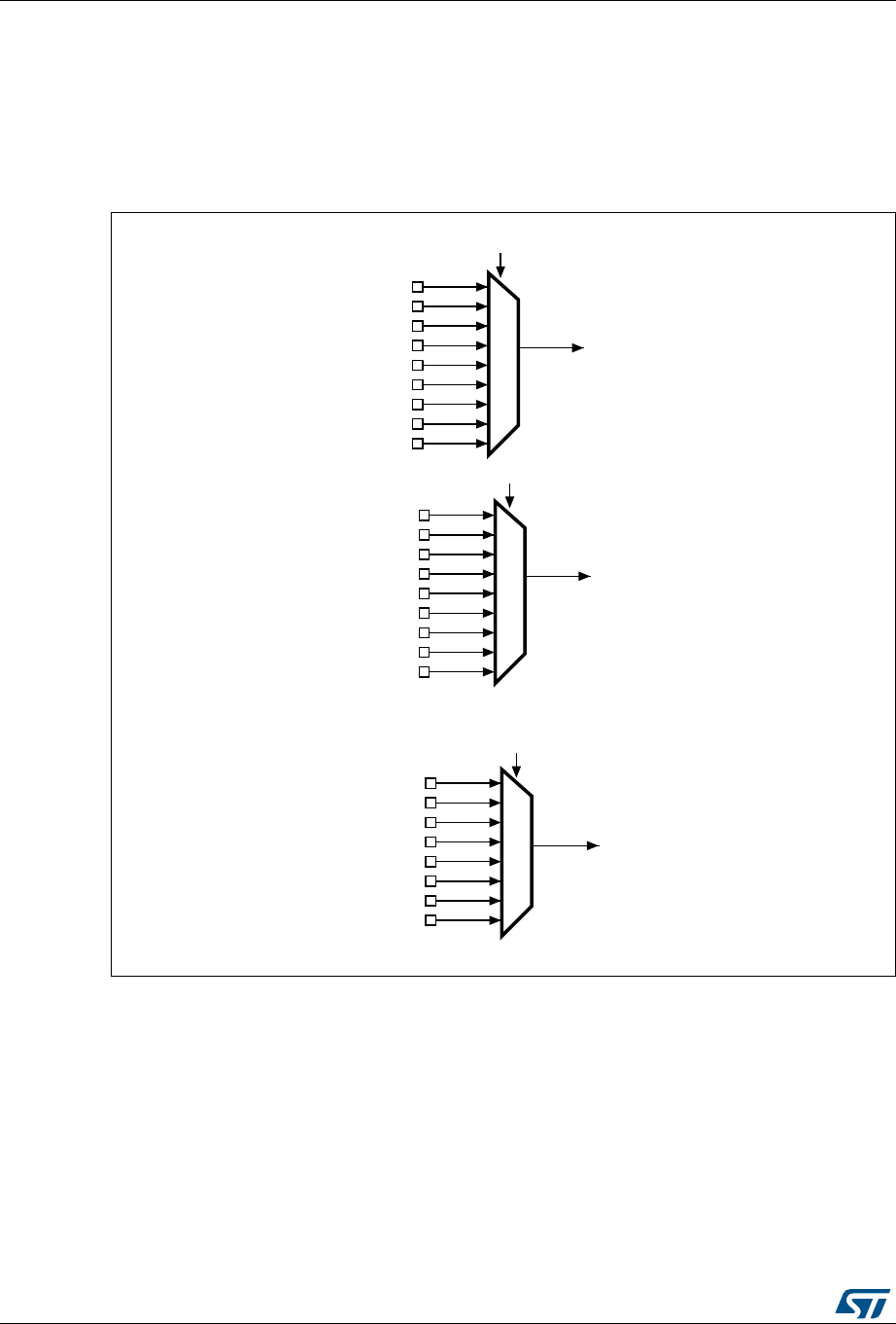
Interrupts and events RM0090
382/1718 DocID018909 Rev 9
12.2.5 External interrupt/event line mapping
Up to 140 GPIOs (STM32F405xx/07xx and STM32F415xx/17xx), 168 GPIOs
(STM32F42xxx and STM32F43xxx) are connected to the 16 external interrupt/event lines in
the following manner:
Figure 42. External interrupt/event GPIO mapping (STM32F405xx/07xx and
STM32F415xx/17xx)
0!
0"
0#
0$
0%
0&
0'
0(
0)
0!
0"
0#
0$
0%
0&
0'
0(
0)
0!
0"
0#
0$
0%
0&
0'
0(
%84)
%84)
%84)
%84);=BITSINTHE393#&'?%84)#2REGISTER
%84);=BITSINTHE393#&'?%84)#2REGISTER
%84);=BITSINTHE393#&'?%84)#2REGISTER
AI
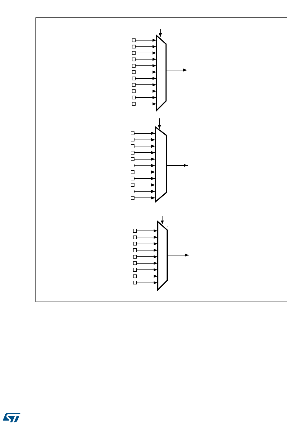
DocID018909 Rev 9 383/1718
RM0090 Interrupts and events
387
Figure 43. External interrupt/event GPIO mapping (STM32F42xxx and STM32F43xxx)
The seven other EXTI lines are connected as follows:
•EXTI line 16 is connected to the PVD output
•EXTI line 17 is connected to the RTC Alarm event
•EXTI line 18 is connected to the USB OTG FS Wakeup event
•EXTI line 19 is connected to the Ethernet Wakeup event
•EXTI line 20 is connected to the USB OTG HS (configured in FS) Wakeup event
•EXTI line 21 is connected to the RTC Tamper and TimeStamp events
•EXTI line 22 is connected to the RTC Wakeup event
3$
3%
3&
3'
3(
3)
3*
3+
3,
3$
3%
3&
3'
3(
3)
3*
3+
3,
3$
3%
3&
3'
3(
3)
3*
3+
(;7,
(;7,
(;7,
(;7,>@ELWVLQWKH6<6&)*B(;7,&5UHJLVWHU
(;7,>@ELWVLQWKH6<6&)*B(;7,&5UHJLVWHU
(;7,>@ELWVLQWKH6<6&)*B(;7,&5UHJLVWHU
069
3-
3.
3-
3.
3-
Interrupts and events RM0090
384/1718 DocID018909 Rev 9
12.3 EXTI registers
Refer to Section 1.1 on page 57 for a list of abbreviations used in register descriptions.
12.3.1 Interrupt mask register (EXTI_IMR)
Address offset: 0x00
Reset value: 0x0000 0000
12.3.2 Event mask register (EXTI_EMR)
Address offset: 0x04
Reset value: 0x0000 0000
31 30 29 28 27 26 25 24 23 22 21 20 19 18 17 16
Reserved MR22 MR21 MR20 MR19 MR18 MR17 MR16
rw rw rw rw rw rw rw
15 14 13 12 11 10 9 8 7 6 5 4 3 2 1 0
MR15 MR14 MR13 MR12 MR11 MR10 MR9 MR8 MR7 MR6 MR5 MR4 MR3 MR2 MR1 MR0
rw rw rw rw rw rw rw rw rw rw rw rw rw rw rw rw
Bits 31:23 Reserved, must be kept at reset value.
Bits 22:0 MRx: Interrupt mask on line x
0: Interrupt request from line x is masked
1: Interrupt request from line x is not masked
31 30 29 28 27 26 25 24 23 22 21 20 19 18 17 16
Reserved MR22 MR21 MR20 MR19 MR18 MR17 MR16
rw rw rw rw rw rw rw
15 14 13 12 11 10 9 8 7 6 5 4 3 2 1 0
MR15 MR14 MR13 MR12 MR11 MR10 MR9 MR8 MR7 MR6 MR5 MR4 MR3 MR2 MR1 MR0
rw rw rw rw rw rw rw rw rw rw rw rw rw rw rw rw
Bits 31:23 Reserved, must be kept at reset value.
Bits 22:0 MRx: Event mask on line x
0: Event request from line x is masked
1: Event request from line x is not masked
DocID018909 Rev 9 385/1718
RM0090 Interrupts and events
387
12.3.3 Rising trigger selection register (EXTI_RTSR)
Address offset: 0x08
Reset value: 0x0000 0000
Note: The external wakeup lines are edge triggered, no glitch must be generated on these lines.
If a rising edge occurs on the external interrupt line while writing to the EXTI_RTSR register,
the pending bit is be set.
Rising and falling edge triggers can be set for the same interrupt line. In this configuration,
both generate a trigger condition.
12.3.4 Falling trigger selection register (EXTI_FTSR)
Address offset: 0x0C
Reset value: 0x0000 0000
Note: The external wakeup lines are edge triggered, no glitch must be generated on these lines.
If a falling edge occurs on the external interrupt line while writing to the EXTI_FTSR register,
the pending bit is not set.
Rising and falling edge triggers can be set for the same interrupt line. In this configuration,
both generate a trigger condition.
31 30 29 28 27 26 25 24 23 22 21 20 19 18 17 16
Reserved TR22 TR21 TR20 TR19 TR18 TR17 TR16
rw rw rw rw rw rw rw
1514131211109 8 765432 1 0
TR15 TR14 TR13 TR12 TR11 TR10 TR9 TR8 TR7 TR6 TR5 TR4 TR3 TR2 TR1 TR0
rw rw rw rw rw rw rw rw rw rw rw rw rw rw rw rw
Bits 31:23 Reserved, must be kept at reset value.
Bits 22:0 TRx: Rising trigger event configuration bit of line x
0: Rising trigger disabled (for Event and Interrupt) for input line
1: Rising trigger enabled (for Event and Interrupt) for input line
31 30 29 28 27 26 25 24 23 22 21 20 19 18 17 16
Reserved TR22 TR21 TR20 TR19 TR18 TR17 TR16
rw rw rw rw rw rw rw
1514131211109 8 765432 1 0
TR15 TR14 TR13 TR12 TR11 TR10 TR9 TR8 TR7 TR6 TR5 TR4 TR3 TR2 TR1 TR0
rw rw rw rw rw rw rw rw rw rw rw rw rw rw rw rw
Bits 31:23 Reserved, must be kept at reset value.
Bits 22:0 TRx: Falling trigger event configuration bit of line x
0: Falling trigger disabled (for Event and Interrupt) for input line
1: Falling trigger enabled (for Event and Interrupt) for input line.
Interrupts and events RM0090
386/1718 DocID018909 Rev 9
12.3.5 Software interrupt event register (EXTI_SWIER)
Address offset: 0x10
Reset value: 0x0000 0000
12.3.6 Pending register (EXTI_PR)
Address offset: 0x14
Reset value: undefined
31 30 29 28 27 26 25 24 23 22 21 20 19 18 17 16
Reserved
SWIER
22
SWIER
21
SWIER
20
SWIER
19
SWIER
18
SWIER
17
SWIER
16
rw rw rw rw rw rw rw
1514131211109 8 765432 1 0
SWIER
15
SWIER
14
SWIER
13
SWIER
12
SWIER
11
SWIER
10
SWIER
9
SWIER
8
SWIER
7
SWIER
6
SWIER
5
SWIER
4
SWIER
3
SWIER
2
SWIER
1
SWIER
0
rw rw rw rw rw rw rw rw rw rw rw rw rw rw rw rw
Bits 31:23 Reserved, must be kept at reset value.
Bits 22:0 SWIERx: Software Interrupt on line x
If interrupt are enabled on line x in the EXTI_IMR register, writing '1' to SWIERx bit when it is
set at '0' sets the corresponding pending bit in the EXTI_PR register, thus resulting in an
interrupt request generation.
This bit is cleared by clearing the corresponding bit in EXTI_PR (by writing a 1 to the bit).
31 30 29 28 27 26 25 24 23 22 21 20 19 18 17 16
Reserved PR22 PR21 PR20 PR19 PR18 PR17 PR16
rc_w1 rc_w1 rc_w1 rc_w1 rc_w1 rc_w1 rc_w1
1514131211109 8 765432 1 0
PR15 PR14 PR13 PR12 PR11 PR10 PR9 PR8 PR7 PR6 PR5 PR4 PR3 PR2 PR1 PR0
rc_w1 rc_w1 rc_w1 rc_w1 rc_w1 rc_w1 rc_w1 rc_w1 rc_w1 rc_w1 rc_w1 rc_w1 rc_w1 rc_w1 rc_w1 rc_w1
Bits 31:23 Reserved, must be kept at reset value.
Bits 22:0 PRx: Pending bit
0: No trigger request occurred
1: selected trigger request occurred
This bit is set when the selected edge event arrives on the external interrupt line.
This bit is cleared by programming it to ‘1’.
DocID018909 Rev 9 387/1718
RM0090 Interrupts and events
387
12.3.7 EXTI register map
Table 64 gives the EXTI register map and the reset values.
Refer to Table 1 on page 64 for the register boundary addresses.
Table 63. External interrupt/event controller register map and reset values
Offset Register
31
30
29
28
27
26
25
24
23
22
21
20
19
18
17
16
15
14
13
12
11
10
9
8
7
6
5
4
3
2
1
0
0x00 EXTI_IMR Reserved MR[22:0]
Reset value 00000000000000000000000
0x04 EXTI_EMR Reserved MR[22:0]
Reset value 00000000000000000000000
0x08 EXTI_RTSR Reserved TR[22:0]
Reset value 00000000000000000000000
0x0C
EXTI_FTSR
Reserved
TR[22:0]
Reset value 00000000000000000000000
0x10
EXTI_SWIER
Reserved
SWIER[22:0]
Reset value 00000000000000000000000
0x14
EXTI_PR
Reserved
PR[22:0]
Reset value 00000000000000000000000

Analog-to-digital converter (ADC) RM0090
388/1718 DocID018909 Rev 9
13 Analog-to-digital converter (ADC)
This section applies to the whole STM32F4xx family, unless otherwise specified.
13.1 ADC introduction
The 12-bit ADC is a successive approximation analog-to-digital converter. It has up to 19
multiplexed channels allowing it to measure signals from 16 external sources, two internal
sources, and the VBAT channel. The A/D conversion of the channels can be performed in
single, continuous, scan or discontinuous mode. The result of the ADC is stored into a left-
or right-aligned 16-bit data register.
The analog watchdog feature allows the application to detect if the input voltage goes
beyond the user-defined, higher or lower thresholds.
13.2 ADC main features
•12-bit, 10-bit, 8-bit or 6-bit configurable resolution
•Interrupt generation at the end of conversion, end of injected conversion, and in case of
analog watchdog or overrun events
•Single and continuous conversion modes
•Scan mode for automatic conversion of channel 0 to channel ‘n’
•Data alignment with in-built data coherency
•Channel-wise programmable sampling time
•External trigger option with configurable polarity for both regular and injected
conversions
•Discontinuous mode
•Dual/Triple mode (on devices with 2 ADCs or more)
•Configurable DMA data storage in Dual/Triple ADC mode
•Configurable delay between conversions in Dual/Triple interleaved mode
•ADC conversion type (refer to the datasheets)
•ADC supply requirements: 2.4 V to 3.6 V at full speed and down to 1.8 V at slower
speed
•ADC input range: VREF– ≤ VIN ≤ VREF+
•DMA request generation during regular channel conversion
Figure 44 shows the block diagram of the ADC.
Note: VREF–, if available (depending on package), must be tied to VSSA.

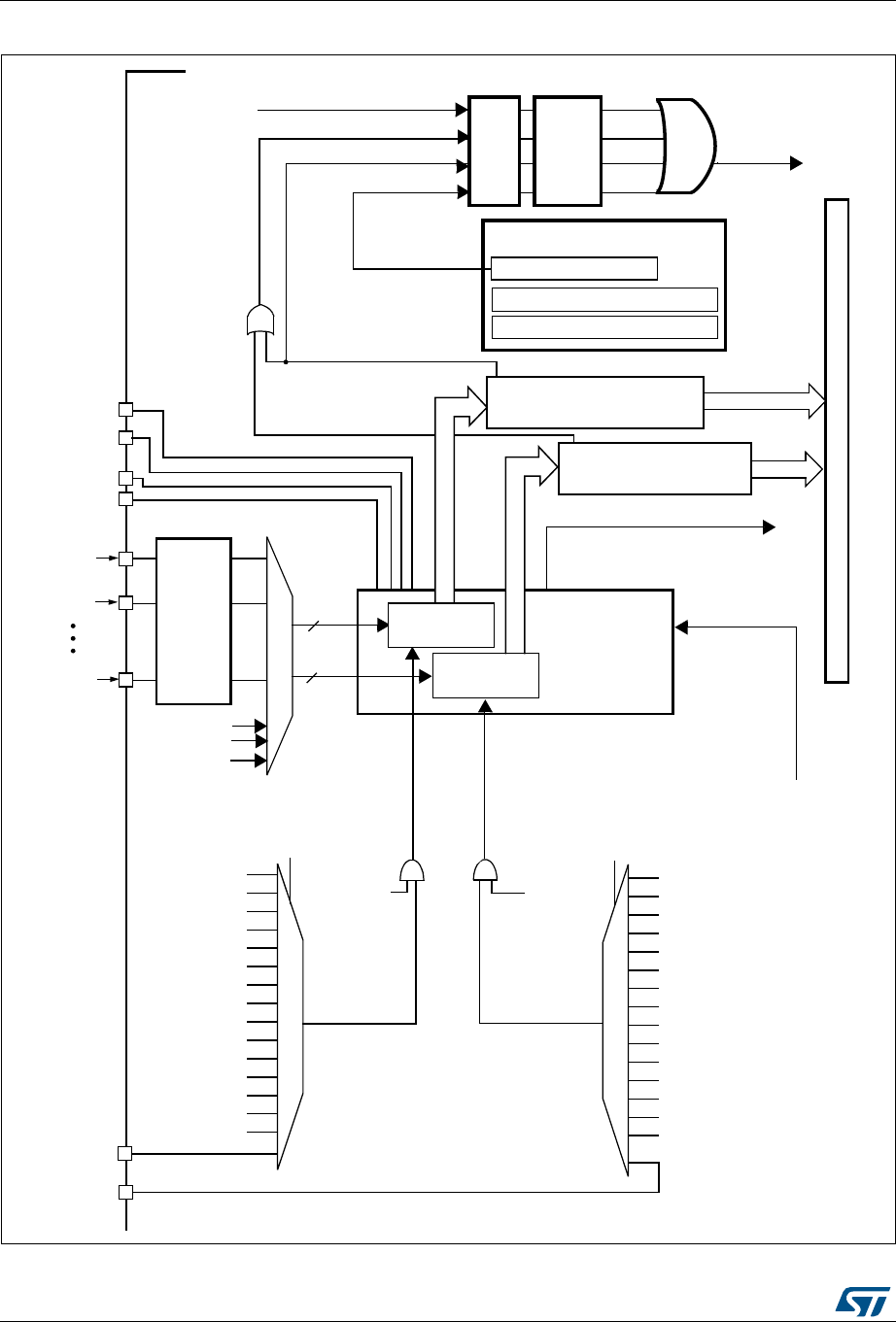
Analog-to-digital converter (ADC) RM0090
390/1718 DocID018909 Rev 9
Figure 44. Single ADC block diagram
!$#X?).
!$#X?).
!NALOG TO DIGITAL
CONVERTER
!$#X?).
!NALOG
MUX
!$##,+
!$#)NTERRUPTTO.6)#
'0)/
PORTS
!NALOGWATCHDOG
!DDRESSDATABUS
,OWERTHRESHOLDBITS
#OMPARERESULT
(IGHERTHRESHOLDBITS
&LAGS ENABLEBITS
%/#
!7$
!NALOGWATCHDOGEVENT
6$$!
633!
62%&
62%&
)NTERRUPT
%84)?
4)-?#(
&ROM!$#PRESCALER
BITS
%NDOFCONVERSION
CHANNELS
)NJECTED
CHANNELS
%NDOFINJECTEDCONVERSION *%/#
%/#)%
!7$)%
*%/#)%
UPTO
UPTO
2EGULARDATAREGISTER
XBITS
)NJECTEDDATAREGISTERS
2EGULAR
3TARTTRIGGER
REGULARGROUP
%843%,;=BITS
%84%.
4)-?#(
%84)?
4)-?42'/
4)-?#(
4)-?42'/
3TARTTRIGGER
INJECTEDGROUP
*%843%,;=BITS
4)-?#(
*%84%. ;=BITS
;=BITS
$-!REQUEST
4EMPSENSOR
62%&).4
/62/62)%
$-!OVERRUN
6"!4
4)-?#(
4)-?42'/
4)-?#(
4)-?#(
4)-?42'/
4)-?#(
4)-?#(
4)-?#(
4)-?#(
4)-?#(
4)-?#(
4)-?#(
4)-?#(
4)-?#(
4)-?#(
4)-?#(
4)-?#(
4)-?#(
4)-?42'/
4)-?#(
4)-?42'/
4)-?#(
4)-?42'/
4)-?#(
AI

DocID018909 Rev 9 391/1718
RM0090 Analog-to-digital converter (ADC)
432
13.3.1 ADC on-off control
The ADC is powered on by setting the ADON bit in the ADC_CR2 register. When the ADON
bit is set for the first time, it wakes up the ADC from the Power-down mode.
Conversion starts when either the SWSTART or the JSWSTART bit is set.
You can stop conversion and put the ADC in power down mode by clearing the ADON bit. In
this mode the ADC consumes almost no power (only a few µA).
13.3.2 ADC clock
The ADC features two clock schemes:
•Clock for the analog circuitry: ADCCLK, common to all ADCs
This clock is generated from the APB2 clock divided by a programmable prescaler that
allows the ADC to work at fPCLK2/2, /4, /6 or /8. Refer to the datasheets for the
maximum value of ADCCLK.
•Clock for the digital interface (used for registers read/write access)
This clock is equal to the APB2 clock. The digital interface clock can be
enabled/disabled individually for each ADC through the RCC APB2 peripheral clock
enable register (RCC_APB2ENR).
13.3.3 Channel selection
There are 16 multiplexed channels. It is possible to organize the conversions in two groups:
regular and injected. A group consists of a sequence of conversions that can be done on
any channel and in any order. For instance, it is possible to implement the conversion
sequence in the following order: ADC_IN3, ADC_IN8, ADC_IN2, ADC_IN2, ADC_IN0,
ADC_IN2, ADC_IN2, ADC_IN15.
•A regular group is composed of up to 16 conversions. The regular channels and their
order in the conversion sequence must be selected in the ADC_SQRx registers. The
total number of conversions in the regular group must be written in the L[3:0] bits in the
ADC_SQR1 register.
•An injected group is composed of up to 4 conversions. The injected channels and
their order in the conversion sequence must be selected in the ADC_JSQR register.
Table 65. ADC pins
Name Signal type Remarks
VREF+
Input, analog reference
positive
The higher/positive reference voltage for the ADC,
1.8 V ≤ VREF+ ≤ VDDA
VDDA Input, analog supply
Analog power supply equal to VDD and
2.4 V ≤ VDDA ≤ VDD (3.6 V) for full speed
1.8 V ≤ VDDA ≤ VDD (3.6 V) for reduced speed
VREF–
Input, analog reference
negative
The lower/negative reference voltage for the ADC,
VREF– = VSSA
VSSA
Input, analog supply
ground Ground for analog power supply equal to VSS
ADCx_IN[15:0] Analog input signals 16 analog input channels

Analog-to-digital converter (ADC) RM0090
392/1718 DocID018909 Rev 9
The total number of conversions in the injected group must be written in the L[1:0] bits
in the ADC_JSQR register.
If the ADC_SQRx or ADC_JSQR registers are modified during a conversion, the current
conversion is reset and a new start pulse is sent to the ADC to convert the newly chosen
group.
Temperature sensor, VREFINT and VBAT internal channels
•For the STM23F40x and STM32F41x devices, the temperature sensor is internally
connected to channel ADC1_IN16.
The internal reference voltage VREFINT is connected to ADC1_IN17.
•For the STM23F42x and STM32F43x devices, the temperature sensor is internally
connected to ADC1_IN18 channel which is shared with VBAT. Only one conversion,
temperature sensor or VBAT, must be selected at a time. When the temperature sensor
and VBAT conversion are set simultaneously, only the VBAT conversion is performed.
The internal reference voltage VREFINT is connected to ADC1_IN17.
The VBAT channel (connected to channel ADC1_IN18) can also be converted as an injected
or regular channel.
Note: The temperature sensor, VREFINT and the VBAT channel are available only on the master
ADC1 peripheral.
13.3.4 Single conversion mode
In Single conversion mode the ADC does one conversion. This mode is started with the
CONT bit at 0 by either:
•setting the SWSTART bit in the ADC_CR2 register (for a regular channel only)
•setting the JSWSTART bit (for an injected channel)
•external trigger (for a regular or injected channel)
Once the conversion of the selected channel is complete:
•If a regular channel was converted:
– The converted data are stored into the 16-bit ADC_DR register
– The EOC (end of conversion) flag is set
– An interrupt is generated if the EOCIE bit is set
•If an injected channel was converted:
– The converted data are stored into the 16-bit ADC_JDR1 register
– The JEOC (end of conversion injected) flag is set
– An interrupt is generated if the JEOCIE bit is set
Then the ADC stops.

DocID018909 Rev 9 393/1718
RM0090 Analog-to-digital converter (ADC)
432
13.3.5 Continuous conversion mode
In continuous conversion mode, the ADC starts a new conversion as soon as it finishes one.
This mode is started with the CONT bit at 1 either by external trigger or by setting the
SWSTRT bit in the ADC_CR2 register (for regular channels only).
After each conversion:
•If a regular group of channels was converted:
– The last converted data are stored into the 16-bit ADC_DR register
– The EOC (end of conversion) flag is set
– An interrupt is generated if the EOCIE bit is set
Note: Injected channels cannot be converted continuously. The only exception is when an injected
channel is configured to be converted automatically after regular channels in continuous
mode (using JAUTO bit), refer to Auto-injection section).
13.3.6 Timing diagram
As shown in Figure 45, the ADC needs a stabilization time of tSTAB before it starts
converting accurately. After the start of the ADC conversion and after 15 clock cycles, the
EOC flag is set and the 16-bit ADC data register contains the result of the conversion.
Figure 45. Timing diagram
13.3.7 Analog watchdog
The AWD analog watchdog status bit is set if the analog voltage converted by the ADC is
below a lower threshold or above a higher threshold. These thresholds are programmed in
the 12 least significant bits of the ADC_HTR and ADC_LTR 16-bit registers. An interrupt can
be enabled by using the AWDIE bit in the ADC_CR1 register.
The threshold value is independent of the alignment selected by the ALIGN bit in the
ADC_CR2 register. The analog voltage is compared to the lower and higher thresholds
before alignment.
Table 66 shows how the ADC_CR1 register should be configured to enable the analog
watchdog on one or more channels.
!$#?#,+
%/#
.EXT!$#CONVERSION
!$#CONVERSION
#ONVERSIONTIME
T34!"
!$#
3OFTWARECLEARSTHE%/#BIT
TOTALCONVTIME
3TARTSTCONVERSION 3TARTNEXTCONVERSION
AIB
!$/.
3734!24
*3734!24
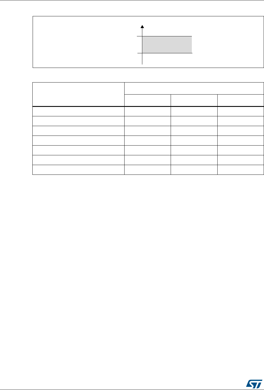
Analog-to-digital converter (ADC) RM0090
394/1718 DocID018909 Rev 9
Figure 46. Analog watchdog’s guarded area
13.3.8 Scan mode
This mode is used to scan a group of analog channels.
The Scan mode is selected by setting the SCAN bit in the ADC_CR1 register. Once this bit
has been set, the ADC scans all the channels selected in the ADC_SQRx registers (for
regular channels) or in the ADC_JSQR register (for injected channels). A single conversion
is performed for each channel of the group. After each end of conversion, the next channel
in the group is converted automatically. If the CONT bit is set, regular channel conversion
does not stop at the last selected channel in the group but continues again from the first
selected channel.
If the DMA bit is set, the direct memory access (DMA) controller is used to transfer the data
converted from the regular group of channels (stored in the ADC_DR register) to SRAM
after each regular channel conversion.
The EOC bit is set in the ADC_SR register:
•At the end of each regular group sequence if the EOCS bit is cleared to 0
•At the end of each regular channel conversion if the EOCS bit is set to 1
The data converted from an injected channel are always stored into the ADC_JDRx
registers.
Table 66. Analog watchdog channel selection
Channels guarded by the analog
watchdog
ADC_CR1 register control bits (x = don’t care)
AWDSGL bit AWDEN bit JAWDEN bit
None x 0 0
All injected channels 0 0 1
All regular channels 0 1 0
All regular and injected channels 0 1 1
Single(1) injected channel
1. Selected by the AWDCH[4:0] bits
101
Single(1) regular channel 1 1 0
Single (1) regular or injected channel 1 1 1
!NALOGVOLTAGE
(IGHERTHRESHOLD
,OWERTHRESHOLD
'UARDEDAREA
(42
,4 2
AI
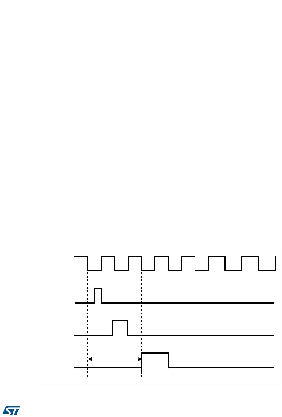
DocID018909 Rev 9 395/1718
RM0090 Analog-to-digital converter (ADC)
432
13.3.9 Injected channel management
Triggered injection
To use triggered injection, the JAUTO bit must be cleared in the ADC_CR1 register.
1. Start the conversion of a group of regular channels either by external trigger or by
setting the SWSTART bit in the ADC_CR2 register.
2. If an external injected trigger occurs or if the JSWSTART bit is set during the
conversion of a regular group of channels, the current conversion is reset and the
injected channel sequence switches to Scan-once mode.
3. Then, the regular conversion of the regular group of channels is resumed from the last
interrupted regular conversion.
If a regular event occurs during an injected conversion, the injected conversion is not
interrupted but the regular sequence is executed at the end of the injected sequence.
Figure 47 shows the corresponding timing diagram.
Note: When using triggered injection, one must ensure that the interval between trigger events is
longer than the injection sequence. For instance, if the sequence length is 30 ADC clock
cycles (that is two conversions with a sampling time of 3 clock periods), the minimum
interval between triggers must be 31 ADC clock cycles.
Auto-injection
If the JAUTO bit is set, then the channels in the injected group are automatically converted
after the regular group of channels. This can be used to convert a sequence of up to 20
conversions programmed in the ADC_SQRx and ADC_JSQR registers.
In this mode, external trigger on injected channels must be disabled.
If the CONT bit is also set in addition to the JAUTO bit, regular channels followed by injected
channels are continuously converted.
Note: It is not possible to use both the auto-injected and discontinuous modes simultaneously.
Figure 47. Injected conversion latency
1. The maximum latency value can be found in the electrical characteristics of the STM32F40x and
STM32F41x datasheets.
!$##,+
)NJECTIONEVENT
2ESET!$#
3/# MAXLATENCY
AI

Analog-to-digital converter (ADC) RM0090
396/1718 DocID018909 Rev 9
13.3.10 Discontinuous mode
Regular group
This mode is enabled by setting the DISCEN bit in the ADC_CR1 register. It can be used to
convert a short sequence of n conversions (n ≤ 8) that is part of the sequence of conversions
selected in the ADC_SQRx registers. The value of n is specified by writing to the
DISCNUM[2:0] bits in the ADC_CR1 register.
When an external trigger occurs, it starts the next n conversions selected in the ADC_SQRx
registers until all the conversions in the sequence are done. The total sequence length is
defined by the L[3:0] bits in the ADC_SQR1 register.
Example:
•n = 3, channels to be converted = 0, 1, 2, 3, 6, 7, 9, 10
•1st trigger: sequence converted 0, 1, 2. An EOC event is generated at each
conversion.
•2nd trigger: sequence converted 3, 6, 7. An EOC event is generated at each
conversion
•3rd trigger: sequence converted 9, 10.An EOC event is generated at each conversion
•4th trigger: sequence converted 0, 1, 2. An EOC event is generated at each conversion
Note: When a regular group is converted in discontinuous mode, no rollover occurs.
When all subgroups are converted, the next trigger starts the conversion of the first
subgroup. In the example above, the 4th trigger reconverts the channels 0, 1 and 2 in the
1st subgroup.
Injected group
This mode is enabled by setting the JDISCEN bit in the ADC_CR1 register. It can be used to
convert the sequence selected in the ADC_JSQR register, channel by channel, after an
external trigger event.
When an external trigger occurs, it starts the next channel conversions selected in the
ADC_JSQR registers until all the conversions in the sequence are done. The total sequence
length is defined by the JL[1:0] bits in the ADC_JSQR register.
Example:
n = 1, channels to be converted = 1, 2, 3
1st trigger: channel 1 converted
2nd trigger: channel 2 converted
3rd trigger: channel 3 converted and JEOC event generated
4th trigger: channel 1
Note: When all injected channels are converted, the next trigger starts the conversion of the first
injected channel. In the example above, the 4th trigger reconverts the 1st injected channel
1.
It is not possible to use both the auto-injected and discontinuous modes simultaneously.
Discontinuous mode must not be set for regular and injected groups at the same time.
Discontinuous mode must be enabled only for the conversion of one group.
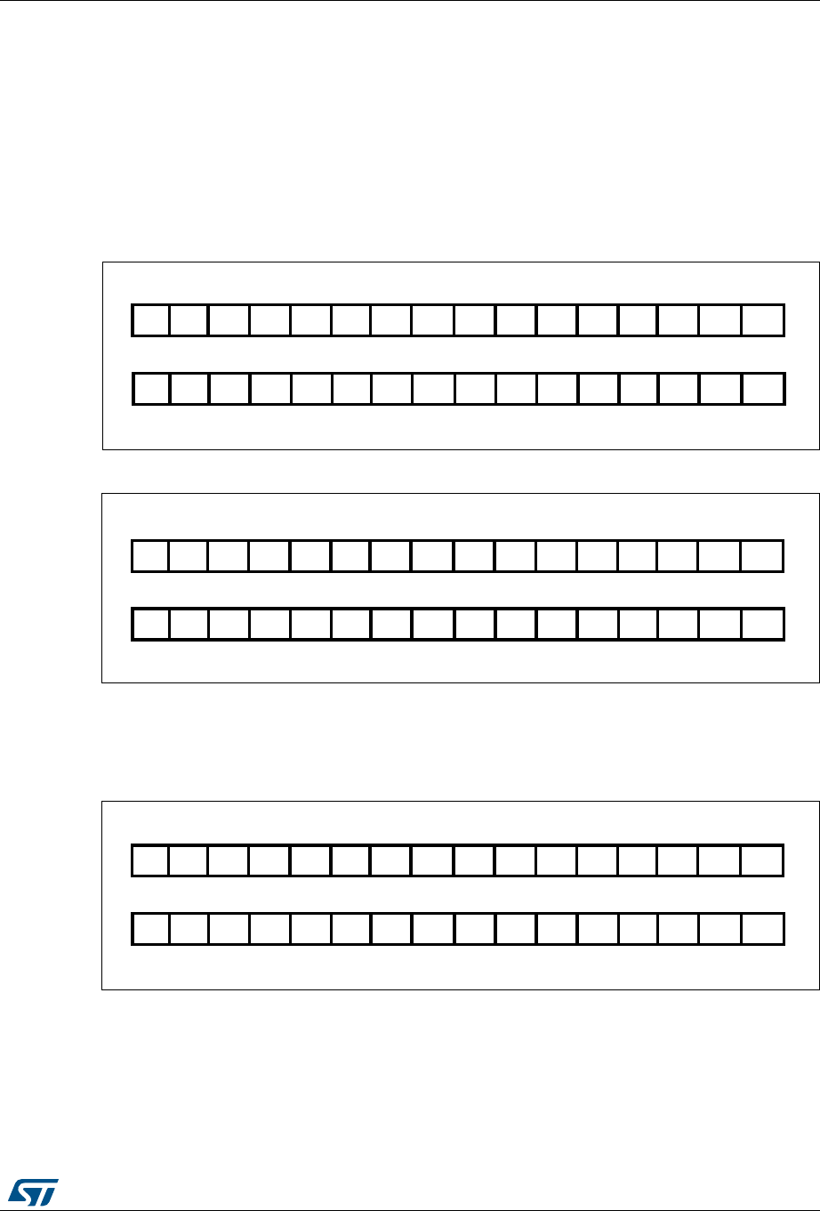
DocID018909 Rev 9 397/1718
RM0090 Analog-to-digital converter (ADC)
432
13.4 Data alignment
The ALIGN bit in the ADC_CR2 register selects the alignment of the data stored after
conversion. Data can be right- or left-aligned as shown in Figure 48 and Figure 49.
The converted data value from the injected group of channels is decreased by the user-
defined offset written in the ADC_JOFRx registers so the result can be a negative value.
The SEXT bit represents the extended sign value.
For channels in a regular group, no offset is subtracted so only twelve bits are significant.
Figure 48. Right alignment of 12-bit data
Figure 49. Left alignment of 12-bit data
Special case: when left-aligned, the data are aligned on a half-word basis except when the
resolution is set to 6-bit. in that case, the data are aligned on a byte basis as shown in
Figure 50.
Figure 50. Left alignment of 6-bit data
$$$ $ $ $ $ $ $ $$$3%843%843%843%84
$$
$$
)NJECTEDGROUP
2EGULARGROUP
$ $ $ $ $ $ $ $
AI
$$
$ $ $ $ $ $$$$$3%84
)NJECTEDGROUP
2EGULARGROUP
AI
$ $ $ $ $ $ $ $ $ $ $ $
$$
3%843%843%843%843%843%84
)NJECTEDGROUP
2EGULARGROUP
AI
$ $ $ $ $ $
3%843%84 $ $ $ $ 3%84
Analog-to-digital converter (ADC) RM0090
398/1718 DocID018909 Rev 9
13.5 Channel-wise programmable sampling time
The ADC samples the input voltage for a number of ADCCLK cycles that can be modified
using the SMP[2:0] bits in the ADC_SMPR1 and ADC_SMPR2 registers. Each channel can
be sampled with a different sampling time.
The total conversion time is calculated as follows:
Tconv = Sampling time + 12 cycles
Example:
With ADCCLK = 30 MHz and sampling time = 3 cycles:
Tconv = 3 + 12 = 15 cycles = 0.5 µs with APB2 at 60 MHz
13.6 Conversion on external trigger and trigger polarity
Conversion can be triggered by an external event (e.g. timer capture, EXTI line). If the
EXTEN[1:0] control bits (for a regular conversion) or JEXTEN[1:0] bits (for an injected
conversion) are different from “0b00”, then external events are able to trigger a conversion
with the selected polarity. Table 67 provides the correspondence between the EXTEN[1:0]
and JEXTEN[1:0] values and the trigger polarity.
Note: The polarity of the external trigger can be changed on the fly.
The EXTSEL[3:0] and JEXTSEL[3:0] control bits are used to select which out of 16 possible
events can trigger conversion for the regular and injected groups.
Table 68 gives the possible external trigger for regular conversion.
Table 67. Configuring the trigger polarity
Source EXTEN[1:0] / JEXTEN[1:0]
Trigger detection disabled 00
Detection on the rising edge 01
Detection on the falling edge 10
Detection on both the rising and falling edges 11

DocID018909 Rev 9 399/1718
RM0090 Analog-to-digital converter (ADC)
432
Table 69 gives the possible external trigger for injected conversion.
Table 68. External trigger for regular channels
Source Type EXTSEL[3:0]
TIM1_CH1 event
Internal signal from on-chip
timers
0000
TIM1_CH2 event 0001
TIM1_CH3 event 0010
TIM2_CH2 event 0011
TIM2_CH3 event 0100
TIM2_CH4 event 0101
TIM2_TRGO event 0110
TIM3_CH1 event 0111
TIM3_TRGO event 1000
TIM4_CH4 event 1001
TIM5_CH1 event 1010
TIM5_CH2 event 1011
TIM5_CH3 event 1100
TIM8_CH1 event 1101
TIM8_TRGO event 1110
EXTI line11 External pin 1111

Analog-to-digital converter (ADC) RM0090
400/1718 DocID018909 Rev 9
Software source trigger events can be generated by setting SWSTART (for regular
conversion) or JSWSTART (for injected conversion) in ADC_CR2.
A regular group conversion can be interrupted by an injected trigger.
Note: The trigger selection can be changed on the fly. However, when the selection changes,
there is a time frame of 1 APB clock cycle during which the trigger detection is disabled.
This is to avoid spurious detection during transitions.
13.7 Fast conversion mode
It is possible to perform faster conversion by reducing the ADC resolution. The RES bits are
used to select the number of bits available in the data register. The minimum conversion
time for each resolution is then as follows:
•12 bits: 3 + 12 = 15 ADCCLK cycles
•10 bits: 3 + 10 = 13 ADCCLK cycles
•8 bits: 3 + 8 = 11 ADCCLK cycles
•6 bits: 3 + 6 = 9 ADCCLK cycles
Table 69. External trigger for injected channels
Source Connection type JEXTSEL[3:0]
TIM1_CH4 event
Internal signal from on-chip
timers
0000
TIM1_TRGO event 0001
TIM2_CH1 event 0010
TIM2_TRGO event 0011
TIM3_CH2 event 0100
TIM3_CH4 event 0101
TIM4_CH1 event 0110
TIM4_CH2 event 0111
TIM4_CH3 event 1000
TIM4_TRGO event 1001
TIM5_CH4 event 1010
TIM5_TRGO event 1011
TIM8_CH2 event 1100
TIM8_CH3 event 1101
TIM8_CH4 event 1110
EXTI line15 External pin 1111

DocID018909 Rev 9 401/1718
RM0090 Analog-to-digital converter (ADC)
432
13.8 Data management
13.8.1 Using the DMA
Since converted regular channel values are stored into a unique data register, it is useful to
use DMA for conversion of more than one regular channel. This avoids the loss of the data
already stored in the ADC_DR register.
When the DMA mode is enabled (DMA bit set to 1 in the ADC_CR2 register), after each
conversion of a regular channel, a DMA request is generated. This allows the transfer of the
converted data from the ADC_DR register to the destination location selected by the
software.
Despite this, if data are lost (overrun), the OVR bit in the ADC_SR register is set and an
interrupt is generated (if the OVRIE enable bit is set). DMA transfers are then disabled and
DMA requests are no longer accepted. In this case, if a DMA request is made, the regular
conversion in progress is aborted and further regular triggers are ignored. It is then
necessary to clear the OVR flag and the DMAEN bit in the used DMA stream, and to re-
initialize both the DMA and the ADC to have the wanted converted channel data transferred
to the right memory location. Only then can the conversion be resumed and the data
transfer, enabled again. Injected channel conversions are not impacted by overrun errors.
When OVR = 1 in DMA mode, the DMA requests are blocked after the last valid data have
been transferred, which means that all the data transferred to the RAM can be considered
as valid.
At the end of the last DMA transfer (number of transfers configured in the DMA controller’s
DMA_SxNTR register):
•No new DMA request is issued to the DMA controller if the DDS bit is cleared to 0 in the
ADC_CR2 register (this avoids generating an overrun error). However the DMA bit is
not cleared by hardware. It must be written to 0, then to 1 to start a new transfer.
•Requests can continue to be generated if the DDS bit is set to 1. This allows
configuring the DMA in double-buffer circular mode.
To recover the ADC from OVR state when the DMA is used, follow the steps below:
1. Reinitialize the DMA (adjust destination address and NDTR counter)
2. Clear the ADC OVR bit in ADC_SR register
3. Trigger the ADC to start the conversion.
13.8.2 Managing a sequence of conversions without using the DMA
If the conversions are slow enough, the conversion sequence can be handled by the
software. In this case the EOCS bit must be set in the ADC_CR2 register for the EOC status
bit to be set at the end of each conversion, and not only at the end of the sequence. When
EOCS = 1, overrun detection is automatically enabled. Thus, each time a conversion is
complete, EOC is set and the ADC_DR register can be read. The overrun management is
the same as when the DMA is used.
To recover the ADC from OVR state when the EOCS is set, follow the steps below:
1. Clear the ADC OVR bit in ADC_SR register
2. Trigger the ADC to start the conversion.

Analog-to-digital converter (ADC) RM0090
402/1718 DocID018909 Rev 9
13.8.3 Conversions without DMA and without overrun detection
It may be useful to let the ADC convert one or more channels without reading the data each
time (if there is an analog watchdog for instance). For that, the DMA must be disabled
(DMA = 0) and the EOC bit must be set at the end of a sequence only (EOCS = 0). In this
configuration, overrun detection is disabled.
13.9 Multi ADC mode
In devices with two ADCs or more, the Dual (with two ADCs) and Triple (with three ADCs)
ADC modes can be used (see Figure 51).
In multi ADC mode, the start of conversion is triggered alternately or simultaneously by the
ADC1 master to the ADC2 and ADC3 slaves, depending on the mode selected by the
MULTI[4:0] bits in the ADC_CCR register.
Note: In multi ADC mode, when configuring conversion trigger by an external event, the
application must set trigger by the master only and disable trigger by slaves to prevent
spurious triggers that would start unwanted slave conversions.
The four possible modes below are implemented:
•Injected simultaneous mode
•Regular simultaneous mode
•Interleaved mode
•Alternate trigger mode
It is also possible to use the previous modes combined in the following ways:
•Injected simultaneous mode + Regular simultaneous mode
•Regular simultaneous mode + Alternate trigger mode
Note: In multi ADC mode, the converted data can be read on the multi-mode data register
(ADC_CDR). The status bits can be read in the multi-mode status register (ADC_CSR).
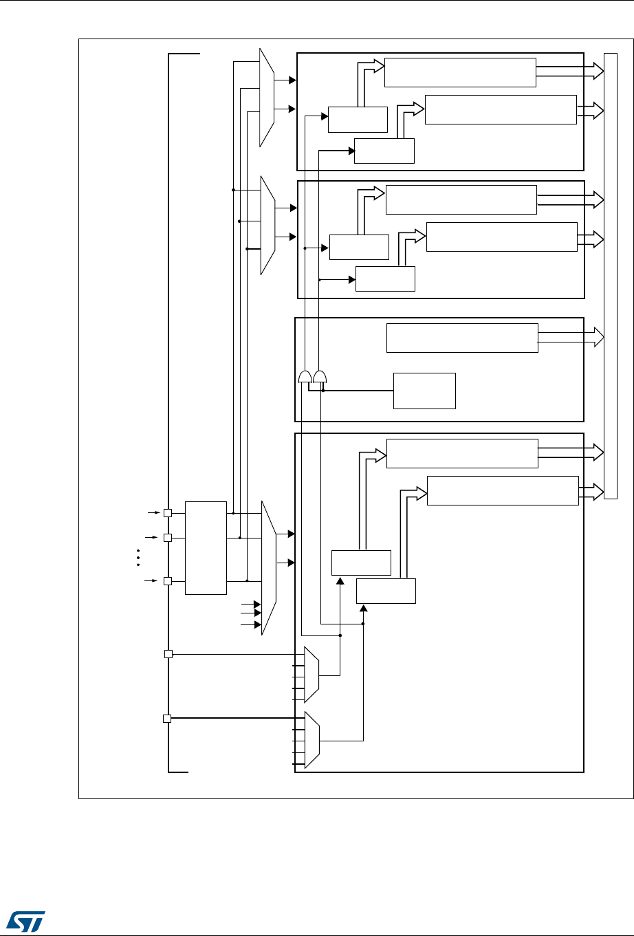
DocID018909 Rev 9 403/1718
RM0090 Analog-to-digital converter (ADC)
432
Figure 51. Multi ADC block diagram(1)
1. Although external triggers are present on ADC2 and ADC3 they are not shown in this diagram.
2. In the Dual ADC mode, the ADC3 slave part is not present.
3. In Triple ADC mode, the ADC common data register (ADC_CDR) contains the ADC1, ADC2 and ADC3’s
regular converted data. All 32 register bits are used according to a selected storage order.
In Dual ADC mode, the ADC common data register (ADC_CDR) contains both the ADC1 and ADC2’s
regular converted data. All 32 register bits are used.
!$#X?).
!$#X?).
!$#X?).
'0)/
0ORTS
!DDRESSDATABUS
%84)?
%84)?
)NJECTEDDATAREGISTERS
XBITS
2EGULAR
CHANNELS
)NJECTED
CHANNELS
!$#3LAVE
BITS
)NJECTEDDATAREGISTERS
XBITS
2EGULAR
CHANNELS
)NJECTED
CHANNELS
!$#-ASTER
$UAL4RIPLE
INTERNALTRIGGERS
3TARTTRIGGERMUX
REGULARGROUP
INJECTEDGROUP
3TARTTRIGGERMUX
CONTROL
4EMPSENSOR
62%&).4
2EGULARDATAREGISTER
BITS
2EGULARDATAREGISTER
BITS
#OMMONREGULARDATAREGISTER
BITS
6"!4
#OMMONPART
MODE
!$#3LAVE
BITS
)NJECTEDDATAREGISTERS
XBITS
2EGULAR
CHANNELS
)NJECTED
CHANNELS
2EGULARDATAREGISTER
BITS
AI

Analog-to-digital converter (ADC) RM0090
404/1718 DocID018909 Rev 9
•DMA requests in Multi ADC mode:
In Multi ADC mode the DMA may be configured to transfer converted data in three
different modes. In all cases, the DMA streams to use are those connected to the ADC:
–DMA mode 1: On each DMA request (one data item is available), a half-word
representing an ADC-converted data item is transferred.
In Dual ADC mode, ADC1 data are transferred on the first request, ADC2 data are
transferred on the second request and so on.
In Triple ADC mode, ADC1 data are transferred on the first request, ADC2 data
are transferred on the second request and ADC3 data are transferred on the third
request; the sequence is repeated. So the DMA first transfers ADC1 data followed
by ADC2 data followed by ADC3 data and so on.
DMA mode 1 is used in regular simultaneous triple mode.
Example:
Regular simultaneous triple mode: 3 consecutive DMA requests are generated
(one for each converted data item)
1st request: ADC_CDR[31:0] = ADC1_DR[15:0]
2nd request: ADC_CDR[31:0] = ADC2_DR[15:0]
3rd request: ADC_CDR[31:0] = ADC3_DR[15:0]
4th request: ADC_CDR[31:0] = ADC1_DR[15:0]
–DMA mode 2: On each DMA request (two data items are available) two half-
words representing two ADC-converted data items are transferred as a word.
In Dual ADC mode, both ADC2 and ADC1 data are transferred on the first request
(ADC2 data take the upper half-word and ADC1 data take the lower half-word) and
so on.
In Triple ADC mode, three DMA requests are generated. On the first request, both
ADC2 and ADC1 data are transferred (ADC2 data take the upper half-word and
ADC1 data take the lower half-word). On the second request, both ADC1 and
ADC3 data are transferred (ADC1 data take the upper half-word and ADC3 data
take the lower half-word).On the third request, both ADC3 and ADC2 data are
transferred (ADC3 data take the upper half-word and ADC2 data take the lower
half-word) and so on.
DMA mode 2 is used in interleaved mode and in regular simultaneous mode (for
Dual ADC mode only).
Example:
a) Interleaved dual mode: a DMA request is generated each time 2 data items are
available:
1st request: ADC_CDR[31:0] = ADC2_DR[15:0] | ADC1_DR[15:0]
2nd request: ADC_CDR[31:0] = ADC2_DR[15:0] | ADC1_DR[15:0]
b) Interleaved triple mode: a DMA request is generated each time 2 data items are
available
1st request: ADC_CDR[31:0] = ADC2_DR[15:0] | ADC1_DR[15:0]
2nd request: ADC_CDR[31:0] = ADC1_DR[15:0] | ADC3_DR[15:0]
3rd request: ADC_CDR[31:0] = ADC3_DR[15:0] | ADC2_DR[15:0]
4th request: ADC_CDR[31:0] = ADC2_DR[15:0] | ADC1_DR[15:0]

DocID018909 Rev 9 405/1718
RM0090 Analog-to-digital converter (ADC)
432
–DMA mode 3: This mode is similar to the DMA mode 2. The only differences are
that the on each DMA request (two data items are available) two bytes
representing two ADC converted data items are transferred as a half-word. The
data transfer order is similar to that of the DMA mode 2.
DMA mode 3 is used in interleaved mode in 6-bit and 8-bit resolutions.
Example:
a) Interleaved dual mode: a DMA request is generated each time 2 data items are
available
1st request: ADC_CDR[15:0] = ADC2_DR[7:0] | ADC1_DR[7:0]
2nd request: ADC_CDR[15:0] = ADC2_DR[7:0] | ADC1_DR[7:0]
b) Interleaved triple mode: a DMA request is generated each time 2 data items are
available
1st request: ADC_CDR[15:0] = ADC2_DR[7:0] | ADC1_DR[7:0]
2nd request: ADC_CDR[15:0] = ADC1_DR[7:0] | ADC3_DR[15:0]
3rd request: ADC_CDR[15:0] = ADC3_DR[7:0] | ADC2_DR[7:0]
4th request: ADC_CDR[15:0] = ADC2_DR[7:0] | ADC1_DR[7:0]
Overrun detection: If an overrun is detected on one of the concerned ADCs (ADC1 and
ADC2 in dual and triple modes, ADC3 in triple mode only), the DMA requests are no longer
issued to ensure that all the data transferred to the RAM are valid. It may happen that the
EOC bit corresponding to one ADC remains set because the data register of this ADC
contains valid data.
13.9.1 Injected simultaneous mode
This mode converts an injected group of channels. The external trigger source comes from
the injected group multiplexer of ADC1 (selected by the JEXTSEL[3:0] bits in the ADC1_CR2
register). A simultaneous trigger is provided to ADC2 and ADC3.
Note: Do not convert the same channel on the two/three ADCs (no overlapping sampling times for
the two/three ADCs when converting the same channel).
In simultaneous mode, one must convert sequences with the same length or ensure that the
interval between triggers is longer than the longer of the 2 sequences (Dual ADC mode) /3
sequences (Triple ADC mode). Otherwise, the ADC with the shortest sequence may restart
while the ADC with the longest sequence is completing the previous conversions.
Regular conversions can be performed on one or all ADCs. In that case, they are
independent of each other and are interrupted when an injected event occurs. They are
resumed at the end of the injected conversion group.
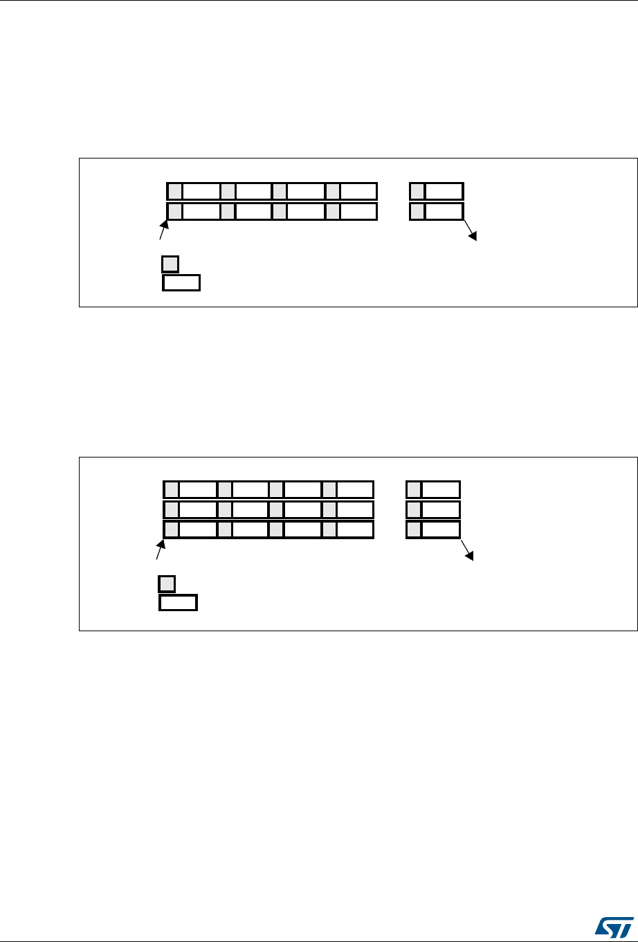
Analog-to-digital converter (ADC) RM0090
406/1718 DocID018909 Rev 9
Dual ADC mode
At the end of conversion event on ADC1 or ADC2:
•The converted data are stored into the ADC_JDRx registers of each ADC interface.
•A JEOC interrupt is generated (if enabled on one of the two ADC interfaces) when the
ADC1/ADC2’s injected channels have all been converted.
Figure 52. Injected simultaneous mode on 4 channels: dual ADC mode
Triple ADC mode
At the end of conversion event on ADC1, ADC2 or ADC3:
•The converted data are stored into the ADC_JDRx registers of each ADC interface.
•A JEOC interrupt is generated (if enabled on one of the three ADC interfaces) when the
ADC1/ADC2/ADC3’s injected channels have all been converted.
Figure 53. Injected simultaneous mode on 4 channels: triple ADC mode
13.9.2 Regular simultaneous mode
This mode is performed on a regular group of channels. The external trigger source comes
from the regular group multiplexer of ADC1 (selected by the EXTSEL[3:0] bits in the
ADC1_CR2 register). A simultaneous trigger is provided to ADC2 and ADC3.
Note: Do not convert the same channel on the two/three ADCs (no overlapping sampling times for
the two/three ADCs when converting the same channel).
In regular simultaneous mode, one must convert sequences with the same length or ensure
that the interval between triggers is longer than the long conversion time of the 2 sequences
(Dual ADC mode) /3 sequences (Triple ADC mode). Otherwise, the ADC with the shortest
sequence may restart while the ADC with the longest sequence is completing the previous
conversions.
Injected conversions must be disabled.
#( #( #( #(
#( #( #( #(
!$#
!$#
4RIGGER %NDOFCONVERSIONON!$#AND!$#
#ONVERSION
3AMPLING
#(
#(
AI
#( #( #( #(
#( #( #( #(
!$#
!$#
4RIGGER %NDOFCONVERSIONON!$#!$#AND!$#
#ONVERSION
3AMPLING
#(
#(
AI
#( #( #( #(
!$# #(
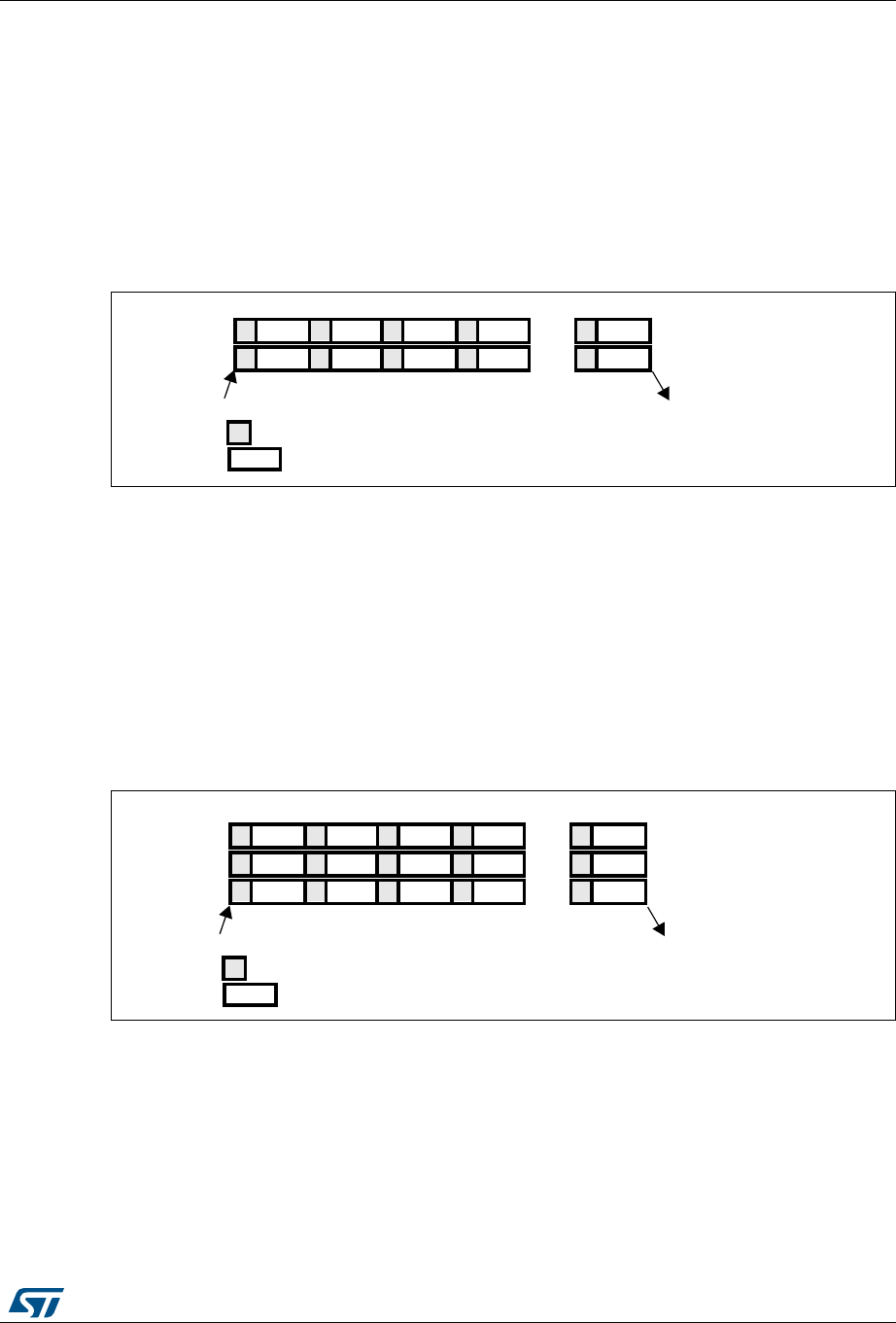
DocID018909 Rev 9 407/1718
RM0090 Analog-to-digital converter (ADC)
432
Dual ADC mode
At the end of conversion event on ADC1 or ADC2:
•A 32-bit DMA transfer request is generated (if DMA[1:0] bits in the ADC_CCR register
are equal to 0b10). This request transfers the ADC2 converted data stored in the upper
half-word of the ADC_CDR 32-bit register to the SRAM and then the ADC1 converted
data stored in the lower half-word of ADC_CCR to the SRAM.
•An EOC interrupt is generated (if enabled on one of the two ADC interfaces) when the
ADC1/ADC2’s regular channels have all been converted.
Figure 54. Regular simultaneous mode on 16 channels: dual ADC mode
Triple ADC mode
At the end of conversion event on ADC1, ADC2 or ADC3:
•Three 32-bit DMA transfer requests are generated (if DMA[1:0] bits in the ADC_CCR
register are equal to 0b01). Three transfers then take place from the ADC_CDR 32-bit
register to SRAM: first the ADC1 converted data, then the ADC2 converted data and
finally the ADC3 converted data. The process is repeated for each new three
conversions.
•An EOC interrupt is generated (if enabled on one of the three ADC interfaces) when the
ADC1/ADC2/ADC3’s regular channels are have all been converted.
Figure 55. Regular simultaneous mode on 16 channels: triple ADC mode
#( #( #( #(
#( #( #( #(
!$#
!$#
4RIGGER %NDOFCONVERSIONON!$#AND!$#
#ONVERSION
3AMPLING
#(
#(
AI
#( #( #( #(
#( #( #( #(
!$#
!$#
4RIGGER %NDOFCONVERSIONON!$#!$#AND!$#
#ONVERSION
3AMPLING
#(
#(
AI
#( #( #( #(
!$# #(
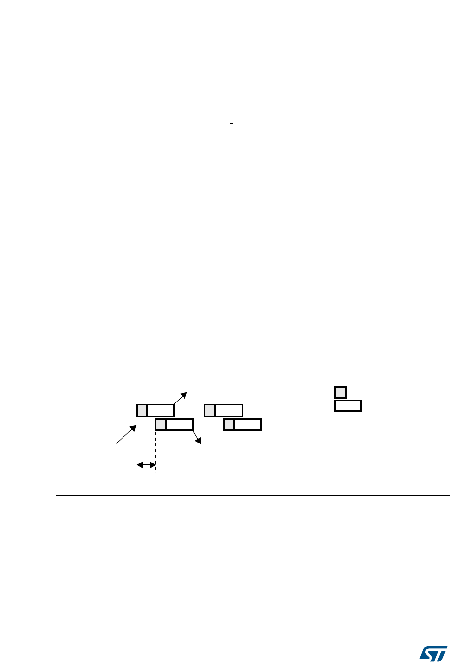
Analog-to-digital converter (ADC) RM0090
408/1718 DocID018909 Rev 9
13.9.3 Interleaved mode
This mode can be started only on a regular group (usually one channel). The external
trigger source comes from the regular channel multiplexer of ADC1.
Dual ADC mode
After an external trigger occurs:
•ADC1 starts immediately
•ADC2 starts after a delay of several ADC clock cycles
The minimum delay which separates 2 conversions in interleaved mode is configured in the
DELAY bits in the ADC_CCR register. However, an ADC cannot start a conversion if the
complementary ADC is still sampling its input (only one ADC can sample the input signal at
a given time). In this case, the delay becomes the sampling time + 2 ADC clock cycles. For
instance, if DELAY = 5 clock cycles and the sampling takes 15 clock cycles on both ADCs,
then 17 clock cycles will separate conversions on ADC1 and ADC2).
If the CONT bit is set on both ADC1 and ADC2, the selected regular channels of both ADCs
are continuously converted.
Note: If the conversion sequence is interrupted (for instance when DMA end of transfer occurs),
the multi-ADC sequencer must be reset by configuring it in independent mode first (bits
DUAL[4:0] = 00000) before reprogramming the interleaved mode.
After an EOC interrupt is generated by ADC2 (if enabled through the EOCIE bit) a 32-bit
DMA transfer request is generated (if the DMA[1:0] bits in ADC_CCR are equal to 0b10).
This request first transfers the ADC2 converted data stored in the upper half-word of the
ADC_CDR 32-bit register into SRAM, then the ADC1 converted data stored in the register’s
lower half-word into SRAM.
Figure 56. Interleaved mode on 1 channel in continuous conversion mode: dual ADC
mode
Triple ADC mode
After an external trigger occurs:
•ADC1 starts immediately and
•ADC2 starts after a delay of several ADC clock cycles
•ADC3 starts after a delay of several ADC clock cycles referred to the ADC2 conversion
The minimum delay which separates 2 conversions in interleaved mode is configured in the
DELAY bits in the ADC_CCR register. However, an ADC cannot start a conversion if the
complementary ADC is still sampling its input (only one ADC can sample the input signal at
#(
#(
!$#
!$#
4RIGGER %NDOFCONVERSIONON!$#
#(
#(
!$##,+
CYCLES
%NDOFCONVERSIONON!$#
#ONVERSION
3AMPLING
AI
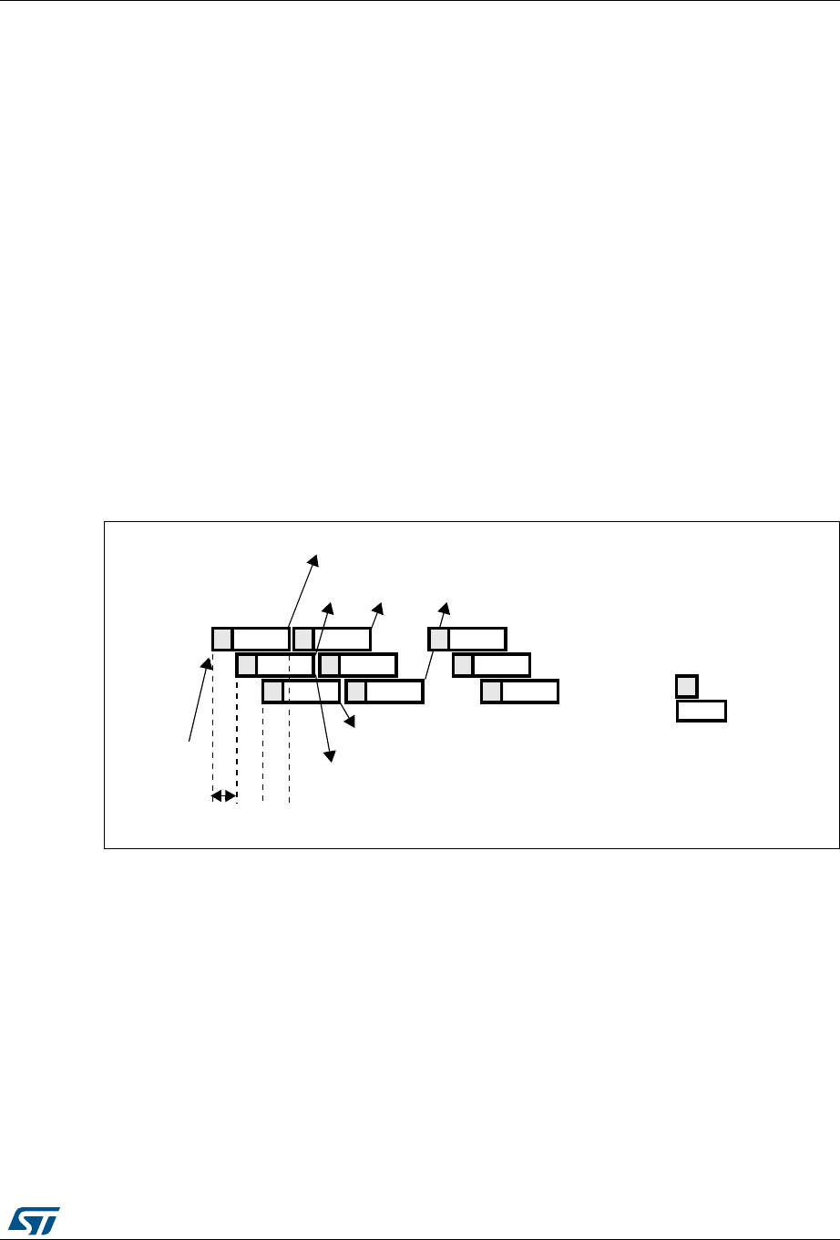
DocID018909 Rev 9 409/1718
RM0090 Analog-to-digital converter (ADC)
432
a given time). In this case, the delay becomes the sampling time + 2 ADC clock cycles. For
instance, if DELAY = 5 clock cycles and the sampling takes 15 clock cycles on the three
ADCs, then 17 clock cycles will separate the conversions on ADC1, ADC2 and ADC3).
If the CONT bit is set on ADC1, ADC2 and ADC3, the selected regular channels of all ADCs
are continuously converted.
Note: If the conversion sequence is interrupted (for instance when DMA end of transfer occurs),
the multi-ADC sequencer must be reset by configuring it in independent mode first (bits
DUAL[4:0] = 00000) before reprogramming the interleaved mode.
In this mode a DMA request is generated each time 2 data items are available, (if the
DMA[1:0] bits in the ADC_CCR register are equal to 0b10). The request first transfers the
first converted data stored in the lower half-word of the ADC_CDR 32-bit register to SRAM,
then it transfers the second converted data stored in ADC_CDR’s upper half-word to SRAM.
The sequence is the following:
•1st request: ADC_CDR[31:0] = ADC2_DR[15:0] | ADC1_DR[15:0]
•2nd request: ADC_CDR[31:0] = ADC1_DR[15:0] | ADC3_DR[15:0]
•3rd request: ADC_CDR[31:0] = ADC3_DR[15:0] | ADC2_DR[15:0]
•4th request: ADC_CDR[31:0] = ADC2_DR[15:0] | ADC1_DR[15:0], ...
Figure 57. Interleaved mode on 1 channel in continuous conversion mode: triple ADC
mode
13.9.4 Alternate trigger mode
This mode can be started only on an injected group. The source of external trigger comes
from the injected group multiplexer of ADC1.
Note: Regular conversions can be enabled on one or all ADCs. In this case the regular
conversions are independent of each other. A regular conversion is interrupted when the
!$#
!$#
4RIGGER %NDOFCONVERSIONON!$#
!$##,+
CYCLES
%NDOFCONVERSIONON!$#
!$#
%NDOFCONVERSIONON!$#
$-!REQUESTEVERYCONVERSIONS
#(
#ONVERSION
3AMPLING
AI
#(
#(
#(
#(
#(
#(
#(
#(
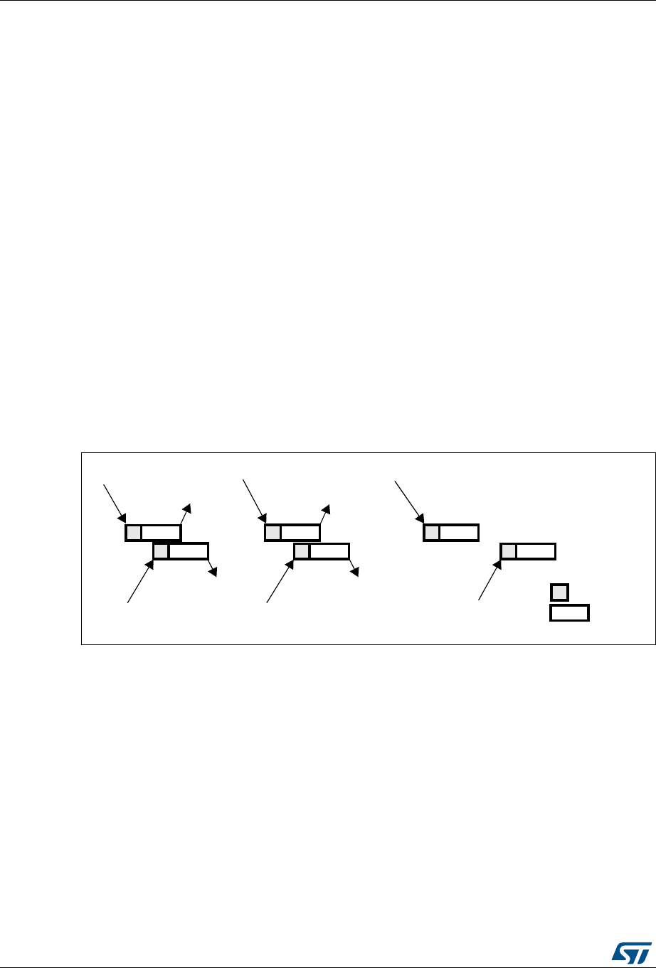
Analog-to-digital converter (ADC) RM0090
410/1718 DocID018909 Rev 9
ADC has to perform an injected conversion. It is resumed when the injected conversion is
finished.
If the conversion sequence is interrupted (for instance when DMA end of transfer occurs),
the multi-ADC sequencer must be reset by configuring it in independent mode first (bits
DUAL[4:0] = 00000) before reprogramming the interleaved mode.
The time interval between 2 trigger events must be greater than or equal to 1 ADC clock
period. The minimum time interval between 2 trigger events that start conversions on the
same ADC is the same as in the single ADC mode.
Dual ADC mode
•When the 1st trigger occurs, all injected ADC1 channels in the group are converted
•When the 2nd trigger occurs, all injected ADC2 channels in the group are converted
•and so on
A JEOC interrupt, if enabled, is generated after all injected ADC1 channels in the group
have been converted.
A JEOC interrupt, if enabled, is generated after all injected ADC2 channels in the group
have been converted.
If another external trigger occurs after all injected channels in the group have been
converted then the alternate trigger process restarts by converting the injected ADC1
channels in the group.
Figure 58. Alternate trigger: injected group of each ADC
If the injected discontinuous mode is enabled for both ADC1 and ADC2:
•When the 1st trigger occurs, the first injected ADC1 channel is converted.
•When the 2nd trigger occurs, the first injected ADC2 channel are converted
•and so on
A JEOC interrupt, if enabled, is generated after all injected ADC1 channels in the group
have been converted.
A JEOC interrupt, if enabled, is generated after all injected ADC2 channels in the group
have been converted.
If another external trigger occurs after all injected channels in the group have been
converted then the alternate trigger process restarts.
!$#
!$#
STTRIGGER
NDTRIGGER
RDTRIGGER
THTRIGGER
NTHTRIGGER
NTHTRIGGER
%/#*%/#
ON!$#
%/#*%/#
ON!$#
%/#*%/#
ON!$#
%/#*%/#
ON!$#
#ONVERSION
3AMPLING
AI
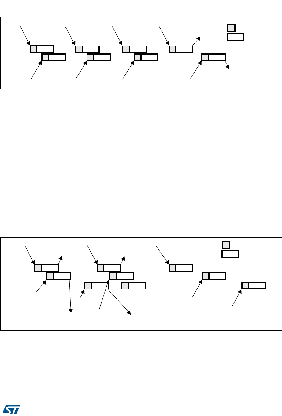
DocID018909 Rev 9 411/1718
RM0090 Analog-to-digital converter (ADC)
432
Figure 59. Alternate trigger: 4 injected channels (each ADC) in discontinuous mode
Triple ADC mode
•When the 1st trigger occurs, all injected ADC1 channels in the group are converted.
•When the 2nd trigger occurs, all injected ADC2 channels in the group are converted.
•When the 3rd trigger occurs, all injected ADC3 channels in the group are converted.
•and so on
A JEOC interrupt, if enabled, is generated after all injected ADC1 channels in the group
have been converted.
A JEOC interrupt, if enabled, is generated after all injected ADC2 channels in the group
have been converted.
A JEOC interrupt, if enabled, is generated after all injected ADC3 channels in the group
have been converted.
If another external trigger occurs after all injected channels in the group have been
converted then the alternate trigger process restarts by converting the injected ADC1
channels in the group.
Figure 60. Alternate trigger: injected group of each ADC
13.9.5 Combined regular/injected simultaneous mode
It is possible to interrupt the simultaneous conversion of a regular group to start the
simultaneous conversion of an injected group.
Note: In combined regular/injected simultaneous mode, one must convert sequences with the
same length or ensure that the interval between triggers is longer than the long conversion
time of the 2 sequences (Dual ADC mode) /3 sequences (Triple ADC mode). Otherwise, the
!$#
!$#
STTRIGGER
#ONVERSION
3AMPLING
NDTRIGGER
RDTRIGGER
THTRIGGER
THTRIGGER
THTRIGGER
THTRIGGER
THTRIGGER
*%/#ON!$#
*%/#ON!$#
AI
!$#
!$#
STTRIGGER
#ONVERSION
3AMPLING
NDTRIGGER
THTRIGGER
RDTRIGGER
NTHTRIGGER
NTHTRIGGER
%/#*%/#
ON!$#
%/#*%/#
ON!$#
%/#*%/#
ON!$# %/#*%/#
ON!$#
THTRIGGER NTHTRIGGER
AI
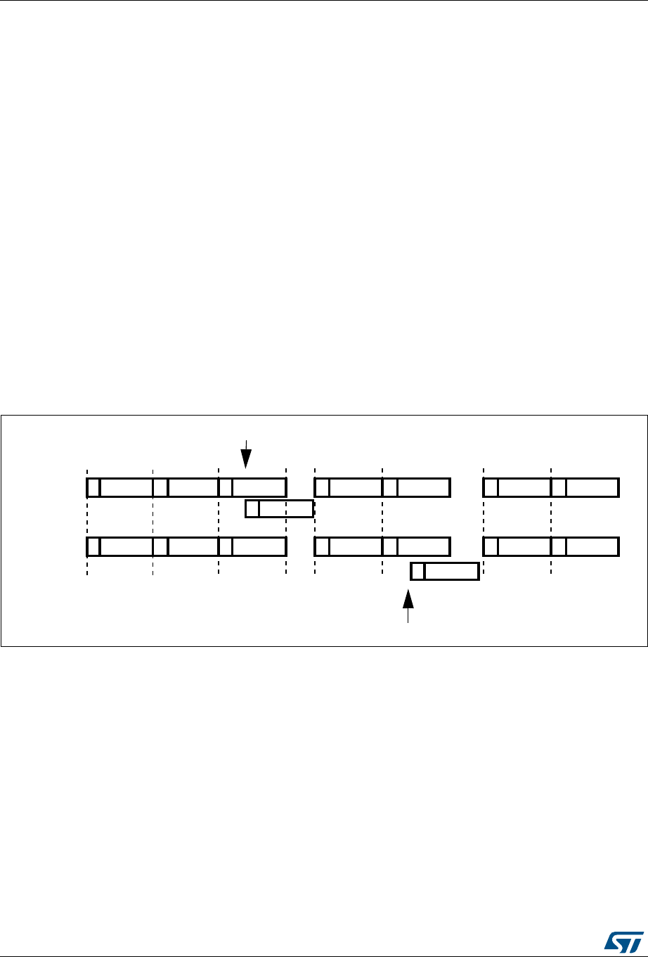
Analog-to-digital converter (ADC) RM0090
412/1718 DocID018909 Rev 9
ADC with the shortest sequence may restart while the ADC with the longest sequence is
completing the previous conversions.
13.9.6 Combined regular simultaneous + alternate trigger mode
It is possible to interrupt the simultaneous conversion of a regular group to start the alternate
trigger conversion of an injected group. Figure 61 shows the behavior of an alternate trigger
interrupting a simultaneous regular conversion.
The injected alternate conversion is immediately started after the injected event. If regular
conversion is already running, in order to ensure synchronization after the injected
conversion, the regular conversion of all (master/slave) ADCs is stopped and resumed
synchronously at the end of the injected conversion.
Note: In combined regular simultaneous + alternate trigger mode, one must convert sequences
with the same length or ensure that the interval between triggers is longer than the long
conversion time of the 2 sequences (Dual ADC mode) /3 sequences (Triple ADC mode).
Otherwise, the ADC with the shortest sequence may restart while the ADC with the longest
sequence is completing the previous conversions.
If the conversion sequence is interrupted (for instance when DMA end of transfer occurs),
the multi-ADC sequencer must be reset by configuring it in independent mode first (bits
DUAL[4:0] = 00000) before reprogramming the interleaved mode.
Figure 61. Alternate + regular simultaneous
If a trigger occurs during an injected conversion that has interrupted a regular conversion, it
is ignored. Figure 62 shows the behavior in this case (2nd trigger is ignored).
!$#REG #( #( #(
#(
#( #(
#(
!$#INJ
!$#REG
!$#INJ
STTRIGGER
NDTRIGGER
SYNCHRONOTLOST
#( #( #( #( #(
#( #(
#( #(
AI

DocID018909 Rev 9 413/1718
RM0090 Analog-to-digital converter (ADC)
432
Figure 62. Case of trigger occurring during injected conversion
13.10 Temperature sensor
The temperature sensor can be used to measure the ambient temperature (TA) of the
device.
•On STM23F40x and STM32F41x devices, the temperature sensor is internally
connected to ADC1_IN16 channel which is used to convert the sensor output voltage
to a digital value.
•On STM23F42x and STM32F43x devices, the temperature sensor is internally
connected to the same input channel, ADC1_IN18, as VBAT: ADC1_IN18 is used to
convert the sensor output voltage or VBAT into a digital value. Only one conversion,
temperature sensor or VBAT, must be selected at a time. When the temperature sensor
and the VBAT conversion are set simultaneously, only the VBAT conversion is
performed.
Figure 63 shows the block diagram of the temperature sensor.
When not in use, the sensor can be put in power down mode.
Note: The TSVREFE bit must be set to enable the conversion of both internal channels: the
ADC1_IN16 or ADC1_IN18 (temperature sensor) and the ADC1_IN17 (VREFINT).
Main features
•Supported temperature range: –40 to 125 °C
•Precision: ±1.5 °C
!$#REG #( #( #(
#(
#( #(
#(
!$#INJ
!$#REG
!$#INJ
STTRIGGER
NDTRIGGER
#( #( #( #( #(
#( #(
#( #(
AI
#(
NDTRIGGER
RDTRIGGER
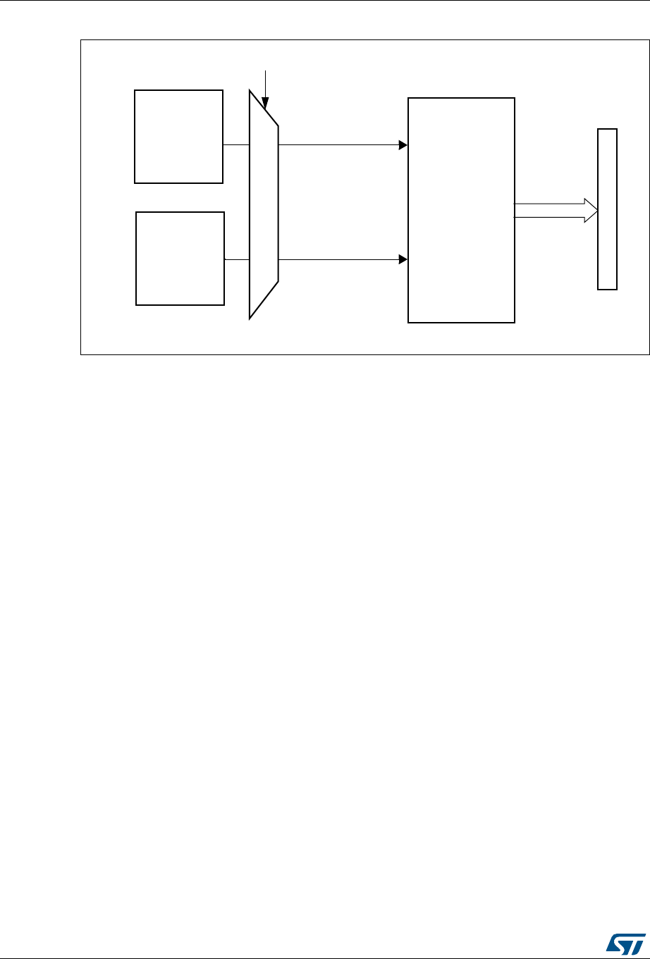
Analog-to-digital converter (ADC) RM0090
414/1718 DocID018909 Rev 9
Figure 63. Temperature sensor and VREFINT channel block diagram
1. VSENSE is input to ADC1_IN16 for the STM23F40x and STM32F41x devices and to ADC1_IN18 for the
STM23F42x and STM32F43x devices.
Reading the temperature
To use the sensor:
3. Select ADC1_IN16 or ADC1_IN18 input channel.
4. Select a sampling time greater than the minimum sampling time specified in the
datasheet.
5. Set the TSVREFE bit in the ADC_CCR register to wake up the temperature sensor
from power down mode
6. Start the ADC conversion by setting the SWSTART bit (or by external trigger)
7. Read the resulting VSENSE data in the ADC data register
8. Calculate the temperature using the following formula:
Temperature (in °C) = {(VSENSE – V25) / Avg_Slope} + 25
Where:
–V
25 = VSENSE value for 25° C
– Avg_Slope = average slope of the temperature vs. VSENSE curve (given in mV/°C
or µV/°C)
Refer to the datasheet’s electrical characteristics section for the actual values of V25
and Avg_Slope.
Note: The sensor has a startup time after waking from power down mode before it can output
VSENSE at the correct level. The ADC also has a startup time after power-on, so to minimize
the delay, the ADON and TSVREFE bits should be set at the same time.
The temperature sensor output voltage changes linearly with temperature. The offset of this
linear function depends on each chip due to process variation (up to 45 °C from one chip to
another).
-36
4EMPERATURE
SENSOR 63%.3%
4362%&%CONTROLBIT
!$#
!DDRESSDATABUS
62%&).4
!$#?).
!$#?).
)NTERNAL
POWERBLOCK !$#?).
CONVERTEDDATA

DocID018909 Rev 9 415/1718
RM0090 Analog-to-digital converter (ADC)
432
The internal temperature sensor is more suited for applications that detect temperature
variations instead of absolute temperatures. If accurate temperature reading is required, an
external temperature sensor should be used.
13.11 Battery charge monitoring
The VBATE bit in the ADC_CCR register is used to switch to the battery voltage. As the
VBAT voltage could be higher than VDDA, to ensure the correct operation of the ADC, the
VBAT pin is internally connected to a bridge divider.
When the VBATE is set, the bridge is automatically enabled to connect:
•VBAT/2 to the ADC1_IN18 input channel, on STM32F40xx and STM32F41xx devices
•VBAT/4 to the ADC1_IN18 input channel, on STM32F42xx and STM32F43xx devices
Note: The VBAT and temperature sensor are connected to the same ADC internal channel
(ADC1_IN18). Only one conversion, either temperature sensor or VBAT, must be selected
at a time. When both conversion are enabled simultaneously, only the VBAT conversion is
performed.
13.12 ADC interrupts
An interrupt can be produced on the end of conversion for regular and injected groups,
when the analog watchdog status bit is set and when the overrun status bit is set. Separate
interrupt enable bits are available for flexibility.
Two other flags are present in the ADC_SR register, but there is no interrupt associated with
them:
•JSTRT (Start of conversion for channels of an injected group)
•STRT (Start of conversion for channels of a regular group)
Table 70. ADC interrupts
Interrupt event Event flag Enable control bit
End of conversion of a regular group EOC EOCIE
End of conversion of an injected group JEOC JEOCIE
Analog watchdog status bit is set AWD AWDIE
Overrun OVR OVRIE

Analog-to-digital converter (ADC) RM0090
416/1718 DocID018909 Rev 9
13.13 ADC registers
Refer to Section 1.1 on page 57 for a list of abbreviations used in register descriptions.
The peripheral registers must be written at word level (32 bits). Read accesses can be done
by bytes (8 bits), half-words (16 bits) or words (32 bits).
13.13.1 ADC status register (ADC_SR)
Address offset: 0x00
Reset value: 0x0000 0000
31 30 29 28 27 26 25 24 23 22 21 20 19 18 17 16
Reserved
1514131211109876543210
Reserved
OVR STRT JSTRT JEOC EOC AWD
rc_w0 rc_w0 rc_w0 rc_w0 rc_w0 rc_w0
Bits 31:6 Reserved, must be kept at reset value.
Bit 5 OVR: Overrun
This bit is set by hardware when data are lost (either in single mode or in dual/triple mode). It
is cleared by software. Overrun detection is enabled only when DMA = 1 or EOCS = 1.
0: No overrun occurred
1: Overrun has occurred
Bit 4 STRT: Regular channel start flag
This bit is set by hardware when regular channel conversion starts. It is cleared by software.
0: No regular channel conversion started
1: Regular channel conversion has started
Bit 3 JSTRT: Injected channel start flag
This bit is set by hardware when injected group conversion starts. It is cleared by software.
0: No injected group conversion started
1: Injected group conversion has started
Bit 2 JEOC: Injected channel end of conversion
This bit is set by hardware at the end of the conversion of all injected channels in the group.
It is cleared by software.
0: Conversion is not complete
1: Conversion complete
Bit 1 EOC: Regular channel end of conversion
This bit is set by hardware at the end of the conversion of a regular group of channels. It is
cleared by software or by reading the ADC_DR register.
0: Conversion not complete (EOCS=0), or sequence of conversions not complete (EOCS=1)
1: Conversion complete (EOCS=0), or sequence of conversions complete (EOCS=1)
Bit 0 AWD: Analog watchdog flag
This bit is set by hardware when the converted voltage crosses the values programmed in
the ADC_LTR and ADC_HTR registers. It is cleared by software.
0: No analog watchdog event occurred
1: Analog watchdog event occurred

DocID018909 Rev 9 417/1718
RM0090 Analog-to-digital converter (ADC)
432
13.13.2 ADC control register 1 (ADC_CR1)
Address offset: 0x04
Reset value: 0x0000 0000
31 30 29 28 27 26 25 24 23 22 21 20 19 18 17 16
Reserved OVRIE RES AWDEN JAWDEN Reserved
rw rw rw rw rw
15 14 13 12 11 10 9 8 7 6 5 4 3 2 1 0
DISCNUM[2:0] JDISCE
N
DISC
EN JAUTO AWDSG
LSCAN JEOCIE AWDIE EOCIE AWDCH[4:0]
rw rw rw rw rw rw rw rw rw rw rw rw rw rw rw rw
Bits 31:27 Reserved, must be kept at reset value.
Bit 26 OVRIE: Overrun interrupt enable
This bit is set and cleared by software to enable/disable the Overrun interrupt.
0: Overrun interrupt disabled
1: Overrun interrupt enabled. An interrupt is generated when the OVR bit is set.
Bits 25:24 RES[1:0]: Resolution
These bits are written by software to select the resolution of the conversion.
00: 12-bit (15 ADCCLK cycles)
01: 10-bit (13 ADCCLK cycles)
10: 8-bit (11 ADCCLK cycles)
11: 6-bit (9 ADCCLK cycles)
Bit 23 AWDEN: Analog watchdog enable on regular channels
This bit is set and cleared by software.
0: Analog watchdog disabled on regular channels
1: Analog watchdog enabled on regular channels
Bit 22 JAWDEN: Analog watchdog enable on injected channels
This bit is set and cleared by software.
0: Analog watchdog disabled on injected channels
1: Analog watchdog enabled on injected channels
Bits 21:16 Reserved, must be kept at reset value.
Bits 15:13 DISCNUM[2:0]: Discontinuous mode channel count
These bits are written by software to define the number of regular channels to be converted
in discontinuous mode, after receiving an external trigger.
000: 1 channel
001: 2 channels
...
111: 8 channels
Bit 12 JDISCEN: Discontinuous mode on injected channels
This bit is set and cleared by software to enable/disable discontinuous mode on the injected
channels of a group.
0: Discontinuous mode on injected channels disabled
1: Discontinuous mode on injected channels enabled

Analog-to-digital converter (ADC) RM0090
418/1718 DocID018909 Rev 9
Bit 11 DISCEN: Discontinuous mode on regular channels
This bit is set and cleared by software to enable/disable Discontinuous mode on regular
channels.
0: Discontinuous mode on regular channels disabled
1: Discontinuous mode on regular channels enabled
Bit 10 JAUTO: Automatic injected group conversion
This bit is set and cleared by software to enable/disable automatic injected group conversion
after regular group conversion.
0: Automatic injected group conversion disabled
1: Automatic injected group conversion enabled
Bit 9 AWDSGL: Enable the watchdog on a single channel in scan mode
This bit is set and cleared by software to enable/disable the analog watchdog on the channel
identified by the AWDCH[4:0] bits.
0: Analog watchdog enabled on all channels
1: Analog watchdog enabled on a single channel
Bit 8 SCAN: Scan mode
This bit is set and cleared by software to enable/disable the Scan mode. In Scan mode, the
inputs selected through the ADC_SQRx or ADC_JSQRx registers are converted.
0: Scan mode disabled
1: Scan mode enabled
Note: An EOC interrupt is generated if the EOCIE bit is set:
– At the end of each regular group sequence if the EOCS bit is cleared to 0
– At the end of each regular channel conversion if the EOCS bit is set to 1
Note: A JEOC interrupt is generated only on the end of conversion of the last channel if the
JEOCIE bit is set.
Bit 7 JEOCIE: Interrupt enable for injected channels
This bit is set and cleared by software to enable/disable the end of conversion interrupt for
injected channels.
0: JEOC interrupt disabled
1: JEOC interrupt enabled. An interrupt is generated when the JEOC bit is set.
Bit 6 AWDIE: Analog watchdog interrupt enable
This bit is set and cleared by software to enable/disable the analog watchdog interrupt.
0: Analog watchdog interrupt disabled
1: Analog watchdog interrupt enabled
Bit 5 EOCIE: Interrupt enable for EOC
This bit is set and cleared by software to enable/disable the end of conversion interrupt.
0: EOC interrupt disabled
1: EOC interrupt enabled. An interrupt is generated when the EOC bit is set.
Bits 4:0 AWDCH[4:0]: Analog watchdog channel select bits
These bits are set and cleared by software. They select the input channel to be guarded by
the analog watchdog.
Note: 00000: ADC analog input Channel0
00001: ADC analog input Channel1
...
01111: ADC analog input Channel15
10000: ADC analog input Channel16
10001: ADC analog input Channel17
10010: ADC analog input Channel18
Other values reserved

DocID018909 Rev 9 419/1718
RM0090 Analog-to-digital converter (ADC)
432
13.13.3 ADC control register 2 (ADC_CR2)
Address offset: 0x08
Reset value: 0x0000 0000
31 30 29 28 27 26 25 24 23 22 21 20 19 18 17 16
reserved
SWST
ART EXTEN EXTSEL[3:0] reserved
JSWST
ART JEXTEN JEXTSEL[3:0]
rw rw rw rw rw rw rw rw rw rw rw rw rw rw
15 14 13 12 11 10 9 8 7 6 5 4 3 2 1 0
reserved
ALIGN EOCS DDS DMA
Reserved
CONT ADON
rw rw rw rw rw rw
Bit 31 Reserved, must be kept at reset value.
Bit 30 SWSTART: Start conversion of regular channels
This bit is set by software to start conversion and cleared by hardware as soon as the
conversion starts.
0: Reset state
1: Starts conversion of regular channels
Note: This bit can be set only when ADON = 1 otherwise no conversion is launched.
Bits 29:28 EXTEN: External trigger enable for regular channels
These bits are set and cleared by software to select the external trigger polarity and enable
the trigger of a regular group.
00: Trigger detection disabled
01: Trigger detection on the rising edge
10: Trigger detection on the falling edge
11: Trigger detection on both the rising and falling edges
Bits 27:24 EXTSEL[3:0]: External event select for regular group
These bits select the external event used to trigger the start of conversion of a regular group:
0000: Timer 1 CC1 event
0001: Timer 1 CC2 event
0010: Timer 1 CC3 event
0011: Timer 2 CC2 event
0100: Timer 2 CC3 event
0101: Timer 2 CC4 event
0110: Timer 2 TRGO event
0111: Timer 3 CC1 event
1000: Timer 3 TRGO event
1001: Timer 4 CC4 event
1010: Timer 5 CC1 event
1011: Timer 5 CC2 event
1100: Timer 5 CC3 event
1101: Timer 8 CC1 event
1110: Timer 8 TRGO event
1111: EXTI line11
Bit 23 Reserved, must be kept at reset value.

Analog-to-digital converter (ADC) RM0090
420/1718 DocID018909 Rev 9
Bit 22 JSWSTART: Start conversion of injected channels
This bit is set by software and cleared by hardware as soon as the conversion starts.
0: Reset state
1: Starts conversion of injected channels
Note: This bit can be set only when ADON = 1 otherwise no conversion is launched.
Bits 21:20 JEXTEN: External trigger enable for injected channels
These bits are set and cleared by software to select the external trigger polarity and enable
the trigger of an injected group.
00: Trigger detection disabled
01: Trigger detection on the rising edge
10: Trigger detection on the falling edge
11: Trigger detection on both the rising and falling edges
Bits 19:16 JEXTSEL[3:0]: External event select for injected group
These bits select the external event used to trigger the start of conversion of an injected
group.
0000: Timer 1 CC4 event
0001: Timer 1 TRGO event
0010: Timer 2 CC1 event
0011: Timer 2 TRGO event
0100: Timer 3 CC2 event
0101: Timer 3 CC4 event
0110: Timer 4 CC1 event
0111: Timer 4 CC2 event
1000: Timer 4 CC3 event
1001: Timer 4 TRGO event
1010: Timer 5 CC4 event
1011: Timer 5 TRGO event
1100: Timer 8 CC2 event
1101: Timer 8 CC3 event
1110: Timer 8 CC4 event
1111: EXTI line15
Bits 15:12 Reserved, must be kept at reset value.
Bit 11 ALIGN: Data alignment
This bit is set and cleared by software. Refer to Figure 48 and Figure 49.
0: Right alignment
1: Left alignment
Bit 10 EOCS: End of conversion selection
This bit is set and cleared by software.
0: The EOC bit is set at the end of each sequence of regular conversions. Overrun detection
is enabled only if DMA=1.
1: The EOC bit is set at the end of each regular conversion. Overrun detection is enabled.
Bit 9 DDS: DMA disable selection (for single ADC mode)
This bit is set and cleared by software.
0: No new DMA request is issued after the last transfer (as configured in the DMA controller)
1: DMA requests are issued as long as data are converted and DMA=1
Bit 8 DMA: Direct memory access mode (for single ADC mode)
This bit is set and cleared by software. Refer to the DMA controller chapter for more details.
0: DMA mode disabled
1: DMA mode enabled

DocID018909 Rev 9 421/1718
RM0090 Analog-to-digital converter (ADC)
432
13.13.4 ADC sample time register 1 (ADC_SMPR1)
Address offset: 0x0C
Reset value: 0x0000 0000
13.13.5 ADC sample time register 2 (ADC_SMPR2)
Address offset: 0x10
Reset value: 0x0000 0000
Bits 7:2 Reserved, must be kept at reset value.
Bit 1 CONT: Continuous conversion
This bit is set and cleared by software. If it is set, conversion takes place continuously until it
is cleared.
0: Single conversion mode
1: Continuous conversion mode
Bit 0 ADON: A/D Converter ON / OFF
This bit is set and cleared by software.
Note: 0: Disable ADC conversion and go to power down mode
1: Enable ADC
31 30 29 28 27 26 25 24 23 22 21 20 19 18 17 16
Reserved
SMP18[2:0] SMP17[2:0] SMP16[2:0] SMP15[2:1]
rw rw rw rw rw rw rw rw rw rw rw
15 14 13 12 11 10 9 8 7 6 5 4 3 2 1 0
SMP15_0 SMP14[2:0] SMP13[2:0] SMP12[2:0] SMP11[2:0] SMP10[2:0]
rw rw rw rw rw rw rw rw rw rw rw rw rw rw rw rw
Bits 31: 27 Reserved, must be kept at reset value.
Bits 26:0 SMPx[2:0]: Channel x sampling time selection
These bits are written by software to select the sampling time individually for each channel.
During sampling cycles, the channel selection bits must remain unchanged.
Note: 000: 3 cycles
001: 15 cycles
010: 28 cycles
011: 56 cycles
100: 84 cycles
101: 112 cycles
110: 144 cycles
111: 480 cycles
31 30 29 28 27 26 25 24 23 22 21 20 19 18 17 16
Reserved SMP9[2:0] SMP8[2:0] SMP7[2:0] SMP6[2:0] SMP5[2:1]
rw rw rw rw rw rw rw rw rw rw rw rw rw rw
1514131211109876543210
SMP
5_0 SMP4[2:0] SMP3[2:0] SMP2[2:0] SMP1[2:0] SMP0[2:0]
rw rw rw rw rw rw rw rw rw rw rw rw rw rw rw rw
Analog-to-digital converter (ADC) RM0090
422/1718 DocID018909 Rev 9
13.13.6 ADC injected channel data offset register x (ADC_JOFRx) (x=1..4)
Address offset: 0x14-0x20
Reset value: 0x0000 0000
13.13.7 ADC watchdog higher threshold register (ADC_HTR)
Address offset: 0x24
Reset value: 0x0000 0FFF
Bits 31:30 Reserved, must be kept at reset value.
Bits 29:0 SMPx[2:0]: Channel x sampling time selection
These bits are written by software to select the sampling time individually for each channel.
During sample cycles, the channel selection bits must remain unchanged.
Note: 000: 3 cycles
001: 15 cycles
010: 28 cycles
011: 56 cycles
100: 84 cycles
101: 112 cycles
110: 144 cycles
111: 480 cycles
31 30 29 28 27 26 25 24 23 22 21 20 19 18 17 16
Reserved
1514131211109876543210
Reserved JOFFSETx[11:0]
rw rw rw rw rw rw rw rw rw rw rw rw
Bits 31:12 Reserved, must be kept at reset value.
Bits 11:0 JOFFSETx[11:0]: Data offset for injected channel x
These bits are written by software to define the offset to be subtracted from the raw
converted data when converting injected channels. The conversion result can be read from
in the ADC_JDRx registers.
31 30 29 28 27 26 25 24 23 22 21 20 19 18 17 16
Reserved
1514131211109876543210
Reserved
HT[11:0]
rw rw rw rw rw rw rw rw rw rw rw rw
Bits 31:12 Reserved, must be kept at reset value.
Bits 11:0 HT[11:0]: Analog watchdog higher threshold
These bits are written by software to define the higher threshold for the analog watchdog.
DocID018909 Rev 9 423/1718
RM0090 Analog-to-digital converter (ADC)
432
13.13.8 ADC watchdog lower threshold register (ADC_LTR)
Address offset: 0x28
Reset value: 0x0000 0000
13.13.9 ADC regular sequence register 1 (ADC_SQR1)
Address offset: 0x2C
Reset value: 0x0000 0000
31 30 29 28 27 26 25 24 23 22 21 20 19 18 17 16
Reserved
1514131211109876543210
Reserved
LT[11:0]
rw rw rw rw rw rw rw rw rw rw rw rw
Bits 31:12 Reserved, must be kept at reset value.
Bits 11:0 LT[11:0]: Analog watchdog lower threshold
These bits are written by software to define the lower threshold for the analog watchdog.
31 30 29 28 27 26 25 24 23 22 21 20 19 18 17 16
Reserved L[3:0] SQ16[4:1]
rw rw rw rw rw rw rw rw
15 14 13 12 11 10 9 8 7 6 5 4 3 2 1 0
SQ16_0 SQ15[4:0] SQ14[4:0] SQ13[4:0]
rw rw rw rw rw rw rw rw rw rw rw rw rw
Bits 31:24 Reserved, must be kept at reset value.
Bits 23:20 L[3:0]: Regular channel sequence length
These bits are written by software to define the total number of conversions in the regular
channel conversion sequence.
0000: 1 conversion
0001: 2 conversions
...
1111: 16 conversions
Bits 19:15 SQ16[4:0]: 16th conversion in regular sequence
These bits are written by software with the channel number (0..18) assigned as the 16th in
the conversion sequence.
Bits 14:10 SQ15[4:0]: 15th conversion in regular sequence
Bits 9:5 SQ14[4:0]: 14th conversion in regular sequence
Bits 4:0 SQ13[4:0]: 13th conversion in regular sequence

Analog-to-digital converter (ADC) RM0090
424/1718 DocID018909 Rev 9
13.13.10 ADC regular sequence register 2 (ADC_SQR2)
Address offset: 0x30
Reset value: 0x0000 0000
13.13.11 ADC regular sequence register 3 (ADC_SQR3)
Address offset: 0x34
Reset value: 0x0000 0000
31 30 29 28 27 26 25 24 23 22 21 20 19 18 17 16
Reserved SQ12[4:0] SQ11[4:0] SQ10[4:1]
rw rw rw rw rw rw rw rw rw rw rw rw rw rw
15 14 13 12 11 10 9 8 7 6 5 4 3 2 1 0
SQ10_0 SQ9[4:0] SQ8[4:0] SQ7[4:0]
rw rw rw rw rw rw rw rw rw rw rw rw rw rw rw rw
Bits 31:30 Reserved, must be kept at reset value.
Bits 29:26 SQ12[4:0]: 12th conversion in regular sequence
These bits are written by software with the channel number (0..18) assigned as the 12th in
the sequence to be converted.
Bits 24:20 SQ11[4:0]: 11th conversion in regular sequence
Bits 19:15 SQ10[4:0]: 10th conversion in regular sequence
Bits 14:10 SQ9[4:0]: 9th conversion in regular sequence
Bits 9:5 SQ8[4:0]: 8th conversion in regular sequence
Bits 4:0 SQ7[4:0]: 7th conversion in regular sequence
31 30 29 28 27 26 25 24 23 22 21 20 19 18 17 16
Reserved SQ6[4:0] SQ5[4:0] SQ4[4:1]
rw rw rw rw rw rw rw rw rw rw rw rw rw rw
1514131211109876543210
SQ4_0 SQ3[4:0] SQ2[4:0] SQ1[4:0]
rw rw rw rw rw rw rw rw rw rw rw rw rw rw rw rw
Bits 31:30 Reserved, must be kept at reset value.
Bits 29:25 SQ6[4:0]: 6th conversion in regular sequence
These bits are written by software with the channel number (0..18) assigned as the 6th in the
sequence to be converted.
Bits 24:20 SQ5[4:0]: 5th conversion in regular sequence
Bits 19:15 SQ4[4:0]: 4th conversion in regular sequence
Bits 14:10 SQ3[4:0]: 3rd conversion in regular sequence
Bits 9:5 SQ2[4:0]: 2nd conversion in regular sequence
Bits 4:0 SQ1[4:0]: 1st conversion in regular sequence
DocID018909 Rev 9 425/1718
RM0090 Analog-to-digital converter (ADC)
432
13.13.12 ADC injected sequence register (ADC_JSQR)
Address offset: 0x38
Reset value: 0x0000 0000
Note: When JL[1:0]=3 (4 injected conversions in the sequencer), the ADC converts the channels
in the following order: JSQ1[4:0], JSQ2[4:0], JSQ3[4:0], and JSQ4[4:0].
When JL=2 (3 injected conversions in the sequencer), the ADC converts the channels in the
following order: JSQ2[4:0], JSQ3[4:0], and JSQ4[4:0].
When JL=1 (2 injected conversions in the sequencer), the ADC converts the channels in
starting from JSQ3[4:0], and then JSQ4[4:0].
When JL=0 (1 injected conversion in the sequencer), the ADC converts only JSQ4[4:0]
channel.
13.13.13 ADC injected data register x (ADC_JDRx) (x= 1..4)
Address offset: 0x3C - 0x48
Reset value: 0x0000 0000
31 30 29 28 27 26 25 24 23 22 21 20 19 18 17 16
Reserved JL[1:0] JSQ4[4:1]
rw rw rw rw rw rw
1514131211109876543210
JSQ4[0] JSQ3[4:0] JSQ2[4:0] JSQ1[4:0]
rw rw rw rw rw rw rw rw rw rw rw rw rw rw rw rw
Bits 31:22 Reserved, must be kept at reset value.
Bits 21:20 JL[1:0]: Injected sequence length
These bits are written by software to define the total number of conversions in the injected
channel conversion sequence.
00: 1 conversion
01: 2 conversions
10: 3 conversions
11: 4 conversions
Bits 19:15 JSQ4[4:0]: 4th conversion in injected sequence (when JL[1:0]=3, see note below)
These bits are written by software with the channel number (0..18) assigned as the 4th in the
sequence to be converted.
Bits 14:10 JSQ3[4:0]: 3rd conversion in injected sequence (when JL[1:0]=3, see note below)
Bits 9:5 JSQ2[4:0]: 2nd conversion in injected sequence (when JL[1:0]=3, see note below)
Bits 4:0 JSQ1[4:0]: 1st conversion in injected sequence (when JL[1:0]=3, see note below)
31 30 29 28 27 26 25 24 23 22 21 20 19 18 17 16
Reserved
1514131211109876543210
JDATA[15:0]
rrrrrr r r r r rrrrrr
Analog-to-digital converter (ADC) RM0090
426/1718 DocID018909 Rev 9
13.13.14 ADC regular data register (ADC_DR)
Address offset: 0x4C
Reset value: 0x0000 0000
13.13.15 ADC Common status register (ADC_CSR)
Address offset: 0x00 (this offset address is relative to ADC1 base address + 0x300)
Reset value: 0x0000 0000
This register provides an image of the status bits of the different ADCs. Nevertheless it is
read-only and does not allow to clear the different status bits. Instead each status bit must
be cleared by writing it to 0 in the corresponding ADC_SR register.
Bits 31:16 Reserved, must be kept at reset value.
Bits 15:0 JDATA[15:0]: Injected data
These bits are read-only. They contain the conversion result from injected channel x. The
data are left -or right-aligned as shown in Figure 48 and Figure 49.
31 30 29 28 27 26 25 24 23 22 21 20 19 18 17 16
Reserved
15 14 13 12 11 10 9 8 7 6 5 4 3 2 1 0
DATA[15:0]
rrrrrrr r r r r r r r r r
Bits 31:16 Reserved, must be kept at reset value.
Bits 15:0 DATA[15:0]: Regular data
These bits are read-only. They contain the conversion result from the regular
channels. The data are left- or right-aligned as shown in Figure 48 and
Figure 49.
31 30 29 28 27 26 25 24 23 22 21 20 19 18 17 16
Reserved
OVR3 STRT3 JSTRT3 JEOC 3 EOC3 AWD3
ADC3
rrrrrr
15 14 13 12 11 10 9 8 7 6 5 4 3 2 1 0
Reserved
OVR2 STRT2 JSTRT
2JEOC2 EOC2 AWD2
Reserved
OVR1 STRT1 JSTRT1 JEOC 1 EOC1 AWD1
ADC2 ADC1
rrrrrr r r r rrr
Bits 31:22 Reserved, must be kept at reset value.
Bit 21 OVR3: Overrun flag of ADC3
This bit is a copy of the OVR bit in the ADC3_SR register.
Bit 20 STRT3: Regular channel Start flag of ADC3
This bit is a copy of the STRT bit in the ADC3_SR register.

DocID018909 Rev 9 427/1718
RM0090 Analog-to-digital converter (ADC)
432
13.13.16 ADC common control register (ADC_CCR)
Address offset: 0x04 (this offset address is relative to ADC1 base address + 0x300)
Reset value: 0x0000 0000
Bit 19 JSTRT3: Injected channel Start flag of ADC3
This bit is a copy of the JSTRT bit in the ADC3_SR register.
Bit 18 JEOC3: Injected channel end of conversion of ADC3
This bit is a copy of the JEOC bit in the ADC3_SR register.
Bit 17 EOC3: End of conversion of ADC3
This bit is a copy of the EOC bit in the ADC3_SR register.
Bit 16 AWD3: Analog watchdog flag of ADC3
This bit is a copy of the AWD bit in the ADC3_SR register.
Bits 15:14 Reserved, must be kept at reset value.
Bit 13 OVR2: Overrun flag of ADC2
This bit is a copy of the OVR bit in the ADC2_SR register.
Bit 12 STRT2: Regular channel Start flag of ADC2
This bit is a copy of the STRT bit in the ADC2_SR register.
Bit 11 JSTRT2: Injected channel Start flag of ADC2
This bit is a copy of the JSTRT bit in the ADC2_SR register.
Bit 10 JEOC2: Injected channel end of conversion of ADC2
This bit is a copy of the JEOC bit in the ADC2_SR register.
Bit 9 EOC2: End of conversion of ADC2
This bit is a copy of the EOC bit in the ADC2_SR register.
Bit 8 AWD2: Analog watchdog flag of ADC2
This bit is a copy of the AWD bit in the ADC2_SR register.
Bits 7:6 Reserved, must be kept at reset value.
Bit 5 OVR1: Overrun flag of ADC1
This bit is a copy of the OVR bit in the ADC1_SR register.
Bit 4 STRT1: Regular channel Start flag of ADC1
This bit is a copy of the STRT bit in the ADC1_SR register.
Bit 3 JSTRT1: Injected channel Start flag of ADC1
This bit is a copy of the JSTRT bit in the ADC1_SR register.
Bit 2 JEOC1: Injected channel end of conversion of ADC1
This bit is a copy of the JEOC bit in the ADC1_SR register.
Bit 1 EOC1: End of conversion of ADC1
This bit is a copy of the EOC bit in the ADC1_SR register.
Bit 0 AWD1: Analog watchdog flag of ADC1
This bit is a copy of the AWD bit in the ADC1_SR register.

Analog-to-digital converter (ADC) RM0090
428/1718 DocID018909 Rev 9
31 30 29 28 27 26 25 24 23 22 21 20 19 18 17 16
Reserved TSVREFE VBATE Reserved ADCPRE
rw rw rw rw
15141312111098 7 654321 0
DMA[1:0] DDS
Res.
DELAY[3:0]
Reserved
MULTI[4:0]
rw rw rw rw rw rw rw rw rw rw rw rw
Bits 31:24 Reserved, must be kept at reset value.
Bit 23 TSVREFE: Temperature sensor and VREFINT enable
This bit is set and cleared by software to enable/disable the temperature sensor and the
VREFINT channel.
0: Temperature sensor and VREFINT channel disabled
1: Temperature sensor and VREFINT channel enabled
Note: On STM32F42x and STM32F43x devices, VBATE must be disabled when TSVREFE is
set. If both bits are set, only the VBAT conversion is performed.
Bit 22 VBATE: VBAT enable
This bit is set and cleared by software to enable/disable the VBAT channel.
0: VBAT channel disabled
1: VBAT channel enabled
Bits 21:18 Reserved, must be kept at reset value.
Bits 17:16 ADCPRE: ADC prescaler
Set and cleared by software to select the frequency of the clock to the ADC. The clock is
common for all the ADCs.
Note: 00: PCLK2 divided by 2
01: PCLK2 divided by 4
10: PCLK2 divided by 6
11: PCLK2 divided by 8
Bits 15:14 DMA: Direct memory access mode for multi ADC mode
This bit-field is set and cleared by software. Refer to the DMA controller section for more
details.
00: DMA mode disabled
01: DMA mode 1 enabled (2 / 3 half-words one by one - 1 then 2 then 3)
10: DMA mode 2 enabled (2 / 3 half-words by pairs - 2&1 then 1&3 then 3&2)
11: DMA mode 3 enabled (2 / 3 bytes by pairs - 2&1 then 1&3 then 3&2)
Bit 13 DDS: DMA disable selection (for multi-ADC mode)
This bit is set and cleared by software.
0: No new DMA request is issued after the last transfer (as configured in the DMA
controller). DMA bits are not cleared by hardware, however they must have been cleared
and set to the wanted mode by software before new DMA requests can be generated.
1: DMA requests are issued as long as data are converted and DMA = 01, 10 or 11.
Bit 12 Reserved, must be kept at reset value.

DocID018909 Rev 9 429/1718
RM0090 Analog-to-digital converter (ADC)
432
Bit 11:8 DELAY: Delay between 2 sampling phases
Set and cleared by software. These bits are used in dual or triple interleaved modes.
0000: 5 * TADCCLK
0001: 6 * TADCCLK
0010: 7 * TADCCLK
...
1111: 20 * TADCCLK
Bits 7:5 Reserved, must be kept at reset value.
Bits 4:0 MULTI[4:0]: Multi ADC mode selection
These bits are written by software to select the operating mode.
– All the ADCs independent:
00000: Independent mode
– 00001 to 01001: Dual mode, ADC1 and ADC2 working together, ADC3 is independent
00001: Combined regular simultaneous + injected simultaneous mode
00010: Combined regular simultaneous + alternate trigger mode
00011: Reserved
00101: Injected simultaneous mode only
00110: Regular simultaneous mode only
00111: interleaved mode only
01001: Alternate trigger mode only
– 10001 to 11001: Triple mode: ADC1, 2 and 3 working together
10001: Combined regular simultaneous + injected simultaneous mode
10010: Combined regular simultaneous + alternate trigger mode
10011: Reserved
10101: Injected simultaneous mode only
10110: Regular simultaneous mode only
10111: interleaved mode only
11001: Alternate trigger mode only
All other combinations are reserved and must not be programmed
Note: In multi mode, a change of channel configuration generates an abort that can cause a
loss of synchronization. It is recommended to disable the multi ADC mode before any
configuration change.
Analog-to-digital converter (ADC) RM0090
430/1718 DocID018909 Rev 9
13.13.17 ADC common regular data register for dual and triple modes
(ADC_CDR)
Address offset: 0x08 (this offset address is relative to ADC1 base address + 0x300)
Reset value: 0x0000 0000
13.13.18 ADC register map
The following table summarizes the ADC registers.
31 30 29 28 27 26 25 24 23 22 21 20 19 18 17 16
DATA2[15:0]
rrrrrr r r r r rrrrrr
1514131211109876543210
DATA1[15:0]
rrrrrr r r r r rrrrrr
Bits 31:16 DATA2[15:0]: 2nd data item of a pair of regular conversions
– In dual mode, these bits contain the regular data of ADC2. Refer to Dual ADC mode.
– In triple mode, these bits contain alternatively the regular data of ADC2, ADC1 and ADC3.
Refer to Triple ADC mode.
Bits 15:0 DATA1[15:0]: 1st data item of a pair of regular conversions
– In dual mode, these bits contain the regular data of ADC1. Refer to Dual ADC mode
– In triple mode, these bits contain alternatively the regular data of ADC1, ADC3 and ADC2.
Refer to Triple ADC mode.
Table 71. ADC global register map
Offset Register
0x000 - 0x04C ADC1
0x050 - 0x0FC Reserved
0x100 - 0x14C ADC2
0x118 - 0x1FC Reserved
0x200 - 0x24C ADC3
0x250 - 0x2FC Reserved
0x300 - 0x308 Common registers
DocID018909 Rev 9 431/1718
RM0090 Analog-to-digital converter (ADC)
432
Table 72. ADC register map and reset values for each ADC
Offset Register
31
30
29
28
27
26
25
24
23
22
21
20
19
18
17
16
15
14
13
12
11
10
9
8
7
6
5
4
3
2
1
0
0x00 ADC_SR Reserved
OVR
STRT
JSTRT
JEOC
EOC
AWD
Reset value 000000
0x04 ADC_CR1 Reserved
OVRIE
RES[1:0]
AWDEN
JAWDEN
Reserved
DISC
NUM [2:0]
JDISCEN
DISCEN
JAUTO
AWD SGL
SCAN
JEOCIE
AWDIE
EOCIE
AWDCH[4:0]
Reset value 00000 0000000000000000
0x08 ADC_CR2
Re
se
rv
ed
SWSTART
EXTEN[1:0]
EXTSEL [3:0]
Re
se
rv
ed
JSWSTART
JEXTEN[1:0]
JEXTSEL
[3:0] Reserved
ALIGN
EOCS
DDS
DMA
Reserved
CONT
ADON
Reset value 0000000 0000000 00 0 00
0x0C ADC_SMPR1 Sample time bits SMPx_x
Reset value 00000000000000000000000000000000
0x10 ADC_SMPR2 Sample time bits SMPx_x
Reset value 00000000000000000000000000000000
0x14 ADC_JOFR1 Reserved JOFFSET1[11:0]
Reset value 000000000000
0x18 ADC_JOFR2 Reserved JOFFSET2[11:0]
Reset value 000000000000
0x1C ADC_JOFR3 Reserved JOFFSET3[11:0]
Reset value 000000000000
0x20 ADC_JOFR4 Reserved JOFFSET4[11:0]
Reset value 000000000000
0x24 ADC_HTR Reserved HT[11:0]
Reset value 111111111111
0x28 ADC_LTR Reserved LT[11:0]
Reset value 000000000000
0x2C ADC_SQR1 Reserved L[3:0] Regular channel sequence SQx_x bits
Reset value 000000000000000000000000
0x30
ADC_SQR2
Reserved
Regular channel sequence SQx_x bits
Reset value 000000000000000000000000000000
0x34
ADC_SQR3
Reserved
Regular channel sequence SQx_x bits
Reset value 000000000000000000000000000000
0x38 ADC_JSQR Reserved JL[1:0] Injected channel sequence JSQx_x bits
Reset value 0000000000000000000000
0x3C ADC_JDR1 Reserved JDATA[15:0]
Reset value 0000000000000000
0x40 ADC_JDR2 Reserved JDATA[15:0]
Reset value 0000000000000000
0x44 ADC_JDR3 Reserved JDATA[15:0]
Reset value 0000000000000000
0x48 ADC_JDR4 Reserved JDATA[15:0]
Reset value 0000000000000000
0x4C ADC_DR Reserved Regular DATA[15:0]
Reset value 0000000000000000

Analog-to-digital converter (ADC) RM0090
432/1718 DocID018909 Rev 9
Refer to Table 1 on page 64 for the register boundary addresses.
Table 73. ADC register map and reset values (common ADC registers)
Offset Register
31
30
29
28
27
26
25
24
23
22
21
20
19
18
17
16
15
14
13
12
11
10
9
8
7
6
5
4
3
2
1
0
0x00
ADC_CSR
Reserved
OVR
STRT
JSTRT
JEOC
EOC
AWD
Reser
ved
OVR
STRT
JSTRT
JEOC
EOC
AWD
Reser
ved
OVR
STRT
JSTRT
JEOC
EOC
AWD
Reset value 000000 000000 000000
ADC3 ADC2 ADC1
0x04 ADC_CCR Reserved
TSVREFE
VBATE
Reserved
ADCPRE[1:0]
DMA[1:0]
DDS
Reserved
DELAY [3:0] Reserved MULTI [4:0]
Reset value 00 00000 0000 00000
0x08 ADC_CDR Regular DATA2[15:0] Regular DATA1[15:0]
Reset value 00000000000000000000000000000000

DocID018909 Rev 9 433/1718
RM0090 Digital-to-analog converter (DAC)
454
14 Digital-to-analog converter (DAC)
This section applies to the whole STM32F4xx family devices, unless otherwise specified.
14.1 DAC introduction
The DAC module is a 12-bit, voltage output digital-to-analog converter. The DAC can be
configured in 8- or 12-bit mode and may be used in conjunction with the DMA controller. In
12-bit mode, the data could be left- or right-aligned. The DAC has two output channels, each
with its own converter. In dual DAC channel mode, conversions could be done
independently or simultaneously when both channels are grouped together for synchronous
update operations. An input reference pin, VREF+ (shared with ADC) is available for better
resolution.
14.2 DAC main features
•Two DAC converters: one output channel each
•Left or right data alignment in 12-bit mode
•Synchronized update capability
•Noise-wave generation
•Triangular-wave generation
•Dual DAC channel for independent or simultaneous conversions
•DMA capability for each channel
•DMA underrun error detection
•External triggers for conversion
•Input voltage reference, VREF+
Figure 64 shows the block diagram of a DAC channel and Table 74 gives the pin
description.
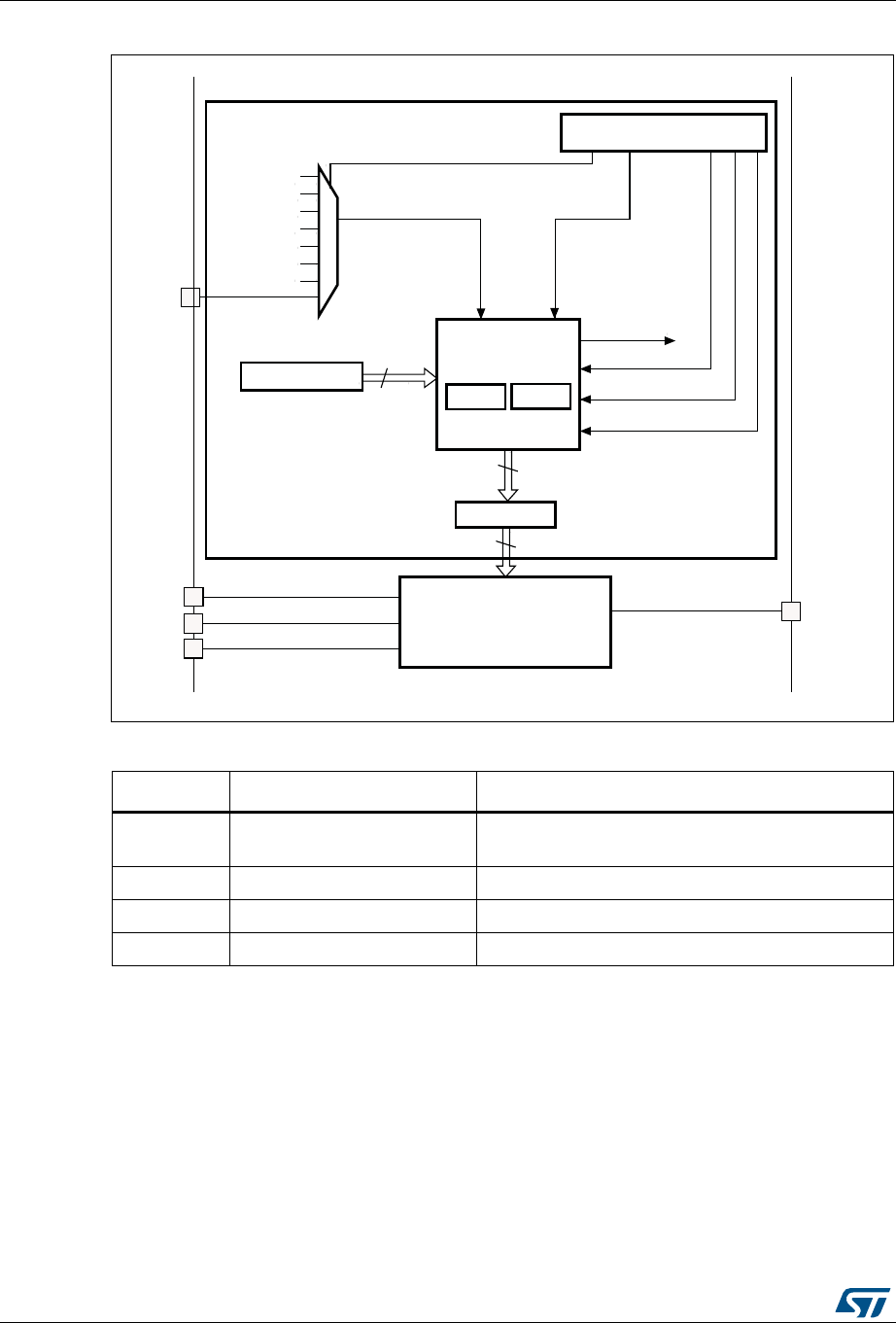
Digital-to-analog converter (DAC) RM0090
434/1718 DocID018909 Rev 9
Figure 64. DAC channel block diagram
Note: Once the DAC channelx is enabled, the corresponding GPIO pin (PA4 or PA5) is
automatically connected to the analog converter output (DAC_OUTx). In order to avoid
parasitic consumption, the PA4 or PA5 pin should first be configured to analog (AIN).
Table 74. DAC pins
Name Signal type Remarks
VREF+
Input, analog reference
positive
The higher/positive reference voltage for the DAC,
1.8 V ≤ V
REF+ ≤ V
DDA
VDDA Input, analog supply Analog power supply
VSSA Input, analog supply ground Ground for analog power supply
DAC_OUTx Analog output signal DAC channelx analog output
V
DDA
V
SSA
V
REF+
DAC_ OU Tx
Control logicx
DHRx
12-bit
12-bit
LFSRx trianglex
DM A requestx
TSELx[2:0] bits
TIM4_T RGO
TIM5_T RGO
TIM6_T RGO
TIM7_T RGO
TIM2_T RGO
TIM8_T RGO
EXTI_9
DMAENx
TENx
MAMPx[3:0] bits
WAVENx[1:0] bits
SWTRIGx
DORx
Digital-to-analog
converterx
12-bit
DAC control register
ai14708b
Trigger selectorx

DocID018909 Rev 9 435/1718
RM0090 Digital-to-analog converter (DAC)
454
14.3 DAC functional description
14.3.1 DAC channel enable
Each DAC channel can be powered on by setting its corresponding ENx bit in the DAC_CR
register. The DAC channel is then enabled after a startup time tWAKEUP
.
Note: The ENx bit enables the analog DAC Channelx macrocell only. The DAC Channelx digital
interface is enabled even if the ENx bit is reset.
14.3.2 DAC output buffer enable
The DAC integrates two output buffers that can be used to reduce the output impedance,
and to drive external loads directly without having to add an external operational amplifier.
Each DAC channel output buffer can be enabled and disabled using the corresponding
BOFFx bit in the DAC_CR register.
14.3.3 DAC data format
Depending on the selected configuration mode, the data have to be written into the specified
register as described below:
•Single DAC channelx, there are three possibilities:
– 8-bit right alignment: the software has to load data into the DAC_DHR8Rx [7:0]
bits (stored into the DHRx[11:4] bits)
– 12-bit left alignment: the software has to load data into the DAC_DHR12Lx [15:4]
bits (stored into the DHRx[11:0] bits)
– 12-bit right alignment: the software has to load data into the DAC_DHR12Rx [11:0]
bits (stored into the DHRx[11:0] bits)
Depending on the loaded DAC_DHRyyyx register, the data written by the user is shifted and
stored into the corresponding DHRx (data holding registerx, which are internal non-memory-
mapped registers). The DHRx register is then loaded into the DORx register either
automatically, by software trigger or by an external event trigger.
Digital-to-analog converter (DAC) RM0090
436/1718 DocID018909 Rev 9
Figure 65. Data registers in single DAC channel mode
•Dual DAC channels, there are three possibilities:
– 8-bit right alignment: data for DAC channel1 to be loaded into the DAC_DHR8RD
[7:0] bits (stored into the DHR1[11:4] bits) and data for DAC channel2 to be loaded
into the DAC_DHR8RD [15:8] bits (stored into the DHR2[11:4] bits)
– 12-bit left alignment: data for DAC channel1 to be loaded into the DAC_DHR12LD
[15:4] bits (stored into the DHR1[11:0] bits) and data for DAC channel2 to be
loaded into the DAC_DHR12LD [31:20] bits (stored into the DHR2[11:0] bits)
– 12-bit right alignment: data for DAC channel1 to be loaded into the
DAC_DHR12RD [11:0] bits (stored into the DHR1[11:0] bits) and data for DAC
channel2 to be loaded into the DAC_DHR12LD [27:16] bits (stored into the
DHR2[11:0] bits)
Depending on the loaded DAC_DHRyyyD register, the data written by the user is shifted
and stored into DHR1 and DHR2 (data holding registers, which are internal non-memory-
mapped registers). The DHR1 and DHR2 registers are then loaded into the DOR1 and
DOR2 registers, respectively, either automatically, by software trigger or by an external
event trigger.
Figure 66. Data registers in dual DAC channel mode
14.3.4 DAC conversion
The DAC_DORx cannot be written directly and any data transfer to the DAC channelx must
be performed by loading the DAC_DHRx register (write to DAC_DHR8Rx, DAC_DHR12Lx,
DAC_DHR12Rx, DAC_DHR8RD, DAC_DHR12LD or DAC_DHR12LD).
Data stored in the DAC_DHRx register are automatically transferred to the DAC_DORx
register after one APB1 clock cycle, if no hardware trigger is selected (TENx bit in DAC_CR
register is reset). However, when a hardware trigger is selected (TENx bit in DAC_CR
register is set) and a trigger occurs, the transfer is performed three APB1 clock cycles later.
When DAC_DORx is loaded with the DAC_DHRx contents, the analog output voltage
becomes available after a time tSETTLING that depends on the power supply voltage and the
analog output load.
31 24 15 7 0
8-bit right aligned
12-bit left aligned
12-bit right aligned
ai14710
31 24 15 7 0
8-bit right aligned
12-bit left aligned
12-bit right aligned
ai14709
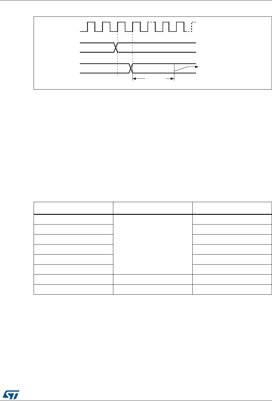
DocID018909 Rev 9 437/1718
RM0090 Digital-to-analog converter (DAC)
454
Figure 67. Timing diagram for conversion with trigger disabled TEN = 0
14.3.5 DAC output voltage
Digital inputs are converted to output voltages on a linear conversion between 0 and VREF+.
The analog output voltages on each DAC channel pin are determined by the following
equation:
14.3.6 DAC trigger selection
If the TENx control bit is set, conversion can then be triggered by an external event (timer
counter, external interrupt line). The TSELx[2:0] control bits determine which out of 8
possible events will trigger conversion as shown in Table 75.
Each time a DAC interface detects a rising edge on the selected timer TRGO output, or on
the selected external interrupt line 9, the last data stored into the DAC_DHRx register are
transferred into the DAC_DORx register. The DAC_DORx register is updated three APB1
cycles after the trigger occurs.
If the software trigger is selected, the conversion starts once the SWTRIG bit is set.
SWTRIG is reset by hardware once the DAC_DORx register has been loaded with the
DAC_DHRx register contents.
APB1_CLK
0x1AC
0x1AC
t
SETTLING
DHR
DOR
Output voltage
available on DAC_OUT pin
ai14711b
DACoutput VREF
DOR
4095
--------------
×=
Table 75. External triggers
Source Type TSEL[2:0]
Timer 6 TRGO event
Internal signal from on-chip
timers
000
Timer 8 TRGO event 001
Timer 7 TRGO event 010
Timer 5 TRGO event 011
Timer 2 TRGO event 100
Timer 4 TRGO event 101
EXTI line9 External pin 110
SWTRIG Software control bit 111

Digital-to-analog converter (DAC) RM0090
438/1718 DocID018909 Rev 9
Note: TSELx[2:0] bit cannot be changed when the ENx bit is set.
When software trigger is selected, the transfer from the DAC_DHRx register to the
DAC_DORx register takes only one APB1 clock cycle.
14.3.7 DMA request
Each DAC channel has a DMA capability. Two DMA channels are used to service DAC
channel DMA requests.
A DAC DMA request is generated when an external trigger (but not a software trigger)
occurs while the DMAENx bit is set. The value of the DAC_DHRx register is then transferred
into the DAC_DORx register.
In dual mode, if both DMAENx bits are set, two DMA requests are generated. If only one
DMA request is needed, you should set only the corresponding DMAENx bit. In this way, the
application can manage both DAC channels in dual mode by using one DMA request and a
unique DMA channel.
DMA underrun
The DAC DMA request is not queued so that if a second external trigger arrives before the
acknowledgement for the first external trigger is received (first request), then no new
request is issued and the DMA channelx underrun flag DMAUDRx in the DAC_SR register
is set, reporting the error condition. DMA data transfers are then disabled and no further
DMA request is treated. The DAC channelx continues to convert old data.
The software should clear the DMAUDRx flag by writing “1”, clear the DMAEN bit of the
used DMA stream and re-initialize both DMA and DAC channelx to restart the transfer
correctly. The software should modify the DAC trigger conversion frequency or lighten the
DMA workload to avoid a new DMA underrun. Finally, the DAC conversion could be
resumed by enabling both DMA data transfer and conversion trigger.
For each DAC channelx, an interrupt is also generated if its corresponding DMAUDRIEx bit
in the DAC_CR register is enabled.
14.3.8 Noise generation
In order to generate a variable-amplitude pseudonoise, an LFSR (linear feedback shift
register) is available. DAC noise generation is selected by setting WAVEx[1:0] to “01”. The
preloaded value in LFSR is 0xAAA. This register is updated three APB1 clock cycles after
each trigger event, following a specific calculation algorithm.
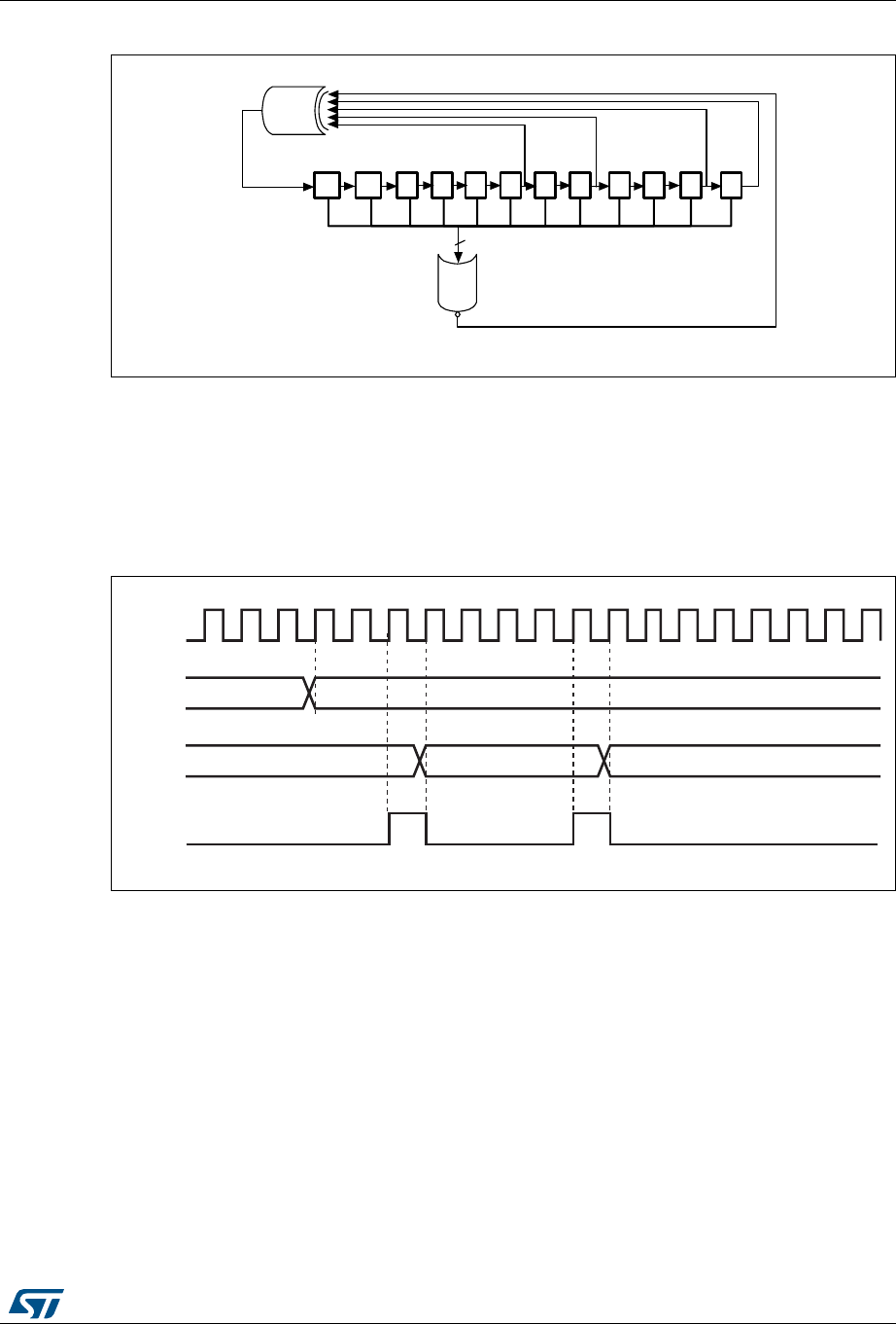
DocID018909 Rev 9 439/1718
RM0090 Digital-to-analog converter (DAC)
454
Figure 68. DAC LFSR register calculation algorithm
The LFSR value, that may be masked partially or totally by means of the MAMPx[3:0] bits in
the DAC_CR register, is added up to the DAC_DHRx contents without overflow and this
value is then stored into the DAC_DORx register.
If LFSR is 0x0000, a ‘1 is injected into it (antilock-up mechanism).
It is possible to reset LFSR wave generation by resetting the WAVEx[1:0] bits.
Figure 69. DAC conversion (SW trigger enabled) with LFSR wave generation
Note: The DAC trigger must be enabled for noise generation by setting the TENx bit in the
DAC_CR register.
14.3.9 Triangle-wave generation
It is possible to add a small-amplitude triangular waveform on a DC or slowly varying signal.
DAC triangle-wave generation is selected by setting WAVEx[1:0] to “10”. The amplitude is
configured through the MAMPx[3:0] bits in the DAC_CR register. An internal triangle counter
is incremented three APB1 clock cycles after each trigger event. The value of this counter is
then added to the DAC_DHRx register without overflow and the sum is stored into the
DAC_DORx register. The triangle counter is incremented as long as it is less than the
maximum amplitude defined by the MAMPx[3:0] bits. Once the configured amplitude is
reached, the counter is decremented down to 0, then incremented again and so on.
It is possible to reset triangle wave generation by resetting the WAVEx[1:0] bits.
11 10 9 8 7 6 5 4 3 2 1 0
12
NOR
X
12
X
0
X
X
4
X
6
XOR
ai14713b
APB1_CLK
0x00
0xAAA
DHR
DOR
ai14714
0xD55
SWTRIG
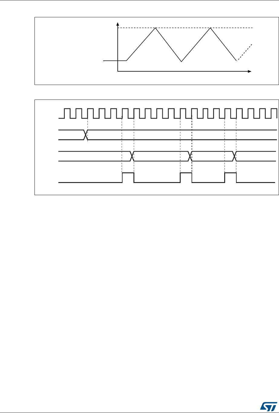
Digital-to-analog converter (DAC) RM0090
440/1718 DocID018909 Rev 9
Figure 70. DAC triangle wave generation
Figure 71. DAC conversion (SW trigger enabled) with triangle wave generation
Note: The DAC trigger must be enabled for noise generation by setting the TENx bit in the
DAC_CR register.
The MAMPx[3:0] bits must be configured before enabling the DAC, otherwise they cannot
be changed.
14.4 Dual DAC channel conversion
To efficiently use the bus bandwidth in applications that require the two DAC channels at the
same time, three dual registers are implemented: DHR8RD, DHR12RD and DHR12LD. A
unique register access is then required to drive both DAC channels at the same time.
Eleven possible conversion modes are possible using the two DAC channels and these dual
registers. All the conversion modes can nevertheless be obtained using separate DHRx
registers if needed.
All modes are described in the paragraphs below.
14.4.1 Independent trigger without wave generation
To configure the DAC in this conversion mode, the following sequence is required:
•Set the two DAC channel trigger enable bits TEN1 and TEN2
•Configure different trigger sources by setting different values in the TSEL1[2:0] and
TSEL2[2:0] bits
•Load the dual DAC channel data into the desired DHR register (DAC_DHR12RD,
DAC_DHR12LD or DAC_DHR8RD)
-!-0X;=MAXAMPLITUDE
$!#?$(2XBASEVALUE
$!#?$(2XBASEVALUE
)NCREMENTATION
AIC
$ECREMENTATION
APB1_CLK
0xABE
0xABE
DHR
DOR
ai14714
0xABF
SWTRIG
0xAC0

DocID018909 Rev 9 441/1718
RM0090 Digital-to-analog converter (DAC)
454
When a DAC channel1 trigger arrives, the DHR1 register is transferred into DAC_DOR1
(three APB1 clock cycles later).
When a DAC channel2 trigger arrives, the DHR2 register is transferred into DAC_DOR2
(three APB1 clock cycles later).
14.4.2 Independent trigger with single LFSR generation
To configure the DAC in this conversion mode, the following sequence is required:
•Set the two DAC channel trigger enable bits TEN1 and TEN2
•Configure different trigger sources by setting different values in the TSEL1[2:0] and
TSEL2[2:0] bits
•Configure the two DAC channel WAVEx[1:0] bits as “01” and the same LFSR mask
value in the MAMPx[3:0] bits
•Load the dual DAC channel data into the desired DHR register (DHR12RD, DHR12LD
or DHR8RD)
When a DAC channel1 trigger arrives, the LFSR1 counter, with the same mask, is added to
the DHR1 register and the sum is transferred into DAC_DOR1 (three APB1 clock cycles
later). Then the LFSR1 counter is updated.
When a DAC channel2 trigger arrives, the LFSR2 counter, with the same mask, is added to
the DHR2 register and the sum is transferred into DAC_DOR2 (three APB1 clock cycles
later). Then the LFSR2 counter is updated.
14.4.3 Independent trigger with different LFSR generation
To configure the DAC in this conversion mode, the following sequence is required:
•Set the two DAC channel trigger enable bits TEN1 and TEN2
•Configure different trigger sources by setting different values in the TSEL1[2:0] and
TSEL2[2:0] bits
•Configure the two DAC channel WAVEx[1:0] bits as “01” and set different LFSR masks
values in the MAMP1[3:0] and MAMP2[3:0] bits
•Load the dual DAC channel data into the desired DHR register (DAC_DHR12RD,
DAC_DHR12LD or DAC_DHR8RD)
When a DAC channel1 trigger arrives, the LFSR1 counter, with the mask configured by
MAMP1[3:0], is added to the DHR1 register and the sum is transferred into DAC_DOR1
(three APB1 clock cycles later). Then the LFSR1 counter is updated.
When a DAC channel2 trigger arrives, the LFSR2 counter, with the mask configured by
MAMP2[3:0], is added to the DHR2 register and the sum is transferred into DAC_DOR2
(three APB1 clock cycles later). Then the LFSR2 counter is updated.

Digital-to-analog converter (DAC) RM0090
442/1718 DocID018909 Rev 9
14.4.4 Independent trigger with single triangle generation
To configure the DAC in this conversion mode, the following sequence is required:
•Set the two DAC channel trigger enable bits TEN1 and TEN2
•Configure different trigger sources by setting different values in the TSEL1[2:0] and
TSEL2[2:0] bits
•Configure the two DAC channel WAVEx[1:0] bits as “1x” and the same maximum
amplitude value in the MAMPx[3:0] bits
•Load the dual DAC channel data into the desired DHR register (DAC_DHR12RD,
DAC_DHR12LD or DAC_DHR8RD)
When a DAC channel1 trigger arrives, the DAC channel1 triangle counter, with the same
triangle amplitude, is added to the DHR1 register and the sum is transferred into
DAC_DOR1 (three APB1 clock cycles later). The DAC channel1 triangle counter is then
updated.
When a DAC channel2 trigger arrives, the DAC channel2 triangle counter, with the same
triangle amplitude, is added to the DHR2 register and the sum is transferred into
DAC_DOR2 (three APB1 clock cycles later). The DAC channel2 triangle counter is then
updated.
14.4.5 Independent trigger with different triangle generation
To configure the DAC in this conversion mode, the following sequence is required:
•Set the two DAC channel trigger enable bits TEN1 and TEN2
•Configure different trigger sources by setting different values in the TSEL1[2:0] and
TSEL2[2:0] bits
•Configure the two DAC channel WAVEx[1:0] bits as “1x” and set different maximum
amplitude values in the MAMP1[3:0] and MAMP2[3:0] bits
•Load the dual DAC channel data into the desired DHR register (DAC_DHR12RD,
DAC_DHR12LD or DAC_DHR8RD)
When a DAC channel1 trigger arrives, the DAC channel1 triangle counter, with a triangle
amplitude configured by MAMP1[3:0], is added to the DHR1 register and the sum is
transferred into DAC_DOR1 (three APB1 clock cycles later). The DAC channel1 triangle
counter is then updated.
When a DAC channel2 trigger arrives, the DAC channel2 triangle counter, with a triangle
amplitude configured by MAMP2[3:0], is added to the DHR2 register and the sum is
transferred into DAC_DOR2 (three APB1 clock cycles later). The DAC channel2 triangle
counter is then updated.
14.4.6 Simultaneous software start
To configure the DAC in this conversion mode, the following sequence is required:
•Load the dual DAC channel data to the desired DHR register (DAC_DHR12RD,
DAC_DHR12LD or DAC_DHR8RD)
In this configuration, one APB1 clock cycle later, the DHR1 and DHR2 registers are
transferred into DAC_DOR1 and DAC_DOR2, respectively.

DocID018909 Rev 9 443/1718
RM0090 Digital-to-analog converter (DAC)
454
14.4.7 Simultaneous trigger without wave generation
To configure the DAC in this conversion mode, the following sequence is required:
•Set the two DAC channel trigger enable bits TEN1 and TEN2
•Configure the same trigger source for both DAC channels by setting the same value in
the TSEL1[2:0] and TSEL2[2:0] bits
•Load the dual DAC channel data to the desired DHR register (DAC_DHR12RD,
DAC_DHR12LD or DAC_DHR8RD)
When a trigger arrives, the DHR1 and DHR2 registers are transferred into DAC_DOR1 and
DAC_DOR2, respectively (after three APB1 clock cycles).
14.4.8 Simultaneous trigger with single LFSR generation
To configure the DAC in this conversion mode, the following sequence is required:
•Set the two DAC channel trigger enable bits TEN1 and TEN2
•Configure the same trigger source for both DAC channels by setting the same value in
the TSEL1[2:0] and TSEL2[2:0] bits
•Configure the two DAC channel WAVEx[1:0] bits as “01” and the same LFSR mask
value in the MAMPx[3:0] bits
•Load the dual DAC channel data to the desired DHR register (DHR12RD, DHR12LD or
DHR8RD)
When a trigger arrives, the LFSR1 counter, with the same mask, is added to the DHR1
register and the sum is transferred into DAC_DOR1 (three APB1 clock cycles later). The
LFSR1 counter is then updated. At the same time, the LFSR2 counter, with the same mask,
is added to the DHR2 register and the sum is transferred into DAC_DOR2 (three APB1
clock cycles later). The LFSR2 counter is then updated.
14.4.9 Simultaneous trigger with different LFSR generation
To configure the DAC in this conversion mode, the following sequence is required:
•Set the two DAC channel trigger enable bits TEN1 and TEN2
•Configure the same trigger source for both DAC channels by setting the same value in
the TSEL1[2:0] and TSEL2[2:0] bits
•Configure the two DAC channel WAVEx[1:0] bits as “01” and set different LFSR mask
values using the MAMP1[3:0] and MAMP2[3:0] bits
•Load the dual DAC channel data into the desired DHR register (DAC_DHR12RD,
DAC_DHR12LD or DAC_DHR8RD)
When a trigger arrives, the LFSR1 counter, with the mask configured by MAMP1[3:0], is
added to the DHR1 register and the sum is transferred into DAC_DOR1 (three APB1 clock
cycles later). The LFSR1 counter is then updated.
At the same time, the LFSR2 counter, with the mask configured by MAMP2[3:0], is added to
the DHR2 register and the sum is transferred into DAC_DOR2 (three APB1 clock cycles
later). The LFSR2 counter is then updated.

Digital-to-analog converter (DAC) RM0090
444/1718 DocID018909 Rev 9
14.4.10 Simultaneous trigger with single triangle generation
To configure the DAC in this conversion mode, the following sequence is required:
•Set the two DAC channel trigger enable bits TEN1 and TEN2
•Configure the same trigger source for both DAC channels by setting the same value in
the TSEL1[2:0] and TSEL2[2:0] bits
•Configure the two DAC channel WAVEx[1:0] bits as “1x” and the same maximum
amplitude value using the MAMPx[3:0] bits
•Load the dual DAC channel data into the desired DHR register (DAC_DHR12RD,
DAC_DHR12LD or DAC_DHR8RD)
When a trigger arrives, the DAC channel1 triangle counter, with the same triangle
amplitude, is added to the DHR1 register and the sum is transferred into DAC_DOR1 (three
APB1 clock cycles later). The DAC channel1 triangle counter is then updated.
At the same time, the DAC channel2 triangle counter, with the same triangle amplitude, is
added to the DHR2 register and the sum is transferred into DAC_DOR2 (three APB1 clock
cycles later). The DAC channel2 triangle counter is then updated.
14.4.11 Simultaneous trigger with different triangle generation
To configure the DAC in this conversion mode, the following sequence is required:
•Set the two DAC channel trigger enable bits TEN1 and TEN2
•Configure the same trigger source for both DAC channels by setting the same value in
the TSEL1[2:0] and TSEL2[2:0] bits
•Configure the two DAC channel WAVEx[1:0] bits as “1x” and set different maximum
amplitude values in the MAMP1[3:0] and MAMP2[3:0] bits
•Load the dual DAC channel data into the desired DHR register (DAC_DHR12RD,
DAC_DHR12LD or DAC_DHR8RD)
When a trigger arrives, the DAC channel1 triangle counter, with a triangle amplitude
configured by MAMP1[3:0], is added to the DHR1 register and the sum is transferred into
DAC_DOR1 (three APB1 clock cycles later). Then the DAC channel1 triangle counter is
updated.
At the same time, the DAC channel2 triangle counter, with a triangle amplitude configured
by MAMP2[3:0], is added to the DHR2 register and the sum is transferred into DAC_DOR2
(three APB1 clock cycles later). Then the DAC channel2 triangle counter is updated.

DocID018909 Rev 9 445/1718
RM0090 Digital-to-analog converter (DAC)
454
14.5 DAC registers
Refer to Section 1.1 on page 57 for a list of abbreviations used in register descriptions.
The peripheral registers have to be accessed by words (32 bits).
14.5.1 DAC control register (DAC_CR)
Address offset: 0x00
Reset value: 0x0000 0000
31 30 29 28 27 26 25 24 23 22 21 20 19 18 17 16
Reserved
DMAU
DRIE2
DMA
EN2 MAMP2[3:0] WAVE2[1:0] TSEL2[2:0] TEN2 BOFF2 EN2
rw rw rw rw rw rw rw rw rw rw rw rw rw rw
1514131211109876543210
Reserved
DMAU
DRIE1
DMA
EN1 MAMP1[3:0] WAVE1[1:0] TSEL1[2:0] TEN1 BOFF1 EN1
rw rw rw rw rw rw rw rw rw rw rw rw rw rw
Bits 31:30 Reserved, must be kept at reset value.
Bits 29 DMAUDRIE2: DAC channel2 DMA underrun interrupt enable
This bit is set and cleared by software.
0: DAC channel2 DMA underrun interrupt disabled
1: DAC channel2 DMA underrun interrupt enabled
Bit 28 DMAEN2: DAC channel2 DMA enable
This bit is set and cleared by software.
0: DAC channel2 DMA mode disabled
1: DAC channel2 DMA mode enabled
Bits 27:24 MAMP2[3:0]: DAC channel2 mask/amplitude selector
These bits are written by software to select mask in wave generation mode or amplitude in
triangle generation mode.
0000: Unmask bit0 of LFSR/ triangle amplitude equal to 1
0001: Unmask bits[1:0] of LFSR/ triangle amplitude equal to 3
0010: Unmask bits[2:0] of LFSR/ triangle amplitude equal to 7
0011: Unmask bits[3:0] of LFSR/ triangle amplitude equal to 15
0100: Unmask bits[4:0] of LFSR/ triangle amplitude equal to 31
0101: Unmask bits[5:0] of LFSR/ triangle amplitude equal to 63
0110: Unmask bits[6:0] of LFSR/ triangle amplitude equal to 127
0111: Unmask bits[7:0] of LFSR/ triangle amplitude equal to 255
1000: Unmask bits[8:0] of LFSR/ triangle amplitude equal to 511
1001: Unmask bits[9:0] of LFSR/ triangle amplitude equal to 1023
1010: Unmask bits[10:0] of LFSR/ triangle amplitude equal to 2047
≥ 1011: Unmask bits[11:0] of LFSR/ triangle amplitude equal to 4095
Bits 23:22 WAVE2[1:0]: DAC channel2 noise/triangle wave generation enable
These bits are set/reset by software.
00: wave generation disabled
01: Noise wave generation enabled
1x: Triangle wave generation enabled
Note: Only used if bit TEN2 = 1 (DAC channel2 trigger enabled)

Digital-to-analog converter (DAC) RM0090
446/1718 DocID018909 Rev 9
Bits 21:19 TSEL2[2:0]: DAC channel2 trigger selection
These bits select the external event used to trigger DAC channel2
000: Timer 6 TRGO event
001: Timer 8 TRGO event
010: Timer 7 TRGO event
011: Timer 5 TRGO event
100: Timer 2 TRGO event
101: Timer 4 TRGO event
110: External line9
111: Software trigger
Note: Only used if bit TEN2 = 1 (DAC channel2 trigger enabled).
Bit 18 TEN2: DAC channel2 trigger enable
This bit is set and cleared by software to enable/disable DAC channel2 trigger
0: DAC channel2 trigger disabled and data written into the DAC_DHRx register are
transferred one APB1 clock cycle later to the DAC_DOR2 register
1: DAC channel2 trigger enabled and data from the DAC_DHRx register are transferred
three APB1 clock cycles later to the DAC_DOR2 register
Note: When software trigger is selected, the transfer from the DAC_DHRx register to the
DAC_DOR2 register takes only one APB1 clock cycle.
Bit 17 BOFF2: DAC channel2 output buffer disable
This bit is set and cleared by software to enable/disable DAC channel2 output buffer.
0: DAC channel2 output buffer enabled
1: DAC channel2 output buffer disabled
Bit 16 EN2: DAC channel2 enable
This bit is set and cleared by software to enable/disable DAC channel2.
0: DAC channel2 disabled
1: DAC channel2 enabled
Bits 15:14 Reserved, must be kept at reset value.
Bit 13 DMAUDRIE1: DAC channel1 DMA Underrun Interrupt enable
This bit is set and cleared by software.
0: DAC channel1 DMA Underrun Interrupt disabled
1: DAC channel1 DMA Underrun Interrupt enabled
Bit 12 DMAEN1: DAC channel1 DMA enable
This bit is set and cleared by software.
0: DAC channel1 DMA mode disabled
1: DAC channel1 DMA mode enabled

DocID018909 Rev 9 447/1718
RM0090 Digital-to-analog converter (DAC)
454
Bits 11:8 MAMP1[3:0]: DAC channel1 mask/amplitude selector
These bits are written by software to select mask in wave generation mode or amplitude in
triangle generation mode.
0000: Unmask bit0 of LFSR/ triangle amplitude equal to 1
0001: Unmask bits[1:0] of LFSR/ triangle amplitude equal to 3
0010: Unmask bits[2:0] of LFSR/ triangle amplitude equal to 7
0011: Unmask bits[3:0] of LFSR/ triangle amplitude equal to 15
0100: Unmask bits[4:0] of LFSR/ triangle amplitude equal to 31
0101: Unmask bits[5:0] of LFSR/ triangle amplitude equal to 63
0110: Unmask bits[6:0] of LFSR/ triangle amplitude equal to 127
0111: Unmask bits[7:0] of LFSR/ triangle amplitude equal to 255
1000: Unmask bits[8:0] of LFSR/ triangle amplitude equal to 511
1001: Unmask bits[9:0] of LFSR/ triangle amplitude equal to 1023
1010: Unmask bits[10:0] of LFSR/ triangle amplitude equal to 2047
≥ 1011: Unmask bits[11:0] of LFSR/ triangle amplitude equal to 4095
Bits 7:6 WAVE1[1:0]: DAC channel1 noise/triangle wave generation enable
These bits are set and cleared by software.
00: wave generation disabled
01: Noise wave generation enabled
1x: Triangle wave generation enabled
Note: Only used if bit TEN1 = 1 (DAC channel1 trigger enabled).
Bits 5:3 TSEL1[2:0]: DAC channel1 trigger selection
These bits select the external event used to trigger DAC channel1.
000: Timer 6 TRGO event
001: Timer 8 TRGO event
010: Timer 7 TRGO event
011: Timer 5 TRGO event
100: Timer 2 TRGO event
101: Timer 4 TRGO event
110: External line9
111: Software trigger
Note: Only used if bit TEN1 = 1 (DAC channel1 trigger enabled).
Bit 2 TEN1: DAC channel1 trigger enable
This bit is set and cleared by software to enable/disable DAC channel1 trigger.
0: DAC channel1 trigger disabled and data written into the DAC_DHRx register are
transferred one APB1 clock cycle later to the DAC_DOR1 register
1: DAC channel1 trigger enabled and data from the DAC_DHRx register are transferred
three APB1 clock cycles later to the DAC_DOR1 register
Note: When software trigger is selected, the transfer from the DAC_DHRx register to the
DAC_DOR1 register takes only one APB1 clock cycle.
Bit 1 BOFF1: DAC channel1 output buffer disable
This bit is set and cleared by software to enable/disable DAC channel1 output buffer.
0: DAC channel1 output buffer enabled
1: DAC channel1 output buffer disabled
Bit 0 EN1: DAC channel1 enable
This bit is set and cleared by software to enable/disable DAC channel1.
0: DAC channel1 disabled
1: DAC channel1 enabled
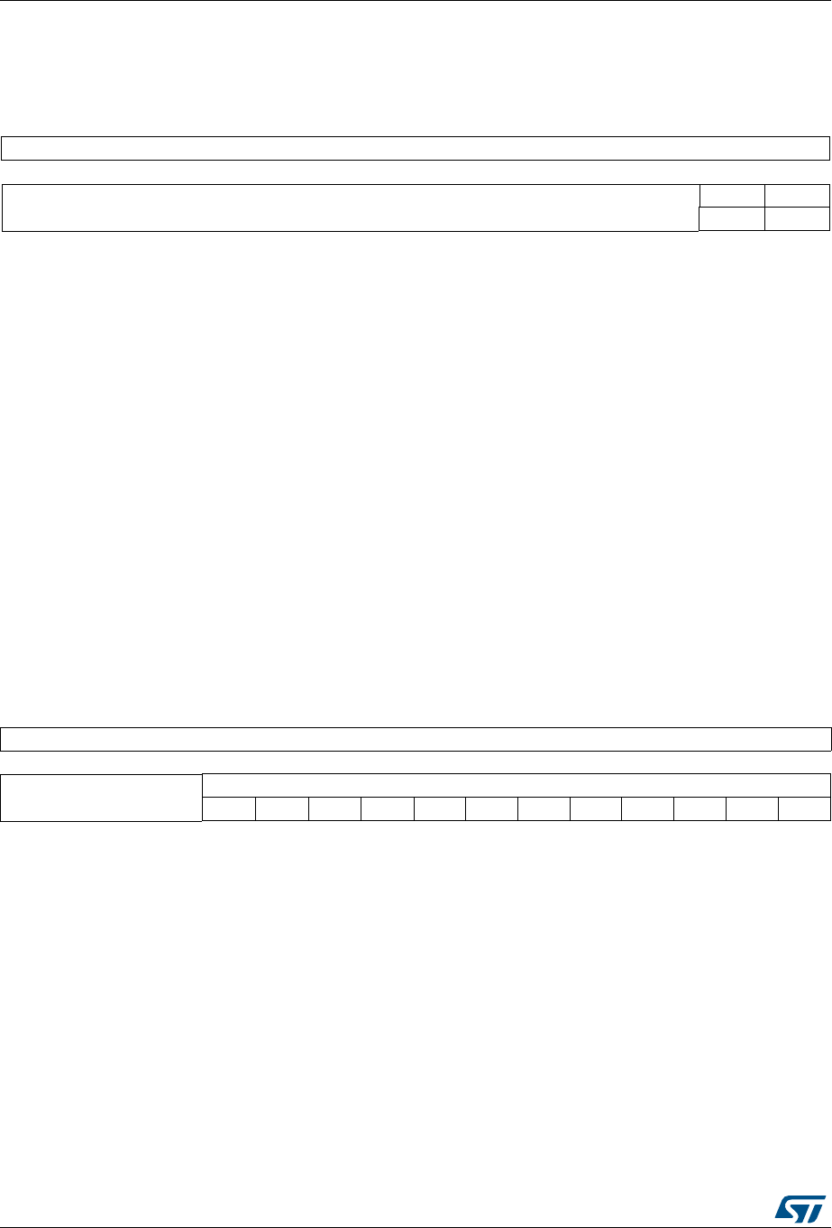
Digital-to-analog converter (DAC) RM0090
448/1718 DocID018909 Rev 9
14.5.2 DAC software trigger register (DAC_SWTRIGR)
Address offset: 0x04
Reset value: 0x0000 0000
14.5.3 DAC channel1 12-bit right-aligned data holding register
(DAC_DHR12R1)
Address offset: 0x08
Reset value: 0x0000 0000
31 30 29 28 27 26 25 24 23 22 21 20 19 18 17 16
Reserved
15 14 13 12 11 10 9 8 7 6 5 4 3 2 1 0
Reserved
SWTRIG2 SWTRIG1
ww
Bits 31:2 Reserved, must be kept at reset value.
Bit 1 SWTRIG2: DAC channel2 software trigger
This bit is set and cleared by software to enable/disable the software trigger.
0: Software trigger disabled
1: Software trigger enabled
Note: This bit is cleared by hardware (one APB1 clock cycle later) once the DAC_DHR2
register value has been loaded into the DAC_DOR2 register.
Bit 0 SWTRIG1: DAC channel1 software trigger
This bit is set and cleared by software to enable/disable the software trigger.
0: Software trigger disabled
1: Software trigger enabled
Note: This bit is cleared by hardware (one APB1 clock cycle later) once the DAC_DHR1
register value has been loaded into the DAC_DOR1 register.
31 30 29 28 27 26 25 24 23 22 21 20 19 18 17 16
Reserved
1514131211109876543210
Reserved
DACC1DHR[11:0]
rw rw rw rw rw rw rw rw rw rw rw rw
Bits 31:12 Reserved, must be kept at reset value.
Bits 11:0 DACC1DHR[11:0]: DAC channel1 12-bit right-aligned data
These bits are written by software which specifies 12-bit data for DAC channel1.
DocID018909 Rev 9 449/1718
RM0090 Digital-to-analog converter (DAC)
454
14.5.4 DAC channel1 12-bit left aligned data holding register
(DAC_DHR12L1)
Address offset: 0x0C
Reset value: 0x0000 0000
14.5.5 DAC channel1 8-bit right aligned data holding register
(DAC_DHR8R1)
Address offset: 0x10
Reset value: 0x0000 0000
31 30 29 28 27 26 25 24 23 22 21 20 19 18 17 16
Reserved
1514131211109876543210
DACC1DHR[11:0] Reserved
rw rw rw rw rw rw rw rw rw rw rw rw
Bits 31:16 Reserved, must be kept at reset value.
Bits 15:4 DACC1DHR[11:0]: DAC channel1 12-bit left-aligned data
These bits are written by software which specifies 12-bit data for DAC channel1.
Bits 3:0 Reserved, must be kept at reset value.
31 30 29 28 27 26 25 24 23 22 21 20 19 18 17 16
Reserved
1514131211109876543210
Reserved
DACC1DHR[7:0]
rw rw rw rw rw rw rw rw
Bits 31:8 Reserved, must be kept at reset value.
Bits 7:0 DACC1DHR[7:0]: DAC channel1 8-bit right-aligned data
These bits are written by software which specifies 8-bit data for DAC channel1.
Digital-to-analog converter (DAC) RM0090
450/1718 DocID018909 Rev 9
14.5.6 DAC channel2 12-bit right aligned data holding register
(DAC_DHR12R2)
Address offset: 0x14
Reset value: 0x0000 0000
14.5.7 DAC channel2 12-bit left aligned data holding register
(DAC_DHR12L2)
Address offset: 0x18
Reset value: 0x0000 0000
14.5.8 DAC channel2 8-bit right-aligned data holding register
(DAC_DHR8R2)
Address offset: 0x1C
Reset value: 0x0000 0000
31 30 29 28 27 26 25 24 23 22 21 20 19 18 17 16
Reserved
1514131211109876543210
Reserved DACC2DHR[11:0]
rw rw rw rw rw rw rw rw rw rw rw rw
Bits 31:12 Reserved, must be kept at reset value.
Bits 11:0 DACC2DHR[11:0]: DAC channel2 12-bit right-aligned data
These bits are written by software which specifies 12-bit data for DAC channel2.
31 30 29 28 27 26 25 24 23 22 21 20 19 18 17 16
Reserved
1514131211109876543210
DACC2DHR[11:0] Reserved
rw rw rw rw rw rw rw rw rw rw rw rw
Bits 31:16 Reserved, must be kept at reset value.
Bits 15:4 DACC2DHR[11:0]: DAC channel2 12-bit left-aligned data
These bits are written by software which specify 12-bit data for DAC channel2.
Bits 3:0 Reserved, must be kept at reset value.
31 30 29 28 27 26 25 24 23 22 21 20 19 18 17 16
Reserved
1514131211109876543210
Reserved
DACC2DHR[7:0]
rw rw rw rw rw rw rw rw
Bits 31:8 Reserved, must be kept at reset value.
Bits 7:0 DACC2DHR[7:0]: DAC channel2 8-bit right-aligned data
These bits are written by software which specifies 8-bit data for DAC channel2.
DocID018909 Rev 9 451/1718
RM0090 Digital-to-analog converter (DAC)
454
14.5.9 Dual DAC 12-bit right-aligned data holding register
(DAC_DHR12RD)
Address offset: 0x20
Reset value: 0x0000 0000
14.5.10 DUAL DAC 12-bit left aligned data holding register
(DAC_DHR12LD)
Address offset: 0x24
Reset value: 0x0000 0000
31 30 29 28 27 26 25 24 23 22 21 20 19 18 17 16
Reserved
DACC2DHR[11:0]
rw rw rw rw rw rw rw rw rw rw rw rw
1514131211109876543210
Reserved
DACC1DHR[11:0]
rw rw rw rw rw rw rw rw rw rw rw rw
Bits 31:28 Reserved, must be kept at reset value.
Bits 27:16 DACC2DHR[11:0]: DAC channel2 12-bit right-aligned data
These bits are written by software which specifies 12-bit data for DAC channel2.
Bits 15:12 Reserved, must be kept at reset value.
Bits 11:0 DACC1DHR[11:0]: DAC channel1 12-bit right-aligned data
These bits are written by software which specifies 12-bit data for DAC channel1.
31 30 29 28 27 26 25 24 23 22 21 20 19 18 17 16
DACC2DHR[11:0]
Reserved
rw rw rw rw rw rw rw rw rw rw rw rw
1514131211109876543210
DACC1DHR[11:0]
Reserved
rw rw rw rw rw rw rw rw rw rw rw rw
Bits 31:20 DACC2DHR[11:0]: DAC channel2 12-bit left-aligned data
These bits are written by software which specifies 12-bit data for DAC channel2.
Bits 19:16 Reserved, must be kept at reset value.
Bits 15:4 DACC1DHR[11:0]: DAC channel1 12-bit left-aligned data
These bits are written by software which specifies 12-bit data for DAC channel1.
Bits 3:0 Reserved, must be kept at reset value.
Digital-to-analog converter (DAC) RM0090
452/1718 DocID018909 Rev 9
14.5.11 DUAL DAC 8-bit right aligned data holding register
(DAC_DHR8RD)
Address offset: 0x28
Reset value: 0x0000 0000
14.5.12 DAC channel1 data output register (DAC_DOR1)
Address offset: 0x2C
Reset value: 0x0000 0000
14.5.13 DAC channel2 data output register (DAC_DOR2)
Address offset: 0x30
Reset value: 0x0000 0000
31 30 29 28 27 26 25 24 23 22 21 20 19 18 17 16
Reserved
1514131211109876543210
DACC2DHR[7:0] DACC1DHR[7:0]
rw rw rw rw rw rw rw rw rw rw rw rw rw rw rw rw
Bits 31:16 Reserved, must be kept at reset value.
Bits 15:8 DACC2DHR[7:0]: DAC channel2 8-bit right-aligned data
These bits are written by software which specifies 8-bit data for DAC channel2.
Bits 7:0 DACC1DHR[7:0]: DAC channel1 8-bit right-aligned data
These bits are written by software which specifies 8-bit data for DAC channel1.
31 30 29 28 27 26 25 24 23 22 21 20 19 18 17 16
Reserved
1514131211109876543210
Reserved DACC1DOR[11:0]
rrrrrrrrrrrr
Bits 31:12 Reserved, must be kept at reset value.
Bit 11:0 DACC1DOR[11:0]: DAC channel1 data output
These bits are read-only, they contain data output for DAC channel1.
31 30 29 28 27 26 25 24 23 22 21 20 19 18 17 16
Reserved
1514131211109876543210
Reserved DACC2DOR[11:0]
rrrrrrrrrrrr
Bits 31:12 Reserved, must be kept at reset value.
Bits 11:0 DACC2DOR[11:0]: DAC channel2 data output
These bits are read-only, they contain data output for DAC channel2.
DocID018909 Rev 9 453/1718
RM0090 Digital-to-analog converter (DAC)
454
14.5.14 DAC status register (DAC_SR)
Address offset: 0x34
Reset value: 0x0000 0000
14.5.15 DAC register map
Table 76 summarizes the DAC registers.
31 30 29 28 27 26 25 24 23 22 21 20 19 18 17 16
Reserved DMAUDR2 Reserved
rc_w1
1514 13 1211109876543210
Reserved DMAUDR1 Reserved
rc_w1
Bits 31:30 Reserved, must be kept at reset value.
Bit 29 DMAUDR2: DAC channel2 DMA underrun flag
This bit is set by hardware and cleared by software (by writing it to 1).
0: No DMA underrun error condition occurred for DAC channel2
1: DMA underrun error condition occurred for DAC channel2 (the currently selected trigger is
driving DAC channel2 conversion at a frequency higher than the DMA service capability rate)
Bits 28:14 Reserved, must be kept at reset value.
Bit 13 DMAUDR1: DAC channel1 DMA underrun flag
This bit is set by hardware and cleared by software (by writing it to 1).
0: No DMA underrun error condition occurred for DAC channel1
1: DMA underrun error condition occurred for DAC channel1 (the currently selected trigger is
driving DAC channel1 conversion at a frequency higher than the DMA service capability rate)
Bits 12:0 Reserved, must be kept at reset value.
Table 76. DAC register map
Offset Register
name
31
30
29
28
27
26
25
24
23
22
21
20
19
18
17
16
15
14
13
12
11
10
9
8
7
6
5
4
3
2
1
0
0x00 DAC_CR
Reserved
DMAUDRIE2
DMAEN2
MAMP2[3:0] WAVE
2[2:0] TSEL2[2:0]
TEN2
BOFF2
EN2
Reserved
DMAUDRIE1
DMAEN1
MAMP1[3:0] WAVE
1[2:0]
TSEL1[2
:0]
TEN1
BOFF1
EN1
0x04 DAC_
SWTRIGR Reserved
SWTRIG2
SWTRIG1
0x08 DAC_
DHR12R1 Reserved DACC1DHR[11:0]
0x0C DAC_
DHR12L1 Reserved DACC1DHR[11:0] Reserved
0x10 DAC_
DHR8R1 Reserved DACC1DHR[7:0]
0x14 DAC_
DHR12R2 Reserved DACC2DHR[11:0]
0x18 DAC_
DHR12L2 Reserved DACC2DHR[11:0] Reserved

Digital-to-analog converter (DAC) RM0090
454/1718 DocID018909 Rev 9
Refer to Table 1 on page 64 for the register boundary addresses.
0x1C DAC_
DHR8R2 Reserved DACC2DHR[7:0]
0x20 DAC_
DHR12RD Reserved DACC2DHR[11:0] Reserved DACC1DHR[11:0]
0x24 DAC_
DHR12LD DACC2DHR[11:0] Reserved DACC1DHR[11:0] Reserved
0x28 DAC_
DHR8RD Reserved DACC2DHR[7:0] DACC1DHR[7:0]
0x2C DAC_
DOR1 Reserved DACC1DOR[11:0]
0x30 DAC_
DOR2 Reserved DACC2DOR[11:0]
0x34 DAC_SR
Reserved
DMAUDR2
Reserved
DMAUDR1
Reserved
Table 76. DAC register map (continued)
Offset Register
name
31
30
29
28
27
26
25
24
23
22
21
20
19
18
17
16
15
14
13
12
11
10
9
8
7
6
5
4
3
2
1
0

DocID018909 Rev 9 455/1718
RM0090 Digital camera interface (DCMI)
477
15 Digital camera interface (DCMI)
This section applies to the whole STM32F4xx family devices, unless otherwise specified.
15.1 DCMI introduction
The digital camera is a synchronous parallel interface able to receive a high-speed data flow
from an external 8-, 10-, 12- or 14-bit CMOS camera module. It supports different data
formats: YCbCr4:2:2/RGB565 progressive video and compressed data (JPEG).
This interface is for use with black & white cameras, X24 and X5 cameras, and it is
assumed that all pre-processing like resizing is performed in the camera module.
15.2 DCMI main features
•8-, 10-, 12- or 14-bit parallel interface
•Embedded/external line and frame synchronization
•Continuous or snapshot mode
•Crop feature
•Supports the following data formats:
– 8/10/12/14- bit progressive video: either monochrome or raw bayer
– YCbCr 4:2:2 progressive video
– RGB 565 progressive video
– Compressed data: JPEG
15.3 DCMI pins
Table 77 shows the DCMI pins.
15.4 DCMI clocks
The digital camera interface uses two clock domains PIXCLK and HCLK. The signals
generated with PIXCLK are sampled on the rising edge of HCLK once they are stable. An
enable signal is generated in the HCLK domain, to indicate that data coming from the
camera are stable and can be sampled. The minimum PIXCLK period must be higher than
2.5 HCLK periods.
Table 77. DCMI pins
Name Signal type
D[0:13] Data inputs
HSYNC Horizontal synchronization input
VSYNC Vertical synchronization input
PIXCLK Pixel clock input
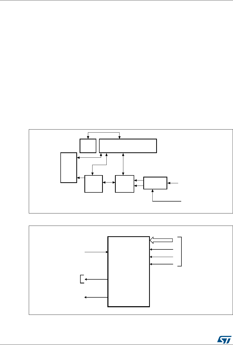
Digital camera interface (DCMI) RM0090
456/1718 DocID018909 Rev 9
15.5 DCMI functional overview
The digital camera interface is a synchronous parallel interface that can receive high-speed
(up to 54 Mbytes/s) data flows. It consists of up to 14 data lines (D13-D0) and a pixel clock
line (PIXCLK). The pixel clock has a programmable polarity, so that data can be captured on
either the rising or the falling edge of the pixel clock.
The data are packed into a 32-bit data register (DCMI_DR) and then transferred through a
general-purpose DMA channel. The image buffer is managed by the DMA, not by the
camera interface.
The data received from the camera can be organized in lines/frames (raw YUB/RGB/Bayer
modes) or can be a sequence of JPEG images. To enable JPEG image reception, the JPEG
bit (bit 3 of DCMI_CR register) must be set.
The data flow is synchronized either by hardware using the optional HSYNC (horizontal
synchronization) and VSYNC (vertical synchronization) signals or by synchronization codes
embedded in the data flow.
Figure 72 shows the DCMI block diagram.
Figure 72. DCMI block diagram
Figure 73. Top-level block diagram
DMA
interface
Control/Status
register
AHB
interface
FIFO/
Data
formatter
Data
extraction Synchronizer DCMI_PIXCLK
DCMI_D[0:13], DCMI_HSYNC, DCMI_VSYNC
ai15604
$#-)
)NTERRUPT
CONTROLLER
$#-)?)4
%XTERNAL
INTERFACE
$#-)?$;=
$#-)?0)8#,+
$#-)?(39.#
$#-)?639.#
$-!?2%1
(#,+
AIB
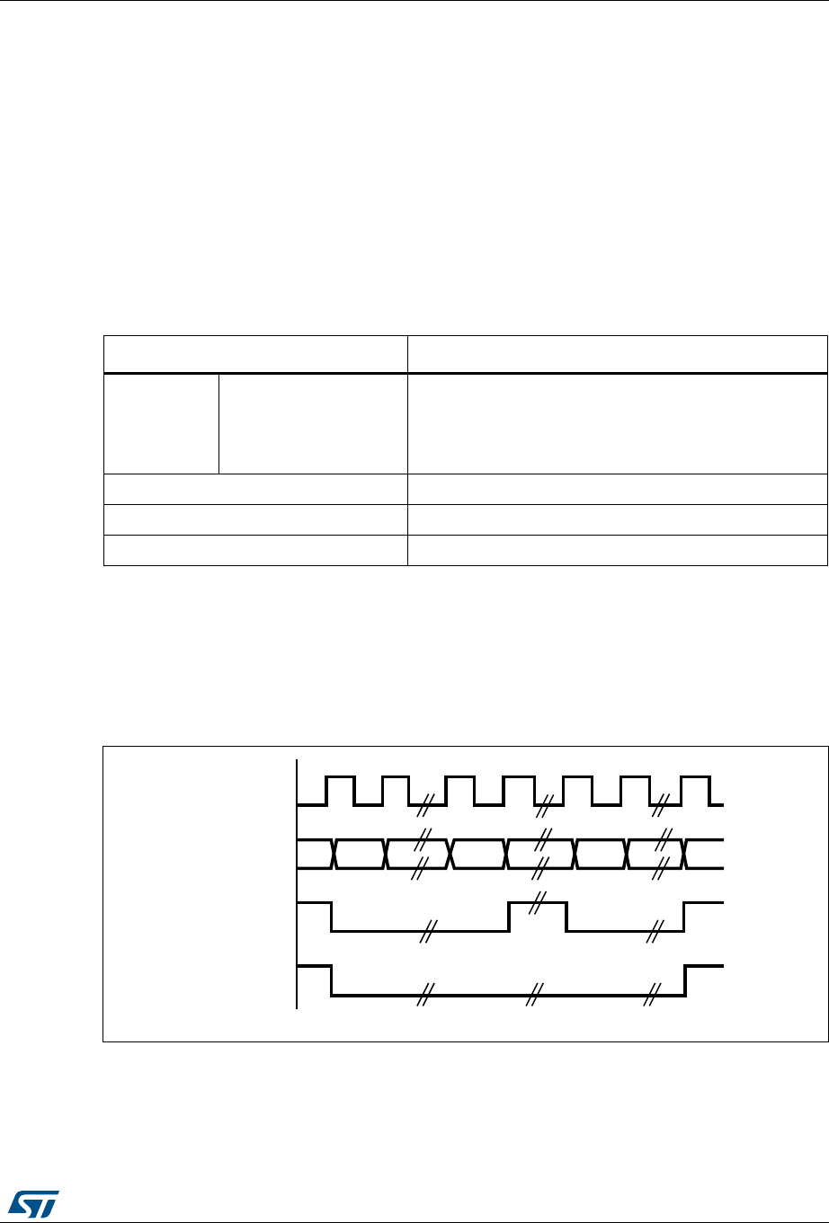
DocID018909 Rev 9 457/1718
RM0090 Digital camera interface (DCMI)
477
15.5.1 DMA interface
The DMA interface is active when the CAPTURE bit in the DCMI_CR register is set. A DMA
request is generated each time the camera interface receives a complete 32-bit data block
in its register.
15.5.2 DCMI physical interface
The interface is composed of 11/13/15/17 inputs. Only the Slave mode is supported.
The camera interface can capture 8-bit, 10-bit, 12-bit or 14-bit data depending on the
EDM[1:0] bits in the DCMI_CR register. If less than 14 bits are used, the unused data pins
must not be assigned to DCMI interface through GPIO alternate functions.
The data are synchronous with PIXCLK and change on the rising/falling edge of the pixel
clock depending on the polarity.
The HSYNC signal indicates the start/end of a line.
The VSYNC signal indicates the start/end of a frame
Figure 74. DCMI signal waveforms
1. The capture edge of DCMI_PIXCLK is the falling edge, the active state of DCMI_HSYNC and
DCMI_VSYNC is 1.
1. DCMI_HSYNC and DCMI_VSYNC can change states at the same time.
Table 78. DCMI signals
Signal name Signal description
8 bits
10 bits
12 bits
14 bits
D[0..7]
D[0..9]
D[0..11]
D[0..13]
Data
PIXCLK Pixel clock
HSYNC Horizontal synchronization / Data valid
VSYNC Vertical synchronization
$#-)?0)8#,+
$#-)?$2;=
$#-)?(39.#
$#-)?639.#
AIB
Digital camera interface (DCMI) RM0090
458/1718 DocID018909 Rev 9
8-bit data
When EDM[1:0] in DCMI_CR are programmed to “00” the interface captures 8 LSB’s at its
input (D[0:7]) and stores them as 8-bit data. The D[13:8] inputs are ignored. In this case, to
capture a 32-bit word, the camera interface takes four pixel clock cycles.
The first captured data byte is placed in the LSB position in the 32-bit word and the 4th
captured data byte is placed in the MSB position in the 32-bit word. Table 79 gives an
example of the positioning of captured data bytes in two 32-bit words.
10-bit data
When EDM[1:0] in DCMI_CR are programmed to “01”, the camera interface captures 10-bit
data at its input D[0..9] and stores them as the 10 least significant bits of a 16-bit word. The
remaining most significant bits in the DCMI_DR register (bits 11 to 15) are cleared to zero.
So, in this case, a 32-bit data word is made up every two pixel clock cycles.
The first captured data are placed in the LSB position in the 32-bit word and the 2nd
captured data are placed in the MSB position in the 32-bit word as shown in Table 80.
12-bit data
When EDM[1:0] in DCMI_CR are programmed to “10”, the camera interface captures the
12-bit data at its input D[0..11] and stores them as the 12 least significant bits of a 16-bit
word. The remaining most significant bits are cleared to zero. So, in this case a 32-bit data
word is made up every two pixel clock cycles.
The first captured data are placed in the LSB position in the 32-bit word and the 2nd
captured data are placed in the MSB position in the 32-bit word as shown in Table 81.
14-bit data
When EDM[1:0] in DCMI_CR are programmed to “11”, the camera interface captures the
14-bit data at its input D[0..13] and stores them as the 14 least significant bits of a 16-bit
Table 79. Positioning of captured data bytes in 32-bit words (8-bit width)
Byte address 31:24 23:16 15:8 7:0
0D
n+3[7:0] Dn+2[7:0] Dn+1[7:0] Dn[7:0]
4D
n+7[7:0] Dn+6[7:0] Dn+5[7:0] Dn+4[7:0]
Table 80. Positioning of captured data bytes in 32-bit words (10-bit width)
Byte address 31:26 25:16 15:10 9:0
00D
n+1[9:0] 0 Dn[9:0]
40D
n+3[9:0] 0 Dn+2[9:0]
Table 81. Positioning of captured data bytes in 32-bit words (12-bit width)
Byte address 31:28 27:16 15:12 11:0
00D
n+1[11:0] 0 Dn[11:0]
40D
n+3[11:0] 0 Dn+2[11:0]
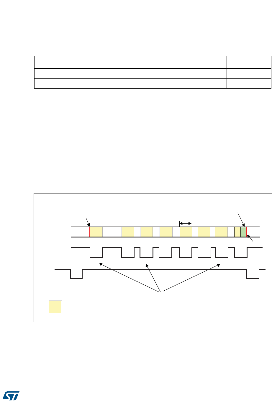
DocID018909 Rev 9 459/1718
RM0090 Digital camera interface (DCMI)
477
word. The remaining most significant bits are cleared to zero. So, in this case a 32-bit data
word is made up every two pixel clock cycles.
The first captured data are placed in the LSB position in the 32-bit word and the 2nd
captured data are placed in the MSB position in the 32-bit word as shown in Table 82.
15.5.3 Synchronization
The digital camera interface supports embedded or hardware (HSYNC & VSYNC)
synchronization. When embedded synchronization is used, it is up to the digital camera
module to make sure that the 0x00 and 0xFF values are used ONLY for synchronization
(not in data). Embedded synchronization codes are supported only for the 8-bit parallel data
interface width (that is, in the DCMI_CR register, the EDM[1:0] bits should be cleared to
“00”).
For compressed data, the DCMI supports only the hardware synchronization mode. In this
case, VSYNC is used as a start/end of the image, and HSYNC is used as a Data Valid
signal. Figure 75 shows the corresponding timing diagram.
Figure 75. Timing diagram
Table 82. Positioning of captured data bytes in 32-bit words (14-bit width)
Byte address 31:30 29:16 15:14 13:0
00D
n+1[13:0] 0 Dn[13:0]
40D
n+3[13:0] 0 Dn+2[13:0]
Padding data at the
end of the JPEG stream
JPEG packet size
programmable
End of JPEG stream
Beginning of JPEG stream
JPEG data
HSYNC
VSYNC
Packet dispatching depends on the image content.
This results in a variable blanking duration.
JPEG packet data
ai15944

Digital camera interface (DCMI) RM0090
460/1718 DocID018909 Rev 9
Hardware synchronization mode
In hardware synchronisation mode, the two synchronization signals (HSYNC/VSYNC) are
used.
Depending on the camera module/mode, data may be transmitted during horizontal/vertical
synchronisation periods. The HSYNC/VSYNC signals act like blanking signals since all the
data received during HSYNC/VSYNC active periods are ignored.
In order to correctly transfer images into the DMA/RAM buffer, data transfer is synchronized
with the VSYNC signal. When the hardware synchronisation mode is selected, and capture
is enabled (CAPTURE bit set in DCMI_CR), data transfer is synchronized with the
deactivation of the VSYNC signal (next start of frame).
Transfer can then be continuous, with successive frames transferred by DMA to successive
buffers or the same/circular buffer. To allow the DMA management of successive frames, a
VSIF (Vertical synchronization interrupt flag) is activated at the end of each frame.
Embedded data synchronization mode
In this synchronisation mode, the data flow is synchronised using 32-bit codes embedded in
the data flow. These codes use the 0x00/0xFF values that are not used in data anymore.
There are 4 types of codes, all with a 0xFF0000XY format. The embedded synchronization
codes are supported only in 8-bit parallel data width capture (in the DCMI_CR register, the
EDM[1:0] bits should be programmed to “00”). For other data widths, this mode generates
unpredictable results and must not be used.
Note: Camera modules can have 8 such codes (in interleaved mode). For this reason, the
interleaved mode is not supported by the camera interface (otherwise, every other half-
frame would be discarded).
•Mode 2
Four embedded codes signal the following events
– Frame start (FS)
– Frame end (FE)
– Line start (LS)
– Line end (LE)
The XY values in the 0xFF0000XY format of the four codes are programmable (see
Section 15.8.7: DCMI embedded synchronization code register (DCMI_ESCR)).
A 0xFF value programmed as a “frame end” means that all the unused codes are
interpreted as valid frame end codes.
In this mode, once the camera interface has been enabled, the frame capture starts
after the first occurrence of the frame end (FE) code followed by a frame start (FS)
code.
•Mode 1
An alternative coding is the camera mode 1. This mode is ITU656 compatible.
The codes signal another set of events:
– SAV (active line) - line start
– EAV (active line) - line end
– SAV (blanking) - end of line during interframe blanking period
– EAV (blanking) - end of line during interframe blanking period
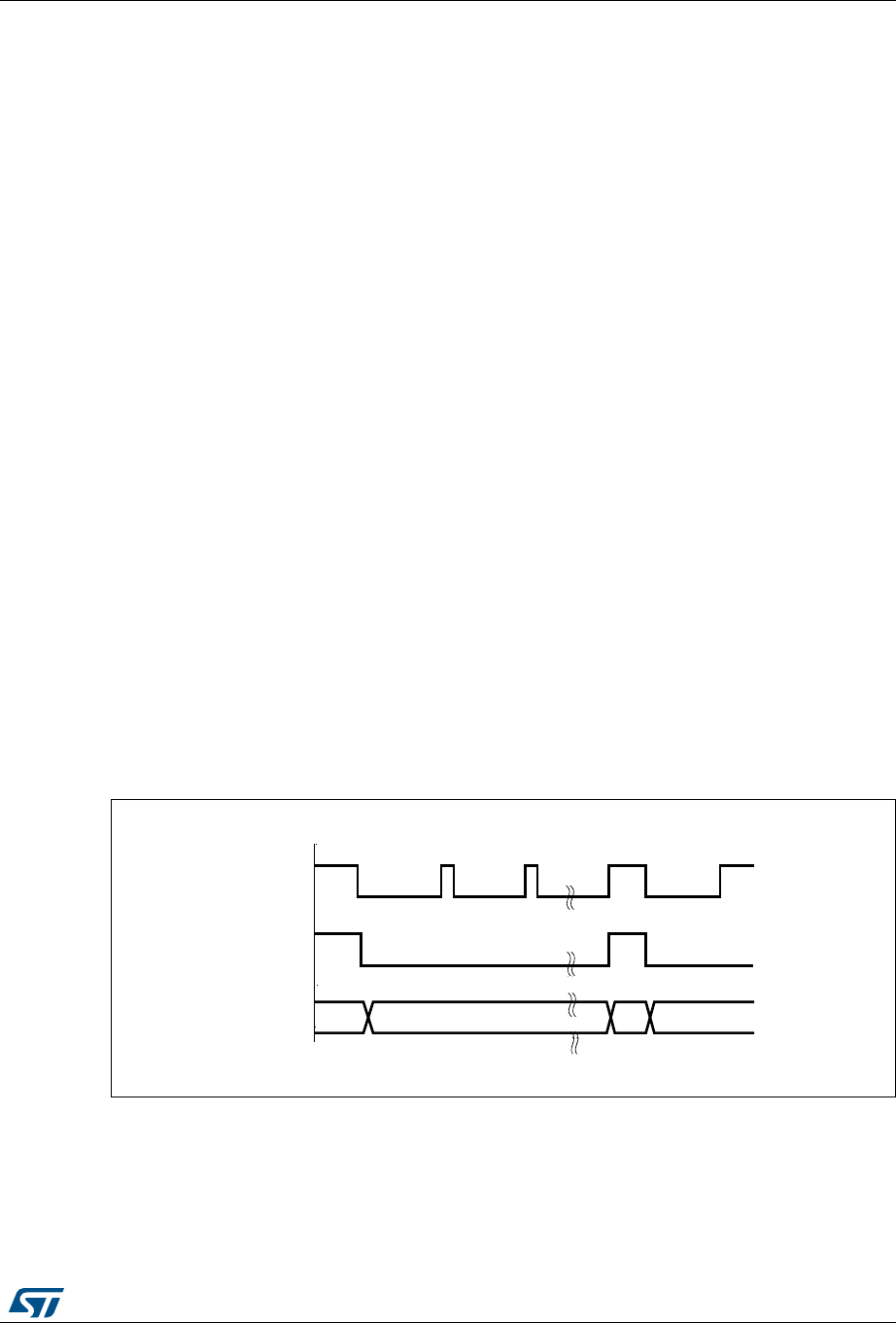
DocID018909 Rev 9 461/1718
RM0090 Digital camera interface (DCMI)
477
This mode can be supported by programming the following codes:
•FS ≤ 0xFF
•FE ≤ 0xFF
•LS ≤ SAV (active)
•LE ≤ EAV (active)
An embedded unmask code is also implemented for frame/line start and frame/line end
codes. Using it, it is possible to compare only the selected unmasked bits with the
programmed code. You can therefore select a bit to compare in the embedded code and
detect a frame/line start or frame/line end. This means that there can be different codes for
the frame/line start and frame/line end with the unmasked bit position remaining the same.
Example
FS = 0xA5
Unmask code for FS = 0x10
In this case the frame start code is embedded in the bit 4 of the frame start code.
15.5.4 Capture modes
This interface supports two types of capture: snapshot (single frame) and continuous grab.
Snapshot mode (single frame)
In this mode, a single frame is captured (CM = ‘1’ in the DCMI_CR register). After the
CAPTURE bit is set in DCMI_CR, the interface waits for the detection of a start of frame
before sampling the data. The camera interface is automatically disabled (CAPTURE bit
cleared in DCMI_CR) after receiving the first complete frame. An interrupt is generated
(IT_FRAME) if it is enabled.
In case of an overrun, the frame is lost and the CAPTURE bit is cleared.
Figure 76. Frame capture waveforms in Snapshot mode
1. Here, the active state of DCMI_HSYNC and DCMI_VSYNC is 1.
2. DCMI_HSYNC and DCMI_VSYNC can change states at the same time.
DCMI_HSYNC
DCMI_VSYNC
Frame 1 captured Frame 2
not captured
ai15832
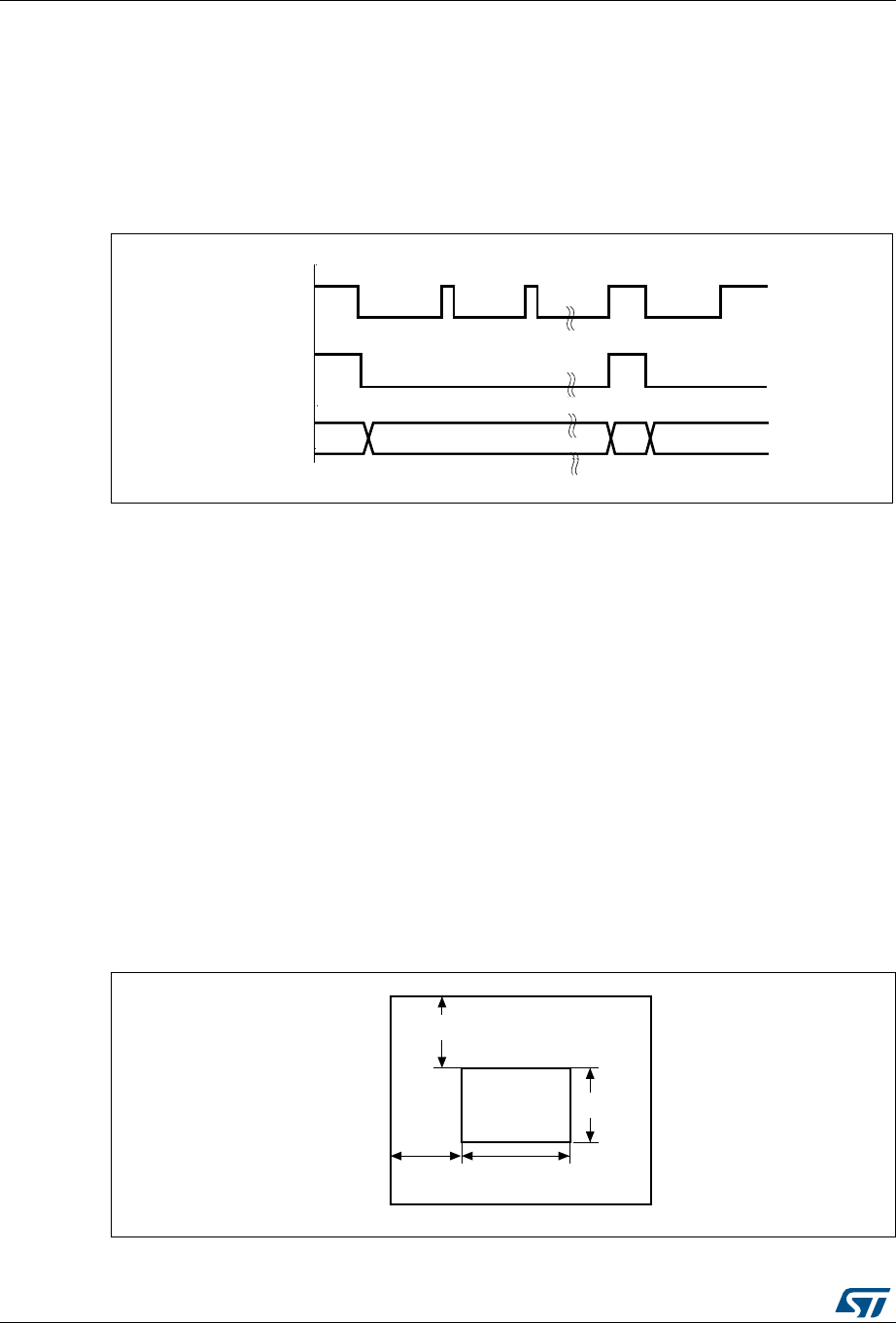
Digital camera interface (DCMI) RM0090
462/1718 DocID018909 Rev 9
Continuous grab mode
In this mode (CM bit = ‘0’ in DCMI_CR), once the CAPTURE bit has been set in DCMI_CR,
the grabbing process starts on the next VSYNC or embedded frame start depending on the
mode. The process continues until the CAPTURE bit is cleared in DCMI_CR. Once the
CAPTURE bit has been cleared, the grabbing process continues until the end of the current
frame.
Figure 77. Frame capture waveforms in continuous grab mode
1. Here, the active state of DCMI_HSYNC and DCMI_VSYNC is 1.
2. DCMI_HSYNC and DCMI_VSYNC can change states at the same time.
In continuous grab mode, you can configure the FCRC bits in DCMI_CR to grab all pictures,
every second picture or one out of four pictures to decrease the frame capture rate.
Note: In the hardware synchronization mode (ESS = ‘0’ in DCMI_CR), the IT_VSYNC interrupt is
generated (if enabled) even when CAPTURE = ‘0’ in DCMI_CR so, to reduce the frame
capture rate even further, the IT_VSYNC interrupt can be used to count the number of
frames between 2 captures in conjunction with the Snapshot mode. This is not allowed by
embedded data synchronization mode.
15.5.5 Crop feature
With the crop feature, the camera interface can select a rectangular window from the
received image. The start (upper left corner) coordinates and size (horizontal dimension in
number of pixel clocks and vertical dimension in number of lines) are specified using two 32-
bit registers (DCMI_CWSTRT and DCMI_CWSIZE). The size of the window is specified in
number of pixel clocks (horizontal dimension) and in number of lines (vertical dimension).
Figure 78. Coordinates and size of the window after cropping
DCMI_HSYNC
DCMI_VSYNC
Frame 1 captured Frame 2 captured
ai15833
CAPCNT bit in DCMI_CSIZE
HOFFCNT bit in DCMI_CSTRT
ai15834
VST bit in DCMI_CSTRT
VLINE bit in DCMI_CSIZE
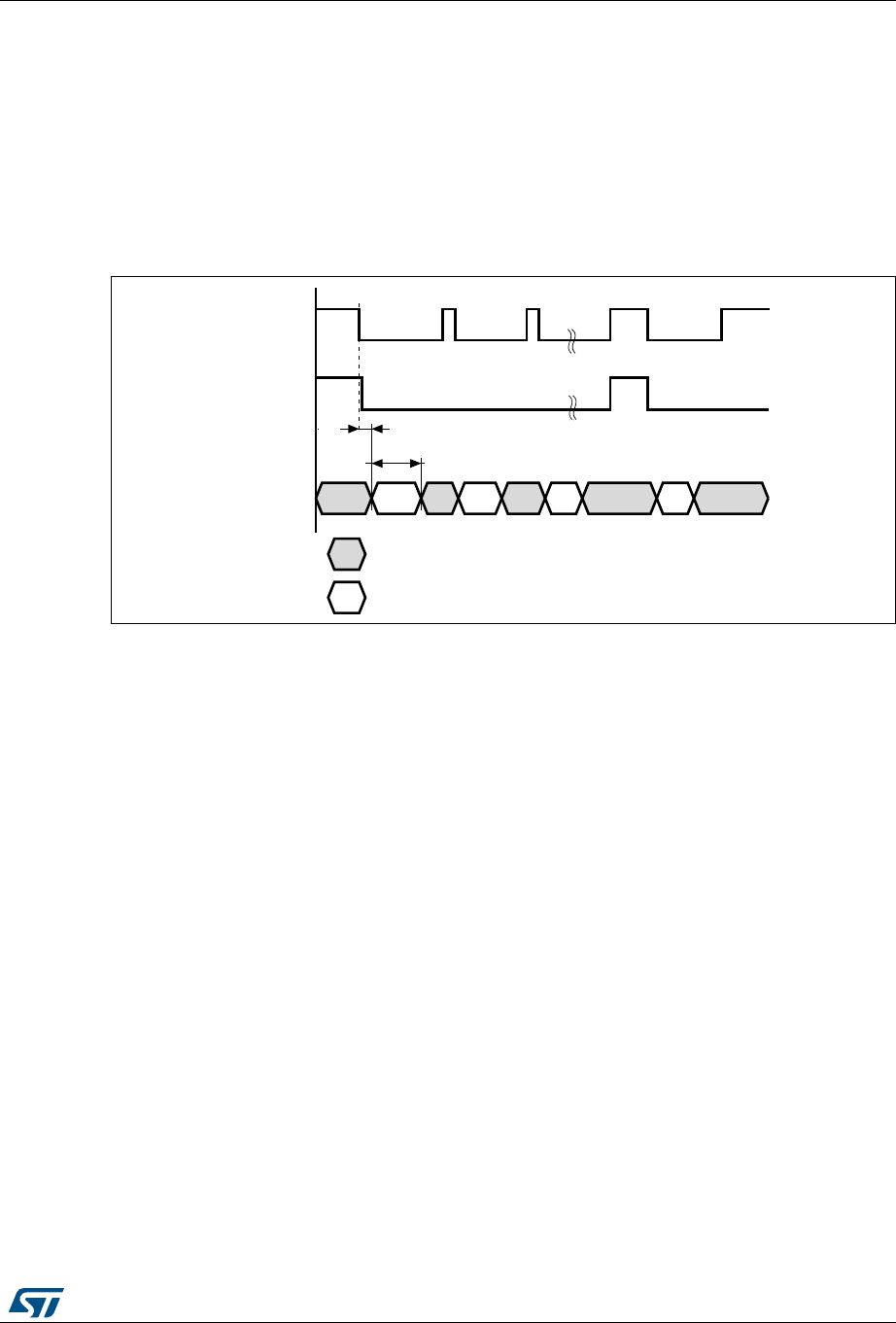
DocID018909 Rev 9 463/1718
RM0090 Digital camera interface (DCMI)
477
These registers specify the coordinates of the starting point of the capture window as a line
number (in the frame, starting from 0) and a number of pixel clocks (on the line, starting from
0), and the size of the window as a line number and a number of pixel clocks. The CAPCNT
value can only be a multiple of 4 (two least significant bits are forced to 0) to allow the
correct transfer of data through the DMA.
If the VSYNC signal goes active before the number of lines is specified in the
DCMI_CWSIZE register, then the capture stops and an IT_FRAME interrupt is generated
when enabled.
Figure 79. Data capture waveforms
1. Here, the active state of DCMI_HSYNC and DCMI_VSYNC is 1.
2. DCMI_HSYNC and DCMI_VSYNC can change states at the same time.
15.5.6 JPEG format
To allow JPEG image reception, it is necessary to set the JPEG bit in the DCMI_CR register.
JPEG images are not stored as lines and frames, so the VSYNC signal is used to start the
capture while HSYNC serves as a data enable signal. The number of bytes in a line may not
be a multiple of 4, you should therefore be careful when handling this case since a DMA
request is generated each time a complete 32-bit word has been constructed from the
captured data. When an end of frame is detected and the 32-bit word to be transferred has
not been completely received, the remaining data are padded with ‘0s’ and a DMA request
is generated.
The crop feature and embedded synchronization codes cannot be used in the JPEG format.
15.5.7 FIFO
A four-word FIFO is implemented to manage data rate transfers on the AHB. The DCMI
features a simple FIFO controller with a read pointer incremented each time the camera
interface reads from the AHB, and a write pointer incremented each time the camera
interface writes to the FIFO. There is no overrun protection to prevent the data from being
overwritten if the AHB interface does not sustain the data transfer rate.
In case of overrun or errors in the synchronization signals, the FIFO is reset and the DCMI
interface waits for a new start of frame.
DCMI_HSYNC
DCMI_VSYNC
ai15833
CAPCNT
HOFFCNT
Data not captured in this phase
Data captured in this phase
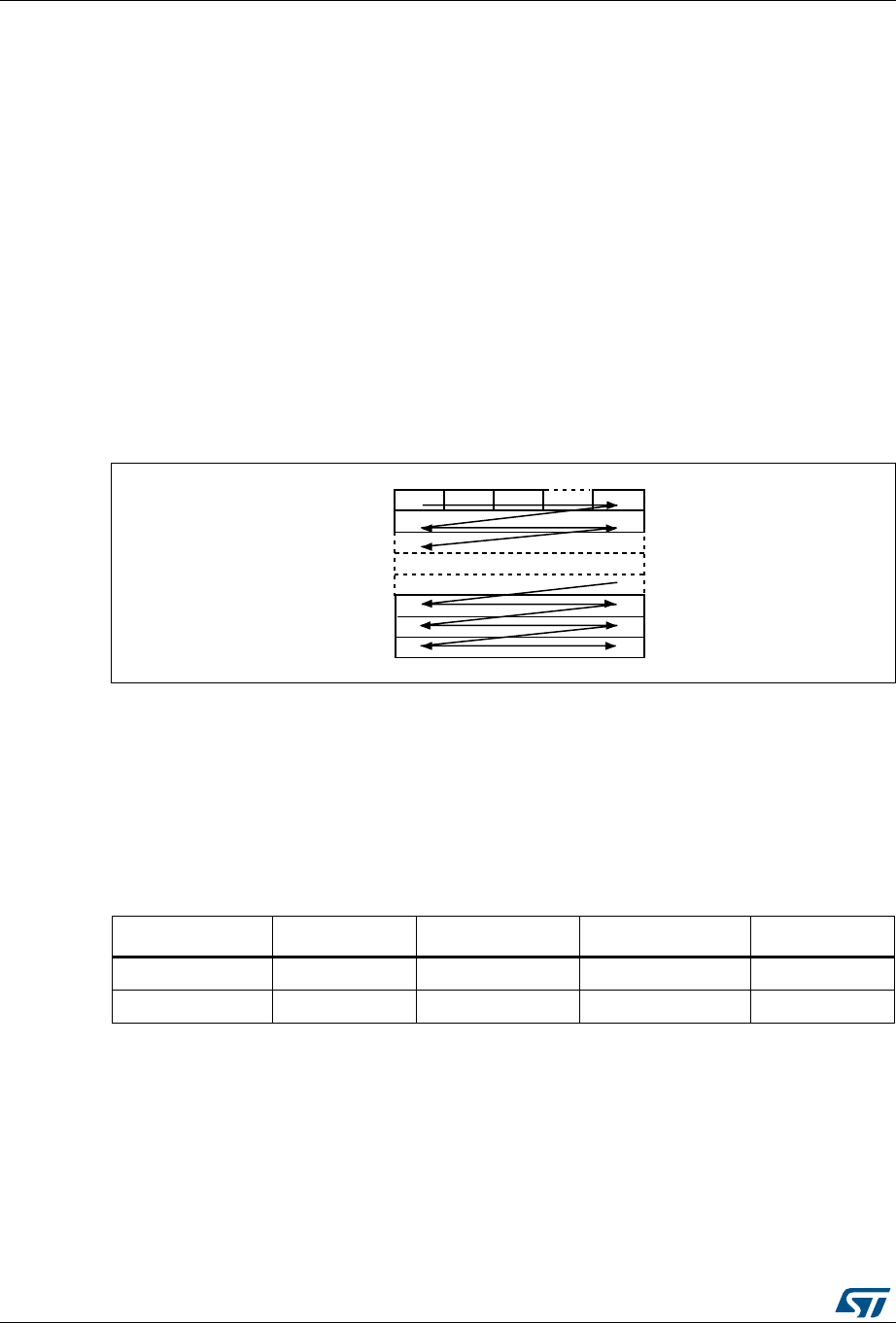
Digital camera interface (DCMI) RM0090
464/1718 DocID018909 Rev 9
15.6 Data format description
15.6.1 Data formats
Three types of data are supported:
•8-bit progressive video: either monochrome or raw Bayer format
•YCbCr 4:2:2 progressive video
•RGB565 progressive video. A pixel coded in 16 bits (5 bits for blue, 5 bits for red, 6 bits
for green) takes two clock cycles to be transferred.
Compressed data: JPEG
For B&W, YCbCr or RGB data, the maximum input size is 2048 × 2048 pixels. No limit in
JPEG compressed mode.
For monochrome, RGB & YCbCr, the frame buffer is stored in raster mode. 32-bit words are
used. Only the little endian format is supported.
Figure 80. Pixel raster scan order
15.6.2 Monochrome format
Characteristics:
•Raster format
•8 bits per pixel
Table 83 shows how the data are stored.
15.6.3 RGB format
Characteristics:
•Raster format
•RGB
•Interleaved: one buffer: R, G & B interleaved: BRGBRGBRG, etc.
•Optimized for display output
0IXELRASTER
SCANORDER
INCREASING
ADDRESSES
7ORD7ORD7ORD0IXELROW
0IXELROWNn
AI
Table 83. Data storage in monochrome progressive video format
Byte address 31:24 23:16 15:8 7:0
0 n + 3 n + 2 n + 1 n
4 n + 7 n + 6 n + 5 n + 4
DocID018909 Rev 9 465/1718
RM0090 Digital camera interface (DCMI)
477
The RGB planar format is compatible with standard OS frame buffer display formats.
Only 16 BPP (bits per pixel): RGB565 (2 pixels per 32-bit word) is supported.
The 24 BPP (palletized format) and grayscale formats are not supported. Pixels are stored
in a raster scan order, that is from top to bottom for pixel rows, and from left to right within a
pixel row. Pixel components are R (red), G (green) and B (blue). All components have the
same spatial resolution (4:4:4 format). A frame is stored in a single part, with the
components interleaved on a pixel basis.
Table 84 shows how the data are stored.
15.6.4 YCbCr format
Characteristics:
•Raster format
•YCbCr 4:2:2
•Interleaved: one Buffer: Y, Cb & Cr interleaved: CbYCrYCbYCr, etc.
Pixel components are Y (luminance or “luma”), Cb and Cr (chrominance or “chroma” blue
and red). Each component is encoded in 8 bits. Luma and chroma are stored together
(interleaved) as shown in Tabl e 85.
15.7 DCMI interrupts
Five interrupts are generated. All interrupts are maskable by software. The global interrupt
(IT_DCMI) is the OR of all the individual interrupts. Table 86 gives the list of all interrupts.
Table 84. Data storage in RGB progressive video format
Byte address 31:27 26:21 20:16 15:11 10:5 4:0
0 Red n + 1 Green n + 1 Blue n + 1 Red n Green n Blue n
4 Red n + 4 Green n + 3 Blue n + 3 Red n + 2 Green n + 2 Blue n + 2
Table 85. Data storage in YCbCr progressive video format
Byte address 31:24 23:16 15:8 7:0
0Y n + 1Cr n Y nCb n
4 Y n + 3 Cr n + 2 Y n + 2 Cb n + 2
Table 86. DCMI interrupts
Interrupt name Interrupt event
IT_LINE Indicates the end of line
IT_FRAME Indicates the end of frame capture
IT_OVR indicates the overrun of data reception
IT_VSYNC Indicates the synchronization frame
IT_ERR Indicates the detection of an error in the embedded synchronization frame
detection
IT_DCMI Logic OR of the previous interrupts

Digital camera interface (DCMI) RM0090
466/1718 DocID018909 Rev 9
15.8 DCMI register description
All DCMI registers have to be accessed as 32-bit words, otherwise a bus error occurs.
15.8.1 DCMI control register 1 (DCMI_CR)
Address offset: 0x00
Reset value: 0x0000 0x0000
313029282726252423222120191817161514131211109876543210
Reserved
ENABLE
Reserved
EDM FCRC
VSPOL
HSPOL
PCKPOL
ESS
JPEG
CROP
CM
CAPTURE
rw rw rw rw rw rw rw rw rw rw rw rw rw
Bit 31:15 Reserved, must be kept at reset value.
Bit 14 ENABLE: DCMI enable
0: DCMI disabled
1: DCMI enabled
Note: The DCMI configuration registers should be programmed correctly before
enabling this Bit
Bit 13: 12 Reserved, must be kept at reset value.
Bits 11:10 EDM[1:0]: Extended data mode
00: Interface captures 8-bit data on every pixel clock
01: Interface captures 10-bit data on every pixel clock
10: Interface captures 12-bit data on every pixel clock
11: Interface captures 14-bit data on every pixel clock
Bits 9:8 FCRC[1:0]: Frame capture rate control
These bits define the frequency of frame capture. They are meaningful only in
Continuous grab mode. They are ignored in snapshot mode.
00: All frames are captured
01: Every alternate frame captured (50% bandwidth reduction)
10: One frame in 4 frames captured (75% bandwidth reduction)
11: reserved
Bit 7 VSPOL: Vertical synchronization polarity
This bit indicates the level on the VSYNC pin when the data are not valid on the
parallel interface.
0: VSYNC active low
1: VSYNC active high
Bit 6 HSPOL: Horizontal synchronization polarity
This bit indicates the level on the HSYNC pin when the data are not valid on the
parallel interface.
0: HSYNC active low
1: HSYNC active high
Bit 5 PCKPOL: Pixel clock polarity
This bit configures the capture edge of the pixel clock
0: Falling edge active.
1: Rising edge active.

DocID018909 Rev 9 467/1718
RM0090 Digital camera interface (DCMI)
477
Bit 4 ESS: Embedded synchronization select
0: Hardware synchronization data capture (frame/line start/stop) is synchronized
with the HSYNC/VSYNC signals.
1: Embedded synchronization data capture is synchronized with synchronization
codes embedded in the data flow.
Note: Valid only for 8-bit parallel data. HSPOL/VSPOL are ignored when the ESS
bit is set.
This bit is disabled in JPEG mode.
Bit 3 JPEG: JPEG format
0: Uncompressed video format
1: This bit is used for JPEG data transfers. The HSYNC signal is used as data
enable. The crop and embedded synchronization features (ESS bit) cannot be
used in this mode.
Bits 2 CROP: Crop feature
0: The full image is captured. In this case the total number of bytes in an image
frame should be a multiple of 4
1: Only the data inside the window specified by the crop register will be captured.
If the size of the crop window exceeds the picture size, then only the picture size
is captured.
Bit 1 CM: Capture mode
0: Continuous grab mode - The received data are transferred into the destination
memory through the DMA. The buffer location and mode (linear or circular
buffer) is controlled through the system DMA.
1: Snapshot mode (single frame) - Once activated, the interface waits for the
start of frame and then transfers a single frame through the DMA. At the end of
the frame, the CAPTURE bit is automatically reset.
Bit 0 CAPTURE: Capture enable
0: Capture disabled.
1: Capture enabled.
The camera interface waits for the first start of frame, then a DMA request is
generated to transfer the received data into the destination memory.
In snapshot mode, the CAPTURE bit is automatically cleared at the end of the
1st frame received.
In continuous grab mode, if the software clears this bit while a capture is
ongoing, the bit will be effectively cleared after the frame end.
Note: The DMA controller and all DCMI configuration registers should be
programmed correctly before enabling this bit.

Digital camera interface (DCMI) RM0090
468/1718 DocID018909 Rev 9
15.8.2 DCMI status register (DCMI_SR)
Address offset: 0x04
Reset value: 0x0000 0x0000
313029282726252423222120191817161514131211109876543210
Reserved
FNE
VSYNC
HSYNC
rrr
Bits 31:3 Reserved, must be kept at reset value.
Bit 2 FNE: FIFO not empty
This bit gives the status of the FIFO
1: FIFO contains valid data
0: FIFO empty
Bit 1 VSYNC
This bit gives the state of the VSYNC pin with the correct programmed polarity.
When embedded synchronization codes are used, the meaning of this bit is the
following:
0: active frame
1: synchronization between frames
In case of embedded synchronization, this bit is meaningful only if the
CAPTURE bit in DCMI_CR is set.
Bit 0 HSYNC
This bit gives the state of the HSYNC pin with the correct programmed polarity.
When embedded synchronization codes are used, the meaning of this bit is the
following:
0: active line
1: synchronization between lines
In case of embedded synchronization, this bit is meaningful only if the
CAPTURE bit in DCMI_CR is set.

DocID018909 Rev 9 469/1718
RM0090 Digital camera interface (DCMI)
477
15.8.3 DCMI raw interrupt status register (DCMI_RIS)
Address offset: 0x08
Reset value: 0x0000 0x0000
DCMI_RIS gives the raw interrupt status and is accessible in read only. When read, this
register returns the status of the corresponding interrupt before masking with the DCMI_IER
register value.
313029282726252423222120191817161514131211109876543210
Reserved
LINE_RIS
VSYNC_RIS
ERR_RIS
OVR_RIS
FRAME_RIS
rrrrr
Bits 31:5 Reserved, must be kept at reset value.
Bit 4 LINE_RIS: Line raw interrupt status
This bit gets set when the HSYNC signal changes from the inactive state to the
active state. It goes high even if the line is not valid.
In the case of embedded synchronization, this bit is set only if the CAPTURE bit
in DCMI_CR is set.
It is cleared by writing a ‘1’ to the LINE_ISC bit in DCMI_ICR.
Bit 3 VSYNC_RIS: VSYNC raw interrupt status
This bit is set when the VSYNC signal changes from the inactive state to the
active state.
In the case of embedded synchronization, this bit is set only if the CAPTURE bit
is set in DCMI_CR.
It is cleared by writing a ‘1’ to the VSYNC_ISC bit in DCMI_ICR.
Bit 2 ERR_RIS: Synchronization error raw interrupt status
0: No synchronization error detected
1: Embedded synchronization characters are not received in the correct order.
This bit is valid only in the embedded synchronization mode. It is cleared by
writing a ‘1’ to the ERR_ISC bit in DCMI_ICR.
Note: This bit is available only in embedded synchronization mode.
Bit 1 OVR_RIS: Overrun raw interrupt status
0: No data buffer overrun occurred
1: A data buffer overrun occurred and the data FIFO is corrupted.
This bit is cleared by writing a ‘1’ to the OVR_ISC bit in DCMI_ICR.
Bit 0 FRAME_RIS: Capture complete raw interrupt status
0: No new capture
1: A frame has been captured.
This bit is set when a frame or window has been captured.
In case of a cropped window, this bit is set at the end of line of the last line in the
crop. It is set even if the captured frame is empty (e.g. window cropped outside
the frame).
This bit is cleared by writing a ‘1’ to the FRAME_ISC bit in DCMI_ICR.

Digital camera interface (DCMI) RM0090
470/1718 DocID018909 Rev 9
15.8.4 DCMI interrupt enable register (DCMI_IER)
Address offset: 0x0C
Reset value: 0x0000 0x0000
The DCMI_IER register is used to enable interrupts. When one of the DCMI_IER bits is set,
the corresponding interrupt is enabled. This register is accessible in both read and write.
313029282726252423222120191817161514131211109876543210
Reserved
LINE_IE
VSYNC_IE
ERR_IE
OVR_IE
FRAME_IE
rw rw rw rw rw
Bits 31:5 Reserved, must be kept at reset value.
Bit 4 LINE_IE: Line interrupt enable
0: No interrupt generation when the line is received
1: An Interrupt is generated when a line has been completely received
Bit 3 VSYNC_IE: VSYNC interrupt enable
0: No interrupt generation
1: An interrupt is generated on each VSYNC transition from the inactive to the
active state
The active state of the VSYNC signal is defined by the VSPOL bit.
Bit 2 ERR_IE: Synchronization error interrupt enable
0: No interrupt generation
1: An interrupt is generated if the embedded synchronization codes are not
received in the correct order.
Note: This bit is available only in embedded synchronization mode.
Bit 1 OVR_IE: Overrun interrupt enable
0: No interrupt generation
1: An interrupt is generated if the DMA was not able to transfer the last data
before new data (32-bit) are received.
Bit 0 FRAME_IE: Capture complete interrupt enable
0: No interrupt generation
1: An interrupt is generated at the end of each received frame/crop window (in
crop mode).

DocID018909 Rev 9 471/1718
RM0090 Digital camera interface (DCMI)
477
15.8.5 DCMI masked interrupt status register (DCMI_MIS)
This DCMI_MIS register is a read-only register. When read, it returns the current masked
status value (depending on the value in DCMI_IER) of the corresponding interrupt. A bit in
this register is set if the corresponding enable bit in DCMI_IER is set and the corresponding
bit in DCMI_RIS is set.
Address offset: 0x10
Reset value: 0x0000
313029282726252423222120191817161514131211109876543210
Reserved
LINE_MIS
VSYNC_MIS
ERR_MIS
OVR_MIS
FRAME_MIS
rrrrr
Bits 31:5 Reserved, must be kept at reset value.
Bit 4 LINE_MIS: Line masked interrupt status
This bit gives the status of the masked line interrupt
0: No interrupt generation when the line is received
1: An Interrupt is generated when a line has been completely received and the
LINE_IE bit is set in DCMI_IER.
Bit 3 VSYNC_MIS: VSYNC masked interrupt status
This bit gives the status of the masked VSYNC interrupt
0: No interrupt is generated on VSYNC transitions
1: An interrupt is generated on each VSYNC transition from the inactive to the
active state and the VSYNC_IE bit is set in DCMI_IER.
The active state of the VSYNC signal is defined by the VSPOL bit.
Bit 2 ERR_MIS: Synchronization error masked interrupt status
This bit gives the status of the masked synchronization error interrupt
0: No interrupt is generated on a synchronization error
1: An interrupt is generated if the embedded synchronization codes are not
received in the correct order and the ERR_IE bit in DCMI_IER is set.
Note: This bit is available only in embedded synchronization mode.
Bit 1 OVR_MIS: Overrun masked interrupt status
This bit gives the status of the masked overflow interrupt
0: No interrupt is generated on overrun
1: An interrupt is generated if the DMA was not able to transfer the last data
before new data (32-bit) are received and the OVR_IE bit is set in DCMI_IER.
Bit 0 FRAME_MIS: Capture complete masked interrupt status
This bit gives the status of the masked capture complete interrupt
0: No interrupt is generated after a complete capture
1: An interrupt is generated at the end of each received frame/crop window (in
crop mode) and the FRAME_IE bit is set in DCMI_IER.

Digital camera interface (DCMI) RM0090
472/1718 DocID018909 Rev 9
15.8.6 DCMI interrupt clear register (DCMI_ICR)
Address offset: 0x14
Reset value: 0x0000 0x0000
The DCMI_ICR register is write-only. Writing a ‘1’ into a bit of this register clears the
corresponding bit in the DCMI_RIS and DCMI_MIS registers. Writing a ‘0’ has no effect.
313029282726252423222120191817161514131211109876543210
Reserved
LINE_ISC
VSYNC_ISC
ERR_ISC
OVR_ISC
FRAME_ISC
wwwww
Bits 15:5 Reserved, must be kept at reset value.
Bit 4 LINE_ISC: line interrupt status clear
Writing a ‘1’ into this bit clears LINE_RIS in the DCMI_RIS register
Bit 3 VSYNC_ISC: Vertical synch interrupt status clear
Writing a ‘1’ into this bit clears the VSYNC_RIS bit in DCMI_RIS
Bit 2 ERR_ISC: Synchronization error interrupt status clear
Writing a ‘1’ into this bit clears the ERR_RIS bit in DCMI_RIS
Note: This bit is available only in embedded synchronization mode.
Bit 1 OVR_ISC: Overrun interrupt status clear
Writing a ‘1’ into this bit clears the OVR_RIS bit in DCMI_RIS
Bits 0 FRAME_ISC: Capture complete interrupt status clear
Writing a ‘1’ into this bit clears the FRAME_RIS bit in DCMI_RIS

DocID018909 Rev 9 473/1718
RM0090 Digital camera interface (DCMI)
477
15.8.7 DCMI embedded synchronization code register (DCMI_ESCR)
Address offset: 0x18
Reset value: 0x0000 0x0000
313029282726252423222120191817161514131211109876543210
FEC LEC LSC FSC
rw rw rw rw rw rw rw rw rw rw rw rw rw rw rw rw rw rw rw rw rw rw rw rw rw rw rw rw rw rw rw rw
Bits 31:24 FEC: Frame end delimiter code
This byte specifies the code of the frame end delimiter. The code consists of 4
bytes in the form of 0xFF, 0x00, 0x00, FEC.
If FEC is programmed to 0xFF, all the unused codes (0xFF0000XY) are
interpreted as frame end delimiters.
Bits 23:16 LEC: Line end delimiter code
This byte specifies the code of the line end delimiter. The code consists of 4
bytes in the form of 0xFF, 0x00, 0x00, LEC.
Bits 15:8 LSC: Line start delimiter code
This byte specifies the code of the line start delimiter. The code consists of 4
bytes in the form of 0xFF, 0x00, 0x00, LSC.
Bits 7:0 FSC: Frame start delimiter code
This byte specifies the code of the frame start delimiter. The code consists of 4
bytes in the form of 0xFF, 0x00, 0x00, FSC.
If FSC is programmed to 0xFF, no frame start delimiter is detected. But, the 1st
occurrence of LSC after an FEC code will be interpreted as a start of frame
delimiter.

Digital camera interface (DCMI) RM0090
474/1718 DocID018909 Rev 9
15.8.8 DCMI embedded synchronization unmask register (DCMI_ESUR)
Address offset: 0x1C
Reset value: 0x0000 0x0000
313029282726252423222120191817161514131211109876543210
FEU LEU LSU FSU
rw rw rw rw rw rw rw rw rw rw rw rw rw rw rw rw rw rw rw rw rw rw rw rw rw rw rw rw rw rw rw rw
Bits 31:24 FEU: Frame end delimiter unmask
This byte specifies the mask to be applied to the code of the frame end delimiter.
0: The corresponding bit in the FEC byte in DCMI_ESCR is masked while
comparing the frame end delimiter with the received data.
1: The corresponding bit in the FEC byte in DCMI_ESCR is compared while
comparing the frame end delimiter with the received data
Bits 23:16 LEU: Line end delimiter unmask
This byte specifies the mask to be applied to the code of the line end delimiter.
0: The corresponding bit in the LEC byte in DCMI_ESCR is masked while
comparing the line end delimiter with the received data
1: The corresponding bit in the LEC byte in DCMI_ESCR is compared while
comparing the line end delimiter with the received data
Bits 15:8 LSU: Line start delimiter unmask
This byte specifies the mask to be applied to the code of the line start delimiter.
0: The corresponding bit in the LSC byte in DCMI_ESCR is masked while
comparing the line start delimiter with the received data
1: The corresponding bit in the LSC byte in DCMI_ESCR is compared while
comparing the line start delimiter with the received data
Bits 7:0 FSU: Frame start delimiter unmask
This byte specifies the mask to be applied to the code of the frame start
delimiter.
0: The corresponding bit in the FSC byte in DCMI_ESCR is masked while
comparing the frame start delimiter with the received data
1: The corresponding bit in the FSC byte in DCMI_ESCR is compared while
comparing the frame start delimiter with the received data
DocID018909 Rev 9 475/1718
RM0090 Digital camera interface (DCMI)
477
15.8.9 DCMI crop window start (DCMI_CWSTRT)
Address offset: 0x20
Reset value: 0x0000 0x0000
15.8.10 DCMI crop window size (DCMI_CWSIZE)
Address offset: 0x24
Reset value: 0x0000 0x0000
313029282726252423222120191817161514131211109876543210
Reserved VST[12:0 Reserv
ed
HOFFCNT[13:0]
rw rw rw rw rw rw rw rw rw rw rw rw rw rw rw rw rw rw rw rw rw rw rw rw rw rw rw
Bits 31:29 Reserved, must be kept at reset value.
Bits 28:16 VST[12:0]: Vertical start line count
The image capture starts with this line number. Previous line data are ignored.
0x0000 => line 1
0x0001 => line 2
0x0002 => line 3
....
Bits 15:14 Reserved, must be kept at reset value.
Bit 13:0 HOFFCNT[13:0]: Horizontal offset count
This value gives the number of pixel clocks to count before starting a capture.
313029282726252423222120191817161514131211109876543210
Reserved
VLINE13:0]
Reserved
CAPCNT[13:0]
rw rw rw rw rw rw rw rw rw rw rw rw rw rw rw rw rw rw rw rw rw rw rw rw rw rw rw rw
Bits 31:30 Reserved, must be kept at reset value.
Bitst 29:16 VLINE[13:0]: Vertical line count
This value gives the number of lines to be captured from the starting point.
0x0000 => 1 line
0x0001 => 2 lines
0x0002 => 3 lines
....
Bits 15:14 Reserved, must be kept at reset value.
Bits 13:0 CAPCNT[13:0]: Capture count
This value gives the number of pixel clocks to be captured from the starting
point on the same line. It value should corresponds to word-aligned data for
different widths of parallel interfaces.
0x0000 => 1 pixel
0x0001 => 2 pixels
0x0002 => 3 pixels
....
Digital camera interface (DCMI) RM0090
476/1718 DocID018909 Rev 9
15.8.11 DCMI data register (DCMI_DR)
Address offset: 0x28
Reset value: 0x0000 0x0000
The digital camera Interface packages all the received data in 32-bit format before
requesting a DMA transfer. A 4-word deep FIFO is available to leave enough time for DMA
transfers and avoid DMA overrun conditions.
15.8.12 DCMI register map
Table 87 summarizes the DCMI registers.
313029282726252423222120191817161514131211109876543210
Byte3 Byte2 Byte1 Byte0
rrrrrrrrrrrrrrrrrrrrrrrrrrrrrrrr
Bits 31:24 Data byte 3
Bits 23:16 Data byte 2
Bits 15:8 Data byte 1
Bits 7:0 Data byte 0
Table 87. DCMI register map and reset values
Offset Register
31
30
29
28
27
26
25
24
23
22
21
20
19
18
17
16
15
14
13
12
11
10
9
8
7
6
5
4
3
2
1
0
0x00
DCMI_CR
Reserved
ENABLE
Reserved
EDM FCR
C
VSPOL
HSPOL
PCKPOL
ESS
JPEG
CROP
CM
CAPTURE
Reset value 0 000000000000
0x04
DCMI_SR
Reserved
FNE
VSYNC
HSYNC
Reset value 000
0x08
DCMI_RIS
Reserved
LINE_RIS
VSYNC_RIS
ERR_RIS
OVR_RIS
FRAME_RIS
Reset value 00000
0x0C
DCMI_IER
Reserved
LINE_IE
VSYNC_IE
ERR_IE
OVR_IE
FRAME_IE
Reset value 00000
0x10
DCMI_MIS
Reserved
LINE_MIS
VSYNC_MIS
ERR_MIS
OVR_MIS
FRAME_MIS
Reset value 00000
DocID018909 Rev 9 477/1718
RM0090 Digital camera interface (DCMI)
477
Refer to Table 1 on page 64 for the register boundary addresses.
0x14
DCMI_ICR
Reserved
LINE_ISC
VSYNC_ISC
ERR_ISC
OVR_ISC
FRAME_ISC
Reset value 00000
0x18
DCMI_ESCR FEC LEC LSC FSC
Reset value 00000000000000000000000000000000
0x1C
DCMI_ESUR FEU LEU LSU FSU
Reset value 00000000000000000000000000000000
0x20
DCMI_CWSTR
TReserve
d
VST[12:0
Reserved
HOFFCNT[13:0]
Reset value 0000000000000 00000000000000
0x24
DCMI_CWSIZ
E
Reserved
VLINE13:0]
Reserved
CAPCNT[13:0]
Reset value 00000000000000 00000000000000
0x28
DCMI_DR Byte3 Byte2 Byte1 Byte0
Reset value 00000000000000000000000000000000
Table 87. DCMI register map and reset values (continued)
Offset Register
31
30
29
28
27
26
25
24
23
22
21
20
19
18
17
16
15
14
13
12
11
10
9
8
7
6
5
4
3
2
1
0

LCD-TFT Controller (LTDC) RM0090
478/1718 DocID018909 Rev 9
16 LCD-TFT Controller (LTDC)
This section applies only to STM32F429xx/439xx devices.
16.1 Introduction
The LCD-TFT (Liquid Crystal Display - Thin Film Transistor) display controller provides a
parallel digital RGB (Red, Green, Blue) and signals for horizontal, vertical synchronisation,
Pixel Clock and Data Enable as output to interface directly to a variety of LCD and TFT
panels.
16.2 LTDC main features
•24-bit RGB Parallel Pixel Output; 8 bits-per-pixel (RGB888)
•2 display layers with dedicated FIFO (64x32-bit)
•Color Look-Up Table (CLUT) up to 256 color (256x24-bit) per layer
•Supports up to XGA (1024x768) resolution
•Programmable timings for different display panels
•Programmable Background color
•Programmable polarity for HSync, VSync and Data Enable
•Up to 8 Input color formats selectable per layer
–ARGB8888
– RGB888
– RGB565
–ARGB1555
–ARGB4444
– L8 (8-bit Luminance or CLUT)
– AL44 (4-bit alpha + 4-bit luminance)
– AL88 (8-bit alpha + 8-bit luminance)
•Pseudo-random dithering output for low bits per channel
– Dither width 2-bits for Red, Green, Blue
•Flexible blending between two layers using alpha value (per pixel or constant)
•Color Keying (transparency color)
•Programmable Window position and size
•Supports thin film transistor (TFT) color displays
•AHB master interface with burst of 16 words
•Up to 4 programmable interrupt events
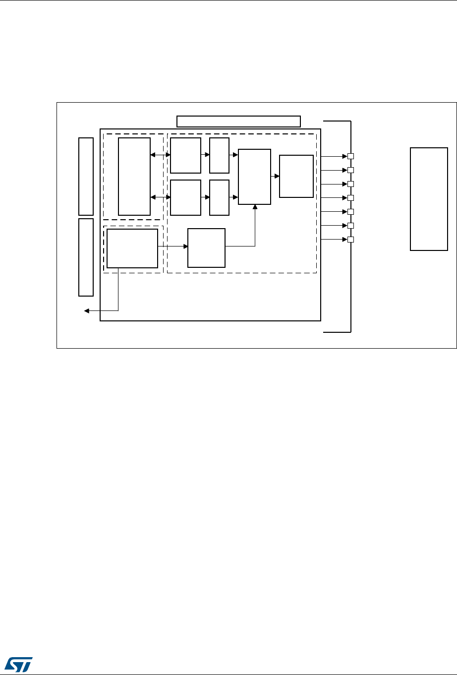
DocID018909 Rev 9 479/1718
RM0090 LCD-TFT Controller (LTDC)
509
16.3 LTDC functional description
16.3.1 LTDC block diagram
The block diagram of the LTDC is shown in Figure 81: LTDC block diagram.
Figure 81. LTDC block diagram
Layer FIFO: One FIFO 64x32 bit per layer.
PFC: Pixel Format Convertor performing the pixel format conversion from the selected input
pixel format of a layer to words.
AHB interface: For data transfer from memories to the FIFO.
Blending, Dithering unit and Timings Generator: Refer to Section 16.4.1 and Section 16.4.2.
16.3.2 LTDC reset and clocks
The LCD-TFT controller peripheral uses 3 clock domains:
•The AHB clock domain (HCLK): for data transfer from the memories to the Layer FIFO
•The APB2 clock domain (PCLK2): for register configuration
•The Pixel Clock domain (LCD_CLK): to generate LCD-TFT interface signals. The
LCD_CLK output should be configured following the panel requirements. The
LCD_CLK is configured through the PLLSAI (refer to RCC section)
The LCD controller can be reset by setting the corresponding bit in the RCC_APB2RSTR
register. It resets the three clock domains.
06Y9
/&'7)7
3DQHO
/&'B+6<1&
/&'B96<1&
/&'B'(
/&'B&/.
/&'B5>@
/&'B*>@
/&'B%>@
3L[HO&ORFNGRPDLQ
'LWKHULQJ
XQLW
%OHQGLQJ
XQLW
3)&
3)&
/D\HU
),)2
/D\HU
),)2
$+%
LQWHUIDFH
7LPLQJ
JHQHUDWRU
&RQILJXUDWLRQ
DQG6WDWXV
UHJLVWHUV
$+%FORFNGRPDLQ$3%FORFNGRPDLQ
,QWHUUXSWV

LCD-TFT Controller (LTDC) RM0090
480/1718 DocID018909 Rev 9
16.3.3 LCD-TFT pins and signal interface
The Table below summarizes the LTDC signal interface:
The LCD-TFT controller pins must be configured by the user application. The unused pins
can be used for other purposes.
For LTDC outputs up to 24-bit (RGB888), if less than 8bpp are used to output for example
RGB565 or RGB666 to interface on 16b-bit or 18-bit displays, the RGB display data lines
must be connected to the MSB of the LCD-TFT controller RGB data lines. As an example, in
the case of an LCD-TFT controller interfacing with a RGB565 16-bit display, the LCD display
R[4:0], G[5:0] and B[4:0] data lines pins must be connected to LCD-TFT controller
LCD_R[7:3], LCD_G[7:2] and LCD_B[7:3].
16.4 LTDC programmable parameters
The LCD-TFT controller provides flexible configurable parameters. It can be enabled or
disabled through the LTDC_GCR register.
16.4.1 LTDC Global configuration parameters
Synchronous Timings:
Figure 82 presents the configurable timing parameters generated by the Synchronous
Timings Generator block presented in the block diagram Figure 81. It generates the
Horizontal and Vertical Synchronization timings panel signals, the Pixel Clock and the Data
Enable signals.
Table 88. LCD-TFT pins and signal interface
LCD-TFT
signals I/O Description
LCD_CLK O Clock Output
LCD_HSYNC O Horizontal Synchronization
LCD_VSYNC O Vertical Synchronization
LCD_DE O Data Enable
LCD_R[7:0] O Data: 8-bit Red data
LCD_G[7:0] O Data: 8-bit Green data
LCD_B[7:0] O Data: 8-bit Blue data
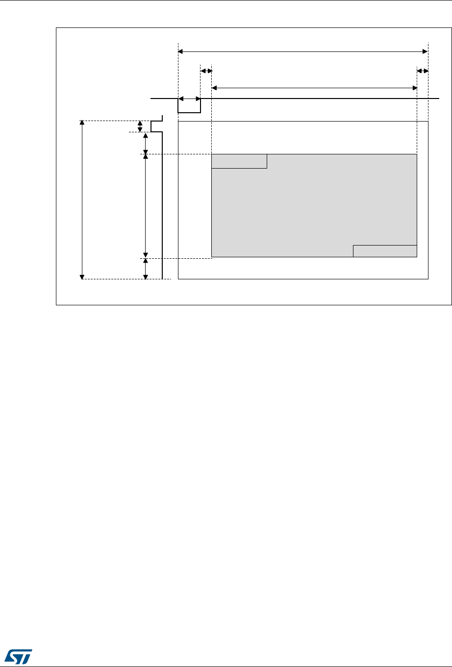
DocID018909 Rev 9 481/1718
RM0090 LCD-TFT Controller (LTDC)
509
Figure 82. LCD-TFT Synchronous timings
Note: The HBP and HFP are respectively the Horizontal back porch and front porch period.
The VBP and the VFP are respectively the Vertical back porch and front porch period.
The LCD-TFT programmable synchronous timings are:
– HSYNC and VSYNC Width: Horizontal and Vertical Synchronization width
configured by programming a value of HSYNC Width - 1 and VSYNC Width - 1 in
the LTDC_SSCR register.
– HBP and VBP: Horizontal and Vertical Synchronization back porch width
configured by programming the accumulated value HSYNC Width + HBP - 1 and
the accumulated value VSYNC Width + VBP - 1 in the LTDC_BPCR register.
– Active Width and Active Height: The Active Width and Active Height are
configured by programming the accumulated value HSYNC Width + HBP +
Active Width - 1 and the accumulated value VSYNC Width + VBP + Active
Height - 1 in the LTDC_AWCR register (only up to 1024x768 is supported).
– Total Width: The Total width is configured by programming the accumulated value
HSYNC Width + HBP + Active Width + HFP - 1 in the LTDC_TWCR register. The
HFP is the Horizontal front porch period.
– Total Height: The Total Height is configured by programming the accumulated
value VSYNC Height + VBP + Active Height + VFP - 1 in the LTDC_TWCR
register. The VFP is the Vertical front porch period.
Note: When the LTDC is enabled, the timings generated start with X/Y=0/0 position as the first
horizontal synchronization pixel in the vertical synchronization area and following the back
porch, active data display area and the front porch.
06Y9
7RWDOZLGWK
$FWLYHZLGWK
+)3+%3
+6<1&
ZLGWK
96<1&ZLGWK
9%3
9)3
$FWLYH+HLJKW
7RWDO+HLJKW
$FWLYH'LVSOD\$UHD
'DWD/LQH
'DWDQ/LQHQ

LCD-TFT Controller (LTDC) RM0090
482/1718 DocID018909 Rev 9
When the LTDC is disabled, the timing generator block is reset to X=Total Width - 1,
Y=Total Height - 1 and held the last pixel before the vertical synchronization phase and the
FIFO are flushed. Therefore only blanking data is output continuously.
Example of Synchronous timings configuration:
TFT-LCD timings (should be extracted from Panel datasheet):
•Horizontal and Vertical Synchronization width: 0x8 pixels and 0x4 lines
•Horizontal and Vertical back porch: 0x7 pixels and 0x2 lines
•Active Width and Active Height: 0x280 pixels, 0x1E0 lines (640x480)
•Horizontal front porch: 0x6 pixels
•Vertical front porch: 0x2 lines
The programmed values in the LTDC Timings registers will be:
•LTDC_SSCR register: to be programmed to 0x00070001. (HSW[11:0] is 0x7 and
VSH[10:0] is 0x3)
•LTDC_BPCR register: to be programmed to 0x000E0005. (AHBP[11:0] is 0xE(0x8 +
0x6) and AVBP[10:0] is 0x5(0x4 + 0x1))
•LTDC_AWCR register: to be programmed to 0x028E01E5. (AAW[11:0] is 0x28E(0x8
+0x7 +0x27F) and AAH[10:0] is 0x1E5(0x4 +0x2 + 0x1DF)
•LTDC_TWCR register: to be programmed to 0x00000294. (TOTALW[11:0] is
0x294(0x8 +0x7 +0x280 + 0x5)
•LTDC_THCR register: to be programmed to 0x000001E7. (TOTALH[10:0] is
0x1E7(0x4 +0x2 + 0x1E0 + 1)
Programmable polarity
The Horizontal and Vertical Synchronization, Data Enable and Pixel Clock output signals
polarity can be programmed to active high or active low through the LTDC_GCR register.
Background Color
A constant background color (RGB888) can programmed through the LTDC_BCCR
register. It is used for blending with the bottom layer.
Dithering
The Dithering pseudo-random technique using an LFSR is used to add a small random
value (threshold) to each pixel color channel (R, G or B) value, thus rounding up the MSB in
some cases when displaying a 24-bit data on 18-bit display. Thus the Dithering technique is
used to round data which is different from one frame to the other.
The Dither pseudo-random technique is the same as comparing LSBs against a threshold
value and adding a 1 to the MSB part only, if the LSB part is >= the threshold. The LSBs are
typically dropped once dithering was applied.
The width of the added pseudo-random value is 2 bits for each color channel; 2 bits for Red,
2 bits for Green and 2 bits for Blue.
Once the LCD-TFT controller is enabled, the LFSR starts running with the first active pixel
and it is kept running even during blanking periods and when dithering is switched off. If the
LTDC is disabled, the LFSR is reset.
The Dithering can be switched On and Off on the fly through the LTDC_GCR register.

DocID018909 Rev 9 483/1718
RM0090 LCD-TFT Controller (LTDC)
509
Reload Shadow registers
Some configuration registers are shadowed. The shadow registers values can be reloaded
immediately to the active registers when writing to these registers or at the beginning of the
vertical blanking period following the configuration in the LTDC_SRCR register. If the
immediate reload configuration is selected, the reload should be only activated when all new
registers have been written.
The shadow registers should not be modified again before the reload has been done.
Reading from the shadow registers returns the actual active value. The new written value
can only be read after the reload has taken place.
A register reload interrupt can be generated if enabled in the LTDC_IER register.
The shadowed registers are all the Layer 1 and Layer 2 registers except the
LTDC_LxCLUTWR register.
Interrupt generation event
Refer to Section 16.5: LTDC interrupts for interrupt configuration.
16.4.2 Layer programmable parameters
Up to two layers can be enabled, disabled and configured separately. The layer display
order is fixed and it is bottom up. If two layers are enabled, the Layer2 is the top displayed
window.
Windowing
Every layer can be positioned and resized and it must be inside the Active Display area.
The window position and size are configured through the top-left and bottom-right X/Y
positions and the Internal timing generator which includes the synchronous, back porch size
and the active data area. Refer to LTDC_LxWHPCR and LTDC_WVPCR registers.
The programmable layer position and size defines the first/last visible pixel of a line and the
first/last visible line in the window. It allows to display either the full image frame or only a
part of the image frame. Refer to Figure 83
•The first and the last visible pixel in the layer are set by configuring the WHSTPOS[11:0]
and WHSPPOS[11:0] in the LTDC_LxWHPCR register.
•The first and the last visible lines in the layer are set by configuring the WHSTPOS[11:0]
and WHSPPOS[11:0] in the LTDC_LxWVPCR register.
Figure 83. Layer window programmable parameters:
$FWLYH'DWD$UHD
:963326ELWVLQ
/7'&B/[:+3&5
/D\HU
:LQG R Z
:LQGRZ
069
:+63326ELWVLQ
/7'&B/[:+3&5
:+67326ELWVLQ
/7'&B/[:+3&5
:967326ELWVLQ
/7'&B/[:+3&5

LCD-TFT Controller (LTDC) RM0090
484/1718 DocID018909 Rev 9
Pixel input Format
The programmable pixel format is used for the data stored in the frame buffer of a layer.
Up to 8 input pixel formats can be configured for every layer through the LTDC_LxPFCR
register
The pixel data is read from the frame buffer and then transformed to the internal 8888
(ARGB) format as follows:
•Components which have a width of less than 8 bits get expanded to 8 bits by bit
replication. The selected bit range is concatenated multiple times until it is longer than
8 bits. Of the resulting vector, the 8 MSB bits are chosen. Example: 5 bits of an
RGB565 red channel become (bit positions): 43210432 (the 3 LSBs are filled with the 3
MSBs of the 5 bits)
The figure below describes the pixel data mapping depending on the selected format.
Table 89. Pixel Data mapping versus Color Format
ARGB8888
@+3
Ax[7:0]
@+2
Rx[7:0]
@+1
Gx[7:0]
@
Bx[7:0]
@+7
Ax+1[7:0]
@+6
Rx+1[7:0]
@+5
Gx+1[7:0]
@+4
Bx+1[7:0]
RGB888
@+3
Bx+1[7:0]
@+2
Rx[7:0]
@+1
Gx[7:0]
@
Bx[7:0]
@+7
Gx+2[7:0]
@+6
Bx+2[7:0]
@+5
Rx+1[7:0]
@+4
Gx+1[7:0]
RGB565
@+3
Rx+1[4:0] Gx+1[5:3]
@+2
Gx+1[2:0] Bx+1[4:0]
@+1
Rx[4:0] Gx[5:3]
@
Gx[2:0] Bx[4:0]
@+7
Rx+3[4:0] Gx+3[5:3]
@+6
Gx+3[2:0] Bx+3[4:0]
@+5
Rx+2[4:0] Gx+2[5:3]
@+4
Gx+2[2:0] Bx+2[4:0]
ARGB1555
@+3
Ax+1[0]Rx+1[4:0]
Gx+1[4:3]
@+2
Gx+1[2:0] Bx+1[4:0]
@+1
Ax[0] Rx[4:0] Gx[4:3]
@
Gx[2:0] Bx[4:0]
@+7
Ax+3[0]Rx+3[4:0]
Gx+3[4:3]
@+6
Gx+3[2:0] Bx+3[4:0]
@+5
Ax+2[0]Rx+2[4:0]Gx+2[4:
3]
@+4
Gx+2[2:0] Bx+2[4:0]
ARGB4444
@+3
Ax+1[3:0]Rx+1[3:0]
@+2
Gx+1[3:0] Bx+1[3:0]
@+1
Ax[3:0] Rx[3:0]
@
Gx[3:0] Bx[3:0]

DocID018909 Rev 9 485/1718
RM0090 LCD-TFT Controller (LTDC)
509
Color Look-Up Table (CLUT)
The CLUT can be enabled at run-time for every layer through the LTDC_LxCR register and
it is only useful in case of indexed color when using the L8, AL44 and AL88 input pixel
format.
First, the CLUT has to be loaded with the R, G and B values that will replace the original R,
G, B values of that pixel (indexed color). Each color (RGB value) has its own address which
is the position within the CLUT.
The R, G and B values and their own respective address are programmed through the
LTDC_LxCLUTWR register.
•In case of L8 and AL88 input pixel format, the CLUT has to be loaded by 256 colors. The
address of each color is configured in the CLUTADD bits in the LTDC_LxCLUTWR
register.
•In case of AL44 input pixel format, the CLUT has to be only loaded by 16 colors. The
address of each color must be filled by replicating the 4-bit L channel to 8-bit as follows:
– L0 (indexed color 0), at address 0x00
– L1, at address 0x11
– L2, at address 0x22
– .....
– L15, at address 0xFF
@+7
Ax+3[3:0]Rx+3[3:0]
@+6
Gx+3[3:0] Bx+3[3:0]
@+5
Ax+2[3:0]Rx+2[3:0]
@+4
Gx+2[3:0] Bx+2[3:0]
L8
@+3
Lx+3[7:0]
@+2
Lx+2[7:0]
@+1
Lx+1[7:0]
@
Lx[7:0]
@+7
Lx+7[7:0]
@+6
Lx+6[7:0]
@+5
Lx+5[7:0]
@+4
Lx+4[7:0]
AL44
@+3
Ax+3[3:0] Lx+3[3:0]
@+2
Ax+2[3:0] Lx+2[3:0]
@+1
Ax+1[3:0] Lx+1[3:0]
@
Ax[3:0] Lx[3:0]
@+7
Ax+7[3:0] Lx+7[3:0]
@+6
Ax+6[3:0] Lx+6[3:0]
@+5
Ax+5[3:0] Lx+5[3:0]
@+4
Ax+4[3:0] Lx+4[3:0]
AL88
@+3
Ax+1[7:0]
@+2
Lx+1[7:0]
@+1
Ax[7:0]
@
Lx[7:0]
@+7
Ax+3[7:0]
@+6
Lx+3[7:0]
@+5
Ax+2[7:0]
@+4
Lx+2[7:0]
Table 89. Pixel Data mapping versus Color Format (continued)
ARGB8888
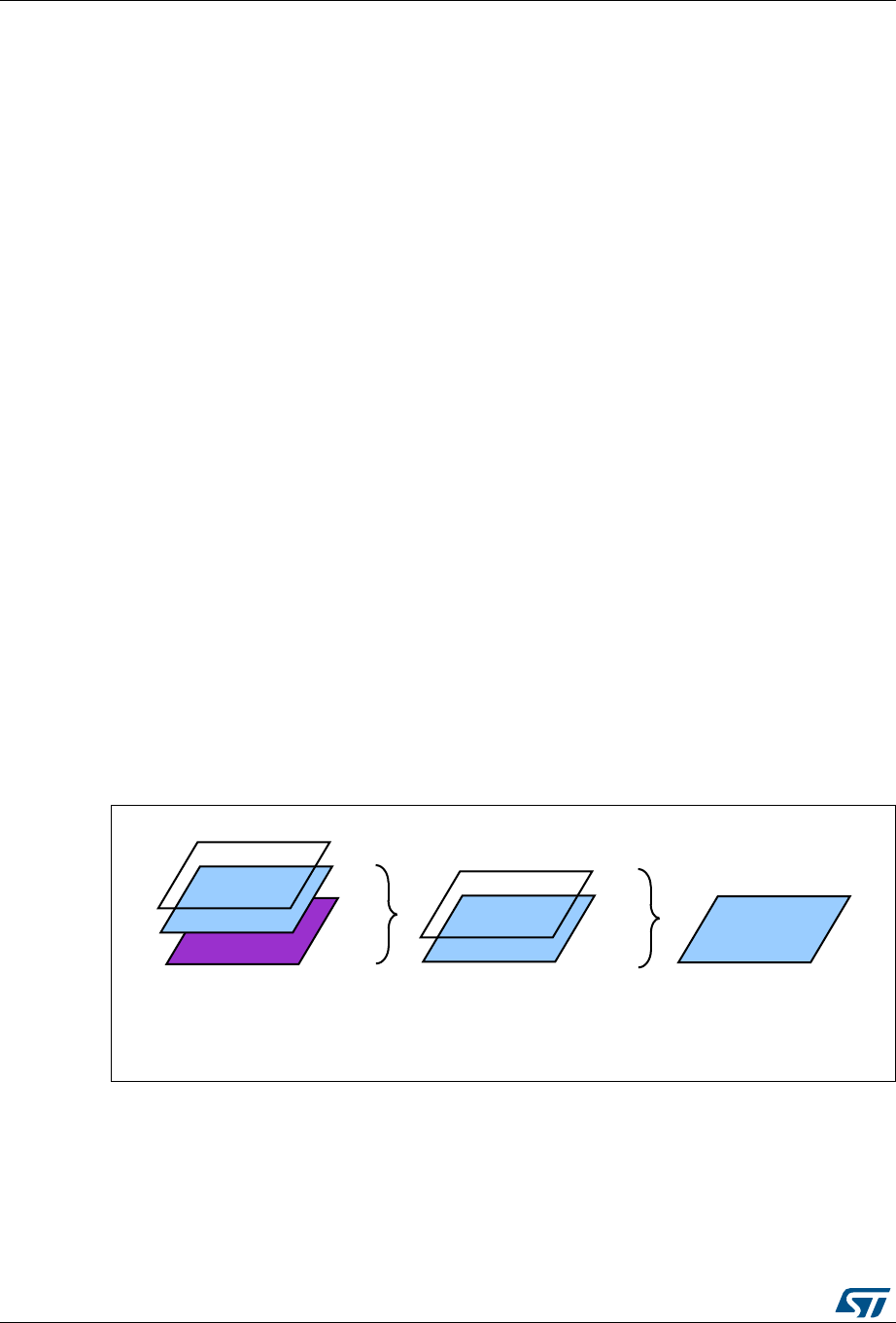
LCD-TFT Controller (LTDC) RM0090
486/1718 DocID018909 Rev 9
Color Frame Buffer Address
Every Layer has a start address for the color frame buffer configured through the
LTDC_LxCFBAR register.
When a layer is enabled, the data is fetched from the Color Frame Buffer.
Color Frame Buffer Length
Every layer has a total line length setting for the color frame buffer in bytes and a number of
lines in the frame buffer configurable in the LTDC_LxCFBLR and LTDC_LxCFBLNR
register respectively.
The line length and the number of lines settings are used to stop the prefetching of data to
the layer FIFO at the end of the frame buffer.
•If it is set to less bytes than required, a FIFO underrun interrupt is generated if it has
been previously enabled.
•If it is set to more bytes than actually required, the useless data read from the FIFO is
discarded. The useless data is not displayed.
Color Frame Buffer Pitch
Every layer has a configurable pitch for the color frame buffer, which is the distance between
the start of one line and the beginning of the next line in bytes. It is configured through the
LTDC_LxCFBLR register.
Layer Blending
The blending is always active and the two layers can be blended following the blending
factors configured through the LTDC_LxBFCR register.
The blending order is fixed and it is bottom up. If two layers are enabled, first the Layer1 is
blended with the Background color, then the Layer2 is blended with the result of blended
color of Layer1 and the background. Refer to Figure 84.
Figure 84. Blending two layers with background
069
/D\HU
/D\HU
%*
/D\HU
/D\HU%*
/D\HU
/D\HU%*

DocID018909 Rev 9 487/1718
RM0090 LCD-TFT Controller (LTDC)
509
Default color
Every layer can have a default color in the format ARGB which is used outside the defined
layer window or when a layer is disabled.
The default color is configured through the LTDC_LxDCCR register.
The blending is always performed between the two layers even when a layer is disabled. To
avoid displaying the default color when a layer is disabled, keep the blending factors of this
layer in the LTDC_LxBFCR register to their reset value.
Color Keying
A color key (RGB) can be configured to be representative for a transparent pixel.
If the Color Keying is enabled, the current pixels (after format conversion and before
blending) are compared to the color key. If they match for the programmed RGB value, all
channels (ARGB) of that pixel are set to 0.
The Color Key value can be configured and used at run-time to replace the pixel RGB value.
The Color Keying is enabled through the LTDC_LxCKCR register.
16.5 LTDC interrupts
The LTDC provides four maskable interrupts logically ORed to two interrupt vectors.
The interrupt sources can be enabled or disabled separately through the LRDC_IER
register. Setting the appropriate mask bit to 1 enables the corresponding interrupt.
The two interrupts are generated on the following events:
•Line interrupt: generated when a programmed line is reached. The line interrupt
position is programmed in the LTDC_LIPCR register
•Register Reload interrupt: generated when the shadow registers reload was performed
during the vertical blanking period
•FIFO Underrun interrupt: generated when a pixel is requested from an empty layer
FIFO
•Transfer Error interrupt: generated when an AHB bus error occurs during data transfer
Those interrupts events are connected to the NVIC controller as described in the figure
below.
Figure 85. Interrupt events
/LQH
5HJLVWHU5HORDG /7'&JOREDOLQWHUUXSW
069
),)28QGHUUXQ
7UDQVIHUHUURU /7'&JOREDO(UURULQWHUUXSW

LCD-TFT Controller (LTDC) RM0090
488/1718 DocID018909 Rev 9
16.6 LTDC programming procedure
•Enable the LTDC clock in the RCC register
•Configure the required Pixel clock following the panel datasheet
•Configure the Synchronous timings: VSYNC, HSYNC, Vertical and Horizontal back
porch, active data area and the front porch timings following the panel datasheet as
described in the Section 16.4.1: LTDC Global configuration parameters
•Configure the synchronous signals and clock polarity in the LTDC_GCR register
•If needed, configure the background color in the LTDC_BCCR register
•Configure the needed interrupts in the LTDC_IER and LTDC_LIPCR register
•Configure the Layer1/2 parameters by programming:
– The Layer window horizontal and vertical position in the LTDC_LxWHPCR and
LTDC_WVPCR registers. The layer window must be in the active data area.
– The pixel input format in the LTDC_LxPFCR register
– The color frame buffer start address in the LTDC_LxCFBAR register
– The line length and pitch of the color frame buffer in the LTDC_LxCFBLR register
– The number of lines of the color frame buffer in the LTDC_LxCFBLNR register
– if needed, load the CLUT with the RGB values and its address in the
LTDC_LxCLUTWR register
– If needed, configure the default color and the blending factors respectively in the
LTDC_LxDCCR and LTDC_LxBFCR registers
•Enable Layer1/2 and if needed the CLUT in the LTDC_LxCR register
•If needed, dithering and color keying can be enabled respectively in the LTDC_GCR
and LTDC_LxCKCR registers. It can be also enabled on the fly.
•Reload the shadow registers to active register through the LTDC_SRCR register.
•Enable the LCD-TFT controller in the LTDC_GCR register.
•All layer parameters can be modified on the fly except the CLUT. The new configuration
has to be either reloaded immediately or during vertical blanking period by configuring
the LTDC_SRCR register.
Note: All layer’s registers are shadowed. Once a register is written, it should not be modified again
before the reload has been done. Thus, a new write to the same register will override the
previous configuration if not yet reloaded.
Table 90. LTDC interrupt requests
Interrupt event Event flag Enable Control bit
Line LIF LIE
Register Reload RRIF RRIEN
FIFO Underrun FUDERRIF FUDERRIE
Transfer Error TERRIF TERRIE
DocID018909 Rev 9 489/1718
RM0090 LCD-TFT Controller (LTDC)
509
16.7 LTDC registers
16.7.1 LTDC Synchronization Size Configuration Register (LTDC_SSCR)
This register defines the number of Horizontal Synchronization pixels minus 1 and the
number of Vertical Synchronization lines minus 1. Refer to Figure 82 and Section 16.4:
LTDC programmable parameters for an example of configuration.
Address offset: 0x08
Reset value: 0x0000 0000
16.7.2 LTDC Back Porch Configuration Register (LTDC_BPCR)
This register defines the accumulated number of Horizontal Synchronization and back porch
pixels minus 1 (HSYNC Width + HBP- 1) and the accumulated number of Vertical
Synchronization and back porch lines minus 1 (VSYNC Height + VBP - 1). Refer to
Figure 82 and Section 16.4: LTDC programmable parameters for an example of
configuration.
Address offset: 0x0C
Reset value: 0x0000 0000
31 30 29 28 27 26 25 24 23 22 21 20 19 18 17 16
Reserved HSW
rw rw rw rw rw rw rw rw rw rw rw rw
15 14 13 12 11 10 9 8 7 6 5 4 3 2 1 0
Reserved VSH
rw rw rw rw rw rw rw rw rw rw rw
Bits 31:28 Reserved, must be kept at reset value
Bits 27:16 HSW[11:0]: Horizontal Synchronization Width (in units of pixel clock period)
These bits define the number of Horizontal Synchronization pixel minus 1.
Bits 15:11 Reserved, must be kept at reset value
Bits 10:0 VSH[10:0]: Vertical Synchronization Height (in units of horizontal scan line)
These bits define the vertical Synchronization height minus 1. It represents the
number
of horizontal synchronization lines.
31 30 29 28 27 26 25 24 23 22 21 20 19 18 17 16
Reserved AHBP
rw rw rw rw rw rw rw rw rw rw rw rw
15 14 13 12 11 10 9 8 7 6 5 4 3 2 1 0
Reserved AVBP
rw rw rw rw rw rw rw rw rw rw rw

LCD-TFT Controller (LTDC) RM0090
490/1718 DocID018909 Rev 9
16.7.3 LTDC Active Width Configuration Register (LTDC_AWCR)
This register defines the accumulated number of Horizontal Synchronization, back porch
and Active pixels minus 1 (HSYNC width + HBP + Active Width - 1) and the accumulated
number of Vertical Synchronization, back porch lines and Active lines minus 1 (VSYNC
Height+ BVBP + Active Height - 1). Refer to Figure 82 and Section 16.4: LTDC
programmable parameters for an example of configuration.
Address offset: 0x10
Reset value: 0x0000 0000
Bits 31:28 Reserved, must be kept at reset value
Bits 27:16 AHBP[11:0]: Accumulated Horizontal back porch (in units of pixel clock period)
These bits define the Accumulated Horizontal back porch width which includes the
Horizontal Synchronization and Horizontal back porch pixels minus 1.
The Horizontal back porch is the period between Horizontal Synchronization going
inactive and the start of the active display part of the next scan line.
Bits 15:11 Reserved, must be kept at reset value
Bits 10:0 AVBP[10:0]: Accumulated Vertical back porch (in units of horizontal scan line)
These bits define the accumulated Vertical back porch width which includes the Vertical
Synchronization and Vertical back porch lines minus 1.
The Vertical back porch is the number of horizontal scan lines at a start of frame to the
start of the first active scan line of the next frame.
31 30 29 28 27 26 25 24 23 22 21 20 19 18 17 16
Reserved AAW
rw rw rw rw rw rw rw rw rw rw rw rw
15 14 13 12 11 10 9 8 7 6 5 4 3 2 1 0
Reserved AAH
rw rw rw rw rw rw rw rw rw rw rw
Bits 31:28 Reserved, must be kept at reset value
Bits 27:16 AAW[11:0]: Accumulated Active Width (in units of pixel clock period)
These bits define the Accumulated Active Width which includes the Horizontal
Synchronization, Horizontal back porch and Active pixels minus 1.
The Active Width is the number of pixels in active display area of the panel scan line. The
maximum Active Width supported is 0x400.
Bits 15:11 Reserved, must be kept at reset value
Bits 10:0 AAH[10:0]: Accumulated Active Height (in units of horizontal scan line)
These bits define the Accumulated Height which includes the Vertical Synchronization,
Vertical back porch and the Active Height lines minus 1. The Active Height is the number
of active lines in the panel. The maximum Active Height supported is 0x300.
DocID018909 Rev 9 491/1718
RM0090 LCD-TFT Controller (LTDC)
509
16.7.4 LTDC Total Width Configuration Register (LTDC_TWCR)
This register defines the accumulated number of Horizontal Synchronization, back porch,
Active and front porch pixels minus 1 (HSYNC Width + HBP + Active Width + HFP - 1) and
the accumulated number of Vertical Synchronization, back porch lines, Active and Front
lines minus 1 (VSYNC Height+ BVBP + Active Height + VFP - 1). Refer to Figure 82 and
Section 16.4: LTDC programmable parameters for an example of configuration.
Address offset: 0x14
Reset value: 0x0000 0000
16.7.5 LTDC Global Control Register (LTDC_GCR)
This register defines the global configuration of the LCD-TFT controller.
Address offset: 0x18
Reset value: 0x0000 2220
31 30 29 28 27 26 25 24 23 22 21 20 19 18 17 16
Reserved TOTALW
rw rw rw rw rw rw rw rw rw rw rw rw
16 14 13 12 11 10 9 8 7 6 5 4 3 2 1 0
Reserved TOTALH
rw rw rw rw rw rw rw rw rw rw rw
Bits 31:28 Reserved, must be kept at reset value
Bits 27:16 TOTALW[11:0]: Total Width (in units of pixel clock period)
These bits defines the accumulated Total Width which includes the Horizontal
Synchronization, Horizontal back porch, Active Width and Horizontal front porch pixels
minus 1.
Bits 15:11 Reserved, must be kept at reset value
Bits 10:0 TOTALH[10:0]: Total Height (in units of horizontal scan line)
These bits defines the accumulated Height which includes the Vertical Synchronization,
Vertical back porch, the Active Height and Vertical front porch Height lines minus 1.
31 30 29 28 27 26 25 24 23 22 21 20 19 18 17 16
HSPOL VSPOL DEPOL PCPOL Reserved DEN
rw rw rw rw rw
15 14 13 12 11 10 9 8 7 6 5 4 3 2 1 0
Reserve
d
DRW Reser
ved
DGW Reser
ved
DBW Reserved LTDCEN
rrr rrr rrr rw

LCD-TFT Controller (LTDC) RM0090
492/1718 DocID018909 Rev 9
Bit 31 HSPOL: Horizontal Synchronization Polarity
This bit is set and cleared by software.
0: Horizontal Synchronization polarity is active low
1: Horizontal Synchronization polarity is active high
Bit 30 VSPOL: Vertical Synchronization Polarity
This bit is set and cleared by software.
0: Vertical Synchronization is active low
1: Vertical Synchronization is active high
Bit 29 DEPOL: Data Enable Polarity
This bit is set and cleared by software.
0: Data Enable polarity is active low
1: Data Enable polarity is active high
Bit 28 PCPOL: Pixel Clock Polarity
This bit is set and cleared by software.
0: input pixel clock
1: inverted input pixel clock
Bits 27:17 Reserved, must be kept at reset value
Bit 16 DEN: Dither Enable
This bit is set and cleared by software.
0: Dither disable
1: Dither enable
Bit 15 Reserved, must be kept at reset value
Bits 14:12 DRW[2:0]: Dither Red Width
These bits return the Dither Red Bits
Bit 11 Reserved, must be kept at reset value
Bits 10:8 DGW[2:0]: Dither Green Width
These bits return the Dither Green Bits
Bit 7 Reserved, must be kept at reset value
Bits 6:4 DBW[2:0]: Dither Blue Width
These bits return the Dither Blue Bits
Bits 3:1 Reserved, must be kept at reset value
Bit 0 LTDCEN: LCD-TFT controller enable bit
This bit is set and cleared by software.
0: LTDC disable
1: LTDC enable
DocID018909 Rev 9 493/1718
RM0090 LCD-TFT Controller (LTDC)
509
16.7.6 LTDC Shadow Reload Configuration Register (LTDC_SRCR)
This register allows to reload either immediately or during the vertical blanking period, the
shadow registers values to the active registers. The shadow registers are all Layer1 and
Layer2 registers except the LTDC_L1CLUTWR and the LTDC_L2CLUTWR.
Address offset: 0x24
Reset value: 0x0000 0000
Note: The shadow registers read back the active values. Until the reload has been done, the 'old'
value will be read.
16.7.7 LTDC Background Color Configuration Register (LTDC_BCCR)
This register defines the background color (RGB888).
Address offset: 0x2C
Reset value: 0x0000 0000
31 30 29 28 27 26 25 24 23 22 21 20 19 18 17 16
Reserved
15 14 13 12 11 10 9 8 7 6 5 4 3 2 1 0
Reserved
VBR IMR
rw rw
Bits 31:2 Reserved, must be kept at reset value
Bit 1 VBR: Vertical Blanking Reload
This bit is set by software and cleared only by hardware after reload. (it cannot
be cleared through register write once it is set)
0: No effect
1: The shadow registers are reloaded during the vertical blanking period (at the
beginning of the first line after the Active Display Area)
Bit 0 IMR: Immediate Reload
This bit is set by software and cleared only by hardware after reload.
0: No effect
1: The shadow registers are reloaded immediately
31 30 29 28 27 26 25 24 23 22 21 20 19 18 17 16
Reserved BCRED
rw rw rw rw rw rw rw rw
15 14 13 12 11 10 9 8 7 6 5 4 3 2 1 0
BCGREEN BCBLUE
rw rw rw rw rw rw rw rw rw

LCD-TFT Controller (LTDC) RM0090
494/1718 DocID018909 Rev 9
16.7.8 LTDC Interrupt Enable Register (LTDC_IER)
This register determines which status flags generate an interrupt request by setting the
corresponding bit to 1.
Address offset: 0x34
Reset value: 0x0000 0000
Bits 31:24 Reserved, must be kept at reset value
Bits 23:16 BCRED[7:0]: Background Color Red value
These bits configure the background red value
Bits 15:8 BCGREEN[7:0]: Background Color Green value
These bits configure the background green value
Bits 7:0 BCBLUE[7:0]: Background Color Blue value
These bits configure the background blue value
31 30 29 28 27 26 25 24 23 22 21 20 19 18 17 16
Reserved
15 14 13 12 11 10 9 8 7 6 5 4 3 2 1 0
Reserved
RRIE TERRIE FUIE LIE
rw rw rw rw
Bits 31:4 Reserved, must be kept at reset value
Bit 3 RRIE: Register Reload interrupt enable
This bit is set and cleared by software
0: Register Reload interrupt disable
1: Register Reload interrupt enable
Bit 2 TERRIE: Transfer Error Interrupt Enable
This bit is set and cleared by software
0: Transfer Error interrupt disable
1: Transfer Error interrupt enable
Bit 1 FUIE: FIFO Underrun Interrupt Enable
This bit is set and cleared by software
0: FIFO Underrun interrupt disable
1: FIFO Underrun Interrupt enable
Bit 0 LIE: Line Interrupt Enable
This bit is set and cleared by software
0: Line interrupt disable
1: Line Interrupt enable
DocID018909 Rev 9 495/1718
RM0090 LCD-TFT Controller (LTDC)
509
16.7.9 LTDC Interrupt Status Register (LTDC_ISR)
This register returns the interrupt status flag
Address offset: 0x38
Reset value: 0x0000 0000
16.7.10 LTDC Interrupt Clear Register (LTDC_ICR)
Address offset: 0x3C
Reset value: 0x0000 0000
31 30 29 28 27 26 25 24 23 22 21 20 19 18 17 16
Reserved
15 14 13 12 11 10 9 8 7 6 5 4 3 2 1 0
Reserved RRIF TERRIF FUIF LIF
rrrr
Bits 31:24 Reserved, must be kept at reset value
Bit 3 RRIF: Register Reload Interrupt Flag
0: No Register Reload interrupt generated
1: Register Reload interrupt generated when a vertical blanking reload occurs (and the
first line after the active area is reached)
Bit 2 TERRIF: Transfer Error interrupt flag
0: No Transfer Error interrupt generated
1: Transfer Error interrupt generated when a Bus error occurs
Bit 1 FUIF: FIFO Underrun Interrupt flag
0: NO FIFO Underrun interrupt generated.
1: A FIFO underrun interrupt is generated, if one of the layer FIFOs is empty and pixel
data is read from the FIFO
Bit 0 LIF: Line Interrupt flag
0: No Line interrupt generated
1: A Line interrupt is generated, when a programmed line is reached
31 30 29 28 27 26 25 24 23 22 21 20 19 18 17 16
Reserved
15 14 13 12 11 10 9 8 7 6 5 4 3 2 1 0
Reserved CRRIF CTERRIF CFUIF CLIF
wwww
LCD-TFT Controller (LTDC) RM0090
496/1718 DocID018909 Rev 9
16.7.11 LTDC Line Interrupt Position Configuration Register (LTDC_LIPCR)
This register defines the position of the line interrupt. The line value to be programmed
depends on the timings parameters. Refer to Figure 82.
Address offset: 0x40
Reset value: 0x0000 0000
16.7.12 LTDC Current Position Status Register (LTDC_CPSR)
Address offset: 0x44
Reset value: 0x0000 0000
Bits 31:24 Reserved, must be kept at reset value
Bit 3 CRRIF: Clears Register Reload Interrupt Flag
0: No effect
1: Clears the RRIF flag in the LTDC_ISR register
Bit 2 CTERRIF: Clears the Transfer Error Interrupt Flag
0: No effect
1: Clears the TERRIF flag in the LTDC_ISR register.
Bit 1 CFUIF: Clears the FIFO Underrun Interrupt flag
0: No effect
1: Clears the FUDERRIF flag in the LTDC_ISR register.
Bit 0 CLIF: Clears the Line Interrupt Flag
0: No effect
1: Clears the LIF flag in the LTDC_ISR register.
31 30 29 28 27 26 25 24 23 22 21 20 19 18 17 16
Reserved
15 14 13 12 11 10 9 8 7 6 5 4 3 2 1 0
Reserved
LIPOS
rw rw rw rw rw rw rw rw rw rw rw
Bits 31:11 Reserved, must be kept at reset value
Bits 10:0 LIPOS[10:0]: Line Interrupt Position
These bits configure the line interrupt position
31 30 29 28 27 26 25 24 23 22 21 20 19 18 17 16
CXPOS
r rrrr r r r r r r r r r r r
15 14 13 12 11 10 9 8 7 6 5 4 3 2 1 0
CYPOS
r rrrr r r r r r r r r r r r

DocID018909 Rev 9 497/1718
RM0090 LCD-TFT Controller (LTDC)
509
16.7.13 LTDC Current Display Status Register (LTDC_CDSR)
This register returns the status of the current display phase which is controlled by the
HSYNC, VSYNC, and Horizontal/Vertical DE signals.
Example: if the current display phase is the vertical synchronization, the VSYNCS bit is set
(active high). If the current display phase is the horizontal synchronization, the HSYNCS bit
is active high.
Address offset: 0x48
Reset value: 0x0000 000F
Note: The returned status does not depend on the configured polarity in the LTDC_GCR register,
instead it returns the current active display phase.
Bits 31:16: CXPOS[15:0]: Current X Position
These bits return the current X position
Bits 15:0 CYPOS[15:0]: Current Y Position
These bits return the current Y position
31 30 29 28 27 26 25 24 23 22 21 20 19 18 17 16
Reserved
15 14 13 12 11 10 9 8 7 6 5 4 3 2 1 0
Reserved
HSYNC
S
VSYNC
SHDES VDES
rrrr
Bits 31:24 Reserved, must be kept at reset value
Bit 3 HSYNCS: Horizontal Synchronization display Status
0: Active low
1: Active high
Bit 2 VSYNCS: Vertical Synchronization display Status
0: Active low
1: Active high
Bit 1 HDES: Horizontal Data Enable display Status
0: Active low
1: Active high
Bit 0 VDES: Vertical Data Enable display Status
0: Active low
1: Active high

LCD-TFT Controller (LTDC) RM0090
498/1718 DocID018909 Rev 9
16.7.14 LTDC Layerx Control Register (LTDC_LxCR) (where x=1..2)
Address offset: 0x84 + 0x80 x (Layerx -1), Layerx = 1 or 2
Reset value: 0x0000 0000
16.7.15 LTDC Layerx Window Horizontal Position Configuration Register
(LTDC_LxWHPCR) (where x=1..2)
This register defines the Horizontal Position (first and last pixel) of the layer 1 or 2 window.
The first visible pixel of a line is the programmed value of AHBP[10:0] bits + 1 in the
LTDC_BPCR register.
The last visible pixel of a line is the programmed value of AAW[10:0] bits in the
LTDC_AWCR register. All values within this range are allowed.
Address offset: 0x88 + 0x80 x (Layerx -1), Layerx = 1 or 2
Reset value: 0x0000 0000
31 30 29 28 27 26 25 24 23 22 21 20 19 18 17 16
Reserved
15 14 13 12 11 10 9 8 7 6 5 4 3 2 1 0
Reserved CLUTEN Reserved COLKEN LEN
rw rw rw
Bits 31:5 Reserved, must be kept at reset value
Bit 4 CLUTEN: Color Look-Up Table Enable
This bit is set and cleared by software.
0: Color Look-Up Table disable
1: Color Look-Up Table enable
The CLUT is only meaningful for L8, AL44 and AL88 pixel format. Refer to Color Look-Up
Table (CLUT) on page 485
Bit 3 Reserved, must be kept at reset value
Bit 2 Reserved, must be kept at reset value
Bit 1 COLKEN: Color Keying Enable
This bit is set and cleared by software.
0: Color Keying disable
1: Color Keying enable
Bit 0 LEN: Layer Enable
This bit is set and cleared by software.
0: Layer disable
1: Layer enable
DocID018909 Rev 9 499/1718
RM0090 LCD-TFT Controller (LTDC)
509
Example:
The LTDC_BPCR register is configured to 0x000E0005(AHBP[11:0] is 0xE) and the
LTDC_AWCR register is configured to 0x028E01E5(AAW[11:0] is 0x28E). To configure the
horizontal position of a window size of 630x460, with horizontal start offset of 5 pixels in the
Active data area.
1. Layer window first pixel: WHSTPOS[11:0] should be programmed to 0x14 (0xE+1+0x5)
2. Layer window last pixel: WHSPPOS[11:0] should be programmed to 0x28A
16.7.16 LTDC Layerx Window Vertical Position Configuration Register
(LTDC_LxWVPCR) (where x=1..2)
This register defines the vertical position (first and last line) of the layer1 or 2 window.
The first visible line of a frame is the programmed value of AVBP[10:0] bits + 1 in the
register LTDC_BPCR register.
The last visible line of a frame is the programmed value of AAH[10:0] bits in the
LTDC_AWCR register. All values within this range are allowed.
Address offset: 0x8C + 0x80 x (Layerx -1), Layerx = 1 or 2
Reset value: 0x0000 0000
31 30 29 28 27 26 25 24 23 22 21 20 19 18 17 16
Reserved
WHSPPOS
rw rw rw rw rw rw rw rw rw rw rw rw
15 14 13 12 11 10 9 8 7 6 5 4 3 2 1 0
Reserved
WHSTPOS
rw rw rw rw rw rw rw rw rw rw rw rw
Bits 31:28 Reserved, must be kept at reset value
Bits 27:16 WHSPPOS[11:0]: Window Horizontal Stop Position
These bits configure the last visible pixel of a line of the layer window.
Bits 15:12 Reserved, must be kept at reset value
Bits 11:0 WHSTPOS[11:0]: Window Horizontal Start Position
These bits configure the first visible pixel of a line of the layer window.
31 30 29 28 27 26 25 24 23 22 21 20 19 18 17 16
Reserved
WVSPPOS
rw rw rw rw rw rw rw rw rw rw rw
15 14 13 12 11 10 9 8 7 6 5 4 3 2 1 0
Reserved
WVSTPOS
rw rw rw rw rw rw rw rw rw rw rw

LCD-TFT Controller (LTDC) RM0090
500/1718 DocID018909 Rev 9
Example:
The LTDC_BPCR register is configured to 0x000E0005 (AVBP[10:0] is 0x5) and the
LTDC_AWCR register is configured to 0x028E01E5 (AAH[10:0] is 0x1E5). To configure the
vertical position of a window size of 630x460, with vertical start offset of 8 lines in the Active
data area:
1. Layer window first line: WVSTPOS[10:0] should be programmed to 0xE (0x5 + 1 + 0x8)
2. Layer window last line: WVSPPOS[10:0] should be programmed to 0x1DA
16.7.17 LTDC Layerx Color Keying Configuration Register (LTDC_LxCKCR)
(where x=1..2)
This register defines the color key value (RGB), which is used by the Color Keying.
Address offset: 0x90 + 0x80 x (Layerx -1), Layerx = 1 or 2
Reset value: 0x0000 0000
Bits 31:27 Reserved, must be kept at reset value
Bits 26:16 WVSPPOS[10:0]: Window Vertical Stop Position
These bits configures the last visible line of the layer window.
Bits 15:11 Reserved, must be kept at reset value
Bits 10:0 WVSTPOS[10:0]: Window Vertical Start Position
These bits configure the first visible line of the layer window.
31 30 29 28 27 26 25 24 23 22 21 20 19 18 17 16
Reserved CKRED
rw rw rw rw rw rw rw rw
15 14 13 12 11 10 9 8 7 6 5 4 3 2 1 0
CKGREEN CKBLUE
rw rw rw rw rw rw rw rw rw
Bits 31:24 Reserved, must be kept at reset value
Bits 23:16 CKRED[7:0]: Color Key Red value
Bits 15:8 CKGREEN[7:0]: Color Key Green value
Bits 7:0 CKBLUE[7:0]: Color Key Blue value

DocID018909 Rev 9 501/1718
RM0090 LCD-TFT Controller (LTDC)
509
16.7.18 LTDC Layerx Pixel Format Configuration Register (LTDC_LxPFCR)
(where x=1..2)
This register defines the pixel format which is used for the stored data in the frame buffer of
a layer. The pixel data is read from the frame buffer and then transformed to the internal
format 8888 (ARGB).
Address offset: 0x94 + 0x80 x (Layerx -1), Layerx = 1 or 2
Reset value: 0x0000 0000
16.7.19 LTDC Layerx Constant Alpha Configuration Register (LTDC_LxCACR)
(where x=1..2)
This register defines the constant alpha value (divided by 255 by Hardware), which is used
in the alpha blending. Refer to LTDC_LxBFCR register.
Address offset: 0x98 + 0x80 x (Layerx -1), Layerx = 1 or 2
Reset value: (Layerx -1) 0x0000 00FF
31 30 29 28 27 26 25 24 23 22 21 20 19 18 17 16
Reserved
15 14 13 12 11 10 9 8 7 6 5 4 3 2 1 0
Reserved PF
rw rw rw
Bits 31:3 Reserved, must be kept at reset value
Bits 2:0 PF[2:0]: Pixel Format
These bits configures the Pixel format
000: ARGB8888
001: RGB888
010: RGB565
011: ARGB1555
100: ARGB4444
101: L8 (8-Bit Luminance)
110: AL44 (4-Bit Alpha, 4-Bit Luminance)
111: AL88 (8-Bit Alpha, 8-Bit Luminance)
31 30 29 28 27 26 25 24 23 22 21 20 19 18 17 16
Reserved
15 14 13 12 11 10 9 8 7 6 5 4 3 2 1 0
Reserved
CONSTA
rw rw rw rw rw rw rw rw

LCD-TFT Controller (LTDC) RM0090
502/1718 DocID018909 Rev 9
16.7.20 LTDC Layerx Default Color Configuration Register (LTDC_LxDCCR)
(where x=1..2)
This register defines the default color of a layer in the format ARGB. The default color is
used outside the defined layer window or when a layer is disabled. The reset value of
0x00000000 defines a transparent black color.
Address offset: 0x9C + 0x80 x (Layerx -1), Layerx = 1 or 2
Reset value: 0x0000 0000
Bits 31:8 Reserved, must be kept at reset value
Bits 7:0 CONSTA[7:0]: Constant Alpha
These bits configure the Constant Alpha used for blending. The Constant Alpha is divided
by 255 by hardware.
Example: if the programmed Constant Alpha is 0xFF, the Constant Alpha value is
255/255=1
31 30 29 28 27 26 25 24 23 22 21 20 19 18 17 16
DCALPHA DCRED
rw rw rw rw rw rw rw rw rw
15 14 13 12 11 10 9 8 7 6 5 4 3 2 1 0
DCGREEN DCBLUE
rw rw rw rw rw rw rw rw rw
Bits 31:24 DCALPHA[7:0]: Default Color Alpha
These bits configure the default alpha value
Bits 23:16 DCRED[7:0]: Default Color Red
These bits configure the default red value
Bits 15:8 DCGREEN[7:0]: Default Color Green
These bits configure the default green value
Bits 7:0 DCBLUE[7:0]: Default Color Blue
These bits configure the default blue value

DocID018909 Rev 9 503/1718
RM0090 LCD-TFT Controller (LTDC)
509
16.7.21 LTDC Layerx Blending Factors Configuration Register (LTDC_LxBFCR)
(where x=1..2)
This register defines the blending factors F1 and F2.
The general blending formula is: BC = BF1 x C + BF2 x Cs
•BC = Blended color
•BF1 = Blend Factor 1
•C = Current layer color
•BF2 = Blend Factor 2
•Cs = subjacent layers blended color
Address offset: 0xA0 + 0x80 x (Layerx -1), Layerx = 1 or 2
Reset value: 0x0000 0607
31 30 29 28 27 26 25 24 23 22 21 20 19 18 17 16
Reserved
15 14 13 12 11 10 9 8 7 6 5 4 3 2 1 0
Reserved
BF1
Reserved
BF2
rw rw rw rw rw rw
Bits 31:11 Reserved, must be kept at reset value
Bits 10:8 BF1[2:0]: Blending Factor 1
These bits select the blending factor F1
000: Reserved
001: Reserved
010: Reserved
011: Reserved
100: Constant Alpha
101: Reserved
110: Pixel Alpha x Constant Alpha
111:Reserved
Bits 7:3 Reserved, must be kept at reset value
Bits 2:0 BF2[2:0]: Blending Factor 2
These bits select the blending factor F2
000: Reserved
001: Reserved
010: Reserved
011: Reserved
100: Reserved
101: 1 - Constant Alpha
110: Reserved
111: 1 - (Pixel Alpha x Constant Alpha)

LCD-TFT Controller (LTDC) RM0090
504/1718 DocID018909 Rev 9
Note: The Constant Alpha value, is the programmed value in the LxCACR register divided by 255
by hardware.
Example: Only layer1 is enabled, BF1 configured to Constant Alpha
BF2 configured to 1 - Constant Alpha
Constant Alpha: The Constant Alpha programmed in the LxCACR register is 240 (0xF0).
Thus, the Constant Alpha value is 240/255 = 0.94
C: Current Layer Color is 128
Cs: Background color is 48
Layer1 is blended with the background color.
BC = Constant Alpha x C + (1 - Constant Alpha) x Cs = 0.94 x 128 + (1- 0.94) x 48 = 123.
16.7.22 LTDC Layerx Color Frame Buffer Address Register (LTDC_LxCFBAR)
(where x=1..2)
This register defines the color frame buffer start address which has to point to the address
where the pixel data of the top left pixel of a layer is stored in the frame buffer.
Address offset: 0xAC + 0x80 x (Layerx -1), Layerx = 1 or 2
Reset value: 0x0000 0000
16.7.23 LTDC Layerx Color Frame Buffer Length Register (LTDC_LxCFBLR)
(where x=1..2)
This register defines the color frame buffer line length and pitch.
Address offset: 0xB0 + 0x80 x (Layerx -1), Layerx = 1 or 2
Reset value: 0x0000 0000
31 30 29 28 27 26 25 24 23 22 21 20 19 18 17 16
CFBADD
rw rw rw rw rw rw rw rw rw rw rw rw rw rw rw rw
15 14 13 12 11 10 9 8 7 6 5 4 3 2 1 0
CFBADD
rw rw rw rw rw rw rw rw rw rw rw rw rw rw rw rw
Bits 31:0 CFBADD[31:0]: Color Frame Buffer Start Address
These bits defines the color frame buffer start address.
31 30 29 28 27 26 25 24 23 22 21 20 19 18 17 16
Reserved CFBP
rw rw rw rw rw rw rw rw rw rw rw rw rw
15 14 13 12 11 10 9 8 7 6 5 4 3 2 1 0
Reserved CFBLL
rw rw rw rw rw rw rw rw rw rw rw rw rw

DocID018909 Rev 9 505/1718
RM0090 LCD-TFT Controller (LTDC)
509
Example:
•A frame buffer having the format RGB565 (2 bytes per pixel) and a width of 256 pixels
(total number of bytes per line is 256x2=512 bytes), where pitch = line length requires a
value of 0x02000203 to be written into this register.
•A frame buffer having the format RGB888 (3 bytes per pixel) and a width of 320 pixels
(total number of bytes per line is 320x3=960), where pitch = line length requires a value
of 0x03C003C3 to be written into this register.
16.7.24 LTDC Layerx ColorFrame Buffer Line Number Register
(LTDC_LxCFBLNR) (where x=1..2)
This register defines the number of lines in the color frame buffer.
Address offset: 0xB4 + 0x80 x (Layerx -1), Layerx = 1 or 2
Reset value: 0x0000 0000
Note: The number of lines and line length settings define how much data is fetched per frame for
every layer. If it is configured to less bytes than required, a FIFO underrun interrupt will be
generated if enabled.
The start address and pitch settings on the other hand define the correct start of every line in
memory.
Bits 31:29 Reserved, must be kept at reset valuer
Bits 28:16 CFBP[17:0]: Color Frame Buffer Pitch in bytes
These bits define the pitch which is the increment from the start of one line of pixels to the
start of the next line in bytes.
Bits 15:13 Reserved, must be kept at reset value
Bits 12:0 CFBLL[12:0]: Color Frame Buffer Line Length
These bits define the length of one line of pixels in bytes + 3.
The line length is computed as follows: Active high width x number of bytes per pixel + 3.
31 30 29 28 27 26 25 24 23 22 21 20 19 18 17 16
Reserved
15 14 13 12 11 10 9 8 7 6 5 4 3 2 1 0
Reserved CFBLNBR
rw rw rw rw rw rw rw rw rw rw rw
Bits 31:11 Reserved, must be kept at reset value
Bits 10:0 CFBLNBR[10:0]: Frame Buffer Line Number
These bits define the number of lines in the frame buffer which corresponds to the Active
high width.

LCD-TFT Controller (LTDC) RM0090
506/1718 DocID018909 Rev 9
16.7.25 LTDC Layerx CLUT Write Register (LTDC_LxCLUTWR)
(where x=1..2)
This register defines the CLUT address and the RGB value.
Address offset: 0xC4 + 0x80 x (Layerx -1), Layerx = 1 or 2
Reset value: 0x0000 0000
Note: The CLUT write register should only be configured during blanking period or if the layer is
disabled. The CLUT can be enabled or disabled in the LTDC_LxCR register.
The CLUT is only meaningful for L8, AL44 and AL88 pixel format.
31 30 29 28 27 26 25 24 23 22 21 20 19 18 17 16
CLUTADD RED
wwwwww w w ww w w w w w w
15 14 13 12 11 10 9 8 7 6 5 4 3 2 1 0
GREEN BLUE
wwwwww w w ww w w w w w w
Bits 31:24 CLUTADD[7:0]: CLUT Address
These bits configure the CLUT address (color position within the CLUT) of each RGB
value
Bits 23:16 RED[7:0]: Red value
These bits configure the red value
Bits 15:8 GREEN[7:0]: Green value
These bits configure the green value
Bits 7:0 BLUE[7:0]: Blue value
These bits configure the blue value
DocID018909 Rev 9 507/1718
RM0090 LCD-TFT Controller (LTDC)
509
16.7.26 LTDC register map
The following table summarizes the LTDC registers. Refer to the register boundary
addresses table for the LTDC register base address.
Table 91. LTDC register map and reset values
Offset Register
31
30
29
28
27
26
25
24
23
22
21
20
19
18
17
16
15
14
13
12
11
10
9
8
7
6
5
4
3
2
1
0
0x0008 LTDC_SSCR Reserved
HSW
Reserved
VSH
Reset value 0000000000 00000000000
0x000C LTDC_BPCR Reserved
AHBP
Reserved
AVBP
Reset value 0000000000 00000000000
0x0010 LTDC_AWCR Reserved
AAV
Reserved
AAH
Reset value 0000000000 00000000000
0x0014 LTDC_TWCR Reserved
TOTALW
Reserved
TOTALH
Reset value 0000000000 00000000000
0x0018 LTDC_GCR
HSPOL
VSPOL
DEPOL
PCPOL
Reserve
DEN
Reserved
DRW
Reserved
DGW
Reserved
DBW
Reserved
LTDCEN
Reset value 0000 0 010 010 010 0
0x0024 LTDC_SRCR Reserved
VBR
IMR
Reset value 00
0x002C LTDC_BCCR Reserved
BC
Reset value 000000000000000000000000
0x0034 LTDC_IER Reserved
RRIE
TERRIE
FUIE
LIE
Reset value 0000
0x0038 LTDC_ISR Reserved
RRIF
TERRIF
FUIF
LIF
Reset value 0000
0x003C LTDC_ICR Reserved
CRRIF
CTERRIF
CFUIF
CLIF
Reset value 0000
0x0040 LTDC_LIPCR Reserved
LIPOS
Reset value 00000000000
0x0044 LTDC_CPSR
CXPOS
CYPOS
Reset value 00000000000000000000000000000000
0x0048 LTDC_CDSR Reserved
HSYNCS
VSYNCS
HDES
VDES
Reset value 1111
0x0084 LTDC_L1CR Reserved
CLUTEN
Reserved
COLKEN
LEN
Reset value 000
0x0088 LTDC_L1WHPCR Reserved
WHSPPOS
Reserved
WHSTPOS
Reset value 000000000000 000000000000
LCD-TFT Controller (LTDC) RM0090
508/1718 DocID018909 Rev 9
0x008C LTDC_L1WVPCR Reserved
WVSPPOS
Reserved
WVSTPOS
Reset value 00000000000 00000000000
0x0090 LTDC_L1CKCR Reserved
CKRED
CKGREEN
CKBLUE
Reset value 000000000000000000000000
0x0094 LTDC_L1PFCR Reserved
PF
Reset value 000
0x0098 LTDC_L1CACR Reserved CONSTA
Reset value 11111111
0x009C LTDC_L1DCCR
DCALPHA
DCRED
DCGREEN
DCBLUE
Reset value 00000000000000000000000000000000
0x00A0 LTDC_L1BFCR Reserved
BF1
Reserved
BF2
Reset value 110 111
0x00AC LTDC_L1CFBAR
CFBADD
Reset value 00000000000000000000000000000000
0x00B0 LTDC_L1CFBLR Reserved
CFBP
Reserved
CFBLL
Reset value 0000000000000 0000000000000
0x00B4 LTDC_L1CFBLNR Reserved
CFBLNBR
Reset value 00000000000
0x00C4 LTDC_L1CLUTWR
CLUTADD
RED
GREEN
BLUE
Reset value 00000000000000000000000000000000
0x0104 LTDC_L2CR Reserved
CLUTEN
Reserved
COLKEN
LEN
Reset value 000
0x0108 LTDC_L2WHPCR Reserved
WHSPPOS
Reserved
WHSTPOS
Reset value 000000000000 000000000000
0x010C LTDC_L2WVPCR Reserved
WVSPPOS
Reserved
WVSTPOS
Reset value 00000000000 00000000000
0x0110 LTDC_L2CKCR Reserved
CKRED
CKGREEN
CKBLUE
Reset value 000000000000000000000000
Table 91. LTDC register map and reset values (continued)
Offset Register
31
30
29
28
27
26
25
24
23
22
21
20
19
18
17
16
15
14
13
12
11
10
9
8
7
6
5
4
3
2
1
0
DocID018909 Rev 9 509/1718
RM0090 LCD-TFT Controller (LTDC)
509
0x0114 LTDC_L2PFCR Reserved
PF
Reset value 000
0x0118 LTDC_L2CACR Reserved CONSTA
Reset value 11111111
0x011C LTDC_L2DCCR
DCALPHA
DCRED
DCGREEN
DCBLUE
Reset value 00000000000000000000000000000000
0x0120 LTDC_L2BFCR Reserved BF1 Reserved BF2
Reset value 110 111
0x012C LTDC_L2CFBAR
CFBADD
Reset value 00000000000000000000000000000000
0x0130 LTDC_L2CFBLR Reserved
CFBP
Reserved
CFBLL
Reset value 0000000000000 0000000000000
0x0134 LTDC_L2CFBLNR Reserved
CFBLNBR
Reset value 00000000000
0x0144 LTDC_L2CLUTWR
CLUTADD
RED
GREEN
BLUE
Reset value 00000000000000000000000000000000
Table 91. LTDC register map and reset values (continued)
Offset Register
31
30
29
28
27
26
25
24
23
22
21
20
19
18
17
16
15
14
13
12
11
10
9
8
7
6
5
4
3
2
1
0

Advanced-control timers (TIM1&TIM8) RM0090
510/1718 DocID018909 Rev 9
17 Advanced-control timers (TIM1&TIM8)
This section applies to the whole STM32F4xx family, unless otherwise specified.
17.1 TIM1&TIM8 introduction
The advanced-control timers (TIM1&TIM8) consist of a 16-bit auto-reload counter driven by
a programmable prescaler.
It may be used for a variety of purposes, including measuring the pulse lengths of input
signals (input capture) or generating output waveforms (output compare, PWM,
complementary PWM with dead-time insertion).
Pulse lengths and waveform periods can be modulated from a few microseconds to several
milliseconds using the timer prescaler and the RCC clock controller prescalers.
The advanced-control (TIM1&TIM8) and general-purpose (TIMx) timers are completely
independent, and do not share any resources. They can be synchronized together as
described in Section 17.3.20.

DocID018909 Rev 9 511/1718
RM0090 Advanced-control timers (TIM1&TIM8)
577
17.2 TIM1&TIM8 main features
TIM1&TIM8 timer features include:
•16-bit up, down, up/down auto-reload counter.
•16-bit programmable prescaler allowing dividing (also “on the fly”) the counter clock
frequency either by any factor between 1 and 65536.
•Up to 4 independent channels for:
– Input Capture
– Output Compare
– PWM generation (Edge and Center-aligned Mode)
– One-pulse mode output
•Complementary outputs with programmable dead-time
•Synchronization circuit to control the timer with external signals and to interconnect
several timers together.
•Repetition counter to update the timer registers only after a given number of cycles of
the counter.
•Break input to put the timer’s output signals in reset state or in a known state.
•Interrupt/DMA generation on the following events:
– Update: counter overflow/underflow, counter initialization (by software or
internal/external trigger)
– Trigger event (counter start, stop, initialization or count by internal/external trigger)
– Input capture
– Output compare
– Break input
•Supports incremental (quadrature) encoder and hall-sensor circuitry for positioning
purposes
•Trigger input for external clock or cycle-by-cycle current management
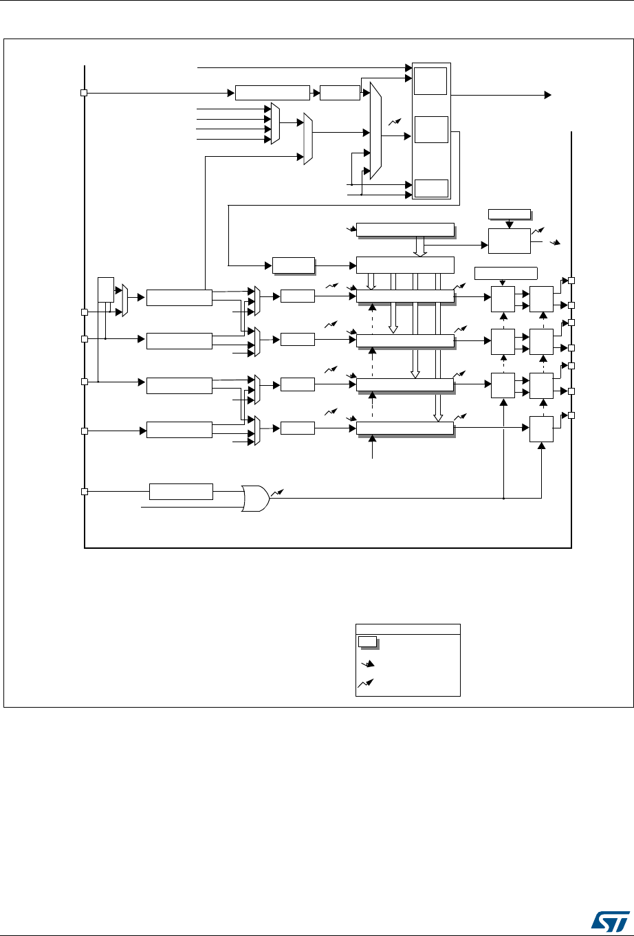
Advanced-control timers (TIM1&TIM8) RM0090
512/1718 DocID018909 Rev 9
Figure 86. Advanced-control timer block diagram
Prescaler
AutoReload Register
COUNTER
Capture/Compare 1 Register
Capture/Compare 2 Register
U
U
U
CC1I
CC2I
ETR
Trigger
Controller
+/-
Stop, Clear or Up/Down
TI1FP1
TI2FP2
ITR0
ITR1
ITR2
TRGI Controller
Encoder
Interface
Capture/Compare 3 Register
U
CC3I
output
control
DTG
DTG
[7:0] registers
TRGO
OC1REF
OC2REF
OC3REF
REP Register
U
Repetition
counter
UI
Reset, Enable, Up/Down, Count
Capture/Compare 4 Register
U
CC4I
OC4REF
CK_PSC
TI4 Prescaler
Prescaler
IC4PS
IC3PS
IC1
IC2
Prescaler
Prescaler
Input Filter &
Edge detector
IC2PS
IC1PS
TI1FP1
output
control
DTG
output
control
DTG
output
control
Reg
event
Notes:
Preload registers transferred
to active registers on U event
according to control bit
interrupt & DMA output
Input Filter
Polarity Selection & Edge
Detector & Prescaler
ETRP
TGI
TRC
TRC
IC3
IC4
ITR
ETRF
TRC
TI1F_ED
Input Filter &
Edge detector
Input Filter &
Edge detector
Input Filter &
Edge detector
CC1I
CC2I
CC3I
CC4I
TI1FP2
TI2FP1
TI2FP2
TI3FP3
TRC
TRC
TI3FP4
TI4FP3
TI4FP4
BI
TI3
TI1
TI2
XOR
TIMx_CH1
TIMx_CH2
TIMx_CH3
TIMx_CH4
BRK
TIMx_BKIN
OC1
OC2
OC3
TIMx_CH1
TIMx_CH2
TIMx_CH3
TIMx_CH3N
OC3N
TIMx_CH2N
OC2N
TIMx_CH1N
OC1N
OC4
TIMx_CH4
TIMx_ETR
to other timers
Mode
Slave
PSC CNT
Internal Clock (CK_INT)
CK_CNT
ETRF
Clock failure event from clock controller
Polarity Selection
CSS (Clock Security system
CK_TIM18 from RCC
to DAC/ADC
ITR3

DocID018909 Rev 9 513/1718
RM0090 Advanced-control timers (TIM1&TIM8)
577
17.3 TIM1&TIM8 functional description
17.3.1 Time-base unit
The main block of the programmable advanced-control timer is a 16-bit counter with its
related auto-reload register. The counter can count up, down or both up and down. The
counter clock can be divided by a prescaler.
The counter, the auto-reload register and the prescaler register can be written or read by
software. This is true even when the counter is running.
The time-base unit includes:
•Counter register (TIMx_CNT)
•Prescaler register (TIMx_PSC)
•Auto-reload register (TIMx_ARR)
•Repetition counter register (TIMx_RCR)
The auto-reload register is preloaded. Writing to or reading from the auto-reload register
accesses the preload register. The content of the preload register are transferred into the
shadow register permanently or at each update event (UEV), depending on the auto-reload
preload enable bit (ARPE) in TIMx_CR1 register. The update event is sent when the counter
reaches the overflow (or underflow when downcounting) and if the UDIS bit equals 0 in the
TIMx_CR1 register. It can also be generated by software. The generation of the update
event is described in detailed for each configuration.
The counter is clocked by the prescaler output CK_CNT, which is enabled only when the
counter enable bit (CEN) in TIMx_CR1 register is set (refer also to the slave mode controller
description to get more details on counter enabling).
Note that the counter starts counting 1 clock cycle after setting the CEN bit in the TIMx_CR1
register.
Prescaler description
The prescaler can divide the counter clock frequency by any factor between 1 and 65536. It
is based on a 16-bit counter controlled through a 16-bit register (in the TIMx_PSC register).
It can be changed on the fly as this control register is buffered. The new prescaler ratio is
taken into account at the next update event.
Figure 87 and Figure 88 give some examples of the counter behavior when the prescaler
ratio is changed on the fly:
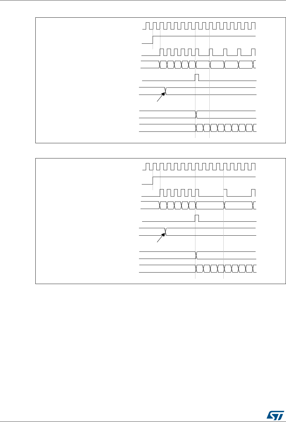
Advanced-control timers (TIM1&TIM8) RM0090
514/1718 DocID018909 Rev 9
Figure 87. Counter timing diagram with prescaler division change from 1 to 2
Figure 88. Counter timing diagram with prescaler division change from 1 to 4
17.3.2 Counter modes
Upcounting mode
In upcounting mode, the counter counts from 0 to the auto-reload value (content of the
TIMx_ARR register), then restarts from 0 and generates a counter overflow event.
If the repetition counter is used, the update event (UEV) is generated after upcounting is
repeated for the number of times programmed in the repetition counter register plus one
(TIMx_RCR+1). Else the update event is generated at each counter overflow.
Setting the UG bit in the TIMx_EGR register (by software or by using the slave mode
controller) also generates an update event.
The UEV event can be disabled by software by setting the UDIS bit in the TIMx_CR1
register. This is to avoid updating the shadow registers while writing new values in the
CK_PSC
00
CEN
Timer clock = CK_CNT
Counter register
Update event (UEV)
0
F9 FA FB FCF7
Prescaler control register 01
Write a new value in TIMx_PSC
01 02 03
Prescaler buffer 01
Prescaler counter 01 0 1 0 1 0 1
F8
CK_PSC
00
CEN
Timer clock = CK_CNT
Counter register
Update event (UEV)
0
F9 FA FB FCF7
Prescaler control register 03
Write a new value in TIMx_PSC
Prescaler buffer 03
Prescaler counter 01 2 3 0 1 2 3
F8 01
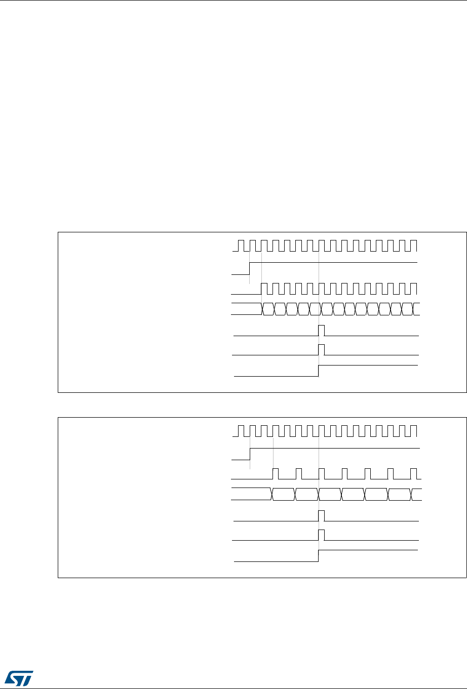
DocID018909 Rev 9 515/1718
RM0090 Advanced-control timers (TIM1&TIM8)
577
preload registers. Then no update event occurs until the UDIS bit has been written to 0.
However, the counter restarts from 0, as well as the counter of the prescaler (but the
prescale rate does not change). In addition, if the URS bit (update request selection) in
TIMx_CR1 register is set, setting the UG bit generates an update event UEV but without
setting the UIF flag (thus no interrupt or DMA request is sent). This is to avoid generating
both update and capture interrupts when clearing the counter on the capture event.
When an update event occurs, all the registers are updated and the update flag (UIF bit in
TIMx_SR register) is set (depending on the URS bit):
•The repetition counter is reloaded with the content of TIMx_RCR register,
•The auto-reload shadow register is updated with the preload value (TIMx_ARR),
•The buffer of the prescaler is reloaded with the preload value (content of the TIMx_PSC
register).
The following figures show some examples of the counter behavior for different clock
frequencies when TIMx_ARR=0x36.
Figure 89. Counter timing diagram, internal clock divided by 1
Figure 90. Counter timing diagram, internal clock divided by 2
CK_PSC
00
CNT_EN
Timer clock = CK_CNT
Counter register
Update interrupt flag (UIF)
Counter overflow
Update event (UEV)
01 02 03 04 05 06 0732 33 34 35 3631
CK_PSC
0035 0000 0001 0002 0003
CNT_EN
Timer clock = CK_CNT
Counter register
Update interrupt flag (UIF)
0034 0036
Counter overflow
Update event (UEV)
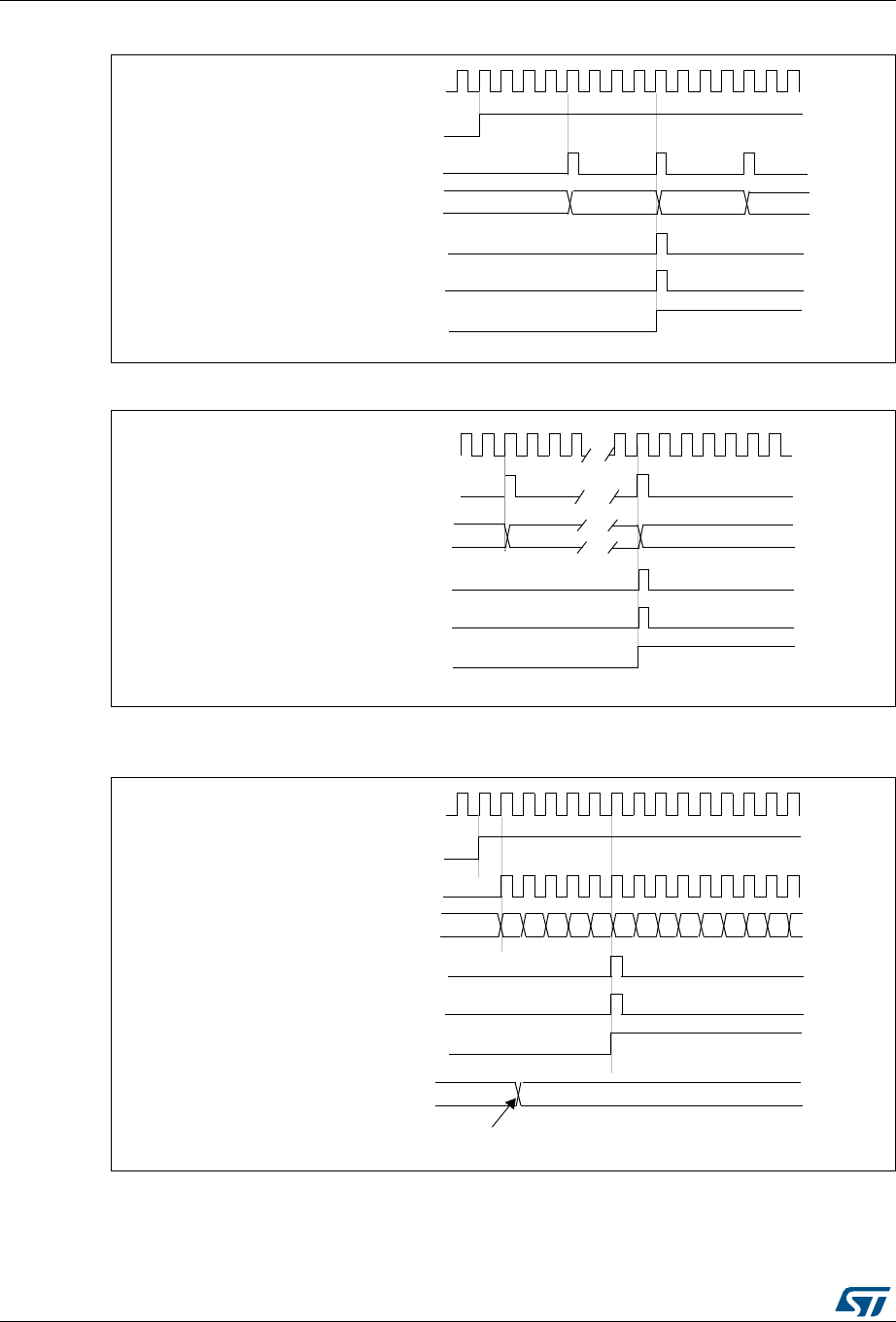
Advanced-control timers (TIM1&TIM8) RM0090
516/1718 DocID018909 Rev 9
Figure 91. Counter timing diagram, internal clock divided by 4
Figure 92. Counter timing diagram, internal clock divided by N
Figure 93. Counter timing diagram, update event when ARPE=0 (TIMx_ARR not
preloaded)
CK_PSC
0000 0001
CNT_EN
Timer clock = CK_CNT
Counter register
Update interrupt flag (UIF)
0035 0036
Counter overflow
Update event (UEV)
Timer clock = CK_CNT
Counter register 00
1F 20
Update interrupt flag (UIF)
Counter overflow
Update event (UEV)
CK_PSC
CK_PSC
00
CEN
Timer clock = CK_CNT
Counter register
Update interrupt flag (UIF)
Counter overflow
Update event (UEV)
01 02 03 04 05 06 0732 33 34 35 3631
Auto-reload register FF 36
Write a new value in TIMx_ARR

DocID018909 Rev 9 517/1718
RM0090 Advanced-control timers (TIM1&TIM8)
577
Figure 94. Counter timing diagram, update event when ARPE=1
(TIMx_ARR preloaded)
Downcounting mode
In downcounting mode, the counter counts from the auto-reload value (content of the
TIMx_ARR register) down to 0, then restarts from the auto-reload value and generates a
counter underflow event.
If the repetition counter is used, the update event (UEV) is generated after downcounting is
repeated for the number of times programmed in the repetition counter register plus one
(TIMx_RCR+1). Else the update event is generated at each counter underflow.
Setting the UG bit in the TIMx_EGR register (by software or by using the slave mode
controller) also generates an update event.
The UEV update event can be disabled by software by setting the UDIS bit in TIMx_CR1
register. This is to avoid updating the shadow registers while writing new values in the
preload registers. Then no update event occurs until UDIS bit has been written to 0.
However, the counter restarts from the current auto-reload value, whereas the counter of the
prescaler restarts from 0 (but the prescale rate doesn’t change).
In addition, if the URS bit (update request selection) in TIMx_CR1 register is set, setting the
UG bit generates an update event UEV but without setting the UIF flag (thus no interrupt or
DMA request is sent). This is to avoid generating both update and capture interrupts when
clearing the counter on the capture event.
When an update event occurs, all the registers are updated and the update flag (UIF bit in
TIMx_SR register) is set (depending on the URS bit):
•The repetition counter is reloaded with the content of TIMx_RCR register
•The buffer of the prescaler is reloaded with the preload value (content of the TIMx_PSC
register)
•The auto-reload active register is updated with the preload value (content of the
TIMx_ARR register). Note that the auto-reload is updated before the counter is
reloaded, so that the next period is the expected one
CK_PSC
00
CEN
Timer clock = CK_CNT
Counter register
Update interrupt flag (UIF)
Counter overflow
Update event (UEV)
01 02 03 04 05 06 07F1 F2 F3 F4 F5F0
Auto-reload preload register F5 36
Auto-reload shadow register F5 36
Write a new value in TIMx_ARR
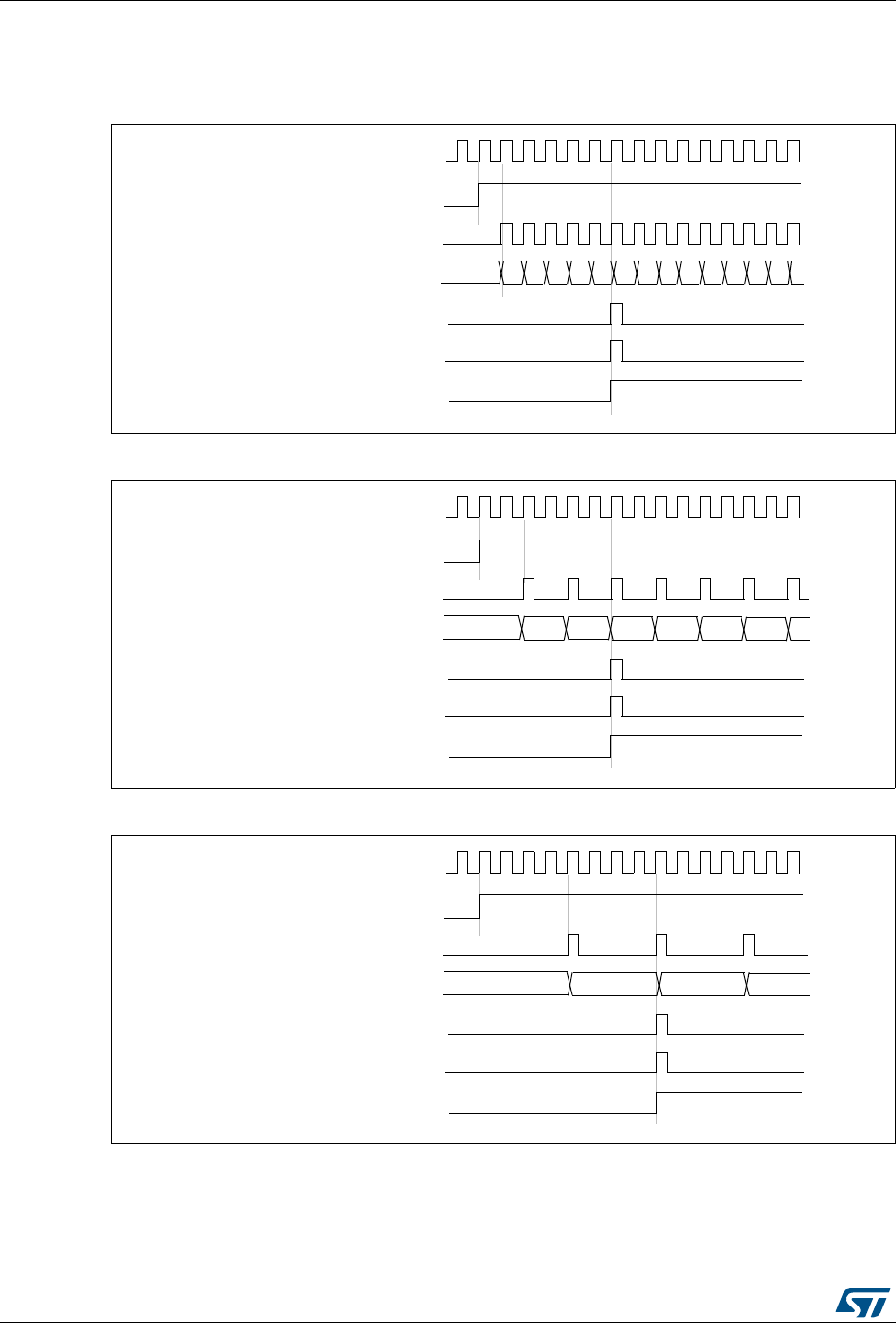
Advanced-control timers (TIM1&TIM8) RM0090
518/1718 DocID018909 Rev 9
The following figures show some examples of the counter behavior for different clock
frequencies when TIMx_ARR=0x36.
Figure 95. Counter timing diagram, internal clock divided by 1
Figure 96. Counter timing diagram, internal clock divided by 2
Figure 97. Counter timing diagram, internal clock divided by 4
CK_PSC
36
CNT_EN
Timer clock = CK_CNT
Counter register
Update interrupt flag (UIF)
Counter underflow (cnt_udf)
Update event (UEV)
35 34 33 32 31 30 2F04 03 02 01 0005
CK_PSC
0001 0036 0035 0034 0033
CNT_EN
Timer clock = CK_CNT
Counter register
Update interrupt flag (UIF)
0002 0000
Counter underflow
Update event (UEV)
CK_PSC
0036 0035
CNT_EN
Timer clock = CK_CNT
Counter register
Update interrupt flag (UIF)
0001 0000
Counter underflow
Update event (UEV)
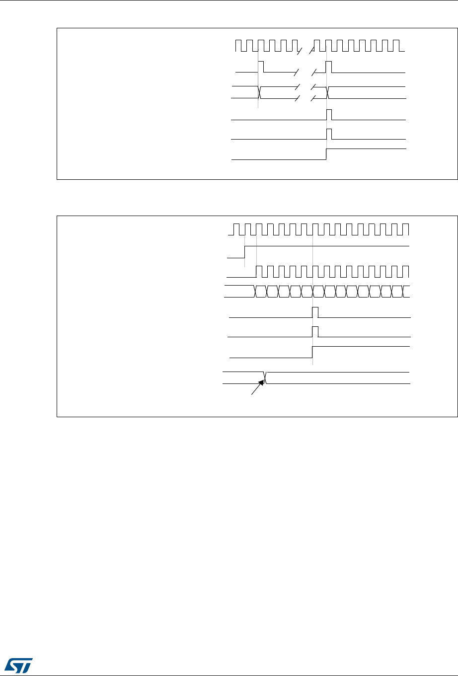
DocID018909 Rev 9 519/1718
RM0090 Advanced-control timers (TIM1&TIM8)
577
Figure 98. Counter timing diagram, internal clock divided by N
Figure 99. Counter timing diagram, update event when repetition counter
is not used
Center-aligned mode (up/down counting)
In center-aligned mode, the counter counts from 0 to the auto-reload value (content of the
TIMx_ARR register) – 1, generates a counter overflow event, then counts from the auto-
reload value down to 1 and generates a counter underflow event. Then it restarts counting
from 0.
Center-aligned mode is active when the CMS bits in TIMx_CR1 register are not equal to
'00'. The Output compare interrupt flag of channels configured in output is set when: the
counter counts down (Center aligned mode 1, CMS = "01"), the counter counts up (Center
aligned mode 2, CMS = "10") the counter counts up and down (Center aligned mode 3,
CMS = "11").
In this mode, the DIR direction bit in the TIMx_CR1 register cannot be written. It is updated
by hardware and gives the current direction of the counter.
The update event can be generated at each counter overflow and at each counter underflow
or by setting the UG bit in the TIMx_EGR register (by software or by using the slave mode
controller) also generates an update event. In this case, the counter restarts counting from
0, as well as the counter of the prescaler.
Timer clock = CK_CNT
Counter register 36
20 1F
Update interrupt flag (UIF)
Counter underflow
Update event (UEV)
CK_PSC
00
CK_PSC
36
CEN
Timer clock = CK_CNT
Counter register
Update interrupt flag (UIF)
Counter underflow
Update event (UEV)
35 34 33 32 31 30 2F04 03 02 01 0005
Auto-reload register FF 36
Write a new value in TIMx_ARR
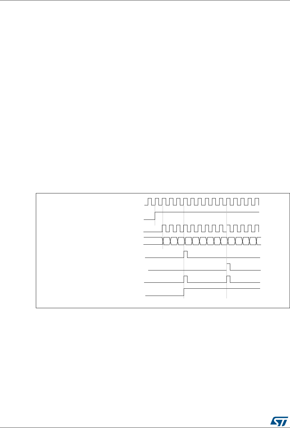
Advanced-control timers (TIM1&TIM8) RM0090
520/1718 DocID018909 Rev 9
The UEV update event can be disabled by software by setting the UDIS bit in the TIMx_CR1
register. This is to avoid updating the shadow registers while writing new values in the
preload registers. Then no update event occurs until UDIS bit has been written to 0.
However, the counter continues counting up and down, based on the current auto-reload
value.
In addition, if the URS bit (update request selection) in TIMx_CR1 register is set, setting the
UG bit generates an UEV update event but without setting the UIF flag (thus no interrupt or
DMA request is sent). This is to avoid generating both update and capture interrupts when
clearing the counter on the capture event.
When an update event occurs, all the registers are updated and the update flag (UIF bit in
TIMx_SR register) is set (depending on the URS bit):
•The repetition counter is reloaded with the content of TIMx_RCR register
•The buffer of the prescaler is reloaded with the preload value (content of the TIMx_PSC
register)
•The auto-reload active register is updated with the preload value (content of the
TIMx_ARR register). Note that if the update source is a counter overflow, the auto-
reload is updated before the counter is reloaded, so that the next period is the expected
one (the counter is loaded with the new value).
The following figures show some examples of the counter behavior for different clock
frequencies.
Figure 100. Counter timing diagram, internal clock divided by 1, TIMx_ARR = 0x6
1. Here, center-aligned mode 1 is used (for more details refer to Section 17.4: TIM1&TIM8 registers on page 551).
CK_PSC
02
CNT_EN
Timer clock = CK_CNT
Counter register
Update interrupt flag (UIF)
Counter underflow
Update event (UEV)
03 04 05 06 05 04 0303 02 01 00 0104
Counter overflow
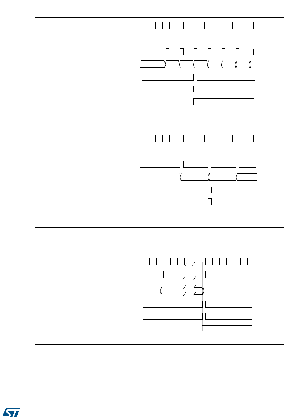
DocID018909 Rev 9 521/1718
RM0090 Advanced-control timers (TIM1&TIM8)
577
Figure 101. Counter timing diagram, internal clock divided by 2
Figure 102. Counter timing diagram, internal clock divided by 4, TIMx_ARR=0x36
1. Center-aligned mode 2 or 3 is used with an UIF on overflow.
Figure 103. Counter timing diagram, internal clock divided by N
CK_PSC
0002 0000 0001 0002 0003
CNT_EN
Timer clock = CK_CNT
Counter register
Update interrupt flag (UIF)
0003 0001
Counter underflow
Update event (UEV)
CK_PSC
0036 0035
CNT_EN
Timer clock = CK_CNT
Counter register
Update interrupt flag (UIF)
0034 0035
Counter overflow
Update event (UEV)
Timer clock = CK_CNT
Counter register 00
20 1F
Update interrupt flag (UIF)
Counter underflow
Update event (UEV)
CK_PSC
01
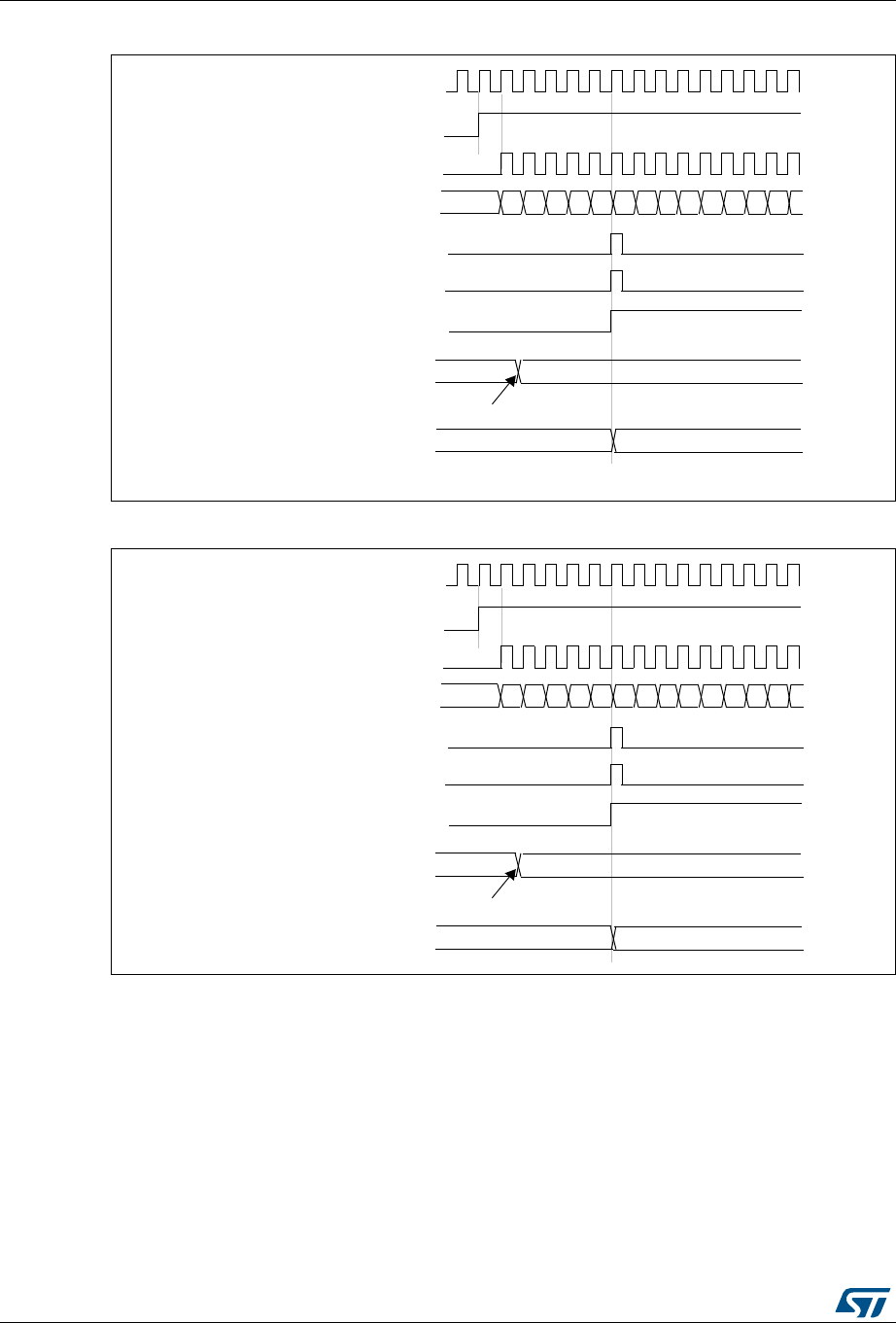
Advanced-control timers (TIM1&TIM8) RM0090
522/1718 DocID018909 Rev 9
Figure 104. Counter timing diagram, update event with ARPE=1 (counter underflow)
Figure 105. Counter timing diagram, Update event with ARPE=1 (counter overflow)
17.3.3 Repetition counter
Section 17.3.1: Time-base unit describes how the update event (UEV) is generated with
respect to the counter overflows/underflows. It is actually generated only when the repetition
counter has reached zero. This can be useful when generating PWM signals.
This means that data are transferred from the preload registers to the shadow registers
(TIMx_ARR auto-reload register, TIMx_PSC prescaler register, but also TIMx_CCRx
capture/compare registers in compare mode) every N+1 counter overflows or underflows,
where N is the value in the TIMx_RCR repetition counter register.
CK_PSC
00
CEN
Timer clock = CK_CNT
Counter register
Update interrupt flag (UIF)
Counter underflow
Update event (UEV)
01 02 03 04 05 06 0705 04 03 02 0106
Auto-reload preload register FD 36
Write a new value in TIMx_ARR
Auto-reload active register FD 36
CK_PSC
36
CEN
Timer clock = CK_CNT
Counter register
Update interrupt flag (UIF)
Counter overflow
Update event (UEV)
35 34 33 32 31 30 2FF8 F9 FA FB FCF7
Auto-reload preload register FD 36
Write a new value in TIMx_ARR
Auto-reload active register FD 36
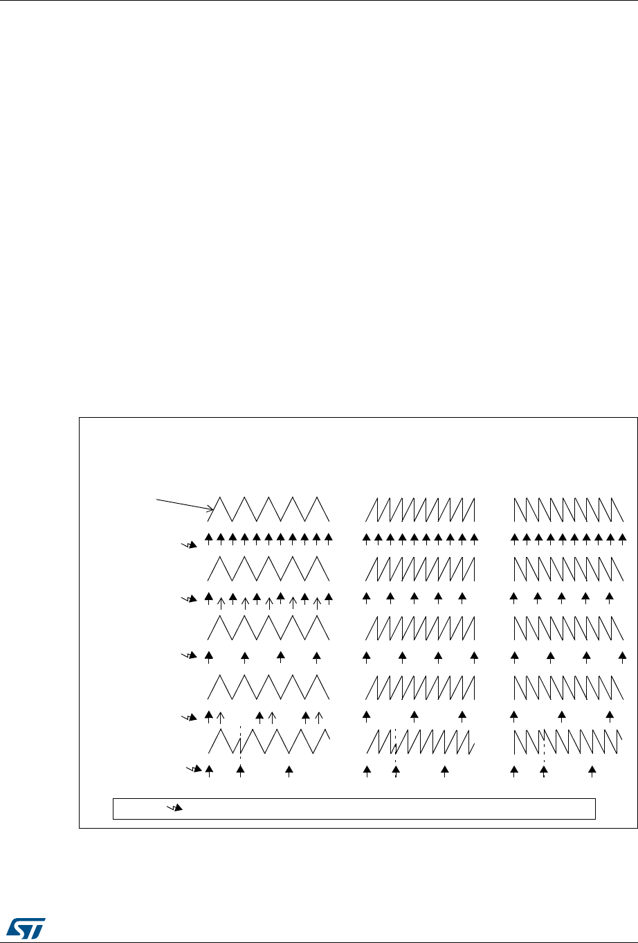
DocID018909 Rev 9 523/1718
RM0090 Advanced-control timers (TIM1&TIM8)
577
The repetition counter is decremented:
•At each counter overflow in upcounting mode,
•At each counter underflow in downcounting mode,
•At each counter overflow and at each counter underflow in center-aligned mode.
Although this limits the maximum number of repetition to 128 PWM cycles, it makes it
possible to update the duty cycle twice per PWM period. When refreshing compare
registers only once per PWM period in center-aligned mode, maximum resolution is
2xTck, due to the symmetry of the pattern.
The repetition counter is an auto-reload type; the repetition rate is maintained as defined by
the TIMx_RCR register value (refer to Figure 106). When the update event is generated by
software (by setting the UG bit in TIMx_EGR register) or by hardware through the slave
mode controller, it occurs immediately whatever the value of the repetition counter is and the
repetition counter is reloaded with the content of the TIMx_RCR register.
In center-aligned mode, for odd values of RCR, the update event occurs either on the
overflow or on the underflow depending on when the RCR register was written and when
the counter was started. If the RCR was written before starting the counter, the UEV occurs
on the overflow. If the RCR was written after starting the counter, the UEV occurs on the
underflow. For example for RCR = 3, the UEV is generated on each 4th overflow or
underflow event depending on when RCR was written.
Figure 106. Update rate examples depending on mode and TIMx_RCR register
settings
Center-aligned mode Edge-aligned mode
UEV Update Event
: Preload registers transferred to active registers and update interrupt generated
Counter
TIMx_RCR = 0
TIMx_RCR = 1
TIMx_RCR = 2
TIMx_RCR = 3
UEV
TIMx_RCR
= 3
and
re-synchronization
(by SW) (by SW)
TIMx_CNT
(by SW)
Upcounting Downcounting
UEV
UEV
UEV
UEV
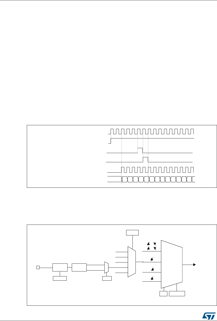
Advanced-control timers (TIM1&TIM8) RM0090
524/1718 DocID018909 Rev 9
17.3.4 Clock selection
The counter clock can be provided by the following clock sources:
•Internal clock (CK_INT)
•External clock mode1: external input pin
•External clock mode2: external trigger input ETR
•Internal trigger inputs (ITRx): using one timer as prescaler for another timer, for
example, you can configure Timer 1 to act as a prescaler for Timer 2. Refer to Using
one timer as prescaler for another for more details.
Internal clock source (CK_INT)
If the slave mode controller is disabled (SMS=000), then the CEN, DIR (in the TIMx_CR1
register) and UG bits (in the TIMx_EGR register) are actual control bits and can be changed
only by software (except UG which remains cleared automatically). As soon as the CEN bit
is written to 1, the prescaler is clocked by the internal clock CK_INT.
Figure 107 shows the behavior of the control circuit and the upcounter in normal mode,
without prescaler.
Figure 107. Control circuit in normal mode, internal clock divided by 1
External clock source mode 1
This mode is selected when SMS=111 in the TIMx_SMCR register. The counter can count at
each rising or falling edge on a selected input.
Figure 108. TI2 external clock connection example
Internal clock
00
Counter clock = CK_CNT = CK_PSC
Counter register 01 02 03 04 05 06 0732 33 34 35 3631
CEN=CNT_EN
UG
CNT_INIT
CK_INT
encoder
mode
external clock
mode 1
external clock
mode 2
internal clock
mode
ETRF
TRGI
TI1F
TI2F or
or
or
(internal clock)
CK_PSC
ECE
TIMx_SMCR
SMS[2:0]
ITRx
TI1_ED
TI1FP1
TI2FP2
ETRF
TIMx_SMCR
TS[2:0]
TI2 0
1
TIMx_CCER
CC2P
Filter
ICF[3:0]
TIMx_CCMR1
Edge
Detector
TI2F_Rising
TI2F_Falling 110
0xx
100
101
111
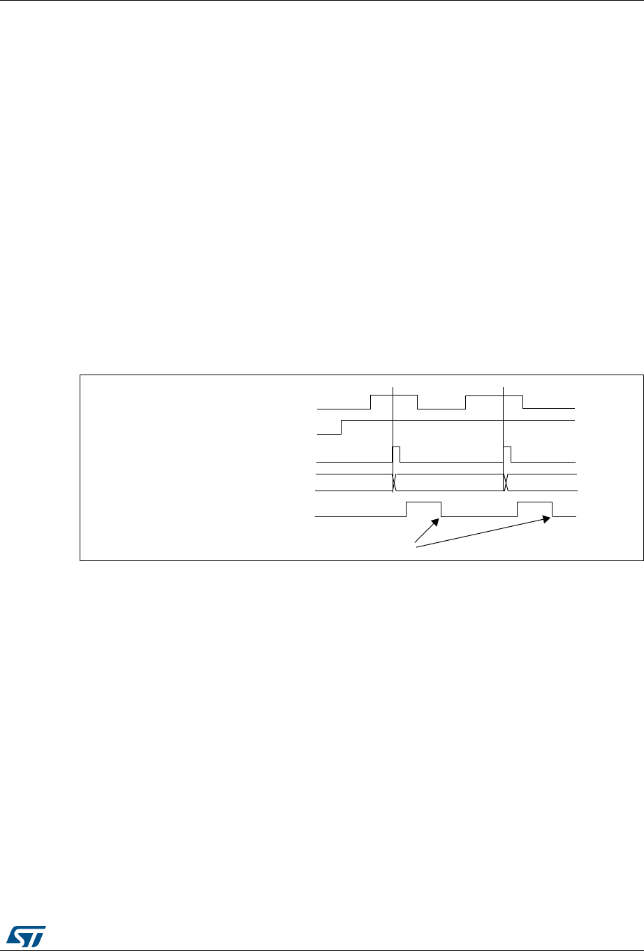
DocID018909 Rev 9 525/1718
RM0090 Advanced-control timers (TIM1&TIM8)
577
For example, to configure the upcounter to count in response to a rising edge on the TI2
input, use the following procedure:
1. Configure channel 2 to detect rising edges on the TI2 input by writing CC2S = ‘01’ in
the TIMx_CCMR1 register.
2. Configure the input filter duration by writing the IC2F[3:0] bits in the TIMx_CCMR1
register (if no filter is needed, keep IC2F=0000).
3. Select rising edge polarity by writing CC2P=0 and CC2NP=0 in the TIMx_CCER
register.
4. Configure the timer in external clock mode 1 by writing SMS=111 in the TIMx_SMCR
register.
5. Select TI2 as the trigger input source by writing TS=110 in the TIMx_SMCR register.
6. Enable the counter by writing CEN=1 in the TIMx_CR1 register.
Note: The capture prescaler is not used for triggering, so you don’t need to configure it.
When a rising edge occurs on TI2, the counter counts once and the TIF flag is set.
The delay between the rising edge on TI2 and the actual clock of the counter is due to the
resynchronization circuit on TI2 input.
Figure 109. Control circuit in external clock mode 1
External clock source mode 2
This mode is selected by writing ECE=1 in the TIMx_SMCR register.
The counter can count at each rising or falling edge on the external trigger input ETR.
Figure 110 gives an overview of the external trigger input block.
Counter clock = CK_CNT = CK_PSC
Counter register 35 3634
TI2
CNT_EN
TIF
Write TIF=0
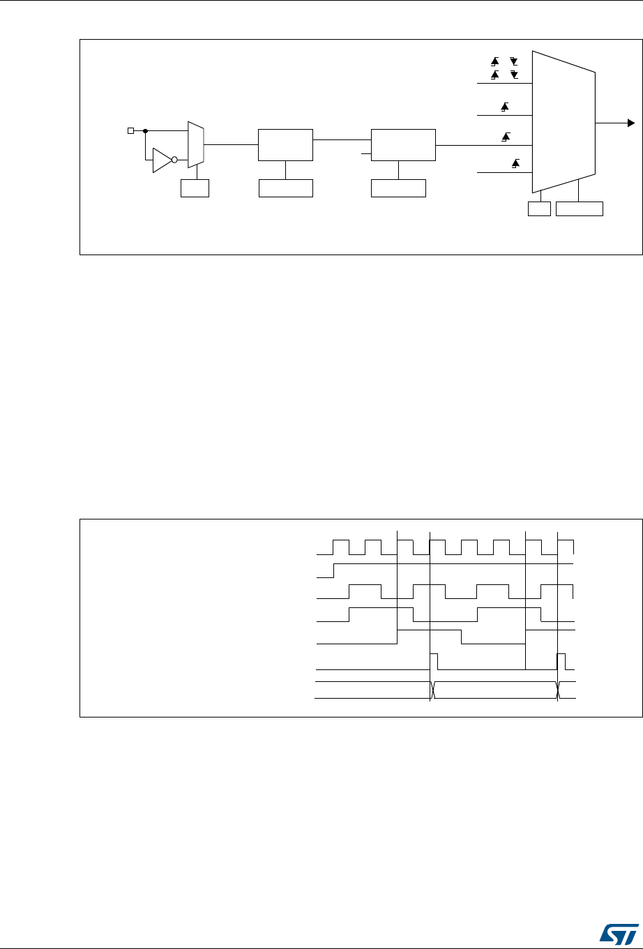
Advanced-control timers (TIM1&TIM8) RM0090
526/1718 DocID018909 Rev 9
Figure 110. External trigger input block
For example, to configure the upcounter to count each 2 rising edges on ETR, use the
following procedure:
1. As no filter is needed in this example, write ETF[3:0]=0000 in the TIMx_SMCR register.
2. Set the prescaler by writing ETPS[1:0]=01 in the TIMx_SMCR register
3. Select rising edge detection on the ETR pin by writing ETP=0 in the TIMx_SMCR
register
4. Enable external clock mode 2 by writing ECE=1 in the TIMx_SMCR register.
5. Enable the counter by writing CEN=1 in the TIMx_CR1 register.
The counter counts once each 2 ETR rising edges.
The delay between the rising edge on ETR and the actual clock of the counter is due to the
resynchronization circuit on the ETRP signal.
Figure 111. Control circuit in external clock mode 2
17.3.5 Capture/compare channels
Each Capture/Compare channel is built around a capture/compare register (including a
shadow register), a input stage for capture (with digital filter, multiplexing and prescaler) and
an output stage (with comparator and output control).
Figure 112 to Figure 115 give an overview of one Capture/Compare channel.
The input stage samples the corresponding TIx input to generate a filtered signal TIxF.
Then, an edge detector with polarity selection generates a signal (TIxFPx) which can be
ETR 0
1
TIMx_SMCR
ETP
divider
/1, /2, /4, /8
ETPS[1:0]
ETRP filter
ETF[3:0]
downcounter
fDTS
TIMx_SMCR
TIMx_SMCR
ETR pin
CK_INT
encoder
mode
external clock
mode 1
external clock
mode 2
internal clock
mode
ETRF
TRGI
TI1F
TI2F or
or
or
(internal clock)
CK_PSC
ECE
TIMx_SMCR
SMS[2:0]
Counter clock = CK_CNT = CK_PSC
Counter register 35 3634
ETR
CNT_EN
fCK_INT
ETRP
ETRF
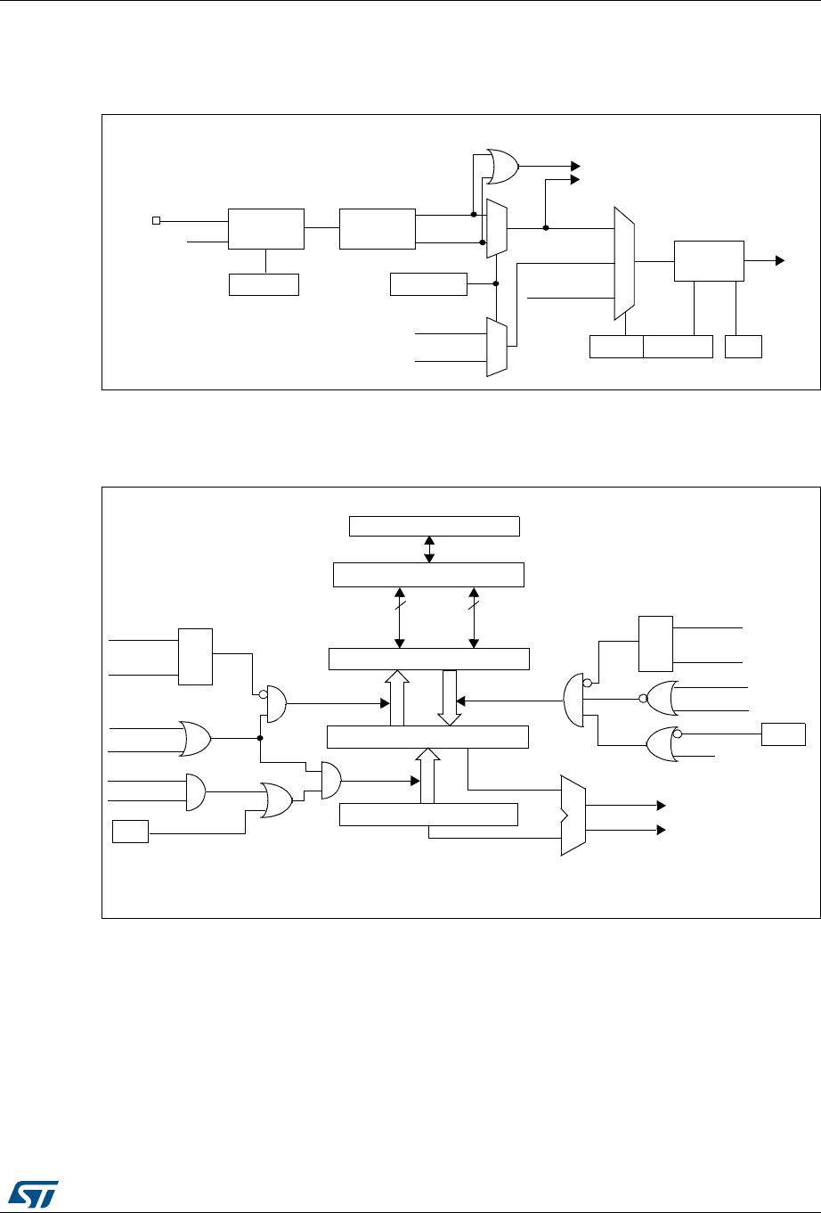
DocID018909 Rev 9 527/1718
RM0090 Advanced-control timers (TIM1&TIM8)
577
used as trigger input by the slave mode controller or as the capture command. It is
prescaled before the capture register (ICxPS).
Figure 112. Capture/compare channel (example: channel 1 input stage)
The output stage generates an intermediate waveform which is then used for reference:
OCxRef (active high). The polarity acts at the end of the chain.
Figure 113. Capture/compare channel 1 main circuit
TI1 0
1
TIMx_CCER
CC1P/CC1NP
divider
/1, /2, /4, /8
ICPS[1:0]
TI1F_ED
filter
ICF[3:0]
downcounter
TIMx_CCMR1
Edge
Detector
TI1F_Rising
TI1F_Falling
to the slave mode controller
TI1FP1
11
01
TIMx_CCMR1
CC1S[1:0]
IC1
TI2FP1
TRC
(from channel 2)
(from slave mode
controller)
10
fDTS
TIMx_CCER
CC1E
IC1PS
TI1F
0
1
TI2F_rising
TI2F_falling
(from channel 2)
CC1E
Capture/compare shadow register
comparator
Capture/compare preload register
Counter
IC1PS
CC1S[0]
CC1S[1]
capture
input
mode
S
R
read CCR1H
read CCR1L
read_in_progress
capture_transfer CC1S[0]
CC1S[1]
S
R
write CCR1H
write CCR1L
write_in_progress
output
mode
UEV
OC1PE
(from time
compare_transfer
APB Bus
88
high
low
(if 16-bit)
MCU-peripheral interface
TIM1_CCMR1
OC1PE
base unit)
CNT>CCR1
CNT=CCR1
TIM1_EGR
CC1G
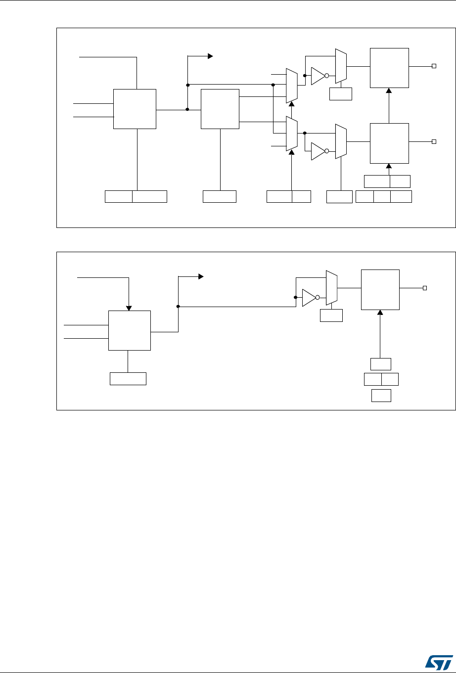
Advanced-control timers (TIM1&TIM8) RM0090
528/1718 DocID018909 Rev 9
Figure 114. Output stage of capture/compare channel (channel 1 to 3)
Figure 115. Output stage of capture/compare channel (channel 4)
The capture/compare block is made of one preload register and one shadow register. Write
and read always access the preload register.
In capture mode, captures are actually done in the shadow register, which is copied into the
preload register.
In compare mode, the content of the preload register is copied into the shadow register
which is compared to the counter.
17.3.6 Input capture mode
In Input capture mode, the Capture/Compare Registers (TIMx_CCRx) are used to latch the
value of the counter after a transition detected by the corresponding ICx signal. When a
capture occurs, the corresponding CCXIF flag (TIMx_SR register) is set and an interrupt or
a DMA request can be sent if they are enabled. If a capture occurs while the CCxIF flag was
already high, then the over-capture flag CCxOF (TIMx_SR register) is set. CCxIF can be
cleared by software by writing it to ‘0’ or by reading the captured data stored in the
TIMx_CCRx register. CCxOF is cleared when you write it to ‘0’.
Output mode
CNT>CCR1
CNT=CCR1 controller
TIM1_CCMR1
OC1M[2:0]
OC1REF
OC1CE
Dead-time
generator
OC1_DT
OC1N_DT
DTG[7:0]
TIM1_BDTR
‘0’
‘0’
CC1E
TIM1_CCER
CC1NE
0
1
CC1P
TIM1_CCER
0
1
CC1NP
TIM1_CCER
Output
enable
circuit
OC1
Output
enable
circuit
OC1N
CC1E TIM1_CCER
CC1NE
OSSI TIM1_BDTR
MOE OSSR
0x
10
11
11
01
x0
ETR
controller
To the master mode
Output mode
CNT > CCR4
CNT = CCR4 controller
TIM1_CCMR2
OC2M[2:0]
OC4 REF
0
1
CC4P
TIM1_CCER
Output
enable
circuit
OC4
CC4E TIM1_CCER
OSSI TIM1_BDTR
MOE
To the master mode
controller
TIM1_CR2
OIS4
ETR

DocID018909 Rev 9 529/1718
RM0090 Advanced-control timers (TIM1&TIM8)
577
The following example shows how to capture the counter value in TIMx_CCR1 when TI1
input rises. To do this, use the following procedure:
•Select the active input: TIMx_CCR1 must be linked to the TI1 input, so write the CC1S
bits to 01 in the TIMx_CCMR1 register. As soon as CC1S becomes different from 00,
the channel is configured in input and the TIMx_CCR1 register becomes read-only.
•Program the input filter duration you need with respect to the signal you connect to the
timer (by programming ICxF bits in the TIMx_CCMRx register if the input is a TIx input).
Let’s imagine that, when toggling, the input signal is not stable during at must 5 internal
clock cycles. We must program a filter duration longer than these 5 clock cycles. We
can validate a transition on TI1 when 8 consecutive samples with the new level have
been detected (sampled at fDTS frequency). Then write IC1F bits to 0011 in the
TIMx_CCMR1 register.
•Select the edge of the active transition on the TI1 channel by writing CC1P and CC1NP
bits to 0 in the TIMx_CCER register (rising edge in this case).
•Program the input prescaler. In our example, we wish the capture to be performed at
each valid transition, so the prescaler is disabled (write IC1PS bits to ‘00’ in the
TIMx_CCMR1 register).
•Enable capture from the counter into the capture register by setting the CC1E bit in the
TIMx_CCER register.
•If needed, enable the related interrupt request by setting the CC1IE bit in the
TIMx_DIER register, and/or the DMA request by setting the CC1DE bit in the
TIMx_DIER register.
When an input capture occurs:
•The TIMx_CCR1 register gets the value of the counter on the active transition.
•CC1IF flag is set (interrupt flag). CC1OF is also set if at least two consecutive captures
occurred whereas the flag was not cleared.
•An interrupt is generated depending on the CC1IE bit.
•A DMA request is generated depending on the CC1DE bit.
In order to handle the overcapture, it is recommended to read the data before the
overcapture flag. This is to avoid missing an overcapture which could happen after reading
the flag and before reading the data.
Note: IC interrupt and/or DMA requests can be generated by software by setting the
corresponding CCxG bit in the TIMx_EGR register.
17.3.7 PWM input mode
This mode is a particular case of input capture mode. The procedure is the same except:
•Two ICx signals are mapped on the same TIx input.
•These 2 ICx signals are active on edges with opposite polarity.
•One of the two TIxFP signals is selected as trigger input and the slave mode controller
is configured in reset mode.
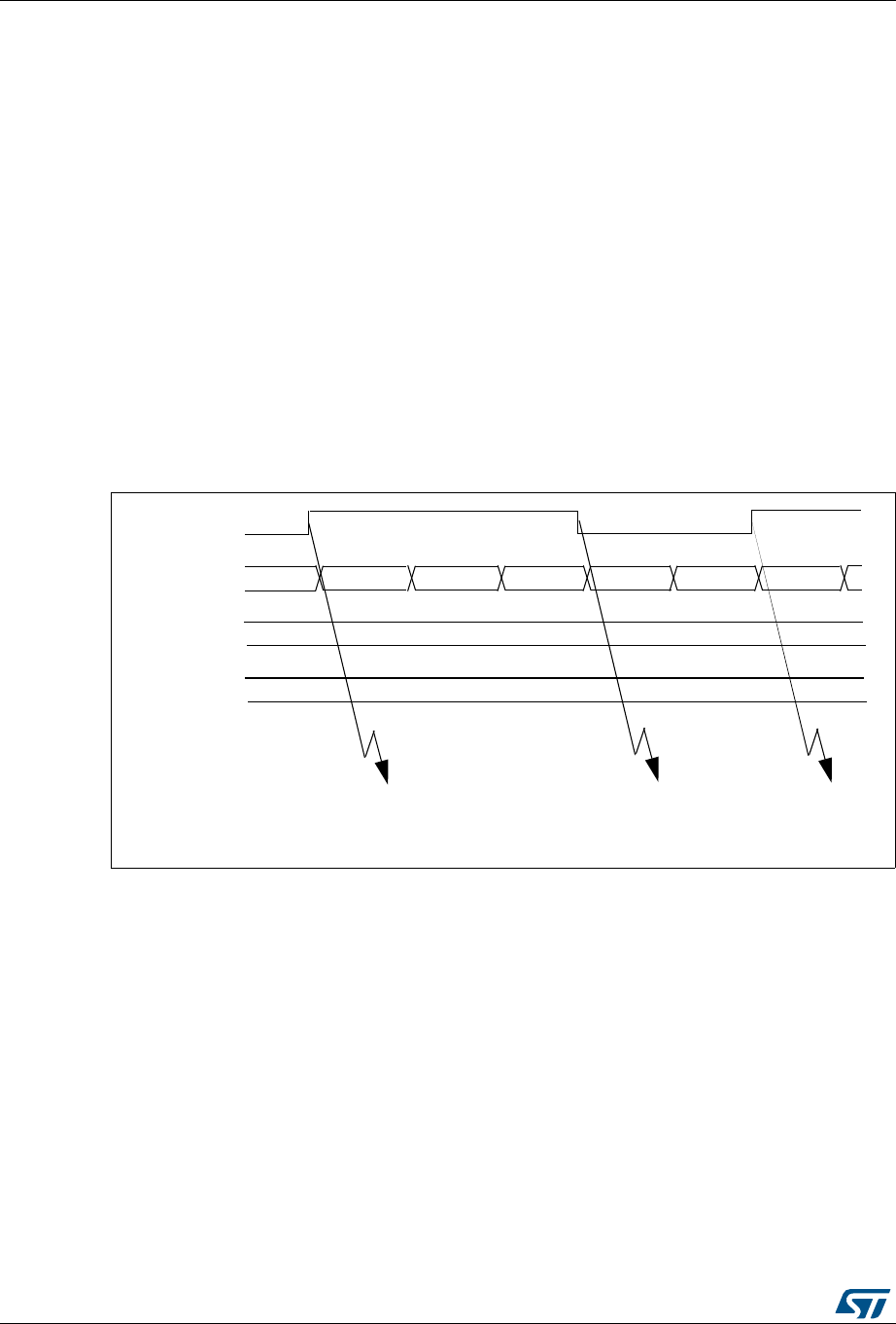
Advanced-control timers (TIM1&TIM8) RM0090
530/1718 DocID018909 Rev 9
For example, you can measure the period (in TIMx_CCR1 register) and the duty cycle (in
TIMx_CCR2 register) of the PWM applied on TI1 using the following procedure (depending
on CK_INT frequency and prescaler value):
•Select the active input for TIMx_CCR1: write the CC1S bits to 01 in the TIMx_CCMR1
register (TI1 selected).
•Select the active polarity for TI1FP1 (used both for capture in TIMx_CCR1 and counter
clear): write the CC1P and CC1NP bits to ‘0’ (active on rising edge).
•Select the active input for TIMx_CCR2: write the CC2S bits to 10 in the TIMx_CCMR1
register (TI1 selected).
•Select the active polarity for TI1FP2 (used for capture in TIMx_CCR2): write the CC2P
and CC2NP bits to ‘1’ (active on falling edge).
•Select the valid trigger input: write the TS bits to 101 in the TIMx_SMCR register
(TI1FP1 selected).
•Configure the slave mode controller in reset mode: write the SMS bits to 100 in the
TIMx_SMCR register.
•Enable the captures: write the CC1E and CC2E bits to ‘1’ in the TIMx_CCER register.
Figure 116. PWM input mode timing
17.3.8 Forced output mode
In output mode (CCxS bits = 00 in the TIMx_CCMRx register), each output compare signal
(OCxREF and then OCx/OCxN) can be forced to active or inactive level directly by software,
independently of any comparison between the output compare register and the counter.
To force an output compare signal (OCXREF/OCx) to its active level, you just need to write
101 in the OCxM bits in the corresponding TIMx_CCMRx register. Thus OCXREF is forced
high (OCxREF is always active high) and OCx get opposite value to CCxP polarity bit.
For example: CCxP=0 (OCx active high) => OCx is forced to high level.
The OCxREF signal can be forced low by writing the OCxM bits to 100 in the TIMx_CCMRx
register.
TI1
TIMx_CNT 0000 0001 0002 0003 0004 00000004
TIMx_CCR1
TIMx_CCR2
0004
0002
IC1 capture
IC2 capture
reset counter
IC2 capture
pulse width
IC1 capture
period
measurementmeasurement
ai15413

DocID018909 Rev 9 531/1718
RM0090 Advanced-control timers (TIM1&TIM8)
577
Anyway, the comparison between the TIMx_CCRx shadow register and the counter is still
performed and allows the flag to be set. Interrupt and DMA requests can be sent
accordingly. This is described in the output compare mode section below.
17.3.9 Output compare mode
This function is used to control an output waveform or indicating when a period of time has
elapsed.
When a match is found between the capture/compare register and the counter, the output
compare function:
•Assigns the corresponding output pin to a programmable value defined by the output
compare mode (OCxM bits in the TIMx_CCMRx register) and the output polarity (CCxP
bit in the TIMx_CCER register). The output pin can keep its level (OCXM=000), be set
active (OCxM=001), be set inactive (OCxM=010) or can toggle (OCxM=011) on match.
•Sets a flag in the interrupt status register (CCxIF bit in the TIMx_SR register).
•Generates an interrupt if the corresponding interrupt mask is set (CCXIE bit in the
TIMx_DIER register).
•Sends a DMA request if the corresponding enable bit is set (CCxDE bit in the
TIMx_DIER register, CCDS bit in the TIMx_CR2 register for the DMA request
selection).
The TIMx_CCRx registers can be programmed with or without preload registers using the
OCxPE bit in the TIMx_CCMRx register.
In output compare mode, the update event UEV has no effect on OCxREF and OCx output.
The timing resolution is one count of the counter. Output compare mode can also be used to
output a single pulse (in One Pulse mode).
Procedure:
1. Select the counter clock (internal, external, prescaler).
2. Write the desired data in the TIMx_ARR and TIMx_CCRx registers.
3. Set the CCxIE bit if an interrupt request is to be generated.
4. Select the output mode. For example:
– Write OCxM = 011 to toggle OCx output pin when CNT matches CCRx
– Write OCxPE = 0 to disable preload register
– Write CCxP = 0 to select active high polarity
– Write CCxE = 1 to enable the output
5. Enable the counter by setting the CEN bit in the TIMx_CR1 register.
The TIMx_CCRx register can be updated at any time by software to control the output
waveform, provided that the preload register is not enabled (OCxPE=’0’, else TIMx_CCRx
shadow register is updated only at the next update event UEV). An example is given in
Figure 117.
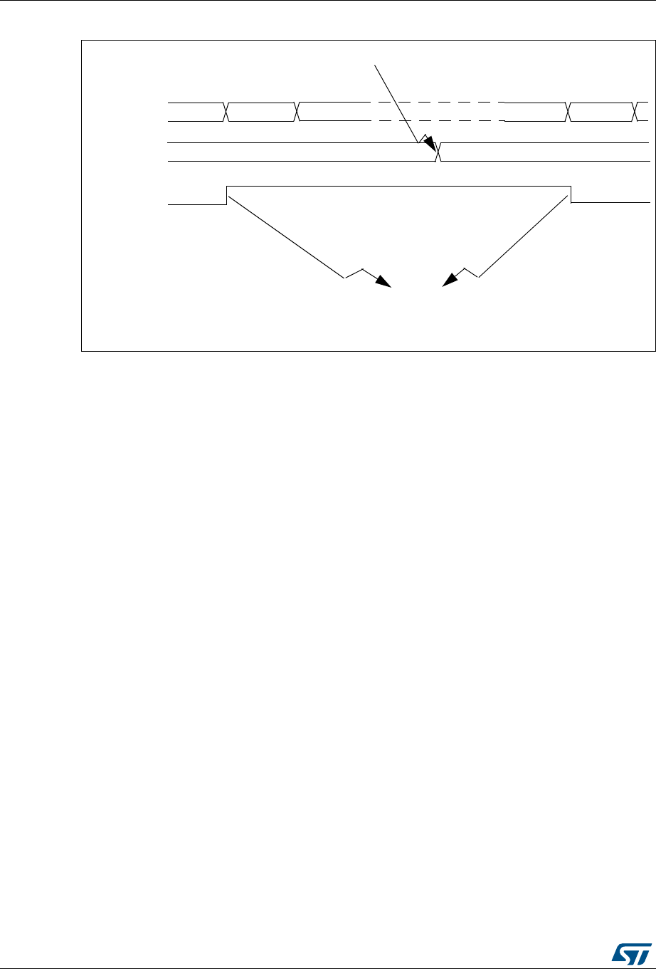
Advanced-control timers (TIM1&TIM8) RM0090
532/1718 DocID018909 Rev 9
Figure 117. Output compare mode, toggle on OC1.
17.3.10 PWM mode
Pulse Width Modulation mode allows you to generate a signal with a frequency determined
by the value of the TIMx_ARR register and a duty cycle determined by the value of the
TIMx_CCRx register.
The PWM mode can be selected independently on each channel (one PWM per OCx
output) by writing ‘110’ (PWM mode 1) or ‘111’ (PWM mode 2) in the OCxM bits in the
TIMx_CCMRx register. You must enable the corresponding preload register by setting the
OCxPE bit in the TIMx_CCMRx register, and eventually the auto-reload preload register (in
upcounting or center-aligned modes) by setting the ARPE bit in the TIMx_CR1 register.
As the preload registers are transferred to the shadow registers only when an update event
occurs, before starting the counter, you have to initialize all the registers by setting the UG
bit in the TIMx_EGR register.
OCx polarity is software programmable using the CCxP bit in the TIMx_CCER register. It
can be programmed as active high or active low. OCx output is enabled by a combination of
the CCxE, CCxNE, MOE, OSSI and OSSR bits (TIMx_CCER and TIMx_BDTR registers).
Refer to the TIMx_CCER register description for more details.
In PWM mode (1 or 2), TIMx_CNT and TIMx_CCRx are always compared to determine
whether TIMx_CCRx ≤TIMx_CNT or TIMx_CNT ≤TIMx_CCRx (depending on the direction
of the counter).
The timer is able to generate PWM in edge-aligned mode or center-aligned mode
depending on the CMS bits in the TIMx_CR1 register.
oc1ref=OC1
TIM1_CNT B200 B201
0039
TIM1_CCR1 003A
Write B201h in the CC1R register
Match detected on CCR1
Interrupt generated if enabled
003B
B201
003A
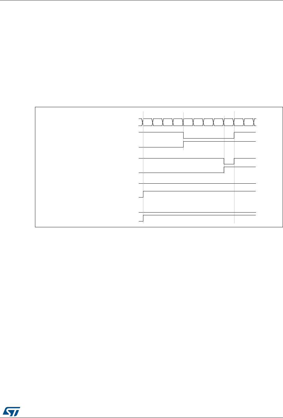
DocID018909 Rev 9 533/1718
RM0090 Advanced-control timers (TIM1&TIM8)
577
PWM edge-aligned mode
•Upcounting configuration
Upcounting is active when the DIR bit in the TIMx_CR1 register is low. Refer to
Section : Upcounting mode on page 514.
In the following example, we consider PWM mode 1. The reference PWM signal
OCxREF is high as long as TIMx_CNT < TIMx_CCRx else it becomes low. If the
compare value in TIMx_CCRx is greater than the auto-reload value (in TIMx_ARR)
then OCxREF is held at ‘1’. If the compare value is 0 then OCxRef is held at ‘0’.
Figure 118 shows some edge-aligned PWM waveforms in an example where
TIMx_ARR=8.
Figure 118. Edge-aligned PWM waveforms (ARR=8)
•Downcounting configuration
Downcounting is active when DIR bit in TIMx_CR1 register is high. Refer to Section :
Downcounting mode on page 517
In PWM mode 1, the reference signal OCxRef is low as long as
TIMx_CNT > TIMx_CCRx else it becomes high. If the compare value in TIMx_CCRx is
greater than the auto-reload value in TIMx_ARR, then OCxREF is held at ‘1’. 0% PWM
is not possible in this mode.
PWM center-aligned mode
Center-aligned mode is active when the CMS bits in TIMx_CR1 register are different from
‘00’ (all the remaining configurations having the same effect on the OCxRef/OCx signals).
The compare flag is set when the counter counts up, when it counts down or both when it
counts up and down depending on the CMS bits configuration. The direction bit (DIR) in the
TIMx_CR1 register is updated by hardware and must not be changed by software. Refer to
Section : Center-aligned mode (up/down counting) on page 519.
Figure 119 shows some center-aligned PWM waveforms in an example where:
•TIMx_ARR=8,
•PWM mode is the PWM mode 1,
•The flag is set when the counter counts down corresponding to the center-aligned
mode 1 selected for CMS=01 in TIMx_CR1 register.
Counter register
‘1’
01234567801
‘0’
OCXREF
CCxIF
OCXREF
CCxIF
OCXREF
CCxIF
OCXREF
CCxIF
CCRx=4
CCRx=8
CCRx>8
CCRx=0
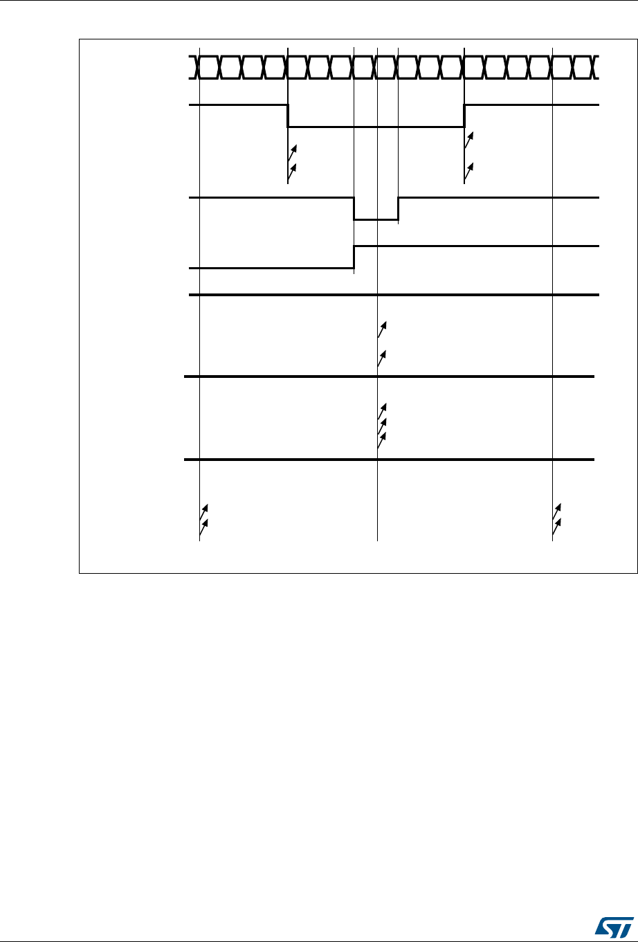
Advanced-control timers (TIM1&TIM8) RM0090
534/1718 DocID018909 Rev 9
Figure 119. Center-aligned PWM waveforms (ARR=8)
Hints on using center-aligned mode:
•When starting in center-aligned mode, the current up-down configuration is used. It
means that the counter counts up or down depending on the value written in the DIR bit
in the TIMx_CR1 register. Moreover, the DIR and CMS bits must not be changed at the
same time by the software.
•Writing to the counter while running in center-aligned mode is not recommended as it
can lead to unexpected results. In particular:
– The direction is not updated if you write a value in the counter that is greater than
the auto-reload value (TIMx_CNT>TIMx_ARR). For example, if the counter was
counting up, it continues to count up.
– The direction is updated if you write 0 or write the TIMx_ARR value in the counter
but no Update Event UEV is generated.
•The safest way to use center-aligned mode is to generate an update by software
(setting the UG bit in the TIMx_EGR register) just before starting the counter and not to
write the counter while it is running.
##X)&
#OUNTERREGISTER
##2X
/#X2%&
#-3
#-3
#-3
##X)&
##2X
/#X2%&
#-3OR
##X)&
##2X
/#X2%&
#-3
#-3
#-3
gg
##X)&
##2X
/#X2%&
#-3
#-3
#-3
gg
##X)&
##2X
/#X2%&
#-3
#-3
#-3
gg
AIB
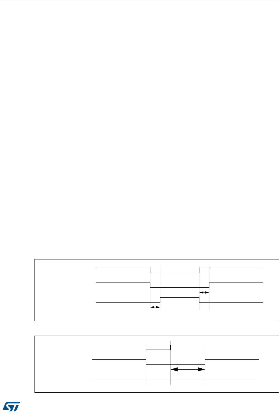
DocID018909 Rev 9 535/1718
RM0090 Advanced-control timers (TIM1&TIM8)
577
17.3.11 Complementary outputs and dead-time insertion
The advanced-control timers (TIM1&TIM8) can output two complementary signals and
manage the switching-off and the switching-on instants of the outputs.
This time is generally known as dead-time and you have to adjust it depending on the
devices you have connected to the outputs and their characteristics (intrinsic delays of level-
shifters, delays due to power switches...)
You can select the polarity of the outputs (main output OCx or complementary OCxN)
independently for each output. This is done by writing to the CCxP and CCxNP bits in the
TIMx_CCER register.
The complementary signals OCx and OCxN are activated by a combination of several
control bits: the CCxE and CCxNE bits in the TIMx_CCER register and the MOE, OISx,
OISxN, OSSI and OSSR bits in the TIMx_BDTR and TIMx_CR2 registers. Refer to
Table 94: Output control bits for complementary OCx and OCxN channels with break
feature on page 568 for more details. In particular, the dead-time is activated when
switching to the IDLE state (MOE falling down to 0).
Dead-time insertion is enabled by setting both CCxE and CCxNE bits, and the MOE bit if the
break circuit is present. DTG[7:0] bits of the TIMx_BDTR register are used to control the
dead-time generation for all channels. From a reference waveform OCxREF, it generates 2
outputs OCx and OCxN. If OCx and OCxN are active high:
•The OCx output signal is the same as the reference signal except for the rising edge,
which is delayed relative to the reference rising edge.
•The OCxN output signal is the opposite of the reference signal except for the rising
edge, which is delayed relative to the reference falling edge.
If the delay is greater than the width of the active output (OCx or OCxN) then the
corresponding pulse is not generated.
The following figures show the relationships between the output signals of the dead-time
generator and the reference signal OCxREF. (we suppose CCxP=0, CCxNP=0, MOE=1,
CCxE=1 and CCxNE=1 in these examples)
Figure 120. Complementary output with dead-time insertion.
Figure 121. Dead-time waveforms with delay greater than the negative pulse.
delay
delay
OCxREF
OCx
OCxN
delay
OCxREF
OCx
OCxN

Advanced-control timers (TIM1&TIM8) RM0090
536/1718 DocID018909 Rev 9
Figure 122. Dead-time waveforms with delay greater than the positive pulse.
The dead-time delay is the same for each of the channels and is programmable with the
DTG bits in the TIMx_BDTR register. Refer to Section 17.4.18: TIM1&TIM8 break and dead-
time register (TIMx_BDTR) on page 572 for delay calculation.
Re-directing OCxREF to OCx or OCxN
In output mode (forced, output compare or PWM), OCxREF can be re-directed to the OCx
output or to OCxN output by configuring the CCxE and CCxNE bits in the TIMx_CCER
register.
This allows you to send a specific waveform (such as PWM or static active level) on one
output while the complementary remains at its inactive level. Other alternative possibilities
are to have both outputs at inactive level or both outputs active and complementary with
dead-time.
Note: When only OCxN is enabled (CCxE=0, CCxNE=1), it is not complemented and becomes
active as soon as OCxREF is high. For example, if CCxNP=0 then OCxN=OCxRef. On the
other hand, when both OCx and OCxN are enabled (CCxE=CCxNE=1) OCx becomes
active when OCxREF is high whereas OCxN is complemented and becomes active when
OCxREF is low.
17.3.12 Using the break function
When using the break function, the output enable signals and inactive levels are modified
according to additional control bits (MOE, OSSI and OSSR bits in the TIMx_BDTR register,
OISx and OISxN bits in the TIMx_CR2 register). In any case, the OCx and OCxN outputs
cannot be set both to active level at a given time. Refer to Table 94: Output control bits for
complementary OCx and OCxN channels with break feature on page 568 for more details.
The break source can be either the break input pin or a clock failure event, generated by the
Clock Security System (CSS), from the Reset Clock Controller. For further information on
the Clock Security System, refer to Section 7.2.7: Clock security system (CSS).
When exiting from reset, the break circuit is disabled and the MOE bit is low. You can enable
the break function by setting the BKE bit in the TIMx_BDTR register. The break input
polarity can be selected by configuring the BKP bit in the same register. BKE and BKP can
be modified at the same time. When the BKE and BKP bits are written, a delay of 1 APB
clock cycle is applied before the writing is effective. Consequently, it is necessary to wait 1
APB clock period to correctly read back the bit after the write operation.
Because MOE falling edge can be asynchronous, a resynchronization circuit has been
inserted between the actual signal (acting on the outputs) and the synchronous control bit
(accessed in the TIMx_BDTR register). It results in some delays between the asynchronous
and the synchronous signals. In particular, if you write MOE to 1 whereas it was low, you
delay
OCxREF
OCx
OCxN

DocID018909 Rev 9 537/1718
RM0090 Advanced-control timers (TIM1&TIM8)
577
must insert a delay (dummy instruction) before reading it correctly. This is because you write
the asynchronous signal and read the synchronous signal.
When a break occurs (selected level on the break input):
•The MOE bit is cleared asynchronously, putting the outputs in inactive state, idle state
or in reset state (selected by the OSSI bit). This feature functions even if the MCU
oscillator is off.
•Each output channel is driven with the level programmed in the OISx bit in the
TIMx_CR2 register as soon as MOE=0. If OSSI=0 then the timer releases the enable
output else the enable output remains high.
•When complementary outputs are used:
– The outputs are first put in reset state inactive state (depending on the polarity).
This is done asynchronously so that it works even if no clock is provided to the
timer.
– If the timer clock is still present, then the dead-time generator is reactivated in
order to drive the outputs with the level programmed in the OISx and OISxN bits
after a dead-time. Even in this case, OCx and OCxN cannot be driven to their
active level together. Note that because of the resynchronization on MOE, the
dead-time duration is a bit longer than usual (around 2 ck_tim clock cycles).
– If OSSI=0 then the timer releases the enable outputs else the enable outputs
remain or become high as soon as one of the CCxE or CCxNE bits is high.
•The break status flag (BIF bit in the TIMx_SR register) is set. An interrupt can be
generated if the BIE bit in the TIMx_DIER register is set. A DMA request can be sent if
the BDE bit in the TIMx_DIER register is set.
•If the AOE bit in the TIMx_BDTR register is set, the MOE bit is automatically set again
at the next update event UEV. This can be used to perform a regulation, for instance.
Else, MOE remains low until you write it to ‘1’ again. In this case, it can be used for
security and you can connect the break input to an alarm from power drivers, thermal
sensors or any security components.
Note: The break inputs is acting on level. Thus, the MOE cannot be set while the break input is
active (neither automatically nor by software). In the meantime, the status flag BIF cannot
be cleared.
The break can be generated by the BRK input which has a programmable polarity and an
enable bit BKE in the TIMx_BDTR Register.
There are two solutions to generate a break:
•By using the BRK input which has a programmable polarity and an enable bit BKE in
the TIMx_BDTR register
•By software through the BG bit of the TIMx_EGR register.
In addition to the break input and the output management, a write protection has been
implemented inside the break circuit to safeguard the application. It allows you to freeze the
configuration of several parameters (dead-time duration, OCx/OCxN polarities and state
when disabled, OCxM configurations, break enable and polarity). You can choose from 3
levels of protection selected by the LOCK bits in the TIMx_BDTR register. Refer to
Section 17.4.18: TIM1&TIM8 break and dead-time register (TIMx_BDTR) on page 572. The
LOCK bits can be written only once after an MCU reset.
Figure 123 shows an example of behavior of the outputs in response to a break.
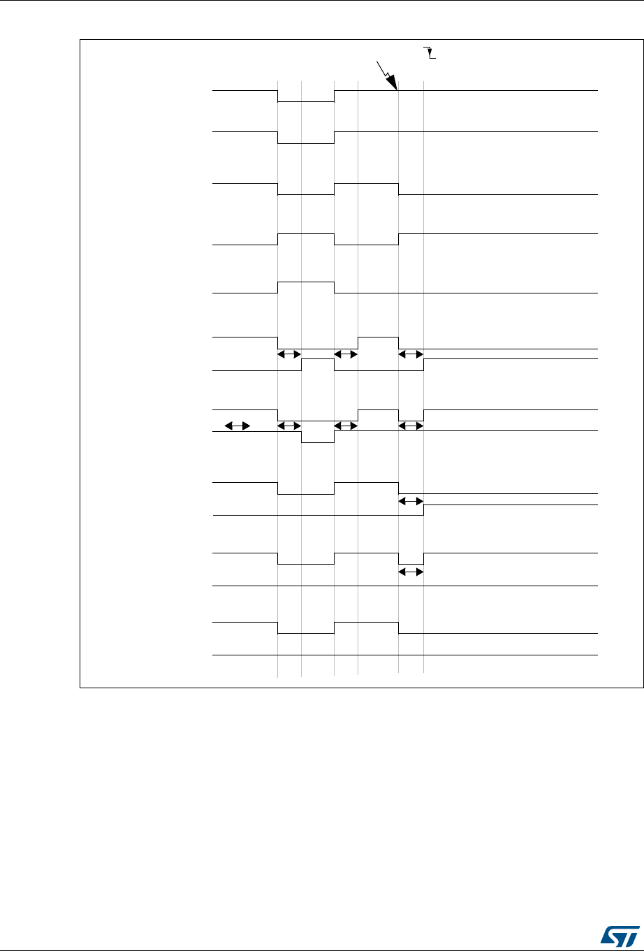
Advanced-control timers (TIM1&TIM8) RM0090
538/1718 DocID018909 Rev 9
Figure 123. Output behavior in response to a break.
delay
OCxREF
BREAK (MOE
OCx
(OCxN not implemented, CCxP=0, OISx=1)
OCx
(OCxN not implemented, CCxP=0, OISx=0)
OCx
(OCxN not implemented, CCxP=1, OISx=1)
OCx
(OCxN not implemented, CCxP=1, OISx=0)
OCx
OCxN
(CCxE=1, CCxP=0, OISx=0, CCxNE=1, CCxNP=0, OISxN=1)
delaydelay
delay
OCx
OCxN
(CCxE=1, CCxP=0, OISx=1, CCxNE=1, CCxNP=1, OISxN=1)
delaydelay
delay
OCx
OCxN
(CCxE=1, CCxP=0, OISx=0, CCxNE=0, CCxNP=0, OISxN=1)
)
delay
OCx
OCxN
(CCxE=1, CCxP=0, OISx=1, CCxNE=0, CCxNP=0, OISxN=0)
OCx
OCxN
(CCxE=1, CCxP=0, CCxNE=0, CCxNP=0, OISx=OISxN=0 or OISx=OISxN=1)
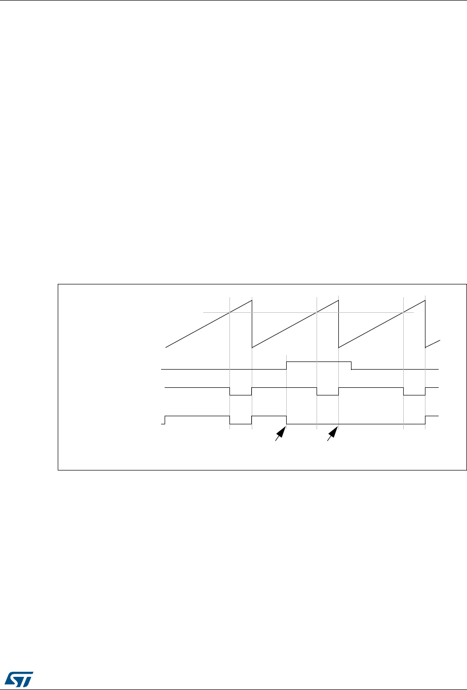
DocID018909 Rev 9 539/1718
RM0090 Advanced-control timers (TIM1&TIM8)
577
17.3.13 Clearing the OCxREF signal on an external event
The OCxREF signal for a given channel can be driven Low by applying a High level to the
ETRF input (OCxCE enable bit of the corresponding TIMx_CCMRx register set to ‘1’). The
OCxREF signal remains Low until the next update event, UEV, occurs.
This function can only be used in output compare and PWM modes, and does not work in
forced mode.
For example, the ETR signal can be connected to the output of a comparator to be used for
current handling. In this case, the ETR must be configured as follow:
1. The External Trigger Prescaler should be kept off: bits ETPS[1:0] of the TIMx_SMCR
register set to ‘00’.
2. The external clock mode 2 must be disabled: bit ECE of the TIMx_SMCR register set to
‘0’.
3. The External Trigger Polarity (ETP) and the External Trigger Filter (ETF) can be
configured according to the user needs.
Figure 124 shows the behavior of the OCxREF signal when the ETRF Input becomes High,
for both values of the enable bit OCxCE. In this example, the timer TIMx is programmed in
PWM mode.
Figure 124. Clearing TIMx OCxREF
Note: In case of a PWM with a 100% duty cycle (if CCRx>ARR), then OCxREF is enabled again at
the next counter overflow.
OCxREF
counter (CNT)
OCxREF
ETRF
(OCxCE=’0’)
(OCxCE=’1’)
ETRF
becomes high
ETRF
still high
(CCRx)
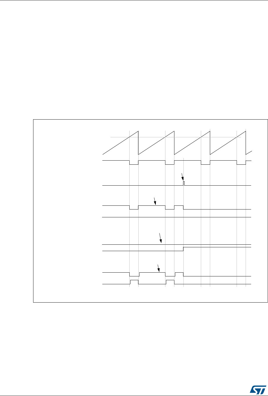
Advanced-control timers (TIM1&TIM8) RM0090
540/1718 DocID018909 Rev 9
17.3.14 6-step PWM generation
When complementary outputs are used on a channel, preload bits are available on the
OCxM, CCxE and CCxNE bits. The preload bits are transferred to the shadow bits at the
COM commutation event. Thus you can program in advance the configuration for the next
step and change the configuration of all the channels at the same time. COM can be
generated by software by setting the COM bit in the TIMx_EGR register or by hardware (on
TRGI rising edge).
A flag is set when the COM event occurs (COMIF bit in the TIMx_SR register), which can
generate an interrupt (if the COMIE bit is set in the TIMx_DIER register) or a DMA request
(if the COMDE bit is set in the TIMx_DIER register).
Figure 125 describes the behavior of the OCx and OCxN outputs when a COM event
occurs, in 3 different examples of programmed configurations.
Figure 125. 6-step generation, COM example (OSSR=1)
(CCRx)
OCx
OCxN
Write COM to 1
counter (CNT)
OCxREF
COM event
CCxE=1
CCxNE=0
OCxM=100
OCx
OCxN
CCxE=0
CCxNE=1
OCxM=101
OCx
OCxN
CCxE=1
CCxNE=0
OCxM=100
Example 1
Example 2
Example 3
write OCxM to 100
CCxE=1
CCxNE=0
OCxM=100 (forced inactive)
CCxE=1
CCxNE=0
OCxM=100 (forced inactive)
Write CCxNE to 1
and OCxM to 101
write CCxNE to 0
and OCxM to 100
CCxE=1
CCxNE=0
OCxM=100 (forced inactive)
ai14910
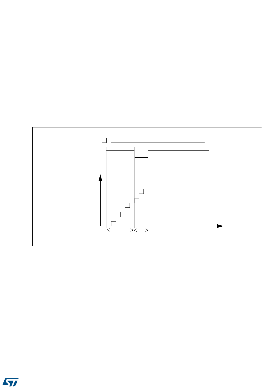
DocID018909 Rev 9 541/1718
RM0090 Advanced-control timers (TIM1&TIM8)
577
17.3.15 One-pulse mode
One-pulse mode (OPM) is a particular case of the previous modes. It allows the counter to
be started in response to a stimulus and to generate a pulse with a programmable length
after a programmable delay.
Starting the counter can be controlled through the slave mode controller. Generating the
waveform can be done in output compare mode or PWM mode. You select One-pulse mode
by setting the OPM bit in the TIMx_CR1 register. This makes the counter stop automatically
at the next update event UEV.
A pulse can be correctly generated only if the compare value is different from the counter
initial value. Before starting (when the timer is waiting for the trigger), the configuration must
be:
•In upcounting: CNT < CCRx ≤ARR (in particular, 0 < CCRx)
•In downcounting: CNT > CCRx
Figure 126. Example of one pulse mode.
For example you may want to generate a positive pulse on OC1 with a length of tPULSE and
after a delay of tDELAY as soon as a positive edge is detected on the TI2 input pin.
Let’s use TI2FP2 as trigger 1:
•Map TI2FP2 to TI2 by writing CC2S=’01’ in the TIMx_CCMR1 register.
•TI2FP2 must detect a rising edge, write CC2P=’0’ and CC2NP=’0’ in the TIMx_CCER
register.
•Configure TI2FP2 as trigger for the slave mode controller (TRGI) by writing TS=’110’ in
the TIMx_SMCR register.
•TI2FP2 is used to start the counter by writing SMS to ‘110’ in the TIMx_SMCR register
(trigger mode).
TI2
OC1REF
Counter
t
0
TIM1_ARR
TIM1_CCR1
OC1
tDELAY tPULSE

Advanced-control timers (TIM1&TIM8) RM0090
542/1718 DocID018909 Rev 9
The OPM waveform is defined by writing the compare registers (taking into account the
clock frequency and the counter prescaler).
•The tDELAY is defined by the value written in the TIMx_CCR1 register.
•The tPULSE is defined by the difference between the auto-reload value and the compare
value (TIMx_ARR - TIMx_CCR1).
•Let’s say you want to build a waveform with a transition from ‘0’ to ‘1’ when a compare
match occurs and a transition from ‘1’ to ‘0’ when the counter reaches the auto-reload
value. To do this you enable PWM mode 2 by writing OC1M=111 in the TIMx_CCMR1
register. You can optionally enable the preload registers by writing OC1PE=’1’ in the
TIMx_CCMR1 register and ARPE in the TIMx_CR1 register. In this case you have to
write the compare value in the TIMx_CCR1 register, the auto-reload value in the
TIMx_ARR register, generate an update by setting the UG bit and wait for external
trigger event on TI2. CC1P is written to ‘0’ in this example.
In our example, the DIR and CMS bits in the TIMx_CR1 register should be low.
You only want 1 pulse (Single mode), so you write '1 in the OPM bit in the TIMx_CR1
register to stop the counter at the next update event (when the counter rolls over from the
auto-reload value back to 0). When OPM bit in the TIMx_CR1 register is set to '0', so the
Repetitive Mode is selected.
Particular case: OCx fast enable:
In One-pulse mode, the edge detection on TIx input set the CEN bit which enables the
counter. Then the comparison between the counter and the compare value makes the
output toggle. But several clock cycles are needed for these operations and it limits the
minimum delay tDELAY min we can get.
If you want to output a waveform with the minimum delay, you can set the OCxFE bit in the
TIMx_CCMRx register. Then OCxRef (and OCx) are forced in response to the stimulus,
without taking in account the comparison. Its new level is the same as if a compare match
had occurred. OCxFE acts only if the channel is configured in PWM1 or PWM2 mode.
17.3.16 Encoder interface mode
To select Encoder Interface mode write SMS=‘001’ in the TIMx_SMCR register if the
counter is counting on TI2 edges only, SMS=’010’ if it is counting on TI1 edges only and
SMS=’011’ if it is counting on both TI1 and TI2 edges.
Select the TI1 and TI2 polarity by programming the CC1P and CC2P bits in the TIMx_CCER
register. When needed, you can program the input filter as well. CC1NP and CC2NP must
be kept low.
The two inputs TI1 and TI2 are used to interface to an incremental encoder. Refer to
Table 92. The counter is clocked by each valid transition on TI1FP1 or TI2FP2 (TI1 and TI2
after input filter and polarity selection, TI1FP1=TI1 if not filtered and not inverted,
TI2FP2=TI2 if not filtered and not inverted) assuming that it is enabled (CEN bit in
TIMx_CR1 register written to ‘1’). The sequence of transitions of the two inputs is evaluated
and generates count pulses as well as the direction signal. Depending on the sequence the
counter counts up or down, the DIR bit in the TIMx_CR1 register is modified by hardware
accordingly. The DIR bit is calculated at each transition on any input (TI1 or TI2), whatever
the counter is counting on TI1 only, TI2 only or both TI1 and TI2.
Encoder interface mode acts simply as an external clock with direction selection. This
means that the counter just counts continuously between 0 and the auto-reload value in the
TIMx_ARR register (0 to ARR or ARR down to 0 depending on the direction). So you must

DocID018909 Rev 9 543/1718
RM0090 Advanced-control timers (TIM1&TIM8)
577
configure TIMx_ARR before starting. in the same way, the capture, compare, prescaler,
repetition counter, trigger output features continue to work as normal. Encoder mode and
External clock mode 2 are not compatible and must not be selected together.
In this mode, the counter is modified automatically following the speed and the direction of
the incremental encoder and its content, therefore, always represents the encoder’s
position. The count direction correspond to the rotation direction of the connected sensor.
The table summarizes the possible combinations, assuming TI1 and TI2 don’t switch at the
same time.
An external incremental encoder can be connected directly to the MCU without external
interface logic. However, comparators are normally be used to convert the encoder’s
differential outputs to digital signals. This greatly increases noise immunity. The third
encoder output which indicate the mechanical zero position, may be connected to an
external interrupt input and trigger a counter reset.
Figure 127 gives an example of counter operation, showing count signal generation and
direction control. It also shows how input jitter is compensated where both edges are
selected. This might occur if the sensor is positioned near to one of the switching points. For
this example we assume that the configuration is the following:
•CC1S=’01’ (TIMx_CCMR1 register, TI1FP1 mapped on TI1).
•CC2S=’01’ (TIMx_CCMR2 register, TI1FP2 mapped on TI2).
•CC1P=’0’, CC1NP=’0’, and IC1F = ‘0000’ (TIMx_CCER register, TI1FP1 non-inverted,
TI1FP1=TI1).
•CC2P=’0’, CC2NP=’0’, and IC2F = ‘0000’ (TIMx_CCER register, TI1FP2 non-inverted,
TI1FP2= TI2).
•SMS=’011’ (TIMx_SMCR register, both inputs are active on both rising and falling
edges).
•CEN=’1’ (TIMx_CR1 register, Counter enabled).
Table 92. Counting direction versus encoder signals
Active edge
Level on
opposite
signal (TI1FP1
for TI2,
TI2FP2 for
TI1)
TI1FP1 signal TI2FP2 signal
Rising Falling Rising Falling
Counting on
TI1 only
High Down Up No Count No Count
Low Up Down No Count No Count
Counting on
TI2 only
High No Count No Count Up Down
Low No Count No Count Down Up
Counting on
TI1 and TI2
High Down Up Up Down
Low Up Down Down Up
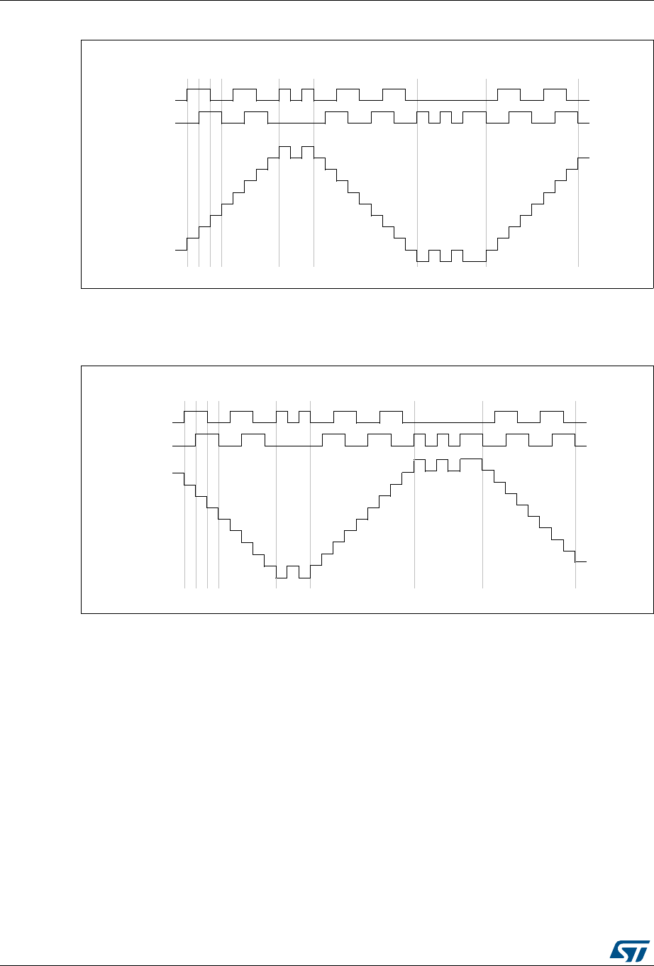
Advanced-control timers (TIM1&TIM8) RM0090
544/1718 DocID018909 Rev 9
Figure 127. Example of counter operation in encoder interface mode.
Figure 128 gives an example of counter behavior when TI1FP1 polarity is inverted (same
configuration as above except CC1P=’1’).
Figure 128. Example of encoder interface mode with TI1FP1 polarity inverted.
The timer, when configured in Encoder Interface mode provides information on the sensor’s
current position. You can obtain dynamic information (speed, acceleration, deceleration) by
measuring the period between two encoder events using a second timer configured in
capture mode. The output of the encoder which indicates the mechanical zero can be used
for this purpose. Depending on the time between two events, the counter can also be read
at regular times. You can do this by latching the counter value into a third input capture
register if available (then the capture signal must be periodic and can be generated by
another timer). when available, it is also possible to read its value through a DMA request
generated by a real-time clock.
17.3.17 Timer input XOR function
The TI1S bit in the TIMx_CR2 register, allows the input filter of channel 1 to be connected to
the output of a XOR gate, combining the three input pins TIMx_CH1, TIMx_CH2 and
TIMx_CH3.
The XOR output can be used with all the timer input functions such as trigger or input
capture. An example of this feature used to interface Hall sensors is given in
TI1
forward forwardbackwardjitter jitter
up down up
TI2
Counter
TI1
forward forwardbackwardjitter jitter
up
down
TI2
Counter
down

DocID018909 Rev 9 545/1718
RM0090 Advanced-control timers (TIM1&TIM8)
577
Section 17.3.18 below.
17.3.18 Interfacing with Hall sensors
This is done using the advanced-control timers (TIM1 or TIM8) to generate PWM signals to
drive the motor and another timer TIMx (TIM2, TIM3, TIM4 or TIM5) referred to as
“interfacing timer” in Figure 129. The “interfacing timer” captures the 3 timer input pins
(TIMx_CH1, TIMx_CH2, and TIMx_CH3) connected through a XOR to the TI1 input channel
(selected by setting the TI1S bit in the TIMx_CR2 register).
The slave mode controller is configured in reset mode; the slave input is TI1F_ED. Thus,
each time one of the 3 inputs toggles, the counter restarts counting from 0. This creates a
time base triggered by any change on the Hall inputs.
On the “interfacing timer”, capture/compare channel 1 is configured in capture mode,
capture signal is TRC (see Figure 112: Capture/compare channel (example: channel 1 input
stage) on page 527). The captured value, which corresponds to the time elapsed between 2
changes on the inputs, gives information about motor speed.
The “interfacing timer” can be used in output mode to generate a pulse which changes the
configuration of the channels of the advanced-control timer (TIM1 or TIM8) (by triggering a
COM event). The TIM1 timer is used to generate PWM signals to drive the motor. To do this,
the interfacing timer channel must be programmed so that a positive pulse is generated
after a programmed delay (in output compare or PWM mode). This pulse is sent to the
advanced-control timer (TIM1 or TIM8) through the TRGO output.
Example: you want to change the PWM configuration of your advanced-control timer TIM1
after a programmed delay each time a change occurs on the Hall inputs connected to one of
the TIMx timers.
•Configure 3 timer inputs ORed to the TI1 input channel by writing the TI1S bit in the
TIMx_CR2 register to ‘1’,
•Program the time base: write the TIMx_ARR to the max value (the counter must be
cleared by the TI1 change. Set the prescaler to get a maximum counter period longer
than the time between 2 changes on the sensors,
•Program channel 1 in capture mode (TRC selected): write the CC1S bits in the
TIMx_CCMR1 register to ‘11’. You can also program the digital filter if needed,
•Program channel 2 in PWM 2 mode with the desired delay: write the OC2M bits to ‘111’
and the CC2S bits to ‘00’ in the TIMx_CCMR1 register,
•Select OC2REF as trigger output on TRGO: write the MMS bits in the TIMx_CR2
register to ‘101’,
In the advanced-control timer TIM1, the right ITR input must be selected as trigger input, the
timer is programmed to generate PWM signals, the capture/compare control signals are
preloaded (CCPC=1 in the TIMx_CR2 register) and the COM event is controlled by the
trigger input (CCUS=1 in the TIMx_CR2 register). The PWM control bits (CCxE, OCxM) are
written after a COM event for the next step (this can be done in an interrupt subroutine
generated by the rising edge of OC2REF).
Figure 129 describes this example.
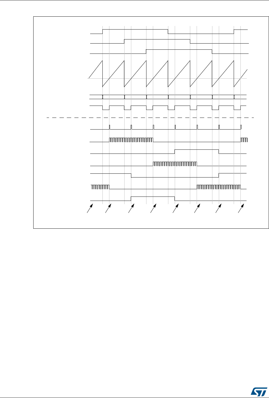
Advanced-control timers (TIM1&TIM8) RM0090
546/1718 DocID018909 Rev 9
Figure 129. Example of hall sensor interface
counter (CNT)
TRGO=OC2REF
(CCR2)
OC1
OC1N
COM
Write CCxE, CCxNE
TIH1
TIH2
TIH3
CCR1
OC2
OC2N
OC3
OC3N
C7A3C7A8C794 C7A5 C7AB C796
and OCxM for next step
Interfacing timer
advanced-control timers (TIM1&TIM8)
ai17335
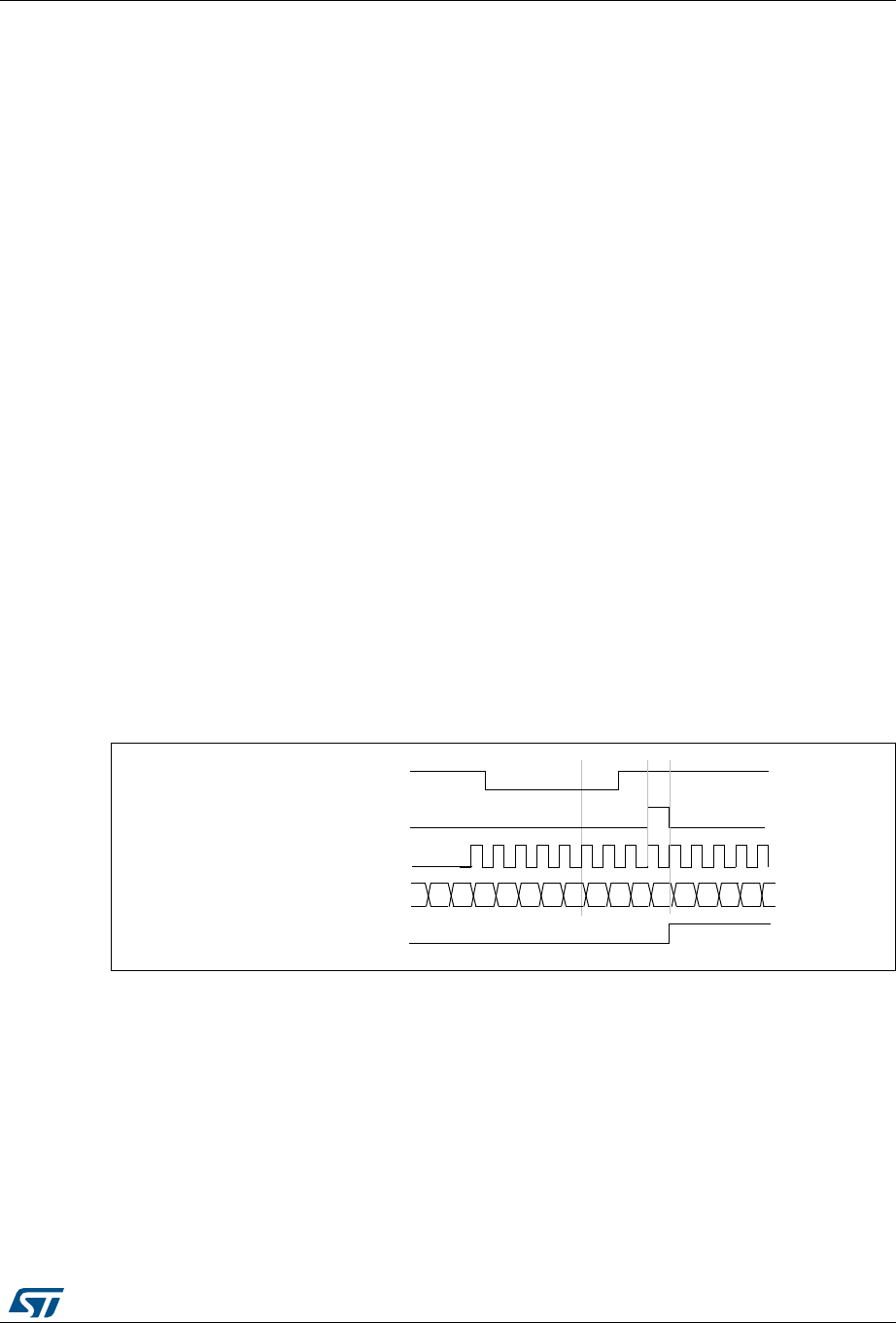
DocID018909 Rev 9 547/1718
RM0090 Advanced-control timers (TIM1&TIM8)
577
17.3.19 TIMx and external trigger synchronization
The TIMx timer can be synchronized with an external trigger in several modes: Reset mode,
Gated mode and Trigger mode.
Slave mode: Reset mode
The counter and its prescaler can be reinitialized in response to an event on a trigger input.
Moreover, if the URS bit from the TIMx_CR1 register is low, an update event UEV is
generated. Then all the preloaded registers (TIMx_ARR, TIMx_CCRx) are updated.
In the following example, the upcounter is cleared in response to a rising edge on TI1 input:
•Configure the channel 1 to detect rising edges on TI1. Configure the input filter duration
(in this example, we don’t need any filter, so we keep IC1F=0000). The capture
prescaler is not used for triggering, so you don’t need to configure it. The CC1S bits
select the input capture source only, CC1S = 01 in the TIMx_CCMR1 register. Write
CC1P=0 and CC1NP=’0’ in TIMx_CCER register to validate the polarity (and detect
rising edges only).
•Configure the timer in reset mode by writing SMS=100 in TIMx_SMCR register. Select
TI1 as the input source by writing TS=101 in TIMx_SMCR register.
•Start the counter by writing CEN=1 in the TIMx_CR1 register.
The counter starts counting on the internal clock, then behaves normally until TI1 rising
edge. When TI1 rises, the counter is cleared and restarts from 0. In the meantime, the
trigger flag is set (TIF bit in the TIMx_SR register) and an interrupt request, or a DMA
request can be sent if enabled (depending on the TIE and TDE bits in TIMx_DIER register).
The following figure shows this behavior when the auto-reload register TIMx_ARR=0x36.
The delay between the rising edge on TI1 and the actual reset of the counter is due to the
resynchronization circuit on TI1 input.
Figure 130. Control circuit in reset mode
00
Counter clock = ck_cnt = ck_psc
Counter register 01 02 03 00 01 02 0332 33 34 35 36
UG
TI1
3130
TIF
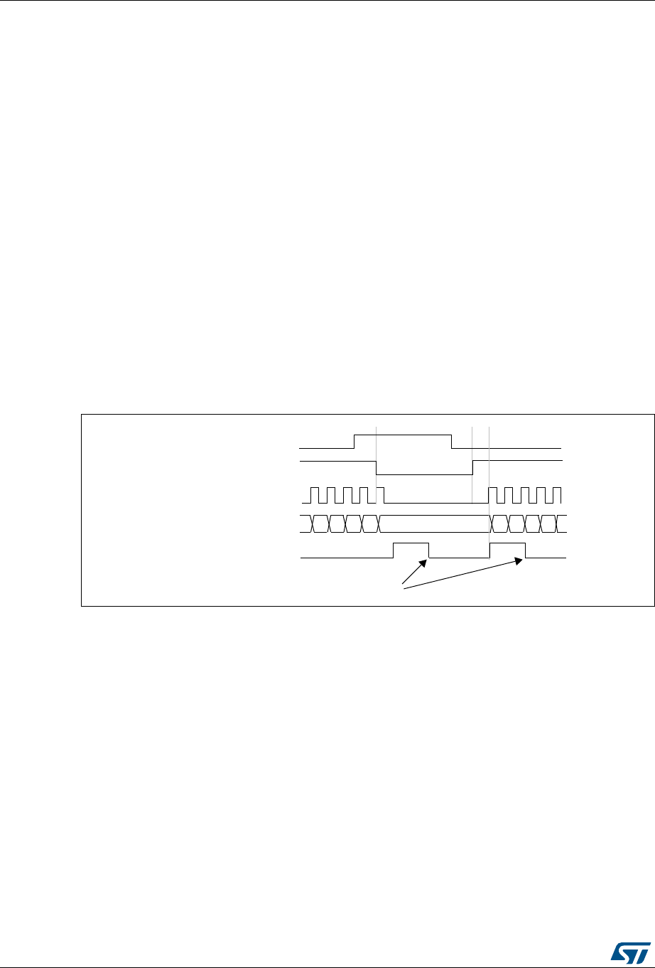
Advanced-control timers (TIM1&TIM8) RM0090
548/1718 DocID018909 Rev 9
Slave mode: Gated mode
The counter can be enabled depending on the level of a selected input.
In the following example, the upcounter counts only when TI1 input is low:
•Configure the channel 1 to detect low levels on TI1. Configure the input filter duration
(in this example, we don’t need any filter, so we keep IC1F=0000). The capture
prescaler is not used for triggering, so you don’t need to configure it. The CC1S bits
select the input capture source only, CC1S=01 in TIMx_CCMR1 register. Write
CC1P=1 and CC1NP=’0’ in TIMx_CCER register to validate the polarity (and detect
low level only).
•Configure the timer in gated mode by writing SMS=101 in TIMx_SMCR register. Select
TI1 as the input source by writing TS=101 in TIMx_SMCR register.
•Enable the counter by writing CEN=1 in the TIMx_CR1 register (in gated mode, the
counter doesn’t start if CEN=0, whatever is the trigger input level).
The counter starts counting on the internal clock as long as TI1 is low and stops as soon as
TI1 becomes high. The TIF flag in the TIMx_SR register is set both when the counter starts
or stops.
The delay between the rising edge on TI1 and the actual stop of the counter is due to the
resynchronization circuit on TI1 input.
Figure 131. Control circuit in gated mode
Counter clock = ck_cnt = ck_psc
Counter register 35 36 37 3832 33 34
TI1
3130
CNT_EN
TIF
Write TIF=0
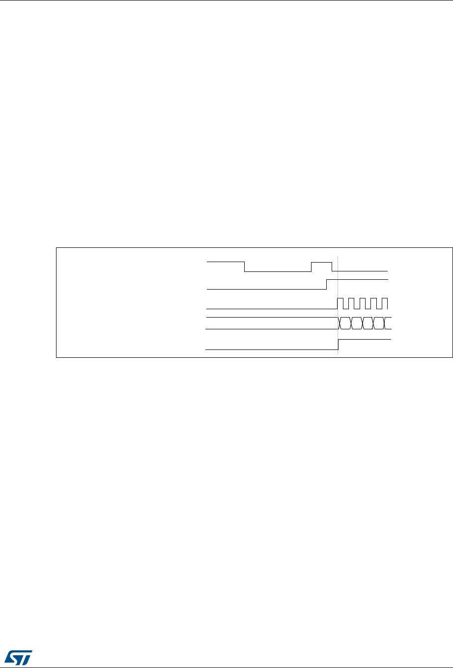
DocID018909 Rev 9 549/1718
RM0090 Advanced-control timers (TIM1&TIM8)
577
Slave mode: Trigger mode
The counter can start in response to an event on a selected input.
In the following example, the upcounter starts in response to a rising edge on TI2 input:
•Configure the channel 2 to detect rising edges on TI2. Configure the input filter duration
(in this example, we don’t need any filter, so we keep IC2F=0000). The capture
prescaler is not used for triggering, so you don’t need to configure it. The CC2S bits are
configured to select the input capture source only, CC2S=01 in TIMx_CCMR1 register.
Write CC2P=1 and CC2NP=0 in TIMx_CCER register to validate the polarity (and
detect low level only).
•Configure the timer in trigger mode by writing SMS=110 in TIMx_SMCR register. Select
TI2 as the input source by writing TS=110 in TIMx_SMCR register.
When a rising edge occurs on TI2, the counter starts counting on the internal clock and the
TIF flag is set.
The delay between the rising edge on TI2 and the actual start of the counter is due to the
resynchronization circuit on TI2 input.
Figure 132. Control circuit in trigger mode
Slave mode: external clock mode 2 + trigger mode
The external clock mode 2 can be used in addition to another slave mode (except external
clock mode 1 and encoder mode). In this case, the ETR signal is used as external clock
input, and another input can be selected as trigger input (in reset mode, gated mode or
trigger mode). It is recommended not to select ETR as TRGI through the TS bits of
TIMx_SMCR register.
In the following example, the upcounter is incremented at each rising edge of the ETR
signal as soon as a rising edge of TI1 occurs:
Counter clock = ck_cnt = ck_psc
Counter register 35 36 37 3834
TI2
CNT_EN
TIF
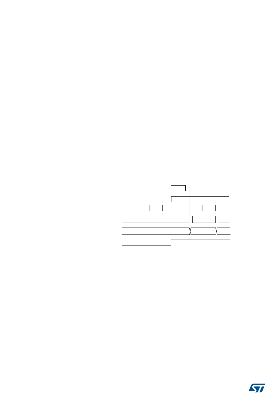
Advanced-control timers (TIM1&TIM8) RM0090
550/1718 DocID018909 Rev 9
1. Configure the external trigger input circuit by programming the TIMx_SMCR register as
follows:
– ETF = 0000: no filter
– ETPS = 00: prescaler disabled
– ETP = 0: detection of rising edges on ETR and ECE=1 to enable the external clock
mode 2.
2. Configure the channel 1 as follows, to detect rising edges on TI:
– IC1F=0000: no filter.
– The capture prescaler is not used for triggering and does not need to be
configured.
– CC1S=01 in TIMx_CCMR1 register to select only the input capture source
– CC1P=0 and CC1NP=’0’ in TIMx_CCER register to validate the polarity (and
detect rising edge only).
3. Configure the timer in trigger mode by writing SMS=110 in TIMx_SMCR register. Select
TI1 as the input source by writing TS=101 in TIMx_SMCR register.
A rising edge on TI1 enables the counter and sets the TIF flag. The counter then counts on
ETR rising edges.
The delay between the rising edge of the ETR signal and the actual reset of the counter is
due to the resynchronization circuit on ETRP input.
Figure 133. Control circuit in external clock mode 2 + trigger mode
17.3.20 Timer synchronization
The TIM timers are linked together internally for timer synchronization or chaining. Refer to
Section 18.3.15: Timer synchronization on page 607 for details.
17.3.21 Debug mode
When the microcontroller enters debug mode (Cortex®-M4 with FPU core halted), the TIMx
counter either continues to work normally or stops, depending on DBG_TIMx_STOP
configuration bit in DBG module. For more details, refer to Section 38.16.2: Debug support
for timers, watchdog, bxCAN and I2C.
Counter clock = CK_CNT = CK_PSC
Counter register 35 3634
ETR
CEN/CNT_EN
TIF
TI1

DocID018909 Rev 9 551/1718
RM0090 Advanced-control timers (TIM1&TIM8)
577
17.4 TIM1&TIM8 registers
Refer to Section 1.1 on page 57 for a list of abbreviations used in register descriptions.
The peripheral registers must be written by half-words (16 bits) or words (32 bits). Read
accesses can be done by bytes (8 bits), half-word (16 bits) or words (32 bits).
17.4.1 TIM1&TIM8 control register 1 (TIMx_CR1)
Address offset: 0x00
Reset value: 0x0000
1514131211109876543210
Reserved CKD[1:0] ARPE CMS[1:0] DIR OPM URS UDIS CEN
rw rw rw rw rw rw rw rw rw rw
Bits 15:10 Reserved, must be kept at reset value.
Bits 9:8 CKD[1:0]: Clock division
This bit-field indicates the division ratio between the timer clock (CK_INT) frequency and the
dead-time and sampling clock (tDTS)used by the dead-time generators and the digital filters
(ETR, TIx),
00: tDTS=tCK_INT
01: tDTS=2*tCK_INT
10: tDTS=4*tCK_INT
11: Reserved, do not program this value
Bit 7 ARPE: Auto-reload preload enable
0: TIMx_ARR register is not buffered
1: TIMx_ARR register is buffered
Bits 6:5 CMS[1:0]: Center-aligned mode selection
00: Edge-aligned mode. The counter counts up or down depending on the direction bit
(DIR).
01: Center-aligned mode 1. The counter counts up and down alternatively. Output compare
interrupt flags of channels configured in output (CCxS=00 in TIMx_CCMRx register) are set
only when the counter is counting down.
10: Center-aligned mode 2. The counter counts up and down alternatively. Output compare
interrupt flags of channels configured in output (CCxS=00 in TIMx_CCMRx register) are set
only when the counter is counting up.
11: Center-aligned mode 3. The counter counts up and down alternatively. Output compare
interrupt flags of channels configured in output (CCxS=00 in TIMx_CCMRx register) are set
both when the counter is counting up or down.
Note: It is not allowed to switch from edge-aligned mode to center-aligned mode as long as
the counter is enabled (CEN=1)
Bit 4 DIR: Direction
0: Counter used as upcounter
1: Counter used as downcounter
Note: This bit is read only when the timer is configured in Center-aligned mode or Encoder
mode.
Bit 3 OPM: One pulse mode
0: Counter is not stopped at update event
1: Counter stops counting at the next update event (clearing the bit CEN)

Advanced-control timers (TIM1&TIM8) RM0090
552/1718 DocID018909 Rev 9
17.4.2 TIM1&TIM8 control register 2 (TIMx_CR2)
Address offset: 0x04
Reset value: 0x0000
Bit 2 URS: Update request source
This bit is set and cleared by software to select the UEV event sources.
0: Any of the following events generate an update interrupt or DMA request if enabled.
These events can be:
– Counter overflow/underflow
– Setting the UG bit
– Update generation through the slave mode controller
1: Only counter overflow/underflow generates an update interrupt or DMA request if
enabled.
Bit 1 UDIS: Update disable
This bit is set and cleared by software to enable/disable UEV event generation.
0: UEV enabled. The Update (UEV) event is generated by one of the following events:
– Counter overflow/underflow
– Setting the UG bit
– Update generation through the slave mode controller
Buffered registers are then loaded with their preload values.
1: UEV disabled. The Update event is not generated, shadow registers keep their value
(ARR, PSC, CCRx). However the counter and the prescaler are reinitialized if the UG bit is
set or if a hardware reset is received from the slave mode controller.
Bit 0 CEN: Counter enable
0: Counter disabled
1: Counter enabled
Note: External clock, gated mode and encoder mode can work only if the CEN bit has been
previously set by software. However trigger mode can set the CEN bit automatically by
hardware.
1514131211109876543210
Res.
OIS4 OIS3N OIS3 OIS2N OIS2 OIS1N OIS1 TI1S MMS[2:0] CCDS CCUS
Res.
CCPC
rw rw rw rw rw rw rw rw rw rw rw rw rw rw
Bit 15 Reserved, must be kept at reset value.
Bit 14 OIS4: Output Idle state 4 (OC4 output)
refer to OIS1 bit
Bit 13 OIS3N: Output Idle state 3 (OC3N output)
refer to OIS1N bit
Bit 12 OIS3: Output Idle state 3 (OC3 output)
refer to OIS1 bit
Bit 11 OIS2N: Output Idle state 2 (OC2N output)
refer to OIS1N bit
Bit 10 OIS2: Output Idle state 2 (OC2 output)
refer to OIS1 bit

DocID018909 Rev 9 553/1718
RM0090 Advanced-control timers (TIM1&TIM8)
577
Bit 9 OIS1N: Output Idle state 1 (OC1N output)
0: OC1N=0 after a dead-time when MOE=0
1: OC1N=1 after a dead-time when MOE=0
Note: This bit can not be modified as long as LOCK level 1, 2 or 3 has been programmed
(LOCK bits in TIMx_BDTR register).
Bit 8 OIS1: Output Idle state 1 (OC1 output)
0: OC1=0 (after a dead-time if OC1N is implemented) when MOE=0
1: OC1=1 (after a dead-time if OC1N is implemented) when MOE=0
Note: This bit can not be modified as long as LOCK level 1, 2 or 3 has been programmed
(LOCK bits in TIMx_BDTR register).
Bit 7 TI1S: TI1 selection
0: The TIMx_CH1 pin is connected to TI1 input
1: The TIMx_CH1, CH2 and CH3 pins are connected to the TI1 input (XOR combination)
Bits 6:4 MMS[2:0]: Master mode selection
These bits allow to select the information to be sent in master mode to slave timers for
synchronization (TRGO). The combination is as follows:
000: Reset - the UG bit from the TIMx_EGR register is used as trigger output (TRGO). If the
reset is generated by the trigger input (slave mode controller configured in reset mode) then
the signal on TRGO is delayed compared to the actual reset.
001: Enable - the Counter Enable signal CNT_EN is used as trigger output (TRGO). It is
useful to start several timers at the same time or to control a window in which a slave timer is
enable. The Counter Enable signal is generated by a logic OR between CEN control bit and
the trigger input when configured in gated mode. When the Counter Enable signal is
controlled by the trigger input, there is a delay on TRGO, except if the master/slave mode is
selected (see the MSM bit description in TIMx_SMCR register).
010: Update - The update event is selected as trigger output (TRGO). For instance a master
timer can then be used as a prescaler for a slave timer.
011: Compare Pulse - The trigger output send a positive pulse when the CC1IF flag is to be
set (even if it was already high), as soon as a capture or a compare match occurred.
(TRGO).
100: Compare - OC1REF signal is used as trigger output (TRGO)
101: Compare - OC2REF signal is used as trigger output (TRGO)
110: Compare - OC3REF signal is used as trigger output (TRGO)
111: Compare - OC4REF signal is used as trigger output (TRGO)
Bit 3 CCDS: Capture/compare DMA selection
0: CCx DMA request sent when CCx event occurs
1: CCx DMA requests sent when update event occurs
Bit 2 CCUS: Capture/compare control update selection
0: When capture/compare control bits are preloaded (CCPC=1), they are updated by setting
the COMG bit only
1: When capture/compare control bits are preloaded (CCPC=1), they are updated by setting
the COMG bit or when an rising edge occurs on TRGI
Note: This bit acts only on channels that have a complementary output.
Bit 1 Reserved, must be kept at reset value.
Bit 0 CCPC: Capture/compare preloaded control
0: CCxE, CCxNE and OCxM bits are not preloaded
1: CCxE, CCxNE and OCxM bits are preloaded, after having been written, they are updated
only when a commutation event (COM) occurs (COMG bit set or rising edge detected on
TRGI, depending on the CCUS bit).
Note: This bit acts only on channels that have a complementary output.

Advanced-control timers (TIM1&TIM8) RM0090
554/1718 DocID018909 Rev 9
17.4.3 TIM1&TIM8 slave mode control register (TIMx_SMCR)
Address offset: 0x08
Reset value: 0x0000
1514131211109876543210
ETP ECE ETPS[1:0] ETF[3:0] MSM TS[2:0] Res. SMS[2:0]
rw rw rw rw rw rw rw rw rw rw rw rw Res. rw rw rw
Bit 15 ETP: External trigger polarity
This bit selects whether ETR or ETR is used for trigger operations
0: ETR is non-inverted, active at high level or rising edge.
1: ETR is inverted, active at low level or falling edge.
Bit 14 ECE: External clock enable
This bit enables External clock mode 2.
0: External clock mode 2 disabled
1: External clock mode 2 enabled. The counter is clocked by any active edge on the ETRF
signal.
Note: 1: Setting the ECE bit has the same effect as selecting external clock mode 1 with
TRGI connected to ETRF (SMS=111 and TS=111).
2: It is possible to simultaneously use external clock mode 2 with the following slave
modes: reset mode, gated mode and trigger mode. Nevertheless, TRGI must not be
connected to ETRF in this case (TS bits must not be 111).
3: If external clock mode 1 and external clock mode 2 are enabled at the same time,
the external clock input is ETRF.
Bits 13:12 ETPS[1:0]: External trigger prescaler
External trigger signal ETRP frequency must be at most 1/4 of TIMxCLK frequency. A
prescaler can be enabled to reduce ETRP frequency. It is useful when inputting fast external
clocks.
00: Prescaler OFF
01: ETRP frequency divided by 2
10: ETRP frequency divided by 4
11: ETRP frequency divided by 8

DocID018909 Rev 9 555/1718
RM0090 Advanced-control timers (TIM1&TIM8)
577
Bits 11:8 ETF[3:0]: External trigger filter
This bit-field then defines the frequency used to sample ETRP signal and the length of the
digital filter applied to ETRP. The digital filter is made of an event counter in which N events
are needed to validate a transition on the output:
0000: No filter, sampling is done at fDTS
0001: fSAMPLING=fCK_INT
, N=2
0010: fSAMPLING=fCK_INT
, N=4
0011: fSAMPLING=fCK_INT
, N=8
0100: fSAMPLING=fDTS/2, N=6
0101: fSAMPLING=fDTS/2, N=8
0110: fSAMPLING=fDTS/4, N=6
0111: fSAMPLING=fDTS/4, N=8
1000: fSAMPLING=fDTS/8, N=6
1001: fSAMPLING=fDTS/8, N=8
1010: fSAMPLING=fDTS/16, N=5
1011: fSAMPLING=fDTS/16, N=6
1100: fSAMPLING=fDTS/16, N=8
1101: fSAMPLING=fDTS/32, N=5
1110: fSAMPLING=fDTS/32, N=6
1111: fSAMPLING=fDTS/32, N=8
Bit 7 MSM: Master/slave mode
0: No action
1: The effect of an event on the trigger input (TRGI) is delayed to allow a perfect
synchronization between the current timer and its slaves (through TRGO). It is useful if we
want to synchronize several timers on a single external event.
Bits 6:4 TS[2:0]: Trigger selection
This bit-field selects the trigger input to be used to synchronize the counter.
000: Internal Trigger 0 (ITR0)
001: Internal Trigger 1 (ITR1)
010: Internal Trigger 2 (ITR2)
011: Internal Trigger 3 (ITR3)
100: TI1 Edge Detector (TI1F_ED)
101: Filtered Timer Input 1 (TI1FP1)
110: Filtered Timer Input 2 (TI2FP2)
111: External Trigger input (ETRF)
See Table 93: TIMx Internal trigger connection on page 556 for more details on ITRx
meaning for each Timer.
Note: These bits must be changed only when they are not used (e.g. when SMS=000) to
avoid wrong edge detections at the transition.
Bit 3 Reserved, must be kept at reset value.
Advanced-control timers (TIM1&TIM8) RM0090
556/1718 DocID018909 Rev 9
17.4.4 TIM1&TIM8 DMA/interrupt enable register (TIMx_DIER)
Address offset: 0x0C
Reset value: 0x0000
Bits 2:0 SMS: Slave mode selection
When external signals are selected the active edge of the trigger signal (TRGI) is linked to
the polarity selected on the external input (see Input Control register and Control Register
description.
000: Slave mode disabled - if CEN = ‘1’ then the prescaler is clocked directly by the internal
clock.
001: Encoder mode 1 - Counter counts up/down on TI2FP2 edge depending on TI1FP1
level.
010: Encoder mode 2 - Counter counts up/down on TI1FP1 edge depending on TI2FP2
level.
011: Encoder mode 3 - Counter counts up/down on both TI1FP1 and TI2FP2 edges
depending on the level of the other input.
100: Reset Mode - Rising edge of the selected trigger input (TRGI) reinitializes the counter
and generates an update of the registers.
101: Gated Mode - The counter clock is enabled when the trigger input (TRGI) is high. The
counter stops (but is not reset) as soon as the trigger becomes low. Both start and stop of
the counter are controlled.
110: Trigger Mode - The counter starts at a rising edge of the trigger TRGI (but it is not
reset). Only the start of the counter is controlled.
111: External Clock Mode 1 - Rising edges of the selected trigger (TRGI) clock the counter.
Note: The gated mode must not be used if TI1F_ED is selected as the trigger input
(TS=’100’). Indeed, TI1F_ED outputs 1 pulse for each transition on TI1F, whereas the
gated mode checks the level of the trigger signal.
Table 93. TIMx Internal trigger connection
Slave TIM ITR0 (TS = 000) ITR1 (TS = 001) ITR2 (TS = 010) ITR3 (TS = 011)
TIM1 TIM5 TIM2 TIM3 TIM4
TIM8 TIM1 TIM2 TIM4 TIM5
1514131211109876543210
Res.
TDE COMDE CC4DE CC3DE CC2DE CC1DE UDE BIE TIE COMIE CC4IE CC3IE CC2IE CC1IE UIE
rw rw rw rw rw rw rw rw rw rw rw rw rw rw rw
Bit 15 Reserved, must be kept at reset value.
Bit 14 TDE: Trigger DMA request enable
0: Trigger DMA request disabled
1: Trigger DMA request enabled
Bit 13 COMDE: COM DMA request enable
0: COM DMA request disabled
1: COM DMA request enabled
Bit 12 CC4DE: Capture/Compare 4 DMA request enable
0: CC4 DMA request disabled
1: CC4 DMA request enabled

DocID018909 Rev 9 557/1718
RM0090 Advanced-control timers (TIM1&TIM8)
577
Bit 11 CC3DE: Capture/Compare 3 DMA request enable
0: CC3 DMA request disabled
1: CC3 DMA request enabled
Bit 10 CC2DE: Capture/Compare 2 DMA request enable
0: CC2 DMA request disabled
1: CC2 DMA request enabled
Bit 9 CC1DE: Capture/Compare 1 DMA request enable
0: CC1 DMA request disabled
1: CC1 DMA request enabled
Bit 8 UDE: Update DMA request enable
0: Update DMA request disabled
1: Update DMA request enabled
Bit 7 BIE: Break interrupt enable
0: Break interrupt disabled
1: Break interrupt enabled
Bit 6 TIE: Trigger interrupt enable
0: Trigger interrupt disabled
1: Trigger interrupt enabled
Bit 5 COMIE: COM interrupt enable
0: COM interrupt disabled
1: COM interrupt enabled
Bit 4 CC4IE: Capture/Compare 4 interrupt enable
0: CC4 interrupt disabled
1: CC4 interrupt enabled
Bit 3 CC3IE: Capture/Compare 3 interrupt enable
0: CC3 interrupt disabled
1: CC3 interrupt enabled
Bit 2 CC2IE: Capture/Compare 2 interrupt enable
0: CC2 interrupt disabled
1: CC2 interrupt enabled
Bit 1 CC1IE: Capture/Compare 1 interrupt enable
0: CC1 interrupt disabled
1: CC1 interrupt enabled
Bit 0 UIE: Update interrupt enable
0: Update interrupt disabled
1: Update interrupt enabled

Advanced-control timers (TIM1&TIM8) RM0090
558/1718 DocID018909 Rev 9
17.4.5 TIM1&TIM8 status register (TIMx_SR)
Address offset: 0x10
Reset value: 0x0000
1514131211109876543210
Reserved CC4OF CC3OF CC2OF CC1OF Res. BIF TIF COMIF CC4IF CC3IF CC2IF CC1IF UIF
rc_w0 rc_w0 rc_w0 rc_w0 Res. rc_w0 rc_w0 rc_w0 rc_w0 rc_w0 rc_w0 rc_w0 rc_w0
Bits 15:13 Reserved, must be kept at reset value.
Bit 12 CC4OF: Capture/Compare 4 overcapture flag
refer to CC1OF description
Bit 11 CC3OF: Capture/Compare 3 overcapture flag
refer to CC1OF description
Bit 10 CC2OF: Capture/Compare 2 overcapture flag
refer to CC1OF description
Bit 9 CC1OF: Capture/Compare 1 overcapture flag
This flag is set by hardware only when the corresponding channel is configured in input
capture mode. It is cleared by software by writing it to ‘0’.
0: No overcapture has been detected.
1: The counter value has been captured in TIMx_CCR1 register while CC1IF flag was
already set
Bit 8 Reserved, must be kept at reset value.
Bit 7 BIF: Break interrupt flag
This flag is set by hardware as soon as the break input goes active. It can be cleared by
software if the break input is not active.
0: No break event occurred.
1: An active level has been detected on the break input.
Bit 6 TIF: Trigger interrupt flag
This flag is set by hardware on trigger event (active edge detected on TRGI input when the
slave mode controller is enabled in all modes but gated mode. It is set when the counter
starts or stops when gated mode is selected. It is cleared by software.
0: No trigger event occurred.
1: Trigger interrupt pending.
Bit 5 COMIF: COM interrupt flag
This flag is set by hardware on COM event (when Capture/compare Control bits - CCxE,
CCxNE, OCxM - have been updated). It is cleared by software.
0: No COM event occurred.
1: COM interrupt pending.
Bit 4 CC4IF: Capture/Compare 4 interrupt flag
refer to CC1IF description
Bit 3 CC3IF: Capture/Compare 3 interrupt flag
refer to CC1IF description

DocID018909 Rev 9 559/1718
RM0090 Advanced-control timers (TIM1&TIM8)
577
17.4.6 TIM1&TIM8 event generation register (TIMx_EGR)
Address offset: 0x14
Reset value: 0x0000
Bit 2 CC2IF: Capture/Compare 2 interrupt flag
refer to CC1IF description
Bit 1 CC1IF: Capture/Compare 1 interrupt flag
If channel CC1 is configured as output:
This flag is set by hardware when the counter matches the compare value, with some
exception in center-aligned mode (refer to the CMS bits in the TIMx_CR1 register
description). It is cleared by software.
0: No match.
1: The content of the counter TIMx_CNT matches the content of the TIMx_CCR1 register.
When the contents of TIMx_CCR1 are greater than the contents of TIMx_ARR, the CC1IF
bit goes high on the counter overflow (in upcounting and up/down-counting modes) or
underflow (in downcounting mode)
If channel CC1 is configured as input:
This bit is set by hardware on a capture. It is cleared by software or by reading the
TIMx_CCR1 register.
0: No input capture occurred
1: The counter value has been captured in TIMx_CCR1 register (An edge has been
detected on IC1 which matches the selected polarity)
Bit 0 UIF: Update interrupt flag
This bit is set by hardware on an update event. It is cleared by software.
0: No update occurred.
1: Update interrupt pending. This bit is set by hardware when the registers are updated:
– At overflow or underflow regarding the repetition counter value (update if repetition counter
= 0) and if the UDIS=0 in the TIMx_CR1 register.
– When CNT is reinitialized by software using the UG bit in TIMx_EGR register, if URS=0 and
UDIS=0 in the TIMx_CR1 register.
– When CNT is reinitialized by a trigger event (refer to Section 17.4.3: TIM1&TIM8 slave
mode control register (TIMx_SMCR)), if URS=0 and UDIS=0 in the TIMx_CR1 register.
1514131211109876543210
Reserved
BG TG COMG CC4G CC3G CC2G CC1G UG
wwwwwwww
Bits 15:8 Reserved, must be kept at reset value.
Bit 7 BG: Break generation
This bit is set by software in order to generate an event, it is automatically cleared by
hardware.
0: No action
1: A break event is generated. MOE bit is cleared and BIF flag is set. Related interrupt or
DMA transfer can occur if enabled.
Bit 6 TG: Trigger generation
This bit is set by software in order to generate an event, it is automatically cleared by
hardware.
0: No action
1: The TIF flag is set in TIMx_SR register. Related interrupt or DMA transfer can occur if
enabled.

Advanced-control timers (TIM1&TIM8) RM0090
560/1718 DocID018909 Rev 9
Bit 5 COMG: Capture/Compare control update generation
This bit can be set by software, it is automatically cleared by hardware
0: No action
1: When CCPC bit is set, it allows to update CCxE, CCxNE and OCxM bits
Note: This bit acts only on channels having a complementary output.
Bit 4 CC4G: Capture/Compare 4 generation
refer to CC1G description
Bit 3 CC3G: Capture/Compare 3 generation
refer to CC1G description
Bit 2 CC2G: Capture/Compare 2 generation
refer to CC1G description
Bit 1 CC1G: Capture/Compare 1 generation
This bit is set by software in order to generate an event, it is automatically cleared by
hardware.
0: No action
1: A capture/compare event is generated on channel 1:
If channel CC1 is configured as output:
CC1IF flag is set, Corresponding interrupt or DMA request is sent if enabled.
If channel CC1 is configured as input:
The current value of the counter is captured in TIMx_CCR1 register. The CC1IF flag is set,
the corresponding interrupt or DMA request is sent if enabled. The CC1OF flag is set if the
CC1IF flag was already high.
Bit 0 UG: Update generation
This bit can be set by software, it is automatically cleared by hardware.
0: No action
1: Reinitialize the counter and generates an update of the registers. Note that the prescaler
counter is cleared too (anyway the prescaler ratio is not affected). The counter is cleared if
the center-aligned mode is selected or if DIR=0 (upcounting), else it takes the auto-reload
value (TIMx_ARR) if DIR=1 (downcounting).

DocID018909 Rev 9 561/1718
RM0090 Advanced-control timers (TIM1&TIM8)
577
17.4.7 TIM1&TIM8 capture/compare mode register 1 (TIMx_CCMR1)
Address offset: 0x18
Reset value: 0x0000
The channels can be used in input (capture mode) or in output (compare mode). The
direction of a channel is defined by configuring the corresponding CCxS bits. All the other
bits of this register have a different function in input and in output mode. For a given bit,
OCxx describes its function when the channel is configured in output, ICxx describes its
function when the channel is configured in input. So you must take care that the same bit
can have a different meaning for the input stage and for the output stage.
Output compare mode:
1514131211109876543210
OC2
CE OC2M[2:0] OC2
PE
OC2
FE CC2S[1:0]
OC1
CE OC1M[2:0] OC1
PE
OC1
FE CC1S[1:0]
IC2F[3:0] IC2PSC[1:0] IC1F[3:0] IC1PSC[1:0]
rw rw rw rw rw rw rw rw rw rw rw rw rw rw rw rw
Bit 15 OC2CE: Output Compare 2 clear enable
Bits 14:12 OC2M[2:0]: Output Compare 2 mode
Bit 11 OC2PE: Output Compare 2 preload enable
Bit 10 OC2FE: Output Compare 2 fast enable
Bits 9:8 CC2S[1:0]: Capture/Compare 2 selection
This bit-field defines the direction of the channel (input/output) as well as the used input.
00: CC2 channel is configured as output
01: CC2 channel is configured as input, IC2 is mapped on TI2
10: CC2 channel is configured as input, IC2 is mapped on TI1
11: CC2 channel is configured as input, IC2 is mapped on TRC. This mode is working only if
an internal trigger input is selected through the TS bit (TIMx_SMCR register)
Note: CC2S bits are writable only when the channel is OFF (CC2E = ‘0’ in TIMx_CCER).
Bit 7 OC1CE: Output Compare 1 clear enable
OC1CE: Output Compare 1 Clear Enable
0: OC1Ref is not affected by the ETRF Input
1: OC1Ref is cleared as soon as a High level is detected on ETRF input

Advanced-control timers (TIM1&TIM8) RM0090
562/1718 DocID018909 Rev 9
Bits 6:4 OC1M: Output Compare 1 mode
These bits define the behavior of the output reference signal OC1REF from which OC1 and
OC1N are derived. OC1REF is active high whereas OC1 and OC1N active level depends
on CC1P and CC1NP bits.
000: Frozen - The comparison between the output compare register TIMx_CCR1 and the
counter TIMx_CNT has no effect on the outputs.(this mode is used to generate a timing
base).
001: Set channel 1 to active level on match. OC1REF signal is forced high when the counter
TIMx_CNT matches the capture/compare register 1 (TIMx_CCR1).
010: Set channel 1 to inactive level on match. OC1REF signal is forced low when the
counter TIMx_CNT matches the capture/compare register 1 (TIMx_CCR1).
011: Toggle - OC1REF toggles when TIMx_CNT=TIMx_CCR1.
100: Force inactive level - OC1REF is forced low.
101: Force active level - OC1REF is forced high.
110: PWM mode 1 - In upcounting, channel 1 is active as long as TIMx_CNT<TIMx_CCR1
else inactive. In downcounting, channel 1 is inactive (OC1REF=‘0’) as long as
TIMx_CNT>TIMx_CCR1 else active (OC1REF=’1’).
111: PWM mode 2 - In upcounting, channel 1 is inactive as long as TIMx_CNT<TIMx_CCR1
else active. In downcounting, channel 1 is active as long as TIMx_CNT>TIMx_CCR1 else
inactive.
Note: 1: These bits can not be modified as long as LOCK level 3 has been programmed
(LOCK bits in TIMx_BDTR register) and CC1S=’00’ (the channel is configured in
output).
2: In PWM mode 1 or 2, the OCREF level changes only when the result of the
comparison changes or when the output compare mode switches from “frozen” mode
to “PWM” mode.
3: On channels having a complementary output, this bit field is preloaded. If the CCPC
bit is set in the TIMx_CR2 register then the OC1M active bits take the new value from
the preloaded bits only when a COM event is generated.
Bit 3 OC1PE: Output Compare 1 preload enable
0: Preload register on TIMx_CCR1 disabled. TIMx_CCR1 can be written at anytime, the
new value is taken in account immediately.
1: Preload register on TIMx_CCR1 enabled. Read/Write operations access the preload
register. TIMx_CCR1 preload value is loaded in the active register at each update event.
Note: 1: These bits can not be modified as long as LOCK level 3 has been programmed
(LOCK bits in TIMx_BDTR register) and CC1S=’00’ (the channel is configured in
output).
2: The PWM mode can be used without validating the preload register only in one
pulse mode (OPM bit set in TIMx_CR1 register). Else the behavior is not guaranteed.
Bit 2 OC1FE: Output Compare 1 fast enable
This bit is used to accelerate the effect of an event on the trigger in input on the CC output.
0: CC1 behaves normally depending on counter and CCR1 values even when the trigger is
ON. The minimum delay to activate CC1 output when an edge occurs on the trigger input is
5 clock cycles.
1: An active edge on the trigger input acts like a compare match on CC1 output. Then, OC is
set to the compare level independently from the result of the comparison. Delay to sample
the trigger input and to activate CC1 output is reduced to 3 clock cycles. OCFE acts only if
the channel is configured in PWM1 or PWM2 mode.

DocID018909 Rev 9 563/1718
RM0090 Advanced-control timers (TIM1&TIM8)
577
Input capture mode
Bits 1:0 CC1S: Capture/Compare 1 selection
This bit-field defines the direction of the channel (input/output) as well as the used input.
00: CC1 channel is configured as output
01: CC1 channel is configured as input, IC1 is mapped on TI1
10: CC1 channel is configured as input, IC1 is mapped on TI2
11: CC1 channel is configured as input, IC1 is mapped on TRC. This mode is working only if
an internal trigger input is selected through TS bit (TIMx_SMCR register)
Note: CC1S bits are writable only when the channel is OFF (CC1E = ‘0’ in TIMx_CCER).
Bits 15:12 IC2F: Input capture 2 filter
Bits 11:10 IC2PSC[1:0]: Input capture 2 prescaler
Bits 9:8 CC2S: Capture/Compare 2 selection
This bit-field defines the direction of the channel (input/output) as well as the used input.
00: CC2 channel is configured as output
01: CC2 channel is configured as input, IC2 is mapped on TI2
10: CC2 channel is configured as input, IC2 is mapped on TI1
11: CC2 channel is configured as input, IC2 is mapped on TRC. This mode is working only if an
internal trigger input is selected through TS bit (TIMx_SMCR register)
Note: CC2S bits are writable only when the channel is OFF (CC2E = ‘0’ in TIMx_CCER).
Bits 7:4 IC1F[3:0]: Input capture 1 filter
This bit-field defines the frequency used to sample TI1 input and the length of the digital filter applied
to TI1. The digital filter is made of an event counter in which N events are needed to validate a
transition on the output:
0000: No filter, sampling is done at fDTS
0001: fSAMPLING=fCK_INT
, N=2
0010: fSAMPLING=fCK_INT
, N=4
0011: fSAMPLING=fCK_INT
, N=8
0100: fSAMPLING=fDTS/2, N=6
0101: fSAMPLING=fDTS/2, N=8
0110: fSAMPLING=fDTS/4, N=6
0111: fSAMPLING=fDTS/4, N=8
1000: fSAMPLING=fDTS/8, N=6
1001: fSAMPLING=fDTS/8, N=8
1010: fSAMPLING=fDTS/16, N=5
1011: fSAMPLING=fDTS/16, N=6
1100: fSAMPLING=fDTS/16, N=8
1101: fSAMPLING=fDTS/32, N=5
1110: fSAMPLING=fDTS/32, N=6
1111: fSAMPLING=fDTS/32, N=8
Bits 3:2 IC1PSC: Input capture 1 prescaler
This bit-field defines the ratio of the prescaler acting on CC1 input (IC1).
The prescaler is reset as soon as CC1E=’0’ (TIMx_CCER register).
00: no prescaler, capture is done each time an edge is detected on the capture input
01: capture is done once every 2 events
10: capture is done once every 4 events
11: capture is done once every 8 events

Advanced-control timers (TIM1&TIM8) RM0090
564/1718 DocID018909 Rev 9
17.4.8 TIM1&TIM8 capture/compare mode register 2 (TIMx_CCMR2)
Address offset: 0x1C
Reset value: 0x0000
Refer to the above CCMR1 register description.
Output compare mode
Bits 1:0 CC1S: Capture/Compare 1 Selection
This bit-field defines the direction of the channel (input/output) as well as the used input.
00: CC1 channel is configured as output
01: CC1 channel is configured as input, IC1 is mapped on TI1
10: CC1 channel is configured as input, IC1 is mapped on TI2
11: CC1 channel is configured as input, IC1 is mapped on TRC. This mode is working only if an
internal trigger input is selected through TS bit (TIMx_SMCR register)
Note: CC1S bits are writable only when the channel is OFF (CC1E = ‘0’ in TIMx_CCER).
1514131211109876543210
OC4
CE OC4M[2:0] OC4
PE
OC4
FE CC4S[1:0]
OC3
CE. OC3M[2:0] OC3
PE
OC3
FE CC3S[1:0]
IC4F[3:0] IC4PSC[1:0] IC3F[3:0] IC3PSC[1:0]
rw rw rw rw rw rw rw rw rw rw rw rw rw rw rw rw
Bit 15 OC4CE: Output compare 4 clear enable
Bits 14:12 OC4M: Output compare 4 mode
Bit 11 OC4PE: Output compare 4 preload enable
Bit 10 OC4FE: Output compare 4 fast enable
Bits 9:8 CC4S: Capture/Compare 4 selection
This bit-field defines the direction of the channel (input/output) as well as the used input.
00: CC4 channel is configured as output
01: CC4 channel is configured as input, IC4 is mapped on TI4
10: CC4 channel is configured as input, IC4 is mapped on TI3
11: CC4 channel is configured as input, IC4 is mapped on TRC. This mode is working only if
an internal trigger input is selected through TS bit (TIMx_SMCR register)
Note: CC4S bits are writable only when the channel is OFF (CC4E = ‘0’ in TIMx_CCER).
Bit 7 OC3CE: Output compare 3 clear enable
Bits 6:4 OC3M: Output compare 3 mode
Bit 3 OC3PE: Output compare 3 preload enable
Bit 2 OC3FE: Output compare 3 fast enable
Bits 1:0 CC3S: Capture/Compare 3 selection
This bit-field defines the direction of the channel (input/output) as well as the used input.
00: CC3 channel is configured as output
01: CC3 channel is configured as input, IC3 is mapped on TI3
10: CC3 channel is configured as input, IC3 is mapped on TI4
11: CC3 channel is configured as input, IC3 is mapped on TRC. This mode is working only if
an internal trigger input is selected through TS bit (TIMx_SMCR register)
Note: CC3S bits are writable only when the channel is OFF (CC3E = ‘0’ in TIMx_CCER).

DocID018909 Rev 9 565/1718
RM0090 Advanced-control timers (TIM1&TIM8)
577
Input capture mode
17.4.9 TIM1&TIM8 capture/compare enable register (TIMx_CCER)
Address offset: 0x20
Reset value: 0x0000
Bits 15:12 IC4F: Input capture 4 filter
Bits 11:10 IC4PSC: Input capture 4 prescaler
Bits 9:8 CC4S: Capture/Compare 4 selection
This bit-field defines the direction of the channel (input/output) as well as the used input.
00: CC4 channel is configured as output
01: CC4 channel is configured as input, IC4 is mapped on TI4
10: CC4 channel is configured as input, IC4 is mapped on TI3
11: CC4 channel is configured as input, IC4 is mapped on TRC. This mode is working only if
an internal trigger input is selected through TS bit (TIMx_SMCR register)
Note: CC4S bits are writable only when the channel is OFF (CC4E = ‘0’ in TIMx_CCER).
Bits 7:4 IC3F: Input capture 3 filter
Bits 3:2 IC3PSC: Input capture 3 prescaler
Bits 1:0 CC3S: Capture/compare 3 selection
This bit-field defines the direction of the channel (input/output) as well as the used input.
00: CC3 channel is configured as output
01: CC3 channel is configured as input, IC3 is mapped on TI3
10: CC3 channel is configured as input, IC3 is mapped on TI4
11: CC3 channel is configured as input, IC3 is mapped on TRC. This mode is working only if
an internal trigger input is selected through TS bit (TIMx_SMCR register)
Note: CC3S bits are writable only when the channel is OFF (CC3E = ‘0’ in TIMx_CCER).
1514131211109876543210
Reserved CC4P CC4E CC3NP CC3NE CC3P CC3E CC2NP CC2NE CC2P CC2E CC1NP CC1NE CC1P CC1E
rw rw rw rw rw rw rw rw rw rw rw rw rw rw
Bits 15:14 Reserved, must be kept at reset value.
Bit 13 CC4P: Capture/Compare 4 output polarity
refer to CC1P description
Bit 12 CC4E: Capture/Compare 4 output enable
refer to CC1E description
Bit 11 CC3NP: Capture/Compare 3 complementary output polarity
refer to CC1NP description
Bit 10 CC3NE: Capture/Compare 3 complementary output enable
refer to CC1NE description
Bit 9 CC3P: Capture/Compare 3 output polarity
refer to CC1P description
Bit 8 CC3E: Capture/Compare 3 output enable
refer to CC1E description

Advanced-control timers (TIM1&TIM8) RM0090
566/1718 DocID018909 Rev 9
Bit 7 CC2NP: Capture/Compare 2 complementary output polarity
refer to CC1NP description
Bit 6 CC2NE: Capture/Compare 2 complementary output enable
refer to CC1NE description
Bit 5 CC2P: Capture/Compare 2 output polarity
refer to CC1P description
Bit 4 CC2E: Capture/Compare 2 output enable
refer to CC1E description
Bit 3 CC1NP: Capture/Compare 1 complementary output polarity
CC1 channel configured as output:
0: OC1N active high.
1: OC1N active low.
CC1 channel configured as input:
This bit is used in conjunction with CC1P to define the polarity of TI1FP1 and TI2FP1. Refer
to CC1P description.
Note: On channels having a complementary output, this bit is preloaded. If the CCPC bit is
set in the TIMx_CR2 register then the CC1NP active bit takes the new value from the
preloaded bit only when a Commutation event is generated.
Note: This bit is not writable as soon as LOCK level 2 or 3 has been programmed (LOCK bits
in TIMx_BDTR register) and CC1S=”00” (the channel is configured in output).
Bit 2 CC1NE: Capture/Compare 1 complementary output enable
0: Off - OC1N is not active. OC1N level is then function of MOE, OSSI, OSSR, OIS1, OIS1N
and CC1E bits.
1: On - OC1N signal is output on the corresponding output pin depending on MOE, OSSI,
OSSR, OIS1, OIS1N and CC1E bits.
Note: On channels having a complementary output, this bit is preloaded. If the CCPC bit is
set in the TIMx_CR2 register then the CC1NE active bit takes the new value from the
preloaded bit only when a Commutation event is generated.

DocID018909 Rev 9 567/1718
RM0090 Advanced-control timers (TIM1&TIM8)
577
Bit 1 CC1P: Capture/Compare 1 output polarity
CC1 channel configured as output:
0: OC1 active high
1: OC1 active low
CC1 channel configured as input:
CC1NP/CC1P bits select the active polarity of TI1FP1 and TI2FP1 for trigger or capture
operations.
00: non-inverted/rising edge
The circuit is sensitive to TIxFP1 rising edge (capture or trigger operations in reset, external
clock or trigger mode), TIxFP1 is not inverted (trigger operation in gated mode or encoder
mode).
01: inverted/falling edge
The circuit is sensitive to TIxFP1 falling edge (capture or trigger operations in reset, external
clock or trigger mode), TIxFP1 is inverted (trigger operation in gated mode or encoder
mode).
10: reserved, do not use this configuration.
11: non-inverted/both edges
The circuit is sensitive to both TIxFP1 rising and falling edges (capture or trigger operations
in reset, external clock or trigger mode), TIxFP1 is not inverted (trigger operation in gated
mode). This configuration must not be used in encoder mode.
Note: On channels having a complementary output, this bit is preloaded. If the CCPC bit is
set in the TIMx_CR2 register then the CC1P active bit takes the new value from the
preloaded bit only when a Commutation event is generated.
Note: This bit is not writable as soon as LOCK level 2 or 3 has been programmed (LOCK bits
in TIMx_BDTR register).
Bit 0 CC1E: Capture/Compare 1 output enable
CC1 channel configured as output:
0: Off - OC1 is not active. OC1 level is then function of MOE, OSSI, OSSR, OIS1, OIS1N
and CC1NE bits.
1: On - OC1 signal is output on the corresponding output pin depending on MOE, OSSI,
OSSR, OIS1, OIS1N and CC1NE bits.
CC1 channel configured as input:
This bit determines if a capture of the counter value can actually be done into the input
capture/compare register 1 (TIMx_CCR1) or not.
0: Capture disabled.
1: Capture enabled.
Note: On channels having a complementary output, this bit is preloaded. If the CCPC bit is
set in the TIMx_CR2 register then the CC1E active bit takes the new value from the
preloaded bit only when a Commutation event is generated.

Advanced-control timers (TIM1&TIM8) RM0090
568/1718 DocID018909 Rev 9
Table 94. Output control bits for complementary OCx and OCxN channels with
break feature
Control bits Output states(1)
MOE
bit
OSSI
bit
OSSR
bit
CCxE
bit
CCxNE
bit OCx output state OCxN output state
1X
00 0
Output Disabled (not driven by
the timer), OCx=0, OCx_EN=0
Output Disabled (not driven by the
timer), OCxN=0, OCxN_EN=0
00 1
Output Disabled (not driven by
the timer), OCx=0, OCx_EN=0
OCxREF + Polarity OCxN=OCxREF
xor CCxNP, OCxN_EN=1
01 0
OCxREF + Polarity
OCx=OCxREF xor CCxP,
OCx_EN=1
Output Disabled (not driven by the
timer)
OCxN=0, OCxN_EN=0
01 1
OCREF + Polarity + dead-time
OCx_EN=1
Complementary to OCREF (not
OCREF) + Polarity + dead-time
OCxN_EN=1
10 0
Output Disabled (not driven by
the timer)
OCx=CCxP, OCx_EN=0
Output Disabled (not driven by the
timer)
OCxN=CCxNP, OCxN_EN=0
10 1
Off-State (output enabled with
inactive state)
OCx=CCxP, OCx_EN=1
OCxREF + Polarity
OCxN=OCxREF xor CCxNP,
OCxN_EN=1
11 0
OCxREF + Polarity
OCx=OCxREF xor CCxP,
OCx_EN=1
Off-State (output enabled with
inactive state)
OCxN=CCxNP, OCxN_EN=1
11 1
OCREF + Polarity + dead-time
OCx_EN=1
Complementary to OCREF (not
OCREF) + Polarity + dead-time
OCxN_EN=1
0
0
X
00
Output Disabled (not driven by
the timer)
OCx=CCxP, OCx_EN=0
Output Disabled (not driven by the
timer)
OCxN=CCxNP, OCxN_EN=0
0 0 1 Output Disabled (not driven by the timer)
Asynchronously: OCx=CCxP, OCx_EN=0, OCxN=CCxNP,
OCxN_EN=0
Then if the clock is present: OCx=OISx and OCxN=OISxN after a
dead-time, assuming that OISx and OISxN do not correspond to OCX
and OCxN both in active state.
010
011
100
Output Disabled (not driven by
the timer)
OCx=CCxP, OCx_EN=0
Output Disabled (not driven by the
timer)
OCxN=CCxNP, OCxN_EN=0
1 0 1 Off-State (output enabled with inactive state)
Asynchronously: OCx=CCxP, OCx_EN=1, OCxN=CCxNP,
OCxN_EN=1
Then if the clock is present: OCx=OISx and OCxN=OISxN after a
dead-time, assuming that OISx and OISxN do not correspond to OCX
and OCxN both in active state
110
111
1. When both outputs of a channel are not used (CCxE = CCxNE = 0), the OISx, OISxN, CCxP and CCxNP bits must be kept
cleared.

DocID018909 Rev 9 569/1718
RM0090 Advanced-control timers (TIM1&TIM8)
577
Note: The state of the external I/O pins connected to the complementary OCx and OCxN channels
depends on the OCx and OCxN channel state and the GPIO registers.
17.4.10 TIM1&TIM8 counter (TIMx_CNT)
Address offset: 0x24
Reset value: 0x0000
17.4.11 TIM1&TIM8 prescaler (TIMx_PSC)
Address offset: 0x28
Reset value: 0x0000
17.4.12 TIM1&TIM8 auto-reload register (TIMx_ARR)
Address offset: 0x2C
Reset value: 0x0000
1514131211109876543210
CNT[15:0]
rw rw rw rw rw rw rw rw rw rw rw rw rw rw rw rw
Bits 15:0 CNT[15:0]: Counter value
1514131211109876543210
PSC[15:0]
rw rw rw rw rw rw rw rw rw rw rw rw rw rw rw rw
Bits 15:0 PSC[15:0]: Prescaler value
The counter clock frequency (CK_CNT) is equal to fCK_PSC / (PSC[15:0] + 1).
PSC contains the value to be loaded in the active prescaler register at each update event
(including when the counter is cleared through UG bit of TIMx_EGR register or through
trigger controller when configured in “reset mode”).
1514131211109876543210
ARR[15:0]
rw rw rw rw rw rw rw rw rw rw rw rw rw rw rw rw
Bits 15:0 ARR[15:0]: Auto-reload value
ARR is the value to be loaded in the actual auto-reload register.
Refer to Section 17.3.1: Time-base unit on page 513 for more details about ARR update
and behavior.
The counter is blocked while the auto-reload value is null.

Advanced-control timers (TIM1&TIM8) RM0090
570/1718 DocID018909 Rev 9
17.4.13 TIM1&TIM8 repetition counter register (TIMx_RCR)
Address offset: 0x30
Reset value: 0x0000
17.4.14 TIM1&TIM8 capture/compare register 1 (TIMx_CCR1)
Address offset: 0x34
Reset value: 0x0000
1514131211109876543210
Reserved REP[7:0]
rw rw rw rw rw rw rw rw
Bits 15:8 Reserved, must be kept at reset value.
Bits 7:0 REP[7:0]: Repetition counter value
These bits allow the user to set-up the update rate of the compare registers (i.e. periodic
transfers from preload to active registers) when preload registers are enable, as well as the
update interrupt generation rate, if this interrupt is enable.
Each time the REP_CNT related downcounter reaches zero, an update event is generated
and it restarts counting from REP value. As REP_CNT is reloaded with REP value only at
the repetition update event U_RC, any write to the TIMx_RCR register is not taken in
account until the next repetition update event.
It means in PWM mode (REP+1) corresponds to:
– the number of PWM periods in edge-aligned mode
– the number of half PWM period in center-aligned mode.
1514131211109876543210
CCR1[15:0]
rw rw rw rw rw rw rw rw rw rw rw rw rw rw rw rw
Bits 15:0 CCR1[15:0]: Capture/Compare 1 value
If channel CC1 is configured as output:
CCR1 is the value to be loaded in the actual capture/compare 1 register (preload value).
It is loaded permanently if the preload feature is not selected in the TIMx_CCMR1 register
(bit OC1PE). Else the preload value is copied in the active capture/compare 1 register when
an update event occurs.
The active capture/compare register contains the value to be compared to the counter
TIMx_CNT and signaled on OC1 output.
If channel CC1 is configured as input:
CCR1 is the counter value transferred by the last input capture 1 event (IC1).

DocID018909 Rev 9 571/1718
RM0090 Advanced-control timers (TIM1&TIM8)
577
17.4.15 TIM1&TIM8 capture/compare register 2 (TIMx_CCR2)
Address offset: 0x38
Reset value: 0x0000
17.4.16 TIM1&TIM8 capture/compare register 3 (TIMx_CCR3)
Address offset: 0x3C
Reset value: 0x0000
1514131211109876543210
CCR2[15:0]
rw rw rw rw rw rw rw rw rw rw rw rw rw rw rw rw
Bits 15:0 CCR2[15:0]: Capture/Compare 2 value
If channel CC2 is configured as output:
CCR2 is the value to be loaded in the actual capture/compare 2 register (preload value).
It is loaded permanently if the preload feature is not selected in the TIMx_CCMR2 register
(bit OC2PE). Else the preload value is copied in the active capture/compare 2 register when
an update event occurs.
The active capture/compare register contains the value to be compared to the counter
TIMx_CNT and signalled on OC2 output.
If channel CC2 is configured as input:
CCR2 is the counter value transferred by the last input capture 2 event (IC2).
1514131211109876543210
CCR3[15:0]
rw rw rw rw rw rw rw rw rw rw rw rw rw rw rw rw
Bits 15:0 CCR3[15:0]: Capture/Compare value
If channel CC3 is configured as output:
CCR3 is the value to be loaded in the actual capture/compare 3 register (preload value).
It is loaded permanently if the preload feature is not selected in the TIMx_CCMR3 register
(bit OC3PE). Else the preload value is copied in the active capture/compare 3 register when
an update event occurs.
The active capture/compare register contains the value to be compared to the counter
TIMx_CNT and signalled on OC3 output.
If channel CC3 is configured as input:
CCR3 is the counter value transferred by the last input capture 3 event (IC3).

Advanced-control timers (TIM1&TIM8) RM0090
572/1718 DocID018909 Rev 9
17.4.17 TIM1&TIM8 capture/compare register 4 (TIMx_CCR4)
Address offset: 0x40
Reset value: 0x0000
17.4.18 TIM1&TIM8 break and dead-time register (TIMx_BDTR)
Address offset: 0x44
Reset value: 0x0000
Note: As the bits AOE, BKP, BKE, OSSI, OSSR and DTG[7:0] can be write-locked depending on
the LOCK configuration, it can be necessary to configure all of them during the first write
access to the TIMx_BDTR register.
1514131211109876543210
CCR4[15:0]
rw rw rw rw rw rw rw rw rw rw rw rw rw rw rw rw
Bits 15:0 CCR4[15:0]: Capture/Compare value
If channel CC4 is configured as output:
CCR4 is the value to be loaded in the actual capture/compare 4 register (preload value).
It is loaded permanently if the preload feature is not selected in the TIMx_CCMR4 register
(bit OC4PE). Else the preload value is copied in the active capture/compare 4 register when
an update event occurs.
The active capture/compare register contains the value to be compared to the counter
TIMx_CNT and signalled on OC4 output.
If channel CC4 is configured as input:
CCR4 is the counter value transferred by the last input capture 4 event (IC4).
1514131211109876543210
MOE AOE BKP BKE OSSR OSSI LOCK[1:0] DTG[7:0]
rw rw rw rw rw rw rw rw rw rw rw rw rw rw rw rw
Bit 15 MOE: Main output enable
This bit is cleared asynchronously by hardware as soon as the break input is active. It is set
by software or automatically depending on the AOE bit. It is acting only on the channels
which are configured in output.
0: OC and OCN outputs are disabled or forced to idle state.
1: OC and OCN outputs are enabled if their respective enable bits are set (CCxE, CCxNE in
TIMx_CCER register).
See OC/OCN enable description for more details (Section 17.4.9: TIM1&TIM8
capture/compare enable register (TIMx_CCER) on page 565).
Bit 14 AOE: Automatic output enable
0: MOE can be set only by software
1: MOE can be set by software or automatically at the next update event (if the break input is
not be active)
Note: This bit can not be modified as long as LOCK level 1 has been programmed (LOCK bits
in TIMx_BDTR register).

DocID018909 Rev 9 573/1718
RM0090 Advanced-control timers (TIM1&TIM8)
577
Bit 13 BKP: Break polarity
0: Break input BRK is active low
1: Break input BRK is active high
Note: This bit can not be modified as long as LOCK level 1 has been programmed (LOCK bits
in TIMx_BDTR register).
Note: Any write operation to this bit takes a delay of 1 APB clock cycle to become effective.
Bit 12 BKE: Break enable
0: Break inputs (BRK and CSS clock failure event) disabled
1; Break inputs (BRK and CSS clock failure event) enabled
Note: This bit cannot be modified when LOCK level 1 has been programmed (LOCK bits in
TIMx_BDTR register).
Note: Any write operation to this bit takes a delay of 1 APB clock cycle to become effective.
Bit 11 OSSR: Off-state selection for Run mode
This bit is used when MOE=1 on channels having a complementary output which are
configured as outputs. OSSR is not implemented if no complementary output is implemented
in the timer.
See OC/OCN enable description for more details (Section 17.4.9: TIM1&TIM8
capture/compare enable register (TIMx_CCER) on page 565).
0: When inactive, OC/OCN outputs are disabled (OC/OCN enable output signal=0).
1: When inactive, OC/OCN outputs are enabled with their inactive level as soon as CCxE=1
or CCxNE=1. Then, OC/OCN enable output signal=1
Note: This bit can not be modified as soon as the LOCK level 2 has been programmed (LOCK
bits in TIMx_BDTR register).
Bit 10 OSSI: Off-state selection for Idle mode
This bit is used when MOE=0 on channels configured as outputs.
See OC/OCN enable description for more details (Section 17.4.9: TIM1&TIM8
capture/compare enable register (TIMx_CCER) on page 565).
0: When inactive, OC/OCN outputs are disabled (OC/OCN enable output signal=0).
1: When inactive, OC/OCN outputs are forced first with their idle level as soon as CCxE=1 or
CCxNE=1. OC/OCN enable output signal=1)
Note: This bit can not be modified as soon as the LOCK level 2 has been programmed (LOCK
bits in TIMx_BDTR register).
Bits 9:8 LOCK[1:0]: Lock configuration
These bits offer a write protection against software errors.
00: LOCK OFF - No bit is write protected.
01: LOCK Level 1 = DTG bits in TIMx_BDTR register, OISx and OISxN bits in TIMx_CR2
register and BKE/BKP/AOE bits in TIMx_BDTR register can no longer be written.
10: LOCK Level 2 = LOCK Level 1 + CC Polarity bits (CCxP/CCxNP bits in TIMx_CCER
register, as long as the related channel is configured in output through the CCxS bits) as well
as OSSR and OSSI bits can no longer be written.
11: LOCK Level 3 = LOCK Level 2 + CC Control bits (OCxM and OCxPE bits in
TIMx_CCMRx registers, as long as the related channel is configured in output through the
CCxS bits) can no longer be written.
Note: The LOCK bits can be written only once after the reset. Once the TIMx_BDTR register
has been written, their content is frozen until the next reset.

Advanced-control timers (TIM1&TIM8) RM0090
574/1718 DocID018909 Rev 9
17.4.19 TIM1&TIM8 DMA control register (TIMx_DCR)
Address offset: 0x48
Reset value: 0x0000
Bits 7:0 DTG[7:0]: Dead-time generator setup
This bit-field defines the duration of the dead-time inserted between the complementary
outputs. DT correspond to this duration.
DTG[7:5]=0xx => DT=DTG[7:0]x tdtg with tdtg=tDTS.
DTG[7:5]=10x => DT=(64+DTG[5:0])xtdtg with Tdtg=2xtDTS.
DTG[7:5]=110 => DT=(32+DTG[4:0])xtdtg with Tdtg=8xtDTS.
DTG[7:5]=111 => DT=(32+DTG[4:0])xtdtg with Tdtg=16xtDTS.
Example if TDTS=125ns (8MHz), dead-time possible values are:
0 to 15875 ns by 125 ns steps,
16 us to 31750 ns by 250 ns steps,
32 us to 63us by 1 us steps,
64 us to 126 us by 2 us steps
Note: This bit-field can not be modified as long as LOCK level 1, 2 or 3 has been programmed
(LOCK bits in TIMx_BDTR register).
1514131211109876543210
Reserved DBL[4:0] Reserved DBA[4:0]
rw rw rw rw rw rw rw rw rw rw
Bits 15:13 Reserved, must be kept at reset value.
Bits 12:8 DBL[4:0]: DMA burst length
This 5-bit vector defines the number of DMA transfers (the timer detects a burst transfer
when a read or a write access to the TIMx_DMAR register address is performed).
the TIMx_DMAR address)
00000: 1 transfer
00001: 2 transfers
00010: 3 transfers
...
10001: 18 transfers
Bits 7:5 Reserved, must be kept at reset value.
Bits 4:0 DBA[4:0]: DMA base address
This 5-bits vector defines the base-address for DMA transfers (when read/write access are
done through the TIMx_DMAR address). DBA is defined as an offset starting from the
address of the TIMx_CR1 register.
Example:
00000: TIMx_CR1,
00001: TIMx_CR2,
00010: TIMx_SMCR,
...
Example: Let us consider the following transfer: DBL = 7 transfers and DBA = TIMx_CR1. In
this case the transfer is done to/from 7 registers starting from the TIMx_CR1 address.

DocID018909 Rev 9 575/1718
RM0090 Advanced-control timers (TIM1&TIM8)
577
17.4.20 TIM1&TIM8 DMA address for full transfer (TIMx_DMAR)
Address offset: 0x4C
Reset value: 0x0000
Example of how to use the DMA burst feature
In this example the timer DMA burst feature is used to update the contents of the CCRx
registers (x = 2, 3, 4) with the DMA transferring half words into the CCRx registers.
This is done in the following steps:
1. Configure the corresponding DMA channel as follows:
– DMA channel peripheral address is the DMAR register address
– DMA channel memory address is the address of the buffer in the RAM containing
the data to be transferred by DMA into CCRx registers.
– Number of data to transfer = 3 (See note below).
– Circular mode disabled.
2. Configure the DCR register by configuring the DBA and DBL bit fields as follows:
DBL = 3 transfers, DBA = 0xE.
3. Enable the TIMx update DMA request (set the UDE bit in the DIER register).
4. Enable TIMx
5. Enable the DMA channel
Note: This example is for the case where every CCRx register to be updated once. If every CCRx
register is to be updated twice for example, the number of data to transfer should be 6. Let's
take the example of a buffer in the RAM containing data1, data2, data3, data4, data5 and
data6. The data is transferred to the CCRx registers as follows: on the first update DMA
request, data1 is transferred to CCR2, data2 is transferred to CCR3, data3 is transferred to
CCR4 and on the second update DMA request, data4 is transferred to CCR2, data5 is
transferred to CCR3 and data6 is transferred to CCR4.
1514131211109876543210
DMAB[15:0]
rw rw rw rw rw rw rw rw rw rw rw rw rw rw rw rw
Bits 15:0 DMAB[15:0]: DMA register for burst accesses
A read or write operation to the DMAR register accesses the register located at the address
(TIMx_CR1 address) + (DBA + DMA index) x 4
where TIMx_CR1 address is the address of the control register 1, DBA is the DMA base
address configured in TIMx_DCR register, DMA index is automatically controlled by the
DMA transfer, and ranges from 0 to DBL (DBL configured in TIMx_DCR).
Advanced-control timers (TIM1&TIM8) RM0090
576/1718 DocID018909 Rev 9
17.4.21 TIM1&TIM8 register map
TIM1&TIM8 registers are mapped as 16-bit addressable registers as described in the table
below:
Table 95. TIM1&TIM8 register map and reset values
Offset Register
31
30
29
28
27
26
25
24
23
22
21
20
19
18
17
16
15
14
13
12
11
10
9
8
7
6
5
4
3
2
1
0
0x00 TIMx_CR1 Reserved
CKD
[1:0]
ARPE
CMS
[1:0]
DIR
OPM
URS
UDIS
CEN
Reset value 0000000000
0x04 TIMx_CR2 Reserved
OIS4
OIS3N
OIS3
OIS2N
OIS2
OIS1N
OIS1
TI1S
MMS[2:0
]
CCDS
CCUS
Reserved
CCPC
Reset value 0000000000000 0
0x08 TIMx_SMCR Reserved
ETP
ECE
ETP
S
[1:0]
ETF[3:0]
MSM
TS[2:0]
Reserved
SMS[2:0]
Reset value 000000000000 000
0x0C TIMx_DIER Reserved
TDE
COMDE
CC4DE
CC3DE
CC2DE
CC1DE
UDE
BIE
TIE
COMIE
CC4IE
CC3IE
CC2IE
CC1IE
UIE
Reset value 000000000000000
0x10 TIMx_SR Reserved
CC4OF
CC3OF
CC2OF
CC1OF
Reserved
BIF
TIF
COMIF
CC4IF
CC3IF
CC2IF
CC1IF
UIF
Reset value 0000 00000000
0x14 TIMx_EGR Reserved
BG
TG
COMG
CC4G
CC3G
CC2G
CC1G
UG
Reset value 00000000
0x18
TIMx_CCMR1
Output
Compare mode Reserved
OC2CE
OC2M
[2:0]
OC2PE
OC2FE
CC2
S
[1:0]
OC1CE
OC1M
[2:0]
OC1PE
OC1FE
CC1
S
[1:0]
Reset value 0000000000000000
TIMx_CCMR1
Input Capture
mode Reserved IC2F[3:0]
IC2
PSC
[1:0]
CC2
S
[1:0]
IC1F[3:0]
IC1
PSC
[1:0]
CC1
S
[1:0]
Reset value 0000000000000000
0x1C
TIMx_CCMR2
Output
Compare mode Reserved
O24CE
OC4M
[2:0]
OC4PE
OC4FE
CC4
S
[1:0]
OC3CE
OC3M
[2:0]
OC3PE
OC3FE
CC3
S
[1:0]
Reset value 0000000000000000
TIMx_CCMR2
Input Capture
mode Reserved IC4F[3:0]
IC4
PSC
[1:0]
CC4
S
[1:0]
IC3F[3:0]
IC3
PSC
[1:0]
CC3
S
[1:0]
Reset value 0000000000000000
0x20 TIMx_CCER Reserved
CC4P
CC4E
CC3NP
CC3NE
CC3P
CC3E
CC2NP
CC2NE
CC2P
CC2E
CC1NP
CC1NE
CC1P
CC1E
Reset value 00000000000000
0x24 TIMx_CNT Reserved CNT[15:0]
Reset value 0000000000000000
0x28 TIMx_PSC Reserved PSC[15:0]
Reset value 0000000000000000
DocID018909 Rev 9 577/1718
RM0090 Advanced-control timers (TIM1&TIM8)
577
Refer to Table 1 on page 64 for the register boundary addresses.
0x2C TIMx_ARR Reserved ARR[15:0]
Reset value 0000000000000000
0x30 TIMx_RCR Reserved REP[7:0]
Reset value 00000000
0x34 TIMx_CCR1 Reserved CCR1[15:0]
Reset value 0000000000000000
0x38 TIMx_CCR2 Reserved CCR2[15:0]
Reset value 0000000000000000
0x3C TIMx_CCR3 Reserved CCR3[15:0]
Reset value 0000000000000000
0x40 TIMx_CCR4 Reserved CCR4[15:0]
Reset value 0000000000000000
0x44 TIMx_BDTR Reserved
MOE
AOE
BKP
BKE
OSSR
OSSI
LOC
K
[1:0]
DT[7:0]
Reset value 0000000000000000
0x48 TIMx_DCR Reserved DBL[4:0] Reserve
d
DBA[4:0]
Reset value 00000 00000
0x4C TIMx_DMAR Reserved DMAB[15:0]
Reset value 0000000000000000
Table 95. TIM1&TIM8 register map and reset values (continued)
Offset Register
31
30
29
28
27
26
25
24
23
22
21
20
19
18
17
16
15
14
13
12
11
10
9
8
7
6
5
4
3
2
1
0

General-purpose timers (TIM2 to TIM5) RM0090
578/1718 DocID018909 Rev 9
18 General-purpose timers (TIM2 to TIM5)
This section applies to the whole STM32F4xx family, unless otherwise specified.
18.1 TIM2 to TIM5 introduction
The general-purpose timers consist of a 16-bit or 32-bit auto-reload counter driven by a
programmable prescaler.
They may be used for a variety of purposes, including measuring the pulse lengths of input
signals (input capture) or generating output waveforms (output compare and PWM).
Pulse lengths and waveform periods can be modulated from a few microseconds to several
milliseconds using the timer prescaler and the RCC clock controller prescalers.
The timers are completely independent, and do not share any resources. They can be
synchronized together as described in Section 18.3.15.
18.2 TIM2 to TIM5 main features
General-purpose TIMx timer features include:
•16-bit (TIM3 and TIM4) or 32-bit (TIM2 and TIM5) up, down, up/down auto-reload
counter.
•16-bit programmable prescaler used to divide (also “on the fly”) the counter clock
frequency by any factor between 1 and 65536.
•Up to 4 independent channels for:
– Input capture
– Output compare
– PWM generation (Edge- and Center-aligned modes)
– One-pulse mode output
•Synchronization circuit to control the timer with external signals and to interconnect
several timers.
•Interrupt/DMA generation on the following events:
– Update: counter overflow/underflow, counter initialization (by software or
internal/external trigger)
– Trigger event (counter start, stop, initialization or count by internal/external trigger)
– Input capture
– Output compare
•Supports incremental (quadrature) encoder and hall-sensor circuitry for positioning
purposes
•Trigger input for external clock or cycle-by-cycle current management
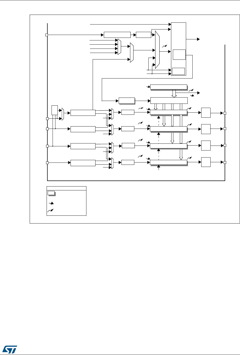
DocID018909 Rev 9 579/1718
RM0090 General-purpose timers (TIM2 to TIM5)
635
Figure 134. General-purpose timer block diagram
18.3 TIM2 to TIM5 functional description
18.3.1 Time-base unit
The main block of the programmable timer is a 16-bit/32-bit counter with its related auto-
reload register. The counter can count up. The counter clock can be divided by a prescaler.
The counter, the auto-reload register and the prescaler register can be written or read by
software. This is true even when the counter is running.
The time-base unit includes:
•Counter Register (TIMx_CNT)
•Prescaler Register (TIMx_PSC):
•Auto-Reload Register (TIMx_ARR)
Autoreload register
Capture/compare 1 register
Capture/compare 2 register
U
U
U
CC1I
CC2I
Trigger
controller
Stop, clear or up/down
TI1FP1
TI2FP2
ITR0
ITR1
ITR2
ITR3
TRGI
Encoder
Interface
Capture/compare 3 register
U
CC3I
output
control
OC1
TRGO
OC1REF
OC2REF
OC3REF
U
UI
Reset, enable, up/down, count,
Capture/compare 4 register
U
CC4I
OC4REF
Prescaler
Prescaler
IC4PS
IC3PS
IC1
IC2
Prescaler
Prescaler
Input filter &
edge detector
IC2PS
IC1PS
TI1FP1
OC2
OC3
OC4
Reg
event
Notes:
Preload registers transferred
to active registers on U event
according to control bit
interrupt & DMA output
TGI
TRC
TRC
IC3
IC4
ITR
TRC
TI1F_ED
Input filter &
edge detector
Input filter &
edge detector
Input filter &
edge detector
CC1I
CC2I
CC3I
CC4I
TI1FP2
TI2FP1
TI2FP2
TI3FP3
TRC
TRC
TI3FP4
TI4FP3
TI4FP4
TI4
TI3
TI1
TI2
XOR
TIMx_CH1
TIMx_CH2
TIMx_CH3
TIMx_CH4
TIMx_CH1
TIMx_CH2
TIMx_CH3
TIMx_CH4
to other timers
TIMxCLK from RCC
Prescaler counter
+/-
CK_PSC PSC CNT
CK_CNT
controller
mode
Slave
Internal Clock (CK_INT)
ETR Input filter
Polarity selection & edge
detector & prescaler
ETRP
ETRF
TIMx_ETR
ETRF
to DAC/ADC
output
control
output
control
output
control
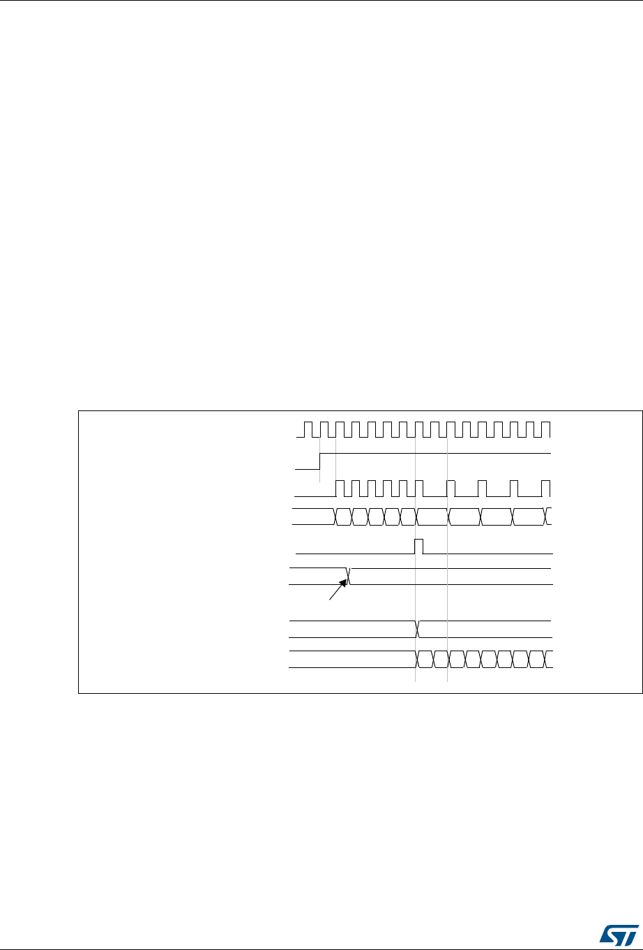
General-purpose timers (TIM2 to TIM5) RM0090
580/1718 DocID018909 Rev 9
The auto-reload register is preloaded. Writing to or reading from the auto-reload register
accesses the preload register. The content of the preload register are transferred into the
shadow register permanently or at each update event (UEV), depending on the auto-reload
preload enable bit (ARPE) in TIMx_CR1 register. The update event is sent when the counter
reaches the overflow (or underflow when downcounting) and if the UDIS bit equals 0 in the
TIMx_CR1 register. It can also be generated by software. The generation of the update
event is described in detail for each configuration.
The counter is clocked by the prescaler output CK_CNT, which is enabled only when the
counter enable bit (CEN) in TIMx_CR1 register is set (refer also to the slave mode controller
description to get more details on counter enabling).
Note that the actual counter enable signal CNT_EN is set 1 clock cycle after CEN.
Prescaler description
The prescaler can divide the counter clock frequency by any factor between 1 and 65536. It
is based on a 16-bit counter controlled through a 16-bit/32-bit register (in the TIMx_PSC
register). It can be changed on the fly as this control register is buffered. The new prescaler
ratio is taken into account at the next update event.
Figure 135 and Figure 136 give some examples of the counter behavior when the prescaler
ratio is changed on the fly:
Figure 135. Counter timing diagram with prescaler division change from 1 to 2
CK_PSC
00
CNT_EN
Timer clock = CK_CNT
Counter register
Update event (UEV)
0
F9 FA FB FCF7
Prescaler control register 01
Write a new value in TIMx_PSC
01 02 03
Prescaler buffer 01
Prescaler counter 01 0 1 0 1 0 1
F8
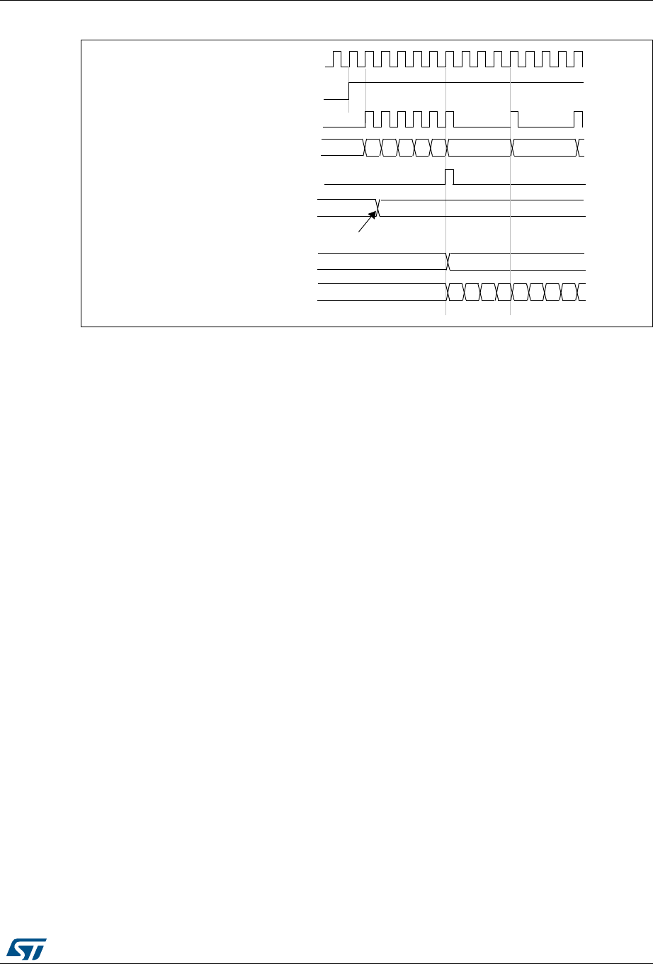
DocID018909 Rev 9 581/1718
RM0090 General-purpose timers (TIM2 to TIM5)
635
Figure 136. Counter timing diagram with prescaler division change from 1 to 4
18.3.2 Counter modes
Upcounting mode
In upcounting mode, the counter counts from 0 to the auto-reload value (content of the
TIMx_ARR register), then restarts from 0 and generates a counter overflow event.
An Update event can be generated at each counter overflow or by setting the UG bit in the
TIMx_EGR register (by software or by using the slave mode controller).
The UEV event can be disabled by software by setting the UDIS bit in TIMx_CR1 register.
This is to avoid updating the shadow registers while writing new values in the preload
registers. Then no update event occurs until the UDIS bit has been written to 0. However,
the counter restarts from 0, as well as the counter of the prescaler (but the prescale rate
does not change). In addition, if the URS bit (update request selection) in TIMx_CR1
register is set, setting the UG bit generates an update event UEV but without setting the UIF
flag (thus no interrupt or DMA request is sent). This is to avoid generating both update and
capture interrupts when clearing the counter on the capture event.
When an update event occurs, all the registers are updated and the update flag (UIF bit in
TIMx_SR register) is set (depending on the URS bit):
•The buffer of the prescaler is reloaded with the preload value (content of the TIMx_PSC
register)
•The auto-reload shadow register is updated with the preload value (TIMx_ARR)
The following figures show some examples of the counter behavior for different clock
frequencies when TIMx_ARR=0x36.
CK_PSC
00
CNT_EN
Timer clock = CK_CNT
Counter register
Update event (UEV)
0
F9 FA FB FCF7
Prescaler control register 03
Write a new value in TIMx_PSC
Prescaler buffer 03
Prescaler counter 01 2 3 0 1 2 3
F8 01
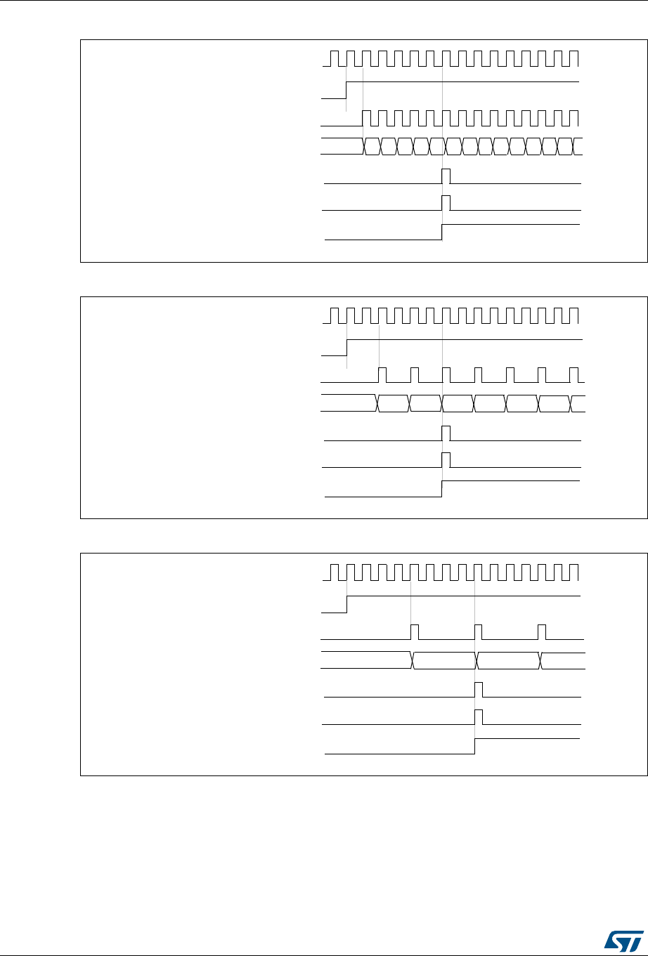
General-purpose timers (TIM2 to TIM5) RM0090
582/1718 DocID018909 Rev 9
Figure 137. Counter timing diagram, internal clock divided by 1
Figure 138. Counter timing diagram, internal clock divided by 2
Figure 139. Counter timing diagram, internal clock divided by 4
CK_INT
00
CNT_EN
Timer clock = CK_CNT
Counter register
Update interrupt flag (UIF)
Counter overflow
Update event (UEV)
01 02 03 04 05 06 0732 33 34 35 3631
CK_INT
0035 0000 0001 0002 0003
CNT_EN
Timer clock = CK_CNT
Counter register
Update interrupt flag (UIF)
0034 0036
Counter overflow
Update event (UEV)
0000 0001
CNT_EN
TImer clock = CK_CNT
Counter register
Update interrupt flag (UIF)
0035 0036
Counter overflow
Update event (UEV)
CK_INT

DocID018909 Rev 9 583/1718
RM0090 General-purpose timers (TIM2 to TIM5)
635
Figure 140. Counter timing diagram, internal clock divided by N
Figure 141. Counter timing diagram, Update event when ARPE=0 (TIMx_ARR not
preloaded)
Timer clock = CK_CNT
Counter register 00
1F 20
Update interrupt flag (UIF)
Counter overflow
Update event (UEV)
CK_INT
00
CNT_EN
Timer clock = CK_CNT
Counter register
Update interrupt flag (UIF)
Counter overflow
Update event (UEV)
01 02 03 04 05 06 0732 33 34 35 3631
Auto-reload register FF 36
Write a new value in TIMx_ARR
CK_INT
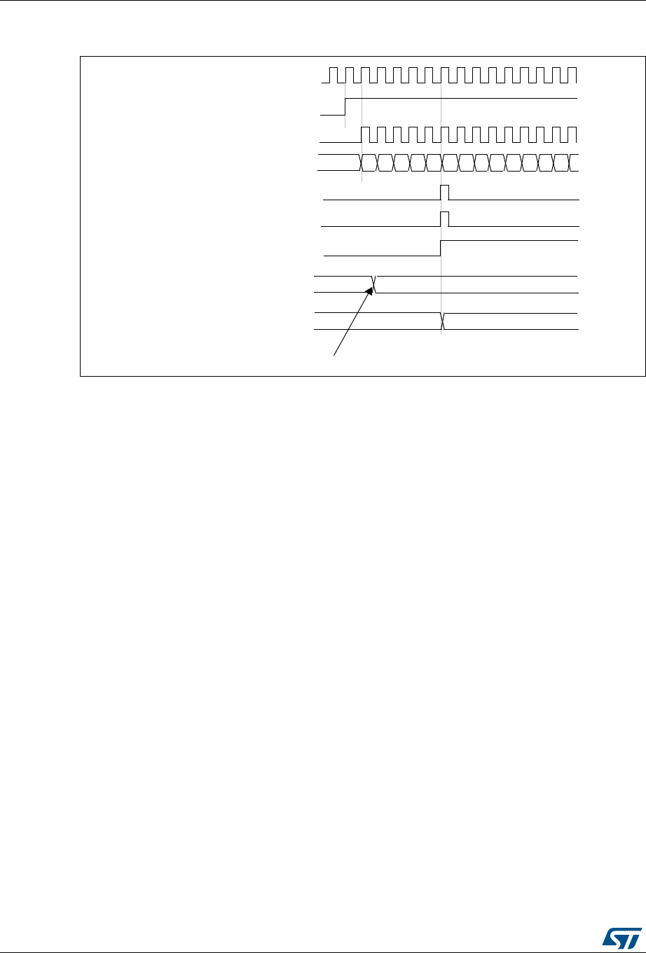
General-purpose timers (TIM2 to TIM5) RM0090
584/1718 DocID018909 Rev 9
Figure 142. Counter timing diagram, Update event when ARPE=1 (TIMx_ARR
preloaded)
Downcounting mode
In downcounting mode, the counter counts from the auto-reload value (content of the
TIMx_ARR register) down to 0, then restarts from the auto-reload value and generates a
counter underflow event.
An Update event can be generate at each counter underflow or by setting the UG bit in the
TIMx_EGR register (by software or by using the slave mode controller)
The UEV update event can be disabled by software by setting the UDIS bit in TIMx_CR1
register. This is to avoid updating the shadow registers while writing new values in the
preload registers. Then no update event occurs until UDIS bit has been written to 0.
However, the counter restarts from the current auto-reload value, whereas the counter of the
prescaler restarts from 0 (but the prescale rate doesn’t change).
In addition, if the URS bit (update request selection) in TIMx_CR1 register is set, setting the
UG bit generates an update event UEV but without setting the UIF flag (thus no interrupt or
DMA request is sent). This is to avoid generating both update and capture interrupts when
clearing the counter on the capture event.
When an update event occurs, all the registers are updated and the update flag (UIF bit in
TIMx_SR register) is set (depending on the URS bit):
•The buffer of the prescaler is reloaded with the preload value (content of the TIMx_PSC
register).
•The auto-reload active register is updated with the preload value (content of the
TIMx_ARR register). Note that the auto-reload is updated before the counter is
reloaded, so that the next period is the expected one.
The following figures show some examples of the counter behavior for different clock
frequencies when TIMx_ARR=0x36.
00
CNT_EN
Timer clock = CK_CNT
Counter register
Update interrupt flag (UIF)
Counter overflow
Update event (UEV)
01 02 03 04 05 06 07F1 F2 F3 F4 F5F0
Auto-reload preload register F5 36
Auto-reload shadow register F5 36
Write a new value in TIMx_ARR
CK_PSC
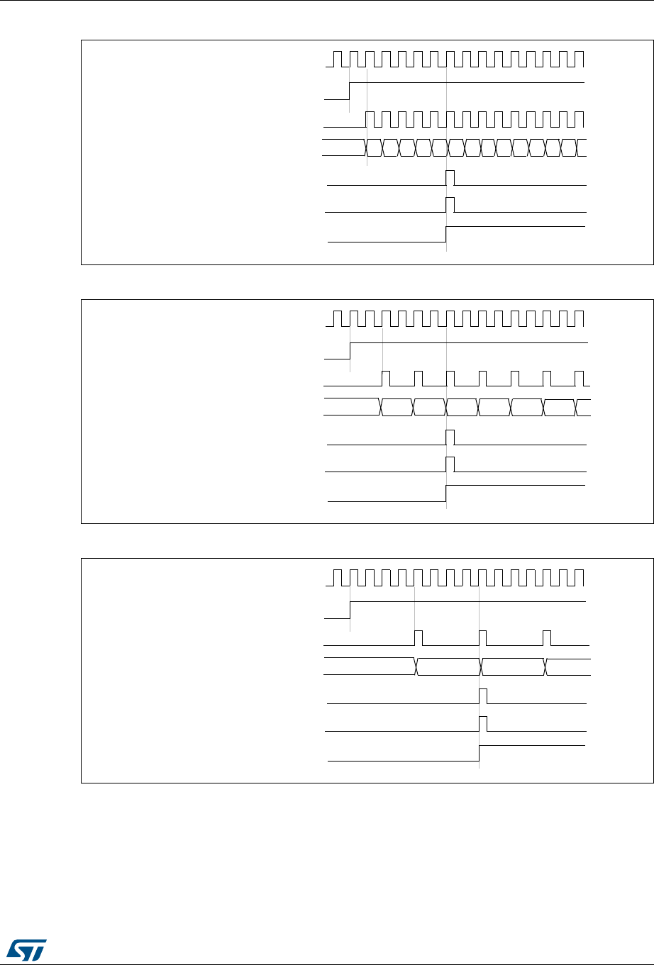
DocID018909 Rev 9 585/1718
RM0090 General-purpose timers (TIM2 to TIM5)
635
Figure 143. Counter timing diagram, internal clock divided by 1
Figure 144. Counter timing diagram, internal clock divided by 2
Figure 145. Counter timing diagram, internal clock divided by 4
CK_INT
36
CNT_EN
Timer clock = CK_CNT
Counter register
Update interrupt flag (UIF)
Counter underflow (cnt_udf)
Update event (UEV)
35 34 33 32 31 30 2F04 03 02 01 0005
CK_INT
0001 0036 0035 0034 0033
CNT_EN
Timer clock = CK_CNT
Counter register
Update interrupt flag (UIF)
0002 0000
Counter underflow
Update event (UEV)
0036 0035
CNT_EN
Timer clock = CK_CNT
Counter register
Update interrupt flag (UIF)
0001 0000
Counter underflow
Update event (UEV)
CK_INT
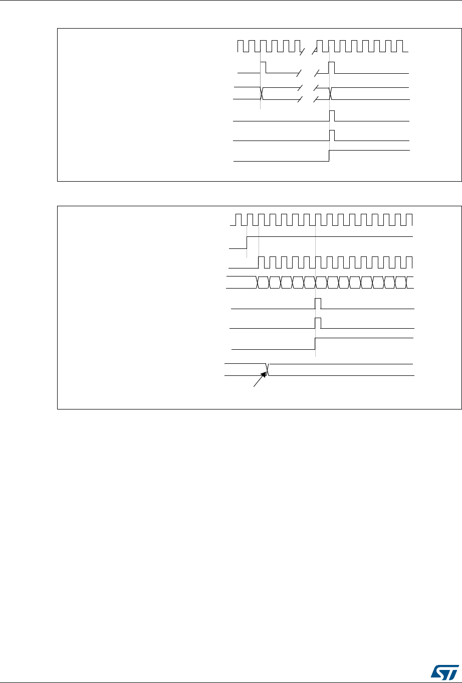
General-purpose timers (TIM2 to TIM5) RM0090
586/1718 DocID018909 Rev 9
Figure 146. Counter timing diagram, internal clock divided by N
Figure 147. Counter timing diagram, Update event
Center-aligned mode (up/down counting)
In center-aligned mode, the counter counts from 0 to the auto-reload value (content of the
TIMx_ARR register) – 1, generates a counter overflow event, then counts from the auto-
reload value down to 1 and generates a counter underflow event. Then it restarts counting
from 0.
Center-aligned mode is active when the CMS bits in TIMx_CR1 register are not equal to
'00'. The Output compare interrupt flag of channels configured in output is set when: the
counter counts down (Center aligned mode 1, CMS = "01"), the counter counts up (Center
aligned mode 2, CMS = "10") the counter counts up and down (Center aligned mode 3,
CMS = "11").
In this mode, the direction bit (DIR from TIMx_CR1 register) cannot be written. It is updated
by hardware and gives the current direction of the counter.
The update event can be generated at each counter overflow and at each counter underflow
or by setting the UG bit in the TIMx_EGR register (by software or by using the slave mode
controller) also generates an update event. In this case, the counter restarts counting from
0, as well as the counter of the prescaler.
Timer clock = CK_CNT
Counter register 36
20 1F
Update interrupt flag (UIF)
Counter underflow
Update event (UEV)
CK_INT
00
36
CNT_EN
Timer clock = CK_CNT
Counter register
Update interrupt flag (UIF)
Counter underflow
Update event (UEV)
35 34 33 32 31 30 2F04 03 02 01 0005
Auto-reload register FF 36
Write a new value in TIMx_ARR
CK_INT
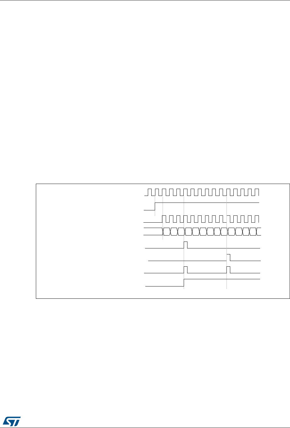
DocID018909 Rev 9 587/1718
RM0090 General-purpose timers (TIM2 to TIM5)
635
The UEV update event can be disabled by software by setting the UDIS bit in TIMx_CR1
register. This is to avoid updating the shadow registers while writing new values in the
preload registers. Then no update event occurs until the UDIS bit has been written to 0.
However, the counter continues counting up and down, based on the current auto-reload
value.
In addition, if the URS bit (update request selection) in TIMx_CR1 register is set, setting the
UG bit generates an update event UEV but without setting the UIF flag (thus no interrupt or
DMA request is sent). This is to avoid generating both update and capture interrupt when
clearing the counter on the capture event.
When an update event occurs, all the registers are updated and the update flag (UIF bit in
TIMx_SR register) is set (depending on the URS bit):
•The buffer of the prescaler is reloaded with the preload value (content of the TIMx_PSC
register).
•The auto-reload active register is updated with the preload value (content of the
TIMx_ARR register). Note that if the update source is a counter overflow, the auto-
reload is updated before the counter is reloaded, so that the next period is the expected
one (the counter is loaded with the new value).
The following figures show some examples of the counter behavior for different clock
frequencies.
Figure 148. Counter timing diagram, internal clock divided by 1, TIMx_ARR=0x6
1. Here, center-aligned mode 1 is used (for more details refer to Section 18.4.1: TIMx control register 1 (TIMx_CR1)
on page 613).
CK_INT
02
CNT_EN
Timer clock = CK_CNT
Counter register
Update interrupt flag (UIF)
Counter underflow
Update event (UEV)
03 04 05 06 05 04 0303 02 01 00 0104
Counter overflow
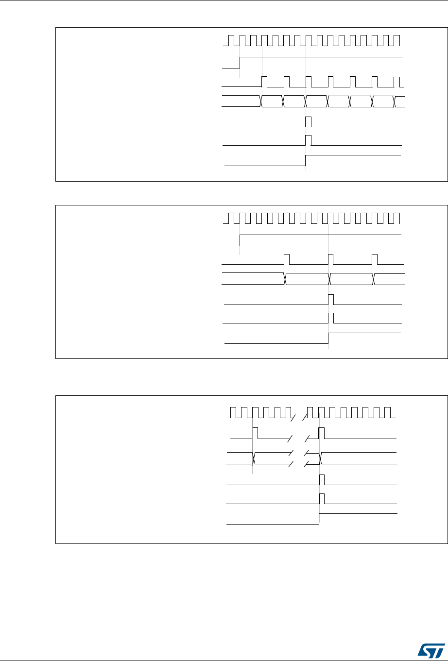
General-purpose timers (TIM2 to TIM5) RM0090
588/1718 DocID018909 Rev 9
Figure 149. Counter timing diagram, internal clock divided by 2
Figure 150. Counter timing diagram, internal clock divided by 4, TIMx_ARR=0x36
1. Center-aligned mode 2 or 3 is used with an UIF on overflow.
Figure 151. Counter timing diagram, internal clock divided by N
0002 0000 0001 0002 0003
CNT_EN
TImer clock = CK_CNT
Counter register
Update interrupt flag (UIF)
0003 0001
Counter underflow
Update event (UEV)
CK_INT
CK_INT
0036 0035
CNT_EN
Timer clock = CK_CNT
Counter register
Update interrupt flag (UIF)
0034 0035
Counter overflow (cnt_ovf)
Update event (UEV)
Timer clock = CK_CNT
Counter register 00
20 1F
Update interrupt flag (UIF)
Counter underflow
Update event (UEV)
CK_INT
01
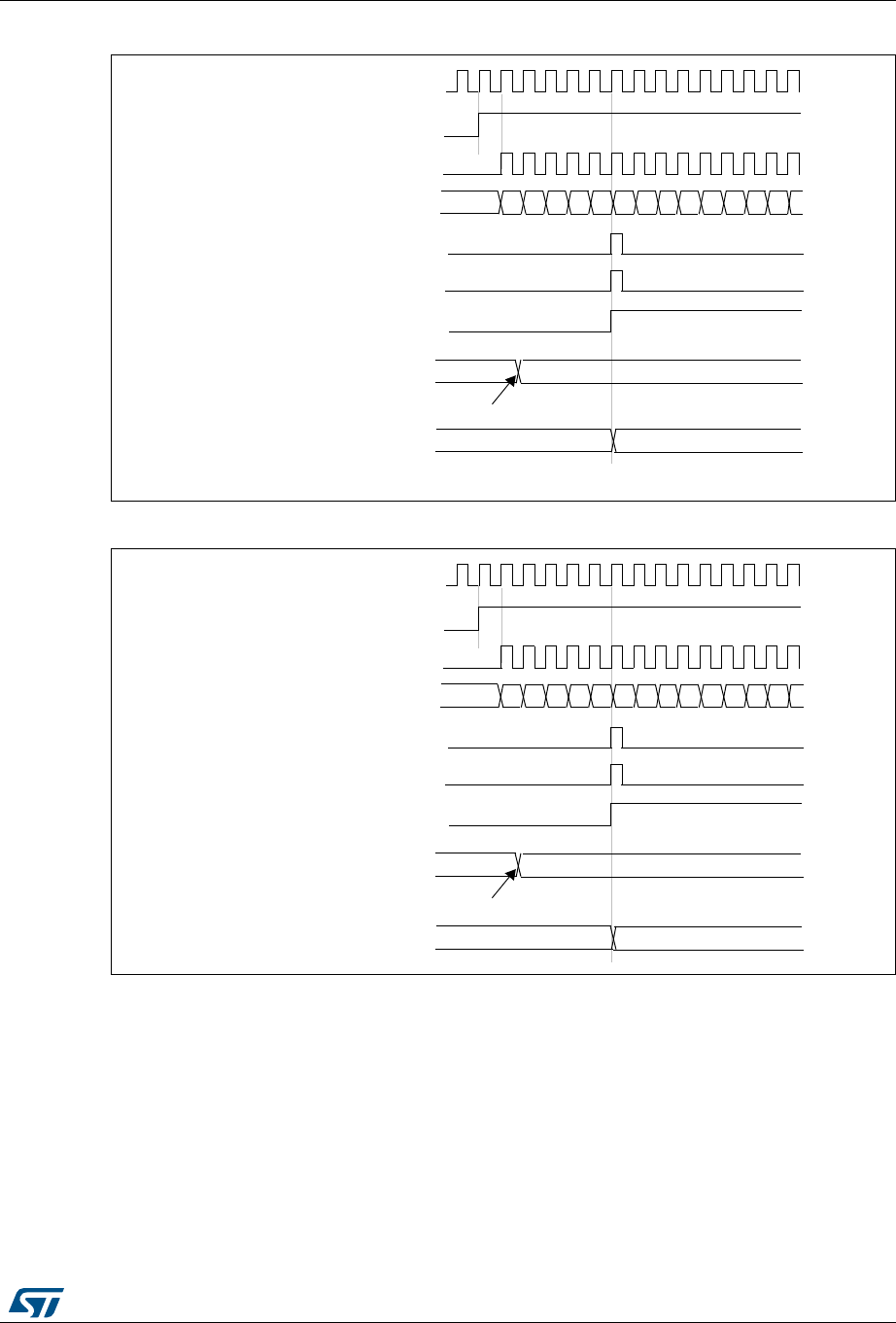
DocID018909 Rev 9 589/1718
RM0090 General-purpose timers (TIM2 to TIM5)
635
Figure 152. Counter timing diagram, Update event with ARPE=1 (counter underflow)
Figure 153. Counter timing diagram, Update event with ARPE=1 (counter overflow)
18.3.3 Clock selection
The counter clock can be provided by the following clock sources:
•Internal clock (CK_INT)
•External clock mode1: external input pin (TIx)
•External clock mode2: external trigger input (ETR) available on TIM2, TIM3 and TIM4
only.
•Internal trigger inputs (ITRx): using one timer as prescaler for another timer, for
example, you can configure Timer to act as a prescaler for Timer 2. Refer to : Using
one timer as prescaler for another on page 608 for more details.
00
CNT_EN
Timer clock = CK_CNT
Counter register
Update interrupt flag (UIF)
Counter underflow
Update event (UEV)
01 02 03 04 05 06 0705 04 03 02 0106
Auto-reload preload register FD 36
Write a new value in TIMx_ARR
Auto-reload active register FD 36
CK_INT
36
CNT_EN
Timer clock = CK_CNT
Counter register
Update interrupt flag (UIF)
Counter overflow
Update event (UEV)
35 34 33 32 31 30 2FF8 F9 FA FB FCF7
Auto-reload preload register FD 36
Write a new value in TIMx_ARR
Auto-reload active register FD 36
CK_INT
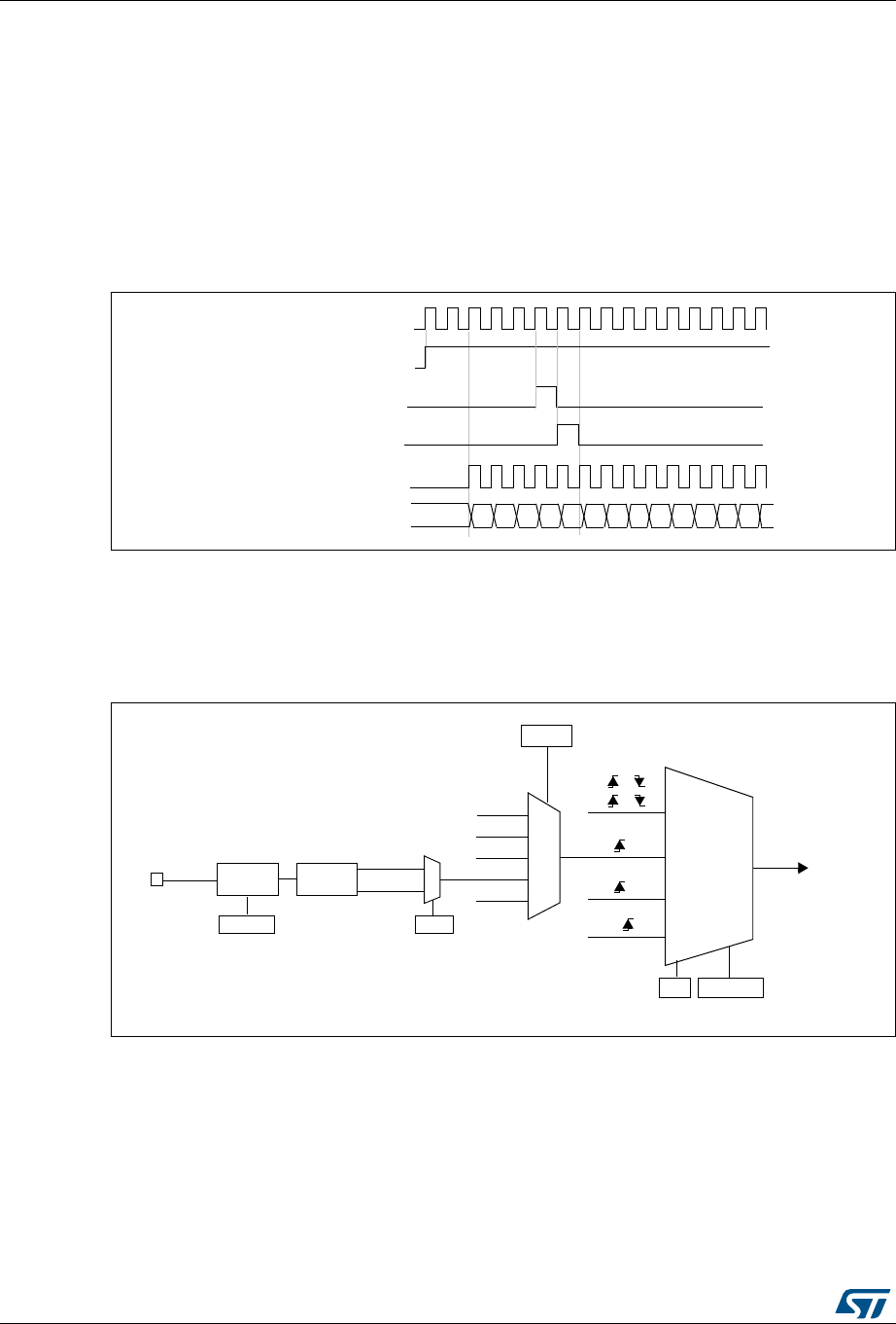
General-purpose timers (TIM2 to TIM5) RM0090
590/1718 DocID018909 Rev 9
Internal clock source (CK_INT)
If the slave mode controller is disabled (SMS=000 in the TIMx_SMCR register), then the
CEN, DIR (in the TIMx_CR1 register) and UG bits (in the TIMx_EGR register) are actual
control bits and can be changed only by software (except UG which remains cleared
automatically). As soon as the CEN bit is written to 1, the prescaler is clocked by the internal
clock CK_INT.
Figure 154 shows the behavior of the control circuit and the upcounter in normal mode,
without prescaler.
Figure 154. Control circuit in normal mode, internal clock divided by 1
External clock source mode 1
This mode is selected when SMS=111 in the TIMx_SMCR register. The counter can count at
each rising or falling edge on a selected input.
Figure 155. TI2 external clock connection example
For example, to configure the upcounter to count in response to a rising edge on the TI2
input, use the following procedure:
1. Configure channel 2 to detect rising edges on the TI2 input by writing CC2S= ‘01 in the
TIMx_CCMR1 register.
2. Configure the input filter duration by writing the IC2F[3:0] bits in the TIMx_CCMR1
register (if no filter is needed, keep IC2F=0000).
CK_INT
00
Counter clock = CK_CNT = CK_PSC
COUNTER REGISTER 01 02 03 04 05 06 0732 33 34 35 3631
CEN=CNT_EN
UG
CNT_INIT
CK_INT
encoder
mode
external clock
mode 1
external clock
mode 2
internal clock
mode
ETRF
TRGI
TI1F
TI2F or
or
or
(internal clock)
CK_PSC
ECE
TIMx_SMCR
SMS[2:0]
ITRx
TI1F_ED
TI1FP1
TI2FP2
ETRF
TIMx_SMCR
TS[2:0]
TI2 0
1
TIMx_CCER
CC2P
Filter
ICF[3:0]
TIMx_CCMR1
Edge
Detector
TI2F_Rising
TI2F_Falling 110
001
100
101
111
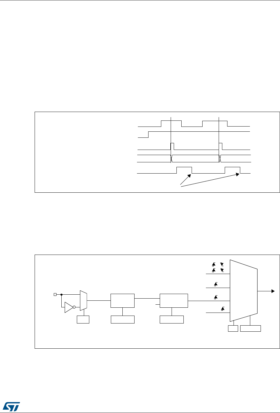
DocID018909 Rev 9 591/1718
RM0090 General-purpose timers (TIM2 to TIM5)
635
Note: The capture prescaler is not used for triggering, so you don’t need to configure it.
3. Select rising edge polarity by writing CC2P=0 and CC2NP=0 in the TIMx_CCER
register.
4. Configure the timer in external clock mode 1 by writing SMS=111 in the TIMx_SMCR
register.
5. Select TI2 as the input source by writing TS=110 in the TIMx_SMCR register.
6. Enable the counter by writing CEN=1 in the TIMx_CR1 register.
When a rising edge occurs on TI2, the counter counts once and the TIF flag is set.
The delay between the rising edge on TI2 and the actual clock of the counter is due to the
resynchronization circuit on TI2 input.
Figure 156. Control circuit in external clock mode 1
External clock source mode 2
This mode is selected by writing ECE=1 in the TIMx_SMCR register.
The counter can count at each rising or falling edge on the external trigger input ETR.
Figure 157 gives an overview of the external trigger input block.
Figure 157. External trigger input block
For example, to configure the upcounter to count each 2 rising edges on ETR, use the
following procedure:
Counter clock = CK_CNT = CK_PSC
Counter register 35 3634
TI2
CNT_EN
TIF
Write TIF=0
ETR 0
1
TIMx_SMCR
ETP
divider
/1, /2, /4, /8
ETPS[1:0]
ETRP filter
ETF[3:0]
downcounter
CK_INT
TIMx_SMCR
TIMx_SMCR
ETR pin
CK_INT
encoder
mode
external clock
mode 1
external clock
mode 2
internal clock
mode
ETRF
TRGI
TI1F
TI2F or
or
or
(internal clock)
CK_PSC
ECE
TIMx_SMCR
SMS[2:0]
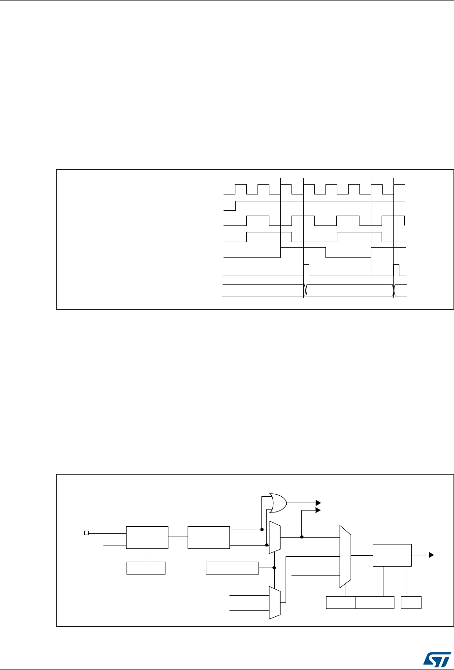
General-purpose timers (TIM2 to TIM5) RM0090
592/1718 DocID018909 Rev 9
1. As no filter is needed in this example, write ETF[3:0]=0000 in the TIMx_SMCR register.
2. Set the prescaler by writing ETPS[1:0]=01 in the TIMx_SMCR register
3. Select rising edge detection on the ETR pin by writing ETP=0 in the TIMx_SMCR
register
4. Enable external clock mode 2 by writing ECE=1 in the TIMx_SMCR register.
5. Enable the counter by writing CEN=1 in the TIMx_CR1 register.
The counter counts once each 2 ETR rising edges.
The delay between the rising edge on ETR and the actual clock of the counter is due to the
resynchronization circuit on the ETRP signal.
Figure 158. Control circuit in external clock mode 2
18.3.4 Capture/compare channels
Each Capture/Compare channel is built around a capture/compare register (including a
shadow register), a input stage for capture (with digital filter, multiplexing and prescaler) and
an output stage (with comparator and output control).
The following figure gives an overview of one Capture/Compare channel.
The input stage samples the corresponding TIx input to generate a filtered signal TIxF.
Then, an edge detector with polarity selection generates a signal (TIxFPx) which can be
used as trigger input by the slave mode controller or as the capture command. It is
prescaled before the capture register (ICxPS).
Figure 159. Capture/compare channel (example: channel 1 input stage)
Counter clock = CK_CNT = CK_PSC
Counter register 35 3634
ETR
CNT_EN
CK_INT
ETRP
ETRF
TI1
TIMx_CCER
CC1P/CC1NP
divider
/1, /2, /4, /8
ICPS[1:0]
TI1F_ED
filter
ICF[3:0]
downcounter
TIMx_CCMR1
Edge
Detector
TI1F_Rising
TI1F_Falling
to the slave mode controller
TI1FP1
11
01
TIMx_CCMR1
CC1S[1:0]
IC1
TI2FP1
TRC
(from channel 2)
(from slave mode
controller)
10
fDTS
TIMx_CCER
CC1E
IC1PS
TI1F
TI2F_rising
TI2F_falling
(from channel 2)
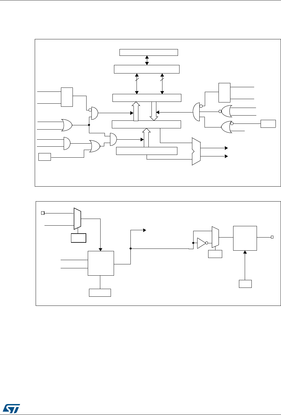
DocID018909 Rev 9 593/1718
RM0090 General-purpose timers (TIM2 to TIM5)
635
The output stage generates an intermediate waveform which is then used for reference:
OCxRef (active high). The polarity acts at the end of the chain.
Figure 160. Capture/compare channel 1 main circuit
Figure 161. Output stage of capture/compare channel (channel 1)
The capture/compare block is made of one preload register and one shadow register. Write
and read always access the preload register.
In capture mode, captures are actually done in the shadow register, which is copied into the
preload register.
In compare mode, the content of the preload register is copied into the shadow register
which is compared to the counter.
CC1E
Capture/Compare Shadow Register
comparator
Capture/Compare Preload Register
Counter
IC1PS
CC1S[0]
CC1S[1]
capture
input
mode
S
R
read CCR1H
read CCR1L
read_in_progress
capture_transfer CC1S[0]
CC1S[1]
S
R
write CCR1H
write CCR1L
write_in_progress
output
mode
UEV
OC1PE
(from time
compare_transfer
APB Bus
88
high
low
(if 16-bit)
MCU-peripheral interface
TIMx_CCMR1
OC1PE
base unit)
CNT>CCR1
CNT=CCR1
TIMx_EGR
CC1G
KƵƚƉƵƚŵŽĚĞ
EdхZϭ
EdсZϭ ĐŽŶƚƌŽůůĞƌ
d/DdžͺDZϭ
KϭDϮ͗Ϭ
ŽĐϭƌĞĨ
Ϭ
ϭ
ϭW
d/DdžͺZ
KƵƚƉƵƚ
ŶĂďůĞ
ŝƌĐƵŝƚ
Kϭ
ϭ
d/DdžͺZ
dŽƚŚĞŵĂƐƚĞƌŵŽĚĞ
ĐŽŶƚƌŽůůĞƌ
dZ&
Ϭ
ϭ
KZ&ͺ>Z
KZ&ͺ>Zͺ/Ed
K^
d/Ddžͺ^DZ
Ăŝϭϳϭϴϳ

General-purpose timers (TIM2 to TIM5) RM0090
594/1718 DocID018909 Rev 9
18.3.5 Input capture mode
In Input capture mode, the Capture/Compare Registers (TIMx_CCRx) are used to latch the
value of the counter after a transition detected by the corresponding ICx signal. When a
capture occurs, the corresponding CCXIF flag (TIMx_SR register) is set and an interrupt or
a DMA request can be sent if they are enabled. If a capture occurs while the CCxIF flag was
already high, then the over-capture flag CCxOF (TIMx_SR register) is set. CCxIF can be
cleared by software by writing it to 0 or by reading the captured data stored in the
TIMx_CCRx register. CCxOF is cleared when you write it to 0.
The following example shows how to capture the counter value in TIMx_CCR1 when TI1
input rises. To do this, use the following procedure:
•Select the active input: TIMx_CCR1 must be linked to the TI1 input, so write the CC1S
bits to 01 in the TIMx_CCMR1 register. As soon as CC1S becomes different from 00,
the channel is configured in input and the TIMx_CCR1 register becomes read-only.
•Program the input filter duration you need with respect to the signal you connect to the
timer (by programming the ICxF bits in the TIMx_CCMRx register if the input is one of
the TIx inputs). Let’s imagine that, when toggling, the input signal is not stable during at
must 5 internal clock cycles. We must program a filter duration longer than these 5
clock cycles. We can validate a transition on TI1 when 8 consecutive samples with the
new level have been detected (sampled at fDTS frequency). Then write IC1F bits to
0011 in the TIMx_CCMR1 register.
•Select the edge of the active transition on the TI1 channel by writing the CC1P and
CC1NP bits to 00 in the TIMx_CCER register (rising edge in this case).
•Program the input prescaler. In our example, we wish the capture to be performed at
each valid transition, so the prescaler is disabled (write IC1PS bits to 00 in the
TIMx_CCMR1 register).
•Enable capture from the counter into the capture register by setting the CC1E bit in the
TIMx_CCER register.
•If needed, enable the related interrupt request by setting the CC1IE bit in the
TIMx_DIER register, and/or the DMA request by setting the CC1DE bit in the
TIMx_DIER register.
When an input capture occurs:
•The TIMx_CCR1 register gets the value of the counter on the active transition.
•CC1IF flag is set (interrupt flag). CC1OF is also set if at least two consecutive captures
occurred whereas the flag was not cleared.
•An interrupt is generated depending on the CC1IE bit.
•A DMA request is generated depending on the CC1DE bit.
In order to handle the overcapture, it is recommended to read the data before the
overcapture flag. This is to avoid missing an overcapture which could happen after reading
the flag and before reading the data.
Note: IC interrupt and/or DMA requests can be generated by software by setting the
corresponding CCxG bit in the TIMx_EGR register.
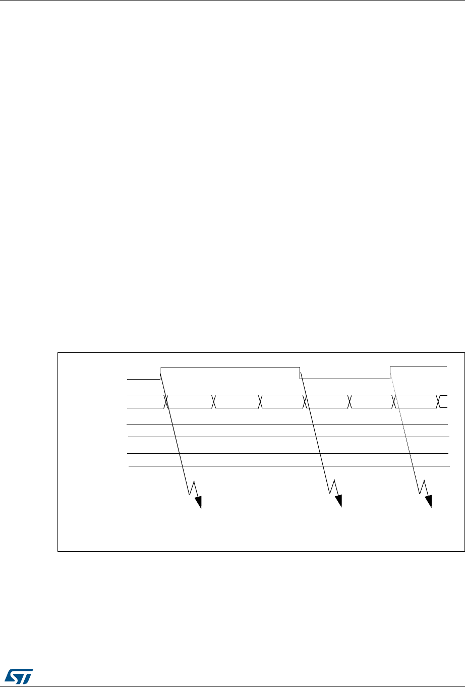
DocID018909 Rev 9 595/1718
RM0090 General-purpose timers (TIM2 to TIM5)
635
18.3.6 PWM input mode
This mode is a particular case of input capture mode. The procedure is the same except:
•Two ICx signals are mapped on the same TIx input.
•These 2 ICx signals are active on edges with opposite polarity.
•One of the two TIxFP signals is selected as trigger input and the slave mode controller
is configured in reset mode.
For example, you can measure the period (in TIMx_CCR1 register) and the duty cycle (in
TIMx_CCR2 register) of the PWM applied on TI1 using the following procedure (depending
on CK_INT frequency and prescaler value):
•Select the active input for TIMx_CCR1: write the CC1S bits to 01 in the TIMx_CCMR1
register (TI1 selected).
•Select the active polarity for TI1FP1 (used both for capture in TIMx_CCR1 and counter
clear): write the CC1P to ‘0’ and the CC1NP bit to ‘0’ (active on rising edge).
•Select the active input for TIMx_CCR2: write the CC2S bits to 10 in the TIMx_CCMR1
register (TI1 selected).
•Select the active polarity for TI1FP2 (used for capture in TIMx_CCR2): write the CC2P
bit to ‘1’ and the CC2NP bit to ’0’(active on falling edge).
•Select the valid trigger input: write the TS bits to 101 in the TIMx_SMCR register
(TI1FP1 selected).
•Configure the slave mode controller in reset mode: write the SMS bits to 100 in the
TIMx_SMCR register.
•Enable the captures: write the CC1E and CC2E bits to ‘1 in the TIMx_CCER register.
Figure 162. PWM input mode timing
18.3.7 Forced output mode
In output mode (CCxS bits = 00 in the TIMx_CCMRx register), each output compare signal
(OCxREF and then OCx) can be forced to active or inactive level directly by software,
independently of any comparison between the output compare register and the counter.
TI1
TIMx_CNT 0000 0001 0002 0003 0004 00000004
TIMx_CCR1
TIMx_CCR2
0004
0002
IC1 capture
IC2 capture
reset counter
IC2 capture
pulse width
IC1 capture
period
measurementmeasurement
ai15413

General-purpose timers (TIM2 to TIM5) RM0090
596/1718 DocID018909 Rev 9
To force an output compare signal (ocxref/OCx) to its active level, you just need to write 101
in the OCxM bits in the corresponding TIMx_CCMRx register. Thus ocxref is forced high
(OCxREF is always active high) and OCx get opposite value to CCxP polarity bit.
e.g.: CCxP=0 (OCx active high) => OCx is forced to high level.
ocxref signal can be forced low by writing the OCxM bits to 100 in the TIMx_CCMRx
register.
Anyway, the comparison between the TIMx_CCRx shadow register and the counter is still
performed and allows the flag to be set. Interrupt and DMA requests can be sent
accordingly. This is described in the Output Compare Mode section.
18.3.8 Output compare mode
This function is used to control an output waveform or indicating when a period of time has
elapsed.
When a match is found between the capture/compare register and the counter, the output
compare function:
•Assigns the corresponding output pin to a programmable value defined by the output
compare mode (OCxM bits in the TIMx_CCMRx register) and the output polarity (CCxP
bit in the TIMx_CCER register). The output pin can keep its level (OCXM=000), be set
active (OCxM=001), be set inactive (OCxM=010) or can toggle (OCxM=011) on match.
•Sets a flag in the interrupt status register (CCxIF bit in the TIMx_SR register).
•Generates an interrupt if the corresponding interrupt mask is set (CCXIE bit in the
TIMx_DIER register).
•Sends a DMA request if the corresponding enable bit is set (CCxDE bit in the
TIMx_DIER register, CCDS bit in the TIMx_CR2 register for the DMA request
selection).
The TIMx_CCRx registers can be programmed with or without preload registers using the
OCxPE bit in the TIMx_CCMRx register.
In output compare mode, the update event UEV has no effect on ocxref and OCx output.
The timing resolution is one count of the counter. Output compare mode can also be used to
output a single pulse (in One-pulse mode).
Procedure:
1. Select the counter clock (internal, external, prescaler).
2. Write the desired data in the TIMx_ARR and TIMx_CCRx registers.
3. Set the CCxIE and/or CCxDE bits if an interrupt and/or a DMA request is to be
generated.
4. Select the output mode. For example, you must write OCxM=011, OCxPE=0, CCxP=0
and CCxE=1 to toggle OCx output pin when CNT matches CCRx, CCRx preload is not
used, OCx is enabled and active high.
5. Enable the counter by setting the CEN bit in the TIMx_CR1 register.
The TIMx_CCRx register can be updated at any time by software to control the output
waveform, provided that the preload register is not enabled (OCxPE=0, else TIMx_CCRx
shadow register is updated only at the next update event UEV). An example is given in
Figure 163.
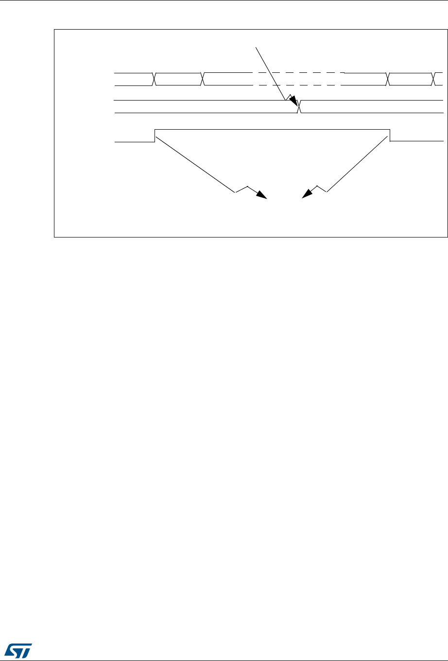
DocID018909 Rev 9 597/1718
RM0090 General-purpose timers (TIM2 to TIM5)
635
Figure 163. Output compare mode, toggle on OC1
18.3.9 PWM mode
Pulse width modulation mode allows you to generate a signal with a frequency determined
by the value of the TIMx_ARR register and a duty cycle determined by the value of the
TIMx_CCRx register.
The PWM mode can be selected independently on each channel (one PWM per OCx
output) by writing 110 (PWM mode 1) or ‘111 (PWM mode 2) in the OCxM bits in the
TIMx_CCMRx register. You must enable the corresponding preload register by setting the
OCxPE bit in the TIMx_CCMRx register, and eventually the auto-reload preload register by
setting the ARPE bit in the TIMx_CR1 register.
As the preload registers are transferred to the shadow registers only when an update event
occurs, before starting the counter, you have to initialize all the registers by setting the UG
bit in the TIMx_EGR register.
OCx polarity is software programmable using the CCxP bit in the TIMx_CCER register. It
can be programmed as active high or active low. OCx output is enabled by the CCxE bit in
the TIMx_CCER register. Refer to the TIMx_CCERx register description for more details.
In PWM mode (1 or 2), TIMx_CNT and TIMx_CCRx are always compared to determine
whether TIMx_CCRx≤TIMx_CNT or TIMx_CNT≤TIMx_CCRx (depending on the direction of
the counter). However, to comply with the ETRF (OCREF can be cleared by an external
event through the ETR signal until the next PWM period), the OCREF signal is asserted
only:
•When the result of the comparison changes, or
•When the output compare mode (OCxM bits in TIMx_CCMRx register) switches from
the “frozen” configuration (no comparison, OCxM=‘000) to one of the PWM modes
(OCxM=‘110 or ‘111).
This forces the PWM by software while the timer is running.
The timer is able to generate PWM in edge-aligned mode or center-aligned mode
depending on the CMS bits in the TIMx_CR1 register.
OC1REF=OC1
TIMx_CNT B200 B201
0039
TIMx_CCR1 003A
Write B201h in the CC1R register
Match detected on CCR1
Interrupt generated if enabled
003B
B201
003A
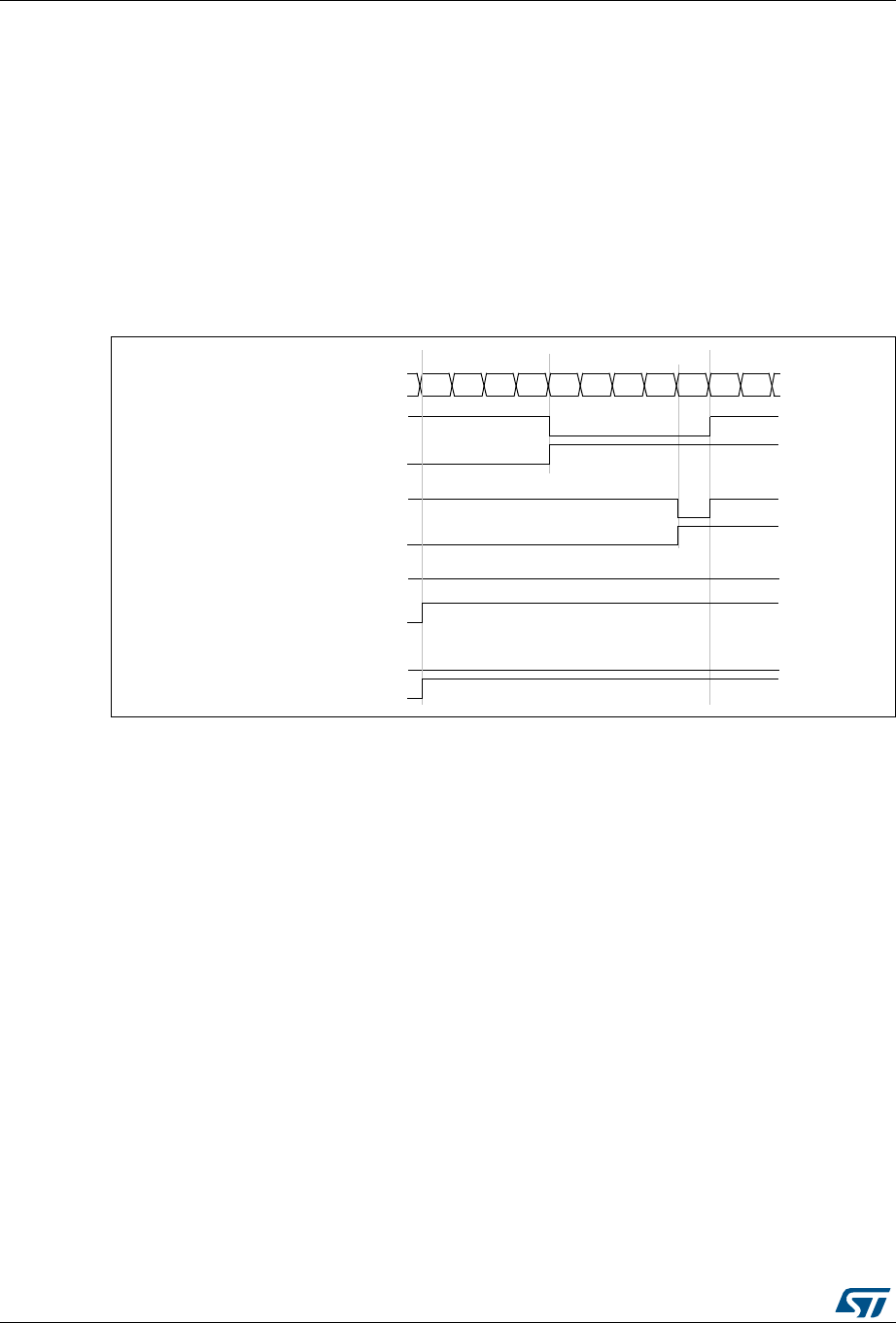
General-purpose timers (TIM2 to TIM5) RM0090
598/1718 DocID018909 Rev 9
PWM edge-aligned mode
Upcounting configuration
Upcounting is active when the DIR bit in the TIMx_CR1 register is low. Refer to Section :
Upcounting mode on page 581.
In the following example, we consider PWM mode 1. The reference PWM signal OCxREF is
high as long as TIMx_CNT <TIMx_CCRx else it becomes low. If the compare value in
TIMx_CCRx is greater than the auto-reload value (in TIMx_ARR) then OCxREF is held at ‘1.
If the compare value is 0 then OCxREF is held at ‘0. Figure 164 shows some edge-aligned
PWM waveforms in an example where TIMx_ARR=8.
Figure 164. Edge-aligned PWM waveforms (ARR=8)
Downcounting configuration
Downcounting is active when DIR bit in TIMx_CR1 register is high. Refer to Section :
Downcounting mode on page 584.
In PWM mode 1, the reference signal ocxref is low as long as TIMx_CNT>TIMx_CCRx else
it becomes high. If the compare value in TIMx_CCRx is greater than the auto-reload value in
TIMx_ARR, then ocxref is held at ‘1. 0% PWM is not possible in this mode.
PWM center-aligned mode
Center-aligned mode is active when the CMS bits in TIMx_CR1 register are different from
‘00 (all the remaining configurations having the same effect on the ocxref/OCx signals). The
compare flag is set when the counter counts up, when it counts down or both when it counts
up and down depending on the CMS bits configuration. The direction bit (DIR) in the
TIMx_CR1 register is updated by hardware and must not be changed by software. Refer to
Section : Center-aligned mode (up/down counting) on page 586.
Figure 165 shows some center-aligned PWM waveforms in an example where:
•TIMx_ARR=8,
•PWM mode is the PWM mode 1,
•The flag is set when the counter counts down corresponding to the center-aligned
mode 1 selected for CMS=01 in TIMx_CR1 register.
Counter register
‘1
01234567801
‘0
OCxREF
CCxIF
OCxREF
CCxIF
OCxREF
CCxIF
OCxREF
CCxIF
CCRx=4
CCRx=8
CCRx>8
CCRx=0
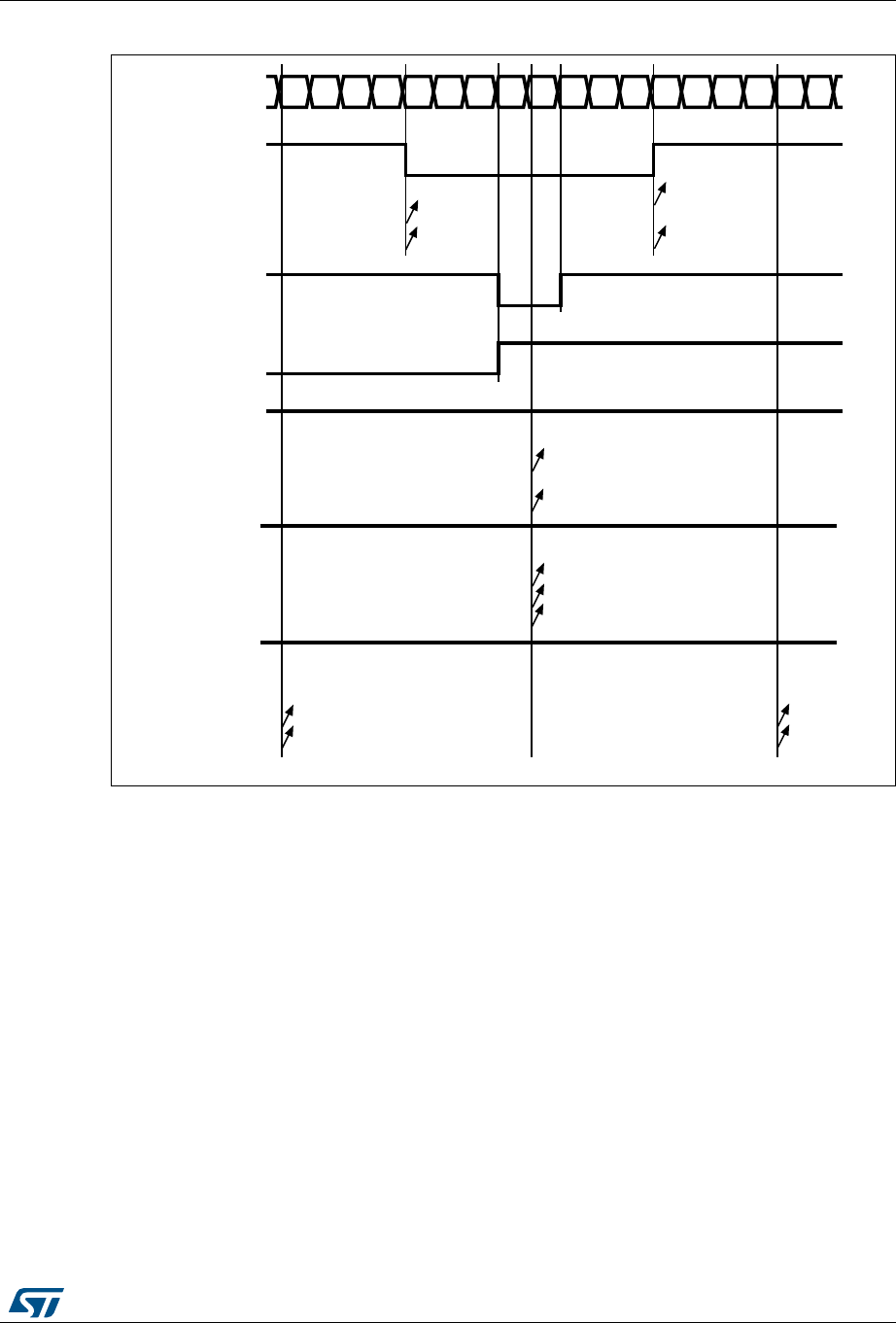
DocID018909 Rev 9 599/1718
RM0090 General-purpose timers (TIM2 to TIM5)
635
Figure 165. Center-aligned PWM waveforms (ARR=8)
Hints on using center-aligned mode:
•When starting in center-aligned mode, the current up-down configuration is used. It
means that the counter counts up or down depending on the value written in the DIR bit
in the TIMx_CR1 register. Moreover, the DIR and CMS bits must not be changed at the
same time by the software.
•Writing to the counter while running in center-aligned mode is not recommended as it
can lead to unexpected results. In particular:
– The direction is not updated if you write a value in the counter that is greater than
the auto-reload value (TIMx_CNT>TIMx_ARR). For example, if the counter was
counting up, it continues to count up.
– The direction is updated if you write 0 or write the TIMx_ARR value in the counter
but no Update Event UEV is generated.
•The safest way to use center-aligned mode is to generate an update by software
(setting the UG bit in the TIMx_EGR register) just before starting the counter and not to
write the counter while it is running.
##X)&
#OUNTERREGISTER
##2X
/#X2%&
#-3
#-3
#-3
##X)&
##2X
/#X2%&
#-3OR
##X)&
##2X
/#X2%&
#-3
#-3
#-3
gg
##X)&
##2X
/#X2%&
#-3
#-3
#-3
gg
##X)&
##2X
/#X2%&
#-3
#-3
#-3
gg
AIB
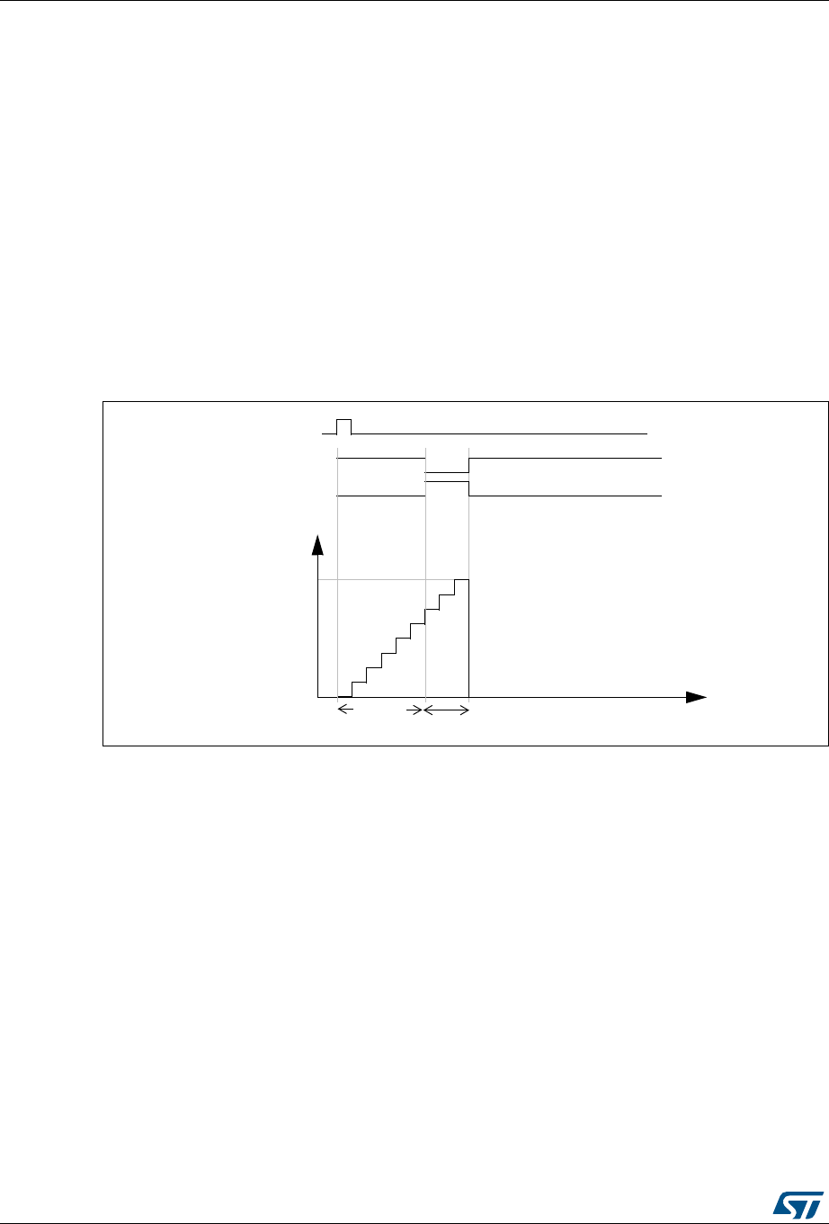
General-purpose timers (TIM2 to TIM5) RM0090
600/1718 DocID018909 Rev 9
18.3.10 One-pulse mode
One-pulse mode (OPM) is a particular case of the previous modes. It allows the counter to
be started in response to a stimulus and to generate a pulse with a programmable length
after a programmable delay.
Starting the counter can be controlled through the slave mode controller. Generating the
waveform can be done in output compare mode or PWM mode. You select One-pulse mode
by setting the OPM bit in the TIMx_CR1 register. This makes the counter stop automatically
at the next update event UEV.
A pulse can be correctly generated only if the compare value is different from the counter
initial value. Before starting (when the timer is waiting for the trigger), the configuration must
be:
•In upcounting: CNT<CCRx≤ARR (in particular, 0<CCRx),
•In downcounting: CNT>CCRx.
Figure 166. Example of one-pulse mode
For example you may want to generate a positive pulse on OC1 with a length of tPULSE and
after a delay of tDELAY as soon as a positive edge is detected on the TI2 input pin.
Let’s use TI2FP2 as trigger 1:
•Map TI2FP2 on TI2 by writing CC2S=01 in the TIMx_CCMR1 register.
•TI2FP2 must detect a rising edge, write CC2P=0 and CC2NP=’0’ in the TIMx_CCER
register.
•Configure TI2FP2 as trigger for the slave mode controller (TRGI) by writing TS=110 in
the TIMx_SMCR register.
•TI2FP2 is used to start the counter by writing SMS to ‘110 in the TIMx_SMCR register
(trigger mode).
TI2
OC1REF
Counter
t
0
TIM1_ARR
TIM1_CCR1
OC1
tDELAY tPULSE

DocID018909 Rev 9 601/1718
RM0090 General-purpose timers (TIM2 to TIM5)
635
The OPM waveform is defined by writing the compare registers (taking into account the
clock frequency and the counter prescaler).
•The tDELAY is defined by the value written in the TIMx_CCR1 register.
•The tPULSE is defined by the difference between the auto-reload value and the compare
value (TIMx_ARR - TIMx_CCR + 1).
•Let’s say you want to build a waveform with a transition from ‘0 to ‘1 when a compare
match occurs and a transition from ‘1 to ‘0 when the counter reaches the auto-reload
value. To do this you enable PWM mode 2 by writing OC1M=111 in the TIMx_CCMR1
register. You can optionally enable the preload registers by writing OC1PE=1 in the
TIMx_CCMR1 register and ARPE in the TIMx_CR1 register. In this case you have to
write the compare value in the TIMx_CCR1 register, the auto-reload value in the
TIMx_ARR register, generate an update by setting the UG bit and wait for external
trigger event on TI2. CC1P is written to ‘0 in this example.
In our example, the DIR and CMS bits in the TIMx_CR1 register should be low.
You only want 1 pulse (Single mode), so you write '1 in the OPM bit in the TIMx_CR1
register to stop the counter at the next update event (when the counter rolls over from the
auto-reload value back to 0). When OPM bit in the TIMx_CR1 register is set to '0', so the
Repetitive Mode is selected.
Particular case: OCx fast enable:
In One-pulse mode, the edge detection on TIx input set the CEN bit which enables the
counter. Then the comparison between the counter and the compare value makes the
output toggle. But several clock cycles are needed for these operations and it limits the
minimum delay tDELAY min we can get.
If you want to output a waveform with the minimum delay, you can set the OCxFE bit in the
TIMx_CCMRx register. Then OCxRef (and OCx) is forced in response to the stimulus,
without taking in account the comparison. Its new level is the same as if a compare match
had occurred. OCxFE acts only if the channel is configured in PWM1 or PWM2 mode.
18.3.11 Clearing the OCxREF signal on an external event
The OCxREF signal for a given channel can be driven Low by applying a High level to the
ETRF input (OCxCE enable bit of the corresponding TIMx_CCMRx register set to '1'). The
OCxREF signal remains Low until the next update event, UEV, occurs.
This function can only be used in output compare and PWM modes, and does not work in
forced mode.
For example, the ETR signal can be connected to the output of a comparator to be used for
current handling. In this case, ETR must be configured as follows:
1. The external trigger prescaler should be kept off: bits ETPS[1:0] in the TIMx_SMCR
register are cleared to 00.
2. The external clock mode 2 must be disabled: bit ECE in the TIM1_SMCR register is
cleared to 0.
3. The external trigger polarity (ETP) and the external trigger filter (ETF) can be
configured according to the application’s needs.
Figure 167 shows the behavior of the OCxREF signal when the ETRF input becomes high,
for both values of the OCxCE enable bit. In this example, the timer TIMx is programmed in
PWM mode.

General-purpose timers (TIM2 to TIM5) RM0090
602/1718 DocID018909 Rev 9
Figure 167. Clearing TIMx OCxREF
1. In case of a PWM with a 100% duty cycle (if CCRx>ARR), OCxREF is enabled again at the next counter
overflow.
18.3.12 Encoder interface mode
To select Encoder Interface mode write SMS=‘001 in the TIMx_SMCR register if the counter
is counting on TI2 edges only, SMS=010 if it is counting on TI1 edges only and SMS=011 if
it is counting on both TI1 and TI2 edges.
Select the TI1 and TI2 polarity by programming the CC1P and CC2P bits in the TIMx_CCER
register. When needed, you can program the input filter as well.
The two inputs TI1 and TI2 are used to interface to an incremental encoder. Refer to
Table 96. The counter is clocked by each valid transition on TI1FP1 or TI2FP2 (TI1 and TI2
after input filter and polarity selection, TI1FP1=TI1 if not filtered and not inverted,
TI2FP2=TI2 if not filtered and not inverted) assuming that it is enabled (CEN bit in
TIMx_CR1 register written to ‘1). The sequence of transitions of the two inputs is evaluated
and generates count pulses as well as the direction signal. Depending on the sequence the
counter counts up or down, the DIR bit in the TIMx_CR1 register is modified by hardware
accordingly. The DIR bit is calculated at each transition on any input (TI1 or TI2), whatever
the counter is counting on TI1 only, TI2 only or both TI1 and TI2.
Encoder interface mode acts simply as an external clock with direction selection. This
means that the counter just counts continuously between 0 and the auto-reload value in the
TIMx_ARR register (0 to ARR or ARR down to 0 depending on the direction). So you must
configure TIMx_ARR before starting. In the same way, the capture, compare, prescaler,
trigger output features continue to work as normal.
In this mode, the counter is modified automatically following the speed and the direction of
the incremental encoder and its content, therefore, always represents the encoder’s
position. The count direction correspond to the rotation direction of the connected sensor.
The table summarizes the possible combinations, assuming TI1 and TI2 don’t switch at the
same time.
OCxREF
counter (CNT)
OCxREF
ETRF
(OCxCE=0)
(OCxCE=1)
ETRF
becomes high
ETRF
still high
(CCRx)
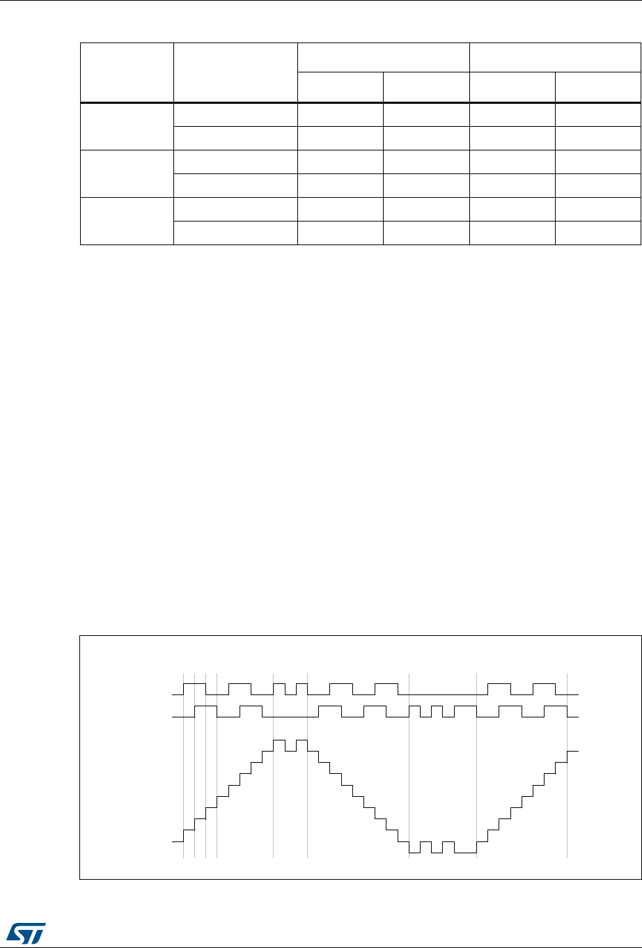
DocID018909 Rev 9 603/1718
RM0090 General-purpose timers (TIM2 to TIM5)
635
An external incremental encoder can be connected directly to the MCU without external
interface logic. However, comparators are normally be used to convert the encoder’s
differential outputs to digital signals. This greatly increases noise immunity. The third
encoder output which indicate the mechanical zero position, may be connected to an
external interrupt input and trigger a counter reset.
Figure 168 gives an example of counter operation, showing count signal generation and
direction control. It also shows how input jitter is compensated where both edges are
selected. This might occur if the sensor is positioned near to one of the switching points. For
this example we assume that the configuration is the following:
•CC1S= ‘01’ (TIMx_CCMR1 register, TI1FP1 mapped on TI1)
•CC2S= ‘01’ (TIMx_CCMR2 register, TI2FP2 mapped on TI2)
•CC1P= ‘0’, CC1NP = ‘0’, IC1F =’0000’ (TIMx_CCER register, TI1FP1 noninverted,
TI1FP1=TI1)
•CC2P= ‘0’, CC2NP = ‘0’, IC2F =’0000’ (TIMx_CCER register, TI2FP2 noninverted,
TI2FP2=TI2)
•SMS= ‘011’ (TIMx_SMCR register, both inputs are active on both rising and falling
edges)
•CEN = 1 (TIMx_CR1 register, Counter is enabled)
Figure 168. Example of counter operation in encoder interface mode
Table 96. Counting direction versus encoder signals
Active edge
Level on opposite
signal (TI1FP1 for
TI2, TI2FP2 for TI1)
TI1FP1 signal TI2FP2 signal
Rising Falling Rising Falling
Counting on
TI1 only
High Down Up No Count No Count
Low Up Down No Count No Count
Counting on
TI2 only
High No Count No Count Up Down
Low No Count No Count Down Up
Counting on
TI1 and TI2
High Down Up Up Down
Low Up Down Down Up
TI1
forward forwardbackwardjitter jitter
up down up
TI2
Counter
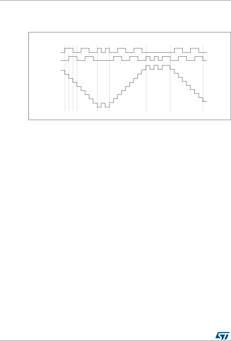
General-purpose timers (TIM2 to TIM5) RM0090
604/1718 DocID018909 Rev 9
Figure 169 gives an example of counter behavior when TI1FP1 polarity is inverted (same
configuration as above except CC1P=1).
Figure 169. Example of encoder interface mode with TI1FP1 polarity inverted
The timer, when configured in Encoder Interface mode provides information on the sensor’s
current position. You can obtain dynamic information (speed, acceleration, deceleration) by
measuring the period between two encoder events using a second timer configured in
capture mode. The output of the encoder which indicates the mechanical zero can be used
for this purpose. Depending on the time between two events, the counter can also be read
at regular times. You can do this by latching the counter value into a third input capture
register if available (then the capture signal must be periodic and can be generated by
another timer). when available, it is also possible to read its value through a DMA request
generated by a Real-Time clock.
18.3.13 Timer input XOR function
The TI1S bit in the TIM_CR2 register, allows the input filter of channel 1 to be connected to
the output of a XOR gate, combining the three input pins TIMx_CH1 to TIMx_CH3.
The XOR output can be used with all the timer input functions such as trigger or input
capture.
18.3.14 Timers and external trigger synchronization
The TIMx Timers can be synchronized with an external trigger in several modes: Reset
mode, Gated mode and Trigger mode.
Slave mode: Reset mode
The counter and its prescaler can be reinitialized in response to an event on a trigger input.
Moreover, if the URS bit from the TIMx_CR1 register is low, an update event UEV is
generated. Then all the preloaded registers (TIMx_ARR, TIMx_CCRx) are updated.
In the following example, the upcounter is cleared in response to a rising edge on TI1 input:
•Configure the channel 1 to detect rising edges on TI1. Configure the input filter duration
(in this example, we don’t need any filter, so we keep IC1F=0000). The capture
prescaler is not used for triggering, so you don’t need to configure it. The CC1S bits
select the input capture source only, CC1S = 01 in the TIMx_CCMR1 register. Write
TI1
forward forwardbackwardjitter jitter
up
down
TI2
Counter
down
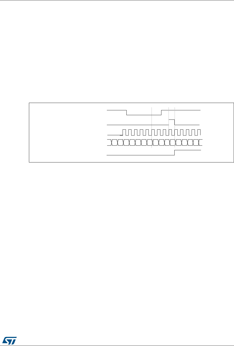
DocID018909 Rev 9 605/1718
RM0090 General-purpose timers (TIM2 to TIM5)
635
CC1P=0 and CC1NP=0 in TIMx_CCER register to validate the polarity (and detect
rising edges only).
•Configure the timer in reset mode by writing SMS=100 in TIMx_SMCR register. Select
TI1 as the input source by writing TS=101 in TIMx_SMCR register.
•Start the counter by writing CEN=1 in the TIMx_CR1 register.
The counter starts counting on the internal clock, then behaves normally until TI1 rising
edge. When TI1 rises, the counter is cleared and restarts from 0. In the meantime, the
trigger flag is set (TIF bit in the TIMx_SR register) and an interrupt request, or a DMA
request can be sent if enabled (depending on the TIE and TDE bits in TIMx_DIER register).
The following figure shows this behavior when the auto-reload register TIMx_ARR=0x36.
The delay between the rising edge on TI1 and the actual reset of the counter is due to the
resynchronization circuit on TI1 input.
Figure 170. Control circuit in reset mode
Slave mode: Gated mode
The counter can be enabled depending on the level of a selected input.
In the following example, the upcounter counts only when TI1 input is low:
•Configure the channel 1 to detect low levels on TI1. Configure the input filter duration
(in this example, we don’t need any filter, so we keep IC1F=0000). The capture
prescaler is not used for triggering, so you don’t need to configure it. The CC1S bits
select the input capture source only, CC1S=01 in TIMx_CCMR1 register. Write
CC1P=1 in TIMx_CCER register to validate the polarity (and detect low level only).
•Configure the timer in gated mode by writing SMS=101 in TIMx_SMCR register. Select
TI1 as the input source by writing TS=101 in TIMx_SMCR register.
•Enable the counter by writing CEN=1 in the TIMx_CR1 register (in gated mode, the
counter doesn’t start if CEN=0, whatever is the trigger input level).
The counter starts counting on the internal clock as long as TI1 is low and stops as soon as
TI1 becomes high. The TIF flag in the TIMx_SR register is set both when the counter starts
or stops.
The delay between the rising edge on TI1 and the actual stop of the counter is due to the
resynchronization circuit on TI1 input.
00
Counter clock = CK_CNT = CK_PSC
Counter register 01 02 03 00 01 02 0332 33 34 35 36
UG
TI1
3130
TIF
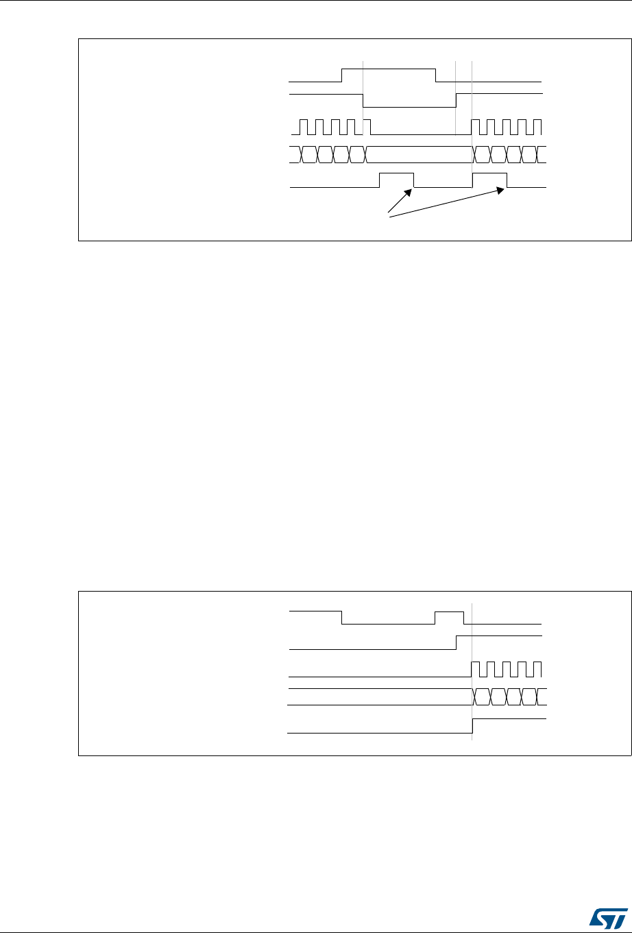
General-purpose timers (TIM2 to TIM5) RM0090
606/1718 DocID018909 Rev 9
Figure 171. Control circuit in gated mode
1. The configuration “CCxP=CCxNP=1” (detection of both rising and falling edges) does not have any effect
in gated mode because gated mode acts on a level and not on an edge.
Slave mode: Trigger mode
The counter can start in response to an event on a selected input.
In the following example, the upcounter starts in response to a rising edge on TI2 input:
•Configure the channel 2 to detect rising edges on TI2. Configure the input filter duration
(in this example, we don’t need any filter, so we keep IC2F=0000). The capture
prescaler is not used for triggering, so you don’t need to configure it. CC2S bits are
selecting the input capture source only, CC2S=01 in TIMx_CCMR1 register. Write
CC2P=1 in TIMx_CCER register to validate the polarity (and detect low level only).
•Configure the timer in trigger mode by writing SMS=110 in TIMx_SMCR register. Select
TI2 as the input source by writing TS=110 in TIMx_SMCR register.
When a rising edge occurs on TI2, the counter starts counting on the internal clock and the
TIF flag is set.
The delay between the rising edge on TI2 and the actual start of the counter is due to the
resynchronization circuit on TI2 input.
Figure 172. Control circuit in trigger mode
Slave mode: External Clock mode 2 + trigger mode
The external clock mode 2 can be used in addition to another slave mode (except external
clock mode 1 and encoder mode). In this case, the ETR signal is used as external clock
input, and another input can be selected as trigger input when operating in reset mode,
gated mode or trigger mode. It is recommended not to select ETR as TRGI through the TS
bits of TIMx_SMCR register.
Counter clock = CK_CNT = CK_PSC
Counter register 35 36 37 3832 33 34
TI1
3130
CNT_EN
TIF
Write TIF=0
Counter clock = CK_CNT = CK_PSC
Counter register 35 36 37 3834
TI2
CNT_EN
TIF
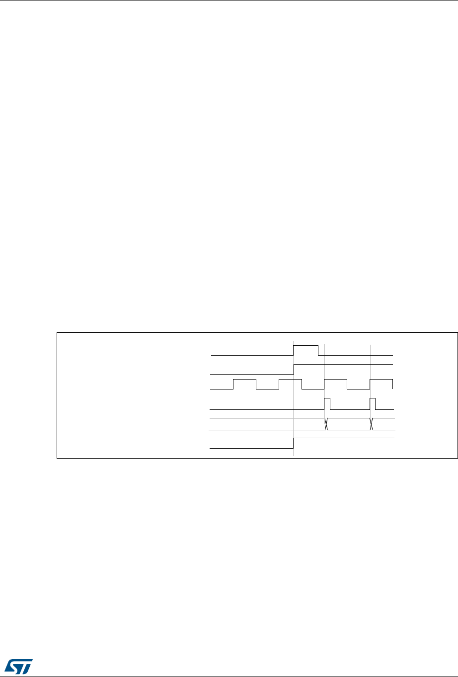
DocID018909 Rev 9 607/1718
RM0090 General-purpose timers (TIM2 to TIM5)
635
In the following example, the upcounter is incremented at each rising edge of the ETR
signal as soon as a rising edge of TI1 occurs:
1. Configure the external trigger input circuit by programming the TIMx_SMCR register as
follows:
– ETF = 0000: no filter
– ETPS = 00: prescaler disabled
– ETP = 0: detection of rising edges on ETR and ECE=1 to enable the external clock
mode 2.
2. Configure the channel 1 as follows, to detect rising edges on TI:
– IC1F = 0000: no filter.
– The capture prescaler is not used for triggering and does not need to be
configured.
– CC1S = 01 in TIMx_CCMR1 register to select only the input capture source
– CC1P = 0 in TIMx_CCER register to validate the polarity (and detect rising edge
only).
3. Configure the timer in trigger mode by writing SMS=110 in TIMx_SMCR register. Select
TI1 as the input source by writing TS=101 in TIMx_SMCR register.
A rising edge on TI1 enables the counter and sets the TIF flag. The counter then counts on
ETR rising edges.
The delay between the rising edge of the ETR signal and the actual reset of the counter is
due to the resynchronization circuit on ETRP input.
Figure 173. Control circuit in external clock mode 2 + trigger mode
18.3.15 Timer synchronization
The TIMx timers are linked together internally for timer synchronization or chaining. When
one Timer is configured in Master Mode, it can reset, start, stop or clock the counter of
another Timer configured in Slave Mode.
Figure 174: Master/Slave timer example presents an overview of the trigger selection and
the master mode selection blocks.
Counter clock = CK_CNT = CK_PSC
Counter register 35 3634
ETR
CEN/CNT_EN
TIF
TI1
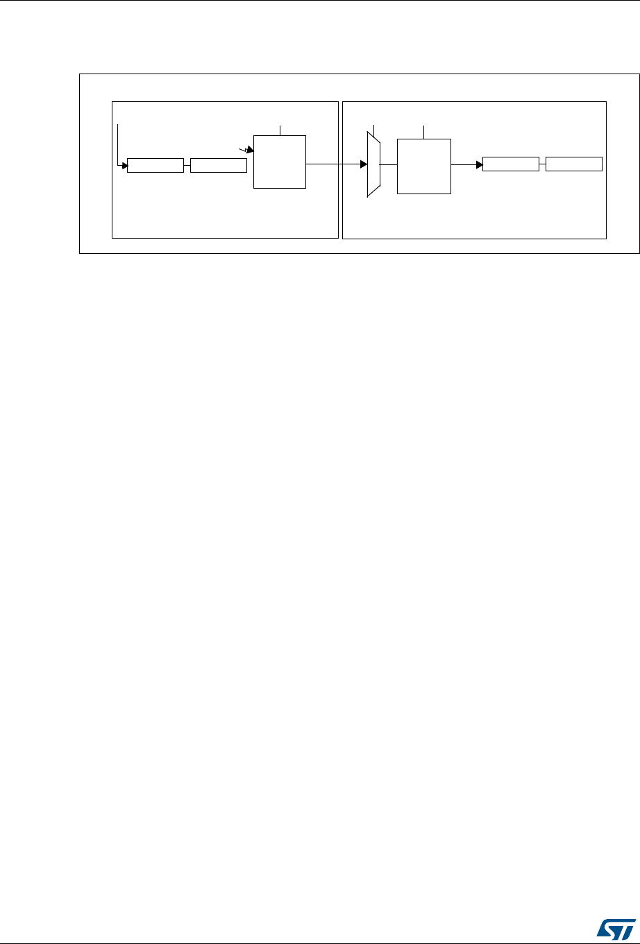
General-purpose timers (TIM2 to TIM5) RM0090
608/1718 DocID018909 Rev 9
Using one timer as prescaler for another
Figure 174. Master/Slave timer example
For example, you can configure Timer 1 to act as a prescaler for Timer 2. Refer to
Figure 174. To do this:
•Configure Timer 1 in master mode so that it outputs a periodic trigger signal on each
update event UEV. If you write MMS=010 in the TIM1_CR2 register, a rising edge is
output on TRGO1 each time an update event is generated.
•To connect the TRGO1 output of Timer 1 to Timer 2, Timer 2 must be configured in
slave mode using ITR0 as internal trigger. You select this through the TS bits in the
TIM2_SMCR register (writing TS=000).
•Then you put the slave mode controller in external clock mode 1 (write SMS=111 in the
TIM2_SMCR register). This causes Timer 2 to be clocked by the rising edge of the
periodic Timer 1 trigger signal (which correspond to the timer 1 counter overflow).
•Finally both timers must be enabled by setting their respective CEN bits (TIMx_CR1
register).
Note: If OCx is selected on Timer 1 as trigger output (MMS=1xx), its rising edge is used to clock
the counter of timer 2.
Using one timer to enable another timer
In this example, we control the enable of Timer 2 with the output compare 1 of Timer 1.
Refer to Figure 174 for connections. Timer 2 counts on the divided internal clock only when
OC1REF of Timer 1 is high. Both counter clock frequencies are divided by 3 by the
prescaler compared to CK_INT (fCK_CNT = fCK_INT/3).
•Configure Timer 1 master mode to send its Output Compare 1 Reference (OC1REF)
signal as trigger output (MMS=100 in the TIM1_CR2 register).
•Configure the Timer 1 OC1REF waveform (TIM1_CCMR1 register).
•Configure Timer 2 to get the input trigger from Timer 1 (TS=000 in the TIM2_SMCR
register).
•Configure Timer 2 in gated mode (SMS=101 in TIM2_SMCR register).
•Enable Timer 2 by writing ‘1 in the CEN bit (TIM2_CR1 register).
•Start Timer 1 by writing ‘1 in the CEN bit (TIM1_CR1 register).
Note: The counter 2 clock is not synchronized with counter 1, this mode only affects the Timer 2
counter enable signal.
TRGO1
UEV ITR0
Prescaler Counter
SMSTSMMS
TIM1 TIM2
Master
mode
control
Slave
mode
control
CK_PSC
Prescaler Counter
Clock
Input
selection
trigger
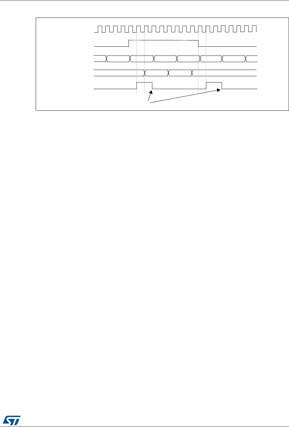
DocID018909 Rev 9 609/1718
RM0090 General-purpose timers (TIM2 to TIM5)
635
Figure 175. Gating timer 2 with OC1REF of timer 1
In the example in Figure 241, the Timer 2 counter and prescaler are not initialized before
being started. So they start counting from their current value. It is possible to start from a
given value by resetting both timers before starting Timer 1. You can then write any value
you want in the timer counters. The timers can easily be reset by software using the UG bit
in the TIMx_EGR registers.
In the next example, we synchronize Timer 1 and Timer 2. Timer 1 is the master and starts
from 0. Timer 2 is the slave and starts from 0xE7. The prescaler ratio is the same for both
timers. Timer 2 stops when Timer 1 is disabled by writing ‘0 to the CEN bit in the TIM1_CR1
register:
•Configure Timer 1 master mode to send its Output Compare 1 Reference (OC1REF)
signal as trigger output (MMS=100 in the TIM1_CR2 register).
•Configure the Timer 1 OC1REF waveform (TIM1_CCMR1 register).
•Configure Timer 2 to get the input trigger from Timer 1 (TS=000 in the TIM2_SMCR
register).
•Configure Timer 2 in gated mode (SMS=101 in TIM2_SMCR register).
•Reset Timer 1 by writing ‘1 in UG bit (TIM1_EGR register).
•Reset Timer 2 by writing ‘1 in UG bit (TIM2_EGR register).
•Initialize Timer 2 to 0xE7 by writing ‘0xE7’ in the timer 2 counter (TIM2_CNTL).
•Enable Timer 2 by writing ‘1 in the CEN bit (TIM2_CR1 register).
•Start Timer 1 by writing ‘1 in the CEN bit (TIM1_CR1 register).
•Stop Timer 1 by writing ‘0 in the CEN bit (TIM1_CR1 register).
TIMER 2-TIF
Write TIF=0
FC FD FE FF 00
3045 3047 3048
CK_INT
TIMER1-OC1REF
TIMER1-CNT
TIMER2-CNT
01
3046
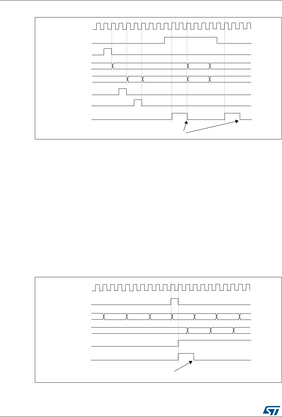
General-purpose timers (TIM2 to TIM5) RM0090
610/1718 DocID018909 Rev 9
Figure 176. Gating timer 2 with Enable of timer 1
Using one timer to start another timer
In this example, we set the enable of Timer 2 with the update event of Timer 1. Refer to
Figure 174 for connections. Timer 2 starts counting from its current value (which can be
nonzero) on the divided internal clock as soon as the update event is generated by Timer 1.
When Timer 2 receives the trigger signal its CEN bit is automatically set and the counter
counts until we write ‘0 to the CEN bit in the TIM2_CR1 register. Both counter clock
frequencies are divided by 3 by the prescaler compared to CK_INT (fCK_CNT = fCK_INT/3).
•Configure Timer 1 master mode to send its Update Event (UEV) as trigger output
(MMS=010 in the TIM1_CR2 register).
•Configure the Timer 1 period (TIM1_ARR registers).
•Configure Timer 2 to get the input trigger from Timer 1 (TS=000 in the TIM2_SMCR
register).
•Configure Timer 2 in trigger mode (SMS=110 in TIM2_SMCR register).
•Start Timer 1 by writing ‘1 in the CEN bit (TIM1_CR1 register).
Figure 177. Triggering timer 2 with update of timer 1
TIMER 2-TIF
Write TIF=0
75 00 01
CK_INT
TIMER1-CEN=CNT_EN
TIMER1-CNT
TIMER2-CNT
02
TIMER1-CNT_INIT
AB 00 E7 E8 E9
TIMER2-CNT_INIT
TIMER2
write CNT
TIMER 2-TIF
Write TIF=0
FD FE FF 00 01
45 47 48
CK_INT
TIMER1-UEV
TIMER1-CNT
TIMER2-CNT
02
46
TIMER2-CEN=CNT_EN
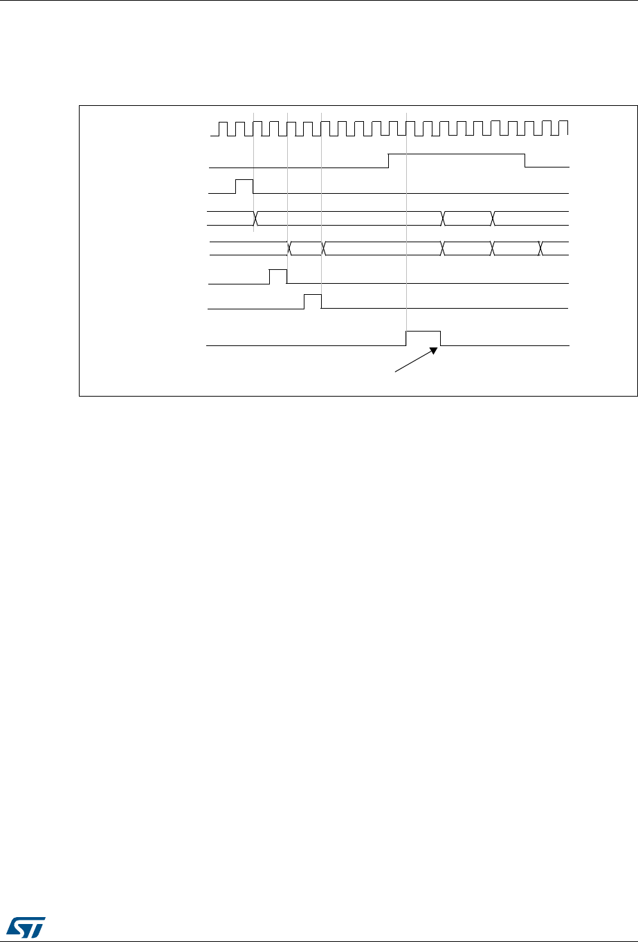
DocID018909 Rev 9 611/1718
RM0090 General-purpose timers (TIM2 to TIM5)
635
As in the previous example, you can initialize both counters before starting counting.
Figure 178 shows the behavior with the same configuration as in Figure 241 but in trigger
mode instead of gated mode (SMS=110 in the TIM2_SMCR register).
Figure 178. Triggering timer 2 with Enable of timer 1
Using one timer as prescaler for another timer
For example, you can configure Timer 1 to act as a prescaler for Timer 2. Refer to
Figure 174 for connections. To do this:
•Configure Timer 1 master mode to send its Update Event (UEV) as trigger output
(MMS=010 in the TIM1_CR2 register). then it outputs a periodic signal on each counter
overflow.
•Configure the Timer 1 period (TIM1_ARR registers).
•Configure Timer 2 to get the input trigger from Timer 1 (TS=000 in the TIM2_SMCR
register).
•Configure Timer 2 in external clock mode 1 (SMS=111 in TIM2_SMCR register).
•Start Timer 2 by writing ‘1 in the CEN bit (TIM2_CR1 register).
•Start Timer 1 by writing ‘1 in the CEN bit (TIM1_CR1 register).
Starting 2 timers synchronously in response to an external trigger
In this example, we set the enable of timer 1 when its TI1 input rises, and the enable of
Timer 2 with the enable of Timer 1. Refer to Figure 174 for connections. To ensure the
TIMER 2-TIF
Write TIF=0
75 00 01
CK_INT
TIMER1-CEN=CNT_EN
TIMER1-CNT
TIMER2-CNT
02
TIMER1-CNT_INIT
CD 00 E7 E8 EA
TIMER2-CNT_INIT
TIMER2
write CNT
E9
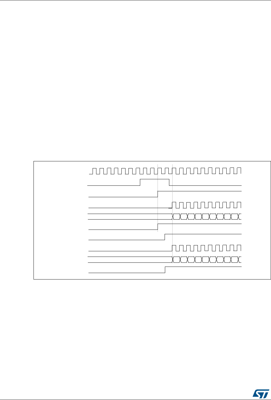
General-purpose timers (TIM2 to TIM5) RM0090
612/1718 DocID018909 Rev 9
counters are aligned, Timer 1 must be configured in Master/Slave mode (slave with respect
to TI1, master with respect to Timer 2):
•Configure Timer 1 master mode to send its Enable as trigger output (MMS=001 in the
TIM1_CR2 register).
•Configure Timer 1 slave mode to get the input trigger from TI1 (TS=100 in the
TIM1_SMCR register).
•Configure Timer 1 in trigger mode (SMS=110 in the TIM1_SMCR register).
•Configure the Timer 1 in Master/Slave mode by writing MSM=1 (TIM1_SMCR register).
•Configure Timer 2 to get the input trigger from Timer 1 (TS=000 in the TIM2_SMCR
register).
•Configure Timer 2 in trigger mode (SMS=110 in the TIM2_SMCR register).
When a rising edge occurs on TI1 (Timer 1), both counters starts counting synchronously on
the internal clock and both TIF flags are set.
Note: In this example both timers are initialized before starting (by setting their respective UG
bits). Both counters starts from 0, but you can easily insert an offset between them by
writing any of the counter registers (TIMx_CNT). You can see that the master/slave mode
insert a delay between CNT_EN and CK_PSC on timer 1.
Figure 179. Triggering timer 1 and 2 with timer 1 TI1 input
18.3.16 Debug mode
When the microcontroller enters debug mode (Cortex®-M4 with FPU core - halted), the
TIMx counter either continues to work normally or stops, depending on DBG_TIMx_STOP
configuration bit in DBGMCU module. For more details, refer to Section 38.16.2: Debug
support for timers, watchdog, bxCAN and I2C.
00 01
CK_INT
TIMER1-CEN=CNT_EN
TIMER1-CNT
TIMER 1-TI1
TIMER 1-CK_PSC
02 03 04 05 06 07 08 09
TIMER1-TIF
00 01
TIMER2-CEN=CNT_EN
TIMER2-CNT
TIMER 2-CK_PSC
02 03 04 05 06 07 08 09
TIMER2-TIF

DocID018909 Rev 9 613/1718
RM0090 General-purpose timers (TIM2 to TIM5)
635
18.4 TIM2 to TIM5 registers
Refer to Section 1.1 on page 57 for a list of abbreviations used in register descriptions.
The 32-bit peripheral registers have to be written by words (32 bits). All other peripheral
registers have to be written by half-words (16 bits) or words (32 bits). Read accesses can be
done by bytes (8 bits), half-words (16 bits) or words (32 bits).
18.4.1 TIMx control register 1 (TIMx_CR1)
Address offset: 0x00
Reset value: 0x0000
1514131211109876543210
Reserved CKD[1:0] ARPE CMS DIR OPM URS UDIS CEN
rw rw rw rw rw rw rw rw rw rw
Bits 15:10 Reserved, must be kept at reset value.
Bits 9:8 CKD: Clock division
This bit-field indicates the division ratio between the timer clock (CK_INT) frequency and
sampling clock used by the digital filters (ETR, TIx),
00: tDTS = tCK_INT
01: tDTS = 2 × tCK_INT
10: tDTS = 4 × tCK_INT
11: Reserved
Bit 7 ARPE: Auto-reload preload enable
0: TIMx_ARR register is not buffered
1: TIMx_ARR register is buffered
Bits 6:5 CMS: Center-aligned mode selection
00: Edge-aligned mode. The counter counts up or down depending on the direction bit
(DIR).
01: Center-aligned mode 1. The counter counts up and down alternatively. Output compare
interrupt flags of channels configured in output (CCxS=00 in TIMx_CCMRx register) are set
only when the counter is counting down.
10: Center-aligned mode 2. The counter counts up and down alternatively. Output compare
interrupt flags of channels configured in output (CCxS=00 in TIMx_CCMRx register) are set
only when the counter is counting up.
11: Center-aligned mode 3. The counter counts up and down alternatively. Output compare
interrupt flags of channels configured in output (CCxS=00 in TIMx_CCMRx register) are set
both when the counter is counting up or down.
Note: It is not allowed to switch from edge-aligned mode to center-aligned mode as long as
the counter is enabled (CEN=1)
Bit 4 DIR: Direction
0: Counter used as upcounter
1: Counter used as downcounter
Note: This bit is read only when the timer is configured in Center-aligned mode or Encoder
mode.
Bit 3 OPM: One-pulse mode
0: Counter is not stopped at update event
1: Counter stops counting at the next update event (clearing the bit CEN)

General-purpose timers (TIM2 to TIM5) RM0090
614/1718 DocID018909 Rev 9
Bit 2 URS: Update request source
This bit is set and cleared by software to select the UEV event sources.
0: Any of the following events generate an update interrupt or DMA request if enabled.
These events can be:
– Counter overflow/underflow
– Setting the UG bit
– Update generation through the slave mode controller
1: Only counter overflow/underflow generates an update interrupt or DMA request if
enabled.
Bit 1 UDIS: Update disable
This bit is set and cleared by software to enable/disable UEV event generation.
0: UEV enabled. The Update (UEV) event is generated by one of the following events:
– Counter overflow/underflow
– Setting the UG bit
– Update generation through the slave mode controller
Buffered registers are then loaded with their preload values.
1: UEV disabled. The Update event is not generated, shadow registers keep their value
(ARR, PSC, CCRx). However the counter and the prescaler are reinitialized if the UG bit is
set or if a hardware reset is received from the slave mode controller.
Bit 0 CEN: Counter enable
0: Counter disabled
1: Counter enabled
Note: External clock, gated mode and encoder mode can work only if the CEN bit has been
previously set by software. However trigger mode can set the CEN bit automatically by
hardware.
CEN is cleared automatically in one-pulse mode, when an update event occurs.

DocID018909 Rev 9 615/1718
RM0090 General-purpose timers (TIM2 to TIM5)
635
18.4.2 TIMx control register 2 (TIMx_CR2)
Address offset: 0x04
Reset value: 0x0000
1514131211109876543210
Reserved TI1S MMS[2:0] CCDS Reserved
rw rw rw rw rw
Bits 15:8 Reserved, must be kept at reset value.
Bit 7 TI1S: TI1 selection
0: The TIMx_CH1 pin is connected to TI1 input
1: The TIMx_CH1, CH2 and CH3 pins are connected to the TI1 input (XOR combination)
Bits 6:4 MMS[2:0]: Master mode selection
These bits allow to select the information to be sent in master mode to slave timers for
synchronization (TRGO). The combination is as follows:
000: Reset - the UG bit from the TIMx_EGR register is used as trigger output (TRGO). If the
reset is generated by the trigger input (slave mode controller configured in reset mode) then
the signal on TRGO is delayed compared to the actual reset.
001: Enable - the Counter enable signal, CNT_EN, is used as trigger output (TRGO). It is
useful to start several timers at the same time or to control a window in which a slave timer is
enabled. The Counter Enable signal is generated by a logic OR between CEN control bit
and the trigger input when configured in gated mode.
When the Counter Enable signal is controlled by the trigger input, there is a delay on TRGO,
except if the master/slave mode is selected (see the MSM bit description in TIMx_SMCR
register).
010: Update - The update event is selected as trigger output (TRGO). For instance a master
timer can then be used as a prescaler for a slave timer.
011: Compare Pulse - The trigger output send a positive pulse when the CC1IF flag is to be
set (even if it was already high), as soon as a capture or a compare match occurred.
(TRGO)
100: Compare - OC1REF signal is used as trigger output (TRGO)
101: Compare - OC2REF signal is used as trigger output (TRGO)
110: Compare - OC3REF signal is used as trigger output (TRGO)
111: Compare - OC4REF signal is used as trigger output (TRGO)
Bit 3 CCDS: Capture/compare DMA selection
0: CCx DMA request sent when CCx event occurs
1: CCx DMA requests sent when update event occurs
Bits 2:0 Reserved, must be kept at reset value.

General-purpose timers (TIM2 to TIM5) RM0090
616/1718 DocID018909 Rev 9
18.4.3 TIMx slave mode control register (TIMx_SMCR)
Address offset: 0x08
Reset value: 0x0000
1514131211109876543210
ETP ECE ETPS[1:0] ETF[3:0] MSM TS[2:0] Res. SMS[2:0]
rw rw rw rw rw rw rw rw rw rw rw rw rw rw rw
Bit 15 ETP: External trigger polarity
This bit selects whether ETR or ETR is used for trigger operations
0: ETR is noninverted, active at high level or rising edge
1: ETR is inverted, active at low level or falling edge
Bit 14 ECE: External clock enable
This bit enables External clock mode 2.
0: External clock mode 2 disabled
1: External clock mode 2 enabled. The counter is clocked by any active edge on the ETRF
signal.
1: Setting the ECE bit has the same effect as selecting external clock mode 1 with TRGI
connected to ETRF (SMS=111 and TS=111).
2: It is possible to simultaneously use external clock mode 2 with the following slave modes:
reset mode, gated mode and trigger mode. Nevertheless, TRGI must not be connected to
ETRF in this case (TS bits must not be 111).
3: If external clock mode 1 and external clock mode 2 are enabled at the same time, the
external clock input is ETRF.
Bits 13:12 ETPS: External trigger prescaler
External trigger signal ETRP frequency must be at most 1/4 of CK_INT frequency. A
prescaler can be enabled to reduce ETRP frequency. It is useful when inputting fast external
clocks.
00: Prescaler OFF
01: ETRP frequency divided by 2
10: ETRP frequency divided by 4
11: ETRP frequency divided by 8
Bits 11:8 ETF[3:0]: External trigger filter
This bit-field then defines the frequency used to sample ETRP signal and the length of the
digital filter applied to ETRP. The digital filter is made of an event counter in which N events
are needed to validate a transition on the output:
0000: No filter, sampling is done at fDTS
0001: fSAMPLING=fCK_INT
, N=2
0010: fSAMPLING=fCK_INT
, N=4
0011: fSAMPLING=fCK_INT
, N=8
0100: fSAMPLING=fDTS/2, N=6
0101: fSAMPLING=fDTS/2, N=8
0110: fSAMPLING=fDTS/4, N=6
0111: fSAMPLING=fDTS/4, N=8
1000: fSAMPLING=fDTS/8, N=6
1001: fSAMPLING=fDTS/8, N=8
1010: fSAMPLING=fDTS/16, N=5
1011: fSAMPLING=fDTS/16, N=6
1100: fSAMPLING=fDTS/16, N=8
1101: fSAMPLING=fDTS/32, N=5
1110: fSAMPLING=fDTS/32, N=6
1111: fSAMPLING=fDTS/32, N=8

DocID018909 Rev 9 617/1718
RM0090 General-purpose timers (TIM2 to TIM5)
635
Bit 7 MSM: Master/Slave mode
0: No action
1: The effect of an event on the trigger input (TRGI) is delayed to allow a perfect
synchronization between the current timer and its slaves (through TRGO). It is useful if we
want to synchronize several timers on a single external event.
Bits 6:4 TS: Trigger selection
This bit-field selects the trigger input to be used to synchronize the counter.
000: Internal Trigger 0 (ITR0)
001: Internal Trigger 1 (ITR1).
010: Internal Trigger 2 (ITR2).
011: Internal Trigger 3 (ITR3).
100: TI1 Edge Detector (TI1F_ED)
101: Filtered Timer Input 1 (TI1FP1)
110: Filtered Timer Input 2 (TI2FP2)
111: External Trigger input (ETRF)
See Table 97: TIMx internal trigger connection on page 618 for more details on ITRx
meaning for each Timer.
Note: These bits must be changed only when they are not used (e.g. when SMS=000) to
avoid wrong edge detections at the transition.
Bit 3 Reserved, must be kept at reset value.
Bits 2:0 SMS: Slave mode selection
When external signals are selected the active edge of the trigger signal (TRGI) is linked to
the polarity selected on the external input (see Input Control register and Control Register
description.
000: Slave mode disabled - if CEN = ‘1 then the prescaler is clocked directly by the internal
clock.
001: Encoder mode 1 - Counter counts up/down on TI2FP2 edge depending on TI1FP1
level.
010: Encoder mode 2 - Counter counts up/down on TI1FP1 edge depending on TI2FP2
level.
011: Encoder mode 3 - Counter counts up/down on both TI1FP1 and TI2FP2 edges
depending on the level of the other input.
100: Reset Mode - Rising edge of the selected trigger input (TRGI) reinitializes the counter
and generates an update of the registers.
101: Gated Mode - The counter clock is enabled when the trigger input (TRGI) is high. The
counter stops (but is not reset) as soon as the trigger becomes low. Both start and stop of
the counter are controlled.
110: Trigger Mode - The counter starts at a rising edge of the trigger TRGI (but it is not
reset). Only the start of the counter is controlled.
111: External Clock Mode 1 - Rising edges of the selected trigger (TRGI) clock the counter.
Note: The gated mode must not be used if TI1F_ED is selected as the trigger input (TS=100).
Indeed, TI1F_ED outputs 1 pulse for each transition on TI1F, whereas the gated mode
checks the level of the trigger signal.

General-purpose timers (TIM2 to TIM5) RM0090
618/1718 DocID018909 Rev 9
18.4.4 TIMx DMA/Interrupt enable register (TIMx_DIER)
Address offset: 0x0C
Reset value: 0x0000
Table 97. TIMx internal trigger connection
Slave TIM ITR0 (TS = 000) ITR1 (TS = 001) ITR2 (TS = 010) ITR3 (TS = 011)
TIM2 TIM1 TIM8 TIM3 TIM4
TIM3 TIM1 TIM2 TIM5 TIM4
TIM4 TIM1 TIM2 TIM3 TIM8
TIM5 TIM2 TIM3 TIM4 TIM8
1514131211109876543210
Res.
TDE
Res
CC4DE CC3DE CC2DE CC1DE UDE
Res.
TIE
Res
CC4IE CC3IE CC2IE CC1IE UIE
rw rw rw rw rw rw rw rw rw rw rw rw
Bit 15 Reserved, must be kept at reset value.
Bit 14 TDE: Trigger DMA request enable
0: Trigger DMA request disabled.
1: Trigger DMA request enabled.
Bit 13 Reserved, always read as 0
Bit 12 CC4DE: Capture/Compare 4 DMA request enable
0: CC4 DMA request disabled.
1: CC4 DMA request enabled.
Bit 11 CC3DE: Capture/Compare 3 DMA request enable
0: CC3 DMA request disabled.
1: CC3 DMA request enabled.
Bit 10 CC2DE: Capture/Compare 2 DMA request enable
0: CC2 DMA request disabled.
1: CC2 DMA request enabled.
Bit 9 CC1DE: Capture/Compare 1 DMA request enable
0: CC1 DMA request disabled.
1: CC1 DMA request enabled.
Bit 8 UDE: Update DMA request enable
0: Update DMA request disabled.
1: Update DMA request enabled.
Bit 7 Reserved, must be kept at reset value.
Bit 6 TIE: Trigger interrupt enable
0: Trigger interrupt disabled.
1: Trigger interrupt enabled.
Bit 5 Reserved, must be kept at reset value.
Bit 4 CC4IE: Capture/Compare 4 interrupt enable
0: CC4 interrupt disabled.
1: CC4 interrupt enabled.

DocID018909 Rev 9 619/1718
RM0090 General-purpose timers (TIM2 to TIM5)
635
18.4.5 TIMx status register (TIMx_SR)
Address offset: 0x10
Reset value: 0x0000
Bit 3 CC3IE: Capture/Compare 3 interrupt enable
0: CC3 interrupt disabled
1: CC3 interrupt enabled
Bit 2 CC2IE: Capture/Compare 2 interrupt enable
0: CC2 interrupt disabled
1: CC2 interrupt enabled
Bit 1 CC1IE: Capture/Compare 1 interrupt enable
0: CC1 interrupt disabled
1: CC1 interrupt enabled
Bit 0 UIE: Update interrupt enable
0: Update interrupt disabled
1: Update interrupt enabled
1514131211109876543210
Reserved CC4OF CC3OF CC2OF CC1OF Reserved TIF Res CC4IF CC3IF CC2IF CC1IF UIF
rc_w0 rc_w0 rc_w0 rc_w0 rc_w0 rc_w0 rc_w0 rc_w0 rc_w0 rc_w0
Bits 15:13 Reserved, must be kept at reset value.
Bit 12 CC4OF: Capture/Compare 4 overcapture flag
refer to CC1OF description
Bit 11 CC3OF: Capture/Compare 3 overcapture flag
refer to CC1OF description
Bit 10 CC2OF: Capture/compare 2 overcapture flag
refer to CC1OF description
Bit 9 CC1OF: Capture/Compare 1 overcapture flag
This flag is set by hardware only when the corresponding channel is configured in input
capture mode. It is cleared by software by writing it to ‘0.
0: No overcapture has been detected
1: The counter value has been captured in TIMx_CCR1 register while CC1IF flag was
already set
Bits 8:7 Reserved, must be kept at reset value.
Bit 6 TIF: Trigger interrupt flag
This flag is set by hardware on trigger event (active edge detected on TRGI input when the
slave mode controller is enabled in all modes but gated mode. It is set when the counter
starts or stops when gated mode is selected. It is cleared by software.
0: No trigger event occurred
1: Trigger interrupt pending
Bit 5 Reserved, must be kept at reset value.
Bit 4 CC4IF: Capture/Compare 4 interrupt flag
refer to CC1IF description

General-purpose timers (TIM2 to TIM5) RM0090
620/1718 DocID018909 Rev 9
Bit 3 CC3IF: Capture/Compare 3 interrupt flag
refer to CC1IF description
Bit 2 CC2IF: Capture/Compare 2 interrupt flag
refer to CC1IF description
Bit 1 CC1IF: Capture/compare 1 interrupt flag
If channel CC1 is configured as output:
This flag is set by hardware when the counter matches the compare value, with some
exception in center-aligned mode (refer to the CMS bits in the TIMx_CR1 register
description). It is cleared by software.
0: No match
1: The content of the counter TIMx_CNT matches the content of the TIMx_CCR1 register.
When the contents of TIMx_CCR1 are greater than the contents of TIMx_ARR, the CC1IF bit
goes high on the counter overflow (in upcounting and up/down-counting modes) or underflow
(in downcounting mode)
If channel CC1 is configured as input:
This bit is set by hardware on a capture. It is cleared by software or by reading the
TIMx_CCR1 register.
0: No input capture occurred
1: The counter value has been captured in TIMx_CCR1 register (An edge has been detected
on IC1 which matches the selected polarity)
Bit 0 UIF: Update interrupt flag
″This bit is set by hardware on an update event. It is cleared by software.
0: No update occurred.
1: Update interrupt pending. This bit is set by hardware when the registers are updated:
″At overflow or underflow (for TIM2 to TIM5) and if UDIS=0 in the TIMx_CR1 register.
″When CNT is reinitialized by software using the UG bit in TIMx_EGR register, if URS=0
and UDIS=0 in the TIMx_CR1 register.
When CNT is reinitialized by a trigger event (refer to the synchro control register description),
if URS=0 and UDIS=0 in the TIMx_CR1 register.

DocID018909 Rev 9 621/1718
RM0090 General-purpose timers (TIM2 to TIM5)
635
18.4.6 TIMx event generation register (TIMx_EGR)
Address offset: 0x14
Reset value: 0x0000
1514131211109876543210
Reserved TG Res. CC4G CC3G CC2G CC1G UG
w wwwww
Bits 15:7 Reserved, must be kept at reset value.
Bit 6 TG: Trigger generation
This bit is set by software in order to generate an event, it is automatically cleared by
hardware.
0: No action
1: The TIF flag is set in TIMx_SR register. Related interrupt or DMA transfer can occur if
enabled.
Bit 5 Reserved, must be kept at reset value.
Bit 4 CC4G: Capture/compare 4 generation
refer to CC1G description
Bit 3 CC3G: Capture/compare 3 generation
refer to CC1G description
Bit 2 CC2G: Capture/compare 2 generation
refer to CC1G description
Bit 1 CC1G: Capture/compare 1 generation
This bit is set by software in order to generate an event, it is automatically cleared by
hardware.
0: No action
1: A capture/compare event is generated on channel 1:
If channel CC1 is configured as output:
CC1IF flag is set, Corresponding interrupt or DMA request is sent if enabled.
If channel CC1 is configured as input:
The current value of the counter is captured in TIMx_CCR1 register. The CC1IF flag is set,
the corresponding interrupt or DMA request is sent if enabled. The CC1OF flag is set if the
CC1IF flag was already high.
Bit 0 UG: Update generation
This bit can be set by software, it is automatically cleared by hardware.
0: No action
1: Re-initialize the counter and generates an update of the registers. Note that the prescaler
counter is cleared too (anyway the prescaler ratio is not affected). The counter is cleared if
the center-aligned mode is selected or if DIR=0 (upcounting), else it takes the auto-reload
value (TIMx_ARR) if DIR=1 (downcounting).

General-purpose timers (TIM2 to TIM5) RM0090
622/1718 DocID018909 Rev 9
18.4.7 TIMx capture/compare mode register 1 (TIMx_CCMR1)
Address offset: 0x18
Reset value: 0x0000
The channels can be used in input (capture mode) or in output (compare mode). The
direction of a channel is defined by configuring the corresponding CCxS bits. All the other
bits of this register have a different function in input and in output mode. For a given bit,
OCxx describes its function when the channel is configured in output, ICxx describes its
function when the channel is configured in input. So you must take care that the same bit
can have a different meaning for the input stage and for the output stage.
Output compare mode
1514131211109876543210
OC2CE OC2M[2:0] OC2PE OC2FE CC2S[1:0] OC1CE OC1M[2:0] OC1PE OC1FE CC1S[1:0]
IC2F[3:0] IC2PSC[1:0] IC1F[3:0] IC1PSC[1:0]
rw rw rw rw rw rw rw rw rw rw rw rw rw rw rw rw
Bit 15 OC2CE: Output compare 2 clear enable
Bits 14:12 OC2M[2:0]: Output compare 2 mode
Bit 11 OC2PE: Output compare 2 preload enable
Bit 10 OC2FE: Output compare 2 fast enable
Bits 9:8 CC2S[1:0]: Capture/Compare 2 selection
This bit-field defines the direction of the channel (input/output) as well as the used input.
00: CC2 channel is configured as output
01: CC2 channel is configured as input, IC2 is mapped on TI2
10: CC2 channel is configured as input, IC2 is mapped on TI1
11: CC2 channel is configured as input, IC2 is mapped on TRC. This mode is working only if
an internal trigger input is selected through the TS bit (TIMx_SMCR register)
Note: CC2S bits are writable only when the channel is OFF (CC2E = 0 in TIMx_CCER).
Bit 7 OC1CE: Output compare 1 clear enable
OC1CE: Output Compare 1 Clear Enable
0: OC1Ref is not affected by the ETRF input
1: OC1Ref is cleared as soon as a High level is detected on ETRF input

DocID018909 Rev 9 623/1718
RM0090 General-purpose timers (TIM2 to TIM5)
635
Bits 6:4 OC1M: Output compare 1 mode
These bits define the behavior of the output reference signal OC1REF from which OC1 and
OC1N are derived. OC1REF is active high whereas OC1 and OC1N active level depends
on CC1P and CC1NP bits.
000: Frozen - The comparison between the output compare register TIMx_CCR1 and the
counter TIMx_CNT has no effect on the outputs.(this mode is used to generate a timing
base).
001: Set channel 1 to active level on match. OC1REF signal is forced high when the counter
TIMx_CNT matches the capture/compare register 1 (TIMx_CCR1).
010: Set channel 1 to inactive level on match. OC1REF signal is forced low when the
counter TIMx_CNT matches the capture/compare register 1 (TIMx_CCR1).
011: Toggle - OC1REF toggles when TIMx_CNT=TIMx_CCR1.
100: Force inactive level - OC1REF is forced low.
101: Force active level - OC1REF is forced high.
110: PWM mode 1 - In upcounting, channel 1 is active as long as TIMx_CNT<TIMx_CCR1
else inactive. In downcounting, channel 1 is inactive (OC1REF=‘0) as long as
TIMx_CNT>TIMx_CCR1 else active (OC1REF=1).
111: PWM mode 2 - In upcounting, channel 1 is inactive as long as TIMx_CNT<TIMx_CCR1
else active. In downcounting, channel 1 is active as long as TIMx_CNT>TIMx_CCR1 else
inactive.
Note: In PWM mode 1 or 2, the OCREF level changes only when the result of the
comparison changes or when the output compare mode switches from “frozen” mode
to “PWM” mode.
Bit 3 OC1PE: Output compare 1 preload enable
0: Preload register on TIMx_CCR1 disabled. TIMx_CCR1 can be written at anytime, the
new value is taken in account immediately.
1: Preload register on TIMx_CCR1 enabled. Read/Write operations access the preload
register. TIMx_CCR1 preload value is loaded in the active register at each update event.
Note: 1: These bits can not be modified as long as LOCK level 3 has been programmed
(LOCK bits in TIMx_BDTR register) and CC1S=00 (the channel is configured in
output).
2: The PWM mode can be used without validating the preload register only in one-
pulse mode (OPM bit set in TIMx_CR1 register). Else the behavior is not guaranteed.
Bit 2 OC1FE: Output compare 1 fast enable
This bit is used to accelerate the effect of an event on the trigger in input on the CC output.
0: CC1 behaves normally depending on counter and CCR1 values even when the trigger is
ON. The minimum delay to activate CC1 output when an edge occurs on the trigger input is
5 clock cycles.
1: An active edge on the trigger input acts like a compare match on CC1 output. Then, OC
is set to the compare level independently from the result of the comparison. Delay to sample
the trigger input and to activate CC1 output is reduced to 3 clock cycles. OCFE acts only if
the channel is configured in PWM1 or PWM2 mode.
Bits 1:0 CC1S: Capture/Compare 1 selection
This bit-field defines the direction of the channel (input/output) as well as the used input.
00: CC1 channel is configured as output.
01: CC1 channel is configured as input, IC1 is mapped on TI1.
10: CC1 channel is configured as input, IC1 is mapped on TI2.
11: CC1 channel is configured as input, IC1 is mapped on TRC. This mode is working only if
an internal trigger input is selected through TS bit (TIMx_SMCR register)
Note: CC1S bits are writable only when the channel is OFF (CC1E = 0 in TIMx_CCER).

General-purpose timers (TIM2 to TIM5) RM0090
624/1718 DocID018909 Rev 9
Input capture mode
Bits 15:12 IC2F: Input capture 2 filter
Bits 11:10 IC2PSC[1:0]: Input capture 2 prescaler
Bits 9:8 CC2S: Capture/compare 2 selection
This bit-field defines the direction of the channel (input/output) as well as the used input.
00: CC2 channel is configured as output.
01: CC2 channel is configured as input, IC2 is mapped on TI2.
10: CC2 channel is configured as input, IC2 is mapped on TI1.
11: CC2 channel is configured as input, IC2 is mapped on TRC. This mode is working only if
an internal trigger input is selected through TS bit (TIMx_SMCR register)
Note: CC2S bits are writable only when the channel is OFF (CC2E = 0 in TIMx_CCER).
Bits 7:4 IC1F: Input capture 1 filter
This bit-field defines the frequency used to sample TI1 input and the length of the digital filter
applied to TI1. The digital filter is made of an event counter in which N events are needed to
validate a transition on the output:
0000: No filter, sampling is done at fDTS
0001: fSAMPLING=fCK_INT
, N=2
0010: fSAMPLING=fCK_INT
, N=4
0011: fSAMPLING=fCK_INT
, N=8
0100: fSAMPLING=fDTS/2, N=6
0101: fSAMPLING=fDTS/2, N=8
0110: fSAMPLING=fDTS/4, N=6
0111: fSAMPLING=fDTS/4, N=8
1000: fSAMPLING=fDTS/8, N=6
1001: fSAMPLING=fDTS/8, N=8
1010: fSAMPLING=fDTS/16, N=5
1011: fSAMPLING=fDTS/16, N=6
1100: fSAMPLING=fDTS/16, N=8
1101: fSAMPLING=fDTS/32, N=5
1110: fSAMPLING=fDTS/32, N=6
1111: fSAMPLING=fDTS/32, N=8
Bits 3:2 IC1PSC: Input capture 1 prescaler
This bit-field defines the ratio of the prescaler acting on CC1 input (IC1).
The prescaler is reset as soon as CC1E=0 (TIMx_CCER register).
00: no prescaler, capture is done each time an edge is detected on the capture input
01: capture is done once every 2 events
10: capture is done once every 4 events
11: capture is done once every 8 events
Bits 1:0 CC1S: Capture/Compare 1 selection
This bit-field defines the direction of the channel (input/output) as well as the used input.
00: CC1 channel is configured as output
01: CC1 channel is configured as input, IC1 is mapped on TI1
10: CC1 channel is configured as input, IC1 is mapped on TI2
11: CC1 channel is configured as input, IC1 is mapped on TRC. This mode is working only if
an internal trigger input is selected through TS bit (TIMx_SMCR register)
Note: CC1S bits are writable only when the channel is OFF (CC1E = 0 in TIMx_CCER).

DocID018909 Rev 9 625/1718
RM0090 General-purpose timers (TIM2 to TIM5)
635
18.4.8 TIMx capture/compare mode register 2 (TIMx_CCMR2)
Address offset: 0x1C
Reset value: 0x0000
Refer to the above CCMR1 register description.
Output compare mode
1514131211109876543210
OC4CE OC4M[2:0] OC4PE OC4FE CC4S[1:0] OC3CE OC3M[2:0] OC3PE OC3FE CC3S[1:0]
IC4F[3:0] IC4PSC[1:0] IC3F[3:0] IC3PSC[1:0]
rw rw rw rw rw rw rw rw rw rw rw rw rw rw rw rw
Bit 15 OC4CE: Output compare 4 clear enable
Bits 14:12 OC4M: Output compare 4 mode
Bit 11 OC4PE: Output compare 4 preload enable
Bit 10 OC4FE: Output compare 4 fast enable
Bits 9:8 CC4S: Capture/Compare 4 selection
This bit-field defines the direction of the channel (input/output) as well as the used input.
00: CC4 channel is configured as output
01: CC4 channel is configured as input, IC4 is mapped on TI4
10: CC4 channel is configured as input, IC4 is mapped on TI3
11: CC4 channel is configured as input, IC4 is mapped on TRC. This mode is working only if
an internal trigger input is selected through TS bit (TIMx_SMCR register)
Note: CC4S bits are writable only when the channel is OFF (CC4E = 0 in TIMx_CCER).
Bit 7 OC3CE: Output compare 3 clear enable
Bits 6:4 OC3M: Output compare 3 mode
Bit 3 OC3PE: Output compare 3 preload enable
Bit 2 OC3FE: Output compare 3 fast enable
Bits 1:0 CC3S: Capture/Compare 3 selection
This bit-field defines the direction of the channel (input/output) as well as the used input.
00: CC3 channel is configured as output
01: CC3 channel is configured as input, IC3 is mapped on TI3
10: CC3 channel is configured as input, IC3 is mapped on TI4
11: CC3 channel is configured as input, IC3 is mapped on TRC. This mode is working only if
an internal trigger input is selected through TS bit (TIMx_SMCR register)
Note: CC3S bits are writable only when the channel is OFF (CC3E = 0 in TIMx_CCER).

General-purpose timers (TIM2 to TIM5) RM0090
626/1718 DocID018909 Rev 9
Input capture mode
18.4.9 TIMx capture/compare enable register (TIMx_CCER)
Address offset: 0x20
Reset value: 0x0000
Bits 15:12 IC4F: Input capture 4 filter
Bits 11:10 IC4PSC: Input capture 4 prescaler
Bits 9:8 CC4S: Capture/Compare 4 selection
This bit-field defines the direction of the channel (input/output) as well as the used input.
00: CC4 channel is configured as output
01: CC4 channel is configured as input, IC4 is mapped on TI4
10: CC4 channel is configured as input, IC4 is mapped on TI3
11: CC4 channel is configured as input, IC4 is mapped on TRC. This mode is working only if
an internal trigger input is selected through TS bit (TIMx_SMCR register)
Note: CC4S bits are writable only when the channel is OFF (CC4E = 0 in TIMx_CCER).
Bits 7:4 IC3F: Input capture 3 filter
Bits 3:2 IC3PSC: Input capture 3 prescaler
Bits 1:0 CC3S: Capture/Compare 3 selection
This bit-field defines the direction of the channel (input/output) as well as the used input.
00: CC3 channel is configured as output
01: CC3 channel is configured as input, IC3 is mapped on TI3
10: CC3 channel is configured as input, IC3 is mapped on TI4
11: CC3 channel is configured as input, IC3 is mapped on TRC. This mode is working only if
an internal trigger input is selected through TS bit (TIMx_SMCR register)
Note: CC3S bits are writable only when the channel is OFF (CC3E = 0 in TIMx_CCER).
1514131211109876543210
CC4NP Res. CC4P CC4E CC3NP Res. CC3P CC3E CC2NP Res. CC2P CC2E CC1NP Res. CC1P CC1E
rw rw rw rw rw rw rw rw rw rw rw rw
Bit 15 CC4NP: Capture/Compare 4 output Polarity.
Refer to CC1NP description
Bit 14 Reserved, must be kept at reset value.
Bit 13 CC4P: Capture/Compare 4 output Polarity.
refer to CC1P description
Bit 12 CC4E: Capture/Compare 4 output enable.
refer to CC1E description
Bit 11 CC3NP: Capture/Compare 3 output Polarity.
refer to CC1NP description
Bit 10 Reserved, must be kept at reset value.
Bit 9 CC3P: Capture/Compare 3 output Polarity.
refer to CC1P description

DocID018909 Rev 9 627/1718
RM0090 General-purpose timers (TIM2 to TIM5)
635
Bit 8 CC3E: Capture/Compare 3 output enable.
refer to CC1E description
Bit 7 CC2NP: Capture/Compare 2 output Polarity.
refer to CC1NP description
Bit 6 Reserved, must be kept at reset value.
Bit 5 CC2P: Capture/Compare 2 output Polarity.
refer to CC1P description
Bit 4 CC2E: Capture/Compare 2 output enable.
refer to CC1E description
Bit 3 CC1NP: Capture/Compare 1 output Polarity.
CC1 channel configured as output:
CC1NP must be kept cleared in this case.
CC1 channel configured as input:
This bit is used in conjunction with CC1P to define TI1FP1/TI2FP1 polarity. refer to CC1P
description.
Bit 2 Reserved, must be kept at reset value.
Bit 1 CC1P: Capture/Compare 1 output Polarity.
CC1 channel configured as output:
0: OC1 active high
1: OC1 active low
CC1 channel configured as input:
CC1NP/CC1P bits select TI1FP1 and TI2FP1 polarity for trigger or capture operations.
00: noninverted/rising edge
Circuit is sensitive to TIxFP1 rising edge (capture, trigger in reset, external clock or trigger
mode), TIxFP1 is not inverted (trigger in gated mode, encoder mode).
01: inverted/falling edge
Circuit is sensitive to TIxFP1 falling edge (capture, trigger in reset, external clock or trigger
mode), TIxFP1 is inverted (trigger in gated mode, encoder mode).
10: reserved, do not use this configuration.
11: noninverted/both edges
Circuit is sensitive to both TIxFP1 rising and falling edges (capture, trigger in reset, external
clock or trigger mode), TIxFP1 is not inverted (trigger in gated mode). This configuration
must not be used for encoder mode.
Bit 0 CC1E: Capture/Compare 1 output enable.
CC1 channel configured as output:
0: Off - OC1 is not active
1: On - OC1 signal is output on the corresponding output pin
CC1 channel configured as input:
This bit determines if a capture of the counter value can actually be done into the input
capture/compare register 1 (TIMx_CCR1) or not.
0: Capture disabled
1: Capture enabled
Table 98. Output control bit for standard OCx channels
CCxE bit OCx output state
0 Output Disabled (OCx=0, OCx_EN=0)
1 OCx=OCxREF + Polarity, OCx_EN=1
General-purpose timers (TIM2 to TIM5) RM0090
628/1718 DocID018909 Rev 9
Note: The state of the external IO pins connected to the standard OCx channels depends on the
OCx channel state and the GPIO registers.
18.4.10 TIMx counter (TIMx_CNT)
Address offset: 0x24
Reset value: 0x0000 0000
18.4.11 TIMx prescaler (TIMx_PSC)
Address offset: 0x28
Reset value: 0x0000
18.4.12 TIMx auto-reload register (TIMx_ARR)
Address offset: 0x2C
Reset value: 0x 0000
31 30 29 28 27 26 25 24 23 22 21 20 19 18 17 16
CNT[31:16] (depending on timers)
rw rw rw rw rw rw rw rw rw rw rw rw rw rw rw rw
1514131211109876543210
CNT[15:0]
rw rw rw rw rw rw rw rw rw rw rw rw rw rw rw rw
Bits 15:0 CNT[15:0]: Counter value
1514131211109876543210
PSC[15:0]
rw rw rw rw rw rw rw rw rw rw rw rw rw rw rw rw
Bits 15:0 PSC[15:0]: Prescaler value
The counter clock frequency CK_CNT is equal to fCK_PSC / (PSC[15:0] + 1).
PSC contains the value to be loaded in the active prescaler register at each update event.
31 30 29 28 27 26 25 24 23 22 21 20 19 18 17 16
ARR[31:16] (depending on timers)
rw rw rw rw rw rw rw rw rw rw rw rw rw rw rw rw
1514131211109876543210
ARR[15:0]
rw rw rw rw rw rw rw rw rw rw rw rw rw rw rw rw
Bits 15:0 ARR[15:0]: Auto-reload value
ARR is the value to be loaded in the actual auto-reload register.
Refer to the Section 18.3.1: Time-base unit on page 579 for more details about ARR update
and behavior.
The counter is blocked while the auto-reload value is null.

DocID018909 Rev 9 629/1718
RM0090 General-purpose timers (TIM2 to TIM5)
635
18.4.13 TIMx capture/compare register 1 (TIMx_CCR1)
Address offset: 0x34
Reset value: 0x0000 0000
18.4.14 TIMx capture/compare register 2 (TIMx_CCR2)
Address offset: 0x38
Reset value: 0x0000 0000
31 30 29 28 27 26 25 24 23 22 21 20 19 18 17 16
CCR1[31:16] (depending on timers)
rw rw rw rw rw rw rw rw rw rw rw rw rw rw rw rw
1514131211109876543210
CCR1[15:0]
rw rw rw rw rw rw rw rw rw rw rw rw rw rw rw rw
Bits 31:16 CCR1[31:16]: High Capture/Compare 1 value (on TIM2 and TIM5).
Bits 15:0 CCR1[15:0]: Low Capture/Compare 1 value
If channel CC1 is configured as output:
CCR1 is the value to be loaded in the actual capture/compare 1 register (preload value).
It is loaded permanently if the preload feature is not selected in the TIMx_CCMR1 register
(bit OC1PE). Else the preload value is copied in the active capture/compare 1 register when
an update event occurs.
The active capture/compare register contains the value to be compared to the counter
TIMx_CNT and signaled on OC1 output.
If channel CC1is configured as input:
CCR1 is the counter value transferred by the last input capture 1 event (IC1).
31 30 29 28 27 26 25 24 23 22 21 20 19 18 17 16
CCR2[31:16] (depending on timers)
rw rw rw rw rw rw rw rw rw rw rw rw rw rw rw rw
1514131211109876543210
CCR2[15:0]
rw rw rw rw rw rw rw rw rw rw rw rw rw rw rw rw
Bits 31:16 CCR2[31:16]: High Capture/Compare 2 value (on TIM2 and TIM5).
Bits 15:0 CCR2[15:0]: Low Capture/Compare 2 value
If channel CC2 is configured as output:
CCR2 is the value to be loaded in the actual capture/compare 2 register (preload value).
It is loaded permanently if the preload feature is not selected in the TIMx_CCMR register (bit
OC2PE). Else the preload value is copied in the active capture/compare 2 register when an
update event occurs.
The active capture/compare register contains the value to be compared to the counter
TIMx_CNT and signalled on OC2 output.
If channel CC2 is configured as input:
CCR2 is the counter value transferred by the last input capture 2 event (IC2).

General-purpose timers (TIM2 to TIM5) RM0090
630/1718 DocID018909 Rev 9
18.4.15 TIMx capture/compare register 3 (TIMx_CCR3)
Address offset: 0x3C
Reset value: 0x0000 0000
18.4.16 TIMx capture/compare register 4 (TIMx_CCR4)
Address offset: 0x40
Reset value: 0x0000 0000
31 30 29 28 27 26 25 24 23 22 21 20 19 18 17 16
CCR3[31:16] (depending on timers)
rw rw rw rw rw rw rw rw rw rw rw rw rw rw rw rw
1514131211109876543210
CCR3[15:0]
rw rw rw rw rw rw rw rw rw rw rw rw rw rw rw rw
Bits 31:16 CCR3[31:16]: High Capture/Compare 3 value (on TIM2 and TIM5).
Bits 15:0 CCR3[15:0]: Low Capture/Compare value
If channel CC3 is configured as output:
CCR3 is the value to be loaded in the actual capture/compare 3 register (preload value).
It is loaded permanently if the preload feature is not selected in the TIMx_CCMR register (bit
OC3PE). Else the preload value is copied in the active capture/compare 3 register when an
update event occurs.
The active capture/compare register contains the value to be compared to the counter
TIMx_CNT and signaled on OC3 output.
If channel CC3 is configured as input:
CCR3 is the counter value transferred by the last input capture 3 event (IC3).
31 30 29 28 27 26 25 24 23 22 21 20 19 18 17 16
CCR4[31:16] (depending on timers)
rw rw rw rw rw rw rw rw rw rw rw rw rw rw rw rw
1514131211109876543210
CCR4[15:0]
rw rw rw rw rw rw rw rw rw rw rw rw rw rw rw rw
Bits 31:16 CCR4[31:16]: High Capture/Compare 4 value (on TIM2 and TIM5).
Bits 15:0 CCR4[15:0]: Low Capture/Compare value
1. if CC4 channel is configured as output (CC4S bits):
CCR4 is the value to be loaded in the actual capture/compare 4 register (preload value).
It is loaded permanently if the preload feature is not selected in the TIMx_CCMR register
(bit OC4PE). Else the preload value is copied in the active capture/compare 4 register
when an update event occurs.
The active capture/compare register contains the value to be compared to the counter
TIMx_CNT and signalled on OC4 output.
2. if CC4 channel is configured as input (CC4S bits in TIMx_CCMR4 register):
CCR4 is the counter value transferred by the last input capture 4 event (IC4).

DocID018909 Rev 9 631/1718
RM0090 General-purpose timers (TIM2 to TIM5)
635
18.4.17 TIMx DMA control register (TIMx_DCR)
Address offset: 0x48
Reset value: 0x0000
18.4.18 TIMx DMA address for full transfer (TIMx_DMAR)
Address offset: 0x4C
Reset value: 0x0000
Example of how to use the DMA burst feature
In this example the timer DMA burst feature is used to update the contents of the CCRx
registers (x = 2, 3, 4) with the DMA transferring half words into the CCRx registers.
1514131211109876543210
Reserved DBL[4:0] Reserved DBA[4:0]
rw rw rw rw rw rw rw rw rw rw
Bits 15:13 Reserved, must be kept at reset value.
Bits 12:8 DBL[4:0]: DMA burst length
This 5-bit vector defines the number of DMA transfers (the timer recognizes a burst transfer
when a read or a write access is done to the TIMx_DMAR address).
00000: 1 transfer,
00001: 2 transfers,
00010: 3 transfers,
...
10001: 18 transfers.
Bits 7:5 Reserved, must be kept at reset value.
Bits 4:0 DBA[4:0]: DMA base address
This 5-bit vector defines the base-address for DMA transfers (when read/write access are
done through the TIMx_DMAR address). DBA is defined as an offset starting from the
address of the TIMx_CR1 register.
Example:
00000: TIMx_CR1,
00001: TIMx_CR2,
00010: TIMx_SMCR,
...
Example: Let us consider the following transfer: DBL = 7 transfers & DBA = TIMx_CR1. In this
case the transfer is done to/from 7 registers starting from the TIMx_CR1 address.
1514131211109876543210
DMAB[15:0]
rw rw rw rw rw rw rw rw rw rw rw rw rw rw rw rw
Bits 15:0 DMAB[15:0]: DMA register for burst accesses
A read or write operation to the DMAR register accesses the register located at the address
(TIMx_CR1 address) + (DBA + DMA index) x 4
where TIMx_CR1 address is the address of the control register 1, DBA is the DMA base
address configured in TIMx_DCR register, DMA index is automatically controlled by the
DMA transfer, and ranges from 0 to DBL (DBL configured in TIMx_DCR).

General-purpose timers (TIM2 to TIM5) RM0090
632/1718 DocID018909 Rev 9
This is done in the following steps:
1. Configure the corresponding DMA channel as follows:
– DMA channel peripheral address is the DMAR register address
– DMA channel memory address is the address of the buffer in the RAM containing
the data to be transferred by DMA into CCRx registers.
– Number of data to transfer = 3 (See note below).
– Circular mode disabled.
2. Configure the DCR register by configuring the DBA and DBL bit fields as follows:
DBL = 3 transfers, DBA = 0xE.
3. Enable the TIMx update DMA request (set the UDE bit in the DIER register).
4. Enable TIMx
5. Enable the DMA channel
Note: This example is for the case where every CCRx register to be updated once. If every CCRx
register is to be updated twice for example, the number of data to transfer should be 6. Let's
take the example of a buffer in the RAM containing data1, data2, data3, data4, data5 and
data6. The data is transferred to the CCRx registers as follows: on the first update DMA
request, data1 is transferred to CCR2, data2 is transferred to CCR3, data3 is transferred to
CCR4 and on the second update DMA request, data4 is transferred to CCR2, data5 is
transferred to CCR3 and data6 is transferred to CCR4.
18.4.19 TIM2 option register (TIM2_OR)
Address offset: 0x50
Reset value: 0x0000
15 14 13 12 11 10 9 8 7 6 5 4 3 2 1 0
Reserved
ITR1_RMP
Reserved
rw rw
Bits 15:12 Reserved, must be kept at reset value.
Bits 11:10 ITR1_RMP: Internal trigger 1 remap
Set and cleared by software.
00: TIM8_TRGOUT
01: PTP trigger output is connected to TIM2_ITR1
10: OTG FS SOF is connected to the TIM2_ITR1 input
11: OTG HS SOF is connected to the TIM2_ITR1 input
Bits 9:0 Reserved, must be kept at reset value.

DocID018909 Rev 9 633/1718
RM0090 General-purpose timers (TIM2 to TIM5)
635
18.4.20 TIM5 option register (TIM5_OR)
Address offset: 0x50
Reset value: 0x0000
15 14 13 12 11 10 9 8 7 6 5 4 3 2 1 0
Reserved TI4_RMP Reserved
rw rw
Bits 15:8 Reserved, must be kept at reset value.
Bits 7:6 TI4_RMP: Timer Input 4 remap
Set and cleared by software.
00: TIM5 Channel4 is connected to the GPIO: Refer to the Alternate function mapping table
in the datasheets.
01: the LSI internal clock is connected to the TIM5_CH4 input for calibration purposes
10: the LSE internal clock is connected to the TIM5_CH4 input for calibration purposes
11: the RTC wakeup interrupt is connected to TIM5_CH4 input for calibration purposes.
Wakeup interrupt should be enabled.
Bits 5:0 Reserved, must be kept at reset value.
General-purpose timers (TIM2 to TIM5) RM0090
634/1718 DocID018909 Rev 9
18.4.21 TIMx register map
TIMx registers are mapped as described in the table below:
Table 99. TIM2 to TIM5 register map and reset values
Offset Register
31
30
29
28
27
26
25
24
23
22
21
20
19
18
17
16
15
14
13
12
11
10
9
8
7
6
5
4
3
2
1
0
0x00 TIMx_CR1 Reserved
CKD
[1:0]
ARPE
CMS
[1:0]
DIR
OPM
URS
UDIS
CEN
Reset value 0000000000
0x04 TIMx_CR2 Reserved
TI1S
MMS[2:0]
CCDS
Reserved
Reset value 00000
0x08 TIMx_SMCR Reserved
ETP
ECE
ETPS
[1:0] ETF[3:0]
MSM
TS[2:0]
Reserved
SMS[2:0]
Reset value 000000000000 000
0x0C TIMx_DIER Reserved
TDE
COMDE
CC4DE
CC3DE
CC2DE
CC1DE
UDE
Reserved
TIE
Reserved
CC4IE
CC3IE
CC2IE
CC1IE
UIE
Reset value 0000000 0 00000
0x10 TIMx_SR Reserved
CC4OF
CC3OF
CC2OF
CC1OF
Reserved
TIF
Reserved
CC4IF
CC3IF
CC2IF
CC1IF
UIF
Reset value 0000 0 00000
0x14 TIMx_EGR Reserved
TG
Reserved
CC4G
CC3G
CC2G
CC1G
UG
Reset value 000000
0x18
TIMx_CCMR1
Output Compare
mode Reserved
OC2CE
OC2M
[2:0]
OC2PE
OC2FE
CC2S
[1:0]
OC1CE
OC1M
[2:0]
OC1PE
OC1FE
CC1S
[1:0]
Reset value 0000000000000000
TIMx_CCMR1
Input Capture
mode Reserved IC2F[3:0]
IC2
PSC
[1:0]
CC2S
[1:0] IC1F[3:0]
IC1
PSC
[1:0]
CC1S
[1:0]
Reset value 0000000000000000
0x1C
TIMx_CCMR2
Output Compare
mode Reserved
O24CE
OC4M
[2:0]
OC4PE
OC4FE
CC4S
[1:0]
OC3CE
OC3M
[2:0]
OC3PE
OC3FE
CC3S
[1:0]
Reset value 0000000000000000
TIMx_CCMR2
Input Capture
mode Reserved IC4F[3:0]
IC4
PSC
[1:0]
CC4S
[1:0] IC3F[3:0]
IC3
PSC
[1:0]
CC3S
[1:0]
Reset value 0 000000000000000
0x20 TIMx_CCER Reserved
CC4NP
Reserved
CC4P
CC4E
CC3NP
Reserved
CC3P
CC3E
CC2NP
Reserved
CC2P
CC2E
CC1NP
Reserved
CC1P
CC1E
Reset value 0 0 0 0 0 0 0 0 0 0 0 0
0x24 TIMx_CNT CNT[31:16]
(TIM2 and TIM5 only, reserved on the other timers) CNT[15:0]
Reset value 000000000000000000 0 0 000000000000
0x28 TIMx_PSC Reserved PSC[15:0]
Reset value 0000000000000000
DocID018909 Rev 9 635/1718
RM0090 General-purpose timers (TIM2 to TIM5)
635
Refer to Table 1 on page 64 for the register boundary addresses.
0x2C TIMx_ARR ARR[31:16]
(TIM2 and TIM5 only, reserved on the other timers) ARR[15:0]
Reset value 000000000000000000 0 0 000000000000
0x30 Reserved
0x34 TIMx_CCR1 CCR1[31:16]
(TIM2 and TIM5 only, reserved on the other timers) CCR1[15:0]
Reset value 000000000000000000 0 0 000000000000
0x38 TIMx_CCR2 CCR2[31:16]
(TIM2 and TIM5 only, reserved on the other timers) CCR2[15:0]
Reset value 000000000000000000 0 0 000000000000
0x3C TIMx_CCR3 CCR3[31:16]
(TIM2 and TIM5 only, reserved on the other timers) CCR3[15:0]
Reset value 000000000000000000 0 0 000000000000
0x40 TIMx_CCR4 CCR4[31:16]
(TIM2 and TIM5 only, reserved on the other timers) CCR4[15:0]
Reset value 000000000000000000 0 0 000000000000
0x44 Reserved
0x48 TIMx_DCR Reserved DBL[4:0] Reserved DBA[4:0]
Reset value 00000 00000
0x4C TIMx_DMAR Reserved DMAB[15:0]
Reset value 0000000000000000
0x50 TIM2_OR Reserved Reserved
ITR1_
RMP Reserved
Reset value 00
0x50 TIM5_OR Reserved Reserved
IT4_
RMP Reserved
Reset value 00
Table 99. TIM2 to TIM5 register map and reset values (continued)
Offset Register
31
30
29
28
27
26
25
24
23
22
21
20
19
18
17
16
15
14
13
12
11
10
9
8
7
6
5
4
3
2
1
0

General-purpose timers (TIM9 to TIM14) RM0090
636/1718 DocID018909 Rev 9
19 General-purpose timers (TIM9 to TIM14)
This section applies to the whole STM32F4xx family unless otherwise specified.
19.1 TIM9 to TIM14 introduction
The TIM9 to TIM14 general-purpose timers consist of a 16-bit auto-reload counter driven by
a programmable prescaler.
They may be used for a variety of purposes, including measuring the pulse lengths of input
signals (input capture) or generating output waveforms (output compare, PWM).
Pulse lengths and waveform periods can be modulated from a few microseconds to several
milliseconds using the timer prescaler and the RCC clock controller prescalers.
The TIM9 to TIM14 timers are completely independent, and do not share any resources.
They can be synchronized together as described in Section 19.3.12.
19.2 TIM9 to TIM14 main features
19.2.1 TIM9/TIM12 main features
The features of the TIM9 to TIM14 general-purpose timers include:
•16-bit auto-reload upcounter
•16-bit programmable prescaler used to divide the counter clock frequency by any factor
between 1 and 65536 (can be changed “on the fly”)
•Up to 2 independent channels for:
– Input capture
– Output compare
– PWM generation (edge-aligned mode)
– One-pulse mode output
•Synchronization circuit to control the timer with external signals and to interconnect
several timers together
•Interrupt generation on the following events:
– Update: counter overflow, counter initialization (by software or internal trigger)
– Trigger event (counter start, stop, initialization or count by internal trigger)
– Input capture
– Output compare
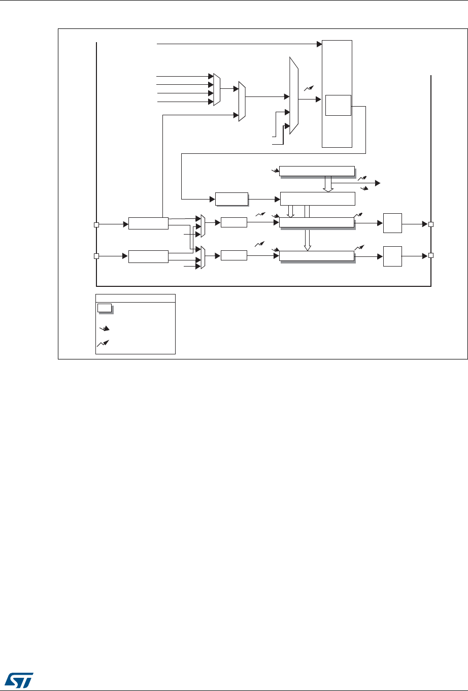
DocID018909 Rev 9 637/1718
RM0090 General-purpose timers (TIM9 to TIM14)
680
Figure 180. General-purpose timer block diagram (TIM9 and TIM12)
19.2.2 TIM10/TIM11 and TIM13/TIM14 main features
The features of general-purpose timers TIM10/TIM11 and TIM13/TIM14 include:
•16-bit auto-reload upcounter
•16-bit programmable prescaler used to divide the counter clock frequency by any factor
between 1 and 65536 (can be changed “on the fly”)
•independent channel for:
– Input capture
– Output compare
– PWM generation (edge-aligned mode)
– One-pulse mode output
•Interrupt generation on the following events:
– Update: counter overflow, counter initialization (by software)
– Input capture
– Output compare
Auto-reload register
Capture/Compare 1 register
Capture/Compare 2 register
U
U
U
CC1I
CC2I
Tr i g g e r
controller
Stop, Clear
TI1FP1
TI2FP2
ITR0
ITR1
ITR2
ITR3
TRGI
output
control
OC1
OC1REF
OC2REF
U
UI
Reset, Enable, Count
IC1
IC2
Prescaler
Prescaler
Input filter &
Edge detector
IC2PS
IC1PS
TI1FP1
output
control
OC2
Reg
event
Notes:
Preload registers transferred
to active registers on
U
event
according to control bit
interrupt
TGI
TRC
TRC
ITR
TRC
TI1F_ED
Input filter &
Edge detector
CC1I
CC2I
TI1FP2
TI2FP1
TI2FP2
TI1
TI2
TIMx_CH1
TIMx_CH2
TIMx_CH1
TIMx_CH2
Prescaler
COUNTER
+/-
CK_PSC
PSC CNT
CK_CNT
controller
mode
Slave
Internal clock (CK_INT)
ai17190
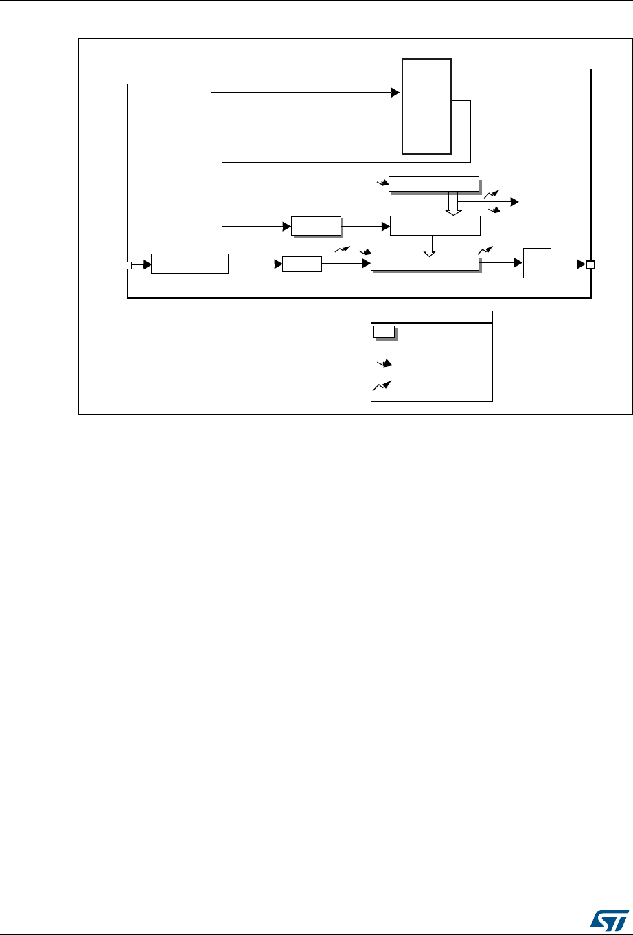
General-purpose timers (TIM9 to TIM14) RM0090
638/1718 DocID018909 Rev 9
Figure 181. General-purpose timer block diagram (TIM10/11/13/14)
!UTORELOADREGISTER
#APTURE#OMPAREREGISTER
5
5
##)
3TOP#LEAR
OUTPUT
CONTROL
/#
/#2%&
5
5)
)#
0RESCALER
)NPUTFILTER
EDGEDETECTOR )#03
4)&0
2EG
EVENT
.OTES
0RELOADREGISTERSTRANSFERRED
TOACTIVEREGISTERSON5EVENT
ACCORDINGTOCONTROLBIT
INTERRUPT$-!OUTPUT
##)
4)
4)-X?#(
PRESCALER COUNTER
#+?03# 03# #.4
#+?#.4
)NTERNALCLOCK#+?).4
AIC
4RIGGER
#ONTROLLER
%NABLE
COUNTER
4)-X?#(

DocID018909 Rev 9 639/1718
RM0090 General-purpose timers (TIM9 to TIM14)
680
19.3 TIM9 to TIM14 functional description
19.3.1 Time-base unit
The main block of the timer is a 16-bit counter with its related auto-reload register. The
counters counts up.
The counter clock can be divided by a prescaler.
The counter, the auto-reload register and the prescaler register can be written or read by
software. This is true even when the counter is running.
The time-base unit includes:
•Counter register (TIMx_CNT)
•Prescaler register (TIMx_PSC)
•Auto-reload register (TIMx_ARR)
The auto-reload register is preloaded. Writing to or reading from the auto-reload register
accesses the preload register. The content of the preload register are transferred into the
shadow register permanently or at each update event (UEV), depending on the auto-reload
preload enable bit (ARPE) in TIMx_CR1 register. The update event is sent when the counter
reaches the overflow and if the UDIS bit equals 0 in the TIMx_CR1 register. It can also be
generated by software. The generation of the update event is described in details for each
configuration.
The counter is clocked by the prescaler output CK_CNT, which is enabled only when the
counter enable bit (CEN) in TIMx_CR1 register is set (refer also to the slave mode controller
description to get more details on counter enabling).
Note that the counter starts counting 1 clock cycle after setting the CEN bit in the TIMx_CR1
register.
Prescaler description
The prescaler can divide the counter clock frequency by any factor between 1 and 65536. It
is based on a 16-bit counter controlled through a 16-bit register (in the TIMx_PSC register).
It can be changed on the fly as this control register is buffered. The new prescaler ratio is
taken into account at the next update event.
Figure 182 and Figure 183 give some examples of the counter behavior when the prescaler
ratio is changed on the fly.

General-purpose timers (TIM9 to TIM14) RM0090
640/1718 DocID018909 Rev 9
Figure 182. Counter timing diagram with prescaler division change from 1 to 2
Figure 183. Counter timing diagram with prescaler division change from 1 to 4
19.3.2 Counter modes
Upcounting mode
In upcounting mode, the counter counts from 0 to the auto-reload value (content of the
TIMx_ARR register), then restarts from 0 and generates a counter overflow event.
Setting the UG bit in the TIMx_EGR register (by software or by using the slave mode
controller on TIM9 and TIM12) also generates an update event.
The UEV event can be disabled by software by setting the UDIS bit in the TIMx_CR1
register. This is to avoid updating the shadow registers while writing new values in the
preload registers. Then no update event occurs until the UDIS bit has been written to 0.
However, the counter restarts from 0, as well as the counter of the prescaler (but the
prescale rate does not change). In addition, if the URS bit (update request selection) in
TIMx_CR1 register is set, setting the UG bit generates an update event UEV but without
CK_PSC
00
CEN
Timer clock = CK_CNT
Counter register
Update event (UEV)
0
F9 FA FB FCF7
Prescaler control register 01
Write a new value in TIMx_PSC
01 02 03
Prescaler buffer 01
Prescaler counter 01 0 1 0 1 0 1
F8
CK_PSC
00
CEN
Timer clock = CK_CNT
Counter register
Update event (UEV)
0
F9 FA FB FCF7
Prescaler control register 03
Write a new value in TIMx_PSC
Prescaler buffer 03
Prescaler counter 01 2 3 0 1 2 3
F8 01
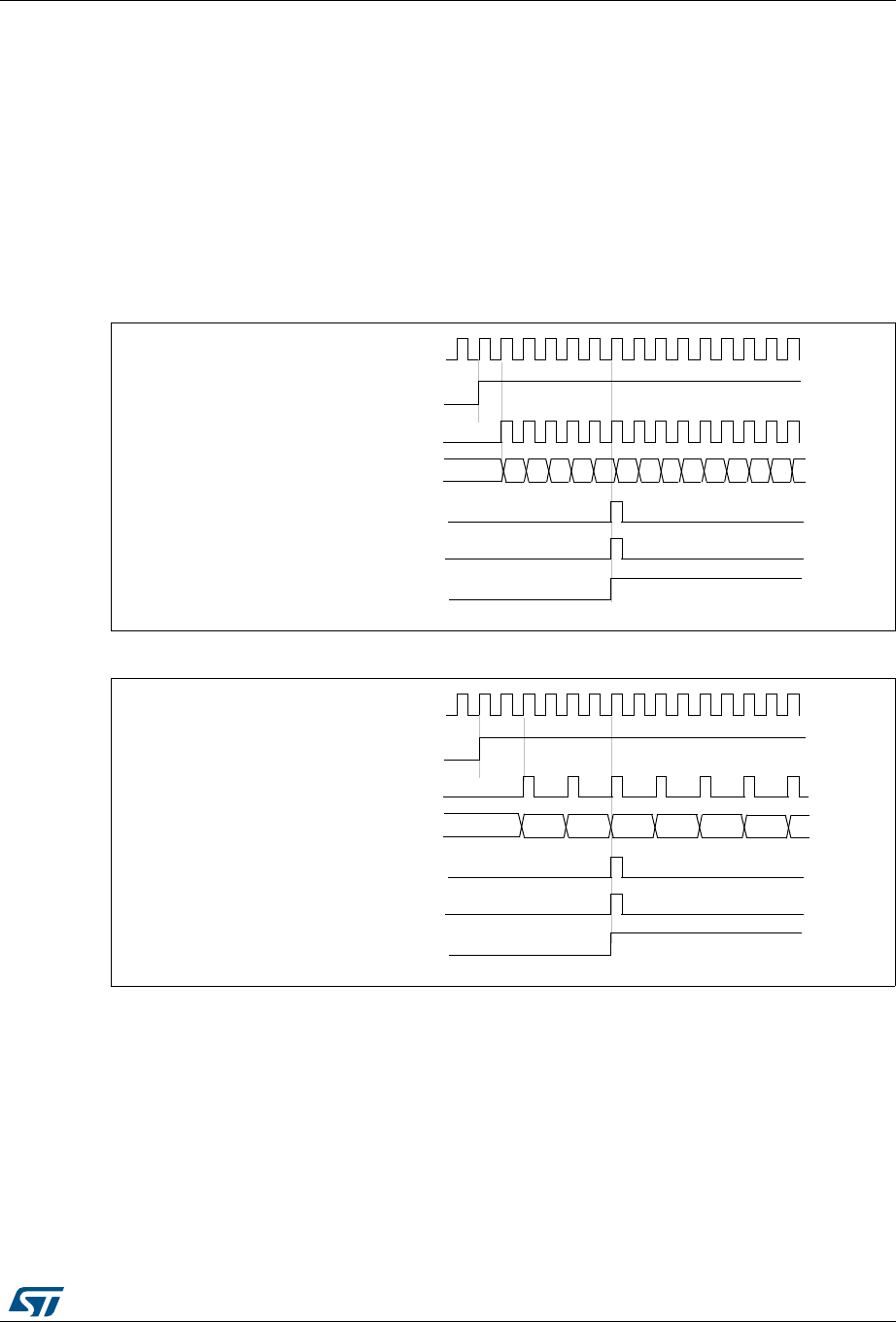
DocID018909 Rev 9 641/1718
RM0090 General-purpose timers (TIM9 to TIM14)
680
setting the UIF flag (thus no interrupt is sent). This is to avoid generating both update and
capture interrupts when clearing the counter on the capture event.
When an update event occurs, all the registers are updated and the update flag (UIF bit in
TIMx_SR register) is set (depending on the URS bit):
•The auto-reload shadow register is updated with the preload value (TIMx_ARR),
•The buffer of the prescaler is reloaded with the preload value (content of the TIMx_PSC
register).
The following figures show some examples of the counter behavior for different clock
frequencies when TIMx_ARR=0x36.
Figure 184. Counter timing diagram, internal clock divided by 1
Figure 185. Counter timing diagram, internal clock divided by 2
CK_PSC
00
CNT_EN
Timer clock = CK_CNT
Counter register
Update interrupt flag (UIF)
Counter overflow
Update event (UEV)
01 02 03 04 05 06 0732 33 34 35 3631
CK_PSC
0035 0000 0001 0002 0003
CNT_EN
Timer clock = CK_CNT
Counter register
Update interrupt flag (UIF)
0034 0036
Counter overflow
Update event (UEV)

General-purpose timers (TIM9 to TIM14) RM0090
642/1718 DocID018909 Rev 9
Figure 186. Counter timing diagram, internal clock divided by 4
Figure 187. Counter timing diagram, internal clock divided by N
Figure 188. Counter timing diagram, update event when ARPE=0 (TIMx_ARR not
preloaded)
CK_PSC
0000 0001
CNT_EN
Timer clock = CK_CNT
Counter register
Update interrupt flag (UIF)
0035 0036
Counter overflow
Update event (UEV)
Timer clock = CK_CNT
Counter register 00
1F 20
Update interrupt flag (UIF)
Counter overflow
Update event (UEV)
CK_PSC
CK_PSC
00
CEN
Timer clock = CK_CNT
Counter register
Update interrupt flag (UIF)
Counter overflow
Update event (UEV)
01 02 03 04 05 06 0732 33 34 35 3631
Auto-reload register FF 36
Write a new value in TIMx_ARR
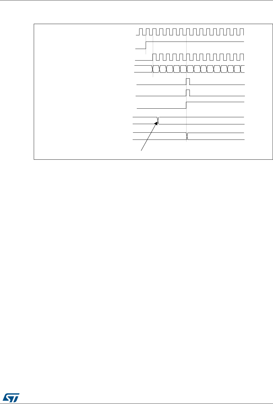
DocID018909 Rev 9 643/1718
RM0090 General-purpose timers (TIM9 to TIM14)
680
Figure 189. Counter timing diagram, update event when ARPE=1 (TIMx_ARR
preloaded)
19.3.3 Clock selection
The counter clock can be provided by the following clock sources:
•Internal clock (CK_INT)
•External clock mode1 (for TIM9 and TIM12): external input pin (TIx)
•Internal trigger inputs (ITRx) (for TIM9 and TIM12): connecting the trigger output from
another timer. Refer to Section : Using one timer as prescaler for another for more
details.
Internal clock source (CK_INT)
The internal clock source is the default clock source for TIM10/TIM11 and TIM13/TIM14.
For TIM9 and TIM12, the internal clock source is selected when the slave mode controller is
disabled (SMS=’000’). The CEN bit in the TIMx_CR1 register and the UG bit in the
TIMx_EGR register are then used as control bits and can be changed only by software
(except for UG which remains cleared). As soon as the CEN bit is programmed to 1, the
prescaler is clocked by the internal clock CK_INT.
Figure 190 shows the behavior of the control circuit and the upcounter in normal mode,
without prescaler.
CK_PSC
00
CEN
Timer clock = CK_CNT
Counter register
Update interrupt flag (UIF)
Counter overflow
Update event (UEV)
01 02 03 04 05 06 07F1 F2 F3 F4 F5F0
Auto-reload preload register F5 36
Auto-reload shadow register F5 36
Write a new value in TIMx_ARR
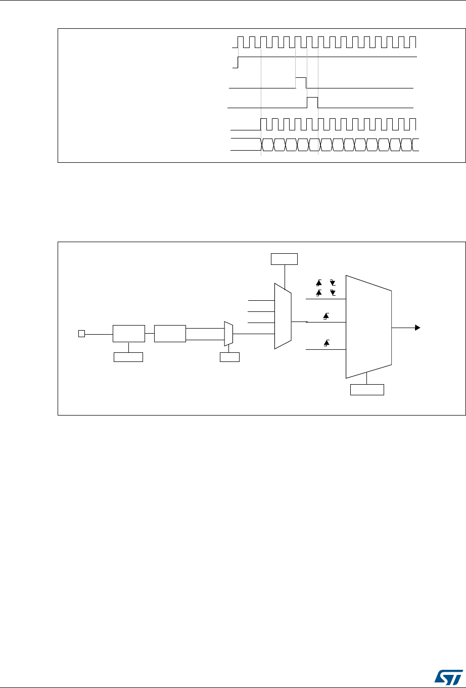
General-purpose timers (TIM9 to TIM14) RM0090
644/1718 DocID018909 Rev 9
Figure 190. Control circuit in normal mode, internal clock divided by 1
External clock source mode 1(TIM9 and TIM12)
This mode is selected when SMS=’111’ in the TIMx_SMCR register. The counter can count
at each rising or falling edge on a selected input.
Figure 191. TI2 external clock connection example
For example, to configure the upcounter to count in response to a rising edge on the TI2
input, use the following procedure:
1. Configure channel 2 to detect rising edges on the TI2 input by writing CC2S = ‘01’ in
the TIMx_CCMR1 register.
2. Configure the input filter duration by writing the IC2F[3:0] bits in the TIMx_CCMR1
register (if no filter is needed, keep IC2F=’0000’).
3. Select the rising edge polarity by writing CC2P=’0’ and CC2NP=’0’ in the TIMx_CCER
register.
4. Configure the timer in external clock mode 1 by writing SMS=’111’ in the TIMx_SMCR
register.
5. Select TI2 as the trigger input source by writing TS=’110’ in the TIMx_SMCR register.
6. Enable the counter by writing CEN=’1’ in the TIMx_CR1 register.
Note: The capture prescaler is not used for triggering, so you don’t need to configure it.
When a rising edge occurs on TI2, the counter counts once and the TIF flag is set.
The delay between the rising edge on TI2 and the actual clock of the counter is due to the
resynchronization circuit on TI2 input.
Internal clock
00
Counter clock = CK_CNT = CK_PSC
Counter register 01 02 03 04 05 06 0732 33 34 35 3631
CEN=CNT_EN
UG
CNT_INIT
CK_INT
external clock
mode 1
internal clock
mode
TRGI
TI1F
TI2F or
or
or
(internal clock)
CK_PSC
TIMx_SMCR
SMS[2:0]
ITRx
TI1_ED
TI1FP1
TI2FP2
TIMx_SMCR
TS[2:0]
TI2 0
1
TIMx_CCER
CC2P
Filter
ICF[3:0]
TIMx_CCMR1
Edge
Detector
TI2F_Rising
TI2F_Falling 110
0xx
100
101
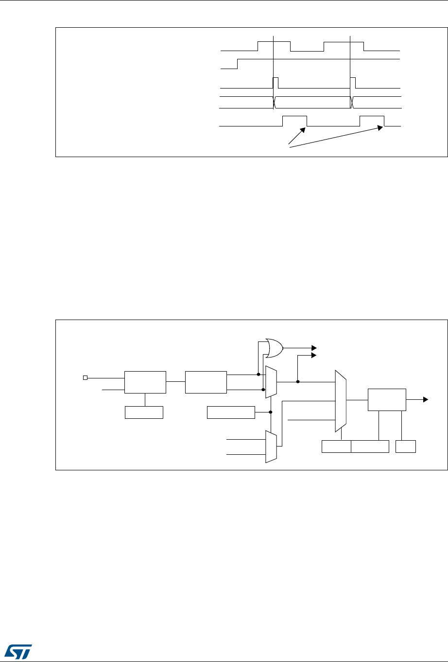
DocID018909 Rev 9 645/1718
RM0090 General-purpose timers (TIM9 to TIM14)
680
Figure 192. Control circuit in external clock mode 1
19.3.4 Capture/compare channels
Each Capture/Compare channel is built around a capture/compare register (including a
shadow register), a input stage for capture (with digital filter, multiplexing and prescaler) and
an output stage (with comparator and output control).
Figure 193 to Figure 195 give an overview of one capture/compare channel.
The input stage samples the corresponding TIx input to generate a filtered signal TIxF.
Then, an edge detector with polarity selection generates a signal (TIxFPx) which can be
used as trigger input by the slave mode controller or as the capture command. It is
prescaled before the capture register (ICxPS).
Figure 193. Capture/compare channel (example: channel 1 input stage)
The output stage generates an intermediate waveform which is then used for reference:
OCxRef (active high). The polarity acts at the end of the chain.
Counter clock = CK_CNT = CK_PSC
Counter register 35 3634
TI2
CNT_EN
TIF
Write TIF=0
TI1 0
1
TIMx_CCER
CC1P/CC1NP
divider
/1, /2, /4, /8
ICPS[1:0]
TI1F_ED
filter
ICF[3:0]
downcounter
TIMx_CCMR1
Edge
Detector
TI1F_Rising
TI1F_Falling
to the slave mode controller
TI1FP1
11
01
TIMx_CCMR1
CC1S[1:0]
IC1
TI2FP1
TRC
(from channel 2)
(from slave mode
controller)
10
fDTS
TIMx_CCER
CC1E
IC1PS
TI1F
0
1
TI2F_rising
TI2F_falling
(from channel 2)
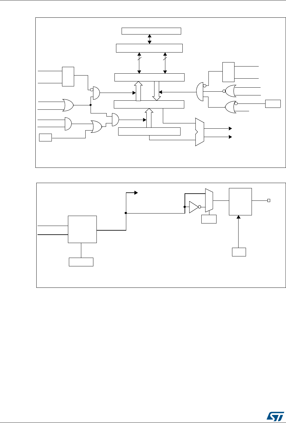
General-purpose timers (TIM9 to TIM14) RM0090
646/1718 DocID018909 Rev 9
Figure 194. Capture/compare channel 1 main circuit
Figure 195. Output stage of capture/compare channel (channel 1)
The capture/compare block is made of one preload register and one shadow register. Write
and read always access the preload register.
In capture mode, captures are actually done in the shadow register, which is copied into the
preload register.
In compare mode, the content of the preload register is copied into the shadow register
which is compared to the counter.
19.3.5 Input capture mode
In Input capture mode, the Capture/Compare Registers (TIMx_CCRx) are used to latch the
value of the counter after a transition detected by the corresponding ICx signal. When a
capture occurs, the corresponding CCXIF flag (TIMx_SR register) is set and an interrupt or
a DMA request can be sent if they are enabled. If a capture occurs while the CCxIF flag was
already high, then the over-capture flag CCxOF (TIMx_SR register) is set. CCxIF can be
CC1E
Capture/compare shadow register
comparator
Capture/compare preload register
Counter
IC1PS
CC1S[0]
CC1S[1]
capture
input
mode
S
R
read CCR1H
read CCR1L
read_in_progress
capture_transfer CC1S[0]
CC1S[1]
S
R
write CCR1H
write CCR1L
write_in_progress
output
mode
UEV
OC1PE
(from time
compare_transfer
APB Bus
88
high
low
(if 16-bit)
MCU-peripheral interface
TIM1_CCMR1
OC1PE
base unit)
CNT>CCR1
CNT=CCR1
TIM1_EGR
CC1G
/UTPUTMODE
#.4##2
#.4##2 CONTROLLER
4)-X?##-2
/#-;=
/#?2%&
##0
4)-X?##%2
/UTPUT
ENABLE
CIRCUIT
/#
##% 4)-X?##%2
4OTHEMASTERMODE
CONTROLLER
AI

DocID018909 Rev 9 647/1718
RM0090 General-purpose timers (TIM9 to TIM14)
680
cleared by software by writing it to ‘0’ or by reading the captured data stored in the
TIMx_CCRx register. CCxOF is cleared when you write it to ‘0’.
The following example shows how to capture the counter value in TIMx_CCR1 when TI1
input rises. To do this, use the following procedure:
1. Select the active input: TIMx_CCR1 must be linked to the TI1 input, so write the CC1S
bits to ‘01’ in the TIMx_CCMR1 register. As soon as CC1S becomes different from ‘00’,
the channel is configured in input mode and the TIMx_CCR1 register becomes read-
only.
2. Program the input filter duration you need with respect to the signal you connect to the
timer (by programming the ICxF bits in the TIMx_CCMRx register if the input is one of
the TIx inputs). Let’s imagine that, when toggling, the input signal is not stable during at
must 5 internal clock cycles. We must program a filter duration longer than these 5
clock cycles. We can validate a transition on TI1 when 8 consecutive samples with the
new level have been detected (sampled at fDTS frequency). Then write IC1F bits to
‘0011’ in the TIMx_CCMR1 register.
3. Select the edge of the active transition on the TI1 channel by programming CC1P and
CC1NP bits to ‘00’ in the TIMx_CCER register (rising edge in this case).
4. Program the input prescaler. In our example, we wish the capture to be performed at
each valid transition, so the prescaler is disabled (write IC1PS bits to ‘00’ in the
TIMx_CCMR1 register).
5. Enable capture from the counter into the capture register by setting the CC1E bit in the
TIMx_CCER register.
6. If needed, enable the related interrupt request by setting the CC1IE bit in the
TIMx_DIER register.
When an input capture occurs:
•The TIMx_CCR1 register gets the value of the counter on the active transition.
•CC1IF flag is set (interrupt flag). CC1OF is also set if at least two consecutive captures
occurred whereas the flag was not cleared.
•An interrupt is generated depending on the CC1IE bit.
In order to handle the overcapture, it is recommended to read the data before the
overcapture flag. This is to avoid missing an overcapture which could happen after reading
the flag and before reading the data.
Note: IC interrupt requests can be generated by software by setting the corresponding CCxG bit in
the TIMx_EGR register.
19.3.6 PWM input mode (only for TIM9/12)
This mode is a particular case of input capture mode. The procedure is the same except:
•Two ICx signals are mapped on the same TIx input.
•These 2 ICx signals are active on edges with opposite polarity.
•One of the two TIxFP signals is selected as trigger input and the slave mode controller
is configured in reset mode.
For example, you can measure the period (in TIMx_CCR1 register) and the duty cycle (in
TIMx_CCR2 register) of the PWM applied on TI1 using the following procedure (depending
on CK_INT frequency and prescaler value):
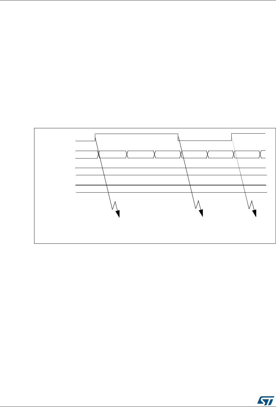
General-purpose timers (TIM9 to TIM14) RM0090
648/1718 DocID018909 Rev 9
1. Select the active input for TIMx_CCR1: write the CC1S bits to ‘01’ in the TIMx_CCMR1
register (TI1 selected).
2. Select the active polarity for TI1FP1 (used both for capture in TIMx_CCR1 and counter
clear): program the CC1P and CC1NP bits to ‘00’ (active on rising edge).
3. Select the active input for TIMx_CCR2: write the CC2S bits to ‘10’ in the TIMx_CCMR1
register (TI1 selected).
4. Select the active polarity for TI1FP2 (used for capture in TIMx_CCR2): program the
CC2P and CC2NP bits to ‘11’ (active on falling edge).
5. Select the valid trigger input: write the TS bits to ‘101’ in the TIMx_SMCR register
(TI1FP1 selected).
6. Configure the slave mode controller in reset mode: write the SMS bits to ‘100’ in the
TIMx_SMCR register.
7. Enable the captures: write the CC1E and CC2E bits to ‘1’ in the TIMx_CCER register.
Figure 196. PWM input mode timing
1. The PWM input mode can be used only with the TIMx_CH1/TIMx_CH2 signals due to the fact that only
TI1FP1 and TI2FP2 are connected to the slave mode controller.
19.3.7 Forced output mode
In output mode (CCxS bits = ‘00’ in the TIMx_CCMRx register), each output compare signal
(OCxREF and then OCx) can be forced to active or inactive level directly by software,
independently of any comparison between the output compare register and the counter.
To force an output compare signal (OCXREF/OCx) to its active level, you just need to write
‘101’ in the OCxM bits in the corresponding TIMx_CCMRx register. Thus OCXREF is forced
high (OCxREF is always active high) and OCx get opposite value to CCxP polarity bit.
For example: CCxP=’0’ (OCx active high) => OCx is forced to high level.
The OCxREF signal can be forced low by writing the OCxM bits to ‘100’ in the
TIMx_CCMRx register.
Anyway, the comparison between the TIMx_CCRx shadow register and the counter is still
performed and allows the flag to be set. Interrupt requests can be sent accordingly. This is
described in the output compare mode section below.
TI1
TIMx_CNT 0000 0001 0002 0003 0004 00000004
TIMx_CCR1
TIMx_CCR2
0004
0002
IC1 capture
IC2 capture
reset counter
IC2 capture
pulse width
IC1 capture
period
measurementmeasurement
ai15413

DocID018909 Rev 9 649/1718
RM0090 General-purpose timers (TIM9 to TIM14)
680
19.3.8 Output compare mode
This function is used to control an output waveform or indicating when a period of time has
elapsed.
When a match is found between the capture/compare register and the counter, the output
compare function:
1. Assigns the corresponding output pin to a programmable value defined by the output
compare mode (OCxM bits in the TIMx_CCMRx register) and the output polarity (CCxP
bit in the TIMx_CCER register). The output pin can keep its level (OCXM=’000’), be set
active (OCxM=’001’), be set inactive (OCxM=’010’) or can toggle (OCxM=’011’) on
match.
2. Sets a flag in the interrupt status register (CCxIF bit in the TIMx_SR register).
3. Generates an interrupt if the corresponding interrupt mask is set (CCXIE bit in the
TIMx_DIER register).
The TIMx_CCRx registers can be programmed with or without preload registers using the
OCxPE bit in the TIMx_CCMRx register.
In output compare mode, the update event UEV has no effect on OCxREF and OCx output.
The timing resolution is one count of the counter. Output compare mode can also be used to
output a single pulse (in One-pulse mode).
Procedure:
1. Select the counter clock (internal, external, prescaler).
2. Write the desired data in the TIMx_ARR and TIMx_CCRx registers.
3. Set the CCxIE bit if an interrupt request is to be generated.
4. Select the output mode. For example:
– Write OCxM = ‘011’ to toggle OCx output pin when CNT matches CCRx
– Write OCxPE = ‘0’ to disable preload register
– Write CCxP = ‘0’ to select active high polarity
– Write CCxE = ‘1’ to enable the output
5. Enable the counter by setting the CEN bit in the TIMx_CR1 register.
The TIMx_CCRx register can be updated at any time by software to control the output
waveform, provided that the preload register is not enabled (OCxPE=’0’, else TIMx_CCRx
shadow register is updated only at the next update event UEV). An example is given in
Figure 197.

General-purpose timers (TIM9 to TIM14) RM0090
650/1718 DocID018909 Rev 9
Figure 197. Output compare mode, toggle on OC1.
19.3.9 PWM mode
Pulse Width Modulation mode allows you to generate a signal with a frequency determined
by the value of the TIMx_ARR register and a duty cycle determined by the value of the
TIMx_CCRx register.
The PWM mode can be selected independently on each channel (one PWM per OCx
output) by writing ‘110’ (PWM mode 1) or ‘111’ (PWM mode 2) in the OCxM bits in the
TIMx_CCMRx register. You must enable the corresponding preload register by setting the
OCxPE bit in the TIMx_CCMRx register, and eventually the auto-reload preload register (in
upcounting or center-aligned modes) by setting the ARPE bit in the TIMx_CR1 register.
As the preload registers are transferred to the shadow registers only when an update event
occurs, before starting the counter, you have to initialize all the registers by setting the UG
bit in the TIMx_EGR register.
The OCx polarity is software programmable using the CCxP bit in the TIMx_CCER register.
It can be programmed as active high or active low. The OCx output is enabled by the CCxE
bit in the TIMx_CCER register. Refer to the TIMx_CCERx register description for more
details.
In PWM mode (1 or 2), TIMx_CNT and TIMx_CCRx are always compared to determine
whether TIMx_CNT ≤TIMx_CCRx.
The timer is able to generate PWM in edge-aligned mode only since the counter is
upcounting.
PWM edge-aligned mode
In the following example, we consider PWM mode 1. The reference PWM signal OCxREF is
high as long as TIMx_CNT < TIMx_CCRx else it becomes low. If the compare value in
TIMx_CCRx is greater than the auto-reload value (in TIMx_ARR) then OCxREF is held at
‘1’. If the compare value is 0 then OCxRef is held at ‘0’. Figure 198 shows some edge-
aligned PWM waveforms in an example where TIMx_ARR=8.
oc1ref=OC1
TIM1_CNT B200 B201
0039
TIM1_CCR1 003A
Write B201h in the CC1R register
Match detected on CCR1
Interrupt generated if enabled
003B
B201
003A
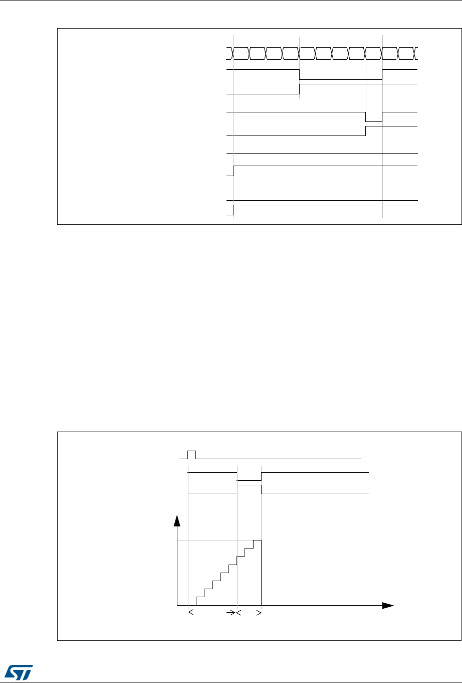
DocID018909 Rev 9 651/1718
RM0090 General-purpose timers (TIM9 to TIM14)
680
Figure 198. Edge-aligned PWM waveforms (ARR=8)
19.3.10 One-pulse mode
One-pulse mode (OPM) is a particular case of the previous modes. It allows the counter to
be started in response to a stimulus and to generate a pulse with a programmable length
after a programmable delay.
Starting the counter can be controlled through the slave mode controller. Generating the
waveform can be done in output compare mode or PWM mode. You select One-pulse mode
by setting the OPM bit in the TIMx_CR1 register. This makes the counter stop automatically
at the next update event UEV.
A pulse can be correctly generated only if the compare value is different from the counter
initial value. Before starting (when the timer is waiting for the trigger), the configuration must
be as follows:
CNT < CCRx≤ARR (in particular, 0 < CCRx)
Figure 199. Example of one pulse mode.
Counter register 01234567801
OCXREF
CCxIF
OCXREF
CCxIF
OCXREF
CCxIF
OCXREF
CCxIF
CCRx=4
CCRx=8
CCRx>8
CCRx=0
TI2
OC1REF
Counter
t
0
TIM1_ARR
TIM1_CCR1
OC1
tDELAY tPULSE

General-purpose timers (TIM9 to TIM14) RM0090
652/1718 DocID018909 Rev 9
For example you may want to generate a positive pulse on OC1 with a length of tPULSE and
after a delay of tDELAY as soon as a positive edge is detected on the TI2 input pin.
Use TI2FP2 as trigger 1:
1. Map TI2FP2 to TI2 by writing CC2S=’01’ in the TIMx_CCMR1 register.
2. TI2FP2 must detect a rising edge, write CC2P=’0’ and CC2NP = ‘0’ in the TIMx_CCER
register.
3. Configure TI2FP2 as trigger for the slave mode controller (TRGI) by writing TS=’110’ in
the TIMx_SMCR register.
4. TI2FP2 is used to start the counter by writing SMS to ‘110’ in the TIMx_SMCR register
(trigger mode).
The OPM waveform is defined by writing the compare registers (taking into account the
clock frequency and the counter prescaler).
•The tDELAY is defined by the value written in the TIMx_CCR1 register.
•The tPULSE is defined by the difference between the auto-reload value and the compare
value (TIMx_ARR - TIMx_CCR1).
•Let’s say you want to build a waveform with a transition from ‘0’ to ‘1’ when a compare
match occurs and a transition from ‘1’ to ‘0’ when the counter reaches the auto-reload
value. To do this you enable PWM mode 2 by writing OC1M=’111’ in the TIMx_CCMR1
register. You can optionally enable the preload registers by writing OC1PE=’1’ in the
TIMx_CCMR1 register and ARPE in the TIMx_CR1 register. In this case you have to
write the compare value in the TIMx_CCR1 register, the auto-reload value in the
TIMx_ARR register, generate an update by setting the UG bit and wait for external
trigger event on TI2. CC1P is written to ‘0’ in this example.
You only want 1 pulse (Single mode), so you write '1 in the OPM bit in the TIMx_CR1
register to stop the counter at the next update event (when the counter rolls over from the
auto-reload value back to 0). When OPM bit in the TIMx_CR1 register is set to '0', so the
Repetitive Mode is selected.
Particular case: OCx fast enable
In One-pulse mode, the edge detection on TIx input set the CEN bit which enables the
counter. Then the comparison between the counter and the compare value makes the
output toggle. But several clock cycles are needed for these operations and it limits the
minimum delay tDELAY min we can get.
If you want to output a waveform with the minimum delay, you can set the OCxFE bit in the
TIMx_CCMRx register. Then OCxRef (and OCx) are forced in response to the stimulus,
without taking in account the comparison. Its new level is the same as if a compare match
had occurred. OCxFE acts only if the channel is configured in PWM1 or PWM2 mode.
19.3.11 TIM9/12 external trigger synchronization
The TIM9/12 timers can be synchronized with an external trigger in several modes: Reset
mode, Gated mode and Trigger mode.
Slave mode: Reset mode
The counter and its prescaler can be reinitialized in response to an event on a trigger input.
Moreover, if the URS bit from the TIMx_CR1 register is low, an update event UEV is
generated. Then all the preloaded registers (TIMx_ARR, TIMx_CCRx) are updated.
In the following example, the upcounter is cleared in response to a rising edge on TI1 input:
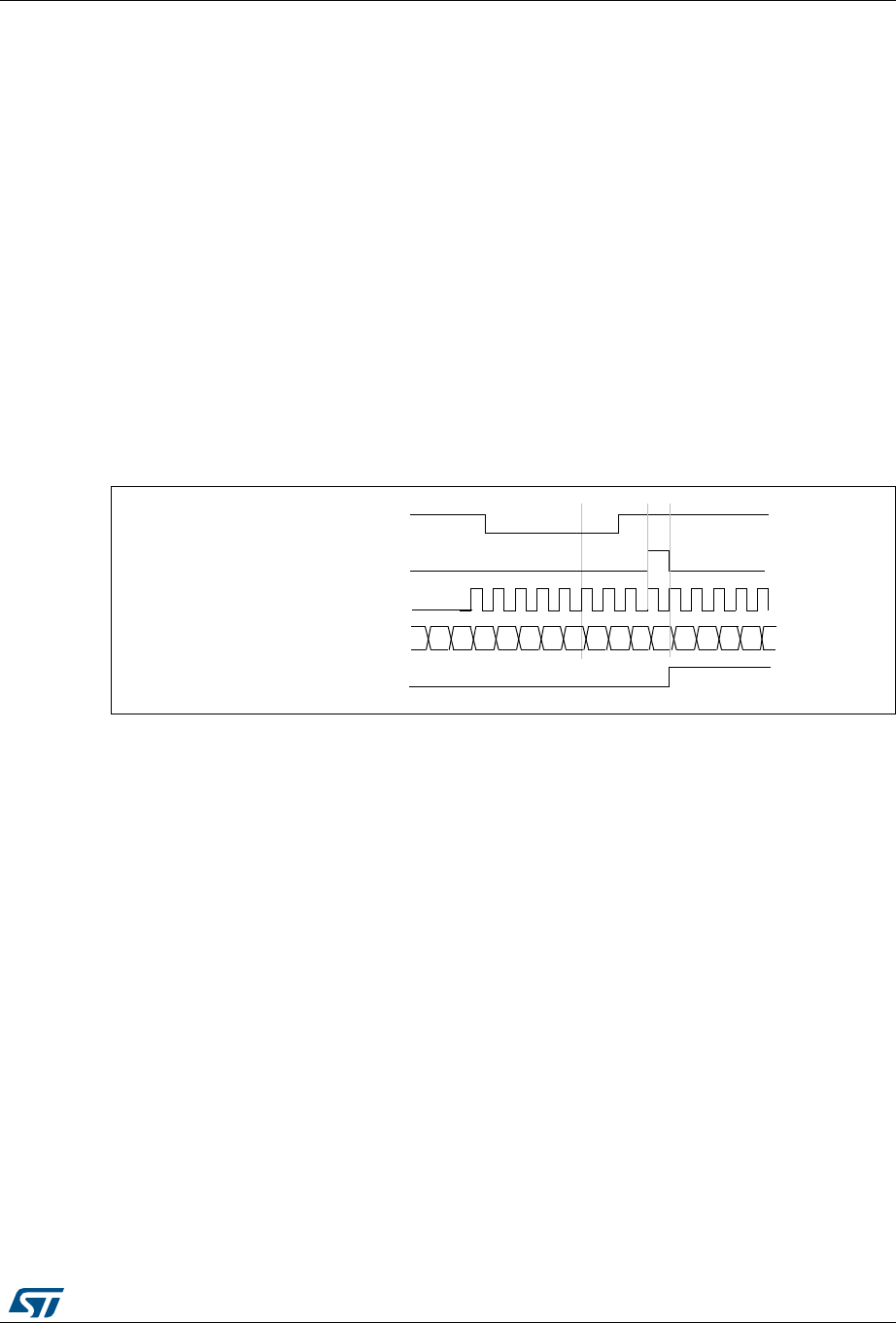
DocID018909 Rev 9 653/1718
RM0090 General-purpose timers (TIM9 to TIM14)
680
1. Configure the channel 1 to detect rising edges on TI1. Configure the input filter duration
(in this example, we don’t need any filter, so we keep IC1F=’0000’). The capture
prescaler is not used for triggering, so you don’t need to configure it. The CC1S bits
select the input capture source only, CC1S = ‘01’ in the TIMx_CCMR1 register.
Program CC1P and CC1NP to ‘00’ in TIMx_CCER register to validate the polarity (and
detect rising edges only).
2. Configure the timer in reset mode by writing SMS=’100’ in TIMx_SMCR register. Select
TI1 as the input source by writing TS=’101’ in TIMx_SMCR register.
3. Start the counter by writing CEN=’1’ in the TIMx_CR1 register.
The counter starts counting on the internal clock, then behaves normally until TI1 rising
edge. When TI1 rises, the counter is cleared and restarts from 0. In the meantime, the
trigger flag is set (TIF bit in the TIMx_SR register) and an interrupt request can be sent if
enabled (depending on the TIE bit in TIMx_DIER register).
The following figure shows this behavior when the auto-reload register TIMx_ARR=0x36.
The delay between the rising edge on TI1 and the actual reset of the counter is due to the
resynchronization circuit on TI1 input.
Figure 200. Control circuit in reset mode
Slave mode: Gated mode
The counter can be enabled depending on the level of a selected input.
In the following example, the upcounter counts only when TI1 input is low:
1. Configure the channel 1 to detect low levels on TI1. Configure the input filter duration
(in this example, we don’t need any filter, so we keep IC1F=’0000’). The capture
prescaler is not used for triggering, so you don’t need to configure it. The CC1S bits
select the input capture source only, CC1S=’01’ in TIMx_CCMR1 register. Program
CC1P=’1’ and CC1NP= ‘0’ in TIMx_CCER register to validate the polarity (and detect
low level only).
2. Configure the timer in gated mode by writing SMS=’101’ in TIMx_SMCR register.
Select TI1 as the input source by writing TS=’101’ in TIMx_SMCR register.
3. Enable the counter by writing CEN=’1’ in the TIMx_CR1 register (in gated mode, the
counter doesn’t start if CEN=’0’, whatever is the trigger input level).
The counter starts counting on the internal clock as long as TI1 is low and stops as soon as
TI1 becomes high. The TIF flag in the TIMx_SR register is set both when the counter starts
or stops.
The delay between the rising edge on TI1 and the actual stop of the counter is due to the
resynchronization circuit on TI1 input.
00
Counter clock = ck_cnt = ck_psc
Counter register 01 02 03 00 01 02 0332 33 34 35 36
UG
TI1
3130
TIF
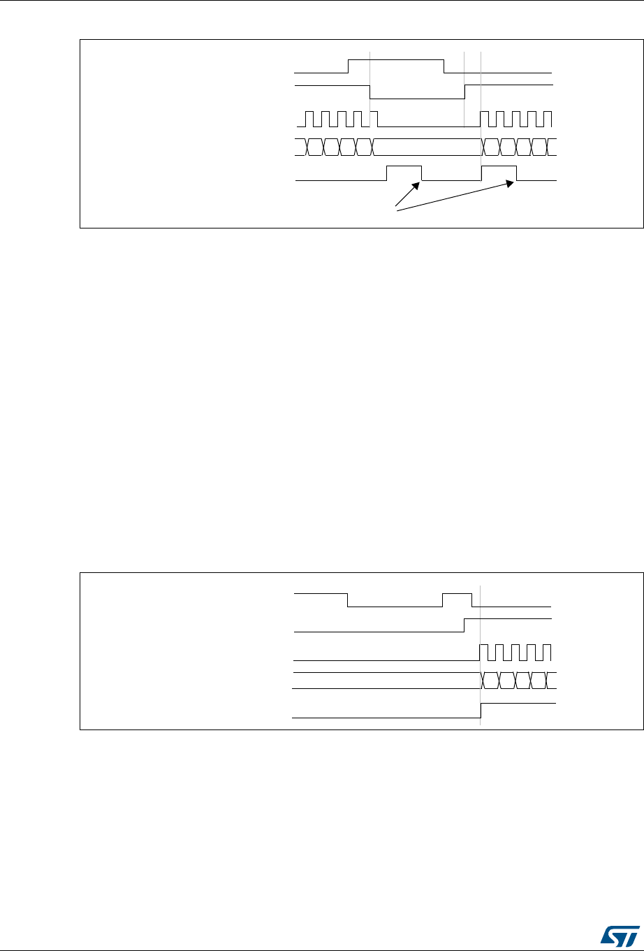
General-purpose timers (TIM9 to TIM14) RM0090
654/1718 DocID018909 Rev 9
Figure 201. Control circuit in gated mode
Slave mode: Trigger mode
The counter can start in response to an event on a selected input.
In the following example, the upcounter starts in response to a rising edge on TI2 input:
1. Configure the channel 2 to detect rising edges on TI2. Configure the input filter duration
(in this example, we don’t need any filter, so we keep IC2F=’0000’). The capture
prescaler is not used for triggering, so you don’t need to configure it. The CC2S bits are
configured to select the input capture source only, CC2S=’01’ in TIMx_CCMR1 register.
Program CC2P=’1’ and CC2NP=’0’ in TIMx_CCER register to validate the polarity (and
detect low level only).
2. Configure the timer in trigger mode by writing SMS=’110’ in TIMx_SMCR register.
Select TI2 as the input source by writing TS=’110’ in TIMx_SMCR register.
When a rising edge occurs on TI2, the counter starts counting on the internal clock and the
TIF flag is set.
The delay between the rising edge on TI2 and the actual start of the counter is due to the
resynchronization circuit on TI2 input.
Figure 202. Control circuit in trigger mode
Counter clock = ck_cnt = ck_psc
Counter register 35 36 37 3832 33 34
TI1
3130
cnt_en
TIF
Write TIF=0
Counter clock = ck_cnt = ck_psc
Counter register 35 36 37 3834
TI2
cnt_en
TIF

DocID018909 Rev 9 655/1718
RM0090 General-purpose timers (TIM9 to TIM14)
680
19.3.12 Timer synchronization (TIM9/12)
The TIM timers are linked together internally for timer synchronization or chaining. Refer to
Section 18.3.15: Timer synchronization on page 607 for details.
19.3.13 Debug mode
When the microcontroller enters debug mode (Cortex®-M4 with FPU core halted), the TIMx
counter either continues to work normally or stops, depending on DBG_TIMx_STOP
configuration bit in DBG module. For more details, refer to Section 38.16.2: Debug support
for timers, watchdog, bxCAN and I2C.
19.4 TIM9 and TIM12 registers
Refer to Section 1.1 for a list of abbreviations used in register descriptions.
The peripheral registers have to be written by half-words (16 bits) or words (32 bits). Read
accesses can be done by bytes (8 bits), half-words (16 bits) or words (32 bits).
19.4.1 TIM9/12 control register 1 (TIMx_CR1)
Address offset: 0x00
Reset value: 0x0000
1514131211109876543210
Reserved CKD[1:0] ARPE Reserved OPM URS UDIS CEN
rw rw rw rw rw rw rw
Bits 15:10 Reserved, must be kept at reset value.
Bits 9:8 CKD: Clock division
This bit-field indicates the division ratio between the timer clock (CK_INT) frequency and
sampling clock used by the digital filters (TIx),
00: tDTS = tCK_INT
01: tDTS = 2 × tCK_INT
10: tDTS = 4 × tCK_INT
11: Reserved
Bit 7 ARPE: Auto-reload preload enable
0: TIMx_ARR register is not buffered.
1: TIMx_ARR register is buffered.
Bits 6:4 Reserved, must be kept at reset value.
Bit 3 OPM: One-pulse mode
0: Counter is not stopped on the update event
1: Counter stops counting on the next update event (clearing the CEN bit).

General-purpose timers (TIM9 to TIM14) RM0090
656/1718 DocID018909 Rev 9
Bit 2 URS: Update request source
This bit is set and cleared by software to select the UEV event sources.
0: Any of the following events generates an update interrupt if enabled:
– Counter overflow
– Setting the UG bit
1: Only counter overflow generates an update interrupt if enabled.
Bit 1 UDIS: Update disable
This bit is set and cleared by software to enable/disable update event (UEV) generation.
0: UEV enabled. An UEV is generated by one of the following events:
– Counter overflow
– Setting the UG bit
Buffered registers are then loaded with their preload values.
1: UEV disabled. No UEV is generated, shadow registers keep their value (ARR, PSC,
CCRx). The counter and the prescaler are reinitialized if the UG bit is set.
Bit 0 CEN: Counter enable
0: Counter disabled
1: Counter enabled
CEN is cleared automatically in one-pulse mode, when an update event occurs.

DocID018909 Rev 9 657/1718
RM0090 General-purpose timers (TIM9 to TIM14)
680
19.4.2 TIM9/12 slave mode control register (TIMx_SMCR)
Address offset: 0x08
Reset value: 0x0000
1514131211109876543210
Reserved MSM TS[2:0] Res. SMS[2:0]
rw rw rw rw rw rw rw
Bits 15:8 Reserved, must be kept at reset value.
Bit 7 MSM: Master/Slave mode
0: No action
1: The effect of an event on the trigger input (TRGI) is delayed to allow a perfect
synchronization between the current timer and its slaves (through TRGO). It is useful in
order to synchronize several timers on a single external event.
Bits 6:4 TS: Trigger selection
This bitfield selects the trigger input to be used to synchronize the counter.
000: Internal Trigger 0 (ITR0)
001: Internal Trigger 1 (ITR1)
010: Internal Trigger 2 (ITR2)
011: Internal Trigger 3 (ITR3)
100: TI1 Edge Detector (TI1F_ED)
101: Filtered Timer Input 1 (TI1FP1)
110: Filtered Timer Input 2 (TI2FP2)
111: Reserved.
See Table 100: TIMx internal trigger connection on page 658 for more details on the
meaning of ITRx for each timer.
Note: These bits must be changed only when they are not used (e.g. when SMS=’000’) to
avoid wrong edge detections at the transition.
Bit 3 Reserved, must be kept at reset value.
Bits 2:0 SMS: Slave mode selection
When external signals are selected, the active edge of the trigger signal (TRGI) is linked to
the polarity selected on the external input (see Input control register and Control register
descriptions.
000: Slave mode disabled - if CEN = 1 then the prescaler is clocked directly by the internal
clock
001: Reserved
010: Reserved
011: Reserved
100: Reset mode - Rising edge of the selected trigger input (TRGI) reinitializes the counter
and generates an update of the registers
101: Gated mode - The counter clock is enabled when the trigger input (TRGI) is high. The
counter stops (but is not reset) as soon as the trigger becomes low. Counter starts and stops
are both controlled
110: Trigger mode - The counter starts on a rising edge of the trigger TRGI (but it is not
reset). Only the start of the counter is controlled
111: External clock mode 1 - Rising edges of the selected trigger (TRGI) clock the counter
Note: The Gated mode must not be used if TI1F_ED is selected as the trigger input
(TS=’100’). Indeed, TI1F_ED outputs 1 pulse for each transition on TI1F, whereas the
Gated mode checks the level of the trigger signal.
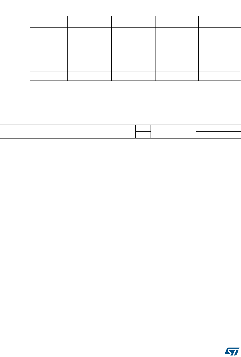
General-purpose timers (TIM9 to TIM14) RM0090
658/1718 DocID018909 Rev 9
19.4.3 TIM9/12 Interrupt enable register (TIMx_DIER)
Address offset: 0x0C
Reset value: 0x0000
Table 100. TIMx internal trigger connection
Slave TIM ITR0 (TS =’ 000’) ITR1 (TS = ‘001’) ITR2 (TS = ‘010’) ITR3 (TS = ’011’)
TIM2 TIM1 TIM8 TIM3 TIM4
TIM3 TIM1 TIM2 TIM5 TIM4
TIM4 TIM1 TIM2 TIM3 TIM8
TIM5 TIM2 TIM3 TIM4 TIM8
TIM9 TIM2 TIM3 TIM10_OC TIM11_OC
TIM12 TIM4 TIM5 TIM13_OC TIM14_OC
1514131211109876543210
Reserved TIE Res CC2IE CC1IE UIE
rw rw rw rw
Bits 15:7 Reserved, must be kept at reset value.
Bit 6 TIE: Trigger interrupt enable
0: Trigger interrupt disabled.
1: Trigger interrupt enabled.
Bit 5:3 Reserved, must be kept at reset value.
Bit 2 CC2IE: Capture/Compare 2 interrupt enable
0: CC2 interrupt disabled.
1: CC2 interrupt enabled.
Bit 1 CC1IE: Capture/Compare 1 interrupt enable
0: CC1 interrupt disabled.
1: CC1 interrupt enabled.
Bit 0 UIE: Update interrupt enable
0: Update interrupt disabled.
1: Update interrupt enabled.

DocID018909 Rev 9 659/1718
RM0090 General-purpose timers (TIM9 to TIM14)
680
19.4.4 TIM9/12 status register (TIMx_SR)
Address offset: 0x10
Reset value: 0x0000
1514131211109876543210
Reserved CC2OF CC1OF Reserved TIF Reserved CC2IF CC1IF UIF
rc_w0 rc_w0 rc_w0 rc_w0 rc_w0 rc_w0
Bits 15:11 Reserved, must be kept at reset value.
Bit 10 CC2OF: Capture/compare 2 overcapture flag
refer to CC1OF description
Bit 9 CC1OF: Capture/Compare 1 overcapture flag
This flag is set by hardware only when the corresponding channel is configured in input
capture mode. It is cleared by software by writing it to ‘0’.
0: No overcapture has been detected.
1: The counter value has been captured in TIMx_CCR1 register while CC1IF flag was
already set
Bits 8:7 Reserved, must be kept at reset value.
Bit 6 TIF: Trigger interrupt flag
This flag is set by hardware on trigger event (active edge detected on TRGI input when the
slave mode controller is enabled in all modes but gated mode. It is set when the counter
starts or stops when gated mode is selected. It is cleared by software.
0: No trigger event occurred.
1: Trigger interrupt pending.
Bits 5:3 Reserved, must be kept at reset value.

General-purpose timers (TIM9 to TIM14) RM0090
660/1718 DocID018909 Rev 9
19.4.5 TIM9/12 event generation register (TIMx_EGR)
Address offset: 0x14
Reset value: 0x0000
Bit 2 CC2IF: Capture/Compare 2 interrupt flag
refer to CC1IF description
Bit 1 CC1IF: Capture/compare 1 interrupt flag
If channel CC1 is configured as output:
This flag is set by hardware when the counter matches the compare value. It is cleared by
software.
0: No match.
1: The content of the counter TIMx_CNT matches the content of the TIMx_CCR1 register.
When the contents of TIMx_CCR1 are greater than the contents of TIMx_ARR, the CC1IF
bit goes high on the counter overflow.
If channel CC1 is configured as input:
This bit is set by hardware on a capture. It is cleared by software or by reading the
TIMx_CCR1 register.
0: No input capture occurred.
1: The counter value has been captured in TIMx_CCR1 register (an edge has been detected
on IC1 which matches the selected polarity).
Bit 0 UIF: Update interrupt flag
This bit is set by hardware on an update event. It is cleared by software.
0: No update occurred.
1: Update interrupt pending. This bit is set by hardware when the registers are updated:
– At overflow and if UDIS=’0’ in the TIMx_CR1 register.
– When CNT is reinitialized by software using the UG bit in TIMx_EGR register, if URS=’0’ and
UDIS=’0’ in the TIMx_CR1 register.
– When CNT is reinitialized by a trigger event (refer to the synchro control register
description), if URS=’0’ and UDIS=’0’ in the TIMx_CR1 register.
1514131211109876543210
Reserved TG Reserved CC2G CC1G UG
w www
Bits 15:7 Reserved, must be kept at reset value.
Bit 6 TG: Trigger generation
This bit is set by software in order to generate an event, it is automatically cleared by
hardware.
0: No action
1: The TIF flag is set in the TIMx_SR register. Related interrupt can occur if enabled
Bits 5:3 Reserved, must be kept at reset value.

DocID018909 Rev 9 661/1718
RM0090 General-purpose timers (TIM9 to TIM14)
680
Bit 2 CC2G: Capture/compare 2 generation
refer to CC1G description
Bit 1 CC1G: Capture/compare 1 generation
This bit is set by software to generate an event, it is automatically cleared by hardware.
0: No action
1: A capture/compare event is generated on channel 1:
If channel CC1 is configured as output:
the CC1IF flag is set, the corresponding interrupt is sent if enabled.
If channel CC1 is configured as input:
The current counter value is captured in the TIMx_CCR1 register. The CC1IF flag is set, the
corresponding interrupt is sent if enabled. The CC1OF flag is set if the CC1IF flag was
already high.
Bit 0 UG: Update generation
This bit can be set by software, it is automatically cleared by hardware.
0: No action
1: Re-initializes the counter and generates an update of the registers. The prescaler counter
is also cleared and the prescaler ratio is not affected. The counter is cleared.

General-purpose timers (TIM9 to TIM14) RM0090
662/1718 DocID018909 Rev 9
19.4.6 TIM9/12 capture/compare mode register 1 (TIMx_CCMR1)
Address offset: 0x18
Reset value: 0x0000
The channels can be used in input (capture mode) or in output (compare mode). The
direction of a channel is defined by configuring the corresponding CCxS bits. All the other
bits in this register have different functions in input and output modes. For a given bit, OCxx
describes its function when the channel is configured in output mode, ICxx describes its
function when the channel is configured in input mode. So you must take care that the same
bit can have different meanings for the input stage and the output stage.
Output compare mode
1514131211109876543210
Res. OC2M[2:0] OC2PE OC2FE CC2S[1:0] Res. OC1M[2:0] OC1PE OC1FE CC1S[1:0]
IC2F[3:0] IC2PSC[1:0] IC1F[3:0] IC1PSC[1:0]
rw rw rw rw rw rw rw rw rw rw rw rw rw rw rw rw
Bit 15 Reserved, must be kept at reset value.
Bits 14:12 OC2M[2:0]: Output compare 2 mode
Bit 11 OC2PE: Output compare 2 preload enable
Bit 10 OC2FE: Output compare 2 fast enable
Bits 9:8 CC2S[1:0]: Capture/Compare 2 selection
This bitfield defines the direction of the channel (input/output) as well as the used input.
00: CC2 channel is configured as output
01: CC2 channel is configured as input, IC2 is mapped on TI2
10: CC2 channel is configured as input, IC2 is mapped on TI1
11: CC2 channel is configured as input, IC2 is mapped on TRC. This mode works only if an
internal trigger input is selected through the TS bit (TIMx_SMCR register
Note: The CC2S bits are writable only when the channel is OFF (CC2E = 0 in TIMx_CCER).
Bit 7 Reserved, must be kept at reset value.

DocID018909 Rev 9 663/1718
RM0090 General-purpose timers (TIM9 to TIM14)
680
Bits 6:4 OC1M: Output compare 1 mode
These bits define the behavior of the output reference signal OC1REF from which OC1 and
OC1N are derived. OC1REF is active high whereas the active levels of OC1 and OC1N
depend on the CC1P and CC1NP bits, respectively.
000: Frozen - The comparison between the output compare register TIMx_CCR1 and the
counter TIMx_CNT has no effect on the outputs.(this mode is used to generate a timing
base).
001: Set channel 1 to active level on match. The OC1REF signal is forced high when the
TIMx_CNT counter matches the capture/compare register 1 (TIMx_CCR1).
010: Set channel 1 to inactive level on match. The OC1REF signal is forced low when the
TIMx_CNT counter matches the capture/compare register 1 (TIMx_CCR1).
011: Toggle - OC1REF toggles when TIMx_CNT=TIMx_CCR1
100: Force inactive level - OC1REF is forced low
101: Force active level - OC1REF is forced high
110: PWM mode 1 - In upcounting, channel 1 is active as long as TIMx_CNT<TIMx_CCR1
else it is inactive. In downcounting, channel 1 is inactive (OC1REF=‘0) as long as
TIMx_CNT>TIMx_CCR1, else it is active (OC1REF=’1’)
111: PWM mode 2 - In upcounting, channel 1 is inactive as long as TIMx_CNT<TIMx_CCR1
else it is active. In downcounting, channel 1 is active as long as TIMx_CNT>TIMx_CCR1
else it is inactive.
Note: In PWM mode 1 or 2, the OCREF level changes only when the result of the
comparison changes or when the output compare mode switches from “frozen” mode
to “PWM” mode.
Bit 3 OC1PE: Output compare 1 preload enable
0: Preload register on TIMx_CCR1 disabled. TIMx_CCR1 can be written at anytime, the
new value is taken into account immediately
1: Preload register on TIMx_CCR1 enabled. Read/Write operations access the preload
register. TIMx_CCR1 preload value is loaded into the active register at each update event
Note: The PWM mode can be used without validating the preload register only in one-pulse
mode (OPM bit set in the TIMx_CR1 register). Else the behavior is not guaranteed.
Bit 2 OC1FE: Output compare 1 fast enable
This bit is used to accelerate the effect of an event on the trigger in input on the CC output.
0: CC1 behaves normally depending on the counter and CCR1 values even when the
trigger is ON. The minimum delay to activate the CC1 output when an edge occurs on the
trigger input is 5 clock cycles
1: An active edge on the trigger input acts like a compare match on the CC1 output. Then,
OC is set to the compare level independently of the result of the comparison. Delay to
sample the trigger input and to activate CC1 output is reduced to 3 clock cycles. OC1FE
acts only if the channel is configured in PWM1 or PWM2 mode.
Bits 1:0 CC1S: Capture/Compare 1 selection
This bitfield defines the direction of the channel (input/output) as well as the used input.
00: CC1 channel is configured as output
01: CC1 channel is configured as input, IC1 is mapped on TI1
10: CC1 channel is configured as input, IC1 is mapped on TI2
11: CC1 channel is configured as input, IC1 is mapped on TRC. This mode works only if an
internal trigger input is selected through the TS bit (TIMx_SMCR register)
Note: The CC1S bits are writable only when the channel is OFF (CC1E = 0 in TIMx_CCER).

General-purpose timers (TIM9 to TIM14) RM0090
664/1718 DocID018909 Rev 9
Input capture mode
Bits 15:12 IC2F: Input capture 2 filter
Bits 11:10 IC2PSC[1:0]: Input capture 2 prescaler
Bits 9:8 CC2S: Capture/compare 2 selection
This bitfield defines the direction of the channel (input/output) as well as the used input.
00: CC2 channel is configured as output
01: CC2 channel is configured as input, IC2 is mapped on TI2
10: CC2 channel is configured as input, IC2 is mapped on TI1
11: CC2 channel is configured as input, IC2 is mapped on TRC. This mode works only if an
internal trigger input is selected through the TS bit (TIMx_SMCR register)
Note: The CC2S bits are writable only when the channel is OFF (CC2E = 0 in TIMx_CCER).
Bits 7:4 IC1F: Input capture 1 filter
This bitfield defines the frequency used to sample the TI1 input and the length of the digital
filter applied to TI1. The digital filter is made of an event counter in which N events are
needed to validate a transition on the output:
0000: No filter, sampling is done at fDTS1000: fSAMPLING=fDTS/8, N=6
0001: fSAMPLING=fCK_INT
, N=21001: fSAMPLING=fDTS/8, N=8
0010: fSAMPLING=fCK_INT
, N=41010: fSAMPLING=fDTS/16, N=5
0011: fSAMPLING=fCK_INT
, N=8 1011: fSAMPLING=fDTS/16, N=6
0100: fSAMPLING=fDTS/2, N=61100: fSAMPLING=fDTS/16, N=8
0101: fSAMPLING=fDTS/2, N=81101: fSAMPLING=fDTS/32, N=5
0110: fSAMPLING=fDTS/4, N=61110: fSAMPLING=fDTS/32, N=6
0111: fSAMPLING=fDTS/4, N=81111: fSAMPLING=fDTS/32, N=8
Bits 3:2 IC1PSC: Input capture 1 prescaler
This bitfield defines the ratio of the prescaler acting on the CC1 input (IC1).
The prescaler is reset as soon as CC1E=’0’ (TIMx_CCER register).
00: no prescaler, capture is done each time an edge is detected on the capture input
01: capture is done once every 2 events
10: capture is done once every 4 events
11: capture is done once every 8 events
Bits 1:0 CC1S: Capture/Compare 1 selection
This bitfield defines the direction of the channel (input/output) as well as the used input.
00: CC1 channel is configured as output
01: CC1 channel is configured as input, IC1 is mapped on TI1
10: CC1 channel is configured as input, IC1 is mapped on TI2
11: CC1 channel is configured as input, IC1 is mapped on TRC. This mode is working only if
an internal trigger input is selected through TS bit (TIMx_SMCR register)
Note: The CC1S bits are writable only when the channel is OFF (CC1E = 0 in TIMx_CCER).

DocID018909 Rev 9 665/1718
RM0090 General-purpose timers (TIM9 to TIM14)
680
19.4.7 TIM9/12 capture/compare enable register (TIMx_CCER)
Address offset: 0x20
Reset value: 0x0000
1514131211109876543210
Reserved CC2NP Res. CC2P CC2E CC1NP Res. CC1P CC1E
rw rw rw rw rw rw
Bits 15:8 Reserved, must be kept at reset value.
Bit 7 CC2NP: Capture/Compare 2 output Polarity
refer to CC1NP description
Bits 6 Reserved, must be kept at reset value.
Bit 5 CC2P: Capture/Compare 2 output Polarity
refer to CC1P description
Bit 4 CC2E: Capture/Compare 2 output enable
refer to CC1E description
Bit 3 CC1NP: Capture/Compare 1 complementary output Polarity
CC1 channel configured as output: CC1NP must be kept cleared
CC1 channel configured as input: CC1NP is used in conjunction with CC1P to define
TI1FP1/TI2FP1 polarity (refer to CC1P description).
Bit 2 Reserved, must be kept at reset value.
Bit 1 CC1P: Capture/Compare 1 output Polarity.
CC1 channel configured as output:
0: OC1 active high.
1: OC1 active low.
CC1 channel configured as input:
CC1NP/CC1P bits select TI1FP1 and TI2FP1 polarity for trigger or capture operations.
00: noninverted/rising edge
Circuit is sensitive to TIxFP1 rising edge (capture, trigger in reset, external clock or trigger
mode), TIxFP1 is not inverted (trigger in gated mode, encoder mode).
01: inverted/falling edge
Circuit is sensitive to TIxFP1 falling edge (capture, trigger in reset, external clock or trigger
mode), TIxFP1 is inverted (trigger in gated mode, encoder mode).
10: reserved, do not use this configuration.
Note: 11: noninverted/both edges
Circuit is sensitive to both TIxFP1 rising and falling edges (capture, trigger in reset,
external clock or trigger mode), TIxFP1 is not inverted (trigger in gated mode). This
configuration must not be used for encoder mode.
Bit 0 CC1E: Capture/Compare 1 output enable.
CC1 channel configured as output:
0: Off - OC1 is not active.
1: On - OC1 signal is output on the corresponding output pin.
CC1 channel configured as input:
This bit determines if a capture of the counter value can actually be done into the input
capture/compare register 1 (TIMx_CCR1) or not.
0: Capture disabled.
1: Capture enabled.
General-purpose timers (TIM9 to TIM14) RM0090
666/1718 DocID018909 Rev 9
Note: The states of the external I/O pins connected to the standard OCx channels depend on the
state of the OCx channel and on the GPIO registers.
19.4.8 TIM9/12 counter (TIMx_CNT)
Address offset: 0x24
Reset value: 0x0000
19.4.9 TIM9/12 prescaler (TIMx_PSC)
Address offset: 0x28
Reset value: 0x0000
19.4.10 TIM9/12 auto-reload register (TIMx_ARR)
Address offset: 0x2C
Reset value: 0x0000
Table 101. Output control bit for standard OCx channels
CCxE bit OCx output state
0 Output disabled (OCx=’0’, OCx_EN=’0’)
1 OCx=OCxREF + Polarity, OCx_EN=’1’
1514131211109876543210
CNT[15:0]
rw rw rw rw rw rw rw rw rw rw rw rw rw rw rw rw
Bits 15:0 CNT[15:0]: Counter value
1514131211109876543210
PSC[15:0]
rw rw rw rw rw rw rw rw rw rw rw rw rw rw rw rw
Bits 15:0 PSC[15:0]: Prescaler value
The counter clock frequency CK_CNT is equal to fCK_PSC / (PSC[15:0] + 1).
PSC contains the value to be loaded into the active prescaler register at each update event.
1514131211109876543210
ARR[15:0]
rw rw rw rw rw rw rw rw rw rw rw rw rw rw rw rw
Bits 15:0 ARR[15:0]: Auto-reload value
ARR is the value to be loaded into the actual auto-reload register.
Refer to the Section 19.3.1: Time-base unit on page 639 for more details about ARR update
and behavior.
The counter is blocked while the auto-reload value is null.

DocID018909 Rev 9 667/1718
RM0090 General-purpose timers (TIM9 to TIM14)
680
19.4.11 TIM9/12 capture/compare register 1 (TIMx_CCR1)
Address offset: 0x34
Reset value: 0x0000
19.4.12 TIM9/12 capture/compare register 2 (TIMx_CCR2)
Address offset: 0x38
Reset value: 0x0000
1514131211109876543210
CCR1[15:0]
rw rw rw rw rw rw rw rw rw rw rw rw rw rw rw rw
Bits 15:0 CCR1[15:0]: Capture/Compare 1 value
If channel CC1 is configured as output:
CCR1 is the value to be loaded into the actual capture/compare 1 register (preload value).
It is loaded permanently if the preload feature is not selected in the TIMx_CCMR1 register
(OC1PE bit). Else the preload value is copied into the active capture/compare 1 register
when an update event occurs.
The active capture/compare register contains the value to be compared to the TIMx_CNT
counter and signaled on the OC1 output.
If channel CC1is configured as input:
CCR1 is the counter value transferred by the last input capture 1 event (IC1).
1514131211109876543210
CCR2[15:0]
rw rw rw rw rw rw rw rw rw rw rw rw rw rw rw rw
Bits 15:0 CCR2[15:0]: Capture/Compare 2 value
If channel CC2 is configured as output:
CCR2 is the value to be loaded into the actual capture/compare 2 register (preload value).
It is loaded permanently if the preload feature is not selected in the TIMx_CCMR2 register
(OC2PE bit). Else the preload value is copied into the active capture/compare 2 register
when an update event occurs.
The active capture/compare register contains the value to be compared to the TIMx_CNT
counter and signalled on the OC2 output.
If channel CC2 is configured as input:
CCR2 is the counter value transferred by the last input capture 2 event (IC2).
General-purpose timers (TIM9 to TIM14) RM0090
668/1718 DocID018909 Rev 9
19.4.13 TIM9/12 register map
TIM9/12 registers are mapped as 16-bit addressable registers as described below:
Table 102. TIM9/12 register map and reset values
Offset Register
31
30
29
28
27
26
25
24
23
22
21
20
19
18
17
16
15
14
13
12
11
10
9
8
7
6
5
4
3
2
1
0
0x00 TIMx_CR1 Reserved
CKD
[1:0]
ARPE
Reserved
OPM
URS
UDIS
CEN
Reset value 000 0000
0x08 TIMx_SMCR Reserved
MSM
TS[2:0]
Reserved
SMS[2:0]
Reset value 000 0 000
0x0C TIMx_DIER Reserved
TIE
Reserved
CC2IE
CC1IE
UIE
Reset value 0000
0x10 TIMx_SR Reserved
CC2OF
CC1OF
Reserved
TIF
Reserved
CC2IF
CC1IF
UIF
Reset value 00 0 000
0x14 TIMx_EGR Reserved
TG
Reserved
CC2G
CC1G
UG
Reset value 0000
0x18
TIMx_CCMR1
Output Compare
mode Reserved
OC2M
[2:0]
OC2PE
OC2FE
CC2S
[1:0]
Reserved
OC1M
[2:0]
OC1PE
OC1FE
CC1
S
[1:0]
Reset value 0 0 0 0 0 0 0 0 0 0 0 0 0 0
TIMx_CCMR1
Input Capture
mode Reserved IC2F[3:0]
IC2
PSC
[1:0]
CC2S
[1:0] IC1F[3:0]
IC1
PSC
[1:0]
CC1
S
[1:0]
Reset value 0 0 0 0 0 0 0 0 0 0 0 0 0 0 0 0
0x1C Reserved
0x20 TIMx_CCER Reserved
CC2NP
Reserved
CC2P
CC2E
CC1NP
Reserved
CC1P
CC1E
Reset value 000000
0x24 TIMx_CNT Reserved CNT[15:0]
Reset value 0 0 0 0 0 0 0 0 0 0 0 0 0 0 0 0
0x28 TIMx_PSC Reserved PSC[15:0]
Reset value 0 0 0 0 0 0 0 0 0 0 0 0 0 0 0 0
0x2C TIMx_ARR Reserved ARR[15:0]
Reset value 0 0 0 0 0 0 0 0 0 0 0 0 0 0 0 0
0x30 Reserved
0x34 TIMx_CCR1 Reserved CCR1[15:0]
Reset value 0 0 0 0 0 0 0 0 0 0 0 0 0 0 0 0

DocID018909 Rev 9 669/1718
RM0090 General-purpose timers (TIM9 to TIM14)
680
Refer to Table 1 on page 64 for the register boundary addresses.
0x38 TIMx_CCR2 Reserved CCR2[15:0]
Reset value 0 0 0 0 0 0 0 0 0 0 0 0 0 0 0 0
0x3C to
0x4C Reserved
Table 102. TIM9/12 register map and reset values (continued)
Offset Register
31
30
29
28
27
26
25
24
23
22
21
20
19
18
17
16
15
14
13
12
11
10
9
8
7
6
5
4
3
2
1
0

General-purpose timers (TIM9 to TIM14) RM0090
670/1718 DocID018909 Rev 9
19.5 TIM10/11/13/14 registers
The peripheral registers have to be written by half-words (16 bits) or words (32 bits). Read
accesses can be done by bytes (8 bits), half-words (16 bits) or words (32 bits).
19.5.1 TIM10/11/13/14 control register 1 (TIMx_CR1)
Address offset: 0x00
Reset value: 0x0000
1514131211109876543210
Reserved CKD[1:0] ARPE Reserved URS UDIS CEN
rw rw rw rw rw rw
Bits 15:10 Reserved, must be kept at reset value.
Bits 9:8 CKD: Clock division
This bit-field indicates the division ratio between the timer clock (CK_INT) frequency and
sampling clock used by the digital filters (TIx),
00: tDTS = tCK_INT
01: tDTS = 2 × tCK_INT
10: tDTS = 4 × tCK_INT
11: Reserved
Bit 7 ARPE: Auto-reload preload enable
0: TIMx_ARR register is not buffered
1: TIMx_ARR register is buffered
Bits 6:3 Reserved, must be kept at reset value.
Bit 2 URS: Update request source
This bit is set and cleared by software to select the update interrupt (UEV) sources.
0: Any of the following events generate an UEV if enabled:
– Counter overflow
– Setting the UG bit
1: Only counter overflow generates an UEV if enabled.
Bit 1 UDIS: Update disable
This bit is set and cleared by software to enable/disable update interrupt (UEV) event
generation.
0: UEV enabled. An UEV is generated by one of the following events:
– Counter overflow
– Setting the UG bit.
Buffered registers are then loaded with their preload values.
1: UEV disabled. No UEV is generated, shadow registers keep their value (ARR, PSC,
CCRx). The counter and the prescaler are reinitialized if the UG bit is set.
Bit 0 CEN: Counter enable
0: Counter disabled
1: Counter enabled

DocID018909 Rev 9 671/1718
RM0090 General-purpose timers (TIM9 to TIM14)
680
19.5.2 TIM10/11/13/14 Interrupt enable register (TIMx_DIER)
Address offset: 0x0C
Reset value: 0x0000
19.5.3 TIM10/11/13/14 status register (TIMx_SR)
Address offset: 0x10
Reset value: 0x0000
1514131211109876543210
Reserved CC1IE UIE
rw rw
Bits 15:2 Reserved, must be kept at reset value.
Bit 1 CC1IE: Capture/Compare 1 interrupt enable
0: CC1 interrupt disabled
1: CC1 interrupt enabled
Bit 0 UIE: Update interrupt enable
0: Update interrupt disabled
1: Update interrupt enabled
1514131211109876543210
Reserved
CC1OF
Reserved
CC1IF UIF
rc_w0 rc_w0 rc_w0
Bits 15:10 Reserved, must be kept at reset value.
Bit 9 CC1OF: Capture/Compare 1 overcapture flag
This flag is set by hardware only when the corresponding channel is configured in input
capture mode. It is cleared by software by writing it to ‘0’.
0: No overcapture has been detected.
1: The counter value has been captured in TIMx_CCR1 register while CC1IF flag was
already set

General-purpose timers (TIM9 to TIM14) RM0090
672/1718 DocID018909 Rev 9
19.5.4 TIM10/11/13/14 event generation register (TIMx_EGR)
Address offset: 0x14
Reset value: 0x0000
Bits 8:2 Reserved, must be kept at reset value.
Bit 1 CC1IF: Capture/compare 1 interrupt flag
If channel CC1 is configured as output:
This flag is set by hardware when the counter matches the compare value. It is cleared by
software.
0: No match.
1: The content of the counter TIMx_CNT matches the content of the TIMx_CCR1 register.
When the contents of TIMx_CCR1 are greater than the contents of TIMx_ARR, the CC1IF bit
goes high on the counter overflow.
If channel CC1 is configured as input:
This bit is set by hardware on a capture. It is cleared by software or by reading the
TIMx_CCR1 register.
0: No input capture occurred.
1: The counter value has been captured in TIMx_CCR1 register (an edge has been detected
on IC1 which matches the selected polarity).
Bit 0 UIF: Update interrupt flag
This bit is set by hardware on an update event. It is cleared by software.
0: No update occurred.
1: Update interrupt pending. This bit is set by hardware when the registers are updated:
– At overflow and if UDIS=’0’ in the TIMx_CR1 register.
– When CNT is reinitialized by software using the UG bit in TIMx_EGR register, if
URS=’0’ and UDIS=’0’ in the TIMx_CR1 register.
1514131211109876543210
Reserved CC1G UG
ww
Bits 15:2 Reserved, must be kept at reset value.
Bit 1 CC1G: Capture/compare 1 generation
This bit is set by software in order to generate an event, it is automatically cleared by
hardware.
0: No action
1: A capture/compare event is generated on channel 1:
If channel CC1 is configured as output:
CC1IF flag is set, Corresponding interrupt or is sent if enabled.
If channel CC1 is configured as input:
The current value of the counter is captured in TIMx_CCR1 register. The CC1IF flag is set,
the corresponding interrupt is sent if enabled. The CC1OF flag is set if the CC1IF flag was
already high.
Bit 0 UG: Update generation
This bit can be set by software, it is automatically cleared by hardware.
0: No action
1: Re-initialize the counter and generates an update of the registers. Note that the prescaler
counter is cleared too (anyway the prescaler ratio is not affected). The counter is cleared.

DocID018909 Rev 9 673/1718
RM0090 General-purpose timers (TIM9 to TIM14)
680
19.5.5 TIM10/11/13/14 capture/compare mode register 1
(TIMx_CCMR1)
Address offset: 0x18
Reset value: 0x0000
The channels can be used in input (capture mode) or in output (compare mode). The
direction of a channel is defined by configuring the corresponding CCxS bits. All the other
bits of this register have a different function in input and in output mode. For a given bit,
OCxx describes its function when the channel is configured in output, ICxx describes its
function when the channel is configured in input. So you must take care that the same bit
can have a different meaning for the input stage and for the output stage.
1514131211109876543210
Reserved OC1M[2:0] OC1PE OC1FE
CC1S[1:0]
Reserved IC1F[3:0] IC1PSC[1:0]
rw rw rw rw rw rw rw rw

General-purpose timers (TIM9 to TIM14) RM0090
674/1718 DocID018909 Rev 9
Output compare mode
Bits 15:7 Reserved, must be kept at reset value.
Bits 6:4 OC1M: Output compare 1 mode
These bits define the behavior of the output reference signal OC1REF from which OC1 is
derived. OC1REF is active high whereas OC1 active level depends on CC1P bit.
000: Frozen. The comparison between the output compare register TIMx_CCR1 and the
counter TIMx_CNT has no effect on the outputs.
001: Set channel 1 to active level on match. OC1REF signal is forced high when the counter
TIMx_CNT matches the capture/compare register 1 (TIMx_CCR1).
010: Set channel 1 to inactive level on match. OC1REF signal is forced low when the
counter TIMx_CNT matches the capture/compare register 1 (TIMx_CCR1).
011: Toggle - OC1REF toggles when TIMx_CNT = TIMx_CCR1.
100: Force inactive level - OC1REF is forced low.
101: Force active level - OC1REF is forced high.
110: PWM mode 1 - Channel 1 is active as long as TIMx_CNT < TIMx_CCR1 else inactive.
111: PWM mode 2 - Channel 1 is inactive as long as TIMx_CNT < TIMx_CCR1 else active.
Note: In PWM mode 1 or 2, the OCREF level changes when the result of the comparison
changes or when the output compare mode switches from frozen to PWM mode.
Bit 3 OC1PE: Output compare 1 preload enable
0: Preload register on TIMx_CCR1 disabled. TIMx_CCR1 can be written at anytime, the
new value is taken in account immediately.
1: Preload register on TIMx_CCR1 enabled. Read/Write operations access the preload
register. TIMx_CCR1 preload value is loaded in the active register at each update event.
Note: The PWM mode can be used without validating the preload register only in one pulse
mode (OPM bit set in TIMx_CR1 register). Else the behavior is not guaranteed.
Bit 2 OC1FE: Output compare 1 fast enable
This bit is used to accelerate the effect of an event on the trigger in input on the CC output.
0: CC1 behaves normally depending on counter and CCR1 values even when the trigger is
ON. The minimum delay to activate CC1 output when an edge occurs on the trigger input is
5 clock cycles.
1: An active edge on the trigger input acts like a compare match on CC1 output. OC is then
set to the compare level independently of the result of the comparison. Delay to sample the
trigger input and to activate CC1 output is reduced to 3 clock cycles. OC1FE acts only if the
channel is configured in PWM1 or PWM2 mode.
Bits 1:0 CC1S: Capture/Compare 1 selection
This bit-field defines the direction of the channel (input/output) as well as the used input.
00: CC1 channel is configured as output.
01: CC1 channel is configured as input, IC1 is mapped on TI1.
10:
11:
Note: CC1S bits are writable only when the channel is OFF (CC1E = 0 in TIMx_CCER).

DocID018909 Rev 9 675/1718
RM0090 General-purpose timers (TIM9 to TIM14)
680
Input capture mode
Bits 15:8 Reserved, must be kept at reset value.
Bits 7:4 IC1F: Input capture 1 filter
This bit-field defines the frequency used to sample TI1 input and the length of the digital filter
applied to TI1. The digital filter is made of an event counter in which N events are needed to
validate a transition on the output:
0000: No filter, sampling is done at fDTS1000: fSAMPLING=fDTS/8, N=6
0001: fSAMPLING=fCK_INT
, N=21001: fSAMPLING=fDTS/8, N=8
0010: fSAMPLING=fCK_INT
, N=41010: fSAMPLING=fDTS/16, N=5
0011: fSAMPLING=fCK_INT
, N=81011: fSAMPLING=fDTS/16, N=6
0100: fSAMPLING=fDTS/2, N=61100: fSAMPLING=fDTS/16, N=8
0101: fSAMPLING=fDTS/2, N=81101: fSAMPLING=fDTS/32, N=5
0110: fSAMPLING=fDTS/4, N=61110: fSAMPLING=fDTS/32, N=6
0111: fSAMPLING=fDTS/4, N=81111: fSAMPLING=fDTS/32, N=8
Bits 3:2 IC1PSC: Input capture 1 prescaler
This bit-field defines the ratio of the prescaler acting on CC1 input (IC1).
The prescaler is reset as soon as CC1E=’0’ (TIMx_CCER register).
00: no prescaler, capture is done each time an edge is detected on the capture input
01: capture is done once every 2 events
10: capture is done once every 4 events
11: capture is done once every 8 events
Bits 1:0 CC1S: Capture/Compare 1 selection
This bit-field defines the direction of the channel (input/output) as well as the used input.
00: CC1 channel is configured as output
01: CC1 channel is configured as input, IC1 is mapped on TI1
10: Reserved
11: Reserved
Note: CC1S bits are writable only when the channel is OFF (CC1E = 0 in TIMx_CCER).
General-purpose timers (TIM9 to TIM14) RM0090
676/1718 DocID018909 Rev 9
19.5.6 TIM10/11/13/14 capture/compare enable register
(TIMx_CCER)
Address offset: 0x20
Reset value: 0x0000
Note: The state of the external I/O pins connected to the standard OCx channels depends on the
OCx channel state and the GPIO registers.
1514131211109876543210
Reserved
CC1NP
Res.
CC1P CC1E
rw rw rw
Bits 15:4 Reserved, must be kept at reset value.
Bit 3 CC1NP: Capture/Compare 1 complementary output Polarity.
CC1 channel configured as output: CC1NP must be kept cleared.
CC1 channel configured as input: CC1NP bit is used in conjunction with CC1P to define
TI1FP1 polarity (refer to CC1P description).
Bit 2 Reserved, must be kept at reset value.
Bit 1 CC1P: Capture/Compare 1 output Polarity.
CC1 channel configured as output:
0: OC1 active high
1: OC1 active low
CC1 channel configured as input:
The CC1P bit selects TI1FP1 and TI2FP1 polarity for trigger or capture operations.
00: noninverted/rising edge
Circuit is sensitive to TI1FP1 rising edge (capture mode), TI1FP1 is not inverted.
01: inverted/falling edge
Circuit is sensitive to TI1FP1 falling edge (capture mode), TI1FP1 is inverted.
10: reserved, do not use this configuration.
11: noninverted/both edges
Circuit is sensitive to both TI1FP1 rising and falling edges (capture mode), TI1FP1 is not
inverted.
Bit 0 CC1E: Capture/Compare 1 output enable.
CC1 channel configured as output:
0: Off - OC1 is not active
1: On - OC1 signal is output on the corresponding output pin
CC1 channel configured as input:
This bit determines if a capture of the counter value can actually be done into the input
capture/compare register 1 (TIMx_CCR1) or not.
0: Capture disabled
1: Capture enabled
Table 103. Output control bit for standard OCx channels
CCxE bit OCx output state
0 Output Disabled (OCx=’0’, OCx_EN=’0’)
1 OCx=OCxREF + Polarity, OCx_EN=’1’

DocID018909 Rev 9 677/1718
RM0090 General-purpose timers (TIM9 to TIM14)
680
19.5.7 TIM10/11/13/14 counter (TIMx_CNT)
Address offset: 0x24
Reset value: 0x0000
19.5.8 TIM10/11/13/14 prescaler (TIMx_PSC)
Address offset: 0x28
Reset value: 0x0000
19.5.9 TIM10/11/13/14 auto-reload register (TIMx_ARR)
Address offset: 0x2C
Reset value: 0x0000
1514131211109876543210
CNT[15:0]
rw rw rw rw rw rw rw rw rw rw rw rw rw rw rw rw
Bits 15:0 CNT[15:0]: Counter value
1514131211109876543210
PSC[15:0]
rw rw rw rw rw rw rw rw rw rw rw rw rw rw rw rw
Bits 15:0 PSC[15:0]: Prescaler value
The counter clock frequency CK_CNT is equal to fCK_PSC / (PSC[15:0] + 1).
PSC contains the value to be loaded in the active prescaler register at each update event.
1514131211109876543210
ARR[15:0]
rw rw rw rw rw rw rw rw rw rw rw rw rw rw rw rw
Bits 15:0 ARR[15:0]: Auto-reload value
ARR is the value to be loaded in the actual auto-reload register.
Refer to Section 19.3.1: Time-base unit on page 639 for more details about ARR update and
behavior.
The counter is blocked while the auto-reload value is null.
General-purpose timers (TIM9 to TIM14) RM0090
678/1718 DocID018909 Rev 9
19.5.10 TIM10/11/13/14 capture/compare register 1 (TIMx_CCR1)
Address offset: 0x34
Reset value: 0x0000
19.5.11 TIM11 option register 1 (TIM11_OR)
Address offset: 0x50
Reset value: 0x0000
1514131211109876543210
CCR1[15:0]
rw rw rw rw rw rw rw rw rw rw rw rw rw rw rw rw
Bits 15:0 CCR1[15:0]: Capture/Compare 1 value
If channel CC1 is configured as output:
CCR1 is the value to be loaded in the actual capture/compare 1 register (preload value).
It is loaded permanently if the preload feature is not selected in the TIMx_CCMR1 register (bit
OC1PE). Else the preload value is copied in the active capture/compare 1 register when an
update event occurs.
The active capture/compare register contains the value to be compared to the counter
TIMx_CNT and signaled on OC1 output.
If channel CC1is configured as input:
CCR1 is the counter value transferred by the last input capture 1 event (IC1).
1514131211109876543210
Reserved TI1_RMP[1:0]
rw
Bits 15:2 Reserved, must be kept at reset value.
Bits 1:0 TI1_RMP[1:0]: TIM11 Input 1 remapping capability
Set and cleared by software.
00,01,11: TIM11 Channel1 is connected to the GPIO (refer to the Alternate function mapping
table in the datasheets).
10: HSE_RTC clock (HSE divided by programmable prescaler) is connected to the
TIM11_CH1 input for measurement purposes
DocID018909 Rev 9 679/1718
RM0090 General-purpose timers (TIM9 to TIM14)
680
19.5.12 TIM10/11/13/14 register map
TIMx registers are mapped as 16-bit addressable registers as described in the tables below:
Table 104. TIM10/11/13/14 register map and reset values
Offset Register
31
30
29
28
27
26
25
24
23
22
21
20
19
18
17
16
15
14
13
12
11
10
9
8
7
6
5
4
3
2
1
0
0x00 TIMx_CR1 Reserved
CKD
[1:0]
ARPE
Reserved
URS
UDIS
CEN
Reset value 000 0 0 0
0x08 TIMx_SMCR Reserved
Reset value
0x0C TIMx_DIER Reserved
CC1IE
UIE
Reset value 00
0x10 TIMx_SR Reserved
CC1OF
Reserved
CC1IF
UIF
Reset value 000
0x14 TIMx_EGR Reserved
CC1G
UG
Reset value 00
0x18
TIMx_CCMR1
Output compare
mode Reserved
OC1M
[2:0]
OC1PE
OC1FE
CC1S
[1:0]
Reset value 00000 0 0
TIMx_CCMR1
Input capture
mode Reserved IC1F[3:0]
IC1
PSC
[1:0]
CC1S
[1:0]
Reset value 000000 0 0
0x1C Reserved
0x20 TIMx_CCER Reserved
CC1NP
Reserved
CC1P
CC1E
Reset value 000
0x24 TIMx_CNT Reserved CNT[15:0]
Reset value 000000000000000 0
0x28 TIMx_PSC Reserved PSC[15:0]
Reset value 000000000000000 0
0x2C TIMx_ARR Reserved ARR[15:0]
Reset value 000000000000000 0
0x30 Reserved
0x34 TIMx_CCR1 Reserved CCR1[15:0]
Reset value 000000000000000 0
0x38 to
0x4C Reserved

General-purpose timers (TIM9 to TIM14) RM0090
680/1718 DocID018909 Rev 9
Refer to Table 1 on page 64 for the register boundary addresses.
0x50 TIMx_OR Reserved
TI1_RMP
Reset value 00
Table 104. TIM10/11/13/14 register map and reset values (continued)
Offset Register
31
30
29
28
27
26
25
24
23
22
21
20
19
18
17
16
15
14
13
12
11
10
9
8
7
6
5
4
3
2
1
0
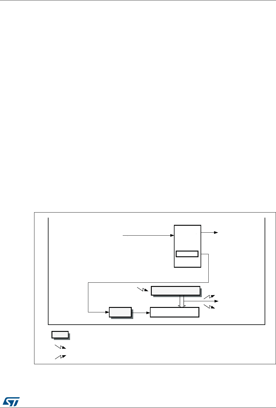
DocID018909 Rev 9 681/1718
RM0090 Basic timers (TIM6&TIM7)
691
20 Basic timers (TIM6&TIM7)
This section applies to the whole STM32F4xx family devices, unless otherwise specified.
20.1 TIM6&TIM7 introduction
The basic timers TIM6 and TIM7 consist of a 16-bit auto-reload counter driven by a
programmable prescaler.
They may be used as generic timers for time-base generation but they are also specifically
used to drive the digital-to-analog converter (DAC). In fact, the timers are internally
connected to the DAC and are able to drive it through their trigger outputs.
The timers are completely independent, and do not share any resources.
20.2 TIM6&TIM7 main features
Basic timer (TIM6&TIM7) features include:
•16-bit auto-reload upcounter
•16-bit programmable prescaler used to divide (also “on the fly”) the counter clock
frequency by any factor between 1 and 65536
•Synchronization circuit to trigger the DAC
•Interrupt/DMA generation on the update event: counter overflow
Figure 203. Basic timer block diagram
U
Trigger
controller
Stop, Clear or up
TRGO
U
UI
Reset, Enable, Count,
event
Preload registers transferred
to active registers on U event according to control bit
interrupt & DMA output
to DAC
COUNTER
CK_PSC CNT
CK_CNT
Controller
Internal clock (CK_INT)
TIMxCLK from RCC
±
Prescaler
PSC
Auto-reload Register
Flag
ai14749b

Basic timers (TIM6&TIM7) RM0090
682/1718 DocID018909 Rev 9
20.3 TIM6&TIM7 functional description
20.3.1 Time-base unit
The main block of the programmable timer is a 16-bit upcounter with its related auto-reload
register. The counter clock can be divided by a prescaler.
The counter, the auto-reload register and the prescaler register can be written or read by
software. This is true even when the counter is running.
The time-base unit includes:
•Counter Register (TIMx_CNT)
•Prescaler Register (TIMx_PSC)
•Auto-Reload Register (TIMx_ARR)
The auto-reload register is preloaded. The preload register is accessed each time an
attempt is made to write or read the auto-reload register. The contents of the preload
register are transferred into the shadow register permanently or at each update event UEV,
depending on the auto-reload preload enable bit (ARPE) in the TIMx_CR1 register. The
update event is sent when the counter reaches the overflow value and if the UDIS bit equals
0 in the TIMx_CR1 register. It can also be generated by software. The generation of the
update event is described in detail for each configuration.
The counter is clocked by the prescaler output CK_CNT, which is enabled only when the
counter enable bit (CEN) in the TIMx_CR1 register is set.
Note that the actual counter enable signal CNT_EN is set 1 clock cycle after CEN.
Prescaler description
The prescaler can divide the counter clock frequency by any factor between 1 and 65536. It
is based on a 16-bit counter controlled through a 16-bit register (in the TIMx_PSC register).
It can be changed on the fly as the TIMx_PSC control register is buffered. The new
prescaler ratio is taken into account at the next update event.
Figure 204 and Figure 205 give some examples of the counter behavior when the prescaler
ratio is changed on the fly.
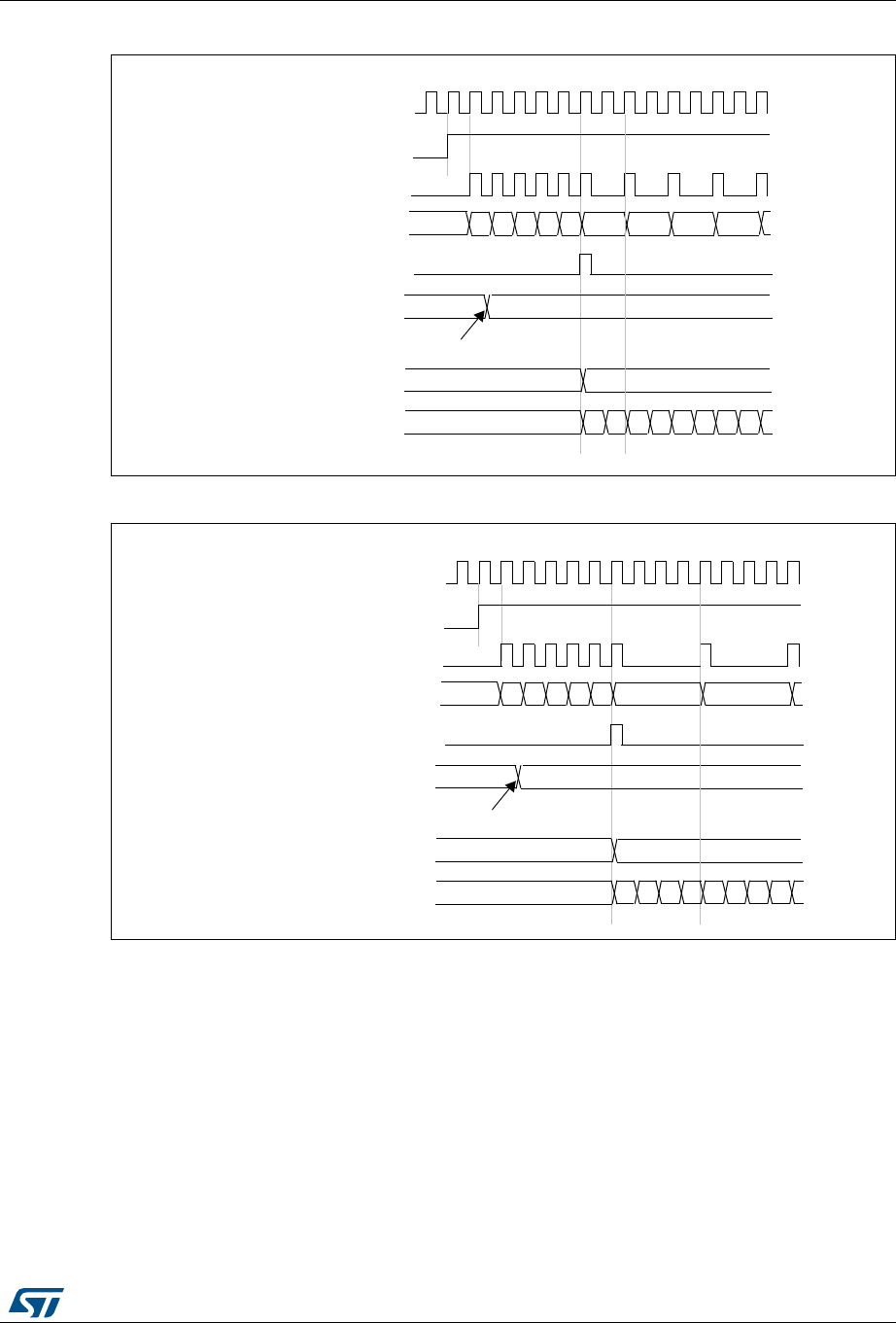
DocID018909 Rev 9 683/1718
RM0090 Basic timers (TIM6&TIM7)
691
Figure 204. Counter timing diagram with prescaler division change from 1 to 2
Figure 205. Counter timing diagram with prescaler division change from 1 to 4
20.3.2 Counting mode
The counter counts from 0 to the auto-reload value (contents of the TIMx_ARR register),
then restarts from 0 and generates a counter overflow event.
An update event can be generate at each counter overflow or by setting the UG bit in the
TIMx_EGR register (by software or by using the slave mode controller).
The UEV event can be disabled by software by setting the UDIS bit in the TIMx_CR1
register. This avoids updating the shadow registers while writing new values into the preload
registers. In this way, no update event occurs until the UDIS bit has been written to 0,
however, the counter and the prescaler counter both restart from 0 (but the prescale rate
does not change). In addition, if the URS (update request selection) bit in the TIMx_CR1
CK_PSC
00
CNT_EN
Timer clock = CK_CNT
Counter register
Update event (UEV)
0
F9 FA FB FCF7
Prescaler control register 01
Write a new value in TIMx_PSC
01 02 03
Prescaler buffer 01
Prescaler counter 01 0 1 0 1 0 1
F8
CK_PSC
00
CNT_EN
Timer clock = CK_CNT
Counter register
Update event (UEV)
0
F9 FA FB FCF7
Prescaler control register 03
Write a new value in TIMx_PSC
Prescaler buffer 03
Prescaler counter 01 2 3 0 1 2 3
F8 01
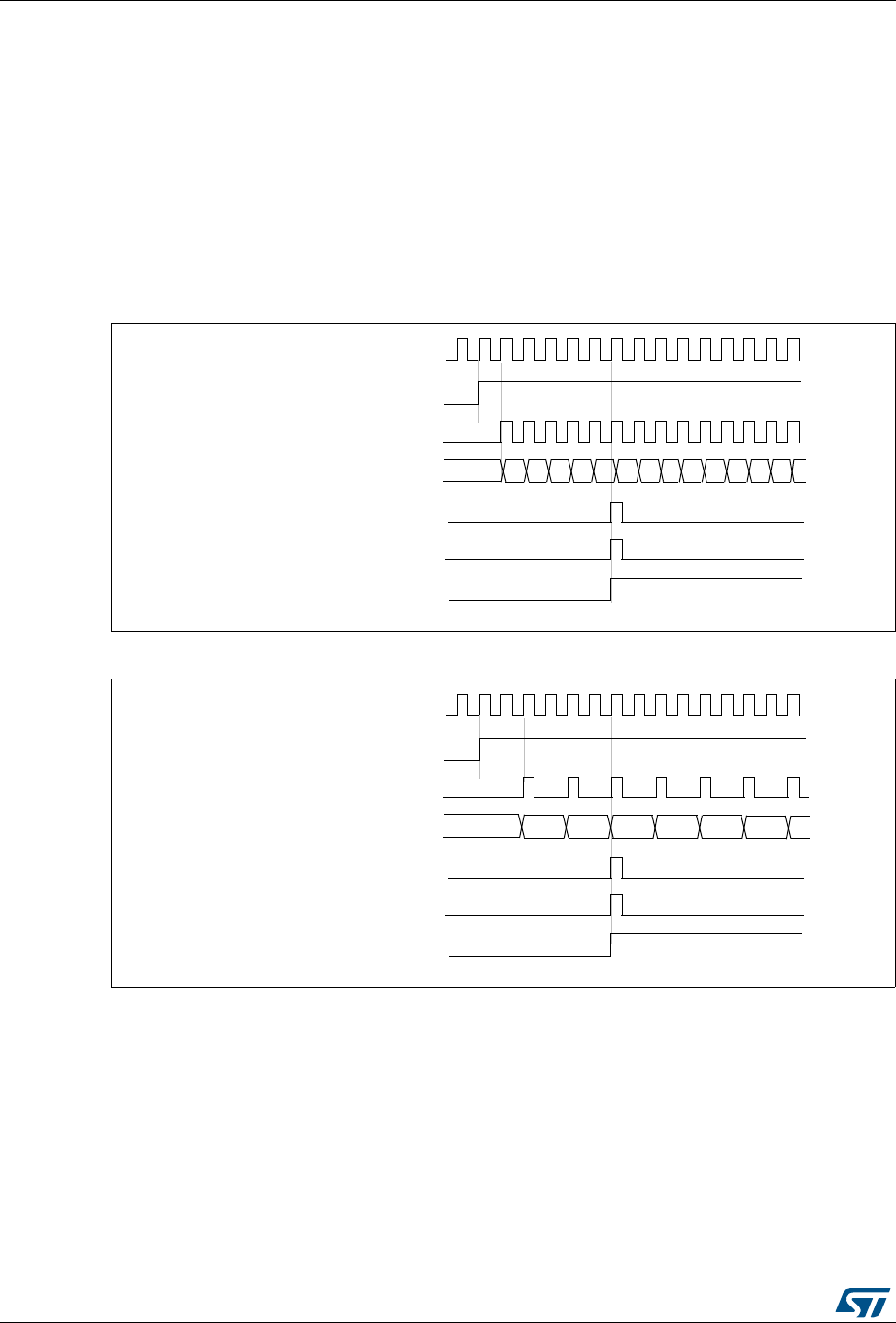
Basic timers (TIM6&TIM7) RM0090
684/1718 DocID018909 Rev 9
register is set, setting the UG bit generates an update event UEV, but the UIF flag is not set
(so no interrupt or DMA request is sent).
When an update event occurs, all the registers are updated and the update flag (UIF bit in
the TIMx_SR register) is set (depending on the URS bit):
•The buffer of the prescaler is reloaded with the preload value (contents of the
TIMx_PSC register)
•The auto-reload shadow register is updated with the preload value (TIMx_ARR)
The following figures show some examples of the counter behavior for different clock
frequencies when TIMx_ARR = 0x36.
Figure 206. Counter timing diagram, internal clock divided by 1
Figure 207. Counter timing diagram, internal clock divided by 2
CK_INT
00
CNT_EN
Timer clock = CK_CNT
Counter register
Update interrupt flag (UIF)
Counter overflow
Update event (UEV)
01 02 03 04 05 06 0732 33 34 35 3631
CK_INT
0035 0000 0001 0002 0003
CNT_EN
Timer clock = CK_CNT
Counter register
Update interrupt flag (UIF)
0034 0036
Counter overflow
Update event (UEV)
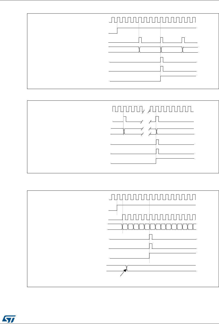
DocID018909 Rev 9 685/1718
RM0090 Basic timers (TIM6&TIM7)
691
Figure 208. Counter timing diagram, internal clock divided by 4
Figure 209. Counter timing diagram, internal clock divided by N
Figure 210. Counter timing diagram, update event when ARPE = 0 (TIMx_ARR not
preloaded)
0000 0001
CNT_EN
TImer clock = CK_CNT
Counter register
Update interrupt flag (UIF)
0035 0036
Counter overflow
Update event (UEV)
CK_INT
Timer clock = CK_CNT
Counter register 00
1F 20
Update interrupt flag (UIF)
Counter overflow
Update event (UEV)
CK_INT
00
CNT_EN
Timer clock = CK_CNT
Counter register
Update interrupt flag (UIF)
Counter overflow
Update event (UEV)
01 02 03 04 05 06 0732 33 34 35 3631
Auto-reload register FF 36
Write a new value in TIMx_ARR
CK_INT
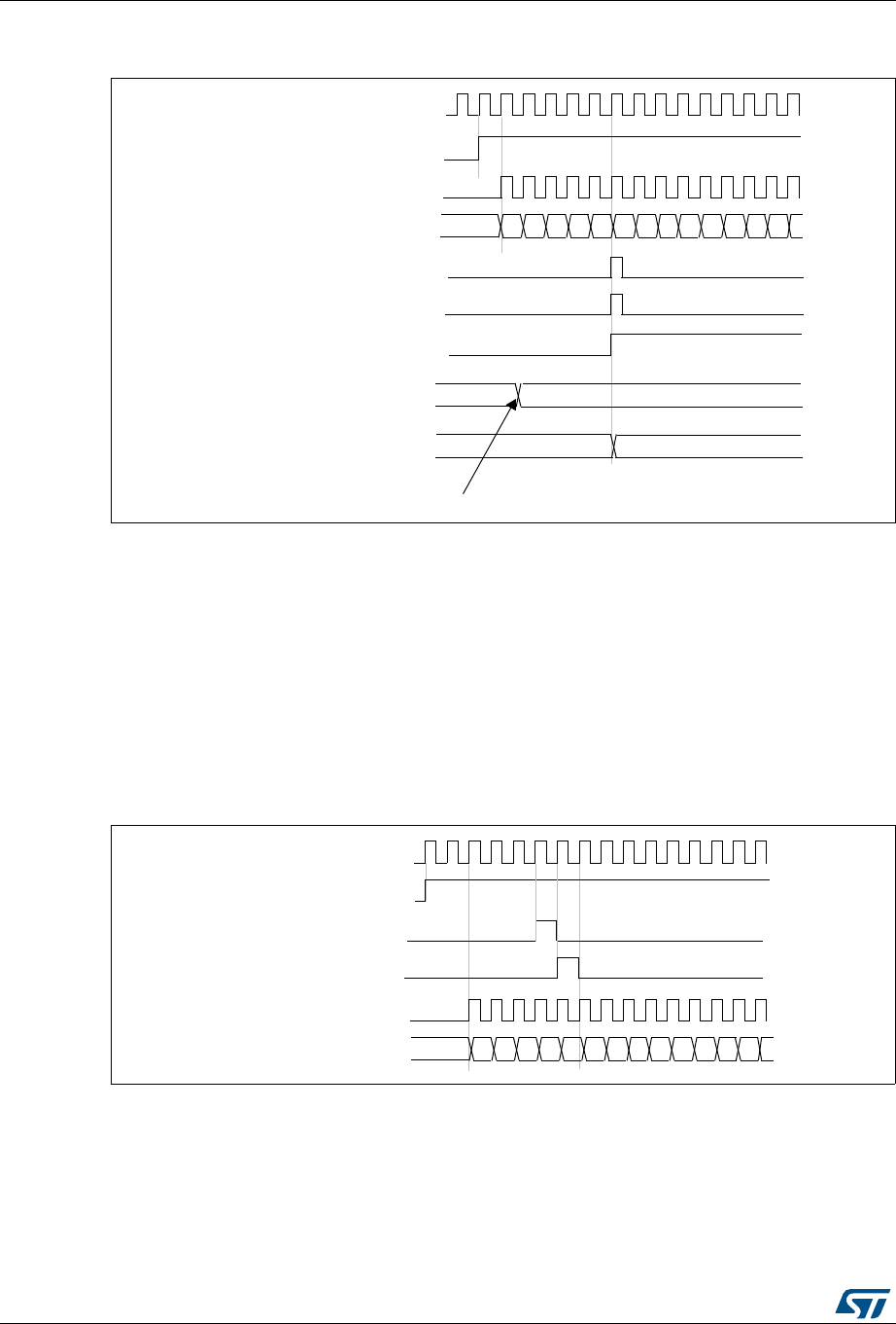
Basic timers (TIM6&TIM7) RM0090
686/1718 DocID018909 Rev 9
Figure 211. Counter timing diagram, update event when ARPE=1 (TIMx_ARR
preloaded)
20.3.3 Clock source
The counter clock is provided by the Internal clock (CK_INT) source.
The CEN (in the TIMx_CR1 register) and UG bits (in the TIMx_EGR register) are actual
control bits and can be changed only by software (except for UG that remains cleared
automatically). As soon as the CEN bit is written to 1, the prescaler is clocked by the internal
clock CK_INT.
Figure 212 shows the behavior of the control circuit and the upcounter in normal mode,
without prescaler.
Figure 212. Control circuit in normal mode, internal clock divided by 1
20.3.4 Debug mode
When the microcontroller enters the debug mode (Cortex®-M4 with FPU core - halted), the
TIMx counter either continues to work normally or stops, depending on the
DBG_TIMx_STOP configuration bit in the DBG module. For more details, refer to
Section 38.16.2: Debug support for timers, watchdog, bxCAN and I2C.
00
CNT_EN
Timer clock = CK_CNT
Counter register
Update interrupt flag (UIF)
Counter overflow
Update event (UEV)
01 02 03 04 05 06 07F1 F2 F3 F4 F5F0
Auto-reload preload register F5 36
Auto-reload shadow register F5 36
Write a new value in TIMx_ARR
CK_PSC
CK_INT
00
Counter clock = CK_CNT = CK_PSC
Counter register 01 02 03 04 05 06 0732 33 34 35 3631
CEN=CNT_EN
UG
CNT_INIT

DocID018909 Rev 9 687/1718
RM0090 Basic timers (TIM6&TIM7)
691
20.4 TIM6&TIM7 registers
Refer to Section 1.1 on page 57 for a list of abbreviations used in register descriptions.
The peripheral registers have to be written by half-words (16 bits) or words (32 bits). Read
accesses can be done by bytes (8 bits), half-words (16 bits) or words (32 bits).
20.4.1 TIM6&TIM7 control register 1 (TIMx_CR1)
Address offset: 0x00
Reset value: 0x0000
15 14 13 12 11 10 9 8 7 6 5 4 3 2 1 0
Reserved ARPE Reserved OPM URS UDIS CEN
rw rw rw rw rw
Bits 15:8 Reserved, must be kept at reset value.
Bit 7 ARPE: Auto-reload preload enable
0: TIMx_ARR register is not buffered.
1: TIMx_ARR register is buffered.
Bits 6:4 Reserved, must be kept at reset value.
Bit 3 OPM: One-pulse mode
0: Counter is not stopped at update event
1: Counter stops counting at the next update event (clearing the CEN bit).
Bit 2 URS: Update request source
This bit is set and cleared by software to select the UEV event sources.
0: Any of the following events generates an update interrupt or DMA request if enabled.
These events can be:
– Counter overflow/underflow
– Setting the UG bit
– Update generation through the slave mode controller
1: Only counter overflow/underflow generates an update interrupt or DMA request if enabled.
Bit 1 UDIS: Update disable
This bit is set and cleared by software to enable/disable UEV event generation.
0: UEV enabled. The Update (UEV) event is generated by one of the following events:
– Counter overflow/underflow
– Setting the UG bit
– Update generation through the slave mode controller
Buffered registers are then loaded with their preload values.
1: UEV disabled. The Update event is not generated, shadow registers keep their value
(ARR, PSC). However the counter and the prescaler are reinitialized if the UG bit is set or if
a hardware reset is received from the slave mode controller.
Bit 0 CEN: Counter enable
0: Counter disabled
1: Counter enabled
Note: Gated mode can work only if the CEN bit has been previously set by software. However
trigger mode can set the CEN bit automatically by hardware.
CEN is cleared automatically in one-pulse mode, when an update event occurs.

Basic timers (TIM6&TIM7) RM0090
688/1718 DocID018909 Rev 9
20.4.2 TIM6&TIM7 control register 2 (TIMx_CR2)
Address offset: 0x04
Reset value: 0x0000
20.4.3 TIM6&TIM7 DMA/Interrupt enable register (TIMx_DIER)
Address offset: 0x0C
Reset value: 0x0000
1514131211109876543210
Reserved
MMS[2:0]
Reserved
rw rw rw
Bits 15:7 Reserved, must be kept at reset value.
Bits 6:4 MMS[2:0]: Master mode selection
These bits are used to select the information to be sent in master mode to slave timers for
synchronization (TRGO). The combination is as follows:
000: Reset - the UG bit from the TIMx_EGR register is used as a trigger output (TRGO). If
reset is generated by the trigger input (slave mode controller configured in reset mode) then
the signal on TRGO is delayed compared to the actual reset.
001: Enable - the Counter enable signal, CNT_EN, is used as a trigger output (TRGO). It is
useful to start several timers at the same time or to control a window in which a slave timer
is enabled. The Counter Enable signal is generated by a logic OR between CEN control bit
and the trigger input when configured in gated mode.
When the Counter Enable signal is controlled by the trigger input, there is a delay on TRGO,
except if the master/slave mode is selected (see the MSM bit description in the TIMx_SMCR
register).
010: Update - The update event is selected as a trigger output (TRGO). For instance a
master timer can then be used as a prescaler for a slave timer.
Bits 3:0 Reserved, must be kept at reset value.
1514131211109876543210
Reserved UDE Reserved UIE
rw rw
Bits 15:9 Reserved, must be kept at reset value.
Bit 8 UDE: Update DMA request enable
0: Update DMA request disabled.
1: Update DMA request enabled.
Bits 7:1 Reserved, must be kept at reset value.
Bit 0 UIE: Update interrupt enable
0: Update interrupt disabled.
1: Update interrupt enabled.
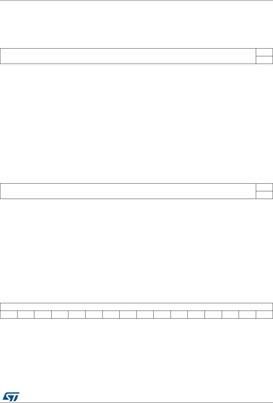
DocID018909 Rev 9 689/1718
RM0090 Basic timers (TIM6&TIM7)
691
20.4.4 TIM6&TIM7 status register (TIMx_SR)
Address offset: 0x10
Reset value: 0x0000
20.4.5 TIM6&TIM7 event generation register (TIMx_EGR)
Address offset: 0x14
Reset value: 0x0000
20.4.6 TIM6&TIM7 counter (TIMx_CNT)
Address offset: 0x24
Reset value: 0x0000
1514131211109876543210
Reserved
UIF
rc_w0
Bits 15:1 Reserved, must be kept at reset value.
Bit 0 UIF: Update interrupt flag
This bit is set by hardware on an update event. It is cleared by software.
0: No update occurred.
1: Update interrupt pending. This bit is set by hardware when the registers are updated:
– At overflow or underflow and if UDIS = 0 in the TIMx_CR1 register.
– When CNT is reinitialized by software using the UG bit in the TIMx_EGR register, if URS = 0
and UDIS = 0 in the TIMx_CR1 register.
1514131211109876543210
Reserved
UG
w
Bits 15:1 Reserved, must be kept at reset value.
Bit 0 UG: Update generation
This bit can be set by software, it is automatically cleared by hardware.
0: No action.
1: Re-initializes the timer counter and generates an update of the registers. Note that the
prescaler counter is cleared too (but the prescaler ratio is not affected).
1514131211109876543210
CNT[15:0]
rw rw rw rw rw rw rw rw rw rw rw rw rw rw rw rw
Bits 15:0 CNT[15:0]: Counter value

Basic timers (TIM6&TIM7) RM0090
690/1718 DocID018909 Rev 9
20.4.7 TIM6&TIM7 prescaler (TIMx_PSC)
Address offset: 0x28
Reset value: 0x0000
20.4.8 TIM6&TIM7 auto-reload register (TIMx_ARR)
Address offset: 0x2C
Reset value: 0x0000
1514131211109876543210
PSC[15:0]
rw rw rw rw rw rw rw rw rw rw rw rw rw rw rw rw
Bits 15:0 PSC[15:0]: Prescaler value
The counter clock frequency CK_CNT is equal to fCK_PSC / (PSC[15:0] + 1).
PSC contains the value to be loaded into the active prescaler register at each update event.
1514131211109876543210
ARR[15:0]
rw rw rw rw rw rw rw rw rw rw rw rw rw rw rw rw
Bits 15:0 ARR[15:0]: Auto-reload value
ARR is the value to be loaded into the actual auto-reload register.
Refer to Section 20.3.1: Time-base unit on page 682 for more details about ARR update and
behavior.
The counter is blocked while the auto-reload value is null.
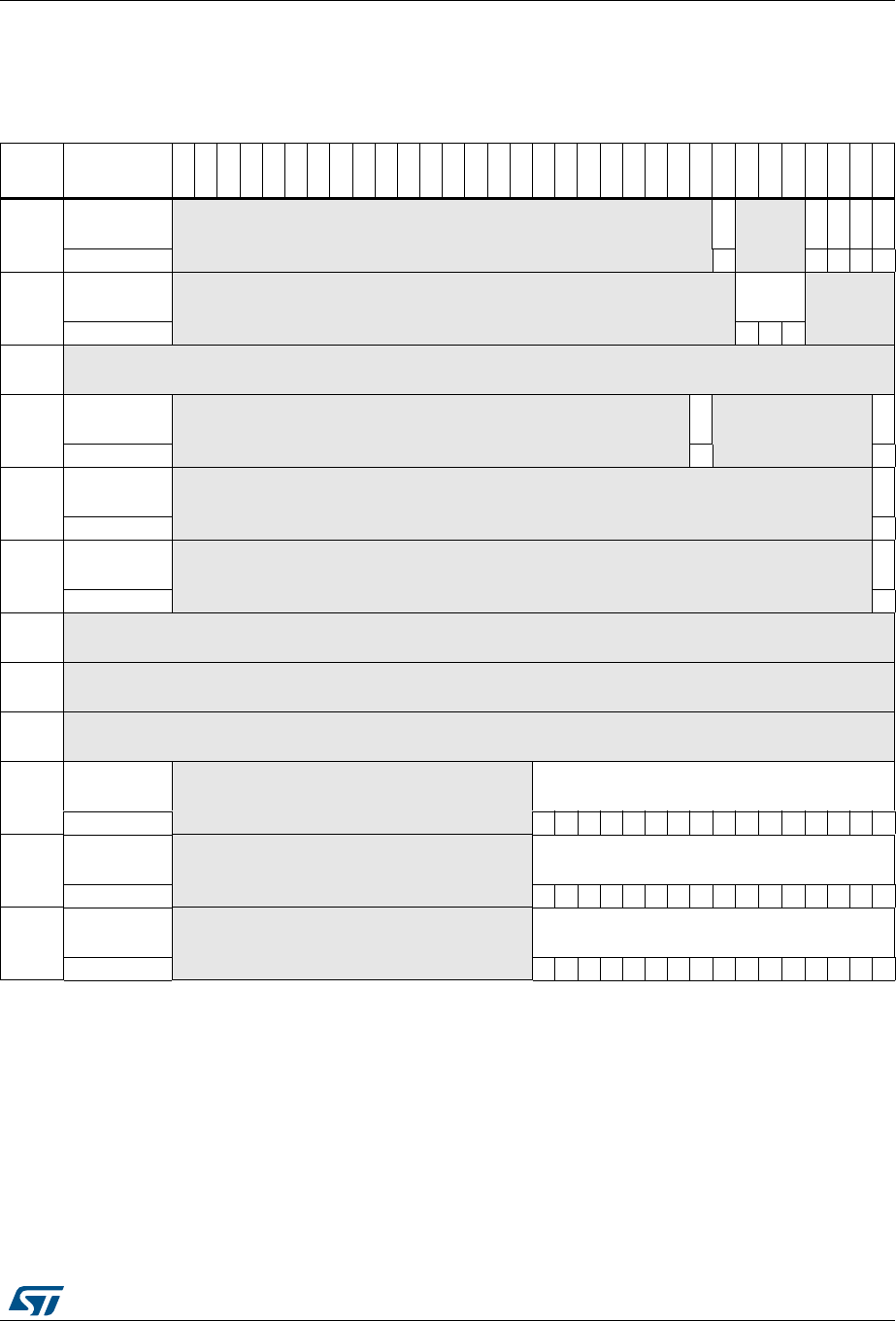
DocID018909 Rev 9 691/1718
RM0090 Basic timers (TIM6&TIM7)
691
20.4.9 TIM6&TIM7 register map
TIMx registers are mapped as 16-bit addressable registers as described in the table below:
Refer to Table 1 on page 64 for the register boundary addresses.
Table 105. TIM6&TIM7 register map and reset values
Offset Register
31
30
29
28
27
26
25
24
23
22
21
20
19
18
17
16
15
14
13
12
11
10
9
8
7
6
5
4
3
2
1
0
0x00 TIMx_CR1 Reserved
ARPE
Reserved
OPM
URS
UDIS
CEN
Reset value 00000
0x04 TIMx_CR2 Reserved MMS[2:0]
Reserved
Reset value 000
0x08 Reserved
0x0C TIMx_DIER Reserved
UDE
Reserved
UIE
Reset value 00
0x10 TIMx_SR Reserved
UIF
Reset value 0
0x14 TIMx_EGR Reserved
UG
Reset value 0
0x18 Reserved
0x1C Reserved
0x20 Reserved
0x24 TIMx_CNT Reserved CNT[15:0]
Reset value 0000000000000000
0x28 TIMx_PSC Reserved PSC[15:0]
Reset value 0000000000000000
0x2C TIMx_ARR Reserved ARR[15:0]
Reset value 0000000000000000

Independent watchdog (IWDG) RM0090
692/1718 DocID018909 Rev 9
21 Independent watchdog (IWDG)
This section applies to the whole STM32F4xx family, unless otherwise specified.
21.1 IWDG introduction
The devices have two embedded watchdog peripherals which offer a combination of high
safety level, timing accuracy and flexibility of use. Both watchdog peripherals (Independent
and Window) serve to detect and resolve malfunctions due to software failure, and to trigger
system reset or an interrupt (window watchdog only) when the counter reaches a given
timeout value.
The independent watchdog (IWDG) is clocked by its own dedicated low-speed clock (LSI)
and thus stays active even if the main clock fails. The window watchdog (WWDG) clock is
prescaled from the APB1 clock and has a configurable time-window that can be
programmed to detect abnormally late or early application behavior.
The IWDG is best suited to applications which require the watchdog to run as a totally
independent process outside the main application, but have lower timing accuracy
constraints. The WWDG is best suited to applications which require the watchdog to react
within an accurate timing window. For further information on the window watchdog, refer to
Section 22 on page 698.
21.2 IWDG main features
•Free-running downcounter
•clocked from an independent RC oscillator (can operate in Standby and Stop modes)
•Reset (if watchdog activated) when the downcounter value of 0x000 is reached
21.3 IWDG functional description
Figure 213 shows the functional blocks of the independent watchdog module.
When the independent watchdog is started by writing the value 0xCCCC in the Key register
(IWDG_KR), the counter starts counting down from the reset value of 0xFFF. When it
reaches the end of count value (0x000) a reset signal is generated (IWDG reset).
Whenever the key value 0xAAAA is written in the IWDG_KR register, the IWDG_RLR value
is reloaded in the counter and the watchdog reset is prevented.
21.3.1 Hardware watchdog
If the “Hardware watchdog” feature is enabled through the device option bits, the watchdog
is automatically enabled at power-on, and will generate a reset unless the Key register is
written by the software before the counter reaches end of count.
21.3.2 Register access protection
Write access to the IWDG_PR and IWDG_RLR registers is protected. To modify them, you
must first write the code 0x5555 in the IWDG_KR register. A write access to this register
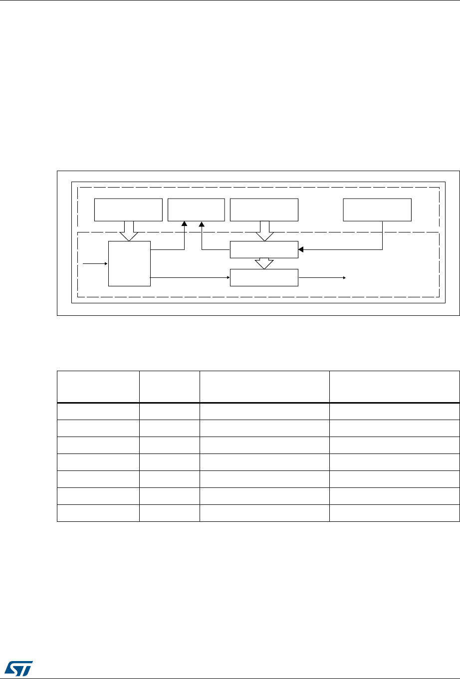
DocID018909 Rev 9 693/1718
RM0090 Independent watchdog (IWDG)
697
with a different value will break the sequence and register access will be protected again.
This implies that it is the case of the reload operation (writing 0xAAAA).
A status register is available to indicate that an update of the prescaler or the down-counter
reload value is on going.
21.3.3 Debug mode
When the microcontroller enters debug mode (Cortex®-M4 with FPU core halted), the IWDG
counter either continues to work normally or stops, depending on DBG_IWDG_STOP
configuration bit in DBG module. For more details, refer to Section 38.16.2: Debug support
for timers, watchdog, bxCAN and I2C.
Figure 213. Independent watchdog block diagram
Note: The watchdog function is implemented in the VDD voltage domain that is still functional in
Stop and Standby modes.
)7$'RESET
PRESCALER
)7$'?02
0RESCALERREGISTER
)7$'?2,2
2ELOADREGISTER
BIT
,3)
K(Z
)7$'?+2
+EYREGISTER
#/2%
6$$VOLTAGEDOMAIN
)7$'?32
3TATUSREGISTER
-36
BITRELOADVALUE
BITDOWNCOUNTER
Table 106. Min/max IWDG timeout period at 32 kHz (LSI)(1)
1. These timings are given for a 32 kHz clock but the microcontroller internal RC frequency can vary. Please
refers to LSI oscillator characteristics table in device datasheet for from max and min values.
Prescaler divider PR[2:0] bits Min timeout (ms) RL[11:0]=
0x000
Max timeout (ms) RL[11:0]=
0xFFF
/4 0 0.125 512
/8 1 0.25 1024
/16 2 0.5 2048
/32 3 1 4096
/64 4 2 8192
/128 5 4 16384
/256 6 8 32768

Independent watchdog (IWDG) RM0090
694/1718 DocID018909 Rev 9
21.4 IWDG registers
Refer to Section 1.1 on page 57 for a list of abbreviations used in register descriptions.
The peripheral registers have to be accessed by half-words (16 bits) or words (32 bits).
21.4.1 Key register (IWDG_KR)
Address offset: 0x00
Reset value: 0x0000 0000 (reset by Standby mode)
313029282726252423222120191817161514131211109876543210
Reserved KEY[15:0]
wwwwwww w w wwwwwww
Bits 31:16 Reserved, must be kept at reset value.
Bits 15:0 KEY[15:0]: Key value (write only, read 0000h)
These bits must be written by software at regular intervals with the key value AAAAh,
otherwise the watchdog generates a reset when the counter reaches 0.
Writing the key value 5555h to enable access to the IWDG_PR and IWDG_RLR registers
(see Section 21.3.2)
Writing the key value CCCCh starts the watchdog (except if the hardware watchdog option is
selected)

DocID018909 Rev 9 695/1718
RM0090 Independent watchdog (IWDG)
697
21.4.2 Prescaler register (IWDG_PR)
Address offset: 0x04
Reset value: 0x0000 0000
21.4.3 Reload register (IWDG_RLR)
Address offset: 0x08
Reset value: 0x0000 0FFF (reset by Standby mode)
313029282726252423222120191817161514131211109876543210
Reserved PR[2:0]
rw rw rw
Bits 31:3 Reserved, must be kept at reset value.
Bits 2:0 PR[2:0]: Prescaler divider
These bits are write access protected seeSection 21.3.2. They are written by software to
select the prescaler divider feeding the counter clock. PVU bit of IWDG_SR must be reset in
order to be able to change the prescaler divider.
000: divider /4
001: divider /8
010: divider /16
011: divider /32
100: divider /64
101: divider /128
110: divider /256
111: divider /256
Note: Reading this register returns the prescaler value from the VDD voltage domain. This
value may not be up to date/valid if a write operation to this register is ongoing. For this
reason the value read from this register is valid only when the PVU bit in the IWDG_SR
register is reset.
313029282726252423222120191817161514131211109876543210
Reserved
RL[11:0]
rw rw rw rw rw rw rw rw rw rw rw rw
Bits 31:12 Reserved, must be kept at reset value.
Bits11:0 RL[11:0]: Watchdog counter reload value
These bits are write access protected see Section 21.3.2. They are written by software to
define the value to be loaded in the watchdog counter each time the value AAAAh is written
in the IWDG_KR register. The watchdog counter counts down from this value. The timeout
period is a function of this value and the clock prescaler. Refer to Table 106.
The RVU bit in the IWDG_SR register must be reset in order to be able to change the reload
value.
Note: Reading this register returns the reload value from the VDD voltage domain. This value
may not be up to date/valid if a write operation to this register is ongoing on this
register. For this reason the value read from this register is valid only when the RVU bit
in the IWDG_SR register is reset.

Independent watchdog (IWDG) RM0090
696/1718 DocID018909 Rev 9
21.4.4 Status register (IWDG_SR)
Address offset: 0x0C
Reset value: 0x0000 0000 (not reset by Standby mode)
Note: If several reload values or prescaler values are used by application, it is mandatory to wait
until RVU bit is reset before changing the reload value and to wait until PVU bit is reset
before changing the prescaler value. However, after updating the prescaler and/or the
reload value it is not necessary to wait until RVU or PVU is reset before continuing code
execution (even in case of low-power mode entry, the write operation is taken into account
and will complete)
3130292827262524232221201918171615141312111098765432 1 0
Reserved RVU PVU
rr
Bits 31:2 Reserved, must be kept at reset value.
Bit 1 RVU: Watchdog counter reload value update
This bit is set by hardware to indicate that an update of the reload value is ongoing. It is reset
by hardware when the reload value update operation is completed in the VDD voltage domain
(takes up to 5 RC 40 kHz cycles).
Reload value can be updated only when RVU bit is reset.
Bit 0 PVU: Watchdog prescaler value update
This bit is set by hardware to indicate that an update of the prescaler value is ongoing. It is
reset by hardware when the prescaler update operation is completed in the VDD voltage
domain (takes up to 5 RC 40 kHz cycles).
Prescaler value can be updated only when PVU bit is reset.

DocID018909 Rev 9 697/1718
RM0090 Independent watchdog (IWDG)
697
21.4.5 IWDG register map
The following table gives the IWDG register map and reset values.
Refer to Table 1 on page 64 for the register boundary addresses.
Table 107. IWDG register map and reset values
Offset Register
31
30
29
28
27
26
25
24
23
22
21
20
19
18
17
16
15
14
13
12
11
10
9
8
7
6
5
4
3
2
1
0
0x00 IWDG_KR Reserved KEY[15:0]
Reset value 0000000000000000
0x04 IWDG_PR Reserved PR[2:0]
Reset value 000
0x08 IWDG_RLR Reserved RL[11:0]
Reset value 111111111111
0x0C IWDG_SR Reserved
RVU
PVU
Reset value 00

Window watchdog (WWDG) RM0090
698/1718 DocID018909 Rev 9
22 Window watchdog (WWDG)
This section applies to the whole STM32F4xx family, unless otherwise specified.
22.1 WWDG introduction
The window watchdog is used to detect the occurrence of a software fault, usually
generated by external interference or by unforeseen logical conditions, which causes the
application program to abandon its normal sequence. The watchdog circuit generates an
MCU reset on expiry of a programmed time period, unless the program refreshes the
contents of the downcounter before the T6 bit becomes cleared. An MCU reset is also
generated if the 7-bit downcounter value (in the control register) is refreshed before the
downcounter has reached the window register value. This implies that the counter must be
refreshed in a limited window.
22.2 WWDG main features
•Programmable free-running downcounter
•Conditional reset
– Reset (if watchdog activated) when the downcounter value becomes less than
0x40
– Reset (if watchdog activated) if the downcounter is reloaded outside the window
(see Figure 215)
•Early wakeup interrupt (EWI): triggered (if enabled and the watchdog activated) when
the downcounter is equal to 0x40.
22.3 WWDG functional description
If the watchdog is activated (the WDGA bit is set in the WWDG_CR register) and when the
7-bit downcounter (T[6:0] bits) rolls over from 0x40 to 0x3F (T6 becomes cleared), it initiates
a reset. If the software reloads the counter while the counter is greater than the value stored
in the window register, then a reset is generated.
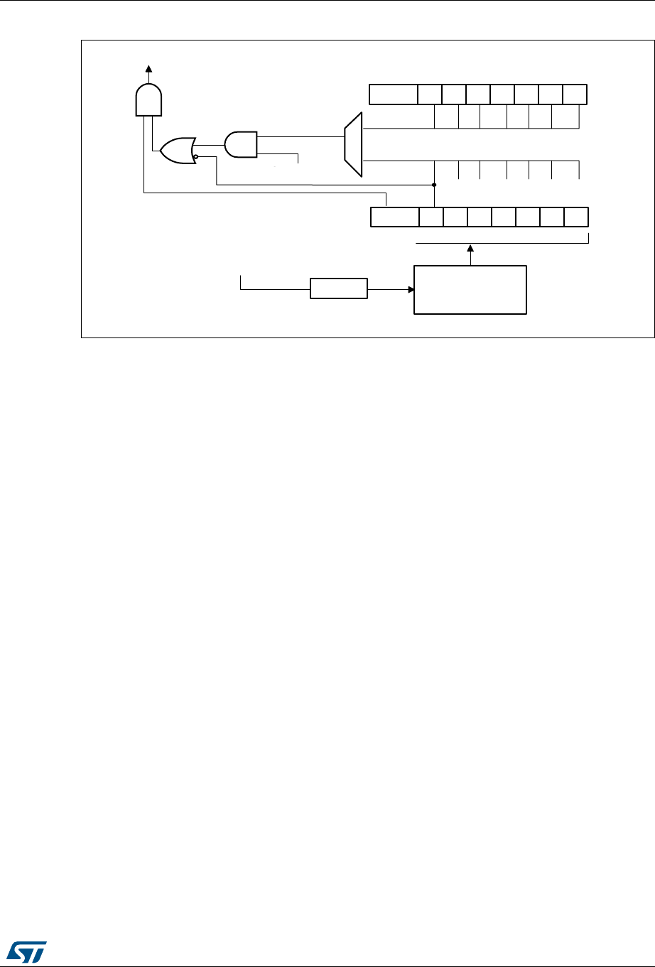
DocID018909 Rev 9 699/1718
RM0090 Window watchdog (WWDG)
704
Figure 214. Watchdog block diagram
The application program must write in the WWDG_CR register at regular intervals during
normal operation to prevent an MCU reset. This operation must occur only when the counter
value is lower than the window register value. The value to be stored in the WWDG_CR
register must be between 0xFF and 0xC0.
Enabling the watchdog
The watchdog is always disabled after a reset. It is enabled by setting the WDGA bit in the
WWDG_CR register, then it cannot be disabled again except by a reset.
Controlling the downcounter
This downcounter is free-running, counting down even if the watchdog is disabled. When
the watchdog is enabled, the T6 bit must be set to prevent generating an immediate reset.
The T[5:0] bits contain the number of increments which represents the time delay before the
watchdog produces a reset. The timing varies between a minimum and a maximum value
due to the unknown status of the prescaler when writing to the WWDG_CR register (see
Figure 215). The Configuration register (WWDG_CFR) contains the high limit of the window:
To prevent a reset, the downcounter must be reloaded when its value is lower than the
window register value and greater than 0x3F. Figure 215 describes the window watchdog
process.
Note: The T6 bit can be used to generate a software reset (the WDGA bit is set and the T6 bit is
cleared).
Advanced watchdog interrupt feature
The Early Wakeup Interrupt (EWI) can be used if specific safety operations or data logging
must be performed before the actual reset is generated. The EWI interrupt is enabled by
setting the EWI bit in the WWDG_CFR register. When the downcounter reaches the value
0x40, an EWI interrupt is generated and the corresponding interrupt service routine (ISR)
can be used to trigger specific actions (such as communications or data logging), before
resetting the device.
06Y9
5(6(7
ELWGRZQFRXQWHU&17
:DWFKGRJFRQILJXUDWLRQUHJLVWHU::'*B&)5
FRPSDUDWRU
7!:
ZKHQ
:ULWH::'*B&5
3&/.
IURP5&&FORFNFRQWUROOHU
:'*SUHVFDOHU
:'*7%
: ::::: :
:'*$ 7
:DWFKGRJFRQWUROUHJLVWHU::'*B&5
77777 7
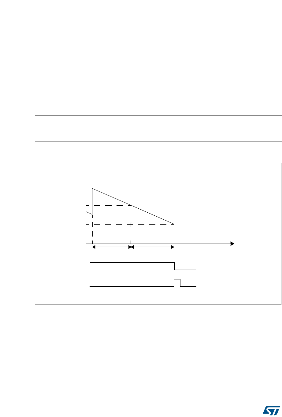
Window watchdog (WWDG) RM0090
700/1718 DocID018909 Rev 9
In some applications, the EWI interrupt can be used to manage a software system check
and/or system recovery/graceful degradation, without generating a WWDG reset. In this
case, the corresponding interrupt service routine (ISR) should reload the WWDG counter to
avoid the WWDG reset, then trigger the required actions.
The EWI interrupt is cleared by writing '0' to the EWIF bit in the WWDG_SR register.
Note: When the EWI interrupt cannot be served, e.g. due to a system lock in a higher priority task,
the WWDG reset will eventually be generated.
22.4 How to program the watchdog timeout
You can use the formula in Figure 215 to calculate the WWDG timeout.
Warning: When writing to the WWDG_CR register, always write 1 in the
T6 bit to avoid generating an immediate reset.
Figure 215. Window watchdog timing diagram
The formula to calculate the timeout value is given by:
where:
tWWDG: WWDG timeout
tPCLK1: APB1 clock period measured in ms
4096: value corresponding to internal divider
AIC
7;=
4;=#.4DOWNCOUNTER
2EFRESHNOTALLOWED
X&
2EFRESHALLOWED 4IME
4BIT
2%3%4
tWWDG tPCLK1 4096×2WDGTB[1:0]
×T[1:0] 1+()×=ms()

DocID018909 Rev 9 701/1718
RM0090 Window watchdog (WWDG)
704
As an example, lets assume APB1 frequency is equal to 24 MHz, WDGTB[1:0] is set to 3
and T[5:0] is set to 63:
Refer to the table below for the minimum and maximum values of the tWWDG
.
22.5 Debug mode
When the microcontroller enters debug mode (Cortex®-M4 with FPU core halted), the
WWDG counter either continues to work normally or stops, depending on
DBG_WWDG_STOP configuration bit in DBG module. For more details, refer to
Section 38.16.2: Debug support for timers, watchdog, bxCAN and I2C.
Table 108. Timeout values at 30 MHz (fPCLK1)
Prescaler WDGTB Min timeout (µs)
T[5:0] = 0x00
Max timeout (ms)
T[5:0] = 0x3F
1 0 136.53 8.74
2 1 273.07 17.48
4 2 546.13 34.95
8 3 1092.27 69.91
tWWDG 1 24000⁄4096×23
×63 1+()×21,85ms==

Window watchdog (WWDG) RM0090
702/1718 DocID018909 Rev 9
22.6 WWDG registers
Refer to Section 1.1 on page 57 for a list of abbreviations used in register descriptions.
The peripheral registers have to be accessed by half-words (16 bits) or words (32 bits).
22.6.1 Control register (WWDG_CR)
Address offset: 0x00
Reset value: 0x0000 007F
31 30 29 28 27 26 25 24 23 22 21 20 19 18 17 16
Reserved
1514131211109876543210
Reserved WDGA T[6:0]
rs rw
Bits 31:8 Reserved, must be kept at reset value.
Bit 7 WDGA: Activation bit
This bit is set by software and only cleared by hardware after a reset. When WDGA = 1, the
watchdog can generate a reset.
0: Watchdog disabled
1: Watchdog enabled
Bits 6:0 T[6:0]: 7-bit counter (MSB to LSB)
These bits contain the value of the watchdog counter. It is decremented every (4096 x
2WDGTB[1:0]) PCLK1 cycles. A reset is produced when it rolls over from 0x40 to 0x3F (T6
becomes cleared).

DocID018909 Rev 9 703/1718
RM0090 Window watchdog (WWDG)
704
22.6.2 Configuration register (WWDG_CFR)
Address offset: 0x04
Reset value: 0x0000 007F
22.6.3 Status register (WWDG_SR)
Address offset: 0x08
Reset value: 0x0000 0000
31 30 29 28 27 26 25 24 23 22 21 20 19 18 17 16
Reserved
1514131211109876543210
Reserved
EWI WDGTB[1:0] W[6:0]
rs rw rw
Bit 31:10 Reserved, must be kept at reset value.
Bit 9 EWI: Early wakeup interrupt
When set, an interrupt occurs whenever the counter reaches the value 0x40. This interrupt is
only cleared by hardware after a reset.
Bits 8:7 WDGTB[1:0]: Timer base
The time base of the prescaler can be modified as follows:
00: CK Counter Clock (PCLK1 div 4096) div 1
01: CK Counter Clock (PCLK1 div 4096) div 2
10: CK Counter Clock (PCLK1 div 4096) div 4
11: CK Counter Clock (PCLK1 div 4096) div 8
Bits 6:0 W[6:0]: 7-bit window value
These bits contain the window value to be compared to the downcounter.
31 30 29 28 27 26 25 24 23 22 21 20 19 18 17 16
Reserved
1514131211109876543210
Reserved EWIF
rc_w0
Bits 31:1 Reserved, must be kept at reset value.
Bit 0 EWIF: Early wakeup interrupt flag
This bit is set by hardware when the counter has reached the value 0x40. It must be cleared
by software by writing ‘0’. A write of ‘1’ has no effect. This bit is also set if the interrupt is not
enabled.
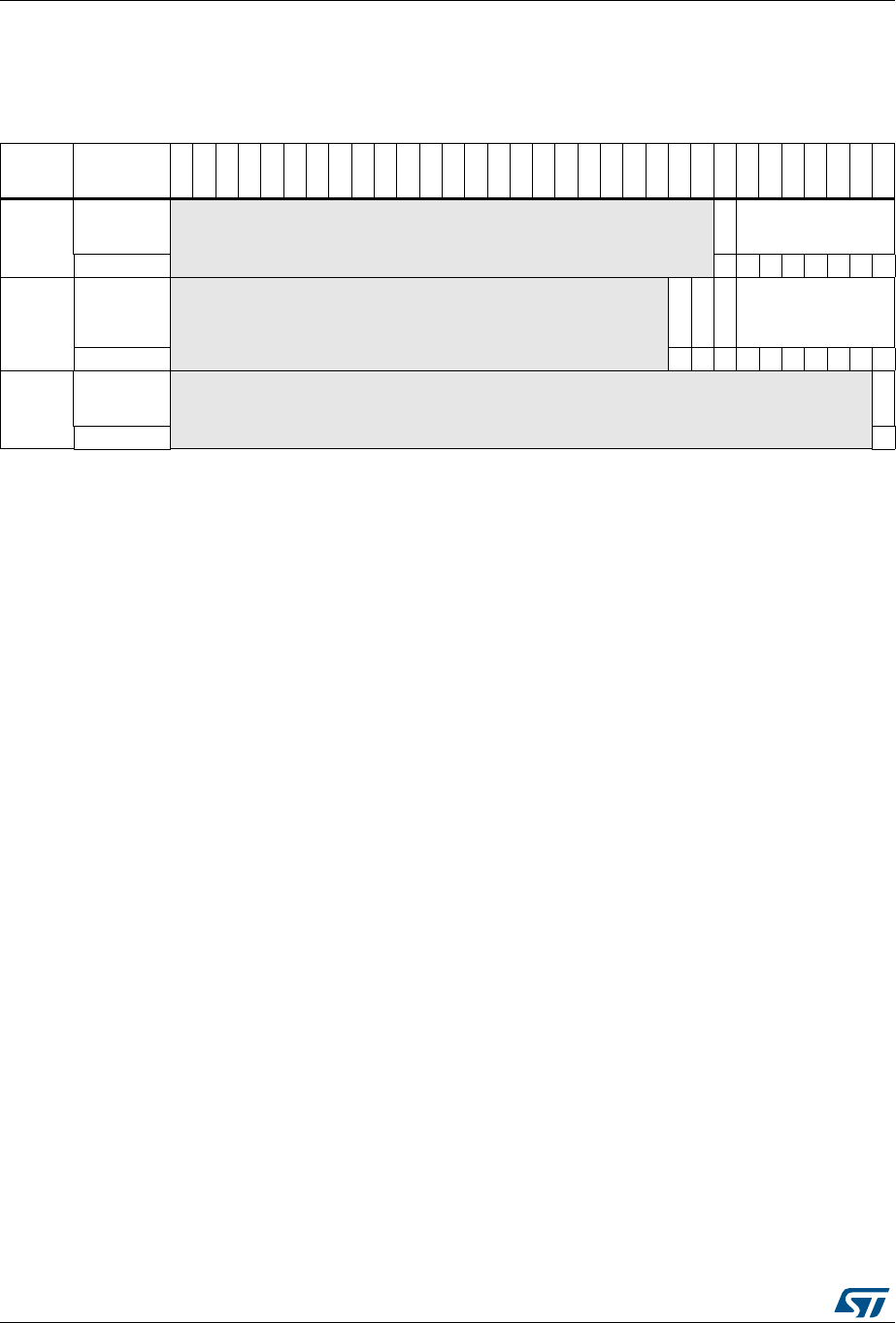
Window watchdog (WWDG) RM0090
704/1718 DocID018909 Rev 9
22.6.4 WWDG register map
The following table gives the WWDG register map and reset values.
Refer to Table 1 on page 64 for the register boundary addresses.
Table 109. WWDG register map and reset values
Offset Register
31
30
29
28
27
26
25
24
23
22
21
20
19
18
17
16
15
14
13
12
11
10
9
8
7
6
5
4
3
2
1
0
0x00 WWDG_CR Reserved
WDGA
T[6:0]
Reset value 01111111
0x04 WWDG_CFR Reserved
EWI
WDGTB1
WDGTB0
W[6:0]
Reset value 0001111111
0x08 WWDG_SR Reserved
EWIF
Reset value 0

DocID018909 Rev 9 705/1718
RM0090 Cryptographic processor (CRYP)
751
23 Cryptographic processor (CRYP)
This section applies to STM32F415/417xx and STM32F43xxx devices.
23.1 CRYP introduction
The cryptographic processor can be used to both encipher and decipher data using the
DES, Triple-DES or AES (128, 192, or 256) algorithms. It is a fully compliant implementation
of the following standards:
•The data encryption standard (DES) and Triple-DES (TDES) as defined by Federal
Information Processing Standards Publication (FIPS PUB 46-3, 1999 October 25). It
follows the American National Standards Institute (ANSI) X9.52 standard.
•The advanced encryption standard (AES) as defined by Federal Information
Processing Standards Publication (FIPS PUB 197, 2001 November 26)
The CRYP processor performs data encryption and decryption using DES and TDES
algorithms in Electronic codebook (ECB) or Cipher block chaining (CBC) mode.
The CRYP peripheral is a 32-bit AHB2 peripheral. It supports DMA transfer for incoming and
processed data, and has input and output FIFOs (each 8 words deep).
23.2 CRYP main features
•Suitable for AES, DES and TDES enciphering and deciphering operations
•AES
– Supports the ECB, CBC, CTR, CCM and GCM chaining algorithms (CCM and
GCM are available on STM32F42xxx and STM32F43xxx only)
– Supports 128-, 192- and 256-bit keys
– 4 × 32-bit initialization vectors (IV) used in the CBC, CTR, CCM and GCM modes
Table 110. Number of cycles required to process each 128-bit block
(STM32F415/417xx)
Algorithm / Key size ECB CBC CTR
128b 14 14 14
192b 16 16 16
256b 18 18 18
Table 111. Number of cycles required to process each 128-bit block
(STM32F43xxx)
Algorithm /
Key size ECB CBC CTR
GCM CCM
Init Header Payload Tag Init Header Payload Tag
128b 1414142410 14 141214 25 14

Cryptographic processor (CRYP) RM0090
706/1718 DocID018909 Rev 9
•DES/TDES
– Direct implementation of simple DES algorithms (a single key, K1, is used)
– Supports the ECB and CBC chaining algorithms
– Supports 64-, 128- and 192-bit keys (including parity)
– 2 × 32-bit initialization vectors (IV) used in the CBC mode
– 16 HCLK cycles to process one 64-bit block in DES
– 48 HCLK cycles to process one 64-bit block in TDES
•Common to DES/TDES and AES
– IN and OUT FIFO (each with an 8-word depth, a 32-bit width, corresponding to 4
DES blocks or 2 AES blocks)
– Automatic data flow control with support of direct memory access (DMA) (using 2
channels, one for incoming data the other for processed data)
– Data swapping logic to support 1-, 8-, 16- or 32-bit data
192b 1616162810 16 161416 29 16
256b 1818183210 18 181618 33 18
Table 111. Number of cycles required to process each 128-bit block
(STM32F43xxx)
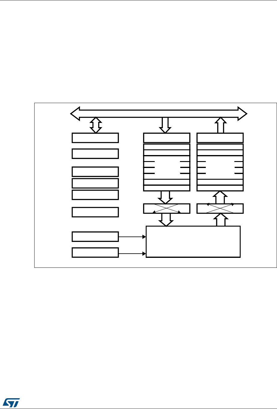
DocID018909 Rev 9 707/1718
RM0090 Cryptographic processor (CRYP)
751
23.3 CRYP functional description
The cryptographic processor implements a Triple-DES (TDES, that also supports DES) core
and an AES cryptographic core. Section 23.3.1 and Section 23.3.2 provide details on these
cores.
Since the TDES and the AES algorithms use block ciphers, incomplete input data blocks
have to be padded prior to encryption (extra bits should be appended to the trailing end of
the data string). After decryption, the padding has to be discarded. The hardware does not
manage the padding operation, the software has to handle it.
Figure 216 shows the block diagram of the cryptographic processor.
Figure 216. Block diagram (STM32F415/417xx)
ELW$+%EXV
3URFHVVRU FRUH
'(67'(6$(6
&5<3B',1
VZDSSL QJ VZDSSLQ J
îELW
,1),)2
îELW
287),)2
&5<3B&5
&5<3B. .
&5<3B,9,9
,9,9
NN
&5<3B,06&5
&5<3B5,6
&5<3B0,65
&5<3B'0$&5
&5<3B65
6WDWXV
'0$FRQWUROUHJLVWHU
,QWHUUXSWUHJLVWHUV
&RQWUROUHJLVWHU
,QLWLDOL]DWLRQYHFWRUV
.H\
DLE
&5<3B'287
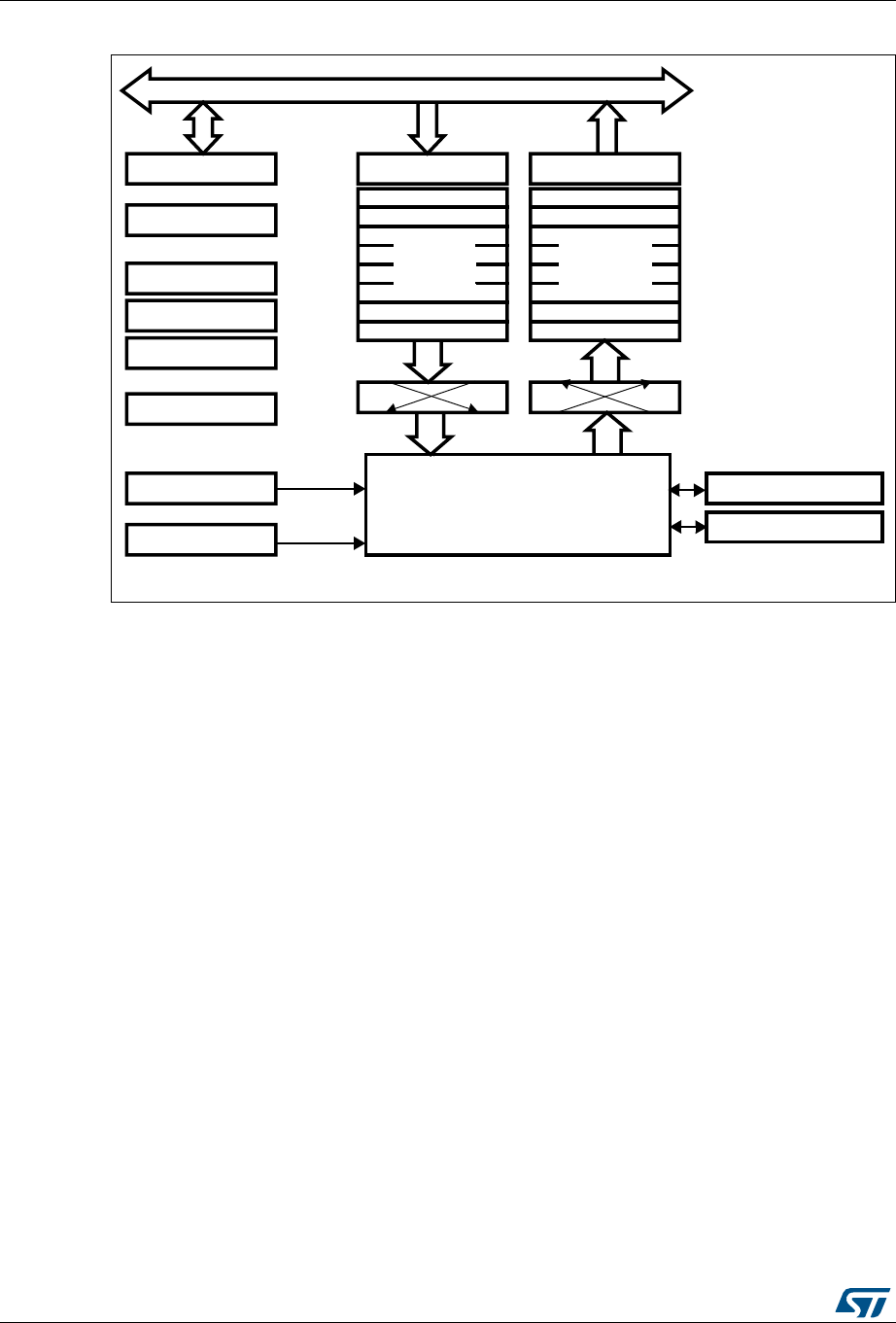
Cryptographic processor (CRYP) RM0090
708/1718 DocID018909 Rev 9
Figure 217. Block diagram (STM32F43xxx)
23.3.1 DES/TDES cryptographic core
The DES/Triple-DES cryptographic core consists of three components:
•The DES algorithm (DEA)
•Multiple keys (1 for the DES algorithm, 1 to 3 for the TDES algorithm)
•The initialization vector (used in the CBC mode)
The basic processing involved in the TDES is as follows: an input block is read in the DEA
and encrypted using the first key, K1 (K0 is not used in TDES mode). The output is then
decrypted using the second key, K2, and encrypted using the third key, K3. The key
depends on the algorithm which is used:
•DES mode: Key = [K1]
•TDES mode: Key = [K3 K2 K1]
where Kx=[KxR KxL], R = right, L = left
According to the mode implemented, the resultant output block is used to calculate the
ciphertext.
Note that the outputs of the intermediate DEA stages is never revealed outside the
cryptographic boundary.
ELW$+%EXV
3URFHVVRU FRUH
'(67'(6$(6
&5<3B',1 &5<3B'287
VZDSSL QJ VZDSSLQ J
îELW
,1),)2
îELW
287),)2
&5<3B&5
&5<3B. .
&5<3B,9,9
,9,9
NN
&5<3B,06&5
&5<3B5,6
&5<3B0,65
&5<3B'0$&5
&5<3B65
6WDWXV
'0$FRQWUROUHJLVWHU
,QWHUUXSWUHJLVWHUV
&RQWUROUHJLVWHU
,QLWLDOL]DWLRQYHFWRUV
.H\
069
&5<3B&6*&0&&0
&RQWH[WVZDSSLQJ
&5<3B&6*&0

DocID018909 Rev 9 709/1718
RM0090 Cryptographic processor (CRYP)
751
The TDES allows three different keying options:
•Three independent keys
The first option specifies that all the keys are independent, that is, K1, K2 and K3 are
independent. FIPS PUB 46-3 – 1999 (and ANSI X9.52 – 1998) refers to this option as
the Keying Option 1 and, to the TDES as 3-key TDES.
•Two independent keys
The second option specifies that K1 and K2 are independent and K3 is equal to K1,
that is, K1 and K2 are independent, K3 = K1. FIPS PUB 46-3 – 1999 (and ANSI X9.52
– 1998) refers to this second option as the Keying Option 2 and, to the TDES as 2-key
TDES.
•Three equal keys
The third option specifies that K1, K2 and K3 are equal, that is, K1 = K2 = K3. FIPS
PUB 46-3 – 1999 (and ANSI X9.52 – 1998) refers to the third option as the Keying
Option 3. This “1-key” TDES is equivalent to single DES.
FIPS PUB 46-3 – 1999 (and ANSI X9.52-1998) provides a thorough explanation of the
processing involved in the four operation modes supplied by the TDEA (TDES algorithm):
TDES-ECB encryption, TDES-ECB decryption, TDES-CBC encryption and TDES-CBC
decryption.
This reference manual only gives a brief explanation of each mode.
DES and TDES Electronic codebook (DES/TDES-ECB) mode
•DES/TDES-ECB mode encryption
Figure 218 illustrates the encryption in DES and TDES Electronic codebook
(DES/TDES-ECB) mode. A 64-bit plaintext data block (P) is used after bit/byte/half-
word swapping (refer to Section 23.3.3: Data type on page 724) as the input block (I).
The input block is processed through the DEA in the encrypt state using K1. The output
of this process is fed back directly to the input of the DEA where the DES is performed
in the decrypt state using K2. The output of this process is fed back directly to the input
of the DEA where the DES is performed in the encrypt state using K3. The resultant 64-
bit output block (O) is used, after bit/byte/half-word swapping, as ciphertext (C) and it is
pushed into the OUT FIFO.
•DES/TDES-ECB mode decryption
Figure 219 illustrates the DES/TDES-ECB decryption. A 64-bit ciphertext block (C) is
used, after bit/byte/half-word swapping, as the input block (I). The keying sequence is
reversed compared to that used in the encryption process. The input block is
processed through the DEA in the decrypt state using K3. The output of this process is
fed back directly to the input of the DEA where the DES is performed in the encrypt
state using K2. The new result is directly fed to the input of the DEA where the DES is
performed in the decrypt state using K1. The resultant 64-bit output block (O), after
bit/byte/half-word swapping, produces the plaintext (P).
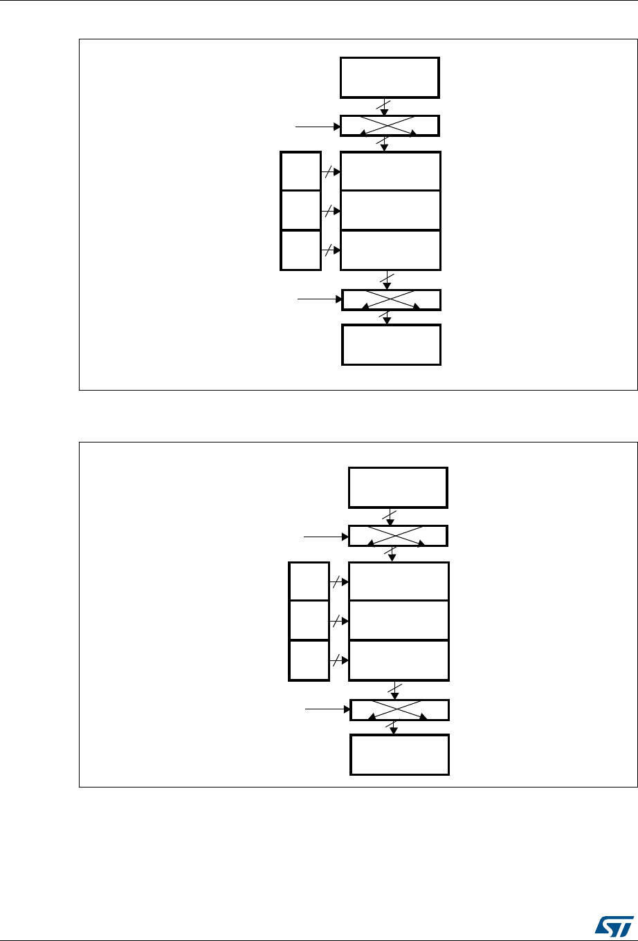
Cryptographic processor (CRYP) RM0090
710/1718 DocID018909 Rev 9
Figure 218. DES/TDES-ECB mode encryption
1. K: key; C: cipher text; I: input block; O: output block; P: plain text.
Figure 219. DES/TDES-ECB mode decryption
1. K: key; C: cipher text; I: input block; O: output block; P: plain text.
).&)&/
$%!ENCRYPT
+
0 BI TS
$%!DECRYPT
+
$%!ENCRYPT
+
/54&)&/
PLAINTEXT0
CIPHERTEXT#
SWAPPING
/BITS
#BITS
SWAPPING
$!4!490%
$!4!490%
AIB
).&)&/
#BITS
/54&)&/
CIPHERTEXT#
PLAINTEXT0
$%!DECRYPT
+
$%!ENCRYPT
+
$%!DECRYPT
+
)BITS
SWAPPING
/BITS
$!4!490%
$!4!490%
0 BITS
SWAPPING
-36

DocID018909 Rev 9 711/1718
RM0090 Cryptographic processor (CRYP)
751
DES and TDES Cipher block chaining (DES/TDES-CBC) mode
•DES/TDES-CBC mode encryption
Figure 220 illustrates the DES and Triple-DES Cipher block chaining (DES/TDES-
CBC) mode encryption. This mode begins by dividing a plaintext message into 64-bit
data blocks. In TCBC encryption, the first input block (I1), obtained after bit/byte/half-
word swapping (refer to Section 23.3.3: Data type on page 724), is formed by
exclusive-ORing the first plaintext data block (P1) with a 64-bit initialization vector IV (I1
= IV ⊕ P1). The input block is processed through the DEA in the encrypt state using K1.
The output of this process is fed back directly to the input of the DEA, which performs
the DES in the decrypt state using K2. The output of this process is fed directly to the
input of the DEA, which performs the DES in the encrypt state using K3. The resultant
64-bit output block (O1) is used directly as the ciphertext (C1), that is, C1 = O1. This first
ciphertext block is then exclusive-ORed with the second plaintext data block to produce
the second input block, (I2) = (C1 ⊕ P2). Note that I2 and P2 now refer to the second
block. The second input block is processed through the TDEA to produce the second
ciphertext block. This encryption process continues to “chain” successive cipher and
plaintext blocks together until the last plaintext block in the message is encrypted. If the
message does not consist of an integral number of data blocks, then the final partial
data block should be encrypted in a manner specified for the application.
•DES/TDES-CBC mode decryption
In DES/TDES-CBC decryption (see Figure 221), the first ciphertext block (C1) is used
directly as the input block (I1). The keying sequence is reversed compared to that used
for the encrypt process. The input block is processed through the DEA in the decrypt
state using K3. The output of this process is fed directly to the input of the DEA where
the DES is processed in the encrypt state using K2. This resulting value is directly fed
to the input of the DEA where the DES is processed in the decrypt state using K1. The
resulting output block is exclusive-ORed with the IV (which must be the same as that
used during encryption) to produce the first plaintext block (P1 = O1 ⊕ IV). The second
ciphertext block is then used as the next input block and is processed through the
TDEA. The resulting output block is exclusive-ORed with the first ciphertext block to
produce the second plaintext data block (P2 = O2 ⊕ C1). (Note that P2 and O2 refer to
the second block of data.) The TCBC decryption process continues in this manner until
the last complete ciphertext block has been decrypted. Ciphertext representing a
partial data block must be decrypted in a manner specified for the application.
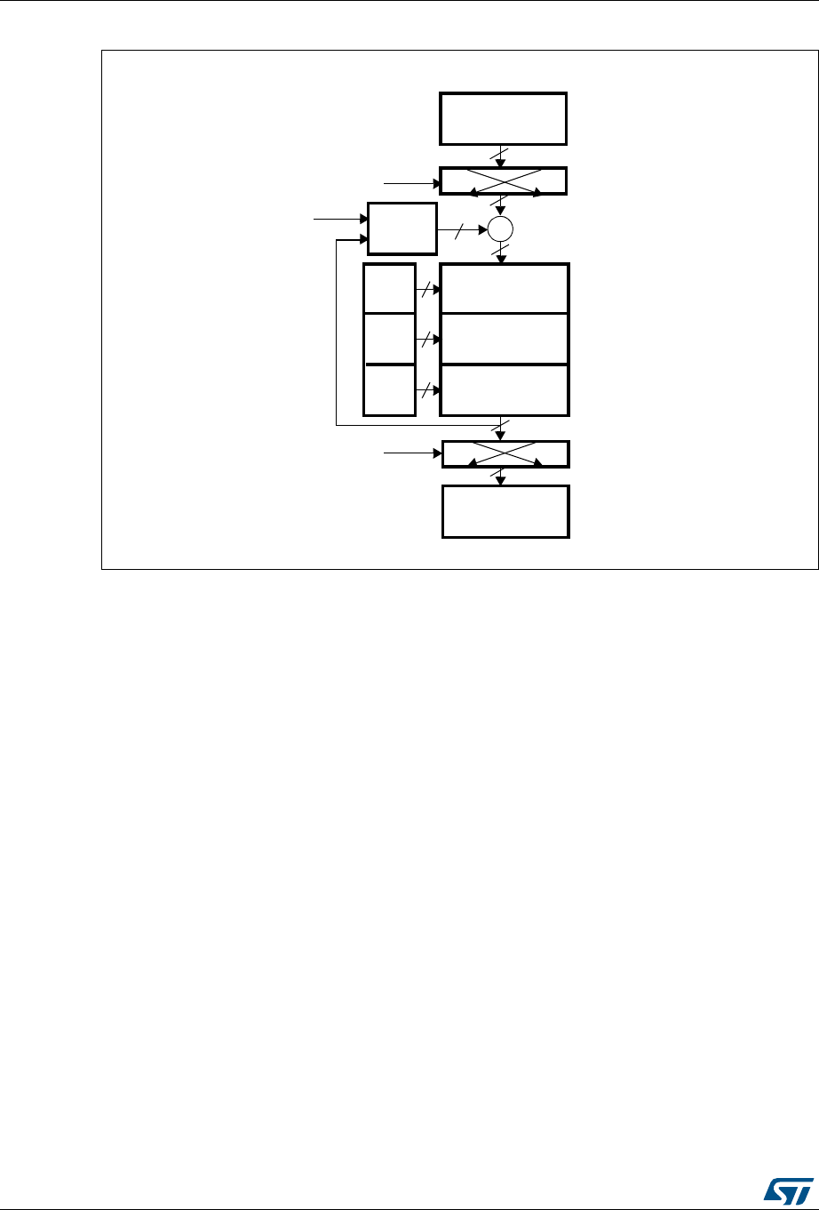
Cryptographic processor (CRYP) RM0090
712/1718 DocID018909 Rev 9
Figure 220. DES/TDES-CBC mode encryption
1. K: key; C: cipher text; I: input block; O: output block; Ps: plain text before swapping (when decoding) or
after swapping (when encoding); P: plain text; IV: initialization vectors.
).&)&/
$%!ENCRYPT
+
0 BITS
$%!DECRYPT
+
$%!ENCRYPT
+
/54&)&/
/BITS
PLAINTEXT0
CIPHERTEXT#
0SBITS
SWAPPING
)6,2
)BITS
BEFORE#290
ISENABLED
/ISWRITTENBACK
INTO)6ATTHE
SAMETIMEASIT
ISPUSHEDINTO
THE/54&)&/
SWAPPING
#BITS
$!4!490%
$!4!490%
!("DATAWRITE
AIB
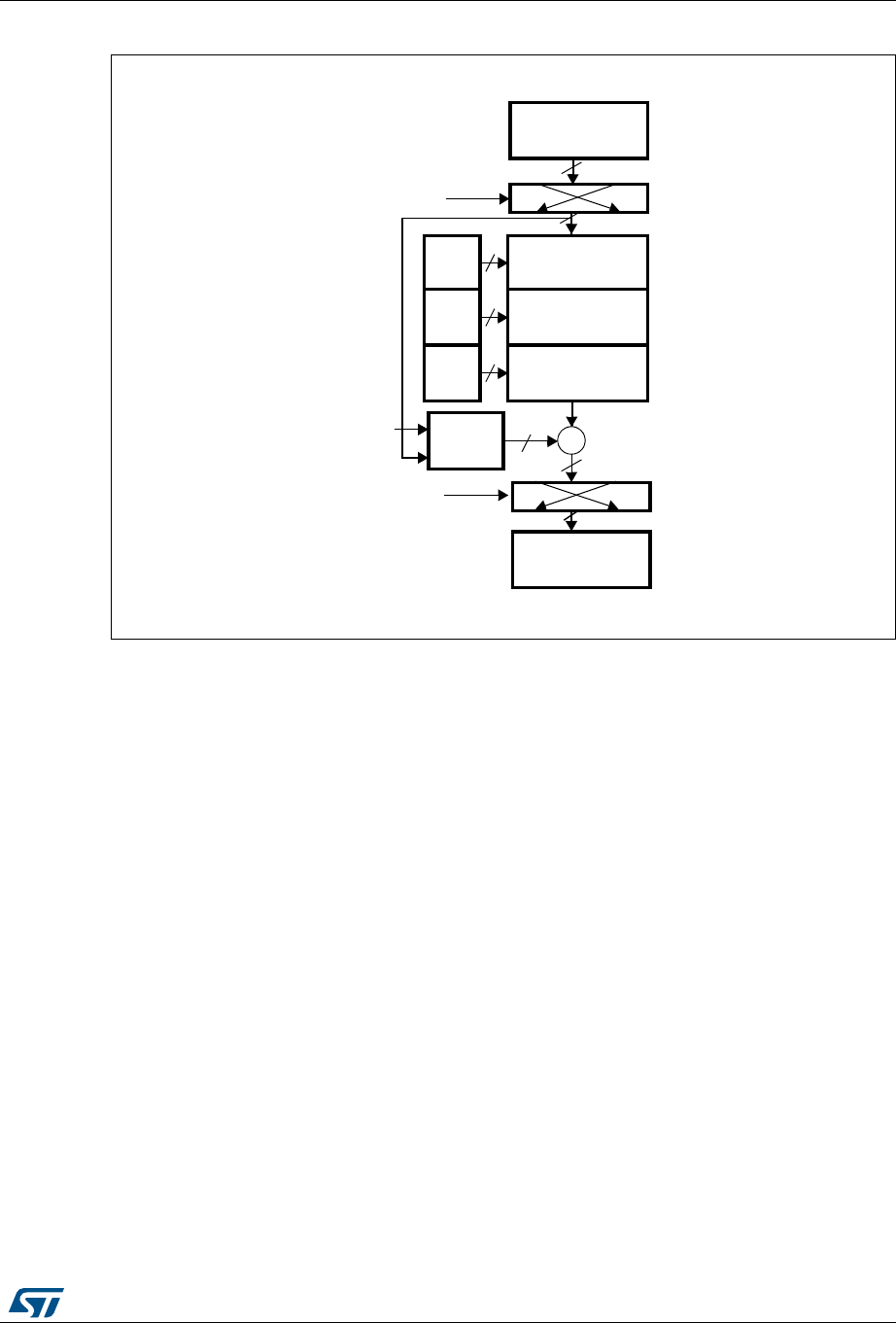
DocID018909 Rev 9 713/1718
RM0090 Cryptographic processor (CRYP)
751
Figure 221. DES/TDES-CBC mode decryption
1. K: key; C: cipher text; I: input block; O: output block; Ps: plain text before swapping (when decoding) or
after swapping (when encoding); P: plain text; IV: initialization vectors.
23.3.2 AES cryptographic core
The AES cryptographic core consists of three components:
•The AES algorithm (AEA: advanced encryption algorithm)
•Multiple keys
•Initialization vector(s) or Nonce
The AES utilizes keys of 3 possible lengths: 128, 192 or 256 bits and, depending on the
operation mode used, zero or one 128-bit initialization vector (IV).
The basic processing involved in the AES is as follows: an input block of 128 bits is read
from the input FIFO and sent to the AEA to be encrypted using the key (K0...3). The key
format depends on the key size:
•If Key size = 128: Key = [K3 K2]
•If Key size = 192: Key = [K3 K2 K1]
•If Key size = 256: Key = [K3 K2 K1 K0]
where Kx=[KxR KxL],R=right, L=left
According to the mode implemented, the resultant output block is used to calculate the
ciphertext.
FIPS PUB 197 (November 26, 2001) provides a thorough explanation of the processing
involved in the four operation modes supplied by the AES core: AES-ECB encryption, AES-
).&)&/
)BITS
/54&)&/
0SBITS
CIPHERTEXT#
PLAINTEXT0
0 BI TS
SWAPPING
$%!DECRYPT
+
$%!ENCRYPT
+
$%!DECRYPT
+
)6,2
!("DATAWRITE
BEFORE#290
ISENABLED
/BITS
)ISWRITTENBACK
INTO)6ATTHE
SAMETIMEAS0
ISPUSHEDINTO
THE/54&)&/
#BITS
SWAPPING
$!4!490%
$!4!490%
-36
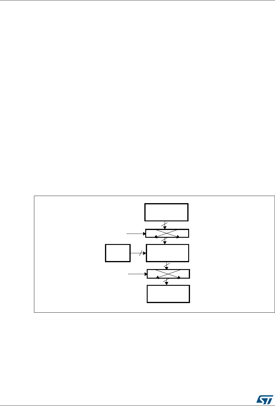
Cryptographic processor (CRYP) RM0090
714/1718 DocID018909 Rev 9
ECB decryption, AES-CBC encryption and AES-CBC decryption.This reference manual
only gives a brief explanation of each mode.
AES Electronic codebook (AES-ECB) mode
•AES-ECB mode encryption
Figure 222 illustrates the AES Electronic codebook (AES-ECB) mode encryption.
In AES-ECB encryption, a 128- bit plaintext data block (P) is used after bit/byte/half-
word swapping (refer to Section 23.3.3: Data type on page 724) as the input block (I).
The input block is processed through the AEA in the encrypt state using the 128, 192 or
256-bit key. The resultant 128-bit output block (O) is used after bit/byte/half-word
swapping as ciphertext (C). It is then pushed into the OUT FIFO.
•AES-ECB mode decryption
Figure 223 illustrates the AES Electronic codebook (AES-ECB) mode encryption.
To perform an AES decryption in the ECB mode, the secret key has to be prepared (it is
necessary to execute the complete key schedule for encryption) by collecting the last
round key, and using it as the first round key for the decryption of the ciphertext. This
preparation function is computed by the AES core. Refer to Section 23.3.6: Procedure
to perform an encryption or a decryption for more details on how to prepare the key.
In AES-ECB decryption, a 128-bit ciphertext block (C) is used after bit/byte/half-word
swapping as the input block (I). The keying sequence is reversed compared to that of
the encryption process. The resultant 128-bit output block (O), after bit/byte or half-
word swapping, produces the plaintext (P).
Figure 222. AES-ECB mode encryption
1. K: key; C: cipher text; I: input block; O: output block; P: plain text.
2. If Key size = 128: Key = [K3 K2].
If Key size = 192: Key = [K3 K2 K1]
If Key size = 256: Key = [K3 K2 K1 K0].
).&)&/
!%!ENCRYPT
+
0 B ITS
/54&)&/
PLAINTEXT0
CIPHERTEXT#
)BITS
SWAPPING
#BITS
SWAPPING
$!4!490%
$!4!490%
OR
AIB
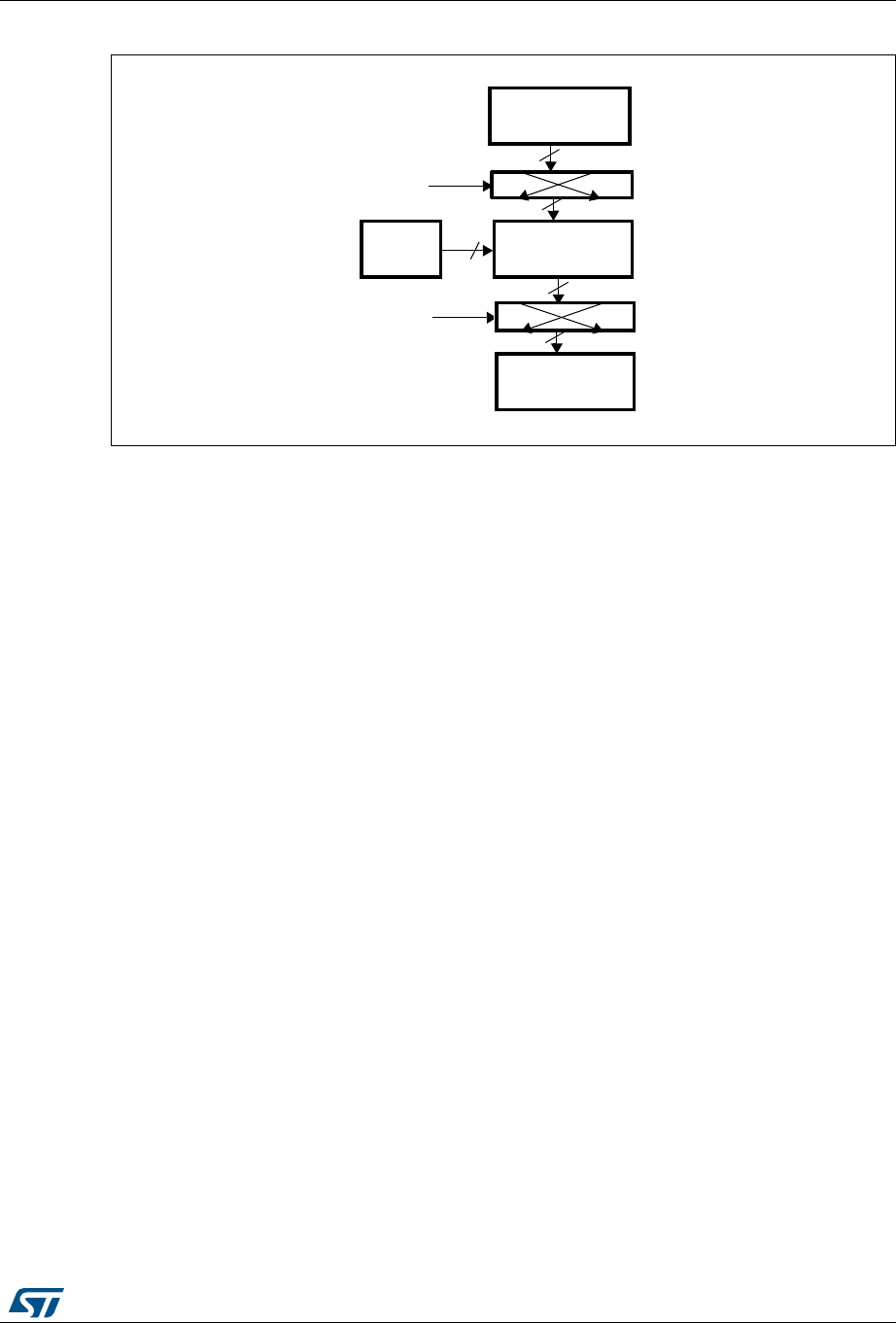
DocID018909 Rev 9 715/1718
RM0090 Cryptographic processor (CRYP)
751
Figure 223. AES-ECB mode decryption
1. K: key; C: cipher text; I: input block; O: output block; P: plain text.
2. If Key size = 128 => Key = [K3 K2].
If Key size = 192 => Key = [K3 K2 K1]
If Key size = 256 => Key = [K3 K2 K1 K0].
AES Cipher block chaining (AES-CBC) mode
•AES-CBC mode encryption
The AES Cipher block chaining (AES-CBC) mode decryption is shown on Figure 224.
In AES-CBC encryption, the first input block (I1) obtained after bit/byte/half-word
swapping (refer to Section 23.3.3: Data type on page 724) is formed by exclusive-
ORing the first plaintext data block (P1) with a 128-bit initialization vector IV (I1 = IV ⊕
P1). The input block is processed through the AEA in the encrypt state using the 128-,
192- or 256-bit key (K0...K3). The resultant 128-bit output block (O1) is used directly as
ciphertext (C1), that is, C1 = O1. This first ciphertext block is then exclusive-ORed with
the second plaintext data block to produce the second input block, (I2) = (C1 ⊕ P2).
Note that I2 and P2 now refer to the second block. The second input block is processed
through the AEA to produce the second ciphertext block. This encryption process
continues to “chain” successive cipher and plaintext blocks together until the last
plaintext block in the message is encrypted. If the message does not consist of an
integral number of data blocks, then the final partial data block should be encrypted in a
manner specified for the application.
In the CBC mode, like in the ECB mode, the secret key must be prepared to perform an
AES decryption. Refer to Section 23.3.6: Procedure to perform an encryption or a
decryption on page 729 for more details on how to prepare the key.
•AES-CBC mode decryption
In AES-CBC decryption (see Figure 225), the first 128-bit ciphertext block (C1) is used
directly as the input block (I1). The input block is processed through the AEA in the
decrypt state using the 128-, 192- or 256-bit key. The resulting output block is
exclusive-ORed with the 128-bit initialization vector IV (which must be the same as that
used during encryption) to produce the first plaintext block (P1 = O1 ⊕ IV). The second
ciphertext block is then used as the next input block and is processed through the AEA.
The resulting output block is exclusive-ORed with the first ciphertext block to produce
the second plaintext data block (P2 = O2 ⊕ C1). (Note that P2 and O2 refer to the second
).&)&/
#BITS
/54&)&/
CIPHERTEXT#
PLAINTEXT0
!%!DECRYPT
)BITS
SWAPPING
/BITS
$!4!490%
$!4!490%
0BITS
SWAPPING
+
OR
-36
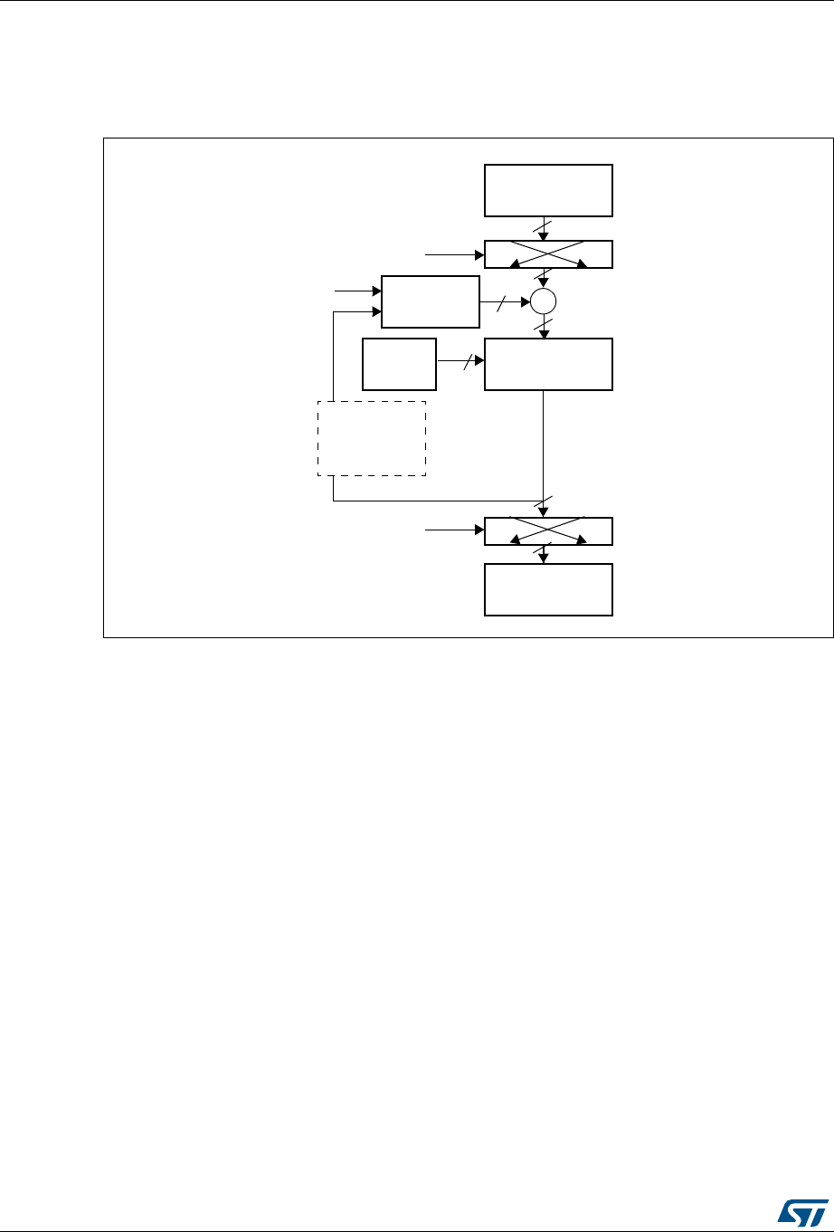
Cryptographic processor (CRYP) RM0090
716/1718 DocID018909 Rev 9
block of data.) The AES-CBC decryption process continues in this manner until the last
complete ciphertext block has been decrypted. Ciphertext representing a partial data
block must be decrypted in a manner specified for the application.
Figure 224. AES-CBC mode encryption
1. K: key; C: cipher text; I: input block; O: output block; Ps: plain text before swapping (when decoding) or
after swapping (when encoding); P: plain text; IV: Initialization vectors.
2. IVx=[IVxR IVxL], R=right, L=left.
3. If Key size = 128 => Key = [K3 K2].
If Key size = 192 => Key = [K3 K2 K1]
If Key size = 256 => Key = [K3 K2 K1 K0].
).&)&/
!%!ENCRYPT
0 B I T S
/54&)&/
/BITS
PLAINTEXT0
CIPHERTEXT#
SWAPPING
)6;)6)6=
)BITS
!(" DATAWRITE
BEFORE#290
ISENABLED
/ISWRITTEN
BACKINTO)6
ATTHESAMETIME
ASITISPUSHED
INTOTHE/54&)&/
SWAPPING
#BITS
$!4!490%
$!4!490%
+
OR
0SBITS
AIB
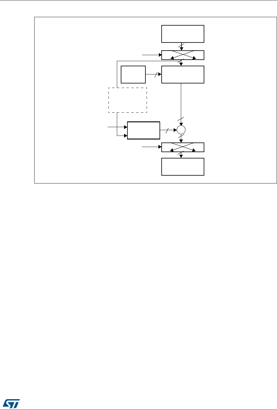
DocID018909 Rev 9 717/1718
RM0090 Cryptographic processor (CRYP)
751
Figure 225. AES-CBC mode decryption
1. K: key; C: cipher text; I: input block; O: output block; Ps: plain text before swapping (when decoding) or
after swapping (when encoding); P: plain text; IV: Initialization vectors.
2. IVx=[IVxR IVxL], R=right, L=left.
3. If Key size = 128 => Key = [K3 K2].
If Key size = 192 => Key = [K3 K2 K1]
If Key size = 256 => Key = [K3 K2 K1 K0].
AES counter mode (AES-CTR) mode
The AES counter mode uses the AES block as a key stream generator. The generated keys
are then XORed with the plaintext to obtain the cipher. For this reason, it makes no sense to
speak of different CTR encryption/decryption, since the two operations are exactly the
same.
In fact, given:
•Plaintext: P[0], P[1], ..., P[n] (128 bits each)
•A key K to be used (the size does not matter)
•An initial counter block (call it ICB but it has the same functionality as the IV of CBC)
The cipher is computed as follows:
C[i] = enck(iv[i]) xor P[i], where:
iv[0] = ICB and iv[i+1] = func(iv[i]), where func is an update function
applied to the previous iv block; func is basically an increment of one of the fields
composing the iv block.
Given that the ICB for decryption is the same as the one for encryption, the key stream
generated during decryption is the same as the one generated during encryption. Then, the
ciphertext is XORed with the key stream in order to retrieve the original plaintext. The
decryption operation therefore acts exactly in the same way as the encryption operation.
).&)&/
)BITS
/54&)&/
CIPHERTEXT#
PLAINTEXT0
0 B ITS
SWAPPING
!%!DECRYPT
+
!(" DATAWRITE
BEFORE#290
ISENABLED /BITS
)ISWRITTEN
BACKINTO)6
ATTHESAMETIME
AS0ISPUSHED
INTOTHE/54&)&/
#BITS
SWAPPING
$!4!490%
$!4!490%
OR
0SBITS
-36
)6;)6)6=
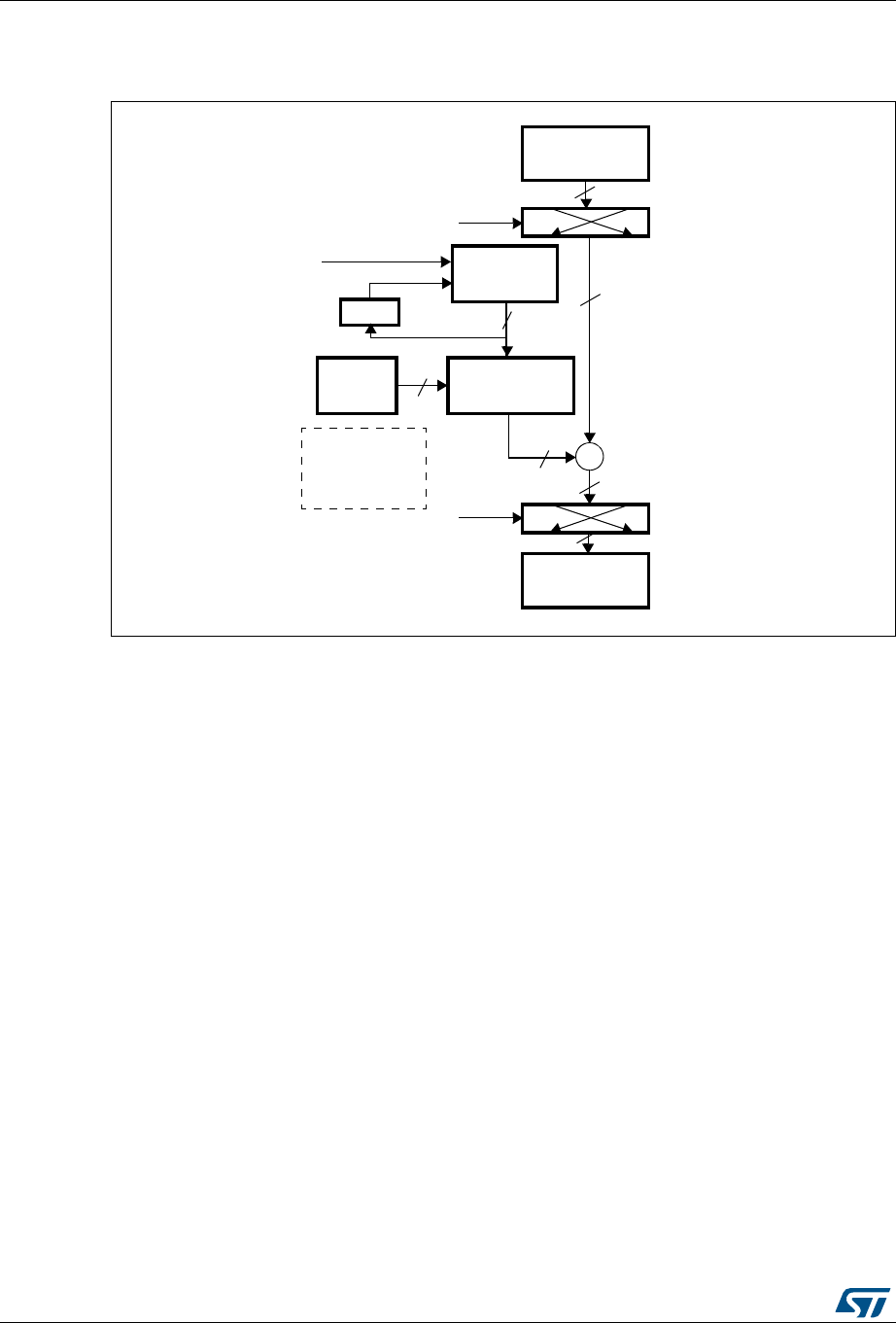
Cryptographic processor (CRYP) RM0090
718/1718 DocID018909 Rev 9
Figure 226 and Figure 227 illustrate AES-CTR encryption and decryption, respectively.
Figure 226. AES-CTR mode encryption
1. K: key; C: cipher text; I: input Block; o: output block; Ps: plain text before swapping (when decoding) or
after swapping (when encoding); Cs: cipher text after swapping (when decoding) or before swapping (when
encoding); P: plain text; IV: Initialization vectors.
).&)&/
!%!ENCRYPT
3 E L W V
/54&)&/
&VELW
PLAINTEXT0
CIPHERTEXT#
SWAPPING
)6,2
2ELWV
,ELWV
$+%GDWDZULWH
EHIRUH&5<3
LVHQDEOHG
,LVZULWWHQ
EDFNLQWR,9
DWVDPHWLPH
WKDQ&LVSXVKHG
LQ287),)2
SWAPPING
&ELWV
'$7$7<3(
'$7$7<3(
+
OR
3VELWV
AIB
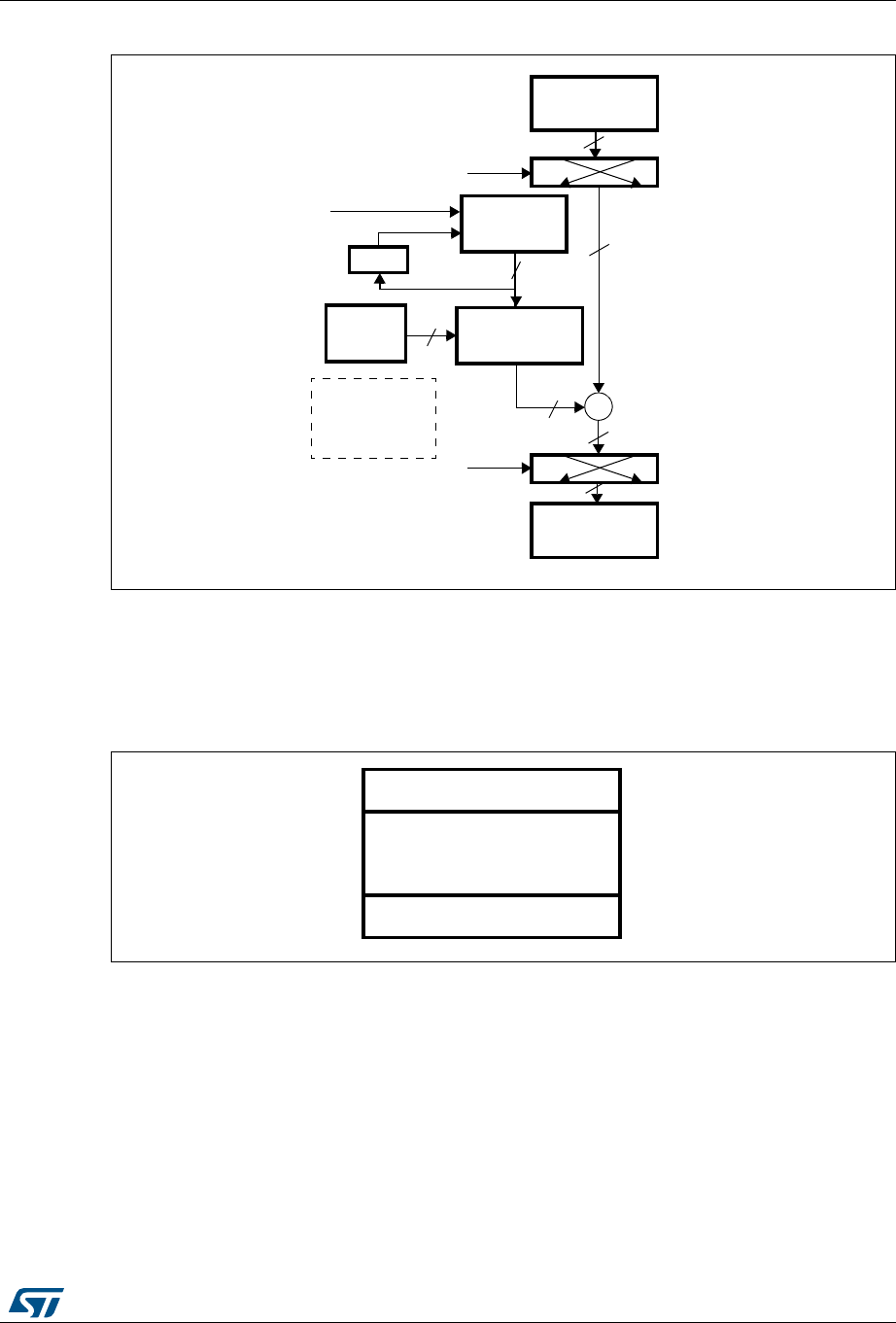
DocID018909 Rev 9 719/1718
RM0090 Cryptographic processor (CRYP)
751
Figure 227. AES-CTR mode decryption
1. K: key; C: cipher text; I: input Block; o: output block; Ps: plain text before swapping (when decoding) or
after swapping (when encoding); Cs: cipher text after swapping (when decoding) or before swapping (when
encoding); P: plain text; IV: Initialization vectors.
Figure 228 shows the structure of the IV block as defined by the standard [2]. It is composed
of three distinct fields.
Figure 228. Initial counter block structure for the Counter mode
•Nonce is a 32-bit, single-use value. A new nonce should be assigned to each different
communication.
•The initialization vector (IV) is a 64-bit value and the standard specifies that the
encryptor must choose IV so as to ensure that a given value is used only once for a
given key
•The counter is a 32-bit big-endian integer that is incremented each time a block has
been encrypted. The initial value of the counter should be set to ‘1’.
The block increments the least significant 32 bits, while it leaves the other (most significant)
96 bits unchanged.
).&)&/
!%!ENCRYPT
&ELWV
/54&)&/
3VELWV
CIPHERTEXT0
PLAINTEXT#
SWAPPING
)6,2
,ELWV
$+%GDWDZULWH
EHIRUH&5<3
LVHQDEOHG
,LVZULWWHQ
EDFNLQWR,9
DWVDPHWLPH
WKDQ3LVSXVKHG
LQ287),)2
SWAPPING
3ELWV
'$7$7<3(
'$7$7<3(
+
RU
&VELWV
2ELWV
-36
.ONCE BITS
)NITIALIZATIONVECTOR)6 BITS
#OUNTER BITS
AI

Cryptographic processor (CRYP) RM0090
720/1718 DocID018909 Rev 9
AES Galois/counter mode (GCM)
The AES Galois/counter mode (GCM) allows encrypting and authenticating the plaintext,
and generating the correspondent ciphertext and tag (also known as message
authentication code or message integrity check). This algorithm is based on AES counter
mode to ensure confidentiality. It uses a multiplier over a fixed finite field to generate the tag.
An initialization vector is required at the beginning of the algorithm.
The message to be processed is split into 2 parts:
•The header (also knows as additional authentication data): data which is authenticated
but no protected (such as information for routing the packet)
•The payload (also knows as plaintext or ciphertext): the message itself which is
authenticated and encrypted.
Note: The header must precede the payload and the two parts cannot be mixed together.
The GCM standard requires to pass, at the end of the message, a specific 128-bit block
composed of the size of the header (64 bits) and the size of the payload (64 bits). During the
computation, the header blocks must be distinguished from the payload blocks.
In GCM mode, four steps are required to perform an encryption/decryption:

DocID018909 Rev 9 721/1718
RM0090 Cryptographic processor (CRYP)
751
1. GCM init phase
During this first step, the HASH key is calculated and saved internally to be used for
processing all the blocks. It is recommended to follow the sequence below:
a) Make sure that the cryptographic processor is disabled by clearing the CRYPEN
bit in the CRYP_CR register.
b) Select the GCM chaining mode by programming ALGOMODE bits to ‘01000’ in
CRYP_CR.
c) Configure GCM_CCMPH bits to ‘00’ in CRYP_CR to start the GCM Init phase.
d) Initialize the key registers (128,192 and 256 bits) in CRYP_KEYRx as well as the
initialization vector (IV).
e) Set CRYPEN bit to ‘1’ to start the calculation of the HASH key.
f) Wait for the CRYPEN bit to be cleared to ‘0’ before moving on to the next phase.
g) Set the CRYPEN bit to ‘1’.
2. GCM header phase
This step must be performed after the GCM Init phase:
h) Set the GCM_CCMPH bits to ‘01’ in CRYP_CR to indicate that the header phase
has started.
i) Write the header data. Three methods can be used:
– Program the data by blocks of 32 bits into the CRYP_DIN register, and use the
IFNF flag to determine if the input FIFO can receive data. The size of the header
must be a multiple of 128 bits (4 words).
– Program the data into the CRYP_DIN register by blocks of 8 words, and use the
IFEM flag to determine if the input FIFO can receive data (IFEM=’1’). The size of
the header must be a multiple of 128 bits (4 words).
– Use the DMA.
j) Once all header data have been supplied, wait until the BUSY bit is cleared in the
CRYP_SR register.
3. GCM payload phase (encryption/decryption)
This step must be performed after the GCM header phase:
k) Configure GCM_CCMPH to ‘10’ in the CRYP_CR register.
l) Select the algorithm direction (encryption or decryption) by using the ALGODIR bit
in CRYP_CR.
m) Program the payload message into the CRYP_DIN register, and use the IFNF flag
to determine if the input FIFO can receive data. Alternatively, the data could be
programmed into the CRYP_DIN register by blocks of 8 words and the IFEM flag
used to determine if the input FIFO can receive data (IFEM=’1’). In parallel, the

Cryptographic processor (CRYP) RM0090
722/1718 DocID018909 Rev 9
OFNE/OFFU flag of the CRYP_DOUT register can be monitored to check if the
output FIFO is not empty.
n) Repeat the previous step until all payload blocks have been encrypted or
decrypted. Alternatively, DMA could be used.
4. GCM final phase
This step generates the authentication tag:
o) Configure GCM_CCMPH[1:0] to ‘11’ in CRYP_CR.
p) Write the input into the CRYP_DIN register 4 times. The input must contain the
number of bits in the header (64 bits) concatenated with the number of bits in the
payload (64 bits).
q) Wait till the
OFNE flag (FIFO output not empty) is set to ‘1’ in the CRYP_SR
register.
r) Read the CRYP_DOUT register 4 times: the output corresponds to the
authentication tag.
s) Disable the cryptographic processor (CRYPEN bit in CRYP_CR = ‘0’)
Note: When a decryption is performed, it is not required to compute the key at the beginning. At
the end of the decryption, the generated tag should be compared with the expected tag
passed with the message. In addition, the ALGODIR bit (algorithm direction) must be set to ‘1’.
No need to disable/enable CRYP processor when moving from header phase to tag phase.
AES Galois message authentication code (GMAC)
The cryptographic processor also supports GMAC to authenticate the plaintext. It uses the
GCM algorithm and a multiplier over a fixed finite field to generate the corresponding tag.
An initialization vector is required at the beginning of the algorithm.
Actually, the GMAC algorithm corresponds to the GCM algorithm applied on a message
composed of the header only. As a consequence, the payload phase is not required.
AES combined cipher machine (CCM)
The CCM algorithm allows encrypting and authenticating the plaintext, as well as generating
the corresponding ciphertext and tag (also known as message authentication code or
message integrity check). This algorithm is based on AES counter mode to ensure
confidentiality. It uses the AES CBC mode to generate a 128-bit tag.
The CCM standard (RFC 3610 Counter with CBC-MAC (CCM) dated September 2003)
defines particular encoding rules for the first authentication block (called B0 in the standard).
In particular, the first block includes flags, a nonce and the payload length expressed in
bytes. The CCM standard specifies another format, called A or counter, for
encryption/decryption. The counter is incremented during the payload phase and its 32 LSB
bits are initialized to ‘1’ during the tag generation (called A0 packet in the CCM standard).
Note: The hardware does not perform the formatting operation of the B0 packet. It should be
handled by the software.
As for the GCM algorithm, the message to be processed is split into 2 parts:
•The header (also knows as additional authentication data): data which is authenticated
but no protected (such as information for routing the packet)
•The payload (also knows as plaintext or ciphertext): the message itself which is
authenticated and encrypted.

DocID018909 Rev 9 723/1718
RM0090 Cryptographic processor (CRYP)
751
Note: The header part must precede the payload and the two parts cannot be mixed together.
In CCM mode, 4 steps are required to perform and encryption or decryption:
1. CCM init phase
In this first step, the B0 packet of the CCM message (1st packet) is programmed into
the CRYP_DIN register. During this phase, the CRYP_DOUT register does not contain
any output data.
The following sequence must be followed:
a) Make sure that the cryptographic processor is disabled by clearing the CRYPEN
bit in the CRYP_CR register.
b) Select the CCM chaining mode by programming the ALGOMODE bits to ‘01001’
in the CRYP_CR register.
c) Configure the GCM_CCMPH bits to ‘00’ in CRYP_CR to start the CCM Init phase.
d) Initialize the key registers (128,192 and 256 bits) in CRYP_KEYRx as well as the
initialization vector (IV).
e) Set the CRYPEN bit to ‘1’ in CRYP_CR.
f) Program the B0 packet into the input data register.
g) Wait for the CRYPEN bit to be cleared before moving on to the next phase.
h) Set CRYPEN to ‘1’.
2. CCM header phase
This step must be performed after the CCM Init phase. The sequence is identical for
encryption and decryption.
During this phase, the CRYP_DOUT register does not contain any output data.
This phase can be skipped if there is no additional authenticated data.
The following sequence must be followed:
i) Set the GCM_CCMPH bit to ’01’ in CRYP_CR to indicate that the header phase
has started.
j) Three methods can be used:
– Program the header data by blocks of 32 bits into the CRYP_DIN register, and use
the IFNF flag to determine if the input FIFO can receive data. The size of the
header must be a multiple of 128 bits (4 words).
– Program the header data into the CRYP_DIN register by blocks of 8 words, and
use the IFEM flag to determine if the input FIFO can receive data (IFEM=’1’). The
size of the header must be a multiple of 128 bits (4 words).
– Use the DMA.

Cryptographic processor (CRYP) RM0090
724/1718 DocID018909 Rev 9
Note: The first block B1 must be formatted with the header length. This task should be handled by
software.
k) Once all header data have been supplied, wait until the BUSY flag is cleared.
3. CCM payload phase (encryption/decryption)
This step must be performed after the CCM header phase. During this phase, the
encrypted/decrypted payload is stored in the CRYP_DOUT register.
The following sequence must be followed:
l) Configure GCM_CCMPH bits to ‘10’ in CRYP_CR.
m) Select the algorithm direction (encryption or decryption) by using the ALGODIR bit
in CRYP_CR.
n) Program the payload message into the CRYP_DIN register, and use the IFNF flag
to determine if the input FIFO can receive data. Alternatively, the data could be
programmed into the CRYP_DIN register by blocks of 8 words and the IFEM flag
used to determine if the input FIFO can receive data (IFEM=’1’). In parallel, the
OFNE/OFFU flag of the CRYP_DOUT register can be monitored to check if the
output FIFO is not empty.
o) Repeat the previous step until all payload blocks have been encrypted or
decrypted. Alternatively, DMA could be used.
4. CCM final phase
This step generates the authentication tag. During this phase, the authentication tag of
the message is generated and stored in the CRYP_DOUT register.
p) Configure GCM_CCMPH[1:0] bits to ‘11’ in CRYP_CR.
q) Load the A0 initialized counter, and program the 128-bit A0 value by writing 4
times 32 bits into the CRYP_DIN register.
r) Wait till the
OFNE flag (FIFO output not empty) is set to ‘1’ in the CRYP_SR
register.
s) Read the CRYP_DOUT register 4 times: the output corresponds to the encrypted
authentication tag.
t) Disable the cryptographic processor (CRYPEN bit in CRYP_CR = ‘0’)
Note: The hardware does not perform the formatting of the original B0 and B1 packets and the tag
comparison between encryption and decryption. They have to be handled by software.
The cryptographic processor does not need to be disabled/enabled when moving from the
header phase to the tag phase.
AES cipher message authentication code (CMAC)
The CMAC algorithm allows authenticating the plaintext, and generating the corresponding
tag. The CMAC sequence is identical to the CCM one, except that the payload phase is
skipped.
23.3.3 Data type
Data enter the CRYP processor 32 bits (word) at a time as they are written into the
CRYP_DIN register. The principle of the DES is that streams of data are processed 64 bits
by 64 bits and, for each 64-bit block, the bits are numbered from M1 to M64, with M1 the left-
most bit and M64 the right-most bit of the block. The same principle is used for the AES, but
with a 128-bit block size.
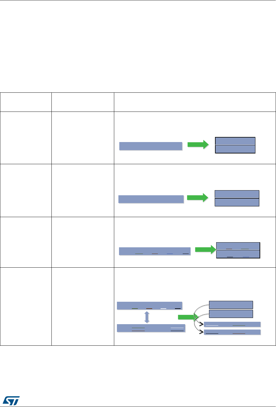
DocID018909 Rev 9 725/1718
RM0090 Cryptographic processor (CRYP)
751
The system memory organization is little-endian: whatever the data type (bit, byte, 16-bit
half-word, 32-bit word) used, the least-significant data occupy the lowest address locations.
A bit, byte, or half-word swapping operation (depending on the kind of data to be encrypted)
therefore has to be performed on the data read from the IN FIFO before they enter the
CRYP processor. The same swapping operation should be performed on the CRYP data
before they are written into the OUT FIFO. For example, the operation would be byte
swapping for an ASCII text stream.
The kind of data to be processed is configured with the DATATYPE bitfield in the CRYP
control register (CRYP_CR).
Figure 229 shows how the 64-bit data block M1...64 is constructed from two consecutive 32-
bit words popped off the IN FIFO by the CRYP processor, according to the DATATYPE
value. The same schematic can easily be extended to form the 128-bit block for the AES
Table 112. Data types
DATATYPE in
CRYP_CR Swapping performed System memory data
(plaintext or cypher)
00b No swapping
Example: TDES block value 0xABCD77206973FE01 is
represented in system memory as:
01b Half-word (16-bit)
swapping
Example: TDES block value 0xABCD77206973FE01 is
represented in system memory as:
10b Byte (8-bit) swapping
Example: TDES block value 0xABCD77206973FE01 is
represented in system memory as:
11b Bit swapping
TDES block value 0x4E6F772069732074 is represented in system
memory as:
[$%&')(
7'(6EORFNVL]H ELW [ELW
[$%&'
[)(
#
#
V\VWHPPHPRU\
[$%&')(
7'(6EORFNVL]H ELW [ELW [$%&'
[)(
#
#
V\VWHPPHPRU\
[$%&')(
7'(6EORFNVL]H ELW [ELW
[&'$%
[)(
#
#
V\VWHPPHPRU\
[()[(()
[(&(
#
#
#
#
V\VWHPPHPRU\
7'(6%ORFVL]H ELW [ELW
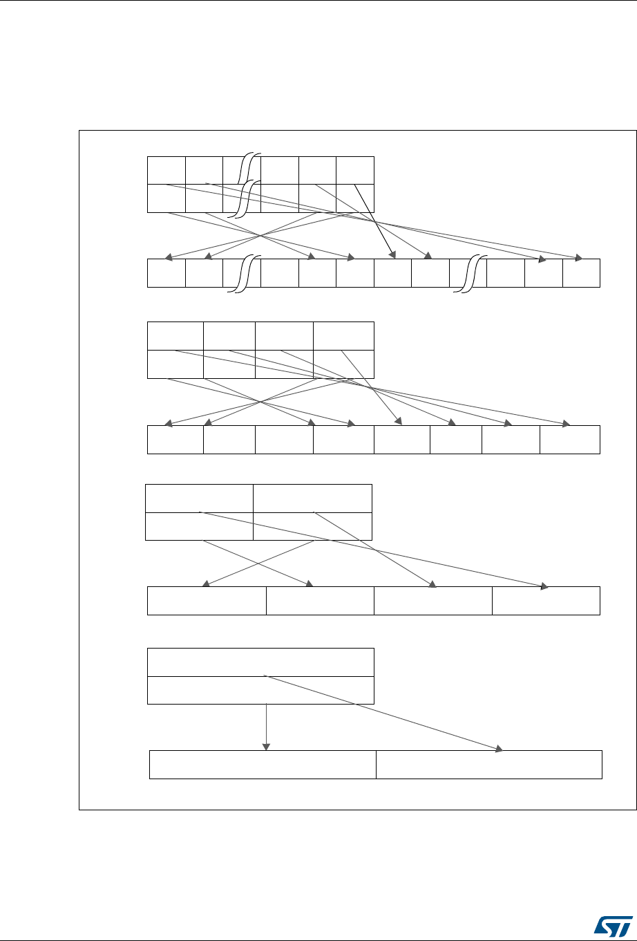
Cryptographic processor (CRYP) RM0090
726/1718 DocID018909 Rev 9
cryptographic algorithm (for the AES, the block length is four 32-bit words, but swapping
only takes place at word level, so it is identical to the one described here for the TDES).
Note: The same swapping is performed between the IN FIFO and the CRYP data block, and
between the CRYP data block and the OUT FIFO.
Figure 229. 64-bit block construction according to DATATYPE
"YTE"YTE"YTE"YTE
--
--
).&)&/
BITSTRING - - - --
BITSWAPPINGOPERATION
).&)&/
BITSTRING
BYTESWAPPINGOPERATION
"YTE"YTE"YTE"YTE
BITSBITS
BITSBITS
).&)&/
BITSTRING
HALDWORDSWAPPINGOPERATION
(ALFWORD
BITS
$!4!490%B
$!4!490%B
$!4!490%B
(ALFWORD
BITS
(ALFWORD
-
(ALFWORD
-
- -- - -
BITBITBITBITBIT
BITBITBITBITBIT FIRSTWORDWRITTENINTOTHE#290?$).REGISTER
SECONDWORDWRITTENINTOTHE#290?$).REGISTER
"YTE"YTE"YTE"YTE
BITS
BITS
BITSBITS
FIRSTWORDWRITTENINTOTHE#290?$).REGISTER
SECONDWORDWRITTENINTOTHE#290?$).REGISTER
"YTE"YTE"YTE"YTE
--
--
BITORDERINGWITHINBYTEISUNCHANGED
(ALFWORD
BITS
(ALFWORD
BITS
FIRSTWORDWRITTENINTOTHE#290?$).REGISTER
SECONDWORDWRITTENINTOTHE#290?$).REGISTER
(ALFWORD
-
(ALFWORD
-
).&)&/
BITSTRING
.OSWAPPINGOPERATION $!4!490%B
7ORD
BITS
7ORD
-
7ORD
BITS
FIRSTWORDWRITTENINTOTHE#290?$).REGISTER
SECONDWORDWRITTENINTOTHE#290?$).REGISTER
7ORD
-
AI

DocID018909 Rev 9 727/1718
RM0090 Cryptographic processor (CRYP)
751
23.3.4 Initialization vectors - CRYP_IV0...1(L/R)
Initialization vectors are considered as two 64-bit data items. They therefore do not have the
same data format and representation in system memory as plaintext or cypher data, and
they are not affected by the DATATYPE value.
Initialization vectors are defined by two consecutive 32-bit words, CRYP_IVL (left part,
noted as bits IV1...32) and CRYP_IVR (right part, noted as bits IV33...64).
During the DES or TDES CBC encryption, the CRYP_IV0(L/R) bits are XORed with the 64-
bit data block popped off the IN FIFO after swapping (according to the DATATYPE value),
that is, with the M1...64 bits of the data block. When the output of the DEA3 block is
available, it is copied back into the CRYP_IV0(L/R) vector, and this new content is XORed
with the next 64-bit data block popped off the IN FIFO, and so on.
During the DES or TDES CBC decryption, the CRYP_IV0(L/R) bits are XORed with the 64-
bit data block (that is, with the M1...64 bits) delivered by the TDEA1 block before swapping
(according to the DATATYPE value), and pushed into the OUT FIFO. When the XORed
result is swapped and pushed into the OUT FIFO, the CRYP_IV0(L/R) value is replaced by
the output of the IN FIFO, then the IN FIFO is popped, and a new 64-bit data block can be
processed.
During the AES CBC encryption, the CRYP_IV0...1(L/R) bits are XORed with the 128-bit
data block popped off the IN FIFO after swapping (according to the DATATYPE value).
When the output of the AES core is available, it is copied back into the CRYP_IV0...1(L/R)
vector, and this new content is XORed with the next 128-bit data block popped off the IN
FIFO, and so on.
During the AES CBC decryption, the CRYP_IV0...1(L/R) bits are XORed with the 128-bit
data block delivered by the AES core before swapping (according to the DATATYPE value)
and pushed into the OUT FIFO. When the XORed result is swapped and pushed into the
OUT FIFO, the CRYP_IV0...1(L/R) value is replaced by the output of the IN FIFO, then the
IN FIFO is popped, and a new 128-bit data block can be processed.
During the AES CTR encryption or decryption, the CRYP_IV0...1(L/R) bits are encrypted by
the AES core. Then the result of the encryption is XORed with the 128-bit data block popped
off the IN FIFO after swapping (according to the DATATYPE value). When the XORed result
is swapped and pushed into the OUT FIFO, the counter part of the CRYP_IV0...1(L/R) value
(32 LSB) is incremented.
Any write operation to the CRYP_IV0...1(L/R) registers when bit BUSY = 1b in the
CRYP_SR register is disregarded (CRYP_IV0...1(L/R) register content not modified). Thus,
you must check that bit BUSY = 0b before modifying initialization vectors.
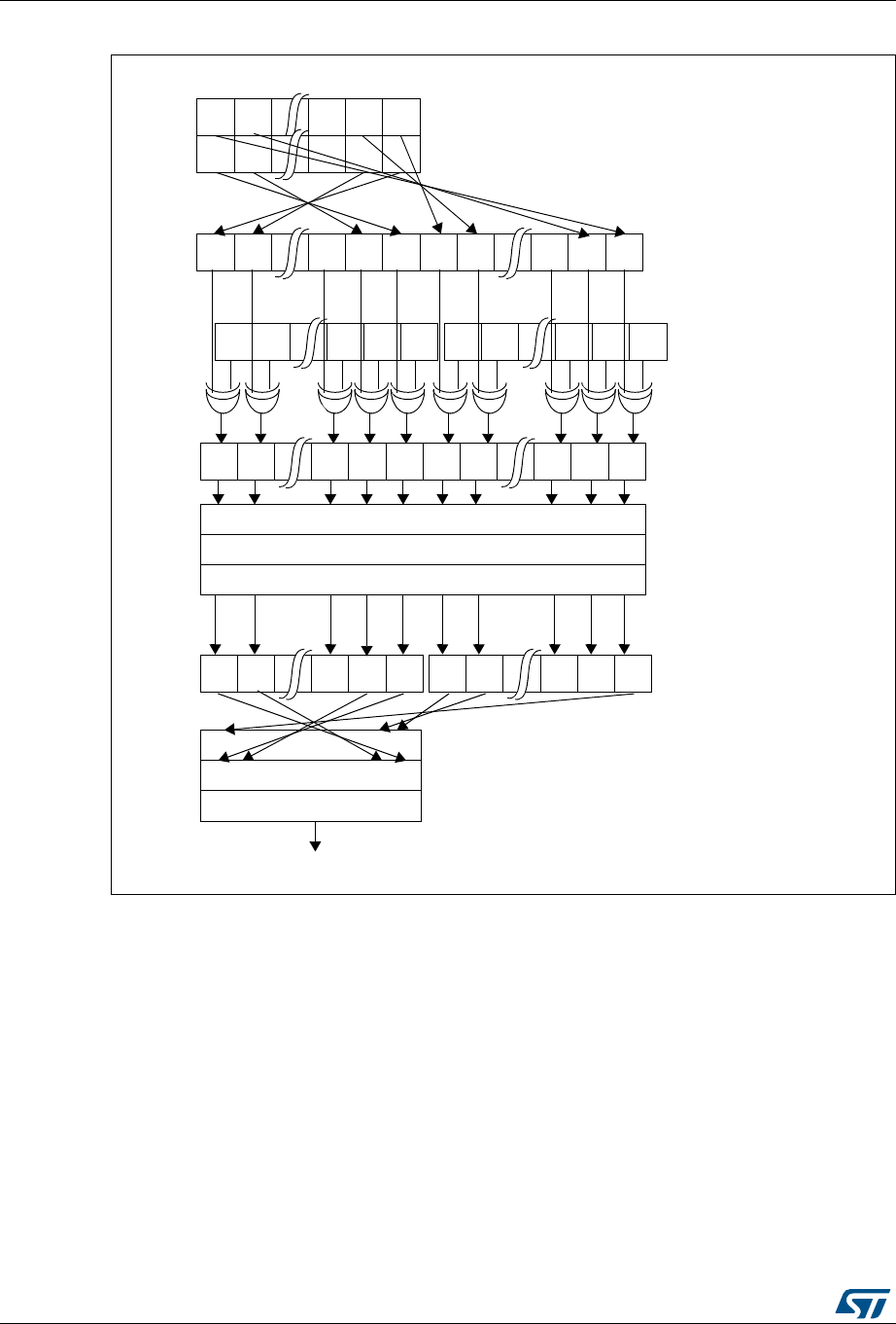
Cryptographic processor (CRYP) RM0090
728/1718 DocID018909 Rev 9
Figure 230. Initialization vectors use in the TDES-CBC encryption
23.3.5 CRYP busy state
When there is enough data in the input FIFO (at least 2 words for the DES or TDES
algorithm mode, 4 words for the AES algorithm mode) and enough free-space in the output
FIFO (at least 2 (DES/TDES) or 4 (AES) word locations), and when the bit CRYPEN = 1 in
the CRYP_CR register, then the cryptographic processor automatically starts an encryption
or decryption process (according to the value of the ALGODIR bit in the CRYP_CR
register).
This process takes 48 AHB2 clock cycles for the Triple-DES algorithm, 16 AHB2 clock
cycles for the simple DES algorithm, and 14, 16 or 18 AHB2 clock cycles for the AES with
key lengths of 128, 192 or 256 bits, respectively. During the whole process, the BUSY bit in
the CRYP_SR register is set to ‘1’. At the end of the process, two (DES/TDES) or four (AES)
words are written by the CRYP Core into the output FIFO, and the BUSY bit is cleared. In
#290?)6,
BITSTRING -----
4$%3#"# ENCRYPTION EXAMPLE $!4!490% B
-----
BIT
BITBITBITBIT
BITBITBITBITBIT FIRSTWORDWRITTENINTOTHE#290?$).REGISTER
SECONDWORDWRITTENINTOTHE#290?$).REGISTER
)6
#290?)62
$%!%NCRYPT +
$%!$ECRYPT +
$%!%NCRYPT +
#290?)6, #290?)62
#290RESULTISCOPIED
BACKTOTHE#290?)6,2
REGISTERSAFTERCYPHERING
/54&)&/
&IRSTWORDFROMTHE/54&)&/CONTAINSTHELEFTPARTOFTHECYPHERTEXTBLOCK/
3ECONDWORDFROM/54&)&/CONTAINSTHERIGHTPARTOFCYPHERTEXTBLOCK/
)6 )6 )6 )6 )6 )6 )6 )6 )6
) ) ) ) ) ) ) )) )
)6 )6 )6 )6 )6 )6 )6 )6 )6 )6
AI

DocID018909 Rev 9 729/1718
RM0090 Cryptographic processor (CRYP)
751
the CBC, CTR mode, the initialization vectors CRYP_IVx(L/R)R (x = 0..3) are updated as
well.
A write operation to the key registers (CRYP_Kx(L/R)R, x = 0..3), the initialization registers
(CRYP_IVx(L/R)R, x = 0..3), or to bits [9:2] in the CRYP_CR register are ignored when the
cryptographic processor is busy (bit BUSY = 1b in the CRYP_SR register), and the registers
are not modified. It is thus not possible to modify the configuration of the cryptographic
processor while it is processing a block of data. It is however possible to clear the CRYPEN
bit while BUSY = 1, in which case the ongoing DES, TDES or AES processing is completed
and the two/four word results are written into the output FIFO, and then, only then, the
BUSY bit is cleared.
Note: When a block is being processed in the DES or TDES mode, if the output FIFO becomes full
and if the input FIFO contains at least one new block, then the new block is popped off the
input FIFO and the BUSY bit remains high until there is enough space to store this new
block into the output FIFO.
23.3.6 Procedure to perform an encryption or a decryption
Initialization
1. Initialize the peripheral (the order of operations is not important except for the key
preparation for AES-ECB or AES-CBC decryption. The key size and the key value
must be entered before preparing the key and the algorithm must be configured once
the key has been prepared):
a) Configure the key size (128-, 192- or 256-bit, in the AES only) with the KEYSIZE
bits in the CRYP_CR register
b) Write the symmetric key into the CRYP_KxL/R registers (2 to 8 registers to be
written depending on the algorithm)
c) Configure the data type (1-, 8-, 16- or 32-bit), with the DATATYPE bits in the
CRYP_CR register
d) In case of decryption in AES-ECB or AES-CBC, you must prepare the key:
configure the key preparation mode by setting the ALGOMODE bits to ‘111’ in the
CRYP_CR register. Then write the CRYPEN bit to ‘1’: the BUSY bit is set. Wait
until BUSY returns to 0 (CRYPEN is automatically cleared as well): the key is
prepared for decryption
e) Configure the algorithm and chaining (the DES/TDES in ECB/CBC, the AES in
ECB/CBC/CTR/GCM/CCM) with the ALGOMODE bits in the CRYP_CR register
f) Configure the direction (encryption/decryption), with the ALGODIR bit in the
CRYP_CR register
g) Write the initialization vectors into the CRYP_IVxL/R register (in CBC or CTR
modes only)
2. Flush the IN and OUT FIFOs by writing the FFLUSH bit to 1 in the CRYP_CR register
Processing when the DMA is used to transfer the data from/to the memory
1. Configure the DMA controller to transfer the input data from the memory. The transfer
length is the length of the message. As message padding is not managed by the
peripheral, the message length must be an entire number of blocks. The data are
transferred in burst mode. The burst length is 4 words in the AES and 2 or 4 words in

Cryptographic processor (CRYP) RM0090
730/1718 DocID018909 Rev 9
the DES/TDES. The DMA should be configured to set an interrupt on transfer
completion of the output data to indicate that the processing is finished.
2. Enable the cryptographic processor by writing the CRYPEN bit to 1. Enable the DMA
requests by setting the DIEN and DOEN bits in the CRYP_DMACR register.
3. All the transfers and processing are managed by the DMA and the cryptographic
processor. The DMA interrupt indicates that the processing is complete. Both FIFOs
are normally empty and BUSY = 0.
Processing when the data are transferred by the CPU during interrupts
1. Enable the interrupts by setting the INIM and OUTIM bits in the CRYP_IMSCR register.
2. Enable the cryptographic processor by setting the CRYPEN bit in the CRYP_CR
register.
3. In the interrupt managing the input data: load the input message into the IN FIFO. You
can load 2 or 4 words at a time, or load data until the FIFO is full. When the last word of
the message has been entered into the FIFO, disable the interrupt by clearing the INIM
bit.
4. In the interrupt managing the output data: read the output message from the OUT
FIFO. You can read 1 block (2 or 4 words) at a time or read data until the FIFO is
empty. When the last word has been read, INIM=0, BUSY=0 and both FIFOs are empty
(IFEM=1 and OFNE=0). You can disable the interrupt by clearing the OUTIM bit and,
the peripheral by clearing the CRYPEN bit.
Processing without using the DMA nor interrupts
1. Enable the cryptographic processor by setting the CRYPEN bit in the CRYP_CR
register.
2. Write the first blocks in the input FIFO (2 to 8 words).
3. Repeat the following sequence until the complete message has been processed:
a) Wait for OFNE=1, then read the OUT-FIFO (1 block or until the FIFO is empty)
b) Wait for IFNF=1, then write the IN FIFO (1 block or until the FIFO is full)
4. At the end of the processing, BUSY=0 and both FIFOs are empty (IFEM=1 and
OFNE=0). You can disable the peripheral by clearing the CRYPEN bit.
23.3.7 Context swapping
If a context switching is needed because a new task launched by the OS requires this
resource, the following tasks have to be performed for full context restoration (example
when the DMA is used):

DocID018909 Rev 9 731/1718
RM0090 Cryptographic processor (CRYP)
751
Case of the AES and DES
1. Context saving
a) Stop DMA transfers on the IN FIFO by clearing the DIEN bit in the CRYP_DMACR
register.
b) Wait until both the IN and OUT FIFOs are empty (IFEM=1 and OFNE=0 in the
CRYP_SR register) and the BUSY bit is cleared.
c) Stop DMA transfers on the OUT FIFO by writing the DOEN bit to 0 in the
CRYP_DMACR register and clear the CRYPEN bit.
d) Save the current configuration (bits [9:2] and bits 19 in the CRYP_CR register)
and, if not in ECB mode, the initialization vectors. The key value must already be
available in the memory. When needed, save the DMA status (pointers for IN and
OUT messages, number of remaining bytes, etc.).
Additional bits should be saved when GCM/GMAC or CCM/CMAC algorithms are
used:
– bits [17:16] in the CRYP_CR register
– context swap registers:
CRYP_CSGCMCCM0..7 for GCM/GMAC or CCM/CMAC algorithm
CRYP_CSGCM0..7 for GCM/GMAC algorithm.
2. Configure and execute the other processing.
3. Context restoration
a) Configure the processor as in Section 23.3.6: Procedure to perform an encryption
or a decryption on page 729, Initialization with the saved configuration. For the
AES-ECB or AES-CBC decryption, the key must be prepared again.
b) If needed, reconfigure the DMA controller to transfer the rest of the message.
c) Enable the processor by setting the CRYPEN bit and, the DMA requests by setting
the DIEN and DOEN bits.
Case of the TDES
Context swapping can be done in the TDES in the same way as in the AES. But as the input
FIFO can contain up to 4 unprocessed blocks and as the processing duration per block is
higher, it can be faster in certain cases to interrupt the processing without waiting for the IN
FIFO to be empty.
1. Context saving
a) Stop DMA transfers on the IN FIFO by clearing the DIEN bit in the CRYP_DMACR
register.
b) Disable the processor by clearing the CRYPEN bit (the processing will stop at the
end of the current block).
c) Wait until the OUT FIFO is empty (OFNE=0 in the CRYP_SR register) and the
BUSY bit is cleared.
d) Stop DMA transfers on the OUT FIFO by writing the DOEN bit to 0 in the
CRYP_DMACR register.
e) Save the current configuration (bits [9:2] and bits 19 in the CRYP_CR register)
and, if not in ECB mode, the initialization vectors. The key value must already be
available in the memory. When needed, save the DMA status (pointers for IN and
OUT messages, number of remaining bytes, etc.). Read back the data loaded in

Cryptographic processor (CRYP) RM0090
732/1718 DocID018909 Rev 9
the IN FIFO that have not been processed and save them in the memory until the
FIFO is empty.
Note: In GCM/GMAC or CCM/CMAC mode, bits [17:16] of the CRYP_CR register should also be
saved.
2. Configure and execute the other processing.
3. Context restoration
a) Configure the processor as in Section 23.3.6: Procedure to perform an encryption
or a decryption on page 729, Initialization with the saved configuration. For the
AES-ECB or AES-CBC decryption, the key must be prepared again.
b) Write the data that were saved during context saving into the IN FIFO.
c) If needed, reconfigure the DMA controller to transfer the rest of the message.
d) Enable the processor by setting the CRYPEN bit and, the DMA requests by setting
the DIEN and DOEN bits.
23.4 CRYP interrupts
There are two individual maskable interrupt sources generated by the CRYP. These two
sources are combined into a single interrupt signal, which is the only interrupt signal from
the CRYP that drives the NVIC (nested vectored interrupt controller). This combined
interrupt, which is an OR function of the individual masked sources, is asserted if any of the
individual interrupts listed below is asserted and enabled.
You can enable or disable the interrupt sources individually by changing the mask bits in the
CRYP_IMSCR register. Setting the appropriate mask bit to ‘1’ enables the interrupt.
The status of the individual interrupt sources can be read either from the CRYP_RISR
register, for raw interrupt status, or from the CRYP_MISR register, for the masked interrupt
status.
Output FIFO service interrupt - OUTMIS
The output FIFO service interrupt is asserted when there is one or more (32-bit word) data
items in the output FIFO. This interrupt is cleared by reading data from the output FIFO until
there is no valid (32-bit) word left (that is, the interrupt follows the state of the OFNE (output
FIFO not empty) flag).
The output FIFO service interrupt OUTMIS is NOT enabled with the CRYP enable bit.
Consequently, disabling the CRYP will not force the OUTMIS signal low if the output FIFO is
not empty.
Input FIFO service interrupt - INMIS
The input FIFO service interrupt is asserted when there are less than four words in the input
FIFO. It is cleared by performing write operations to the input FIFO until it holds four or more
words.
The input FIFO service interrupt INMIS is enabled with the CRYP enable bit. Consequently,
when CRYP is disabled, the INMIS signal is low even if the input FIFO is empty.
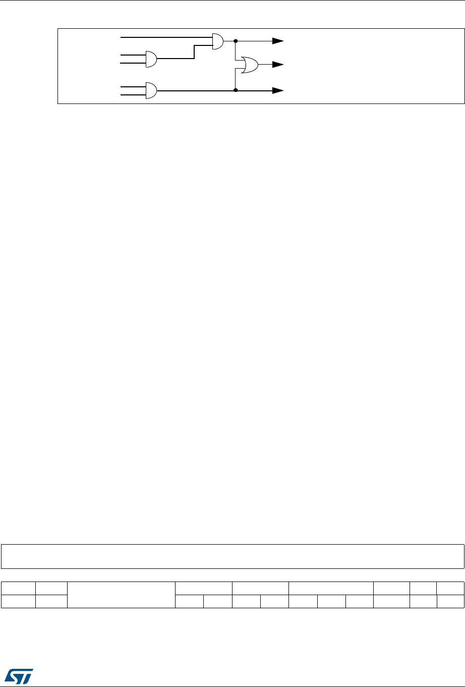
DocID018909 Rev 9 733/1718
RM0090 Cryptographic processor (CRYP)
751
Figure 231. CRYP interrupt mapping diagram
23.5 CRYP DMA interface
The cryptographic processor provides an interface to connect to the DMA controller. The
DMA operation is controlled through the CRYP DMA control register, CRYP_DMACR.
The burst and single transfer request signals are not mutually exclusive. They can both be
asserted at the same time. For example, when there are 6 words available in the OUT FIFO,
the burst transfer request and the single transfer request are asserted. After a burst transfer
of 4 words, the single transfer request only is asserted to transfer the last 2 available words.
This is useful for situations where the number of words left to be received in the stream is
less than a burst.
Each request signal remains asserted until the relevant DMA clear signal is asserted. After
the request clear signal is deasserted, a request signal can become active again, depending
on the above described conditions. All request signals are deasserted if the CRYP
peripheral is disabled or the DMA enable bit is cleared (DIEN bit for the IN FIFO and DOEN
bit for the OUT FIFO in the CRYP_DMACR register).
Note: The DMA controller must be configured to perform burst of 4 words or less. Otherwise some
data could be lost.
In order to let the DMA controller empty the OUT FIFO before filling up the IN FIFO, the
OUTDMA channel should have a higher priority than the INDMA channel.
23.6 CRYP registers
The cryptographic core is associated with several control and status registers, eight key
registers and four initialization vectors registers.
23.6.1 CRYP control register (CRYP_CR) for STM32F415/417xx
Address offset: 0x00
Reset value: 0x0000 0000
).2)3
).)-
#290%.
).-)3
).&)&/)NTERRUPT).-)3
/542)3
/54)-
/54-)3 /54&)&/)NTERRUPT/54-)3
'LOBAL)NTERRUPT
AI
31 30 29 28 27 26 25 24 23 22 21 20 19 18 17 16
Reserved
15 14 13 12 11 10 9 8 76543 2 10
CRYPEN FFLUSH Reserved KEYSIZE DATATYPE ALGOMODE[2:0] ALGODIR Res. Res.
rw w rw rw rw rw rw rw rw rw

Cryptographic processor (CRYP) RM0090
734/1718 DocID018909 Rev 9
Bits 31:18 Reserved, must be kept at reset value
Bits 17:16 Reserved, must be kept at reset value
Bit 15 CRYPEN: Cryptographic processor enable
0: CRYP processor is disabled
1: CRYP processor is enabled
Note: The CRYPEN bit is automatically cleared by hardware when the key
preparation process ends (ALGOMODE=111b) or GCM_CCM init Phase
Bit 14 FFLUSH: FIFO flush
When CRYPEN = 0, writing this bit to 1 flushes the IN and OUT FIFOs (that is
read and write pointers of the FIFOs are reset. Writing this bit to 0 has no effect.
When CRYPEN = 1, writing this bit to 0 or 1 has no effect.
Reading this bit always returns 0.
Bits 13:10 Reserved, must be kept at reset value
Bits 9:8 KEYSIZE[1:0]: Key size selection (AES mode only)
This bitfield defines the bit-length of the key used for the AES cryptographic core.
This bitfield is ‘don’t care’ in the DES or TDES modes.
00: 128 bit key length
01: 192 bit key length
10: 256 bit key length
11: Reserved, do not use this value
Bits 7:6 DATATYPE[1:0]: Data type selection
This bitfield defines the format of data entered in the CRYP_DIN register (refer to
Section 23.3.3: Data type).
00: 32-bit data. No swapping of each word. First word pushed into the IN FIFO
(or popped off the OUT FIFO) forms bits 1...32 of the data block, the second
word forms bits 33...64.
01: 16-bit data, or half-word. Each word pushed into the IN FIFO (or popped off
the OUT FIFO) is considered as 2 half-words, which are swapped with each
other.
10: 8-bit data, or bytes. Each word pushed into the IN FIFO (or popped off the
OUT FIFO) is considered as 4 bytes, which are swapped with each other.
11: bit data, or bit-string. Each word pushed into the IN FIFO (or popped off the
OUT FIFO) is considered as 32 bits (1st bit of the string at position 0), which are
swapped with each other.

DocID018909 Rev 9 735/1718
RM0090 Cryptographic processor (CRYP)
751
Note: Writing to the KEYSIZE, DATATYPE, ALGOMODE and ALGODIR bits while BUSY=1 has
no effect. These bits can only be configured when BUSY=0.
The FFLUSH bit has to be set only when BUSY=0. If not, the FIFO is flushed, but the block
being processed may be pushed into the output FIFO just after the flush operation, resulting
in a nonempty FIFO condition.
23.6.2 CRYP control register (CRYP_CR) for STM32F415/417xx
Address offset: 0x00
Reset value: 0x0000 0000
Bits 5:3 ALGOMODE[2:0]: Algorithm mode
000: TDES-ECB (triple-DES Electronic codebook): no feedback between blocks
of data. Initialization vectors (CRYP_IV0(L/R)) are not used, three key vectors
(K1, K2, and K3) are used (K0 is not used).
001: TDES-CBC (triple-DES Cipher block chaining): output block is XORed with
the subsequent input block before its entry into the algorithm. Initialization
vectors (CRYP_IV0L/R) must be initialized, three key vectors (K1, K2, and K3)
are used (K0 is not used).
010: DES-ECB (simple DES Electronic codebook): no feedback between blocks
of data. Initialization vectors (CRYP_IV0L/R) are not used, only one key vector
(K1) is used (K0, K2, K3 are not used).
011: DES-CBC (simple DES Cipher block chaining): output block is XORed with
the subsequent input block before its entry into the algorithm. Initialization
vectors (CRYP_IV0L/R) must be initialized. Only one key vector (K1) is used
(K0, K2, K3 are not used).
100: AES-ECB (AES Electronic codebook): no feedback between blocks of data.
Initialization vectors (CRYP_IV0L/R...1L/R) are not used. All four key vectors
(K0...K3) are used.
101: AES-CBC (AES Cipher block chaining): output block is XORed with the
subsequent input block before its entry into the algorithm. Initialization vectors
(CRYP_IV0L/R...1L/R) must be initialized. All four key vectors (K0...K3) are
used.
110: AES-CTR (AES counter mode): output block is XORed with the subsequent
input block before its entry into the algorithm. Initialization vectors
(CRYP_IV0L/R...1L/R) must be initialized. All four key vectors (K0...K3) are
used. CTR decryption does not differ from CTR encryption, since the core
always encrypts the current counter block to produce the key stream that will be
XORed with the plaintext or cipher in input. Thus, ALGODIR is don’t care when
ALGOMODE = 110b, and the key must NOT be unrolled (prepared) for
decryption.
111: AES key preparation for decryption mode. Writing this value when CRYPEN
= 1 immediately starts an AES round for key preparation. The secret key must
have previously been loaded into the K0...K3 registers. The BUSY bit in the
CRYP_SR register is set during the key preparation. After key processing, the
resulting key is copied back into the K0...K3 registers, and the BUSY bit is
cleared.
Bit 2 ALGODIR: Algorithm direction
0: Encrypt
1: Decrypt
Bits 1:0 Reserved, must be kept at reset value

Cryptographic processor (CRYP) RM0090
736/1718 DocID018909 Rev 9
31 30 29 28 27 26 25 24 23 22 21 20 19 18 17 16
Reserved
ALGO
MODE
[3] Res.
GCM_CCMPH
rw rw rw
1514131211109876543 2 10
CRYPEN FFLUSH Reserved KEYSIZE DATATYPE ALGOMODE[2:0] ALGODIR Reserved
rw w rwrwrwrwrwrwrw rw
Bits 31:20 Reserved, forced by hardware to 0.
Bit 18 Reserved, forced by hardware to 0.
Bits 17:16 GCM_CCMPH[1:0]: no effect if “GCM or CCM algorithm” is not set
00: GCM_CCM init Phase
01: GCM_CCM header phase
10: GCM_CCM payload phase
11: GCM_CCM final phase
Bit 15 CRYPEN: Cryptographic processor enable
0: CRYP processor is disabled
1: CRYP processor is enabled
Note: The CRYPEN bit is automatically cleared by hardware when the key
preparation process ends (ALGOMODE=111b) or GCM_CCM init Phase
Bit 14 FFLUSH: FIFO flush
When CRYPEN = 0, writing this bit to 1 flushes the IN and OUT FIFOs (that is
read and write pointers of the FIFOs are reset. Writing this bit to 0 has no effect.
When CRYPEN = 1, writing this bit to 0 or 1 has no effect.
Reading this bit always returns 0.
Bits 13:10 Reserved, forced by hardware to 0.
Bits 9:8 KEYSIZE[1:0]: Key size selection (AES mode only)
This bitfield defines the bit-length of the key used for the AES cryptographic core.
This bitfield is ‘don’t care’ in the DES or TDES modes.
00: 128 bit key length
01: 192 bit key length
10: 256 bit key length
11: Reserved, do not use this value
Bits 7:6 DATATYPE[1:0]: Data type selection
This bitfield defines the format of data entered in the CRYP_DIN register (refer to
Section 23.3.3: Data type).
00: 32-bit data. No swapping of each word. First word pushed into the IN FIFO
(or popped off the OUT FIFO) forms bits 1...32 of the data block, the second
word forms bits 33...64.
01: 16-bit data, or half-word. Each word pushed into the IN FIFO (or popped off
the OUT FIFO) is considered as 2 half-words, which are swapped with each
other.
10: 8-bit data, or bytes. Each word pushed into the IN FIFO (or popped off the
OUT FIFO) is considered as 4 bytes, which are swapped with each other.
11: bit data, or bit-string. Each word pushed into the IN FIFO (or popped off the
OUT FIFO) is considered as 32 bits (1st bit of the string at position 0), which are
swapped with each other.

DocID018909 Rev 9 737/1718
RM0090 Cryptographic processor (CRYP)
751
Note: Writing to the KEYSIZE, DATATYPE, ALGOMODE and ALGODIR bits while BUSY=1 has
no effect. These bits can only be configured when BUSY=0.
The FFLUSH bit has to be set only when BUSY=0. If not, the FIFO is flushed, but the block
being processed may be pushed into the output FIFO just after the flush operation, resulting
in a nonempty FIFO condition.
Bits 19 and 5:3 ALGOMODE[3:0]: Algorithm mode
0000: TDES-ECB (triple-DES Electronic codebook): no feedback between
blocks of data. Initialization vectors (CRYP_IV0(L/R)) are not used, three key
vectors (K1, K2, and K3) are used (K0 is not used).
0001: TDES-CBC (triple-DES Cipher block chaining): output block is XORed
with the subsequent input block before its entry into the algorithm. Initialization
vectors (CRYP_IV0L/R) must be initialized, three key vectors (K1, K2, and K3)
are used (K0 is not used).
0010: DES-ECB (simple DES Electronic codebook): no feedback between
blocks of data. Initialization vectors (CRYP_IV0L/R) are not used, only one key
vector (K1) is used (K0, K2, K3 are not used).
0011: DES-CBC (simple DES Cipher block chaining): output block is XORed with
the subsequent input block before its entry into the algorithm. Initialization
vectors (CRYP_IV0L/R) must be initialized. Only one key vector (K1) is used
(K0, K2, K3 are not used).
0100: AES-ECB (AES Electronic codebook): no feedback between blocks of
data. Initialization vectors (CRYP_IV0L/R...1L/R) are not used. All four key
vectors (K0...K3) are used.
0101: AES-CBC (AES Cipher block chaining): output block is XORed with the
subsequent input block before its entry into the algorithm. Initialization vectors
(CRYP_IV0L/R...1L/R) must be initialized. All four key vectors (K0...K3) are
used.
0110: AES-CTR (AES Counter mode): output block is XORed with the
subsequent input block before its entry into the algorithm. Initialization vectors
(CRYP_IV0L/R...1L/R) must be initialized. All four key vectors (K0...K3) are
used. CTR decryption does not differ from CTR encryption, since the core
always encrypts the current counter block to produce the key stream that will be
XORed with the plaintext or cipher in input. Thus, ALGODIR is don’t care when
ALGOMODE = 110b, and the key must NOT be unrolled (prepared) for
decryption.
0111: AES key preparation for decryption mode. Writing this value when
CRYPEN = 1 immediately starts an AES round for key preparation. The secret
key must have previously been loaded into the K0...K3 registers. The BUSY bit
in the CRYP_SR register is set during the key preparation. After key processing,
the resulting key is copied back into the K0...K3 registers, and the BUSY bit is
cleared.
1000: Galois Counter Mode (GCM). This algorithm mode is also used for the
GMAC algorithm.
1001: Counter with CBC-MAC (CCM). This algorithm mode is also used for the
CMAC algorithm.
Bit 2 ALGODIR: Algorithm direction
0: Encrypt
1: Decrypt
Bits 1:0 Reserved, must be kept to 0.

Cryptographic processor (CRYP) RM0090
738/1718 DocID018909 Rev 9
23.6.3 CRYP status register (CRYP_SR)
Address offset: 0x04
Reset value: 0x0000 0003
31 30 29 28 27 26 25 24 23 22 21 20 19 18 17 16
Reserved
1514131211109876543210
Reserved
BUSY OFFU OFNE IFNF IFEM
rrrrr
Bits 31:5 Reserved, must be kept at reset value
Bit 4 BUSY: Busy bit
0: The CRYP Core is not processing any data. The reason is either that:
– the CRYP core is disabled (CRYPEN=0 in the CRYP_CR register) and
the last processing has completed, or
– The CRYP core is waiting for enough data in the input FIFO or enough
free space in the output FIFO (that is in each case at least 2 words in
the DES, 4 words in the AES).
1: The CRYP core is currently processing a block of data or a key preparation
(for AES decryption).
Bit 3 OFFU: Output FIFO full
0: Output FIFO is not full
1: Output FIFO is full
Bit 2 OFNE: Output FIFO not empty
0: Output FIFO is empty
1: Output FIFO is not empty
Bit 1 IFNF: Input FIFO not full
0: Input FIFO is full
1: Input FIFO is not full
Bit 0 IFEM: Input FIFO empty
0: Input FIFO is not empty
1: Input FIFO is empty

DocID018909 Rev 9 739/1718
RM0090 Cryptographic processor (CRYP)
751
23.6.4 CRYP data input register (CRYP_DIN)
Address offset: 0x08
Reset value: 0x0000 0000
The CRYP_DIN register is the data input register. It is 32-bit wide. It is used to enter up to
four 64-bit (TDES) or two 128-bit (AES) plaintext (when encrypting) or ciphertext (when
decrypting) blocks into the input FIFO, one 32-bit word at a time.
The first word written into the FIFO is the MSB of the input block. The LSB of the input block
is written at the end. Disregarding the data swapping, this gives:
•In the DES/TDES modes: a block is a sequence of bits numbered from bit 1 (leftmost
bit) to bit 64 (rightmost bit). Bit 1 corresponds to the MSB (bit 31) of the first word
entered into the FIFO, bit 64 corresponds to the LSB (bit 0) of the second word entered
into the FIFO.
•In the AES mode: a block is a sequence of bits numbered from 0 (leftmost bit) to 127
(rightmost bit). Bit 0 corresponds to the MSB (bit 31) of the first word written into the
FIFO, bit 127 corresponds to the LSB (bit 0) of the 4th word written into the FIFO.
To fit different data sizes, the data written in the CRYP_DIN register can be swapped before
being processed by configuring the DATATYPE bits in the CRYP_CR register. Refer to
Section 23.3.3: Data type on page 724 for more details.
When CRYP_DIN register is written to, the data are pushed into the input FIFO. When at
least two 32-bit words in the DES/TDES mode (or four 32-bit words in the AES mode) have
been pushed into the input FIFO, and when at least 2 words are free in the output FIFO, the
CRYP engine starts an encrypting or decrypting process. This process takes two 32-bit
words in the DES/TDES mode (or four 32-bit words in the AES mode) from the input FIFO
and delivers two 32-bit words (or 4, respectively) to the output FIFO per process round.
When CRYP_DIN register is read:
•If CRYPEN = 0, the FIFO is popped, and then the data present in the Input FIFO are
returned, from the oldest one (first reading) to the newest one (last reading). The IFEM
flag must be checked before each read operation to make sure that the FIFO is not
empty.
•if CRYPEN = 1, an undefined value is returned.
After the CRYP_DIN register has been read once or several times, the FIFO must be
flushed by setting the FFLUSH bit prior to processing new data.
31 30 29 28 27 26 25 24 23 22 21 20 19 18 17 16
DATAIN
rw rw rw rw rw rw rw rw rw rw rw rw rw rw rw rw
1514131211109876543210
DATAIN
rw rw rw rw rw rw rw rw rw rw rw rw rw rw rw rw
Bits 31:0 DATAIN: Data input
Read = returns Input FIFO content if CRYPEN = 0, else returns an undefined
value.
Write = Input FIFO is written.
Cryptographic processor (CRYP) RM0090
740/1718 DocID018909 Rev 9
23.6.5 CRYP data output register (CRYP_DOUT)
Address offset: 0x0C
Reset value: 0x0000 0000
The CRYP_DOUT register is the data output register. It is read-only and 32-bit wide. It is
used to retrieve up to four 64-bit (TDES mode) or two 128-bit (AES mode) ciphertext (when
encrypting) or plaintext (when decrypting) blocks from the output FIFO, one 32-bit word at a
time.
Like for the input data, the MSB of the output block is the first word read from the output
FIFO. The LSB of the output block is read at the end. Disregarding data swapping, this
gives:
•In the DES/TDES modes: Bit 1 (leftmost bit) corresponds to the MSB (bit 31) of the first
word read from the FIFO, bit 64 (rightmost bit) corresponds to the LSB (bit 0) of the
second word read from the FIFO.
•In the AES mode: Bit 0 (leftmost bit) corresponds to the MSB (bit 31) of the first word
read from the FIFO, bit 127 (rightmost bit) corresponds to the LSB (bit 0) of the 4th
word read from the FIFO.
To fit different data sizes, the data can be swapped after processing by configuring the
DATATYPE bits in the CRYP_CR register. Refer to Section 23.3.3: Data type on page 724
for more details.
When CRYP_DOUT register is read, the last data entered into the output FIFO (pointed to
by the read pointer) is returned.
31 30 29 28 27 26 25 24 23 22 21 20 19 18 17 16
DATAOUT
rrrrrrrrrrrrrrrr
1514131211109876543210
DATAOUT
rrrrrrrrrrrrrrrr
Bits 31:0 DATAOUT: Data output
Read = returns output FIFO content.
Write = No effect.

DocID018909 Rev 9 741/1718
RM0090 Cryptographic processor (CRYP)
751
23.6.6 CRYP DMA control register (CRYP_DMACR)
Address offset: 0x10
Reset value: 0x0000 0000
23.6.7 CRYP interrupt mask set/clear register (CRYP_IMSCR)
Address offset: 0x14
Reset value: 0x0000 0000
The CRYP_IMSCR register is the interrupt mask set or clear register. It is a read/write
register. On a read operation, this register gives the current value of the mask on the
relevant interrupt. Writing 1 to the particular bit sets the mask, enabling the interrupt to be
read. Writing 0 to this bit clears the corresponding mask. All the bits are cleared to 0 when
the peripheral is reset.
31 30 29 28 27 26 25 24 23 22 21 20 19 18 17 16
Reserved
1514131211109876543210
Reserved
DOEN DIEN
rw rw
Bits 31:2 Reserved, must be kept at reset value
Bit 1 DOEN: DMA output enable
0: DMA for outgoing data transfer is disabled
1: DMA for outgoing data transfer is enabled
Bit 0 DIEN: DMA input enable
0: DMA for incoming data transfer is disabled
1: DMA for incoming data transfer is enabled
31 30 29 28 27 26 25 24 23 22 21 20 19 18 17 16
Reserved
1514131211109876543210
Reserved OUTIM INIM
rw rw
Bits 31:2 Reserved, must be kept at reset value
Bit 1 OUTIM: Output FIFO service interrupt mask
0: Output FIFO service interrupt is masked
1: Output FIFO service interrupt is not masked
Bit 0 INIM: Input FIFO service interrupt mask
0: Input FIFO service interrupt is masked
1: Input FIFO service interrupt is not masked
Cryptographic processor (CRYP) RM0090
742/1718 DocID018909 Rev 9
23.6.8 CRYP raw interrupt status register (CRYP_RISR)
Address offset: 0x18
Reset value: 0x0000 0001
The CRYP_RISR register is the raw interrupt status register. It is a read-only register. On a
read, this register gives the current raw status of the corresponding interrupt prior to
masking. A write has no effect.
23.6.9 CRYP masked interrupt status register (CRYP_MISR)
Address offset: 0x1C
Reset value: 0x0000 0000
The CRYP_MISR register is the masked interrupt status register. It is a read-only register.
On a read, this register gives the current masked status of the corresponding interrupt prior
to masking. A write has no effect.
31 30 29 28 27 26 25 24 23 22 21 20 19 18 17 16
Reserved
15141312111098765432 1 0
Reserved
OUTRIS INRIS
rr
Bits 31:2 Reserved, must be kept at reset value
Bit 1 OUTRIS: Output FIFO service raw interrupt status
Gives the raw interrupt state prior to masking of the output FIFO service
interrupt.
0: Raw interrupt not pending
1: Raw interrupt pending
Bit 0 INRIS: Input FIFO service raw interrupt status
Gives the raw interrupt state prior to masking of the Input FIFO service interrupt.
0: Raw interrupt not pending
1: Raw interrupt pending
31 30 29 28 27 26 25 24 23 22 21 20 19 18 17 16
Reserved
15 14 13 12 11 10 9 8 7 6 5 4 3 2 1 0
Reserved
OUTMIS INMIS
rr

DocID018909 Rev 9 743/1718
RM0090 Cryptographic processor (CRYP)
751
23.6.10 CRYP key registers (CRYP_K0...3(L/R)R)
Address offset: 0x20 to 0x3C
Reset value: 0x0000 0000
These registers contain the cryptographic keys.
In the TDES mode, keys are 64-bit binary values (number from left to right, that is the
leftmost bit is bit 1), named K1, K2 and K3 (K0 is not used), each key consists of 56
information bits and 8 parity bits. The parity bits are reserved for error detection purposes
and are not used by the current block. Thus, bits 8, 16, 24, 32, 40, 48, 56 and 64 of each 64-
bit key value Kx[1:64] are not used.
In the AES mode, the key is considered as a single 128-, 192- or 256-bit long bit sequence,
k0k1k2...k127/191/255 (k0 being the leftmost bit). The AES key is entered into the registers as
follows:
•for AES-128: k0..k127 corresponds to b127..b0 (b255..b128 are not used),
•for AES-192: k0..k191 corresponds to b191..b0 (b255..b192 are not used),
•for AES-256: k0..k255 corresponds to b255..b0.
In any case b0 is the rightmost bit.
CRYP_K0LR (address offset: 0x20)
CRYP_K0RR (address offset: 0x24)
Bits 31:2 Reserved, must be kept at reset value
Bit 1 OUTMIS: Output FIFO service masked interrupt status
Gives the interrupt state after masking of the output FIFO service interrupt.
0: Interrupt not pending
1: Interrupt pending
Bit 0 INMIS: Input FIFO service masked interrupt status
Gives the interrupt state after masking of the input FIFO service interrupt.
0: Interrupt not pending
1: Interrupt pending when CRYPEN = 1
31 30 29 28 27 26 25 24 23 22 21 20 19 18 17 16
b255 b254 b253 b252 b251 b250 b249 b248 b247 b246 b245 b244 b243 b242 b241 b240
wwwwwwwwwwwwwwww
1514131211109876543210
b239 b238 b237 b236 b235 b234 b233 b232 b231 b230 b229 b228 b227 b226 b225 b224
wwwwwwwwwwwwwwww
31 30 29 28 27 26 25 24 23 22 21 20 19 18 17 16
b223 b222 b221 b220 b219 b218 b217 b216 b215 b214 b213 b212 b211 b210 b209 b208
wwwwwwwwwwwwwwww
1514131211109876543210
b207 b206 b205 b204 b203 b202 b201 b200 b199 b198 b197 b196 b195 b194 b193 b192
wwwwwwwwwwwwwwww
Cryptographic processor (CRYP) RM0090
744/1718 DocID018909 Rev 9
CRYP_K1LR (address offset: 0x28)
CRYP_K1RR (address offset: 0x2C)
CRYP_K2LR (address offset: 0x30)
CRYP_K2RR (address offset: 0x34)
CRYP_K3LR (address offset: 0x38)
31 30 29 28 27 26 25 24 23 22 21 20 19 18 17 16
k1.1
b191
k1.2
b190
k1.3
b189
k1.4
b188
k1.5
b187
k1.6
b186
k1.7
b185
k1.8
b184
k1.9
b183
k1.10
b182
k1.11
b181
k1.12
b180
k1.13
b179
k1.14
b178
k1.15
b177
k1.16
b176
wwwwwwwwwwwwwwww
1514131211109876543210
k1.17
b175
k1.18
b174
k1.19
b173
k1.20
b172
k1.21
b171
k1.22
b170
k1.23
b169
k1.24
b168
k1.25
b167
k1.26
b166
k1.27
b165
k1.28
b164
k1.29
b163
k1.30
b162
k1.31
b161
k1.32
b160
wwwwwwwwwwwwwwww
31 30 29 28 27 26 25 24 23 22 21 20 19 18 17 16
k1.33
b159
k1.34
b158
k1.35
b157
k1.36
b156
k1.37
b155
k1.38
b154
k1.39
b153
k1.40
b152
k1.41
b151
k1.42
b150
k1.43
b149
k1.44
b148
k1.45
b147
k1.46
b146
k1.47
b145
k1.48
b144
wwwwwwwwwwwwwwww
1514131211109876543210
k1.49
b143
k1.50
b142
k1.51
b141
k1.52
b140
k1.53
b139
k1.54
b138
k1.55
b137
k1.56
b136
k1.57
b135
k1.58
b134
k1.59
b133
k1.60
b132
k1.61
b131
k1.62
b130
k1.63
b129
k1.64
b128
wwwwwwwwwwwwwwww
31 30 29 28 27 26 25 24 23 22 21 20 19 18 17 16
k2.1
b127
k2.2
b126
k2.3
b125
k2.4
b124
k2.5
b123
k2.6
b122
k2.7
b121
k2.8
b120
k2.9
b119
k2.10
b118
k2.11
b117
k2.12
b116
k2.13
b115
k2.14
b114
k2.15
b113
k2.16
b112
wwwwwwwwwwwwwwww
1514131211109876543210
k2.17
b111
k2.18
b110
k2.19
b109
k2.20
b108
k2.21
b107
k2.22
b106
k2.23
b105
k2.24
b104
k2.25
b103
k2.26
b102
k2.27
b101
k2.28
b100
k2.29
b99
k2.30
b98
k2.31
b97
k2.32
b96
wwwwwwwwwwwwwwww
31 30 29 28 27 26 25 24 23 22 21 20 19 18 17 16
k2.33
b95
k2.34
b94
k2.35
b93
k2.36
b92
k2.37
b91
k2.38
b90
k2.39
b89
k2.40
b88
k2.41
b87
k2.42
b86
k2.43
b85
k2.44
b84
k2.45
b83
k2.46
b82
k2.47
b81
k2.48
b80
wwwwwwwwwwwwwwww
1514131211109876543210
k2.49
b79
k2.50
b78
k2.51
b77
k2.52
b76
k2.53
b75
k2.54
b74
k2.55
b73
k2.56
b72
k2.57
b71
k2.58
b70
k2.59
b69
k2.60
b68
k2.61
b67
k2.62
b66
k2.63
b65
k2.64
b64
wwwwwwwwwwwwwwww
31 30 29 28 27 26 25 24 23 22 21 20 19 18 17 16
k3.1
b63
k3.2
b62
k3.3
b61
k3.4
b60
k3.5
b59
k3.6
b58
k3.7
b57
k3.8
b56
k3.9
b55
k3.10
b54
k3.11
b53
k3.12
b52
k3.13
b51
k3.14
b50
k3.15
b49
k3.16
b48
wwwwwwwwwwwwwwww
1514131211109876543210
k3.17
b47
k3.18
b46
k3.19
b45
k3.20
b44
k3.21
b43
k3.22
b42
k3.23
b41
k3.24
b40
k3.25
b39
k3.26
b38
k3.27
b37
k3.28
b36
k3.29
b35
k3.30
b34
k3.31
b33
k3.32
b32
wwwwwwwwwwwwwwww

DocID018909 Rev 9 745/1718
RM0090 Cryptographic processor (CRYP)
751
CRYP_K3RR (address offset: 0x3C)
Note: Write accesses to these registers are disregarded when the cryptographic processor is busy
(bit BUSY = 1 in the CRYP_SR register).
23.6.11 CRYP initialization vector registers (CRYP_IV0...1(L/R)R)
Address offset: 0x40 to 0x4C
Reset value: 0x0000 0000
The CRYP_IV0...1(L/R)R are the left-word and right-word registers for the initialization
vector (64 bits for DES/TDES and 128 bits for AES) and are used in the CBC (Cipher block
chaining) and Counter (CTR) modes. After each computation round of the TDES or AES
Core, the CRYP_IV0...1(L/R)R registers are updated as described in Section : DES and
TDES Cipher block chaining (DES/TDES-CBC) mode on page 711, Section : AES Cipher
block chaining (AES-CBC) mode on page 715 and Section : AES counter mode (AES-CTR)
mode on page 717.
IV0 is the leftmost bit whereas IV63 (DES, TDES) or IV127 (AES) are the rightmost bits of
the initialization vector. IV1(L/R)R is used only in the AES.
CRYP_IV0LR (address offset: 0x40)
CRYP_IV0RR (address offset: 0x44)
31 30 29 28 27 26 25 24 23 22 21 20 19 18 17 16
k3.33
b31
k3.34
b30
k3.35
b29
k3.36
b28
k3.37
b27
k3.38
b26
k3.39
b25
k3.40
b24
k3.41
b23
k3.42
b22
k3.43
b21
k3.44
b20
k3.45
b19
k3.46
b18
k3.47
b17
k3.48
b16
wwwwwwwwwwwwwwww
1514131211109876543210
k3.49
b15
k3.50
b14
k3.51
b13
k3.52
b12
k3.53
b11
k3.54
b10
k3.55
b9
k3.56
b8
k3.57
b7
k3.58
b6
k3.59
b5
k3.60
b4
k3.61
b3
k3.62
b2
k3.63
b1
k3.64
b0
wwwwwwwwwwwwwwww
31 30 29 28 27 26 25 24 23 22 21 20 19 18 17 16
IV0 IV1 IV2 IV3 IV4 IV5 IV6 IV7 IV8 IV9 IV10 IV11 IV12 IV13 IV14 IV15
rw rw rw rw rw rw rw rw rw rw rw rw rw rw rw rw
1514131211109876543210
IV16 IV17 IV18 IV19 IV20 IV21 IV22 IV23 IV24 IV25 IV26 IV27 IV28 IV29 IV30 IV31
rw rw rw rw rw rw rw rw rw rw rw rw rw rw rw rw
31 30 29 28 27 26 25 24 23 22 21 20 19 18 17 16
IV32 IV33 IV34 IV35 IV36 IV37 IV38 IV39 IV40 IV41 IV42 IV43 IV44 IV45 IV46 IV47
rw rw rw rw rw rw rw rw rw rw rw rw rw rw rw rw
1514131211109876543210
IV48 IV49 IV50 IV51 IV52 IV53 IV54 IV55 IV56 IV57 IV58 IV59 IV60 IV61 IV62 IV63
rw rw rw rw rw rw rw rw rw rw rw rw rw rw rw rw

Cryptographic processor (CRYP) RM0090
746/1718 DocID018909 Rev 9
CRYP_IV1LR (address offset: 0x48)
CRYP_IV1RR (address offset: 0x4C)
Note: In DES/3DES modes, only CRYP_IV0(L/R) is used.
Write access to these registers are disregarded when the cryptographic processor is busy
(bit BUSY = 1 in the CRYP_SR register).
31 30 29 28 27 26 25 24 23 22 21 20 19 18 17 16
IV64 IV65 IV66 IV67 IV68 IV69 IV70 IV71 IV72 IV73 IV74 IV75 IV76 IV77 IV78 IV79
rw rw rw rw rw rw rw rw rw rw rw rw rw rw rw rw
1514131211109876543210
IV80 IV81 IV82 IV83 IV84 IV85 IV86 IV87 IV88 IV89 IV90 IV91 IV92 IV93 IV94 IV95
rw rw rw rw rw rw rw rw rw rw rw rw rw rw rw rw
31 30 29 28 27 26 25 24 23 22 21 20 19 18 17 16
IV96 IV97 IV98 IV99 IV100 IV101 IV102 IV103 IV104 IV105 IV106 IV107 IV108 IV109 IV110 IV111
rw rw rw rw rw rw rw rw rw rw rw rw rw rw rw rw
1514131211109876543210
IV112 IV113 IV114 IV115 IV116 IV117 IV118 IV119 IV120 IV121 IV122 IV123 IV124 IV125 IV126 IV127
rw rw rw rw rw rw rw rw rw rw rw rw rw rw rw rw
DocID018909 Rev 9 747/1718
RM0090 Cryptographic processor (CRYP)
751
23.6.12 CRYP context swap registers (CRYP_CSGCMCCM0..7R and
CRYP_CSGCM0..7R) for STM32F42xxx and STM32F43xxx
Address offset:
•CRYP_CSGCMCCM0..7: 0x050 to 0x06C: used for GCM/GMAC or CCM/CMAC
alogrithm only
•CRYP_CSGCM0..7: 0x070 to 0x08C: used for GCM/GMAC algorithm only
Reset value: 0x0000 0000
These registers contain the complete internal register states of the CRYP processor when
the GCM/GMAC or CCM/CMAC algorithm is selected. They are useful when a context swap
has to be performed because a high-priority task needs the cryptographic processor while it
is already in use by another task.
When such an event occurs, the CRYP_CSGCMCCM0..7R and CRYP_CSGCM0..7R (in
GCM/GMAC mode) or CRYP_CSGCMCCM0..7R (in CCM/CMAC mode) registers have to
be read and the values retrieved have to be saved in the system memory space. The
cryptographic processor can then be used by the preemptive task, and when the
cryptographic computation is complete, the saved context can be read from memory and
written back into the corresponding context swap registers.
Note: These registers are used only when GCM/GMAC or CCM/CMAC algorithm mode is
selected.
CRYP_CSGCMCCMxR: where x=[7:0]
CRYP_CSGCMxR: where x=[7:0]
31 30 29 28 27 26 25 24 23 22 21 20 19 18 17 16
CRYP_CSGCMCCMxR
rw rw rw rw rw rw rw rw rw rw rw rw rw rw rw rw
1514131211109876543210
CRYP_CSGCMCCMxR
rw rw rw rw rw rw rw rw rw rw rw rw rw rw rw rw
31 30 29 28 27 26 25 24 23 22 21 20 19 18 17 16
CRYP_CSGCMxR
rw rw rw rw rw rw rw rw rw rw rw rw rw rw rw rw
1514131211109876543210
CRYP_CSGCMxR
rw rw rw rw rw rw rw rw rw rw rw rw rw rw rw rw
Cryptographic processor (CRYP) RM0090
748/1718 DocID018909 Rev 9
23.6.13 CRYP register map
Table 113. CRYP register map and reset values for STM32F415/417xx
Offset
Register
name and
reset value
31
30
29
28
27
26
25
24
23
22
21
20
19
18
17
16
15
14
13
12
11
10
9
8
7
6
5
4
3
2
1
0
0x00
0x00
CRYP_CR Reserved
CRYPEN
FFLUSH
Reserved
KEYSIZE
DATATYPE
ALOMODE[2:0]
ALGODIR
Res.
Reset value 00 00000000
0x04 CRYP_SR Reserved
BUSY
OFFU
OFNE
IFNF
IFEM
Reset value 00011
0x08 CRYP_DIN DATAIN
Reset value 0000000000000
0x0C CRYP_DOUT DATAOUT
Reset value 0000000000000
0x10
CRYP_DMAC
RReserved
DOEN
DIEN
Reset value 00
0x14
CRYP_IMSC
RReserved
OUTIM
INIM
Reset value 00
0x18 CRYP_RISR Reserved
OUTRIS
INRIS
Reset value 01
0x1C CRYP_MISR Reserved
OUTMIS
IN%IS
Reset value 00
0x20 CRYP_K0LR CRYP_K0LR
Reset value 00000000000000000000000000000000
0x24 CRYP_K0RR CRYP_K0RR
Reset value 00000000000000000000000000000000
...
0x38 CRYP_K3LR CRYP_K3LR
Reset value 00000000000000000000000000000000
0x3C CRYP_K3RR CRYP_K3RR
Reset value 00000000000000000000000000000000
0x40 CRYP_IV0LR CRYP_IV0LR
Reset value 00000000000000000000000000000000
DocID018909 Rev 9 749/1718
RM0090 Cryptographic processor (CRYP)
751
0x44 CRYP_IV0RR CRYP_IV0RR
Reset value 00000000000000000000000000000000
0x48 CRYP_IV1LR CRYP_IV1LR
Reset value 00000000000000000000000000000000
0x4C CRYP_IV1RR CRYP_IV1RR
Reset value 00000000000000000000000000000000
Table 113. CRYP register map and reset values for STM32F415/417xx (continued)
Offset
Register
name and
reset value
31
30
29
28
27
26
25
24
23
22
21
20
19
18
17
16
15
14
13
12
11
10
9
8
7
6
5
4
3
2
1
0
Table 114. CRYP register map and reset values for STM32F43xxx
Offset
Register
name
reset value
31
30
29
28
27
26
25
24
23
22
21
20
19
18
17
16
15
14
13
12
11
10
9
8
7
6
5
4
3
2
1
0
0x00
0x00
CRYP_CR Reserved
ALGOMODE[3]
Res.
GCM_CCMPH
CRYPEN
FFLUSH
Reserved
KEYSIZE
DATATYPE
ALOMODE[2:0]
ALGODIR
Res..
Reset value 0000 00000000
0x04 CRYP_SR Reserved
BUSY
OFFU
OFNE
IFNF
IFEM
Reset value 00011
0x08 CRYP_DIN DATAIN
Reset value 0000000000000
0x0C CRYP_DOUT DATAOUT
Reset value 0000000000000
0x10
CRYP_DMAC
RReserved
DOEN
DIEN
Reset value 00
0x14
CRYP_IMSC
RReserved
OUTIM
INIM
Reset value 00
0x18 CRYP_RISR Reserved
OUTRIS
INRIS
Reset value 01
Cryptographic processor (CRYP) RM0090
750/1718 DocID018909 Rev 9
0x1C CRYP_MISR Reserved
OUTMIS
IN%IS
Reset value 00
0x20 CRYP_K0LR CRYP_K0LR
Reset value 00000000000000000000000000000000
0x24 CRYP_K0RR CRYP_K0RR
Reset value 00000000000000000000000000000000
...
...
0x38 CRYP_K3LR CRYP_K3LR
Reset value 00000000000000000000000000000000
0x3C CRYP_K3RR CRYP_K3RR
Reset value 00000000000000000000000000000000
0x40 CRYP_IV0LR CRYP_IV0LR
Reset value 00000000000000000000000000000000
0x44 CRYP_IV0RR CRYP_IV0RR
Reset value 00000000000000000000000000000000
0x48 CRYP_IV1LR CRYP_IV1LR
Reset value 00000000000000000000000000000000
0x4C CRYP_IV1RR CRYP_IV1RR
Reset value 00000000000000000000000000000000
0x50
CRYP_
CSGCMCCM
R
CRYP_CSGCMCCM0R
Reset value 00000000000000000000000000000000
0x54
CRYP_
CSGCMCCM
1R
CRYP_CSGCMCCM1R
Reset value 00000000000000000000000000000000
0x58
CRYP_
CSGCMCCM
2R
CRYP_CSGCMCCM2R
Reset value 00000000000000000000000000000000
0x5C
CRYP_
CSGCMCCM
3R
CRYP_CSGCMCCM3R
Reset value 00000000000000000000000000000000
Table 114. CRYP register map and reset values for STM32F43xxx (continued)
Offset
Register
name
reset value
31
30
29
28
27
26
25
24
23
22
21
20
19
18
17
16
15
14
13
12
11
10
9
8
7
6
5
4
3
2
1
0
DocID018909 Rev 9 751/1718
RM0090 Cryptographic processor (CRYP)
751
RRefer to Table 1 on page 64 for the register boundary addresses.
0x60
CRYP_
CSGCMCCM
4R
CRYP_CSGCMCCM4R
Reset value 00000000000000000000000000000000
0x64
CRYP_
CSGCMCCM
5R
CRYP_CSGCMCCM5R
Reset value 00000000000000000000000000000000
0x68
CRYP_
CSGCMCCM
6R
CRYP_CSGCMCCM6R
Reset value 00000000000000000000000000000000
0x6C
CRYP_
CSGCMCCM
7R
CRYP_CSGCMCCM7R
Reset value 00000000000000000000000000000000
0x70
CRYP_CSGC
M0R CRYP_CSGCM0R
Reset value 00000000000000000000000000000000
0x74
CRYP_CSGC
M1R CRYP_CSGCM1R
Reset value 00000000000000000000000000000000
0x78
CRYP_CSGC
M2R CRYP_CSGCM2R
Reset value 00000000000000000000000000000000
0x7C
CRYP_CSGC
M3R CRYP_CSGCM3R
Reset value 00000000000000000000000000000000
0x80
CRYP_CSGC
M4R CRYP_CSGCM4R
Reset value 00000000000000000000000000000000
0x84
CRYP_CSGC
M5R CRYP_CSGCM5R
Reset value 00000000000000000000000000000000
0x88
CRYP_CSGC
M6R CRYP_CSGCM6R
Reset value 00000000000000000000000000000000
0x8C
CRYP_CSGC
M7R CRYP_CSGCM7R
Reset value 00000000000000000000000000000000
Table 114. CRYP register map and reset values for STM32F43xxx (continued)
Offset
Register
name
reset value
31
30
29
28
27
26
25
24
23
22
21
20
19
18
17
16
15
14
13
12
11
10
9
8
7
6
5
4
3
2
1
0
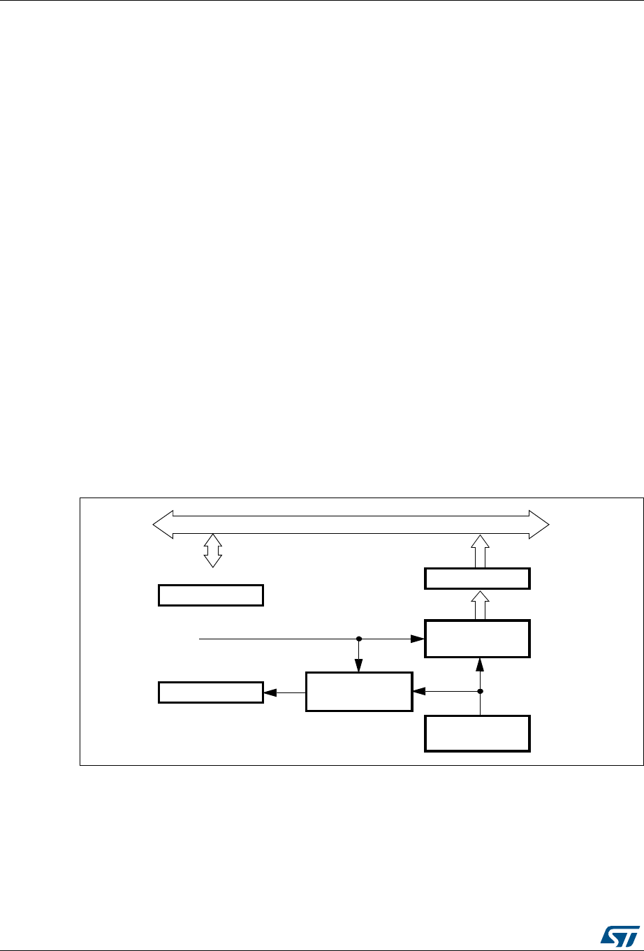
Random number generator (RNG) RM0090
752/1718 DocID018909 Rev 9
24 Random number generator (RNG)
This section applies to the whole STM32F4xx family devices, unless otherwise specified.
24.1 RNG introduction
The RNG processor is a random number generator, based on a continuous analog noise,
that provides a random 32-bit value to the host when read.
The RNG passed the FIPS PUB 140-2 (2001 October 10) tests with a success ratio of 99%.
24.2 RNG main features
•It delivers 32-bit random numbers, produced by an analog generator
•40 periods of the RNG_CLK clock signal between two consecutive random numbers
•Monitoring of the RNG entropy to flag abnormal behavior (generation of stable values,
or of a stable sequence of values)
•It can be disabled to reduce power consumption
24.3 RNG functional description
Figure 232 shows the RNG block diagram.
Figure 232. Block diagram
1. For more details about RNG Clock (RNG_CLK) source, please refer to Section 6: Reset and clock control
for STM32F42xxx and STM32F43xxx (RCC) and Section 7: Reset and clock control for
STM32F405xx/07xx and STM32F415xx/17xx(RCC).
The random number generator implements an analog circuit. This circuit generates seeds
that feed a linear feedback shift register (RNG_LFSR) in order to produce 32-bit random
numbers.
BIT!("BUS
2.'?$2
2.'
?#2
2.'
?32
3TATUSREGISTER
#ONTROLREGISTER
FAULTDETECTOR
,&32
!NALOGSEED
2.'?#,+
#LOCKCHECKER
DATAREGISTER
3HIFT2EGISTER
FEEDA,INEAR&EEDBACK
AI

DocID018909 Rev 9 753/1718
RM0090 Random number generator (RNG)
756
The analog circuit is made of several ring oscillators whose outputs are XORed to generate
the seeds. The RNG_LFSR is clocked by a dedicated clock (RNG_CLK) at a constant
frequency, so that the quality of the random number is independent of the HCLK frequency.
The contents of the RNG_LFSR are transferred into the data register (RNG_DR) when a
significant number of seeds have been introduced into the RNG_LFSR.
In parallel, the analog seed and the dedicated RNG_CLK clock are monitored. Status bits (in
the RNG_SR register) indicate when an abnormal sequence occurs on the seed or when
the frequency of the RNG_CLK clock is too low. An interrupt can be generated when an
error is detected.
24.3.1 Operation
To run the RNG, follow the steps below:
1. Enable the interrupt if needed (to do so, set the IE bit in the RNG_CR register). An
interrupt is generated when a random number is ready or when an error occurs.
2. Enable the random number generation by setting the RNGEN bit in the RNG_CR
register. This activates the analog part, the RNG_LFSR and the error detector.
3. At each interrupt, check that no error occurred (the SEIS and CEIS bits should be ‘0’ in
the RNG_SR register) and that a random number is ready (the DRDY bit is ‘1’ in the
RNG_SR register). The contents of the RNG_DR register can then be read.
As required by the FIPS PUB (Federal Information Processing Standard Publication) 140-2,
the first random number generated after setting the RNGEN bit should not be used, but
saved for comparison with the next generated random number. Each subsequent generated
random number has to be compared with the previously generated number. The test fails if
any two compared numbers are equal (continuous random number generator test).
24.3.2 Error management
If the CEIS bit is read as ‘1’ (clock error)
In the case of a clock, the RNG is no more able to generate random numbers because the
RNG_CLK clock is not correct. Check that the clock controller is correctly configured to
provide the RNG clock and clear the CEIS bit. The RNG can work when the CECS bit is ‘0’.
The clock error has no impact on the previously generated random numbers, and the
RNG_DR register contents can be used.
If the SEIS bit is read as ‘1’ (seed error)
In the case of a seed error, the generation of random numbers is interrupted for as long as
the SECS bit is ‘1’. If a number is available in the RNG_DR register, it must not be used
because it may not have enough entropy.
What you should do is clear the SEIS bit, then clear and set the RNGEN bit to reinitialize
and restart the RNG.
24.4 RNG registers
The RNG is associated with a control register, a data register and a status register. They
have to be accessed by words (32 bits).

Random number generator (RNG) RM0090
754/1718 DocID018909 Rev 9
24.4.1 RNG control register (RNG_CR)
Address offset: 0x00
Reset value: 0x0000 0000
24.4.2 RNG status register (RNG_SR)
Address offset: 0x04
Reset value: 0x0000 0000
31 30 29 28 27 26 25 24 23 22 21 20 19 18 17 16
Reserved
15 14 13 12 11 10 9 8 7 6 5 4 3 2 1 0
Reserved
IE RNGEN
Reserved
rw rw
Bits 31:4 Reserved, must be kept at reset value
Bit 3 IE: Interrupt enable
0: RNG Interrupt is disabled
1: RNG Interrupt is enabled. An interrupt is pending as soon as DRDY=1 or SEIS=1 or
CEIS=1 in the RNG_SR register.
Bit 2 RNGEN: Random number generator enable
0: Random number generator is disabled
1: random Number Generator is enabled.
Bits 1:0 Reserved, must be kept at reset value
31 30 29 28 27 26 25 24 23 22 21 20 19 18 17 16
Reserved
1514131211109876543210
Reserved SEIS CEIS Reserved SECS CECS DRDY
rc_w0 rc_w0 r r r
Bits 31:3 Reserved, must be kept at reset value
Bit 6 SEIS: Seed error interrupt status
This bit is set at the same time as SECS, it is cleared by writing it to 0.
0: No faulty sequence detected
1: One of the following faulty sequences has been detected:
– More than 64 consecutive bits at the same value (0 or 1)
– More than 32 consecutive alternances of 0 and 1 (0101010101...01)
An interrupt is pending if IE = 1 in the RNG_CR register.
Bit 5 CEIS: Clock error interrupt status
This bit is set at the same time as CECS, it is cleared by writing it to 0.
0: The RNG_CLK clock was correctly detected
1: The RNG_CLK was not correctly detected (fRNG_CLK< fHCLK/16)
An interrupt is pending if IE = 1 in the RNG_CR register.
Bits 4:3 Reserved, must be kept at reset value

DocID018909 Rev 9 755/1718
RM0090 Random number generator (RNG)
756
24.4.3 RNG data register (RNG_DR)
Address offset: 0x08
Reset value: 0x0000 0000
The RNG_DR register is a read-only register that delivers a 32-bit random value when read.
After being read, this register delivers a new random value after a maximum time of 40
periods of the RNG_CLK clock. The software must check that the DRDY bit is set before
reading the RNDATA value.
Bit 2 SECS: Seed error current status
0: No faulty sequence has currently been detected. If the SEIS bit is set, this means that a
faulty sequence was detected and the situation has been recovered.
1: One of the following faulty sequences has been detected:
– More than 64 consecutive bits at the same value (0 or 1)
– More than 32 consecutive alternances of 0 and 1 (0101010101...01)
Bit 1 CECS: Clock error current status
0: The RNG_CLK clock has been correctly detected. If the CEIS bit is set, this means that a
clock error was detected and the situation has been recovered
1: The RNG_CLK was not correctly detected (fRNG_CLK< fHCLK/16).
Bit 0 DRDY: Data ready
0: The RNG_DR register is not yet valid, no random data is available
1: The RNG_DR register contains valid random data
Note: An interrupt is pending if IE = 1 in the RNG_CR register.
Once the RNG_DR register has been read, this bit returns to 0 until a new valid value is
computed.
31 30 29 28 27 26 25 24 23 22 21 20 19 18 17 16
RNDATA
rrrrrrrrrrrrrrrr
1514131211109876543210
RNDATA
rrrrrrrrrrrrrrrr
Bits 31:0 RNDATA: Random data
32-bit random data.
Random number generator (RNG) RM0090
756/1718 DocID018909 Rev 9
24.4.4 RNG register map
Table 115 gives the RNG register map and reset values.
Table 115. RNG register map and reset map
Offset
Register
name
reset value
Register size
31
30
29
28
27
26
25
24
23
22
21
20
19
18
17
16
15
14
13
12
11
10
9
8
7
6
5
4
3
2
1
0
0x00 RNG_CR
0x0000000 Reserved
IE
RNGEN
Reserved
0x04 RNG_SR
0x0000000 Reserved
SEIS
CEIS
Reserved
SECS
CECS
DRDY
0x08 RNG_DR
0x0000000 RNDATA[31:0]

DocID018909 Rev 9 757/1718
RM0090 Hash processor (HASH)
782
25 Hash processor (HASH)
This section applies to STM32F415/417xx and STM32F43xxx devices.
25.1 HASH introduction
The hash processor is a fully compliant implementation of the secure hash algorithm
(SHA-1, SHA-224, SHA-256), the MD5 (message-digest algorithm 5) hash algorithm and
the HMAC (keyed-hash message authentication code) algorithm suitable for a variety of
applications. It computes a message digest (160 bits for the SHA-1 algorithm, 256 bits for
the SHA-256 algorithm and 224 bits for the SHA-224 algorithm,128 bits for the MD5
algorithm) for messages of up to (264 – 1) bits, while HMAC algorithms provide a way of
authenticating messages by means of hash functions. HMAC algorithms consist in calling
the SHA-1, SHA-224, SHA-256 or MD5 hash function twice.
25.2 HASH main features
•Suitable for data authentication applications, compliant with:
– FIPS PUB 180-2 (Federal Information Processing Standards Publication 180-2)
– Secure Hash Standard specifications (SHA-1, SHA-224 and SHA-256)
– IETF RFC 1321 (Internet Engineering Task Force Request For Comments number
1321) specifications (MD5)
•Fast computation of SHA-1, SHA-224 and SHA-256, and MD5 (SHA-224 and SHA-256
are available on STM32F43xxx only)
•AHB slave peripheral
•32-bit data words for input data, supporting word, half-word, byte and bit bit-string
representations, with little-endian data representation only.
•Automatic swapping to comply with the big-endian SHA1, SHA-224 and SHA-256
computation standard with little-endian input bit-string representation
•Automatic padding to complete the input bit string to fit modulo 512 (16 × 32 bits)
message digest computing
•5× 32-bit words (H0 to H5) on STM32F415/417xx and 8 × 32-bit words (H0 to H7) on
STM32F43xxx for output message digest, reload able to continue interrupted message
digest computation.
•Corresponding 32-bit words of the digest from consecutive message blocks are added
to each other to form the digest of the whole message
•Automatic data flow control with support for direct memory access (DMA)
Note: Padding, as defined in the SHA-1, SHA-224 and SHA-256 algorithm, consists in adding a bit
at bx1 followed by N bits at bx0 to get a total length congruent to 448 modulo 512. After this,
the message is completed with a 64-bit integer which is the binary representation of the
original message length.
For this hash processor, the quanta for entering the message is a 32-bit word, so an
additional information must be provided at the end of the message entry, which is the
number of valid bits in the last 32-bit word entered.
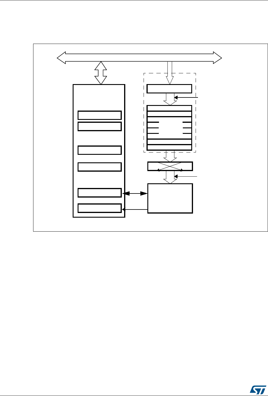
Hash processor (HASH) RM0090
758/1718 DocID018909 Rev 9
25.3 HASH functional description
Figure 1 shows the block diagram of the hash processor.
Figure 233. Block diagram for STM32F415/417xx
BIT!("BUS
(ASH(-!#
3(!-$
(!3(?$).
SWA PPIN G
§BIT
).&)&/
(!3(?#2
(!3(?((
(!3(?#32
CONTEXT
DIGEST
(!3(?)-2
(!3(?32
)NTERRUPTREGISTERS
#ONTROLREGISTER
#ONTEXTSWAPPING
-ESSAGEDIGEST
PROCESSOR CORE
(!3(?34 2
3TARTREGISTER
).&)&/FULL
WRITEINTO(!3(?$).
#ONTROLANDSTATUS
REGISTERS
$ATA
REGISTER
ORWRITE$#!,BITTO
ORCOMPLETEBLOCK
OR$#!,WRITTENTO
).BUFFER
TRANSFERREDBYTHE$-!
AI
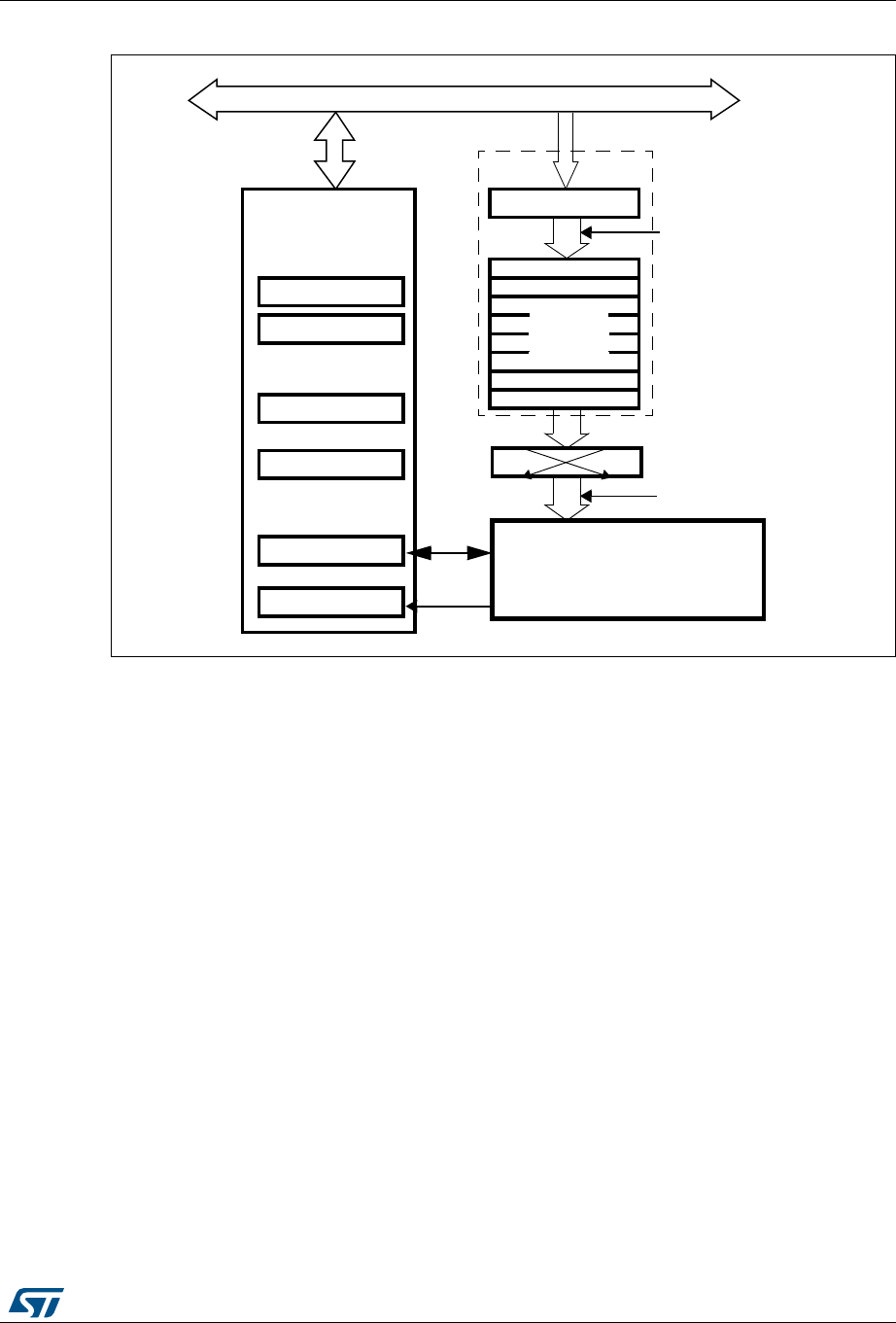
DocID018909 Rev 9 759/1718
RM0090 Hash processor (HASH)
782
Figure 234. Block diagram for STM32F43xxx
The FIPS PUB 180-2 standard and the IETF RFC 1321 publication specify the SHA-1, SHA-
224 and SHA-256 and MD5 secure hash algorithms, respectively, for computing a
condensed representation of a message or data file. When a message of any length below
264 bits is provided on input, the SHA-1, SHA-224 and SHA-256 and MD5 produce
respective a 160-bit, 224 bit, 256 bit and 128-bit output string, respectively, called a
message digest. The message digest can then be processed with a digital signature
algorithm in order to generate or verify the signature for the message. Signing the message
digest rather than the message often improves the efficiency of the process because the
message digest is usually much smaller in size than the message. The verifier of a digital
signature has to use the same hash algorithm as the one used by the creator of the digital
signature.
The SHA-1, SHA-224 and SHA-256 and MD5 are qualified as “secure” because it is
computationally infeasible to find a message that corresponds to a given message digest, or
to find two different messages that produce the same message digest. Any change to a
message in transit will, with very high probability, result in a different message digest, and
the signature will fail to verify. For more detail on the SHA-1 or SHA-224 and SHA-256
algorithm, please refer to the FIPS PUB 180-2 (Federal Information Processing Standards
Publication 180-2), 2002 august 1.
The current implementation of this standard works with little-endian input data convention.
For example, the C string “abc” must be represented in memory as the 24-bit hexadecimal
value 0x434241.
A message or data file to be processed by the hash processor should be considered a bit
string. The length of the message is the number of bits in the message (the empty message
BIT!("BUS
(ASH(-!#
3(!3(!3(!AND-$
(!3(?$).
SWA PPIN G
§BIT
).&)&/
(!3(?#2
(!3(?((
(!3(?#32
CONTEXT
DIGEST
(!3(?)-2
(!3(?32
)NTERRUPTREGISTERS
#ONTROLREGISTER
#ONTEXTSWAPPING
-ESSAGEDIGEST
PROCESSOR CORE
(!3(?34 2
3TARTREGISTER
).&)&/FULL
WRITEINTO(!3(?$).
#ONTROLANDSTATUS
REGISTERS
$ATA
REGISTER
ORWRITE$#!,BITTO
ORCOMPLETEBLOCK
OR$#!,WRITTENTO
).BUFFER
TRANSFERREDBYTHE$-!
-36

Hash processor (HASH) RM0090
760/1718 DocID018909 Rev 9
has length 0). You can consider that 32 bits of this bit string forms a 32-bit word. Note that
the FIPS PUB 180-1 standard uses the convention that bit strings grow from left to right, and
bits can be grouped as bytes (8 bits) or words (32 bits) (but some implementations also use
half-words (16 bits), and implicitly, uses the big-endian byte (half-word) ordering. This
convention is mainly important for padding (see Section 1.3.4: Message padding on
page 12).
25.3.1 Duration of the processing
The computation of an intermediate block of a message takes:
•66 HCLK clock cycles in SHA-1
•50 HCLK clock cycles in SHA-224
•50 HCLK clock cycles in SHA-256
•50 HCLK clock cycles in MD5
to which you must add the time needed to load the 16 words of the block into the processor
(at least 16 clock cycles for a 512-bit block).
The time needed to process the last block of a message (or of a key in HMAC) can be
longer. This time depends on the length of the last block and the size of the key (in HMAC
mode). Compared to the processing of an intermediate block, it can be increased by a factor
of:
•1 to 2.5 for a hash message
•around 2.5 for an HMAC input-key
•1 to 2.5 for an HMAC message
•around 2.5 for an HMAC output key in case of a short key
•3.5 to 5 for an HMAC output key in case of a long key
25.3.2 Data type
Data are entered into the hash processor 32 bits (word) at a time, by writing them into the
HASH_DIN register. But the original bit-string can be organized in bytes, half-words or
words, or even be represented as bits. As the system memory organization is little-endian
and SHA1, SHA-224 and SHA-256 computation is big-endian, depending on the way the
original bit string is grouped, a bit, byte, or half-word swapping operation is performed
automatically by the hash processor.
The kind of data to be processed is configured with the DATATYPE bitfield in the HASH
control register (HASH_CR).
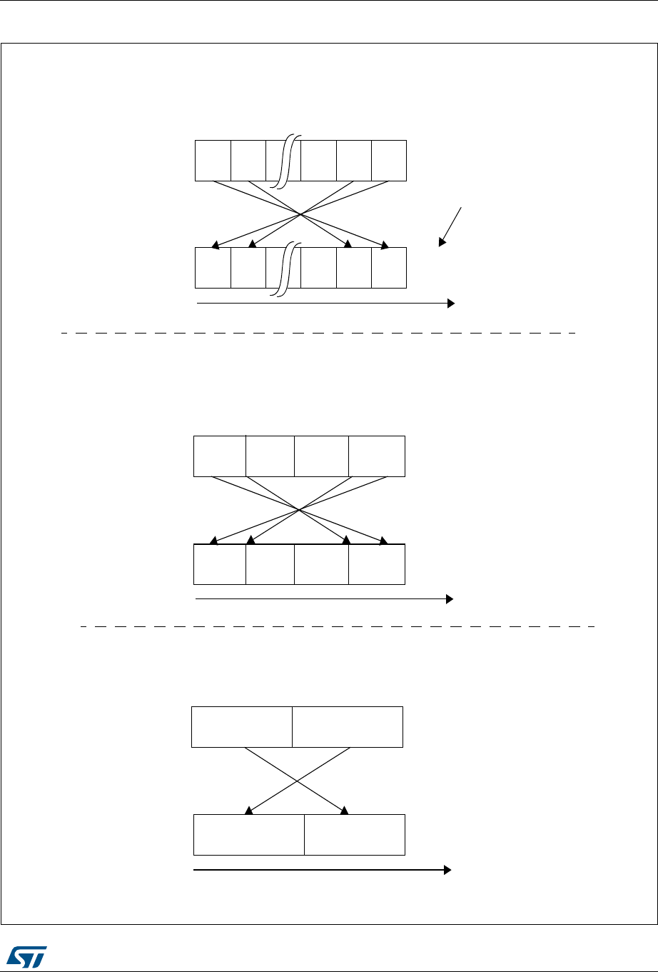
DocID018909 Rev 9 761/1718
RM0090 Hash processor (HASH)
782
Figure 235. Bit, byte and half-word swapping
"YTE"YTE"YTE"YTE
BITSBITS
BITSBITS
(
!
3
(?$
)
.
BITSTRINGORGANIZATIONIN
BITBITBITBITBIT
"IT
S
W
A
P
PI
N
G
OPE
R
A
T
I
O
N
B
I
T
S
TR
I
N
G
G
R
O
WS
I
N
T
HI
S
DI
RECT
IO
N
AS
D
E
F
I
N
E
D
B
Y
&)03
05"
S
T
D
BITBITBITBITBIT
(
!
3
(?$
)
.
"
Y
T
E
S
W
A
P
PING
OPE
R
A
T
I
O
N
B
I
T
S
TR
I
N
G
G
R
O
WS
I
N
T
HI
S
DI
RECT
IO
N
AS
D
E
F
I
N
E
D
B
Y
&)03
05"
S
T
D
"YTE"YTE"YTE"YTE
BITSBITS
BITSBITS
(!
3
(?
$
)
.
(
A
L
F
W
O
R
D
S
W
A
PPING
O
P
ER
A
T
IO
N
B
I
TSTR
IN
G
G
R
O
WS
I
N
T
H
IS
D
I
RECT
I
O
N
A
S
D
E
FI
N
E
D
B
Y
&
)
03
05"
S
T
D
(ALFWORD
BITS
$
!
4
!
490%
BX
$
!
4
!
4
90%
BX
$
!
4
!
4
90%
BX
(ALFWORD
BITS
(ALFWORD
BITS
(ALFWORD
BITS
tÞtá
P
AD
D
INGISPERFO
R
M
ED
ONTHISSIDEOFTHE
BIT
S
T
RI
N
G
AI
(ASHPROCESSOR"IG%NDIAN
"ITSENTREDWITHLITTLE%NDIANFORMAT
!)NCASEOFBINARYDATAHASHALLBITSSHOULDBESWAPPEDASBELOW
")NCASEOFBYTEDATAHASHALLBYTESSHOULDBESWAPPEDASBELOW
#)NCASEOFHALFWORDHASHALLHALFWORDSHOULDBESWAPPEDASBELOW
"YTESENTREDWITHLITTLE%NDIANFORMAT
"ITSTRINGORGANIZATIONIN
(ASHPROCESSOR"IG%NDIAN
HALFWORDENTREDWITHLITTLE%NDIANFORMAT
"ITSTRINGORGANIZATIONIN
(ASHPROCESSOR"IG%NDIAN

Hash processor (HASH) RM0090
762/1718 DocID018909 Rev 9
The least significant bit of the message has to be at position 0 (right) in the first word
entered into the hash processor, the 32nd bit of the bit string has to be at position 0 in the
second word entered into the hash processor and so on.
25.3.3 Message digest computing
The HASH sequentially processes blocks of 512 bits when computing the message digest.
Thus, each time 16 × 32-bit words (= 512 bits) have been written by the DMA or the CPU,
into the hash processor, the HASH automatically starts computing the message digest. This
operation is known as a partial digest computation.
The message to be processed is entered into the peripheral by 32-bit words written into the
HASH_DIN register. The current contents of the HASH_DIN register are transferred to the
input FIFO (IN FIFO) each time the register is written with new data. HASH_DIN and the
input FIFO form a FIFO of a 17-word length (named the IN buffer).
The processing of a block can start only once the last value of the block has entered the IN
FIFO. The peripheral must get the information as to whether the HASH_DIN register
contains the last bits of the message or not. Two cases may occur:
•When the DMA is not used:
– In case of a partial digest computation, this is done by writing an additional word
into the HASH_DIN register (actually the first word of the next block). Then the
software must wait until the processor is ready again (when DINIS=1) before
writing new data into HASH_DIN.
– In case of a final digest computation (last block entered), this is done by writing the
DCAL bit to 1.
•When the DMA is used:
The contents of the HASH_DIN register are interpreted automatically with the
information sent by the DMA controller.
– In case of a single DMA transfer: Multiple DMA transfer (MDMAT) bit should be
cleared on STM32F43xxx. When the last block has been transferred to the
HASH_DIN register via DMA channel, DCAL bit will be set to automatically to 1 in
the HASH_STR register in order to launch the final digest calculation.
– In case of a multiple DMA transfer (available only on STM32F43xxx): Multiple
DMA transfer (MDMAT) bit should be set to 1 by software so DCAL bit does not
get set automatically by HW, in this case the final digest calculation for hash and
for each phases for HMAC (for more details about HMAC phases please refer to
HMAC operation section) will not be launched a the end of the DMA transfer
request, allowing the processor to receive a new DMA transfer. During the last
DMA transfer, Multiple DMA transfer (MDMAT) bit should be cleared by software in
order to set automatically DCAL bit at the end of the last bloc and lunch the final
digest.
– The contents of the HASH_DIN register are interpreted automatically with the
information sent by the DMA controller.
This process —data entering + partial digest computation— continues until the last bits of
the original message are written to the HASH_DIN register. As the length (number of bits) of
a message can be any integer value, the last word written into the HASH processor may
have a valid number of bits between 1 and 32. This number of valid bits in the last word,
NBLW, has to be written into the HASH_STR register, so that message padding is correctly
performed before the final message digest computation.

DocID018909 Rev 9 763/1718
RM0090 Hash processor (HASH)
782
Once this is done, writing into HASH_STR with bit DCAL = 1 starts the processing of the last
entered block of message by the hash processor. This processing consists in:
•Automatically performing the message padding operation: the purpose of this operation
is to make the total length of a padded message a multiple of 512. The HASH
sequentially processes blocks of 512 bits when computing the message digest
•Computing the final message digest
When the DMA is enabled, it provides the information to the hash processor when it is
transferring the last data word. Then the padding and digest computation are performed
automatically as if DCAL had been written to 1.
25.3.4 Message padding
Message padding consists in appending a “1” followed by m “0”s followed by a 64-bit integer
to the end of the original message to produce a padded message block of length 512. The
“1” is added to the last word written into the HASH_DIN register at the bit position defined by
the NBLW bitfield, and the remaining upper bits are cleared (“0”s).
Example: let us assume that the original message is the ASCII binary-coded form of “abc”,
of length L = 24:
byte 0 byte 1 byte 2 byte 3
01100001 01100010 01100011 UUUUUUUU
<-- 1st word written to HASH_DIN -->
NBLW has to be loaded with the value 24: a “1” is appended at bit location 24 in the bit string
(starting counting from left to right in the above bit string), which corresponds to bit 31 in the
HASH_DIN register (little-endian convention):
01100001 01100010 01100011 1UUUUUUU
Since L = 24, the number of bits in the above bit string is 25, and 423 “0”s are appended,
making now 448. This gives (in hexadecimal, big-endian format):
61626380 00000000 00000000 00000000
00000000 00000000 00000000 00000000
00000000 00000000 00000000 00000000
00000000 00000000
The L value, in two-word representation (that is 00000000 00000018) is appended. Hence
the final padded message in hexadecimal:
61626380 00000000 00000000 00000000
00000000 00000000 00000000 00000000
00000000 00000000 00000000 00000000
00000000 00000000 00000000 00000028
If the HASH is programmed to use the little-endian byte input format, the above message
has to be entered by doing the following steps:
1. 0xUU636261 is written into the HASH_DIN register (where ‘U’ means don’t care)
2. 0x18 is written into the HASH_STR register (the number of valid bits in the last word
written into the HASH_DIN register is 24, as the original message length is 24 bits)
3. 0x10 is written into the HASH_STR register to start the message padding and digest
computation. When NBLW ≠ 0x00, the message padding puts a “1” into the HASH_DIN
register at the bit position defined by the NBLW value, and inserts “0”s at bit locations
[31:(NBLW+1)]. When NBLW == 0x00, the message padding inserts one new word with

Hash processor (HASH) RM0090
764/1718 DocID018909 Rev 9
value 0x0000 0001. Then an all zero word (0x0000 0000) is added and the message
length in a two-word representation, to get a block of 16 x 32-bit words.
4. The HASH computing is performed, and the message digest is then available in the
HASH_Hx registers (x = 0...4) for the SHA-1 algorithm. For example:
H0 = 0xA9993E36
H1 = 0x4706816A
H2 = 0xBA3E2571
H3 = 0x7850C26C
H4 = 0x9CD0D89D
25.3.5 Hash operation
The hash function (SHA-1, SHA-224, SHA-256 and MD5) is selected when the INIT bit is
written to ‘1’ in the HASH_CR register while the MODE bit is at ‘0’ in HASH_CR. The
algorithm (SHA-1, SHA-224,SHA-256 or MD5) is selected at the same time (that is when the
INIT bit is set) using the ALGO bits.
The message can then be sent by writing it word by word into the HASH_DIN register. When
a block of 512 bits —that is 16 words— has been written, a partial digest computation starts
upon writing the first data of the next block. The hash processor remains busy for 66 cycles
for the SHA-1 algorithm, or 50 cycles for the MD5 algorithm, SHA-224 algorithm and SHA-
256 algorithm.
The process can then be repeated until the last word of the message. If DMA transfers are
used, refer to the Procedure where the data are loaded by DMA section. Otherwise, if the
message length is not an exact multiple of 512 bits, then the HASH_STR register has to be
written to launch the computation of the final digest.
Once computed, the digest can be read from the HASH_H0...HASH_H4 registers (for the
MD5 algorithm, HASH_H4 is not relevant) on STM32F415/417xx, and from the
HASH_H0...HASH_H7 registers on STM32F43xxx where:
HASH_H4..HASH_H7 are not relevant when the MD5 algorithm is selected,
HASH_H5.. HASH_H7 are not relevant when the SHA-1algorithm is selected,
HASH_H7 is not relevant when the SHA-224 algorithm is selected.
25.3.6 HMAC operation
The HMAC algorithm is used for message authentication, by irreversibly binding the
message being processed to a key chosen by the user. For HMAC specifications, refer to
“HMAC: keyed-hashing for message authentication, H. Krawczyk, M. Bellare, R. Canetti,
February 1997.
Basically, the algorithm consists of two nested hash operations:
HMAC(message) = Hash[((key | pad) XOR 0x5C)
| Hash(((key | pad) XOR 0x36) | message)]
where:
•pad is a sequence of zeroes needed to extend the key to the length of the underlying
hash function data block (that is 512 bits for both the SHA-1, SHA224, SHA-256 and
MD5 hash algorithms)
•| represents the concatenation operator
To compute the HMAC, four different phases are required:

DocID018909 Rev 9 765/1718
RM0090 Hash processor (HASH)
782
1. The block is initialized by writing the INIT bit to ‘1’ with the MODE bit at ‘1’ and the
ALGO bits set to the value corresponding to the desired algorithm. The LKEY bit must
also be set during this phase if the key being used is longer than 64 bytes (in this case,
the HMAC specifications specify that the hash of the key should be used in place of the
real key).
2. The key (to be used for the inner hash function) is then given to the core. This
operation follows the same mechanism as the one used to send the message in the
hash operation (that is, by writing into HASH_DIN and, finally, into HASH_STR).
3. Once the last word has been entered and computation has started, the hash processor
elaborates the key. It is then ready to accept the message text using the same
mechanism as the one used to send the message in the hash operation.
4. After the first hash round, the hash processor returns “ready” to indicate that it is ready
to receive the key to be used for the outer hash function (normally, this key is the same
as the one used for the inner hash function). When the last word of the key is entered
and computation starts, the HMAC result is made available in the
HASH_H0...HASH_H4 registers on STM32F415/417xx and on HASH_H0...HASH_H7
registers on STM32F43xxx.
Note: 1 The computation latency of the HMAC primitive depends on the lengths of the keys and
message. You could the HMAC as two nested underlying hash functions with the same key
length (long or short).
25.3.7 Context swapping
It is possible to interrupt a hash/HMAC process to perform another processing with a higher
priority, and to complete the interrupted process later on, when the higher-priority task is
complete. To do so, the context of the interrupted task must be saved from the hash
registers to memory, and then be restored from memory to the hash registers.
The procedures where the data flow is controlled by software or by DMA are described
below.

Hash processor (HASH) RM0090
766/1718 DocID018909 Rev 9
Procedure where the data are loaded by software
The context can be saved only when no block is currently being processed. That is, you
must wait for DINIS = 1 (the last block has been processed and the input FIFO is empty) or
NBW ≠0 (the FIFO is not full and no processing is ongoing).
•Context saving:
Store the contents of the following registers into memory:
– HASH_IMR
– HASH_STR
– HASH_CR
– HASH_CSR0 to HASH_CSR50 on STM32F415/417xx, and HASH_CSR0 to
HASH_CSR53 on STM32F43xxx.
•Context restoring:
The context can be restored when the high-priority task is complete. Please follow the
order of the sequence below.
a) Write the following registers with the values saved in memory: HASH_IMR,
HASH_STR and HASH_CR
b) Initialize the hash processor by setting the INIT bit in the HASH_CR register
c) Write the HASH_CSR0 to HASH_CSR50 (STM32F415/417xx), and HASH_CSR0
to HASH_CSR53 (STM32F43xxx) registers with the values saved in memory
You can now restart the processing from the point where it has been interrupted.
Procedure where the data are loaded by DMA
In this case it is not possible to predict if a DMA transfer is in progress or if the process is
ongoing. Thus, you must stop the DMA transfers, then wait until the HASH is ready in order
to interrupt the processing of a message.
•Interrupting a processing:
– Clear the DMAE bit to disable the DMA interface
– Wait until the current DMA transfer is complete (wait for DMAES = 0 in the
HASH_SR register). Note that the block may or not have been totally transferred
to the HASH.
– Disable the corresponding channel in the DMA controller
– Wait until the hash processor is ready (no block is being processed), that is wait
for DINIS = 1
•The context saving and context restoring phases are the same as above (see
Procedure where the data are loaded by software).
Reconfigure the DMA controller so that it transfers the end of the message. You can now
restart the processing from the point where it was interrupted by setting the DMAE bit.
Note: If context swapping does not involve HMAC operations, the HASH_CSR38 to
HASH_CSR50 (STM32F415/417xx) and HASH_CSR38 to HASH_CSR53 (STM32F43xxx)
registers do not have to be saved and restored.
If context swapping occurs between two blocks (the last block was completely processed
and the next block has not yet been pushed into the IN FIFO, NBW = 000 in the HASH_CR
register), the HASH_CSR22 to HASH_CSR37 registers do not have to be saved and
restored.
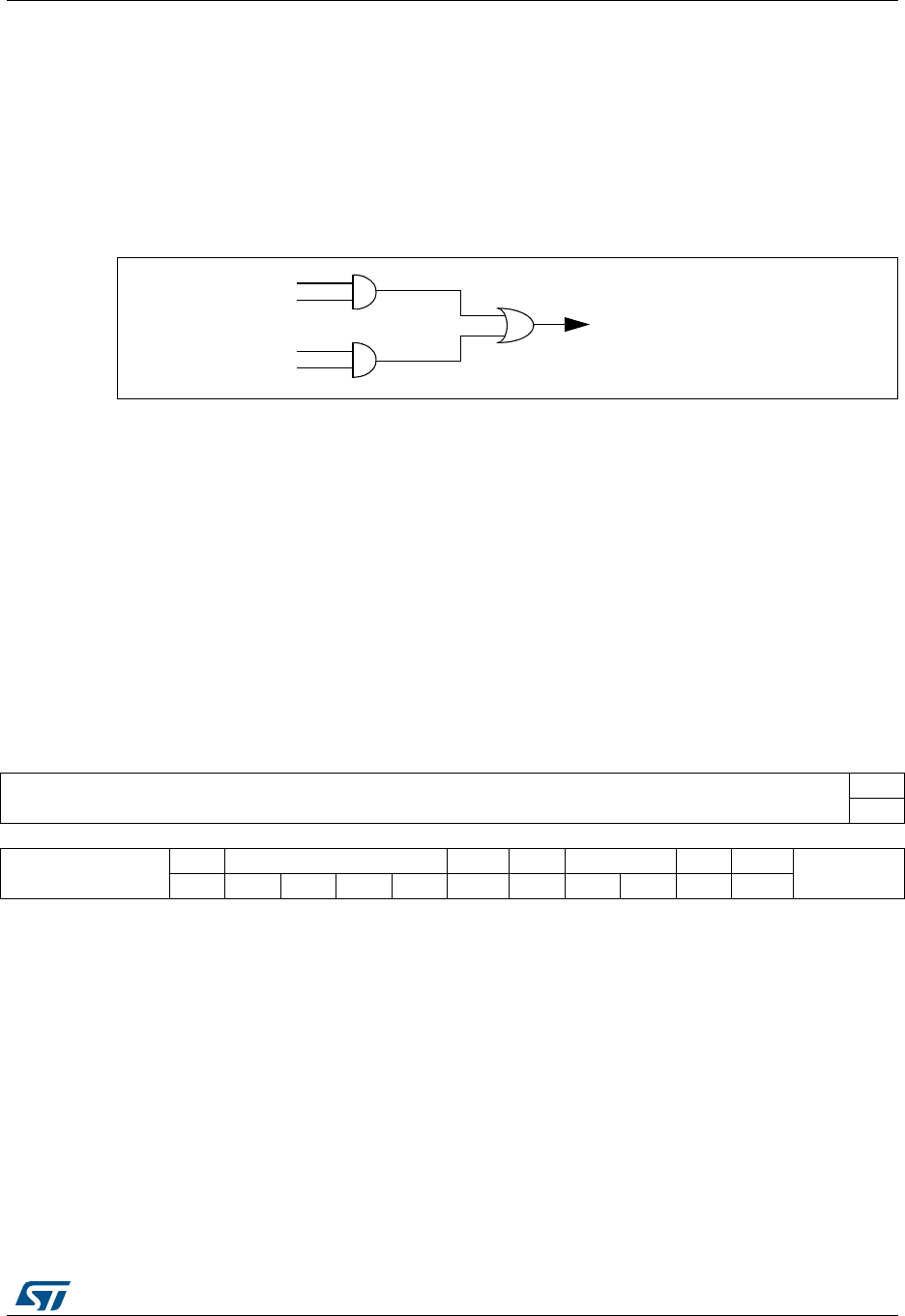
DocID018909 Rev 9 767/1718
RM0090 Hash processor (HASH)
782
25.3.8 HASH interrupt
There are two individual maskable interrupt sources generated by the HASH processor.
They are connected to the same interrupt vector.
You can enable or disable the interrupt sources individually by changing the mask bits in the
HASH_IMR register. Setting the appropriate mask bit to 1 enables the interrupt.
The status of the individual interrupt sources can be read from the HASH_SR register.
Figure 236. HASH interrupt mapping diagram
25.4 HASH registers
The HASH core is associated with several control and status registers and five message
digest registers.
All these registers are accessible through word accesses only, else an AHB error is
generated.
25.4.1 HASH control register (HASH_CR) for STM32F415/417xx
Address offset: 0x00
Reset value: 0x0000 0000
$#)3
$#)-
$).)3
$).)-
(!3(INTERRUPTTO.6)#
AI
31 30 29 28 27 26 25 24 23 22 21 20 19 18 17 16
Reserved
LKEY
rw
15 14 13 12 11 10 9 8 7 6 5 4 3 2 1 0
Reserved
DINNE NBW ALGO[0] MODE DATATYPE DMAE INIT
Reserved
rrrrrrwrwrwrwrww
Bits 31:17 Reserved, forced by hardware to 0.
Bit 16 LKEY: Long key selection
This bit selects between short key (≤ 64 bytes) or long key (> 64 bytes) in HMAC
mode
0: Short key (≤ 64 bytes)
1: Long key (> 64 bytes)
Note: This selection is only taken into account when the INIT bit is set and MODE
= 1. Changing this bit during a computation has no effect.
Bits 15:13 Reserved, forced by hardware to 0.

Hash processor (HASH) RM0090
768/1718 DocID018909 Rev 9
Bit 12 DINNE: DIN not empty
This bit is set when the HASH_DIN register holds valid data (that is after being
written at least once). It is cleared when either the INIT bit (initialization) or the
DCAL bit (completion of the previous message processing) is written to 1.
0: No data are present in the data input buffer
1: The input buffer contains at least one word of data
Bits 11:8 NBW: Number of words already pushed
This bitfield reflects the number of words in the message that have already been
pushed into the IN FIFO.
NBW increments (+1) when a write access is performed to the HASH_DIN
register while DINNE = 1.
It goes to 0000 when the INIT bit is written to 1 or when a digest calculation
starts (DCAL written to 1 or DMA end of transfer).
″If the DMA is not used:
0000 and DINNE=0: no word has been pushed into the DIN buffer (the buffer is
empty, both the HASH_DIN register and the IN FIFO are empty)
0000 and DINNE=1: 1 word has been pushed into the DIN buffer (The
HASH_DIN register contains 1 word, the IN FIFO is empty)
0001: 2 words have been pushed into the DIN buffer (the HASH_DIN register
and the IN FIFO contain 1 word each)
...
1111: 16 words have been pushed into the DIN buffer
″If the DMA is used, NBW is the exact number of words that have been
pushed into the IN FIFO.
Bit 7 ALGO[1:0]: Algorithm selection
These bits selects the SHA-1 or the MD5 algorithm:
0: SHA-1 algorithm selected
1: MD5 algorithm selected
Note: This selection is only taken into account when the INIT bit is set. Changing
this bit during a computation has no effect.
Bit 6 MODE: Mode selection
This bit selects the HASH or HMAC mode for the selected algorithm:
0: Hash mode selected
1: HMAC mode selected. LKEY must be set if the key being used is longer than
64 bytes.
Note: This selection is only taken into account when the INIT bit is set. Changing
this bit during a computation has no effect.
Bits 5:4 DATATYPE: Data type selection
Defines the format of the data entered into the HASH_DIN register:
00: 32-bit data. The data written into HASH_DIN are directly used by the HASH
processing, without reordering.
01: 16-bit data, or half-word. The data written into HASH_DIN are considered as
2 half-words, and are swapped before being used by the HASH processing.
10: 8-bit data, or bytes. The data written into HASH_DIN are considered as 4
bytes, and are swapped before being used by the HASH processing.
11: bit data, or bit-string. The data written into HASH_DIN are considered as 32
bits (1st bit of the sting at position 0), and are swapped before being used by the
HASH processing (1st bit of the string at position 31).

DocID018909 Rev 9 769/1718
RM0090 Hash processor (HASH)
782
Bit 3 DMAE: DMA enable
0: DMA transfers disabled
1: DMA transfers enabled. A DMA request is sent as soon as the HASH core is
ready to receive data.
Note: 1: This bit is cleared by hardware when the DMA asserts the DMA terminal
count signal (while transferring the last data of the message). This bit is not
cleared when the INIT bit is written to 1.
2: If this bit is written to 0 while a DMA transfer has already been requested
to the DMA, DMAE is cleared but the current transfer is not aborted.
Instead, the DMA interface remains internally enabled until the transfer is
complete or INIT is written to 1.
Bit 2 INIT: Initialize message digest calculation
Writing this bit to 1 resets the hash processor core, so that the HASH is ready to
compute the message digest of a new message.
Writing this bit to 0 has no effect.
Reading this bit always return 0.
Bits 1:0 Reserved, must be kept cleared.

Hash processor (HASH) RM0090
770/1718 DocID018909 Rev 9
25.4.2 HASH control register (HASH_CR) for STM32F43xxx
Address offset: 0x00
Reset value: 0x0000 0000
31 30 29 28 27 26 25 24 23 22 21 20 19 18 17 16
Reserved
ALGO[1]
Reserved
LKEY
rw rw
15 14 13 12 11 10 9 8 7 6 5 4 3 2 1 0
Reserved
MDMAT DINNE NBW ALGO[0] MODE DATATYPE DMAE INIT
Reserved
rwrrrrrrwrwrwrwrww
Bits 31:19 Reserved, forced by hardware to 0.
Bit 17 Reserved, forced by hardware to 0.
Bit 16 LKEY: Long key selection
This bit selects between short key (≤ 64 bytes) or long key (> 64 bytes) in HMAC
mode
0: Short key (≤ 64 bytes)
1: Long key (> 64 bytes)
Note: This selection is only taken into account when the INIT bit is set and MODE
= 1. Changing this bit during a computation has no effect.
Bits 15:14 Reserved, forced by hardware to 0.
Bit 13 MDMAT: Multiple DMA Transfers
This bit is set when hashing large files when multiple DMA transfers are needed.
0: DCAL is automatically set at the end of a DMA transfer.
1: DCAL is not automatically set at the end of a DMA transfer.
Bit 12 DINNE: DIN not empty
This bit is set when the HASH_DIN register holds valid data (that is after being
written at least once). It is cleared when either the INIT bit (initialization) or the
DCAL bit (completion of the previous message processing) is written to 1.
0: No data are present in the data input buffer
1: The input buffer contains at least one word of data

DocID018909 Rev 9 771/1718
RM0090 Hash processor (HASH)
782
Bits 11:8 NBW: Number of words already pushed
This bitfield reflects the number of words in the message that have already been
pushed into the IN FIFO.
NBW increments (+1) when a write access is performed to the HASH_DIN
register while DINNE = 1.
It goes to 0000 when the INIT bit is written to 1 or when a digest calculation
starts (DCAL written to 1 or DMA end of transfer).
″If the DMA is not used:
0000 and DINNE=0: no word has been pushed into the DIN buffer (the buffer is
empty, both the HASH_DIN register and the IN FIFO are empty)
0000 and DINNE=1: 1 word has been pushed into the DIN buffer (The
HASH_DIN register contains 1 word, the IN FIFO is empty)
0001: 2 words have been pushed into the DIN buffer (the HASH_DIN register
and the IN FIFO contain 1 word each)
...
1111: 16 words have been pushed into the DIN buffer
″If the DMA is used, NBW is the exact number of words that have been
pushed into the IN FIFO.
Bit 18 and bit 7 ALGO[1:0]: Algorithm selection
These bits selects the SHA-1, SHA-224, SHA256 or the MD5 algorithm:
00: SHA-1 algorithm selected
01: MD5 algorithm selected
10: SHA224 algorithm selected
11: SHA256 algorithm selected
Note: This selection is only taken into account when the INIT bit is set. Changing
this bit during a computation has no effect.
Bit 6 MODE: Mode selection
This bit selects the HASH or HMAC mode for the selected algorithm:
0: Hash mode selected
1: HMAC mode selected. LKEY must be set if the key being used is longer than
64 bytes.
Note: This selection is only taken into account when the INIT bit is set. Changing
this bit during a computation has no effect.
Bits 5:4 DATATYPE: Data type selection
Defines the format of the data entered into the HASH_DIN register:
00: 32-bit data. The data written into HASH_DIN are directly used by the HASH
processing, without reordering.
01: 16-bit data, or half-word. The data written into HASH_DIN are considered as
2 half-words, and are swapped before being used by the HASH processing.
10: 8-bit data, or bytes. The data written into HASH_DIN are considered as 4
bytes, and are swapped before being used by the HASH processing.
11: bit data, or bit-string. The data written into HASH_DIN are considered as 32
bits (1st bit of the sting at position 0), and are swapped before being used by the
HASH processing (1st bit of the string at position 31).

Hash processor (HASH) RM0090
772/1718 DocID018909 Rev 9
Bit 3 DMAE: DMA enable
0: DMA transfers disabled
1: DMA transfers enabled. A DMA request is sent as soon as the HASH core is
ready to receive data.
Note: 1: This bit is cleared by hardware when the DMA asserts the DMA terminal
count signal (while transferring the last data of the message). This bit is not
cleared when the INIT bit is written to 1.
2: If this bit is written to 0 while a DMA transfer has already been requested
to the DMA, DMAE is cleared but the current transfer is not aborted.
Instead, the DMA interface remains internally enabled until the transfer is
complete or INIT is written to 1.
Bit 2 INIT: Initialize message digest calculation
Writing this bit to 1 resets the hash processor core, so that the HASH is ready to
compute the message digest of a new message.
Writing this bit to 0 has no effect.
Reading this bit always return 0.
Bits 1:0 Reserved, must be kept cleared.

DocID018909 Rev 9 773/1718
RM0090 Hash processor (HASH)
782
25.4.3 HASH data input register (HASH_DIN)
Address offset: 0x04
Reset value: 0x0000 0000
HASH_DIN is the data input register. It is 32-bit wide. It is used to enter the message by
blocks of 512 bits. When the HASH_DIN register is written to, the value presented on the
AHB databus is ‘pushed’ into the HASH core and the register takes the new value presented
on the AHB databus. The DATATYPE bits must previously have been configured in the
HASH_CR register to get a correct message representation.
When a block of 16 words has been written to the HASH_DIN register, an intermediate
digest calculation is launched:
•by writing new data into the HASH_DIN register (the first word of the next block) if the
DMA is not used (intermediate digest calculation)
•automatically if the DMA is used
When the last block has been written to the HASH_DIN register, the final digest calculation
(including padding) is launched:
•by writing the DCAL bit to 1 in the HASH_STR register (final digest calculation)
•automatically if the DMA is used and MDMAT bit is set to ‘0’.
When a digest calculation (intermediate or final) is in progress, any new write access to the
HASH_DIN register is extended (by wait-state insertion on the AHB bus) until the HASH
calculation completes.
When the HASH_DIN register is read, the last word written in this location is accessed (zero
after reset).
.
31 30 29 28 27 26 25 24 23 22 21 20 19 18 17 16
DATAIN
rw rw rw rw rw rw rw rw rw rw rw rw rw rw rw rw
1514131211109876543210
DATAIN
rw rw rw rw rw rw rw rw rw rw rw rw rw rw rw rw
Bits 31:0 DATAIN: Data input
Read = returns the current register content.
Write = the current register content is pushed into the IN FIFO, and the register
takes the new value presented on the AHB databus.

Hash processor (HASH) RM0090
774/1718 DocID018909 Rev 9
25.4.4 HASH start register (HASH_STR)
Address offset: 0x08
Reset value: 0x0000 0000
The HASH_STR register has two functions:
•It is used to define the number of valid bits in the last word of the message entered in
the hash processor (that is the number of valid least significant bits in the last data
written into the HASH_DIN register)
•It is used to start the processing of the last block in the message by writing the DCAL
bit to 1
31 30 29 28 27 26 25 24 23 22 21 20 19 18 17 16
Reserved
1514131211109876543210
Reserved
DCAL
Reserved
NBLW
w rwrwrwrwrw
Bits 31:9 Reserved, forced by hardware to 0.
Bit 8 DCAL: Digest calculation
Writing this bit to 1 starts the message padding, using the previously written
value of NBLW, and starts the calculation of the final message digest with all data
words written to the IN FIFO since the INIT bit was last written to 1.
Reading this bit returns 0.
Note
Bits 7:5 Reserved, forced by hardware to 0.
Bits 4:0 NBLW: Number of valid bits in the last word of the message in the bit string
organization of hash processor
When these bits are written and DCAL is at ‘0’, they take the value on the AHB
databus:
0x00: All 32 bits of the last data written in the bit string organization of hash
processor (after data swapping) are valid.
0x01: Only bit [31] of the last data written in the bit string organization of hash
processor (after data swapping) are valid
0x02: Only bits [31:30] of the last data written in the bit string organization of
hash processor (after data swapping) are valid
0x03: Only bits [31:29] of the last data written in the bit string organization of
hash processor (after data swapping) are valid
...
0x1F: Only bits [0] of the last data written in the bit string organization of hash
processor (after data swapping) are valid
When these bits are written and DCAL is at ‘1’, the bitfield is not changed.
Reading them returns the last value written to NBLW.
Note: These bits must be configured before setting the DCAL bit, else they are not
taken into account. Especially, it is not possible to configure NBLW and set
DCAL at the same time.

DocID018909 Rev 9 775/1718
RM0090 Hash processor (HASH)
782
25.4.5 HASH digest registers (HASH_HR0..4/5/6/7)
Address offset: 0x0C to 0x1C (STM32F415/417xx), plus 0x310 to 0x32C (STM32F43xxx)
Reset value: 0x0000 0000
These registers contain the message digest result named as:
1. H0, H1, H2, H3 and H4, respectively, in the SHA1 algorithm description
Note that in this case, the HASH_H5 to HASH_H7 register is not used, and is read as
zero.
2. A, B, C and D, respectively, in the MD5 algorithm description
Note that in this case, the HASH_H4 to HASH_H7 register is not used, and is read as
zero.
3. H0 to H6, respectively, in the SHA224 algorithm description,
Note that in this case, the HASH_H7 register is not used, and is read as zero.
4. H0 to H7, respectively, in the SHA256 algorithm description,
If a read access to one of these registers occurs while the HASH core is calculating an
intermediate digest or a final message digest (that is when the DCAL bit has been written to
1), then the read is stalled until the completion of the HASH calculation.
Note: H0, H1, H2, H3 and H4 mapping are duplicated in two region.
HASH_HR0
Address offset: 0x0C and 0x310
HASH_HR1
Address offset: 0x10 and 0x314
HASH_HR2
Address offset: 0x14 and 0x318
31 30 29 28 27 26 25 24 23 22 21 20 19 18 17 16
H0
rrrrrrrrrrrrrrrr
1514131211109876543210
H0
rrrrrrrrrrrrrrrr
31 30 29 28 27 26 25 24 23 22 21 20 19 18 17 16
H1
rrrrrrrrrrrrrrrr
1514131211109876543210
H1
rrrrrrrrrrrrrrrr
31 30 29 28 27 26 25 24 23 22 21 20 19 18 17 16
H2
rrrrrrrrrrrrrrrr

Hash processor (HASH) RM0090
776/1718 DocID018909 Rev 9
HASH_HR3
Address offset: 0x18 and 0x31C
HASH_HR4
Address offset: 0x1C and 0x320
HASH_HR5
Address offset: 0x324
HASH_HR6
Address offset: 0x328
HASH_HR7
Address offset: 0x32C
1514131211109876543210
H2
rrrrrrrrrrrrrrrr
31 30 29 28 27 26 25 24 23 22 21 20 19 18 17 16
H3
rrrrrrrrrrrrrrrr
1514131211109876543210
H3
rrrrrrrrrrrrrrrr
31 30 29 28 27 26 25 24 23 22 21 20 19 18 17 16
H4
rrrrrrrrrrrrrrrr
1514131211109876543210
H4
rrrrrrrrrrrrrrrr
31 30 29 28 27 26 25 24 23 22 21 20 19 18 17 16
H5
rrrrrrrrrrrrrrrr
1514131211109876543210
H5
rrrrrrrrrrrrrrrr
31 30 29 28 27 26 25 24 23 22 21 20 19 18 17 16
H6
rrrrrrrrrrrrrrrr
1514131211109876543210
H6
rrrrrrrrrrrrrrrr

DocID018909 Rev 9 777/1718
RM0090 Hash processor (HASH)
782
Note: When starting a digest computation for a new bit stream (by writing the INIT bit to 1), these
registers assume their reset values.
25.4.6 HASH interrupt enable register (HASH_IMR)
Address offset: 0x20
Reset value: 0x0000 0000
31 30 29 28 27 26 25 24 23 22 21 20 19 18 17 16
H7
rrrrrrrrrrrrrrrr
1514131211109876543210
H7
rrrrrrrrrrrrrrrr
31 30 29 28 27 26 25 24 23 22 21 20 19 18 17 16
Reserved
1514131211109876543210
Reserved DCIE DINIE
rw rw
Bits 31:2 Reserved, forced by hardware to 0.
Bit 1 DCIE: Digest calculation completion interrupt enable
0: Digest calculation completion interrupt disabled
1: Digest calculation completion interrupt enabled.
Bit 0 DINIE: Data input interrupt enable
0: Data input interrupt disabled
1: Data input interrupt enabled

Hash processor (HASH) RM0090
778/1718 DocID018909 Rev 9
25.4.7 HASH status register (HASH_SR)
Address offset: 0x24
Reset value: 0x0000 0001
31 30 29 28 27 26 25 24 23 22 21 20 19 18 17 16
Reserved
1514131211109876543210
Reserved
BUSY DMAS DCIS DINIS
rrrc_w0rc_w0
Bits 31:4 Reserved, forced by hardware to 0.
Bit 3 BUSY: Busy bit
0: No block is currently being processed
1: The hash core is processing a block of data
Bit 2 DMAS: DMA Status
This bit provides information on the DMA interface activity. It is set with DMAE
and cleared when DMAE=0 and no DMA transfer is ongoing. No interrupt is
associated with this bit.
0: DMA interface is disabled (DMAE=0) and no transfer is ongoing
1: DMA interface is enabled (DMAE=1) or a transfer is ongoing
Bit 1 DCIS: Digest calculation completion interrupt status
This bit is set by hardware when a digest becomes ready (the whole message
has been processed). It is cleared by writing it to 0 or by writing the INIT bit to 1
in the HASH_CR register.
0: No digest available in the HASH_Hx registers
1: Digest calculation complete, a digest is available in the HASH_Hx registers.
An interrupt is generated if the DCIE bit is set in the HASH_IMR register.
Bit 0 DINIS: Data input interrupt status
This bit is set by hardware when the input buffer is ready to get a new block (16
locations are free). It is cleared by writing it to 0 or by writing the HASH_DIN
register.
0: Less than 16 locations are free in the input buffer
1: A new block can be entered into the input buffer. An interrupt is generated if
the DINIE bit is set in the HASH_IMR register.
DocID018909 Rev 9 779/1718
RM0090 Hash processor (HASH)
782
25.4.8 HASH context swap registers (HASH_CSRx)
Address offset: 0x0F8 to 0x1C0
•For HASH_CSR0 register: Reset value is 0x0000 0002.
•For others registers: Reset value is 0x0000 0000 , except for STM32F43xxx devices
where the HASH_CSR2 register reset value is 0x2000 0000
Additional registers are available from 0x1C1 to 0x1CC on STM32F43xxx:
•Reset value: 0x0000 0000.
These registers contain the complete internal register states of the hash processor, and are
useful when a context swap has to be done because a high-priority task has to use the hash
processor while it is already in use by another task.
When such an event occurs, the HASH_CSRx registers have to be read and the read
values have to be saved somewhere in the system memory space. Then the hash
processor can be used by the preemptive task, and when hash computation is finished, the
saved context can be read from memory and written back into these HASH_CSRx registers.
HASH_CSRx
Address offset: 0x0F8 to 0x1C0 on STM32F415/417xx
Address offset: 0x0F8 to 0x1CC on STM32F43xxx
31 30 29 28 27 26 25 24 23 22 21 20 19 18 17 16
CSx
rw rw rw rw rw rw rw rw rw rw rw rw rw rw rw rw
1514131211109876543210
CSx
rw rw rw rw rw rw rw rw rw rw rw rw rw rw rw rw
Hash processor (HASH) RM0090
780/1718 DocID018909 Rev 9
25.4.9 HASH register map
Table 9 gives the summary HASH register map and reset values.
Table 116. HASH register map and reset values on STM32F415/417xx
Offset
Register
name
reset value
Register size
31
30
29
28
27
26
25
24
23
22
21
20
19
18
17
16
15
14
13
12
11
10
9
8
7
6
5
4
3
2
1
0
0x00 HASH_CR Reserved
LKEY
Reserved
DINNE
NBW
ALGO[0]
MODE
DATATYPE
DMAE
INIT
Reserved
Reset value 0 00000000000
0x04 HASH_DIN DATAIN
Reset value 00000000000000000000000000000000
0x08 HASH_STR Reserved
DCAL
Reserved
NBLW
Reset value 0 00000
0x0C HASH_HR0 H0
Reset value 00000000000000000000000000000000
0x10 HASH_HR1 H1
Reset value 00000000000000000000000000000000
0x14 HASH_HR2 H2
Reset value 00000000000000000000000000000000
0x18 HASH_HR3 H3
Reset value 00000000000000000000000000000000
0x1C HASH_HR4 H4
Reset value 00000000000000000000000000000000
0x20 HASH_IMR Reserved
DCIE
DINIE
Reset value 00000000000000000000000000000000
0x24 HASH_SR Reserved
BUSY
DMAS
DCIS
DINIS
Reset value 0001
0xF8 HASH_CSR0 CSR0
Reset value 00000000000000000000000000000010
...
...
0x1C0 HASH_CSR50 CSR50
Reset value 00000000000000000000000000000000
Reserved
0x310 HASH_HR0 H0
Reset value 00000000000000000000000000000000
DocID018909 Rev 9 781/1718
RM0090 Hash processor (HASH)
782
0x314 HASH_HR1 H1
Reset value 00000000000000000000000000000000
0x318 HASH_HR2 H2
Reset value 00000000000000000000000000000000
0x31C HASH_HR3 H3
Reset value 00000000000000000000000000000000
0x320 HASH_HR4 H4
Reset value 00000000000000000000000000000000
Table 117. HASH register map and reset values on STM32F43xxx
Offse
t
Register
name
reset value
Register size
31
30
29
28
27
26
25
24
23
22
21
20
19
18
17
16
15
14
13
12
11
10
9
8
7
6
5
4
3
2
1
0
0x00
HASH_CR
Reserved
ALGO[1]
Reserved
LKEY
Reserved
MDMAT
DINNE
NBW
ALGO[0]
MODE
DATATYPE
DMAE
INIT
Reserved
Reset value 0 0 000000000000
0x04
HASH_DIN DATAIN
Reset value 00000000000000000000000000000000
0x08
HASH_STR
Reserved
DCAL
Reserved
NBLW
Reset value 0 00000
0x0C
HASH_HR0 H0
Reset value 00000000000000000000000000000000
0x10
HASH_HR1 H1
Reset value 00000000000000000000000000000000
0x14
HASH_HR2 H2
Reset value 00000000000000000000000000000000
0x18
HASH_HR3 H3
Reset value 00000000000000000000000000000000
0x1C
HASH_HR4 H4
Reset value 00000000000000000000000000000000
Table 116. HASH register map and reset values on STM32F415/417xx (continued)
Offset
Register
name
reset value
Register size
31
30
29
28
27
26
25
24
23
22
21
20
19
18
17
16
15
14
13
12
11
10
9
8
7
6
5
4
3
2
1
0
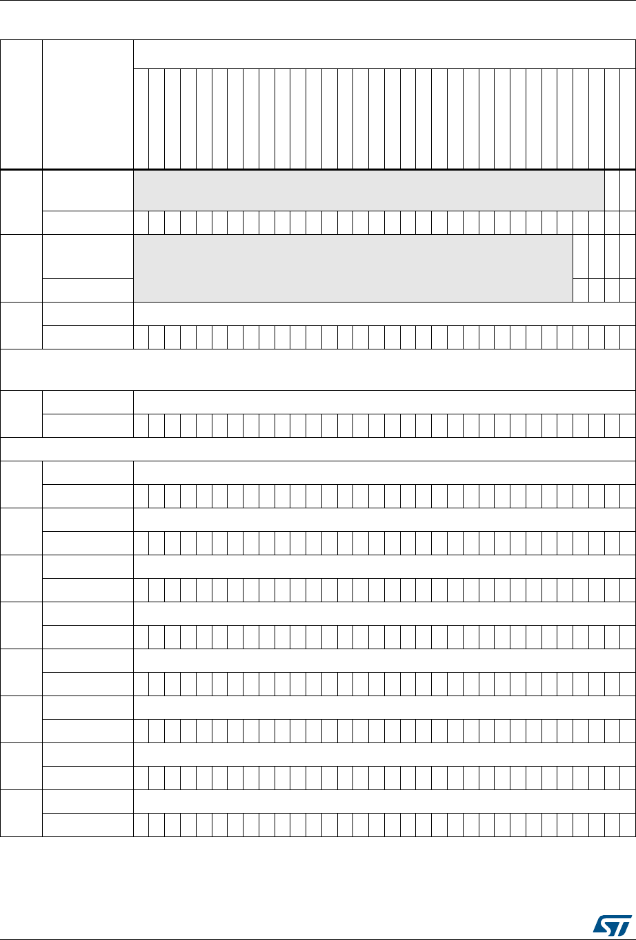
Hash processor (HASH) RM0090
782/1718 DocID018909 Rev 9
0x20
HASH_IMR Reserved
DCIE
DINIE
Reset value 00000000000000000000000000000000
0x24
HASH_SR
Reserved
BUSY
DMAS
DCIS
DINIS
Reset value 0001
0xF8
HASH_CSR0 CSR0
Reset value 00000000000000000000000000000010
...
...
0x1C
C
HASH_CSR53 CSR53
Reset value 00000000000000000000000000000000
Reserved
0x310
HASH_HR0 H0
Reset value 00000000000000000000000000000000
0x314
HASH_HR1 H1
Reset value 00000000000000000000000000000000
0x318
HASH_HR2 H2
Reset value 00000000000000000000000000000000
0x31
C
HASH_HR3 H3
Reset value 00000000000000000000000000000000
0x320
HASH_HR4 H4
Reset value 00000000000000000000000000000000
0x324
HASH_HR5 H5
Reset value 00000000000000000000000000000000
0x328
HASH_HR6 H6
Reset value 00000000000000000000000000000000
0x32
C
HASH_HR7 H7
Reset value 00000000000000000000000000000000
Table 117. HASH register map and reset values on STM32F43xxx (continued)
Offse
t
Register
name
reset value
Register size
31
30
29
28
27
26
25
24
23
22
21
20
19
18
17
16
15
14
13
12
11
10
9
8
7
6
5
4
3
2
1
0

DocID018909 Rev 9 783/1718
RM0090 Real-time clock (RTC)
822
26 Real-time clock (RTC)
This section applies to the whole STM32F4xx family, unless otherwise specified.
26.1 Introduction
The real-time clock (RTC) is an independent BCD timer/counter. The RTC provides a time-
of-day clock/calendar, two programmable alarm interrupts, and a periodic programmable
wakeup flag with interrupt capability. The RTC also includes an automatic wakeup unit to
manage low-power modes.
Two 32-bit registers contain the seconds, minutes, hours (12- or 24-hour format), day (day
of week), date (day of month), month, and year, expressed in binary coded decimal format
(BCD). The sub-seconds value is also available in binary format.
Compensations for 28-, 29- (leap year), 30-, and 31-day months are performed
automatically. Daylight saving time compensation can also be performed.
Additional 32-bit registers contain the programmable alarm subseconds, seconds, minutes,
hours, day, and date.
A digital calibration feature is available to compensate for any deviation in crystal oscillator
accuracy.
After backup domain reset, all RTC registers are protected against possible parasitic write
accesses.
As long as the supply voltage remains in the operating range, the RTC never stops,
regardless of the device status (Run mode, low-power mode or under reset).

Real-time clock (RTC) RM0090
784/1718 DocID018909 Rev 9
26.2 RTC main features
The RTC unit main features are the following (see Figure 237: RTC block diagram):
•Calendar with subseconds, seconds, minutes, hours (12 or 24 format), day (day of
week), date (day of month), month, and year.
•Daylight saving compensation programmable by software.
•Two programmable alarms with interrupt function. The alarms can be triggered by any
combination of the calendar fields.
•Automatic wakeup unit generating a periodic flag that triggers an automatic wakeup
interrupt.
•Reference clock detection: a more precise second source clock (50 or 60 Hz) can be
used to enhance the calendar precision.
•Accurate synchronization with an external clock using the subsecond shift feature.
•Maskable interrupts/events:
–Alarm A
–Alarm B
– Wakeup interrupt
–Timestamp
– Tamper detection
•Digital calibration circuit (periodic counter correction)
– 5 ppm accuracy
– 0.95 ppm accuracy, obtained in a calibration window of several seconds
•Timestamp function for event saving (1 event)
•Tamper detection:
– 2 tamper events with configurable filter and internal pull-up.
•20 backup registers (80 bytes). The backup registers are reset when a tamper
detection event occurs.
•Alternate function output (RTC_OUT) which selects one of the following two outputs:
– RTC_CALIB: 512 Hz or 1 Hz clock output (with an LSE frequency of 32.768 kHz).
This output is enabled by setting the COE bit in the RTC_CR register. It is routed
to the device RTC_AF1 function.
– RTC_ALARM (Alarm A, Alarm B or wakeup).
This output is selected by configuring the OSEL[1:0] bits in the RTC_CR register.
It is routed to the device RTC_AF1 function.
• RTC alternate function inputs:
– RTC_TS: timestamp event detection. It is routed to the device RTC_AF1 and
RTC_AF2 functions.
– RTC_TAMP1: TAMPER1 event detection. It is routed to the device RTC_AF1 and
RTC_AF2 functions.
– RTC_TAMP2: TAMPER2 event detection.
– RTC_REFIN: reference clock input (usually the mains, 50 or 60 Hz).
Refer to Section 8.3.15: Selection of RTC_AF1 and RTC_AF2 alternate functions.
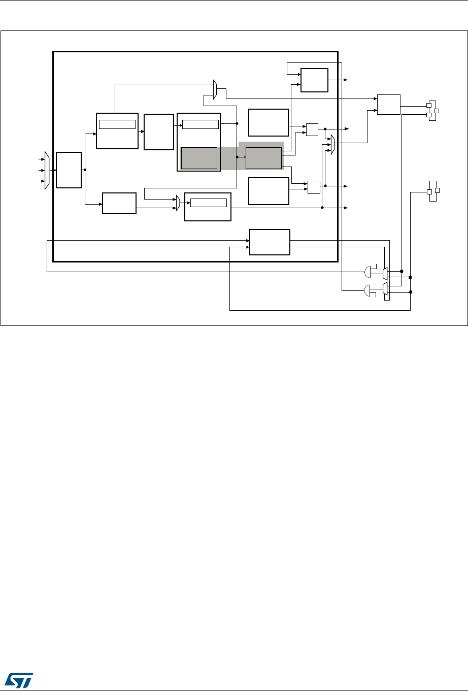
DocID018909 Rev 9 785/1718
RM0090 Real-time clock (RTC)
822
Figure 237. RTC block diagram
1. On STM32F4xx devices, the RTC_AF1 and RTC_AF2 alternate functions are connected to PC13 and PI8,
respectively.
26.3 RTC functional description
26.3.1 Clock and prescalers
The RTC clock source (RTCCLK) is selected through the clock controller among the LSE
clock, the LSI oscillator clock, and the HSE clock. For more information on the RTC clock
source configuration, refer to Section 7: Reset and clock control for STM32F405xx/07xx
and STM32F415xx/17xx(RCC) and Section 6: Reset and clock control for STM32F42xxx
and STM32F43xxx (RCC).
A programmable prescaler stage generates a 1 Hz clock which is used to update the
calendar. To minimize power consumption, the prescaler is split into 2 programmable
prescalers (see Figure 237: RTC block diagram):
•A 7-bit asynchronous prescaler configured through the PREDIV_A bits of the
RTC_PRER register.
• A 15-bit synchronous prescaler configured through the PREDIV_S bits of the
RTC_PRER register.
Note: When both prescalers are used, it is recommended to configure the asynchronous prescaler
to a high value to minimize consumption.
The asynchronous prescaler division factor is set to 128, and the synchronous division
factor to 256, to obtain an internal clock frequency of 1 Hz (ck_spre) with an LSE frequency
of 32.768 kHz.
-36
CK?APRE
DEFAULT(Z
CK SPRE
DEFAULT(Z
24#?#!,)"
(Z
24#?7542
24##,+
754&
(3%?24#
-(ZMAX
,3%(Z
,3)
!SYN CH
BITPRESCALER
DEFAULT
3YNCHRONOUS
BITPRESCALER
DEFAULT #ALENDAR
BITWAKEUP
AUTORELOADTIMER
!LARM!
24#?!,2-!2
REGISTERS !,2!&
24#?!,!2-
24#?02%2 24#?02%2
3HADOWREGISTERS
24#?42
24#?$2
#OARSE
#ALIBRATION
24#?#!,)"2
!,2"&
4IMESTAMP
REGISTE RS 43&
/UTPUT
CONTROL 24#?!&
24#?/54
(Z
24#?!,2-!332
!LARM"
24#?!,2-"2
REGISTERS
24#?!,2-"332
3MOOTH
CALIBRATION
24#?#!,2
0RESCALER
75#+3%,;=
"ACKUPAND
24#TAMPER
CONTROLREGISTERS
24#?4!-0
24#?43
4!-0%
43%
24#?!&
3HADOWREGISTER
24#?332
24#?4!-0

Real-time clock (RTC) RM0090
786/1718 DocID018909 Rev 9
The minimum division factor is 1 and the maximum division factor is 222.
This corresponds to a maximum input frequency of around 4 MHz.
fck_apre is given by the following formula:
The ck_apre clock is used to clock the binary RTC_SSR subseconds downcounter. When it
reaches 0, RTC_SSR is reloaded with the content of PREDIV_S.
fck_spre is given by the following formula:
The ck_spre clock can be used either to update the calendar or as timebase for the 16-bit
wakeup auto-reload timer. To obtain short timeout periods, the 16-bit wakeup auto-reload
timer can also run with the RTCCLK divided by the programmable 4-bit asynchronous
prescaler (see Section 26.3.4: Periodic auto-wakeup for details).
26.3.2 Real-time clock and calendar
The RTC calendar time and date registers are accessed through shadow registers which
are synchronized with PCLK1 (APB1 clock). They can also be accessed directly in order to
avoid waiting for the synchronization duration.
•RTC_SSR for the subseconds
•RTC_TR for the time
•RTC_DR for the date
Every two RTCCLK periods, the current calendar value is copied into the shadow registers,
and the RSF bit of RTC_ISR register is set (see Section 26.6.4). The copy is not performed
in Stop and Standby mode. When exiting these modes, the shadow registers are updated
after up to 2 RTCCLK periods.
When the application reads the calendar registers, it accesses the content of the shadow
registers.t is possible to make a direct access to the calendar registers by setting the
BYPSHAD control bit in the RTC_CR register. By default, this bit is cleared, and the user
accesses the shadow registers.
When reading the RTC_SSR, RTC_TR or RTC_DR registers in BYPSHAD=0 mode, the
frequency of the APB clock (fAPB) must be at least 7 times the frequency of the RTC clock
(fRTCCLK).
The shadow registers are reset by system reset.
26.3.3 Programmable alarms
The RTC unit provides two programmable alarms, Alarm A and Alarm B.
The programmable alarm functions are enabled through the ALRAIE and ALRBIE bits in the
RTC_CR register. The ALRAF and ALRBF flags are set to 1 if the calendar subseconds,
seconds, minutes, hours, date or day match the values programmed in the alarm registers
RTC_ALRMASSR/RTC_ALRMAR and RTC_ALRMBSSR/RTC_ALRMBR, respectively.
fCK_APRE
fRTCCLK
PREDIV_A 1+
---------------------------------------
=
fCK_SPRE
fRTCCLK
PREDIV_S 1+()PREDIV_A 1+()×
----------------------------------------------------------------------------------------------
=

DocID018909 Rev 9 787/1718
RM0090 Real-time clock (RTC)
822
Each calendar field can be independently selected through the MSKx bits of the
RTC_ALRMAR and RTC_ALRMBR registers, and through the MASKSSx bits of the
RTC_ALRMASSR and RTC_ALRMBSSR registers. The alarm interrupts are enabled
through the ALRAIE and ALRBIE bits in the RTC_CR register.
Alarm A and Alarm B (if enabled by bits OSEL[1:0] in RTC_CR register) can be routed to the
RTC_ALARM output. RTC_ALARM polarity can be configured through bit POL in the
RTC_CR register.
Caution: If the seconds field is selected (MSK0 bit reset in RTC_ALRMAR or RTC_ALRMBR), the
synchronous prescaler division factor set in the RTC_PRER register must be at least 3 to
ensure correct behavior.
26.3.4 Periodic auto-wakeup
The periodic wakeup flag is generated by a 16-bit programmable auto-reload down-counter.
The wakeup timer range can be extended to 17 bits.
The wakeup function is enabled through the WUTE bit in the RTC_CR register.
The wakeup timer clock input can be:
•RTC clock (RTCCLK) divided by 2, 4, 8, or 16.
When RTCCLK is LSE(32.768kHz), this allows to configure the wakeup interrupt period
from 122 µs to 32 s, with a resolution down to 61µs.
•ck_spre (usually 1 Hz internal clock)
When ck_spre frequency is 1Hz, this allows to achieve a wakeup time from 1 s to
around 36 hours with one-second resolution. This large programmable time range is
divided in 2 parts:
– from 1s to 18 hours when WUCKSEL [2:1] = 10
– and from around 18h to 36h when WUCKSEL[2:1] = 11. In this last case 216 is
added to the 16-bit counter current value.When the initialization sequence is
complete (see Programming the wakeup timer on page 789), the timer starts
counting down.When the wakeup function is enabled, the down-counting remains
active in low-power modes. In addition, when it reaches 0, the WUTF flag is set in
the RTC_ISR register, and the wakeup counter is automatically reloaded with its
reload value (RTC_WUTR register value).
The WUTF flag must then be cleared by software.
When the periodic wakeup interrupt is enabled by setting the WUTIE bit in the RTC_CR2
register, it can exit the device from low-power modes.
The periodic wakeup flag can be routed to the RTC_ALARM output provided it has been
enabled through bits OSEL[1:0] of RTC_CR register. RTC_ALARM polarity can be
configured through the POL bit in the RTC_CR register.
System reset, as well as low-power modes (Sleep, Stop and Standby) have no influence on
the wakeup timer.

Real-time clock (RTC) RM0090
788/1718 DocID018909 Rev 9
26.3.5 RTC initialization and configuration
RTC register access
The RTC registers are 32-bit registers. The APB interface introduces 2 wait-states in RTC
register accesses except on read accesses to calendar shadow registers when
BYPSHAD=0.
RTC register write protection
After system reset, the RTC registers are protected against parasitic write access with the
DBP bit of the PWR power control register (PWR_CR). The DBP bit must be set to enable
RTC registers write access.
After backup domain reset, all the RTC registers are write-protected. Writing to the RTC
registers is enabled by writing a key into the Write Protection register, RTC_WPR.
The following steps are required to unlock the write protection on all the RTC registers
except for RTC_ISR[13:8], RTC_TAFCR, and RTC_BKPxR.
1. Write ‘0xCA’ into the RTC_WPR register.
2. Write ‘0x53’ into the RTC_WPR register.
Writing a wrong key reactivates the write protection.
The protection mechanism is not affected by system reset.
Calendar initialization and configuration
To program the initial time and date calendar values, including the time format and the
prescaler configuration, the following sequence is required:
1. Set INIT bit to 1 in the RTC_ISR register to enter initialization mode. In this mode, the
calendar counter is stopped and its value can be updated.
2. Poll INITF bit of in the RTC_ISR register. The initialization phase mode is entered when
INITF is set to 1. It takes from 1 to 2 RTCCLK clock cycles (due to clock
synchronization).
3. To generate a 1 Hz clock for the calendar counter, program first the synchronous
prescaler factor in RTC_PRER register, and then program the asynchronous prescaler
factor. Even if only one of the two fields needs to be changed, 2 separate write
accesses must be performed to the RTC_PRER register.
4. Load the initial time and date values in the shadow registers (RTC_TR and RTC_DR),
and configure the time format (12 or 24 hours) through the FMT bit in the RTC_CR
register.
5. Exit the initialization mode by clearing the INIT bit. The actual calendar counter value is
then automatically loaded and the counting restarts after 4 RTCCLK clock cycles.
When the initialization sequence is complete, the calendar starts counting.
Note: After a system reset, the application can read the INITS flag in the RTC_ISR register to
check if the calendar has been initialized or not. If this flag equals 0, the calendar has not
been initialized since the year field is set at its backup domain reset default value (0x00).
To read the calendar after initialization, the software must first check that the RSF flag is set
in the RTC_ISR register.

DocID018909 Rev 9 789/1718
RM0090 Real-time clock (RTC)
822
Daylight saving time
The daylight saving time management is performed through bits SUB1H, ADD1H, and BKP
of the RTC_CR register.
Using SUB1H or ADD1H, the software can subtract or add one hour to the calendar in one
single operation without going through the initialization procedure.
In addition, the software can use the BKP bit to memorize this operation.
Programming the alarm
A similar procedure must be followed to program or update the programmable alarm (Alarm
A or Alarm B):
1. Clear ALRAE or ALRBIE in RTC_CR to disable Alarm A or Alarm B.
2. Poll ALRAWF or ALRBWF in RTC_ISR until it is set to make sure the access to alarm
registers is allowed. This takes 1 to 2 RTCCLK clock cycles (due to clock
synchronization).
3. Program the Alarm A or Alarm B registers (RTC_ALRMASSR/RTC_ALRMAR or
RTC_ALRMBSSR/RTC_ALRMBR).
4. Set ALRAE or ALRBIE in the RTC_CR register to enable Alarm A or Alarm B again.
Note: Each change of the RTC_CR register is taken into account after 1 to 2 RTCCLK clock cycles
due to clock synchronization.
Programming the wakeup timer
The following sequence is required to configure or change the wakeup timer auto-reload
value (WUT[15:0] in RTC_WUTR):
1. Clear WUTE in RTC_CR to disable the wakeup timer.
2. Poll WUTWF until it is set in RTC_ISR to make sure the access to wakeup auto-reload
counter and to WUCKSEL[2:0] bits is allowed. It takes 1 to 2 RTCCLK clock cycles
(due to clock synchronization).
3. Program the wakeup auto-reload value WUT[15:0], and the wakeup clock selection
(WUCKSEL[2:0] bits in RTC_CR).Set WUTE in RTC_CR to enable the timer again.
The wakeup timer restarts down-counting.
26.3.6 Reading the calendar
When BYPSHAD control bit is cleared in the RTC_CR register
To read the RTC calendar registers (RTC_SSR, RTC_TR and RTC_DR) properly, the APB1
clock frequency (fPCLK1) must be equal to or greater than seven times the fRTCCLK RTC
clock frequency. This ensures a secure behavior of the synchronization mechanism.
If the APB1 clock frequency is less than seven times the RTC clock frequency, the software
must read the calendar time and date registers twice. If the second read of the RTC_TR
gives the same result as the first read, this ensures that the data is correct. Otherwise a third
read access must be done. In any case the APB1 clock frequency must never be lower than
the RTC clock frequency.
The RSF bit is set in RTC_ISR register each time the calendar registers are copied into the
RTC_SSR, RTC_TR and RTC_DR shadow registers. The copy is performed every two
RTCCLK cycles. To ensure consistency between the 3 values, reading either RTC_SSR or

Real-time clock (RTC) RM0090
790/1718 DocID018909 Rev 9
RTC_TR locks the values in the higher-order calendar shadow registers until RTC_DR is
read. In case the software makes read accesses to the calendar in a time interval smaller
than 2 RTCCLK periods: RSF must be cleared by software after the first calendar read, and
then the software must wait until RSF is set before reading again the RTC_SSR, RTC_TR
and RTC_DR registers.
After waking up from low-power mode (Stop or Standby), RSF must be cleared by software.
The software must then wait until it is set again before reading the RTC_SSR, RTC_TR and
RTC_DR registers.
The RSF bit must be cleared after wakeup and not before entering low-power mode.
Note: After a system reset, the software must wait until RSF is set before reading the RTC_SSR,
RTC_TR and RTC_DR registers. Indeed, a system reset resets the shadow registers to
their default values.
After an initialization (refer to Calendar initialization and configuration on page 788): the
software must wait until RSF is set before reading the RTC_SSR, RTC_TR and RTC_DR
registers.
After synchronization (refer to Section 26.3.8: RTC synchronization): the software must wait
until RSF is set before reading the RTC_SSR, RTC_TR and RTC_DR registers.
When the BYPSHAD control bit is set in the RTC_CR register (bypass shadow
registers)
Reading the calendar registers gives the values from the calendar counters directly, thus
eliminating the need to wait for the RSF bit to be set. This is especially useful after exiting
from low power modes (STOP or Standby), since the shadow registers are not updated
during these modes.
When the BYPSHAD bit is set to 1, the results of the different registers might not be
coherent with each other if an RTCCLK edge occurs between two read accesses to the
registers. Additionally, the value of one of the registers may be incorrect if an RTCCLK edge
occurs during the read operation. The software must read all the registers twice, and then
compare the results to confirm that the data is coherent and correct. Alternatively, the
software can just compare the two results of the least-significant calendar register.
Note: While BYPSHAD=1, instructions which read the calendar registers require one extra APB
cycle to complete.
26.3.7 Resetting the RTC
The calendar shadow registers (RTC_SSR, RTC_TR and RTC_DR) and some bits of the
RTC status register (RTC_ISR) are reset to their default values by all available system reset
sources.
On the contrary, the following registers are resetted to their default values by a backup
domain reset and are not affected by a system reset: the RTC current calendar registers,
the RTC control register (RTC_CR), the prescaler register (RTC_PRER), the RTC
calibration registers (RTC_CALIBR or RTC_CALR), the RTC shift register (RTC_SHIFTR),
the RTC timestamp registers (RTC_TSSSR, RTC_TSTR and RTC_TSDR), the RTC tamper
and alternate function configuration register (RTC_TAFCR), the RTC backup registers
(RTC_BKPxR), the wakeup timer register (RTC_WUTR), the Alarm A and Alarm B registers
(RTC_ALRMASSR/RTC_ALRMAR and RTC_ALRMBSSR/RTC_ALRMBR).

DocID018909 Rev 9 791/1718
RM0090 Real-time clock (RTC)
822
In addition, the RTC keeps on running under system reset if the reset source is different
from a backup domain reset. When a backup domain reset occurs, the RTC is stopped and
all the RTC registers are set to their reset values.
26.3.8 RTC synchronization
The RTC can be synchronized to a remote clock with a high degree of precision. After
reading the sub-second field (RTC_SSR or RTC_TSSSR), a calculation can be made of the
precise offset between the times being maintained by the remote clock and the RTC. The
RTC can then be adjusted to eliminate this offset by “shifting” its clock by a fraction of a
second using RTC_SHIFTR.
RTC_SSR contains the value of the synchronous prescaler’s counter. This allows one to
calculate the exact time being maintained by the RTC down to a resolution of
1 / (PREDIV_S + 1) seconds. As a consequence, the resolution can be improved by
increasing the synchronous prescaler value (PREDIV_S[14:0]. The maximum resolution
allowed (30.52 μs with a 32768 Hz clock) is obtained with PREDIV_S set to 0x7FFF.
However, increasing PREDIV_S means that PREDIV_A must be decreased in order to
maintain the synchronous prescaler’s output at 1 Hz. In this way, the frequency of the
asynchronous prescaler’s output increases, which may increase the RTC dynamic
consumption.
The RTC can be finely adjusted using the RTC shift control register (RTC_SHIFTR). Writing
to RTC_SHIFTR can shift (either delay or advance) the clock by up to a second with a
resolution of 1 / (PREDIV_S + 1) seconds. The shift operation consists of adding the
SUBFS[14:0] value to the synchronous prescaler counter SS[15:0]: this will delay the clock.
If at the same time the ADD1S bit is set, this results in adding one second and at the same
time subtracting a fraction of second, so this will advance the clock.
Caution: Before initiating a shift operation, the user must check that SS[15] = 0 in order to ensure that
no overflow will occur.
As soon as a shift operation is initiated by a write to the RTC_SHIFTR register, the SHPF
flag is set by hardware to indicate that a shift operation is pending. This bit is cleared by
hardware as soon as the shift operation has completed.
Caution: This synchronization feature is not compatible with the reference clock detection feature:
firmware must not write to RTC_SHIFTR when REFCKON=1.
26.3.9 RTC reference clock detection
The RTC calendar update can be synchronized to a reference clock RTC_REFIN, usually
the mains (50 or 60 Hz). The RTC_REFIN reference clock should have a higher precision
than the 32.768 kHz LSE clock. When the RTC_REFIN detection is enabled (REFCKON bit
of RTC_CR set to 1), the calendar is still clocked by the LSE, and RTC_REFIN is used to
compensate for the imprecision of the calendar update frequency (1 Hz).
Each 1 Hz clock edge is compared to the nearest reference clock edge (if one is found
within a given time window). In most cases, the two clock edges are properly aligned. When
the 1 Hz clock becomes misaligned due to the imprecision of the LSE clock, the RTC shifts
the 1 Hz clock a bit so that future 1 Hz clock edges are aligned. Thanks to this mechanism,
the calendar becomes as precise as the reference clock.
The RTC detects if the reference clock source is present by using the 256 Hz clock
(ck_apre) generated from the 32.768 kHz quartz. The detection is performed during a time

Real-time clock (RTC) RM0090
792/1718 DocID018909 Rev 9
window around each of the calendar updates (every 1 s). The window equals 7 ck_apre
periods when detecting the first reference clock edge. A smaller window of 3 ck_apre
periods is used for subsequent calendar updates.
Each time the reference clock is detected in the window, the asynchronous prescaler which
outputs the ck_apre clock is forced to reload. This has no effect when the reference clock
and the 1 Hz clock are aligned because the prescaler is being reloaded at the same
moment. When the clocks are not aligned, the reload shifts future 1 Hz clock edges a little
for them to be aligned with the reference clock.
If the reference clock halts (no reference clock edge occurred during the 3 ck_apre window),
the calendar is updated continuously based solely on the LSE clock. The RTC then waits for
the reference clock using a large 7 ck_apre period detection window centered on the
ck_spre edge.
When the reference clock detection is enabled, PREDIV_A and PREDIV_S must be set to
their default values:
•PREDIV_A = 0x007F
•PREDIV_S = 0x00FF
Note: The reference clock detection is not available in Standby mode.
Caution: The reference clock detection feature cannot be used in conjunction with the coarse digital
calibration: RTC_CALIBR must be kept at 0x0000 0000 when REFCKON=1.
26.3.10 RTC coarse digital calibration
Two digital calibration methods are available: coarse and smooth calibration. To perform
coarse calibration refer to Section 26.6.7: RTC calibration register (RTC_CALIBR).
The two calibration methods are not intended to be used together, the application must
select one of the two methods. Coarse calibration is provided for compatibly reasons. To
perform smooth calibration refer to Section 26.3.11: RTC smooth digital calibration and the
Section 26.6.16: RTC calibration register (RTC_CALR)
The coarse digital calibration can be used to compensate crystal inaccuracy by adding
(positive calibration) or masking (negative calibration) clock cycles at the output of the
asynchronous prescaler (ck_apre).
Positive and negative calibration are selected by setting the DCS bit in RTC_CALIBR
register to ‘0’ and ‘1’, respectively.
When positive calibration is enabled (DCS = ‘0’), 2 ck_apre cycles are added every minute
(around 15360 ck_apre cycles) for 2xDC minutes. This causes the calendar to be updated
sooner, thereby adjusting the effective RTC frequency to be a bit higher.
When negative calibration is enabled (DCS = ‘1’), 1 ck_apre cycle is removed every minute
(around 15360 ck_apre cycles) for 2xDC minutes. This causes the calendar to be updated
later, thereby adjusting the effective RTC frequency to be a bit lower.
DC is configured through bits DC[4:0] of RTC_CALIBR register. This number ranges from 0
to 31 corresponding to a time interval (2xDC) ranging from 0 to 62.
The coarse digital calibration can be configured only in initialization mode, and starts when
the INIT bit is cleared. The full calibration cycle lasts 64 minutes. The first 2xDC minutes of
the 64 -minute cycle are modified as just described.

DocID018909 Rev 9 793/1718
RM0090 Real-time clock (RTC)
822
Negative calibration can be performed with a resolution of about 2 ppm while positive
calibration can be performed with a resolution of about 4 ppm. The maximum calibration
ranges from −63 ppm to 126 ppm.
The calibration can be performed either on the LSE or on the HSE clock.
Caution: Digital calibration may not work correctly if PREDIV_A < 6.
Case of RTCCLK=32.768 kHz and PREDIV_A+1=128
The following description assumes that ck_apre frequency is 256 Hz obtained with an LSE
clock nominal frequency of 32.768 kHz, and PREDIV_A set to 127 (default value).
The ck_spre clock frequency is only modified during the first 2xDC minutes of the 64-minute
cycle. For example, when DC equals 1, only the first 2 minutes are modified. This means
that the first 2xDC minutes of each 64-minute cycle have, once per minute, one second
either shortened by 256 or lengthened by 128 RTCCLK cycles, given that each ck_apre
cycle represents 128 RTCCLK cycles (with PREDIV_A+1=128).
Therefore each calibration step has the effect of adding 512 or subtracting 256 oscillator
cycles for every 125829120 RTCCLK cycles (64min x 60 s/min x 32768 cycles/s). This is
equivalent to +4.069 ppm or-2.035 ppm per calibration step. As a result, the calibration
resolution is +10.5 or −5.27 seconds per month, and the total calibration ranges from +5.45
to −2.72 minutes per month.
In order to measure the clock deviation, a 512 Hz clock is output for calibration.Refer to
Section 26.3.14: Calibration clock output.
26.3.11 RTC smooth digital calibration
RTC frequency can be digitally calibrated with a resolution of about 0.954 ppm with a range
from -487.1 ppm to +488.5 ppm. The correction of the frequency is performed using series
of small adjustments (adding and/or subtracting individual RTCCLK pulses). These
adjustments are fairly well distributed so that the RTC is well calibrated even when observed
over short durations of time.
The smooth digital calibration is performed during a cycle of about 220 RTCCLK pulses, or
32 seconds when the input frequency is 32768 Hz. This cycle is maintained by a 20-bit
counter, cal_cnt[19:0], clocked by RTCCLK.
The smooth calibration register (RTC_CALR) specifies the number of RTCCLK clock cycles
to be masked during the 32-second cycle:
•Setting the bit CALM[0] to 1 causes exactly one pulse to be masked during the 32-
second cycle.
•Setting CALM[1] to 1 causes two additional cycles to be masked
•Setting CALM[2] to 1 causes four additional cycles to be masked
•and so on up to CALM[8] set to 1 which causes 256 clocks to be masked.
Note: CALM[8:0] (RTC_CALRx) specifies the number of RTCCLK pulses to be masked during the
32-second cycle. Setting the bit CALM[0] to ‘1’ causes exactly one pulse to be masked
during the 32-second cycle at the moment when cal_cnt[19:0] is 0x80000; CALM[1]=1
causes two other cycles to be masked (when cal_cnt is 0x40000 and 0xC0000); CALM[2]=1
causes four other cycles to be masked (cal_cnt = 0x20000/0x60000/0xA0000/ 0xE0000);
and so on up to CALM[8]=1 which causes 256 clocks to be masked (cal_cnt = 0xXX800).

Real-time clock (RTC) RM0090
794/1718 DocID018909 Rev 9
While CALM allows the RTC frequency to be reduced by up to 487.1 ppm with fine
resolution, the bit CALP can be used to increase the frequency by 488.5 ppm. Setting CALP
to ‘1’ effectively inserts an extra RTCCLK pulse every 211 RTCCLK cycles, which means
that 512 clocks are added during every 32-second cycle.
Using CALM together with CALP, an offset ranging from -511 to +512 RTCCLK cycles can
be added during the 32-second cycle, which translates to a calibration range of -487.1 ppm
to +488.5 ppm with a resolution of about 0.954 ppm.
The formula to calculate the effective calibrated frequency (FCAL) given the input frequency
(FRTCCLK) is as follows:
FCAL = FRTCCLK x [1 + (CALP x 512 - CALM) / (220 + CALM - CALP x 512)]
Calibration when PREDIV_A<3
The CALP bit can not be set to 1 when the asynchronous prescaler value (PREDIV_A bits in
RTC_PRER register) is less than 3. If CALP was already set to 1 and PREDIV_A bits are
set to a value less than 3, CALP is ignored and the calibration operates as if CALP was
equal to 0.
To perform a calibration with PREDIV_A less than 3, the synchronous prescaler value
(PREDIV_S) should be reduced so that each second is accelerated by 8 RTCCLK clock
cycles, which is equivalent to adding 256 clock cycles every 32 seconds. As a result,
between 255 and 256 clock pulses (corresponding to a calibration range from 243.3 to
244.1 ppm) can effectively be added during each 32-second cycle using only the CALM bits.
With a nominal RTCCLK frequency of 32768 Hz, when PREDIV_A equals 1 (division factor
of 2), PREDIV_S should be set to 16379 rather than 16383 (4 less). The only other
interesting case is when PREDIV_A equals 0, PREDIV_S should be set to 32759 rather
than 32767 (8 less).
If PREDIV_S is reduced in this way, the formula given the effective frequency of the
calibrated input clock is as follows:
FCAL = FRTCCLK x [1 + (256 - CALM) / (220 + CALM - 256)]
In this case, CALM[7:0] equals 0x100 (the midpoint of the CALM range) is the correct
setting if RTCCLK is exactly 32768.00 Hz.
Verifying the RTC calibration
RTC precision is performed by measuring the precise frequency of RTCCLK and calculating
the correct CALM value and CALP values. An optional 1 Hz output is provided to allow
applications to measure and verify the RTC precision.
Measuring the precise frequency of the RTC over a limited interval can result in a
measurement error of up to 2 RTCCLK clock cycles over the measurement period,
depending on how the digital calibration cycle is aligned with the measurement period.

DocID018909 Rev 9 795/1718
RM0090 Real-time clock (RTC)
822
However, this measurement error can be eliminated if the measurement period is the same
length as the calibration cycle period. In this case, the only error observed is the error due to
the resolution of the digital calibration.
•By default, the calibration cycle period is 32 seconds.
Using this mode and measuring the accuracy of the 1 Hz output over exactly 32
seconds guarantees that the measure is within 0.477 ppm (0.5 RTCCLK cycles over 32
seconds, due to the limitation of the calibration resolution).
•CALW16 bit of the RTC_CALR register can be set to 1 to force a 16- second calibration
cycle period.
In this case, the RTC precision can be measured during 16 seconds with a maximum
error of 0.954 ppm (0.5 RTCCLK cycles over 16 seconds). However, since the
calibration resolution is reduced, the long term RTC precision is also reduced to 0.954
ppm: CALM[0] bit is stuck at 0 when CALW16 is set to 1.
•CALW8 bit of the RTC_CALR register can be set to 1 to force a 8- second calibration
cycle period.
In this case, the RTC precision can be measured during 8 seconds with a maximum
error of 1.907 ppm (0.5 RTCCLK cycles over 8s). The long term RTC precision is also
reduced to 1.907 ppm: CALM[1:0] bits are stuck at 00 when CALW8 is set to 1.
Re-calibration on-the-fly
The calibration register (RTC_CALR) can be updated on-the-fly while RTC_ISR/INITF=0, by
using the follow process:
1. Poll the RTC_ISR/RECALPF (re-calibration pending flag).
2. If it is set to 0, write a new value to RTC_CALR, if necessary. RECALPF is then
automatically set to 1
3. Within three ck_apre cycles after the write operation to RTC_CALR, the new calibration
settings take effect.
26.3.12 Timestamp function
Timestamp is enabled by setting the TSE bit of RTC_CR register to 1.
The calendar is saved in the timestamp registers (RTC_TSSSR, RTC_TSTR, RTC_TSDR)
when a timestamp event is detected on the pin to which the TIMESTAMP alternate function
is mapped. When a timestamp event occurs, the timestamp flag bit (TSF) in RTC_ISR
register is set.
By setting the TSIE bit in the RTC_CR register, an interrupt is generated when a timestamp
event occurs.
If a new timestamp event is detected while the timestamp flag (TSF) is already set, the
timestamp overflow flag (TSOVF) flag is set and the timestamp registers (RTC_TSTR and
RTC_TSDR) maintain the results of the previous event.
Note: TSF is set 2 ck_apre cycles after the timestamp event occurs due to synchronization
process.
There is no delay in the setting of TSOVF. This means that if two timestamp events are
close together, TSOVF can be seen as '1' while TSF is still '0'. As a consequence, it is
recommended to poll TSOVF only after TSF has been set.
Caution: If a timestamp event occurs immediately after the TSF bit is supposed to be cleared, then
both TSF and TSOVF bits are set. To avoid masking a timestamp event occurring at the

Real-time clock (RTC) RM0090
796/1718 DocID018909 Rev 9
same moment, the application must not write ‘0’ into TSF bit unless it has already read it to
‘1’.
Optionally, a tamper event can cause a timestamp to be recorded. See the description of the
TAMPTS control bit in Section 26.6.17: RTC tamper and alternate function configuration
register (RTC_TAFCR). If the timestamp event is on the same pin as a tamper event
configured in filtered mode (TAMPFLT set to a non-zero value), the timestamp on tamper
detection event mode must be selected by setting TAMPTS='1' in RTC_TAFCR register.
TIMESTAMP alternate function
The TIMESTAMP alternate function (RTC_TS) can be mapped either to RTC_AF1 or to
RTC_AF2 depending on the value of the TSINSEL bit in the RTC_TAFCR register (see
Section 26.6.17: RTC tamper and alternate function configuration register (RTC_TAFCR)).
Mapping the timestamp event on RTC_AF2 is not allowed if RTC_AF1 is used as TAMPER
in filtered mode (TAMPFLT set to a non-zero value).
26.3.13 Tamper detection
Two tamper detection inputs are available. They can be configured either for edge detection,
or for level detection with filtering.
RTC backup registers
The backup registers (RTC_BKPxR) are twenty 32-bit registers for storing 80 bytes of user
application data. They are implemented in the backup domain that remains powered-on by
VBAT when the VDD power is switched off. They are not reset by system reset or when the
device wakes up from Standby mode. They are reset by a backup domain reset
The backup registers are reset when a tamper detection event occurs (see Section 26.6.20:
RTC backup registers (RTC_BKPxR) and Tamper detection initialization on page 796.
Tamper detection initialization
Each tamper detection input is associated with the TAMP1F/TAMP2F flags in the RTC_ISR2
register. Each input can be enabled by setting the corresponding TAMP1E/TAMP2E bits to 1
in the RTC_TAFCR register.
A tamper detection event resets all backup registers (RTC_BKPxR).
By setting the TAMPIE bit in the RTC_TAFCR register, an interrupt is generated when a
tamper detection event occurs.
Timestamp on tamper event
With TAMPTS set to ‘1 , any tamper event causes a timestamp to occur. In this case, either
the TSF bit or the TSOVF bit are set in RTC_ISR, in the same manner as if a normal
timestamp event occurs. The affected tamper flag register (TAMP1F, TAMP2F) is set at the
same time that TSF or TSOVF is set.
Edge detection on tamper inputs
If the TAMPFLT bits are “00”, the TAMPER pins generate tamper detection events
(RTC_TAMP[2:1]) when either a rising edge is observed or an falling edge is observed
depending on the corresponding TAMPxTRG bit. The internal pull-up resistors on the
TAMPER inputs are deactivated when edge detection is selected.

DocID018909 Rev 9 797/1718
RM0090 Real-time clock (RTC)
822
Caution: To avoid losing tamper detection events, the signal used for edge detection is logically
ANDed with TAMPxE in order to detect a tamper detection event in case it occurs before the
TAMPERx pin is enabled.
•When TAMPxTRG = 0: if the TAMPERx alternate function is already high before
tamper detection is enabled (TAMPxE bit set to 1), a tamper event is detected as soon
as TAMPERx is enabled, even if there was no rising edge on TAMPERx after TAMPxE
was set.
•When TAMPxTRG = 1: if the TAMPERx alternate function is already low before tamper
detection is enabled, a tamper event is detected as soon as TAMPERx is enabled
(even if there was no falling edge on TAMPERx after TAMPxE was set.
After a tamper event has been detected and cleared, the TAMPERx alternate function
should be disabled and then re-enabled (TAMPxE set to 1) before re-programming the
backup registers (RTC_BKPxR). This prevents the application from writing to the backup
registers while the TAMPERx value still indicates a tamper detection. This is equivalent to a
level detection on the TAMPERx alternate function.
Note: Tamper detection is still active when VDD power is switched off. To avoid unwanted resetting
of the backup registers, the pin to which the TAMPER alternate function is mapped should
be externally tied to the correct level.
Level detection with filtering on tamper inputs
Level detection with filtering is performed by setting TAMPFLT to a non-zero value. A tamper
detection event is generated when either 2, 4, or 8 (depending on TAMPFLT) consecutive
samples are observed at the level designated by the TAMPxTRG bits
(TAMP1TRG/TAMP2TRG).
The TAMPER inputs are pre-charged through the I/O internal pull-up resistance before its
state is sampled, unless disabled by setting TAMPPUDIS to 1,The duration of the precharge
is determined by the TAMPPRCH bits, allowing for larger capacitances on the tamper
inputs.
The trade-off between tamper detection latency and power consumption through the pull-up
can be optimized by using TAMPFREQ to determine the frequency of the sampling for level
detection.
Note: Refer to the datasheets for the electrical characteristics of the pull-up resistors.
TAMPER alternate function detection
The TAMPER1 alternate function (RTC_TAMP1) can be mapped either to RTC_AF1(PC13)
or RTC_AF2 (PI8) depending on the value of TAMP1INSEL bit in RTC_TAFCR register (see
Section 26.6.17: RTC tamper and alternate function configuration register (RTC_TAFCR)).
TAMPE bit must be cleared when TAMP1INSEL is modified to avoid unwanted setting of
TAMPF.
The TAMPER 2 alternate function corresponds to RTC_TAMP2 pin.
26.3.14 Calibration clock output
When the COE bit is set to 1 in the RTC_CR register, a reference clock is provided on the
RTC_CALIB device output. If the COSEL bit in the RTC_CR register is reset and
PREDIV_A = 0x7F, the RTC_CALIB frequency is fRTCCLK/64. This corresponds to a
calibration output at 512 Hz for an RTCCLK frequency at 32.768 kHz.

Real-time clock (RTC) RM0090
798/1718 DocID018909 Rev 9
The RTC_CALIB output is not impacted by the calibration value programmed in
RTC_CALIBR register. The RTC_CALIB duty cycle is irregular: there is a light jitter on falling
edges. It is therefore recommended to use rising edges.
If COSEL is set and “PREDIV_S+1” is a non-zero multiple of 256 (i.e: PREDIV_S[7:0] =
0xFF), the RTC_CALIB frequency is fRTCCLK/(256 * (PREDIV_A+1)). This corresponds to a
calibration output at 1 Hz for prescaler default values (PREDIV_A = Ox7F, PREDIV_S =
0xFF), with an RTCCLK frequency at 32.768 kHz.
Calibration alternate function output
When the COE bit in the RTC_CR register is set to 1, the calibration alternate function
(RTC_CALIB) is enabled on RTC_AF1.
Note: When RTC_CALIB or RTC_ALARM is selected, RTC_AF1 is automatically configured in
output alternate function.
26.3.15 Alarm output
Three functions can be selected on Alarm output: ALRAF, ALRBF and WUTF. These
functions reflect the contents of the corresponding flags in the RTC_ISR register.
The OSEL[1:0] control bits in the RTC_CR register are used to activate the alarm alternate
function output (RTC_ALARM) in RTC_AF1, and to select the function which is output on
RTC_ALARM.
The polarity of the output is determined by the POL control bit in RTC_CR so that the
opposite of the selected flag bit is output when POL is set to 1.
Alarm alternate function output
RTC_ALARM can be configured in output open drain or output push-pull using the control
bit ALARMOUTTYPE in the RTC_TAFCR register.
Note: Once RTC_ALARM is enabled, it has priority over RTC_CALIB (COE bit is don't care on
RTC_AF1).
When RTC_CALIB or RTC_ALARM is selected, RTC_AF1 is automatically configured in
output alternate function.
26.4 RTC and low-power modes
Table 118. Effect of low-power modes on RTC
Mode Description
Sleep No effect
RTC interrupts cause the device to exit the Sleep mode.
Stop
The RTC remains active when the RTC clock source is LSE or LSI. RTC alarm, RTC
tamper event, RTC time stamp event, and RTC Wakeup cause the device to exit the Stop
mode.
Standby
The RTC remains active when the RTC clock source is LSE or LSI. RTC alarm, RTC
tamper event, RTC time stamp event, and RTC Wakeup cause the device to exit the
Standby mode.

DocID018909 Rev 9 799/1718
RM0090 Real-time clock (RTC)
822
26.5 RTC interrupts
All RTC interrupts are connected to the EXTI controller.
To enable the RTC Alarm interrupt, the following sequence is required:
1. Configure and enable the EXTI Line 17 in interrupt mode and select the rising edge
sensitivity.
2. Configure and enable the RTC_Alarm IRQ channel in the NVIC.
3. Configure the RTC to generate RTC alarms (Alarm A or Alarm B).
To enable the RTC Wakeup interrupt, the following sequence is required:
1. Configure and enable the EXTI Line 22 in interrupt mode and select the rising edge
sensitivity.
2. Configure and enable the RTC_WKUP IRQ channel in the NVIC.
3. Configure the RTC to generate the RTC wakeup timer event.
To enable the RTC Tamper interrupt, the following sequence is required:
1. Configure and enable the EXTI Line 21 in interrupt mode and select the rising edge
sensitivity.
2. Configure and Enable the TAMP_STAMP IRQ channel in the NVIC.
3. Configure the RTC to detect the RTC tamper event.
To enable the RTC TimeStamp interrupt, the following sequence is required:
1. Configure and enable the EXTI Line 21 in interrupt mode and select the rising edge
sensitivity.
2. Configure and Enable the TAMP_STAMP IRQ channel in the NVIC.
3. Configure the RTC to detect the RTC timestamp event.
Table 119. Interrupt control bits
Interrupt event Event flag
Enable
control
bit
Exit the
Sleep
mode
Exit the
Stop
mode
Exit the
Standby
mode
Alarm A ALRAF ALRAIE yes yes(1)
1. Wakeup from STOP and Standby modes is possible only when the RTC clock source is LSE or LSI.
yes(1)
Alarm B ALRBF ALRBIE yes yes(1) yes(1)
Wakeup WUTF WUTIE yes yes(1) yes(1)
TimeStamp TSF TSIE yes yes(1) yes(1)
Tamper1 detection TAMP1F TAMPIE yes yes(1) yes(1)
Tamper2 detection(2)
2. If RTC_TAMPER2 pin is present. Refer to device datasheet pinout.
TAMP2F TAMPIE yes yes(1) yes(1)

Real-time clock (RTC) RM0090
800/1718 DocID018909 Rev 9
26.6 RTC registers
Refer to Section 1.1 of the reference manual for a list of abbreviations used in register
descriptions.
The peripheral registers have to be accessed by words (32 bits).
26.6.1 RTC time register (RTC_TR)
The RTC_TR is the calendar time shadow register. This register must be written in
initialization mode only. Refer to Calendar initialization and configuration on page 788 and
Reading the calendar on page 789.
Address offset: 0x00
Backup domain reset value: 0x0000 0000
System reset: 0x0000 0000 when BYPSHAD = 0. Not affected when BYPSHAD = 1.
Note: This register is write protected. The write access procedure is described in RTC register
write protection on page 788.
31 30 29 28 27 26 25 24 23 22 21 20 19 18 17 16
Reserved PM HT[1:0] HU[3:0]
rw rw rw rw rw rw rw
1514131211109876543210
Res. MNT[2:0] MNU[3:0] Res. ST[2:0] SU[3:0]
rw rw rw rw rw rw rw rw rw rw rw rw rw rw
Bits 31-24 Reserved
Bit 23 Reserved, must be kept at reset value.
Bit 22 PM: AM/PM notation
0: AM or 24-hour format
1: PM
Bits 21:20 HT[1:0]: Hour tens in BCD format
Bits 19:16 HU[3:0]: Hour units in BCD format
Bit 15 Reserved, must be kept at reset value.
Bits 14:12 MNT[2:0]: Minute tens in BCD format
Bit 11:8 MNU[3:0]: Minute units in BCD format
Bit 7 Reserved, must be kept at reset value.
Bits 6:4 ST[2:0]: Second tens in BCD format
Bits 3:0 SU[3:0]: Second units in BCD format

DocID018909 Rev 9 801/1718
RM0090 Real-time clock (RTC)
822
26.6.2 RTC date register (RTC_DR)
The RTC_DR is the calendar date shadow register. This register must be written in
initialization mode only. Refer to Calendar initialization and configuration on page 788 and
Reading the calendar on page 789.
Address offset: 0x04
Backup domain reset value: 0x0000 2101
System reset: 0x0000 2101 when BYPSHAD = 0. Not affected when BYPSHAD = 1.
Note: This register is write protected. The write access procedure is described in RTC register
write protection on page 788.
31 30 29 28 27 26 25 24 23 22 21 20 19 18 17 16
Reserved YT[3:0] YU[3:0]
rw rw rw rw rw rw rw rw
1514131211109876543210
WDU[2:0] MT MU[3:0] Reserved DT[1:0] DU[3:0]
rw rw rw rw rw rw rw rw rw rw rw rw rw rw
Bits 31-24 Reserved
Bits 23:20 YT[3:0]: Year tens in BCD format
Bits 19:16 YU[3:0]: Year units in BCD format
Bits 15:13 WDU[2:0]: Week day units
000: forbidden
001: Monday
...
111: Sunday
Bit 12 MT: Month tens in BCD format
Bits 11:8 MU: Month units in BCD format
Bits 7:6 Reserved, must be kept at reset value.
Bits 5:4 DT[1:0]: Date tens in BCD format
Bits 3:0 DU[3:0]: Date units in BCD format

Real-time clock (RTC) RM0090
802/1718 DocID018909 Rev 9
26.6.3 RTC control register (RTC_CR)
Address offset: 0x08
Backup domain reset value: 0x0000 0000
System reset: not affected
31 30 29 28 27 26 25 24 23 22 21 20 19 18 17 16
Reserved COE OSEL[1:0] POL COSEL BKP SUB1H ADD1H
rw rw rw rw rw rw w w
15 14 13 12 11 10 9 8 7 6 5 4 3 2 1 0
TSIE WUTIE ALRBIE ALRAIE TSE WUTE ALRBE ALRAE DCE FMT BYPS
HAD REFCKON TSEDGE WUCKSEL[2:0]
rw rw rw rw rw rw rw rw rw rw rw rw rw rw rw rw
Bits 31:24 Reserved, must be kept at reset value.
Bit 23 COE: Calibration output enable
This bit enables the RTC_CALIB output
0: Calibration output disabled
1: Calibration output enabled
Bits 22:21 OSEL[1:0]: Output selection
These bits are used to select the flag to be routed to RTC_ALARM output
00: Output disabled
01: Alarm A output enabled
10:Alarm B output enabled
11: Wakeup output enabled
Bit 20 POL: Output polarity
This bit is used to configure the polarity of RTC_ALARM output
0: The pin is high when ALRAF/ALRBF/WUTF is asserted (depending on OSEL[1:0])
1: The pin is low when ALRAF/ALRBF/WUTF is asserted (depending on OSEL[1:0]).
Bit 19 COSEL: Calibration output selection
When COE=1, this bit selects which signal is output on RTC_CALIB.
0: Calibration output is 512 Hz
1: Calibration output is 1 Hz
These frequencies are valid for RTCCLK at 32.768 kHz and prescalers at their default
values (PREDIV_A=127 and PREDIV_S=255). Refer to Section 26.3.14: Calibration clock
output
Bit 18 BKP: Backup
This bit can be written by the user to memorize whether the daylight saving time change has
been performed or not.
Bit 17 SUB1H: Subtract 1 hour (winter time change)
When this bit is set outside initialization mode, 1 hour is subtracted to the calendar time if the
current hour is not 0. This bit is always read as 0.
Setting this bit has no effect when current hour is 0.
0: No effect
1: Subtracts 1 hour to the current time. This can be used for winter time change.

DocID018909 Rev 9 803/1718
RM0090 Real-time clock (RTC)
822
Bit 16 ADD1H: Add 1 hour (summer time change)
When this bit is set outside initialization mode, 1 hour is added to the calendar time. This bit
is always read as 0.
0: No effect
1: Adds 1 hour to the current time. This can be used for summer time change
Bit 15 TSIE: Timestamp interrupt enable
0: Timestamp Interrupt disable
1: Timestamp Interrupt enable
Bit 14 WUTIE: Wakeup timer interrupt enable
0: Wakeup timer interrupt disabled
1: Wakeup timer interrupt enabled
Bit 13 ALRBIE: Alarm B interrupt enable
0: Alarm B Interrupt disable
1: Alarm B Interrupt enable
Bit 12 ALRAIE: Alarm A interrupt enable
0: Alarm A interrupt disabled
1: Alarm A interrupt enabled
Bit 11 TSE: Time stamp enable
0: Time stamp disable
1: Time stamp enable
Bit 10 WUTE: Wakeup timer enable
0: Wakeup timer disabled
1: Wakeup timer enabled
Bit 9 ALRBE: Alarm B enable
0: Alarm B disabled
1: Alarm B enabled
Bit 8 ALRAE: Alarm A enable
0: Alarm A disabled
1: Alarm A enabled
Bit 7 DCE: Coarse digital calibration enable
0: Digital calibration disabled
1: Digital calibration enabled
PREDIV_A must be 6 or greater
Bit 6 FMT: Hour format
0: 24 hour/day format
1: AM/PM hour format
Bit 5 BYPSHAD: Bypass the shadow registers
0: Calendar values (when reading from RTC_SSR, RTC_TR, and RTC_DR) are taken from
the shadow registers, which are updated once every two RTCCLK cycles.
1: Calendar values (when reading from RTC_SSR, RTC_TR, and RTC_DR) are taken
directly from the calendar counters.
Note: If the frequency of the APB1 clock is less than seven times the frequency of RTCCLK,
BYPSHAD must be set to ‘1’.

Real-time clock (RTC) RM0090
804/1718 DocID018909 Rev 9
Note: WUT = Wakeup unit counter value. WUT = (0x0000 to 0xFFFF) + 0x10000 added when
WUCKSEL[2:1 = 11].
Bits 7, 6 and 4 of this register can be written in initialization mode only (RTC_ISR/INITF = 1).
Bits 2 to 0 of this register can be written only when RTC_CR WUTE bit = 0 and RTC_ISR
WUTWF bit = 1.
It is recommended not to change the hour during the calendar hour increment as it could
mask the incrementation of the calendar hour.
ADD1H and SUB1H changes are effective in the next second.
This register is write protected. The write access procedure is described in RTC register
write protection on page 788.
26.6.4 RTC initialization and status register (RTC_ISR)
Address offset: 0x0C
Backup domain reset value: 0x0000 0007
System reset value: Not affected except INIT, INITF and RSF which are cleared to 0.
Bit 4 REFCKON: Reference clock detection enable (50 or 60 Hz)
0: Reference clock detection disabled
1: Reference clock detection enabled
Note: PREDIV_S must be 0x00FF.
Bit 3 TSEDGE: Timestamp event active edge
0: TIMESTAMP rising edge generates a timestamp event
1: TIMESTAMP falling edge generates a timestamp event
TSE must be reset when TSEDGE is changed to avoid unwanted TSF setting
Bits 2:0 WUCKSEL[2:0]: Wakeup clock selection
000: RTC/16 clock is selected
001: RTC/8 clock is selected
010: RTC/4 clock is selected
011: RTC/2 clock is selected
10x: ck_spre (usually 1 Hz) clock is selected
11x: ck_spre (usually 1 Hz) clock is selected and 216 is added to the WUT counter value
(see note below)
31 30 29 28 27 26 25 24 23 22 21 20 19 18 17 16
Reserved
RECAL
PF
r
1514131211109876543210
Res. TAMP
2F
TAMP
1F TSOVF TSF WUTF ALRBF ALRAF INIT INITF RSF INITS SHPF WUT
WF
ALRB
WF
ALRA
WF
rc_w0rc_w0rc_w0rc_w0rc_w0rc_w0rc_w0rwrrc_w0rrrrr

DocID018909 Rev 9 805/1718
RM0090 Real-time clock (RTC)
822
Bits 31:17 Reserved
Bit 16 RECALPF: Recalibration pending Flag
The RECALPF status flag is automatically set to ‘1’ when software writes to the RTC_CALR
register, indicating that the RTC_CALR register is blocked. When the new calibration
settings are taken into account, this bit returns to ‘0’. Refer to Section : Re-calibration on-the-
fly.
Bit 15 Reserved, must be kept at reset value.
Bit 14 TAMP2F: TAMPER2 detection flag
This flag is set by hardware when a tamper detection event is detected on tamper input 2.
It is cleared by software writing 0.
Bit 13 TAMP1F: Tamper detection flag
This flag is set by hardware when a tamper detection event is detected.
It is cleared by software writing 0.
Bit 12 TSOVF: Timestamp overflow flag
This flag is set by hardware when a timestamp event occurs while TSF is already set.
This flag is cleared by software by writing 0. It is recommended to check and then clear
TSOVF only after clearing the TSF bit. Otherwise, an overflow might not be noticed if a
timestamp event occurs immediately before the TSF bit is cleared.
Bit 11 TSF: Timestamp flag
This flag is set by hardware when a timestamp event occurs.
This flag is cleared by software by writing 0.
Bit 10 WUTF: Wakeup timer flag
This flag is set by hardware when the wakeup auto-reload counter reaches 0.
This flag is cleared by software by writing 0.
This flag must be cleared by software at least 1.5 RTCCLK periods before WUTF is set to 1
again.
Bit 9 ALRBF: Alarm B flag
This flag is set by hardware when the time/date registers (RTC_TR and RTC_DR) match the
Alarm B register (RTC_ALRMBR).
This flag is cleared by software by writing 0.
Bit 8 ALRAF: Alarm A flag
This flag is set by hardware when the time/date registers (RTC_TR and RTC_DR) match the
Alarm A register (RTC_ALRMAR).
This flag is cleared by software by writing 0.
Bit 7 INIT: Initialization mode
0: Free running mode
1: Initialization mode used to program time and date register (RTC_TR and RTC_DR), and
prescaler register (RTC_PRER). Counters are stopped and start counting from the new
value when INIT is reset.
Bit 6 INITF: Initialization flag
When this bit is set to 1, the RTC is in initialization state, and the time, date and prescaler
registers can be updated.
0: Calendar registers update is not allowed
1: Calendar registers update is allowed.

Real-time clock (RTC) RM0090
806/1718 DocID018909 Rev 9
Note: The ALRAF, ALRBF, WUTF and TSF bits are cleared 2 APB clock cycles after programming
them to 0.
This register is write protected (except for RTC_ISR[13:8] bits). The write access procedure
is described in RTC register write protection on page 788.
Bit 5 RSF: Registers synchronization flag
This bit is set by hardware each time the calendar registers are copied into the shadow
registers (RTC_SSRx, RTC_TRx and RTC_DRx). This bit is cleared by hardware in
initialization mode, while a shift operation is pending (SHPF=1), or when in bypass shadow
register mode (BYPSHAD=1). This bit can also be cleared by software.
0: Calendar shadow registers not yet synchronized
1: Calendar shadow registers synchronized
Bit 4 INITS: Initialization status flag
This bit is set by hardware when the calendar year field is different from 0 (backup domain
reset value state).
0: Calendar has not been initialized
1: Calendar has been initialized
Bit 3 SHPF: Shift operation pending
0: No shift operation is pending
1: A shift operation is pending
This flag is set by hardware as soon as a shift operation is initiated by a write to the
RTC_SHIFTR. It is cleared by hardware when the corresponding shift operation has been
executed. Writing to SHPF has no effect.
Bit 2 WUTWF: Wakeup timer write flag
This bit is set by hardware when the wakeup timer values can be changed, after the WUTE
bit has been set to 0 in RTC_CR.
0: Wakeup timer configuration update not allowed
1: Wakeup timer configuration update allowed
Bit 1 ALRBWF: Alarm B write flag
This bit is set by hardware when Alarm B values can be changed, after the ALRBIE bit has
been set to 0 in RTC_CR.
It is cleared by hardware in initialization mode.
0: Alarm B update not allowed
1: Alarm B update allowed.
Bit 0 ALRAWF: Alarm A write flag
This bit is set by hardware when Alarm A values can be changed, after the ALRAE bit has
been set to 0 in RTC_CR.
It is cleared by hardware in initialization mode.
0: Alarm A update not allowed
1: Alarm A update allowed
DocID018909 Rev 9 807/1718
RM0090 Real-time clock (RTC)
822
26.6.5 RTC prescaler register (RTC_PRER)
Address offset: 0x10
Backup domain reset value: 0x007F 00FF
System reset: not affected
Note: This register must be written in initialization mode only. The initialization must be performed
in two separate write accesses. Refer to Calendar initialization and configuration on
page 788
This register is write protected. The write access procedure is described in RTC register
write protection on page 788.
26.6.6 RTC wakeup timer register (RTC_WUTR)
Address offset: 0x14
Backup domain reset value: 0x0000 FFFF
System reset: not affected
31 30 29 28 27 26 25 24 23 22 21 20 19 18 17 16
Reserved PREDIV_A[6:0]
rw rw rw rw rw rw rw
1514131211109876543210
Res. PREDIV_S[14:0]
rw rw rw rw rw rw rw rw rw rw rw rw rw rw rw
Bits 31:24 Reserved
Bit 23 Reserved, must be kept at reset value.
Bits 22:16 PREDIV_A[6:0]: Asynchronous prescaler factor
This is the asynchronous division factor:
ck_apre frequency = RTCCLK frequency/(PREDIV_A+1)
Bit 15 Reserved, must be kept at reset value.
Bits 14:0 PREDIV_S[14:0]: Synchronous prescaler factor
This is the synchronous division factor:
ck_spre frequency = ck_apre frequency/(PREDIV_S+1)
31 30 29 28 27 26 25 24 23 22 21 20 19 18 17 16
Reserved
1514131211109876543210
WUT[15:0]
rw rw rw rw rw rw rw rw rw rw rw rw rw rw rw rw
Real-time clock (RTC) RM0090
808/1718 DocID018909 Rev 9
Note: This register can be written only when WUTWF is set to 1 in RTC_ISR.
This register is write protected. The write access procedure is described in RTC register
write protection on page 788.
26.6.7 RTC calibration register (RTC_CALIBR)
Address offset: 0x18
Backup domain reset value: 0x0000 0000
System reset: not affected
Bits 31:16 Reserved
Bits 15:0 WUT[15:0]: Wakeup auto-reload value bits
When the wakeup timer is enabled (WUTE set to 1), the WUTF flag is set every (WUT[15:0]
+ 1) ck_wut cycles. The ck_wut period is selected through WUCKSEL[2:0] bits of the
RTC_CR register
When WUCKSEL[2] = 1, the wakeup timer becomes 17-bits and WUCKSEL[1] effectively
becomes WUT[16] the most-significant bit to be reloaded into the timer.
Note: The first assertion of WUTF occurs (WUT+1) ck_wut cycles after WUTE is set. Setting
WUT[15:0] to 0x0000 with WUCKSEL[2:0] =011 (RTCCLK/2) is forbidden.
31 30 29 28 27 26 25 24 23 22 21 20 19 18 17 16
Reserved
15 14 13 12 11 10 9 8 7 6 5 4 3 2 1 0
Reserved DCS Reserved DC[4:0]
rw rw rw rw rw rw
Bits 31:8 Reserved
Bit 7 DCS: Digital calibration sign
0: Positive calibration: calendar update frequency is increased
1: Negative calibration: calendar update frequency is decreased
Bits 6:5 Reserved, must be kept at reset value.
Bits 4:0 DC[4:0]: Digital calibration
DCS = 0 (positive calibration)
00000: + 0 ppm
00001: + 4 ppm (rounded value)
00010: + 8 ppm (rounded value)
..
11111: + 126 ppm (rounded value)
DCS = 1 (negative calibration)
00000: − 0 ppm
00001: − 2 ppm (rounded value)
00010: − 4 ppm (rounded value)
..
11111: − 63 ppm (rounded value)
Refer to Case of RTCCLK=32.768 kHz and PREDIV_A+1=128 on page 793 for the exact
step value.

DocID018909 Rev 9 809/1718
RM0090 Real-time clock (RTC)
822
Note: This register can be written in initialization mode only (RTC_ISR/INITF = ‘1’).
This register is write protected. The write access procedure is described in RTC register
write protection on page 788.
26.6.8 RTC alarm A register (RTC_ALRMAR)
Address offset: 0x1C
Backup domain reset value: 0x0000 0000
System reset: not affected
31 30 29 28 27 26 25 24 23 22 21 20 19 18 17 16
MSK4 WDSEL DT[1:0] DU[3:0] MSK3 PM HT[1:0] HU[3:0]
rw rw rw rw rw rw rw rw rw rw rw rw rw rw rw rw
1514131211109876543210
MSK2 MNT[2:0] MNU[3:0] MSK1 ST[2:0] SU[3:0]
rw rw rw rw rw rw rw rw rw rw rw rw rw rw rw rw
Bit 31 MSK4: Alarm A date mask
0: Alarm A set if the date/day match
1: Date/day don’t care in Alarm A comparison
Bit 30 WDSEL: Week day selection
0: DU[3:0] represents the date units
1: DU[3:0] represents the week day. DT[1:0] is don’t care.
Bits 29:28 DT[1:0]: Date tens in BCD format.
Bits 27:24 DU[3:0]: Date units or day in BCD format.
Bit 23 MSK3: Alarm A hours mask
0: Alarm A set if the hours match
1: Hours don’t care in Alarm A comparison
Bit 22 PM: AM/PM notation
0: AM or 24-hour format
1: PM
Bits 21:20 HT[1:0]: Hour tens in BCD format.
Bits 19:16 HU[3:0]: Hour units in BCD format.
Bit 15 MSK2: Alarm A minutes mask
0: Alarm A set if the minutes match
1: Minutes don’t care in Alarm A comparison
Bits 14:12 MNT[2:0]: Minute tens in BCD format.
Bits 11:8 MNU[3:0]: Minute units in BCD format.
Bit 7 MSK1: Alarm A seconds mask
0: Alarm A set if the seconds match
1: Seconds don’t care in Alarm A comparison
Bits 6:4 ST[2:0]: Second tens in BCD format.
Bits 3:0 SU[3:0]: Second units in BCD format.

Real-time clock (RTC) RM0090
810/1718 DocID018909 Rev 9
Note: This register can be written only when ALRAWF is set to 1 in RTC_ISR, or in initialization
mode.
This register is write protected. The write access procedure is described in RTC register
write protection on page 788.
26.6.9 RTC alarm B register (RTC_ALRMBR)
Address offset: 0x20
Backup domain reset value: 0x0000 0000
System reset: not affected
31 30 29 28 27 26 25 24 23 22 21 20 19 18 17 16
MSK4 WDSEL DT[1:0] DU[3:0] MSK3 PM HT[1:0] HU[3:0]
rw rw rw rw rw rw rw rw rw rw rw rw rw rw rw rw
15 14 13 12 11 10 9 8 7 6 5 4 3 2 1 0
MSK2 MNT[2:0] MNU[3:0] MSK1 ST[2:0] SU[3:0]
rw rw rw rw rw rw rw rw rw rw rw rw rw rw rw rw
Bit 31 MSK4: Alarm B date mask
0: Alarm B set if the date and day match
1: Date and day don’t care in Alarm B comparison
Bit 30 WDSEL: Week day selection
0: DU[3:0] represents the date units
1: DU[3:0] represents the week day. DT[1:0] is don’t care.
Bits 29:28 DT[1:0]: Date tens in BCD format
Bits 27:24 DU[3:0]: Date units or day in BCD format
Bit 23 MSK3: Alarm B hours mask
0: Alarm B set if the hours match
1: Hours don’t care in Alarm B comparison
Bit 22 PM: AM/PM notation
0: AM or 24-hour format
1: PM
Bits 21:20 HT[1:0]: Hour tens in BCD format
Bits 19:16 HU[3:0]: Hour units in BCD format
Bit 15 MSK2: Alarm B minutes mask
0: Alarm B set if the minutes match
1: Minutes don’t care in Alarm B comparison
Bits 14:12 MNT[2:0]: Minute tens in BCD format
Bits 11:8 MNU[3:0]: Minute units in BCD format
Bit 7 MSK1: Alarm B seconds mask
0: Alarm B set if the seconds match
1: Seconds don’t care in Alarm B comparison
Bits 6:4 ST[2:0]: Second tens in BCD format
Bits 3:0 SU[3:0]: Second units in BCD format
DocID018909 Rev 9 811/1718
RM0090 Real-time clock (RTC)
822
Note: This register can be written only when ALRBWF is set to 1 in RTC_ISR, or in initialization
mode.
This register is write protected. The write access procedure is described in RTC register
write protection on page 788.
26.6.10 RTC write protection register (RTC_WPR)
Address offset: 0x24
Backup domain reset value: 0x0000 0000
26.6.11 RTC sub second register (RTC_SSR)
Address offset: 0x28
Backup domain reset value: 0x0000 0000
System reset: 0x0000 0000 when BYPSHAD = 0. Not affected when BYPSHAD = 1.
31 30 29 28 27 26 25 24 23 22 21 20 19 18 17 16
Reserved
1514131211109876543210
Reserved
KEY
wwwwwwww
Bits 31:8 Reserved, must be kept at reset value.
Bits 7:0 KEY: Write protection key
This byte is written by software.
Reading this byte always returns 0x00.
Refer to RTC register write protection for a description of how to unlock RTC register write
protection.
31 30 29 28 27 26 25 24 23 22 21 20 19 18 17 16
Reserved
rrrrrrrrrrrrrrrr
15 14 13 12 11 10 9 8 7 6 5 4 3 2 1 0
SS[15:0]
rrrr rrrrrrrrrr r r
Bits 31:16 Reserved
Bits 15:0 SS: Sub second value
SS[15:0] is the value in the synchronous prescaler’s counter. The fraction of a second is
given by the formula below:
Second fraction = ( PREDIV_S - SS ) / ( PREDIV_S + 1 )
Note: SS can be larger than PREDIV_S only after a shift operation. In that case, the correct
time/date is one second less than as indicated by RTC_TR/RTC_DR.
Real-time clock (RTC) RM0090
812/1718 DocID018909 Rev 9
26.6.12 RTC shift control register (RTC_SHIFTR)
Address offset: 0x2C
Backup domain reset value: 0x0000 0000
System reset: not affected
Note: This register is write protected. The write access procedure is described in RTC register
write protection on page 788
26.6.13 RTC time stamp time register (RTC_TSTR)
Address offset: 0x30
Backup domain reset value: 0x0000 0000
System reset: not affected
31 30 29 28 27 26 25 24 23 22 21 20 19 18 17 16
ADD1S Reserved
wrrrrrrrrrrrrrrr
15 14 13 12 11 10 9 8 7 6 5 4 3 2 1 0
Res. SUBFS[14:0]
r www wwwwwwwwww w w
Bit 31 ADD1S: Add one second
0: No effect
1: Add one second to the clock/calendar
This bit is write only and is always read as zero. Writing to this bit has no effect when a shift
operation is pending (when SHPF=1, in RTC_ISR).
This function is intended to be used with SUBFS (see description below) in order to
effectively add a fraction of a second to the clock in an atomic operation.
Bits 30:15 Reserved
Bits 14:0 SUBFS: Subtract a fraction of a second
These bits are write only and is always read as zero. Writing to this bit has no effect when a
shift operation is pending (when SHPF=1, in RTC_ISR).
The value which is written to SUBFS is added to the synchronous prescaler’s counter. Since
this counter counts down, this operation effectively subtracts from (delays) the clock by:
Delay (seconds) = SUBFS / ( PREDIV_S + 1 )
A fraction of a second can effectively be added to the clock (advancing the clock) when the
ADD1S function is used in conjunction with SUBFS, effectively advancing the clock by:
Advance (seconds) = ( 1 - ( SUBFS / ( PREDIV_S + 1 ) ) ) .
Note: Writing to SUBFS causes RSF to be cleared. Software can then wait until RSF=1 to be
sure that the shadow registers have been updated with the shifted time.
Refer to Section 26.3.8: RTC synchronization.
31 30 29 28 27 26 25 24 23 22 21 20 19 18 17 16
Reserved
PM HT[1:0] HU[3:0]
rrrrrrr

DocID018909 Rev 9 813/1718
RM0090 Real-time clock (RTC)
822
Note: The content of this register is valid only when TSF is set to 1 in RTC_ISR. It is cleared when
TSF bit is reset.
26.6.14 RTC time stamp date register (RTC_TSDR)
Address offset: 0x34
Backup domain reset value: 0x0000 0000
System reset: not affected
Note: The content of this register is valid only when TSF is set to 1 in RTC_ISR. It is cleared when
TSF bit is reset.
15 14 13 12 11 10 9 8 7 6 5 4 3 2 1 0
Res. MNT[2:0] MNU[3:0] Res. ST[2:0] SU[3:0]
rrr rrrr rrrrr r r
Bits 31:23 Reserved, must be kept at reset value.
Bit 22 PM: AM/PM notation
0: AM or 24-hour format
1: PM
Bits 21:20 HT[1:0]: Hour tens in BCD format.
Bits 19:16 HU[3:0]: Hour units in BCD format.
Bit 15 Reserved, must be kept at reset value.
Bits 14:12 MNT[2:0]: Minute tens in BCD format.
Bits 11:8 MNU[3:0]: Minute units in BCD format.
Bit 7 Reserved, must be kept at reset value.
Bits 6:4 ST[2:0]: Second tens in BCD format.
Bits 3:0 SU[3:0]: Second units in BCD format.
31 30 29 28 27 26 25 24 23 22 21 20 19 18 17 16
Reserved
1514131211109876543210
WDU[1:0] MT MU[3:0]
Reserved
DT[1:0] DU[3:0]
rrrrrrrr rrrrrr
Bits 31:16 Reserved, must be kept at reset value.
Bits 15:13 WDU[1:0]: Week day units
Bit 12 MT: Month tens in BCD format
Bits 11:8 MU[3:0]: Month units in BCD format
Bits 7:6 Reserved, must be kept at reset value.
Bits 5:4 DT[1:0]: Date tens in BCD format
Bit 3:0 DU[3:0]: Date units in BCD format
Real-time clock (RTC) RM0090
814/1718 DocID018909 Rev 9
26.6.15 RTC timestamp sub second register (RTC_TSSSR)
Address offset: 0x38
Backup domain reset value: 0x0000 0000
System reset: not affected
Note: The content of this register is valid only when RTC_ISR/TSF is set. It is cleared when the
RTC_ISR/TSF bit is reset.
26.6.16 RTC calibration register (RTC_CALR)
Address offset: 0x3C
Backup domain reset value: 0x0000 0000
System reset: not affected
31 30 29 28 27 26 25 24 23 22 21 20 19 18 17 16
Reserved
rrrrrrrrrrrrrrrr
15 14 13 12 11 10 9 8 7 6 5 4 3 2 1 0
SS[15:0]
rrrr rrrrrrrrrr r r
Bits 31:16 Reserved
Bits 15:0 SS: Sub second value
SS[15:0] is the value of the synchronous prescaler’s counter when the timestamp event
occurred.
31 30 29 28 27 26 25 24 23 22 21 20 19 18 17 16
Reserved
rrrrrrrrrrrrrrrr
15141312111098765432 1 0
CALP CALW8 CALW16 Reserved CALM[8:0]
rw rw rw r r r r rw rw rw rw rw rw rw rw rw

DocID018909 Rev 9 815/1718
RM0090 Real-time clock (RTC)
822
Note: This register is write protected. The write access procedure is described in RTC register
write protection on page 788
Bits 31:16 Reserved
Bit 15 CALP: Increase frequency of RTC by 488.5 ppm
0: No RTCCLK pulses are added.
1: One RTCCLK pulse is effectively inserted every 211 pulses (frequency increased by
488.5 ppm).
This feature is intended to be used in conjunction with CALM, which lowers the frequency of
the calendar with a fine resolution. if the input frequency is 32768 Hz, the number of
RTCCLK pulses added during a 32-second window is calculated as follows: (512 * CALP) -
CALM.
Refer to Section 26.3.11: RTC smooth digital calibration.
Bit 14 CALW8: Use an 8-second calibration cycle period
When CALW8 is set to ‘1’, the 8-second calibration cycle period is selected.
CALM[1:0] are stuck at “00” when CALW8=’1’.
Refer to Section 26.3.11: RTC smooth digital calibration.
Bit 13 CALW16: Use a 16-second calibration cycle period
When CALW16 is set to ‘1’, the 16-second calibration cycle period is selected. This bit must
not be set to ‘1’ if CALW8=1.
Note: CALM[0] is stuck at ‘0’ when CALW16=’1’.
Refer to Section 26.3.11: RTC smooth digital calibration.
Bits 12:9 Reserved
Bits 8:0 CALM[8:0]: Calibration minus
The frequency of the calendar is reduced by masking CALM out of 220 RTCCLK pulses (32
seconds if the input frequency is 32768 Hz). This decreases the frequency of the calendar
with a resolution of 0.9537 ppm.
To increase the frequency of the calendar, this feature should be used in conjunction with
CALP.
See Section 26.3.11: RTC smooth digital calibration on page 793.

Real-time clock (RTC) RM0090
816/1718 DocID018909 Rev 9
26.6.17 RTC tamper and alternate function configuration register
(RTC_TAFCR)
Address offset: 0x40
Backup domain reset value: 0x0000 0000
System reset: not affected
31 30 29 28 27 26 25 24 23 22 21 20 19 18 17 16
Reserved
ALARMOUT
TYPE
TSIN
SEL
TAMP1
INSEL
rw rw rw
1514131211109876543 2 10
TAMP-
PUDIS
TAMP-
PRCH[1:0] TAMPFLT[1:0] TAMPFREQ[2:0] TAMPT
SReserved
TAMP2
-TRG
TAMP2
ETAMPIE TAMP1
TRG
TAMP1
E
rw rw rw rw rw rw rw rw rw rw rw rw rw rw
Bits 31:19 Reserved. Always read as 0.
Bit 18 ALARMOUTTYPE: RTC_ALARM output type
0: RTC_ALARM is an open-drain output
1: RTC_ALARM is a push-pull output
Bit 17 TSINSEL: TIMESTAMP mapping
0: RTC_AF1 used as TIMESTAMP
1: RTC_AF2 used as TIMESTAMP
Bit 16 TAMP1INSEL: TAMPER1 mapping
0: RTC_AF1 used as TAMPER1
1: RTC_AF2 used as TAMPER1
Note: TAMP1E must be reset when TAMP1INSEL is changed to avoid unwanted setting of
TAMP1F.
Bit 15 TAMPPUDIS: TAMPER pull-up disable
This bit determines if each of the tamper pins are pre-charged before each sample.
0: Precharge tamper pins before sampling (enable internal pull-up)
1: Disable precharge of tamper pins
Note:
Bits 14:13 TAMPPRCH[1:0]: Tamper precharge duration
These bit determines the duration of time during which the pull-up/is activated before each
sample. TAMPPRCH is valid for each of the tamper inputs.
0x0: 1 RTCCLK cycle
0x1: 2 RTCCLK cycles
0x2: 4 RTCCLK cycles
0x3: 8 RTCCLK cycles

DocID018909 Rev 9 817/1718
RM0090 Real-time clock (RTC)
822
Bits 12:11 TAMPFLT[1:0]: Tamper filter count
These bits determines the number of consecutive samples at the specified level
(TAMP*TRG) necessary to activate a Tamper event. TAMPFLT is valid for each of the tamper
inputs.
0x0: Tamper is activated on edge of tamper input transitions to the active level (no internal
pull-up on tamper input).
0x1: Tamper is activated after 2 consecutive samples at the active level.
0x2: Tamper is activated after 4 consecutive samples at the active level.
0x3: Tamper is activated after 8 consecutive samples at the active level.
Bits 10:8 TAMPFREQ[2:0]: Tamper sampling frequency
Determines the frequency at which each of the tamper inputs are sampled.
0x0: RTCCLK / 32768 (1 Hz when RTCCLK = 32768 Hz)
0x1: RTCCLK / 16384 (2 Hz when RTCCLK = 32768 Hz)
0x2: RTCCLK / 8192 (4 Hz when RTCCLK = 32768 Hz)
0x3: RTCCLK / 4096 (8 Hz when RTCCLK = 32768 Hz)
0x4: RTCCLK / 2048 (16 Hz when RTCCLK = 32768 Hz)
0x5: RTCCLK / 1024 (32 Hz when RTCCLK = 32768 Hz)
0x6: RTCCLK / 512 (64 Hz when RTCCLK = 32768 Hz)
0x7: RTCCLK / 256 (128 Hz when RTCCLK = 32768 Hz)
Bit 7 TAMPTS: Activate timestamp on tamper detection event
0: Tamper detection event does not cause a timestamp to be saved
1: Save timestamp on tamper detection event
TAMPTS is valid even if TSE=0 in the RTC_CR register.
Bits 6:5 Reserved. Always read as 0.
Bit 4 TAMP2TRG: Active level for tamper 2
if TAMPFLT != 00
0: TAMPER2 staying low triggers a tamper detection event.
1: TAMPER2 staying high triggers a tamper detection event.
if TAMPFLT = 00:
0: TAMPER2 rising edge triggers a tamper detection event.
1: TAMPER2 falling edge triggers a tamper detection event.
Bit 3 TAMP2E: Tamper 2 detection enable
0: Tamper 2 detection disabled
1: Tamper 2 detection enabled
Bit 2 TAMPIE: Tamper interrupt enable
0: Tamper interrupt disabled
1: Tamper interrupt enabled
Real-time clock (RTC) RM0090
818/1718 DocID018909 Rev 9
26.6.18 RTC alarm A sub second register (RTC_ALRMASSR)
Address offset: 0x44
Backup domain reset value: 0x0000 0000
System reset: not affected
Bit 1 TAMP1TRG: Active level for tamper 1
if TAMPFLT != 00
0: TAMPER1 staying low triggers a tamper detection event.
1: TAMPER1 staying high triggers a tamper detection event.
if TAMPFLT = 00:
0: TAMPER1 rising edge triggers a tamper detection event.
1: TAMPER1 falling edge triggers a tamper detection event.
Caution: When TAMPFLT = 0, TAMP1E must be reset when TAMP1TRG is changed to avoid
spuriously setting TAMP1F.
Bit 0 TAMP1E: Tamper 1 detection enable
0: Tamper 1 detection disabled
1: Tamper 1 detection enabled
31 30 29 28 27 26 25 24 23 22 21 20 19 18 17 16
Reserved MASKSS[3:0] Reserved
rrrrrwrwrwrwrrrrrrrr
15141312111098765432 1 0
Reserved SS[14:0]
r rwrwrw rwrwrwrwrwrwrwrwrww rw rw
Bits 31:28 Reserved
Bits 27:24 MASKSS[3:0]: Mask the most-significant bits starting at this bit
0: No comparison on sub seconds for Alarm A. The alarm is set when the seconds unit is
incremented (assuming that the rest of the fields match).
1: SS[14:1] are don’t care in Alarm A comparison. Only SS[0] is compared.
2: SS[14:2] are don’t care in Alarm A comparison. Only SS[1:0] are compared.
3: SS[14:3] are don’t care in Alarm A comparison. Only SS[2:0] are compared.
...
12: SS[14:12] are don’t care in Alarm A comparison. SS[11:0] are compared.
13: SS[14:13] are don’t care in Alarm A comparison. SS[12:0] are compared.
14: SS[14] is don’t care in Alarm A comparison. SS[13:0] are compared.
15: All 15 SS bits are compared and must match to activate alarm.
The overflow bits of the synchronous counter (bits 15) is never compared. This bit can be
different from 0 only after a shift operation.
Bits 23:15 Reserved
Bits 14:0 SS[14:0]: Sub seconds value
This value is compared with the contents of the synchronous prescaler’s counter to
determine if Alarm A is to be activated. Only bits 0 up MASKSS-1 are compared.

DocID018909 Rev 9 819/1718
RM0090 Real-time clock (RTC)
822
Note: This register can be written only when ALRAE is reset in RTC_CR register, or in initialization
mode.
This register is write protected. The write access procedure is described in RTC register
write protection on page 788
26.6.19 RTC alarm B sub second register (RTC_ALRMBSSR)
Address offset: 0x48
Backup domain reset value: 0x0000 0000
System reset: not affected
Note: This register can be written only when ALRBIE is reset in RTC_CR register, or in
initialization mode.
This register is write protected.The write access procedure is described in Section : RTC
register write protection
31 30 29 28 27 26 25 24 23 22 21 20 19 18 17 16
Reserved MASKSS[3:0] Reserved
rrrrrwrwrwrwrrrrrrrr
15141312111098765432 1 0
Reserved SS[14:0]
r rwrwrw rwrwrwrwrwrwrwrwrww rw rw
Bits 31:28 Reserved
Bits 27:24 MASKSS[3:0]: Mask the most-significant bits starting at this bit
0x0: No comparison on sub seconds for Alarm B. The alarm is set when the seconds unit is
incremented (assuming that the rest of the fields match).
0x1: SS[14:1] are don’t care in Alarm B comparison. Only SS[0] is compared.
0x2: SS[14:2] are don’t care in Alarm B comparison. Only SS[1:0] are compared.
0x3: SS[14:3] are don’t care in Alarm B comparison. Only SS[2:0] are compared.
...
0xC: SS[14:12] are don’t care in Alarm B comparison. SS[11:0] are compared.
0xD: SS[14:13] are don’t care in Alarm B comparison. SS[12:0] are compared.
0xE: SS[14] is don’t care in Alarm B comparison. SS[13:0] are compared.
0xF: All 15 SS bits are compared and must match to activate alarm.
The overflow bits of the synchronous counter (bits 15) is never compared. This bit can be
different from 0 only after a shift operation.
Bits 23:15 Reserved
Bits 14:0 SS[14:0]: Sub seconds value
This value is compared with the contents of the synchronous prescaler’s counter to
determine if Alarm B is to be activated. Only bits 0 up to MASKSS-1 are compared.
Real-time clock (RTC) RM0090
820/1718 DocID018909 Rev 9
26.6.20 RTC backup registers (RTC_BKPxR)
Address offset: 0x50 to 0x9C
Backup domain reset value: 0x0000 0000
System reset: not affected
26.6.21 RTC register map
31 30 29 28 27 26 25 24 23 22 21 20 19 18 17 16
BKP[31:16]
rw rw rw rw rw rw rw rw rw rw rw rw rw rw rw rw
1514131211109876543210
BKP[15:0]
rw rw rw rw rw rw rw rw rw rw rw rw rw w rw rw
Bits 31:0 BKP[31:0]
The application can write or read data to and from these registers.
They are powered-on by VBAT when VDD is switched off, so that they are not reset by
System reset, and their contents remain valid when the device operates in low-power mode.
This register is reset on a tamper detection event, as long as TAMPxF=1.
Table 120. RTC register map and reset values
Offset Register
31
30
29
28
27
26
25
24
23
22
21
20
19
18
17
16
15
14
13
12
11
10
9
8
7
6
5
4
3
2
1
0
0x00 RTC_TR Reserved
PM
HT
[1:0] HU[3:0]
Reserved
MNT[2:0] MNU[3:0]
Reserved
ST[2:0] SU[3:0]
Reset value 0 0 0 0 0 0 0 0 0 0 0 0 0 0 0 0 0 0 0 0 0
0x04 RTC_DR Reserved YT[3:0] YU[3:0] WDU[2:0]
MT
MU[3:0]
Reserved
DT
[1:0] DU[3:0]
Reset value 0 0 1 00001 0000 0 1
0x08 RTC_CR Reserved
COE
OSEL
[1:0]
POL
COSEL
BKP
SUB1H
ADD1H
TSIE
WUTIE
ALRBIE
ALRAIE
TSE
WUTE
ALRBE
ALRAE
DCE
FMT
BYPSHAD
REFCKON
TSEDGE
WCKSEL
[2:0]
Reset value 00 0 00000 0 0 000000000000 0 0
0x0C RTC_ISR Reserved
TAMP2F
TAMP1F
TSOVF
TSF
WUTF
ALRBF
ALRAF
INIT
INITF
RSF
INITS
SHPF
WUTWF
ALRBWF
ALRAWF
Reset value 0 000000000001 0 1
0x10
RTC_PRER
Reserved
PREDIV_A[6:0]
Reserved
PREDIV_S[14:0]
Reset value 1 1 1 1 1 1 1 0000000111111 1 1
0x14 RTC_WUTR Reserved WUT[15:0]
Reset value 1 1 1 11111111111 1 1
0x18 RTC_CALIBR Reserved
DCS
Reserved
DC[4:0]
Reset value 000000
DocID018909 Rev 9 821/1718
RM0090 Real-time clock (RTC)
822
0x1C RTC_ALRMAR
MSK4
WDSEL
DT
[1:0] DU[3:0]
MSK3
PM
HT
[1:0] HU[3:0]
MSK2
MNT[2:0] MNU[3:0]
MSK1
ST[2:0] SU[3:0]
Reset value 0000 0 0 0 00 0 0000000 0 0 000000000000 0
0x20 RTC_ALRMBR
MSK4
WDSEL
DT
[1:0] DU[3:0]
MSK3
PM
HT
[1:0] HU[3:0]
MSK2
MNT[2:0] MNU[3:0]
MSK2
ST[2:0] SU[3:0]
Reset value 0000 0 0 0 00 0 0000000 0 0 000000000000 0
0x24 RTC_WPR Reserved KEY[7:0]
Reset value 000000 0 0
0x28 RTC_SSR Reserved SS[15:0]
Reset value 0 0 0 00000000000 0 0
0x2C
RTC_SHIFTR
ADD1S
Reserved SUBFS[14:0]
Reset value 0 000000000000000
0x30 RTC_TSTR Reserved
PM
HT[1:0]
HU[3:0]
Reserved
MNT[2:0]
MNU[3:0]
Reserved
ST[2:0] SU[3:0]
Reset value 0 0 0 0 0 0 0 0 0 0 0 0 0 0 0 0 0 0 0 0 0
0x38 RTC_TSSSR Reserved SS[15:0]
Reset value 0 0 0 00000000000 0 0
0x3C RTC_ CALR Reserved
CALP
CALW8
CALW16
Reserved
CALM[8:0]
Reset value 0 0 0 0000000 0 0
0x40 RTC_TAFCR Reserved
ALARMOUTTYPE
TSINSEL
TAMP1INSEL
TAMPPUDIS
TAMPPRCH[1:0]
TAMPFLT[1:0]
TAMPFREQ[2:0]
TAMPTS
Reserved
TAMP2TRG
TAMP2E
TAMPIE
TAMP1ETRG
TAMP1E
Reset value 0000 0 0 000000 0000 0
0x44
RTC_
ALRMASSR Reserved MASKSS[3:0] Reserved SS[14:0]
Reset value 0 0 0 0 0 000000000000 00
0x48
RTC_
ALRMBSSR Reserved MASKSS[3:0] Reserved SS[14:0]
Reset value 0 0 0 0 0 000000000000 00
0x50
to 0x9C
RTC_BKP0R BKP[31:0]
Reset value 0000 0 0 0 00 0 0000000 0 0 000000000000 0
to
RTC_BKP19R BKP[31:0]
Reset value 0000 0 0 0 00 0 0000000 0 0 000000000000 0
Table 120. RTC register map and reset values (continued)
Offset Register
31
30
29
28
27
26
25
24
23
22
21
20
19
18
17
16
15
14
13
12
11
10
9
8
7
6
5
4
3
2
1
0

Real-time clock (RTC) RM0090
822/1718 DocID018909 Rev 9
Refer to Table 1 on page 64 for the register boundary addresses.
Caution: In Table 120, the reset value is the value after a backup domain reset. The majority of the
registers are not affected by a system reset. For more information, please refer to
Section 26.3.7: Resetting the RTC.

DocID018909 Rev 9 823/1718
RM0090 Inter-integrated circuit (I2C) interface
858
27 Inter-integrated circuit (I2C) interface
This section applies to the whole STM32F4xx family, unless otherwise specified.
27.1 I2C introduction
I2C (inter-integrated circuit) bus Interface serves as an interface between the microcontroller
and the serial I2C bus. It provides multimaster capability, and controls all I2C bus-specific
sequencing, protocol, arbitration and timing. It supports the standard mode (Sm, up to 100
kHz) and Fm mode (Fm, up to 400 kHz).
It may be used for a variety of purposes, including CRC generation and verification, SMBus
(system management bus) and PMBus (power management bus).
Depending on specific device implementation DMA capability can be available for reduced
CPU overload.

Inter-integrated circuit (I2C) interface RM0090
824/1718 DocID018909 Rev 9
27.2 I2C main features
•Parallel-bus/I2C protocol converter
•Multimaster capability: the same interface can act as Master or Slave
•I2C Master features:
– Clock generation
– Start and Stop generation
•I2C Slave features:
– Programmable I2C Address detection
– Dual Addressing Capability to acknowledge 2 slave addresses
– Stop bit detection
•Generation and detection of 7-bit/10-bit addressing and General Call
•Supports different communication speeds:
– Standard Speed (up to 100 kHz)
– Fast Speed (up to 400 kHz)
•Analog noise filter
•Programmable digital noise filter for STM32F42xxx and STM32F43xxx
•Status flags:
– Transmitter/Receiver mode flag
– End-of-Byte transmission flag
–I
2C busy flag
•Error flags:
– Arbitration lost condition for master mode
– Acknowledgment failure after address/ data transmission
– Detection of misplaced start or stop condition
– Overrun/Underrun if clock stretching is disabled
•2 Interrupt vectors:
– 1 Interrupt for successful address/ data communication
– 1 Interrupt for error condition
•Optional clock stretching
•1-byte buffer with DMA capability
•Configurable PEC (packet error checking) generation or verification:
– PEC value can be transmitted as last byte in Tx mode
– PEC error checking for last received byte
•SMBus 2.0 Compatibility:
– 25 ms clock low timeout delay
– 10 ms master cumulative clock low extend time
– 25 ms slave cumulative clock low extend time
– Hardware PEC generation/verification with ACK control
– Address Resolution Protocol (ARP) supported
•PMBus Compatibility
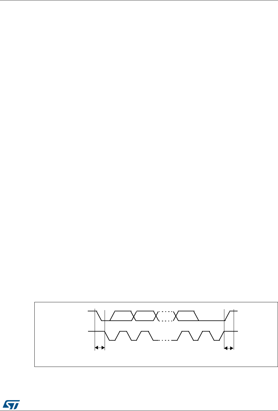
DocID018909 Rev 9 825/1718
RM0090 Inter-integrated circuit (I2C) interface
858
Note: Some of the above features may not be available in certain products. The user should refer
to the product data sheet, to identify the specific features supported by the I2C interface
implementation.
27.3 I2C functional description
In addition to receiving and transmitting data, this interface converts it from serial to parallel
format and vice versa. The interrupts are enabled or disabled by software. The interface is
connected to the I2C bus by a data pin (SDA) and by a clock pin (SCL). It can be connected
with a standard (up to 100 kHz) or fast (up to 400 kHz) I2C bus.
27.3.1 Mode selection
The interface can operate in one of the four following modes:
•Slave transmitter
•Slave receiver
•Master transmitter
•Master receiver
By default, it operates in slave mode. The interface automatically switches from slave to
master, after it generates a START condition and from master to slave, if an arbitration loss
or a Stop generation occurs, allowing multimaster capability.
Communication flow
In Master mode, the I2C interface initiates a data transfer and generates the clock signal. A
serial data transfer always begins with a start condition and ends with a stop condition. Both
start and stop conditions are generated in master mode by software.
In Slave mode, the interface is capable of recognizing its own addresses (7 or 10-bit), and
the General Call address. The General Call address detection may be enabled or disabled
by software.
Data and addresses are transferred as 8-bit bytes, MSB first. The first byte(s) following the
start condition contain the address (one in 7-bit mode, two in 10-bit mode). The address is
always transmitted in Master mode.
A 9th clock pulse follows the 8 clock cycles of a byte transfer, during which the receiver must
send an acknowledge bit to the transmitter. Refer to Figure 238.
Figure 238. I2C bus protocol
Acknowledge may be enabled or disabled by software. The I2C interface addresses (dual
addressing 7-bit/ 10-bit and/or general call address) can be selected by software.
SCL
SDA
12 8 9
MSB ACK
Stop
Start
condition
condition
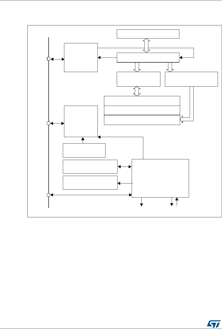
Inter-integrated circuit (I2C) interface RM0090
826/1718 DocID018909 Rev 9
The block diagram of the I2C interface is shown in Figure 239.
Figure 239. I2C block diagram for STM32F40x/41x
Data shift register
Comparator
Own address register
Clock control
Status registers
Control registers
Control
Clock
control
Data
control
SCL
logic
Dual address register
Data register
PEC register
Interrupts
PEC calculation
SMBA
SDA
Register (CCR)
(SR1&SR2)
(CR1&CR2)
DMA requests & ACK
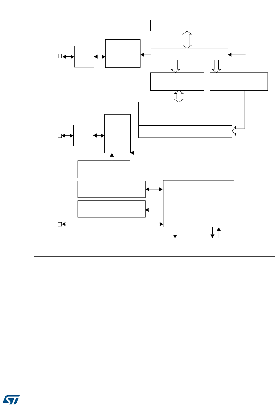
DocID018909 Rev 9 827/1718
RM0090 Inter-integrated circuit (I2C) interface
858
Figure 240. I2C block diagram for STM32F42x/43x
1. SMBA is an optional signal in SMBus mode. This signal is not applicable if SMBus is disabled.
27.3.2 I2C slave mode
By default the I2C interface operates in Slave mode. To switch from default Slave mode to
Master mode a Start condition generation is needed.
The peripheral input clock must be programmed in the I2C_CR2 register in order to
generate correct timings. The peripheral input clock frequency must be at least:
•2 MHz in Sm mode
•4 MHz in Fm mode
As soon as a start condition is detected, the address is received from the SDA line and sent
to the shift register. Then it is compared with the address of the interface (OAR1) and with
OAR2 (if ENDUAL=1) or the General Call address (if ENGC = 1).
Note: In 10-bit addressing mode, the comparison includes the header sequence (11110xx0),
where xx denotes the two most significant bits of the address.
$ATASHIFTREGISTER
#OMPARATOR
/WNADDRESSREGISTER
#LOCKCONTROL
3TATUSREGISTERS
#ONTROLREGISTERS
#ONTROL
#LOCK
CONTROL
$ATA
CONTROL
3#,
LOGIC
$UALADDRESSREGISTER
$ATAREGISTER
0%#REGISTER
)NTERRUPTS
0%#CALCULATION
3-"!
3$!
2EGISTER##2
3232
#2#2
$-!REQUESTS!#+
-36
.OISE
FILTER
.OISE
FILTER

Inter-integrated circuit (I2C) interface RM0090
828/1718 DocID018909 Rev 9
Header or address not matched: the interface ignores it and waits for another Start
condition.
Header matched (10-bit mode only): the interface generates an acknowledge pulse if the
ACK bit is set and waits for the 8-bit slave address.
Address matched: the interface generates in sequence:
•An acknowledge pulse if the ACK bit is set
•The ADDR bit is set by hardware and an interrupt is generated if the ITEVFEN bit is
set.
•If ENDUAL=1, the software has to read the DUALF bit to check which slave address
has been acknowledged.
In 10-bit mode, after receiving the address sequence the slave is always in Receiver mode.
It will enter Transmitter mode on receiving a repeated Start condition followed by the header
sequence with matching address bits and the least significant bit set (11110xx1).
The TRA bit indicates whether the slave is in Receiver or Transmitter mode.
Slave transmitter
Following the address reception and after clearing ADDR, the slave sends bytes from the
DR register to the SDA line via the internal shift register.
The slave stretches SCL low until ADDR is cleared and DR filled with the data to be sent
(see Figure 241 Transfer sequencing EV1 EV3).
When the acknowledge pulse is received:
•The TxE bit is set by hardware with an interrupt if the ITEVFEN and the ITBUFEN bits
are set.
If TxE is set and some data were not written in the I2C_DR register before the end of the
next data transmission, the BTF bit is set and the interface waits until BTF is cleared by a
read to I2C_SR1 followed by a write to the I2C_DR register, stretching SCL low.

DocID018909 Rev 9 829/1718
RM0090 Inter-integrated circuit (I2C) interface
858
Figure 241. Transfer sequence diagram for slave transmitter
1. The EV1 and EV3_1 events stretch SCL low until the end of the corresponding software sequence.
2. The EV3 event stretches SCL low if the software sequence is not completed before the end of the next byte
transmission
Slave receiver
Following the address reception and after clearing ADDR, the slave receives bytes from the
SDA line into the DR register via the internal shift register. After each byte the interface
generates in sequence:
•An acknowledge pulse if the ACK bit is set
•The RxNE bit is set by hardware and an interrupt is generated if the ITEVFEN and
ITBUFEN bit is set.
If RxNE is set and the data in the DR register is not read before the end of the next data
reception, the BTF bit is set and the interface waits until BTF is cleared by a read from the
I2C_DR register, stretching SCL low (see Figure 242 Transfer sequencing).
7-bit slave transmitter
10-bit slave transmitter
Legend: S= Start, S
r
= Repeated Start, P= Stop, A= Acknowledge, NA= Non-acknowledge,
EVx= Event (with interrupt if ITEVFEN=1)
EV1: ADDR=1, cleared by reading SR1 followed by reading SR2
EV3-1: TxE=1, shift register empty, data register empty, write Data1 in DR.
EV3: TxE=1, shift register not empty, data register empty, cleared by writing DR
EV3-2: AF=1; AF is cleared by writing ‘0’ in AF bit of SR1 register.
SAddress AData1A Data2A ..... DataNNAP
EV1 EV3-1 EV3EV3EV3EV3-2
SHeader A Address A
EV1
SrHeader A Data1A .... DataNNA
P
EV1 EV3_1 EV3EV3EV3-2
ai18209

Inter-integrated circuit (I2C) interface RM0090
830/1718 DocID018909 Rev 9
Figure 242. Transfer sequence diagram for slave receiver
1. The EV1 event stretches SCL low until the end of the corresponding software sequence.
2. The EV2 event stretches SCL low if the software sequence is not completed before the end of the next byte
reception.
3. After checking the SR1 register content, the user should perform the complete clearing sequence for each
flag found set.
Thus, for ADDR and STOPF flags, the following sequence is required inside the I2C interrupt routine:
READ SR1
if (ADDR == 1) {READ SR1; READ SR2}
if (STOPF == 1) {READ SR1; WRITE CR1}
The purpose is to make sure that both ADDR and STOPF flags are cleared if both are found set.
Closing slave communication
After the last data byte is transferred a Stop Condition is generated by the master. The
interface detects this condition and sets:
•The STOPF bit and generates an interrupt if the ITEVFEN bit is set.
The STOPF bit is cleared by a read of the SR1 register followed by a write to the CR1
register (see Figure 242: Transfer sequence diagram for slave receiver EV4).
27.3.3 I2C master mode
In Master mode, the I2C interface initiates a data transfer and generates the clock signal. A
serial data transfer always begins with a Start condition and ends with a Stop condition.
Master mode is selected as soon as the Start condition is generated on the bus with a
START bit.
The following is the required sequence in master mode.
•Program the peripheral input clock in I2C_CR2 Register in order to generate correct
timings
•Configure the clock control registers
•Configure the rise time register
•Program the I2C_CR1 register to enable the peripheral
•Set the START bit in the I2C_CR1 register to generate a Start condition
The peripheral input clock frequency must be at least:
•2 MHz in Sm mode
•4 MHz in Fm mode
7-bit slave receiver
10-bit slave receiver
Legend: S= Start, S
r
= Repeated Start, P= Stop, A= Acknowledge,
EVx= Event (with interrupt if ITEVFEN=1)
EV1: ADDR=1, cleared by reading SR1 followed by reading SR2
EV2: RxNE=1 cleared by reading DR register.
EV4: STOPF=1, cleared by reading SR1 register followed by writing to the CR1 register
SAddress AData1AData2A ..... DataNA P
EV1 EV2 EV2 EV2 EV4
SHeader A Address AData1A ..... DataNA P
EV1 EV2 EV2 EV4
ai18208

DocID018909 Rev 9 831/1718
RM0090 Inter-integrated circuit (I2C) interface
858
SCL master clock generation
The CCR bits are used to generate the high and low level of the SCL clock, starting from the
generation of the rising and falling edge (respectively). As a slave may stretch the SCL line,
the peripheral checks the SCL input from the bus at the end of the time programmed in
TRISE bits after rising edge generation.
•If the SCL line is low, it means that a slave is stretching the bus, and the high level
counter stops until the SCL line is detected high. This allows to guarantee the minimum
HIGH period of the SCL clock parameter.
•If the SCL line is high, the high level counter keeps on counting.
Indeed, the feedback loop from the SCL rising edge generation by the peripheral to the SCL
rising edge detection by the peripheral takes time even if no slave stretches the clock. This
loopback duration is linked to the SCL rising time (impacting SCL VIH input detection), plus
delay due to the noise filter present on the SCL input path, plus delay due to internal SCL
input synchronization with APB clock. The maximum time used by the feedback loop is
programmed in the TRISE bits, so that the SCL frequency remains stable whatever the SCL
rising time.
Start condition
Setting the START bit causes the interface to generate a Start condition and to switch to
Master mode (MSL bit set) when the BUSY bit is cleared.
Note: In master mode, setting the START bit causes the interface to generate a ReStart condition
at the end of the current byte transfer.
Once the Start condition is sent:
•The SB bit is set by hardware and an interrupt is generated if the ITEVFEN bit is set.
Then the master waits for a read of the SR1 register followed by a write in the DR register
with the Slave address (see Figure 243 and Figure 244 Transfer sequencing EV5).
Slave address transmission
Then the slave address is sent to the SDA line via the internal shift register.
•In 10-bit addressing mode, sending the header sequence causes the following event:
– The ADD10 bit is set by hardware and an interrupt is generated if the ITEVFEN bit
is set.
Then the master waits for a read of the SR1 register followed by a write in the DR
register with the second address byte (see Figure 243 and Figure 244 Transfer
sequencing).
– The ADDR bit is set by hardware and an interrupt is generated if the ITEVFEN bit
is set.
Then the master waits for a read of the SR1 register followed by a read of the SR2
register (see Figure 243 and Figure 244 Transfer sequencing).
•In 7-bit addressing mode, one address byte is sent.
As soon as the address byte is sent,
– The ADDR bit is set by hardware and an interrupt is generated if the ITEVFEN bit
is set.
Then the master waits for a read of the SR1 register followed by a read of the SR2
register (see Figure 243 and Figure 244 Transfer sequencing).

Inter-integrated circuit (I2C) interface RM0090
832/1718 DocID018909 Rev 9
The master can decide to enter Transmitter or Receiver mode depending on the LSB of the
slave address sent.
•In 7-bit addressing mode,
– To enter Transmitter mode, a master sends the slave address with LSB reset.
– To enter Receiver mode, a master sends the slave address with LSB set.
•In 10-bit addressing mode,
– To enter Transmitter mode, a master sends the header (11110xx0) and then the
slave address, (where xx denotes the two most significant bits of the address).
– To enter Receiver mode, a master sends the header (11110xx0) and then the
slave address. Then it should send a repeated Start condition followed by the
header (11110xx1), (where xx denotes the two most significant bits of the
address).
The TRA bit indicates whether the master is in Receiver or Transmitter mode.
Master transmitter
Following the address transmission and after clearing ADDR, the master sends bytes from
the DR register to the SDA line via the internal shift register.
The master waits until the first data byte is written into I2C_DR (see Figure 243 Transfer
sequencing EV8_1).
When the acknowledge pulse is received, the TxE bit is set by hardware and an interrupt is
generated if the ITEVFEN and ITBUFEN bits are set.
If TxE is set and a data byte was not written in the DR register before the end of the last data
transmission, BTF is set and the interface waits until BTF is cleared by a write to I2C_DR,
stretching SCL low.
Closing the communication
After the last byte is written to the DR register, the STOP bit is set by software to generate a
Stop condition (see Figure 243 Transfer sequencing EV8_2). The interface automatically
goes back to slave mode (MSL bit cleared).
Note: Stop condition should be programmed during EV8_2 event, when either TxE or BTF is set.

DocID018909 Rev 9 833/1718
RM0090 Inter-integrated circuit (I2C) interface
858
Figure 243. Transfer sequence diagram for master transmitter
1. The EV5, EV6, EV9, EV8_1 and EV8_2 events stretch SCL low until the end of the corresponding software
sequence.
2. The EV8 event stretches SCL low if the software sequence is not complete before the end of the next byte
transmission.
7-bit master transmitter
10-bit master transmitter
Legend: S= Start, Sr = Repeated Start, P= Stop, A= Acknowledge,
EVx= Event (with interrupt if ITEVFEN = 1)
EV5: SB=1, cleared by reading SR1 register followed by writing DR register with Address.
EV6: ADDR=1, cleared by reading SR1 register followed by reading SR2.
EV8_1: TxE=1, shift register empty, data register empty, write Data1 in DR.
EV8: TxE=1, shift register not empty, data register empty, cleared by writing DR register.
EV8_2: TxE=1, BTF = 1, Program Stop request. TxE and BTF are cleared by hardware by the Stop condition
EV9: ADD10=1, cleared by reading SR1 register followed by writing DR register.
SAddress AData1A Data2A ..... DataNA P
EV5 EV6 EV8_1 EV8EV8EV8EV8_2
SHeader A Address AData1A ..... DataNA P
EV5 EV9 EV6 EV8_1 EV8EV8EV8_2
ai18210

Inter-integrated circuit (I2C) interface RM0090
834/1718 DocID018909 Rev 9
Master receiver
Following the address transmission and after clearing ADDR, the I2C interface enters
Master Receiver mode. In this mode the interface receives bytes from the SDA line into the
DR register via the internal shift register. After each byte the interface generates in
sequence:
1. An acknowledge pulse if the ACK bit is set
2. The RxNE bit is set and an interrupt is generated if the ITEVFEN and ITBUFEN bits are
set (see Figure 244 Transfer sequencing EV7).
If the RxNE bit is set and the data in the DR register is not read before the end of the last
data reception, the BTF bit is set by hardware and the interface waits until BTF is cleared by
a read in the DR register, stretching SCL low.
Closing the communication
The master sends a NACK for the last byte received from the slave. After receiving this
NACK, the slave releases the control of the SCL and SDA lines. Then the master can send
a Stop/Restart condition.
1. To generate the nonacknowledge pulse after the last received data byte, the ACK bit
must be cleared just after reading the second last data byte (after second last RxNE
event).
2. In order to generate the Stop/Restart condition, software must set the STOP/START bit
after reading the second last data byte (after the second last RxNE event).
3. In case a single byte has to be received, the Acknowledge disable is made during EV6
(before ADDR flag is cleared) and the STOP condition generation is made after EV6.
After the Stop condition generation, the interface goes automatically back to slave mode
(MSL bit cleared).

DocID018909 Rev 9 835/1718
RM0090 Inter-integrated circuit (I2C) interface
858
Figure 244. Transfer sequence diagram for master receiver
1. If a single byte is received, it is NA.
2. The EV5, EV6 and EV9 events stretch SCL low until the end of the corresponding software sequence.
3. The EV7 event stretches SCL low if the software sequence is not completed before the end of the next byte
reception.
4. The EV7_1 software sequence must be completed before the ACK pulse of the current byte transfer.
The procedures described below are recommended if the EV7-1 software sequence is not
completed before the ACK pulse of the current byte transfer.
These procedures must be followed to make sure:
•The ACK bit is set low on time before the end of the last data reception
•The STOP bit is set high after the last data reception without reception of
supplementary data.
For 2-byte reception:
•Wait until ADDR = 1 (SCL stretched low until the ADDR flag is cleared)
•Set ACK low, set POS high
•Clear ADDR flag
•Wait until BTF = 1 (Data 1 in DR, Data2 in shift register, SCL stretched low until a data
1 is read)
•Set STOP high
•Read data 1 and 2
BITMASTERRECEIVER
BITMASTERRECEIVER
,EGEND33TART3R2EPEATED3TART03TOP!!CKNOWLEDGE.!.ONACKNOWLEDGE
%6X%VENTWITHINTERRUPTIF)4%6&%.
%63"CLEAREDBYREADING32REGISTERFOLLOWEDBYWRITING$2REGISTER
%6!$$2CLEAREDBYREADING32REGISTERFOLLOWEDBYREADING32)NBITMASTERRECEIVERMODETHISSE
QUENCESHOULDBEFOLLOWEDBYWRITING#2WITH34!24
%62X.%CLEAREDBYREADING$2REGISTER
%6?2X.%CLEAREDBYREADING$2REGISTERPROGRAM!#+AND34/0REQUEST
%6!$$CLEAREDBYREADING32REGISTERFOLLOWEDBYWRITING$2REGISTER
3 !DDRESS ! $ATA ! $ATA ! $ATA. .! 0
%6 %6 %6 %6 %6? %6
3 (EADER ! !DDRESS !
%6 %6 %6
3R(EADER ! $ATA !
%6 %6 %6
$ATA !
%6
$ATA. .! 0
%6? %6
AID
)NCASEOFTHERECEPTIONOFBYTETHE!CKNOWLEDGEDISABLEMUSTBEPERFORMEDDURING%6EVENTIEBEFORECLEARING!$$2FLAG

Inter-integrated circuit (I2C) interface RM0090
836/1718 DocID018909 Rev 9
For N >2 -byte reception, from N-2 data reception
•Wait until BTF = 1 (data N-2 in DR, data N-1 in shift register, SCL stretched low until
data N-2 is read)
•Set ACK low
•Read data N-2
•Wait until BTF = 1 (data N-1 in DR, data N in shift register, SCL stretched low until a
data N-1 is read)
•Set STOP high
•Read data N-1 and N
27.3.4 Error conditions
The following are the error conditions which may cause communication to fail.
Bus error (BERR)
This error occurs when the I2C interface detects an external Stop or Start condition during
an address or a data transfer. In this case:
•the BERR bit is set and an interrupt is generated if the ITERREN bit is set
•in Slave mode: data are discarded and the lines are released by hardware:
– in case of a misplaced Start, the slave considers it is a restart and waits for an
address, or a Stop condition
– in case of a misplaced Stop, the slave behaves like for a Stop condition and the
lines are released by hardware
•In Master mode: the lines are not released and the state of the current transmission is
not affected. It is up to the software to abort or not the current transmission
Acknowledge failure (AF)
This error occurs when the interface detects a nonacknowledge bit. In this case:
•the AF bit is set and an interrupt is generated if the ITERREN bit is set
•a transmitter which receives a NACK must reset the communication:
– If Slave: lines are released by hardware
– If Master: a Stop or repeated Start condition must be generated by software
Arbitration lost (ARLO)
This error occurs when the I2C interface detects an arbitration lost condition. In this case,
•the ARLO bit is set by hardware (and an interrupt is generated if the ITERREN bit is
set)
•the I2C Interface goes automatically back to slave mode (the MSL bit is cleared). When
the I2C loses the arbitration, it is not able to acknowledge its slave address in the same
transfer, but it can acknowledge it after a repeated Start from the winning master.
•lines are released by hardware

DocID018909 Rev 9 837/1718
RM0090 Inter-integrated circuit (I2C) interface
858
Overrun/underrun error (OVR)
An overrun error can occur in slave mode when clock stretching is disabled and the I2C
interface is receiving data. The interface has received a byte (RxNE=1) and the data in DR
has not been read, before the next byte is received by the interface. In this case,
•The last received byte is lost.
•In case of Overrun error, software should clear the RxNE bit and the transmitter should
re-transmit the last received byte.
Underrun error can occur in slave mode when clock stretching is disabled and the I2C
interface is transmitting data. The interface has not updated the DR with the next byte
(TxE=1), before the clock comes for the next byte. In this case,
•The same byte in the DR register will be sent again
•The user should make sure that data received on the receiver side during an underrun
error are discarded and that the next bytes are written within the clock low time
specified in the I2C bus standard.
For the first byte to be transmitted, the DR must be written after ADDR is cleared and before
the first SCL rising edge. If not possible, the receiver must discard the first data.
27.3.5 Programmable noise filter
The programmable noise filter is available on STM32F42xxx and STM32F43xxx devices
only.
In Fm mode, the I2C standard requires that spikes are suppressed to a length of 50 ns on
SDA and SCL lines.
An analog noise filter is implemented in the SDA and SCL I/Os. This filter is enabled by
default and can be disabled by setting the ANOFF bit in the I2C_FLTR register.
A digital noise filter can be enabled by configuring the DNF[3:0] bits to a non-zero value.
This suppresses the spikes on SDA and SCL inputs with a length of up to DNF[3:0] *
TPCLK1.
Enabling the digital noise filter increases the SDA hold time by (DNF[3:0] +1)* TPCLK.
To be compliant with the maximum hold time of the I2C-bus specification version 2.1
(Thd:dat), the DNF bits must be programmed using the constraints shown in Table 121, and
assuming that the analog filter is disabled.
Note: DNF[3:0] must only be configured when the I2C is disabled (PE = 0). If the analog filter is
also enabled, the digital filter is added to the analog filter.
Table 121. Maximum DNF[3:0] value to be compliant with Thd:dat(max)
PCLK1 frequency
Maximum DNF value
Sm mode Fm mode
2 <= FPCLK1 <= 5 2 0
5 < FPCLK1 <= 10 12 0
10 < FPCLK1 <= 20 15 1
20 < FPCLK1 <= 30 15 7

Inter-integrated circuit (I2C) interface RM0090
838/1718 DocID018909 Rev 9
Note: For each frequency range, the constraint is given based on the worst case which is the
minimum frequency of the range. Greater DNF values can be used if the system can
support maximum hold time violation.
27.3.6 SDA/SCL line control
•If clock stretching is enabled:
– Transmitter mode: If TxE=1 and BTF=1: the interface holds the clock line low
before transmission to wait for the microcontroller to write the byte in the Data
Register (both buffer and shift register are empty).
– Receiver mode: If RxNE=1 and BTF=1: the interface holds the clock line low after
reception to wait for the microcontroller to read the byte in the Data Register (both
buffer and shift register are full).
•If clock stretching is disabled in Slave mode:
– Overrun Error in case of RxNE=1 and no read of DR has been done before the
next byte is received. The last received byte is lost.
– Underrun Error in case TxE=1 and no write into DR has been done before the next
byte must be transmitted. The same byte will be sent again.
– Write Collision not managed.
27.3.7 SMBus
Introduction
The System Management Bus (SMBus) is a two-wire interface through which various
devices can communicate with each other and with the rest of the system. It is based on I2C
principles of operation. SMBus provides a control bus for system and power management
related tasks. A system may use SMBus to pass messages to and from devices instead of
toggling individual control lines.
The System Management Bus Specification refers to three types of devices. A slave is a
device that is receiving or responding to a command. A master is a device that issues
commands, generates the clocks, and terminates the transfer. A host is a specialized
master that provides the main interface to the system's CPU. A host must be a master-slave
and must support the SMBus host notify protocol. Only one host is allowed in a system.
Similarities between SMBus and I2C
•2 wire bus protocol (1 Clk, 1 Data) + SMBus Alert line optional
•Master-slave communication, Master provides clock
•Multi master capability
•SMBus data format similar to I2C 7-bit addressing format (Figure 238).
30 < FPCLK1 <= 40 15 13
40 < FPCLK1 <= 50 15 15
Table 121. Maximum DNF[3:0] value to be compliant with Thd:dat(max) (continued)
PCLK1 frequency
Maximum DNF value
Sm mode Fm mode

DocID018909 Rev 9 839/1718
RM0090 Inter-integrated circuit (I2C) interface
858
Differences between SMBus and I2C
The following table describes the differences between SMBus and I2C.
SMBus application usage
With System Management Bus, a device can provide manufacturer information, tell the
system what its model/part number is, save its state for a suspend event, report different
types of errors, accept control parameters, and return its status. SMBus provides a control
bus for system and power management related tasks.
Device identification
Any device that exists on the System Management Bus as a slave has a unique address
called the Slave Address. For the list of reserved slave addresses, refer to the SMBus
specification version. 2.0 (http://smbus.org/).
Bus protocols
The SMBus specification supports up to 9 bus protocols. For more details of these protocols
and SMBus address types, refer to SMBus specification version. 2.0 (http://smbus.org/).
These protocols should be implemented by the user software.
Address resolution protocol (ARP)
SMBus slave address conflicts can be resolved by dynamically assigning a new unique
address to each slave device. The Address Resolution Protocol (ARP) has the following
attributes:
•Address assignment uses the standard SMBus physical layer arbitration mechanism
•Assigned addresses remain constant while device power is applied; address retention
through device power loss is also allowed
•No additional SMBus packet overhead is incurred after address assignment. (i.e.
subsequent accesses to assigned slave addresses have the same overhead as
accesses to fixed address devices.)
•Any SMBus master can enumerate the bus
Unique device identifier (UDID)
In order to provide a mechanism to isolate each device for the purpose of address
assignment, each device must implement a unique device identifier (UDID).
Table 122. SMBus vs. I2C
SMBus I2C
Max. speed 100 kHz Max. speed 400 kHz
Min. clock speed 10 kHz No minimum clock speed
35 ms clock low timeout No timeout
Logic levels are fixed Logic levels are VDD dependent
Different address types (reserved, dynamic etc.) 7-bit, 10-bit and general call slave address types
Different bus protocols (quick command, process
call etc.) No bus protocols

Inter-integrated circuit (I2C) interface RM0090
840/1718 DocID018909 Rev 9
For the details on 128 bit UDID and more information on ARP, refer to SMBus specification
version 2.0 (http://smbus.org/).
SMBus alert mode
SMBus Alert is an optional signal with an interrupt line for devices that want to trade their
ability to master for a pin. SMBA is a wired-AND signal just as the SCL and SDA signals are.
SMBA is used in conjunction with the SMBus General Call Address. Messages invoked with
the SMBus are 2 bytes long.
A slave-only device can signal the host through SMBA that it wants to talk by setting ALERT
bit in I2C_CR1 register. The host processes the interrupt and simultaneously accesses all
SMBA devices through the Alert Response Address (known as ARA having a value 0001
100X). Only the device(s) which pulled SMBA low will acknowledge the Alert Response
Address. This status is identified using SMBALERT Status flag in I2C_SR1 register. The
host performs a modified Receive Byte operation. The 7 bit device address provided by the
slave transmit device is placed in the 7 most significant bits of the byte. The eighth bit can
be a zero or one.
If more than one device pulls SMBA low, the highest priority (lowest address) device will win
communication rights via standard arbitration during the slave address transfer. After
acknowledging the slave address the device must disengage its SMBA pull-down. If the
host still sees SMBA low when the message transfer is complete, it knows to read the ARA
again.
A host which does not implement the SMBA signal may periodically access the ARA.
For more details on SMBus Alert mode, refer to SMBus specification version 2.0
(http://smbus.org/).
Timeout error
There are differences in the timing specifications between I2C and SMBus.
SMBus defines a clock low timeout, TIMEOUT of 35 ms. Also SMBus specifies TLOW:
SEXT as the cumulative clock low extend time for a slave device. SMBus specifies TLOW:
MEXT as the cumulative clock low extend time for a master device. For more details on
these timeouts, refer to SMBus specification version 2.0 (http://smbus.org/).
The status flag Timeout or Tlow Error in I2C_SR1 shows the status of this feature.
How to use the interface in SMBus mode
To switch from I2C mode to SMBus mode, the following sequence should be performed.
•Set the SMBus bit in the I2C_CR1 register
•Configure the SMBTYPE and ENARP bits in the I2C_CR1 register as required for the
application
If you want to configure the device as a master, follow the Start condition generation
procedure in Section 27.3.3: I2C master mode. Otherwise, follow the sequence in
Section 27.3.2: I2C slave mode.
The application has to control the various SMBus protocols by software.
•SMB Device Default Address acknowledged if ENARP=1 and SMBTYPE=0
•SMB Host Header acknowledged if ENARP=1 and SMBTYPE=1
•SMB Alert Response Address acknowledged if SMBALERT=1

DocID018909 Rev 9 841/1718
RM0090 Inter-integrated circuit (I2C) interface
858
27.3.8 DMA requests
DMA requests (when enabled) are generated only for data transfer. DMA requests are
generated by Data Register becoming empty in transmission and Data Register becoming
full in reception. The DMA must be initialized and enabled before the I2C data transfer. The
DMAEN bit must be set in the I2C_CR2 register before the ADDR event. In master mode or
in slave mode when clock stretching is enabled, the DMAEN bit can also be set during the
ADDR event, before clearing the ADDR flag. The DMA request must be served before the
end of the current byte transfer. When the number of data transfers which has been
programmed for the corresponding DMA stream is reached, the DMA controller sends an
End of Transfer EOT signal to the I2C interface and generates a Transfer Complete interrupt
if enabled:
•Master transmitter: In the interrupt routine after the EOT interrupt, disable DMA
requests then wait for a BTF event before programming the Stop condition.
•Master receiver
– When the number of bytes to be received is equal to or greater than two, the DMA
controller sends a hardware signal, EOT_1, corresponding to the last but one data
byte (number_of_bytes – 1). If, in the I2C_CR2 register, the LAST bit is set, I2C
automatically sends a NACK after the next byte following EOT_1. The user can
generate a Stop condition in the DMA Transfer Complete interrupt routine if
enabled.
– When a single byte must be received: the NACK must be programmed during EV6
event, i.e. program ACK=0 when ADDR=1, before clearing ADDR flag. Then the
user can program the STOP condition either after clearing ADDR flag, or in the
DMA Transfer Complete interrupt routine.
Transmission using DMA
DMA mode can be enabled for transmission by setting the DMAEN bit in the I2C_CR2
register. Data will be loaded from a Memory area configured using the DMA peripheral (refer
to the DMA specification) to the I2C_DR register whenever the TxE bit is set. To map a DMA
stream x for I2C transmission (where x is the stream number), perform the following
sequence:
1. Set the I2C_DR register address in the DMA_SxPAR register. The data will be moved
to this address from the memory after each TxE event.
2. Set the memory address in the DMA_SxMA0R register (and in DMA_SxMA1R register
in the case of a bouble buffer mode). The data will be loaded into I2C_DR from this
memory after each TxE event.
3. Configure the total number of bytes to be transferred in the DMA_SxNDTR register.
After each TxE event, this value will be decremented.
4. Configure the DMA stream priority using the PL[0:1] bits in the DMA_SxCR register
5. Set the DIR bit in the DMA_SxCR register and configure interrupts after half transfer or
full transfer depending on application requirements.
6. Activate the stream by setting the EN bit in the DMA_SxCR register.
When the number of data transfers which has been programmed in the DMA Controller
registers is reached, the DMA controller sends an End of Transfer EOT/ EOT_1 signal to the
I2C interface and the DMA generates an interrupt, if enabled, on the DMA stream interrupt
vector.
Note: Do not enable the ITBUFEN bit in the I2C_CR2 register if DMA is used for transmission.

Inter-integrated circuit (I2C) interface RM0090
842/1718 DocID018909 Rev 9
Reception using DMA
DMA mode can be enabled for reception by setting the DMAEN bit in the I2C_CR2 register.
Data will be loaded from the I2C_DR register to a Memory area configured using the DMA
peripheral (refer to the DMA specification) whenever a data byte is received. To map a DMA
stream x for I2C reception (where x is the stream number), perform the following sequence:
1. Set the I2C_DR register address in DMA_SxPAR register. The data will be moved from
this address to the memory after each RxNE event.
2. Set the memory address in the DMA_SxMA0R register (and in DMA_SxMA1R register
in the case of a bouble buffer mode). The data will be loaded from the I2C_DR register
to this memory area after each RxNE event.
3. Configure the total number of bytes to be transferred in the DMA_SxNDTR register.
After each RxNE event, this value will be decremented.
4. Configure the stream priority using the PL[0:1] bits in the DMA_SxCR register
5. Reset the DIR bit and configure interrupts in the DMA_SxCR register after half transfer
or full transfer depending on application requirements.
6. Activate the stream by setting the EN bit in the DMA_SxCR register.
When the number of data transfers which has been programmed in the DMA Controller
registers is reached, the DMA controller sends an End of Transfer EOT/ EOT_1 signal to the
I2C interface and DMA generates an interrupt, if enabled, on the DMA stream interrupt
vector.
Note: Do not enable the ITBUFEN bit in the I2C_CR2 register if DMA is used for reception.
27.3.9 Packet error checking
A PEC calculator has been implemented to improve the reliability of communication. The
PEC is calculated by using the C(x) = x8 + x2 + x + 1 CRC-8 polynomial serially on each bit.
•PEC calculation is enabled by setting the ENPEC bit in the I2C_CR1 register. PEC is a
CRC-8 calculated on all message bytes including addresses and R/W bits.
– In transmission: set the PEC transfer bit in the I2C_CR1 register after the TxE
event corresponding to the last byte. The PEC will be transferred after the last
transmitted byte.
– In reception: set the PEC bit in the I2C_CR1 register after the RxNE event
corresponding to the last byte so that the receiver sends a NACK if the next
received byte is not equal to the internally calculated PEC. In case of Master-
Receiver, a NACK must follow the PEC whatever the check result. The PEC must

DocID018909 Rev 9 843/1718
RM0090 Inter-integrated circuit (I2C) interface
858
be set before the ACK of the CRC reception in slave mode. It must be set when
the ACK is set low in master mode.
•A PECERR error flag/interrupt is also available in the I2C_SR1 register.
•If DMA and PEC calculation are both enabled:-
– In transmission: when the I2C interface receives an EOT signal from the DMA
controller, it automatically sends a PEC after the last byte.
– In reception: when the I2C interface receives an EOT_1 signal from the DMA
controller, it will automatically consider the next byte as a PEC and will check it. A
DMA request is generated after PEC reception.
•To allow intermediate PEC transfers, a control bit is available in the I2C_CR2 register
(LAST bit) to determine if it is really the last DMA transfer or not. If it is the last DMA
request for a master receiver, a NACK is automatically sent after the last received byte.
•PEC calculation is corrupted by an arbitration loss.
27.4 I2C interrupts
The table below gives the list of I2C interrupt requests.
Note: SB, ADDR, ADD10, STOPF, BTF, RxNE and TxE are logically ORed on the same interrupt
channel.
BERR, ARLO, AF, OVR, PECERR, TIMEOUT and SMBALERT are logically ORed on the
same interrupt channel.
Table 123. I2C Interrupt requests
Interrupt event Event flag Enable control bit
Start bit sent (Master) SB
ITEVFEN
Address sent (Master) or Address matched (Slave) ADDR
10-bit header sent (Master) ADD10
Stop received (Slave) STOPF
Data byte transfer finished BTF
Receive buffer not empty RxNE
ITEVFEN and ITBUFEN
Transmit buffer empty TxE
Bus error BERR
ITERREN
Arbitration loss (Master) ARLO
Acknowledge failure AF
Overrun/Underrun OVR
PEC error PECERR
Timeout/Tlow error TIMEOUT
SMBus Alert SMBALERT
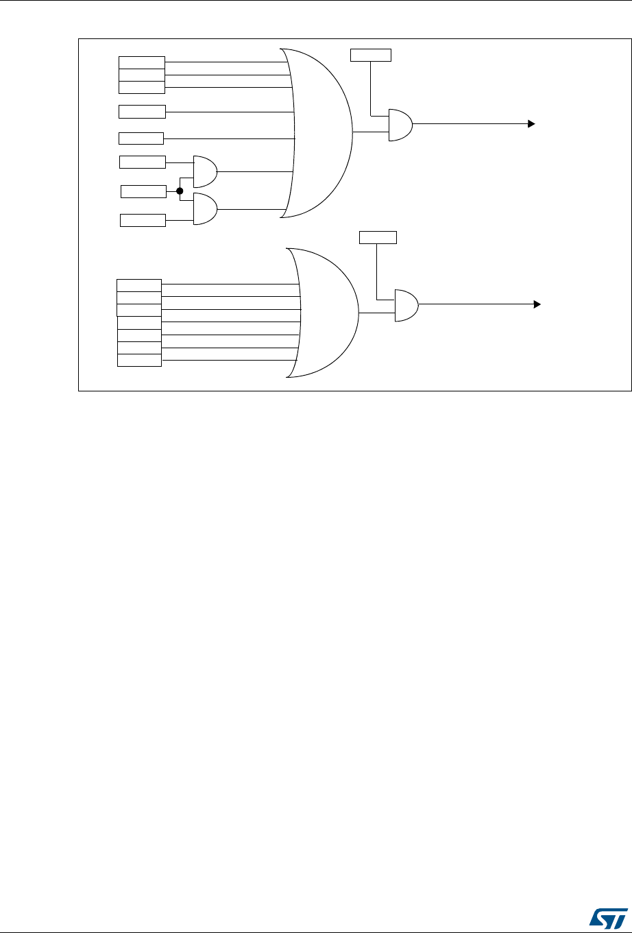
Inter-integrated circuit (I2C) interface RM0090
844/1718 DocID018909 Rev 9
Figure 245. I2C interrupt mapping diagram
ADDR
SB
ADD10
RxNE
TxE
BTF
it_event
ARLO
BERR
AF
OVR
PECERR
TIMEOUT
SMBALERT
ITERREN
it_error
ITEVFEN
ITBUFEN
STOPF

DocID018909 Rev 9 845/1718
RM0090 Inter-integrated circuit (I2C) interface
858
27.5 I2C debug mode
When the microcontroller enters the debug mode (Cortex®-M4 with FPU core halted), the
SMBUS timeout either continues to work normally or stops, depending on the
DBG_I2Cx_SMBUS_TIMEOUT configuration bits in the DBG module. For more details,
refer to Section 38.16.2: Debug support for timers, watchdog, bxCAN and I2C on
page 1682.
27.6 I2C registers
Refer to Section 1.1 on page 57 for a list of abbreviations used in register descriptions.
The peripheral registers have to be accessed by half-words (16 bits) or words (32 bits).
27.6.1 I2C Control register 1 (I2C_CR1)
Address offset: 0x00
Reset value: 0x0000
15141312111098 7 6543210
SWRST Res. ALERT PEC POS ACK STOP START NO
STRETCH ENGC ENPEC ENARP SMB
TYPE Res.
SMBU
SPE
rw rw rw rw rw rw rw rw rw rw rw rw rw rw
Bit 15 SWRST: Software reset
When set, the I2C is under reset state. Before resetting this bit, make sure the I2C lines are
released and the bus is free.
0: I2C Peripheral not under reset
1: I2C Peripheral under reset state
Note: This bit can be used to reinitialize the peripheral after an error or a locked state. As an
example, if the BUSY bit is set and remains locked due to a glitch on the bus, the
SWRST bit can be used to exit from this state.
Bit 14 Reserved, must be kept at reset value
Bit 13 ALERT: SMBus alert
This bit is set and cleared by software, and cleared by hardware when PE=0.
0: Releases SMBA pin high. Alert Response Address Header followed by NACK.
1: Drives SMBA pin low. Alert Response Address Header followed by ACK.
Bit 12 PEC: Packet error checking
This bit is set and cleared by software, and cleared by hardware when PEC is transferred or
by a START or Stop condition or when PE=0.
0: No PEC transfer
1: PEC transfer (in Tx or Rx mode)
Note: PEC calculation is corrupted by an arbitration loss.

Inter-integrated circuit (I2C) interface RM0090
846/1718 DocID018909 Rev 9
Bit 11 POS: Acknowledge/PEC Position (for data reception)
This bit is set and cleared by software and cleared by hardware when PE=0.
0: ACK bit controls the (N)ACK of the current byte being received in the shift register. The
PEC bit indicates that current byte in shift register is a PEC.
1: ACK bit controls the (N)ACK of the next byte which will be received in the shift register.
The PEC bit indicates that the next byte in the shift register is a PEC
Note: The POS bit must be used only in 2-byte reception configuration in master mode. It
must be configured before data reception starts, as described in the 2-byte reception
procedure recommended in Section : Master receiver on page 834.
Bit 10 ACK: Acknowledge enable
This bit is set and cleared by software and cleared by hardware when PE=0.
0: No acknowledge returned
1: Acknowledge returned after a byte is received (matched address or data)
Bit 9 STOP: Stop generation
The bit is set and cleared by software, cleared by hardware when a Stop condition is
detected, set by hardware when a timeout error is detected.
In Master Mode:
0: No Stop generation.
1: Stop generation after the current byte transfer or after the current Start condition is sent.
In Slave mode:
0: No Stop generation.
1: Release the SCL and SDA lines after the current byte transfer.
Bit 8 START: Start generation
This bit is set and cleared by software and cleared by hardware when start is sent or PE=0.
In Master Mode:
0: No Start generation
1: Repeated start generation
In Slave mode:
0: No Start generation
1: Start generation when the bus is free
Bit 7 NOSTRETCH: Clock stretching disable (Slave mode)
This bit is used to disable clock stretching in slave mode when ADDR or BTF flag is set, until
it is reset by software.
0: Clock stretching enabled
1: Clock stretching disabled
Bit 6 ENGC: General call enable
0: General call disabled. Address 00h is NACKed.
1: General call enabled. Address 00h is ACKed.
Bit 5 ENPEC: PEC enable
0: PEC calculation disabled
1: PEC calculation enabled
Bit 4 ENARP: ARP enable
0: ARP disable
1: ARP enable
SMBus Device default address recognized if SMBTYPE=0
SMBus Host address recognized if SMBTYPE=1
Bit 3 SMBTYPE: SMBus type
0: SMBus Device
1: SMBus Host

DocID018909 Rev 9 847/1718
RM0090 Inter-integrated circuit (I2C) interface
858
Note: When the STOP, START or PEC bit is set, the software must not perform any write access
to I2C_CR1 before this bit is cleared by hardware. Otherwise there is a risk of setting a
second STOP, START or PEC request.
27.6.2 I2C Control register 2 (I2C_CR2)
Address offset: 0x04
Reset value: 0x0000
Bit 2 Reserved, must be kept at reset value
Bit 1 SMBUS: SMBus mode
0: I2C mode
1: SMBus mode
Bit 0 PE: Peripheral enable
0: Peripheral disable
1: Peripheral enable
Note: If this bit is reset while a communication is on going, the peripheral is disabled at the
end of the current communication, when back to IDLE state.
All bit resets due to PE=0 occur at the end of the communication.
In master mode, this bit must not be reset before the end of the communication.
1514131211109876543210
Reserved LAST DMA
EN
ITBUF
EN
ITEVTE
N
ITERR
EN Reserved FREQ[5:0]
rw rw rw rw rw rw rw rw rw rw rw
Bits 15:13 Reserved, must be kept at reset value
Bit 12 LAST: DMA last transfer
0: Next DMA EOT is not the last transfer
1: Next DMA EOT is the last transfer
Note: This bit is used in master receiver mode to permit the generation of a NACK on the last
received data.
Bit 11 DMAEN: DMA requests enable
0: DMA requests disabled
1: DMA request enabled when TxE=1 or RxNE =1
Bit 10 ITBUFEN: Buffer interrupt enable
0: TxE = 1 or RxNE = 1 does not generate any interrupt.
1: TxE = 1 or RxNE = 1 generates Event Interrupt (whatever the state of DMAEN)

Inter-integrated circuit (I2C) interface RM0090
848/1718 DocID018909 Rev 9
Bit 9 ITEVTEN: Event interrupt enable
0: Event interrupt disabled
1: Event interrupt enabled
This interrupt is generated when:
– SB = 1 (Master)
– ADDR = 1 (Master/Slave)
– ADD10= 1 (Master)
– STOPF = 1 (Slave)
– BTF = 1 with no TxE or RxNE event
– TxE event to 1 if ITBUFEN = 1
– RxNE event to 1if ITBUFEN = 1
ITERREN: Error interrupt enable
0: Error interrupt disabled
1: Error interrupt enabled
This interrupt is generated when:
–BERR = 1
–ARLO = 1
–AF = 1
–OVR = 1
– PECERR = 1
–TIMEOUT = 1
– SMBALERT = 1
Bits 7:6 Reserved, must be kept at reset value
Bits 5:0 FREQ[5:0]: Peripheral clock frequency
The FREQ bits must be configured with the APB clock frequency value (I2C peripheral
connected to APB). The FREQ field is used by the peripheral to generate data setup and
hold times compliant with the I2C specifications. The minimum allowed frequency is 2 MHz,
the maximum frequency is limited by the maximum APB frequency and cannot exceed
50 MHz (peripheral intrinsic maximum limit).
0b000000: Not allowed
0b000001: Not allowed
0b000010: 2 MHz
...
0b101010: 50 MHz
Higher than 0b101010: Not allowed
DocID018909 Rev 9 849/1718
RM0090 Inter-integrated circuit (I2C) interface
858
27.6.3 I2C Own address register 1 (I2C_OAR1)
Address offset: 0x08
Reset value: 0x0000
27.6.4 I2C Own address register 2 (I2C_OAR2)
Address offset: 0x0C
Reset value: 0x0000
15141312111098 7 654321 0
ADD
MODE Reserved
ADD[9:8] ADD[7:1] ADD0
rw rw rw rw rw rw rw rw rw rw rw
Bit 15 ADDMODE Addressing mode (slave mode)
0: 7-bit slave address (10-bit address not acknowledged)
1: 10-bit slave address (7-bit address not acknowledged)
Bit 14 Should always be kept at 1 by software.
Bits 13:10 Reserved, must be kept at reset value
Bits 9:8 ADD[9:8]: Interface address
7-bit addressing mode: don’t care
10-bit addressing mode: bits9:8 of address
Bits 7:1 ADD[7:1]: Interface address
bits 7:1 of address
Bit 0 ADD0: Interface address
7-bit addressing mode: don’t care
10-bit addressing mode: bit 0 of address
151413121110987 654321 0
Reserved ADD2[7:1] ENDUAL
rw rw rw rw rw rw rw rw
Bits 15:8 Reserved, must be kept at reset value
Bits 7:1 ADD2[7:1]: Interface address
bits 7:1 of address in dual addressing mode
Bit 0 ENDUAL: Dual addressing mode enable
0: Only OAR1 is recognized in 7-bit addressing mode
1: Both OAR1 and OAR2 are recognized in 7-bit addressing mode

Inter-integrated circuit (I2C) interface RM0090
850/1718 DocID018909 Rev 9
27.6.5 I2C Data register (I2C_DR)
Address offset: 0x10
Reset value: 0x0000
27.6.6 I2C Status register 1 (I2C_SR1)
Address offset: 0x14
Reset value: 0x0000
151413121110987 654321 0
Reserved
DR[7:0]
rw rw rw rw rw rw rw rw
Bits 15:8 Reserved, must be kept at reset value
Bits 7:0 DR[7:0] 8-bit data register
Byte received or to be transmitted to the bus.
– Transmitter mode: Byte transmission starts automatically when a byte is written in the DR
register. A continuous transmit stream can be maintained if the next data to be transmitted is
put in DR once the transmission is started (TxE=1)
– Receiver mode: Received byte is copied into DR (RxNE=1). A continuous transmit stream
can be maintained if DR is read before the next data byte is received (RxNE=1).
Note: In slave mode, the address is not copied into DR.
Write collision is not managed (DR can be written if TxE=0).
If an ARLO event occurs on ACK pulse, the received byte is not copied into DR
and so cannot be read.
151413121110987 654321 0
SMB
ALERT
TIME
OUT Res.
PEC
ERR OVR AF ARLO BERR TxE RxNE Res. STOPF ADD10 BTF ADDR SB
rc_w0rc_w0 rc_w0rc_w0rc_w0rc_w0rc_w0r r rrrr r

DocID018909 Rev 9 851/1718
RM0090 Inter-integrated circuit (I2C) interface
858
Bit 15 SMBALERT: SMBus alert
In SMBus host mode:
0: no SMBALERT
1: SMBALERT event occurred on pin
In SMBus slave mode:
0: no SMBALERT response address header
1: SMBALERT response address header to SMBALERT LOW received
– Cleared by software writing 0, or by hardware when PE=0.
Bit 14 TIMEOUT: Timeout or Tlow error
0: No timeout error
1: SCL remained LOW for 25 ms (Timeout)
or
Master cumulative clock low extend time more than 10 ms (Tlow:mext)
or
Slave cumulative clock low extend time more than 25 ms (Tlow:sext)
– When set in slave mode: slave resets the communication and lines are released by
hardware
– When set in master mode: Stop condition sent by hardware
– Cleared by software writing 0, or by hardware when PE=0.
Note: This functionality is available only in SMBus mode.
Bit 13 Reserved, must be kept at reset value
Bit 12 PECERR: PEC Error in reception
0: no PEC error: receiver returns ACK after PEC reception (if ACK=1)
1: PEC error: receiver returns NACK after PEC reception (whatever ACK)
– Cleared by software writing 0, or by hardware when PE=0.
– Note: When the received CRC is wrong, PECERR is not set in slave mode if the PEC control
bit is not set before the end of the CRC reception. Nevertheless, reading the PEC value
determines whether the received CRC is right or wrong.
Bit 11 OVR: Overrun/Underrun
0: No overrun/underrun
1: Overrun or underrun
– Set by hardware in slave mode when NOSTRETCH=1 and:
– In reception when a new byte is received (including ACK pulse) and the DR register has not
been read yet. New received byte is lost.
– In transmission when a new byte should be sent and the DR register has not been written
yet. The same byte is sent twice.
– Cleared by software writing 0, or by hardware when PE=0.
Note: If the DR write occurs very close to SCL rising edge, the sent data is unspecified and a
hold timing error occurs
Bit 10 AF: Acknowledge failure
0: No acknowledge failure
1: Acknowledge failure
– Set by hardware when no acknowledge is returned.
– Cleared by software writing 0, or by hardware when PE=0.

Inter-integrated circuit (I2C) interface RM0090
852/1718 DocID018909 Rev 9
Bit 9 ARLO: Arbitration lost (master mode)
0: No Arbitration Lost detected
1: Arbitration Lost detected
Set by hardware when the interface loses the arbitration of the bus to another master
– Cleared by software writing 0, or by hardware when PE=0.
After an ARLO event the interface switches back automatically to Slave mode (MSL=0).
Note: In SMBUS, the arbitration on the data in slave mode occurs only during the data phase,
or the acknowledge transmission (not on the address acknowledge).
Bit 8 BERR: Bus error
0: No misplaced Start or Stop condition
1: Misplaced Start or Stop condition
– Set by hardware when the interface detects an SDA rising or falling edge while SCL is high,
occurring in a non-valid position during a byte transfer.
– Cleared by software writing 0, or by hardware when PE=0.
Bit 7 TxE: Data register empty (transmitters)
0: Data register not empty
1: Data register empty
– Set when DR is empty in transmission. TxE is not set during address phase.
– Cleared by software writing to the DR register or by hardware after a start or a stop condition
or when PE=0.
TxE is not set if either a NACK is received, or if next byte to be transmitted is PEC (PEC=1)
Note: TxE is not cleared by writing the first data being transmitted, or by writing data when
BTF is set, as in both cases the data register is still empty.
Bit 6 RxNE: Data register not empty (receivers)
0: Data register empty
1: Data register not empty
– Set when data register is not empty in receiver mode. RxNE is not set during address phase.
– Cleared by software reading or writing the DR register or by hardware when PE=0.
RxNE is not set in case of ARLO event.
Note: RxNE is not cleared by reading data when BTF is set, as the data register is still full.
Bit 5 Reserved, must be kept at reset value
Bit 4 STOPF: Stop detection (slave mode)
0: No Stop condition detected
1: Stop condition detected
– Set by hardware when a Stop condition is detected on the bus by the slave after an
acknowledge (if ACK=1).
– Cleared by software reading the SR1 register followed by a write in the CR1 register, or by
hardware when PE=0
Note: The STOPF bit is not set after a NACK reception.
It is recommended to perform the complete clearing sequence (READ SR1 then
WRITE CR1) after the STOPF is set. Refer to Figure 242: Transfer sequence diagram
for slave receiver on page 830.

DocID018909 Rev 9 853/1718
RM0090 Inter-integrated circuit (I2C) interface
858
Bit 3 ADD10: 10-bit header sent (Master mode)
0: No ADD10 event occurred.
1: Master has sent first address byte (header).
– Set by hardware when the master has sent the first byte in 10-bit address mode.
– Cleared by software reading the SR1 register followed by a write in the DR register of the
second address byte, or by hardware when PE=0.
Note: ADD10 bit is not set after a NACK reception
Bit 2 BTF: Byte transfer finished
0: Data byte transfer not done
1: Data byte transfer succeeded
– Set by hardware when NOSTRETCH=0 and:
– In reception when a new byte is received (including ACK pulse) and DR has not been read
yet (RxNE=1).
– In transmission when a new byte should be sent and DR has not been written yet (TxE=1).
– Cleared by software by either a read or write in the DR register or by hardware after a start or
a stop condition in transmission or when PE=0.
Note: The BTF bit is not set after a NACK reception
The BTF bit is not set if next byte to be transmitted is the PEC (TRA=1 in I2C_SR2
register and PEC=1 in I2C_CR1 register)
Bit 1 ADDR: Address sent (master mode)/matched (slave mode)
This bit is cleared by software reading SR1 register followed reading SR2, or by hardware
when PE=0.
Address matched (Slave)
0: Address mismatched or not received.
1: Received address matched.
– Set by hardware as soon as the received slave address matched with the OAR registers
content or a general call or a SMBus Device Default Address or SMBus Host or SMBus Alert
is recognized. (when enabled depending on configuration).
Note: In slave mode, it is recommended to perform the complete clearing sequence (READ
SR1 then READ SR2) after ADDR is set. Refer to Figure 242: Transfer sequence
diagram for slave receiver on page 830.
Address sent (Master)
0: No end of address transmission
1: End of address transmission
– For 10-bit addressing, the bit is set after the ACK of the 2nd byte.
– For 7-bit addressing, the bit is set after the ACK of the byte.
Note: ADDR is not set after a NACK reception
Bit 0 SB: Start bit (Master mode)
0: No Start condition
1: Start condition generated.
– Set when a Start condition generated.
– Cleared by software by reading the SR1 register followed by writing the DR register, or by
hardware when PE=0

Inter-integrated circuit (I2C) interface RM0090
854/1718 DocID018909 Rev 9
27.6.7 I2C Status register 2 (I2C_SR2)
Address offset: 0x18
Reset value: 0x0000
Note: Reading I2C_SR2 after reading I2C_SR1 clears the ADDR flag, even if the ADDR flag was
set after reading I2C_SR1. Consequently, I2C_SR2 must be read only when ADDR is found
set in I2C_SR1 or when the STOPF bit is cleared.
15 14 13 12 11 10 9 8 7 6 5 4 3 2 1 0
PEC[7:0] DUALF SMB
HOST
SMBDE
FAULT
GEN
CALL Res. TRA BUSY MSL
rr r rrrrr r r r r r r r
Bits 15:8 PEC[7:0] Packet error checking register
This register contains the internal PEC when ENPEC=1.
Bit 7 DUALF: Dual flag (Slave mode)
0: Received address matched with OAR1
1: Received address matched with OAR2
– Cleared by hardware after a Stop condition or repeated Start condition, or when PE=0.
Bit 6 SMBHOST: SMBus host header (Slave mode)
0: No SMBus Host address
1: SMBus Host address received when SMBTYPE=1 and ENARP=1.
– Cleared by hardware after a Stop condition or repeated Start condition, or when PE=0.
Bit 5 SMBDEFAULT: SMBus device default address (Slave mode)
0: No SMBus Device Default address
1: SMBus Device Default address received when ENARP=1
– Cleared by hardware after a Stop condition or repeated Start condition, or when PE=0.
Bit 4 GENCALL: General call address (Slave mode)
0: No General Call
1: General Call Address received when ENGC=1
– Cleared by hardware after a Stop condition or repeated Start condition, or when PE=0.
Bit 3 Reserved, must be kept at reset value

DocID018909 Rev 9 855/1718
RM0090 Inter-integrated circuit (I2C) interface
858
Note: Reading I2C_SR2 after reading I2C_SR1 clears the ADDR flag, even if the ADDR flag was
set after reading I2C_SR1. Consequently, I2C_SR2 must be read only when ADDR is found
set in I2C_SR1 or when the STOPF bit is cleared.
27.6.8 I2C Clock control register (I2C_CCR)
Address offset: 0x1C
Reset value: 0x0000
Note: fPCLK1 must be at least 2 MHz to achieve Sm mode I²C frequencies. It must be at least 4
MHz to achieve Fm mode I²C frequencies. It must be a multiple of 10MHz to reach the
400 kHz maximum I²C Fm mode clock.
The CCR register must be configured only when the I2C is disabled (PE = 0).
Bit 2 TRA: Transmitter/receiver
0: Data bytes received
1: Data bytes transmitted
This bit is set depending on the R/W bit of the address byte, at the end of total address
phase.
It is also cleared by hardware after detection of Stop condition (STOPF=1), repeated Start
condition, loss of bus arbitration (ARLO=1), or when PE=0.
Bit 1 BUSY: Bus busy
0: No communication on the bus
1: Communication ongoing on the bus
– Set by hardware on detection of SDA or SCL low
– cleared by hardware on detection of a Stop condition.
It indicates a communication in progress on the bus. This information is still updated when
the interface is disabled (PE=0).
Bit 0 MSL: Master/slave
0: Slave Mode
1: Master Mode
– Set by hardware as soon as the interface is in Master mode (SB=1).
– Cleared by hardware after detecting a Stop condition on the bus or a loss of arbitration
(ARLO=1), or by hardware when PE=0.
151413121110987 654321 0
F/S DUTY
Reserved
CCR[11:0]
rw rw rw rw rw rw rw rw rw rw rw rw rw rw
Bit 15 F/S: I2C master mode selection
0: Sm mode I2C
1: Fm mode I2C

Inter-integrated circuit (I2C) interface RM0090
856/1718 DocID018909 Rev 9
27.6.9 I2C TRISE register (I2C_TRISE)
Address offset: 0x20
Reset value: 0x0002
Bit 14 DUTY: Fm mode duty cycle
0: Fm mode tlow/thigh = 2
1: Fm mode tlow/thigh = 16/9 (see CCR)
Bits 13:12 Reserved, must be kept at reset value
Bits 11:0 CCR[11:0]: Clock control register in Fm/Sm mode (Master mode)
Controls the SCL clock in master mode.
Sm mode or SMBus:
Thigh = CCR * TPCLK1
Tlow = CCR * TPCLK1
Fm mode:
If DUTY = 0:
Thigh = CCR * TPCLK1
Tlow = 2 * CCR * TPCLK1
If DUTY = 1: (to reach 400 kHz)
Thigh = 9 * CCR * TPCLK1
Tlow = 16 * CCR * TPCLK1
For instance: in Sm mode, to generate a 100 kHz SCL frequency:
If FREQR = 08, TPCLK1 = 125 ns so CCR must be programmed with 0x28
(0x28 <=> 40d x 125 ns = 5000 ns.)
Note: The minimum allowed value is 0x04, except in FAST DUTY mode where the minimum
allowed value is 0x01
thigh = tr(SCL) + tw(SCLH). See device datasheet for the definitions of parameters.
tlow = tf(SCL) + tw(SCLL). See device datasheet for the definitions of parameters.
I2C communication speed, fSCL ~ 1/(thigh + tlow). The real frequency may differ due to
the analog noise filter input delay.
The CCR register must be configured only when the I2C is disabled (PE = 0).
151413121110987 654321 0
Reserved TRISE[5:0]
rw rw rw rw rw rw
Bits 15:6 Reserved, must be kept at reset value
Bits 5:0 TRISE[5:0]: Maximum rise time in Fm/Sm mode (Master mode)
These bits should provide the maximum duration of the SCL feedback loop in master mode.
The purpose is to keep a stable SCL frequency whatever the SCL rising edge duration.
These bits must be programmed with the maximum SCL rise time given in the I2C bus
specification, incremented by 1.
For instance: in Sm mode, the maximum allowed SCL rise time is 1000 ns.
If, in the I2C_CR2 register, the value of FREQ[5:0] bits is equal to 0x08 and TPCLK1 = 125 ns
therefore the TRISE[5:0] bits must be programmed with 09h.
(1000 ns / 125 ns = 8 + 1)
The filter value can also be added to TRISE[5:0].
If the result is not an integer, TRISE[5:0] must be programmed with the integer part, in order
to respect the tHIGH parameter.
Note: TRISE[5:0] must be configured only when the I2C is disabled (PE = 0).

DocID018909 Rev 9 857/1718
RM0090 Inter-integrated circuit (I2C) interface
858
27.6.10 I2C FLTR register (I2C_FLTR)
Address offset: 0x24
Reset value: 0x0000
The I2C_FLTR is available on STM32F42xxx and STM32F43xxx only.
151413121110987 654321 0
Reserved ANOFF DNF[3:0]
rw rw rw rw rw
Bits 15:5 Reserved, must be kept at reset value
Bit 4 ANOFF: Analog noise filter OFF
0: Analog noise filter enable
1: Analog noise filter disable
Note: ANOFF must be configured only when the I2C is disabled (PE = 0).
Bits 3:0 DNF[3:0]: Digital noise filter
These bits are used to configure the digital noise filter on SDA and SCL inputs. The digital filter
will suppress the spikes with a length of up to DNF[3:0] * TPCLK1.
0000: Digital noise filter disable
0001: Digital noise filter enabled and filtering capability up to 1* TPCLK1.
...
1111: Digital noise filter enabled and filtering capability up to 15* TPCLK1.
Note: DNF[3:0] must be configured only when the I2C is disabled (PE = 0). If the analog filter
is also enabled, the digital filter is added to the analog filter.
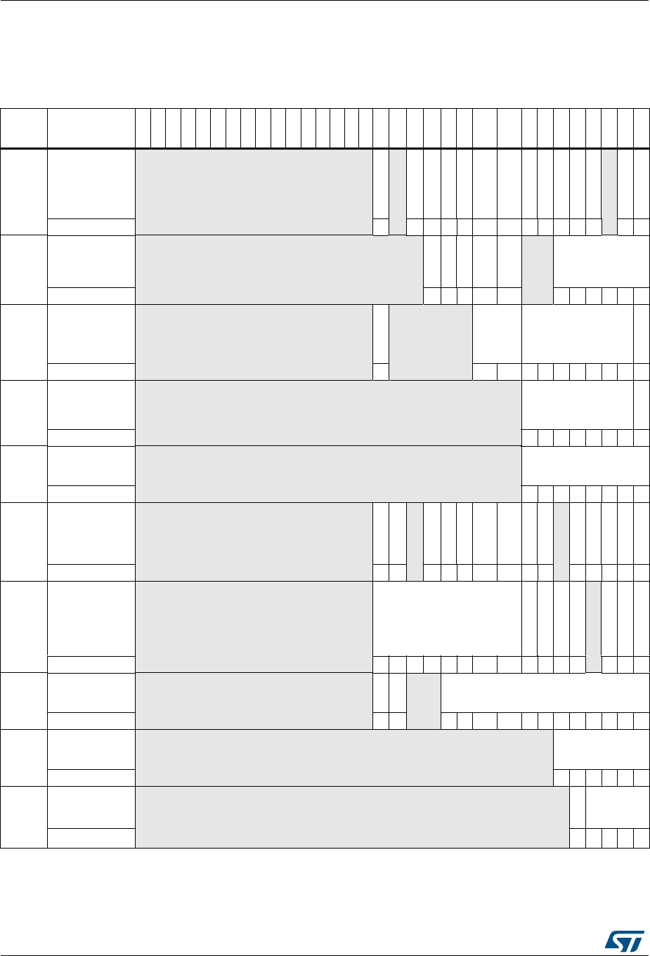
Inter-integrated circuit (I2C) interface RM0090
858/1718 DocID018909 Rev 9
27.6.11 I2C register map
The table below provides the I2C register map and reset values.
Refer to Table 1 on page 64 for the register boundary addresses table.
Table 124. I2C register map and reset values
Offset Register
31
30
29
28
27
26
25
24
23
22
21
20
19
18
17
16
15
14
13
12
11
10
9
8
7
6
5
4
3
2
1
0
0x00 I2C_CR1 Reserved
SWRST
Reserved
ALERT
PEC
POS
ACK
STOP
START
NOSTRETCH
ENGC
ENPEC
ENARP
SMBTYPE
Reserved
SMBUS
PE
Reset value 0 0 000 0 0 00000 00
0x04 I2C_CR2 Reserved
LAST
DMAEN
ITBUFEN
ITEVTEN
ITERREN
Reserved
FREQ[5:0]
Reset value 000 0 0 000000
0x08 I2C_OAR1 Reserved
ADDMODE
Reserved ADD[9:8] ADD[7:1]
ADD0
Reset value 0 0 0 00000000
0x0C I2C_OAR2 Reserved ADD2[7:1]
ENDUAL
Reset value 00000000
0x10 I2C_DR Reserved DR[7:0]
Reset value 00000000
0x14 I2C_SR1 Reserved
SMBALERT
TIMEOUT
Reserved
PECERR
OVR
AF
ARLO
BERR
TxE
RxNE
Reserved
STOPF
ADD10
BTF
ADDR
SB
Reset value 00 000 0 0 00 00000
0x18 I2C_SR2 Reserved PEC[7:0]
DUALF
SMBHOST
SMBDEFAULT
GENCALL
Reserved
TRA
BUSY
MSL
Reset value 00 0 000 0 0 0000 000
0x1C I2C_CCR Reserved
F/S
DUTY
Reserved
CCR[11:0]
Reset value 00 00 0 0 00000000
0x20 I2C_TRISE Reserved TRISE[5:0]
Reset value 000010
0x24
I2C_FLTR
Reserved
ANOFF
DNF[3:0]
Reset value 00000

DocID018909 Rev 9 859/1718
RM0090 Serial peripheral interface (SPI)
912
28 Serial peripheral interface (SPI)
This section applies to the whole STM32F4xx family, unless otherwise specified.
28.1 SPI introduction
The SPI interface provides two main functions, supporting either the SPI protocol or the I2S
audio protocol. By default, it is the SPI function that is selected. It is possible to switch the
interface from SPI to I2S by software.
The serial peripheral interface (SPI) allows half/ full-duplex, synchronous, serial
communication with external devices. The interface can be configured as the master and in
this case it provides the communication clock (SCK) to the external slave device. The
interface is also capable of operating in multimaster configuration.
It may be used for a variety of purposes, including simplex synchronous transfers on two
lines with a possible bidirectional data line or reliable communication using CRC checking.
The I2S is also a synchronous serial communication interface. It can address four different
audio standards including the I2S Philips standard, the MSB- and LSB-justified standards,
and the PCM standard. It can operate as a slave or a master device in full-duplex mode
(using 4 pins) or in half-duplex mode (using 3 pins). Master clock can be provided by the
interface to an external slave component when the I2S is configured as the communication
master.
Warning: Since some SPI1 and SPI3/I2S3 pins may be mapped onto
some pins used by the JTAG interface (SPI1_NSS onto JTDI,
SPI3_NSS/I2S3_WS onto JTDI and SPI3_SCK/I2S3_CK onto
JTDO), you may either:
– map SPI/I2S onto other pins
– disable the JTAG and use the SWD interface prior to
configuring the pins listed as SPI I/Os (when debugging the
application) or
– disable both JTAG/SWD interfaces (for standalone
applications).
For more information on the configuration of the JTAG/SWD
interface pins, please refer to Section 8.3.2: I/O pin
multiplexer and mapping.

Serial peripheral interface (SPI) RM0090
860/1718 DocID018909 Rev 9
28.2 SPI and I2S main features
28.2.1 SPI features
•Full-duplex synchronous transfers on three lines
•Simplex synchronous transfers on two lines with or without a bidirectional data line
•8- or 16-bit transfer frame format selection
•Master or slave operation
•Multimaster mode capability
•8 master mode baud rate prescalers (fPCLK/2 max.)
•Slave mode frequency (fPCLK/2 max)
•Faster communication for both master and slave
•NSS management by hardware or software for both master and slave: dynamic change
of master/slave operations
•Programmable clock polarity and phase
•Programmable data order with MSB-first or LSB-first shifting
•Dedicated transmission and reception flags with interrupt capability
•SPI bus busy status flag
•SPI TI mode
•Hardware CRC feature for reliable communication:
– CRC value can be transmitted as last byte in Tx mode
– Automatic CRC error checking for last received byte
•Master mode fault, overrun and CRC error flags with interrupt capability
•1-byte transmission and reception buffer with DMA capability: Tx and Rx requests

DocID018909 Rev 9 861/1718
RM0090 Serial peripheral interface (SPI)
912
28.2.2 I2S features
•Full duplex communication
•Half-duplex communication (only transmitter or receiver)
•Master or slave operations
•8-bit programmable linear prescaler to reach accurate audio sample frequencies (from
8 kHz to 192 kHz)
•Data format may be 16-bit, 24-bit or 32-bit
•Packet frame is fixed to 16-bit (16-bit data frame) or 32-bit (16-bit, 24-bit, 32-bit data
frame) by audio channel
•Programmable clock polarity (steady state)
•Underrun flag in slave transmission mode, overrun flag in reception mode (master and
slave), and Frame Error flag in reception and transmission mode (slave only)
•16-bit register for transmission and reception with one data register for both channel
sides
•Supported I2S protocols:
–I
2S Phillps standard
– MSB-justified standard (left-justified)
– LSB-justified standard (right-justified)
– PCM standard (with short and long frame synchronization on 16-bit channel frame
or 16-bit data frame extended to 32-bit channel frame)
•Data direction is always MSB first
•DMA capability for transmission and reception (16-bit wide)
•Master clock may be output to drive an external audio component. Ratio is fixed at
256 × FS (where FS is the audio sampling frequency)
•Both I2S (I2S2 and I2S3) have a dedicated PLL (PLLI2S) to generate an even more
accurate clock.
•I2S (I2S2 and I2S3) clock can be derived from an external clock mapped on the
I2S_CKIN pin.
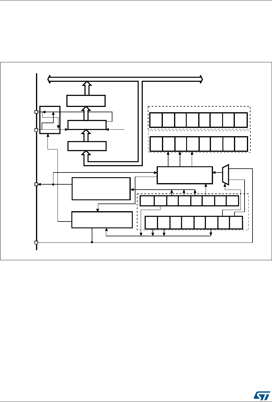
Serial peripheral interface (SPI) RM0090
862/1718 DocID018909 Rev 9
28.3 SPI functional description
28.3.1 General description
The block diagram of the SPI is shown in Figure 246.
Figure 246. SPI block diagram
Usually, the SPI is connected to external devices through 4 pins:
•MISO: Master In / Slave Out data. This pin can be used to transmit data in slave mode
and receive data in master mode.
•MOSI: Master Out / Slave In data. This pin can be used to transmit data in master
mode and receive data in slave mode.
•SCK: Serial Clock output for SPI masters and input for SPI slaves.
•NSS: Slave select. This is an optional pin to select a slave device. This pin acts as a
‘chip select’ to let the SPI master communicate with slaves individually and to avoid
contention on the data lines. Slave NSS inputs can be driven by standard IO ports on
the master device. The NSS pin may also be used as an output if enabled (SSOE bit)
and driven low if the SPI is in master configuration. In this manner, all NSS pins from
devices connected to the Master NSS pin see a low level and become slaves when
they are configured in NSS hardware mode. When configured in master mode with
NSS configured as an input (MSTR=1 and SSOE=0) and if NSS is pulled low, the SPI
enters the master mode fault state: the MSTR bit is automatically cleared and the
-/3)
-)3/
"AUDRATEGENERATOR
3#+
-ASTERCONTROLLOGIC
#OMMUNICATION
CONTROL
30% "2 "2 "2 -342 #0/, #0(!
"2;=
28.%
,3"
")$)
-/$%
")$)
/% 33- 33)
"39 /62 -/$ 28.%48%
%22
48%
$&&
33/%
#2#
%.
28
/.,9
#2#
.EXT
#2#
%22
.33
)%
&
&)234
30)?#2
30)?#2
30)?32
48$-
!%.
28$-
!%.
)%)%
!DDRESSANDDATABUS
2EAD
2XBUFFER
3HIFTREGISTER
,3"FIRST
4XBUFFER
7RITE
AI
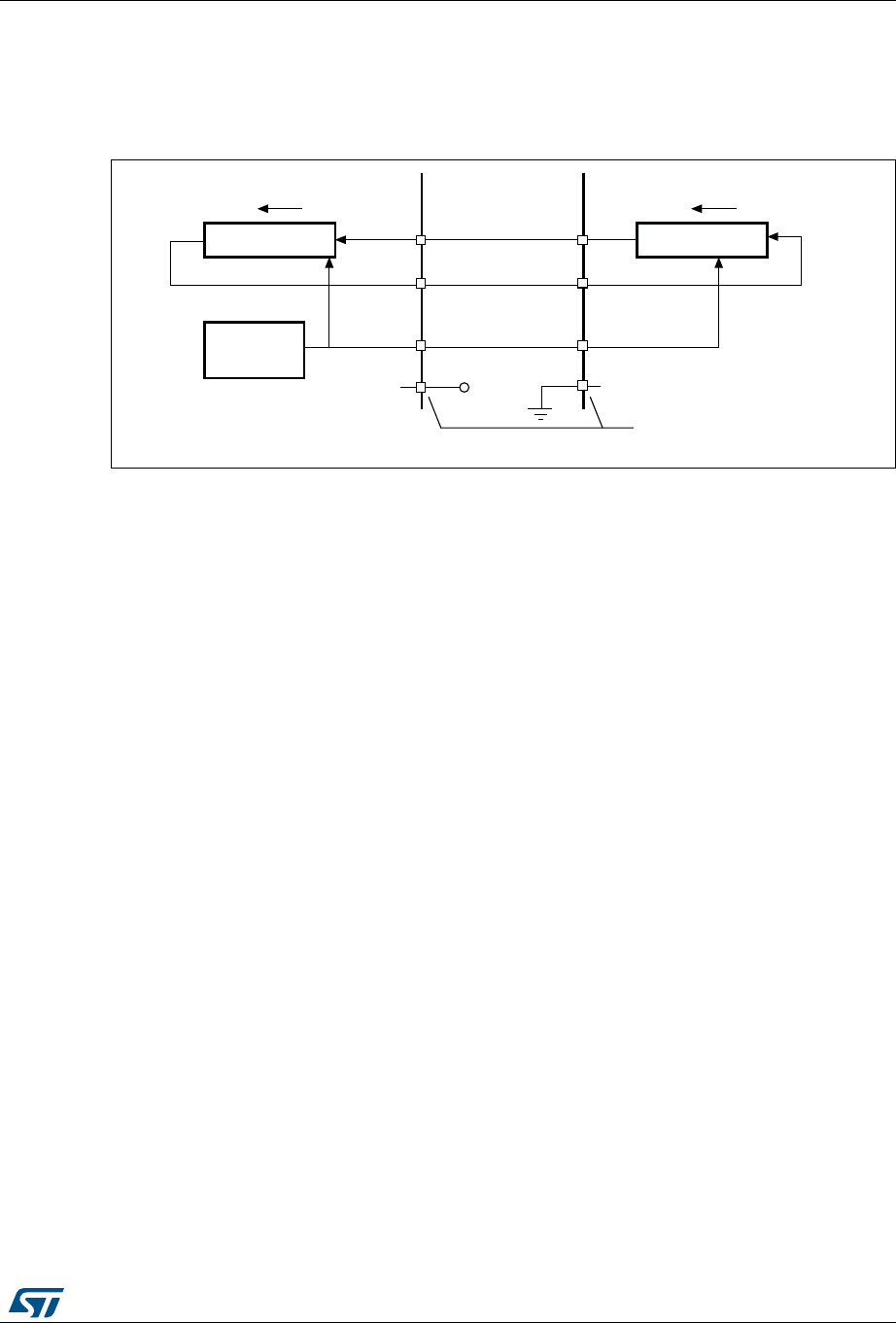
DocID018909 Rev 9 863/1718
RM0090 Serial peripheral interface (SPI)
912
device is configured in slave mode (refer to Section 28.3.10: Error flags on page 883).
A basic example of interconnections between a single master and a single slave is
illustrated in Figure 247.
Figure 247. Single master/ single slave application
1. Here, the NSS pin is configured as an input.
The MOSI pins are connected together and the MISO pins are connected together. In this
way data is transferred serially between master and slave (most significant bit first).
The communication is always initiated by the master. When the master device transmits
data to a slave device via the MOSI pin, the slave device responds via the MISO pin. This
implies full-duplex communication with both data out and data in synchronized with the
same clock signal (which is provided by the master device via the SCK pin).
Slave select (NSS) pin management
Hardware or software slave select management can be set using the SSM bit in the
SPI_CR1 register.
•Software NSS management (SSM = 1)
The slave select information is driven internally by the value of the SSI bit in the
SPI_CR1 register. The external NSS pin remains free for other application uses.
•Hardware NSS management (SSM = 0)
Two configurations are possible depending on the NSS output configuration (SSOE bit
in register SPI_CR2).
– NSS output enabled (SSM = 0, SSOE = 1)
This configuration is used only when the device operates in master mode. The
NSS signal is driven low when the master starts the communication and is kept
low until the SPI is disabled.
– NSS output disabled (SSM = 0, SSOE = 0)
This configuration allows multimaster capability for devices operating in master
mode. For devices set as slave, the NSS pin acts as a classical NSS input: the
slave is selected when NSS is low and deselected when NSS high.
Clock phase and clock polarity
Four possible timing relationships may be chosen by software, using the CPOL and CPHA
bits in the SPI_CR1 register. The CPOL (clock polarity) bit controls the steady state value of
8-bit shift register
SPI clock
generator
8-bit shift register
MISO
MOSI MOSI
MISO
SCK SCK
SlaveMaster
NSS
(1)
NSS
(1)
V
DD
MSBit LSBit MSBit LSBit
Not used if NSS is managed
by software
ai14745

Serial peripheral interface (SPI) RM0090
864/1718 DocID018909 Rev 9
the clock when no data is being transferred. This bit affects both master and slave modes. If
CPOL is reset, the SCK pin has a low-level idle state. If CPOL is set, the SCK pin has a
high-level idle state.
If the CPHA (clock phase) bit is set, the second edge on the SCK pin (falling edge if the
CPOL bit is reset, rising edge if the CPOL bit is set) is the MSBit capture strobe. Data are
latched on the occurrence of the second clock transition. If the CPHA bit is reset, the first
edge on the SCK pin (falling edge if CPOL bit is set, rising edge if CPOL bit is reset) is the
MSBit capture strobe. Data are latched on the occurrence of the first clock transition.
The combination of the CPOL (clock polarity) and CPHA (clock phase) bits selects the data
capture clock edge.
Figure 248, shows an SPI transfer with the four combinations of the CPHA and CPOL bits.
The diagram may be interpreted as a master or slave timing diagram where the SCK pin,
the MISO pin, the MOSI pin are directly connected between the master and the slave
device.
Note: Prior to changing the CPOL/CPHA bits the SPI must be disabled by resetting the SPE bit.
Master and slave must be programmed with the same timing mode.
The idle state of SCK must correspond to the polarity selected in the SPI_CR1 register (by
pulling up SCK if CPOL=1 or pulling down SCK if CPOL=0).
The Data Frame Format (8- or 16-bit) is selected through the DFF bit in SPI_CR1 register,
and determines the data length during transmission/reception.
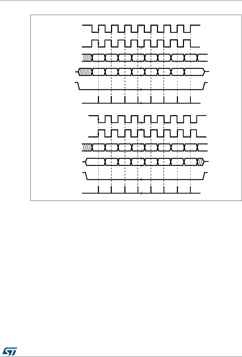
DocID018909 Rev 9 865/1718
RM0090 Serial peripheral interface (SPI)
912
Figure 248. Data clock timing diagram
1. These timings are shown with the LSBFIRST bit reset in the SPI_CR1 register.
Data frame format
Data can be shifted out either MSB-first or LSB-first depending on the value of the
LSBFIRST bit in the SPI_CR1 Register.
Each data frame is 8 or 16 bits long depending on the size of the data programmed using
the DFF bit in the SPI_CR1 register. The selected data frame format is applicable for
transmission and/or reception.
28.3.2 Configuring the SPI in slave mode
In the slave configuration, the serial clock is received on the SCK pin from the master
device. The value set in the BR[2:0] bits in the SPI_CR1 register, does not affect the data
transfer rate.
Note: It is recommended to enable the SPI slave before the master sends the clock. If not,
undesired data transmission might occur. The data register of the slave needs to be ready
before the first edge of the communication clock or before the end of the ongoing
communication. It is mandatory to have the polarity of the communication clock set to the
steady state value before the slave and the master are enabled.
Follow the procedure below to configure the SPI in slave mode:
#0/,
#0/,
-3"IT ,3"IT
-3"IT ,3"IT
-)3/
-/3)
.33
TOSLAVE
#APTURESTROBE
#0(!
#0/,
#0/,
-3"IT ,3"IT
-3"IT ,3"IT
-)3/
-/3)
.33
TOSLAVE
#APTURESTROBE
#0(!
ORBITSDEPENDINGONTHE$ATAFRAMEFORMATBITSEE$&&IN30)?#2
ORBITSDEPENDINGONTHE$ATAFRAMEFORMATBITSEE$&&IN30)?#2
AIB

Serial peripheral interface (SPI) RM0090
866/1718 DocID018909 Rev 9
Procedure
1. Set the DFF bit to define 8- or 16-bit data frame format
2. Select the CPOL and CPHA bits to define one of the four relationships between the
data transfer and the serial clock (see Figure 248). For correct data transfer, the CPOL
and CPHA bits must be configured in the same way in the slave device and the master
device. This step is not required when the TI mode is selected through the FRF bit in
the SPI_CR2 register.
3. The frame format (MSB-first or LSB-first depending on the value of the LSBFIRST bit in
the SPI_CR1 register) must be the same as the master device. This step is not
required when TI mode is selected.
4. In Hardware mode (refer to Slave select (NSS) pin management on page 863), the
NSS pin must be connected to a low level signal during the complete byte transmit
sequence. In NSS software mode, set the SSM bit and clear the SSI bit in the SPI_CR1
register. This step is not required when TI mode is selected.
5. Set the FRF bit in the SPI_CR2 register to select the TI mode protocol for serial
communications.
6. Clear the MSTR bit and set the SPE bit (both in the SPI_CR1 register) to assign the
pins to alternate functions.
In this configuration the MOSI pin is a data input and the MISO pin is a data output.
Transmit sequence
The data byte is parallel-loaded into the Tx buffer during a write cycle.
The transmit sequence begins when the slave device receives the clock signal and the most
significant bit of the data on its MOSI pin. The remaining bits (the 7 bits in 8-bit data frame
format, and the 15 bits in 16-bit data frame format) are loaded into the shift-register. The
TXE flag in the SPI_SR register is set on the transfer of data from the Tx Buffer to the shift
register and an interrupt is generated if the TXEIE bit in the SPI_CR2 register is set.
Receive sequence
For the receiver, when data transfer is complete:
•The Data in shift register is transferred to Rx Buffer and the RXNE flag (SPI_SR
register) is set
•An Interrupt is generated if the RXNEIE bit is set in the SPI_CR2 register.
After the last sampling clock edge the RXNE bit is set, a copy of the data byte received in
the shift register is moved to the Rx buffer. When the SPI_DR register is read, the SPI
peripheral returns this buffered value.
Clearing of the RXNE bit is performed by reading the SPI_DR register.
SPI TI protocol in slave mode
In slave mode, the SPI interface is compatible with the TI protocol. The FRF bit of the
SPI_CR2 register can be used to configure the slave SPI serial communications to be
compliant with this protocol.
The clock polarity and phase are forced to conform to the TI protocol requirements whatever
the values set in the SPI_CR1 register. NSS management is also specific to the TI protocol
which makes the configuration of NSS management through the SPI_CR1 and SPI_CR2
registers (such as SSM, SSI, SSOE) transparent for the user.
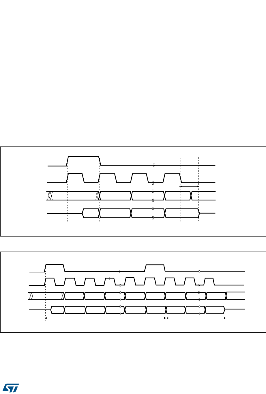
DocID018909 Rev 9 867/1718
RM0090 Serial peripheral interface (SPI)
912
In Slave mode (Figure 249: TI mode - Slave mode, single transfer and Figure 250: TI mode
- Slave mode, continuous transfer), the SPI baud rate prescaler is used to control the
moment when the MISO pin state changes to HI-Z. Any baud rate can be used thus allowing
to determine this moment with optimal flexibility. However, the baud rate is generally set to
the external master clock baud rate. The time for the MISO signal to become HI-Z (trelease)
depends on internal resynchronizations and on the baud rate value set in through BR[2:0] of
SPI_CR1 register. It is given by the formula:
Note: This feature is not available for Motorola SPI communications (FRF bit set to 0).
To detect TI frame errors in Slave transmitter only mode by using the Error interrupt (ERRIE
= 1), the SPI must be configured in 2-line unidirectional mode by setting BIDIMODE and
BIDIOE to 1 in the SPI_CR1 register. When BIDIMODE is set to 0, OVR is set to 1 because
the data register is never read and error interrupt are always generated, while when
BIDIMODE is set to 1, data are not received and OVR is never set.
Figure 249. TI mode - Slave mode, single transfer
Figure 250. TI mode - Slave mode, continuous transfer
tbaud_rate
2
----------------------4t
pclk
×+trelease
tbaud_rate
2
----------------------6t
pclk
×+<<
AI
-3").
-/3)
INPUT
.33
INPUT
3#+
INPUT
TRIGGER
EDGE
SAMPLING
EDGE
TRIGGER
EDGE
SAMPLING
EDGE
TRIGGER
EDGE SAMPLING
EDGE
$/.4#!2% ,3"). $/.4#!2%
-)3/
OUTPUT OR -3"/54 ,3"/54
T2ELEASE
AI
-3").
-/3)
INPUT
.33
INPUT
3#+
INPUT
TRIGGER SAMPLING TRIGGER SAMPLING TRIGGER SAMPLING
$/.4#!2% ,3"). $/.4#!2%
-)3/
OUTPUT OR -3"/54 ,3"/54
-3"). ,3").
-3"/54 ,3"/54
&2!-% &2!-%

Serial peripheral interface (SPI) RM0090
868/1718 DocID018909 Rev 9
28.3.3 Configuring the SPI in master mode
In the master configuration, the serial clock is generated on the SCK pin.
Procedure
1. Select the BR[2:0] bits to define the serial clock baud rate (see SPI_CR1 register).
2. Select the CPOL and CPHA bits to define one of the four relationships between the
data transfer and the serial clock (see Figure 248). This step is not required when the
TI mode is selected.
3. Set the DFF bit to define 8- or 16-bit data frame format
4. Configure the LSBFIRST bit in the SPI_CR1 register to define the frame format. This
step is not required when the TI mode is selected.
5. If the NSS pin is required in input mode, in hardware mode, connect the NSS pin to a
high-level signal during the complete byte transmit sequence. In NSS software mode,
set the SSM and SSI bits in the SPI_CR1 register. If the NSS pin is required in output
mode, the SSOE bit only should be set. This step is not required when the TI mode is
selected.
6. Set the FRF bit in SPI_CR2 to select the TI protocol for serial communications.
7. The MSTR and SPE bits must be set (they remain set only if the NSS pin is connected
to a high-level signal).
In this configuration the MOSI pin is a data output and the MISO pin is a data input.
Transmit sequence
The transmit sequence begins when a byte is written in the Tx Buffer.
The data byte is parallel-loaded into the shift register (from the internal bus) during the first
bit transmission and then shifted out serially to the MOSI pin MSB first or LSB first
depending on the LSBFIRST bit in the SPI_CR1 register. The TXE flag is set on the transfer
of data from the Tx Buffer to the shift register and an interrupt is generated if the TXEIE bit in
the SPI_CR2 register is set.
Receive sequence
For the receiver, when data transfer is complete:
•The data in the shift register is transferred to the RX Buffer and the RXNE flag is set
•An interrupt is generated if the RXNEIE bit is set in the SPI_CR2 register
At the last sampling clock edge the RXNE bit is set, a copy of the data byte received in the
shift register is moved to the Rx buffer. When the SPI_DR register is read, the SPI
peripheral returns this buffered value.
Clearing the RXNE bit is performed by reading the SPI_DR register.
A continuous transmit stream can be maintained if the next data to be transmitted is put in
the Tx buffer once the transmission is started. Note that TXE flag should be ‘1 before any
attempt to write the Tx buffer is made.
Note: When a master is communicating with SPI slaves which need to be de-selected between
transmissions, the NSS pin must be configured as GPIO or another GPIO must be used and
toggled by software.
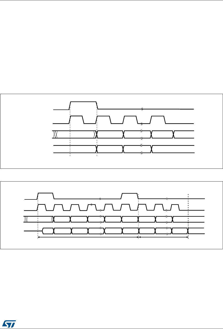
DocID018909 Rev 9 869/1718
RM0090 Serial peripheral interface (SPI)
912
SPI TI protocol in master mode
In master mode, the SPI interface is compatible with the TI protocol. The FRF bit of the
SPI_CR2 register can be used to configure the master SPI serial communications to be
compliant with this protocol.
The clock polarity and phase are forced to conform to the TI protocol requirements whatever
the values set in the SPI_CR1 register. NSS management is also specific to the TI protocol
which makes the configuration of NSS management through the SPI_CR1 and SPI_CR2
registers (SSM, SSI, SSOE) transparent for the user.
Figure 251: TI mode - master mode, single transfer and Figure 252: TI mode - master mode,
continuous transfer) show the SPI master communication waveforms when the TI mode is
selected in master mode.
Figure 251. TI mode - master mode, single transfer
Figure 252. TI mode - master mode, continuous transfer
AI
-3").
-/3)
INPUT
.33
OUTPUT
3#+
OUTPUT
TRIGGER
EDGE
SAMPLING
EDGE
TRIGGER
EDGE
SAMPLING
EDGE
TRIGGER
EDGE SAMPLING
EDGE
$/.4#!2% ,3"). $/.4#!2%
-)3/
OUTPUT OR -3"/54 ,3"/54
AI
-3"/54
-/3)
OUTPUT
.33
OUTPUT
3#+
OUTPUT
TRIGGER SAMPLING TRIGGER SAMPLING TRIGGER SAMPLING
$/.4#!2% ,3"/54
$/.4#!2%
-)3/
INTPUT OR -3"). ,3").
-3"/54 ,3"/54
-3"). ,3").
&2!-% &2!-%

Serial peripheral interface (SPI) RM0090
870/1718 DocID018909 Rev 9
28.3.4 Configuring the SPI for half-duplex communication
The SPI is capable of operating in half-duplex mode in 2 configurations.
•1 clock and 1 bidirectional data wire
•1 clock and 1 data wire (receive-only or transmit-only)
1 clock and 1 bidirectional data wire (BIDIMODE=1)
This mode is enabled by setting the BIDIMODE bit in the SPI_CR1 register. In this mode
SCK is used for the clock and MOSI in master or MISO in slave mode is used for data
communication. The transfer direction (Input/Output) is selected by the BIDIOE bit in the
SPI_CR1 register. When this bit is 1, the data line is output otherwise it is input.
1 clock and 1 unidirectional data wire (BIDIMODE=0)
In this mode, the application can use the SPI either in transmit-only mode or in receive-only
mode.
•Transmit-only mode is similar to full-duplex mode (BIDIMODE=0, RXONLY=0): the
data are transmitted on the transmit pin (MOSI in master mode or MISO in slave mode)
and the receive pin (MISO in master mode or MOSI in slave mode) can be used as a
general-purpose IO. In this case, the application just needs to ignore the Rx buffer (if
the data register is read, it does not contain the received value).
•In receive-only mode, the application can disable the SPI output function by setting the
RXONLY bit in the SPI_CR2 register. In this case, it frees the transmit IO pin (MOSI in
master mode or MISO in slave mode), so it can be used for other purposes.
To start the communication in receive-only mode, configure and enable the SPI:
•In master mode, the communication starts immediately and stops when the SPE bit is
cleared and the current reception stops. There is no need to read the BSY flag in this
mode. It is always set when an SPI communication is ongoing.
•In slave mode, the SPI continues to receive as long as the NSS is pulled down (or the
SSI bit is cleared in NSS software mode) and the SCK is running.
28.3.5 Data transmission and reception procedures
Rx and Tx buffers
In reception, data are received and then stored into an internal Rx buffer while In
transmission, data are first stored into an internal Tx buffer before being transmitted.
A read access of the SPI_DR register returns the Rx buffered value whereas a write access
to the SPI_DR stores the written data into the Tx buffer.

DocID018909 Rev 9 871/1718
RM0090 Serial peripheral interface (SPI)
912
Start sequence in master mode
•In full-duplex (BIDIMODE=0 and RXONLY=0)
– The sequence begins when data are written into the SPI_DR register (Tx buffer).
– The data are then parallel loaded from the Tx buffer into the 8-bit shift register
during the first bit transmission and then shifted out serially to the MOSI pin.
– At the same time, the received data on the MISO pin is shifted in serially to the 8-
bit shift register and then parallel loaded into the SPI_DR register (Rx buffer).
•In unidirectional receive-only mode (BIDIMODE=0 and RXONLY=1)
– The sequence begins as soon as SPE=1
– Only the receiver is activated and the received data on the MISO pin are shifted in
serially to the 8-bit shift register and then parallel loaded into the SPI_DR register
(Rx buffer).
•In bidirectional mode, when transmitting (BIDIMODE=1 and BIDIOE=1)
– The sequence begins when data are written into the SPI_DR register (Tx buffer).
– The data are then parallel loaded from the Tx buffer into the 8-bit shift register
during the first bit transmission and then shifted out serially to the MOSI pin.
– No data are received.
•In bidirectional mode, when receiving (BIDIMODE=1 and BIDIOE=0)
– The sequence begins as soon as SPE=1 and BIDIOE=0.
– The received data on the MOSI pin are shifted in serially to the 8-bit shift register
and then parallel loaded into the SPI_DR register (Rx buffer).
– The transmitter is not activated and no data are shifted out serially to the MOSI
pin.
Start sequence in slave mode
•In full-duplex mode (BIDIMODE=0 and RXONLY=0)
– The sequence begins when the slave device receives the clock signal and the first
bit of the data on its MOSI pin. The 7 remaining bits are loaded into the shift
register.
– At the same time, the data are parallel loaded from the Tx buffer into the 8-bit shift
register during the first bit transmission, and then shifted out serially to the MISO
pin. The software must have written the data to be sent before the SPI master
device initiates the transfer.
•In unidirectional receive-only mode (BIDIMODE=0 and RXONLY=1)
– The sequence begins when the slave device receives the clock signal and the first
bit of the data on its MOSI pin. The 7 remaining bits are loaded into the shift
register.
– The transmitter is not activated and no data are shifted out serially to the MISO
pin.
•In bidirectional mode, when transmitting (BIDIMODE=1 and BIDIOE=1)
– The sequence begins when the slave device receives the clock signal and the first
bit in the Tx buffer is transmitted on the MISO pin.
– The data are then parallel loaded from the Tx buffer into the 8-bit shift register
during the first bit transmission and then shifted out serially to the MISO pin. The

Serial peripheral interface (SPI) RM0090
872/1718 DocID018909 Rev 9
software must have written the data to be sent before the SPI master device
initiates the transfer.
– No data are received.
•In bidirectional mode, when receiving (BIDIMODE=1 and BIDIOE=0)
– The sequence begins when the slave device receives the clock signal and the first
bit of the data on its MISO pin.
– The received data on the MISO pin are shifted in serially to the 8-bit shift register
and then parallel loaded into the SPI_DR register (Rx buffer).
– The transmitter is not activated and no data are shifted out serially to the MISO
pin.
Handling data transmission and reception
The TXE flag (Tx buffer empty) is set when the data are transferred from the Tx buffer to the
shift register. It indicates that the internal Tx buffer is ready to be loaded with the next data.
An interrupt can be generated if the TXEIE bit in the SPI_CR2 register is set. Clearing the
TXE bit is performed by writing to the SPI_DR register.
Note: The software must ensure that the TXE flag is set to 1 before attempting to write to the Tx
buffer. Otherwise, it overwrites the data previously written to the Tx buffer.
The RXNE flag (Rx buffer not empty) is set on the last sampling clock edge, when the data
are transferred from the shift register to the Rx buffer. It indicates that data are ready to be
read from the SPI_DR register. An interrupt can be generated if the RXNEIE bit in the
SPI_CR2 register is set. Clearing the RXNE bit is performed by reading the SPI_DR
register.
For some configurations, the BSY flag can be used during the last data transfer to wait until
the completion of the transfer.
Full-duplex transmit and receive procedure in master or slave mode (BIDIMODE=0 and
RXONLY=0)
The software has to follow this procedure to transmit and receive data (see Figure 253 and
Figure 254):
1. Enable the SPI by setting the SPE bit to 1.
2. Write the first data item to be transmitted into the SPI_DR register (this clears the TXE
flag).
3. Wait until TXE=1 and write the second data item to be transmitted. Then wait until
RXNE=1 and read the SPI_DR to get the first received data item (this clears the RXNE
bit). Repeat this operation for each data item to be transmitted/received until the n–1
received data.
4. Wait until RXNE=1 and read the last received data.
5. Wait until TXE=1 and then wait until BSY=0 before disabling the SPI.
This procedure can also be implemented using dedicated interrupt subroutines launched at
each rising edges of the RXNE or TXE flag.
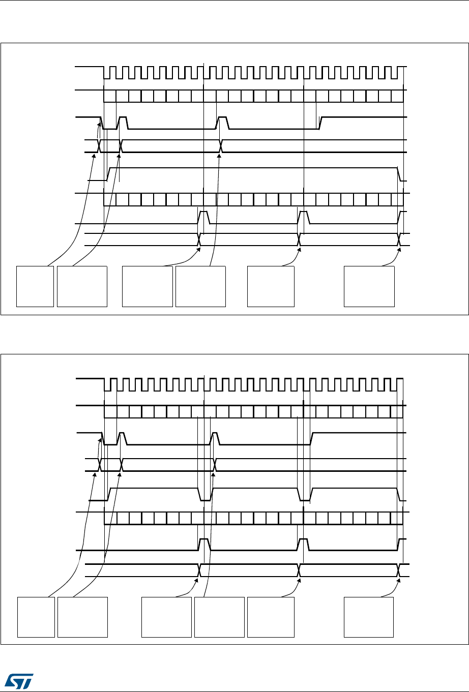
DocID018909 Rev 9 873/1718
RM0090 Serial peripheral interface (SPI)
912
Figure 253. TXE/RXNE/BSY behavior in Master / full-duplex mode (BIDIMODE=0 and
RXONLY=0) in the case of continuous transfers
Figure 254. TXE/RXNE/BSY behavior in Slave / full-duplex mode (BIDIMODE=0,
RXONLY=0) in the case of continuous transfers
MISO/MOSI (in)
Tx buffer
DATA1 = 0xA1
TXE flag
0xF2
BSY flag
0xF3
software
writes 0xF1
into SPI_DR
software waits
until TXE=1 and
writes 0xF2 into
SPI_DR
software waits
until RXNE=1
and reads 0xA1
from SPI_DR
set by hardware
cleared by software
set by hardware
cleared by software set by hardware
set by hardware
SCK
DATA 2 = 0xA2 DATA 3 = 0xA3
reset by hardware
Example in Master mode with CPOL=1, CPHA=1
0xF1
RXNE flag
(write SPI_DR)
Rx buffer
set by hardware
MISO/MOSI (out)
DATA1 = 0xF1 DATA2 = 0xF2 DATA3 = 0xF3
(read SPI_DR) 0xA1 0xA2 0xA3
software waits
until TXE=1 and
writes 0xF3 into
SPI_DR
software waits
until RXNE=1
and reads 0xA2
from SPI_ DR
software waits
until RXNE=1
and reads 0xA3
from SPI_DR
b0 b1 b2 b3b4 b5 b6 b7 b0 b1 b2 b3b4 b5 b6 b7 b0 b1 b2 b3b4 b5 b6 b7
b0 b1 b2 b3b4 b5 b6 b7 b0 b1 b2 b3b4 b5 b6 b7 b0 b1 b2 b3b4 b5 b6 b7
cleared by software
ai17343
0xF1
set by cleared by software
MISO/MOSI (in)
Tx buffer
DATA 1 = 0xA1
TXE flag
0xF2
BSY flag
0xF3
software
writes 0xF1
into SPI_DR
software waits
until TXE=1 and
writes 0xF2 into
SPI_DR
software waits
until RXNE=1
and reads 0xA1
from SPI_DR
set by hardware
cleared by software
set by hardware
cleared by software set by hardware
SCK
DATA 2 = 0xA2 DATA 3 = 0xA3
reset by hardware
Example in Slave mode with CPOL=1, CPHA=1
RXNE flag
(write to SPI_DR)
Rx buffer
set by hardware
MISO/MOSI (out)
DATA 1 = 0xF1 DATA 2 = 0xF2 DATA 3 = 0xF3
(read from SPI_DR) 0xA1 0xA2 0xA3
software waits
until TXE=1 and
writes 0xF3 into
SPI_DR
software waits
until RXNE=1
and reads 0xA2
from SPI_ DR
software waits
until RXNE=1
and reads 0xA3
from SPI_DR
b0 b1 b2 b3b4 b5 b6 b7 b0 b1 b2 b3b4 b5 b6 b7 b0 b1 b2 b3b4 b5 b6 b7
b0 b1 b2 b3b4 b5 b6 b7 b0 b1 b2 b3b4 b5 b6 b7 b0 b1 b2 b3b4 b5 b6 b7
cleared by software
ai17344
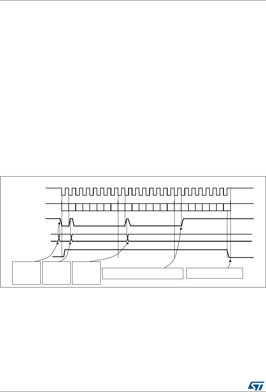
Serial peripheral interface (SPI) RM0090
874/1718 DocID018909 Rev 9
Transmit-only procedure (BIDIMODE=0 RXONLY=0)
In this mode, the procedure can be reduced as described below and the BSY bit can be
used to wait until the completion of the transmission (see Figure 255 and Figure 256).
1. Enable the SPI by setting the SPE bit to 1.
2. Write the first data item to send into the SPI_DR register (this clears the TXE bit).
3. Wait until TXE=1 and write the next data item to be transmitted. Repeat this step for
each data item to be transmitted.
4. After writing the last data item into the SPI_DR register, wait until TXE=1, then wait until
BSY=0, this indicates that the transmission of the last data is complete.
This procedure can be also implemented using dedicated interrupt subroutines launched at
each rising edge of the TXE flag.
Note: During discontinuous communications, there is a 2 APB clock period delay between the
write operation to SPI_DR and the BSY bit setting. As a consequence, in transmit-only
mode, it is mandatory to wait first until TXE is set and then until BSY is cleared after writing
the last data.
After transmitting two data items in transmit-only mode, the OVR flag is set in the SPI_SR
register since the received data are never read.
Figure 255. TXE/BSY behavior in Master transmit-only mode (BIDIMODE=0 and
RXONLY=0) in
case of continuous transfers
0xF1
Tx buffer
TXE flag
0xF2
BSY flag
0xF3
software writes
0xF1 into
SPI_DR
software waits
until TXE=1 and
writes 0xF2 into
SPI_DR
set by hardware
cleared by software
set by hardware
cleared by software set by hardware
set by hardware
SCK
reset by hardware
Example in Master mode with CPOL=1, CPHA=1
(write to SPI_DR)
MISO/MOSI (out)
DATA 1 = 0xF1 DATA 2 = 0xF2 DATA 3 = 0xF3
software waits
until TXE=1 and
writes 0xF3 into
SPI_DR
software waits until BSY=0software waits until TXE=1
b0 b1 b2 b3b4 b5 b6 b7 b0 b1 b2 b3b4 b5 b6 b7 b0 b1 b2 b3b4 b5 b6 b7
ai17345
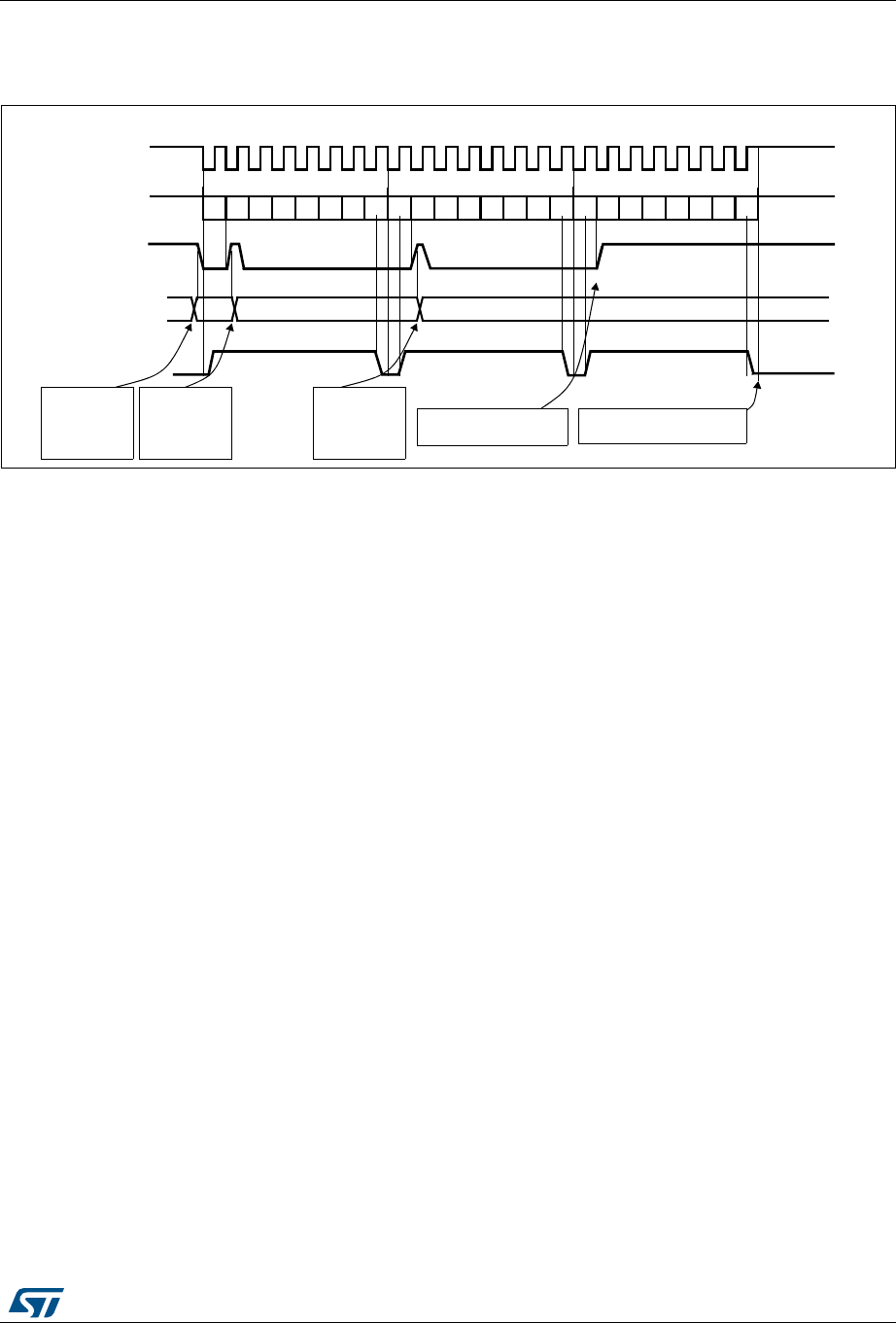
DocID018909 Rev 9 875/1718
RM0090 Serial peripheral interface (SPI)
912
Figure 256. TXE/BSY in Slave transmit-only mode (BIDIMODE=0 and RXONLY=0) in
the case of
continuous transfers
Bidirectional transmit procedure (BIDIMODE=1 and BIDIOE=1)
In this mode, the procedure is similar to the procedure in Transmit-only mode except that
the BIDIMODE and BIDIOE bits both have to be set in the SPI_CR2 register before enabling
the SPI.
Unidirectional receive-only procedure (BIDIMODE=0 and RXONLY=1)
In this mode, the procedure can be reduced as described below (see Figure 257):
1. Set the RXONLY bit in the SPI_CR2 register.
2. Enable the SPI by setting the SPE bit to 1:
a) In master mode, this immediately activates the generation of the SCK clock, and
data are serially received until the SPI is disabled (SPE=0).
b) In slave mode, data are received when the SPI master device drives NSS low and
generates the SCK clock.
3. Wait until RXNE=1 and read the SPI_DR register to get the received data (this clears
the RXNE bit). Repeat this operation for each data item to be received.
This procedure can also be implemented using dedicated interrupt subroutines launched at
each rising edge of the RXNE flag.
Note: If it is required to disable the SPI after the last transfer, follow the recommendation
described in Section 28.3.8: Disabling the SPI on page 880.
0xF1
Tx buffer
TXE flag
0xF2
BSY flag
0xF3
software writes
0xF1 into
SPI_DR
software waits
until TXE=1 and
writes 0xF2 into
SPI_DR
set by hardware
cleared by software
set by hardware
cleared by software set by hardware
set by hardware
SCK
reset by hardware
Example in slave mode with CPOL=1, CPHA=1
(write to SPI_DR)
MISO/MOSI (out)
DATA 1 = 0xF1 DATA 2 = 0xF2 DATA 3 = 0xF3
software waits
until TXE=1 and
writes 0xF3 into
SPI_DR
software waits until BSY=0software waits until TXE=1
b0 b1 b2 b3b4 b5 b6 b7 b0 b1 b2 b3b4 b5 b6 b7 b0 b1 b2 b3b4 b5 b6 b7
ai17346
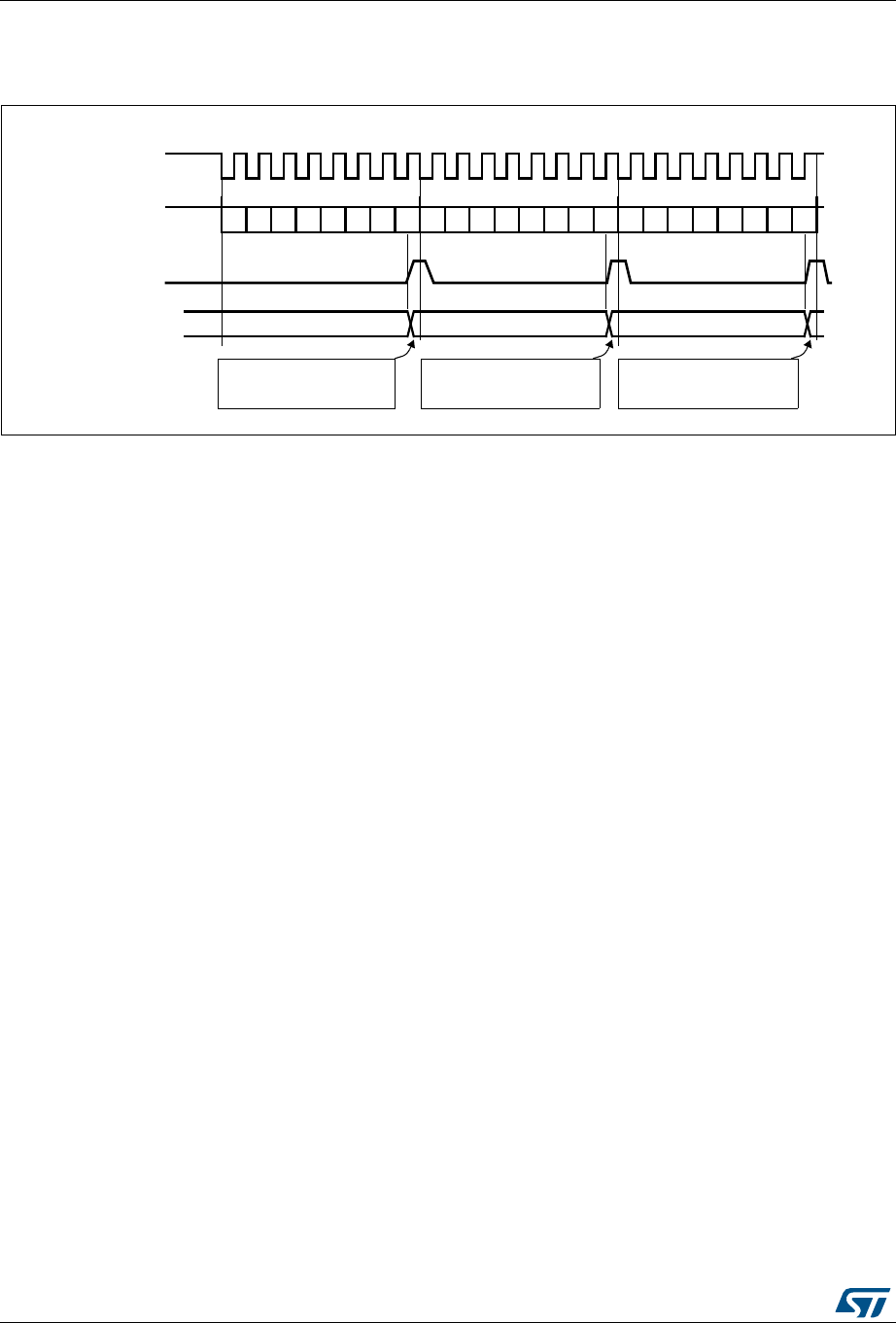
Serial peripheral interface (SPI) RM0090
876/1718 DocID018909 Rev 9
Figure 257. RXNE behavior in receive-only mode (BIDIRMODE=0 and RXONLY=1) in
the case of
continuous transfers
Bidirectional receive procedure (BIDIMODE=1 and BIDIOE=0)
In this mode, the procedure is similar to the Receive-only mode procedure except that the
BIDIMODE bit has to be set and the BIDIOE bit cleared in the SPI_CR2 register before
enabling the SPI.
Continuous and discontinuous transfers
When transmitting data in master mode, if the software is fast enough to detect each rising
edge of TXE (or TXE interrupt) and to immediately write to the SPI_DR register before the
ongoing data transfer is complete, the communication is said to be continuous. In this case,
there is no discontinuity in the generation of the SPI clock between each data item and the
BSY bit is never cleared between each data transfer.
On the contrary, if the software is not fast enough, this can lead to some discontinuities in
the communication. In this case, the BSY bit is cleared between each data transmission
(see Figure 258).
In Master receive-only mode (RXONLY=1), the communication is always continuous and
the BSY flag is always read at 1.
In slave mode, the continuity of the communication is decided by the SPI master device. In
any case, even if the communication is continuous, the BSY flag goes low between each
transfer for a minimum duration of one SPI clock cycle (see Figure 256).
MISO/MOSI (in)
DATA 1 = 0xA1
software waits until RXNE=1
and reads 0xA1 from SPI_DR
SCK
DATA 2 = 0xA2 DATA 3 = 0xA3
Example with CPOL=1, CPHA=1, RXONLY=1
RXNE flag
Rx buffer
set by hardware
(read from SPI_DR) 0xA1 0xA2 0xA3
software waits until RXNE=1
and reads 0xA2 from SPI_DR
software waits until RXNE=1
and reads 0xA3 from SPI_DR
b0 b1 b2 b3b4 b5 b6 b7 b0 b1 b2 b3b4 b5 b6 b7 b0 b1 b2 b3b4 b5 b6 b7
cleared by software
ai17347
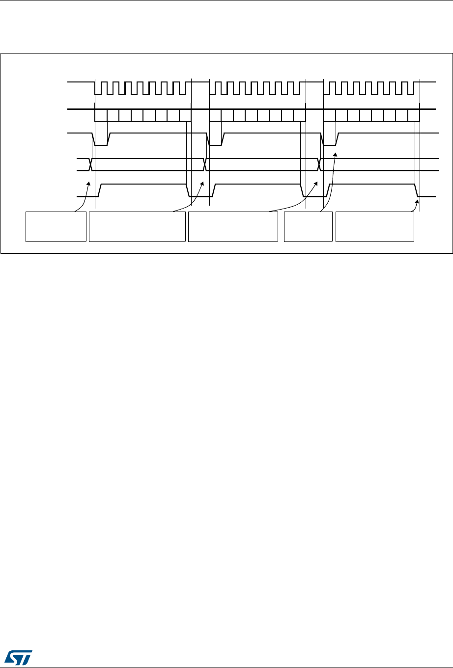
DocID018909 Rev 9 877/1718
RM0090 Serial peripheral interface (SPI)
912
Figure 258. TXE/BSY behavior when transmitting (BIDIRMODE=0 and RXONLY=0) in
the case of
discontinuous transfers
28.3.6 CRC calculation
A CRC calculator has been implemented for communication reliability. Separate CRC
calculators are implemented for transmitted data and received data. The CRC is calculated
using a programmable polynomial serially on each bit. It is calculated on the sampling clock
edge defined by the CPHA and CPOL bits in the SPI_CR1 register.
Note: This SPI offers two kinds of CRC calculation standard which depend directly on the data
frame format selected for the transmission and/or reception: 8-bit data (CR8) and 16-bit data
(CRC16).
CRC calculation is enabled by setting the CRCEN bit in the SPI_CR1 register. This action
resets the CRC registers (SPI_RXCRCR and SPI_TXCRCR). In full duplex or transmitter
only mode, when the transfers are managed by the software (CPU mode), it is necessary to
write the bit CRCNEXT immediately after the last data to be transferred is written to the
SPI_DR. At the end of this last data transfer, the SPI_TXCRCR value is transmitted.
In receive only mode and when the transfers are managed by software (CPU mode), it is
necessary to write the CRCNEXT bit after the second last data has been received. The CRC
is received just after the last data reception and the CRC check is then performed.
At the end of data and CRC transfers, the CRCERR flag in the SPI_SR register is set if
corruption occurs during the transfer.
If data are present in the TX buffer, the CRC value is transmitted only after the transmission
of the data byte. During CRC transmission, the CRC calculator is switched off and the
register value remains unchanged.
SPI communication using the CRC is possible through the following procedure:
MOSI (out)
Tx buffer
DATA 1 = 0xF1
TXE flag
0xF1
BSY flag
0xF2
software writes 0xF1
into SPI_DR
software waits until TXE=1 but is
late to write 0xF2 into SPI_DR
software waits until TXE=1 but
is late to write 0xF3 into
SPI_DR
SCK
3Fx0 = 3 ATAD2Fx0 = 2 ATAD
Example with CPOL=1, CPHA=1
0xF3
software waits
until TXE=1
software waits until BSY=0
(write to SPI_DR)
b0 b1 b2 b3b4 b5 b6 b7 b0 b1 b2 b3b4 b5 b6 b7 b0 b1 b2 b3b4 b5 b6 b7
ai17348

Serial peripheral interface (SPI) RM0090
878/1718 DocID018909 Rev 9
1. Program the CPOL, CPHA, LSBFirst, BR, SSM, SSI and MSTR values.
2. Program the polynomial in the SPI_CRCPR register.
3. Enable the CRC calculation by setting the CRCEN bit in the SPI_CR1 register. This
also clears the SPI_RXCRCR and SPI_TXCRCR registers.
4. Enable the SPI by setting the SPE bit in the SPI_CR1 register.
5. Start the communication and sustain the communication until all but one byte or half-
word have been transmitted or received.
– In full duplex or transmitter-only mode, when the transfers are managed by
software, when writing the last byte or half word to the Tx buffer, set the
CRCNEXT bit in the SPI_CR1 register to indicate that the CRC will be transmitted
after the transmission of the last byte.
– In receiver only mode, set the bit CRCNEXT just after the reception of the second
to last data to prepare the SPI to enter in CRC Phase at the end of the reception of
the last data. CRC calculation is frozen during the CRC transfer.
6. After the transfer of the last byte or half word, the SPI enters the CRC transfer and
check phase. In full duplex mode or receiver-only mode, the received CRC is
compared to the SPI_RXCRCR value. If the value does not match, the CRCERR flag in
SPI_SR is set and an interrupt can be generated when the ERRIE bit in the SPI_CR2
register is set.
Note: When the SPI is in slave mode, be careful to enable CRC calculation only when the clock is
stable, that is, when the clock is in the steady state. If not, a wrong CRC calculation may be
done. In fact, the CRC is sensitive to the SCK slave input clock as soon as CRCEN is set,
and this, whatever the value of the SPE bit.
With high bitrate frequencies, be careful when transmitting the CRC. As the number of used
CPU cycles has to be as low as possible in the CRC transfer phase, it is forbidden to call
software functions in the CRC transmission sequence to avoid errors in the last data and
CRC reception. In fact, CRCNEXT bit has to be written before the end of the
transmission/reception of the last data.
For high bit rate frequencies, it is advised to use the DMA mode to avoid the degradation of
the SPI speed performance due to CPU accesses impacting the SPI bandwidth.
When the devices are configured as slaves and the NSS hardware mode is used, the NSS
pin needs to be kept low between the data phase and the CRC phase.
When the SPI is configured in slave mode with the CRC feature enabled, CRC calculation
takes place even if a high level is applied on the NSS pin. This may happen for example in
case of a multislave environment where the communication master addresses slaves
alternately.
Between a slave deselection (high level on NSS) and a new slave selection (low level on
NSS), the CRC value should be cleared on both master and slave sides in order to
resynchronize the master and slave for their respective CRC calculation.
To clear the CRC, follow the procedure below:
1. Disable SPI (SPE = 0)
2. Clear the CRCEN bit
3. Set the CRCEN bit
4. Enable the SPI (SPE = 1)

DocID018909 Rev 9 879/1718
RM0090 Serial peripheral interface (SPI)
912
28.3.7 Status flags
Four status flags are provided for the application to completely monitor the state of the SPI
bus.
Tx buffer empty flag (TXE)
When it is set, this flag indicates that the Tx buffer is empty and the next data to be
transmitted can be loaded into the buffer. The TXE flag is cleared when writing to the
SPI_DR register.
Rx buffer not empty (RXNE)
When set, this flag indicates that there are valid received data in the Rx buffer. It is cleared
when SPI_DR is read.
BUSY flag
This BSY flag is set and cleared by hardware (writing to this flag has no effect). The BSY
flag indicates the state of the communication layer of the SPI.
When BSY is set, it indicates that the SPI is busy communicating. There is one exception in
master mode / bidirectional receive mode (MSTR=1 and BDM=1 and BDOE=0) where the
BSY flag is kept low during reception.
The BSY flag is useful to detect the end of a transfer if the software wants to disable the SPI
and enter Halt mode (or disable the peripheral clock). This avoids corrupting the last
transfer. For this, the procedure described below must be strictly respected.
The BSY flag is also useful to avoid write collisions in a multimaster system.
The BSY flag is set when a transfer starts, with the exception of master mode / bidirectional
receive mode (MSTR=1 and BDM=1 and BDOE=0).
It is cleared:
•when a transfer is finished (except in master mode if the communication is continuous)
•when the SPI is disabled
•when a master mode fault occurs (MODF=1)
When communication is not continuous, the BSY flag is low between each communication.
When communication is continuous:
•in master mode, the BSY flag is kept high during all the transfers
•in slave mode, the BSY flag goes low for one SPI clock cycle between each transfer
Note: Do not use the BSY flag to handle each data transmission or reception. It is better to use the
TXE and RXNE flags instead.

Serial peripheral interface (SPI) RM0090
880/1718 DocID018909 Rev 9
28.3.8 Disabling the SPI
When a transfer is terminated, the application can stop the communication by disabling the
SPI peripheral. This is done by clearing the SPE bit.
For some configurations, disabling the SPI and entering the Halt mode while a transfer is
ongoing can cause the current transfer to be corrupted and/or the BSY flag might become
unreliable.
To avoid any of those effects, it is recommended to respect the following procedure when
disabling the SPI:
In master or slave full-duplex mode (BIDIMODE=0, RXONLY=0)
1. Wait until RXNE=1 to receive the last data
2. Wait until TXE=1
3. Then wait until BSY=0
4. Disable the SPI (SPE=0) and, eventually, enter the Halt mode (or disable the peripheral
clock)
In master or slave unidirectional transmit-only mode (BIDIMODE=0,
RXONLY=0) or bidirectional transmit mode (BIDIMODE=1, BIDIOE=1)
After the last data is written into the SPI_DR register:
1. Wait until TXE=1
2. Then wait until BSY=0
3. Disable the SPI (SPE=0) and, eventually, enter the Halt mode (or disable the peripheral
clock)
In master unidirectional receive-only mode (MSTR=1, BIDIMODE=0,
RXONLY=1) or bidirectional receive mode (MSTR=1, BIDIMODE=1, BIDIOE=0)
This case must be managed in a particular way to ensure that the SPI does not initiate a
new transfer. The sequence below is valid only for SPI Motorola configuration (FRF bit set to
0):
1. Wait for the second to last occurrence of RXNE=1 (n–1)
2. Then wait for one SPI clock cycle (using a software loop) before disabling the SPI
(SPE=0)
3. Then wait for the last RXNE=1 before entering the Halt mode (or disabling the
peripheral clock)
When the SPI is configured in TI mode (Bit FRF set to 1), the following procedure has to be
respected to avoid generating an undesired pulse on NSS when the SPI is disabled:
1. Wait for the second to last occurrence of RXNE = 1 (n-1).
2. Disable the SPI (SPE = 0) in the following window frame using a software loop:
– After at least one SPI clock cycle,
– Before the beginning of the LSB data transfer.
Note: In master bidirectional receive mode (MSTR=1 and BDM=1 and BDOE=0), the BSY flag is
kept low during transfers.

DocID018909 Rev 9 881/1718
RM0090 Serial peripheral interface (SPI)
912
In slave receive-only mode (MSTR=0, BIDIMODE=0, RXONLY=1) or
bidirectional receive mode (MSTR=0, BIDIMODE=1, BIDOE=0)
1. You can disable the SPI (write SPE=1) at any time: the current transfer will complete
before the SPI is effectively disabled
2. Then, if you want to enter the Halt mode, you must first wait until BSY = 0 before
entering the Halt mode (or disabling the peripheral clock).
28.3.9 SPI communication using DMA (direct memory addressing)
To operate at its maximum speed, the SPI needs to be fed with the data for transmission
and the data received on the Rx buffer should be read to avoid overrun. To facilitate the
transfers, the SPI features a DMA capability implementing a simple request/acknowledge
protocol.
A DMA access is requested when the enable bit in the SPI_CR2 register is enabled.
Separate requests must be issued to the Tx and Rx buffers (see Figure 259 and
Figure 260):
•In transmission, a DMA request is issued each time TXE is set to 1. The DMA then
writes to the SPI_DR register (this clears the TXE flag).
•In reception, a DMA request is issued each time RXNE is set to 1. The DMA then reads
the SPI_DR register (this clears the RXNE flag).
When the SPI is used only to transmit data, it is possible to enable only the SPI Tx DMA
channel. In this case, the OVR flag is set because the data received are not read.
When the SPI is used only to receive data, it is possible to enable only the SPI Rx DMA
channel.
In transmission mode, when the DMA has written all the data to be transmitted (flag TCIF is
set in the DMA_ISR register), the BSY flag can be monitored to ensure that the SPI
communication is complete. This is required to avoid corrupting the last transmission before
disabling the SPI or entering the Stop mode. The software must first wait until TXE=1 and
then until BSY=0.
Note: During discontinuous communications, there is a 2 APB clock period delay between the
write operation to SPI_DR and the BSY bit setting. As a consequence, it is mandatory to
wait first until TXE=1 and then until BSY=0 after writing the last data.
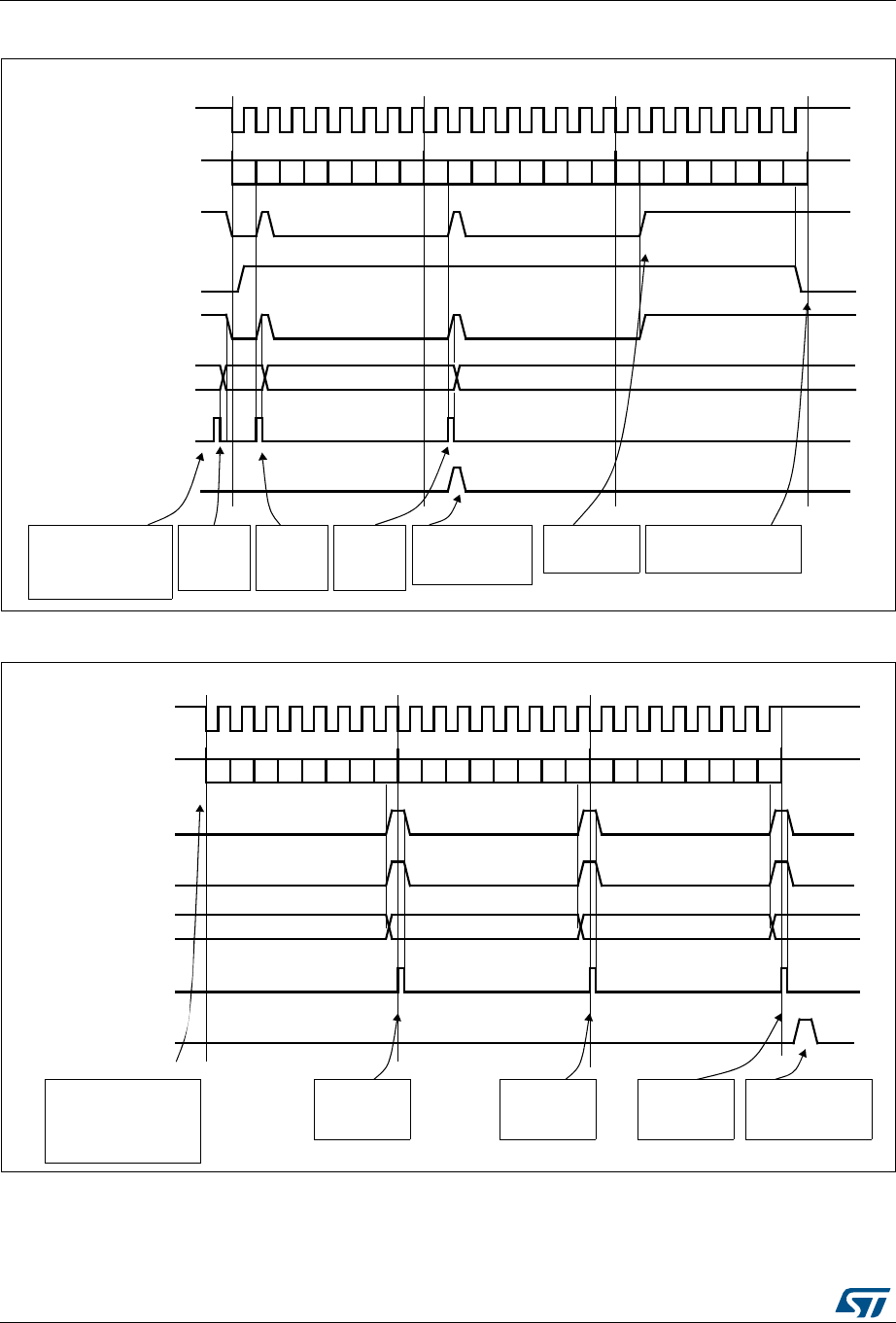
Serial peripheral interface (SPI) RM0090
882/1718 DocID018909 Rev 9
Figure 259. Transmission using DMA
Figure 260. Reception using DMA
0xF1
Tx buffer
TXE flag
0xF2
BSY flag
0xF3
set by hardware
clear by DMA write
set by hardware
cleared by DMA write set by hardware
set by hardware
SCK
reset
Example with CPOL=1, CPHA=1
(write to SPI_DR)
MISO/MOSI (out)
DATA 1 = 0xF1 DATA 2 = 0xF2 DATA 3 = 0xF3
software configures the
DMA SPI Tx channel
to send 3 data items
and enables the SPI
DMA writes to SPI_DR
DMA requestignored by the DMA because
DMA TCIF flagset by hardware clear by software
DMA writes
DATA1 into
SPI_DR
by hardware
DMA writes
DATA2 into
SPI_DR
DMA writes
DATA3 into
SPI_DR
software waits until BSY=0
(DMA transfer complete)
DMA transfer is
complete (TCIF=1 in
DMA_ISR)
software waits
until TXE=1
DMA transfer is complete
b0 b1 b2 b3b4 b5 b6 b7 b0 b1 b2 b3b4 b5 b6 b7 b0 b1 b2 b3b4 b5 b6 b7
ai17349
MISO/MOSI (in)
DATA 1 = 0xA1
software configures the
DMA SPI Rx channel
to receive 3 data items
and enables the SPI
SCK
DATA 2 = 0xA2 DATA 3 = 0xA3
Example with CPOL=1, CPHA=1
RXNE flag
Rx buffer
set by hardware
(read from SPI_DR) 0xA1 0xA2 0xA3
DMA request
DMA reads
DATA3 from
SPI_DR
flag DMA TCIF set by hardware clear
by software
DMA read from SPI_DR
The DMA transfer is
complete (TCIF=1 in
DMA_ISR)
DMA reads
DATA2 from
SPI_DR
DMA reads
DATA1 from
SPI_DR
(DMA transfer complete)
b0 b1 b2 b3b4 b5 b6 b7 b0 b1 b2 b3b4 b5 b6 b7 b0 b1 b2 b3b4 b5 b6 b7
clear by DMA read
ai17350

DocID018909 Rev 9 883/1718
RM0090 Serial peripheral interface (SPI)
912
DMA capability with CRC
When SPI communication is enabled with CRC communication and DMA mode, the
transmission and reception of the CRC at the end of communication are automatic that is
without using the bit CRCNEXT. After the CRC reception, the CRC must be read in the
SPI_DR register to clear the RXNE flag.
At the end of data and CRC transfers, the CRCERR flag in SPI_SR is set if corruption
occurs during the transfer.
28.3.10 Error flags
Master mode fault (MODF)
Master mode fault occurs when the master device has its NSS pin pulled low (in NSS
hardware mode) or SSI bit low (in NSS software mode), this automatically sets the MODF
bit. Master mode fault affects the SPI peripheral in the following ways:
•The MODF bit is set and an SPI interrupt is generated if the ERRIE bit is set.
•The SPE bit is cleared. This blocks all output from the device and disables the SPI
interface.
•The MSTR bit is cleared, thus forcing the device into slave mode.
Use the following software sequence to clear the MODF bit:
1. Make a read or write access to the SPI_SR register while the MODF bit is set.
2. Then write to the SPI_CR1 register.
To avoid any multiple slave conflicts in a system comprising several MCUs, the NSS pin
must be pulled high during the MODF bit clearing sequence. The SPE and MSTR bits can
be restored to their original state after this clearing sequence.
As a security, hardware does not allow the setting of the SPE and MSTR bits while the
MODF bit is set.
In a slave device the MODF bit cannot be set. However, in a multimaster configuration, the
device can be in slave mode with this MODF bit set. In this case, the MODF bit indicates
that there might have been a multimaster conflict for system control. An interrupt routine can
be used to recover cleanly from this state by performing a reset or returning to a default
state.
Overrun condition
An overrun condition occurs when the master device has sent data bytes and the slave
device has not cleared the RXNE bit resulting from the previous data byte transmitted.
When an overrun condition occurs:
•the OVR bit is set and an interrupt is generated if the ERRIE bit is set.
In this case, the receiver buffer contents will not be updated with the newly received data
from the master device. A read from the SPI_DR register returns this byte. All other
subsequently transmitted bytes are lost.
Clearing the OVR bit is done by a read from the SPI_DR register followed by a read access
to the SPI_SR register.
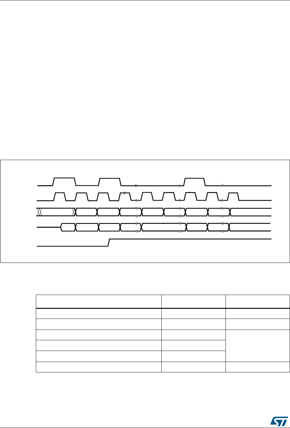
Serial peripheral interface (SPI) RM0090
884/1718 DocID018909 Rev 9
CRC error
This flag is used to verify the validity of the value received when the CRCEN bit in the
SPI_CR1 register is set. The CRCERR flag in the SPI_SR register is set if the value
received in the shift register does not match the receiver SPI_RXCRCR value.
TI mode frame format error
A TI mode frame format error is detected when an NSS pulse occurs during an ongoing
communication when the SPI is acting in slave mode and configured to conform to the TI
mode protocol. When this error occurs, the FRE flag is set in the SPI_SR register. The SPI
is not disabled when an error occurs, the NSS pulse is ignored, and the SPI waits for the
next NSS pulse before starting a new transfer. The data may be corrupted since the error
detection may result in the lost of two data bytes.
The FRE flag is cleared when SPI_SR register is read. If the bit ERRIE is set, an interrupt is
generated on the NSS error detection. In this case, the SPI should be disabled because
data consistency is no more guaranteed and communications should be reinitiated by the
master when the slave SPI is re-enabled.
Figure 261. TI mode frame format error detection
28.3.11 SPI interrupts
AI
-3").
-/3)
INPUT
.33
OUTPUT
3#+
OUTPUT
TRIGGER SAMPLING TRIGGER SAMPLING TRIGGER SAMPLING
$/.4#!2%
-)3/
OUTPUT OR -3"/54 ,3"/54
-3"). ,3").
-3"/54 ,3"/54
TRIGGER SAMPLING TRIGGER SAMPLING TRIGGER SAMPLING TRIGGER SAMPLING
,3"). $/.4#!2%
4)&2&%
Table 125. SPI interrupt requests
Interrupt event Event flag Enable Control bit
Transmit buffer empty flag TXE TXEIE
Receive buffer not empty flag RXNE RXNEIE
Master Mode fault event MODF
ERRIEOverrun error OVR
CRC error flag CRCERR
TI frame format error FRE ERRIE
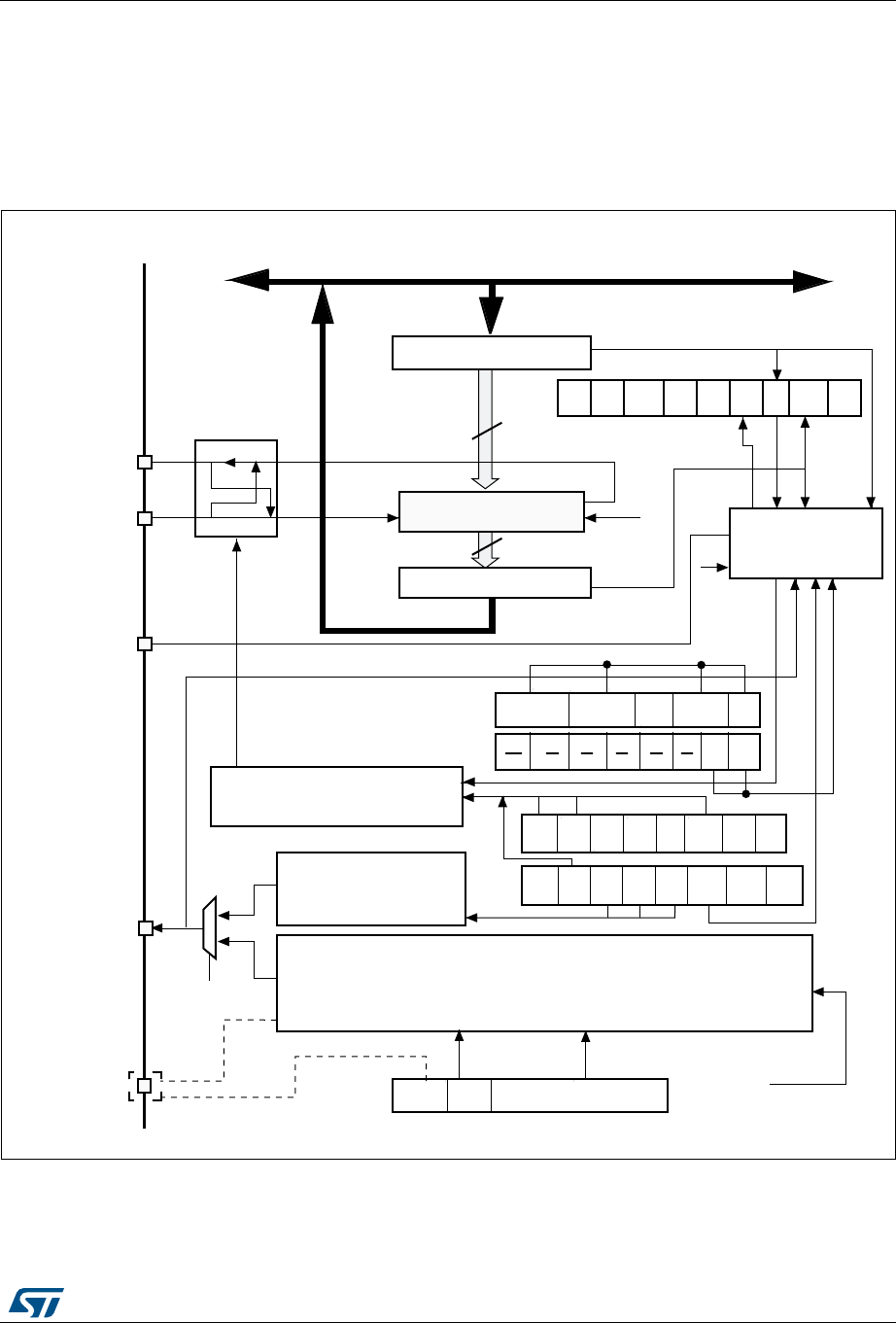
DocID018909 Rev 9 885/1718
RM0090 Serial peripheral interface (SPI)
912
28.4 I2S functional description
28.4.1 I2S general description
The block diagram of the I2S is shown in Figure 262.
Figure 262. I2S block diagram
1. I2S2ext_SD and I2S3ext_SD are the extended SD pins that control the I2S full duplex mode.
4XBUFFER
3HIFTREGISTER
BIT
#OMMUNICATION
2XBUFFER
BIT
-/3) 3$
-ASTERCONTROLLOGIC
-)3/
)3EXT?3$
)3EXT?3$
30)
BAUDRATEGENERATOR
#+
)3-/$
,3"FIRST
,3"
&IRST 30% "2 "2 "2 -342 #0/, #0(!
"IDI
MODE
"IDI
/%
#2#
%.
#2#
.EXT $&& 2X
ONLY 33- 33)
!DDRESSANDDATABUS
CONTROL
.3373
"39 /62 -/$& #2#
%22
#(
3)$% 4X% 2X.%
)3CLOCKGENERATOR
-#+
)3?#+
)3
-/$ )3%
#(
$!4,%. ,%.
#+
0/,
)3#&' )334$
-#+/%/$$ )3$)6;=
;= ;= ;=
5$2
)3X#,+
-36
&2%

Serial peripheral interface (SPI) RM0090
886/1718 DocID018909 Rev 9
The SPI could function as an audio I2S interface when the I2S capability is enabled (by
setting the I2SMOD bit in the SPI_I2SCFGR register). This interface uses almost the same
pins, flags and interrupts as the SPI.
The I2S shares three common pins with the SPI:
•SD: Serial Data (mapped on the MOSI pin) to transmit or receive the two time-
multiplexed data channels (in half-duplex mode only).
•WS: Word Select (mapped on the NSS pin) is the data control signal output in master
mode and input in slave mode.
•CK: Serial Clock (mapped on the SCK pin) is the serial clock output in master mode
and serial clock input in slave mode.
•I2S2ext_SD and I2S3ext_SD: additional pins (mapped on the MISO pin) to control the
I2S full duplex mode.
An additional pin could be used when a master clock output is needed for some external
audio devices:
•MCK: Master Clock (mapped separately) is used, when the I2S is configured in master
mode (and when the MCKOE bit in the SPI_I2SPR register is set), to output this
additional clock generated at a preconfigured frequency rate equal to 256 × FS, where
FS is the audio sampling frequency.
The I2S uses its own clock generator to produce the communication clock when it is set in
master mode. This clock generator is also the source of the master clock output. Two
additional registers are available in I2S mode. One is linked to the clock generator
configuration SPI_I2SPR and the other one is a generic I2S configuration register
SPI_I2SCFGR (audio standard, slave/master mode, data format, packet frame, clock
polarity, etc.).
The SPI_CR1 register and all CRC registers are not used in the I2S mode. Likewise, the
SSOE bit in the SPI_CR2 register and the MODF and CRCERR bits in the SPI_SR are not
used.
The I2S uses the same SPI register for data transfer (SPI_DR) in 16-bit wide mode.
28.4.2 I2S full duplex
To support I2S full duplex mode, two extra I2S instances called extended I2Ss (I2S2_ext,
I2S3_ext) are available in addition to I2S2 and I2S3 (see Figure 263). The first I2S full-
duplex interface is consequently based on I2S2 and I2S2_ext, and the second one on I2S3
and I2S3_ext.
Note: I2S2_ext an I2S3_ext are used only in full-duplex mode.
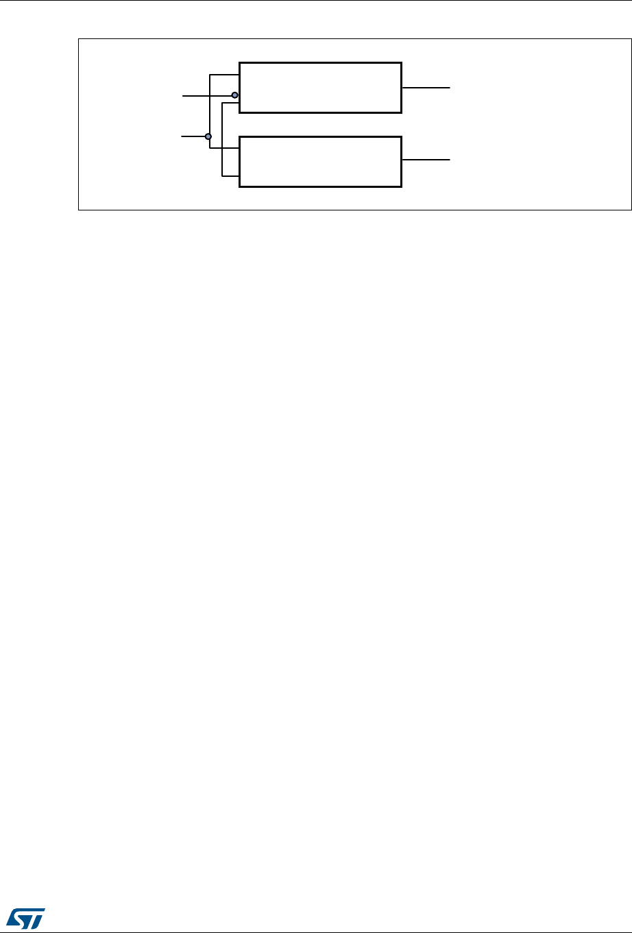
DocID018909 Rev 9 887/1718
RM0090 Serial peripheral interface (SPI)
912
Figure 263. I2S full duplex block diagram
1. Where x can be 2 or 3.
I2Sx can operate in master mode. As a result:
• Only I2Sx can output SCK and WS in half duplex mode
• Only I2Sx can deliver SCK and WS to I2S2_ext and I2S3_ext in full duplex mode.
The extended I2Ss (I2Sx_ext) can be used only in full duplex mode. The I2Sx_ext operate
always in slave mode.
Both I2Sx and I2Sx_ext can be configured as transmitters or receivers.
28.4.3 Supported audio protocols
The four-line bus has to handle only audio data generally time-multiplexed on two channels:
the right channel and the left channel. However there is only one 16-bit register for the
transmission and the reception. So, it is up to the software to write into the data register the
adequate value corresponding to the considered channel side, or to read the data from the
data register and to identify the corresponding channel by checking the CHSIDE bit in the
SPI_SR register. Channel Left is always sent first followed by the channel right (CHSIDE
has no meaning for the PCM protocol).
Four data and packet frames are available. Data may be sent with a format of:
•16-bit data packed in 16-bit frame
•16-bit data packed in 32-bit frame
•24-bit data packed in 32-bit frame
•32-bit data packed in 32-bit frame
When using 16-bit data extended on 32-bit packet, the first 16 bits (MSB) are the significant
bits, the 16-bit LSB is forced to 0 without any need for software action or DMA request (only
one read/write operation).
The 24-bit and 32-bit data frames need two CPU read or write operations to/from the
SPI_DR or two DMA operations if the DMA is preferred for the application. For 24-bit data
frame specifically, the 8 nonsignificant bits are extended to 32 bits with 0-bits (by hardware).
For all data formats and communication standards, the most significant bit is always sent
first (MSB first).
The I2S interface supports four audio standards, configurable using the I2SSTD[1:0] and
PCMSYNC bits in the SPI_I2SCFGR register.
-36
30))3X
)3X?EXT
30)X?-/3))3X?3$INOUT
)3? 73
)3X?3#+
)3X?EXT3$INOUT
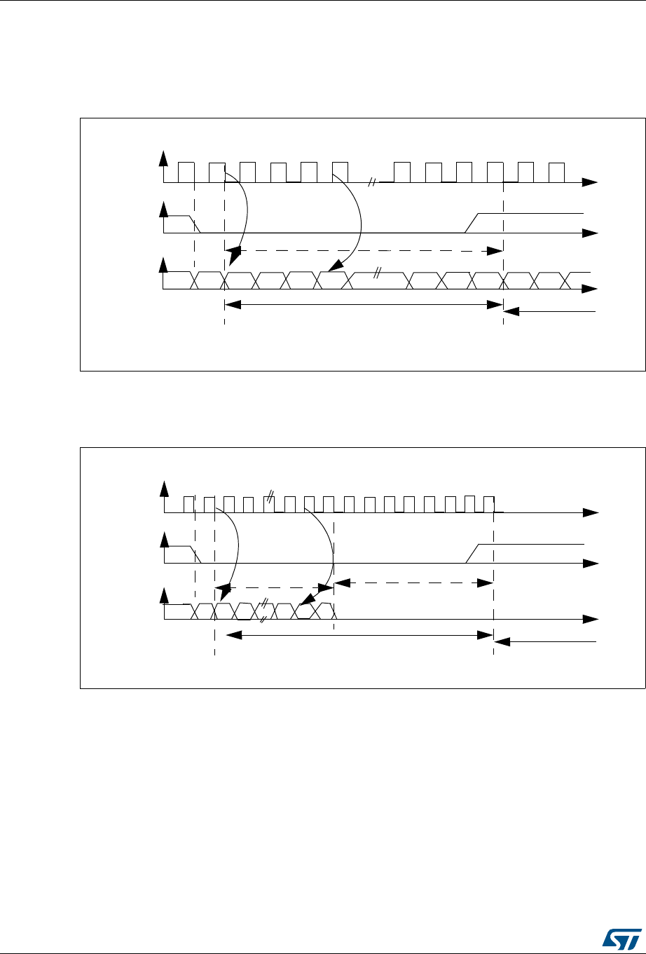
Serial peripheral interface (SPI) RM0090
888/1718 DocID018909 Rev 9
I2S Philips standard
For this standard, the WS signal is used to indicate which channel is being transmitted. It is
activated one CK clock cycle before the first bit (MSB) is available.
Figure 264. I2S Philips protocol waveforms (16/32-bit full accuracy, CPOL = 0)
Data are latched on the falling edge of CK (for the transmitter) and are read on the rising
edge (for the receiver). The WS signal is also latched on the falling edge of CK.
Figure 265. I2S Philips standard waveforms (24-bit frame with CPOL = 0)
This mode needs two write or read operations to/from the SPI_DR.
•In transmission mode:
if 0x8EAA33 has to be sent (24-bit):
MSB LSB MSB
CK
WS
SD
Channel left
Channel right
May be 16-bit, 32-bit
Transmission Reception
CK
WS
SD
Channel left 32-bit
Channel right
MSB LSB
8-bit remaining
0 forced
24-bit data
Transmission Reception
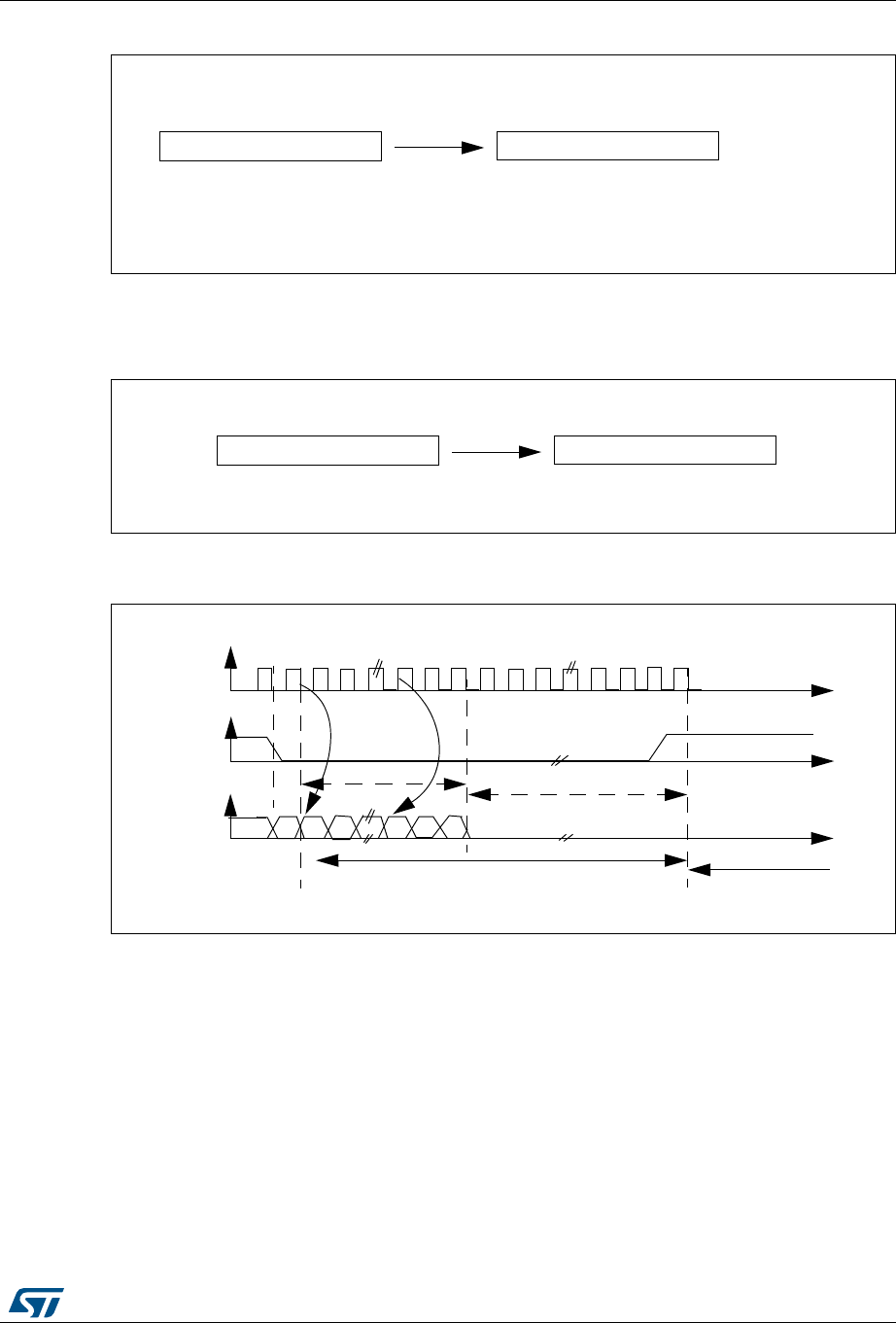
DocID018909 Rev 9 889/1718
RM0090 Serial peripheral interface (SPI)
912
Figure 266. Transmitting 0x8EAA33
•In reception mode:
if data 0x8EAA33 is received:
Figure 267. Receiving 0x8EAA33
Figure 268. I2S Philips standard (16-bit extended to 32-bit packet frame with
CPOL = 0)
When 16-bit data frame extended to 32-bit channel frame is selected during the I2S
configuration phase, only one access to SPI_DR is required. The 16 remaining bits are
forced by hardware to 0x0000 to extend the data to 32-bit format.
If the data to transmit or the received data are 0x76A3 (0x76A30000 extended to 32-bit), the
operation shown in Figure 269 is required.
0x8EAA 0x33XX
Only the 8 MSBs are sent to complete the 24 bits
First write to Data register Second write to Data register
8 LSB bits have no meaning and could be
anything
0x8EAA 0x3300
Only the 8MSB are right
First read from Data register Second read from Data register
The 8 LSB will always be 00
CK
WS
SD
Channel left 32-bit
Channel right
MSB LSB
16-bit remaining
16-bit data
0 forced
Transmission Reception
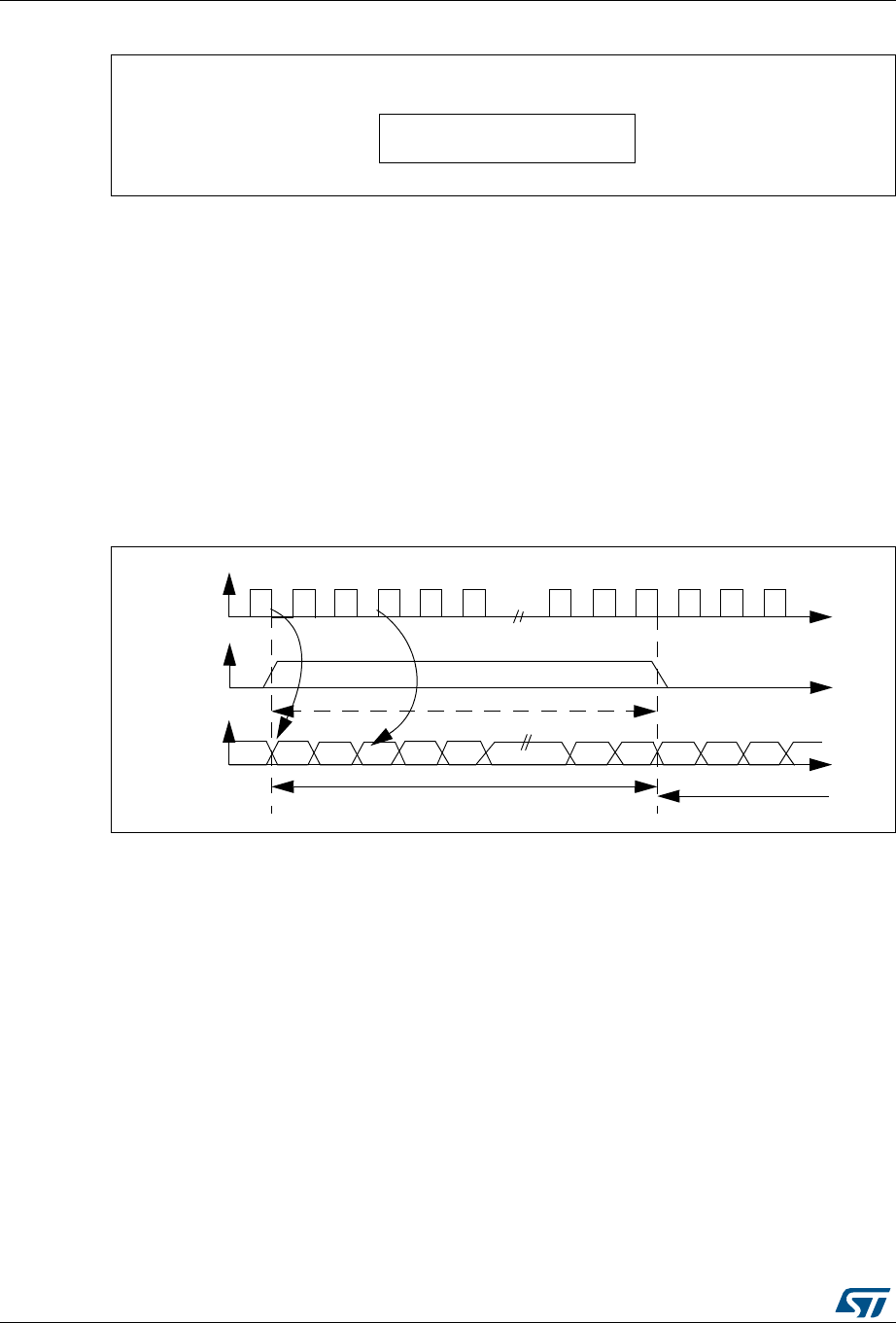
Serial peripheral interface (SPI) RM0090
890/1718 DocID018909 Rev 9
Figure 269. Example
For transmission, each time an MSB is written to SPI_DR, the TXE flag is set and its
interrupt, if allowed, is generated to load SPI_DR with the new value to send. This takes
place even if 0x0000 have not yet been sent because it is done by hardware.
For reception, the RXNE flag is set and its interrupt, if allowed, is generated when the first
16 MSB half-word is received.
In this way, more time is provided between two write or read operations, which prevents
underrun or overrun conditions (depending on the direction of the data transfer).
MSB justified standard
For this standard, the WS signal is generated at the same time as the first data bit, which is
the MSBit.
Figure 270. MSB Justified 16-bit or 32-bit full-accuracy length with CPOL = 0
Data are latched on the falling edge of CK (for transmitter) and are read on the rising edge
(for the receiver).
0X76A3
Only one access to SPI_DR
MSB LSB MSB
CK
WS
SD
Channel left
Channel right
May be 16-bit, 32-bit
Transmission Reception
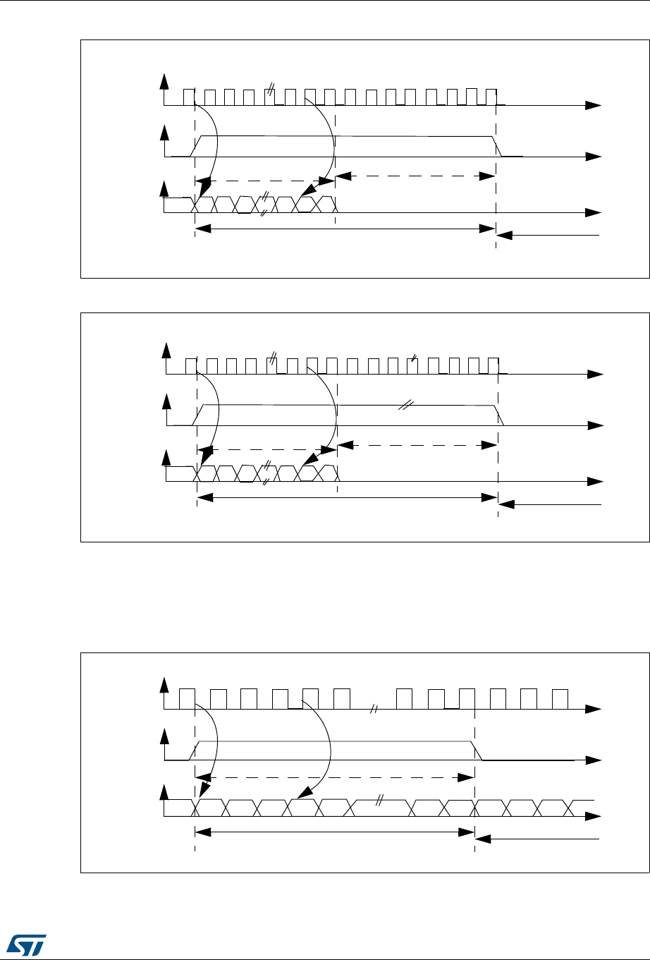
DocID018909 Rev 9 891/1718
RM0090 Serial peripheral interface (SPI)
912
Figure 271. MSB Justified 24-bit frame length with CPOL = 0
Figure 272. MSB Justified 16-bit extended to 32-bit packet frame with CPOL = 0
LSB justified standard
This standard is similar to the MSB justified standard (no difference for the 16-bit and 32-bit
full-accuracy frame formats).
Figure 273. LSB justified 16-bit or 32-bit full-accuracy with CPOL = 0
CK
WS
SD
Channel left 32-bit
Channel right
MSB LSB
8-bit remaining
0 forced
24-bit data
Transmission Reception
CK
WS
SD
Channel left 32-bit
Channel right
MSB LSB
16-bit remaining
0 forced
16-bit data
Transmission Reception
MSB LSB MSB
CK
WS
SD
Channel left
Channel right
May be 16-bit, 32-bit
Transmission Reception
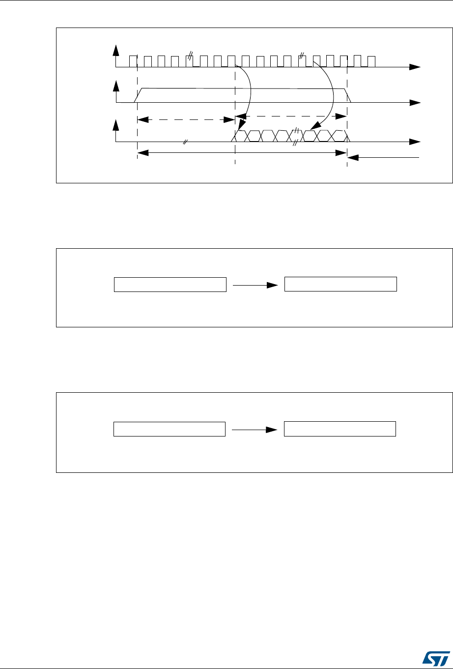
Serial peripheral interface (SPI) RM0090
892/1718 DocID018909 Rev 9
Figure 274. LSB Justified 24-bit frame length with CPOL = 0
•In transmission mode:
If data 0x3478AE have to be transmitted, two write operations to the SPI_DR register
are required from software or by DMA. The operations are shown below.
Figure 275. Operations required to transmit 0x3478AE
•In reception mode:
If data 0x3478AE are received, two successive read operations from SPI_DR are
required on each RXNE event.
Figure 276. Operations required to receive 0x3478AE
CK
WS
SD
Channel left 32-bit
Channel right
MSB LSB
24-bit remaining
0 forced
8-bit data
Transmission Reception
0xXX34 0x78AE
First write to Data register Second write to Data register
Only the 8 LSB bits of the half-word
are significant. Whatever the 8 MSBs
a field of 0x00 is forced instead
conditioned by TXE = ‘1’ conditioned by TXE = ‘1’
0x0034 0x78AE
First read from Data register Second read from Data register
Only the 8 LSB bits of the half-word
are significant. Whatever the 8 MSBs,
a field of 0x00 is forced instead
conditioned by RXNE = ‘1’ conditioned by RXNE = ‘1’
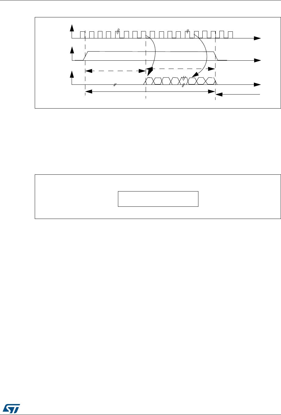
DocID018909 Rev 9 893/1718
RM0090 Serial peripheral interface (SPI)
912
Figure 277. LSB justified 16-bit extended to 32-bit packet frame with CPOL = 0
When 16-bit data frame extended to 32-bit channel frame is selected during the I2S
configuration phase, Only one access to SPI_DR is required. The 16 remaining bits are
forced by hardware to 0x0000 to extend the data to 32-bit format. In this case it corresponds
to the half-word MSB.
If the data to transmit or the received data are 0x76A3 (0x0000 76A3 extended to 32-bit),
the operation shown in Figure 278 is required.
Figure 278. Example of LSB justified 16-bit extended to 32-bit packet frame
In transmission mode, when TXE is asserted, the application has to write the data to be
transmitted (in this case 0x76A3). The 0x000 field is transmitted first (extension on 32-bit).
TXE is asserted again as soon as the effective data (0x76A3) is sent on SD.
In reception mode, RXNE is asserted as soon as the significant half-word is received (and
not the 0x0000 field).
In this way, more time is provided between two write or read operations to prevent underrun
or overrun conditions.
PCM standard
For the PCM standard, there is no need to use channel-side information. The two PCM
modes (short and long frame) are available and configurable using the PCMSYNC bit in
SPI_I2SCFGR.
CK
WS
SD
Channel left 32-bit
Channel right
MSB LSB
16-bit remaining
0 forced
16-bit data
Transmission Reception
0X76A3
Only one access to SPI_DR
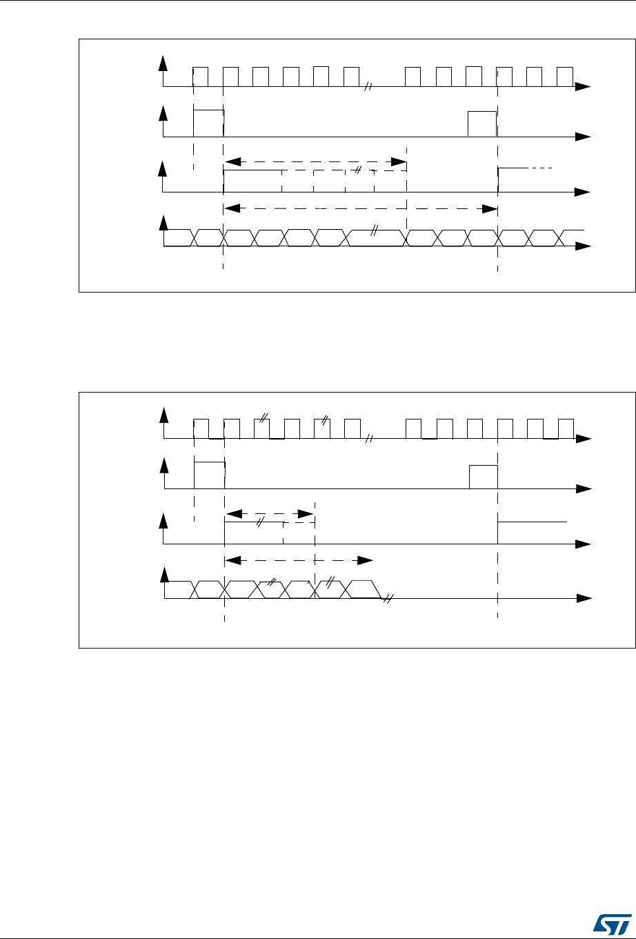
Serial peripheral interface (SPI) RM0090
894/1718 DocID018909 Rev 9
Figure 279. PCM standard waveforms (16-bit)
For long frame synchronization, the WS signal assertion time is fixed 13 bits in master
mode.
For short frame synchronization, the WS synchronization signal is only one cycle long.
Figure 280. PCM standard waveforms (16-bit extended to 32-bit packet frame)
Note: For both modes (master and slave) and for both synchronizations (short and long), the
number of bits between two consecutive pieces of data (and so two synchronization signals)
needs to be specified (DATLEN and CHLEN bits in the SPI_I2SCFGR register) even in
slave mode.
28.4.4 Clock generator
The I2S bitrate determines the dataflow on the I2S data line and the I2S clock signal
frequency.
I2S bitrate = number of bits per channel × number of channels × sampling audio frequency
For a 16-bit audio, left and right channel, the I2S bitrate is calculated as follows:
I2S bitrate = 16 × 2 × FS
MSB LSB MSB
CK
WS
SD
16-bit
WS fixed to 13-bit
short
frame
long
frame
MSB
CK
WS
SD
16-bit
WS
fixed to 13-bit
short
frame
long
frame
LSB
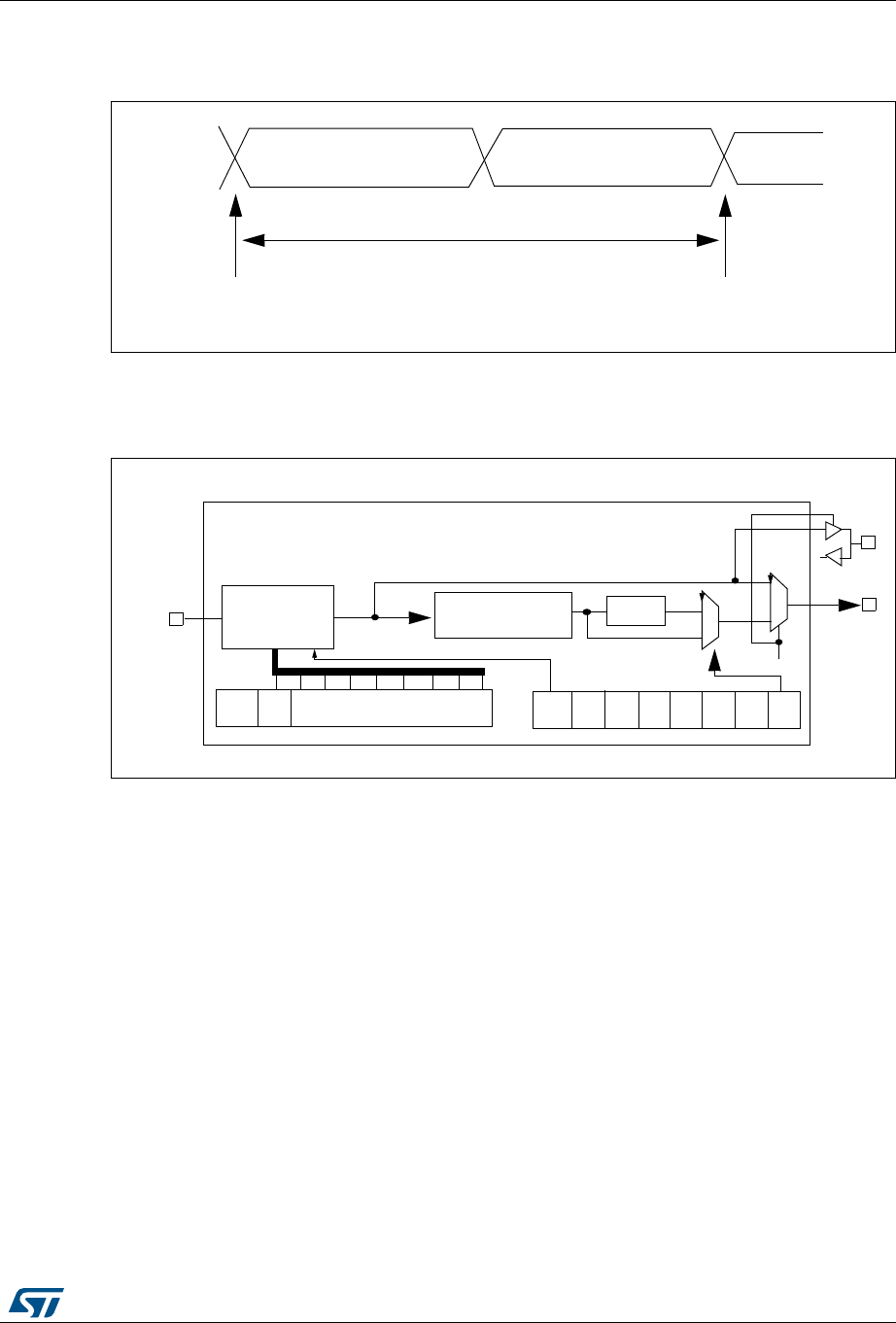
DocID018909 Rev 9 895/1718
RM0090 Serial peripheral interface (SPI)
912
It will be: I2S bitrate = 32 x 2 x FS if the packet length is 32-bit wide.
Figure 281. Audio sampling frequency definition
When the master mode is configured, a specific action needs to be taken to properly
program the linear divider in order to communicate with the desired audio frequency.
Figure 282. I2S clock generator architecture
1. Where x could be 2 or 3.
Figure 281 presents the communication clock architecture. To achieve high-quality audio
performance, the I2SxCLK clock source can be either the PLLI2S output (through R division
factor) or an external clock (mapped to I2S_CKIN pin).
The audio sampling frequency can be 192 kHz, 96 kHz, or 48 kHz. In order to reach the
desired frequency, the linear divider needs to be programmed according to the formulas
below:
When the master clock is generated (MCKOE in the SPI_I2SPR register is set):
FS = I2SxCLK / [(16*2)*((2*I2SDIV)+ODD)*8)] when the channel frame is 16-bit wide
FS = I2SxCLK / [(32*2)*((2*I2SDIV)+ODD)*4)] when the channel frame is 32-bit wide
When the master clock is disabled (MCKOE bit cleared):
FS = I2SxCLK / [(16*2)*((2*I2SDIV)+ODD))] when the channel frame is 16-bit wide
FS = I2SxCLK / [(32*2)*((2*I2SDIV)+ODD))] when the channel frame is 32-bit wide
Table 126 provides example precision values for different clock configurations.
Note: Other configurations are possible that allow optimum clock precision.
16-bit or 32-bit Left channel 16-bit or 32-bit Right channel
sampling point sampling point
32-bits or 64-bits
FS
FS: Audio sampling frequency
8-bit
Divider +
Linear
CK
ODD I2SDIV[7:0]
I2SxCLK
CHLENI2SMOD
reshaping stage
Divider by 4 Div2
1
0
MCKOE
MCKOE
MCK
0
1

Serial peripheral interface (SPI) RM0090
896/1718 DocID018909 Rev 9
28.4.5 I2S master mode
The I2S can be configured as follows:
•In master mode for transmission or reception (half-duplex mode using I2Sx)
•In master mode transmission and reception (full duplex mode using I2Sx and
I2Sx_ext).
This means that the serial clock is generated on the CK pin as well as the Word Select
signal WS. Master clock (MCK) may be output or not, thanks to the MCKOE bit in the
SPI_I2SPR register.
Table 126. Audio frequency precision (for PLLM VCO = 1 MHz or 2 MHz)(1)
Master
clock
Target fS
(Hz)
Data
format PLLI2SN PLLI2SR I2SDIV I2SODD Real fS (Hz) Error
Disabled
8000
16-bit 192 2 187 1 8000 0.0000%
32-bit 192 3 62 1 8000 0.0000%
16000
16-bit 192 3 62 1 16000 0.0000%
32-bit 256 2 62 1 16000 0.0000%
32000
16-bit 256 2 62 1 32000 0.0000%
32-bit 256 5 12 1 32000 0.0000%
48000
16-bit 192 5 12 1 48000 0.0000%
32-bit 384 5 12 1 48000 0.0000%
96000
16-bit 384 5 12 1 96000 0.0000%
32-bit 424 3 11 1 96014.49219 0.0151%
22050
16-bit 290 3 68 1 22049.87695 0.0006%
32-bit 302 2 53 1 22050.23438 0.0011%
44100
16-bit 302 2 53 1 44100.46875 0.0011%
32-bit 429 4 19 0 44099.50781 0.0011%
192000
16-bit 424 3 11 1 192028.9844 0.0151%
32-bit 258 3 3 1 191964.2813 0.0186%
Enabled
8000 don't care 256 5 12 1 8000 0.0000%
16000 don't care 213 2 13 0 16000.60059 0.0038%
32000 don't care 213 2 6 1 32001.20117 0.0038%
48000 don't care 258 3 3 1 47991.07031 0.0186%
96000 don't care 344 2 3 1 95982.14063 0.0186%
22050 don't care 429 4 9 1 22049.75391 0.0011%
44100 don't care 271 2 6 0 44108.07422 0.0183%
1. This table gives only example values for different clock configurations. Other configurations allowing optimum clock
precision are possible.

DocID018909 Rev 9 897/1718
RM0090 Serial peripheral interface (SPI)
912
Procedure
1. Select the I2SDIV[7:0] bits in the SPI_I2SPR register to define the serial clock baud
rate to reach the proper audio sample frequency. The ODD bit in the SPI_I2SPR
register also has to be defined.
2. Select the CKPOL bit to define the steady level for the communication clock. Set the
MCKOE bit in the SPI_I2SPR register if the master clock MCK needs to be provided to
the external DAC/ADC audio component (the I2SDIV and ODD values should be
computed depending on the state of the MCK output, for more details refer to
Section 28.4.4: Clock generator).
3. Set the I2SMOD bit in SPI_I2SCFGR to activate the I2S functionalities and choose the
I2S standard through the I2SSTD[1:0] and PCMSYNC bits, the data length through the
DATLEN[1:0] bits and the number of bits per channel by configuring the CHLEN bit.
Select also the I2S master mode and direction (Transmitter or Receiver) through the
I2SCFG[1:0] bits in the SPI_I2SCFGR register.
4. If needed, select all the potential interruption sources and the DMA capabilities by
writing the SPI_CR2 register.
5. The I2SE bit in SPI_I2SCFGR register must be set.
WS and CK are configured in output mode. MCK is also an output, if the MCKOE bit in
SPI_I2SPR is set.
Transmission sequence
The transmission sequence begins when a half-word is written into the Tx buffer.
Assumedly, the first data written into the Tx buffer correspond to the channel Left data.
When data are transferred from the Tx buffer to the shift register, TXE is set and data
corresponding to the channel Right have to be written into the Tx buffer. The CHSIDE flag
indicates which channel is to be transmitted. It has a meaning when the TXE flag is set
because the CHSIDE flag is updated when TXE goes high.
A full frame has to be considered as a Left channel data transmission followed by a Right
channel data transmission. It is not possible to have a partial frame where only the left
channel is sent.
The data half-word is parallel loaded into the 16-bit shift register during the first bit
transmission, and then shifted out, serially, to the MOSI/SD pin, MSB first. The TXE flag is
set after each transfer from the Tx buffer to the shift register and an interrupt is generated if
the TXEIE bit in the SPI_CR2 register is set.
For more details about the write operations depending on the I2S standard mode selected,
refer to Section 28.4.3: Supported audio protocols).
To ensure a continuous audio data transmission, it is mandatory to write the SPI_DR with
the next data to transmit before the end of the current transmission.
To switch off the I2S, by clearing I2SE, it is mandatory to wait for TXE = 1 and BSY = 0.
Reception sequence
The operating mode is the same as for the transmission mode except for the point 3 (refer to
the procedure described in Section 28.4.5: I2S master mode), where the configuration
should set the master reception mode through the I2SCFG[1:0] bits.
Whatever the data or channel length, the audio data are received by 16-bit packets. This
means that each time the Rx buffer is full, the RXNE flag is set and an interrupt is generated

Serial peripheral interface (SPI) RM0090
898/1718 DocID018909 Rev 9
if the RXNEIE bit is set in SPI_CR2 register. Depending on the data and channel length
configuration, the audio value received for a right or left channel may result from one or two
receptions into the Rx buffer.
Clearing the RXNE bit is performed by reading the SPI_DR register.
CHSIDE is updated after each reception. It is sensitive to the WS signal generated by the
I2S cell.
For more details about the read operations depending on the I2S standard mode selected,
refer to Section 28.4.3: Supported audio protocols.
If data are received while the previously received data have not been read yet, an overrun is
generated and the OVR flag is set. If the ERRIE bit is set in the SPI_CR2 register, an
interrupt is generated to indicate the error.
To switch off the I2S, specific actions are required to ensure that the I2S completes the
transfer cycle properly without initiating a new data transfer. The sequence depends on the
configuration of the data and channel lengths, and on the audio protocol mode selected. In
the case of:
•16-bit data length extended on 32-bit channel length (DATLEN = 00 and CHLEN = 1)
using the LSB justified mode (I2SSTD = 10)
a) Wait for the second to last RXNE = 1 (n – 1)
b) Then wait 17 I2S clock cycles (using a software loop)
c) Disable the I2S (I2SE = 0)
•16-bit data length extended on 32-bit channel length (DATLEN = 00 and CHLEN = 1) in
MSB justified, I2S or PCM modes (I2SSTD = 00, I2SSTD = 01 or I2SSTD = 11,
respectively)
a) Wait for the last RXNE
b) Then wait 1 I2S clock cycle (using a software loop)
c) Disable the I2S (I2SE = 0)
•For all other combinations of DATLEN and CHLEN, whatever the audio mode selected
through the I2SSTD bits, carry out the following sequence to switch off the I2S:
a) Wait for the second to last RXNE = 1 (n – 1)
b) Then wait one I2S clock cycle (using a software loop)
c) Disable the I2S (I2SE = 0)
Note: The BSY flag is kept low during transfers.
28.4.6 I2S slave mode
The I2S can be configured as follows:
•In slave mode for transmission or reception (half-duplex mode using I2Sx)
•In slave mode transmission and reception (full duplex mode using I2Sx and I2Sx_ext).
The operating mode is following mainly the same rules as described for the I2S master
configuration. In slave mode, there is no clock to be generated by the I2S interface. The
clock and WS signals are input from the external master connected to the I2S interface.
There is then no need, for the user, to configure the clock.
The configuration steps to follow are listed below:

DocID018909 Rev 9 899/1718
RM0090 Serial peripheral interface (SPI)
912
1. Set the I2SMOD bit in the SPI_I2SCFGR register to reach the I2S functionalities and
choose the I2S standard through the I2SSTD[1:0] bits, the data length through the
DATLEN[1:0] bits and the number of bits per channel for the frame configuring the
CHLEN bit. Select also the mode (transmission or reception) for the slave through the
I2SCFG[1:0] bits in SPI_I2SCFGR register.
2. If needed, select all the potential interrupt sources and the DMA capabilities by writing
the SPI_CR2 register.
3. The I2SE bit in SPI_I2SCFGR register must be set.
Transmission sequence
The transmission sequence begins when the external master device sends the clock and
when the NSS_WS signal requests the transfer of data. The slave has to be enabled before
the external master starts the communication. The I2S data register has to be loaded before
the master initiates the communication.
For the I2S, MSB justified and LSB justified modes, the first data item to be written into the
data register corresponds to the data for the left channel. When the communication starts,
the data are transferred from the Tx buffer to the shift register. The TXE flag is then set in
order to request the right channel data to be written into the I2S data register.
The CHSIDE flag indicates which channel is to be transmitted. Compared to the master
transmission mode, in slave mode, CHSIDE is sensitive to the WS signal coming from the
external master. This means that the slave needs to be ready to transmit the first data
before the clock is generated by the master. WS assertion corresponds to left channel
transmitted first.
Note: The I2SE has to be written at least two PCLK cycles before the first clock of the master
comes on the CK line.
The data half-word is parallel-loaded into the 16-bit shift register (from the internal bus)
during the first bit transmission, and then shifted out serially to the MOSI/SD pin MSB first.
The TXE flag is set after each transfer from the Tx buffer to the shift register and an interrupt
is generated if the TXEIE bit in the SPI_CR2 register is set.
Note that the TXE flag should be checked to be at 1 before attempting to write the Tx buffer.
For more details about the write operations depending on the I2S standard mode selected,
refer to Section 28.4.3: Supported audio protocols.
To secure a continuous audio data transmission, it is mandatory to write the SPI_DR
register with the next data to transmit before the end of the current transmission. An
underrun flag is set and an interrupt may be generated if the data are not written into the
SPI_DR register before the first clock edge of the next data communication. This indicates
to the software that the transferred data are wrong. If the ERRIE bit is set into the SPI_CR2
register, an interrupt is generated when the UDR flag in the SPI_SR register goes high. In
this case, it is mandatory to switch off the I2S and to restart a data transfer starting from the
left channel.
To switch off the I2S, by clearing the I2SE bit, it is mandatory to wait for TXE = 1 and BSY =
0.
Reception sequence
The operating mode is the same as for the transmission mode except for the point 1 (refer to
the procedure described in Section 28.4.6: I2S slave mode), where the configuration should
set the master reception mode using the I2SCFG[1:0] bits in the SPI_I2SCFGR register.

Serial peripheral interface (SPI) RM0090
900/1718 DocID018909 Rev 9
Whatever the data length or the channel length, the audio data are received by 16-bit
packets. This means that each time the RX buffer is full, the RXNE flag in the SPI_SR
register is set and an interrupt is generated if the RXNEIE bit is set in the SPI_CR2 register.
Depending on the data length and channel length configuration, the audio value received for
a right or left channel may result from one or two receptions into the RX buffer.
The CHSIDE flag is updated each time data are received to be read from SPI_DR. It is
sensitive to the external WS line managed by the external master component.
Clearing the RXNE bit is performed by reading the SPI_DR register.
For more details about the read operations depending the I2S standard mode selected, refer
to Section 28.4.3: Supported audio protocols.
If data are received while the precedent received data have not yet been read, an overrun is
generated and the OVR flag is set. If the bit ERRIE is set in the SPI_CR2 register, an
interrupt is generated to indicate the error.
To switch off the I2S in reception mode, I2SE has to be cleared immediately after receiving
the last RXNE = 1.
Note: The external master components should have the capability of sending/receiving data in 16-
bit or 32-bit packets via an audio channel.
28.4.7 Status flags
Three status flags are provided for the application to fully monitor the state of the I2S bus.
Busy flag (BSY)
The BSY flag is set and cleared by hardware (writing to this flag has no effect). It indicates
the state of the communication layer of the I2S.
When BSY is set, it indicates that the I2S is busy communicating. There is one exception in
master receive mode (I2SCFG = 11) where the BSY flag is kept low during reception.
The BSY flag is useful to detect the end of a transfer if the software needs to disable the I2S.
This avoids corrupting the last transfer. For this, the procedure described below must be
strictly respected.
The BSY flag is set when a transfer starts, except when the I2S is in master receiver mode.
The BSY flag is cleared:
•when a transfer completes (except in master transmit mode, in which the
communication is supposed to be continuous)
•when the I2S is disabled
When communication is continuous:
•In master transmit mode, the BSY flag is kept high during all the transfers
•In slave mode, the BSY flag goes low for one I2S clock cycle between each transfer
Note: Do not use the BSY flag to handle each data transmission or reception. It is better to use the
TXE and RXNE flags instead.

DocID018909 Rev 9 901/1718
RM0090 Serial peripheral interface (SPI)
912
Tx buffer empty flag (TXE)
When set, this flag indicates that the Tx buffer is empty and the next data to be transmitted
can then be loaded into it. The TXE flag is reset when the Tx buffer already contains data to
be transmitted. It is also reset when the I2S is disabled (I2SE bit is reset).
RX buffer not empty (RXNE)
When set, this flag indicates that there are valid received data in the RX Buffer. It is reset
when SPI_DR register is read.
Channel Side flag (CHSIDE)
In transmission mode, this flag is refreshed when TXE goes high. It indicates the channel
side to which the data to transfer on SD has to belong. In case of an underrun error event in
slave transmission mode, this flag is not reliable and I2S needs to be switched off and
switched on before resuming the communication.
In reception mode, this flag is refreshed when data are received into SPI_DR. It indicates
from which channel side data have been received. Note that in case of error (like OVR) this
flag becomes meaningless and the I2S should be reset by disabling and then enabling it
(with configuration if it needs changing).
This flag has no meaning in the PCM standard (for both Short and Long frame modes).
When the OVR or UDR flag in the SPI_SR is set and the ERRIE bit in SPI_CR2 is also set,
an interrupt is generated. This interrupt can be cleared by reading the SPI_SR status
register (once the interrupt source has been cleared).
28.4.8 Error flags
There are three error flags for the I2S cell.
Underrun flag (UDR)
In slave transmission mode this flag is set when the first clock for data transmission appears
while the software has not yet loaded any value into SPI_DR. It is available when the
I2SMOD bit in SPI_I2SCFGR is set. An interrupt may be generated if the ERRIE bit in
SPI_CR2 is set.
The UDR bit is cleared by a read operation on the SPI_SR register.
Overrun flag (OVR)
This flag is set when data are received and the previous data have not yet been read from
SPI_DR. As a result, the incoming data are lost. An interrupt may be generated if the ERRIE
bit is set in SPI_CR2.
In this case, the receive buffer contents are not updated with the newly received data from
the transmitter device. A read operation to the SPI_DR register returns the previous
correctly received data. All other subsequently transmitted half-words are lost.
Clearing the OVR bit is done by a read operation on the SPI_DR register followed by a read
access to the SPI_SR register.
Frame error flag (FRE)
This flag can be set by hardware only if the I2S is configured in Slave mode. It is set if the
external master is changing the WS line at a moment when the slave is not expected this

Serial peripheral interface (SPI) RM0090
902/1718 DocID018909 Rev 9
change. If the synchronization is lost, to recover from this state and resynchronize the
external master device with the I2S slave device, follow the steps below:
1. Disable the I2S
2. Re-enable it when the correct level is detected on the WS line (WS line is high in I2S
mode, or low for MSB- or LSB-justified or PCM modes).
Desynchronization between the master and slave device may be due to noisy environment
on the SCK communication clock or on the WS frame synchronization line. An error interrupt
can be generated if the ERRIE bit is set. The desynchronization flag (FRE) is cleared by
software when the status register is read.
28.4.9 I2S interrupts
Table 127 provides the list of I2S interrupts.
28.4.10 DMA features
DMA is working in exactly the same way as for the SPI mode. There is no difference on the
I2S. Only the CRC feature is not available in I2S mode since there is no data transfer
protection system.
Table 127. I2S interrupt requests
Interrupt event Event flag Enable Control bit
Transmit buffer empty flag TXE TXEIE
Receive buffer not empty flag RXNE RXNEIE
Overrun error OVR
ERRIE
Underrun error UDR
Frame error flag FRE ERRIE

DocID018909 Rev 9 903/1718
RM0090 Serial peripheral interface (SPI)
912
28.5 SPI and I2S registers
Refer to Section 1.1 on page 57for a list of abbreviations used in register descriptions.
The peripheral registers have to be accessed by half-words (16 bits) or words (32 bits).
28.5.1 SPI control register 1 (SPI_CR1) (not used in I2S mode)
Address offset: 0x00
Reset value: 0x0000
1514131211109876543210
BIDI
MODE
BIDI
OE
CRC
EN
CRC
NEXT DFF RX
ONLY SSM SSI LSB
FIRST SPE BR [2:0] MSTR CPOL CPHA
rw rw rw rw rw rw rw rw rw rw rw rw rw rw rw rw
Bit 15 BIDIMODE: Bidirectional data mode enable
0: 2-line unidirectional data mode selected
1: 1-line bidirectional data mode selected
Note: This bit is not used in I2S mode
Bit 14 BIDIOE: Output enable in bidirectional mode
This bit combined with the BIDImode bit selects the direction of transfer in bidirectional mode
0: Output disabled (receive-only mode)
1: Output enabled (transmit-only mode)
Note: This bit is not used in I2S mode.
In master mode, the MOSI pin is used while the MISO pin is used in slave mode.
Bit 13 CRCEN: Hardware CRC calculation enable
0: CRC calculation disabled
1: CRC calculation enabled
Note: This bit should be written only when SPI is disabled (SPE = ‘0’) for correct operation.
It is not used in I2S mode.
Bit 12 CRCNEXT: CRC transfer next
0: Data phase (no CRC phase)
1: Next transfer is CRC (CRC phase)
Note: When the SPI is configured in full duplex or transmitter only modes, CRCNEXT must be
written as soon as the last data is written to the SPI_DR register.
When the SPI is configured in receiver only mode, CRCNEXT must be set after the
second last data reception.
This bit should be kept cleared when the transfers are managed by DMA.
It is not used in I2S mode.
Bit 11 DFF: Data frame format
0: 8-bit data frame format is selected for transmission/reception
1: 16-bit data frame format is selected for transmission/reception
Note: This bit should be written only when SPI is disabled (SPE = ‘0’) for correct operation.
It is not used in I2S mode.

Serial peripheral interface (SPI) RM0090
904/1718 DocID018909 Rev 9
Bit 10 RXONLY: Receive only
This bit combined with the BIDImode bit selects the direction of transfer in 2-line
unidirectional mode. This bit is also useful in a multislave system in which this particular
slave is not accessed, the output from the accessed slave is not corrupted.
0: Full duplex (Transmit and receive)
1: Output disabled (Receive-only mode)
Note: This bit is not used in I2S mode
Bit 9 SSM: Software slave management
When the SSM bit is set, the NSS pin input is replaced with the value from the SSI bit.
0: Software slave management disabled
1: Software slave management enabled
Note: This bit is not used in I2S mode and SPI TI mode
Bit 8 SSI: Internal slave select
This bit has an effect only when the SSM bit is set. The value of this bit is forced onto the
NSS pin and the IO value of the NSS pin is ignored.
Note: This bit is not used in I2S mode and SPI TI mode
Bit 7 LSBFIRST: Frame format
0: MSB transmitted first
1: LSB transmitted first
Note: This bit should not be changed when communication is ongoing.
It is not used in I2S mode and SPI TI mode
Bit 6 SPE: SPI enable
0: Peripheral disabled
1: Peripheral enabled
Note: This bit is not used in I2S mode.
When disabling the SPI, follow the procedure described in Section 28.3.8: Disabling the
SPI.
Bits 5:3 BR[2:0]: Baud rate control
000: fPCLK/2
001: fPCLK/4
010: fPCLK/8
011: fPCLK/16
100: fPCLK/32
101: fPCLK/64
110: fPCLK/128
111: fPCLK/256
Note: These bits should not be changed when communication is ongoing.
They are not used in I2S mode.

DocID018909 Rev 9 905/1718
RM0090 Serial peripheral interface (SPI)
912
28.5.2 SPI control register 2 (SPI_CR2)
Address offset: 0x04
Reset value: 0x0000
Bit 2 MSTR: Master selection
0: Slave configuration
1: Master configuration
Note: This bit should not be changed when communication is ongoing.
It is not used in I2S mode.
Bit1 CPOL: Clock polarity
0: CK to 0 when idle
1: CK to 1 when idle
Note: This bit should not be changed when communication is ongoing.
It is not used in I2S mode and SPI TI mode.
Bit 0 CPHA: Clock phase
0: The first clock transition is the first data capture edge
1: The second clock transition is the first data capture edge
Note: This bit should not be changed when communication is ongoing.
It is not used in I2S mode and SPI TI mode.
15 14 13 12 11 10 9 8 7 6 5 4 3 2 1 0
Reserved
TXEIE RXNEIE ERRIE FRF
Res.
SSOE TXDMAEN RXDMAEN
rw rw rw rw rw rw rw
Bits 15:8 Reserved, must be kept at reset value.
Bit 7 TXEIE: Tx buffer empty interrupt enable
0: TXE interrupt masked
1: TXE interrupt not masked. Used to generate an interrupt request when the TXE flag is set.
Bit 6 RXNEIE: RX buffer not empty interrupt enable
0: RXNE interrupt masked
1: RXNE interrupt not masked. Used to generate an interrupt request when the RXNE flag is
set.
Bit 5 ERRIE: Error interrupt enable
This bit controls the generation of an interrupt when an error condition occurs )(CRCERR,
OVR, MODF in SPI mode, FRE in TI mode and UDR, OVR, and FRE in I2S mode).
0: Error interrupt is masked
1: Error interrupt is enabled
Bit 4 FRF: Frame format
0: SPI Motorola mode
1 SPI TI mode
Note: This bit is not used in I2S mode.
Bit 3 Reserved. Forced to 0 by hardware.

Serial peripheral interface (SPI) RM0090
906/1718 DocID018909 Rev 9
28.5.3 SPI status register (SPI_SR)
Address offset: 0x08
Reset value: 0x0002
Bit 2 SSOE: SS output enable
0: SS output is disabled in master mode and the cell can work in multimaster configuration
1: SS output is enabled in master mode and when the cell is enabled. The cell cannot work
in a multimaster environment.
Note: This bit is not used in I2S mode and SPI TI mode.
Bit 1 TXDMAEN: Tx buffer DMA enable
When this bit is set, the DMA request is made whenever the TXE flag is set.
0: Tx buffer DMA disabled
1: Tx buffer DMA enabled
Bit 0 RXDMAEN: Rx buffer DMA enable
When this bit is set, the DMA request is made whenever the RXNE flag is set.
0: Rx buffer DMA disabled
1: Rx buffer DMA enabled
1514131211109876543210
Reserved FRE BSY OVR MODF CRC
ERR UDR CHSID
ETXE RXNE
rrrrrc_w0rrrr
Bits 15:9 Reserved. Forced to 0 by hardware.
Bit 8 FRE: Frame format error
0: No frame format error
1: A frame format error occurred
This flag is set by hardware and cleared by software when the SPIx_SR register is read.
Note: This flag is used when the SPI operates in TI slave mode or I2S slave mode (refer to
Section 28.3.10).
Bit 7 BSY: Busy flag
0: SPI (or I2S) not busy
1: SPI (or I2S) is busy in communication or Tx buffer is not empty
This flag is set and cleared by hardware.
Note: BSY flag must be used with caution: refer to Section 28.3.7: Status flags and
Section 28.3.8: Disabling the SPI.
Bit 6 OVR: Overrun flag
0: No overrun occurred
1: Overrun occurred
This flag is set by hardware and reset by a software sequence. Refer to Section 28.4.8 on
page 901 for the software sequence.
Bit 5 MODF: Mode fault
0: No mode fault occurred
1: Mode fault occurred
This flag is set by hardware and reset by a software sequence. Refer to Section 28.3.10 on
page 883 for the software sequence.
Note: This bit is not used in I2S mode

DocID018909 Rev 9 907/1718
RM0090 Serial peripheral interface (SPI)
912
28.5.4 SPI data register (SPI_DR)
Address offset: 0x0C
Reset value: 0x0000
Bit 4 CRCERR: CRC error flag
0: CRC value received matches the SPI_RXCRCR value
1: CRC value received does not match the SPI_RXCRCR value
This flag is set by hardware and cleared by software writing 0.
Note: This bit is not used in I2S mode.
Bit 3 UDR: Underrun flag
0: No underrun occurred
1: Underrun occurred
This flag is set by hardware and reset by a software sequence. Refer to Section 28.4.8 on
page 901 for the software sequence.
Note: This bit is not used in SPI mode.
Bit 2 CHSIDE: Channel side
0: Channel Left has to be transmitted or has been received
1: Channel Right has to be transmitted or has been received
Note: This bit is not used for SPI mode and is meaningless in PCM mode.
Bit 1 TXE: Transmit buffer empty
0: Tx buffer not empty
1: Tx buffer empty
Bit 0 RXNE: Receive buffer not empty
0: Rx buffer empty
1: Rx buffer not empty
1514131211109876543210
DR[15:0]
rw rw rw rw rw rw rw rw rw rw rw rw rw rw rw rw
Bits 15:0 DR[15:0]: Data register
Data received or to be transmitted.
The data register is split into 2 buffers - one for writing (Transmit Buffer) and another one for
reading (Receive buffer). A write to the data register will write into the Tx buffer and a read
from the data register will return the value held in the Rx buffer.
Note: These notes apply to SPI mode:
Depending on the data frame format selection bit (DFF in SPI_CR1 register), the data
sent or received is either 8-bit or 16-bit. This selection has to be made before enabling
the SPI to ensure correct operation.
For an 8-bit data frame, the buffers are 8-bit and only the LSB of the register
(SPI_DR[7:0]) is used for transmission/reception. When in reception mode, the MSB of
the register (SPI_DR[15:8]) is forced to 0.
For a 16-bit data frame, the buffers are 16-bit and the entire register, SPI_DR[15:0] is
used for transmission/reception.

Serial peripheral interface (SPI) RM0090
908/1718 DocID018909 Rev 9
28.5.5 SPI CRC polynomial register (SPI_CRCPR) (not used in I2S
mode)
Address offset: 0x10
Reset value: 0x0007
28.5.6 SPI RX CRC register (SPI_RXCRCR) (not used in I2S mode)
Address offset: 0x14
Reset value: 0x0000
28.5.7 SPI TX CRC register (SPI_TXCRCR) (not used in I2S mode)
Address offset: 0x18
Reset value: 0x0000
1514131211109876543210
CRCPOLY[15:0]
rw rw rw rw rw rw rw rw rw rw rw rw rw rw rw rw
Bits 15:0 CRCPOLY[15:0]: CRC polynomial register
This register contains the polynomial for the CRC calculation.
The CRC polynomial (0007h) is the reset value of this register. Another polynomial can be
configured as required.
Note: These bits are not used for the I2S mode.
1514131211109876543210
RXCRC[15:0]
rrrrrrrrrrrrrrrr
Bits 15:0 RXCRC[15:0]: Rx CRC register
When CRC calculation is enabled, the RxCRC[15:0] bits contain the computed CRC value of
the subsequently received bytes. This register is reset when the CRCEN bit in SPI_CR1
register is written to 1. The CRC is calculated serially using the polynomial programmed in
the SPI_CRCPR register.
Only the 8 LSB bits are considered when the data frame format is set to be 8-bit data (DFF
bit of SPI_CR1 is cleared). CRC calculation is done based on any CRC8 standard.
The entire 16-bits of this register are considered when a 16-bit data frame format is selected
(DFF bit of the SPI_CR1 register is set). CRC calculation is done based on any CRC16
standard.
Note: A read to this register when the BSY Flag is set could return an incorrect value.
Theser bits are not used for I2S mode.
1514131211109876543210
TXCRC[15:0]
rrrrrrrrrrrrrrrr

DocID018909 Rev 9 909/1718
RM0090 Serial peripheral interface (SPI)
912
28.5.8 SPI_I2S configuration register (SPI_I2SCFGR)
Address offset: 0x1C
Reset value: 0x0000
Bits 15:0 TXCRC[15:0]: Tx CRC register
When CRC calculation is enabled, the TxCRC[7:0] bits contain the computed CRC value of
the subsequently transmitted bytes. This register is reset when the CRCEN bit of SPI_CR1
is written to 1. The CRC is calculated serially using the polynomial programmed in the
SPI_CRCPR register.
Only the 8 LSB bits are considered when the data frame format is set to be 8-bit data (DFF
bit of SPI_CR1 is cleared). CRC calculation is done based on any CRC8 standard.
The entire 16-bits of this register are considered when a 16-bit data frame format is selected
(DFF bit of the SPI_CR1 register is set). CRC calculation is done based on any CRC16
standard.
Note: A read to this register when the BSY flag is set could return an incorrect value.
These bits are not used for I2S mode.
15 14 13 12 11 10 9 8 7 6 5 4 3 2 1 0
Reserved
I2SMOD I2SE I2SCFG PCMSY
NC Res.
I2SSTD CKPOL DATLEN CHLEN
rw rw rw rw rw rw rw rw rw rw rw
Bits 15:12 Reserved, must be kept at reset value.
Bit 11 I2SMOD: I2S mode selection
0: SPI mode is selected
1: I2S mode is selected
Note: This bit should be configured when the SPI or I2S is disabled
Bit 10 I2SE: I2S Enable
0: I2S peripheral is disabled
1: I2S peripheral is enabled
Note: This bit is not used in SPI mode.
Bits 9:8 I2SCFG: I2S configuration mode
00: Slave - transmit
01: Slave - receive
10: Master - transmit
11: Master - receive
Note: This bit should be configured when the I2S is disabled.
It is not used in SPI mode.
Bit 7 PCMSYNC: PCM frame synchronization
0: Short frame synchronization
1: Long frame synchronization
Note: This bit has a meaning only if I2SSTD = 11 (PCM standard is used)
It is not used in SPI mode.
Bit 6 Reserved: forced at 0 by hardware

Serial peripheral interface (SPI) RM0090
910/1718 DocID018909 Rev 9
28.5.9 SPI_I2S prescaler register (SPI_I2SPR)
Address offset: 0x20
Reset value: 0000 0010 (0x0002)
Bits 5:4 I2SSTD: I2S standard selection
00: I2S Philips standard.
01: MSB justified standard (left justified)
10: LSB justified standard (right justified)
11: PCM standard
For more details on I2S standards, refer to Section 28.4.3 on page 887. Not used in SPI mode.
Note: For correct operation, these bits should be configured when the I2S is disabled.
Bit 3 CKPOL: Steady state clock polarity
0: I2S clock steady state is low level
1: I2S clock steady state is high level
Note: For correct operation, this bit should be configured when the I2S is disabled.
This bit is not used in SPI mode
Bits 2:1 DATLEN: Data length to be transferred
00: 16-bit data length
01: 24-bit data length
10: 32-bit data length
11: Not allowed
Note: For correct operation, these bits should be configured when the I2S is disabled.
This bit is not used in SPI mode.
Bit 0 CHLEN: Channel length (number of bits per audio channel)
0: 16-bit wide
1: 32-bit wide
The bit write operation has a meaning only if DATLEN = 00 otherwise the channel length is fixed to
32-bit by hardware whatever the value filled in. Not used in SPI mode.
Note: For correct operation, this bit should be configured when the I2S is disabled.
1514131211109 876543210
Reserved MCKOE ODD I2SDIV
rw rw rw

DocID018909 Rev 9 911/1718
RM0090 Serial peripheral interface (SPI)
912
Bits 15:10 Reserved, must be kept at reset value.
Bit 9 MCKOE: Master clock output enable
0: Master clock output is disabled
1: Master clock output is enabled
Note: This bit should be configured when the I2S is disabled. It is used only when the I2S is in master
mode.
This bit is not used in SPI mode.
Bit 8 ODD: Odd factor for the prescaler
0: real divider value is = I2SDIV *2
1: real divider value is = (I2SDIV * 2)+1
Refer to Section 28.4.4 on page 894. Not used in SPI mode.
Note: This bit should be configured when the I2S is disabled. It is used only when the I2S is in master
mode.
Bits 7:0 I2SDIV: I2S Linear prescaler
I2SDIV [7:0] = 0 or I2SDIV [7:0] = 1 are forbidden values.
Refer to Section 28.4.4 on page 894. Not used in SPI mode.
Note: These bits should be configured when the I2S is disabled. It is used only when the I2S is in
master mode.
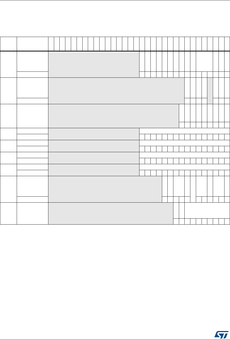
Serial peripheral interface (SPI) RM0090
912/1718 DocID018909 Rev 9
28.5.10 SPI register map
The table provides shows the SPI register map and reset values.
Refer to Table 1 on page 64 for the register boundary addresses.
Table 128. SPI register map and reset values
Offset Register
31
30
29
28
27
26
25
24
23
22
21
20
19
18
17
16
15
14
13
12
11
10
9
8
7
6
5
4
3
2
1
0
0x00 SPI_CR1 Reserved
BIDIMODE
BIDIOE
CRCEN
CRCNEXT
DFF
RXONLY
SSM
SSI
LSBFIRST
SPE
BR [2:0]
MSTR
CPOL
CPHA
Reset value 0000000000000000
0x04 SPI_CR2 Reserved
TXEIE
RXNEIE
ERRIE
FRF
Reserved
SSOE
TXDMAEN
RXDMAEN
Reset value 0000 000
0x08 SPI_SR Reserved
FRE
BSY
OVR
MODF
CRCERR
UDR
CHSIDE
TXE
RXNE
Reset value 000000010
0x0C SPI_DR Reserved DR[15:0]
Reset value 0000000000000000
0x10 SPI_CRCPR Reserved CRCPOLY[15:0]
Reset value 0000000000000111
0x14 SPI_RXCRCR Reserved RxCRC[15:0]
Reset value 0000000000000000
0x18 SPI_TXCRCR Reserved TxCRC[15:0]
Reset value 0000000000000000
0x1C SPI_I2SCFGR Reserved
I2SMOD
I2SE
I2SCFG
PCMSYNC
Reserved
I2SSTD
CKPOL
DATLEN
CHLEN
Reset value 00000 000000
0x20 SPI_I2SPR Reserved
MCKOE
ODD
I2SDIV
Reset value 0000000010

DocID018909 Rev 9 913/1718
RM0090 Serial audio interface (SAI)
951
29 Serial audio interface (SAI)
This section applies to the STM32F42xxx and STM32F43xxx family.
29.1 Introduction
The SAI interface (serial audio interface) offers a wide set of audio protocols due to its
flexibility and wide range of configurations. Many stereo or mono audio applications may be
targeted. I2S standards, LSB or MSB-justified, PCM/DSP, TDM, and AC’97 protocols may
be addressed for example.
To bring this level of flexibility and configurability, the SAI contains two audio sub-blocks that
are fully independent of each other. Each audio sub-block is connected to up to 4 pins (SD,
SCK, FS, MCLK). Some of these pins can be shared if the two sub-blocks are declared as
synchronous to leave some free to be used as general purpose I/Os. The MCLK pin can be
output, or not, depending on the application, the decoder requirement and whether the
audio block is configured as the master.
The SAI can work in master or slave configuration. The audio sub-blocks can be either
receiver or transmitter and can work synchronously or not (with respect to the other one).

Serial audio interface (SAI) RM0090
914/1718 DocID018909 Rev 9
29.2 Main features
•Two independent audio sub-blocks which can be transmitters or receivers with their
respective FIFO.
•8-word integrated FIFOs for each audio sub-block.
•Synchronous or asynchronous mode between the audio sub-blocks.
•Master or slave configuration independent for both audio sub-blocks.
•Clock generator for each audio block to target independent audio frequency sampling
when both audio sub-blocks are configured in master mode.
•Data size configurable: 8-, 10-, 16-, 20-, 24-, 32-bit.
•Peripheral with large configurability and flexibility allowing to target as example the
following audio protocol: I2S, LSB or MSB-justified, PCM/DSP, TDM, AC’97
•Up to 16 slots available with configurable size and with the possibility to select which
ones are active in the audio frame.
•Number of bits by frame may be configurable.
•Frame synchronization active level configurable (offset, bit length, level).
•First active bit position in the slot is configurable.
•LSB first or MSB first for data transfer.
•Mute mode.
•Stereo/Mono audio frame capability.
•Communication clock strobing edge configurable (SCK).
•Error flags with associated interrupts if enabled respectively.
– Overrun and underrun detection,
– Anticipated frame synchronization signal detection in slave mode,
– Late frame synchronization signal detection in slave mode,
– Codec not ready for the AC’97 mode in reception.
•Interruption sources when enabled:
–Errors,
– FIFO requests.
•DMA interface with 2 dedicated channels to handle access to the dedicated integrated
FIFO of each SAI audio sub-block.
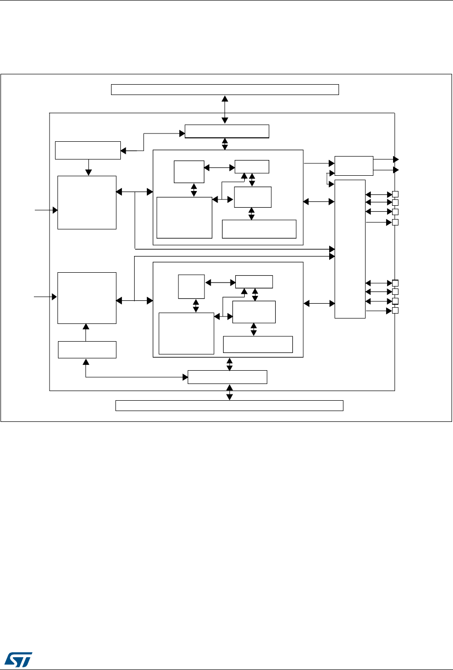
DocID018909 Rev 9 915/1718
RM0090 Serial audio interface (SAI)
951
29.3 Functional block diagram
The block diagram of the SAI is shown in Figure 283.
Figure 283. Functional block diagram
The SAI is mainly composed of two audio sub-blocks with their own clock generator. Each
audio block integrates a 32-bit shift register controlled by their own functional state machine.
Data are stored or read from the dedicated FIFO. FIFO may be accessed by the CPU, or by
DMA in order to leave the CPU free during the communication. Each audio block is
independent. They can be synchronous with each other.
An I/O line controller manages each dedicated pins for a given audio block in the SAI. If the
two blocks are synchronized, this controller reduces the number of I/Os used, freeing up an
FS pin, an SCK pin and eventually an MCLK pin, making them general purpose I/Os.
The functional state machine can be configured to address a wide range of audio protocols.
Some registers are present to set-up the desired protocols (audio frame waveform
generator).
The audio block can be a transmitter or receiver, in master or slave mode. The master mode
means the bit clock SCK and the frame synchronization signal are generated from the SAI,
whereas in slave mode, they come from another external or internal master. There is a
particular case for which the FS signal direction is not directly linked to the master or slave
069
),)2
),)2
$XGLREORFN$
ELWVKLIWUHJLVWHU
$3%LQWHUIDFH
$3%LQWHUIDFH
6HULDO$XGLR,QWHUIDFH
),)2FWUO
)60
&RQILJXUDWLRQ
UHJLVWHUVDQG
6WDWXVUHJLVWHU
$3%
$3%
6$,B&.B$
V\QFKUR
FWUORXW
LQWBVFN
LQWB)6
)6B$
6&.B$
6'B$
0&/.B$
6$,B;&5
&ORFNJHQHUDWRU
$XGLREORFN$
)60
6$,
$XGLREORFN%
),)2FWUO
&RQILJXUDWLRQ
UHJLVWHUVDQG
6WDWXVUHJLVWHU
&ORFNJHQHUDWRU
$XGLREORFN%
6$,B;&5
6$,B&.B%
,2OLQH0DQDJHPHQW
)6B%
6&.B%
6'B%
0&/.B%
ELWVKLIWUHJLVWHU

Serial audio interface (SAI) RM0090
916/1718 DocID018909 Rev 9
mode definition. In AC’97 protocol, it will be an SAI output even if the SAI (link controller) is
set-up to consume the SCK clock (and so to be in Slave mode).
29.4 Main SAI modes
Each audio sub-block of the SAI can be configured to be master or slave via bit MODE[0] in
the SAI_xCR1 register of the selected audio block.
In master mode:
•The bit clock is generated by the SAI using the clock generator on pin SCK_A or
SCK_B (depending which audio block is declared as a master in the SAI).
•The dedicated pin SCK_x is considered as an output.
In slave mode:
•The slave must be enabled before the master is enabled.
•The slave audio block’s SCK clock I/O pin is considered input if it is configured in
asynchronous mode.
•If the audio block is declared synchronous with the second audio block in the SAI, its
SCK I/O pin is released to leave it free to be used as a general purpose I/O and is
connected internally to the SCK pin of the device with which it will be synchronized.
Each audio sub-block can be independently defined as a transmitter or receiver by bit
MODE[1] in the SAI_xCR1 register of the relevant audio block. The I/O pin SD will be
defined respectively as an output or an input.
It is possible to declare two master audio blocks in the same SAI with two different MCLK
and SCK clock frequencies (they have to be declared asynchronous).
Each of the audio blocks in the SAI are enabled by bit SAIxEN in the SAI_xCR1 register. As
soon as this bit is active, the transmitter or the receiver is sensitive to the activity on the
clock line, data line and synchronization line in slave mode.
In master TX mode, enabling the audio block immediately generates the bit clock for the
external slaves even if there is no data in the FIFO, However FS signal generation is
conditioned by the presence of data in the FIFO. After the FIFO receives the first data to
transmit, this data is output to external slaves. If there is no data to transmit in the FIFO, 0
values are then sent in the audio frame with an underrun flag generation.
In slave mode, the audio frame starts when the audio block is enabled and when a start of
frame is detected.
In Slave TX mode, no underrun event is possible on the first frame after the audio block is
enabled, because the mandatory operating sequence in this case is:
1. Write into the SAI_xDR (by software or by DMA).
2. Wait until the FIFO threshold (FLH) flag is different from 000b (FIFO empty).
3. Enable the audio block in slave transmitter mode.
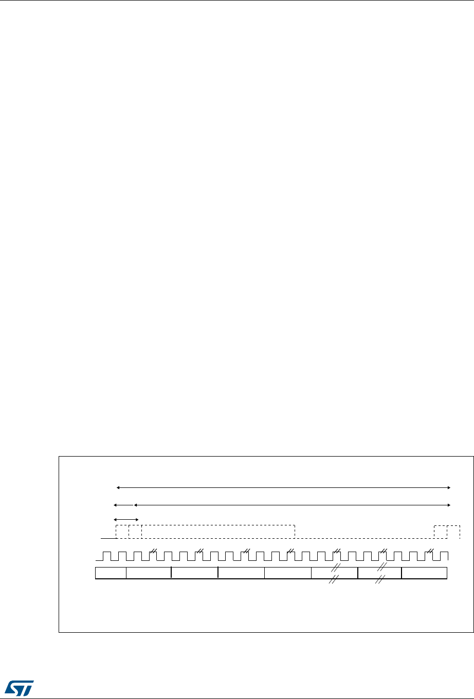
DocID018909 Rev 9 917/1718
RM0090 Serial audio interface (SAI)
951
29.5 SAI synchronization mode
Internal synchronization
An audio block can be declared synchronous with the second audio block. In this case, the
bit clock and the frame synchronization signals are shared to reduce the number of external
pins used for the communication. The audio block declared as synchronous with the other
one will see its own SCK_x, FS_x, and MCLK_x pins released to bring them back as GPIOs.
The one declared asynchronous is the one for which the I/O pins FS_x and SCK_x ad
MCLK_x (if the audio block is considered as master) are considered.
Typically, the audio block synchronous mode may be used to configure the SAI in full duplex
mode. One of the two audio blocks can be configured as master and the other as slave, or
both can be slaves; with one block declared as asynchronous (respective bit SYNCEN[1:0]
= 00 in SAI_xCR1) and the other one declared as synchronous with the other audio block
(respective bit SYNCEN[1:0] = 01 in the SAI_xCR1).
Note: APB frequency PCLK must be greater or equal to twice the bit rate clock frequency (due to
internal resynchronization stages).
29.6 Audio data size
The audio frame can target different data sizes by configuring bit DS[2:0] in the SAI_xCR1
register. The data sizes may be 8-, 10-, 16-, 20-, 24- or 32-bit. During the transfer, either the
MSB or the LSB of the data are sent first, depending on the configuration of bit LSBFIRST in
the SAI_xCR1 register.
29.7 Frame synchronization
The FS signal acts as the Frame synchronization signal in the audio frame (start of frame).
The shape of this signal is completely configurable in order to target the different audio
protocols with their own specificities concerning this Frame synchronization behavior. This
configurability is done using register SAI_xFRCR. Figure 284 gives a view of this flexibility.
Figure 284. Audio frame
3LOT
&S
SCK
SD
&SOFFSET
&SLENGTHBITS
&SACTIVELENGTHBITS
-36
3LOT 3LOT 3LOT 3LOTN
xx

Serial audio interface (SAI) RM0090
918/1718 DocID018909 Rev 9
In AC’97 mode (bit PRTCFG[1:0] = 10 in the SAI_xCR1 register), the frame synchronization
shape is forced to be configured to target these protocols. The SAI_xFRCR register value is
ignored.
Each audio block is independent and so each requires a specific configuration.
29.7.1 Frame length
•Master mode: The audio frame length can be configured up to 256 bit clock, setting bit
FRL[7:0] in the SAI_xFRCR register. If the frame length is greater than the number of
declared slots for the frame, the remaining bits to transmit will be extended to 0 or the
SD line will be released to HI-z depending the state of bit TRIS in the SAI_xCR2
register (refer to Section 29.12.4). In reception mode, the remaining bit is ignored.
•Slave mode: The audio frame length is mainly used in order to specify to the slave the
number of bit clocks per audio frame sent by the external master. It is used mainly to
detect from the master, any anticipated or late occurrence of the Frame
synchronization signal during an on-going audio frame. An error will be generated in
such case. For more details please refer to the Section 29.13.
The number of bits in the frame is equal to FRL[7:0] + 1.
The minimum number of bits to transfer in an audio frame is 8. This is the case when the
data size is 8-bit and only one slot is defined in NBSLOT[3:0] in the SAI_xSLOTR register
(NBSLOT[3:0] = 0000 for slot 0).
In master mode:
•If bit NODIV in the SAI_xCR1 register is cleared, the frame length should be aligned to
a number equal to a power of 2, from 8 to 256. This is to ensure that an audio frame
contains an integer number of MCLK pulses per bit clock, which ensures correct
operation of the external DAC/ADC inside the decoders. If the value set in FRL[7:0]
does not respect this rule, flag WCKCFG is set when the audio block is enabled and an
interrupt is generated if bit WCKCFGIE is set in the SAI_xIM register. The SAI is
automatically disabled.
•If bit NODIV in the SAI_xCR1 register is set, the FRL[7:0] bit can take any of the values
without constraint since the input clock of the audio block should be equal to the bit
clock. There is no MCLK_x clock which can be output. MCLK_x output pad is
automatically disabled.
In slave mode, there are no constraints for the FRL[7:0] bit configuration in the SAI_xFRCR
register.
29.7.2 Frame synchronization polarity
Bit FSPOL in the SAI_xFRCR register sets the active polarity of the FS pin from which a
frame is started. The start of frame is edge sensitive.
In slave mode, the audio block waits for a valid frame to start to transmit or to receive. Start
of frame is synchronized to this signal. It is effective only if the start of frame is not detected
during an on-going communication and assimilated to an anticipated start of frame (refer to
Section 29.13).
In master mode, the frame synchronization is sent continuously each time an audio frame is
complete until the SAIxEN bit in the SAI_xCR1 register is cleared. If no data is present in the
FIFO at the end of the previous audio frame, an underrun condition will be managed as
described in Section 29.13), but there will be no interruption in the audio communication

DocID018909 Rev 9 919/1718
RM0090 Serial audio interface (SAI)
951
flow.
29.7.3 Frame synchronization active level length
Bit FSALL[6:0] in the SAI_xFRCR register configures the length of the active level of the
Frame synchronization signal. The length can be set from 1 to 128 bit clock SCK.
The active length may be half of the frame length in I2S, LSB or MSB-justified modes for
instance, or one-bit wide for PCM/DSP or TDM mode, or even 16-bit length in AC’97.
29.7.4 Frame synchronization offset
Depending on the audio protocol targeted in the application, the Frame synchronization
signal can be asserted when transmitting the last bit or the first bit of the audio frame (as for
instance, respectively, in I2S standard protocol and in MSB-justified protocol). Bit FSOFF in
the SAI_xFRCR register makes the choice.
29.7.5 FS signal role
The FS signal may have a different meaning depending on the FS function. Bit FSDEF in
the SAI_xFRCR register selects which meaning it will have. It may be either:
•0: a start of frame, like for instance the PCM/DSP, TDM, AC’97, audio protocols,
•1: a start of frame and a channel side identification within the audio frame like for the
I2S, the MSB or LSB-justified protocols.
When the FS signal is considered as a start of frame and channel side identification within
the frame, the number of declared slots must be considered to be half of the number for the
left channel and half of the number for the right channel. If the number of bit clock on half
audio frame is greater than the number of slots dedicated to a channel side, if TRIS = 0, 0 is
sent for transmission for the remaining bit clock in the SAI_xCR2 register, otherwise if TRIS
= 1, the SD line is released to HI-Z. In reception, the remaining bit clock are not considered
until the channel side changes.
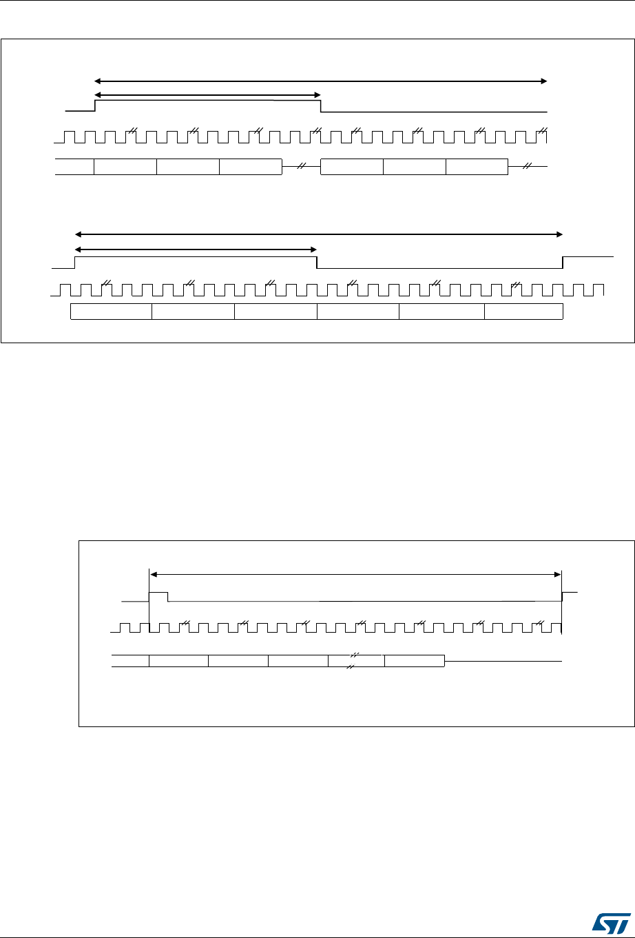
Serial audio interface (SAI) RM0090
920/1718 DocID018909 Rev 9
Figure 285. FS role is start of frame + channel side identification (FSDEF = TRIS = 1)
1. The frame length should be even.
If bit FSDEF in SAI_xFRCR is kept clear, so FS signal is equivalent to a start of frame, and
if the number of slots defined in bit NBSLOT[3:0] in SAI_xSLOTR multiplied by
the number of bits by slot configured in bit SLOTSZ[1:0] in SAI_xSLOTR is less than the
frame size (bit FRL[7:0] in the SAI_xFRCR register), then,
•if TRIS = 0 in the SAI_xCR2 register, the remaining bit after the last slot will be forced to
0 until the end of frame in case of transmission,
•if TRIS = 1, the line will be released to HI-Z during the transfer of these remaining bits.
In reception mode, these bits are discarded.
Figure 286. FS role is start of frame (FSDEF = 0)
29.8 Slot configuration
The slot is the basic element in the audio frame. The number of slots in the audio frame is
equal to the configured setting of bit NBSLOT[3:0] in the SAI_xSLOTR register +1.
The maximum number of slots per audio frame is fixed at 16.
For AC’97 protocol (when bit PRTCFG[1:0] = 10), the number of slots is automatically set to
target the protocol specification, and the value of NBSLOT[3:0] is ignored.
VFN
VORW
$XGLRIUDPH
)6
+DOIRIIUDPH
$XGLRIUDPH
)6
+DOIRIIUDPH
1XPEHURIVORWVQRWDOLJQHGZLWKWKHDXGLRIUDPH
1XPEHURIVORWVDOLJQHGZLWKWKHDXGLRIUDPH
-36
3LOT
VFN
VORW 3LOT 3LOT 3LOT 3LOT
3LOT
3LOT/. 3LOT/&& 3LOT/. 3LOT/. 3LOT/&& 3LOT/.
$XGLRIUDPH
'DWD DIWHUVORWQLI75,6
6'RXWSXWUHOHDVHG+,=DIWHUVORWQLI75,6
069
VFN
VORW 6ORW 6ORW 6ORW 6ORWQ
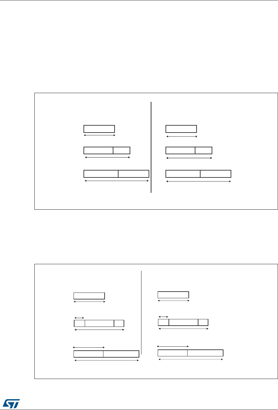
DocID018909 Rev 9 921/1718
RM0090 Serial audio interface (SAI)
951
Each slot can be defined as a valid slot, or not, by setting bit SLOTEN[15:0] in the
SAI_xSLOTR register. In an audio frame, during the transfer of a non-valid slot, 0 value will
be forced on the data line or the SD data line will be released to HI-z (refer to
Section 29.12.4) if the audio block is transmitter, or the received value from the end of this
slot will be ignored. Consequently, there will be no FIFO access and so no request to read
or write the FIFO linked to this inactive slot status.
The slot size is also configurable as shown in the Figure 287. The size of the slots is
selected by setting bit SLOTSZ[1:0] in the SAI_xSLOTR register. The size is applied
identically for each slot in an audio frame.
Figure 287. Slot size configuration with FBOFF = 0 in SAI_xSLOTR
It is possible to choose the position of the first data bit to transfer within the slots, this offset
is configured by bit FBOFF[5:0] in the SAI_xSLOTR register. 0 values will be injected in
transmitter mode from the beginning of the slot until this offset position is reached. In
reception, the bit in the offset phase is ignored. This feature targets the LSB justified
protocol (if the offset is equal to the slot size minus the data size).
Figure 288. First bit offset
069
;;
;; ;;
;GRQ¶WFDUH
$XGLREORFNLVWUDQVPLWWHU
6ORWVL]H GDWDVL]H
GDWDVL]H
GDWDVL]H
GDWDVL]H
GDWDVL]H
VORW[
VORW[
VORW[
ELW
ELW
$XGLREORFNLVUHFHLYHU
6ORWVL]H GDWDVL]H
GDWDVL]H
GDWDVL]H
GDWDVL]H
VORW[
VORW[
VORW[
ELW
ELW
GDWDVL]H
069
;;;;
;GRQ¶WFDUH
$XGLREORFNLVWUDQVPLWWHU
6ORWVL]H GDWDVL]H
GDWDVL]H
GDWDVL]H
GDWDVL]H
GDWDVL]H
VORW[
VORW[
VORW[
ELW
ELW
$XGLREORFNLVUHFHLYHU
)%2))
)%2)) 6/276='6
;;
6ORWVL]H GDWDVL]H
GDWDVL]H
GDWDVL]H
GDWDVL]H
GDWDVL]H
VORW[
VORW[
VORW[
ELW
ELW
;;
)%2))
)%2)) 6/276='6
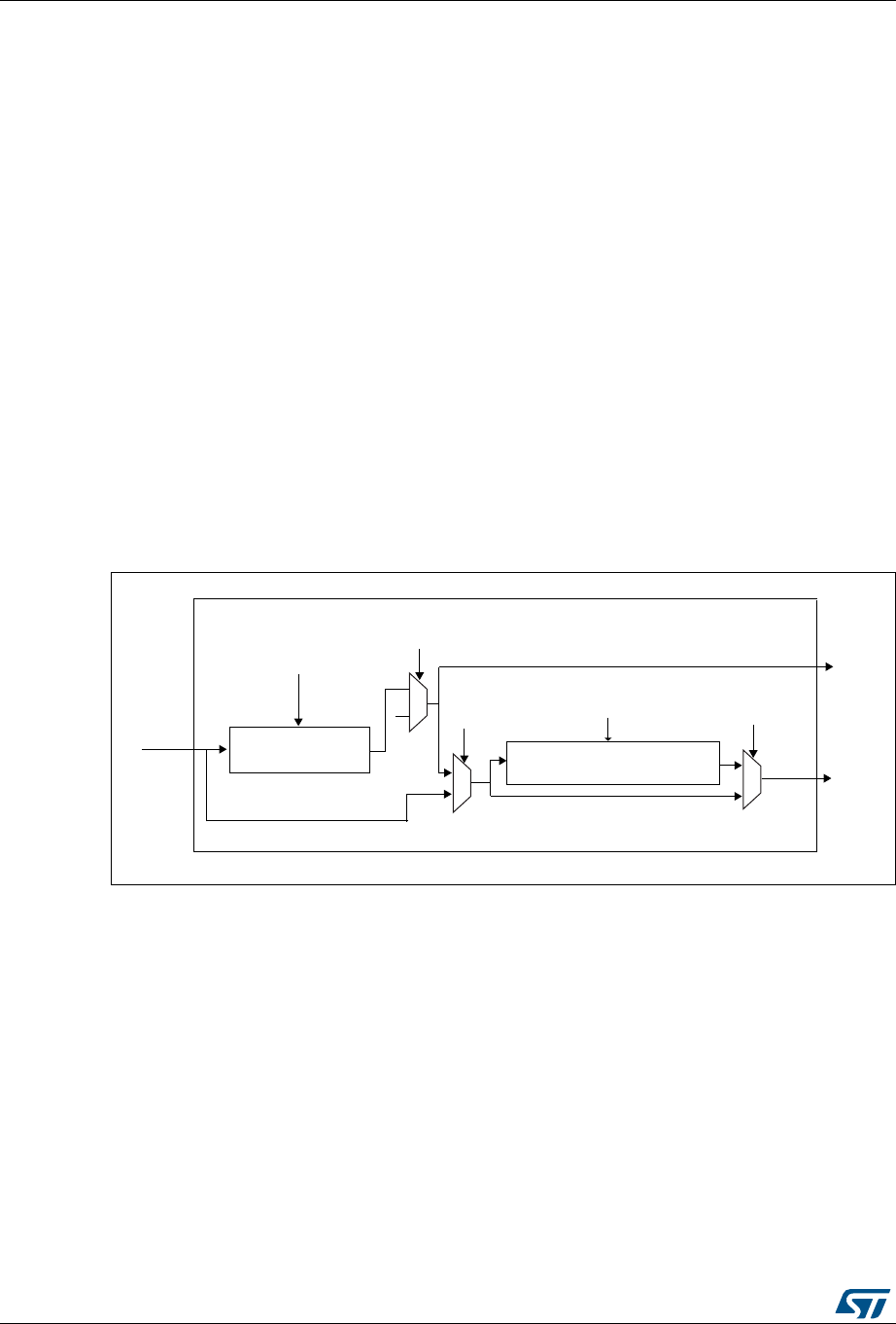
Serial audio interface (SAI) RM0090
922/1718 DocID018909 Rev 9
It is mandatory to respect the following conditions in order to avoid bad SAI behavior:
FBOFF ≤ (SLOTSZ - DS),
DS ≤ SLOTSZ,
NBSLOT x SLOTSZ ≤ FRL (frame length),
The number of slots should be even when bit FSDEF in the SAI_xFRCR register is set.
In AC’97 (bit PRTCFG[1:0] = 10), the slot size is automatically set as defined in
Section 29.11.
29.9 SAI clock generator
Each audio block has its own clock generator to make these two blocks completely
independent. There is no difference in terms of functionality between these two clock
generators. They are exactly the same.
When the audio block is defined as Master, the clock generator generates the
communication clock (the bit clock) and the master clock for external decoders.
When the audio block is defined as slave, the clock generator is OFF.
Figure 289 illustrates the architecture of the audio block clock generator.
Figure 289. Audio block clock generator overview
Note: If NoDiv is set to 1, the MCLK_x signal will be set at 0 level if this pin is configured as the
SAI pin in GPIO peripherals.
The clock source for the clock generator comes from the product clock controller. The
SAI_CK_x clock is equivalent to the master clock which may be divided for the external
decoders using bit MCKDIV[3:0]:
MCLK_x = SAI_CK_x / (MCKDIV[3:0] * 2), if MCKDIV[3:0] is not equal to 0000.
MCLK_x = SAI_CK_x, if MCKDIV[3:0] is equal to 0000.
MCLK_x signal is used only in TDM.
The division must be even in order to keep 50% on the Duty cycle on the MCLK output and
on the SCK_x clock. If bit MCKDIV[3:0] = 0000, division by one is applied to have MCLK_x
= SAI_CK_x.
In the SAI, the single ratio MCLK/FS = 256 is considered. Mostly, three frequency ranges
will be encountered as illustrated in the Table 129.
0DVWHUFORFN
GLYLGHU %LWFORFNGLYLGHU
0&.',9>@
6&.B[
0&/.B[
12',9
12',9
12',9
6$,B&.B[
069
)5/>@

DocID018909 Rev 9 923/1718
RM0090 Serial audio interface (SAI)
951
The master clock may be generated externally on an I/O pad for external decoders if the
corresponding audio block is declared as master with bit NODIV = 0 in the SAI_xCR1
register. In slave, the value set in this last bit is ignored since the clock generator is OFF,
and the MCLK_x I/O pin is released for use as a general purpose I/O.
The bit clock is derived from the master clock. The bit clock divider sets the divider factor
between the bit clock SCK_x and the master clock MCLK_x following the formula:
SCK_x = MCLK x (FRL[7:0] +1) / 256
where:
256 is the fixed ratio between MCLK and the audio frequency sampling.
FRL[7:0] is the number of bit clock - 1 in the audio frame, configured in the SAI_xFRCR
register.
It is mandatory in master mode that (FRL[7:0] +1) should be equal to a number with a power
of 2 (refer to Section 29.7) in order to have an even integer number of MCLK_x pulses by bit
clock. The 50% duty cycle is guaranteed on the bit clock SCK_x.
The SAI_CK_x clock can be also equal to the bit clock frequency. In this case, bit NODIV in
the SAI_xCR1 register should be set and the value inside the MCKDIV divider and the bit
clock divider will be ignored. In this case, the number of bits per frame is fully configurable
without the need to be equal to a power of two.
The bit clock strobing edge on SCK can be configured by bit CKSTR in the SAI_xCR1
register.
29.10 Internal FIFOs
Each audio block in the SAI has its own FIFO. Depending if the block is defined to be a
transmitter or a receiver, the FIFO will be written or read, respectively. There is therefore
only one FIFO request linked to FREQ bit in the SAI_xSR register.
Table 129. Example of possible audio frequency sampling range
Input SAI_CK_x clock
frequency
Most usual audio frequency
sampling achievable MCKDIV[3:0]
192 kHz x 256
192 kHz MCKDIV[3:0] = 0000
96 kHz MCKDIV[3:0] = 0001
48 kHz MCKDIV[3:0] = 0010
16 kHz MCKDIV[3:0] = 0100
8 kHz MCKDIV[3:0] = 1000
44.1 kHz x 256
44.1 kHz MCKDIV[3:0] = 0000
22.05 kHz MCKDIV[3:0] = 0001
11.025 kHz MCKDIV[3:0] = 0010
SAI_CK_x = MCLK(1)
1. This may happen when the product clock controller selects an external clock source, instead of PLL clock.
MCLK MCKDIV[3:0] = 0000

Serial audio interface (SAI) RM0090
924/1718 DocID018909 Rev 9
An interrupt is generated if FREQIE bit is enabled in the SAI_xIM register. This depends on:
•FIFO threshold setting (FLTH bits in SAI_CR2)
•Communication direction transmitter or receiver (see Section : Interrupt generation in
transmitter mode and Section : Interrupt generation in reception mode)
Interrupt generation in transmitter mode
The interrupt generation depends on the FIFO configuration in transmitter mode:
•When the FIFO threshold bits in SAI_XCR2 register are configured as FIFO empty
(FTH[2:0] set to 000b), an interrupt is generated (FREQ bit set by hardware to 1 in
SAI_XSR register) if no data are available in SAI_xDR register (FLTH[2:0] bits in SAI_xSR
is less than 001b). This Interrupt (FREQ bit in SAI_XSR register) is cleared by hardware
when the FIFO became not empty (FLTH[2:0] bits in SAI_xSR are different from 000b) i.e
one or more data are stored in the FIFO.
•When the FIFO threshold bits in SAI_XCR2 register are configured as FIFO quarter full
(FTH[2:0] set to 001b), an interrupt is generated (FREQ bit set by hardware to 1 in
SAI_XSR register) if less than a quarter of the FIFO contains data (FLTH[2:0] bits in
SAI_xSR are less than 010b). This Interrupt (FREQ bit in SAI_XSR register) is cleared by
hardware when at least a quarter of the FIFO contains data (FLTH[2:0] bits in SAI_xSR
are higher or equal to 010b).
•When the FIFO threshold bits in SAI_XCR2 register are configured as FIFO half full
(FTH[2:0] set to 010b), an interrupt is generated (FREQ bit set by hardware to 1 in
SAI_XSR register) if less than half of the FIFO contains data (FLTH[2:0] bits in SAI_xSR
are less than 011b). This Interrupt (FREQ bit in SAI_XSR register) is cleared by hardware
when at least half of the FIFO contains data (FLTH[2:0] bits in SAI_xSR are higher or
equal to 011b).
•When the FIFO threshold bits in SAI_XCR2 register are configured as FIFO three quarter
(FTH[2:0] set to 011b), an interrupt is generated (FREQ bit is set by hardware to 1 in
SAI_XSR register) if less than three quarters of the FIFO contain data (FLTH[2:0] bits in
SAI_xSR are less than 100b). This Interrupt (FREQ bit in SAI_XSR register) is cleared by
hardware when at least three quarters of the FIFO contain data (FLTH[2:0] bits in
SAI_xSR are higher or equal to 100b).
•When the FIFO threshold bits in SAI_XCR2 register are configured as FIFO full (FTH[2:0]
set to 100b), an interrupt is generated (FREQ bit is set by hardware to 1 in SAI_XSR
register) if the FIFO is not full (FLTH[2:0] bits in SAI_xSR is less than 101b). This Interrupt
(FREQ bit in SAI_XSR register) is cleared by hardware when the FIFO is full (FLTH[2:0]
bits in SAI_xSR is equal to 101b value).
Interrupt generation in reception mode
The interrupt generation depends on the FIFO configuration in reception mode:
•When the FIFO threshold bits in SAI_XCR2 register are configured as FIFO empty
(FTH[2:0] set to 000b), an interrupt is generated (FREQ bit is set by hardware to 1 in
SAI_XSR register) if at least one data is available in SAI_xDR register(FLTH[2:0] bits in
SAI_xSR is higher or equal to 001b). This Interrupt (FREQ bit in SAI_XSR register) is
cleared by hardware when the FIFO became empty (FLTH[2:0] bits in SAI_xSR is equal
to 000b) i.e no data is stored in FIFO.
•When the FIFO threshold bits in SAI_XCR2 register are configured as FIFO quarter fully
(FTH[2:0] set to 001b), an interrupt is generated (FREQ bit is set by hardware to 1 in
SAI_XSR register) if at less one quarter of the FIFO data locations are available

DocID018909 Rev 9 925/1718
RM0090 Serial audio interface (SAI)
951
(FLTH[2:0] bits in SAI_xSR is higher or equal to 010b). This Interrupt (FREQ bit in
SAI_XSR register) is cleared by hardware when less than a quarter of the FIFO data
locations become available (FLTH[2:0] bits in SAI_xSR is less than 010b).
•When the FIFO threshold bits in SAI_XCR2 register are configured as FIFO half fully
(FTH[2:0] set to 010b value), an interrupt is generated (FREQ bit is set by hardware to 1
in SAI_XSR register) if at least half of the FIFO data locations are available (FLTH[2:0]
bits in SAI_xSR is higher or equal to 011b). This Interrupt (FREQ bit in SAI_XSR register)
is cleared by hardware when less than half of the FIFO data locations become available
(FLTH[2:0] bits in SAI_xSR is less than 011b).
•When the FIFO threshold bits in SAI_XCR2 register are configured as FIFO three quarter
full(FTH[2:0] set to 011b value), an interrupt is generated (FREQ bit is set by hardware to
1 in SAI_XSR register) if at least three quarters of the FIFO data locations are available
(FLTH[2:0] bits in SAI_xSR is higher or equal to 100b). This Interrupt (FREQ bit in
SAI_XSR register) is cleared by hardware when the FIFO has less than three quarters of
the FIFO data locations avalable(FLTH[2:0] bits in SAI_xSR is less than 100b).
•When the FIFO threshold bits in SAI_XCR2 register are configured as FIFO full(FTH[2:0]
set to 100b), an interrupt is generated (FREQ bit is set by hardware to 1 in SAI_XSR
register) if the FIFO is full (FLTH[2:0] bits in SAI_xSR is equal to 101b). This Interrupt
(FREQ bit in SAI_XSR register) is cleared by hardware when the FIFO is not full
(FLTH[2:0] bits in SAI_xSR is less than 101b).
Like interrupt generation, the SAI can use the DMA if DMAEN bit in the SAI_xCR1 register is
set. The FREQ bit assertion mechanism is the same as the interruption generation
mechanism described above for FREQIE.
Each FIFO is an 8-word FIFO. Each read or write operation from/to the FIFO targets one
word FIFO allocation whatever the access size. Each FIFO word contains one audio frame.
FIFO pointers are incremented by one word after each access to the SAI_xDR register.
Data should be right aligned when it is written in the SAI_xDR.
Data received will be right aligned in the SAI_xDR.
The FIFO pointers can be reinitialized when the SAI is disabled by setting bit FFLUSH in the
SAI_xCR2 register. If FFLUSH is set when the SAI is enabled the data present in the FIFO
will be lost automatically.
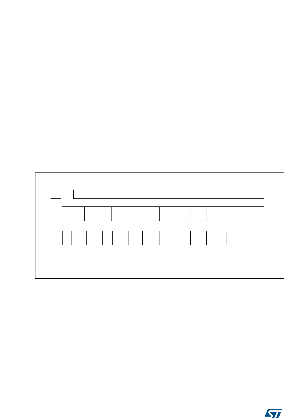
Serial audio interface (SAI) RM0090
926/1718 DocID018909 Rev 9
29.11 AC’97 link controller
The SAI is able to work as an AC’97 link controller. In this protocol:
•The slot number and the slot size are fixed.
•The frame synchronization signal is perfectly defined and has a fixed shape.
To select this protocol, set bit PRTCFG[1:0] in the SAI_xCR1 register to 10. When AC’97
mode is selected the data sizes that can be used are 16-bit or 20-bit only, else SAI behavior
is not guaranteed.
•Bits NBSLOT[3:0] and SLOTSZ[1:0] are consequently ignored.
•The number of slots is fixed at 13 slots. The first one is 16 bits wide and all the others
are 20 bits wide (data slots).
•Bit FBOFF[5:0] in the SAI_xSLOTR register is ignored
•The SAI_xFRCR register is ignored.
The FS signal from the block defined as asynchronous is configured automatically as an
output, since the AC’97 controller link drives the FS signal whatever the master or slave
configuration.
Figure 290 presents an AC’97 audio frame structure.
Figure 290. AC’97 audio frame
Note: In AC’97 protocol, bit 2 of the tag is reserved (always 0), so whatever the value written in the
SAI FIFO, bit 2 of the TAG is forced to 0 level.
For more details about TAG representation, please refer to the AC’97 protocol standard.
One SAI can be used to target an AC’97 point-to-point communication.
In receiver mode, the SAI acting as an AC’97 link controller will require no FIFO request and
so no data storage in the FIFO when the codec ready bit in the slot 0 is decoded low. If bit
CNRDYIE is enabled in the SAI_xIM register, flag CNRDY will be set in the SAI_xSR
register and an interrupt is generated. This flag is dedicated to the AC’97 protocol.
069
)6
6',
6'2
7DJ &0'
$''5
&0'
'$7$
/,1(
'$&
3&0
/)5217
3&0
5)5217
3&0
&(17(5
3&0
/6855
3&0
56855
3&0
/)(
/,1(
'$&
+6(7
'$&
,2
&75/
7DJ 67$786
$''5
67$786
'$7$
/,1(
$'&
3&0
/()7
3&0
5,*+7
3&0
0,&
565
9'
565
/9'
/,1(
$'& +6(7 ,2
67$786
565
9'

DocID018909 Rev 9 927/1718
RM0090 Serial audio interface (SAI)
951
29.12 Specific features
The SAI has some specific functions which can be useful depending on the audio protocol
selected. These functions are accessible through specific bits in the SAI_xCR2 register.
29.12.1 Mute mode
Mute mode may be used when the audio block is a transmitter or receiver.
Transmitter
In transmitter mode, Mute mode can be selected at anytime. Mute mode is active for entire
audio frames. The bit MUTE in the SAI_xCR2 register requests Mute mode when it is set
during an on-going frame.
The mute mode bit is strobed only at the end of the frame. If set at this time, the mute mode
is active at the beginning of the new audio frame, for a complete frame, until the next end of
frame, it then strobes the bit to determine if the next frame will still be a mute frame.
If the number of slots set in bit NBSLOT[3:0] in the SAI_xSLOTR register is lower than or
equal to two, it is possible to specify if the value sent during the Mute mode is 0 or if it is the
last value of each slot. The selection is done via bit MUTEVAL in the SAI_xCR2 register.
If the number of slots set in bit NBSLOT[3:0] in the SAI_xSLOTR register is greater than
two, MUTEVAL bit in the SAI_xCR2 has no meaning as 0 values are sent on each bit on
each slot.
During Mute mode, the FIFO pointers are still incremented, meaning that data which was
present in the FIFO and for which the Mute mode is requested is discarded.
Receiver
In receiver mode, it is possible to detect a Mute mode sent from the external transmitter
when all the declared and valid slots of the audio frame receive 0 for a given consecutive
number of audio frames (bit MUTECNT[5:0] in the SAI_xCR2 register).
When the number of MUTE frames is detected, flag MUTEDET in the SAI_xSR register is
set and an interrupt can be generated if bit MUTEDETIE is set in the SAI_xCR2.
The mute frame counter is cleared when the audio block is disabled or when a valid slot
receives at least one data in an audio frame. The interrupt is generated just once, when the
counter reaches the specified value in bit MUTECNT[5:0]. Then the interrupt event is re-
armed when the counter is cleared.
29.12.2 MONO/STEREO function
In transmission mode, it is possible to address the Mono mode without any data pre-
processing in memory when the number of slot is equal to 2 (NBSLOT[3:0] = 0001 in the
SAI_xSLOTR). In such a case, the access to and from the FIFO will be reduced by two
since in transmission, the data for slot 0 is duplicated into data slot 1.
To select the Mono feature, set bit MONO in the SAI_xCR1 register.
In reception mode, bit MONO can be set and has a meaning only if the number of slots is
equal to 2 like for the transmission mode. When it is set, only the data of slot 0 will be stored
in the FIFO. The data belonging to slot 1 will be discarded since in this case, it is supposed
to be the same as the previous slot. If the data flux in reception is a real stereo audio flow
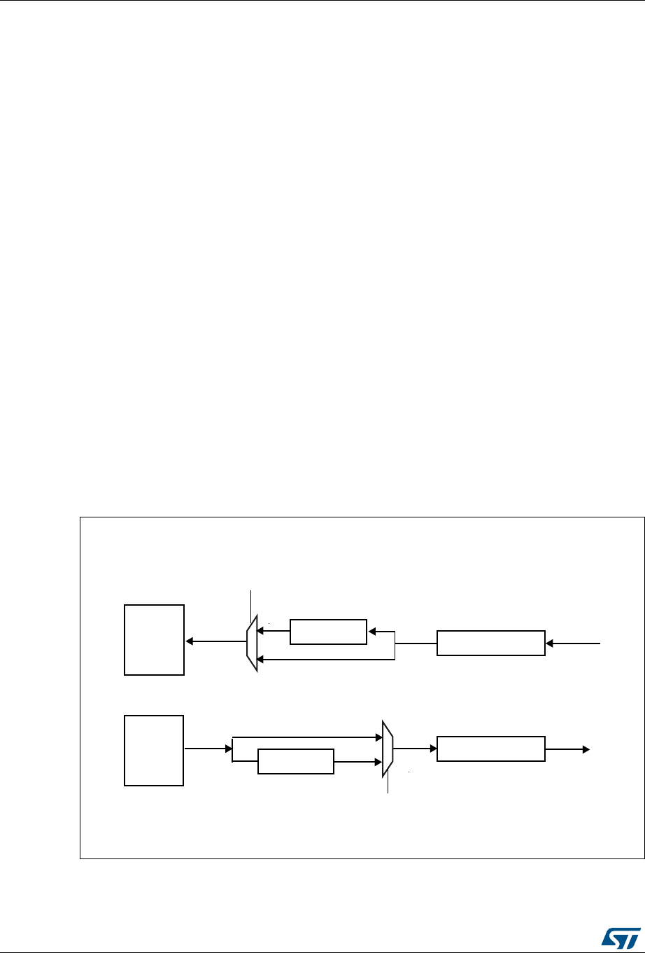
Serial audio interface (SAI) RM0090
928/1718 DocID018909 Rev 9
with a distinct and different left and right data, bit MONO has no meaning. The conversion
from the output stereo file to the equivalent mono file is done by software.
Note: To enable Mono mode, NBSLOT and SLOTEN must equal two and MONO bit set to 1.
29.12.3 Companding mode
Telecommunication applications may require to process the data to transmit or to receive
with a data companding algorithm.
Depending on the COMP[1:0] bit in the SAI_xCR2 register (used only when TDM mode is
selected), the software may choose to process or not the data before sending it on SD serial
output line (compression) or to expand the data after the reception on SD serial input line
(expansion) as illustrated in Figure 291,.The two companding modes supported are the µ-
Law and the A-Law log which are a part of the CCITT G.711 recommendation.
The companding standard employed in the United States and Japan is the µ-Law and allows
14 bits of dynamic range (COMP[1:0] = 10 in the SAI_xCR2 register).
The European companding standard is A-Law and allows 13 bits of dynamic range
(COMP[1:0] = 11 in the SAI_xCR2 register).
Companding standard (µ-Law or A-Law) can be computed based on 1’s complement or 2’s
complement representation depending on the CPL bit setting in the SAI_xCR2 register.
The µ-Law and A-Law formats encode data into 8-bit code elements with MSB alignment.
Companded data is always 8 bits wide. For this reason, bit DS[2:0] in the SAI_xCR1 register
will be forced to 010 when the SAI audio block is enabled (bit SAIxEN = 1 in the SAI_xCR1
register) and when the COMP[1:0] bit selects one of these two companding modes.
If no companding processing is required, COMP[1:0] bit in the SAI_xCR2 register should be
kept cleared.
Figure 291. Data companding hardware in an audio block in the SAI
Note: Not applicable when AC’97 selected.
H[SDQG
),)2
&203>@
&203>@
ELWVKLIWUHJLVWHU
6'
5HFHLYHUPRGHELW02'(>@ LQ6$,B[&5
7UDQVPLWWHUPRGHELW02'(>@ LQ6$,B[&5
069
ELWVKLIWUHJLVWHU
6'
FRPSUHVV
),)2

DocID018909 Rev 9 929/1718
RM0090 Serial audio interface (SAI)
951
Expansion or compression mode is automatically selected by the SAI configuration.
•If the SAI audio block is configured to be a transmitter, and if the COMP[1] bit is set in
the SAI_xCR2 register, the compression mode will be applied.
•If the SAI audio block is declared as a receiver, the expansion algorithm will be applied.
29.12.4 Output data line management on an inactive slot
In transmitter mode, it is possible to choose the behavior of the SD line in output when an
inactive slot is sent on the data line (via bit TRIS in the SAI_xCR2 register when the SAI is
disabled).
•Either the SAI forces 0 on the SD output line when an inactive slot is transmitted, or
•The line is released in HI-z state at the end of the last bit of data transferred, to release
the line for other transmitters connected to this node.
It is important to note that the two transmitters do not attempt to drive the same SD output
pin simultaneously, which could result in a short circuit. In order to ensure a gap between
transmissions, if the data is lower than 32-bit, the data can be extended to 32-bit by setting
bit SLOTSZ[1:0] = 10 in the SAI_xSLOTR register. Then, the SD output pin will be tristated
at the end of the LSB of the active slot (during the padding to 0 phase to extend the data to
32-bit) if the following slot is declared inactive.
In addition, if the number of slots multiplied by the slot size is lower than the frame length,
the SD output line will be tristated when the padding to 0 is done to complete the audio
frame.
Figure 292 illustrates these behaviors.
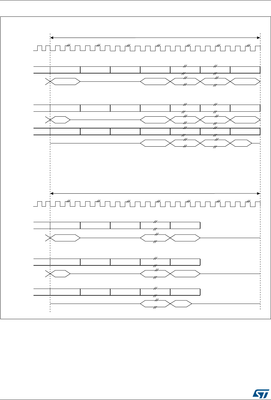
Serial audio interface (SAI) RM0090
930/1718 DocID018909 Rev 9
Figure 292. Tristate strategy on SD output line on an inactive slot
When the selected audio protocol uses the FS signal as a start of frame and a channel side
identification (bit FSDEF = 1 in the SAI_xFRCR register), the tristate mode is managed
according to Figure 293 (where bit TRIS in the SAI_xCR1 register = 1, and FSDEF=1, and
half frame length > number of slots/2, and NBSLOT=6).
VORW
$XGLRIUDPH
%LW75,6 LQWKH6$,B[&5DQGIUDPHOHQJWK QXPEHURIVORWV
069
6ORWVL]H GDWDVL]H
6ORWVL]H!GDWDVL]H
%LW75,6 LQWKH6$,B[&5DQGIUDPHOHQJWK!QXPEHURIVORWV
6'RXWSXW
SCK
3LOT/. 3LOT/&& 3LOT/&& 3LOT/. /. /. 3LOTN/.
$ATA $ATA $ATAM
3LOT/. 3LOT/&& 3LOT/&& 3LOT/. /. /. 3LOTN/.
$ATA $ATA $ATAM
3LOT/. 3LOT/&& 3LOT/&& 3LOT/. /. /. 3LOTN/.
$ATA $ATAM
VORW
6'RXWSXW
VORW
6'RXWSXW
VORW
$XGLRIUDPH
6ORWVL]H GDWDVL]H
6'RXWSXW
SCK
3LOT/. 3LOT/&& 3LOT/&& /. 3LOTN/.
$ATA $ATAM
VORW
6ORWVL]H!GDWDVL]H
6'RXWSXW
3LOT/. 3LOT/&& 3LOT/&& /. 3LOTN/.
$ATAM
$ATA
VORW
6'RXWSXW
3LOT/. 3LOT/&& 3LOT/&& /.
$ATAM
/.
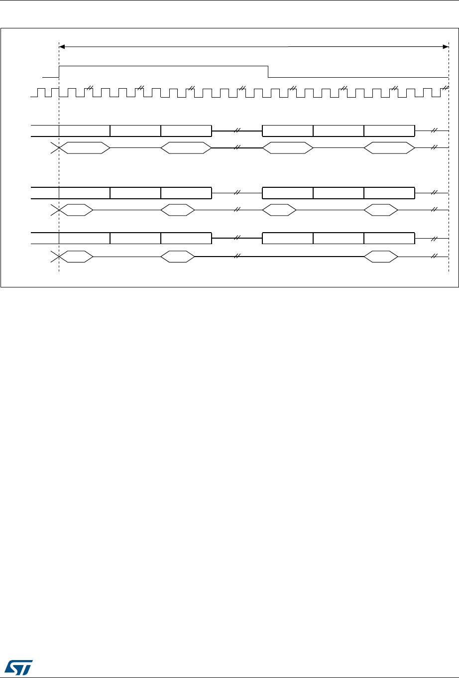
DocID018909 Rev 9 931/1718
RM0090 Serial audio interface (SAI)
951
Figure 293. Tristate on output data line in a protocol like I2S
If the TRIS bit in the SAI_xCR2 register is cleared, all the High impedance states on the SD
output line on Figure 292 and Figure 293 are replaced by a drive with a value of 0.
29.13 Error flags
The SAI embeds some error flags:
– FIFO overrun/underrun,
– Anticipated frame synchronization detection,
– Late frame synchronization detection,
– Codec not ready (AC’97 exclusively),
– Wrong clock configuration in master mode.
29.13.1 FIFO overrun/underrun (OVRUDR)
The FIFO Overrun/Underrun bit is called OVRUDR in the SAI_xSR register.
The overrun or underrun errors occupy the same bit since an audio block can be either
receiver or transmitter and each audio block in an SAI has its own SAI_xSR register.
Overrun
When the audio block is configured as receiver, an overrun condition may appear if data is
received in an audio frame when the FIFO is full and is not able to store the received data.
In this case, the received data is lost, the flag OVRUDR in the SAI_xSR register is set and
an interrupt is generated if bit OVRUDRIE is set in the SAI_xIM register. The slot number
from which the overrun occurs, is stored internally. No more data will be stored into the FIFO
until it becomes free to store new data. When the FIFO has at least one data free, the SAI
audio block receiver will store new data (from new audio frame) from the slot number which
VORW
069
6ORWVL]H GDWDVL]H
6ORWVL]H!GDWDVL]H
6'RXWSXW
SCK
3LOT/. 3LOT/&& 3LOT/. 3LOT/. 3LOT/&& 3LOT/.
$ATA $ATA
3LOT/. 3LOT/&& 3LOT/.
$ATA
VORW
6'RXWSXW
$ATA $ATA
3LOT/. 3LOT/&& 3LOT/.
$ATA $ATA $ATA
3LOT/. 3LOT/&& 3LOT/.
$ATA
VORW
6'RXWSXW
3LOT/. 3LOT/&& 3LOT/.
$ATA $ATAM
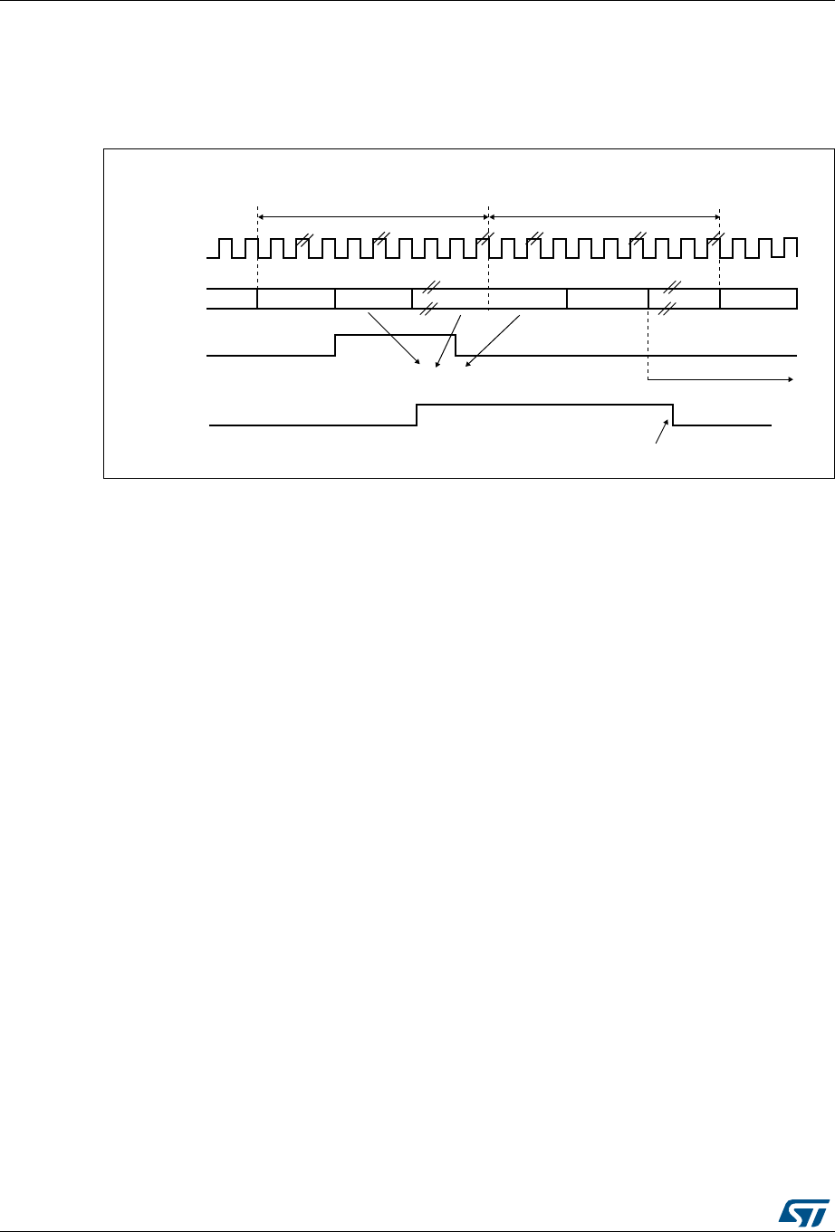
Serial audio interface (SAI) RM0090
932/1718 DocID018909 Rev 9
was stored internally when the overrun condition was detected, and this, to avoid data slot
de-alignment in the destination memory (refer to Figure 294).
The OVRUDR flag is cleared when bit COVRUDR is set in the SAI_xCLRFR register.
Figure 294. Overrun detection error
Underrun
An underrun may occur when the audio block in the SAI is a transmitter and the FIFO is
empty when data needs to be transmitted (the audio block configuration (Master or Slave) is
not relevant). If an underrun is detected, the software must resynchronize data and slot.
Proceed as follows:
1. Disable the SAI peripheral by resetting the SAIEN bit of the SAI_xCR1 register. Check
that the SAI has been disabled by reading back the SAIEN bit (SAIEN should be equal
to 0).
2. Flush the Tx FIFO through the FFLUS bit of the SAI_xCR2 register.
3. Re-assigned to the correct data to be transferred on the first active slot of the new
frame.
4. Re-enabling the SAI peripheral (SAIEN bit set to 1).
The underrun event sets the OVRUDR flag in the SAI_xSR register and an interrupt is
generated if the OVRUDRIE bit is set in the SAI_xIM register. To clear this flag, set the
COVRUDR bit in the SAI_xCLRFR register.
069
VFN
GDWD 6ORW21
([DPSOH),)2RYHUUXQRQ6ORW
$XGLRIUDPH $XGLRIUDPH
6ORWQ2121
),)2IXOO
2958'5
6ORW21 3LOT/. 6ORW21 6ORW21
5HFHLYHGGDWDGLVFDUGHG 'DWDVWRUHGDJDLQLQ),)2
&2958'5

DocID018909 Rev 9 933/1718
RM0090 Serial audio interface (SAI)
951
Figure 295. FIFO underrun event
29.13.2 Anticipated frame synchronisation detection (AFSDET)
This flag AFSDET is used only in Slave mode. In master mode, it is never asserted. It
informs about the detection of a frame synchronisation (FS) earlier than expected since the
frame length, the frame polarity, the frame offset are defined and known.
Early detection sets flag AFSDET in the SAI_xSR register.
This detection has no effect on the current audio frame which is not sensitive to the
anticipated FS. This means that “parasitic” events on signal FS are flagged without any
perturbation of the current audio frame.
If bit AFSDETIE is set in the SAI_xIM register, an interrupt is generated. To clear the flag
AFSDET, bit CAFSDET in the SAI_xCLRFR register has to be set.
To resynchronize with the master after Anticipated frame detection error, four steps should
be respected:
1. SAI block should be disabled by resetting SAIEN bit in SAI_xCR1 register, to be sure
that the SAI is disabled SAIEN bit is should be equal to 0 (reading back this bit).
2. FIFO should be flushed via FFLUS bit in SAI_xCR2 register.
3. Re-enabling the SAI peripheral (SAIEN bit set to 1) then the SAI.
4. SAI block will wait for the assertion on FS to restart the synchronization with master.
Note: This flag is not asserted in AC’97 since the SAI audio block acts as a link controller and
generates the FS signal even when declared as slave.
29.13.3 Late frame synchronization detection
Flag LFSDET in the SAI_xSR register can be set only when the SAI audio block is defined
as slave. The frame length, the frame polarity and the frame offset configuration are known
in register SAI_xFRCR.
If the external master does not send the FS signal at the expecting time (generating the
signal too late), the flag LFSDET in the SAI_xSR register will be set and an interrupt is
generated if bit LFSDETIE in the SAI_xIM register is set.
The flag is cleared when bit CLFSDET is set in the SAI_xCLRFR register.
-36
VFN
GDWD 6ORW21 087(
3LOTSIZEDATASIZE
6'RXWSXW
([DPSOH),)2XQGHUUXQRQ6ORW
$XGLRIUDPH $XGLRIUDPH
087( 6ORW21 21 6ORW21
29581'
087(
),)2HPSW\
29581'

Serial audio interface (SAI) RM0090
934/1718 DocID018909 Rev 9
The late frame synchronisation detection flag is set when the error is detected, SAI needs to
be resynchronized with the master (the four steps described above should be respected).
This detection and flag assertion can detect glitches on the SCK clock in a noisy
environment, detected by the state machine of the audio block. It could incorrectly shift the
SAI audio block state machine from one state in the current audio frame, thus corrupting the
frame.
There is no corruption if the external master is not managing the audio data frame transfer in
a continuous mode, which should not be the case for most application purposes. In this
case, flag LFSDET will be set.
Note: This flag is not asserted in AC’97 mode since the SAI audio block acts as a link controller
and generates the FS signal even when declared as slave.
29.13.4 Codec not ready (CNRDY AC’97)
The flag CNRDY in the SAI_xSR register is relevant only if the SAI audio block is configured
to work in AC’97 mode (bit PRTCFG[1:0] = 10 in the SAI_xCR1 register). If bit CNRDYIE is
set in the SAI_xIM register, an interrupt will be generated when the flag CNRDY is set.
It is asserted when the codec is not ready to communicate during the reception of the TAG 0
(slot0) of the AC’97 audio frame. In this case, there will be no data automatically stored into
the FIFO since the codec is not ready, until the TAG 0 indicates that the codec is ready. All
the active slots defined in the SAI_xSLOTR register will be captured when the codec is
ready.
To clear the flag, bit CCNRDY in the SAI_xCLRFR register has to be set.
29.13.5 Wrong clock configuration in master mode (with NODIV = 0)
When the audio block is master (MODE[1] = 0 in the SAI_xCR1 register) and if bit NODIV in
the SAI_xCR1 is clear, the flag WCKCFG will be set if bit FRL[7:0] in the SAI_xFRCR is not
set with a proper value when the SAIxEN bit in the SAI_xCR1 register is set, in order to
respect this following rule:
where n is in the range from 3 to 8.
If bit WCKCFGIE is set, an interrupt is generated when flag WCKCFG is set in the SAI_xSR
register. To clear the flag, set bit CWCKCFG bit in the SAI_xCLRFR register.
When bit WCKCFG is set, the audio block is automatically disabled, clearing bit SAIxEN in
the SAI_xCR1 register via hardware.
The above formula is intended to guarantee that the number of MCLK pulses by bit clock is
an even integer in the audio frame with a 50% duty cycle bit clock generation to guarantee
the good quality of the audio sounds or acquisitions.
FRL[7,0]()1+2n
=

DocID018909 Rev 9 935/1718
RM0090 Serial audio interface (SAI)
951
29.14 Interrupt sources
The SAI has 7 possible interrupt sources as illustrated by Table .
Below are the SAI configuration steps to follow when an interrupt occurs:
1. Disable SAI interrupt.
2. Configure SAI.
3. Configure SAI interrupt source.
4. Enable SAI.
29.15 Disabling the SAI
The audio block in the SAI can be disabled at any moment by clearing bit SAIxEN in the
SAI_xCR1 register. All the frames that have already started will be automatically completed
before the total extinction of the SAI. Bit SAIxEN in the SAI_xCR1 register will stay high until
the SAI is completely switched-off at the end of the current audio frame transfer.
Table 130. Interrupt sources
Interrupt
source
Interru
pt
group
Audio block mode Interrupt enable Interrupt clear
FREQ FREQ Master or Slave
Receiver or transmitter
FREQIE in
SAI_xIM register
Depend on:
- FIFO threshold setting
(FLTH bits in SAI_CR2)
- Communication direction
transmitter or receiver
for more details please refer
to Internal FIFOs section
OVRUDR ERROR Master or Slave
Receiver or transmitter
OVRUDRIE in
SAI_xIM register
COVRUDR = 1 in
SAI_xCLRFR register
AFSDET ERROR
Slave
(Not used in AC’97
mode)
AFSDETIE in
SAI_xIM register
CAFSDET = 1 in
SAI_xCLRFR register
LFSDET ERROR
Slave
(Not used in AC’97
mode)
LFSDETIE in
SAI_xIM register
CLFSDET = 1 in
SAI_xCLRFR register
CNRDY ERROR Slave
(Only in AC’97 mode)
CNRDYIE in
SAI_xIM register
CCNRDY = 1 in
SAI_xCLRFR register
MUTEDE
TMUTE Master or slave
Receiver mode only
MUTEDETIE in
SAI_xIM register
CMUTEDET = 1 in
SAI_xCLRFR register
WCKCFG ERROR
Master with NODIV = 0
in the SAI_xCR1
register
WCKCFGIE in
SAI_xIM register
CWCKCFG = 1 in
SAI_xCLRFR register

Serial audio interface (SAI) RM0090
936/1718 DocID018909 Rev 9
If there is an audio block in the SAI synchronous with the other one, the one which is the
master must be disabled first.
29.16 SAI DMA interface
In order to free the CPU and to optimize the bus bandwidth, each SAI audio block has an
independent DMA interface in order to read or to write into the SAI_xDR register (to hit the
internal FIFO). There is one DMA channel per audio block following basic DMA
request/acknowledge protocol.
To configure the audio block to transfer through the DMA interface, set bit DMAEN in the
SAI_xCR1 register. The DMA request is managed directly by the FIFO controller depend of
FIFO threshold level (for more details please refer to Internal FIFOs section). DMA direction
is linked to the SAI audio block configuration:
•If the audio block is a transmitter, the audio block’s FIFO controller outputs a DMA
request to load the FIFO with data written in the SAI_xDR register.
•If the audio block is a receiver, the DMA request will concern read operations from the
SAI_xDR register.
Below are the SAI configuration steps followed when DMA is used:
1. Configure SAI and FIFO Threshold level (in order to specify when the DMA request to
be launched)
2. Configure SAI DMA channel
3. Enable DMA
4. Enable SAI
Note: Before configuring the SAI block, the SAI DMA channel must be disabled.

DocID018909 Rev 9 937/1718
RM0090 Serial audio interface (SAI)
951
29.17 SAI registers
29.17.1 SAI xConfiguration register 1 (SAI_xCR1) where x is A or B
Address offset: Block A: 0x004
Address offset: Block B: 0x024
Reset value: 0x0000 0040
31 30 29 28 27 26 25 24 23 22 21 20 19 18 17 16
Reserved MCKDIV[3:0] NODIV Res. DMAEN SAIxEN
rw rw rw rw rw rw rw
15 14 13 12 11 10 9 8 7 6 5 4 3 2 1 0
Reserved
OutDri
vMONO SYNCEN[1:0] CKSTR LSBFIR
ST DS[2:0] Res. PRTCFG[1:0] MODE[1:0]
rw rw rw rw rw rw rw rw rw rw rw rw rw
Bits 31:24 Reserved, always read as 0.
Bit 23:20 MCKDIV[3:0]: Master clock divider. These bits are set and cleared by software.
0000: Divides by 1 the master clock input.
Otherwise, The Master clock frequency is calculated accordingly to the following formula:
MCLK_x = SAI_CK_x / (MCKDIV[3:0] * 2)
These bits have no meaning when the audio block is slave.
They have to be configured when the audio block is disabled.
Bit 19 NODIV: No divider. This bit is set and cleared by software.
0: Master Clock divider is enabled
1: No divider used in the clock generator (in this case Master Clock Divider bit has no effect)
Bit 18 Reserved, always read as 0.
Bit 17 DMAEN: DMA enable. This bit is set and cleared by software.
0: DMA is disabled
1: DMA is enabled
Note: In receiver mode, the bits MODE must be configured before setting bit DMAEN to avoid a DMA
request since the audio block is transmitter after reset (default setting)
Bit 16 SAIxEN: Audio block enable where x is A or B. This bit is set by software. It is cleared by hardware,
after disabling it by software (writing the bit low), the audio is completely disabled (waiting for the end
of the current frame).
0: Audio block is disabled
1: Audio block is enabled: this bit can be set only if it is at 0 during the write operation (means the
SAI is completely disabled before being re-enabled).
This bit allows to control the state of the audio block. If it is disabled somewhere in an audio frame,
the on-going transfer will be completed and the cell will be totally disabled at the end of this audio
frame transfer.
Note: When SAIx block is configured as master mode, clock must be present on the input of the SAI
before setting SAIxEN bit.
Bits 15:14 Reserved, always read as 0.
Bit 13 OUTDRIV: Output drive. This bit is set and cleared by software.
0: Audio block output driven when SAIEN is set
1: Audio block output driven immediately after the setting of this bit.
Note: This bit has to be set before enabling the audio block but after the audio block configuration.

Serial audio interface (SAI) RM0090
938/1718 DocID018909 Rev 9
Bit 12 MONO: Mono mode. This bit is set and cleared by software.
0: Stereo mode
1: Mono mode.
This bit has a meaning only when the number of slots is equal to 2.
When the Mono mode is selected, the data of the slot 0 data is duplicated on the slot 1 when the
audio block is a transmitter. In reception mode, the slot1 is discarded and only the data received
from the slot 0 will be stored.
Refer to Section 29.12.2 for more details.
Bits 11:10 SYNCEN[1:0]: Synchronization enable. This bit is set and cleared by software.
00: audio block is asynchronous.
01: audio block is synchronous with the other internal audio block. In this case audio block should be
configured in Slave mode
10: Reserved.
11: Not used
These bits have to be configured when the audio block is disabled.
Bit 9 CKSTR: Clock strobing edge. This bit is set and cleared by software.
0: data strobing edge is falling edge of SCK
1: data strobing edge is rising edge of SCK
This bit has to be configured when the audio block is disabled.
Bit 8 LSBFIRST: Least significant bit first. This bit is set and cleared by software.
0: data is transferred with the MSB of the data first
1: data is transferred with the LSB of the data first
This bit has to be configured when the audio block is disabled.
This bit has no meaning in AC’97 audio protocol since in AC’97 data is transferred with the MSB of
the data first.
Bits 7:5 DS[2:0]: Data size. These bits are set and cleared by software.
000: Not used
001: Not used
010: 8-bit
011: 10-bit
100: 16-bit
101: 20-bit
110: 24-bit
111: 32-bit
When the companding mode is selected (bit COMP[1:0]), these DS[1:0] are ignored since the data
size is fixed to 8-bit mode by the algorithm itself.
These bits must be configured when the audio block is disabled.
Note: When AC’97 mode is selected the data sizes that can be used are: 16-bit or 20-bit only, else
SAI behavior is not guaranteed.

DocID018909 Rev 9 939/1718
RM0090 Serial audio interface (SAI)
951
Bit 4 Reserved, always read as 0.
Bits 3:2 PRTCFG[1:0]: Protocol configuration. These bits are set and cleared by software.
00: Free protocol
01: Not used
10: AC’97 protocol
11: Not used
Free protocol selection allows to use the powerful configuration of the audio block to address a
specific audio protocol (like I2S, LSB/MSB justified, TDM, PCM/DSP...) setting most of the
configuration register bits as well as frame configuration register.
These bits have to be configured when the audio block is disabled.
Bits 1:0 MODE[1:0]: Audio block mode. These bits are set and cleared by software.
00: Master transmitter
01: Master receiver
10: Slave transmitter
11: Slave receiver
These bits have to be configured when the audio block is disabled.
Note: In Master transmitter mode the audio block will start to generate the FS and clocks

Serial audio interface (SAI) RM0090
940/1718 DocID018909 Rev 9
29.17.2 SAI xConfiguration register 2 (SAI_xCR2) where x is A or B
Address offset: Block A: 0x008
Address offset: Block B: 0x028
Reset value: 0x0000 0000
31 30 29 28 27 26 25 24 23 22 21 20 19 18 17 16
Reserved
15 14 13 12 11 10 9 8 7 6 5 4 3 2 1 0
COMP[1:0] CPL MUTECNT[5:0] MUTE
VAL Mute TRIS FFLUS FTH
rw rw rw rw rw rw rw rw rw rw rw rw rw rw rw rw
Bits 31:16 Reserved, always read as 0
Bits 15:14 COMP[1:0]: Companding mode. These bits are set and cleared by software.
00: No companding algorithm
01: Reserved.
10: µ-Law algorithm
11: A-Law algorithm
The µ-Law and the A-Law log are a part of the CCITT G.711 recommendation, the type of
complement that will be used depends on ComPLement bit.
The data expansion or data compression are determined by the state of bit MODE[0].
The data compression is applied if the audio block is configured as a transmitter.
The data expansion is automatically applied when the audio block is configured as a receiver.
Refer to Section 29.12.3 for more details.
Note: Companding mode is applicable only when TDM is selected.
Bit 13 CPL: Complement bit. This bit is set and cleared by software.
It defines the type of complement to be used for companding mode
0: 1’s complement representation.
1: 2’s complement representation.
Note: This bit has effect only when the companding mode is µ-Law algorithm or A-Law algorithm.
Bits 12:7 MUTECNT[5:0]: Mute counter. These bits are set and cleared by software.
These bits are used only in reception mode.
The value set in these bits is compared to the number of consecutive mute frames detected in
reception. When the number of mute frames is equal to this value, the flag MUTEDET will be set and
an interrupt will be generated if bit MUTEDETIE is set.
Refer to Section 29.12.1 for more details.

DocID018909 Rev 9 941/1718
RM0090 Serial audio interface (SAI)
951
Bit 6 MUTEVAL: Mute value. This bit is set and cleared by software.This bit has to be written before
enabling the audio block: SAIxEN.
0: Bit value 0 is sent during the MUTE mode.
1: Last values are sent during the MUTE mode.
This bit has a meaning only when the audio block is a transmitter and when the number of slots is
lower or equal to 2 and if the MUTE bit is set.
If more slots are declared, the bit value sent during the transmission in mute mode will be equal to 0,
whatever the value of this MUTEVAL bit.
if the number of slot is lower or equal to 2 and MUTEVAL = 1, the mute value transmitted for each
slot will be the ones sent during the previous frame.
Refer to Section 29.12.1 for more details.
Bit 5 MUTE: Mute. This bit is set and cleared by software.
0: No Mute mode.
1: Mute mode enabled.
This bit has a meaning only when the audio block is a transmitter. The MUTE value is linked to the
MUTEVAL value if the number of slots is lower or equal to 2, or equal to 0 if it is greater than 2.
Refer to Section 29.12.1 for more details.
Bit 4 TRIS: Tristate management on data line. This bit is set and cleared by software.
0: SD output line is still driven by the SAI when a slot is inactive.
1: SD output line is released (HI-Z) at the end of the last data bit of the last active slot if the next one
is inactive.
This bit has a meaning only if the audio block is configured to be a transmitter.
This bit should be configured when SAI is disabled.
Refer to Section 29.12.4 for more details.
Bit 3 FFLUSH: FIFO flush. This bit is set by software. It is always read low.
0: No FIFO flush.
1: FIFO flush.
Writing 1 to the bit triggers the FIFO Flush. All the internal FIFO pointers (read and write) are
cleared.
Data still present in the FIFO will be lost in such case (no more transmission or received data lost).
This bit should be configured when SAI is disabled.
Before flushing SAI, DMA stream/interruption must be disabled
Bits 2:0 FTH: FIFO threshold. This bit is set and cleared by software.
000: FIFO empty
001: ¼ FIFO
010: ½ FIFO
011: ¾ FIFO
100: FIFO full
101: Reserved
110: Reserved
111: Reserved

Serial audio interface (SAI) RM0090
942/1718 DocID018909 Rev 9
29.17.3 SAI xFrame configuration register (SAI_XFRCR) where x is A or B
Address offset: Block A: 0x00C
Address offset: Block B: 0x02C
Reset value: 0x0000 0007
Note: This register has no meaning in AC’97 audio protocol
31 30 29 28 27 26 25 24 23 22 21 20 19 18 17 16
Reserved FSOFF FSPOL FSDEF
rw rw r
15 14 13 12 11 10 9 8 7 6 5 4 3 2 1 0
Res. FSALL[6:0] FRL[7:0]
rw rw rw rw rw rw rw rw rw rw rw rw rw rw rw
Bits 31:19 Reserved, always read as 0.
Bit 18 FSOFF: Frame synchronization offset. This bit is set and cleared by software.
0: FS is asserted on the first bit of the slot 0.
1: FS is asserted one bit before the first bit of the slot 0.
This bit has no meaning and is not used in AC’97 audio block configuration.
This bit must be configured when the audio block is disabled.
Bit 17 FSPOL: Frame synchronization polarity. This bit is set and cleared by software
0: FS is active low (falling edge)
1: FS is active high (rising edge)
This bit is used to configure the level of the start of frame on the FS signal.
This bit has no meaning and is not used in AC’97 audio block configuration.
This bit must be configured when the audio block is disabled.
Bit 16 FSDEF: Frame synchronization definition. This bit is set and cleared by software.
0: FS signal is a start frame signal
1: FS signal is a start of frame signal + channel side identification
When the bit is set, the number of slots defined in the SAI_ASLOTR register has to be even. It
means that there will be half of this number of slots dedicated for the left channel and the other slots
for the right channel (e.g: this bit has to be set for I2S or MSB/LSB-justified protocols...)
This bit has no meaning and is not used in AC’97 audio block configuration.
This bit must be configured when the audio block is disabled.

DocID018909 Rev 9 943/1718
RM0090 Serial audio interface (SAI)
951
Bit 15 Reserved, always read as 0.
Bits 14:8 FSALL[6:0]: Frame synchronization active level length. These bits are set and cleared by software
The value set in these bits specifies the length in number of bit clock (SCK) + 1 (FSALL[6:0] + 1) of
the active level of the FS signal in the audio frame
These bits have no meaning and are not used in AC’97 audio block configuration.
These bits must be configured when the audio block is disabled.
Bits 7:0 FRL[7:0]: Frame length. These bits are set and cleared by software.
They define the length of the audio frame. More precisely, these bits define the number of SCK
clocks for each audio frame.
The number of bits in the frame is equal to FRL[7:0] + 1.
The minimum number of bits to transfer in an audio frame has to be equal to 8 or else the audio
block will have unexpected behavior. This is the case when the data size is 8-bit and only one slot 0
is defined in NBSLOT[4:0] in the SAI_ASLOTR register (NBSLOT[3:0] = 0000).
In master mode, if the master clock MCLK_x pin is declared as an output, the frame length should
be aligned to a number equal to a power of 2, from 8 to 256 in order to keep in an audio frame, an
integer number of MCLK pulses by bit clock for correct operation for external DAC/ADC inside the
decoders.
The Frame length should be even.
These bits have no meaning and are not used in AC’97 audio block configuration.

Serial audio interface (SAI) RM0090
944/1718 DocID018909 Rev 9
29.17.4 SAI xSlot register (SAI_xSLOTR) where x is A or B
Address offset: Block A: 0x010
Address offset: Block B: 0x030
Reset value: 0x0000 0000
Note: This register has no meaning in AC’97 audio protocol
31 30 29 28 27 26 25 24 23 22 21 20 19 18 17 16
SLOTEN[15:0]
rw rw rw rw rw rw rw rw rw rw rw rw rw rw rw rw
15 14 13 12 11 10 9 8 7 6 5 4 3 2 1 0
Reserved NBSLOT[3:0] SLOTSZ[1:0] Res FBOFF[4:0]
rw rw rw rw rw rw rw rw rw rw rw
Bits 31:16 SLOTEN[15:0]: Slot enable. These bits are set and cleared by software.
Each bit of the SLOTEN bits identify a slot position from 0 to 15 (maximum 16 slots)
0: Inactive slot.
1: Active slot.
These bits must be set when the audio block is disabled.
They are ignored in AC’97 mode.
Bits 15:12 Reserved, always read as 0.
Bits 11:8 NBSLOT[3:0]: Number of slots in an audio frame. These bits are set and cleared by software.
The value set in these bits register represents the number of slots + 1 in the audio frame (including
the number of inactive slots). The maximum number of slots is 16.
The number of slots should be even if bit FSDEF in the SAI_AFRCR register is set.
If the size is greater than the data size, the remaining bits will be forced to 0 if bit TRIS in the
SAI_xCR1 register is clear, otherwise they will be forced to 0 if the next slot is active or the SD line
will be forced to HI-Z if the next slot is inactive and bit TRIS = 1.
These bits must be set when the audio block is disabled.
They are ignored in AC’97 omode.
Bits 7:6 SLOTSZ[1:0]: Slot size
This bits is set and cleared by software.
00: The slot size is equivalent to the data size (specified in DS[3:0] in the SAI_ACR1 register).
01: 16-bit
10: 32-bit
11: Reserved
The slot size must be greater or equal to the data size. If this condition is not respected, the behavior
of the SAI will be undetermined.
These bits must be set when the audio block is disabled.
They are ignored in AC’97 mode.
Bit 1 Reserved, always read as 0.
Bits 4:0 FBOFF[4:0]: First bit offset
These bits are set and cleared by software.
The value set in these bits represents the position of the first data transfer bit in the slot. It represents
an offset value. During this offset phase 0 value are sent on the data line for transmission mode. For
reception mode, the received bit are discarded during the offset phase.
These bits must be set when the audio block is disabled.
They are ignored in AC’97 mode.

DocID018909 Rev 9 945/1718
RM0090 Serial audio interface (SAI)
951
29.17.5 SAI xInterrupt mask register2(SAI_xIM) where x is A or B
Address offset: blockA: 0x014
Address offset: block B: 0x034
Reset value: 0x0000 0000
31 30 29 28 27 26 25 24 23 22 21 20 19 18 17 16
Reserved
15 14 13 12 11 10 9 8 7 6 5 4 3 2 1 0
Reserved
LFSDETI
E
AFSDET
IE
CNRDY
IE
FREQI
E
WCKC
FGIE
MUT
EDET
IE
OVRU
DRIE
rw rw rw rw rw rw rw
Bits 31:7 Reserved, always read as 0.
Bit 6 LFSDETIE: Late frame synchronization detection interrupt enable. This bit is set and cleared by
software.
0: Interrupt is disabled
1: Interrupt is enabled
When this bit is set, an interrupt will be generated if the LFSDET bit is set in the SAI_ASR register.
This bit has no meaning in AC’97 mode. It has no meaning also if the audio block is master.
Bit 5 AFSDETIE: Anticipated frame synchronization detection interrupt enable. This bit is set and cleared by
software.
0: Interrupt is disabled
1: Interrupt is enabled
When this bit is set, an interrupt will be generated if the AFSDET bit in the SAI_ASR register is set.
This bit has no meaning in AC’97 mode. It has no meaning also if the audio block is master.
Bit 4 CNRDYIE: Codec not ready interrupt enable (ac’97). This bit is set and cleared by software.
0: Interrupt is disabled
1: Interrupt is enabled
When the interrupt is enabled, the audio block will detect in the slot 0 (tag0) of the AC’97 frame if the
codec connected on this line is ready or not. If not, the flag CNRDY in the SAI_ASR register will be
set and an interruption will be generated.
This bit has a meaning only if the AC97 mode is selected (bit PRTCFG[1:0]) and the audio block is a
receiver.
Bit 3 FREQIE: FIFO request interrupt enable. This bit is set and cleared by software.
0: Interrupt is disabled
1: Interrupt is enabled
When this bit is set, an interrupt will be generated if the FREQ bit in the SAI_ASR register is set.
In receiver mode, the bit MODE must be configured before setting bit FREQIE to avoid a parasitic
interruption since the audio block is a transmitter (default setting).

Serial audio interface (SAI) RM0090
946/1718 DocID018909 Rev 9
Bit 2 WCKCFGIE: Wrong clock configuration interrupt enable. This bit is set and cleared by software.
0: Interrupt is disabled
1: Interrupt is enabled
This bit is considered only if the audio block is configured as master (MODE[1] = 0 in the SAI_ACR1
register) and bit NODIV = 0 in the SAI_xCR1 register.
It generates an interrupt if the flag WCKCFG in the SAI_ASR register is set.
Note: This bit is used only in TDM mode and has no meaning for other modes.
Bit 1 MUTEDETIE: Mute detection interrupt enable. This bit is set and cleared by software.
0: Interrupt is disabled
1: Interrupt is enabled
When this bit is set, an interrupt will be generated if the MUTEDET bit in the SAI_ASR register is set.
This bit has a meaning only if the audio block is configured in receiver mode.
Bit 0 OVRUDRIE: Overrun/underrun interrupt enable. This bit is set and cleared by software.
0: Interrupt is disabled
1: Interrupt is enabled
When this bit is set, an interrupt will be generated if the OVRUDR bit in the SAI_ASR register is set.

DocID018909 Rev 9 947/1718
RM0090 Serial audio interface (SAI)
951
29.17.6 SAI xStatus register (SAI_xSR) where x is A or B
Address offset: block A: 0x018
Address offset: block B: 0x038
Reset value: 0x0000 0008
31 30 29 28 27 26 25 24 23 22 21 20 19 18 17 16
Reserved FLTH
rrr
15 14 13 12 11 10 9 8 7 6 5 4 3 2 1 0
Reserved LFSDET AFSDET CNRDY FREQ WCKCFG MUTED
ET OVRUDR
rr r r r rr
Bits 31:19 Reserved, always read as 0.
Bits 18:16 FLTH: FIFO level threshold. This bit is read only. The FIFO level threshold flag is managed only by
hardware and its setting depends on SAI block configuration (transmitter or receiver mode).
If SAI block is configured as transmitter:
000: FIFO_empty
001: FIFO <= ¼ but not empty
010: ¼ < FIFO <= ½
011: ½ < FIFO <= ¾
100: ¾ < FIFO but not full
101: FIFO full
If SAI block is configured as receiver:
000: FIFO_empty
001: FIFO < ¼ but not empty
010: ¼ <= FIFO < ½
011: ½ =< FIFO < ¾
100: ¾ =< FIFO but not full
101: FIFO full
Bits 15:7 Reserved, always read as 0.
Bit 6 LFSDET: Late frame synchronization detection. This bit is read only.
0: No error.
1: Frame synchronization signal is not present at the right time.
This flag can be set only if the audio block is configured in Slave mode.
It is not used in AC’97 mode.
It may generate an interrupt if bit LFSDETIE in the SAI_xIM register is set.
This flag is cleared when the software sets bit CLFSDET in the SAI_xCLRFR register
Bit 5 AFSDET: Anticipated frame synchronization detection. This bit is read only.
0: No error.
1: Frame synchronization signal is detected earlier than expected.
This flag can be set only if the audio block is configured in Slave mode.
It is not used in AC’97.
It may generate an interrupt if bit AFSDETIE in the SAI_xIM register is set.
This flag is cleared when the software sets bit CAFSDET in the SAI_xCLRFR register

Serial audio interface (SAI) RM0090
948/1718 DocID018909 Rev 9
Bit 4 CNRDY: Codec not ready. This bit is read only.
0: The external AC’97 codec is ready
1: The external AC’97 codec is not ready
This bit is used only when the AC’97 audio protocol is selected in the SAI_xCR1 register and is
configured in receiver mode.
It may generate an interrupt if bit CNRDYIE in the SAI_xIM register is set.
This flag is cleared when the software sets bit CCNRDY in the SAI_xCLRFR register
Bit 3 FREQ: FIFO request. This bit is read only.
0: No FIFO request.
1: FIFO request to read or to write the SAI_xDR.
The request depends on the audio block configuration.
If configured in transmission, the FIFO request concerns a write request operation in the SAI_xDR.
If configured in reception, the FIFO request concerns a read request operation from the SAI_xDR.
This flag can generate an interrupt if bit FREQIE in the SAI_xIM register is set.
Bit 2 WCKCFG: Wrong clock configuration flag. This bit is read only.
0: The clock configuration is correct
1: The clock configuration does not respect the rule concerning the frame length specification
defined in Section 29.7 (configuration of FRL[7:0] bit in the SAI_x FRCR register)
This bit is used only when the audio block is master (MODE[1] = 0 in the SAI_xCR1 register) and
when NODIV = 0 in the SAI_xCR1 register.
It may generate an interrupt if bit WCKCFGIE in the SAI_xIM register is set.
This flag is cleared when the software sets bit CWCKCFG in the SAI_xCLRFR register
Bit 1 MUTEDET: Mute detection. This bit is read only.
0: No MUTE detection on the SD input line
1: MUTE value detected on the SD input line (0 value) for a specified number of consecutive audio
frame
This flag is set if consecutive 0 values are received in each slot of an audio frame and for a
consecutive number of audio frames (set in the MUTECNT bit in the SAI_xCR2 register).
It may generate an interrupt if bit MUTEDETIE in the SAI_xIM register is set.
This flag is cleared when the software sets bit CMUTEDET in the SAI_xCLRFR register.
Bit 0 OVRUDR: Overrun / underrun. This bit is read only.
0: No overrun/underrun error.
1: Overrun/underrun error detection.
The overrun condition can occur only when the audio block is configured in reception.
The underrun condition can occur only when the audio block is configured in transmission.
It may generate an interrupt if bit OVRUDRIE in the SAI_xIM register is set.
This flag is cleared when the software set bit COVRUDR bit in the SAI_xCLRFR register.

DocID018909 Rev 9 949/1718
RM0090 Serial audio interface (SAI)
951
29.17.7 SAI xClear flag register (SAI_xCLRFR) where X is A or B
Address offset: block A: 0x01C
Address offset: block B: 0x03C
Reset value: 0x0000 0000
31 30 29 28 27 26 25 24 23 22 21 20 19 18 17 16
Reserved
15 14 13 12 11 10 9 8 7 6 5 4 3 2 1 0
Reserved CLFSDET CAFSDE
TCCNRDY Reserved CWCKCFG CMUTE
DET
COVRUD
R
rw rw rw rw rw rw
Bits 31:7 Reserved, always read as 0.
Bit 6 CLFSDET: Clear late frame synchronization detection flag. This bit is write only.
Writing 1 in this bit clears the flag LFSDET in the SAI_xSR register.
It is not used in AC’97.
Reading this bit always returns the value 0.
Bit 5 .CAFSDET: Clear anticipated frame synchronization detection flag. This bit is write only.
Writing 1 in this bit clears the flag AFSDET in the SAI_xSR register.
It is not used in AC’97.
Reading this bit always returns the value 0.
Bit 4 CCNRDY: Clear codec not ready flag. This bit is write only.
Writing 1 in this bit clears the flag CNRDY in the SAI_xSR register.
This bit is used only when the AC’97 audio protocol is selected in the SAI_xCR1 register.
Reading this bit always returns the value 0.
Bit 3 Reserved, always read as 0.
Bit 2 CWCKCFG: Clear wrong clock configuration flag. This bit is write only.
Writing 1 in this bit clears the flag WCKCFG in the SAI_xSR register.
This bit is used only when the audio block is set as master (MODE[1] = 0 in the SAI_ACR1 register)
and bit NODIV = 0 in the SAI_xCR1 register.
Reading this bit always returns the value 0.
Bit 1 CMUTEDET: Mute detection flag. This bit is write only.
Writing 1 in this bit clears the flag MUTEDET in the SAI_xSR register.
Reading this bit always returns the value 0.
Bit 0 COVRUDR: Clear overrun / underrun. This bit is write only.
Writing 1 in this bit clears the flag OVRUDR in the SAI_xSR register.
Reading this bit always returns the value 0.
Serial audio interface (SAI) RM0090
950/1718 DocID018909 Rev 9
29.17.8 SAI xData register (SAI_xDR) where x is A or B
Address offset: block A: 0x020
Address offset: block B: 0x040
Reset value: 0x0000 0000
29.17.9 SAI register map
The following table summarizes the SAI registers.
31 30 29 28 27 26 25 24 23 22 21 20 19 18 17 16
DATA[31:16]
rw rw rw rw rw rw rw rw rw rw rw rw rw rw rw rw
15 14 13 12 11 10 9 8 7 6 5 4 3 2 1 0
DATA[15:0]
rw rw rw rw rw rw rw rw rw rw rw rw rw rw rw rw
Bits 31:0 DATA[31:0]: Data
A write into this register has the effect of loading the FIFO if the FIFO is not full.
A read from this register has to effect of draining-up the FIFO if the FIFO is not empty.
Table 131. SAI register map and reset values
Offset
Register
and reset
value
31
30
29
28
27
26
25
24
23
22
21
20
19
18
17
16
15
14
13
12
11
10
9
8
7
6
5
4
3
2
1
0
0x0004
or
0x0024
SAI_xCR1
Reserved
MCJDIV[3:0]
NODIV
Res.
DMAEN
SAIxEN
Reserved.
OutDri
MONO
SYNCE
N[1:0]
CKSTR
LSBFIRST
DS[2:0]
Res.
PRTCF
G[1:0]
MODE[
1:0]
Reset value 00000 00 000000010 0000
0x0008
or 0x0028
SAI_xCR2
Reserved
COMP[
1:0]
CPL
MUTECN[5:0]
MUTE VAL
MUTE
TRIS
FFLUS
FTH
Reset value 0000000000000000
0x000Cor
0x002C
SAI_xFRCR
Reserved
FSOFF
FSPOL
FSDEF
Reserved
FSALL[6:0] FRL[7:0]
Reset value 000 000000000000111
0x0010 or
0x0030
SAI_xSLOTR SLOTEN[15:0]
Reserved
NBSLOT[3:0] SLOTS
Z[1:0}
Reserved
FBOFF[4:0]
Reset value0000000000000000 000000 00000
0x0014
or 0x0034
SAI_xIM
Reserved
LFSDET
AFSDETIE
CNRDYIE
FREQIE
WCKCFG
MUTEDET
OVRUDRIE
Reset value 0000000
0x0018
or
0x0038
SAI_xSR
Reserved
FLVL[2:0]
Reserved
LFSDET
AFSDET
CNRDY
FREQ
WCKCFG
MUTEDET
OVRUDR
Reset value 000 0000100

DocID018909 Rev 9 951/1718
RM0090 Serial audio interface (SAI)
951
Refer to Table 1 on page 64 for the register boundary addresses.
0x001C
or 0x003C
SAI_xCLRFR
Reserved
LFSDET
CAFSDET
CNRDY
Res.
WCKCFG
MUTEDET
OVRUDR
Reset value 000 000
0x0020
or 0x0040
SAI_xDR DATA[31:0]
Reset value 00000000000000000000000000000000
Table 131. SAI register map and reset values (continued)
Offset
Register
and reset
value
31
30
29
28
27
26
25
24
23
22
21
20
19
18
17
16
15
14
13
12
11
10
9
8
7
6
5
4
3
2
1
0

Universal synchronous asynchronous receiver transmitter (USART) RM0090
952/1718 DocID018909 Rev 9
30 Universal synchronous asynchronous receiver
transmitter (USART)
This section applies to the whole STM32F4xx family, unless otherwise specified.
30.1 USART introduction
The universal synchronous asynchronous receiver transmitter (USART) offers a flexible
means of full-duplex data exchange with external equipment requiring an industry standard
NRZ asynchronous serial data format. The USART offers a very wide range of baud rates
using a fractional baud rate generator.
It supports synchronous one-way communication and half-duplex single wire
communication. It also supports the LIN (local interconnection network), Smartcard Protocol
and IrDA (infrared data association) SIR ENDEC specifications, and modem operations
(CTS/RTS). It allows multiprocessor communication.
High speed data communication is possible by using the DMA for multibuffer configuration.

DocID018909 Rev 9 953/1718
RM0090 Universal synchronous asynchronous receiver transmitter (USART)
1003
30.2 USART main features
•Full duplex, asynchronous communications
•NRZ standard format (Mark/Space)
•Configurable oversampling method by 16 or by 8 to give flexibility between speed and
clock tolerance
•Fractional baud rate generator systems
– Common programmable transmit and receive baud rate (refer to the datasheets
for the value of the baud rate at the maximum APB frequency.
•Programmable data word length (8 or 9 bits)
•Configurable stop bits - support for 1 or 2 stop bits
•LIN Master Synchronous Break send capability and LIN slave break detection
capability
– 13-bit break generation and 10/11 bit break detection when USART is hardware
configured for LIN
•Transmitter clock output for synchronous transmission
•IrDA SIR encoder decoder
– Support for 3/16 bit duration for normal mode
•Smartcard emulation capability
– The Smartcard interface supports the asynchronous protocol Smartcards as
defined in the ISO 7816-3 standards
– 0.5, 1.5 stop bits for Smartcard operation
•Single-wire half-duplex communication
•Configurable multibuffer communication using DMA (direct memory access)
– Buffering of received/transmitted bytes in reserved SRAM using centralized DMA
•Separate enable bits for transmitter and receiver
•Transfer detection flags:
– Receive buffer full
– Transmit buffer empty
– End of transmission flags
•Parity control:
– Transmits parity bit
– Checks parity of received data byte
•Four error detection flags:
– Overrun error
– Noise detection
– Frame error
– Parity error
•Ten interrupt sources with flags:
– CTS changes
– LIN break detection
– Transmit data register empty
– Transmission complete

Universal synchronous asynchronous receiver transmitter (USART) RM0090
954/1718 DocID018909 Rev 9
– Receive data register full
– Idle line received
– Overrun error
– Framing error
– Noise error
– Parity error
•Multiprocessor communication - enter into mute mode if address match does not occur
•Wake up from mute mode (by idle line detection or address mark detection)
•Two receiver wakeup modes: Address bit (MSB, 9th bit), Idle line
30.3 USART functional description
The interface is externally connected to another device by three pins (see Figure 296). Any
USART bidirectional communication requires a minimum of two pins: Receive Data In (RX)
and Transmit Data Out (TX):
RX: Receive Data Input is the serial data input. Oversampling techniques are used for data
recovery by discriminating between valid incoming data and noise.
TX: Transmit Data Output. When the transmitter is disabled, the output pin returns to its I/O
port configuration. When the transmitter is enabled and nothing is to be transmitted, the TX
pin is at high level. In single-wire and smartcard modes, this I/O is used to transmit and
receive the data (at USART level, data are then received on SW_RX).
Through these pins, serial data is transmitted and received in normal USART mode as
frames comprising:
•An Idle Line prior to transmission or reception
•A start bit
•A data word (8 or 9 bits) least significant bit first
•0.5,1, 1.5, 2 Stop bits indicating that the frame is complete
•This interface uses a fractional baud rate generator - with a 12-bit mantissa and 4-bit
fraction
•A status register (USART_SR)
•Data Register (USART_DR)
•A baud rate register (USART_BRR) - 12-bit mantissa and 4-bit fraction.
•A Guardtime Register (USART_GTPR) in case of Smartcard mode.
Refer to Section 30.6: USART registers on page 992 for the definitions of each bit.
The following pin is required to interface in synchronous mode:
•SCLK: Transmitter clock output. This pin outputs the transmitter data clock for
synchronous transmission corresponding to SPI master mode (no clock pulses on start
bit and stop bit, and a software option to send a clock pulse on the last data bit). In
parallel data can be received synchronously on RX. This can be used to control
peripherals that have shift registers (e.g. LCD drivers). The clock phase and polarity
are software programmable. In smartcard mode, SCLK can provide the clock to the
smartcard.
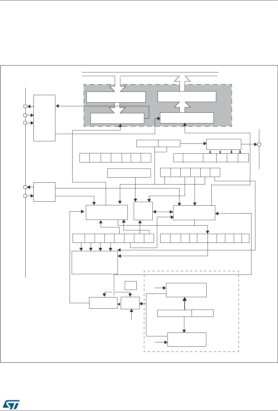
DocID018909 Rev 9 955/1718
RM0090 Universal synchronous asynchronous receiver transmitter (USART)
1003
The following pins are required in Hardware flow control mode:
•nCTS: Clear To Send blocks the data transmission at the end of the current transfer
when high
•nRTS: Request to send indicates that the USART is ready to receive a data (when
low).
Figure 296. USART block diagram
Wakeup
unit
Receiver
control
SR
Transmit
control
TXETC RXNEIDLEORE NF FE
USART
control
interrupt
CR1
MWAKE
Receive data register (RDR)
Receive Shift Register
Read
Transmit data register (TDR)
Transmit Shift Register
Write
SW_RX
TX
(Data register) DR
Transmitter
clock
Receiver
clock
Receiver rate
Transmitter rate
f
PCLKx(x=1,2)
control
control
/
[8 x (2 - OVER8)]
Conventional baud rate generator
SBKRWURETE
IDLERXNE
TCIETXEIE
CR1
UE PCE PS
PEIE
PE
PWDATA
IRLP
SCEN IREN
DMAR
DMAT
USART Address
CR2
CR3
IrDA
SIR
ENDEC
block
LINE CKEN CPOL CPHA LBCL
SCLK control SCLK
CR2
GT
STOP[1:0]
NACK
DIV_Mantissa
15 0
RE
USART_BRR
/USARTDIV
TE
HD
(CPU or DMA)
(CPU or DMA)
PRDATA
Hardware
flow
controller
CTSLBD
RX
nRTS
nCTS
GTPR
PSC
IE IE
DIV_Fraction
4
USARTDIV = DIV_Mantissa + (DIV_Fraction / 8 × (2 – OVER8))
SAMPLING
CR1
OVER8
DIVIDER
ai16099
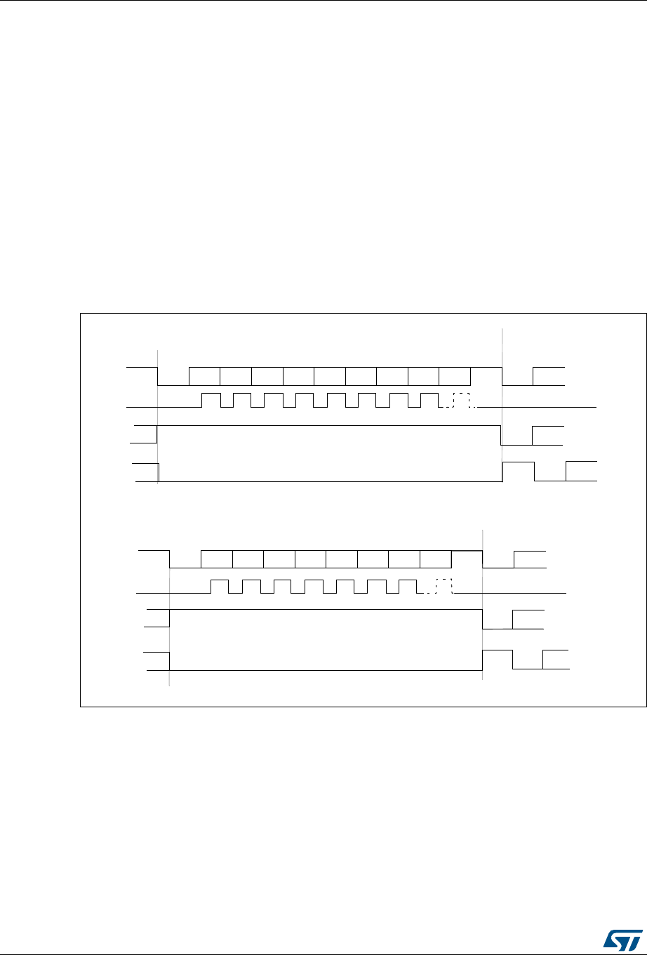
Universal synchronous asynchronous receiver transmitter (USART) RM0090
956/1718 DocID018909 Rev 9
30.3.1 USART character description
Word length may be selected as being either 8 or 9 bits by programming the M bit in the
USART_CR1 register (see Figure 297).
The TX pin is in low state during the start bit. It is in high state during the stop bit.
An Idle character is interpreted as an entire frame of “1”s followed by the start bit of the
next frame which contains data (The number of “1” ‘s will include the number of stop bits).
A Break character is interpreted on receiving “0”s for a frame period. At the end of the
break frame the transmitter inserts either 1 or 2 stop bits (logic “1” bit) to acknowledge the
start bit.
Transmission and reception are driven by a common baud rate generator, the clock for each
is generated when the enable bit is set respectively for the transmitter and receiver.
The details of each block is given below.
Figure 297. Word length programming
Bit0 Bit1 Bit2 Bit3 Bit4 Bit5 Bit6 Bit7 Bit8
Start
bit Stop
bit
Next
Start
bit
Idle frame
Bit0 Bit1 Bit2 Bit3 Bit4 Bit5 Bit6 Bit7
Start
Bit Stop
bit
Next
start
bit
Idle frame Start
bit
9-bit word length (M bit is set), 1 stop bit
8-bit word length (M bit is reset), 1 stop bit
Possible
parity
bit
Possible
Parity
Bit
Break frame Start
bit
Stop
bit
Data frame
Break frame Start
bit
Stop
bit
Data frame
Next data frame
Next data frame
Start
bit
****
** LBCL bit controls last data clock pulse
Clock
Clock
** LBCL bit controls last data clock pulse
**
**

DocID018909 Rev 9 957/1718
RM0090 Universal synchronous asynchronous receiver transmitter (USART)
1003
30.3.2 Transmitter
The transmitter can send data words of either 8 or 9 bits depending on the M bit status.
When the transmit enable bit (TE) is set, the data in the transmit shift register is output on
the TX pin and the corresponding clock pulses are output on the SCLK pin.
Character transmission
During an USART transmission, data shifts out least significant bit first on the TX pin. In this
mode, the USART_DR register consists of a buffer (TDR) between the internal bus and the
transmit shift register (see Figure 296).
Every character is preceded by a start bit which is a logic level low for one bit period. The
character is terminated by a configurable number of stop bits.
The following stop bits are supported by USART: 0.5, 1, 1.5 and 2 stop bits.
Note: The TE bit should not be reset during transmission of data. Resetting the TE bit during the
transmission will corrupt the data on the TX pin as the baud rate counters will get frozen.
The current data being transmitted will be lost.
An idle frame will be sent after the TE bit is enabled.
Configurable stop bits
The number of stop bits to be transmitted with every character can be programmed in
Control register 2, bits 13,12.
•1 stop bit: This is the default value of number of stop bits.
•2 Stop bits: This will be supported by normal USART, single-wire and modem modes.
•0.5 stop bit: To be used when receiving data in Smartcard mode.
•1.5 stop bits: To be used when transmitting and receiving data in Smartcard mode.
An idle frame transmission will include the stop bits.
A break transmission will be 10 low bits followed by the configured number of stop bits
(when m = 0) and 11 low bits followed by the configured number of stop bits (when m = 1). It
is not possible to transmit long breaks (break of length greater than 10/11 low bits).
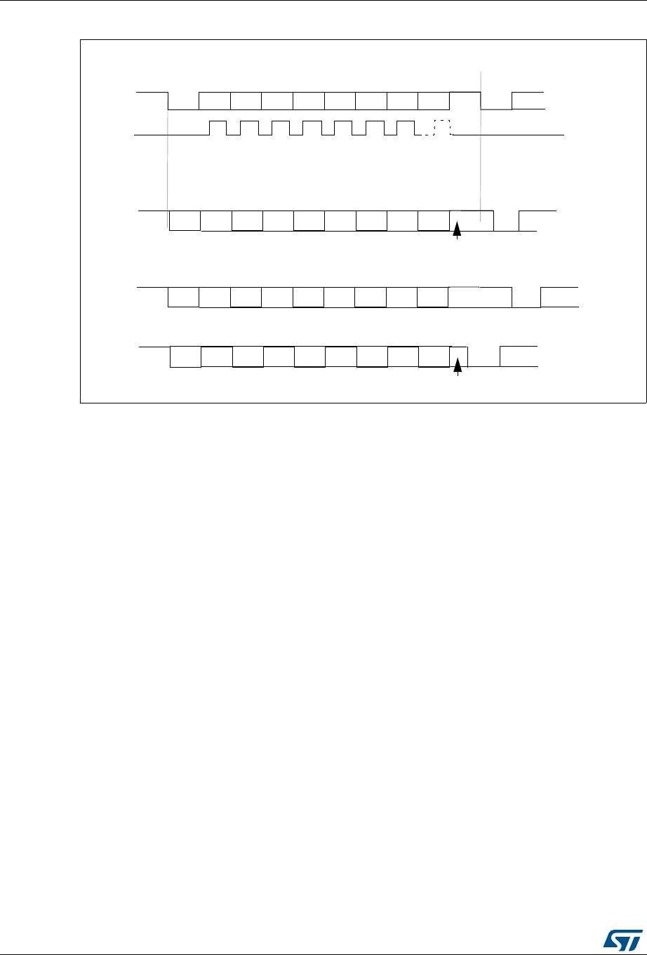
Universal synchronous asynchronous receiver transmitter (USART) RM0090
958/1718 DocID018909 Rev 9
Figure 298. Configurable stop bits
Procedure:
1. Enable the USART by writing the UE bit in USART_CR1 register to 1.
2. Program the M bit in USART_CR1 to define the word length.
3. Program the number of stop bits in USART_CR2.
4. Select DMA enable (DMAT) in USART_CR3 if Multi buffer Communication is to take
place. Configure the DMA register as explained in multibuffer communication.
5. Select the desired baud rate using the USART_BRR register.
6. Set the TE bit in USART_CR1 to send an idle frame as first transmission.
7. Write the data to send in the USART_DR register (this clears the TXE bit). Repeat this
for each data to be transmitted in case of single buffer.
8. After writing the last data into the USART_DR register, wait until TC=1. This indicates
that the transmission of the last frame is complete. This is required for instance when
the USART is disabled or enters the Halt mode to avoid corrupting the last
transmission.
Single byte communication
Clearing the TXE bit is always performed by a write to the data register.
The TXE bit is set by hardware and it indicates:
•The data has been moved from TDR to the shift register and the data transmission has
started.
•The TDR register is empty.
•The next data can be written in the USART_DR register without overwriting the
previous data.
This flag generates an interrupt if the TXEIE bit is set.
Bit0 Bit1 Bit2 Bit3 Bit4 Bit5 Bit6 Bit7
Start
Bit Stop
bit
Next
start
bit
8-bit Word length (M bit is reset)
Possible
parity
bit
Data frame
Next data frame
****
** LBCL bit controls last data clock pulse
CLOCK **
Bit0 Bit1 Bit2 Bit3 Bit4 Bit5 Bit6 Bit7
Start
Bit
2 Stop
Bits
Next
Start
Bit
Possible
parity
bit
Data frame
Next data frame
Bit0 Bit1 Bit2 Bit3 Bit4 Bit5 Bit6 Bit7
Start
Bit
Next
start
bit
Possible
Parity
Bit
Data frame
Next data frame
1/2 stop bit
Bit0 Bit1 Bit2 Bit3 Bit4 Bit5 Bit6 Bit7
Start
Bit
Next
start
bit
Possible
Parity
Bit
Data frame
Next data frame
1 1/2 stop bits
a) 1 Stop Bit
b) 1 1/2 stop Bits
c) 2 Stop Bits
d) 1/2 Stop Bit
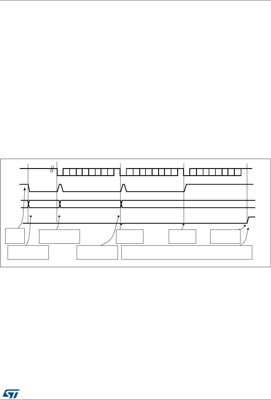
DocID018909 Rev 9 959/1718
RM0090 Universal synchronous asynchronous receiver transmitter (USART)
1003
When a transmission is taking place, a write instruction to the USART_DR register stores
the data in the TDR register and which is copied in the shift register at the end of the current
transmission.
When no transmission is taking place, a write instruction to the USART_DR register places
the data directly in the shift register, the data transmission starts, and the TXE bit is
immediately set.
If a frame is transmitted (after the stop bit) and the TXE bit is set, the TC bit goes high. An
interrupt is generated if the TCIE bit is set in the USART_CR1 register.
After writing the last data into the USART_DR register, it is mandatory to wait for TC=1
before disabling the USART or causing the microcontroller to enter the low-power mode
(see Figure 299: TC/TXE behavior when transmitting).
The TC bit is cleared by the following software sequence:
1. A read from the USART_SR register
2. A write to the USART_DR register
Note: The TC bit can also be cleared by writing a ‘0 to it. This clearing sequence is recommended
only for Multibuffer communication.
Figure 299. TC/TXE behavior when transmitting
Break characters
Setting the SBK bit transmits a break character. The break frame length depends on the M
bit (see Figure 297).
If the SBK bit is set to ‘1 a break character is sent on the TX line after completing the current
character transmission. This bit is reset by hardware when the break character is completed
(during the stop bit of the break character). The USART inserts a logic 1 bit at the end of the
last break frame to guarantee the recognition of the start bit of the next frame.
Note: If the software resets the SBK bit before the commencement of break transmission, the
break character will not be transmitted. For two consecutive breaks, the SBK bit should be
set after the stop bit of the previous break.
Idle characters
Setting the TE bit drives the USART to send an idle frame before the first data frame.
TX line
USART_DR
Frame 1
TXE flag
F2
TC flag
F3
Frame 2
software waits until TXE=1
and writes F2 into DR
software waits until TXE=1
and writes F3 into DR
TC is not set
because TXE=0
software waits until TC=1
Frame 3
TC is set because
TXE=1
set by hardware
cleared by software
set by hardware
cleared by software set by hardware
set
Idle preamble
by hardware
F1
software
enables the
USART
TC is not set
because TXE=0
software waits until TXE=1
and writes F1 into DR
ai17121b
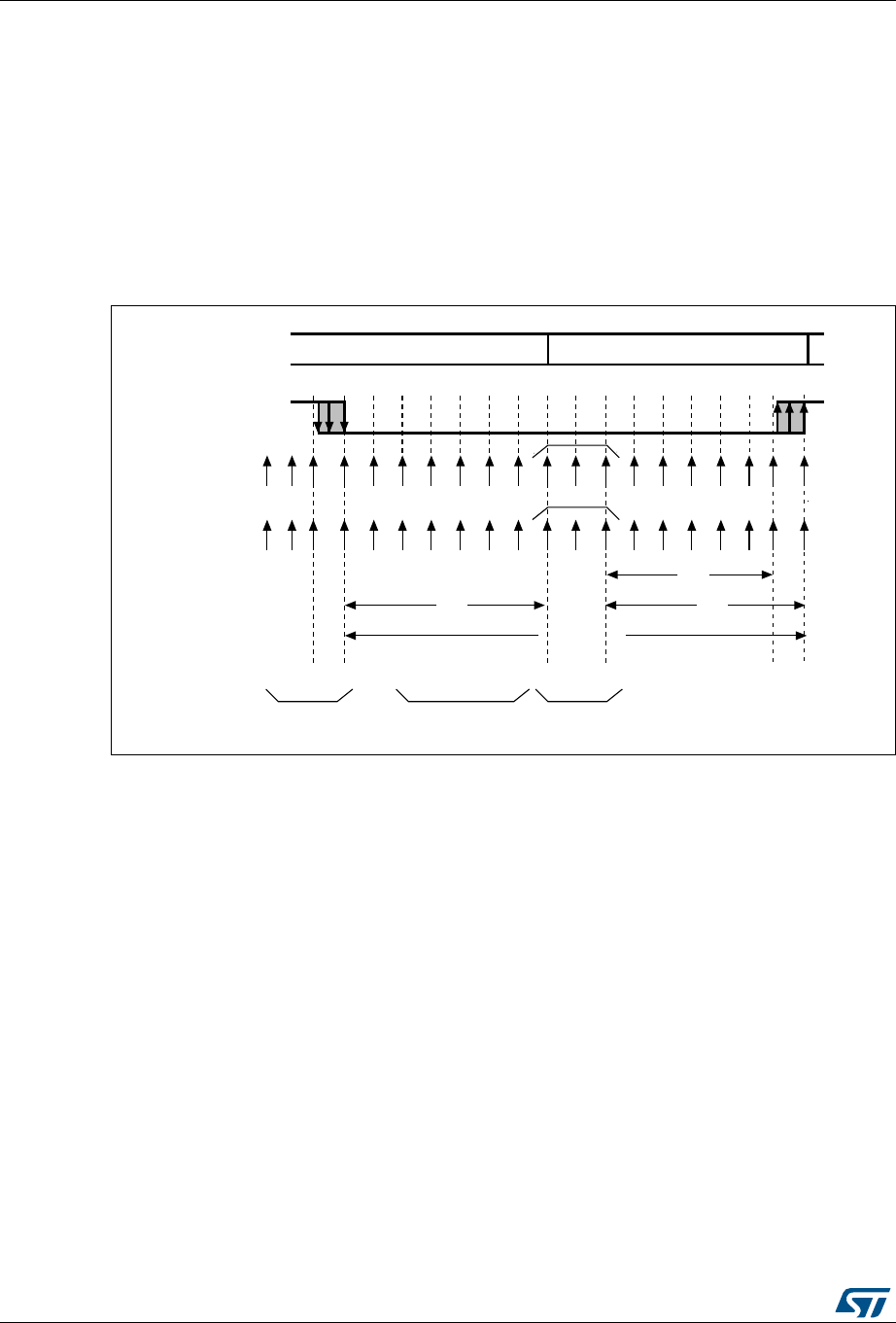
Universal synchronous asynchronous receiver transmitter (USART) RM0090
960/1718 DocID018909 Rev 9
30.3.3 Receiver
The USART can receive data words of either 8 or 9 bits depending on the M bit in the
USART_CR1 register.
Start bit detection
The start bit detection sequence is the same when oversampling by 16 or by 8.
In the USART, the start bit is detected when a specific sequence of samples is recognized.
This sequence is: 1 1 1 0 X 0 X 0 X 0 0 0 0.
Figure 300. Start bit detection when oversampling by 16 or 8
Note: If the sequence is not complete, the start bit detection aborts and the receiver returns to the
idle state (no flag is set) where it waits for a falling edge.
The start bit is confirmed (RXNE flag set, interrupt generated if RXNEIE=1) if the 3 sampled
bits are at 0 (first sampling on the 3rd, 5th and 7th bits finds the 3 bits at 0 and second
sampling on the 8th, 9th and 10th bits also finds the 3 bits at 0).
The start bit is validated (RXNE flag set, interrupt generated if RXNEIE=1) but the NE noise
flag is set if, for both samplings, at least 2 out of the 3 sampled bits are at 0 (sampling on the
3rd, 5th and 7th bits and sampling on the 8th, 9th and 10th bits). If this condition is not met,
the start detection aborts and the receiver returns to the idle state (no flag is set).
If, for one of the samplings (sampling on the 3rd, 5th and 7th bits or sampling on the 8th, 9th
and 10th bits), 2 out of the 3 bits are found at 0, the start bit is validated but the NE noise
flag bit is set.
Character reception
During an USART reception, data shifts in least significant bit first through the RX pin. In this
mode, the USART_DR register consists of a buffer (RDR) between the internal bus and the
received shift register.
Procedure:
RX line
sampled values
Idle Start bitRX state
Real
sample
clock
Ideal
sample
clock
010X0X0000XXXXXX
Conditions
to validate
the start bit At least 2 bits
out of 3 at 0
At least 2 bits
out of 3 at 0
Falling edge
detection
11
1 2 3 4 5 6 7 8 9 10 11 12 13 14 15 16
X X X X X X X X 9 10 111213141516
6/16
7/16
One-bit time
7/16
X
ai15471

DocID018909 Rev 9 961/1718
RM0090 Universal synchronous asynchronous receiver transmitter (USART)
1003
1. Enable the USART by writing the UE bit in USART_CR1 register to 1.
2. Program the M bit in USART_CR1 to define the word length.
3. Program the number of stop bits in USART_CR2.
4. Select DMA enable (DMAR) in USART_CR3 if multibuffer communication is to take
place. Configure the DMA register as explained in multibuffer communication. STEP 3
5. Select the desired baud rate using the baud rate register USART_BRR
6. Set the RE bit USART_CR1. This enables the receiver which begins searching for a
start bit.
When a character is received
•The RXNE bit is set. It indicates that the content of the shift register is transferred to the
RDR. In other words, data has been received and can be read (as well as its
associated error flags).
•An interrupt is generated if the RXNEIE bit is set.
•The error flags can be set if a frame error, noise or an overrun error has been detected
during reception.
•In multibuffer, RXNE is set after every byte received and is cleared by the DMA read to
the Data Register.
•In single buffer mode, clearing the RXNE bit is performed by a software read to the
USART_DR register. The RXNE flag can also be cleared by writing a zero to it. The
RXNE bit must be cleared before the end of the reception of the next character to avoid
an overrun error.
Note: The RE bit should not be reset while receiving data. If the RE bit is disabled during
reception, the reception of the current byte will be aborted.
Break character
When a break character is received, the USART handles it as a framing error.
Idle character
When an idle frame is detected, there is the same procedure as a data received character
plus an interrupt if the IDLEIE bit is set.
Overrun error
An overrun error occurs when a character is received when RXNE has not been reset. Data
can not be transferred from the shift register to the RDR register until the RXNE bit is
cleared.

Universal synchronous asynchronous receiver transmitter (USART) RM0090
962/1718 DocID018909 Rev 9
The RXNE flag is set after every byte received. An overrun error occurs if RXNE flag is set
when the next data is received or the previous DMA request has not been serviced. When
an overrun error occurs:
•The ORE bit is set.
•The RDR content will not be lost. The previous data is available when a read to
USART_DR is performed.
•The shift register will be overwritten. After that point, any data received during overrun
is lost.
•An interrupt is generated if either the RXNEIE bit is set or both the EIE and DMAR bits
are set.
•The ORE bit is reset by a read to the USART_SR register followed by a USART_DR
register read operation.
Note: The ORE bit, when set, indicates that at least 1 data has been lost. There are two
possibilities:
•if RXNE=1, then the last valid data is stored in the receive register RDR and can be
read,
•if RXNE=0, then it means that the last valid data has already been read and thus there
is nothing to be read in the RDR. This case can occur when the last valid data is read in
the RDR at the same time as the new (and lost) data is received. It may also occur
when the new data is received during the reading sequence (between the USART_SR
register read access and the USART_DR read access).
Selecting the proper oversampling method
The receiver implements different user-configurable oversampling techniques (except in
synchronous mode) for data recovery by discriminating between valid incoming data and
noise.
The oversampling method can be selected by programming the OVER8 bit in the
USART_CR1 register and can be either 16 or 8 times the baud rate clock (Figure 301 and
Figure 302).
Depending on the application:
•select oversampling by 8 (OVER8=1) to achieve higher speed (up to fPCLK/8). In this
case the maximum receiver tolerance to clock deviation is reduced (refer to
Section 30.3.5: USART receiver tolerance to clock deviation on page 975)
•select oversampling by 16 (OVER8=0) to increase the tolerance of the receiver to clock
deviations. In this case, the maximum speed is limited to maximum fPCLK/16
Programming the ONEBIT bit in the USART_CR3 register selects the method used to
evaluate the logic level. There are two options:
•the majority vote of the three samples in the center of the received bit. In this case,
when the 3 samples used for the majority vote are not equal, the NF bit is set
•a single sample in the center of the received bit
Depending on the application:
– select the three samples’ majority vote method (ONEBIT=0) when operating in a
noisy environment and reject the data when a noise is detected (refer to
Figure 132) because this indicates that a glitch occurred during the sampling.
– select the single sample method (ONEBIT=1) when the line is noise-free to
increase the receiver’s tolerance to clock deviations (see Section 30.3.5: USART
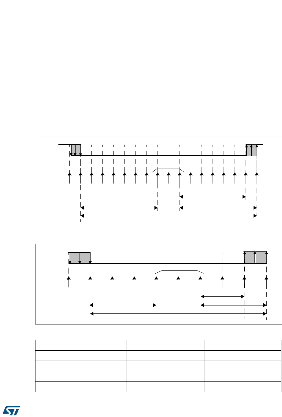
DocID018909 Rev 9 963/1718
RM0090 Universal synchronous asynchronous receiver transmitter (USART)
1003
receiver tolerance to clock deviation on page 975). In this case the NF bit will
never be set.
When noise is detected in a frame:
•The NF bit is set at the rising edge of the RXNE bit.
•The invalid data is transferred from the Shift register to the USART_DR register.
•No interrupt is generated in case of single byte communication. However this bit rises
at the same time as the RXNE bit which itself generates an interrupt. In case of
multibuffer communication an interrupt will be issued if the EIE bit is set in the
USART_CR3 register.
The NF bit is reset by a USART_SR register read operation followed by a USART_DR
register read operation.
Note: Oversampling by 8 is not available in the Smartcard, IrDA and LIN modes. In those modes,
the OVER8 bit is forced to ‘0 by hardware.
Figure 301. Data sampling when oversampling by 16
Figure 302. Data sampling when oversampling by 8
Table 132. Noise detection from sampled data
Sampled value NE status Received bit value
000 0 0
001 1 0
010 1 0
011 1 1
RX LINE
Sample
clock 1234567891011
12 13 14 15 16
sampled values
One bit time
6/16
7/16 7/16
RX LINE
One bit time
3/8 3/8
12345678
2/8
Sample
clock(x8)
sampled values

Universal synchronous asynchronous receiver transmitter (USART) RM0090
964/1718 DocID018909 Rev 9
Framing error
A framing error is detected when:
The stop bit is not recognized on reception at the expected time, following either a de-
synchronization or excessive noise.
When the framing error is detected:
•The FE bit is set by hardware
•The invalid data is transferred from the Shift register to the USART_DR register.
•No interrupt is generated in case of single byte communication. However this bit rises
at the same time as the RXNE bit which itself generates an interrupt. In case of
multibuffer communication an interrupt will be issued if the EIE bit is set in the
USART_CR3 register.
The FE bit is reset by a USART_SR register read operation followed by a USART_DR
register read operation.
Configurable stop bits during reception
The number of stop bits to be received can be configured through the control bits of Control
Register 2 - it can be either 1 or 2 in normal mode and 0.5 or 1.5 in Smartcard mode.
1. 0.5 stop bit (reception in Smartcard mode): No sampling is done for 0.5 stop bit. As
a consequence, no framing error and no break frame can be detected when 0.5 stop bit
is selected.
2. 1 stop bit: Sampling for 1 stop Bit is done on the 8th, 9th and 10th samples.
3. 1.5 stop bits (Smartcard mode): When transmitting in smartcard mode, the device
must check that the data is correctly sent. Thus the receiver block must be enabled (RE
=1 in the USART_CR1 register) and the stop bit is checked to test if the smartcard has
detected a parity error. In the event of a parity error, the smartcard forces the data
signal low during the sampling - NACK signal-, which is flagged as a framing error.
Then, the FE flag is set with the RXNE at the end of the 1.5 stop bit. Sampling for 1.5
stop bits is done on the 16th, 17th and 18th samples (1 baud clock period after the
beginning of the stop bit). The 1.5 stop bit can be decomposed into 2 parts: one 0.5
baud clock period during which nothing happens, followed by 1 normal stop bit period
during which sampling occurs halfway through. Refer to Section 30.3.11: Smartcard on
page 983 for more details.
4. 2 stop bits: Sampling for 2 stop bits is done on the 8th, 9th and 10th samples of the
first stop bit. If a framing error is detected during the first stop bit the framing error flag
will be set. The second stop bit is not checked for framing error. The RXNE flag will be
set at the end of the first stop bit.
100 1 0
101 1 1
110 1 1
111 0 1
Table 132. Noise detection from sampled data (continued)
Sampled value NE status Received bit value

DocID018909 Rev 9 965/1718
RM0090 Universal synchronous asynchronous receiver transmitter (USART)
1003
30.3.4 Fractional baud rate generation
The baud rate for the receiver and transmitter (Rx and Tx) are both set to the same value as
programmed in the Mantissa and Fraction values of USARTDIV.
Equation 1: Baud rate for standard USART (SPI mode included)
Equation 2: Baud rate in Smartcard, LIN and IrDA modes
USARTDIV is an unsigned fixed point number that is coded on the USART_BRR register.
•When OVER8=0, the fractional part is coded on 4 bits and programmed by the
DIV_fraction[3:0] bits in the USART_BRR register
•When OVER8=1, the fractional part is coded on 3 bits and programmed by the
DIV_fraction[2:0] bits in the USART_BRR register, and bit DIV_fraction[3] must be kept
cleared.
Note: The baud counters are updated to the new value in the baud registers after a write operation
to USART_BRR. Hence the baud rate register value should not be changed during
communication.
How to derive USARTDIV from USART_BRR register values when OVER8=0
Example 1:
If DIV_Mantissa = 0d27 and DIV_Fraction = 0d12 (USART_BRR = 0x1BC), then
Mantissa (USARTDIV) = 0d27
Fraction (USARTDIV) = 12/16 = 0d0.75
Therefore USARTDIV = 0d27.75
Example 2:
To program USARTDIV = 0d25.62
This leads to:
DIV_Fraction = 16*0d0.62 = 0d9.92
The nearest real number is 0d10 = 0xA
DIV_Mantissa = mantissa (0d25.620) = 0d25 = 0x19
Then, USART_BRR = 0x19A hence USARTDIV = 0d25.625
Example 3:
To program USARTDIV = 0d50.99
This leads to:
Tx/Rx baud fCK
8 2 OVER8–()USARTDIV××
-----------------------------------------------------------------------------------
=
Tx/Rx baud fCK
16 USARTDIV×
---------------------------------------------
=

Universal synchronous asynchronous receiver transmitter (USART) RM0090
966/1718 DocID018909 Rev 9
DIV_Fraction = 16*0d0.99 = 0d15.84
The nearest real number is 0d16 = 0x10 => overflow of DIV_frac[3:0] => carry must be
added up to the mantissa
DIV_Mantissa = mantissa (0d50.990 + carry) = 0d51 = 0x33
Then, USART_BRR = 0x330 hence USARTDIV = 0d51.000
How to derive USARTDIV from USART_BRR register values when OVER8=1
Example 1:
If DIV_Mantissa = 0x27 and DIV_Fraction[2:0]= 0d6 (USART_BRR = 0x1B6), then
Mantissa (USARTDIV) = 0d27
Fraction (USARTDIV) = 6/8 = 0d0.75
Therefore USARTDIV = 0d27.75
Example 2:
To program USARTDIV = 0d25.62
This leads to:
DIV_Fraction = 8*0d0.62 = 0d4.96
The nearest real number is 0d5 = 0x5
DIV_Mantissa = mantissa (0d25.620) = 0d25 = 0x19
Then, USART_BRR = 0x195 => USARTDIV = 0d25.625
Example 3:
To program USARTDIV = 0d50.99
This leads to:
DIV_Fraction = 8*0d0.99 = 0d7.92
The nearest real number is 0d8 = 0x8 => overflow of the DIV_frac[2:0] => carry must be
added up to the mantissa
DIV_Mantissa = mantissa (0d50.990 + carry) = 0d51 = 0x33
Then, USART_BRR = 0x0330 => USARTDIV = 0d51.000
Table 133. Error calculation for programmed baud rates at fPCLK = 8 MHz or fPCLK = 12 MHz,
oversampling by 16(1)
Oversampling by 16 (OVER8=0)
Baud rate7 fPCLK = 8 MHz fPCLK = 12 MHz
S.No Desired Actual
Value
programmed
in the baud
rate register
% Error =
(Calculated -
Desired) B.rate /
Desired B.rate
Actual
Value
programmed
in the baud
rate register
% Error
1 1.2 KBps 1.2 KBps 416.6875 0 1.2 KBps 625 0
2 2.4 KBps 2.4 KBps 208.3125 0.01 2.4 KBps 312.5 0

DocID018909 Rev 9 967/1718
RM0090 Universal synchronous asynchronous receiver transmitter (USART)
1003
3 9.6 KBps 9.604 KBps 52.0625 0.04 9.6 KBps 78.125 0
4 19.2 KBps 19.185 KBps 26.0625 0.08 19.2 KBps 39.0625 0
5 38.4 KBps 38.462 KBps 13 0.16 38.339 KBps 19.5625 0.16
6 57.6 KBps 57.554 KBps 8.6875 0.08 57.692 KBps 13 0.16
7 115.2 KBps 115.942 KBps 4.3125 0.64 115.385 KBps 6.5 0.16
8 230.4 KBps 228.571 KBps 2.1875 0.79 230.769 KBps 3.25 0.16
9 460.8 KBps 470.588 KBps 1.0625 2.12 461.538 KBps 1.625 0.16
10 921.6 KBps NA NA NA NA NA NA
11 2 MBps NA NA NA NA NA NA
12 3 MBps NA NA NA NA NA NA
1. The lower the CPU clock the lower the accuracy for a particular baud rate. The upper limit of the achievable baud rate can
be fixed with these data.
Table 133. Error calculation for programmed baud rates at fPCLK = 8 MHz or fPCLK = 12 MHz,
oversampling by 16(1) (continued)
Oversampling by 16 (OVER8=0)
Baud rate7 fPCLK = 8 MHz fPCLK = 12 MHz
S.No Desired Actual
Value
programmed
in the baud
rate register
% Error =
(Calculated -
Desired) B.rate /
Desired B.rate
Actual
Value
programmed
in the baud
rate register
% Error
Table 134. Error calculation for programmed baud rates at fPCLK = 8 MHz or fPCLK =12 MHz,
oversampling by 8(1)
Oversampling by 8 (OVER8 = 1)
Baud rate fPCLK = 8 MHz fPCLK = 12 MHz
S.No Desired Actual
Value
programmed
in the baud
rate register
% Error =
(Calculated -
Desired)
B.rate /
Desired
B.rate
Actual
Value
programmed
in the baud
rate register
% Error
1 1.2 KBps 1.2 KBps 833.375 0 1.2 KBps 1250 0
2 2.4 KBps 2.4 KBps 416.625 0.01 2.4 KBps 625 0
3 9.6 KBps 9.604 KBps 104.125 0.04 9.6 KBps 156.25 0
4 19.2 KBps 19.185 KBps 52.125 0.08 19.2 KBps 78.125 0
5 38.4 KBps 38.462 KBps 26 0.16 38.339 KBps 39.125 0.16
6 57.6 KBps 57.554 KBps 17.375 0.08 57.692 KBps 26 0.16
7 115.2 KBps 115.942 KBps 8.625 0.64 115.385 KBps 13 0.16
8 230.4 KBps 228.571 KBps 4.375 0.79 230.769 KBps 6.5 0.16
9 460.8 KBps 470.588 KBps 2.125 2.12 461.538 KBps 3.25 0.16

Universal synchronous asynchronous receiver transmitter (USART) RM0090
968/1718 DocID018909 Rev 9
10 921.6 KBps 888.889 KBps 1.125 3.55 923.077 KBps 1.625 0.16
11 2 MBps NA NA NA NA NA NA
12 3 MBps NA NA NA NA NA NA
1. The lower the CPU clock the lower the accuracy for a particular baud rate. The upper limit of the achievable baud rate can
be fixed with these data.
Table 134. Error calculation for programmed baud rates at fPCLK = 8 MHz or fPCLK =12 MHz,
oversampling by 8(1) (continued)
Oversampling by 8 (OVER8 = 1)
Baud rate fPCLK = 8 MHz fPCLK = 12 MHz
S.No Desired Actual
Value
programmed
in the baud
rate register
% Error =
(Calculated -
Desired)
B.rate /
Desired
B.rate
Actual
Value
programmed
in the baud
rate register
% Error
Table 135. Error calculation for programmed baud rates at fPCLK = 16 MHz or fPCLK = 24 MHz,
oversampling by 16(1)
Oversampling by 16 (OVER8 = 0)
Baud rate fPCLK = 16 MHz fPCLK = 24 MHz
S.No Desired Actual
Value
programmed
in the baud
rate register
% Error =
(Calculated -
Desired) B.rate /
Desired B.rate
Actual
Value
programmed
in the baud
rate register
% Error
1 1.2 KBps 1.2 KBps 833.3125 0 1.2 1250 0
2 2.4 KBps 2.4 KBps 416.6875 0 2.4 625 0
3 9.6 KBps 9.598 KBps 104.1875 0.02 9.6 156.25 0
4 19.2 KBps 19.208 KBps 52.0625 0.04 19.2 78.125 0
5 38.4 KBps 38.369 KBps 26.0625 0.08 38.4 39.0625 0
6 57.6 KBps 57.554 KBps 17.375 0.08 57.554 26.0625 0.08
7 115.2 KBps 115.108 KBps 8.6875 0.08 115.385 13 0.16
8 230.4 KBps 231.884 KBps 4.3125 0.64 230.769 6.5 0.16
9 460.8 KBps 457.143 KBps 2.1875 0.79 461.538 3.25 0.16
10 921.6 KBps 941.176 KBps 1.0625 2.12 923.077 1.625 0.16
11 2 MBps NA NA NA NA NA NA
12 3 MBps NA NA NA NA NA NA
1. The lower the CPU clock the lower the accuracy for a particular baud rate. The upper limit of the achievable baud rate can
be fixed with these data.

DocID018909 Rev 9 969/1718
RM0090 Universal synchronous asynchronous receiver transmitter (USART)
1003
Table 136. Error calculation for programmed baud rates at fPCLK = 16 MHz or fPCLK = 24 MHz,
oversampling by 8(1)
Oversampling by 8 (OVER8=1)
Baud rate fPCLK = 16 MHz fPCLK = 24 MHz
S.No Desired Actual
Value
programmed
in the baud
rate register
% Error =
(Calculated -
Desired) B.rate /
Desired B.rate
Actual
Value
programmed
in the baud
rate register
% Error
1 1.2 KBps 1.2 KBps 1666.625 0 1.2 KBps 2500 0
2 2.4 KBps 2.4 KBps 833.375 0 2.4 KBps 1250 0
3 9.6 KBps 9.598 KBps 208.375 0.02 9.6 KBps 312.5 0
4 19.2 KBps 19.208 KBps 104.125 0.04 19.2 KBps 156.25 0
5 38.4 KBps 38.369 KBps 52.125 0.08 38.4 KBps 78.125 0
6 57.6 KBps 57.554 KBps 34.75 0.08 57.554 KBps 52.125 0.08
7 115.2 KBps 115.108 KBps 17.375 0.08 115.385 KBps 26 0.16
8 230.4 KBps 231.884 KBps 8.625 0.64 230.769 KBps 13 0.16
9 460.8 KBps 457.143 KBps 4.375 0.79 461.538 KBps 6.5 0.16
10 921.6 KBps 941.176 KBps 2.125 2.12 923.077 KBps 3.25 0.16
11 2 MBps 2000 KBps 1 0 2000 KBps 1.5 0
12 3 MBps NA NA NA 3000 KBps 1 0
1. The lower the CPU clock the lower the accuracy for a particular baud rate. The upper limit of the achievable baud rate can
be fixed with these data.
Table 137. Error calculation for programmed baud rates at fPCLK = 8 MHz or fPCLK = 16 MHz,
oversampling by 16(1)
Oversampling by 16 (OVER8=0)
Baud rate fPCLK = 8 MHz fPCLK = 16 MHz
S.No Desired Actual
Value
programme
d in the
baud rate
register
% Error =
(Calculated -
Desired)B.Rate
/Desired B.Rate
Actual
Value
programmed
in the baud
rate register
% Error
1. 2.4 KBps 2.400 KBps 208.3125 0.00% 2.400 KBps 416.6875 0.00%
2. 9.6 KBps 9.604 KBps 52.0625 0.04% 9.598 KBps 104.1875 0.02%
3. 19.2 KBps 19.185 KBps 26.0625 0.08% 19.208 KBps 52.0625 0.04%
4. 57.6 KBps 57.554 KBps 8.6875 0.08% 57.554 KBps 17.3750 0.08%
5. 115.2 KBps 115.942 KBps 4.3125 0.64% 115.108 KBps 8.6875 0.08%
6. 230.4 KBps 228.571
KBps 2.1875 0.79% 231.884 KBps 4.3125 0.64%

Universal synchronous asynchronous receiver transmitter (USART) RM0090
970/1718 DocID018909 Rev 9
7. 460.8 KBps 470.588
KBps 1.0625 2.12% 457.143 KBps 2.1875 0.79%
8. 896 KBps NA NA NA 888.889 KBps 1.1250 0.79%
9. 921.6 KBps NA NA NA 941.176 KBps 1.0625 2.12%
10. 1.792 MBps NA NA NA NA NA NA
11. 1.8432 MBps NA NA NA NA NA NA
12. 3.584 MBps NA NA NA NA NA NA
13. 3.6864 MBps NA NA NA NA NA NA
14. 7.168 MBps NA NA NA NA NA NA
15. 7.3728 MBps NA NA NA NA NA NA
1. The lower the CPU clock the lower the accuracy for a particular baud rate. The upper limit of the achievable baud rate can
be fixed with these data.
Table 138. Error calculation for programmed baud rates at fPCLK = 8 MHz or fPCLK = 16 MHz,
oversampling by 8(1)
Oversampling by 8 (OVER8=1)
Baud rate fPCLK = 8 MHz fPCLK = 16 MHz
S.No Desired Actual
Value
programmed
in the baud
rate register
% Error =
(Calculated -
Desired)B.Rate
/Desired B.Rate
Actual
Value
programmed
in the baud
rate register
%
Error
1. 2.4 KBps 2.400 KBps 416.625 0.01% 2.400 KBps 833.375 0.00%
2. 9.6 KBps 9.604 KBps 104.125 0.04% 9.598 KBps 208.375 0.02%
3. 19.2 KBps 19.185 KBps 52.125 0.08% 19.208 KBps 104.125 0.04%
4. 57.6 KBps 57.557 KBps 17.375 0.08% 57.554 KBps 34.750 0.08%
5. 115.2 KBps 115.942 KBps 8.625 0.64% 115.108 KBps 17.375 0.08%
6. 230.4 KBps 228.571 KBps 4.375 0.79% 231.884 KBps 8.625 0.64%
7. 460.8 KBps 470.588 KBps 2.125 2.12% 457.143 KBps 4.375 0.79%
8. 896 KBps 888.889 KBps 1.125 0.79% 888.889 KBps 2.250 0.79%
9. 921.6 KBps 888.889 KBps 1.125 3.55% 941.176 KBps 2.125 2.12%
10. 1.792 MBps NA NA NA 1.7777 MBps 1.125 0.79%
Table 137. Error calculation for programmed baud rates at fPCLK = 8 MHz or fPCLK = 16 MHz,
oversampling by 16(1) (continued)
Oversampling by 16 (OVER8=0)
Baud rate fPCLK = 8 MHz fPCLK = 16 MHz
S.No Desired Actual
Value
programme
d in the
baud rate
register
% Error =
(Calculated -
Desired)B.Rate
/Desired B.Rate
Actual
Value
programmed
in the baud
rate register
% Error

DocID018909 Rev 9 971/1718
RM0090 Universal synchronous asynchronous receiver transmitter (USART)
1003
11. 1.8432 MBps NA NA NA 1.7777 MBps 1.125 3.55%
12. 3.584 MBps NA NA NA NA NA NA
13. 3.6864 MBps NA NA NA NA NA NA
14. 7.168 MBps NA NA NA NA NA NA
15. 7.3728 MBps NA NA NA NA NA NA
1. The lower the CPU clock the lower the accuracy for a particular baud rate. The upper limit of the achievable baud rate can
be fixed with these data.
Table 138. Error calculation for programmed baud rates at fPCLK = 8 MHz or fPCLK = 16 MHz,
oversampling by 8(1) (continued)
Oversampling by 8 (OVER8=1)
Baud rate fPCLK = 8 MHz fPCLK = 16 MHz
S.No Desired Actual
Value
programmed
in the baud
rate register
% Error =
(Calculated -
Desired)B.Rate
/Desired B.Rate
Actual
Value
programmed
in the baud
rate register
%
Error
Table 139. Error calculation for programmed baud rates at fPCLK = 30 MHz or fPCLK = 60 MHz,
oversampling by 16(1)(2)
Oversampling by 16 (OVER8=0)
Baud rate fPCLK = 30 MHz fPCLK = 60 MHz
S.No Desired Actual
Value
programme
d in the
baud rate
register
% Error =
(Calculated -
Desired)B.Rate
/Desired B.Rate
Actual
Value
programmed
in the baud
rate register
%
Error
1. 2.4 KBps 2.400 KBps 781.2500 0.00% 2.400 KBps 1562.5000 0.00%
2. 9.6 KBps 9.600 KBps 195.3125 0.00% 9.600 KBps 390.6250 0.00%
3. 19.2 KBps 19.194 KBps 97.6875 0.03% 19.200 KBps 195.3125 0.00%
4. 57.6 KBps 57.582KBps 32.5625 0.03% 57.582 KBps 65.1250 0.03%
5. 115.2 KBps 115.385 KBps 16.2500 0.16% 115.163 KBps 32.5625 0.03%
6. 230.4 KBps 230.769 KBps 8.1250 0.16% 230.769KBps 16.2500 0.16%
7. 460.8 KBps 461.538 KBps 4.0625 0.16% 461.538 KBps 8.1250 0.16%
8. 896 KBps 909.091 KBps 2.0625 1.46% 895.522 KBps 4.1875 0.05%
9. 921.6 KBps 909.091 KBps 2.0625 1.36% 923.077 KBps 4.0625 0.16%
10. 1.792 MBps 1.1764 MBps 1.0625 1.52% 1.8182 MBps 2.0625 1.36%
11. 1.8432
MBps 1.8750 MBps 1.0000 1.73% 1.8182 MBps 2.0625 1.52%
12. 3.584 MBps NA NA NA 3.2594 MBps 1.0625 1.52%
13. 3.6864
MBps NA NA NA 3.7500 MBps 1.0000 1.73%

Universal synchronous asynchronous receiver transmitter (USART) RM0090
972/1718 DocID018909 Rev 9
14. 7.168 MBps NA NA NA NA NA NA
15. 7.3728
MBps NA NA NA NA NA NA
1. The lower the CPU clock the lower the accuracy for a particular baud rate. The upper limit of the achievable baud rate can
be fixed with these data.
2. Only USART1 and USART6 are clocked with PCLK2. Other USARTs are clocked with PCLK1. Refer to the device
datasheets for the maximum values for PCLK1 and PCLK2.
Table 139. Error calculation for programmed baud rates at fPCLK = 30 MHz or fPCLK = 60 MHz,
oversampling by 16(1)(2) (continued)
Oversampling by 16 (OVER8=0)
Baud rate fPCLK = 30 MHz fPCLK = 60 MHz
S.No Desired Actual
Value
programme
d in the
baud rate
register
% Error =
(Calculated -
Desired)B.Rate
/Desired B.Rate
Actual
Value
programmed
in the baud
rate register
%
Error
Table 140. Error calculation for programmed baud rates at fPCLK = 30 MHz or fPCLK = 60 MHz,
oversampling by 8(1) (2)
Oversampling by 8 (OVER8=1)
Baud rate fPCLK = 30 MHz fPCLK =60 MHz
S.No Desired Actual
Value
programme
d in the
baud rate
register
% Error =
(Calculated -
Desired)B.Rate
/Desired B.Rate
Actual
Value
programmed
in the baud
rate register
%
Error
1. 2.4 KBps 2.400 KBps 1562.5000 0.00% 2.400 KBps 3125.0000 0.00%
2. 9.6 KBps 9.600 KBps 390.6250 0.00% 9.600 KBps 781.2500 0.00%
3. 19.2 KBps 19.194 KBps 195.3750 0.03% 19.200 KBps 390.6250 0.00%
4. 57.6 KBps 57.582 KBps 65.1250 0.16% 57.582 KBps 130.2500 0.03%
5. 115.2 KBps 115.385 KBps 32.5000 0.16% 115.163 KBps 65.1250 0.03%
6. 230.4 KBps 230.769 KBps 16.2500 0.16% 230.769 KBps 32.5000 0.16%
7. 460.8 KBps 461.538 KBps 8.1250 0.16% 461.538 KBps 16.2500 0.16%
8. 896 KBps 909.091 KBps 4.1250 1.46% 895.522 KBps 8.3750 0.05%
9. 921.6 KBps 909.091 KBps 4.1250 1.36% 923.077 KBps 8.1250 0.16%
10. 1.792 MBps 1.7647 MBps 2.1250 1.52% 1.8182 MBps 4.1250 1.46%
11. 1.8432 MBps 1.8750 MBps 2.0000 1.73% 1.8182 MBps 4.1250 1.36%
12. 3.584 MBps 3.7500 MBps 1.0000 4.63% 3.5294 MBps 2.1250 1.52%
13. 3.6864 MBps 3.7500 MBps 1.0000 1.73% 3.7500 MBps 2.0000 1.73%
14. 7.168 MBps NA NA NA 7.5000 MBps 1.0000 4.63%
15. 7.3728 MBps NA NA NA 7.5000 MBps 1.0000 1.73%

DocID018909 Rev 9 973/1718
RM0090 Universal synchronous asynchronous receiver transmitter (USART)
1003
1. The lower the CPU clock the lower the accuracy for a particular baud rate. The upper limit of the achievable baud rate can
be fixed with these data.
2. Only USART1 and USART6 are clocked with PCLK2. Other USARTs are clocked with PCLK1. Refer to the device
datasheets for the maximum values for PCLK1 and PCLK2.
Table 141. Error calculation for programmed baud rates at fPCLK = 42 MHz or fPCLK = 84 Hz,
oversampling by 16(1)(2)
Oversampling by 16 (OVER8=0)
Baud rate fPCLK = 42 MHz fPCLK = 84 MHz
S.No Desired Actual
Value
programme
d in the
baud rate
register
% Error =
(Calculated -
Desired)B.Rate
/Desired B.Rate
Actual
Value
programmed
in the baud
rate register
%
Error
1 1.2 KBps 1.2 KBps 2187.5 0 1.2 KBps 4375 0
2 2.4 KBps 2.4 KBps 1093.75 0 2.4 KBps 2187.5 0
3 9.6 KBps 9.6 KBps 273.4375 0 9.6 KBps 546.875 0
4 19.2 KBps 19.195 KBps 136.75 0.02 19.2 KBps 273.4375 0
5 38.4 KBps 38.391 KBps 68.375 0.02 38.391 KBps 136.75 0.02
6 57.6 KBps 57.613 KBps 45.5625 0.02 57.613 KBps 91.125 0.02
7 115.2 KBps 115.068 KBps 22.8125 0.11 115.226 KBps 45.5625 0.02
8 230.4 KBps 230.769 KBps 11.375 0.16 230.137 KBps 22.8125 0.11
9 460.8 KBps 461.538 KBps 5.6875 0.16 461.538 KBps 11.375 0.16
10 921.6 KBps 913.043 KBps 2.875 0.93 923.076 KBps 5.6875 0.93
11 1.792 MBps 1.826 MBps 1.4375 1.9 1.787 MBps 2.9375 0.27
12 1.8432
MBps 1.826 MBps 1.4375 0.93 1.826 MBps 2.875 0.93
13 3.584 MBps N.A N.A N.A 3.652 MBps 1.4375 1.9
14 3.6864
MBps N.A N.A N.A 3.652 MBps 1.4375 0.93
15 7.168 MBps N.A N.A N.A N.A N.A N.A
16 7.3728
MBps N.A N.A N.A N.A N.A N.A
18 9 MBps N.A N.A N.A N.A N.A N.A
20 10.5 MBps N.A N.A N.A N.A N.A N.A
1. The lower the CPU clock the lower the accuracy for a particular baud rate. The upper limit of the achievable baud rate can
be fixed with these data.
2. Only USART1 and USART6 are clocked with PCLK2. Other USARTs are clocked with PCLK1. Refer to the device
datasheets for the maximum values for PCLK1 and PCLK2.

Universal synchronous asynchronous receiver transmitter (USART) RM0090
974/1718 DocID018909 Rev 9
Table 142. Error calculation for programmed baud rates at fPCLK = 42 MHz or fPCLK = 84 MHz,
oversampling by 8(1)(2)
Oversampling by 8 (OVER8=1)
Baud rate fPCLK = 42 MHz fPCLK = 84 MHz
S.No Desired Actual
Value
programme
d in the
baud rate
register
% Error =
(Calculated -
Desired)B.Rate
/Desired B.Rate
Actual
Value
programmed
in the baud
rate register
%
Error
1. 1.2 KBps 1.2 KBps 4375 0 1.2 KBps 8750 0
2. 2.4 KBps 2.4 KBps 2187.5 0 2.4 KBps 4375 0
3. 9.6 KBps 9.6 KBps 546.875 0 9.6 KBps 1093.75 0
4. 19.2 KBps 19.195 KBps 273.5 0.02 19.2 KBps 546.875 0
5. 38.4 KBps 38.391 KBps 136.75 0.02 38.391 KBps 273.5 0.02
6. 57.6 KBps 57.613 KBps 91.125 0.02 57.613 KBps 182.25 0.02
7. 115.2 KBps 115.068 KBps 45.625 0.11 115.226 KBps 91.125 0.02
8. 230.4 KBps 230.769 KBps 22.75 0.11 230.137 KBps 45.625 0.11
9. 460.8 KBps 461.538 KBps 11.375 0.16 461.538 KBps 22.75 0.16
10. 921.6 KBps 913.043 KBps 5.75 0.93 923.076 KBps 11.375 0.93
11. 1.792 MBps 1.826 MBps 2.875 1.9 1.787Mbps 5.875 0.27
12. 1.8432 MBps 1.826 MBps 2.875 0.93 1.826 MBps 5.75 0.93
13. 3.584 MBps 3.5 MBps 1.5 2.34 3.652 MBps 2.875 1.9
14. 3.6864 MBps 3.82 MBps 1.375 3.57 3.652 MBps 2.875 0.93
15. 7.168 MBps N.A N.A N.A 7 MBps 1.5 2.34
16. 7.3728 MBps N.A N.A N.A 7.636 MBps 1.375 3.57
18. 9 MBps N.A N.A N.A 9.333 MBps 1.125 3.7
20. 10.5 MBps N.A N.A N.A 10.5 MBps 1 0
1. The lower the CPU clock the lower the accuracy for a particular baud rate. The upper limit of the achievable baud rate can
be fixed with these data.
2. Only USART1 and USART6 are clocked with PCLK2. Other USARTs are clocked with PCLK1. Refer to the device
datasheets for the maximum values for PCLK1 and PCLK2.

DocID018909 Rev 9 975/1718
RM0090 Universal synchronous asynchronous receiver transmitter (USART)
1003
30.3.5 USART receiver tolerance to clock deviation
The USART asynchronous receiver works correctly only if the total clock system deviation is
smaller than the USART receiver’s tolerance. The causes which contribute to the total
deviation are:
•DTRA: Deviation due to the transmitter error (which also includes the deviation of the
transmitter’s local oscillator)
•DQUANT: Error due to the baud rate quantization of the receiver
•DREC: Deviation of the receiver’s local oscillator
•DTCL: Deviation due to the transmission line (generally due to the transceivers which
can introduce an asymmetry between the low-to-high transition timing and the high-to-
low transition timing)
DTRA + DQUANT + DREC + DTCL < USART receiver’s tolerance
The USART receiver’s tolerance to properly receive data is equal to the maximum tolerated
deviation and depends on the following choices:
•10- or 11-bit character length defined by the M bit in the USART_CR1 register
•oversampling by 8 or 16 defined by the OVER8 bit in the USART_CR1 register
•use of fractional baud rate or not
•use of 1 bit or 3 bits to sample the data, depending on the value of the ONEBIT bit in
the USART_CR3 register
Note: The figures specified in Table 143 and Table 144 may slightly differ in the special case when
the received frames contain some Idle frames of exactly 10-bit times when M=0 (11-bit times
when M=1).
30.3.6 Multiprocessor communication
There is a possibility of performing multiprocessor communication with the USART (several
USARTs connected in a network). For instance one of the USARTs can be the master, its TX
output is connected to the RX input of the other USART. The others are slaves, their
respective TX outputs are logically ANDed together and connected to the RX input of the
master.
Table 143. USART receiver’s tolerance when DIV fraction is 0
M bit
OVER8 bit = 0 OVER8 bit = 1
ONEBIT=0 ONEBIT=1 ONEBIT=0 ONEBIT=1
0 3.75% 4.375% 2.50% 3.75%
1 3.41% 3.97% 2.27% 3.41%
Table 144. USART receiver tolerance when DIV_Fraction is different from 0
M bit
OVER8 bit = 0 OVER8 bit = 1
ONEBIT=0 ONEBIT=1 ONEBIT=0 ONEBIT=1
0 3.33% 3.88% 2% 3%
1 3.03% 3.53% 1.82% 2.73%
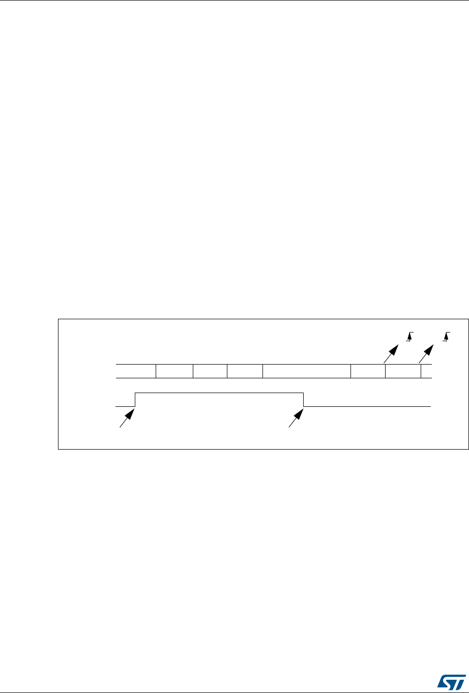
Universal synchronous asynchronous receiver transmitter (USART) RM0090
976/1718 DocID018909 Rev 9
In multiprocessor configurations it is often desirable that only the intended message
recipient should actively receive the full message contents, thus reducing redundant USART
service overhead for all non addressed receivers.
The non addressed devices may be placed in mute mode by means of the muting function.
In mute mode:
•None of the reception status bits can be set.
•All the receive interrupts are inhibited.
•The RWU bit in USART_CR1 register is set to 1. RWU can be controlled automatically
by hardware or written by the software under certain conditions.
The USART can enter or exit from mute mode using one of two methods, depending on the
WAKE bit in the USART_CR1 register:
•Idle Line detection if the WAKE bit is reset,
•Address Mark detection if the WAKE bit is set.
Idle line detection (WAKE=0)
The USART enters mute mode when the RWU bit is written to 1.
It wakes up when an Idle frame is detected. Then the RWU bit is cleared by hardware but
the IDLE bit is not set in the USART_SR register. RWU can also be written to 0 by software.
An example of mute mode behavior using Idle line detection is given in Figure 303.
Figure 303. Mute mode using Idle line detection
Address mark detection (WAKE=1)
In this mode, bytes are recognized as addresses if their MSB is a ‘1 else they are
considered as data. In an address byte, the address of the targeted receiver is put on the 4
LSB. This 4-bit word is compared by the receiver with its own address which is programmed
in the ADD bits in the USART_CR2 register.
The USART enters mute mode when an address character is received which does not
match its programmed address. In this case, the RWU bit is set by hardware. The RXNE
flag is not set for this address byte and no interrupt nor DMA request is issued as the
USART would have entered mute mode.
It exits from mute mode when an address character is received which matches the
programmed address. Then the RWU bit is cleared and subsequent bytes are received
normally. The RXNE bit is set for the address character since the RWU bit has been
cleared.
RWU written to 1
Data 1 IDLE
RX Data 2 Data 3 Data 4 Data 6Data 5
RWU Mute Mode Normal Mode
Idle frame detected
RXNE RXNE
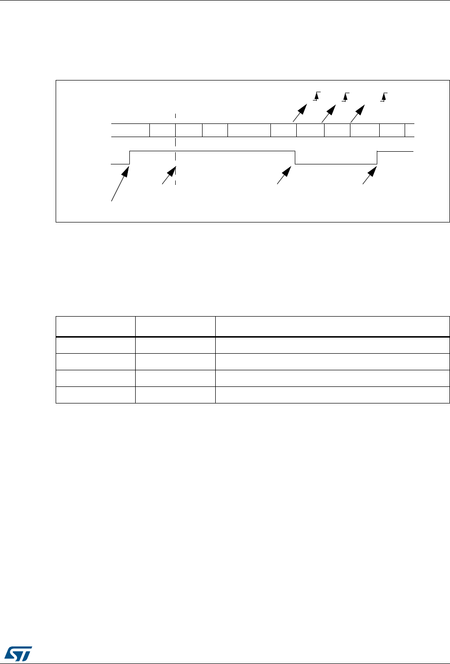
DocID018909 Rev 9 977/1718
RM0090 Universal synchronous asynchronous receiver transmitter (USART)
1003
The RWU bit can be written to as 0 or 1 when the receiver buffer contains no data (RXNE=0
in the USART_SR register). Otherwise the write attempt is ignored.
An example of mute mode behavior using address mark detection is given in Figure 304.
Figure 304. Mute mode using address mark detection
30.3.7 Parity control
Parity control (generation of parity bit in transmission and parity checking in reception) can
be enabled by setting the PCE bit in the USART_CR1 register. Depending on the frame
length defined by the M bit, the possible USART frame formats are as listed in Table 145.
Even parity
The parity bit is calculated to obtain an even number of “1s” inside the frame made of the 7
or 8 LSB bits (depending on whether M is equal to 0 or 1) and the parity bit.
E.g.: data=00110101; 4 bits set => parity bit will be 0 if even parity is selected (PS bit in
USART_CR1 = 0).
Odd parity
The parity bit is calculated to obtain an odd number of “1s” inside the frame made of the 7 or
8 LSB bits (depending on whether M is equal to 0 or 1) and the parity bit.
E.g.: data=00110101; 4 bits set => parity bit will be 1 if odd parity is selected (PS bit in
USART_CR1 = 1).
RWU written to 1
IDLE
RX Addr=0
RWU Mute Mode Normal Mode
Matching address
RXNE RXNE
(RXNE was cleared)
Data 2 Data 3 Data 4 Data 5Data 1 IDLE Addr=1 Addr=2
Mute Mode
In this example, the current address of the receiver is 1
(programmed in the USART_CR2 register)
nonmatching address nonmatching address
RXNE
Table 145. Frame formats
M bit PCE bit USART frame(1)
1. Legends: SB: start bit, STB: stop bit, PB: parity bit.
0 0 | SB | 8 bit data | STB |
0 1 | SB | 7-bit data | PB | STB |
1 0 | SB | 9-bit data | STB |
1 1 | SB | 8-bit data PB | STB |

Universal synchronous asynchronous receiver transmitter (USART) RM0090
978/1718 DocID018909 Rev 9
Parity checking in reception
If the parity check fails, the PE flag is set in the USART_SR register and an interrupt is
generated if PEIE is set in the USART_CR1 register. The PE flag is cleared by a software
sequence (a read from the status register followed by a read or write access to the
USART_DR data register).
Note: In case of wakeup by an address mark: the MSB bit of the data is taken into account to
identify an address but not the parity bit. And the receiver does not check the parity of the
address data (PE is not set in case of a parity error).
Parity generation in transmission
If the PCE bit is set in USART_CR1, then the MSB bit of the data written in the data register
is transmitted but is changed by the parity bit (even number of “1s” if even parity is selected
(PS=0) or an odd number of “1s” if odd parity is selected (PS=1)).
Note: The software routine that manages the transmission can activate the software sequence
which clears the PE flag (a read from the status register followed by a read or write access
to the data register). When operating in half-duplex mode, depending on the software, this
can cause the PE flag to be unexpectedly cleared.
30.3.8 LIN (local interconnection network) mode
The LIN mode is selected by setting the LINEN bit in the USART_CR2 register. In LIN
mode, the following bits must be kept cleared:
•STOP[1:0] and CLKEN in the USART_CR2 register
•SCEN, HDSEL and IREN in the USART_CR3 register.
LIN transmission
The same procedure explained in Section 30.3.2 has to be applied for LIN Master
transmission than for normal USART transmission with the following differences:
•Clear the M bit to configure 8-bit word length.
•Set the LINEN bit to enter LIN mode. In this case, setting the SBK bit sends 13 ‘0 bits
as a break character. Then a bit of value ‘1 is sent to allow the next start detection.
LIN reception
A break detection circuit is implemented on the USART interface. The detection is totally
independent from the normal USART receiver. A break can be detected whenever it occurs,
during Idle state or during a frame.
When the receiver is enabled (RE=1 in USART_CR1), the circuit looks at the RX input for a
start signal. The method for detecting start bits is the same when searching break
characters or data. After a start bit has been detected, the circuit samples the next bits
exactly like for the data (on the 8th, 9th and 10th samples). If 10 (when the LBDL = 0 in
USART_CR2) or 11 (when LBDL=1 in USART_CR2) consecutive bits are detected as ‘0,
and are followed by a delimiter character, the LBD flag is set in USART_SR. If the LBDIE
bit=1, an interrupt is generated. Before validating the break, the delimiter is checked for as it
signifies that the RX line has returned to a high level.
If a ‘1 is sampled before the 10 or 11 have occurred, the break detection circuit cancels the
current detection and searches for a start bit again.
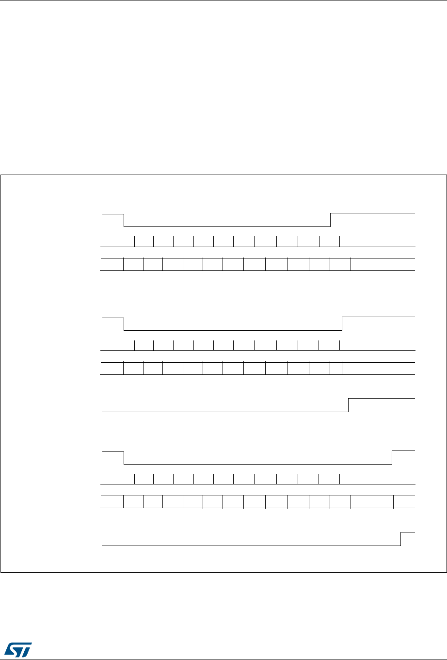
DocID018909 Rev 9 979/1718
RM0090 Universal synchronous asynchronous receiver transmitter (USART)
1003
If the LIN mode is disabled (LINEN=0), the receiver continues working as normal USART,
without taking into account the break detection.
If the LIN mode is enabled (LINEN=1), as soon as a framing error occurs (i.e. stop bit
detected at ‘0, which will be the case for any break frame), the receiver stops until the break
detection circuit receives either a ‘1, if the break word was not complete, or a delimiter
character if a break has been detected.
The behavior of the break detector state machine and the break flag is shown on the
Figure 305: Break detection in LIN mode (11-bit break length - LBDL bit is set) on page 979.
Examples of break frames are given on Figure 306: Break detection in LIN mode vs.
Framing error detection on page 980.
Figure 305. Break detection in LIN mode (11-bit break length - LBDL bit is set)
Case 1: break signal not long enough => break discarded, LBD is not set
Break Frame
RX line
Break State machine
Capture Strobe
0
Bit1 Bit2 Bit3 Bit4 Bit5 Bit6 Bit7 Bit8 Bit9
Idle Idle
Read Samples
Bit0
0000000001
Bit10
Break Frame
RX line
Break State machine
Capture Strobe
0
Bit1 Bit2 Bit3 Bit4 Bit5 Bit6 Bit7 Bit8 Bit9
Idle Idle
Read Samples
Bit0
0000000000
B10
Case 2: break signal just long enough => break detected, LBD is set
LBD
Break Frame
RX line
Break State machine
Capture Strobe
0
Bit1 Bit2 Bit3 Bit4 Bit5 Bit6 Bit7 Bit8 Bit9
Idle Idle
Read Samples
Bit0
0000000000
Bit10
Case 3: break signal long enough => break detected, LBD is set
wait delimiter
LBD
delimiter is immediate
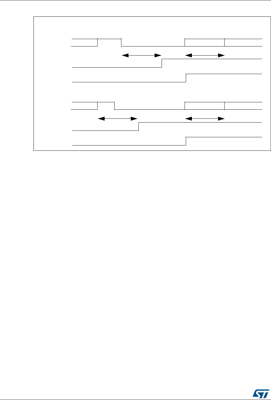
Universal synchronous asynchronous receiver transmitter (USART) RM0090
980/1718 DocID018909 Rev 9
Figure 306. Break detection in LIN mode vs. Framing error detection
30.3.9 USART synchronous mode
The synchronous mode is selected by writing the CLKEN bit in the USART_CR2 register to
1. In synchronous mode, the following bits must be kept cleared:
•LINEN bit in the USART_CR2 register,
•SCEN, HDSEL and IREN bits in the USART_CR3 register.
The USART allows the user to control a bidirectional synchronous serial communications in
master mode. The SCLK pin is the output of the USART transmitter clock. No clock pulses
are sent to the SCLK pin during start bit and stop bit. Depending on the state of the LBCL bit
in the USART_CR2 register clock pulses will or will not be generated during the last valid
data bit (address mark). The CPOL bit in the USART_CR2 register allows the user to select
the clock polarity, and the CPHA bit in the USART_CR2 register allows the user to select the
phase of the external clock (see Figure 307, Figure 308 & Figure 309).
During the Idle state, preamble and send break, the external SCLK clock is not activated.
In synchronous mode the USART transmitter works exactly like in asynchronous mode. But
as SCLK is synchronized with TX (according to CPOL and CPHA), the data on TX is
synchronous.
In this mode the USART receiver works in a different manner compared to the
asynchronous mode. If RE=1, the data is sampled on SCLK (rising or falling edge,
depending on CPOL and CPHA), without any oversampling. A setup and a hold time must
be respected (which depends on the baud rate: 1/16 bit time).
Note: The SCLK pin works in conjunction with the TX pin. Thus, the clock is provided only if the
transmitter is enabled (TE=1) and a data is being transmitted (the data register USART_DR
Case 1: break occurring after an Idle
IDLE data2 (0x55)data 1 data 3 (header)
In these examples, we suppose that LBDL=1 (11-bit break length), M=0 (8-bit data)
RX line
RXNE / FE
LBD
1 data time 1 data time
Case 1: break occurring while a data is being received
data 2 data2 (0x55)data 1 data 3 (header)
RX line
RXNE / FE
LBD
1 data time 1 data time
BREAK
BREAK
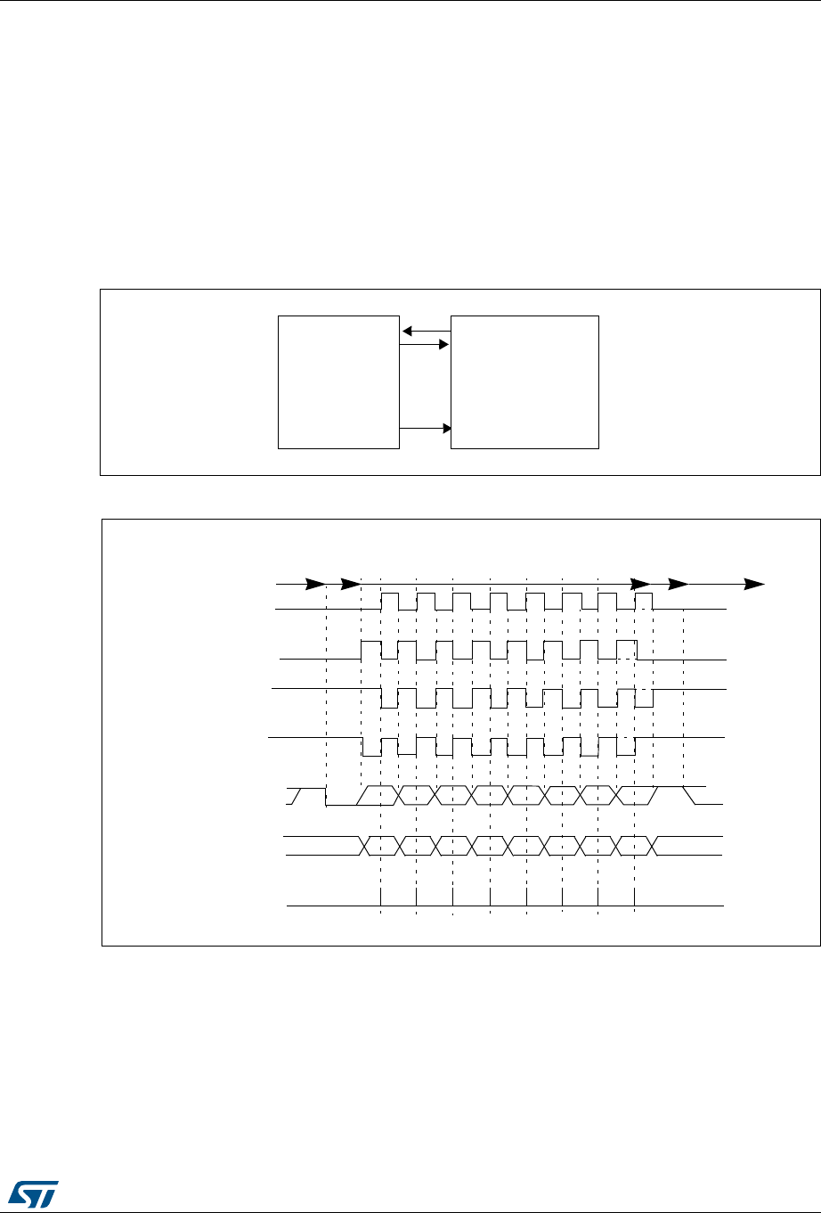
DocID018909 Rev 9 981/1718
RM0090 Universal synchronous asynchronous receiver transmitter (USART)
1003
has been written). This means that it is not possible to receive a synchronous data without
transmitting data.
The LBCL, CPOL and CPHA bits have to be selected when both the transmitter and the
receiver are disabled (TE=RE=0) to ensure that the clock pulses function correctly. These
bits should not be changed while the transmitter or the receiver is enabled.
It is advised that TE and RE are set in the same instruction in order to minimize the setup
and the hold time of the receiver.
The USART supports master mode only: it cannot receive or send data related to an input
clock (SCLK is always an output).
Figure 307. USART example of synchronous transmission
Figure 308. USART data clock timing diagram (M=0)
RX
TX
SCLK
USART
Data out
Data in
Synchronous device
Clock
(e.g. slave SPI)
M=0 (8 data bits)
Clock (CPOL=0, CPHA=1)
Clock (CPOL=1, CPHA=0)
Clock (CPOL=1, CPHA=1)
Start LSB MSB Stop
* LBCL bit controls last data clock pulse
Start
Idle or preceding
transmission
Data on TX
Stop
Clock (CPOL=0, CPHA=0)
01 234 56 7
*
*
*
*
Idle or next
transmission
*
Capture Strobe
LSB MSB
Data on RX 01 234 56 7
(from master)
(from slave)
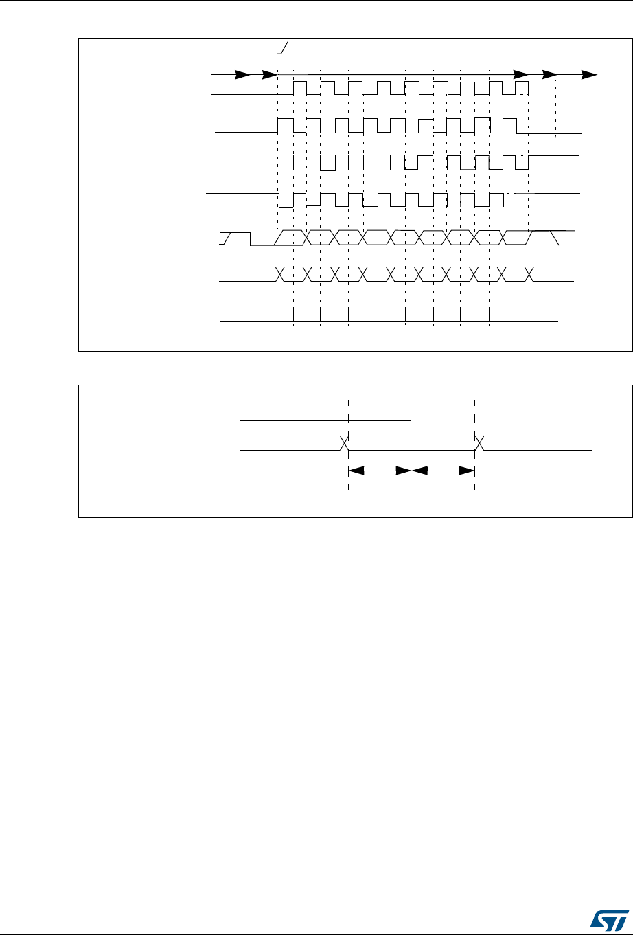
Universal synchronous asynchronous receiver transmitter (USART) RM0090
982/1718 DocID018909 Rev 9
Figure 309. USART data clock timing diagram (M=1)
Figure 310. RX data setup/hold time
Note: The function of SCLK is different in Smartcard mode. Refer to the Smartcard mode chapter
for more details.
30.3.10 Single-wire half-duplex communication
The single-wire half-duplex mode is selected by setting the HDSEL bit in the USART_CR3
register. In this mode, the following bits must be kept cleared:
•LINEN and CLKEN bits in the USART_CR2 register,
•SCEN and IREN bits in the USART_CR3 register.
The USART can be configured to follow a single-wire half-duplex protocol where the TX and
RX lines are internally connected. The selection between half- and full-duplex
communication is made with a control bit ‘HALF DUPLEX SEL’ (HDSEL in USART_CR3).
As soon as HDSEL is written to 1:
•the TX and RX lines are internally connected
•the RX pin is no longer used
•the TX pin is always released when no data is transmitted. Thus, it acts as a standard
I/O in idle or in reception. It means that the I/O must be configured so that TX is
configured as floating input (or output high open-drain) when not driven by the USART.
Idle or next
M=1 (9 data bits)
Clock (CPOL=0, CPHA=1)
Clock (CPOL=1, CPHA=0)
Clock (CPOL=1, CPHA=1)
Start LSB MSB Stop
* LBCL bit controls last data clock pulse
Start
Idle or preceding
transmission
Data on TX
Stop
Clock (CPOL=0, CPHA=0)
01 234 56 7
*
*
*
*
8
transmission
Capture Strobe
LSB MSB
Data on RX 01 234 56 7
(from slave)
(from master)
*
8
valid DATA bit
tSETUP tHOLD
SCLK (capture strobe on SCLK
rising edge in this example)
Data on RX
(from slave)
tSETUP = tHOLD 1/16 bit time
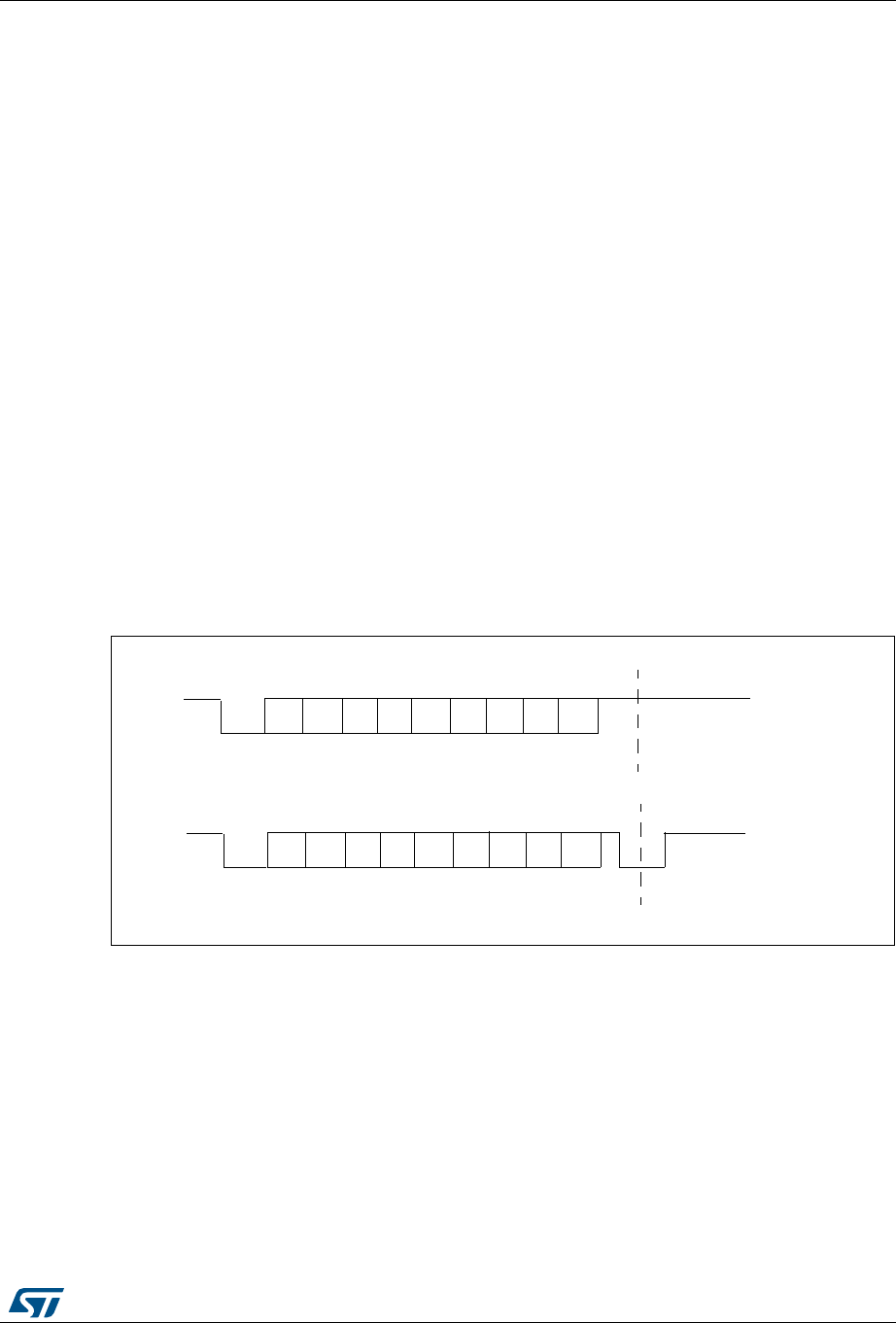
DocID018909 Rev 9 983/1718
RM0090 Universal synchronous asynchronous receiver transmitter (USART)
1003
Apart from this, the communications are similar to what is done in normal USART mode.
The conflicts on the line must be managed by the software (by the use of a centralized
arbiter, for instance). In particular, the transmission is never blocked by hardware and
continue to occur as soon as a data is written in the data register while the TE bit is set.
30.3.11 Smartcard
The Smartcard mode is selected by setting the SCEN bit in the USART_CR3 register. In
smartcard mode, the following bits must be kept cleared:
•LINEN bit in the USART_CR2 register,
•HDSEL and IREN bits in the USART_CR3 register.
Moreover, the CLKEN bit may be set in order to provide a clock to the smartcard.
The Smartcard interface is designed to support asynchronous protocol Smartcards as
defined in the ISO 7816-3 standard. The USART should be configured as:
•8 bits plus parity: where M=1 and PCE=1 in the USART_CR1 register
•1.5 stop bits when transmitting and receiving: where STOP=11 in the USART_CR2
register.
Note: It is also possible to choose 0.5 stop bit for receiving but it is recommended to use 1.5 stop
bits for both transmitting and receiving to avoid switching between the two configurations.
Figure 311 shows examples of what can be seen on the data line with and without parity
error.
Figure 311. ISO 7816-3 asynchronous protocol
When connected to a Smartcard, the TX output of the USART drives a bidirectional line that
is also driven by the Smartcard. The TX pin must be configured as open-drain.
Smartcard is a single wire half duplex communication protocol.
•Transmission of data from the transmit shift register is guaranteed to be delayed by a
minimum of 1/2 baud clock. In normal operation a full transmit shift register will start
shifting on the next baud clock edge. In Smartcard mode this transmission is further
delayed by a guaranteed 1/2 baud clock.
•If a parity error is detected during reception of a frame programmed with a 0.5 or 1.5
stop bit period, the transmit line is pulled low for a baud clock period after the
completion of the receive frame. This is to indicate to the Smartcard that the data
transmitted to USART has not been correctly received. This NACK signal (pulling
transmit line low for 1 baud clock) will cause a framing error on the transmitter side
S0123 5
467P
Start
bit
Guard time
S0123 5
467P
Start
bit
Line pulled low
by receiver during stop in
case of parity error
Guard time
Without Parity error
With Parity error
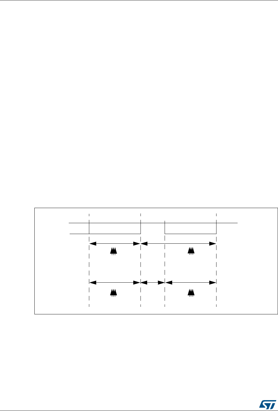
Universal synchronous asynchronous receiver transmitter (USART) RM0090
984/1718 DocID018909 Rev 9
(configured with 1.5 stop bits). The application can handle re-sending of data according
to the protocol. A parity error is ‘NACK’ed by the receiver if the NACK control bit is set,
otherwise a NACK is not transmitted.
•The assertion of the TC flag can be delayed by programming the Guard Time register.
In normal operation, TC is asserted when the transmit shift register is empty and no
further transmit requests are outstanding. In Smartcard mode an empty transmit shift
register triggers the guard time counter to count up to the programmed value in the
Guard Time register. TC is forced low during this time. When the guard time counter
reaches the programmed value TC is asserted high.
•The de-assertion of TC flag is unaffected by Smartcard mode.
•If a framing error is detected on the transmitter end (due to a NACK from the receiver),
the NACK will not be detected as a start bit by the receive block of the transmitter.
According to the ISO protocol, the duration of the received NACK can be 1 or 2 baud
clock periods.
•On the receiver side, if a parity error is detected and a NACK is transmitted the receiver
will not detect the NACK as a start bit.
Note: A break character is not significant in Smartcard mode. A 0x00 data with a framing error will
be treated as data and not as a break.
No Idle frame is transmitted when toggling the TE bit. The Idle frame (as defined for the
other configurations) is not defined by the ISO protocol.
Figure 312 details how the NACK signal is sampled by the USART. In this example the
USART is transmitting a data and is configured with 1.5 stop bits. The receiver part of the
USART is enabled in order to check the integrity of the data and the NACK signal.
Figure 312. Parity error detection using the 1.5 stop bits
The USART can provide a clock to the smartcard through the SCLK output. In smartcard
mode, SCLK is not associated to the communication but is simply derived from the internal
peripheral input clock through a 5-bit prescaler. The division ratio is configured in the
prescaler register USART_GTPR. SCLK frequency can be programmed from fCK/2 to
fCK/62, where fCK is the peripheral input clock.
1 bit time 1.5 bit time
0.5 bit time 1 bit time
sampling at
8th, 9th, 10th
sampling at
8th, 9th, 10th
sampling at
8th, 9th, 10th
sampling at
16th, 17th, 18th
Bit 7 Parity Bit 1.5 Stop Bit

DocID018909 Rev 9 985/1718
RM0090 Universal synchronous asynchronous receiver transmitter (USART)
1003
30.3.12 IrDA SIR ENDEC block
The IrDA mode is selected by setting the IREN bit in the USART_CR3 register. In IrDA
mode, the following bits must be kept cleared:
•LINEN, STOP and CLKEN bits in the USART_CR2 register,
•SCEN and HDSEL bits in the USART_CR3 register.
The IrDA SIR physical layer specifies use of a Return to Zero, Inverted (RZI) modulation
scheme that represents logic 0 as an infrared light pulse (see Figure 313).
The SIR Transmit encoder modulates the Non Return to Zero (NRZ) transmit bit stream
output from USART. The output pulse stream is transmitted to an external output driver and
infrared LED. USART supports only bit rates up to 115.2Kbps for the SIR ENDEC. In normal
mode the transmitted pulse width is specified as 3/16 of a bit period.
The SIR receive decoder demodulates the return-to-zero bit stream from the infrared
detector and outputs the received NRZ serial bit stream to USART. The decoder input is
normally HIGH (marking state) in the Idle state. The transmit encoder output has the
opposite polarity to the decoder input. A start bit is detected when the decoder input is low.
•IrDA is a half duplex communication protocol. If the Transmitter is busy (i.e. the USART
is sending data to the IrDA encoder), any data on the IrDA receive line will be ignored
by the IrDA decoder and if the Receiver is busy (USART is receiving decoded data
from the USART), data on the TX from the USART to IrDA will not be encoded by IrDA.
While receiving data, transmission should be avoided as the data to be transmitted
could be corrupted.
•A ‘0 is transmitted as a high pulse and a ‘1 is transmitted as a ‘0. The width of the pulse
is specified as 3/16th of the selected bit period in normal mode (see Figure 314).
•The SIR decoder converts the IrDA compliant receive signal into a bit stream for
USART.
•The SIR receive logic interprets a high state as a logic one and low pulses as logic
zeros.
•The transmit encoder output has the opposite polarity to the decoder input. The SIR
output is in low state when Idle.
•The IrDA specification requires the acceptance of pulses greater than 1.41 us. The
acceptable pulse width is programmable. Glitch detection logic on the receiver end
filters out pulses of width less than 2 PSC periods (PSC is the prescaler value
programmed in the IrDA low-power Baud Register, USART_GTPR). Pulses of width
less than 1 PSC period are always rejected, but those of width greater than one and
less than two periods may be accepted or rejected, those greater than 2 periods will be
accepted as a pulse. The IrDA encoder/decoder doesn’t work when PSC=0.
•The receiver can communicate with a low-power transmitter.
•In IrDA mode, the STOP bits in the USART_CR2 register must be configured to “1 stop
bit”.
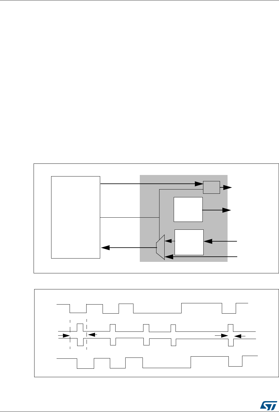
Universal synchronous asynchronous receiver transmitter (USART) RM0090
986/1718 DocID018909 Rev 9
IrDA low-power mode
Transmitter:
In low-power mode the pulse width is not maintained at 3/16 of the bit period. Instead, the
width of the pulse is 3 times the low-power baud rate which can be a minimum of 1.42 MHz.
Generally this value is 1.8432 MHz (1.42 MHz < PSC< 2.12 MHz). A low-power mode
programmable divisor divides the system clock to achieve this value.
Receiver:
Receiving in low-power mode is similar to receiving in normal mode. For glitch detection the
USART should discard pulses of duration shorter than 1/PSC. A valid low is accepted only if
its duration is greater than 2 periods of the IrDA low-power Baud clock (PSC value in
USART_GTPR).
Note: A pulse of width less than two and greater than one PSC period(s) may or may not be
rejected.
The receiver set up time should be managed by software. The IrDA physical layer
specification specifies a minimum of 10 ms delay between transmission and reception (IrDA
is a half duplex protocol).
Figure 313. IrDA SIR ENDEC- block diagram
Figure 314. IrDA data modulation (3/16) -Normal mode
USART
SIR
Transmit
Encoder
SIR
Receive
Decoder
OR USART_TX
IrDA_OUT
IrDA_IN
USART_RX
TX
RX
SIREN
TX
IrDA_OUT
IrDA_IN
RX
Start
bit
0101001101
3/16
stop bit
bit period
0101001101

DocID018909 Rev 9 987/1718
RM0090 Universal synchronous asynchronous receiver transmitter (USART)
1003
30.3.13 Continuous communication using DMA
The USART is capable of continuous communication using the DMA. The DMA requests for
Rx buffer and Tx buffer are generated independently.
Transmission using DMA
DMA mode can be enabled for transmission by setting DMAT bit in the USART_CR3
register. Data is loaded from a SRAM area configured using the DMA peripheral (refer to the
DMA specification) to the USART_DR register whenever the TXE bit is set. To map a DMA
channel for USART transmission, use the following procedure (x denotes the channel
number):
1. Write the USART_DR register address in the DMA control register to configure it as the
destination of the transfer. The data will be moved to this address from memory after
each TXE event.
2. Write the memory address in the DMA control register to configure it as the source of
the transfer. The data will be loaded into the USART_DR register from this memory
area after each TXE event.
3. Configure the total number of bytes to be transferred to the DMA control register.
4. Configure the channel priority in the DMA register
5. Configure DMA interrupt generation after half/ full transfer as required by the
application.
6. Clear the TC bit in the SR register by writing 0 to it.
7. Activate the channel in the DMA register.
When the number of data transfers programmed in the DMA Controller is reached, the DMA
controller generates an interrupt on the DMA channel interrupt vector.
In transmission mode, once the DMA has written all the data to be transmitted (the TCIF flag
is set in the DMA_ISR register), the TC flag can be monitored to make sure that the USART
communication is complete. This is required to avoid corrupting the last transmission before
disabling the USART or entering the Stop mode. The software must wait until TC=1. The TC
flag remains cleared during all data transfers and it is set by hardware at the last frame’s
end of transmission.
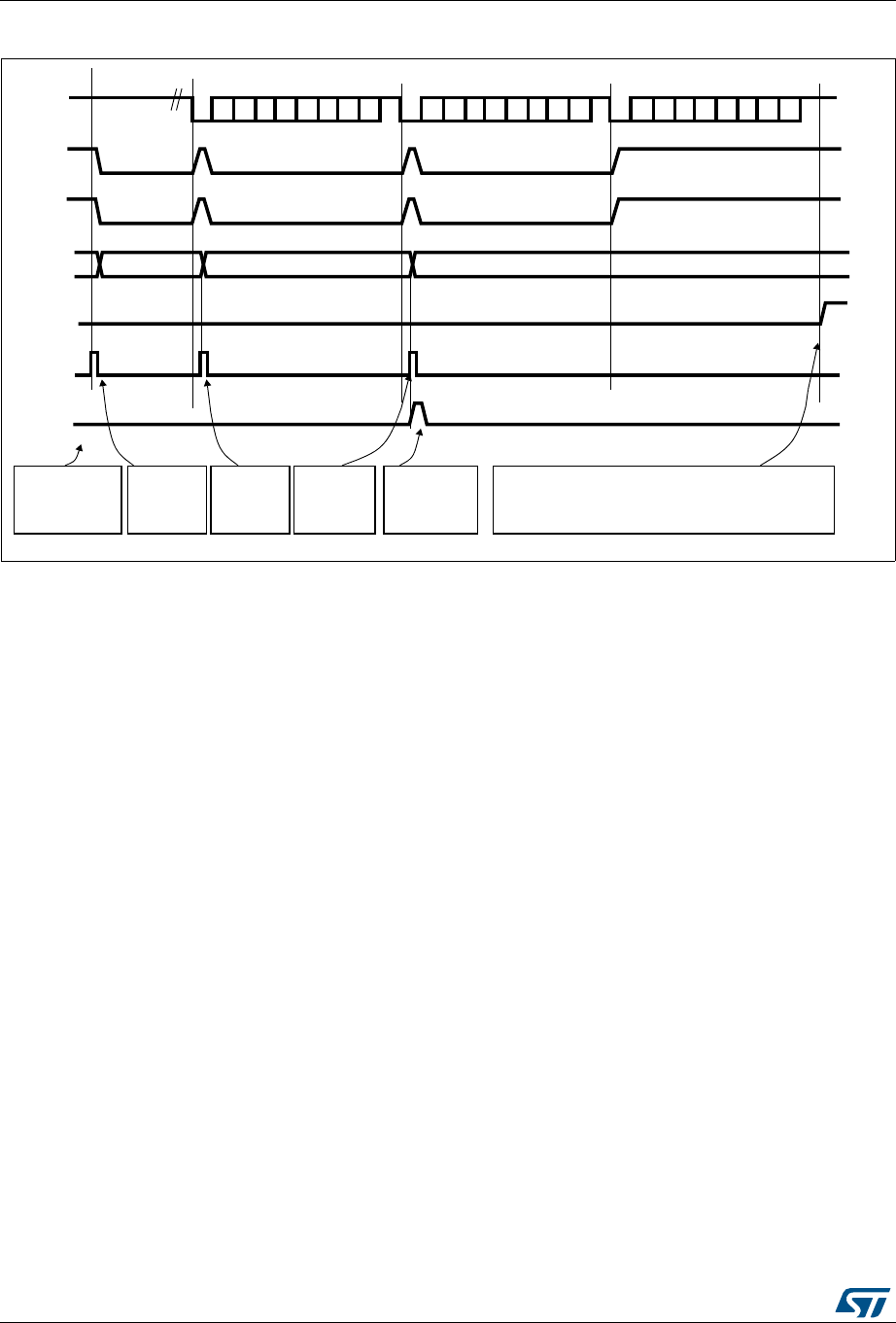
Universal synchronous asynchronous receiver transmitter (USART) RM0090
988/1718 DocID018909 Rev 9
Figure 315. Transmission using DMA
Reception using DMA
DMA mode can be enabled for reception by setting the DMAR bit in USART_CR3 register.
Data is loaded from the USART_DR register to a SRAM area configured using the DMA
peripheral (refer to the DMA specification) whenever a data byte is received. To map a DMA
channel for USART reception, use the following procedure:
1. Write the USART_DR register address in the DMA control register to configure it as the
source of the transfer. The data will be moved from this address to the memory after
each RXNE event.
2. Write the memory address in the DMA control register to configure it as the destination
of the transfer. The data will be loaded from USART_DR to this memory area after each
RXNE event.
3. Configure the total number of bytes to be transferred in the DMA control register.
4. Configure the channel priority in the DMA control register
5. Configure interrupt generation after half/ full transfer as required by the application.
6. Activate the channel in the DMA control register.
When the number of data transfers programmed in the DMA Controller is reached, the DMA
controller generates an interrupt on the DMA channel interrupt vector. The DMAR bit should
be cleared by software in the USART_CR3 register during the interrupt subroutine.
48LINE
53!24?$2
&RAME
48%FLAG
&
4#FLAG
&
&RAME
VRIWZDUHZDLWVXQWLO7&
&RAME
SETBYHARDWARE
CLEAREDBY$-!READ
SETBYHARDWARE
CLEAREDBY$-!READ SETBYHARDWARE
SET
)DLEPREAMBLE
BYHARDWARE
&
VRIWZDUHFRQILJXUHV
WKH'0$WRVHQG
GDWDDQGHQDEOHVWKH
86$57
$-!REQUEST IGNOREDBYTHE$-!
$-!WRITES
FLAG$-!4#)& SETBYHARDWARE CLEAR
BYSOFTWARE
53!24?$2
BECAUSE$-!TRANSFERISCOMPLETE
'0$ZULWHV)
LQWR
86$57B'5
'0$ZULWHV)
LQWR
86$57B'5
'0$ZULWHV)
LQWR
86$57B'5
7KH'0$WUDQVIHU
LVFRPSOHWH
7&,) LQ
'0$B,65
4RA NSFERCOMPLETE
AIB
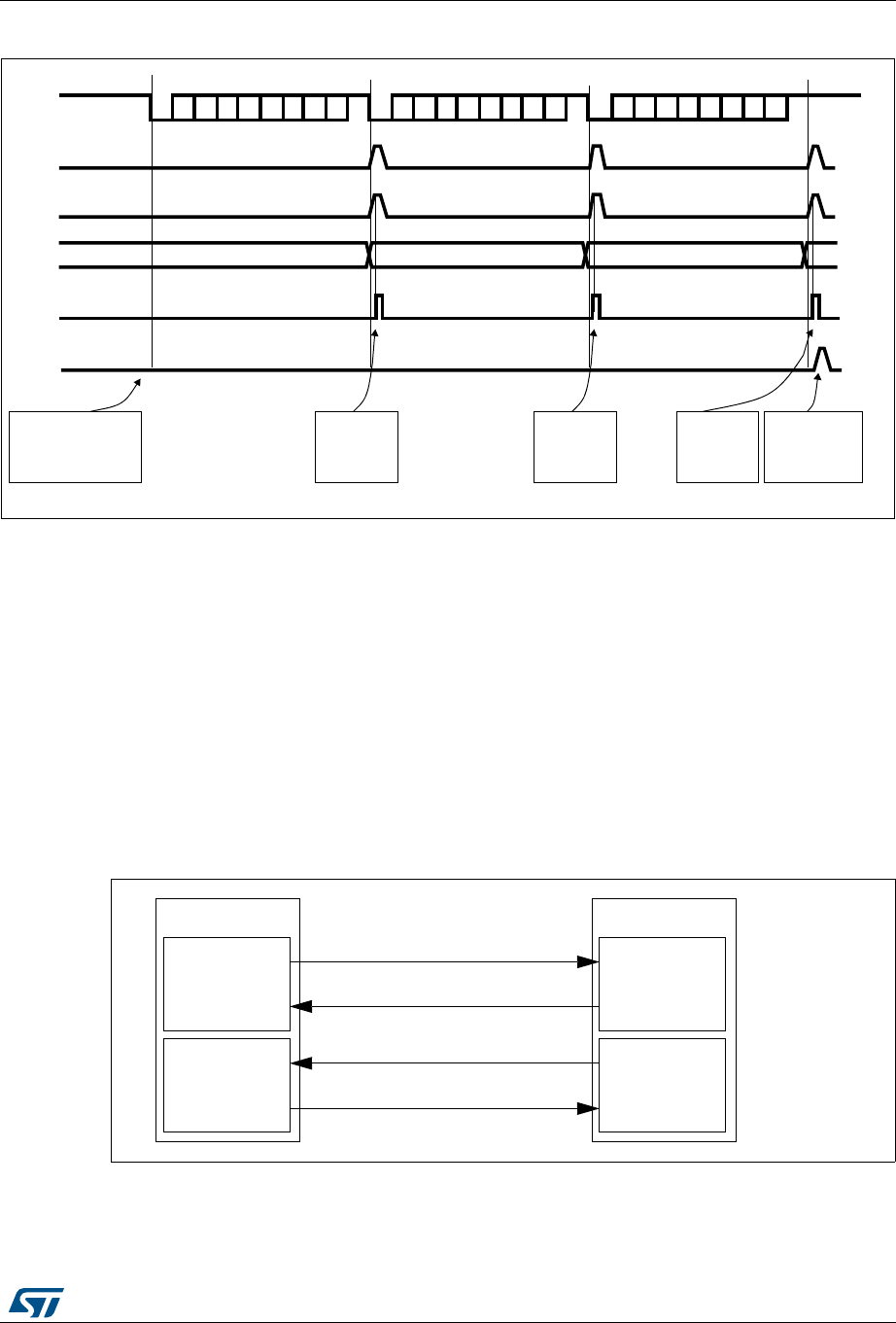
DocID018909 Rev 9 989/1718
RM0090 Universal synchronous asynchronous receiver transmitter (USART)
1003
Figure 316. Reception using DMA
Error flagging and interrupt generation in multibuffer communication
In case of multibuffer communication if any error occurs during the transaction the error flag
will be asserted after the current byte. An interrupt will be generated if the interrupt enable
flag is set. For framing error, overrun error and noise flag which are asserted with RXNE in
case of single byte reception, there will be separate error flag interrupt enable bit (EIE bit in
the USART_CR3 register), which if set will issue an interrupt after the current byte with
either of these errors.
30.3.14 Hardware flow control
It is possible to control the serial data flow between 2 devices by using the nCTS input and
the nRTS output. The Figure 317 shows how to connect 2 devices in this mode:
Figure 317. Hardware flow control between 2 USARTs
RTS and CTS flow control can be enabled independently by writing respectively RTSE and
CTSE bits to 1 (in the USART_CR3 register).
48LINE
53!24?$2
&RAME
28.%FLAG
& &
&RAME &RAME
SETBYHARDWARE
CLEAREDBY$-!READ
&
VRIWZDUHFRQILJXUHVWKH
'0$WRUHFHLYHGDWD
EORFNVDQGHQDEOHV
WKH86$57
$-!REQUEST
$-!READS53!24?$2
$-!4#)&FLAG SETBYHARDWARE CLEARED
BYSOFTWARE
'0$UHDGV)
IURP
86$57B'5
4RA NSFERCOMPLETE
'0$UHDGV)
IURP
86$57B'5
'0$UHDGV)
IURP
86$57B'5
7KH'0$WUDQVIHU
LVFRPSOHWH
7&,) LQ
'0$B,65
AIB
USART 1
RX circuit
TX circuit
USART 2
TX circuit
RX circuit
RXTX
TX
RX
nCTS nRTS
nRTS nCTS
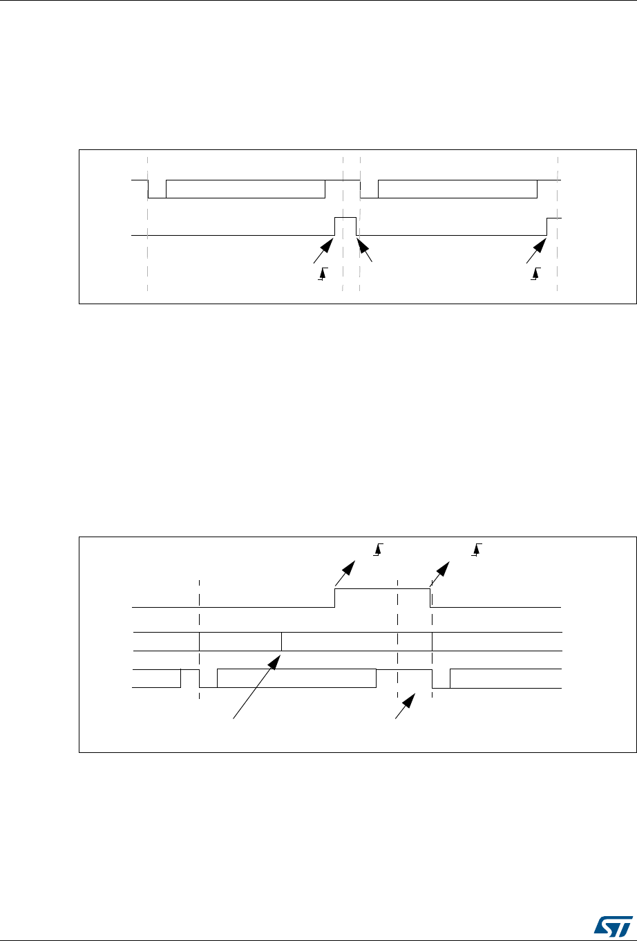
Universal synchronous asynchronous receiver transmitter (USART) RM0090
990/1718 DocID018909 Rev 9
RTS flow control
If the RTS flow control is enabled (RTSE=1), then nRTS is asserted (tied low) as long as the
USART receiver is ready to receive a new data. When the receive register is full, nRTS is
deasserted, indicating that the transmission is expected to stop at the end of the current
frame. Figure 318 shows an example of communication with RTS flow control enabled.
Figure 318. RTS flow control
CTS flow control
If the CTS flow control is enabled (CTSE=1), then the transmitter checks the nCTS input
before transmitting the next frame. If nCTS is asserted (tied low), then the next data is
transmitted (assuming that a data is to be transmitted, in other words, if TXE=0), else the
transmission does not occur. When nCTS is deasserted during a transmission, the current
transmission is completed before the transmitter stops.
When CTSE=1, the CTSIF status bit is automatically set by hardware as soon as the nCTS
input toggles. It indicates when the receiver becomes ready or not ready for communication.
An interrupt is generated if the CTSIE bit in the USART_CR3 register is set. The figure
below shows an example of communication with CTS flow control enabled.
Figure 319. CTS flow control
Note: Special behavior of break frames: when the CTS flow is enabled, the transmitter does not
check the nCTS input state to send a break.
Start
Bit Stop
Bit
Data 1 IdleStart
Bit
Stop
Bit
Data 2
RX
nRTS
RXNE Data 1 read RXNE
Data 2 can now be transmitted
Start
Bit
Stop
Bit
Data 2 Idle Start
Bit Data 3
TX
nCTS
CTS
Transmission of Data 3
Data 1 Stop
Bit
is delayed until nCTS = 0
CTS
Data 2 Data 3empty empty
Transmit data register
TDR
Writing data 3 in TDR
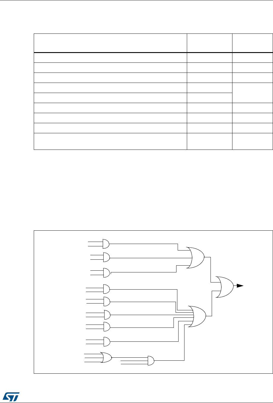
DocID018909 Rev 9 991/1718
RM0090 Universal synchronous asynchronous receiver transmitter (USART)
1003
30.4 USART interrupts
The USART interrupt events are connected to the same interrupt vector (see Figure 320).
•During transmission: Transmission Complete, Clear to Send or Transmit Data Register
empty interrupt.
•While receiving: Idle Line detection, Overrun error, Receive Data register not empty,
Parity error, LIN break detection, Noise Flag (only in multi buffer communication) and
Framing Error (only in multi buffer communication).
These events generate an interrupt if the corresponding Enable Control Bit is set.
Figure 320. USART interrupt mapping diagram
Table 146. USART interrupt requests
Interrupt event Event flag Enable control
bit
Transmit Data Register Empty TXE TXEIE
CTS flag CTS CTSIE
Transmission Complete TC TCIE
Received Data Ready to be Read RXNE
RXNEIE
Overrun Error Detected ORE
Idle Line Detected IDLE IDLEIE
Parity Error PE PEIE
Break Flag LBD LBDIE
Noise Flag, Overrun error and Framing Error in multibuffer
communication NF or ORE or FE EIE
TC
TCIE
TXE
TXEIE
IDLE
IDLEIE
RXNEIE
ORE
RXNEIE
RXNE
PE
PEIE
FE
NE
ORE EIE
DMAR
USART
LBD
LBDIE
CTS
CTSIE
interrupt
Universal synchronous asynchronous receiver transmitter (USART) RM0090
992/1718 DocID018909 Rev 9
30.5 USART mode configuration
30.6 USART registers
Refer to Section 1.1 on page 57 for a list of abbreviations used in register descriptions.
The peripheral registers have to be accessed by half-words (16 bits) or words (32 bits).
30.6.1 Status register (USART_SR)
Address offset: 0x00
Reset value: 0x00C0 0000
Table 147. USART mode configuration(1)
1. X = supported; NA = not applicable.
USART modes USART
1
USART
2
USART
3UART4 UART5 USART
6
Asynchronous mode XXXXXX
Hardware flow control XXXNANAX
Multibuffer communication (DMA)XXXXXX
Multiprocessor communicationXXXXXX
Synchronous XXXNANAX
Smartcard XXXNANAX
Half-duplex (single-wire mode)XXXXXX
IrDA XXXXXX
LIN XXXXXX
31 30 29 28 27 26 25 24 23 22 21 20 19 18 17 16
Reserved
1514131211109876543210
Reserved CTS LBD TXE TC RXNE IDLE ORE NF FE PE
rc_w0rc_w0rrc_w0rc_w0rrrrr

DocID018909 Rev 9 993/1718
RM0090 Universal synchronous asynchronous receiver transmitter (USART)
1003
Bits 31:10 Reserved, must be kept at reset value
Bit 9 CTS: CTS flag
This bit is set by hardware when the nCTS input toggles, if the CTSE bit is set. It is cleared
by software (by writing it to 0). An interrupt is generated if CTSIE=1 in the USART_CR3
register.
0: No change occurred on the nCTS status line
1: A change occurred on the nCTS status line
Note: This bit is not available for UART4 & UART5.
Bit 8 LBD: LIN break detection flag
This bit is set by hardware when the LIN break is detected. It is cleared by software (by
writing it to 0). An interrupt is generated if LBDIE = 1 in the USART_CR2 register.
0: LIN Break not detected
1: LIN break detected
Note: An interrupt is generated when LBD=1 if LBDIE=1
Bit 7 TXE: Transmit data register empty
This bit is set by hardware when the content of the TDR register has been transferred into
the shift register. An interrupt is generated if the TXEIE bit =1 in the USART_CR1 register. It
is cleared by a write to the USART_DR register.
0: Data is not transferred to the shift register
1: Data is transferred to the shift register)
Note: This bit is used during single buffer transmission.
Bit 6 TC: Transmission complete
This bit is set by hardware if the transmission of a frame containing data is complete and if
TXE is set. An interrupt is generated if TCIE=1 in the USART_CR1 register. It is cleared by
a software sequence (a read from the USART_SR register followed by a write to the
USART_DR register). The TC bit can also be cleared by writing a '0' to it. This clearing
sequence is recommended only for multibuffer communication.
0: Transmission is not complete
1: Transmission is complete
Bit 5 RXNE: Read data register not empty
This bit is set by hardware when the content of the RDR shift register has been transferred
to the USART_DR register. An interrupt is generated if RXNEIE=1 in the USART_CR1
register. It is cleared by a read to the USART_DR register. The RXNE flag can also be
cleared by writing a zero to it. This clearing sequence is recommended only for multibuffer
communication.
0: Data is not received
1: Received data is ready to be read.
Bit 4 IDLE: IDLE line detected
This bit is set by hardware when an Idle Line is detected. An interrupt is generated if the
IDLEIE=1 in the USART_CR1 register. It is cleared by a software sequence (an read to the
USART_SR register followed by a read to the USART_DR register).
0: No Idle Line is detected
1: Idle Line is detected
Note: The IDLE bit will not be set again until the RXNE bit has been set itself (i.e. a new idle
line occurs).

Universal synchronous asynchronous receiver transmitter (USART) RM0090
994/1718 DocID018909 Rev 9
Bit 3 ORE: Overrun error
This bit is set by hardware when the word currently being received in the shift register is
ready to be transferred into the RDR register while RXNE=1. An interrupt is generated if
RXNEIE=1 in the USART_CR1 register. It is cleared by a software sequence (an read to the
USART_SR register followed by a read to the USART_DR register).
0: No Overrun error
1: Overrun error is detected
Note: When this bit is set, the RDR register content will not be lost but the shift register will be
overwritten. An interrupt is generated on ORE flag in case of Multi Buffer
communication if the EIE bit is set.
Bit 2 NF: Noise detected flag
This bit is set by hardware when noise is detected on a received frame. It is cleared by a
software sequence (an read to the USART_SR register followed by a read to the
USART_DR register).
0: No noise is detected
1: Noise is detected
Note: This bit does not generate interrupt as it appears at the same time as the RXNE bit
which itself generates an interrupting interrupt is generated on NF flag in case of Multi
Buffer communication if the EIE bit is set.
Note: When the line is noise-free, the NF flag can be disabled by programming the ONEBIT
bit to 1 to increase the USART tolerance to deviations (Refer to Section 30.3.5: USART
receiver tolerance to clock deviation on page 975).
Bit 1 FE: Framing error
This bit is set by hardware when a de-synchronization, excessive noise or a break character
is detected. It is cleared by a software sequence (an read to the USART_SR register
followed by a read to the USART_DR register).
0: No Framing error is detected
1: Framing error or break character is detected
Note: This bit does not generate interrupt as it appears at the same time as the RXNE bit
which itself generates an interrupt. If the word currently being transferred causes both
frame error and overrun error, it will be transferred and only the ORE bit will be set.
An interrupt is generated on FE flag in case of Multi Buffer communication if the EIE bit
is set.
Bit 0 PE: Parity error
This bit is set by hardware when a parity error occurs in receiver mode. It is cleared by a
software sequence (a read from the status register followed by a read or write access to the
USART_DR data register). The software must wait for the RXNE flag to be set before
clearing the PE bit.
An interrupt is generated if PEIE = 1 in the USART_CR1 register.
0: No parity error
1: Parity error

DocID018909 Rev 9 995/1718
RM0090 Universal synchronous asynchronous receiver transmitter (USART)
1003
30.6.2 Data register (USART_DR)
Address offset: 0x04
Reset value: 0xXXXX XXXX
30.6.3 Baud rate register (USART_BRR)
Note: The baud counters stop counting if the TE or RE bits are disabled respectively.
Address offset: 0x08
Reset value: 0x0000 0000
30.6.4 Control register 1 (USART_CR1)
Address offset: 0x0C
Reset value: 0x0000 0000
Bits 31:9 Reserved, must be kept at reset value
Bits 8:0 DR[8:0]: Data value
Contains the Received or Transmitted data character, depending on whether it is read from
or written to.
The Data register performs a double function (read and write) since it is composed of two
registers, one for transmission (TDR) and one for reception (RDR)
The TDR register provides the parallel interface between the internal bus and the output shift
register (see Figure 1).
The RDR register provides the parallel interface between the input shift register and the
internal bus.
When transmitting with the parity enabled (PCE bit set to 1 in the USART_CR1 register), the
value written in the MSB (bit 7 or bit 8 depending on the data length) has no effect because
it is replaced by the parity.
When receiving with the parity enabled, the value read in the MSB bit is the received parity
bit.
31 30 29 28 27 26 25 24 23 22 21 20 19 18 17 16
Reserved
1514131211109876543210
DIV_Mantissa[11:0] DIV_Fraction[3:0]
rw rw rw rw rw rw rw rw rw rw rw rw rw rw rw rw
Bits 31:16 Reserved, must be kept at reset value
Bits 15:4 DIV_Mantissa[11:0]: mantissa of USARTDIV
These 12 bits define the mantissa of the USART Divider (USARTDIV)
Bits 3:0 DIV_Fraction[3:0]: fraction of USARTDIV
These 4 bits define the fraction of the USART Divider (USARTDIV). When OVER8=1, the
DIV_Fraction3 bit is not considered and must be kept cleared.
31 30 29 28 27 26 25 24 23 22 21 20 19 18 17 16
Reserved
15 14 13 12 11 10 9 8 7 6 5 4 3 2 1 0
OVER8 Reserved UE M WAKE PCE PS PEIE TXEIE TCIE RXNEIE IDLEIE TE RE RWU SBK
rw Res. rw rw rw rw rw rw rw rw rw rw rw rw rw rw

Universal synchronous asynchronous receiver transmitter (USART) RM0090
996/1718 DocID018909 Rev 9
Bits 31:16 Reserved, must be kept at reset value
Bit 15 OVER8: Oversampling mode
0: oversampling by 16
1: oversampling by 8
Note: Oversampling by 8 is not available in the Smartcard, IrDA and LIN modes: when
SCEN=1,IREN=1 or LINEN=1 then OVER8 is forced to ‘0 by hardware.
Bit 14 Reserved, must be kept at reset value
Bit 13 UE: USART enable
When this bit is cleared, the USART prescalers and outputs are stopped and the end of the
current byte transfer in order to reduce power consumption. This bit is set and cleared by
software.
0: USART prescaler and outputs disabled
1: USART enabled
Bit 12 M: Word length
This bit determines the word length. It is set or cleared by software.
0: 1 Start bit, 8 Data bits, n Stop bit
1: 1 Start bit, 9 Data bits, n Stop bit
Note: The M bit must not be modified during a data transfer (both transmission and reception)
Bit 11 WAKE: Wakeup method
This bit determines the USART wakeup method, it is set or cleared by software.
0: Idle Line
1: Address Mark
Bit 10 PCE: Parity control enable
This bit selects the hardware parity control (generation and detection). When the parity
control is enabled, the computed parity is inserted at the MSB position (9th bit if M=1; 8th bit
if M=0) and parity is checked on the received data. This bit is set and cleared by software.
Once it is set, PCE is active after the current byte (in reception and in transmission).
0: Parity control disabled
1: Parity control enabled
Bit 9 PS: Parity selection
This bit selects the odd or even parity when the parity generation/detection is enabled (PCE
bit set). It is set and cleared by software. The parity will be selected after the current byte.
0: Even parity
1: Odd parity
Bit 8 PEIE: PE interrupt enable
This bit is set and cleared by software.
0: Interrupt is inhibited
1: An USART interrupt is generated whenever PE=1 in the USART_SR register
Bit 7 TXEIE: TXE interrupt enable
This bit is set and cleared by software.
0: Interrupt is inhibited
1: An USART interrupt is generated whenever TXE=1 in the USART_SR register
Bit 6 TCIE: Transmission complete interrupt enable
This bit is set and cleared by software.
0: Interrupt is inhibited
1: An USART interrupt is generated whenever TC=1 in the USART_SR register

DocID018909 Rev 9 997/1718
RM0090 Universal synchronous asynchronous receiver transmitter (USART)
1003
Bit 5 RXNEIE: RXNE interrupt enable
This bit is set and cleared by software.
0: Interrupt is inhibited
1: An USART interrupt is generated whenever ORE=1 or RXNE=1 in the USART_SR
register
Bit 4 IDLEIE: IDLE interrupt enable
This bit is set and cleared by software.
0: Interrupt is inhibited
1: An USART interrupt is generated whenever IDLE=1 in the USART_SR register
Bit 3 TE: Transmitter enable
This bit enables the transmitter. It is set and cleared by software.
0: Transmitter is disabled
1: Transmitter is enabled
Note: During transmission, a “0” pulse on the TE bit (“0” followed by “1”) sends a preamble
(idle line) after the current word, except in smartcard mode.
When TE is set, there is a 1 bit-time delay before the transmission starts.
Bit 2 RE: Receiver enable
This bit enables the receiver. It is set and cleared by software.
0: Receiver is disabled
1: Receiver is enabled and begins searching for a start bit
Bit 1 RWU: Receiver wakeup
This bit determines if the USART is in mute mode or not. It is set and cleared by software
and can be cleared by hardware when a wakeup sequence is recognized.
0: Receiver in active mode
1: Receiver in mute mode
Note: Before selecting Mute mode (by setting the RWU bit) the USART must first receive a
data byte, otherwise it cannot function in Mute mode with wakeup by Idle line detection.
In Address Mark Detection wakeup configuration (WAKE bit=1) the RWU bit cannot be
modified by software while the RXNE bit is set.
Bit 0 SBK: Send break
This bit set is used to send break characters. It can be set and cleared by software. It should
be set by software, and will be reset by hardware during the stop bit of break.
0: No break character is transmitted
1: Break character will be transmitted

Universal synchronous asynchronous receiver transmitter (USART) RM0090
998/1718 DocID018909 Rev 9
30.6.5 Control register 2 (USART_CR2)
Address offset: 0x10
Reset value: 0x0000 0000
31 30 29 28 27 26 25 24 23 22 21 20 19 18 17 16
Reserved
1514131211109876543210
Res.
LINEN STOP[1:0] CLKEN CPOL CPHA LBCL Res. LBDIE LBDL Res. ADD[3:0]
rw rw rw rw rw rw rw rw rw rw rw rw rw rw
Bits 31:15 Reserved, must be kept at reset value
Bit 14 LINEN: LIN mode enable
This bit is set and cleared by software.
0: LIN mode disabled
1: LIN mode enabled
The LIN mode enables the capability to send LIN Synch Breaks (13 low bits) using the SBK bit in
the USART_CR1 register, and to detect LIN Sync breaks.
Bits 13:12 STOP: STOP bits
These bits are used for programming the stop bits.
00: 1 Stop bit
01: 0.5 Stop bit
10: 2 Stop bits
11: 1.5 Stop bit
Note: The 0.5 Stop bit and 1.5 Stop bit are not available for UART4 & UART5.
Bit 11 CLKEN: Clock enable
This bit allows the user to enable the SCLK pin.
0: SCLK pin disabled
1: SCLK pin enabled
This bit is not available for UART4 & UART5.
Bit 10 CPOL: Clock polarity
This bit allows the user to select the polarity of the clock output on the SCLK pin in synchronous
mode. It works in conjunction with the CPHA bit to produce the desired clock/data relationship
0: Steady low value on SCLK pin outside transmission window.
1: Steady high value on SCLK pin outside transmission window.
This bit is not available for UART4 & UART5.
Bit 9 CPHA: Clock phase
This bit allows the user to select the phase of the clock output on the SCLK pin in synchronous
mode. It works in conjunction with the CPOL bit to produce the desired clock/data relationship (see
figures 308 to 309)
0: The first clock transition is the first data capture edge
1: The second clock transition is the first data capture edge
Note: This bit is not available for UART4 & UART5.

DocID018909 Rev 9 999/1718
RM0090 Universal synchronous asynchronous receiver transmitter (USART)
1003
Note: These 3 bits (CPOL, CPHA, LBCL) should not be written while the transmitter is enabled.
30.6.6 Control register 3 (USART_CR3)
Address offset: 0x14
Reset value: 0x0000 0000
Bit 8 LBCL: Last bit clock pulse
This bit allows the user to select whether the clock pulse associated with the last data bit
transmitted (MSB) has to be output on the SCLK pin in synchronous mode.
0: The clock pulse of the last data bit is not output to the SCLK pin
1: The clock pulse of the last data bit is output to the SCLK pin
Note: 1: The last bit is the 8th or 9th data bit transmitted depending on the 8 or 9 bit format selected
by the M bit in the USART_CR1 register.
2: This bit is not available for UART4 & UART5.
Bit 7 Reserved, must be kept at reset value
Bit 6 LBDIE: LIN break detection interrupt enable
Break interrupt mask (break detection using break delimiter).
0: Interrupt is inhibited
1: An interrupt is generated whenever LBD=1 in the USART_SR register
Bit 5 LBDL: lin break detection length
This bit is for selection between 11 bit or 10 bit break detection.
0: 10-bit break detection
1: 11-bit break detection
Bit 4 Reserved, must be kept at reset value
Bits 3:0 ADD[3:0]: Address of the USART node
This bit-field gives the address of the USART node.
This is used in multiprocessor communication during mute mode, for wake up with address mark
detection.
31 30 29 28 27 26 25 24 23 22 21 20 19 18 17 16
Reserved
15 14 13 12 11 10 9 8 7 6 5 4 3 2 1 0
Reserved ONEBIT CTSIE CTSE RTSE DMAT DMAR SCEN NACK HDSEL IRLP IREN EIE
rw rw rw rw rw rw rw rw rw rw rw rw
Bits 31:12 Reserved, must be kept at reset value
Bit 11 ONEBIT: One sample bit method enable
This bit allows the user to select the sample method. When the one sample bit method is
selected the noise detection flag (NF) is disabled.
0: Three sample bit method
1: One sample bit method
Bit 10 CTSIE: CTS interrupt enable
0: Interrupt is inhibited
1: An interrupt is generated whenever CTS=1 in the USART_SR register
Note: This bit is not available for UART4 & UART5.

Universal synchronous asynchronous receiver transmitter (USART) RM0090
1000/1718 DocID018909 Rev 9
Bit 9 CTSE: CTS enable
0: CTS hardware flow control disabled
1: CTS mode enabled, data is only transmitted when the nCTS input is asserted (tied to 0).
If the nCTS input is deasserted while a data is being transmitted, then the transmission is
completed before stopping. If a data is written into the data register while nCTS is
deasserted, the transmission is postponed until nCTS is asserted.
Note: This bit is not available for UART4 & UART5.
Bit 8 RTSE: RTS enable
0: RTS hardware flow control disabled
1: RTS interrupt enabled, data is only requested when there is space in the receive buffer.
The transmission of data is expected to cease after the current character has been
transmitted. The nRTS output is asserted (tied to 0) when a data can be received.
Note: This bit is not available for UART4 & UART5.
Bit 7 DMAT: DMA enable transmitter
This bit is set/reset by software
1: DMA mode is enabled for transmission.
0: DMA mode is disabled for transmission.
Bit 6 DMAR: DMA enable receiver
This bit is set/reset by software
1: DMA mode is enabled for reception
0: DMA mode is disabled for reception
Bit 5 SCEN: Smartcard mode enable
This bit is used for enabling Smartcard mode.
0: Smartcard Mode disabled
1: Smartcard Mode enabled
Note: This bit is not available for UART4 & UART5.
Bit 4 NACK: Smartcard NACK enable
0: NACK transmission in case of parity error is disabled
1: NACK transmission during parity error is enabled
Note: This bit is not available for UART4 & UART5.
Bit 3 HDSEL: Half-duplex selection
Selection of Single-wire Half-duplex mode
0: Half duplex mode is not selected
1: Half duplex mode is selected

DocID018909 Rev 9 1001/1718
RM0090 Universal synchronous asynchronous receiver transmitter (USART)
1003
Bit 2 IRLP: IrDA low-power
This bit is used for selecting between normal and low-power IrDA modes
0: Normal mode
1: Low-power mode
Bit 1 IREN: IrDA mode enable
This bit is set and cleared by software.
0: IrDA disabled
1: IrDA enabled
Bit 0 EIE: Error interrupt enable
Error Interrupt Enable Bit is required to enable interrupt generation in case of a framing
error, overrun error or noise flag (FE=1 or ORE=1 or NF=1 in the USART_SR register) in
case of Multi Buffer Communication (DMAR=1 in the USART_CR3 register).
0: Interrupt is inhibited
1: An interrupt is generated whenever DMAR=1 in the USART_CR3 register and FE=1 or
ORE=1 or NF=1 in the USART_SR register.

Universal synchronous asynchronous receiver transmitter (USART) RM0090
1002/1718 DocID018909 Rev 9
30.6.7 Guard time and prescaler register (USART_GTPR)
Address offset: 0x18
Reset value: 0x0000 0000
31 30 29 28 27 26 25 24 23 22 21 20 19 18 17 16
Reserved
1514131211109876543210
GT[7:0] PSC[7:0]
rw rw rw rw rw rw rw rw rw rw rw rw rw rw rw rw
Bits 31:16 Reserved, must be kept at reset value
Bits 15:8 GT[7:0]: Guard time value
This bit-field gives the Guard time value in terms of number of baud clocks.
This is used in Smartcard mode. The Transmission Complete flag is set after this guard time
value.
Note: This bit is not available for UART4 & UART5.
Bits 7:0 PSC[7:0]: Prescaler value
–In IrDA Low-power mode:
PSC[7:0] = IrDA Low-Power Baud Rate
Used for programming the prescaler for dividing the system clock to achieve the low-power
frequency:
The source clock is divided by the value given in the register (8 significant bits):
00000000: Reserved - do not program this value
00000001: divides the source clock by 1
00000010: divides the source clock by 2
...
–In normal IrDA mode: PSC must be set to 00000001.
– In smartcard mode:
PSC[4:0]: Prescaler value
Used for programming the prescaler for dividing the system clock to provide the smartcard
clock.
The value given in the register (5 significant bits) is multiplied by 2 to give the division factor
of the source clock frequency:
00000: Reserved - do not program this value
00001: divides the source clock by 2
00010: divides the source clock by 4
00011: divides the source clock by 6
...
Note: 1: Bits [7:5] have no effect if Smartcard mode is used.
2: This bit is not available for UART4 & UART5.
DocID018909 Rev 9 1003/1718
RM0090 Universal synchronous asynchronous receiver transmitter (USART)
1003
30.6.8 USART register map
The table below gives the USART register map and reset values.
Refer to Table 1 on page 64 for the register boundary addresses.
Table 148. USART register map and reset values
Offset Register
31
30
29
28
27
26
25
24
23
22
21
20
19
18
17
16
15
14
13
12
11
10
9
8
7
6
5
4
3
2
1
0
0x00 USART_SR Reserved
CTS
LBD
TXE
TC
RXNE
IDLE
ORE
NF
FE
PE
Reset value 0011000000
0x04 USART_DR Reserved DR[8:0]
Reset value 000000000
0x08 USART_BRR Reserved DIV_Mantissa[15:4] DIV_Fraction
[3:0]
Reset value 0000000000000000
0x0C USART_CR1 Reserved
OVER8
Reserved
UE
M
WAKE
PCE
PS
PEIE
TXEIE
TCIE
RXNEIE
IDLEIE
TE
RE
RWU
SBK
Reset value 0 00000000000000
0x10 USART_CR2 Reserved
LINEN
STOP
[1:0]
CLKEN
CPOL
CPHA
LBCL
Reserved
LBDIE
LBDL
Reserved
ADD[3:0]
Reset value 0000000 00 0000
0x14 USART_CR3 Reserved
ONEBIT
CTSIE
CTSE
RTSE
DMAT
DMAR
SCEN
NACK
HDSEL
IRLP
IREN
EIE
Reset value 000000000000
0x18 USART_GTPR Reserved GT[7:0] PSC[7:0]
Reset value 0000000000000000

Secure digital input/output interface (SDIO) RM0090
1004/1718 DocID018909 Rev 9
31 Secure digital input/output interface (SDIO)
This section applies to the whole STM32F4xx family devices, unless otherwise specified.
31.1 SDIO main features
The SD/SDIO MMC card host interface (SDIO) provides an interface between the APB2
peripheral bus and MultiMediaCards (MMCs), SD memory cards, SDIO cards and CE-ATA
devices.
The MultiMediaCard system specifications are available through the MultiMediaCard
Association website at http://www.jedec.org/, published by the MMCA technical committee.
SD memory card and SD I/O card system specifications are available through the SD card
Association website at http://www.sdcard.org.
CE-ATA system specifications are available through the CE-ATA workgroup website.
The SDIO features include the following:
•Full compliance with MultiMediaCard System Specification Version 4.2. Card support
for three different databus modes: 1-bit (default), 4-bit and 8-bit
•Full compatibility with previous versions of MultiMediaCards (forward compatibility)
•Full compliance with SD Memory Card Specifications Version 2.0
•Full compliance with SD I/O Card Specification Version 2.0: card support for two
different databus modes: 1-bit (default) and 4-bit
•Full support of the CE-ATA features (full compliance with CE-ATA digital protocol
Rev1.1)
•Data transfer up to 48 MHz for the 8 bit mode
•Data and command output enable signals to control external bidirectional drivers.
Note: The SDIO does not have an SPI-compatible communication mode.
The SD memory card protocol is a superset of the MultiMediaCard protocol as defined in the
MultiMediaCard system specification V2.11. Several commands required for SD memory
devices are not supported by either SD I/O-only cards or the I/O portion of combo cards.
Some of these commands have no use in SD I/O devices, such as erase commands, and
thus are not supported in the SDIO. In addition, several commands are different between
SD memory cards and SD I/O cards and thus are not supported in the SDIO. For details
refer to SD I/O card Specification Version 1.0. CE-ATA is supported over the MMC electrical
interface using a protocol that utilizes the existing MMC access primitives. The interface
electrical and signaling definition is as defined in the MMC reference.
The MultiMediaCard/SD bus connects cards to the controller.
The current version of the SDIO supports only one SD/SDIO/MMC4.2 card at any one time
and a stack of MMC4.1 or previous.
31.2 SDIO bus topology
Communication over the bus is based on command and data transfers.
DocID018909 Rev 9 1005/1718
RM0090 Secure digital input/output interface (SDIO)
1059
The basic transaction on the MultiMediaCard/SD/SD I/O bus is the command/response
transaction. These types of bus transaction transfer their information directly within the
command or response structure. In addition, some operations have a data token.
Data transfers to/from SD/SDIO memory cards are done in data blocks. Data transfers
to/from MMC are done data blocks or streams. Data transfers to/from the CE-ATA Devices
are done in data blocks.
Figure 321. SDIO “no response” and “no data” operations
Figure 322. SDIO (multiple) block read operation
Operation (no response) Operation (no data)
SDIO_CMD
SDIO_D
From host to card(s) From host to card From card to host
ResponseCommand Command
ai14734
ai14735
Command Response
Data block crc Data block crc Data block crc
Block read operation
Multiple block read operation Data stop operation
From host to card From card to host
data from card to host Stop command
stops data transfer
Command Response
SDIO_CMD
SDIO_D
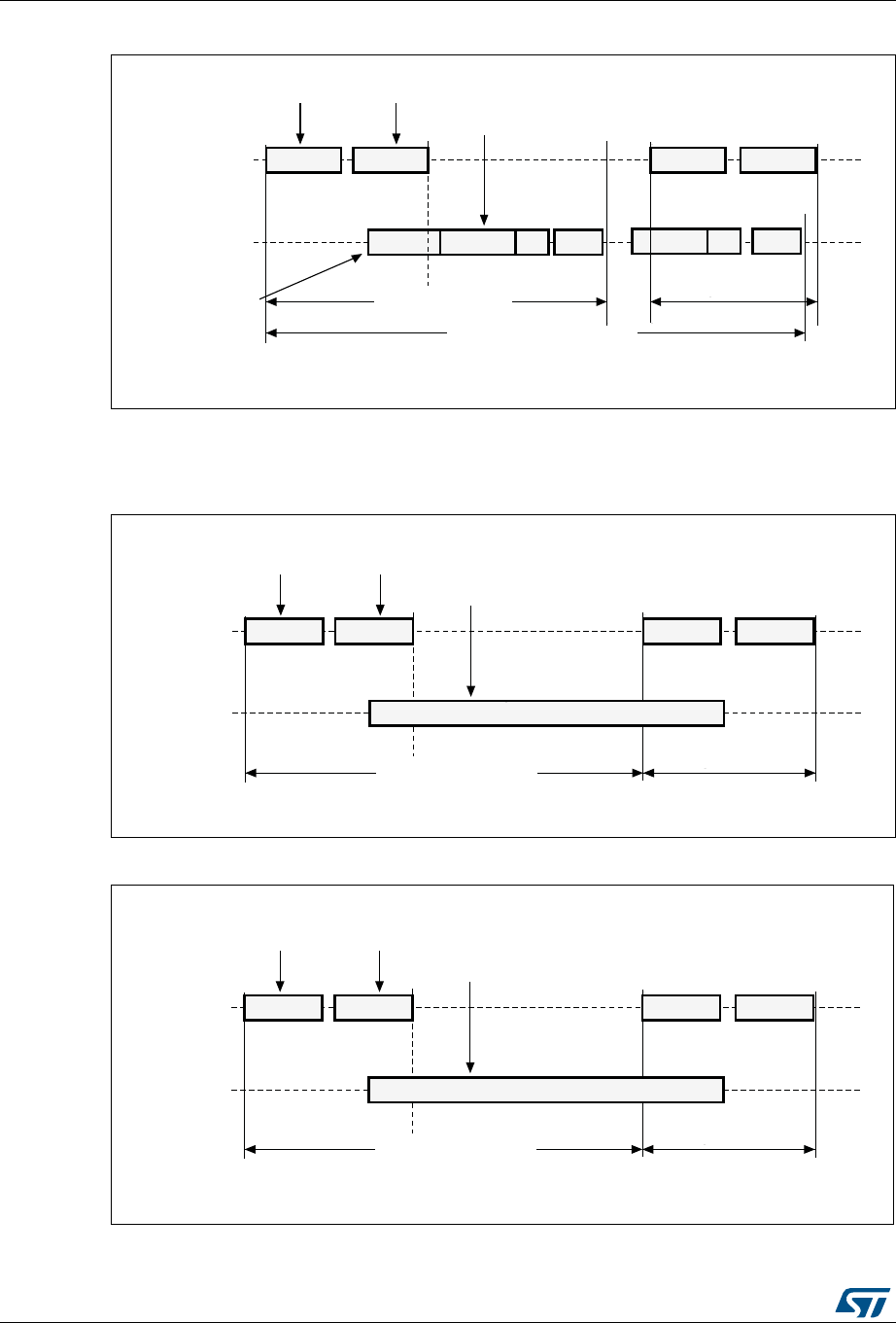
Secure digital input/output interface (SDIO) RM0090
1006/1718 DocID018909 Rev 9
Figure 323. SDIO (multiple) block write operation
Note: The SDIO will not send any data as long as the Busy signal is asserted (SDIO_D0 pulled
low).
Figure 324. SDIO sequential read operation
Figure 325. SDIO sequential write operation
ai14737
Block write operation Data stop operation
Multiple block write operation
From host to card From card to host
Data from host to card
Stop command
stops data transfer
Optional cards Busy.
Needed for CE-ATA
Command Response Command Response
Data block crc
Busy Busy Data block crc Busy
SDIO_CMD
SDIO_D
ai14738
Data stop operation
From card to host Stop command
stops data transfer
Command Response Command Response
Data transfer operation
Data stream
From host to
card(s)
Data from card to host
SDIO_CMD
SDIO_D
ai14739
Data stop operation
From card to host Stop command
stops data transfer
Command Response Command Response
Data transfer operation
Data stream
From host to
card(s)
Data from host to card
SDIO_CMD
SDIO_D
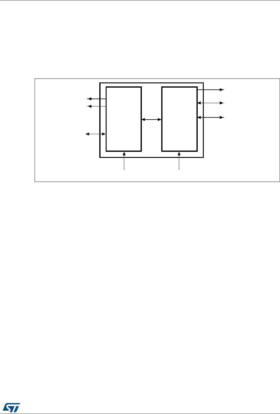
DocID018909 Rev 9 1007/1718
RM0090 Secure digital input/output interface (SDIO)
1059
31.3 SDIO functional description
The SDIO consists of two parts:
•The SDIO adapter block provides all functions specific to the MMC/SD/SD I/O card
such as the clock generation unit, command and data transfer.
•The APB2 interface accesses the SDIO adapter registers, and generates interrupt and
DMA request signals.
Figure 326. SDIO block diagram
By default SDIO_D0 is used for data transfer. After initialization, the host can change the
databus width.
If a MultiMediaCard is connected to the bus, SDIO_D0, SDIO_D[3:0] or SDIO_D[7:0] can be
used for data transfer. MMC V3.31 or previous, supports only 1 bit of data so only SDIO_D0
can be used.
If an SD or SD I/O card is connected to the bus, data transfer can be configured by the host
to use SDIO_D0 or SDIO_D[3:0]. All data lines are operating in push-pull mode.
SDIO_CMD has two operational modes:
•Open-drain for initialization (only for MMCV3.31 or previous)
•Push-pull for command transfer (SD/SD I/O card MMC4.2 use push-pull drivers also for
initialization)
SDIO_CK is the clock to the card: one bit is transferred on both command and data lines
with each clock cycle. The clock frequency can vary between 0 MHz and 20 MHz (for a
MultiMediaCard V3.31), between 0 and 48 MHz for a MultiMediaCard V4.0/4.2, or between
0 and 25 MHz (for an SD/SD I/O card).
The SDIO uses two clock signals:
•SDIO adapter clock (SDIOCLK = 48 MHz)
•APB2 bus clock (PCLK2)
PCLK2 and SDIO_CK clock frequencies must respect the following condition:
The signals shown in Table 149 are used on the MultiMediaCard/SD/SD I/O card bus.
!0"BUS
!0"
)NTERRUPTSAND
0#,+
3$)/?#+
ADAPTER
INTERFACE
$-!REQUEST
3$)/#,+
3$)/
3$)/
3$)/?$;=
3$)/?#-$
AI
Frequenc PCLK2()38⁄Frequency SDIO_CK()×≥
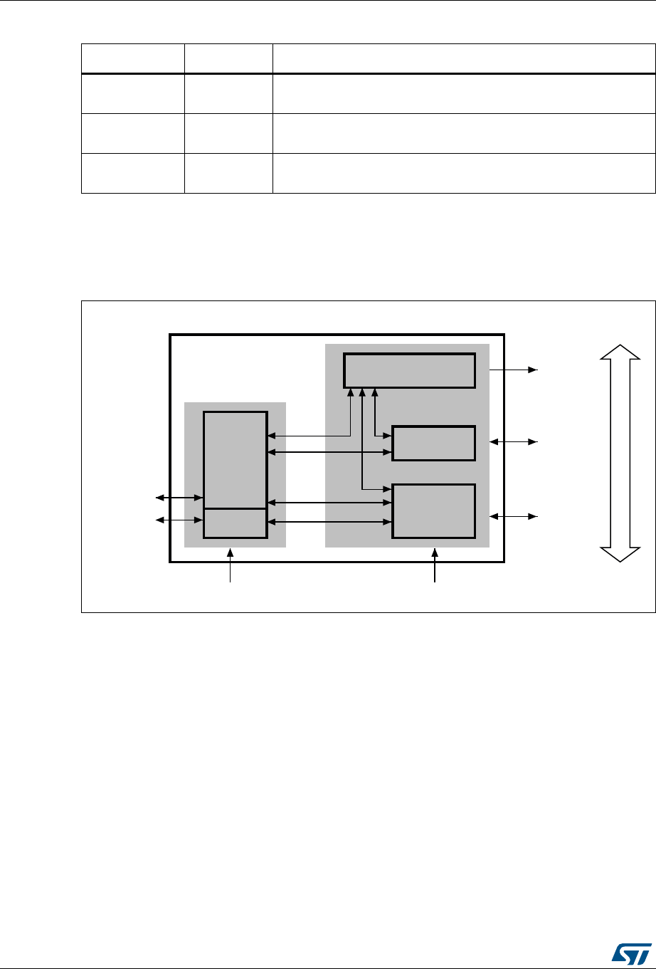
Secure digital input/output interface (SDIO) RM0090
1008/1718 DocID018909 Rev 9
31.3.1 SDIO adapter
Figure 327 shows a simplified block diagram of an SDIO adapter.
Figure 327. SDIO adapter
The SDIO adapter is a multimedia/secure digital memory card bus master that provides an
interface to a multimedia card stack or to a secure digital memory card. It consists of five
subunits:
•Adapter register block
•Control unit
•Command path
•Data path
•Data FIFO
Note: The adapter registers and FIFO use the APB2 bus clock domain (PCLK2). The control unit,
command path and data path use the SDIO adapter clock domain (SDIOCLK).
Adapter register block
The adapter register block contains all system registers. This block also generates the
signals that clear the static flags in the multimedia card. The clear signals are generated
when 1 is written into the corresponding bit location in the SDIO Clear register.
Table 149. SDIO I/O definitions
Pin Direction Description
SDIO_CK Output MultiMediaCard/SD/SDIO card clock. This pin is the clock from
host to card.
SDIO_CMD Bidirectional MultiMediaCard/SD/SDIO card command. This pin is the
bidirectional command/response signal.
SDIO_D[7:0] Bidirectional MultiMediaCard/SD/SDIO card data. These pins are the
bidirectional databus.
4O!0"
INTERFACE
AI
#ONTROLUNIT
#OMMAND
PATH
$ATAPATH
!DAPTER
REGISTERS
&)&/
3$)/?#+
3$)/?#-$
3$)/?$;=
0#,+ 3$)/#,+
#ARDBUS
3$)/ADAPTER
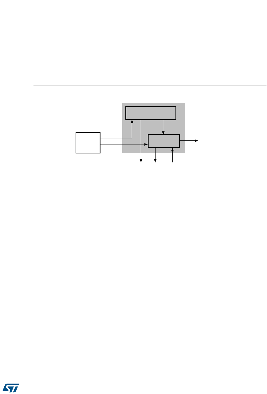
DocID018909 Rev 9 1009/1718
RM0090 Secure digital input/output interface (SDIO)
1059
Control unit
The control unit contains the power management functions and the clock divider for the
memory card clock.
There are three power phases:
•power-off
•power-up
•power-on
Figure 328. Control unit
The control unit is illustrated in Figure 328. It consists of a power management subunit and
a clock management subunit.
The power management subunit disables the card bus output signals during the power-off
and power-up phases.
The clock management subunit generates and controls the SDIO_CK signal. The SDIO_CK
output can use either the clock divide or the clock bypass mode. The clock output is
inactive:
•after reset
•during the power-off or power-up phases
•if the power saving mode is enabled and the card bus is in the Idle state (eight clock
periods after both the command and data path subunits enter the Idle phase)
Command path
The command path unit sends commands to and receives responses from the cards.
ai14804
Power management
Clock
management
Adapter
registers
SDIO_CK
Control unit
To command and data path
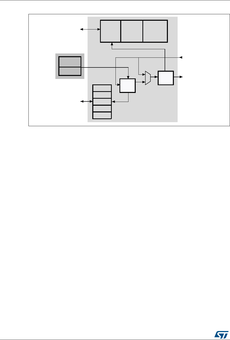
Secure digital input/output interface (SDIO) RM0090
1010/1718 DocID018909 Rev 9
Figure 329. SDIO adapter command path
•Command path state machine (CPSM)
– When the command register is written to and the enable bit is set, command
transfer starts. When the command has been sent, the command path state
machine (CPSM) sets the status flags and enters the Idle state if a response is not
required. If a response is required, it waits for the response (see Figure 330 on
page 1011). When the response is received, the received CRC code and the
internally generated code are compared, and the appropriate status flags are set.
AI
#-$
3TATUS
FLAG
#ONTROL
LOGIC
#OMMAND
TIMER
#2#
!RGUMENT
3HIFT
REGISTER
#-$
2ESPONSE
REGISTERS
4OCONTROLUNIT
3$)/?#-$IN
3$)/?#-$OUT
4O!0"INTERFACE
!DAPTERREGISTERS
DocID018909 Rev 9 1011/1718
RM0090 Secure digital input/output interface (SDIO)
1059
Figure 330. Command path state machine (CPSM)
When the Wait state is entered, the command timer starts running. If the timeout is reached
before the CPSM moves to the Receive state, the timeout flag is set and the Idle state is
entered.
Note: The command timeout has a fixed value of 64 SDIO_CK clock periods.
If the interrupt bit is set in the command register, the timer is disabled and the CPSM waits
for an interrupt request from one of the cards. If a pending bit is set in the command register,
the CPSM enters the Pend state, and waits for a CmdPend signal from the data path
subunit. When CmdPend is detected, the CPSM moves to the Send state. This enables the
data counter to trigger the stop command transmission.
Note: The CPSM remains in the Idle state for at least eight SDIO_CK periods to meet the NCC and
NRC timing constraints. NCC is the minimum delay between two host commands, and NRC is
the minimum delay between the host command and the card response.
Idle
Pend
Send
Wait
Receive
Last Data
CPSM
disabled
Enabled and
command start CPSM disabled or
no response
Wait for response
Response
started
Response received or
disabled or command
CRC failed
CPSM Disabled or
command timeout
CPSM Enabled and
pending command
ai14806b
Wait_CPL
Response Received in CE-ATA
mode and no interrupt and
wait for CE-ATA Command
Completion signal enabled
Response Received in CE-ATA mode and
no interrupt and wait for CE-ATA
Command Completion signal disabled
CE-ATA Command
Completion signal
received or
CPSM disabled or
Command CRC failed
On reset
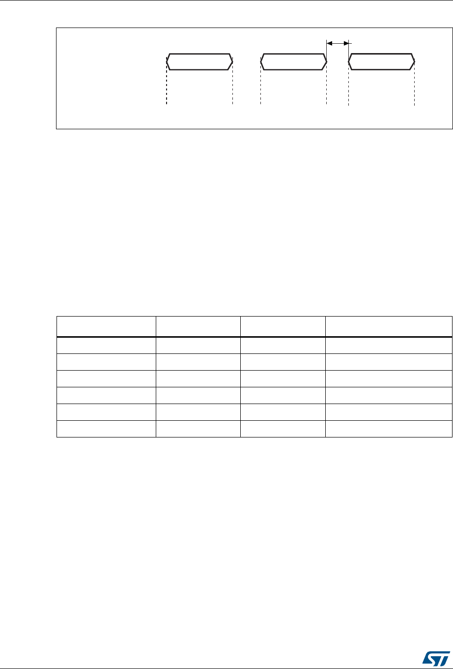
Secure digital input/output interface (SDIO) RM0090
1012/1718 DocID018909 Rev 9
Figure 331. SDIO command transfer
•Command format
– Command: a command is a token that starts an operation. Command are sent
from the host either to a single card (addressed command) or to all connected
cards (broadcast command are available for MMC V3.31 or previous). Commands
are transferred serially on the CMD line. All commands have a fixed length of 48
bits. The general format for a command token for MultiMediaCards, SD-Memory
cards and SDIO-Cards is shown in Table 150. CE-ATA commands are an
extension of MMC commands V4.2, and so have the same format.
The command path operates in a half-duplex mode, so that commands and
responses can either be sent or received. If the CPSM is not in the Send state, the
SDIO_CMD output is in the Hi-Z state, as shown in Figure 331 on page 1012.
Data on SDIO_CMD are synchronous with the rising edge of SDIO_CK. Table
shows the command format.
– Response: a response is a token that is sent from an addressed card (or
synchronously from all connected cards for MMC V3.31 or previous), to the host
as an answer to a previously received command. Responses are transferred
serially on the CMD line.
The SDIO supports two response types. Both use CRC error checking:
•48 bit short response
•136 bit long response
Note: If the response does not contain a CRC (CMD1 response), the device driver must ignore the
CRC failed status.
Table 150. Command format
Bit position Width Value Description
47 1 0 Start bit
46 1 1 Transmission bit
[45:40] 6 - Command index
[39:8] 32 - Argument
[7:1] 7 - CRC7
011End bit
SDIO_CK
SDIO_CMD
Command Response Command
State Idle Send Wait Receive Idle Send
Hi-Z Controller drives Hi-Z Card drives Hi-Z Controller drives
ai14707
at least 8 SDIO_CK cycles

DocID018909 Rev 9 1013/1718
RM0090 Secure digital input/output interface (SDIO)
1059
The command register contains the command index (six bits sent to a card) and the
command type. These determine whether the command requires a response, and whether
the response is 48 or 136 bits long (see Section 31.9.4 on page 1047). The command path
implements the status flags shown in Table 153:
The CRC generator calculates the CRC checksum for all bits before the CRC code. This
includes the start bit, transmitter bit, command index, and command argument (or card
status). The CRC checksum is calculated for the first 120 bits of CID or CSD for the long
response format. Note that the start bit, transmitter bit and the six reserved bits are not used
in the CRC calculation.
The CRC checksum is a 7-bit value:
CRC[6:0] = Remainder [(M(x) * x7) / G(x)]
G(x) = x7 + x3 + 1
M(x) = (start bit) * x39 + ... + (last bit before CRC) * x0, or
M(x) = (start bit) * x119 + ... + (last bit before CRC) * x0
Table 151. Short response format
Bit position Width Value Description
47 1 0 Start bit
46 1 0 Transmission bit
[45:40] 6 - Command index
[39:8] 32 - Argument
[7:1] 7 - CRC7(or 1111111)
011End bit
Table 152. Long response format
Bit position Width Value Description
135 1 0 Start bit
134 1 0 Transmission bit
[133:128] 6 111111 Reserved
[127:1] 127 - CID or CSD (including internal CRC7)
0 1 1 End bit
Table 153. Command path status flags
Flag Description
CMDREND Set if response CRC is OK.
CCRCFAIL Set if response CRC fails.
CMDSENT Set when command (that does not require response) is sent
CTIMEOUT Response timeout.
CMDACT Command transfer in progress.
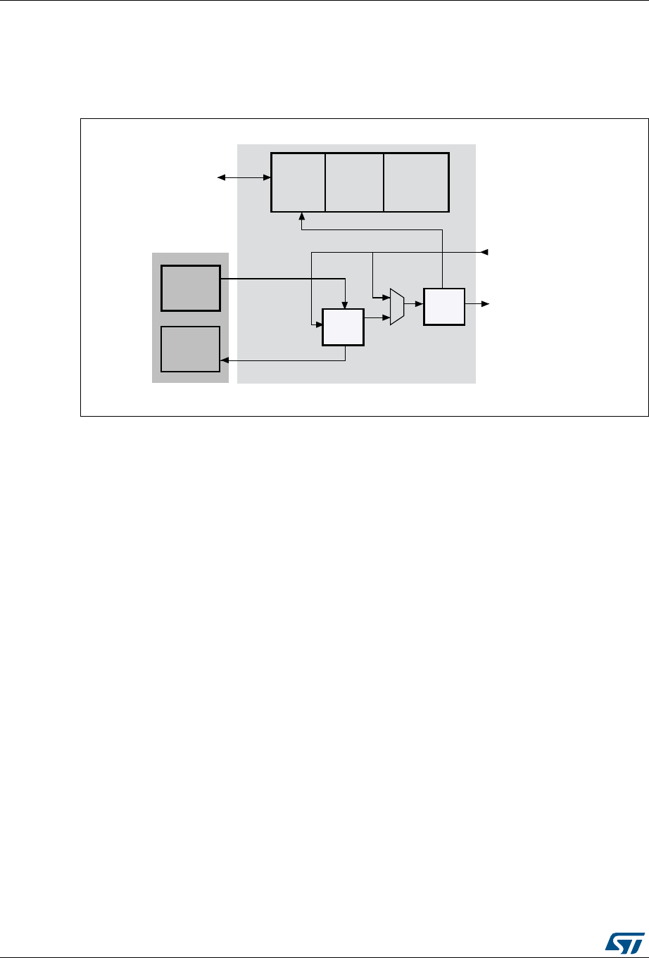
Secure digital input/output interface (SDIO) RM0090
1014/1718 DocID018909 Rev 9
Data path
The data path subunit transfers data to and from cards. Figure 332 shows a block diagram
of the data path.
Figure 332. Data path
The card databus width can be programmed using the clock control register. If the 4-bit wide
bus mode is enabled, data is transferred at four bits per clock cycle over all four data signals
(SDIO_D[3:0]). If the 8-bit wide bus mode is enabled, data is transferred at eight bits per
clock cycle over all eight data signals (SDIO_D[7:0]). If the wide bus mode is not enabled,
only one bit per clock cycle is transferred over SDIO_D0.
Depending on the transfer direction (send or receive), the data path state machine (DPSM)
moves to the Wait_S or Wait_R state when it is enabled:
•Send: the DPSM moves to the Wait_S state. If there is data in the transmit FIFO, the
DPSM moves to the Send state, and the data path subunit starts sending data to a
card.
•Receive: the DPSM moves to the Wait_R state and waits for a start bit. When it
receives a start bit, the DPSM moves to the Receive state, and the data path subunit
starts receiving data from a card.
Data path state machine (DPSM)
The DPSM operates at SDIO_CK frequency. Data on the card bus signals is synchronous to
the rising edge of SDIO_CK. The DPSM has six states, as shown in Figure 333: Data path
state machine (DPSM).
ai14808
Transmit
Status
flag
Control
logic
Data
timer
CRC
Receive
Shift
register
To control unit
SDIO_Din[7:0]
SDIO_Dout[7:0]
Data FIFO
Data path
DocID018909 Rev 9 1015/1718
RM0090 Secure digital input/output interface (SDIO)
1059
Figure 333. Data path state machine (DPSM)
•Idle: the data path is inactive, and the SDIO_D[7:0] outputs are in Hi-Z. When the data
control register is written and the enable bit is set, the DPSM loads the data counter
with a new value and, depending on the data direction bit, moves to either the Wait_S
or the Wait_R state.
•Wait_R: if the data counter equals zero, the DPSM moves to the Idle state when the
receive FIFO is empty. If the data counter is not zero, the DPSM waits for a start bit on
SDIO_D. The DPSM moves to the Receive state if it receives a start bit before a
timeout, and loads the data block counter. If it reaches a timeout before it detects a
start bit, or a start bit error occurs, it moves to the Idle state and sets the timeout status
flag.
•Receive: serial data received from a card is packed in bytes and written to the data
FIFO. Depending on the transfer mode bit in the data control register, the data transfer
mode can be either block or stream:
– In block mode, when the data block counter reaches zero, the DPSM waits until it
receives the CRC code. If the received code matches the internally generated
CRC code, the DPSM moves to the Wait_R state. If not, the CRC fail status flag is
set and the DPSM moves to the Idle state.
– In stream mode, the DPSM receives data while the data counter is not zero. When
the counter is zero, the remaining data in the shift register is written to the data
FIFO, and the DPSM moves to the Wait_R state.
If a FIFO overrun error occurs, the DPSM sets the FIFO error flag and moves to the
Idle state:
•Wait_S: the DPSM moves to the Idle state if the data counter is zero. If not, it waits until
the data FIFO empty flag is deasserted, and moves to the Send state.
Idle
Busy
Send
Wait_R
Receive
End of packet
Disabled or CRC fail
or timeout
Not busy
Disabled or
end of data
Data ready
End of packet or
end of data or
FIFO overrun
Enable and not send
Disabled or
Rx FIFO empty or timeout or
start bit error
Disabled or FIFO underrun or
end of data or CRC fail
ai14809b
Wait_S
Start bit
On reset
Disabled or CRC fail
Enable and send
DPSM disabled
Read Wait
DPSM enabled and
Read Wait Started
and SD I/O mode enabled
ReadWait Stop
Data received and
Read Wait Started and
SD I/O mode enabled

Secure digital input/output interface (SDIO) RM0090
1016/1718 DocID018909 Rev 9
Note: The DPSM remains in the Wait_S state for at least two clock periods to meet the NWR timing
requirements, where NWR is the number of clock cycles between the reception of the card
response and the start of the data transfer from the host.
•Send: the DPSM starts sending data to a card. Depending on the transfer mode bit in
the data control register, the data transfer mode can be either block or stream:
– In block mode, when the data block counter reaches zero, the DPSM sends an
internally generated CRC code and end bit, and moves to the Busy state.
– In stream mode, the DPSM sends data to a card while the enable bit is high and
the data counter is not zero. It then moves to the Idle state.
If a FIFO underrun error occurs, the DPSM sets the FIFO error flag and moves to the
Idle state.
•Busy: the DPSM waits for the CRC status flag:
– If it does not receive a positive CRC status, it moves to the Idle state and sets the
CRC fail status flag.
– If it receives a positive CRC status, it moves to the Wait_S state if SDIO_D0 is not
low (the card is not busy).
If a timeout occurs while the DPSM is in the Busy state, it sets the data timeout flag and
moves to the Idle state.
The data timer is enabled when the DPSM is in the Wait_R or Busy state, and
generates the data timeout error:
– When transmitting data, the timeout occurs if the DPSM stays in the Busy state for
longer than the programmed timeout period
– When receiving data, the timeout occurs if the end of the data is not true, and if the
DPSM stays in the Wait_R state for longer than the programmed timeout period.
•Data: data can be transferred from the card to the host or vice versa. Data is
transferred via the data lines. They are stored in a FIFO of 32 words, each word is 32
bits wide.
Data FIFO
The data FIFO (first-in-first-out) subunit is a data buffer with a transmit and receive unit.
The FIFO contains a 32-bit wide, 32-word deep data buffer, and transmit and receive logic.
Because the data FIFO operates in the APB2 clock domain (PCLK2), all signals from the
subunits in the SDIO clock domain (SDIOCLK) are resynchronized.
Table 154. Data token format
Description Start bit Data CRC16 End bit
Block Data 0 - yes 1
Stream Data 0 - no 1

DocID018909 Rev 9 1017/1718
RM0090 Secure digital input/output interface (SDIO)
1059
Depending on the TXACT and RXACT flags, the FIFO can be disabled, transmit enabled, or
receive enabled. TXACT and RXACT are driven by the data path subunit and are mutually
exclusive:
– The transmit FIFO refers to the transmit logic and data buffer when TXACT is
asserted
– The receive FIFO refers to the receive logic and data buffer when RXACT is
asserted
•Transmit FIFO:
Data can be written to the transmit FIFO through the APB2 interface when the SDIO is
enabled for transmission.
The transmit FIFO is accessible via 32 sequential addresses. The transmit FIFO
contains a data output register that holds the data word pointed to by the read pointer.
When the data path subunit has loaded its shift register, it increments the read pointer
and drives new data out.
If the transmit FIFO is disabled, all status flags are deasserted. The data path subunit
asserts TXACT when it transmits data.
•Receive FIFO
When the data path subunit receives a word of data, it drives the data on the write
databus. The write pointer is incremented after the write operation completes. On the
read side, the contents of the FIFO word pointed to by the current value of the read
pointer is driven onto the read databus. If the receive FIFO is disabled, all status flags
are deasserted, and the read and write pointers are reset. The data path subunit
asserts RXACT when it receives data. Table 156 lists the receive FIFO status flags.
The receive FIFO is accessible via 32 sequential addresses.
Table 155. Transmit FIFO status flags
Flag Description
TXFIFOF Set to high when all 32 transmit FIFO words contain valid data.
TXFIFOE Set to high when the transmit FIFO does not contain valid data.
TXFIFOHE Set to high when 8 or more transmit FIFO words are empty. This flag can be used
as a DMA request.
TXDAVL Set to high when the transmit FIFO contains valid data. This flag is the inverse of
the TXFIFOE flag.
TXUNDERR Set to high when an underrun error occurs. This flag is cleared by writing to the
SDIO Clear register.

Secure digital input/output interface (SDIO) RM0090
1018/1718 DocID018909 Rev 9
31.3.2 SDIO APB2 interface
The APB2 interface generates the interrupt and DMA requests, and accesses the SDIO
adapter registers and the data FIFO. It consists of a data path, register decoder, and
interrupt/DMA logic.
SDIO interrupts
The interrupt logic generates an interrupt request signal that is asserted when at least one
of the selected status flags is high. A mask register is provided to allow selection of the
conditions that will generate an interrupt. A status flag generates the interrupt request if a
corresponding mask flag is set.
SDIO/DMA interface - procedure for data transfers between the SDIO and
memory
In the example shown, the transfer is from the SDIO host controller to an MMC (512 bytes
using CMD24 (WRITE_BLOCK). The SDIO FIFO is filled by data stored in a memory using
the DMA controller.
1. Do the card identification process
2. Increase the SDIO_CK frequency
3. Select the card by sending CMD7
4. Configure the DMA2 as follows:
a) Enable DMA2 controller and clear any pending interrupts.
b) Program the DMA2_Stream3 or DMA2_Stream6 Channel4 source address
register with the memory location’s base address and DMA2_Stream3 or
Table 156. Receive FIFO status flags
Flag Description
RXFIFOF Set to high when all 32 receive FIFO words contain valid data
RXFIFOE Set to high when the receive FIFO does not contain valid data.
RXFIFOHF Set to high when 8 or more receive FIFO words contain valid data. This flag can be
used as a DMA request.
RXDAVL Set to high when the receive FIFO is not empty. This flag is the inverse of the
RXFIFOE flag.
RXOVERR Set to high when an overrun error occurs. This flag is cleared by writing to the SDIO
Clear register.

DocID018909 Rev 9 1019/1718
RM0090 Secure digital input/output interface (SDIO)
1059
DMA2_Stream6 Channel4 destination address register with the SDIO_FIFO
register address.
c) Program DMA2_Stream3 or DMA2_Stream6 Channel4 control register (memory
increment, not peripheral increment, peripheral and source width is word size).
d) Program DMA2_Stream3 or DMA2_Stream6 Channel4 to select the peripheral as
flow controller (set PFCTRL bit in DMA_S3CR or DMA_S6CR configuration
register).
e) Configure the incremental burst transfer to 4 beats (at least from peripheral side)
in DMA2_Stream3 or DMA2_Stream6 Channel4.
f) Enable DMA2_Stream3 or DMA2_Stream6 Channel4
5. Send CMD24 (WRITE_BLOCK) as follows:
a) Program the SDIO data length register (SDIO data timer register should be
already programmed before the card identification process).
b) Program the SDIO argument register with the address location of the card where
data is to be transferred.
c) Program the SDIO command register: CmdIndex with 24 (WRITE_BLOCK);
WaitResp with ‘1’ (SDIO card host waits for a response); CPSMEN with ‘1’ (SDIO
card host enabled to send a command). Other fields are at their reset value.
d) Wait for SDIO_STA[6] = CMDREND interrupt, then program the SDIO data control
register: DTEN with ‘1’ (SDIO card host enabled to send data); DTDIR with ‘0’
(from controller to card); DTMODE with ‘0’ (block data transfer); DMAEN with ‘1’
(DMA enabled); DBLOCKSIZE with 0x9 (512 bytes). Other fields are don’t care.
e) Wait for SDIO_STA[10] = DBCKEND.
6. Check that no channels are still enabled by polling the DMA Enabled Channel Status
register.
31.4 Card functional description
31.4.1 Card identification mode
While in card identification mode the host resets all cards, validates the operation voltage
range, identifies cards and sets a relative card address (RCA) for each card on the bus. All
data communications in the card identification mode use the command line (CMD) only.
31.4.2 Card reset
The GO_IDLE_STATE command (CMD0) is the software reset command and it puts the
MultiMediaCard and SD memory in the Idle state. The IO_RW_DIRECT command (CMD52)
resets the SD I/O card. After power-up or CMD0, all cards output bus drivers are in the high-
impedance state and the cards are initialized with a default relative card address
(RCA=0x0001) and with a default driver stage register setting (lowest speed, highest driving
current capability).
31.4.3 Operating voltage range validation
All cards can communicate with the SDIO card host using any operating voltage within the
specification range. The supported minimum and maximum VDD values are defined in the
operation conditions register (OCR) on the card.

Secure digital input/output interface (SDIO) RM0090
1020/1718 DocID018909 Rev 9
Cards that store the card identification number (CID) and card specific data (CSD) in the
payload memory are able to communicate this information only under data-transfer VDD
conditions. When the SDIO card host module and the card have incompatible VDD ranges,
the card is not able to complete the identification cycle and cannot send CSD data. For this
purpose, the special commands, SEND_OP_COND (CMD1), SD_APP_OP_COND (ACMD41
for SD Memory), and IO_SEND_OP_COND (CMD5 for SD I/O), are designed to provide a
mechanism to identify and reject cards that do not match the VDD range desired by the
SDIO card host. The SDIO card host sends the required VDD voltage window as the
operand of these commands. Cards that cannot perform data transfer in the specified range
disconnect from the bus and go to the inactive state.
By using these commands without including the voltage range as the operand, the SDIO
card host can query each card and determine the common voltage range before placing out-
of-range cards in the inactive state. This query is used when the SDIO card host is able to
select a common voltage range or when the user requires notification that cards are not
usable.
31.4.4 Card identification process
The card identification process differs for MultiMediaCards and SD cards. For
MultiMediaCard cards, the identification process starts at clock rate Fod. The SDIO_CMD
line output drivers are open-drain and allow parallel card operation during this process. The
registration process is accomplished as follows:
1. The bus is activated.
2. The SDIO card host broadcasts SEND_OP_COND (CMD1) to receive operation
conditions.
3. The response is the wired AND operation of the operation condition registers from all
cards.
4. Incompatible cards are placed in the inactive state.
5. The SDIO card host broadcasts ALL_SEND_CID (CMD2) to all active cards.
6. The active cards simultaneously send their CID numbers serially. Cards with outgoing
CID bits that do not match the bits on the command line stop transmitting and must wait
for the next identification cycle. One card successfully transmits a full CID to the SDIO
card host and enters the Identification state.
7. The SDIO card host issues SET_RELATIVE_ADDR (CMD3) to that card. This new
address is called the relative card address (RCA); it is shorter than the CID and
addresses the card. The assigned card changes to the Standby state, it does not react
to further identification cycles, and its output switches from open-drain to push-pull.
8. The SDIO card host repeats steps 5 through 7 until it receives a timeout condition.
For the SD card, the identification process starts at clock rate Fod, and the SDIO_CMD line
output drives are push-pull drivers instead of open-drain. The registration process is
accomplished as follows:

DocID018909 Rev 9 1021/1718
RM0090 Secure digital input/output interface (SDIO)
1059
1. The bus is activated.
2. The SDIO card host broadcasts SD_APP_OP_COND (ACMD41).
3. The cards respond with the contents of their operation condition registers.
4. The incompatible cards are placed in the inactive state.
5. The SDIO card host broadcasts ALL_SEND_CID (CMD2) to all active cards.
6. The cards send back their unique card identification numbers (CIDs) and enter the
Identification state.
7. The SDIO card host issues SET_RELATIVE_ADDR (CMD3) to an active card with an
address. This new address is called the relative card address (RCA); it is shorter than
the CID and addresses the card. The assigned card changes to the Standby state. The
SDIO card host can reissue this command to change the RCA. The RCA of the card is
the last assigned value.
8. The SDIO card host repeats steps 5 through 7 with all active cards.
For the SD I/O card, the registration process is accomplished as follows:
1. The bus is activated.
2. The SDIO card host sends IO_SEND_OP_COND (CMD5).
3. The cards respond with the contents of their operation condition registers.
4. The incompatible cards are set to the inactive state.
5. The SDIO card host issues SET_RELATIVE_ADDR (CMD3) to an active card with an
address. This new address is called the relative card address (RCA); it is shorter than
the CID and addresses the card. The assigned card changes to the Standby state. The
SDIO card host can reissue this command to change the RCA. The RCA of the card is
the last assigned value.
31.4.5 Block write
During block write (CMD24 - 27) one or more blocks of data are transferred from the host to
the card with a CRC appended to the end of each block by the host. A card supporting block
write is always able to accept a block of data defined by WRITE_BL_LEN. If the CRC fails,
the card indicates the failure on the SDIO_D line and the transferred data are discarded and
not written, and all further transmitted blocks (in multiple block write mode) are ignored.
If the host uses partial blocks whose accumulated length is not block aligned and, block
misalignment is not allowed (CSD parameter WRITE_BLK_MISALIGN is not set), the card
will detect the block misalignment error before the beginning of the first misaligned block.
(ADDRESS_ERROR error bit is set in the status register). The write operation will also be
aborted if the host tries to write over a write-protected area. In this case, however, the card
will set the WP_VIOLATION bit.
Programming of the CID and CSD registers does not require a previous block length setting.
The transferred data is also CRC protected. If a part of the CSD or CID register is stored in
ROM, then this unchangeable part must match the corresponding part of the receive buffer.
If this match fails, then the card reports an error and does not change any register contents.
Some cards may require long and unpredictable times to write a block of data. After
receiving a block of data and completing the CRC check, the card begins writing and holds
the SDIO_D line low if its write buffer is full and unable to accept new data from a new
WRITE_BLOCK command. The host may poll the status of the card with a SEND_STATUS
command (CMD13) at any time, and the card will respond with its status. The
READY_FOR_DATA status bit indicates whether the card can accept new data or whether
the write process is still in progress. The host may deselect the card by issuing CMD7 (to

Secure digital input/output interface (SDIO) RM0090
1022/1718 DocID018909 Rev 9
select a different card), which will place the card in the Disconnect state and release the
SDIO_D line(s) without interrupting the write operation. When selecting the card again, it will
reactivate busy indication by pulling SDIO_D to low if programming is still in progress and
the write buffer is unavailable.
31.4.6 Block read
In Block read mode the basic unit of data transfer is a block whose maximum size is defined
in the CSD (READ_BL_LEN). If READ_BL_PARTIAL is set, smaller blocks whose start and
end addresses are entirely contained within one physical block (as defined by
READ_BL_LEN) may also be transmitted. A CRC is appended to the end of each block,
ensuring data transfer integrity. CMD17 (READ_SINGLE_BLOCK) initiates a block read and
after completing the transfer, the card returns to the Transfer state.
CMD18 (READ_MULTIPLE_BLOCK) starts a transfer of several consecutive blocks.
The host can abort reading at any time, within a multiple block operation, regardless of its
type. Transaction abort is done by sending the stop transmission command.
If the card detects an error (for example, out of range, address misalignment or internal
error) during a multiple block read operation (both types) it stops the data transmission and
remains in the data state. The host must than abort the operation by sending the stop
transmission command. The read error is reported in the response to the stop transmission
command.
If the host sends a stop transmission command after the card transmits the last block of a
multiple block operation with a predefined number of blocks, it is responded to as an illegal
command, since the card is no longer in the data state. If the host uses partial blocks whose
accumulated length is not block-aligned and block misalignment is not allowed, the card
detects a block misalignment error condition at the beginning of the first misaligned block
(ADDRESS_ERROR error bit is set in the status register).
31.4.7 Stream access, stream write and stream read
(MultiMediaCard only)
In stream mode, data is transferred in bytes and no CRC is appended at the end of each
block.
Stream write (MultiMediaCard only)
WRITE_DAT_UNTIL_STOP (CMD20) starts the data transfer from the SDIO card host to the
card, beginning at the specified address and continuing until the SDIO card host issues a
stop command. When partial blocks are allowed (CSD parameter WRITE_BL_PARTIAL is
set), the data stream can start and stop at any address within the card address space,
otherwise it can only start and stop at block boundaries. Because the amount of data to be
transferred is not determined in advance, a CRC cannot be used. When the end of the
memory range is reached while sending data and no stop command is sent by the SD card
host, any additional transferred data are discarded.

DocID018909 Rev 9 1023/1718
RM0090 Secure digital input/output interface (SDIO)
1059
The maximum clock frequency for a stream write operation is given by the following
equation fields of the card-specific data register:
•Maximumspeed = maximum write frequency
•TRANSPEED = maximum data transfer rate
•writebllen = maximum write data block length
•NSAC = data read access time 2 in CLK cycles
•TAAC = data read access time 1
•R2WFACTOR = write speed factor
If the host attempts to use a higher frequency, the card may not be able to process the data
and stop programming, set the OVERRUN error bit in the status register, and while ignoring
all further data transfer, wait (in the receive data state) for a stop command. The write
operation is also aborted if the host tries to write over a write-protected area. In this case,
however, the card sets the WP_VIOLATION bit.
Stream read (MultiMediaCard only)
READ_DAT_UNTIL_STOP (CMD11) controls a stream-oriented data transfer.
This command instructs the card to send its data, starting at a specified address, until the
SDIO card host sends STOP_TRANSMISSION (CMD12). The stop command has an
execution delay due to the serial command transmission and the data transfer stops after
the end bit of the stop command. When the end of the memory range is reached while
sending data and no stop command is sent by the SDIO card host, any subsequent data
sent are considered undefined.
The maximum clock frequency for a stream read operation is given by the following
equation and uses fields of the card specific data register.
•Maximumspeed = maximum read frequency
•TRANSPEED = maximum data transfer rate
•readbllen = maximum read data block length
•writebllen = maximum write data block length
•NSAC = data read access time 2 in CLK cycles
•TAAC = data read access time 1
•R2WFACTOR = write speed factor
If the host attempts to use a higher frequency, the card is not able to sustain data transfer. If
this happens, the card sets the UNDERRUN error bit in the status register, aborts the
transmission and waits in the data state for a stop command.
31.4.8 Erase: group erase and sector erase
The erasable unit of the MultiMediaCard is the erase group. The erase group is measured in
write blocks, which are the basic writable units of the card. The size of the erase group is a
card-specific parameter and defined in the CSD.
Maximumspeed MIN TRANSPEED 82
writebllen
×()NSAC–()
TAAC R2WFACTOR×
------------------------------------------------------------------------(, )=
Maximumspeed MIN TRANSPEED 82
readbllen
×()NSAC–()
TAAC R2WFACTOR×
-----------------------------------------------------------------------(, )=

Secure digital input/output interface (SDIO) RM0090
1024/1718 DocID018909 Rev 9
The host can erase a contiguous range of Erase Groups. Starting the erase process is a
three-step sequence.
First the host defines the start address of the range using the ERASE_GROUP_START
(CMD35) command, next it defines the last address of the range using the
ERASE_GROUP_END (CMD36) command and, finally, it starts the erase process by issuing
the ERASE (CMD38) command. The address field in the erase commands is an Erase
Group address in byte units. The card ignores all LSBs below the Erase Group size,
effectively rounding the address down to the Erase Group boundary.
If an erase command is received out of sequence, the card sets the ERASE_SEQ_ERROR
bit in the status register and resets the whole sequence.
If an out-of-sequence (neither of the erase commands, except SEND_STATUS) command
received, the card sets the ERASE_RESET status bit in the status register, resets the erase
sequence and executes the last command.
If the erase range includes write protected blocks, they are left intact and only unprotected
blocks are erased. The WP_ERASE_SKIP status bit in the status register is set.
The card indicates that an erase is in progress by holding SDIO_D low. The actual erase
time may be quite long, and the host may issue CMD7 to deselect the card.
31.4.9 Wide bus selection or deselection
Wide bus (4-bit bus width) operation mode is selected or deselected using
SET_BUS_WIDTH (ACMD6). The default bus width after power-up or GO_IDLE_STATE
(CMD0) is 1 bit. SET_BUS_WIDTH (ACMD6) is only valid in a transfer state, which means
that the bus width can be changed only after a card is selected by
SELECT/DESELECT_CARD (CMD7).
31.4.10 Protection management
Three write protection methods for the cards are supported in the SDIO card host module:
1. internal card write protection (card responsibility)
2. mechanical write protection switch (SDIO card host module responsibility only)
3. password-protected card lock operation
Internal card write protection
Card data can be protected against write and erase. By setting the permanent or temporary
write-protect bits in the CSD, the entire card can be permanently write-protected by the
manufacturer or content provider. For cards that support write protection of groups of
sectors by setting the WP_GRP_ENABLE bit in the CSD, portions of the data can be
protected, and the write protection can be changed by the application. The write protection
is in units of WP_GRP_SIZE sectors as specified in the CSD. The SET_WRITE_PROT and
CLR_WRITE_PROT commands control the protection of the addressed group. The
SEND_WRITE_PROT command is similar to a single block read command. The card sends
a data block containing 32 write protection bits (representing 32 write protect groups starting
at the specified address) followed by 16 CRC bits. The address field in the write protect
commands is a group address in byte units.
The card ignores all LSBs below the group size.

DocID018909 Rev 9 1025/1718
RM0090 Secure digital input/output interface (SDIO)
1059
Mechanical write protect switch
A mechanical sliding tab on the side of the card allows the user to set or clear the write
protection on a card. When the sliding tab is positioned with the window open, the card is
write-protected, and when the window is closed, the card contents can be changed. A
matched switch on the socket side indicates to the SDIO card host module that the card is
write-protected. The SDIO card host module is responsible for protecting the card. The
position of the write protect switch is unknown to the internal circuitry of the card.
Password protect
The password protection feature enables the SDIO card host module to lock and unlock a
card with a password. The password is stored in the 128-bit PWD register and its size is set
in the 8-bit PWD_LEN register. These registers are nonvolatile so that a power cycle does
not erase them. Locked cards respond to and execute certain commands. This means that
the SDIO card host module is allowed to reset, initialize, select, and query for status,
however it is not allowed to access data on the card. When the password is set (as indicated
by a nonzero value of PWD_LEN), the card is locked automatically after power-up. As with
the CSD and CID register write commands, the lock/unlock commands are available in the
transfer state only. In this state, the command does not include an address argument and
the card must be selected before using it. The card lock/unlock commands have the
structure and bus transaction types of a regular single-block write command. The
transferred data block includes all of the required information for the command (the
password setting mode, the PWD itself, and card lock/unlock). The command data block
size is defined by the SDIO card host module before it sends the card lock/unlock
command, and has the structure shown in Table 170.
The bit settings are as follows:
•ERASE: setting it forces an erase operation. All other bits must be zero, and only the
command byte is sent
•LOCK_UNLOCK: setting it locks the card. LOCK_UNLOCK can be set simultaneously
with SET_PWD, however not with CLR_PWD
•CLR_PWD: setting it clears the password data
•SET_PWD: setting it saves the password data to memory
•PWD_LEN: it defines the length of the password in bytes
•PWD: the password (new or currently used, depending on the command)
The following sections list the command sequences to set/reset a password, lock/unlock the
card, and force an erase.
Setting the password
1. Select a card (SELECT/DESELECT_CARD, CMD7), if none is already selected.
2. Define the block length (SET_BLOCKLEN, CMD16) to send, given by the 8-bit card
lock/unlock mode, the 8-bit PWD_LEN, and the number of bytes of the new password.
When a password replacement is done, the block size must take into account that both
the old and the new passwords are sent with the command.
3. Send LOCK/UNLOCK (CMD42) with the appropriate data block size on the data line
including the 16-bit CRC. The data block indicates the mode (SET_PWD = 1), the
length (PWD_LEN), and the password (PWD) itself. When a password replacement is
done, the length value (PWD_LEN) includes the length of both passwords, the old and

Secure digital input/output interface (SDIO) RM0090
1026/1718 DocID018909 Rev 9
the new one, and the PWD field includes the old password (currently used) followed by
the new password.
4. When the password is matched, the new password and its size are saved into the PWD
and PWD_LEN fields, respectively. When the old password sent does not correspond
(in size and/or content) to the expected password, the LOCK_UNLOCK_FAILED error
bit is set in the card status register, and the password is not changed.
The password length field (PWD_LEN) indicates whether a password is currently set. When
this field is nonzero, there is a password set and the card locks itself after power-up. It is
possible to lock the card immediately in the current power session by setting the
LOCK_UNLOCK bit (while setting the password) or sending an additional command for card
locking.
Resetting the password
1. Select a card (SELECT/DESELECT_CARD, CMD7), if none is already selected.
2. Define the block length (SET_BLOCKLEN, CMD16) to send, given by the 8-bit card
lock/unlock mode, the 8-bit PWD_LEN, and the number of bytes in the currently used
password.
3. Send LOCK/UNLOCK (CMD42) with the appropriate data block size on the data line
including the 16-bit CRC. The data block indicates the mode (CLR_PWD = 1), the
length (PWD_LEN) and the password (PWD) itself. The LOCK_UNLOCK bit is ignored.
4. When the password is matched, the PWD field is cleared and PWD_LEN is set to 0.
When the password sent does not correspond (in size and/or content) to the expected
password, the LOCK_UNLOCK_FAILED error bit is set in the card status register, and
the password is not changed.
Locking a card
1. Select a card (SELECT/DESELECT_CARD, CMD7), if none is already selected.
2. Define the block length (SET_BLOCKLEN, CMD16) to send, given by the 8-bit card
lock/unlock mode (byte 0 in Table 170), the 8-bit PWD_LEN, and the number of bytes
of the current password.
3. Send LOCK/UNLOCK (CMD42) with the appropriate data block size on the data line
including the 16-bit CRC. The data block indicates the mode (LOCK_UNLOCK = 1), the
length (PWD_LEN), and the password (PWD) itself.
4. When the password is matched, the card is locked and the CARD_IS_LOCKED status
bit is set in the card status register. When the password sent does not correspond (in
size and/or content) to the expected password, the LOCK_UNLOCK_FAILED error bit
is set in the card status register, and the lock fails.
It is possible to set the password and to lock the card in the same sequence. In this case,
the SDIO card host module performs all the required steps for setting the password (see
Setting the password on page 1025), however it is necessary to set the LOCK_UNLOCK bit
in Step 3 when the new password command is sent.
When the password is previously set (PWD_LEN is not 0), the card is locked automatically
after power-on reset. An attempt to lock a locked card or to lock a card that does not have a
password fails and the LOCK_UNLOCK_FAILED error bit is set in the card status register.

DocID018909 Rev 9 1027/1718
RM0090 Secure digital input/output interface (SDIO)
1059
Unlocking the card
1. Select a card (SELECT/DESELECT_CARD, CMD7), if none is already selected.
2. Define the block length (SET_BLOCKLEN, CMD16) to send, given by the 8-bit
cardlock/unlock mode (byte 0 in Table 170), the 8-bit PWD_LEN, and the number of
bytes of the current password.
3. Send LOCK/UNLOCK (CMD42) with the appropriate data block size on the data line
including the 16-bit CRC. The data block indicates the mode (LOCK_UNLOCK = 0), the
length (PWD_LEN), and the password (PWD) itself.
4. When the password is matched, the card is unlocked and the CARD_IS_LOCKED
status bit is cleared in the card status register. When the password sent is not correct in
size and/or content and does not correspond to the expected password, the
LOCK_UNLOCK_FAILED error bit is set in the card status register, and the card
remains locked.
The unlocking function is only valid for the current power session. When the PWD field is not
clear, the card is locked automatically on the next power-up.
An attempt to unlock an unlocked card fails and the LOCK_UNLOCK_FAILED error bit is set
in the card status register.
Forcing erase
If the user has forgotten the password (PWD content), it is possible to access the card after
clearing all the data on the card. This forced erase operation erases all card data and all
password data.
1. Select a card (SELECT/DESELECT_CARD, CMD7), if none is already selected.
2. Set the block length (SET_BLOCKLEN, CMD16) to 1 byte. Only the 8-bit card
lock/unlock byte (byte 0 in Table 170) is sent.
3. Send LOCK/UNLOCK (CMD42) with the appropriate data byte on the data line including
the 16-bit CRC. The data block indicates the mode (ERASE = 1). All other bits must be
zero.
4. When the ERASE bit is the only bit set in the data field, all card contents are erased,
including the PWD and PWD_LEN fields, and the card is no longer locked. When any
other bits are set, the LOCK_UNLOCK_FAILED error bit is set in the card status
register and the card retains all of its data, and remains locked.
An attempt to use a force erase on an unlocked card fails and the LOCK_UNLOCK_FAILED
error bit is set in the card status register.
31.4.11 Card status register
The response format R1 contains a 32-bit field named card status. This field is intended to
transmit the card status information (which may be stored in a local status register) to the
host. If not specified otherwise, the status entries are always related to the previously issued
command.
Table 157 defines the different entries of the status. The type and clear condition fields in
the table are abbreviated as follows:

Secure digital input/output interface (SDIO) RM0090
1028/1718 DocID018909 Rev 9
Type:
•E: error bit
•S: status bit
•R: detected and set for the actual command response
•X: detected and set during command execution. The SDIO card host must poll the card
by issuing the status command to read these bits.
Clear condition:
•A: according to the card current state
•B: always related to the previous command. Reception of a valid command clears it
(with a delay of one command)
•C: clear by read
Table 157. Card status
Bits Identifier Type Value Description Clear
condition
31 ADDRESS_
OUT_OF_RANGE E R X ’0’= no error
’1’= error
The command address argument was out
of the allowed range for this card.
A multiple block or stream read/write
operation is (although started in a valid
address) attempting to read or write
beyond the card capacity.
C
30 ADDRESS_MISALIGN - ’0’= no error
’1’= error
The commands address argument (in
accordance with the currently set block
length) positions the first data block
misaligned to the card physical blocks.
A multiple block read/write operation
(although started with a valid
address/block-length combination) is
attempting to read or write a data block
which is not aligned with the physical
blocks of the card.
C
29 BLOCK_LEN_ERROR - ’0’= no error
’1’= error
Either the argument of a
SET_BLOCKLEN command exceeds the
maximum value allowed for the card, or
the previously defined block length is
illegal for the current command (e.g. the
host issues a write command, the current
block length is smaller than the maximum
allowed value for the card and it is not
allowed to write partial blocks)
C
28 ERASE_SEQ_ERROR - ’0’= no error
’1’= error
An error in the sequence of erase
commands occurred. C
27 ERASE_PARAM E X ’0’= no error
’1’= error
An invalid selection of erase groups for
erase occurred. C
26 WP_VIOLATION E X ’0’= no error
’1’= error
Attempt to program a write-protected
block. C

DocID018909 Rev 9 1029/1718
RM0090 Secure digital input/output interface (SDIO)
1059
25 CARD_IS_LOCKED S R
‘0’ = card
unlocked
‘1’ = card locked
When set, signals that the card is locked
by the host A
24 LOCK_UNLOCK_
FAILED E X ’0’= no error
’1’= error
Set when a sequence or password error
has been detected in lock/unlock card
command
C
23 COM_CRC_ERROR E R ’0’= no error
’1’= error
The CRC check of the previous command
failed. B
22 ILLEGAL_COMMAND E R ’0’= no error
’1’= error Command not legal for the card state B
21 CARD_ECC_FAILED E X ’0’= success
’1’= failure
Card internal ECC was applied but failed
to correct the data. C
20 CC_ERROR E R ’0’= no error
’1’= error
(Undefined by the standard) A card error
occurred, which is not related to the host
command.
C
19 ERROR E X ’0’= no error
’1’= error
(Undefined by the standard) A generic
card error related to the (and detected
during) execution of the last host
command (e.g. read or write failures).
C
18 Reserved
17 Reserved
16 CID/CSD_OVERWRITE E X ’0’= no error ‘1’=
error
Can be either of the following errors:
– The CID register has already been
written and cannot be overwritten
– The read-only section of the CSD does
not match the card contents
– An attempt to reverse the copy (set as
original) or permanent WP
(unprotected) bits was made
C
15 WP_ERASE_SKIP E X ’0’= not protected
’1’= protected
Set when only partial address space
was erased due to existing write C
14 CARD_ECC_DISABLED S X ’0’= enabled
’1’= disabled
The command has been executed without
using the internal ECC. A
13 ERASE_RESET - ’0’= cleared
’1’= set
An erase sequence was cleared before
executing because an out of erase
sequence command was received
(commands other than CMD35, CMD36,
CMD38 or CMD13)
C
Table 157. Card status (continued)
Bits Identifier Type Value Description Clear
condition

Secure digital input/output interface (SDIO) RM0090
1030/1718 DocID018909 Rev 9
31.4.12 SD status register
The SD status contains status bits that are related to the SD memory card proprietary
features and may be used for future application-specific usage. The size of the SD Status is
one data block of 512 bits. The contents of this register are transmitted to the SDIO card
host if ACMD13 is sent (CMD55 followed with CMD13). ACMD13 can be sent to a card in
transfer state only (card is selected).
Table 158 defines the different entries of the SD status register. The type and clear condition
fields in the table are abbreviated as follows:
Type:
•E: error bit
•S: status bit
•R: detected and set for the actual command response
•X: detected and set during command execution. The SDIO card Host must poll the card
by issuing the status command to read these bits
12:9 CURRENT_STATE S R
0 = Idle
1 = Ready
2 = Ident
3 = Stby
4 = Tran
5 = Data
6 = Rcv
7 = Prg
8 = Dis
9 = Btst
10-15 = reserved
The state of the card when receiving the
command. If the command execution
causes a state change, it will be visible to
the host in the response on the next
command. The four bits are interpreted as
a binary number between 0 and 15.
B
8 READY_FOR_DATA S R ’0’= not ready ‘1’
= ready
Corresponds to buffer empty signalling on
the bus -
7 SWITCH_ERROR E X ’0’= no error
’1’= switch error
If set, the card did not switch to the
expected mode as requested by the
SWITCH command
B
6 Reserved
5 APP_CMD S R ‘0’ = Disabled
‘1’ = Enabled
The card will expect ACMD, or an
indication that the command has been
interpreted as ACMD
C
4 Reserved for SD I/O Card
3 AKE_SEQ_ERROR E R ’0’= no error
’1’= error
Error in the sequence of the
authentication process C
2 Reserved for application specific commands
1
Reserved for manufacturer test mode
0
Table 157. Card status (continued)
Bits Identifier Type Value Description Clear
condition

DocID018909 Rev 9 1031/1718
RM0090 Secure digital input/output interface (SDIO)
1059
Clear condition:
•A: according to the card current state
•B: always related to the previous command. Reception of a valid command clears it
(with a delay of one command)
•C: clear by read
Table 158. SD status
Bits Identifier Type Value Description Clear
condition
511: 510 DAT_BUS_WIDTH S R
’00’= 1 (default)
‘01’= reserved
‘10’= 4 bit width
‘11’= reserved
Shows the currently defined
databus width that was
defined by
SET_BUS_WIDTH
command
A
509 SECURED_MODE S R ’0’= Not in the mode
’1’= In Secured Mode
Card is in Secured Mode of
operation (refer to the “SD
Security Specification”).
A
508: 496 Reserved
495: 480 SD_CARD_TYPE S R
’00xxh’= SD Memory Cards as
defined in Physical Spec Ver1.01-
2.00 (’x’= don’t care). The
following cards are currently
defined:
’0000’= Regular SD RD/WR Card.
’0001’= SD ROM Card
In the future, the 8 LSBs will
be used to define different
variations of an SD memory
card (each bit will define
different SD types). The 8
MSBs will be used to define
SD Cards that do not comply
with current SD physical
layer specification.
A
479: 448 SIZE_OF_PROTE
CT ED_AREA S R Size of protected area (See
below) (See below) A
447: 440 SPEED_CLASS S R Speed Class of the card (See
below) (See below) A
439: 432 PERFORMANCE_
MOVE S R
Performance of move indicated by
1 [MB/s] step.
(See below)
(See below) A
431:428 AU_SIZE S R Size of AU
(See below) (See below) A
427:424 Reserved
423:408 ERASE_SIZE S R Number of AUs to be erased at a
time (See below) A
407:402 ERASE_TIMEOUT S R
Timeout value for erasing areas
specified by
UNIT_OF_ERASE_AU
(See below) A
401:400 ERASE_OFFSET S R Fixed offset value added to erase
time. (See below) A
399:312 Reserved
311:0 Reserved for Manufacturer
Secure digital input/output interface (SDIO) RM0090
1032/1718 DocID018909 Rev 9
SIZE_OF_PROTECTED_AREA
Setting this field differs between standard- and high-capacity cards. In the case of a
standard-capacity card, the capacity of protected area is calculated as follows:
Protected area = SIZE_OF_PROTECTED_AREA_* MULT * BLOCK_LEN.
SIZE_OF_PROTECTED_AREA is specified by the unit in MULT*BLOCK_LEN.
In the case of a high-capacity card, the capacity of protected area is specified in this field:
Protected area = SIZE_OF_PROTECTED_AREA
SIZE_OF_PROTECTED_AREA is specified by the unit in bytes.
SPEED_CLASS
This 8-bit field indicates the speed class and the value can be calculated by PW/2 (where
PW is the write performance).
PERFORMANCE_MOVE
This 8-bit field indicates Pm (performance move) and the value can be set by 1 [MB/sec]
steps. If the card does not move used RUs (recording units), Pm should be considered as
infinity. Setting the field to FFh means infinity.
AU_SIZE
This 4-bit field indicates the AU size and the value can be selected in the power of 2 base
from 16 KB.
Table 159. Speed class code field
SPEED_CLASS Value definition
00h Class 0
01h Class 2
02h Class 4
03h Class 6
04h – FFh Reserved
Table 160. Performance move field
PERFORMANCE_MOVE Value definition
00h Not defined
01h 1 [MB/sec]
02h 02h 2 [MB/sec]
--------- ---------
FEh 254 [MB/sec]
FFh Infinity

DocID018909 Rev 9 1033/1718
RM0090 Secure digital input/output interface (SDIO)
1059
The maximum AU size, which depends on the card capacity, is defined in Table 162. The
card can be set to any AU size between RU size and maximum AU size.
ERASE_SIZE
This 16-bit field indicates NERASE. When NERASE numbers of AUs are erased, the
timeout value is specified by ERASE_TIMEOUT (Refer to ERASE_TIMEOUT). The host
should determine the proper number of AUs to be erased in one operation so that the host
can show the progress of the erase operation. If this field is set to 0, the erase timeout
calculation is not supported.
ERASE_TIMEOUT
This 6-bit field indicates TERASE and the value indicates the erase timeout from offset
when multiple AUs are being erased as specified by ERASE_SIZE. The range of
Table 161. AU_SIZE field
AU_SIZE Value definition
00h Not defined
01h 16 KB
02h 32 KB
03h 64 KB
04h 128 KB
05h 256 KB
06h 512 KB
07h 1 MB
08h 2 MB
09h 4 MB
Ah – Fh Reserved
Table 162. Maximum AU size
Capacity 16 MB-64 MB 128 MB-256 MB 512 MB 1 GB-32 GB
Maximum AU Size 512 KB 1 MB 2 MB 4 MB
Table 163. Erase size field
ERASE_SIZE Value definition
0000h Erase timeout calculation is not supported.
0001h 1 AU
0002h 2 AU
0003h 3 AU
--------- ---------
FFFFh 65535 AU
Secure digital input/output interface (SDIO) RM0090
1034/1718 DocID018909 Rev 9
ERASE_TIMEOUT can be defined as up to 63 seconds and the card manufacturer can
choose any combination of ERASE_SIZE and ERASE_TIMEOUT depending on the
implementation. Determining ERASE_TIMEOUT determines the ERASE_SIZE.
ERASE_OFFSET
This 2-bit field indicates TOFFSET and one of four values can be selected. This field is
meaningless if the ERASE_SIZE and ERASE_TIMEOUT fields are set to 0.
31.4.13 SD I/O mode
SD I/O interrupts
To allow the SD I/O card to interrupt the MultiMediaCard/SD module, an interrupt function is
available on a pin on the SD interface. Pin 8, used as SDIO_D1 when operating in the 4-bit
SD mode, signals the cards interrupt to the MultiMediaCard/SD module. The use of the
interrupt is optional for each card or function within a card. The SD I/O interrupt is level-
sensitive, which means that the interrupt line must be held active (low) until it is either
recognized and acted upon by the MultiMediaCard/SD module or deasserted due to the end
of the interrupt period. After the MultiMediaCard/SD module has serviced the interrupt, the
interrupt status bit is cleared via an I/O write to the appropriate bit in the SD I/O card’s
internal registers. The interrupt output of all SD I/O cards is active low and the application
must provide external pull-up resistors on all data lines (SDIO_D[3:0]). The
MultiMediaCard/SD module samples the level of pin 8 (SDIO_D/IRQ) into the interrupt
detector only during the interrupt period. At all other times, the MultiMediaCard/SD module
ignores this value.
The interrupt period is applicable for both memory and I/O operations. The definition of the
interrupt period for operations with single blocks is different from the definition for multiple-
block data transfers.
Table 164. Erase timeout field
ERASE_TIMEOUT Value definition
00 Erase timeout calculation is not supported.
01 1 [sec]
02 2 [sec]
03 3 [sec]
--------- ---------
63 63 [sec]
Table 165. Erase offset field
ERASE_OFFSET Value definition
0h 0 [sec]
1h 1 [sec]
2h 2 [sec]
3h 3 [sec]

DocID018909 Rev 9 1035/1718
RM0090 Secure digital input/output interface (SDIO)
1059
SD I/O suspend and resume
Within a multifunction SD I/O or a card with both I/O and memory functions, there are
multiple devices (I/O and memory) that share access to the MMC/SD bus. To share access
to the MMC/SD module among multiple devices, SD I/O and combo cards optionally
implement the concept of suspend/resume. When a card supports suspend/resume, the
MMC/SD module can temporarily halt a data transfer operation to one function or memory
(suspend) to free the bus for a higher-priority transfer to a different function or memory. After
this higher-priority transfer is complete, the original transfer is resumed (restarted) where it
left off. Support of suspend/resume is optional on a per-card basis. To perform the
suspend/resume operation on the MMC/SD bus, the MMC/SD module performs the
following steps:
1. Determines the function currently using the SDIO_D [3:0] line(s)
2. Requests the lower-priority or slower transaction to suspend
3. Waits for the transaction suspension to complete
4. Begins the higher-priority transaction
5. Waits for the completion of the higher priority transaction
6. Restores the suspended transaction
SD I/O ReadWait
The optional ReadWait (RW) operation is defined only for the SD 1-bit and 4-bit modes. The
ReadWait operation allows the MMC/SD module to signal a card that it is reading multiple
registers (IO_RW_EXTENDED, CMD53) to temporarily stall the data transfer while allowing
the MMC/SD module to send commands to any function within the SD I/O device. To
determine when a card supports the ReadWait protocol, the MMC/SD module must test
capability bits in the internal card registers. The timing for ReadWait is based on the
interrupt period.
31.4.14 Commands and responses
Application-specific and general commands
The SD card host module system is designed to provide a standard interface for a variety of
applications types. In this environment, there is a need for specific customer/application
features. To implement these features, two types of generic commands are defined in the
standard: application-specific commands (ACMD) and general commands (GEN_CMD).
When the card receives the APP_CMD (CMD55) command, the card expects the next
command to be an application-specific command. ACMDs have the same structure as
regular MultiMediaCard commands and can have the same CMD number. The card
recognizes it as ACMD because it appears after APP_CMD (CMD55). When the command
immediately following the APP_CMD (CMD55) is not a defined application-specific
command, the standard command is used. For example, when the card has a definition for
SD_STATUS (ACMD13), and receives CMD13 immediately following APP_CMD (CMD55),
this is interpreted as SD_STATUS (ACMD13). However, when the card receives CMD7
immediately following APP_CMD (CMD55) and the card does not have a definition for
ACMD7, this is interpreted as the standard (SELECT/DESELECT_CARD) CMD7.
To use one of the manufacturer-specific ACMDs the SD card Host must perform the
following steps:

Secure digital input/output interface (SDIO) RM0090
1036/1718 DocID018909 Rev 9
1. Send APP_CMD (CMD55)
The card responds to the MultiMediaCard/SD module, indicating that the APP_CMD bit
is set and an ACMD is now expected.
2. Send the required ACMD
The card responds to the MultiMediaCard/SD module, indicating that the APP_CMD bit
is set and that the accepted command is interpreted as an ACMD. When a nonACMD
is sent, it is handled by the card as a normal MultiMediaCard command and the
APP_CMD bit in the card status register stays clear.
When an invalid command is sent (neither ACMD nor CMD) it is handled as a standard
MultiMediaCard illegal command error.
The bus transaction for a GEN_CMD is the same as the single-block read or write
commands (WRITE_BLOCK, CMD24 or READ_SINGLE_BLOCK,CMD17). In this case, the
argument denotes the direction of the data transfer rather than the address, and the data
block has vendor-specific format and meaning.
The card must be selected (in transfer state) before sending GEN_CMD (CMD56). The data
block size is defined by SET_BLOCKLEN (CMD16). The response to GEN_CMD (CMD56)
is in R1b format.
Command types
Both application-specific and general commands are divided into the four following types:
•broadcast command (BC): sent to all cards; no responses returned.
•broadcast command with response (BCR): sent to all cards; responses received
from all cards simultaneously.
•addressed (point-to-point) command (AC): sent to the card that is selected; does
not include a data transfer on the SDIO_D line(s).
•addressed (point-to-point) data transfer command (ADTC): sent to the card that is
selected; includes a data transfer on the SDIO_D line(s).
Command formats
See Table 150 on page 1012 for command formats.
Commands for the MultiMediaCard/SD module
Table 166. Block-oriented write commands
CMD
index Type Argument Response
format Abbreviation Description
CMD23 ac
[31:16] set to 0
[15:0] number
of blocks
R1 SET_BLOCK_COUNT
Defines the number of blocks which
are going to be transferred in the
multiple-block read or write command
that follows.
CMD24 adtc [31:0] data
address R1 WRITE_BLOCK Writes a block of the size selected by
the SET_BLOCKLEN command.
CMD25 adtc [31:0] data
address R1 WRITE_MULTIPLE_BLOCK
Continuously writes blocks of data
until a STOP_TRANSMISSION
follows or the requested number of
blocks has been received.

DocID018909 Rev 9 1037/1718
RM0090 Secure digital input/output interface (SDIO)
1059
CMD26 adtc [31:0] stuff bits R1 PROGRAM_CID
Programming of the card identification
register. This command must be
issued only once per card. The card
contains hardware to prevent this
operation after the first programming.
Normally this command is reserved
for manufacturer.
CMD27 adtc [31:0] stuff bits R1 PROGRAM_CSD Programming of the programmable
bits of the CSD.
Table 166. Block-oriented write commands (continued)
CMD
index Type Argument Response
format Abbreviation Description
Table 167. Block-oriented write protection commands
CMD
index Type Argument Response
format Abbreviation Description
CMD28 ac [31:0] data
address R1b SET_WRITE_PROT
If the card has write protection features,
this command sets the write protection bit
of the addressed group. The properties of
write protection are coded in the card-
specific data (WP_GRP_SIZE).
CMD29 ac [31:0] data
address R1b CLR_WRITE_PROT
If the card provides write protection
features, this command clears the write
protection bit of the addressed group.
CMD30 adtc
[31:0] write
protect data
address
R1 SEND_WRITE_PROT
If the card provides write protection
features, this command asks the card to
send the status of the write protection
bits.
CMD31 Reserved
Table 168. Erase commands
CMD
index Type Argument Response
format Abbreviation Description
CMD32
...
CMD34
Reserved. These command indexes cannot be used in order to maintain backward compatibility with older
versions of the MultiMediaCard.
CMD35 ac [31:0] data address R1 ERASE_GROUP_START
Sets the address of the first erase
group within a range to be selected
for erase.
CMD36 ac [31:0] data address R1 ERASE_GROUP_END
Sets the address of the last erase
group within a continuous range to be
selected for erase.
CMD37 Reserved. This command index cannot be used in order to maintain backward compatibility with older
versions of the MultiMediaCards
CMD38 ac [31:0] stuff bits R1 ERASE Erases all previously selected write
blocks.

Secure digital input/output interface (SDIO) RM0090
1038/1718 DocID018909 Rev 9
Table 169. I/O mode commands
CMD
index Type Argument Response
format Abbreviation Description
CMD39 ac
[31:16] RCA
[15:15] register
write flag
[14:8] register
address
[7:0] register data
R4 FAST_IO
Used to write and read 8-bit (register) data
fields. The command addresses a card and a
register and provides the data for writing if
the write flag is set. The R4 response
contains data read from the addressed
register. This command accesses
application-dependent registers that are not
defined in the MultiMediaCard standard.
CMD40 bcr [31:0] stuff bits R5 GO_IRQ_STATE Places the system in the interrupt mode.
CMD41 Reserved
Table 170. Lock card
CMD
index Type Argument Response
format Abbreviation Description
CMD42 adtc [31:0] stuff bits R1b LOCK_UNLOCK
Sets/resets the password or locks/unlocks
the card. The size of the data block is set
by the SET_BLOCK_LEN command.
CMD43
...
CMD54
Reserved
Table 171. Application-specific commands
CMD
index Type Argument Response
format Abbreviation Description
CMD55 ac [31:16] RCA
[15:0] stuff bits R1 APP_CMD
Indicates to the card that the next command
bits is an application specific command rather
than a standard command
CMD56 adtc [31:1] stuff bits
[0]: RD/WR
Used either to transfer a data block to the card
or to get a data block from the card for general
purpose/application-specific commands. The
size of the data block shall be set by the
SET_BLOCK_LEN command.
CMD57
...
CMD59
Reserved.
CMD60
...
CMD63
Reserved for manufacturer.

DocID018909 Rev 9 1039/1718
RM0090 Secure digital input/output interface (SDIO)
1059
31.5 Response formats
All responses are sent via the MCCMD command line SDIO_CMD. The response
transmission always starts with the left bit of the bit string corresponding to the response
code word. The code length depends on the response type.
A response always starts with a start bit (always 0), followed by the bit indicating the
direction of transmission (card = 0). A value denoted by x in the tables below indicates a
variable entry. All responses, except for the R3 response type, are protected by a CRC.
Every command code word is terminated by the end bit (always 1).
There are five types of responses. Their formats are defined as follows:
31.5.1 R1 (normal response command)
Code length = 48 bits. The 45:40 bits indicate the index of the command to be responded to,
this value being interpreted as a binary-coded number (between 0 and 63). The status of the
card is coded in 32 bits.
31.5.2 R1b
It is identical to R1 with an optional busy signal transmitted on the data line. The card may
become busy after receiving these commands based on its state prior to the command
reception.
31.5.3 R2 (CID, CSD register)
Code length = 136 bits. The contents of the CID register are sent as a response to the
CMD2 and CMD10 commands. The contents of the CSD register are sent as a response to
CMD9. Only the bits [127...1] of the CID and CSD are transferred, the reserved bit [0] of
these registers is replaced by the end bit of the response. The card indicates that an erase
is in progress by holding MCDAT low. The actual erase time may be quite long, and the host
may issue CMD7 to deselect the card.
Table 172. R1 response
Bit position Width (bits Value Description
47 1 0 Start bit
46 1 0 Transmission bit
[45:40] 6 X Command index
[39:8] 32 X Card status
[7:1] 7 X CRC7
011 End bit
Secure digital input/output interface (SDIO) RM0090
1040/1718 DocID018909 Rev 9
31.5.4 R3 (OCR register)
Code length: 48 bits. The contents of the OCR register are sent as a response to CMD1.
The level coding is as follows: restricted voltage windows = low, card busy = low.
31.5.5 R4 (Fast I/O)
Code length: 48 bits. The argument field contains the RCA of the addressed card, the
register address to be read from or written to, and its content.
Table 173. R2 response
Bit position Width (bits Value Description
135 1 0 Start bit
134 1 0 Transmission bit
[133:128] 6 ‘111111’ Command index
[127:1] 127 X Card status
011 End bit
Table 174. R3 response
Bit position Width (bits Value Description
47 1 0 Start bit
46 1 0 Transmission bit
[45:40] 6 ‘111111’ Reserved
[39:8] 32 X OCR register
[7:1] 7 ‘1111111’ Reserved
011 End bit
Table 175. R4 response
Bit position Width (bits Value Description
47 1 0 Start bit
46 1 0 Transmission bit
[45:40] 6 ‘100111’ CMD39
[39:8] Argument field
[31:16] 16 X RCA
[15:8] 8 X register address
[7:0] 8 X read register contents
[7:1] 7 X CRC7
0 1 1 End bit

DocID018909 Rev 9 1041/1718
RM0090 Secure digital input/output interface (SDIO)
1059
31.5.6 R4b
For SD I/O only: an SDIO card receiving the CMD5 will respond with a unique SDIO
response R4. The format is:
Once an SD I/O card has received a CMD5, the I/O portion of that card is enabled to
respond normally to all further commands. This I/O enable of the function within the I/O card
will remain set until a reset, power cycle or CMD52 with write to I/O reset is received by the
card. Note that an SD memory-only card may respond to a CMD5. The proper response for
a memory-only card would be Present memory = 1 and Number of I/O functions = 0. A
memory-only card built to meet the SD Memory Card specification version 1.0 would detect
the CMD5 as an illegal command and not respond. The I/O aware host will send CMD5. If
the card responds with response R4, the host determines the card’s configuration based on
the data contained within the R4 response.
31.5.7 R5 (interrupt request)
Only for MultiMediaCard. Code length: 48 bits. If the response is generated by the host, the
RCA field in the argument will be 0x0.
Table 176. R4b response
Bit position Width (bits Value Description
47 1 0 Start bit
46 1 0 Transmission bit
[45:40] 6 x Reserved
[39:8] Argument field
39 16 X Card is ready
[38:36] 3 X Number of I/O functions
35 1 X Present memory
[34:32] 3 X Stuff bits
[31:8] 24 X I/O ORC
[7:1] 7 X Reserved
0 1 1 End bit
Table 177. R5 response
Bit position Width (bits Value Description
47 1 0 Start bit
46 1 0 Transmission bit
[45:40] 6 ‘101000’ CMD40
[39:8] Argument field
[31:16] 16 X RCA [31:16] of winning
card or of the host
[15:0] 16 X Not defined. May be used
for IRQ data
[7:1] 7 X CRC7
0 1 1 End bit

Secure digital input/output interface (SDIO) RM0090
1042/1718 DocID018909 Rev 9
31.5.8 R6
Only for SD I/O. The normal response to CMD3 by a memory device. It is shown in
Table 178.
The card [23:8] status bits are changed when CMD3 is sent to an I/O-only card. In this case,
the 16 bits of response are the SD I/O-only values:
•Bit [15] COM_CRC_ERROR
•Bit [14] ILLEGAL_COMMAND
•Bit [13] ERROR
•Bits [12:0] Reserved
31.6 SDIO I/O card-specific operations
The following features are SD I/O-specific operations:
•SDIO read wait operation by SDIO_D2 signalling
•SDIO read wait operation by stopping the clock
•SDIO suspend/resume operation (write and read suspend)
•SDIO interrupts
The SDIO supports these operations only if the SDIO_DCTRL[11] bit is set, except for read
suspend that does not need specific hardware implementation.
31.6.1 SDIO I/O read wait operation by SDIO_D2 signalling
It is possible to start the readwait interval before the first block is received: when the data
path is enabled (SDIO_DCTRL[0] bit set), the SDIO-specific operation is enabled
(SDIO_DCTRL[11] bit set), read wait starts (SDI0_DCTRL[10] =0 and SDI_DCTRL[8] =1)
and data direction is from card to SDIO (SDIO_DCTRL[1] = 1), the DPSM directly moves
from Idle to Readwait. In Readwait the DPSM drives SDIO_D2 to 0 after 2 SDIO_CK clock
cycles. In this state, when you set the RWSTOP bit (SDIO_DCTRL[9]), the DPSM remains
in Wait for two more SDIO_CK clock cycles to drive SDIO_D2 to 1 for one clock cycle (in
accordance with SDIO specification). The DPSM then starts waiting again until it receives
data from the card. The DPSM will not start a readwait interval while receiving a block even
if read wait start is set: the readwait interval will start after the CRC is received. The
Table 178. R6 response
Bit position Width (bits) Value Description
47 1 0 Start bit
46 1 0 Transmission bit
[45:40] 6 ‘101000’ CMD40
[39:8] Argument
field
[31:16] 16 X RCA [31:16] of winning card or of the host
[15:0] 16 X Not defined. May be used for IRQ data
[7:1] 7 X CRC7
0 1 1 End bit

DocID018909 Rev 9 1043/1718
RM0090 Secure digital input/output interface (SDIO)
1059
RWSTOP bit has to be cleared to start a new read wait operation. During the readwait
interval, the SDIO can detect SDIO interrupts on SDIO_D1.
31.6.2 SDIO read wait operation by stopping SDIO_CK
If the SDIO card does not support the previous read wait method, the SDIO can perform a
read wait by stopping SDIO_CK (SDIO_DCTRL is set just like in the method presented in
Section 31.6.1, but SDIO_DCTRL[10] =1): DSPM stops the clock two SDIO_CK cycles after
the end bit of the current received block and starts the clock again after the read wait start bit
is set.
As SDIO_CK is stopped, any command can be issued to the card. During a read/wait
interval, the SDIO can detect SDIO interrupts on SDIO_D1.
31.6.3 SDIO suspend/resume operation
While sending data to the card, the SDIO can suspend the write operation. the
SDIO_CMD[11] bit is set and indicates to the CPSM that the current command is a suspend
command. The CPSM analyzes the response and when the ACK is received from the card
(suspend accepted), it acknowledges the DPSM that goes Idle after receiving the CRC
token of the current block.
The hardware does not save the number of the remaining block to be sent to complete the
suspended operation (resume).
The write operation can be suspended by software, just by disabling the DPSM
(SDIO_DCTRL[0] =0) when the ACK of the suspend command is received from the card.
The DPSM enters then the Idle state.
To suspend a read: the DPSM waits in the Wait_r state as the function to be suspended
sends a complete packet just before stopping the data transaction. The application
continues reading RxFIFO until the FIF0 is empty, and the DPSM goes Idle automatically.
31.6.4 SDIO interrupts
SDIO interrupts are detected on the SDIO_D1 line once the SDIO_DCTRL[11] bit is set.
31.7 CE-ATA specific operations
The following features are CE-ATA specific operations:
•sending the command completion signal disable to the CE-ATA device
•receiving the command completion signal from the CE-ATA device
•signaling the completion of the CE-ATA command to the CPU, using the status bit
and/or interrupt.
The SDIO supports these operations only for the CE-ATA CMD61 command, that is, if
SDIO_CMD[14] is set.
31.7.1 Command completion signal disable
Command completion signal disable is sent 8 bit cycles after the reception of a short
response if the ‘enable CMD completion’ bit, SDIO_CMD[12], is not set and the ‘not interrupt
Enable’ bit, SDIO_CMD[13], is set.

Secure digital input/output interface (SDIO) RM0090
1044/1718 DocID018909 Rev 9
The CPSM enters the Pend state, loading the command shift register with the disable
sequence “00001” and, the command counter with 43. Eight cycles after, a trigger moves
the CPSM to the Send state. When the command counter reaches 48, the CPSM becomes
Idle as no response is awaited.
31.7.2 Command completion signal enable
If the ‘enable CMD completion’ bit SDIO_CMD[12] is set and the ‘not interrupt Enable’ bit
SDIO_CMD[13] is set, the CPSM waits for the command completion signal in the Waitcpl
state.
When ‘0’ is received on the CMD line, the CPSM enters the Idle state. No new command
can be sent for 7 bit cycles. Then, for the last 5 cycles (out of the 7) the CMD line is driven to
‘1’ in push-pull mode.
31.7.3 CE-ATA interrupt
The command completion is signaled to the CPU by the status bit SDIO_STA[23]. This static
bit can be cleared with the clear bit SDIO_ICR[23].
The SDIO_STA[23] status bit can generate an interrupt on each interrupt line, depending on
the mask bit SDIO_MASKx[23].
31.7.4 Aborting CMD61
If the command completion disable signal has not been sent and CMD61 needs to be
aborted, the command state machine must be disabled. It then becomes Idle, and the
CMD12 command can be sent. No command completion disable signal is sent during the
operation.
31.8 HW flow control
The HW flow control functionality is used to avoid FIFO underrun (TX mode) and overrun
(RX mode) errors.
The behavior is to stop SDIO_CK and freeze SDIO state machines. The data transfer is
stalled while the FIFO is unable to transmit or receive data. Only state machines clocked by
SDIOCLK are frozen, the APB2 interface is still alive. The FIFO can thus be filled or emptied
even if flow control is activated.
To enable HW flow control, the SDIO_CLKCR[14] register bit must be set to 1. After reset
Flow Control is disabled.
31.9 SDIO registers
The device communicates to the system via 32-bit-wide control registers accessible via
APB2.
The peripheral registers have to be accessed by words (32 bits).
31.9.1 SDIO power control register (SDIO_POWER)
Address offset: 0x00
DocID018909 Rev 9 1045/1718
RM0090 Secure digital input/output interface (SDIO)
1059
Reset value: 0x0000 0000
Note: At least seven HCLK clock periods are needed between two write accesses to this register.
Note: After a data write, data cannot be written to this register for three SDIOCLK (48 MHz) clock
periods plus two PCLK2 clock periods.
31.9.2 SDI clock control register (SDIO_CLKCR)
Address offset: 0x04
Reset value: 0x0000 0000
The SDIO_CLKCR register controls the SDIO_CK output clock.
313029282726252423222120191817161514131211109876543210
Reserved
PWRC
TRL
rw rw
Bits 31:2 Reserved, must be kept at reset value
Bits 1:0 PWRCTRL: Power supply control bits.
These bits are used to define the current functional state of the card clock:
00: Power-off: the clock to card is stopped.
01: Reserved
10: Reserved power-up
11: Power-on: the card is clocked.
313029282726252423222120191817161514131211109876543210
Reserved
HWFC_EN
NEGEDGE
WID
BUS
BYPASS
PWRSAV
CLKEN
CLKDIV
rw rw rw rw rw rw rw rw rw rw rw rw rw rw rw
Bits 31:15 Reserved, must be kept at reset value
Bit 14 HWFC_EN: HW Flow Control enable
0b: HW Flow Control is disabled
1b: HW Flow Control is enabled
When HW Flow Control is enabled, the meaning of the TXFIFOE and RXFIFOF interrupt
signals, please see SDIO Status register definition in Section 31.9.11.
Bit 13 NEGEDGE:SDIO_CK dephasing selection bit
0b: SDIO_CK generated on the rising edge of the master clock SDIOCLK
1b: SDIO_CK generated on the falling edge of the master clock SDIOCLK
Bits 12:11 WIDBUS: Wide bus mode enable bit
00: Default bus mode: SDIO_D0 used
01: 4-wide bus mode: SDIO_D[3:0] used
10: 8-wide bus mode: SDIO_D[7:0] used

Secure digital input/output interface (SDIO) RM0090
1046/1718 DocID018909 Rev 9
Note: While the SD/SDIO card or MultiMediaCard is in identification mode, the SDIO_CK
frequency must be less than 400 kHz.
The clock frequency can be changed to the maximum card bus frequency when relative
card addresses are assigned to all cards.
After a data write, data cannot be written to this register for three SDIOCLK (48 MHz) clock
periods plus two PCLK2 clock periods. SDIO_CK can also be stopped during the read wait
interval for SD I/O cards: in this case the SDIO_CLKCR register does not control SDIO_CK.
31.9.3 SDIO argument register (SDIO_ARG)
Address offset: 0x08
Reset value: 0x0000 0000
The SDIO_ARG register contains a 32-bit command argument, which is sent to a card as
part of a command message.
Bit 10 BYPASS: Clock divider bypass enable bit
0: Disable bypass: SDIOCLK is divided according to the CLKDIV value before driving the
SDIO_CK output signal.
1: Enable bypass: SDIOCLK directly drives the SDIO_CK output signal.
Bit 9 PWRSAV: Power saving configuration bit
For power saving, the SDIO_CK clock output can be disabled when the bus is idle by setting
PWRSAV:
0: SDIO_CK clock is always enabled
1: SDIO_CK is only enabled when the bus is active
Bit 8 CLKEN: Clock enable bit
0: SDIO_CK is disabled
1: SDIO_CK is enabled
Bits 7:0 CLKDIV: Clock divide factor
This field defines the divide factor between the input clock (SDIOCLK) and the output clock
(SDIO_CK): SDIO_CK frequency = SDIOCLK / [CLKDIV + 2].
313029282726252423222120191817161514131211109876543210
CMDARG
rw rw rw rw rw rw rw rw rw rw rw rw rw rw rw rw rw rw rw rw rw rw rw rw rw rw rw rw rw rw rw rw
Bits 31:0 CMDARG: Command argument
Command argument sent to a card as part of a command message. If a command contains
an argument, it must be loaded into this register before writing a command to the command
register.

DocID018909 Rev 9 1047/1718
RM0090 Secure digital input/output interface (SDIO)
1059
31.9.4 SDIO command register (SDIO_CMD)
Address offset: 0x0C
Reset value: 0x0000 0000
The SDIO_CMD register contains the command index and command type bits. The
command index is sent to a card as part of a command message. The command type bits
control the command path state machine (CPSM).
Note: After a data write, data cannot be written to this register for three SDIOCLK (48 MHz) clock
periods plus two PCLK2 clock periods.
MultiMediaCards can send two kinds of response: short responses, 48 bits long, or long
responses,136 bits long. SD card and SD I/O card can send only short responses, the
313029282726252423222120191817161514131211109876543210
Reserved
CE-ATACMD
nIEN
ENCMDcompl
SDIOSuspend
CPSMEN
WAITPEND
WAITINT
WAITRESP
CMDINDEX
rw rw rw rw rw rw rw rw rw rw rw rw rw rw rw
Bits 31:15 Reserved, must be kept at reset value
Bit 14 ATACMD: CE-ATA command
If ATACMD is set, the CPSM transfers CMD61.
Bit 13 nIEN: not Interrupt Enable
if this bit is 0, interrupts in the CE-ATA device are enabled.
Bit 12 ENCMDcompl: Enable CMD completion
If this bit is set, the command completion signal is enabled.
Bit 11 SDIOSuspend: SD I/O suspend command
If this bit is set, the command to be sent is a suspend command (to be used only with SDIO
card).
Bit 10 CPSMEN: Command path state machine (CPSM) Enable bit
If this bit is set, the CPSM is enabled.
Bit 9 WAITPEND: CPSM Waits for ends of data transfer (CmdPend internal signal).
If this bit is set, the CPSM waits for the end of data transfer before it starts sending a
command.
Bit 8 WAITINT: CPSM waits for interrupt request
If this bit is set, the CPSM disables command timeout and waits for an interrupt request.
Bits 7:6 WAITRESP: Wait for response bits
They are used to configure whether the CPSM is to wait for a response, and if yes, which
kind of response.
00: No response, expect CMDSENT flag
01: Short response, expect CMDREND or CCRCFAIL flag
10: No response, expect CMDSENT flag
11: Long response, expect CMDREND or CCRCFAIL flag
Bits 5:0 CMDINDEX: Command index
The command index is sent to the card as part of a command message.
Secure digital input/output interface (SDIO) RM0090
1048/1718 DocID018909 Rev 9
argument can vary according to the type of response: the software will distinguish the type
of response according to the sent command. CE-ATA devices send only short responses.
31.9.5 SDIO command response register (SDIO_RESPCMD)
Address offset: 0x10
Reset value: 0x0000 0000
The SDIO_RESPCMD register contains the command index field of the last command
response received. If the command response transmission does not contain the command
index field (long or OCR response), the RESPCMD field is unknown, although it must
contain 111111b (the value of the reserved field from the response).
31.9.6 SDIO response 1..4 register (SDIO_RESPx)
Address offset: (0x10 + (4 × x)); x = 1..4
Reset value: 0x0000 0000
The SDIO_RESP1/2/3/4 registers contain the status of a card, which is part of the received
response.
The Card Status size is 32 or 127 bits, depending on the response type.
The most significant bit of the card status is received first. The SDIO_RESP3 register LSB is
always 0b.
313029282726252423222120191817161514131211109876543210
Reserved
RESPCMD
rrrrrr
Bits 31:6 Reserved, must be kept at reset value
Bits 5:0 RESPCMD: Response command index
Read-only bit field. Contains the command index of the last command response received.
313029282726252423222120191817161514131211109876543210
CARDSTATUSx
rrrrrrrrrrrrrrrrrrrrrrrrrrrrrrrr
Bits 31:0 CARDSTATUSx: see Table 179.
Table 179. Response type and SDIO_RESPx registers
Register Short response Long response
SDIO_RESP1 Card Status[31:0] Card Status [127:96]
SDIO_RESP2 Unused Card Status [95:64]
SDIO_RESP3 Unused Card Status [63:32]
SDIO_RESP4 Unused Card Status [31:1]0b

DocID018909 Rev 9 1049/1718
RM0090 Secure digital input/output interface (SDIO)
1059
31.9.7 SDIO data timer register (SDIO_DTIMER)
Address offset: 0x24
Reset value: 0x0000 0000
The SDIO_DTIMER register contains the data timeout period, in card bus clock periods.
A counter loads the value from the SDIO_DTIMER register, and starts decrementing when
the data path state machine (DPSM) enters the Wait_R or Busy state. If the timer reaches 0
while the DPSM is in either of these states, the timeout status flag is set.
Note: A data transfer must be written to the data timer register and the data length register before
being written to the data control register.
31.9.8 SDIO data length register (SDIO_DLEN)
Address offset: 0x28
Reset value: 0x0000 0000
The SDIO_DLEN register contains the number of data bytes to be transferred. The value is
loaded into the data counter when data transfer starts.
Note: For a block data transfer, the value in the data length register must be a multiple of the block
size (see SDIO_DCTRL). A data transfer must be written to the data timer register and the
data length register before being written to the data control register.
For an SDIO multibyte transfer the value in the data length register must be between 1 and
512.
313029282726252423222120191817161514131211109876543210
DATATIME
rw rw rw rw rw rw rw rw rw rw rw rw rw rw rw rw rw rw rw rw rw rw rw rw rw rw rw rw rw rw rw rw
Bits 31:0 DATATIME: Data timeout period
Data timeout period expressed in card bus clock periods.
313029282726252423222120191817161514131211109876543210
Reserved DATALENGTH
rw rw rw rw rw rw rw rw rw rw rw rw rw rw rw rw rw rw rw rw rw rw rw rw rw
Bits 31:25 Reserved, must be kept at reset value
Bits 24:0 DATALENGTH: Data length value
Number of data bytes to be transferred.

Secure digital input/output interface (SDIO) RM0090
1050/1718 DocID018909 Rev 9
31.9.9 SDIO data control register (SDIO_DCTRL)
Address offset: 0x2C
Reset value: 0x0000 0000
The SDIO_DCTRL register control the data path state machine (DPSM).
313029282726252423222120191817161514131211109876543210
Reserved
SDIOEN
RWMOD
RWSTOP
RWSTART
DBLOCKSIZE
DMAEN
DTMODE
DTDIR
DTEN
rw rw rw rw rw rw rw rw rw rw rw rw
Bits 31:12 Reserved, must be kept at reset value
Bit 11 SDIOEN: SD I/O enable functions
If this bit is set, the DPSM performs an SD I/O-card-specific operation.
Bit 10 RWMOD: Read wait mode
0: Read Wait control stopping SDIO_D2
1: Read Wait control using SDIO_CK
Bit 9 RWSTOP: Read wait stop
0: Read wait in progress if RWSTART bit is set
1: Enable for read wait stop if RWSTART bit is set
Bit 8 RWSTART: Read wait start
If this bit is set, read wait operation starts.
Bits 7:4 DBLOCKSIZE: Data block size
Define the data block length when the block data transfer mode is selected:
0000: (0 decimal) lock length = 20 = 1 byte
0001: (1 decimal) lock length = 21 = 2 bytes
0010: (2 decimal) lock length = 22 = 4 bytes
0011: (3 decimal) lock length = 23 = 8 bytes
0100: (4 decimal) lock length = 24 = 16 bytes
0101: (5 decimal) lock length = 25 = 32 bytes
0110: (6 decimal) lock length = 26 = 64 bytes
0111: (7 decimal) lock length = 27 = 128 bytes
1000: (8 decimal) lock length = 28 = 256 bytes
1001: (9 decimal) lock length = 29 = 512 bytes
1010: (10 decimal) lock length = 210 = 1024 bytes
1011: (11 decimal) lock length = 211 = 2048 bytes
1100: (12 decimal) lock length = 212 = 4096 bytes
1101: (13 decimal) lock length = 213 = 8192 bytes
1110: (14 decimal) lock length = 214 = 16384 bytes
1111: (15 decimal) reserved
Bit 3 DMAEN: DMA enable bit
0: DMA disabled.
1: DMA enabled.

DocID018909 Rev 9 1051/1718
RM0090 Secure digital input/output interface (SDIO)
1059
Note: After a data write, data cannot be written to this register for three SDIOCLK (48 MHz) clock
periods plus two PCLK2 clock periods.
The meaning of the DTMODE bit changes according to the value of the SDIOEN bit. When
SDIOEN=0 and DTMODE=1, the MultiMediaCard stream mode is enabled, and when
SDIOEN=1 and DTMODE=1, the peripheral enables an SDIO multibyte transfer.
31.9.10 SDIO data counter register (SDIO_DCOUNT)
Address offset: 0x30
Reset value: 0x0000 0000
The SDIO_DCOUNT register loads the value from the data length register (see
SDIO_DLEN) when the DPSM moves from the Idle state to the Wait_R or Wait_S state. As
data is transferred, the counter decrements the value until it reaches 0. The DPSM then
moves to the Idle state and the data status end flag, DATAEND, is set.
Note: This register should be read only when the data transfer is complete.
Bit 2 DTMODE: Data transfer mode selection 1: Stream or SDIO multibyte data transfer.
0: Block data transfer
1: Stream or SDIO multibyte data transfer
Bit 1 DTDIR: Data transfer direction selection
0: From controller to card.
1: From card to controller.
Bit 0 DTEN: Data transfer enabled bit
Data transfer starts if 1b is written to the DTEN bit. Depending on the direction bit, DTDIR,
the DPSM moves to the Wait_S, Wait_R state or Readwait if RW Start is set immediately at
the beginning of the transfer. It is not necessary to clear the enable bit after the end of a data
transfer but the SDIO_DCTRL must be updated to enable a new data transfer
313029282726252423222120191817161514131211109876543210
Reserved DATACOUNT
rrrrrrrrrrrrrrrrrrrrrrrrr
Bits 31:25 Reserved, must be kept at reset value
Bits 24:0 DATACOUNT: Data count value
When this bit is read, the number of remaining data bytes to be transferred is returned. Write
has no effect.

Secure digital input/output interface (SDIO) RM0090
1052/1718 DocID018909 Rev 9
31.9.11 SDIO status register (SDIO_STA)
Address offset: 0x34
Reset value: 0x0000 0000
The SDIO_STA register is a read-only register. It contains two types of flag:
•Static flags (bits [23:22,10:0]): these bits remain asserted until they are cleared by
writing to the SDIO Interrupt Clear register (see SDIO_ICR)
•Dynamic flags (bits [21:11]): these bits change state depending on the state of the
underlying logic (for example, FIFO full and empty flags are asserted and deasserted
as data while written to the FIFO)
313029282726252423222120191817161514131211109876543210
Reserved
CEATAEND
SDIOIT
RXDAVL
TXDAVL
RXFIFOE
TXFIFOE
RXFIFOF
TXFIFOF
RXFIFOHF
TXFIFOHE
RXACT
TXACT
CMDACT
DBCKEND
STBITERR
DATAEND
CMDSENT
CMDREND
RXOVERR
TXUNDERR
DTIMEOUT
CTIMEOUT
DCRCFAIL
CCRCFAIL
rrrrrrrrrrrrrrrrrrrrrrrr
Bits 31:24 Reserved, must be kept at reset value
Bit 23 CEATAEND: CE-ATA command completion signal received for CMD61
Bit 22 SDIOIT: SDIO interrupt received
Bit 21 RXDAVL: Data available in receive FIFO
Bit 20 TXDAVL: Data available in transmit FIFO
Bit 19 RXFIFOE: Receive FIFO empty
Bit 18 TXFIFOE: Transmit FIFO empty
When HW Flow Control is enabled, TXFIFOE signals becomes activated when the FIFO
contains 2 words.
Bit 17 RXFIFOF: Receive FIFO full
When HW Flow Control is enabled, RXFIFOF signals becomes activated 2 words before the
FIFO is full.
Bit 16 TXFIFOF: Transmit FIFO full
Bit 15 RXFIFOHF: Receive FIFO half full: there are at least 8 words in the FIFO
Bit 14 TXFIFOHE: Transmit FIFO half empty: at least 8 words can be written into the FIFO
Bit 13 RXACT: Data receive in progress
Bit 12 TXACT: Data transmit in progress
Bit 11 CMDACT: Command transfer in progress
Bit 10 DBCKEND: Data block sent/received (CRC check passed)
Bit 9 STBITERR: Start bit not detected on all data signals in wide bus mode
Bit 8 DATAEND: Data end (data counter, SDIDCOUNT, is zero)
Bit 7 CMDSENT: Command sent (no response required)
Bit 6 CMDREND: Command response received (CRC check passed)
Bit 5 RXOVERR: Received FIFO overrun error

DocID018909 Rev 9 1053/1718
RM0090 Secure digital input/output interface (SDIO)
1059
31.9.12 SDIO interrupt clear register (SDIO_ICR)
Address offset: 0x38
Reset value: 0x0000 0000
The SDIO_ICR register is a write-only register. Writing a bit with 1b clears the corresponding
bit in the SDIO_STA Status register.
Bit 4 TXUNDERR: Transmit FIFO underrun error
Bit 3 DTIMEOUT: Data timeout
Bit 2 CTIMEOUT: Command response timeout
The Command TimeOut period has a fixed value of 64 SDIO_CK clock periods.
Bit 1 DCRCFAIL: Data block sent/received (CRC check failed)
Bit 0 CCRCFAIL: Command response received (CRC check failed)
313029282726252423222120191817161514131211109876543210
Reserved
CEATAENDC
SDIOITC
Reserved
DBCKENDC
STBITERRC
DATAENDC
CMDSENTC
CMDRENDC
RXOVERRC
TXUNDERRC
DTIMEOUTC
CTIMEOUTC
DCRCFAILC
CCRCFAILC
rw rw rw rw rw rw rw rw rw rw rw rw rw
Bits 31:24 Reserved, must be kept at reset value
Bit 23 CEATAENDC: CEATAEND flag clear bit
Set by software to clear the CEATAEND flag.
0: CEATAEND not cleared
1: CEATAEND cleared
Bit 22 SDIOITC: SDIOIT flag clear bit
Set by software to clear the SDIOIT flag.
0: SDIOIT not cleared
1: SDIOIT cleared
Bits 21:11 Reserved, must be kept at reset value
Bit 10 DBCKENDC: DBCKEND flag clear bit
Set by software to clear the DBCKEND flag.
0: DBCKEND not cleared
1: DBCKEND cleared
Bit 9 STBITERRC: STBITERR flag clear bit
Set by software to clear the STBITERR flag.
0: STBITERR not cleared
1: STBITERR cleared
Bit 8 DATAENDC: DATAEND flag clear bit
Set by software to clear the DATAEND flag.
0: DATAEND not cleared
1: DATAEND cleared

Secure digital input/output interface (SDIO) RM0090
1054/1718 DocID018909 Rev 9
Bit 7 CMDSENTC: CMDSENT flag clear bit
Set by software to clear the CMDSENT flag.
0: CMDSENT not cleared
1: CMDSENT cleared
Bit 6 CMDRENDC: CMDREND flag clear bit
Set by software to clear the CMDREND flag.
0: CMDREND not cleared
1: CMDREND cleared
Bit 5 RXOVERRC: RXOVERR flag clear bit
Set by software to clear the RXOVERR flag.
0: RXOVERR not cleared
1: RXOVERR cleared
Bit 4 TXUNDERRC: TXUNDERR flag clear bit
Set by software to clear TXUNDERR flag.
0: TXUNDERR not cleared
1: TXUNDERR cleared
Bit 3 DTIMEOUTC: DTIMEOUT flag clear bit
Set by software to clear the DTIMEOUT flag.
0: DTIMEOUT not cleared
1: DTIMEOUT cleared
Bit 2 CTIMEOUTC: CTIMEOUT flag clear bit
Set by software to clear the CTIMEOUT flag.
0: CTIMEOUT not cleared
1: CTIMEOUT cleared
Bit 1 DCRCFAILC: DCRCFAIL flag clear bit
Set by software to clear the DCRCFAIL flag.
0: DCRCFAIL not cleared
1: DCRCFAIL cleared
Bit 0 CCRCFAILC: CCRCFAIL flag clear bit
Set by software to clear the CCRCFAIL flag.
0: CCRCFAIL not cleared
1: CCRCFAIL cleared

DocID018909 Rev 9 1055/1718
RM0090 Secure digital input/output interface (SDIO)
1059
31.9.13 SDIO mask register (SDIO_MASK)
Address offset: 0x3C
Reset value: 0x0000 0000
The interrupt mask register determines which status flags generate an interrupt request by
setting the corresponding bit to 1b.
313029282726252423222120191817161514131211109876543210
Reserved
CEATAENDIE
SDIOITIE
RXDAVLIE
TXDAVLIE
RXFIFOEIE
TXFIFOEIE
RXFIFOFIE
TXFIFOFIE
RXFIFOHFIE
TXFIFOHEIE
RXACTIE
TXACTIE
CMDACTIE
DBCKENDIE
STBITERRIE
DATAENDIE
CMDSENTIE
CMDRENDIE
RXOVERRIE
TXUNDERRIE
DTIMEOUTIE
CTIMEOUTIE
DCRCFAILIE
CCRCFAILIE
rw rw rw rw rw rw rw rw rw rw rw rw rw rw rw rw rw rw rw rw rw rw rw rw
Bits 31:24 Reserved, must be kept at reset value
Bit 23 CEATAENDIE: CE-ATA command completion signal received interrupt enable
Set and cleared by software to enable/disable the interrupt generated when receiving the
CE-ATA command completion signal.
0: CE-ATA command completion signal received interrupt disabled
1: CE-ATA command completion signal received interrupt enabled
Bit 22 SDIOITIE: SDIO mode interrupt received interrupt enable
Set and cleared by software to enable/disable the interrupt generated when receiving the
SDIO mode interrupt.
0: SDIO Mode Interrupt Received interrupt disabled
1: SDIO Mode Interrupt Received interrupt enabled
Bit 21 RXDAVLIE: Data available in Rx FIFO interrupt enable
Set and cleared by software to enable/disable the interrupt generated by the presence of
data available in Rx FIFO.
0: Data available in Rx FIFO interrupt disabled
1: Data available in Rx FIFO interrupt enabled
Bit 20 TXDAVLIE: Data available in Tx FIFO interrupt enable
Set and cleared by software to enable/disable the interrupt generated by the presence of
data available in Tx FIFO.
0: Data available in Tx FIFO interrupt disabled
1: Data available in Tx FIFO interrupt enabled
Bit 19 RXFIFOEIE: Rx FIFO empty interrupt enable
Set and cleared by software to enable/disable interrupt caused by Rx FIFO empty.
0: Rx FIFO empty interrupt disabled
1: Rx FIFO empty interrupt enabled
Bit 18 TXFIFOEIE: Tx FIFO empty interrupt enable
Set and cleared by software to enable/disable interrupt caused by Tx FIFO empty.
0: Tx FIFO empty interrupt disabled
1: Tx FIFO empty interrupt enabled
Bit 17 RXFIFOFIE: Rx FIFO full interrupt enable
Set and cleared by software to enable/disable interrupt caused by Rx FIFO full.
0: Rx FIFO full interrupt disabled
1: Rx FIFO full interrupt enabled

Secure digital input/output interface (SDIO) RM0090
1056/1718 DocID018909 Rev 9
Bit 16 TXFIFOFIE: Tx FIFO full interrupt enable
Set and cleared by software to enable/disable interrupt caused by Tx FIFO full.
0: Tx FIFO full interrupt disabled
1: Tx FIFO full interrupt enabled
Bit 15 RXFIFOHFIE: Rx FIFO half full interrupt enable
Set and cleared by software to enable/disable interrupt caused by Rx FIFO half full.
0: Rx FIFO half full interrupt disabled
1: Rx FIFO half full interrupt enabled
Bit 14 TXFIFOHEIE: Tx FIFO half empty interrupt enable
Set and cleared by software to enable/disable interrupt caused by Tx FIFO half empty.
0: Tx FIFO half empty interrupt disabled
1: Tx FIFO half empty interrupt enabled
Bit 13 RXACTIE: Data receive acting interrupt enable
Set and cleared by software to enable/disable interrupt caused by data being received (data
receive acting).
0: Data receive acting interrupt disabled
1: Data receive acting interrupt enabled
Bit 12 TXACTIE: Data transmit acting interrupt enable
Set and cleared by software to enable/disable interrupt caused by data being transferred
(data transmit acting).
0: Data transmit acting interrupt disabled
1: Data transmit acting interrupt enabled
Bit 11 CMDACTIE: Command acting interrupt enable
Set and cleared by software to enable/disable interrupt caused by a command being
transferred (command acting).
0: Command acting interrupt disabled
1: Command acting interrupt enabled
Bit 10 DBCKENDIE: Data block end interrupt enable
Set and cleared by software to enable/disable interrupt caused by data block end.
0: Data block end interrupt disabled
1: Data block end interrupt enabled
Bit 9 STBITERRIE: Start bit error interrupt enable
Set and cleared by software to enable/disable interrupt caused by start bit error.
0: Start bit error interrupt disabled
1: Start bit error interrupt enabled
Bit 8 DATAENDIE: Data end interrupt enable
Set and cleared by software to enable/disable interrupt caused by data end.
0: Data end interrupt disabled
1: Data end interrupt enabled
Bit 7 CMDSENTIE: Command sent interrupt enable
Set and cleared by software to enable/disable interrupt caused by sending command.
0: Command sent interrupt disabled
1: Command sent interrupt enabled

DocID018909 Rev 9 1057/1718
RM0090 Secure digital input/output interface (SDIO)
1059
31.9.14 SDIO FIFO counter register (SDIO_FIFOCNT)
Address offset: 0x48
Reset value: 0x0000 0000
The SDIO_FIFOCNT register contains the remaining number of words to be written to or
read from the FIFO. The FIFO counter loads the value from the data length register (see
SDIO_DLEN) when the data transfer enable bit, DTEN, is set in the data control register
(SDIO_DCTRL register) and the DPSM is at the Idle state. If the data length is not word-
aligned (multiple of 4), the remaining 1 to 3 bytes are regarded as a word.
Bit 6 CMDRENDIE: Command response received interrupt enable
Set and cleared by software to enable/disable interrupt caused by receiving command
response.
0: Command response received interrupt disabled
1: command Response Received interrupt enabled
Bit 5 RXOVERRIE: Rx FIFO overrun error interrupt enable
Set and cleared by software to enable/disable interrupt caused by Rx FIFO overrun error.
0: Rx FIFO overrun error interrupt disabled
1: Rx FIFO overrun error interrupt enabled
Bit 4 TXUNDERRIE: Tx FIFO underrun error interrupt enable
Set and cleared by software to enable/disable interrupt caused by Tx FIFO underrun error.
0: Tx FIFO underrun error interrupt disabled
1: Tx FIFO underrun error interrupt enabled
Bit 3 DTIMEOUTIE: Data timeout interrupt enable
Set and cleared by software to enable/disable interrupt caused by data timeout.
0: Data timeout interrupt disabled
1: Data timeout interrupt enabled
Bit 2 CTIMEOUTIE: Command timeout interrupt enable
Set and cleared by software to enable/disable interrupt caused by command timeout.
0: Command timeout interrupt disabled
1: Command timeout interrupt enabled
Bit 1 DCRCFAILIE: Data CRC fail interrupt enable
Set and cleared by software to enable/disable interrupt caused by data CRC failure.
0: Data CRC fail interrupt disabled
1: Data CRC fail interrupt enabled
Bit 0 CCRCFAILIE: Command CRC fail interrupt enable
Set and cleared by software to enable/disable interrupt caused by command CRC failure.
0: Command CRC fail interrupt disabled
1: Command CRC fail interrupt enabled
313029282726252423222120191817161514131211109876543210
Reserved FIFOCOUNT
rrrrrrrrrrrrrrrrrrrrrrrr
Bits 31:24 Reserved, must be kept at reset value
Bits 23:0 FIFOCOUNT: Remaining number of words to be written to or read from the FIFO.
Secure digital input/output interface (SDIO) RM0090
1058/1718 DocID018909 Rev 9
31.9.15 SDIO data FIFO register (SDIO_FIFO)
Address offset: 0x80
Reset value: 0x0000 0000
The receive and transmit FIFOs can be read or written as 32-bit wide registers. The FIFOs
contain 32 entries on 32 sequential addresses. This allows the CPU to use its load and store
multiple operands to read from/write to the FIFO.
31.9.16 SDIO register map
The following table summarizes the SDIO registers.
313029282726252423222120191817161514131211109876543210
FIF0Data
rw rw rw rw rw rw rw rw rw rw rw rw rw rw rw rw rw rw rw rw rw rw rw rw rw rw rw rw rw rw rw rw
bits 31:0 FIFOData: Receive and transmit FIFO data
The FIFO data occupies 32 entries of 32-bit words, from address:
SDIO base + 0x080 to SDIO base + 0xFC.
Table 180. SDIO register map
Offset Register
31
30
29
28
27
26
25
24
23
22
21
20
19
18
17
16
15
14
13
12
11
10
9
8
7
6
5
4
3
2
1
0
0x00 SDIO_POWER
Reserved
PWRCTRL
0x04 SDIO_CLKCR
Reserved
HWFC_EN
NEGEDGE
WIDBUS
BYPASS
PWRSAV
CLKEN
CLKDIV
0x08 SDIO_ARG CMDARG
0x0C SDIO_CMD
Reserved
CE-ATACMD
nIEN
ENCMDcompl
SDIOSuspend
CPSMEN
WAITPEND
WAITINT
WAITRESP
CMDINDEX
0x10 SDIO_RESPCMD Reserved RESPCMD
0x14 SDIO_RESP1 CARDSTATUS1
0x18 SDIO_RESP2 CARDSTATUS2
0x1C SDIO_RESP3 CARDSTATUS3
0x20 SDIO_RESP4 CARDSTATUS4
0x24 SDIO_DTIMER DATATIME
0x28 SDIO_DLEN Reserved DATALENGTH
0x2C SDIO_DCTRL
Reserved
SDIOEN
RWMOD
RWSTOP
RWSTART
DBLOCKSIZE
DMAEN
DTMODE
DTDIR
DTEN
0x30 SDIO_DCOUNT Reserved DATACOUNT

DocID018909 Rev 9 1059/1718
RM0090 Secure digital input/output interface (SDIO)
1059
0x34 SDIO_STA
Reserved
CEATAEND
SDIOIT
RXDAVL
TXDAVL
RXFIFOE
TXFIFOE
RXFIFOF
TXFIFOF
RXFIFOHF
TXFIFOHE
RXACT
TXACT
CMDACT
DBCKEND
STBITERR
DATAEND
CMDSENT
CMDREND
RXOVERR
TXUNDERR
DTIMEOUT
CTIMEOUT
DCRCFAIL
CCRCFAIL
0x38 SDIO_ICR
Reserved
CEATAENDC
SDIOITC
Reserved
DBCKENDC
STBITERRC
DATAENDC
CMDSENTC
CMDRENDC
RXOVERRC
TXUNDERRC
DTIMEOUTC
CTIMEOUTC
DCRCFAILC
CCRCFAILC
0x3C SDIO_MASK
Reserved
CEATAENDIE
SDIOITIE
RXDAVLIE
TXDAVLIE
RXFIFOEIE
TXFIFOEIE
RXFIFOFIE
TXFIFOFIE
RXFIFOHFIE
TXFIFOHEIE
RXACTIE
TXACTIE
CMDACTIE
DBCKENDIE
STBITERRIE
DATAENDIE
CMDSENTIE
CMDRENDIE
RXOVERRIE
TXUNDERRIE
DTIMEOUTIE
CTIMEOUTIE
DCRCFAILIE
CCRCFAILIE
0x48 SDIO_FIFOCNT Reserved FIFOCOUNT
0x80 SDIO_FIFO FIF0Data
Table 180. SDIO register map (continued)
Offset Register
31
30
29
28
27
26
25
24
23
22
21
20
19
18
17
16
15
14
13
12
11
10
9
8
7
6
5
4
3
2
1
0

Controller area network (bxCAN) RM0090
1060/1718 DocID018909 Rev 9
32 Controller area network (bxCAN)
This section applies to the whole STM32F4xx family devices, unless otherwise specified.
32.1 bxCAN introduction
The Basic Extended CAN peripheral, named bxCAN, interfaces the CAN network. It
supports the CAN protocols version 2.0A and B. It has been designed to manage a high
number of incoming messages efficiently with a minimum CPU load. It also meets the
priority requirements for transmit messages.
For safety-critical applications, the CAN controller provides all hardware functions for
supporting the CAN Time Triggered Communication option.
32.2 bxCAN main features
•Supports CAN protocol version 2.0 A, B Active
•Bit rates up to 1 Mbit/s
•Supports the Time Triggered Communication option
Transmission
•Three transmit mailboxes
•Configurable transmit priority
•Time Stamp on SOF transmission
Reception
•Two receive FIFOs with three stages
•Scalable filter banks:
– 28 filter banks shared between CAN1 and CAN2
•Identifier list feature
•Configurable FIFO overrun
•Time Stamp on SOF reception
Time-triggered communication option
•Disable automatic retransmission mode
•16-bit free running timer
•Time Stamp sent in last two data bytes
Management
•Maskable interrupts
•Software-efficient mailbox mapping at a unique address space
DocID018909 Rev 9 1061/1718
RM0090 Controller area network (bxCAN)
1104
Dual CAN
•CAN1: Master bxCAN for managing the communication between a Slave bxCAN and
the 512-byte SRAM memory
•CAN2: Slave bxCAN, with no direct access to the SRAM memory.
•The two bxCAN cells share the 512-byte SRAM memory (see Figure 335: Dual CAN
block diagram)
32.3 bxCAN general description
In today’s CAN applications, the number of nodes in a network is increasing and often
several networks are linked together via gateways. Typically the number of messages in the
system (and thus to be handled by each node) has significantly increased. In addition to the
application messages, Network Management and Diagnostic messages have been
introduced.
•An enhanced filtering mechanism is required to handle each type of message.
Furthermore, application tasks require more CPU time, therefore real-time constraints
caused by message reception have to be reduced.
•A receive FIFO scheme allows the CPU to be dedicated to application tasks for a long
time period without losing messages.
The standard HLP (Higher Layer Protocol) based on standard CAN drivers requires an
efficient interface to the CAN controller.
Figure 334. CAN network topology
32.3.1 CAN 2.0B active core
The bxCAN module handles the transmission and the reception of CAN messages fully
autonomously. Standard identifiers (11-bit) and extended identifiers (29-bit) are fully
supported by hardware.
CAN node 1
CAN node 2
CAN node n
CAN
CAN
HighLow
CAN
CAN
Rx Tx
CAN
Transceiver
CAN
Controller
MCU
CAN Bus
Application

Controller area network (bxCAN) RM0090
1062/1718 DocID018909 Rev 9
32.3.2 Control, status and configuration registers
The application uses these registers to:
•Configure CAN parameters, e.g. baud rate
•Request transmissions
•Handle receptions
•Manage interrupts
•Get diagnostic information
32.3.3 Tx mailboxes
Three transmit mailboxes are provided to the software for setting up messages. The
transmission Scheduler decides which mailbox has to be transmitted first.
32.3.4 Acceptance filters
The bxCAN provides 28 scalable/configurable identifier filter banks for selecting the
incoming messages the software needs and discarding the others.
The bxCAN provides 28 scalable/configurable identifier filter banks for selecting the
incoming messages the software needs and discarding the others. In other devices there
are 14 scalable/configurable identifier filter banks.
Receive FIFO
Two receive FIFOs are used by hardware to store the incoming messages. Three complete
messages can be stored in each FIFO. The FIFOs are managed completely by hardware.
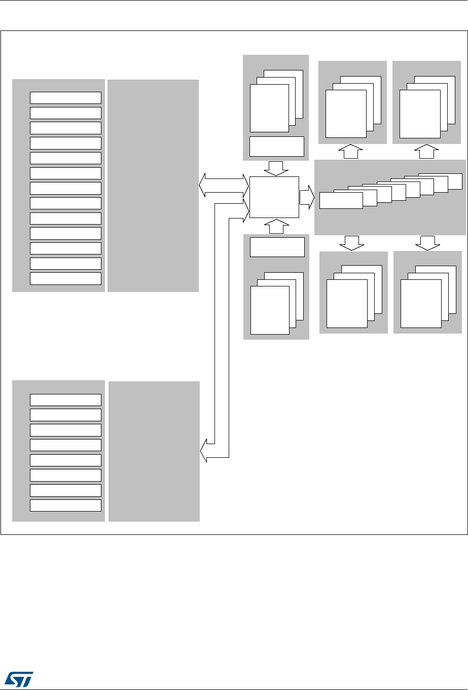
DocID018909 Rev 9 1063/1718
RM0090 Controller area network (bxCAN)
1104
Figure 335. Dual CAN block diagram
32.4 bxCAN operating modes
bxCAN has three main operating modes: initialization, normal and Sleep. After a
hardware reset, bxCAN is in Sleep mode to reduce power consumption and an internal pull-
up is active on CANTX. The software requests bxCAN to enter initialization or Sleep mode
by setting the INRQ or SLEEP bits in the CAN_MCR register. Once the mode has been
entered, bxCAN confirms it by setting the INAK or SLAK bits in the CAN_MSR register and
the internal pull-up is disabled. When neither INAK nor SLAK are set, bxCAN is in normal
$FFHSW DQFH)LO W HUV
)L O W HU
7U DQ VP L VVL R Q
6FKHGXOHU
0DLOER[
5H FH L Y H ), )2
0DLOER[
5HFHLYH),)2
0DLOER[
7[0DLOER[HV
7U DQ VP L VVL R Q
6FKHGXOHU
0DLOER[
5HFHLYH),)2
0DLOER[
5H F H L Y H ) ,) 2
0DLOER[
7[0DLOER[HV
0HPRU\
$FFHVV
&R Q W U R O O HU
0DVW HU&RQW URO
0DVW HU6W DW XV
5[ ), )2 6W D W X V
5[ ), )2 6W D W X V
(UURU6WDWXV
%L W 7L P L Q J
,QWHUUXSW(QDEOH
&RQWURO6WDWXV&RQILJXUDWLRQ
7[6W DW X V
0DVWHU&RQWURO
0DVWHU6WDWXV
5[ ), )2 6W D W X V
5[ ), )2 6W D W X V
(UURU6WDWXV
%L W 7L P L Q J
)LOWHU0RGH
)LOWHU6FDOH
,QWHUUXSW(QDEOH
&RQWURO6WDWXV&RQILJXUDWLRQ
7[6W DW X V
)L O W HU ), ) 2 $V VL J Q
)LOWHU0DVWHU
)LOWHU$FWLYDWLRQ
&$1%$FWLYH&RUH
&$16ODYH
&$1%$FWLYH&RUH
&$10DVWHUZLWKE\WHV65$0
0DVWHU UHWVD0UHWVD0
0DVWHU)LOWHUV
6O D Y H
6O D Y H 6O DY H
6ODYH)LOWHUV
WR
WR
1RW H &$1V WDUW I L OW H UEDQ NQX PE HUQ LVFRQIL JXUDEOHE\ZULWLQJWR
WKH&$16%>@ELWVLQWKH&$1B)05UHJLVWHU
DLE

Controller area network (bxCAN) RM0090
1064/1718 DocID018909 Rev 9
mode. Before entering normal mode bxCAN always has to synchronize on the CAN bus.
To synchronize, bxCAN waits until the CAN bus is idle, this means 11 consecutive recessive
bits have been monitored on CANRX.
32.4.1 Initialization mode
The software initialization can be done while the hardware is in Initialization mode. To enter
this mode the software sets the INRQ bit in the CAN_MCR register and waits until the
hardware has confirmed the request by setting the INAK bit in the CAN_MSR register.
To leave Initialization mode, the software clears the INQR bit. bxCAN has left Initialization
mode once the INAK bit has been cleared by hardware.
While in Initialization Mode, all message transfers to and from the CAN bus are stopped and
the status of the CAN bus output CANTX is recessive (high).
Entering Initialization Mode does not change any of the configuration registers.
To initialize the CAN Controller, software has to set up the Bit Timing (CAN_BTR) and CAN
options (CAN_MCR) registers.
To initialize the registers associated with the CAN filter banks (mode, scale, FIFO
assignment, activation and filter values), software has to set the FINIT bit (CAN_FMR). Filter
initialization also can be done outside the initialization mode.
Note: When FINIT=1, CAN reception is deactivated.
The filter values also can be modified by deactivating the associated filter activation bits (in
the CAN_FA1R register).
If a filter bank is not used, it is recommended to leave it non active (leave the corresponding
FACT bit cleared).
32.4.2 Normal mode
Once the initialization is complete, the software must request the hardware to enter Normal
mode to be able to synchronize on the CAN bus and start reception and transmission.
The request to enter Normal mode is issued by clearing the INRQ bit in the CAN_MCR
register. The bxCAN enters Normal mode and is ready to take part in bus activities when it
has synchronized with the data transfer on the CAN bus. This is done by waiting for the
occurrence of a sequence of 11 consecutive recessive bits (Bus Idle state). The switch to
Normal mode is confirmed by the hardware by clearing the INAK bit in the CAN_MSR
register.
The initialization of the filter values is independent from Initialization Mode but must be done
while the filter is not active (corresponding FACTx bit cleared). The filter scale and mode
configuration must be configured before entering Normal Mode.
32.4.3 Sleep mode (low power)
To reduce power consumption, bxCAN has a low-power mode called Sleep mode. This
mode is entered on software request by setting the SLEEP bit in the CAN_MCR register. In
this mode, the bxCAN clock is stopped, however software can still access the bxCAN
mailboxes.
If software requests entry to initialization mode by setting the INRQ bit while bxCAN is in
Sleep mode, it must also clear the SLEEP bit.
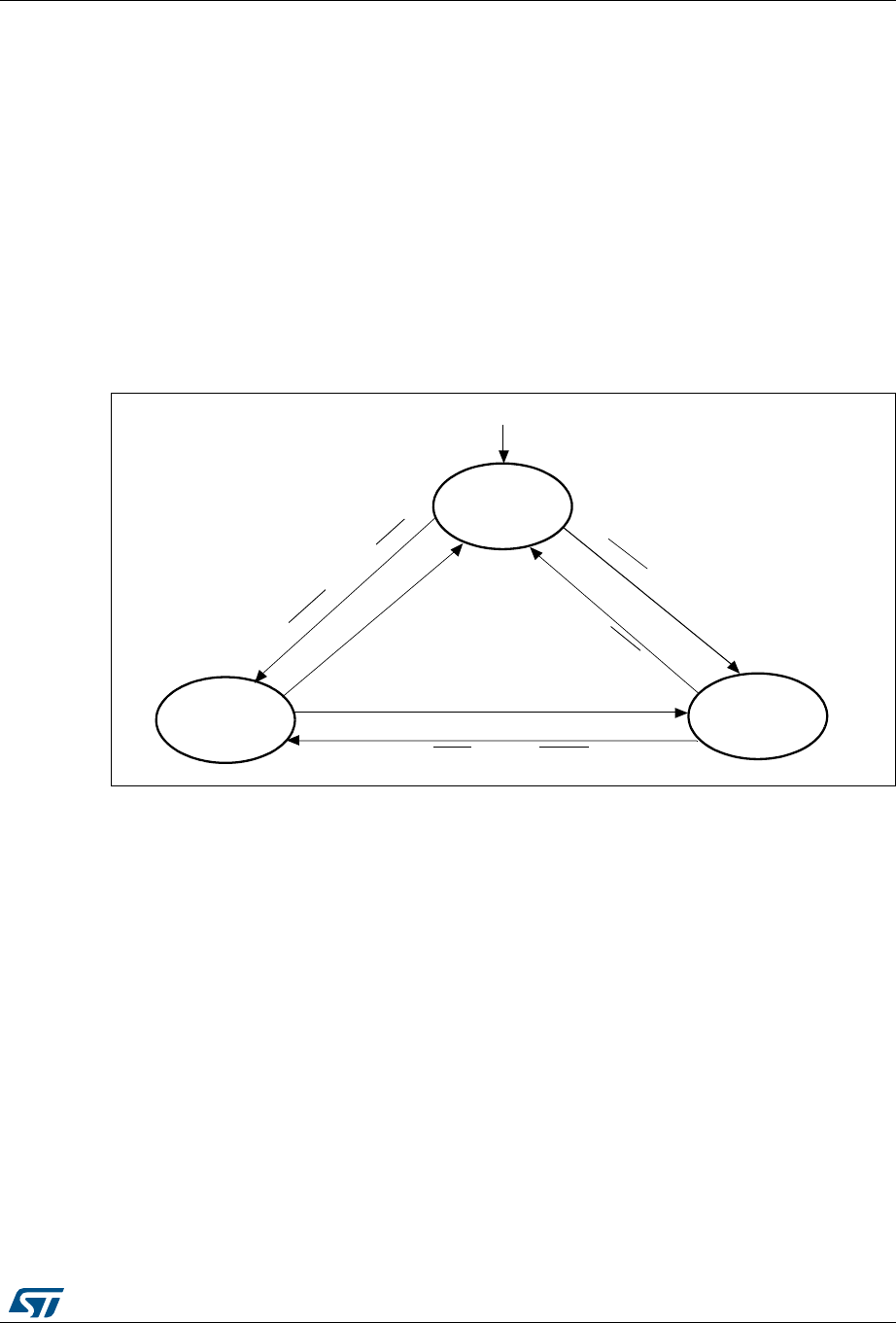
DocID018909 Rev 9 1065/1718
RM0090 Controller area network (bxCAN)
1104
bxCAN can be woken up (exit Sleep mode) either by software clearing the SLEEP bit or on
detection of CAN bus activity.
On CAN bus activity detection, hardware automatically performs the wakeup sequence by
clearing the SLEEP bit if the AWUM bit in the CAN_MCR register is set. If the AWUM bit is
cleared, software has to clear the SLEEP bit when a wakeup interrupt occurs, in order to exit
from Sleep mode.
Note: If the wakeup interrupt is enabled (WKUIE bit set in CAN_IER register) a wakeup interrupt
will be generated on detection of CAN bus activity, even if the bxCAN automatically
performs the wakeup sequence.
After the SLEEP bit has been cleared, Sleep mode is exited once bxCAN has synchronized
with the CAN bus, refer to Figure 336: bxCAN operating modes. The Sleep mode is exited
once the SLAK bit has been cleared by hardware.
Figure 336. bxCAN operating modes
1. ACK = The wait state during which hardware confirms a request by setting the INAK or SLAK bits in the
CAN_MSR register
2. SYNC = The state during which bxCAN waits until the CAN bus is idle, meaning 11 consecutive recessive
bits have been monitored on CANRX
32.5 Test mode
Test mode can be selected by the SILM and LBKM bits in the CAN_BTR register. These bits
must be configured while bxCAN is in Initialization mode. Once test mode has been
selected, the INRQ bit in the CAN_MCR register must be reset to enter Normal mode.
32.5.1 Silent mode
The bxCAN can be put in Silent mode by setting the SILM bit in the CAN_BTR register.
In Silent mode, the bxCAN is able to receive valid data frames and valid remote frames, but
it sends only recessive bits on the CAN bus and it cannot start a transmission. If the bxCAN
has to send a dominant bit (ACK bit, overload flag, active error flag), the bit is rerouted
internally so that the CAN Core monitors this dominant bit, although the CAN bus may
3LEEP
)NITIALIZATION
.ORMAL
2ESET
3,!+
).!+
3,!+
).!+
3,!+
).!+
3,%%0).21!#+
3,%%0).21!#+
).21!#+
).2139.#3,%%0
3,%%0!#+
3,%%039.#).21
AI
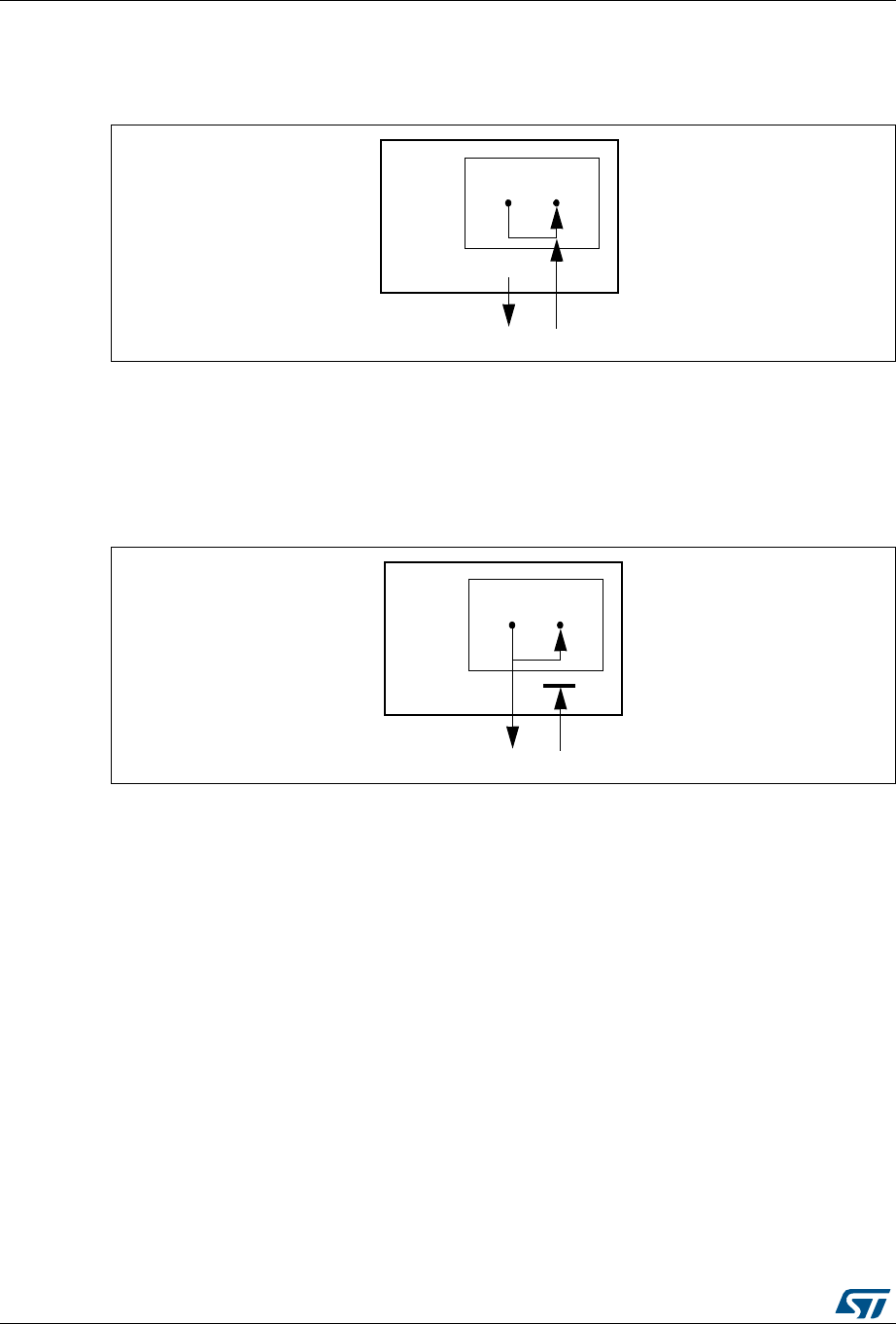
Controller area network (bxCAN) RM0090
1066/1718 DocID018909 Rev 9
remain in recessive state. Silent mode can be used to analyze the traffic on a CAN bus
without affecting it by the transmission of dominant bits (Acknowledge Bits, Error Frames).
Figure 337. bxCAN in silent mode
32.5.2 Loop back mode
The bxCAN can be set in Loop Back Mode by setting the LBKM bit in the CAN_BTR
register. In Loop Back Mode, the bxCAN treats its own transmitted messages as received
messages and stores them (if they pass acceptance filtering) in a Receive mailbox.
Figure 338. bxCAN in loop back mode
This mode is provided for self-test functions. To be independent of external events, the CAN
Core ignores acknowledge errors (no dominant bit sampled in the acknowledge slot of a
data / remote frame) in Loop Back Mode. In this mode, the bxCAN performs an internal
feedback from its Tx output to its Rx input. The actual value of the CANRX input pin is
disregarded by the bxCAN. The transmitted messages can be monitored on the CANTX pin.
32.5.3 Loop back combined with silent mode
It is also possible to combine Loop Back mode and Silent mode by setting the LBKM and
SILM bits in the CAN_BTR register. This mode can be used for a “Hot Selftest”, meaning the
bxCAN can be tested like in Loop Back mode but without affecting a running CAN system
connected to the CANTX and CANRX pins. In this mode, the CANRX pin is disconnected
from the bxCAN and the CANTX pin is held recessive.
bxCAN
CANTX CANRX
Tx Rx
=1
bxCAN
CANTX CANRX
Tx Rx

DocID018909 Rev 9 1067/1718
RM0090 Controller area network (bxCAN)
1104
Figure 339. bxCAN in combined mode
32.6 Debug mode
When the microcontroller enters the debug mode (Cortex®-M4 with FPU core halted), the
bxCAN continues to work normally or stops, depending on:
•the DBG_CAN1_STOP bit for CAN1 or the DBG_CAN2_STOP bit for CAN2 in the
DBG module. For more details, refer to Section 38.16.2: Debug support for timers,
watchdog, bxCAN and I2C.
•the DBF bit in CAN_MCR. For more details, refer to Section 32.9.2: CAN control and
status registers.
32.7 bxCAN functional description
32.7.1 Transmission handling
In order to transmit a message, the application must select one empty transmit mailbox, set
up the identifier, the data length code (DLC) and the data before requesting the transmission
by setting the corresponding TXRQ bit in the CAN_TIxR register. Once the mailbox has left
empty state, the software no longer has write access to the mailbox registers. Immediately
after the TXRQ bit has been set, the mailbox enters pending state and waits to become the
highest priority mailbox, see Transmit Priority. As soon as the mailbox has the highest
priority it will be scheduled for transmission. The transmission of the message of the
scheduled mailbox will start (enter transmit state) when the CAN bus becomes idle. Once
the mailbox has been successfully transmitted, it will become empty again. The hardware
indicates a successful transmission by setting the RQCP and TXOK bits in the CAN_TSR
register.
If the transmission fails, the cause is indicated by the ALST bit in the CAN_TSR register in
case of an Arbitration Lost, and/or the TERR bit, in case of transmission error detection.
Transmit priority
By identifier
When more than one transmit mailbox is pending, the transmission order is given by the
identifier of the message stored in the mailbox. The message with the lowest identifier value
has the highest priority according to the arbitration of the CAN protocol. If the identifier
values are equal, the lower mailbox number will be scheduled first.
By transmit request order
bxCAN
CANTX CANRX
Tx Rx
=1
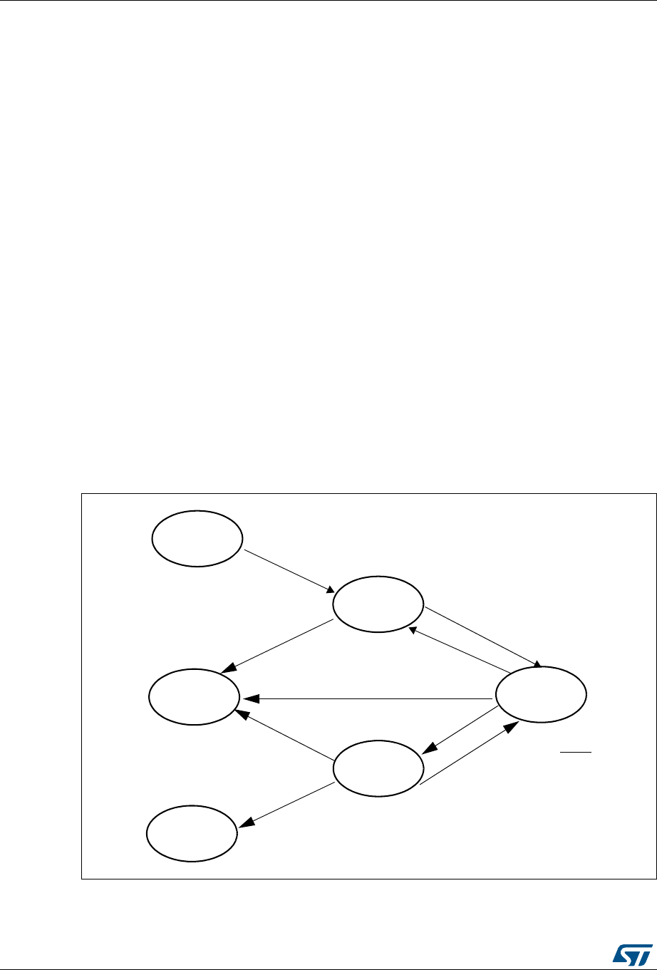
Controller area network (bxCAN) RM0090
1068/1718 DocID018909 Rev 9
The transmit mailboxes can be configured as a transmit FIFO by setting the TXFP bit in the
CAN_MCR register. In this mode the priority order is given by the transmit request order.
This mode is very useful for segmented transmission.
Abort
A transmission request can be aborted by the user setting the ABRQ bit in the CAN_TSR
register. In pending or scheduled state, the mailbox is aborted immediately. An abort
request while the mailbox is in transmit state can have two results. If the mailbox is
transmitted successfully the mailbox becomes empty with the TXOK bit set in the
CAN_TSR register. If the transmission fails, the mailbox becomes scheduled, the
transmission is aborted and becomes empty with TXOK cleared. In all cases the mailbox
will become empty again at least at the end of the current transmission.
Nonautomatic retransmission mode
This mode has been implemented in order to fulfil the requirement of the Time Triggered
Communication option of the CAN standard. To configure the hardware in this mode the
NART bit in the CAN_MCR register must be set.
In this mode, each transmission is started only once. If the first attempt fails, due to an
arbitration loss or an error, the hardware will not automatically restart the message
transmission.
At the end of the first transmission attempt, the hardware considers the request as
completed and sets the RQCP bit in the CAN_TSR register. The result of the transmission is
indicated in the CAN_TSR register by the TXOK, ALST and TERR bits.
Figure 340. Transmit mailbox states
EMPTY
TXRQ=1
RQCP=X
TXOK=X
PENDING
RQCP=0
TXOK=0
SCHEDULED
RQCP=0
TXOK=0
Mailbox has
TRANSMIT
RQCP=0
TXOK=0
CAN Bus = IDLE
Transmit failed * NART
Transmit succeeded
Mailbox does not
EMPTY
RQCP=1
TXOK=0
highest priority
have highest priority
EMPTY
RQCP=1
TXOK=1
ABRQ=1
ABRQ=1
Transmit failed * NART
TME = 1
TME = 0
TME = 0
TME = 0
TME = 1
TME = 1
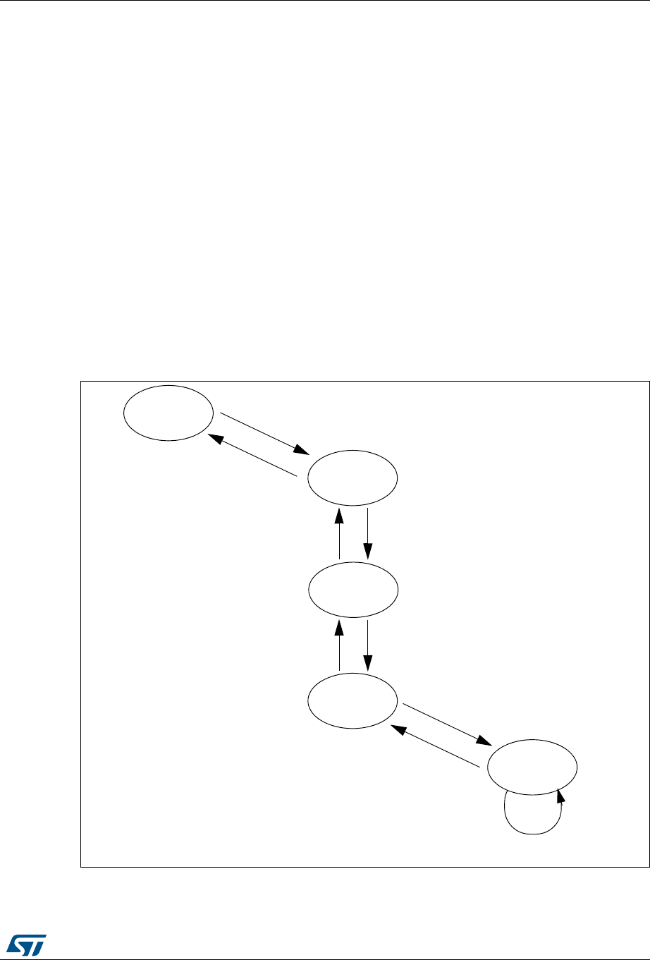
DocID018909 Rev 9 1069/1718
RM0090 Controller area network (bxCAN)
1104
32.7.2 Time triggered communication mode
In this mode, the internal counter of the CAN hardware is activated and used to generate the
Time Stamp value stored in the CAN_RDTxR/CAN_TDTxR registers, respectively (for Rx
and Tx mailboxes). The internal counter is incremented each CAN bit time (refer to
Section 32.7.7: Bit timing). The internal counter is captured on the sample point of the Start
Of Frame bit in both reception and transmission.
32.7.3 Reception handling
For the reception of CAN messages, three mailboxes organized as a FIFO are provided. In
order to save CPU load, simplify the software and guarantee data consistency, the FIFO is
managed completely by hardware. The application accesses the messages stored in the
FIFO through the FIFO output mailbox.
Valid message
A received message is considered as valid when it has been received correctly according to
the CAN protocol (no error until the last but one bit of the EOF field) and It passed through
the identifier filtering successfully, see Section 32.7.4: Identifier filtering.
Figure 341. Receive FIFO states
EMPTY
Valid Message
FMP=0x00
FOVR=0
PENDING_1
FMP=0x01
FOVR=0
Received
PENDING_2
FMP=0x10
FOVR=0
PENDING_3
FMP=0x11
FOVR=0
Valid Message
Received
Release
OVERRUN
FMP=0x11
FOVR=1
Mailbox
Release
Mailbox
Valid Message
Received
Valid Message
Received
Release
Mailbox
Release
Mailbox
Valid Message
Received
RFOM=1
RFOM=1
RFOM=1

Controller area network (bxCAN) RM0090
1070/1718 DocID018909 Rev 9
FIFO management
Starting from the empty state, the first valid message received is stored in the FIFO which
becomes pending_1. The hardware signals the event setting the FMP[1:0] bits in the
CAN_RFR register to the value 01b. The message is available in the FIFO output mailbox.
The software reads out the mailbox content and releases it by setting the RFOM bit in the
CAN_RFR register. The FIFO becomes empty again. If a new valid message has been
received in the meantime, the FIFO stays in pending_1 state and the new message is
available in the output mailbox.
If the application does not release the mailbox, the next valid message will be stored in the
FIFO which enters pending_2 state (FMP[1:0] = 10b). The storage process is repeated for
the next valid message putting the FIFO into pending_3 state (FMP[1:0] = 11b). At this
point, the software must release the output mailbox by setting the RFOM bit, so that a
mailbox is free to store the next valid message. Otherwise the next valid message received
will cause a loss of message.
Refer also to Section 32.7.5: Message storage
Overrun
Once the FIFO is in pending_3 state (i.e. the three mailboxes are full) the next valid
message reception will lead to an overrun and a message will be lost. The hardware
signals the overrun condition by setting the FOVR bit in the CAN_RFR register. Which
message is lost depends on the configuration of the FIFO:
•If the FIFO lock function is disabled (RFLM bit in the CAN_MCR register cleared) the
last message stored in the FIFO will be overwritten by the new incoming message. In
this case the latest messages will be always available to the application.
•If the FIFO lock function is enabled (RFLM bit in the CAN_MCR register set) the most
recent message will be discarded and the software will have the three oldest messages
in the FIFO available.
Reception related interrupts
Once a message has been stored in the FIFO, the FMP[1:0] bits are updated and an
interrupt request is generated if the FMPIE bit in the CAN_IER register is set.
When the FIFO becomes full (i.e. a third message is stored) the FULL bit in the CAN_RFR
register is set and an interrupt is generated if the FFIE bit in the CAN_IER register is set.
On overrun condition, the FOVR bit is set and an interrupt is generated if the FOVIE bit in
the CAN_IER register is set.
32.7.4 Identifier filtering
In the CAN protocol the identifier of a message is not associated with the address of a node
but related to the content of the message. Consequently a transmitter broadcasts its
message to all receivers. On message reception a receiver node decides - depending on
the identifier value - whether the software needs the message or not. If the message is
needed, it is copied into the SRAM. If not, the message must be discarded without
intervention by the software.
To fulfill this requirement, the bxCAN Controller provides 28 configurable and scalable filter
banks (27-0) to the application. In other devices the bxCAN Controller provides 14
configurable and scalable filter banks (13-0) to the application in order to receive only the
messages the software needs. This hardware filtering saves CPU resources which would be

DocID018909 Rev 9 1071/1718
RM0090 Controller area network (bxCAN)
1104
otherwise needed to perform filtering by software. Each filter bank x consists of two 32-bit
registers, CAN_FxR0 and CAN_FxR1.
Scalable width
To optimize and adapt the filters to the application needs, each filter bank can be scaled
independently. Depending on the filter scale a filter bank provides:
•One 32-bit filter for the STDID[10:0], EXTID[17:0], IDE and RTR bits.
•Two 16-bit filters for the STDID[10:0], RTR, IDE and EXTID[17:15] bits.
Refer to Figure 342.
Furthermore, the filters can be configured in mask mode or in identifier list mode.
Mask mode
In mask mode the identifier registers are associated with mask registers specifying which
bits of the identifier are handled as “must match” or as “don’t care”.
Identifier list mode
In identifier list mode, the mask registers are used as identifier registers. Thus instead of
defining an identifier and a mask, two identifiers are specified, doubling the number of single
identifiers. All bits of the incoming identifier must match the bits specified in the filter
registers.
Filter bank scale and mode configuration
The filter banks are configured by means of the corresponding CAN_FMR register. To
configure a filter bank it must be deactivated by clearing the FACT bit in the CAN_FAR
register. The filter scale is configured by means of the corresponding FSCx bit in the
CAN_FS1R register, refer to Figure 342. The identifier list or identifier mask mode for the
corresponding Mask/Identifier registers is configured by means of the FBMx bits in the
CAN_FMR register.
To filter a group of identifiers, configure the Mask/Identifier registers in mask mode.
To select single identifiers, configure the Mask/Identifier registers in identifier list mode.
Filters not used by the application should be left deactivated.
Each filter within a filter bank is numbered (called the Filter Number) from 0 to a maximum
dependent on the mode and the scale of each of the filter banks.
Concerning the filter configuration, refer to Figure 342.
Controller area network (bxCAN) RM0090
1072/1718 DocID018909 Rev 9
Figure 342. Filter bank scale configuration - register organization
Filter match index
Once a message has been received in the FIFO it is available to the application. Typically,
application data is copied into SRAM locations. To copy the data to the right location the
application has to identify the data by means of the identifier. To avoid this, and to ease the
access to the SRAM locations, the CAN controller provides a Filter Match Index.
This index is stored in the mailbox together with the message according to the filter priority
rules. Thus each received message has its associated filter match index.
The Filter Match index can be used in two ways:
•Compare the Filter Match index with a list of expected values.
•Use the Filter Match Index as an index on an array to access the data destination
location.
For nonmasked filters, the software no longer has to compare the identifier.
If the filter is masked the software reduces the comparison to the masked bits only.
The index value of the filter number does not take into account the activation state of the
filter banks. In addition, two independent numbering schemes are used, one for each FIFO.
Refer to Figure 343 for an example.
One 32-Bit Filter - Identifier Mask
Two 16-Bit Filters - Identifier Mask
CAN_FxR1[31:24]
CAN_FxR2[31:24]
CAN_FxR1[15:8]
CAN_FxR1[31:24]
CAN_FxR1[7:0]
CAN_FxR1[23:16]
x = filter bank number
FSCx = 1FSCx = 0
1 These bits are located in the CAN_FS1R register
Filter Bank Scale
ID
Mask
ID
Mask
STID[10:3]
STID[2:0]
EXID[12:5]
Mapping
STID[10:3]
ID
Mask
Mapping
RTR
Two 32-Bit Filters - Identifier List
ID
ID
STID[10:3] STID[2:0] EXID[12:5]
Mapping
Four 16-Bit Filters - Identifier List
ID
ID
STID[10:3]
ID
ID
Mapping
n
n+1
n+2
n+3
n+1
Filter Bank Mode2
n
n
n+1
EXID[4:0] IDE
EXID[17:13]
EXID[17:13]
STID[2:0] RTR IDE EXID[17:15]
FBMx = 0FBMx = 1
Filter
2 These bits are located in the CAN_FM1R register
n
Num.
FBMx = 0FBMx = 1
Config. Bits1
STID[2:0] RTR IDE EXID[17:15]
0
RTREXID[4:0] IDE 0
CAN_FxR1[23:16] CAN_FxR1[15:8] CAN_FxR1[7:0]
CAN_FxR2[7:0]CAN_FxR2[15:8]CAN_FxR2[23:16]
CAN_FxR1[31:24]
CAN_FxR2[31:24]
CAN_FxR1[23:16] CAN_FxR1[15:8] CAN_FxR1[7:0]
CAN_FxR2[7:0]CAN_FxR2[15:8]CAN_FxR2[23:16]
CAN_FxR2[15:8]
CAN_FxR2[31:24]
CAN_FxR2[7:0]
CAN_FxR2[23:16]
CAN_FxR1[15:8]
CAN_FxR1[31:24]
CAN_FxR1[7:0]
CAN_FxR1[23:16]
CAN_FxR2[15:8]
CAN_FxR2[31:24]
CAN_FxR2[7:0]
CAN_FxR2[23:16]
ID=Identifier
DocID018909 Rev 9 1073/1718
RM0090 Controller area network (bxCAN)
1104
Figure 343. Example of filter numbering
Filter priority rules
Depending on the filter combination it may occur that an identifier passes successfully
through several filters. In this case the filter match value stored in the receive mailbox is
chosen according to the following priority rules:
•A 32-bit filter takes priority over a 16-bit filter.
•For filters of equal scale, priority is given to the Identifier List mode over the Identifier
Mask mode
•For filters of equal scale and mode, priority is given by the filter number (the lower the
number, the higher the priority).
9
8
ID List (32-bit)
ID Mask (32-bit)
ID List (16-bit)
ID List (32-bit)
Deactivated
ID Mask (16-bit)
ID List (32-bit)
Filter
0
1
3
5
6
9
ID Mask (32-bit)
13
FIFO0 Filter
0
1
2
3
4
5
6
7
10
11
12
13
ID Mask (16-bit)
ID List (32-bit)
ID Mask (16-bit)
ID List (16-bit)
Deactivated
ID Mask (16-bit)
ID List (32-bit)
Filter
2
4
7
8
10
11
ID Mask (32-bit)
12
FIFO1 Filter
0
1
2
4
5
6
7
8
11
12
13
14
3
Deactivated
9
10
Num. Num.BankBank
ID=Identifier
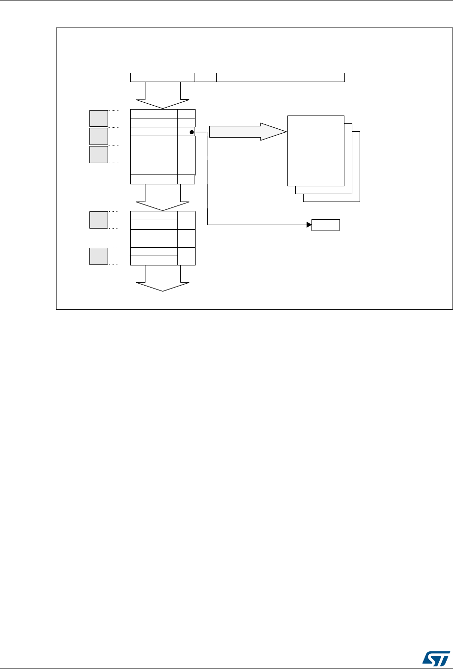
Controller area network (bxCAN) RM0090
1074/1718 DocID018909 Rev 9
Figure 344. Filtering mechanism - example
The example above shows the filtering principle of the bxCAN. On reception of a message,
the identifier is compared first with the filters configured in identifier list mode. If there is a
match, the message is stored in the associated FIFO and the index of the matching filter is
stored in the Filter Match Index. As shown in the example, the identifier matches with
Identifier #2 thus the message content and FMI 2 is stored in the FIFO.
If there is no match, the incoming identifier is then compared with the filters configured in
mask mode.
If the identifier does not match any of the identifiers configured in the filters, the message is
discarded by hardware without disturbing the software.
32.7.5 Message storage
The interface between the software and the hardware for the CAN messages is
implemented by means of mailboxes. A mailbox contains all information related to a
message; identifier, data, control, status and time stamp information.
Transmit mailbox
The software sets up the message to be transmitted in an empty transmit mailbox. The
status of the transmission is indicated by hardware in the CAN_TSR register.
Identifier List
Message Discarded
Identifier & Mask
Identifier 0
Identifier 1
Identifier 4
Identifier 5
Identifier 2
Mask
Identifier 3
Mask
Identifier
Message Received
Ctrl Data
Identifier #4 Match
Message
Stored
Receive FIFO
No Match
Found
Filter number stored
in the Filter Match
Index field within the
CAN_RDTxR register
FMI
Filter bank
0
2
3
1
4
Example of 3 filter banks in 32-bit Unidentified List mode and
Num
the remaining in 32-bit Identifier Mask mode
DocID018909 Rev 9 1075/1718
RM0090 Controller area network (bxCAN)
1104
Receive mailbox
When a message has been received, it is available to the software in the FIFO output
mailbox. Once the software has handled the message (e.g. read it) the software must
release the FIFO output mailbox by means of the RFOM bit in the CAN_RFR register to
make the next incoming message available. The filter match index is stored in the MFMI
field of the CAN_RDTxR register. The 16-bit time stamp value is stored in the TIME[15:0]
field of CAN_RDTxR.
Figure 345. CAN error state diagram
Table 181. Transmit mailbox mapping
Offset to transmit mailbox base address Register name
0CAN_TIxR
4 CAN_TDTxR
8CAN_TDLxR
12 CAN_TDHxR
Table 182. Receive mailbox mapping
Offset to receive mailbox base
address (bytes) Register name
0CAN_RIxR
4 CAN_RDTxR
8 CAN_RDLxR
12 CAN_RDHxR
%22/20! 33)6%
7HEN4%#OR2%#
7HEN4%#AND2%#
%22/2!#4)6%
"53/&&
7HEN4%#7HENRECESSIVEBITSOCCUR
AI

Controller area network (bxCAN) RM0090
1076/1718 DocID018909 Rev 9
32.7.6 Error management
The error management as described in the CAN protocol is handled entirely by hardware
using a Transmit Error Counter (TEC value, in CAN_ESR register) and a Receive Error
Counter (REC value, in the CAN_ESR register), which get incremented or decremented
according to the error condition. For detailed information about TEC and REC management,
please refer to the CAN standard.
Both of them may be read by software to determine the stability of the network.
Furthermore, the CAN hardware provides detailed information on the current error status in
CAN_ESR register. By means of the CAN_IER register (ERRIE bit, etc.), the software can
configure the interrupt generation on error detection in a very flexible way.
Bus-Off recovery
The Bus-Off state is reached when TEC is greater than 255, this state is indicated by BOFF
bit in CAN_ESR register. In Bus-Off state, the bxCAN is no longer able to transmit and
receive messages.
Depending on the ABOM bit in the CAN_MCR register bxCAN will recover from Bus-Off
(become error active again) either automatically or on software request. But in both cases
the bxCAN has to wait at least for the recovery sequence specified in the CAN standard
(128 occurrences of 11 consecutive recessive bits monitored on CANRX).
If ABOM is set, the bxCAN will start the recovering sequence automatically after it has
entered Bus-Off state.
If ABOM is cleared, the software must initiate the recovering sequence by requesting
bxCAN to enter and to leave initialization mode.
Note: In initialization mode, bxCAN does not monitor the CANRX signal, therefore it cannot
complete the recovery sequence. To recover, bxCAN must be in normal mode.
32.7.7 Bit timing
The bit timing logic monitors the serial bus-line and performs sampling and adjustment of
the sample point by synchronizing on the start-bit edge and resynchronizing on the following
edges.
Its operation may be explained simply by splitting nominal bit time into three segments as
follows:
•Synchronization segment (SYNC_SEG): a bit change is expected to occur within this
time segment. It has a fixed length of one time quantum (1 x tCAN).
•Bit segment 1 (BS1): defines the location of the sample point. It includes the
PROP_SEG and PHASE_SEG1 of the CAN standard. Its duration is programmable
between 1 and 16 time quanta but may be automatically lengthened to compensate for
positive phase drifts due to differences in the frequency of the various nodes of the
network.
•Bit segment 2 (BS2): defines the location of the transmit point. It represents the
PHASE_SEG2 of the CAN standard. Its duration is programmable between 1 and 8
time quanta but may also be automatically shortened to compensate for negative
phase drifts.
The resynchronization Jump Width (SJW) defines an upper bound to the amount of
lengthening or shortening of the bit segments. It is programmable between 1 and 4 time
quanta.
DocID018909 Rev 9 1077/1718
RM0090 Controller area network (bxCAN)
1104
A valid edge is defined as the first transition in a bit time from dominant to recessive bus
level provided the controller itself does not send a recessive bit.
If a valid edge is detected in BS1 instead of SYNC_SEG, BS1 is extended by up to SJW so
that the sample point is delayed.
Conversely, if a valid edge is detected in BS2 instead of SYNC_SEG, BS2 is shortened by
up to SJW so that the transmit point is moved earlier.
As a safeguard against programming errors, the configuration of the Bit Timing Register
(CAN_BTR) is only possible while the device is in Standby mode.
Note: For a detailed description of the CAN bit timing and resynchronization mechanism, please
refer to the ISO 11898 standard.
Figure 346. Bit timing
SYNC_SEG BIT SEGMENT 1 (BS1) BIT SEGMENT 2 (BS2)
NOMINAL BIT TIME
1 x tqtBS1 tBS2
SAMPLE POINT TRANSMIT POINT
NominalBitTime 1tq
×tBS1 tBS2
++=
with:
tBS1 = tq x (TS1[3:0] + 1),
tBS2 = tq x (TS2[2:0] + 1),
tq = (BRP[9:0] + 1) x tPCLK
tPCLK = time period of the APB clock,
BRP[9:0], TS1[3:0] and TS2[2:0] are defined in the CAN_BTR Register.
BaudRate 1
NominalBitTime
----------------------------------------------=
where tq refers to the Time quantum
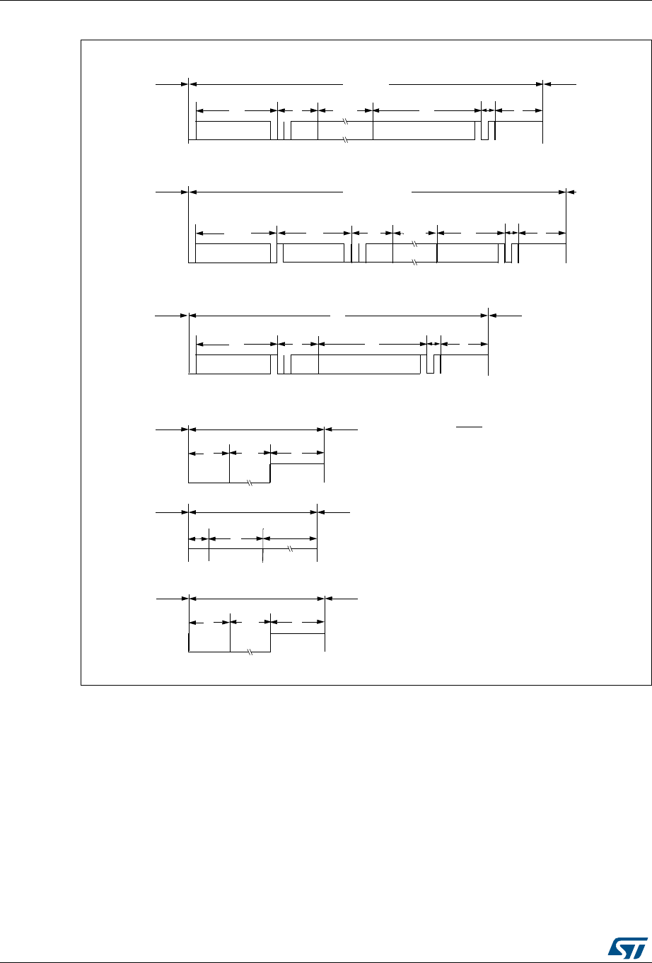
Controller area network (bxCAN) RM0090
1078/1718 DocID018909 Rev 9
Figure 347. CAN frames
32.8 bxCAN interrupts
Four interrupt vectors are dedicated to bxCAN. Each interrupt source can be independently
enabled or disabled by means of the CAN Interrupt Enable Register (CAN_IER).
Data Frame or
Remote Frame
Data Field
8 * N
Ctrl Field
6
Arbitration Field
32
CRC Field
16
Ack Field
7
SOF
ID DLC CRC
Data Frame (Standard identifier)
44 + 8 * N
Arbitration Field
32
RTR
IDE
r0
SOF
ID DLC
Remote Frame
44
CRC Field
16 7
CRC
Ctrl Field
6
Overload
Overload Frame
Error
6
Error Delimiter
8
Error Frame
Flag Echo
6
Bus Idle
Inter-Frame Space
Suspend
8
Intermission
3Transmission
ACK
ACK
2
2
Inter-Frame Space
or Overload Frame
Inter-Frame Space
Inter-Frame Space
or Overload Frame
Inter-Frame Space
Inter-Frame Space
or Overload Frame Notes:
0 <= N <= 8
SOF = Start Of Frame
ID = Identifier
RTR = Remote Transmission Request
IDE = Identifier Extension Bit
r0 = Reserved Bit
DLC = Data Length Code
CRC = Cyclic Redundancy Code
Error flag: 6 dominant bits if node is error
active else 6 recessive bits.
Suspend transmission: applies to error
passive nodes only.
EOF = End of Frame
ACK = Acknowledge bit
Ctrl = Control
Data Frame or
Remote Frame
Any Frame
Inter-Frame Space
or Error Frame
End Of Frame or
Error Delimiter or
Overload Delimiter
Ack Field
EOF
RTR
IDE
r0
EOF
Data Field
8 * N
Ctrl Field
6
32
CRC Field
16
Ack Field
7
SOF
ID DLC CRC
Data Frame (Extended Identifier)
64 + 8 * N
ACK
2
Inter-Frame Space
or Overload Frame
Inter-Frame Space
SRR
IDE
EOF
RTR
r1
r0
32
6
Overload
8
6
Overload
Flag Echo Delimiter
Flag
ai15154
Arbitration Field Arbitration Field
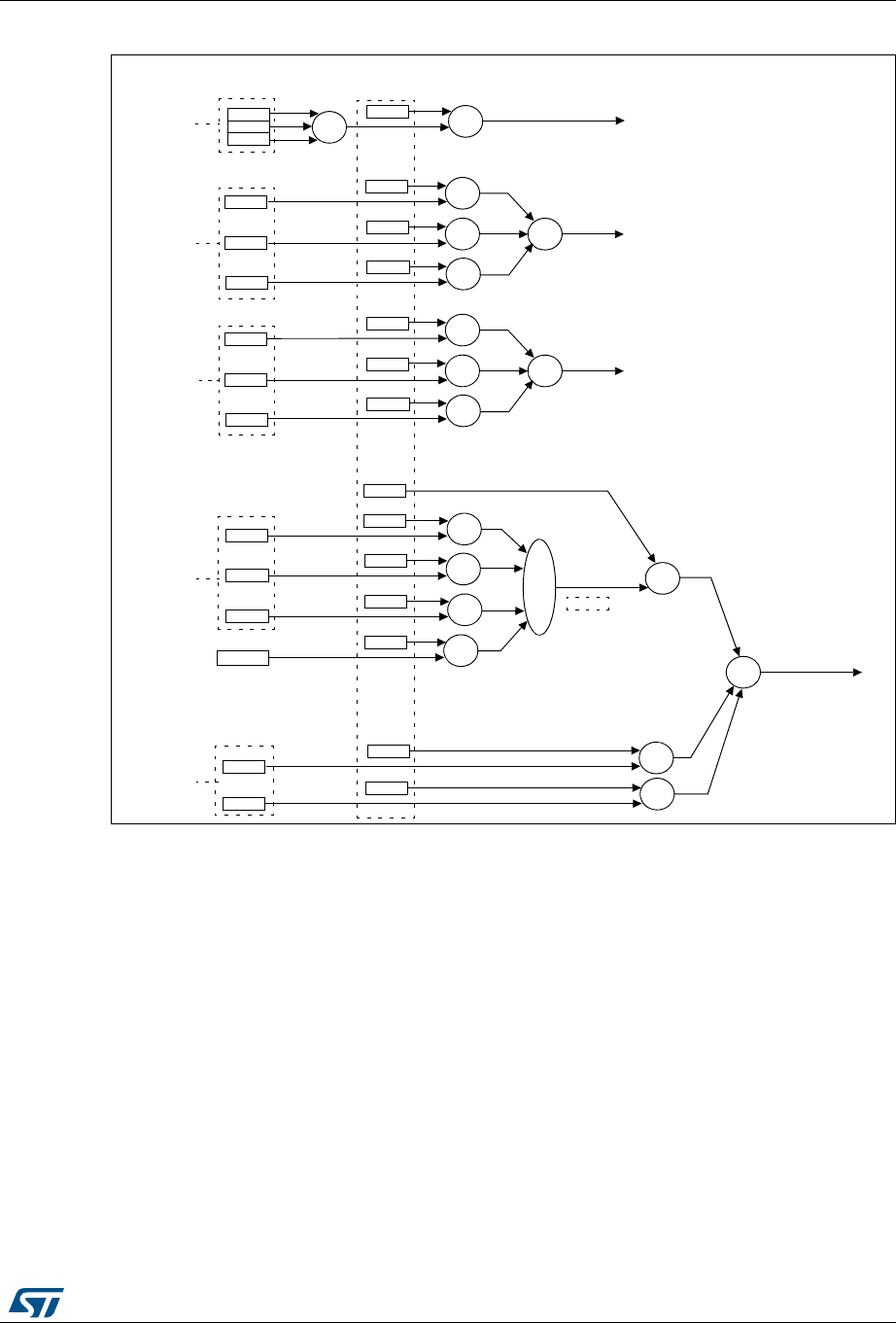
DocID018909 Rev 9 1079/1718
RM0090 Controller area network (bxCAN)
1104
Figure 348. Event flags and interrupt generation
•The transmit interrupt can be generated by the following events:
– Transmit mailbox 0 becomes empty, RQCP0 bit in the CAN_TSR register set.
– Transmit mailbox 1 becomes empty, RQCP1 bit in the CAN_TSR register set.
– Transmit mailbox 2 becomes empty, RQCP2 bit in the CAN_TSR register set.
•The FIFO 0 interrupt can be generated by the following events:
– Reception of a new message, FMP0 bits in the CAN_RF0R register are not ‘00’.
– FIFO0 full condition, FULL0 bit in the CAN_RF0R register set.
– FIFO0 overrun condition, FOVR0 bit in the CAN_RF0R register set.
•The FIFO 1 interrupt can be generated by the following events:
– Reception of a new message, FMP1 bits in the CAN_RF1R register are not ‘00’.
– FIFO1 full condition, FULL1 bit in the CAN_RF1R register set.
– FIFO1 overrun condition, FOVR1 bit in the CAN_RF1R register set.
•The error and status change interrupt can be generated by the following events:
– Error condition, for more details on error conditions please refer to the CAN Error
Status register (CAN_ESR).
RQCP0
RQCP1
FMP1
CAN_TSR+TMEIE
CAN_IER
TRANSMIT
&
FMPIE1
FULL1 &
FFIE1
FOVR1 &
FOVIE1
&
+
CAN_RF1R
FIFO 1
EWGF
EWGIE
EPVF
EPVIE
BOFF
BOFIE
1≤LEC≤6
LECIE
&
&
&
&
CAN_ESR+&
ERRIE
INTERRUPT
INTERRUPT
FMP0 &
FMPIE0
FULL0 &
FFIE0
FOVR0 &
FOVIE0
+
CAN_RF0R
FIFO 0
INTERRUPT
RQCP2
WKUI &
WKUIE
CAN_MSR
+
INTERRUPT
ERROR
STATUS CHANGE
ERRI
SLAKI
SLKIE &
CAN_MSR
Controller area network (bxCAN) RM0090
1080/1718 DocID018909 Rev 9
– Wakeup condition, SOF monitored on the CAN Rx signal.
– Entry into Sleep mode.
32.9 CAN registers
The peripheral registers have to be accessed by words (32 bits).
32.9.1 Register access protection
Erroneous access to certain configuration registers can cause the hardware to temporarily
disturb the whole CAN network. Therefore the CAN_BTR register can be modified by
software only while the CAN hardware is in initialization mode.
Although the transmission of incorrect data will not cause problems at the CAN network
level, it can severely disturb the application. A transmit mailbox can be only modified by
software while it is in empty state, refer to Figure 340: Transmit mailbox states.
The filter values can be modified either deactivating the associated filter banks or by setting
the FINIT bit. Moreover, the modification of the filter configuration (scale, mode and FIFO
assignment) in CAN_FMxR, CAN_FSxR and CAN_FFAR registers can only be done when
the filter initialization mode is set (FINIT=1) in the CAN_FMR register.
32.9.2 CAN control and status registers
Refer to Section 1.1 for a list of abbreviations used in register descriptions.
CAN master control register (CAN_MCR)
Address offset: 0x00
Reset value: 0x0001 0002
31 30 29 28 27 26 25 24 23 22 21 20 19 18 17 16
Reserved DBF
rw
1514131211109876543210
RESET Reserved TTCM ABOM AWUM NART RFLM TXFP SLEEP INRQ
rs rw rw rw rw rw rw rw rw
Bits 31:17 Reserved, must be kept at reset value.
Bit 16 DBF: Debug freeze
0: CAN working during debug
1: CAN reception/transmission frozen during debug. Reception FIFOs can still be
accessed/controlled normally.
Bit 15 RESET: bxCAN software master reset
0: Normal operation.
1: Force a master reset of the bxCAN -> Sleep mode activated after reset (FMP bits and
CAN_MCR register are initialized to the reset values). This bit is automatically reset to 0.
Bits 14:8 Reserved, must be kept at reset value.

DocID018909 Rev 9 1081/1718
RM0090 Controller area network (bxCAN)
1104
Bit 7 TTCM: Time triggered communication mode
0: Time Triggered Communication mode disabled.
1: Time Triggered Communication mode enabled
Note: For more information on Time Triggered Communication mode, please refer to
Section 32.7.2: Time triggered communication mode.
Bit 6 ABOM: Automatic bus-off management
This bit controls the behavior of the CAN hardware on leaving the Bus-Off state.
0: The Bus-Off state is left on software request, once 128 occurrences of 11 recessive bits
have been monitored and the software has first set and cleared the INRQ bit of the
CAN_MCR register.
1: The Bus-Off state is left automatically by hardware once 128 occurrences of 11 recessive
bits have been monitored.
For detailed information on the Bus-Off state please refer to Section 32.7.6: Error
management.
Bit 5 AWUM: Automatic wakeup mode
This bit controls the behavior of the CAN hardware on message reception during Sleep
mode.
0: The Sleep mode is left on software request by clearing the SLEEP bit of the CAN_MCR
register.
1: The Sleep mode is left automatically by hardware on CAN message detection.
The SLEEP bit of the CAN_MCR register and the SLAK bit of the CAN_MSR register are
cleared by hardware.
Bit 4 NART: No automatic retransmission
0: The CAN hardware will automatically retransmit the message until it has been
successfully transmitted according to the CAN standard.
1: A message will be transmitted only once, independently of the transmission result
(successful, error or arbitration lost).
Bit 3 RFLM: Receive FIFO locked mode
0: Receive FIFO not locked on overrun. Once a receive FIFO is full the next incoming
message will overwrite the previous one.
1: Receive FIFO locked against overrun. Once a receive FIFO is full the next incoming
message will be discarded.
Bit 2 TXFP: Transmit FIFO priority
This bit controls the transmission order when several mailboxes are pending at the same
time.
0: Priority driven by the identifier of the message
1: Priority driven by the request order (chronologically)
Bit 1 SLEEP: Sleep mode request
This bit is set by software to request the CAN hardware to enter the Sleep mode. Sleep
mode will be entered as soon as the current CAN activity (transmission or reception of a
CAN frame) has been completed.
This bit is cleared by software to exit Sleep mode.
This bit is cleared by hardware when the AWUM bit is set and a SOF bit is detected on the
CAN Rx signal.
This bit is set after reset - CAN starts in Sleep mode.

Controller area network (bxCAN) RM0090
1082/1718 DocID018909 Rev 9
CAN master status register (CAN_MSR)
Address offset: 0x04
Reset value: 0x0000 0C02
Bit 0 INRQ: Initialization request
The software clears this bit to switch the hardware into normal mode. Once 11 consecutive
recessive bits have been monitored on the Rx signal the CAN hardware is synchronized and
ready for transmission and reception. Hardware signals this event by clearing the INAK bit in
the CAN_MSR register.
Software sets this bit to request the CAN hardware to enter initialization mode. Once
software has set the INRQ bit, the CAN hardware waits until the current CAN activity
(transmission or reception) is completed before entering the initialization mode. Hardware
signals this event by setting the INAK bit in the CAN_MSR register.
31 30 29 28 27 26 25 24 23 22 21 20 19 18 17 16
Reserved
1514131211109876543210
Reserved.
RX SAMP RXM TXM
Reserved
SLAKI WKUI ERRI SLAK INAK
rrrr rc_w1rc_w1rc_w1rr
Bits 31:12 Reserved, must be kept at reset value.
Bit 11 RX: CAN Rx signal
Monitors the actual value of the CAN_RX Pin.
Bit 10 SAMP: Last sample point
The value of RX on the last sample point (current received bit value).
Bit 9 RXM: Receive mode
The CAN hardware is currently receiver.
Bit 8 TXM: Transmit mode
The CAN hardware is currently transmitter.
Bits 7:5 Reserved, must be kept at reset value.
Bit 4 SLAKI: Sleep acknowledge interrupt
When SLKIE=1, this bit is set by hardware to signal that the bxCAN has entered Sleep
Mode. When set, this bit generates a status change interrupt if the SLKIE bit in the
CAN_IER register is set.
This bit is cleared by software or by hardware, when SLAK is cleared.
Note: When SLKIE=0, no polling on SLAKI is possible. In this case the SLAK bit can be
polled.
Bit 3 WKUI: Wakeup interrupt
This bit is set by hardware to signal that a SOF bit has been detected while the CAN
hardware was in Sleep mode. Setting this bit generates a status change interrupt if the
WKUIE bit in the CAN_IER register is set.
This bit is cleared by software.

DocID018909 Rev 9 1083/1718
RM0090 Controller area network (bxCAN)
1104
CAN transmit status register (CAN_TSR)
Address offset: 0x08
Reset value: 0x1C00 0000
Bit 2 ERRI: Error interrupt
This bit is set by hardware when a bit of the CAN_ESR has been set on error detection and
the corresponding interrupt in the CAN_IER is enabled. Setting this bit generates a status
change interrupt if the ERRIE bit in the CAN_IER register is set.
This bit is cleared by software.
Bit 1 SLAK: Sleep acknowledge
This bit is set by hardware and indicates to the software that the CAN hardware is now in
Sleep mode. This bit acknowledges the Sleep mode request from the software (set SLEEP
bit in CAN_MCR register).
This bit is cleared by hardware when the CAN hardware has left Sleep mode (to be
synchronized on the CAN bus). To be synchronized the hardware has to monitor a
sequence of 11 consecutive recessive bits on the CAN RX signal.
Note: The process of leaving Sleep mode is triggered when the SLEEP bit in the CAN_MCR
register is cleared. Please refer to the AWUM bit of the CAN_MCR register description
for detailed information for clearing SLEEP bit
Bit 0 INAK: Initialization acknowledge
This bit is set by hardware and indicates to the software that the CAN hardware is now in
initialization mode. This bit acknowledges the initialization request from the software (set
INRQ bit in CAN_MCR register).
This bit is cleared by hardware when the CAN hardware has left the initialization mode (to
be synchronized on the CAN bus). To be synchronized the hardware has to monitor a
sequence of 11 consecutive recessive bits on the CAN RX signal.
31 30 29 28 27 26 25 24 23 22 21 20 19 18 17 16
LOW2 LOW1 LOW0 TME2 TME1 TME0 CODE[1:0] ABRQ2
Reserved
TERR2 ALST2 TXOK2 RQCP2
rrrrrrrrrs rc_w1rc_w1rc_w1rc_w1
1514131211109876543210
ABRQ1 Reserved
Res.
TERR1 ALST1 TXOK1 RQCP1 ABRQ0
Reserved
TERR0 ALST0 TXOK0 RQCP0
rs rc_w1 rc_w1 rc_w1 rc_w1 rs rc_w1 rc_w1 rc_w1 rc_w1
Bit 31 LOW2: Lowest priority flag for mailbox 2
This bit is set by hardware when more than one mailbox are pending for transmission and
mailbox 2 has the lowest priority.
Bit 30 LOW1: Lowest priority flag for mailbox 1
This bit is set by hardware when more than one mailbox are pending for transmission and
mailbox 1 has the lowest priority.
Bit 29 LOW0: Lowest priority flag for mailbox 0
This bit is set by hardware when more than one mailbox are pending for transmission and
mailbox 0 has the lowest priority.
Note: The LOW[2:0] bits are set to zero when only one mailbox is pending.
Bit 28 TME2: Transmit mailbox 2 empty
This bit is set by hardware when no transmit request is pending for mailbox 2.
Bit 27 TME1: Transmit mailbox 1 empty
This bit is set by hardware when no transmit request is pending for mailbox 1.

Controller area network (bxCAN) RM0090
1084/1718 DocID018909 Rev 9
Bit 26 TME0: Transmit mailbox 0 empty
This bit is set by hardware when no transmit request is pending for mailbox 0.
Bits 25:24 CODE[1:0]: Mailbox code
In case at least one transmit mailbox is free, the code value is equal to the number of the
next transmit mailbox free.
In case all transmit mailboxes are pending, the code value is equal to the number of the
transmit mailbox with the lowest priority.
Bit 23 ABRQ2: Abort request for mailbox 2
Set by software to abort the transmission request for the corresponding mailbox.
Cleared by hardware when the mailbox becomes empty.
Setting this bit has no effect when the mailbox is not pending for transmission.
Bits 22:20 Reserved, must be kept at reset value.
Bit 19 TERR2: Transmission error of mailbox 2
This bit is set when the previous TX failed due to an error.
Bit 18 ALST2: Arbitration lost for mailbox 2
This bit is set when the previous TX failed due to an arbitration lost.
Bit 17 TXOK2: Transmission OK of mailbox 2
The hardware updates this bit after each transmission attempt.
0: The previous transmission failed
1: The previous transmission was successful
This bit is set by hardware when the transmission request on mailbox 2 has been completed
successfully. Please refer to Figure 340.
Bit 16 RQCP2: Request completed mailbox2
Set by hardware when the last request (transmit or abort) has been performed.
Cleared by software writing a “1” or by hardware on transmission request (TXRQ2 set in
CAN_TMID2R register).
Clearing this bit clears all the status bits (TXOK2, ALST2 and TERR2) for Mailbox 2.
Bit 15 ABRQ1: Abort request for mailbox 1
Set by software to abort the transmission request for the corresponding mailbox.
Cleared by hardware when the mailbox becomes empty.
Setting this bit has no effect when the mailbox is not pending for transmission.
Bits 14:12 Reserved, must be kept at reset value.
Bit 11 TERR1: Transmission error of mailbox1
This bit is set when the previous TX failed due to an error.
Bit 10 ALST1: Arbitration lost for mailbox1
This bit is set when the previous TX failed due to an arbitration lost.
Bit 9 TXOK1: Transmission OK of mailbox1
The hardware updates this bit after each transmission attempt.
0: The previous transmission failed
1: The previous transmission was successful
This bit is set by hardware when the transmission request on mailbox 1 has been completed
successfully. Please refer to Figure 340
Bit 8 RQCP1: Request completed mailbox1
Set by hardware when the last request (transmit or abort) has been performed.
Cleared by software writing a “1” or by hardware on transmission request (TXRQ1 set in
CAN_TI1R register).
Clearing this bit clears all the status bits (TXOK1, ALST1 and TERR1) for Mailbox 1.

DocID018909 Rev 9 1085/1718
RM0090 Controller area network (bxCAN)
1104
CAN receive FIFO 0 register (CAN_RF0R)
Address offset: 0x0C
Reset value: 0x0000 0000
Bit 7 ABRQ0: Abort request for mailbox0
Set by software to abort the transmission request for the corresponding mailbox.
Cleared by hardware when the mailbox becomes empty.
Setting this bit has no effect when the mailbox is not pending for transmission.
Bits 6:4 Reserved, must be kept at reset value.
Bit 3 TERR0: Transmission error of mailbox0
This bit is set when the previous TX failed due to an error.
Bit 2 ALST0: Arbitration lost for mailbox0
This bit is set when the previous TX failed due to an arbitration lost.
Bit 1 TXOK0: Transmission OK of mailbox0
The hardware updates this bit after each transmission attempt.
0: The previous transmission failed
1: The previous transmission was successful
This bit is set by hardware when the transmission request on mailbox 1 has been completed
successfully. Please refer to Figure 340
Bit 0 RQCP0: Request completed mailbox0
Set by hardware when the last request (transmit or abort) has been performed.
Cleared by software writing a “1” or by hardware on transmission request (TXRQ0 set in
CAN_TI0R register).
Clearing this bit clears all the status bits (TXOK0, ALST0 and TERR0) for Mailbox 0.
31 30 29 28 27 26 25 24 23 22 21 20 19 18 17 16
Reserved
1514131211109876 5 43210
Reserved RFOM0 FOVR0 FULL0 Res. FMP0[1:0]
rs rc_w1 rc_w1 r r
Bits 31:6 Reserved, must be kept at reset value.
Bit 5 RFOM0: Release FIFO 0 output mailbox
Set by software to release the output mailbox of the FIFO. The output mailbox can only be
released when at least one message is pending in the FIFO. Setting this bit when the FIFO
is empty has no effect. If at least two messages are pending in the FIFO, the software has to
release the output mailbox to access the next message.
Cleared by hardware when the output mailbox has been released.
Bit 4 FOVR0: FIFO 0 overrun
This bit is set by hardware when a new message has been received and passed the filter
while the FIFO was full.
This bit is cleared by software.
Bit 3 FULL0: FIFO 0 full
Set by hardware when three messages are stored in the FIFO.
This bit is cleared by software.
Bit 2 Reserved, must be kept at reset value.
Controller area network (bxCAN) RM0090
1086/1718 DocID018909 Rev 9
CAN receive FIFO 1 register (CAN_RF1R)
Address offset: 0x10
Reset value: 0x0000 0000
CAN interrupt enable register (CAN_IER)
Address offset: 0x14
Reset value: 0x0000 0000
Bits 1:0 FMP0[1:0]: FIFO 0 message pending
These bits indicate how many messages are pending in the receive FIFO.
FMP is increased each time the hardware stores a new message in to the FIFO. FMP is
decreased each time the software releases the output mailbox by setting the RFOM0 bit.
31 30 29 28 27 26 25 24 23 22 21 20 19 18 17 16
Reserved
1514131211109876 5 43210
Reserved RFOM1 FOVR1 FULL1 Res. FMP1[1:0]
rs rc_w1 rc_w1 r r
Bits 31:6 Reserved, must be kept at reset value.
Bit 5 RFOM1: Release FIFO 1 output mailbox
Set by software to release the output mailbox of the FIFO. The output mailbox can only be
released when at least one message is pending in the FIFO. Setting this bit when the FIFO
is empty has no effect. If at least two messages are pending in the FIFO, the software has to
release the output mailbox to access the next message.
Cleared by hardware when the output mailbox has been released.
Bit 4 FOVR1: FIFO 1 overrun
This bit is set by hardware when a new message has been received and passed the filter
while the FIFO was full.
This bit is cleared by software.
Bit 3 FULL1: FIFO 1 full
Set by hardware when three messages are stored in the FIFO.
This bit is cleared by software.
Bit 2 Reserved, must be kept at reset value.
Bits 1:0 FMP1[1:0]: FIFO 1 message pending
These bits indicate how many messages are pending in the receive FIFO1.
FMP1 is increased each time the hardware stores a new message in to the FIFO1. FMP is
decreased each time the software releases the output mailbox by setting the RFOM1 bit.
31 30 29 28 27 26 25 24 23 22 21 20 19 18 17 16
Reserved
SLKIE WKUIE
rw rw
151413121110987654321 0
ERRIE Reserved
LEC
IE
BOF
IE
EPV
IE
EWG
IE Res.
FOV
IE1
FF
IE1
FMP
IE1
FOV
IE0
FF
IE0
FMP
IE0
TME
IE
rw rw rw rw rw rw rw rw rw rw rw rw

DocID018909 Rev 9 1087/1718
RM0090 Controller area network (bxCAN)
1104
Bits 31:18 Reserved, must be kept at reset value.
Bit 17 SLKIE: Sleep interrupt enable
0: No interrupt when SLAKI bit is set.
1: Interrupt generated when SLAKI bit is set.
Bit 16 WKUIE: Wakeup interrupt enable
0: No interrupt when WKUI is set.
1: Interrupt generated when WKUI bit is set.
Bit 15 ERRIE: Error interrupt enable
0: No interrupt will be generated when an error condition is pending in the CAN_ESR.
1: An interrupt will be generation when an error condition is pending in the CAN_ESR.
Bits 14:12 Reserved, must be kept at reset value.
Bit 11 LECIE: Last error code interrupt enable
0: ERRI bit will not be set when the error code in LEC[2:0] is set by hardware on error
detection.
1: ERRI bit will be set when the error code in LEC[2:0] is set by hardware on error detection.
Bit 10 BOFIE: Bus-off interrupt enable
0: ERRI bit will not be set when BOFF is set.
1: ERRI bit will be set when BOFF is set.
Bit 9 EPVIE: Error passive interrupt enable
0: ERRI bit will not be set when EPVF is set.
1: ERRI bit will be set when EPVF is set.
Bit 8 EWGIE: Error warning interrupt enable
0: ERRI bit will not be set when EWGF is set.
1: ERRI bit will be set when EWGF is set.
Bit 7 Reserved, must be kept at reset value.
Bit 6 FOVIE1: FIFO overrun interrupt enable
0: No interrupt when FOVR is set.
1: Interrupt generation when FOVR is set.
Bit 5 FFIE1: FIFO full interrupt enable
0: No interrupt when FULL bit is set.
1: Interrupt generated when FULL bit is set.
Bit 4 FMPIE1: FIFO message pending interrupt enable
0: No interrupt generated when state of FMP[1:0] bits are not 00b.
1: Interrupt generated when state of FMP[1:0] bits are not 00b.
Bit 3 FOVIE0: FIFO overrun interrupt enable
0: No interrupt when FOVR bit is set.
1: Interrupt generated when FOVR bit is set.

Controller area network (bxCAN) RM0090
1088/1718 DocID018909 Rev 9
CAN error status register (CAN_ESR)
Address offset: 0x18
Reset value: 0x0000 0000
Bit 2 FFIE0: FIFO full interrupt enable
0: No interrupt when FULL bit is set.
1: Interrupt generated when FULL bit is set.
Bit 1 FMPIE0: FIFO message pending interrupt enable
0: No interrupt generated when state of FMP[1:0] bits are not 00b.
1: Interrupt generated when state of FMP[1:0] bits are not 00b.
Bit 0 TMEIE: Transmit mailbox empty interrupt enable
0: No interrupt when RQCPx bit is set.
1: Interrupt generated when RQCPx bit is set.
Note: Refer to Section 32.8: bxCAN interrupts.
31 30 29 28 27 26 25 24 23 22 21 20 19 18 17 16
REC[7:0] TEC[7:0]
rrrrrrrrrrrrrrrr
1514131211109876543210
Reserved
LEC[2:0]
Res.
BOFF EPVF EWGF
rw rw rw r r r
Bits 31:24 REC[7:0]: Receive error counter
The implementing part of the fault confinement mechanism of the CAN protocol. In case of
an error during reception, this counter is incremented by 1 or by 8 depending on the error
condition as defined by the CAN standard. After every successful reception the counter is
decremented by 1 or reset to 120 if its value was higher than 128. When the counter value
exceeds 127, the CAN controller enters the error passive state.
Bits 23:16 TEC[7:0]: Least significant byte of the 9-bit transmit error counter
The implementing part of the fault confinement mechanism of the CAN protocol.
Bits 15:7 Reserved, must be kept at reset value.
Bits 6:4 LEC[2:0]: Last error code
This field is set by hardware and holds a code which indicates the error condition of the last
error detected on the CAN bus. If a message has been transferred (reception or
transmission) without error, this field will be cleared to ‘0’.
The LEC[2:0] bits can be set to value 0b111 by software. They are updated by hardware to
indicate the current communication status.
000: No Error
001: Stuff Error
010: Form Error
011: Acknowledgment Error
100: Bit recessive Error
101: Bit dominant Error
110: CRC Error
111: Set by software
Bit 3 Reserved, must be kept at reset value.

DocID018909 Rev 9 1089/1718
RM0090 Controller area network (bxCAN)
1104
CAN bit timing register (CAN_BTR)
Address offset: 0x1C
Reset value: 0x0123 0000
This register can only be accessed by the software when the CAN hardware is in
initialization mode.
Bit 2 BOFF: Bus-off flag
This bit is set by hardware when it enters the bus-off state. The bus-off state is entered on
TEC overflow, greater than 255, refer to Section 32.7.6 on page 1076.
Bit 1 EPVF: Error passive flag
This bit is set by hardware when the Error Passive limit has been reached (Receive Error
Counter or Transmit Error Counter>127).
Bit 0 EWGF: Error warning flag
This bit is set by hardware when the warning limit has been reached
(Receive Error Counter or Transmit Error Counter≥96).
31 30 29 28 27 26 25 24 23 22 21 20 19 18 17 16
SILM LBKM Reserved SJW[1:0] Res. TS2[2:0] TS1[3:0]
rw rw rw rw rw rw rw rw rw rw rw
1514131211109876543210
Reserved BRP[9:0]
rw rw rw rw rw rw rw rw rw rw
Bit 31 SILM: Silent mode (debug)
0: Normal operation
1: Silent Mode
Bit 30 LBKM: Loop back mode (debug)
0: Loop Back Mode disabled
1: Loop Back Mode enabled
Bits 29:26 Reserved, must be kept at reset value.
Bits 25:24 SJW[1:0]: Resynchronization jump width
These bits define the maximum number of time quanta the CAN hardware is allowed to
lengthen or shorten a bit to perform the resynchronization.
tRJW = tCAN x (SJW[1:0] + 1)
Bit 23 Reserved, must be kept at reset value.
Bits 22:20 TS2[2:0]: Time segment 2
These bits define the number of time quanta in Time Segment 2.
tBS2 = tCAN x (TS2[2:0] + 1)
Controller area network (bxCAN) RM0090
1090/1718 DocID018909 Rev 9
32.9.3 CAN mailbox registers
This chapter describes the registers of the transmit and receive mailboxes. Refer to
Section 32.7.5: Message storage on page 1074 for detailed register mapping.
Transmit and receive mailboxes have the same registers except:
•The FMI field in the CAN_RDTxR register.
•A receive mailbox is always write protected.
•A transmit mailbox is write-enabled only while empty, corresponding TME bit in the
CAN_TSR register set.
There are 3 TX Mailboxes and 2 RX Mailboxes. Each RX Mailbox allows access to a 3 level
depth FIFO, the access being offered only to the oldest received message in the FIFO.
Each mailbox consist of 4 registers.
Figure 349. RX and TX mailboxes
Bits 19:16 TS1[3:0]: Time segment 1
These bits define the number of time quanta in Time Segment 1
tBS1 = tCAN x (TS1[3:0] + 1)
For more information on bit timing, please refer to Section 32.7.7: Bit timing on page 1076.
Bits 15:10 Reserved, must be kept at reset value.
Bits 9:0 BRP[9:0]: Baud rate prescaler
These bits define the length of a time quanta.
tq = (BRP[9:0]+1) x tPCLK
CAN_RI0R
CAN_RDT0R
CAN_RL0R
CAN_RH0R
CAN_TI0R
CAN_TDT0R
CAN_TDL0R
CAN_TDH0R
FIFO0 Three Tx Mailboxes
CAN_RI1R
CAN_RDT1R
CAN_RL1R
CAN_RH1R
FIFO1
CAN_TI1R
CAN_TDT1R
CAN_TDL1R
CAN_TDH1R
CAN_TI2R
CAN_TDT2R
CAN_TDL2R
CAN_TDH2R

DocID018909 Rev 9 1091/1718
RM0090 Controller area network (bxCAN)
1104
CAN TX mailbox identifier register (CAN_TIxR) (x=0..2)
Address offsets: 0x180, 0x190, 0x1A0
Reset value: 0xXXXX XXXX (except bit 0, TXRQ = 0)
All TX registers are write protected when the mailbox is pending transmission (TMEx reset).
This register also implements the TX request control (bit 0) - reset value 0.
31 30 29 28 27 26 25 24 23 22 21 20 19 18 17 16
STID[10:0]/EXID[28:18] EXID[17:13]
rw rw rw rw rw rw rw rw rw rw rw rw rw rw rw rw
1514131211109876543210
EXID[12:0] IDE RTR TXRQ
rw rw rw rw rw rw rw rw rw rw rw rw rw rw rw rw
Bits 31:21 STID[10:0]/EXID[28:18]: Standard identifier or extended identifier
The standard identifier or the MSBs of the extended identifier (depending on the IDE bit
value).
Bits 20:3 EXID[17:0]: Extended identifier
The LSBs of the extended identifier.
Bit 2 IDE: Identifier extension
This bit defines the identifier type of message in the mailbox.
0: Standard identifier.
1: Extended identifier.
Bit 1 RTR: Remote transmission request
0: Data frame
1: Remote frame
Bit 0 TXRQ: Transmit mailbox request
Set by software to request the transmission for the corresponding mailbox.
Cleared by hardware when the mailbox becomes empty.

Controller area network (bxCAN) RM0090
1092/1718 DocID018909 Rev 9
CAN mailbox data length control and time stamp register (CAN_TDTxR)
(x=0..2)
All bits of this register are write protected when the mailbox is not in empty state.
Address offsets: 0x184, 0x194, 0x1A4
Reset value: 0xXXXX XXXX
31 30 29 28 27 26 25 24 23 22 21 20 19 18 17 16
TIME[15:0]
rw rw rw rw rw rw rw rw rw rw rw rw rw rw rw rw
1514131211109876543210
Reserved TGT Reserved DLC[3:0]
rw rw rw rw rw
Bits 31:16 TIME[15:0]: Message time stamp
This field contains the 16-bit timer value captured at the SOF transmission.
Bits 15:9 Reserved, must be kept at reset value.
Bit 8 TGT: Transmit global time
This bit is active only when the hardware is in the Time Trigger Communication mode,
TTCM bit of the CAN_MCR register is set.
0: Time stamp TIME[15:0] is not sent.
1: Time stamp TIME[15:0] value is sent in the last two data bytes of the 8-byte message:
TIME[7:0] in data byte 7 and TIME[15:8] in data byte 6, replacing the data written in
CAN_TDHxR[31:16] register (DATA6[7:0] and DATA7[7:0]). DLC must be programmed as 8
in order these two bytes to be sent over the CAN bus.
Bits 7:4 Reserved, must be kept at reset value.
Bits 3:0 DLC[3:0]: Data length code
This field defines the number of data bytes a data frame contains or a remote frame request.
A message can contain from 0 to 8 data bytes, depending on the value in the DLC field.

DocID018909 Rev 9 1093/1718
RM0090 Controller area network (bxCAN)
1104
CAN mailbox data low register (CAN_TDLxR) (x=0..2)
All bits of this register are write protected when the mailbox is not in empty state.
Address offsets: 0x188, 0x198, 0x1A8
Reset value: 0xXXXX XXXX
CAN mailbox data high register (CAN_TDHxR) (x=0..2)
All bits of this register are write protected when the mailbox is not in empty state.
Address offsets: 0x18C, 0x19C, 0x1AC
Reset value: 0xXXXX XXXX
31 30 29 28 27 26 25 24 23 22 21 20 19 18 17 16
DATA3[7:0] DATA2[7:0]
rw rw rw rw rw rw rw rw rw rw rw rw rw rw rw rw
1514131211109876543210
DATA1[7:0] DATA0[7:0]
rw rw rw rw rw rw rw rw rw rw rw rw rw rw rw rw
Bits 31:24 DATA3[7:0]: Data byte 3
Data byte 3 of the message.
Bits 23:16 DATA2[7:0]: Data byte 2
Data byte 2 of the message.
Bits 15:8 DATA1[7:0]: Data byte 1
Data byte 1 of the message.
Bits 7:0 DATA0[7:0]: Data byte 0
Data byte 0 of the message.
A message can contain from 0 to 8 data bytes and starts with byte 0.
31 30 29 28 27 26 25 24 23 22 21 20 19 18 17 16
DATA7[7:0] DATA6[7:0]
rw rw rw rw rw rw rw rw rw rw rw rw rw rw rw rw
1514131211109876543210
DATA5[7:0] DATA4[7:0]
rw rw rw rw rw rw rw rw rw rw rw rw rw rw rw rw
Bits 31:24 DATA7[7:0]: Data byte 7
Data byte 7 of the message.
Note: If TGT of this message and TTCM are active, DATA7 and DATA6 will be replaced by
the TIME stamp value.
Bits 23:16 DATA6[7:0]: Data byte 6
Data byte 6 of the message.
Bits 15:8 DATA5[7:0]: Data byte 5
Data byte 5 of the message.
Bits 7:0 DATA4[7:0]: Data byte 4
Data byte 4 of the message.

Controller area network (bxCAN) RM0090
1094/1718 DocID018909 Rev 9
CAN receive FIFO mailbox identifier register (CAN_RIxR) (x=0..1)
Address offsets: 0x1B0, 0x1C0
Reset value: 0xXXXX XXXX
All RX registers are write protected.
31 30 29 28 27 26 25 24 23 22 21 20 19 18 17 16
STID[10:0]/EXID[28:18] EXID[17:13]
rrrrrrrrrrrrrrrr
1514131211109876543210
EXID[12:0] IDE RTR
Res.
rrrrrrrrrrrrrrr
Bits 31:21 STID[10:0]/EXID[28:18]: Standard identifier or extended identifier
The standard identifier or the MSBs of the extended identifier (depending on the IDE bit
value).
Bits 20:3 EXID[17:0]: Extended identifier
The LSBs of the extended identifier.
Bit 2 IDE: Identifier extension
This bit defines the identifier type of message in the mailbox.
0: Standard identifier.
1: Extended identifier.
Bit 1 RTR: Remote transmission request
0: Data frame
1: Remote frame
Bit 0 Reserved, must be kept at reset value.

DocID018909 Rev 9 1095/1718
RM0090 Controller area network (bxCAN)
1104
CAN receive FIFO mailbox data length control and time stamp register
(CAN_RDTxR) (x=0..1)
Address offsets: 0x1B4, 0x1C4
Reset value: 0xXXXX XXXX
All RX registers are write protected.
31 30 29 28 27 26 25 24 23 22 21 20 19 18 17 16
TIME[15:0]
rrrrrrrrrrrrrrrr
1514131211109876543210
FMI[7:0] Reserved DLC[3:0]
rrrrrrrr rrrr
Bits 31:16 TIME[15:0]: Message time stamp
This field contains the 16-bit timer value captured at the SOF detection.
Bits 15:8 FMI[7:0]: Filter match index
This register contains the index of the filter the message stored in the mailbox passed
through. For more details on identifier filtering please refer to Section 32.7.4: Identifier
filtering on page 1070 - Filter Match Index paragraph.
Bits 7:4 Reserved, must be kept at reset value.
Bits 3:0 DLC[3:0]: Data length code
This field defines the number of data bytes a data frame contains (0 to 8). It is 0 in the case
of a remote frame request.

Controller area network (bxCAN) RM0090
1096/1718 DocID018909 Rev 9
CAN receive FIFO mailbox data low register (CAN_RDLxR) (x=0..1)
All bits of this register are write protected when the mailbox is not in empty state.
Address offsets: 0x1B8, 0x1C8
Reset value: 0xXXXX XXXX
All RX registers are write protected.
CAN receive FIFO mailbox data high register (CAN_RDHxR) (x=0..1)
Address offsets: 0x1BC, 0x1CC
Reset value: 0xXXXX XXXX
All RX registers are write protected.
31 30 29 28 27 26 25 24 23 22 21 20 19 18 17 16
DATA3[7:0] DATA2[7:0]
rrrrrrrrrrrrrrrr
1514131211109876543210
DATA1[7:0] DATA0[7:0]
rrrrrrrrrrrrrrrr
Bits 31:24 DATA3[7:0]: Data Byte 3
Data byte 3 of the message.
Bits 23:16 DATA2[7:0]: Data Byte 2
Data byte 2 of the message.
Bits 15:8 DATA1[7:0]: Data Byte 1
Data byte 1 of the message.
Bits 7:0 DATA0[7:0]: Data Byte 0
Data byte 0 of the message.
A message can contain from 0 to 8 data bytes and starts with byte 0.
31 30 29 28 27 26 25 24 23 22 21 20 19 18 17 16
DATA7[7:0] DATA6[7:0]
rrrrrrrrrrrrrrrr
1514131211109876543210
DATA5[7:0] DATA4[7:0]
rrrrrrrrrrrrrrrr
Bits 31:24 DATA7[7:0]: Data Byte 7
Data byte 3 of the message.
Bits 23:16 DATA6[7:0]: Data Byte 6
Data byte 2 of the message.
Bits 15:8 DATA5[7:0]: Data Byte 5
Data byte 1 of the message.
Bits 7:0 DATA4[7:0]: Data Byte 4
Data byte 0 of the message.

DocID018909 Rev 9 1097/1718
RM0090 Controller area network (bxCAN)
1104
32.9.4 CAN filter registers
CAN filter master register (CAN_FMR)
Address offset: 0x200
Reset value: 0x2A1C 0E01
All bits of this register are set and cleared by software.
31 30 29 28 27 26 25 24 23 22 21 20 19 18 17 16
Reserved
1514131211109876543210
Reserved CAN2SB[5:0] Reserved FINIT
rw rw rw rw rw rw rw
Bits 31:14 Reserved, must be kept at reset value.
Bits 13:8 CAN2SB[5:0]: CAN2 start bank
These bits are set and cleared by software. They define the start bank for the CAN2
interface (Slave) in the range 0 to 27.
Note: When CAN2SB[5:0] = 28d, all the filters to CAN1 can be used.
When CAN2SB[5:0] is set to 0, no filters are assigned to CAN1.
Bits 7:1 Reserved, must be kept at reset value.
Bit 0 FINIT
: Filter init mode
Initialization mode for filter banks
0: Active filters mode.
1: Initialization mode for the filters.

Controller area network (bxCAN) RM0090
1098/1718 DocID018909 Rev 9
CAN filter mode register (CAN_FM1R)
Address offset: 0x204
Reset value: 0x0000 0000
This register can be written only when the filter initialization mode is set (FINIT=1) in the
CAN_FMR register.
Note: Please refer to Figure 342: Filter bank scale configuration - register organization on
page 1072
CAN filter scale register (CAN_FS1R)
Address offset: 0x20C
Reset value: 0x0000 0000
This register can be written only when the filter initialization mode is set (FINIT=1) in the
CAN_FMR register.
Note: Please refer to Figure 342: Filter bank scale configuration - register organization on
page 1072.
31 30 29 28 27 26 25 24 23 22 21 20 19 18 17 16
Reserved
FBM27 FBM26 FBM25 FBM24 FBM23 FBM22 FBM21 FBM20 FBM19 FBM18 FBM17 FBM16
rw rw rw rw rw rw rw rw rw rw rw rw
1514131211109876543210
FBM15 FBM14 FBM13 FBM12 FBM11 FBM10 FBM9 FBM8 FBM7 FBM6 FBM5 FBM4 FBM3 FBM2 FBM1 FBM0
rw rw rw rw rw rw rw rw rw rw rw rw rw rw rw rw
Bits 31:28 Reserved, must be kept at reset value.
Bits 27:0 FBMx: Filter mode
Mode of the registers of Filter x.
0: Two 32-bit registers of filter bank x are in Identifier Mask mode.
1: Two 32-bit registers of filter bank x are in Identifier List mode.
31 30 29 28 27 26 25 24 23 22 21 20 19 18 17 16
Reserved FSC27 FSC26 FSC25 FSC24 FSC23 FSC22 FSC21 FSC20 FSC19 FSC18 FSC17 FSC16
rw rw rw rw rw rw rw rw rw rw rw rw
1514131211109876543210
FSC15 FSC14 FSC13 FSC12 FSC11 FSC10 FSC9 FSC8 FSC7 FSC6 FSC5 FSC4 FSC3 FSC2 FSC1 FSC0
rw rw rw rw rw rw rw rw rw rw rw rw rw rw rw rw
Bits 31:28 Reserved, must be kept at reset value.
Bits 27:0 FSCx: Filter scale configuration
These bits define the scale configuration of Filters 13-0.
0: Dual 16-bit scale configuration
1: Single 32-bit scale configuration

DocID018909 Rev 9 1099/1718
RM0090 Controller area network (bxCAN)
1104
CAN filter FIFO assignment register (CAN_FFA1R)
Address offset: 0x214
Reset value: 0x0000 0000
This register can be written only when the filter initialization mode is set (FINIT=1) in the
CAN_FMR register.
CAN filter activation register (CAN_FA1R)
Address offset: 0x21C
Reset value: 0x0000 0000
31 30 29 28 27 26 25 24 23 22 21 20 19 18 17 16
Reserved
FFA27 FFA26 FFA25 FFA24 FFA23 FFA22 FFA21 FFA20 FFA19 FFA18 FFA17 FFA16
rw rw rw rw rw rw rw rw rw rw rw rw
1514131211109876543210
FFA15 FFA14 FFA13 FFA12 FFA11 FFA10 FFA9 FFA8 FFA7 FFA6 FFA5 FFA4 FFA3 FFA2 FFA1 FFA0
rw rw rw rw rw rw rw rw rw rw rw rw rw rw rw rw
Bits 31:28 Reserved, must be kept at reset value.
Bits 27:0 FFAx: Filter FIFO assignment for filter x
The message passing through this filter will be stored in the specified FIFO.
0: Filter assigned to FIFO 0
1: Filter assigned to FIFO 1
31 30 29 28 27 26 25 24 23 22 21 20 19 18 17 16
Reserved FACT27 FACT26 FACT25 FACT24 FACT23 FACT22 FACT21 FACT20 FACT19 FACT18 FACT17 FACT16
rw rw rw rw rw rw rw rw rw rw rw rw
1514131211109876543210
FACT15 FACT14 FACT13 FACT12 FACT11 FACT10 FACT9 FACT8 FACT7 FACT6 FACT5 FACT4 FACT3 FACT2 FACT1 FACT0
rw rw rw rw rw rw rw rw rw rw rw rw rw rw rw rw
Bits 31:28 Reserved, must be kept at reset value.
Bits 27:0 FACTx: Filter active
The software sets this bit to activate Filter x. To modify the Filter x registers (CAN_FxR[0:7]),
the FACTx bit must be cleared or the FINIT bit of the CAN_FMR register must be set.
0: Filter x is not active
1: Filter x is active

Controller area network (bxCAN) RM0090
1100/1718 DocID018909 Rev 9
Filter bank i register x (CAN_FiRx) (i=0..27, x=1, 2)
Address offsets: 0x240..0x31C
Reset value: 0xXXXX XXXX
There are 28 filter banks, i=0 .. 27. Each filter bank i is composed of two 32-bit registers,
CAN_FiR[2:1].
This register can only be modified when the FACTx bit of the CAN_FAxR register is cleared
or when the FINIT bit of the CAN_FMR register is set.
In all configurations:
Note: Depending on the scale and mode configuration of the filter the function of each register can
differ. For the filter mapping, functions description and mask registers association, refer to
Section 32.7.4: Identifier filtering on page 1070.
A Mask/Identifier register in mask mode has the same bit mapping as in identifier list
mode.
For the register mapping/addresses of the filter banks please refer to the Table 183 on
page 1101.
31 30 29 28 27 26 25 24 23 22 21 20 19 18 17 16
FB31 FB30 FB29 FB28 FB27 FB26 FB25 FB24 FB23 FB22 FB21 FB20 FB19 FB18 FB17 FB16
rw rw rw rw rw rw rw rw rw rw rw rw rw rw rw rw
1514131211109876543210
FB15 FB14 FB13 FB12 FB11 FB10 FB9 FB8 FB7 FB6 FB5 FB4 FB3 FB2 FB1 FB0
rw rw rw rw rw rw rw rw rw rw rw rw rw rw rw rw
Bits 31:0 FB[31:0]: Filter bits
Identifier
Each bit of the register specifies the level of the corresponding bit of the expected identifier.
0: Dominant bit is expected
1: Recessive bit is expected
Mask
Each bit of the register specifies whether the bit of the associated identifier register must
match with the corresponding bit of the expected identifier or not.
0: Don’t care, the bit is not used for the comparison
1: Must match, the bit of the incoming identifier must have the same level has specified in
the corresponding identifier register of the filter.
DocID018909 Rev 9 1101/1718
RM0090 Controller area network (bxCAN)
1104
32.9.5 bxCAN register map
Refer to Section 1.1 on page 57 for the register boundary addresses. The registers from
offset 0x200 to 31C are present only in CAN1.
Table 183. bxCAN register map and reset values
Offset Register
31
30
29
28
27
26
25
24
23
22
21
20
19
18
17
16
15
14
13
12
11
10
9
8
7
6
5
4
3
2
1
0
0x000 CAN_MCR Reserved
DBF
RESET
Reserved
TTCM
ABOM
AWUM
NART
RFLM
TXFP
SLEEP
INRQ
Reset value 10 00000010
0x004 CAN_MSR Reserved
RX
SAMP
RXM
TXM
Res.
SLAKI
WKUI
ERRI
SLAK
INAK
Reset value 1100 00010
0x008 CAN_TSR
LOW[2:0]
TME[2:0]
CODE[1:0]
ABRQ2
Res.
TERR2
ALST2
TXOK2
RQCP2
ABRQ1
Res.
TERR1
ALST1
TXOK1
RQCP1
ABRQ0
Res..
TERR0
ALST0
TXOK0
RQCP0
Reset value 000111000 00000 00000 0000
0x00C CAN_RF0R Reserved
RFOM0
FOVR0
FULL0
Reserved
FMP0[1:0]
Reset value 000 00
0x010 CAN_RF1R Reserved
RFOM1
FOVR1
FULL1
Reserved
FMP1[1:0]
Reset value 000 00
0x014 CAN_IER Reserved
SLKIE
WKUIE
ERRIE
Res.
LECIE
BOFIE
EPVIE
EWGIE
Reserved
FOVIE1
FFIE1
FMPIE1
FOVIE0
FFIE0
FMPIE0
TMEIE
Reset value 000 0000 0000000
0x018 CAN_ESR REC[7:0] TEC[7:0] Reserved
LEC[2:0]
Reserved
BOFF
EPVF
EWGF
Reset value 0000000000000000 000 000
0x01C CAN_BTR
SILM
LBKM
Reserved
SJW[1:0]
Reserved
TS2[2:0] TS1[3:0] Reserved BRP[9:0]
Reset value 00 00 0100011 0000000000
0x020-
0x17F Reserved
0x180 CAN_TI0R STID[10:0]/EXID[28:18] EXID[17:0]
IDE
RTR
TXRQ
Reset value xxxxxxxxxxxxxxxxxxxxxxxxxxxxxxx0
0x184 CAN_TDT0R TIME[15:0] Reserved
TGT
Reserved DLC[3:0]
Reset value xxxxxxxxxxxxxxxx x xxxx
0x188 CAN_TDL0R DATA3[7:0] DATA2[7:0] DATA1[7:0] DATA0[7:0]
Reset value xxxxxxxxxxxxxxxxxxxxxxxxxxxxxxxx
Controller area network (bxCAN) RM0090
1102/1718 DocID018909 Rev 9
0x18C CAN_TDH0R DATA7[7:0] DATA6[7:0] DATA5[7:0] DATA4[7:0]
Reset value xxxxxxxxxxxxxxxxxxxxxxxxxxxxxxxx
0x190 CAN_TI1R STID[10:0]/EXID[28:18] EXID[17:0]
IDE
RTR
TXRQ
Reset value xxxxxxxxxxxxxxxxxxxxxxxxxxxxxxx0
0x194 CAN_TDT1R TIME[15:0] Reserved
TGT
Reserved DLC[3:0]
Reset value xxxxxxxxxxxxxxxx x xxxx
0x198 CAN_TDL1R DATA3[7:0] DATA2[7:0] DATA1[7:0] DATA0[7:0]
Reset value xxxxxxxxxxxxxxxxxxxxxxxxxxxxxxxx
0x19C CAN_TDH1R DATA7[7:0] DATA6[7:0] DATA5[7:0] DATA4[7:0]
Reset value xxxxxxxxxxxxxxxxxxxxxxxxxxxxxxxx
0x1A0 CAN_TI2R STID[10:0]/EXID[28:18] EXID[17:0]
IDE
RTR
TXRQ
Reset value xxxxxxxxxxxxxxxxxxxxxxxxxxxxxxx0
0x1A4 CAN_TDT2R TIME[15:0] Reserved
TGT
Reserved DLC[3:0]
Reset value xxxxxxxxxxxxxxxx x xxxx
0x1A8 CAN_TDL2R DATA3[7:0] DATA2[7:0] DATA1[7:0] DATA0[7:0]
Reset value xxxxxxxxxxxxxxxxxxxxxxxxxxxxxxxx
0x1AC CAN_TDH2R DATA7[7:0] DATA6[7:0] DATA5[7:0] DATA4[7:0]
Reset value xxxxxxxxxxxxxxxxxxxxxxxxxxxxxxxx
0x1B0
CAN_RI0R STID[10:0]/EXID[28:18] EXID[17:0]
IDE
RTR
Reserved
Reset value xxxxxxxxxxxxxxxxxxxxxxxxxxxxxxx
0x1B4 CAN_RDT0R TIME[15:0] FMI[7:0] Reserved DLC[3:0]
Reset value xxxxxxxxxxxxxxxxxxxxxxxx xxxx
0x1B8 CAN_RDL0R DATA3[7:0] DATA2[7:0] DATA1[7:0] DATA0[7:0]
Reset value xxxxxxxxxxxxxxxxxxxxxxxxxxxxxxxx
0x1BC CAN_RDH0R DATA7[7:0] DATA6[7:0] DATA5[7:0] DATA4[7:0]
Reset value xxxxxxxxxxxxxxxxxxxxxxxxxxxxxxxx
0x1C0
CAN_RI1R STID[10:0]/EXID[28:18] EXID[17:0]
IDE
RTR
Reserved
Reset value xxxxxxxxxxxxxxxxxxxxxxxxxxxxxxx
Table 183. bxCAN register map and reset values (continued)
Offset Register
31
30
29
28
27
26
25
24
23
22
21
20
19
18
17
16
15
14
13
12
11
10
9
8
7
6
5
4
3
2
1
0
DocID018909 Rev 9 1103/1718
RM0090 Controller area network (bxCAN)
1104
0x1C4 CAN_RDT1R TIME[15:0] FMI[7:0] Reserved DLC[3:0]
Reset value xxxxxxxxxxxxxxxxxxxxxxxx xxxx
0x1C8 CAN_RDL1R DATA3[7:0] DATA2[7:0] DATA1[7:0] DATA0[7:0]
Reset value xxxxxxxxxxxxxxxxxxxxxxxxxxxxxxxx
0x1CC CAN_RDH1R DATA7[7:0] DATA6[7:0] DATA5[7:0] DATA4[7:0]
Reset value xxxxxxxxxxxxxxxxxxxxxxxxxxxxxxxx
0x1D0-
0x1FF Reserved
0x200 CAN_FMR Reserved CAN2SB[5:0] Reserved
FINIT
Reset value 001110 1
0x204 CAN_FM1R Reserved FBM[27:0]
Reset value 0000000000000000000000000000
0x208 Reserved
0x20C CAN_FS1R Reserved FSC[27:0]
Reset value 0000000000000000000000000000
0x210 Reserved
0x214 CAN_FFA1R Reserved FFA[27:0]
Reset value 0000000000000000000000000000
0x218 Reserved
0x21C CAN_FA1R Reserved FACT[27:0]
Reset value 0000000000000000000000000000
0x220 Reserved
0x224-
0x23F Reserved
0x240 CAN_F0R1 FB[31:0]
Reset value xxxxxxxxxxxxxxxxxxxxxxxxxxxxxxxx
0x244 CAN_F0R2 FB[31:0]
Reset value xxxxxxxxxxxxxxxxxxxxxxxxxxxxxxxx
0x248 CAN_F1R1 FB[31:0]
Reset value xxxxxxxxxxxxxxxxxxxxxxxxxxxxxxxx
Table 183. bxCAN register map and reset values (continued)
Offset Register
31
30
29
28
27
26
25
24
23
22
21
20
19
18
17
16
15
14
13
12
11
10
9
8
7
6
5
4
3
2
1
0

Controller area network (bxCAN) RM0090
1104/1718 DocID018909 Rev 9
0x24C CAN_F1R2 FB[31:0]
Reset value xxxxxxxxxxxxxxxxxxxxxxxxxxxxxxxx
.
.
.
.
.
.
.
.
.
.
.
.
0x318 CAN_F27R1 FB[31:0]
Reset value xxxxxxxxxxxxxxxxxxxxxxxxxxxxxxxx
0x31C CAN_F27R2 FB[31:0]
Reset value xxxxxxxxxxxxxxxxxxxxxxxxxxxxxxxx
Table 183. bxCAN register map and reset values (continued)
Offset Register
31
30
29
28
27
26
25
24
23
22
21
20
19
18
17
16
15
14
13
12
11
10
9
8
7
6
5
4
3
2
1
0

DocID018909 Rev 9 1105/1718
RM0090 Ethernet (ETH): media access control (MAC) with DMA controller
1224
33 Ethernet (ETH): media access control (MAC) with
DMA controller
This section applies to the whole STM32F4xx family devices, unless otherwise specified.
33.1 Ethernet introduction
Portions Copyright (c) 2004, 2005 Synopsys, Inc. All rights reserved. Used with permission.
The Ethernet peripheral enables the STM32F4xx to transmit and receive data over Ethernet
in compliance with the IEEE 802.3-2002 standard.
The Ethernet provides a configurable, flexible peripheral to meet the needs of various
applications and customers. It supports two industry standard interfaces to the external
physical layer (PHY): the default media independent interface (MII) defined in the IEEE
802.3 specifications and the reduced media independent interface (RMII). It can be used in
number of applications such as switches, network interface cards, etc.
The Ethernet is compliant with the following standards:
•IEEE 802.3-2002 for Ethernet MAC
•IEEE 1588-2008 standard for precision networked clock synchronization
•AMBA 2.0 for AHB Master/Slave ports
•RMII specification from RMII consortium
33.2 Ethernet main features
The Ethernet (ETH) peripheral includes the following features, listed by category:

Ethernet (ETH): media access control (MAC) with DMA controller RM0090
1106/1718 DocID018909 Rev 9
33.2.1 MAC core features
•Supports 10/100 Mbit/s data transfer rates with external PHY interfaces
•IEEE 802.3-compliant MII interface to communicate with an external Fast Ethernet
PHY
•Supports both full-duplex and half-duplex operations
– Supports CSMA/CD Protocol for half-duplex operation
– Supports IEEE 802.3x flow control for full-duplex operation
– Optional forwarding of received pause control frames to the user application in full-
duplex operation
– Back-pressure support for half-duplex operation
– Automatic transmission of zero-quanta pause frame on deassertion of flow control
input in full-duplex operation
•Preamble and start-of-frame data (SFD) insertion in Transmit, and deletion in Receive
paths
•Automatic CRC and pad generation controllable on a per-frame basis
•Options for automatic pad/CRC stripping on receive frames
•Programmable frame length to support Standard frames with sizes up to 16 KB
•Programmable interframe gap (40-96 bit times in steps of 8)
•Supports a variety of flexible address filtering modes:
– Up to four 48-bit perfect (DA) address filters with masks for each byte
– Up to three 48-bit SA address comparison check with masks for each byte
– 64-bit Hash filter (optional) for multicast and unicast (DA) addresses
– Option to pass all multicast addressed frames
– Promiscuous mode support to pass all frames without any filtering for network
monitoring
– Passes all incoming packets (as per filter) with a status report
•Separate 32-bit status returned for transmission and reception packets
•Supports IEEE 802.1Q VLAN tag detection for reception frames
•Separate transmission, reception, and control interfaces to the Application
•Supports mandatory network statistics with RMON/MIB counters (RFC2819/RFC2665)
•MDIO interface for PHY device configuration and management
•Detection of LAN wakeup frames and AMD Magic Packet™ frames
•Receive feature for checksum off-load for received IPv4 and TCP packets
encapsulated by the Ethernet frame
•Enhanced receive feature for checking IPv4 header checksum and TCP, UDP, or ICMP
checksum encapsulated in IPv4 or IPv6 datagrams
•Support Ethernet frame time stamping as described in IEEE 1588-2008. Sixty-four-bit
time stamps are given in each frame’s transmit or receive status
•Two sets of FIFOs: a 2-KB Transmit FIFO with programmable threshold capability, and
a 2-KB Receive FIFO with a configurable threshold (default of 64 bytes)
•Receive Status vectors inserted into the Receive FIFO after the EOF transfer enables
multiple-frame storage in the Receive FIFO without requiring another FIFO to store
those frames’ Receive Status
•Option to filter all error frames on reception and not forward them to the application in

DocID018909 Rev 9 1107/1718
RM0090 Ethernet (ETH): media access control (MAC) with DMA controller
1224
Store-and-Forward mode
•Option to forward under-sized good frames
•Supports statistics by generating pulses for frames dropped or corrupted (due to
overflow) in the Receive FIFO
•Supports Store and Forward mechanism for transmission to the MAC core
•Automatic generation of PAUSE frame control or back pressure signal to the MAC core
based on Receive FIFO-fill (threshold configurable) level
•Handles automatic retransmission of Collision frames for transmission
•Discards frames on late collision, excessive collisions, excessive deferral and underrun
conditions
•Software control to flush Tx FIFO
•Calculates and inserts IPv4 header checksum and TCP, UDP, or ICMP checksum in
frames transmitted in Store-and-Forward mode
•Supports internal loopback on the MII for debugging
33.2.2 DMA features
•Supports all AHB burst types in the AHB Slave Interface
•Software can select the type of AHB burst (fixed or indefinite burst) in the AHB Master
interface.
•Option to select address-aligned bursts from AHB master port
•Optimization for packet-oriented DMA transfers with frame delimiters
•Byte-aligned addressing for data buffer support
•Dual-buffer (ring) or linked-list (chained) descriptor chaining
•Descriptor architecture, allowing large blocks of data transfer with minimum CPU
intervention;
•each descriptor can transfer up to 8 KB of data
•Comprehensive status reporting for normal operation and transfers with errors
•Individual programmable burst size for Transmit and Receive DMA Engines for optimal
host bus utilization
•Programmable interrupt options for different operational conditions
•Per-frame Transmit/Receive complete interrupt control
•Round-robin or fixed-priority arbitration between Receive and Transmit engines
•Start/Stop modes
•Current Tx/Rx Buffer pointer as status registers
•Current Tx/Rx Descriptor pointer as status registers
33.2.3 PTP features
•Received and transmitted frames time stamping
•Coarse and fine correction methods
•Trigger interrupt when system time becomes greater than target time
•Pulse per second output (product alternate function output)

Ethernet (ETH): media access control (MAC) with DMA controller RM0090
1108/1718 DocID018909 Rev 9
33.3 Ethernet pins
Table 184 shows the MAC signals and the corresponding MII/RMII signal mapping. All MAC
signals are mapped onto AF11, some signals are mapped onto different I/O pins, and
should be configured in Alternate function mode (for more details, refer to Section 8.3.2: I/O
pin multiplexer and mapping).
Table 184. Alternate function mapping
Port
AF11
ETH
PA0-WKUP ETH_MII_CRS
PA1 ETH_MII _RX_CLK / ETH_RMII _REF_CLK
PA2 ETH _MDIO
PA3 ETH _MII_COL
PA7 ETH_MII _RX_DV / ETH_RMII _CRS_DV
PB0 ETH _MII_RXD2
PB1 ETH _MII_RXD3
PB5 ETH _PPS_OUT
PB8 ETH _MII_TXD3
PB10 ETH_ MII_RX_ER
PB11 ETH _MII_TX_EN / ETH _RMII_TX_EN
PB12 ETH _MII_TXD0 / ETH _RMII_TXD0
PB13 ETH _MII_TXD1 / ETH _RMII_TXD1
PC1 ETH _MDC
PC2 ETH _MII_TXD2
PC3 ETH _MII_TX_CLK
PC4 ETH_MII_RXD0 / ETH_RMII_RXD0
PC5 ETH _MII_RXD1/ ETH _RMII_RXD1
PE2 ETH_MII_TXD3
PG8 ETH_PPS_OUT
PG11 ETH _MII_TX_EN / ETH _RMII_TX_EN
PG13 ETH _MII_TXD0 / ETH _RMII_TXD0
PG14 ETH _MII_TXD1 / ETH _RMII_TXD1
PH2 ETH _MII_CRS
PH3 ETH _MII_COL
PH6 ETH _MII_RXD2
PH7 ETH _MII_RXD3
PI10 ETH _MII_RX_ER
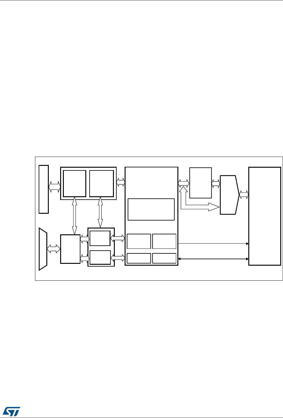
DocID018909 Rev 9 1109/1718
RM0090 Ethernet (ETH): media access control (MAC) with DMA controller
1224
33.4 Ethernet functional description: SMI, MII and RMII
The Ethernet peripheral consists of a MAC 802.3 (media access control) with a dedicated
DMA controller. It supports both default media-independent interface (MII) and reduced
media-independent interface (RMII) through one selection bit (refer to SYSCFG_PMC
register).
The DMA controller interfaces with the Core and memories through the AHB Master and
Slave interfaces. The AHB Master Interface controls data transfers while the AHB Slave
interface accesses Control and Status Registers (CSR) space.
The Transmit FIFO (Tx FIFO) buffers data read from system memory by the DMA before
transmission by the MAC Core. Similarly, the Receive FIFO (Rx FIFO) stores the Ethernet
frames received from the line until they are transferred to system memory by the DMA.
The Ethernet peripheral also includes an SMI to communicate with external PHY. A set of
configuration registers permit the user to select the desired mode and features for the MAC
and the DMA controller.
Note: The AHB clock frequency must be at least 25 MHz when the Ethernet is used.
Figure 350. ETH block diagram
1. For AHB connections please refer to Figure 1: System architecture for STM32F405xx/07xx and
STM32F415xx/17xx devices and Figure 2: System architecture for STM32F42xxx and STM32F43xxx
devices.
33.4.1 Station management interface: SMI
The station management interface (SMI) allows the application to access any PHY registers
through a 2-wire clock and data lines. The interface supports accessing up to 32 PHYs.
The application can select one of the 32 PHYs and one of the 32 registers within any PHY
and send control data or receive status information. Only one register in one PHY can be
addressed at any given time.
Both the MDC clock line and the MDIO data line are implemented as alternate function I/O
in the microcontroller:
•MDC: a periodic clock that provides the timing reference for the data transfer at the
maximum frequency of 2.5 MHz. The minimum high and low times for MDC must be
+BYTE
28&)&/
%THERNET
$-!
-EDIAACCESS
CONTROL
-!#
-!#
CONTROL
REGISTERS
$-!
CONTROL
STATUS
REGISTERS
/PERATION
MODE
REGISTER
)NTERFACE
3ELECT
-))
-$#
-$)/
!("3LAVEINTERFACE
2-))
AIC
"USMATRIX
%XTERNAL0(9
#HECKSUM
OFFLOAD
040
)%%%
0-4 --#
+BYTE
48&)&/
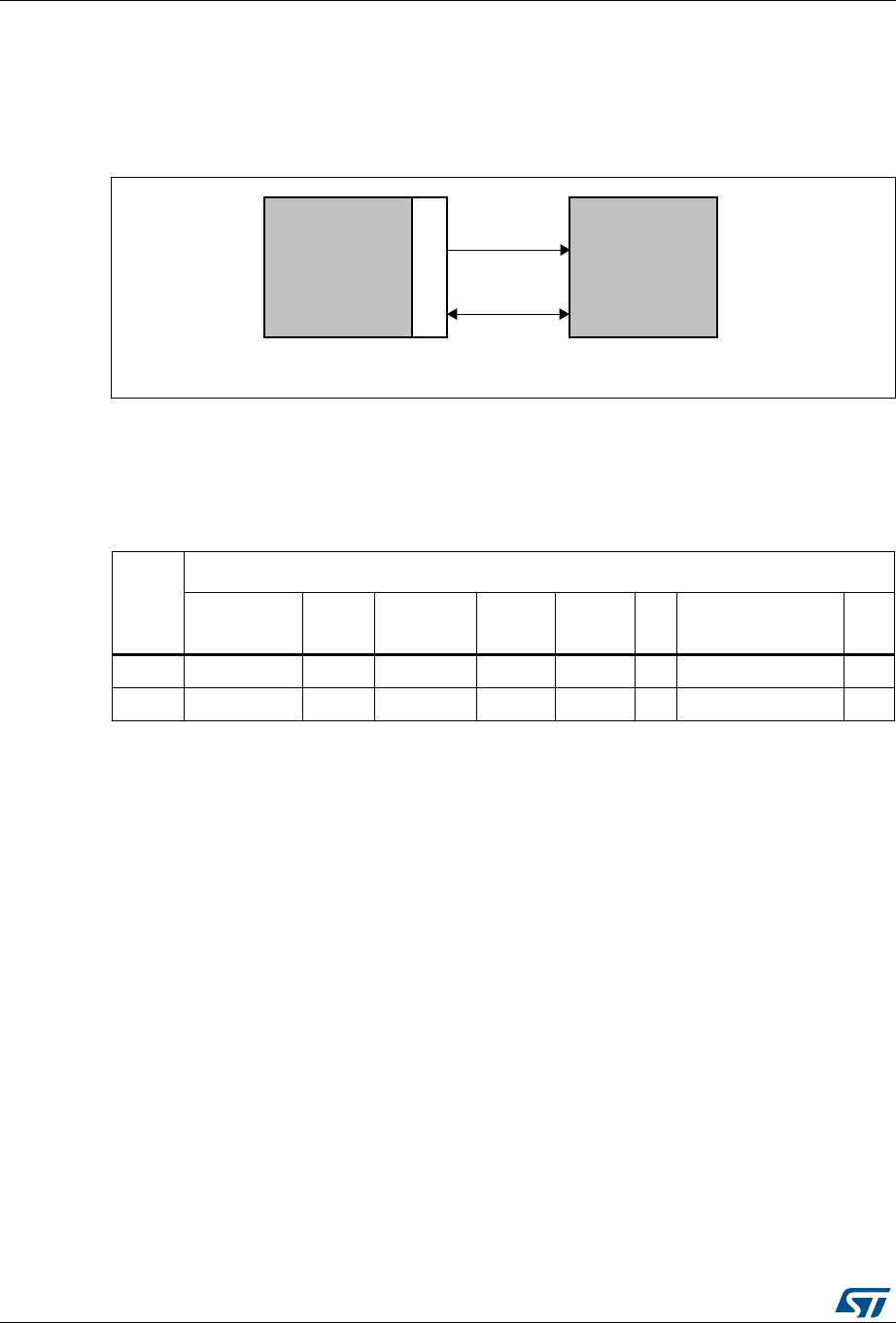
Ethernet (ETH): media access control (MAC) with DMA controller RM0090
1110/1718 DocID018909 Rev 9
160 ns each, and the minimum period for MDC must be 400 ns. In idle state the SMI
management interface drives the MDC clock signal low.
•MDIO: data input/output bitstream to transfer status information to/from the PHY device
synchronously with the MDC clock signal
Figure 351. SMI interface signals
SMI frame format
The frame structure related to a read or write operation is shown in Table 13, the order of bit
transmission must be from left to right.
The management frame consists of eight fields:
•Preamble: each transaction (read or write) can be initiated with the preamble field that
corresponds to 32 contiguous logic one bits on the MDIO line with 32 corresponding
cycles on MDC. This field is used to establish synchronization with the PHY device.
•Start: the start of frame is defined by a <01> pattern to verify transitions on the line
from the default logic one state to zero and back to one.
•Operation: defines the type of transaction (read or write) in progress.
•PADDR: the PHY address is 5 bits, allowing 32 unique PHY addresses. The MSB bit of
the address is the first transmitted and received.
•RADDR: the register address is 5 bits, allowing 32 individual registers to be addressed
within the selected PHY device. The MSB bit of the address is the first transmitted and
received.
•TA: the turn-around field defines a 2-bit pattern between the RADDR and DATA fields
to avoid contention during a read transaction. For a read transaction the MAC controller
drives high-impedance on the MDIO line for the 2 bits of TA. The PHY device must
drive a high-impedance state on the first bit of TA, a zero bit on the second one.
Table 185. Management frame format
Management frame fields
Preamble
(32 bits) Start Operation PADDR RADDR TA Data (16 bits) Idle
Read 1... 1 01 10 ppppp rrrrr Z0 ddddddddddddddd Z
Write 1... 1 01 01 ppppp rrrrr 10 ddddddddddddddd Z
6700&8
0',2
0'& ([WHUQDO
3+<
DLE
-!#
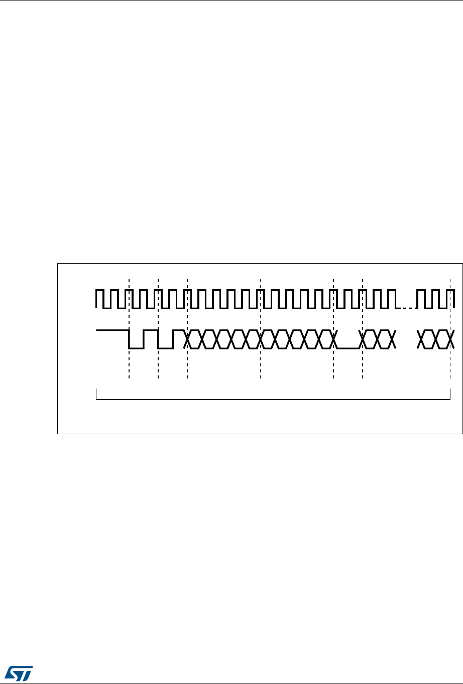
DocID018909 Rev 9 1111/1718
RM0090 Ethernet (ETH): media access control (MAC) with DMA controller
1224
For a write transaction, the MAC controller drives a <10> pattern during the TA field.
The PHY device must drive a high-impedance state for the 2 bits of TA.
•Data: the data field is 16-bit. The first bit transmitted and received must be bit 15 of the
ETH_MIID register.
•Idle: the MDIO line is driven in high-impedance state. All three-state drivers must be
disabled and the PHY’s pull-up resistor keeps the line at logic one.
SMI write operation
When the application sets the MII Write and Busy bits (in Ethernet MAC MII address register
(ETH_MACMIIAR)), the SMI initiates a write operation into the PHY registers by transferring
the PHY address, the register address in PHY, and the write data (in Ethernet MAC MII data
register (ETH_MACMIIDR). The application should not change the MII Address register
contents or the MII Data register while the transaction is ongoing. Write operations to the MII
Address register or the MII Data Register during this period are ignored (the Busy bit is
high), and the transaction is completed without any error. After the Write operation has
completed, the SMI indicates this by resetting the Busy bit.
Figure 352 shows the frame format for the write operation.
Figure 352. MDIO timing and frame structure - Write cycle
SMI read operation
When the user sets the MII Busy bit in the Ethernet MAC MII address register
(ETH_MACMIIAR) with the MII Write bit at 0, the SMI initiates a read operation in the PHY
registers by transferring the PHY address and the register address in PHY. The application
should not change the MII Address register contents or the MII Data register while the
transaction is ongoing. Write operations to the MII Address register or MII Data Register
during this period are ignored (the Busy bit is high) and the transaction is completed without
any error. After the read operation has completed, the SMI resets the Busy bit and then
updates the MII Data register with the data read from the PHY.
Figure 353 shows the frame format for the read operation.
-$#
-$)/ gS ! ! ! ! ! 2 2 2 2 2
$ $
$ $
0REAMBLE 3TART
OF
FRAME
/0
CODE 0(9ADDRESS 2EGISTERADDRESS 4U R N
AROUND DATA
$ATATO0(9
AI
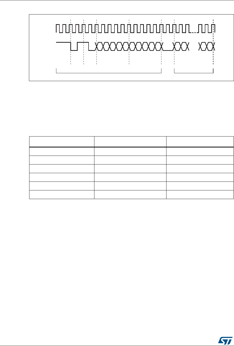
Ethernet (ETH): media access control (MAC) with DMA controller RM0090
1112/1718 DocID018909 Rev 9
Figure 353. MDIO timing and frame structure - Read cycle
SMI clock selection
The MAC initiates the Management Write/Read operation. The SMI clock is a divided clock
whose source is the application clock (AHB clock). The divide factor depends on the clock
range setting in the MII Address register.
Table 186 shows how to set the clock ranges.
33.4.2 Media-independent interface: MII
The media-independent interface (MII) defines the interconnection between the MAC
sublayer and the PHY for data transfer at 10 Mbit/s and 100 Mbit/s.
Table 186. Clock range
Selection HCLK clock MDC clock
000 60-100 MHz AHB clock / 42
001 100-150 MHz AHB clock / 62
010 20-35 MHz AHB clock / 16
011 35-60 MHz AHB clock / 26
100 150-180 MHz AHB clock / 102
101, 110, 111 Reserved -
MDC
MDIO 32 1's 0 1 1 0
A4 A3 A2 A1 A0 R4 R3 R2 R1 R0
D15 D14
D1 D0
Preamble
Start
of
frame
OP
code PHY address Register address Turn
around data
Data to PHY
ai15627
Data from PHY

DocID018909 Rev 9 1113/1718
RM0090 Ethernet (ETH): media access control (MAC) with DMA controller
1224
Figure 354. Media independent interface signals
•MII_TX_CLK: continuous clock that provides the timing reference for the TX data
transfer. The nominal frequency is: 2.5 MHz at 10 Mbit/s speed; 25 MHz at 100 Mbit/s
speed.
•MII_RX_CLK: continuous clock that provides the timing reference for the RX data
transfer. The nominal frequency is: 2.5 MHz at 10 Mbit/s speed; 25 MHz at 100 Mbit/s
speed.
•MII_TX_EN: transmission enable indicates that the MAC is presenting nibbles on the
MII for transmission. It must be asserted synchronously (MII_TX_CLK) with the first
nibble of the preamble and must remain asserted while all nibbles to be transmitted are
presented to the MII.
•MII_TXD[3:0]: transmit data is a bundle of 4 data signals driven synchronously by the
MAC sublayer and qualified (valid data) on the assertion of the MII_TX_EN signal.
MII_TXD[0] is the least significant bit, MII_TXD[3] is the most significant bit. While
MII_TX_EN is deasserted the transmit data must have no effect upon the PHY.
•MII_CRS: carrier sense is asserted by the PHY when either the transmit or receive
medium is non idle. It shall be deasserted by the PHY when both the transmit and
receive media are idle. The PHY must ensure that the MII_CS signal remains asserted
throughout the duration of a collision condition. This signal is not required to transition
synchronously with respect to the TX and RX clocks. In full duplex mode the state of
this signal is don’t care for the MAC sublayer.
•MII_COL: collision detection must be asserted by the PHY upon detection of a collision
on the medium and must remain asserted while the collision condition persists. This
signal is not required to transition synchronously with respect to the TX and RX clocks.
In full duplex mode the state of this signal is don’t care for the MAC sublayer.
•MII_RXD[3:0]: reception data is a bundle of 4 data signals driven synchronously by the
PHY and qualified (valid data) on the assertion of the MII_RX_DV signal. MII_RXD[0] is
the least significant bit, MII_RXD[3] is the most significant bit. While MII_RX_EN is
deasserted and MII_RX_ER is asserted, a specific MII_RXD[3:0] value is used to
transfer specific information from the PHY (see Table 188).
•MII_RX_DV: receive data valid indicates that the PHY is presenting recovered and
decoded nibbles on the MII for reception. It must be asserted synchronously
(MII_RX_CLK) with the first recovered nibble of the frame and must remain asserted
through the final recovered nibble. It must be deasserted prior to the first clock cycle
-$#
-$)/
28?$6
#23
#/,
48?%.
28?#,+
28$;=
28?%2
48?#,+
48$;=
%XTERNAL
0(9
AIC
-!#
6700&8

Ethernet (ETH): media access control (MAC) with DMA controller RM0090
1114/1718 DocID018909 Rev 9
that follows the final nibble. In order to receive the frame correctly, the MII_RX_DV
signal must encompass the frame, starting no later than the SFD field.
•MII_RX_ER: receive error must be asserted for one or more clock periods
(MII_RX_CLK) to indicate to the MAC sublayer that an error was detected somewhere
in the frame. This error condition must be qualified by MII_RX_DV assertion as
described in Table 188.
MII clock sources
To generate both TX_CLK and RX_CLK clock signals, the external PHY must be clocked
with an external 25 MHz as shown in Figure 355. Instead of using an external 25 MHz
quartz to provide this clock, the STM32F4xxmicrocontroller can output this signal on its
MCO pin. In this case, the PLL multiplier has to be configured so as to get the desired
frequency on the MCO pin, from the 25 MHz external quartz.
Table 187. TX interface signal encoding
MII_TX_EN MII_TXD[3:0] Description
0 0000 through 1111 Normal inter-frame
1 0000 through 1111 Normal data transmission
Table 188. RX interface signal encoding
MII_RX_DV MII_RX_ERR MII_RXD[3:0] Description
0 0 0000 through 1111 Normal inter-frame
0 1 0000 Normal inter-frame
0 1 0001 through 1101 Reserved
0 1 1110 False carrier indication
0 1 1111 Reserved
1 0 0000 through 1111 Normal data reception
1 1 0000 through 1111 Data reception with errors
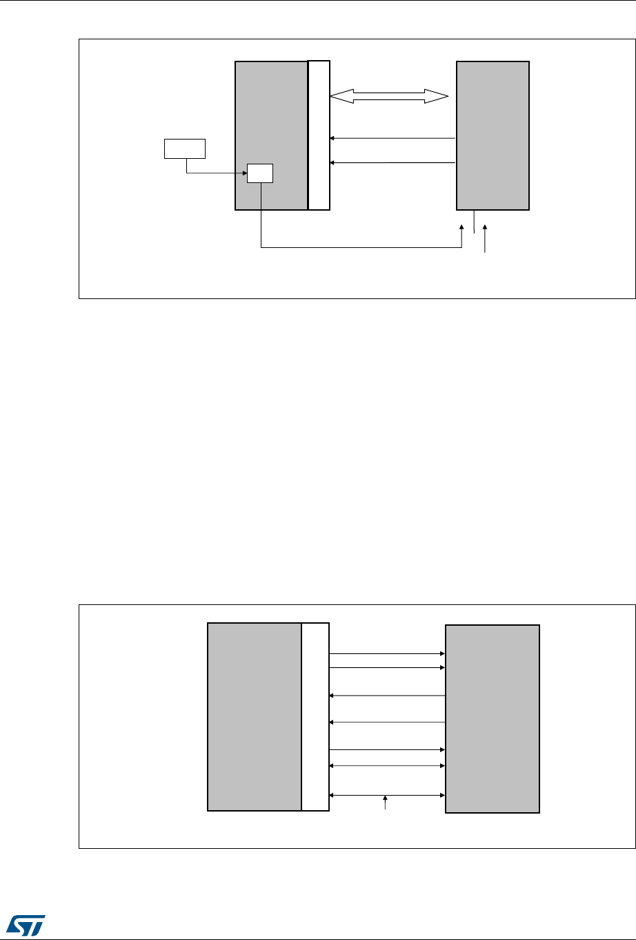
DocID018909 Rev 9 1115/1718
RM0090 Ethernet (ETH): media access control (MAC) with DMA controller
1224
Figure 355. MII clock sources
33.4.3 Reduced media-independent interface: RMII
The reduced media-independent interface (RMII) specification reduces the pin count
between the microcontroller Ethernet peripheral and the external Ethernet in 10/100 Mbit/s.
According to the IEEE 802.3u standard, an MII contains 16 pins for data and control. The
RMII specification is dedicated to reduce the pin count to 7 pins (a 62.5% decrease in pin
count).
The RMII is instantiated between the MAC and the PHY. This helps translation of the MAC’s
MII into the RMII. The RMII block has the following characteristics:
•It supports 10-Mbit/s and 100-Mbit/s operating rates
•The clock reference must be doubled to 50 MHz
•The same clock reference must be sourced externally to both MAC and external
Ethernet PHY
•It provides independent 2-bit wide (dibit) transmit and receive data paths
Figure 356. Reduced media-independent interface signals
670
0&8
0&2
0+]
0+]
7;B&/.
)RU0ELWV
5;B&/.
+6(
0$&
DLE
([WHUQDO
3+<
670
0&8
7;'>@
7;B(1
5;'>@
&56B'9
0'&
0',2
5()B &/.
&ORFNVRXUFH
0$&
([WHUQDO
3+<
DLE
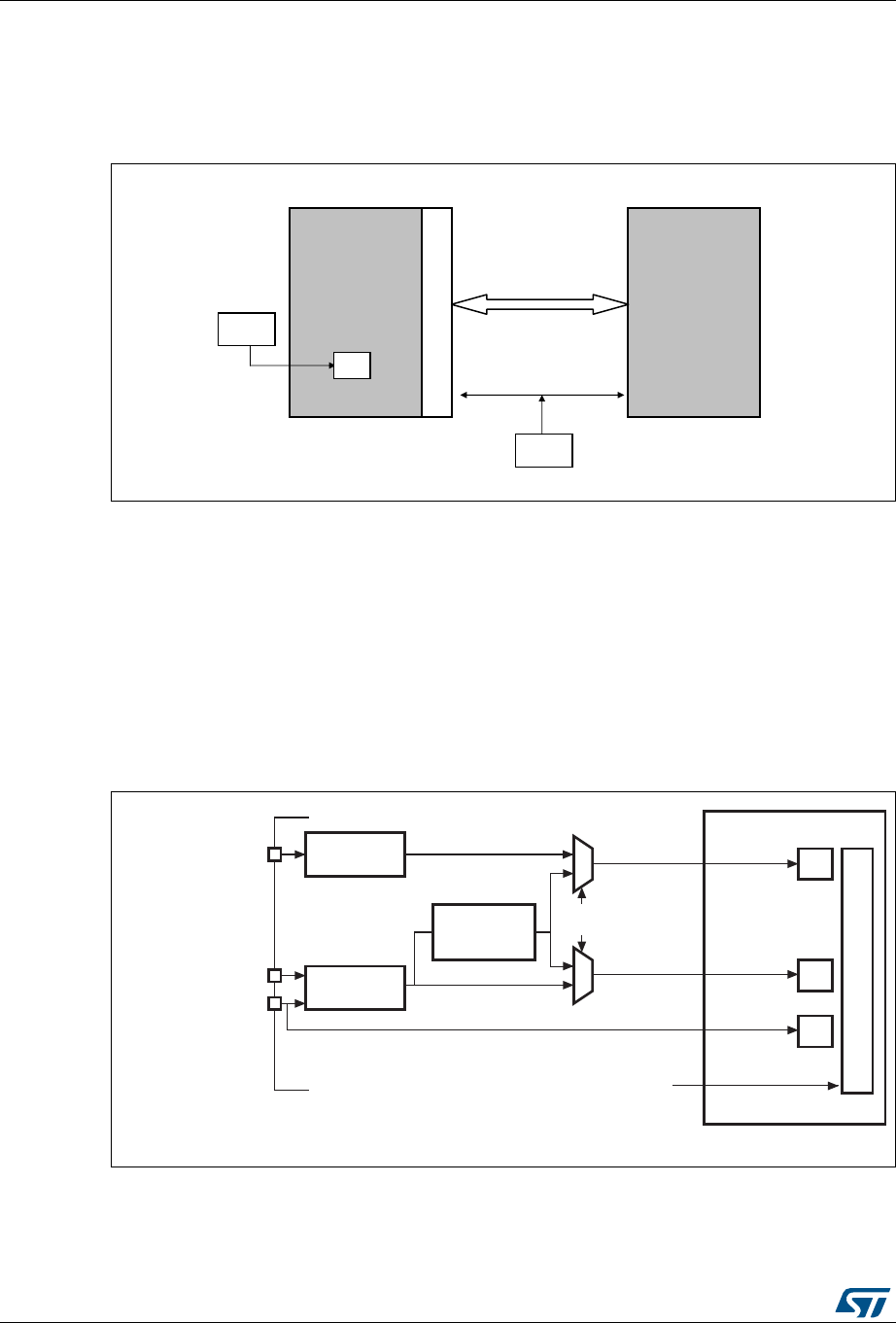
Ethernet (ETH): media access control (MAC) with DMA controller RM0090
1116/1718 DocID018909 Rev 9
RMII clock sources
Either clock the PHY from an external 50 MHz clock or use a PHY with an embedded PLL to
generate the 50 MHz frequency.
Figure 357. RMII clock sources
33.4.4 MII/RMII selection
The mode, MII or RMII, is selected using the configuration bit 23, MII_RMII_SEL, in the
SYSCFG_PMC register. The application has to set the MII/RMII mode while the Ethernet
controller is under reset or before enabling the clocks.
MII/RMII internal clock scheme
The clock scheme required to support both the MII and RMII, as well as 10 and 100 Mbit/s
operations is described in Figure 358.
Figure 358. Clock scheme
1. The MII/RMII selection is controlled through bit 23, MII_RMII_SEL, in the SYSCFG_PMC register.
To save a pin, the two input clock signals, RMII_REF_CK and MII_RX_CLK, are multiplexed
on the same GPIO pin.
069
670
0&8
5()B&/.
0+]
0+]
3//
)RU0ELWV
([WHUQDO
3+<
0$&
GPIO and AF
controller
GPIO and AF
controller
MII_TX_CLK as AF
(25 MHz or 2.5 MHz)
MII_RX_CLK as AF
(25 MHz or 2.5 MHz)
Sync. divider
/2 for 100 Mb/s
/20 for 10 Mb/s
50 MHz
0
1
0
1
25 MHz or 2.5 MHz
25 MHz or 2.5 MHz
0 MII
1 RMII(1)
25 MHz
or 2.5 MHz
25 MHz
or 2.5 MHz
MACTXCLK
MACRXCLK
TX
RX
AHB
HCLK
HCLK
MAC
must be greater
than 25 MHz
ai15650
RMII
RMII_REF_CK as AF
(50 MHz)

DocID018909 Rev 9 1117/1718
RM0090 Ethernet (ETH): media access control (MAC) with DMA controller
1224
33.5 Ethernet functional description: MAC 802.3
The IEEE 802.3 International Standard for local area networks (LANs) employs the
CSMA/CD (carrier sense multiple access with collision detection) as the access method.
The Ethernet peripheral consists of a MAC 802.3 (media access control) controller with
media independent interface (MII) and a dedicated DMA controller.
The MAC block implements the LAN CSMA/CD sublayer for the following families of
systems: 10 Mbit/s and 100 Mbit/s of data rates for baseband and broadband systems. Half-
and full-duplex operation modes are supported. The collision detection access method is
applied only to the half-duplex operation mode. The MAC control frame sublayer is
supported.
The MAC sublayer performs the following functions associated with a data link control
procedure:
•Data encapsulation (transmit and receive)
– Framing (frame boundary delimitation, frame synchronization)
– Addressing (handling of source and destination addresses)
– Error detection
•Media access management
– Medium allocation (collision avoidance)
– Contention resolution (collision handling)
Basically there are two operating modes of the MAC sublayer:
•Half-duplex mode: the stations contend for the use of the physical medium, using the
CSMA/CD algorithms.
•Full duplex mode: simultaneous transmission and reception without contention
resolution (CSMA/CD algorithm are unnecessary) when all the following conditions are
met:
– physical medium capability to support simultaneous transmission and reception
– exactly 2 stations connected to the LAN
– both stations configured for full-duplex operation
33.5.1 MAC 802.3 frame format
The MAC block implements the MAC sublayer and the optional MAC control sublayer
(10/100 Mbit/s) as specified by the IEEE 802.3-2002 standard.
Two frame formats are specified for data communication systems using the CSMA/CD
MAC:
•Basic MAC frame format
•Tagged MAC frame format (extension of the basic MAC frame format)

Ethernet (ETH): media access control (MAC) with DMA controller RM0090
1118/1718 DocID018909 Rev 9
Figure 360 and Figure 361 describe the frame structure (untagged and tagged) that
includes the following fields:
•Preamble: 7-byte field used for synchronization purposes (PLS circuitry)
Hexadecimal value: 55-55-55-55-55-55-55
Bit pattern: 01010101 01010101 01010101 01010101 01010101 01010101 01010101
(right-to-left bit transmission)
•Start frame delimiter (SFD): 1-byte field used to indicate the start of a frame.
Hexadecimal value: D5
Bit pattern: 11010101 (right-to-left bit transmission)
•Destination and Source Address fields: 6-byte fields to indicate the destination and
source station addresses as follows (see Figure 359):
– Each address is 48 bits in length
– The first LSB bit (I/G) in the destination address field is used to indicate an
individual (I/G = 0) or a group address (I/G = 1). A group address could identify
none, one or more, or all the stations connected to the LAN. In the source address
the first bit is reserved and reset to 0.
– The second bit (U/L) distinguishes between locally (U/L = 1) or globally (U/L = 0)
administered addresses. For broadcast addresses this bit is also 1.
– Each byte of each address field must be transmitted least significant bit first.
The address designation is based on the following types:
•Individual address: this is the physical address associated with a particular station on
the network.
•Group address. A multidestination address associated with one or more stations on a
given network. There are two kinds of multicast address:
– Multicast-group address: an address associated with a group of logically related
stations.
– Broadcast address: a distinguished, predefined multicast address (all 1’s in the
destination address field) that always denotes all the stations on a given LAN.
Figure 359. Address field format
•QTag Prefix: 4-byte field inserted between the Source address field and the MAC Client
Length/Type field. This field is an extension of the basic frame (untagged) to obtain the
tagged MAC frame. The untagged MAC frames do not include this field. The
extensions for tagging are as follows:
– 2-byte constant Length/Type field value consistent with the Type interpretation
(greater than 0x0600) equal to the value of the 802.1Q Tag Protocol Type (0x8100
MSB LSB
Bit transmission order (right to left)
U/L I/G
46-bit address
I/G = 0 Individual address
I/G = 1 Group address
U/L = 0 Globally administered address
U/L = 1 Locally administered address
ai15628

DocID018909 Rev 9 1119/1718
RM0090 Ethernet (ETH): media access control (MAC) with DMA controller
1224
hexadecimal). This constant field is used to distinguish tagged and untagged MAC
frames.
– 2-byte field containing the Tag control information field subdivided as follows: a 3-
bit user priority, a canonical format indicator (CFI) bit and a 12-bit VLAN Identifier.
The length of the tagged MAC frame is extended by 4 bytes by the QTag Prefix.
•MAC client length/type: 2-byte field with different meaning (mutually exclusive),
depending on its value:
– If the value is less than or equal to maxValidFrame (0d1500) then this field
indicates the number of MAC client data bytes contained in the subsequent data
field of the 802.3 frame (length interpretation).
– If the value is greater than or equal to MinTypeValue (0d1536 decimal, 0x0600)
then this field indicates the nature of the MAC client protocol (Type interpretation)
related to the Ethernet frame.
Regardless of the interpretation of the length/type field, if the length of the data field is
less than the minimum required for proper operation of the protocol, a PAD field is
added after the data field but prior to the FCS (frame check sequence) field. The
length/type field is transmitted and received with the higher-order byte first.
For length/type field values in the range between maxValidLength and minTypeValue
(boundaries excluded), the behavior of the MAC sublayer is not specified: they may or
may not be passed by the MAC sublayer.
•Data and PAD fields: n-byte data field. Full data transparency is provided, it means that
any arbitrary sequence of byte values may appear in the data field. The size of the
PAD, if any, is determined by the size of the data field. Max and min length of the data
and PAD field are:
– Maximum length = 1500 bytes
– Minimum length for untagged MAC frames = 46 bytes
– Minimum length for tagged MAC frames = 42 bytes
When the data field length is less than the minimum required, the PAD field is added to
match the minimum length (42 bytes for tagged frames, 46 bytes for untagged frames).
•Frame check sequence: 4-byte field that contains the cyclic redundancy check (CRC)
value. The CRC computation is based on the following fields: source address,
destination address, QTag prefix, length/type, LLC data and PAD (that is, all fields
except the preamble, SFD). The generating polynomial is the following:
The CRC value of a frame is computed as follows:
•The first 2 bits of the frame are complemented
•The n-bits of the frame are the coefficients of a polynomial M(x) of degree (n – 1). The
first bit of the destination address corresponds to the xn – 1 term and the last bit of the
data field corresponds to the x0 term
•M(x) is multiplied by x32 and divided by G(x), producing a remainder R(x) of degree
≤31
•The coefficients of R(x) are considered as a 32-bit sequence
•The bit sequence is complemented and the result is the CRC
•The 32-bits of the CRC value are placed in the frame check sequence. The x32 term is
the first transmitted, the x0 term is the last one
Gx() x32 x26 x23 x22 x16 x12 x11 x10 x8x7x5x4x2x1+ + + + + + + +++++++=
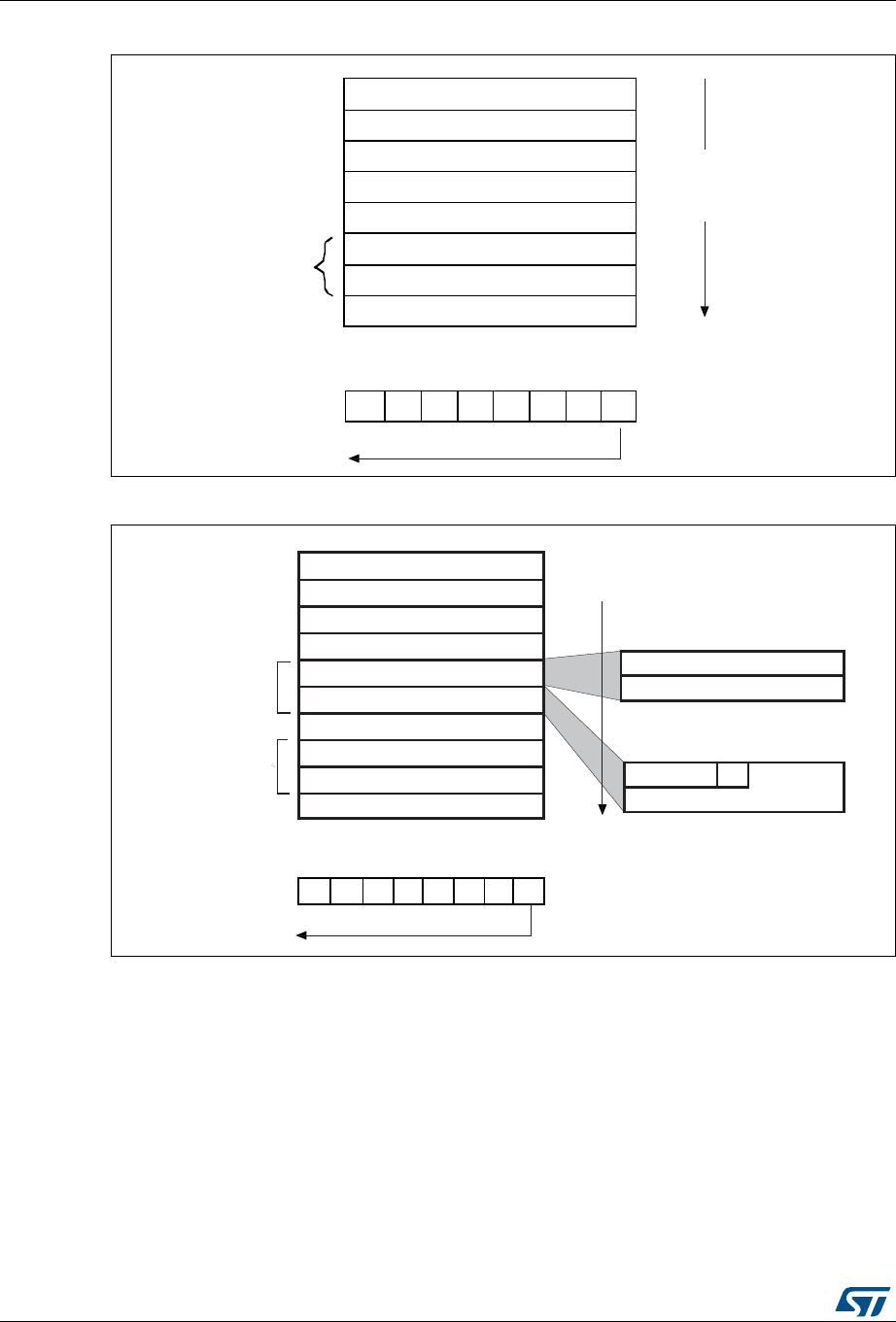
Ethernet (ETH): media access control (MAC) with DMA controller RM0090
1120/1718 DocID018909 Rev 9
Figure 360. MAC frame format
Figure 361. Tagged MAC frame format
Each byte of the MAC frame, except the FCS field, is transmitted low-order bit first.
An invalid MAC frame is defined by one of the following conditions:
•The frame length is inconsistent with the expected value as specified by the length/type
field. If the length/type field contains a type value, then the frame length is assumed to
be consistent with this field (no invalid frame)
•The frame length is not an integer number of bytes (extra bits)
•The CRC value computed on the incoming frame does not match the included FCS
Preamble
SFD
Destination address
Source address
MAC client length/type
MAC client data
PAD
Frame check sequence
7 bytes
1 byte
6 bytes
6 bytes
2 bytes
46-1500 bytes
4 bytes
MSB LSB
Bit transmission order (right to left)
Bytes within
frame transmitted
top to bottom
ai15629
Preamble
SFD
Destination address
Source address
Length/type = 802.1QTagType
Tag control information
MAC client length/type
MAC client data
7 bytes
1 byt e
6 bytes
6 bytes
QTag Prefix
42-1500 byt es
2 bytes
MSB LSB
Bit transmission order (r ight to left)
bytes within
frame transmitted
top to bottom
Frame check sequence
Pad
4 bytes
4 bytes
1 0 0 0 0 0 0 0 1
VLAN identifier (VID, 12 bits)
CFIUser priority
MSB LSB
0 0 0 0 0 0 0 0 0
ai15630

DocID018909 Rev 9 1121/1718
RM0090 Ethernet (ETH): media access control (MAC) with DMA controller
1224
33.5.2 MAC frame transmission
The DMA controls all transactions for the transmit path. Ethernet frames read from the
system memory are pushed into the FIFO by the DMA. The frames are then popped out and
transferred to the MAC core. When the end-of-frame is transferred, the status of the
transmission is taken from the MAC core and transferred back to the DMA. The Transmit
FIFO has a depth of 2 Kbyte. FIFO-fill level is indicated to the DMA so that it can initiate a
data fetch in required bursts from the system memory, using the AHB interface. The data
from the AHB Master interface is pushed into the FIFO.
When the SOF is detected, the MAC accepts the data and begins transmitting to the MII.
The time required to transmit the frame data to the MII after the application initiates
transmission is variable, depending on delay factors like IFG delay, time to transmit
preamble/SFD, and any back-off delays for Half-duplex mode. After the EOF is transferred
to the MAC core, the core completes normal transmission and then gives the status of
transmission back to the DMA. If a normal collision (in Half-duplex mode) occurs during
transmission, the MAC core makes the transmit status valid, then accepts and drops all
further data until the next SOF is received. The same frame should be retransmitted from
SOF on observing a Retry request (in the Status) from the MAC. The MAC issues an
underflow status if the data are not provided continuously during the transmission. During
the normal transfer of a frame, if the MAC receives an SOF without getting an EOF for the
previous frame, then the SOF is ignored and the new frame is considered as the
continuation of the previous frame.
There are two modes of operation for popping data towards the MAC core:
•In Threshold mode, as soon as the number of bytes in the FIFO crosses the configured
threshold level (or when the end-of-frame is written before the threshold is crossed),
the data is ready to be popped out and forwarded to the MAC core. The threshold level
is configured using the TTC bits of ETH_DMABMR.
•In Store-and-forward mode, only after a complete frame is stored in the FIFO, the frame
is popped towards the MAC core. If the Tx FIFO size is smaller than the Ethernet frame
to be transmitted, then the frame is popped towards the MAC core when the Tx FIFO
becomes almost full.
The application can flush the Transmit FIFO of all contents by setting the FTF
(ETH_DMAOMR register [20]) bit. This bit is self-clearing and initializes the FIFO pointers to
the default state. If the FTF bit is set during a frame transfer to the MAC core, then transfer
is stopped as the FIFO is considered to be empty. Hence an underflow event occurs at the
MAC transmitter and the corresponding Status word is forwarded to the DMA.
Automatic CRC and pad generation
When the number of bytes received from the application falls below 60 (DA+SA+LT+Data),
zeros are appended to the transmitting frame to make the data length exactly 46 bytes to
meet the minimum data field requirement of IEEE 802.3. The MAC can be programmed not
to append any padding. The cyclic redundancy check (CRC) for the frame check sequence
(FCS) field is calculated and appended to the data being transmitted. When the MAC is
programmed to not append the CRC value to the end of Ethernet frames, the computed
CRC is not transmitted. An exception to this rule is that when the MAC is programmed to
append pads for frames (DA+SA+LT+Data) less than 60 bytes, CRC will be appended at the
end of the padded frames.

Ethernet (ETH): media access control (MAC) with DMA controller RM0090
1122/1718 DocID018909 Rev 9
The CRC generator calculates the 32-bit CRC for the FCS field of the Ethernet frame. The
encoding is defined by the following polynomial.
Transmit protocol
The MAC controls the operation of Ethernet frame transmission. It performs the following
functions to meet the IEEE 802.3/802.3z specifications. It:
•generates the preamble and SFD
•generates the jam pattern in Half-duplex mode
•controls the Jabber timeout
•controls the flow for Half-duplex mode (back pressure)
•generates the transmit frame status
•contains time stamp snapshot logic in accordance with IEEE 1588
When a new frame transmission is requested, the MAC sends out the preamble and SFD,
followed by the data. The preamble is defined as 7 bytes of 0b10101010 pattern, and the
SFD is defined as 1 byte of 0b10101011 pattern. The collision window is defined as 1 slot
time (512 bit times for 10/100 Mbit/s Ethernet). The jam pattern generation is applicable only
to Half-duplex mode, not to Full-duplex mode.
In MII mode, if a collision occurs at any time from the beginning of the frame to the end of
the CRC field, the MAC sends a 32-bit jam pattern of 0x5555 5555 on the MII to inform all
other stations that a collision has occurred. If the collision is seen during the preamble
transmission phase, the MAC completes the transmission of the preamble and SFD and
then sends the jam pattern.
A jabber timer is maintained to cut off the transmission of Ethernet frames if more than 2048
(default) bytes have to be transferred. The MAC uses the deferral mechanism for flow
control (back pressure) in Half-duplex mode. When the application requests to stop
receiving frames, the MAC sends a JAM pattern of 32 bytes whenever it senses the
reception of a frame, provided that transmit flow control is enabled. This results in a collision
and the remote station backs off. The application requests flow control by setting the BPA bit
(bit 0) in the ETH_MACFCR register. If the application requests a frame to be transmitted,
then it is scheduled and transmitted even when back pressure is activated. Note that if back
pressure is kept activated for a long time (and more than 16 consecutive collision events
occur) then the remote stations abort their transmissions due to excessive collisions. If IEEE
1588 time stamping is enabled for the transmit frame, this block takes a snapshot of the
system time when the SFD is put onto the transmit MII bus.
Transmit scheduler
The MAC is responsible for scheduling the frame transmission on the MII. It maintains the
interframe gap between two transmitted frames and follows the truncated binary exponential
backoff algorithm for Half-duplex mode. The MAC enables transmission after satisfying the
IFG and backoff delays. It maintains an idle period of the configured interframe gap (IFG bits
in the ETH_MACCR register) between any two transmitted frames. If frames to be
transmitted arrive sooner than the configured IFG time, the MII waits for the enable signal
from the MAC before starting the transmission on it. The MAC starts its IFG counter as soon
as the carrier signal of the MII goes inactive. At the end of the programmed IFG value, the
MAC enables transmission in Full-duplex mode. In Half-duplex mode and when IFG is
Gx() x32 x26 x23 x22 x16 x12 x11 x10 x8x7x5x4x2x1+ + + + + + + +++++++=

DocID018909 Rev 9 1123/1718
RM0090 Ethernet (ETH): media access control (MAC) with DMA controller
1224
configured for 96 bit times, the MAC follows the rule of deference specified in Section
4.2.3.2.1 of the IEEE 802.3 specification. The MAC resets its IFG counter if a carrier is
detected during the first two-thirds (64-bit times for all IFG values) of the IFG interval. If the
carrier is detected during the final one third of the IFG interval, the MAC continues the IFG
count and enables the transmitter after the IFG interval. The MAC implements the truncated
binary exponential backoff algorithm when it operates in Half-duplex mode.
Transmit flow control
When the Transmit Flow Control Enable bit (TFE bit in ETH_MACFCR) is set, the MAC
generates Pause frames and transmits them as necessary, in Full-duplex mode. The Pause
frame is appended with the calculated CRC, and is sent. Pause frame generation can be
initiated in two ways.
A pause frame is sent either when the application sets the FCB bit in the ETH_MACFCR
register or when the receive FIFO is full (packet buffer).
•If the application has requested flow control by setting the FCB bit in ETH_MACFCR,
the MAC generates and transmits a single Pause frame. The value of the pause time in
the generated frame contains the programmed pause time value in ETH_MACFCR. To
extend the pause or end the pause prior to the time specified in the previously
transmitted Pause frame, the application must request another Pause frame
transmission after programming the Pause Time value (PT in ETH_MACFCR register)
with the appropriate value.
•If the application has requested flow control when the receive FIFO is full, the MAC
generates and transmits a Pause frame. The value of the pause time in the generated
frame is the programmed pause time value in ETH_MACFCR. If the receive FIFO
remains full at a configurable number of slot-times (PLT bits in ETH_MACFCR) before
this Pause time runs out, a second Pause frame is transmitted. The process is
repeated as long as the receive FIFO remains full. If this condition is no more satisfied
prior to the sampling time, the MAC transmits a Pause frame with zero pause time to
indicate to the remote end that the receive buffer is ready to receive new data frames.
Single-packet transmit operation
The general sequence of events for a transmit operation is as follows:
1. If the system has data to be transferred, the DMA controller fetches them from the
memory through the AHB Master interface and starts forwarding them to the FIFO. It
continues to receive the data until the end of frame is transferred.
2. When the threshold level is crossed or a full packet of data is received into the FIFO,
the frame data are popped and driven to the MAC core. The DMA continues to transfer
data from the FIFO until a complete packet has been transferred to the MAC. Upon
completion of the frame, the DMA controller is notified by the status coming from the
MAC.
Transmit operation—Two packets in the buffer
1. Because the DMA must update the descriptor status before releasing it to the Host,
there can be at the most two frames inside a transmit FIFO. The second frame is
fetched by the DMA and put into the FIFO only if the OSF (operate on second frame)
bit is set. If this bit is not set, the next frame is fetched from the memory only after the
MAC has completely processed the frame and the DMA has released the descriptors.
2. If the OSF bit is set, the DMA starts fetching the second frame immediately after
completing the transfer of the first frame to the FIFO. It does not wait for the status to
be updated. In the meantime, the second frame is received into the FIFO while the first

Ethernet (ETH): media access control (MAC) with DMA controller RM0090
1124/1718 DocID018909 Rev 9
frame is being transmitted. As soon as the first frame has been transferred and the
status is received from the MAC, it is pushed to the DMA. If the DMA has already
completed sending the second packet to the FIFO, the second transmission must wait
for the status of the first packet before proceeding to the next frame.
Retransmission during collision
While a frame is being transferred to the MAC, a collision event may occur on the MAC line
interface in Half-duplex mode. The MAC would then indicate a retry attempt by giving the
status even before the end of frame is received. Then the retransmission is enabled and the
frame is popped out again from the FIFO. After more than 96 bytes have been popped
towards the MAC core, the FIFO controller frees up that space and makes it available to the
DMA to push in more data. This means that the retransmission is not possible after this
threshold is crossed or when the MAC core indicates a late collision event.
Transmit FIFO flush operation
The MAC provides a control to the software to flush the Transmit FIFO through the use of Bit
20 in the Operation mode register. The Flush operation is immediate and the Tx FIFO and
the corresponding pointers are cleared to the initial state even if the Tx FIFO is in the middle
of transferring a frame to the MAC Core. This results in an underflow event in the MAC
transmitter, and the frame transmission is aborted. The status of such a frame is marked
with both underflow and frame flush events (TDES0 bits 13 and 1). No data are coming to
the FIFO from the application (DMA) during the Flush operation. Transfer transmit status
words are transferred to the application for the number of frames that is flushed (including
partial frames). Frames that are completely flushed have the Frame flush status bit (TDES0
13) set. The Flush operation is completed when the application (DMA) has accepted all of
the Status words for the frames that were flushed. The Transmit FIFO Flush control register
bit is then cleared. At this point, new frames from the application (DMA) are accepted. All
data presented for transmission after a Flush operation are discarded unless they start with
an SOF marker.
Transmit status word
At the end of the Ethernet frame transfer to the MAC core and after the core has completed
the transmission of the frame, the transmit status is given to the application. The detailed
description of the Transmit Status is the same as for bits [23:0] in TDES0. If IEEE 1588 time
stamping is enabled, a specific frames’ 64-bit time stamp is returned, along with the transmit
status.
Transmit checksum offload
Communication protocols such as TCP and UDP implement checksum fields, which helps
determine the integrity of data transmitted over a network. Because the most widespread
use of Ethernet is to encapsulate TCP and UDP over IP datagrams, the Ethernet controller
has a transmit checksum offload feature that supports checksum calculation and insertion in
the transmit path, and error detection in the receive path. This section explains the operation
of the checksum offload feature for transmitted frames.
Note: The checksum for TCP, UDP or ICMP is calculated over a complete frame, then inserted
into its corresponding header field. Due to this requirement, this function is enabled only
when the Transmit FIFO is configured for Store-and-forward mode (that is, when the TSF bit

DocID018909 Rev 9 1125/1718
RM0090 Ethernet (ETH): media access control (MAC) with DMA controller
1224
is set in the ETH_ETH_DMAOMR register). If the core is configured for Threshold (cut-
through) mode, the Transmit checksum offload is bypassed.
You must make sure the Transmit FIFO is deep enough to store a complete frame before
that frame is transferred to the MAC Core transmitter. If the FIFO depth is less than the input
Ethernet frame size, the payload (TCP/UDP/ICMP) checksum insertion function is bypassed
and only the frame’s IPv4 Header checksum is modified, even in Store-and-forward mode.
The transmit checksum offload supports two types of checksum calculation and insertion.
This checksum can be controlled for each frame by setting the CIC bits (Bits 28:27 in
TDES1, described in TDES1: Transmit descriptor Word1 on page 1158).
See IETF specifications RFC 791, RFC 793, RFC 768, RFC 792, RFC 2460 and RFC 4443
for IPv4, TCP, UDP, ICMP, IPv6 and ICMPv6 packet header specifications, respectively.
•IP header checksum
In IPv4 datagrams, the integrity of the header fields is indicated by the 16-bit header
checksum field (the eleventh and twelfth bytes of the IPv4 datagram). The checksum
offload detects an IPv4 datagram when the Ethernet frame’s Type field has the value
0x0800 and the IP datagram’s Version field has the value 0x4. The input frame’s
checksum field is ignored during calculation and replaced by the calculated value. IPv6
headers do not have a checksum field; thus, the checksum offload does not modify
IPv6 header fields. The result of this IP header checksum calculation is indicated by the
IP Header Error status bit in the Transmit status (Bit 16). This status bit is set whenever
the values of the Ethernet Type field and the IP header’s Version field are not
consistent, or when the Ethernet frame does not have enough data, as indicated by the
IP header Length field. In other words, this bit is set when an IP header error is
asserted under the following circumstances:
a) For IPv4 datagrams:
– The received Ethernet type is 0x0800, but the IP header’s Version field does not
equal 0x4
– The IPv4 Header Length field indicates a value less than 0x5 (20 bytes)
– The total frame length is less than the value given in the IPv4 Header Length field
b) For IPv6 datagrams:
– The Ethernet type is 0x86DD but the IP header Version field does not equal 0x6
– The frame ends before the IPv6 header (40 bytes) or extension header (as given
in the corresponding Header Length field in an extension header) has been
completely received. Even when the checksum offload detects such an IP header

Ethernet (ETH): media access control (MAC) with DMA controller RM0090
1126/1718 DocID018909 Rev 9
error, it inserts an IPv4 header checksum if the Ethernet Type field indicates an
IPv4 payload.
•TCP/UDP/ICMP checksum
The TCP/UDP/ICMP checksum processes the IPv4 or IPv6 header (including
extension headers) and determines whether the encapsulated payload is TCP, UDP or
ICMP.
Note that:
a) For non-TCP, -UDP, or -ICMP/ICMPv6 payloads, this checksum is bypassed and
nothing further is modified in the frame.
b) Fragmented IP frames (IPv4 or IPv6), IP frames with security features (such as an
authentication header or encapsulated security payload), and IPv6 frames with
routing headers are bypassed and not processed by the checksum.
The checksum is calculated for the TCP, UDP, or ICMP payload and inserted into its
corresponding field in the header. It can work in the following two modes:
– In the first mode, the TCP, UDP, or ICMPv6 pseudo-header is not included in the
checksum calculation and is assumed to be present in the input frame’s checksum
field. The checksum field is included in the checksum calculation, and then
replaced by the final calculated checksum.
– In the second mode, the checksum field is ignored, the TCP, UDP, or ICMPv6
pseudo-header data are included into the checksum calculation, and the
checksum field is overwritten with the final calculated value.
Note that: for ICMP-over-IPv4 packets, the checksum field in the ICMP packet must
always be 0x0000 in both modes, because pseudo-headers are not defined for such
packets. If it does not equal 0x0000, an incorrect checksum may be inserted into the
packet.
The result of this operation is indicated by the payload checksum error status bit in the
Transmit Status vector (bit 12). The payload checksum error status bit is set when
either of the following is detected:
– the frame has been forwarded to the MAC transmitter in Store-and-forward mode
without the end of frame being written to the FIFO
– the packet ends before the number of bytes indicated by the payload length field in
the IP header is received.
When the packet is longer than the indicated payload length, the bytes are ignored as
stuff bytes, and no error is reported. When the first type of error is detected, the TCP,
UDP or ICMP header is not modified. For the second error type, still, the calculated
checksum is inserted into the corresponding header field.
MII/RMII transmit bit order
Each nibble from the MII is transmitted on the RMII a dibit at a time with the order of dibit
transmission shown in Figure 362. Lower order bits (D1 and D0) are transmitted first
followed by higher order bits (D2 and D3).
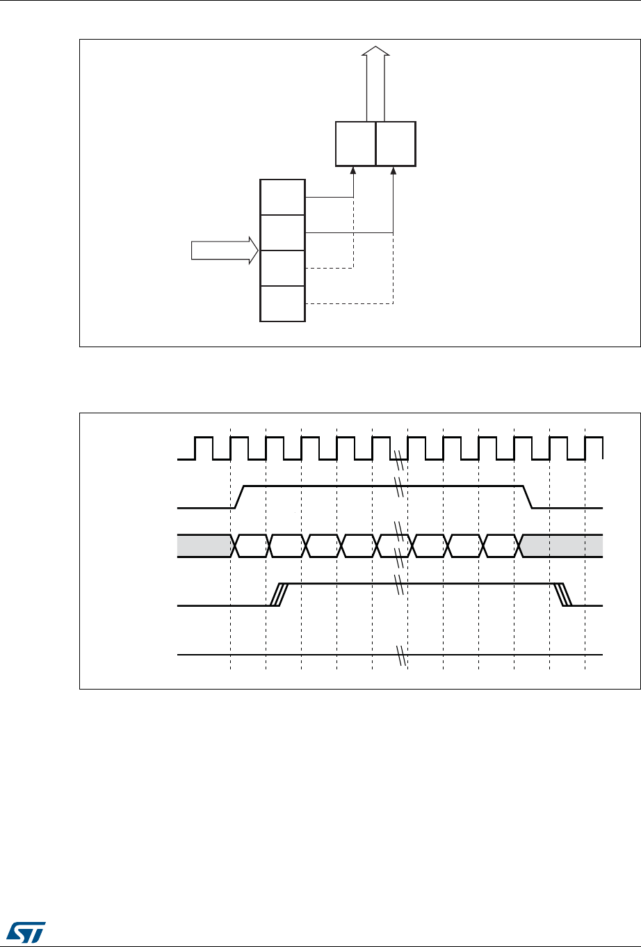
DocID018909 Rev 9 1127/1718
RM0090 Ethernet (ETH): media access control (MAC) with DMA controller
1224
Figure 362. Transmission bit order
MII/RMII transmit timing diagrams
Figure 363. Transmission with no collision
D0
D1
D2
D3
LSB
MII_TXD[3:0]
MSB
D0 D1
LSB MSB
RMII_TXD[1:0]
Bibit stream
Nibble stream
ai15632
MII_TX_CLK
MII_TX_EN
MII_TXD[ 3:0] PR EA MB LE
MII_CS
MII_COL
ai15631
Low
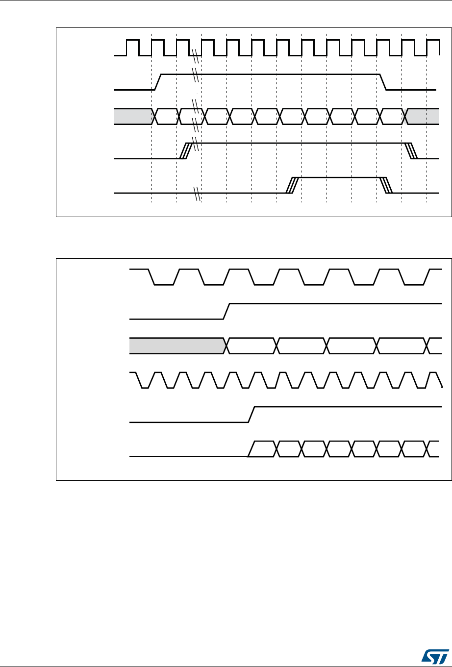
Ethernet (ETH): media access control (MAC) with DMA controller RM0090
1128/1718 DocID018909 Rev 9
Figure 364. Transmission with collision
Figure 365 shows a frame transmission in MII and RMII.
Figure 365. Frame transmission in MMI and RMII modes
33.5.3 MAC frame reception
The MAC received frames are pushes into the Rx FIFO. The status (fill level) of this FIFO is
indicated to the DMA once it crosses the configured receive threshold (RTC in the
ETH_DMAOMR register) so that the DMA can initiate pre-configured burst transfers
towards the AHB interface.
In the default Cut-through mode, when 64 bytes (configured with the RTC bits in the
ETH_DMAOMR register) or a full packet of data are received into the FIFO, the data are
popped out and the DMA is notified of its availability. Once the DMA has initiated the
transfer to the AHB interface, the data transfer continues from the FIFO until a complete
MII_TX_CLK
MII_TX_EN
MII_TXD[ 3:0] PR EAM BLE SFD
MII_CS
MII_COL
ai15651
DA DA JAM JAM JAM JAM
MII_RX_CLK
MII_TX_EN
MII_TXD[3:0]
RMII_REF_CLK
RMII_TXD[1:0]
RMII_TX_EN
ai15652

DocID018909 Rev 9 1129/1718
RM0090 Ethernet (ETH): media access control (MAC) with DMA controller
1224
packet has been transferred. Upon completion of the EOF frame transfer, the status word is
popped out and sent to the DMA controller.
In Rx FIFO Store-and-forward mode (configured by the RSF bit in the ETH_DMAOMR
register), a frame is read only after being written completely into the Receive FIFO. In this
mode, all error frames are dropped (if the core is configured to do so) such that only valid
frames are read and forwarded to the application. In Cut-through mode, some error frames
are not dropped, because the error status is received at the end of the frame, by which time
the start of that frame has already been read of the FIFO.
A receive operation is initiated when the MAC detects an SFD on the MII. The core strips the
preamble and SFD before proceeding to process the frame. The header fields are checked
for the filtering and the FCS field used to verify the CRC for the frame. The frame is dropped
in the core if it fails the address filter.
Receive protocol
The received frame preamble and SFD are stripped. Once the SFD has been detected, the
MAC starts sending the Ethernet frame data to the receive FIFO, beginning with the first
byte following the SFD (destination address). If IEEE 1588 time stamping is enabled, a
snapshot of the system time is taken when any frame's SFD is detected on the MII. Unless
the MAC filters out and drops the frame, this time stamp is passed on to the application.
If the received frame length/type field is less than 0x600 and if the MAC is programmed for
the auto CRC/pad stripping option, the MAC sends the data of the frame to RxFIFO up to
the count specified in the length/type field, then starts dropping bytes (including the FCS
field). If the Length/Type field is greater than or equal to 0x600, the MAC sends all received
Ethernet frame data to Rx FIFO, regardless of the value on the programmed auto-CRC strip
option. The MAC watchdog timer is enabled by default, that is, frames above 2048 bytes
(DA + SA + LT + Data + pad + FCS) are cut off. This feature can be disabled by
programming the watchdog disable (WD) bit in the MAC configuration register. However,
even if the watchdog timer is disabled, frames greater than 16 KB in size are cut off and a
watchdog timeout status is given.
Receive CRC: automatic CRC and pad stripping
The MAC checks for any CRC error in the receiving frame. It calculates the 32-bit CRC for
the received frame that includes the Destination address field through the FCS field. The
encoding is defined by the following polynomial.
Regardless of the auto-pad/CRC strip, the MAC receives the entire frame to compute the
CRC check for the received frame.
Receive checksum offload
Both IPv4 and IPv6 frames in the received Ethernet frames are detected and processed for
data integrity. You can enable the receive checksum offload by setting the IPCO bit in the
ETH_MACCR register. The MAC receiver identifies IPv4 or IPv6 frames by checking for
value 0x0800 or 0x86DD, respectively, in the received Ethernet frame Type field. This
identification applies to VLAN-tagged frames as well. The receive checksum offload
calculates IPv4 header checksums and checks that they match the received IPv4 header
checksums. The IP Header Error bit is set for any mismatch between the indicated payload
Gx() x32 x26 x23 x22 x16 x12 x11 x10 x8x7x5x4x2x1+ + + + + + + +++++++=

Ethernet (ETH): media access control (MAC) with DMA controller RM0090
1130/1718 DocID018909 Rev 9
type (Ethernet Type field) and the IP header version, or when the received frame does not
have enough bytes, as indicated by the IPv4 header’s Length field (or when fewer than 20
bytes are available in an IPv4 or IPv6 header). The receive checksum offload also identifies
a TCP, UDP or ICMP payload in the received IP datagrams (IPv4 or IPv6) and calculates the
checksum of such payloads properly, as defined in the TCP, UDP or ICMP specifications. It
includes the TCP/UDP/ICMPv6 pseudo-header bytes for checksum calculation and checks
whether the received checksum field matches the calculated value. The result of this
operation is given as a Payload Checksum Error bit in the receive status word. This status
bit is also set if the length of the TCP, UDP or ICMP payload does not match the expected
payload length given in the IP header. As mentioned in TCP/UDP/ICMP checksum on
page 1126, the receive checksum offload bypasses the payload of fragmented IP
datagrams, IP datagrams with security features, IPv6 routing headers, and payloads other
than TCP, UDP or ICMP. This information (whether the checksum is bypassed or not) is
given in the receive status, as described in the RDES0: Receive descriptor Word0 section.
In this configuration, the core does not append any payload checksum bytes to the received
Ethernet frames.
As mentioned in RDES0: Receive descriptor Word0 on page 1165, the meaning of certain
register bits changes as shown in Table 189.
Receive frame controller
If the RA bit is reset in the MAC CSR frame filter register, the MAC performs frame filtering
based on the destination/source address (the application still needs to perform another level
of filtering if it decides not to receive any bad frames like runt, CRC error frames, etc.). On
detecting a filter-fail, the frame is dropped and not transferred to the application. When the
filtering parameters are changed dynamically, and in case of (DA-SA) filter-fail, the rest of
Table 189. Frame statuses
Bit 18:
Ethernet frame
Bit 27: Header
checksum error
Bit 28: Payload
checksum error Frame status
000
The frame is an IEEE 802.3 frame (Length
field value is less than 0x0600).
100
IPv4/IPv6 Type frame in which no checksum
error is detected.
101
IPv4/IPv6 Type frame in which a payload
checksum error (as described for PCE) is
detected
110
IPv4/IPv6 Type frame in which IP header
checksum error (as described for IPCO HCE)
is detected.
111
IPv4/IPv6 Type frame in which both PCE and
IPCO HCE are detected.
001
IPv4/IPv6 Type frame in which there is no IP
HCE and the payload check is bypassed due
to unsupported payload.
011
Type frame which is neither IPv4 or IPv6
(checksum offload bypasses the checksum
check completely)
0 1 0 Reserved

DocID018909 Rev 9 1131/1718
RM0090 Ethernet (ETH): media access control (MAC) with DMA controller
1224
the frame is dropped and the Rx Status Word is immediately updated (with zero frame
length, CRC error and Runt Error bits set), indicating the filter fail. In Ethernet power down
mode, all received frames are dropped, and are not forwarded to the application.
Receive flow control
The MAC detects the receiving Pause frame and pauses the frame transmission for the
delay specified within the received Pause frame (only in Full-duplex mode). The Pause
frame detection function can be enabled or disabled with the RFCE bit in ETH_MACFCR.
Once receive flow control has been enabled, the received frame destination address begins
to be monitored for any match with the multicast address of the control frame
(0x0180 C200 0001). If a match is detected (the destination address of the received frame
matches the reserved control frame destination address), the MAC then decides whether or
not to transfer the received control frame to the application, based on the level of the PCF
bit in ETH_MACFFR.
The MAC also decodes the type, opcode, and Pause Timer fields of the receiving control
frame. If the byte count of the status indicates 64 bytes, and if there is no CRC error, the
MAC transmitter pauses the transmission of any data frame for the duration of the decoded
Pause time value, multiplied by the slot time (64 byte times for both 10/100 Mbit/s modes).
Meanwhile, if another Pause frame is detected with a zero Pause time value, the MAC
resets the Pause time and manages this new pause request.
If the received control frame matches neither the type field (0x8808), the opcode (0x00001),
nor the byte length (64 bytes), or if there is a CRC error, the MAC does not generate a
Pause.
In the case of a pause frame with a multicast destination address, the MAC filters the frame
based on the address match.
For a pause frame with a unicast destination address, the MAC filtering depends on whether
the DA matched the contents of the MAC address 0 register and whether the UPDF bit in
ETH_MACFCR is set (detecting a pause frame even with a unicast destination address).
The PCF register bits (bits [7:6] in ETH_MACFFR) control filtering for control frames in
addition to address filtering.
Receive operation multiframe handling
Since the status is available immediately following the data, the FIFO is capable of storing
any number of frames into it, as long as it is not full.
Error handling
If the Rx FIFO is full before it receives the EOF data from the MAC, an overflow is declared
and the whole frame is dropped, and the overflow counter in the (ETH_DMAMFBOCR
register) is incremented. The status indicates a partial frame due to overflow. The Rx FIFO
can filter error and undersized frames, if enabled (using the FEF and FUGF bits in
ETH_DMAOMR).
If the Receive FIFO is configured to operate in Store-and-forward mode, all error frames can
be filtered and dropped.
In Cut-through mode, if a frame's status and length are available when that frame's SOF is
read from the Rx FIFO, then the complete erroneous frame can be dropped. The DMA can
flush the error frame being read from the FIFO, by enabling the receive frame flash bit. The
data transfer to the application (DMA) is then stopped and the rest of the frame is internally
read and dropped. The next frame transfer can then be started, if available.
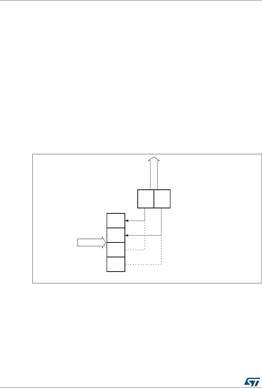
Ethernet (ETH): media access control (MAC) with DMA controller RM0090
1132/1718 DocID018909 Rev 9
Receive status word
At the end of the Ethernet frame reception, the MAC outputs the receive status to the
application (DMA). The detailed description of the receive status is the same as for
bits[31:0] in RDES0, given in RDES0: Receive descriptor Word0 on page 1165.
Frame length interface
In case of switch applications, data transmission and reception between the application and
MAC happen as complete frame transfers. The application layer should be aware of the
length of the frames received from the ingress port in order to transfer the frame to the
egress port. The MAC core provides the frame length of each received frame inside the
status at the end of each frame reception.
Note: A frame length value of 0 is given for partial frames written into the Rx FIFO due to overflow.
MII/RMII receive bit order
Each nibble is transmitted to the MII from the dibit received from the RMII in the nibble
transmission order shown in Figure 366. The lower-order bits (D0 and D1) are received first,
followed by the higher-order bits (D2 and D3).
Figure 366. Receive bit order
D0
D1
D2
D3
LSB
MII_RXD[3:0]
MSB
D0 D1
LSB MSB
RMII_RXD[1:0]
Di-bit stream
Nibble stream
ai15633
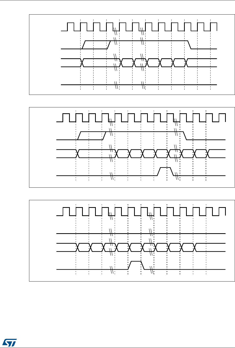
DocID018909 Rev 9 1133/1718
RM0090 Ethernet (ETH): media access control (MAC) with DMA controller
1224
Figure 367. Reception with no error
Figure 368. Reception with errors
Figure 369. Reception with false carrier indication
33.5.4 MAC interrupts
Interrupts can be generated from the MAC core as a result of various events.
The ETH_MACSR register describes the events that can cause an interrupt from the MAC
core. You can prevent each event from asserting the interrupt by setting the corresponding
mask bits in the Interrupt Mask register.
MII_RX_CLK
MII_RX_DV
MII_RXD[3:0] PREAMBLE SFD
MII_RX_ERR
ai15634
FCS
MII_RX_CLK
MII_RX_DV
MII_RXD[3:0] PREAMBLE SFD
MII_RX_ERR
ai15635
DA DA XX XX XX
MII_RX_CLK
MII_RX_DV
MII_RXD[3:0] XX
MII_RX_ERR
ai15636
0E XX XX XX XX
XX XXXX
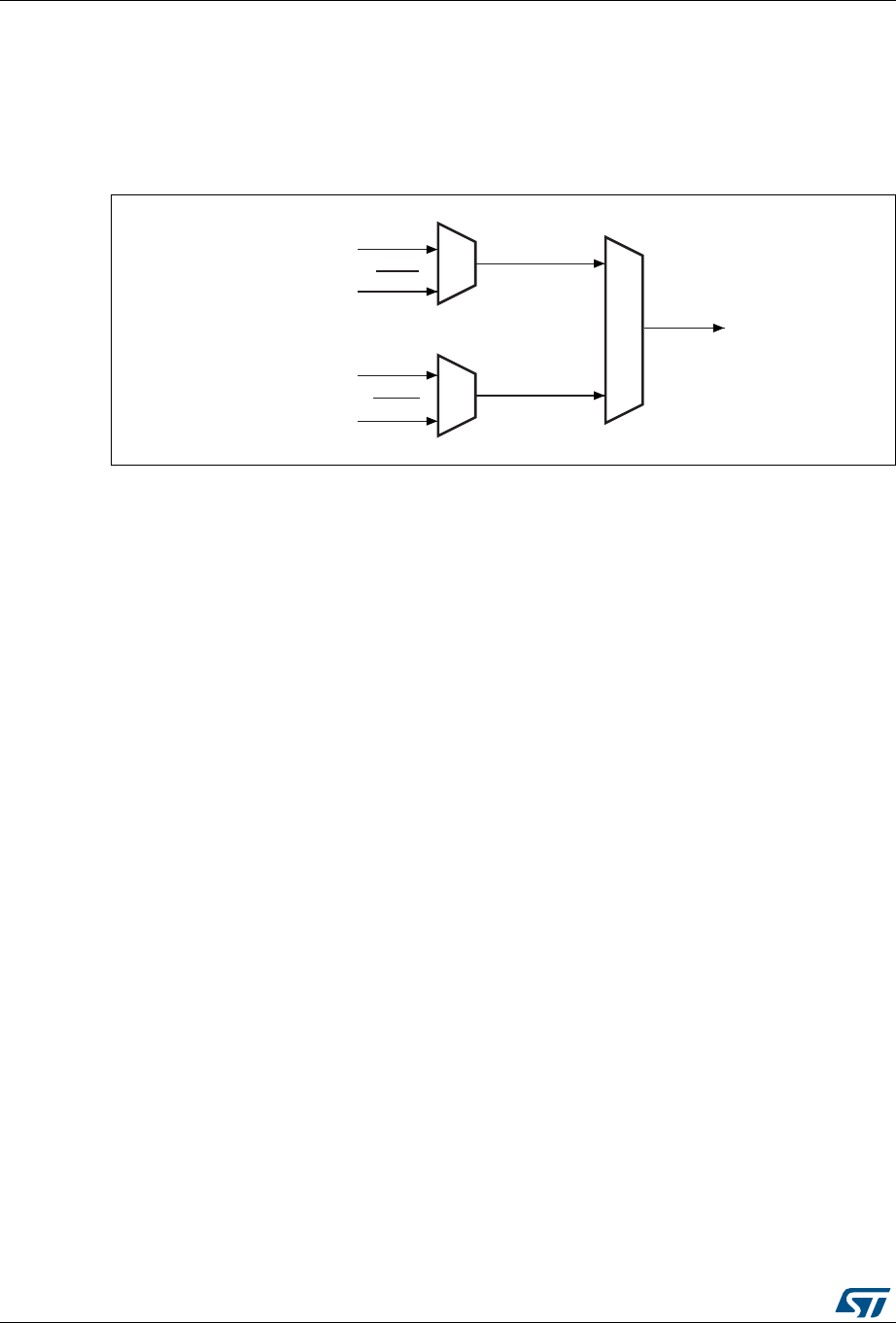
Ethernet (ETH): media access control (MAC) with DMA controller RM0090
1134/1718 DocID018909 Rev 9
The interrupt register bits only indicate the block from which the event is reported. You have
to read the corresponding status registers and other registers to clear the interrupt. For
example, bit 3 of the Interrupt register, set high, indicates that the Magic packet or Wake-on-
LAN frame is received in Power-down mode. You must read the ETH_MACPMTCSR
Register to clear this interrupt event.
Figure 370. MAC core interrupt masking scheme
33.5.5 MAC filtering
Address filtering
Address filtering checks the destination and source addresses on all received frames and
the address filtering status is reported accordingly. Address checking is based on different
parameters (Frame filter register) chosen by the application. The filtered frame can also be
identified: multicast or broadcast frame.
Address filtering uses the station's physical (MAC) address and the Multicast Hash table for
address checking purposes.
Unicast destination address filter
The MAC supports up to 4 MAC addresses for unicast perfect filtering. If perfect filtering is
selected (HU bit in the Frame filter register is reset), the MAC compares all 48 bits of the
received unicast address with the programmed MAC address for any match. Default
MacAddr0 is always enabled, other addresses MacAddr1–MacAddr3 are selected with an
individual enable bit. Each byte of these other addresses (MacAddr1–MacAddr3) can be
masked during comparison with the corresponding received DA byte by setting the
corresponding Mask Byte Control bit in the register. This helps group address filtering for the
DA. In Hash filtering mode (when HU bit is set), the MAC performs imperfect filtering for
unicast addresses using a 64-bit Hash table. For hash filtering, the MAC uses the 6 upper
CRC (see note 1 below) bits of the received destination address to index the content of the
Hash table. A value of 000000 selects bit 0 in the selected register, and a value of 111111
selects bit 63 in the Hash Table register. If the corresponding bit (indicated by the 6-bit CRC)
is set to 1, the unicast frame is said to have passed the Hash filter; otherwise, the frame has
failed the Hash filter.
Note: This CRC is a 32-bit value coded by the following polynomial (for more details refer to
Section 33.5.3: MAC frame reception):
AND
AND
OR
TSTI
PMTI
Interrupt
TSTS
PMTS
PMTIM
ai15637
TSTIM
Gx() x32 x26 x23 x22 x16 x12 x11 x10 x8x7x5x4x2x1+ + + + + + + +++++++=

DocID018909 Rev 9 1135/1718
RM0090 Ethernet (ETH): media access control (MAC) with DMA controller
1224
Multicast destination address filter
The MAC can be programmed to pass all multicast frames by setting the PAM bit in the
Frame filter register. If the PAM bit is reset, the MAC performs the filtering for multicast
addresses based on the HM bit in the Frame filter register. In Perfect filtering mode, the
multicast address is compared with the programmed MAC destination address registers (1–
3). Group address filtering is also supported. In Hash filtering mode, the MAC performs
imperfect filtering using a 64-bit Hash table. For hash filtering, the MAC uses the 6 upper
CRC (see note 1 below) bits of the received multicast address to index the content of the
Hash table. A value of 000000 selects bit 0 in the selected register and a value of 111111
selects bit 63 in the Hash Table register. If the corresponding bit is set to 1, then the
multicast frame is said to have passed the Hash filter; otherwise, the frame has failed the
Hash filter.
Note: This CRC is a 32-bit value coded by the following polynomial (for more details refer to
Section 33.5.3: MAC frame reception):
Hash or perfect address filter
The DA filter can be configured to pass a frame when its DA matches either the Hash filter
or the Perfect filter by setting the HPF bit in the Frame filter register and setting the
corresponding HU or HM bits. This configuration applies to both unicast and multicast
frames. If the HPF bit is reset, only one of the filters (Hash or Perfect) is applied to the
received frame.
Broadcast address filter
The MAC does not filter any broadcast frames in the default mode. However, if the MAC is
programmed to reject all broadcast frames by setting the BFD bit in the Frame filter register,
any broadcast frames are dropped.
Unicast source address filter
The MAC can also perform perfect filtering based on the source address field of the
received frames. By default, the MAC compares the SA field with the values programmed in
the SA registers. The MAC address registers [1:3] can be configured to contain SA instead
of DA for comparison, by setting bit 30 in the corresponding register. Group filtering with SA
is also supported. The frames that fail the SA filter are dropped by the MAC if the SAF bit in
the Frame filter register is set. Otherwise, the result of the SA filter is given as a status bit in
the Receive Status word (see RDES0: Receive descriptor Word0).
When the SAF bit is set, the result of the SA and DA filters is AND’ed to decide whether the
frame needs to be forwarded. This means that either of the filter fail result will drop the
frame. Both filters have to pass the frame for the frame to be forwarded to the application.
Inverse filtering operation
For both destination and source address filtering, there is an option to invert the filter-match
result at the final output. These are controlled by the DAIF and SAIF bits in the Frame filter
register, respectively. The DAIF bit is applicable for both Unicast and Multicast DA frames.
The result of the unicast/multicast destination address filter is inverted in this mode.
Similarly, when the SAIF bit is set, the result of the unicast SA filter is inverted. Table 190
Gx() x32 x26 x23 x22 x16 x12 x11 x10 x8x7x5x4x2x1+ + + + + + + +++++++=

Ethernet (ETH): media access control (MAC) with DMA controller RM0090
1136/1718 DocID018909 Rev 9
and Table 191 summarize destination and source address filtering based on the type of
frame received.
Table 190. Destination address filtering
Frame
type PM HPF HU DAIF HM PAM DB DA filter operation
Broadcast
1XXX X XXPass
0XXX X X0Pass
0XXX X X1Fail
Unicast
1 X X X X X X Pass all frames
0 X 0 0 X X X Pass on perfect/group filter match
0 X 0 1 X X X Fail on perfect/Group filter match
0 0 1 0 X X X Pass on hash filter match
0 0 1 1 X X X Fail on hash filter match
011 0 X XX
Pass on hash or perfect/Group filter
match
0 1 1 1 X X X Fail on hash or perfect/Group filter match
Multicast
1 X X X X X X Pass all frames
X X X X X 1 X Pass all frames
0XX0 0 0 X
Pass on Perfect/Group filter match and
drop PAUSE control frames if PCF = 0x
00 X0 1 0 X
Pass on hash filter match and drop
PAUSE control frames if PCF = 0x
01 X0 1 0 X
Pass on hash or perfect/Group filter
match and drop PAUSE control frames if
PCF = 0x
0XX1 0 0 X
Fail on perfect/Group filter match and
drop PAUSE control frames if PCF = 0x
00 X1 1 0 X
Fail on hash filter match and drop PAUSE
control frames if PCF = 0x
01 X1 1 0 X
Fail on hash or perfect/Group filter match
and drop PAUSE control frames if PCF =
0x

DocID018909 Rev 9 1137/1718
RM0090 Ethernet (ETH): media access control (MAC) with DMA controller
1224
33.5.6 MAC loopback mode
The MAC supports loopback of transmitted frames onto its receiver. By default, the MAC
loopback function is disabled, but this feature can be enabled by programming the
Loopback bit in the MAC ETH_MACCR register.
33.5.7 MAC management counters: MMC
The MAC management counters (MMC) maintain a set of registers for gathering statistics
on the received and transmitted frames. These include a control register for controlling the
behavior of the registers, two 32-bit registers containing generated interrupts (receive and
transmit), and two 32-bit registers containing masks for the Interrupt register (receive and
transmit). These registers are accessible from the application. Each register is 32 bits wide.
Section 33.8: Ethernet register descriptions describes the various counters and lists the
addresses of each of the statistics counters. This address is used for read/write accesses to
the desired transmit/receive counter.
The Receive MMC counters are updated for frames that pass address filtering. Dropped
frames statistics are not updated unless the dropped frames are runt frames of less than 6
bytes (DA bytes are not received fully).
Good transmitted and received frames
Transmitted frames are considered “good” if transmitted successfully. In other words, a
transmitted frame is good if the frame transmission is not aborted due to any of the following
errors:
+ Jabber Timeout
+ No Carrier/Loss of Carrier
+ Late Collision
+ Frame Underflow
+ Excessive Deferral
+ Excessive Collision
Table 191. Source address filtering
Frame type PM SAIF SAF SA filter operation
Unicast
1 X X Pass all frames
000Pass status on perfect/Group filter match but do not drop
frames that fail
010Fail status on perfect/group filter match but do not drop frame
001Pass on perfect/group filter match and drop frames that fail
011Fail on perfect/group filter match and drop frames that fail

Ethernet (ETH): media access control (MAC) with DMA controller RM0090
1138/1718 DocID018909 Rev 9
Received frames are considered “good” if none of the following errors exists:
+ CRC error
+ Runt Frame (shorter than 64 bytes)
+ Alignment error (in 10/ 100 Mbit/s only)
+ Length error (non-Type frames only)
+ Out of Range (non-Type frames only, longer than maximum size)
+ MII_RXER Input error
The maximum frame size depends on the frame type, as follows:
+ Untagged frame maxsize = 1518
+ VLAN Frame maxsize = 1522
33.5.8 Power management: PMT
This section describes the power management (PMT) mechanisms supported by the MAC.
PMT supports the reception of network (remote) wakeup frames and Magic Packet frames.
PMT generates interrupts for wakeup frames and Magic Packets received by the MAC. The
PMT block is enabled with remote wakeup frame enable and Magic Packet enable. These
enable bits (WFE and MPE) are in the ETH_MACPMTCSR register and are programmed by
the application. When the power down mode is enabled in the PMT, then all received frames
are dropped by the MAC and they are not forwarded to the application. The MAC comes out
of the power down mode only when either a Magic Packet or a Remote wakeup frame is
received and the corresponding detection is enabled.
Remote wakeup frame filter register
There are eight wakeup frame filter registers. To write on each of them, load the wakeup
frame filter register value by value. The wanted values of the wakeup frame filter are loaded
by sequentially loading eight times the wakeup frame filter register. The read operation is
identical to the write operation. To read the eight values, you have to read eight times the
wakeup frame filter register to reach the last register. Each read/write points the wakeup
frame filter register to the next filter register.

DocID018909 Rev 9 1139/1718
RM0090 Ethernet (ETH): media access control (MAC) with DMA controller
1224
Figure 371. Wakeup frame filter register
•Filter i Byte Mask
This register defines which bytes of the frame are examined by filter i (0, 1, 2, and 3) in
order to determine whether or not the frame is a wakeup frame. The MSB (thirty-first
bit) must be zero. Bit j [30:0] is the Byte Mask. If bit j (byte number) of the Byte Mask is
set, then Filter i Offset + j of the incoming frame is processed by the CRC block;
otherwise Filter i Offset + j is ignored.
•Filter i Command
This 4-bit command controls the filter i operation. Bit 3 specifies the address type,
defining the pattern’s destination address type. When the bit is set, the pattern applies
to only multicast frames. When the bit is reset, the pattern applies only to unicast
frames. Bit 2 and bit 1 are reserved. Bit 0 is the enable bit for filter i; if bit 0 is not set,
filter i is disabled.
•Filter i Offset
This register defines the offset (within the frame) from which the frames are examined
by filter i. This 8-bit pattern offset is the offset for the filter i first byte to be examined.
The minimum allowed is 12, which refers to the 13th byte of the frame (offset value 0
refers to the first byte of the frame).
•Filter i CRC-16
This register contains the CRC_16 value calculated from the pattern, as well as the
byte mask programmed to the wakeup filter register block.
Remote wakeup frame detection
When the MAC is in sleep mode and the remote wakeup bit is enabled in the
ETH_MACPMTCSR register, normal operation is resumed after receiving a remote wakeup
frame. The application writes all eight wakeup filter registers, by performing a sequential
write to the wakeup frame filter register address. The application enables remote wakeup by
writing a 1 to bit 2 in the ETH_MACPMTCSR register. PMT supports four programmable
filters that provide different receive frame patterns. If the incoming frame passes the
address filtering of Filter Command, and if Filter CRC-16 matches the incoming examined
pattern, then the wakeup frame is received. Filter_offset (minimum value 12, which refers to
the 13th byte of the frame) determines the offset from which the frame is to be examined.
Filter Byte Mask determines which bytes of the frame must be examined. The thirty-first bit
of Byte Mask must be set to zero. The wakeup frame is checked only for length error, FCS
error, dribble bit error, MII error, collision, and to ensure that it is not a runt frame. Even if the
Filter 0 Byte Mask
Filter 1 Byte Mask
Filter 2 Byte Mask
Filter 3 Byte Mask
RSVD
Filter 3
Command
RSVD
Filter 2
Command
RSVD
Filter 1
Command
RSVD
Filter 0
Command
Filter 3 Offset Filter 2 Offset Filter 1 Offset Filter 0 Offset
Filter 1 CRC - 16 Filter 0 CRC - 16
Filter 3 CRC - 16 Filter 2 CRC - 16
Wakeup frame filter reg0
Wakeup frame filter reg1
Wakeup frame filter reg2
Wakeup frame filter reg3
Wakeup frame filter reg4
Wakeup frame filter reg5
Wakeup frame filter reg6
Wakeup frame filter reg7
ai15647

Ethernet (ETH): media access control (MAC) with DMA controller RM0090
1140/1718 DocID018909 Rev 9
wakeup frame is more than 512 bytes long, if the frame has a valid CRC value, it is
considered valid. Wakeup frame detection is updated in the ETH_MACPMTCSR register for
every remote wakeup frame received. If enabled, a PMT interrupt is generated to indicate
the reception of a remote wakeup frame.
Magic packet detection
The Magic Packet frame is based on a method that uses Advanced Micro Device’s Magic
Packet technology to power up the sleeping device on the network. The MAC receives a
specific packet of information, called a Magic Packet, addressed to the node on the network.
Only Magic Packets that are addressed to the device or a broadcast address are checked to
determine whether they meet the wakeup requirements. Magic Packets that pass address
filtering (unicast or broadcast) are checked to determine whether they meet the remote
Wake-on-LAN data format of 6 bytes of all ones followed by a MAC address appearing 16
times. The application enables Magic Packet wakeup by writing a 1 to bit 1 in the
ETH_MACPMTCSR register. The PMT block constantly monitors each frame addressed to
the node for a specific Magic Packet pattern. Each received frame is checked for a
0xFFFF FFFF FFFF pattern following the destination and source address field. The PMT
block then checks the frame for 16 repetitions of the MAC address without any breaks or
interruptions. In case of a break in the 16 repetitions of the address, the 0xFFFF FFFF FFFF
pattern is scanned for again in the incoming frame. The 16 repetitions can be anywhere in
the frame, but must be preceded by the synchronization stream (0xFFFF FFFF FFFF). The
device also accepts a multicast frame, as long as the 16 duplications of the MAC address
are detected. If the MAC address of a node is 0x0011 2233 4455, then the MAC scans for
the data sequence:
Destination address source address ……………….. FFFF FFFF FFFF
0011 2233 4455 0011 2233 4455 0011 2233 4455 0011 2233 4455
0011 2233 4455 0011 2233 4455 0011 2233 4455 0011 2233 4455
0011 2233 4455 0011 2233 4455 0011 2233 4455 0011 2233 4455
0011 2233 4455 0011 2233 4455 0011 2233 4455 0011 2233 4455
…CRC
Magic Packet detection is updated in the ETH_MACPMTCSR register for received Magic
Packet. If enabled, a PMT interrupt is generated to indicate the reception of a Magic Packet.
System consideration during power-down
The Ethernet PMT block is able to detect frames while the system is in the Stop mode,
provided that the EXTI line 19 is enabled.
The MAC receiver state machine should remain enabled during the power-down mode. This
means that the RE bit has to remain set in the ETH_MACCR register because it is involved
in magic packet/ wake-on-LAN frame detection. The transmit state machine should however
be turned off during the power-down mode by clearing the TE bit in the ETH_MACCR
register. Moreover, the Ethernet DMA should be disabled during the power-down mode,
because it is not necessary to copy the magic packet/wake-on-LAN frame into the SRAM.
To disable the Ethernet DMA, clear the ST bit and the SR bit (for the transmit DMA and the
receive DMA, respectively) in the ETH_DMAOMR register.
The recommended power-down and wakeup sequences are as follows:

DocID018909 Rev 9 1141/1718
RM0090 Ethernet (ETH): media access control (MAC) with DMA controller
1224
1. Disable the transmit DMA and wait for any previous frame transmissions to complete.
These transmissions can be detected when the transmit interrupt ETH_DMASR
register[0] is received.
2. Disable the MAC transmitter and MAC receiver by clearing the RE and TE bits in the
ETH_MACCR configuration register.
3. Wait for the receive DMA to have emptied all the frames in the Rx FIFO.
4. Disable the receive DMA.
5. Configure and enable the EXTI line 19 to generate either an event or an interrupt.
6. If you configure the EXTI line 19 to generate an interrupt, you also have to correctly
configure the ETH_WKUP_IRQ Handler function, which should clear the pending bit of
the EXTI line 19.
7. Enable Magic packet/Wake-on-LAN frame detection by setting the MFE/ WFE bit in the
ETH_MACPMTCSR register.
8. Enable the MAC power-down mode, by setting the PD bit in the ETH_MACPMTCSR
register.
9. Enable the MAC Receiver by setting the RE bit in the ETH_MACCR register.
10. Enter the system’s Stop mode (for more details refer to Section 5.3.4: Stop mode):
11. On receiving a valid wakeup frame, the Ethernet peripheral exits the power-down
mode.
12. Read the ETH_MACPMTCSR to clear the power management event flag, enable the
MAC transmitter state machine, and the receive and transmit DMA.
13. Configure the system clock: enable the HSE and set the clocks.
33.5.9 Precision time protocol (IEEE1588 PTP)
The IEEE 1588 standard defines a protocol that allows precise clock synchronization in
measurement and control systems implemented with technologies such as network
communication, local computing and distributed objects. The protocol applies to systems
that communicate by local area networks supporting multicast messaging, including (but not
limited to) Ethernet. This protocol is used to synchronize heterogeneous systems that
include clocks of varying inherent precision, resolution and stability. The protocol supports
system-wide synchronization accuracy in the submicrosecond range with minimum network
and local clock computing resources. The message-based protocol, known as the precision
time protocol (PTP), is transported over UDP/IP. The system or network is classified into
Master and Slave nodes for distributing the timing/clock information. The protocol’s
technique for synchronizing a slave node to a master node by exchanging PTP messages is
described in Figure 372.
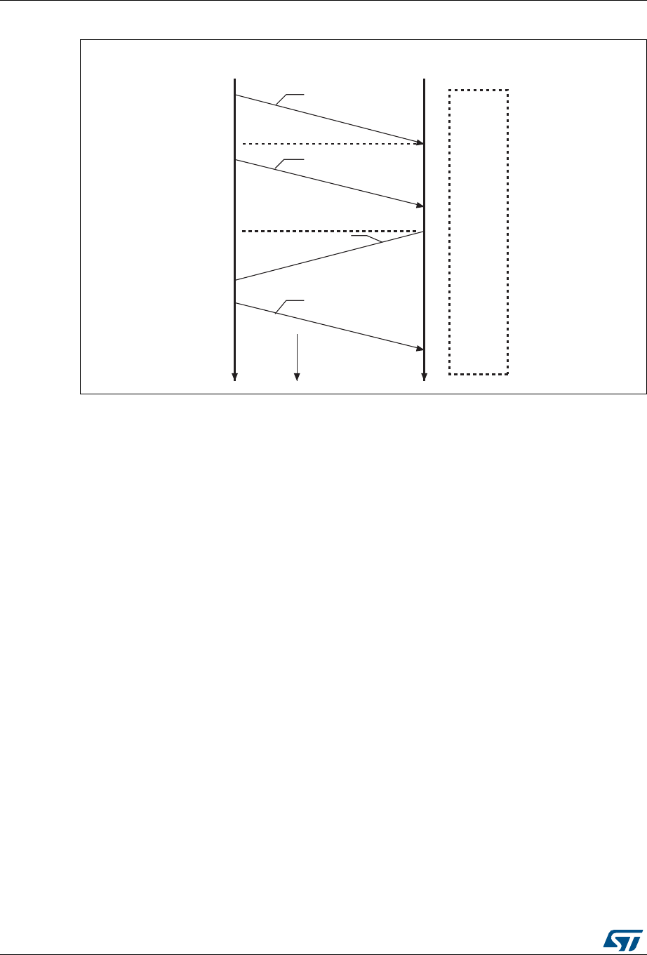
Ethernet (ETH): media access control (MAC) with DMA controller RM0090
1142/1718 DocID018909 Rev 9
Figure 372. Networked time synchronization
1. The master broadcasts PTP Sync messages to all its nodes. The Sync message
contains the master’s reference time information. The time at which this message
leaves the master’s system is t1. For Ethernet ports, this time has to be captured at the
MII.
2. A slave receives the Sync message and also captures the exact time, t2, using its
timing reference.
3. The master then sends the slave a Follow_up message, which contains the t1
information for later use.
4. The slave sends the master a Delay_Req message, noting the exact time, t3, at which
this frame leaves the MII.
5. The master receives this message and captures the exact time, t4, at which it enters its
system.
6. The master sends the t4 information to the slave in the Delay_Resp message.
7. The slave uses the four values of t1, t2, t3, and t4 to synchronize its local timing
reference to the master’s timing reference.
Most of the protocol implementation occurs in the software, above the UDP layer. As
described above, however, hardware support is required to capture the exact time when
specific PTP packets enter or leave the Ethernet port at the MII. This timing information has
to be captured and returned to the software for a proper, high-accuracy implementation of
PTP.
Reference timing source
To get a snapshot of the time, the core requires a reference time in 64-bit format (split into
two 32-bit channels, with the upper 32 bits providing time in seconds, and the lower 32 bits
indicating time in nanoseconds) as defined in the IEEE 1588 specification.
The PTP reference clock input is used to internally generate the reference time (also called
the System Time) and to capture time stamps. The frequency of this reference clock must
Master clock time Slave clock time
Data at
slave clock
Sync message
Follow_up message
containing value of t1
Delay_Req message
Delay_Resp message
containing value of t4
time
t1
t2m
t3m
t4
t1, t2, t3, t4
t2
t1, t2
t3
t2
t1, t2, t3
ai15669

DocID018909 Rev 9 1143/1718
RM0090 Ethernet (ETH): media access control (MAC) with DMA controller
1224
be greater than or equal to the resolution of time stamp counter. The synchronization
accuracy target between the master node and the slaves is around 100 ns.
The generation, update and modification of the System Time are described in the Section :
System Time correction methods.
The accuracy depends on the PTP reference clock input period, the characteristics of the
oscillator (drift) and the frequency of the synchronization procedure.
Due to the synchronization from the Tx and Rx clock input domain to the PTP reference
clock domain, the uncertainty on the time stamp latched value is 1 reference clock period. If
we add the uncertainty due to resolution, we will add half the period for time stamping.
Transmission of frames with the PTP feature
When a frame’s SFD is output on the MII, a time stamp is captured. Frames for which time
stamp capture is required are controllable on a per-frame basis. In other words, each
transmitted frame can be marked to indicate whether a time stamp must be captured or not
for that frame. The transmitted frames are not processed to identify PTP frames. Frame
control is exercised through the control bits in the transmit descriptor. Captured time stamps
are returned to the application in the same way as the status is provided for frames. The
time stamp is sent back along with the Transmit status of the frame, inside the
corresponding transmit descriptor, thus connecting the time stamp automatically to the
specific PTP frame. The 64-bit time stamp information is written back to the TDES2 and
TDES3 fields, with TDES2 holding the time stamp’s 32 least significant bits.
Reception of frames with the PTP feature
When the IEEE 1588 time stamping feature is enabled, the Ethernet MAC captures the time
stamp of all frames received on the MII. The MAC provides the time stamp as soon as the
frame reception is complete. Captured time stamps are returned to the application in the
same way as the frame status is provided. The time stamp is sent back along with the
Receive status of the frame, inside the corresponding receive descriptor. The 64-bit time
stamp information is written back to the RDES2 and RDES3 fields, with RDES2 holding the
time stamp’s 32 least significant bits.
System Time correction methods
The 64-bit PTP time is updated using the PTP input reference clock, HCLK. This PTP time
is used as a source to take snapshots (time stamps) of the Ethernet frames being
transmitted or received at the MII. The System Time counter can be initialized or corrected
using either the Coarse or the Fine correction method.
In the Coarse correction method, the initial value or the offset value is written to the Time
stamp update register (refer to Section 33.8.3: IEEE 1588 time stamp registers on
page 1199). For initialization, the System Time counter is written with the value in the Time
stamp update registers, whereas for system time correction, the offset value (Time stamp
update register) is added to or subtracted from the system time.
In the Fine correction method, the slave clock (reference clock) frequency drift with respect
to the master clock (as defined in IEEE 1588) is corrected over a period of time, unlike in the
Coarse correction method where it is corrected in a single clock cycle. The longer correction
time helps maintain linear time and does not introduce drastic changes (or a large jitter) in
the reference time between PTP Sync message intervals. In this method, an accumulator
sums up the contents of the Addend register as shown in Figure 373. The arithmetic carry
that the accumulator generates is used as a pulse to increment the system time counter.
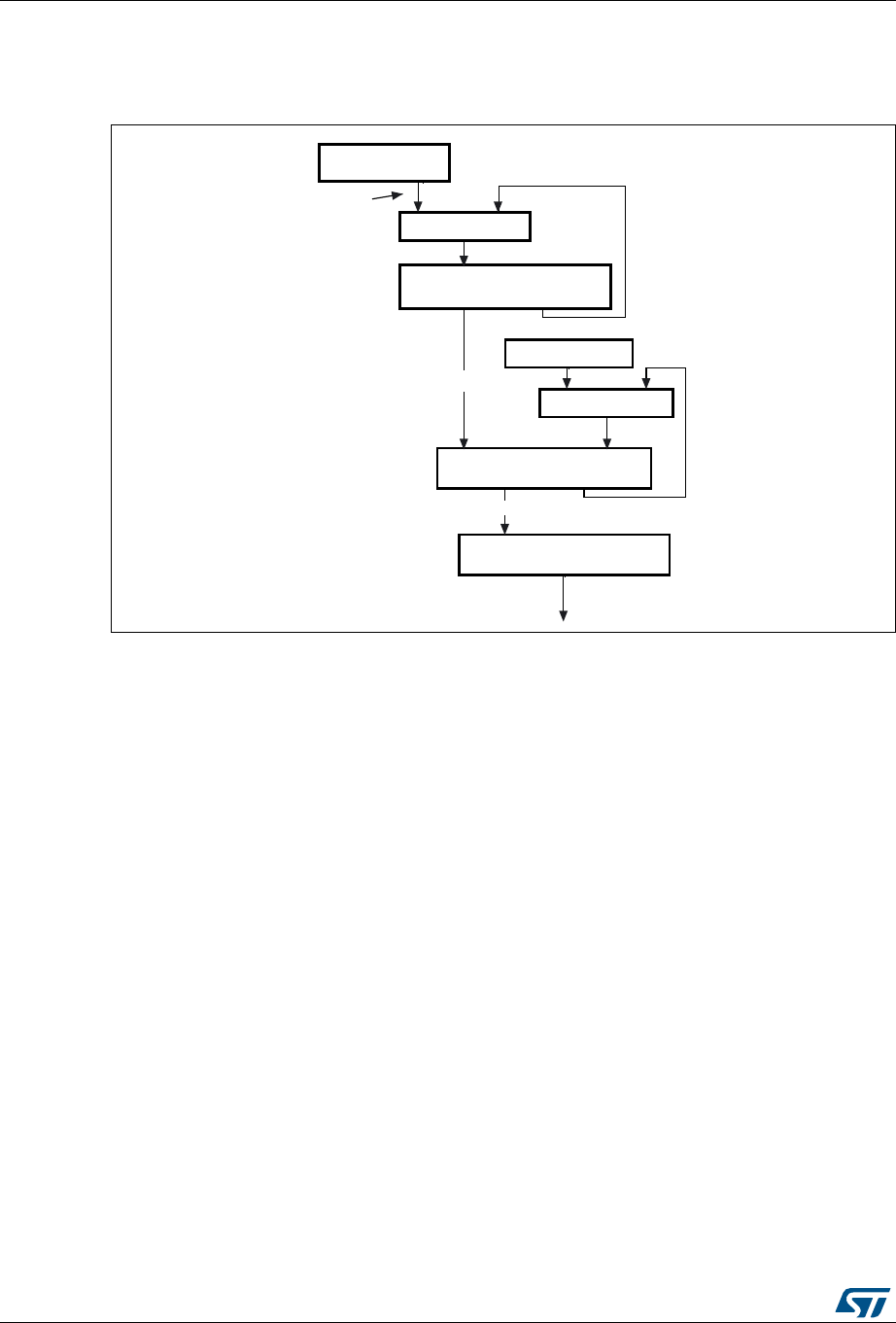
Ethernet (ETH): media access control (MAC) with DMA controller RM0090
1144/1718 DocID018909 Rev 9
The accumulator and the addend are 32-bit registers. Here, the accumulator acts as a high-
precision frequency multiplier or divider. Figure 373 shows this algorithm.
Figure 373. System time update using the Fine correction method
The system time update logic requires a 50 MHz clock frequency to achieve 20 ns accuracy.
The frequency division is the ratio of the reference clock frequency to the required clock
frequency. Hence, if the reference clock (HCLK) is, let us say, 66 MHz, the ratio is calculated
as 66 MHz/50 MHz = 1.32. Hence, the default addend value to be set in the register is
232/1.32, which is equal to 0xC1F0 7C1F.
If the reference clock drifts lower, to 65 MHz for example, the ratio is 65/50 or 1.3 and the
value to set in the addend register is 232/1.30 equal to 0xC4EC 4EC4. If the clock drifts
higher, to 67 MHz for example, the addend register must be set to 0xBF0 B7672. When the
clock drift is zero, the default addend value of 0xC1F0 7C1F (232/1.32) should be
programmed.
In Figure 373, the constant value used to increment the subsecond register is 0d43. This
makes an accuracy of 20 ns in the system time (in other words, it is incremented by 20 ns
steps).
The software has to calculate the drift in frequency based on the Sync messages, and to
update the Addend register accordingly. Initially, the slave clock is set with
FreqCompensationValue0 in the Addend register. This value is as follows:
FreqCompensationValue0 = 232 / FreqDivisionRatio
If MasterToSlaveDelay is initially assumed to be the same for consecutive Sync messages,
the algorithm described below must be applied. After a few Sync cycles, frequency lock
occurs. The slave clock can then determine a precise MasterToSlaveDelay value and re-
synchronize with the master using the new value.
Addend register
+
Accumulator register
Subsecond register
+
Constant value
Second register
Increment Second register
Addend update
ai15670
Increment Subsecond
register

DocID018909 Rev 9 1145/1718
RM0090 Ethernet (ETH): media access control (MAC) with DMA controller
1224
The algorithm is as follows:
•At time MasterSyncTime (n) the master sends the slave clock a Sync message. The
slave receives this message when its local clock is SlaveClockTime (n) and computes
MasterClockTime (n) as:
MasterClockTime (n) = MasterSyncTime (n) + MasterToSlaveDelay (n)
•The master clock count for current Sync cycle, MasterClockCount (n) is given by:
MasterClockCount (n) = MasterClockTime (n) – MasterClockTime (n – 1) (assuming
that MasterToSlaveDelay is the same for Sync cycles n and n – 1)
•The slave clock count for current Sync cycle, SlaveClockCount (n) is given by:
SlaveClockCount (n) = SlaveClockTime (n) – SlaveClockTime (n – 1)
•The difference between master and slave clock counts for current Sync cycle,
ClockDiffCount (n) is given by:
ClockDiffCount (n) = MasterClockCount (n) – SlaveClockCount (n)
•The frequency-scaling factor for slave clock, FreqScaleFactor (n) is given by:
FreqScaleFactor (n) = (MasterClockCount (n) + ClockDiffCount (n)) /
SlaveClockCount (n)
•The frequency compensation value for Addend register, FreqCompensationValue (n) is
given by:
FreqCompensationValue (n) = FreqScaleFactor (n) × FreqCompensationValue (n – 1)
In theory, this algorithm achieves lock in one Sync cycle; however, it may take several
cycles, due to changing network propagation delays and operating conditions.
This algorithm is self-correcting: if for any reason the slave clock is initially set to a value
from the master that is incorrect, the algorithm corrects it at the cost of more Sync cycles.
Programming steps for system time generation initialization
The time stamping feature can be enabled by setting bit 0 in the Time stamp control register
(ETH__PTPTSCR). However, it is essential to initialize the time stamp counter after this bit
is set to start time stamp operation. The proper sequence is the following:
1. Mask the Time stamp trigger interrupt by setting bit 9 in the MACIMR register.
2. Program Time stamp register bit 0 to enable time stamping.
3. Program the Subsecond increment register based on the PTP clock frequency.
4. If you are using the Fine correction method, program the Time stamp addend register
and set Time stamp control register bit 5 (addend register update).
5. Poll the Time stamp control register until bit 5 is cleared.
6. To select the Fine correction method (if required), program Time stamp control register
bit 1.
7. Program the Time stamp high update and Time stamp low update registers with the
appropriate time value.
8. Set Time stamp control register bit 2 (Time stamp init).
9. The Time stamp counter starts operation as soon as it is initialized with the value
written in the Time stamp update register.
10. Enable the MAC receiver and transmitter for proper time stamping.
Note: If time stamp operation is disabled by clearing bit 0 in the ETH_PTPTSCR register, the
above steps must be repeated to restart the time stamp operation.

Ethernet (ETH): media access control (MAC) with DMA controller RM0090
1146/1718 DocID018909 Rev 9
Programming steps for system time update in the Coarse correction method
To synchronize or update the system time in one process (coarse correction method),
perform the following steps:
1. Write the offset (positive or negative) in the Time stamp update high and low registers.
2. Set bit 3 (TSSTU) in the Time stamp control register.
3. The value in the Time stamp update registers is added to or subtracted from the system
time when the TSSTU bit is cleared.
Programming steps for system time update in the Fine correction method
To synchronize or update the system time to reduce system-time jitter (fine correction
method), perform the following steps:
1. With the help of the algorithm explained in Section : System Time correction methods,
calculate the rate by which you want to speed up or slow down the system time
increments.
2. Update the time stamp.
3. Wait the time you want the new value of the Addend register to be active. You can do
this by activating the Time stamp trigger interrupt after the system time reaches the
target value.
4. Program the required target time in the Target time high and low registers. Unmask the
Time stamp interrupt by clearing bit 9 in the ETH_MACIMR register.
5. Set Time stamp control register bit 4 (TSARU).
6. When this trigger causes an interrupt, read the ETH_MACSR register.
7. Reprogram the Time stamp addend register with the old value and set ETH_TPTSCR
bit 5 again.
PTP trigger internal connection with TIM2
The MAC provides a trigger interrupt when the system time becomes greater than the target
time. Using an interrupt introduces a known latency plus an uncertainty in the command
execution time.
In order to avoid this uncertainty, a PTP trigger output signal is set high when the system
time is greater than the target time. It is internally connected to the TIM2 input trigger. With
this signal, the input capture feature, the output compare feature and the waveforms of the
timer can be used, triggered by the synchronized PTP system time. No uncertainty is
introduced since the clock of the timer (PCLK1: TIM2 APB1 clock) and PTP reference clock
(HCLK) are synchronous.
This PTP trigger signal is connected to the TIM2 ITR1 input selectable by software. The
connection is enabled through bits 11 and 10 in the TIM2 option register (TIM2_OR).
Figure 374 shows the connection.
Figure 374. PTP trigger output to TIM2 ITR1 connection
Ethernet MAC
ai15671
TIM2
ITR1PTP trigger
DocID018909 Rev 9 1147/1718
RM0090 Ethernet (ETH): media access control (MAC) with DMA controller
1224
PTP pulse-per-second output signal
This PTP pulse output is used to check the synchronization between all nodes in the
network. To be able to test the difference between the local slave clock and the master
reference clock, both clocks were given a pulse-per-second (PPS) output signal that may be
connected to an oscilloscope if necessary. The deviation between the two signals can
therefore be measured. The pulse width of the PPS output is 125 ms.
The PPS output is enabled through a GPIO alternate function. (GPIO_AFR register).
The default frequency of the PPS output is 1 Hz. PPSFREQ[3:0] (in ETH_PTPPPSCR) can
be used to set the frequency of the PPS output to 2PPSFREQ Hz.
When set to 1 Hz, the PPS pulse width is 125 ms with binary rollover (TSSSR=0, bit 9 in
ETH_PTPTSCR) and 100 ms with digital rollover (TSSSR=1). When set to 2 Hz and higher,
the duty cycle of the PPS output is 50% with binary rollover.
With digital rollover (TSSSR=1), it is recommended not to use the PPS output with a
frequency other than 1 Hz as it would have irregular waveforms (though its average
frequency would always be correct during any one-second window).
Figure 375. PPS output
33.6 Ethernet functional description: DMA controller operation
The DMA has independent transmit and receive engines, and a CSR space. The transmit
engine transfers data from system memory into the Tx FIFO while the receive engine
transfers data from the Rx FIFO into system memory. The controller utilizes descriptors to
efficiently move data from source to destination with minimum CPU intervention. The DMA
is designed for packet-oriented data transfers such as frames in Ethernet. The controller can
be programmed to interrupt the CPU in cases such as frame transmit and receive transfer
completion, and other normal/error conditions. The DMA and the STM32F4xx communicate
through two data structures:
•Control and status registers (CSR)
•Descriptor lists and data buffers.
Control and status registers are described in detail in Section 33.8 on page 1175.
Descriptors are described in detail in Section on page 1155.
The DMA transfers the received data frames to the receive buffer in the STM32F4xx
memory, and transmits data frames from the transmit buffer in the STM32F4xx memory.
Descriptors that reside in the STM32F4xx memory act as pointers to these buffers. There
are two descriptor lists: one for reception, and one for transmission. The base address of
each list is written into DMA Registers 3 and 4, respectively. A descriptor list is forward-
linked (either implicitly or explicitly). The last descriptor may point back to the first entry to
create a ring structure. Explicit chaining of descriptors is accomplished by configuring the
second address chained in both the receive and transmit descriptors (RDES1[14] and
TDES0[20]). The descriptor lists reside in the Host’s physical memory space. Each
descriptor can point to a maximum of two buffers. This enables the use of two physically
Ethernet MAC
ai15672
PPS output
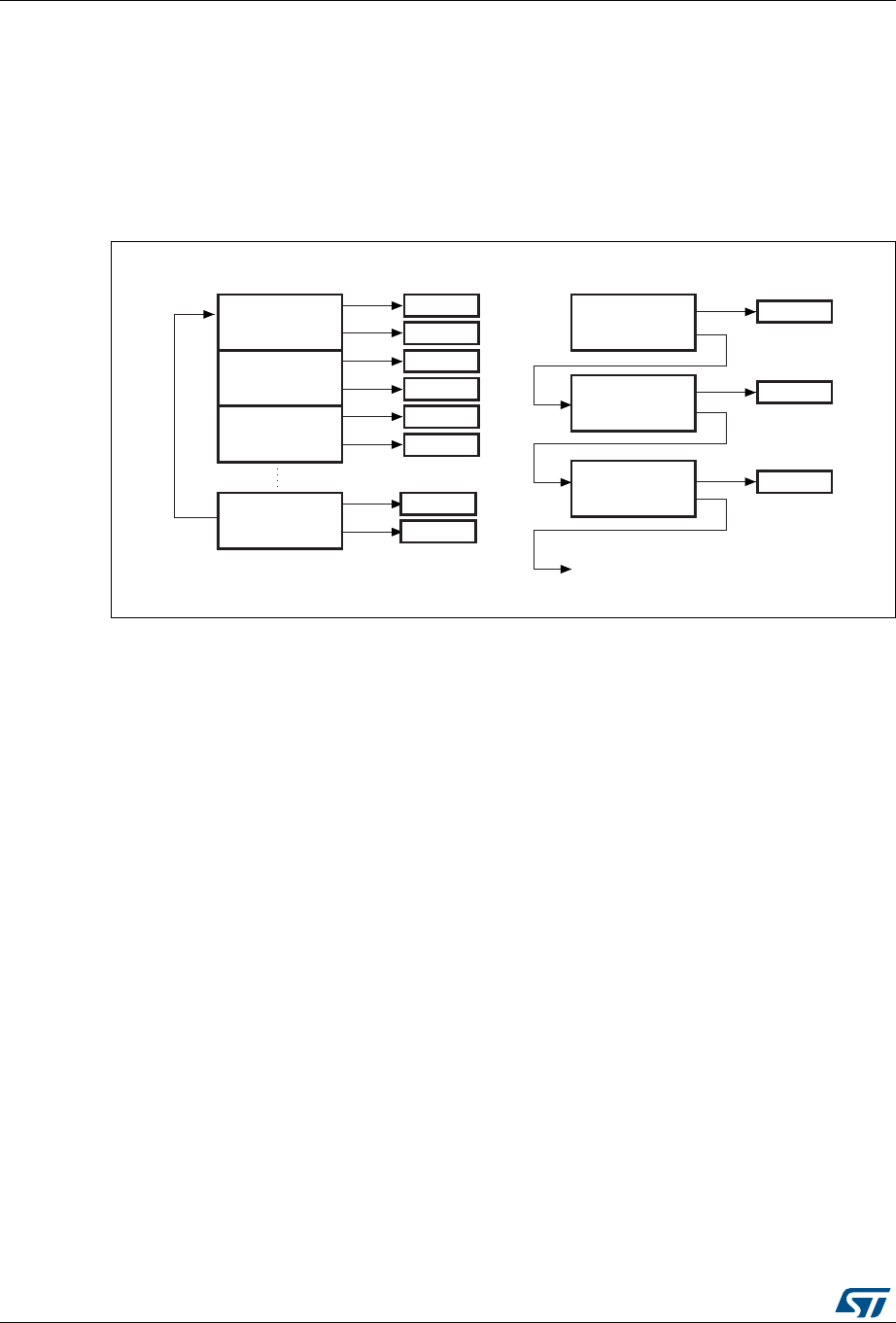
Ethernet (ETH): media access control (MAC) with DMA controller RM0090
1148/1718 DocID018909 Rev 9
addressed buffers, instead of two contiguous buffers in memory. A data buffer resides in the
Host’s physical memory space, and consists of an entire frame or part of a frame, but cannot
exceed a single frame. Buffers contain only data. The buffer status is maintained in the
descriptor. Data chaining refers to frames that span multiple data buffers. However, a single
descriptor cannot span multiple frames. The DMA skips to the next frame buffer when the
end of frame is detected. Data chaining can be enabled or disabled. The descriptor ring and
chain structure is shown in Figure 376.
Figure 376. Descriptor ring and chain structure
33.6.1 Initialization of a transfer using DMA
Initialization for the MAC is as follows:
1. Write to ETH_DMABMR to set STM32F4xx bus access parameters.
2. Write to the ETH_DMAIER register to mask unnecessary interrupt causes.
3. The software driver creates the transmit and receive descriptor lists. Then it writes to
both the ETH_DMARDLAR and ETH_DMATDLAR registers, providing the DMA with
the start address of each list.
4. Write to MAC Registers 1, 2, and 3 to choose the desired filtering options.
5. Write to the MAC ETH_MACCR register to configure and enable the transmit and
receive operating modes. The PS and DM bits are set based on the auto-negotiation
result (read from the PHY).
6. Write to the ETH_DMAOMR register to set bits 13 and 1 and start transmission and
reception.
7. The transmit and receive engines enter the running state and attempt to acquire
descriptors from the respective descriptor lists. The receive and transmit engines then
begin processing receive and transmit operations. The transmit and receive processes
are independent of each other and can be started or stopped separately.
33.6.2 Host bus burst access
The DMA attempts to execute fixed-length burst transfers on the AHB master interface if
configured to do so (FB bit in ETH_DMABMR). The maximum burst length is indicated and
limited by the PBL field (ETH_DMABMR [13:8]). The receive and transmit descriptors are
Descriptor 0
ai15638
Descriptor 1
Descriptor 2
Descriptor n
Buffer 1
Buffer 2
Buffer 1
Buffer 2
Buffer 1
Buffer 2
Buffer 1
Buffer 2
Ring structure Chain structure
Descriptor 0
Descriptor 1
Descriptor 2
Buffer 1
Buffer 1
Buffer 1
Next descriptor

DocID018909 Rev 9 1149/1718
RM0090 Ethernet (ETH): media access control (MAC) with DMA controller
1224
always accessed in the maximum possible burst size (limited by PBL) for the 16 bytes to be
read.
The Transmit DMA initiates a data transfer only when there is sufficient space in the
Transmit FIFO to accommodate the configured burst or the number of bytes until the end of
frame (when it is less than the configured burst length). The DMA indicates the start address
and the number of transfers required to the AHB Master Interface. When the AHB Interface
is configured for fixed-length burst, then it transfers data using the best combination of
INCR4, INCR8, INCR16 and SINGLE transactions. Otherwise (no fixed-length burst), it
transfers data using INCR (undefined length) and SINGLE transactions.
The Receive DMA initiates a data transfer only when sufficient data for the configured burst
is available in Receive FIFO or when the end of frame (when it is less than the configured
burst length) is detected in the Receive FIFO. The DMA indicates the start address and the
number of transfers required to the AHB master interface. When the AHB interface is
configured for fixed-length burst, then it transfers data using the best combination of INCR4,
INCR8, INCR16 and SINGLE transactions. If the end of frame is reached before the fixed-
burst ends on the AHB interface, then dummy transfers are performed in order to complete
the fixed-length burst. Otherwise (FB bit in ETH_DMABMR is reset), it transfers data using
INCR (undefined length) and SINGLE transactions.
When the AHB interface is configured for address-aligned beats, both DMA engines ensure
that the first burst transfer the AHB initiates is less than or equal to the size of the configured
PBL. Thus, all subsequent beats start at an address that is aligned to the configured PBL.
The DMA can only align the address for beats up to size 16 (for PBL > 16), because the
AHB interface does not support more than INCR16.
33.6.3 Host data buffer alignment
The transmit and receive data buffers do not have any restrictions on start address
alignment. In our system with 32-bit memory, the start address for the buffers can be aligned
to any of the four bytes. However, the DMA always initiates transfers with address aligned to
the bus width with dummy data for the byte lanes not required. This typically happens during
the transfer of the beginning or end of an Ethernet frame.
•Example of buffer read:
If the Transmit buffer address is 0x0000 0FF2, and 15 bytes need to be transferred,
then the DMA will read five full words from address 0x0000 0FF0, but when transferring
data to the Transmit FIFO, the extra bytes (the first two bytes) will be dropped or
ignored. Similarly, the last 3 bytes of the last transfer will also be ignored. The DMA
always ensures it transfers a full 32-bit data items to the Transmit FIFO, unless it is the
end of frame.
•Example of buffer write:
If the Receive buffer address is 0x0000 0FF2, and 16 bytes of a received frame need to
be transferred, then the DMA will write five full 32-bit data items from address
0x0000 0FF0. But the first 2 bytes of the first transfer and the last 2 bytes of the third
transfer will have dummy data.
33.6.4 Buffer size calculations
The DMA does not update the size fields in the transmit and receive descriptors. The DMA
updates only the status fields (xDES0) of the descriptors. The driver has to calculate the
sizes. The transmit DMA transfers the exact number of bytes (indicated by buffer size field in
TDES1) towards the MAC core. If a descriptor is marked as first (FS bit in TDES0 is set),

Ethernet (ETH): media access control (MAC) with DMA controller RM0090
1150/1718 DocID018909 Rev 9
then the DMA marks the first transfer from the buffer as the start of frame. If a descriptor is
marked as last (LS bit in TDES0), then the DMA marks the last transfer from that data buffer
as the end of frame. The receive DMA transfers data to a buffer until the buffer is full or the
end of frame is received. If a descriptor is not marked as last (LS bit in RDES0), then the
buffer(s) that correspond to the descriptor are full and the amount of valid data in a buffer is
accurately indicated by the buffer size field minus the data buffer pointer offset when the
descriptor’s FS bit is set. The offset is zero when the data buffer pointer is aligned to the
databus width. If a descriptor is marked as last, then the buffer may not be full (as indicated
by the buffer size in RDES1). To compute the amount of valid data in this final buffer, the
driver must read the frame length (FL bits in RDES0[29:16]) and subtract the sum of the
buffer sizes of the preceding buffers in this frame. The receive DMA always transfers the
start of next frame with a new descriptor.
Note: Even when the start address of a receive buffer is not aligned to the system databus width
the system should allocate a receive buffer of a size aligned to the system bus width. For
example, if the system allocates a 1024 byte (1 KB) receive buffer starting from address
0x1000, the software can program the buffer start address in the receive descriptor to have
a 0x1002 offset. The receive DMA writes the frame to this buffer with dummy data in the first
two locations (0x1000 and 0x1001). The actual frame is written from location 0x1002. Thus,
the actual useful space in this buffer is 1022 bytes, even though the buffer size is
programmed as 1024 bytes, due to the start address offset.
33.6.5 DMA arbiter
The arbiter inside the DMA takes care of the arbitration between transmit and receive
channel accesses to the AHB master interface. Two types of arbitrations are possible:
round-robin, and fixed-priority. When round-robin arbitration is selected (DA bit in
ETH_DMABMR is reset), the arbiter allocates the databus in the ratio set by the PM bits in
ETH_DMABMR, when both transmit and receive DMAs request access simultaneously.
When the DA bit is set, the receive DMA always gets priority over the transmit DMA for data
access.
33.6.6 Error response to DMA
For any data transfer initiated by a DMA channel, if the slave replies with an error response,
that DMA stops all operations and updates the error bits and the fatal bus error bit in the
Status register (ETH_DMASR register). That DMA controller can resume operation only
after soft- or hard-resetting the peripheral and re-initializing the DMA.
33.6.7 Tx DMA configuration
TxDMA operation: default (non-OSF) mode
The transmit DMA engine in default mode proceeds as follows:
1. The user sets up the transmit descriptor (TDES0-TDES3) and sets the OWN bit
(TDES0[31]) after setting up the corresponding data buffer(s) with Ethernet frame data.
2. Once the ST bit (ETH_DMAOMR register[13]) is set, the DMA enters the Run state.
3. While in the Run state, the DMA polls the transmit descriptor list for frames requiring
transmission. After polling starts, it continues in either sequential descriptor ring order
or chained order. If the DMA detects a descriptor flagged as owned by the CPU, or if an
error condition occurs, transmission is suspended and both the Transmit Buffer

DocID018909 Rev 9 1151/1718
RM0090 Ethernet (ETH): media access control (MAC) with DMA controller
1224
Unavailable (ETH_DMASR register[2]) and Normal Interrupt Summary (ETH_DMASR
register[16]) bits are set. The transmit engine proceeds to Step 9.
4. If the acquired descriptor is flagged as owned by DMA (TDES0[31] is set), the DMA
decodes the transmit data buffer address from the acquired descriptor.
5. The DMA fetches the transmit data from the STM32F4xx memory and transfers the
data.
6. If an Ethernet frame is stored over data buffers in multiple descriptors, the DMA closes
the intermediate descriptor and fetches the next descriptor. Steps 3, 4, and 5 are
repeated until the end of Ethernet frame data is transferred.
7. When frame transmission is complete, if IEEE 1588 time stamping was enabled for the
frame (as indicated in the transmit status) the time stamp value is written to the transmit
descriptor (TDES2 and TDES3) that contains the end-of-frame buffer. The status
information is then written to this transmit descriptor (TDES0). Because the OWN bit is
cleared during this step, the CPU now owns this descriptor. If time stamping was not
enabled for this frame, the DMA does not alter the contents of TDES2 and TDES3.
8. Transmit Interrupt (ETH_DMASR register [0]) is set after completing the transmission
of a frame that has Interrupt on Completion (TDES1[31]) set in its last descriptor. The
DMA engine then returns to Step 3.
9. In the Suspend state, the DMA tries to re-acquire the descriptor (and thereby returns to
Step 3) when it receives a transmit poll demand, and the Underflow Interrupt Status bit
is cleared.
Figure 377 shows the TxDMA transmission flow in default mode.
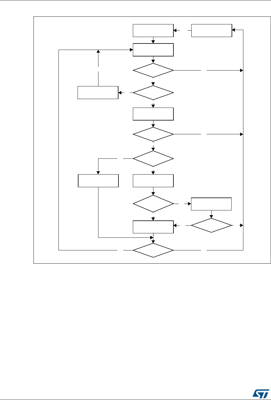
Ethernet (ETH): media access control (MAC) with DMA controller RM0090
1152/1718 DocID018909 Rev 9
Figure 377. TxDMA operation in Default mode
TxDMA operation: OSF mode
While in the Run state, the transmit process can simultaneously acquire two frames without
closing the Status descriptor of the first (if the OSF bit is set in ETH_DMAOMR register[2]).
As the transmit process finishes transferring the first frame, it immediately polls the transmit
descriptor list for the second frame. If the second frame is valid, the transmit process
transfers this frame before writing the first frame’s status information. In OSF mode, the
Run-state transmit DMA operates according to the following sequence:
Start TxDMA
(Re-)fetch next
descriptor
Write status word
to TDES0
Wait for Tx status
Transfer data from
buffer(s)
(AHB)
error?
Own
bit set?
(AHB)
error?
Frame xfer
complete?
Time stamp
present?
(AHB)
error?
Write time stamp to
TDES2 and TDES3
(AHB)
error?
Stop TxDMA
TxDMA suspended
No
Ye s
No
Ye s
No
No
Start
Ye s
Ye s
Ye s
Close intermediate
descriptor
No
Ye s
No
Ye s
No
Poll demand
ai15639

DocID018909 Rev 9 1153/1718
RM0090 Ethernet (ETH): media access control (MAC) with DMA controller
1224
1. The DMA operates as described in steps 1–6 of the TxDMA (default mode).
2. Without closing the previous frame’s last descriptor, the DMA fetches the next
descriptor.
3. If the DMA owns the acquired descriptor, the DMA decodes the transmit buffer address
in this descriptor. If the DMA does not own the descriptor, the DMA goes into Suspend
mode and skips to Step 7.
4. The DMA fetches the Transmit frame from the STM32F4xx memory and transfers the
frame until the end of frame data are transferred, closing the intermediate descriptors if
this frame is split across multiple descriptors.
5. The DMA waits for the transmission status and time stamp of the previous frame. When
the status is available, the DMA writes the time stamp to TDES2 and TDES3, if such
time stamp was captured (as indicated by a status bit). The DMA then writes the status,
with a cleared OWN bit, to the corresponding TDES0, thus closing the descriptor. If
time stamping was not enabled for the previous frame, the DMA does not alter the
contents of TDES2 and TDES3.
6. If enabled, the Transmit interrupt is set, the DMA fetches the next descriptor, then
proceeds to Step 3 (when Status is normal). If the previous transmission status shows
an underflow error, the DMA goes into Suspend mode (Step 7).
7. In Suspend mode, if a pending status and time stamp are received by the DMA, it
writes the time stamp (if enabled for the current frame) to TDES2 and TDES3, then
writes the status to the corresponding TDES0. It then sets relevant interrupts and
returns to Suspend mode.
8. The DMA can exit Suspend mode and enter the Run state (go to Step 1 or Step 2
depending on pending status) only after receiving a Transmit Poll demand
(ETH_DMATPDR register).
Figure 378 shows the basic flowchart in OSF mode.
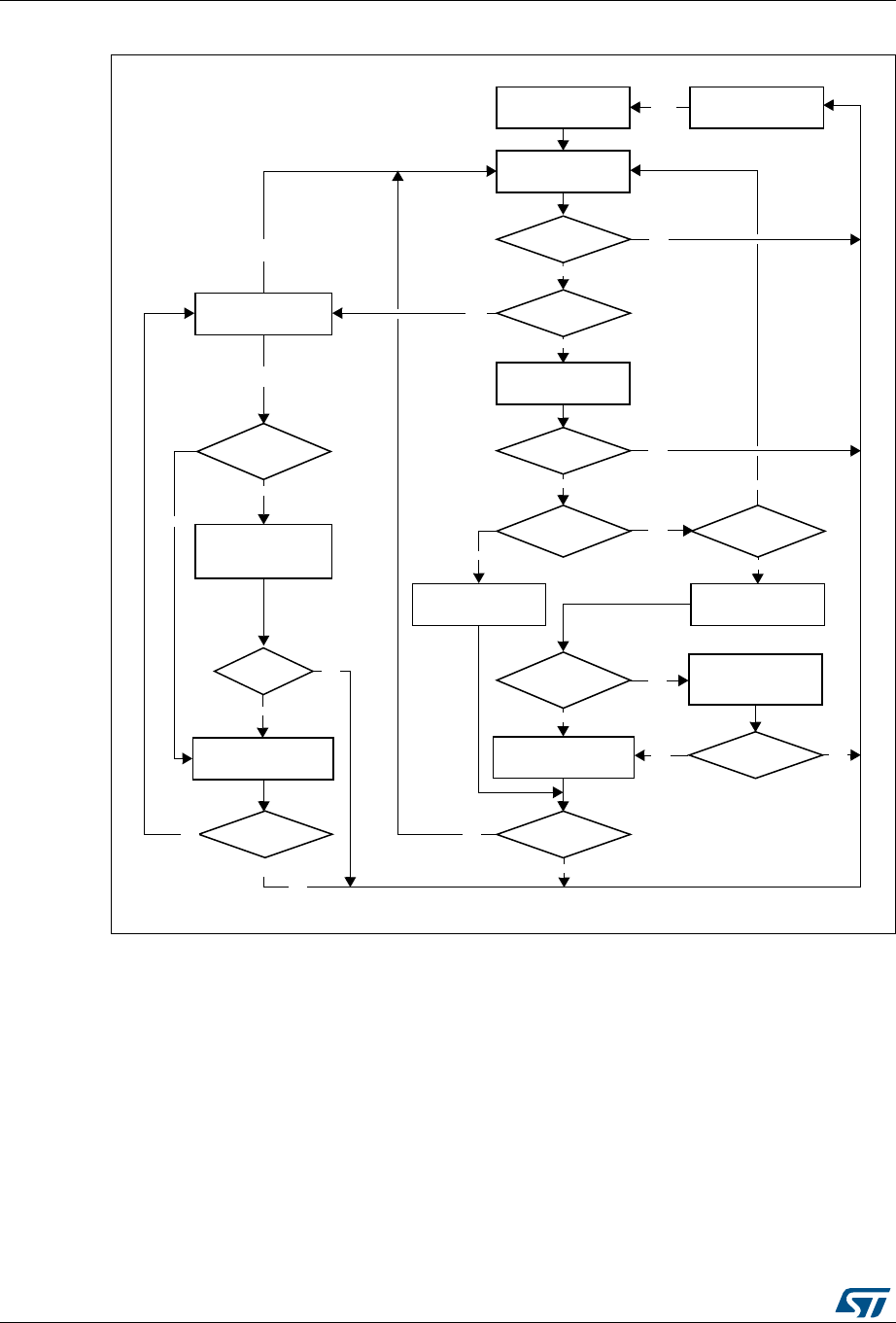
Ethernet (ETH): media access control (MAC) with DMA controller RM0090
1154/1718 DocID018909 Rev 9
Figure 378. TxDMA operation in OSF mode
Transmit frame processing
The transmit DMA expects that the data buffers contain complete Ethernet frames,
excluding preamble, pad bytes, and FCS fields. The DA, SA, and Type/Len fields contain
valid data. If the transmit descriptor indicates that the MAC core must disable CRC or pad
insertion, the buffer must have complete Ethernet frames (excluding preamble), including
the CRC bytes. Frames can be data-chained and span over several buffers. Frames have to
be delimited by the first descriptor (TDES0[28]) and the last descriptor (TDES0[29]). As the
transmission starts, TDES0[28] has to be set in the first descriptor. When this occurs, the
frame data are transferred from the memory buffer to the Transmit FIFO. Concurrently, if the
last descriptor (TDES0[29]) of the current frame is cleared, the transmit process attempts to
acquire the next descriptor. The transmit process expects TDES0[28] to be cleared in this
descriptor. If TDES0[29] is cleared, it indicates an intermediary buffer. If TDES0[29] is set, it
Previous frame
status available
Start TxDMA
(Re-)fetch next
descriptor
Write status word to
prev. frame’s TDES0
Transfer data from
buffer(s)
(AHB)
error?
Own
bit set?
(AHB)
error?
Frame xfer
complete?
Time stamp
present?
(AHB)
error?
Write time stamp to
TDES2 & TDES3
for previous frame
(AHB)
error?
Stop TxDMA
No
Ye s
No
Ye s
No
Start
Ye s
Close intermediate
descriptor
No
No
Wait for previous
frame’s Tx status
Second
frame?
Ye s
Ye s
No
Ye s
Ye s
Write time stamp to
TDES2 & TDES3
for previous frame
(AHB)
error?
(AHB)
error?
Ye s
Time stamp
present?
Ye s
Write status word to
prev. frame’s TDES0
TxDMA suspended
Ye s
No
Ye s
No
No
Poll
demand
No
No
ai15640

DocID018909 Rev 9 1155/1718
RM0090 Ethernet (ETH): media access control (MAC) with DMA controller
1224
indicates the last buffer of the frame. After the last buffer of the frame has been transmitted,
the DMA writes back the final status information to the transmit descriptor 0 (TDES0) word
of the descriptor that has the last segment set in transmit descriptor 0 (TDES0[29]). At this
time, if Interrupt on Completion (TDES0[30]) is set, Transmit Interrupt (in ETH_DMASR
register [0]) is set, the next descriptor is fetched, and the process repeats. Actual frame
transmission begins after the Transmit FIFO has reached either a programmable transmit
threshold (ETH_DMAOMR register[16:14]), or a full frame is contained in the FIFO. There is
also an option for the Store and forward mode (ETH_DMAOMR register[21]). Descriptors
are released (OWN bit TDES0[31] is cleared) when the DMA finishes transferring the frame.
Transmit polling suspended
Transmit polling can be suspended by either of the following conditions:
•The DMA detects a descriptor owned by the CPU (TDES0[31]=0) and the Transmit
buffer unavailable flag is set (ETH_DMASR register[2]). To resume, the driver must
give descriptor ownership to the DMA and then issue a Poll Demand command.
•A frame transmission is aborted when a transmit error due to underflow is detected.
The appropriate Transmit Descriptor 0 (TDES0) bit is set. If the second condition
occurs, both the Abnormal Interrupt Summary (in ETH_DMASR register [15]) and
Transmit Underflow bits (in ETH_DMASR register[5]) are set, and the information is
written to Transmit Descriptor 0, causing the suspension. If the DMA goes into
Suspend state due to the first condition, then both the Normal Interrupt Summary
(ETH_DMASR register [16]) and Transmit Buffer Unavailable (ETH_DMASR
register[2]) bits are set. In both cases, the position in the transmit list is retained. The
retained position is that of the descriptor following the last descriptor closed by the
DMA. The driver must explicitly issue a Transmit Poll Demand command after rectifying
the suspension cause.
Normal Tx DMA descriptors
The normal transmit descriptor structure consists of four 32-bit words as shown in
Figure 379. The bit descriptions of TDES0, TDES1, TDES2 and TDES3 are given below.
Note that enhanced descriptors must be used if time stamping is activated (ETH_PTPTSCR
bit 0, TSE=1) or if IPv4 checksum offload is activated (ETH_MACCR bit 10, IPCO=1).
Figure 379. Normal transmit descriptor
TDES 3
O
W
N
Ctrl
[30:26]
Res.
24
Ctrl
[23:20]
Reserved
[19:18]Status [16:0]
Reserved
[31:29]
Buffer 2 byte count
[28:16]
Reserved
[15:13]
Buffer 1 byte count
[12:0]
Buffer 1 address [31:0] / Time stamp low [31:0]
Buffer 2 address [31:0] or Next descriptor address [31:0] / Time stamp high [31:0]
TDES 0
TDES 1
TDES 2
31 0
ai15642b
T
T
S
E
T
T
S
S

Ethernet (ETH): media access control (MAC) with DMA controller RM0090
1156/1718 DocID018909 Rev 9
•TDES0: Transmit descriptor Word0
The application software has to program the control bits [30:26]+[23:20] plus the OWN
bit [31] during descriptor initialization. When the DMA updates the descriptor (or writes
it back), it resets all the control bits plus the OWN bit, and reports only the status bits.
31 30 29 28 27 26 25 24 23 22 21 20 19 18 17 16
OWN IC LS FS DC DP TTSE Res CIC TER TCH Res. TTSS IHE
rw rw rw rw rw rw rw rw rw rw rw rw rw
1514131211109 8 76543210
ES JT FF IPE LCA NC LCO EC VF CC ED UF DB
rw rw rw rw rw rw rw rw rw rw rw rw rw rw rw rw
Bit 31 OWN: Own bit
When set, this bit indicates that the descriptor is owned by the DMA. When this bit is reset, it
indicates that the descriptor is owned by the CPU. The DMA clears this bit either when it
completes the frame transmission or when the buffers allocated in the descriptor are read
completely. The ownership bit of the frame’s first descriptor must be set after all subsequent
descriptors belonging to the same frame have been set.
Bit 30 IC: Interrupt on completion
When set, this bit sets the Transmit Interrupt (Register 5[0]) after the present frame has
been transmitted.
Bit 29 LS: Last segment
When set, this bit indicates that the buffer contains the last segment of the frame.
Bit 28 FS: First segment
When set, this bit indicates that the buffer contains the first segment of a frame.
Bit 27 DC: Disable CRC
When this bit is set, the MAC does not append a cyclic redundancy check (CRC) to the end
of the transmitted frame. This is valid only when the first segment (TDES0[28]) is set.
Bit 26 DP: Disable pad
When set, the MAC does not automatically add padding to a frame shorter than 64 bytes.
When this bit is reset, the DMA automatically adds padding and CRC to a frame shorter than
64 bytes, and the CRC field is added despite the state of the DC (TDES0[27]) bit. This is
valid only when the first segment (TDES0[28]) is set.
Bit 25 TTSE: Transmit time stamp enable
When TTSE is set and when TSE is set (ETH_PTPTSCR bit 0), IEEE1588 hardware time
stamping is activated for the transmit frame described by the descriptor. This field is only valid
when the First segment control bit (TDES0[28]) is set.
Bit 24 Reserved, must be kept at reset value.
Bits 23:22 CIC: Checksum insertion control
These bits control the checksum calculation and insertion. Bit encoding is as shown below:
00: Checksum Insertion disabled
01: Only IP header checksum calculation and insertion are enabled
10: IP header checksum and payload checksum calculation and insertion are enabled, but
pseudo-header checksum is not calculated in hardware
11: IP Header checksum and payload checksum calculation and insertion are enabled, and
pseudo-header checksum is calculated in hardware.

DocID018909 Rev 9 1157/1718
RM0090 Ethernet (ETH): media access control (MAC) with DMA controller
1224
Bit 21 TER: Transmit end of ring
When set, this bit indicates that the descriptor list reached its final descriptor. The DMA
returns to the base address of the list, creating a descriptor ring.
Bit 20 TCH: Second address chained
When set, this bit indicates that the second address in the descriptor is the next descriptor
address rather than the second buffer address. When TDES0[20] is set, TBS2
(TDES1[28:16]) is a “don’t care” value. TDES0[21] takes precedence over TDES0[20].
Bits 19:18 Reserved, must be kept at reset value.
Bit 17 TTSS: Transmit time stamp status
This field is used as a status bit to indicate that a time stamp was captured for the described
transmit frame. When this bit is set, TDES2 and TDES3 have a time stamp value captured for the
transmit frame. This field is only valid when the descriptor’s Last segment control bit (TDES0[29])
is set.
Note that when enhanced descriptors are enabled (EDFE=1 in ETH_DMABMR), TTSS=1
indicates that TDES6 and TDES7 have the time stamp value.
Bit 16 IHE: IP header error
When set, this bit indicates that the MAC transmitter detected an error in the IP datagram
header. The transmitter checks the header length in the IPv4 packet against the number of
header bytes received from the application and indicates an error status if there is a
mismatch. For IPv6 frames, a header error is reported if the main header length is not 40
bytes. Furthermore, the Ethernet length/type field value for an IPv4 or IPv6 frame must
match the IP header version received with the packet. For IPv4 frames, an error status is
also indicated if the Header Length field has a value less than 0x5.
Bit 15 ES: Error summary
Indicates the logical OR of the following bits:
TDES0[14]: Jabber timeout
TDES0[13]: Frame flush
TDES0[11]: Loss of carrier
TDES0[10]: No carrier
TDES0[9]: Late collision
TDES0[8]: Excessive collision
TDES0[2]:Excessive deferral
TDES0[1]: Underflow error
TDES0[16]: IP header error
TDES0[12]: IP payload error
Bit 14 JT: Jabber timeout
When set, this bit indicates the MAC transmitter has experienced a jabber timeout. This bit is
only set when the MAC configuration register’s JD bit is not set.
Bit 13 FF: Frame flushed
When set, this bit indicates that the DMA/MTL flushed the frame due to a software Flush
command given by the CPU.
Bit 12 IPE: IP payload error
When set, this bit indicates that MAC transmitter detected an error in the TCP, UDP, or ICMP
IP datagram payload. The transmitter checks the payload length received in the IPv4 or IPv6
header against the actual number of TCP, UDP or ICMP packet bytes received from the
application and issues an error status in case of a mismatch.

Ethernet (ETH): media access control (MAC) with DMA controller RM0090
1158/1718 DocID018909 Rev 9
•TDES1: Transmit descriptor Word1
Bit 11 LCA: Loss of carrier
When set, this bit indicates that a loss of carrier occurred during frame transmission (that is,
the MII_CRS signal was inactive for one or more transmit clock periods during frame
transmission). This is valid only for the frames transmitted without collision when the MAC
operates in Half-duplex mode.
Bit 10 NC: No carrier
When set, this bit indicates that the Carrier Sense signal form the PHY was not asserted
during transmission.
Bit 9 LCO: Late collision
When set, this bit indicates that frame transmission was aborted due to a collision occurring
after the collision window (64 byte times, including preamble, in MII mode). This bit is not
valid if the Underflow Error bit is set.
Bit 8 EC: Excessive collision
When set, this bit indicates that the transmission was aborted after 16 successive collisions
while attempting to transmit the current frame. If the RD (Disable retry) bit in the MAC
Configuration register is set, this bit is set after the first collision, and the transmission of the
frame is aborted.
Bit 7 VF: VLAN frame
When set, this bit indicates that the transmitted frame was a VLAN-type frame.
Bits 6:3 CC: Collision count
This 4-bit counter value indicates the number of collisions occurring before the frame was
transmitted. The count is not valid when the Excessive collisions bit (TDES0[8]) is set.
Bit 2 ED: Excessive deferral
When set, this bit indicates that the transmission has ended because of excessive deferral
of over 24 288 bit times if the Deferral check (DC) bit in the MAC Control register is set high.
Bit 1 UF: Underflow error
When set, this bit indicates that the MAC aborted the frame because data arrived late from
the RAM memory. Underflow error indicates that the DMA encountered an empty transmit
buffer while transmitting the frame. The transmission process enters the Suspended state
and sets both Transmit underflow (Register 5[5]) and Transmit interrupt (Register 5[0]).
Bit 0 DB: Deferred bit
When set, this bit indicates that the MAC defers before transmission because of the
presence of the carrier. This bit is valid only in Half-duplex mode.
31 30 29 28 27 26 25 24 23 22 21 20 19 18 17 16 15 14 13 12 11 10 9 8 7 6 5 4 3 2 1 0
Reserved
TBS2
Reserved
TBS1
rw rw rw rw rw rw rw rw rw rw rw rw rw rw rw rw rw rw rw rw rw rw rw rw rw rw
31:29 Reserved, must be kept at reset value.

DocID018909 Rev 9 1159/1718
RM0090 Ethernet (ETH): media access control (MAC) with DMA controller
1224
•TDES2: Transmit descriptor Word2
TDES2 contains the address pointer to the first buffer of the descriptor or it contains
time stamp data.
•TDES3: Transmit descriptor Word3
TDES3 contains the address pointer either to the second buffer of the descriptor or the
next descriptor, or it contains time stamp data.
28:16 TBS2: Transmit buffer 2 size
These bits indicate the second data buffer size in bytes. This field is not valid if TDES0[20] is
set.
15:13 Reserved, must be kept at reset value.
12:0 TBS1: Transmit buffer 1 size
These bits indicate the first data buffer byte size, in bytes. If this field is 0, the DMA ignores
this buffer and uses Buffer 2 or the next descriptor, depending on the value of TCH
(TDES0[20]).
31 30 29 28 27 26 25 24 23 22 21 20 19 18 17 16 15 14 13 12 11 10 9 8 7 6 5 4 3 2 1 0
TBAP1/TBAP/TTSL
rw
Bits 31:0 TBAP1: Transmit buffer 1 address pointer / Transmit frame time stamp low
These bits have two different functions: they indicate to the DMA the location of data in
memory, and after all data are transferred, the DMA can then use these bits to pass back time
stamp data.
TBAP: When the software makes this descriptor available to the DMA (at the moment that the
OWN bit is set to 1 in TDES0), these bits indicate the physical address of Buffer 1. There is no
limitation on the buffer address alignment. See Host data buffer alignment on page 1149 for further
details on buffer address alignment.
TTSL: Before it clears the OWN bit in TDES0, the DMA updates this field with the 32 least
significant bits of the time stamp captured for the corresponding transmit frame (overwriting
the value for TBAP1). This field has the time stamp only if time stamping is activated for this
frame (see TTSE, TDES0 bit 25) and if the Last segment control bit (LS) in the descriptor is
set.
31 30 29 28 27 26 25 24 23 22 21 20 19 18 17 16 15 14 13 12 11 10 9 8 7 6 5 4 3 2 1 0
TBAP2/TBAP2/TTSH
rw

Ethernet (ETH): media access control (MAC) with DMA controller RM0090
1160/1718 DocID018909 Rev 9
Enhanced Tx DMA descriptors
Enhanced descriptors (enabled with EDFE=1, ETHDMABMR bit 7), must be used if time
stamping is activated (TSE=1, ETH_PTPTSCR bit 0) or if IPv4 checksum offload is
activated (IPCO=1, ETH_MACCR bit 10).
Enhanced descriptors comprise eight 32-bit words, twice the size of normal descriptors.
TDES0, TDES1, TDES2 and TDES3 have the same definitions as for normal transmit
descriptors (refer to Normal Tx DMA descriptors). TDES6 and TDES7 hold the time stamp.
TDES4, TDES5, TDES6 and TDES7 are defined below.
When the Enhanced descriptor mode is selected, the software needs to allocate 32-bytes (8
DWORDS) of memory for every descriptor. When time stamping or IPv4 checksum offload
are not being used, the enhanced descriptor format may be disabled and the software can
use normal descriptors with the default size of 16 bytes.
Bits 31:0 TBAP2: Transmit buffer 2 address pointer (Next descriptor address) / Transmit frame time
stamp high
These bits have two different functions: they indicate to the DMA the location of data in
memory, and after all data are transferred, the DMA can then use these bits to pass back
time stamp data.
TBAP2: When the software makes this descriptor available to the DMA (at the moment when
the OWN bit is set to 1 in TDES0), these bits indicate the physical address of Buffer 2 when a
descriptor ring structure is used. If the Second address chained (TDES1 [20]) bit is set, this
address contains the pointer to the physical memory where the next descriptor is present. The
buffer address pointer must be aligned to the bus width only when TDES1 [20] is set. (LSBs are
ignored internally.)
TTSH: Before it clears the OWN bit in TDES0, the DMA updates this field with the 32 most
significant bits of the time stamp captured for the corresponding transmit frame (overwriting
the value for TBAP2). This field has the time stamp only if time stamping is activated for this
frame (see TDES0 bit 25, TTSE) and if the Last segment control bit (LS) in the descriptor is
set.

DocID018909 Rev 9 1161/1718
RM0090 Ethernet (ETH): media access control (MAC) with DMA controller
1224
Figure 380. Enhanced transmit descriptor
•TDES4: Transmit descriptor Word4
Reserved
•TDES5: Transmit descriptor Word5
Reserved
•TDES6: Transmit descriptor Word6
4$%3
/
7
.
#TRL
;=
2ES
#TRL
;=
2ESERVED
;= 3TATUS;=
2ESERVED
;=
"UFFERBYTECOUNT
;=
2ESERVED
;=
"UFFERBYTECOUNT
;=
"UFFERADDRESS;=
"UFFERADDRESS;=OR.EXTDESCRIPTORADDRESS;=
4$%3
4$%3
4$%3
AIB
4
4
3
%
4
4
3
3
4$%3
4$%3
4$%3
4$%3
2ESERVED
2ESERVED
4IMESTAMPLOW;=
4IMESTAMPHIGH;=
31 30 29 28 27 26 25 24 23 22 21 20 19 18 17 16 15 14 13 12 11 10 9 8 7 6 5 4 3 2 1 0
TTSL
rw
Bits 31:0 TTSL: Transmit frame time stamp low
This field is updated by DMA with the 32 least significant bits of the time stamp captured
for the corresponding transmit frame. This field has the time stamp only if the Last segment
control bit (LS) in the descriptor is set.

Ethernet (ETH): media access control (MAC) with DMA controller RM0090
1162/1718 DocID018909 Rev 9
•TDES7: Transmit descriptor Word7
33.6.8 Rx DMA configuration
The Receive DMA engine’s reception sequence is illustrated in Figure 381 and described
below:
1. The CPU sets up Receive descriptors (RDES0-RDES3) and sets the OWN bit
(RDES0[31]).
2. Once the SR (ETH_DMAOMR register[1]) bit is set, the DMA enters the Run state.
While in the Run state, the DMA polls the receive descriptor list, attempting to acquire
free descriptors. If the fetched descriptor is not free (is owned by the CPU), the DMA
enters the Suspend state and jumps to Step 9.
3. The DMA decodes the receive data buffer address from the acquired descriptors.
4. Incoming frames are processed and placed in the acquired descriptor’s data buffers.
5. When the buffer is full or the frame transfer is complete, the Receive engine fetches the
next descriptor.
6. If the current frame transfer is complete, the DMA proceeds to step 7. If the DMA does
not own the next fetched descriptor and the frame transfer is not complete (EOF is not
yet transferred), the DMA sets the Descriptor error bit in RDES0 (unless flushing is
disabled). The DMA closes the current descriptor (clears the OWN bit) and marks it as
intermediate by clearing the Last segment (LS) bit in the RDES1 value (marks it as last
descriptor if flushing is not disabled), then proceeds to step 8. If the DMA owns the next
descriptor but the current frame transfer is not complete, the DMA closes the current
descriptor as intermediate and returns to step 4.
7. If IEEE 1588 time stamping is enabled, the DMA writes the time stamp (if available) to
the current descriptor’s RDES2 and RDES3. It then takes the received frame’s status
and writes the status word to the current descriptor’s RDES0, with the OWN bit cleared
and the Last segment bit set.
8. The Receive engine checks the latest descriptor’s OWN bit. If the CPU owns the
descriptor (OWN bit is at 0) the Receive buffer unavailable bit (in ETH_DMASR
register[7]) is set and the DMA Receive engine enters the Suspended state (step 9). If
the DMA owns the descriptor, the engine returns to step 4 and awaits the next frame.
9. Before the Receive engine enters the Suspend state, partial frames are flushed from
the Receive FIFO (you can control flushing using bit 24 in the ETH_DMAOMR
register).
10. The Receive DMA exits the Suspend state when a Receive Poll demand is given or the
start of next frame is available from the Receive FIFO. The engine proceeds to step 2
and re-fetches the next descriptor.
31 30 29 28 27 26 25 24 23 22 21 20 19 18 17 16 15 14 13 12 11 10 9 8 7 6 5 4 3 2 1 0
TTSH
rw
Bits 31:0 TTSH: Transmit frame time stamp high
This field is updated by DMA with the 32 most significant bits of the time stamp captured for
the corresponding transmit frame. This field has the time stamp only if the Last segment control
bit (LS) in the descriptor is set.
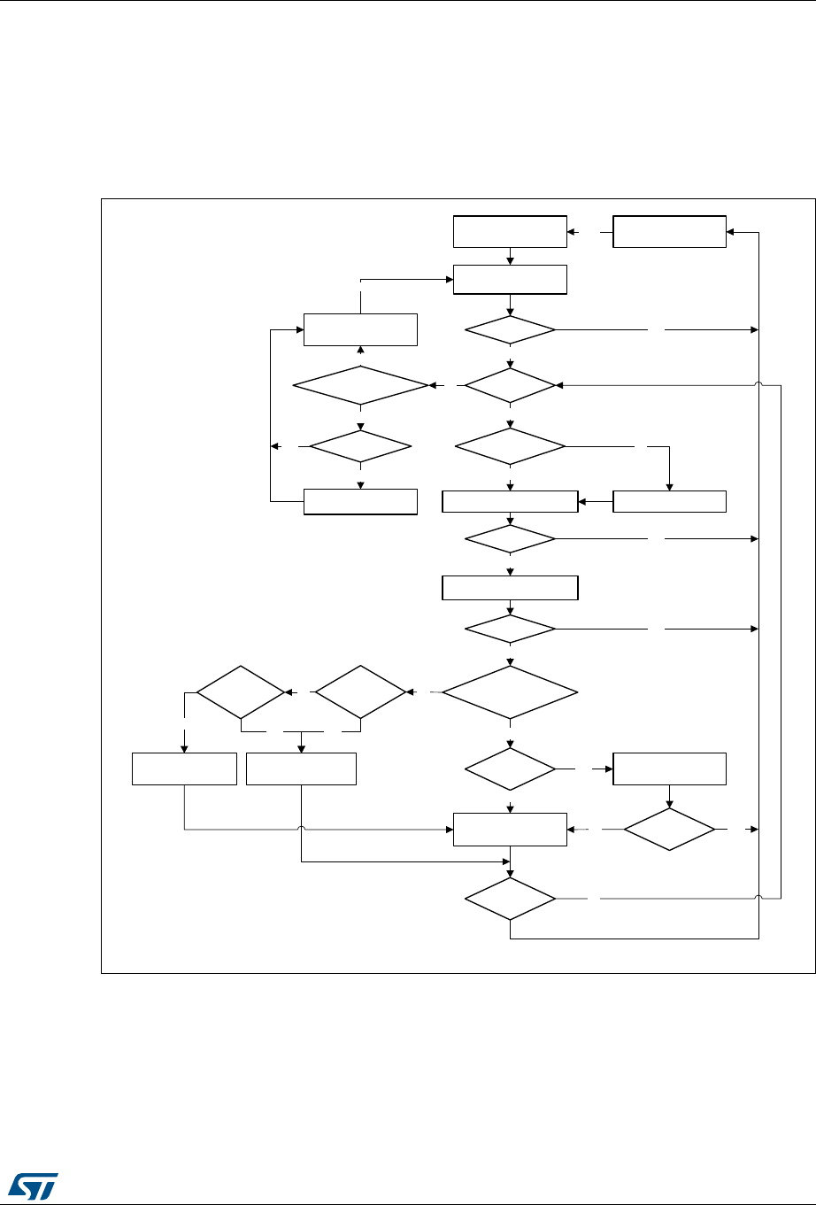
DocID018909 Rev 9 1163/1718
RM0090 Ethernet (ETH): media access control (MAC) with DMA controller
1224
The DMA does not acknowledge accepting the status until it has completed the time stamp
write-back and is ready to perform status write-back to the descriptor. If software has
enabled time stamping through CSR, when a valid time stamp value is not available for the
frame (for example, because the receive FIFO was full before the time stamp could be
written to it), the DMA writes all ones to RDES2 and RDES3. Otherwise (that is, if time
stamping is not enabled), RDES2 and RDES3 remain unchanged.
Figure 381. Receive DMA operation
(Re-)Fetch next
descriptor
(AHB)
error?
No
Own bit set?
Yes
Yes
Stop RxDMAStart RxDMA Start
(AHB)
error?
No
RxDMA suspended
Yes
Frame data
available?
Wait for frame dataWrite data to buffer(s)
Yes
Yes
Fetch next descriptor
Yes
No
Frame transfer
complete?
No
Set descriptor error
Yes
Time stamp
present?
No
Close RDES0 as last
descriptor
Write time stamp to
RDES2 & RDES3
No (AHB)
error? Yes
Close RDES0 as
intermediate descriptor
Frame transfer
complete?
No
Flush disabled ?
No
Flush the
remaining frame
Yes
Yes
No
No
No
Yes
Yes
Poll demand/
new frame available
No
Yes
(AHB)
error?
(AHB)
error?
No
Own bit set
for next desc?
Flush
disabled?
ai15643

Ethernet (ETH): media access control (MAC) with DMA controller RM0090
1164/1718 DocID018909 Rev 9
Receive descriptor acquisition
The receive engine always attempts to acquire an extra descriptor in anticipation of an
incoming frame. Descriptor acquisition is attempted if any of the following conditions is/are
satisfied:
•The receive Start/Stop bit (ETH_DMAOMR register[1]) has been set immediately after
the DMA has been placed in the Run state.
•The data buffer of the current descriptor is full before the end of the frame currently
being transferred
•The controller has completed frame reception, but the current receive descriptor has
not yet been closed.
•The receive process has been suspended because of a CPU-owned buffer
(RDES0[31] = 0) and a new frame is received.
•A Receive poll demand has been issued.
Receive frame processing
The MAC transfers the received frames to the STM32F4xx memory only when the frame
passes the address filter and the frame size is greater than or equal to the configurable
threshold bytes set for the Receive FIFO, or when the complete frame is written to the FIFO
in Store-and-forward mode. If the frame fails the address filtering, it is dropped in the MAC
block itself (unless Receive All ETH_MACFFR [31] bit is set). Frames that are shorter than
64 bytes, because of collision or premature termination, can be purged from the Receive
FIFO. After 64 (configurable threshold) bytes have been received, the DMA block begins
transferring the frame data to the receive buffer pointed to by the current descriptor. The
DMA sets the first descriptor (RDES0[9]) after the DMA AHB Interface becomes ready to
receive a data transfer (if DMA is not fetching transmit data from the memory), to delimit the
frame. The descriptors are released when the OWN (RDES0[31]) bit is reset to 0, either as
the data buffer fills up or as the last segment of the frame is transferred to the receive buffer.
If the frame is contained in a single descriptor, both the last descriptor (RDES0[8]) and first
descriptor (RDES0[9]) bits are set. The DMA fetches the next descriptor, sets the last
descriptor (RDES0[8]) bit, and releases the RDES0 status bits in the previous frame
descriptor. Then the DMA sets the receive interrupt bit (ETH_DMASR register [6]). The
same process repeats unless the DMA encounters a descriptor flagged as being owned by
the CPU. If this occurs, the receive process sets the receive buffer unavailable bit
(ETH_DMASR register[7]) and then enters the Suspend state. The position in the receive
list is retained.
Receive process suspended
If a new receive frame arrives while the receive process is in Suspend state, the DMA re-
fetches the current descriptor in the STM32F4xx memory. If the descriptor is now owned by
the DMA, the receive process re-enters the Run state and starts frame reception. If the
descriptor is still owned by the host, by default, the DMA discards the current frame at the
top of the Rx FIFO and increments the missed frame counter. If more than one frame is
stored in the Rx FIFO, the process repeats. The discarding or flushing of the frame at the
top of the Rx FIFO can be avoided by setting the DMA Operation mode register bit 24
(DFRF). In such conditions, the receive process sets the receive buffer unavailable status
bit and returns to the Suspend state.
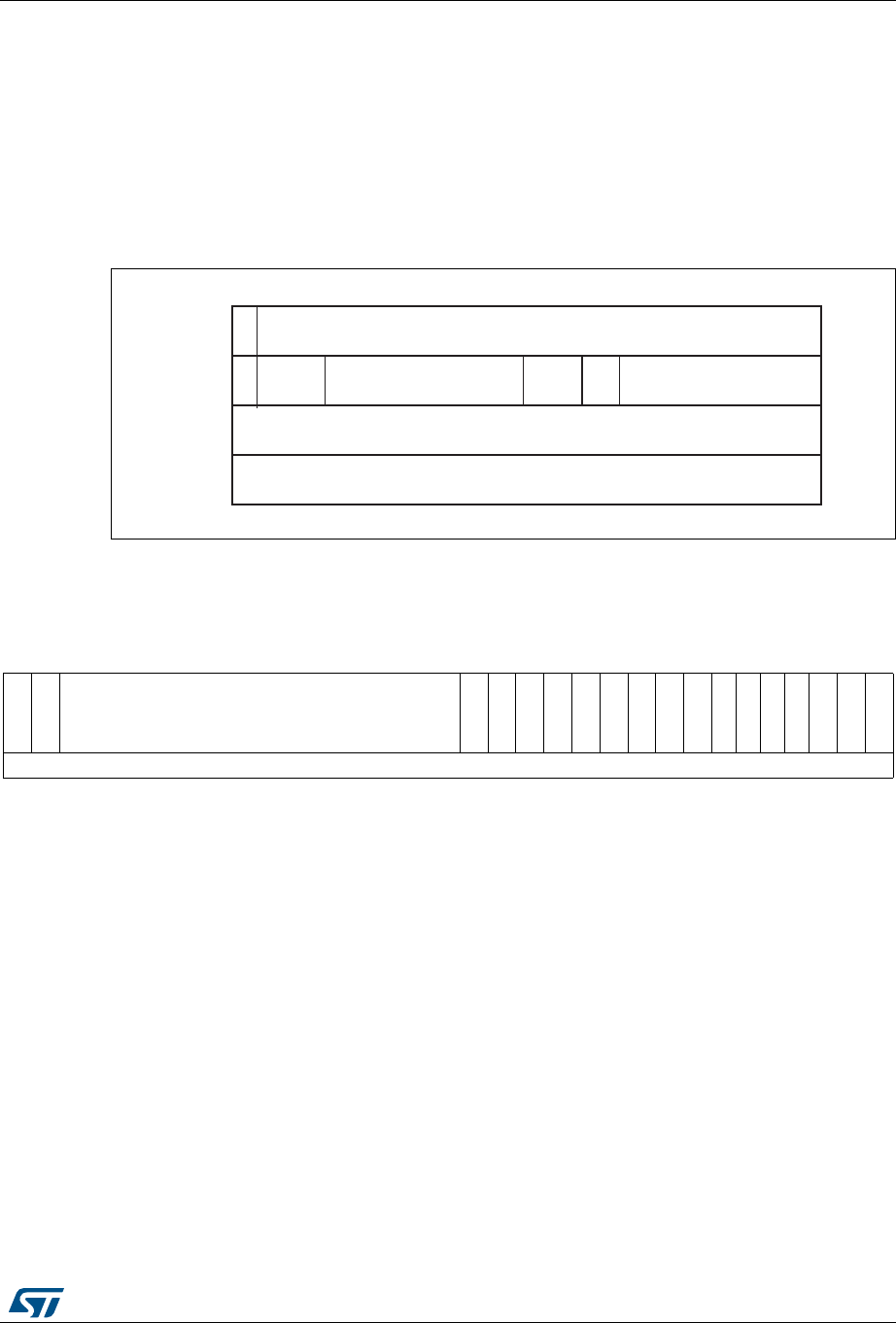
DocID018909 Rev 9 1165/1718
RM0090 Ethernet (ETH): media access control (MAC) with DMA controller
1224
Normal Rx DMA descriptors
The normal receive descriptor structure consists of four 32-bit words (16 bytes). These are
shown in Figure 382. The bit descriptions of RDES0, RDES1, RDES2 and RDES3 are given
below.
Note that enhanced descriptors must be used if time stamping is activated (TSE=1,
ETH_PTPTSCR bit 0) or if IPv4 checksum offload is activated (IPCO=1, ETH_MACCR bit
10).
Figure 382. Normal Rx DMA descriptor structure
•RDES0: Receive descriptor Word0
RDES0 contains the received frame status, the frame length and the descriptor
ownership information.
RDES 3
O
W
NStatus [30:0]
Reserved
[30:29]
Buffer 2 byte count
[28:16]
CTRL
[15:14]
Buffer 1 byte count
[12:0]
Buffer 1 address [31:0]
Buffer 2 address [31:0] or Next descriptor address [31:0]
RDES 0
RDES 1
RDES 2
31 0
ai15644
Res.
CT
RL
31 30 29 28 27 26 25 24 23 22 21 20 19 18 17 16 15 14 13 12 11 10 9 8 7 6 5 4 3 2 1 0
OWN
AFM
FL
ES
DE
SAF
LE
OE
VLAN
FS
LS
IPHCE/TSV
LCO
FT
RWT
RE
DE
CE
PCE/ESA
rw
Bit 31 OWN: Own bit
When set, this bit indicates that the descriptor is owned by the DMA of the MAC Subsystem.
When this bit is reset, it indicates that the descriptor is owned by the Host. The DMA clears this bit
either when it completes the frame reception or when the buffers that are associated with this
descriptor are full.
Bit 30 AFM: Destination address filter fail
When set, this bit indicates a frame that failed the DA filter in the MAC Core.
Bits 29:16 FL: Frame length
These bits indicate the byte length of the received frame that was transferred to host memory
(including CRC). This field is valid only when last descriptor (RDES0[8]) is set and descriptor error
(RDES0[14]) is reset.
This field is valid when last descriptor (RDES0[8]) is set. When the last descriptor and error
summary bits are not set, this field indicates the accumulated number of bytes that have been
transferred for the current frame.

Ethernet (ETH): media access control (MAC) with DMA controller RM0090
1166/1718 DocID018909 Rev 9
Bit 15 ES: Error summary
Indicates the logical OR of the following bits:
RDES0[1]: CRC error
RDES0[3]: Receive error
RDES0[4]: Watchdog timeout
RDES0[6]: Late collision
RDES0[7]: Giant frame (This is not applicable when RDES0[7] indicates an IPV4 header
checksum error.)
RDES0[11]: Overflow error
RDES0[14]: Descriptor error.
This field is valid only when the last descriptor (RDES0[8]) is set.
Bit 14 DE: Descriptor error
When set, this bit indicates a frame truncation caused by a frame that does not fit within the current
descriptor buffers, and that the DMA does not own the next descriptor. The frame is truncated.
This field is valid only when the last descriptor (RDES0[8]) is set.
Bit 13 SAF: Source address filter fail
When set, this bit indicates that the SA field of frame failed the SA filter in the MAC Core.
Bit 12 LE: Length error
When set, this bit indicates that the actual length of the received frame does not match the value in
the Length/ Type field. This bit is valid only when the Frame type (RDES0[5]) bit is reset.
Bit 1
1
OE: Overflow error
When set, this bit indicates that the received frame was damaged due to buffer overflow.
Bit 10 VLAN: VLAN tag
When set, this bit indicates that the frame pointed to by this descriptor is a VLAN frame tagged
by the MAC core.
Bit 9 FS: First descriptor
When set, this bit indicates that this descriptor contains the first buffer of the frame. If the size of the
first buffer is 0, the second buffer contains the beginning of the frame. If the size of the second buffer
is also 0, the next descriptor contains the beginning of the frame.
Bit 8 LS: Last descriptor
When set, this bit indicates that the buffers pointed to by this descriptor are the last buffers of
the frame.
Bit 7 IPHCE/TSV: IPv header checksum error / time stamp valid
If IPHCE is set, it indicates an error in the IPv4 or IPv6 header. This error can be due to inconsistent
Ethernet Type field and IP header Version field values, a header checksum mismatch in IPv4, or an
Ethernet frame lacking the expected number of IP header bytes. This bit can take on special
meaning as specified in Table 192.
If enhanced descriptor format is enabled (EDFE=1, bit 7 of ETH_DMABMR), this bit takes on
the TSV function (otherwise it is IPHCE). When TSV is set, it indicates that a snapshot of the
timestamp is written in descriptor words 6 (RDES6) and 7 (RDES7). TSV is valid only when
the Last descriptor bit (RDES0[8]) is set.
Bit 6 LCO: Late collision
When set, this bit indicates that a late collision has occurred while receiving the frame in Half-
duplex mode.

DocID018909 Rev 9 1167/1718
RM0090 Ethernet (ETH): media access control (MAC) with DMA controller
1224
Bits 5, 7, and 0 reflect the conditions discussed in Table 192.
Bit 5 FT: Frame type
When set, this bit indicates that the Receive frame is an Ethernet-type frame (the LT field is greater
than or equal to 0x0600). When this bit is reset, it indicates that the received frame is an
IEEE802.3 frame. This bit is not valid for Runt frames less than 14 bytes. When the normal
descriptor format is used (ETH_DMABMR EDFE=0), FT can take on special meaning as
specified in Table 192.
Bit 4 RWT: Receive watchdog timeout
When set, this bit indicates that the Receive watchdog timer has expired while receiving the
current frame and the current frame is truncated after the watchdog timeout.
Bit 3 RE: Receive error
When set, this bit indicates that the RX_ERR signal is asserted while RX_DV is asserted
during frame reception.
Bit 2 DE: Dribble bit error
When set, this bit indicates that the received frame has a non-integer multiple of bytes (odd
nibbles). This bit is valid only in MII mode.
Bit 1 CE: CRC error
When set, this bit indicates that a cyclic redundancy check (CRC) error occurred on the
received frame. This field is valid only when the last descriptor (RDES0[8]) is set.
Bit 0 PCE/ESA: Payload checksum error / extended status available
When set, it indicates that the TCP, UDP or ICMP checksum the core calculated does not
match the received encapsulated TCP, UDP or ICMP segment’s Checksum field. This bit is
also set when the received number of payload bytes does not match the value indicated in
the Length field of the encapsulated IPv4 or IPv6 datagram in the received Ethernet frame.
This bit can take on special meaning as specified in Table 192.
If the enhanced descriptor format is enabled (EDFE=1, bit 7 in ETH_DMABMR), this bit takes
on the ESA function (otherwise it is PCE). When ESA is set, it indicates that the extended
status is available in descriptor word 4 (RDES4). ESA is valid only when the last descriptor bit
(RDES0[8]) is set.
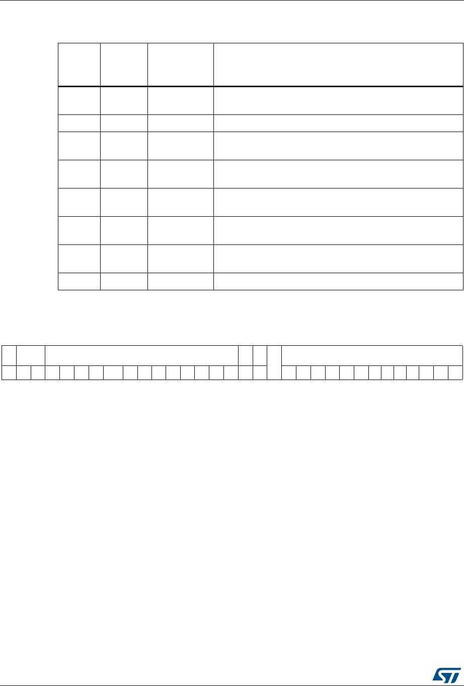
Ethernet (ETH): media access control (MAC) with DMA controller RM0090
1168/1718 DocID018909 Rev 9
•RDES1: Receive descriptor Word1
Table 192. Receive descriptor 0 - encoding for bits 7, 5 and 0 (normal descriptor
format only, EDFE=0)
Bit 5:
frame
type
Bit 7: IPC
checksum
error
Bit 0: payload
checksum
error
Frame status
00 0
IEEE 802.3 Type frame (Length field value is less than
0x0600.)
1 0 0 IPv4/IPv6 Type frame, no checksum error detected
10 1
IPv4/IPv6 Type frame with a payload checksum error (as described
for PCE) detected
11 0
IPv4/IPv6 Type frame with an IP header checksum error (as
described for IPC CE) detected
11 1
IPv4/IPv6 Type frame with both IP header and payload checksum
errors detected
00 1
IPv4/IPv6 Type frame with no IP header checksum error and the
payload check bypassed, due to an unsupported payload
01 1
A Type frame that is neither IPv4 or IPv6 (the checksum offload
engine bypasses checksum completely.)
0 1 0 Reserved
31 30 29 28 27 26 25 24 23 22 21 20 19 18 17 16 15 14 13 12 11 10 9 8 7 6 5 4 3 2 1 0
DIC
RBS2 RBS2
RER
RCH
Reserved
RBS
rw rw rw rw rw rw rw rw rw rw rw rw rw rw rw rw rw rw rw rw rw rw rw rw rw rw rw rw rw rw rw
Bit 31 DIC: Disable interrupt on completion
When set, this bit prevents setting the Status register’s RS bit (CSR5[6]) for the received frame
ending in the buffer indicated by this descriptor. This, in turn, disables the assertion of the interrupt to
Host due to RS for that frame.
Bits 30:29 Reserved, must be kept at reset value.
Bits 28:16 RBS2: Receive buffer 2 size
These bits indicate the second data buffer size, in bytes. The buffer size must be a multiple of 4,
8, or 16, depending on the bus widths (32, 64 or 128, respectively), even if the value of RDES3
(buffer2 address pointer) is not aligned to bus width. If the buffer size is not an appropriate multiple
of 4, 8 or 16, the resulting behavior is undefined. This field is not valid if RDES1 [14] is set.
Bit 15 RER: Receive end of ring
When set, this bit indicates that the descriptor list reached its final descriptor. The DMA returns to the
base address of the list, creating a descriptor ring.

DocID018909 Rev 9 1169/1718
RM0090 Ethernet (ETH): media access control (MAC) with DMA controller
1224
•RDES2: Receive descriptor Word2
RDES2 contains the address pointer to the first data buffer in the descriptor, or it
contains time stamp data.
Bit 14 RCH: Second address chained
When set, this bit indicates that the second address in the descriptor is the next descriptor address
rather than the second buffer address. When this bit is set, RBS2 (RDES1[28:16]) is a “don’t
care” value. RDES1[15] takes precedence over RDES1[14].
Bit 13 Reserved, must be kept at reset value.
Bits 12:0 RBS1: Receive buffer 1 size
Indicates the first data buffer size in bytes. The buffer size must be a multiple of 4, 8 or 16,
depending upon the bus widths (32, 64 or 128), even if the value of RDES2 (buffer1 address
pointer) is not aligned. When the buffer size is not a multiple of 4, 8 or 16, the resulting behavior is
undefined. If this field is 0, the DMA ignores this buffer and uses Buffer 2 or next descriptor
depending on the value of RCH (bit 14).
31 30 29 28 27 26 25 24 23 22 21 20 19 18 17 16 15 14 13 12 11 10 9 8 7 6 5 4 3 2 1 0
RBP1 / RTSL
rw rw rw rw rw rw rw rw rw rw rw rw rw rw rw rw rw rw rw rw rw rw rw rw rw rw rw rw rw rw rw rw
Bits 31:0 RBAP1 / RTSL: Receive buffer 1 address pointer / Receive frame time stamp low
These bits take on two different functions: the application uses them to indicate to the DMA
where to store the data in memory, and then after transferring all the data the DMA may use
these bits to pass back time stamp data.
RBAP1: When the software makes this descriptor available to the DMA (at the moment that
the OWN bit is set to 1 in RDES0), these bits indicate the physical address of Buffer 1. There are
no limitations on the buffer address alignment except for the following condition: the DMA uses the
configured value for its address generation when the RDES2 value is used to store the start of
frame. Note that the DMA performs a write operation with the RDES2[3/2/1:0] bits as 0 during the
transfer of the start of frame but the frame data is shifted as per the actual Buffer address pointer.
The DMA ignores RDES2[3/2/1:0] (corresponding to bus width of 128/64/32) if the address pointer
is to a buffer where the middle or last part of the frame is stored.
RTSL: Before it clears the OWN bit in RDES0, the DMA updates this field with the 32 least
significant bits of the time stamp captured for the corresponding receive frame (overwriting
the value for RBAP1). This field has the time stamp only if time stamping is activated for this
frame and if the Last segment control bit (LS) in the descriptor is set.

Ethernet (ETH): media access control (MAC) with DMA controller RM0090
1170/1718 DocID018909 Rev 9
•RDES3: Receive descriptor Word3
RDES3 contains the address pointer either to the second data buffer in the descriptor
or to the next descriptor, or it contains time stamp data.
Enhanced Rx DMA descriptors format with IEEE1588 time stamp
Enhanced descriptors (enabled with EDFE=1, ETHDMABMR bit 7), must be used if time
stamping is activated (TSE=1, ETH_PTPTSCR bit 0) or if IPv4 checksum offload is
activated (IPCO=1, ETH_MACCR bit 10).
Enhanced descriptors comprise eight 32-bit words, twice the size of normal descriptors.
RDES0, RDES1, RDES2 and RDES3 have the same definitions as for normal receive
descriptors (refer to Normal Rx DMA descriptors). RDES4 contains extended status while
RDES6 and RDES7 hold the time stamp. RDES4, RDES5, RDES6 and RDES7 are defined
below.
When the Enhanced descriptor mode is selected, the software needs to allocate 32 bytes (8
DWORDS) of memory for every descriptor. When time stamping or IPv4 checksum offload
are not being used, the enhanced descriptor format may be disabled and the software can
use normal descriptors with the default size of 16 bytes.
31 30 29 28 27 26 25 24 23 22 21 20 19 18 17 16 15 14 13 12 11 10 9 8 7 6 5 4 3 2 1 0
RBP2 / RTSH
rw rw rw rw rw rw rw rw rw rw rw rw rw rw rw rw rw rw rw rw rw rw rw rw rw rw rw rw rw rw rw rw
Bits 31:0 RBAP2 / RTSH: Receive buffer 2 address pointer (next descriptor address) / Receive frame
time stamp high
These bits take on two different functions: the application uses them to indicate to the DMA
the location of where to store the data in memory, and then after transferring all the data the
DMA may use these bits to pass back time stamp data.
RBAP1: When the software makes this descriptor available to the DMA (at the moment that
the OWN bit is set to 1 in RDES0), these bits indicate the physical address of buffer 2 when a
descriptor ring structure is used. If the second address chained (RDES1 [24]) bit is set, this address
contains the pointer to the physical memory where the next descriptor is present. If RDES1 [24] is
set, the buffer (next descriptor) address pointer must be bus width-aligned (RDES3[3, 2, or
1:0] = 0, corresponding to a bus width of 128, 64 or 32. LSBs are ignored internally.)
However, when RDES1 [24] is reset, there are no limitations on the RDES3 value, except for the
following condition: the DMA uses the configured value for its buffer address generation when the
RDES3 value is used to store the start of frame. The DMA ignores RDES3[3, 2, or 1:0]
(corresponding to a bus width of 128, 64 or 32) if the address pointer is to a buffer where the
middle or last part of the frame is stored.
RTSH: Before it clears the OWN bit in RDES0, the DMA updates this field with the 32 most
significant bits of the time stamp captured for the corresponding receive frame (overwriting
the value for RBAP2). This field has the time stamp only if time stamping is activated and if
the Last segment control bit (LS) in the descriptor is set.
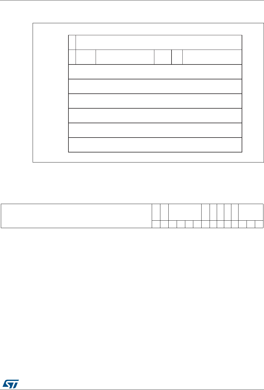
DocID018909 Rev 9 1171/1718
RM0090 Ethernet (ETH): media access control (MAC) with DMA controller
1224
Figure 383. Enhanced receive descriptor field format with IEEE1588 time stamp
enabled
•RDES4: Receive descriptor Word4
The extended status, shown below, is valid only when there is status related to IPv4
checksum or time stamp available as indicated by bit 0 in RDES0.
RDES 3
O
W
NStatus [30:0]
Reserved
[30:29]
Buffer 2 byte count
[28:16]
CTRL
[15:14]
Buffer 1 byte count
[12:0]
Buffer 1 address [31:0]
Buffer 2 address [31:0] or Next descriptor address [31:0]
RDES 0
RDES 1
RDES 2
31 0
ai17104
Res.
CT
RL
RDES 7
RDES 4
RDES 5
RDES 6
Extended Status [31:0]
Reserved
Time stamp low [31:0]
Time stamp high [31:0]
31 30 29 28 27 26 25 24 23 22 21 20 19 18 17 16 15 14 13 12 11 10 9 8 7 6 5 4 3 2 1 0
Reserved
PV
PFT
PMT
IPV6PR
IPV4PR
IPCB
IPPE
IPHE
IPPT
rw rw rw rw rw rw rw rw rw rw rw rw rw rw
Bits 31:14 Reserved, must be kept at reset value.
Bit 13 PV: PTP version
When set, indicates that the received PTP message uses the IEEE 1588 version 2 format.
When cleared, it uses version 1 format. This is valid only if the message type is non-zero.
Bit 12 PFT: PTP frame type
When set, this bit indicates that the PTP message is sent directly over Ethernet. When this bit
is cleared and the message type is non-zero, it indicates that the PTP message is sent over
UDP-IPv4 or UDP-IPv6. The information on IPv4 or IPv6 can be obtained from bits 6 and 7.

Ethernet (ETH): media access control (MAC) with DMA controller RM0090
1172/1718 DocID018909 Rev 9
•RDES5: Receive descriptor Word5
Reserved.
•RDES6: Receive descriptor Word6
The table below describes the fields that have different meaning for RDES6 when the
receive descriptor is closed and time stamping is enabled.
Bits 11:8 PMT: PTP message type
These bits are encoded to give the type of the message received.
– 0000: No PTP message received
– 0001: SYNC (all clock types)
– 0010: Follow_Up (all clock types)
– 0011: Delay_Req (all clock types)
– 0100: Delay_Resp (all clock types)
– 0101: Pdelay_Req (in peer-to-peer transparent clock) or Announce (in ordinary or boundary
clock)
– 0110: Pdelay_Resp (in peer-to-peer transparent clock) or Management (in ordinary or
boundary clock)
– 0111: Pdelay_Resp_Follow_Up (in peer-to-peer transparent clock) or Signaling (for ordinary
or boundary clock)
– 1xxx - Reserved
Bit 7 IPV6PR: IPv6 packet received
When set, this bit indicates that the received packet is an IPv6 packet.
Bit 6 IPV4PR: IPv4 packet received
When set, this bit indicates that the received packet is an IPv4 packet.
Bit 5 IPCB: IP checksum bypassed
When set, this bit indicates that the checksum offload engine is bypassed.
Bit 4 IPPE: IP payload error
When set, this bit indicates that the 16-bit IP payload checksum (that is, the TCP, UDP, or
ICMP checksum) that the core calculated does not match the corresponding checksum field
in the received segment. It is also set when the TCP, UDP, or ICMP segment length does not
match the payload length value in the IP Header field.
Bit 3 IPHE: IP header error
When set, this bit indicates either that the 16-bit IPv4 header checksum calculated by the
core does not match the received checksum bytes, or that the IP datagram version is not
consistent with the Ethernet Type value.
Bits 2:0 IPPT: IP payload type
if IPv4 checksum offload is activated (IPCO=1, ETH_MACCR bit 10), these bits
indicate the type of payload encapsulated in the IP datagram. These bits are ‘00’ if there is an IP
header error or fragmented IP.
– 000: Unknown or did not process IP payload
– 001: UDP
–010: TCP
–011: ICMP
– 1xx: Reserved

DocID018909 Rev 9 1173/1718
RM0090 Ethernet (ETH): media access control (MAC) with DMA controller
1224
.
•RDES7: Receive descriptor Word7
The table below describes the fields that have a different meaning for RDES7 when the
receive descriptor is closed and time stamping is enabled.
.
33.6.9 DMA interrupts
Interrupts can be generated as a result of various events. The ETH_DMASR register
contains all the bits that might cause an interrupt. The ETH_DMAIER register contains an
enable bit for each of the events that can cause an interrupt.
There are two groups of interrupts, Normal and Abnormal, as described in the ETH_DMASR
register. Interrupts are cleared by writing a 1 to the corresponding bit position. When all the
enabled interrupts within a group are cleared, the corresponding summary bit is cleared. If
the MAC core is the cause for assertion of the interrupt, then any of the TSTS or PMTS bits
in the ETH_DMASR register is set high.
Interrupts are not queued and if the interrupt event occurs before the driver has responded
to it, no additional interrupts are generated. For example, the Receive Interrupt bit
(ETH_DMASR register [6]) indicates that one or more frames were transferred to the
STM32F4xx buffer. The driver must scan all descriptors, from the last recorded position to
the first one owned by the DMA.
An interrupt is generated only once for simultaneous, multiple events. The driver must scan
the ETH_DMASR register for the cause of the interrupt. The interrupt is not generated again
unless a new interrupting event occurs, after the driver has cleared the appropriate bit in the
ETH_DMASR register. For example, the controller generates a Receive interrupt
(ETH_DMASR register[6]) and the driver begins reading the ETH_DMASR register. Next,
receive buffer unavailable (ETH_DMASR register[7]) occurs. The driver clears the Receive
interrupt. Even then, a new interrupt is generated, due to the active or pending Receive
buffer unavailable interrupt.
31 30 29 28 27 26 25 24 23 22 21 20 19 18 17 16 15 14 13 12 11 10 9 8 7 6 5 4 3 2 1 0
RTSL
rw rw rw rw rw rw rw rw rw rw rw rw rw rw rw rw rw rw rw rw rw rw rw rw rw rw rw rw rw rw rw rw
Bits 31:0 RTSL: Receive frame time stamp low
The DMA updates this field with the 32 least significant bits of the time stamp captured for the
corresponding receive frame. The DMA updates this field only for the last descriptor of the receive
frame indicated by last descriptor status bit (RDES0[8]). When this field and the RTSH field in
RDES7 show all ones, the time stamp must be treated as corrupt.
31 30 29 28 27 26 25 24 23 22 21 20 19 18 17 16 15 14 13 12 11 10 9 8 7 6 5 4 3 2 1 0
RTSH
rw rw rw rw rw rw rw rw rw rw rw rw rw rw rw rw rw rw rw rw rw rw rw rw rw rw rw rw rw rw rw rw
Bits 31:0 RTSH: Receive frame time stamp high
The DMA updates this field with the 32 most significant bits of the time stamp captured for the
corresponding receive frame. The DMA updates this field only for the last descriptor of the receive
frame indicated by last descriptor status bit (RDES0[8]).
When this field and RDES7’s RTSL field show all ones, the time stamp must be treated as
corrupt.
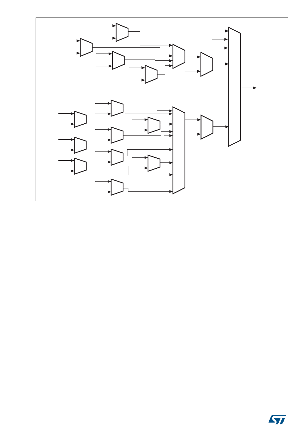
Ethernet (ETH): media access control (MAC) with DMA controller RM0090
1174/1718 DocID018909 Rev 9
Figure 384. Interrupt scheme
33.7 Ethernet interrupts
The Ethernet controller has two interrupt vectors: one dedicated to normal Ethernet
operations and the other, used only for the Ethernet wakeup event (with wakeup frame or
Magic Packet detection) when it is mapped on EXTI lIne19.
The first Ethernet vector is reserved for interrupts generated by the MAC and the DMA as
listed in the MAC interrupts and DMA interrupts sections.
The second vector is reserved for interrupts generated by the PMT on wakeup events. The
mapping of a wakeup event on EXTI line19 causes the STM32F4xx to exit the low-power
mode, and generates an interrupt.
When an Ethernet wakeup event mapped on EXTI Line19 occurs and the MAC PMT
interrupt is enabled and the EXTI Line19 interrupt, with detection on rising edge, is also
enabled, both interrupts are generated.
A watchdog timer (see ETH_DMARSWTR register) is given for flexible control of the RS bit
(ETH_DMASR register). When this watchdog timer is programmed with a non-zero value, it
gets activated as soon as the RxDMA completes a transfer of a received frame to system
memory without asserting the Receive Status because it is not enabled in the corresponding
Receive descriptor (RDES1[31]). When this timer runs out as per the programmed value,
the RS bit is set and the interrupt is asserted if the corresponding RIE is enabled in the
ETH_DMAIER register. This timer is disabled before it runs out, when a frame is transferred
to memory and the RS is set because it is enabled for that descriptor.
AND
AND
OR
OR
AND
NIS
NISE
AND
AIS
AISE
OR Interrupt
TS
TIE
FBES
FBEIE
AI15646
PMTI
TSTI
MMCI
AND
TBUS
TBUIE
AND
RS
RIE
AND
ERS
ERIE
AND
TPSS
TPSSIE AND
TJTS
TJTIE
AND
ROS
ROIE
AND
TUS
TUIE
AND
RBU
RBUIE AND
RPSS
RPSSIE
AND
RWTS
RWTIE
AND
ETS
ETIE

DocID018909 Rev 9 1175/1718
RM0090 Ethernet (ETH): media access control (MAC) with DMA controller
1224
Note: Reading the PMT control and status register automatically clears the Wakeup Frame
Received and Magic Packet Received PMT interrupt flags. However, since the registers for
these flags are in the CLK_RX domain, there may be a significant delay before this update
is visible by the firmware. The delay is especially long when the RX clock is slow (in 10 Mbit
mode) and when the AHB bus is high-frequency.
Since interrupt requests from the PMT to the CPU are based on the same registers in the
CLK_RX domain, the CPU may spuriously call the interrupt routine a second time even after
reading PMT_CSR. Thus, it may be necessary that the firmware polls the Wakeup Frame
Received and Magic Packet Received bits and exits the interrupt service routine only when
they are found to be at ‘0’.
33.8 Ethernet register descriptions
The peripheral registers can be accessed by bytes (8-bit), half-words (16-bit) or words (32-
bits).
33.8.1 MAC register description
Ethernet MAC configuration register (ETH_MACCR)
Address offset: 0x0000
Reset value: 0x0000 8000
The MAC configuration register is the operation mode register of the MAC. It establishes
receive and transmit operating modes.
313029282726252423222120191817161514131211109876543210
Reserved
CSTF
Reserved
WD
JD
Reserved
IFG
CSD
Reserved
FES
ROD
LM
DM
IPCO
RD
Reserved
APCS
BL
DC
TE
RE
Reserved
rw rw rw rw rw rw rw rw rw rw rw rw rw rw rw rw
Bits 31:26 Reserved, must be kept at reset value.
Bit 25
CSTF: CRC stripping for Type frames
When set, the last 4 bytes (FCS) of all frames of Ether type (type field greater than
0x0600) will be stripped and dropped before forwarding the frame to the application.
Bit 24Reserved, must be kept at reset value.
Bit 23 WD: Watchdog disable
When this bit is set, the MAC disables the watchdog timer on the receiver, and can receive
frames of up to 16 384 bytes.
When this bit is reset, the MAC allows no more than 2 048 bytes of the frame being received
and cuts off any bytes received after that.
Bit 22 JD: Jabber disable
When this bit is set, the MAC disables the jabber timer on the transmitter, and can transfer
frames of up to 16 384 bytes.
When this bit is reset, the MAC cuts off the transmitter if the application sends out more than
2 048 bytes of data during transmission.
Bits 21:20 Reserved, must be kept at reset value.

Ethernet (ETH): media access control (MAC) with DMA controller RM0090
1176/1718 DocID018909 Rev 9
Bits 19:17 IFG: Interframe gap
These bits control the minimum interframe gap between frames during transmission.
000: 96 bit times
001: 88 bit times
010: 80 bit times
….
111: 40 bit times
Note: In Half-duplex mode, the minimum IFG can be configured for 64 bit times (IFG = 100)
only. Lower values are not considered.
Bit 16 CSD: Carrier sense disable
When set high, this bit makes the MAC transmitter ignore the MII CRS signal during frame
transmission in Half-duplex mode. No error is generated due to Loss of Carrier or No Carrier
during such transmission.
When this bit is low, the MAC transmitter generates such errors due to Carrier Sense and
even aborts the transmissions.
Bit 15 Reserved, must be kept at reset value.
Bit 14 FES: Fast Ethernet speed
Indicates the speed in Fast Ethernet (MII) mode:
0: 10 Mbit/s
1: 100 Mbit/s
Bit 13 ROD: Receive own disable
When this bit is set, the MAC disables the reception of frames in Half-duplex mode.
When this bit is reset, the MAC receives all packets that are given by the PHY while
transmitting.
This bit is not applicable if the MAC is operating in Full-duplex mode.
Bit 12 LM: Loopback mode
When this bit is set, the MAC operates in loopback mode at the MII. The MII receive clock
input (RX_CLK) is required for the loopback to work properly, as the transmit clock is not
looped-back internally.
Bit 11 DM: Duplex mode
When this bit is set, the MAC operates in a Full-duplex mode where it can transmit and
receive simultaneously.
Bit 10 IPCO: IPv4 checksum offload
When set, this bit enables IPv4 checksum checking for received frame payloads'
TCP/UDP/ICMP headers. When this bit is reset, the checksum offload function in the
receiver is disabled and the corresponding PCE and IP HCE status bits (see Table 189 on
page 1130) are always cleared.
Bit 9 RD: Retry disable
When this bit is set, the MAC attempts only 1 transmission. When a collision occurs on the
MII, the MAC ignores the current frame transmission and reports a Frame Abort with
excessive collision error in the transmit frame status.
When this bit is reset, the MAC attempts retries based on the settings of BL.
Note: This bit is applicable only in the Half-duplex mode.
Bit 8 Reserved, must be kept at reset value.

DocID018909 Rev 9 1177/1718
RM0090 Ethernet (ETH): media access control (MAC) with DMA controller
1224
Bit 7 APCS: Automatic pad/CRC stripping
When this bit is set, the MAC strips the Pad/FCS field on incoming frames only if the
length’s field value is less than or equal to 1 500 bytes. All received frames with length field
greater than or equal to 1 501 bytes are passed on to the application without stripping the
Pad/FCS field.
When this bit is reset, the MAC passes all incoming frames unmodified.
Bits 6:5 BL: Back-off limit
The Back-off limit determines the random integer number (r) of slot time delays (4 096 bit
times for 1000 Mbit/s and 512 bit times for 10/100 Mbit/s) the MAC waits before
rescheduling a transmission attempt during retries after a collision.
Note: This bit is applicable only to Half-duplex mode.
00: k = min (n, 10)
01: k = min (n, 8)
10: k = min (n, 4)
11: k = min (n, 1),
where n = retransmission attempt. The random integer r takes the value in the range 0 ≤ r <
2k
Bit 4 DC: Deferral check
When this bit is set, the deferral check function is enabled in the MAC. The MAC issues a
Frame Abort status, along with the excessive deferral error bit set in the transmit frame
status when the transmit state machine is deferred for more than 24 288 bit times in 10/100-
Mbit/s mode. Deferral begins when the transmitter is ready to transmit, but is prevented
because of an active CRS (carrier sense) signal on the MII. Defer time is not cumulative. If
the transmitter defers for 10 000 bit times, then transmits, collides, backs off, and then has
to defer again after completion of back-off, the deferral timer resets to 0 and restarts.
When this bit is reset, the deferral check function is disabled and the MAC defers until the
CRS signal goes inactive. This bit is applicable only in Half-duplex mode.
Bit 3 TE: Transmitter enable
When this bit is set, the transmit state machine of the MAC is enabled for transmission on
the MII. When this bit is reset, the MAC transmit state machine is disabled after the
completion of the transmission of the current frame, and does not transmit any further
frames.
Bit 2 RE: Receiver enable
When this bit is set, the receiver state machine of the MAC is enabled for receiving frames
from the MII. When this bit is reset, the MAC receive state machine is disabled after the
completion of the reception of the current frame, and will not receive any further frames from
the MII.
Bits 1:0 Reserved, must be kept at reset value.

Ethernet (ETH): media access control (MAC) with DMA controller RM0090
1178/1718 DocID018909 Rev 9
Ethernet MAC frame filter register (ETH_MACFFR)
Address offset: 0x0004
Reset value: 0x0000 0000
The MAC frame filter register contains the filter controls for receiving frames. Some of the
controls from this register go to the address check block of the MAC, which performs the
first level of address filtering. The second level of filtering is performed on the incoming
frame, based on other controls such as pass bad frames and pass control frames.
313029282726252423222120191817161514131211109876543210
RA Reserved
HPF
SAF
SAIF
PCF
BFD
PAM
DAIF
HM
HU
PM
rw rw rw rw rw rw rw rw rw rw rw rw
Bit 31 RA: Receive all
When this bit is set, the MAC receiver passes all received frames on to the application,
irrespective of whether they have passed the address filter. The result of the SA/DA filtering
is updated (pass or fail) in the corresponding bits in the receive status word. When this bit is
reset, the MAC receiver passes on to the application only those frames that have passed the
SA/DA address filter.
Bits 30:11 Reserved, must be kept at reset value.
Bit 10 HPF: Hash or perfect filter
When this bit is set and if the HM or HU bit is set, the address filter passes frames that
match either the perfect filtering or the hash filtering.
When this bit is cleared and if the HU or HM bit is set, only frames that match the Hash filter
are passed.
Bit 9 SAF: Source address filter
The MAC core compares the SA field of the received frames with the values programmed in
the enabled SA registers. If the comparison matches, then the SAMatch bit in the RxStatus
word is set high. When this bit is set high and the SA filter fails, the MAC drops the frame.
When this bit is reset, the MAC core forwards the received frame to the application. It also
forwards the updated SA Match bit in RxStatus depending on the SA address comparison.
Bit 8 SAIF: Source address inverse filtering
When this bit is set, the address check block operates in inverse filtering mode for the SA
address comparison. The frames whose SA matches the SA registers are marked as failing
the SA address filter.
When this bit is reset, frames whose SA does not match the SA registers are marked as
failing the SA address filter.

DocID018909 Rev 9 1179/1718
RM0090 Ethernet (ETH): media access control (MAC) with DMA controller
1224
Ethernet MAC hash table high register (ETH_MACHTHR)
Address offset: 0x0008
Reset value: 0x0000 0000
The 64-bit Hash table is used for group address filtering. For hash filtering, the contents of
the destination address in the incoming frame are passed through the CRC logic, and the
upper 6 bits in the CRC register are used to index the contents of the Hash table. This CRC
is a 32-bit value coded by the following polynomial (for more details refer to Section 33.5.3:
Bits 7:6 PCF: Pass control frames
These bits control the forwarding of all control frames (including unicast and multicast
PAUSE frames). Note that the processing of PAUSE control frames depends only on RFCE
in Flow Control Register[2].
00: MAC prevents all control frames from reaching the application
01: MAC forwards all control frames to application except Pause control frames
10: MAC forwards all control frames to application even if they fail the address filter
11: MAC forwards control frames that pass the address filter.
These bits control the forwarding of all control frames (including unicast and multicast
PAUSE frames). Note that the processing of PAUSE control frames depends only on RFCE
in Flow Control Register[2].
00 or 01: MAC prevents all control frames from reaching the application
10: MAC forwards all control frames to application even if they fail the address filter
11: MAC forwards control frames that pass the address filter.
Bit 5 BFD: Broadcast frames disable
When this bit is set, the address filters filter all incoming broadcast frames.
When this bit is reset, the address filters pass all received broadcast frames.
Bit 4 PAM: Pass all multicast
When set, this bit indicates that all received frames with a multicast destination address (first
bit in the destination address field is '1') are passed.
When reset, filtering of multicast frame depends on the HM bit.
Bit 3 DAIF: Destination address inverse filtering
When this bit is set, the address check block operates in inverse filtering mode for the DA
address comparison for both unicast and multicast frames.
When reset, normal filtering of frames is performed.
Bit 2 HM: Hash multicast
When set, MAC performs destination address filtering of received multicast frames
according to the hash table.
When reset, the MAC performs a perfect destination address filtering for multicast frames,
that is, it compares the DA field with the values programmed in DA registers.
Bit 1 HU: Hash unicast
When set, MAC performs destination address filtering of unicast frames according to the
hash table.
When reset, the MAC performs a perfect destination address filtering for unicast frames, that
is, it compares the DA field with the values programmed in DA registers.
Bit 0 PM: Promiscuous mode
When this bit is set, the address filters pass all incoming frames regardless of their
destination or source address. The SA/DA filter fails status bits in the receive status word
are always cleared when PM is set.
Ethernet (ETH): media access control (MAC) with DMA controller RM0090
1180/1718 DocID018909 Rev 9
MAC frame reception):
The most significant bit determines the register to be used (hash table high/hash table low),
and the other 5 bits determine which bit within the register. A hash value of 0b0 0000 selects
bit 0 in the selected register, and a value of 0b1 1111 selects bit 31 in the selected register.
For example, if the DA of the incoming frame is received as 0x1F52 419C B6AF (0x1F is the
first byte received on the MII interface), then the internally calculated 6-bit Hash value is
0x2C and the HTH register bit[12] is checked for filtering. If the DA of the incoming frame is
received as 0xA00A 9800 0045, then the calculated 6-bit Hash value is 0x07 and the HTL
register bit[7] is checked for filtering.
If the corresponding bit value in the register is 1, the frame is accepted. Otherwise, it is
rejected. If the PAM (pass all multicast) bit is set in the ETH_MACFFR register, then all
multicast frames are accepted regardless of the multicast hash values.
The Hash table high register contains the higher 32 bits of the multicast Hash table.
Ethernet MAC hash table low register (ETH_MACHTLR)
Address offset: 0x000C
Reset value: 0x0000 0000
The Hash table low register contains the lower 32 bits of the multi-cast Hash table.
Ethernet MAC MII address register (ETH_MACMIIAR)
Address offset: 0x0010
Reset value: 0x0000 0000
The MII address register controls the management cycles to the external PHY through the
management interface.
Gx() x32 x26 x23 x22 x16 x12 x11 x10 x8x7x5x4x2x1+ + + + + + + +++++++=
313029282726252423222120191817161514131211109876543210
HTH
rw rw rw rw rw rw rw rw rw rw rw rw rw rw rw rw rw rw rw rw rw rw rw rw rw rw rw rw rw rw rw rw
Bits 31:0 HTH: Hash table high
This field contains the upper 32 bits of Hash table.
313029282726252423222120191817161514131211109876543210
HTL
rw rw rw rw rw rw rw rw rw rw rw rw rw rw rw rw rw rw rw rw rw rw rw rw rw rw rw rw rw rw rw rw
Bits 31:0 HTL: Hash table low
This field contains the lower 32 bits of the Hash table.
3130292827262524232221201918171615141312111098765432 1 0
Reserved
PA MR
Reserved
CR MW MB
rw rw rw rw rw rw rw rw rw rw rw rw rw rw rc_
w1

DocID018909 Rev 9 1181/1718
RM0090 Ethernet (ETH): media access control (MAC) with DMA controller
1224
Ethernet MAC MII data register (ETH_MACMIIDR)
Address offset: 0x0014
Reset value: 0x0000 0000
The MAC MII Data register stores write data to be written to the PHY register located at the
address specified in ETH_MACMIIAR. ETH_MACMIIDR also stores read data from the PHY
register located at the address specified by ETH_MACMIIAR.
Bits 31:16 Reserved, must be kept at reset value.
Bits 15:11 PA: PHY address
This field tells which of the 32 possible PHY devices are being accessed.
Bits 10:6 MR: MII register
These bits select the desired MII register in the selected PHY device.
Bit 5 Reserved, must be kept at reset value.
Bits 4:2 CR: Clock range
The CR clock range selection determines the HCLK frequency and is used to decide the
frequency of the MDC clock:
Selection HCLK MDC Clock
000 60-100 MHz HCLK/42
001 100-150 MHzHCLK/62
010 20-35 MHz HCLK/16
011 35-60 MHz HCLK/26
100 150-168 MHz HCLK/102
101, 110, 111 Reserved -
Bit 1 MW: MII write
When set, this bit tells the PHY that this will be a Write operation using the MII Data register. If
this bit is not set, this will be a Read operation, placing the data in the MII Data register.
Bit 0 MB: MII busy
This bit should read a logic 0 before writing to ETH_MACMIIAR and ETH_MACMIIDR. This
bit must also be reset to 0 during a Write to ETH_MACMIIAR. During a PHY register access,
this bit is set to 0b1 by the application to indicate that a read or write access is in progress.
ETH_MACMIIDR (MII Data) should be kept valid until this bit is cleared by the MAC during a
PHY Write operation. The ETH_MACMIIDR is invalid until this bit is cleared by the MAC
during a PHY Read operation. The ETH_MACMIIAR (MII Address) should not be written to
until this bit is cleared.
3130292827262524232221201918171615141312111098765432 1 0
Reserved
MD
rw rw rw rw rw rw rw rw rw rw rw rw rw rw rw rw
Bits 31:16 Reserved, must be kept at reset value.
Bits 15:0 MD: MII data
This contains the 16-bit data value read from the PHY after a Management Read operation,
or the 16-bit data value to be written to the PHY before a Management Write operation.

Ethernet (ETH): media access control (MAC) with DMA controller RM0090
1182/1718 DocID018909 Rev 9
Ethernet MAC flow control register (ETH_MACFCR)
Address offset: 0x0018
Reset value: 0x0000 0000
The Flow control register controls the generation and reception of the control (Pause
Command) frames by the MAC. A write to a register with the Busy bit set to '1' causes the
MAC to generate a pause control frame. The fields of the control frame are selected as
specified in the 802.3x specification, and the Pause Time value from this register is used in
the Pause Time field of the control frame. The Busy bit remains set until the control frame is
transferred onto the cable. The Host must make sure that the Busy bit is cleared before
writing to the register.
31 30 29 28 27 26 25 24 23 22 21 20 19 18 17 16 15 14 13 12 11 10 9 8 7 6 5 4 3 2 1 0
PT
Reserved
ZQPD
Reserved
PLT
UPFD
RFCE
TFCE
FCB/
BPA
rw rw rw rw rw rw rw rw rw rw rw rw rw rw rw rw rw rw rw rw rw rw rc_w1
/rw
Bits 31:16 PT: Pause time
This field holds the value to be used in the Pause Time field in the transmit control frame. If
the Pause Time bits is configured to be double-synchronized to the MII clock domain, then
consecutive write operations to this register should be performed only after at least 4 clock
cycles in the destination clock domain.
Bits 15:8 Reserved, must be kept at reset value.
Bit 7 ZQPD: Zero-quanta pause disable
When set, this bit disables the automatic generation of Zero-quanta pause control frames on
the deassertion of the flow-control signal from the FIFO layer.
When this bit is reset, normal operation with automatic Zero-quanta pause control frame
generation is enabled.
Bit 6 Reserved, must be kept at reset value.
Bits 5:4 PLT: Pause low threshold
This field configures the threshold of the Pause timer at which the Pause frame is
automatically retransmitted. The threshold values should always be less than the Pause
Time configured in bits[31:16]. For example, if PT = 100H (256 slot-times), and PLT = 01,
then a second PAUSE frame is automatically transmitted if initiated at 228 (256 – 28) slot-
times after the first PAUSE frame is transmitted.
Selection Threshold
00 Pause time minus 4 slot times
01 Pause time minus 28 slot times
10 Pause time minus 144 slot times
11 Pause time minus 256 slot times
Slot time is defined as time taken to transmit 512 bits (64 bytes) on the MII interface.
Bit 3 UPFD: Unicast pause frame detect
When this bit is set, the MAC detects the Pause frames with the station’s unicast address
specified in the ETH_MACA0HR and ETH_MACA0LR registers, in addition to detecting
Pause frames with the unique multicast address.
When this bit is reset, the MAC detects only a Pause frame with the unique multicast
address specified in the 802.3x standard.

DocID018909 Rev 9 1183/1718
RM0090 Ethernet (ETH): media access control (MAC) with DMA controller
1224
Ethernet MAC VLAN tag register (ETH_MACVLANTR)
Address offset: 0x001C
Reset value: 0x0000 0000
The VLAN tag register contains the IEEE 802.1Q VLAN Tag to identify the VLAN frames.
The MAC compares the 13th and 14th bytes of the receiving frame (Length/Type) with
0x8100, and the following 2 bytes are compared with the VLAN tag; if a match occurs, the
received VLAN bit in the receive frame status is set. The legal length of the frame is
increased from 1518 bytes to 1522 bytes.
Bit 2 RFCE: Receive flow control enable
When this bit is set, the MAC decodes the received Pause frame and disables its transmitter
for a specified (Pause Time) time.
When this bit is reset, the decode function of the Pause frame is disabled.
Bit 1 TFCE: Transmit flow control enable
In Full-duplex mode, when this bit is set, the MAC enables the flow control operation to
transmit Pause frames. When this bit is reset, the flow control operation in the MAC is
disabled, and the MAC does not transmit any Pause frames.
In Half-duplex mode, when this bit is set, the MAC enables the back-pressure operation.
When this bit is reset, the back pressure feature is disabled.
Bit 0 FCB/BPA: Flow control busy/back pressure activate
This bit initiates a Pause Control frame in Full-duplex mode and activates the back pressure
function in Half-duplex mode if TFCE bit is set.
In Full-duplex mode, this bit should be read as 0 before writing to the Flow control register.
To initiate a Pause control frame, the Application must set this bit to 1. During a transfer of
the Control frame, this bit continues to be set to signify that a frame transmission is in
progress. After completion of the Pause control frame transmission, the MAC resets this bit
to 0. The Flow control register should not be written to until this bit is cleared.
In Half-duplex mode, when this bit is set (and TFCE is set), back pressure is asserted by the
MAC core. During back pressure, when the MAC receives a new frame, the transmitter
starts sending a JAM pattern resulting in a collision. When the MAC is configured to Full-
duplex mode, the BPA is automatically disabled.
31 30 29 28 27 26 25 24 23 22 21 20 19 18 17 16 15 14 13 12 11 10 9 8 7 6 5 4 3 2 1 0
Reserved
VLANTC
VLANTI
rw rw rw rw rw rw rw rw rw rw rw rw rw rw rw rw rw

Ethernet (ETH): media access control (MAC) with DMA controller RM0090
1184/1718 DocID018909 Rev 9
Ethernet MAC remote wakeup frame filter register (ETH_MACRWUFFR)
Address offset: 0x0028
Reset value: 0x0000 0000
This is the address through which the remote wakeup frame filter registers are written/read
by the application. The Wakeup frame filter register is actually a pointer to eight (not
transparent) such wakeup frame filter registers. Eight sequential write operations to this
address with the offset (0x0028) will write all wakeup frame filter registers. Eight sequential
read operations from this address with the offset (0x0028) will read all wakeup frame filter
registers. This register contains the higher 16 bits of the 7th MAC address. Refer to Remote
wakeup frame filter register section for additional information.
Figure 385. Ethernet MAC remote wakeup frame filter register (ETH_MACRWUFFR)
Bits 31:17 Reserved, must be kept at reset value.
Bit 16 VLANTC: 12-bit VLAN tag comparison
When this bit is set, a 12-bit VLAN identifier, rather than the complete 16-bit VLAN tag, is
used for comparison and filtering. Bits[11:0] of the VLAN tag are compared with the
corresponding field in the received VLAN-tagged frame.
When this bit is reset, all 16 bits of the received VLAN frame’s fifteenth and sixteenth bytes
are used for comparison.
Bits 15:0 VLANTI: VLAN tag identifier (for receive frames)
This contains the 802.1Q VLAN tag to identify VLAN frames, and is compared to the fifteenth
and sixteenth bytes of the frames being received for VLAN frames. Bits[15:13] are the user
priority, Bit[12] is the canonical format indicator (CFI) and bits[11:0] are the VLAN tag’s VLAN
identifier (VID) field. When the VLANTC bit is set, only the VID (bits[11:0]) is used for
comparison.
If VLANTI (VLANTI[11:0] if VLANTC is set) is all zeros, the MAC does not check the fifteenth
and sixteenth bytes for VLAN tag comparison, and declares all frames with a Type field value
of 0x8100 as VLAN frames.
Filter 0 Byte Mask
Filter 1 Byte Mask
Filter 2 Byte Mask
Filter 3 Byte Mask
RSVD
Filter 3
Command
RSVD
Filter 2
Command
RSVD
Filter 1
Command
RSVD
Filter 0
Command
Filter 3 Offset Filter 2 Offset Filter 1 Offset Filter 0 Offset
Filter 1 CRC - 16 Filter 0 CRC - 16
Filter 3 CRC - 16 Filter 2 CRC - 16
Wakeup frame filter reg0
Wakeup frame filter reg1
Wakeup frame filter reg2
Wakeup frame filter reg3
Wakeup frame filter reg4
Wakeup frame filter reg5
Wakeup frame filter reg6
Wakeup frame filter reg7
ai15648

DocID018909 Rev 9 1185/1718
RM0090 Ethernet (ETH): media access control (MAC) with DMA controller
1224
Ethernet MAC PMT control and status register (ETH_MACPMTCSR)
Address offset: 0x002C
Reset value: 0x0000 0000
The ETH_MACPMTCSR programs the request wakeup events and monitors the wakeup
events.
31 30 29 28 27 26 25 24 23 22 21 20 19 18 17 16 15 14 13 12 11 10 9 8 7 6 5 4 3 2 1 0
WFFRPR
Reserved
GU
Reserved
WFR
MPR
Reserved
WFE
MPE
PD
rs Res. rw rc_r rc_r rw rw rs
Bit 31 WFFRPR: Wakeup frame filter register pointer reset
When set, it resets the Remote wakeup frame filter register pointer to 0b000. It is
automatically cleared after 1 clock cycle.
Bits 30:10 Reserved, must be kept at reset value.
Bit 9 GU: Global unicast
When set, it enables any unicast packet filtered by the MAC (DAF) address recognition to be
a wakeup frame.
Bits 8:7 Reserved, must be kept at reset value.
Bit 6 WFR: Wakeup frame received
When set, this bit indicates the power management event was generated due to reception of
a wakeup frame. This bit is cleared by a read into this register.
Bit 5 MPR: Magic packet received
When set, this bit indicates the power management event was generated by the reception of
a Magic Packet. This bit is cleared by a read into this register.
Bits 4:3 Reserved, must be kept at reset value.
Bit 2 WFE: Wakeup frame enable
When set, this bit enables the generation of a power management event due to wakeup
frame reception.
Bit 1 MPE: Magic Packet enable
When set, this bit enables the generation of a power management event due to Magic
Packet reception.
Bit 0 PD: Power down
When this bit is set, all received frames will be dropped. This bit is cleared automatically
when a magic packet or wakeup frame is received, and Power-down mode is disabled.
Frames received after this bit is cleared are forwarded to the application. This bit must only
be set when either the Magic Packet Enable or Wakeup Frame Enable bit is set high.

Ethernet (ETH): media access control (MAC) with DMA controller RM0090
1186/1718 DocID018909 Rev 9
Ethernet MAC debug register (ETH_MACDBGR)
Address offset: 0x0034
Reset value: 0x0000 0000
This debug register gives the status of all the main modules of the transmit and receive data
paths and the FIFOs. An all-zero status indicates that the MAC core is in Idle state (and
FIFOs are empty) and no activity is going on in the data paths.
31 30 29 28 27 26 25 24 23 22 21 20 19 18 17 16 15 14 13 12 11 10 9 8 7 6 5 4 3 2 1 0
Reserved
TFF
TFNE
Reserved
TFWA
TFRS
MTP
MTFCS
MMTEA
Reserved
RFFL
Reserved
RFRCS
RFWRA
Reserved
MSFRWCS
MMRPEA
ro ro ro ro ro ro ro ro ro ro ro ro ro ro ro ro ro
Bits 31:26 Reserved, must be kept at reset value.
Bit 25 TFF: Tx FIFO full
When high, it indicates that the Tx FIFO is full and hence no more frames will be accepted
for transmission.
Bit 24 TFNE: Tx FIFO not empty
When high, it indicates that the TxFIFO is not empty and has some data left for
transmission.
Bit 23 Reserved, must be kept at reset value.
Bit 22 TFWA: Tx FIFO write active
When high, it indicates that the TxFIFO write controller is active and transferring data to the
TxFIFO.
Bits 21:20 TFRS: Tx FIFO read status
This indicates the state of the TxFIFO read controller:
00: Idle state
01: Read state (transferring data to the MAC transmitter)
10: Waiting for TxStatus from MAC transmitter
11: Writing the received TxStatus or flushing the TxFIFO
Bit 19 MTP: MAC transmitter in pause
When high, it indicates that the MAC transmitter is in Pause condition (in full-duplex mode
only) and hence will not schedule any frame for transmission
Bits 18:17 MTFCS: MAC transmit frame controller status
This indicates the state of the MAC transmit frame controller:
00: Idle
01: Waiting for Status of previous frame or IFG/backoff period to be over
10: Generating and transmitting a Pause control frame (in full duplex mode)
11: Transferring input frame for transmission
Bit 16 MMTEA: MAC MII transmit engine active
When high, it indicates that the MAC MII transmit engine is actively transmitting data and
that it is not in the Idle state.
Bits 15:10 Reserved, must be kept at reset value.

DocID018909 Rev 9 1187/1718
RM0090 Ethernet (ETH): media access control (MAC) with DMA controller
1224
Bits 9:8 RFFL: Rx FIFO fill level
This gives the status of the Rx FIFO fill-level:
00: RxFIFO empty
01: RxFIFO fill-level below flow-control de-activate threshold
10: RxFIFO fill-level above flow-control activate threshold
11: RxFIFO full
Bit 7 Reserved, must be kept at reset value.
Bits 6:5 RFRCS: Rx FIFO read controller status
It gives the state of the Rx FIFO read controller:
00: IDLE state
01: Reading frame data
10: Reading frame status (or time-stamp)
11: Flushing the frame data and status
Bit 4 RFWRA: Rx FIFO write controller active
When high, it indicates that the Rx FIFO write controller is active and transferring a received
frame to the FIFO.
Bit 3 Reserved, must be kept at reset value.
Bits 2:1 MSFRWCS: MAC small FIFO read / write controllers status
When high, these bits indicate the respective active state of the small FIFO read and write
controllers of the MAC receive frame controller module.
Bit 0 MMRPEA: MAC MII receive protocol engine active
When high, it indicates that the MAC MII receive protocol engine is actively receiving data
and is not in the Idle state.

Ethernet (ETH): media access control (MAC) with DMA controller RM0090
1188/1718 DocID018909 Rev 9
Ethernet MAC interrupt status register (ETH_MACSR)
Address offset: 0x0038
Reset value: 0x0000 0000
The ETH_MACSR register contents identify the events in the MAC that can generate an
interrupt.
15 14 13 12 11 10 9 8 7 6 5 4 3 2 1 0
Reserved
TSTS
Reserved
MMCTS MMCRS MMCS PMTS
Reserved
rc_r rrrr
Bits 15:10 Reserved, must be kept at reset value.
Bit 9 TSTS: Time stamp trigger status
This bit is set high when the system time value equals or exceeds the value specified in the
Target time high and low registers. This bit is cleared by reading the ETH_PTPTSSR
register.
Bits 8:7 Reserved, must be kept at reset value.
Bit 6 MMCTS: MMC transmit status
This bit is set high whenever an interrupt is generated in the ETH_MMCTIR Register. This bit
is cleared when all the bits in this interrupt register (ETH_MMCTIR) are cleared.
Bit 5 MMCRS: MMC receive status
This bit is set high whenever an interrupt is generated in the ETH_MMCRIR register. This bit
is cleared when all the bits in this interrupt register (ETH_MMCRIR) are cleared.
Bit 4 MMCS: MMC status
This bit is set high whenever any of bits 6:5 is set high. It is cleared only when both bits are
low.
Bit 3 PMTS: PMT status
This bit is set whenever a Magic packet or Wake-on-LAN frame is received in Power-down
mode (See bits 5 and 6 in the ETH_MACPMTCSR register Ethernet MAC PMT control and
status register (ETH_MACPMTCSR) on page 1185). This bit is cleared when both bits[6:5],
of this last register, are cleared due to a read operation to the ETH_MACPMTCSR register.
Bits 2:0 Reserved, must be kept at reset value.
DocID018909 Rev 9 1189/1718
RM0090 Ethernet (ETH): media access control (MAC) with DMA controller
1224
Ethernet MAC interrupt mask register (ETH_MACIMR)
Address offset: 0x003C
Reset value: 0x0000 0000
The ETH_MACIMR register bits make it possible to mask the interrupt signal due to the
corresponding event in the ETH_MACSR register.
Ethernet MAC address 0 high register (ETH_MACA0HR)
Address offset: 0x0040
Reset value: 0x8000 FFFF
The MAC address 0 high register holds the upper 16 bits of the 6-byte first MAC address of
the station. Note that the first DA byte that is received on the MII interface corresponds to
the LS Byte (bits [7:0]) of the MAC address low register. For example, if 0x1122 3344 5566
is received (0x11 is the first byte) on the MII as the destination address, then the MAC
address 0 register [47:0] is compared with 0x6655 4433 2211.
15 14 13 12 11 10 9 8 7 6 5 4 3 2 1 0
Reserved
TSTIM
Reserved
PMTIM
Reserved
rw rw
Bits 15:10 Reserved, must be kept at reset value.
Bit 9 TSTIM: Time stamp trigger interrupt mask
When set, this bit disables the time stamp interrupt generation.
Bits 8:4 Reserved, must be kept at reset value.
Bit 3 PMTIM: PMT interrupt mask
When set, this bit disables the assertion of the interrupt signal due to the setting of the PMT
Status bit in ETH_MACSR.
Bits 2:0 Reserved, must be kept at reset value.
313029282726252423222120191817161514131211109876543210
MO
Reserved
MACA0H
1rw rw rw rw rw rw rw rw rw rw rw rw rw rw rw rw
Bit 31 MO: Always 1.
Bits 30:16 Reserved, must be kept at reset value.
Bits 15:0 MACA0H: MAC address0 high [47:32]
This field contains the upper 16 bits (47:32) of the 6-byte MAC address0. This is used by the
MAC for filtering for received frames and for inserting the MAC address in the transmit flow
control (Pause) frames.
Ethernet (ETH): media access control (MAC) with DMA controller RM0090
1190/1718 DocID018909 Rev 9
Ethernet MAC address 0 low register (ETH_MACA0LR)
Address offset: 0x0044
Reset value: 0xFFFF FFFF
The MAC address 0 low register holds the lower 32 bits of the 6-byte first MAC address of
the station.
Ethernet MAC address 1 high register (ETH_MACA1HR)
Address offset: 0x0048
Reset value: 0x0000 FFFF
The MAC address 1 high register holds the upper 16 bits of the 6-byte second MAC address
of the station.
313029282726252423222120191817161514131211109876543210
MACA0L
rw rw rw rw rw rw rw rw rw rw rw rw rw rw rw rw rw rw rw rw rw rw rw rw rw rw rw rw rw rw rw rw
Bits 31:0 MACA0L: MAC address0 low [31:0]
This field contains the lower 32 bits of the 6-byte MAC address0. This is used by the MAC
for filtering for received frames and for inserting the MAC address in the transmit flow control
(Pause) frames.
313029282726252423222120191817161514131211109876543210
AE SA MBC Reserved MACA1H
rw rw rw rw rw rw rw rw rw rw rw rw rw rw rw rw rw rw rw rw rw rw rw rw
Bit 31 AE: Address enable
When this bit is set, the address filters use the MAC address1 for perfect filtering. When this
bit is cleared, the address filters ignore the address for filtering.
Bit 30 SA: Source address
When this bit is set, the MAC address1[47:0] is used for comparison with the SA fields of the
received frame.
When this bit is cleared, the MAC address1[47:0] is used for comparison with the DA fields
of the received frame.

DocID018909 Rev 9 1191/1718
RM0090 Ethernet (ETH): media access control (MAC) with DMA controller
1224
Ethernet MAC address1 low register (ETH_MACA1LR)
Address offset: 0x004C
Reset value: 0xFFFF FFFF
The MAC address 1 low register holds the lower 32 bits of the 6-byte second MAC address
of the station.
Ethernet MAC address 2 high register (ETH_MACA2HR)
Address offset: 0x0050
Reset value: 0x0000 FFFF
The MAC address 2 high register holds the upper 16 bits of the 6-byte second MAC address
of the station.
Bits 29:24 MBC: Mask byte control
These bits are mask control bits for comparison of each of the MAC address1 bytes. When
they are set high, the MAC core does not compare the corresponding byte of received
DA/SA with the contents of the MAC address1 registers. Each bit controls the masking of the
bytes as follows:
– Bit 29: ETH_MACA1HR [15:8]
– Bit 28: ETH_MACA1HR [7:0]
– Bit 27: ETH_MACA1LR [31:24]
…
– Bit 24: ETH_MACA1LR [7:0]
Bits 23:16 Reserved, must be kept at reset value.
Bits 15:0 MACA1H: MAC address1 high [47:32]
This field contains the upper 16 bits (47:32) of the 6-byte second MAC address.
313029282726252423222120191817161514131211109876543210
MACA1L
rw rw rw rw rw rw rw rw rw rw rw rw rw rw rw rw rw rw rw rw rw rw rw rw rw rw rw rw rw rw rw rw
Bits 31:0 MACA1L: MAC address1 low [31:0]
This field contains the lower 32 bits of the 6-byte MAC address1. The content of this field is
undefined until loaded by the application after the initialization process.
313029282726252423222120191817161514131211109876543210
AE SA MBC
Reserved
MACA2H
rw rw rw rw rw rw rw rw rw rw rw rw rw rw rw rw rw rw rw rw rw rw rw rw

Ethernet (ETH): media access control (MAC) with DMA controller RM0090
1192/1718 DocID018909 Rev 9
Ethernet MAC address 2 low register (ETH_MACA2LR)
Address offset: 0x0054
Reset value: 0xFFFF FFFF
The MAC address 2 low register holds the lower 32 bits of the 6-byte second MAC address
of the station.
Bit 31 AE: Address enable
When this bit is set, the address filters use the MAC address2 for perfect filtering. When
reset, the address filters ignore the address for filtering.
Bit 30 SA: Source address
When this bit is set, the MAC address 2 [47:0] is used for comparison with the SA fields of
the received frame.
When this bit is reset, the MAC address 2 [47:0] is used for comparison with the DA fields of
the received frame.
Bits 29:24 MBC: Mask byte control
These bits are mask control bits for comparison of each of the MAC address2 bytes. When
set high, the MAC core does not compare the corresponding byte of received DA/SA with the
contents of the MAC address 2 registers. Each bit controls the masking of the bytes as
follows:
– Bit 29: ETH_MACA2HR [15:8]
– Bit 28: ETH_MACA2HR [7:0]
– Bit 27: ETH_MACA2LR [31:24]
…
– Bit 24: ETH_MACA2LR [7:0]
Bits 23:16Reserved, must be kept at reset value.
Bits 15:0MACA2H: MAC address2 high [47:32]
This field contains the upper 16 bits (47:32) of the 6-byte MAC address2.
313029282726252423222120191817161514131211109876543210
MACA2L
rw rw rw rw rw rw rw rw rw rw rw rw rw rw rw rw rw rw rw rw rw rw rw rw rw rw rw rw rw rw rw rw
Bits 31:0 MACA2L: MAC address2 low [31:0]
This field contains the lower 32 bits of the 6-byte second MAC address2. The content of this
field is undefined until loaded by the application after the initialization process.

DocID018909 Rev 9 1193/1718
RM0090 Ethernet (ETH): media access control (MAC) with DMA controller
1224
Ethernet MAC address 3 high register (ETH_MACA3HR)
Address offset: 0x0058
Reset value: 0x0000 FFFF
The MAC address 3 high register holds the upper 16 bits of the 6-byte second MAC address
of the station.
Ethernet MAC address 3 low register (ETH_MACA3LR)
Address offset: 0x005C
Reset value: 0xFFFF FFFF
The MAC address 3 low register holds the lower 32 bits of the 6-byte second MAC address
of the station.
313029282726252423222120191817161514131211109876543210
AE SA MBC
Reserved
MACA3H
rw rw rw rw rw rw rw rw rw rw rw rw rw rw rw rw rw rw rw rw rw rw rw rw
Bit 31 AE: Address enable
When this bit is set, the address filters use the MAC address3 for perfect filtering. When this
bit is cleared, the address filters ignore the address for filtering.
Bit 30 SA: Source address
When this bit is set, the MAC address 3 [47:0] is used for comparison with the SA fields of the
received frame.
When this bit is cleared, the MAC address 3[47:0] is used for comparison with the DA fields
of the received frame.
Bits 29:24 MBC: Mask byte control
These bits are mask control bits for comparison of each of the MAC address3 bytes. When
these bits are set high, the MAC core does not compare the corresponding byte of received
DA/SA with the contents of the MAC address 3 registers. Each bit controls the masking of the
bytes as follows:
– Bit 29: ETH_MACA3HR [15:8]
– Bit 28: ETH_MACA3HR [7:0]
– Bit 27: ETH_MACA3LR [31:24]
…
– Bit 24: ETH_MACA3LR [7:0]
Bits 23:16 Reserved, must be kept at reset value.
Bits 15:0 MACA3H: MAC address3 high [47:32]
This field contains the upper 16 bits (47:32) of the 6-byte MAC address3.
313029282726252423222120191817161514131211109876543210
MACA3L
rw rw rw rw rw rw rw rw rw rw rw rw rw rw rw rw rw rw rw rw rw rw rw rw rw rw rw rw rw rw rw rw
Bits 31:0 MACA3L: MAC address3 low [31:0]
This field contains the lower 32 bits of the 6-byte second MAC address3. The content of this
field is undefined until loaded by the application after the initialization process.

Ethernet (ETH): media access control (MAC) with DMA controller RM0090
1194/1718 DocID018909 Rev 9
33.8.2 MMC register description
Ethernet MMC control register (ETH_MMCCR)
Address offset: 0x0100
Reset value: 0x0000 0000
The Ethernet MMC Control register establishes the operating mode of the management
counters.
Ethernet MMC receive interrupt register (ETH_MMCRIR)
Address offset: 0x0104
Reset value: 0x0000 0000
The Ethernet MMC receive interrupt register maintains the interrupts generated when
receive statistic counters reach half their maximum values. (MSB of the counter is set.) It is
a 32-bit wide register. An interrupt bit is cleared when the respective MMC counter that
313029282726252423222120191817161514131211109876543210
Reserved
MCFHP
MCP
MCF
ROR
CSR
CR
rw rw rw rw rw rw
Bits 31:6 Reserved, must be kept at reset value.
Bit 5
MCFHP: MMC counter Full-Half preset
When MCFHP is low and bit4 is set, all MMC counters get preset to almost-half value. All
frame-counters get preset to 0x7FFF_FFF0 (half - 16)
When MCFHP is high and bit4 is set, all MMC counters get preset to almost-full value. All
frame-counters get preset to 0xFFFF_FFF0 (full - 16)
Bit 4
MCP: MMC counter preset
When set, all counters will be initialized or preset to almost full or almost half as per
Bit5 above. This bit will be cleared automatically after 1 clock cycle. This bit along
with bit5 is useful for debugging and testing the assertion of interrupts due to MMC
counter becoming half-full or full.
Bit 3 MCF: MMC counter freeze
When set, this bit freezes all the MMC counters to their current value. (None of the MMC
counters are updated due to any transmitted or received frame until this bit is cleared to 0. If
any MMC counter is read with the Reset on Read bit set, then that counter is also cleared in
this mode.)
Bit 2 ROR: Reset on read
When this bit is set, the MMC counters is reset to zero after read (self-clearing after reset).
The counters are cleared when the least significant byte lane (bits [7:0]) is read.
Bit 1 CSR: Counter stop rollover
When this bit is set, the counter does not roll over to zero after it reaches the maximum
value.
Bit 0 CR: Counter reset
When it is set, all counters are reset. This bit is cleared automatically after 1 clock cycle.

DocID018909 Rev 9 1195/1718
RM0090 Ethernet (ETH): media access control (MAC) with DMA controller
1224
caused the interrupt is read. The least significant byte lane (bits [7:0]) of the respective
counter must be read in order to clear the interrupt bit.
Ethernet MMC transmit interrupt register (ETH_MMCTIR)
Address offset: 0x0108
Reset value: 0x0000 0000
The Ethernet MMC transmit Interrupt register maintains the interrupts generated when
transmit statistic counters reach half their maximum values. (MSB of the counter is set.) It is
a 32-bit wide register. An interrupt bit is cleared when the respective MMC counter that
caused the interrupt is read. The least significant byte lane (bits [7:0]) of the respective
counter must be read in order to clear the interrupt bit.
31 30 29 28 27 26 25 24 23 22 21 20 19 18 17 16 15 14 13 12 11 10 9 8 7 6 5 4 3 2 1 0
Reserved
RGUFS
Reserved
RFAES
RFCES
Reserved
rc_r rc_r rc_r
Bits 31:18 Reserved, must be kept at reset value.
Bit 17 RGUFS: Received Good Unicast Frames Status
This bit is set when the received, good unicast frames, counter reaches half the maximum
value.
Bits 16:7 Reserved, must be kept at reset value.
Bit 6 RFAES: Received frames alignment error status
This bit is set when the received frames, with alignment error, counter reaches half the
maximum value.
Bit 5 RFCES: Received frames CRC error status
This bit is set when the received frames, with CRC error, counter reaches half the maximum
value.
Bits 4:0 Reserved, must be kept at reset value.
313029282726252423222120191817161514131211109876543210
Reserved
TGFS
Reserved
TGFMSCS
TGFSCS
Reserved
rc_r rc_r rc_r
Bits 31:22 Reserved, must be kept at reset value.
Bit 21 TGFS: Transmitted good frames status
This bit is set when the transmitted, good frames, counter reaches half the maximum value.
Bits 20:16 Reserved, must be kept at reset value.

Ethernet (ETH): media access control (MAC) with DMA controller RM0090
1196/1718 DocID018909 Rev 9
Ethernet MMC receive interrupt mask register (ETH_MMCRIMR)
Address offset: 0x010C
Reset value: 0x0000 0000
The Ethernet MMC receive interrupt mask register maintains the masks for interrupts
generated when the receive statistic counters reach half their maximum value. (MSB of the
counter is set.) It is a 32-bit wide register.
Bit 15 TGFMSCS: Transmitted good frames more single collision status
This bit is set when the transmitted, good frames after more than a single collision, counter
reaches half the maximum value.
Bit 14 TGFSCS: Transmitted good frames single collision status
This bit is set when the transmitted, good frames after a single collision, counter reaches half
the maximum value.
Bits 13:0 Reserved, must be kept at reset value.
313029282726252423222120191817161514131211109 87 6 5 43210
Reserved
RGUFM
Reserved
RFAEM
RFCEM
Reserved
rw rw rw
Bits 31:18 Reserved, must be kept at reset value.
Bit 17 RGUFM: Received good unicast frames mask
Setting this bit masks the interrupt when the received, good unicast frames, counter
reaches half the maximum value.
Bits 16:7 Reserved, must be kept at reset value.
Bit 6 RFAEM: Received frames alignment error mask
Setting this bit masks the interrupt when the received frames, with alignment error, counter
reaches half the maximum value.
Bit 5 RFCEM: Received frame CRC error mask
Setting this bit masks the interrupt when the received frames, with CRC error, counter
reaches half the maximum value.
Bits 4:0 Reserved, must be kept at reset value.

DocID018909 Rev 9 1197/1718
RM0090 Ethernet (ETH): media access control (MAC) with DMA controller
1224
Ethernet MMC transmit interrupt mask register (ETH_MMCTIMR)
Address offset: 0x0110
Reset value: 0x0000 0000
The Ethernet MMC transmit interrupt mask register maintains the masks for interrupts
generated when the transmit statistic counters reach half their maximum value. (MSB of the
counter is set). It is a 32-bit wide register.
Ethernet MMC transmitted good frames after a single collision counter
register (ETH_MMCTGFSCCR)
Address offset: 0x014C
Reset value: 0x0000 0000
This register contains the number of successfully transmitted frames after a single collision
in Half-duplex mode.
31 30 29 28 27 26 25 24 23 22 21 20 19 18 17 16 15 14 13 12 11 10 9 8 7 6 5 4 3 2 1 0
Reserved
TGFM
Reserved
TGFMSCM
TGFSCM
Reserved
rw rw rw
Bits 31:22 Reserved, must be kept at reset value.
Bit 21 TGFM: Transmitted good frames mask
Setting this bit masks the interrupt when the transmitted, good frames, counter reaches half
the maximum value.
Bits 20:16 Reserved, must be kept at reset value.
Bit 15 TGFMSCM: Transmitted good frames more single collision mask
Setting this bit masks the interrupt when the transmitted good frames after more than a
single collision counter reaches half the maximum value.
Bit 14 TGFSCM: Transmitted good frames single collision mask
Setting this bit masks the interrupt when the transmitted good frames after a single collision
counter reaches half the maximum value.
Bits 13:0 Reserved, must be kept at reset value.
313029282726252423222120191817161514131211109876543210
TGFSCC
rrrrrrrrrrrrrrrrrrrrrrrrrrrrrrrr
Bits 31:0 TGFSCC: Transmitted good frames single collision counter
Transmitted good frames after a single collision counter.
Ethernet (ETH): media access control (MAC) with DMA controller RM0090
1198/1718 DocID018909 Rev 9
Ethernet MMC transmitted good frames after more than a single collision
counter register (ETH_MMCTGFMSCCR)
Address offset: 0x0150
Reset value: 0x0000 0000
This register contains the number of successfully transmitted frames after more than a
single collision in Half-duplex mode.
Ethernet MMC transmitted good frames counter register (ETH_MMCTGFCR)
Address offset: 0x0168
Reset value: 0x0000 0000
This register contains the number of good frames transmitted.
Ethernet MMC received frames with CRC error counter register
(ETH_MMCRFCECR)
Address offset: 0x0194
Reset value: 0x0000 0000
This register contains the number of frames received with CRC error.
313029282726252423222120191817161514131211109876543210
TGFMSCC
rrrrrrrrrrrrrrrrrrrrrrrrrrrrrrrr
Bits 31:0 TGFMSCC: Transmitted good frames more single collision counter
Transmitted good frames after more than a single collision counter
313029282726252423222120191817161514131211109876543210
TGFC
rrrrrrrrrrrrrrrrrrrrrrrrrrrrrrrr
Bits 31:0 TGFC: Transmitted good frames counter
313029282726252423222120191817161514131211109876543210
RFCEC
rrrrrrrrrrrrrrrrrrrrrrrrrrrrrrrr
Bits 31:0 RFCEC: Received frames CRC error counter
Received frames with CRC error counter
DocID018909 Rev 9 1199/1718
RM0090 Ethernet (ETH): media access control (MAC) with DMA controller
1224
Ethernet MMC received frames with alignment error counter register
(ETH_MMCRFAECR)
Address offset: 0x0198
Reset value: 0x0000 0000
This register contains the number of frames received with alignment (dribble) error.
MMC received good unicast frames counter register (ETH_MMCRGUFCR)
Address offset: 0x01C4
Reset value: 0x0000 0000
This register contains the number of good unicast frames received.
33.8.3 IEEE 1588 time stamp registers
This section describes the registers required to support precision network clock
synchronization functions under the IEEE 1588 standard.
Ethernet PTP time stamp control register (ETH_PTPTSCR)
Address offset: 0x0700
Reset value: 0x0000 00002000
This register controls the time stamp generation and update logic.
313029282726252423222120191817161514131211109876543210
RFAEC
rrrrrrrrrrrrrrrrrrrrrrrrrrrrrrrr
Bits 31:0 RFAEC: Received frames alignment error counter
Received frames with alignment error counter
313029282726252423222120191817161514131211109876543210
RGUFC
rrrrrrrrrrrrrrrrrrrrrrrrrrrrrrrr
Bits 31:0 RGUFC: Received good unicast frames counter
313029282726252423222120191817161514131211109876543210
Reserved
TSPFFMAE
TSCNT
TSSMRME
TSSEME
TSSIPV4FE
TSSIPV6FE
TSSPTPOEFE
TSPTPPSV2E
TSSSR
TSSARFE
Reserved
TTSARU
TSITE
TSSTU
TSSTI
TSFCU
TSE
rw rw rw rw rw rw rw rw rw rw rw rw rw rw rw rw

Ethernet (ETH): media access control (MAC) with DMA controller RM0090
1200/1718 DocID018909 Rev 9
Bits 31:19 Reserved, must be kept at reset value.
Bit 18 TSPFFMAE: Time stamp PTP frame filtering MAC address enable
When set, this bit uses the MAC address (except for MAC address 0) to filter the PTP frames
when PTP is sent directly over Ethernet.
Bits 17:16 TSCNT: Time stamp clock node type
The following are the available types of clock node:
00: Ordinary clock
01: Boundary clock
10: End-to-end transparent clock
11: Peer-to-peer transparent clock
Bit 15 TSSMRME: Time stamp snapshot for message relevant to master enable
When this bit is set, the snapshot is taken for messages relevant to the master node only.
When this bit is cleared the snapshot is taken for messages relevant to the slave node only.
This is valid only for the ordinary clock and boundary clock nodes.
Bit 14 TSSEME: Time stamp snapshot for event message enable
When this bit is set, the time stamp snapshot is taken for event messages only (SYNC,
Delay_Req, Pdelay_Req or Pdelay_Resp). When this bit is cleared the snapshot is taken for
all other messages except for Announce, Management and Signaling.
Bit 13 TSSIPV4FE: Time stamp snapshot for IPv4 frames enable
When this bit is set, the time stamp snapshot is taken for IPv4 frames.
Bit 12 TSSIPV6FE: Time stamp snapshot for IPv6 frames enable
When this bit is set, the time stamp snapshot is taken for IPv6 frames.
Bit 11 TSSPTPOEFE: Time stamp snapshot for PTP over ethernet frames enable
When this bit is set, the time stamp snapshot is taken for frames which have PTP messages
in Ethernet frames (PTP over Ethernet) also. By default snapshots are taken for UDP-
IPEthernet PTP packets.
Bit 10 TSPTPPSV2E: Time stamp PTP packet snooping for version2 format enable
When this bit is set, the PTP packets are snooped using the version 2 format. When the bit is
cleared, the PTP packets are snooped using the version 1 format.
Note: IEEE 1588 Version 1 and Version 2 formats as indicated in IEEE standard 1588-2008
(Revision of IEEE STD. 1588-2002).
Bit 9 TSSSR: Time stamp subsecond rollover: digital or binary rollover control
When this bit is set, the Time stamp low register rolls over when the subsecond counter
reaches the value 0x3B9A C9FF (999 999 999 in decimal), and increments the Time Stamp
(high) seconds.
When this bit is cleared, the rollover value of the subsecond register reaches 0x7FFF FFFF.
The subsecond increment has to be programmed correctly depending on the PTP’s
reference clock frequency and this bit value.
Bit 8 TSSARFE: Time stamp snapshot for all received frames enable
When this bit is set, the time stamp snapshot is enabled for all frames received by the core.
Bits 7:6 Reserved, must be kept at reset value.
Bit 5 TSARU: Time stamp addend register update
When this bit is set, the Time stamp addend register’s contents are updated to the PTP block
for fine correction. This bit is cleared when the update is complete. This register bit must be
read as zero before you can set it.

DocID018909 Rev 9 1201/1718
RM0090 Ethernet (ETH): media access control (MAC) with DMA controller
1224
The table below indicates the messages for which a snapshot is taken depending on the
clock, enable master and enable snapshot for event message register settings.
Bit 4 TSITE: Time stamp interrupt trigger enable
When this bit is set, a time stamp interrupt is generated when the system time becomes
greater than the value written in the Target time register. When the Time stamp trigger
interrupt is generated, this bit is cleared.
Bit 3 TSSTU: Time stamp system time update
When this bit is set, the system time is updated (added to or subtracted from) with the value
specified in the Time stamp high update and Time stamp low update registers. Both the
TSSTU and TSSTI bits must be read as zero before you can set this bit. Once the update is
completed in hardware, this bit is cleared.
Bit 2 TSSTI: Time stamp system time initialize
When this bit is set, the system time is initialized (overwritten) with the value specified in the
Time stamp high update and Time stamp low update registers. This bit must be read as zero
before you can set it. When initialization is complete, this bit is cleared.
Bit 1 TSFCU: Time stamp fine or coarse update
When set, this bit indicates that the system time stamp is to be updated using the Fine
Update method. When cleared, it indicates the system time stamp is to be updated using the
Coarse method.
Bit 0 TSE: Time stamp enable
When this bit is set, time stamping is enabled for transmit and receive frames. When this bit
is cleared, the time stamp function is suspended and time stamps are not added for transmit
and receive frames. Because the maintained system time is suspended, you must always
initialize the time stamp feature (system time) after setting this bit high.
Table 193. Time stamp snapshot dependency on registers bits
TSCNT
(bits 17:16)
TSSMRME
(bit 15)(1)
1. N/A = not applicable.
TSSEME
(bit 14) Messages for which snapshots are taken
00 or 01 X(2)
2. X = don’t care.
0 SYNC, Follow_Up, Delay_Req, Delay_Resp
00 or 01 1 1 Delay_Req
00 or 01 0 1 SYNC
10 N/A 0 SYNC, Follow_Up, Delay_Req, Delay_Resp
10 N/A 1 SYNC, Follow_Up
11 N/A 0 SYNC, Follow_Up, Delay_Req, Delay_Resp,
Pdelay_Req, Pdelay_Resp
11 N/A 1 SYNC, Pdelay_Req, Pdelay_Resp

Ethernet (ETH): media access control (MAC) with DMA controller RM0090
1202/1718 DocID018909 Rev 9
Ethernet PTP subsecond increment register (ETH_PTPSSIR)
Address offset: 0x0704
Reset value: 0x0000 0000
This register contains the 8-bit value by which the subsecond register is incremented. In
Coarse update mode (TSFCU bit in ETH_PTPTSCR), the value in this register is added to
the system time every clock cycle of HCLK. In Fine update mode, the value in this register is
added to the system time whenever the accumulator gets an overflow.
Ethernet PTP time stamp high register (ETH_PTPTSHR)
Address offset: 0x0708
Reset value: 0x0000 0000
This register contains the most significant (higher) 32 time bits. This read-only register
contains the seconds system time value. The Time stamp high register, along with Time
stamp low register, indicates the current value of the system time maintained by the MAC.
Though it is updated on a continuous basis.
313029282726252423222120191817161514131211109876543210
Reserved
STSSI
rw rw rw rw rw rw rw rw
Bits 31:8 Reserved, must be kept at reset value.
Bits 7:0 STSSI: System time subsecond increment
The value programmed in this register is added to the contents of the subsecond value of the
system time in every update.
For example, to achieve 20 ns accuracy, the value is: 20 / 0.467 = ~ 43 (or 0x2A).
313029282726252423222120191817161514131211109876543210
STS
rrrrrrrrrrrrrrrrrrrrrrrrrrrrrrrr
Bits 31:0 STS: System time second
The value in this field indicates the current value in seconds of the System Time maintained
by the core.

DocID018909 Rev 9 1203/1718
RM0090 Ethernet (ETH): media access control (MAC) with DMA controller
1224
Ethernet PTP time stamp low register (ETH_PTPTSLR)
Address offset: 0x070C
Reset value: 0x0000 0000
This register contains the least significant (lower) 32 time bits. This read-only register
contains the subsecond system time value.
Ethernet PTP time stamp high update register (ETH_PTPTSHUR)
Address offset: 0x0710
Reset value: 0x0000 0000
This register contains the most significant (higher) 32 bits of the time to be written to, added
to, or subtracted from the System Time value. The Time stamp high update register, along
with the Time stamp update low register, initializes or updates the system time maintained
by the MAC. You have to write both of these registers before setting the TSSTI or TSSTU
bits in the Time stamp control register.
313029282726252423222120191817161514131211109876543210
STPNS
STSS
r rrrrrrrrrrrrrrrrrrrrrrrrrrrrrrr
Bit 31 STPNS: System time positive or negative sign
This bit indicates a positive or negative time value. When set, the bit indicates that time
representation is negative. When cleared, it indicates that time representation is positive.
Because the system time should always be positive, this bit is normally zero.
Bits 30:0 STSS: System time subseconds
The value in this field has the subsecond time representation, with 0.46 ns accuracy.
313029282726252423222120191817161514131211109876543210
TSUS
rw rw rw rw rw rw rw rw rw rw rw rw rw rw rw rw rw rw rw rw rw rw rw rw rw rw rw rw rw rw rw rw
Bits 31:0 TSUS: Time stamp update second
The value in this field indicates the time, in seconds, to be initialized or added to the system
time.

Ethernet (ETH): media access control (MAC) with DMA controller RM0090
1204/1718 DocID018909 Rev 9
Ethernet PTP time stamp low update register (ETH_PTPTSLUR)
Address offset: 0x0714
Reset value: 0x0000 0000
This register contains the least significant (lower) 32 bits of the time to be written to, added
to, or subtracted from the System Time value.
Ethernet PTP time stamp addend register (ETH_PTPTSAR)
Address offset: 0x0718
Reset value: 0x0000 0000
This register is used by the software to readjust the clock frequency linearly to match the
master clock frequency. This register value is used only when the system time is configured
for Fine update mode (TSFCU bit in ETH_PTPTSCR). This register content is added to a
32-bit accumulator in every clock cycle and the system time is updated whenever the
accumulator overflows.
31 30 29 28 27 26 25 24 23 22 21 20 19 18 17 16 15 14 13 12 11 10 9 8 7 6 5 4 3 2 1 0
TSUPNS
TSUSS
rw rw rw rw rw rw rw rw rw rw rw rw rw rw rw rw rw rw rw rw rw rw rw rw rw rw rw rw rw rw rw rw
Bit 31 TSUPNS: Time stamp update positive or negative sign
This bit indicates positive or negative time value. When set, the bit indicates that time
representation is negative. When cleared, it indicates that time representation is positive.
When TSSTI is set (system time initialization) this bit should be zero. If this bit is set when
TSSTU is set, the value in the Time stamp update registers is subtracted from the system
time. Otherwise it is added to the system time.
Bits 30:0 TSUSS: Time stamp update subseconds
The value in this field indicates the subsecond time to be initialized or added to the system
time. This value has an accuracy of 0.46 ns (in other words, a value of 0x0000_0001 is
0.46 ns).
313029282726252423222120191817161514131211109876543210
TSA
rw rw rw rw rw rw rw rw rw rw rw rw rw rw rw rw rw rw rw rw rw rw rw rw rw rw rw rw rw rw rw rw
Bits 31:0 TSA: Time stamp addend
This register indicates the 32-bit time value to be added to the Accumulator register to
achieve time synchronization.

DocID018909 Rev 9 1205/1718
RM0090 Ethernet (ETH): media access control (MAC) with DMA controller
1224
Ethernet PTP target time high register (ETH_PTPTTHR)
Address offset: 0x071C
Reset value: 0x0000 0000
This register contains the higher 32 bits of time to be compared with the system time for
interrupt event generation. The Target time high register, along with Target time low register,
is used to schedule an interrupt event (TSARU bit in ETH_PTPTSCR) when the system time
exceeds the value programmed in these registers.
Ethernet PTP target time low register (ETH_PTPTTLR)
Address offset: 0x0720
Reset value: 0x0000 0000
This register contains the lower 32 bits of time to be compared with the system time for
interrupt event generation.
Ethernet PTP time stamp status register (ETH_PTPTSSR)
Address offset: 0x0728
Reset value: 0x0000 0000
This register contains the time stamp status register.
313029282726252423222120191817161514131211109876543210
TTSH
rw rw rw rw rw rw rw rw rw rw rw rw rw rw rw rw rw rw rw rw rw rw rw rw rw rw rw rw rw rw rw rw
Bits 31:0 TTSH: Target time stamp high
This register stores the time in seconds. When the time stamp value matches or exceeds
both Target time stamp registers, the MAC, if enabled, generates an interrupt.
313029282726252423222120191817161514131211109876543210
TTSL
rw rw rw rw rw rw rw rw rw rw rw rw rw rw rw rw rw rw rw rw rw rw rw rw rw rw rw rw rw rw rw rw
Bits 31:0 TTSL: Target time stamp low
This register stores the time in (signed) nanoseconds. When the value of the time stamp
matches or exceeds both Target time stamp registers, the MAC, if enabled, generates an
interrupt.
313029282726252423222120191817161514131211109876543210
Reserved
TSTTR
TSSO
ro ro

Ethernet (ETH): media access control (MAC) with DMA controller RM0090
1206/1718 DocID018909 Rev 9
Ethernet PTP PPS control register (ETH_PTPPPSCR)
Address offset: 0x072C
Reset value: 0x0000 0000
This register controls the frequency of the PPS output.
Bits 31:2 Reserved, must be kept at reset value.
Bit 1 TSTTR: Time stamp target time reached
When set, this bit indicates that the value of the system time is greater than or equal to the
value specified in the Target time high and low registers. This bit is cleared when the
ETH_PTPTSSR register is read.
Bit 0 TSSO: Time stamp second overflow
When set, this bit indicates that the second value of the time stamp has overflowed beyond
0xFFFF FFFF.
313029282726252423222120191817161514131211109876543210
Reserved PPSFREQ
ro ro
Bits 31:4 Reserved, must be kept at reset value.
Bits 3:0 PPSFREQ: PPS frequency selection
The PPS output frequency is set to 2PPSFREQ Hz.
0000: 1 Hz with a pulse width of 125 ms for binary rollover and, of 100 ms for digital rollover
0001: 2 Hz with 50% duty cycle for binary rollover (digital rollover not recommended)
0010: 4 Hz with 50% duty cycle for binary rollover (digital rollover not recommended)
0011: 8 Hz with 50% duty cycle for binary rollover (digital rollover not recommended)
0100: 16 Hz with 50% duty cycle for binary rollover (digital rollover not recommended)
...
1111: 32768 Hz with 50% duty cycle for binary rollover (digital rollover not recommended)
Note: If digital rollover is used (TSSSR=1, bit 9 in ETH_PTPTSCR), it is recommended not to
use the PPS output with a frequency other than 1 Hz. Otherwise, with digital rollover,
the PPS output has irregular waveforms at higher frequencies (though its average
frequency will always be correct during any one-second window).

DocID018909 Rev 9 1207/1718
RM0090 Ethernet (ETH): media access control (MAC) with DMA controller
1224
33.8.4 DMA register description
This section defines the bits for each DMA register. Non-32 bit accesses are allowed as long
as the address is word-aligned.
Ethernet DMA bus mode register (ETH_DMABMR)
Address offset: 0x1000
Reset value: 0x0002 0101
The bus mode register establishes the bus operating modes for the DMA.
313029282726252423222120191817161514131211109876543210
Reserved
MB
AAB
FPM
USP
RDP
FB
PM PBL
EDFE
DSL
DA
SR
rw rw rw rw rw rw rw rw rw rw rw rw rw rw rw rw rw rw rw rw rw rw rw rw rw rs
Bits 31:27 Reserved, must be kept at reset value.
Bit 26 MB: Mixed burst
When this bit is set high and the FB bit is low, the AHB master interface starts all bursts of a
length greater than 16 with INCR (undefined burst). When this bit is cleared, it reverts to
fixed burst transfers (INCRx and SINGLE) for burst lengths of 16 and below.
Bit 25 AAB: Address-aligned beats
When this bit is set high and the FB bit equals 1, the AHB interface generates all bursts
aligned to the start address LS bits. If the FB bit equals 0, the first burst (accessing the data
buffer’s start address) is not aligned, but subsequent bursts are aligned to the address.
Bit 24 FPM: 4xPBL mode
When set high, this bit multiplies the PBL value programmed (bits [22:17] and bits [13:8])
four times. Thus the DMA transfers data in a maximum of 4, 8, 16, 32, 64 and 128 beats
depending on the PBL value.
Bit 23 USP: Use separate PBL
When set high, it configures the RxDMA to use the value configured in bits [22:17] as PBL
while the PBL value in bits [13:8] is applicable to TxDMA operations only. When this bit is
cleared, the PBL value in bits [13:8] is applicable for both DMA engines.
Bits 22:17 RDP: Rx DMA PBL
These bits indicate the maximum number of beats to be transferred in one RxDMA
transaction. This is the maximum value that is used in a single block read/write operation.
The RxDMA always attempts to burst as specified in RDP each time it starts a burst transfer
on the host bus. RDP can be programmed with permissible values of 1, 2, 4, 8, 16, and 32.
Any other value results in undefined behavior.
These bits are valid and applicable only when USP is set high.
Bit 16 FB: Fixed burst
This bit controls whether the AHB Master interface performs fixed burst transfers or not.
When set, the AHB uses only SINGLE, INCR4, INCR8 or INCR16 during start of normal
burst transfers. When reset, the AHB uses SINGLE and INCR burst transfer operations.

Ethernet (ETH): media access control (MAC) with DMA controller RM0090
1208/1718 DocID018909 Rev 9
Ethernet DMA transmit poll demand register (ETH_DMATPDR)
Address offset: 0x1004
Reset value: 0x0000 0000
This register is used by the application to instruct the DMA to poll the transmit descriptor list.
The transmit poll demand register enables the Transmit DMA to check whether or not the
current descriptor is owned by DMA. The Transmit Poll Demand command is given to wake
up the TxDMA if it is in Suspend mode. The TxDMA can go into Suspend mode due to an
underflow error in a transmitted frame or due to the unavailability of descriptors owned by
Bits 15:14 PM: Rx Tx priority ratio
RxDMA requests are given priority over TxDMA requests in the following ratio:
00: 1:1
01: 2:1
10: 3:1
11: 4:1
This is valid only when the DA bit is cleared.
Bits 13:8 PBL: Programmable burst length
These bits indicate the maximum number of beats to be transferred in one DMA transaction.
This is the maximum value that is used in a single block read/write operation. The DMA
always attempts to burst as specified in PBL each time it starts a burst transfer on the host
bus. PBL can be programmed with permissible values of 1, 2, 4, 8, 16, and 32. Any other
value results in undefined behavior. When USP is set, this PBL value is applicable for
TxDMA transactions only.
The PBL values have the following limitations:
– The maximum number of beats (PBL) possible is limited by the size of the Tx FIFO and Rx
FIFO.
– The FIFO has a constraint that the maximum beat supported is half the depth of the FIFO.
– If the PBL is common for both transmit and receive DMA, the minimum Rx FIFO and Tx
FIFO depths must be considered.
– Do not program out-of-range PBL values, because the system may not behave properly.
Bit 7 EDFE: Enhanced descriptor format enable
When this bit is set, the enhanced descriptor format is enabled and the descriptor size is
increased to 32 bytes (8 DWORDS). This is required when time stamping is activated
(TSE=1, ETH_PTPTSCR bit 0) or if IPv4 checksum offload is activated (IPCO=1,
ETH_MACCR bit 10).
Bits 6:2 DSL: Descriptor skip length
This bit specifies the number of words to skip between two unchained descriptors. The
address skipping starts from the end of current descriptor to the start of next descriptor.
When DSL value equals zero, the descriptor table is taken as contiguous by the DMA, in
Ring mode.
Bit 1 DA: DMA Arbitration
0: Round-robin with Rx:Tx priority given in bits [15:14]
1: Rx has priority over Tx
Bit 0 SR: Software reset
When this bit is set, the MAC DMA controller resets all MAC Subsystem internal registers
and logic. It is cleared automatically after the reset operation has completed in all of the core
clock domains. Read a 0 value in this bit before re-programming any register of the core.

DocID018909 Rev 9 1209/1718
RM0090 Ethernet (ETH): media access control (MAC) with DMA controller
1224
transmit DMA. You can issue this command anytime and the TxDMA resets it once it starts
re-fetching the current descriptor from host memory.
EHERNET DMA receive poll demand register (ETH_DMARPDR)
Address offset: 0x1008
Reset value: 0x0000 0000
This register is used by the application to instruct the DMA to poll the receive descriptor list.
The Receive poll demand register enables the receive DMA to check for new descriptors.
This command is given to wake up the RxDMA from Suspend state. The RxDMA can go into
Suspend state only due to the unavailability of descriptors owned by it.
Ethernet DMA receive descriptor list address register (ETH_DMARDLAR)
Address offset: 0x100C
Reset value: 0x0000 0000
The Receive descriptor list address register points to the start of the receive descriptor list.
The descriptor lists reside in the STM32F4xx's physical memory space and must be word-
aligned. The DMA internally converts it to bus-width aligned address by making the
corresponding LS bits low. Writing to the ETH_DMARDLAR register is permitted only when
reception is stopped. When stopped, the ETH_DMARDLAR register must be written to
before the receive Start command is given.
313029282726252423222120191817161514131211109876543210
TPD
rw_wt
Bits 31:0 TPD: Transmit poll demand
When these bits are written with any value, the DMA reads the current descriptor pointed to
by the ETH_DMACHTDR register. If that descriptor is not available (owned by Host),
transmission returns to the Suspend state and ETH_DMASR register bit 2 is asserted. If the
descriptor is available, transmission resumes.
313029282726252423222120191817161514131211109876543210
RPD
rw_wt
Bits 31:0 RPD: Receive poll demand
When these bits are written with any value, the DMA reads the current descriptor pointed to
by the ETH_DMACHRDR register. If that descriptor is not available (owned by Host),
reception returns to the Suspended state and ETH_DMASR register bit 7 is not asserted. If
the descriptor is available, the Receive DMA returns to active state.
313029282726252423222120191817161514131211109876543210
SRL
rw rw rw rw rw rw rw rw rw rw rw rw rw rw rw rw rw rw rw rw rw rw rw rw rw rw rw rw rw rw rw rw

Ethernet (ETH): media access control (MAC) with DMA controller RM0090
1210/1718 DocID018909 Rev 9
Ethernet DMA transmit descriptor list address register (ETH_DMATDLAR)
Address offset: 0x1010
Reset value: 0x0000 0000
The Transmit descriptor list address register points to the start of the transmit descriptor list.
The descriptor lists reside in the STM32F4xx's physical memory space and must be word-
aligned. The DMA internally converts it to bus-width-aligned address by taking the
corresponding LSB to low. Writing to the ETH_DMATDLAR register is permitted only when
transmission has stopped. Once transmission has stopped, the ETH_DMATDLAR register
can be written before the transmission Start command is given.
Ethernet DMA status register (ETH_DMASR)
Address offset: 0x1014
Reset value: 0x0000 0000
The Status register contains all the status bits that the DMA reports to the application. The
ETH_DMASR register is usually read by the software driver during an interrupt service
routine or polling. Most of the fields in this register cause the host to be interrupted. The
ETH_DMASR register bits are not cleared when read. Writing 1 to (unreserved) bits in
ETH_DMASR register[16:0] clears them and writing 0 has no effect. Each field (bits [16:0])
can be masked by masking the appropriate bit in the ETH_DMAIER register.
Bits 31:0 SRL: Start of receive list
This field contains the base address of the first descriptor in the receive descriptor list. The
LSB bits [1/2/3:0] for 32/64/128-bit bus width) are internally ignored and taken as all-zero by
the DMA. Hence these LSB bits are read only.
313029282726252423222120191817161514131211109876543210
STL
rw rw rw rw rw rw rw rw rw rw rw rw rw rw rw rw rw rw rw rw rw rw rw rw rw rw rw rw rw rw rw rw
Bits 31:0 STL: Start of transmit list
This field contains the base address of the first descriptor in the transmit descriptor list. The
LSB bits [1/2/3:0] for 32/64/128-bit bus width) are internally ignored and taken as all-zero
by the DMA. Hence these LSB bits are read-only.
313029282726252423222120191817161514131211109876543210
Reserved
TSTS
PMTS
MMCS
Reserved
EBS
TPS
RPS
NIS
AIS
ERS
FBES
Reserved
ETS
RWTS
RPSS
RBUS
RS
TUS
ROS
TJTS
TBUS
TPSS
TS
rrr rrrrrrrrr
rc-
w1
rc-
w1
rc-
w1
rc-
w1
rc-
w1
rc-
w1
rc-
w1
rc-
w1
rc-
w1
rc-
w1
rc-
w1
rc-
w1
rc-
w1
rc-
w1
rc-
w1

DocID018909 Rev 9 1211/1718
RM0090 Ethernet (ETH): media access control (MAC) with DMA controller
1224
Bits 31:30 Reserved, must be kept at reset value.
Bit 29 TSTS: Time stamp trigger status
This bit indicates an interrupt event in the MAC core's Time stamp generator block. The
software must read the MAC core’s status register, clearing its source (bit 9), to reset this bit
to 0. When this bit is high an interrupt is generated if enabled.
Bit 28 PMTS: PMT status
This bit indicates an event in the MAC core’s PMT. The software must read the
corresponding registers in the MAC core to get the exact cause of interrupt and clear its
source to reset this bit to 0. The interrupt is generated when this bit is high if enabled.
Bit 27 MMCS: MMC status
This bit reflects an event in the MMC of the MAC core. The software must read the
corresponding registers in the MAC core to get the exact cause of interrupt and clear the
source of interrupt to make this bit as 0. The interrupt is generated when this bit is high if
enabled.
Bit 26 Reserved, must be kept at reset value.
Bits 25:23 EBS: Error bits status
These bits indicate the type of error that caused a bus error (error response on the AHB
interface). Valid only with the fatal bus error bit (ETH_DMASR register [13]) set. This field
does not generate an interrupt.
Bit 231 Error during data transfer by TxDMA
0 Error during data transfer by RxDMA
Bit 24 1 Error during read transfer
0 Error during write transfer
Bit 25 1 Error during descriptor access
0 Error during data buffer access
Bits 22:20 TPS: Transmit process state
These bits indicate the Transmit DMA FSM state. This field does not generate an interrupt.
000: Stopped; Reset or Stop Transmit Command issued
001: Running; Fetching transmit transfer descriptor
010: Running; Waiting for status
011: Running; Reading Data from host memory buffer and queuing it to transmit buffer (Tx
FIFO)
100, 101: Reserved for future use
110: Suspended; Transmit descriptor unavailable or transmit buffer underflow
111: Running; Closing transmit descriptor
Bits 19:17 RPS: Receive process state
These bits indicate the Receive DMA FSM state. This field does not generate an interrupt.
000: Stopped: Reset or Stop Receive Command issued
001: Running: Fetching receive transfer descriptor
010: Reserved for future use
011: Running: Waiting for receive packet
100: Suspended: Receive descriptor unavailable
101: Running: Closing receive descriptor
110: Reserved for future use
111: Running: Transferring the receive packet data from receive buffer to host memory

Ethernet (ETH): media access control (MAC) with DMA controller RM0090
1212/1718 DocID018909 Rev 9
Bit 16 NIS: Normal interrupt summary
The normal interrupt summary bit value is the logical OR of the following when the
corresponding interrupt bits are enabled in the ETH_DMAIER register:
– ETH_DMASR [0]: Transmit interrupt
– ETH_DMASR [2]: Transmit buffer unavailable
– ETH_DMASR [6]: Receive interrupt
– ETH_DMASR [14]: Early receive interrupt
Only unmasked bits affect the normal interrupt summary bit.
This is a sticky bit and it must be cleared (by writing a 1 to this bit) each time a corresponding
bit that causes NIS to be set is cleared.
Bit 15 AIS: Abnormal interrupt summary
The abnormal interrupt summary bit value is the logical OR of the following when the
corresponding interrupt bits are enabled in the ETH_DMAIER register:
– ETH_DMASR [1]:Transmit process stopped
– ETH_DMASR [3]:Transmit jabber timeout
– ETH_DMASR [4]: Receive FIFO overflow
– ETH_DMASR [5]: Transmit underflow
– ETH_DMASR [7]: Receive buffer unavailable
– ETH_DMASR [8]: Receive process stopped
– ETH_DMASR [9]: Receive watchdog timeout
– ETH_DMASR [10]: Early transmit interrupt
– ETH_DMASR [13]: Fatal bus error
Only unmasked bits affect the abnormal interrupt summary bit.
This is a sticky bit and it must be cleared each time a corresponding bit that causes AIS to be
set is cleared.
Bit 14 ERS: Early receive status
This bit indicates that the DMA had filled the first data buffer of the packet. Receive Interrupt
ETH_DMASR [6] automatically clears this bit.
Bit 13 FBES: Fatal bus error status
This bit indicates that a bus error occurred, as detailed in [25:23]. When this bit is set, the
corresponding DMA engine disables all its bus accesses.
Bits 12:11 Reserved, must be kept at reset value.
Bit 10 ETS: Early transmit status
This bit indicates that the frame to be transmitted was fully transferred to the Transmit FIFO.
Bit 9 RWTS: Receive watchdog timeout status
This bit is asserted when a frame with a length greater than 2 048 bytes is received.
Bit 8 RPSS: Receive process stopped status
This bit is asserted when the receive process enters the Stopped state.
Bit 7 RBUS: Receive buffer unavailable status
This bit indicates that the next descriptor in the receive list is owned by the host and cannot
be acquired by the DMA. Receive process is suspended. To resume processing receive
descriptors, the host should change the ownership of the descriptor and issue a Receive Poll
Demand command. If no Receive Poll Demand is issued, receive process resumes when the
next recognized incoming frame is received. ETH_DMASR [7] is set only when the previous
receive descriptor was owned by the DMA.

DocID018909 Rev 9 1213/1718
RM0090 Ethernet (ETH): media access control (MAC) with DMA controller
1224
Ethernet DMA operation mode register (ETH_DMAOMR)
Address offset: 0x1018
Reset value: 0x0000 0000
The operation mode register establishes the Transmit and Receive operating modes and
commands. The ETH_DMAOMR register should be the last CSR to be written as part of
DMA initialization.
Bit 6 RS: Receive status
This bit indicates the completion of the frame reception. Specific frame status information
has been posted in the descriptor. Reception remains in the Running state.
Bit 5 TUS: Transmit underflow status
This bit indicates that the transmit buffer had an underflow during frame transmission.
Transmission is suspended and an underflow error TDES0[1] is set.
Bit 4 ROS: Receive overflow status
This bit indicates that the receive buffer had an overflow during frame reception. If the partial
frame is transferred to the application, the overflow status is set in RDES0[11].
Bit 3 TJTS: Transmit jabber timeout status
This bit indicates that the transmit jabber timer expired, meaning that the transmitter had
been excessively active. The transmission process is aborted and placed in the Stopped
state. This causes the transmit jabber timeout TDES0[14] flag to be asserted.
Bit 2 TBUS: Transmit buffer unavailable status
This bit indicates that the next descriptor in the transmit list is owned by the host and cannot
be acquired by the DMA. Transmission is suspended. Bits [22:20] explain the transmit
process state transitions. To resume processing transmit descriptors, the host should change
the ownership of the bit of the descriptor and then issue a Transmit Poll Demand command.
Bit 1 TPSS: Transmit process stopped status
This bit is set when the transmission is stopped.
Bit 0 TS: Transmit status
This bit indicates that frame transmission is finished and TDES1[31] is set in the first
descriptor.
313029282726252423222120191817161514131211109876543210
Reserved
DTCEFD
RSF
DFRF
Reserved
TSF
FTF
Reserved
TTC
ST
Reserved
FEF
FUGF
Reserved
RTC
OSF
SR
Reserved
rw rw rw rw rs rw rw rw rw rw rw rw rw rw rw

Ethernet (ETH): media access control (MAC) with DMA controller RM0090
1214/1718 DocID018909 Rev 9
Bits 31:27 Reserved, must be kept at reset value.
Bit 26 DTCEFD: Dropping of TCP/IP checksum error frames disable
When this bit is set, the core does not drop frames that only have errors detected by the
receive checksum offload engine. Such frames do not have any errors (including FCS error)
in the Ethernet frame received by the MAC but have errors in the encapsulated payload only.
When this bit is cleared, all error frames are dropped if the FEF bit is reset.
Bit 25 RSF: Receive store and forward
When this bit is set, a frame is read from the Rx FIFO after the complete frame has been
written to it, ignoring RTC bits. When this bit is cleared, the Rx FIFO operates in Cut-through
mode, subject to the threshold specified by the RTC bits.
Bit 24 DFRF: Disable flushing of received frames
When this bit is set, the RxDMA does not flush any frames due to the unavailability of
receive descriptors/buffers as it does normally when this bit is cleared. (See Receive
process suspended on page 1164)
Bits 23:22 Reserved, must be kept at reset value.
Bit 21 TSF: Transmit store and forward
When this bit is set, transmission starts when a full frame resides in the Transmit FIFO.
When this bit is set, the TTC values specified by the ETH_DMAOMR register bits [16:14] are
ignored.
When this bit is cleared, the TTC values specified by the ETH_DMAOMR register bits
[16:14] are taken into account.
This bit should be changed only when transmission is stopped.
Bit 20 FTF: Flush transmit FIFO
When this bit is set, the transmit FIFO controller logic is reset to its default values and thus
all data in the Tx FIFO are lost/flushed. This bit is cleared internally when the flushing
operation is complete. The Operation mode register should not be written to until this bit is
cleared.
Bits 19:17 Reserved, must be kept at reset value.
Bits 16:14 TTC: Transmit threshold control
These three bits control the threshold level of the Transmit FIFO. Transmission starts when
the frame size within the Transmit FIFO is larger than the threshold. In addition, full frames
with a length less than the threshold are also transmitted. These bits are used only when the
TSF bit (Bit 21) is cleared.
000: 64
001: 128
010: 192
011: 256
100: 40
101: 32
110: 24
111: 16

DocID018909 Rev 9 1215/1718
RM0090 Ethernet (ETH): media access control (MAC) with DMA controller
1224
Bit 13 ST: Start/stop transmission
When this bit is set, transmission is placed in the Running state, and the DMA checks the
transmit list at the current position for a frame to be transmitted. Descriptor acquisition is
attempted either from the current position in the list, which is the transmit list base address
set by the ETH_DMATDLAR register, or from the position retained when transmission was
stopped previously. If the current descriptor is not owned by the DMA, transmission enters
the Suspended state and the transmit buffer unavailable bit (ETH_DMASR [2]) is set. The
Start Transmission command is effective only when transmission is stopped. If the command
is issued before setting the DMA ETH_DMATDLAR register, the DMA behavior is
unpredictable.
When this bit is cleared, the transmission process is placed in the Stopped state after
completing the transmission of the current frame. The next descriptor position in the transmit
list is saved, and becomes the current position when transmission is restarted. The Stop
Transmission command is effective only when the transmission of the current frame is
complete or when the transmission is in the Suspended state.
Bits 12:8 Reserved, must be kept at reset value.
Bit 7 FEF: Forward error frames
When this bit is set, all frames except runt error frames are forwarded to the DMA.
When this bit is cleared, the Rx FIFO drops frames with error status (CRC error, collision
error, giant frame, watchdog timeout, overflow). However, if the frame’s start byte (write)
pointer is already transferred to the read controller side (in Threshold mode), then the
frames are not dropped. The Rx FIFO drops the error frames if that frame's start byte is not
transferred (output) on the ARI bus.
Bit 6 FUGF: Forward undersized good frames
When this bit is set, the Rx FIFO forwards undersized frames (frames with no error and
length less than 64 bytes) including pad-bytes and CRC).
When this bit is cleared, the Rx FIFO drops all frames of less than 64 bytes, unless such a
frame has already been transferred due to lower value of receive threshold (e.g., RTC = 01).
Bit 5 Reserved, must be kept at reset value.
Bits 4:3 RTC: Receive threshold control
These two bits control the threshold level of the Receive FIFO. Transfer (request) to DMA
starts when the frame size within the Receive FIFO is larger than the threshold. In addition,
full frames with a length less than the threshold are transferred automatically.
Note: Note that value of 11 is not applicable if the configured Receive FIFO size is 128 bytes.
Note: These bits are valid only when the RSF bit is zero, and are ignored when the RSF bit is
set to 1.
00: 64
01: 32
10: 96
11: 128

Ethernet (ETH): media access control (MAC) with DMA controller RM0090
1216/1718 DocID018909 Rev 9
Bit 2 OSF: Operate on second frame
When this bit is set, this bit instructs the DMA to process a second frame of Transmit data
even before status for first frame is obtained.
Bit 1 SR: Start/stop receive
When this bit is set, the receive process is placed in the Running state. The DMA attempts to
acquire the descriptor from the receive list and processes incoming frames. Descriptor
acquisition is attempted from the current position in the list, which is the address set by the
DMA ETH_DMARDLAR register or the position retained when the receive process was
previously stopped. If no descriptor is owned by the DMA, reception is suspended and the
receive buffer unavailable bit (ETH_DMASR [7]) is set. The Start Receive command is
effective only when reception has stopped. If the command was issued before setting the
DMA ETH_DMARDLAR register, the DMA behavior is unpredictable.
When this bit is cleared, RxDMA operation is stopped after the transfer of the current frame.
The next descriptor position in the receive list is saved and becomes the current position
when the receive process is restarted. The Stop Receive command is effective only when
the Receive process is in either the Running (waiting for receive packet) or the Suspended
state.
Bit 0 Reserved, must be kept at reset value.

DocID018909 Rev 9 1217/1718
RM0090 Ethernet (ETH): media access control (MAC) with DMA controller
1224
Ethernet DMA interrupt enable register (ETH_DMAIER)
Address offset: 0x101C
Reset value: 0x0000 0000
The Interrupt enable register enables the interrupts reported by ETH_DMASR. Setting a bit
to 1 enables a corresponding interrupt. After a hardware or software reset, all interrupts are
disabled.
313029282726252423222120191817161514131211109876543210
Reserved
NISE
AISE
ERIE
FBEIE
Reserved
ETIE
RWTIE
RPSIE
RBUIE
RIE
TUIE
ROIE
TJTIE
TBUIE
TPSIE
TIE
rw rw rw rw rw rw rw rw rw rw rw rw rw rw rw
Bits 31:17 Reserved, must be kept at reset value.
Bit 16 NISE: Normal interrupt summary enable
When this bit is set, a normal interrupt is enabled. When this bit is cleared, a normal
interrupt is disabled. This bit enables the following bits:
– ETH_DMASR [0]: Transmit Interrupt
– ETH_DMASR [2]: Transmit buffer unavailable
– ETH_DMASR [6]: Receive interrupt
– ETH_DMASR [14]: Early receive interrupt
Bit 15 AISE: Abnormal interrupt summary enable
When this bit is set, an abnormal interrupt is enabled. When this bit is cleared, an abnormal
interrupt is disabled. This bit enables the following bits:
– ETH_DMASR [1]: Transmit process stopped
– ETH_DMASR [3]: Transmit jabber timeout
– ETH_DMASR [4]: Receive overflow
– ETH_DMASR [5]: Transmit underflow
– ETH_DMASR [7]: Receive buffer unavailable
– ETH_DMASR [8]: Receive process stopped
– ETH_DMASR [9]: Receive watchdog timeout
– ETH_DMASR [10]: Early transmit interrupt
– ETH_DMASR [13]: Fatal bus error
Bit 14 ERIE: Early receive interrupt enable
When this bit is set with the normal interrupt summary enable bit (ETH_DMAIER
register[16]), the early receive interrupt is enabled.
When this bit is cleared, the early receive interrupt is disabled.
Bit 13 FBEIE: Fatal bus error interrupt enable
When this bit is set with the abnormal interrupt summary enable bit (ETH_DMAIER
register[15]), the fatal bus error interrupt is enabled.
When this bit is cleared, the fatal bus error enable interrupt is disabled.
Bits 12:11 Reserved, must be kept at reset value.
Bit 10 ETIE: Early transmit interrupt enable
When this bit is set with the abnormal interrupt summary enable bit (ETH_DMAIER register
[15]), the early transmit interrupt is enabled.
When this bit is cleared, the early transmit interrupt is disabled.

Ethernet (ETH): media access control (MAC) with DMA controller RM0090
1218/1718 DocID018909 Rev 9
The Ethernet interrupt is generated only when the TSTS or PMTS bits of the DMA Status
register is asserted with their corresponding interrupt are unmasked, or when the NIS/AIS
Status bit is asserted and the corresponding Interrupt Enable bits (NISE/AISE) are enabled.
Bit 9 RWTIE: receive watchdog timeout interrupt enable
When this bit is set with the abnormal interrupt summary enable bit (ETH_DMAIER
register[15]), the receive watchdog timeout interrupt is enabled.
When this bit is cleared, the receive watchdog timeout interrupt is disabled.
Bit 8 RPSIE: Receive process stopped interrupt enable
When this bit is set with the abnormal interrupt summary enable bit (ETH_DMAIER
register[15]), the receive stopped interrupt is enabled. When this bit is cleared, the receive
stopped interrupt is disabled.
Bit 7 RBUIE: Receive buffer unavailable interrupt enable
When this bit is set with the abnormal interrupt summary enable bit (ETH_DMAIER
register[15]), the receive buffer unavailable interrupt is enabled.
When this bit is cleared, the receive buffer unavailable interrupt is disabled.
Bit 6 RIE: Receive interrupt enable
When this bit is set with the normal interrupt summary enable bit (ETH_DMAIER
register[16]), the receive interrupt is enabled.
When this bit is cleared, the receive interrupt is disabled.
Bit 5 TUIE: Underflow interrupt enable
When this bit is set with the abnormal interrupt summary enable bit (ETH_DMAIER
register[15]), the transmit underflow interrupt is enabled.
When this bit is cleared, the underflow interrupt is disabled.
Bit 4 ROIE: Overflow interrupt enable
When this bit is set with the abnormal interrupt summary enable bit (ETH_DMAIER
register[15]), the receive overflow interrupt is enabled.
When this bit is cleared, the overflow interrupt is disabled.
Bit 3 TJTIE: Transmit jabber timeout interrupt enable
When this bit is set with the abnormal interrupt summary enable bit (ETH_DMAIER
register[15]), the transmit jabber timeout interrupt is enabled.
When this bit is cleared, the transmit jabber timeout interrupt is disabled.
Bit 2 TBUIE: Transmit buffer unavailable interrupt enable
When this bit is set with the normal interrupt summary enable bit (ETH_DMAIER
register[16]), the transmit buffer unavailable interrupt is enabled.
When this bit is cleared, the transmit buffer unavailable interrupt is disabled.
Bit 1 TPSIE: Transmit process stopped interrupt enable
When this bit is set with the abnormal interrupt summary enable bit (ETH_DMAIER
register[15]), the transmission stopped interrupt is enabled.
When this bit is cleared, the transmission stopped interrupt is disabled.
Bit 0 TIE: Transmit interrupt enable
When this bit is set with the normal interrupt summary enable bit (ETH_DMAIER
register[16]), the transmit interrupt is enabled.
When this bit is cleared, the transmit interrupt is disabled.

DocID018909 Rev 9 1219/1718
RM0090 Ethernet (ETH): media access control (MAC) with DMA controller
1224
Ethernet DMA missed frame and buffer overflow counter register
(ETH_DMAMFBOCR)
Address offset: 0x1020
Reset value: 0x0000 0000
The DMA maintains two counters to track the number of missed frames during reception.
This register reports the current value of the counter. The counter is used for diagnostic
purposes. Bits [15:0] indicate missed frames due to the STM32F4xx buffer being
unavailable (no receive descriptor was available). Bits [27:17] indicate missed frames due to
Rx FIFO overflow conditions and runt frames (good frames of less than 64 bytes).
Ethernet DMA receive status watchdog timer register (ETH_DMARSWTR)
Address offset: 0x1024
Reset value: 0x0000 0000
This register, when written with a non-zero value, enables the watchdog timer for the receive
status (RS, ETH_DMASR[6]).
313029282726252423222120191817161514131211109876543210
Reserved
OFOC
MFA
OMFC
MFC
rc_
r
rc_
r
rc_
r
rc_
r
rc_
r
rc_
r
rc_
r
rc_
r
rc_
r
rc_
r
rc_
r
rc_
r
rc_
r
rc_
r
rc_
r
rc_
r
rc_
r
rc_
r
rc_
r
rc_
r
rc_
r
rc_
r
rc_
r
rc_
r
rc_
r
rc_
r
rc_
r
rc_
r
rc_
r
Bits 31:29 Reserved, must be kept at reset value.
Bit 28 OFOC: Overflow bit for FIFO overflow counter
Bits 27:17 MFA: Missed frames by the application
Indicates the number of frames missed by the application
Bit 16 OMFC: Overflow bit for missed frame counter
Bits 15:0 MFC: Missed frames by the controller
Indicates the number of frames missed by the Controller due to the host receive buffer being
unavailable. This counter is incremented each time the DMA discards an incoming frame.
313029282726252423222120191817161514131211109876543210
Reserved RSWTC
rw rw rw rw rw rw rw rw
Bits 31:8 Reserved, must be kept at reset value.
Bits 7:0 RSWTC: Receive status (RS) watchdog timer count
Indicates the number of HCLK clock cycles multiplied by 256 for which the watchdog timer
is set. The watchdog timer gets triggered with the programmed value after the RxDMA
completes the transfer of a frame for which the RS status bit is not set due to the setting of
RDES1[31] in the corresponding descriptor. When the watchdog timer runs out, the RS bit
is set and the timer is stopped. The watchdog timer is reset when the RS bit is set high due
to automatic setting of RS as per RDES1[31] of any received frame.

Ethernet (ETH): media access control (MAC) with DMA controller RM0090
1220/1718 DocID018909 Rev 9
Ethernet DMA current host transmit descriptor register (ETH_DMACHTDR)
Address offset: 0x1048
Reset value: 0x0000 0000
The Current host transmit descriptor register points to the start address of the current
transmit descriptor read by the DMA.
Ethernet DMA current host receive descriptor register (ETH_DMACHRDR)
Address offset: 0x104C
Reset value: 0x0000 0000
The Current host receive descriptor register points to the start address of the current receive
descriptor read by the DMA.
Ethernet DMA current host transmit buffer address register
(ETH_DMACHTBAR)
Address offset: 0x1050
Reset value: 0x0000 0000
The Current host transmit buffer address register points to the current transmit buffer
address being read by the DMA.
313029282726252423222120191817161514131211109876543210
HTDAP
rrrrrrrrrrrrrrrrrrrrrrrrrrrrrrrr
Bits 31:0 HTDAP: Host transmit descriptor address pointer
Cleared . Pointer updated by DMA during operation.
313029282726252423222120191817161514131211109876543210
HRDAP
rrrrrrrrrrrrrrrrrrrrrrrrrrrrrrrr
Bits 31:0 HRDAP: Host receive descriptor address pointer
Cleared On Reset. Pointer updated by DMA during operation.
313029282726252423222120191817161514131211109876543210
HTBAP
rrrrrrrrrrrrrrrrrrrrrrrrrrrrrrrr
Bits 31:0 HTBAP: Host transmit buffer address pointer
Cleared On Reset. Pointer updated by DMA during operation.
DocID018909 Rev 9 1221/1718
RM0090 Ethernet (ETH): media access control (MAC) with DMA controller
1224
Ethernet DMA current host receive buffer address register
(ETH_DMACHRBAR)
Address offset: 0x1054
Reset value: 0x0000 0000
The current host receive buffer address register points to the current receive buffer address
being read by the DMA.
33.8.5 Ethernet register maps
Table 194 gives the ETH register map and reset values.
313029282726252423222120191817161514131211109876543210
HRBAP
rrrrrrrrrrrrrrrrrrrrrrrrrrrrrrrr
Bits 31:0 HRBAP: Host receive buffer address pointer
Cleared On Reset. Pointer updated by DMA during operation.
Table 194. Ethernet register map and reset values
Offset Register
31
30
29
28
27
26
25
24
23
22
21
20
19
18
17
16
15
14
13
12
11
10
9
8
7
6
5
4
3
2
1
0
0x00 ETH_MACCR Reserved
CSTF
eserved
WD
JD
Reserved
IFG
CSD
Reserved
FES
ROD
LM
DM
IPCO
RD
Reserved
APCS
BL
DC
TE
RE
Reserved
Reset value 0 00 0000 000000 000000
0x04 ETH_MACFFR
RA
Reserved
HPF
SAF
SAIF
PCF
BFD
PAM
DAIF
HM
HU
PM
Reset value 0 00000000000
0x08 ETH_MACHTHR HTH[31:0]
Reset value 00000000000000000000000000000000
0x0C ETH_MACHTLR HTL[31:0]
Reset value 00000000000000000000000000000000
0x10 ETH_MACMIIAR Reserved PA MR
CR
M
W
M
B
Reset value 0000000000000000
0x14 ETH_MACMIIDR Reserved MD
Reset value 0000000000000000
0x18 ETH_MACFCR PT Reserved
ZQPD
Reserved
PLT
UPFD
RFCE
TFCE
FCB/BPA
Reset value 0000000000000000 0 000000
0x1C
ETH_
MACVLANTR Reserved
VLANTC
VLANTI
Reset value 00000000000 000000
0x28
ETH_
MACRWUFFR Frame filter reg0\Frame filter reg1\Frame filter reg2\Frame filter reg3\Frame filter reg4\...\Frame filter reg7
Reset value 0
Ethernet (ETH): media access control (MAC) with DMA controller RM0090
1222/1718 DocID018909 Rev 9
0x2C ETH_
MACPMTCSR
WFFRPR
Reserved
GU
Reserved
WFR
MPR
Reserved
WFE
MPE
PD
Reset value 0 000000
0x34
ETH_
MACDBGR
Reserved
TFF
TFNEGU
Reserved
TFWA
TFRS
MTP
MTFCS
MMTEA
Reserved
RFFL
Reserved
RFRCS
RFWRA
Reserved
MSFRWCS
MMRPEA
Reset value 00 0000000 00 000 000
0x38 ETH_MACSR Reserved
TSTS
Reserved
MMCTS
MMCRS
MMCS
PMTS
Reserve
d
Reset value 00000
0x3C ETH_MACIMR Reserved
TSTIM
Reserved
PMTIM
Reserve
d
Reset value 00
0x40 ETH_MACA0HR
MO
Reserved MACA0H
Reset value 10000000000000001111111111111111
0x44 ETH_MACA0LR MACA0L
Reset value 11111111111111111111111111111111
0x48 ETH_MACA1HR
AE
SA
MBC[6:0] Reserved MACA1H
Reset value 00000000 1111111111111111
0x4C ETH_MACA1LR MACA1L
Reset value 11111111111111111111111111111111
0x50 ETH_MACA2HR
AE
SA
MBC Reserved MACA2H
Reset value 00000000 1111111111111111
0x54 ETH_MACA2LR MACA2L
Reset value 11111111111111111111111111111111
0x58 ETH_MACA3HR
AE
SA
MBC Reserved MACA3H
Reset value 00000000 1111111111111111
0x5C ETH_MACA3LR MACA3L
Reset value 11111111111111111111111111111111
0x100 ETH_MMCCR Reserved
MCFHP
MCP
MCF
ROR
CSR
CR
Reset value 000000
0x104 ETH_MMCRIR Reserved
RGUFS
Reserved
RFAES
RFCES
Reserved
Reset value 0 0 0
0x108 ETH_MMCTIR Reserved
TGFS
Reserved
TGFMSCS
TGFSCS
Reserved
Reset value 0 0 0
0x10C ETH_MMCRIMR Reserved
RGUFM
Reserved
RFAEM
RFCEM
Reserved
Reset value 0 0 0
Table 194. Ethernet register map and reset values (continued)
Offset Register
31
30
29
28
27
26
25
24
23
22
21
20
19
18
17
16
15
14
13
12
11
10
9
8
7
6
5
4
3
2
1
0
DocID018909 Rev 9 1223/1718
RM0090 Ethernet (ETH): media access control (MAC) with DMA controller
1224
0x110 ETH_MMCTIMR Reserved
TGFM
Reserved
TGFMSCM
TGFSCM
Reserved
Reset value 0 0 0
0x14C
ETH_MMCTGFS
CCR TGFSCC
Reset value 00000000000000000000000000000000
0x150
ETH_MMCTGF
MSCCR TGFMSCC
Reset value 00000000000000000000000000000000
0x168
ETH_MMCTGF
CR TGFC
Reset value 00000000000000000000000000000000
0x194
ETH_MMCRFC
ECR RFCEC
Reset value 00000000000000000000000000000000
0x198
ETH_MMCRFAE
CR RFAEC
Reset value 00000000000000000000000000000000
0x1C4
ETH_MMCRGU
FCR RGUFC
Reset value 00000000000000000000000000000000
0x700 ETH_PTPTSCR Reserved
TSPFFMAE
TSCNT
TSSMRME
TSSEME
TSSIPV4FE
TSSIPV6FE
TSSPTPOEFE
TSPTPPSV2E
TSSSR
TSSARFE
Reserved
TTSARU
TSITE
TSSTU
TSSTI
TSFCU
TSE
Reset value 00000100000 000000
0x704 ETH_PTPSSIR Reserved STSSI
Reset value 00000000
0x708 ETH_PTPTSHR STS[31:0]
Reset value 00000000000000000000000000000000
0x70C ETH_PTPTSLR
STPNS
STSS
Reset value 00000000000000000000000000000000
0x710
ETH_PTPTSHU
RTSUS
Reset value 00000000000000000000000000000000
0x714
ETH_PTPTSLU
R
TSUPNS
TSUSS
Reset value 00000000000000000000000000000000
0x718 ETH_PTPTSAR TSA
Reset value 00000000000000000000000000000000
0x71C ETH_PTPTTHR TTSH
Reset value 00000000000000000000000000000000
0x720 ETH_PTPTTLR TTSL
Reset value 00000000000000000000000000000000
Table 194. Ethernet register map and reset values (continued)
Offset Register
31
30
29
28
27
26
25
24
23
22
21
20
19
18
17
16
15
14
13
12
11
10
9
8
7
6
5
4
3
2
1
0
Ethernet (ETH): media access control (MAC) with DMA controller RM0090
1224/1718 DocID018909 Rev 9
Refer to Table 1 on page 64 for the register boundary addresses.
0x728 ETH_PTPTSSR Reserved
TSTTR
TSSO
Reset value 00
0x72C
ETH_PTPPPSC
RReserved
PPS
FREQ
Reset value 000
0x1000 ETH_DMABMR Reserved
MB
AAB
FPM
USP
RDP
FB
PM PBL
EDFE
DSL
DA
SR
Reset value 000000000100000000100000001
0x1004 ETH_DMATPDR TPD
Reset value 00000000000000000000000000000000
0x1008 ETH_DMARPDR RPD
Reset value 00000000000000000000000000000000
0x100C
ETH_DMARDLA
RSRL
Reset value 00000000000000000000000000000000
0x1010
ETH_DMATDLA
RSTL
Reset value 00000000000000000000000000000000
0x1014 ETH_DMASR
Reserved
TSTS
PMTS
MMCS
Reserved
EBS
TPS
RPS
NIS
AIS
ERS
FBES
Reserved
ETS
RWTS
RPSS
RBUS
RS
TUS
ROS
TJTS
TBUS
TPSS
TS
Reset value 000 0000000000000 00000000000
0x1018 ETH_DMAOMR Reserved
DTCEFD
RSF
DFRF
Reserved
TSF
FTF
Reserve
d
TTC
ST
Reserved
FEF
FUGF
Reserved
RTC
OSF
SR
Reserved
Reset value 000 00 0000 00 0000
0x101C ETH_DMAIER Reserved
NISE
AISE
ERIE
FBEIE
Reserved
ETIE
RWTIE
RPSIE
RBUIE
RIE
TUIE
ROIE
TJTIE
TBUIE
TPSIE
TIE
Reset value 0000 00000 000000
0x1020
ETH_DMAMFB
OCR Reserve
d
OFOC
MFA
OMFC
MFC
Reset value 00000000000000000000000000000
0x1024
ETH_
DMARSWTR Reserved RSWTC
Reset value 00000000
0x1048
ETH_
DMACHTDR HTDAP
Reset value 00000000000000000000000000000000
0x104C
ETH_
DMACHRDR HRDAP
Reset value 00000000000000000000000000000000
0x1050
ETH_
DMACHTBAR HTBAP
Reset value 00000000000000000000000000000000
0x1054
ETH_
DMACHRBAR HRBAP
Reset value 00000000000000000000000000000000
Table 194. Ethernet register map and reset values (continued)
Offset Register
31
30
29
28
27
26
25
24
23
22
21
20
19
18
17
16
15
14
13
12
11
10
9
8
7
6
5
4
3
2
1
0

DocID018909 Rev 9 1225/1718
RM0090 USB on-the-go full-speed (OTG_FS)
1362
34 USB on-the-go full-speed (OTG_FS)
This section applies to the whole STM32F4xx family devices, unless otherwise specified.
34.1 OTG_FS introduction
Portions Copyright (c) 2004, 2005 Synopsys, Inc. All rights reserved. Used with permission.
This section presents the architecture and the programming model of the OTG_FS
controller.
The following acronyms are used throughout the section:
References are made to the following documents:
•USB On-The-Go Supplement, Revision 1.3
•Universal Serial Bus Revision 2.0 Specification
The OTG_FS is a dual-role device (DRD) controller that supports both device and host
functions and is fully compliant with the On-The-Go Supplement to the USB 2.0
Specification. It can also be configured as a host-only or device-only controller, fully
compliant with the USB 2.0 Specification. In host mode, the OTG_FS supports full-speed
(FS, 12 Mbits/s) and low-speed (LS, 1.5 Mbits/s) transfers whereas in device mode, it only
supports full-speed (FS, 12 Mbits/s) transfers. The OTG_FS supports both HNP and SRP.
The only external device required is a charge pump for VBUS in host mode.
34.2 OTG_FS main features
The main features can be divided into three categories: general, host-mode and device-
mode features.
FS full-speed
LS Low-speed
MAC Media access controller
OTG On-the-go
PFC Packet FIFO controller
PHY Physical layer
USB Universal serial bus
UTMI USB 2.0 transceiver macrocell interface (UTMI)

USB on-the-go full-speed (OTG_FS) RM0090
1226/1718 DocID018909 Rev 9
34.2.1 General features
The OTG_FS interface general features are the following:
•It is USB-IF certified to the Universal Serial Bus Specification Rev 2.0
•It includes full support (PHY) for the optional On-The-Go (OTG) protocol detailed in the
On-The-Go Supplement Rev 1.3 specification
– Integrated support for A-B Device Identification (ID line)
– Integrated support for host Negotiation Protocol (HNP) and Session Request
Protocol (SRP)
– It allows host to turn VBUS off to conserve battery power in OTG applications
– It supports OTG monitoring of VBUS levels with internal comparators
– It supports dynamic host-peripheral switch of role
•It is software-configurable to operate as:
– SRP capable USB FS Peripheral (B-device)
– SRP capable USB FS/LS host (A-device)
– USB On-The-Go Full-Speed Dual Role device
•It supports FS SOF and LS Keep-alives with
– SOF pulse PAD connectivity
– SOF pulse internal connection to timer2 (TIM2)
– Configurable framing period
– Configurable end of frame interrupt
•It includes power saving features such as system stop during USB Suspend, switch-off
of clock domains internal to the digital core, PHY and DFIFO power management
•It features a dedicated RAM of 1.25 Kbytes with advanced FIFO control:
– Configurable partitioning of RAM space into different FIFOs for flexible and
efficient use of RAM
– Each FIFO can hold multiple packets
– Dynamic memory allocation
– Configurable FIFO sizes that are not powers of 2 to allow the use of contiguous
memory locations
•It guarantees max USB bandwidth for up to one frame (1ms) without system
intervention
34.2.2 Host-mode features
The OTG_FS interface main features and requirements in host-mode are the following:
•External charge pump for VBUS voltage generation.
•Up to 8 host channels (pipes): each channel is dynamically reconfigurable to allocate
any type of USB transfer.
•Built-in hardware scheduler holding:
– Up to 8 interrupt plus isochronous transfer requests in the periodic hardware
queue
– Up to 8 control plus bulk transfer requests in the non-periodic hardware queue
•Management of a shared RX FIFO, a periodic TX FIFO and a nonperiodic TX FIFO for
efficient usage of the USB data RAM.
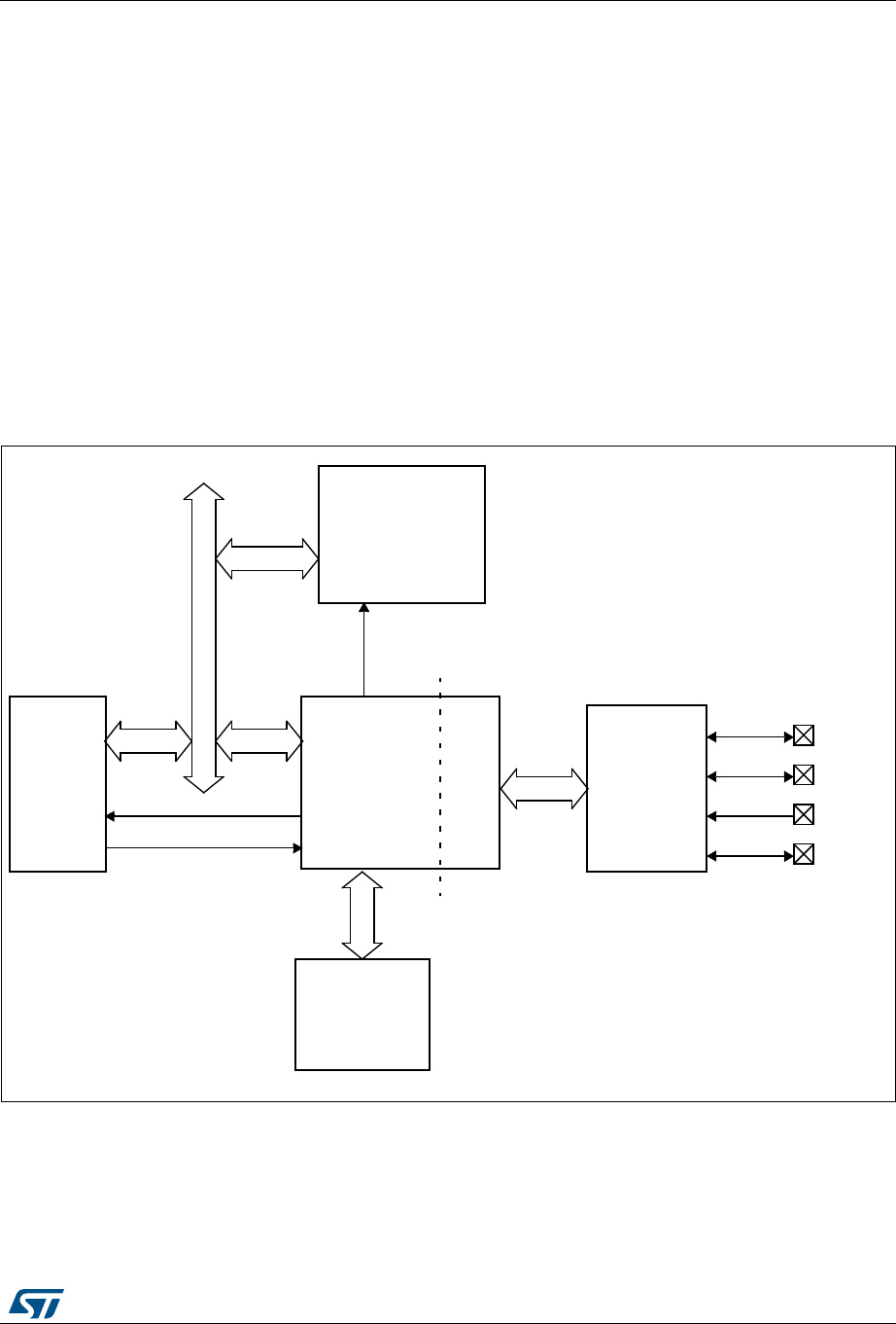
DocID018909 Rev 9 1227/1718
RM0090 USB on-the-go full-speed (OTG_FS)
1362
34.2.3 Peripheral-mode features
The OTG_FS interface main features in peripheral-mode are the following:
•1 bidirectional control endpoint0
•3 IN endpoints (EPs) configurable to support Bulk, Interrupt or Isochronous transfers
•3 OUT endpoints configurable to support Bulk, Interrupt or Isochronous transfers
•Management of a shared Rx FIFO and a Tx-OUT FIFO for efficient usage of the USB
data RAM
•Management of up to 4 dedicated Tx-IN FIFOs (one for each active IN EP) to put less
load on the application
•Support for the soft disconnect feature.
34.3 OTG_FS functional description
Figure 386. OTG full-speed block diagram
34.3.1 OTG full-speed core
The USB OTG FS receives the 48 MHz ±0.25% clock from the reset and clock controller
(RCC), via an external quartz. The USB clock is used for driving the 48 MHz domain at full-
speed (12 Mbit/s) and must be enabled prior to configuring the OTG FS core.
$0
$-
)$
6"53
/4'
&3
0(9
53"
/4'&3
#ORE 54-)&3
+BYTES
53"DATA
&)&/S
!("0ERIPHERAL
0OWER
#LOCK
#42,
53")NTERRUPT
53"SUSPEND
53"#LOCKAT-(Z
#ORTEXCORE
3YSTEMCLOCK
DOMAIN 53"CLOCK
DOMAIN
5NIVERSALSERIALBUS
2!-BUS
-36

USB on-the-go full-speed (OTG_FS) RM0090
1228/1718 DocID018909 Rev 9
The CPU reads and writes from/to the OTG FS core registers through the AHB peripheral
bus. It is informed of USB events through the single USB OTG interrupt line described in
Section 34.15: OTG_FS interrupts.
The CPU submits data over the USB by writing 32-bit words to dedicated OTG_FS locations
(push registers). The data are then automatically stored into Tx-data FIFOs configured
within the USB data RAM. There is one Tx-FIFO push register for each in-endpoint
(peripheral mode) or out-channel (host mode).
The CPU receives the data from the USB by reading 32-bit words from dedicated OTG_FS
addresses (pop registers). The data are then automatically retrieved from a shared Rx-FIFO
configured within the 1.25 KB USB data RAM. There is one Rx-FIFO pop register for each
out-endpoint or in-channel.
The USB protocol layer is driven by the serial interface engine (SIE) and serialized over the
USB by the full-/low-speed transceiver module within the on-chip physical layer (PHY).
34.3.2 Full-speed OTG PHY
The embedded full-speed OTG PHY is controlled by the OTG FS core and conveys USB
control & data signals through the full-speed subset of the UTMI+ Bus (UTMIFS). It provides
the physical support to USB connectivity.
The full-speed OTG PHY includes the following components:
•FS/LS transceiver module used by both host and device. It directly drives transmission
and reception on the single-ended USB lines.
•integrated ID pull-up resistor used to sample the ID line for A/B device identification.
•DP/DM integrated pull-up and pull-down resistors controlled by the OTG_FS core
depending on the current role of the device. As a peripheral, it enables the DP pull-up
resistor to signal full-speed peripheral connections as soon as VBUS is sensed to be at
a valid level (B-session valid). In host mode, pull-down resistors are enabled on both
DP/DM. Pull-up and pull-down resistors are dynamically switched when the device’s
role is changed via the host negotiation protocol (HNP).
•Pull-up/pull-down resistor ECN circuit. The DP pull-up consists of 2 resistors controlled
separately from the OTG_FS as per the resistor Engineering Change Notice applied to
USB Rev2.0. The dynamic trimming of the DP pull-up strength allows for better noise
rejection and Tx/Rx signal quality.
•VBUS sensing comparators with hysteresis used to detect VBUS Valid, A-B Session
Valid and session-end voltage thresholds. They are used to drive the session request
protocol (SRP), detect valid startup and end-of-session conditions, and constantly
monitor the VBUS supply during USB operations.
•VBUS pulsing method circuit used to charge/discharge VBUS through resistors during
the SRP (weak drive).
Caution: To guarantee a correct operation for the USB OTG FS peripheral, the AHB frequency should
be higher than 14.2 MHz.
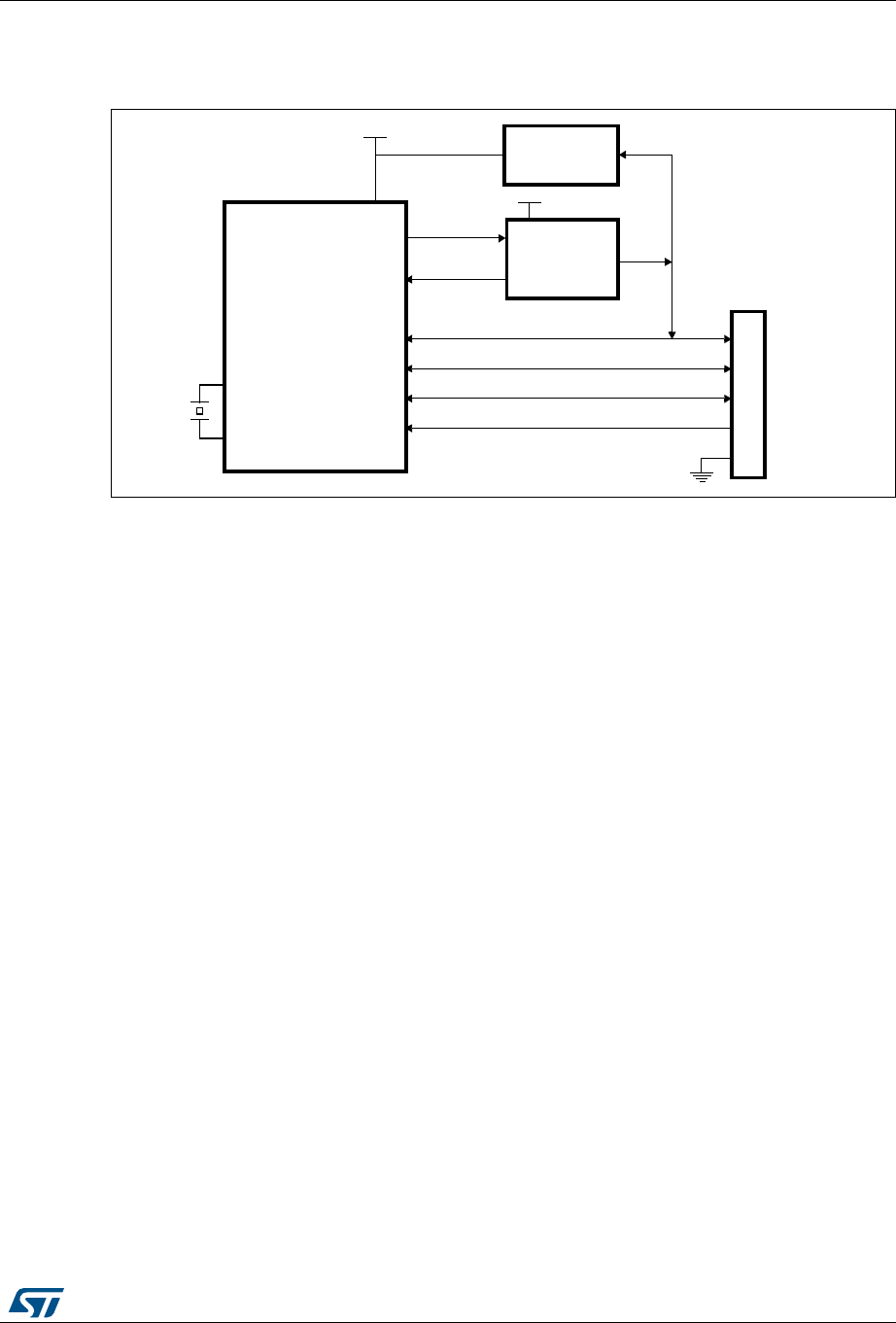
DocID018909 Rev 9 1229/1718
RM0090 USB on-the-go full-speed (OTG_FS)
1362
34.4 OTG dual role device (DRD)
Figure 387. OTG A-B device connection
1. External voltage regulator only needed when building a VBUS powered device
2. STMPS2141STR needed only if the application has to support a VBUS powered device. A basic power
switch can be used if 5 V are available on the application board.
34.4.1 ID line detection
The host or peripheral (the default) role is assumed depending on the ID input pin. The ID
line status is determined on plugging in the USB, depending on which side of the USB cable
is connected to the micro-AB receptacle.
•If the B-side of the USB cable is connected with a floating ID wire, the integrated pull-
up resistor detects a high ID level and the default Peripheral role is confirmed. In this
configuration the OTG_FS complies with the standard FSM described by section 6.8.2:
On-The-Go B-device of the On-The-Go Specification Rev1.3 supplement to the
USB2.0.
•If the A-side of the USB cable is connected with a grounded ID, the OTG_FS issues an
ID line status change interrupt (CIDSCHG bit in OTG_FS_GINTSTS) for host software
initialization, and automatically switches to the host role. In this configuration the
OTG_FS complies with the standard FSM described by section 6.8.1: On-The-Go A-
device of the On-The-Go Specification Rev1.3 supplement to the USB2.0.
34.4.2 HNP dual role device
The HNP capable bit in the Global USB configuration register (HNPCAP bit in OTG_FS_
GUSBCFG) enables the OTG_FS core to dynamically change its role from A-host to A-
peripheral and vice-versa, or from B-Peripheral to B-host and vice-versa according to the
host negotiation protocol (HNP). The current device status can be read by the combined
values of the Connector ID Status bit in the Global OTG control and status register (CIDSTS
bit in OTG_FS_GOTGCTL) and the current mode of operation bit in the global interrupt and
status register (CMOD bit in OTG_FS_GINTSTS).
The HNP program model is described in detail in Section 34.17: OTG_FS programming
model.
34--#5 34-03342
#URRENTLIMITED
POWERDISTRIBUTION
SWITCH
6$$
6"53
$0
633
0!
0!
0!
53"MICRO!"CONNECTOR
$-
'0)/)21
'0)/ %.
/VERCURRENT
60WR
6TO6$$
VOLTAGEREGULATOR
6$$
)$
0!
/3#?).
/3#?/54
-36

USB on-the-go full-speed (OTG_FS) RM0090
1230/1718 DocID018909 Rev 9
34.4.3 SRP dual role device
The SRP capable bit in the global USB configuration register (SRPCAP bit in
OTG_FS_GUSBCFG) enables the OTG_FS core to switch off the generation of VBUS for
the A-device to save power. Note that the A-device is always in charge of driving VBUS
regardless of the host or peripheral role of the OTG_FS.
the SRP A/B-device program model is described in detail in Section 34.17: OTG_FS
programming model.
34.5 USB peripheral
This section gives the functional description of the OTG_FS in the USB peripheral mode.
The OTG_FS works as an USB peripheral in the following circumstances:
•OTG B-Peripheral
– OTG B-device default state if B-side of USB cable is plugged in
•OTG A-Peripheral
– OTG A-device state after the HNP switches the OTG_FS to its peripheral role
•B-device
– If the ID line is present, functional and connected to the B-side of the USB cable,
and the HNP-capable bit in the Global USB Configuration register (HNPCAP bit in
OTG_FS_GUSBCFG) is cleared (see On-The-Go Rev1.3 par. 6.8.3).
•Peripheral only (see Figure 388: USB peripheral-only connection)
– The force device mode bit in the Global USB configuration register (FDMOD in
OTG_FS_GUSBCFG) is set to 1, forcing the OTG_FS core to work as a USB
peripheral-only (see On-The-Go Rev1.3 par. 6.8.3). In this case, the ID line is
ignored even if present on the USB connector.
Note: To build a bus-powered device implementation in case of the B-device or peripheral-only
configuration, an external regulator has to be added that generates the VDD chip-supply
from VBUS.
The VBUS pin can be freed by disabling the VBUS sensing option. This is done by setting the
NOVBUSSENS bit in the OTG_FS_GCCFG register. In this case the VBUS is considered
internally to be always at VBUS valid level (5 V).
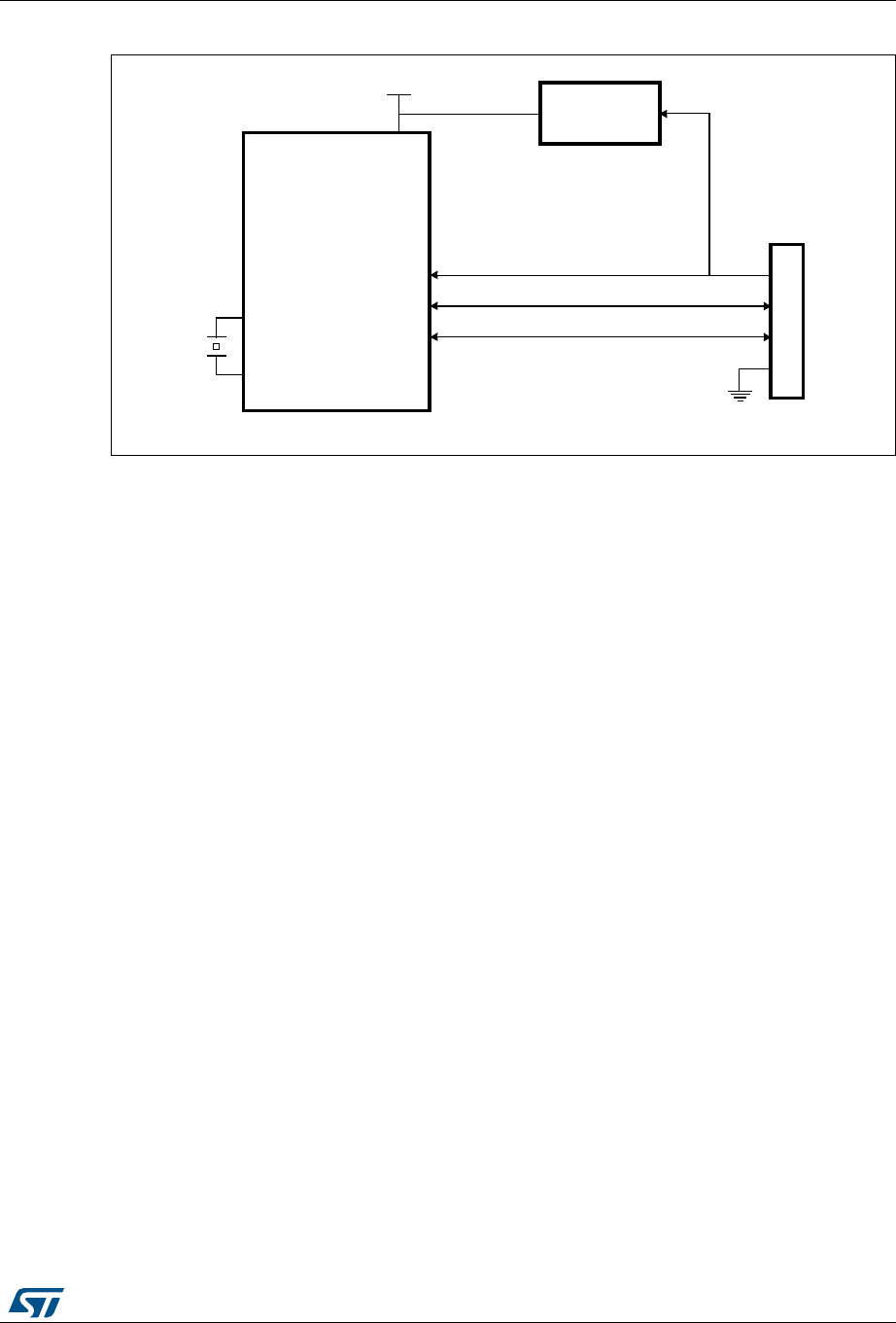
DocID018909 Rev 9 1231/1718
RM0090 USB on-the-go full-speed (OTG_FS)
1362
Figure 388. USB peripheral-only connection
1. Use a regulator to build a bus-powered device.
34.5.1 SRP-capable peripheral
The SRP capable bit in the Global USB configuration register (SRPCAP bit in
OTG_FS_GUSBCFG) enables the OTG_FS to support the session request protocol (SRP).
In this way, it allows the remote A-device to save power by switching off VBUS while the USB
session is suspended.
The SRP peripheral mode program model is described in detail in the B-device session
request protocol section.
34.5.2 Peripheral states
Powered state
The VBUS input detects the B-Session valid voltage by which the USB peripheral is allowed
to enter the powered state (see USB2.0 par9.1). The OTG_FS then automatically connects
the DP pull-up resistor to signal full-speed device connection to the host and generates the
session request interrupt (SRQINT bit in OTG_FS_GINTSTS) to notify the powered state.
The VBUS input also ensures that valid VBUS levels are supplied by the host during USB
operations. If a drop in VBUS below B-session valid happens to be detected (for instance
because of a power disturbance or if the host port has been switched off), the OTG_FS
automatically disconnects and the session end detected (SEDET bit in
OTG_FS_GOTGINT) interrupt is generated to notify that the OTG_FS has exited the
powered state.
In the powered state, the OTG_FS expects to receive some reset signaling from the host.
No other USB operation is possible. When a reset signaling is received the reset detected
interrupt (USBRST in OTG_FS_GINTSTS) is generated. When the reset signaling is
complete, the enumeration done interrupt (ENUMDNE bit in OTG_FS_GINTSTS) is
generated and the OTG_FS enters the Default state.
34--#5
6TO6$$
6OLATGEREGULATOR
6$$
6"53
$0
633
0!
0!
0!
53"3TD"CONNECTOR
$-
/3#?).
/3#?/54
-36

USB on-the-go full-speed (OTG_FS) RM0090
1232/1718 DocID018909 Rev 9
Soft disconnect
The powered state can be exited by software with the soft disconnect feature. The DP pull-
up resistor is removed by setting the soft disconnect bit in the device control register (SDIS
bit in OTG_FS_DCTL), causing a device disconnect detection interrupt on the host side
even though the USB cable was not really removed from the host port.
Default state
In the Default state the OTG_FS expects to receive a SET_ADDRESS command from the
host. No other USB operation is possible. When a valid SET_ADDRESS command is
decoded on the USB, the application writes the corresponding number into the device
address field in the device configuration register (DAD bit in OTG_FS_DCFG). The
OTG_FS then enters the address state and is ready to answer host transactions at the
configured USB address.
Suspended state
The OTG_FS peripheral constantly monitors the USB activity. After counting 3 ms of USB
idleness, the early suspend interrupt (ESUSP bit in OTG_FS_GINTSTS) is issued, and
confirmed 3 ms later, if appropriate, by the suspend interrupt (USBSUSP bit in
OTG_FS_GINTSTS). The device suspend bit is then automatically set in the device status
register (SUSPSTS bit in OTG_FS_DSTS) and the OTG_FS enters the suspended state.
The suspended state may optionally be exited by the device itself. In this case the
application sets the remote wakeup signaling bit in the device control register (RWUSIG bit
in OTG_FS_DCTL) and clears it after 1 to 15 ms.
When a resume signaling is detected from the host, the resume interrupt (WKUPINT bit in
OTG_FS_GINTSTS) is generated and the device suspend bit is automatically cleared.
34.5.3 Peripheral endpoints
The OTG_FS core instantiates the following USB endpoints:
•Control endpoint 0:
– Bidirectional and handles control messages only
– Separate set of registers to handle in and out transactions
– Proper control (OTG_FS_DIEPCTL0/OTG_FS_DOEPCTL0), transfer
configuration (OTG_FS_DIEPTSIZ0/OTG_FS_DIEPTSIZ0), and status-interrupt
(OTG_FS_DIEPINTx/)OTG_FS_DOEPINT0) registers. The available set of bits
inside the control and transfer size registers slightly differs from that of other
endpoints
•3 IN endpoints
– Each of them can be configured to support the isochronous, bulk or interrupt
transfer type
– Each of them has proper control (OTG_FS_DIEPCTLx), transfer configuration
(OTG_FS_DIEPTSIZx), and status-interrupt (OTG_FS_DIEPINTx) registers
– The Device IN endpoints common interrupt mask register (OTG_FS_DIEPMSK) is
available to enable/disable a single kind of endpoint interrupt source on all of the
IN endpoints (EP0 included)
– Support for incomplete isochronous IN transfer interrupt (IISOIXFR bit in
OTG_FS_GINTSTS), asserted when there is at least one isochronous IN endpoint

DocID018909 Rev 9 1233/1718
RM0090 USB on-the-go full-speed (OTG_FS)
1362
on which the transfer is not completed in the current frame. This interrupt is
asserted along with the end of periodic frame interrupt
(OTG_FS_GINTSTS/EOPF).
•3 OUT endpoints
– Each of them can be configured to support the isochronous, bulk or interrupt
transfer type
– Each of them has a proper control (OTG_FS_DOEPCTLx), transfer configuration
(OTG_FS_DOEPTSIZx) and status-interrupt (OTG_FS_DOEPINTx) register
– Device Out endpoints common interrupt mask register (OTG_FS_DOEPMSK) is
available to enable/disable a single kind of endpoint interrupt source on all of the
OUT endpoints (EP0 included)
– Support for incomplete isochronous OUT transfer interrupt (INCOMPISOOUT bit
in OTG_FS_GINTSTS), asserted when there is at least one isochronous OUT
endpoint on which the transfer is not completed in the current frame. This interrupt
is asserted along with the end of periodic frame interrupt
(OTG_FS_GINTSTS/EOPF).
Endpoint control
•The following endpoint controls are available to the application through the device
endpoint-x IN/OUT control register (DIEPCTLx/DOEPCTLx):
– Endpoint enable/disable
– Endpoint activate in current configuration
– Program USB transfer type (isochronous, bulk, interrupt)
– Program supported packet size
– Program Tx-FIFO number associated with the IN endpoint
– Program the expected or transmitted data0/data1 PID (bulk/interrupt only)
– Program the even/odd frame during which the transaction is received or
transmitted (isochronous only)
– Optionally program the NAK bit to always negative-acknowledge the host
regardless of the FIFO status
– Optionally program the STALL bit to always stall host tokens to that endpoint
– Optionally program the SNOOP mode for OUT endpoint not to check the CRC
field of received data
Endpoint transfer
The device endpoint-x transfer size registers (DIEPTSIZx/DOEPTSIZx) allow the application
to program the transfer size parameters and read the transfer status. Programming must be
done before setting the endpoint enable bit in the endpoint control register. Once the
endpoint is enabled, these fields are read-only as the OTG FS core updates them with the
current transfer status.
The following transfer parameters can be programmed:
•Transfer size in bytes
•Number of packets that constitute the overall transfer size

USB on-the-go full-speed (OTG_FS) RM0090
1234/1718 DocID018909 Rev 9
Endpoint status/interrupt
The device endpoint-x interrupt registers (DIEPINTx/DOPEPINTx) indicate the status of an
endpoint with respect to USB- and AHB-related events. The application must read these
registers when the OUT endpoint interrupt bit or the IN endpoint interrupt bit in the core
interrupt register (OEPINT bit in OTG_FS_GINTSTS or IEPINT bit in OTG_FS_GINTSTS,
respectively) is set. Before the application can read these registers, it must first read the
device all endpoints interrupt (OTG_FS_DAINT) register to get the exact endpoint number
for the device endpoint-x interrupt register. The application must clear the appropriate bit in
this register to clear the corresponding bits in the DAINT and GINTSTS registers
The peripheral core provides the following status checks and interrupt generation:
•Transfer completed interrupt, indicating that data transfer was completed on both the
application (AHB) and USB sides
•Setup stage has been done (control-out only)
•Associated transmit FIFO is half or completely empty (in endpoints)
•NAK acknowledge has been transmitted to the host (isochronous-in only)
•IN token received when Tx-FIFO was empty (bulk-in/interrupt-in only)
•Out token received when endpoint was not yet enabled
•Babble error condition has been detected
•Endpoint disable by application is effective
•Endpoint NAK by application is effective (isochronous-in only)
•More than 3 back-to-back setup packets were received (control-out only)
•Timeout condition detected (control-in only)
•Isochronous out packet has been dropped, without generating an interrupt
34.6 USB host
This section gives the functional description of the OTG_FS in the USB host mode. The
OTG_FS works as a USB host in the following circumstances:
•OTG A-host
– OTG A-device default state when the A-side of the USB cable is plugged in
•OTG B-host
– OTG B-device after HNP switching to the host role
•A-device
– If the ID line is present, functional and connected to the A-side of the USB cable,
and the HNP-capable bit is cleared in the Global USB Configuration register
(HNPCAP bit in OTG_FS_GUSBCFG). Integrated pull-down resistors are
automatically set on the DP/DM lines.
•Host only (see figure Figure 389: USB host-only connection).
– The force host mode bit in the global USB configuration register (FHMOD bit in
OTG_FS_GUSBCFG) forces the OTG_FS core to work as a USB host-only. In this
case, the ID line is ignored even if present on the USB connector. Integrated pull-
down resistors are automatically set on the DP/DM lines.
Note: On-chip 5 V VBUS generation is not supported. For this reason, a charge pump or, if 5 V are
available on the application board, a basic power switch must be added externally to drive
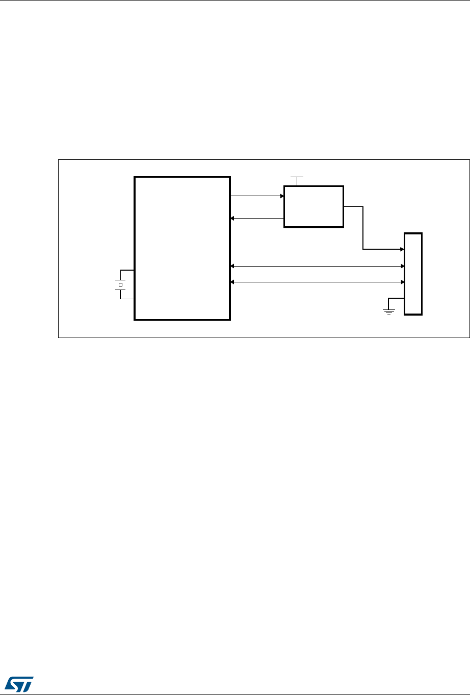
DocID018909 Rev 9 1235/1718
RM0090 USB on-the-go full-speed (OTG_FS)
1362
the 5 V VBUS line. The external charge pump can be driven by any GPIO output. This is
required for the OTG A-host, A-device and host-only configurations.
The VBUS input ensures that valid VBUS levels are supplied by the charge pump during USB
operations while the charge pump overcurrent output can be input to any GPIO pin
configured to generate port interrupts. The overcurrent ISR must promptly disable the VBUS
generation.
The VBUS pin can be freed by disabling the VBUS sensing option. This is done by setting the
NOVBUSSENS bit in the OTG_FS_GCCFG register. In this case the VBUS is considered
internally to be always at VBUS valid level (5 V).
Figure 389. USB host-only connection
1. STMPS2141STR needed only if the application has to support a VBUS powered device. A basic power
switch can be used if 5 V are available on the application board.
2. VDD range is between 2 V and 3.6 V.
34.6.1 SRP-capable host
SRP support is available through the SRP capable bit in the global USB configuration
register (SRPCAP bit in OTG_FS_GUSBCFG). With the SRP feature enabled, the host can
save power by switching off the VBUS power while the USB session is suspended.
The SRP host mode program model is described in detail in the A-device session request
protocol) section.
34.6.2 USB host states
Host port power
On-chip 5 V VBUS generation is not supported. For this reason, a charge pump or, if 5 V are
available on the application board, a basic power switch, must be added externally to drive
the 5 V VBUS line. The external charge pump can be driven by any GPIO output. When the
application decides to power on VBUS using the chosen GPIO, it must also set the port
power bit in the host port control and status register (PPWR bit in OTG_FS_HPRT).
VBUS valid
When HNP or SRP is enabled the VBUS sensing pin (PA9) pin should be connected to
VBUS. The VBUS input ensures that valid VBUS levels are supplied by the charge pump
34--#5 34-03342
#URRENTLIMITED
POWERDISTRIBUTION
SWITCH
6$$
6"53
$0
633
0
0!
0!
53"3TD!CONNECTOR
$-
'0)/)21
'0)/ %.
/VERCURRENT
60WR
/3#?).
/3#?/54
-36

USB on-the-go full-speed (OTG_FS) RM0090
1236/1718 DocID018909 Rev 9
during USB operations. Any unforeseen VBUS voltage drop below the VBUS valid threshold
(4.25 V) leads to an OTG interrupt triggered by the session end detected bit (SEDET bit in
OTG_FS_GOTGINT). The application is then required to remove the VBUS power and clear
the port power bit.
When HNP and SRP are both disabled, the VBUS sensing pin (PA9) should not be
connected to VBUS. This pin can be can be used as GPIO.
The charge pump overcurrent flag can also be used to prevent electrical damage. Connect
the overcurrent flag output from the charge pump to any GPIO input and configure it to
generate a port interrupt on the active level. The overcurrent ISR must promptly disable the
VBUS generation and clear the port power bit.
Host detection of a peripheral connection
If SRP or HNP are enabled, even if USB peripherals or B-devices can be attached at any
time, the OTG_FS will not detect any bus connection until VBUS is no longer sensed at a
valid level (5 V). When VBUS is at a valid level and a remote B-device is attached, the
OTG_FS core issues a host port interrupt triggered by the device connected bit in the host
port control and status register (PCDET bit in OTG_FS_HPRT).
When HNP and SRP are both disabled, USB peripherals or B-device are detected as soon
as they are connected. The OTG_FS core issues a host port interrupt triggered by the
device connected bit in the host port control and status (PCDET bit in OTG_FS_HPRT).
Host detection of peripheral a disconnection
The peripheral disconnection event triggers the disconnect detected interrupt (DISCINT bit
in OTG_FS_GINTSTS).
Host enumeration
After detecting a peripheral connection the host must start the enumeration process by
sending USB reset and configuration commands to the new peripheral.
Before starting to drive a USB reset, the application waits for the OTG interrupt triggered by
the debounce done bit (DBCDNE bit in OTG_FS_GOTGINT), which indicates that the bus is
stable again after the electrical debounce caused by the attachment of a pull-up resistor on
DP (FS) or DM (LS).
The application drives a USB reset signaling (single-ended zero) over the USB by keeping
the port reset bit set in the host port control and status register (PRST bit in
OTG_FS_HPRT) for a minimum of 10 ms and a maximum of 20 ms. The application takes
care of the timing count and then of clearing the port reset bit.
Once the USB reset sequence has completed, the host port interrupt is triggered by the port
enable/disable change bit (PENCHNG bit in OTG_FS_HPRT). This informs the application
that the speed of the enumerated peripheral can be read from the port speed field in the
host port control and status register (PSPD bit in OTG_FS_HPRT) and that the host is
starting to drive SOFs (FS) or Keep alives (LS). The host is now ready to complete the
peripheral enumeration by sending peripheral configuration commands.
Host suspend
The application decides to suspend the USB activity by setting the port suspend bit in the
host port control and status register (PSUSP bit in OTG_FS_HPRT). The OTG_FS core
stops sending SOFs and enters the suspended state.

DocID018909 Rev 9 1237/1718
RM0090 USB on-the-go full-speed (OTG_FS)
1362
The suspended state can be optionally exited on the remote device’s initiative (remote
wakeup). In this case the remote wakeup interrupt (WKUPINT bit in OTG_FS_GINTSTS) is
generated upon detection of a remote wakeup signaling, the port resume bit in the host port
control and status register (PRES bit in OTG_FS_HPRT) self-sets, and resume signaling is
automatically driven over the USB. The application must time the resume window and then
clear the port resume bit to exit the suspended state and restart the SOF.
If the suspended state is exited on the host initiative, the application must set the port
resume bit to start resume signaling on the host port, time the resume window and finally
clear the port resume bit.
34.6.3 Host channels
The OTG_FS core instantiates 8 host channels. Each host channel supports an USB host
transfer (USB pipe). The host is not able to support more than 8 transfer requests at the
same time. If more than 8 transfer requests are pending from the application, the host
controller driver (HCD) must re-allocate channels when they become available from
previous duty, that is, after receiving the transfer completed and channel halted interrupts.
Each host channel can be configured to support in/out and any type of periodic/nonperiodic
transaction. Each host channel makes us of proper control (HCCHARx), transfer
configuration (HCTSIZx) and status/interrupt (HCINTx) registers with associated mask
(HCINTMSKx) registers.
Host channel control
•The following host channel controls are available to the application through the host
channel-x characteristics register (HCCHARx):
– Channel enable/disable
– Program the FS/LS speed of target USB peripheral
– Program the address of target USB peripheral
– Program the endpoint number of target USB peripheral
– Program the transfer IN/OUT direction
– Program the USB transfer type (control, bulk, interrupt, isochronous)
– Program the maximum packet size (MPS)
– Program the periodic transfer to be executed during odd/even frames
Host channel transfer
The host channel transfer size registers (HCTSIZx) allow the application to program the
transfer size parameters, and read the transfer status. Programming must be done before
setting the channel enable bit in the host channel characteristics register. Once the endpoint
is enabled the packet count field is read-only as the OTG FS core updates it according to
the current transfer status.
•The following transfer parameters can be programmed:
– transfer size in bytes
– number of packets making up the overall transfer size
– initial data PID

USB on-the-go full-speed (OTG_FS) RM0090
1238/1718 DocID018909 Rev 9
Host channel status/interrupt
The host channel-x interrupt register (HCINTx) indicates the status of an endpoint with
respect to USB- and AHB-related events. The application must read these register when the
host channels interrupt bit in the core interrupt register (HCINT bit in OTG_FS_GINTSTS) is
set. Before the application can read these registers, it must first read the host all channels
interrupt (HCAINT) register to get the exact channel number for the host channel-x interrupt
register. The application must clear the appropriate bit in this register to clear the
corresponding bits in the HAINT and GINTSTS registers. The mask bits for each interrupt
source of each channel are also available in the OTG_FS_HCINTMSK-x register.
•The host core provides the following status checks and interrupt generation:
– Transfer completed interrupt, indicating that the data transfer is complete on both
the application (AHB) and USB sides
– Channel has stopped due to transfer completed, USB transaction error or disable
command from the application
– Associated transmit FIFO is half or completely empty (IN endpoints)
– ACK response received
– NAK response received
– STALL response received
– USB transaction error due to CRC failure, timeout, bit stuff error, false EOP
– Babble error
– fraMe overrun
– dAta toggle error
34.6.4 Host scheduler
The host core features a built-in hardware scheduler which is able to autonomously re-order
and manage the USB transaction requests posted by the application. At the beginning of
each frame the host executes the periodic (isochronous and interrupt) transactions first,
followed by the nonperiodic (control and bulk) transactions to achieve the higher level of
priority granted to the isochronous and interrupt transfer types by the USB specification.
The host processes the USB transactions through request queues (one for periodic and one
for nonperiodic). Each request queue can hold up to 8 entries. Each entry represents a
pending transaction request from the application, and holds the IN or OUT channel number
along with other information to perform a transaction on the USB. The order in which the
requests are written to the queue determines the sequence of the transactions on the USB
interface.
At the beginning of each frame, the host processes the periodic request queue first, followed
by the nonperiodic request queue. The host issues an incomplete periodic transfer interrupt
(IPXFR bit in OTG_FS_GINTSTS) if an isochronous or interrupt transaction scheduled for
the current frame is still pending at the end of the current frame. The OTG HS core is fully
responsible for the management of the periodic and nonperiodic request queues.The
periodic transmit FIFO and queue status register (HPTXSTS) and nonperiodic transmit
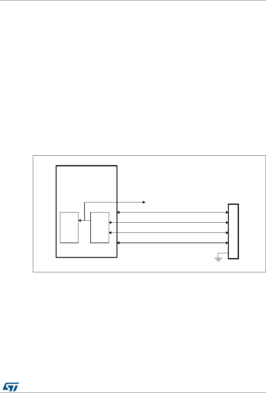
DocID018909 Rev 9 1239/1718
RM0090 USB on-the-go full-speed (OTG_FS)
1362
FIFO and queue status register (HNPTXSTS) are read-only registers which can be used by
the application to read the status of each request queue. They contain:
•The number of free entries currently available in the periodic (nonperiodic) request
queue (8 max)
•Free space currently available in the periodic (nonperiodic) Tx-FIFO (out-transactions)
•IN/OUT token, host channel number and other status information.
As request queues can hold a maximum of 8 entries each, the application can push to
schedule host transactions in advance with respect to the moment they physically reach the
SB for a maximum of 8 pending periodic transactions plus 8 pending nonperiodic
transactions.
To post a transaction request to the host scheduler (queue) the application must check that
there is at least 1 entry available in the periodic (nonperiodic) request queue by reading the
PTXQSAV bits in the OTG_FS_HNPTXSTS register or NPTQXSAV bits in the
OTG_FS_HNPTXSTS register.
34.7 SOF trigger
Figure 390. SOF connectivity
The OTG FS core provides means to monitor, track and configure SOF framing in the host
and peripheral, as well as an SOF pulse output connectivity feature.
Such utilities are especially useful for adaptive audio clock generation techniques, where
the audio peripheral needs to synchronize to the isochronous stream provided by the PC, or
the host needs to trim its framing rate according to the requirements of the audio peripheral.
34.7.1 Host SOFs
In host mode the number of PHY clocks occurring between the generation of two
consecutive SOF (FS) or Keep-alive (LS) tokens is programmable in the host frame interval
register (HFIR), thus providing application control over the SOF framing period. An interrupt
is generated at any start of frame (SOF bit in OTH_FS_GINTSTS). The current frame
34--#5
6"53
$
633
0!
0!
0!
53"MICRO!"CONNECTOR
$
)$4)-
)42 3/&
PULSE
3/&GEN
0!
0!
3/&PULSEOUTPUTTO
EXTERNALAUDIOCONTROL
-36

USB on-the-go full-speed (OTG_FS) RM0090
1240/1718 DocID018909 Rev 9
number and the time remaining until the next SOF are tracked in the host frame number
register (HFNUM).
An SOF pulse signal, generated at any SOF starting token and with a width of 12 system
clock cycles, can be made available externally on the SOF pin using the SOFOUTEN bit in
the global control and configuration register. The SOF pulse is also internally connected to
the input trigger of timer 2 (TIM2), so that the input capture feature, the output compare
feature and the timer can be triggered by the SOF pulse. The TIM2 connection is enabled
through the ITR1_RMP bits of TIM2_OR register.
34.7.2 Peripheral SOFs
In device mode, the start of frame interrupt is generated each time an SOF token is received
on the USB (SOF bit in OTH_FS_GINTSTS). The corresponding frame number can be read
from the device status register (FNSOF bit in OTG_FS_DSTS). An SOF pulse signal with a
width of 12 system clock cycles is also generated and can be made available externally on
the SOF pin by using the SOF output enable bit in the global control and configuration
register (SOFOUTEN bit in OTG_FS_GCCFG). The SOF pulse signal is also internally
connected to the TIM2 input trigger, so that the input capture feature, the output compare
feature and the timer can be triggered by the SOF pulse. The TIM2 connection is enabled
through the ITR1_RMP bits of the TIM2 option register (TIM2_OR).
The end of periodic frame interrupt (GINTSTS/EOPF) is used to notify the application when
80%, 85%, 90% or 95% of the time frame interval elapsed depending on the periodic frame
interval field in the device configuration register (PFIVL bit in OTG_FS_DCFG). This feature
can be used to determine if all of the isochronous traffic for that frame is complete.
34.8 Power options
The power consumption of the OTG PHY is controlled by three bits in the general core
configuration register:
•PHY power down (GCCFG/PWRDWN)
It switches on/off the full-speed transceiver module of the PHY. It must be preliminarily
set to allow any USB operation.
•A-VBUS sensing enable (GCCFG/VBUSASEN)
It switches on/off the VBUS comparators associated with A-device operations. It must
be set when in A-device (USB host) mode and during HNP.
•B-VBUS sensing enable (GCCFG/VBUSASEN)
It switches on/off the VBUS comparators associated with B-device operations. It must
be set when in B-device (USB peripheral) mode and during HNP.
Power reduction techniques are available while in the USB suspended state, when the USB
session is not yet valid or the device is disconnected.
•Stop PHY clock (STPPCLK bit in OTG_FS_PCGCCTL)
When setting the stop PHY clock bit in the clock gating control register, most of the
48 MHz clock domain internal to the OTG full-speed core is switched off by clock
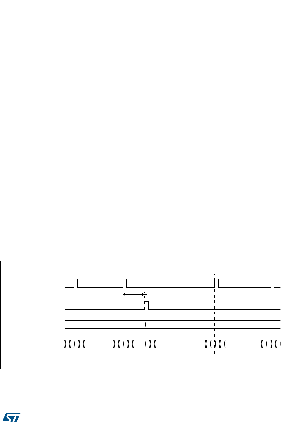
DocID018909 Rev 9 1241/1718
RM0090 USB on-the-go full-speed (OTG_FS)
1362
gating. The dynamic power consumption due to the USB clock switching activity is cut
even if the 48 MHz clock input is kept running by the application
Most of the transceiver is also disabled, and only the part in charge of detecting the
asynchronous resume or remote wakeup event is kept alive.
•Gate HCLK (GATEHCLK bit in OTG_FS_PCGCCTL)
When setting the Gate HCLK bit in the clock gating control register, most of the system
clock domain internal to the OTG_FS core is switched off by clock gating. Only the
register read and write interface is kept alive. The dynamic power consumption due to
the USB clock switching activity is cut even if the system clock is kept running by the
application for other purposes.
•USB system stop
When the OTG_FS is in the USB suspended state, the application may decide to
drastically reduce the overall power consumption by a complete shut down of all the
clock sources in the system. USB System Stop is activated by first setting the Stop
PHY clock bit and then configuring the system deep sleep mode in the power control
system module (PWR).
The OTG_FS core automatically reactivates both system and USB clocks by
asynchronous detection of remote wakeup (as an host) or resume (as a device)
signaling on the USB.
To save dynamic power, the USB data FIFO is clocked only when accessed by the OTG_FS
core.
34.9 Dynamic update of the OTG_FS_HFIR register
The USB core embeds a dynamic trimming capability of micro-SOF framing period in host
mode allowing to synchronize an external device with the micro-SOF frames.
When the OTG_HS_HFIR register is changed within a current micro-SOF frame, the SOF
period correction is applied in the next frame as described in Figure 391.
Figure 391. Updating OTG_FS_HFIR dynamically
xxxx
,ATENCY
3/&
RELOAD
/4'?&3?(&)2
WRITE
VALUE
&RAME
TIMER
/LD/4'?&3?()&2VALUE
PERIODS
/4'?&3?()&2VALUE
PERIODS()&2WRITELATENCY
.EW/4'?&3?()&2VALUE
PERIODS
/4'?&3?(&)2
AI
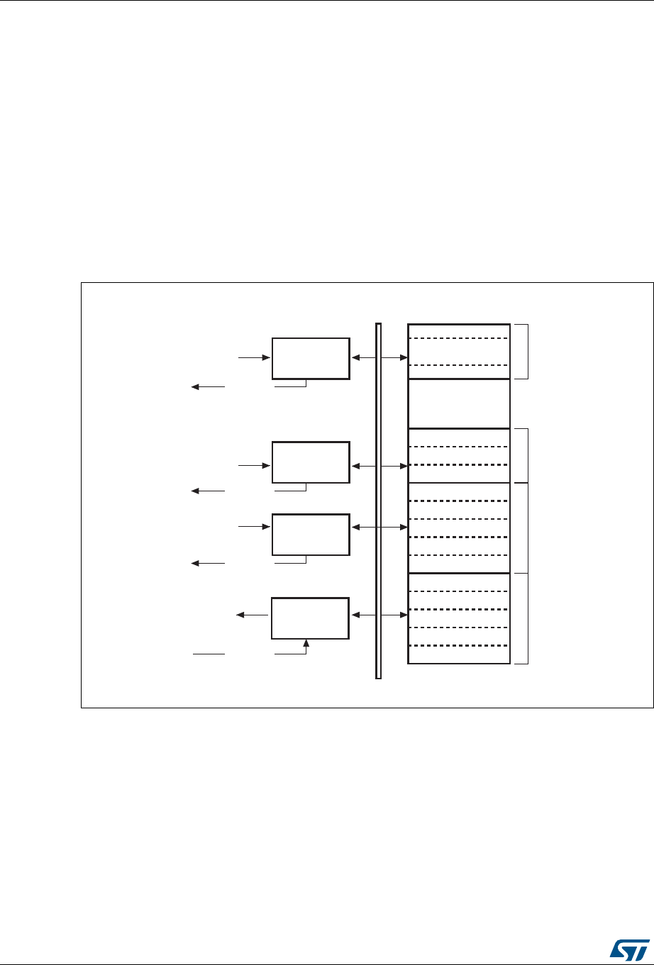
USB on-the-go full-speed (OTG_FS) RM0090
1242/1718 DocID018909 Rev 9
34.10 USB data FIFOs
The USB system features 1.25 Kbyte of dedicated RAM with a sophisticated FIFO control
mechanism. The packet FIFO controller module in the OTG_FS core organizes RAM space
into Tx-FIFOs into which the application pushes the data to be temporarily stored before the
USB transmission, and into a single Rx FIFO where the data received from the USB are
temporarily stored before retrieval (popped) by the application. The number of instructed
FIFOs and how these are organized inside the RAM depends on the device’s role. In
peripheral mode an additional Tx-FIFO is instructed for each active IN endpoint. Any FIFO
size is software configured to better meet the application requirements.
34.11 Peripheral FIFO architecture
Figure 392. Device-mode FIFO address mapping and AHB FIFO access mapping
34.11.1 Peripheral Rx FIFO
The OTG peripheral uses a single receive FIFO that receives the data directed to all OUT
endpoints. Received packets are stacked back-to-back until free space is available in the
Rx-FIFO. The status of the received packet (which contains the OUT endpoint destination
number, the byte count, the data PID and the validity of the received data) is also stored by
the core on top of the data payload. When no more space is available, host transactions are
NACKed and an interrupt is received on the addressed endpoint. The size of the receive
FIFO is configured in the receive FIFO Size register (GRXFSIZ).
IN endpoint Tx FIFO #n
DFIFO push access
from AHB
Any OUT endpoint DFIFO pop
access from AHB
Dedicated Tx
FIFO #n control
(optional)
Dedicated Tx
FIFO #1 control
(optional)
Rx FIFO control
IN endpoint Tx FIFO #1
DFIFO push access
from AHB
MAC pop
MAC pop
MAC push
Single data
FIFO
Tx FIFO #n
packet
Tx FIFO #0 packet
DIEPTXF2[31:16]
DIEPTXFx[15:0]
DIEPTXF2[15:0]
DIEPTXF1[31:16]
DIEPTXF1[15:0]
GNPTXFSIZ[31:16]
ai15611
IN endpoint Tx FIFO #0
DFIFO push access
from AHB
Dedicated Tx
FIFO #0 control
(optional)
MAC pop
Tx FIFO #1 packet
Rx packets
(Rx start
address
fixed to 0)
.
.
..
.
..
.
.
GNPTXFSIZ[15:0]
GRXFSIZ[31:16]
A1 = 0
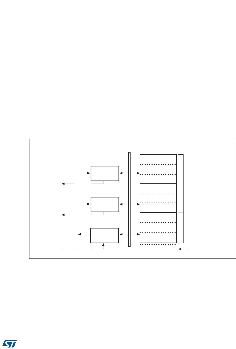
DocID018909 Rev 9 1243/1718
RM0090 USB on-the-go full-speed (OTG_FS)
1362
The single receive FIFO architecture makes it more efficient for the USB peripheral to fill in
the receive RAM buffer:
•All OUT endpoints share the same RAM buffer (shared FIFO)
•The OTG FS core can fill in the receive FIFO up to the limit for any host sequence of
OUT tokens
The application keeps receiving the Rx-FIFO non-empty interrupt (RXFLVL bit in
OTG_FS_GINTSTS) as long as there is at least one packet available for download. It reads
the packet information from the receive status read and pop register (GRXSTSP) and finally
pops data off the receive FIFO by reading from the endpoint-related pop address.
34.11.2 Peripheral Tx FIFOs
The core has a dedicated FIFO for each IN endpoint. The application configures FIFO sizes
by writing the non periodic transmit FIFO size register (OTG_FS_TX0FSIZ) for IN endpoint0
and the device IN endpoint transmit FIFOx registers (DIEPTXFx) for IN endpoint-x.
34.12 Host FIFO architecture
Figure 393. Host-mode FIFO address mapping and AHB FIFO access mapping
34.12.1 Host Rx FIFO
The host uses one receiver FIFO for all periodic and nonperiodic transactions. The FIFO is
used as a receive buffer to hold the received data (payload of the received packet) from the
USB until it is transferred to the system memory. Packets received from any remote IN
endpoint are stacked back-to-back until free space is available. The status of each received
packet with the host channel destination, byte count, data PID and validity of the received
data are also stored into the FIFO. The size of the receive FIFO is configured in the receive
FIFO size register (GRXFSIZ).
Any periodic channel
DFIFO push access
from AHB
Any channel DFIFO pop
access from AHB
Periodic Tx
FIFO control
(optional)
Non-periodic
Tx FIFO control
Rx FIFO control
Any non-periodic
channel DFIFO push
access from AHB
MAC pop
MAC pop
MAC push
Single data
FIFO
Periodic Tx packets
Periodic Tx packets
Rx packets
HPTXFSIZ[31:16]
HPTXFSIZ[15:0]
NPTXFSIZ[31:16]
NPTXFSIZ[15:0]
RXFSIZ[31:16]
Rx start address
fixed to 0
A1 = 0
ai15610

USB on-the-go full-speed (OTG_FS) RM0090
1244/1718 DocID018909 Rev 9
The single receive FIFO architecture makes it highly efficient for the USB host to fill in the
receive data buffer:
•All IN configured host channels share the same RAM buffer (shared FIFO)
•The OTG FS core can fill in the receive FIFO up to the limit for any sequence of IN
tokens driven by the host software
The application receives the Rx FIFO not-empty interrupt as long as there is at least one
packet available for download. It reads the packet information from the receive status read
and pop register and finally pops the data off the receive FIFO.
34.12.2 Host Tx FIFOs
The host uses one transmit FIFO for all non-periodic (control and bulk) OUT transactions
and one transmit FIFO for all periodic (isochronous and interrupt) OUT transactions. FIFOs
are used as transmit buffers to hold the data (payload of the transmit packet) to be
transmitted over the USB. The size of the periodic (nonperiodic) Tx FIFO is configured in the
host periodic (nonperiodic) transmit FIFO size (HPTXFSIZ/HNPTXFSIZ) register.
The two Tx FIFO implementation derives from the higher priority granted to the periodic type
of traffic over the USB frame. At the beginning of each frame, the built-in host scheduler
processes the periodic request queue first, followed by the nonperiodic request queue.
The two transmit FIFO architecture provides the USB host with separate optimization for
periodic and nonperiodic transmit data buffer management:
•All host channels configured to support periodic (nonperiodic) transactions in the OUT
direction share the same RAM buffer (shared FIFOs)
•The OTG FS core can fill in the periodic (nonperiodic) transmit FIFO up to the limit for
any sequence of OUT tokens driven by the host software
The OTG_FS core issues the periodic Tx FIFO empty interrupt (PTXFE bit in
OTG_FS_GINTSTS) as long as the periodic Tx-FIFO is half or completely empty,
depending on the value of the periodic Tx-FIFO empty level bit in the AHB configuration
register (PTXFELVL bit in OTG_FS_GAHBCFG). The application can push the transmission
data in advance as long as free space is available in both the periodic Tx FIFO and the
periodic request queue. The host periodic transmit FIFO and queue status register
(HPTXSTS) can be read to know how much space is available in both.
OTG_FS core issues the non periodic Tx FIFO empty interrupt (NPTXFE bit in
OTG_FS_GINTSTS) as long as the nonperiodic Tx FIFO is half or completely empty
depending on the non periodic Tx FIFO empty level bit in the AHB configuration register
(TXFELVL bit in OTG_FS_GAHBCFG). The application can push the transmission data as
long as free space is available in both the nonperiodic Tx FIFO and nonperiodic request
queue. The host nonperiodic transmit FIFO and queue status register (HNPTXSTS) can be
read to know how much space is available in both.
34.13 FIFO RAM allocation
34.13.1 Device mode
Receive FIFO RAM allocation: the application should allocate RAM for SETUP Packets:
10 locations must be reserved in the receive FIFO to receive SETUP packets on control
endpoint. The core does not use these locations, which are reserved for SETUP packets, to
write any other data. One location is to be allocated for Global OUT NAK. Status information

DocID018909 Rev 9 1245/1718
RM0090 USB on-the-go full-speed (OTG_FS)
1362
is written to the FIFO along with each received packet. Therefore, a minimum space of
(Largest Packet Size / 4) + 1 must be allocated to receive packets. If multiple isochronous
endpoints are enabled, then at least two (Largest Packet Size / 4) + 1 spaces must be
allocated to receive back-to-back packets. Typically, two (Largest Packet Size / 4) + 1
spaces are recommended so that when the previous packet is being transferred to the CPU,
the USB can receive the subsequent packet.
Along with the last packet for each endpoint, transfer complete status information is also
pushed to the FIFO. Typically, one location for each OUT endpoint is recommended.
Transmit FIFO RAM allocation: the minimum RAM space required for each IN Endpoint
Transmit FIFO is the maximum packet size for that particular IN endpoint.
Note: More space allocated in the transmit IN Endpoint FIFO results in better performance on the
USB.
34.13.2 Host mode
Receive FIFO RAM allocation
Status information is written to the FIFO along with each received packet. Therefore, a
minimum space of (Largest Packet Size / 4) + 1 must be allocated to receive packets. If
multiple isochronous channels are enabled, then at least two (Largest Packet Size / 4) + 1
spaces must be allocated to receive back-to-back packets. Typically, two (Largest Packet
Size / 4) + 1 spaces are recommended so that when the previous packet is being
transferred to the CPU, the USB can receive the subsequent packet.
Along with the last packet in the host channel, transfer complete status information is also
pushed to the FIFO. So one location must be allocated for this.
Transmit FIFO RAM allocation
The minimum amount of RAM required for the host Non-periodic Transmit FIFO is the
largest maximum packet size among all supported non-periodic OUT channels.
Typically, two Largest Packet Sizes worth of space is recommended, so that when the
current packet is under transfer to the USB, the CPU can get the next packet.
The minimum amount of RAM required for host periodic Transmit FIFO is the largest
maximum packet size out of all the supported periodic OUT channels. If there is at least one
Isochronous OUT endpoint, then the space must be at least two times the maximum packet
size of that channel.
Note: More space allocated in the Transmit Non-periodic FIFO results in better performance on
the USB.
34.14 USB system performance
Best USB and system performance is achieved owing to the large RAM buffers, the highly
configurable FIFO sizes, the quick 32-bit FIFO access through AHB push/pop registers and,
especially, the advanced FIFO control mechanism. Indeed, this mechanism allows the

USB on-the-go full-speed (OTG_FS) RM0090
1246/1718 DocID018909 Rev 9
OTG_FS to fill in the available RAM space at best regardless of the current USB sequence.
With these features:
•The application gains good margins to calibrate its intervention in order to optimize the
CPU bandwidth usage:
– It can accumulate large amounts of transmission data in advance compared to
when they are effectively sent over the USB
– It benefits of a large time margin to download data from the single receive FIFO
•The USB Core is able to maintain its full operating rate, that is to provide maximum full-
speed bandwidth with a great margin of autonomy versus application intervention:
– It has a large reserve of transmission data at its disposal to autonomously manage
the sending of data over the USB
– It has a lot of empty space available in the receive buffer to autonomously fill it in
with the data coming from the USB
As the OTG_FS core is able to fill in the 1.25 Kbyte RAM buffer very efficiently, and as
1.25 Kbyte of transmit/receive data is more than enough to cover a full speed frame, the
USB system is able to withstand the maximum full-speed data rate for up to one USB frame
(1 ms) without any CPU intervention.
34.15 OTG_FS interrupts
When the OTG_FS controller is operating in one mode, either device or host, the application
must not access registers from the other mode. If an illegal access occurs, a mode
mismatch interrupt is generated and reflected in the Core interrupt register (MMIS bit in the
OTG_FS_GINTSTS register). When the core switches from one mode to the other, the
registers in the new mode of operation must be reprogrammed as they would be after a
power-on reset.
Figure 394 shows the interrupt hierarchy.
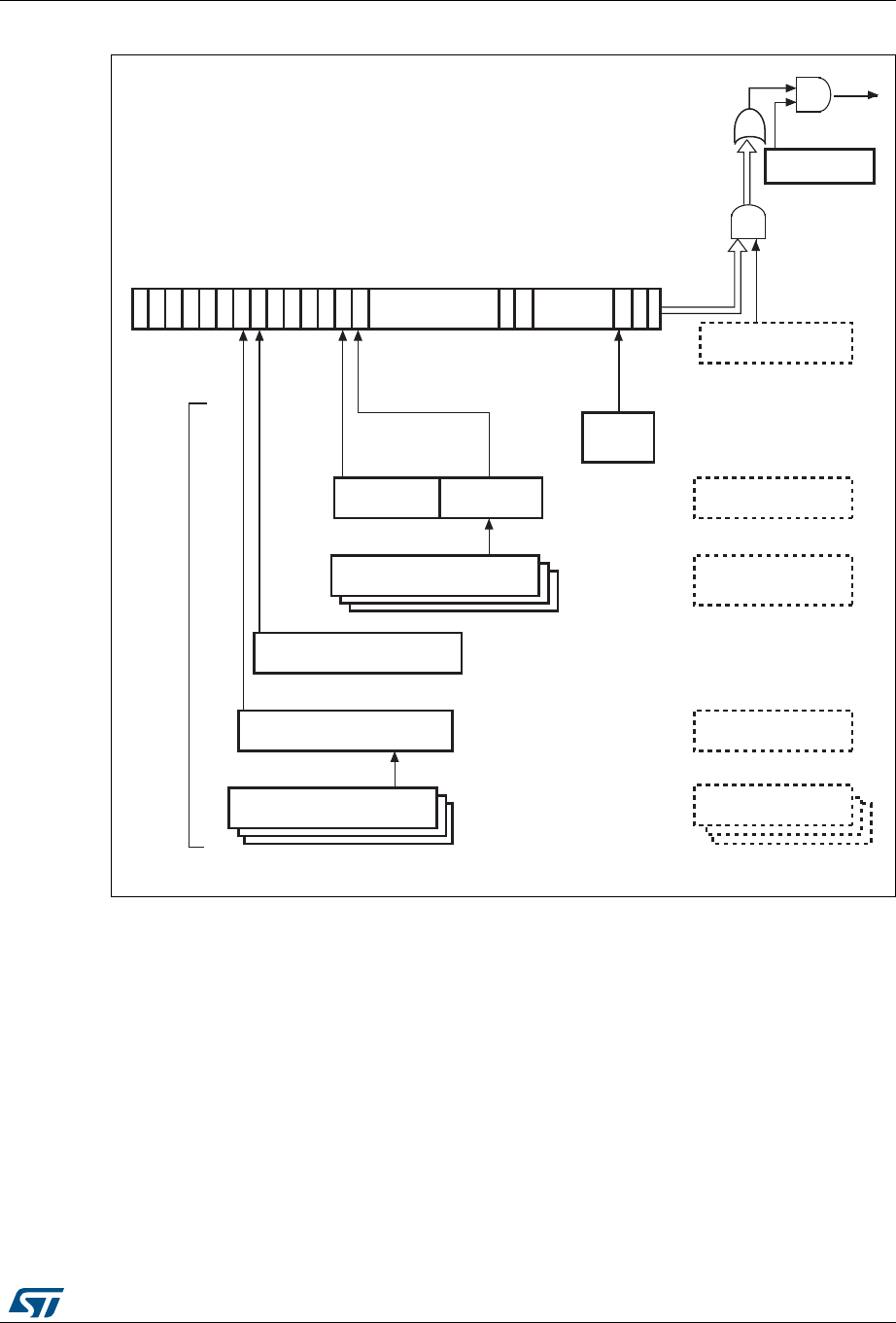
DocID018909 Rev 9 1247/1718
RM0090 USB on-the-go full-speed (OTG_FS)
1362
Figure 394. Interrupt hierarchy
1. The core interrupt register bits are shown in OTG_FS core interrupt register (OTG_FS_GINTSTS) on
page 1262.
34.16 OTG_FS control and status registers
By reading from and writing to the control and status registers (CSRs) through the AHB
slave interface, the application controls the OTG_FS controller. These registers are 32 bits
wide, and the addresses are 32-bit block aligned. The OTG_FS registers must be accessed
by words (32 bits).
31 30 29 28 27 26 25 24 23 20 19 18 17:10 9 8 7:3 2 1 0
AND
OR
Interrupt
Global interrupt
mask (Bit 0)
AHB configuration
register
Core interrupt mask
register
OTG
interrupt
register
Core interrupt
register(1)
Device IN/OUT endpoint
interrupt registers 0 to 3
Device all endpoints
interrupt register
16:9
OUT endpoints
3:0
IN endpoints
Interrupt
sources
Host port control and status
register
Host all channels interrupt
register
Host channels interrupt
mask registers 0 to 7
Host all channels
interrupt mask register
Host channels interrupt
registers 0 to 7
22 21
Device all endpoints
interrupt mask register
Device IN/OUT
endpoints common
interrupt mask register
ai15616b

USB on-the-go full-speed (OTG_FS) RM0090
1248/1718 DocID018909 Rev 9
CSRs are classified as follows:
•Core global registers
•Host-mode registers
•Host global registers
•Host port CSRs
•Host channel-specific registers
•Device-mode registers
•Device global registers
•Device endpoint-specific registers
•Power and clock-gating registers
•Data FIFO (DFIFO) access registers
Only the Core global, Power and clock-gating, Data FIFO access, and host port control and
status registers can be accessed in both host and device modes. When the OTG_FS
controller is operating in one mode, either device or host, the application must not access
registers from the other mode. If an illegal access occurs, a mode mismatch interrupt is
generated and reflected in the Core interrupt register (MMIS bit in the OTG_FS_GINTSTS
register). When the core switches from one mode to the other, the registers in the new mode
of operation must be reprogrammed as they would be after a power-on reset.
34.16.1 CSR memory map
The host and device mode registers occupy different addresses. All registers are
implemented in the AHB clock domain.

DocID018909 Rev 9 1249/1718
RM0090 USB on-the-go full-speed (OTG_FS)
1362
Figure 395. CSR memory map
1. x = 3 in device mode and x = 7 in host mode.
Global CSR map
These registers are available in both host and device modes.
0000h
Core global CSRs (1 Kbyte)
0400h
Host mode CSRs (1 Kbyte)
0800h
Device mode CSRs (1.5 Kbyte)
0E00h
Power and clock gating CSRs (0.5 Kbyte)
1000h
Device EP 0/Host channel 0 FIFO (4 Kbyte)
2000h
Device EP1/Host channel 1 FIFO (4 Kbyte)
3000h
Device EP (x – 1)
(1)
/Host channel (x – 1)
(1)
FIFO (4 Kbyte)
Device EP x
(1)
/Host channel x
(1)
FIFO (4 Kbyte)
Reserved
DFIFO
push/pop
to this region
2 0000h
3 FFFFh
Direct access to data FIFO RAM
for debugging (128 Kbyte)
DFIFO
debug read/
write to this
region
ai15615b
Table 195. Core global control and status registers (CSRs)
Acronym Address
offset Register name
OTG_FS_GOTGCTL 0x000 OTG_FS control and status register (OTG_FS_GOTGCTL) on page 1253
OTG_FS_GOTGINT 0x004 OTG_FS interrupt register (OTG_FS_GOTGINT) on page 1255
OTG_FS_GAHBCFG 0x008 OTG_FS AHB configuration register (OTG_FS_GAHBCFG) on page 1257
OTG_FS_GUSBCFG 0x00C OTG_FS USB configuration register (OTG_FS_GUSBCFG) on page 1258
OTG_FS_GRSTCTL 0x010 OTG_FS reset register (OTG_FS_GRSTCTL) on page 1260
OTG_FS_GINTSTS 0x014 OTG_FS core interrupt register (OTG_FS_GINTSTS) on page 1262
OTG_FS_GINTMSK 0x018 OTG_FS interrupt mask register (OTG_FS_GINTMSK) on page 1266

USB on-the-go full-speed (OTG_FS) RM0090
1250/1718 DocID018909 Rev 9
Host-mode CSR map
These registers must be programmed every time the core changes to host mode.
OTG_FS_GRXSTSR 0x01C OTG_FS Receive status debug read/OTG status read and pop registers
(OTG_FS_GRXSTSR/OTG_FS_GRXSTSP) on page 1269
OTG_FS_GRXSTSP 0x020
OTG_FS_GRXFSIZ 0x024 OTG_FS Receive FIFO size register (OTG_FS_GRXFSIZ) on page 1270
OTG_FS_HNPTXFSIZ/
OTG_FS_DIEPTXF0(1) 0x028
OTG_FS Host non-periodic transmit FIFO size register
(OTG_FS_HNPTXFSIZ)/Endpoint 0 Transmit FIFO size
(OTG_FS_DIEPTXF0)
OTG_FS_HNPTXSTS 0x02C OTG_FS non-periodic transmit FIFO/queue status register
(OTG_FS_HNPTXSTS) on page 1271
OTG_FS_GCCFG 0x038 OTG_FS general core configuration register (OTG_FS_GCCFG) on
page 1272
OTG_FS_CID 0x03C OTG_FS core ID register (OTG_FS_CID) on page 1273
OTG_FS_HPTXFSIZ 0x100 OTG_FS Host periodic transmit FIFO size register (OTG_FS_HPTXFSIZ) on
page 1274
OTG_FS_DIEPTXFx
0x104
0x124
...
0x138
OTG_FS device IN endpoint transmit FIFO size register
(OTG_FS_DIEPTXFx) (x = 1..3, where x is the FIFO_number) on page 1274
1. The general rule is to use OTG_FS_HNPTXFSIZ for host mode and OTG_FS_DIEPTXF0 for device mode.
Table 195. Core global control and status registers (CSRs) (continued)
Acronym Address
offset Register name
Table 196. Host-mode control and status registers (CSRs)
Acronym Offset
address Register name
OTG_FS_HCFG 0x400 OTG_FS Host configuration register (OTG_FS_HCFG) on page 1275
OTG_FS_HFIR 0x404 OTG_FS Host frame interval register (OTG_FS_HFIR) on page 1275
OTG_FS_HFNUM 0x408 OTG_FS Host frame number/frame time remaining register
(OTG_FS_HFNUM) on page 1276
OTG_FS_HPTXSTS 0x410 OTG_FS_Host periodic transmit FIFO/queue status register
(OTG_FS_HPTXSTS) on page 1276
OTG_FS_HAINT 0x414 OTG_FS Host all channels interrupt register (OTG_FS_HAINT) on
page 1277
OTG_FS_HAINTMSK 0x418 OTG_FS Host all channels interrupt mask register (OTG_FS_HAINTMSK)
on page 1278
OTG_FS_HPRT 0x440 OTG_FS Host port control and status register (OTG_FS_HPRT) on
page 1278

DocID018909 Rev 9 1251/1718
RM0090 USB on-the-go full-speed (OTG_FS)
1362
Device-mode CSR map
These registers must be programmed every time the core changes to device mode.
OTG_FS_HCCHARx
0x500
0x520
...
0x6E0h
OTG_FS Host channel-x characteristics register (OTG_FS_HCCHARx)
(x = 0..7, where x = Channel_number) on page 1281
OTG_FS_HCINTx 508h OTG_FS Host channel-x interrupt register (OTG_FS_HCINTx) (x = 0..7,
where x = Channel_number) on page 1282
OTG_FS_HCINTMSKx 50Ch OTG_FS Host channel-x interrupt mask register (OTG_FS_HCINTMSKx)
(x = 0..7, where x = Channel_number) on page 1283
OTG_FS_HCTSIZx 510h OTG_FS Host channel-x transfer size register (OTG_FS_HCTSIZx)
(x = 0..7, where x = Channel_number) on page 1284
Table 196. Host-mode control and status registers (CSRs) (continued)
Acronym Offset
address Register name
Table 197. Device-mode control and status registers
Acronym Offset
address Register name
OTG_FS_DCFG 0x800 OTG_FS device configuration register (OTG_FS_DCFG) on page 1285
OTG_FS_DCTL 0x804 OTG_FS device control register (OTG_FS_DCTL) on page 1286
OTG_FS_DSTS 0x808 OTG_FS device status register (OTG_FS_DSTS) on page 1287
OTG_FS_DIEPMSK 0x810 OTG_FS device IN endpoint common interrupt mask register
(OTG_FS_DIEPMSK) on page 1288
OTG_FS_DOEPMSK 0x814 OTG_FS device OUT endpoint common interrupt mask register
(OTG_FS_DOEPMSK) on page 1289
OTG_FS_DAINT 0x818 OTG_FS device all endpoints interrupt register (OTG_FS_DAINT) on
page 1290
OTG_FS_DAINTMSK 0x81C OTG_FS all endpoints interrupt mask register (OTG_FS_DAINTMSK)
on page 1291
OTG_FS_DVBUSDIS 0x828 OTG_FS device VBUS discharge time register (OTG_FS_DVBUSDIS)
on page 1291
OTG_FS_DVBUSPULS
E0x82C OTG_FS device VBUS pulsing time register (OTG_FS_DVBUSPULSE)
on page 1292
OTG_FS_DIEPEMPMSK 0x834 OTG_FS device IN endpoint FIFO empty interrupt mask register:
(OTG_FS_DIEPEMPMSK) on page 1292
OTG_FS_DIEPCTL0 0x900 OTG_FS device control IN endpoint 0 control register
(OTG_FS_DIEPCTL0) on page 1293

USB on-the-go full-speed (OTG_FS) RM0090
1252/1718 DocID018909 Rev 9
Data FIFO (DFIFO) access register map
These registers, available in both host and device modes, are used to read or write the FIFO
space for a specific endpoint or a channel, in a given direction. If a host channel is of type
IN, the FIFO can only be read on the channel. Similarly, if a host channel is of type OUT, the
FIFO can only be written on the channel.
OTG_FS_DIEPCTLx
0x920
0x940
...
0xAE0
OTG device endpoint-x control register (OTG_FS_DIEPCTLx) (x = 1..3,
where x = Endpoint_number) on page 1294
OTG_FS_DIEPINTx 0x908 OTG_FS device endpoint-x interrupt register (OTG_FS_DIEPINTx)
(x = 0..3, where x = Endpoint_number) on page 1301
OTG_FS_DIEPTSIZ0 0x910 OTG_FS device IN endpoint 0 transfer size register
(OTG_FS_DIEPTSIZ0) on page 1303
OTG_FS_DTXFSTSx 0x918
OTG_FS device IN endpoint transmit FIFO status register
(OTG_FS_DTXFSTSx) (x = 0..3, where x = Endpoint_number) on
page 1306
OTG_FS_DIEPTSIZx
0x930
0x950
...
0xAF0
OTG_FS device OUT endpoint-x transfer size register
(OTG_FS_DOEPTSIZx) (x = 1..3, where x = Endpoint_number) on
page 1306
OTG_FS_DOEPCTL0 0xB00 OTG_FS device control OUT endpoint 0 control register
(OTG_FS_DOEPCTL0) on page 1297
OTG_FS_DOEPCTLx
0xB20
0xB40
...
0xCC0
0xCE0
0xCFD
OTG device endpoint-x control register (OTG_FS_DIEPCTLx) (x = 1..3,
where x = Endpoint_number) on page 1294
OTG_FS_DOEPINTx 0xB08 OTG_FS device endpoint-x interrupt register (OTG_FS_DIEPINTx)
(x = 0..3, where x = Endpoint_number) on page 1301
OTG_FS_DOEPTSIZx 0xB10
OTG_FS device OUT endpoint-x transfer size register
(OTG_FS_DOEPTSIZx) (x = 1..3, where x = Endpoint_number) on
page 1306
Table 197. Device-mode control and status registers (continued)
Acronym Offset
address Register name
DocID018909 Rev 9 1253/1718
RM0090 USB on-the-go full-speed (OTG_FS)
1362
Power and clock gating CSR map
There is a single register for power and clock gating. It is available in both host and device
modes.
34.16.2 OTG_FS global registers
These registers are available in both host and device modes, and do not need to be
reprogrammed when switching between these modes.
Bit values in the register descriptions are expressed in binary unless otherwise specified.
OTG_FS control and status register (OTG_FS_GOTGCTL)
Address offset: 0x000
Reset value: 0x0000 0800
The OTG_FS_GOTGCTL register controls the behavior and reflects the status of the OTG
function of the core.
Table 198. Data FIFO (DFIFO) access register map
FIFO access register section Address range Access
Device IN Endpoint 0/Host OUT Channel 0: DFIFO Write Access
Device OUT Endpoint 0/Host IN Channel 0: DFIFO Read Access 0x1000–0x1FFC w
r
Device IN Endpoint 1/Host OUT Channel 1: DFIFO Write Access
Device OUT Endpoint 1/Host IN Channel 1: DFIFO Read Access 0x2000–0x2FFC w
r
... ... ...
Device IN Endpoint x(1)/Host OUT Channel x(1): DFIFO Write Access
Device OUT Endpoint x(1)/Host IN Channel x(1): DFIFO Read Access
1. Where x is 3 in device mode and 7 in host mode.
0xX000–0xXFFC w
r
Table 199. Power and clock gating control and status registers
Register name Acronym Offset address: 0xE00–0xFFF
Power and clock gating control register PCGCR 0xE00-0xE04
Reserved 0xE05–0xFFF
313029282726252423222120191817161514131211109876543210
Reserved
BSVLD
ASVLD
DBCT
CIDSTS
Reserved
DHNPEN
HSHNPEN
HNPRQ
HNGSCS
Reserved
SRQ
SRQSCS
rrrr rwrwrwr rwr

USB on-the-go full-speed (OTG_FS) RM0090
1254/1718 DocID018909 Rev 9
Bits 31:20 Reserved, must be kept at reset value.
Bit 19 BSVLD: B-session valid
Indicates the device mode transceiver status.
0: B-session is not valid.
1: B-session is valid.
In OTG mode, you can use this bit to determine if the device is connected or disconnected.
Note: Only accessible in device mode.
Bit 18 ASVLD: A-session valid
Indicates the host mode transceiver status.
0: A-session is not valid
1: A-session is valid
Note: Only accessible in host mode.
Bit 17 DBCT: Long/short debounce time
Indicates the debounce time of a detected connection.
0: Long debounce time, used for physical connections (100 ms + 2.5 µs)
1: Short debounce time, used for soft connections (2.5 µs)
Note: Only accessible in host mode.
Bit 16 CIDSTS: Connector ID status
Indicates the connector ID status on a connect event.
0: The OTG_FS controller is in A-device mode
1: The OTG_FS controller is in B-device mode
Note: Accessible in both device and host modes.
Bits 15:12 Reserved, must be kept at reset value.
Bit 11 DHNPEN: Device HNP enabled
The application sets this bit when it successfully receives a SetFeature.SetHNPEnable
command from the connected USB host.
0: HNP is not enabled in the application
1: HNP is enabled in the application
Note: Only accessible in device mode.
Bit 10 HSHNPEN: host set HNP enable
The application sets this bit when it has successfully enabled HNP (using the
SetFeature.SetHNPEnable command) on the connected device.
0: Host Set HNP is not enabled
1: Host Set HNP is enabled
Note: Only accessible in host mode.
Bit 9 HNPRQ: HNP request
The application sets this bit to initiate an HNP request to the connected USB host. The
application can clear this bit by writing a 0 when the host negotiation success status change
bit in the OTG_FS_GOTGINT register (HNSSCHG bit in OTG_FS_GOTGINT) is set. The
core clears this bit when the HNSSCHG bit is cleared.
0: No HNP request
1: HNP request
Note: Only accessible in device mode.

DocID018909 Rev 9 1255/1718
RM0090 USB on-the-go full-speed (OTG_FS)
1362
OTG_FS interrupt register (OTG_FS_GOTGINT)
Address offset: 0x04
Reset value: 0x0000 0000
The application reads this register whenever there is an OTG interrupt and clears the bits in
this register to clear the OTG interrupt.
Bit 8 HNGSCS: Host negotiation success
The core sets this bit when host negotiation is successful. The core clears this bit when the
HNP Request (HNPRQ) bit in this register is set.
0: Host negotiation failure
1: Host negotiation success
Note: Only accessible in device mode.
Bits 7:2 Reserved, must be kept at reset value.
Bit 1 SRQ: Session request
The application sets this bit to initiate a session request on the USB. The application can
clear this bit by writing a 0 when the host negotiation success status change bit in the
OTG_FS_GOTGINT register (HNSSCHG bit in OTG_FS_GOTGINT) is set. The core clears
this bit when the HNSSCHG bit is cleared.
If you use the USB 1.1 full-speed serial transceiver interface to initiate the session request,
the application must wait until VBUS discharges to 0.2 V, after the B-Session Valid bit in this
register (BSVLD bit in OTG_FS_GOTGCTL) is cleared. This discharge time varies between
different PHYs and can be obtained from the PHY vendor.
0: No session request
1: Session request
Note: Only accessible in device mode.
Bit 0 SRQSCS: Session request success
The core sets this bit when a session request initiation is successful.
0: Session request failure
1: Session request success
Note: Only accessible in device mode.
313029282726252423222120191817161514131211109876543210
Reserved
DBCDNE
ADTOCHG
HNGDET
Reserved
HNSSCHG
SRSSCHG
Reserved
SEDET
Res.
rc_
w1
rc_
w1
rc_
w1
rc_
w1
rc_
w1
rc_
w1
Bits 31:20 Reserved, must be kept at reset value.
Bit 19 DBCDNE: Debounce done
The core sets this bit when the debounce is completed after the device connect. The
application can start driving USB reset after seeing this interrupt. This bit is only valid when
the HNP Capable or SRP Capable bit is set in the OTG_FS_GUSBCFG register (HNPCAP
bit or SRPCAP bit in OTG_FS_GUSBCFG, respectively).
Note: Only accessible in host mode.

USB on-the-go full-speed (OTG_FS) RM0090
1256/1718 DocID018909 Rev 9
Bit 18 ADTOCHG: A-device timeout change
The core sets this bit to indicate that the A-device has timed out while waiting for the B-device
to connect.
Note: Accessible in both device and host modes.
Bit 17 HNGDET: Host negotiation detected
The core sets this bit when it detects a host negotiation request on the USB.
Note: Accessible in both device and host modes.
Bits 16:10 Reserved, must be kept at reset value.
Bit 9 HNSSCHG: Host negotiation success status change
The core sets this bit on the success or failure of a USB host negotiation request. The
application must read the host negotiation success bit of the OTG_FS_GOTGCTL register
(HNGSCS in OTG_FS_GOTGCTL) to check for success or failure.
Note: Accessible in both device and host modes.
Bits 7:3 Reserved, must be kept at reset value.
Bit 8 SRSSCHG: Session request success status change
The core sets this bit on the success or failure of a session request. The application must
read the session request success bit in the OTG_FS_GOTGCTL register (SRQSCS bit in
OTG_FS_GOTGCTL) to check for success or failure.
Note: Accessible in both device and host modes.
Bit 2 SEDET: Session end detected
The core sets this bit to indicate that the level of the voltage on VBUS is no longer valid for a
B-Peripheral session when VBUS < 0.8 V.
Bits 1:0 Reserved, must be kept at reset value.

DocID018909 Rev 9 1257/1718
RM0090 USB on-the-go full-speed (OTG_FS)
1362
OTG_FS AHB configuration register (OTG_FS_GAHBCFG)
Address offset: 0x008
Reset value: 0x0000 0000
This register can be used to configure the core after power-on or a change in mode. This
register mainly contains AHB system-related configuration parameters. Do not change this
register after the initial programming. The application must program this register before
starting any transactions on either the AHB or the USB.
313029282726252423222120191817161514131211109876543210
Reserved
PTXFELVL
TXFELVL
Reserved
GINTMSK
rw rw rw
Bits 31:20 Reserved, must be kept at reset value.
Bit 8 PTXFELVL: Periodic TxFIFO empty level
Indicates when the periodic TxFIFO empty interrupt bit in the OTG_FS_GINTSTS register
(PTXFE bit in OTG_FS_GINTSTS) is triggered.
0: PTXFE (in OTG_FS_GINTSTS) interrupt indicates that the Periodic TxFIFO is half empty
1: PTXFE (in OTG_FS_GINTSTS) interrupt indicates that the Periodic TxFIFO is completely
empty
Note: Only accessible in host mode.
Bit 7 TXFELVL: TxFIFO empty level
In device mode, this bit indicates when IN endpoint Transmit FIFO empty interrupt (TXFE in
OTG_FS_DIEPINTx.) is triggered.
0: the TXFE (in OTG_FS_DIEPINTx) interrupt indicates that the IN Endpoint TxFIFO is half
empty
1: the TXFE (in OTG_FS_DIEPINTx) interrupt indicates that the IN Endpoint TxFIFO is
completely empty
In host mode, this bit indicates when the nonperiodic Tx FIFO empty interrupt (NPTXFE bit in
OTG_FS_GINTSTS) is triggered:
0: the NPTXFE (in OTG_FS_GINTSTS) interrupt indicates that the nonperiodic Tx FIFO is
half empty
1: the NPTXFE (in OTG_FS_GINTSTS) interrupt indicates that the nonperiodic Tx FIFO is
completely empty
Bits 6:1 Reserved, must be kept at reset value.
Bit 0 GINTMSK: Global interrupt mask
The application uses this bit to mask or unmask the interrupt line assertion to itself.
Irrespective of this bit’s setting, the interrupt status registers are updated by the core.
0: Mask the interrupt assertion to the application.
1: Unmask the interrupt assertion to the application.
Note: Accessible in both device and host modes.

USB on-the-go full-speed (OTG_FS) RM0090
1258/1718 DocID018909 Rev 9
OTG_FS USB configuration register (OTG_FS_GUSBCFG)
Address offset: 0x00C
Reset value: 0x0000 0A00
This register can be used to configure the core after power-on or a changing to host mode
or device mode. It contains USB and USB-PHY related configuration parameters. The
application must program this register before starting any transactions on either the AHB or
the USB. Do not make changes to this register after the initial programming.
3130292827262524232221201918171615141312111098 7 6543210
CTXPKT
FDMOD
FHMOD
Reserved
TRDT
HNPCAP
SRPCAP
Res.
PHYSEL
Reserved
TOCAL
rw rw rw rw
r/rw
r/rw
wo rw
Bits 31:20 Reserved, must be kept at reset value.
Bit 31 CTXPKT: Corrupt Tx packet
This bit is for debug purposes only. Never set this bit to 1.
Note: Accessible in both device and host modes.
Bit 30 FDMOD: Force device mode
Writing a 1 to this bit forces the core to device mode irrespective of the OTG_FS_ID input
pin.
0: Normal mode
1: Force device mode
After setting the force bit, the application must wait at least 25 ms before the change takes
effect.
Note: Accessible in both device and host modes.
Bit 29 FHMOD: Force host mode
Writing a 1 to this bit forces the core to host mode irrespective of the OTG_FS_ID input pin.
0: Normal mode
1: Force host mode
After setting the force bit, the application must wait at least 25 ms before the change takes
effect.
Note: Accessible in both device and host modes.
Bits 28:14 Reserved, must be kept at reset value.
Bits 13:10 TRDT: USB turnaround time
These bits allows to set the turnaround time in PHY clocks. They must be configured
according to Table 200: TRDT values, depending on the application AHB frequency. Higher
TRDT values allow stretching the USB response time to IN tokens in order to compensate for
longer AHB read access latency to the Data FIFO.
Note: Only accessible in device mode.
Bit 9 HNPCAP: HNP-capable
The application uses this bit to control the OTG_FS controller’s HNP capabilities.
0: HNP capability is not enabled.
1: HNP capability is enabled.
Note: Accessible in both device and host modes.

DocID018909 Rev 9 1259/1718
RM0090 USB on-the-go full-speed (OTG_FS)
1362
Bit 8 SRPCAP: SRP-capable
The application uses this bit to control the OTG_FS controller’s SRP capabilities. If the core
operates as a non-SRP-capable
B-device, it cannot request the connected A-device (host) to activate VBUS and start a
session.
0: SRP capability is not enabled.
1: SRP capability is enabled.
Note: Accessible in both device and host modes.
Bit 7 Reserved, must be kept at reset value.
Bit 6 PHYSEL: Full Speed serial transceiver select
This bit is always 1 with write-only access.
Bits 5:3 Reserved, must be kept at reset value.
Bits 2:0 TOCAL: FS timeout calibration
The number of PHY clocks that the application programs in this field is added to the full-
speed interpacket timeout duration in the core to account for any additional delays
introduced by the PHY. This can be required, because the delay introduced by the PHY in
generating the line state condition can vary from one PHY to another.
The USB standard timeout value for full-speed operation is 16 to 18 (inclusive) bit times. The
application must program this field based on the speed of enumeration. The number of bit
times added per PHY clock is 0.25 bit times.
Table 200. TRDT values
AHB frequency range (MHz)
TRDT minimum value
Min. Max
14.2 15 0xF
15 16 0xE
16 17.2 0xD
17.2 18.5 0xC
18.5 20 0xB
20 21.8 0xA
21.8 24 0x9
24 27.5 0x8
27.5 32 0x7
32 - 0x6

USB on-the-go full-speed (OTG_FS) RM0090
1260/1718 DocID018909 Rev 9
OTG_FS reset register (OTG_FS_GRSTCTL)
Address offset: 0x10
Reset value: 0x2000 0000
The application uses this register to reset various hardware features inside the core.
313029282726252423222120191817161514131211109876543210
AHBIDL
Reserved TXFNUM
TXFFLSH
RXFFLSH
Reserved
FCRST
HSRST
CSRST
rrw rs rs rs rs rs
Bit 31 AHBIDL: AHB master idle
Indicates that the AHB master state machine is in the Idle condition.
Note: Accessible in both device and host modes.
Bits 30:11 Reserved, must be kept at reset value.
Bits 10:6 TXFNUM: TxFIFO number
This is the FIFO number that must be flushed using the TxFIFO Flush bit. This field must not
be changed until the core clears the TxFIFO Flush bit.
00000:
– Non-periodic TxFIFO flush in host mode
– Tx FIFO 0 flush in device mode
00001:
– Periodic TxFIFO flush in host mode
– TXFIFO 1 flush in device mode
00010: TXFIFO 2 flush in device mode
...
00101: TXFIFO 15 flush in device mode
10000: Flush all the transmit FIFOs in device or host mode.
Note: Accessible in both device and host modes.
Bit 5 TXFFLSH: TxFIFO flush
This bit selectively flushes a single or all transmit FIFOs, but cannot do so if the core is in the
midst of a transaction.
The application must write this bit only after checking that the core is neither writing to the
TxFIFO nor reading from the TxFIFO. Verify using these registers:
Read—NAK Effective Interrupt ensures the core is not reading from the FIFO
Write—AHBIDL bit in OTG_FS_GRSTCTL ensures the core is not writing anything to the
FIFO.
Note: Accessible in both device and host modes.
Bit 4 RXFFLSH: RxFIFO flush
The application can flush the entire RxFIFO using this bit, but must first ensure that the core
is not in the middle of a transaction.
The application must only write to this bit after checking that the core is neither reading from
the RxFIFO nor writing to the RxFIFO.
The application must wait until the bit is cleared before performing any other operations. This
bit requires 8 clocks (slowest of PHY or AHB clock) to clear.
Note: Accessible in both device and host modes.
Bit 3 Reserved, must be kept at reset value.

DocID018909 Rev 9 1261/1718
RM0090 USB on-the-go full-speed (OTG_FS)
1362
Bit 2 FCRST: Host frame counter reset
The application writes this bit to reset the frame number counter inside the core. When the
frame counter is reset, the subsequent SOF sent out by the core has a frame number of 0.
Note: Only accessible in host mode.
Bit 1 HSRST: HCLK soft reset
The application uses this bit to flush the control logic in the AHB Clock domain. Only AHB
Clock Domain pipelines are reset.
FIFOs are not flushed with this bit.
All state machines in the AHB clock domain are reset to the Idle state after terminating the
transactions on the AHB, following the protocol.
CSR control bits used by the AHB clock domain state machines are cleared.
To clear this interrupt, status mask bits that control the interrupt status and are generated by
the AHB clock domain state machine are cleared.
Because interrupt status bits are not cleared, the application can get the status of any core
events that occurred after it set this bit.
This is a self-clearing bit that the core clears after all necessary logic is reset in the core. This
can take several clocks, depending on the core’s current state.
Note: Accessible in both device and host modes.
Bit 0 CSRST: Core soft reset
Resets the HCLK and PCLK domains as follows:
Clears the interrupts and all the CSR register bits except for the following bits:
– RSTPDMODL bit in OTG_FS_PCGCCTL
– GAYEHCLK bit in OTG_FS_PCGCCTL
– PWRCLMP bit in OTG_FS_PCGCCTL
– STPPCLK bit in OTG_FS_PCGCCTL
– FSLSPCS bit in OTG_FS_HCFG
– DSPD bit in OTG_FS_DCFG
All module state machines (except for the AHB slave unit) are reset to the Idle state, and all
the transmit FIFOs and the receive FIFO are flushed.
Any transactions on the AHB Master are terminated as soon as possible, after completing the
last data phase of an AHB transfer. Any transactions on the USB are terminated immediately.
The application can write to this bit any time it wants to reset the core. This is a self-clearing
bit and the core clears this bit after all the necessary logic is reset in the core, which can take
several clocks, depending on the current state of the core. Once this bit has been cleared,
the software must wait at least 3 PHY clocks before accessing the PHY domain
(synchronization delay). The software must also check that bit 31 in this register is set to 1
(AHB Master is Idle) before starting any operation.
Typically, the software reset is used during software development and also when you
dynamically change the PHY selection bits in the above listed USB configuration registers.
When you change the PHY, the corresponding clock for the PHY is selected and used in the
PHY domain. Once a new clock is selected, the PHY domain has to be reset for proper
operation.
Note: Accessible in both device and host modes.

USB on-the-go full-speed (OTG_FS) RM0090
1262/1718 DocID018909 Rev 9
OTG_FS core interrupt register (OTG_FS_GINTSTS)
Address offset: 0x014
Reset value: 0x0400 0020
This register interrupts the application for system-level events in the current mode (device
mode or host mode).
Some of the bits in this register are valid only in host mode, while others are valid in device
mode only. This register also indicates the current mode. To clear the interrupt status bits of
the rc_w1 type, the application must write 1 into the bit.
The FIFO status interrupts are read-only; once software reads from or writes to the FIFO
while servicing these interrupts, FIFO interrupt conditions are cleared automatically.
The application must clear the OTG_FS_GINTSTS register at initialization before
unmasking the interrupt bit to avoid any interrupts generated prior to initialization.
313029282726252423222120191817161514131211109876543210
WKUINT
SRQINT
DISCINT
CIDSCHG
Reserved
PTXFE
HCINT
HPRTINT
Reserved
IPXFR/INCOMPISOOUT
IISOIXFR
OEPINT
IEPINT
Reserved
EOPF
ISOODRP
ENUMDNE
USBRST
USBSUSP
ESUSP
Reserved
GOUTNAKEFF
GINAKEFF
NPTXFE
RXFLVL
SOF
OTGINT
MMIS
CMOD
rc_w1 rrr Res.rc_w1rr rc_w1 rrrr
rc_w1
r
rc_w1
r
Bit 31 WKUPINT: Resume/remote wakeup detected interrupt
In device mode, this interrupt is asserted when a resume is detected on the USB. In host
mode, this interrupt is asserted when a remote wakeup is detected on the USB.
Note: Accessible in both device and host modes.
Bit 30 SRQINT: Session request/new session detected interrupt
In host mode, this interrupt is asserted when a session request is detected from the device.
In device mode, this interrupt is asserted when VBUS is in the valid range for a B-peripheral
device. Accessible in both device and host modes.
Bit 29 DISCINT: Disconnect detected interrupt
Asserted when a device disconnect is detected.
Note: Only accessible in host mode.
Bit 28 CIDSCHG: Connector ID status change
The core sets this bit when there is a change in connector ID status.
Note: Accessible in both device and host modes.
Bit 27 Reserved, must be kept at reset value.
Bit 26 PTXFE: Periodic TxFIFO empty
Asserted when the periodic transmit FIFO is either half or completely empty and there is
space for at least one entry to be written in the periodic request queue. The half or
completely empty status is determined by the periodic TxFIFO empty level bit in the
OTG_FS_GAHBCFG register (PTXFELVL bit in OTG_FS_GAHBCFG).
Note: Only accessible in host mode.

DocID018909 Rev 9 1263/1718
RM0090 USB on-the-go full-speed (OTG_FS)
1362
Bit 25 HCINT: Host channels interrupt
The core sets this bit to indicate that an interrupt is pending on one of the channels of the
core (in host mode). The application must read the OTG_FS_HAINT register to determine
the exact number of the channel on which the interrupt occurred, and then read the
corresponding OTG_FS_HCINTx register to determine the exact cause of the interrupt. The
application must clear the appropriate status bit in the OTG_FS_HCINTx register to clear
this bit.
Note: Only accessible in host mode.
Bit 24 HPRTINT: Host port interrupt
The core sets this bit to indicate a change in port status of one of the OTG_FS controller
ports in host mode. The application must read the OTG_FS_HPRT register to determine the
exact event that caused this interrupt. The application must clear the appropriate status bit in
the OTG_FS_HPRT register to clear this bit.
Note: Only accessible in host mode.
Bits 23:22 Reserved, must be kept at reset value.
Bit 21 IPXFR: Incomplete periodic transfer
In host mode, the core sets this interrupt bit when there are incomplete periodic transactions
still pending, which are scheduled for the current frame.
INCOMPISOOUT: Incomplete isochronous OUT transfer
In device mode, the core sets this interrupt to indicate that there is at least one isochronous
OUT endpoint on which the transfer is not completed in the current frame. This interrupt is
asserted along with the End of periodic frame interrupt (EOPF) bit in this register.
Bit 20 IISOIXFR: Incomplete isochronous IN transfer
The core sets this interrupt to indicate that there is at least one isochronous IN endpoint on
which the transfer is not completed in the current frame. This interrupt is asserted along with
the End of periodic frame interrupt (EOPF) bit in this register.
Note: Only accessible in device mode.
Bit 19 OEPINT: OUT endpoint interrupt
The core sets this bit to indicate that an interrupt is pending on one of the OUT endpoints of
the core (in device mode). The application must read the OTG_FS_DAINT register to
determine the exact number of the OUT endpoint on which the interrupt occurred, and then
read the corresponding OTG_FS_DOEPINTx register to determine the exact cause of the
interrupt. The application must clear the appropriate status bit in the corresponding
OTG_FS_DOEPINTx register to clear this bit.
Note: Only accessible in device mode.
Bit 18 IEPINT: IN endpoint interrupt
The core sets this bit to indicate that an interrupt is pending on one of the IN endpoints of the
core (in device mode). The application must read the OTG_FS_DAINT register to determine
the exact number of the IN endpoint on which the interrupt occurred, and then read the
corresponding OTG_FS_DIEPINTx register to determine the exact cause of the interrupt.
The application must clear the appropriate status bit in the corresponding
OTG_FS_DIEPINTx register to clear this bit.
Note: Only accessible in device mode.
Bits 17:16 Reserved, must be kept at reset value.
Bit 15 EOPF: End of periodic frame interrupt
Indicates that the period specified in the periodic frame interval field of the OTG_FS_DCFG
register (PFIVL bit in OTG_FS_DCFG) has been reached in the current frame.
Note: Only accessible in device mode.

USB on-the-go full-speed (OTG_FS) RM0090
1264/1718 DocID018909 Rev 9
Bit 14 ISOODRP: Isochronous OUT packet dropped interrupt
The core sets this bit when it fails to write an isochronous OUT packet into the RxFIFO
because the RxFIFO does not have enough space to accommodate a maximum size packet
for the isochronous OUT endpoint.
Note: Only accessible in device mode.
Bit 13 ENUMDNE: Enumeration done
The core sets this bit to indicate that speed enumeration is complete. The application must
read the OTG_FS_DSTS register to obtain the enumerated speed.
Note: Only accessible in device mode.
Bit 12 USBRST: USB reset
The core sets this bit to indicate that a reset is detected on the USB.
Note: Only accessible in device mode.
Bit 11 USBSUSP: USB suspend
The core sets this bit to indicate that a suspend was detected on the USB. The core enters
the Suspended state when there is no activity on the data lines for a period of 3 ms.
Note: Only accessible in device mode.
Bit 10 ESUSP: Early suspend
The core sets this bit to indicate that an Idle state has been detected on the USB for 3 ms.
Note: Only accessible in device mode.
Bits 9:8 Reserved, must be kept at reset value.
Bit 7 GONAKEFF: Global OUT NAK effective
Indicates that the Set global OUT NAK bit in the OTG_FS_DCTL register (SGONAK bit in
OTG_FS_DCTL), set by the application, has taken effect in the core. This bit can be cleared
by writing the Clear global OUT NAK bit in the OTG_FS_DCTL register (CGONAK bit in
OTG_FS_DCTL).
Note: Only accessible in device mode.
Bit 6 GINAKEFF: Global IN non-periodic NAK effective
Indicates that the Set global non-periodic IN NAK bit in the OTG_FS_DCTL register
(SGINAK bit in OTG_FS_DCTL), set by the application, has taken effect in the core. That is,
the core has sampled the Global IN NAK bit set by the application. This bit can be cleared by
clearing the Clear global non-periodic IN NAK bit in the OTG_FS_DCTL register (CGINAK
bit in OTG_FS_DCTL).
This interrupt does not necessarily mean that a NAK handshake is sent out on the USB. The
STALL bit takes precedence over the NAK bit.
Note: Only accessible in device mode.
Bit 5 NPTXFE: Non-periodic TxFIFO empty
This interrupt is asserted when the non-periodic TxFIFO is either half or completely empty,
and there is space for at least one entry to be written to the non-periodic transmit request
queue. The half or completely empty status is determined by the non-periodic TxFIFO empty
level bit in the OTG_FS_GAHBCFG register (TXFELVL bit in OTG_FS_GAHBCFG).
Note: Accessible in host mode only.
Bit 4 RXFLVL: RxFIFO non-empty
Indicates that there is at least one packet pending to be read from the RxFIFO.
Note: Accessible in both host and device modes.

DocID018909 Rev 9 1265/1718
RM0090 USB on-the-go full-speed (OTG_FS)
1362
Bit 3 SOF: Start of frame
In host mode, the core sets this bit to indicate that an SOF (FS), or Keep-Alive (LS) is
transmitted on the USB. The application must write a 1 to this bit to clear the interrupt.
In device mode, in the core sets this bit to indicate that an SOF token has been received on
the USB. The application can read the Device Status register to get the current frame
number. This interrupt is seen only when the core is operating in FS.
Note: Accessible in both host and device modes.
Bit 2 OTGINT: OTG interrupt
The core sets this bit to indicate an OTG protocol event. The application must read the OTG
Interrupt Status (OTG_FS_GOTGINT) register to determine the exact event that caused this
interrupt. The application must clear the appropriate status bit in the OTG_FS_GOTGINT
register to clear this bit.
Note: Accessible in both host and device modes.
Bit 1 MMIS: Mode mismatch interrupt
The core sets this bit when the application is trying to access:
– A host mode register, when the core is operating in device mode
– A device mode register, when the core is operating in host mode
The register access is completed on the AHB with an OKAY response, but is ignored by the
core internally and does not affect the operation of the core.
Note: Accessible in both host and device modes.
Bit 0 CMOD: Current mode of operation
Indicates the current mode.
0: Device mode
1: Host mode
Note: Accessible in both host and device modes.

USB on-the-go full-speed (OTG_FS) RM0090
1266/1718 DocID018909 Rev 9
OTG_FS interrupt mask register (OTG_FS_GINTMSK)
Address offset: 0x018
Reset value: 0x0000 0000
This register works with the Core interrupt register to interrupt the application. When an
interrupt bit is masked, the interrupt associated with that bit is not generated. However, the
Core Interrupt (OTG_FS_GINTSTS) register bit corresponding to that interrupt is still set.
313029282726252423222120191817161514131211109876543210
WUIM
SRQIM
DISCINT
CIDSCHGM
Reserved
PTXFEM
HCIM
PRTIM
Reserved
IPXFRM/IISOOXFRM
IISOIXFRM
OEPINT
IEPINT
EPMISM
Reserved
EOPFM
ISOODRPM
ENUMDNEM
USBRST
USBSUSPM
ESUSPM
Reserved
GONAKEFFM
GINAKEFFM
NPTXFEM
RXFLVLM
SOFM
OTGINT
MMISM
Reserved
rwrwrwrw rwrw r rwrwrwrwrw rwrwrwrwrwrw rwrwrwrwrwrwrw
Bit 31 WUIM: Resume/remote wakeup detected interrupt mask
0: Masked interrupt
1: Unmasked interrupt
Note: Accessible in both host and device modes.
Bit 30 SRQIM: Session request/new session detected interrupt mask
0: Masked interrupt
1: Unmasked interrupt
Note: Accessible in both host and device modes.
Bit 29 DISCINT: Disconnect detected interrupt mask
0: Masked interrupt
1: Unmasked interrupt
Note: Only accessible in device mode.
Bit 28 CIDSCHGM: Connector ID status change mask
0: Masked interrupt
1: Unmasked interrupt
Note: Accessible in both host and device modes.
Bit 27 Reserved, must be kept at reset value.
Bit 26 PTXFEM: Periodic TxFIFO empty mask
0: Masked interrupt
1: Unmasked interrupt
Note: Only accessible in host mode.
Bit 25 HCIM: Host channels interrupt mask
0: Masked interrupt
1: Unmasked interrupt
Note: Only accessible in host mode.
Bit 24 PRTIM: Host port interrupt mask
0: Masked interrupt
1: Unmasked interrupt
Note: Only accessible in host mode.

DocID018909 Rev 9 1267/1718
RM0090 USB on-the-go full-speed (OTG_FS)
1362
Bits 23:22 Reserved, must be kept at reset value.
Bit 21 IPXFRM: Incomplete periodic transfer mask
0: Masked interrupt
1: Unmasked interrupt
Note: Only accessible in host mode.
IISOOXFRM: Incomplete isochronous OUT transfer mask
0: Masked interrupt
1: Unmasked interrupt
Note: Only accessible in device mode.
Bit 20 IISOIXFRM: Incomplete isochronous IN transfer mask
0: Masked interrupt
1: Unmasked interrupt
Note: Only accessible in device mode.
Bit 19 OEPINT: OUT endpoints interrupt mask
0: Masked interrupt
1: Unmasked interrupt
Note: Only accessible in device mode.
Bit 18 IEPINT: IN endpoints interrupt mask
0: Masked interrupt
1: Unmasked interrupt
Note: Only accessible in device mode.
Bit 17 EPMISM: Endpoint mismatch interrupt mask
0: Masked interrupt
1: Unmasked interrupt
Note: Only accessible in device mode.
Bit 16 Reserved, must be kept at reset value.
Bit 15 EOPFM: End of periodic frame interrupt mask
0: Masked interrupt
1: Unmasked interrupt
Note: Only accessible in device mode.
Bit 14 ISOODRPM: Isochronous OUT packet dropped interrupt mask
0: Masked interrupt
1: Unmasked interrupt
Note: Only accessible in device mode.
Bit 13 ENUMDNEM: Enumeration done mask
0: Masked interrupt
1: Unmasked interrupt
Note: Only accessible in device mode.
Bit 12 USBRST: USB reset mask
0: Masked interrupt
1: Unmasked interrupt
Note: Only accessible in device mode.

USB on-the-go full-speed (OTG_FS) RM0090
1268/1718 DocID018909 Rev 9
Bit 11 USBSUSPM: USB suspend mask
0: Masked interrupt
1: Unmasked interrupt
Note: Only accessible in device mode.
Bit 10 ESUSPM: Early suspend mask
0: Masked interrupt
1: Unmasked interrupt
Note: Only accessible in device mode.
Bits 9:8 Reserved, must be kept at reset value.
Bit 7 GONAKEFFM: Global OUT NAK effective mask
0: Masked interrupt
1: Unmasked interrupt
Note: Only accessible in device mode.
Bit 6 GINAKEFFM: Global non-periodic IN NAK effective mask
0: Masked interrupt
1: Unmasked interrupt
Note: Only accessible in device mode.
Bit 5 NPTXFEM: Non-periodic TxFIFO empty mask
0: Masked interrupt
1: Unmasked interrupt
Note: Only accessible in Host mode.
Bit 4 RXFLVLM: Receive FIFO non-empty mask
0: Masked interrupt
1: Unmasked interrupt
Note: Accessible in both device and host modes.
Bit 3 SOFM: Start of frame mask
0: Masked interrupt
1: Unmasked interrupt
Note: Accessible in both device and host modes.
Bit 2 OTGINT: OTG interrupt mask
0: Masked interrupt
1: Unmasked interrupt
Note: Accessible in both device and host modes.
Bit 1 MMISM: Mode mismatch interrupt mask
0: Masked interrupt
1: Unmasked interrupt
Note: Accessible in both device and host modes.
Bit 0 Reserved, must be kept at reset value.
DocID018909 Rev 9 1269/1718
RM0090 USB on-the-go full-speed (OTG_FS)
1362
OTG_FS Receive status debug read/OTG status read and pop registers
(OTG_FS_GRXSTSR/OTG_FS_GRXSTSP)
Address offset for Read: 0x01C
Address offset for Pop: 0x020
Reset value: 0x0000 0000
A read to the Receive status debug read register returns the contents of the top of the
Receive FIFO. A read to the Receive status read and pop register additionally pops the top
data entry out of the RxFIFO.
The receive status contents must be interpreted differently in host and device modes. The
core ignores the receive status pop/read when the receive FIFO is empty and returns a
value of 0x0000 0000. The application must only pop the Receive Status FIFO when the
Receive FIFO non-empty bit of the Core interrupt register (RXFLVL bit in
OTG_FS_GINTSTS) is asserted.
Host mode:
Device mode:
313029282726252423222120191817161514131211109876543210
Reserved PKTSTS DPID BCNT CHNUM
rr r r
Bits 31:21 Reserved, must be kept at reset value.
Bits 20:17 PKTSTS: Packet status
Indicates the status of the received packet
0010: IN data packet received
0011: IN transfer completed (triggers an interrupt)
0101: Data toggle error (triggers an interrupt)
0111: Channel halted (triggers an interrupt)
Others: Reserved
Bits 16:15 DPID: Data PID
Indicates the Data PID of the received packet
00: DATA0
10: DATA1
01: DATA2
11: MDATA
Bits 14:4 BCNT: Byte count
Indicates the byte count of the received IN data packet.
Bits 3:0 CHNUM: Channel number
Indicates the channel number to which the current received packet belongs.
313029282726252423222120191817161514131211109876543210
Reserved
FRMNUM PKTSTS DPID BCNT EPNUM
rrr r r

USB on-the-go full-speed (OTG_FS) RM0090
1270/1718 DocID018909 Rev 9
OTG_FS Receive FIFO size register (OTG_FS_GRXFSIZ)
Address offset: 0x024
Reset value: 0x0000 0200
The application can program the RAM size that must be allocated to the RxFIFO.
Bits 31:25 Reserved, must be kept at reset value.
Bits 24:21 FRMNUM: Frame number
This is the least significant 4 bits of the frame number in which the packet is received on the
USB. This field is supported only when isochronous OUT endpoints are supported.
Bits 20:17 PKTSTS: Packet status
Indicates the status of the received packet
0001: Global OUT NAK (triggers an interrupt)
0010: OUT data packet received
0011: OUT transfer completed (triggers an interrupt)
0100: SETUP transaction completed (triggers an interrupt)
0110: SETUP data packet received
Others: Reserved
Bits 16:15 DPID: Data PID
Indicates the Data PID of the received OUT data packet
00: DATA0
10: DATA1
01: DATA2
11: MDATA
Bits 14:4 BCNT: Byte count
Indicates the byte count of the received data packet.
Bits 3:0 EPNUM: Endpoint number
Indicates the endpoint number to which the current received packet belongs.
313029282726252423222120191817161514131211109876543210
Reserved RXFD
r/rw
Bits 31:16 Reserved, must be kept at reset value.
Bits 15:0 RXFD: RxFIFO depth
This value is in terms of 32-bit words.
Minimum value is 16
Maximum value is 256
The power-on reset value of this register is specified as the largest Rx data FIFO depth.

DocID018909 Rev 9 1271/1718
RM0090 USB on-the-go full-speed (OTG_FS)
1362
OTG_FS Host non-periodic transmit FIFO size register
(OTG_FS_HNPTXFSIZ)/Endpoint 0 Transmit FIFO size (OTG_FS_DIEPTXF0)
Address offset: 0x028
Reset value: 0x0000 0200
Host mode
Device mode
OTG_FS non-periodic transmit FIFO/queue status register
(OTG_FS_HNPTXSTS)
Address offset: 0x02C
Reset value: 0x0008 0200
Note: In Device mode, this register is not valid.
This read-only register contains the free space information for the non-periodic TxFIFO and
the non-periodic transmit request queue.
313029282726252423222120191817161514131211109876543210
NPTXFD/TX0FD NPTXFSA/TX0FSA
r/rw r/rw
Bits 31:16 NPTXFD: Non-periodic TxFIFO depth
This value is in terms of 32-bit words.
Minimum value is 16
Maximum value is 256
Bits 15:0 NPTXFSA: Non-periodic transmit RAM start address
This field contains the memory start address for non-periodic transmit FIFO RAM.
Bits 31:16 TX0FD: Endpoint 0 TxFIFO depth
This value is in terms of 32-bit words.
Minimum value is 16
Maximum value is 256
Bits 15:0 TX0FSA: Endpoint 0 transmit RAM start address
This field contains the memory start address for the endpoint 0 transmit FIFO RAM.
313029282726252423222120191817161514131211109876543210
Reserved
NPTXQTOP NPTQXSAV NPTXFSAV
rr r

USB on-the-go full-speed (OTG_FS) RM0090
1272/1718 DocID018909 Rev 9
OTG_FS general core configuration register (OTG_FS_GCCFG)
Address offset: 0x038
Reset value: 0x0000 0000
Bit 31 Reserved, must be kept at reset value.
Bits 30:24 NPTXQTOP: Top of the non-periodic transmit request queue
Entry in the non-periodic Tx request queue that is currently being processed by the MAC.
Bits 30:27: Channel/endpoint number
Bits 26:25:
– 00: IN/OUT token
– 01: Zero-length transmit packet (device IN/host OUT)
– 11: Channel halt command
Bit 24: Terminate (last entry for selected channel/endpoint)
Bits 23:16 NPTQXSAV: Non-periodic transmit request queue space available
Indicates the amount of free space available in the non-periodic transmit request queue.
This queue holds both IN and OUT requests in host mode. Device mode has only IN
requests.
00: Non-periodic transmit request queue is full
01: 1 location available
10: 2 locations available
bxn: n locations available (0 ≤ n ≤ 8)
Others: Reserved
Bits 15:0 NPTXFSAV: Non-periodic TxFIFO space available
Indicates the amount of free space available in the non-periodic TxFIFO.
Values are in terms of 32-bit words.
00: Non-periodic TxFIFO is full
01: 1 word available
10: 2 words available
0xn: n words available (where 0 ≤ n ≤ 256)
Others: Reserved
313029282726252423222120191817161514131211109876543210
Reserved
NOVBUSSENS
SOFOUTEN
VBUSBSEN
VBUSASEN
Reserved
.PWRDWN
Reserved
rw rw rw rw rw

DocID018909 Rev 9 1273/1718
RM0090 USB on-the-go full-speed (OTG_FS)
1362
OTG_FS core ID register (OTG_FS_CID)
Address offset: 0x03C
Reset value:0x0000 1100
This is a read only register containing the Product ID.
Bits 31:22 Reserved, must be kept at reset value.
Bit 21 NOVBUSSENS: VBUS sensing disable option
When this bit is set, VBUS is considered internally to be always at VBUS valid level (5 V). This
option removes the need for a dedicated VBUS pad, and leave this pad free to be used for
other purposes such as a shared functionality. VBUS connection can be remapped on
another general purpose input pad and monitored by software.
This option is only suitable for host-only or device-only applications.
0: VBUS sensing available by hardware
1: VBUS sensing not available by hardware.
Bit 20 SOFOUTEN: SOF output enable
0: SOF pulse not available on PAD
1: SOF pulse available on PAD
Bit 19 VBUSBSEN: Enable the VBUS sensing “B” device
0: VBUS sensing “B” disabled
1: VBUS sensing “B” enabled
Bit 18 VBUSASEN: Enable the VBUS sensing “A” device
0: VBUS sensing “A” disabled
1: VBUS sensing “A” enabled
Bit 17 Reserved, must be kept at reset value.
Bit 16 PWRDWN: Power down
Used to activate the transceiver in transmission/reception
0: Power down active
1: Power down deactivated (“Transceiver active”)
Bits 15:0 Reserved, must be kept at reset value.
313029282726252423222120191817161514131211109876543210
PRODUCT_ID
rw rw rw rw rw rw rw rw rw rw rw rw rw rw rw rw rw rw rw rw rw rw rw rw rw rw rw rw rw rw rw rw
Bits 31:0 PRODUCT_ID: Product ID field
Application-programmable ID field.

USB on-the-go full-speed (OTG_FS) RM0090
1274/1718 DocID018909 Rev 9
OTG_FS Host periodic transmit FIFO size register (OTG_FS_HPTXFSIZ)
Address offset: 0x100
Reset value: 0x0200 0600
OTG_FS device IN endpoint transmit FIFO size register (OTG_FS_DIEPTXFx)
(x = 1..3, where x is the FIFO_number)
Address offset: 0x104 + (FIFO_number – 1) × 0x04
Reset value: 0x02000400
313029282726252423222120191817161514131211109876543210
PTXFSIZ PTXSA
r/r
w
r/r
w
r/r
w
r/r
w
r/r
w
r/r
w
r/r
w
r/r
w
r/r
w
r/r
w
r/r
w
r/r
w
r/r
w
r/r
w
r/r
w
r/r
w
r/r
w
r/r
w
r/r
w
r/r
w
r/r
w
r/r
w
r/r
w
r/r
w
r/r
w
r/r
w
r/r
w
r/r
w
r/r
w
r/r
w
r/r
w
r/r
w
Bits 31:16 PTXFD: Host periodic TxFIFO depth
This value is in terms of 32-bit words.
Minimum value is 16
Bits 15:0 PTXSA: Host periodic TxFIFO start address
The power-on reset value of this register is the sum of the largest Rx data FIFO depth and
largest non-periodic Tx data FIFO depth.
313029282726252423222120191817161514131211109876543210
INEPTXFD INEPTXSA
r/r
w
r/r
w
r/r
w
r/r
w
r/r
w
r/r
w
r/r
w
r/r
w
r/r
w
r/r
w
r/r
w
r/r
w
r/r
w
r/r
w
r/r
w
r/r
w
r/r
w
r/r
w
r/r
w
r/r
w
r/r
w
r/r
w
r/r
w
r/r
w
r/r
w
r/r
w
r/r
w
r/r
w
r/r
w
r/r
w
r/r
w
r/r
w
Bits 31:16 INEPTXFD: IN endpoint TxFIFO depth
This value is in terms of 32-bit words.
Minimum value is 16
The power-on reset value of this register is specified as the largest IN endpoint FIFO
number depth.
Bits 15:0 INEPTXSA: IN endpoint FIFOx transmit RAM start address
This field contains the memory start address for IN endpoint transmit FIFOx. The address
must be aligned with a 32-bit memory location.

DocID018909 Rev 9 1275/1718
RM0090 USB on-the-go full-speed (OTG_FS)
1362
34.16.3 Host-mode registers
Bit values in the register descriptions are expressed in binary unless otherwise specified.
Host-mode registers affect the operation of the core in the host mode. Host mode registers
must not be accessed in device mode, as the results are undefined. Host mode registers
can be categorized as follows:
OTG_FS Host configuration register (OTG_FS_HCFG)
Address offset: 0x400
Reset value: 0x0000 0000
This register configures the core after power-on. Do not make changes to this register after
initializing the host.
OTG_FS Host frame interval register (OTG_FS_HFIR)
Address offset: 0x404
Reset value: 0x0000 EA60
This register stores the frame interval information for the current speed to which the
OTG_FS controller has enumerated.
313029282726252423222120191817161514131211109876543210
Reserved
FSLSS
FSLSPCS
rrwrw
Bits 31:3 Reserved, must be kept at reset value.
Bit 2 FSLSS: FS- and LS-only support
The application uses this bit to control the core’s enumeration speed. Using this bit, the
application can make the core enumerate as an FS host, even if the connected device
supports HS traffic. Do not make changes to this field after initial programming.
1: FS/LS-only, even if the connected device can support HS (read-only)
Bits 1:0 FSLSPCS: FS/LS PHY clock select
When the core is in FS host mode
01: PHY clock is running at 48 MHz
Others: Reserved
When the core is in LS host mode
00: Reserved
01: Select 48 MHz PHY clock frequency
10: Select 6 MHz PHY clock frequency
11: Reserved
Note: The FSLSPCS must be set on a connection event according to the speed of the
connected device (after changing this bit, a software reset must be performed).
313029282726252423222120191817161514131211109876543210
Reserved
FRIVL
rw rw rw rw rw rw rw rw rw rw rw rw rw rw rw rw

USB on-the-go full-speed (OTG_FS) RM0090
1276/1718 DocID018909 Rev 9
OTG_FS Host frame number/frame time remaining register (OTG_FS_HFNUM)
Address offset: 0x408
Reset value: 0x0000 3FFF
This register indicates the current frame number. It also indicates the time remaining (in
terms of the number of PHY clocks) in the current frame.
OTG_FS_Host periodic transmit FIFO/queue status register
(OTG_FS_HPTXSTS)
Address offset: 0x410
Reset value: 0x0008 0100
This read-only register contains the free space information for the periodic TxFIFO and the
periodic transmit request queue.
Bits 31:16 Reserved, must be kept at reset value.
Bits 15:0 FRIVL: Frame interval
The value that the application programs to this field specifies the interval between two
consecutive SOFs (FS) or Keep-Alive tokens (LS). This field contains the number of PHY
clocks that constitute the required frame interval. The application can write a value to this
register only after the Port enable bit of the host port control and status register (PENA bit in
OTG_FS_HPRT) has been set. If no value is programmed, the core calculates the value
based on the PHY clock specified in the FS/LS PHY Clock Select field of the host
configuration register (FSLSPCS in OTG_FS_HCFG). Do not change the value of this field
after the initial configuration.
1 ms × (PHY clock frequency)
313029282726252423222120191817161514131211109876543210
FTREM FRNUM
rrrrrrrrrrrrrrrrrrrrrrrrrrrrrrrr
Bits 31:16 FTREM: Frame time remaining
Indicates the amount of time remaining in the current frame, in terms of PHY clocks. This
field decrements on each PHY clock. When it reaches zero, this field is reloaded with the
value in the Frame interval register and a new SOF is transmitted on the USB.
Bits 15:0 FRNUM: Frame number
This field increments when a new SOF is transmitted on the USB, and is cleared to 0 when
it reaches 0x3FFF.
313029282726252423222120191817161514131211109876543210
PTXQTOP PTXQSAV PTXFSAVL
rrrrrrrrrrrrrrrrrwrwrwrwrwrwrwrwrwrwrwrwrwrwrwrw

DocID018909 Rev 9 1277/1718
RM0090 USB on-the-go full-speed (OTG_FS)
1362
OTG_FS Host all channels interrupt register (OTG_FS_HAINT)
Address offset: 0x414
Reset value: 0x0000 000
When a significant event occurs on a channel, the host all channels interrupt register
interrupts the application using the host channels interrupt bit of the Core interrupt register
(HCINT bit in OTG_FS_GINTSTS). This is shown in Figure 394. There is one interrupt bit
per channel, up to a maximum of 16 bits. Bits in this register are set and cleared when the
application sets and clears bits in the corresponding host channel-x interrupt register.
Bits 31:24 PTXQTOP: Top of the periodic transmit request queue
This indicates the entry in the periodic Tx request queue that is currently being processed by
the MAC.
This register is used for debugging.
Bit 31: Odd/Even frame
– 0: send in even frame
– 1: send in odd frame
Bits 30:27: Channel/endpoint number
Bits 26:25: Type
– 00: IN/OUT
– 01: Zero-length packet
– 11: Disable channel command
Bit 24: Terminate (last entry for the selected channel/endpoint)
Bits 23:16 PTXQSAV: Periodic transmit request queue space available
Indicates the number of free locations available to be written in the periodic transmit request
queue. This queue holds both IN and OUT requests.
00: Periodic transmit request queue is full
01: 1 location available
10: 2 locations available
bxn: n locations available (0 ≤ n ≤ 8)
Others: Reserved
Bits 15:0 PTXFSAVL: Periodic transmit data FIFO space available
Indicates the number of free locations available to be written to in the periodic TxFIFO.
Values are in terms of 32-bit words
0000: Periodic TxFIFO is full
0001: 1 word available
0010: 2 words available
bxn: n words available (where 0 ≤n≤PTXFD)
Others: Reserved
313029282726252423222120191817161514131211109876543210
Reserved HAINT
rrrrrrrrrrrrrrrr
Bits 31:16 Reserved, must be kept at reset value.
Bits 15:0 HAINT: Channel interrupts
One bit per channel: Bit 0 for Channel 0, bit 15 for Channel 15
USB on-the-go full-speed (OTG_FS) RM0090
1278/1718 DocID018909 Rev 9
OTG_FS Host all channels interrupt mask register (OTG_FS_HAINTMSK)
Address offset: 0x418
Reset value: 0x0000 0000
The host all channel interrupt mask register works with the host all channel interrupt register
to interrupt the application when an event occurs on a channel. There is one interrupt mask
bit per channel, up to a maximum of 16 bits.
OTG_FS Host port control and status register (OTG_FS_HPRT)
Address offset: 0x440
Reset value: 0x0000 0000
This register is available only in host mode. Currently, the OTG host supports only one port.
A single register holds USB port-related information such as USB reset, enable, suspend,
resume, connect status, and test mode for each port. It is shown in Figure 394. The rc_w1
bits in this register can trigger an interrupt to the application through the host port interrupt
bit of the core interrupt register (HPRTINT bit in OTG_FS_GINTSTS). On a Port Interrupt,
the application must read this register and clear the bit that caused the interrupt. For the
rc_w1 bits, the application must write a 1 to the bit to clear the interrupt.
313029282726252423222120191817161514131211109876543210
Reserved
HAINTM
rw rw rw rw rw rw rw rw rw rw rw rw rw rw rw rw
Bits 31:16 Reserved, must be kept at reset value.
Bits 15:0 HAINTM: Channel interrupt mask
0: Masked interrupt
1: Unmasked interrupt
One bit per channel: Bit 0 for channel 0, bit 15 for channel 15
3130292827262524232221201918171615141312111098765 43210
Reserved
PSPD PTCTL
PPWR
PLSTS
Reserved
PRST
PSUSP
PRES
POCCHNG
POCA
PENCHNG
PENA
PCDET
PCSTS
r r rw rw rw rw rw r r rw rs rw rc_
w1 rrc_
w1
rc_
w0
rc_
w1 r
Bits 31:19 Reserved, must be kept at reset value.
Bits 18:17 PSPD: Port speed
Indicates the speed of the device attached to this port.
01: Full speed
10: Low speed
11: Reserved

DocID018909 Rev 9 1279/1718
RM0090 USB on-the-go full-speed (OTG_FS)
1362
Bits 16:13 PTCTL: Port test control
The application writes a nonzero value to this field to put the port into a Test mode, and the
corresponding pattern is signaled on the port.
0000: Test mode disabled
0001: Test_J mode
0010: Test_K mode
0011: Test_SE0_NAK mode
0100: Test_Packet mode
0101: Test_Force_Enable
Others: Reserved
Bit 12 PPWR: Port power
The application uses this field to control power to this port, and the core clears this bit on an
overcurrent condition.
0: Power off
1: Power on
Bits 11:10 PLSTS: Port line status
Indicates the current logic level USB data lines
Bit 10: Logic level of OTG_FS_FS_DP
Bit 11: Logic level of OTG_FS_FS_DM
Bit 9 Reserved, must be kept at reset value.
Bit 8 PRST: Port reset
When the application sets this bit, a reset sequence is started on this port. The application
must time the reset period and clear this bit after the reset sequence is complete.
0: Port not in reset
1: Port in reset
The application must leave this bit set for a minimum duration of at least 10 ms to start a
reset on the port. The application can leave it set for another 10 ms in addition to the
required minimum duration, before clearing the bit, even though there is no maximum limit
set by the USB standard.
Bit 7 PSUSP: Port suspend
The application sets this bit to put this port in Suspend mode. The core only stops sending
SOFs when this is set. To stop the PHY clock, the application must set the Port clock stop
bit, which asserts the suspend input pin of the PHY.
The read value of this bit reflects the current suspend status of the port. This bit is cleared
by the core after a remote wakeup signal is detected or the application sets the Port reset bit
or Port resume bit in this register or the Resume/remote wakeup detected interrupt bit or
Disconnect detected interrupt bit in the Core interrupt register (WKUINT or DISCINT in
OTG_FS_GINTSTS, respectively).
0: Port not in Suspend mode
1: Port in Suspend mode
Bit 6 PRES: Port resume
The application sets this bit to drive resume signaling on the port. The core continues to
drive the resume signal until the application clears this bit.
If the core detects a USB remote wakeup sequence, as indicated by the Port
resume/remote wakeup detected interrupt bit of the Core interrupt register (WKUINT bit in
OTG_FS_GINTSTS), the core starts driving resume signaling without application
intervention and clears this bit when it detects a disconnect condition. The read value of this
bit indicates whether the core is currently driving resume signaling.
0: No resume driven
1: Resume driven

USB on-the-go full-speed (OTG_FS) RM0090
1280/1718 DocID018909 Rev 9
Bit 5 POCCHNG: Port overcurrent change
The core sets this bit when the status of the Port overcurrent active bit (bit 4) in this register
changes.
Bit 4 POCA: Port overcurrent active
Indicates the overcurrent condition of the port.
0: No overcurrent condition
1: Overcurrent condition
Bit 3 PENCHNG: Port enable/disable change
The core sets this bit when the status of the Port enable bit 2 in this register changes.
Bit 2 PENA: Port enable
A port is enabled only by the core after a reset sequence, and is disabled by an overcurrent
condition, a disconnect condition, or by the application clearing this bit. The application
cannot set this bit by a register write. It can only clear it to disable the port. This bit does not
trigger any interrupt to the application.
0: Port disabled
1: Port enabled
Bit 1 PCDET: Port connect detected
The core sets this bit when a device connection is detected to trigger an interrupt to the
application using the host port interrupt bit in the Core interrupt register (HPRTINT bit in
OTG_FS_GINTSTS). The application must write a 1 to this bit to clear the interrupt.
Bit 0 PCSTS: Port connect status
0: No device is attached to the port
1: A device is attached to the port

DocID018909 Rev 9 1281/1718
RM0090 USB on-the-go full-speed (OTG_FS)
1362
OTG_FS Host channel-x characteristics register (OTG_FS_HCCHARx)
(x = 0..7, where x = Channel_number)
Address offset: 0x500 + (Channel_number × 0x20)
Reset value: 0x0000 0000
313029282726252423222120191817161514131211109876543210
CHENA
CHDIS
ODDFRM
DAD MCNT
EPTYP
LSDEV
Reserved
EPDIR
EPNUM MPSIZ
rs rs rw rw rw rw rw rw rw rw rw rw rw rw rw rw rw rw rw rw rw rw rw rw rw rw rw rw rw rw rw
Bit 31 CHENA: Channel enable
This field is set by the application and cleared by the OTG host.
0: Channel disabled
1: Channel enabled
Bit 30 CHDIS: Channel disable
The application sets this bit to stop transmitting/receiving data on a channel, even before
the transfer for that channel is complete. The application must wait for the Channel disabled
interrupt before treating the channel as disabled.
Bit 29 ODDFRM: Odd frame
This field is set (reset) by the application to indicate that the OTG host must perform a
transfer in an odd frame. This field is applicable for only periodic (isochronous and interrupt)
transactions.
0: Even frame
1: Odd frame
Bits 28:22 DAD: Device address
This field selects the specific device serving as the data source or sink.
Bits 21:20 MCNT: Multicount
This field indicates to the host the number of transactions that must be executed per frame
for this periodic endpoint. For non-periodic transfers, this field is not used
00: Reserved. This field yields undefined results
01: 1 transaction
10: 2 transactions per frame to be issued for this endpoint
11: 3 transactions per frame to be issued for this endpoint
Note: This field must be set to at least 01.
Bits 19:18 EPTYP: Endpoint type
Indicates the transfer type selected.
00: Control
01: Isochronous
10: Bulk
11: Interrupt
Bit 17 LSDEV: Low-speed device
This field is set by the application to indicate that this channel is communicating to a low-
speed device.
Bit 16 Reserved, must be kept at reset value.
USB on-the-go full-speed (OTG_FS) RM0090
1282/1718 DocID018909 Rev 9
OTG_FS Host channel-x interrupt register (OTG_FS_HCINTx) (x = 0..7, where
x = Channel_number)
Address offset: 0x508 + (Channel_number × 0x20)
Reset value: 0x0000 0000
This register indicates the status of a channel with respect to USB- and AHB-related events.
It is shown in Figure 394. The application must read this register when the host channels
interrupt bit in the Core interrupt register (HCINT bit in OTG_FS_GINTSTS) is set. Before
the application can read this register, it must first read the host all channels interrupt
(OTG_FS_HAINT) register to get the exact channel number for the host channel-x interrupt
register. The application must clear the appropriate bit in this register to clear the
corresponding bits in the OTG_FS_HAINT and OTG_FS_GINTSTS registers.
Bit 15 EPDIR: Endpoint direction
Indicates whether the transaction is IN or OUT.
0: OUT
1: IN
Bits 14:11 EPNUM: Endpoint number
Indicates the endpoint number on the device serving as the data source or sink.
Bits 10:0 MPSIZ: Maximum packet size
Indicates the maximum packet size of the associated endpoint.
313029282726252423222120191817161514131211109876543210
Reserved
DTERR
FRMOR
BBERR
TXERR
Reserved
ACK
NAK
STALL
Reserved
CHH
XFRC
rc_
w1
rc_
w1
rc_
w1
rc_
w1
rc_
w1
rc_
w1
rc_
w1
rc_
w1
rc_
w1
Bits 31:11 Reserved, must be kept at reset value.
Bit 10 DTERR: Data toggle error
Bit 9 FRMOR: Frame overrun
Bit 8 BBERR: Babble error
Bit 7 TXERR: Transaction error
Indicates one of the following errors occurred on the USB.
CRC check failure
Timeout
Bit stuff error
False EOP
Bit 6 Reserved, must be kept at reset value.
Bit 5 ACK: ACK response received/transmitted interrupt
Bit 4 NAK: NAK response received interrupt
Bit 3 STALL: STALL response received interrupt

DocID018909 Rev 9 1283/1718
RM0090 USB on-the-go full-speed (OTG_FS)
1362
OTG_FS Host channel-x interrupt mask register (OTG_FS_HCINTMSKx)
(x = 0..7, where x = Channel_number)
Address offset: 0x50C + (Channel_number × 0x20)
Reset value: 0x0000 0000
This register reflects the mask for each channel status described in the previous section.
Bit 2 Reserved, must be kept at reset value.
Bit 1 CHH: Channel halted
Indicates the transfer completed abnormally either because of any USB transaction error or
in response to disable request by the application.
Bit 0 XFRC: Transfer completed
Transfer completed normally without any errors.
313029282726252423222120191817161514131211109876543210
Reserved
DTERRM
FRMORM
BBERRM
TXERRM
NYET
ACKM
NAKM
STALLM
Reserved
CHHM
XFRCM
rw rw rw rw rw rw rw rw rw rw
Bits 31:11 Reserved, must be kept at reset value.
Bit 10 DTERRM: Data toggle error mask
0: Masked interrupt
1: Unmasked interrupt
Bit 9 FRMORM: Frame overrun mask
0: Masked interrupt
1: Unmasked interrupt
Bit 8 BBERRM: Babble error mask
0: Masked interrupt
1: Unmasked interrupt
Bit 7 TXERRM: Transaction error mask
0: Masked interrupt
1: Unmasked interrupt
Bit 6 NYET: response received interrupt mask
0: Masked interrupt
1: Unmasked interrupt
Bit 5 ACKM: ACK response received/transmitted interrupt mask
0: Masked interrupt
1: Unmasked interrupt
Bit 4 NAKM: NAK response received interrupt mask
0: Masked interrupt
1: Unmasked interrupt
Bit 3 STALLM: STALL response received interrupt mask
0: Masked interrupt
1: Unmasked interrupt

USB on-the-go full-speed (OTG_FS) RM0090
1284/1718 DocID018909 Rev 9
OTG_FS Host channel-x transfer size register (OTG_FS_HCTSIZx) (x = 0..7,
where x = Channel_number)
Address offset: 0x510 + (Channel_number × 0x20)
Reset value: 0x0000 0000
Bit 2 Reserved, must be kept at reset value.
Bit 1 CHHM: Channel halted mask
0: Masked interrupt
1: Unmasked interrupt
Bit 0 XFRCM: Transfer completed mask
0: Masked interrupt
1: Unmasked interrupt
313029282726252423222120191817161514131211109876543210
Reserved
DPID PKTCNT XFRSIZ
rw rw rw rw rw rw rw rw rw rw rw rw rw rw rw rw rw rw rw rw rw rw rw rw rw rw rw rw rw rw rw rw
Bit 31 Reserved, must be kept at reset value.
Bits 30:29 DPID: Data PID
The application programs this field with the type of PID to use for the initial transaction. The
host maintains this field for the rest of the transfer.
00: DATA0
01: DATA2
10: DATA1
11: MDATA (non-control)/SETUP (control)
Bits 28:19 PKTCNT: Packet count
This field is programmed by the application with the expected number of packets to be
transmitted (OUT) or received (IN).
The host decrements this count on every successful transmission or reception of an OUT/IN
packet. Once this count reaches zero, the application is interrupted to indicate normal
completion.
Bits 18:0 XFRSIZ: Transfer size
For an OUT, this field is the number of data bytes the host sends during the transfer.
For an IN, this field is the buffer size that the application has reserved for the transfer. The
application is expected to program this field as an integer multiple of the maximum packet
size for IN transactions (periodic and non-periodic).

DocID018909 Rev 9 1285/1718
RM0090 USB on-the-go full-speed (OTG_FS)
1362
34.16.4 Device-mode registers
OTG_FS device configuration register (OTG_FS_DCFG)
Address offset: 0x800
Reset value: 0x0220 0000
This register configures the core in device mode after power-on or after certain control
commands or enumeration. Do not make changes to this register after initial programming.
313029282726252423222120191817161514131211109876543210
Reserved
PFIVL
DAD
Reserved
NZLSOHSK
DSPD
rw rw rw rw rw rw rw rw rw rw rw
Bits 31:13 Reserved, must be kept at reset value.
Bits 12:11 PFIVL: Periodic frame interval
Indicates the time within a frame at which the application must be notified using the end of
periodic frame interrupt. This can be used to determine if all the isochronous traffic for that
frame is complete.
00: 80% of the frame interval
01: 85% of the frame interval
10: 90% of the frame interval
11: 95% of the frame interval
Bits 10:4 DAD: Device address
The application must program this field after every SetAddress control command.
Bit 3 Reserved, must be kept at reset value.
Bit 2 NZLSOHSK: Non-zero-length status OUT handshake
The application can use this field to select the handshake the core sends on receiving a
nonzero-length data packet during the OUT transaction of a control transfer’s Status stage.
1: Send a STALL handshake on a nonzero-length status OUT transaction and do not send
the received OUT packet to the application.
0: Send the received OUT packet to the application (zero-length or nonzero-length) and
send a handshake based on the NAK and STALL bits for the endpoint in the Device
endpoint control register.
Bits 1:0 DSPD: Device speed
Indicates the speed at which the application requires the core to enumerate, or the
maximum speed the application can support. However, the actual bus speed is determined
only after the chirp sequence is completed, and is based on the speed of the USB host to
which the core is connected.
00: Reserved
01: Reserved
10: Reserved
11: Full speed (USB 1.1 transceiver clock is 48 MHz)

USB on-the-go full-speed (OTG_FS) RM0090
1286/1718 DocID018909 Rev 9
OTG_FS device control register (OTG_FS_DCTL)
Address offset: 0x804
Reset value: 0x0000 0000
313029282726252423222120191817161514131211109876543210
Reserved
POPRGDNE
CGONAK
SGONAK
CGINAK
SGINAK
TCTL
GONSTS
GINSTS
SDIS
RWUSIG
rwwwwwrwrwrwr rrwrw
Bits 31:12 Reserved, must be kept at reset value.
Bit 11 POPRGDNE: Power-on programming done
The application uses this bit to indicate that register programming is completed after a
wakeup from power down mode.
Bit 10 CGONAK: Clear global OUT NAK
A write to this field clears the Global OUT NAK.
Bit 9 SGONAK: Set global OUT NAK
A write to this field sets the Global OUT NAK.
The application uses this bit to send a NAK handshake on all OUT endpoints.
The application must set the this bit only after making sure that the Global OUT NAK
effective bit in the Core interrupt register (GONAKEFF bit in OTG_FS_GINTSTS) is cleared.
Bit 8 CGINAK: Clear global IN NAK
A write to this field clears the Global IN NAK.
Bit 7 SGINAK: Set global IN NAK
A write to this field sets the Global non-periodic IN NAK.The application uses this bit to send
a NAK handshake on all non-periodic IN endpoints.
The application must set this bit only after making sure that the Global IN NAK effective bit
in the Core interrupt register (GINAKEFF bit in OTG_FS_GINTSTS) is cleared.
Bits 6:4 TCTL: Test control
000: Test mode disabled
001: Test_J mode
010: Test_K mode
011: Test_SE0_NAK mode
100: Test_Packet mode
101: Test_Force_Enable
Others: Reserved
Bit 3 GONSTS: Global OUT NAK status
0: A handshake is sent based on the FIFO Status and the NAK and STALL bit settings.
1: No data is written to the RxFIFO, irrespective of space availability. Sends a NAK
handshake on all packets, except on SETUP transactions. All isochronous OUT packets are
dropped.
DocID018909 Rev 9 1287/1718
RM0090 USB on-the-go full-speed (OTG_FS)
1362
Table 201 contains the minimum duration (according to device state) for which the Soft
disconnect (SDIS) bit must be set for the USB host to detect a device disconnect. To
accommodate clock jitter, it is recommended that the application add some extra delay to
the specified minimum duration.
OTG_FS device status register (OTG_FS_DSTS)
Address offset: 0x808
Reset value: 0x0000 0010
This register indicates the status of the core with respect to USB-related events. It must be
read on interrupts from the device all interrupts (OTG_FS_DAINT) register.
Bit 2 GINSTS: Global IN NAK status
0: A handshake is sent out based on the data availability in the transmit FIFO.
1: A NAK handshake is sent out on all non-periodic IN endpoints, irrespective of the data
availability in the transmit FIFO.
Bit 1 SDIS: Soft disconnect
The application uses this bit to signal the USB OTG core to perform a soft disconnect. As
long as this bit is set, the host does not see that the device is connected, and the device
does not receive signals on the USB. The core stays in the disconnected state until the
application clears this bit.
0: Normal operation. When this bit is cleared after a soft disconnect, the core generates a
device connect event to the USB host. When the device is reconnected, the USB host
restarts device enumeration.
1: The core generates a device disconnect event to the USB host.
Bit 0 RWUSIG: Remote wakeup signaling
When the application sets this bit, the core initiates remote signaling to wake up the USB
host. The application must set this bit to instruct the core to exit the Suspend state. As
specified in the USB 2.0 specification, the application must clear this bit 1 ms to 15 ms after
setting it.
Table 201. Minimum duration for soft disconnect
Operating speed Device state Minimum duration
Full speed Suspended 1 ms + 2.5 µs
Full speed Idle 2.5 µs
Full speed Not Idle or Suspended (Performing transactions) 2.5 µs
313029282726252423222120191817161514131211109876543210
Reserved
FNSOF
Reserved
EERR
ENUMSPD
SUSPSTS
rrrrrrrrrrrrrr rrrr
Bits 31:22 Reserved, must be kept at reset value.
Bits 21:8 FNSOF: Frame number of the received SOF
Bits 7:4 Reserved, must be kept at reset value.

USB on-the-go full-speed (OTG_FS) RM0090
1288/1718 DocID018909 Rev 9
OTG_FS device IN endpoint common interrupt mask register
(OTG_FS_DIEPMSK)
Address offset: 0x810
Reset value: 0x0000 0000
This register works with each of the OTG_FS_DIEPINTx registers for all endpoints to
generate an interrupt per IN endpoint. The IN endpoint interrupt for a specific status in the
OTG_FS_DIEPINTx register can be masked by writing to the corresponding bit in this
register. Status bits are masked by default.
Bit 3 EERR: Erratic error
The core sets this bit to report any erratic errors.
Due to erratic errors, the OTG_FS controller goes into Suspended state and an interrupt is
generated to the application with Early suspend bit of the OTG_FS_GINTSTS register
(ESUSP bit in OTG_FS_GINTSTS). If the early suspend is asserted due to an erratic error,
the application can only perform a soft disconnect recover.
Bits 2:1 ENUMSPD: Enumerated speed
Indicates the speed at which the OTG_FS controller has come up after speed detection
through a chirp sequence.
01: Reserved
10: Reserved
11: Full speed (PHY clock is running at 48 MHz)
Others: reserved
Bit 0 SUSPSTS: Suspend status
In device mode, this bit is set as long as a Suspend condition is detected on the USB. The
core enters the Suspended state when there is no activity on the USB data lines for a period
of 3 ms. The core comes out of the suspend:
– When there is an activity on the USB data lines
– When the application writes to the Remote wakeup signaling bit in the OTG_FS_DCTL
register (RWUSIG bit in OTG_FS_DCTL).
313029282726252423222120191817161514131211109876543210
Reserved
INEPNEM
INEPNMM
ITTXFEMSK
TOM
Reserved
EPDM
XFRCM
rw rw rw rw rw rw
Bits 31:7 Reserved, must be kept at reset value.
Bit 6 INEPNEM: IN endpoint NAK effective mask
0: Masked interrupt
1: Unmasked interrupt
Bit 5 INEPNMM: IN token received with EP mismatch mask
0: Masked interrupt
1: Unmasked interrupt
Bit 4 ITTXFEMSK: IN token received when TxFIFO empty mask
0: Masked interrupt
1: Unmasked interrupt

DocID018909 Rev 9 1289/1718
RM0090 USB on-the-go full-speed (OTG_FS)
1362
OTG_FS device OUT endpoint common interrupt mask register
(OTG_FS_DOEPMSK)
Address offset: 0x814
Reset value: 0x0000 0000
This register works with each of the OTG_FS_DOEPINTx registers for all endpoints to
generate an interrupt per OUT endpoint. The OUT endpoint interrupt for a specific status in
the OTG_FS_DOEPINTx register can be masked by writing into the corresponding bit in this
register. Status bits are masked by default.
Bit 3 TOM: Timeout condition mask (Non-isochronous endpoints)
0: Masked interrupt
1: Unmasked interrupt
Bit 2 Reserved, must be kept at reset value.
Bit 1 EPDM: Endpoint disabled interrupt mask
0: Masked interrupt
1: Unmasked interrupt
Bit 0 XFRCM: Transfer completed interrupt mask
0: Masked interrupt
1: Unmasked interrupt
313029282726252423222120191817161514131211109876543210
Reserved
OTEPDM
STUPM
Reserved
EPDM
XFRCM
rw rw rw rw
Bits 31:5 Reserved, must be kept at reset value.
Bit 4 OTEPDM: OUT token received when endpoint disabled mask
Applies to control OUT endpoints only.
0: Masked interrupt
1: Unmasked interrupt
Bit 3 STUPM: SETUP phase done mask
Applies to control endpoints only.
0: Masked interrupt
1: Unmasked interrupt
Bit 2 Reserved, must be kept at reset value.
Bit 1 EPDM: Endpoint disabled interrupt mask
0: Masked interrupt
1: Unmasked interrupt
Bit 0 XFRCM: Transfer completed interrupt mask
0: Masked interrupt
1: Unmasked interrupt

USB on-the-go full-speed (OTG_FS) RM0090
1290/1718 DocID018909 Rev 9
OTG_FS device all endpoints interrupt register (OTG_FS_DAINT)
Address offset: 0x818
Reset value: 0x0000 0000
When a significant event occurs on an endpoint, a OTG_FS_DAINT register interrupts the
application using the Device OUT endpoints interrupt bit or Device IN endpoints interrupt bit
of the OTG_FS_GINTSTS register (OEPINT or IEPINT in OTG_FS_GINTSTS,
respectively). There is one interrupt bit per endpoint, up to a maximum of 16 bits for OUT
endpoints and 16 bits for IN endpoints. For a bidirectional endpoint, the corresponding IN
and OUT interrupt bits are used. Bits in this register are set and cleared when the
application sets and clears bits in the corresponding Device Endpoint-x interrupt register
(OTG_FS_DIEPINTx/OTG_FS_DOEPINTx).
313029282726252423222120191817161514131211109876543210
OEPINT IEPINT
rrrrrrrrrrrrrrrrrrrrrrrrrrrrrrrr
Bits 31:16 OEPINT: OUT endpoint interrupt bits
One bit per OUT endpoint:
Bit 16 for OUT endpoint 0, bit 18 for OUT endpoint 3.
Bits 15:0 IEPINT: IN endpoint interrupt bits
One bit per IN endpoint:
Bit 0 for IN endpoint 0, bit 3 for endpoint 3.
DocID018909 Rev 9 1291/1718
RM0090 USB on-the-go full-speed (OTG_FS)
1362
OTG_FS all endpoints interrupt mask register (OTG_FS_DAINTMSK)
Address offset: 0x81C
Reset value: 0x0000 0000
The OTG_FS_DAINTMSK register works with the Device endpoint interrupt register to
interrupt the application when an event occurs on a device endpoint. However, the
OTG_FS_DAINT register bit corresponding to that interrupt is still set.
OTG_FS device VBUS discharge time register (OTG_FS_DVBUSDIS)
Address offset: 0x0828
Reset value: 0x0000 17D7
This register specifies the VBUS discharge time after VBUS pulsing during SRP.
313029282726252423222120191817161514131211109876543210
OEPM IEPM
rw rw rw rw rw rw rw rw rw rw rw rw rw rw rw rw rw rw rw rw rw rw rw rw rw rw rw rw rw rw rw rw
Bits 31:16 OEPM: OUT EP interrupt mask bits
One per OUT endpoint:
Bit 16 for OUT EP 0, bit 18 for OUT EP 3
0: Masked interrupt
1: Unmasked interrupt
Bits 15:0 IEPM: IN EP interrupt mask bits
One bit per IN endpoint:
Bit 0 for IN EP 0, bit 3 for IN EP 3
0: Masked interrupt
1: Unmasked interrupt
313029282726252423222120191817161514131211109876543210
Reserved VBUSDT
rw rw rw rw rw rw rw rw rw rw rw rw rw rw rw rw
Bits 31:16 Reserved, must be kept at reset value.
Bits 15:0 VBUSDT: Device VBUS discharge time
Specifies the VBUS discharge time after VBUS pulsing during SRP. This value equals:
VBUS discharge time in PHY clocks / 1 024
Depending on your VBUS load, this value may need adjusting.
USB on-the-go full-speed (OTG_FS) RM0090
1292/1718 DocID018909 Rev 9
OTG_FS device VBUS pulsing time register (OTG_FS_DVBUSPULSE)
Address offset: 0x082C
Reset value: 0x0000 05B8
This register specifies the VBUS pulsing time during SRP.
OTG_FS device IN endpoint FIFO empty interrupt mask register:
(OTG_FS_DIEPEMPMSK)
Address offset: 0x834
Reset value: 0x0000 0000
This register is used to control the IN endpoint FIFO empty interrupt generation
(TXFE_OTG_FS_DIEPINTx).
313029282726252423222120191817161514131211109876543210
Reserved
DVBUSP
rw rw rw rw rw rw rw rw rw rw rw rw
Bits 31:12 Reserved, must be kept at reset value.
Bits 11:0 DVBUSP: Device VBUS pulsing time
Specifies the VBUS pulsing time during SRP. This value equals:
VBUS pulsing time in PHY clocks / 1 024
313029282726252423222120191817161514131211109876543210
Reserved INEPTXFEM
rw rw rw rw rw rw rw rw rw rw rw rw rw rw rw rw
Bits 31:16 Reserved, must be kept at reset value.
Bits 15:0 INEPTXFEM: IN EP Tx FIFO empty interrupt mask bits
These bits act as mask bits for OTG_FS_DIEPINTx.
TXFE interrupt one bit per IN endpoint:
Bit 0 for IN endpoint 0, bit 3 for IN endpoint 3
0: Masked interrupt
1: Unmasked interrupt

DocID018909 Rev 9 1293/1718
RM0090 USB on-the-go full-speed (OTG_FS)
1362
OTG_FS device control IN endpoint 0 control register (OTG_FS_DIEPCTL0)
Address offset: 0x900
Reset value: 0x0000 0000
This section describes the OTG_FS_DIEPCTL0 register. Nonzero control endpoints use
registers for endpoints 1–3.
313029282726252423222120191817161514131211109876543210
EPENA
EPDIS
Reserved
SNAK
CNAK
TXFNUM
STALL
Reserved
EPTYP
NAKSTS
Reserved
USBAEP
Reserved MPSIZ
r r w w rw rw rw rw rs r r r r rw rw
Bit 31 EPENA: Endpoint enable
The application sets this bit to start transmitting data on the endpoint 0.
The core clears this bit before setting any of the following interrupts on this endpoint:
– Endpoint disabled
– Transfer completed
Bit 30 EPDIS: Endpoint disable
The application sets this bit to stop transmitting data on an endpoint, even before the
transfer for that endpoint is complete. The application must wait for the Endpoint disabled
interrupt before treating the endpoint as disabled. The core clears this bit before setting the
Endpoint disabled interrupt. The application must set this bit only if Endpoint enable is
already set for this endpoint.
Bits 29:28 Reserved, must be kept at reset value.
Bit 27 SNAK: Set NAK
A write to this bit sets the NAK bit for the endpoint.
Using this bit, the application can control the transmission of NAK handshakes on an
endpoint. The core can also set this bit for an endpoint after a SETUP packet is received on
that endpoint.
Bit 26 CNAK: Clear NAK
A write to this bit clears the NAK bit for the endpoint.
Bits 25:22 TXFNUM: TxFIFO number
This value is set to the FIFO number that is assigned to IN endpoint 0.
Bit 21 STALL: STALL handshake
The application can only set this bit, and the core clears it when a SETUP token is received
for this endpoint. If a NAK bit, a Global IN NAK or Global OUT NAK is set along with this bit,
the STALL bit takes priority.
Bit 20 Reserved, must be kept at reset value.
Bits 19:18 EPTYP: Endpoint type
Hardcoded to ‘00’ for control.

USB on-the-go full-speed (OTG_FS) RM0090
1294/1718 DocID018909 Rev 9
OTG device endpoint-x control register (OTG_FS_DIEPCTLx) (x = 1..3, where
x = Endpoint_number)
Address offset: 0x900 + (Endpoint_number × 0x20)
Reset value: 0x0000 0000
The application uses this register to control the behavior of each logical endpoint other than
endpoint 0.
Bit 17 NAKSTS: NAK status
Indicates the following:
0: The core is transmitting non-NAK handshakes based on the FIFO status
1: The core is transmitting NAK handshakes on this endpoint.
When this bit is set, either by the application or core, the core stops transmitting data, even
if there are data available in the TxFIFO. Irrespective of this bit’s setting, the core always
responds to SETUP data packets with an ACK handshake.
Bit 16 Reserved, must be kept at reset value.
Bit 15 USBAEP: USB active endpoint
This bit is always set to 1, indicating that control endpoint 0 is always active in all
configurations and interfaces.
Bits 14:2 Reserved, must be kept at reset value.
Bits 1:0 MPSIZ: Maximum packet size
The application must program this field with the maximum packet size for the current logical
endpoint.
00: 64 bytes
01: 32 bytes
10: 16 bytes
11: 8 bytes
313029282726252423222120191817161514131211109876543210
EPENA
EPDIS
SODDFRM
SD0PID/SEVNFRM
SNAK
CNAK
TXFNUM
Stall
Reserved
EPTYP
NAKSTS
EONUM/DPID
USBAEP
Reserved
MPSIZ
rsrswwwwrwrwrwrw
rw/
rs rw rw r r rw rw rw rw rw rw rw rw rw rw rw rw
Bit 31 EPENA: Endpoint enable
The application sets this bit to start transmitting data on an endpoint.
The core clears this bit before setting any of the following interrupts on this endpoint:
– SETUP phase done
– Endpoint disabled
– Transfer completed

DocID018909 Rev 9 1295/1718
RM0090 USB on-the-go full-speed (OTG_FS)
1362
Bit 30 EPDIS: Endpoint disable
The application sets this bit to stop transmitting/receiving data on an endpoint, even before
the transfer for that endpoint is complete. The application must wait for the Endpoint
disabled interrupt before treating the endpoint as disabled. The core clears this bit before
setting the Endpoint disabled interrupt. The application must set this bit only if Endpoint
enable is already set for this endpoint.
Bit 29 SODDFRM: Set odd frame
Applies to isochronous IN and OUT endpoints only.
Writing to this field sets the Even/Odd frame (EONUM) field to odd frame.
Bit 28 SD0PID: Set DATA0 PID
Applies to interrupt/bulk IN endpoints only.
Writing to this field sets the endpoint data PID (DPID) field in this register to DATA0.
SEVNFRM: Set even frame
Applies to isochronous IN endpoints only.
Writing to this field sets the Even/Odd frame (EONUM) field to even frame.
Bit 27 SNAK: Set NAK
A write to this bit sets the NAK bit for the endpoint.
Using this bit, the application can control the transmission of NAK handshakes on an
endpoint. The core can also set this bit for OUT endpoints on a Transfer completed interrupt,
or after a SETUP is received on the endpoint.
Bit 26 CNAK: Clear NAK
A write to this bit clears the NAK bit for the endpoint.
Bits 25:22 TXFNUM: TxFIFO number
These bits specify the FIFO number associated with this endpoint. Each active IN endpoint
must be programmed to a separate FIFO number.
This field is valid only for IN endpoints.
Bit 21 STALL: STALL handshake
Applies to non-control, non-isochronous IN endpoints only (access type is rw).
The application sets this bit to stall all tokens from the USB host to this endpoint. If a NAK
bit, Global IN NAK, or Global OUT NAK is set along with this bit, the STALL bit takes priority.
Only the application can clear this bit, never the core.
Applies to control endpoints only (access type is rs).
The application can only set this bit, and the core clears it, when a SETUP token is received
for this endpoint. If a NAK bit, Global IN NAK, or Global OUT NAK is set along with this bit,
the STALL bit takes priority. Irrespective of this bit’s setting, the core always responds to
SETUP data packets with an ACK handshake.
Bit 20 Reserved, must be kept at reset value.
Bits 19:18 EPTYP: Endpoint type
This is the transfer type supported by this logical endpoint.
00: Control
01: Isochronous
10: Bulk
11: Interrupt

USB on-the-go full-speed (OTG_FS) RM0090
1296/1718 DocID018909 Rev 9
Bit 17 NAKSTS: NAK status
It indicates the following:
0: The core is transmitting non-NAK handshakes based on the FIFO status.
1: The core is transmitting NAK handshakes on this endpoint.
When either the application or the core sets this bit:
For non-isochronous IN endpoints: The core stops transmitting any data on an IN endpoint,
even if there are data available in the TxFIFO.
For isochronous IN endpoints: The core sends out a zero-length data packet, even if there
are data available in the TxFIFO.
Irrespective of this bit’s setting, the core always responds to SETUP data packets with an
ACK handshake.
Bit 16 EONUM: Even/odd frame
Applies to isochronous IN endpoints only.
Indicates the frame number in which the core transmits/receives isochronous data for this
endpoint. The application must program the even/odd frame number in which it intends to
transmit/receive isochronous data for this endpoint using the SEVNFRM and SODDFRM
fields in this register.
0: Even frame
1: Odd frame
DPID: Endpoint data PID
Applies to interrupt/bulk IN endpoints only.
Contains the PID of the packet to be received or transmitted on this endpoint. The
application must program the PID of the first packet to be received or transmitted on this
endpoint, after the endpoint is activated. The application uses the SD0PID register field to
program either DATA0 or DATA1 PID.
0: DATA0
1: DATA1
Bit 15 USBAEP: USB active endpoint
Indicates whether this endpoint is active in the current configuration and interface. The core
clears this bit for all endpoints (other than EP 0) after detecting a USB reset. After receiving
the SetConfiguration and SetInterface commands, the application must program endpoint
registers accordingly and set this bit.
Bits 14:11 Reserved, must be kept at reset value.
Bits 10:0 MPSIZ: Maximum packet size
The application must program this field with the maximum packet size for the current logical
endpoint. This value is in bytes.

DocID018909 Rev 9 1297/1718
RM0090 USB on-the-go full-speed (OTG_FS)
1362
OTG_FS device control OUT endpoint 0 control register
(OTG_FS_DOEPCTL0)
Address offset: 0xB00
Reset value: 0x0000 8000
This section describes the OTG_FS_DOEPCTL0 register. Nonzero control endpoints use
registers for endpoints 1–3.
313029282726252423222120191817161514131211109876543210
EPENA
EPDIS
Reserved
SNAK
CNAK
Reserved
Stall
SNPM
EPTYP
NAKSTS
Reserved
USBAEP
Reserved MPSIZ
w r w w rs rw r r r r r r
Bit 31 EPENA: Endpoint enable
The application sets this bit to start transmitting data on endpoint 0.
The core clears this bit before setting any of the following interrupts on this endpoint:
– SETUP phase done
– Endpoint disabled
– Transfer completed
Bit 30 EPDIS: Endpoint disable
The application cannot disable control OUT endpoint 0.
Bits 29:28 Reserved, must be kept at reset value.
Bit 27 SNAK: Set NAK
A write to this bit sets the NAK bit for the endpoint.
Using this bit, the application can control the transmission of NAK handshakes on an
endpoint. The core can also set this bit on a Transfer completed interrupt, or after a SETUP
is received on the endpoint.
Bit 26 CNAK: Clear NAK
A write to this bit clears the NAK bit for the endpoint.
Bits 25:22 Reserved, must be kept at reset value.
Bit 21 STALL: STALL handshake
The application can only set this bit, and the core clears it, when a SETUP token is received
for this endpoint. If a NAK bit or Global OUT NAK is set along with this bit, the STALL bit
takes priority. Irrespective of this bit’s setting, the core always responds to SETUP data
packets with an ACK handshake.
Bit 20 SNPM: Snoop mode
This bit configures the endpoint to Snoop mode. In Snoop mode, the core does not check
the correctness of OUT packets before transferring them to application memory.
Bits 19:18 EPTYP: Endpoint type
Hardcoded to 2’b00 for control.

USB on-the-go full-speed (OTG_FS) RM0090
1298/1718 DocID018909 Rev 9
OTG_FS device endpoint-x control register (OTG_FS_DOEPCTLx) (x = 1..3,
where x = Endpoint_number)
Address offset for OUT endpoints: 0xB00 + (Endpoint_number × 0x20)
Reset value: 0x0000 0000
The application uses this register to control the behavior of each logical endpoint other than
endpoint 0.
Bit 17 NAKSTS: NAK status
Indicates the following:
0: The core is transmitting non-NAK handshakes based on the FIFO status.
1: The core is transmitting NAK handshakes on this endpoint.
When either the application or the core sets this bit, the core stops receiving data, even if
there is space in the RxFIFO to accommodate the incoming packet. Irrespective of this bit’s
setting, the core always responds to SETUP data packets with an ACK handshake.
Bit 16 Reserved, must be kept at reset value.
Bit 15 USBAEP: USB active endpoint
This bit is always set to 1, indicating that a control endpoint 0 is always active in all
configurations and interfaces.
Bits 14:2 Reserved, must be kept at reset value.
Bits 1:0 MPSIZ: Maximum packet size
The maximum packet size for control OUT endpoint 0 is the same as what is programmed in
control IN endpoint 0.
00: 64 bytes
01: 32 bytes
10: 16 bytes
11: 8 bytes
313029282726252423222120191817161514131211109876543210
EPENA
EPDIS
SODDFRM/SD1PID
SD0PID/SEVNFRM
SNAK
CNAK
Reserved
Stall
SNPM
EPTYP
NAKSTS
EONUM/DPID
USBAEP
Reserved
MPSIZ
rsrswwww rw/
rs rw rw rw r r rw rw rw rw rw rw rw rw rw rw rw rw
Bit 31 EPENA: Endpoint enable
Applies to IN and OUT endpoints.
The application sets this bit to start transmitting data on an endpoint.
The core clears this bit before setting any of the following interrupts on this endpoint:
– SETUP phase done
– Endpoint disabled
– Transfer completed

DocID018909 Rev 9 1299/1718
RM0090 USB on-the-go full-speed (OTG_FS)
1362
Bit 30 EPDIS: Endpoint disable
The application sets this bit to stop transmitting/receiving data on an endpoint, even before
the transfer for that endpoint is complete. The application must wait for the Endpoint
disabled interrupt before treating the endpoint as disabled. The core clears this bit before
setting the Endpoint disabled interrupt. The application must set this bit only if Endpoint
enable is already set for this endpoint.
Bit 29 SD1PID: Set DATA1 PID
Applies to interrupt/bulk IN and OUT endpoints only. Writing to this field sets the endpoint
data PID (DPID) field in this register to DATA1.
SODDFRM: Set odd frame
Applies to isochronous IN and OUT endpoints only. Writing to this field sets the Even/Odd
frame (EONUM) field to odd frame.
Bit 28 SD0PID: Set DATA0 PID
Applies to interrupt/bulk OUT endpoints only.
Writing to this field sets the endpoint data PID (DPID) field in this register to DATA0.
SEVNFRM: Set even frame
Applies to isochronous OUT endpoints only.
Writing to this field sets the Even/Odd frame (EONUM) field to even frame.
Bit 27 SNAK: Set NAK
A write to this bit sets the NAK bit for the endpoint.
Using this bit, the application can control the transmission of NAK handshakes on an
endpoint. The core can also set this bit for OUT endpoints on a Transfer Completed
interrupt, or after a SETUP is received on the endpoint.
Bit 26 CNAK: Clear NAK
A write to this bit clears the NAK bit for the endpoint.
Bits 25:22 Reserved, must be kept at reset value.
Bit 21 STALL: STALL handshake
Applies to non-control, non-isochronous OUT endpoints only (access type is rw).
The application sets this bit to stall all tokens from the USB host to this endpoint. If a NAK
bit, Global IN NAK, or Global OUT NAK is set along with this bit, the STALL bit takes
priority. Only the application can clear this bit, never the core.
Applies to control endpoints only (access type is rs).
The application can only set this bit, and the core clears it, when a SETUP token is received
for this endpoint. If a NAK bit, Global IN NAK, or Global OUT NAK is set along with this bit,
the STALL bit takes priority. Irrespective of this bit’s setting, the core always responds to
SETUP data packets with an ACK handshake.
Bit 20 SNPM: Snoop mode
This bit configures the endpoint to Snoop mode. In Snoop mode, the core does not check
the correctness of OUT packets before transferring them to application memory.
Bits 19:18 EPTYP: Endpoint type
This is the transfer type supported by this logical endpoint.
00: Control
01: Isochronous
10: Bulk
11: Interrupt

USB on-the-go full-speed (OTG_FS) RM0090
1300/1718 DocID018909 Rev 9
Bit 17 NAKSTS: NAK status
Indicates the following:
0: The core is transmitting non-NAK handshakes based on the FIFO status.
1: The core is transmitting NAK handshakes on this endpoint.
When either the application or the core sets this bit:
The core stops receiving any data on an OUT endpoint, even if there is space in the
RxFIFO to accommodate the incoming packet.
Irrespective of this bit’s setting, the core always responds to SETUP data packets with an
ACK handshake.
Bit 16 EONUM: Even/odd frame
Applies to isochronous IN and OUT endpoints only.
Indicates the frame number in which the core transmits/receives isochronous data for this
endpoint. The application must program the even/odd frame number in which it intends to
transmit/receive isochronous data for this endpoint using the SEVNFRM and SODDFRM
fields in this register.
0: Even frame
1: Odd frame
DPID: Endpoint data PID
Applies to interrupt/bulk OUT endpoints only.
Contains the PID of the packet to be received or transmitted on this endpoint. The
application must program the PID of the first packet to be received or transmitted on this
endpoint, after the endpoint is activated. The application uses the SD0PID register field to
program either DATA0 or DATA1 PID.
0: DATA0
1: DATA1
Bit 15 USBAEP: USB active endpoint
Indicates whether this endpoint is active in the current configuration and interface. The core
clears this bit for all endpoints (other than EP 0) after detecting a USB reset. After receiving
the SetConfiguration and SetInterface commands, the application must program endpoint
registers accordingly and set this bit.
Bits 14:11 Reserved, must be kept at reset value.
Bits 10:0 MPSIZ: Maximum packet size
The application must program this field with the maximum packet size for the current logical
endpoint. This value is in bytes.

DocID018909 Rev 9 1301/1718
RM0090 USB on-the-go full-speed (OTG_FS)
1362
OTG_FS device endpoint-x interrupt register (OTG_FS_DIEPINTx) (x = 0..3,
where x = Endpoint_number)
Address offset: 0x908 + (Endpoint_number × 0x20)
Reset value: 0x0000 0080
This register indicates the status of an endpoint with respect to USB- and AHB-related
events. It is shown in Figure 394. The application must read this register when the IN
endpoints interrupt bit of the Core interrupt register (IEPINT in OTG_FS_GINTSTS) is set.
Before the application can read this register, it must first read the device all endpoints
interrupt (OTG_FS_DAINT) register to get the exact endpoint number for the Device
endpoint-x interrupt register. The application must clear the appropriate bit in this register to
clear the corresponding bits in the OTG_FS_DAINT and OTG_FS_GINTSTS registers.
313029282726252423222120191817161514131211109876543210
Reserved
TXFE
INEPNE
Reserved
ITTXFE
TOC
Reserved
EPDISD
XFRC
r
rc_
w1
/rw
rc_
w1
rc_
w1
rc_
w1
rc_
w1
Bits 31:8 Reserved, must be kept at reset value.
Bit 7 TXFE: Transmit FIFO empty
This interrupt is asserted when the TxFIFO for this endpoint is either half or completely
empty. The half or completely empty status is determined by the TxFIFO Empty Level bit in
the OTG_FS_GAHBCFG register (TXFELVL bit in OTG_FS_GAHBCFG).
Bit 6 INEPNE: IN endpoint NAK effective
This bit can be cleared when the application clears the IN endpoint NAK by writing to the
CNAK bit in OTG_FS_DIEPCTLx.
This interrupt indicates that the core has sampled the NAK bit set (either by the application
or by the core). The interrupt indicates that the IN endpoint NAK bit set by the application
has taken effect in the core.
This interrupt does not guarantee that a NAK handshake is sent on the USB. A STALL bit
takes priority over a NAK bit.
Bit 5 Reserved, must be kept at reset value.
Bit 4 ITTXFE: IN token received when TxFIFO is empty
Applies to non-periodic IN endpoints only.
Indicates that an IN token was received when the associated TxFIFO (periodic/non-periodic)
was empty. This interrupt is asserted on the endpoint for which the IN token was received.
Bit 3 TOC: Timeout condition
Applies only to Control IN endpoints.
Indicates that the core has detected a timeout condition on the USB for the last IN token on
this endpoint.
Bit 2 Reserved, must be kept at reset value.
Bit 1 EPDISD: Endpoint disabled interrupt
This bit indicates that the endpoint is disabled per the application’s request.
Bit 0 XFRC: Transfer completed interrupt
This field indicates that the programmed transfer is complete on the AHB as well as on the
USB, for this endpoint.

USB on-the-go full-speed (OTG_FS) RM0090
1302/1718 DocID018909 Rev 9
OTG_FS device endpoint-x interrupt register (OTG_FS_DOEPINTx) (x = 0..3,
where x = Endpoint_number)
Address offset: 0xB08 + (Endpoint_number × 0x20)
Reset value: 0x0000 0080
This register indicates the status of an endpoint with respect to USB- and AHB-related
events. It is shown in Figure 394. The application must read this register when the OUT
Endpoints Interrupt bit of the OTG_FS_GINTSTS register (OEPINT bit in
OTG_FS_GINTSTS) is set. Before the application can read this register, it must first read
the OTG_FS_DAINT register to get the exact endpoint number for the OTG_FS_DOEPINTx
register. The application must clear the appropriate bit in this register to clear the
corresponding bits in the OTG_FS_DAINT and OTG_FS_GINTSTS registers.
313029282726252423222120191817161514131211109876543210
Reserved
Reserved
B2BSTUP
Reserved
OTEPDIS
STUP
Reserved
EPDISD
XFRC
rc_
w1
/rw
rc_
w1
rc_
w1
rc_
w1
rc_
w1
Bits 31:7 Reserved, must be kept at reset value.
Bit 6 B2BSTUP: Back-to-back SETUP packets received
Applies to control OUT endpoint only.
This bit indicates that the core has received more than three back-to-back SETUP packets
for this particular endpoint.
Bit 5 Reserved, must be kept at reset value.
Bit 4 OTEPDIS: OUT token received when endpoint disabled
Applies only to control OUT endpoints.
Indicates that an OUT token was received when the endpoint was not yet enabled. This
interrupt is asserted on the endpoint for which the OUT token was received.
Bit 3 STUP: SETUP phase done
Applies to control OUT endpoint only.
Indicates that the SETUP phase for the control endpoint is complete and no more back-to-
back SETUP packets were received for the current control transfer. On this interrupt, the
application can decode the received SETUP data packet.
Bit 2 Reserved, must be kept at reset value.
Bit 1 EPDISD: Endpoint disabled interrupt
This bit indicates that the endpoint is disabled per the application’s request.
Bit 0 XFRC: Transfer completed interrupt
This field indicates that the programmed transfer is complete on the AHB as well as on the
USB, for this endpoint.

DocID018909 Rev 9 1303/1718
RM0090 USB on-the-go full-speed (OTG_FS)
1362
OTG_FS device IN endpoint 0 transfer size register (OTG_FS_DIEPTSIZ0)
Address offset: 0x910
Reset value: 0x0000 0000
The application must modify this register before enabling endpoint 0. Once endpoint 0 is
enabled using the endpoint enable bit in the device control endpoint 0 control registers
(EPENA in OTG_FS_DIEPCTL0), the core modifies this register. The application can only
read this register once the core has cleared the Endpoint enable bit.
Nonzero endpoints use the registers for endpoints 1–3.
313029282726252423222120191817161514131211109876543210
Reserved
PKTCNT
Reserved
XFRSIZ
rw rw rw rw rw rw rw rw rw
Bits 31:21 Reserved, must be kept at reset value.
Bits 20:19 PKTCNT: Packet count
Indicates the total number of USB packets that constitute the Transfer Size amount of data
for endpoint 0.
This field is decremented every time a packet (maximum size or short packet) is read from
the TxFIFO.
Bits 18:7 Reserved, must be kept at reset value.
Bits 6:0 XFRSIZ: Transfer size
Indicates the transfer size in bytes for endpoint 0. The core interrupts the application only
after it has exhausted the transfer size amount of data. The transfer size can be set to the
maximum packet size of the endpoint, to be interrupted at the end of each packet.
The core decrements this field every time a packet from the external memory is written to
the TxFIFO.

USB on-the-go full-speed (OTG_FS) RM0090
1304/1718 DocID018909 Rev 9
OTG_FS device OUT endpoint 0 transfer size register (OTG_FS_DOEPTSIZ0)
Address offset: 0xB10
Reset value: 0x0000 0000
The application must modify this register before enabling endpoint 0. Once endpoint 0 is
enabled using the Endpoint enable bit in the OTG_FS_DOEPCTL0 registers (EPENA bit in
OTG_FS_DOEPCTL0), the core modifies this register. The application can only read this
register once the core has cleared the Endpoint enable bit.
Nonzero endpoints use the registers for endpoints 1–3.
313029282726252423222120191817161514131211109876543210
Reserved
STUPC
NT Reserved
PKTCNT
Reserved XFRSIZ
rw rw rw rw rw rw rw rw rw rw
Bit 31 Reserved, must be kept at reset value.
Bits 30:29 STUPCNT: SETUP packet count
This field specifies the number of back-to-back SETUP data packets the endpoint can
receive.
01: 1 packet
10: 2 packets
11: 3 packets
Bits 28:20 Reserved, must be kept at reset value.
Bit 19 PKTCNT: Packet count
This field is decremented to zero after a packet is written into the RxFIFO.
Bits 18:7 Reserved, must be kept at reset value.
Bits 6:0 XFRSIZ: Transfer size
Indicates the transfer size in bytes for endpoint 0. The core interrupts the application only
after it has exhausted the transfer size amount of data. The transfer size can be set to the
maximum packet size of the endpoint, to be interrupted at the end of each packet.
The core decrements this field every time a packet is read from the RxFIFO and written to
the external memory.

DocID018909 Rev 9 1305/1718
RM0090 USB on-the-go full-speed (OTG_FS)
1362
OTG_FS device endpoint-x transfer size register (OTG_FS_DIEPTSIZx)
(x = 1..3, where x = Endpoint_number)
Address offset: 0x910 + (Endpoint_number × 0x20)
Reset value: 0x0000 0000
The application must modify this register before enabling the endpoint. Once the endpoint is
enabled using the Endpoint enable bit in the OTG_FS_DIEPCTLx registers (EPENA bit in
OTG_FS_DIEPCTLx), the core modifies this register. The application can only read this
register once the core has cleared the Endpoint enable bit.
313029282726252423222120191817161514131211109876543210
Reserved
MCNT PKTCNT XFRSIZ
rw/
r/r
w
rw/
r/r
w
rw rw rw rw rw rw rw rw rw rw rw rw rw rw rw rw rw rw rw rw rw rw rw rw rw rw rw rw rw
Bit 31 Reserved, must be kept at reset value.
Bits 30:29 MCNT: Multi count
For periodic IN endpoints, this field indicates the number of packets that must be transmitted
per frame on the USB. The core uses this field to calculate the data PID for isochronous IN
endpoints.
01: 1 packet
10: 2 packets
11: 3 packets
Bit 28:19 PKTCNT: Packet count
Indicates the total number of USB packets that constitute the Transfer Size amount of data
for this endpoint.
This field is decremented every time a packet (maximum size or short packet) is read from
the TxFIFO.
Bits 18:0 XFRSIZ: Transfer size
This field contains the transfer size in bytes for the current endpoint. The core only interrupts
the application after it has exhausted the transfer size amount of data. The transfer size can
be set to the maximum packet size of the endpoint, to be interrupted at the end of each
packet.
The core decrements this field every time a packet from the external memory is written to the
TxFIFO.

USB on-the-go full-speed (OTG_FS) RM0090
1306/1718 DocID018909 Rev 9
OTG_FS device IN endpoint transmit FIFO status register
(OTG_FS_DTXFSTSx) (x = 0..3, where x = Endpoint_number)
Address offset for IN endpoints: 0x918 + (Endpoint_number × 0x20) This read-only register
contains the free space information for the Device IN endpoint TxFIFO.
OTG_FS device OUT endpoint-x transfer size register (OTG_FS_DOEPTSIZx)
(x = 1..3, where x = Endpoint_number)
Address offset: 0xB10 + (Endpoint_number × 0x20)
Reset value: 0x0000 0000
The application must modify this register before enabling the endpoint. Once the endpoint is
enabled using Endpoint Enable bit of the OTG_FS_DOEPCTLx registers (EPENA bit in
OTG_FS_DOEPCTLx), the core modifies this register. The application can only read this
register once the core has cleared the Endpoint enable bit.
313029282726252423222120191817161514131211109876543210
Reserved INEPTFSAV
rrrrrrrrrrrrrrrr
31:16 Reserved, must be kept at reset value.
15:0 INEPTFSAV: IN endpoint TxFIFO space available
Indicates the amount of free space available in the Endpoint TxFIFO.
Values are in terms of 32-bit words:
0x0: Endpoint TxFIFO is full
0x1: 1 word available
0x2: 2 words available
0xn: n words available
Others: Reserved
3130 29282726252423222120191817161514131211109876543210
Reserved
RXDPID/S
TUPCNT PKTCNT XFRSIZ
rw/r/
rw
rw/r/
rw rw rw rw rw rw rw rw rw rw rw rw rw rw rw rw rw rw rw rw rw rw rw rw rw rw rw rw rw rw
Bit 31 Reserved, must be kept at reset value.
Bits 30:29 RXDPID: Received data PID
Applies to isochronous OUT endpoints only.
This is the data PID received in the last packet for this endpoint.
00: DATA0
01: DATA2
10: DATA1
11: MDATA

DocID018909 Rev 9 1307/1718
RM0090 USB on-the-go full-speed (OTG_FS)
1362
34.16.5 OTG_FS power and clock gating control register
(OTG_FS_PCGCCTL)
Address offset: 0xE00
Reset value: 0x0000 0000
This register is available in host and device modes.
STUPCNT: SETUP packet count
Applies to control OUT Endpoints only.
This field specifies the number of back-to-back SETUP data packets the endpoint can
receive.
01: 1 packet
10: 2 packets
11: 3 packets
Bit 28:19 PKTCNT: Packet count
Indicates the total number of USB packets that constitute the Transfer Size amount of data
for this endpoint.
This field is decremented every time a packet (maximum size or short packet) is written to
the RxFIFO.
Bits 18:0 XFRSIZ: Transfer size
This field contains the transfer size in bytes for the current endpoint. The core only interrupts
the application after it has exhausted the transfer size amount of data. The transfer size can
be set to the maximum packet size of the endpoint, to be interrupted at the end of each
packet.
The core decrements this field every time a packet is read from the RxFIFO and written to
the external memory.
3130 29282726252423222120191817161514131211109876543210
Reserved
PHYSUSP
Reserved
GATEHCLK
STPPCLK
rw rw rw
Bit 31:5 Reserved, must be kept at reset value.
Bit 4 PHYSUSP: PHY Suspended
Indicates that the PHY has been suspended. This bit is updated once the PHY is suspended
after the application has set the STPPCLK bit (bit 0).
Bits 3:2 Reserved, must be kept at reset value.
Bit 1 GATEHCLK: Gate HCLK
The application sets this bit to gate HCLK to modules other than the AHB Slave and Master
and wakeup logic when the USB is suspended or the session is not valid. The application
clears this bit when the USB is resumed or a new session starts.
Bit 0 STPPCLK: Stop PHY clock
The application sets this bit to stop the PHY clock when the USB is suspended, the session
is not valid, or the device is disconnected. The application clears this bit when the USB is
resumed or a new session starts.
USB on-the-go full-speed (OTG_FS) RM0090
1308/1718 DocID018909 Rev 9
34.16.6 OTG_FS register map
The table below gives the USB OTG register map and reset values.
Table 202. OTG_FS register map and reset values
Offset Register
31
30
29
28
27
26
25
24
23
22
21
20
19
18
17
16
15
14
13
12
11
10
9
8
7
6
5
4
3
2
1
0
0x000
OTG_FS_GOT
GCTL Reserved
BSVLD
ASVLD
DBCT
CIDSTS
Reserved
DHNPEN
HSHNPEN
HNPRQ
HNGSCS
Reserved
SRQ
SRQSCS
Reset value 0 0 0 1 0 0 0 0 0 0
0x004
OTG_FS_GOT
GINT Reserved
DBCDNE
ADTOCHG
HNGDET
Reserved
HNSSCHG
SRSSCHG
Reserved
SEDET
Res.
Reset value 0 0 0 0 0 0
0x008
OTG_FS_GAH
BCFG Reserved
PTXFELVL
TXFELVL
Reserved
GINTMSK
Reset value 00 0
0x00C
OTG_FS_GUS
BCFG
CTXPKT
FDMOD
FHMOD
Reserved TRDT
HNPCAP
SRPCAP
Reserved
PHYSEL
Reserve
d
TOCAL
Reset value 010100 1 000
0x010
OTG_FS_GRS
TCTL
AHBIDL
Reserved TXFNUM
RXFFLSH
Reserved
FCRST
HSRST
CSRST
Reset value 1 000 0000000
0x014
OTG_FS_GIN
TSTS
WKUINT
SRQINT
DISCINT
CIDSCHG
Reserved
PTXFE
HCINT
HPRTINT
Reserved
IPXFR/INCOMPISOOUT
IISOIXFR
OEPINT
IEPINT
Reserved
EOPF
ISOODRP
ENUMDNE
USBRST
USBSUSP
ESUSP
Reserved
GOUTNAKEFF
GINAKEFF
NPTXFE
RXFLVL
SOF
OTGINT
MMIS
CMOD
Reset value 0000 1 00 0000 000000 00100000
0x018
OTG_FS_GIN
TMSK
WUIM
SRQIM
DISCINT
CIDSCHGM
Reserved
PTXFEM
HCIM
PRTIM
Reserved
IPXFRM/IISOOXFRM
IISOIXFRM
OEPINT
IEPINT
EPMISM
Reserved
EOPFM
ISOODRPM
ENUMDNEM
USBRST
USBSUSPM
ESUSPM
Reserved
GONAKEFFM
GINAKEFFM
NPTXFEM
RXFLVLM
SOFM
OTGINT
MMISM
Reserved
Reset value 0000 000 00000 000000 0000000
0x01C
OTG_FS_GRX
STSR (host
mode) Reserved PKTSTS DPID BCNT CHNUM
Reset value 0000 000000000000000
OTG_FS_GRX
STSR (Device
mode) Reserved FRMNUM PKTSTS DPID BCNT EPNUM
Reset value 0000000000000000000000000
DocID018909 Rev 9 1309/1718
RM0090 USB on-the-go full-speed (OTG_FS)
1362
0x020
OTG_FS_GRX
STSR (host
mode) Reserved PKTSTS DPID BCNT CHNUM
Reset value 0000 000000000000000
OTG_FS_GRX
STSPR
(Device mode) Reserved FRMNUM PKTSTS DPID BCNT EPNUM
Reset value 0000000000000000000000000
0x024
OTG_FS_GRX
FSIZ Reserved RXFD
Reset value 0000001000000000
0x028
OTG_FS_HNP
TXFSIZ/
OTG_FS_DIE
PTXF0
NPTXFD/TX0FD NPTXFSA/TX0FSA
Reset value 00000000000000000000001000000000
0x02C
OTG_FS_HNP
TXSTS
Res.
NPTXQTOP NPTQXSAV NPTXFSAV
Reset value 0000000000001000000001000000000
0x038
OTG_FS_
GCCFG Reserved
NOVBUSSENS
SOFOUTEN
VBUSBSEN
VBUSASEN
Reserved
.PWRDWN
Reserved
Reset value 0 0 0 0 0
0x03C OTG_FS_CID PRODUCT_ID
Reset value 00000000000000000001000100000000
0x100
OTG_FS_HPT
XFSIZ PTXFSIZ PTXSA
Reset value 00000111011010000001000000100100
0x104
OTG_FS_DIE
PTXF1 INEPTXFD INEPTXSA
Reset value 00000010000000000000010000000000
0x108
OTG_FS_DIE
PTXF2 INEPTXFD INEPTXSA
Reset value 00000010000000000000010000000000
0x10C
OTG_FS_DIE
PTXF3 INEPTXFD INEPTXSA
Reset value 00000010000000000000010000000000
0x400
OTG_FS_HCF
GReserved
FSLSS
FSLSPCS
Reset value 000
0x404
OTG_FS_HFI
RReserved FRIVL
Reset value 1110101001100000
0x408
OTG_FS_HFN
UM FTREM FRNUM
Reset value 00000000000000000011111111111111
0x410
OTG_FS_HPT
XSTS PTXQTOP PTXQSAV PTXFSAVL
Reset value 0 0 000 0 00YYYYYYYYYYYYYYYYYYYYYYYY
0x414
OTG_FS_HAI
NT Reserved HAINT
Reset value 0000000000000000
Table 202. OTG_FS register map and reset values (continued)
Offset Register
31
30
29
28
27
26
25
24
23
22
21
20
19
18
17
16
15
14
13
12
11
10
9
8
7
6
5
4
3
2
1
0
USB on-the-go full-speed (OTG_FS) RM0090
1310/1718 DocID018909 Rev 9
0x418
OTG_FS_HAI
NTMSK Reserved HAINTM
Reset value 0000000000000000
0x440
OTG_FS_HPR
TReserved
PSP
DPTCTL
PPWR
PLSTS
Reserved
PRST
PSUSP
PRES
POCCHNG
POCA
PENCHNG
PENA
PCDET
PCSTS
Reset value 0000000000000000000
0x500
OTG_FS_HCC
HAR0
CHENA
CHDIS
ODDFRM
DAD MCN
T
EPTYP
LSDEV
Reserved
EPDIR
EPNUM MPSIZ
Reset value 000000000000000 0000000000000000
0x520
OTG_FS_HCC
HAR1
CHENA
CHDIS
ODDFRM
DAD MCN
T
EPTYP
LSDEV
Reserved
EPDIR
EPNUM MPSIZ
Reset value 000000000000000 0000000000000000
0x540
OTG_FS_HCC
HAR2
CHENA
CHDIS
ODDFRM
DAD MCN
T
EPTYP
LSDEV
Reserved
EPDIR
EPNUM MPSIZ
Reset value 000000000000000 0000000000000000
0x560
OTG_FS_HCC
HAR3
CHENA
CHDIS
ODDFRM
DAD MCN
T
EPTYP
LSDEV
Reserved
EPDIR
EPNUM MPSIZ
Reset value 000000000000000 0000000000000000
0x580
OTG_FS_HCC
HAR4
CHENA
CHDIS
ODDFRM
DAD MCN
T
EPTYP
LSDEV
Reserved
EPDIR
EPNUM MPSIZ
Reset value 000000000000000 0000000000000000
0x5A0
OTG_FS_HCC
HAR5
CHENA
CHDIS
ODDFRM
DAD MCN
T
EPTYP
LSDEV
Reserved
EPDIR
EPNUM MPSIZ
Reset value 000000000000000 0000000000000000
0x5C0
OTG_FS_HCC
HAR6
CHENA
CHDIS
ODDFRM
DAD MCN
T
EPTYP
LSDEV
Reserved
EPDIR
EPNUM MPSIZ
Reset value 000000000000000 0000000000000000
0x5E0
OTG_FS_HCC
HAR7
CHENA
CHDIS
ODDFRM
DAD MCN
T
EPTYP
LSDEV
Reserved
EPDIR
EPNUM MPSIZ
Reset value 000000000000000 0000000000000000
0x508
OTG_FS_HCI
NT0 Reserved
DTERR
FRMOR
BBERR
TXERR
Reserved
ACK
NAK
STALL
Reserved
CHH
XFRC
Reset value 0000 000 00
0x528
OTG_FS_HCI
NT1 Reserved
DTERR
FRMOR
BBERR
TXERR
Reserved
ACK
NAK
STALL
Reserved
CHH
XFRC
Reset value 0000 000 00
Table 202. OTG_FS register map and reset values (continued)
Offset Register
31
30
29
28
27
26
25
24
23
22
21
20
19
18
17
16
15
14
13
12
11
10
9
8
7
6
5
4
3
2
1
0

DocID018909 Rev 9 1311/1718
RM0090 USB on-the-go full-speed (OTG_FS)
1362
0x548
OTG_FS_HCI
NT2 Reserved
DTERR
FRMOR
BBERR
TXERR
Reserved
ACK
NAK
STALL
Reserved
CHH
XFRC
Reset value 0000 000 00
0x568
OTG_FS_HCI
NT3 Reserved
DTERR
FRMOR
BBERR
TXERR
Reserved
ACK
NAK
STALL
Reserved
CHH
XFRC
Reset value 0000 000 00
0x588
OTG_FS_HCI
NT4 Reserved
DTERR
FRMOR
BBERR
TXERR
Reserved
ACK
NAK
STALL
Reserved
CHH
XFRC
Reset value 0000 000 00
0x5A8
OTG_FS_HCI
NT5 Reserved
DTERR
FRMOR
BBERR
TXERR
Reserved
ACK
NAK
STALL
Reserved
CHH
XFRC
Reset value 0000 000 00
0x5C8
OTG_FS_HCI
NT6 Reserved
DTERR
FRMOR
BBERR
TXERR
Reserved
ACK
NAK
STALL
Reserved
CHH
XFRC
Reset value 0000 000 00
0x5E8
OTG_FS_HCI
NT7 Reserved
DTERR
FRMOR
BBERR
TXERR
Reserved
ACK
NAK
STALL
Reserved
CHH
XFRC
Reset value 0000 000 00
0x50C
OTG_FS_HCI
NTMSK0 Reserved
DTERRM
FRMORM
BBERRM
TXERRM
NYET
ACKM
NAKM
STALLM
Reserved
CHHM
XFRCM
Reset value 00000000 00
0x52C
OTG_FS_HCI
NTMSK1 Reserved
DTERRM
FRMORM
BBERRM
TXERRM
NYET
ACKM
NAKM
STALLM
Reserved
CHHM
XFRCM
Reset value 00000000 00
0x54C
OTG_FS_HCI
NTMSK2 Reserved
DTERRM
FRMORM
BBERRM
TXERRM
NYET
ACKM
NAKM
STALLM
Reserved
CHHM
XFRCM
Reset value 00000000 00
0x56C
OTG_FS_HCI
NTMSK3 Reserved
DTERRM
FRMORM
BBERRM
TXERRM
NYET
ACKM
NAKM
STALLM
Reserved
CHHM
XFRCM
Reset value 00000000 00
0x58C
OTG_FS_HCI
NTMSK4 Reserved
DTERRM
FRMORM
BBERRM
TXERRM
NYET
ACKM
NAKM
STALLM
Reserved
CHHM
XFRCM
Reset value 00000000 00
0x5AC
OTG_FS_HCI
NTMSK5 Reserved
DTERRM
FRMORM
BBERRM
TXERRM
NYET
ACKM
NAKM
STALLM
Reserved
CHHM
XFRCM
Reset value 00000000 00
Table 202. OTG_FS register map and reset values (continued)
Offset Register
31
30
29
28
27
26
25
24
23
22
21
20
19
18
17
16
15
14
13
12
11
10
9
8
7
6
5
4
3
2
1
0
USB on-the-go full-speed (OTG_FS) RM0090
1312/1718 DocID018909 Rev 9
0x5CC
OTG_FS_HCI
NTMSK6 Reserved
DTERRM
FRMORM
BBERRM
TXERRM
NYET
ACKM
NAKM
STALLM
Reserved
CHHM
XFRCM
Reset value 00000000 00
0x5EC
OTG_FS_HCI
NTMSK7 Reserved
DTERRM
FRMORM
BBERRM
TXERRM
NYET
ACKM
NAKM
STALLM
Reserved
CHHM
XFRCM
Reset value 00000000 00
0x510
OTG_FS_HCT
SIZ0
Reserved
DPID PKTCNT XFRSIZ
Reset value 0000000000000000000000000000000
0x530
OTG_FS_HCT
SIZ1
Reserved
DPID PKTCNT XFRSIZ
Reset value 0000000000000000000000000000000
0x550
OTG_FS_HCT
SIZ2
Reserved
DPID PKTCNT XFRSIZ
Reset value 0000000000000000000000000000000
0x570
OTG_FS_HCT
SIZ3
Reserved
DPID PKTCNT XFRSIZ
Reset value 0000000000000000000000000000000
0x590
OTG_FS_HCT
SIZ4
Reserved
DPID PKTCNT XFRSIZ
Reset value 0000000000000000000000000000000
0x5B0
OTG_FS_HCT
SIZ5
Reserved
DPID PKTCNT XFRSIZ
Reset value 0000000000000000000000000000000
0x5D0
OTG_FS_HCT
SIZ6
Reserved
DPID PKTCNT XFRSIZ
Reset value 0000000000000000000000000000000
0x5F0
OTG_FS_HCT
SIZ7
Reserved
DPID PKTCNT XFRSIZ
Reset value 0000000000000000000000000000000
0x800
OTG_FS_DCF
GReserved
PFIVL
DAD
Reserved
NZLSOHSK
DSPD
Reset value 000000000 000
0x804
OTG_FS_DCT
LReserved
POPRGDNE
CGONAK
SGONAK
CGINAK
SGINAK
TCTL
GONSTS
GINSTS
SDIS
RWUSIG
Reset value 000000000000
0x808
OTG_FS_DST
SReserved FNSOF Reserved
EERR
ENUMSPD
SUSPSTS
Reset value 00000000000000 0000
Table 202. OTG_FS register map and reset values (continued)
Offset Register
31
30
29
28
27
26
25
24
23
22
21
20
19
18
17
16
15
14
13
12
11
10
9
8
7
6
5
4
3
2
1
0
DocID018909 Rev 9 1313/1718
RM0090 USB on-the-go full-speed (OTG_FS)
1362
0x810
OTG_FS_DIE
PMSK Reserved
INEPNEM
INEPNMM
ITTXFEMSK
TOM
Reserved
EPDM
XFRCM
Reset value 0000 00
0x814
OTG_FS_DOE
PMSK Reserved
OTEPDM
STUPM
Reserved
EPDM
XFRCM
Reset value 00 00
0x818
OTG_FS_DAI
NT OEPINT IEPINT
Reset value 00000000000000000000000000000000
0x81C
OTG_FS_DAI
NTMSK OEPM IEPM
Reset value 00000000000000000000000000000000
0x828
OTG_FS_DVB
USDIS Reserved VBUSDT
Reset value 0001011111010111
0x82C
OTG_FS_DVB
USPULSE Reserved DVBUSP
Reset value 010110111000
0x834
OTG_FS_DIE
PEMPMSK Reserved INEPTXFEM
Reset value 0000000000000000
0x900
OTG_FS_DIE
PCTL0
EPENA
EPDIS
Reserved
SNAK
CNAK
TXFNUM
Stall
Reserved
EPT
YP
NAKSTS
Reserved
USBAEP
Reserved
MPSI
Z
Reset value 00 0000000 000 1 00
0x918
TG_FS_DTXF
STS0 Reserved INEPTFSAV
Reset value 0000001000000000
0x920
OTG_FS_DIE
PCTL1
EPENA
EPDIS
SODDFRM/SD1PID
SD0PID/SEVNFRM
SNAK
CNAK
TXFNUM
Stall
Reserved
EPTYP
NAKSTS
EONUM/DPID
USBAEP
Reserved MPSIZ
Reset value 00000000000 00000 00000000000
0x938
TG_FS_DTXF
STS1 Reserved INEPTFSAV
Reset value 0000001000000000
0x940
OTG_FS_DIE
PCTL2
EPENA
EPDIS
SODDFRM
SD0PID/SEVNFRM
SNAK
CNAK
TXFNUM
Stall
Reserved
EPTYP
NAKSTS
EONUM/DPID
USBAEP
Reserved MPSIZ
Reset value 00000000000 00000 00000000000
0x958
TG_FS_DTXF
STS2 Reserved INEPTFSAV
Reset value 0000001000000000
Table 202. OTG_FS register map and reset values (continued)
Offset Register
31
30
29
28
27
26
25
24
23
22
21
20
19
18
17
16
15
14
13
12
11
10
9
8
7
6
5
4
3
2
1
0
USB on-the-go full-speed (OTG_FS) RM0090
1314/1718 DocID018909 Rev 9
0x960
OTG_FS_DIE
PCTL3
EPENA
EPDIS
SODDFRM
SD0PID/SEVNFRM
SNAK
CNAK
TXFNUM
Stall
Reserved
EPTYP
NAKSTS
EONUM/DPID
USBAEP
Reserved MPSIZ
Reset value 00000000000 00000 00000000000
0x978
TG_FS_DTXF
STS3 Reserved INEPTFSAV
Reset value 0000001000000000
0xB00
OTG_FS_DOE
PCTL0
EPENA
EPDIS
Reserved
SNAK
CNAK
Reserved
Stall
SNPM
EPT
YP
NAKSTS
Reserved
USBAEP
Reserved
MPSI
Z
Reset value 0 0 0 0 0 0 0 0 0 1 0 0
0xB20
OTG_FS_DOE
PCTL1
EPENA
EPDIS
SODDFRM
SD0PID/SEVNFRM
SNAK
CNAK
Reserved
Stall
SNPM
EPTYP
NAKSTS
EONUM/DPID
USBAEP
Reserved MPSIZ
Reset value 000000 0000000 00000000000
0xB40
OTG_FS_DOE
PCTL2
EPENA
EPDIS
SODDFRM
SD0PID/SEVNFRM
SNAK
CNAK
Reserved
Stall
SNPM
EPTYP
NAKSTS
EONUM/DPID
USBAEP
Reserved MPSIZ
Reset value 000000 0000000 00000000000
0xB60
OTG_FS_DOE
PCTL3
EPENA
EPDIS
SODDFRM
SD0PID/SEVNFRM
SNAK
CNAK
Reserved
Stall
SNPM
EPTYP
NAKSTS
EONUM/DPID
USBAEP
Reserved MPSIZ
Reset value 000000 0000000 00000000000
0x908
OTG_FS_DIE
PINT0 Reserved
TXFE
INEPNE
Reserved
ITTXFE
TOC
Reserved
EPDISD
XFRC
Reset value 10 00 00
0x928
OTG_FS_DIE
PINT1 Reserved
TXFE
INEPNE
Reserved
ITTXFE
TOC
Reserved
EPDISD
XFRC
Reset value 10 00 00
0x948
OTG_FS_DIE
PINT2 Reserved
TXFE
INEPNE
Reserved
ITTXFE
TOC
Reserved
EPDISD
XFRC
Reset value 10 00 00
0x968
OTG_FS_DIE
PINT3 Reserved
TXFE
INEPNE
Reserved
ITTXFE
TOC
Reserved
EPDISD
XFRC
Reset value 10 00 00
Table 202. OTG_FS register map and reset values (continued)
Offset Register
31
30
29
28
27
26
25
24
23
22
21
20
19
18
17
16
15
14
13
12
11
10
9
8
7
6
5
4
3
2
1
0
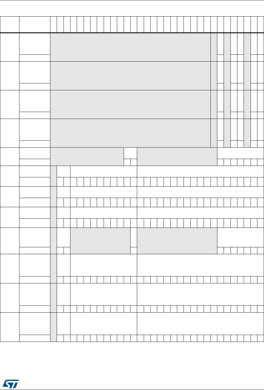
DocID018909 Rev 9 1315/1718
RM0090 USB on-the-go full-speed (OTG_FS)
1362
0xB08
OTG_FS_DOE
PINT0 Reserved
Reserved
B2BSTUP
Reserved
OTEPDIS
STUP
Reserved
EPDISD
XFRC
Reset value 00000
0xB28
OTG_FS_DOE
PINT1 Reserved
Reserved
B2BSTUP
Reserved
OTEPDIS
STUP
Reserved
EPDISD
XFRC
Reset value 00000
0xB48
OTG_FS_DOE
PINT2 Reserved
Reserved
B2BSTUP
Reserved
OTEPDIS
STUP
Reserved
EPDISD
XFRC
Reset value 00000
0xB68
OTG_FS_DOE
PINT3 Reserved
Reserved
B2BSTUP
Reserved
OTEPDIS
STUP
Reserved
EPDISD
XFRC
Reset value 00000
0x910
OTG_FS_DIE
PTSIZ0 Reserved
PKT
CNT Reserved XFRSIZ
Reset value 00 0000000
0x930
OTG_FS_DIE
PTSIZ1
Reserved
MCN
TPKTCNT XFRSIZ
Reset value 0000000000000000000000000000000
0x950
OTG_FS_DIE
PTSIZ2
Reserved
MCN
TPKTCNT XFRSIZ
Reset value 0000000000000000000000000000000
0x970
OTG_FS_DIE
PTSIZ3
Reserved
MCN
TPKTCNT XFRSIZ
Reset value 0000000000000000000000000000000
0xB10
OTG_FS_DOE
PTSIZ0
Reserved
STU
PCN
TReserved
PKTCNT
Reserved XFRSIZ
Reset value 00 0 0000000
0xB30
OTG_FS_DOE
PTSIZ1
Reserved
RXDPID/
STUPCNT
PKTCNT XFRSIZ
Reset value 0000000000000000000000000000000
0xB50
OTG_FS_DOE
PTSIZ2
Reserved
RXDPID/
STUPCNT
PKTCNT XFRSIZ
Reset value 0000000000000000000000000000000
0xB70
OTG_FS_DOE
PTSIZ3
Reserved
RXDPID/
STUPCNT
PKTCNT XFRSIZ
Reset value 0000000000000000000000000000000
Table 202. OTG_FS register map and reset values (continued)
Offset Register
31
30
29
28
27
26
25
24
23
22
21
20
19
18
17
16
15
14
13
12
11
10
9
8
7
6
5
4
3
2
1
0

USB on-the-go full-speed (OTG_FS) RM0090
1316/1718 DocID018909 Rev 9
Refer to Table 1 on page 64 for the register boundary addresses.
0xE00
OTG_FS_PCG
CCTL Reserved
PHYSUSP
Reserved
GATEHCLK
STPPCLK
Reset value
Table 202. OTG_FS register map and reset values (continued)
Offset Register
31
30
29
28
27
26
25
24
23
22
21
20
19
18
17
16
15
14
13
12
11
10
9
8
7
6
5
4
3
2
1
0

DocID018909 Rev 9 1317/1718
RM0090 USB on-the-go full-speed (OTG_FS)
1362
34.17 OTG_FS programming model
34.17.1 Core initialization
The application must perform the core initialization sequence. If the cable is connected
during power-up, the current mode of operation bit in the OTG_FS_GINTSTS (CMOD bit in
OTG_FS_GINTSTS) reflects the mode. The OTG_FS controller enters host mode when an
“A” plug is connected or device mode when a “B” plug is connected.
This section explains the initialization of the OTG_FS controller after power-on. The
application must follow the initialization sequence irrespective of host or device mode
operation. All core global registers are initialized according to the core’s configuration:
1. Program the following fields in the OTG_FS_GAHBCFG register:
– Global interrupt mask bit GINTMSK = 1
– RxFIFO non-empty (RXFLVL bit in OTG_FS_GINTSTS)
– Periodic TxFIFO empty level
2. Program the following fields in the OTG_FS_GUSBCFG register:
– HNP capable bit
– SRP capable bit
– FS timeout calibration field
– USB turnaround time field
3. The software must unmask the following bits in the OTG_FS_GINTMSK register:
OTG interrupt mask
Mode mismatch interrupt mask
4. The software can read the CMOD bit in OTG_FS_GINTSTS to determine whether the
OTG_FS controller is operating in host or device mode.

USB on-the-go full-speed (OTG_FS) RM0090
1318/1718 DocID018909 Rev 9
34.17.2 Host initialization
To initialize the core as host, the application must perform the following steps:
1. Program the HPRTINT in the OTG_FS_GINTMSK register to unmask
2. Program the OTG_FS_HCFG register to select full-speed host
3. Program the PPWR bit in OTG_FS_HPRT to 1. This drives VBUS on the USB.
4. Wait for the PCDET interrupt in OTG_FS_HPRT0. This indicates that a device is
connecting to the port.
5. Program the PRST bit in OTG_FS_HPRT to 1. This starts the reset process.
6. Wait at least 10 ms for the reset process to complete.
7. Program the PRST bit in OTG_FS_HPRT to 0.
8. Wait for the PENCHNG interrupt in OTG_FS_HPRT.
9. Read the PSPD bit in OTG_FS_HPRT to get the enumerated speed.
10. Program the HFIR register with a value corresponding to the selected PHY clock 1
11. Program the FSLSPCS field in the OTG_FS_HCFG register following the speed of the
device detected in step 9. If FSLSPCS has been changed a port reset must be
performed.
12. Program the OTG_FS_GRXFSIZ register to select the size of the receive FIFO.
13. Program the OTG_FS_HNPTXFSIZ register to select the size and the start address of
the Non-periodic transmit FIFO for non-periodic transactions.
14. Program the OTG_FS_HPTXFSIZ register to select the size and start address of the
periodic transmit FIFO for periodic transactions.
To communicate with devices, the system software must initialize and enable at least one
channel.
34.17.3 Device initialization
The application must perform the following steps to initialize the core as a device on power-
up or after a mode change from host to device.
1. Program the following fields in the OTG_FS_DCFG register:
– Device speed
– Non-zero-length status OUT handshake
2. Program the OTG_FS_GINTMSK register to unmask the following interrupts:
– USB reset
– Enumeration done
– Early suspend
– USB suspend
–SOF
3. Program the VBUSBSEN bit in the OTG_FS_GCCFG register to enable VBUS sensing
in “B” device mode and supply the 5 volts across the pull-up resistor on the DP line.
4. Wait for the USBRST interrupt in OTG_FS_GINTSTS. It indicates that a reset has been
detected on the USB that lasts for about 10 ms on receiving this interrupt.
Wait for the ENUMDNE interrupt in OTG_FS_GINTSTS. This interrupt indicates the end of
reset on the USB. On receiving this interrupt, the application must read the OTG_FS_DSTS
register to determine the enumeration speed and perform the steps listed in Endpoint

DocID018909 Rev 9 1319/1718
RM0090 USB on-the-go full-speed (OTG_FS)
1362
initialization on enumeration completion on page 1335.
At this point, the device is ready to accept SOF packets and perform control transfers on
control endpoint 0.
34.17.4 Host programming model
Channel initialization
The application must initialize one or more channels before it can communicate with
connected devices. To initialize and enable a channel, the application must perform the
following steps:
1. Program the OTG_FS_GINTMSK register to unmask the following:
2. Channel interrupt
– Non-periodic transmit FIFO empty for OUT transactions (applicable when
operating in pipelined transaction-level with the packet count field programmed
with more than one).
– Non-periodic transmit FIFO half-empty for OUT transactions (applicable when
operating in pipelined transaction-level with the packet count field programmed
with more than one).
3. Program the OTG_FS_HAINTMSK register to unmask the selected channels’
interrupts.
4. Program the OTG_FS_HCINTMSK register to unmask the transaction-related
interrupts of interest given in the host channel interrupt register.
5. Program the selected channel’s OTG_FS_HCTSIZx register with the total transfer size,
in bytes, and the expected number of packets, including short packets. The application
must program the PID field with the initial data PID (to be used on the first OUT
transaction or to be expected from the first IN transaction).
6. Program the OTG_FS_HCCHARx register of the selected channel with the device’s
endpoint characteristics, such as type, speed, direction, and so forth. (The channel can
be enabled by setting the channel enable bit to 1 only when the application is ready to
transmit or receive any packet).
Halting a channel
The application can disable any channel by programming the OTG_FS_HCCHARx register
with the CHDIS and CHENA bits set to 1. This enables the OTG_FS host to flush the posted
requests (if any) and generates a channel halted interrupt. The application must wait for the
CHH interrupt in OTG_FS_HCINTx before reallocating the channel for other transactions.
The OTG_FS host does not interrupt the transaction that has already been started on the
USB.
Before disabling a channel, the application must ensure that there is at least one free space
available in the non-periodic request queue (when disabling a non-periodic channel) or the
periodic request queue (when disabling a periodic channel). The application can simply
flush the posted requests when the Request queue is full (before disabling the channel), by
programming the OTG_FS_HCCHARx register with the CHDIS bit set to 1, and the CHENA
bit cleared to 0.
The application is expected to disable a channel on any of the following conditions:
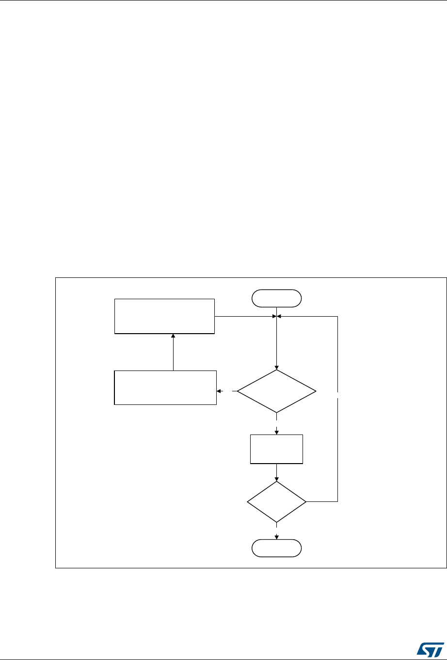
USB on-the-go full-speed (OTG_FS) RM0090
1320/1718 DocID018909 Rev 9
1. When an STALL, TXERR, BBERR or DTERR interrupt in OTG_FS_HCINTx is received
for an IN or OUT channel. The application must be able to receive other interrupts
(DTERR, Nak, Data, TXERR) for the same channel before receiving the halt.
2. When a DISCINT (Disconnect Device) interrupt in OTG_FS_GINTSTS is received.
(The application is expected to disable all enabled channels).
3. When the application aborts a transfer before normal completion.
Operational model
The application must initialize a channel before communicating to the connected device.
This section explains the sequence of operation to be performed for different types of USB
transactions.
•Writing the transmit FIFO
The OTG_FS host automatically writes an entry (OUT request) to the periodic/non-
periodic request queue, along with the last DWORD write of a packet. The application
must ensure that at least one free space is available in the periodic/non-periodic
request queue before starting to write to the transmit FIFO. The application must
always write to the transmit FIFO in DWORDs. If the packet size is non-DWORD
aligned, the application must use padding. The OTG_FS host determines the actual
packet size based on the programmed maximum packet size and transfer size.
Figure 396. Transmit FIFO write task
•Reading the receive FIFO
The application must ignore all packet statuses other than IN data packet (bx0010).
MPS: Maximum packet size
Start
ai15673b
Wait for NPTXFE/PTXFE
interrupt in
OTG_FS_GINTSTS
Read GNPTXSTS/HPTXFSIZ
registers for available FIFO
and queue spaces
1 MPS or
LPS FIFO space
available?
Write 1 packet
data to
transmit FIFO
More packets
to send?
Done
No
No Ye s
Ye s
LPS: Last packet size

DocID018909 Rev 9 1321/1718
RM0090 USB on-the-go full-speed (OTG_FS)
1362
Figure 397. Receive FIFO read task
•Bulk and control OUT/SETUP transactions
A typical bulk or control OUT/SETUP pipelined transaction-level operation is shown in
Figure 398. See channel 1 (ch_1). Two bulk OUT packets are transmitted. A control
SETUP transaction operates in the same way but has only one packet. The
assumptions are:
– The application is attempting to send two maximum-packet-size packets (transfer
size = 1, 024 bytes).
– The non-periodic transmit FIFO can hold two packets (128 bytes for FS).
– The non-periodic request queue depth = 4.
•Normal bulk and control OUT/SETUP operations
The sequence of operations in (channel 1) is as follows:
a) Initialize channel 1
b) Write the first packet for channel 1
c) Along with the last Word write, the core writes an entry to the non-periodic request
queue
d) As soon as the non-periodic queue becomes non-empty, the core attempts to
send an OUT token in the current frame
e) Write the second (last) packet for channel 1
f) The core generates the XFRC interrupt as soon as the last transaction is
completed successfully
g) In response to the XFRC interrupt, de-allocate the channel for other transfers
h) Handling non-ACK responses
RXFLVL
interrupt ?
Read the received
packet from the
Receive FIFO
Read
OTG_FS_GRXSTSP
PKTSTS
0b0010?
Yes
Yes
Unmask RXFLVL
interrupt
BCNT > 0?
No
Mask RXFLVL
interrupt
Yes
Unmask RXFLVL
interrupt
No
No
Start
ai15674
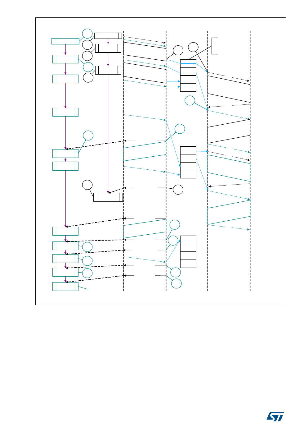
USB on-the-go full-speed (OTG_FS) RM0090
1322/1718 DocID018909 Rev 9
Figure 398. Normal bulk/control OUT/SETUP and bulk/control IN transactions
The channel-specific interrupt service routine for bulk and control OUT/SETUP
transactions is shown in the following code samples.
•Interrupt service routine for bulk/control OUT/SETUP and bulk/control IN
transactions
a) Bulk/Control OUT/SETUP
Unmask (NAK/TXERR/STALL/XFRC)
if (XFRC)
{
Reset Error Count
Mask ACK
ACK
HostApplication DeviceAHB USB
OUT
DATA0
MPS
1
MPS
1
MPS
w rit e_t x _fifo
(ch_1)
init_reg(ch_1)
set _ ch_e n
(ch_2)
init_reg(ch_2)
w rit e_t x _fifo
(ch_1)
set _ ch_e n
(ch_2)
ch_2
ch_2
ch_1
ch_1
De-allocate
(ch_1)
IN
ch_2
ch_2
ch_2
ch_1
ACK
OUT
set _ ch_e n
(ch_2)
Non-Periodic Request
Queu e
Assume that this queue
can hold 4 entries.
4
1
6
ACK
DATA0
IN
ACK
read_rx_sts
read_rx_fifo
1
MPS
set _ ch_e n
(ch_2)
1
MPS
read_rx_stsre
ad_rx_fifo
read_rx_sts
Disable
(ch_2)
1
2
34
5
6
7
De-allocate
(ch_2)
CHH interruptr
ch_2
2
3
5
7
8
9
12
13
read_rx_sts 10
11
DATA1
MPS
DATA1
ai15675
RXFLVL interrupt
XFRC interrupt
RXFLVL interrupt
RXFLVL interrupt
RXFLVL interrupt
XFRC interrupt

DocID018909 Rev 9 1323/1718
RM0090 USB on-the-go full-speed (OTG_FS)
1362
De-allocate Channel
}
else if (STALL)
{
Transfer Done = 1
Unmask CHH
Disable Channel
}
else if (NAK or TXERR )
{
Rewind Buffer Pointers
Unmask CHH
Disable Channel
if (TXERR)
{
Increment Error Count
Unmask ACK
}
else
{
Reset Error Count
}
}
else if (CHH)
{
Mask CHH
if (Transfer Done or (Error_count == 3))
{
De-allocate Channel
}
else
{
Re-initialize Channel
}
}
else if (ACK)
{
Reset Error Count
Mask ACK
}
The application is expected to write the data packets into the transmit FIFO as and
when the space is available in the transmit FIFO and the Request queue. The
application can make use of the NPTXFE interrupt in OTG_FS_GINTSTS to find the
transmit FIFO space.
b) Bulk/Control IN
Unmask (TXERR/XFRC/BBERR/STALL/DTERR)
if (XFRC)
{
Reset Error Count
Unmask CHH
Disable Channel

USB on-the-go full-speed (OTG_FS) RM0090
1324/1718 DocID018909 Rev 9
Reset Error Count
Mask ACK
}
else if (TXERR or BBERR or STALL)
{
Unmask CHH
Disable Channel
if (TXERR)
{
Increment Error Count
Unmask ACK
}
}
else if (CHH)
{
Mask CHH
if (Transfer Done or (Error_count == 3))
{
De-allocate Channel
}
else
{
Re-initialize Channel
}
}
else if (ACK)
{
Reset Error Count
Mask ACK
}
else if (DTERR)
{
Reset Error Count
}
The application is expected to write the requests as and when the Request queue space is
available and until the XFRC interrupt is received.
•Bulk and control IN transactions
A typical bulk or control IN pipelined transaction-level operation is shown in Figure 399.
See channel 2 (ch_2). The assumptions are:
– The application is attempting to receive two maximum-packet-size packets
(transfer size = 1 024 bytes).
– The receive FIFO can contain at least one maximum-packet-size packet and two
status Words per packet (72 bytes for FS).
– The non-periodic request queue depth = 4.
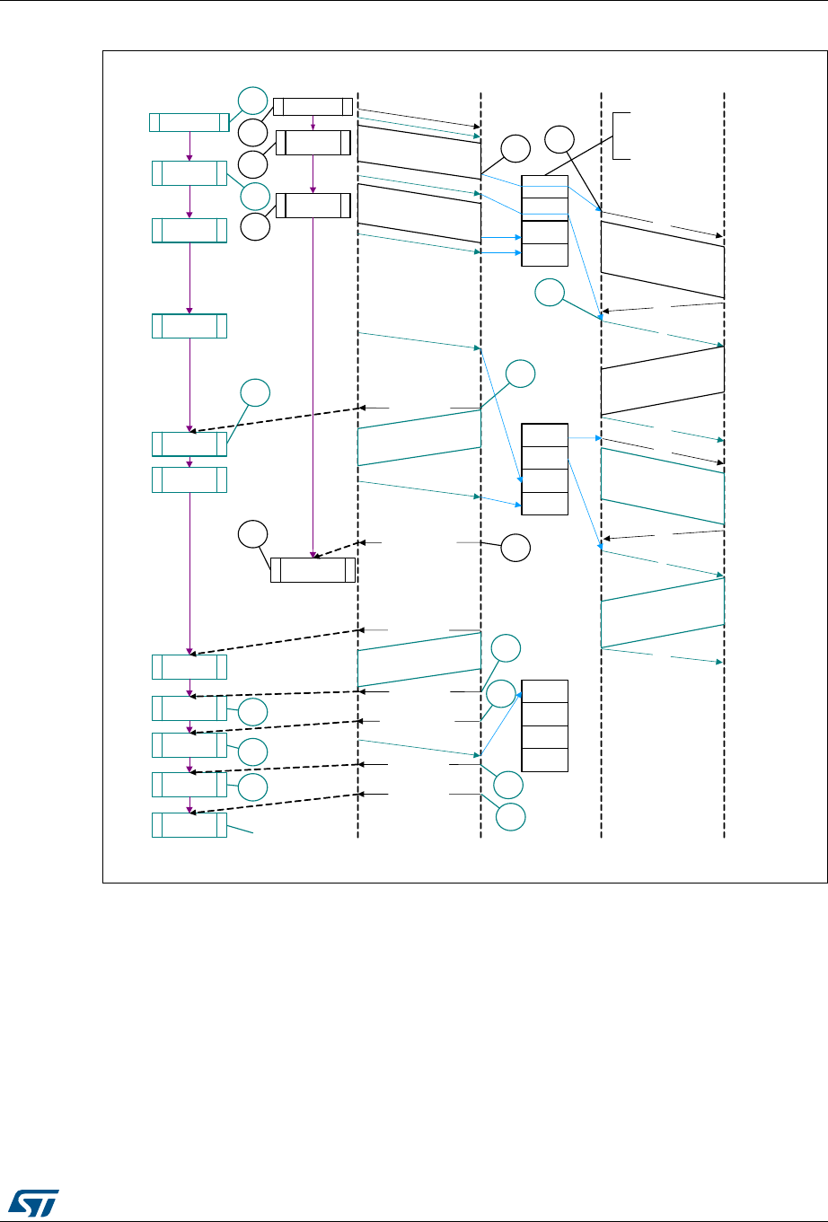
DocID018909 Rev 9 1325/1718
RM0090 USB on-the-go full-speed (OTG_FS)
1362
Figure 399. Bulk/control IN transactions
The sequence of operations is as follows:
a) Initialize channel 2.
b) Set the CHENA bit in HCCHAR2 to write an IN request to the non-periodic request
queue.
c) The core attempts to send an IN token after completing the current OUT
transaction.
d) The core generates an RXFLVL interrupt as soon as the received packet is written
to the receive FIFO.
e) In response to the RXFLVL interrupt, mask the RXFLVL interrupt and read the
received packet status to determine the number of bytes received, then read the
receive FIFO accordingly. Following this, unmask the RXFLVL interrupt.
ACK
HostApplication DeviceAHB USB
OUT
DATA0
MPS
1
MPS
1
MPS
w rit e_t x _fifo
(ch_1)
init_reg(ch_1)
set _ ch_e n
(ch_2)
init_reg(ch_2)
w rit e_t x _fifo
(ch_1)
set _ ch_e n
(ch_2)
ch_2
ch_2
ch_1
ch_1
De-allocate
(ch_1)
IN
ch_2
ch_2
ch_2
ch_1
ACK
OUT
set _ ch_e n
(ch_2)
Non-Periodic Request
Queu e
Assume that this queue
can hold 4 entries.
4
1
6
ACK
DATA0
IN
ACK
read_rx_sts
read_rx_fifo
1
MPS
set _ ch_e n
(ch_2)
1
MPS
read_rx_stsre
ad_rx_fifo
read_rx_sts
Disable
(ch_2)
1
2
34
5
6
7
De-allocate
(ch_2)
CHH interruptr
ch_2
2
3
5
7
8
9
12
13
read_rx_sts 10
11
DATA1
MPS
DATA1
ai15675
RXFLVL interrupt
XFRC interrupt
RXFLVL interrupt
RXFLVL interrupt
RXFLVL interrupt
XFRC interrupt

USB on-the-go full-speed (OTG_FS) RM0090
1326/1718 DocID018909 Rev 9
f) The core generates the RXFLVL interrupt for the transfer completion status entry
in the receive FIFO.
g) The application must read and ignore the receive packet status when the receive
packet status is not an IN data packet (PKTSTS in GRXSTSR ≠0b0010).
h) The core generates the XFRC interrupt as soon as the receive packet status is
read.
i) In response to the XFRC interrupt, disable the channel and stop writing the
OTG_FS_HCCHAR2 register for further requests. The core writes a channel
disable request to the non-periodic request queue as soon as the
OTG_FS_HCCHAR2 register is written.
j) The core generates the RXFLVL interrupt as soon as the halt status is written to
the receive FIFO.
k) Read and ignore the receive packet status.
l) The core generates a CHH interrupt as soon as the halt status is popped from the
receive FIFO.
m) In response to the CHH interrupt, de-allocate the channel for other transfers.
n) Handling non-ACK responses
•Control transactions
Setup, Data, and Status stages of a control transfer must be performed as three
separate transfers. Setup-, Data- or Status-stage OUT transactions are performed
similarly to the bulk OUT transactions explained previously. Data- or Status-stage IN
transactions are performed similarly to the bulk IN transactions explained previously.
For all three stages, the application is expected to set the EPTYP field in
OTG_FS_HCCHAR1 to Control. During the Setup stage, the application is expected to
set the PID field in OTG_FS_HCTSIZ1 to SETUP.
•Interrupt OUT transactions
A typical interrupt OUT operation is shown in Figure 400. The assumptions are:
– The application is attempting to send one packet in every frame (up to 1 maximum
packet size), starting with the odd frame (transfer size = 1 024 bytes)
– The periodic transmit FIFO can hold one packet (1 KB)
– Periodic request queue depth = 4
The sequence of operations is as follows:
a) Initialize and enable channel 1. The application must set the ODDFRM bit in
OTG_FS_HCCHAR1.
b) Write the first packet for channel 1.
c) Along with the last Word write of each packet, the OTG_FS host writes an entry to
the periodic request queue.
d) The OTG_FS host attempts to send an OUT token in the next (odd) frame.
e) The OTG_FS host generates an XFRC interrupt as soon as the last packet is
transmitted successfully.
f) In response to the XFRC interrupt, reinitialize the channel for the next transfer.
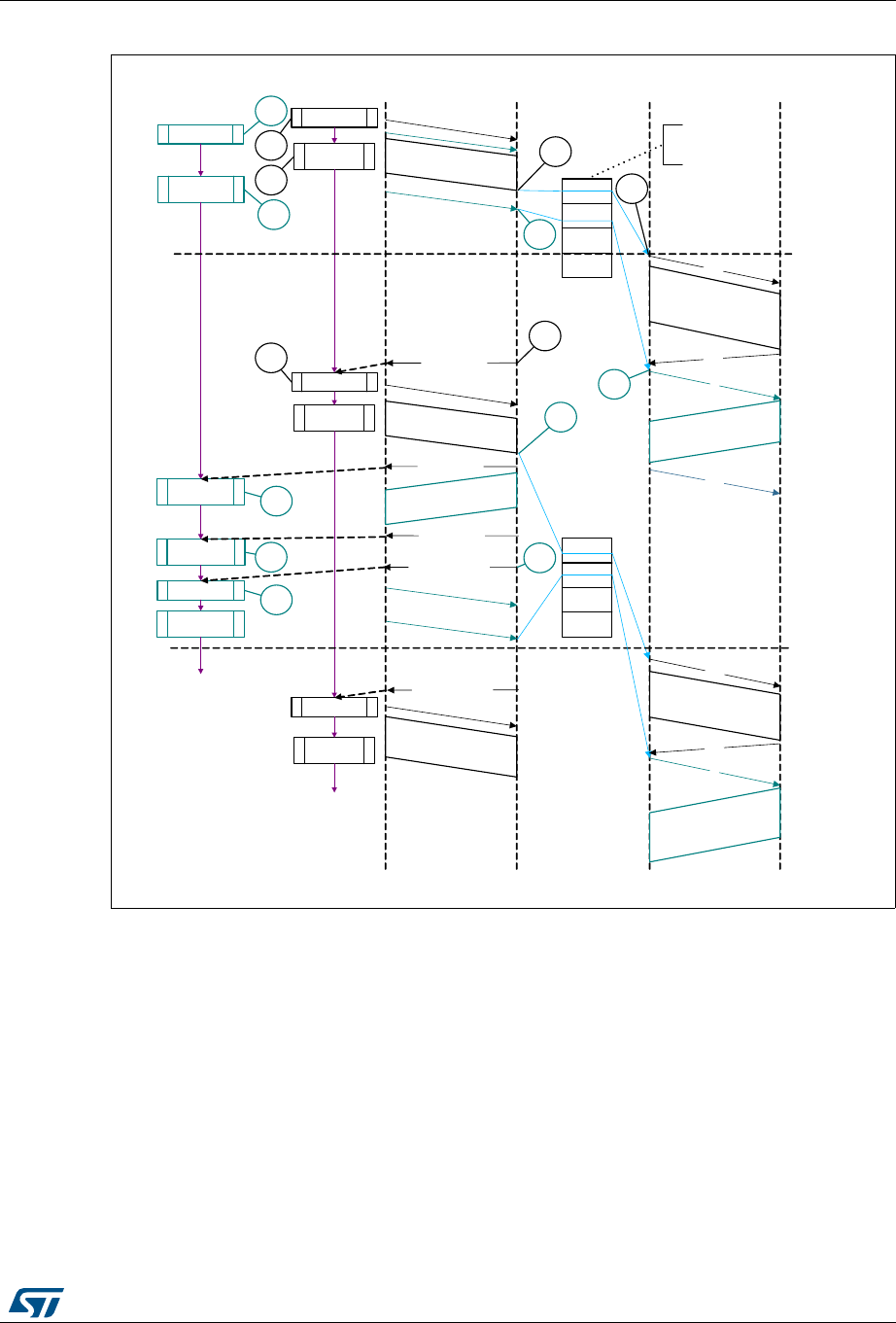
DocID018909 Rev 9 1327/1718
RM0090 USB on-the-go full-speed (OTG_FS)
1362
Figure 400. Normal interrupt OUT/IN transactions
•Interrupt service routine for interrupt OUT/IN transactions
a) Interrupt OUT
Unmask (NAK/TXERR/STALL/XFRC/FRMOR)
if (XFRC)
{
Reset Error Count
Mask ACK
De-allocate Channel
}
else
if (STALL or FRMOR)
{
Mask ACK
Unmask CHH
Host
Application DeviceAHB USB
OUT
DATA0
MPS
1
MPS
1
MPS
write_tx_fifo
(ch_1)
init_reg(ch_1)
set_ch_en
(ch_2)
init_reg(ch _2)
write_tx_fifo
(ch_1)
IN
OUT
DATA1
MPS
Periodic Request Queue
Assume that this queue
can hold 4 entries.
1
5
DATA0
IN
RXFLVL interrupt
1
MPS
read_rx_sts
read_rx_fifo
read_rx_sts
1
2
3
4
6
2
3
6
78
9
Odd
(micro)
frame
Even
(micro)
frame
init_reg(ch_1)
set_ch_en
(ch_2)
init_reg(ch _2)
write_tx_fifo
(ch_1)
init_reg(ch_1)
1
MPS
DATA1
5
4
ACK
ACK
ACK
ch_1
ch_2
ch_2
ch_1
ai15676
RXFLVL interrupt
XFRC interrupt
XFRC interrupt
XFRC interrupt

USB on-the-go full-speed (OTG_FS) RM0090
1328/1718 DocID018909 Rev 9
Disable Channel
if (STALL)
{
Transfer Done = 1
}
}
else
if (NAK or TXERR)
{
Rewind Buffer Pointers
Reset Error Count
Mask ACK
Unmask CHH
Disable Channel
}
else
if (CHH)
{
Mask CHH
if (Transfer Done or (Error_count == 3))
{
De-allocate Channel
}
else
{
Re-initialize Channel (in next b_interval - 1 Frame)
}
}
else
if (ACK)
{
Reset Error Count
Mask ACK
}
The application uses the NPTXFE interrupt in OTG_FS_GINTSTS to find the transmit
FIFO space.
b) Interrupt IN
Unmask (NAK/TXERR/XFRC/BBERR/STALL/FRMOR/DTERR)
if (XFRC)
{
Reset Error Count
Mask ACK
if (OTG_FS_HCTSIZx.PKTCNT == 0)
{
De-allocate Channel
}
else
{
Transfer Done = 1
Unmask CHH
Disable Channel

DocID018909 Rev 9 1329/1718
RM0090 USB on-the-go full-speed (OTG_FS)
1362
}
}
else
if (STALL or FRMOR or NAK or DTERR or BBERR)
{
Mask ACK
Unmask CHH
Disable Channel
if (STALL or BBERR)
{
Reset Error Count
Transfer Done = 1
}
else
if (!FRMOR)
{
Reset Error Count
}
}
else
if (TXERR)
{
Increment Error Count
Unmask ACK
Unmask CHH
Disable Channel
}
else
if (CHH)
{
Mask CHH
if (Transfer Done or (Error_count == 3))
{
De-allocate Channel
}
else
Re-initialize Channel (in next b_interval - 1 /Frame)
}
}
else
if (ACK)
{
Reset Error Count
Mask ACK

USB on-the-go full-speed (OTG_FS) RM0090
1330/1718 DocID018909 Rev 9
}
•Interrupt IN transactions
The assumptions are:
– The application is attempting to receive one packet (up to 1 maximum packet size)
in every frame, starting with odd (transfer size = 1 024 bytes).
– The receive FIFO can hold at least one maximum-packet-size packet and two
status Words per packet (1 031 bytes).
– Periodic request queue depth = 4.
•Normal interrupt IN operation
The sequence of operations is as follows:
a) Initialize channel 2. The application must set the ODDFRM bit in
OTG_FS_HCCHAR2.
b) Set the CHENA bit in OTG_FS_HCCHAR2 to write an IN request to the periodic
request queue.
c) The OTG_FS host writes an IN request to the periodic request queue for each
OTG_FS_HCCHAR2 register write with the CHENA bit set.
d) The OTG_FS host attempts to send an IN token in the next (odd) frame.
e) As soon as the IN packet is received and written to the receive FIFO, the OTG_FS
host generates an RXFLVL interrupt.
f) In response to the RXFLVL interrupt, read the received packet status to determine
the number of bytes received, then read the receive FIFO accordingly. The
application must mask the RXFLVL interrupt before reading the receive FIFO, and
unmask after reading the entire packet.
g) The core generates the RXFLVL interrupt for the transfer completion status entry
in the receive FIFO. The application must read and ignore the receive packet
status when the receive packet status is not an IN data packet (PKTSTS in
GRXSTSR ≠0b0010).
h) The core generates an XFRC interrupt as soon as the receive packet status is
read.
i) In response to the XFRC interrupt, read the PKTCNT field in OTG_FS_HCTSIZ2.
If the PKTCNT bit in OTG_FS_HCTSIZ2 is not equal to 0, disable the channel
before re-initializing the channel for the next transfer, if any). If PKTCNT bit in

DocID018909 Rev 9 1331/1718
RM0090 USB on-the-go full-speed (OTG_FS)
1362
OTG_FS_HCTSIZ2 = 0, reinitialize the channel for the next transfer. This time, the
application must reset the ODDFRM bit in OTG_FS_HCCHAR2.
•Isochronous OUT transactions
A typical isochronous OUT operation is shown in Figure 401. The assumptions are:
– The application is attempting to send one packet every frame (up to 1 maximum
packet size), starting with an odd frame. (transfer size = 1 024 bytes).
– The periodic transmit FIFO can hold one packet (1 KB).
– Periodic request queue depth = 4.
The sequence of operations is as follows:
a) Initialize and enable channel 1. The application must set the ODDFRM bit in
OTG_FS_HCCHAR1.
b) Write the first packet for channel 1.
c) Along with the last Word write of each packet, the OTG_FS host writes an entry to
the periodic request queue.
d) The OTG_FS host attempts to send the OUT token in the next frame (odd).
e) The OTG_FS host generates the XFRC interrupt as soon as the last packet is
transmitted successfully.
f) In response to the XFRC interrupt, reinitialize the channel for the next transfer.
g) Handling non-ACK responses
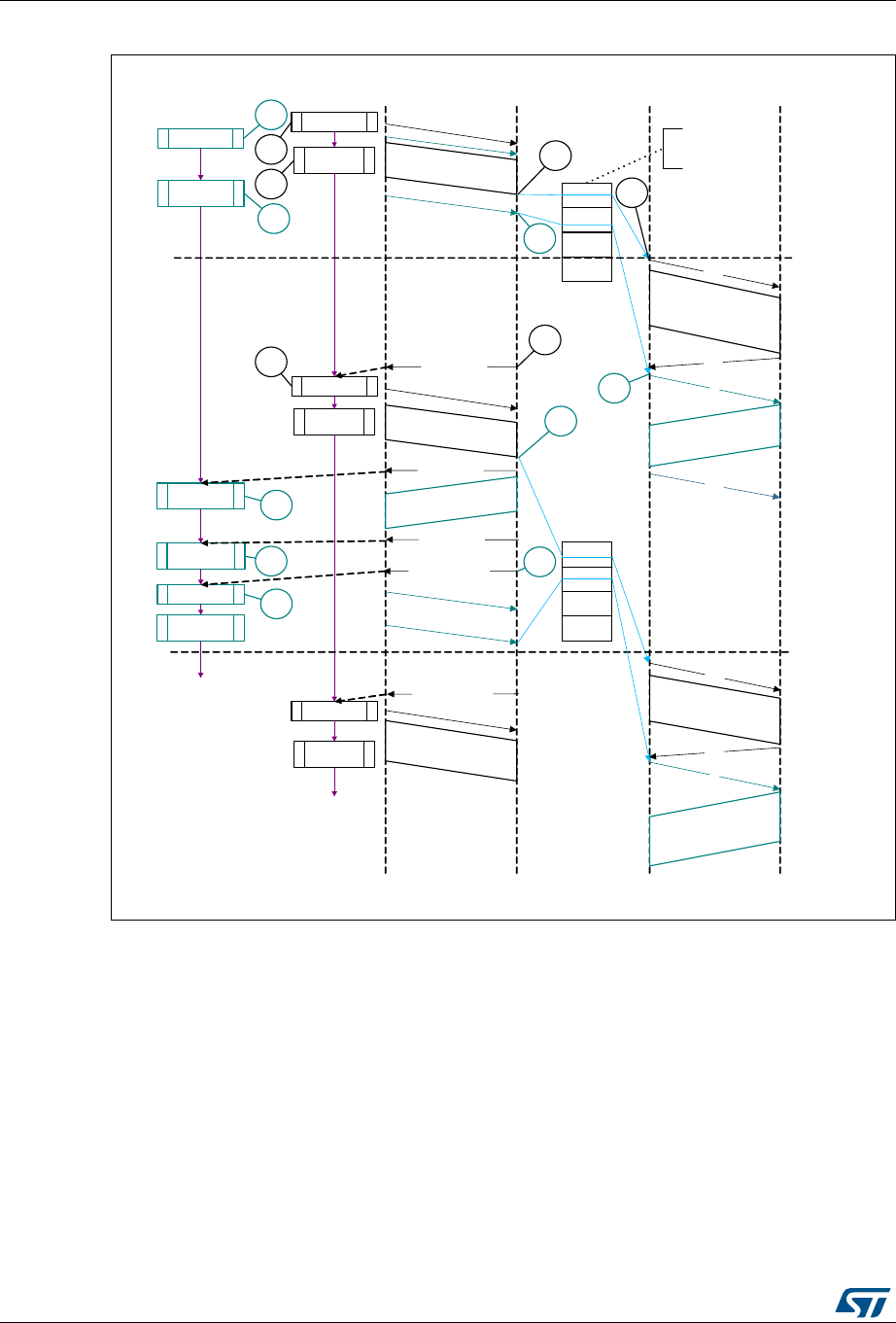
USB on-the-go full-speed (OTG_FS) RM0090
1332/1718 DocID018909 Rev 9
Figure 401. Normal isochronous OUT/IN transactions
•Interrupt service routine for isochronous OUT/IN transactions
Code sample: Isochronous OUT
Unmask (FRMOR/XFRC)
if (XFRC)
{
De-allocate Channel
}
else
if (FRMOR)
{
Unmask CHH
Disable Channel
}
Host
Application DeviceAHB USB
OUT
DATA0
MPS
1
MPS
1
MPS
write_tx_fifo
(ch_1)
init_reg(ch_1)
set_ch_en
(ch_2)
init_reg(ch _2)
write_tx_fifo
(ch_1)
IN
OUT
DATA1
MPS
Periodic Request Queue
Assume that this queue
can hold 4 entries.
1
5
DATA0
IN
RXFLVL interrupt
1
MPS
read_rx_sts
read_rx_fifo
read_rx_sts
1
2
3
4
6
2
3
6
78
9
Odd
(micro)
frame
Even
(micro)
frame
init_reg(ch_1)
set_ch_en
(ch_2)
init_reg(ch _2)
write_tx_fifo
(ch_1)
init_reg(ch_1)
1
MPS
DATA1
5
4
ACK
ACK
ACK
ch_1
ch_2
ch_2
ch_1
ai15676
RXFLVL interrupt
XFRC interrupt
XFRC interrupt
XFRC interrupt

DocID018909 Rev 9 1333/1718
RM0090 USB on-the-go full-speed (OTG_FS)
1362
else
if (CHH)
{
Mask CHH
De-allocate Channel
}
Code sample: Isochronous IN
Unmask (TXERR/XFRC/FRMOR/BBERR)
if (XFRC or FRMOR)
{
if (XFRC and (OTG_FS_HCTSIZx.PKTCNT == 0))
{
Reset Error Count
De-allocate Channel
}
else
{
Unmask CHH
Disable Channel
}
}
else
if (TXERR or BBERR)
{
Increment Error Count
Unmask CHH
Disable Channel
}
else
if (CHH)
{
Mask CHH
if (Transfer Done or (Error_count == 3))
{
De-allocate Channel
}
else
{
Re-initialize Channel
}
}

USB on-the-go full-speed (OTG_FS) RM0090
1334/1718 DocID018909 Rev 9
•Isochronous IN transactions
The assumptions are:
– The application is attempting to receive one packet (up to 1 maximum packet size)
in every frame starting with the next odd frame (transfer size = 1 024 bytes).
– The receive FIFO can hold at least one maximum-packet-size packet and two
status Word per packet (1 031 bytes).
– Periodic request queue depth = 4.
The sequence of operations is as follows:
a) Initialize channel 2. The application must set the ODDFRM bit in
OTG_FS_HCCHAR2.
b) Set the CHENA bit in OTG_FS_HCCHAR2 to write an IN request to the periodic
request queue.
c) The OTG_FS host writes an IN request to the periodic request queue for each
OTG_FS_HCCHAR2 register write with the CHENA bit set.
d) The OTG_FS host attempts to send an IN token in the next odd frame.
e) As soon as the IN packet is received and written to the receive FIFO, the OTG_FS
host generates an RXFLVL interrupt.
f) In response to the RXFLVL interrupt, read the received packet status to determine
the number of bytes received, then read the receive FIFO accordingly. The
application must mask the RXFLVL interrupt before reading the receive FIFO, and
unmask it after reading the entire packet.
g) The core generates an RXFLVL interrupt for the transfer completion status entry in
the receive FIFO. This time, the application must read and ignore the receive
packet status when the receive packet status is not an IN data packet (PKTSTS bit
in OTG_FS_GRXSTSR ≠0b0010).
h) The core generates an XFRC interrupt as soon as the receive packet status is
read.
i) In response to the XFRC interrupt, read the PKTCNT field in OTG_FS_HCTSIZ2.
If PKTCNT≠0 in OTG_FS_HCTSIZ2, disable the channel before re-initializing the
channel for the next transfer, if any. If PKTCNT = 0 in OTG_FS_HCTSIZ2,
reinitialize the channel for the next transfer. This time, the application must reset
the ODDFRM bit in OTG_FS_HCCHAR2.
•Selecting the queue depth
Choose the periodic and non-periodic request queue depths carefully to match the
number of periodic/non-periodic endpoints accessed.
The non-periodic request queue depth affects the performance of non-periodic
transfers. The deeper the queue (along with sufficient FIFO size), the more often the
core is able to pipeline non-periodic transfers. If the queue size is small, the core is
able to put in new requests only when the queue space is freed up.
The core’s periodic request queue depth is critical to perform periodic transfers as
scheduled. Select the periodic queue depth, based on the number of periodic transfers
scheduled in a microframe. If the periodic request queue depth is smaller than the
periodic transfers scheduled in a microframe, a frame overrun condition occurs.
•Handling babble conditions
OTG_FS controller handles two cases of babble: packet babble and port babble.
Packet babble occurs if the device sends more data than the maximum packet size for

DocID018909 Rev 9 1335/1718
RM0090 USB on-the-go full-speed (OTG_FS)
1362
the channel. Port babble occurs if the core continues to receive data from the device at
EOF2 (the end of frame 2, which is very close to SOF).
When OTG_FS controller detects a packet babble, it stops writing data into the Rx
buffer and waits for the end of packet (EOP). When it detects an EOP, it flushes already
written data in the Rx buffer and generates a Babble interrupt to the application.
When OTG_FS controller detects a port babble, it flushes the RxFIFO and disables the
port. The core then generates a Port disabled interrupt (HPRTINT in
OTG_FS_GINTSTS, PENCHNG in OTG_FS_HPRT). On receiving this interrupt, the
application must determine that this is not due to an overcurrent condition (another
cause of the Port Disabled interrupt) by checking POCA in OTG_FS_HPRT, then
perform a soft reset. The core does not send any more tokens after it has detected a
port babble condition.
34.17.5 Device programming model
Endpoint initialization on USB reset
1. Set the NAK bit for all OUT endpoints
– SNAK = 1 in OTG_FS_DOEPCTLx (for all OUT endpoints)
2. Unmask the following interrupt bits
– INEP0 = 1 in OTG_FS_DAINTMSK (control 0 IN endpoint)
– OUTEP0 = 1 in OTG_FS_DAINTMSK (control 0 OUT endpoint)
–STUP=1 in DOEPMSK
– XFRC = 1 in DOEPMSK
– XFRC = 1 in DIEPMSK
– TOC = 1 in DIEPMSK
3. Set up the Data FIFO RAM for each of the FIFOs
– Program the OTG_FS_GRXFSIZ register, to be able to receive control OUT data
and setup data. If thresholding is not enabled, at a minimum, this must be equal to
1 max packet size of control endpoint 0 + 2 Words (for the status of the control
OUT data packet) + 10 Words (for setup packets).
– Program the OTG_FS_TX0FSIZ register (depending on the FIFO number chosen)
to be able to transmit control IN data. At a minimum, this must be equal to 1 max
packet size of control endpoint 0.
4. Program the following fields in the endpoint-specific registers for control OUT endpoint
0 to receive a SETUP packet
– STUPCNT = 3 in OTG_FS_DOEPTSIZ0 (to receive up to 3 back-to-back SETUP
packets)
At this point, all initialization required to receive SETUP packets is done.
Endpoint initialization on enumeration completion
1. On the Enumeration Done interrupt (ENUMDNE in OTG_FS_GINTSTS), read the
OTG_FS_DSTS register to determine the enumeration speed.
2. Program the MPSIZ field in OTG_FS_DIEPCTL0 to set the maximum packet size. This
step configures control endpoint 0. The maximum packet size for a control endpoint
depends on the enumeration speed.

USB on-the-go full-speed (OTG_FS) RM0090
1336/1718 DocID018909 Rev 9
At this point, the device is ready to receive SOF packets and is configured to perform control
transfers on control endpoint 0.
Endpoint initialization on SetAddress command
This section describes what the application must do when it receives a SetAddress
command in a SETUP packet.
1. Program the OTG_FS_DCFG register with the device address received in the
SetAddress command
1. Program the core to send out a status IN packet
Endpoint initialization on SetConfiguration/SetInterface command
This section describes what the application must do when it receives a SetConfiguration or
SetInterface command in a SETUP packet.
1. When a SetConfiguration command is received, the application must program the
endpoint registers to configure them with the characteristics of the valid endpoints in
the new configuration.
2. When a SetInterface command is received, the application must program the endpoint
registers of the endpoints affected by this command.
3. Some endpoints that were active in the prior configuration or alternate setting are not
valid in the new configuration or alternate setting. These invalid endpoints must be
deactivated.
4. Unmask the interrupt for each active endpoint and mask the interrupts for all inactive
endpoints in the OTG_FS_DAINTMSK register.
5. Set up the Data FIFO RAM for each FIFO.
6. After all required endpoints are configured; the application must program the core to
send a status IN packet.
At this point, the device core is configured to receive and transmit any type of data packet.
Endpoint activation
This section describes the steps required to activate a device endpoint or to configure an
existing device endpoint to a new type.
1. Program the characteristics of the required endpoint into the following fields of the
OTG_FS_DIEPCTLx register (for IN or bidirectional endpoints) or the
OTG_FS_DOEPCTLx register (for OUT or bidirectional endpoints).
– Maximum packet size
– USB active endpoint = 1
– Endpoint start data toggle (for interrupt and bulk endpoints)
– Endpoint type
– TxFIFO number
2. Once the endpoint is activated, the core starts decoding the tokens addressed to that
endpoint and sends out a valid handshake for each valid token received for the
endpoint.
Endpoint deactivation
This section describes the steps required to deactivate an existing endpoint.

DocID018909 Rev 9 1337/1718
RM0090 USB on-the-go full-speed (OTG_FS)
1362
1. In the endpoint to be deactivated, clear the USB active endpoint bit in the
OTG_FS_DIEPCTLx register (for IN or bidirectional endpoints) or the
OTG_FS_DOEPCTLx register (for OUT or bidirectional endpoints).
2. Once the endpoint is deactivated, the core ignores tokens addressed to that endpoint,
which results in a timeout on the USB.
Note: The application must meet the following conditions to set up the device core to handle
traffic:
NPTXFEM and RXFLVLM in the OTG_FS_GINTMSK register must be cleared.
34.17.6 Operational model
SETUP and OUT data transfers
This section describes the internal data flow and application-level operations during data
OUT transfers and SETUP transactions.
•Packet read
This section describes how to read packets (OUT data and SETUP packets) from the
receive FIFO.
1. On catching an RXFLVL interrupt (OTG_FS_GINTSTS register), the application must
read the Receive status pop register (OTG_FS_GRXSTSP).
2. The application can mask the RXFLVL interrupt (in OTG_FS_GINTSTS) by writing to
RXFLVL = 0 (in OTG_FS_GINTMSK), until it has read the packet from the receive
FIFO.
3. If the received packet’s byte count is not 0, the byte count amount of data is popped
from the receive Data FIFO and stored in memory. If the received packet byte count is
0, no data is popped from the receive data FIFO.
4. The receive FIFO’s packet status readout indicates one of the following:
a) Global OUT NAK pattern:
PKTSTS = Global OUT NAK, BCNT = 0x000, EPNUM = Don’t Care (0x0),
DPID = Don’t Care (0b00).
These data indicate that the global OUT NAK bit has taken effect.
b) SETUP packet pattern:
PKTSTS = SETUP, BCNT = 0x008, EPNUM = Control EP Num, DPID = D0.
These data indicate that a SETUP packet for the specified endpoint is now
available for reading from the receive FIFO.
c) Setup stage done pattern:
PKTSTS = Setup Stage Done, BCNT = 0x0, EPNUM = Control EP Num,
DPID = Don’t Care (0b00).
These data indicate that the Setup stage for the specified endpoint has completed
and the Data stage has started. After this entry is popped from the receive FIFO,
the core asserts a Setup interrupt on the specified control OUT endpoint.
d) Data OUT packet pattern:
PKTSTS = DataOUT, BCNT = size of the received data OUT packet (0 ≤ BCNT
≤ 1 024), EPNUM = EPNUM on which the packet was received, DPID = Actual
Data PID.
e) Data transfer completed pattern:
PKTSTS = Data OUT Transfer Done, BCNT = 0x0, EPNUM = OUT EP Num
on which the data transfer is complete, DPID = Don’t Care (0b00).
These data indicate that an OUT data transfer for the specified OUT endpoint has
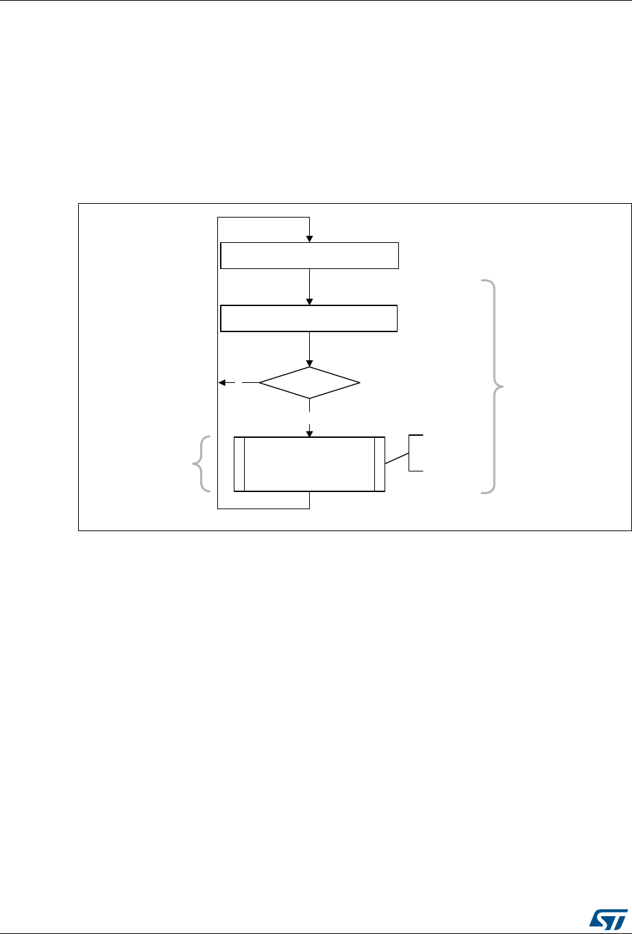
USB on-the-go full-speed (OTG_FS) RM0090
1338/1718 DocID018909 Rev 9
completed. After this entry is popped from the receive FIFO, the core asserts a
Transfer Completed interrupt on the specified OUT endpoint.
5. After the data payload is popped from the receive FIFO, the RXFLVL interrupt
(OTG_FS_GINTSTS) must be unmasked.
6. Steps 1–5 are repeated every time the application detects assertion of the interrupt line
due to RXFLVL in OTG_FS_GINTSTS. Reading an empty receive FIFO can result in
undefined core behavior.
Figure 402 provides a flowchart of the above procedure.
Figure 402. Receive FIFO packet read
•SETUP transactions
This section describes how the core handles SETUP packets and the application’s
sequence for handling SETUP transactions.
•Application requirements
1. To receive a SETUP packet, the STUPCNT field (OTG_FS_DOEPTSIZx) in a control
OUT endpoint must be programmed to a non-zero value. When the application
programs the STUPCNT field to a non-zero value, the core receives SETUP packets
and writes them to the receive FIFO, irrespective of the NAK status and EPENA bit
setting in OTG_FS_DOEPCTLx. The STUPCNT field is decremented every time the
control endpoint receives a SETUP packet. If the STUPCNT field is not programmed to
a proper value before receiving a SETUP packet, the core still receives the SETUP
packet and decrements the STUPCNT field, but the application may not be able to
word_cnt =
BCNT[11:2] +C
(BCNT[1]
| BCNT[1])
rcv_out_pkt()
rd_data = rd_reg (OTG_FS_GRXSTSP);
mem[0: word_cnt – 1] =
rd_rxfifo(rd_data.EPNUM,
word_cnt)
N
rd_data.BCNT = 0
wait until RXFLVL in OTG_FS_GINTSTSG
packet
store in
memory
Y
ai15677b

DocID018909 Rev 9 1339/1718
RM0090 USB on-the-go full-speed (OTG_FS)
1362
determine the correct number of SETUP packets received in the Setup stage of a
control transfer.
– STUPCNT = 3 in OTG_FS_DOEPTSIZx
2. The application must always allocate some extra space in the Receive data FIFO, to be
able to receive up to three SETUP packets on a control endpoint.
– The space to be reserved is 10 Words. Three Words are required for the first
SETUP packet, 1 Word is required for the Setup stage done Word and 6 Words
are required to store two extra SETUP packets among all control endpoints.
– 3 Words per SETUP packet are required to store 8 bytes of SETUP data and 4
bytes of SETUP status (Setup packet pattern). The core reserves this space in the
receive data.
– FIFO to write SETUP data only, and never uses this space for data packets.
3. The application must read the 2 Words of the SETUP packet from the receive FIFO.
4. The application must read and discard the Setup stage done Word from the receive
FIFO.
•Internal data flow
5. When a SETUP packet is received, the core writes the received data to the receive
FIFO, without checking for available space in the receive FIFO and irrespective of the
endpoint’s NAK and STALL bit settings.
– The core internally sets the IN NAK and OUT NAK bits for the control IN/OUT
endpoints on which the SETUP packet was received.
6. For every SETUP packet received on the USB, 3 Words of data are written to the
receive FIFO, and the STUPCNT field is decremented by 1.
– The first Word contains control information used internally by the core
– The second Word contains the first 4 bytes of the SETUP command
– The third Word contains the last 4 bytes of the SETUP command
7. When the Setup stage changes to a Data IN/OUT stage, the core writes an entry
(Setup stage done Word) to the receive FIFO, indicating the completion of the Setup
stage.
8. On the AHB side, SETUP packets are emptied by the application.
9. When the application pops the Setup stage done Word from the receive FIFO, the core
interrupts the application with an STUP interrupt (OTG_FS_DOEPINTx), indicating it
can process the received SETUP packet.
– The core clears the endpoint enable bit for control OUT endpoints.
•Application programming sequence
1. Program the OTG_FS_DOEPTSIZx register.
– STUPCNT =3
2. Wait for the RXFLVL interrupt (OTG_FS_GINTSTS) and empty the data packets from
the receive FIFO.
3. Assertion of the STUP interrupt (OTG_FS_DOEPINTx) marks a successful completion
of the SETUP Data Transfer.
– On this interrupt, the application must read the OTG_FS_DOEPTSIZx register to
determine the number of SETUP packets received and process the last received
SETUP packet.
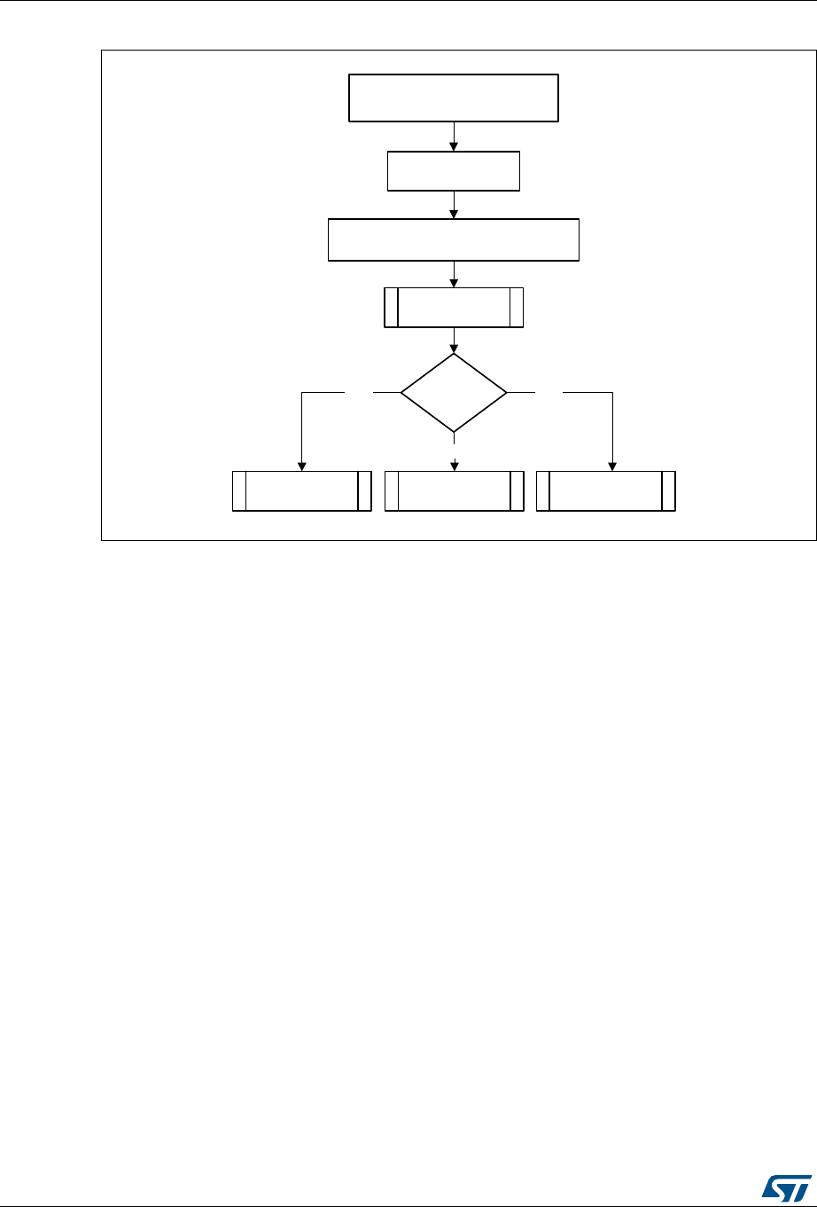
USB on-the-go full-speed (OTG_FS) RM0090
1340/1718 DocID018909 Rev 9
Figure 403. Processing a SETUP packet
•Handling more than three back-to-back SETUP packets
Per the USB 2.0 specification, normally, during a SETUP packet error, a host does not send
more than three back-to-back SETUP packets to the same endpoint. However, the USB 2.0
specification does not limit the number of back-to-back SETUP packets a host can send to
the same endpoint. When this condition occurs, the OTG_FS controller generates an
interrupt (B2BSTUP in OTG_FS_DOEPINTx).
•Setting the global OUT NAK
Internal data flow:
1. When the application sets the Global OUT NAK (SGONAK bit in OTG_FS_DCTL), the
core stops writing data, except SETUP packets, to the receive FIFO. Irrespective of the
space availability in the receive FIFO, non-isochronous OUT tokens receive a NAK
handshake response, and the core ignores isochronous OUT data packets
2. The core writes the Global OUT NAK pattern to the receive FIFO. The application must
reserve enough receive FIFO space to write this data pattern.
3. When the application pops the Global OUT NAK pattern Word from the receive FIFO,
the core sets the GONAKEFF interrupt (OTG_FS_GINTSTS).
4. Once the application detects this interrupt, it can assume that the core is in Global OUT
NAK mode. The application can clear this interrupt by clearing the SGONAK bit in
OTG_FS_DCTL.
Application programming sequence
Wait for STUP in OTG_FS_DOEPINTx
rem_supcnt =
rd_reg(DOEPTSIZx)
setup_cmd[31:0] = mem[4 – 2 * rem_supcnt]
setup_cmd[63:32] = mem[5 – 2 * rem_supcnt]
ctrl-rd/wr/2 stage
Find setup cmd type
Write
2-stage
Read
setup_np_in_pkt
Status IN phase
rcv_out_pkt
Data OUT phase
setup_np_in_pkt
Data IN phase
ai15678

DocID018909 Rev 9 1341/1718
RM0090 USB on-the-go full-speed (OTG_FS)
1362
1. To stop receiving any kind of data in the receive FIFO, the application must set the
Global OUT NAK bit by programming the following field:
– SGONAK = 1 in OTG_FS_DCTL
2. Wait for the assertion of the GONAKEFF interrupt in OTG_FS_GINTSTS. When
asserted, this interrupt indicates that the core has stopped receiving any type of data
except SETUP packets.
3. The application can receive valid OUT packets after it has set SGONAK in
OTG_FS_DCTL and before the core asserts the GONAKEFF interrupt
(OTG_FS_GINTSTS).
4. The application can temporarily mask this interrupt by writing to the GINAKEFFM bit in
the OTG_FS_GINTMSK register.
– GINAKEFFM = 0 in the OTG_FS_GINTMSK register
5. Whenever the application is ready to exit the Global OUT NAK mode, it must clear the
SGONAK bit in OTG_FS_DCTL. This also clears the GONAKEFF interrupt
(OTG_FS_GINTSTS).
– OTG_FS_DCTL = 1 in CGONAK
6. If the application has masked this interrupt earlier, it must be unmasked as follows:
– GINAKEFFM = 1 in GINTMSK
•Disabling an OUT endpoint
The application must use this sequence to disable an OUT endpoint that it has enabled.
Application programming sequence:
1. Before disabling any OUT endpoint, the application must enable Global OUT NAK
mode in the core.
– SGONAK = 1 in OTG_FS_DCTL
2. Wait for the GONAKEFF interrupt (OTG_FS_GINTSTS)
3. Disable the required OUT endpoint by programming the following fields:
– EPDIS = 1 in OTG_FS_DOEPCTLx
– SNAK = 1 in OTG_FS_DOEPCTLx
4. Wait for the EPDISD interrupt (OTG_FS_DOEPINTx), which indicates that the OUT
endpoint is completely disabled. When the EPDISD interrupt is asserted, the core also
clears the following bits:
– EPDIS = 0 in OTG_FS_DOEPCTLx
– EPENA = 0 in OTG_FS_DOEPCTLx
5. The application must clear the Global OUT NAK bit to start receiving data from other
non-disabled OUT endpoints.
– SGONAK = 0 in OTG_FS_DCTL
•Generic non-isochronous OUT data transfers
This section describes a regular non-isochronous OUT data transfer (control, bulk, or
interrupt).
Application requirements:

USB on-the-go full-speed (OTG_FS) RM0090
1342/1718 DocID018909 Rev 9
1. Before setting up an OUT transfer, the application must allocate a buffer in the memory
to accommodate all data to be received as part of the OUT transfer.
2. For OUT transfers, the transfer size field in the endpoint’s transfer size register must be
a multiple of the maximum packet size of the endpoint, adjusted to the Word boundary.
– transfer size[EPNUM] = n × (MPSIZ[EPNUM] + 4 – (MPSIZ[EPNUM] mod 4))
– packet count[EPNUM] = n
–n > 0
3. On any OUT endpoint interrupt, the application must read the endpoint’s transfer size
register to calculate the size of the payload in the memory. The received payload size
can be less than the programmed transfer size.
– Payload size in memory = application programmed initial transfer size – core
updated final transfer size
– Number of USB packets in which this payload was received = application
programmed initial packet count – core updated final packet count
Internal data flow:
1. The application must set the transfer size and packet count fields in the endpoint-
specific registers, clear the NAK bit, and enable the endpoint to receive the data.
2. Once the NAK bit is cleared, the core starts receiving data and writes it to the receive
FIFO, as long as there is space in the receive FIFO. For every data packet received on
the USB, the data packet and its status are written to the receive FIFO. Every packet
(maximum packet size or short packet) written to the receive FIFO decrements the
packet count field for that endpoint by 1.
– OUT data packets received with bad data CRC are flushed from the receive FIFO
automatically.
– After sending an ACK for the packet on the USB, the core discards non-
isochronous OUT data packets that the host, which cannot detect the ACK, re-
sends. The application does not detect multiple back-to-back data OUT packets
on the same endpoint with the same data PID. In this case the packet count is not
decremented.
– If there is no space in the receive FIFO, isochronous or non-isochronous data
packets are ignored and not written to the receive FIFO. Additionally, non-
isochronous OUT tokens receive a NAK handshake reply.
– In all the above three cases, the packet count is not decremented because no data
are written to the receive FIFO.
3. When the packet count becomes 0 or when a short packet is received on the endpoint,
the NAK bit for that endpoint is set. Once the NAK bit is set, the isochronous or non-

DocID018909 Rev 9 1343/1718
RM0090 USB on-the-go full-speed (OTG_FS)
1362
isochronous data packets are ignored and not written to the receive FIFO, and non-
isochronous OUT tokens receive a NAK handshake reply.
4. After the data are written to the receive FIFO, the application reads the data from the
receive FIFO and writes it to external memory, one packet at a time per endpoint.
5. At the end of every packet write on the AHB to external memory, the transfer size for
the endpoint is decremented by the size of the written packet.
6. The OUT data transfer completed pattern for an OUT endpoint is written to the receive
FIFO on one of the following conditions:
– The transfer size is 0 and the packet count is 0
– The last OUT data packet written to the receive FIFO is a short packet
(0 ≤ packet size < maximum packet size)
7. When either the application pops this entry (OUT data transfer completed), a transfer
completed interrupt is generated for the endpoint and the endpoint enable is cleared.
Application programming sequence:
1. Program the OTG_FS_DOEPTSIZx register for the transfer size and the corresponding
packet count.
2. Program the OTG_FS_DOEPCTLx register with the endpoint characteristics, and set
the EPENA and CNAK bits.
– EPENA = 1 in OTG_FS_DOEPCTLx
– CNAK = 1 in OTG_FS_DOEPCTLx
3. Wait for the RXFLVL interrupt (in OTG_FS_GINTSTS) and empty the data packets
from the receive FIFO.
– This step can be repeated many times, depending on the transfer size.
4. Asserting the XFRC interrupt (OTG_FS_DOEPINTx) marks a successful completion of
the non-isochronous OUT data transfer.
5. Read the OTG_FS_DOEPTSIZx register to determine the size of the received data
payload.
•Generic isochronous OUT data transfer
This section describes a regular isochronous OUT data transfer.
Application requirements:
1. All the application requirements for non-isochronous OUT data transfers also apply to
isochronous OUT data transfers.
2. For isochronous OUT data transfers, the transfer size and packet count fields must
always be set to the number of maximum-packet-size packets that can be received in a
single frame and no more. Isochronous OUT data transfers cannot span more than 1
frame.
3. The application must read all isochronous OUT data packets from the receive FIFO
(data and status) before the end of the periodic frame (EOPF interrupt in
OTG_FS_GINTSTS).
4. To receive data in the following frame, an isochronous OUT endpoint must be enabled
after the EOPF (OTG_FS_GINTSTS) and before the SOF (OTG_FS_GINTSTS).
Internal data flow:

USB on-the-go full-speed (OTG_FS) RM0090
1344/1718 DocID018909 Rev 9
1. The internal data flow for isochronous OUT endpoints is the same as that for non-
isochronous OUT endpoints, but for a few differences.
2. When an isochronous OUT endpoint is enabled by setting the Endpoint Enable and
clearing the NAK bits, the Even/Odd frame bit must also be set appropriately. The core
receives data on an isochronous OUT endpoint in a particular frame only if the
following condition is met:
– EONUM (in OTG_FS_DOEPCTLx) = SOFFN[0] (in OTG_FS_DSTS)
3. When the application completely reads an isochronous OUT data packet (data and
status) from the receive FIFO, the core updates the RXDPID field in
OTG_FS_DOEPTSIZx with the data PID of the last isochronous OUT data packet read
from the receive FIFO.
Application programming sequence:
1. Program the OTG_FS_DOEPTSIZx register for the transfer size and the corresponding
packet count
2. Program the OTG_FS_DOEPCTLx register with the endpoint characteristics and set
the Endpoint Enable, ClearNAK, and Even/Odd frame bits.
– EPENA = 1
–CNAK=1
– EONUM = (0: Even/1: Odd)
3. Wait for the RXFLVL interrupt (in OTG_FS_GINTSTS) and empty the data packets
from the receive FIFO
– This step can be repeated many times, depending on the transfer size.
4. The assertion of the XFRC interrupt (in OTG_FS_DOEPINTx) marks the completion of
the isochronous OUT data transfer. This interrupt does not necessarily mean that the
data in memory are good.
5. This interrupt cannot always be detected for isochronous OUT transfers. Instead, the
application can detect the IISOOXFRM interrupt in OTG_FS_GINTSTS.
6. Read the OTG_FS_DOEPTSIZx register to determine the size of the received transfer
and to determine the validity of the data received in the frame. The application must
treat the data received in memory as valid only if one of the following conditions is met:
– RXDPID = D0 (in OTG_FS_DOEPTSIZx) and the number of USB packets in
which this payload was received = 1
– RXDPID = D1 (in OTG_FS_DOEPTSIZx) and the number of USB packets in
which this payload was received = 2
– RXDPID = D2 (in OTG_FS_DOEPTSIZx) and the number of USB packets in
which this payload was received = 3
The number of USB packets in which this payload was received =
Application programmed initial packet count – Core updated final packet count
The application can discard invalid data packets.
•Incomplete isochronous OUT data transfers
This section describes the application programming sequence when isochronous OUT data
packets are dropped inside the core.
Internal data flow:
1. For isochronous OUT endpoints, the XFRC interrupt (in OTG_FS_DOEPINTx) may not
always be asserted. If the core drops isochronous OUT data packets, the application

DocID018909 Rev 9 1345/1718
RM0090 USB on-the-go full-speed (OTG_FS)
1362
could fail to detect the XFRC interrupt (OTG_FS_DOEPINTx) under the following
circumstances:
– When the receive FIFO cannot accommodate the complete ISO OUT data packet,
the core drops the received ISO OUT data
– When the isochronous OUT data packet is received with CRC errors
– When the isochronous OUT token received by the core is corrupted
– When the application is very slow in reading the data from the receive FIFO
2. When the core detects an end of periodic frame before transfer completion to all
isochronous OUT endpoints, it asserts the incomplete Isochronous OUT data interrupt
(IISOOXFRM in OTG_FS_GINTSTS), indicating that an XFRC interrupt (in
OTG_FS_DOEPINTx) is not asserted on at least one of the isochronous OUT
endpoints. At this point, the endpoint with the incomplete transfer remains enabled, but
no active transfers remain in progress on this endpoint on the USB.
Application programming sequence:
1. Asserting the IISOOXFRM interrupt (OTG_FS_GINTSTS) indicates that in the current
frame, at least one isochronous OUT endpoint has an incomplete transfer.
2. If this occurs because isochronous OUT data is not completely emptied from the
endpoint, the application must ensure that the application empties all isochronous OUT
data (data and status) from the receive FIFO before proceeding.
– When all data are emptied from the receive FIFO, the application can detect the
XFRC interrupt (OTG_FS_DOEPINTx). In this case, the application must re-
enable the endpoint to receive isochronous OUT data in the next frame.
3. When it receives an IISOOXFRM interrupt (in OTG_FS_GINTSTS), the application
must read the control registers of all isochronous OUT endpoints
(OTG_FS_DOEPCTLx) to determine which endpoints had an incomplete transfer in the
current microframe. An endpoint transfer is incomplete if both the following conditions
are met:
– EONUM bit (in OTG_FS_DOEPCTLx) = SOFFN[0] (in OTG_FS_DSTS)
– EPENA = 1 (in OTG_FS_DOEPCTLx)
4. The previous step must be performed before the SOF interrupt (in OTG_FS_GINTSTS)
is detected, to ensure that the current frame number is not changed.
5. For isochronous OUT endpoints with incomplete transfers, the application must discard
the data in the memory and disable the endpoint by setting the EPDIS bit in
OTG_FS_DOEPCTLx.
6. Wait for the EPDIS interrupt (in OTG_FS_DOEPINTx) and enable the endpoint to
receive new data in the next frame.
– Because the core can take some time to disable the endpoint, the application may
not be able to receive the data in the next frame after receiving bad isochronous
data.
•Stalling a non-isochronous OUT endpoint
This section describes how the application can stall a non-isochronous endpoint.
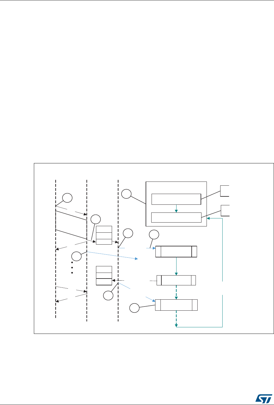
USB on-the-go full-speed (OTG_FS) RM0090
1346/1718 DocID018909 Rev 9
1. Put the core in the Global OUT NAK mode.
2. Disable the required endpoint
– When disabling the endpoint, instead of setting the SNAK bit in
OTG_FS_DOEPCTL, set STALL = 1 (in OTG_FS_DOEPCTL).
The STALL bit always takes precedence over the NAK bit.
3. When the application is ready to end the STALL handshake for the endpoint, the
STALL bit (in OTG_FS_DOEPCTLx) must be cleared.
4. If the application is setting or clearing a STALL for an endpoint due to a
SetFeature.Endpoint Halt or ClearFeature.Endpoint Halt command, the STALL bit must
be set or cleared before the application sets up the Status stage transfer on the control
endpoint.
Examples
This section describes and depicts some fundamental transfer types and scenarios.
•Bulk OUT transaction
Figure 404 depicts the reception of a single Bulk OUT Data packet from the USB to the AHB
and describes the events involved in the process.
Figure 404. Bulk OUT transaction
After a SetConfiguration/SetInterface command, the application initializes all OUT endpoints
by setting CNAK = 1 and EPENA = 1 (in OTG_FS_DOEPCTLx), and setting a suitable
XFRSIZ and PKTCNT in the OTG_FS_DOEPTSIZx register.
init_out_ep
Host DeviceUSB
OUT
ACK
RXFLVL intr i
wr_reg(DOEPTSIZx)
wr_reg(DOEPCTLx)
64 bytes
OUT
NAK
xact _1
Application
XFRC
intr
DOEPCTLx.NAK=1
PKTCNT 0
XFRSIZ = 0
r
idle until intr
rcv_out _pkt()
idle until intr
On new xfer
or RxFIFO
not empty
1
2
3
4
5
6
7
8
XFRSIZ = 64 bytes
PKTCNT = 1
EPENA = 1
CNAK = 1
ai15679b

DocID018909 Rev 9 1347/1718
RM0090 USB on-the-go full-speed (OTG_FS)
1362
1. host attempts to send data (OUT token) to an endpoint.
2. When the core receives the OUT token on the USB, it stores the packet in the RxFIFO
because space is available there.
3. After writing the complete packet in the RxFIFO, the core then asserts the RXFLVL
interrupt (in OTG_FS_GINTSTS).
4. On receiving the PKTCNT number of USB packets, the core internally sets the NAK bit
for this endpoint to prevent it from receiving any more packets.
5. The application processes the interrupt and reads the data from the RxFIFO.
6. When the application has read all the data (equivalent to XFRSIZ), the core generates
an XFRC interrupt (in OTG_FS_DOEPINTx).
7. The application processes the interrupt and uses the setting of the XFRC interrupt bit
(in OTG_FS_DOEPINTx) to determine that the intended transfer is complete.
IN data transfers
•Packet write
This section describes how the application writes data packets to the endpoint FIFO when
dedicated transmit FIFOs are enabled.
1. The application can either choose the polling or the interrupt mode.
– In polling mode, the application monitors the status of the endpoint transmit data
FIFO by reading the OTG_FS_DTXFSTSx register, to determine if there is enough
space in the data FIFO.
– In interrupt mode, the application waits for the TXFE interrupt (in
OTG_FS_DIEPINTx) and then reads the OTG_FS_DTXFSTSx register, to
determine if there is enough space in the data FIFO.
– To write a single non-zero length data packet, there must be space to write the
entire packet in the data FIFO.
– To write zero length packet, the application must not look at the FIFO space.
2. Using one of the above mentioned methods, when the application determines that
there is enough space to write a transmit packet, the application must first write into the
endpoint control register, before writing the data into the data FIFO. Typically, the
application, must do a read modify write on the OTG_FS_DIEPCTLx register to avoid
modifying the contents of the register, except for setting the Endpoint Enable bit.
The application can write multiple packets for the same endpoint into the transmit FIFO, if
space is available. For periodic IN endpoints, the application must write packets only for one
microframe. It can write packets for the next periodic transaction only after getting transfer
complete for the previous transaction.
•Setting IN endpoint NAK
Internal data flow:

USB on-the-go full-speed (OTG_FS) RM0090
1348/1718 DocID018909 Rev 9
1. When the application sets the IN NAK for a particular endpoint, the core stops
transmitting data on the endpoint, irrespective of data availability in the endpoint’s
transmit FIFO.
2. Non-isochronous IN tokens receive a NAK handshake reply
– Isochronous IN tokens receive a zero-data-length packet reply
3. The core asserts the INEPNE (IN endpoint NAK effective) interrupt in
OTG_FS_DIEPINTx in response to the SNAK bit in OTG_FS_DIEPCTLx.
4. Once this interrupt is seen by the application, the application can assume that the
endpoint is in IN NAK mode. This interrupt can be cleared by the application by setting
the CNAK bit in OTG_FS_DIEPCTLx.
Application programming sequence:
1. To stop transmitting any data on a particular IN endpoint, the application must set the
IN NAK bit. To set this bit, the following field must be programmed.
– SNAK = 1 in OTG_FS_DIEPCTLx
2. Wait for assertion of the INEPNE interrupt in OTG_FS_DIEPINTx. This interrupt
indicates that the core has stopped transmitting data on the endpoint.
3. The core can transmit valid IN data on the endpoint after the application has set the
NAK bit, but before the assertion of the NAK Effective interrupt.
4. The application can mask this interrupt temporarily by writing to the INEPNEM bit in
DIEPMSK.
– INEPNEM = 0 in DIEPMSK
5. To exit Endpoint NAK mode, the application must clear the NAK status bit (NAKSTS) in
OTG_FS_DIEPCTLx. This also clears the INEPNE interrupt (in OTG_FS_DIEPINTx).
– CNAK = 1 in OTG_FS_DIEPCTLx
6. If the application masked this interrupt earlier, it must be unmasked as follows:
– INEPNEM = 1 in DIEPMSK
•IN endpoint disable
Use the following sequence to disable a specific IN endpoint that has been previously
enabled.
Application programming sequence:

DocID018909 Rev 9 1349/1718
RM0090 USB on-the-go full-speed (OTG_FS)
1362
1. The application must stop writing data on the AHB for the IN endpoint to be disabled.
2. The application must set the endpoint in NAK mode.
– SNAK = 1 in OTG_FS_DIEPCTLx
3. Wait for the INEPNE interrupt in OTG_FS_DIEPINTx.
4. Set the following bits in the OTG_FS_DIEPCTLx register for the endpoint that must be
disabled.
– EPDIS = 1 in OTG_FS_DIEPCTLx
– SNAK = 1 in OTG_FS_DIEPCTLx
5. Assertion of the EPDISD interrupt in OTG_FS_DIEPINTx indicates that the core has
completely disabled the specified endpoint. Along with the assertion of the interrupt, the
core also clears the following bits:
– EPENA = 0 in OTG_FS_DIEPCTLx
– EPDIS = 0 in OTG_FS_DIEPCTLx
6. The application must read the OTG_FS_DIEPTSIZx register for the periodic IN EP, to
calculate how much data on the endpoint were transmitted on the USB.
7. The application must flush the data in the Endpoint transmit FIFO, by setting the
following fields in the OTG_FS_GRSTCTL register:
– TXFNUM (in OTG_FS_GRSTCTL) = Endpoint transmit FIFO number
– TXFFLSH in (OTG_FS_GRSTCTL) = 1
The application must poll the OTG_FS_GRSTCTL register, until the TXFFLSH bit is cleared
by the core, which indicates the end of flush operation. To transmit new data on this
endpoint, the application can re-enable the endpoint at a later point.

USB on-the-go full-speed (OTG_FS) RM0090
1350/1718 DocID018909 Rev 9
•Generic non-periodic IN data transfers
Application requirements:
1. Before setting up an IN transfer, the application must ensure that all data to be
transmitted as part of the IN transfer are part of a single buffer.
2. For IN transfers, the Transfer Size field in the Endpoint Transfer Size register denotes a
payload that constitutes multiple maximum-packet-size packets and a single short
packet. This short packet is transmitted at the end of the transfer.
– To transmit a few maximum-packet-size packets and a short packet at the end of
the transfer:
Transfer size[EPNUM] = x × MPSIZ[EPNUM] + sp
If (sp > 0), then packet count[EPNUM] = x + 1.
Otherwise, packet count[EPNUM] = x
– To transmit a single zero-length data packet:
Transfer size[EPNUM] = 0
Packet count[EPNUM] = 1
– To transmit a few maximum-packet-size packets and a zero-length data packet at
the end of the transfer, the application must split the transfer into two parts. The
first sends maximum-packet-size data packets and the second sends the zero-
length data packet alone.
First transfer: transfer size[EPNUM] = x × MPSIZ[epnum]; packet count = n;
Second transfer: transfer size[EPNUM] = 0; packet count = 1;
3. Once an endpoint is enabled for data transfers, the core updates the Transfer size
register. At the end of the IN transfer, the application must read the Transfer size
register to determine how much data posted in the transmit FIFO have already been
sent on the USB.
4. Data fetched into transmit FIFO = Application-programmed initial transfer size – core-
updated final transfer size
– Data transmitted on USB = (application-programmed initial packet count – Core
updated final packet count) × MPSIZ[EPNUM]
– Data yet to be transmitted on USB = (Application-programmed initial transfer size
– data transmitted on USB)
Internal data flow:
1. The application must set the transfer size and packet count fields in the endpoint-
specific registers and enable the endpoint to transmit the data.
2. The application must also write the required data to the transmit FIFO for the endpoint.
3. Every time a packet is written into the transmit FIFO by the application, the transfer size
for that endpoint is decremented by the packet size. The data is fetched from the
memory by the application, until the transfer size for the endpoint becomes 0. After
writing the data into the FIFO, the “number of packets in FIFO” count is incremented
(this is a 3-bit count, internally maintained by the core for each IN endpoint transmit
FIFO. The maximum number of packets maintained by the core at any time in an IN
endpoint FIFO is eight). For zero-length packets, a separate flag is set for each FIFO,
without any data in the FIFO.
4. Once the data are written to the transmit FIFO, the core reads them out upon receiving
an IN token. For every non-isochronous IN data packet transmitted with an ACK

DocID018909 Rev 9 1351/1718
RM0090 USB on-the-go full-speed (OTG_FS)
1362
handshake, the packet count for the endpoint is decremented by one, until the packet
count is zero. The packet count is not decremented on a timeout.
5. For zero length packets (indicated by an internal zero length flag), the core sends out a
zero-length packet for the IN token and decrements the packet count field.
6. If there are no data in the FIFO for a received IN token and the packet count field for
that endpoint is zero, the core generates an “IN token received when TxFIFO is empty”
(ITTXFE) Interrupt for the endpoint, provided that the endpoint NAK bit is not set. The
core responds with a NAK handshake for non-isochronous endpoints on the USB.
7. The core internally rewinds the FIFO pointers and no timeout interrupt is generated.
8. When the transfer size is 0 and the packet count is 0, the transfer complete (XFRC)
interrupt for the endpoint is generated and the endpoint enable is cleared.
Application programming sequence:
1. Program the OTG_FS_DIEPTSIZx register with the transfer size and corresponding
packet count.
2. Program the OTG_FS_DIEPCTLx register with the endpoint characteristics and set the
CNAK and EPENA (Endpoint Enable) bits.
3. When transmitting non-zero length data packet, the application must poll the
OTG_FS_DTXFSTSx register (where x is the FIFO number associated with that
endpoint) to determine whether there is enough space in the data FIFO. The
application can optionally use TXFE (in OTG_FS_DIEPINTx) before writing the data.
•Generic periodic IN data transfers
This section describes a typical periodic IN data transfer.
Application requirements:
1. Application requirements 1, 2, 3, and 4 of Generic non-periodic IN data transfers on
page 1350 also apply to periodic IN data transfers, except for a slight modification of
requirement 2.
– The application can only transmit multiples of maximum-packet-size data packets
or multiples of maximum-packet-size packets, plus a short packet at the end. To

USB on-the-go full-speed (OTG_FS) RM0090
1352/1718 DocID018909 Rev 9
transmit a few maximum-packet-size packets and a short packet at the end of the
transfer, the following conditions must be met:
transfer size[EPNUM] = x × MPSIZ[EPNUM] + sp
(where x is an integer ≥ 0, and 0 ≤ sp < MPSIZ[EPNUM])
If (sp > 0), packet count[EPNUM] = x + 1
Otherwise, packet count[EPNUM] = x;
MCNT[EPNUM] = packet count[EPNUM]
– The application cannot transmit a zero-length data packet at the end of a transfer.
It can transmit a single zero-length data packet by itself. To transmit a single zero-
length data packet:
– transfer size[EPNUM] = 0
packet count[EPNUM] = 1
MCNT[EPNUM] = packet count[EPNUM]
2. The application can only schedule data transfers one frame at a time.
– (MCNT – 1) × MPSIZ ≤ XFERSIZ ≤ MCNT × MPSIZ
– PKTCNT = MCNT (in OTG_FS_DIEPTSIZx)
– If XFERSIZ < MCNT × MPSIZ, the last data packet of the transfer is a short
packet.
– Note that: MCNT is in OTG_FS_DIEPTSIZx, MPSIZ is in OTG_FS_DIEPCTLx,
PKTCNT is in OTG_FS_DIEPTSIZx and XFERSIZ is in OTG_FS_DIEPTSIZx
3. The complete data to be transmitted in the frame must be written into the transmit FIFO
by the application, before the IN token is received. Even when 1 Word of the data to be
transmitted per frame is missing in the transmit FIFO when the IN token is received, the
core behaves as when the FIFO is empty. When the transmit FIFO is empty:
– A zero data length packet would be transmitted on the USB for isochronous IN
endpoints
– A NAK handshake would be transmitted on the USB for interrupt IN endpoints
Internal data flow:
1. The application must set the transfer size and packet count fields in the endpoint-
specific registers and enable the endpoint to transmit the data.
2. The application must also write the required data to the associated transmit FIFO for
the endpoint.
3. Every time the application writes a packet to the transmit FIFO, the transfer size for that
endpoint is decremented by the packet size. The data are fetched from application
memory until the transfer size for the endpoint becomes 0.
4. When an IN token is received for a periodic endpoint, the core transmits the data in the
FIFO, if available. If the complete data payload (complete packet, in dedicated FIFO

DocID018909 Rev 9 1353/1718
RM0090 USB on-the-go full-speed (OTG_FS)
1362
mode) for the frame is not present in the FIFO, then the core generates an IN token
received when TxFIFO empty interrupt for the endpoint.
– A zero-length data packet is transmitted on the USB for isochronous IN endpoints
– A NAK handshake is transmitted on the USB for interrupt IN endpoints
5. The packet count for the endpoint is decremented by 1 under the following conditions:
– For isochronous endpoints, when a zero- or non-zero-length data packet is
transmitted
– For interrupt endpoints, when an ACK handshake is transmitted
– When the transfer size and packet count are both 0, the transfer completed
interrupt for the endpoint is generated and the endpoint enable is cleared.
6. At the “Periodic frame Interval” (controlled by PFIVL in OTG_FS_DCFG), when the
core finds non-empty any of the isochronous IN endpoint FIFOs scheduled for the
current frame non-empty, the core generates an IISOIXFR interrupt in
OTG_FS_GINTSTS.
Application programming sequence:
1. Program the OTG_FS_DIEPCTLx register with the endpoint characteristics and set the
CNAK and EPENA bits.
2. Write the data to be transmitted in the next frame to the transmit FIFO.
3. Asserting the ITTXFE interrupt (in OTG_FS_DIEPINTx) indicates that the application
has not yet written all data to be transmitted to the transmit FIFO.
4. If the interrupt endpoint is already enabled when this interrupt is detected, ignore the
interrupt. If it is not enabled, enable the endpoint so that the data can be transmitted on
the next IN token attempt.
5. Asserting the XFRC interrupt (in OTG_FS_DIEPINTx) with no ITTXFE interrupt in
OTG_FS_DIEPINTx indicates the successful completion of an isochronous IN transfer.
A read to the OTG_FS_DIEPTSIZx register must give transfer size = 0 and packet
count = 0, indicating all data were transmitted on the USB.
6. Asserting the XFRC interrupt (in OTG_FS_DIEPINTx), with or without the ITTXFE
interrupt (in OTG_FS_DIEPINTx), indicates the successful completion of an interrupt
IN transfer. A read to the OTG_FS_DIEPTSIZx register must give transfer size = 0 and
packet count = 0, indicating all data were transmitted on the USB.
7. Asserting the incomplete isochronous IN transfer (IISOIXFR) interrupt in
OTG_FS_GINTSTS with none of the aforementioned interrupts indicates the core did
not receive at least 1 periodic IN token in the current frame.
•Incomplete isochronous IN data transfers
This section describes what the application must do on an incomplete isochronous IN data
transfer.
Internal data flow:
1. An isochronous IN transfer is treated as incomplete in one of the following conditions:
a) The core receives a corrupted isochronous IN token on at least one isochronous
IN endpoint. In this case, the application detects an incomplete isochronous IN
transfer interrupt (IISOIXFR in OTG_FS_GINTSTS).
b) The application is slow to write the complete data payload to the transmit FIFO
and an IN token is received before the complete data payload is written to the
FIFO. In this case, the application detects an IN token received when TxFIFO
empty interrupt in OTG_FS_DIEPINTx. The application can ignore this interrupt,

USB on-the-go full-speed (OTG_FS) RM0090
1354/1718 DocID018909 Rev 9
as it eventually results in an incomplete isochronous IN transfer interrupt
(IISOIXFR in OTG_FS_GINTSTS) at the end of periodic frame.
The core transmits a zero-length data packet on the USB in response to the
received IN token.
2. The application must stop writing the data payload to the transmit FIFO as soon as
possible.
3. The application must set the NAK bit and the disable bit for the endpoint.
4. The core disables the endpoint, clears the disable bit, and asserts the Endpoint Disable
interrupt for the endpoint.
Application programming sequence:
1. The application can ignore the IN token received when TxFIFO empty interrupt in
OTG_FS_DIEPINTx on any isochronous IN endpoint, as it eventually results in an
incomplete isochronous IN transfer interrupt (in OTG_FS_GINTSTS).
2. Assertion of the incomplete isochronous IN transfer interrupt (in OTG_FS_GINTSTS)
indicates an incomplete isochronous IN transfer on at least one of the isochronous IN
endpoints.
3. The application must read the Endpoint Control register for all isochronous IN
endpoints to detect endpoints with incomplete IN data transfers.
4. The application must stop writing data to the Periodic Transmit FIFOs associated with
these endpoints on the AHB.
5. Program the following fields in the OTG_FS_DIEPCTLx register to disable the
endpoint:
– SNAK = 1 in OTG_FS_DIEPCTLx
– EPDIS = 1 in OTG_FS_DIEPCTLx
6. The assertion of the Endpoint Disabled interrupt in OTG_FS_DIEPINTx indicates that
the core has disabled the endpoint.
– At this point, the application must flush the data in the associated transmit FIFO or
overwrite the existing data in the FIFO by enabling the endpoint for a new transfer
in the next microframe. To flush the data, the application must use the
OTG_FS_GRSTCTL register.
•Stalling non-isochronous IN endpoints
This section describes how the application can stall a non-isochronous endpoint.
Application programming sequence:

DocID018909 Rev 9 1355/1718
RM0090 USB on-the-go full-speed (OTG_FS)
1362
1. Disable the IN endpoint to be stalled. Set the STALL bit as well.
2. EPDIS = 1 in OTG_FS_DIEPCTLx, when the endpoint is already enabled
– STALL = 1 in OTG_FS_DIEPCTLx
– The STALL bit always takes precedence over the NAK bit
3. Assertion of the Endpoint Disabled interrupt (in OTG_FS_DIEPINTx) indicates to the
application that the core has disabled the specified endpoint.
4. The application must flush the non-periodic or periodic transmit FIFO, depending on
the endpoint type. In case of a non-periodic endpoint, the application must re-enable
the other non-periodic endpoints that do not need to be stalled, to transmit data.
5. Whenever the application is ready to end the STALL handshake for the endpoint, the
STALL bit must be cleared in OTG_FS_DIEPCTLx.
6. If the application sets or clears a STALL bit for an endpoint due to a
SetFeature.Endpoint Halt command or ClearFeature.Endpoint Halt command, the
STALL bit must be set or cleared before the application sets up the Status stage
transfer on the control endpoint.
Special case: stalling the control OUT endpoint
The core must stall IN/OUT tokens if, during the data stage of a control transfer, the host
sends more IN/OUT tokens than are specified in the SETUP packet. In this case, the
application must enable the ITTXFE interrupt in OTG_FS_DIEPINTx and the OTEPDIS
interrupt in OTG_FS_DOEPINTx during the data stage of the control transfer, after the core
has transferred the amount of data specified in the SETUP packet. Then, when the
application receives this interrupt, it must set the STALL bit in the corresponding endpoint
control register, and clear this interrupt.
34.17.7 Worst case response time
When the OTG_FS controller acts as a device, there is a worst case response time for any
tokens that follow an isochronous OUT. This worst case response time depends on the AHB
clock frequency.
The core registers are in the AHB domain, and the core does not accept another token
before updating these register values. The worst case is for any token following an
isochronous OUT, because for an isochronous transaction, there is no handshake and the
next token could come sooner. This worst case value is 7 PHY clocks when the AHB clock
is the same as the PHY clock. When the AHB clock is faster, this value is smaller.
If this worst case condition occurs, the core responds to bulk/interrupt tokens with a NAK
and drops isochronous and SETUP tokens. The host interprets this as a timeout condition
for SETUP and retries the SETUP packet. For isochronous transfers, the Incomplete
isochronous IN transfer interrupt (IISOIXFR) and Incomplete isochronous OUT transfer
interrupt (IISOOXFR) inform the application that isochronous IN/OUT packets were
dropped.
Choosing the value of TRDT in OTG_FS_GUSBCFG
The value in TRDT (OTG_FS_GUSBCFG) is the time it takes for the MAC, in terms of PHY
clocks after it has received an IN token, to get the FIFO status, and thus the first data from
the PFC block. This time involves the synchronization delay between the PHY and AHB
clocks. The worst case delay for this is when the AHB clock is the same as the PHY clock.
In this case, the delay is 5 clocks.
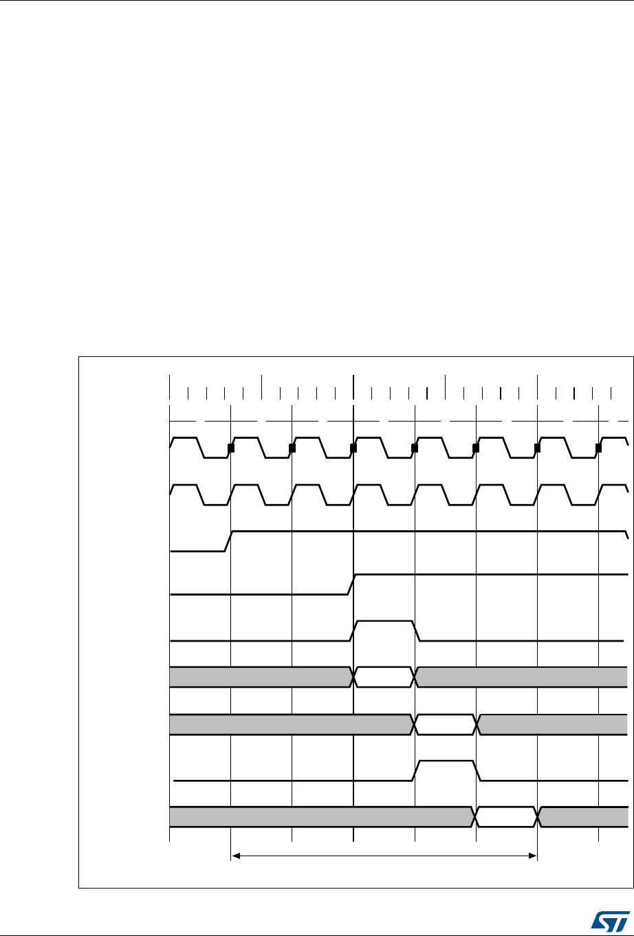
USB on-the-go full-speed (OTG_FS) RM0090
1356/1718 DocID018909 Rev 9
Once the MAC receives an IN token, this information (token received) is synchronized to the
AHB clock by the PFC (the PFC runs on the AHB clock). The PFC then reads the data from
the SPRAM and writes them into the dual clock source buffer. The MAC then reads the data
out of the source buffer (4 deep).
If the AHB is running at a higher frequency than the PHY, the application can use a smaller
value for TRDT (in OTG_FS_GUSBCFG).
Figure 405 has the following signals:
•tkn_rcvd: Token received information from MAC to PFC
•dynced_tkn_rcvd: Doubled sync tkn_rcvd, from PCLK to HCLK domain
•spr_read: Read to SPRAM
•spr_addr: Address to SPRAM
•spr_rdata: Read data from SPRAM
•srcbuf_push: Push to the source buffer
•srcbuf_rdata: Read data from the source buffer. Data seen by MAC
Refer to Table 200: TRDT values for the values of TRDT versus AHB clock frequency.
Figure 405. TRDT max timing case
12345678
0ns 50ns 100ns 150ns 200ns
HCLK
PCLK
tkn_rcvd
dsynced_tkn_rcvd
spr_read
spr_addr
spr_rdata
srcbuf_push
srcbuf_rdata
5 Clocks
D1
A1
D1
ai15680

DocID018909 Rev 9 1357/1718
RM0090 USB on-the-go full-speed (OTG_FS)
1362
34.17.8 OTG programming model
The OTG_FS controller is an OTG device supporting HNP and SRP. When the core is
connected to an “A” plug, it is referred to as an A-device. When the core is connected to a
“B” plug it is referred to as a B-device. In host mode, the OTG_FS controller turns off VBUS
to conserve power. SRP is a method by which the B-device signals the A-device to turn on
VBUS power. A device must perform both data-line pulsing and VBUS pulsing, but a host can
detect either data-line pulsing or VBUS pulsing for SRP. HNP is a method by which the B-
device negotiates and switches to host role. In Negotiated mode after HNP, the B-device
suspends the bus and reverts to the device role.
A-device session request protocol
The application must set the SRP-capable bit in the Core USB configuration register. This
enables the OTG_FS controller to detect SRP as an A-device.
Figure 406. A-device SRP
1. DRV_VBUS = VBUS drive signal to the PHY
VBUS_VALID = VBUS valid signal from PHY
A_VALID = A-peripheral VBUS level signal to PHY
D+ = Data plus line
D- = Data minus line
ai15681
DRV_VBUS
VBUS_VALID
A_VALID
D+
D-
Suspend
VBUS pulsing
Data line pulsing Connect
1
6
25
3
47
Low
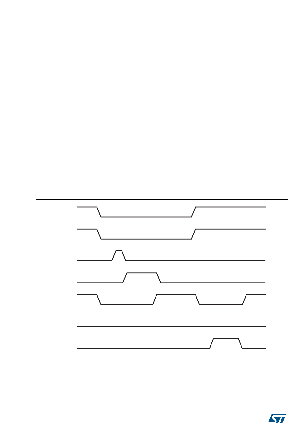
USB on-the-go full-speed (OTG_FS) RM0090
1358/1718 DocID018909 Rev 9
1. To save power, the application suspends and turns off port power when the bus is idle
by writing the port suspend and port power bits in the host port control and status
register.
2. PHY indicates port power off by deasserting the VBUS_VALID signal.
3. The device must detect SE0 for at least 2 ms to start SRP when VBUS power is off.
4. To initiate SRP, the device turns on its data line pull-up resistor for 5 to 10 ms. The
OTG_FS controller detects data-line pulsing.
5. The device drives VBUS above the A-device session valid (2.0 V minimum) for VBUS
pulsing.
The OTG_FS controller interrupts the application on detecting SRP. The Session
request detected bit is set in Global interrupt status register (SRQINT set in
OTG_FS_GINTSTS).
6. The application must service the Session request detected interrupt and turn on the
port power bit by writing the port power bit in the host port control and status register.
The PHY indicates port power-on by asserting the VBUS_VALID signal.
7. When the USB is powered, the device connects, completing the SRP process.
B-device session request protocol
The application must set the SRP-capable bit in the Core USB configuration register. This
enables the OTG_FS controller to initiate SRP as a B-device. SRP is a means by which the
OTG_FS controller can request a new session from the host.
Figure 407. B-device SRP
1. VBUS_VALID = VBUS valid signal from PHY
B_VALID = B-peripheral valid session to PHY
DISCHRG_VBUS = discharge signal to PHY
SESS_END = session end signal to PHY
CHRG_VBUS = charge VBUS signal to PHY
DP = Data plus line
DM = Data minus line
ai15682
VBUS_VALID
B_VALID
DISCHRG_VBUS
SESS_END
DP
DM
CHRG_VBUS
Suspend
Data line pulsing Connect
VBUS pulsing
1
6
2
3
4
58
7
Low
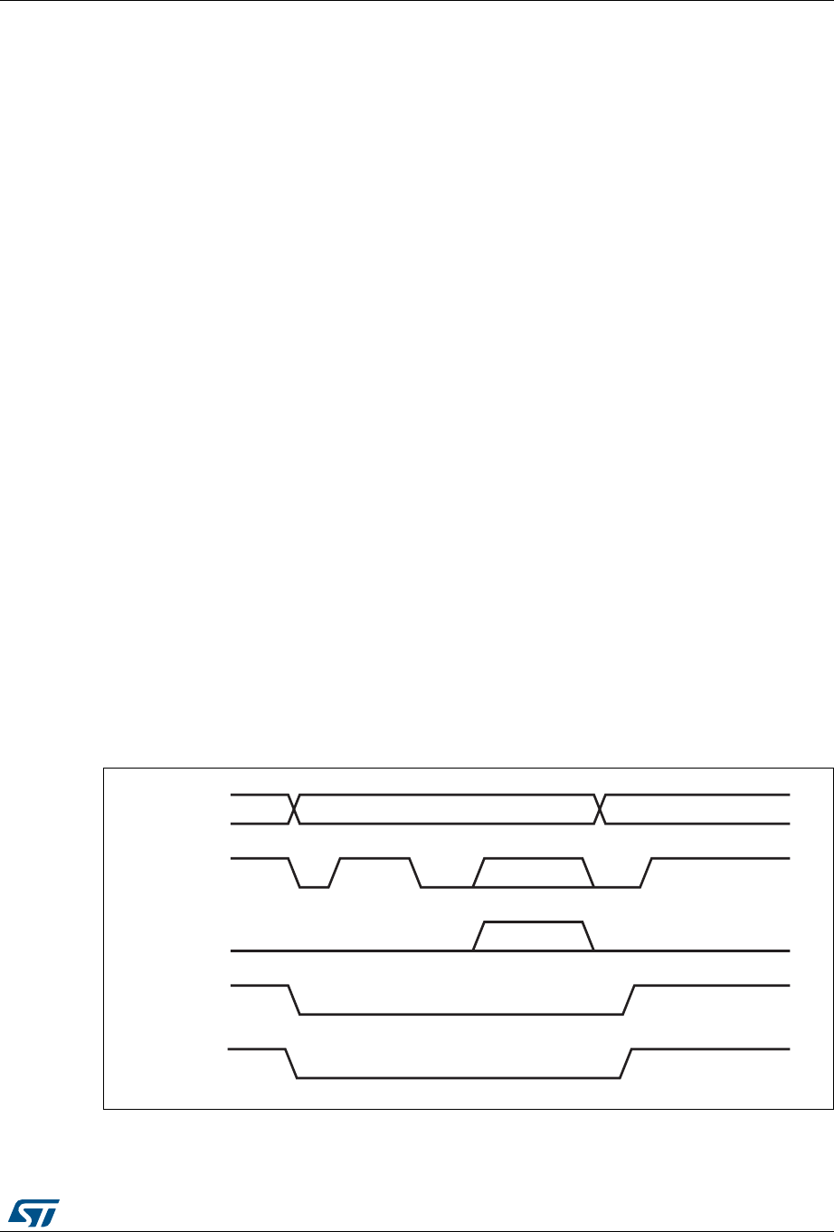
DocID018909 Rev 9 1359/1718
RM0090 USB on-the-go full-speed (OTG_FS)
1362
1. To save power, the host suspends and turns off port power when the bus is idle.
The OTG_FS controller sets the early suspend bit in the Core interrupt register after 3
ms of bus idleness. Following this, the OTG_FS controller sets the USB suspend bit in
the Core interrupt register.
The OTG_FS controller informs the PHY to discharge VBUS.
2. The PHY indicates the session’s end to the device. This is the initial condition for SRP.
The OTG_FS controller requires 2 ms of SE0 before initiating SRP.
For a USB 1.1 full-speed serial transceiver, the application must wait until VBUS
discharges to 0.2 V after BSVLD (in OTG_FS_GOTGCTL) is deasserted. This
discharge time can be obtained from the transceiver vendor and varies from one
transceiver to another.
3. The USB OTG core informs the PHY to speed up VBUS discharge.
4. The application initiates SRP by writing the session request bit in the OTG Control and
status register. The OTG_FS controller perform data-line pulsing followed by VBUS
pulsing.
5. The host detects SRP from either the data-line or VBUS pulsing, and turns on VBUS.
The PHY indicates VBUS power-on to the device.
6. The OTG_FS controller performs VBUS pulsing.
The host starts a new session by turning on VBUS, indicating SRP success. The
OTG_FS controller interrupts the application by setting the session request success
status change bit in the OTG interrupt status register. The application reads the session
request success bit in the OTG control and status register.
7. When the USB is powered, the OTG_FS controller connects, completing the SRP
process.
A-device host negotiation protocol
HNP switches the USB host role from the A-device to the B-device. The application must set
the HNP-capable bit in the Core USB configuration register to enable the OTG_FS
controller to perform HNP as an A-device.
Figure 408. A-device HNP
1. DPPULLDOWN = signal from core to PHY to enable/disable the pull-down on the DP line inside the PHY.
DMPULLDOWN = signal from core to PHY to enable/disable the pull-down on the DM line inside the PHY.
ai15683
OTG core
DP
DM
DPPULLDOWN
DMPULLDOWN
Host Device Host
1
Suspend 2
3
45
Reset
6
Traffic 7
8
Connect
Traffic

USB on-the-go full-speed (OTG_FS) RM0090
1360/1718 DocID018909 Rev 9
1. The OTG_FS controller sends the B-device a SetFeature b_hnp_enable descriptor to
enable HNP support. The B-device’s ACK response indicates that the B-device
supports HNP. The application must set host Set HNP Enable bit in the OTG Control
and status register to indicate to the OTG_FS controller that the B-device supports
HNP.
2. When it has finished using the bus, the application suspends by writing the Port
suspend bit in the host port control and status register.
3. When the B-device observes a USB suspend, it disconnects, indicating the initial
condition for HNP. The B-device initiates HNP only when it must switch to the host role;
otherwise, the bus continues to be suspended.
The OTG_FS controller sets the host negotiation detected interrupt in the OTG
interrupt status register, indicating the start of HNP.
The OTG_FS controller deasserts the DM pull down and DM pull down in the PHY to
indicate a device role. The PHY enables the OTG_FS_DP pull-up resistor to indicate a
connect for B-device.
The application must read the current mode bit in the OTG Control and status register
to determine device mode operation.
4. The B-device detects the connection, issues a USB reset, and enumerates the
OTG_FS controller for data traffic.
5. The B-device continues the host role, initiating traffic, and suspends the bus when
done.
The OTG_FS controller sets the early suspend bit in the Core interrupt register after 3
ms of bus idleness. Following this, the OTG_FS controller sets the USB Suspend bit in
the Core interrupt register.
6. In Negotiated mode, the OTG_FS controller detects the suspend, disconnects, and
switches back to the host role. The OTG_FS controller asserts the DM pull down and
DM pull down in the PHY to indicate its assumption of the host role.
7. The OTG_FS controller sets the Connector ID status change interrupt in the OTG
Interrupt Status register. The application must read the connector ID status in the OTG
Control and Status register to determine the OTG_FS controller operation as an A-
device. This indicates the completion of HNP to the application. The application must
read the Current mode bit in the OTG control and status register to determine host
mode operation.
8. The B-device connects, completing the HNP process.
B-device host negotiation protocol
HNP switches the USB host role from B-device to A-device. The application must set the
HNP-capable bit in the Core USB configuration register to enable the OTG_FS controller to
perform HNP as a B-device.

DocID018909 Rev 9 1361/1718
RM0090 USB on-the-go full-speed (OTG_FS)
1362
Figure 409. B-device HNP
1. DPPULLDOWN = signal from core to PHY to enable/disable the pull-down on the DP line inside the PHY.
DMPULLDOWN = signal from core to PHY to enable/disable the pull-down on the DM line inside the PHY.
1. The A-device sends the SetFeature b_hnp_enable descriptor to enable HNP support.
The OTG_FS controller’s ACK response indicates that it supports HNP. The application
must set the device HNP enable bit in the OTG Control and status register to indicate
HNP support.
The application sets the HNP request bit in the OTG Control and status register to
indicate to the OTG_FS controller to initiate HNP.
2. When it has finished using the bus, the A-device suspends by writing the Port suspend
bit in the host port control and status register.
The OTG_FS controller sets the Early suspend bit in the Core interrupt register after 3
ms of bus idleness. Following this, the OTG_FS controller sets the USB suspend bit in
the Core interrupt register.
The OTG_FS controller disconnects and the A-device detects SE0 on the bus,
indicating HNP. The OTG_FS controller asserts the DP pull down and DM pull down in
the PHY to indicate its assumption of the host role.
The A-device responds by activating its OTG_FS_DP pull-up resistor within 3 ms of
detecting SE0. The OTG_FS controller detects this as a connect.
The OTG_FS controller sets the host negotiation success status change interrupt in the
OTG Interrupt status register, indicating the HNP status. The application must read the
host negotiation success bit in the OTG Control and status register to determine host
ai15684
OTG core
DP
DM
DPPULLDOWN
DMPULLDOWN
HostDevice Device
1
Suspend 2
3
45
Reset
6
Traffic 7
8
Connect
Traffic

USB on-the-go full-speed (OTG_FS) RM0090
1362/1718 DocID018909 Rev 9
negotiation success. The application must read the current Mode bit in the Core
interrupt register (OTG_FS_GINTSTS) to determine host mode operation.
3. The application sets the reset bit (PRST in OTG_FS_HPRT) and the OTG_FS
controller issues a USB reset and enumerates the A-device for data traffic.
4. The OTG_FS controller continues the host role of initiating traffic, and when done,
suspends the bus by writing the Port suspend bit in the host port control and status
register.
5. In Negotiated mode, when the A-device detects a suspend, it disconnects and switches
back to the host role. The OTG_FS controller deasserts the DP pull down and DM pull
down in the PHY to indicate the assumption of the device role.
6. The application must read the current mode bit in the Core interrupt
(OTG_FS_GINTSTS) register to determine the host mode operation.
7. The OTG_FS controller connects, completing the HNP process.

DocID018909 Rev 9 1363/1718
RM0090 USB on-the-go high-speed (OTG_HS)
1523
35 USB on-the-go high-speed (OTG_HS)
This section applies to the whole STM32F4xx family devices, unless otherwise specified.
35.1 OTG_HS introduction
Portions Copyright (c) 2004, 2005 Synopsys, Inc. All rights reserved. Used with permission.
This section presents the architecture and the programming model of the OTG_HS
controller.
The following acronyms are used throughout the section:
References are made to the following documents:
•USB On-The-Go Supplement, Revision 1.3
•Universal Serial Bus Revision 2.0 Specification
The OTG_HS is a dual-role device (DRD) controller that supports both peripheral and host
functions and is fully compliant with the On-The-Go Supplement to the USB 2.0
Specification. It can also be configured as a host-only or peripheral-only controller, fully
compliant with the USB 2.0 Specification. In host mode, the OTG_HS supports high-speed
(HS, 480 Mbits/s), full-speed (FS, 12 Mbits/s) and low-speed (LS, 1.5 Mbits/s) transfers
whereas in peripheral mode, it only supports high-speed (HS, 480Mbits/s) and full-speed
(FS, 12 Mbits/s) transfers. The OTG_HS supports both HNP and SRP. The only external
device required is a charge pump for VBUS in OTG mode.
35.2 OTG_HS main features
The main features can be divided into three categories: general, host-mode and peripheral-
mode features.
FS full-speed
HS High-speed
LS Low-speed
USB Universal serial bus
OTG On-the-go
PHY Physical layer
MAC Media access controller
PFC Packet FIFO controller
UTMI USB Transceiver Macrocell Interface
ULPI UTMI+ Low Pin Interface

USB on-the-go high-speed (OTG_HS) RM0090
1364/1718 DocID018909 Rev 9
35.2.1 General features
The OTG_HS interface main features are the following:
•It is USB-IF certified in compliance with the Universal Serial Bus Revision 2.0
Specification
•It supports 3 PHY interfaces
– An on-chip full-speed PHY
–An I
2C Interface for external full-speed I2C PHY
– An ULPI interface for external high-speed PHY.
•It supports the host negotiation protocol (HNP) and the session request protocol (SRP)
•It allows the host to turn VBUS off to save power in OTG applications, with no need for
external components
•It allows to monitor VBUS levels using internal comparators
•It supports dynamic host-peripheral role switching
•It is software-configurable to operate as:
– An SRP-capable USB HS/FS peripheral (B-device)
– An SRP-capable USB HS/FS/low-speed host (A-device)
– An USB OTG FS dual-role device
•It supports HS/FS SOFs as well as low-speed (LS) keep-alive tokens with:
– SOF pulse PAD output capability
– SOF pulse internal connection to timer 2 (TIM2)
– Configurable framing period
– Configurable end-of-frame interrupt
•It embeds an internal DMA with shareholding support and software selectable AHB
burst type in DMA mode
•It has power saving features such as system clock stop during USB suspend, switching
off of the digital core internal clock domains, PHY and DFIFO power management
•It features a dedicated 4-Kbyte data RAM with advanced FIFO management:
– The memory partition can be configured into different FIFOs to allow flexible and
efficient use of RAM
– Each FIFO can contain multiple packets
– Memory allocation is performed dynamically
– The FIFO size can be configured to values that are not powers of 2 to allow the
use of contiguous memory locations
•It ensures a maximum USB bandwidth of up to one frame without application
intervention

DocID018909 Rev 9 1365/1718
RM0090 USB on-the-go high-speed (OTG_HS)
1523
35.2.2 Host-mode features
The OTG_HS interface features in host mode are the following:
•It requires an external charge pump to generate VBUS
•It has up to 12 host channels (pipes), each channel being dynamically reconfigurable to
support any kind of USB transfer
•It features a built-in hardware scheduler holding:
– Up to 8 interrupt plus isochronous transfer requests in the periodic hardware
queue
– Up to 8 control plus bulk transfer requests in the nonperiodic hardware queue
•It manages a shared RX FIFO, a periodic TX FIFO, and a nonperiodic TX FIFO for
efficient usage of the USB data RAM
•It features dynamic trimming capability of SOF framing period in host mode.
35.2.3 Peripheral-mode features
The OTG_HS interface main features in peripheral mode are the following:
•It has 1 bidirectional control endpoint 0
•It has 5 IN endpoints (EP) configurable to support bulk, interrupt or isochronous
transfers
•It has 5 OUT endpoints configurable to support bulk, interrupt or isochronous transfers
•It manages a shared Rx FIFO and a Tx-OUT FIFO for efficient usage of the USB data
RAM
•It manages up to 6 dedicated Tx-IN FIFOs (one for each IN-configured EP) to reduce
the application load
•It features soft disconnect capability
35.3 OTG_HS functional description
Figure 410 shows the OTG_HS interface block diagram.
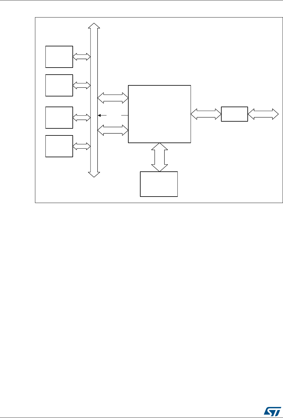
USB on-the-go high-speed (OTG_HS) RM0090
1366/1718 DocID018909 Rev 9
Figure 410. USB OTG interface block diagram
1. The USB DMA cannot directly address the internal Flash memory.
35.3.1 High-speed OTG PHY
The USB OTG HS core embeds an ULPI interface to connect an external HS phy.
35.3.2 External Full-speed OTG PHY using the I2C interface
The USB OTG HS core embeds an I2C interface allowing to connect an external FS phy.
35.3.3 Embedded Full-speed OTG PHY
The full-speed OTG PHY includes the following components:
•FS/LS transceiver module used by both host and Device. It directly drives transmission
and reception on the single-ended USB lines.
•Integrated ID pull-up resistor used to sample the ID line for A/B Device identification.
•DP/DM integrated pull-up and pull-down resistors controlled by the OTG_HS core
depending on the current role of the device. As a peripheral, it enables the DP pull-up
resistor to signal full-speed peripheral connections as soon as VBUS is sensed to be at
a valid level (B-session valid). In host mode, pull-down resistors are enabled on both
DP/DM. Pull-up and pull-down resistors are dynamically switched when the peripheral
role is changed via the host negotiation protocol (HNP).
•Pull-up/pull-down resistor ECN circuit
The DP pull-up consists of 2 resistors controlled separately from the OTG_HS as per
the resistor Engineering Change Notice applied to USB Rev2.0. The dynamic trimming
!("MASTERINTERFACE
!("SLAVEINTERFACE
#05
-EMORY
0ERIPHERAL
0ERIPHERAL
5,0)INTERFACE 5,0)0(9 53"
$ATA&)&/
SINGLEPORT2!-
302!-
$ATA&)&/
2!-INTERFACE
)NTERRUPT
!("APPLICATIONBUS
53"/4'(3CORE
AIB

DocID018909 Rev 9 1367/1718
RM0090 USB on-the-go high-speed (OTG_HS)
1523
of the DP pull-up strength allows to achieve a better noise rejection and Tx/Rx signal
quality.
•VBUS sensing comparators with hysteresis used to detect VBUS_VALID, A-B Session
Valid and session-end voltage thresholds. They are used to drive the session request
protocol (SRP), detect valid startup and end-of-session conditions, and constantly
monitor the VBUS supply during USB operations.
•VBUS pulsing method circuit used to charge/discharge VBUS through resistors during
the SRP (weak drive).
Caution: To guarantee a correct operation for the USB OTG HS peripheral, the AHB frequency
should be higher than 30 MHz.
35.4 OTG dual-role device
35.4.1 ID line detection
The host or peripheral (the default) role depends on the level of the ID input line. It is
determined when the USB cable is plugged in and depends on which side of the USB cable
is connected to the micro-AB receptacle:
•If the B-side of the USB cable is connected with a floating ID wire, the integrated pull-
up resistor detects a high ID level and the default peripheral role is confirmed. In this
configuration the OTG_HS conforms to the FSM standard described in
section 6.8.2. On-The-Go B-device of the USB On-The-Go Supplement, Revision 1.3.
•If the A-side of the USB cable is connected with a grounded ID, the OTG_HS issues an
ID line status change interrupt (CIDSCHG bit in the OTG_HS_GINTSTS register) for
host software initialization, and automatically switches to host role. In this configuration
the OTG_HS conforms to the FSM standard described by section 6.8.1: On-The-Go A-
Device of the USB On-The-Go Supplement, Revision 1.3.
35.4.2 HNP dual role device
The HNP capable bit in the Global USB configuration register (HNPCAP bit in the
OTG_HS_ GUSBCFG register) configures the OTG_HS core to dynamically change from
A-host to A-device role and vice-versa, or from B-device to B-host role and vice-versa,
according to the host negotiation protocol (HNP). The current device status is defined by the
combination of the Connector ID Status bit in the Global OTG control and status register
(CIDSTS bit in OTG_HS_GOTGCTL) and the current mode of operation bit in the global
interrupt and status register (CMOD bit in OTG_HS_GINTSTS).
The HNP programming model is described in detail in Section 35.13: OTG_HS
programming model.
35.4.3 SRP dual-role device
The SRP capable bit in the global USB configuration register (SRPCAP bit in
OTG_HS_GUSBCFG) configures the OTG_HS core to switch VBUS off for the A-device in
order to save power. The A-device is always in charge of driving VBUS regardless of the
OTG_HS role (host or peripheral). The SRP A/B-device program model is described in
detail in Section 35.13: OTG_HS programming model.

USB on-the-go high-speed (OTG_HS) RM0090
1368/1718 DocID018909 Rev 9
35.5 USB functional description in peripheral mode
The OTG_HS operates as an USB peripheral in the following circumstances:
•OTG B-device
OTG B-device default state if the B-side of USB cable is plugged in
•OTG A-device
OTG A-device state after the HNP switches the OTG_HS to peripheral role
•B-Device
If the ID line is present, functional and connected to the B-side of the USB cable, and
the HNP-capable bit in the Global USB Configuration register (HNPCAP bit in
OTG_HS_GUSBCFG) is cleared (see On-The-Go specification Revision 1.3 section
6.8.3).
•Peripheral only (see Figure 388: USB peripheral-only connection)
The force peripheral mode bit in the Global USB configuration register (FDMOD in
OTG_HS_GUSBCFG) is set to 1, forcing the OTG_HS core to operate in USB
peripheral-only mode (see On-The-Go specification Revision 1.3 section 6.8.3). In this
case, the ID line is ignored even if it is available on the USB connector.
Note: To build a bus-powered device architecture in the B-Device or peripheral-only configuration,
an external regulator must be added to generate the VDD supply voltage from VBUS.
35.5.1 SRP-capable peripheral
The SRP capable bit in the Global USB configuration register (SRPCAP bit in
OTG_HS_GUSBCFG) configures the OTG_HS to support the session request protocol
(SRP). As a result, it allows the remote A-device to save power by switching VBUS off when
the USB session is suspended.
The SRP peripheral mode program model is described in detail in Section : B-device
session request protocol.
35.5.2 Peripheral states
Powered state
The VBUS input detects the B-session valid voltage used to put the USB peripheral in the
Powered state (see USB2.0 specification section 9.1). The OTG_HS then automatically
connects the DP pull-up resistor to signal full-speed device connection to the host, and
generates the session request interrupt (SRQINT bit in OTG_HS_GINTSTS) to notify the
Powered state. The VBUS input also ensures that valid VBUS levels are supplied by the host
during USB operations. If VBUS drops below the B-session valid voltage (for example
because power disturbances occurred or the host port has been switched off), the OTG_HS
automatically disconnects and the session end detected (SEDET bit in
OTG_HS_GOTGINT) interrupt is generated to notify that the OTG_HS has exited the
Powered state.
In Powered state, the OTG_HS expects a reset from the host. No other USB operations are
possible. When a reset is received, the reset detected interrupt (USBRST in
OTG_HS_GINTSTS) is generated. When the reset is complete, the enumeration done
interrupt (ENUMDNE bit in OTG_HS_GINTSTS) is generated and the OTG_HS enters the
Default state.

DocID018909 Rev 9 1369/1718
RM0090 USB on-the-go high-speed (OTG_HS)
1523
Soft disconnect
The Powered state can be exited by software by using the soft disconnect feature. The DP
pull-up resistor is removed by setting the Soft disconnect bit in the device control register
(SDIS bit in OTG_HS_DCTL), thus generating a device disconnect detection interrupt on
the host side even though the USB cable was not really unplugged from the host port.
Default state
In Default state the OTG_HS expects to receive a SET_ADDRESS command from the host.
No other USB operations are possible. When a valid SET_ADDRESS command is decoded
on the USB, the application writes the corresponding number into the device address field in
the device configuration register (DAD bit in OTG_HS_DCFG). The OTG_HS then enters
the address state and is ready to answer host transactions at the configured USB address.
Suspended state
The OTG_HS peripheral constantly monitors the USB activity. When the USB remains idle
for 3 ms, the early suspend interrupt (ESUSP bit in OTG_HS_GINTSTS) is issued. It is
confirmed 3 ms later, if appropriate, by generating a suspend interrupt (USBSUSP bit in
OTG_HS_GINTSTS). The device suspend bit is then automatically set in the device status
register (SUSPSTS bit in OTG_HS_DSTS) and the OTG_HS enters the Suspended state.
The device can also exit from the Suspended state by itself. In this case the application sets
the remote wakeup signaling bit in the device control register (RWUSIG bit in
OTG_HS_DCTL) and clears it after 1 to 15 ms.
When a resume signaling is detected from the host, the resume interrupt (WKUPINT bit in
OTG_HS_GINTSTS) is generated and the device suspend bit is automatically cleared.
35.5.3 Peripheral endpoints
The OTG_HS core instantiates the following USB endpoints:
•Control endpoint 0
This endpoint is bidirectional and handles control messages only.
It has a separate set of registers to handle IN and OUT transactions, as well as
dedicated control (OTG_HS_DIEPCTL0/OTG_HS_DOEPCTL0), transfer configuration
(OTG_HS_DIEPTSIZ0/OTG_HS_DIEPTSIZ0), and status-interrupt
(OTG_HS_DIEPINTx/)OTG_HS_DOEPINT0) registers. The bits available inside the
control and transfer size registers slightly differ from other endpoints.
•5 IN endpoints
– They can be configured to support the isochronous, bulk or interrupt transfer type.
– They feature dedicated control (OTG_HS_DIEPCTLx), transfer configuration
(OTG_HS_DIEPTSIZx), and status-interrupt (OTG_HS_DIEPINTx) registers.
– The Device IN endpoints common interrupt mask register (OTG_HS_DIEPMSK)
allows to enable/disable a single endpoint interrupt source on all of the
IN endpoints (EP0 included).
– They support incomplete isochronous IN transfer interrupt (IISOIXFR bit in
OTG_HS_GINTSTS). This interrupt is asserted when there is at least one
isochronous IN endpoint for which the transfer is not completed in the current

USB on-the-go high-speed (OTG_HS) RM0090
1370/1718 DocID018909 Rev 9
frame. This interrupt is asserted along with the end of periodic frame interrupt
(OTG_HS_GINTSTS/EOPF).
•5 OUT endpoints
– They can be configured to support the isochronous, bulk or interrupt transfer type.
– They feature dedicated control (OTG_HS_DOEPCTLx), transfer configuration
(OTG_HS_DOEPTSIZx) and status-interrupt (OTG_HS_DOEPINTx) registers.
– The Device Out endpoints common interrupt mask register
(OTG_HS_DOEPMSK) allows to enable/disable a single endpoint interrupt source
on all OUT endpoints (EP0 included).
– They support incomplete isochronous OUT transfer interrupt (INCOMPISOOUT
bit in OTG_HS_GINTSTS). This interrupt is asserted when there is at least one
isochronous OUT endpoint on which the transfer is not completed in the current
frame. This interrupt is asserted along with the end of periodic frame interrupt
(OTG_HS_GINTSTS/EOPF).
Endpoint controls
The following endpoint controls are available through the device endpoint-x IN/OUT control
register (DIEPCTLx/DOEPCTLx):
•Endpoint enable/disable
•Endpoint activation in current configuration
•Program the USB transfer type (isochronous, bulk, interrupt)
•Program the supported packet size
•Program the Tx-FIFO number associated with the IN endpoint
•Program the expected or transmitted data0/data1 PID (bulk/interrupt only)
•Program the even/odd frame during which the transaction is received or transmitted
(isochronous only)
•Optionally program the NAK bit to always send a negative acknowledge to the host
regardless of the FIFO status
•Optionally program the STALL bit to always stall host tokens to that endpoint
•Optionally program the Snoop mode for OUT endpoint where the received data CRC is
not checked
Endpoint transfer
The device endpoint-x transfer size registers (DIEPTSIZx/DOEPTSIZx) allow the application
to program the transfer size parameters and read the transfer status.
The programming operation must be performed before setting the endpoint enable bit in the
endpoint control register.
Once the endpoint is enabled, these fields are read-only as the OTG FS core updates them
with the current transfer status.
The following transfer parameters can be programmed:
•Transfer size in bytes
•Number of packets constituting the overall transfer size.

DocID018909 Rev 9 1371/1718
RM0090 USB on-the-go high-speed (OTG_HS)
1523
Endpoint status/interrupt
The device endpoint-x interrupt registers (DIEPINTx/DOPEPINTx) indicate the status of an
endpoint with respect to USB- and AHB-related events. The application must read these
registers when the OUT endpoint interrupt bit or the IN endpoint interrupt bit in the core
interrupt register (OEPINT bit in OTG_HS_GINTSTS or IEPINT bit in OTG_HS_GINTSTS,
respectively) is set. Before the application can read these registers, it must first read the
device all endpoints interrupt register (OTG_HS_DAINT) to get the exact endpoint number
for the device endpoint-x interrupt register. The application must clear the appropriate bit in
this register to clear the corresponding bits in the DAINT and GINTSTS registers.
The peripheral core provides the following status checks and interrupt generation:
•Transfer completed interrupt, indicating that data transfer has completed on both the
application (AHB) and USB sides
•Setup stage done (control-out only)
•Associated transmit FIFO is half or completely empty (in endpoints)
•NAK acknowledge transmitted to the host (isochronous-in only)
•IN token received when Tx-FIFO was empty (bulk-in/interrupt-in only)
•OUT token received when endpoint was not yet enabled
•Babble error condition detected
•Endpoint disable by application is effective
•Endpoint NAK by application is effective (isochronous-in only)
•More than 3 back-to-back setup packets received (control-out only)
•Timeout condition detected (control-in only)
•Isochronous out packet dropped without generating an interrupt

USB on-the-go high-speed (OTG_HS) RM0090
1372/1718 DocID018909 Rev 9
35.6 USB functional description on host mode
This section gives the functional description of the OTG_HS in the USB host mode. The
OTG_HS works as a USB host in the following circumstances:
•OTG A-host
OTG A-device default state when the A-side of the USB cable is plugged in
•OTG B-host
OTG B-device after HNP switching to the host role
•A-device
If the ID line is present, functional and connected to the A-side of the USB cable, and
the HNP-capable bit is cleared in the Global USB Configuration register (HNPCAP bit
in OTG_HS_GUSBCFG). Integrated pull-down resistors are automatically set on the
DP/DM lines.
•Host only (Figure 389: USB host-only connection).
The force host mode bit in the global USB configuration register (FHMOD bit in
OTG_HS_GUSBCFG) forces the OTG_HS core to operate in USB host-only mode. In
this case, the ID line is ignored even if it is available on the USB connector. Integrated
pull-down resistors are automatically set on the OTG_HS_FS_DP/OTG_HS_FS_DM
lines.
Note: On-chip 5 V VBUS generation is not supported. As a result, a charge pump or a basic power
switch (if a 5 V supply is available on the application board) must be added externally to
drive the 5 V VBUS line. The external charge pump can be driven by any GPIO output. This
is required for the OTG A-host, A-device and host-only configurations.
The VBUS input ensures that valid VBUS levels are supplied by the charge pump during USB
operations while the charge pump overcurrent output can be input to any GPIO pin
configured to generate port interrupts. The overcurrent ISR must promptly disable the VBUS
generation.
35.6.1 SRP-capable host
SRP support is available through the SRP capable bit in the global USB configuration
register (SRPCAP bit in OTG_HS_GUSBCFG). When the SRP feature is enabled, the host
can save power by switching off the VBUS power while the USB session is suspended. The
SRP host mode program model is described in detail in Section : A-device session request
protocol.
35.6.2 USB host states
Host port power
On-chip 5 V VBUS generation is not supported. As a result, a charge pump or a basic power
switch (if a 5 V supply voltage is available on the application board) must be added
externally to drive the 5 V VBUS line. The external charge pump can be driven by any GPIO
output. When the application powers on VBUS through the selected GPIO, it must also set
the port power bit in the host port control and status register (PPWR bit in OTG_HS_HPRT).
VBUS valid
When SRP or HNP is enabled the VBUS sensing pin (PB13) pin should be connected to
VBUS. The VBUS input ensures that valid VBUS levels are supplied by the charge pump

DocID018909 Rev 9 1373/1718
RM0090 USB on-the-go high-speed (OTG_HS)
1523
during USB operations. Any unforeseen VBUS voltage drop below the VBUS valid threshold
(4.25 V) generates an OTG interrupt triggered by the session end detected bit (SEDET bit in
OTG_HS_GOTGINT). The application must then switch the VBUS power off and clear the
port power bit.
When HNP and SRP are both disabled, the VBUS sensing pin (PB13) should not be
connected to VBUS. This pin can be can be used as GPIO.
The charge pump overcurrent flag can also be used to prevent electrical damage. Connect
the overcurrent flag output from the charge pump to any GPIO input, and configure it to
generate a port interrupt on the active level. The overcurrent ISR must promptly disable the
VBUS generation and clear the port power bit.
Detection of peripheral connection by the host
If SRP or HNP are enabled, even if USB peripherals or B-devices can be attached at any
time, the OTG_HS does not detect a bus connection until the end of the VBUS sensing
(VBUS over 4.75 V).
When VBUS is at a valid level and a remote B-device is attached, the OTG_HS core issues a
host port interrupt triggered by the device connected bit in the host port control and status
register (PCDET bit in OTG_HS_HPRT).
When HNP and SRP are both disabled, USB peripherals or B-device are detected as
soon as they are connected. The OTG_FS core issues a host port interrupt triggered by
the device connected bit in the host port control and status (PCDET bit in OTG_FS_HPRT).
Detection of peripheral disconnection by the host
The peripheral disconnection event triggers the disconnect detected interrupt (DISCINT bit
in OTG_HS_GINTSTS).
Host enumeration
After detecting a peripheral connection, the host must start the enumeration process by
issuing an USB reset and configuration commands to the new peripheral.
Before sending an USB reset, the application waits for the OTG interrupt triggered by the
debounce done bit (DBCDNE bit in OTG_HS_GOTGINT), which indicates that the bus is
stable again after the electrical debounce caused by the attachment of a pull-up resistor on
OTG_HS_FS_DP (full speed) or OTG_HS_FS_DM (low speed).
The application issues an USB reset (single-ended zero) via the USB by keeping the port
reset bit set in the Host port control and status register (PRST bit in OTG_HS_HPRT) for a
minimum of 10 ms and a maximum of 20 ms. The application monitors the time and then
clears the port reset bit.
Once the USB reset sequence has completed, the host port interrupt is triggered by the port
enable/disable change bit (PENCHNG bit in OTG_HS_HPRT) to inform the application that
the speed of the enumerated peripheral can be read from the port speed field in the host
port control and status register (PSPD bit in OTG_HS_HPRT), and that the host is starting
to drive SOFs (full speed) or keep-alive tokens (low speed). The host is then ready to
complete the peripheral enumeration by sending peripheral configuration commands.

USB on-the-go high-speed (OTG_HS) RM0090
1374/1718 DocID018909 Rev 9
Host suspend
The application can decide to suspend the USB activity by setting the port suspend bit in the
host port control and status register (PSUSP bit in OTG_HS_HPRT). The OTG_HS core
stops sending SOFs and enters the Suspended state.
The Suspended state can be exited on the remote device initiative (remote wakeup). In this
case the remote wakeup interrupt (WKUPINT bit in OTG_HS_GINTSTS) is generated upon
detection of a remote wakeup event, the port resume bit in the host port control and status
register (PRES bit in OTG_HS_HPRT) is set, and a resume signaling is automatically
issued on the USB. The application must monitor the resume window duration, and then
clear the port resume bit to exit the Suspended state and restart the SOF.
If the Suspended state is exited on the host initiative, the application must set the port
resume bit to start resume signaling on the host port, monitor the resume window duration
and then clear the port resume bit.
35.6.3 Host channels
The OTG_HS core instantiates 12 host channels. Each host channel supports an USB host
transfer (USB pipe). The host is not able to support more than 8 transfer requests
simultaneously. If more than 8 transfer requests are pending from the application, the host
controller driver (HCD) must re-allocate channels when they become available, that is, after
receiving the transfer completed and channel halted interrupts.
Each host channel can be configured to support IN/OUT and any type of
periodic/nonperiodic transaction. Each host channel has dedicated control (HCCHARx),
transfer configuration (HCTSIZx) and status/interrupt (HCINTx) registers with associated
mask (HCINTMSKx) registers.
Host channel controls
The following host channel controls are available through the host channel-x characteristics
register (HCCHARx):
•Channel enable/disable
•Program the HS/FS/LS speed of target USB peripheral
•Program the address of target USB peripheral
•Program the endpoint number of target USB peripheral
•Program the transfer IN/OUT direction
•Program the USB transfer type (control, bulk, interrupt, isochronous)
•Program the maximum packet size (MPS)
•Program the periodic transfer to be executed during odd/even frames
Host channel transfer
The host channel transfer size registers (HCTSIZx) allow the application to program the
transfer size parameters, and read the transfer status.
The programming operation must be performed before setting the channel enable bit in the
host channel characteristics register. Once the endpoint is enabled, the packet count field is
read-only as the OTG HS core updates it according to the current transfer status.

DocID018909 Rev 9 1375/1718
RM0090 USB on-the-go high-speed (OTG_HS)
1523
The following transfer parameters can be programmed:
•Transfer size in bytes
•Number of packets constituting the overall transfer size
•Initial data PID
Host channel status/interrupt
The host channel-x interrupt register (HCINTx) indicates the status of an endpoint with
respect to USB- and AHB-related events. The application must read these register when the
host channels interrupt bit in the core interrupt register (HCINT bit in OTG_HS_GINTSTS) is
set. Before the application can read these registers, it must first read the host all channels
interrupt (HCAINT) register to get the exact channel number for the host channel-x interrupt
register. The application must clear the appropriate bit in this register to clear the
corresponding bits in the HAINT and GINTSTS registers. The mask bits for each interrupt
source of each channel are also available in the OTG_HS_HCINTMSK-x register.
The host core provides the following status checks and interrupt generation:
•Transfer completed interrupt, indicating that the data transfer is complete on both the
application (AHB) and USB sides
•Channel stopped due to transfer completed, USB transaction error or disable
command from the application
•Associated transmit FIFO half or completely empty (IN endpoints)
•ACK response received
•NAK response received
•STALL response received
•USB transaction error due to CRC failure, timeout, bit stuff error, false EOP
•Babble error
•Frame overrun
•Data toggle error
35.6.4 Host scheduler
The host core features a built-in hardware scheduler which is able to autonomously re-order
and manage the USB the transaction requests posted by the application. At the beginning of
each frame the host executes the periodic (isochronous and interrupt) transactions first,
followed by the nonperiodic (control and bulk) transactions to achieve the higher level of
priority granted to the isochronous and interrupt transfer types by the USB specification.
The host processes the USB transactions through request queues (one for periodic and one
for nonperiodic). Each request queue can hold up to 8 entries. Each entry represents a
pending transaction request from the application, and holds the IN or OUT channel number
along with other information to perform a transaction on the USB. The order in which the
requests are written to the queue determines the sequence of the transactions on the USB
interface.
At the beginning of each frame, the host processes the periodic request queue first, followed
by the nonperiodic request queue. The host issues an incomplete periodic transfer interrupt
(IPXFR bit in OTG_HS_GINTSTS) if an isochronous or interrupt transaction scheduled for
the current frame is still pending at the end of the current frame. The OTG HS core is fully
responsible for the management of the periodic and nonperiodic request queues.The
periodic transmit FIFO and queue status register (HPTXSTS) and nonperiodic transmit

USB on-the-go high-speed (OTG_HS) RM0090
1376/1718 DocID018909 Rev 9
FIFO and queue status register (HNPTXSTS) are read-only registers which can be used by
the application to read the status of each request queue. They contain:
•The number of free entries currently available in the periodic (nonperiodic) request
queue (8 max)
•Free space currently available in the periodic (nonperiodic) Tx-FIFO (out-transactions)
•IN/OUT token, host channel number and other status information.
As request queues can hold a maximum of 8 entries each, the application can push to
schedule host transactions in advance with respect to the moment they physically reach the
USB for a maximum of 8 pending periodic transactions plus 8 pending nonperiodic
transactions.
To post a transaction request to the host scheduler (queue) the application must check that
there is at least 1 entry available in the periodic (nonperiodic) request queue by reading the
PTXQSAV bits in the OTG_HS_HNPTXSTS register or NPTQXSAV bits in the
OTG_HS_HNPTXSTS register.
35.7 SOF trigger
The OTG FS core allows to monitor, track and configure SOF framing in the host and
peripheral. It also features an SOF pulse output connectivity.
These capabilities are particularly useful to implement adaptive audio clock generation
techniques, where the audio peripheral needs to synchronize to the isochronous stream
provided by the PC, or the host needs trimming its framing rate according to the
requirements of the audio peripheral.
35.7.1 Host SOFs
In host mode the number of PHY clocks occurring between the generation of two
consecutive SOF (FS) or keep-alive (LS) tokens is programmable in the host frame interval
register (OTG_HS_HFIR), thus providing application control over the SOF framing period.
An interrupt is generated at any start of frame (SOF bit in OTG_HS_GINTSTS). The current
frame number and the time remaining until the next SOF are tracked in the host frame
number register (OTG_HS_HFNUM).
An SOF pulse signal is generated at any SOF starting token and with a width of 12 system
clock cycles. It can be made available externally on the SOF pin using the SOFOUTEN bit in
the global control and configuration register. The SOF pulse is also internally connected to
the input trigger of timer 2 (TIM2), so that the input capture feature, the output compare
feature and the timer can be triggered by the SOF pulse. The TIM2 connection is enabled
through ITR1_RMP bits of TIM2_OR register.
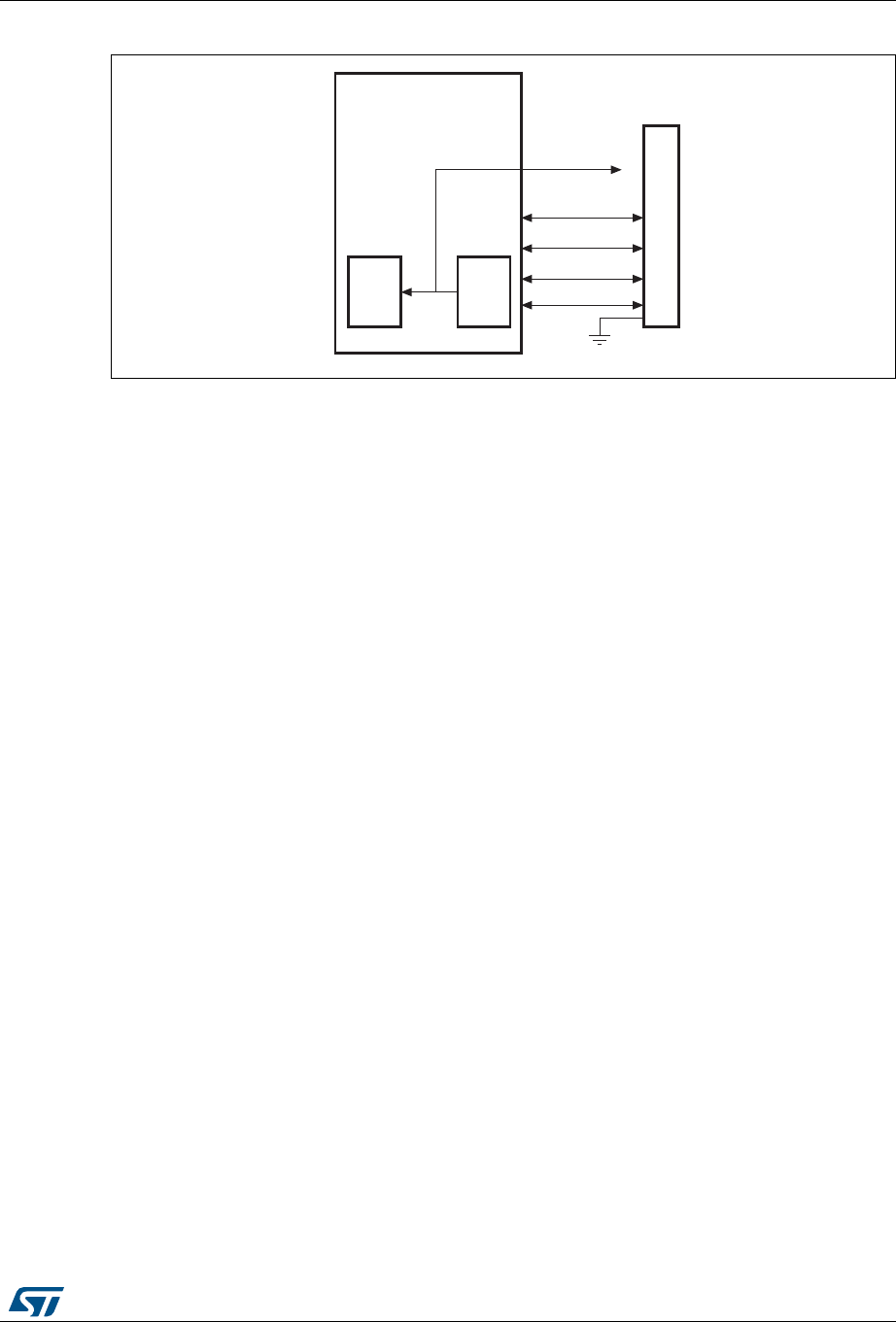
DocID018909 Rev 9 1377/1718
RM0090 USB on-the-go high-speed (OTG_HS)
1523
SOF trigger output to TIM2 ITR1 connection
35.7.2 Peripheral SOFs
In peripheral mode, the start of frame interrupt is generated each time an SOF token is
received on the USB (SOF bit in OTG_HS_GINTSTS). The corresponding frame number
can be read from the device status register (FNSOF bit in OTG_HS_DSTS). An SOF pulse
signal with a width of 12 system clock cycles is also generated and can be made available
externally on the SOF pin by using the SOF output enable bit in the global control and
configuration register (SOFOUTEN bit in OTG_HS_GCCFG). The SOF pulse signal is also
internally connected to the TIM2 input trigger, so that the input capture feature, the output
compare feature and the timer can be triggered by the SOF pulse (see Figure ). The TIM2
connection is enabled through ITR1_RMP bits of TIM2_OR register.
The end of periodic frame interrupt (GINTSTS/EOPF) is used to notify the application when
80%, 85%, 90% or 95% of the time frame interval elapsed depending on the periodic frame
interval field in the device configuration register (PFIVL bit in OTG_HS_DCFG).
This feature can be used to determine if all of the isochronous traffic for that frame is
complete.
SOF
pulse
ITR1
TIM2
OTG_HS_Core
SOF output pulse
USB Micro-AB connector
VBUS
DP
DM
ID
ai16092

USB on-the-go high-speed (OTG_HS) RM0090
1378/1718 DocID018909 Rev 9
35.8 USB_HS power modes
The power consumption of the OTG PHY is controlled by three bits in the general core
configuration register:
•PHY power down (GCCFG/PWRDWN)
This bit switches on/off the PHY full-speed transceiver module. It must be preliminarily
set to allow any USB operation.
•A-VBUS sensing enable (GCCFG/VBUSASEN)
This bit switches on/off the VBUS comparators associated with A-device operations. It
must be set when in A-device (USB host) mode and during HNP.
•B-VBUS sensing enable (GCCFG/VBUSASEN)
This bit switches on/off the VBUS comparators associated with B-device operations. It
must be set when in B-device (USB peripheral) mode and during HNP.
Power reduction techniques are available in the USB suspended state, when the USB
session is not yet valid or the device is disconnected.
•Stop PHY clock (STPPCLK bit in OTG_HS_PCGCCTL)
– When setting the stop PHY clock bit in the clock gating control register, most of the
clock domain internal to the OTG high-speed core is switched off by clock gating.
The dynamic power consumption due to the USB clock switching activity is cut
even if the clock input is kept running by the application
– Most of the transceiver is also disabled, and only the part in charge of detecting
the asynchronous resume or remote wakeup event is kept alive.
•Gate HCLK (GATEHCLK bit in OTG_HS_PCGCCTL)
When setting the Gate HCLK bit in the clock gating control register, most of the system
clock domain internal to the OTG_HS core is switched off by clock gating. Only the
register read and write interface is kept alive. The dynamic power consumption due to
the USB clock switching activity is cut even if the system clock is kept running by the
application for other purposes.
•USB system stop
– When the OTG_HS is in USB suspended state, the application can decide to
drastically reduce the overall power consumption by shutting down all the clock
sources in the system. USB System Stop is activated by first setting the Stop PHY
clock bit and then configuring the system deep sleep mode in the powercontrol
system module (PWR).
– The OTG_HS core automatically reactivates both system and USB clocks by
asynchronous detection of remote wakeup (as an host) or resume (as a Device)
signaling on the USB.
35.9 Dynamic update of the OTG_HS_HFIR register
The USB core embeds a dynamic trimming capability of micro-SOF framing period in host
mode allowing to synchronize an external device with the micro-SOF frames.
When the OTG_HS_HFIR register is changed within a current micro-SOF frame, the SOF
period correction is applied in the next frame as described in Figure 411.

DocID018909 Rev 9 1379/1718
RM0090 USB on-the-go high-speed (OTG_HS)
1523
Figure 411. Updating OTG_HS_HFIR dynamically
35.10 FIFO RAM allocation
35.10.1 Peripheral mode
Receive FIFO RAM
For Receive FIFO RAM, the application should allocate RAM for SETUP packets: 10
locations must be reserved in the receive FIFO to receive SETUP packets on control
endpoints. These locations are reserved for SETUP packets and are not used by the core to
write any other data.
One location must be allocated for Global OUT NAK. Status information are also written to
the FIFO along with each received packet. Therefore, a minimum space of (Largest Packet
Size / 4) + 1 must be allocated to receive packets. If a high-bandwidth endpoint or multiple
isochronous endpoints are enabled, at least two spaces of (Largest Packet Size / 4) + 1
must be allotted to receive back-to-back packets. Typically, two (Largest Packet Size / 4) + 1
spaces are recommended so that when the previous packet is being transferred to AHB, the
USB can receive the subsequent packet.
Along with each endpoints last packet, transfer complete status information are also pushed
to the FIFO. Typically, one location for each OUT endpoint is recommended.
Transmit FIFO RAM
For Transmit FIFO RAM, the minimum RAM space required for each IN Endpoint Transmit
FIFO is the maximum packet size for this IN endpoint.
Note: More space allocated in the transmit IN Endpoint FIFO results in a better performance on
the USB.
35.10.2 Host mode
Receive FIFO RAM
For Receive FIFO RAM allocation, Status information are written to the FIFO along with
each received packet. Therefore, a minimum space of (Largest Packet Size / 4) + 1 must be
allocated to receive packets. If a high-bandwidth channel or multiple isochronous channels
xxx xx
,ATENCY
3/&
RELOAD
/4'?(3?(&)2
WRITE
VALUE
&RAME
TIMER
/LD/4'?(3?()&2VALUE
PERIODS
/4'?(3?()&2VALUE
PERIODS()&2WRITELATENCY
.EW/4'?(3?()&2VALUE
PERIODS
/4'?(3?(&)2
AIB

USB on-the-go high-speed (OTG_HS) RM0090
1380/1718 DocID018909 Rev 9
are enabled, at least two spaces of (Largest Packet Size / 4) + 1 must be allocated to
receive back-to-back packets. Typically, two (Largest Packet Size / 4) + 1 spaces are
recommended so that when the previous packet is being transferred to AHB, the USB can
receive the subsequent packet.
Along with each host channels last packet, transfer complete status information are also
pushed to the FIFO. As a consequence, one location must be allocated to store this data.
Transmit FIFO RAM
For Transmit FIFO RAM allocation, the minimum amount of RAM required for the host
nonperiodic Transmit FIFO is the largest maximum packet size for all supported nonperiodic
OUT channels. Typically, a space corresponding to two Largest Packet Size is
recommended, so that when the current packet is being transferred to the USB, the AHB
can transmit the subsequent packet.
The minimum amount of RAM required for Host periodic Transmit FIFO is the largest
maximum packet size for all supported periodic OUT channels. If there is at least one High
Bandwidth Isochronous OUT endpoint, then the space must be at least two times the
maximum packet size for that channel.
Note: More space allocated in the Transmit nonperiodic FIFO results in better performance on the
USB.
When operating in DMA mode, the DMA address register for each host channel (HCDMAn)
is stored in the SPRAM (FIFO). One location for each channel must be reserved for this.
35.11 OTG_HS interrupts
When the OTG_HS controller is operating in one mode, either peripheral or host, the
application must not access registers from the other mode. If an illegal access occurs, a
mode mismatch interrupt is generated and reflected in the Core interrupt register (MMIS bit
in the OTG_HS_GINTSTS register). When the core switches from one mode to the other,
the registers in the new mode of operation must be reprogrammed as they would be after a
power-on reset.
Figure 412 shows the interrupt hierarchy.
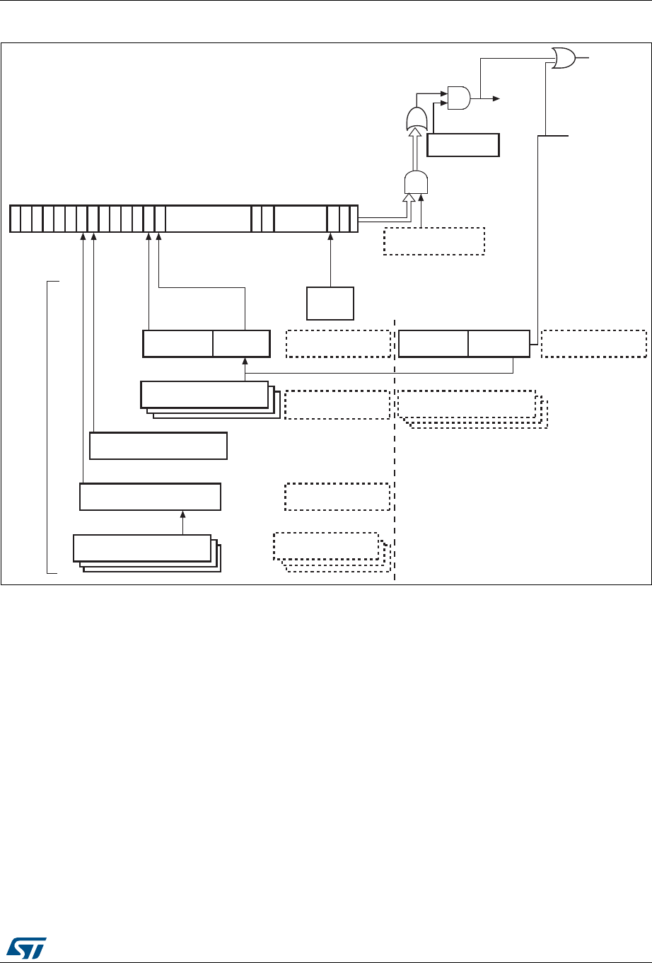
DocID018909 Rev 9 1381/1718
RM0090 USB on-the-go high-speed (OTG_HS)
1523
Figure 412. Interrupt hierarchy
1. The core interrupt register bits are shown in OTG_HS core interrupt register (OTG_HS_GINTSTS) on
page 1398.
35.12 OTG_HS control and status registers
By reading from and writing to the control and status registers (CSRs) through the AHB
slave interface, the application controls the OTG_HS controller. These registers are 32 bits
3130 29 2827 26 25 24 2320 19 1817:10 9 87:3210
AND
OR
Interrupt
Global interrupt
mask (Bit 0)
AHB configuration
register
Core interrupt mask
register
OTG
interrupt
register
Core interrupt
register(1)
Device IN/OUT endpoint
interrupt registers 0 to 5
Device all endpoints
interrupt register
21:16
OUT endpoints
5:0
IN endpoints
Interrupt
sources
Host port control and status
register
Host all channels interrupt
register
Host channels interrupt
mask registers 0 to 11
Host all channels
interrupt mask register
Host channels interrupt
registers 0 to 11
22 21
Device all endpoints
interrupt mask register
Device IN/OUT
endpoints common
interrupt mask register
ai16093b
OR
AND
Device each IN/OUT endpoint
interrupt mask register
Device each endpoint
interrupt register
31:16
EP1OUT
15:0
EP1IN
Device each endpoint
interrupt mask register
endp_interrupt[31:0]
endp_multi_proc_intrpt

USB on-the-go high-speed (OTG_HS) RM0090
1382/1718 DocID018909 Rev 9
wide, and the addresses are 32-bit block aligned. The OTG_HS registers must be accessed
by words (32 bits). CSRs are classified as follows:
•Core global registers
•Host-mode registers
•Host global registers
•Host port CSRs
•Host channel-specific registers
•Device-mode registers
•Device global registers
•Device endpoint-specific registers
•Power and clock-gating registers
•Data FIFO (DFIFO) access registers
Only the Core global, Power and clock-gating, Data FIFO access, and host port control and
status registers can be accessed in both host and peripheral modes. When the OTG_HS
controller is operating in one mode, either peripheral or host, the application must not
access registers from the other mode. If an illegal access occurs, a mode mismatch
interrupt is generated and reflected in the Core interrupt register (MMIS bit in the
OTG_HS_GINTSTS register). When the core switches from one mode to the other, the
registers in the new mode of operation must be reprogrammed as they would be after a
power-on reset.
35.12.1 CSR memory map
The host and peripheral mode registers occupy different addresses. All registers are
implemented in the AHB clock domain.

DocID018909 Rev 9 1383/1718
RM0090 USB on-the-go high-speed (OTG_HS)
1523
Figure 413. CSR memory map
1. x = 5 in peripheral mode and x = 11 in host mode.
Global CSR map
These registers are available in both host and peripheral modes.
0000h
Core global CSRs (1 Kbyte)
0400h
Host mode CSRs (1 Kbyte)
0800h
Device mode CSRs (1.5 Kbyte)
0E00h
Power and clock gating CSRs (0.5 Kbyte)
1000h
Device EP 0/Host channel 0 FIFO (4 Kbyte)
2000h
Device EP1/Host channel 1 FIFO (4 Kbyte)
3000h
Device EP (x – 1)(1)/Host channel (x – 1)(1) FIFO (4 Kbyte)
Device EP x(1)/Host channel x(1) FIFO (4 Kbyte)
Reserved
DFIFO
push/pop
to this region
2 0000h
3 FFFFh
Direct access to data FIFO RAM
for debugging (128 Kbyte)
DFIFO
debug read/
write to this
region
ai15615b
Table 203. Core global control and status registers (CSRs)
Acronym Address
offset Register name
OTG_HS_GOTGCTL 0x000 OTG_HS control and status register (OTG_HS_GOTGCTL) on page 1387
OTG_HS_GOTGINT 0x004 OTG_HS interrupt register (OTG_HS_GOTGINT) on page 1389
OTG_HS_GAHBCFG 0x008 OTG_HS AHB configuration register (OTG_HS_GAHBCFG) on page 1391
OTG_HS_GUSBCFG 0x00C OTG_HS USB configuration register (OTG_HS_GUSBCFG) on page 1392
OTG_HS_GRSTCTL 0x010 OTG_HS reset register (OTG_HS_GRSTCTL) on page 1395
OTG_HS_GINTSTS 0x014 OTG_HS core interrupt register (OTG_HS_GINTSTS) on page 1398
OTG_HS_GINTMSK 0x018 OTG_HS interrupt mask register (OTG_HS_GINTMSK) on page 1402

USB on-the-go high-speed (OTG_HS) RM0090
1384/1718 DocID018909 Rev 9
Host-mode CSR map
These registers must be programmed every time the core changes to host mode.
OTG_HS_GRXSTSR 0x01C OTG_HS Receive status debug read/OTG status read and pop registers
(OTG_HS_GRXSTSR/OTG_HS_GRXSTSP) on page 1405
OTG_HS_GRXSTSP 0x020
OTG_HS_GRXFSIZ 0x024 OTG_HS Receive FIFO size register (OTG_HS_GRXFSIZ) on page 1406
OTG_HS_GNPTXFSIZ/
OTG_HS_TX0FSIZ 0x028 OTG_HS nonperiodic transmit FIFO size/Endpoint 0 transmit FIFO size
register (OTG_HS_GNPTXFSIZ/OTG_HS_TX0FSIZ) on page 1407
OTG_HS_GNPTXSTS 0x02C OTG_HS nonperiodic transmit FIFO/queue status register
(OTG_HS_GNPTXSTS) on page 1407
OTG_HS_GCCFG 0x038 OTG_HS general core configuration register (OTG_HS_GCCFG) on
page 1410
OTG_HS_CID 0x03C OTG_HS core ID register (OTG_HS_CID) on page 1411
OTG_HS_HPTXFSIZ 0x100 OTG_HS Host periodic transmit FIFO size register (OTG_HS_HPTXFSIZ)
on page 1411
OTG_HS_DIEPTXFx
0x104
0x124
...
0x13C
OTG_HS device IN endpoint transmit FIFO size register
(OTG_HS_DIEPTXFx) (x = 1..7, where x is the FIFO_number) on page 1411
Table 203. Core global control and status registers (CSRs) (continued)
Acronym Address
offset Register name
Table 204. Host-mode control and status registers (CSRs)
Acronym Offset
address Register name
OTG_HS_HCFG 0x400 OTG_HS host configuration register (OTG_HS_HCFG) on page 1412
OTG_HS_HFIR 0x404 OTG_HS Host frame interval register (OTG_HS_HFIR) on page 1413
OTG_HS_HFNUM 0x408 OTG_HS host frame number/frame time remaining register
(OTG_HS_HFNUM) on page 1413
OTG_HS_HPTXSTS 0x410 OTG_HS_Host periodic transmit FIFO/queue status register
(OTG_HS_HPTXSTS) on page 1414
OTG_HS_HAINT 0x414 OTG_HS Host all channels interrupt register (OTG_HS_HAINT) on
page 1415
OTG_HS_HAINTMSK 0x418 OTG_HS host all channels interrupt mask register (OTG_HS_HAINTMSK)
on page 1415
OTG_HS_HPRT 0x440 OTG_HS host port control and status register (OTG_HS_HPRT) on
page 1416

DocID018909 Rev 9 1385/1718
RM0090 USB on-the-go high-speed (OTG_HS)
1523
Device-mode CSR map
These registers must be programmed every time the core changes to peripheral mode.
OTG_HS_HCCHARx
0x500
0x520
...
0x6E0
OTG_HS host channel-x characteristics register (OTG_HS_HCCHARx)
(x = 0..11, where x = Channel_number) on page 1418
OTG_HS_HCSPLTx 0x504 OTG_HS host channel-x split control register (OTG_HS_HCSPLTx)
(x = 0..11, where x = Channel_number) on page 1420
OTG_HS_HCINTx 0x508 OTG_HS host channel-x interrupt register (OTG_HS_HCINTx) (x = 0..11,
where x = Channel_number) on page 1421
OTG_HS_HCINTMSKx 0x50C OTG_HS host channel-x interrupt mask register (OTG_HS_HCINTMSKx)
(x = 0..11, where x = Channel_number) on page 1422
OTG_HS_HCTSIZx 0x510 OTG_HS host channel-x transfer size register (OTG_HS_HCTSIZx)
(x = 0..11, where x = Channel_number) on page 1423
OTG_HS_HCDMAx 0x514 OTG_HS host channel-x DMA address register (OTG_HS_HCDMAx)
(x = 0..11, where x = Channel_number) on page 1424
Table 204. Host-mode control and status registers (CSRs) (continued)
Acronym Offset
address Register name
Table 205. Device-mode control and status registers
Acronym Offset
address Register name
OTG_HS_DCFG 0x800 OTG_HS device configuration register (OTG_HS_DCFG) on
page 1424
OTG_HS_DCTL 0x804 OTG_HS device control register (OTG_HS_DCTL) on page 1426
OTG_HS_DSTS 0x808 OTG_HS device status register (OTG_HS_DSTS) on page 1428
OTG_HS_DIEPMSK 0x810 OTG_HS device IN endpoint common interrupt mask register
(OTG_HS_DIEPMSK) on page 1429
OTG_HS_DOEPMSK 0x814 OTG_HS device OUT endpoint common interrupt mask register
(OTG_HS_DOEPMSK) on page 1430
OTG_HS_DAINT 0x818 OTG_HS device all endpoints interrupt register (OTG_HS_DAINT)
on page 1431
OTG_HS_DAINTMSK 0x81C OTG_HS all endpoints interrupt mask register
(OTG_HS_DAINTMSK) on page 1431
OTG_HS_DVBUSDIS 0x828 OTG_HS device VBUS discharge time register
(OTG_HS_DVBUSDIS) on page 1432
OTG_HS_DVBUSPULSE 0x82C OTG_HS device VBUS pulsing time register
(OTG_HS_DVBUSPULSE) on page 1432
OTG_HS_DIEPEMPMSK 0x834 OTG_HS device IN endpoint FIFO empty interrupt mask register:
(OTG_HS_DIEPEMPMSK) on page 1434

USB on-the-go high-speed (OTG_HS) RM0090
1386/1718 DocID018909 Rev 9
OTG_HS_EACHHINT 0x838 OTG_HS device each endpoint interrupt register
(OTG_HS_DEACHINT) on page 1434
OTG_HS_EACHHINTMSK 0x83C OTG_HS device each endpoint interrupt register mask
(OTG_HS_DEACHINTMSK) on page 1435
OTG_HS_DIEPEACHMSK1 0x844 OTG_HS device each in endpoint-1 interrupt register
(OTG_HS_DIEPEACHMSK1) on page 1435
OTG_HS_DOEPEACHMSK1 0x884 OTG_HS device each OUT endpoint-1 interrupt register
(OTG_HS_DOEPEACHMSK1) on page 1436
OTG_HS_DIEPCTLx
0x920
0x940
...
0xAE0
OTG device endpoint-x control register (OTG_HS_DIEPCTLx) (x =
0..7, where x = Endpoint_number) on page 1437
OTG_HS_DIEPINTx 0x908
OTG_HS device endpoint-x interrupt register
(OTG_HS_DIEPINTx) (x = 0..7, where x = Endpoint_number) on
page 1444
OTG_HS_DIEPTSIZ0 0x910 OTG_HS device IN endpoint 0 transfer size register
(OTG_HS_DIEPTSIZ0) on page 1447
OTG_HS_DIEPDMAx 0x914
OTG_HS device endpoint-x DMA address register
(OTG_HS_DIEPDMAx / OTG_HS_DOEPDMAx) (x = 1..5, where
x = Endpoint_number) on page 1451
OTG_HS_DTXFSTSx 0x918
OTG_HS device IN endpoint transmit FIFO status register
(OTG_HS_DTXFSTSx) (x = 0..5, where x = Endpoint_number) on
page 1450
OTG_HS_DIEPTSIZx
0x930
0x950
...
0xAF0
OTG_HS device endpoint-x transfer size register
(OTG_HS_DOEPTSIZx) (x = 1..5, where x = Endpoint_number)
on page 1450
OTG_HS_DOEPCTL0 0xB00 OTG_HS device control OUT endpoint 0 control register
(OTG_HS_DOEPCTL0) on page 1440
OTG_HS_DOEPCTLx
0xB20
0xB40
...
0xCC0
0xCE0
0xCFD
OTG device endpoint-x control register (OTG_HS_DIEPCTLx) (x =
0..7, where x = Endpoint_number) on page 1437
OTG_HS_DOEPINTx 0xB08
OTG_HS device endpoint-x interrupt register
(OTG_HS_DIEPINTx) (x = 0..7, where x = Endpoint_number) on
page 1444
OTG_HS_DOEPTSIZx 0xB10
OTG_HS device endpoint-x transfer size register
(OTG_HS_DOEPTSIZx) (x = 1..5, where x = Endpoint_number)
on page 1450
Table 205. Device-mode control and status registers (continued)
Acronym Offset
address Register name

DocID018909 Rev 9 1387/1718
RM0090 USB on-the-go high-speed (OTG_HS)
1523
Data FIFO (DFIFO) access register map
These registers, available in both host and peripheral modes, are used to read or write the
FIFO space for a specific endpoint or a channel, in a given direction. If a host channel is of
type IN, the FIFO can only be read on the channel. Similarly, if a host channel is of type
OUT, the FIFO can only be written on the channel.
Power and clock gating CSR map
There is a single register for power and clock gating. It is available in both host and
peripheral modes.
35.12.2 OTG_HS global registers
These registers are available in both host and peripheral modes, and do not need to be
reprogrammed when switching between these modes.
Bit values in the register descriptions are expressed in binary unless otherwise specified.
OTG_HS control and status register (OTG_HS_GOTGCTL)
Address offset: 0x000
Reset value: 0x0000 0800
The OTG control and status register controls the behavior and reflects the status of the OTG
function of the core.
Table 206. Data FIFO (DFIFO) access register map
FIFO access register section Address range Access
Device IN Endpoint 0/Host OUT Channel 0: DFIFO Write Access
Device OUT Endpoint 0/Host IN Channel 0: DFIFO Read Access 0x1000–0x1FFC w
r
Device IN Endpoint 1/Host OUT Channel 1: DFIFO Write Access
Device OUT Endpoint 1/Host IN Channel 1: DFIFO Read Access 0x2000–0x2FFC w
r
... ... ...
Device IN Endpoint x(1)/Host OUT Channel x(1): DFIFO Write Access
Device OUT Endpoint x(1)/Host IN Channel x(1): DFIFO Read Access
1. Where x is 5 in peripheral mode and 11 in host mode.
0xX000h–0xXFFC w
r
Table 207. Power and clock gating control and status registers
Register name Acronym Offset address: 0xE00–0xFFF
Power and clock gating control register PCGCR 0xE00-0xE04
Reserved 0xE05–0xFFF

USB on-the-go high-speed (OTG_HS) RM0090
1388/1718 DocID018909 Rev 9
313029282726252423222120191817161514131211109876543210
Reserved
BSVLD
ASVLD
DBCT
CIDSTS
Reserved
DHNPEN
HSHNPEN
HNPRQ
HNGSCS
Reserved
SRQ
SRQSCS
rrrr rwrwrwr rwr
Bits 31:20 Reserved, must be kept at reset value.
Bit 19 BSVLD: B-session valid
Indicates the peripheral mode transceiver status.
0: B-session is not valid.
1: B-session is valid.
In OTG mode, you can use this bit to determine if the device is connected or disconnected.
Note: Only accessible in peripheral mode.
Bit 18 ASVLD: A-session valid
Indicates the host mode transceiver status.
0: A-session is not valid
1: A-session is valid
Note: Only accessible in host mode.
Bit 17 DBCT: Long/short debounce time
Indicates the debounce time of a detected connection.
0: Long debounce time, used for physical connections (100 ms + 2.5 µs)
1: Short debounce time, used for soft connections (2.5 µs)
Note: Only accessible in host mode.
Bit 16 CIDSTS: Connector ID status
Indicates the connector ID status on a connect event.
0: The OTG_HS controller is in A-device mode
1: The OTG_HS controller is in B-device mode
Note: Accessible in both peripheral and host modes.
Bits 15:12 Reserved, must be kept at reset value.
Bit 11 DHNPEN: Device HNP enabled
The application sets this bit when it successfully receives a SetFeature.SetHNPEnable
command from the connected USB host.
0: HNP is not enabled in the application
1: HNP is enabled in the application
Note: Only accessible in peripheral mode.
Bit 10 HSHNPEN: Host set HNP enable
The application sets this bit when it has successfully enabled HNP (using the
SetFeature.SetHNPEnable command) on the connected device.
0: Host Set HNP is not enabled
1: Host Set HNP is enabled
Note: Only accessible in host mode.

DocID018909 Rev 9 1389/1718
RM0090 USB on-the-go high-speed (OTG_HS)
1523
OTG_HS interrupt register (OTG_HS_GOTGINT)
Address offset: 0x04
Reset value: 0x0000 0000
The application reads this register whenever there is an OTG interrupt and clears the bits in
this register to clear the OTG interrupt.
Bit 9 HNPRQ: HNP request
The application sets this bit to initiate an HNP request to the connected USB host. The
application can clear this bit by writing a 0 when the host negotiation success status change
bit in the OTG interrupt register (HNSSCHG bit in OTG_HS_GOTGINT) is set. The core
clears this bit when the HNSSCHG bit is cleared.
0: No HNP request
1: HNP request
Note: Only accessible in peripheral mode.
Bit 8 HNGSCS: Host negotiation success
The core sets this bit when host negotiation is successful. The core clears this bit when the
HNP Request (HNPRQ) bit in this register is set.
0: Host negotiation failure
1: Host negotiation success
Note: Only accessible in peripheral mode.
Bits 7:2 Reserved, must be kept at reset value.
Bit 1 SRQ: Session request
The application sets this bit to initiate a session request on the USB. The application can
clear this bit by writing a 0 when the host negotiation success status change bit in the OTG
Interrupt register (HNSSCHG bit in OTG_HS_GOTGINT) is set. The core clears this bit when
the HNSSCHG bit is cleared.
If you use the USB 1.1 full-speed serial transceiver interface to initiate the session request,
the application must wait until VBUS discharges to 0.2 V, after the B-Session Valid bit in this
register (BSVLD bit in OTG_HS_GOTGCTL) is cleared. This discharge time varies between
different PHYs and can be obtained from the PHY vendor.
0: No session request
1: Session request
Note: Only accessible in peripheral mode.
Bit 0 SRQSCS: Session request success
The core sets this bit when a session request initiation is successful.
0: Session request failure
1: Session request success
Note: Only accessible in peripheral mode.
313029282726252423222120191817161514131211109876543210
Reserved
DBCDNE
ADTOCHG
HNGDET
Reserved
HNSSCHG
SRSSCHG
Reserved
SEDET
Res.
rc_
w1
rc_
w1
rc_
w1
rc_
w1
rc_
w1
rc_
w1

USB on-the-go high-speed (OTG_HS) RM0090
1390/1718 DocID018909 Rev 9
Bits 31:20 Reserved, must be kept at reset value.
Bit 19 DBCDNE: Debounce done
The core sets this bit when the debounce is completed after the device connect. The
application can start driving USB reset after seeing this interrupt. This bit is only valid when
the HNP Capable or SRP Capable bit is set in the Core USB Configuration register (HNPCAP
bit or SRPCAP bit in OTG_HS_GUSBCFG, respectively).
Note: Only accessible in host mode.
Bit 18 ADTOCHG: A-device timeout change
The core sets this bit to indicate that the A-device has timed out while waiting for the B-device
to connect.
Note: Accessible in both peripheral and host modes.
Bit 17 HNGDET: Host negotiation detected
The core sets this bit when it detects a host negotiation request on the USB.
Note: Accessible in both peripheral and host modes.
Bits 16:10 Reserved, must be kept at reset value.
Bit 9 HNSSCHG: Host negotiation success status change
The core sets this bit on the success or failure of a USB host negotiation request. The
application must read the host negotiation success bit of the OTG Control and Status register
(HNGSCS in OTG_HS_GOTGCTL) to check for success or failure.
Note: Accessible in both peripheral and host modes.
Bits 7:3 Reserved, must be kept at reset value.
Bit 8 SRSSCHG: Session request success status change
The core sets this bit on the success or failure of a session request. The application must
read the session request success bit in the OTG Control and status register (SRQSCS bit in
OTG_HS_GOTGCTL) to check for success or failure.
Note: Accessible in both peripheral and host modes.
Bit 2 SEDET: Session end detected
The core sets this bit to indicate that the level of the voltage on VBUS is no longer valid for a
B-device session when VBUS < 0.8 V.
Bits 1:0 Reserved, must be kept at reset value.

DocID018909 Rev 9 1391/1718
RM0090 USB on-the-go high-speed (OTG_HS)
1523
OTG_HS AHB configuration register (OTG_HS_GAHBCFG)
Address offset: 0x008
Reset value: 0x0000 0000
This register can be used to configure the core after power-on or a change in mode. This
register mainly contains AHB system-related configuration parameters. Do not change this
register after the initial programming. The application must program this register before
starting any transactions on either the AHB or the USB.
313029282726252423222120191817161514131211109876543210
Reserved
PTXFELVL
TXFELVL
Reserved
DMAEN
HBSTLEN
GINT
rw rw rw rw
Bits 31:20 Reserved, must be kept at reset value.
Bit 8 PTXFELVL: Periodic TxFIFO empty level
Indicates when the periodic TxFIFO empty interrupt bit in the Core interrupt register (PTXFE
bit in OTG_HS_GINTSTS) is triggered.
0: PTXFE (in OTG_HS_GINTSTS) interrupt indicates that the Periodic TxFIFO is half empty
1: PTXFE (in OTG_HS_GINTSTS) interrupt indicates that the Periodic TxFIFO is completely
empty
Note: Only accessible in host mode.
Bit 7 TXFELVL: TxFIFO empty level
In peripheral mode, this bit indicates when the IN endpoint Transmit FIFO empty interrupt
(TXFE in OTG_HS_DIEPINTx.) is triggered.
0: TXFE (in OTG_HS_DIEPINTx) interrupt indicates that the IN Endpoint TxFIFO is half
empty
1: TXFE (in OTG_HS_DIEPINTx) interrupt indicates that the IN Endpoint TxFIFO is
completely empty
Note: Only accessible in peripheral mode.
Bit 6 Reserved, must be kept at reset value.
Bits5 DMAEN: DMA enable
0: The core operates in slave mode
1: The core operates in DMA mode
Bits 4:1 HBSTLEN: Burst length/type
0000 Single
0001 INCR
0011 INCR4
0101 INCR8
0111 INCR16
Others: Reserved
Bit 0 GINT: Global interrupt mask
This bit is used to mask or unmask the interrupt line assertion to the application. Irrespective
of this bit setting, the interrupt status registers are updated by the core.
0: Mask the interrupt assertion to the application.
1: Unmask the interrupt assertion to the application
Note: Accessible in both peripheral and host modes.

USB on-the-go high-speed (OTG_HS) RM0090
1392/1718 DocID018909 Rev 9
OTG_HS USB configuration register (OTG_HS_GUSBCFG)
Address offset: 0x00C
Reset value: 0x0000 0A00
This register can be used to configure the core after power-on or a changing to host mode
or peripheral mode. It contains USB and USB-PHY related configuration parameters. The
application must program this register before starting any transactions on either the AHB or
the USB. Do not make changes to this register after the initial programming.
313029282726252423222120191817161514131211109876543210
CTXPKT
FDMOD
FHMOD
Reserved
ULPIIPD
PTCI
PCCI
TSDPS
ULPIEVBUSI
ULPIEVBUSD
ULPICSM
ULPIAR
ULPIFSLS
Reserved
PHYLPCS
Reserved
TRDT
HNPCAP
SRPCAP
Reserved
PHSEL
Reserved
TOCAL
rw rw rw rw rw rw rw rw rw rw rw rw rw rw
r/rw
r/rw
wo rw
Bit 31 CTXPKT: Corrupt Tx packet
This bit is for debug purposes only. Never set this bit to 1.
Note: Accessible in both peripheral and host modes.
Bit 30 FDMOD: Forced peripheral mode
Writing a 1 to this bit forces the core to peripheral mode irrespective of the OTG_HS_ID input
pin.
0: Normal mode
1: Forced peripheral mode
After setting the force bit, the application must wait at least 25 ms before the change takes
effect.
Note: Accessible in both peripheral and host modes.
Bit 29 FHMOD: Forced host mode
Writing a 1 to this bit forces the core to host mode irrespective of the OTG_HS_ID input pin.
0: Normal mode
1: Forced host mode
After setting the force bit, the application must wait at least 25 ms before the change takes
effect.
Note: Accessible in both peripheral and host modes.
Bits 28:26 Reserved, must be kept at reset value.
Bit 25 ULPIIPD: ULPI interface protect disable
This bit controls the circuitry built in the PHY to protect the ULPI interface when the link tri-
states stp and data. Any pull-up or pull-down resistors employed by this feature can be
disabled. Please refer to the ULPI specification for more details.
0: Enables the interface protection circuit
1: Disables the interface protection circuit
Bit 24 PTCI: Indicator pass through
This bit controls whether the complement output is qualified with the internal VBUS valid
comparator before being used in the VBUS state in the RX CMD. Please refer to the ULPI
specification for more details.
0: Complement Output signal is qualified with the Internal VBUS valid comparator
1: Complement Output signal is not qualified with the Internal VBUS valid comparator

DocID018909 Rev 9 1393/1718
RM0090 USB on-the-go high-speed (OTG_HS)
1523
Bit 23 PCCI: Indicator complement
This bit controls the PHY to invert the ExternalVbusIndicator input signal, and generate the
complement output. Please refer to the ULPI specification for more details.
0: PHY does not invert the ExternalVbusIndicator signal
1: PHY inverts ExternalVbusIndicator signal
Bit 22 TSDPS: TermSel DLine pulsing selection
This bit selects utmi_termselect to drive the data line pulse during SRP (session request
protocol).
0: Data line pulsing using utmi_txvalid (default)
1: Data line pulsing using utmi_termsel
Bit 21 ULPIEVBUSI: ULPI external VBUS indicator
This bit indicates to the ULPI PHY to use an external VBUS overcurrent indicator.
0: PHY uses an internal VBUS valid comparator
1: PHY uses an external VBUS valid comparator
Bit 20 ULPIEVBUSD: ULPI External VBUS Drive
This bit selects between internal or external supply to drive 5 V on VBUS, in the ULPI PHY.
0: PHY drives VBUS using internal charge pump (default)
1: PHY drives VBUS using external supply.
Bit 19 ULPICSM: ULPI Clock SuspendM
This bit sets the ClockSuspendM bit in the interface control register on the ULPI PHY. This bit
applies only in the serial and carkit modes.
0: PHY powers down the internal clock during suspend
1: PHY does not power down the internal clock
Bit 18 ULPIAR: ULPI Auto-resume
This bit sets the AutoResume bit in the interface control register on the ULPI PHY.
0: PHY does not use AutoResume feature
1: PHY uses AutoResume feature
Bit 17 ULPIFSLS: ULPI FS/LS select
The application uses this bit to select the FS/LS serial interface for the ULPI PHY. This bit is
valid only when the FS serial transceiver is selected on the ULPI PHY.
0: ULPI interface
1: ULPI FS/LS serial interface
Bit 16 Reserved, must be kept at reset value.
Bit 15 PHYLPCS: PHY Low-power clock select
This bit selects either 480 MHz or 48 MHz (low-power) PHY mode. In FS and LS modes, the
PHY can usually operate on a 48 MHz clock to save power.
0: 480 MHz internal PLL clock
1: 48 MHz external clock
In 480 MHz mode, the UTMI interface operates at either 60 or 30 MHz, depending on
whether the 8- or 16-bit data width is selected. In 48 MHz mode, the UTMI interface operates
at 48 MHz in FS and LS modes.
Bit 14 Reserved, must be kept at reset value.
Bits 13:10 TRDT: USB turnaround time
These bits allows to set the turnaround time in PHY clocks. They must be configured
according to Table 208: TRDT values, depending on the application AHB frequency. Higher
TRDT values allow stretching the USB response time to IN tokens in order to compensate for
longer AHB read access latency to the Data FIFO.

USB on-the-go high-speed (OTG_HS) RM0090
1394/1718 DocID018909 Rev 9
Bit 9 HNPCAP: HNP-capable
The application uses this bit to control the OTG_HS controller’s HNP capabilities.
0: HNP capability is not enabled
1: HNP capability is enabled
Note: Accessible in both peripheral and host modes.
Bit 8 SRPCAP: SRP-capable
The application uses this bit to control the OTG_HS controller’s SRP capabilities. If the core
operates as a nonSRP-capable B-device, it cannot request the connected A-device (host) to
activate VBUS and start a session.
0: SRP capability is not enabled
1: SRP capability is enabled
Note: Accessible in both peripheral and host modes.
Bit 7 Reserved, must be kept at reset value.
Bit 6 PHSEL: USB 2.0 high-speed ULPI PHY or USB 1.1 full-speed serial transceiver select
0: USB 2.0 high-speed ULPI PHY
1: USB 1.1 full-speed serial transceiver
Bits 5:3 Reserved, must be kept at reset value.
Bits 2:0 TOCAL: FS timeout calibration
The number of PHY clocks that the application programs in this field is added to the full-
speed interpacket timeout duration in the core to account for any additional delays
introduced by the PHY. This can be required, because the delay introduced by the PHY in
generating the line state condition can vary from one PHY to another.
The USB standard timeout value for full-speed operation is 16 to 18 (inclusive) bit times. The
application must program this field based on the speed of enumeration. The number of bit
times added per PHY clock is 0.25 bit times.
Table 208. TRDT values
AHB frequency range (MHz)
TRDT minimum value
Min. Max
30 - 0x9

DocID018909 Rev 9 1395/1718
RM0090 USB on-the-go high-speed (OTG_HS)
1523
OTG_HS reset register (OTG_HS_GRSTCTL)
Address offset: 0x010
Reset value: 0x2000 0000
The application uses this register to reset various hardware features inside the core.
313029282726252423222120191817161514131211109876543210
AHBIDL
DMAREQ
Reserved
TXFNUM
TXFFLSH
RXFFLSH
Reserved
FCRST
HSRST
CSRST
rr rw rs rs rs rs rs
Bit 31 AHBIDL: AHB master idle
Indicates that the AHB master state machine is in the Idle condition.
Note: Accessible in both peripheral and host modes.
Bit 30 DMAREQ: DMA request signal
This bit indicates that the DMA request is in progress. Used for debug.
Bits 29:11 Reserved, must be kept at reset value.
Bits 10:6 TXFNUM: TxFIFO number
This is the FIFO number that must be flushed using the TxFIFO Flush bit. This field must not
be changed until the core clears the TxFIFO Flush bit.
″00000:
– Nonperiodic TxFIFO flush in host mode
– Tx FIFO 0 flush in peripheral mode
″00001:
– Periodic TxFIFO flush in host mode
– TXFIFO 1 flush in peripheral mode
″00010: TXFIFO 2 flush in peripheral mode
...
″00101: TXFIFO 15 flush in peripheral mode
″10000: Flush all the transmit FIFOs in peripheral or host mode.
Note: Accessible in both peripheral and host modes.
Bit 5 TXFFLSH: TxFIFO flush
This bit selectively flushes a single or all transmit FIFOs, but cannot do so if the core is in the
midst of a transaction.
The application must write this bit only after checking that the core is neither writing to the
TxFIFO nor reading from the TxFIFO. Verify using these registers:
– Read: the NAK effective interrupt ensures the core is not reading from the FIFO
– Write: the AHBIDL bit in OTG_HS_GRSTCTL ensures that the core is not writing
anything to the FIFO
Note: Accessible in both peripheral and host modes.

USB on-the-go high-speed (OTG_HS) RM0090
1396/1718 DocID018909 Rev 9
Bit 4 RXFFLSH: RxFIFO flush
The application can flush the entire RxFIFO using this bit, but must first ensure that the core
is not in the middle of a transaction.
The application must only write to this bit after checking that the core is neither reading from
the RxFIFO nor writing to the RxFIFO.
The application must wait until the bit is cleared before performing any other operation. This
bit requires 8 clocks (slowest of PHY or AHB clock) to be cleared.
Note: Accessible in both peripheral and host modes.
Bit 3 Reserved, must be kept at reset value.

DocID018909 Rev 9 1397/1718
RM0090 USB on-the-go high-speed (OTG_HS)
1523
Bit 2 FCRST: Host frame counter reset
The application writes this bit to reset the frame number counter inside the core. When the
frame counter is reset, the subsequent SOF sent out by the core has a frame number of 0.
Note: Only accessible in host mode.
Bit 1 HSRST: HCLK soft reset
The application uses this bit to flush the control logic in the AHB Clock domain. Only AHB
Clock Domain pipelines are reset.
FIFOs are not flushed with this bit.
All state machines in the AHB clock domain are reset to the Idle state after terminating the
transactions on the AHB, following the protocol.
CSR control bits used by the AHB clock domain state machines are cleared.
To clear this interrupt, status mask bits that control the interrupt status and are generated by
the AHB clock domain state machine are cleared.
Because interrupt status bits are not cleared, the application can get the status of any core
events that occurred after it set this bit.
This is a self-clearing bit that the core clears after all necessary logic is reset in the core. This
can take several clocks, depending on the core’s current state.
Note: Accessible in both peripheral and host modes.
Bit 0 CSRST: Core soft reset
Resets the HCLK and PCLK domains as follows:
Clears the interrupts and all the CSR register bits except for the following bits:
– RSTPDMODL bit in OTG_HS_PCGCCTL
– GAYEHCLK bit in OTG_HS_PCGCCTL
– PWRCLMP bit in OTG_HS_PCGCCTL
– STPPCLK bit in OTG_HS_PCGCCTL
– FSLSPCS bit in OTG_HS_HCFG
– DSPD bit in OTG_HS_DCFG
All module state machines (except for the AHB slave unit) are reset to the Idle state, and all
the transmit FIFOs and the receive FIFO are flushed.
Any transactions on the AHB Master are terminated as soon as possible, after completing the
last data phase of an AHB transfer. Any transactions on the USB are terminated immediately.
The application can write to this bit any time it wants to reset the core. This is a self-clearing bit
and the core clears this bit after all the necessary logic is reset in the core, which can take
several clocks, depending on the current state of the core. Once this bit has been cleared, the
software must wait at least 3 PHY clocks before accessing the PHY domain (synchronization
delay). The software must also check that bit 31 in this register is set to 1 (AHB Master is Idle)
before starting any operation.
Typically, the software reset is used during software development and also when you
dynamically change the PHY selection bits in the above listed USB configuration registers.
When you change the PHY, the corresponding clock for the PHY is selected and used in the
PHY domain. Once a new clock is selected, the PHY domain has to be reset for proper
operation.
Note: Accessible in both peripheral and host modes.

USB on-the-go high-speed (OTG_HS) RM0090
1398/1718 DocID018909 Rev 9
OTG_HS core interrupt register (OTG_HS_GINTSTS)
Address offset: 0x014
Reset value: 0x0400 0020
This register interrupts the application for system-level events in the current mode
(peripheral mode or host mode).
Some of the bits in this register are valid only in host mode, while others are valid in
peripheral mode only. This register also indicates the current mode. To clear the interrupt
status bits of the rc_w1 type, the application must write 1 into the bit.
The FIFO status interrupts are read-only; once software reads from or writes to the FIFO
while servicing these interrupts, FIFO interrupt conditions are cleared automatically.
The application must clear the OTG_HS_GINTSTS register at initialization before
unmasking the interrupt bit to avoid any interrupts generated prior to initialization.
313029282726252423222120191817161514131211109876543210
WKUINT
SRQINT
DISCINT
CIDSCHG
Reserved
PTXFE
HCINT
HPRTINT
Reserved
DATAFSUSP
IPXFR/INCOMPISOOUT
IISOIXFR
OEPINT
IEPINT
Reserved
EOPF
ISOODRP
ENUMDNE
USBRST
USBSUSP
ESUSP
Reserved
BOUTNAKEFF
GINAKEFF
NPTXFE
RXFLVL
SOF
OTGINT
MMIS
CMOD
rc_w1 rrr rc_w1rr rc_w1 rrrr
rc_w1
r
rc_w1
r
Bit 31 WKUPINT: Resume/remote wakeup detected interrupt
In peripheral mode, this interrupt is asserted when a resume is detected on the USB. In host
mode, this interrupt is asserted when a remote wakeup is detected on the USB.
Note: Accessible in both peripheral and host modes.
Bit 30 SRQINT: Session request/new session detected interrupt
In host mode, this interrupt is asserted when a session request is detected from the device.
In peripheral mode, this interrupt is asserted when VBUS is in the valid range for a B-device
device. Accessible in both peripheral and host modes.
Bit 29 DISCINT: Disconnect detected interrupt
Asserted when a device disconnect is detected.
Note: Only accessible in host mode.
Bit 28 CIDSCHG: Connector ID status change
The core sets this bit when there is a change in connector ID status.
Note: Accessible in both peripheral and host modes.
Bit 27 Reserved, must be kept at reset value.
Bit 26 PTXFE: Periodic TxFIFO empty
Asserted when the periodic transmit FIFO is either half or completely empty and there is
space for at least one entry to be written in the periodic request queue. The half or
completely empty status is determined by the periodic TxFIFO empty level bit in the Core
AHB configuration register (PTXFELVL bit in OTG_HS_GAHBCFG).
Note: Only accessible in host mode.

DocID018909 Rev 9 1399/1718
RM0090 USB on-the-go high-speed (OTG_HS)
1523
Bit 25 HCINT: Host channels interrupt
The core sets this bit to indicate that an interrupt is pending on one of the channels of the
core (in host mode). The application must read the host all channels interrupt
(OTG_HS_HAINT) register to determine the exact number of the channel on which the
interrupt occurred, and then read the corresponding host channel-x interrupt
(OTG_HS_HCINTx) register to determine the exact cause of the interrupt. The application
must clear the appropriate status bit in the OTG_HS_HCINTx register to clear this bit.
Note: Only accessible in host mode.
Bit 24 HPRTINT: Host port interrupt
The core sets this bit to indicate a change in port status of one of the OTG_HS controller
ports in host mode. The application must read the host port control and status
(OTG_HS_HPRT) register to determine the exact event that caused this interrupt. The
application must clear the appropriate status bit in the host port control and status register to
clear this bit.
Note: Only accessible in host mode.
Bits 23 Reserved, must be kept at reset value.
Bit 22 DATAFSUSP: Data fetch suspended
This interrupt is valid only in DMA mode. This interrupt indicates that the core has stopped
fetching data for IN endpoints due to the unavailability of TxFIFO space or request queue
space. This interrupt is used by the application for an endpoint mismatch algorithm. For
example, after detecting an endpoint mismatch, the application:
– Sets a global nonperiodic IN NAK handshake
– Disables IN endpoints
– Flushes the FIFO
– Determines the token sequence from the IN token sequence learning queue
– Re-enables the endpoints
– Clears the global nonperiodic IN NAK handshake If the global nonperiodic IN NAK
is cleared, the core has not yet fetched data for the IN endpoint, and the IN token is
received: the core generates an “IN token received when FIFO empty” interrupt.
The OTG then sends a NAK response to the host. To avoid this scenario, the
application can check the FetSusp interrupt in OTG_FS_GINTSTS, which ensures
that the FIFO is full before clearing a global NAK handshake. Alternatively, the
application can mask the “IN token received when FIFO empty” interrupt when
clearing a global IN NAK handshake.
Bit 21 IPXFR: Incomplete periodic transfer
In host mode, the core sets this interrupt bit when there are incomplete periodic transactions
still pending, which are scheduled for the current frame.
Note: Only accessible in host mode.
INCOMPISOOUT: Incomplete isochronous OUT transfer
In peripheral mode, the core sets this interrupt to indicate that there is at least one
isochronous OUT endpoint on which the transfer is not completed in the current frame. This
interrupt is asserted along with the End of periodic frame interrupt (EOPF) bit in this register.
Note: Only accessible in peripheral mode.
Bit 20 IISOIXFR: Incomplete isochronous IN transfer
The core sets this interrupt to indicate that there is at least one isochronous IN endpoint on
which the transfer is not completed in the current frame. This interrupt is asserted along with
the End of periodic frame interrupt (EOPF) bit in this register.
Note: Only accessible in peripheral mode.

USB on-the-go high-speed (OTG_HS) RM0090
1400/1718 DocID018909 Rev 9
Bit 19 OEPINT: OUT endpoint interrupt
The core sets this bit to indicate that an interrupt is pending on one of the OUT endpoints of
the core (in peripheral mode). The application must read the device all endpoints interrupt
(OTG_HS_DAINT) register to determine the exact number of the OUT endpoint on which
the interrupt occurred, and then read the corresponding device OUT Endpoint-x Interrupt
(OTG_HS_DOEPINTx) register to determine the exact cause of the interrupt. The
application must clear the appropriate status bit in the corresponding OTG_HS_DOEPINTx
register to clear this bit.
Note: Only accessible in peripheral mode.
Bit 18 IEPINT: IN endpoint interrupt
The core sets this bit to indicate that an interrupt is pending on one of the IN endpoints of the
core (in peripheral mode). The application must read the device All Endpoints Interrupt
(OTG_HS_DAINT) register to determine the exact number of the IN endpoint on which the
interrupt occurred, and then read the corresponding device IN Endpoint-x interrupt
(OTG_HS_DIEPINTx) register to determine the exact cause of the interrupt. The application
must clear the appropriate status bit in the corresponding OTG_HS_DIEPINTx register to
clear this bit.
Note: Only accessible in peripheral mode.
Bits 17:16 Reserved, must be kept at reset value.
Bit 15 EOPF: End of periodic frame interrupt
Indicates that the period specified in the periodic frame interval field of the device
configuration register (PFIVL bit in OTG_HS_DCFG) has been reached in the current frame.
Note: Only accessible in peripheral mode.
Bit 14 ISOODRP: Isochronous OUT packet dropped interrupt
The core sets this bit when it fails to write an isochronous OUT packet into the RxFIFO
because the RxFIFO does not have enough space to accommodate a maximum size packet
for the isochronous OUT endpoint.
Note: Only accessible in peripheral mode.
Bit 13 ENUMDNE: Enumeration done
The core sets this bit to indicate that speed enumeration is complete. The application must
read the device Status (OTG_HS_DSTS) register to obtain the enumerated speed.
Note: Only accessible in peripheral mode.
Bit 12 USBRST: USB reset
The core sets this bit to indicate that a reset is detected on the USB.
Note: Only accessible in peripheral mode.
Bit 11 USBSUSP: USB suspend
The core sets this bit to indicate that a suspend was detected on the USB. The core enters
the Suspended state when there is no activity on the data lines for a period of 3 ms.
Note: Only accessible in peripheral mode.
Bit 10 ESUSP: Early suspend
The core sets this bit to indicate that an Idle state has been detected on the USB for 3 ms.
Note: Only accessible in peripheral mode.
Bits 9:8 Reserved, must be kept at reset value.

DocID018909 Rev 9 1401/1718
RM0090 USB on-the-go high-speed (OTG_HS)
1523
Bit 7 GONAKEFF: Global OUT NAK effective
Indicates that the Set global OUT NAK bit in the Device control register (SGONAK bit in
OTG_HS_DCTL), set by the application, has taken effect in the core. This bit can be cleared
by writing the Clear global OUT NAK bit in the Device control register (CGONAK bit in
OTG_HS_DCTL).
Note: Only accessible in peripheral mode.
Bit 6 GINAKEFF: Global IN nonperiodic NAK effective
Indicates that the Set global nonperiodic IN NAK bit in the Device control register (SGINAK
bit in OTG_HS_DCTL), set by the application, has taken effect in the core. That is, the core
has sampled the Global IN NAK bit set by the application. This bit can be cleared by clearing
the Clear global nonperiodic IN NAK bit in the Device control register (CGINAK bit in
OTG_HS_DCTL).
This interrupt does not necessarily mean that a NAK handshake is sent out on the USB. The
STALL bit takes precedence over the NAK bit.
Note: Only accessible in peripheral mode.
Bit 5 NPTXFE: Nonperiodic TxFIFO empty
This interrupt is asserted when the nonperiodic TxFIFO is either half or completely empty,
and there is space in at least one entry to be written to the nonperiodic transmit request
queue. The half or completely empty status is determined by the nonperiodic TxFIFO empty
level bit in the OTG_HS_GAHBCFG register (TXFELVL bit in OTG_HS_GAHBCFG).
Note: Only accessible in host mode.
Bit 4 RXFLVL: RxFIFO nonempty
Indicates that there is at least one packet pending to be read from the RxFIFO.
Note: Accessible in both host and peripheral modes.
Bit 3 SOF: Start of frame
In host mode, the core sets this bit to indicate that an SOF (FS), or Keep-Alive (LS) is
transmitted on the USB. The application must write a 1 to this bit to clear the interrupt.
In peripheral mode, in the core sets this bit to indicate that an SOF token has been received
on the USB. The application can read the Device Status register to get the current frame
number. This interrupt is seen only when the core is operating in FS.
Note: Accessible in both host and peripheral modes.
Bit 2 OTGINT: OTG interrupt
The core sets this bit to indicate an OTG protocol event. The application must read the OTG
Interrupt Status (OTG_HS_GOTGINT) register to determine the exact event that caused this
interrupt. The application must clear the appropriate status bit in the OTG_HS_GOTGINT
register to clear this bit.
Note: Accessible in both host and peripheral modes.
Bit 1 MMIS: Mode mismatch interrupt
The core sets this bit when the application is trying to access:
A host mode register, when the core is operating in peripheral mode
A peripheral mode register, when the core is operating in host mode
The register access is completed on the AHB with an OKAY response, but is ignored by the
core internally and does not affect the operation of the core.
Note: Accessible in both host and peripheral modes.
Bit 0 CMOD: Current mode of operation
Indicates the current mode.
0: Peripheral mode
1: Host mode
Note: Accessible in both host and peripheral modes.

USB on-the-go high-speed (OTG_HS) RM0090
1402/1718 DocID018909 Rev 9
OTG_HS interrupt mask register (OTG_HS_GINTMSK)
Address offset: 0x018
Reset value: 0x0000 0000
This register works with the Core interrupt register to interrupt the application. When an
interrupt bit is masked, the interrupt associated with that bit is not generated. However, the
Core Interrupt (OTG_HS_GINTSTS) register bit corresponding to that interrupt is still set.
313029282726252423222120191817161514131211109876543210
WUIM
SRQIM
DISCINT
CIDSCHGM
Reserved
PTXFEM
HCIM
PRTIM
Reserved
FSUSPM
IPXFRM/IISOOXFRM
IISOIXFRM
OEPINT
IEPINT
EPMISM
Reserved
EOPFM
ISOODRPM
ENUMDNEM
USBRST
USBSUSPM
ESUSPM
Reserved
GONAKEFFM
GINAKEFFM
NPTXFEM
RXFLVLM
SOFM
OTGINT
MMISM
Reserved
rwrwrwrw rwrw r rwrwrwrwrwrw rwrwrwrwrwrw rwrwrwrwrwrwrw
Bit 31 WUIM: Resume/remote wakeup detected interrupt mask
0: Masked interrupt
1: Unmasked interrupt
Note: Accessible in both host and peripheral modes.
Bit 30 SRQIM: Session request/new session detected interrupt mask
0: Masked interrupt
1: Unmasked interrupt
Note: Accessible in both host and peripheral modes.
Bit 29 DISCINT: Disconnect detected interrupt mask
0: Masked interrupt
1: Unmasked interrupt
Note: Accessible in both host and peripheral modes.
Bit 28 CIDSCHGM: Connector ID status change mask
0: Masked interrupt
1: Unmasked interrupt
Note: Accessible in both host and peripheral modes.
Bit 27 Reserved, must be kept at reset value.
Bit 26 PTXFEM: Periodic TxFIFO empty mask
0: Masked interrupt
1: Unmasked interrupt
Note: Only accessible in host mode.
Bit 25 HCIM: Host channels interrupt mask
0: Masked interrupt
1: Unmasked interrupt
Note: Only accessible in host mode.
Bit 24 PRTIM: Host port interrupt mask
0: Masked interrupt
1: Unmasked interrupt
Note: Only accessible in host mode.
Bit 23 Reserved, must be kept at reset value.

DocID018909 Rev 9 1403/1718
RM0090 USB on-the-go high-speed (OTG_HS)
1523
Bit 22 FSUSPM: Data fetch suspended mask
0: Masked interrupt
1: Unmasked interrupt
Note: Only accessible in peripheral mode.
Bit 21 IPXFRM: Incomplete periodic transfer mask
0: Masked interrupt
1: Unmasked interrupt
Note: Only accessible in host mode.
IISOOXFRM: Incomplete isochronous OUT transfer mask
0: Masked interrupt
1: Unmasked interrupt
Note: Only accessible in peripheral mode.
Bit 20 IISOIXFRM: Incomplete isochronous IN transfer mask
0: Masked interrupt
1: Unmasked interrupt
Note: Only accessible in peripheral mode.
Bit 19 OEPINT: OUT endpoints interrupt mask
0: Masked interrupt
1: Unmasked interrupt
Note: Only accessible in peripheral mode.
Bit 18 IEPINT: IN endpoints interrupt mask
0: Masked interrupt
1: Unmasked interrupt
Note: Only accessible in peripheral mode.
Bit 17 EPMISM: Endpoint mismatch interrupt mask
0: Masked interrupt
1: Unmasked interrupt
Note: Only accessible in peripheral mode.
Bit 16 Reserved, must be kept at reset value.
Bit 15 EOPFM: End of periodic frame interrupt mask
0: Masked interrupt
1: Unmasked interrupt
Note: Only accessible in peripheral mode.
Bit 14 ISOODRPM: Isochronous OUT packet dropped interrupt mask
0: Masked interrupt
1: Unmasked interrupt
Note: Only accessible in peripheral mode.
Bit 13 ENUMDNEM: Enumeration done mask
0: Masked interrupt
1: Unmasked interrupt
Note: Only accessible in peripheral mode.
Bit 12 USBRST: USB reset mask
0: Masked interrupt
1: Unmasked interrupt
Note: Only accessible in peripheral mode.

USB on-the-go high-speed (OTG_HS) RM0090
1404/1718 DocID018909 Rev 9
Bit 11 USBSUSPM: USB suspend mask
0: Masked interrupt
1: Unmasked interrupt
Note: Only accessible in peripheral mode.
Bit 10 ESUSPM: Early suspend mask
0: Masked interrupt
1: Unmasked interrupt
Note: Only accessible in peripheral mode.
Bits 9:8 Reserved, must be kept at reset value.
Bit 7 GONAKEFFM: Global OUT NAK effective mask
0: Masked interrupt
1: Unmasked interrupt
Note: Only accessible in peripheral mode.
Bit 6 GINAKEFFM: Global nonperiodic IN NAK effective mask
0: Masked interrupt
1: Unmasked interrupt
Note: Only accessible in peripheral mode.
Bit 5 NPTXFEM: Nonperiodic TxFIFO empty mask
0: Masked interrupt
1: Unmasked interrupt
Note: Accessible in both peripheral and host modes.
Bit 4 RXFLVLM: Receive FIFO nonempty mask
0: Masked interrupt
1: Unmasked interrupt
Note: Accessible in both peripheral and host modes.
Bit 3 SOFM: Start of frame mask
0: Masked interrupt
1: Unmasked interrupt
Note: Accessible in both peripheral and host modes.
Bit 2 OTGINT: OTG interrupt mask
0: Masked interrupt
1: Unmasked interrupt
Note: Accessible in both peripheral and host modes.
Bit 1 MMISM: Mode mismatch interrupt mask
0: Masked interrupt
1: Unmasked interrupt
Note: Accessible in both peripheral and host modes.
Bit 0 Reserved, must be kept at reset value.

DocID018909 Rev 9 1405/1718
RM0090 USB on-the-go high-speed (OTG_HS)
1523
OTG_HS Receive status debug read/OTG status read and pop registers
(OTG_HS_GRXSTSR/OTG_HS_GRXSTSP)
Address offset for Read: 0x01C
Address offset for Pop: 0x020
Reset value: 0x0000 0000
A read to the Receive status debug read register returns the contents of the top of the
Receive FIFO. A read to the Receive status read and pop register additionally pops the top
data entry out of the RxFIFO.
The receive status contents must be interpreted differently in host and peripheral modes.
The core ignores the receive status pop/read when the receive FIFO is empty and returns a
value of 0x0000 0000. The application must only pop the Receive Status FIFO when the
Receive FIFO nonempty bit of the Core interrupt register (RXFLVL bit in
OTG_HS_GINTSTS) is asserted.
Host mode:
313029282726252423222120191817161514131211109876543210
Reserved
PKTSTS DPID BCNT CHNUM
rr r r
Bits 31:21 Reserved, must be kept at reset value.
Bits 20:17 PKTSTS: Packet status
Indicates the status of the received packet
0010: IN data packet received
0011: IN transfer completed (triggers an interrupt)
0101: Data toggle error (triggers an interrupt)
0111: Channel halted (triggers an interrupt)
Others: Reserved
Bits 16:15 DPID: Data PID
Indicates the Data PID of the received packet
00: DATA0
10: DATA1
01: DATA2
11: MDATA
Bits 14:4 BCNT: Byte count
Indicates the byte count of the received IN data packet.
Bits 3:0 CHNUM: Channel number
Indicates the channel number to which the current received packet belongs.

USB on-the-go high-speed (OTG_HS) RM0090
1406/1718 DocID018909 Rev 9
Peripheral mode:
OTG_HS Receive FIFO size register (OTG_HS_GRXFSIZ)
Address offset: 0x024
Reset value: 0x0000 0200
The application can program the RAM size that must be allocated to the RxFIFO.
313029282726252423222120191817161514131211109876543210
Reserved FRMNUM PKTSTS DPID BCNT EPNUM
rrr r r
Bits 31:25 Reserved, must be kept at reset value.
Bits 24:21 FRMNUM: Frame number
This is the least significant 4 bits of the frame number in which the packet is received on the
USB. This field is supported only when isochronous OUT endpoints are supported.
Bits 20:17 PKTSTS: Packet status
Indicates the status of the received packet
0001: Global OUT NAK (triggers an interrupt)
0010: OUT data packet received
0011: OUT transfer completed (triggers an interrupt)
0100: SETUP transaction completed (triggers an interrupt)
0110: SETUP data packet received
Others: Reserved
Bits 16:15 DPID: Data PID
Indicates the Data PID of the received OUT data packet
00: DATA0
10: DATA1
01: DATA2
11: MDATA
Bits 14:4 BCNT: Byte count
Indicates the byte count of the received data packet.
Bits 3:0 EPNUM: Endpoint number
Indicates the endpoint number to which the current received packet belongs.
313029282726252423222120191817161514131211109876543210
Reserved
RXFD
r/rw
Bits 31:16 Reserved, must be kept at reset value.
Bits 15:0 RXFD: RxFIFO depth
This value is in terms of 32-bit words.
Minimum value is 16
Maximum value is 1024
The power-on reset value of this register is specified as the largest Rx data FIFO depth.

DocID018909 Rev 9 1407/1718
RM0090 USB on-the-go high-speed (OTG_HS)
1523
OTG_HS nonperiodic transmit FIFO size/Endpoint 0 transmit FIFO size
register (OTG_HS_GNPTXFSIZ/OTG_HS_TX0FSIZ)
Address offset: 0x028
Reset value: 0x0000 0200
Host mode:
Peripheral mode:
OTG_HS nonperiodic transmit FIFO/queue status register
(OTG_HS_GNPTXSTS)
Address offset: 0x02C
Reset value: 0x0008 0200
Note: In peripheral mode, this register is not valid.
This read-only register contains the free space information for the nonperiodic TxFIFO and
the nonperiodic transmit request queue.
313029282726252423222120191817161514131211109876543210
NPTXFD NPTXFSA
r/rw r/rw
Bits 31:16 NPTXFD: Nonperiodic TxFIFO depth
This value is in terms of 32-bit words.
Minimum value is 16
Maximum value is 1024
Bits 15:0 NPTXFSA: Nonperiodic transmit RAM start address
This field contains the memory start address for nonperiodic transmit FIFO RAM.
313029282726252423222120191817161514131211109876543210
TX0FD TX0FSA
r/rw r/rw
Bits 31:16 T0XFD: Endpoint 0 TxFIFO depth
This value is in terms of 32-bit words.
Minimum value is 16
Maximum value is 256
Bits 15:0 TX0FSA: Endpoint 0 transmit RAM start address
This field contains the memory start address for Endpoint 0 transmit FIFO RAM.
313029282726252423222120191817161514131211109876543210
Reserved
NPTXQTOP NPTQXSAV NPTXFSAV
rr r

USB on-the-go high-speed (OTG_HS) RM0090
1408/1718 DocID018909 Rev 9
OTG_HS I2C access register (OTG_HS_GI2CCTL)
Address offset: 0x030
Reset value: 0x0000 0000
Bit 31 Reserved, must be kept at reset value.
Bits 30:24 NPTXQTOP: Top of the nonperiodic transmit request queue
Entry in the nonperiodic Tx request queue that is currently being processed by the MAC.
Bits [30:27]: Channel/endpoint number
Bits [26:25]:
– 00: IN/OUT token
– 01: Zero-length transmit packet (device IN/host OUT)
– 10: PING/CSPLIT token
– 11: Channel halt command
Bit [24]: Terminate (last entry for selected channel/endpoint)
Bits 23:16 NPTQXSAV: Nonperiodic transmit request queue space available
Indicates the amount of free space available in the nonperiodic transmit request queue.
This queue holds both IN and OUT requests in host mode. Peripheral mode has only IN
requests.
00: Nonperiodic transmit request queue is full
01: dx1 location available
10: dx2 locations available
bxn: dxn locations available (0 ≤ n ≤ dx8)
Others: Reserved
Bits 15:0 NPTXFSAV: Nonperiodic TxFIFO space available
Indicates the amount of free space available in the nonperiodic TxFIFO.
Values are in terms of 32-bit words.
00: Nonperiodic TxFIFO is full
01: dx1 word available
10: dx2 words available
0xn: dxn words available (where 0 ≤ n ≤ dx1024)
Others: Reserved
3130 29 282726 25 2423222120191817161514131211109876543210
BSYDNE
RW
Reserved
I2CDATSE0
I2CDEV
ADR Reserved
ACK
I2CEN
ADDR REGADDR RWDATA
rw rw rw rw rw rw rw rw rw rw rw rw rw rw rw rw rw rw rw rw rw rw rw rw rw rw rw rw rw rw

DocID018909 Rev 9 1409/1718
RM0090 USB on-the-go high-speed (OTG_HS)
1523
Bit 31 BSYDNE: I2C Busy/Done
The application sets this bit to 1 to start a request on the I2C interface. When the transfer is
complete, the core deasserts this bit to 0. As long as the bit is set indicating that the I2C
interface is busy, the application cannot start another request on the interface.
Bit 30 RW: Read/Write Indicator
This bit indicates whether a read or write register transfer must be performed on the
interface.
0: Write
1: Read
Note: Read/write bursting is not supported for registers.
Bit 29 Reserved, must be kept at reset value.
Bit 28 I2CDATSE0: I2C DatSe0 USB mode
This bit is used to select the full-speed interface USB mode.
0: VP_VM USB mode
1: DAT_SE0 USB mode
Bits 27:26 I2CDEVADR: I2C Device Address
This bit selects the address of the I2C slave on the USB 1.1 full-speed serial transceiver
corresponding to the one used by the core for OTG signalling.
Bit 25 Reserved, must be kept at reset value.
Bit 24 ACK: I2C ACK
This bit indicates whether an ACK response was received from the I2C slave. It is valid when
BSYDNE is cleared by the core, after the application has initiated an I2C access.
0: NAK
1: ACK
Bit 23 I2CEN: I2C Enable
This bit enables the I2C master to initiate transactions on the I2C interface.
Bits 22:16 ADDR: I2C Address
This is the 7-bit I2C device address used by the application to access any external I2C slave,
including the I2C slave on a USB 1.1 OTG full-speed serial transceiver.
Bits 15:8 REGADDR: I2C Register Address
These bits allow to program the address of the register to be read from or written to.
Bits 7:0 RWDATA: I2C Read/Write Data
After a register read operation, these bits hold the read data for the application.
During a write operation, the application can use this register to program the data to be
written to a register.

USB on-the-go high-speed (OTG_HS) RM0090
1410/1718 DocID018909 Rev 9
OTG_HS general core configuration register (OTG_HS_GCCFG)
Address offset: 0x038
Reset value: 0x0000 0000
313029282726252423222120191817161514131211109876543210
Reserved
NOVBUSSENS
SOFOUTEN
VBUSBSEN
VBUSASEN
I2CPADEN
.PWRDWN
Reserved
rw rw rw rw rw rw
Bits 31:22 Reserved, must be kept at reset value.
Bit 21 NOVBUSSENS: VBUS sensing disable option
When this bit is set, VBUS is considered internally to be always at VBUS valid level (5 V). This
option removes the need for a dedicated VBUS pad, and leave this pad free to be used for
other purposes such as a shared functionality. VBUS connection can be remapped on
another general purpose input pad and monitored by software.
This option is only suitable for host-only or device-only applications.
0: VBUS sensing available by hardware
1: VBUS sensing not available by hardware.
Bit 20 SOFOUTEN: SOF output enable
0: SOF pulse not available on PAD
1: SOF pulse available on PAD
Bit 19 VBUSBSEN: Enable the VBUS sensing “B” device
0: VBUS sensing “B” disabled
1: VBUS sensing “B” enabled
Bit 18 VBUSASEN: Enable the VBUS sensing “A” device
0: VBUS sensing “A” disabled
1: VBUS sensing “A” enabled
Bit 17 I2CPADEN: Enable I2C bus connection for the external I2C PHY interface.
0: I2C bus disabled
1: I2C bus enabled
Bit 16 PWRDWN: Power down
Used to activate the transceiver in transmission/reception
0: Power down active
1: Power down deactivated (“Transceiver active”)
Bits 15:0 Reserved, must be kept at reset value.
DocID018909 Rev 9 1411/1718
RM0090 USB on-the-go high-speed (OTG_HS)
1523
OTG_HS core ID register (OTG_HS_CID)
Address offset: 0x03C
Reset value:0x0000 1100
This is a read only register containing the Product ID.
OTG_HS Host periodic transmit FIFO size register (OTG_HS_HPTXFSIZ)
Address offset: 0x100
Reset value: 0x0200 0600
OTG_HS device IN endpoint transmit FIFO size register (OTG_HS_DIEPTXFx)
(x = 1..7, where x is the FIFO_number)
Address offset: 0x104 + (FIFO_number – 1) × 0x04
Reset value: 0x02000400
313029282726252423222120191817161514131211109876543210
PRODUCT_ID
rw rw rw rw rw rw rw rw rw rw rw rw rw rw rw rw rw rw rw rw rw rw rw rw rw rw rw rw rw rw rw rw
Bits 31:0 PRODUCT_ID: Product ID field
Application-programmable ID field.
313029282726252423222120191817161514131211109876543210
PTXFD PTXSA
r/r
w
r/r
w
r/r
w
r/r
w
r/r
w
r/r
w
r/r
w
r/r
w
r/r
w
r/r
w
r/r
w
r/r
w
r/r
w
r/r
w
r/r
w
r/r
w
r/r
w
r/r
w
r/r
w
r/r
w
r/r
w
r/r
w
r/r
w
r/r
w
r/r
w
r/r
w
r/r
w
r/r
w
r/r
w
r/r
w
r/r
w
r/r
w
Bits 31:16 PTXFD: Host periodic TxFIFO depth
This value is in terms of 32-bit words.
Minimum value is 16
Maximum value is 512
Bits 15:0 PTXSA: Host periodic TxFIFO start address
The power-on reset value of this register is the sum of the largest Rx data FIFO depth and
largest nonperiodic Tx data FIFO depth.
313029282726252423222120191817161514131211109876543210
INEPTXFD INEPTXSA
r/r
w
r/r
w
r/r
w
r/r
w
r/r
w
r/r
w
r/r
w
r/r
w
r/r
w
r/r
w
r/r
w
r/r
w
r/r
w
r/r
w
r/r
w
r/r
w
r/r
w
r/r
w
r/r
w
r/r
w
r/r
w
r/r
w
r/r
w
r/r
w
r/r
w
r/r
w
r/r
w
r/r
w
r/r
w
r/r
w
r/r
w
r/r
w

USB on-the-go high-speed (OTG_HS) RM0090
1412/1718 DocID018909 Rev 9
35.12.3 Host-mode registers
Bit values in the register descriptions are expressed in binary unless otherwise specified.
Host-mode registers affect the operation of the core in the host mode. Host mode registers
must not be accessed in peripheral mode, as the results are undefined. Host mode registers
can be categorized as follows:
OTG_HS host configuration register (OTG_HS_HCFG)
Address offset: 0x400
Reset value: 0x0000 0000
This register configures the core after power-on. Do not change to this register after
initializing the host.
Bits 31:16 INEPTXFD: IN endpoint TxFIFO depth
This value is in terms of 32-bit words.
Minimum value is 16
Maximum value is 512
The power-on reset value of this register is specified as the largest IN endpoint FIFO
number depth.
Bits 15:0 INEPTXSA: IN endpoint FIFOx transmit RAM start address
This field contains the memory start address for IN endpoint transmit FIFOx. The address
must be aligned with a 32-bit memory location.
313029282726252423222120191817161514131211109876543210
Reserved
FSLSS
FSLSPCS
rrwrw
Bits 31:3 Reserved, must be kept at reset value.
Bit 2 FSLSS: FS- and LS-only support
The application uses this bit to control the core’s enumeration speed. Using this bit, the
application can make the core enumerate as an FS host, even if the connected device
supports HS traffic. Do not make changes to this field after initial programming.
0: HS/FS/LS, based on the maximum speed supported by the connected device
1: FS/LS-only, even if the connected device can support HS (read-only)
Bits 1:0 FSLSPCS: FS/LS PHY clock select
When the core is in FS host mode:
01: PHY clock is running at 48 MHz
Others: Reserved
When the core is in LS host mode:
00: Reserved
01: PHY clock is running at 48 MHz.
10: Select 6 MHz PHY clock frequency
11: Reserved
Note: The FSLSPCS bit must be set on a connection event according to the speed of the
connected device. A software reset must be performed after changing this bit.

DocID018909 Rev 9 1413/1718
RM0090 USB on-the-go high-speed (OTG_HS)
1523
OTG_HS Host frame interval register (OTG_HS_HFIR)
Address offset: 0x404
Reset value: 0x0000 EA60
This register stores the frame interval information for the current speed to which the
OTG_HS controller has enumerated.
OTG_HS host frame number/frame time remaining register
(OTG_HS_HFNUM)
Address offset: 0x408
Reset value: 0x0000 3FFF
This register indicates the current frame number. It also indicates the time remaining (in
terms of the number of PHY clocks) in the current frame.
313029282726252423222120191817161514131211109876543210
Reserved
FRIVL
rw rw rw rw rw rw rw rw rw rw rw rw rw rw rw rw
Bits 31:16 Reserved, must be kept at reset value.
Bits 15:0 FRIVL: Frame interval
The value that the application programs to this field specifies the interval between two
consecutive SOFs (FS), micro-SOFs (HS) or Keep-Alive tokens (LS). This field contains the
number of PHY clocks that constitute the required frame interval. The application can write a
value to this register only after the Port enable bit of the host port control and status register
(PENA bit in OTG_HS_HPRT) has been set. If no value is programmed, the core calculates
the value based on the PHY clock specified in the FS/LS PHY Clock Select field of the Host
configuration register (FSLSPCS in OTG_HS_HCFG):
frame duration × PHY clock frequency
Note: The FRIVL bit can be modified whenever the application needs to change the Frame
interval time.
313029282726252423222120191817161514131211109876543210
FTREM FRNUM
rrrrrrrrrrrrrrrrrrrrrrrrrrrrrrrr
Bits 31:16 FTREM: Frame time remaining
Indicates the amount of time remaining in the current frame, in terms of PHY clocks. This
field decrements on each PHY clock. When it reaches zero, this field is reloaded with the
value in the Frame interval register and a new SOF is transmitted on the USB.
Bits 15:0 FRNUM: Frame number
This field increments when a new SOF is transmitted on the USB, and is cleared to 0 when
it reaches 0x3FFF.

USB on-the-go high-speed (OTG_HS) RM0090
1414/1718 DocID018909 Rev 9
OTG_HS_Host periodic transmit FIFO/queue status register
(OTG_HS_HPTXSTS)
Address offset: 0x410
Reset value: 0x0008 0100
This read-only register contains the free space information for the periodic TxFIFO and the
periodic transmit request queue.
313029282726252423222120191817161514131211109876543210
PTXQTOP PTXQSAV PTXFSAVL
rrrrrrrrrrrrrrrrrwrwrwrwrwrwrwrwrwrwrwrwrwrwrwrw
Bits 31:24 PTXQTOP: Top of the periodic transmit request queue
This indicates the entry in the periodic Tx request queue that is currently being processed by
the MAC.
This register is used for debugging.
Bit [31]: Odd/Even frame
– 0: send in even (micro) frame
– 1: send in odd (micro) frame
Bits [30:27]: Channel/endpoint number
Bits [26:25]: Type
– 00: IN/OUT
– 01: Zero-length packet
– 11: Disable channel command
Bit [24]: Terminate (last entry for the selected channel/endpoint)
Bits 23:16 PTXQSAV: Periodic transmit request queue space available
Indicates the number of free locations available to be written in the periodic transmit request
queue. This queue holds both IN and OUT requests.
00: Periodic transmit request queue is full
01: dx1 location available
10: dx2 locations available
bxn: dxn locations available (0 ≤ dxn ≤ PTXFD)
Others: Reserved
Bits 15:0 PTXFSAVL: Periodic transmit data FIFO space available
Indicates the number of free locations available to be written to in the periodic TxFIFO.
Values are in terms of 32-bit words
0000: Periodic TxFIFO is full
0001: dx1 word available
0010: dx2 words available
bxn: dxn words available (where 0 ≤dxn ≤dx512)
Others: Reserved
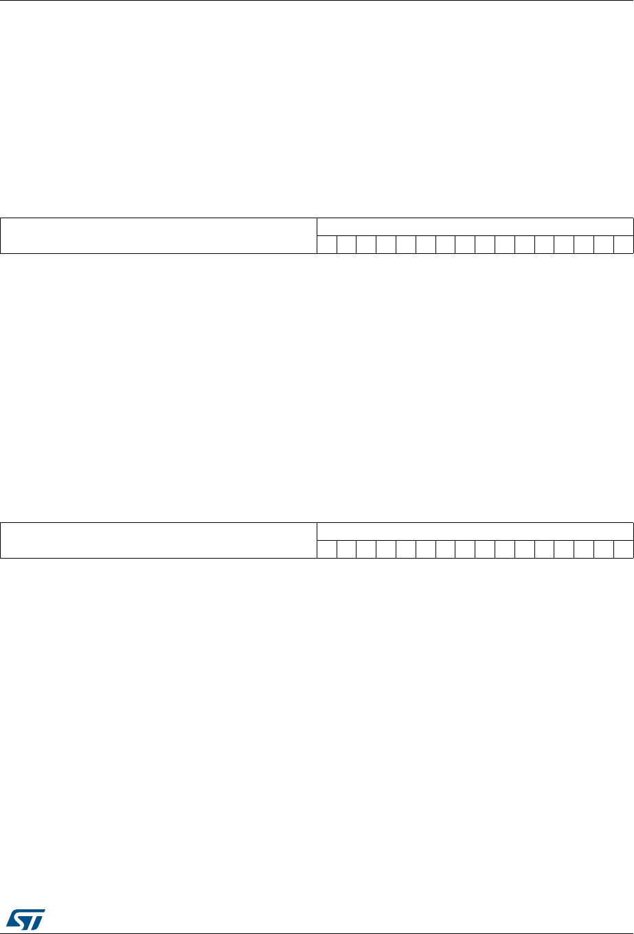
DocID018909 Rev 9 1415/1718
RM0090 USB on-the-go high-speed (OTG_HS)
1523
OTG_HS Host all channels interrupt register (OTG_HS_HAINT)
Address offset: 0x414
Reset value: 0x0000 000
When a significant event occurs on a channel, the host all channels interrupt register
interrupts the application using the host channels interrupt bit of the Core interrupt register
(HCINT bit in OTG_HS_GINTSTS). This is shown in Figure 412. There is one interrupt bit
per channel, up to a maximum of 16 bits. Bits in this register are set and cleared when the
application sets and clears bits in the corresponding host channel-x interrupt register.
OTG_HS host all channels interrupt mask register (OTG_HS_HAINTMSK)
Address offset: 0x418
Reset value: 0x0000 0000
The host all channel interrupt mask register works with the host all channel interrupt register
to interrupt the application when an event occurs on a channel. There is one interrupt mask
bit per channel, up to a maximum of 16 bits.
313029282726252423222120191817161514131211109876543210
Reserved
HAINT
rrrrrrrrrrrrrrrr
Bits 31:16 Reserved, must be kept at reset value.
Bits 15:0 HAINT: Channel interrupts
One bit per channel: Bit 0 for Channel 0, bit 15 for Channel 15
313029282726252423222120191817161514131211109876543210
Reserved
HAINTM
rw rw rw rw rw rw rw rw rw rw rw rw rw rw rw rw
Bits 31:16 Reserved, must be kept at reset value.
Bits 15:0 HAINTM: Channel interrupt mask
0: Masked interrupt
1: Unmasked interrupt
One bit per channel: Bit 0 for channel 0, bit 15 for channel 15

USB on-the-go high-speed (OTG_HS) RM0090
1416/1718 DocID018909 Rev 9
OTG_HS host port control and status register (OTG_HS_HPRT)
Address offset: 0x440
Reset value: 0x0000 0000
This register is available only in host mode. Currently, the OTG host supports only one port.
A single register holds USB port-related information such as USB reset, enable, suspend,
resume, connect status, and test mode for each port. It is shown in Figure 412. The rc_w1
bits in this register can trigger an interrupt to the application through the host port interrupt
bit of the core interrupt register (HPRTINT bit in OTG_HS_GINTSTS). On a Port Interrupt,
the application must read this register and clear the bit that caused the interrupt. For the
rc_w1 bits, the application must write a 1 to the bit to clear the interrupt.
3130292827262524232221201918171615141312111098765 43210
Reserved
PSPD PTCTL
PPWR
PLSTS
Reserved
PRST
PSUSP
PRES
POCCHNG
POCA
PENCHNG
PENA
PCDET
PCSTS
r r rw rw rw rw rw r r rw rs rw rc_
w1 rrc_
w1
rc_
w0
rc_
w1 r
Bits 31:19 Reserved, must be kept at reset value.
Bits 18:17 PSPD: Port speed
Indicates the speed of the device attached to this port.
00: High speed
01: Full speed
10: Low speed
11: Reserved
Bits 16:13 PTCTL: Port test control
The application writes a nonzero value to this field to put the port into a Test mode, and the
corresponding pattern is signaled on the port.
0000: Test mode disabled
0001: Test_J mode
0010: Test_K mode
0011: Test_SE0_NAK mode
0100: Test_Packet mode
0101: Test_Force_Enable
Others: Reserved
Bit 12 PPWR: Port power
The application uses this field to control power to this port, and the core clears this bit on an
overcurrent condition.
0: Power off
1: Power on
Bits 11:10 PLSTS: Port line status
Indicates the current logic level USB data lines
Bit [10]: Logic level of OTG_HS_FS_DP
Bit [11]: Logic level of OTG_HS_FS_DM
Bit 9 Reserved, must be kept at reset value.

DocID018909 Rev 9 1417/1718
RM0090 USB on-the-go high-speed (OTG_HS)
1523
Bit 8 PRST: Port reset
When the application sets this bit, a reset sequence is started on this port. The application
must time the reset period and clear this bit after the reset sequence is complete.
0: Port not in reset
1: Port in reset
The application must leave this bit set for a minimum duration of at least 10 ms to start a
reset on the port. The application can leave it set for another 10 ms in addition to the
required minimum duration, before clearing the bit, even though there is no maximum limit
set by the USB standard.
High speed: 50 ms
Full speed/Low speed: 10 ms
Bit 7 PSUSP: Port suspend
The application sets this bit to put this port in Suspend mode. The core only stops sending
SOFs when this is set. To stop the PHY clock, the application must set the Port clock stop
bit, which asserts the suspend input pin of the PHY.
The read value of this bit reflects the current suspend status of the port. This bit is cleared
by the core after a remote wakeup signal is detected or the application sets the Port reset bit
or Port resume bit in this register or the Resume/remote wakeup detected interrupt bit or
Disconnect detected interrupt bit in the Core interrupt register (WKUINT or DISCINT in
OTG_HS_GINTSTS, respectively).
0: Port not in Suspend mode
1: Port in Suspend mode
Bit 6 PRES: Port resume
The application sets this bit to drive resume signaling on the port. The core continues to
drive the resume signal until the application clears this bit.
If the core detects a USB remote wakeup sequence, as indicated by the Port
resume/remote wakeup detected interrupt bit of the Core interrupt register (WKUINT bit in
OTG_HS_GINTSTS), the core starts driving resume signaling without application
intervention and clears this bit when it detects a disconnect condition. The read value of this
bit indicates whether the core is currently driving resume signaling.
0: No resume driven
1: Resume driven
Bit 5 POCCHNG: Port overcurrent change
The core sets this bit when the status of the Port overcurrent active bit (bit 4) in this register
changes.
Bit 4 POCA: Port overcurrent active
Indicates the overcurrent condition of the port.
0: No overcurrent condition
1: Overcurrent condition
Bit 3 PENCHNG: Port enable/disable change
The core sets this bit when the status of the Port enable bit [2] in this register changes.
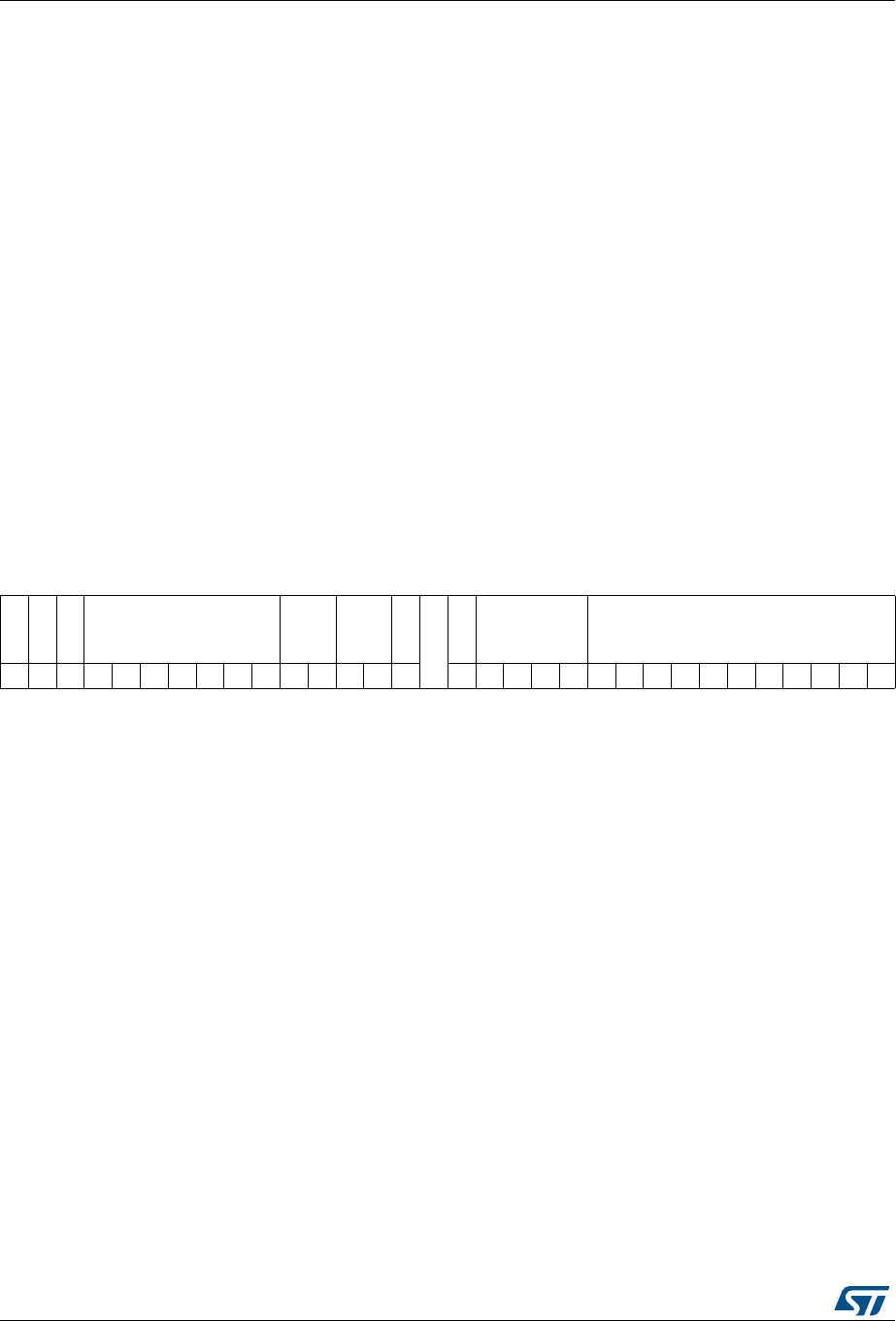
USB on-the-go high-speed (OTG_HS) RM0090
1418/1718 DocID018909 Rev 9
OTG_HS host channel-x characteristics register (OTG_HS_HCCHARx)
(x = 0..11, where x = Channel_number)
Address offset: 0x500 + (Channel_number × 0x20)
Reset value: 0x0000 0000
Bit 2 PENA: Port enable
A port is enabled only by the core after a reset sequence, and is disabled by an overcurrent
condition, a disconnect condition, or by the application clearing this bit. The application
cannot set this bit by a register write. It can only clear it to disable the port. This bit does not
trigger any interrupt to the application.
0: Port disabled
1: Port enabled
Bit 1 PCDET: Port connect detected
The core sets this bit when a device connection is detected to trigger an interrupt to the
application using the host port interrupt bit in the Core interrupt register (HPRTINT bit in
OTG_HS_GINTSTS). The application must write a 1 to this bit to clear the interrupt.
Bit 0 PCSTS: Port connect status
0: No device is attached to the port
1: A device is attached to the port
313029282726252423222120191817161514131211109876543210
CHENA
CHDIS
ODDFRM
DAD MC
EPTYP
LSDEV
Reserved
EPDIR
EPNUM MPSIZ
rs rs rw rw rw rw rw rw rw rw rw rw rw rw rw rw rw rw rw rw rw rw rw rw rw rw rw rw rw rw rw
Bit 31 CHENA: Channel enable
This field is set by the application and cleared by the OTG host.
0: Channel disabled
1: Channel enabled
Bit 30 CHDIS: Channel disable
The application sets this bit to stop transmitting/receiving data on a channel, even before
the transfer for that channel is complete. The application must wait for the Channel disabled
interrupt before treating the channel as disabled.
Bit 29 ODDFRM: Odd frame
This field is set (reset) by the application to indicate that the OTG host must perform a
transfer in an odd frame. This field is applicable for only periodic (isochronous and interrupt)
transactions.
0: Even (micro) frame
1: Odd (micro) frame
Bits 28:22 DAD: Device address
This field selects the specific device serving as the data source or sink.

DocID018909 Rev 9 1419/1718
RM0090 USB on-the-go high-speed (OTG_HS)
1523
Bits 21:20 MC: Multi Count (MC) / Error Count (EC)
– When the split enable bit (SPLITEN) in the host channel-x split control register
(OTG_HS_HCSPLTx) is reset (0), this field indicates to the host the number of transactions
that must be executed per micro-frame for this periodic endpoint. For nonperiodic transfers,
this field specifies the number of packets to be fetched for this channel before the internal
DMA engine changes arbitration.
00: Reserved This field yields undefined results
01: 1 transaction
b10: 2 transactions to be issued for this endpoint per micro-frame
11: 3 transactions to be issued for this endpoint per micro-frame.
– When the SPLITEN bit is set (1) in OTG_HS_HCSPLTx, this field indicates the number of
immediate retries to be performed for a periodic split transaction on transaction errors. This
field must be set to at least 01.
Bits 19:18 EPTYP: Endpoint type
Indicates the transfer type selected.
00: Control
01: Isochronous
10: Bulk
11: Interrupt
Bit 17 LSDEV: Low-speed device
This field is set by the application to indicate that this channel is communicating to a low-
speed device.
Bit 16 Reserved, must be kept at reset value.
Bit 15 EPDIR: Endpoint direction
Indicates whether the transaction is IN or OUT.
0: OUT
1: IN
Bits 14:11 EPNUM: Endpoint number
Indicates the endpoint number on the device serving as the data source or sink.
Bits 10:0 MPSIZ: Maximum packet size
Indicates the maximum packet size of the associated endpoint.

USB on-the-go high-speed (OTG_HS) RM0090
1420/1718 DocID018909 Rev 9
OTG_HS host channel-x split control register (OTG_HS_HCSPLTx) (x = 0..11,
where x = Channel_number)
Address offset: 0x504 + (Channel_number × 0x20)
Reset value: 0x0000 0000
313029282726252423222120191817161514131211109876543210
SPLITEN
Reserved
COMPLSPLT
XACTPOS
HUBADDR
PRTADDR
rw rw rw rw rw rw rw rw rw rw rw rw rw rw rw rw rw rw
Bit 31 SPLITEN: Split enable
The application sets this bit to indicate that this channel is enabled to perform split
transactions.
Bits 30:17 Reserved, must be kept at reset value.
Bit 16 COMPLSPLT: Do complete split
The application sets this bit to request the OTG host to perform a complete split transaction.
Bits 15:14 XACTPOS: Transaction position
This field is used to determine whether to send all, first, middle, or last payloads with each
OUT transaction.
11: All. This is the entire data payload of this transaction (which is less than or equal to 188
bytes)
10: Begin. This is the first data payload of this transaction (which is larger than 188 bytes)
00: Mid. This is the middle payload of this transaction (which is larger than 188 bytes)
01: End. This is the last payload of this transaction (which is larger than 188 bytes)
Bits 13:7 HUBADDR: Hub address
This field holds the device address of the transaction translator’s hub.
Bits 6:0 PRTADDR: Port address
This field is the port number of the recipient transaction translator.

DocID018909 Rev 9 1421/1718
RM0090 USB on-the-go high-speed (OTG_HS)
1523
OTG_HS host channel-x interrupt register (OTG_HS_HCINTx) (x = 0..11, where
x = Channel_number)
Address offset: 0x508 + (Channel_number × 0x20)
Reset value: 0x0000 0000
This register indicates the status of a channel with respect to USB- and AHB-related events.
It is shown in Figure 412. The application must read this register when the host channels
interrupt bit in the Core interrupt register (HCINT bit in OTG_HS_GINTSTS) is set. Before
the application can read this register, it must first read the host all channels interrupt
(OTG_HS_HAINT) register to get the exact channel number for the host channel-x interrupt
register. The application must clear the appropriate bit in this register to clear the
corresponding bits in the OTG_HS_HAINT and OTG_HS_GINTSTS registers.
313029282726252423222120191817161514131211109876543210
Reserved
DTERR
FRMOR
BBERR
TXERR
NYET
ACK
NAK
STALL
AHBERR
CHH
XFRC
rc_
w1
rc_
w1
rc_
w1
rc_
w1
rc_
w1
rc_
w1
rc_
w1
rc_
w1
rc_
w1
rc_
w1
rc_
w1
Bits 31:11 Reserved, must be kept at reset value.
Bit 10 DTERR: Data toggle error
Bit 9 FRMOR: Frame overrun
Bit 8 BBERR: Babble error
Bit 7 TXERR: Transaction error
Indicates one of the following errors occurred on the USB.
CRC check failure
Timeout
Bit stuff error
False EOP
Bit 6 NYET: Response received interrupt
Bit 5 ACK: ACK response received/transmitted interrupt
Bit 4 NAK: NAK response received interrupt
Bit 3 STALL: STALL response received interrupt
Bit 2 AHBERR: AHB error
This error is generated only in Internal DMA mode when an AHB error occurs during an AHB
read/write operation. The application can read the corresponding DMA channel address
register to get the error address.
Bit 1 CHH: Channel halted
Indicates the transfer completed abnormally either because of any USB transaction error or in
response to disable request by the application.
Bit 0 XFRC: Transfer completed
Transfer completed normally without any errors.

USB on-the-go high-speed (OTG_HS) RM0090
1422/1718 DocID018909 Rev 9
OTG_HS host channel-x interrupt mask register (OTG_HS_HCINTMSKx)
(x = 0..11, where x = Channel_number)
Address offset: 0x50C + (Channel_number × 0x20)
Reset value: 0x0000 0000
This register reflects the mask for each channel status described in the previous section.
313029282726252423222120191817161514131211109876543210
Reserved
DTERRM
FRMORM
BBERRM
TXERRM
NYET
ACKM
NAKM
STALLM
AHBERR
CHHM
XFRCM
rw rw rw rw rw rw rw rw rw rw rw
Bits 31:11 Reserved, must be kept at reset value.
Bit 10 DTERRM: Data toggle error mask
0: Masked interrupt
1: Unmasked interrupt
Bit 9 FRMORM: Frame overrun mask
0: Masked interrupt
1: Unmasked interrupt
Bit 8 BBERRM: Babble error mask
0: Masked interrupt
1: Unmasked interrupt
Bit 7 TXERRM: Transaction error mask
0: Masked interrupt
1: Unmasked interrupt
Bit 6 NYET: response received interrupt mask
0: Masked interrupt
1: Unmasked interrupt
Bit 5 ACKM: ACK response received/transmitted interrupt mask
0: Masked interrupt
1: Unmasked interrupt
Bit 4 NAKM: NAK response received interrupt mask
0: Masked interrupt
1: Unmasked interrupt
Bit 3 STALLM: STALL response received interrupt mask
0: Masked interrupt
1: Unmasked interrupt

DocID018909 Rev 9 1423/1718
RM0090 USB on-the-go high-speed (OTG_HS)
1523
OTG_HS host channel-x transfer size register (OTG_HS_HCTSIZx) (x = 0..11,
where x = Channel_number)
Address offset: 0x510 + (Channel_number × 0x20)
Reset value: 0x0000 0000
Bit 2 AHBERR: AHB error
This is generated only in Internal DMA mode when there is an AHB error during AHB
read/write. The application can read the corresponding channel’s DMA address register to
get the error address.
Bit 1 CHHM: Channel halted mask
0: Masked interrupt
1: Unmasked interrupt
Bit 0 XFRCM: Transfer completed mask
0: Masked interrupt
1: Unmasked interrupt
313029282726252423222120191817161514131211109876543210
DOPING
DPID PKTCNT XFRSIZ
rw rw rw rw rw rw rw rw rw rw rw rw rw rw rw rw rw rw rw rw rw rw rw rw rw rw rw rw rw rw rw rw
Bit 31 DOPING: Doping
This bit is used only for OUT transfers. Setting this field to 1 directs the host to do PING
protocol.
Note: Do not set this bit for IN transfers. If this bit is set for IN transfers it disables the channel.
Bits 30:29 DPID: Data PID
The application programs this field with the type of PID to use for the initial transaction. The
host maintains this field for the rest of the transfer.
00: DATA0
01: DATA2
10: DATA1
11: MDATA (noncontrol)/SETUP (control)
Bits 28:19 PKTCNT: Packet count
This field is programmed by the application with the expected number of packets to be
transmitted (OUT) or received (IN).
The host decrements this count on every successful transmission or reception of an OUT/IN
packet. Once this count reaches zero, the application is interrupted to indicate normal
completion.
Bits 18:0 XFRSIZ: Transfer size
For an OUT, this field is the number of data bytes the host sends during the transfer.
For an IN, this field is the buffer size that the application has reserved for the transfer. The
application is expected to program this field as an integer multiple of the maximum packet
size for IN transactions (periodic and nonperiodic).

USB on-the-go high-speed (OTG_HS) RM0090
1424/1718 DocID018909 Rev 9
OTG_HS host channel-x DMA address register (OTG_HS_HCDMAx) (x = 0..11,
where x = Channel_number)
Address offset: 0x514 + (Channel_number × 0x20)
Reset value: 0x0000 0000
35.12.4 Device-mode registers
OTG_HS device configuration register (OTG_HS_DCFG)
Address offset: 0x800
Reset value: 0x0220 0000
This register configures the core in peripheral mode after power-on or after certain control
commands or enumeration. Do not make changes to this register after initial programming.
313029282726252423222120191817161514131211109876543210
DMAADDR
rw rw rw rw rw rw rw rw rw rw rw rw rw rw rw rw rw rw rw rw rw rw rw rw rw rw rw rw rw rw rw rw
Bits 31:0 DMAADDR: DMA address
This field holds the start address in the external memory from which the data for the endpoint
must be fetched or to which it must be stored. This register is incremented on every AHB
transaction.
313029282726252423222120191817161514131211109876543210
Reserved
PERSCHIVL
Reserved
Reserved
PFIVL
DAD
Reserved
NZLSOHSK
DSPD
rw rw rw rw rw rw rw rw rw rw rw rw rw
Bits 31:26 Reserved, must be kept at reset value.
Bits 25:24 PERSCHIVL: Periodic scheduling interval
This field specifies the amount of time the Internal DMA engine must allocate for fetching
periodic IN endpoint data. Based on the number of periodic endpoints, this value must be
specified as 25, 50 or 75% of the (micro)frame.
– When any periodic endpoints are active, the internal DMA engine allocates the
specified amount of time in fetching periodic IN endpoint data
– When no periodic endpoint is active, then the internal DMA engine services
nonperiodic endpoints, ignoring this field
– After the specified time within a (micro)frame, the DMA switches to fetching
nonperiodic endpoints
00: 25% of (micro)frame
01: 50% of (micro)frame
10: 75% of (micro)frame
11: Reserved
Bits 23:13 Reserved, must be kept at reset value.

DocID018909 Rev 9 1425/1718
RM0090 USB on-the-go high-speed (OTG_HS)
1523
Bits 12:11 PFIVL: Periodic (micro)frame interval
Indicates the time within a (micro) frame at which the application must be notified using the
end of periodic (micro) frame interrupt. This can be used to determine if all the isochronous
traffic for that frame is complete.
00: 80% of the frame interval
01: 85% of the frame interval
10: 90% of the frame interval
11: 95% of the frame interval
Bits 10:4 DAD: Device address
The application must program this field after every SetAddress control command.
Bit 3 Reserved, must be kept at reset value.
Bit 2 NZLSOHSK: Nonzero-length status OUT handshake
The application can use this field to select the handshake the core sends on receiving a
nonzero-length data packet during the OUT transaction of a control transfer’s Status stage.
1: Send a STALL handshake on a nonzero-length status OUT transaction and do not send
the received OUT packet to the application.
0: Send the received OUT packet to the application (zero-length or nonzero-length) and
send a handshake based on the NAK and STALL bits for the endpoint in the device endpoint
control register.
Bits 1:0 DSPD: Device speed
Indicates the speed at which the application requires the core to enumerate, or the
maximum speed the application can support. However, the actual bus speed is determined
only after the chirp sequence is completed, and is based on the speed of the USB host to
which the core is connected.
00: High speed
01: Full speed using external ULPI PHY
10: Reserved
11: Full speed using internal embedded PHY

USB on-the-go high-speed (OTG_HS) RM0090
1426/1718 DocID018909 Rev 9
OTG_HS device control register (OTG_HS_DCTL)
Address offset: 0x804
Reset value: 0x0000 0000
313029282726252423222120191817161514131211109876543210
Reserved
POPRGDNE
CGONAK
SGONAK
CGINAK
SGINAK
TCTL
GONSTS
GINSTS
SDIS
RWUSIG
rwwwwwrwrwrwr rrwrw
Bits 31:12 Reserved, must be kept at reset value.
Bit 11 POPRGDNE: Power-on programming done
The application uses this bit to indicate that register programming is completed after a
wakeup from power down mode.
Bit 10 CGONAK: Clear global OUT NAK
A write to this field clears the Global OUT NAK.
Bit 9 SGONAK: Set global OUT NAK
A write to this field sets the Global OUT NAK.
The application uses this bit to send a NAK handshake on all OUT endpoints.
The application must set the this bit only after making sure that the Global OUT NAK
effective bit in the Core interrupt register (GONAKEFF bit in OTG_HS_GINTSTS) is
cleared.
Bit 8 CGINAK: Clear global IN NAK
A write to this field clears the Global IN NAK.
Bit 7 SGINAK: Set global IN NAK
A write to this field sets the Global nonperiodic IN NAK.The application uses this bit to send
a NAK handshake on all nonperiodic IN endpoints.
The application must set this bit only after making sure that the Global IN NAK effective bit
in the Core interrupt register (GINAKEFF bit in OTG_HS_GINTSTS) is cleared.
Bits 6:4 TCTL: Test control
000: Test mode disabled
001: Test_J mode
010: Test_K mode
011: Test_SE0_NAK mode
100: Test_Packet mode
101: Test_Force_Enable
Others: Reserved
Bit 3 GONSTS: Global OUT NAK status
0: A handshake is sent based on the FIFO Status and the NAK and STALL bit settings.
1: No data is written to the RxFIFO, irrespective of space availability. Sends a NAK
handshake on all packets, except on SETUP transactions. All isochronous OUT packets are
dropped.
DocID018909 Rev 9 1427/1718
RM0090 USB on-the-go high-speed (OTG_HS)
1523
Table 209 contains the minimum duration (according to device state) for which the Soft
disconnect (SDIS) bit must be set for the USB host to detect a device disconnect. To
accommodate clock jitter, it is recommended that the application add some extra delay to
the specified minimum duration.
Bit 2 GINSTS: Global IN NAK status
0: A handshake is sent out based on the data availability in the transmit FIFO.
1: A NAK handshake is sent out on all nonperiodic IN endpoints, irrespective of the data
availability in the transmit FIFO.
Bit 1 SDIS: Soft disconnect
The application uses this bit to signal the USB OTG core to perform a soft disconnect. As
long as this bit is set, the host does not see that the device is connected, and the device
does not receive signals on the USB. The core stays in the disconnected state until the
application clears this bit.
0: Normal operation. When this bit is cleared after a soft disconnect, the core generates a
device connect event to the USB host. When the device is reconnected, the USB host
restarts device enumeration.
1: The core generates a device disconnect event to the USB host.
Bit 0 RWUSIG: Remote wakeup signaling
When the application sets this bit, the core initiates remote signaling to wake up the USB
host. The application must set this bit to instruct the core to exit the Suspend state. As
specified in the USB 2.0 specification, the application must clear this bit 1 ms to 15 ms after
setting it.
Table 209. Minimum duration for soft disconnect
Operating speed Device state Minimum duration
High speed Not Idle or Suspended (Performing transactions) 125 µs
Full speed Suspended 1 ms + 2.5 µs
Full speed Idle 2.5 µs
Full speed Not Idle or Suspended (Performing transactions) 2.5 µs

USB on-the-go high-speed (OTG_HS) RM0090
1428/1718 DocID018909 Rev 9
OTG_HS device status register (OTG_HS_DSTS)
Address offset: 0x808
Reset value: 0x0000 0010
This register indicates the status of the core with respect to USB-related events. It must be
read on interrupts from the device all interrupts (OTG_HS_DAINT) register.
313029282726252423222120191817161514131211109876543210
Reserved FNSOF Reserved
EERR
ENUMSPD
SUSPSTS
rrrrrrrrrrrrrr rrrr
Bits 31:22 Reserved, must be kept at reset value.
Bits 21:8 FNSOF: Frame number of the received SOF
Bits 7:4 Reserved, must be kept at reset value.
Bit 3 EERR: Erratic error
The core sets this bit to report any erratic errors.
Due to erratic errors, the OTG_HS controller goes into Suspended state and an interrupt is
generated to the application with Early suspend bit of the Core interrupt register (ESUSP bit
in OTG_HS_GINTSTS). If the early suspend is asserted due to an erratic error, the
application can only perform a soft disconnect recover.
Bits 2:1 ENUMSPD: Enumerated speed
Indicates the speed at which the OTG_HS controller has come up after speed detection
through a chirp sequence.
00: High speed
01: Reserved
10: Reserved
11: Full speed (PHY clock is running at 48 MHz)
Others: reserved
Bit 0 SUSPSTS: Suspend status
In peripheral mode, this bit is set as long as a Suspend condition is detected on the USB.
The core enters the Suspended state when there is no activity on the USB data lines for a
period of 3 ms. The core comes out of the suspend:
– When there is an activity on the USB data lines
– When the application writes to the Remote wakeup signaling bit in the Device control register
(RWUSIG bit in OTG_HS_DCTL).

DocID018909 Rev 9 1429/1718
RM0090 USB on-the-go high-speed (OTG_HS)
1523
OTG_HS device IN endpoint common interrupt mask register
(OTG_HS_DIEPMSK)
Address offset: 0x810
Reset value: 0x0000 0000
This register works with each of the Device IN endpoint interrupt (OTG_HS_DIEPINTx)
registers for all endpoints to generate an interrupt per IN endpoint. The IN endpoint interrupt
for a specific status in the OTG_HS_DIEPINTx register can be masked by writing to the
corresponding bit in this register. Status bits are masked by default.
313029282726252423222120191817161514131211109876543210
Reserved
BIM
TXFURM
Reserved
INEPNEM
INEPNMM
ITTXFEMSK
TOM
Reserved
EPDM
XFRCM
rw rw rw rw rw rw rw rw
Bits 31:10 Reserved, must be kept at reset value.
Bit 9 BIM: BNA interrupt mask
0: Masked interrupt
1: Unmasked interrupt
Bit 8 TXFURM: FIFO underrun mask
0: Masked interrupt
1: Unmasked interrupt
Bit 7 Reserved, must be kept at reset value.
Bit 6 INEPNEM: IN endpoint NAK effective mask
0: Masked interrupt
1: Unmasked interrupt
Bit 5 INEPNMM: IN token received with EP mismatch mask
0: Masked interrupt
1: Unmasked interrupt
Bit 4 ITTXFEMSK: IN token received when TxFIFO empty mask
0: Masked interrupt
1: Unmasked interrupt
Bit 3 TOM: Timeout condition mask (nonisochronous endpoints)
0: Masked interrupt
1: Unmasked interrupt
Bit 2 Reserved, must be kept at reset value.
Bit 1 EPDM: Endpoint disabled interrupt mask
0: Masked interrupt
1: Unmasked interrupt
Bit 0 XFRCM: Transfer completed interrupt mask
0: Masked interrupt
1: Unmasked interrupt

USB on-the-go high-speed (OTG_HS) RM0090
1430/1718 DocID018909 Rev 9
OTG_HS device OUT endpoint common interrupt mask register
(OTG_HS_DOEPMSK)
Address offset: 0x814
Reset value: 0x0000 0000
This register works with each of the Device OUT endpoint interrupt (OTG_HS_DOEPINTx)
registers for all endpoints to generate an interrupt per OUT endpoint. The OUT endpoint
interrupt for a specific status in the OTG_HS_DOEPINTx register can be masked by writing
into the corresponding bit in this register. Status bits are masked by default.
313029282726252423222120191817161514131211109876543210
Reserved
BOIM
OPEM
Reserved
B2BSTUP
Reserved
OTEPDM
STUPM
Reserved
EPDM
XFRCM
rw rw rw rw rw rw rw
Bits 31:10 Reserved, must be kept at reset value.
Bit 9 BOIM: BNA interrupt mask
0: Masked interrupt
1: Unmasked interrupt
Bit 8 OPEM: OUT packet error mask
0: Masked interrupt
1: Unmasked interrupt
Bit 7 Reserved, must be kept at reset value.
Bit 6 B2BSTUP: Back-to-back SETUP packets received mask
Applies to control OUT endpoints only.
0: Masked interrupt
1: Unmasked interrupt
Bit 5 Reserved, must be kept at reset value.
Bit 4 OTEPDM: OUT token received when endpoint disabled mask
Applies to control OUT endpoints only.
0: Masked interrupt
1: Unmasked interrupt
Bit 3 STUPM: SETUP phase done mask
Applies to control endpoints only.
0: Masked interrupt
1: Unmasked interrupt
Bit 2 Reserved, must be kept at reset value.
Bit 1 EPDM: Endpoint disabled interrupt mask
0: Masked interrupt
1: Unmasked interrupt
Bit 0 XFRCM: Transfer completed interrupt mask
0: Masked interrupt
1: Unmasked interrupt

DocID018909 Rev 9 1431/1718
RM0090 USB on-the-go high-speed (OTG_HS)
1523
OTG_HS device all endpoints interrupt register (OTG_HS_DAINT)
Address offset: 0x818
Reset value: 0x0000 0000
When a significant event occurs on an endpoint, a device all endpoints interrupt register
interrupts the application using the Device OUT endpoints interrupt bit or Device IN
endpoints interrupt bit of the Core interrupt register (OEPINT or IEPINT in
OTG_HS_GINTSTS, respectively). There is one interrupt bit per endpoint, up to a maximum
of 16 bits for OUT endpoints and 16 bits for IN endpoints. For a bidirectional endpoint, the
corresponding IN and OUT interrupt bits are used. Bits in this register are set and cleared
when the application sets and clears bits in the corresponding Device Endpoint-x interrupt
register (OTG_HS_DIEPINTx/OTG_HS_DOEPINTx).
OTG_HS all endpoints interrupt mask register (OTG_HS_DAINTMSK)
Address offset: 0x81C
Reset value: 0x0000 0000
The device endpoint interrupt mask register works with the device endpoint interrupt register
to interrupt the application when an event occurs on a device endpoint. However, the device
all endpoints interrupt (OTG_HS_DAINT) register bit corresponding to that interrupt is still
set.
313029282726252423222120191817161514131211109876543210
OEPINT IEPINT
rrrrrrrrrrrrrrrrrrrrrrrrrrrrrrrr
Bits 31:16 OEPINT: OUT endpoint interrupt bits
One bit per OUT endpoint:
Bit 16 for OUT endpoint 0, bit 31 for OUT endpoint 15
Bits 15:0 IEPINT: IN endpoint interrupt bits
One bit per IN endpoint:
Bit 0 for IN endpoint 0, bit 15 for endpoint 15
313029282726252423222120191817161514131211109876543210
OEPM IEPM
rw rw rw rw rw rw rw rw rw rw rw rw rw rw rw rw rw rw rw rw rw rw rw rw rw rw rw rw rw rw rw rw
Bits 31:16 OEPM: OUT EP interrupt mask bits
One per OUT endpoint:
Bit 16 for OUT EP 0, bit 18 for OUT EP 3
0: Masked interrupt
1: Unmasked interrupt
Bits 15:0 IEPM: IN EP interrupt mask bits
One bit per IN endpoint:
Bit 0 for IN EP 0, bit 3 for IN EP 3
0: Masked interrupt
1: Unmasked interrupt

USB on-the-go high-speed (OTG_HS) RM0090
1432/1718 DocID018909 Rev 9
OTG_HS device VBUS discharge time register (OTG_HS_DVBUSDIS)
Address offset: 0x0828
Reset value: 0x0000 17D7
This register specifies the VBUS discharge time after VBUS pulsing during SRP.
OTG_HS device VBUS pulsing time register (OTG_HS_DVBUSPULSE)
Address offset: 0x082C
Reset value: 0x0000 05B8
This register specifies the VBUS pulsing time during SRP.
313029282726252423222120191817161514131211109876543210
Reserved
VBUSDT
rw rw rw rw rw rw rw rw rw rw rw rw rw rw rw rw
Bits 31:16 Reserved, must be kept at reset value.
Bits 15:0 VBUSDT: Device VBUS discharge time
Specifies the VBUS discharge time after VBUS pulsing during SRP. This value equals:
VBUS discharge time in PHY clocks / 1 024
Depending on your VBUS load, this value may need adjusting.
313029282726252423222120191817161514131211109876543210
Reserved
DVBUSP
rw rw rw rw rw rw rw rw rw rw rw rw
Bits 31:12 Reserved, must be kept at reset value.
Bits 11:0 DVBUSP: Device VBUS pulsing time
Specifies the VBUS pulsing time during SRP. This value equals:
VBUS pulsing time in PHY clocks / 1 024

DocID018909 Rev 9 1433/1718
RM0090 USB on-the-go high-speed (OTG_HS)
1523
OTG_HS Device threshold control register (OTG_HS_DTHRCTL)
Address offset: 0x0830
Reset value: 0x0000 0000
313029282726252423222120191817161514131211109876543210
Reserved
ARPEN
Reserved
RXTHRLEN
RXTHREN
Reserved TXTHRLEN
ISOTHREN
NONISOTHREN
rw rw rw rw rw rw rw rw rw rw rw rw rw rw rw rw rw rw rw rw rw rw
Bits 31:28 Reserved, must be kept at reset value.
Bit 27 ARPEN: Arbiter parking enable
This bit controls internal DMA arbiter parking for IN endpoints. When thresholding is enabled
and this bit is set to one, then the arbiter parks on the IN endpoint for which there is a token
received on the USB. This is done to avoid getting into underrun conditions. By default
parking is enabled.
Bit 26 Reserved, must be kept at reset value.
Bits 25: 17 RXTHRLEN: Receive threshold length
This field specifies the receive thresholding size in DWORDS. This field also specifies the
amount of data received on the USB before the core can start transmitting on the AHB. The
threshold length has to be at least eight DWORDS. The recommended value for
RXTHRLEN is to be the same as the programmed AHB burst length (HBSTLEN bit in
OTG_HS_GAHBCFG).
Bit 16 RXTHREN: Receive threshold enable
When this bit is set, the core enables thresholding in the receive direction.
Bits 15: 11 Reserved, must be kept at reset value.
Bits 10:2 TXTHRLEN: Transmit threshold length
This field specifies the transmit thresholding size in DWORDS. This field specifies the
amount of data in bytes to be in the corresponding endpoint transmit FIFO, before the core
can start transmitting on the USB. The threshold length has to be at least eight DWORDS.
This field controls both isochronous and nonisochronous IN endpoint thresholds. The
recommended value for TXTHRLEN is to be the same as the programmed AHB burst length
(HBSTLEN bit in OTG_HS_GAHBCFG).
Bit 1 ISOTHREN: ISO IN endpoint threshold enable
When this bit is set, the core enables thresholding for isochronous IN endpoints.
Bit 0 NONISOTHREN: Nonisochronous IN endpoints threshold enable
When this bit is set, the core enables thresholding for nonisochronous IN endpoints.
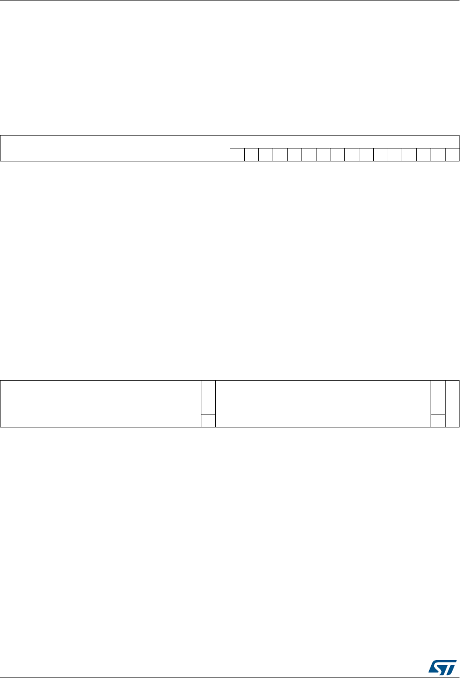
USB on-the-go high-speed (OTG_HS) RM0090
1434/1718 DocID018909 Rev 9
OTG_HS device IN endpoint FIFO empty interrupt mask register:
(OTG_HS_DIEPEMPMSK)
Address offset: 0x834
Reset value: 0x0000 0000
This register is used to control the IN endpoint FIFO empty interrupt generation
(TXFE_OTG_HS_DIEPINTx).
OTG_HS device each endpoint interrupt register (OTG_HS_DEACHINT)
Address offset: 0x0838
Reset value: 0x0000 0000
There is one interrupt bit for endpoint 1 IN and one interrupt bit for endpoint 1 OUT.
313029282726252423222120191817161514131211109876543210
Reserved INEPTXFEM
rw rw rw rw rw rw rw rw rw rw rw rw rw rw rw rw
Bits 31:16 Reserved, must be kept at reset value.
Bits 15:0 INEPTXFEM: IN EP Tx FIFO empty interrupt mask bits
These bits act as mask bits for OTG_HS_DIEPINTx.
TXFE interrupt one bit per IN endpoint:
Bit 0 for IN endpoint 0, bit 15 for IN endpoint 15
0: Masked interrupt
1: Unmasked interrupt
313029282726252423222120191817161514131211109876543210
Reserved
OEP1INT
Reserved
IEP1INT
Reserved
Bits 31:18 Reserved, must be kept at reset value.
Bit 17 OEP1INT: OUT endpoint 1 interrupt bit
Bits 16:2 Reserved, must be kept at reset value.
Bit 1 IEP1INT: IN endpoint 1interrupt bit
Bit 0 Reserved, must be kept at reset value.
DocID018909 Rev 9 1435/1718
RM0090 USB on-the-go high-speed (OTG_HS)
1523
OTG_HS device each endpoint interrupt register mask
(OTG_HS_DEACHINTMSK)
Address offset: 0x083C
Reset value: 0x0000 0000
There is one interrupt bit for endpoint 1 IN and one interrupt bit for endpoint 1 OUT.
OTG_HS device each in endpoint-1 interrupt register
(OTG_HS_DIEPEACHMSK1)
Address offset: 0x844
Reset value: 0x0000 0000
313029282726252423222120191817161514131211109876543210
Reserved
OEP1INTM
Reserved
IEP1INTM
Reserved
Bits 31:18 Reserved, must be kept at reset value.
Bit 17 OEP1INTM: OUT Endpoint 1 interrupt mask bit
Bits 16:2 Reserved, must be kept at reset value.
Bit 1 IEP1INTM: IN Endpoint 1 interrupt mask bit
Bit 0 Reserved, must be kept at reset value.
313029282726252423222120191817161514131211109876543210
Reserved
NAKM
Reserved
BIM
TXFURM
Reserved
INEPNEM
INEPNMM
ITTXFEMSK
TOM
Reserved
EPDM
XFRCM
rw rw rw rw rw rw rw rw rw
Bits 31:14 Reserved, must be kept at reset value.
Bit 13 NAKM: NAK interrupt mask
0: Masked interrupt
1: unmasked interrupt
Bit 12:10 Reserved, must be kept at reset value.
Bit 9 BIM: BNA interrupt mask
0: Masked interrupt
1: Unmasked interrupt
Bit 8 TXFURM: FIFO underrun mask
0: Masked interrupt
1: Unmasked interrupt
Bit 7 Reserved, must be kept at reset value.
USB on-the-go high-speed (OTG_HS) RM0090
1436/1718 DocID018909 Rev 9
OTG_HS device each OUT endpoint-1 interrupt register
(OTG_HS_DOEPEACHMSK1)
Address offset: 0x884
Reset value: 0x0000 0000
Bit 6 INEPNEM: IN endpoint NAK effective mask
0: Masked interrupt
1: Unmasked interrupt
Bit 5 INEPNMM: IN token received with EP mismatch mask
0: Masked interrupt
1: Unmasked interrupt
Bit 4 ITTXFEMSK: IN token received when TxFIFO empty mask
0: Masked interrupt
1: Unmasked interrupt
Bit 3 TOM: Timeout condition mask (nonisochronous endpoints)
0: Masked interrupt
1: Unmasked interrupt
Bit 2 Reserved, must be kept at reset value.
Bit 1 EPDM: Endpoint disabled interrupt mask
0: Masked interrupt
1: Unmasked interrupt
Bit 0 XFRCM: Transfer completed interrupt mask
0: Masked interrupt
1: Unmasked interrupt
313029282726252423222120191817161514131211109876543210
Reserved
NYETM
NAKM
BERRM
Reserved
BIM
TXFURM
Reserved
INEPNEM
INEPNMM
ITTXFEMSK
TOM
Reserved
EPDM
XFRCM
rw rw rw rw rw rw rw rw rw rw rw
Bits 31:15 Reserved, must be kept at reset value.
Bit 14 NYETM: NYET interrupt mask
0: Masked interrupt
1: unmasked interrupt
Bit 13 NAKM: NAK interrupt mask
0: Masked interrupt
1: Unmasked interrupt
Bit 12 BERRM: Bubble error interrupt mask
0: Masked interrupt
1: Unmasked interrupt
Bit 11:10 Reserved, must be kept at reset value.

DocID018909 Rev 9 1437/1718
RM0090 USB on-the-go high-speed (OTG_HS)
1523
OTG device endpoint-x control register (OTG_HS_DIEPCTLx) (x = 0..7, where
x = Endpoint_number)
Address offset: 0x900 + (Endpoint_number × 0x20)
Reset value: 0x0000 0000
The application uses this register to control the behavior of each logical endpoint other than
endpoint 0.
Bit 9 BIM: BNA interrupt mask
0: Masked interrupt
1: Unmasked interrupt
Bit 8 OPEM: OUT packet error mask
0: Masked interrupt
1: Unmasked interrupt
Bits 7:3 Reserved, must be kept at reset value.
Bit 2 AHBERRM: AHB error mask
0: Masked interrupt
1: Unmasked interrupt
Bit 1 EPDM: Endpoint disabled interrupt mask
0: Masked interrupt
1: Unmasked interrupt
Bit 0 XFRCM: Transfer completed interrupt mask
0: Masked interrupt
1: Unmasked interrupt
313029282726252423222120191817161514131211109876543210
EPENA
EPDIS
SODDFRM
SD0PID/SEVNFRM
SNAK
CNAK
TXFNUM
Stall
Reserved
EPTYP
NAKSTS
EONUM/DPID
USBAEP
Reserved
MPSIZ
rsrswwwwrwrwrwrw
rw/
rs rw rw r r rw rw rw rw rw rw rw rw rw rw rw rw

USB on-the-go high-speed (OTG_HS) RM0090
1438/1718 DocID018909 Rev 9
Bit 31 EPENA: Endpoint enable
The application sets this bit to start transmitting data on an endpoint.
The core clears this bit before setting any of the following interrupts on this endpoint:
– SETUP phase done
– Endpoint disabled
– Transfer completed
Bit 30 EPDIS: Endpoint disable
The application sets this bit to stop transmitting/receiving data on an endpoint, even before
the transfer for that endpoint is complete. The application must wait for the Endpoint
disabled interrupt before treating the endpoint as disabled. The core clears this bit before
setting the Endpoint disabled interrupt. The application must set this bit only if Endpoint
enable is already set for this endpoint.
Bit 29 SODDFRM: Set odd frame
Applies to isochronous IN and OUT endpoints only.
Writing to this field sets the Even/Odd frame (EONUM) field to odd frame.
Bit 28 SD0PID: Set DATA0 PID
Applies to interrupt/bulk IN endpoints only.
Writing to this field sets the endpoint data PID (DPID) field in this register to DATA0.
SEVNFRM: Set even frame
Applies to isochronous IN endpoints only.
Writing to this field sets the Even/Odd frame (EONUM) field to even frame.
Bit 27 SNAK: Set NAK
A write to this bit sets the NAK bit for the endpoint.
Using this bit, the application can control the transmission of NAK handshakes on an
endpoint. The core can also set this bit for OUT endpoints on a Transfer completed interrupt,
or after a SETUP is received on the endpoint.
Bit 26 CNAK: Clear NAK
A write to this bit clears the NAK bit for the endpoint.
Bits 25:22 TXFNUM: TxFIFO number
These bits specify the FIFO number associated with this endpoint. Each active IN endpoint
must be programmed to a separate FIFO number.
This field is valid only for IN endpoints.
Bit 21 STALL: STALL handshake
Applies to noncontrol, nonisochronous IN endpoints only (access type is rw).
The application sets this bit to stall all tokens from the USB host to this endpoint. If a NAK
bit, Global IN NAK, or Global OUT NAK is set along with this bit, the STALL bit takes priority.
Only the application can clear this bit, never the core.
Applies to control endpoints only (access type is rs).
The application can only set this bit, and the core clears it, when a SETUP token is received
for this endpoint. If a NAK bit, Global IN NAK, or Global OUT NAK is set along with this bit,
the STALL bit takes priority. Irrespective of this bit’s setting, the core always responds to
SETUP data packets with an ACK handshake.
Bit 20 Reserved, must be kept at reset value.

DocID018909 Rev 9 1439/1718
RM0090 USB on-the-go high-speed (OTG_HS)
1523
Bits 19:18 EPTYP: Endpoint type
This is the transfer type supported by this logical endpoint.
00: Control
01: Isochronous
10: Bulk
11: Interrupt
Bit 17 NAKSTS: NAK status
It indicates the following:
0: The core is transmitting nonNAK handshakes based on the FIFO status.
1: The core is transmitting NAK handshakes on this endpoint.
When either the application or the core sets this bit:
For nonisochronous IN endpoints: The core stops transmitting any data on an IN endpoint,
even if there are data available in the TxFIFO.
For isochronous IN endpoints: The core sends out a zero-length data packet, even if there
are data available in the TxFIFO.
Irrespective of this bit’s setting, the core always responds to SETUP data packets with an ACK
handshake.
Bit 16 EONUM: Even/odd frame
Applies to isochronous IN endpoints only.
Indicates the frame number in which the core transmits/receives isochronous data for this
endpoint. The application must program the even/odd frame number in which it intends to
transmit/receive isochronous data for this endpoint using the SEVNFRM and SODDFRM
fields in this register.
0: Even frame
1: Odd frame
DPID: Endpoint data PID
Applies to interrupt/bulk IN endpoints only.
Contains the PID of the packet to be received or transmitted on this endpoint. The
application must program the PID of the first packet to be received or transmitted on this
endpoint, after the endpoint is activated. The application uses the SD0PID register field to
program either DATA0 or DATA1 PID.
0: DATA0
1: DATA1
Bit 15 USBAEP: USB active endpoint
Indicates whether this endpoint is active in the current configuration and interface. The core
clears this bit for all endpoints (other than EP 0) after detecting a USB reset. After receiving
the SetConfiguration and SetInterface commands, the application must program endpoint
registers accordingly and set this bit.
Bits 14:11 Reserved, must be kept at reset value.
Bits 10:0 MPSIZ: Maximum packet size
The application must program this field with the maximum packet size for the current logical
endpoint. This value is in bytes.

USB on-the-go high-speed (OTG_HS) RM0090
1440/1718 DocID018909 Rev 9
OTG_HS device control OUT endpoint 0 control register
(OTG_HS_DOEPCTL0)
Address offset: 0xB00
Reset value: 0x0000 8000
This section describes the device control OUT endpoint 0 control register. Nonzero control
endpoints use registers for endpoints 1–15.
313029282726252423222120191817161514131211109876543210
EPENA
EPDIS
Reserved
SNAK
CNAK
Reserved
Stall
SNPM
EPTYP
NAKSTS
Reserved
USBAEP
Reserved MPSIZ
w r w w rs rw r r r r r r
Bit 31 EPENA: Endpoint enable
The application sets this bit to start transmitting data on endpoint 0.
The core clears this bit before setting any of the following interrupts on this endpoint:
– SETUP phase done
– Endpoint disabled
– Transfer completed
Bit 30 EPDIS: Endpoint disable
The application cannot disable control OUT endpoint 0.
Bits 29:28 Reserved, must be kept at reset value.
Bit 27 SNAK: Set NAK
A write to this bit sets the NAK bit for the endpoint.
Using this bit, the application can control the transmission of NAK handshakes on an
endpoint. The core can also set this bit on a Transfer completed interrupt, or after a SETUP
is received on the endpoint.
Bit 26 CNAK: Clear NAK
A write to this bit clears the NAK bit for the endpoint.
Bits 25:22 Reserved, must be kept at reset value.
Bit 21 STALL: STALL handshake
The application can only set this bit, and the core clears it, when a SETUP token is received
for this endpoint. If a NAK bit or Global OUT NAK is set along with this bit, the STALL bit
takes priority. Irrespective of this bit’s setting, the core always responds to SETUP data
packets with an ACK handshake.
Bit 20 SNPM: Snoop mode
This bit configures the endpoint to Snoop mode. In Snoop mode, the core does not check
the correctness of OUT packets before transferring them to application memory.
Bits 19:18 EPTYP: Endpoint type
Hardcoded to 2’b00 for control.

DocID018909 Rev 9 1441/1718
RM0090 USB on-the-go high-speed (OTG_HS)
1523
OTG_HS device endpoint-x control register (OTG_HS_DOEPCTLx) (x = 1..3,
where x = Endpoint_number)
Address offset for OUT endpoints: 0xB00 + (Endpoint_number × 0x20)
Reset value: 0x0000 0000
The application uses this register to control the behavior of each logical endpoint other than
endpoint 0.
Bit 17 NAKSTS: NAK status
Indicates the following:
0: The core is transmitting nonNAK handshakes based on the FIFO status.
1: The core is transmitting NAK handshakes on this endpoint.
When either the application or the core sets this bit, the core stops receiving data, even if
there is space in the RxFIFO to accommodate the incoming packet. Irrespective of this bit’s
setting, the core always responds to SETUP data packets with an ACK handshake.
Bit 16 Reserved, must be kept at reset value.
Bit 15 USBAEP: USB active endpoint
This bit is always set to 1, indicating that a control endpoint 0 is always active in all
configurations and interfaces.
Bits 14:2 Reserved, must be kept at reset value.
Bits 1:0 MPSIZ: Maximum packet size
The maximum packet size for control OUT endpoint 0 is the same as what is programmed in
control IN endpoint 0.
00: 64 bytes
01: 32 bytes
10: 16 bytes
11: 8 bytes
313029282726252423222120191817161514131211109876543210
EPENA
EPDIS
SODDFRM
SD0PID/SEVNFRM
SNAK
CNAK
Reserved
Stall
SNPM
EPTYP
NAKSTS
EONUM/DPID
USBAEP
Reserved
MPSIZ
rsrswwww rw/
rs rw rw rw r r rw rw rw rw rw rw rw rw rw rw rw rw

USB on-the-go high-speed (OTG_HS) RM0090
1442/1718 DocID018909 Rev 9
Bit 31 EPENA: Endpoint enable
Applies to IN and OUT endpoints.
The application sets this bit to start transmitting data on an endpoint.
The core clears this bit before setting any of the following interrupts on this endpoint:
– SETUP phase done
– Endpoint disabled
– Transfer completed
Bit 30 EPDIS: Endpoint disable
The application sets this bit to stop transmitting/receiving data on an endpoint, even before
the transfer for that endpoint is complete. The application must wait for the Endpoint
disabled interrupt before treating the endpoint as disabled. The core clears this bit before
setting the Endpoint disabled interrupt. The application must set this bit only if Endpoint
enable is already set for this endpoint.
Bit 29 SODDFRM: Set odd frame
Applies to isochronous OUT endpoints only.
Writing to this field sets the Even/Odd frame (EONUM) field to odd frame.
Bit 28 SD0PID: Set DATA0 PID
Applies to interrupt/bulk OUT endpoints only.
Writing to this field sets the endpoint data PID (DPID) field in this register to DATA0.
SEVNFRM: Set even frame
Applies to isochronous OUT endpoints only.
Writing to this field sets the Even/Odd frame (EONUM) field to even frame.
Bit 27 SNAK: Set NAK
A write to this bit sets the NAK bit for the endpoint.
Using this bit, the application can control the transmission of NAK handshakes on an
endpoint. The core can also set this bit for OUT endpoints on a Transfer Completed
interrupt, or after a SETUP is received on the endpoint.
Bit 26 CNAK: Clear NAK
A write to this bit clears the NAK bit for the endpoint.
Bits 25:22 Reserved, must be kept at reset value.
Bit 21 STALL: STALL handshake
Applies to noncontrol, nonisochronous OUT endpoints only (access type is rw).
The application sets this bit to stall all tokens from the USB host to this endpoint. If a NAK
bit, Global IN NAK, or Global OUT NAK is set along with this bit, the STALL bit takes
priority. Only the application can clear this bit, never the core.
Applies to control endpoints only (access type is rs).
The application can only set this bit, and the core clears it, when a SETUP token is received
for this endpoint. If a NAK bit, Global IN NAK, or Global OUT NAK is set along with this bit,
the STALL bit takes priority. Irrespective of this bit’s setting, the core always responds to
SETUP data packets with an ACK handshake.
Bit 20 SNPM: Snoop mode
This bit configures the endpoint to Snoop mode. In Snoop mode, the core does not check
the correctness of OUT packets before transferring them to application memory.

DocID018909 Rev 9 1443/1718
RM0090 USB on-the-go high-speed (OTG_HS)
1523
Bits 19:18 EPTYP: Endpoint type
This is the transfer type supported by this logical endpoint.
00: Control
01: Isochronous
10: Bulk
11: Interrupt
Bit 17 NAKSTS: NAK status
Indicates the following:
0: The core is transmitting nonNAK handshakes based on the FIFO status.
1: The core is transmitting NAK handshakes on this endpoint.
When either the application or the core sets this bit:
The core stops receiving any data on an OUT endpoint, even if there is space in the
RxFIFO to accommodate the incoming packet.
Irrespective of this bit’s setting, the core always responds to SETUP data packets with an
ACK handshake.
Bit 16 EONUM: Even/odd frame
Applies to isochronous IN and OUT endpoints only.
Indicates the frame number in which the core transmits/receives isochronous data for this
endpoint. The application must program the even/odd frame number in which it intends to
transmit/receive isochronous data for this endpoint using the SEVNFRM and SODDFRM
fields in this register.
0: Even frame
1: Odd frame
DPID: Endpoint data PID
Applies to interrupt/bulk OUT endpoints only.
Contains the PID of the packet to be received or transmitted on this endpoint. The
application must program the PID of the first packet to be received or transmitted on this
endpoint, after the endpoint is activated. The application uses the SD0PID register field to
program either DATA0 or DATA1 PID.
0: DATA0
1: DATA1
Bit 15 USBAEP: USB active endpoint
Indicates whether this endpoint is active in the current configuration and interface. The core
clears this bit for all endpoints (other than EP 0) after detecting a USB reset. After receiving
the SetConfiguration and SetInterface commands, the application must program endpoint
registers accordingly and set this bit.
Bits 14:11 Reserved, must be kept at reset value.
Bits 10:0 MPSIZ: Maximum packet size
The application must program this field with the maximum packet size for the current logical
endpoint. This value is in bytes.
USB on-the-go high-speed (OTG_HS) RM0090
1444/1718 DocID018909 Rev 9
OTG_HS device endpoint-x interrupt register (OTG_HS_DIEPINTx) (x = 0..7,
where x = Endpoint_number)
Address offset: 0x908 + (Endpoint_number × 0x20)
Reset value: 0x0000 0080
This register indicates the status of an endpoint with respect to USB- and AHB-related
events. It is shown in Figure 412. The application must read this register when the IN
endpoints interrupt bit of the Core interrupt register (IEPINT in OTG_HS_GINTSTS) is set.
Before the application can read this register, it must first read the device all endpoints
interrupt (OTG_HS_DAINT) register to get the exact endpoint number for the device
endpoint-x interrupt register. The application must clear the appropriate bit in this register to
clear the corresponding bits in the OTG_HS_DAINT and OTG_HS_GINTSTS registers.
313029282726252423222120191817161514131211109876543210
Reserved
NAK
BERR
PKTDRPSTS
Reserved
BNA
TXFIFOUDRN
TXFE
INEPNE
Reserved
ITTXFE
TOC
Reserved
EPDISD
XFRC
r
rc_
w1
/rw
rc_
w1
rc_
w1
rc_
w1
rc_
w1
Bits 31:14 Reserved, must be kept at reset value.
Bit 13 NAK: NAK interrupt
The core generates this interrupt when a NAK is transmitted or received by the device. In
case of isochronous IN endpoints the interrupt gets generated when a zero length packet is
transmitted due to unavailability of data in the Tx FIFO.
Bit 12 BERR: Babble error interrupt
Bit 11 PKTDRPSTS: Packet dropped status
This bit indicates to the application that an ISOC OUT packet has been dropped. This bit
does not have an associated mask bit and does not generate an interrupt.
Bit10 Reserved, must be kept at reset value.
Bit 9 BNA: Buffer not available interrupt
The core generates this interrupt when the descriptor accessed is not ready for the Core to
process, such as host busy or DMA done.
Bit 8 TXFIFOUDRN: Transmit Fifo Underrun (TxfifoUndrn) The core generates this interrupt when it
detects a transmit FIFO underrun condition for this endpoint.
Dependency: This interrupt is valid only when Thresholding is enabled
Bit 7 TXFE: Transmit FIFO empty
This interrupt is asserted when the TxFIFO for this endpoint is either half or completely
empty. The half or completely empty status is determined by the TxFIFO empty level bit in
the Core AHB configuration register (TXFELVL bit in OTG_HS_GAHBCFG).

DocID018909 Rev 9 1445/1718
RM0090 USB on-the-go high-speed (OTG_HS)
1523
Bit 6 INEPNE: IN endpoint NAK effective
This bit can be cleared when the application clears the IN endpoint NAK by writing to the
CNAK bit in OTG_HS_DIEPCTLx.
This interrupt indicates that the core has sampled the NAK bit set (either by the application
or by the core). The interrupt indicates that the IN endpoint NAK bit set by the application
has taken effect in the core.
This interrupt does not guarantee that a NAK handshake is sent on the USB. A STALL bit
takes priority over a NAK bit.
Bit 5 Reserved, must be kept at reset value.
Bit 4 ITTXFE: IN token received when TxFIFO is empty
Applies to nonperiodic IN endpoints only.
Indicates that an IN token was received when the associated TxFIFO (periodic/nonperiodic)
was empty. This interrupt is asserted on the endpoint for which the IN token was received.
Bit 3 TOC: Timeout condition
Applies only to Control IN endpoints.
Indicates that the core has detected a timeout condition on the USB for the last IN token on
this endpoint.
Bit 2 Reserved, must be kept at reset value.
Bit 1 EPDISD: Endpoint disabled interrupt
This bit indicates that the endpoint is disabled per the application’s request.
Bit 0 XFRC: Transfer completed interrupt
This field indicates that the programmed transfer is complete on the AHB as well as on the
USB, for this endpoint.

USB on-the-go high-speed (OTG_HS) RM0090
1446/1718 DocID018909 Rev 9
OTG_HS device endpoint-x interrupt register (OTG_HS_DOEPINTx) (x = 0..7,
where x = Endpoint_number)
Address offset: 0xB08 + (Endpoint_number × 0x20)
Reset value: 0x0000 0080
This register indicates the status of an endpoint with respect to USB- and AHB-related
events. It is shown in Figure 412. The application must read this register when the OUT
Endpoints Interrupt bit of the Core interrupt register (OEPINT bit in OTG_HS_GINTSTS) is
set. Before the application can read this register, it must first read the device all endpoints
interrupt (OTG_HS_DAINT) register to get the exact endpoint number for the device
Endpoint-x interrupt register. The application must clear the appropriate bit in this register to
clear the corresponding bits in the OTG_HS_DAINT and OTG_HS_GINTSTS registers.
313029282726252423222120191817161514131211109876543210
Reserved
NYET
Reserved
B2BSTUP
Reserved
OTEPDIS
STUP
Reserved
EPDISD
XFRC
rc_
w1
/rw
rc_
w1
rc_
w1
rc_
w1
rc_
w1
Bits 31:15 Reserved, must be kept at reset value.
Bit 14 NYET: NYET interrupt
The core generates this interrupt when a NYET response is transmitted for a
nonisochronous OUT endpoint.
Bits 13:7 Reserved, must be kept at reset value.
Bit 6 B2BSTUP: Back-to-back SETUP packets received
Applies to Control OUT endpoint only.
This bit indicates that the core has received more than three back-to-back SETUP packets
for this particular endpoint.
Bit 5 Reserved, must be kept at reset value.
Bit 4 OTEPDIS: OUT token received when endpoint disabled
Applies only to control OUT endpoint.
Indicates that an OUT token was received when the endpoint was not yet enabled. This
interrupt is asserted on the endpoint for which the OUT token was received.
Bit 3 STUP: SETUP phase done
Applies to control OUT endpoints only.
Indicates that the SETUP phase for the control endpoint is complete and no more back-to-
back SETUP packets were received for the current control transfer. On this interrupt, the
application can decode the received SETUP data packet.
Bit 2 Reserved, must be kept at reset value.
Bit 1 EPDISD: Endpoint disabled interrupt
This bit indicates that the endpoint is disabled per the application’s request.
Bit 0 XFRC: Transfer completed interrupt
This field indicates that the programmed transfer is complete on the AHB as well as on the
USB, for this endpoint.

DocID018909 Rev 9 1447/1718
RM0090 USB on-the-go high-speed (OTG_HS)
1523
OTG_HS device IN endpoint 0 transfer size register (OTG_HS_DIEPTSIZ0)
Address offset: 0x910
Reset value: 0x0000 0000
The application must modify this register before enabling endpoint 0. Once endpoint 0 is
enabled using the endpoint enable bit in the device control endpoint 0 control registers
(EPENA in OTG_HS_DIEPCTL0), the core modifies this register. The application can only
read this register once the core has cleared the Endpoint enable bit.
Nonzero endpoints use the registers for endpoints 1–15.
313029282726252423222120191817161514131211109876543210
Reserved
PKTCNT
Reserved
XFRSIZ
rw rw rw rw rw rw rw rw rw
Bits 31:21 Reserved, must be kept at reset value.
Bits 20:19 PKTCNT: Packet count
Indicates the total number of USB packets that constitute the Transfer Size amount of data
for endpoint 0.
This field is decremented every time a packet (maximum size or short packet) is read from
the TxFIFO.
Bits 18:7 Reserved, must be kept at reset value.
Bits 6:0 XFRSIZ: Transfer size
Indicates the transfer size in bytes for endpoint 0. The core interrupts the application only
after it has exhausted the transfer size amount of data. The transfer size can be set to the
maximum packet size of the endpoint, to be interrupted at the end of each packet.
The core decrements this field every time a packet from the external memory is written to
the TxFIFO.

USB on-the-go high-speed (OTG_HS) RM0090
1448/1718 DocID018909 Rev 9
OTG_HS device OUT endpoint 0 transfer size register (OTG_HS_DOEPTSIZ0)
Address offset: 0xB10
Reset value: 0x0000 0000
The application must modify this register before enabling endpoint 0. Once endpoint 0 is
enabled using the Endpoint enable bit in the device control endpoint 0 control registers
(EPENA bit in OTG_HS_DOEPCTL0), the core modifies this register. The application can
only read this register once the core has cleared the Endpoint enable bit.
Nonzero endpoints use the registers for endpoints 1–15.
313029282726252423222120191817161514131211109876543210
Reserved
STUPC
NT Reserved
PKTCNT
Reserved XFRSIZ
rw rw rw rw rw rw rw rw rw rw
Bit 31 Reserved, must be kept at reset value.
Bits 30:29 STUPCNT: SETUP packet count
This field specifies the number of back-to-back SETUP data packets the endpoint can
receive.
01: 1 packet
10: 2 packets
11: 3 packets
Bits 28:20 Reserved, must be kept at reset value.
Bit 19 PKTCNT: Packet count
This field is decremented to zero after a packet is written into the RxFIFO.
Bits 18:7 Reserved, must be kept at reset value.
Bits 6:0 XFRSIZ: Transfer size
Indicates the transfer size in bytes for endpoint 0. The core interrupts the application only
after it has exhausted the transfer size amount of data. The transfer size can be set to the
maximum packet size of the endpoint, to be interrupted at the end of each packet.
The core decrements this field every time a packet is read from the RxFIFO and written to
the external memory.

DocID018909 Rev 9 1449/1718
RM0090 USB on-the-go high-speed (OTG_HS)
1523
OTG_HS device endpoint-x transfer size register (OTG_HS_DIEPTSIZx)
(x = 1..3, where x = Endpoint_number)
Address offset: 0x910 + (Endpoint_number × 0x20)
Reset value: 0x0000 0000
The application must modify this register before enabling the endpoint. Once the endpoint is
enabled using the Endpoint enable bit in the device endpoint-x control registers (EPENA bit
in OTG_HS_DIEPCTLx), the core modifies this register. The application can only read this
register once the core has cleared the Endpoint enable bit.
313029282726252423222120191817161514131211109876543210
Reserved
MCNT PKTCNT XFRSIZ
rw/
r/r
w
rw/
r/r
w
rw rw rw rw rw rw rw rw rw rw rw rw rw rw rw rw rw rw rw rw rw rw rw rw rw rw rw rw rw
Bit 31 Reserved, must be kept at reset value.
Bits 30:29 MCNT: Multi count
For periodic IN endpoints, this field indicates the number of packets that must be transmitted
per frame on the USB. The core uses this field to calculate the data PID for isochronous IN
endpoints.
01: 1 packet
10: 2 packets
11: 3 packets
Bit 28:19 PKTCNT: Packet count
Indicates the total number of USB packets that constitute the Transfer Size amount of data
for this endpoint.
This field is decremented every time a packet (maximum size or short packet) is read from
the TxFIFO.
Bits 18:0 XFRSIZ: Transfer size
This field contains the transfer size in bytes for the current endpoint. The core only interrupts
the application after it has exhausted the transfer size amount of data. The transfer size can
be set to the maximum packet size of the endpoint, to be interrupted at the end of each
packet.
The core decrements this field every time a packet from the external memory is written to the
TxFIFO.

USB on-the-go high-speed (OTG_HS) RM0090
1450/1718 DocID018909 Rev 9
OTG_HS device IN endpoint transmit FIFO status register
(OTG_HS_DTXFSTSx) (x = 0..5, where x = Endpoint_number)
Address offset for IN endpoints: 0x918 + (Endpoint_number × 0x20) This read-only register
contains the free space information for the Device IN endpoint TxFIFO.
OTG_HS device endpoint-x transfer size register (OTG_HS_DOEPTSIZx)
(x = 1..5, where x = Endpoint_number)
Address offset: 0xB10 + (Endpoint_number × 0x20)
Reset value: 0x0000 0000
The application must modify this register before enabling the endpoint. Once the endpoint is
enabled using Endpoint Enable bit of the device endpoint-x control registers (EPENA bit in
OTG_HS_DOEPCTLx), the core modifies this register. The application can only read this
register once the core has cleared the Endpoint enable bit.
313029282726252423222120191817161514131211109876543210
Reserved INEPTFSAV
rrrrrrrrrrrrrrrr
31:16 Reserved, must be kept at reset value.
15:0 INEPTFSAV: IN endpoint TxFIFO space avail ()
Indicates the amount of free space available in the Endpoint TxFIFO.
Values are in terms of 32-bit words:
0x0: Endpoint TxFIFO is full
0x1: 1 word available
0x2: 2 words available
0xn: n words available (0 < n < 512)
Others: Reserved
3130 29282726252423222120191817161514131211109876543210
Reserved
RXDPID/S
TUPCNT PKTCNT XFRSIZ
rw/r/
rw
rw/r/
rw rw rw rw rw rw rw rw rw rw rw rw rw rw rw rw rw rw rw rw rw rw rw rw rw rw rw rw rw rw

DocID018909 Rev 9 1451/1718
RM0090 USB on-the-go high-speed (OTG_HS)
1523
OTG_HS device endpoint-x DMA address register (OTG_HS_DIEPDMAx /
OTG_HS_DOEPDMAx) (x = 1..5, where x = Endpoint_number)
Address offset for IN endpoints: 0x914 + (Endpoint_number × 0x20)
Reset value: 0xXXXX XXXX
Address offset for OUT endpoints: 0xB14 + (Endpoint_number × 0x20)
Reset value: 0xXXXX XXXX
Bit 31 Reserved, must be kept at reset value.
Bits 30:29 RXDPID: Received data PID
Applies to isochronous OUT endpoints only.
This is the data PID received in the last packet for this endpoint.
00: DATA0
01: DATA2
10: DATA1
11: MDATA
STUPCNT: SETUP packet count
Applies to control OUT Endpoints only.
This field specifies the number of back-to-back SETUP data packets the endpoint can
receive.
01: 1 packet
10: 2 packets
11: 3 packets
Bit 28:19 PKTCNT: Packet count
Indicates the total number of USB packets that constitute the Transfer Size amount of data
for this endpoint.
This field is decremented every time a packet (maximum size or short packet) is written to
the RxFIFO.
Bits 18:0 XFRSIZ: Transfer size
This field contains the transfer size in bytes for the current endpoint. The core only interrupts
the application after it has exhausted the transfer size amount of data. The transfer size can
be set to the maximum packet size of the endpoint, to be interrupted at the end of each
packet.
The core decrements this field every time a packet is read from the RxFIFO and written to
the external memory.
3130 29282726252423222120191817161514131211109876543210
DMAADDR
Bits 31:0 DMAADDR: DMA address
This bit holds the start address of the external memory for storing or fetching endpoint data.
Note: For control endpoints, this field stores control OUT data packets as well as SETUP
transaction data packets. When more than three SETUP packets are received back-to-
back, the SETUP data packet in the memory is overwritten. This register is incremented
on every AHB transaction. The application can give only a DWORD-aligned address.
USB on-the-go high-speed (OTG_HS) RM0090
1452/1718 DocID018909 Rev 9
35.12.5 OTG_HS power and clock gating control register
(OTG_HS_PCGCCTL)
Address offset: 0xE00
Reset value: 0x0000 0000
This register is available in host and peripheral modes.
35.12.6 OTG_HS register map
The table below gives the USB OTG register map and reset values.
3130 29282726252423222120191817161514131211109876543210
Reserved
PHYSUSP
Reserved
GATEHCLK
STPPCLK
rw rw rw
Bit 31:5 Reserved, must be kept at reset value.
Bit 4 PHYSUSP: PHY suspended
Indicates that the PHY has been suspended. This bit is updated once the PHY is suspended
after the application has set the STPPCLK bit (bit 0).
Bits 3:2 Reserved, must be kept at reset value.
Bit 1 GATEHCLK: Gate HCLK
The application sets this bit to gate HCLK to modules other than the AHB Slave and Master
and wakeup logic when the USB is suspended or the session is not valid. The application
clears this bit when the USB is resumed or a new session starts.
Bit 0 STPPCLK: Stop PHY clock
The application sets this bit to stop the PHY clock when the USB is suspended, the session
is not valid, or the device is disconnected. The application clears this bit when the USB is
resumed or a new session starts.
Table 210. OTG_HS register map and reset values
Offset Register
31
30
29
28
27
26
25
24
23
22
21
20
19
18
17
16
15
14
13
12
11
10
9
8
7
6
5
4
3
2
1
0
0x000
OTG_HS_GO
TGCTL Reserved
BSVLD
ASVLD
DBCT
CIDSTS
Reserved
DHNPEN
HSHNPEN
HNPRQ
HNGSCS
Reserved
SRQ
SRQSCS
Reset value 0 0 0 1 0 0 0 0 0 0
0x004
OTG_HS_GO
TGINT Reserved
DBCDNE
ADTOCHG
HNGDET
Reserved
HNSSCHG
SRSSCHG
Reserved
SEDET
Res.
Reset value 0 0 0 0 0 0
0x008
OTG_HS_GA
HBCFG Reserved
PTXFELVL
TXFELVL
Reserved
GINT
Reset value 00 0
DocID018909 Rev 9 1453/1718
RM0090 USB on-the-go high-speed (OTG_HS)
1523
0x00C
OTG_HS_GU
SBCFG
CTXPKT
FDMOD
FHMOD
Reserve
d
ULPIIPD
PTCI
PCCI
TSDPS
ULPIEVBUSI
ULPIEVBUSD
ULPICSM
ULPIAR
ULPIFSLS
Reserved
PHYLPCS
Reserved
TRDT
HNPCAP
SRPCAP
Reserved
PHSEL
Reserve
d
TOCAL
Reset value 000 000000000 0 001010 1 000
0x010
OTG_HS_GR
STCTL
AHBIDL
DMAREQ
Reserved TXFNUM
TXFFLSH
RXFFLSH
Reserved
FCRST
HSRST
CSRST
Reset value 1 0 00000000000
0x014
OTG_HS_GIN
TSTS
WKUINT
SRQINT
DISCINT
CIDSCHG
Reserved
PTXFE
HCINT
HPRTINT
Reserved
DATAFSUSP
IPXFR/INCOMPISOOUT
IISOIXFR
OEPINT
IEPINT
Reserved
EOPF
ISOODRP
ENUMDNE
USBRST
USBSUSP
ESUSP
Reserved
BOUTNAKEFF
GINAKEFF
NPTXFE
RXFLVL
SOF
OTGINT
MMIS
CMOD
Reset value 0000 100 00000 000000 00100000
0x018
OTG_HS_GIN
TMSK
WUIM
SRQIM
DISCINT
CIDSCHGM
Reserved
PTXFEM
HCIM
PRTIM
Reserved
FSUSPM
IPXFRM/IISOOXFRM
IISOIXFRM
OEPINT
IEPINT
EPMISM
Reserved
EOPFM
ISOODRPM
ENUMDNEM
USBRST
USBSUSPM
ESUSPM
Reserved
GONAKEFFM
GINAKEFFM
NPTXFEM
RXFLVLM
SOFM
OTGINT
MMISM
Reserved
Reset value 0000 000 000000 000000 0000000
0x01C
OTG_HS_GR
XSTSR (Host
mode) Reserved PKTSTS DPID BCNT CHNUM
Reset value 0000 000000000000000
OTG_HS_GR
XSTSR
(peripheral
mode) Reserved FRMNUM PKTSTS DPID BCNT EPNUM
Reset value 0000000000000000000000000
0x020
OTG_HS_GR
XSTSP (Host
mode) Reserved PKTSTS DPID BCNT CHNUM
Reset value 0000 000000000000000
OTG_HS_GR
XSTSP
(peripheral
mode) Reserved FRMNUM PKTSTS DPID BCNT EPNUM
Reset value 0000000000000000000000000
0x024
OTG_HS_GR
XFSIZ Reserved RXFD
Reset value 0000001000000000
Table 210. OTG_HS register map and reset values (continued)
Offset Register
31
30
29
28
27
26
25
24
23
22
21
20
19
18
17
16
15
14
13
12
11
10
9
8
7
6
5
4
3
2
1
0
USB on-the-go high-speed (OTG_HS) RM0090
1454/1718 DocID018909 Rev 9
0x028
OTG_HS_GN
PTXFSIZ
(Host mode)
NPTXFD NPTXFSA
Reset value 00000000000000000000001000000000
OTG_HS_GN
PTXFSIZ
(peripheral
mode)
TX0FD TX0FSA
Reset value 00000000000000000000001000000000
0x02C
OTG_HS_GN
PTXSTS
Res.
NPTXQTOP NPTQXSAV NPTXFSAV
Reset value 0000000000001000000001000000000
0x030
OTG_HS_GI2
CCTL
BSYDNE
RW
Reserved
I2CDATSE0
I2CDEVADR
Reserved
ACK
I2CEN
ADDR REGADDR RWDATA
Reset value 00 000 000000000
0x038
OTG_HS_GC
CFG Reserved
NOVBUSSENS
SOFOUTEN
VBUSBSEN
VBUSASEN
.I2CPADEN
.PWRDWN
Reserved
Reset value 0 0 0 0 0 0
0x03C OTG_HS_CID PRODUCT_ID
Reset value 00000000000000000001000100000000
0x100
OTG_HS_HPT
XFSIZ PTXFD PTXSA
Reset value 00000111011010000001000000100100
0x104
OTG_HS_DIE
PTXF1 INEPTXFD INEPTXSA
Reset value 00000010000000000000010000000000
0x108
OTG_HS_DIE
PTXF2 INEPTXFD INEPTXSA
Reset value 00000010000000000000010000000000
0x10C
OTG_HS_DIE
PTXF3 INEPTXFD INEPTXSA
Reset value 00000010000000000000010000000000
0x110
OTG_HS_DIE
PTXF4 INEPTXFD INEPTXSA
Reset value 00000010000000000000010000000000
0x400
OTG_HS_HCF
GReserved
FSLSS
FSLSPCS
Reset value 000
0x404
OTG_HS_HFI
RReserved FRIVL
Reset value 1110101001100000
0x408
OTG_HS_HFN
UM FTREM FRNUM
Reset value 00000000000000000011111111111111
0x410
OTG_HS_HPT
XSTS PTXQTOP PTXQSAV PTXFSAVL
Reset value 0 0 000 0 00YYYYYYYYYYYYYYYYYYYYYYYY
Table 210. OTG_HS register map and reset values (continued)
Offset Register
31
30
29
28
27
26
25
24
23
22
21
20
19
18
17
16
15
14
13
12
11
10
9
8
7
6
5
4
3
2
1
0
DocID018909 Rev 9 1455/1718
RM0090 USB on-the-go high-speed (OTG_HS)
1523
0x414
OTG_HS_HAI
NT Reserved HAINT
Reset value 0000000000000000
0x418
OTG_HS_HAI
NTMSK Reserved HAINTM
Reset value 0000000000000000
0x440
OTG_HS_HPR
TReserved
PSP
DPTCTL
PPWR
PLSTS
Reserved
PRST
PSUSP
PRES
POCCHNG
POCA
PENCHNG
PENA
PCDET
PCSTS
Reset value 0000000000000000000
0x500
OTG_HS_HC
CHAR0
CHENA
CHDIS
ODDFRM
DAD MC
EPTYP
LSDEV
Reserved
EPDIR
EPNUM MPSIZ
Reset value 000000000000000 0000000000000000
0x520
OTG_HS_HC
CHAR1
CHENA
CHDIS
ODDFRM
DAD MC
EPTYP
LSDEV
Reserved
EPDIR
EPNUM MPSIZ
Reset value 000000000000000 0000000000000000
0x540
OTG_HS_HC
CHAR2
CHENA
CHDIS
ODDFRM
DAD MC
EPTYP
LSDEV
Reserved
EPDIR
EPNUM MPSIZ
Reset value 000000000000000 0000000000000000
0x560
OTG_HS_HC
CHAR3
CHENA
CHDIS
ODDFRM
DAD MC
EPTYP
LSDEV
Reserved
EPDIR
EPNUM MPSIZ
Reset value 000000000000000 0000000000000000
0x580
OTG_HS_HC
CHAR4
CHENA
CHDIS
ODDFRM
DAD MC
EPTYP
LSDEV
Reserved
EPDIR
EPNUM MPSIZ
Reset value 000000000000000 0000000000000000
0x5A0
OTG_HS_HC
CHAR5
CHENA
CHDIS
ODDFRM
DAD MC
EPTYP
LSDEV
Reserved
EPDIR
EPNUM MPSIZ
Reset value 000000000000000 0000000000000000
0x5C0
OTG_HS_HC
CHAR6
CHENA
CHDIS
ODDFRM
DAD MC
EPTYP
LSDEV
Reserved
EPDIR
EPNUM MPSIZ
Reset value 000000000000000 0000000000000000
0x5E0
OTG_HS_HC
CHAR7
CHENA
CHDIS
ODDFRM
DAD MC
EPTYP
LSDEV
Reserved
EPDIR
EPNUM MPSIZ
Reset value 000000000000000 0000000000000000
0x600
OTG_HS_HC
CHAR8
CHENA
CHDIS
ODDFRM
DAD MC
EPTYP
LSDEV
Reserved
EPDIR
EPNUM MPSIZ
Reset value 000000000000000 0000000000000000
Table 210. OTG_HS register map and reset values (continued)
Offset Register
31
30
29
28
27
26
25
24
23
22
21
20
19
18
17
16
15
14
13
12
11
10
9
8
7
6
5
4
3
2
1
0
USB on-the-go high-speed (OTG_HS) RM0090
1456/1718 DocID018909 Rev 9
0x620
OTG_HS_HC
CHAR9
CHENA
CHDIS
ODDFRM
DAD MC
EPTYP
LSDEV
Reserved
EPDIR
EPNUM MPSIZ
Reset value 000000000000000 0000000000000000
0x640
OTG_HS_HC
CHAR10
CHENA
CHDIS
ODDFRM
DAD MC
EPTYP
LSDEV
Reserved
EPDIR
EPNUM MPSIZ
Reset value 000000000000000 0000000000000000
0x660
OTG_HS_HC
CHAR11
CHENA
CHDIS
ODDFRM
DAD MC
EPTYP
LSDEV
Reserved
EPDIR
EPNUM MPSIZ
Reset value 000000000000000 0000000000000000
0x504
OTG_HS_HCS
PLT0
SPLITEN
Reserved
COMPLSPLT
XACTPOS
HUBADDR PRTADDR
Reset value 0 00000000000000000
0x508
OTG_HS_HCI
NT0 Reserved
DTERR
FRMOR
BBERR
TXERR
NYET
ACK
NAK
STALL
AHBERR
CHH
XFRC
Reset value 00000000000
0x524
OTG_HS_HCS
PL1
SPLITEN
Reserved
COMPLSPLT
XACTPOS
HUBADDR PRTADDR
Reset value 0 00000000000000000
0x528
OTG_HS_HCI
NT1 Reserved
DTERR
FRMOR
BBERR
TXERR
NYET
ACK
NAK
STALL
AHBERR
CHH
XFRC
Reset value 00000000000
0x544
OTG_HS_HCS
PLT2
SPLITEN
Reserved
COMPLSPLT
XACTPOS
HUBADDR PRTADDR
Reset value 0 00000000000000000
0x548
OTG_HS_HCI
NT2 Reserved
DTERR
FRMOR
BBERR
TXERR
NYET
ACK
NAK
STALL
AHBERR
CHH
XFRC
Reset value 00000000000
0x564
OTG_HS_HCS
PLT3
SPLITEN
Reserved
COMPLSPLT
XACTPOS
HUBADDR PRTADDR
Reset value 0 00000000000000000
0x568
OTG_HS_HCI
NT3 Reserved
DTERR
FRMOR
BBERR
TXERR
NYET
ACK
NAK
STALL
AHBERR
CHH
XFRC
Reset value 00000000000
Table 210. OTG_HS register map and reset values (continued)
Offset Register
31
30
29
28
27
26
25
24
23
22
21
20
19
18
17
16
15
14
13
12
11
10
9
8
7
6
5
4
3
2
1
0
DocID018909 Rev 9 1457/1718
RM0090 USB on-the-go high-speed (OTG_HS)
1523
0x584
OTG_HS_HCS
PLT4
SPLITEN
Reserved
COMPLSPLT
XACTPOS
HUBADDR PRTADDR
Reset value 0 00000000000000000
0x588
OTG_HS_HCI
NT4 Reserved
DTERR
FRMOR
BBERR
TXERR
NYET
ACK
NAK
STALL
AHBERR
CHH
XFRC
Reset value 00000000000
0x5A4
OTG_HS_HCS
PLT5
SPLITEN
Reserved
COMPLSPLT
XACTPOS
HUBADDR PRTADDR
Reset value 0 00000000000000000
0x5A8
OTG_HS_HCI
NT5 Reserved
DTERR
FRMOR
BBERR
TXERR
NYET
ACK
NAK
STALL
AHBERR
CHH
XFRC
Reset value 00000000000
0x5C4
OTG_HS_HCS
PLT6
SPLITEN
Reserved
COMPLSPLT
XACTPOS
HUBADDR PRTADDR
Reset value 0 00000000000000000
0x5C8
OTG_HS_HCI
NT6 Reserved
DTERR
FRMOR
BBERR
TXERR
NYET
ACK
NAK
STALL
AHBERR
CHH
XFRC
Reset value 00000000000
0x5E4
OTG_HS_HCS
PLT7
SPLITEN
Reserved
COMPLSPLT
XACTPOS
HUBADDR PRTADDR
Reset value 0 00000000000000000
0x5E8
OTG_HS_HCI
NT7 Reserved
DTERR
FRMOR
BBERR
TXERR
NYET
ACK
NAK
STALL
AHBERR
CHH
XFRC
Reset value 00000000000
0x604
OTG_HS_HCS
PLT8
SPLITEN
Reserved
COMPLSPLT
XACTPOS
HUBADDR PRTADDR
Reset value 0 00000000000000000
0x608
OTG_HS_HCI
NT8 Reserved
DTERR
FRMOR
BBERR
TXERR
NYET
ACK
NAK
STALL
AHBERR
CHH
XFRC
Reset value 00000000000
Table 210. OTG_HS register map and reset values (continued)
Offset Register
31
30
29
28
27
26
25
24
23
22
21
20
19
18
17
16
15
14
13
12
11
10
9
8
7
6
5
4
3
2
1
0

USB on-the-go high-speed (OTG_HS) RM0090
1458/1718 DocID018909 Rev 9
0x624
OTG_HS_HCS
PLT9
SPLITEN
Reserved
COMPLSPLT
XACTPOS
HUBADDR PRTADDR
Reset value 0 00000000000000000
0x628
OTG_HS_HCI
NT9 Reserved
DTERR
FRMOR
BBERR
TXERR
NYET
ACK
NAK
STALL
AHBERR
CHH
XFRC
Reset value 00000000000
0x644
OTG_HS_HCS
PLT10
SPLITEN
Reserved
COMPLSPLT
XACTPOS
HUBADDR PRTADDR
Reset value 0 00000000000000000
0x648
OTG_HS_HCI
NT10 Reserved
DTERR
FRMOR
BBERR
TXERR
NYET
ACK
NAK
STALL
AHBERR
CHH
XFRC
Reset value 00000000000
0x664
OTG_HS_HCS
PLT11
SPLITEN
Reserved
COMPLSPLT
XACTPOS
HUBADDR PRTADDR
Reset value 0 00000000000000000
0x668
OTG_HS_HCI
NT11 Reserved
DTERR
FRMOR
BBERR
TXERR
NYET
ACK
NAK
STALL
AHBERR
CHH
XFRC
Reset value 00000000000
0x50C
OTG_HS_HCI
NTMSK0 Reserved
DTERRM
FRMORM
BBERRM
TXERRM
NYET
ACKM
NAKM
STALLM
CHHM
XFRCM
Reset value 00000000000
0x52C
OTG_HS_HCI
NTMSK1 Reserved
DTERRM
FRMORM
BBERRM
TXERRM
NYET
ACKM
NAKM
STALLM
AHBERR
CHHM
XFRCM
Reset value 00000000000
0x54C
OTG_HS_HCI
NTMSK2 Reserved
DTERRM
FRMORM
BBERRM
TXERRM
NYET
ACKM
NAKM
STALLM
AHBERR
CHHM
XFRCM
Reset value 00000000000
0x56C
OTG_HS_HCI
NTMSK3 Reserved
DTERRM
FRMORM
BBERRM
TXERRM
NYET
ACKM
NAKM
STALLM
AHBERR
CHHM
XFRCM
Reset value 00000000000
0x58C
OTG_HS_HCI
NTMSK4 Reserved
DTERRM
FRMORM
BBERRM
TXERRM
NYET
ACKM
NAKM
STALLM
AHBERR
CHHM
XFRCM
Reset value 00000000000
Table 210. OTG_HS register map and reset values (continued)
Offset Register
31
30
29
28
27
26
25
24
23
22
21
20
19
18
17
16
15
14
13
12
11
10
9
8
7
6
5
4
3
2
1
0

DocID018909 Rev 9 1459/1718
RM0090 USB on-the-go high-speed (OTG_HS)
1523
0x5AC
OTG_HS_HCI
NTMSK5 Reserved
DTERRM
FRMORM
BBERRM
TXERRM
NYET
ACKM
NAKM
STALLM
AHBERR
CHHM
XFRCM
Reset value 00000000000
0x5CC
OTG_HS_HCI
NTMSK6 Reserved
DTERRM
FRMORM
BBERRM
TXERRM
NYET
ACKM
NAKM
STALLM
AHBERR
CHHM
XFRCM
Reset value 00000000000
0x5EC
OTG_HS_HCI
NTMSK7 Reserved
DTERRM
FRMORM
BBERRM
TXERRM
NYET
ACKM
NAKM
STALLM
AHBERR
CHHM
XFRCM
Reset value 00000000000
0x60C
OTG_HS_HCI
NTMSK8 Reserved
DTERRM
FRMORM
BBERRM
TXERRM
NYET
ACKM
NAKM
STALLM
AHBERR
CHHM
XFRCM
Reset value 00000000000
0x62C
OTG_HS_HCI
NTMSK9 Reserved
DTERRM
FRMORM
BBERRM
TXERRM
NYET
ACKM
NAKM
STALLM
AHBERR
CHHM
XFRCM
Reset value 00000000000
0x64C
OTG_HS_HCI
NTMSK10 Reserved
DTERRM
FRMORM
BBERRM
TXERRM
NYET
ACKM
NAKM
STALLM
AHBERR
CHHM
XFRCM
Reset value 00000000000
0x66C
OTG_HS_HCI
NTMSK11 Reserved
DTERRM
FRMORM
BBERRM
TXERRM
NYET
ACKM
NAKM
STALLM
AHBERR
CHHM
XFRCM
Reset value 00000000000
0x510
OTG_HS_HCT
SIZ0
DOPING
DPID PKTCNT XFRSIZ
Reset value 00000000000000000000000000000000
0x530
OTG_HS_HCT
SIZ1
DOPING
DPID PKTCNT XFRSIZ
Reset value 00000000000000000000000000000000
0x550
OTG_HS_HCT
SIZ2
DOPING
DPID PKTCNT XFRSIZ
Reset value 00000000000000000000000000000000
0x570
OTG_HS_HCT
SIZ3
DOPING
DPID PKTCNT XFRSIZ
Reset value 00000000000000000000000000000000
0x590
OTG_HS_HCT
SIZ4
DOPING
DPID PKTCNT XFRSIZ
Reset value 00000000000000000000000000000000
Table 210. OTG_HS register map and reset values (continued)
Offset Register
31
30
29
28
27
26
25
24
23
22
21
20
19
18
17
16
15
14
13
12
11
10
9
8
7
6
5
4
3
2
1
0
USB on-the-go high-speed (OTG_HS) RM0090
1460/1718 DocID018909 Rev 9
0x5B0
OTG_HS_HCT
SIZ5
DOPING
DPID PKTCNT XFRSIZ
Reset value 00000000000000000000000000000000
0x5D0
OTG_HS_HCT
SIZ6
DOPING
DPID PKTCNT XFRSIZ
Reset value 00000000000000000000000000000000
0x5F0
OTG_HS_HCT
SIZ7
DOPING
DPID PKTCNT XFRSIZ
Reset value 00000000000000000000000000000000
0x610
OTG_HS_HCT
SIZ8
DOPING
DPID PKTCNT XFRSIZ
Reset value 00000000000000000000000000000000
0x630
OTG_HS_HCT
SIZ9
DOPING
DPID PKTCNT XFRSIZ
Reset value 00000000000000000000000000000000
0x650
OTG_HS_HCT
SIZ10
DOPING
DPID PKTCNT XFRSIZ
Reset value 00000000000000000000000000000000
0x670
OTG_HS_HCT
SIZ11
DOPING
DPID PKTCNT XFRSIZ
Reset value 00000000000000000000000000000000
0x514
OTG_HS_HC
DMA0 DMAADDR
Reset value 00000000000000000000000000000000
0x524
OTG_HS_HC
DMA1 DMAADDR
Reset value 00000000000000000000000000000000
0x544
OTG_HS_HC
DMA2 DMAADDR
Reset value 00000000000000000000000000000000
0x564
OTG_HS_HC
DMA3 DMAADDR
Reset value 00000000000000000000000000000000
0x584
OTG_HS_HC
DMA4 DMAADDR
Reset value 00000000000000000000000000000000
0x5A4
OTG_HS_HC
DMA5 DMAADDR
Reset value 00000000000000000000000000000000
0x5C4
OTG_HS_HC
DMA6 DMAADDR
Reset value 00000000000000000000000000000000
0x5E4
OTG_HS_HC
DMA7 DMAADDR
Reset value 00000000000000000000000000000000
Table 210. OTG_HS register map and reset values (continued)
Offset Register
31
30
29
28
27
26
25
24
23
22
21
20
19
18
17
16
15
14
13
12
11
10
9
8
7
6
5
4
3
2
1
0
DocID018909 Rev 9 1461/1718
RM0090 USB on-the-go high-speed (OTG_HS)
1523
0x604
OTG_HS_HC
DMA8 DMAADDR
Reset value 00000000000000000000000000000000
0x624
OTG_HS_HC
DMA9 DMAADDR
Reset value 00000000000000000000000000000000
0x644
OTG_HS_HC
DMA10 DMAADDR
Reset value 00000000000000000000000000000000
0x664
OTG_HS_HC
DMA11 DMAADDR
Reset value 00000000000000000000000000000000
0x800
OTG_HS_
DCFG Reserved
PERSCHIVL
Reserved
Reserved
PFIVL
DAD
Reserved
NZLSOHSK
DSPD
Reset value 10 000000000 000
0x804
OTG_HS_DCT
LReserved
POPRGDNE
CGONAK
SGONAK
CGINAK
SGINAK
TCTL
GONSTS
GINSTS
SDIS
RWUSIG
Reset value 000000000000
0x808
OTG_HS_DST
SReserved FNSOF Reserved
EERR
ENUMSPD
SUSPSTS
Reset value 00000000000000 0000
0x810
OTG_HS_DIE
PMSK Reserved
BIM
TXFURM
Reserved
INEPNEM
INEPNMM
ITTXFEMSK
TOM
Reserved
EPDM
XFRCM
Reset value 0000000 00
0x814
OTG_HS_DO
EPMSK Reserved
BOIM
OPEM
Reserved
B2BSTUP
Reserved
OTEPDM
STUPM
Reserved
EPDM
XFRCM
Reset value 00 0000 00
0x818
OTG_HS_DAI
NT OEPINT IEPINT
Reset value 00000000000000000000000000000000
0x81C
OTG_HS_DAI
NTMSK OEPM IEPM
Reset value 00000000000000000000000000000000
0x828
OTG_HS_DVB
USDIS Reserved VBUSDT
Reset value 0001011111010111
0x82C
OTG_HS_DVB
USPULSE Reserved DVBUSP
Reset value 010110111000
Table 210. OTG_HS register map and reset values (continued)
Offset Register
31
30
29
28
27
26
25
24
23
22
21
20
19
18
17
16
15
14
13
12
11
10
9
8
7
6
5
4
3
2
1
0
USB on-the-go high-speed (OTG_HS) RM0090
1462/1718 DocID018909 Rev 9
0x830
OTG_HS_DTH
RCTL Reserved
ARPEN
Reserved
RXTHRLEN
RXTHREN
Reserved TXTHRLEN
ISOTHREN
NONISOTHREN
Reset value 0 0000000000 00000000000
0x834
OTG_HS_DIE
PEMPMSK Reserved INEPTXFEM
Reset value 0000000000000000
0x838
OTG_HS_DEA
CHINT Reserved Reserved
Reserved
Reset value 0 0
0x83C
OTG_HS_DEA
CHINTMSK Reserved Reserved
Reserved
Reset value 0 0
0x844
OTG_HS_DIE
PEACHMSK1 Reserved
NAKM
Reserve
d
BIM
TXFURM
Reserved
INEPNEM
INEPNMM
ITTXFEMSK
TOM
Reserved
EPDM
XFRCM
Reset value 0 00 0000 00
0x884
OTG_HS_DO
EPEACHMSK
1Reserved
NYETM
NAKM
BERRM
Reserved
BIM
TXFURM
Reserved
INEPNEM
INEPNMM
ITTXFEMSK
TOM
Reserved
EPDM
XFRCM
Reset value 000 00 0000 00
0x900
OTG_HS_DIE
PCTL0
EPENA
EPDIS
SODDFRM
SD0PID/SEVNFRM
SNAK
CNAK
TXFNUM
STALL
Reserved
EPTYP
NAKSTS
EONUM/DPID
USBAEP
Reserved MPSIZ
Reset value 00000000000 00000 00000000000
0x918
TG_FS_DTXF
STS0 Reserved INEPTFSAV
Reset value 0000001000000000
0x920
OTG_HS_DIE
PCTL1
EPENA
EPDIS
SODDFRM
SD0PID/SEVNFRM
SNAK
CNAK
TXFNUM
Stall
Reserved
EPTYP
NAKSTS
EONUM/DPID
USBAEP
Reserved MPSIZ
Reset value 00000000000 00000 00000000000
0x938
TG_FS_DTXF
STS1 Reserved INEPTFSAV
Reset value 0000001000000000
Table 210. OTG_HS register map and reset values (continued)
Offset Register
31
30
29
28
27
26
25
24
23
22
21
20
19
18
17
16
15
14
13
12
11
10
9
8
7
6
5
4
3
2
1
0
DocID018909 Rev 9 1463/1718
RM0090 USB on-the-go high-speed (OTG_HS)
1523
0x940
OTG_HS_DIE
PCTL2
EPENA
EPDIS
SODDFRM
SD0PID/SEVNFRM
SNAK
CNAK
TXFNUM
Stall
Reserved
EPTYP
NAKSTS
EONUM/DPID
USBAEP
Reserved MPSIZ
Reset value 00000000000 00000 00000000000
0x958
TG_FS_DTXF
STS2 Reserved INEPTFSAV
Reset value 0000001000000000
0x960
OTG_HS_DIE
PCTL3
EPENA
EPDIS
SODDFRM
SD0PID/SEVNFRM
SNAK
CNAK
TXFNUM
Stall
Reserved
EPTYP
NAKSTS
EONUM/DPID
USBAEP
Reserved MPSIZ
Reset value 00000000000 00000 00000000000
0x978
TG_FS_DTXF
STS3 Reserved INEPTFSAV
Reset value 0000001000000000
0x980
OTG_HS_DIE
PCTL4
EPENA
EPDIS
SODDFRM
SD0PID/SEVNFRM
SNAK
CNAK
TXFNUM
Stall
Reserved
EPTYP
NAKSTS
EONUM/DPID
USBAEP
Reserved MPSIZ
Reset value 00000000000 00000 00000000000
0x9A0
OTG_HS_DIE
PCTL5
EPENA
EPDIS
SODDFRM
SD0PID/SEVNFRM
SNAK
CNAK
TXFNUM
STALL
Reserved
EPTYP
NAKSTS
EONUM/DPID
USBAEP
Reserved MPSIZ
Reset value 00000000000 00000 00000000000
0x9C0
OTG_HS_DIE
PCTL6
EPENA
EPDIS
SODDFRM
SD0PID/SEVNFRM
SNAK
CNAK
TXFNUM
STALL
Reserved
EPTYP
NAKSTS
EONUM/DPID
USBAEP
Reserved MPSIZ
Reset value 00000000000 00000 00000000000
0x9E0
OTG_HS_DIE
PCTL7
EPENA
EPDIS
SODDFRM
SD0PID/SEVNFRM
SNAK
CNAK
TXFNUM
STALL
Reserved
EPTYP
NAKSTS
EONUM/DPID
USBAEP
Reserved MPSIZ
Reset value 00000000000 00000 00000000000
0xB00
OTG_HS_DO
EPCTL0
EPENA
EPDIS
Reserved
SNAK
CNAK
Reserved
STALL
SNPM
EPT
YP
NAKSTS
Reserved
USBAEP
Reserved
MPSI
Z
Reset value 0 0 0 0 0 0 0 0 0 1 0 0
Table 210. OTG_HS register map and reset values (continued)
Offset Register
31
30
29
28
27
26
25
24
23
22
21
20
19
18
17
16
15
14
13
12
11
10
9
8
7
6
5
4
3
2
1
0
USB on-the-go high-speed (OTG_HS) RM0090
1464/1718 DocID018909 Rev 9
0xB20
OTG_HS_DO
EPCTL1
EPENA
EPDIS
SODDFRM
SD0PID/SEVNFRM
SNAK
CNAK
Reserved
STALL
SNPM
EPTYP
NAKSTS
EONUM/DPID
USBAEP
Reserved MPSIZ
Reset value 000000 0000000 00000000000
0xB40
OTG_HS_DO
EPCTL2
EPENA
EPDIS
SODDFRM
SD0PID/SEVNFRM
SNAK
CNAK
Reserved
Stall
SNPM
EPTYP
NAKSTS
EONUM/DPID
USBAEP
Reserved MPSIZ
Reset value 000000 0000000 00000000000
0xB60
OTG_HS_DO
EPCTL3
EPENA
EPDIS
SODDFRM
SD0PID/SEVNFRM
SNAK
CNAK
Reserved
Stall
SNPM
EPTYP
NAKSTS
EONUM/DPID
USBAEP
Reserved MPSIZ
Reset value 000000 0000000 00000000000
0x908
OTG_HS_DIE
PINT0 Reserved
NAK
BERR
PKTDRPSTS
Reserved
BNA
TXFIFOUDRN
TXFE
INEPNE
Reserved
ITTXFE
TOC
Reserved
EPDISD
XFRC
Reset value 000 0010 00 00
0x928
OTG_HS_DIE
PINT1 Reserved
NAK
BERR
PKTDRPSTS
Reserved
BNA
TXFIFOUDRN
TXFE
INEPNE
Reserved
ITTXFE
TOC
Reserved
EPDISD
XFRC
Reset value 000 0010 00 00
0x948
OTG_HS_DIE
PINT2 Reserved
NAK
BERR
PKTDRPSTS
Reserved
BNA
TXFIFOUDRN
TXFE
INEPNE
Reserved
ITTXFE
TOC
Reserved
EPDISD
XFRC
Reset value 000 0010 00 00
0x968
OTG_HS_DIE
PINT3 Reserved
NAK
BERR
PKTDRPSTS
Reserved
BNA
TXFIFOUDRN
TXFE
INEPNE
Reserved
ITTXFE
TOC
Reserved
EPDISD
XFRC
Reset value 000 0010 00 00
0x988
OTG_HS_DIE
PINT4 Reserved
NAK
BERR
PKTDRPSTS
Reserved
BNA
TXFIFOUDRN
TXFE
INEPNE
Reserved
ITTXFE
TOC
Reserved
EPDISD
XFRC
Reset value 000 0010 00 00
Table 210. OTG_HS register map and reset values (continued)
Offset Register
31
30
29
28
27
26
25
24
23
22
21
20
19
18
17
16
15
14
13
12
11
10
9
8
7
6
5
4
3
2
1
0

DocID018909 Rev 9 1465/1718
RM0090 USB on-the-go high-speed (OTG_HS)
1523
0x9A8
OTG_HS_DIE
PINT5 Reserved
NAK
BERR
PKTDRPSTS
Reserved
BNA
TXFIFOUDRN
TXFE
INEPNE
Reserved
ITTXFE
TOC
Reserved
EPDISD
XFRC
Reset value 000 0010 00 00
0x9C8
OTG_HS_DIE
PINT6 Reserved
NAK
BERR
PKTDRPSTS
Reserved
BNA
TXFIFOUDRN
TXFE
INEPNE
Reserved
ITTXFE
TOC
Reserved
EPDISD
XFRC
Reset value 000 0010 00 00
0x9E8
OTG_HS_DIE
PINT7 Reserved
NAK
BERR
PKTDRPSTS
Reserved
BNA
TXFIFOUDRN
TXFE
INEPNE
Reserved
ITTXFE
TOC
Reserved
EPDISD
XFRC
Reset value 000 0010 00 00
0xB08
OTG_HS_DO
EPINT0 Reserved
NYET
Reserved
B2BSTUP
Reserved
OTEPDIS
STUP
Reserved
EPDISD
XFRC
Reset value 0 0 0 1 0 0
0xB28
OTG_HS_DO
EPINT1 Reserved
NYET
Reserved
B2BSTUP
Reserved
OTEPDIS
STUP
Reserved
EPDISD
XFRC
Reset value 0 0 0 0 0 0
0xB48
OTG_HS_DO
EPINT2 Reserved
NYET
Reserved
B2BSTUP
Reserved
OTEPDIS
STUP
Reserved
EPDISD
XFRC
Reset value 0 0 0 0 0 0
0xB68
OTG_HS_DO
EPINT3 Reserved
NYET
Reserved
B2BSTUP
Reserved
OTEPDIS
STUP
Reserved
EPDISD
XFRC
Reset value 0 0 0 0 0 0
0xB88
OTG_HS_DO
EPINT4 Reserved
NYET
Reserved
B2BSTUP
Reserved
OTEPDIS
STUP
Reserved
EPDISD
XFRC
Reset value 0 0 0 0 0 0
0xBA8
OTG_HS_DO
EPINT5 Reserved
NYET
Reserved
B2BSTUP
Reserved
OTEPDIS
STUP
Reserved
EPDISD
XFRC
Reset value 0 0 0 0 0 0
0xBC8
OTG_HS_DO
EPINT6 Reserved
NYET
Reserved
B2BSTUP
Reserved
OTEPDIS
STUP
Reserved
EPDISD
XFRC
Reset value 0 0 0 0 0 0
Table 210. OTG_HS register map and reset values (continued)
Offset Register
31
30
29
28
27
26
25
24
23
22
21
20
19
18
17
16
15
14
13
12
11
10
9
8
7
6
5
4
3
2
1
0
USB on-the-go high-speed (OTG_HS) RM0090
1466/1718 DocID018909 Rev 9
0xBE8
OTG_HS_DO
EPINT7 Reserved
NYET
Reserved
B2BSTUP
Reserved
OTEPDIS
STUP
Reserved
EPDISD
XFRC
Reset value 0 0 0 0 0 0
0x910
OTG_HS_DIE
PTSIZ0 Reserved
PKT
CNT Reserved XFRSIZ
Reset value 00 0000000
0x930
OTG_HS_DIE
PTSIZ1
Reserved
MCN
TPKTCNT XFRSIZ
Reset value 0000000000000000000000000000000
0x934
OTG_HS_DIE
PDMA1 DMAADDR
Reset value 0000000000000000000000000000000
0x93C
OTG_HS_DIE
PDMAB1 DMABADDR
Reset value 00000000000000000000000000000000
0x950
OTG_HS_DIE
PTSIZ2
Reserved
MCN
TPKTCNT XFRSIZ
Reset value 0000000000000000000000000000000
0x954
OTG_HS_DIE
PDMA2 DMAADDR
Reset value 00000000000000000000000000000000
0x95C
OTG_HS_DIE
PDMAB2 DMABADDR
Reset value 00000000000000000000000000000000
0x970
OTG_HS_DIE
PTSIZ3
Reserved
MCN
TPKTCNT XFRSIZ
Reset value 0000000000000000000000000000000
0x974
OTG_HS_DIE
PDMA3 DMAADDR
Reset value 00000000000000000000000000000000
0x97C
OTG_HS_DIE
PDMAB3 DMABADDR
Reset value 00000000000000000000000000000000
0xB10
OTG_HS_DO
EPTSIZ0
Reserved
STU
PCN
TReserved
PKTCNT
Reserved XFRSIZ
Reset value 00 0 0000000
0xB30
OTG_HS_DO
EPTSIZ1
Reserved
RXDPID/
STUPCNT
PKTCNT XFRSIZ
Reset value 0000000000000000000000000000000
0xB34
OTG_HS_DO
EPDMA1 DMAADDR
Reset value 00000000000000000000000000000000
0xB3C
OTG_HS_DO
EPDMAB1 DMABADDR
Reset value 00000000000000000000000000000000
Table 210. OTG_HS register map and reset values (continued)
Offset Register
31
30
29
28
27
26
25
24
23
22
21
20
19
18
17
16
15
14
13
12
11
10
9
8
7
6
5
4
3
2
1
0
DocID018909 Rev 9 1467/1718
RM0090 USB on-the-go high-speed (OTG_HS)
1523
Refer to Table 1 on page 64 for the register boundary addresses.
35.13 OTG_HS programming model
35.13.1 Core initialization
The application must perform the core initialization sequence. If the cable is connected
during power-up, the current mode of operation bit in the Core interrupt register (CMOD bit
in OTG_HS_GINTSTS) reflects the mode. The OTG_HS controller enters host mode when
an “A” plug is connected or peripheral mode when a “B” plug is connected.
This section explains the initialization of the OTG_HS controller after power-on. The
application must follow the initialization sequence irrespective of host or peripheral mode
operation. All core global registers are initialized according to the core’s configuration:
0xB50
OTG_HS_DO
EPTSIZ2
Reserved
RXDPID/
STUPCNT
PKTCNT XFRSIZ
Reset value 0000000000000000000000000000000
0xB54
OTG_HS_DO
EPDMA2 DMAADDR
Reset value 00000000000000000000000000000000
0xB5C
OTG_HS_DO
EPDMAB2 DMABADDR
Reset value 00000000000000000000000000000000
0xB70
OTG_HS_DO
EPTSIZ3
Reserved
RXDPID/
STUPCNT
PKTCNT XFRSIZ
Reset value 0000000000000000000000000000000
0xB74
OTG_HS_DO
EPDMA3 DMAADDR
Reset value 00000000000000000000000000000000
0xB7C
OTG_HS_DO
EPDMAB3 DMABADDR
Reset value 00000000000000000000000000000000
0xE00
OTG_HS_PC
GCCTL Reserved
PHYSUSP
Reserved
GATEHCLK
STPPCLK
Reset value
Table 210. OTG_HS register map and reset values (continued)
Offset Register
31
30
29
28
27
26
25
24
23
22
21
20
19
18
17
16
15
14
13
12
11
10
9
8
7
6
5
4
3
2
1
0

USB on-the-go high-speed (OTG_HS) RM0090
1468/1718 DocID018909 Rev 9
1. Program the following fields in the Global AHB configuration (OTG_HS_GAHBCFG)
register:
– DMA mode bit
– AHB burst length field
– Global interrupt mask bit GINT = 1
– RxFIFO nonempty (RXFLVL bit in OTG_HS_GINTSTS)
– Periodic TxFIFO empty level
2. Program the following fields in OTG_HS_GUSBCFG register:
– HNP capable bit
– SRP capable bit
– FS timeout calibration field
– USB turnaround time field
3. The software must unmask the following bits in the GINTMSK register:
OTG interrupt mask
Mode mismatch interrupt mask
4. The software can read the CMOD bit in OTG_HS_GINTSTS to determine whether the
OTG_HS controller is operating in host or peripheral mode.
35.13.2 Host initialization
To initialize the core as host, the application must perform the following steps:
1. Program the HPRTINT in GINTMSK to unmask
2. Program the OTG_HS_HCFG register to select full-speed host
3. Program the PPWR bit in OTG_HS_HPRT to 1. This drives VBUS on the USB.
4. Wait for the PCDET interrupt in OTG_HS_HPRT0. This indicates that a device is
connecting to the port.
5. Program the PRST bit in OTG_HS_HPRT to 1. This starts the reset process.
6. Wait at least 10 ms for the reset process to complete.
7. Program the PRST bit in OTG_HS_HPRT to 0.
8. Wait for the PENCHNG interrupt in OTG_HS_HPRT.
9. Read the PSPD bit in OTG_HS_HPRT to get the enumerated speed.
10. Program the HFIR register with a value corresponding to the selected PHY clock 1.
11. Program the FSLSPCS field in OTG_FS_HCFG register according to the speed of the
detected device read in step 9. If FSLSPCS has been changed, reset the port.
12. Program the OTG_HS_GRXFSIZ register to select the size of the receive FIFO.
13. Program the OTG_HS_GNPTXFSIZ register to select the size and the start address of
the nonperiodic transmit FIFO for nonperiodic transactions.
14. Program the OTG_HS_HPTXFSIZ register to select the size and start address of the
periodic transmit FIFO for periodic transactions.
To communicate with devices, the system software must initialize and enable at least one
channel.

DocID018909 Rev 9 1469/1718
RM0090 USB on-the-go high-speed (OTG_HS)
1523
35.13.3 Device initialization
The application must perform the following steps to initialize the core as a device on power-
up or after a mode change from host to device.
1. Program the following fields in the OTG_HS_DCFG register:
– Device speed
– Nonzero-length status OUT handshake
2. Program the OTG_HS_GINTMSK register to unmask the following interrupts:
– USB reset
– Enumeration done
– Early suspend
– USB suspend
–SOF
3. Program the VBUSBSEN bit in the OTG_HS_GCCFG register to enable VBUS sensing
in “B” peripheral mode and supply the 5 volts across the pull-up resistor on the DP line.
4. Wait for the USBRST interrupt in OTG_HS_GINTSTS. It indicates that a reset has
been detected on the USB that lasts for about 10 ms on receiving this interrupt.
Wait for the ENUMDNE interrupt in OTG_HS_GINTSTS. This interrupt indicates the end of
reset on the USB. On receiving this interrupt, the application must read the OTG_HS_DSTS
register to determine the enumeration speed and perform the steps listed in Endpoint
initialization on enumeration completion on page 1497.
At this point, the device is ready to accept SOF packets and perform control transfers on
control endpoint 0.
35.13.4 DMA mode
The OTG host uses the AHB master interface to fetch the transmit packet data (AHB to
USB) and receive the data update (USB to AHB). The AHB master uses the programmed
DMA address (HCDMAx register in host mode and DIEPDMAx/DOEPDMAx register in
peripheral mode) to access the data buffers.
35.13.5 Host programming model
Channel initialization
The application must initialize one or more channels before it can communicate with
connected devices. To initialize and enable a channel, the application must perform the
following steps:

USB on-the-go high-speed (OTG_HS) RM0090
1470/1718 DocID018909 Rev 9
1. Program the GINTMSK register to unmask the following:
2. Channel interrupt
– Nonperiodic transmit FIFO empty for OUT transactions (applicable for Slave mode
that operates in pipelined transaction-level with the packet count field
programmed with more than one).
– Nonperiodic transmit FIFO half-empty for OUT transactions (applicable for Slave
mode that operates in pipelined transaction-level with the packet count field
programmed with more than one).
3. Program the OTG_HS_HAINTMSK register to unmask the selected channels’
interrupts.
4. Program the OTG_HS_HCINTMSK register to unmask the transaction-related
interrupts of interest given in the host channel interrupt register.
5. Program the selected channel’s OTG_HS_HCTSIZx register with the total transfer size,
in bytes, and the expected number of packets, including short packets. The application
must program the PID field with the initial data PID (to be used on the first OUT
transaction or to be expected from the first IN transaction).
6. Program the selected channels in the OTG_HS_HCSPLTx register(s) with the hub and
port addresses (split transactions only).
7. Program the selected channels in the HCDMAx register(s) with the buffer start address.
8. Program the OTG_HS_HCCHARx register of the selected channel with the device’s
endpoint characteristics, such as type, speed, direction, and so forth. (The channel can
be enabled by setting the channel enable bit to 1 only when the application is ready to
transmit or receive any packet).
Halting a channel
The application can disable any channel by programming the OTG_HS_HCCHARx register
with the CHDIS and CHENA bits set to 1. This enables the OTG_HS host to flush the posted
requests (if any) and generates a channel halted interrupt. The application must wait for the
CHH interrupt in OTG_HS_HCINTx before reallocating the channel for other transactions.
The OTG_HS host does not interrupt the transaction that has already been started on the
USB.
To disable a channel in DMA mode operation, the application does not need to check for
space in the request queue. The OTG_HS host checks for space to write the disable
request on the disabled channel’s turn during arbitration. Meanwhile, all posted requests are
dropped from the request queue when the CHDIS bit in HCCHARx is set to 1.
Before disabling a channel, the application must ensure that there is at least one free space
available in the nonperiodic request queue (when disabling a nonperiodic channel) or the
periodic request queue (when disabling a periodic channel). The application can simply
flush the posted requests when the Request queue is full (before disabling the channel), by
programming the OTG_HS_HCCHARx register with the CHDIS bit set to 1, and the CHENA
bit cleared to 0.
The application is expected to disable a channel on any of the following conditions:
1. When an XFRC interrupt in OTG_HS_HCINTx is received during a nonperiodic IN
transfer or high-bandwidth interrupt IN transfer (Slave mode only)
2. When an STALL, TXERR, BBERR or DTERR interrupt in OTG_HS_HCINTx is
received for an IN or OUT channel (Slave mode only). For high-bandwidth interrupt INs
in Slave mode, once the application has received a DTERR interrupt it must disable the

DocID018909 Rev 9 1471/1718
RM0090 USB on-the-go high-speed (OTG_HS)
1523
channel and wait for a channel halted interrupt. The application must be able to receive
other interrupts (DTERR, NAK, Data, TXERR) for the same channel before receiving
the halt.
3. When a DISCINT (Disconnect Device) interrupt in OTG_HS_GINTSTS is received.
(The application is expected to disable all enabled channels
4. When the application aborts a transfer before normal completion.
Ping protocol
When the OTG_HS host operates in high speed, the application must initiate the ping
protocol when communicating with high-speed bulk or control (data and status stage) OUT
endpoints.
The application must initiate the ping protocol when it receives a NAK/NYET/TXERR
interrupt. When the HS_OTG host receives one of the above responses, it does not
continue any transaction for a specific endpoint, drops all posted or fetched OUT requests
(from the request queue), and flushes the corresponding data (from the transmit FIFO).
This is valid in slave mode only. In Slave mode, the application can send a ping token either
by setting the DOPING bit in HCTSIZx before enabling the channel or by just writing the
HCTSIZx register with the DOPING bit set when the channel is already enabled. This
enables the HS_OTG host to write a ping request entry to the request queue. The
application must wait for the response to the ping token (a NAK, ACK, or TXERR interrupt)
before continuing the transaction or sending another ping token. The application can
continue the data transaction only after receiving an ACK from the OUT endpoint for the
requested ping. In DMA mode operation, the application does not need to set the DOPING
bit in HCTSIZx for a NAK/NYET response in case of Bulk/Control OUT. The OTG_HS host
automatically sets the DOPING bit in HCTSIZx, and issues the ping tokens for Bulk/Control
OUT. The HS_OTG host continues sending ping tokens until it receives an ACK, and then
switches automatically to the data transaction.
Operational model
The application must initialize a channel before communicating to the connected device.
This section explains the sequence of operation to be performed for different types of USB
transactions.
•Writing the transmit FIFO
The OTG_HS host automatically writes an entry (OUT request) to the periodic/nonperiodic
request queue, along with the last DWORD write of a packet. The application must ensure
that at least one free space is available in the periodic/nonperiodic request queue before
starting to write to the transmit FIFO. The application must always write to the transmit FIFO
in DWORDs. If the packet size is nonDWORD aligned, the application must use padding.
The OTG_HS host determines the actual packet size based on the programmed maximum
packet size and transfer size.
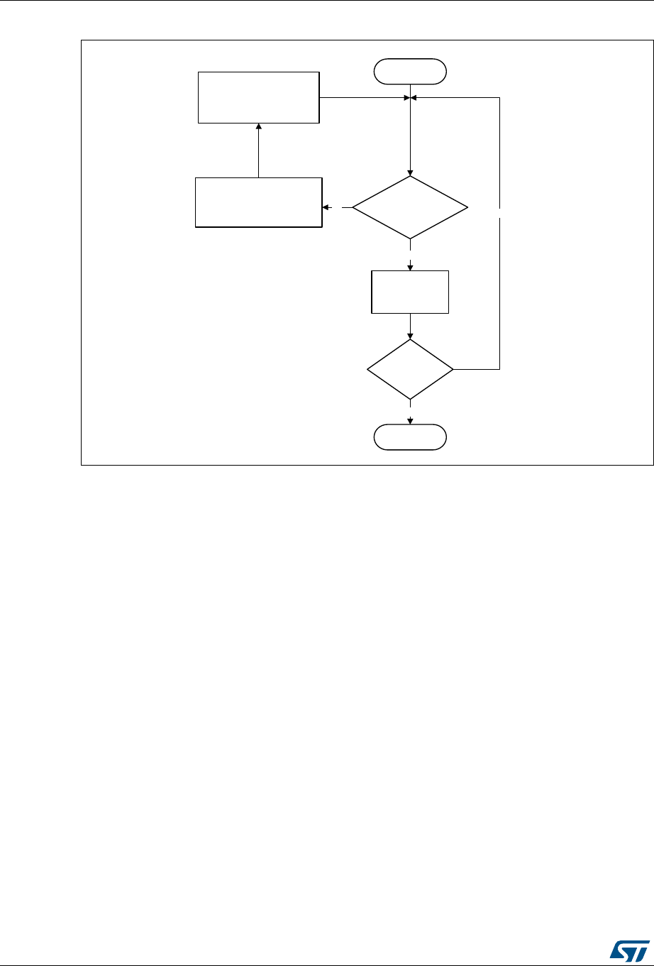
USB on-the-go high-speed (OTG_HS) RM0090
1472/1718 DocID018909 Rev 9
Figure 414. Transmit FIFO write task
•Reading the receive FIFO
The application must ignore all packet statuses other than IN data packet (bx0010).
1 MPS
or LPS FIFO space
available?
Wait for
Write 1 packet
data to
Transmit FIFO
More packets
to send?
Yes
No
No
Read GNPTXSTS/
HPTXFSIZ registers for
available FIFO and
queue spaces
Yes
MPS: Maximum packet size
LPS: Last packet sizetacet
Start
Done
ai15673
TXFELVL or PTXFELVL
interrupt in
OTG_FS_GAHBCFG
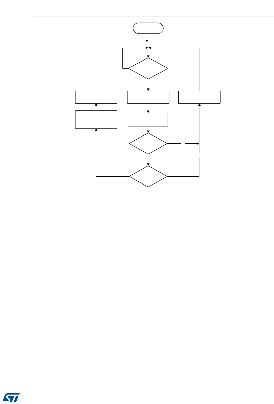
DocID018909 Rev 9 1473/1718
RM0090 USB on-the-go high-speed (OTG_HS)
1523
Figure 415. Receive FIFO read task
•Bulk and control OUT/SETUP transactions
A typical bulk or control OUT/SETUP pipelined transaction-level operation is shown in
Figure 416. See channel 1 (ch_1). Two bulk OUT packets are transmitted. A control
SETUP transaction operates in the same way but has only one packet. The
assumptions are:
– The application is attempting to send two maximum-packet-size packets (transfer
size = 1, 024 bytes).
– The nonperiodic transmit FIFO can hold two packets (128 bytes for FS).
– The nonperiodic request queue depth = 4.
•Normal bulk and control OUT/SETUP operations
The sequence of operations for channel 1 is as follows:
a) Initialize channel 1
b) Write the first packet for channel 1
c) Along with the last DWORD write, the core writes an entry to the nonperiodic
request queue
d) As soon as the nonperiodic queue becomes nonempty, the core attempts to send
an OUT token in the current frame
e) Write the second (last) packet for channel 1
f) The core generates the XFRC interrupt as soon as the last transaction is
completed successfully
g) In response to the XFRC interrupt, de-allocate the channel for other transfers
h) Handling nonACK responses
RXFLVL
interrupt ?
Read the received
packet from the
Receive FIFO
Read
OTG_FS_GRXSTSP
PKTSTS
0b0010?
Yes
Yes
Unmask RXFLVL
interrupt
BCNT > 0?
No
Mask RXFLVL
interrupt
Yes
Unmask RXFLVL
interrupt
No
No
Start
ai15674
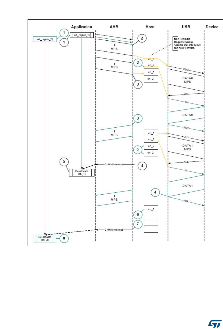
USB on-the-go high-speed (OTG_HS) RM0090
1474/1718 DocID018909 Rev 9
Figure 416. Normal bulk/control OUT/SETUP and bulk/control IN transactions - DMA
mode
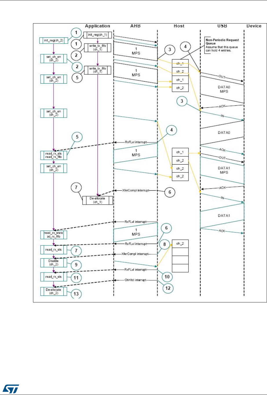
DocID018909 Rev 9 1475/1718
RM0090 USB on-the-go high-speed (OTG_HS)
1523
Figure 417. Normal bulk/control OUT/SETUP and bulk/control IN transactions - Slave
mode
The channel-specific interrupt service routine for bulk and control OUT/SETUP
transactions in Slave mode is shown in the following code samples.
•Interrupt service routine for bulk/control OUT/SETUP and bulk/control IN
transactions
a) Bulk/Control OUT/SETUP
Unmask (NAK/TXERR/STALL/XFRC)
if (XFRC)
{
Reset Error Count

USB on-the-go high-speed (OTG_HS) RM0090
1476/1718 DocID018909 Rev 9
Mask ACK
De-allocate Channel
}
else if (STALL)
{
Transfer Done = 1
Unmask CHH
Disable Channel
}
else if (NAK or TXERR )
{
Rewind Buffer Pointers
Unmask CHH
Disable Channel
if (TXERR)
{
Increment Error Count
Unmask ACK
}
else
{
Reset Error Count
}
}
else if (CHH)
{
Mask CHH
if (Transfer Done or (Error_count == 3))
{
De-allocate Channel
}
else
{
Re-initialize Channel
}
}
else if (ACK)
{
Reset Error Count
Mask ACK
}
The application is expected to write the data packets into the transmit FIFO as and
when the space is available in the transmit FIFO and the Request queue. The
application can make use of the NPTXFE interrupt in OTG_HS_GINTSTS to find the
transmit FIFO space.
b) Bulk/Control IN
Unmask (TXERR/XFRC/BBERR/STALL/DTERR)
if (XFRC)
{
Reset Error Count
Unmask CHH
Disable Channel

DocID018909 Rev 9 1477/1718
RM0090 USB on-the-go high-speed (OTG_HS)
1523
Reset Error Count
Mask ACK
}
else if (TXERR or BBERR or STALL)
{
Unmask CHH
Disable Channel
if (TXERR)
{
Increment Error Count
Unmask ACK
}
}
else if (CHH)
{
Mask CHH
if (Transfer Done or (Error_count == 3))
{
De-allocate Channel
}
else
{
Re-initialize Channel
}
}
else if (ACK)
{
Reset Error Count
Mask ACK
}
else if (DTERR)
{
Reset Error Count
}
The application is expected to write the requests as and when the Request queue
space is available and until the XFRC interrupt is received.
•Bulk and control IN transactions
A typical bulk or control IN pipelined transaction-level operation is shown in Figure 418.
See channel 2 (ch_2). The assumptions are:
– The application is attempting to receive two maximum-packet-size packets
(transfer size = 1 024 bytes).
– The receive FIFO can contain at least one maximum-packet-size packet and two
status DWORDs per packet (72 bytes for FS).
– The nonperiodic request queue depth = 4.
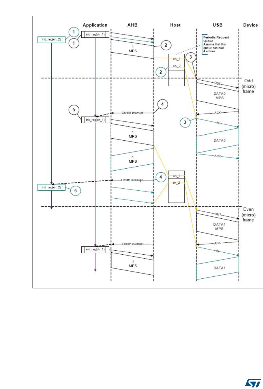
USB on-the-go high-speed (OTG_HS) RM0090
1478/1718 DocID018909 Rev 9
Figure 418. Bulk/control IN transactions - DMA mode
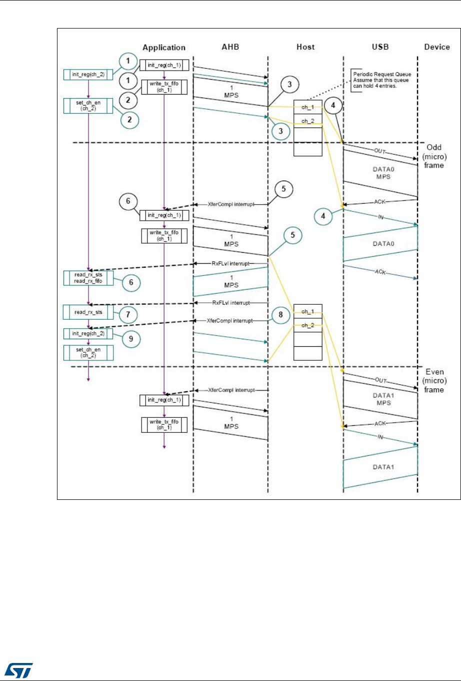
DocID018909 Rev 9 1479/1718
RM0090 USB on-the-go high-speed (OTG_HS)
1523
Figure 419. Bulk/control IN transactions - Slave mode
The sequence of operations is as follows:
a) Initialize channel 2.
b) Set the CHENA bit in HCCHAR2 to write an IN request to the nonperiodic request
queue.
c) The core attempts to send an IN token after completing the current OUT
transaction.
d) The core generates an RXFLVL interrupt as soon as the received packet is written
to the receive FIFO.
e) In response to the RXFLVL interrupt, mask the RXFLVL interrupt and read the
received packet status to determine the number of bytes received, then read the

USB on-the-go high-speed (OTG_HS) RM0090
1480/1718 DocID018909 Rev 9
receive FIFO accordingly. Following this, unmask the RXFLVL interrupt.
f) The core generates the RXFLVL interrupt for the transfer completion status entry
in the receive FIFO.
g) The application must read and ignore the receive packet status when the receive
packet status is not an IN data packet (PKTSTS in GRXSTSR ≠0b0010).
h) The core generates the XFRC interrupt as soon as the receive packet status is
read.
i) In response to the XFRC interrupt, disable the channel and stop writing the
OTG_HS_HCCHAR2 register for further requests. The core writes a channel
disable request to the nonperiodic request queue as soon as the
OTG_HS_HCCHAR2 register is written.
j) The core generates the RXFLVL interrupt as soon as the halt status is written to
the receive FIFO.
k) Read and ignore the receive packet status.
l) The core generates a CHH interrupt as soon as the halt status is popped from the
receive FIFO.
m) In response to the CHH interrupt, de-allocate the channel for other transfers.
n) Handling nonACK responses
•Control transactions in slave mode
Setup, Data, and Status stages of a control transfer must be performed as three
separate transfers. Setup-, Data- or Status-stage OUT transactions are performed
similarly to the bulk OUT transactions explained previously. Data- or Status-stage IN
transactions are performed similarly to the bulk IN transactions explained previously.
For all three stages, the application is expected to set the EPTYP field in
OTG_HS_HCCHAR1 to Control. During the Setup stage, the application is expected to
set the PID field in OTG_HS_HCTSIZ1 to SETUP.
•Interrupt OUT transactions
A typical interrupt OUT operation in Slave mode is shown in Figure 420. The
assumptions are:
– The application is attempting to send one packet in every frame (up to 1 maximum
packet size), starting with the odd frame (transfer size = 1 024 bytes)
– The periodic transmit FIFO can hold one packet (1 KB)
– Periodic request queue depth = 4
The sequence of operations is as follows:
a) Initialize and enable channel 1. The application must set the ODDFRM bit in
OTG_HS_HCCHAR1.
b) Write the first packet for channel 1. For a high-bandwidth interrupt transfer, the
application must write the subsequent packets up to MCNT (maximum number of
packets to be transmitted in the next frame times) before switching to another
channel.
c) Along with the last DWORD write of each packet, the OTG_HS host writes an
entry to the periodic request queue.
d) The OTG_HS host attempts to send an OUT token in the next (odd) frame.
e) The OTG_HS host generates an XFRC interrupt as soon as the last packet is
transmitted successfully.
f) In response to the XFRC interrupt, reinitialize the channel for the next transfer.
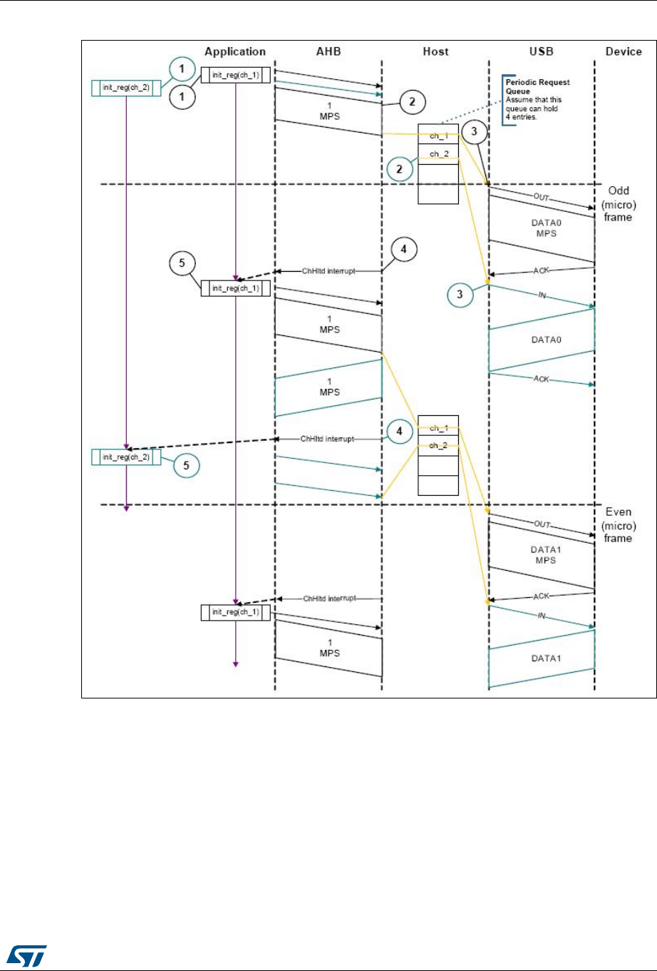
DocID018909 Rev 9 1481/1718
RM0090 USB on-the-go high-speed (OTG_HS)
1523
Figure 420. Normal interrupt OUT/IN transactions - DMA mode
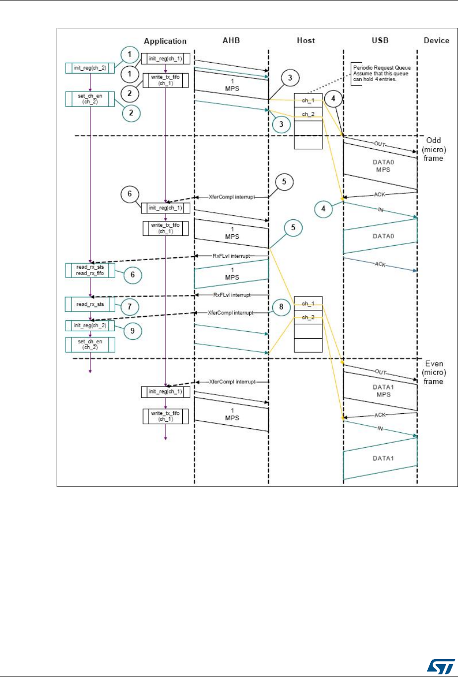
USB on-the-go high-speed (OTG_HS) RM0090
1482/1718 DocID018909 Rev 9
Figure 421. Normal interrupt OUT/IN transactions - Slave mode
•Interrupt service routine for interrupt OUT/IN transactions
a) Interrupt OUT
Unmask (NAK/TXERR/STALL/XFRC/FRMOR)
if (XFRC)
{
Reset Error Count
Mask ACK
De-allocate Channel
}
else
if (STALL or FRMOR)
{

DocID018909 Rev 9 1483/1718
RM0090 USB on-the-go high-speed (OTG_HS)
1523
Mask ACK
Unmask CHH
Disable Channel
if (STALL)
{
Transfer Done = 1
}
}
else
if (NAK or TXERR)
{
Rewind Buffer Pointers
Reset Error Count
Mask ACK
Unmask CHH
Disable Channel
}
else
if (CHH)
{
Mask CHH
if (Transfer Done or (Error_count == 3))
{
De-allocate Channel
}
else
{
Re-initialize Channel (in next b_interval - 1 Frame)
}
}
else
if (ACK)
{
Reset Error Count
Mask ACK
}
The application is expected to write the data packets into the transmit FIFO when the
space is available in the transmit FIFO and the Request queue up to the count
specified in the MCNT field before switching to another channel. The application uses
the NPTXFE interrupt in OTG_HS_GINTSTS to find the transmit FIFO space.
b) Interrupt IN
Unmask (NAK/TXERR/XFRC/BBERR/STALL/FRMOR/DTERR)
if (XFRC)
{
Reset Error Count
Mask ACK
if (OTG_HS_HCTSIZx.PKTCNT == 0)
{
De-allocate Channel
}
else
{

USB on-the-go high-speed (OTG_HS) RM0090
1484/1718 DocID018909 Rev 9
Transfer Done = 1
Unmask CHH
Disable Channel
}
}
else
if (STALL or FRMOR or NAK or DTERR or BBERR)
{
Mask ACK
Unmask CHH
Disable Channel
if (STALL or BBERR)
{
Reset Error Count
Transfer Done = 1
}
else
if (!FRMOR)
{
Reset Error Count
}
}
else
if (TXERR)
{
Increment Error Count
Unmask ACK
Unmask CHH
Disable Channel
}
else
if (CHH)
{
Mask CHH
if (Transfer Done or (Error_count == 3))
{
De-allocate Channel
}
else
Re-initialize Channel (in next b_interval - 1 /Frame)
}
}
else
if (ACK)
{
Reset Error Count
Mask ACK

DocID018909 Rev 9 1485/1718
RM0090 USB on-the-go high-speed (OTG_HS)
1523
}
The application is expected to write the requests for the same channel when the
Request queue space is available up to the count specified in the MCNT field before
switching to another channel (if any).
•Interrupt IN transactions
The assumptions are:
– The application is attempting to receive one packet (up to 1 maximum packet size)
in every frame, starting with odd (transfer size = 1 024 bytes).
– The receive FIFO can hold at least one maximum-packet-size packet and two
status DWORDs per packet (1 031 bytes).
– Periodic request queue depth = 4.
•Normal interrupt IN operation
The sequence of operations is as follows:
a) Initialize channel 2. The application must set the ODDFRM bit in
OTG_HS_HCCHAR2.
b) Set the CHENA bit in OTG_HS_HCCHAR2 to write an IN request to the periodic
request queue. For a high-bandwidth interrupt transfer, the application must write
the OTG_HS_HCCHAR2 register MCNT (maximum number of expected packets
in the next frame times) before switching to another channel.
c) The OTG_HS host writes an IN request to the periodic request queue for each
OTG_HS_HCCHAR2 register write with the CHENA bit set.
d) The OTG_HS host attempts to send an IN token in the next (odd) frame.
e) As soon as the IN packet is received and written to the receive FIFO, the OTG_HS
host generates an RXFLVL interrupt.
f) In response to the RXFLVL interrupt, read the received packet status to determine
the number of bytes received, then read the receive FIFO accordingly. The
application must mask the RXFLVL interrupt before reading the receive FIFO, and
unmask after reading the entire packet.
g) The core generates the RXFLVL interrupt for the transfer completion status entry
in the receive FIFO. The application must read and ignore the receive packet
status when the receive packet status is not an IN data packet (PKTSTS in
GRXSTSR ≠0b0010).
h) The core generates an XFRC interrupt as soon as the receive packet status is
read.
i) In response to the XFRC interrupt, read the PKTCNT field in OTG_HS_HCTSIZ2.
If the PKTCNT bit in OTG_HS_HCTSIZ2 is not equal to 0, disable the channel
before re-initializing the channel for the next transfer, if any). If PKTCNT bit in

USB on-the-go high-speed (OTG_HS) RM0090
1486/1718 DocID018909 Rev 9
OTG_HS_HCTSIZ2 = 0, reinitialize the channel for the next transfer. This time, the
application must reset the ODDFRM bit in OTG_HS_HCCHAR2.
•Isochronous OUT transactions
A typical isochronous OUT operation in Slave mode is shown in Figure 422. The
assumptions are:
– The application is attempting to send one packet every frame (up to 1 maximum
packet size), starting with an odd frame. (transfer size = 1 024 bytes).
– The periodic transmit FIFO can hold one packet (1 KB).
– Periodic request queue depth = 4.
The sequence of operations is as follows:
a) Initialize and enable channel 1. The application must set the ODDFRM bit in
OTG_HS_HCCHAR1.
b) Write the first packet for channel 1. For a high-bandwidth isochronous transfer, the
application must write the subsequent packets up to MCNT (maximum number of
packets to be transmitted in the next frame times before switching to another
channel.
c) Along with the last DWORD write of each packet, the OTG_HS host writes an
entry to the periodic request queue.
d) The OTG_HS host attempts to send the OUT token in the next frame (odd).
e) The OTG_HS host generates the XFRC interrupt as soon as the last packet is
transmitted successfully.
f) In response to the XFRC interrupt, reinitialize the channel for the next transfer.
g) Handling nonACK responses
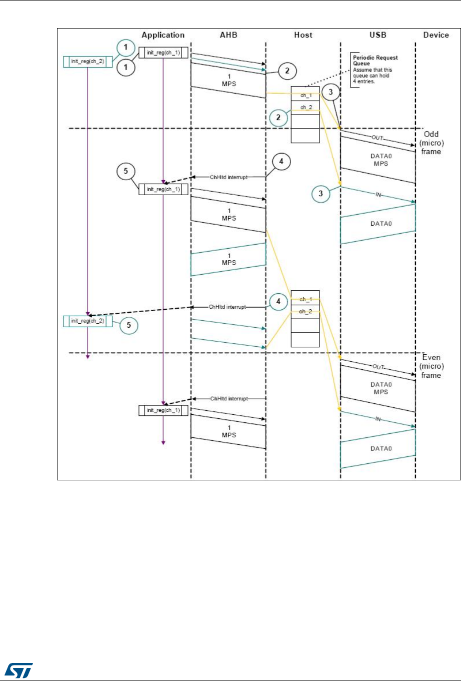
DocID018909 Rev 9 1487/1718
RM0090 USB on-the-go high-speed (OTG_HS)
1523
Figure 422. Normal isochronous OUT/IN transactions - DMA mode
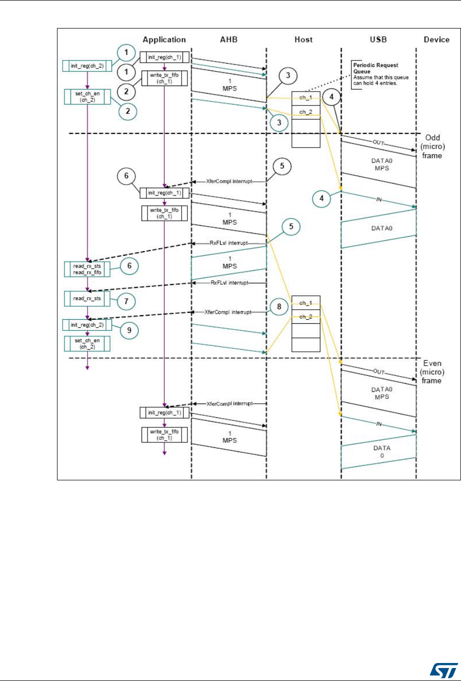
USB on-the-go high-speed (OTG_HS) RM0090
1488/1718 DocID018909 Rev 9
Figure 423. Normal isochronous OUT/IN transactions - Slave mode
•Interrupt service routine for isochronous OUT/IN transactions
Code sample: Isochronous OUT
Unmask (FRMOR/XFRC)
if (XFRC)
{
De-allocate Channel
}
else
if (FRMOR)
{
Unmask CHH
Disable Channel
}

DocID018909 Rev 9 1489/1718
RM0090 USB on-the-go high-speed (OTG_HS)
1523
else
if (CHH)
{
Mask CHH
De-allocate Channel
}
Code sample: Isochronous IN
Unmask (TXERR/XFRC/FRMOR/BBERR)
if (XFRC or FRMOR)
{
if (XFRC and (OTG_HS_HCTSIZx.PKTCNT == 0))
{
Reset Error Count
De-allocate Channel
}
else
{
Unmask CHH
Disable Channel
}
}
else
if (TXERR or BBERR)
{
Increment Error Count
Unmask CHH
Disable Channel
}
else
if (CHH)
{
Mask CHH
if (Transfer Done or (Error_count == 3))
{
De-allocate Channel
}
else
{
Re-initialize Channel
}
}

USB on-the-go high-speed (OTG_HS) RM0090
1490/1718 DocID018909 Rev 9
•Isochronous IN transactions
The assumptions are:
– The application is attempting to receive one packet (up to 1 maximum packet size)
in every frame starting with the next odd frame (transfer size = 1 024 bytes).
– The receive FIFO can hold at least one maximum-packet-size packet and two
status DWORDs per packet (1 031 bytes).
– Periodic request queue depth = 4.
The sequence of operations is as follows:
a) Initialize channel 2. The application must set the ODDFRM bit in
OTG_HS_HCCHAR2.
b) Set the CHENA bit in OTG_HS_HCCHAR2 to write an IN request to the periodic
request queue. For a high-bandwidth isochronous transfer, the application must
write the OTG_HS_HCCHAR2 register MCNT (maximum number of expected
packets in the next frame times) before switching to another channel.
c) The OTG_HS host writes an IN request to the periodic request queue for each
OTG_HS_HCCHAR2 register write with the CHENA bit set.
d) The OTG_HS host attempts to send an IN token in the next odd frame.
e) As soon as the IN packet is received and written to the receive FIFO, the OTG_HS
host generates an RXFLVL interrupt.
f) In response to the RXFLVL interrupt, read the received packet status to determine
the number of bytes received, then read the receive FIFO accordingly. The
application must mask the RXFLVL interrupt before reading the receive FIFO, and
unmask it after reading the entire packet.
g) The core generates an RXFLVL interrupt for the transfer completion status entry in
the receive FIFO. This time, the application must read and ignore the receive
packet status when the receive packet status is not an IN data packet (PKTSTS bit
in OTG_HS_GRXSTSR ≠0b0010).
h) The core generates an XFRC interrupt as soon as the receive packet status is
read.
i) In response to the XFRC interrupt, read the PKTCNT field in OTG_HS_HCTSIZ2.
If PKTCNT≠0 in OTG_HS_HCTSIZ2, disable the channel before re-initializing the
channel for the next transfer, if any. If PKTCNT = 0 in OTG_HS_HCTSIZ2,
reinitialize the channel for the next transfer. This time, the application must reset
the ODDFRM bit in OTG_HS_HCCHAR2.
•Selecting the queue depth
Choose the periodic and nonperiodic request queue depths carefully to match the
number of periodic/nonperiodic endpoints accessed.
The nonperiodic request queue depth affects the performance of nonperiodic transfers.
The deeper the queue (along with sufficient FIFO size), the more often the core is able
to pipeline nonperiodic transfers. If the queue size is small, the core is able to put in
new requests only when the queue space is freed up.
The core’s periodic request queue depth is critical to perform periodic transfers as
scheduled. Select the periodic queue depth, based on the number of periodic transfers
scheduled in a micro-frame. In Slave mode, however, the application must also take
into account the disable entry that must be put into the queue. So, if there are two
nonhigh-bandwidth periodic endpoints, the periodic request queue depth must be at
least 4. If at least one high-bandwidth endpoint is supported, the queue depth must be

DocID018909 Rev 9 1491/1718
RM0090 USB on-the-go high-speed (OTG_HS)
1523
8. If the periodic request queue depth is smaller than the periodic transfers scheduled
in a micro-frame, a frame overrun condition occurs.
•Handling babble conditions
OTG_HS controller handles two cases of babble: packet babble and port babble.
Packet babble occurs if the device sends more data than the maximum packet size for
the channel. Port babble occurs if the core continues to receive data from the device at
EOF2 (the end of frame 2, which is very close to SOF).
When OTG_HS controller detects a packet babble, it stops writing data into the Rx
buffer and waits for the end of packet (EOP). When it detects an EOP, it flushes already
written data in the Rx buffer and generates a Babble interrupt to the application.
When OTG_HS controller detects a port babble, it flushes the RxFIFO and disables the
port. The core then generates a Port disabled interrupt (HPRTINT in
OTG_HS_GINTSTS, PENCHNG in OTG_HS_HPRT). On receiving this interrupt, the
application must determine that this is not due to an overcurrent condition (another
cause of the Port Disabled interrupt) by checking POCA in OTG_HS_HPRT, then
perform a soft reset. The core does not send any more tokens after it has detected a
port babble condition.
•Bulk and control OUT/SETUP transactions in DMA mode
The sequence of operations is as follows:
a) Initialize and enable channel 1 as explained in Section : Channel initialization.
b) The HS_OTG host starts fetching the first packet as soon as the channel is
enabled. For internal DMA mode, the OTG_HS host uses the programmed DMA
address to fetch the packet.
c) After fetching the last DWORD of the second (last) packet, the OTG_HS host
masks channel 1 internally for further arbitration.
d) The HS_OTG host generates a CHH interrupt as soon as the last packet is sent.
e) In response to the CHH interrupt, de-allocate the channel for other transfers.
•NAK and NYET handling with internal DMA
a) The OTG_HS host sends a bulk OUT transaction.
b) The device responds with NAK or NYET.
c) If the application has unmasked NAK or NYET, the core generates the
corresponding interrupt(s) to the application. The application is not required to

USB on-the-go high-speed (OTG_HS) RM0090
1492/1718 DocID018909 Rev 9
service these interrupts, since the core takes care of rewinding the buffer pointers
and re-initializing the Channel without application intervention.
d) The core automatically issues a ping token.
e) When the device returns an ACK, the core continues with the transfer. Optionally,
the application can utilize these interrupts, in which case the NAK or NYET
interrupt is masked by the application.
The core does not generate a separate interrupt when NAK or NYET is received by the
host functionality.
•Bulk and control IN transactions in DMA mode
The sequence of operations is as follows:
a) Initialize and enable the used channel (channel x) as explained in Section :
Channel initialization.
b) The OTG_HS host writes an IN request to the request queue as soon as the
channel receives the grant from the arbiter (arbitration is performed in a round-
robin fashion).
c) The OTG_HS host starts writing the received data to the system memory as soon
as the last byte is received with no errors.
d) When the last packet is received, the OTG_HS host sets an internal flag to remove
any extra IN requests from the request queue.
e) The OTG_HS host flushes the extra requests.
f) The final request to disable channel x is written to the request queue. At this point,
channel 2 is internally masked for further arbitration.
g) The OTG_HS host generates the CHH interrupt as soon as the disable request
comes to the top of the queue.
h) In response to the CHH interrupt, de-allocate the channel for other transfers.
•Interrupt OUT transactions in DMA mode
a) Initialize and enable channel x as explained in Section : Channel initialization.
b) The OTG_HS host starts fetching the first packet as soon the channel is enabled
and writes the OUT request along with the last DWORD fetch. In high-bandwidth

DocID018909 Rev 9 1493/1718
RM0090 USB on-the-go high-speed (OTG_HS)
1523
transfers, the HS_OTG host continues fetching the next packet (up to the value
specified in the MC field) before switching to the next channel.
c) The OTG_HS host attempts to send the OUT token at the beginning of the next
odd frame/micro-frame.
d) After successfully transmitting the packet, the OTG_HS host generates a CHH
interrupt.
e) In response to the CHH interrupt, reinitialize the channel for the next transfer.
•Interrupt IN transactions in DMA mode
The sequence of operations (channelx) is as follows:
a) Initialize and enable channel x as explained in Section : Channel initialization.
b) The OTG_HS host writes an IN request to the request queue as soon as the
channel x gets the grant from the arbiter (round-robin with fairness). In high-
bandwidth transfers, the OTG_HS host writes consecutive writes up to MC times.
c) The OTG_HS host attempts to send an IN token at the beginning of the next (odd)
frame/micro-frame.
d) As soon the packet is received and written to the receive FIFO, the OTG_HS host
generates a CHH interrupt.
e) In response to the CHH interrupt, reinitialize the channel for the next transfer.
•Isochronous OUT transactions in DMA mode
a) Initialize and enable channel x as explained in Section : Channel initialization.
b) The OTG_HS host starts fetching the first packet as soon as the channel is
enabled, and writes the OUT request along with the last DWORD fetch. In high-
bandwidth transfers, the OTG_HS host continues fetching the next packet (up to
the value specified in the MC field) before switching to the next channel.
c) The OTG_HS host attempts to send an OUT token at the beginning of the next
(odd) frame/micro-frame.
d) After successfully transmitting the packet, the HS_OTG host generates a CHH
interrupt.
e) In response to the CHH interrupt, reinitialize the channel for the next transfer.
•Isochronous IN transactions in DMA mode
The sequence of operations ((channel x) is as follows:
a) Initialize and enable channel x as explained in Section : Channel initialization.
b) The OTG_HS host writes an IN request to the request queue as soon as the
channel x gets the grant from the arbiter (round-robin with fairness). In high-

USB on-the-go high-speed (OTG_HS) RM0090
1494/1718 DocID018909 Rev 9
bandwidth transfers, the OTG_HS host performs consecutive write operations up
to MC times.
c) The OTG_HS host attempts to send an IN token at the beginning of the next (odd)
frame/micro-frame.
d) As soon the packet is received and written to the receive FIFO, the OTG_HS host
generates a CHH interrupt.
e) In response to the CHH interrupt, reinitialize the channel for the next transfer.
•Bulk and control OUT/SETUP split transactions in DMA mode
The sequence of operations in (channel x) is as follows:
a) Initialize and enable channel x for start split as explained in Section : Channel
initialization.
b) The OTG_HS host starts fetching the first packet as soon the channel is enabled
and writes the OUT request along with the last DWORD fetch.
c) After successfully transmitting start split, the OTG_HS host generates the CHH
interrupt.
d) In response to the CHH interrupt, set the COMPLSPLT bit in HCSPLT1 to send the
complete split.
e) After successfully transmitting complete split, the OTG_HS host generates the
CHH interrupt.
f) In response to the CHH interrupt, de-allocate the channel.
•Bulk/Control IN split transactions in DMA mode
The sequence of operations (channel x) is as follows:
a) Initialize and enable channel x as explained in Section : Channel initialization.
b) The OTG_HS host writes the start split request to the nonperiodic request after
getting the grant from the arbiter. The OTG_HS host masks the channel x
internally for the arbitration after writing the request.
c) As soon as the IN token is transmitted, the OTG_HS host generates the CHH
interrupt.
d) In response to the CHH interrupt, set the COMPLSPLT bit in HCSPLT2 and re-
enable the channel to send the complete split token. This unmasks channel x for
arbitration.
e) The OTG_HS host writes the complete split request to the nonperiodic request
after receiving the grant from the arbiter.
f) The OTG_HS host starts writing the packet to the system memory after receiving
the packet successfully.
g) As soon as the received packet is written to the system memory, the OTG_HS
host generates a CHH interrupt.
h) In response to the CHH interrupt, de-allocate the channel.
•Interrupt OUT split transactions in DMA mode
The sequence of operations in (channel x) is as follows:
a) Initialize and enable channel 1 for start split as explained in Section : Channel
initialization. The application must set the ODDFRM bit in HCCHAR1.
b) The HS_OTG host starts reading the packet.
c) The HS_OTG host attempts to send the start split transaction.
d) After successfully transmitting the start split, the OTG_HS host generates the

DocID018909 Rev 9 1495/1718
RM0090 USB on-the-go high-speed (OTG_HS)
1523
CHH interrupt.
e) In response to the CHH interrupt, set the COMPLSPLT bit in HCSPLT1 to send the
complete split.
f) After successfully completing the complete split transaction, the OTG_HS host
generates the CHH interrupt.
g) In response to CHH interrupt, de-allocate the channel.
•Interrupt IN split transactions in DMA mode
The sequence of operations in (channel x) is as follows:
a) Initialize and enable channel x for start split as explained in Section : Channel
initialization.
b) The OTG_HS host writes an IN request to the request queue as soon as channel
x receives the grant from the arbiter.
c) The OTG_HS host attempts to send the start split IN token at the beginning of the
next odd micro-frame.
d) The OTG_HS host generates the CHH interrupt after successfully transmitting the
start split IN token.
e) In response to the CHH interrupt, set the COMPLSPLT bit in HCSPLT2 to send the
complete split.
f) As soon as the packet is received successfully, the OTG_HS host starts writing the
data to the system memory.
g) The OTG_HS host generates the CHH interrupt after transferring the received
data to the system memory.
h) In response to the CHH interrupt, de-allocate or reinitialize the channel for the next
start split.
•Isochronous OUT split transactions in DMA mode
The sequence of operations (channel x) is as follows:
a) Initialize and enable channel x for start split (begin) as explained in Section :
Channel initialization. The application must set the ODDFRM bit in HCCHAR1.
Program the MPS field.
b) The HS_OTG host starts reading the packet.
c) After successfully transmitting the start split (begin), the HS_OTG host generates
the CHH interrupt.
d) In response to the CHH interrupt, reinitialize the registers to send the start split
(end).
e) After successfully transmitting the start split (end), the OTG_HS host generates a
CHH interrupt.
f) In response to the CHH interrupt, de-allocate the channel.
•Isochronous IN split transactions in DMA mode
The sequence of operations (channel x) is as follows:
a) Initialize and enable channel x for start split as explained in Section : Channel
initialization.
b) The OTG_HS host writes an IN request to the request queue as soon as channel
x receives the grant from the arbiter.
c) The OTG_HS host attempts to send the start split IN token at the beginning of the
next odd micro-frame.

USB on-the-go high-speed (OTG_HS) RM0090
1496/1718 DocID018909 Rev 9
d) The OTG_HS host generates the CHH interrupt after successfully transmitting the
start split IN token.
e) In response to the CHH interrupt, set the COMPLSPLT bit in HCSPLT2 to send the
complete split.
f) As soon as the packet is received successfully, the OTG_HS host starts writing the
data to the system memory.
g) The OTG_HS host generates the CHH interrupt after transferring the received
data to the system memory. In response to the CHH interrupt, de-allocate the
channel or reinitialize the channel for the next start split.
35.13.6 Device programming model
Endpoint initialization on USB reset
1. Set the NAK bit for all OUT endpoints
– SNAK = 1 in OTG_HS_DOEPCTLx (for all OUT endpoints)
2. Unmask the following interrupt bits
– INEP0 = 1 in OTG_HS_DAINTMSK (control 0 IN endpoint)
– OUTEP0 = 1 in OTG_HS_DAINTMSK (control 0 OUT endpoint)
–STUP=1 in DOEPMSK
– XFRC = 1 in DOEPMSK
– XFRC = 1 in DIEPMSK
– TOC = 1 in DIEPMSK
3. Set up the Data FIFO RAM for each of the FIFOs
– Program the OTG_HS_GRXFSIZ register, to be able to receive control OUT data
and setup data. If thresholding is not enabled, at a minimum, this must be equal to
1 max packet size of control endpoint 0 + 2 DWORDs (for the status of the control
OUT data packet) + 10 DWORDs (for setup packets).
– Program the OTG_HS_TX0FSIZ register (depending on the FIFO number
chosen) to be able to transmit control IN data. At a minimum, this must be equal to
1 max packet size of control endpoint 0.
4. Program the following fields in the endpoint-specific registers for control OUT endpoint
0 to receive a SETUP packet
– STUPCNT = 3 in OTG_HS_DOEPTSIZ0 (to receive up to 3 back-to-back SETUP
packets)
5. In DMA mode, the DOEPDMA0 register should have a valid memory address to store
any SETUP packets received.
At this point, all initialization required to receive SETUP packets is done.

DocID018909 Rev 9 1497/1718
RM0090 USB on-the-go high-speed (OTG_HS)
1523
Endpoint initialization on enumeration completion
1. On the Enumeration Done interrupt (ENUMDNE in OTG_HS_GINTSTS), read the
OTG_HS_DSTS register to determine the enumeration speed.
2. Program the MPSIZ field in OTG_HS_DIEPCTL0 to set the maximum packet size. This
step configures control endpoint 0. The maximum packet size for a control endpoint
depends on the enumeration speed.
3. In DMA mode, program the DOEPCTL0 register to enable control OUT endpoint 0, to
receive a SETUP packet.
– EPENA bit in DOEPCTL0 = 1
At this point, the device is ready to receive SOF packets and is configured to perform control
transfers on control endpoint 0.
Endpoint initialization on SetAddress command
This section describes what the application must do when it receives a SetAddress
command in a SETUP packet.
1. Program the OTG_HS_DCFG register with the device address received in the
SetAddress command
1. Program the core to send out a status IN packet
Endpoint initialization on SetConfiguration/SetInterface command
This section describes what the application must do when it receives a SetConfiguration or
SetInterface command in a SETUP packet.
1. When a SetConfiguration command is received, the application must program the
endpoint registers to configure them with the characteristics of the valid endpoints in
the new configuration.
2. When a SetInterface command is received, the application must program the endpoint
registers of the endpoints affected by this command.
3. Some endpoints that were active in the prior configuration or alternate setting are not
valid in the new configuration or alternate setting. These invalid endpoints must be
deactivated.
4. Unmask the interrupt for each active endpoint and mask the interrupts for all inactive
endpoints in the OTG_HS_DAINTMSK register.
5. Set up the Data FIFO RAM for each FIFO.
6. After all required endpoints are configured; the application must program the core to
send a status IN packet.
At this point, the device core is configured to receive and transmit any type of data packet.
Endpoint activation
This section describes the steps required to activate a device endpoint or to configure an
existing device endpoint to a new type.

USB on-the-go high-speed (OTG_HS) RM0090
1498/1718 DocID018909 Rev 9
1. Program the characteristics of the required endpoint into the following fields of the
OTG_HS_DIEPCTLx register (for IN or bidirectional endpoints) or the
OTG_HS_DOEPCTLx register (for OUT or bidirectional endpoints).
– Maximum packet size
– USB active endpoint = 1
– Endpoint start data toggle (for interrupt and bulk endpoints)
– Endpoint type
– TxFIFO number
2. Once the endpoint is activated, the core starts decoding the tokens addressed to that
endpoint and sends out a valid handshake for each valid token received for the
endpoint.
Endpoint deactivation
This section describes the steps required to deactivate an existing endpoint.
1. In the endpoint to be deactivated, clear the USB active endpoint bit in the
OTG_HS_DIEPCTLx register (for IN or bidirectional endpoints) or the
OTG_HS_DOEPCTLx register (for OUT or bidirectional endpoints).
2. Once the endpoint is deactivated, the core ignores tokens addressed to that endpoint,
which results in a timeout on the USB.
Note: The application must meet the following conditions to set up the device core to handle
traffic:
NPTXFEM and RXFLVLM in GINTMSK must be cleared.
35.13.7 Operational model
SETUP and OUT data transfers
This section describes the internal data flow and application-level operations during data
OUT transfers and SETUP transactions.
•Packet read
This section describes how to read packets (OUT data and SETUP packets) from the
receive FIFO in Slave mode.
1. On catching an RXFLVL interrupt (OTG_HS_GINTSTS register), the application must
read the Receive status pop register (OTG_HS_GRXSTSP).
2. The application can mask the RXFLVL interrupt (in OTG_HS_GINTSTS) by writing to
RXFLVL = 0 (in GINTMSK), until it has read the packet from the receive FIFO.
3. If the received packet’s byte count is not 0, the byte count amount of data is popped
from the receive Data FIFO and stored in memory. If the received packet byte count is
0, no data is popped from the receive data FIFO.
4. The receive FIFO’s packet status readout indicates one of the following:
a) Global OUT NAK pattern:
PKTSTS = Global OUT NAK, BCNT = 0x000, EPNUM = Don’t Care (0x0),
DPID = Don’t Care (0b00).
These data indicate that the global OUT NAK bit has taken effect.
b) SETUP packet pattern:
PKTSTS = SETUP, BCNT = 0x008, EPNUM = Control EP Num, DPID = D0.
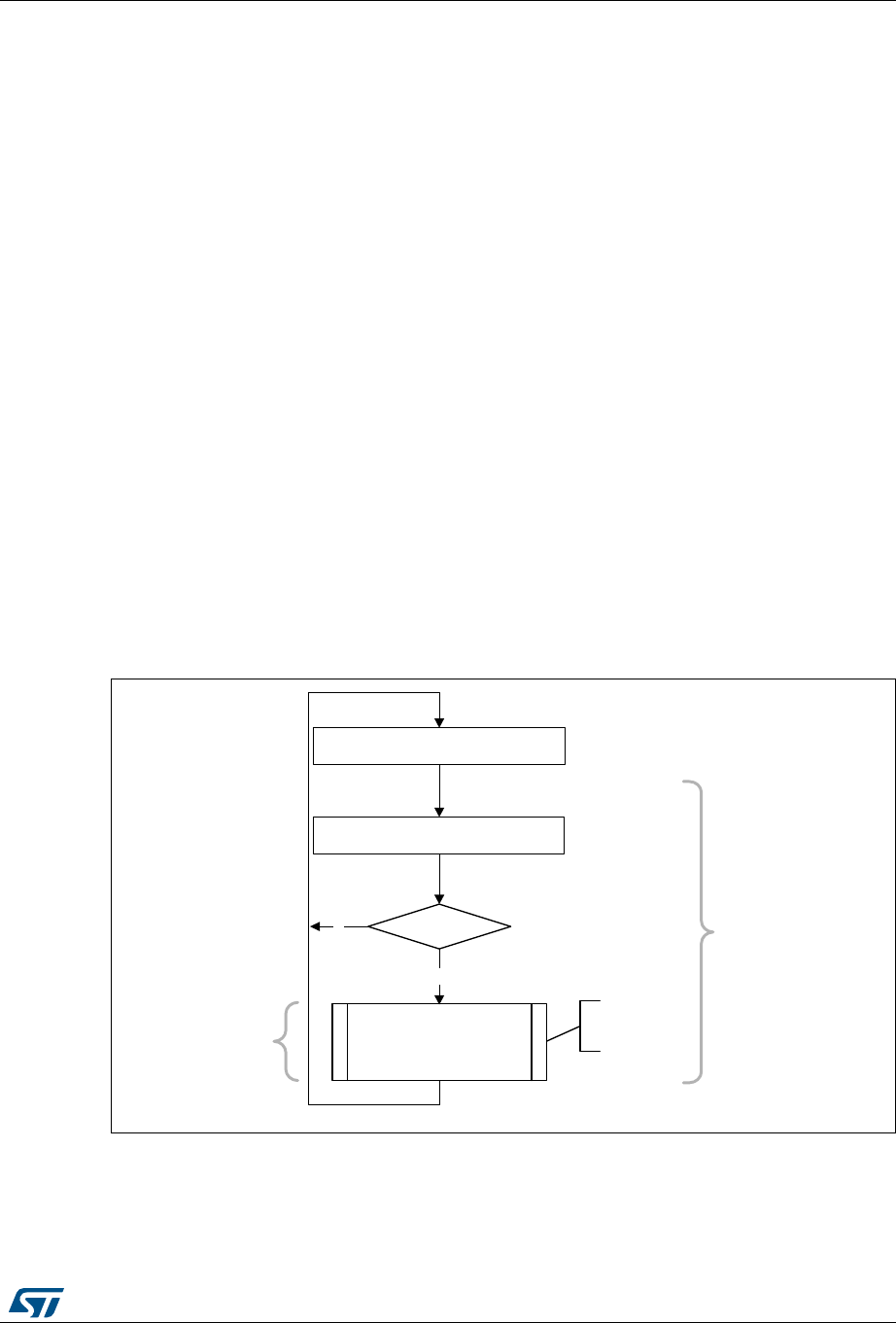
DocID018909 Rev 9 1499/1718
RM0090 USB on-the-go high-speed (OTG_HS)
1523
These data indicate that a SETUP packet for the specified endpoint is now
available for reading from the receive FIFO.
c) Setup stage done pattern:
PKTSTS = Setup Stage Done, BCNT = 0x0, EPNUM = Control EP Num,
DPID = Don’t Care (0b00).
These data indicate that the Setup stage for the specified endpoint has completed
and the Data stage has started. After this entry is popped from the receive FIFO,
the core asserts a Setup interrupt on the specified control OUT endpoint.
d) Data OUT packet pattern:
PKTSTS = DataOUT, BCNT = size of the received data OUT packet (0 ≤ BCNT
≤ 1 024), EPNUM = EPNUM on which the packet was received, DPID = Actual
Data PID.
e) Data transfer completed pattern:
PKTSTS = Data OUT Transfer Done, BCNT = 0x0, EPNUM = OUT EP Num
on which the data transfer is complete, DPID = Don’t Care (0b00).
These data indicate that an OUT data transfer for the specified OUT endpoint has
completed. After this entry is popped from the receive FIFO, the core asserts a
Transfer Completed interrupt on the specified OUT endpoint.
5. After the data payload is popped from the receive FIFO, the RXFLVL interrupt
(OTG_HS_GINTSTS) must be unmasked.
6. Steps 1–5 are repeated every time the application detects assertion of the interrupt line
due to RXFLVL in OTG_HS_GINTSTS. Reading an empty receive FIFO can result in
undefined core behavior.
Figure 424 provides a flowchart of the above procedure.
Figure 424. Receive FIFO packet read in slave mode
•SETUP transactions
This section describes how the core handles SETUP packets and the application’s
sequence for handling SETUP transactions.
•Application requirements
dword_cnt =
BCNT[11:2] +C
(BCNT[1]
| BCNT[1])
rcv_out_pkt()
rd_data = rd_reg (OTG_FS_GRXSTSP);
mem[0:dword_cnt-1] =
rd_rxfifo(rd_data.EPNUM,
dword_cnt)
N
rd_data.BCNT = 0
wait until RXFLVL in OTG_FS_GINTSTSG
packet
store in
memory
Y
ai15677

USB on-the-go high-speed (OTG_HS) RM0090
1500/1718 DocID018909 Rev 9
1. To receive a SETUP packet, the STUPCNT field (OTG_HS_DOEPTSIZx) in a control
OUT endpoint must be programmed to a nonzero value. When the application
programs the STUPCNT field to a nonzero value, the core receives SETUP packets
and writes them to the receive FIFO, irrespective of the NAK status and EPENA bit
setting in OTG_HS_DOEPCTLx. The STUPCNT field is decremented every time the
control endpoint receives a SETUP packet. If the STUPCNT field is not programmed to
a proper value before receiving a SETUP packet, the core still receives the SETUP
packet and decrements the STUPCNT field, but the application may not be able to
determine the correct number of SETUP packets received in the Setup stage of a
control transfer.
– STUPCNT = 3 in OTG_HS_DOEPTSIZx
2. The application must always allocate some extra space in the Receive data FIFO, to be
able to receive up to three SETUP packets on a control endpoint.
– The space to be reserved is 10 DWORDs. Three DWORDs are required for the
first SETUP packet, 1 DWORD is required for the Setup stage done DWORD and
6 DWORDs are required to store two extra SETUP packets among all control
endpoints.
– 3 DWORDs per SETUP packet are required to store 8 bytes of SETUP data and 4
bytes of SETUP status (Setup packet pattern). The core reserves this space in the
receive data.
– FIFO to write SETUP data only, and never uses this space for data packets.
3. The application must read the 2 DWORDs of the SETUP packet from the receive FIFO.
4. The application must read and discard the Setup stage done DWORD from the receive
FIFO.
•Internal data flow
5. When a SETUP packet is received, the core writes the received data to the receive
FIFO, without checking for available space in the receive FIFO and irrespective of the
endpoint’s NAK and STALL bit settings.
– The core internally sets the IN NAK and OUT NAK bits for the control IN/OUT
endpoints on which the SETUP packet was received.
6. For every SETUP packet received on the USB, 3 DWORDs of data are written to the
receive FIFO, and the STUPCNT field is decremented by 1.
– The first DWORD contains control information used internally by the core
– The second DWORD contains the first 4 bytes of the SETUP command
– The third DWORD contains the last 4 bytes of the SETUP command
7. When the Setup stage changes to a Data IN/OUT stage, the core writes an entry
(Setup stage done DWORD) to the receive FIFO, indicating the completion of the
Setup stage.
8. On the AHB side, SETUP packets are emptied by the application.
9. When the application pops the Setup stage done DWORD from the receive FIFO, the
core interrupts the application with an STUP interrupt (OTG_HS_DOEPINTx),
indicating it can process the received SETUP packet.
– The core clears the endpoint enable bit for control OUT endpoints.
•Application programming sequence
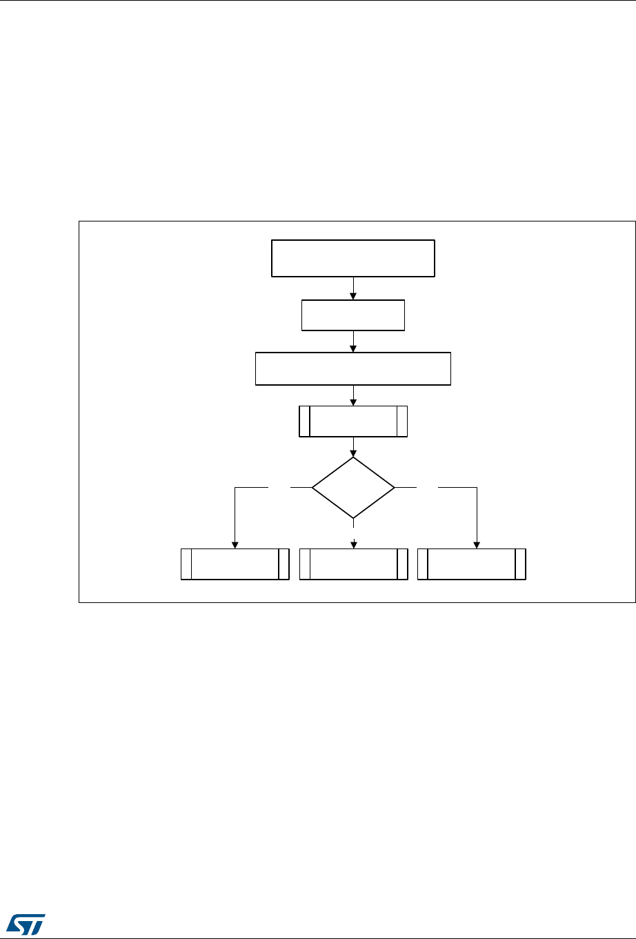
DocID018909 Rev 9 1501/1718
RM0090 USB on-the-go high-speed (OTG_HS)
1523
1. Program the OTG_HS_DOEPTSIZx register.
– STUPCNT =3
2. Wait for the RXFLVL interrupt (OTG_HS_GINTSTS) and empty the data packets from
the receive FIFO.
3. Assertion of the STUP interrupt (OTG_HS_DOEPINTx) marks a successful completion
of the SETUP Data Transfer.
– On this interrupt, the application must read the OTG_HS_DOEPTSIZx register to
determine the number of SETUP packets received and process the last received
SETUP packet.
Figure 425. Processing a SETUP packet
•Handling more than three back-to-back SETUP packets
Per the USB 2.0 specification, normally, during a SETUP packet error, a host does not send
more than three back-to-back SETUP packets to the same endpoint. However, the USB 2.0
specification does not limit the number of back-to-back SETUP packets a host can send to
the same endpoint. When this condition occurs, the OTG_HS controller generates an
interrupt (B2BSTUP in OTG_HS_DOEPINTx).
•Setting the global OUT NAK
Internal data flow:
1. When the application sets the Global OUT NAK (SGONAK bit in OTG_HS_DCTL), the
core stops writing data, except SETUP packets, to the receive FIFO. Irrespective of the
Wait for STUP in OTG_FS_DOEPINTx
rem_supcnt =
rd_reg(DOEPTSIZx)
setup_cmd[31:0] = mem[4 – 2 * rem_supcnt]
setup_cmd[63:32] = mem[5 – 2 * rem_supcnt]
ctrl-rd/wr/2 stage
Find setup cmd type
Write
2-stage
Read
setup_np_in_pkt
Status IN phase
rcv_out_pkt
Data OUT phase
setup_np_in_pkt
Data IN phase
ai15678

USB on-the-go high-speed (OTG_HS) RM0090
1502/1718 DocID018909 Rev 9
space availability in the receive FIFO, nonisochronous OUT tokens receive a NAK
handshake response, and the core ignores isochronous OUT data packets
2. The core writes the Global OUT NAK pattern to the receive FIFO. The application must
reserve enough receive FIFO space to write this data pattern.
3. When the application pops the Global OUT NAK pattern DWORD from the receive
FIFO, the core sets the GONAKEFF interrupt (OTG_HS_GINTSTS).
4. Once the application detects this interrupt, it can assume that the core is in Global OUT
NAK mode. The application can clear this interrupt by clearing the SGONAK bit in
OTG_HS_DCTL.
Application programming sequence
1. To stop receiving any kind of data in the receive FIFO, the application must set the
Global OUT NAK bit by programming the following field:
– SGONAK = 1 in OTG_HS_DCTL
2. Wait for the assertion of the GONAKEFF interrupt in OTG_HS_GINTSTS. When
asserted, this interrupt indicates that the core has stopped receiving any type of data
except SETUP packets.
3. The application can receive valid OUT packets after it has set SGONAK in
OTG_HS_DCTL and before the core asserts the GONAKEFF interrupt
(OTG_HS_GINTSTS).
4. The application can temporarily mask this interrupt by writing to the GINAKEFFM bit in
GINTMSK.
– GINAKEFFM = 0 in GINTMSK
5. Whenever the application is ready to exit the Global OUT NAK mode, it must clear the
SGONAK bit in OTG_HS_DCTL. This also clears the GONAKEFF interrupt
(OTG_HS_GINTSTS).
– OTG_HS_DCTL = 1 in CGONAK
6. If the application has masked this interrupt earlier, it must be unmasked as follows:
– GINAKEFFM = 1 in GINTMSK
•Disabling an OUT endpoint
The application must use this sequence to disable an OUT endpoint that it has enabled.
Application programming sequence:

DocID018909 Rev 9 1503/1718
RM0090 USB on-the-go high-speed (OTG_HS)
1523
1. Before disabling any OUT endpoint, the application must enable Global OUT NAK
mode in the core.
– SGONAK = 1 in OTG_HS_DCTL
2. Wait for the GONAKEFF interrupt (OTG_HS_GINTSTS)
3. Disable the required OUT endpoint by programming the following fields:
– EPDIS = 1 in OTG_HS_DOEPCTLx
– SNAK = 1 in OTG_HS_DOEPCTLx
4. Wait for the EPDISD interrupt (OTG_HS_DOEPINTx), which indicates that the OUT
endpoint is completely disabled. When the EPDISD interrupt is asserted, the core also
clears the following bits:
– EPDIS = 0 in OTG_HS_DOEPCTLx
– EPENA = 0 in OTG_HS_DOEPCTLx
5. The application must clear the Global OUT NAK bit to start receiving data from other
nondisabled OUT endpoints.
– SGONAK = 0 in OTG_HS_DCTL
•Generic nonisochronous OUT data transfers
This section describes a regular nonisochronous OUT data transfer (control, bulk, or
interrupt).
Application requirements:
1. Before setting up an OUT transfer, the application must allocate a buffer in the memory
to accommodate all data to be received as part of the OUT transfer.
2. For OUT transfers, the transfer size field in the endpoint’s transfer size register must be
a multiple of the maximum packet size of the endpoint, adjusted to the DWORD
boundary.
– transfer size[EPNUM] = n × (MPSIZ[EPNUM] + 4 – (MPSIZ[EPNUM] mod 4))
– packet count[EPNUM] = n
–n > 0
3. On any OUT endpoint interrupt, the application must read the endpoint’s transfer size
register to calculate the size of the payload in the memory. The received payload size
can be less than the programmed transfer size.
– Payload size in memory = application programmed initial transfer size – core
updated final transfer size
– Number of USB packets in which this payload was received = application
programmed initial packet count – core updated final packet count
Internal data flow:
1. The application must set the transfer size and packet count fields in the endpoint-
specific registers, clear the NAK bit, and enable the endpoint to receive the data.
2. Once the NAK bit is cleared, the core starts receiving data and writes it to the receive
FIFO, as long as there is space in the receive FIFO. For every data packet received on
the USB, the data packet and its status are written to the receive FIFO. Every packet

USB on-the-go high-speed (OTG_HS) RM0090
1504/1718 DocID018909 Rev 9
(maximum packet size or short packet) written to the receive FIFO decrements the
packet count field for that endpoint by 1.
– OUT data packets received with bad data CRC are flushed from the receive FIFO
automatically.
– After sending an ACK for the packet on the USB, the core discards
nonisochronous OUT data packets that the host, which cannot detect the ACK, re-
sends. The application does not detect multiple back-to-back data OUT packets
on the same endpoint with the same data PID. In this case the packet count is not
decremented.
– If there is no space in the receive FIFO, isochronous or nonisochronous data
packets are ignored and not written to the receive FIFO. Additionally,
nonisochronous OUT tokens receive a NAK handshake reply.
– In all the above three cases, the packet count is not decremented because no data
are written to the receive FIFO.
3. When the packet count becomes 0 or when a short packet is received on the endpoint,
the NAK bit for that endpoint is set. Once the NAK bit is set, the isochronous or
nonisochronous data packets are ignored and not written to the receive FIFO, and
nonisochronous OUT tokens receive a NAK handshake reply.
4. After the data are written to the receive FIFO, the application reads the data from the
receive FIFO and writes it to external memory, one packet at a time per endpoint.
5. At the end of every packet write on the AHB to external memory, the transfer size for
the endpoint is decremented by the size of the written packet.
6. The OUT data transfer completed pattern for an OUT endpoint is written to the receive
FIFO on one of the following conditions:
– The transfer size is 0 and the packet count is 0
– The last OUT data packet written to the receive FIFO is a short packet
(0 ≤ packet size < maximum packet size)
7. When either the application pops this entry (OUT data transfer completed), a transfer
completed interrupt is generated for the endpoint and the endpoint enable is cleared.
Application programming sequence:
1. Program the OTG_HS_DOEPTSIZx register for the transfer size and the
corresponding packet count.
2. Program the OTG_HS_DOEPCTLx register with the endpoint characteristics, and set
the EPENA and CNAK bits.
– EPENA = 1 in OTG_HS_DOEPCTLx
– CNAK = 1 in OTG_HS_DOEPCTLx
3. Wait for the RXFLVL interrupt (in OTG_HS_GINTSTS) and empty the data packets
from the receive FIFO.
– This step can be repeated many times, depending on the transfer size.
4. Asserting the XFRC interrupt (OTG_HS_DOEPINTx) marks a successful completion of
the nonisochronous OUT data transfer.
5. Read the OTG_HS_DOEPTSIZx register to determine the size of the received data
payload.
•Generic isochronous OUT data transfer
This section describes a regular isochronous OUT data transfer.
Application requirements:

DocID018909 Rev 9 1505/1718
RM0090 USB on-the-go high-speed (OTG_HS)
1523
1. All the application requirements for nonisochronous OUT data transfers also apply to
isochronous OUT data transfers.
2. For isochronous OUT data transfers, the transfer size and packet count fields must
always be set to the number of maximum-packet-size packets that can be received in a
single frame and no more. Isochronous OUT data transfers cannot span more than 1
frame.
3. The application must read all isochronous OUT data packets from the receive FIFO
(data and status) before the end of the periodic frame (EOPF interrupt in
OTG_HS_GINTSTS).
4. To receive data in the following frame, an isochronous OUT endpoint must be enabled
after the EOPF (OTG_HS_GINTSTS) and before the SOF (OTG_HS_GINTSTS).
Internal data flow:
1. The internal data flow for isochronous OUT endpoints is the same as that for
nonisochronous OUT endpoints, but for a few differences.
2. When an isochronous OUT endpoint is enabled by setting the Endpoint Enable and
clearing the NAK bits, the Even/Odd frame bit must also be set appropriately. The core
receives data on an isochronous OUT endpoint in a particular frame only if the
following condition is met:
– EONUM (in OTG_HS_DOEPCTLx) = SOFFN[0] (in OTG_HS_DSTS)
3. When the application completely reads an isochronous OUT data packet (data and
status) from the receive FIFO, the core updates the RXDPID field in
OTG_HS_DOEPTSIZx with the data PID of the last isochronous OUT data packet read
from the receive FIFO.
Application programming sequence:

USB on-the-go high-speed (OTG_HS) RM0090
1506/1718 DocID018909 Rev 9
1. Program the OTG_HS_DOEPTSIZx register for the transfer size and the
corresponding packet count
2. Program the OTG_HS_DOEPCTLx register with the endpoint characteristics and set
the Endpoint Enable, ClearNAK, and Even/Odd frame bits.
– EPENA = 1
–CNAK=1
– EONUM = (0: Even/1: Odd)
3. In Slave mode, wait for the RXFLVL interrupt (in OTG_HS_GINTSTS) and empty the
data packets from the receive FIFO
– This step can be repeated many times, depending on the transfer size.
4. The assertion of the XFRC interrupt (in OTG_HS_DOEPINTx) marks the completion of
the isochronous OUT data transfer. This interrupt does not necessarily mean that the
data in memory are good.
5. This interrupt cannot always be detected for isochronous OUT transfers. Instead, the
application can detect the IISOOXFRM interrupt in OTG_HS_GINTSTS.
6. Read the OTG_HS_DOEPTSIZx register to determine the size of the received transfer
and to determine the validity of the data received in the frame. The application must
treat the data received in memory as valid only if one of the following conditions is met:
– RXDPID = D0 (in OTG_HS_DOEPTSIZx) and the number of USB packets in
which this payload was received = 1
– RXDPID = D1 (in OTG_HS_DOEPTSIZx) and the number of USB packets in
which this payload was received = 2
– RXDPID = D2 (in OTG_HS_DOEPTSIZx) and the number of USB packets in
which this payload was received = 3
The number of USB packets in which this payload was received =
Application programmed initial packet count – Core updated final packet count
The application can discard invalid data packets.
•Incomplete isochronous OUT data transfers
This section describes the application programming sequence when isochronous OUT data
packets are dropped inside the core.
Internal data flow:
1. For isochronous OUT endpoints, the XFRC interrupt (in OTG_HS_DOEPINTx) may not
always be asserted. If the core drops isochronous OUT data packets, the application
could fail to detect the XFRC interrupt (OTG_HS_DOEPINTx) under the following
circumstances:
– When the receive FIFO cannot accommodate the complete ISO OUT data packet,
the core drops the received ISO OUT data
– When the isochronous OUT data packet is received with CRC errors
– When the isochronous OUT token received by the core is corrupted
– When the application is very slow in reading the data from the receive FIFO
2. When the core detects an end of periodic frame before transfer completion to all
isochronous OUT endpoints, it asserts the incomplete Isochronous OUT data interrupt
(IISOOXFRM in OTG_HS_GINTSTS), indicating that an XFRC interrupt (in
OTG_HS_DOEPINTx) is not asserted on at least one of the isochronous OUT
endpoints. At this point, the endpoint with the incomplete transfer remains enabled, but
no active transfers remain in progress on this endpoint on the USB.

DocID018909 Rev 9 1507/1718
RM0090 USB on-the-go high-speed (OTG_HS)
1523
Application programming sequence:
1. Asserting the IISOOXFRM interrupt (OTG_HS_GINTSTS) indicates that in the current
frame, at least one isochronous OUT endpoint has an incomplete transfer.
2. If this occurs because isochronous OUT data is not completely emptied from the
endpoint, the application must ensure that the application empties all isochronous OUT
data (data and status) from the receive FIFO before proceeding.
– When all data are emptied from the receive FIFO, the application can detect the
XFRC interrupt (OTG_HS_DOEPINTx). In this case, the application must re-
enable the endpoint to receive isochronous OUT data in the next frame.
3. When it receives an IISOOXFRM interrupt (in OTG_HS_GINTSTS), the application
must read the control registers of all isochronous OUT endpoints
(OTG_HS_DOEPCTLx) to determine which endpoints had an incomplete transfer in
the current micro-frame. An endpoint transfer is incomplete if both the following
conditions are met:
– EONUM bit (in OTG_HS_DOEPCTLx) = SOFFN[0] (in OTG_HS_DSTS)
– EPENA = 1 (in OTG_HS_DOEPCTLx)
4. The previous step must be performed before the SOF interrupt (in
OTG_HS_GINTSTS) is detected, to ensure that the current frame number is not
changed.
5. For isochronous OUT endpoints with incomplete transfers, the application must discard
the data in the memory and disable the endpoint by setting the EPDIS bit in
OTG_HS_DOEPCTLx.
6. Wait for the EPDIS interrupt (in OTG_HS_DOEPINTx) and enable the endpoint to
receive new data in the next frame.
– Because the core can take some time to disable the endpoint, the application may
not be able to receive the data in the next frame after receiving bad isochronous
data.
•Stalling a nonisochronous OUT endpoint
This section describes how the application can stall a nonisochronous endpoint.
1. Put the core in the Global OUT NAK mode.
2. Disable the required endpoint
– When disabling the endpoint, instead of setting the SNAK bit in
OTG_HS_DOEPCTL, set STALL = 1 (in OTG_HS_DOEPCTL).
The STALL bit always takes precedence over the NAK bit.
3. When the application is ready to end the STALL handshake for the endpoint, the
STALL bit (in OTG_HS_DOEPCTLx) must be cleared.
4. If the application is setting or clearing a STALL for an endpoint due to a
SetFeature.Endpoint Halt or ClearFeature.Endpoint Halt command, the STALL bit must
be set or cleared before the application sets up the Status stage transfer on the control
endpoint.
Examples
This section describes and depicts some fundamental transfer types and scenarios.
•Slave mode bulk OUT transaction
Figure 426 depicts the reception of a single Bulk OUT Data packet from the USB to the AHB
and describes the events involved in the process.
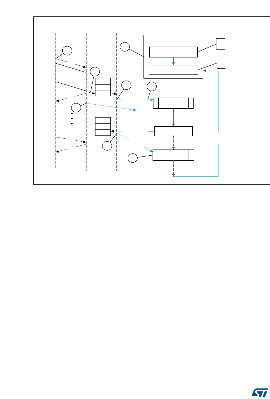
USB on-the-go high-speed (OTG_HS) RM0090
1508/1718 DocID018909 Rev 9
Figure 426. Slave mode bulk OUT transaction
After a SetConfiguration/SetInterface command, the application initializes all OUT endpoints
by setting CNAK = 1 and EPENA = 1 (in OTG_HS_DOEPCTLx), and setting a suitable
XFRSIZ and PKTCNT in the OTG_HS_DOEPTSIZx register.
1. Host attempts to send data (OUT token) to an endpoint.
2. When the core receives the OUT token on the USB, it stores the packet in the RxFIFO
because space is available there.
3. After writing the complete packet in the RxFIFO, the core then asserts the RXFLVL
interrupt (in OTG_HS_GINTSTS).
4. On receiving the PKTCNT number of USB packets, the core internally sets the NAK bit
for this endpoint to prevent it from receiving any more packets.
5. The application processes the interrupt and reads the data from the RxFIFO.
6. When the application has read all the data (equivalent to XFRSIZ), the core generates
an XFRC interrupt (in OTG_HS_DOEPINTx).
7. The application processes the interrupt and uses the setting of the XFRC interrupt bit
(in OTG_HS_DOEPINTx) to determine that the intended transfer is complete.
IN data transfers
•Packet write
This section describes how the application writes data packets to the endpoint FIFO in Slave
mode when dedicated transmit FIFOs are enabled.
init_out_ep
Host DeviceUSB
OUT
ACK
RXFLVL intr i
wr_reg(DOEPTSIZx)
wr_reg(DOEPCTLx)
512 bytes
OUT
NAK
xact _1
Application
XFRC
intr
DOEPCTLx.NAK=1
PKTCNT 0
XFRSIZ = 0
r
idle until intr
rcv_out _pkt()
idle until intr
On new xfer
or RxFIFO
not empty
1
2
3
4
5
6
7
8
XFRSIZ = 512 bytes
PKTCNT = 1
EPENA = 1
CNAK = 1
ai15679

DocID018909 Rev 9 1509/1718
RM0090 USB on-the-go high-speed (OTG_HS)
1523
1. The application can either choose the polling or the interrupt mode.
– In polling mode, the application monitors the status of the endpoint transmit data
FIFO by reading the OTG_HS_DTXFSTSx register, to determine if there is
enough space in the data FIFO.
– In interrupt mode, the application waits for the TXFE interrupt (in
OTG_HS_DIEPINTx) and then reads the OTG_HS_DTXFSTSx register, to
determine if there is enough space in the data FIFO.
– To write a single nonzero length data packet, there must be space to write the
entire packet in the data FIFO.
– To write zero length packet, the application must not look at the FIFO space.
2. Using one of the above mentioned methods, when the application determines that
there is enough space to write a transmit packet, the application must first write into the
endpoint control register, before writing the data into the data FIFO. Typically, the
application, must do a read modify write on the OTG_HS_DIEPCTLx register to avoid
modifying the contents of the register, except for setting the Endpoint Enable bit.
The application can write multiple packets for the same endpoint into the transmit FIFO, if
space is available. For periodic IN endpoints, the application must write packets only for one
micro-frame. It can write packets for the next periodic transaction only after getting transfer
complete for the previous transaction.
•Setting IN endpoint NAK
Internal data flow:
1. When the application sets the IN NAK for a particular endpoint, the core stops
transmitting data on the endpoint, irrespective of data availability in the endpoint’s
transmit FIFO.
2. Nonisochronous IN tokens receive a NAK handshake reply
– Isochronous IN tokens receive a zero-data-length packet reply
3. The core asserts the INEPNE (IN endpoint NAK effective) interrupt in
OTG_HS_DIEPINTx in response to the SNAK bit in OTG_HS_DIEPCTLx.
4. Once this interrupt is seen by the application, the application can assume that the
endpoint is in IN NAK mode. This interrupt can be cleared by the application by setting
the CNAK bit in OTG_HS_DIEPCTLx.
Application programming sequence:

USB on-the-go high-speed (OTG_HS) RM0090
1510/1718 DocID018909 Rev 9
1. To stop transmitting any data on a particular IN endpoint, the application must set the
IN NAK bit. To set this bit, the following field must be programmed.
– SNAK = 1 in OTG_HS_DIEPCTLx
2. Wait for assertion of the INEPNE interrupt in OTG_HS_DIEPINTx. This interrupt
indicates that the core has stopped transmitting data on the endpoint.
3. The core can transmit valid IN data on the endpoint after the application has set the
NAK bit, but before the assertion of the NAK Effective interrupt.
4. The application can mask this interrupt temporarily by writing to the INEPNEM bit in
DIEPMSK.
– INEPNEM = 0 in DIEPMSK
5. To exit Endpoint NAK mode, the application must clear the NAK status bit (NAKSTS) in
OTG_HS_DIEPCTLx. This also clears the INEPNE interrupt (in OTG_HS_DIEPINTx).
– CNAK = 1 in OTG_HS_DIEPCTLx
6. If the application masked this interrupt earlier, it must be unmasked as follows:
– INEPNEM = 1 in DIEPMSK
•IN endpoint disable
Use the following sequence to disable a specific IN endpoint that has been previously
enabled.
Application programming sequence:
1. The application must stop writing data on the AHB for the IN endpoint to be disabled.
2. The application must set the endpoint in NAK mode.
– SNAK = 1 in OTG_HS_DIEPCTLx
3. Wait for the INEPNE interrupt in OTG_HS_DIEPINTx.
4. Set the following bits in the OTG_HS_DIEPCTLx register for the endpoint that must be
disabled.
– EPDIS = 1 in OTG_HS_DIEPCTLx
– SNAK = 1 in OTG_HS_DIEPCTLx
5. Assertion of the EPDISD interrupt in OTG_HS_DIEPINTx indicates that the core has
completely disabled the specified endpoint. Along with the assertion of the interrupt, the
core also clears the following bits:
– EPENA = 0 in OTG_HS_DIEPCTLx
– EPDIS = 0 in OTG_HS_DIEPCTLx
6. The application must read the OTG_HS_DIEPTSIZx register for the periodic IN EP, to
calculate how much data on the endpoint were transmitted on the USB.
7. The application must flush the data in the Endpoint transmit FIFO, by setting the
following fields in the OTG_HS_GRSTCTL register:
– TXFNUM (in OTG_HS_GRSTCTL) = Endpoint transmit FIFO number
– TXFFLSH in (OTG_HS_GRSTCTL) = 1
The application must poll the OTG_HS_GRSTCTL register, until the TXFFLSH bit is cleared
by the core, which indicates the end of flush operation. To transmit new data on this
endpoint, the application can re-enable the endpoint at a later point.
•Generic nonperiodic IN data transfers
Application requirements:

DocID018909 Rev 9 1511/1718
RM0090 USB on-the-go high-speed (OTG_HS)
1523
1. Before setting up an IN transfer, the application must ensure that all data to be
transmitted as part of the IN transfer are part of a single buffer.
2. For IN transfers, the Transfer Size field in the Endpoint Transfer Size register denotes a
payload that constitutes multiple maximum-packet-size packets and a single short
packet. This short packet is transmitted at the end of the transfer.
– To transmit a few maximum-packet-size packets and a short packet at the end of
the transfer:
Transfer size[EPNUM] = x × MPSIZ[EPNUM] + sp
If (sp > 0), then packet count[EPNUM] = x + 1.
Otherwise, packet count[EPNUM] = x
– To transmit a single zero-length data packet:
Transfer size[EPNUM] = 0
Packet count[EPNUM] = 1
– To transmit a few maximum-packet-size packets and a zero-length data packet at
the end of the transfer, the application must split the transfer into two parts. The
first sends maximum-packet-size data packets and the second sends the zero-
length data packet alone.
First transfer: transfer size[EPNUM] = x × MPSIZ[epnum]; packet count = n;
Second transfer: transfer size[EPNUM] = 0; packet count = 1;
3. Once an endpoint is enabled for data transfers, the core updates the Transfer size
register. At the end of the IN transfer, the application must read the Transfer size
register to determine how much data posted in the transmit FIFO have already been
sent on the USB.
4. Data fetched into transmit FIFO = Application-programmed initial transfer size – core-
updated final transfer size
– Data transmitted on USB = (application-programmed initial packet count – Core
updated final packet count) × MPSIZ[EPNUM]
– Data yet to be transmitted on USB = (Application-programmed initial transfer size
– data transmitted on USB)
Internal data flow:
1. The application must set the transfer size and packet count fields in the endpoint-
specific registers and enable the endpoint to transmit the data.
2. The application must also write the required data to the transmit FIFO for the endpoint.
3. Every time a packet is written into the transmit FIFO by the application, the transfer size
for that endpoint is decremented by the packet size. The data is fetched from the
memory by the application, until the transfer size for the endpoint becomes 0. After
writing the data into the FIFO, the “number of packets in FIFO” count is incremented
(this is a 3-bit count, internally maintained by the core for each IN endpoint transmit
FIFO. The maximum number of packets maintained by the core at any time in an IN
endpoint FIFO is eight). For zero-length packets, a separate flag is set for each FIFO,
without any data in the FIFO.
4. Once the data are written to the transmit FIFO, the core reads them out upon receiving
an IN token. For every nonisochronous IN data packet transmitted with an ACK

USB on-the-go high-speed (OTG_HS) RM0090
1512/1718 DocID018909 Rev 9
handshake, the packet count for the endpoint is decremented by one, until the packet
count is zero. The packet count is not decremented on a timeout.
5. For zero length packets (indicated by an internal zero length flag), the core sends out a
zero-length packet for the IN token and decrements the packet count field.
6. If there are no data in the FIFO for a received IN token and the packet count field for
that endpoint is zero, the core generates an “IN token received when TxFIFO is empty”
(ITTXFE) Interrupt for the endpoint, provided that the endpoint NAK bit is not set. The
core responds with a NAK handshake for nonisochronous endpoints on the USB.
7. The core internally rewinds the FIFO pointers and no timeout interrupt is generated.
8. When the transfer size is 0 and the packet count is 0, the transfer complete (XFRC)
interrupt for the endpoint is generated and the endpoint enable is cleared.
Application programming sequence:
1. Program the OTG_HS_DIEPTSIZx register with the transfer size and corresponding
packet count.
2. Program the OTG_HS_DIEPCTLx register with the endpoint characteristics and set the
CNAK and EPENA (Endpoint Enable) bits.
3. When transmitting nonzero length data packet, the application must poll the
OTG_HS_DTXFSTSx register (where x is the FIFO number associated with that
endpoint) to determine whether there is enough space in the data FIFO. The
application can optionally use TXFE (in OTG_HS_DIEPINTx) before writing the data.
•Generic periodic IN data transfers
This section describes a typical periodic IN data transfer.
Application requirements:
1. Application requirements 1, 2, 3, and 4 of Generic nonperiodic IN data transfers on
page 1510 also apply to periodic IN data transfers, except for a slight modification of
requirement 2.
– The application can only transmit multiples of maximum-packet-size data packets
or multiples of maximum-packet-size packets, plus a short packet at the end. To

DocID018909 Rev 9 1513/1718
RM0090 USB on-the-go high-speed (OTG_HS)
1523
transmit a few maximum-packet-size packets and a short packet at the end of the
transfer, the following conditions must be met:
transfer size[EPNUM] = x × MPSIZ[EPNUM] + sp
(where x is an integer ≥ 0, and 0 ≤ sp < MPSIZ[EPNUM])
If (sp > 0), packet count[EPNUM] = x + 1
Otherwise, packet count[EPNUM] = x;
MCNT[EPNUM] = packet count[EPNUM]
– The application cannot transmit a zero-length data packet at the end of a transfer.
It can transmit a single zero-length data packet by itself. To transmit a single zero-
length data packet:
– transfer size[EPNUM] = 0
packet count[EPNUM] = 1
MCNT[EPNUM] = packet count[EPNUM]
2. The application can only schedule data transfers one frame at a time.
– (MCNT – 1) × MPSIZ ≤ XFERSIZ ≤ MCNT × MPSIZ
– PKTCNT = MCNT (in OTG_HS_DIEPTSIZx)
– If XFERSIZ < MCNT × MPSIZ, the last data packet of the transfer is a short
packet.
– Note that: MCNT is in OTG_HS_DIEPTSIZx, MPSIZ is in OTG_HS_DIEPCTLx,
PKTCNT is in OTG_HS_DIEPTSIZx and XFERSIZ is in OTG_HS_DIEPTSIZx
3. The complete data to be transmitted in the frame must be written into the transmit FIFO
by the application, before the IN token is received. Even when 1 DWORD of the data to
be transmitted per frame is missing in the transmit FIFO when the IN token is received,
the core behaves as when the FIFO is empty. When the transmit FIFO is empty:
– A zero data length packet would be transmitted on the USB for isochronous IN
endpoints
– A NAK handshake would be transmitted on the USB for interrupt IN endpoints
4. For a high-bandwidth IN endpoint with three packets in a frame, the application can
program the endpoint FIFO size to be 2 × max_pkt_size and have the third packet
loaded in after the first packet has been transmitted on the USB.
Internal data flow:
1. The application must set the transfer size and packet count fields in the endpoint-
specific registers and enable the endpoint to transmit the data.
2. The application must also write the required data to the associated transmit FIFO for
the endpoint.
3. Every time the application writes a packet to the transmit FIFO, the transfer size for that
endpoint is decremented by the packet size. The data are fetched from application
memory until the transfer size for the endpoint becomes 0.
4. When an IN token is received for a periodic endpoint, the core transmits the data in the
FIFO, if available. If the complete data payload (complete packet, in dedicated FIFO

USB on-the-go high-speed (OTG_HS) RM0090
1514/1718 DocID018909 Rev 9
mode) for the frame is not present in the FIFO, then the core generates an IN token
received when TxFIFO empty interrupt for the endpoint.
– A zero-length data packet is transmitted on the USB for isochronous IN endpoints
– A NAK handshake is transmitted on the USB for interrupt IN endpoints
5. The packet count for the endpoint is decremented by 1 under the following conditions:
– For isochronous endpoints, when a zero- or nonzero-length data packet is
transmitted
– For interrupt endpoints, when an ACK handshake is transmitted
– When the transfer size and packet count are both 0, the transfer completed
interrupt for the endpoint is generated and the endpoint enable is cleared.
6. At the “Periodic frame Interval” (controlled by PFIVL in OTG_HS_DCFG), when the
core finds nonempty any of the isochronous IN endpoint FIFOs scheduled for the
current frame nonempty, the core generates an IISOIXFR interrupt in
OTG_HS_GINTSTS.
Application programming sequence:
1. Program the OTG_HS_DIEPCTLx register with the endpoint characteristics and set the
CNAK and EPENA bits.
2. Write the data to be transmitted in the next frame to the transmit FIFO.
3. Asserting the ITTXFE interrupt (in OTG_HS_DIEPINTx) indicates that the application
has not yet written all data to be transmitted to the transmit FIFO.
4. If the interrupt endpoint is already enabled when this interrupt is detected, ignore the
interrupt. If it is not enabled, enable the endpoint so that the data can be transmitted on
the next IN token attempt.
5. Asserting the XFRC interrupt (in OTG_HS_DIEPINTx) with no ITTXFE interrupt in
OTG_HS_DIEPINTx indicates the successful completion of an isochronous IN transfer.
A read to the OTG_HS_DIEPTSIZx register must give transfer size = 0 and packet
count = 0, indicating all data were transmitted on the USB.
6. Asserting the XFRC interrupt (in OTG_HS_DIEPINTx), with or without the ITTXFE
interrupt (in OTG_HS_DIEPINTx), indicates the successful completion of an interrupt
IN transfer. A read to the OTG_HS_DIEPTSIZx register must give transfer size = 0 and
packet count = 0, indicating all data were transmitted on the USB.
7. Asserting the incomplete isochronous IN transfer (IISOIXFR) interrupt in
OTG_HS_GINTSTS with none of the aforementioned interrupts indicates the core did
not receive at least 1 periodic IN token in the current frame.
•Incomplete isochronous IN data transfers
This section describes what the application must do on an incomplete isochronous IN data
transfer.
Internal data flow:
1. An isochronous IN transfer is treated as incomplete in one of the following conditions:
a) The core receives a corrupted isochronous IN token on at least one isochronous
IN endpoint. In this case, the application detects an incomplete isochronous IN
transfer interrupt (IISOIXFR in OTG_HS_GINTSTS).
b) The application is slow to write the complete data payload to the transmit FIFO
and an IN token is received before the complete data payload is written to the
FIFO. In this case, the application detects an IN token received when TxFIFO
empty interrupt in OTG_HS_DIEPINTx. The application can ignore this interrupt,

DocID018909 Rev 9 1515/1718
RM0090 USB on-the-go high-speed (OTG_HS)
1523
as it eventually results in an incomplete isochronous IN transfer interrupt
(IISOIXFR in OTG_HS_GINTSTS) at the end of periodic frame.
The core transmits a zero-length data packet on the USB in response to the
received IN token.
2. The application must stop writing the data payload to the transmit FIFO as soon as
possible.
3. The application must set the NAK bit and the disable bit for the endpoint.
4. The core disables the endpoint, clears the disable bit, and asserts the Endpoint Disable
interrupt for the endpoint.
Application programming sequence
1. The application can ignore the IN token received when TxFIFO empty interrupt in
OTG_HS_DIEPINTx on any isochronous IN endpoint, as it eventually results in an
incomplete isochronous IN transfer interrupt (in OTG_HS_GINTSTS).
2. Assertion of the incomplete isochronous IN transfer interrupt (in OTG_HS_GINTSTS)
indicates an incomplete isochronous IN transfer on at least one of the isochronous IN
endpoints.
3. The application must read the Endpoint Control register for all isochronous IN
endpoints to detect endpoints with incomplete IN data transfers.
4. The application must stop writing data to the Periodic Transmit FIFOs associated with
these endpoints on the AHB.
5. Program the following fields in the OTG_HS_DIEPCTLx register to disable the
endpoint:
– SNAK = 1 in OTG_HS_DIEPCTLx
– EPDIS = 1 in OTG_HS_DIEPCTLx
6. The assertion of the Endpoint Disabled interrupt in OTG_HS_DIEPINTx indicates that
the core has disabled the endpoint.
– At this point, the application must flush the data in the associated transmit FIFO or
overwrite the existing data in the FIFO by enabling the endpoint for a new transfer
in the next micro-frame. To flush the data, the application must use the
OTG_HS_GRSTCTL register.
•Stalling nonisochronous IN endpoints
This section describes how the application can stall a nonisochronous endpoint.
Application programming sequence:

USB on-the-go high-speed (OTG_HS) RM0090
1516/1718 DocID018909 Rev 9
1. Disable the IN endpoint to be stalled. Set the STALL bit as well.
2. EPDIS = 1 in OTG_HS_DIEPCTLx, when the endpoint is already enabled
– STALL = 1 in OTG_HS_DIEPCTLx
– The STALL bit always takes precedence over the NAK bit
3. Assertion of the Endpoint Disabled interrupt (in OTG_HS_DIEPINTx) indicates to the
application that the core has disabled the specified endpoint.
4. The application must flush the nonperiodic or periodic transmit FIFO, depending on the
endpoint type. In case of a nonperiodic endpoint, the application must re-enable the
other nonperiodic endpoints that do not need to be stalled, to transmit data.
5. Whenever the application is ready to end the STALL handshake for the endpoint, the
STALL bit must be cleared in OTG_HS_DIEPCTLx.
6. If the application sets or clears a STALL bit for an endpoint due to a
SetFeature.Endpoint Halt command or ClearFeature.Endpoint Halt command, the
STALL bit must be set or cleared before the application sets up the Status stage
transfer on the control endpoint.
Special case: stalling the control OUT endpoint
The core must stall IN/OUT tokens if, during the data stage of a control transfer, the host
sends more IN/OUT tokens than are specified in the SETUP packet. In this case, the
application must enable the ITTXFE interrupt in OTG_HS_DIEPINTx and the OTEPDIS
interrupt in OTG_HS_DOEPINTx during the data stage of the control transfer, after the core
has transferred the amount of data specified in the SETUP packet. Then, when the
application receives this interrupt, it must set the STALL bit in the corresponding endpoint
control register, and clear this interrupt.
35.13.8 Worst case response time
When the OTG_HS controller acts as a device, there is a worst case response time for any
tokens that follow an isochronous OUT. This worst case response time depends on the AHB
clock frequency.
The core registers are in the AHB domain, and the core does not accept another token
before updating these register values. The worst case is for any token following an
isochronous OUT, because for an isochronous transaction, there is no handshake and the
next token could come sooner. This worst case value is 7 PHY clocks when the AHB clock
is the same as the PHY clock. When the AHB clock is faster, this value is smaller.
If this worst case condition occurs, the core responds to bulk/interrupt tokens with a NAK
and drops isochronous and SETUP tokens. The host interprets this as a timeout condition
for SETUP and retries the SETUP packet. For isochronous transfers, the Incomplete
isochronous IN transfer interrupt (IISOIXFR) and Incomplete isochronous OUT transfer
interrupt (IISOOXFR) inform the application that isochronous IN/OUT packets were
dropped.
Choosing the value of TRDT in OTG_HS_GUSBCFG
The value in TRDT (OTG_HS_GUSBCFG) is the time it takes for the MAC, in terms of PHY
clocks after it has received an IN token, to get the FIFO status, and thus the first data from
the PFC block. This time involves the synchronization delay between the PHY and AHB
clocks. The worst case delay for this is when the AHB clock is the same as the PHY clock.
In this case, the delay is 5 clocks.
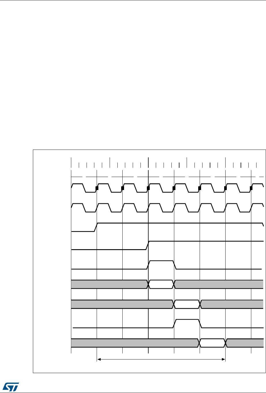
DocID018909 Rev 9 1517/1718
RM0090 USB on-the-go high-speed (OTG_HS)
1523
Once the MAC receives an IN token, this information (token received) is synchronized to the
AHB clock by the PFC (the PFC runs on the AHB clock). The PFC then reads the data from
the SPRAM and writes them into the dual clock source buffer. The MAC then reads the data
out of the source buffer (4 deep).
If the AHB is running at a higher frequency than the PHY, the application can use a smaller
value for TRDT (in OTG_HS_GUSBCFG).
Figure 427 has the following signals:
•tkn_rcvd: Token received information from MAC to PFC
•dynced_tkn_rcvd: Doubled sync tkn_rcvd, from PCLK to HCLK domain
•spr_read: Read to SPRAM
•spr_addr: Address to SPRAM
•spr_rdata: Read data from SPRAM
•srcbuf_push: Push to the source buffer
•srcbuf_rdata: Read data from the source buffer. Data seen by MAC
Refer to Table 208: TRDT values for the values of TRDT versus AHB clock frequency.
Figure 427. TRDT max timing case
12345678
0ns 50ns 100ns 150ns 200ns
HCLK
PCLK
tkn_rcvd
dsynced_tkn_rcvd
spr_read
spr_addr
spr_rdata
srcbuf_push
srcbuf_rdata
5 Clocks
D1
A1
D1
ai15680
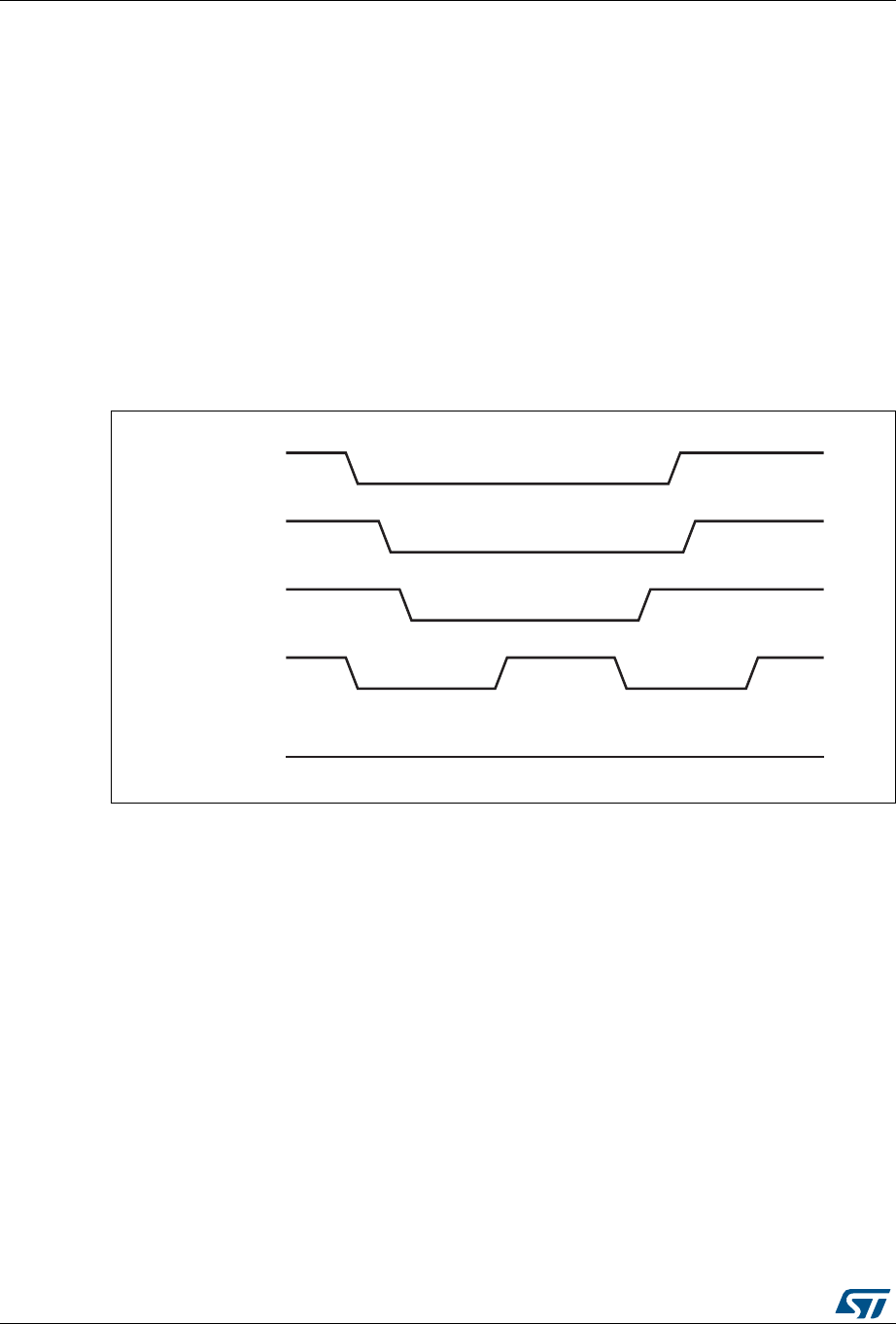
USB on-the-go high-speed (OTG_HS) RM0090
1518/1718 DocID018909 Rev 9
35.13.9 OTG programming model
The OTG_HS controller is an OTG device supporting HNP and SRP. When the core is
connected to an “A” plug, it is referred to as an A-device. When the core is connected to a
“B” plug it is referred to as a B-device. In host mode, the OTG_HS controller turns off VBUS
to conserve power. SRP is a method by which the B-device signals the A-device to turn on
VBUS power. A device must perform both data-line pulsing and VBUS pulsing, but a host can
detect either data-line pulsing or VBUS pulsing for SRP. HNP is a method by which the B-
device negotiates and switches to host role. In Negotiated mode after HNP, the B-device
suspends the bus and reverts to the device role.
A-device session request protocol
The application must set the SRP-capable bit in the Core USB configuration register. This
enables the OTG_HS controller to detect SRP as an A-device.
Figure 428. A-device SRP
1. DRV_VBUS = VBUS drive signal to the PHY
VBUS_VALID = VBUS valid signal from PHY
A_VALID = A-device VBUS level signal to PHY
DP = Data plus line
DM = Data minus line
ai15681b
DRV_VBUS
VBUS_VALID
A_VALID
OTG_HS_FS_DP
OTG_HS_FS_DM
Suspend
VBUS pulsing
Data line pulsing Connect
1
6
25
3
47
Low
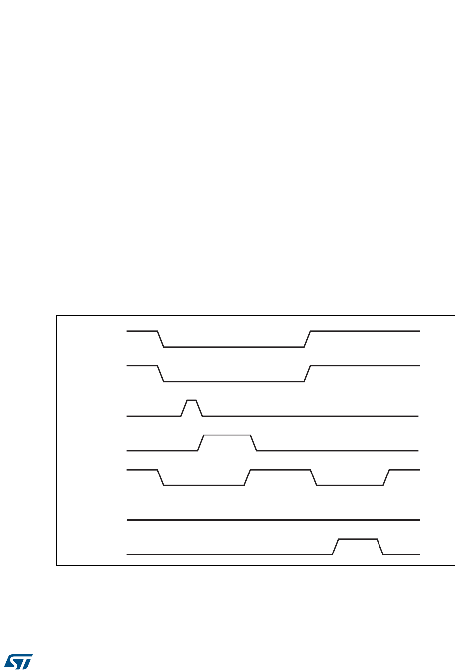
DocID018909 Rev 9 1519/1718
RM0090 USB on-the-go high-speed (OTG_HS)
1523
1. To save power, the application suspends and turns off port power when the bus is idle
by writing the port suspend and port power bits in the host port control and status
register.
2. PHY indicates port power off by deasserting the VBUS_VALID signal.
3. The device must detect SE0 for at least 2 ms to start SRP when VBUS power is off.
4. To initiate SRP, the device turns on its data line pull-up resistor for 5 to 10 ms. The
OTG_HS controller detects data-line pulsing.
5. The device drives VBUS above the A-device session valid (2.0 V minimum) for VBUS
pulsing.
The OTG_HS controller interrupts the application on detecting SRP. The Session
request detected bit is set in Global interrupt status register (SRQINT set in
OTG_HS_GINTSTS).
6. The application must service the Session request detected interrupt and turn on the
port power bit by writing the port power bit in the host port control and status register.
The PHY indicates port power-on by asserting the VBUS_VALID signal.
7. When the USB is powered, the device connects, completing the SRP process.
B-device session request protocol
The application must set the SRP-capable bit in the Core USB configuration register. This
enables the OTG_HS controller to initiate SRP as a B-device. SRP is a means by which the
OTG_HS controller can request a new session from the host.
Figure 429. B-device SRP
1. VBUS_VALID = VBUS valid signal from PHY
B_VALID = B-device valid session to PHY
DISCHRG_VBUS = discharge signal to PHY
SESS_END = session end signal to PHY
CHRG_VBUS = charge VBUS signal to PHY
DP = Data plus line
DM = Data minus line
ai1568b2
VBUS_VALID
B_VALID
DISCHRG_VBUS
SESS_END
OTG_HS_FS_DP
OTG_HS_FS_DM
CHRG_VBUS
Suspend
Data line pulsing Connect
V
BUS
pulsing
1
6
2
3
4
58
7
Low
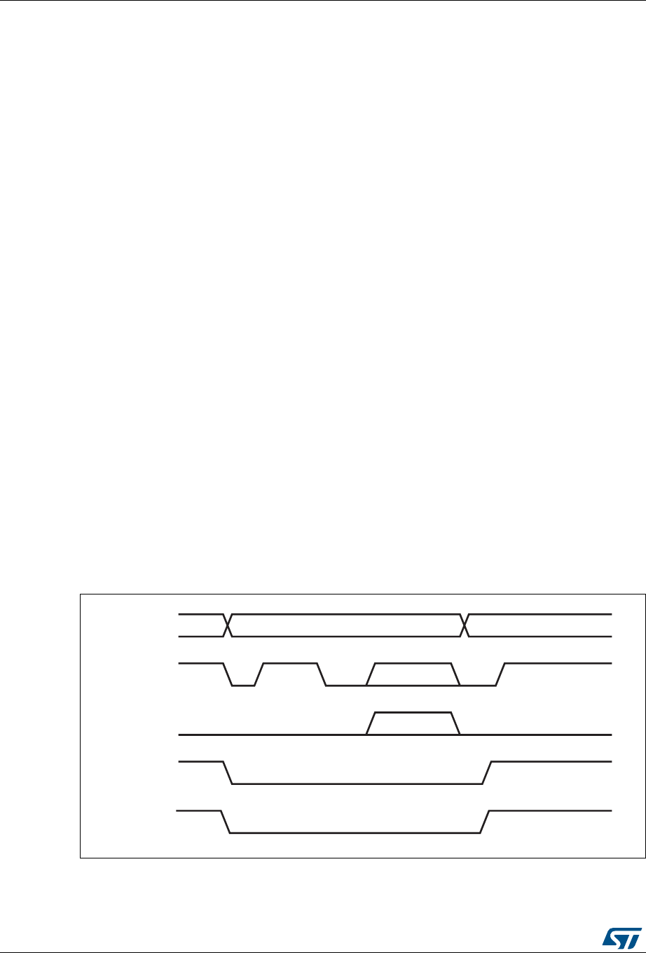
USB on-the-go high-speed (OTG_HS) RM0090
1520/1718 DocID018909 Rev 9
1. To save power, the host suspends and turns off port power when the bus is idle.
The OTG_HS controller sets the early suspend bit in the Core interrupt register after 3
ms of bus idleness. Following this, the OTG_HS controller sets the USB suspend bit in
the Core interrupt register.
The OTG_HS controller informs the PHY to discharge VBUS.
2. The PHY indicates the session’s end to the device. This is the initial condition for SRP.
The OTG_HS controller requires 2 ms of SE0 before initiating SRP.
For a USB 1.1 full-speed serial transceiver, the application must wait until VBUS
discharges to 0.2 V after BSVLD (in OTG_HS_GOTGCTL) is deasserted. This
discharge time can be obtained from the transceiver vendor and varies from one
transceiver to another.
3. The USB OTG core informs the PHY to speed up VBUS discharge.
4. The application initiates SRP by writing the session request bit in the OTG Control and
status register. The OTG_HS controller perform data-line pulsing followed by VBUS
pulsing.
5. The host detects SRP from either the data-line or VBUS pulsing, and turns on VBUS.
The PHY indicates VBUS power-on to the device.
6. The OTG_HS controller performs VBUS pulsing.
The host starts a new session by turning on VBUS, indicating SRP success. The
OTG_HS controller interrupts the application by setting the session request success
status change bit in the OTG interrupt status register. The application reads the session
request success bit in the OTG control and status register.
7. When the USB is powered, the OTG_HS controller connects, completing the SRP
process.
A-device host negotiation protocol
HNP switches the USB host role from the A-device to the B-device. The application must set
the HNP-capable bit in the Core USB configuration register to enable the OTG_HS
controller to perform HNP as an A-device.
Figure 430. A-device HNP
1. DPPULLDOWN = signal from core to PHY to enable/disable the pull-down on the DP line inside the PHY.
DMPULLDOWN = signal from core to PHY to enable/disable the pull-down on the DM line inside the PHY.
ai15683b
OTG core
DP
DM
DPPULLDOWN
DMPULLDOWN
Host Device Host
1
Suspend 2
3
45
Reset
6
Traffic 7
8
Connect
Traffic

DocID018909 Rev 9 1521/1718
RM0090 USB on-the-go high-speed (OTG_HS)
1523
1. The OTG_HS controller sends the B-device a SetFeature b_hnp_enable descriptor to
enable HNP support. The B-device’s ACK response indicates that the B-device
supports HNP. The application must set host Set HNP Enable bit in the OTG Control
and status register to indicate to the OTG_HS controller that the B-device supports
HNP.
2. When it has finished using the bus, the application suspends by writing the Port
suspend bit in the host port control and status register.
3. When the B-device observes a USB suspend, it disconnects, indicating the initial
condition for HNP. The B-device initiates HNP only when it must switch to the host role;
otherwise, the bus continues to be suspended.
The OTG_HS controller sets the host negotiation detected interrupt in the OTG
interrupt status register, indicating the start of HNP.
The OTG_HS controller deasserts the DM pull down and DM pull down in the PHY to
indicate a device role. The PHY enables the OTG_HS_DP pull-up resistor to indicate a
connect for B-device.
The application must read the current mode bit in the OTG Control and status register
to determine peripheral mode operation.
4. The B-device detects the connection, issues a USB reset, and enumerates the
OTG_HS controller for data traffic.
5. The B-device continues the host role, initiating traffic, and suspends the bus when
done.
The OTG_HS controller sets the early suspend bit in the Core interrupt register after 3
ms of bus idleness. Following this, the OTG_HS controller sets the USB Suspend bit in
the Core interrupt register.
6. In Negotiated mode, the OTG_HS controller detects the suspend, disconnects, and
switches back to the host role. The OTG_HS controller asserts the DM pull down and
DM pull down in the PHY to indicate its assumption of the host role.
7. The OTG_HS controller sets the Connector ID status change interrupt in the OTG
Interrupt Status register. The application must read the connector ID status in the OTG
Control and Status register to determine the OTG_HS controller operation as an A-
device. This indicates the completion of HNP to the application. The application must
read the Current mode bit in the OTG control and status register to determine host
mode operation.
8. The B-device connects, completing the HNP process.
B-device host negotiation protocol
HNP switches the USB host role from B-device to A-device. The application must set the
HNP-capable bit in the Core USB configuration register to enable the OTG_HS controller to
perform HNP as a B-device.

USB on-the-go high-speed (OTG_HS) RM0090
1522/1718 DocID018909 Rev 9
Figure 431. B-device HNP
1. DPPULLDOWN = signal from core to PHY to enable/disable the pull-down on the DP line inside the PHY.
DMPULLDOWN = signal from core to PHY to enable/disable the pull-down on the DM line inside the PHY.
1. The A-device sends the SetFeature b_hnp_enable descriptor to enable HNP support.
The OTG_HS controller’s ACK response indicates that it supports HNP. The
application must set the Device HNP enable bit in the OTG Control and status register
to indicate HNP support.
The application sets the HNP request bit in the OTG Control and status register to
indicate to the OTG_HS controller to initiate HNP.
2. When it has finished using the bus, the A-device suspends by writing the Port suspend
bit in the host port control and status register.
The OTG_HS controller sets the Early suspend bit in the Core interrupt register after 3
ms of bus idleness. Following this, the OTG_HS controller sets the USB suspend bit in
the Core interrupt register.
The OTG_HS controller disconnects and the A-device detects SE0 on the bus,
indicating HNP. The OTG_HS controller asserts the DP pull down and DM pull down in
the PHY to indicate its assumption of the host role.
The A-device responds by activating its OTG_HS_DP pull-up resistor within 3 ms of
detecting SE0. The OTG_HS controller detects this as a connect.
The OTG_HS controller sets the host negotiation success status change interrupt in
the OTG Interrupt status register, indicating the HNP status. The application must read
the host negotiation success bit in the OTG Control and status register to determine
ai15684b
OTG core
DP
DM
DPPULLDOWN
DMPULLDOWN
HostDevice Device
1
Suspend 2
3
45
Reset
6
Traffic 7
8
Connect
Traffic

DocID018909 Rev 9 1523/1718
RM0090 USB on-the-go high-speed (OTG_HS)
1523
host negotiation success. The application must read the current Mode bit in the Core
interrupt register (OTG_HS_GINTSTS) to determine host mode operation.
3. The application sets the reset bit (PRST in OTG_HS_HPRT) and the OTG_HS
controller issues a USB reset and enumerates the A-device for data traffic.
4. The OTG_HS controller continues the host role of initiating traffic, and when done,
suspends the bus by writing the Port suspend bit in the host port control and status
register.
5. In Negotiated mode, when the A-device detects a suspend, it disconnects and switches
back to the host role. The OTG_HS controller deasserts the DP pull down and DM pull
down in the PHY to indicate the assumption of the device role.
6. The application must read the current mode bit in the Core interrupt
(OTG_HS_GINTSTS) register to determine the host mode operation.
7. The OTG_HS controller connects, completing the HNP process.

Flexible static memory controller (FSMC) RM0090
1524/1718 DocID018909 Rev 9
36 Flexible static memory controller (FSMC)
This section applies to the whole STM32F40x/41x family only.
36.1 FSMC main features
The FSMC block is able to interface with synchronous and asynchronous memories and 16-
bit PC memory cards. Its main purpose is to:
•Translate the AHB transactions into the appropriate external device protocol
•Meet the access timing requirements of the external devices
All external memories share the addresses, data and control signals with the controller.
Each external device is accessed by means of a unique chip select. The FSMC performs
only one access at a time to an external device.
The FSMC has the following main features:
•Interfaces with static memory-mapped devices including:
– Static random access memory (SRAM)
– NOR Flash memory/OneNAND Flash memory
– PSRAM (4 memory banks)
•Two banks of NAND Flash with ECC hardware that checks up to 8 Kbytes of data
•16-bit PC Card compatible devices
•Supports burst mode access to synchronous devices (NOR Flash and PSRAM)
•8- or 16-bit wide databus
•Independent chip select control for each memory bank
•Independent configuration for each memory bank
•Programmable timings to support a wide range of devices, in particular:
– Programmable wait states (up to 15)
– Programmable bus turnaround cycles (up to 15)
– Programmable output enable and write enable delays (up to 15)
– Independent read and write timings and protocol, so as to support the widest
variety of memories and timings
•Write enable and byte lane select outputs for use with PSRAM and SRAM devices
•Translation of 32-bit wide AHB transactions into consecutive 16-bit or 8-bit accesses to
external 16-bit or 8-bit devices
•A Write FIFO, 2-word long (16-word long for STM32F42x and STM32F43x), each word
is 32 bits wide, only stores data and not the address. Therefore, this FIFO only buffers
AHB write burst transactions. This makes it possible to write to slow memories and free
the AHB quickly for other operations. Only one burst at a time is buffered: if a new AHB
burst or single transaction occurs while an operation is in progress, the FIFO is
drained. The FSMC will insert wait states until the current memory access is complete.
•External asynchronous wait control
The FSMC registers that define the external device type and associated characteristics are
usually set at boot time and do not change until the next reset or power-up. However, it is
possible to change the settings at any time.
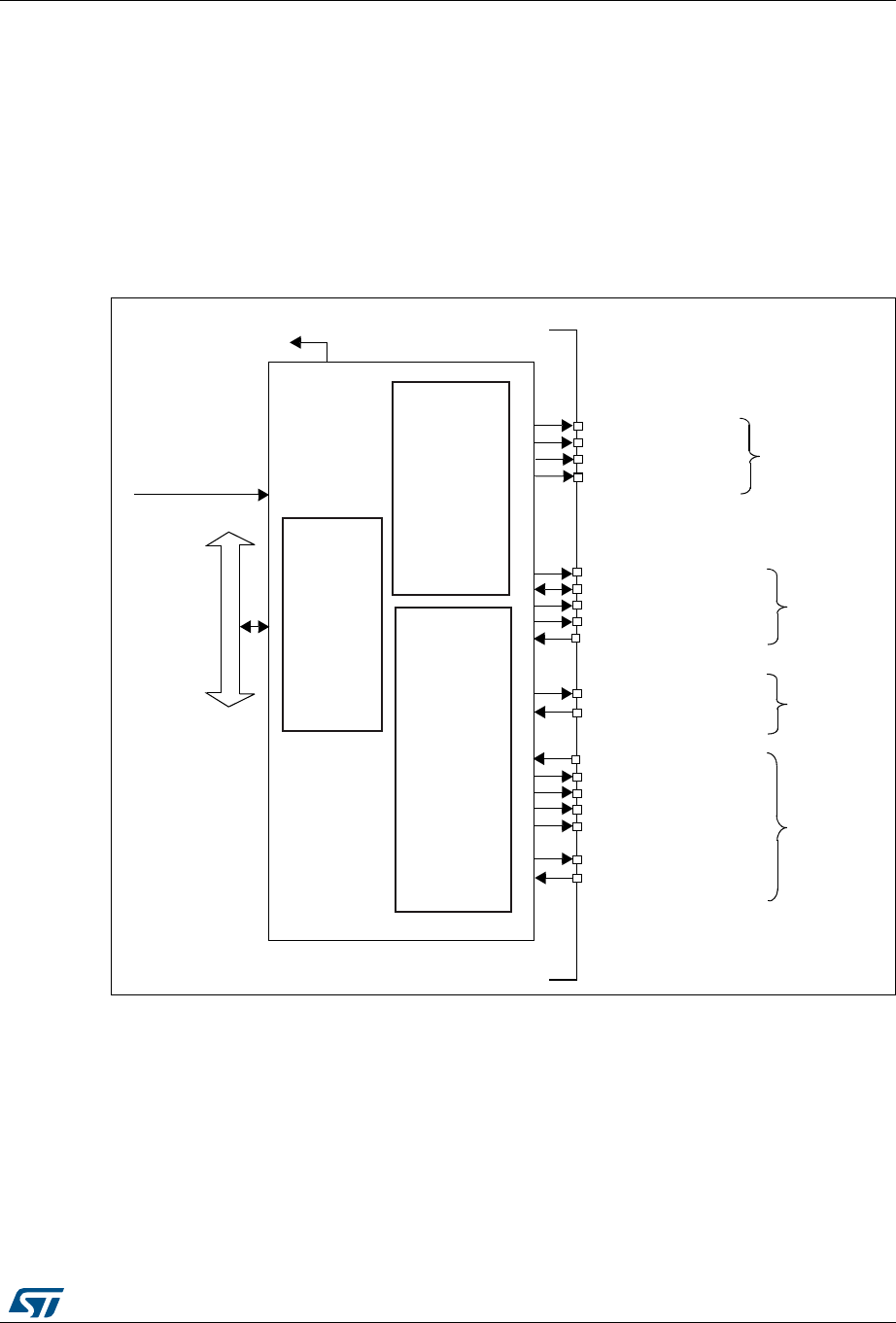
DocID018909 Rev 9 1525/1718
RM0090 Flexible static memory controller (FSMC)
1581
36.2 Block diagram
The FSMC consists of four main blocks:
•The AHB interface (including the FSMC configuration registers)
•The NOR Flash/PSRAM controller
•The NAND Flash/PC Card controller
•The external device interface
The block diagram is shown in Figure 432.
Figure 432. FSMC block diagram
36.3 AHB interface
The AHB slave interface enables internal CPUs and other bus master peripherals to access
the external static memories.
AHB transactions are translated into the external device protocol. In particular, if the
selected external memory is 16 or 8 bits wide, 32-bit wide transactions on the AHB are split
into consecutive 16- or 8-bit accesses. The Chip Select toggles for each access.
!("BUS
&3-#INTERRUPTTO.6)#
./2032!-
MEMORY
CONTROLLER
(#,+
&ROMCLOCK
CONTROLLER
.!.$0##ARD
MEMORY
CONTROLLER
SIGNALS
.!.$
3HARED
SIGNALS
SIGNALS
./2032!-
&3-#?.%;=
&3-#?.,OR.!$6
&3-#?.7!)4
&3-#?./%
&3-#?.7%
&3-#?.)/2$
&3-#?.2%'
&3-#?#$
SIGNALS
0##ARD
AIB
&3-#?.",;=
&3-#?.#%;=
&3-#?).4;=
&3-#?).42
&3-#?.#%?
&3-#?.#%?
&3-#?.)/72
&3-#?#,+
#ONFIGURATION
REGISTERS
&3-#?!;=
&3-#?$;=

Flexible static memory controller (FSMC) RM0090
1526/1718 DocID018909 Rev 9
The FSMC generates an AHB error in the following conditions:
•When reading or writing to an FSMC bank which is not enabled
•When reading or writing to the NOR Flash bank while the FACCEN bit is reset in the
FSMC_BCRx register.
•When reading or writing to the PC Card banks while the input pin FSMC_CD (Card
Presence Detection) is low.
The effect of this AHB error depends on the AHB master which has attempted the R/W
access:
•If it is the Cortex®-M4 with FPU CPU, a hard fault interrupt is generated
•If is a DMA, a DMA transfer error is generated and the corresponding DMA channel is
automatically disabled.
The AHB clock (HCLK) is the reference clock for the FSMC.
36.3.1 Supported memories and transactions
General transaction rules
The requested AHB transaction data size can be 8-, 16- or 32-bit wide whereas the
accessed external device has a fixed data width. This may lead to inconsistent transfers.
Therefore, some simple transaction rules must be followed:
•AHB transaction size and memory data size are equal
There is no issue in this case.
•AHB transaction size is greater than the memory size
In this case, the FSMC splits the AHB transaction into smaller consecutive memory
accesses in order to meet the external data width.
•AHB transaction size is smaller than the memory size
Asynchronous transfers may or not be consistent depending on the type of external
device.
– Asynchronous accesses to devices that have the byte select feature (SRAM,
ROM, PSRAM).
a) FSMC allows write transactions accessing the right data through its byte lanes
NBL[1:0]
b) Read transactions are allowed. All memory bytes are read and the useless
ones are discarded. The NBL[1:0] are kept low during read transactions.
– Asynchronous accesses to devices that do not have the byte select feature (NOR
and NAND Flash 16-bit).
This situation occurs when a byte access is requested to a 16-bit wide Flash
memory. Clearly, the device cannot be accessed in byte mode (only 16-bit words
can be read from/written to the Flash memory) therefore:
a) Write transactions are not allowed
b) Read transactions are allowed. All memory bytes are read and the useless ones
are discarded. The NBL[1:0] are set to 0 during read transactions.
Configuration registers
The FSMC can be configured using a register set. See Section 36.5.6, for a detailed
description of the NOR Flash/PSRAM control registers. See Section 36.6.8, for a detailed
description of the NAND Flash/PC Card registers.

DocID018909 Rev 9 1527/1718
RM0090 Flexible static memory controller (FSMC)
1581
36.4 External device address mapping
From the FSMC point of view, the external memory is divided into 4 fixed-size banks of
256 Mbytes each (Refer to Figure 433):
•Bank 1 used to address up to 4 NOR Flash or PSRAM memory devices. This bank is
split into 4 NOR/PSRAM subbanks with 4 dedicated Chip Selects, as follows:
– Bank 1 - NOR/PSRAM 1
– Bank 1 - NOR/PSRAM 2
– Bank 1 - NOR/PSRAM 3
– Bank 1 - NOR/PSRAM 4
•Banks 2 and 3 used to address NAND Flash devices (1 device per bank)
•Bank 4 used to address a PC Card device
For each bank the type of memory to be used is user-defined in the Configuration register.
Figure 433. FSMC memory banks
36.4.1 NOR/PSRAM address mapping
HADDR[27:26] bits are used to select one of the four memory banks as shown in Table 211.
Bank 1
NAND Flash
NOR / PSRAM
Supported memory typeBanks
4 × 64 MB
6000 0000h
6FF F FFF Fh
Address
7000 0000h
7FF F FFF Fh
8000 0000h
8FF F FFF Fh
9000 0000h
9FF F FFF Fh
Bank 2
4 × 64 MB
Bank 3
4 × 64 MB
Bank 4
4 × 64 MB
PC Ca rd
ai14719
Table 211. NOR/PSRAM bank selection
HADDR[27:26](1) Selected bank
00 Bank 1 - NOR/PSRAM 1
01 Bank 1 - NOR/PSRAM 2
Flexible static memory controller (FSMC) RM0090
1528/1718 DocID018909 Rev 9
HADDR[25:0] contain the external memory address. Since HADDR is a byte address
whereas the memory is addressed in words, the address actually issued to the memory
varies according to the memory data width, as shown in the following table.
Wrap support for NOR Flash/PSRAM
Wrap burst mode for synchronous memories is not supported. The memories must be
configured in linear burst mode of undefined length.
36.4.2 NAND/PC Card address mapping
In this case, three banks are available, each of them divided into memory spaces as
indicated in Table 213.
For NAND Flash memory, the common and attribute memory spaces are subdivided into
three sections (see in Table 214 below) located in the lower 256 Kbytes:
•Data section (first 64 Kbytes in the common/attribute memory space)
•Command section (second 64 Kbytes in the common / attribute memory space)
•Address section (next 128 Kbytes in the common / attribute memory space)
10 Bank 1 - NOR/PSRAM 3
11 Bank 1 - NOR/PSRAM 4
1. HADDR are internal AHB address lines that are translated to external memory.
Table 212. External memory address
Memory width(1)
1. In case of a 16-bit external memory width, the FSMC will internally use HADDR[25:1] to generate the
address for external memory FSMC_A[24:0].
Whatever the external memory width (16-bit or 8-bit), FSMC_A[0] should be connected to external memory
address A[0].
Data address issued to the memory Maximum memory capacity (bits)
8-bit HADDR[25:0] 64 Mbytes x 8 = 512 Mbit
16-bit HADDR[25:1] >> 1 64 Mbytes/2 x 16 = 512 Mbit
Table 211. NOR/PSRAM bank selection (continued)
HADDR[27:26](1) Selected bank
Table 213. Memory mapping and timing registers
Start address End address FSMC Bank Memory space Timing register
0x9C00 0000 0x9FFF FFFF
Bank 4 - PC card
I/O FSMC_PIO4 (0xB0)
0x9800 0000 0x9BFF FFFF Attribute FSMC_PATT4 (0xAC)
0x9000 0000 0x93FF FFFF Common FSMC_PMEM4 (0xA8)
0x8800 0000 0x8BFF FFFF
Bank 3 - NAND Flash
Attribute FSMC_PATT3 (0x8C)
0x8000 0000 0x83FF FFFF Common FSMC_PMEM3 (0x88)
0x7800 0000 0x7BFF FFFF
Bank 2- NAND Flash
Attribute FSMC_PATT2 (0x6C)
0x7000 0000 0x73FF FFFF Common FSMC_PMEM2 (0x68)

DocID018909 Rev 9 1529/1718
RM0090 Flexible static memory controller (FSMC)
1581
The application software uses the 3 sections to access the NAND Flash memory:
•To send a command to NAND Flash memory: the software must write the command
value to any memory location in the command section.
•To specify the NAND Flash address that must be read or written: the software
must write the address value to any memory location in the address section. Since an
address can be 4 or 5 bytes long (depending on the actual memory size), several
consecutive writes to the address section are needed to specify the full address.
•To read or write data: the software reads or writes the data value from or to any
memory location in the data section.
Since the NAND Flash memory automatically increments addresses, there is no need to
increment the address of the data section to access consecutive memory locations.
36.5 NOR Flash/PSRAM controller
The FSMC generates the appropriate signal timings to drive the following types of
memories:
•Asynchronous SRAM and ROM
–8-bit
– 16-bit
– 32-bit
•PSRAM (Cellular RAM)
– Asynchronous mode
– Burst mode for synchronous accesses
– Multiplexed or nonmultiplexed
•NOR Flash
– Asynchronous mode
– Burst mode for synchronous accesses
– Multiplexed or nonmultiplexed
The FSMC outputs a unique chip select signal NE[4:1] per bank. All the other signals
(addresses, data and control) are shared.
For synchronous accesses, the FSMC issues the clock (CLK) to the selected external
device only during the read/write transactions. This clock is a submultiple of the HCLK clock.
The size of each bank is fixed and equal to 64 Mbytes.
Each bank is configured by means of dedicated registers (see Section 36.5.6).
The programmable memory parameters include access timings (see Table 215) and support
for wait management (for PSRAM and NOR Flash accessed in burst mode).
Table 214. NAND bank selections
Section name HADDR[17:16] Address range
Address section 1X 0x020000-0x03FFFF
Command section 01 0x010000-0x01FFFF
Data section 00 0x000000-0x0FFFF
Flexible static memory controller (FSMC) RM0090
1530/1718 DocID018909 Rev 9
36.5.1 External memory interface signals
Table 216, Table 217 and Table 218 list the signals that are typically used to interface NOR
Flash, SRAM and PSRAM.
Note: Prefix “N”. specifies the associated signal as active low.
NOR Flash, nonmultiplexed I/Os
NOR Flash memories are addressed in 16-bit words. The maximum capacity is 512 Mbit (26
address lines).
Table 215. Programmable NOR/PSRAM access parameters
Parameter Function Access mode Unit Min. Max.
Address
setup
Duration of the address
setup phase Asynchronous AHB clock cycle
(HCLK) 015
Address hold Duration of the address hold
phase
Asynchronous,
muxed I/Os
AHB clock cycle
(HCLK) 115
Data setup Duration of the data setup
phase Asynchronous AHB clock cycle
(HCLK) 1256
Bust turn Duration of the bus
turnaround phase
Asynchronous and
synchronous
read/write
AHB clock cycle
(HCLK) 015
Clock divide
ratio
Number of AHB clock cycles
(HCLK) to build one memory
clock cycle (CLK)
Synchronous AHB clock cycle
(HCLK) 2 16
Data latency
Number of clock cycles to
issue to the memory before
the first data of the burst
Synchronous Memory clock
cycle (CLK) 2 17
Table 216. Nonmultiplexed I/O NOR Flash
FSMC signal name I/O Function
CLK O Clock (for synchronous access)
A[25:0] O Address bus
D[15:0] I/O Bidirectional data bus
NE[x] O Chip select, x = 1..4
NOE O Output enable
NWE O Write enable
NL(=NADV) O Latch enable (this signal is called address
valid, NADV, by some NOR Flash devices)
NWAIT I NOR Flash wait input signal to the FSMC
DocID018909 Rev 9 1531/1718
RM0090 Flexible static memory controller (FSMC)
1581
NOR Flash, multiplexed I/Os
NOR-Flash memories are addressed in 16-bit words. The maximum capacity is 512 Mbit
(26 address lines).
PSRAM/SRAM, nonmultiplexed I/Os
PSRAM memories are addressed in 16-bit words. The maximum capacity is 512 Mbit (26
address lines).
PSRAM, multiplexed I/Os
Table 217. Multiplexed I/O NOR Flash
FSMC signal name I/O Function
CLK O Clock (for synchronous access)
A[25:16] O Address bus
AD[15:0] I/O 16-bit multiplexed, bidirectional address/data bus
NE[x] O Chip select, x = 1..4
NOE O Output enable
NWE O Write enable
NL(=NADV) O Latch enable (this signal is called address valid, NADV, by some NOR
Flash devices)
NWAIT I NOR Flash wait input signal to the FSMC
Table 218. Nonmultiplexed I/Os PSRAM/SRAM
FSMC signal name I/O Function
CLK O Clock (only for PSRAM synchronous access)
A[25:0] O Address bus
D[15:0] I/O Data bidirectional bus
NE[x] O Chip select, x = 1..4 (called NCE by PSRAM (Cellular RAM i.e. CRAM))
NOE O Output enable
NWE O Write enable
NL(= NADV) O Address valid only for PSRAM input (memory signal name: NADV)
NWAIT I PSRAM wait input signal to the FSMC
NBL[1] O Upper byte enable (memory signal name: NUB)
NBL[0] O Lowed byte enable (memory signal name: NLB)
Table 219. Multiplexed I/O PSRAM
FSMC signal name I/O Function
CLK O Clock (for synchronous access)
A[25:16] O Address bus
Flexible static memory controller (FSMC) RM0090
1532/1718 DocID018909 Rev 9
PSRAM memories are addressed in 16-bit words. The maximum capacity is 512 Mbit (26
address lines).
36.5.2 Supported memories and transactions
Table 220 below displays an example of the supported devices, access modes and
transactions when the memory data bus is 16-bit for NOR, PSRAM and SRAM.
Transactions not allowed (or not supported) by the FSMC in this example appear in gray.
AD[15:0] I/O 16-bit multiplexed, bidirectional address/data bus
NE[x] O Chip select, x = 1..4 (called NCE by PSRAM (Cellular RAM i.e. CRAM))
NOE O Output enable
NWE O Write enable
NL(= NADV) O Address valid PSRAM input (memory signal name: NADV)
NWAIT I PSRAM wait input signal to the FSMC
NBL[1] O Upper byte enable (memory signal name: NUB)
NBL[0] O Lowed byte enable (memory signal name: NLB)
Table 219. Multiplexed I/O PSRAM (continued)
FSMC signal name I/O Function
Table 220. NOR Flash/PSRAM controller: example of supported memories
and transactions
Device Mode R/W
AHB
data
size
Memory
data size
Allowed/
not
allowed
Comments
NOR Flash
(muxed I/Os
and nonmuxed
I/Os)
Asynchronous R 8 16 Y
Asynchronous W 8 16 N
Asynchronous R 16 16 Y
Asynchronous W 16 16 Y
Asynchronous R 32 16 Y Split into 2 FSMC accesses
Asynchronous W 32 16 Y Split into 2 FSMC accesses
Asynchronous
page R -16 N Mode is not supported
Synchronous R 8 16 N
Synchronous R 16 16 Y
Synchronous R 32 16 Y

DocID018909 Rev 9 1533/1718
RM0090 Flexible static memory controller (FSMC)
1581
36.5.3 General timing rules
Signals synchronization
•All controller output signals change on the rising edge of the internal clock (HCLK)
•In synchronous mode (read or write), all output signals change on the rising edge of
HCLK. Whatever the CLKDIV value, all outputs change as follows:
– NOEL/NWEL/ NEL/NADVL/ NADVH /NBLL/ Address valid outputs change on the
falling edge of FSMC_CLK clock.
– NOEH/ NWEH / NEH/ NOEH/NBLH/ Address invalid outputs change on the rising
edge of FSMC_CLK clock.
PSRAM
(multiplexed
I/Os and
nonmultiplexed
I/Os)
Asynchronous R 8 16 Y
Asynchronous W 8 16 Y Use of byte lanes NBL[1:0]
Asynchronous R 16 16 Y
Asynchronous W 16 16 Y
Asynchronous R 32 16 Y Split into 2 FSMC accesses
Asynchronous W 32 16 Y Split into 2 FSMC accesses
Asynchronous
page R -16 N Mode is not supported
Synchronous R 8 16 N
Synchronous R 16 16 Y
Synchronous R 32 16 Y
Synchronous W 8 16 Y Use of byte lanes NBL[1:0]
Synchronous W 16/32 16 Y
SRAM and
ROM
Asynchronous R 8 / 16 16 Y
Asynchronous W 8 / 16 16 Y Use of byte lanes NBL[1:0]
Asynchronous R 32 16 Y Split into 2 FSMC accesses
Asynchronous W 32 16 Y
Split into 2 FSMC
accesses.
Use of byte lanes NBL[1:0]
Table 220. NOR Flash/PSRAM controller: example of supported memories
and transactions (continued)
Device Mode R/W
AHB
data
size
Memory
data size
Allowed/
not
allowed
Comments
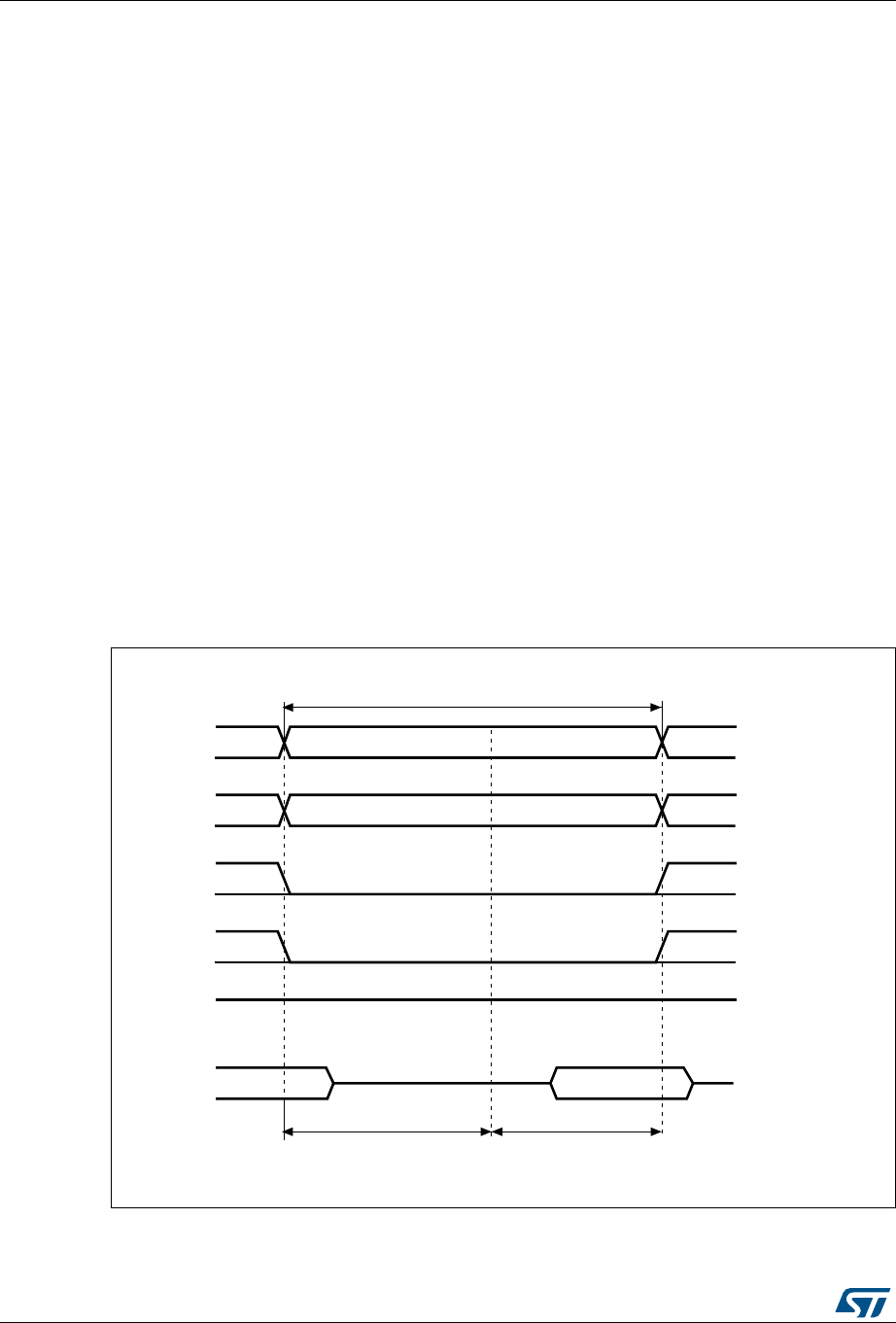
Flexible static memory controller (FSMC) RM0090
1534/1718 DocID018909 Rev 9
36.5.4 NOR Flash/PSRAM controller asynchronous transactions
Asynchronous static memories (NOR Flash memory, PSRAM, SRAM)
•Signals are synchronized by the internal clock HCLK. This clock is not issued to the
memory
•The FSMC always samples the data before de-asserting the chip select signal NE. This
guarantees that the memory data-hold timing constraint is met (chip enable high to
data transition, usually 0 ns min.)
•If the extended mode is enabled (EXTMOD bit is set in the FSMC_BCRx register), up
to four extended modes (A, B, C and D) are available. It is possible to mix A, B, C and
D modes for read and write operations. For example, read operation can be performed
in mode A and write in mode B.
•If the extended mode is disabled (EXTMOD bit is reset in the FSMC_BCRx register),
the FSMC can operate in Mode1 or Mode2 as follows:
– Mode 1 is the default mode when SRAM/PSRAM memory type is selected (MTYP
= 0x0 or 0x01 in the FSMC_BCRx register)
– Mode 2 is the default mode when NOR memory type is selected (MTYP = 0x10 in
the FSMC_BCRx register).
Mode 1 - SRAM/PSRAM (CRAM)
The next figures show the read and write transactions for the supported modes followed by
the required configuration of FSMC _BCRx, and FSMC_BTRx/FSMC_BWTRx registers.
Figure 434. Mode1 read accesses
1. NBL[1:0] are driven low during read access.
A[25:0]
NOE
ADDSET DATAST
Memory transaction
NEx
D[15:0]
HCLK cycles HCLK cycles
NWE
NBL[1:0]
data driven
by memory
ai15557
High
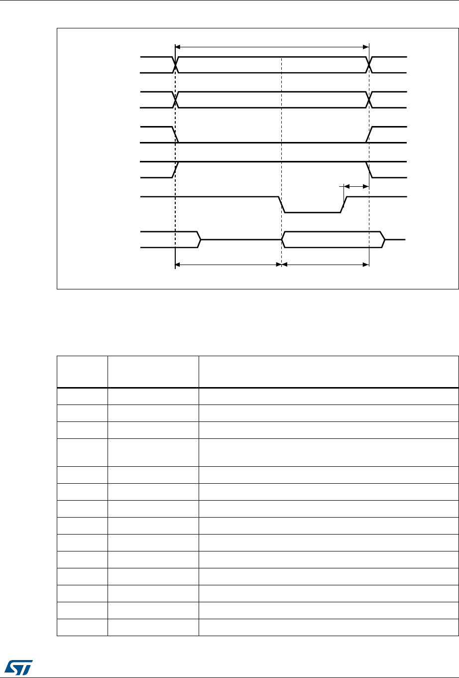
DocID018909 Rev 9 1535/1718
RM0090 Flexible static memory controller (FSMC)
1581
Figure 435. Mode1 write accesses
The one HCLK cycle at the end of the write transaction helps guarantee the address and
data hold time after the NWE rising edge. Due to the presence of this one HCLK cycle, the
DATAST value must be greater than zero (DATAST > 0).
Table 221. FSMC_BCRx bit fields
Bit
number Bit name Value to set
31-20 Reserved 0x000
19 CBURSTRW 0x0 (no effect on asynchronous mode)
18:16 Reserved 0x0
15 ASYNCWAIT Set to 1 if the memory supports this feature. Otherwise keep at
0.
14 EXTMOD 0x0
13 WAITEN 0x0 (no effect on asynchronous mode)
12 WREN As needed
11 WAITCFG Don’t care
10 WRAPMOD 0x0
9 WAITPOL Meaningful only if bit 15 is 1
8 BURSTEN 0x0
7 Reserved 0x1
6 FACCEN Don’t care
5-4 MWID As needed
A[25:0]
NOE
ADDSET (DATAST + 1)
Memory transaction
NEx
D[15:0]
HCLK cycles HCLK cycles
NWE
NBL[1:0]
data driven by FSMC
ai15558
1HCLK

Flexible static memory controller (FSMC) RM0090
1536/1718 DocID018909 Rev 9
3-2 MTYP As needed, exclude 0x2 (NOR Flash)
1 MUXE 0x0
0 MBKEN 0x1
Table 222. FSMC_BTRx bit fields
Bit
number Bit name Value to set
31:30 Reserved 0x0
29-28 ACCMOD Don’t care
27-24 DATLAT Don’t care
23-20 CLKDIV Don’t care
19-16 BUSTURN Time between NEx high to NEx low (BUSTURN HCLK)
15-8 DATAST Duration of the second access phase (DATAST+1 HCLK cycles for
write accesses, DATAST HCLK cycles for read accesses).
7-4 ADDHLD Don’t care
3-0 ADDSET Duration of the first access phase (ADDSET HCLK cycles).
Minimum value for ADDSET is 0.
Table 221. FSMC_BCRx bit fields (continued)
Bit
number Bit name Value to set
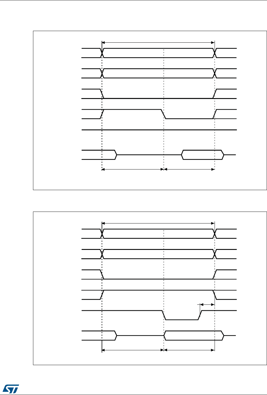
DocID018909 Rev 9 1537/1718
RM0090 Flexible static memory controller (FSMC)
1581
Mode A - SRAM/PSRAM (CRAM) OE toggling
Figure 436. ModeA read accesses
1. NBL[1:0] are driven low during read access.
Figure 437. ModeA write accesses
A[25:0]
NOE
ADDSET DATAST
Memory transaction
NEx
D[15:0]
HCLK cycles HCLK cycles
NWE
NBL[1:0]
data driven
by memory
ai15559
High
A[25:0]
NOE
ADDSET (DATAST + 1)
Memory transaction
NEx
D[15:0]
HCLK cycles HCLK cycles
NWE
NBL[1:0]
data driven by FSMC
ai15560
1HCLK

Flexible static memory controller (FSMC) RM0090
1538/1718 DocID018909 Rev 9
The differences compared with mode1 are the toggling of NOE and the independent read
and write timings.
Table 223. FSMC_BCRx bit fields
Bit
number Bit name Value to set
31-20 Reserved 0x000
19 CBURSTRW 0x0 (no effect on asynchronous mode)
18:16 Reserved 0x0
15 ASYNCWAIT Set to 1 if the memory supports this feature. Otherwise keep at
0.
14 EXTMOD 0x1
13 WAITEN 0x0 (no effect on asynchronous mode)
12 WREN As needed
11 WAITCFG Don’t care
10 WRAPMOD 0x0
9 WAITPOL Meaningful only if bit 15 is 1
8 BURSTEN 0x0
7 Reserved 0x1
6 FACCEN Don’t care
5-4 MWID As needed
3-2 MTYP As needed, exclude 0x2 (NOR Flash)
1 MUXEN 0x0
0 MBKEN 0x1
Table 224. FSMC_BTRx bit fields
Bit
number Bit name Value to set
31:30 Reserved 0x0
29-28 ACCMOD 0x0
27-24 DATLAT Don’t care
23-20 CLKDIV Don’t care
19-16 BUSTURN Time between NEx high to NEx low (BUSTURN HCLK)
15-8 DATAST Duration of the second access phase (DATAST HCLK cycles) for
read accesses.
7-4 ADDHLD Don’t care
3-0 ADDSET
Duration of the first access phase (ADDSET HCLK cycles) for read
accesses.
Minimum value for ADDSET is 0.
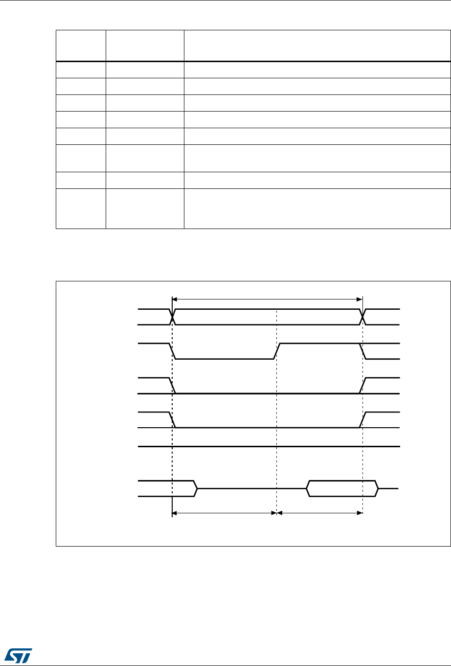
DocID018909 Rev 9 1539/1718
RM0090 Flexible static memory controller (FSMC)
1581
Mode 2/B - NOR Flash
Figure 438. Mode2 and mode B read accesses
Table 225. FSMC_BWTRx bit fields
Bit
number Bit name Value to set
31:30 Reserved 0x0
29-28 ACCMOD 0x0
27-24 DATLAT Don’t care
23-20 CLKDIV Don’t care
19-16 BUSTURN Time between NEx high to NEx low (BUSTURN HCLK)
15-8 DATAST Duration of the second access phase (DATAST+1 HCLK cycles for
write accesses,
7-4 ADDHLD Don’t care
3-0 ADDSET
Duration of the first access phase (ADDSET HCLK cycles) for write
accesses.
Minimum value for ADDSET is 0.
A[25:0]
NOE
ADDSET DATAST
Memory transaction
NEx
D[15:0]
HCLK cycles HCLK cycles
NWE
NADV
data driven
by memory
ai15561
High
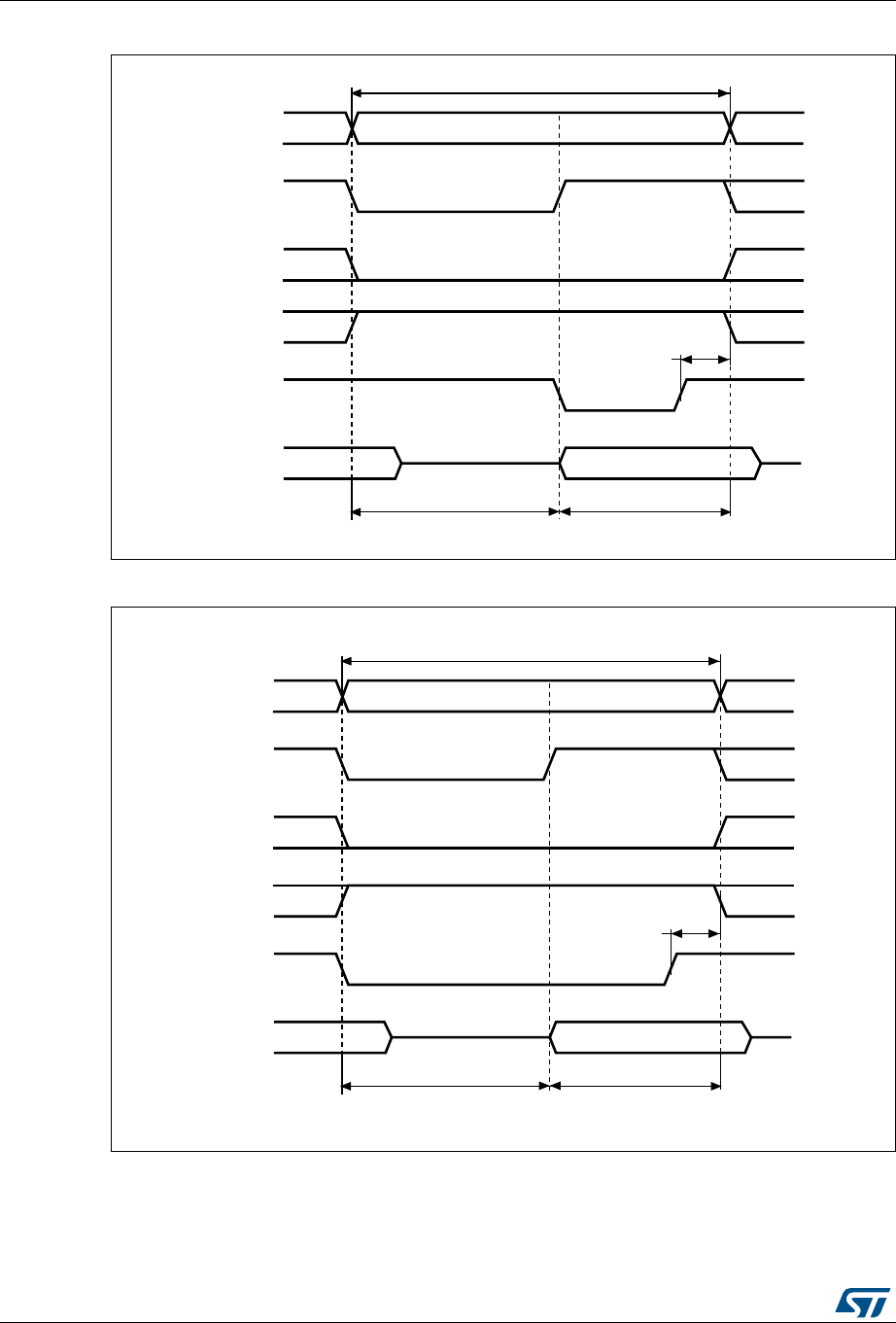
Flexible static memory controller (FSMC) RM0090
1540/1718 DocID018909 Rev 9
Figure 439. Mode2 write accesses
Figure 440. Mode B write accesses
The differences with mode1 are the toggling of NWE and the independent read and write
timings when extended mode is set (Mode B).
A[25:0]
NOE
ADDSET (DATAST + 1)
Memory transaction
NEx
D[15:0]
HCLK cycles HCLK cycles
NWE
NADV
data driven by FSMC
ai15562
1HCLK
A[25:0]
NOE
ADDSET (DATAST + 1)
Memory transaction
NEx
D[15:0]
HCLK cycles HCLK cycles
NWE
NADV
data driven by FSMC
ai15563
1HCLK

DocID018909 Rev 9 1541/1718
RM0090 Flexible static memory controller (FSMC)
1581
Table 226. FSMC_BCRx bit fields
Bit
number Bit name Value to set
31-20 Reserved 0x000
19 CBURSTRW 0x0 (no effect on asynchronous mode)
18:16 Reserved 0x0
15 ASYNCWAIT Set to 1 if the memory supports this feature. Otherwise keep at
0.
14 EXTMOD 0x1 for mode B, 0x0 for mode 2
13 WAITEN 0x0 (no effect on asynchronous mode)
12 WREN As needed
11 WAITCFG Don’t care
10 WRAPMOD 0x0
9 WAITPOL Meaningful only if bit 15 is 1
8 BURSTEN 0x0
7 Reserved 0x1
6 FACCEN 0x1
5-4 MWID As needed
3-2 MTYP 0x2 (NOR Flash memory)
1 MUXEN 0x0
0 MBKEN 0x1
Table 227. FSMC_BTRx bit fields
Bit
number Bit name Value to set
31:30 Reserved 0x0
29-28 ACCMOD 0x1
27-24 DATLAT Don’t care
23-20 CLKDIV Don’t care
19-16 BUSTURN Time between NEx high to NEx low (BUSTURN HCLK)
15-8 DATAST Duration of the second access phase (DATAST HCLK cycles) for
read accesses.
7-4 ADDHLD Don’t care
3-0 ADDSET
Duration of the first access phase (ADDSET HCLK cycles) for read
accesses.
Minimum value for ADDSET is 0.
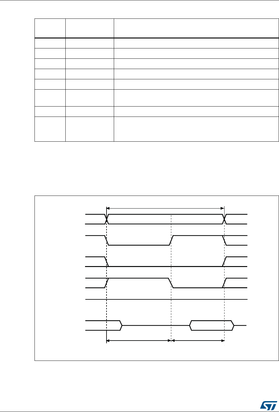
Flexible static memory controller (FSMC) RM0090
1542/1718 DocID018909 Rev 9
Note: The FSMC_BWTRx register is valid only if extended mode is set (mode B), otherwise all its
content is don’t care.
Mode C - NOR Flash - OE toggling
Figure 441. Mode C read accesses
Table 228. FSMC_BWTRx bit fields
Bit
number Bit name Value to set
31:30 Reserved 0x0
29-28 ACCMOD 0x1
27-24 DATLAT Don’t care
23-20 CLKDIV Don’t care
19-16 BUSTURN Time between NEx high to NEx low (BUSTURN HCLK)
15-8 DATAST Duration of the second access phase (DATAST+1 HCLK cycles for
write accesses,
7-4 ADDHLD Don’t care
3-0 ADDSET
Duration of the first access phase (ADDSET HCLK cycles) for write
accesses.
Minimum value for ADDSET is 0.
A[25:0]
NOE
ADDSET DATAST
Memory transaction
NEx
D[15:0]
HCLK cycles HCLK cycles
NWE
NADV
data driven
by memory
ai15564
High
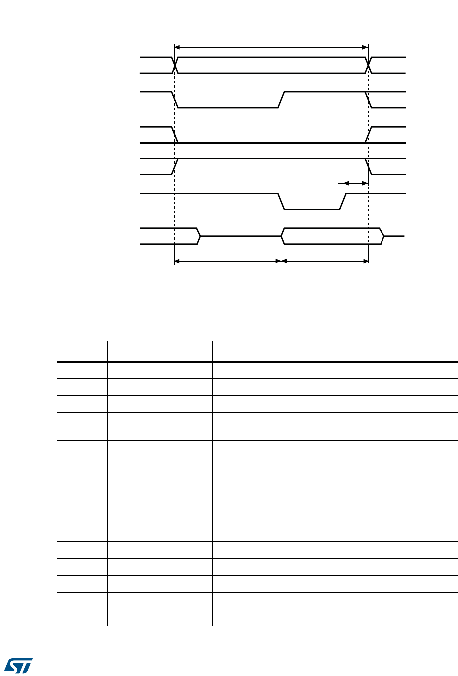
DocID018909 Rev 9 1543/1718
RM0090 Flexible static memory controller (FSMC)
1581
Figure 442. Mode C write accesses
The differences compared with mode1 are the toggling of NOE and the independent read
and write timings.
Table 229. FSMC_BCRx bit fields
Bit No. Bit name Value to set
31-20 Reserved 0x000
19 CBURSTRW 0x0 (no effect on asynchronous mode)
18:16 Reserved 0x0
15 ASYNCWAIT Set to 1 if the memory supports this feature. Otherwise keep
at 0.
14 EXTMOD 0x1
13 WAITEN 0x0 (no effect on asynchronous mode)
12 WREN As needed
11 WAITCFG Don’t care
10 WRAPMOD 0x0
9 WAITPOL Meaningful only if bit 15 is 1
8 BURSTEN 0x0
7 Reserved 0x1
6 FACCEN 0x1
5-4 MWID As needed
3-2 MTYP 0x2 (NOR Flash memory)
A[25:0]
NOE
ADDSET (DATAST + 1)
Memory transaction
NEx
D[15:0]
HCLK cycles HCLK cycles
NWE
NADV
data driven by FSMC
ai15565
1HCLK

Flexible static memory controller (FSMC) RM0090
1544/1718 DocID018909 Rev 9
1 MUXEN 0x0
0 MBKEN 0x1
Table 230. FSMC_BTRx bit fields
Bit
number Bit name Value to set
31:30 Reserved 0x0
29-28 ACCMOD 0x2
27-24 DATLAT 0x0
23-20 CLKDIV 0x0
19-16 BUSTURN Time between NEx high to NEx low (BUSTURN HCLK)
15-8 DATAST Duration of the second access phase (DATAST HCLK cycles) for
read accesses.
7-4 ADDHLD Don’t care
3-0 ADDSET
Duration of the first access phase (ADDSET HCLK cycles) for read
accesses.
Minimum value for ADDSET is 0.
Table 231. FSMC_BWTRx bit fields
Bit
number Bit name Value to set
31:30 Reserved 0x0
29-28 ACCMOD 0x2
27-24 DATLAT Don’t care
23-20 CLKDIV Don’t care
19-16 BUSTURN Time between NEx high to NEx low (BUSTURN HCLK)
15-8 DATAST Duration of the second access phase (DATAST+1 HCLK cycles for
write accesses,
7-4 ADDHLD Don’t care
3-0 ADDSET
Duration of the first access phase (ADDSET HCLK cycles) for write
accesses.
Minimum value for ADDSET is 0.
Table 229. FSMC_BCRx bit fields (continued)
Bit No. Bit name Value to set
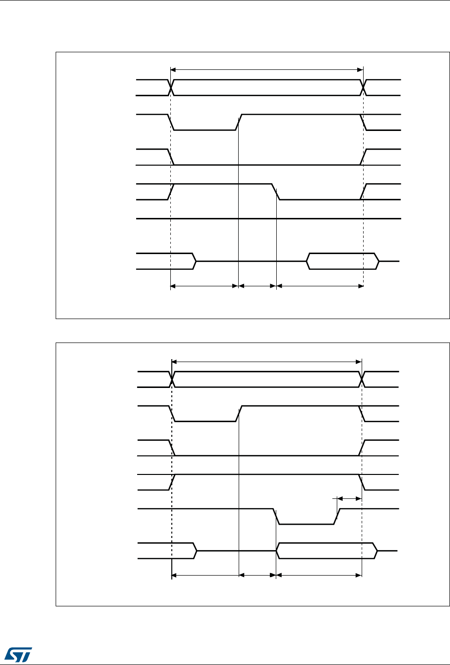
DocID018909 Rev 9 1545/1718
RM0090 Flexible static memory controller (FSMC)
1581
Mode D - asynchronous access with extended address
Figure 443. Mode D read accesses
Figure 444. Mode D write accesses
A[25:0]
NOE
ADDSET DATAST
Memory transaction
NEx
D[15:0]
HCLK cycles HCLK cycles
NWE
NADV
data driven
by memory
ai15566
High
ADDHLD
HCLK cycles
A[25:0]
NOE
ADDSET (DATAST+ 1)
Memory transaction
NEx
D[15:0]
HCLK cycles HCLK cycles
NWE
NADV
data driven by FSMC
ai15567
1HCLK
ADDHLD
HCLK cycles

Flexible static memory controller (FSMC) RM0090
1546/1718 DocID018909 Rev 9
The differences with mode1 are the toggling of NOE that goes on toggling after NADV
changes and the independent read and write timings.
Table 232. FSMC_BCRx bit fields
Bit No. Bit name Value to set
31-20 Reserved 0x000
19 CBURSTRW 0x0 (no effect on asynchronous mode)
18:16 Reserved 0x0
15 ASYNCWAIT Set to 1 if the memory supports this feature. Otherwise keep
at 0.
14 EXTMOD 0x1
13 WAITEN 0x0 (no effect on asynchronous mode)
12 WREN As needed
11 WAITCFG Don’t care
10 WRAPMOD 0x0
9 WAITPOL Meaningful only if bit 15 is 1
8 BURSTEN 0x0
7 Reserved 0x1
6 FACCEN Set according to memory support
5-4 MWID As needed
3-2 MTYP As needed
1 MUXEN 0x0
0 MBKEN 0x1
Table 233. FSMC_BTRx bit fields
Bit No. Bit name Value to set
31:30 Reserved 0x0
29-28 ACCMOD 0x3
27-24 DATLAT Don’t care
23-20 CLKDIV Don’t care
19-16 BUSTURN Time between NEx high to NEx low (BUSTURN HCLK)
15-8 DATAST Duration of the second access phase (DATAST HCLK cycles) for
read accesses.
7-4 ADDHLD Duration of the middle phase of the read access (ADDHLD HCLK
cycles)
3-0 ADDSET Duration of the first access phase (ADDSET HCLK cycles) for read
accesses. Minimum value for ADDSET is 0.
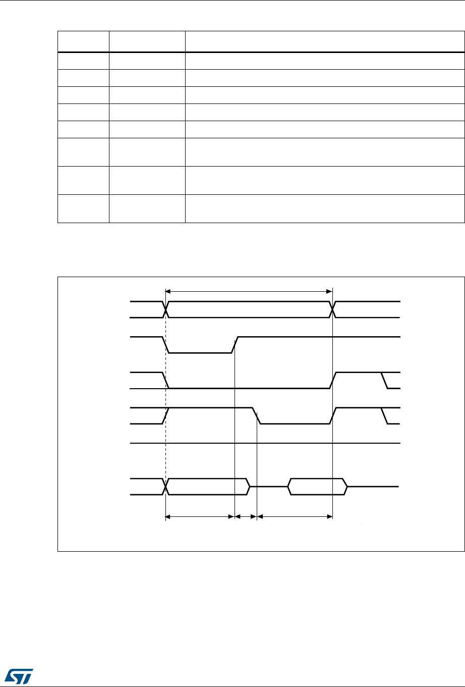
DocID018909 Rev 9 1547/1718
RM0090 Flexible static memory controller (FSMC)
1581
Muxed mode - multiplexed asynchronous access to NOR Flash memory
Figure 445. Multiplexed read accesses
Table 234. FSMC_BWTRx bit fields
Bit No. Bit name Value to set
31:30 Reserved 0x0
29-28 ACCMOD 0x3
27-24 DATLAT 0x0
23-20 CLKDIV 0x0
19-16 BUSTURN Time between NEx high to NEx low (BUSTURN HCLK)
15-8 DATAST Duration of the second access phase (DATAST+1 HCLK cycles) for
write accesses
7-4 ADDHLD Duration of the middle phase of the write access (ADDHLD HCLK
cycles)
3-0 ADDSET Duration of the first access phase (ADDSET+1 HCLK cycles) for
write accesses. Minimum value for ADDSET is 0.
A[25:16]
NOE
ADDSET DATAST
Memory transaction
NEx
AD[15:0]
HCLK cycles HCLK cycles
NWE
NADV
data driven
by memory
ai15568
High
ADDHLD
HCLK cycles
Lower address
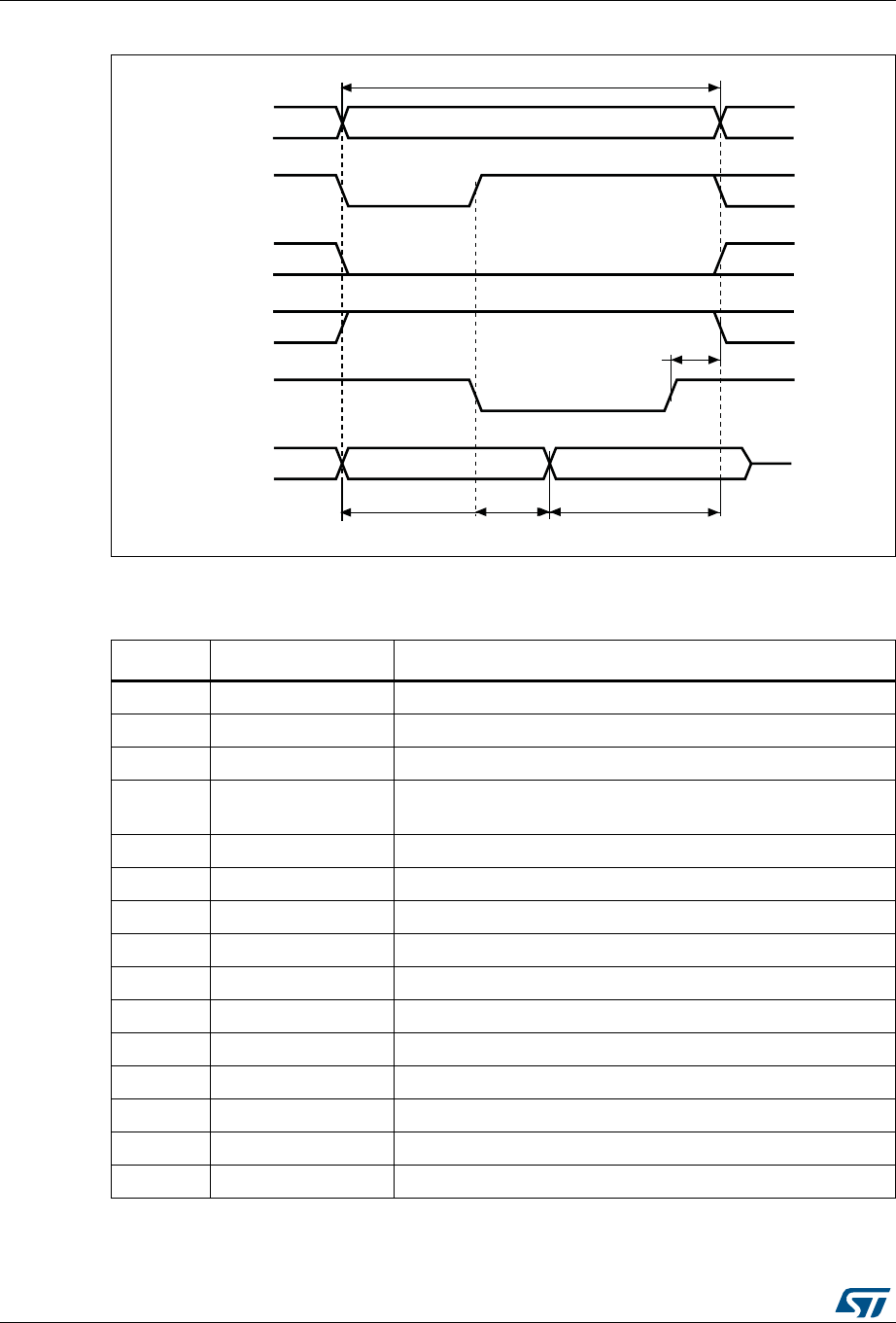
Flexible static memory controller (FSMC) RM0090
1548/1718 DocID018909 Rev 9
Figure 446. Multiplexed write accesses
The difference with mode D is the drive of the lower address byte(s) on the databus.
Table 235. FSMC_BCRx bit fields
Bit No. Bit name Value to set
31-21 Reserved 0x000
19 CBURSTRW 0x0 (no effect on asynchronous mode)
18:16 Reserved 0x0
15 ASYNCWAIT Set to 1 if the memory supports this feature. Otherwise keep at
0.
14 EXTMOD 0x0
13 WAITEN 0x0 (no effect on asynchronous mode)
12 WREN As needed
11 WAITCFG Don’t care
10 WRAPMOD 0x0
9 WAITPOL Meaningful only if bit 15 is 1
8 BURSTEN 0x0
7 Reserved 0x1
6 FACCEN 0x1
5-4 MWID As needed
3-2 MTYP 0x2 (NOR Flash memory)
A[25:16]
NOE
ADDSET (DATAST + 1)
Memory transaction
NEx
AD[15:0]
HCLK cycles HCLK cycles
NWE
NADV
data driven by FSMC
ai15569
1HCLK
ADDHLD
HCLK cycles
Lower address

DocID018909 Rev 9 1549/1718
RM0090 Flexible static memory controller (FSMC)
1581
WAIT management in asynchronous accesses
If the asynchronous memory asserts a WAIT signal to indicate that it is not yet ready to
accept or to provide data, the ASYNCWAIT bit has to be set in FSMC_BCRx register.
If the WAIT signal is active (high or low depending on the WAITPOL bit), the second access
phase (Data setup phase) programmed by the DATAST bits, is extended until WAIT
becomes inactive. Unlike the data setup phase, the first access phases (Address setup and
Address hold phases), programmed by the ADDSET and ADDHLD bits, are not WAIT
sensitive and so they are not prolonged.
The data setup phase (DATAST in the FSMC_BTRx register) must be programmed so that
WAIT can be detected 4 HCLK cycles before the end of memory transaction. The following
cases must be considered:
1 MUXEN 0x1
0 MBKEN 0x1
Table 236. FSMC_BTRx bit fields
Bit No. Bit name Value to set
31:30 Reserved 0x0
29-28 ACCMOD 0x0
27-24 DATLAT Don’t care
23-20 CLKDIV Don’t care
19-16 BUSTURN Time between NEx high to NEx low (BUSTURN HCLK)
15-8 DATAST Duration of the second access phase (DATAST HCLK cycles for
read accesses and DATAST+1 HCLK cycles for write accesses).
7-4 ADDHLD Duration of the middle phase of the access (ADDHLD HCLK cycles).
3-0 ADDSET Duration of the first access phase (ADDSET HCLK cycles).
Minimum value for ADDSET is 1.
Table 235. FSMC_BCRx bit fields (continued)
Bit No. Bit name Value to set
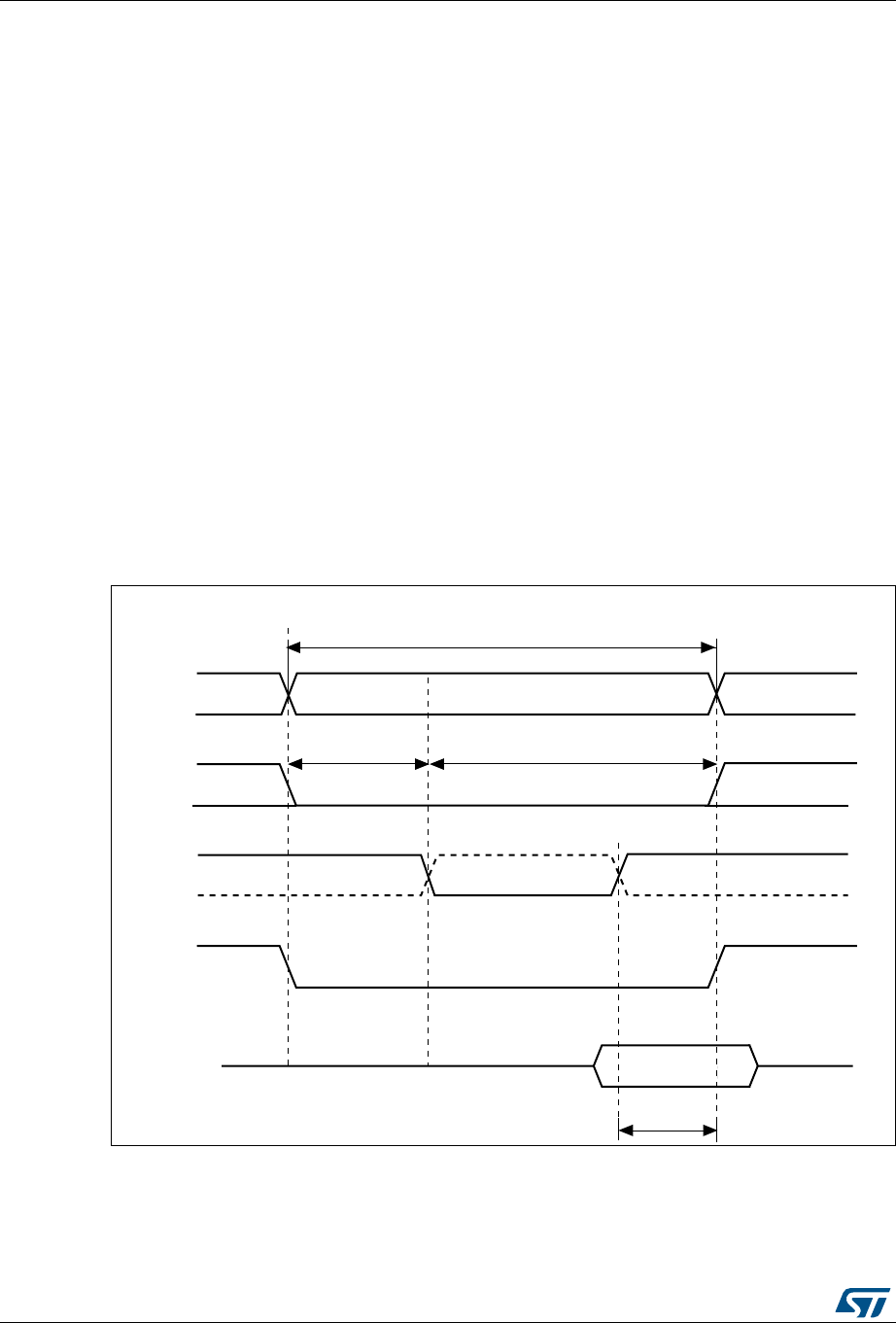
Flexible static memory controller (FSMC) RM0090
1550/1718 DocID018909 Rev 9
1. DATAST in FSMC_BTRx register) Memory asserts the WAIT signal aligned to
NOE/NWE which toggles:
2. Memory asserts the WAIT signal aligned to NEx (or NOE/NWE not toggling):
if
then
otherwise
where max_wait_assertion_time is the maximum time taken by the memory to assert
the WAIT signal once NEx/NOE/NWE is low.
Figure 447 and Figure 448 show the number of HCLK clock cycles that are added to the
memory access after WAIT is released by the asynchronous memory (independently of the
above cases).
Figure 447. Asynchronous wait during a read access
1. NWAIT polarity depends on WAITPOL bit setting in FSMC_BCRx register.
DATAST 4 HCLK×()max_wait_assertion_time+≥
max_wait_assertion_time address_phase hold_phase+>
DATAST 4 HCLK×()max_wait_assertion_time address_phase–hold_phase–()+≥
DATAST 4 HCLK×≥
!;=
./%
(#,+
-EMORYTRANSACTION
.7!)4
$;=
.%X
DATADRIVEN
BYMEMORY
ADDRESSPHASE
DONTCARE
DATASETUPPHASE
DONTCARE
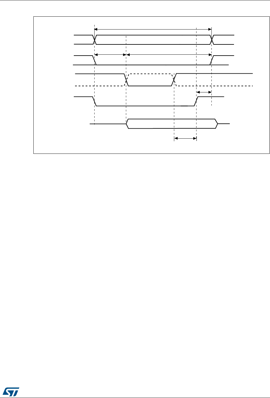
DocID018909 Rev 9 1551/1718
RM0090 Flexible static memory controller (FSMC)
1581
Figure 448. Asynchronous wait during a write access
1. NWAIT polarity depends on WAITPOL bit setting in FSMC_BCRx register.
!;=
.7%
-EMORYTRANSACTION
.7!)4
$;=
.%X
DATADRIVENBY&3-#
AIC
(#,+
ADDRESSPHASE DATASETUPPHASE
(#,+
DONTCARE DONTCARE

Flexible static memory controller (FSMC) RM0090
1552/1718 DocID018909 Rev 9
36.5.5 Synchronous transactions
The memory clock, CLK, is a submultiple of HCLK according to the value of parameter
CLKDIV.
NOR Flash memories specify a minimum time from NADV assertion to CLK high. To meet
this constraint, the FSMC does not issue the clock to the memory during the first internal
clock cycle of the synchronous access (before NADV assertion). This guarantees that the
rising edge of the memory clock occurs in the middle of the NADV low pulse.
Data latency versus NOR Flash latency
The data latency is the number of cycles to wait before sampling the data. The DATLAT
value must be consistent with the latency value specified in the NOR Flash configuration
register. The FSMC does not include the clock cycle when NADV is low in the data latency
count.
Caution: Some NOR Flash memories include the NADV Low cycle in the data latency count, so the
exact relation between the NOR Flash latency and the FMSC DATLAT parameter can be
either of:
•NOR Flash latency = (DATLAT + 2) CLK clock cycles
•NOR Flash latency = (DATLAT + 3) CLK clock cycles
Some recent memories assert NWAIT during the latency phase. In such cases DATLAT can
be set to its minimum value. As a result, the FSMC samples the data and waits long enough
to evaluate if the data are valid. Thus the FSMC detects when the memory exits latency and
real data are taken.
Other memories do not assert NWAIT during latency. In this case the latency must be set
correctly for both the FSMC and the memory, otherwise invalid data are mistaken for good
data, or valid data are lost in the initial phase of the memory access.
Single-burst transfer
When the selected bank is configured in burst mode for synchronous accesses, if for
example an AHB single-burst transaction is requested on 16-bit memories, the FSMC
performs a burst transaction of length 1 (if the AHB transfer is 16-bit), or length 2 (if the AHB
transfer is 32-bit) and de-assert the chip select signal when the last data is strobed.
Clearly, such a transfer is not the most efficient in terms of cycles (compared to an
asynchronous read). Nevertheless, a random asynchronous access would first require to re-
program the memory access mode, which would altogether last longer.
Wait management
For synchronous NOR Flash memories, NWAIT is evaluated after the programmed latency
period, (DATLAT+2) CLK clock cycles.
If NWAIT is sensed active (low level when WAITPOL = 0, high level when WAITPOL = 1),
wait states are inserted until NWAIT is sensed inactive (high level when WAITPOL = 0, low
level when WAITPOL = 1).
When NWAIT is inactive, the data is considered valid either immediately (bit WAITCFG = 1)
or on the next clock edge (bit WAITCFG = 0).
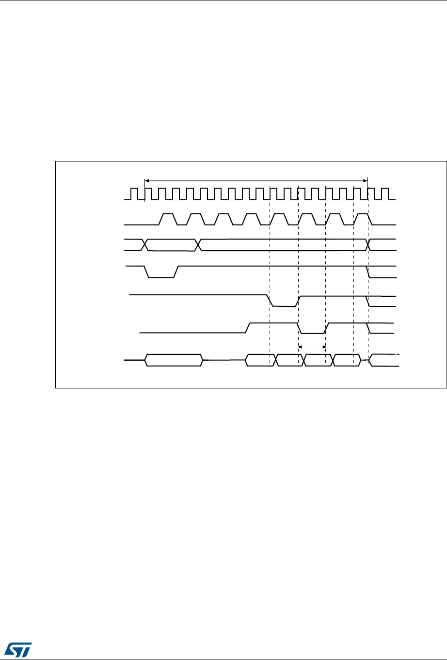
DocID018909 Rev 9 1553/1718
RM0090 Flexible static memory controller (FSMC)
1581
During wait-state insertion via the NWAIT signal, the controller continues to send clock
pulses to the memory, keeping the chip select and output enable signals valid, and does not
consider the data valid.
There are two timing configurations for the NOR Flash NWAIT signal in burst mode:
•Flash memory asserts the NWAIT signal one data cycle before the wait state (default
after reset)
•Flash memory asserts the NWAIT signal during the wait state
These two NOR Flash wait state configurations are supported by the FSMC, individually for
each chip select, thanks to the WAITCFG bit in the FSMC_BCRx registers (x = 0..3).
Figure 449. Wait configurations
AADDR;= DATA DATA
ADDR;=
-EMORYTRANSACTIONBURSTOFHALFWORDS
(#,+
#,+
!;=
.!$6
.7!)4
7!)4#&'
!$;=
INSERTEDWAITSTATE
DATA
.7!)4
7!)4#&'
AIB
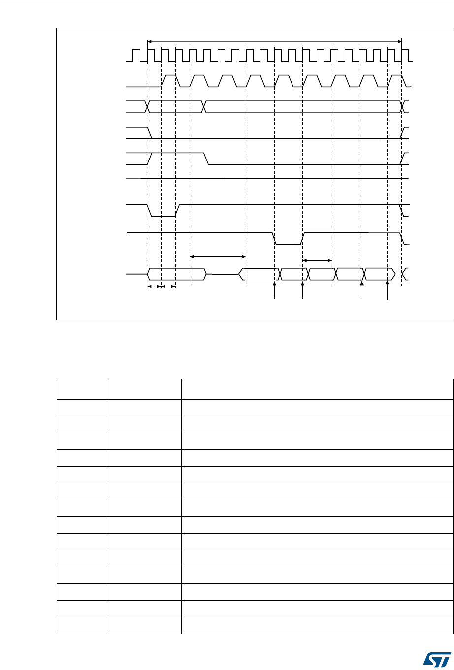
Flexible static memory controller (FSMC) RM0090
1554/1718 DocID018909 Rev 9
Figure 450. Synchronous multiplexed read mode - NOR, PSRAM (CRAM)
1. Byte lane outputs BL are not shown; for NOR access, they are held high, and, for PSRAM (CRAM) access,
they are held low.
2. NWAIT polarity is set to 0.
Table 237. FSMC_BCRx bit fields
Bit No. Bit name Value to set
31-20 Reserved 0x000
19 CBURSTRW No effect on synchronous read
18-16 Reserved 0x0
15 ASCYCWAIT 0x0
14 EXTMOD 0x0
13 WAITEN Set to 1 if the memory supports this feature, otherwise keep at 0.
12 WREN no effect on synchronous read
11 WAITCFG to be set according to memory
10 WRAPMOD 0x0
9 WAITPOL to be set according to memory
8 BURSTEN 0x1
7 Reserved 0x1
6 FACCEN Set according to memory support (NOR Flash memory)
5-4 MWID As needed
$GGU>@ GDWD GDWD
DGGU>@
0HPRU\WUDQVDFWLRQ EXUVWRIKDOIZRUGV
+&/.
&/.
$>@
1([
12(
1:( +LJK
1$'9
1:$,7
:$,7&)*
$'>@
FORFN
F\FOH
FORFN
F\FOH
'$7/$7 LQVHUWHGZDLWVWDWH
'DWDVWUREHV DLI
&/.F\FOHV
GDWD GDWD
'DWDVWUREHV

DocID018909 Rev 9 1555/1718
RM0090 Flexible static memory controller (FSMC)
1581
3-2 MTYP 0x1 or 0x2
1 MUXEN As needed
0 MBKEN 0x1
Table 238. FSMC_BTRx bit fields
Bit No. Bit name Value to set
31:30 Reserved 0x0
29:28 ACCMOD 0x0
27-24 DATLAT Data latency
23-20 CLKDIV
0x0 to get CLK = HCLK (not supported)
0x1 to get CLK = 2 × HCLK
..
19-16 BUSTURN Time between NEx high to NEx low (BUSTURN HCLK)
15-8 DATAST Don’t care
7-4 ADDHLD Don’t care
3-0 ADDSET Don’t care
Table 237. FSMC_BCRx bit fields (continued)
Bit No. Bit name Value to set
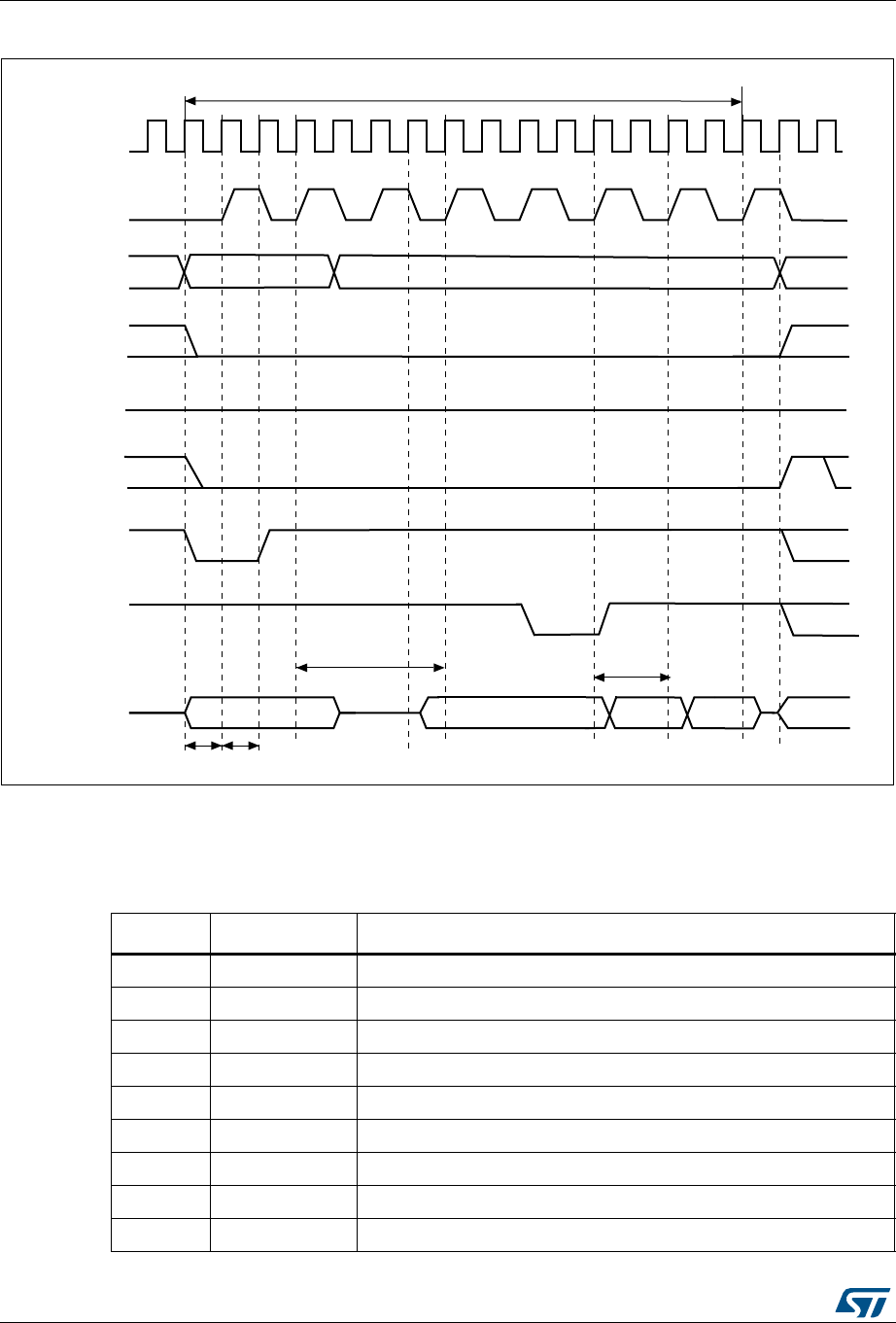
Flexible static memory controller (FSMC) RM0090
1556/1718 DocID018909 Rev 9
Figure 451. Synchronous multiplexed write mode - PSRAM (CRAM)
1. Memory must issue NWAIT signal one cycle in advance, accordingly WAITCFG must be programmed to 0.
2. NWAIT polarity is set to 0.
3. Byte Lane (NBL) outputs are not shown, they are held low while NEx is active.
!DDR;= DATA
ADDR;=
-EMORYTRANSACTIONBURSTOFHALFWORDS
(#,+
#,+
!;=
.%X
./%
.7%
(I:
.!$6
.7!)4
7!)4#&'
!$;=
CLOCK CLOCK
$!4,!4 INSERTEDWAITSTATE
AIF
#,+CYCLES
DATA
Table 239. FSMC_BCRx bit fields
Bit No. Bit name Value to set
31-20 Reserved 0x000
19 CBURSTRW 0x1
18-16 Reserved 0x0
15 ASCYCWAIT 0x0
14 EXTMOD 0x0
13 WAITEN Set to 1 if the memory supports this feature, otherwise keep at 0.
12 WREN 0x1
11 WAITCFG 0x0
10 WRAPMOD 0x0

DocID018909 Rev 9 1557/1718
RM0090 Flexible static memory controller (FSMC)
1581
9 WAITPOL to be set according to memory
8 BURSTEN no effect on synchronous write
7 Reserved 0x1
6 FACCEN Set according to memory support
5-4 MWID As needed
3-2 MTYP 0x1
1 MUXEN As needed
0 MBKEN 0x1
Table 240. FSMC_BTRx bit fields
Bit No. Bit name Value to set
31:30 Reserved 0x0
29:28 ACCMOD 0x0
27-24 DATLAT Data latency
23-20 CLKDIV 0x0 to get CLK = HCLK (not supported)
0x1 to get CLK = 2 × HCLK
19-16 BUSTURN Time between NEx high to NEx low (BUSTURN HCLK)
15-8 DATAST Don’t care
7-4 ADDHLD Don’t care
3-0 ADDSET Don’t care
Table 239. FSMC_BCRx bit fields (continued)
Bit No. Bit name Value to set

Flexible static memory controller (FSMC) RM0090
1558/1718 DocID018909 Rev 9
36.5.6 NOR/PSRAM control registers
The NOR/PSRAM control registers have to be accessed by words (32 bits).
SRAM/NOR-Flash chip-select control registers 1..4 (FSMC_BCR1..4)
Address offset: 0xA000 0000 + 8 * (x – 1), x = 1...4
Reset value: 0x0000 30DB for Bank1 and 0x0000 30D2 for Bank 2 to 4
This register contains the control information of each memory bank, used for SRAMs,
PSRAM and NOR Flash memories.
3130292827262524232221201918171615141312111098 76543210
Reserved
CBURSTRW
Reserved
ASCYCWAIT
EXTMOD
WAITEN
WREN
WAITCFG
WRAPMOD
WAITPOL
BURSTEN
Reserved
FACCEN
MWID
MTYP
MUXEN
MBKEN
rw rw rw rw rw rw rw rw rw rw rw rw rw rw rw rw
Bits 31: 20 Reserved, must be kept at reset value.
Bit 19 CBURSTRW: Write burst enable.
For Cellular RAM (PSRAM) memories, this bit enables the synchronous burst protocol
during write operations. The enable bit for synchronous read accesses is the
BURSTEN bit in the FSMC_BCRx register.
0: Write operations are always performed in asynchronous mode
1: Write operations are performed in synchronous mode.
Bits 18: 16 Reserved, must be kept at reset value.
Bit 15 ASYNCWAIT: Wait signal during asynchronous transfers
This bit enables/disables the FSMC to use the wait signal even during an asynchronous
protocol.
0: NWAIT signal is not taken into account when running an asynchronous protocol
(default after reset)
1: NWAIT signal is taken into account when running an asynchronous protocol
Bit 14 EXTMOD: Extended mode enable.
This bit enables the FSMC to program the write timings for non-multiplexed
asynchronous accesses inside the FSMC_BWTR register, thus resulting in different
timings for read and write operations.
0: values inside FSMC_BWTR register are not taken into account (default after reset)
1: values inside FSMC_BWTR register are taken into account
Note: When the extended mode is disabled, the FSMC can operate in Mode1 or Mode2
as follows:
– Mode 1 is the default mode when the SRAM/PSRAM memory type is selected
(MTYP =0x0 or 0x01)
– Mode 2 is the default mode when the NOR memory type is selected (MTYP =
0x10).

DocID018909 Rev 9 1559/1718
RM0090 Flexible static memory controller (FSMC)
1581
Bit 13 WAITEN: Wait enable bit.
This bit enables/disables wait-state insertion via the NWAIT signal when accessing the
Flash memory in synchronous mode.
0: NWAIT signal is disabled (its level not taken into account, no wait state inserted after
the programmed Flash latency period)
1: NWAIT signal is enabled (its level is taken into account after the programmed Flash
latency period to insert wait states if asserted) (default after reset)
Bit 12 WREN: Write enable bit.
This bit indicates whether write operations are enabled/disabled in the bank by the
FSMC:
0: Write operations are disabled in the bank by the FSMC, an AHB error is reported,
1: Write operations are enabled for the bank by the FSMC (default after reset).
Bit 11 WAITCFG: Wait timing configuration.
The NWAIT signal indicates whether the data from the memory are valid or if a wait
state must be inserted when accessing the Flash memory in synchronous mode. This
configuration bit determines if NWAIT is asserted by the memory one clock cycle
before the wait state or during the wait state:
0: NWAIT signal is active one data cycle before wait state (default after reset),
1: NWAIT signal is active during wait state (not used for PRAM).
Bit 10 WRAPMOD: Wrapped burst mode support.
Defines whether the controller will or not split an AHB burst wrap access into two linear
accesses. Valid only when accessing memories in burst mode
0: Direct wrapped burst is not enabled (default after reset),
1: Direct wrapped burst is enabled.
Note: This bit has no effect as the CPU and DMA cannot generate wrapping burst
transfers.
Bit 9 WAITPOL: Wait signal polarity bit.
Defines the polarity of the wait signal from memory. Valid only when accessing the
memory in burst mode:
0: NWAIT active low (default after reset),
1: NWAIT active high.
Bit 8 BURSTEN: Burst enable bit.
This bit enables/disables synchronous accesses during read operations. It is valid only
for synchronous memories operating in burst mode:
0: Burst mode disabled (default after reset). Read accesses are performed in
asynchronous mode.
1: Burst mode enable. Read accesses are performed in synchronous mode.
Bit 7 Reserved, must be kept at reset value.
Bit 6 FACCEN: Flash access enable
Enables NOR Flash memory access operations.
0: Corresponding NOR Flash memory access is disabled
1: Corresponding NOR Flash memory access is enabled (default after reset)
Bits 5:4 MWID: Memory databus width.
Defines the external memory device width, valid for all type of memories.
00: 8 bits,
01: 16 bits (default after reset),
10: reserved, do not use,
11: reserved, do not use.

Flexible static memory controller (FSMC) RM0090
1560/1718 DocID018909 Rev 9
Bits 3:2 MTYP: Memory type.
Defines the type of external memory attached to the corresponding memory bank:
00: SRAM (default after reset for Bank 2...4)
01: PSRAM (CRAM)
10: NOR Flash/OneNAND Flash (default after reset for Bank 1)
11: reserved
Bit 1 MUXEN: Address/data multiplexing enable bit.
When this bit is set, the address and data values are multiplexed on the databus, valid
only with NOR and PSRAM memories:
0: Address/Data nonmultiplexed
1: Address/Data multiplexed on databus (default after reset)
Bit 0 MBKEN: Memory bank enable bit.
Enables the memory bank. After reset Bank1 is enabled, all others are disabled.
Accessing a disabled bank causes an ERROR on AHB bus.
0: Corresponding memory bank is disabled
1: Corresponding memory bank is enabled

DocID018909 Rev 9 1561/1718
RM0090 Flexible static memory controller (FSMC)
1581
SRAM/NOR-Flash chip-select timing registers 1..4 (FSMC_BTR1..4)
Address offset: 0xA000 0000 + 0x04 + 8 * (x – 1), x = 1..4
Reset value: 0x0FFF FFFF
This register contains the control information of each memory bank, used for SRAMs,
PSRAM and NOR Flash memories.If the EXTMOD bit is set in the FSMC_BCRx register,
then this register is partitioned for write and read access, that is, 2 registers are available:
one to configure read accesses (this register) and one to configure write accesses
(FSMC_BWTRx registers).
313029282726252423222120191817161514131211109876543210
Reserved
ACCMOD
DATLAT
CLKDIV
BUSTURN
DATAST
ADDHLD
ADDSET
rw rw rw rw rw rw rw rw rw rw rw rw rw rw rw rw rw rw rw rw rw rw rw rw rw rw rw rw rw rw
Bits 31:30 Reserved, must be kept at reset value.
Bits 29:28 ACCMOD: Access mode
Specifies the asynchronous access modes as shown in the timing diagrams. These bits are
taken into account only when the EXTMOD bit in the FSMC_BCRx register is 1.
00: access mode A
01: access mode B
10: access mode C
11: access mode D
Bits 27:24 DATLAT: Data latency for synchronous memory (see note below bit description table)
For synchronous accesses with read/write burst mode enabled (BURSTEN / CBURSTRW
bits set), this field defines the number of memory clock cycles (+2) to issue to the memory
before reading/writing the first data. This timing parameter is not expressed in HCLK periods,
but in FSMC_CLK periods. For asynchronous accesses, this value is don't care.
0000: Data latency of 2 CLK clock cycles for first burst access
1111: Data latency of 17 CLK clock cycles for first burst access (default value after reset)
Bits 23:20 CLKDIV: Clock divide ratio (for FSMC_CLK signal)
Defines the period of FSMC_CLK clock output signal, expressed in number of HCLK cycles:
0000: Reserved
0001: FSMC_CLK period = 2 × HCLK periods
0010: FSMC_CLK period = 3 × HCLK periods
1111: FSMC_CLK period = 16 × HCLK periods (default value after reset)
In asynchronous NOR Flash, SRAM or PSRAM accesses, this value is don’t care.
Bits 19:16 BUSTURN: Bus turnaround phase duration
These bits are written by software to add a delay at the end of a write/read transaction. This
delay allows to match the minimum time between consecutive transactions (tEHEL from NEx
high to NEx low) and the maximum time needed by the memory to free the data bus after a
read access (tEHQZ):
(BUSTRUN + 1)HCLK period ≥ tEHELmin and (BUSTRUN + 2)HCLK period ≥ tEHQZmax if
EXTMOD = ‘0’
(BUSTRUN + 2)HCLK period ≥ max (tEHELmin, tEHQZmax) if EXTMOD = ‘1’.
0000: BUSTURN phase duration = 0 HCLK clock cycle added
...
1111: BUSTURN phase duration = 15 × HCLK clock cycles (default value after reset)

Flexible static memory controller (FSMC) RM0090
1562/1718 DocID018909 Rev 9
Note: PSRAMs (CRAMs) have a variable latency due to internal refresh. Therefore these
memories issue the NWAIT signal during the whole latency phase to prolong the latency as
needed.
With PSRAMs (CRAMs) the DATLAT field must be set to 0, so that the FSMC exits its
latency phase soon and starts sampling NWAIT from memory, then starts to read or write
when the memory is ready.
This method can be used also with the latest generation of synchronous Flash memories
that issue the NWAIT signal, unlike older Flash memories (check the datasheet of the
specific Flash memory being used).
SRAM/NOR-Flash write timing registers 1..4 (FSMC_BWTR1..4)
Address offset: 0xA000 0000 + 0x104 + 8 * (x – 1), x = 1...4
Reset value: 0x0FFF FFFF
Bits 15:8 DATAST: Data-phase duration
These bits are written by software to define the duration of the data phase (refer to
Figure 434 to Figure 446), used in asynchronous accesses:
0000 0000: Reserved
0000 0001: DATAST phase duration = 1 × HCLK clock cycles
0000 0010: DATAST phase duration = 2 × HCLK clock cycles
...
1111 1111: DATAST phase duration = 255 × HCLK clock cycles (default value after reset)
For each memory type and access mode data-phase duration, please refer to the respective
figure (Figure 434 to Figure 446).
Example: Mode1, write access, DATAST=1: Data-phase duration= DATAST+1 = 2 HCLK
clock cycles.
Note: In synchronous accesses, this value is don't care.
Bits 7:4 ADDHLD: Address-hold phase duration
These bits are written by software to define the duration of the address hold phase (refer to
Figure 443 to Figure 446), used in mode D and multiplexed accesses:
0000: Reserved
0001: ADDHLD phase duration =1 × HCLK clock cycle
0010: ADDHLD phase duration = 2 × HCLK clock cycle
...
1111: ADDHLD phase duration = 15 × HCLK clock cycles (default value after reset)
For each access mode address-hold phase duration, please refer to the respective figure
(Figure 443 to Figure 446).
Note: In synchronous accesses, this value is not used, the address hold phase is always 1
memory clock period duration.
Bits 3:0 ADDSET: Address setup phase duration
These bits are written by software to define the duration of the address setup phase (refer to
Figure 434 to Figure 446), used in SRAMs, ROMs and asynchronous NOR Flash and
PSRAM accesses:
0000: ADDSET phase duration = 0 × HCLK clock cycle
...
1111: ADDSET phase duration = 15 × HCLK clock cycles (default value after reset)
For each access mode address setup phase duration, please refer to the respective figure
(refer to Figure 434 to Figure 446).
Note: In synchronous NOR Flash and PSRAM accesses, this value is don’t care.

DocID018909 Rev 9 1563/1718
RM0090 Flexible static memory controller (FSMC)
1581
This register contains the control information of each memory bank, used for SRAMs,
PSRAMs and NOR Flash memories. This register is active for write asynchronous access
only when the EXTMOD bit is set in the FSMC_BCRx register.
313029282726252423222120191817161514131211109876543210
Res.
ACCM
OD Reserved BUSTURN DATAST ADDHLD ADDSET
rw rw rw rw rw rw rw rw rw rw rw rw rw rw rw rw rw rw rw rw rw rw
Bits 31:30 Reserved, must be kept at reset value.
Bits 29:28 ACCMOD: Access mode.
Specifies the asynchronous access modes as shown in the next timing diagrams.These bits are
taken into account only when the EXTMOD bit in the FSMC_BCRx register is 1.
00: access mode A
01: access mode B
10: access mode C
11: access mode D
Bits 27:20 Reserved, must be kept at reset value.
Bits 19:16 BUSTURN: Bus turnaround phase duration
These bits are written by software to add a delay at the end of a write transaction to match the
minimum time between consecutive transactions (tEHEL from ENx high to ENx low):
(BUSTRUN + 1) HCLK period ≥ tEHELmin.
0000: BUSTURN phase duration = 0 HCLK clock cycle added
...
1111: BUSTURN phase duration = 15 HCLK clock cycles added (default value after reset)

Flexible static memory controller (FSMC) RM0090
1564/1718 DocID018909 Rev 9
36.6 NAND Flash/PC Card controller
The FSMC generates the appropriate signal timings to drive the following types of device:
•NAND Flash
–8-bit
– 16-bit
•16-bit PC Card compatible devices
The NAND/PC Card controller can control three external banks. Bank 2 and bank 3 support
NAND Flash devices. Bank 4 supports PC Card devices.
Each bank is configured by means of dedicated registers (Section 36.6.8). The
programmable memory parameters include access timings (shown in Table 241) and ECC
configuration.
Bits 15:8 DATAST: Data-phase duration.
These bits are written by software to define the duration of the data phase (refer to Figure 434 to
Figure 446), used in asynchronous SRAM, PSRAM and NOR Flash memory accesses:
0000 0000: Reserved
0000 0001: DATAST phase duration = 1 × HCLK clock cycles
0000 0010: DATAST phase duration = 2 × HCLK clock cycles
...
1111 1111: DATAST phase duration = 255 × HCLK clock cycles (default value after reset)
Note: In synchronous accesses, this value is don't care.
Bits 7:4 ADDHLD: Address-hold phase duration.
These bits are written by software to define the duration of the address hold phase (refer to
Figure 443 to Figure 446), used in asynchronous multiplexed accesses:
0000: Reserved
0001: ADDHLD phase duration = 1 × HCLK clock cycle
0010: ADDHLD phase duration = 2 × HCLK clock cycle
...
1111: ADDHLD phase duration = 15 × HCLK clock cycles (default value after reset)
Note: In synchronous NOR Flash accesses, this value is not used, the address hold phase is always
1 Flash clock period duration.
Bits 3:0 ADDSET: Address setup phase duration.
These bits are written by software to define the duration of the address setup phase in HCLK
cycles (refer to Figure 443 to Figure 446), used in asynchronous accessed:
0000: ADDSET phase duration = 0 × HCLK clock cycle
...
1111: ADDSET phase duration = 15 × HCLK clock cycles (default value after reset)
Note: In synchronous NOR Flash and PSRAM accesses, this value is don’t care.

DocID018909 Rev 9 1565/1718
RM0090 Flexible static memory controller (FSMC)
1581
36.6.1 External memory interface signals
The following tables list the signals that are typically used to interface NAND Flash and PC
Card.
Note: Prefix “N”. specifies the associated signal as active low.
8-bit NAND Flash
t
There is no theoretical capacity limitation as the FSMC can manage as many address
cycles as needed.
Table 241. Programmable NAND/PC Card access parameters
Parameter Function Access mode Unit Min. Max.
Memory setup
time
Number of clock cycles (HCLK)
to set up the address before the
command assertion
Read/Write AHB clock cycle
(HCLK) 1 256
Memory wait Minimum duration (HCLK clock
cycles) of the command assertion Read/Write AHB clock cycle
(HCLK) 2 256
Memory hold
Number of clock cycles (HCLK)
to hold the address (and the data
in case of a write access) after
the command de-assertion
Read/Write AHB clock cycle
(HCLK) 1 255
Memory
databus high-Z
Number of clock cycles (HCLK)
during which the databus is kept
in high-Z state after the start of a
write access
Write AHB clock cycle
(HCLK) 0 255
Table 242. 8-bit NAND Flash
FSMC signal name I/O Function
A[17] O NAND Flash address latch enable (ALE) signal
A[16] O NAND Flash command latch enable (CLE) signal
D[7:0] I/O 8-bit multiplexed, bidirectional address/data bus
NCE[x] O Chip select, x = 2, 3
NOE(= NRE) O Output enable (memory signal name: read enable, NRE)
NWE O Write enable
NWAIT/INT[3:2] I NAND Flash ready/busy input signal to the FSMC

Flexible static memory controller (FSMC) RM0090
1566/1718 DocID018909 Rev 9
16-bit NAND Flash
There is no theoretical capacity limitation as the FSMC can manage as many address
cycles as needed.
16-bit PC Card
Table 243. 16-bit NAND Flash
FSMC signal name I/O Function
A[17] O NAND Flash address latch enable (ALE) signal
A[16] O NAND Flash command latch enable (CLE) signal
D[15:0] I/O 16-bit multiplexed, bidirectional address/data bus
NCE[x] O Chip select, x = 2, 3
NOE(= NRE) O Output enable (memory signal name: read enable, NRE)
NWE O Write enable
NWAIT/INT[3:2] I NAND Flash ready/busy input signal to the FSMC
Table 244. 16-bit PC Card
FSMC signal name I/O Function
A[10:0] O Address bus
NIORD O Output enable for I/O space
NIOWR O Write enable for I/O space
NREG O Register signal indicating if access is in Common or Attribute space
D[15:0] I/O Bidirectional databus
NCE4_1 O Chip select 1
NCE4_2 O Chip select 2 (indicates if access is 16-bit or 8-bit)
NOE O Output enable in Common and in Attribute space
NWE O Write enable in Common and in Attribute space
NWAIT I PC Card wait input signal to the FSMC (memory signal name
IORDY)
INTR I PC Card interrupt to the FSMC (only for PC Cards that can generate
an interrupt)
CD I
PC Card presence detection. Active high. If an access is performed
to the PC Card banks while CD is low, an AHB error is generated.
Refer to Section 36.3: AHB interface

DocID018909 Rev 9 1567/1718
RM0090 Flexible static memory controller (FSMC)
1581
36.6.2 NAND Flash / PC Card supported memories and transactions
Table 245 below shows the supported devices, access modes and transactions.
Transactions not allowed (or not supported) by the NAND Flash / PC Card controller appear
in gray.
36.6.3 Timing diagrams for NAND and PC Card
Each PC Card/CompactFlash and NAND Flash memory bank is managed through a set of
registers:
•Control register: FSMC_PCRx
•Interrupt status register: FSMC_SRx
•ECC register: FSMC_ECCRx
•Timing register for Common memory space: FSMC_PMEMx
•Timing register for Attribute memory space: FSMC_PATTx
•Timing register for I/O space: FSMC_PIOx
Each timing configuration register contains three parameters used to define number of
HCLK cycles for the three phases of any PC Card/CompactFlash or NAND Flash access,
plus one parameter that defines the timing for starting driving the databus in the case of a
write. Figure 452 shows the timing parameter definitions for common memory accesses,
knowing that Attribute and I/O (only for PC Card) memory space access timings are similar.
Table 245. Supported memories and transactions
Device Mode R/W
AHB
data size
Memory
data size
Allowed/
not allowed Comments
NAND 8-bit
Asynchronous R 8 8 Y
Asynchronous W 8 8 Y
Asynchronous R 16 8 Y Split into 2 FSMC accesses
Asynchronous W 16 8 Y Split into 2 FSMC accesses
Asynchronous R 32 8 Y Split into 4 FSMC accesses
Asynchronous W 32 8 Y Split into 4 FSMC accesses
NAND 16-bit
Asynchronous R 8 16 Y
Asynchronous W 8 16 N
Asynchronous R 16 16 Y
Asynchronous W 16 16 Y
Asynchronous R 32 16 Y Split into 2 FSMC accesses
Asynchronous W 32 16 Y Split into 2 FSMC accesses
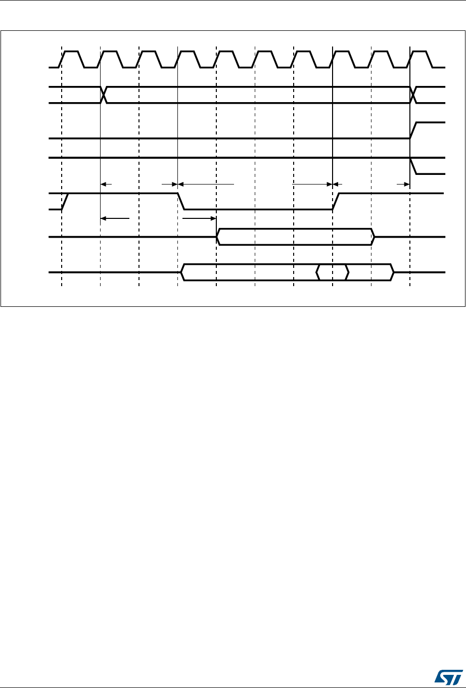
Flexible static memory controller (FSMC) RM0090
1568/1718 DocID018909 Rev 9
Figure 452. NAND/PC Card controller timing for common memory access
1. NOE remains high (inactive) during write access. NWE remains high (inactive) during read access.
36.6.4 NAND Flash operations
The command latch enable (CLE) and address latch enable (ALE) signals of the NAND
Flash device are driven by some address signals of the FSMC controller. This means that to
send a command or an address to the NAND Flash memory, the CPU has to perform a write
to a certain address in its memory space.
A typical page read operation from the NAND Flash device is as follows:
1. Program and enable the corresponding memory bank by configuring the FSMC_PCRx
and FSMC_PMEMx (and for some devices, FSMC_PATTx, see Section 36.6.5: NAND
Flash pre-wait functionality on page 1569) registers according to the characteristics of
the NAND Flash (PWID bits for the databus width of the NAND Flash, PTYP = 1,
PWAITEN = 0 or 1 as needed, see section Common memory space timing register 2..4
(FSMC_PMEM2..4) on page 1575 for timing configuration).
2. The CPU performs a byte write in the common memory space, with data byte equal to
one Flash command byte (for example 0x00 for Samsung NAND Flash devices). The
CLE input of the NAND Flash is active during the write strobe (low pulse on NWE), thus
the written byte is interpreted as a command by the NAND Flash. Once the command
is latched by the NAND Flash device, it does not need to be written for the following
page read operations.
3. The CPU can send the start address (STARTAD) for a read operation by writing the
required bytes (for example four bytes or three for smaller capacity devices),
STARTAD[7:0], STARTAD[15:8], STARTAD[23:16] and finally STARTAD[25:24] for
64 Mb x 8 bit NAND Flash) in the common memory or attribute space. The ALE input of
the NAND Flash device is active during the write strobe (low pulse on NWE), thus the
written bytes are interpreted as the start address for read operations. Using the
IB
(#,+
!;=
.#%X
.2%'
.)/7
.)/2
.7%
./%
WRITE?DATA
READ?DATA
(IGH
6ALID
-%-X3%4
-%-X7!)4
-%-X(/,$
-%-X():
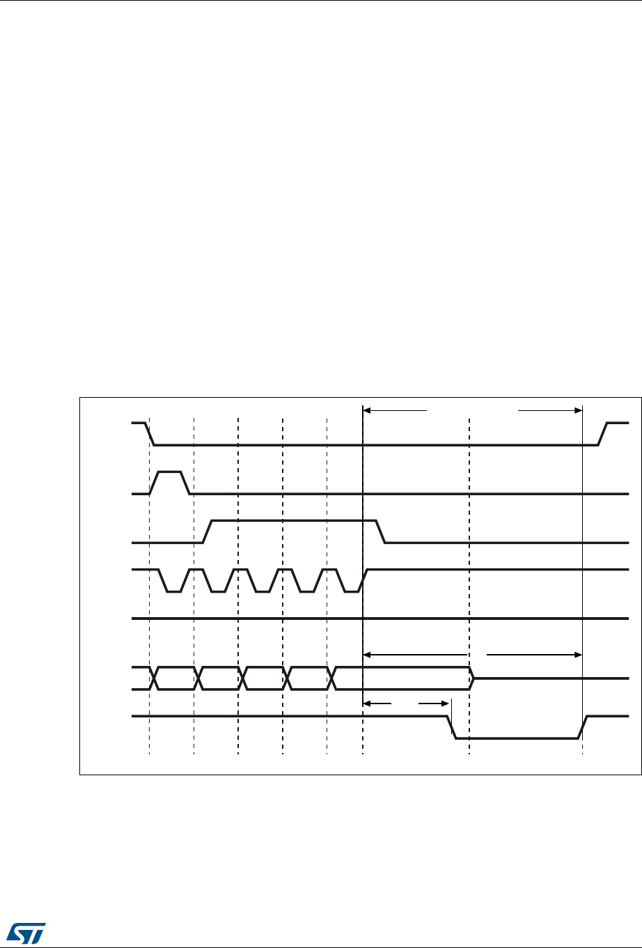
DocID018909 Rev 9 1569/1718
RM0090 Flexible static memory controller (FSMC)
1581
attribute memory space makes it possible to use a different timing configuration of the
FSMC, which can be used to implement the prewait functionality needed by some
NAND Flash memories (see details in Section 36.6.5: NAND Flash pre-wait
functionality on page 1569).
4. The controller waits for the NAND Flash to be ready (R/NB signal high) to become
active, before starting a new access (to same or another memory bank). While waiting,
the controller maintains the NCE signal active (low).
5. The CPU can then perform byte read operations in the common memory space to read
the NAND Flash page (data field + Spare field) byte by byte.
6. The next NAND Flash page can be read without any CPU command or address write
operation, in three different ways:
– by simply performing the operation described in step 5
– a new random address can be accessed by restarting the operation at step 3
– a new command can be sent to the NAND Flash device by restarting at step 2
36.6.5 NAND Flash pre-wait functionality
Some NAND Flash devices require that, after writing the last part of the address, the
controller wait for the R/NB signal to go low as shown in Figure 453.
Figure 453. Access to non ‘CE don’t care’ NAND-Flash
1. CPU wrote byte 0x00 at address 0x7001 0000.
2. CPU wrote byte A7-A0 at address 0x7002 0000.
3. CPU wrote byte A15-A8 at address 0x7002 0000.
4. CPU wrote byte A23-A16 at address 0x7002 0000.
5. CPU wrote byte A25-A24 at address 0x7802 0000: FSMC performs a write access using FSMC_PATT2
timing definition, where ATTHOLD ≥ 7 (providing that (7+1) × HCLK = 112 ns > tWB max). This guarantees
that NCE remains low until R/NB goes low and high again (only requested for NAND Flash memories
where NCE is not don’t care).
.#%
./%
)/;=
2."
AIB
(IGH
T7"
#,%
!,%
X !! !! !! !!
T2
.7%
.#%MUSTSTAYLOW

Flexible static memory controller (FSMC) RM0090
1570/1718 DocID018909 Rev 9
When this functionality is needed, it can be guaranteed by programming the MEMHOLD
value to meet the tWB timing, however any CPU read or write access to the NAND Flash
then has the hold delay of (MEMHOLD + 1) HCLK cycles inserted from the rising edge of
the NWE signal to the next access.
To overcome this timing constraint, the attribute memory space can be used by
programming its timing register with an ATTHOLD value that meets the tWB timing, and
leaving the MEMHOLD value at its minimum. Then, the CPU must use the common memory
space for all NAND Flash read and write accesses, except when writing the last address
byte to the NAND Flash device, where the CPU must write to the attribute memory space.
36.6.6 Computation of the error correction code (ECC)
in NAND Flash memory
The FSMC PC-Card controller includes two error correction code computation hardware
blocks, one per memory bank. They are used to reduce the host CPU workload when
processing the error correction code by software in the system.
These two registers are identical and associated with bank 2 and bank 3, respectively. As a
consequence, no hardware ECC computation is available for memories connected to bank
4.
The error correction code (ECC) algorithm implemented in the FSMC can perform 1-bit error
correction and 2-bit error detection per 256, 512, 1 024, 2 048, 4 096 or 8 192 bytes read
from or written to NAND Flash memory. It is based on the Hamming coding algorithm and
consists in calculating the row and column parity.
The ECC modules monitor the NAND Flash databus and read/write signals (NCE and NWE)
each time the NAND Flash memory bank is active.
The functional operations are:
•When access to NAND Flash is made to bank 2 or bank 3, the data present on the
D[15:0] bus is latched and used for ECC computation.
•When access to NAND Flash occurs at any other address, the ECC logic is idle, and
does not perform any operation. Thus, write operations for defining commands or
addresses to NAND Flash are not taken into account for ECC computation.
Once the desired number of bytes has been read from/written to the NAND Flash by the
host CPU, the FSMC_ECCR2/3 registers must be read in order to retrieve the computed
value. Once read, they should be cleared by resetting the ECCEN bit to zero. To compute a
new data block, the ECCEN bit must be set to one in the FSMC_PCR2/3 registers.
To perform an ECC computation:

DocID018909 Rev 9 1571/1718
RM0090 Flexible static memory controller (FSMC)
1581
1. Enable the ECCEN bit in the FSMC_PCR2/3 register.
2. Write data to the NAND Flash memory page. While the NAND page is written, the ECC
block computes the ECC value.
3. Read the ECC value available in the FSMC_ECCR2/3 register and store it in a
variable.
4. Clear the ECCEN bit and then enable it in the FSMC_PCR2/3 register before reading
back the written data from the NAND page. While the NAND page is read, the ECC
block computes the ECC value.
5. Read the new ECC value available in the FSMC_ECCR2/3 register.
6. If the two ECC values are the same, no correction is required, otherwise there is an
ECC error and the software correction routine returns information on whether the error
can be corrected or not.
36.6.7 PC Card/CompactFlash operations
Address spaces and memory accesses
The FSMC supports Compact Flash storage or PC Cards in Memory Mode and I/O Mode
(True IDE mode is not supported).
The Compact Flash storage and PC Cards are made of 3 memory spaces:
•Common Memory Space
•Attribute Space
•I/O Memory Space
The nCE2 and nCE1 pins (FSMC_NCE4_2 and FSMC_NCE4_1 respectively) select the
card and indicate whether a byte or a word operation is being performed: nCE2 accesses
the odd byte on D15-8 and nCE1 accesses the even byte on D7-0 if A0=0 or the odd byte on
D7-0 if A0=1. The full word is accessed on D15-0 if both nCE2 and nCE1 are low.
The memory space is selected by asserting low nOE for read accesses or nWE for write
accesses, combined with the low assertion of nCE2/nCE1 and nREG.
•If pin nREG=1 during the memory access, the common memory space is selected
•If pin nREG=0 during the memory access, the attribute memory space is selected
The I/O Space is selected by asserting low nIORD for read accesses or nIOWR for write
accesses [instead of nOE/nWE for memory Space], combined with nCE2/nCE1. Note that
nREG must also be asserted low during accesses to I/O Space.
Three type of accesses are allowed for a 16-bit PC Card:
•Accesses to Common Memory Space for data storage can be either 8-bit accesses at
even addresses or 16 bit AHB accesses.
Note that 8-bit accesses at odd addresses are not supported and will not lead to the
low assertion of nCE2. A 32-bit AHB request is translated into two 16-bit memory
accesses.
•Accesses to Attribute Memory Space where the PC Card stores configuration
information are limited to 8-bit AHB accesses at even addresses.
Note that a 16-bit AHB access will be converted into a single 8-bit memory transfer:
nCE1 will be asserted low, nCE2 will be asserted high and only the even Byte on D7-
D0 will be valid. Instead a 32-bit AHB access will be converted into two 8-bit memory

Flexible static memory controller (FSMC) RM0090
1572/1718 DocID018909 Rev 9
transfers at even addresses: nCE1 will be asserted low, NCE2 will be asserted high
and only the even bytes will be valid.
•Accesses to I/O Space can be performed either through AHB 8-bit or 16-bit accesses.
The FSMC Bank 4 gives access to those 3 memory spaces as described in Section 36.4.2:
NAND/PC Card address mapping - Table 213: Memory mapping and timing registers
Wait Feature
The CompactFlash Storage or PC Card may request the FSMC to extend the length of the
access phase programmed by MEMWAITx/ATTWAITx/IOWAITx bits, asserting the nWAIT
signal after nOE/nWE or nIORD/nIOWR activation if the wait feature is enabled through the
PWAITEN bit in the FSMC_PCRx register. In order to detect the nWAIT assertion correctly,
the MEMWAITx/ATTWAITx/IOWAITx bits must be programmed as follows:
Table 246. 16-bit PC-Card signals and access type
nCE2
nCE1
nREG
nOE/nWE
nIORD /nIOWR
A10
A9
A7-1
A0
Space Access Type Allowed/not
Allowed
1 0 101XXX-XX Common
Memory
Space
Read/Write byte on D7-D0 YES
0 1 1 0 1 X X X-X X Read/Write byte on D15-D8 Not supported
0 0 1 0 1 X X X-X 0 Read/Write word on D15-D0 YES
X0 00101X-X0
Attribute
Space
Read or Write Configuration
Registers YES
X0 00100X-X0 Read or Write CIS (Card
Information Structure) YES
1 0 001XXX-X1
Attribute
Space
Invalid Read or Write (odd
address) YES
0 1 001XXX-Xx Invalid Read or Write (odd
address) YES
1 0 010XXX-X0
I/O space
Read Even Byte on D7-0 YES
1 0 0 1 0 X X X-X 1 Read Odd Byte on D7-0 YES
1 0 0 1 0 X X X-X 0 Write Even Byte on D7-0 YES
1 0 0 1 0 X X X-X 1 Write Odd Byte on D7-0 YES
0 0 0 1 0 X X X-X 0 Read Word on D15-0 YES
0 0 0 1 0 X X X-X 0 Write word on D15-0 YES
0 1 0 1 0 X X X-X X Read Odd Byte on D15-8 Not supported
0 1 0 1 0 X X X-X X Write Odd Byte on D15-8 Not supported

DocID018909 Rev 9 1573/1718
RM0090 Flexible static memory controller (FSMC)
1581
xxWAITx >= 4 + max_wait_assertion_time/HCLK
Where max_wait_assertion_time is the maximum time taken by NWAIT to go low once
nOE/nWE or nIORD/nIOWR is low.
After the de-assertion of nWAIT, the FSMC extends the WAIT phase for 4 HCLK clock
cycles.
36.6.8 NAND Flash/PC Card control registers
The NAND Flash/PC Card control registers have to be accessed by words (32 bits).
PC Card/NAND Flash control registers 2..4 (FSMC_PCR2..4)
Address offset: 0xA0000000 + 0x40 + 0x20 * (x – 1), x = 2..4
Reset value: 0x0000 0018
31302928272625242322212019181716151413121110987654321 0
Reserved ECCPS TAR TCLR Res.
ECCEN
PWID
PTYP
PBKEN
PWAITEN
Reserved
rw rw rw rw rw rw rw rw rw rw rw rw rw rw rw rw rw
Bits 31:20 Reserved, must be kept at reset value.
Bits 19:17 ECCPS: ECC page size.
Defines the page size for the extended ECC:
000: 256 bytes
001: 512 bytes
010: 1024 bytes
011: 2048 bytes
100: 4096 bytes
101: 8192 bytes
Bits 16:13 TAR: ALE to RE delay.
Sets time from ALE low to RE low in number of AHB clock cycles (HCLK).
Time is: t_ar = (TAR + SET + 2) × THCLK where THCLK is the HCLK clock period
0000: 1 HCLK cycle (default)
1111: 16 HCLK cycles
Note: SET is MEMSET or ATTSET according to the addressed space.
Bits 12:9 TCLR: CLE to RE delay.
Sets time from CLE low to RE low in number of AHB clock cycles (HCLK).
Time is t_clr = (TCLR + SET + 2) × THCLK where THCLK is the HCLK clock period
0000: 1 HCLK cycle (default)
1111: 16 HCLK cycles
Note: SET is MEMSET or ATTSET according to the addressed space.
Bits 8:7 Reserved, must be kept at reset value.
Bit 6 ECCEN: ECC computation logic enable bit
0: ECC logic is disabled and reset (default after reset),
1: ECC logic is enabled.

Flexible static memory controller (FSMC) RM0090
1574/1718 DocID018909 Rev 9
FIFO status and interrupt register 2..4 (FSMC_SR2..4)
Address offset: 0xA000 0000 + 0x44 + 0x20 * (x-1), x = 2..4
Reset value: 0x0000 0040
This register contains information about FIFO status and interrupt. The FSMC has a FIFO
that is used when writing to memories to store up to16 words of data from the AHB.
This is used to quickly write to the AHB and free it for transactions to peripherals other than
the FSMC, while the FSMC is draining its FIFO into the memory. This register has one of its
bits that indicates the status of the FIFO, for ECC purposes.
The ECC is calculated while the data are written to the memory, so in order to read the
correct ECC the software must wait until the FIFO is empty.
Bits 5:4 PWID: Databus width.
Defines the external memory device width.
00: 8 bits
01: 16 bits (default after reset). This value is mandatory for PC Cards.
10: reserved, do not use
11: reserved, do not use
Bit 3 PTYP: Memory type.
Defines the type of device attached to the corresponding memory bank:
0: PC Card, CompactFlash, CF+ or PCMCIA
1: NAND Flash (default after reset)
Bit 2 PBKEN: PC Card/NAND Flash memory bank enable bit.
Enables the memory bank. Accessing a disabled memory bank causes an ERROR on AHB
bus
0: Corresponding memory bank is disabled (default after reset)
1: Corresponding memory bank is enabled
Bit 1 PWAITEN: Wait feature enable bit.
Enables the Wait feature for the PC Card/NAND Flash memory bank:
0: disabled
1: enabled
Note: For a PC Card, when the wait feature is enabled, the MEMWAITx/ATTWAITx/IOWAITx
bits must be programmed to a value as follows:
xxWAITx ≥ 4 + max_wait_assertion_time/HCLK
Where max_wait_assertion_time is the maximum time taken by NWAIT to go low once
nOE/nWE or nIORD/nIOWR is low.
Bit 0 Reserved, must be kept at reset value.
313029282726252423222120191817161514131211109876543210
Reserved
FEMPT
IFEN
ILEN
IREN
IFS
ILS
IRS
r rwrwrwrwrwrw

DocID018909 Rev 9 1575/1718
RM0090 Flexible static memory controller (FSMC)
1581
Common memory space timing register 2..4 (FSMC_PMEM2..4)
Address offset: Address: 0xA000 0000 + 0x48 + 0x20 * (x – 1), x = 2..4
Reset value: 0xFCFC FCFC
Each FSMC_PMEMx (x = 2..4) read/write register contains the timing information for PC
Card or NAND Flash memory bank x, used for access to the common memory space of the
16-bit PC Card/CompactFlash, or to access the NAND Flash for command, address write
access and data read/write access.
Bits 31:7 Reserved, must be kept at reset value.
Bit 6 FEMPT: FIFO empty.
Read-only bit that provides the status of the FIFO
0: FIFO not empty
1: FIFO empty
Bit 5 IFEN: Interrupt falling edge detection enable bit
0: Interrupt falling edge detection request disabled
1: Interrupt falling edge detection request enabled
Bit 4 ILEN: Interrupt high-level detection enable bit
0: Interrupt high-level detection request disabled
1: Interrupt high-level detection request enabled
Bit 3 IREN: Interrupt rising edge detection enable bit
0: Interrupt rising edge detection request disabled
1: Interrupt rising edge detection request enabled
Bit 2 IFS: Interrupt falling edge status
The flag is set by hardware and reset by software.
0: No interrupt falling edge occurred
1: Interrupt falling edge occurred
Bit 1 ILS: Interrupt high-level status
The flag is set by hardware and reset by software.
0: No Interrupt high-level occurred
1: Interrupt high-level occurred
Bit 0 IRS: Interrupt rising edge status
The flag is set by hardware and reset by software.
0: No interrupt rising edge occurred
1: Interrupt rising edge occurred
313029282726252423222120191817161514131211109876543210
MEMHIZx MEMHOLDx MEMWAITx MEMSETx
rw rw rw rw rw rw rw rw rw rw rw rw rw rw rw rw rw rw rw rw rw rw rw rw rw rw rw rw rw rw rw rw

Flexible static memory controller (FSMC) RM0090
1576/1718 DocID018909 Rev 9
Attribute memory space timing registers 2..4 (FSMC_PATT2..4)
Address offset: 0xA000 0000 + 0x4C + 0x20 * (x – 1), x = 2..4
Reset value: 0xFCFC FCFC
Each FSMC_PATTx (x = 2..4) read/write register contains the timing information for PC
Card/CompactFlash or NAND Flash memory bank x. It is used for 8-bit accesses to the
attribute memory space of the PC Card/CompactFlash or to access the NAND Flash for the
last address write access if the timing must differ from that of previous accesses (for
Ready/Busy management, refer to Section 36.6.5: NAND Flash pre-wait functionality).
Bits 31:24 MEMHIZx: Common memory x databus HiZ time
Defines the number of HCLK clock cycles during which the databus is kept in HiZ after the
start of a PC Card/NAND Flash write access to common memory space on socket x. Only
valid for write transaction:
0000 0000: (0x00) 0 HCLK cycle (for PC Card)
1111 1111: (0xFF) 255 HCLK cycles (for PC Card) - (default value after reset)
Bits 23:16 MEMHOLDx: Common memory x hold time
Defines the number of HCLK clock cycles to hold address (and data for write access) after
the command deassertion (NWE, NOE), for PC Card/NAND Flash read or write access to
common memory space on socket x:
0000 0000: reserved
0000 0001: 1 HCLK cycle
1111 1111: 255 HCLK cycles (default value after reset)
Bits 15:8 MEMWAITx: Common memory x wait time
Defines the minimum number of HCLK (+1) clock cycles to assert the command (NWE,
NOE), for PC Card/NAND Flash read or write access to common memory space on socket
x. The duration for command assertion is extended if the wait signal (NWAIT) is active (low)
at the end of the programmed value of HCLK:
0000 0000: reserved
0000 0001: 2HCLK cycles (+ wait cycle introduced by deasserting NWAIT)
1111 1111: 256 HCLK cycles (+ wait cycle introduced by the Card deasserting NWAIT)
(default value after reset)
Bits 7:0 MEMSETx: Common memory x setup time
Defines the number of HCLK () clock cycles to set up the address before the command
assertion (NWE, NOE), for PC Card/NAND Flash read or write access to common memory
space on socket x:
0000 0000: 1 HCLK cycle (for PC Card) / HCLK cycles (for NAND Flash)
1111 1111: 256 HCLK cycles (for PC Card) / 257 HCLK cycles (for NAND Flash) - (default
value after reset)
313029282726252423222120191817161514131211109876543210
ATTHIZx ATTHOLDx ATTWAITx ATTSETx
rw rw rw rw rw rw rw rw rw rw rw rw rw rw rw rw rw rw rw rw rw rw rw rw rw rw rw rw rw rw rw rw

DocID018909 Rev 9 1577/1718
RM0090 Flexible static memory controller (FSMC)
1581
I/O space timing register 4 (FSMC_PIO4)
Address offset: 0xA000 0000 + 0xB0
Reset value: 0xFCFCFCFC
The FSMC_PIO4 read/write registers contain the timing information used to gain access to
the I/O space of the 16-bit PC Card/CompactFlash.
Bits 31:24 ATTHIZx: Attribute memory x databus HiZ time
Defines the number of HCLK clock cycles during which the databus is kept in HiZ after the
start of a PC CARD/NAND Flash write access to attribute memory space on socket x. Only
valid for write transaction:
0000 0000: 0 HCLK cycle
1111 1111: 255 HCLK cycles (default value after reset)
Bits 23:16 ATTHOLDx: Attribute memory x hold time
Defines the number of HCLK clock cycles to hold address (and data for write access) after
the command deassertion (NWE, NOE), for PC Card/NAND Flash read or write access to
attribute memory space on socket x
0000 0000: reserved
0000 0001: 1 HCLK cycle
1111 1111: 255 HCLK cycles (default value after reset)
Bits 15:8 ATTWAITx: Attribute memory x wait time
Defines the minimum number of HCLK (+1) clock cycles to assert the command (NWE,
NOE), for PC Card/NAND Flash read or write access to attribute memory space on socket x.
The duration for command assertion is extended if the wait signal (NWAIT) is active (low) at
the end of the programmed value of HCLK:
0000 0000: reserved
0000 0001: 2 HCLK cycles (+ wait cycle introduced by deassertion of NWAIT)
1111 1111: 256 HCLK cycles (+ wait cycle introduced by the card deasserting NWAIT)
(default value after reset)
Bits 7:0 ATTSETx: Attribute memory x setup time
Defines the number of HCLK (+1) clock cycles to set up address before the command
assertion (NWE, NOE), for PC CARD/NAND Flash read or write access to attribute memory
space on socket x:
0000 0000: 1 HCLK cycle
1111 1111: 256 HCLK cycles (default value after reset)
313029282726252423222120191817161514131211109876543210
IOHIZx IOHOLDx IOWAITx IOSETx
rw rw rw rw rw rw rw rw rw rw rw rw rw rw rw rw rw rw rw rw rw rw rw rw rw rw rw rw rw rw rw rw

Flexible static memory controller (FSMC) RM0090
1578/1718 DocID018909 Rev 9
ECC result registers 2/3 (FSMC_ECCR2/3)
Address offset: 0xA000 0000 + 0x54 + 0x20 * (x – 1), x = 2 or 3
Reset value: 0x0000 0000
These registers contain the current error correction code value computed by the ECC
computation modules of the FSMC controller (one module per NAND Flash memory bank).
When the CPU reads the data from a NAND Flash memory page at the correct address
(refer to Section 36.6.6: Computation of the error correction code (ECC) in NAND Flash
memory), the data read from or written to the NAND Flash are processed automatically by
ECC computation module. At the end of X bytes read (according to the ECCPS field in the
FSMC_PCRx registers), the CPU must read the computed ECC value from the
FSMC_ECCx registers, and then verify whether these computed parity data are the same
as the parity value recorded in the spare area, to determine whether a page is valid, and, to
correct it if applicable. The FSMC_ECCRx registers should be cleared after being read by
setting the ECCEN bit to zero. For computing a new data block, the ECCEN bit must be set
to one.
Bits 31:24 IOHIZx: I/O x databus HiZ time
Defines the number of HCLK clock cycles during which the databus is kept in HiZ after the
start of a PC Card write access to I/O space on socket x. Only valid for write transaction:
0000 0000: 0 HCLK cycle
1111 1111: 255 HCLK cycles (default value after reset)
Bits 23:16 IOHOLDx: I/O x hold time
Defines the number of HCLK clock cycles to hold address (and data for write access) after
the command deassertion (NWE, NOE), for PC Card read or write access to I/O space on
socket x:
0000 0000: reserved
0000 0001: 1 HCLK cycle
1111 1111: 255 HCLK cycles (default value after reset)
Bits 15:8 IOWAITx: I/O x wait time
Defines the minimum number of HCLK (+1) clock cycles to assert the command (SMNWE,
SMNOE), for PC Card read or write access to I/O space on socket x. The duration for
command assertion is extended if the wait signal (NWAIT) is active (low) at the end of the
programmed value of HCLK:
0000 0000: reserved, do not use this value
0000 0001: 2 HCLK cycles (+ wait cycle introduced by deassertion of NWAIT)
1111 1111: 256 HCLK cycles (+ wait cycle introduced by the Card deasserting NWAIT)
(default value after reset)
Bits 7:0 IOSETx: I/O x setup time
Defines the number of HCLK (+1) clock cycles to set up the address before the command
assertion (NWE, NOE), for PC Card read or write access to I/O space on socket x:
0000 0000: 1 HCLK cycle
1111 1111: 256 HCLK cycles (default value after reset)
313029282726252423222120191817161514131211109876543210
ECCx
r

DocID018909 Rev 9 1579/1718
RM0090 Flexible static memory controller (FSMC)
1581
Bits 31:0 ECCx: ECC result
This field provides the value computed by the ECC computation logic. Table 247 hereafter
describes the contents of these bit fields.
Table 247. ECC result relevant bits
ECCPS[2:0] Page size in bytes ECC bits
000 256 ECC[21:0]
001 512 ECC[23:0]
010 1024 ECC[25:0]
011 2048 ECC[27:0]
100 4096 ECC[29:0]
101 8192 ECC[31:0]
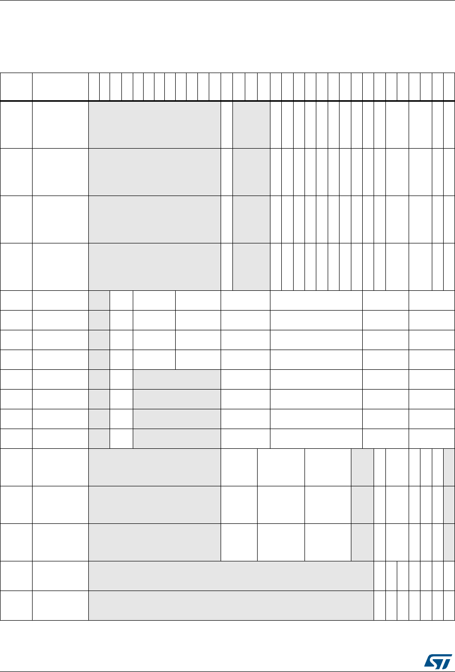
Flexible static memory controller (FSMC) RM0090
1580/1718 DocID018909 Rev 9
36.6.9 FSMC register map
The following table summarizes the FSMC registers.
Table 248. FSMC register map
Offset Register
31
30
29
28
27
26
25
24
23
22
21
20
19
18
17
16
15
14
13
12
11
10
9
8
7
6
5
4
3
2
1
0
0000 FSMC_BCR1 Reserved
CBURSTRW
Reserved
ASYNCWAIT
EXTMOD
WAITEN
WREN
WAITCFG
WRAPMOD
WAITPOL
BURSTEN
Reserved
FACCEN
MWID
MTYP
MUXEN
MBKEN
0008 FSMC_BCR2 Reserved
CBURSTRW
Reserved
ASYNCWAIT
EXTMOD
WAITEN
WREN
WAITCFG
WRAPMOD
WAITPOL
BURSTEN
Reserved
FACCEN
MWID
MTYP
MUXEN
MBKEN
0010 FSMC_BCR3 Reserved
CBURSTRW
Reserved
ASYNCWAIT
EXTMOD
WAITEN
WREN
WAITCFG
WRAPMOD
WAITPOL
BURSTEN
Reserved
FACCEN
MWID
MTYP
MUXEN
MBKEN
0018 FSMC_BCR4 Reserved
CBURSTRW
Reserved
ASYNCWAIT
EXTMOD
WAITEN
WREN
WAITCFG
WRAPMOD
WAITPOL
BURSTEN
Reserved
FACCEN
MWID
MTYP
MUXEN
MBKEN
0004 FSMC_BTR1 Res. ACC
MOD DATLAT CLKDIV BUSTURN DATAST ADDHLD ADDSET
000C FSMC_BTR2 Res. ACC
MOD DATLAT CLKDIV BUSTURN DATAST ADDHLD ADDSET
0014 FSMC_BTR3 Res. ACC
MOD DATLAT CLKDIV BUSTURN DATAST ADDHLD ADDSET
001C FSMC_BTR4 Res. ACC
MOD DATLAT CLKDIV BUSTURN DATAST ADDHLD ADDSET
0104 FSMC_BWTR1 Res. ACC
MOD Res. BUSTURN DATAST ADDHLD ADDSET
010C FSMC_BWTR2 Res. ACC
MOD Res. BUSTURN DATAST ADDHLD ADDSET
0114 FSMC_BWTR3 Res. ACC
MOD Res. BUSTURN DATAST ADDHLD ADDSET
011C FSMC_BWTR4 Res. ACC
MOD Res. BUSTURN DATAST ADDHLD ADDSET
0xA000
0060 FSMC_PCR2 Reserved ECCPS TAR TCLR Res.
ECCEN
PWI
D
PTYP
PBKEN
PWAITEN
Reserved
0xA000
0080 FSMC_PCR3 Reserved ECCPS TAR TCLR Res.
ECCEN
PWI
D
PTYP
PBKEN
PWAITEN
Reserved
0xA000
00A0 FSMC_PCR4 Reserved ECCPS TAR TCLR Res.
ECCEN
PWI
D
PTYP
PBKEN
PWAITEN
Reserved
0xA000
0064 FSMC_SR2 Reserved
FEMPT
IFEN
ILEN
IREN
IFS
ILS
IRS
0xA000
0084 FSMC_SR3 Reserved
FEMPT
IFEN
ILEN
IREN
IFS
ILS
IRS
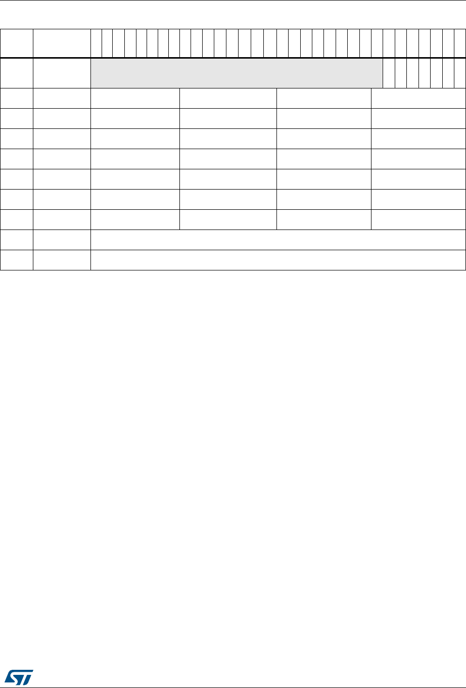
DocID018909 Rev 9 1581/1718
RM0090 Flexible static memory controller (FSMC)
1581
Refer to Table 1 on page 64 for the register boundary addresses.
0xA000
00A4 FSMC_SR4 Reserved
FEMPT
IFEN
ILEN
IREN
IFS
ILS
IRS
0xA000
0068 FSMC_PMEM2 MEMHIZx MEMHOLDx MEMWAITx MEMSETx
0xA000
0088 FSMC_PMEM3 MEMHIZx MEMHOLDx MEMWAITx MEMSETx
0xA000
00A8 FSMC_PMEM4 MEMHIZx MEMHOLDx MEMWAITx MEMSETx
0xA000
006C FSMC_PATT2 ATTHIZx ATTHOLDx ATTWAITx ATTSETx
0xA000
008C FSMC_PATT3 ATTHIZx ATTHOLDx ATTWAITx ATTSETx
0xA000
00AC FSMC_PATT4 ATTHIZx ATTHOLDx ATTWAITx ATTSETx
0xA000
00B0 FSMC_PIO4 IOHIZx IOHOLDx IOWAITx IOSETx
0xA000
0074 FSMC_ECCR2 ECCx
0xA000
0094 FSMC_ECCR3 ECCx
Table 248. FSMC register map (continued)
Offset Register
31
30
29
28
27
26
25
24
23
22
21
20
19
18
17
16
15
14
13
12
11
10
9
8
7
6
5
4
3
2
1
0

Flexible memory controller (FMC) RM0090
1582/1718 DocID018909 Rev 9
37 Flexible memory controller (FMC)
The Flexible memory controller (FMC) includes three memory controllers:
•The NOR/PSRAM memory controller
•The NAND/PC Card memory controller
•The Synchronous DRAM (SDRAM/Mobile LPSDR SDRAM) controller
This section applies to STM32F42xxx and STM32F43xxx only.
37.1 FMC main features
The FMC functional block makes the interface with synchronous and asynchronous static
memories, SDRAM memories, and 16-bit PC memory cards. Its main purposes are:
•to translate AHB transactions into the appropriate external device protocol
•to meet the access time requirements of the external memory devices
All external memories share the addresses, data and control signals with the controller.
Each external device is accessed by means of a unique Chip Select. The FMC performs
only one access at a time to an external device.
The main features of the FMC controller are the following:
•Interface with static-memory mapped devices including:
– Static random access memory (SRAM)
– NOR Flash memory/OneNAND Flash memory
– PSRAM (4 memory banks)
– 16-bit PC Card compatible devices
– Two banks of NAND Flash memory with ECC hardware to check up to 8 Kbytes of
data
•Interface with synchronous DRAM (SDRAM/Mobile LPSDR SDRAM) memories
•Burst mode support for faster access to synchronous devices such as NOR Flash
memory, PSRAM and SDRAM)
•Programmable continuous clock output for asynchronous and synchronous accesses
•8-,16- or 32-bit wide data bus
•Independent Chip Select control for each memory bank
•Independent configuration for each memory bank
•Write enable and byte lane select outputs for use with PSRAM, SRAM and SDRAM
devices
•External asynchronous wait control
•Write Data FIFO with 16 x33-bit depth
•Write Address FIFO with 16x30-bit depth
•Cacheable Read FIFO with 6 x32-bit depth (6 x14-bit address tag) for SDRAM
controller.

DocID018909 Rev 9 1583/1718
RM0090 Flexible memory controller (FMC)
1660
The FMC embeds two Write FIFOs: a Write Data FIFO with a 16x33-bit depth and a Write
Address FIFO with a 16x30-bit depth.
•The Write Data FIFO stores the AHB data to be written to the memory (up to 32 bits)
plus one bit for the AHB transfer (burst or not sequential mode)
•The Write Address FIFO stores the AHB address (up to 28 bits) plus the AHB data size
(up to 2 bits). When operating in burst mode, only the start address is stored except
when crossing a page boundary (for PSRAM and SDRAM). In this case, the AHB burst
is broken into two FIFO entries.
At startup the FMC pins must be configured by the user application. The FMC I/O pins which
are not used by the application can be used for other purposes.
The FMC registers that define the external device type and associated characteristics are
usually set at boot time and do not change until the next reset or power-up. However, the
settings can be changed at any time.
37.2 Block diagram
The FMC consists of five main blocks:
•The AHB interface (including the FMC configuration registers)
•The NOR Flash/PSRAM/SRAM controller
•The NAND Flash/PC Card controller
•The SDRAM controller
•The external device interface
The block diagram is shown in Figure 454.
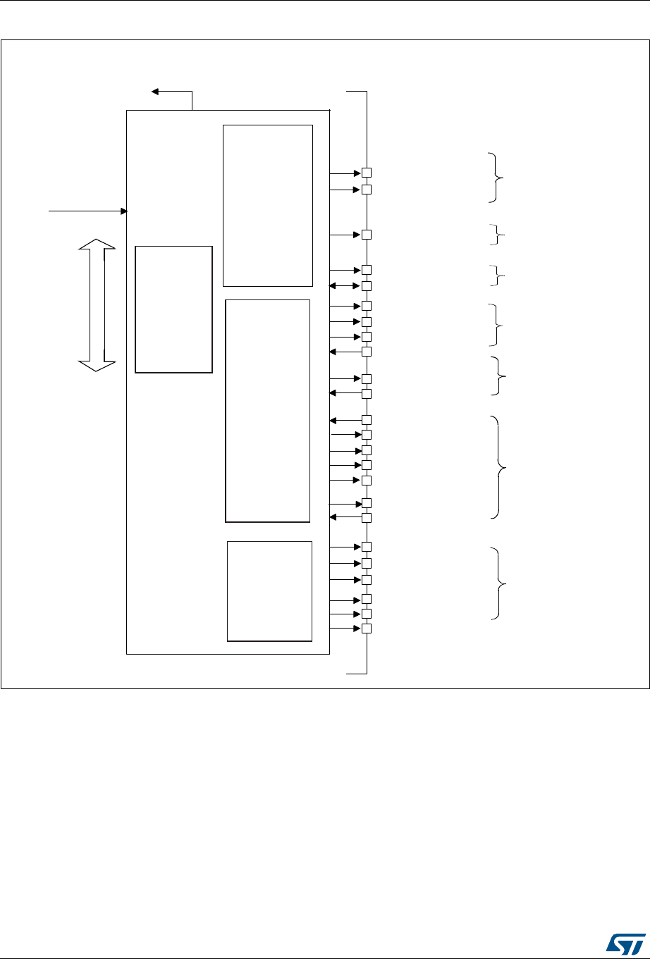
Flexible memory controller (FMC) RM0090
1584/1718 DocID018909 Rev 9
Figure 454. FMC block diagram
37.3 AHB interface
The AHB slave interface allows internal CPUs and other bus master peripherals to access
the external memories.
AHB transactions are translated into the external device protocol. In particular, if the
selected external memory is 16- or 8-bit wide, 32-bit wide transactions on the AHB are split
into consecutive 16- or 8-bit accesses. The FMC Chip Select (FMC_NEx) does not toggle
between the consecutive accesses.
069
+&/.
1$1'3&&DUG
PHPRU\
FRQWUROOHU
1$1'
VLJQDOV
6KDUHG
VLJQDOV
125365$0
VLJQDOV
)0&B1(>@
)0&B1/RU1$'9
)0&B1:$,7
)0&B'> @
)0&B12(
)0&B1:(
)0&B1,25'
)0&B15(*
)0&B&'
3&&DUG
VLJQDOV
)0&B1%/>@
)0&B1&(>@
)0&B,17>@
)0&B,175
)0&B1&(B
)0&B1&(B
)0&B1,2:5
)0&B&/.
6'5$0
FRQWUROOHU
)0&B6'1:(
)0&B6'&.(>@
)0&B6'1(>@
)0&B15$6
)0&B1&$6
6'5$0
VLJQDOV
)0&B$>@
125365$065$0
6KDUHGVLJQDOV
65$0365$06'5$0
6KDUHGVLJQDOV
)0&B6'&/.
)0&LQWHUUXSWVWR19,&
)URPFORFN
FRQWUROOHU
&RQILJXUDWLRQ
UHJLVWHUV
125365$0
PHPRU\
FRQWUROOHU

DocID018909 Rev 9 1585/1718
RM0090 Flexible memory controller (FMC)
1660
The FMC generates an AHB error in the following conditions:
•When reading or writing to an FMC bank (Bank 1 to 4) which is not enabled.
•When reading or writing to the NOR Flash bank while the FACCEN bit is reset in the
FMC_BCRx register.
•When reading or writing to the PC Card banks while the FMC_CD input pin (Card
Presence Detection) is low.
•When writing to a write protected SDRAM bank (WP bit set in the SDRAM_SDCRx
register).
•When the SDRAM address range is violated (access to reserved address range)
The effect of an AHB error depends on the AHB master which has attempted the R/W
access:
•If the access has been attempted by the Cortex®-M4 with FPU CPU, a hard fault
interrupt is generated.
•If the access has been performed by a DMA controller, a DMA transfer error is
generated and the corresponding DMA channel is automatically disabled.
The AHB clock (HCLK) is the reference clock for the FMC.
37.3.1 Supported memories and transactions
General transaction rules
The requested AHB transaction data size can be 8-, 16- or 32-bit wide whereas the
accessed external device has a fixed data width. This may lead to inconsistent transfers.
Therefore, some simple transaction rules must be followed:
•AHB transaction size and memory data size are equal
There is no issue in this case.
•AHB transaction size is greater than the memory size:
In this case, the FMC splits the AHB transaction into smaller consecutive memory
accesses to meet the external data width. The FMC Chip Select (FMC_NEx) does not
toggle between the consecutive accesses.
•AHB transaction size is smaller than the memory size:
The transfer may or not be consistent depending on the type of external device:
– Accesses to devices that have the byte select feature (SRAM, ROM, PSRAM,
SDRAM)
In this case, the FMC allows read/write transactions and accesses the right data
through its byte lanes BL[3:0].
Bytes to be written are addressed by NBL[3:0].
All memory bytes are read (NBL[3:0] are driven low during read transaction) and
the useless ones are discarded.
– Accesses to devices that do not have the byte select feature (16-bit NOR and
NAND Flash memories)
This situation occurs when a byte access is requested to a 16-bit wide Flash
memory. Since the device cannot be accessed in byte mode (only 16-bit words
can be read/written from/to the Flash memory), Write transactions and Read
transactions are allowed (the controller reads the entire 16-bit memory word and
uses only the required byte).

Flexible memory controller (FMC) RM0090
1586/1718 DocID018909 Rev 9
Configuration registers
The FMC can be configured through a set of registers. Refer to Section 37.5.6, for a
detailed description of the NOR Flash/PSRAM controller registers. Refer to Section 37.6.8,
for a detailed description of the NAND Flash/PC Card registers and to Section 37.7.5 for a
detailed description of the SDRAM controller registers.
37.4 External device address mapping
From the FMC point of view, the external memory is divided into 6 fixed-size banks of
256 Mbytes each (see Figure 455):
•Bank 1 used to address up to 4 NOR Flash memory or PSRAM devices. This bank is
split into 4 NOR/PSRAM subbanks with 4 dedicated Chip Selects, as follows:
– Bank 1 - NOR/PSRAM 1
– Bank 1 - NOR/PSRAM 2
– Bank 1 - NOR/PSRAM 3
– Bank 1 - NOR/PSRAM 4
•Banks 2 and 3 used to address NAND Flash memory devices (1 device per bank)
•Bank 4 used to address a PC Card
•Bank 5 and 6 used to address SDRAM devices (1 device per bank).
For each bank the type of memory to be used can be configured by the user application
through the Configuration register.
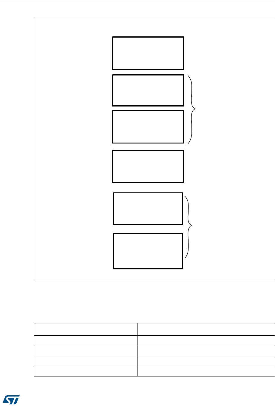
DocID018909 Rev 9 1587/1718
RM0090 Flexible memory controller (FMC)
1660
Figure 455. FMC memory banks
37.4.1 NOR/PSRAM address mapping
HADDR[27:26] bits are used to select one of the four memory banks as shown in Table 249.
"ANK
X-"
./2032!-32!-
3UPPORTEDMEMORYTYPE"ANK
X
!DDRESS
0##ARD
-36
3$2!-
X&&&&&&&
X
X&&&&&&&
X
X&&&&&&&
X
X&&&&&&&
X#
X#&&&&&&&
X$
X$&&&&&&&
"ANK
X-"
"ANK
X-"
"ANK
X-"
3$2!-"ANK
X-"
3$2!-"ANK
X-"
.!.$&LASHMEMORY
Table 249. NOR/PSRAM bank selection
HADDR[27:26](1)
1. HADDR are internal AHB address lines that are translated to external memory.
Selected bank
00 Bank 1 - NOR/PSRAM 1
01 Bank 1 - NOR/PSRAM 2
10 Bank 1 - NOR/PSRAM 3
11 Bank 1 - NOR/PSRAM 4
Flexible memory controller (FMC) RM0090
1588/1718 DocID018909 Rev 9
The HADDR[25:0] bits contain the external memory address. Since HADDR is a byte
address whereas the memory is addressed at word level, the address actually issued to the
memory varies according to the memory data width, as shown in the following table.
Wrap support for NOR Flash/PSRAM
Wrap burst mode for synchronous memories is not supported. The memories must be
configured in linear burst mode of undefined length.
37.4.2 NAND Flash memory/PC Card address mapping
In this case, three banks are available, each of them being divided into memory areas as
indicated in Table 251.
For NAND Flash memory, the common and attribute memory spaces are subdivided into
three sections (see in Table 252 below) located in the lower 256 Kbytes:
•Data section (first 64 Kbytes in the common/attribute memory space)
•Command section (second 64 Kbytes in the common / attribute memory space)
•Address section (next 128 Kbytes in the common / attribute memory space)
Table 250. NOR/PSRAM External memory address
Memory width(1)
1. In case of a 16-bit external memory width, the FMC will internally use HADDR[25:1] to generate the
address for external memory FMC_A[24:0]. In case of a 32-bit memory width, the FMC will internally use
HADDR[25:2] to generate the external address.
Whatever the external memory width, FMC_A[0] should be connected to external memory address A[0].
Data address issued to the memory Maximum memory capacity (bits)
8-bit HADDR[25:0] 64 Mbytes x 8 = 512 Mbit
16-bit HADDR[25:1] >> 1 64 Mbytes/2 x 16 = 512 Mbit
32-bit HADDR[25:2] >> 2 64 Mbytes/4 x 32 = 512 Mbit
Table 251. NAND/PC Card memory mapping and timing registers
Start address End address FMC bank Memory space Timing register
0x9C00 0000 0x9FFF FFFF
Bank 4 - PC card
I/O FMC_PIO4 (0xB0)
0x9800 0000 0x9BFF FFFF Attribute FMC_PATT4 (0xAC)
0x9000 0000 0x93FF FFFF Common FMC_PMEM4 (0xA8)
0x8800 0000 0x8BFF FFFF
Bank 3 - NAND Flash
Attribute FMC_PATT3 (0x8C)
0x8000 0000 0x83FF FFFF Common FMC_PMEM3 (0x88)
0x7800 0000 0x7BFF FFFF
Bank 2- NAND Flash
Attribute FMC_PATT2 (0x6C)
0x7000 0000 0x73FF FFFF Common FMC_PMEM2 (0x68)
DocID018909 Rev 9 1589/1718
RM0090 Flexible memory controller (FMC)
1660
The application software uses the 3 sections to access the NAND Flash memory:
•To sending a command to NAND Flash memory, the software must write the
command value to any memory location in the command section.
•To specify the NAND Flash address that must be read or written, the software
must write the address value to any memory location in the address section. Since an
address can be 4 or 5 bytes long (depending on the actual memory size), several
consecutive write operations to the address section are required to specify the full
address.
•To read or write data, the software reads or writes the data from/to any memory
location in the data section.
Since the NAND Flash memory automatically increments addresses, there is no need to
increment the address of the data section to access consecutive memory locations.
37.4.3 SDRAM address mapping
The HADDR[28] bit (internal AHB address line 28) is used to select one of the two memory
banks as indicated in Table 253.
The following table shows SDRAM mapping for an 13-bit row and a 11-bit column
configuration.
Table 252. NAND bank selection
Section name HADDR[17:16] Address range
Address section 1X 0x020000-0x03FFFF
Command section 01 0x010000-0x01FFFF
Data section 00 0x000000-0x0FFFF
Table 253. SDRAM bank selection
HADDR[28] Selected bank Control register Timing register
0 SDRAM Bank1 FMC_SDCR1 FMC_SDTR1
1 SDRAM Bank2 FMC_SDCR2 FMC_SDTR2
Table 254. SDRAM address mapping
Memory width(1) Internal bank Row address Column
address(2)
Maximum
memory capacity
(Mbytes)
8-bit HADDR[25:24] HADDR[23:11] HADDR[10:0] 64 Mbytes:
4 x 8K x 2K
16-bit HADDR[26:25] HADDR[24:12] HADDR[11:1] 128 Mbytes:
4 x 8K x 2K x 2
32-bit HADDR[27:26] HADDR[25:13] HADDR[12:2] 256 Mbytes:
4 x 8K x 2K x 4

Flexible memory controller (FMC) RM0090
1590/1718 DocID018909 Rev 9
The HADDR[27:0] bits are translated to external SDRAM address depending on the
SDRAM controller configuration:
•Data size:8, 16 or 32 bits
•Row size:11, 12 or 13 bits
•Column size: 8, 9, 10 or 11 bits
•Number of internal banks: two or four internal banks
Table 255 to Table shows the SDRAM address mapping versus the SDRAM controller
configuration.
)
1. When interfacing with a 16-bit memory, the FMC internally uses the HADDR[11:1] internal AHB address
lines to generate the external address. When interfacing with a 32-bit memory, the FMC internally uses
HADDR[12:2] lines to generate the external address. Whatever the memory width, FMC_A[0] has to be
connected to the external memory address A[0].
2. The AutoPrecharge is not supported. FMC_A[10] must be connected to the external memory address
A[10] but it will be always driven ‘low’.
Table 255. SDRAM address mapping with 8-bit data bus width(1)(2)
Row size
configuration
HADDR(AHB Internal Address Lines)
27 26 25 24 23 22 21 20 19 18 17 16 15 14 13 12 11 10 9 8 7 6 5 4 3 2 1 0
11-bit row size
configuration
Res. Bank
[1:0] Row[10:0] Column[7:0]
Res. Bank
[1:0] Row[10:0] Column[8:0]
Res. Bank
[1:0] Row[10:0] Column[9:0]
Res. Bank
[1:0] Row[10:0] Column[10:0]
12-bit row size
configuration
Res. Bank
[1:0] Row[11:0] Column[7:0]
Res. Bank
[1:0] Row[11:0] Column[8:0]
Res. Bank
[1:0] Row[11:0] Column[9:0]
Res. Bank
[1:0] Row[11:0] Column[10:0]
13-bit row size
configuration
Res. Bank
[1:0] Row[12:0] Column[7:0]
Res. Bank
[1:0] Row[12:0] Column[8:0]
Res. Bank
[1:0] Row[12:0] Column[9:0]
Res. Bank
[1:0] Row[12:0] Column[10:0]
1. BANK[1:0] are the Bank Address BA[1:0]. When only 2 internal banks are used, BA1 must always be set to ‘0’.
2. Access to Reserved (Res.) address range generates an AHB error.
DocID018909 Rev 9 1591/1718
RM0090 Flexible memory controller (FMC)
1660
)
Table 256. SDRAM address mapping with 16-bit data bus width(1)(2)
Row size
Configuration
HADDR(AHB address Lines)
27
26
25
24
23
22
21
20
19
18
17
16
15
14
13
12
11
10
9
8
7
6
5
4
3
2
1
0
11-bit row size
configuration
Res. Bank
[1:0] Row[10:0] Column[7:0] BM0(3)
Res. Bank
[1:0] Row[10:0] Column[8:0] BM0
Res. Bank
[1:0] Row[10:0] Column[9:0] BM0
Res. Bank
[1:0] Row[10:0] Column[10:0] BM0
12-bit row size
configuration
Res. Bank
[1:0] Row[11:0] Column[7:0] BM0
Res. Bank
[1:0] Row[11:0] Column[8:0] BM0
Res. Bank
[1:0] Row[11:0] Column[9:0] BM0
Res. Bank
[1:0] Row[11:0] Column[10:0] BM0
13-bit row size
configuration
Res. Bank
[1:0] Row[12:0] Column[7:0] BM0
Res. Bank
[1:0] Row[12:0] Column[8:0] BM0
Res. Bank
[1:0] Row[12:0] Column[9:0] BM0
Re
s.
Bank
[1:0] Row[12:0] Column[10:0] BM0
1. BANK[1:0] are the Bank Address BA[1:0]. When only 2 internal banks are used, BA1 must always be set to ‘0’.
2. Access to Reserved space (Res.) generates an AHB error.
3. BM0: is the byte mask for 16-bit access.
Table 257. SDRAM address mapping with 32-bit data bus width(1)(2)
Row size
configuration
HADDR(AHB address Lines)
27
26
25
24
23
22
21
20
19
18
17
16
15
14
13
12
11
10
9
8
7
6
5
4
3
2
1
0
11-bit row size
configuration
Res. Bank
[1:0] Row[10:0] Column[7:0] BM[1:0
](3)
Res. Bank
[1:0] Row[10:0] Column[8:0] BM[1:0
Res. Bank
[1:0] Row[10:0] Column[9:0] BM[1:0
Res. Bank
[1:0] Row[10:0] Column[10:0] BM[1:0
Flexible memory controller (FMC) RM0090
1592/1718 DocID018909 Rev 9
37.5 NOR Flash/PSRAM controller
The FMC generates the appropriate signal timings to drive the following types of memories:
•Asynchronous SRAM and ROM
–8 bits
– 16 bits
– 32 bits
•PSRAM (Cellular RAM)
– Asynchronous mode
– Burst mode for synchronous accesses
– Multiplexed or non-multiplexed
•NOR Flash memory
– Asynchronous mode
– Burst mode for synchronous accesses
– Multiplexed or non-multiplexed
The FMC outputs a unique Chip Select signal, NE[4:1], per bank. All the other signals
(addresses, data and control) are shared.
12-bit row size
configuration
Res. Bank
[1:0] Row[11:0] Column[7:0] BM[1:0
Res. Bank
[1:0] Row[11:0] Column[8:0] BM[1:0
Res. Bank
[1:0] Row[11:0] Column[9:0] BM[1:0
Res. Bank
[1:0] Row[11:0] Column[10:0] BM[1:0
13-bit row size
configuration
Res. Bank
[1:0] Row[12:0] Column[7:0] BM[1:0
Res. Bank
[1:0] Row[12:0] Column[8:0] BM[1:0
Res. Bank
[1:0] Row[12:0] Column[9:0] BM[1:0
Bank
[1:0] Row[12:0] Column[10:0] BM[1:0
1. BANK[1:0] are the Bank Address BA[1:0]. When only 2 internal banks are used, BA1 must always be set to ‘0’.
2. Access to Reserved space (Res.) generates an AHB error.
3. BM[1:0]: is the byte mask for 32-bit access.
Table 257. SDRAM address mapping with 32-bit data bus width(1)(2) (continued)
Row size
configuration
HADDR(AHB address Lines)
27
26
25
24
23
22
21
20
19
18
17
16
15
14
13
12
11
10
9
8
7
6
5
4
3
2
1
0

DocID018909 Rev 9 1593/1718
RM0090 Flexible memory controller (FMC)
1660
The FMC supports a wide range of devices through a programmable timings among which:
•Programmable wait states (up to 15)
•Programmable bus turnaround cycles (up to 15)
•Programmable output enable and write enable delays (up to 15)
•Independent read and write timings and protocol to support the widest variety of
memories and timings
•Programmable continuous clock (FMC_CLK) output.
The FMC Clock (FMC_CLK) is a submultiple of the HCLK clock. It can be delivered to the
selected external device either during synchronous accesses only or during asynchronous
and synchronous accesses depending on the CCKEN bit configuration in the FMC_BCR1
register:
•If the CCLKEN bit is reset, the FMC generates the clock (CLK) only during
synchronous accesses (Read/write transactions).
•If the CCLKEN bit is set, the FMC generates a continuous clock during asynchronous
and synchronous accesses. To generate the FMC_CLK continuous clock, Bank 1 must
be configured in synchronous mode (see Section 37.5.6: NOR/PSRAM controller
registers). Since the same clock is used for all synchronous memories, when a
continuous output clock is generated and synchronous accesses are performed, the
AHB data size has to be the same as the memory data width (MWID) otherwise the
FMC_CLK frequency will be changed depending on AHB data transaction (refer to
Section 37.5.5: Synchronous transactions for FMC_CLK divider ratio formula).
The size of each bank is fixed and equal to 64 Mbytes. Each bank is configured through
dedicated registers (see Section 37.5.6: NOR/PSRAM controller registers).
The programmable memory parameters include access times (see Table 258) and support
for wait management (for PSRAM and NOR Flash accessed in burst mode).
Table 258. Programmable NOR/PSRAM access parameters
Parameter Function Access mode Unit Min. Max.
Address
setup
Duration of the address
setup phase Asynchronous AHB clock cycle
(HCLK) 015
Address hold Duration of the address hold
phase
Asynchronous,
muxed I/Os
AHB clock cycle
(HCLK) 115
Data setup Duration of the data setup
phase Asynchronous AHB clock cycle
(HCLK) 1256
Bust turn Duration of the bus
turnaround phase
Asynchronous and
synchronous
read/write
AHB clock cycle
(HCLK) 015
Clock divide
ratio
Number of AHB clock cycles
(HCLK) to build one memory
clock cycle (CLK)
Synchronous AHB clock cycle
(HCLK) 2 16
Data latency
Number of clock cycles to
issue to the memory before
the first data of the burst
Synchronous Memory clock
cycle (CLK) 2 17

Flexible memory controller (FMC) RM0090
1594/1718 DocID018909 Rev 9
37.5.1 External memory interface signals
Table 259, Table 260 and Table 261 list the signals that are typically used to interface with
NOR Flash memory, SRAM and PSRAM.
Note: The prefix “N” identifies the signals which are active low.
NOR Flash memory, non-multiplexed I/Os
The maximum capacity is 512 Mbits (26 address lines).
NOR Flash memory, 16-bit multiplexed I/Os
The maximum capacity is 512 Mbits.
Table 259. Non-multiplexed I/O NOR Flash memory
FMC signal name I/O Function
CLK O Clock (for synchronous access)
A[25:0] O Address bus
D[31:0] I/O Bidirectional data bus
NE[x] O Chip Select, x = 1..4
NOE O Output enable
NWE O Write enable
NL(=NADV) O Latch enable (this signal is called address
valid, NADV, by some NOR Flash devices)
NWAIT I NOR Flash wait input signal to the FMC
Table 260. 16-bit multiplexed I/O NOR Flash memory
FMC signal name I/O Function
CLK O Clock (for synchronous access)
A[25:16] O Address bus
AD[15:0] I/O
16-bit multiplexed, bidirectional address/data bus (the 16-bit address
A[15:0] and data D[15:0] are multiplexed on the databus)
NE[x] O Chip Select, x = 1..4
NOE O Output enable
NWE O Write enable
NL(=NADV) O Latch enable (this signal is called address valid, NADV, by some NOR
Flash devices)
NWAIT I NOR Flash wait input signal to the FMC

DocID018909 Rev 9 1595/1718
RM0090 Flexible memory controller (FMC)
1660
PSRAM/SRAM, non-multiplexed I/Os
The maximum capacity is 512 Mbits.
PSRAM, 16-bit multiplexed I/Os
The maximum capacity is 512 Mbits (26 address lines).
Table 261. Non-multiplexed I/Os PSRAM/SRAM
FMC signal name I/O Function
CLK O Clock (only for PSRAM synchronous access)
A[25:0] O Address bus
D[31:0] I/O Data bidirectional bus
NE[x] O Chip Select, x = 1..4 (called NCE by PSRAM (Cellular RAM i.e.
CRAM))
NOE O Output enable
NWE O Write enable
NL(= NADV) O Address valid only for PSRAM input (memory signal name: NADV)
NWAIT I PSRAM wait input signal to the FMC
NBL[3] O Byte3 Upper byte enable (memory signal name: NUB)
NBL[2] O Byte2 Lowed byte enable (memory signal name: NLB)
NBL[1] O Byte1 Upper byte enable (memory signal name: NLB)
NBL[0] O Byte0 Lower byte enable (memory signal name: NLB)
Table 262. 16-Bit multiplexed I/O PSRAM
FMC signal name I/O Function
CLK O Clock (for synchronous access)
A[25:16] O Address bus
AD[15:0] I/O
16-bit multiplexed, bidirectional address/data bus (the 16-bit address
A[15:0] and data D[15:0] are multiplexed on the databus)
NE[x] O Chip Select, x = 1..4 (called NCE by PSRAM (Cellular RAM i.e.
CRAM))
NOE O Output enable
NWE O Write enable
NL(= NADV) O Address valid PSRAM input (memory signal name: NADV)
NWAIT I PSRAM wait input signal to the FMC
NBL[1] O Upper byte enable (memory signal name: NUB)
NBL[0] O Lowed byte enable (memory signal name: NLB)

Flexible memory controller (FMC) RM0090
1596/1718 DocID018909 Rev 9
37.5.2 Supported memories and transactions
Table 263 below shows an example of the supported devices, access modes and
transactions when the memory data bus is 16-bit wide for NOR Flash memory, PSRAM and
SRAM. The transactions not allowed (or not supported) by the FMC are shown in gray in
this example.
Table 263. NOR Flash/PSRAM: Example of supported memories and transactions
Device Mode R/W
AHB
data
size
Memory
data size
Allowed/
not
allowed
Comments
NOR Flash
(muxed I/Os
and nonmuxed
I/Os)
Asynchronous R 8 16 Y
Asynchronous W 8 16 N
Asynchronous R 16 16 Y
Asynchronous W 16 16 Y
Asynchronous R 32 16 Y Split into 2 FMC accesses
Asynchronous W 32 16 Y Split into 2 FMC accesses
Asynchronous
page R -16 N Mode is not supported
Synchronous R 8 16 N
Synchronous R 16 16 Y
Synchronous R 32 16 Y
PSRAM
(multiplexed
I/Os and non-
multiplexed
I/Os)
Asynchronous R 8 16 Y
Asynchronous W 8 16 Y Use of byte lanes NBL[1:0]
Asynchronous R 16 16 Y
Asynchronous W 16 16 Y
Asynchronous R 32 16 Y Split into 2 FMC accesses
Asynchronous W 32 16 Y Split into 2 FMC accesses
Asynchronous
page R -16 N Mode is not supported
Synchronous R 8 16 N
Synchronous R 16 16 Y
Synchronous R 32 16 Y
Synchronous W 8 16 Y Use of byte lanes NBL[1:0]
Synchronous W 16/32 16 Y
SRAM and
ROM
Asynchronous R 8 / 16 16 Y
Asynchronous W 8 / 16 16 Y Use of byte lanes NBL[1:0]
Asynchronous R 32 16 Y Split into 2 FMC accesses
Asynchronous W 32 16 Y Split into 2 FMC accesses
Use of byte lanes NBL[1:0]

DocID018909 Rev 9 1597/1718
RM0090 Flexible memory controller (FMC)
1660
37.5.3 General timing rules
Signals synchronization
•All controller output signals change on the rising edge of the internal clock (HCLK)
•In synchronous mode (read or write), all output signals change on the rising edge of
HCLK. Whatever the CLKDIV value, all outputs change as follows:
– NOEL/NWEL/ NEL/NADVL/ NADVH /NBLL/ Address valid outputs change on the
falling edge of FMC_CLK clock.
– NOEH/ NWEH / NEH/ NOEH/NBLH/ Address invalid outputs change on the rising
edge of FMC_CLK clock.
37.5.4 NOR Flash/PSRAM controller asynchronous transactions
Asynchronous static memories (NOR Flash, PSRAM, SRAM)
•Signals are synchronized by the internal clock HCLK. This clock is not issued to the
memory
•The FMC always samples the data before de-asserting the Chip Select signal NE. This
guarantees that the memory data hold timing constraint is met (minimum Chip Enable
high to data transition is usually 0 ns)
•If the extended mode is enabled (EXTMOD bit is set in the FMC_BCRx register), up to
four extended modes (A, B, C and D) are available. It is possible to mix A, B, C and D
modes for read and write operations. For example, read operation can be performed in
mode A and write in mode B.
•If the extended mode is disabled (EXTMOD bit is reset in the FMC_BCRx register), the
FMC can operate in Mode1 or Mode2 as follows:
– Mode 1 is the default mode when SRAM/PSRAM memory type is selected (MTYP
= 0x0 or 0x01 in the FMC_BCRx register)
– Mode 2 is the default mode when NOR memory type is selected (MTYP = 0x10 in
the FMC_BCRx register).
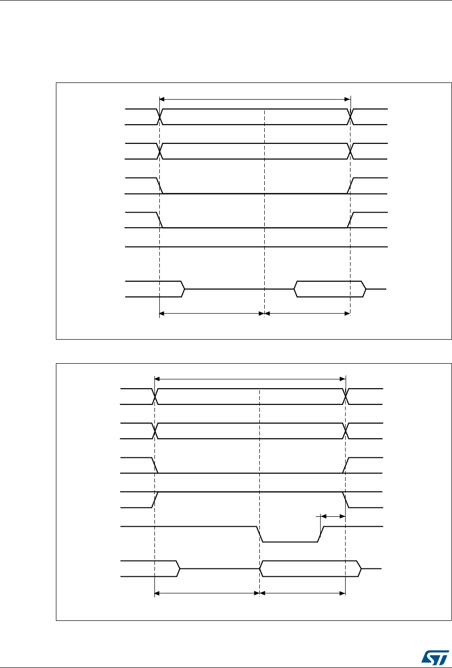
Flexible memory controller (FMC) RM0090
1598/1718 DocID018909 Rev 9
Mode 1 - SRAM/PSRAM (CRAM)
The next figures show the read and write transactions for the supported modes followed by
the required configuration of FMC _BCRx, and FMC_BTRx/FMC_BWTRx registers.
Figure 456. Mode1 read access waveforms
Figure 457. Mode1 write access waveforms
!;=
./%
!$$3%4 $!4!34
-EMORYTRANSACTION
.%X
$;=
(#,+CYCLES (#,+CYCLES
.7%
.",;=
DATADRIVEN
BYMEMORY
-36
(IGH
!;=
./%
!$$3%4 $!4!34
-EMORYTRANSACTION
.%X
$;=
(#,+CYCLES (#,+CYCLES
.7%
.",;=
DATADRIVENBY&3-#
-36
(#,+

DocID018909 Rev 9 1599/1718
RM0090 Flexible memory controller (FMC)
1660
The one HCLK cycle at the end of the write transaction helps guarantee the address and
data hold time after the NWE rising edge. Due to the presence of this HCLK cycle, the
DATAST value must be greater than zero (DATAST > 0).
Table 264. FMC_BCRx bit fields
Bit
number Bit name Value to set
31-21 Reserved 0x000
20 CCLKEN As needed
19 CBURSTRW 0x0 (no effect in asynchronous mode)
18:16 Reserved 0x0
15 ASYNCWAIT Set to 1 if the memory supports this feature. Otherwise keep at
0.
14 EXTMOD 0x0
13 WAITEN 0x0 (no effect in asynchronous mode)
12 WREN As needed
11 WAITCFG Don’t care
10 WRAPMOD 0x0
9 WAITPOL Meaningful only if bit 15 is 1
8 BURSTEN 0x0
7 Reserved 0x1
6 FACCEN Don’t care
5-4 MWID As needed
3-2 MTYP As needed, exclude 0x2 (NOR Flash memory)
1 MUXE 0x0
0 MBKEN 0x1
Table 265. FMC_BTRx bit fields
Bit
number Bit name Value to set
31:30 Reserved 0x0
29-28 ACCMOD Don’t care
27-24 DATLAT Don’t care
23-20 CLKDIV Don’t care
19-16 BUSTURN Time between NEx high to NEx low (BUSTURN HCLK)
15-8 DATAST Duration of the second access phase (DATAST+1 HCLK cycles for
write accesses, DATAST HCLK cycles for read accesses).
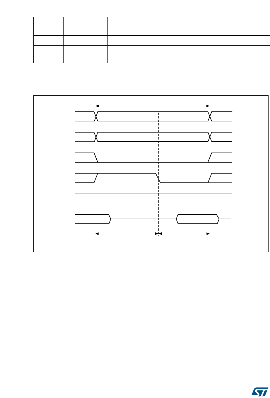
Flexible memory controller (FMC) RM0090
1600/1718 DocID018909 Rev 9
Mode A - SRAM/PSRAM (CRAM) OE toggling
Figure 458. ModeA read access waveforms
1. NBL[3:0] are driven low during the read access
7-4 ADDHLD Don’t care
3-0 ADDSET Duration of the first access phase (ADDSET HCLK cycles).
Minimum value for ADDSET is 0.
Table 265. FMC_BTRx bit fields (continued)
Bit
number Bit name Value to set
!;=
./%
!$$3%4 $!4!34
-EMORYTRANSACTION
.%X
$;=
(#,+CYCLES (#,+CYCLES
.7%
.",;=
DATADRIVEN
BYMEMORY
-36
(IGH
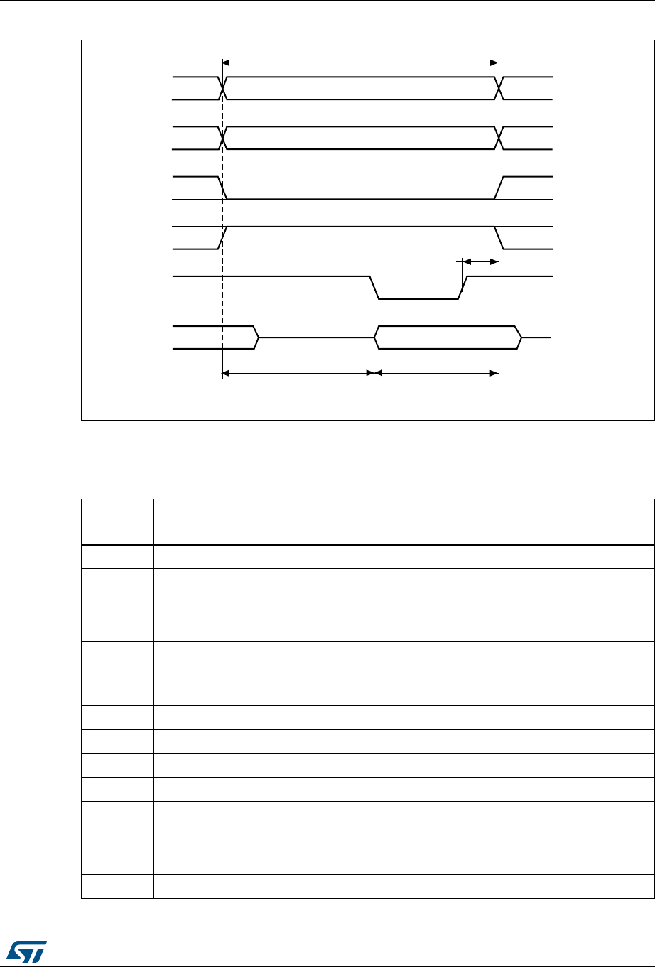
DocID018909 Rev 9 1601/1718
RM0090 Flexible memory controller (FMC)
1660
Figure 459. ModeA write access waveforms
The differences compared with mode1 are the toggling of NOE and the independent read
and write timings.
Table 266. FMC_BCRx bit fields
Bit
number Bit name Value to set
31-21 Reserved 0x000
20 CCLKEN As needed
19 CBURSTRW 0x0 (no effect in asynchronous mode)
18:16 Reserved 0x0
15 ASYNCWAIT Set to 1 if the memory supports this feature. Otherwise keep at
0.
14 EXTMOD 0x1
13 WAITEN 0x0 (no effect in asynchronous mode)
12 WREN As needed
11 WAITCFG Don’t care
10 WRAPMOD 0x0
9 WAITPOL Meaningful only if bit 15 is 1
8 BURSTEN 0x0
7 Reserved 0x1
6 FACCEN Don’t care
Ϯϱ͗Ϭ
EK
^d ;d^dнϭͿ
DĞŵŽƌLJƚƌĂŶƐĂĐƚŝŽŶ
Edž
ϯϭ͗Ϭ
,><ĐLJĐůĞƐ ,><ĐLJĐůĞƐ
Et
E>ϯ͗Ϭ
ĚĂƚĂĚƌŝǀĞŶďLJ&^D
D^ϯϬϰϱϱsϭ
ϭ,><

Flexible memory controller (FMC) RM0090
1602/1718 DocID018909 Rev 9
5-4 MWID As needed
3-2 MTYP As needed, exclude 0x2 (NOR Flash memory)
1 MUXEN 0x0
0 MBKEN 0x1
Table 267. FMC_BTRx bit fields
Bit
number Bit name Value to set
31:30 Reserved 0x0
29-28 ACCMOD 0x0
27-24 DATLAT Don’t care
23-20 CLKDIV Don’t care
19-16 BUSTURN Time between NEx high to NEx low (BUSTURN HCLK)
15-8 DATAST Duration of the second access phase (DATAST HCLK cycles) for read
accesses.
7-4 ADDHLD Don’t care
3-0 ADDSET
Duration of the first access phase (ADDSET HCLK cycles) for read
accesses.
Minimum value for ADDSET is 0.
Table 268. FMC_BWTRx bit fields
Bit
number Bit name Value to set
31:30 Reserved 0x0
29-28 ACCMOD 0x0
27-24 DATLAT Don’t care
23-20 CLKDIV Don’t care
19-16 BUSTURN Time between NEx high to NEx low (BUSTURN HCLK)
15-8 DATAST Duration of the second access phase (DATAST HCLK cycles) for write
accesses.
7-4 ADDHLD Don’t care
3-0 ADDSET
Duration of the first access phase (ADDSET HCLK cycles) for write
accesses.
Minimum value for ADDSET is 0.
Table 266. FMC_BCRx bit fields (continued)
Bit
number Bit name Value to set
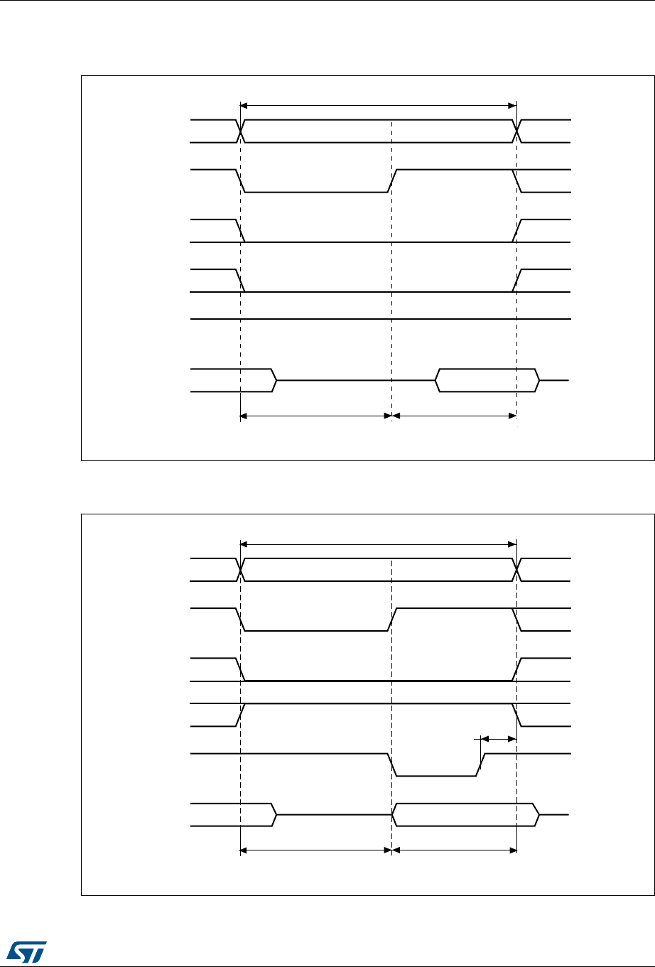
DocID018909 Rev 9 1603/1718
RM0090 Flexible memory controller (FMC)
1660
Mode 2/B - NOR Flash
Figure 460. Mode2 and mode B read access waveforms
1. NBL[3:0] are driven low during the read access
Figure 461. Mode2 write access waveforms
!;=
./%
!$$3%4 $!4!34
-EMORYTRANSACTION
.%X
$;=
(#,+CYCLES (#,+CYCLES
.7%
.!$6
DATADRIVEN
BYMEMORY
-36
(IGH
!;=
./%
!$$3%4 $!4!34
-EMORYTRANSACTION
.%X
$;=
(#,+CYCLES (#,+CYCLES
.7%
.!$6
DATADRIVENBY&3-#
-36
(#,+
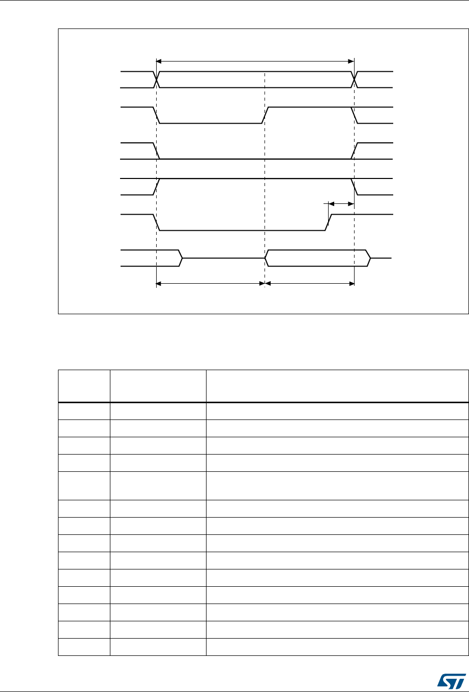
Flexible memory controller (FMC) RM0090
1604/1718 DocID018909 Rev 9
Figure 462. ModeB write access waveforms
The differences with mode1 are the toggling of NWE and the independent read and write
timings when extended mode is set (Mode B).
Table 269. FMC_BCRx bit fields
Bit
number Bit name Value to set
31-21 Reserved 0x000
20 CCLKEN As needed
19 CBURSTRW 0x0 (no effect in asynchronous mode)
18:16 Reserved 0x0
15 ASYNCWAIT Set to 1 if the memory supports this feature. Otherwise keep at
0.
14 EXTMOD 0x1 for mode B, 0x0 for mode 2
13 WAITEN 0x0 (no effect in asynchronous mode)
12 WREN As needed
11 WAITCFG Don’t care
10 WRAPMOD 0x0
9 WAITPOL Meaningful only if bit 15 is 1
8 BURSTEN 0x0
7 Reserved 0x1
6 FACCEN 0x1
!;=
./%
!$$3%4 $!4!34
-EMORYTRANSACTION
.%X
$;=
(#,+CYCLES (#,+CYCLES
.7%
.!$6
DATADRIVENBY&3-#
-36
(#,+

DocID018909 Rev 9 1605/1718
RM0090 Flexible memory controller (FMC)
1660
Note: The FMC_BWTRx register is valid only if the extended mode is set (mode B), otherwise its
content is don’t care.
5-4 MWID As needed
3-2 MTYP 0x2 (NOR Flash memory)
1 MUXEN 0x0
0 MBKEN 0x1
Table 270. FMC_BTRx bit fields
Bit number Bit name Value to set
31-30 Reserved 0x0
29-28 ACCMOD 0x1 if extended mode is set
27-24 DATLAT Don’t care
23-20 CLKDIV Don’t care
19-16 BUSTURN Time between NEx high to NEx low (BUSTURN HCLK)
15-8 DATAST Duration of the access second phase (DATAST HCLK cycles) for
read accesses.
7-4 ADDHLD Don’t care
3-0 ADDSET Duration of the access first phase (ADDSET HCLK cycles) for read
accesses. Minimum value for ADDSET is 0.
Table 271. FMC_BWTRx bit fields
Bit number Bit name Value to set
31-30 Reserved 0x0
29-28 ACCMOD 0x1 if extended mode is set
27-24 DATLAT Don’t care
23-20 CLKDIV Don’t care
19-16 BUSTURN Time between NEx high to NEx low (BUSTURN HCLK)
15-8 DATAST Duration of the access second phase (DATAST HCLK cycles) for
write accesses.
7-4 ADDHLD Don’t care
3-0 ADDSET Duration of the access first phase (ADDSET HCLK cycles) for write
accesses. Minimum value for ADDSET is 0.
Table 269. FMC_BCRx bit fields (continued)
Bit
number Bit name Value to set
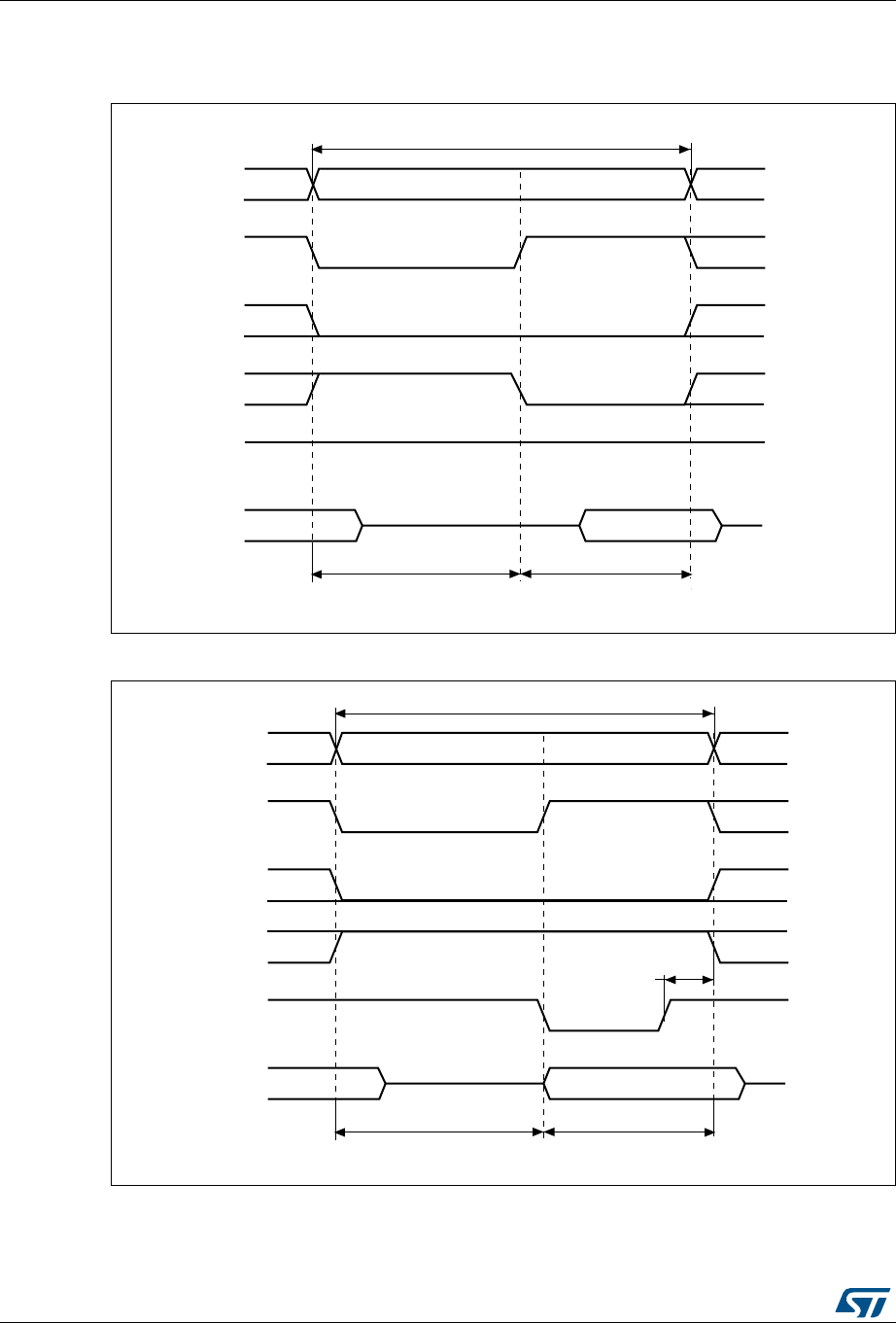
Flexible memory controller (FMC) RM0090
1606/1718 DocID018909 Rev 9
Mode C - NOR Flash - OE toggling
Figure 463. ModeC read access waveforms
Figure 464. ModeC write access waveforms
The differences compared with mode1 are the toggling of NOE and the independent read
and write timings.
!;=
./%
!$$3%4 $!4!34
-EMORYTRANSACTION
.%X
$;=
(#,+CYCLES (#,+CYCLES
.7%
.!$6
DATADRIVEN
BYMEMORY
-36
(IGH
!;=
./%
!$$3%4 $!4!34
-EMORYTRANSACTION
.%X
$;=
(#,+CYCLES (#,+CYCLES
.7%
.!$6
DATADRIVENBY&3-#
-36
(#,+

DocID018909 Rev 9 1607/1718
RM0090 Flexible memory controller (FMC)
1660
Table 272. FMC_BCRx bit fields
Bit No. Bit name Value to set
31-21 Reserved 0x000
20 CCLKEN As needed
19 CBURSTRW 0x0 (no effect in asynchronous mode)
18:16 Reserved 0x0
15 ASYNCWAIT Set to 1 if the memory supports this feature. Otherwise keep at 0.
14 EXTMOD 0x1
13 WAITEN 0x0 (no effect in asynchronous mode)
12 WREN As needed
11 WAITCFG Don’t care
10 WRAPMOD 0x0
9 WAITPOL Meaningful only if bit 15 is 1
8 BURSTEN 0x0
7 Reserved 0x1
6 FACCEN 0x1
5-4 MWID As needed
3-2 MTYP 0x02 (NOR Flash memory)
1 MUXEN 0x0
0 MBKEN 0x1
Table 273. FMC_BTRx bit fields
Bit No. Bit name Value to set
31:30 Reserved 0x0
29-28 ACCMOD 0x2
27-24 DATLAT 0x0
23-20 CLKDIV 0x0
19-16 BUSTURN Time between NEx high to NEx low (BUSTURN HCLK)
15-8 DATAST Duration of the second access phase (DATAST HCLK cycles) for
read accesses.
7-4 ADDHLD Don’t care
3-0 ADDSET Duration of the first access phase (ADDSET HCLK cycles) for read
accesses. Minimum value for ADDSET is 0.
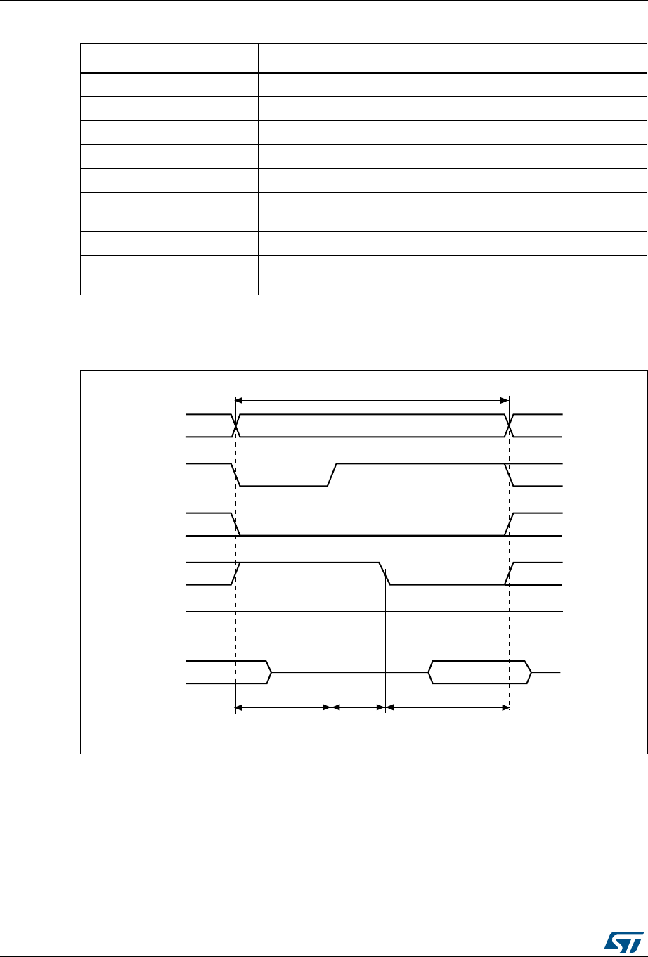
Flexible memory controller (FMC) RM0090
1608/1718 DocID018909 Rev 9
Mode D - asynchronous access with extended address
Figure 465. ModeD read access waveforms
Table 274. FMC_BWTRx bit fields
Bit No. Bit name Value to set
31:30 Reserved 0x0
29-28 ACCMOD 0x2
27-24 DATLAT Don’t care
23-20 CLKDIV Don’t care
19-16 BUSTURN Time between NEx high to NEx low (BUSTURN HCLK)
15-8 DATAST Duration of the second access phase (DATAST HCLK cycles) for
write accesses.
7-4 ADDHLD Don’t care
3-0 ADDSET Duration of the first access phase (ADDSET HCLK cycles) for write
accesses. Minimum value for ADDSET is 0.
!;=
./%
!$$3%4 $!4!34
-EMORYTRANSACTION
.%X
$;=
(#,+CYCLES (#,+CYCLES
.7%
.!$6
DATADRIVEN
BYMEMORY
-36
(IGH
!$$(,$
(#,+CYCLES
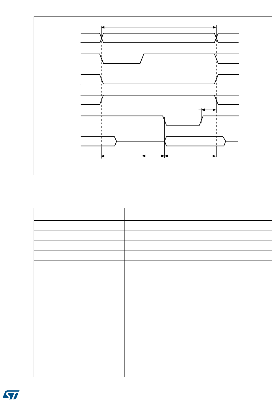
DocID018909 Rev 9 1609/1718
RM0090 Flexible memory controller (FMC)
1660
Figure 466. ModeD write access waveforms
The differences with mode1 are the toggling of NOE that goes on toggling after NADV
changes and the independent read and write timings.
Table 275. FMC_BCRx bit fields
Bit No. Bit name Value to set
31-21 Reserved 0x000
20 CCLKEN As needed
19 CBURSTRW 0x0 (no effect in asynchronous mode)
18:16 Reserved 0x0
15 ASYNCWAIT Set to 1 if the memory supports this feature. Otherwise keep
at 0.
14 EXTMOD 0x1
13 WAITEN 0x0 (no effect in asynchronous mode)
12 WREN As needed
11 WAITCFG Don’t care
10 WRAPMOD 0x0
9 WAITPOL Meaningful only if bit 15 is 1
8 BURSTEN 0x0
7 Reserved 0x1
6 FACCEN Set according to memory support
5-4 MWID As needed
$>@
12(
$''6(7 '$7$67
0HPRU\WUDQVDFWLRQ
1([
'>@
+&/.F\FOHV +&/.F\FOHV
1:(
1$'9
GDWDGULYHQE\)60&
069
+&/.
$''+/'
+&/.F\FOHV

Flexible memory controller (FMC) RM0090
1610/1718 DocID018909 Rev 9
3-2 MTYP As needed
1 MUXEN 0x0
0 MBKEN 0x1
Table 276. FMC_BTRx bit fields
Bit No. Bit name Value to set
31:30 Reserved 0x0
29-28 ACCMOD 0x3
27-24 DATLAT Don’t care
23-20 CLKDIV Don’t care
19-16 BUSTURN Time between NEx high to NEx low (BUSTURN HCLK)
15-8 DATAST Duration of the second access phase (DATAST HCLK cycles) for
read accesses.
7-4 ADDHLD Duration of the middle phase of the read access (ADDHLD HCLK
cycles)
3-0 ADDSET Duration of the first access phase (ADDSET HCLK cycles) for read
accesses. Minimum value for ADDSET is 1.
Table 277. FMC_BWTRx bit fields
Bit No. Bit name Value to set
31:30 Reserved 0x0
29-28 ACCMOD 0x3
27-24 DATLAT Don’t care
23-20 CLKDIV Don’t care
19-16 BUSTURN Time between NEx high to NEx low (BUSTURN HCLK)
15-8 DATAST Duration of the second access phase (DATAST + 1 HCLK cycles) for
write accesses.
7-4 ADDHLD Duration of the middle phase of the write access (ADDHLD HCLK
cycles)
3-0 ADDSET Duration of the first access phase (ADDSET HCLK cycles) for write
accesses. Minimum value for ADDSET is 1.
Table 275. FMC_BCRx bit fields (continued)
Bit No. Bit name Value to set
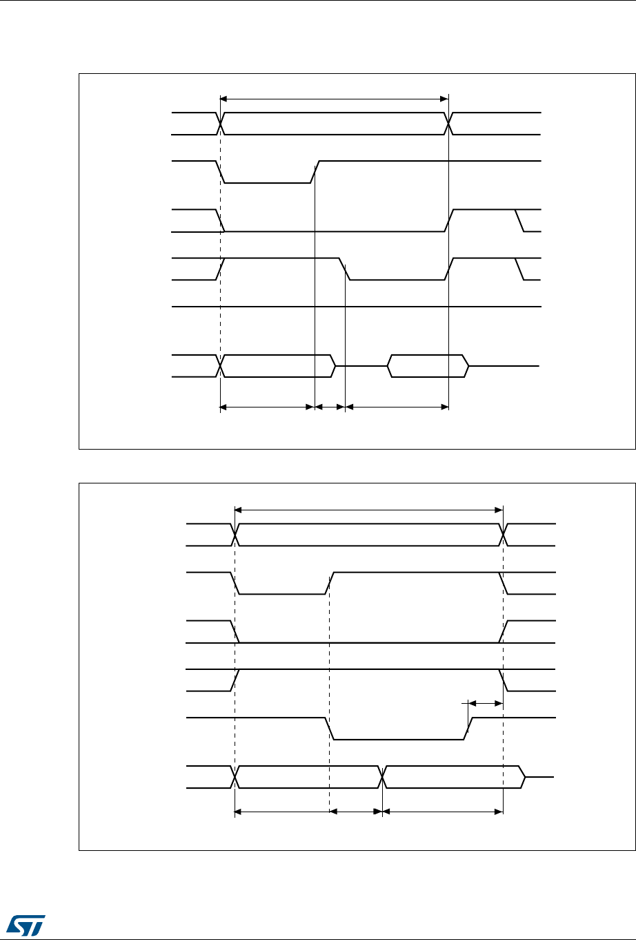
DocID018909 Rev 9 1611/1718
RM0090 Flexible memory controller (FMC)
1660
Muxed mode - multiplexed asynchronous access to NOR Flash memory
Figure 467. Muxed read access waveforms
Figure 468. Muxed write access waveforms
The difference with mode D is the drive of the lower address byte(s) on the data bus.
!;=
./%
!$$3%4 $!4!34
-EMORYTRANSACTION
.%X
!$;=
(#,+CYCLES (#,+CYCLES
.7%
.!$6
DATADRIVEN
BYMEMORY
AI
(IGH
!$$(,$
(#,+CYCLES
,OWERADDRESS
!;=
./%
!$$3%4 $!4!34
-EMORYTRANSACTION
.%X
!$;=
(#,+CYCLES (#,+CYCLES
.7%
.!$6
DATADRIVENBY&3-#
AI
(#,+
!$$(,$
(#,+CYCLES
,OWERADDRESS

Flexible memory controller (FMC) RM0090
1612/1718 DocID018909 Rev 9
WAIT management in asynchronous accesses
If the asynchronous memory asserts the WAIT signal to indicate that it is not yet ready to
accept or to provide data, the ASYNCWAIT bit has to be set in FMC_BCRx register.
Table 278. FMC_BCRx bit fields
Bit No. Bit name Value to set
31-21 Reserved 0x000
20 CCLKEN As needed
19 CBURSTRW 0x0 (no effect in asynchronous mode)
18:16 Reserved 0x0
15 ASYNCWAIT Set to 1 if the memory supports this feature. Otherwise keep at
0.
14 EXTMOD 0x0
13 WAITEN 0x0 (no effect in asynchronous mode)
12 WREN As needed
11 WAITCFG Don’t care
10 WRAPMOD 0x0
9 WAITPOL Meaningful only if bit 15 is 1
8 BURSTEN 0x0
7 Reserved 0x1
6 FACCEN 0x1
5-4 MWID As needed
3-2 MTYP 0x2 (NOR Flash memory)
1 MUXEN 0x1
0 MBKEN 0x1
Table 279. FMC_BTRx bit fields
Bit No. Bit name Value to set
31:30 Reserved 0x0
29-28 ACCMOD 0x0
27-24 DATLAT Don’t care
23-20 CLKDIV Don’t care
19-16 BUSTURN Time between NEx high to NEx low (BUSTURN HCLK)
15-8 DATAST Duration of the second access phase (DATAST HCLK cycles for
read accesses and DATAST+1 HCLK cycles for write accesses).
7-4 ADDHLD Duration of the middle phase of the access (ADDHLD HCLK cycles).
3-0 ADDSET Duration of the first access phase (ADDSET HCLK cycles).
Minimum value for ADDSET is 1.
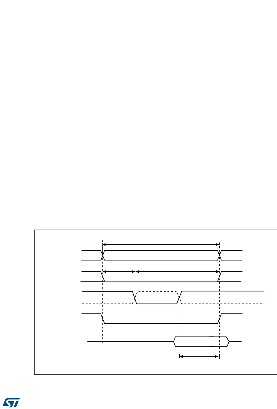
DocID018909 Rev 9 1613/1718
RM0090 Flexible memory controller (FMC)
1660
If the WAIT signal is active (high or low depending on the WAITPOL bit), the second access
phase (Data setup phase), programmed by the DATAST bits, is extended until WAIT
becomes inactive. Unlike the data setup phase, the first access phases (Address setup and
Address hold phases), programmed by the ADDSET and ADDHLD bits, are not WAIT
sensitive and so they are not prolonged.
The data setup phase must be programmed so that WAIT can be detected 4 HCLK cycles
before the end of the memory transaction. The following cases must be considered:
1. The memory asserts the WAIT signal aligned to NOE/NWE which toggles:
2. The memory asserts the WAIT signal aligned to NEx (or NOE/NWE not toggling):
if
then:
otherwise
where max_wait_assertion_time is the maximum time taken by the memory to assert
the WAIT signal once NEx/NOE/NWE is low.
Figure 469 and Figure 470 show the number of HCLK clock cycles that are added to the
memory access phase after WAIT is released by the asynchronous memory (independently
of the above cases).
Figure 469. Asynchronous wait during a read access waveforms
1. NWAIT polarity depends on WAITPOL bit setting in FMC_BCRx register.
DATAST 4 HCLK×()max_wait_assertion_time+≥
max_wait_assertion_time address_phase hold_phase+>
DATAST 4 HCLK×()max_wait_assertion_time address_phase–hold_phase–()+≥
DATAST 4 HCLK×≥
$>@
12(
+&/.
0HPRU\WUDQVDFWLRQ
'>@
1([
GDWDGULYHQE\PHPRU\
069
DGGUHVVSKDVH GDWDVHWXSSKDVH
.7!)4 DONTCARE DONTCARE
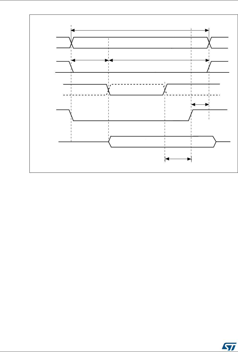
Flexible memory controller (FMC) RM0090
1614/1718 DocID018909 Rev 9
Figure 470. Asynchronous wait during a write access waveforms
1. NWAIT polarity depends on WAITPOL bit setting in FMC_BCRx register.
37.5.5 Synchronous transactions
The memory clock, FMC_CLK, is a submultiple of HCLK. It depends on the value of
CLKDIV and the MWID/ AHB data size, following the formula given below:
If MWID is 16 or 8 bits, the FMC_CLK divider ratio is always defined by the programmed
CLKDIV value.
If MWID is 32 bits, the FMC_CLK divider ratio depends also on AHB data size.
Example:
•If CLKDIV=1, MWID=32 bits, AHB data size=8 bits, FMC_CLK=HCLK/4.
•If CLKDIV=1, MWID=16 bits, AHB data size=8 bits, FMC_CLK=HCLK/2.
NOR Flash memories specify a minimum time from NADV assertion to CLK high. To meet
this constraint, the FMC does not issue the clock to the memory during the first internal
clock cycle of the synchronous access (before NADV assertion). This guarantees that the
rising edge of the memory clock occurs in the middle of the NADV low pulse.
Data latency versus NOR memory latency
The data latency is the number of cycles to wait before sampling the data. The DATLAT
value must be consistent with the latency value specified in the NOR Flash configuration
$>@
1:(
0HPRU\WUDQVDFWLRQ
'>@
1([
GDWDGULYHQE\)60&
069
+&/.
DGGUHVVSKDVH GDWDVHWXSSKDVH
+&/.
.7!)4 DONTCARE DONTCARE
FMC_CLK divider ratio max CLKDIV 1+MWID AHB data size()(, )=

DocID018909 Rev 9 1615/1718
RM0090 Flexible memory controller (FMC)
1660
register. The FMC does not include the clock cycle when NADV is low in the data latency
count.
Caution: Some NOR Flash memories include the NADV Low cycle in the data latency count, so that
the exact relation between the NOR Flash latency and the FMC DATLAT parameter can be
either:
•NOR Flash latency = (DATLAT + 2) CLK clock cycles
•or NOR Flash latency = (DATLAT + 3) CLK clock cycles
Some recent memories assert NWAIT during the latency phase. In such cases DATLAT can
be set to its minimum value. As a result, the FMC samples the data and waits long enough
to evaluate if the data are valid. Thus the FMC detects when the memory exits latency and
real data are processed.
Other memories do not assert NWAIT during latency. In this case the latency must be set
correctly for both the FMC and the memory, otherwise invalid data are mistaken for good
data, or valid data are lost in the initial phase of the memory access.
Single-burst transfer
When the selected bank is configured in burst mode for synchronous accesses, if for
example an AHB single-burst transaction is requested on 16-bit memories, the FMC
performs a burst transaction of length 1 (if the AHB transfer is 16 bits), or length 2 (if the
AHB transfer is 32 bits) and de-assert the Chip Select signal when the last data is strobed.
Such transfers are not the most efficient in terms of cycles compared to asynchronous read
operations. Nevertheless, a random asynchronous access would first require to re-program
the memory access mode, which would altogether last longer.
Wait management
For synchronous NOR Flash memories, NWAIT is evaluated after the programmed latency
period, which corresponds to (DATLAT+2) CLK clock cycles.
If NWAIT is active (low level when WAITPOL = 0, high level when WAITPOL = 1), wait
states are inserted until NWAIT is inactive (high level when WAITPOL = 0, low level when
WAITPOL = 1).
When NWAIT is inactive, the data is considered valid either immediately (bit WAITCFG = 1)
or on the next clock edge (bit WAITCFG = 0).
During wait-state insertion via the NWAIT signal, the controller continues to send clock
pulses to the memory, keeping the Chip Select and output enable signals valid. It does not
consider the data as valid.
In burst mode, there are two timing configurations for the NOR Flash NWAIT signal:
•The Flash memory asserts the NWAIT signal one data cycle before the wait state
(default after reset).
•The Flash memory asserts the NWAIT signal during the wait state
The FMC supports both NOR Flash wait state configurations, for each Chip Select, thanks
to the WAITCFG bit in the FMC_BCRx registers (x = 0..3).
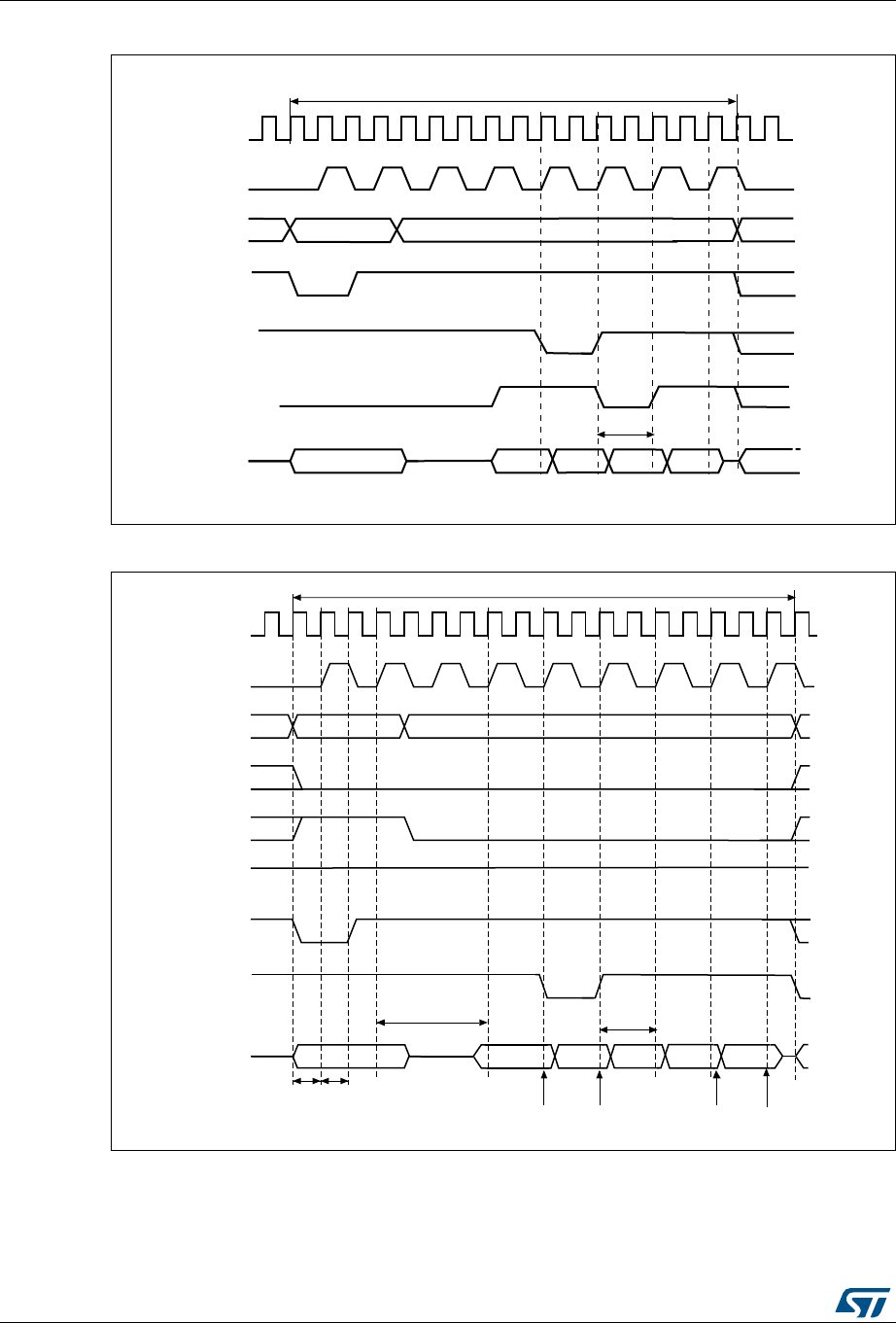
Flexible memory controller (FMC) RM0090
1616/1718 DocID018909 Rev 9
Figure 471. Wait configuration waveforms
Figure 472. Synchronous multiplexed read mode waveforms - NOR, PSRAM (CRAM)
1. Byte lane outputs BL are not shown; for NOR access, they are held high, and, for PSRAM (CRAM) access,
they are held low.
DGGU>@ GDWD GDWD
DGGU>@
0HPRU\WUDQVDFWLRQ EXUVWRIKDOIZRUGV
+&/.
&/.
$>@
1$'9
1:$,7
:$,7&)*
$'>@
LQVHUWHGZDLWVWDWH
GDWD
1:$,7
:$,7&)*
DLF
$GGU>@ GDWD GDWD
DGGU>@
0HPRU\WUDQVDFWLRQ EXUVWRIKDOIZRUGV
+&/.
&/.
$>@
1([
12(
1:( +LJK
1$'9
1:$,7
:$,7&)*
$'>@
FORFN
F\FOH
FORFN
F\FOH
'$7/$7 LQVHUWHGZDLWVWDWH
'DWDVWUREHV DLI
&/.F\FOHV
GDWD GDWD
'DWDVWUREHV

DocID018909 Rev 9 1617/1718
RM0090 Flexible memory controller (FMC)
1660
Table 280. FMC_BCRx bit fields
Bit No. Bit name Value to set
31-21 Reserved 0x000
20 CCLKEN As needed
19 CBURSTRW No effect on synchronous read
18-15 Reserved 0x0
14 EXTMOD 0x0
13 WAITEN to be set to 1 if the memory supports this feature, to be kept at 0
otherwise
12 WREN no effect on synchronous read
11 WAITCFG to be set according to memory
10 WRAPMOD 0x0
9 WAITPOL to be set according to memory
8 BURSTEN 0x1
7 Reserved 0x1
6 FACCEN Set according to memory support (NOR Flash memory)
5-4 MWID As needed
3-2 MTYP 0x1 or 0x2
1 MUXEN As needed
0 MBKEN 0x1
Table 281. FMC_BTRx bit fields
Bit No. Bit name Value to set
31:30 Reserved 0x0
29:28 ACCMOD 0x0
27-24 DATLAT Data latency
27-24 DATLAT Data latency
23-20 CLKDIV
0x0 to get CLK = HCLK (Not supported)
0x1 to get CLK = 2 × HCLK
..
19-16 BUSTURN Time between NEx high to NEx low (BUSTURN HCLK)
15-8 DATAST Don’t care
7-4 ADDHLD Don’t care
3-0 ADDSET Don’t care
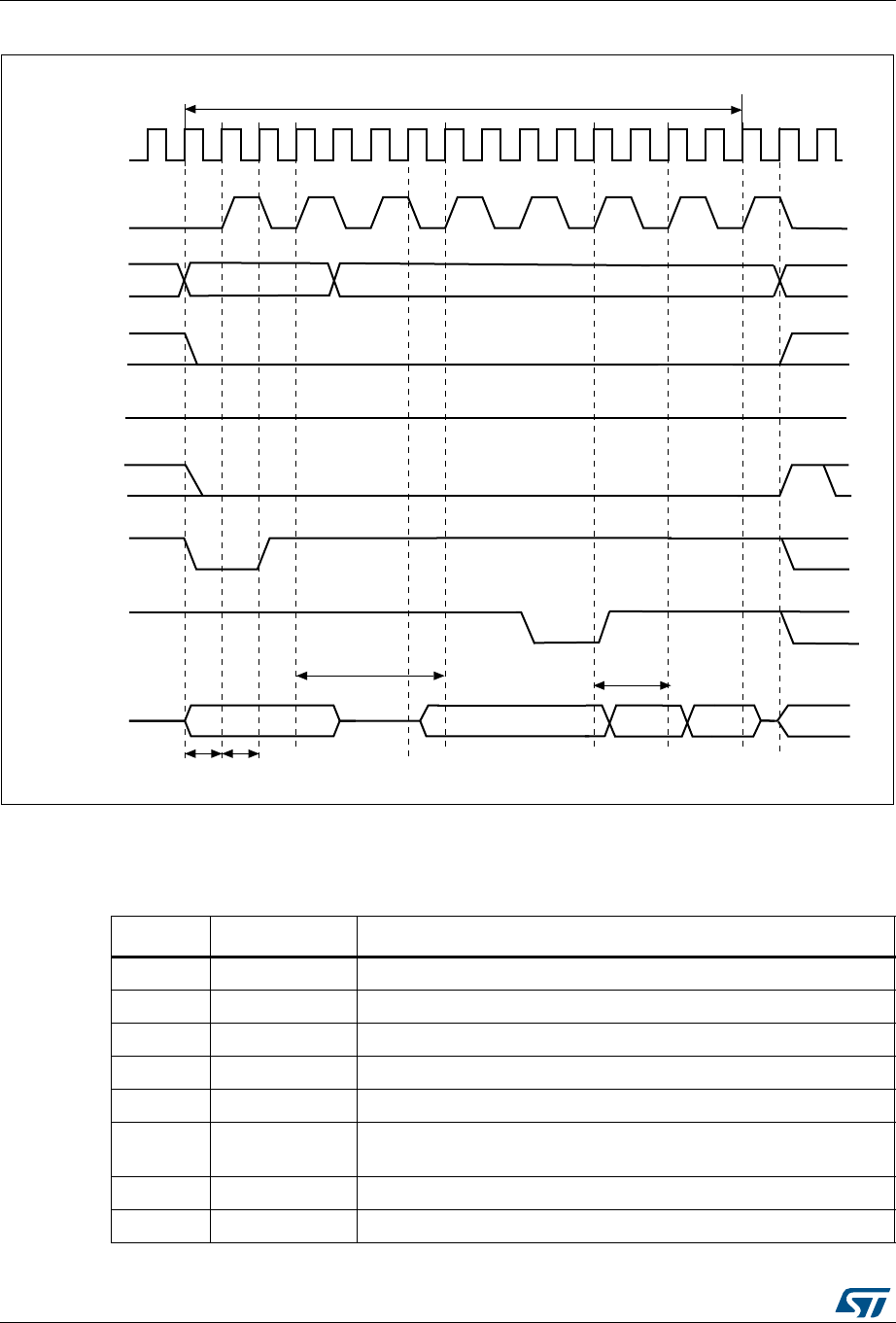
Flexible memory controller (FMC) RM0090
1618/1718 DocID018909 Rev 9
Figure 473. Synchronous multiplexed write mode waveforms - PSRAM (CRAM)
1. The memory must issue NWAIT signal one cycle in advance, accordingly WAITCFG must be programmed
to 0.
2. Byte Lane (NBL) outputs are not shown, they are held low while NEx is active.
!DDR;= DATA
ADDR;=
-EMORYTRANSACTIONBURSTOFHALFWORDS
(#,+
#,+
!;=
.%X
./%
.7%
(I:
.!$6
.7!)4
7!)4#&'
!$;=
CLOCK CLOCK
$!4,!4 INSERTEDWAITSTATE
AIF
#,+CYCLES
DATA
Table 282. FMC_BCRx bit fields
Bit No. Bit name Value to set
31-20 Reserved 0x000
20 CCLKEN As needed
19 CBURSTRW 0x1
18-15 Reserved 0x0
14 EXTMOD 0x0
13 WAITEN to be set to 1 if the memory supports this feature, to be kept at 0
otherwise.
12 WREN 0x1
11 WAITCFG 0x0

DocID018909 Rev 9 1619/1718
RM0090 Flexible memory controller (FMC)
1660
10 WRAPMOD 0x0
9 WAITPOL to be set according to memory
8 BURSTEN no effect on synchronous write
7 Reserved 0x1
6 FACCEN Set according to memory support
5-4 MWID As needed
3-2 MTYP 0x1
1 MUXEN As needed
0 MBKEN 0x1
Table 283. FMC_BTRx bit fields
Bit No. Bit name Value to set
31-30 Reserved 0x0
29:28 ACCMOD 0x0
27-24 DATLAT Data latency
23-20 CLKDIV 0x0 to get CLK = HCLK (not supported)
0x1 to get CLK = 2 × HCLK
19-16 BUSTURN Time between NEx high to NEx low (BUSTURN HCLK)
15-8 DATAST Don’t care
7-4 ADDHLD Don’t care
3-0 ADDSET Don’t care
Table 282. FMC_BCRx bit fields (continued)
Bit No. Bit name Value to set

Flexible memory controller (FMC) RM0090
1620/1718 DocID018909 Rev 9
37.5.6 NOR/PSRAM controller registers
SRAM/NOR-Flash chip-select control registers 1..4 (FMC_BCR1..4)
Address offset: 8 * (x – 1), x = 1...4
Reset value: 0x0000 30DB for Bank1 and 0x0000 30D2 for Bank 2 to 4
This register contains the control information of each memory bank, used for SRAMs,
PSRAM and NOR Flash memories.
3130292827262524232221201918171615141312111098 76543210
Reserved
CCLKEN
CBURSTRW
Reserved
ASCYCWAIT
EXTMOD
WAITEN
WREN
WAITCFG
WRAPMOD
WAITPOL
BURSTEN
Reserved
FACCEN
MWID
MTYP
MUXEN
MBKEN
rw rw rw rw rw rw rw rw rw rw rw rw rw rw rw rw rw
Bits 31: 21 Reserved, must be kept at reset value
Bit 20 CCLKEN: Continuous Clock Enable.
This bit enables the FMC_CLK clock output to external memory devices.
0: The FMC_CLK is only generated during the synchronous memory access (read/write
transaction). The FMC_CLK clock ratio is specified by the programmed CLKDIV value in the
FMC_BCRx register (default after reset) .
1: The FMC_CLK is generated continuously during asynchronous and synchronous access. The
FMC_CLK clock is activated when the CCLKEN is set.
Note: The CCLKEN bit of the FMC_BCR2..4 registers is don’t care. It is only enabled through the
FMC_BCR1 register. Bank 1 must be configured in synchronous mode to generate the
FMC_CLK continuous clock.
Note: If CCLKEN bit is set, the FMC_CLK clock ratio is specified by CLKDIV value in the
FMC_BTR1 register. CLKDIV in FMC_BWTR1 is don’t care.
Note: If the synchronous mode is used and CCLKEN bit is set, the synchronous memories
connected to other banks than Bank 1 are clocked by the same clock (the CLKDIV value in
the FMC_BTR2..4 and FMC_BWTR2..4 registers for other banks has no effect.)
Bit 19 CBURSTRW: Write burst enable.
For PSRAM (CRAM) operating in burst mode, the bit enables synchronous accesses during write
operations. The enable bit for synchronous read accesses is the BURSTEN bit in the FMC_BCRx
register.
0: Write operations are always performed in asynchronous mode
1: Write operations are performed in synchronous mode.
Bits 18:16 Reserved, must be kept at reset value
Bit 15 ASYNCWAIT: Wait signal during asynchronous transfers
This bit enables/disables the FMC to use the wait signal even during an asynchronous protocol.
0: NWAIT signal is not taken in to account when running an asynchronous protocol (default after
reset)
1: NWAIT signal is taken in to account when running an asynchronous protocol

DocID018909 Rev 9 1621/1718
RM0090 Flexible memory controller (FMC)
1660
Bit 14 EXTMOD: Extended mode enable.
This bit enables the FMC to program the write timings for non-multiplexed asynchronous accesses
inside the FMC_BWTR register, thus resulting in different timings for read and write operations.
0: values inside FMC_BWTR register are not taken into account (default after reset)
1: values inside FMC_BWTR register are taken into account
Note: When the extended mode is disabled, the FMC can operate in Mode1 or Mode2 as follows:
– Mode 1 is the default mode when the SRAM/PSRAM memory type is selected (MTYP
=0x0 or 0x01)
– Mode 2 is the default mode when the NOR memory type is selected (MTYP = 0x10).
Bit 13 WAITEN: Wait enable bit.
This bit enables/disables wait-state insertion via the NWAIT signal when accessing the memory in
synchronous mode.
0: NWAIT signal is disabled (its level not taken into account, no wait state inserted after the
programmed Flash latency period)
1: NWAIT signal is enabled (its level is taken into account after the programmed latency period to
insert wait states if asserted) (default after reset)
Bit 12 WREN: Write enable bit.
This bit indicates whether write operations are enabled/disabled in the bank by the FMC:
0: Write operations are disabled in the bank by the FMC, an AHB error is reported,
1: Write operations are enabled for the bank by the FMC (default after reset).
Bit 11 WAITCFG: Wait timing configuration.
The NWAIT signal indicates whether the data from the memory are valid or if a wait state must be
inserted when accessing the memory in synchronous mode. This configuration bit determines if
NWAIT is asserted by the memory one clock cycle before the wait state or during the wait state:
0: NWAIT signal is active one data cycle before wait state (default after reset),
1: NWAIT signal is active during wait state (not used for PSRAM).
Bit 10 WRAPMOD: Wrapped burst mode support.
Defines whether the controller will or not split an AHB burst wrap access into two linear accesses.
Valid only when accessing memories in burst mode
0: Direct wrapped burst is not enabled (default after reset),
1: Direct wrapped burst is enabled.
Note: This bit has no effect as the CPU and DMA cannot generate wrapping burst transfers.
Bit 9 WAITPOL: Wait signal polarity bit.
Defines the polarity of the wait signal from memory used for either in synchronous or
asynchronous mode:
0: NWAIT active low (default after reset),
1: NWAIT active high.
Bit 8 BURSTEN: Burst enable bit.
This bit enables/disables synchronous accesses during read operations. It is valid only for
synchronous memories operating in burst mode:
0: Burst mode disabled (default after reset). Read accesses are performed in asynchronous mode.
1: Burst mode enable. Read accesses are performed in synchronous mode.
Bit 7 Reserved, must be kept at reset value
Bit 6 FACCEN: Flash access enable
Enables NOR Flash memory access operations.
0: Corresponding NOR Flash memory access is disabled
1: Corresponding NOR Flash memory access is enabled (default after reset)

Flexible memory controller (FMC) RM0090
1622/1718 DocID018909 Rev 9
SRAM/NOR-Flash chip-select timing registers 1..4 (FMC_BTR1..4)
Address offset: 0x04 + 8 * (x – 1), x = 1..4
Reset value: 0x0FFF FFFF
Reset value: 0x0FFF FFFF
This register contains the control information of each memory bank, used for SRAMs,
PSRAM and NOR Flash memories.If the EXTMOD bit is set in the FMC_BCRx register, then
this register is partitioned for write and read access, that is, 2 registers are available: one to
configure read accesses (this register) and one to configure write accesses (FMC_BWTRx
registers).
Bits 5:4 MWID: Memory data bus width.
Defines the external memory device width, valid for all type of memories.
00: 8 bits,
01: 16 bits (default after reset),
10: 32 bits,
11: reserved, do not use.
Bits 3:2 MTYP: Memory type.
Defines the type of external memory attached to the corresponding memory bank:
00: SRAM (default after reset for Bank 2...4)
01: PSRAM (CRAM)
10: NOR Flash/OneNAND Flash (default after reset for Bank 1)
11: reserved
Bit 1 MUXEN: Address/data multiplexing enable bit.
When this bit is set, the address and data values are multiplexed on the data bus, valid only with
NOR and PSRAM memories:
0: Address/Data nonmultiplexed
1: Address/Data multiplexed on databus (default after reset)
Bit 0 MBKEN: Memory bank enable bit.
Enables the memory bank. After reset Bank1 is enabled, all others are disabled. Accessing a
disabled bank causes an ERROR on AHB bus.
0: Corresponding memory bank is disabled
1: Corresponding memory bank is enabled
313029282726252423222120191817161514131211109876543210
Reserved
ACCMOD
DATLAT
CLKDIV
BUSTURN
DATAST
ADDHLD
ADDSET
rw rw rw rw rw rw rw rw rw rw rw rw rw rw rw rw rw rw rw rw rw rw rw rw rw rw rw rw rw rw

DocID018909 Rev 9 1623/1718
RM0090 Flexible memory controller (FMC)
1660
Bits 31:30 Reserved, must be kept at reset value
Bits 29:28 ACCMOD: Access mode
Specifies the asynchronous access modes as shown in the timing diagrams. These bits are
taken into account only when the EXTMOD bit in the FMC_BCRx register is 1.
00: access mode A
01: access mode B
10: access mode C
11: access mode D
Bits 27:24 DATLAT: Data latency for synchronous memory (see note below bit description table)
For synchronous accesses with read/write burst mode enabled (BURSTEN / CBURSTRW
bits set), this field defines the number of memory clock cycles (+2) to issue to the memory
before reading/writing the first data. This timing parameter is not expressed in HCLK periods,
but in FMC_CLK periods. For asynchronous accesses, this value is don't care.
0000: Data latency of 2 CLK clock cycles for first burst access
1111: Data latency of 17 CLK clock cycles for first burst access (default value after reset)
Bits 23:20 CLKDIV: Clock divide ratio (for FMC_CLK signal)
Defines the period of FMC_CLK clock output signal, expressed in number of HCLK cycles:
0000: Reserved
0001: FMC_CLK period = 2 × HCLK periods
0010: FMC_CLK period = 3 × HCLK periods
1111: FMC_CLK period = 16 × HCLK periods (default value after reset)
In asynchronous NOR Flash, SRAM or PSRAM accesses, this value is don’t care.
Note: Refer to section 37.5.5: Synchronous transactions for FMC_CLK divider ratio formula)
Bits 19:16 BUSTURN: Bus turnaround phase duration
These bits are written by software to add a delay at the end of a write/read transaction. This
delay allows to match the minimum time between consecutive transactions (tEHEL from NEx
high to NEx low) and the maximum time needed by the memory to free the data bus after a
read access (tEHQZ):
(BUSTRUN + 1)HCLK period ≥ tEHELmin and (BUSTRUN + 2)HCLK period ≥ tEHQZmax if
EXTMOD = ‘0’
(BUSTRUN + 2)HCLK period ≥ max (tEHELmin, tEHQZmax) if EXTMOD = ‘1’.
0000: BUSTURN phase duration = 0 HCLK clock cycle added
...
1111: BUSTURN phase duration = 15 × HCLK clock cycles (default value after reset)

Flexible memory controller (FMC) RM0090
1624/1718 DocID018909 Rev 9
Note: PSRAMs (CRAMs) have a variable latency due to internal refresh. Therefore these
memories issue the NWAIT signal during the whole latency phase to prolong the latency as
needed.
With PSRAMs (CRAMs) the filled DATLAT must be set to 0, so that the FMC exits its latency
phase soon and starts sampling NWAIT from memory, then starts to read or write when the
memory is ready.
This method can be used also with the latest generation of synchronous Flash memories
that issue the NWAIT signal, unlike older Flash memories (check the datasheet of the
specific Flash memory being used).
Bits 15:8 DATAST: Data-phase duration
These bits are written by software to define the duration of the data phase (refer to
Figure 456 to Figure 468), used in asynchronous accesses:
0000 0000: Reserved
0000 0001: DATAST phase duration = 1 × HCLK clock cycles
0000 0010: DATAST phase duration = 2 × HCLK clock cycles
...
1111 1111: DATAST phase duration = 255 × HCLK clock cycles (default value after reset)
For each memory type and access mode data-phase duration, please refer to the respective
figure (Figure 456 to Figure 468).
Example: Mode1, write access, DATAST=1: Data-phase duration= DATAST+1 = 2 HCLK
clock cycles.
Note: In synchronous accesses, this value is don’t care.
Bits 7:4 ADDHLD: Address-hold phase duration
These bits are written by software to define the duration of the address hold phase (refer to
Figure 465 to Figure 468), used in mode D or multiplexed accesses:
0000: Reserved
0001: ADDHLD phase duration =1 × HCLK clock cycle
0010: ADDHLD phase duration = 2 × HCLK clock cycle
...
1111: ADDHLD phase duration = 15 × HCLK clock cycles (default value after reset)
For each access mode address-hold phase duration, please refer to the respective figure
(Figure 465 to Figure 468).
Note: In synchronous accesses, this value is not used, the address hold phase is always 1
memory clock period duration.
Bits 3:0 ADDSET: Address setup phase duration
These bits are written by software to define the duration of the address setup phase (refer to
Figure 456 to Figure 468), used in SRAMs, ROMs and asynchronous NOR Flash and
PSRAM accesses:
0000: ADDSET phase duration = 0 × HCLK clock cycle
...
1111: ADDSET phase duration = 15 × HCLK clock cycles (default value after reset)
For each access mode address setup phase duration, please refer to the respective figure
(refer to Figure 456 to Figure 468).
Note: In synchronous accesses, this value is don’t care.
In Muxed mode or Mode D, the minimum value for ADDSET is 1.

DocID018909 Rev 9 1625/1718
RM0090 Flexible memory controller (FMC)
1660
SRAM/NOR-Flash write timing registers 1..4 (FMC_BWTR1..4)
Address offset: 0x104 + 8 * (x – 1), x = 1...4
Reset value: 0x0FFF FFFF
This register contains the control information of each memory bank. It is used for SRAMs,
PSRAMs and NOR Flash memories. When the EXTMOD bit is set in the FMC_BCRx
register, then this register is active for write access.
313029282726252423222120191817161514131211109876543210
Reserved
ACCMOD
Reserved
BUSTURN
DATAST
ADDHLD
ADDSET
rw rw rw rw rw rw rw rw rw rw rw rw rw rw rw rw rw rw rw rw rw rw
Bits 31:30 Reserved, must be kept at reset value
Bits 29:28 ACCMOD: Access mode.
Specifies the asynchronous access modes as shown in the next timing diagrams.These bits are
taken into account only when the EXTMOD bit in the FMC_BCRx register is 1.
00: access mode A
01: access mode B
10: access mode C
11: access mode D
Bits 27:20 Reserved, must be kept at reset value
Bits 19:16 BUSTURN: Bus turnaround phase duration
These bits are written by software to add a delay at the end of a write transaction to match the
minimum time between consecutive transactions (tEHEL from ENx high to ENx low):
(BUSTRUN + 1) HCLK period ≥ tEHELmin.
0000: BUSTURN phase duration = 0 HCLK clock cycle added
...
1111: BUSTURN phase duration = 15 HCLK clock cycles added (default value after reset)
Bits 15:8 DATAST: Data-phase duration.
These bits are written by software to define the duration of the data phase (refer toFigure 456 to
Figure 468), used in asynchronous SRAM, PSRAM and NOR Flash memory accesses:
0000 0000: Reserved
0000 0001: DATAST phase duration = 1 × HCLK clock cycles
0000 0010: DATAST phase duration = 2 × HCLK clock cycles
...
1111 1111: DATAST phase duration = 255 × HCLK clock cycles (default value after reset)
Bits 7:4 ADDHLD: Address-hold phase duration.
These bits are written by software to define the duration of the address hold phase (refer to
Figure 465 to Figure 468), used in asynchronous multiplexed accesses:
0000: Reserved
0001: ADDHLD phase duration = 1 × HCLK clock cycle
0010: ADDHLD phase duration = 2 × HCLK clock cycle
...
1111: ADDHLD phase duration = 15 × HCLK clock cycles (default value after reset)
Note: In synchronous NOR Flash accesses, this value is not used, the address hold phase is always
1 Flash clock period duration.

Flexible memory controller (FMC) RM0090
1626/1718 DocID018909 Rev 9
37.6 NAND Flash/PC Card controller
The FMC generates the appropriate signal timings to drive the following types of device:
•8- and 16-bit NAND Flash memories
•16-bit PC Card compatible devices
The NAND Flash/PC Card controller can control three external banks, Bank 2, 3 and 4:
•Bank 2 and Bank 3 support NAND Flash devices
•Bank 4 supports PC Card devices.
Each bank is configured through dedicated registers (Section 37.6.8). The programmable
memory parameters include access timings (shown in Table 284) and ECC configuration.
Bits 3:0 ADDSET: Address setup phase duration.
These bits are written by software to define the duration of the address setup phase in HCLK
cycles (refer to Figure 465 to Figure 468), used in asynchronous accesses:
0000: ADDSET phase duration = 0 × HCLK clock cycle
...
1111: ADDSET phase duration = 15 × HCLK clock cycles (default value after reset)
Note: In synchronous NOR Flash and PSRAM accesses, this value is not used, the address setup
phase is always 1 Flash clock period duration. In muxed mode, the minimum ADDSET value
is 1.

DocID018909 Rev 9 1627/1718
RM0090 Flexible memory controller (FMC)
1660
37.6.1 External memory interface signals
The following tables list the signals that are typically used to interface NAND Flash memory
and PC Card.
Note: The prefix “N” identifies the signals which are active low.
8-bit NAND Flash memory
t
Theoretically, there is no capacity limitation as the FMC can manage as many address
cycles as needed.
Table 284. Programmable NAND Flash/PC Card access parameters
Parameter Function Access mode Unit Min. Max.
Memory setup
time
Number of clock cycles (HCLK)
required to set up the address
before the command assertion
Read/Write AHB clock cycle
(HCLK) 1 256
Memory wait Minimum duration (in HCLK clock
cycles) of the command assertion Read/Write AHB clock cycle
(HCLK) 2255
Memory hold
Number of clock cycles (HCLK)
during which the address must be
held (as well as the data if a write
access is performed) after the
command de-assertion
Read/Write AHB clock cycle
(HCLK) 1 255
Memory
databus high-Z
Number of clock cycles (HCLK)
during which the data bus is kept
in high-Z state after a write
access has started
Write AHB clock cycle
(HCLK) 1 255
Table 285. 8-bit NAND Flash
FMC signal name I/O Function
A[17] O NAND Flash address latch enable (ALE) signal
A[16] O NAND Flash command latch enable (CLE) signal
D[7:0] I/O 8-bit multiplexed, bidirectional address/data bus
NCE[x] O Chip Select, x = 2, 3
NOE(= NRE) O Output enable (memory signal name: read enable, NRE)
NWE O Write enable
NWAIT/INT[3:2] I NAND Flash ready/busy input signal to the FMC

Flexible memory controller (FMC) RM0090
1628/1718 DocID018909 Rev 9
16-bit NAND Flash memory
Theoretically, there is no capacity limitation as the FMC can manage as many address
cycles as needed.
Table 286. 16-bit NAND Flash
FMC signal name I/O Function
A[17] O NAND Flash address latch enable (ALE) signal
A[16] O NAND Flash command latch enable (CLE) signal
D[15:0] I/O 16-bit multiplexed, bidirectional address/data bus
NCE[x] O Chip Select, x = 2, 3
NOE(= NRE) O Output enable (memory signal name: read enable, NRE)
NWE O Write enable
NWAIT/INT[3:2] I NAND Flash ready/busy input signal to the FMC
Table 287. 16-bit PC Card
FMC signal name I/O Function
A[10:0] O Address bus
NIORD O Output enable for I/O space
NIOWR O Write enable for I/O space
NREG O Register signal indicating if access is in Common or Attribute space
D[15:0] I/O Bidirectional databus
NCE4_1 O Chip Select 1
NCE4_2 O Chip Select 2 (indicates if access is 16-bit or 8-bit)
NOE O Output enable in Common and in Attribute space
NWE O Write enable in Common and in Attribute space
NWAIT I PC Card wait input signal to the FMC (memory signal name IORDY)
INTR I PC Card interrupt to the FMC (only for PC Cards that can generate
an interrupt)
CD I
PC Card presence detection. Active high. If an access is performed
to the PC Card banks while CD is low, an AHB error is generated.
Refer to Section 37.3: AHB interface

DocID018909 Rev 9 1629/1718
RM0090 Flexible memory controller (FMC)
1660
37.6.2 NAND Flash / PC Card supported memories and transactions
Table 288 shows the supported devices, access modes and transactions. Transactions not
allowed (or not supported) by the NAND Flash / PC Card controller are shown in gray.
37.6.3 Timing diagrams for NAND Flash memory and PC Card
Each PC Card/CompactFlash and NAND Flash memory bank is managed through a set of
registers:
•Control register: FMC_PCRx
•Interrupt status register: FMC_SRx
•ECC register: FMC_ECCRx
•Timing register for Common memory space: FMC_PMEMx
•Timing register for Attribute memory space: FMC_PATTx
•Timing register for I/O space: FMC_PIOx
Each timing configuration register contains three parameters used to define number of
HCLK cycles for the three phases of any PC Card/CompactFlash or NAND Flash access,
plus one parameter that defines the timing for starting driving the data bus when a write
access is performed. Figure 474 shows the timing parameter definitions for common
memory accesses, knowing that Attribute and I/O (only for PC Card) memory space access
timings are similar.
Table 288. Supported memories and transactions
Device Mode R/W
AHB
data size
Memory
data size
Allowed/
not allowed Comments
NAND 8-bit
Asynchronous R 8 8 Y
Asynchronous W 8 8 Y
Asynchronous R 16 8 Y Split into 2 FMC accesses
Asynchronous W 16 8 Y Split into 2 FMC accesses
Asynchronous R 32 8 Y Split into 4 FMC accesses
Asynchronous W 32 8 Y Split into 4 FMC accesses
NAND 16-bit
Asynchronous R 8 16 Y
Asynchronous W 8 16 N
Asynchronous R 16 16 Y
Asynchronous W 16 16 Y
Asynchronous R 32 16 Y Split into 2 FMC accesses
Asynchronous W 32 16 Y Split into 2 FMC accesses
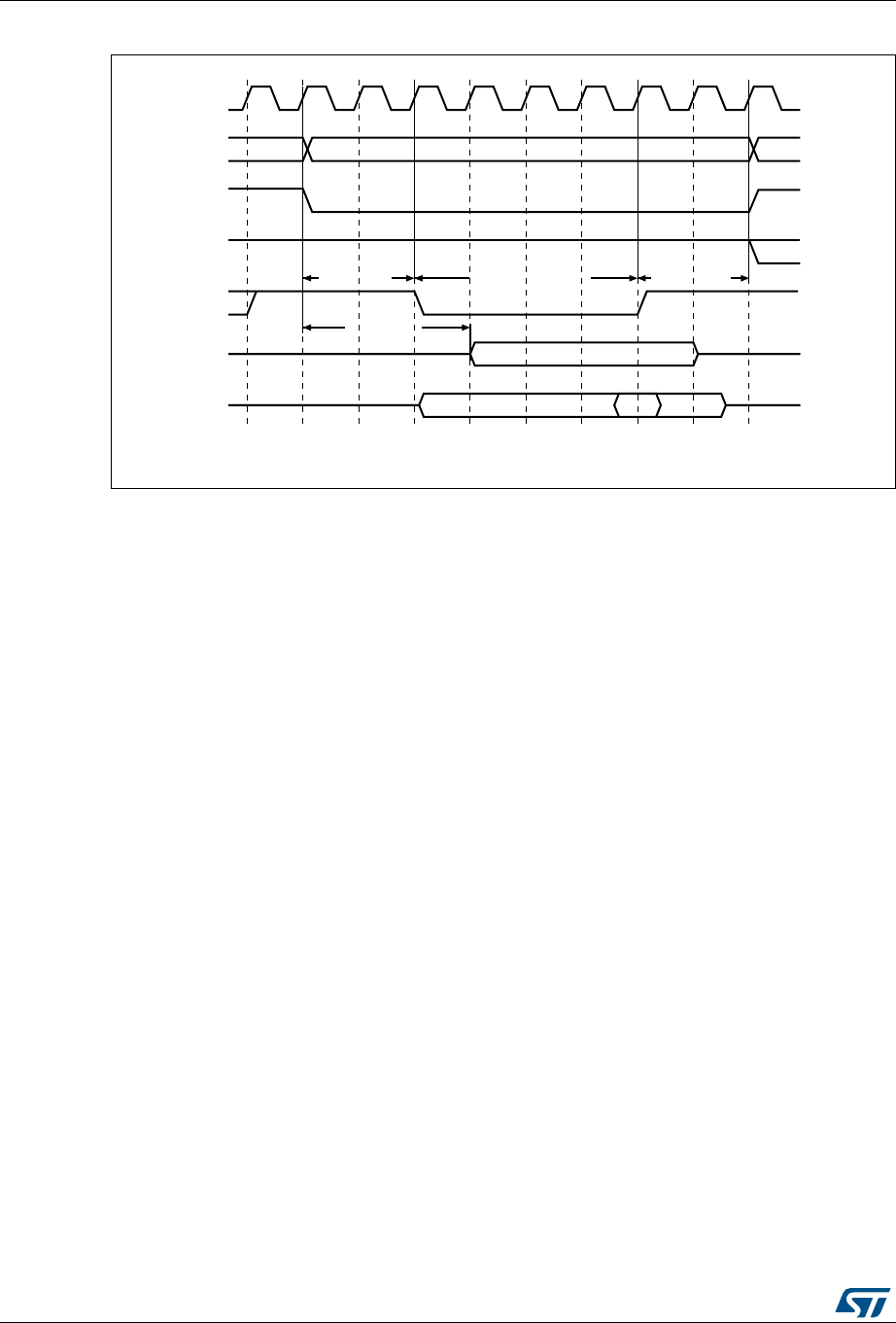
Flexible memory controller (FMC) RM0090
1630/1718 DocID018909 Rev 9
Figure 474. NAND Flash/PC Card controller waveforms for common memory access
1. NOE remains high (inactive) during write accesses. NWE remains high (inactive) during read accesses.
37.6.4 NAND Flash operations
The command latch enable (CLE) and address latch enable (ALE) signals of the NAND
Flash memory device are driven by address signals from the FMC controller. This means
that to send a command or an address to the NAND Flash memory, the CPU has to perform
a write to a specific address in its memory space.
A typical page read operation from the NAND Flash device requires the following steps:
3. Program and enable the corresponding memory bank by configuring the FMC_PCRx
and FMC_PMEMx (and for some devices, FMC_PATTx, see Section 37.6.5: NAND
Flash prewait functionality) registers according to the characteristics of the NAND
Flash memory (PWID bits for the data bus width of the NAND Flash, PTYP = 1,
PWAITEN = 0 or 1 as needed, see section Section 37.4.2: NAND Flash memory/PC
Card address mapping for timing configuration).
4. The CPU performs a byte write to the common memory space, with data byte equal to
one Flash command byte (for example 0x00 for Samsung NAND Flash devices). The
LE input of the NAND Flash memory is active during the write strobe (low pulse on
NWE), thus the written byte is interpreted as a command by the NAND Flash memory.
Once the command is latched by the memory device, it does not need to be written
again for the following page read operations.
5. The CPU can send the start address (STARTAD) for a read operation by writing four
bytes (or three for smaller capacity devices), STARTAD[7:0], STARTAD[16:9],
STARTAD[24:17] and finally STARTAD[25] (for 64 Mb x 8 bit NAND Flash memories) in
the common memory or attribute space. The ALE input of the NAND Flash device is
active during the write strobe (low pulse on NWE), thus the written bytes are
interpreted as the start address for read operations. Using the attribute memory space
makes it possible to use a different timing configuration of the FMC, which can be used
to implement the prewait functionality needed by some NAND Flash memories (see
069
+&/.
$>@
1&([
15(*
1,2:
1,25
1:(
12(
ZULWHBGDWD
UHDGBGDWD
+LJK
9DOLG
0(0[6(7
0(0[:$,7
0(0[+2/'
0(0[+,=
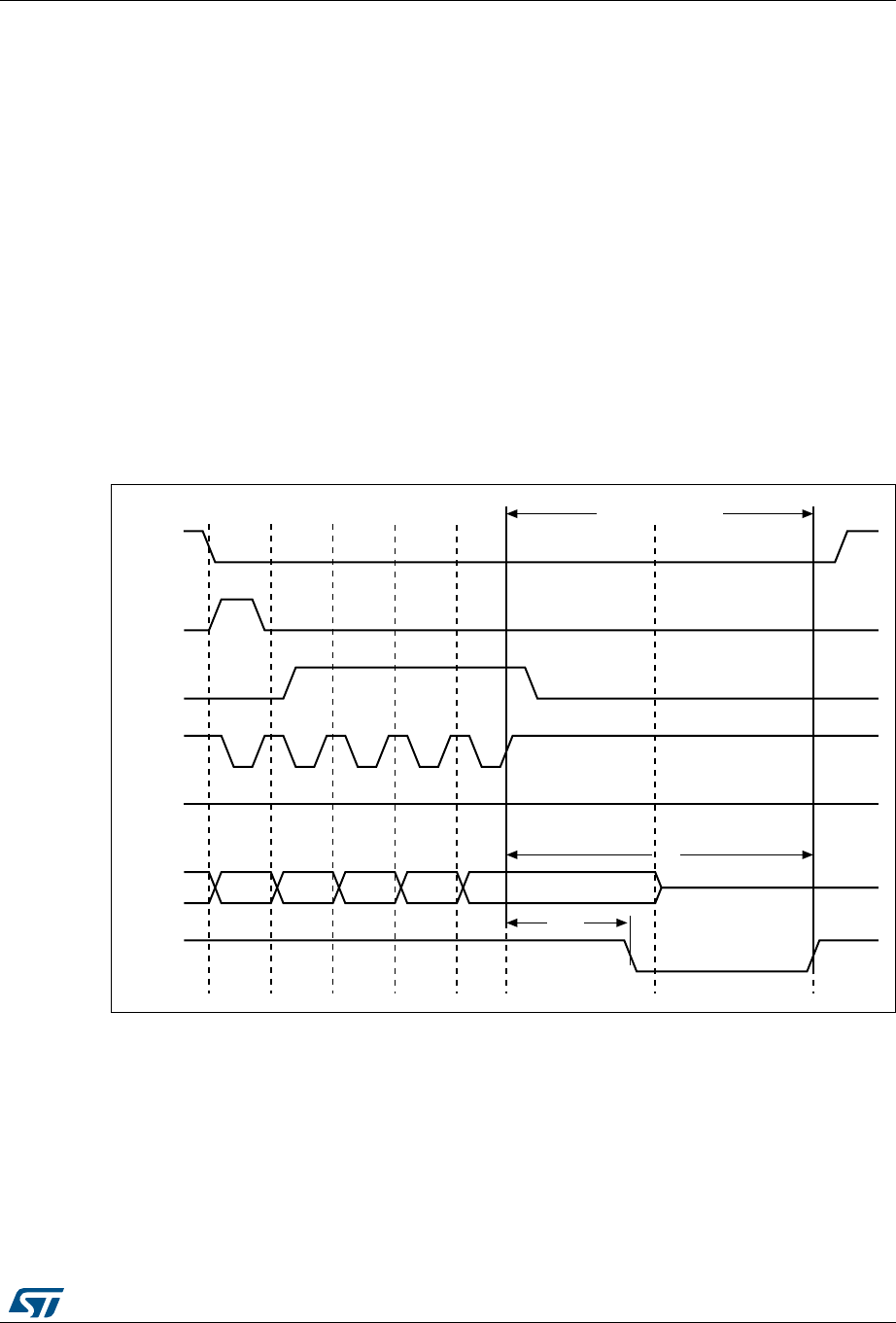
DocID018909 Rev 9 1631/1718
RM0090 Flexible memory controller (FMC)
1660
details in Section 37.6.5: NAND Flash prewait functionality).
6. The controller waits for the NAND Flash memory to be ready (R/NB signal high), before
starting a new access to the same or another memory bank. While waiting, the
controller holds the NCE signal active (low).
7. The CPU can then perform byte read operations from the common memory space to
read the NAND Flash page (data field + Spare field) byte by byte.
8. The next NAND Flash page can be read without any CPU command or address write
operation. This can be done in three different ways:
– by simply performing the operation described in step 5
– a new random address can be accessed by restarting the operation at step 3
– a new command can be sent to the NAND Flash device by restarting at step 2
37.6.5 NAND Flash prewait functionality
Some NAND Flash devices require that, after writing the last part of the address, the
controller waits for the R/NB signal to go low. (see Figure 455).
Figure 475. Access to non ‘CE don’t care’ NAND-Flash
1. CPU wrote byte 0x00 at address 0x7001 0000.
2. CPU wrote byte A7~A0 at address 0x7002 0000.
3. CPU wrote byte A16~A9 at address 0x7002 0000.
4. CPU wrote byte A24~A17 at address 0x7002 0000.
5. CPU wrote byte A25 at address 0x7802 0000: FMC performs a write access using FMC_PATT2 timing
definition, where ATTHOLD ≥ 7 (providing that (7+1) × HCLK = 112 ns > tWB max). This guarantees that
NCE remains low until R/NB goes low and high again (only requested for NAND Flash memories where
NCE is not don’t care).
When this functionality is required, it can be ensured by programming the MEMHOLD value
to meet the tWB timing. However any CPU read or write access to the NAND Flash memory
.#%
./%
)/;=
2."
(IGH
T7"
#,%
!,%
X !! !! !! !
T2
.7%
.#%MUSTSTAYLOW

Flexible memory controller (FMC) RM0090
1632/1718 DocID018909 Rev 9
has a hold delay of (MEMHOLD + 1) HCLK cycles inserted between the rising edge of the
NWE signal and the next access.
To cope with this timing constraint, the attribute memory space can be used by
programming its timing register with an ATTHOLD value that meets the tWB timing, and by
keeping the MEMHOLD value at its minimum value. The CPU must then use the common
memory space for all NAND Flash read and write accesses, except when writing the last
address byte to the NAND Flash device, where the CPU must write to the attribute memory
space.
37.6.6 Computation of the error correction code (ECC)
in NAND Flash memory
The FMC PC Card controller includes two error correction code computation hardware
blocks, one per memory bank. They reduce the host CPU workload when processing the
ECC by software.
These two ECC blocks are identical and associated with Bank 2 and Bank 3. As a
consequence, no hardware ECC computation is available for memories connected to Bank
4.
The ECC algorithm implemented in the FMC can perform 1-bit error correction and 2-bit
error detection per 256, 512, 1 024, 2 048, 4 096 or 8 192 bytes read or written from/to the
NAND Flash memory. It is based on the Hamming coding algorithm and consists in
calculating the row and column parity.
The ECC modules monitor the NAND Flash data bus and read/write signals (NCE and
NWE) each time the NAND Flash memory bank is active.
The ECC operates as follows:
•When accessing NAND Flash memory bank 2 or bank 3, the data present on the
D[15:0] bus is latched and used for ECC computation.
•When accessing any other address in NAND Flash memory, the ECC logic is idle, and
does not perform any operation. As a result, write operations to define commands or
addresses to the NAND Flash memory are not taken into account for ECC
computation.
Once the desired number of bytes has been read/written from/to the NAND Flash memory
by the host CPU, the FMC_ECCR2/3 registers must be read to retrieve the computed value.
Once read, they should be cleared by resetting the ECCEN bit to ‘0’. To compute a new data
block, the ECCEN bit must be set to one in the FMC_PCR2/3 registers.
To perform an ECC computation:
1. Enable the ECCEN bit in the FMC_PCR2/3 register.
2. Write data to the NAND Flash memory page. While the NAND page is written, the ECC
block computes the ECC value.
3. Read the ECC value available in the FMC_ECCR2/3 register and store it in a variable.
4. Clear the ECCEN bit and then enable it in the FMC_PCR2/3 register before reading
back the written data from the NAND page. While the NAND page is read, the ECC
block computes the ECC value.
5. Read the new ECC value available in the FMC_ECCR2/3 register.
6. If the two ECC values are the same, no correction is required, otherwise there is an
ECC error and the software correction routine returns information on whether the error
can be corrected or not.

DocID018909 Rev 9 1633/1718
RM0090 Flexible memory controller (FMC)
1660
37.6.7 PC Card/CompactFlash operations
Address spaces and memory accesses
The FMC supports CompactFlash devices and PC Cards in Memory mode and I/O mode
(True IDE mode is not supported).
The CompactFlash and PC Cards are made of 3 memory spaces:
•Common Memory space
•Attribute space
•I/O Memory space
The nCE2 and nCE1 pins (FMC_NCE4_2 and FMC_NCE4_1 respectively) select the card
and indicate whether a byte or a word operation is being performed: nCE2 accesses the odd
byte on D15-8 and nCE1 accesses the even byte on D7-0 if A0=0 or the odd byte on D7-0 if
A0=1. The full word is accessed on D15-0 if both nCE2 and nCE1 are low.
The memory space is selected by asserting low nOE for read accesses or nWE for write
accesses, combined with the low assertion of nCE2/nCE1 and nREG.
•If pin nREG=1 during the memory access, the common memory space is selected
•If pin nREG=0 during the memory access, the attribute memory space is selected
The I/O space is selected by asserting nIORD space for read accesses or nIOWR for write
accesses [instead of nOE/nWE for memory space], combined with nCE2/nCE1. Note that
nREG must also be asserted low when accessing I/O space.
Three type of accesses are allowed for a 16-bit PC Card:
•Accesses to Common Memory space for data storage can be either 8-bit accesses at
even addresses or 16-bit AHB accesses.
Note that 8-bit accesses at odd addresses are not supported and nCE2 will not be
driven low. A 32-bit AHB request is translated into two 16-bit memory accesses.
•Accesses to Attribute Memory space where the PC Card stores configuration
information are limited to 8-bit AHB accesses at even addresses.
Note that a 16-bit AHB access will be converted into a single 8-bit memory transfer:
nCE1 will be asserted low, nCE2 will be asserted high and only the even byte on D7-D0
will be valid. Instead a 32-bit AHB access will be converted into two 8-bit memory
transfers at even addresses: nCE1 will be asserted low, NCE2 will be asserted high
and only the even bytes will be valid.
•Accesses to I/O space can be either 8-bit or 16 bit AHB accesses.

Flexible memory controller (FMC) RM0090
1634/1718 DocID018909 Rev 9
FMC Bank 4 gives access to those 3 memory spaces as described in Section 37.4.2: NAND
Flash memory/PC Card address mapping and Table 251: NAND/PC Card memory mapping
and timing registers.
Wait feature
The CompactFlash or PC Card may request the FMC to extend the length of the access
phase programmed by MEMWAITx/ATTWAITx/IOWAITx bits, asserting the nWAIT signal
after nOE/nWE or nIORD/nIOWR activation if the wait feature is enabled through the
Table 289. 16-bit PC-Card signals and access type
nCE2
nCE1
nREG
nOE/nWE
nIORD /nIOWR
A10
A9
A7-1
A0
Space Access type Allowed/not
Allowed
1 0 101XXX-XX Common
Memory
Space
Read/Write byte on D7-D0 YES
0 1 1 0 1 X X X-X X Read/Write byte on D15-D8 Not supported
0 0 1 0 1 X X X-X 0 Read/Write word on D15-D0 YES
X0 00101X-X0
Attribute
Space
Read or Write Configuration
Registers YES
X0 00100X-X0 Read or Write CIS (Card
Information Structure) YES
1 0 001XXX-X1
Attribute
Space
Invalid Read or Write (odd
address) YES
0 1 001XXX-Xx Invalid Read or Write (odd
address) YES
1 0 010XXX-X0
I/O space
Read Even Byte on D7-0 YES
1 0 0 1 0 X X X-X 1 Read Odd Byte on D7-0 YES
1 0 0 1 0 X X X-X 0 Write Even Byte on D7-0 YES
1 0 0 1 0 X X X-X 1 Write Odd Byte on D7-0 YES
0 0 0 1 0 X X X-X 0 Read Word on D15-0 YES
0 0 0 1 0 X X X-X 0 Write word on D15-0 YES
0 1 0 1 0 X X X-X X Read Odd Byte on D15-8 Not supported
0 1 0 1 0 X X X-X X Write Odd Byte on D15-8 Not supported

DocID018909 Rev 9 1635/1718
RM0090 Flexible memory controller (FMC)
1660
PWAITEN bit in the FMC_PCRx register. To detect correctly the nWAIT assertion, the
MEMWAITx/ATTWAITx/IOWAITx bits must be programmed as follows:
where max_wait_assertion_time is the maximum time taken by NWAIT to go low once
nOE/nWE or nIORD/nIOWR is low.
After WAIT de-assertion, the FMC extends the WAIT phase for 4 HCLK clock cycles.
37.6.8 NAND Flash/PC Card controller registers
PC Card/NAND Flash control registers 2..4 (FMC_PCR2..4)
Address offset: 0x40 + 0x20 * (x – 1), x = 2..4
Reset value: 0x0000 0018
xxWAITx 4 max_wait_assertion_time
HCLK
-------------------------------------------------------------------+≥
31302928272625242322212019181716151413121110987654321 0
Reserved
ECCPS TAR TCLR
Res.
ECCEN
PWID
PTYP
PBKEN
PWAITEN
Reserved
rw rw rw rw rw rw rw rw rw rw rw rw rw rw rw rw rw
Bits 31:20 Reserved, must be kept at reset value
Bits 19:17 ECCPS: ECC page size.
Defines the page size for the extended ECC:
000: 256 bytes
001: 512 bytes
010: 1024 bytes
011: 2048 bytes
100: 4096 bytes
101: 8192 bytes
Bits 16:13 TAR: ALE to RE delay.
Sets time from ALE low to RE low in number of AHB clock cycles (HCLK).
Time is: t_ar = (TAR + SET + 2) × THCLK where THCLK is the HCLK clock period
0000: 1 HCLK cycle (default)
1111: 16 HCLK cycles
Note: SET is MEMSET or ATTSET according to the addressed space.
Bits 12:9 TCLR: CLE to RE delay.
Sets time from CLE low to RE low in number of AHB clock cycles (HCLK).
Time is t_clr = (TCLR + SET + 2) × THCLK where THCLK is the HCLK clock period
0000: 1 HCLK cycle (default)
1111: 16 HCLK cycles
Note: SET is MEMSET or ATTSET according to the addressed space.
Bits 8:7 Reserved, must be kept at reset value
Bit 6 ECCEN: ECC computation logic enable bit
0: ECC logic is disabled and reset (default after reset),
1: ECC logic is enabled.

Flexible memory controller (FMC) RM0090
1636/1718 DocID018909 Rev 9
FIFO status and interrupt register 2..4 (FMC_SR2..4)
Address offset: 0x44 + 0x20 * (x-1), x = 2..4
Reset value: 0x0000 0040
This register contains information about the FIFO status and interrupt. The FMC features a
FIFO that is used when writing to memories to transfer up to 16 words of data from the AHB.
This is used to quickly write to the FIFO and free the AHB for transactions to peripherals
other than the FMC, while the FMC is draining its FIFO into the memory. One of these
register bits indicates the status of the FIFO, for ECC purposes.
The ECC is calculated while the data are written to the memory. To read the correct ECC,
the software must consequently wait until the FIFO is empty.
Bits 5:4 PWID: Data bus width.
Defines the external memory device width.
00: 8 bits
01: 16 bits (default after reset). This value is mandatory for PC Cards.
10: reserved, do not use
11: reserved, do not use
Bit 3 PTYP: Memory type.
Defines the type of device attached to the corresponding memory bank:
0: PC Card, CompactFlash, CF+ or PCMCIA
1: NAND Flash (default after reset)
Bit 2 PBKEN: PC Card/NAND Flash memory bank enable bit.
Enables the memory bank. Accessing a disabled memory bank causes an ERROR on AHB
bus
0: Corresponding memory bank is disabled (default after reset)
1: Corresponding memory bank is enabled
Bit 1 PWAITEN: Wait feature enable bit.
Enables the Wait feature for the PC Card/NAND Flash memory bank:
0: disabled
1: enabled
Note: For a PC Card, when the wait feature is enabled, the MEMWAITx/ATTWAITx/IOWAITx
bits must be programmed to a value as follows:
xxWAITx ≥ 4 + max_wait_assertion_time/HCLK
Where max_wait_assertion_time is the maximum time taken by NWAIT to go low once
nOE/nWE or nIORD/nIOWR is low.
Bit 0 Reserved.
313029282726252423222120191817161514131211109876543210
Reserved
FEMPT
IFEN
ILEN
IREN
IFS
ILS
IRS
r rwrwrwrwrwrw
Bits 31:7 Reserved, must be kept at reset value

DocID018909 Rev 9 1637/1718
RM0090 Flexible memory controller (FMC)
1660
Common memory space timing register 2..4 (FMC_PMEM2..4)
Address offset: Address: 0x48 + 0x20 * (x – 1), x = 2..4
Reset value: 0xFCFC FCFC
Each FMC_PMEMx (x = 2..4) read/write register contains the timing information for PC Card
or NAND Flash memory bank x. This information is used to access either the common
memory space of the 16-bit PC Card/CompactFlash, or the NAND Flash for command,
address write access and data read/write access.
Bit 6 FEMPT: FIFO empty.
Read-only bit that provides the status of the FIFO
0: FIFO not empty
1: FIFO empty
Bit 5 IFEN: Interrupt falling edge detection enable bit
0: Interrupt falling edge detection request disabled
1: Interrupt falling edge detection request enabled
Bit 4 ILEN: Interrupt high-level detection enable bit
0: Interrupt high-level detection request disabled
1: Interrupt high-level detection request enabled
Bit 3 IREN: Interrupt rising edge detection enable bit
0: Interrupt rising edge detection request disabled
1: Interrupt rising edge detection request enabled
Bit 2 IFS: Interrupt falling edge status
The flag is set by hardware and reset by software.
0: No interrupt falling edge occurred
1: Interrupt falling edge occurred
Bit 1 ILS: Interrupt high-level status
The flag is set by hardware and reset by software.
0: No Interrupt high-level occurred
1: Interrupt high-level occurred
Bit 0 IRS: Interrupt rising edge status
The flag is set by hardware and reset by software.
0: No interrupt rising edge occurred
1: Interrupt rising edge occurred
313029282726252423222120191817161514131211109876543210
MEMHIZx MEMHOLDx MEMWAITx MEMSETx
rw rw rw rw rw rw rw rw rw rw rw rw rw rw rw rw rw rw rw rw rw rw rw rw rw rw rw rw rw rw rw rw
Bits 31:24 MEMHIZx: Common memory x data bus Hi-Z time
Defines the number of HCLK clock cycles during which the data bus is kept Hi-Z after the
start of a PC Card/NAND Flash write access to common memory space on socket x. This is
only valid for write transactions:
0000 0000: (0x00) 0 HCLK cycle (for PC Card) / 1 HCLK cycle (for NAND Flash)
1111 1111: (0xFF) 255 HCLK cycles (for PC Card) / 256 HCLK cycles (for NAND Flash)

Flexible memory controller (FMC) RM0090
1638/1718 DocID018909 Rev 9
Attribute memory space timing registers 2..4 (FMC_PATT2..4)
Address offset: 0x4C + 0x20 * (x – 1), x = 2..4
Reset value: 0xFCFC FCFC
Each FMC_PATTx (x = 2..4) read/write register contains the timing information for PC
Card/CompactFlash or NAND Flash memory bank x. It is used for 8-bit accesses to the
attribute memory space of the PC Card/CompactFlash or to access the NAND Flash for the
last address write access if the timing must differ from that of previous accesses (for
Ready/Busy management, refer to Section 37.6.5: NAND Flash prewait functionality).
Bits 23:16 MEMHOLDx: Common memory x hold time
Defines the number of HCLK clock cycles during which the address is held (and data for
write accesses) after the command is deasserted (NWE, NOE), for PC Card/NAND Flash
read or write access to common memory space on socket x:
0000 0000: reserved
0000 0001: 1 HCLK cycle
1111 1111: 255 HCLK cycles
Bits 15:8 MEMWAITx: Common memory x wait time
Defines the minimum number of HCLK (+1) clock cycles to assert the command (NWE,
NOE), for PC Card/NAND Flash read or write access to common memory space on socket
x. The duration of command assertion is extended if the wait signal (NWAIT) is active (low)
at the end of the programmed value of HCLK:
0000 0000: reserved
0000 0001: 2HCLK cycles (+ wait cycle introduced by deasserting NWAIT)
1111 1111: 256 HCLK cycles (+ wait cycle introduced by the Card deasserting NWAIT)
Bits 7:0 MEMSETx: Common memory x setup time
Defines the number of HCLK (+1) clock cycles to set up the address before the command
assertion (NWE, NOE), for PC Card/NAND Flash read or write access to common memory
space on socket x:
0000 0000: 1 HCLK cycle (for PC Card) / 1 HCLK cycles (for NAND Flash)
1111 1111: 256 HCLK cycles (for PC Card) / 257 HCLK cycles (for NAND Flash)
313029282726252423222120191817161514131211109876543210
ATTHIZx ATTHOLDx ATTWAITx ATTSETx
rw rw rw rw rw rw rw rw rw rw rw rw rw rw rw rw rw rw rw rw rw rw rw rw rw rw rw rw rw rw rw rw
Bits 31:24 ATTHIZx: Attribute memory x data bus Hi-Z time
Defines the number of HCLK clock cycles during which the data bus is kept in Hi-Z after the
start of a PC CARD/NAND Flash write access to attribute memory space on socket x. Only
valid for write transaction:
0000 0000: 0 HCLK cycle
1111 1111: 255 HCLK cycles
Bits 23:16 ATTHOLDx: Attribute memory x hold time
Defines the number of HCLK clock cycles during which the address is held (and data for
write access) after the command deassertion (NWE, NOE), for PC Card/NAND Flash read
or write access to attribute memory space on socket x
0000 0000: reserved
0000 0001: 1 HCLK cycle
1111 1111: 255 HCLK cycles

DocID018909 Rev 9 1639/1718
RM0090 Flexible memory controller (FMC)
1660
I/O space timing register 4 (FMC_PIO4)
Address offset: 0xB0
Reset value: 0xFCFCFCFC
The FMC_PIO4 read/write registers contain the timing information used to access the I/O
space of the 16-bit PC Card/CompactFlash.
Bits 15:8 ATTWAITx: Attribute memory x wait time
Defines the minimum number of HCLK (+1) clock cycles to assert the command (NWE,
NOE), for PC Card/NAND Flash read or write access to attribute memory space on socket x.
The duration for command assertion is extended if the wait signal (NWAIT) is active (low) at
the end of the programmed value of HCLK:
0000 0000: reserved
0000 0001: 2 HCLK cycles (+ wait cycle introduced by deassertion of NWAIT)
1111 1111: 256 HCLK cycles (+ wait cycle introduced by the card deasserting NWAIT)
Bits 7:0 ATTSETx: Attribute memory x setup time
Defines the number of HCLK (+1) clock cycles to set up address before the command
assertion (NWE, NOE), for PC CARD/NAND Flash read or write access to attribute memory
space on socket x:
0000 0000: 1 HCLK cycle
1111 1111: 256 HCLK cycles
313029282726252423222120191817161514131211109876543210
IOHIZx IOHOLDx IOWAITx IOSETx
rw rw rw rw rw rw rw rw rw rw rw rw rw rw rw rw rw rw rw rw rw rw rw rw rw rw rw rw rw rw rw rw
Bits 31:24 IOHIZx: I/O x data bus Hi-Z time
Defines the number of HCLK clock cycles during which the data bus is kept in Hi-Z after the
start of a PC Card write access to I/O space on socket x. Only valid for write transaction:
0000 0000: 0 HCLK cycle
1111 1111: 255 HCLK cycles

Flexible memory controller (FMC) RM0090
1640/1718 DocID018909 Rev 9
Bits 23:16 IOHOLDx: I/O x hold time
Defines the number of HCLK clock cycles during which the address is held (and data for
write access) after the command deassertion (NWE, NOE), for PC Card read or write access
to I/O space on socket x:
0000 0000: reserved
0000 0001: 1 HCLK cycle
1111 1111: 255 HCLK cycles
Bits 15:8 IOWAITx: I/O x wait time
Defines the minimum number of HCLK (+1) clock cycles to assert the command (SMNWE,
SMNOE), for PC Card read or write access to I/O space on socket x. The duration for
command assertion is extended if the wait signal (NWAIT) is active (low) at the end of the
programmed value of HCLK:
0000 0000: reserved, do not use this value
0000 0001: 2 HCLK cycles (+ wait cycle introduced by deassertion of NWAIT)
1111 1111: 256 HCLK cycles (+ wait cycle introduced by the Card deasserting NWAIT)
Bits 7:0 IOSETx: I/O x setup time
Defines the number of HCLK (+1) clock cycles to set up the address before the command
assertion (NWE, NOE), for PC Card read or write access to I/O space on socket x:
0000 0000: 1 HCLK cycle
1111 1111: 256 HCLK cycles
DocID018909 Rev 9 1641/1718
RM0090 Flexible memory controller (FMC)
1660
ECC result registers 2/3 (FMC_ECCR2/3)
Address offset: 0x54 + 0x20 * (x – 1), x = 2 or 3
Reset value: 0x0000 0000
These registers contain the current error correction code value computed by the ECC
computation modules of the FMC controller (one module per NAND Flash memory bank).
When the CPU reads the data from a NAND Flash memory page at the correct address
(refer to Section 37.6.6: Computation of the error correction code (ECC) in NAND Flash
memory), the data read/written from/to the NAND Flash memory are processed
automatically by the ECC computation module. When X bytes have been read (according to
the ECCPS field in the FMC_PCRx registers), the CPU must read the computed ECC value
from the FMC_ECCx registers. It then verifies if these computed parity data are the same as
the parity value recorded in the spare area, to determine whether a page is valid, and, to
correct it otherwise. The FMC_ECCRx registers should be cleared after being read by
setting the ECCEN bit to ‘0’. To compute a new data block, the ECCEN bit must be set to ’1’.
313029282726252423222120191817161514131211109876543210
ECCx
r
Bits 31:0 ECCx: ECC result
This field contains the value computed by the ECC computation logic. Table 290 describes
the contents of these bit fields.
Table 290. ECC result relevant bits
ECCPS[2:0] Page size in bytes ECC bits
000 256 ECC[21:0]
001 512 ECC[23:0]
010 1024 ECC[25:0]
011 2048 ECC[27:0]
100 4096 ECC[29:0]
101 8192 ECC[31:0]

Flexible memory controller (FMC) RM0090
1642/1718 DocID018909 Rev 9
37.7 SDRAM controller
37.7.1 SDRAM controller main features
The main features of the SDRAM controller are the following:
•Two SDRAM banks with independent configuration
•8-bit, 16-bit, 32-bit data bus width
•13-bits Address Row, 11-bits Address Column, 4 internal banks: 4x16Mx32bit
(256 MB), 4x16Mx16bit (128 MB), 4x16Mx8bit (64 MB)
•Word, half-word, byte access
•SDRAM clock can be HCLK/2 or HCLK/3
•Automatic row and bank boundary management
•Multibank ping-pong access
•Programmable timing parameters
•Automatic Refresh operation with programmable Refresh rate
•Self-refresh mode
•Power-down mode
•SDRAM power-up initialization by software
•CAS latency of 1,2,3
•Cacheable Read FIFO with depth of 6 lines x32-bit (6 x14-bit address tag)
37.7.2 SDRAM External memory interface signals
At startup, the SDRAM I/O pins used to interface the FMC SDRAM controller with the
external SDRAM devices must configured by the user application. The SDRAM controller
I/O pins which are not used by the application, can be used for other purposes.
Table 291. SDRAM signals
SDRAM signal I/O
type Description Alternate function
SDCLK O SDRAM clock
SDCKE[1:0] O SDCKE0: SDRAM Bank 1 Clock Enable
SDCKE1: SDRAM Bank 2 Clock Enable
SDNE[1:0] O SDNE0: SDRAM Bank 1 Chip Enable
SDNE1: SDRAM Bank 2 Chip Enable
A[12:0] O Address FMC_A[12:0]
D[31:0] I/O Bidirectional data bus FMC_D[31:0]
BA[1:0] O Bank Address FMC_A[15:14]
NRAS O Row Address Strobe
NCAS O Column Address Strobe
SDNWE O Write Enable
NBL[3:0] O Output Byte Mask for write accesses
(memory signal name: DQM[3:0]) FMC_NBL[3:0]

DocID018909 Rev 9 1643/1718
RM0090 Flexible memory controller (FMC)
1660
37.7.3 SDRAM controller functional description
All SDRAM controller outputs (signals, address and data) change on the falling edge of the
memory clock (FMC_SDCLK).
SDRAM initialization
The initialization sequence is managed by software. If the two banks are used, the
initialization sequence must be generated simultaneously to Bank 1and Bank 2 by setting
the Target Bank bits CTB1 and CTB2 in the FMC_SDCMR register:
1. Program the memory device features into the FMC_SDCRx register.The SDRAM clock
frequency, RBURST and RPIPE must be programmed in the FMC_SDCR1 register.
2. Program the memory device timing into the FMC_SDTRx register. The TRP and TRC
timings must be programmed in the FMC_SDTR1 register.
3. Set MODE bits to ‘001’ and configure the Target Bank bits (CTB1 and/or CTB2) in the
FMC_SDCMR register to start delivering the clock to the memory (SDCKE is driven
high).
4. Wait during the prescribed delay period. Typical delay is around 100 μs (refer to the
SDRAM datasheet for the required delay after power-up).
5. Set MODE bits to ‘010’ and configure the Target Bank bits (CTB1 and/or CTB2) in the
FMC_SDCMR register to issue a “Precharge All” command.
6. Set MODE bits to ‘011’, and configure the Target Bank bits (CTB1 and/or CTB2) as well
as the number of consecutive Auto-refresh commands (NRFS) in the FMC_SDCMR
register. Refer to the SDRAM datasheet for the number of Auto-refresh commands that
should be issued. Typical number is 8.
7. Configure the MRD field according to your SDRAM device, set the MODE bits to '100',
and configure the Target Bank bits (CTB1 and/or CTB2) in the FMC_SDCMR register
to issue a "Load Mode Register" command in order to program the SDRAM. In
particular:
a) The CAS latency must be selected following configured value in FMC_SDCR1/2
registers
b) The Burst Length (BL) of 1 must be selected by configuring the M[2:0] bits to 000
in the mode register (refer to the SDRAM datasheet). If the Mode Register is not
the same for both SDRAM banks, this step has to be repeated twice, once for
each bank, and the Target Bank bits set accordingly.
8. Program the refresh rate in the FMC_SDRTR register
The refresh rate corresponds to the delay between refresh cycles. Its value must be
adapted to SDRAM devices.
At this stage the SDRAM device is ready to accept commands. If a system reset occurs
during an ongoing SDRAM access, the data bus might still be driven by the SDRAM device.
Therefor the SDRAM device must be first reinitialized after reset before issuing any new
access by the NOR Flash/PSRAM/SRAM or NAND Flash/PC Card controller.
Note: If two SDRAM devices are connected to the FMC, all the accesses performed at the same
time to both devices by the Command Mode register (Load Mode Register and Self-refresh
commands) are issued using the timing parameters configured for SDRAM Bank 1 (TMRD,
TRAS and TXSR timings) in the FMC_SDTR1 register.
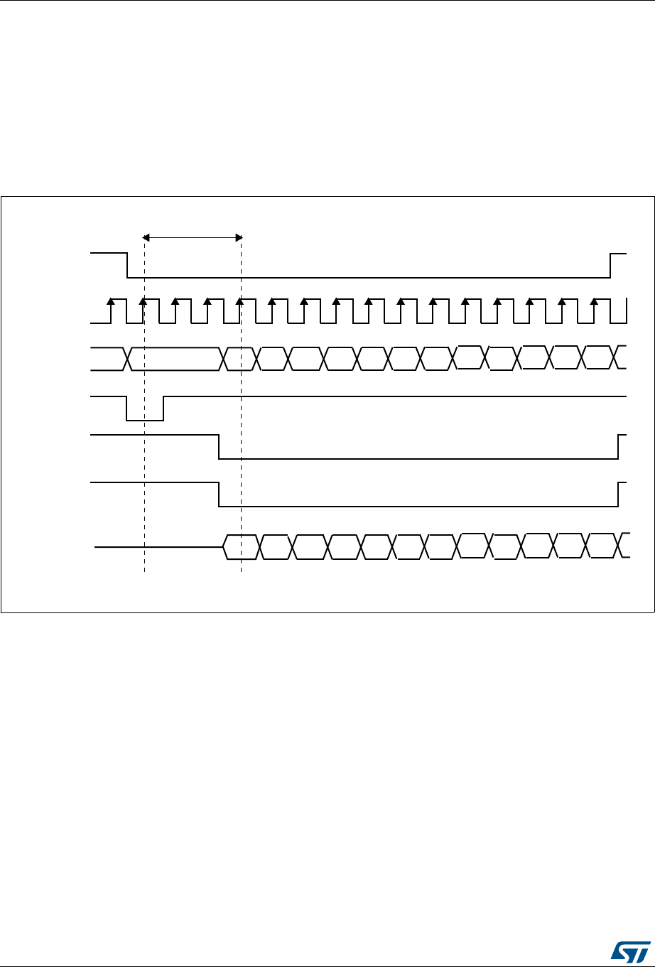
Flexible memory controller (FMC) RM0090
1644/1718 DocID018909 Rev 9
SDRAM controller write cycle
The SDRAM controller accepts single and burst write requests and translates them into
single memory accesses. In both cases, the SDRAM controller keeps track of the active row
for each bank to be able to perform consecutive write accesses to different banks (Multibank
ping-pong access).
Before performing any write access, the SDRAM bank write protection must be disabled by
clearing the WP bit in the FMC_SDCRx register.
Figure 476. Burst write SDRAM access waveforms
The SDRAM controller always checks the next access.
•If the next access is in the same row or in another active row, the write operation is
carried out,
•if the next access targets another row (not active), the SDRAM controller generates a
precharge command, activates the new row and initiates a write command.
SDRAM controller read cycle
The SDRAM controller accepts single and burst read requests and translates them into
single memory accesses. In both cases, the SDRAM controller keeps track of the active row
in each bank to be able to perform consecutive read accesses in different banks (Multibank
ping-pong access).
-36
.2!3
!;=
3$#,+
2OWN #OLC
3$.%
42#$
3$.7%
#OLA #OLD
#OLB #OLE #OLF #OG #OLH #OLI #OLJ #OLK #OLL
.#!3
$!4!;= $NC
$NE
$NA $NF $NG $NH $NI $NJ $NK $NL
$NB $ND
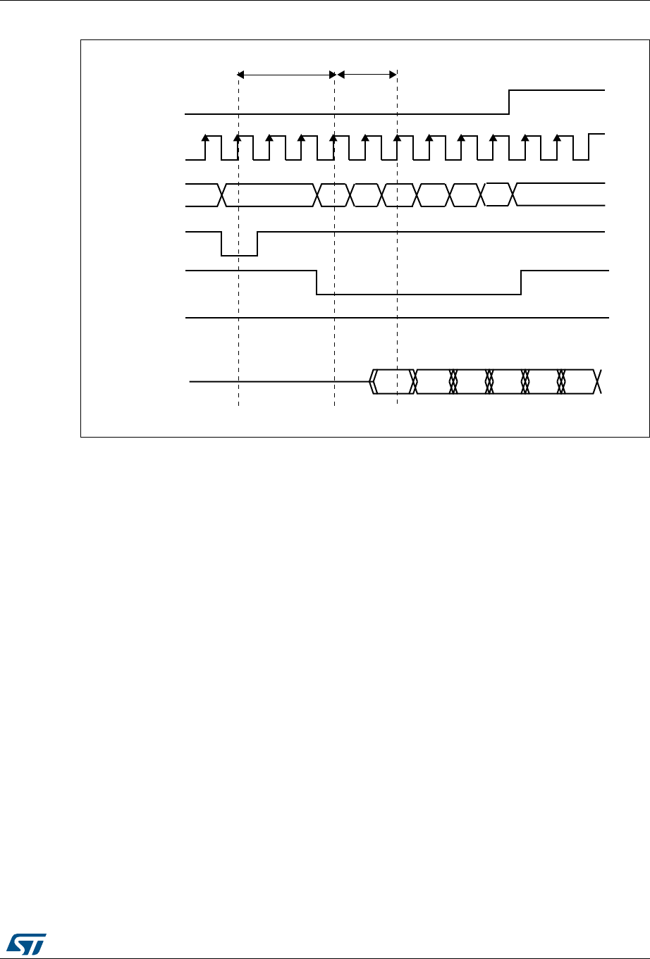
DocID018909 Rev 9 1645/1718
RM0090 Flexible memory controller (FMC)
1660
Figure 477. Burst read SDRAM access
The FMC SDRAM controller features a Cacheable read FIFO (6 lines x 32 bits). It is used to
store data read in advance during the CAS latency period (up to 3 memory clock cycles,
programmed FMC_SDCRx) and during the RPIPE delay (up to 2xHCLK clock cycles as
configured in FMC_SDCR1). The RBURST bit must be set in the FMC_SDCR1 register to
anticipate the next read access.
Example:
•CAS=3, SDCLK= HCLK/2, RPIPE= 2xHCLK. In this case, 4 data (not committed) are
stored in the FIFO (3 data during CAS latency and 1 data during RPIPE delay)
The read FIFO features a 14-bit address tag to each line to identify its content: 11 bits for the
column address, 2 bits to select the internal bank and the active row, and 1 bit to select the
SDRAM device
When the end of the row is reached in advance during an AHB burst read, the data read in
advance (not committed) are not stored in the read FIFO. For single read access, data are
correctly stored in the FIFO.
Each time a read request occurs, the SDRAM controller checks:
•If the address matches one of the address tags, data are directly read from the FIFO
and the corresponding address tag/ line content is cleared and the remaining data in
the FIFO are compacted to avoid empty lines.
•Otherwise, a new read command is issued to the memory and the FIFO is updated with
new data. If the FIFO is full, the older data are lost.
-36
.2!3
!;=
3$#,+
2OWN #OLC
3$.%
42#$
.7%
#OLA #OLD
#OLB #OLE #OLF
.#!3
$!4!;= $NC $NE$NA $NF
$NB $ND
#!3LATENCY
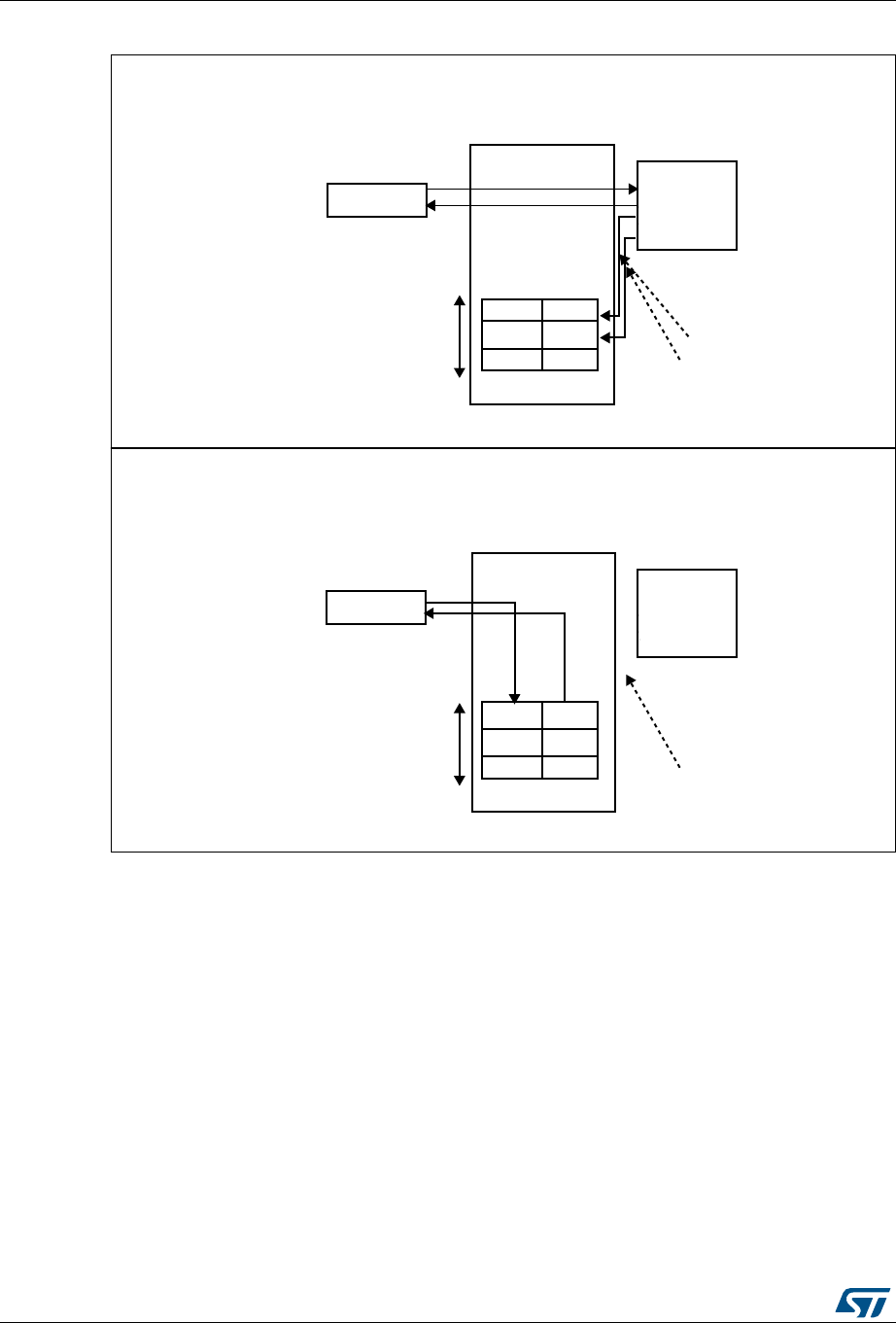
Flexible memory controller (FMC) RM0090
1646/1718 DocID018909 Rev 9
Figure 478. Logic diagram of Read access with RBURST bit set (CAS=2, RPIPE=0)
During a write access or a Precharge command, the read FIFO is flushed and ready to be
filled with new data.
After the first read request, if the current access was not performed to a row boundary, the
SDRAM controller anticipates the next read access during the CAS latency period and the
RPIPE delay (if configured). This is done by incrementing the memory address. The
following condition must be met:
•RBURST control bit should be set to ‘1’ in the FMC_SDCR1 register.
-36
!("-ASTER
X
X
$ATA
$ATA
3$2!-
$EVICE
#!3
READREQUEST X
$ATA
LINES&)&/
!DD4AGREAD&)&/
$ATASTOREDIN&)&/
INADVANCEDURING
THE#!3LATENCYPERIOD
!DDRESSMATCHESWITH
ONEOFTHEADDRESSTAGS
&-#3$2!-#ONTROLLER
ND2EADACCESS 2EQUESTEDDATAWASPREVIOUSLYSTOREDINTHE&)&/
ST2EADACCESS2EQUESTEDDATAISNOTINTHE&)&/
!("-ASTER
X
X
$ATA
$ATA
3$2!-
$EVICE
#!3
READREQUEST X
$ATA
LINES&)&/
$ATAREADFROM&)&/
&-#3$2!-#ONTROLLER
!DD4AGREAD&)&/

DocID018909 Rev 9 1647/1718
RM0090 Flexible memory controller (FMC)
1660
The address management depends on the next AHB request:
•Next AHB request is sequential (AHB Burst)
In this case, the SDRAM controller increments the address.
•Next AHB request is not sequential
– If the new read request targets the same row or another active row, the new
address is passed to the memory and the master is stalled for the CAS latency
period, waiting for the new data from memory.
– If the new read request does not target an active row, the SDRAM controller
generates a Precharge command, activates the new row, and initiates a read
command.
If the RURST is reset, the read FIFO is not used.
Row and bank boundary management
When a read or write access crosses a row boundary, if the next read or write access is
sequential and the current access was performed to a row boundary, the SDRAM controller
executes the following operations:
1. Precharge of the active row,
2. Activation of the new row
3. Start of a read/write command.
At a row boundary, the automatic activation of the next row is supported for all columns and
data bus width configurations.
If necessary, the SDRAM controller inserts additional clock cycles between the following
commands:
•Between Precharge and Active commands to match TRP parameter (only if the next
access is in a different row in the same bank),
•Between Active and Read commands to match the TRCD parameter.
These parameters are defined into the FMC_SDTRx register.
Refer to Figure 479 and Figure 480 for read and burst write access crossing a row
boundary.
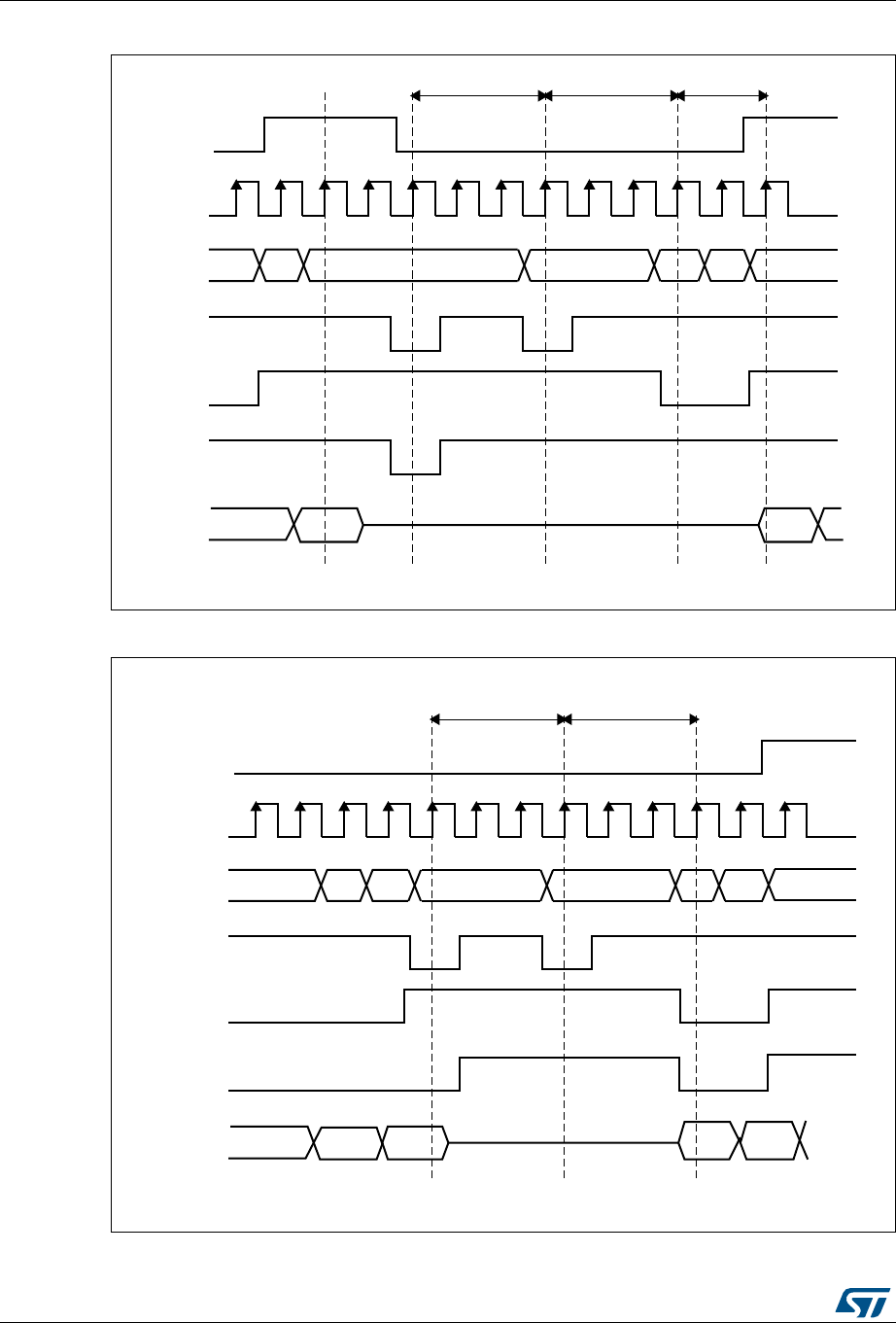
Flexible memory controller (FMC) RM0090
1648/1718 DocID018909 Rev 9
Figure 479. Read access crossing row boundary
Figure 480. Write access crossing row boundary
-36
$ATA;=
.#!3
.2! 3
!;=
3$#,+
#OLA #OLA #OLB2OWN
$NA $N A
3$.%
420 #!3LATENCY
.7 %
0RECHARGE !CTIVATE 2OW 2EAD #OMMAND
2OW N
42#$
-36
$ATA;=
.#!3
.2! 3
!;=
3$#,+
#NA #OLA2OWN
$NA $NA
3$.%
420
.7 %
0RECHARGE !CTIVATE 2OW 7RITECOMMAND
#OLB #OLB
$NB $NB
42#$

DocID018909 Rev 9 1649/1718
RM0090 Flexible memory controller (FMC)
1660
If the next access is sequential and the current access crosses a bank boundary, the
SDRAM controller activates the first row in the next bank and initiates a new read/write
command. Two cases are possible:
•If the current bank is not the last one, the active row in the new bank must be
precharged. At a bank boundary, the automatic activation of the next row is supported
for all rows/columns and data bus width configuration.
•For 13-bit row address, 11-bit column address, 4 internal banks and bus width 32-bit
SDRAM memories, if the current bank is the last one and the selected SDRAM device
is connected to Bank 1, the SDRAM controller continues to read/write from the second
SDRAM device (assuming it has been initialized):
a) The SDRAM controller activates the first row (after precharging the active row, if
there is already an active row in the first internal bank, and initiates a new
read/write command.
b) If the first row is already activated, the SDRAM controller just initiates a read/write
command.
Note: At bank boundary, if the current bank is the last one, the automatic activation of the next row
is supported only when addressing 13-bit rows, 11-bit columns, 4 internal banks and 32-bit
data bus SDRAM devices. Otherwise, the SDRAM address range is violated and an AHB
error is generated.
SDRAM controller refresh cycle
The Auto-refresh command is used to refresh the SDRAM device content. The SDRAM
controller periodically issues auto-refresh commands. An internal counter is loaded with the
COUNT value in the register FMC_SDRTR. This value defines the number of memory clock
cycles between the refresh cycles (refresh rate). When this counter reaches zero, an
internal pulse is generated.
If a memory access is ongoing, the auto-refresh request is delayed. However, if the memory
access and the auto-refresh requests are generated simultaneously, the auto-refresh
request takes precedence.
If the memory access occurs during an auto-refresh operation, the request is buffered and
processed when the auto-refresh is complete.
If a new auto-refresh request occurs while the previous one was not served, the RE
(Refresh Error) bit is set in the Status register. An Interrupt is generated if it has been
enabled (REIE = ‘1’).
If SDRAM lines are not in idle state (not all row are closed), the SDRAM controller generates
a PALL (Precharge ALL) command before the auto-refresh.
If the Auto-refresh command is generated by the FMC_SDCMR Command Mode register
(Mode bits = ‘011’), a PALL command (Mode bits =’ 010’) must be issued first.
37.7.4 Low power modes
Two low power modes are available:
•Self-refresh mode
The auto-refresh cycles are performed by the SDRAM device itself to retain data
without external clocking.
•Power-down mode
The auto-refresh cycles are performed by the SDRAM controller.

Flexible memory controller (FMC) RM0090
1650/1718 DocID018909 Rev 9
Self-refresh mode
This mode is selected by setting the MODE bits to ‘101’ and by configuring the Target Bank
bits (CTB1 and/or CTB2) in the FMC_SDCMR register.
The SDRAM clock stops running after a TRAS delay and the internal refresh timer stops
counting only if one of the following conditions is met:
•A Self-refresh command is issued to both devices
•One of the devices is not activated (SDRAM bank is not initialized).
Before entering Self-Refresh mode, the SDRAM controller automatically issues a PALL
command.
If the Write data FIFO is not empty, all data are sent to the memory before activating the
Self-refresh mode and the BUSY status flag remains set.
In Self-refresh mode, all SDRAM device inputs become don’t care except for SDCKE which
remains low.
The SDRAM device must remain in Self-refresh mode for a minimum period of time of
TRAS and can remain in Self-refresh mode for an indefinite period beyond that. To
guarantee this minimum period, the BUSY status flag remains high after the Self-refresh
activation during a TRAS delay.
As soon as an SDRAM device is selected, the SDRAM controller generates a sequence of
commands to exit from Self-refresh mode. After the memory access, the selected device
remains in Normal mode.
To exit from Self-refresh, the MODE bits must be set to ‘000’ (Normal mode) and the Target
Bank bits (CTB1 and/or CTB2) must be configured in the FMC_SDCMR register.
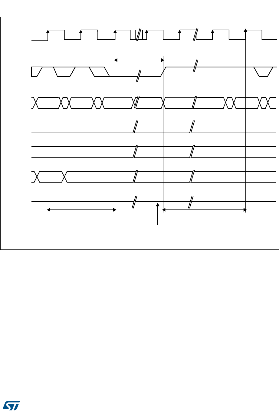
DocID018909 Rev 9 1651/1718
RM0090 Flexible memory controller (FMC)
1660
Figure 481. Self-refresh mode
Power-down mode
This mode is selected by setting the MODE bits to ‘110’ and by configuring the Target Bank
bits (CTB1 and/or CTB2) in the FMC_SDCMR register.
02%#(!2'%
3$#,+
3$#+%
4 4 4 4N 4 4
T2!3MIN
#/--!.$ ./0 !54/
2%&2%3( ./0OR#/--!.$
).(%2)4
!54/
2%&2%3(
$/-
$/-,$/-5
!!
!!
! !,,
"!.+3
$ATA;= (I:
T20
0RECHARGEALL
ACTIVEBANKS %NTER3ELFREFRESHMODE
#,+STABLEPRIORTOEXISTING
3ELFREFRESHMODE
%XIT3ELFREFRESHMODE
RESTARTREFRESHTIMEBASE
T832
-36
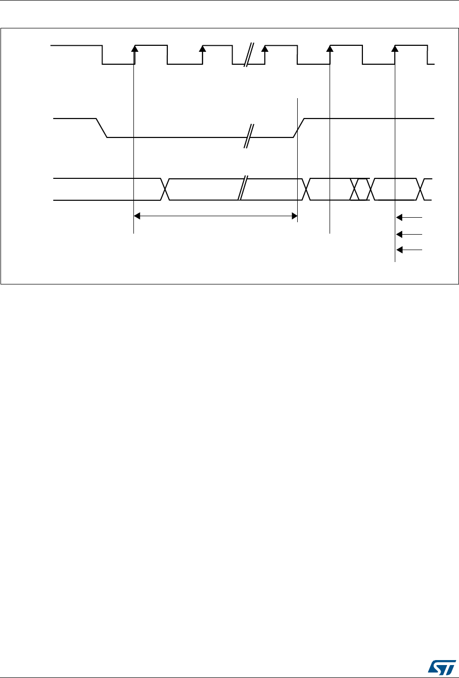
Flexible memory controller (FMC) RM0090
1652/1718 DocID018909 Rev 9
Figure 482. Power-down mode
If the Write data FIFO is not empty, all data are sent to the memory before activating the
Power-down mode.
As soon as an SDRAM device is selected, the SDRAM controller exits from the Power-down
mode. After the memory access, the selected SDRAM device remains in Normal mode.
During Power-down mode, all SDRAM device input and output buffers are deactivated
except for the SDCKE which remains low.
The SDRAM device cannot remain in Power-down mode longer than the refresh period and
cannot perform the Auto-refresh cycles by itself. Therefore, the SDRAM controller carries
out the refresh operation by executing the operations below:
1. Exit from Power-down mode and drive the SDCKE high
2. Generate the PALL command only if a row was active during Power-down mode
3. Generate the auto-refresh command
4. Drive SDCKE low again to return to Power-down mode.
To exit from Power-down mode, the MODE bits must be set to ‘000’ (Normal mode) and the
Target Bank bits (CTB1 and/or CTB2) must be configured in the FMC_SDCMR register.
37.7.5 SDRAM controller registers
SDRAM Control registers 1,2 (FMC_SDCR1,2)
Address offset: 0x140+ 4* (x – 1), x = 1,2
Reset value: 0x0000 02D0
This register contains the control parameters for each SDRAM memory bank
3$#,+
3$#+%
#/--!.$ ./0 ./0 !#4)6%
)NPUTBUFFERSGATEDOFF!LLBANKSIDLE
%NTER0OWERDOWN %XIT0OWERDOWN
T2#$
T2!3
T2#
-36

DocID018909 Rev 9 1653/1718
RM0090 Flexible memory controller (FMC)
1660
313029282726252423222120191817161514131211109876543210
Reserved
RPIPE
RBURST
SDCLK
WP
CAS
NB
MWID
NR
NC
rw rw rw rw rw rw rw rw rw rw rw rw rw rw rw
Bits 31:15 Reserved, must be kept at reset value
Bits 14:13 RPIPE: Read pipe
These bits define the delay, in HCLK clock cycles, for reading data after CAS latency.
00: No HCLK clock cycle delay
01: One HCLK clock cycle delay
10: Two HCLK clock cycle delay
11: reserved, do not use
Note: The corresponding bits in the FMC_SDCR2 register are don’t care.
Bit 12 RBURST: Burst read
This bit enables burst read mode. The SDRAM controller anticipates the next read commands
during the CAS latency and stores data in the Read FIFO.
0: single read requests are not managed as bursts
1: single read requests are always managed as bursts
Note: The corresponding bit in the FMC_SDCR2 register is don’t care.
Bits 11:10 SDCLK: SDRAM clock configuration
These bits define the SDRAM clock period for both SDRAM banks and allow disabling the clock
before changing the frequency. In this case the SDRAM must be re-initialized.
00: SDCLK clock disabled
01: Reserved
10: SDCLK period = 2 x HCLK periods
11: SDCLK period = 3 x HCLK periods
Note: The corresponding bits in the FMC_SDCR2 register are don’t care.
Bit 9 WP: Write protection
This bit enables write mode access to the SDRAM bank.
0: Write accesses allowed
1: Write accesses ignored
Bits 8:7 CAS: CAS Latency
This bits sets the SDRAM CAS latency in number of memory clock cycles
00: reserved, do not use.
01: 1 cycle
10: 2 cycles
11: 3 cycles
Bit 6 NB: Number of internal banks
This bit sets the number of internal banks.
0: Two internal Banks
1: Four internal Banks
Bits 5:4 MWID: Memory data bus width.
These bits define the memory device width.
00: 8 bits
01: 16 bits
10: 32 bits
11: reserved, do not use.

Flexible memory controller (FMC) RM0090
1654/1718 DocID018909 Rev 9
Note: Before modifying the RBURST or RPIPE settings or disabling the SDCLK clock, the user
must first send a PALL command to make sure ongoing operations are complete.
SDRAM Timing registers 1,2 (FMC_SDTR1,2)
Address offset: 0x148 + 4 * (x – 1), x = 1,2
Reset value: 0x0FFF FFFF
This register contains the timing parameters of each SDRAM bank
Bits 3:2 NR: Number of row address bits
These bits define the number of bits of a row address.
00: 11 bit
01: 12 bits
10: 13 bits
11: reserved, do not use.
Bits 1:0 NC: Number of column address bits
These bits define the number of bits of a column address.
00: 8 bits
01: 9 bits
10: 10 bits
11: 11 bits.
313029282726252423222120191817161514131211109876543210
Reserved TRCD TRP TWR TRC TRAS TXSR TMRD
rw rw rw rw rw rw rw rw rw rw rw rw rw rw rw rw rw rw rw rw rw rw rw rw rw rw rw rw rw rw rw rw
Bits 31:28 Reserved, must be kept at reset value
Bits 27:24 TRCD: Row to column delay
These bits define the delay between the Activate command and a Read/Write command in number
of memory clock cycles.
0000: 1 cycle.
0001: 2 cycles
....
1111: 16 cycles
Bits 23:20 TRP: Row precharge delay
These bits define the delay between a Precharge command and another command in number of
memory clock cycles. The TRP timing is only configured in the FMC_SDTR1 register. If two
SDRAM devices are used, the TRP must be programmed with the timing of the slowest device.
0000: 1 cycle
0001: 2 cycles
....
1111: 16 cycles
Note: The corresponding bits in the FMC_SDTR2 register are don’t care.

DocID018909 Rev 9 1655/1718
RM0090 Flexible memory controller (FMC)
1660
Note: If two SDRAM devices are connected, all the accesses performed simultaneously to both
devices by the Command Mode register (Load Mode Register and Self-refresh commands)
Bits 19:16 TWR: Recovery delay
These bits define the delay between a Write and a Precharge command in number of memory clock
cycles.
0000: 1 cycle
0001: 2 cycles
....
1111: 16 cycles
Note: TWR must be programmed to match the write recovery time (tWR) defined in the SDRAM
datasheet, and to guarantee that:
TWR ≥ TRAS - TRCD and TWR ≥TRC - TRCD - TRP
Example: TRAS= 4 cycles, TRCD= 2 cycles. So, TWR >= 2 cycles. TWR must be
programmed to 0x1.
If two SDRAM devices are used, the FMC_SDTR1 and FMC_SDTR2 must be programmed
with the same TWR timing corresponding to the slowest SDRAM device.
Bits 15:12 TRC: Row cycle delay
These bits define the delay between the Refresh command and the Activate command, as well as d
the delay between two consecutive Refresh commands. It is expressed in number of memory clock
cycles. The TRC timing is only configured in the FMC_SDTR1 register. If two SDRAM devices are
used, the TRC must be programmed with the timings of the slowest device.
0000: 1 cycle
0001: 2 cycles
....
1111: 16 cycles
Note: TRC must match the TRC and TRFC (Auto Refresh period) timings defined in the SDRAM
device datasheet.
Note: The corresponding bits in the FMC_SDTR2 register are don’t care.
Bits 11:8 TRAS: Self refresh time
These bits define the minimum Self-refresh period in number of memory clock cycles.
0000: 1 cycle
0001: 2 cycles
....
1111: 16 cycles
Bits 7:4 TXSR: Exit Self-refresh delay
These bits define the delay from releasing the Self-refresh command to issuing the Activate
command in number of memory clock cycles.
0000: 1 cycle
0001: 2 cycles
....
1111: 16 cycles
Bits 3:0 TMRD: Load Mode Register to Active
These bits define the delay between a Load Mode Register command and an Active or Refresh
command in number of memory clock cycles.
0000: 1 cycle
0001: 2 cycles
....
1111: 16 cycles

Flexible memory controller (FMC) RM0090
1656/1718 DocID018909 Rev 9
are issued using the timing parameters configured for Bank 1 (TMRD, TRAS and TXSR
timings) in the FMC_SDTR1 register.
The TRP and TRC timings are only configured in the FMC_SDTR1 register. If two SDRAM
devices are used, the TRP and TRC timings must be programmed with the timings of the
slowest device.
SDRAM Command Mode register (FMC_SDCMR)
Address offset: 0x150
Reset value: 0x0000 0000
This register contains the command issued when the SDRAM device is accessed. This
register is used to initialize the SDRAM device, and to activate the Self-refresh and the
Power-down modes. As soon as the MODE field is written, the command will be issued only
to one or to both SDRAM banks according to CTB1 and CTB2 command bits. This register
is the same for both SDRAM banks.
313029282726252423222120191817161514131211109876543210
Reserved
MRD NRFS CT
B1
CT
B2 MODE
rwrwrwrwrwrwrwrwrwrwrwrwrwrwrwrwrwwwwww
Bits 31:22 Reserved, must be kept at reset value
Bits 21:9 MRD: Mode Register definition
This 13-bit field defines the SDRAM Mode Register content. The Mode Register is programmed
using the Load Mode Register command.
Bits 8:5 NRFS: Number of Auto-refresh
These bits define the number of consecutive Auto-refresh commands issued when MODE = ‘011’.
0000: 1 Auto-refresh cycle
0001: 2 Auto-refresh cycles
....
1110: 15 Auto-refresh cycles
1111: Reserved
Bit 4 CTB1: Command Target Bank 1
This bit indicates whether the command will be issued to SDRAM Bank 1 or not.
0: Command not issued to SDRAM Bank 1
1: Command issued to SDRAM Bank 1
Bit 3 CTB2: Command Target Bank 2
This bit indicates whether the command will be issued to SDRAM Bank 2 or not.
0: Command not issued to SDRAM Bank 2
1: Command issued to SDRAM Bank 2

DocID018909 Rev 9 1657/1718
RM0090 Flexible memory controller (FMC)
1660
SDRAM Refresh Timer register (FMC_SDRTR)
Address offset:0x154
Reset value: 0x0000 0000
This register sets the refresh rate in number of SDCLK clock cycles between the refresh
cycles by configuring the Refresh Timer Count value.
Example
where 64 ms is the SDRAM refresh period.
The refresh rate must be increased by 20 SDRAM clock cycles (as in the above example) to
obtain a safe margin if an internal refresh request occurs when a read request has been
accepted. It corresponds to a COUNT value of ‘0000111000000’ (448).
This 13-bit field is loaded into a timer which is decremented using the SDRAM clock. This
timer generates a refresh pulse when zero is reached. The COUNT value must be set at
least to 41 SDRAM clock cycles.
As soon as the FMC_SDRTR register is programmed, the timer starts counting. If the value
programmed in the register is ’0’, no refresh is carried out. This register must not be
reprogrammed after the initialization procedure to avoid modifying the refresh rate.
Each time a refresh pulse is generated, this 13-bit COUNT field is reloaded into the counter.
If a memory access is in progress, the Auto-refresh request is delayed. However, if the
memory access and Auto-refresh requests are generated simultaneously, the Auto-refresh
takes precedence. If the memory access occurs during a refresh operation, the request is
buffered to be processed when the refresh is complete.
This register common to SDRAM bank 1 and bank 2.
Bits 2:0 MODE: Command mode
These bits define the command issued to the SDRAM device.
000: Normal Mode
001: Clock Configuration Enable
010: PALL (“All Bank Precharge”) command
011: Auto-refresh command
100: Load Mode Register
101: Self-refresh command
110: Power-down command
111: Reserved
Note: When a command is issued, at least one Command Target Bank bit ( CBT1 or CBT2) must be
set. If both banks are used, the commands must be issued to the two banks at the same time
by setting the CBT1 and CBT2 bits.
Refresh rate SDRAM refresh rate SDRAM clock frequency×()20–=
SDRAM refresh rate SDRAM refresh period Number of rows⁄=
SDRAM refresh rate 64 ms 8196rows()⁄7,81μs==
7,81μs60MHz×468,6=
Flexible memory controller (FMC) RM0090
1658/1718 DocID018909 Rev 9
.
Note: The programmed COUNT value must not be equal to the sum of the following timings:
TWR+TRP+TRC+TRCD+4 memory clock cycles .
SDRAM Status register (FMC_SDSR)
Address offset: 0x158
Reset value: 0x0000 0000
3130292827262524232221201918171615 1413121110987654321 0
Reserved REIE COUNT CRE
rw rw rw rw rw rw rw rw rw rw rw rw rw rw w
Bits 31: 15 Reserved, must be kept at reset value
Bit 14 REIE: RES Interrupt Enable
0: Interrupt is disabled
1: An Interrupt is generated if RE = 1
Bits 13:1 COUNT: Refresh Timer Count
This 13-bit field defines the refresh rate of the SDRAM device. It is expressed in number of memory
clock cycles. It must be set at least to 41 SDRAM clock cycles (0x29).
COUNT = (SDRAM refresh rate x SDRAM clock frequency) - 20
SDRAM refresh rate = SDRAM refresh period / Number of rows
Bit 0 CRE: Clear Refresh error flag
This bit is used to clear the Refresh Error Flag (RE) in the Status Register.
0: no effect
1: Refresh Error flag is cleared
31 30 29 28 27 26 25 24 23 22 21 20 19 18 17 16 15 14 13 12 11 10 9 8 7 6 5 4 3 2 1 0
Reserved
BUSY
MODES2
MODES1
RE
rrrrrr
Bits 31:5 Reserved, must be kept at reset value
Bit 5 BUSY: Busy status
This bit defines the status of the SDRAM controller after a Command Mode request
0: SDRAM Controller is ready to accept a new request
1; SDRAM Controller is not ready to accept a new request
Bits 4:3 MODES2: Status Mode for Bank 2
This bit defines the Status Mode of SDRAM Bank 2.
00: Normal Mode
01: Self-refresh mode
10: Power-down mode
Bits 2:1 MODES1: Status Mode for Bank 1
This bit defines the Status Mode of SDRAM Bank 1.
00: Normal Mode
01: Self-refresh mode
10: Power-down mode
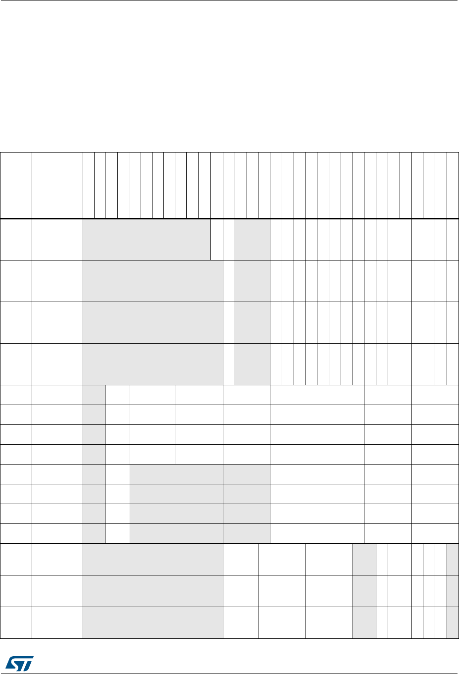
DocID018909 Rev 9 1659/1718
RM0090 Flexible memory controller (FMC)
1660
37.8 FMC register map
The following table summarizes the FMC registers.
Bit 0 RE: Refresh error flag
0: No refresh error has been detected
1: A refresh error has been detected
An interrupt is generated if REIE = 1 and RE = 1
Table 292. FMC register map
Offset Register
31
30
29
28
27
26
25
24
23
22
21
20
19
18
17
16
15
14
13
12
11
10
9
8
7
6
5
4
3
2
1
0
0x00 FMC_BCR1 Reserved
CCLKEN
CBURSTRW
Reserved
ASYNCWAIT
EXTMOD
WAITEN
WREN
WAITCFG
WRAPMOD
WAITPOL
BURSTEN
Reserved
FACCEN
MWID
MTYP
MUXEN
MBKEN
0x08 FMC_BCR2 Reserved
CBURSTRW
Reserved
ASYNCWAIT
EXTMOD
WAITEN
WREN
WAITCFG
WRAPMOD
WAITPOL
BURSTEN
Reserved
FACCEN
MWID
MTYP
MUXEN
MBKEN
0x10 FMC_BCR3 Reserved
CBURSTRW
Reserved
ASYNCWAIT
EXTMOD
WAITEN
WREN
WAITCFG
WRAPMOD
WAITPOL
BURSTEN
Reserved
FACCEN
MWID
MTYP
MUXEN
MBKEN
0x18 FMC_BCR4 Reserved
CBURSTRW
Reserved
ASYNCWAIT
EXTMOD
WAITEN
WREN
WAITCFG
WRAPMOD
WAITPOL
BURSTEN
Reserved
FACCEN
MWID
MTYP
MUXEN
MBKEN
0x04 FMC_BTR1 Res. ACCM
OD DATLAT CLKDIV BUSTURN DATAST ADDHLD ADDSET
0x0C FMC_BTR2 Res. ACCM
OD DATLAT CLKDIV BUSTURN DATAST ADDHLD ADDSET
0x14 FMC_BTR3 Res. ACCM
OD DATLAT CLKDIV BUSTURN DATAST ADDHLD ADDSET
0x1C FMC_BTR4 Res. ACCM
OD DATLAT CLKDIV BUSTURN DATAST ADDHLD ADDSET
0x104 FMC_BWTR1 Res. ACCM
OD Res. Reserved DATAST ADDHLD ADDSET
0x10C FMC_BWTR2 Res. ACCM
OD Res. Reserved DATAST ADDHLD ADDSET
0x104 FMC_BWTR3 Res. ACCM
OD Res. Reserved DATAST ADDHLD ADDSET
0x10C FMC_BWTR4 Res. ACCM
OD Res. Reserved DATAST ADDHLD ADDSET
0x60 FMC_PCR2 Reserved ECCPS TAR TCLR Res.
ECCEN
PWID
PTYP
PBKEN
PWAITEN
Reserved
0x80 FMC_PCR3 Reserved ECCPS TAR TCLR Res.
ECCEN
PWID
PTYP
PBKEN
PWAITEN
Reserved
0xA0 FMC_PCR4 Reserved ECCPS TAR TCLR Res.
ECCEN
PWID
PTYP
PBKEN
PWAITEN
Reserved
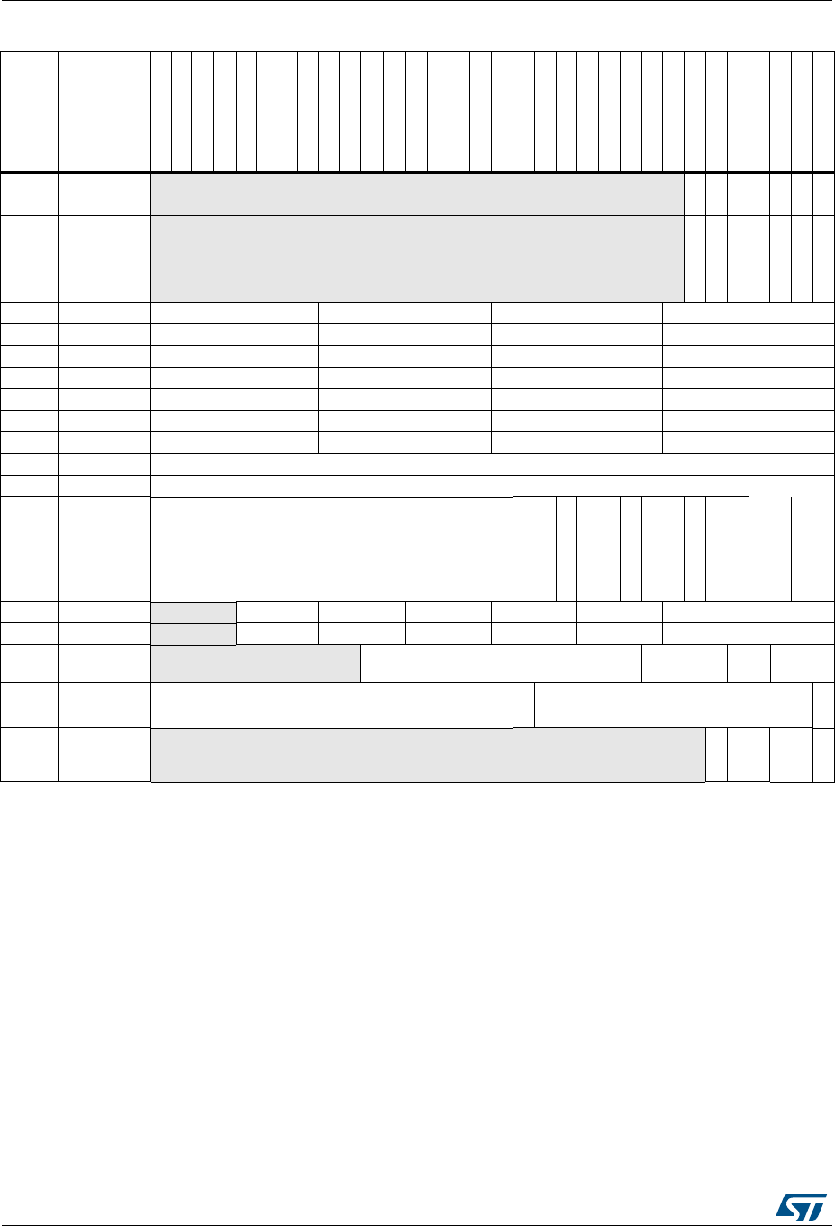
Flexible memory controller (FMC) RM0090
1660/1718 DocID018909 Rev 9
0x64 FMC_SR2 Reserved
FEMPT
IFEN
ILEN
IREN
IFS
ILS
IRS
0x84 FMC_SR3 Reserved
FEMPT
IFEN
ILEN
IREN
IFS
ILS
IRS
0xA4 FMC_SR4 Reserved
FEMPT
IFEN
ILEN
IREN
IFS
ILS
IRS
0x68 FMC_PMEM2 MEMHIZx MEMHOLDx MEMWAITx MEMSETx
0x88 FMC_PMEM3 MEMHIZx MEMHOLDx MEMWAITx MEMSETx
0xA8 FMC_PMEM4 MEMHIZx MEMHOLDx MEMWAITx MEMSETx
0x6C FMC_PATT2 ATTHIZx ATTHOLDx ATTWAITx ATTSETx
0x8C FMC_PATT3 ATTHIZx ATTHOLDx ATTWAITx ATTSETx
0xAC FMC_PATT4 ATTHIZx ATTHOLDx ATTWAITx ATTSETx
0xB0 FMC_PIO4 IOHIZx IOHOLDx IOWAITx IOSETx
0x74 FMC_ECCR2 ECCx
0x94 FMC_ECCR3 ECCx
0x140 FMC_SDCR_1 Reserved
RPIPE
RBURST
CLK
WP
CAS
NB
MWID
NR
NC
0x144 FMC_SDCR_2 Reserved
RPIPE
RBURST
CLK
WP
CAS
NB
MWID
NR
NC
0x148 FMC_SDTR1 Reserved TRCD TRP TWR TRC TRAS TXSR TMRD
0x14C FMC_SDTR2 Reserved TRCD TRP TWR TRC TRAS TXSR TMRD
0x150 FMC_SDCMR Reserved
MRD
NRFS
CTB1
CTB2
MODE
0x154 FMC_SDRTR Reserved
REIE
COUNT
CRE
0x158 FMC_SDSR Reserved
BUSY
MODES2
MODES1
RE
Table 292. FMC register map (continued)
Offset Register
31
30
29
28
27
26
25
24
23
22
21
20
19
18
17
16
15
14
13
12
11
10
9
8
7
6
5
4
3
2
1
0
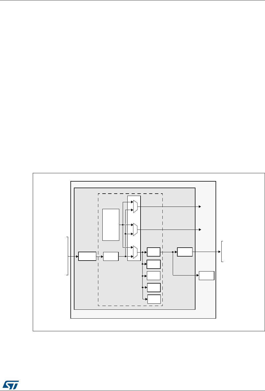
DocID018909 Rev 9 1661/1718
RM0090 Debug support (DBG)
1692
38 Debug support (DBG)
This section applies to the whole STM32F4xx family, unless otherwise specified.
38.1 Overview
The STM32F4xx are built around a Cortex®-M4 with FPU core which contains hardware
extensions for advanced debugging features. The debug extensions allow the core to be
stopped either on a given instruction fetch (breakpoint) or data access (watchpoint). When
stopped, the core’s internal state and the system’s external state may be examined. Once
examination is complete, the core and the system may be restored and program execution
resumed.
The debug features are used by the debugger host when connecting to and debugging the
STM32F4xx MCUs.
Two interfaces for debug are available:
•Serial wire
•JTAG debug port
Figure 483. Block diagram of STM32 MCU and Cortex®-M4 with FPU-level
debug support
Note: The debug features embedded in the Cortex®-M4 with FPU core are a subset of the ARM®
CoreSight Design Kit.
ESTRICTED$I
#ORTEX-
CORE
37*$0 !("!0
"RIDGE
.6)#
$74
&0"
)4-
40)5
$#ODE
INTERFACE
3YSTEM
INTERFACE
)NTERNALPRIVATE
PERIPHERALBUS00"
%XTERNALPRIVATE
PERIPHERALBUS00"
"USMATRIX
$ATA
4RAC E PO R T
$"'-#5
34-&XXDEBUGSUPPORT
#ORTEX-DEBUGSUPPORT
*4-3
*4$)
*4$/
.*4234
*4#+
37$)/
37#,+
42!#%37/
42!#%37/
42!#%#+
42!#%$;=
-36

Debug support (DBG) RM0090
1662/1718 DocID018909 Rev 9
The ARM® Cortex®-M4 with FPU core provides integrated on-chip debug support. It is
comprised of:
•SWJ-DP: Serial wire / JTAG debug port
•AHP-AP: AHB access port
•ITM: Instrumentation trace macrocell
•FPB: Flash patch breakpoint
•DWT: Data watchpoint trigger
•TPUI: Trace port unit interface (available on larger packages, where the corresponding
pins are mapped)
•ETM: Embedded Trace Macrocell (available on larger packages, where the
corresponding pins are mapped)
It also includes debug features dedicated to the STM32F4xx:
•Flexible debug pinout assignment
•MCU debug box (support for low-power modes, control over peripheral clocks, etc.)
Note: For further information on debug functionality supported by the ARM® Cortex®-M4 with FPU
core, refer to the Cortex®-M4 with FPU-r0p1 Technical Reference Manual and to the
CoreSight Design Kit-r0p1 TRM (see Section 38.2: Reference ARM® documentation).
38.2 Reference ARM® documentation
•Cortex®-M4 with FPU r0p1 Technical Reference Manual (TRM)
(see Related documents on page 1)
•ARM® Debug Interface V5
•ARM® CoreSight Design Kit revision r0p1 Technical Reference Manual
38.3 SWJ debug port (serial wire and JTAG)
The core of the STM32F4xx integrates the Serial Wire / JTAG Debug Port (SWJ-DP). It is an
ARM® standard CoreSight debug port that combines a JTAG-DP (5-pin) interface and a
SW-DP (2-pin) interface.
•The JTAG Debug Port (JTAG-DP) provides a 5-pin standard JTAG interface to the
AHP-AP port.
•The Serial Wire Debug Port (SW-DP) provides a 2-pin (clock + data) interface to the
AHP-AP port.
In the SWJ-DP, the two JTAG pins of the SW-DP are multiplexed with some of the five JTAG
pins of the JTAG-DP.
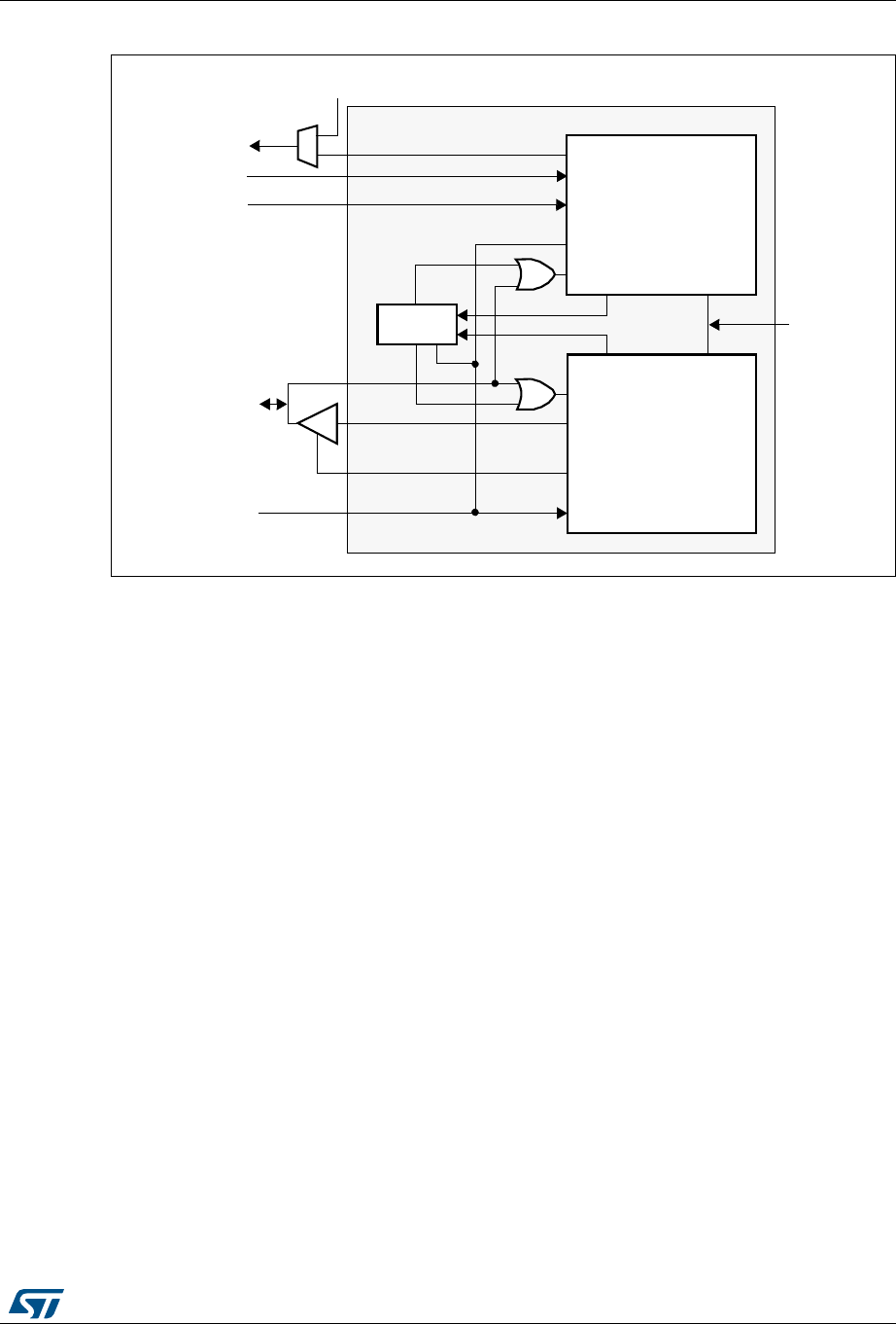
DocID018909 Rev 9 1663/1718
RM0090 Debug support (DBG)
1692
Figure 484. SWJ debug port
Figure 484 shows that the asynchronous TRACE output (TRACESWO) is multiplexed with
TDO. This means that the asynchronous trace can only be used with SW-DP, not JTAG-DP.
38.3.1 Mechanism to select the JTAG-DP or the SW-DP
By default, the JTAG-Debug Port is active.
If the debugger host wants to switch to the SW-DP, it must provide a dedicated JTAG
sequence on TMS/TCK (respectively mapped to SWDIO and SWCLK) which disables the
JTAG-DP and enables the SW-DP. This way it is possible to activate the SWDP using only
the SWCLK and SWDIO pins.
This sequence is:
1. Send more than 50 TCK cycles with TMS (SWDIO) =1
2. Send the 16-bit sequence on TMS (SWDIO) = 0111100111100111 (MSB transmitted
first)
3. Send more than 50 TCK cycles with TMS (SWDIO) =1
38.4 Pinout and debug port pins
The STM32F4xx MCUs are available in various packages with different numbers of
available pins. As a result, some functionality (ETM) related to pin availability may differ
between packages.
TRACESWO
JTDO
JTDI
NJTRSTnTRST
TDI
TDO
SWJ-DP
TDO
TDI
nTRST
TCK
TMSnPOTRST
JTAG-DP
nPOTRST
From
power-on
reset
DBGRESETn
DBGDI
DBGDO
DBGDOEN
DBGCLK
SW-DP
SWCLKTCK
SWDOEN
SWDO
SWDITMS
SWD/JTAG
select
JTMS/SWDIO
JTCK/SWCLK
(asynchronous trace)
ai17139
Debug support (DBG) RM0090
1664/1718 DocID018909 Rev 9
38.4.1 SWJ debug port pins
Five pins are used as outputs from the STM32F4xx for the SWJ-DP as alternate functions of
general-purpose I/Os. These pins are available on all packages.
38.4.2 Flexible SWJ-DP pin assignment
After RESET (SYSRESETn or PORESETn), all five pins used for the SWJ-DP are assigned
as dedicated pins immediately usable by the debugger host (note that the trace outputs are
not assigned except if explicitly programmed by the debugger host).
However, the STM32F4xx MCUs offers the possibility of disabling some or all of the SWJ-
DP ports and so, of releasing the associated pins for general-purpose IO (GPIO) usage. For
more details on how to disable SWJ-DP port pins, please refer to Section 8.3.2: I/O pin
multiplexer and mapping.
Note: When the APB bridge write buffer is full, it takes one extra APB cycle when writing the
GPIO_AFR register. This is because the deactivation of the JTAGSW pins is done in two
cycles to guarantee a clean level on the nTRST and TCK input signals of the core.
•Cycle 1: the JTAGSW input signals to the core are tied to 1 or 0 (to 1 for nTRST, TDI
and TMS, to 0 for TCK)
•Cycle 2: the GPIO controller takes the control signals of the SWJTAG IO pins (like
controls of direction, pull-up/down, Schmitt trigger activation, etc.).
Table 293. SWJ debug port pins
SWJ-DP pin name
JTAG debug port SW debug port Pin
assign
ment
Type Description Type Debug assignment
JTMS/SWDIO I JTAG Test Mode
Selection IO Serial Wire Data
Input/Output PA13
JTCK/SWCLK I JTAG Test Clock I Serial Wire Clock PA14
JTDI I JTAG Test Data Input - - PA15
JTDO/TRACESWO O JTAG Test Data Output - TRACESWO if async trace
is enabled PB3
NJTRST I JTAG Test nReset - - PB4
Table 294. Flexible SWJ-DP pin assignment
Available debug ports
SWJ IO pin assigned
PA13 /
JTMS /
SWDIO
PA14 /
JTCK /
SWCLK
PA15 /
JTDI
PB3 /
JTDO
PB4 /
NJTRST
Full SWJ (JTAG-DP + SW-DP) - Reset State X X X X X
Full SWJ (JTAG-DP + SW-DP) but without NJTRST X X X X
JTAG-DP Disabled and SW-DP Enabled X X
JTAG-DP Disabled and SW-DP Disabled Released

DocID018909 Rev 9 1665/1718
RM0090 Debug support (DBG)
1692
38.4.3 Internal pull-up and pull-down on JTAG pins
It is necessary to ensure that the JTAG input pins are not floating since they are directly
connected to flip-flops to control the debug mode features. Special care must be taken with
the SWCLK/TCK pin which is directly connected to the clock of some of these flip-flops.
To avoid any uncontrolled IO levels, the device embeds internal pull-ups and pull-downs on
the JTAG input pins:
•NJTRST: Internal pull-up
•JTDI: Internal pull-up
•JTMS/SWDIO: Internal pull-up
•TCK/SWCLK: Internal pull-down
Once a JTAG IO is released by the user software, the GPIO controller takes control again.
The reset states of the GPIO control registers put the I/Os in the equivalent state:
•NJTRST: AF input pull-up
•JTDI: AF input pull-up
•JTMS/SWDIO: AF input pull-up
•JTCK/SWCLK: AF input pull-down
•JTDO: AF output floating
The software can then use these I/Os as standard GPIOs.
Note: The JTAG IEEE standard recommends to add pull-ups on TDI, TMS and nTRST but there is
no special recommendation for TCK. However, for JTCK, the device needs an integrated
pull-down.
Having embedded pull-ups and pull-downs removes the need to add external resistors.

Debug support (DBG) RM0090
1666/1718 DocID018909 Rev 9
38.4.4 Using serial wire and releasing the unused debug pins as GPIOs
To use the serial wire DP to release some GPIOs, the user software must change the GPIO
(PA15, PB3 and PB4) configuration mode in the GPIO_MODER register. This releases
PA15, PB3 and PB4 which now become available as GPIOs.
When debugging, the host performs the following actions:
•Under system reset, all SWJ pins are assigned (JTAG-DP + SW-DP).
•Under system reset, the debugger host sends the JTAG sequence to switch from the
JTAG-DP to the SW-DP.
•Still under system reset, the debugger sets a breakpoint on vector reset.
•The system reset is released and the Core halts.
•All the debug communications from this point are done using the SW-DP. The other
JTAG pins can then be reassigned as GPIOs by the user software.
Note: For user software designs, note that:
To release the debug pins, remember that they will be first configured either in input-pull-up
(nTRST, TMS, TDI) or pull-down (TCK) or output tristate (TDO) for a certain duration after
reset until the instant when the user software releases the pins.
When debug pins (JTAG or SW or TRACE) are mapped, changing the corresponding IO pin
configuration in the IOPORT controller has no effect.
38.5 STM32F4xx JTAG TAP connection
The STM32F4xx MCUs integrate two serially connected JTAG TAPs, the boundary scan
TAP (IR is 5-bit wide) and the Cortex®-M4 with FPU TAP (IR is 4-bit wide).
To access the TAP of the Cortex®-M4 with FPU for debug purposes:
1. First, it is necessary to shift the BYPASS instruction of the boundary scan TAP.
2. Then, for each IR shift, the scan chain contains 9 bits (=5+4) and the unused TAP
instruction must be shifted in using the BYPASS instruction.
3. For each data shift, the unused TAP, which is in BYPASS mode, adds 1 extra data bit in
the data scan chain.
Note: Important: Once Serial-Wire is selected using the dedicated ARM® JTAG sequence, the
boundary scan TAP is automatically disabled (JTMS forced high).
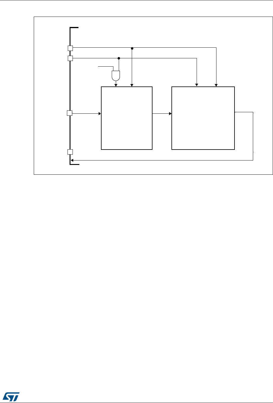
DocID018909 Rev 9 1667/1718
RM0090 Debug support (DBG)
1692
Figure 485. JTAG TAP connections
"OUNDARYSCAN
4!0
.*4234
#ORTEX-4!0
*4-3
4-3 N42344-3 N4234
*4$)
*4$/
4$) 4$/ 4$) 4$/
37$0
34-&XXX
3ELECTED
)2ISBITWIDE )2ISBITWIDE
-36

Debug support (DBG) RM0090
1668/1718 DocID018909 Rev 9
38.6 ID codes and locking mechanism
There are several ID codes inside the STM32F4xx MCUs. ST strongly recommends tools
designers to lock their debuggers using the MCU DEVICE ID code located in the external
PPB memory map at address 0xE0042000.
38.6.1 MCU device ID code
The STM32F4xx MCUs integrate an MCU ID code. This ID identifies the ST MCU part-
number and the die revision. It is part of the DBG_MCU component and is mapped on the
external PPB bus (see Section 38.16 on page 1681). This code is accessible using the
JTAG debug port (4 to 5 pins) or the SW debug port (two pins) or by the user software. It is
even accessible while the MCU is under system reset.
DBGMCU_IDCODE
Address: 0xE004 2000
Only 32-bits access supported. Read-only.
31 30 29 28 27 26 25 24 23 22 21 20 19 18 17 16
REV_ID
rrrrrr r r r r rrrrrr
1514131211109876543210
Reserved DEV_ID
rrrrrrrrrrrr
Bits 31:16 REV_ID(15:0) Revision identifier
This field indicates the revision of the device.
STM32F405xx/07xx and STM32F415xx/17xx devices:
0x1000 = Revision A
0x1001 = Revision Z
0x1003 = Revision 1
0x1007 = Revision 2
0x100F= Revision Y
STM32F42xxx and STM32F43xxx devices:
0x1000 = Revision A
0x1003 = Revision Y
0x1007 = Revision 1
0x2001= Revision 3
Bits 15:12 Reserved, must be kept at reset value.
Bits 11:0 DEV_ID(11:0): Device identifier (STM32F405xx/07xx and STM32F415xx/17xx)
The device ID is 0x413.
Bits 11:0 DEV_ID(11:0): Device identifier (STM32F42xxx and STM32F43xxx)
The device ID is 0x419

DocID018909 Rev 9 1669/1718
RM0090 Debug support (DBG)
1692
38.6.2 Boundary scan TAP
JTAG ID code
The TAP of the STM32F4xx BSC (boundary scan) integrates a JTAG ID code equal to .
•0x06413041 for STM32F405xx/07xx and STM32F415xx/17xx devices
•0x06419041 for STM32F42xxx and STM32F43xxx devices
38.6.3 Cortex®-M4 with FPU TAP
The TAP of the ARM® Cortex®-M4 with FPU integrates a JTAG ID code. This ID code is the
ARM® default one and has not been modified. This code is only accessible by the JTAG
Debug Port.
This code is 0x4BA00477 (corresponds to Cortex®-M4 with FPU r0p1, see Section 38.2:
Reference ARM® documentation).
Only the DEV_ID(11:0) should be used for identification by the debugger/programmer tools.
38.6.4 Cortex®-M4 with FPU JEDEC-106 ID code
The ARM® Cortex®-M4 with FPU integrates a JEDEC-106 ID code. It is located in the 4KB
ROM table mapped on the internal PPB bus at address 0xE00FF000_0xE00FFFFF.
This code is accessible by the JTAG Debug Port (4 to 5 pins) or by the SW Debug Port (two
pins) or by the user software.
38.7 JTAG debug port
A standard JTAG state machine is implemented with a 4-bit instruction register (IR) and five
data registers (for full details, refer to the Cortex®-M4 with FPU r0p1 Technical Reference
Manual (TRM), for references, please see Section 38.2: Reference ARM® documentation).
Table 295. JTAG debug port data registers
IR(3:0) Data register Details
1111 BYPASS
[1 bit]
1110 IDCODE
[32 bits]
ID CODE
0x4BA00477 (ARM® Cortex®-M4 with FPU r0p1 ID Code)

Debug support (DBG) RM0090
1670/1718 DocID018909 Rev 9
1010 DPACC
[35 bits]
Debug port access register
This initiates a debug port and allows access to a debug port register.
– When transferring data IN:
Bits 34:3 = DATA[31:0] = 32-bit data to transfer for a write request
Bits 2:1 = A[3:2] = 2-bit address of a debug port register.
Bit 0 = RnW = Read request (1) or write request (0).
– When transferring data OUT:
Bits 34:3 = DATA[31:0] = 32-bit data which is read following a read
request
Bits 2:0 = ACK[2:0] = 3-bit Acknowledge:
010 = OK/FAULT
001 = WAIT
OTHER = reserved
Refer to Table 296 for a description of the A[3:2] bits
1011 APACC
[35 bits]
Access port access register
Initiates an access port and allows access to an access port register.
– When transferring data IN:
Bits 34:3 = DATA[31:0] = 32-bit data to shift in for a write request
Bits 2:1 = A[3:2] = 2-bit address (sub-address AP registers).
Bit 0 = RnW= Read request (1) or write request (0).
– When transferring data OUT:
Bits 34:3 = DATA[31:0] = 32-bit data which is read following a read
request
Bits 2:0 = ACK[2:0] = 3-bit Acknowledge:
010 = OK/FAULT
001 = WAIT
OTHER = reserved
There are many AP Registers (see AHB-AP) addressed as the
combination of:
– The shifted value A[3:2]
– The current value of the DP SELECT register
1000 ABORT
[35 bits]
Abort register
– Bits 31:1 = Reserved
– Bit 0 = DAPABORT: write 1 to generate a DAP abort.
Table 296. 32-bit debug port registers addressed through the shifted value A[3:2]
Address A[3:2] value Description
0x0 00 Reserved, must be kept at reset value.
0x4 01
DP CTRL/STAT register. Used to:
– Request a system or debug power-up
– Configure the transfer operation for AP accesses
– Control the pushed compare and pushed verify operations.
– Read some status flags (overrun, power-up acknowledges)
Table 295. JTAG debug port data registers (continued)
IR(3:0) Data register Details

DocID018909 Rev 9 1671/1718
RM0090 Debug support (DBG)
1692
38.8 SW debug port
38.8.1 SW protocol introduction
This synchronous serial protocol uses two pins:
•SWCLK: clock from host to target
•SWDIO: bidirectional
The protocol allows two banks of registers (DPACC registers and APACC registers) to be
read and written to.
Bits are transferred LSB-first on the wire.
For SWDIO bidirectional management, the line must be pulled-up on the board (100 KΩ
recommended by ARM®).
Each time the direction of SWDIO changes in the protocol, a turnaround time is inserted
where the line is not driven by the host nor the target. By default, this turnaround time is one
bit time, however this can be adjusted by configuring the SWCLK frequency.
38.8.2 SW protocol sequence
Each sequence consist of three phases:
1. Packet request (8 bits) transmitted by the host
2. Acknowledge response (3 bits) transmitted by the target
3. Data transfer phase (33 bits) transmitted by the host or the target
0x8 10
DP SELECT register: Used to select the current access port and the
active 4-words register window.
– Bits 31:24: APSEL: select the current AP
– Bits 23:8: reserved
– Bits 7:4: APBANKSEL: select the active 4-words register window on the
current AP
– Bits 3:0: reserved
0xC 11
DP RDBUFF register: Used to allow the debugger to get the final result
after a sequence of operations (without requesting new JTAG-DP
operation)
Table 296. 32-bit debug port registers addressed through the shifted value A[3:2]
Address A[3:2] value Description
Table 297. Packet request (8-bits)
Bit Name Description
0 Start Must be “1”
1 APnDP 0: DP Access
1: AP Access
2RnW 0: Write Request
1: Read Request

Debug support (DBG) RM0090
1672/1718 DocID018909 Rev 9
Refer to the Cortex®-M4 with FPUr0p1 TRM for a detailed description of DPACC and
APACC registers.
The packet request is always followed by the turnaround time (default 1 bit) where neither
the host nor target drive the line.
The ACK Response must be followed by a turnaround time only if it is a READ transaction
or if a WAIT or FAULT acknowledge has been received.
The DATA transfer must be followed by a turnaround time only if it is a READ transaction.
38.8.3 SW-DP state machine (reset, idle states, ID code)
The State Machine of the SW-DP has an internal ID code which identifies the SW-DP. It
follows the JEP-106 standard. This ID code is the default ARM® one and is set to
0x2BA01477 (corresponding to Cortex®-M4 with FPU r0p1).
Note: Note that the SW-DP state machine is inactive until the target reads this ID code.
•The SW-DP state machine is in RESET STATE either after power-on reset, or after the
DP has switched from JTAG to SWD or after the line is high for more than 50 cycles
•The SW-DP state machine is in IDLE STATE if the line is low for at least two cycles
after RESET state.
•After RESET state, it is mandatory to first enter into an IDLE state AND to perform a
READ access of the DP-SW ID CODE register. Otherwise, the target will issue a
FAULT acknowledge response on another transactions.
4:3 A[3:2]Address field of the DP or AP registers (refer to Table 296)
5 Parity Single bit parity of preceding bits
6Stop 0
7Park Not driven by the host. Must be read as “1” by the target because of
the pull-up
Table 298. ACK response (3 bits)
Bit Name Description
0..2 ACK
001: FAULT
010: WAIT
100: OK
Table 299. DATA transfer (33 bits)
Bit Name Description
0..31 WDATA or RDATA Write or Read data
32 Parity Single parity of the 32 data bits
Table 297. Packet request (8-bits) (continued)
Bit Name Description

DocID018909 Rev 9 1673/1718
RM0090 Debug support (DBG)
1692
Further details of the SW-DP state machine can be found in the Cortex®-M4 with FPU r0p1
TRM and the CoreSight Design Kit r0p1 TRM.
38.8.4 DP and AP read/write accesses
•Read accesses to the DP are not posted: the target response can be immediate (if
ACK=OK) or can be delayed (if ACK=WAIT).
•Read accesses to the AP are posted. This means that the result of the access is
returned on the next transfer. If the next access to be done is NOT an AP access, then
the DP-RDBUFF register must be read to obtain the result.
The READOK flag of the DP-CTRL/STAT register is updated on every AP read access
or RDBUFF read request to know if the AP read access was successful.
•The SW-DP implements a write buffer (for both DP or AP writes), that enables it to
accept a write operation even when other transactions are still outstanding. If the write
buffer is full, the target acknowledge response is “WAIT”. With the exception of
IDCODE read or CTRL/STAT read or ABORT write which are accepted even if the write
buffer is full.
•Because of the asynchronous clock domains SWCLK and HCLK, two extra SWCLK
cycles are needed after a write transaction (after the parity bit) to make the write
effective internally. These cycles should be applied while driving the line low (IDLE
state)
This is particularly important when writing the CTRL/STAT for a power-up request. If the
next transaction (requiring a power-up) occurs immediately, it will fail.
38.8.5 SW-DP registers
Access to these registers are initiated when APnDP=0
Table 300. SW-DP registers
A[3:2]R/W
CTRLSEL bit
of SELECT
register
Register Notes
00 Read - IDCODE The manufacturer code is not set to ST
code. 0x2BA01477 (identifies the SW-DP)
00 Write - ABORT -
01 Read/Write 0 DP-
CTRL/STAT
Purpose is to:
– request a system or debug power-up
– configure the transfer operation for AP
accesses
– control the pushed compare and pushed
verify operations.
– read some status flags (overrun, power-
up acknowledges)
01 Read/Write 1 WIRE
CONTROL
Purpose is to configure the physical serial
port protocol (like the duration of the
turnaround time)
10 Read READ
RESEND
Enables recovery of the read data from a
corrupted debugger transfer, without
repeating the original AP transfer.

Debug support (DBG) RM0090
1674/1718 DocID018909 Rev 9
38.8.6 SW-AP registers
Access to these registers are initiated when APnDP=1
There are many AP Registers (see AHB-AP) addressed as the combination of:
•The shifted value A[3:2]
•The current value of the DP SELECT register
38.9 AHB-AP (AHB access port) - valid for both JTAG-DP
and SW-DP
Features:
•System access is independent of the processor status.
•Either SW-DP or JTAG-DP accesses AHB-AP.
•The AHB-AP is an AHB master into the Bus Matrix. Consequently, it can access all the
data buses (Dcode Bus, System Bus, internal and external PPB bus) but the ICode
bus.
•Bitband transactions are supported.
•AHB-AP transactions bypass the FPB.
The address of the 32-bits AHP-AP resisters are 6-bits wide (up to 64 words or 256 bytes)
and consists of:
c) Bits [7:4] = the bits [7:4] APBANKSEL of the DP SELECT register
d) Bits [3:2] = the 2 address bits of A[3:2] of the 35-bit packet request for SW-DP.
The AHB-AP of the Cortex®-M4 with FPU includes 9 x 32-bits registers:
10 Write SELECT The purpose is to select the current access
port and the active 4-words register window
11 Read/Write READ
BUFFER
This read buffer is useful because AP
accesses are posted (the result of a read AP
request is available on the next AP
transaction).
This read buffer captures data from the AP,
presented as the result of a previous read,
without initiating a new transaction
Table 300. SW-DP registers (continued)
A[3:2]R/W
CTRLSEL bit
of SELECT
register
Register Notes

DocID018909 Rev 9 1675/1718
RM0090 Debug support (DBG)
1692
Refer to the Cortex®-M4 with FPU r0p1 TRM for further details.
Table 301. Cortex®-M4 with FPU AHB-AP registers
Address
offset Register name Notes
0x00 AHB-AP Control and Status
Word
Configures and controls transfers through the AHB
interface (size, hprot, status on current transfer, address
increment type
0x04 AHB-AP Transfer Address -
0x0C AHB-AP Data Read/Write -
0x10 AHB-AP Banked Data 0
Directly maps the 4 aligned data words without rewriting
the Transfer Address Register.
0x14 AHB-AP Banked Data 1
0x18 AHB-AP Banked Data 2
0x1C AHB-AP Banked Data 3
0xF8 AHB-AP Debug ROM Address Base Address of the debug interface
0xFC AHB-AP ID Register -

Debug support (DBG) RM0090
1676/1718 DocID018909 Rev 9
38.10 Core debug
Core debug is accessed through the core debug registers. Debug access to these registers
is by means of the Advanced High-performance Bus (AHB-AP) port. The processor can
access these registers directly over the internal Private Peripheral Bus (PPB).
It consists of 4 registers:
Note: Important: these registers are not reset by a system reset. They are only reset by a power-
on reset.
Refer to the Cortex®-M4 with FPU r0p1 TRM for further details.
To Halt on reset, it is necessary to:
•enable the bit0 (VC_CORRESET) of the Debug and Exception Monitor Control
Register
•enable the bit0 (C_DEBUGEN) of the Debug Halting Control and Status Register.
Table 302. Core debug registers
Register Description
DHCSR
The 32-bit Debug Halting Control and Status Register
This provides status information about the state of the processor enable core debug
halt and step the processor
DCRSR The 17-bit Debug Core Register Selector Register:
This selects the processor register to transfer data to or from.
DCRDR
The 32-bit Debug Core Register Data Register:
This holds data for reading and writing registers to and from the processor selected
by the DCRSR (Selector) register.
DEMCR
The 32-bit Debug Exception and Monitor Control Register:
This provides Vector Catching and Debug Monitor Control. This register contains a
bit named TRCENA which enable the use of a TRACE.

DocID018909 Rev 9 1677/1718
RM0090 Debug support (DBG)
1692
38.11 Capability of the debugger host to connect under system
reset
The reset system of the STM32F4xx MCU comprises the following reset sources:
•POR (power-on reset) which asserts a RESET at each power-up.
•Internal watchdog reset
•Software reset
•External reset
The Cortex®-M4 with FPU differentiates the reset of the debug part (generally
PORRESETn) and the other one (SYSRESETn)
This way, it is possible for the debugger to connect under System Reset, programming the
Core Debug Registers to halt the core when fetching the reset vector. Then the host can
release the system reset and the core will immediately halt without having executed any
instructions. In addition, it is possible to program any debug features under System Reset.
Note: It is highly recommended for the debugger host to connect (set a breakpoint in the reset
vector) under system reset.
38.12 FPB (Flash patch breakpoint)
The FPB unit:
•implements hardware breakpoints
•patches code and data from code space to system space. This feature gives the
possibility to correct software bugs located in the Code Memory Space.
The use of a Software Patch or a Hardware Breakpoint is exclusive.
The FPB consists of:
•2 literal comparators for matching against literal loads from Code Space and remapping
to a corresponding area in the System Space.
•6 instruction comparators for matching against instruction fetches from Code Space.
They can be used either to remap to a corresponding area in the System Space or to
generate a Breakpoint Instruction to the core.

Debug support (DBG) RM0090
1678/1718 DocID018909 Rev 9
38.13 DWT (data watchpoint trigger)
The DWT unit consists of four comparators. They are configurable as:
•a hardware watchpoint or
•a trigger to an ETM or
•a PC sampler or
•a data address sampler
The DWT also provides some means to give some profiling informations. For this, some
counters are accessible to give the number of:
•Clock cycle
•Folded instructions
•Load store unit (LSU) operations
•Sleep cycles
•CPI (clock per instructions)
•Interrupt overhead
38.14 ITM (instrumentation trace macrocell)
38.14.1 General description
The ITM is an application-driven trace source that supports printf style debugging to trace
Operating System (OS) and application events, and emits diagnostic system information.
The ITM emits trace information as packets which can be generated as:
•Software trace. Software can write directly to the ITM stimulus registers to emit
packets.
•Hardware trace. The DWT generates these packets, and the ITM emits them.
•Time stamping. Timestamps are emitted relative to packets. The ITM contains a 21-bit
counter to generate the timestamp. The Cortex®-M4 with FPU clock or the bit clock rate
of the Serial Wire Viewer (SWV) output clocks the counter.
The packets emitted by the ITM are output to the TPIU (Trace Port Interface Unit). The
formatter of the TPIU adds some extra packets (refer to TPIU) and then output the complete
packets sequence to the debugger host.
The bit TRCEN of the Debug Exception and Monitor Control Register must be enabled
before you program or use the ITM.
38.14.2 Time stamp packets, synchronization and overflow packets
Time stamp packets encode time stamp information, generic control and synchronization. It
uses a 21-bit timestamp counter (with possible prescalers) which is reset at each time
stamp packet emission. This counter can be either clocked by the CPU clock or the SWV
clock.
A synchronization packet consists of 6 bytes equal to 0x80_00_00_00_00_00 which is
emitted to the TPIU as 00 00 00 00 00 80 (LSB emitted first).
A synchronization packet is a timestamp packet control. It is emitted at each DWT trigger.

DocID018909 Rev 9 1679/1718
RM0090 Debug support (DBG)
1692
For this, the DWT must be configured to trigger the ITM: the bit CYCCNTENA (bit0) of the
DWT Control Register must be set. In addition, the bit2 (SYNCENA) of the ITM Trace
Control Register must be set.
Note: If the SYNENA bit is not set, the DWT generates Synchronization triggers to the TPIU which
will send only TPIU synchronization packets and not ITM synchronization packets.
An overflow packet consists is a special timestamp packets which indicates that data has
been written but the FIFO was full.
Example of configuration
To output a simple value to the TPIU:
•Configure the TPIU and assign TRACE I/Os by configuring the DBGMCU_CR (refer to
Section 38.17.2: TRACE pin assignment and Section 38.16.3: Debug MCU
Table 303. Main ITM registers
Address Register Details
@E0000FB0 ITM lock access Write 0xC5ACCE55 to unlock Write Access to the other ITM
registers
@E0000E80 ITM trace control
Bits 31-24 = Always 0
Bits 23 = Busy
Bits 22-16 = 7-bits ATB ID which identifies the source of the
trace data.
Bits 15-10 = Always 0
Bits 9:8 = TSPrescale = Time Stamp Prescaler
Bits 7-5 = Reserved
Bit 4 = SWOENA = Enable SWV behavior (to clock the
timestamp counter by the SWV clock).
Bit 3 = DWTENA: Enable the DWT Stimulus
Bit 2 = SYNCENA: this bit must be to 1 to enable the DWT to
generate synchronization triggers so that the TPIU can then
emit the synchronization packets.
Bit 1 = TSENA (Timestamp Enable)
Bit 0 = ITMENA: Global Enable Bit of the ITM
@E0000E40 ITM trace privilege
Bit 3: mask to enable tracing ports31:24
Bit 2: mask to enable tracing ports23:16
Bit 1: mask to enable tracing ports15:8
Bit 0: mask to enable tracing ports7:0
@E0000E00 ITM trace enable Each bit enables the corresponding Stimulus port to generate
trace.
@E0000000-
E000007C
Stimulus port
registers 0-31
Write the 32-bits data on the selected Stimulus Port (32
available) to be traced out.

Debug support (DBG) RM0090
1680/1718 DocID018909 Rev 9
configuration register)
•Write 0xC5ACCE55 to the ITM Lock Access Register to unlock the write access to the
ITM registers
•Write 0x00010005 to the ITM Trace Control Register to enable the ITM with Sync
enabled and an ATB ID different from 0x00
•Write 0x1 to the ITM Trace Enable Register to enable the Stimulus Port 0
•Write 0x1 to the ITM Trace Privilege Register to unmask stimulus ports 7:0
•Write the value to output in the Stimulus Port Register 0: this can be done by software
(using a printf function)
38.15 ETM (Embedded trace macrocell)
38.15.1 General description
The ETM enables the reconstruction of program execution. Data are traced using the Data
Watchpoint and Trace (DWT) component or the Instruction Trace Macrocell (ITM) whereas
instructions are traced using the Embedded Trace Macrocell (ETM).
The ETM transmits information as packets and is triggered by embedded resources. These
resources must be programmed independently and the trigger source is selected using the
Trigger Event Register (0xE0041008). An event could be a simple event (address match
from an address comparator) or a logic equation between 2 events. The trigger source is
one of the fourth comparators of the DWT module, The following events can be monitored:
•Clock cycle matching
•Data address matching
For more informations on the trigger resources refer to Section 38.13: DWT (data
watchpoint trigger).
The packets transmitted by the ETM are output to the TPIU (Trace Port Interface Unit). The
formatter of the TPIU adds some extra packets (refer to Section 38.17: TPIU (trace port
interface unit)) and then outputs the complete packet sequence to the debugger host.
38.15.2 Signal protocol, packet types
This part is described in the chapter 7 ETMv3 Signal Protocol of the ARM® IHI 0014N
document.
38.15.3 Main ETM registers
For more information on registers refer to the chapter 3 of the ARM® IHI 0014N
specification.
Table 304. Main ETM registers
Address Register Details
0xE0041FB0 ETM Lock Access Write 0xC5ACCE55 to unlock the write access to the
other ETM registers.
0xE0041000 ETM Control This register controls the general operation of the ETM,
for instance how tracing is enabled.

DocID018909 Rev 9 1681/1718
RM0090 Debug support (DBG)
1692
38.15.4 Configuration example
To output a simple value to the TPIU:
•Configure the TPIU and enable the I/IO_TRACEN to assign TRACE I/Os in the
STM32F4xx debug configuration register.
•Write 0xC5ACCE55 to the ETM Lock Access Register to unlock the write access to the
ITM registers
•Write 0x00001D1E to the control register (configure the trace)
•Write 0000406F to the Trigger Event register (define the trigger event)
•Write 0000006F to the Trace Enable Event register (define an event to start/stop)
•Write 00000001 to the Trace Start/stop register (enable the trace)
•Write 0000191E to the ETM Control Register (end of configuration)
38.16 MCU debug component (DBGMCU)
The MCU debug component helps the debugger provide support for:
•Low-power modes
•Clock control for timers, watchdog, I2C and bxCAN during a breakpoint
•Control of the trace pins assignment
38.16.1 Debug support for low-power modes
To enter low-power mode, the instruction WFI or WFE must be executed.
The MCU implements several low-power modes which can either deactivate the CPU clock
or reduce the power of the CPU.
The core does not allow FCLK or HCLK to be turned off during a debug session. As these
are required for the debugger connection, during a debug, they must remain active. The
MCU integrates special means to allow the user to debug software in low-power modes.
0xE0041010 ETM Status This register provides information about the current status
of the trace and trigger logic.
0xE0041008 ETM Trigger Event This register defines the event that will control trigger.
0xE004101C ETM Trace Enable
Control This register defines which comparator is selected.
0xE0041020 ETM Trace Enable Event This register defines the trace enabling event.
0xE0041024 ETM Trace Start/Stop This register defines the traces used by the trigger source
to start and stop the trace, respectively.
Table 304. Main ETM registers (continued)
Address Register Details

Debug support (DBG) RM0090
1682/1718 DocID018909 Rev 9
For this, the debugger host must first set some debug configuration registers to change the
low-power mode behavior:
•In Sleep mode, DBG_SLEEP bit of DBGMCU_CR register must be previously set by
the debugger. This will feed HCLK with the same clock that is provided to FCLK
(system clock previously configured by the software).
•In Stop mode, the bit DBG_STOP must be previously set by the debugger. This will
enable the internal RC oscillator clock to feed FCLK and HCLK in STOP mode.
38.16.2 Debug support for timers, watchdog, bxCAN and I2C
During a breakpoint, it is necessary to choose how the counter of timers and watchdog
should behave:
•They can continue to count inside a breakpoint. This is usually required when a PWM is
controlling a motor, for example.
•They can stop to count inside a breakpoint. This is required for watchdog purposes.
For the bxCAN, the user can choose to block the update of the receive register during a
breakpoint.
For the I2C, the user can choose to block the SMBUS timeout during a breakpoint.
38.16.3 Debug MCU configuration register
This register allows the configuration of the MCU under DEBUG. This concerns:
•Low-power mode support
•Timer and watchdog counter support
•bxCAN communication support
•Trace pin assignment
This DBGMCU_CR is mapped on the External PPB bus at address 0xE0042004
It is asynchronously reset by the PORESET (and not the system reset). It can be written by
the debugger under system reset.
If the debugger host does not support these features, it is still possible for the user software
to write to these registers.
DBGMCU_CR register
Address: 0xE004 2004
Only 32-bit access supported
POR Reset: 0x0000 0000 (not reset by system reset)
31 30 29 28 27 26 25 24 23 22 21 20 19 18 17 16
Reserved
15 14 13 12 11 10 9 8 7 6 5 4 3 2 1 0
Reserved
TRACE_
MODE
[1:0]
TRACE
_IOEN Reserved
DBG_
STAND
BY
DBG_
STOP
DBG_
SLEEP
rw rw rw rw rw rw

DocID018909 Rev 9 1683/1718
RM0090 Debug support (DBG)
1692
38.16.4 Debug MCU APB1 freeze register (DBGMCU_APB1_FZ)
The DBGMCU_APB1_FZ register is used to configure the MCU under Debug. It concerns
APB1 peripherals. It is mapped on the external PPB bus at address 0xE004 2008.
The register is asynchronously reset by the POR (and not the system reset). It can be
written by the debugger under system reset.
Address : 0xE004 2008
Only 32-bits access are supported.
Power-on reset (POR): 0x0000 0000 (not reset by system reset)
Bits 31:8 Reserved, must be kept at reset value.
Bits 7:5 TRACE_MODE[1:0] and TRACE_IOEN: Trace pin assignment control
– With TRACE_IOEN=0:
TRACE_MODE=xx: TRACE pins not assigned (default state)
– With TRACE_IOEN=1:
– TRACE_MODE=00: TRACE pin assignment for Asynchronous Mode
– TRACE_MODE=01: TRACE pin assignment for Synchronous Mode with a
TRACEDATA size of 1
– TRACE_MODE=10: TRACE pin assignment for Synchronous Mode with a
TRACEDATA size of 2
– TRACE_MODE=11: TRACE pin assignment for Synchronous Mode with a
TRACEDATA size of 4
Bits 4:3 Reserved, must be kept at reset value.
Bit 2 DBG_STANDBY: Debug Standby mode
0: (FCLK=Off, HCLK=Off) The whole digital part is unpowered.
From software point of view, exiting from Standby is identical than fetching reset vector
(except a few status bit indicated that the MCU is resuming from Standby)
1: (FCLK=On, HCLK=On) In this case, the digital part is not unpowered and FCLK and
HCLK are provided by the internal RC oscillator which remains active. In addition, the MCU
generate a system reset during Standby mode so that exiting from Standby is identical than
fetching from reset
Bit 1 DBG_STOP: Debug Stop mode
0: (FCLK=Off, HCLK=Off) In STOP mode, the clock controller disables all clocks (including
HCLK and FCLK). When exiting from STOP mode, the clock configuration is identical to the
one after RESET (CPU clocked by the 8 MHz internal RC oscillator (HSI)). Consequently,
the software must reprogram the clock controller to enable the PLL, the Xtal, etc.
1: (FCLK=On, HCLK=On) In this case, when entering STOP mode, FCLK and HCLK are
provided by the internal RC oscillator which remains active in STOP mode. When exiting
STOP mode, the software must reprogram the clock controller to enable the PLL, the Xtal,
etc. (in the same way it would do in case of DBG_STOP=0)
Bit 0 DBG_SLEEP: Debug Sleep mode
0: (FCLK=On, HCLK=Off) In Sleep mode, FCLK is clocked by the system clock as
previously configured by the software while HCLK is disabled.
In Sleep mode, the clock controller configuration is not reset and remains in the previously
programmed state. Consequently, when exiting from Sleep mode, the software does not
need to reconfigure the clock controller.
1: (FCLK=On, HCLK=On) In this case, when entering Sleep mode, HCLK is fed by the same
clock that is provided to FCLK (system clock as previously configured by the software).

Debug support (DBG) RM0090
1684/1718 DocID018909 Rev 9
31 30 29 28 27 26 25 24 23 22 21 20 19 18 17 16
Reserved
DBG_CAN2_STOP
DBG_CAN1_STOP
Reserved
DBG_I2C3_SMBUS_TIMEOUT
DBG_I2C2_SMBUS_TIMEOUT
DBG_I2C1_SMBUS_TIMEOUT
Reserved
rw rw rw rw rw
1514131211109876543210
Reserved
DBG_IWDG_STOP
DBG_WWDG_STOP
DBG_RTC_STOP
Reserved
DBG_TIM14_STOP
DBG_TIM13_STOP
DBG_TIM12_STOP
DBG_TIM7_STOP
DBG_TIM6_STOP
DBG_TIM5_STOP
DBG_TIM4_STOP
DBG_TIM3_STOP
DBG_TIM2_STOP
rw rw rw rw rw rw rw rw rw rw rw
Bits 31:27 Reserved, must be kept at reset value.
Bit 26 DBG_CAN2_STOP: Debug CAN2 stopped when Core is halted
0: Same behavior as in normal mode
1: The CAN2 receive registers are frozen
Bit 25 DBG_CAN1_STOP: Debug CAN2 stopped when Core is halted
0: Same behavior as in normal mode
1: The CAN2 receive registers are frozen
Bit 24 Reserved, must be kept at reset value.
Bit 23 DBG_I2C3_SMBUS_TIMEOUT: SMBUS timeout mode stopped when Core is halted
0: Same behavior as in normal mode
1: The SMBUS timeout is frozen
Bit 22 DBG_I2C2_SMBUS_TIMEOUT: SMBUS timeout mode stopped when Core is halted
0: Same behavior as in normal mode
1: The SMBUS timeout is frozen
Bit 21 DBG_I2C1_SMBUS_TIMEOUT: SMBUS timeout mode stopped when Core is halted
0: Same behavior as in normal mode
1: The SMBUS timeout is frozen
Bit 20:13 Reserved, must be kept at reset value.
Bit 12 DBG_IWDG_STOP: Debug independent watchdog stopped when core is halted
0: The independent watchdog counter clock continues even if the core is halted
1: The independent watchdog counter clock is stopped when the core is halted
Bit 11 DBG_WWDG_STOP: Debug Window Watchdog stopped when Core is halted
0: The window watchdog counter clock continues even if the core is halted
1: The window watchdog counter clock is stopped when the core is halted

DocID018909 Rev 9 1685/1718
RM0090 Debug support (DBG)
1692
38.16.5 Debug MCU APB2 Freeze register (DBGMCU_APB2_FZ)
The DBGMCU_APB2_FZ register is used to configure the MCU under Debug. It concerns
APB2 peripherals.
This register is mapped on the external PPB bus at address 0xE004 200C
It is asynchronously reset by the POR (and not the system reset). It can be written by the
debugger under system reset.
Address: 0xE004 200C
Only 32-bit access is supported.
POR: 0x0000 0000 (not reset by system reset)
Bit 10 DBG_RTC_STOP: RTC stopped when Core is halted
0: The RTC counter clock continues even if the core is halted
1: The RTC counter clock is stopped when the core is halted
Bit 9 Reserved, must be kept at reset value.
Bits 8:0 DBG_TIMx_STOP: TIMx counter stopped when core is halted (x=2..7, 12..14)
0: The clock of the involved Timer Counter is fed even if the core is halted
1: The clock of the involved Timer counter is stopped when the core is halted
31 30 29 28 27 26 25 24 23 22 21 20 19 18 17 16
Reserved
DBG_TIM11
_STOP
DBG_TIM10
_STOP
DBG_TIM9_
STOP
rw rw rw
15 14 13 12 11 10 9 8 7 6 5 4 3 2 1 0
Reserved
DBG_TIM8_
STOP
DBG_TIM1_
STOP
rw rw
Bits 31:19 Reserved, must be kept at reset value.
Bits 18:16 DBG_TIMx_STOP: TIMx counter stopped when core is halted (x=9..11)
0: The clock of the involved Timer Counter is fed even if the core is halted
1: The clock of the involved Timer counter is stopped when the core is halted
Bits 15:2 Reserved, must be kept at reset value.
Bit 1 DBG_TIM8_STOP: TIM8 counter stopped when core is halted
0: The clock of the involved Timer Counter is fed even if the core is halted
1: The clock of the involved Timer counter is stopped when the core is halted
Bit 0 DBG_TIM1_STOP: TIM1 counter stopped when core is halted
0: The clock of the involved Timer Counter is fed even if the core is halted
1: The clock of the involved Timer counter is stopped when the core is halted
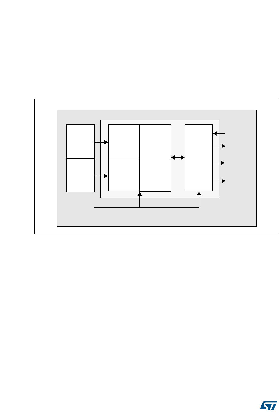
Debug support (DBG) RM0090
1686/1718 DocID018909 Rev 9
38.17 TPIU (trace port interface unit)
38.17.1 Introduction
The TPIU acts as a bridge between the on-chip trace data from the ITM and the ETM.
The output data stream encapsulates the trace source ID, that is then captured by a trace
port analyzer (TPA).
The core embeds a simple TPIU, especially designed for low-cost debug (consisting of a
special version of the CoreSight TPIU).
Figure 486. TPIU block diagram
formatter
Trace out
(serializer)
TRACECLKIN
TRACECK
TRACEDATA
[3:0]
TRACESWO
CLK domain TRACECLKIN domain
External PPB bus
TPIU
TPIU
Asynchronous
FIFO
Asynchronous
FIFO
ETM
ITM
ai17114

DocID018909 Rev 9 1687/1718
RM0090 Debug support (DBG)
1692
38.17.2 TRACE pin assignment
•Asynchronous mode
The asynchronous mode requires 1 extra pin and is available on all packages. It is only
available if using Serial Wire mode (not in JTAG mode).
•Synchronous mode
The synchronous mode requires from 2 to 6 extra pins depending on the data trace
size and is only available in the larger packages. In addition it is available in JTAG
mode and in Serial Wire mode and provides better bandwidth output capabilities than
asynchronous trace.
TPUI TRACE pin assignment
By default, these pins are NOT assigned. They can be assigned by setting the
TRACE_IOEN and TRACE_MODE bits in the MCU Debug component configuration
register. This configuration has to be done by the debugger host.
In addition, the number of pins to assign depends on the trace configuration (asynchronous
or synchronous).
•Asynchronous mode: 1 extra pin is needed
•Synchronous mode: from 2 to 5 extra pins are needed depending on the size of the
data trace port register (1, 2 or 4):
– TRACECK
– TRACED(0) if port size is configured to 1, 2 or 4
– TRACED(1) if port size is configured to 2 or 4
– TRACED(2) if port size is configured to 4
– TRACED(3) if port size is configured to 4
To assign the TRACE pin, the debugger host must program the bits TRACE_IOEN and
TRACE_MODE[1:0] of the Debug MCU configuration Register (DBGMCU_CR). By default
the TRACE pins are not assigned.
This register is mapped on the external PPB and is reset by the PORESET (and not by the
SYSTEM reset). It can be written by the debugger under SYSTEM reset.
Table 305. Asynchronous TRACE pin assignment
TPUI pin name
Trace synchronous mode STM32F4xx pin
assignment
Type Description
TRACESWO O TRACE Async Data Output PB3
Table 306. Synchronous TRACE pin assignment
TPUI pin name
Trace synchronous mode STM32F4xxpin
assignment
Type Description
TRACECK O TRACE Clock PE2
TRACED[3:0] O TRACE Sync Data Outputs
Can be 1, 2 or 4. PE[6:3]

Debug support (DBG) RM0090
1688/1718 DocID018909 Rev 9
Note: By default, the TRACECLKIN input clock of the TPIU is tied to GND. It is assigned to HCLK
two clock cycles after the bit TRACE_IOEN has been set.
The debugger must then program the Trace Mode by writing the PROTOCOL[1:0] bits in the
SPP_R (Selected Pin Protocol) register of the TPIU.
•PROTOCOL=00: Trace Port Mode (synchronous)
•PROTOCOL=01 or 10: Serial Wire (Manchester or NRZ) Mode (asynchronous mode).
Default state is 01
It then also configures the TRACE port size by writing the bits [3:0] in the CPSPS_R
(Current Sync Port Size Register) of the TPIU:
•0x1 for 1 pin (default state)
•0x2 for 2 pins
•0x8 for 4 pins
38.17.3 TPUI formatter
The formatter protocol outputs data in 16-byte frames:
•seven bytes of data
•eight bytes of mixed-use bytes consisting of:
– 1 bit (LSB) to indicate it is a DATA byte (‘0) or an ID byte (‘1).
– 7 bits (MSB) which can be data or change of source ID trace.
•one byte of auxiliary bits where each bit corresponds to one of the eight mixed-use
bytes:
– if the corresponding byte was a data, this bit gives bit0 of the data.
– if the corresponding byte was an ID change, this bit indicates when that ID change
takes effect.
Table 307. Flexible TRACE pin assignment
DBGMCU_CR
register
Pins
assigned for:
TRACE IO pin assigned
TRACE
_IOEN
TRACE
_MODE
[1:0]
PB3 /JTDO/
TRACESWO
PE2/
TRACECK
PE3 /
TRACED[0]
PE4 /
TRACED[1]
PE5 /
TRACED[2]
PE6 /
TRACED[3]
0XX
No Trace
(default state) Released (1) -
100
Asynchronous
Trace TRACESWO - - Released
(usable as GPIO)
101
Synchronous
Trace 1 bit
Released (1)
TRACECK TRACED[0] ---
110
Synchronous
Trace 2 bit TRACECK TRACED[0] TRACED[1] - -
111
Synchronous
Trace 4 bit TRACECK TRACED[0] TRACED[1] TRACED[2] TRACED[3]
1. When Serial Wire mode is used, it is released. But when JTAG is used, it is assigned to JTDO.

DocID018909 Rev 9 1689/1718
RM0090 Debug support (DBG)
1692
Note: Refer to the ARM® CoreSight Architecture Specification v1.0 (ARM® IHI 0029B) for further
information
38.17.4 TPUI frame synchronization packets
The TPUI can generate two types of synchronization packets:
•The Frame Synchronization packet (or Full Word Synchronization packet)
It consists of the word: 0x7F_FF_FF_FF (LSB emitted first). This sequence can not
occur at any other time provided that the ID source code 0x7F has not been used.
It is output periodically between frames.
In continuous mode, the TPA must discard all these frames once a synchronization
frame has been found.
•The Half-Word Synchronization packet
It consists of the half word: 0x7F_FF (LSB emitted first).
It is output periodically between or within frames.
These packets are only generated in continuous mode and enable the TPA to detect
that the TRACE port is in IDLE mode (no TRACE to be captured). When detected by
the TPA, it must be discarded.
38.17.5 Transmission of the synchronization frame packet
There is no Synchronization Counter register implemented in the TPIU of the core.
Consequently, the synchronization trigger can only be generated by the DWT. Refer to the
registers DWT Control Register (bits SYNCTAP[11:10]) and the DWT Current PC Sampler
Cycle Count Register.
The TPUI Frame synchronization packet (0x7F_FF_FF_FF) is emitted:
•after each TPIU reset release. This reset is synchronously released with the rising
edge of the TRACECLKIN clock. This means that this packet is transmitted when the
TRACE_IOEN bit in the DBGMCU_CFG register is set. In this case, the word
0x7F_FF_FF_FF is not followed by any formatted packet.
•at each DWT trigger (assuming DWT has been previously configured). Two cases
occur:
– If the bit SYNENA of the ITM is reset, only the word 0x7F_FF_FF_FF is emitted
without any formatted stream which follows.
– If the bit SYNENA of the ITM is set, then the ITM synchronization packets will
follow (0x80_00_00_00_00_00), formatted by the TPUI (trace source ID added).
38.17.6 Synchronous mode
The trace data output size can be configured to 4, 2 or 1 pin: TRACED(3:0)
The output clock is output to the debugger (TRACECK)
Here, TRACECLKIN is driven internally and is connected to HCLK only when TRACE is
used.
Note: In this synchronous mode, it is not required to provide a stable clock frequency.
The TRACE I/Os (including TRACECK) are driven by the rising edge of TRACLKIN (equal
to HCLK). Consequently, the output frequency of TRACECK is equal to HCLK/2.

Debug support (DBG) RM0090
1690/1718 DocID018909 Rev 9
38.17.7 Asynchronous mode
This is a low cost alternative to output the trace using only 1 pin: this is the asynchronous
output pin TRACESWO. Obviously there is a limited bandwidth.
TRACESWO is multiplexed with JTDO when using the SW-DP pin. This way, this
functionality is available in all STM32F4xx packages.
This asynchronous mode requires a constant frequency for TRACECLKIN. For the standard
UART (NRZ) capture mechanism, 5% accuracy is needed. The Manchester encoded
version is tolerant up to 10%.
38.17.8 TRACECLKIN connection inside the STM32F4xx
In the STM32F4xx, this TRACECLKIN input is internally connected to HCLK. This means
that when in asynchronous trace mode, the application is restricted to use to time frames
where the CPU frequency is stable.
Note: Important: when using asynchronous trace: it is important to be aware that:
The default clock of the STM32F4xx MCUs is the internal RC oscillator. Its frequency under
reset is different from the one after reset release. This is because the RC calibration is the
default one under system reset and is updated at each system reset release.
Consequently, the trace port analyzer (TPA) should not enable the trace (with the
TRACE_IOEN bit) under system reset, because a Synchronization Frame Packet will be
issued with a different bit time than trace packets which will be transmitted after reset
release.
38.17.9 TPIU registers
The TPIU APB registers can be read and written only if the bit TRCENA of the Debug
Exception and Monitor Control Register (DEMCR) is set. Otherwise, the registers are read
as zero (the output of this bit enables the PCLK of the TPIU).
Table 308. Important TPIU registers
Address Register Description
0xE0040004 Current port size
Allows the trace port size to be selected:
Bit 0: Port size = 1
Bit 1: Port size = 2
Bit 2: Port size = 3, not supported
Bit 3: Port Size = 4
Only 1 bit must be set. By default, the port size is one bit. (0x00000001)
0xE00400F0 Selected pin
protocol
Allows the Trace Port Protocol to be selected:
Bit1:0=
00: Sync Trace Port Mode
01: Serial Wire Output - manchester (default value)
10: Serial Wire Output - NRZ
11: reserved

DocID018909 Rev 9 1691/1718
RM0090 Debug support (DBG)
1692
38.17.10 Example of configuration
•Set the bit TRCENA in the Debug Exception and Monitor Control Register (DEMCR)
•Write the TPIU Current Port Size Register to the desired value (default is 0x1 for a 1-bit
port size)
•Write TPIU Formatter and Flush Control Register to 0x102 (default value)
•Write the TPIU Select Pin Protocol to select the sync or async mode. Example: 0x2 for
async NRZ mode (UART like)
•Write the DBGMCU control register to 0x20 (bit IO_TRACEN) to assign TRACE I/Os
for async mode. A TPIU Sync packet is emitted at this time (FF_FF_FF_7F)
•Configure the ITM and write the ITM Stimulus register to output a value
38.18 DBG register map
The following table summarizes the Debug registers.
.
0xE0040304 Formatter and flush
control
Bits 31-9 = always ‘0
Bit 8 = TrigIn = always ‘1 to indicate that triggers are indicated
Bits 7-4 = always 0
Bits 3-2 = always 0
Bit 1 = EnFCont. In Sync Trace mode (Select_Pin_Protocol register
bit1:0=00), this bit is forced to ‘1: the formatter is automatically enabled
in continuous mode. In asynchronous mode (Select_Pin_Protocol
register bit1:0 <> 00), this bit can be written to activate or not the
formatter.
Bit 0 = always 0
The resulting default value is 0x102
Note: In synchronous mode, because the TRACECTL pin is not mapped
outside the chip, the formatter is always enabled in continuous mode -this
way the formatter inserts some control packets to identify the source of
the trace packets).
0xE0040300 Formatter and flush
status Not used in Cortex®-M4 with FPU, always read as 0x00000008
Table 308. Important TPIU registers (continued)
Address Register Description
Table 309. DBG register map and reset values
Addr. Register
31
30
29
28
27
26
25
24
23
22
21
20
19
18
17
16
15
14
13
12
11
10
9
8
7
6
5
4
3
2
1
0
0xE004
2000
DBGMCU
_IDCODE REV_ID
Reserved
DEV_ID
Reset value(1) XXXXXXXXXXXXXXXX XXXXXXXXXXXX
Debug support (DBG) RM0090
1692/1718 DocID018909 Rev 9
0xE004
2004
DBGMCU_CR Reserved
DBG_TIM7_STOP
DBG_TIM6_STOP
DBG_TIM5_STOP
DBG_TIM8_STOP
DBG_I2C2_SMBUS_TIMEOUT
Reserved
TRACE_
MODE
[1:0]
TRACE_
Reserved
DBG_STANDBY
DBG_STOP
DBG_SLEEP
Reset value 00000 000 000
0xE004
2008
DBGMCU_
APB1_FZ Reserved
DBG_CAN2_STOP
DBG_CAN1_STOP
Reserved
DBG_I2C3_SMBUS_TIMEOUT
DBG_I2C2_SMBUS_TIMEOUT
DBG_I2C1_SMBUS_TIMEOUT
Reserved
DBG_IWDG_STOP
DBG_WWDG_STOP
Reserved
DBG_RTC_STOP
DBG_TIM14_STOP
DBG_TIM13_STOP
DBG_TIM12_STOP
DBG_TIM7_STOP
DBG_TIM6_STOP
DBG_TIM5_STOP
DBG_TIM4_STOP
DBG_TIM3_STOP
DBG_TIM2_STOP
Reset value 000000 00 0000000000
0xE004
200C
DBGMCU_
APB2_FZ Reserved
DBG_TIM11_STOP
DBG_TIM10_STOP
DBG_TIM9_STOP
Reserved
DBG_TIM8_STOP
DBG_TIM1_STOP
Reset value 000 00
1. The reset value is product dependent. For more information, refer to Section 38.6.1: MCU device ID code.
Table 309. DBG register map and reset values (continued)
Addr. Register
31
30
29
28
27
26
25
24
23
22
21
20
19
18
17
16
15
14
13
12
11
10
9
8
7
6
5
4
3
2
1
0

DocID018909 Rev 9 1693/1718
RM0090 Device electronic signature
1694
39 Device electronic signature
The electronic signature is stored in the Flash memory area. It can be read using the
JTAG/SWD or the CPU. It contains factory-programmed identification data that allow the
user firmware or other external devices to automatically match its interface to the
characteristics of the STM32F4xx microcontrollers.
39.1 Unique device ID register (96 bits)
The unique device identifier is ideally suited:
•for use as serial numbers (for example USB string serial numbers or other end
applications)
•for use as security keys in order to increase the security of code in Flash memory while
using and combining this unique ID with software cryptographic primitives and
protocols before programming the internal Flash memory
•to activate secure boot processes, etc.
The 96-bit unique device identifier provides a reference number which is unique for any
device and in any context. These bits can never be altered by the user.
The 96-bit unique device identifier can also be read in single bytes/half-words/words in
different ways and then be concatenated using a custom algorithm.
Base address: 0x1FFF 7A10
Address offset: 0x00
Read only = 0xXXXX XXXX where X is factory-programmed
Address offset: 0x04
Read only = 0xXXXX XXXX where X is factory-programmed
313029282726252423222120191817161514131211109876543210
U_ID(31:0)
rrrrrrrrrrrrrrrrrrrrrrrrrrrrrrrr
Bits 31:0 U_ID(31:0): 31:0 unique ID bits
31 30 29 28 27 26 25 24 23 22 21 20 19 18 17 16
U_ID(63:48)
rrrrrrrrrrrrrrrr
15 14 13 12 11 10 9 8 7 6 5 4 3 2 1 0
U_ID(47:32)
rrrrrrrrrrrrrrrr
Bits 31:0 U_ID(63:32): 63:32 unique ID bits

Device electronic signature RM0090
1694/1718 DocID018909 Rev 9
Address offset: 0x08
Read only = 0xXXXX XXXX where X is factory-programmed
39.2 Flash size
Base address: 0x1FFF 7A22
Address offset: 0x00
Read only = 0xXXXX where X is factory-programmed
31 30 29 28 27 26 25 24 23 22 21 20 19 18 17 16
U_ID(95:80)
rrrrrrrrrrrrrrrr
1514131211109876543210
U_ID(79:64)
rrrrrrrrrrrrrrrr
Bits 31:0 U_ID(95:64): 95:64 Unique ID bits.
1514131211109876543210
F_SIZE
rrrrrrrrrrrrrrrr
Bits 15:0 F_ID(15:0): Flash memory size
This bitfield indicates the size of the device Flash memory expressed in Kbytes.
As an example, 0x0400 corresponds to 1024 Kbytes.

DocID018909 Rev 9 1695/1718
RM0090 Revision history
1713
Revision history
Table 310. Document revision history
Date Version Changes
15-Sep-2011 1 Initial release.
19-Oct-2012 2
Updated reference documents and added Table 1: Applicable
products on cover page.
MEMORY:
Updated Section 2: Memory and bus architecture.
PWR:
Updated VDDA and VREF+ decoupling capacitor in Figure 7: Power
supply overview.
Updated case of no external battery in Section 5.1.2: Battery backup
domain.
VOSRDY bit changed to read-only in Section 5.4.3: PWR power
control/status register (PWR_CSR).
Removed VDDA in Section 5.2.3: Programmable voltage detector
(PVD) and remove VDDA in PVDO bit description (Section 5.4.3:
PWR power control/status register (PWR_CSR)).
RCC:
Updated Figure 20: Simplified diagram of the reset circuit and
minimum reset pulse duration guaranteed by pulse generator
restricted to internal reset sources.
GPIOs:
Updated Section 8.3.1: General-purpose I/O (GPIO).
19-Oct-2012 2
(continued)
DMA:
Updated direct mode description in Section 10.2: DMA main
features.
Updated direct mode description in Section : Memory-to-peripheral
mode, and Section 10.3.12: FIFO/: Direct mode.
Updated register access in Section 10.5: DMA registers.
Modified Stream2 /Channel 2 in Table 42: DMA1 request mapping.
Added note related to EN bit in Section 10.5.5: DMA stream x
configuration register (DMA_SxCR) (x = 0..7). Updated definition of
NDT[15:0] bits in Section 10.5.6: DMA stream x number of data
register (DMA_SxNDTR) (x = 0..7).
Interrupts:
Updated number of maskable interrupts to 82 in Section 12.1.1:
NVIC featuress.
Updated Section 12.2: External interrupt/event controller (EXTI).

Revision history RM0090
1696/1718 DocID018909 Rev 9
19-Oct-2012 2
(continued)
ADC:
Changed ADCCLK frequency to 30 MHz in Section 13.5: Channel-
wise programmable sampling timee.
Added recovery from ADC sequence in Section 13.8.1: Using the
DMA and Section 13.8.2: Managing a sequence of conversions
without using the DMA.
Updated AWDIE in Section 13.13.2: ADC control register 1
(ADC_CR1). Added read and write access in Section 13.13: ADC
registers.
Advanced control timers (TIM1 and TIM8):
Updated 16-bit prescaler range in Section 17.2: TIM1&TIM8 main
features.
Updated OC1 block diagram in Figure 114: Output stage of
capture/compare channel (channel 1 to 3).
Updated update event generation in Upcounting mode and
Downcounting mode in Section 17.3.2: Counter modes and
Section 17.3.3: Repetition counter.
Updated bits that control the dead-time generation in
Section 17.3.11: Complementary outputs and dead-time insertion.
Updated ways to generate a break in Section 17.3.12: Using the
break function.
Changed OCxREF to ETR in the example given in Section 17.3.13:
Clearing the OCxREF signal on an external event and changed
OCREF_CLR to ETRF in Figure 124: Clearing TIMx OCxREF.
Updated configuration for example of counter operation in encoder
interface mode in Section 17.3.16: Encoder interface mode.
Added register access in Section 17.4: TIM1&TIM8 registers.
Changed definition of ARR[15:0] bits in Section 17.4.12: TIM1&TIM8
auto-reload register (TIMx_ARR).
Updated BKE definition in Section 17.4.18: TIM1&TIM8 break and
dead-time register (TIMx_BDTR).
Table 310. Document revision history
Date Version Changes

DocID018909 Rev 9 1697/1718
RM0090 Revision history
1713
19-Oct-2012 2
(continued)
General purpose timers (TIM2 to TIM5):
Removed all references to “repetition counter”.
Added Figure 134: General-purpose timer block diagram.
Updated 16-bit prescaler range in Section 18.2: TIM2 to TIM5 main
features.
External clock mode 2 ETR restricted to TIM2 to TIM4 in
Section 18.3.3: Clock selection and Section 18.3.6: PWM input
mode.
Updated Section 18.3.9: PWM mode and Section 18.3.11: Clearing
the OCxREF signal on an external event.
Updated Figure 174: Master/Slave timer example to change ITR1 to
ITR0.
Updated read and write access to registers in Section 18.4: TIM2 to
TIM5 registerss.
Restored bits 15 to 8 of TIMx_SMCR as well as Table 97: TIMx
internal trigger connection in Section 14.4.3.
Removed note 1 related to OC1M bits in Section 18.4.13: TIMx
capture/compare register 1 (TIMx_CCR1).
Updated TIMx_CCER bit description for TIM2 to TIM5 in
Section 18.4.9: TIMx capture/compare enable register
(TIMx_CCER).
General purpose timers (TIM9 to TIM14):
Updated 16-bit prescaler range in Section 19.2.1: TIM9/TIM12 main
features and Section 19.2.2: TIM10/TIM11 and TIM13/TIM14 main
features.
Updated Figure 181: General-purpose timer block diagram
(TIM10/11/13/14)) to remove TRGO trigger controller output.
Added register access in Section 19.4: TIM9 and TIM12 registers
and Section 19.5: TIM10/11/13/14 registers.
Basic timers (TIM6 and TIM7):
Removed all references to “repetition counter”.
Updated 16-bit prescaler range in Section 20.2: TIM6&TIM7 main
features.
HASH:
Updated Section 25.3.1: Duration of the processing.
RNG:
Updated Section 24.1: RNG introduction.
Table 310. Document revision history
Date Version Changes

Revision history RM0090
1698/1718 DocID018909 Rev 9
19-Oct-2012 2
(continued)
RTC:
Updated Figure 237: RTC block diagram.
Added formula to compute fck_apre in Figure 26.3.1: Clock and
prescalers.
Updated Section 26.3.9: RTC reference clock detection.
Updated Section : RTC register write protection.
Added RTC_SSR shadow register in Section 26.3.6: Reading the
calendar.
Updated description of DC[4:0] bits in Section 26.6.7: RTC
calibration register (RTC_CALIBR).
Renamed RTC_BKxR into RTC_BKPxR in Table 120: RTC register
map and reset values.
Added power-on reset value and changed reset value to system
reset value in Section 26.6.11: RTC sub second register
(RTC_SSR).
Updated definition of ALARMOUTTYPE in Section 26.6.17: RTC
tamper and alternate function configuration register (RTC_TAFCR).
I2C:
Modified Section 27.3.8: DMA requests.
Updated bit 14 description in Section 27.6.3: I2C Own address
register 1 (I2C_OAR1)).
Updated definition of PE bit and note related to SWRST bit; moved
note related to STOP bit to the whole register in Section 27.6.1: I2C
Control register 1 (I2C_CR1).
USART:
Section 30.6.6: Control register 3 (USART_CR3)): removed notes
related to UART5 in DMAT and DMAR description.
Updated TTable 141: Error calculation for programmed baud rates at
fPCLK = 42 MHz or fPCLK = 84 Hz, oversampling by 16 and
Table 142: Error calculation for programmed baud rates at fPCLK =
42 MHz or fPCLK = 84 MHz, oversampling by 8.
SPI/I2S:
Updated Section 28.1: SPI introduction.
Changed I2S simplex communication/mode to half-duplex
communication/mode. Updated flags in reception/transmission
modes in Section 28.2.2: I2S features. Added Frame error flag in
Table 127: I2S interrupt requests.
Added register access in Section 28.5: SPI and I2S registers.
Updated ERRIE definition in Section 28.5.2: SPI control register 2
(SPI_CR2).
Renamed TIFRFE to FRE and definition updated in Section 28.5.3:
SPI status register (SPI_SR).
Table 310. Document revision history
Date Version Changes

DocID018909 Rev 9 1699/1718
RM0090 Revision history
1713
19-Oct-2012 2
(continued)
SDIO:
Updated value and description for bits [45:40] and [7:1] in Table 175:
R4 response. Updated value at bits [45:40] in Table 177: R5
response.
CAN:
Updated Figure 335: Dual CAN block diagram.
Modified definition of CAN2SB bits in Section : CAN filter master
register (CAN_FMR).
Added register access in Section 32.9: CAN registers
ETHERNET:
Updated standard for precision networked clock synchronization in
Section 33.1: Ethernet introduction and Section 33.2.1: MAC core
features.
Updated CR bit definition in Section : Ethernet MAC MII address
register (ETH_MACMIIAR).
Replace RTPR by PM bit in Table 191: Source address filtering.
USB OTG FS
Updated remote wakeup signaling bit and the resume
interrupt in Section : Suspended state.
Added peripheral register access in Section 34.16: OTG_FS control
and status registerss.
Updated INEPTXSA description in OTG_FS_DIEPTXFx.
Changed PHYSEL from bit 7 to bit 6 of the OTG_FS_GUSBCFG
register.
USB OTG HS
Updated remote wakeup signaling bit and the resume
interrupt in Section : Suspended state.
Added peripheral register access in Section 35.12: OTG_HS control
and status registers.
Updated OTG_HS_CID reset value.
Updated INEPTXSA description in OTG_HS_DIEPTXFx.
Updated FSLSPCS for LS host mode, added PHYSEL in Section :
OTG_HS host configuration register (OTG_HS_HCFG).
Renamed PHYSEL into PHSEL and changed from bit 7 to bit 6 of
the OTG_HS_GUSBCFG register.
Updated OTG_HS_DIEPEACHMSK1 and
OTG_HS_DOEPEACHMSK1 reset values.
Table 310. Document revision history
Date Version Changes

Revision history RM0090
1700/1718 DocID018909 Rev 9
19-Oct-2012 2
(continued)
FSMC:
Updated step b) in Section 36.3.1: Supported memories and
transactions.
Updated Table 196: FSMC_BTRx bit fields.
Changed Clock divide ration min in Table 241: Programmable
NAND/PC Card access parameters.
Updated case of synchronous accesses in Section 36.5: NOR
Flash/PSRAM controller.
Changed minimum value for ADDSET to 0 in Table 203, Table 206,
Table 207, Table 209, and Table 210.
Move note from Figure 435: Mode1 write accesses and Figure 434:
Mode1 read accesses. Move note from Figure 437: ModeA write
accesses to Figure 436: ModeA read accesses.
Updated Section : WAIT management in asynchronous accesses.
Added register access in Section 36.5.6: NOR/PSRAM control
registers and Section 36.6.2: NAND Flash / PC Card supported
memories and transactions.
Removed caution note in Section 36.6.1: External memory interface
signalss.
Updated Table 244: 16-bit PC Card.
Updated step 3 in Section 36.6.4: NAND Flash operations.
Updated Figure 453: Access to non ‘CE don’t care’ NAND-Flash and
note below in Section 36.6.5: NAND Flash pre-wait functionality.
Updated access to I/O Space in Section 36.6.7: PC
Card/CompactFlash operationss. Updated Table 246: 16-bit PC-Card
signals and access type. Updated BUSTURN bit definition in
Section : SRAM/NOR-Flash chip-select timing registers 1..4
(FSMC_BTR1..4)). Changed bits 16 to 19 to BUSTURN in Section :
SRAM/NOR-Flash write timing registers 1..4 (FSMC_BWTR1..4)
DEBUG:
Updated Section 38.4.3: Internal pull-up and pull-down on JTAG
pins.
Electronic signature
Updated Section 39: Device electronic signature introduction.
Updated REV_ID[15:0] to add revision Z in Section 39.1: Unique
device ID register (96 bits).
Updated address and example in Section 39.2: Flash size.
Table 310. Document revision history
Date Version Changes

DocID018909 Rev 9 1701/1718
RM0090 Revision history
1713
13-Nov-2012 3
Added STM32F42x and STM32F43x devices.
Removed reference du Flash programming manual on cover page.
Added Section 2.3.2: Flash memory overview and Section 3:
Embedded Flash memory interface.
Change RTC_50Hz into RTC_REFIN in Section 8.3.2: I/O pin
multiplexer and mapping. Modified RTC alternate function naming in
Section 8: General-purpose I/Os (GPIO) and Section 26: Real-time
clock (RTC).
Updated max. input frequency in Section 26.3.1: Clock and
prescalers.
Changed bit access type from ‘rw’ to ‘w’ and bit description updated
in Section 10.5.3: DMA low interrupt flag clear register (DMA_LIFCR)
and Section 10.5.4: DMA high interrupt flag clear register
(DMA_HIFCR).
Updated Figure 18: Frequency measurement with TIM5 in Input
capture mode.
Updated Section : Signals synchronization in Section 36: Flexible
static memory controller (FSMC)
Section 34: USB on-the-go full-speed (OTG_FS): updated
Section Figure 389.: USB host-only connection, Section : VBUS
valid, and Section : Host detection of a peripheral connection.
Section 35: USB on-the-go high-speed (OTG_HS): updated
Section : VBUS valid, and Section : Detection of peripheral
connection by the host.
Table 310. Document revision history
Date Version Changes

Revision history RM0090
1702/1718 DocID018909 Rev 9
19-Feb-2013 4
Updated Section 2: Memory and bus architecture.
Updated Figure 1: System architecture for STM32F405xx/07xx and
STM32F415xx/17xx devices, and Figure 1: System architecture for
STM32F405xx/07xx and STM32F415xx/17xx devices. Updated
Table 4: Memory mapping vs. Boot mode/physical remap. Updated
Figure 5: Sequential 32-bit instruction execution. removed note 1
from Table 12: Program/erase parallelism.
PWR:
Updated Figure 7: Power supply overview.
Updated Section 5.1.3: Voltage regulator.
Added ADCDC1 bit in Section 5.5.1: PWR power control register
(PWR_CR) for STM32F42xxx and STM32F43xxx.
SYSCFG:
Added ADCxDC2 bit in Section 8.2.3: SYSCFG peripheral mode
configuration register (SYSCFG_PMC) for STM32F42xxx and
STM32F43xxx.
ADC:
Updated Section 13.9.3: Interleaved mode, Section 13.9.4: Alternate
trigger mode, and Section 13.9.5: Combined regular/injected
simultaneous mode to describe case of interrupted conversion.
Updated Section : Temperature sensor, VREFINT and VBAT internal
channels, Section 13.10: Temperature sensor, and Section 13.11:
Battery charge monitoring.
RTC:
Updated BKP[31:0] bit description in Section 26.6.20: RTC backup
registers (RTC_BKPxR).
I2C:
Updated Section 27.3.5: Programmable noise filter.
Table 310. Document revision history
Date Version Changes

DocID018909 Rev 9 1703/1718
RM0090 Revision history
1713
19-Feb-2013 4
(continued)
FSMC:
Updated write FIFO size in Section 36.1: FSMC main features.
Updated Figure 432: FSMC block diagram.
Updated Section 36.5.4: NOR Flash/PSRAM controller
asynchronous transactions.
Modified differences between Mode B and mode 1 in Section : Mode
2/B - NOR Flash.
Modified differences between Mode C and mode 1 in Section : Mode
C - NOR Flash - OE toggling.
Modified differences between Mode D and mode 1 in Section : Mode
D - asynchronous access with extended address.
Updated NWAIT signal in Figure 447: Asynchronous wait during a
read access, Figure 448: Asynchronous wait during a write access,
Figure 449: Wait configurations, Figure 450: Synchronous
multiplexed read mode - NOR, PSRAM (CRAM), and Figure 451:
Synchronous multiplexed write mode - PSRAM (CRAM).
Updated Table 195 to Table 21 4 .
Updated Section : SRAM/NOR-Flash chip-select control registers
1..4 (FSMC_BCR1..4).
DEBUG
Updated Figure 483: Block diagram of STM32 MCU and Cortex®-
M4 with FPU-level debug support.
Table 310. Document revision history
Date Version Changes

Revision history RM0090
1704/1718 DocID018909 Rev 9
15-Sep-2013 5
Added STM32F429xx and STM32F439xx part numbers.
Replaced FSMC by FMC added Chrom-ART Accelerator, LCD-TFT
and SAI interface.
Updated Figure 2: System architecture for STM32F42xxx and
STM32F43xxx devices.
PWR:
Updated Section 5.2.2: Brownout reset (BOR).
Added note related to CSS enabling in Entering Stop mode sections
in Section 5.3.4: Stop mode (STM32F405xx/07xx and
STM32F415xx/17xx) and Section 5.3.5: Stop mode (STM32F42xxx
and STM32F43xxx). Updated Stop mode entry in Table 27 and
Table 29.
Updated WUF bit defienition in PWR_CSR registers. Changed
CWUF and CSBF access type to ‘w’ in PWR_CR register.
RCC: Updated LSEBYP bit definition in RCC_BDCR register.
GPIOs:
Updated description of OSPEEDR bits. Removed frequency value in
description of OSPEEDR bits.Corrected typos: "IDRy[15:0]" replaced
with "IDRy" in "GPIOx_IDR" register, "ODRy[15:0]" replaced with
"ODRy" in "GPIOx_ODR" register and "OTy[1:0]" replaced with
"OTy" in "GPIOx_OTYPER" register.
DCMI: Updated Section 15.4: DCMI clocks.
IWDG: Corrected Figure 213: Independent watchdog block diagram.
RTC:
Replaced all occurrences of “power-on reset” with “backup domain
reset”. Added caution note under Table 120: RTC register map and
reset values. Changed SHPF bit type to ‘r’ in Section 26.6.4: RTC
initialization and status register (RTC_ISR)..
SPI: Updated definition of ERRIE bit in Section 28.5.2: SPI control
register 2 (SPI_CR2).
UART:
Updated Section 30.3.8: LIN (local interconnection network) mode.
Removed note in Section 30.3.13: Continuous communication using
DMA.
ETHERNET:
Modified ETH_MACA0HR (and ETH_DMABMR reset values.
Updated definitions of TSTS bit in ETH_MACSR, and TSTTR in
ETH_PTPTSSR.
Table 310. Document revision history
Date Version Changes

DocID018909 Rev 9 1705/1718
RM0090 Revision history
1713
15-Sep-2013 5
(continued)
USB OTG-FS:
Removed note related to VDD range limitation below Figure 387:
OTG A-B device connection and Figure 388: USB peripheral-only
connection.
FSMC:
Updated Table 224, Table 22 7 , Table 230, Table 234.
Replaced all occurences of DATALAT by DATLAT and SRAM/CRAM
by SRAM/PSRAM in the whole section.
Updated Section 36.1: FSMC main features. Changed bits 27 to 20
of FSMC_BWTR1..4 to reserved.
Updated Section 36.6.7: PC Card/CompactFlash operations.
Updated WREN bit in Table 226, Table 227, Ta ble 228, Table 231,
Table 234, Table 237, Table 240, and Table 24 4 .
Updated Section 36.5.4: NOR Flash/PSRAM controller
asynchronous transactions, Section : SRAM/NOR-Flash chip-select
control registers 1..4 (FSMC_BCR1..4), Section : SRAM/NOR-Flash
chip-select timing registers 1..4 (FSMC_BTR1..4) and Section :
SRAM/NOR-Flash write timing registers 1..4 (FSMC_BWTR1..4).
Updated definition of PWID in Section : PC Card/NAND Flash control
registers 2..4 (FSMC_PCR2..4).
FMC:
Updated TRDC definition in Section : SDRAM Timing registers 1,2
(FMC_SDTR1,2).
DEBUG: updated Figure 485: JTAG TAP connections.
Table 310. Document revision history
Date Version Changes

Revision history RM0090
1706/1718 DocID018909 Rev 9
03-Feb-2014 6
Added note related to over-drive mode unavailable in 1.8 to
2.1 V VDD range in Section 3.5.1: Relation between CPU clock
frequency and Flash memory read time.
Updated maximum CPU frequency in Section 3.5.2: Adaptive
real-time memory accelerator (ART Accelerator™).
PWR:
Updated Run mode/ over-drive mode in Section 5.1.4: Voltage
regulator for STM32F42xxx and STM32F43xxx.
RCC for STM32F42/43xx:
Changed APB1/2 and AHB maximum frequencies.xw
GPIOs:
Updated Figure 27: Selecting an alternate function on STM32F42xxx
and STM32F43xxx.
DMA:
Updated Section 10.3.7: Pointer incrementation and Section 10.3.11:
Single and burst transfers..
INTERRUPTS AND EVENTS:
Updated Table 62: Vector table for STM32F42xxx and
STM32F43xxx.
ADC:
Updated Section 13.3.10: Discontinuous mode/Section : Regular
group.
DCMI:
Updated Section 15.5.2: DCMI physical interface.
LTDC:
Updated resolution in note below Figure 82: LCD-TFT Synchronous
timings.
TIM1 and 8:
Added note related to IC1F in Section 17.4.7: TIM1&TIM8
capture/compare mode register 1 (TIMx_CCMR1).
TIM2 to 5:
Updated note related to IC1F in Section 18.4.7: TIMx
capture/compare mode register 1 (TIMx_CCMR1).
Table 310. Document revision history
Date Version Changes

DocID018909 Rev 9 1707/1718
RM0090 Revision history
1713
03-Feb-2014 6
(continued)
TIM9 to 14:
Updated note related to IC1F in Section 19.5.5: TIM10/11/13/14
capture/compare mode register 1 (TIMx_CCMR1).
RTC:
Updated Section 26.3.11: RTC smooth digital calibration.
Changed ALRBIE to ALRBE (bit 9) in Section 26.6.3: RTC control
register (RTC_CR).
I2C:
Introduced Sm (standard mode) and Fm (fast mode) acronyms.
FSMC:
Updated BUSTURN definition in Table 240: FSMC_BTRx bit fields.
FMC:
Added Mobile LPSDR SDRAM.
Updated Section : SDRAM initialization and Section : SDRAM
controller read cycle and Figure 474: NAND Flash/PC Card
controller waveforms for common memory access.
Updated Section : SRAM/NOR-Flash chip-select control registers
1..4 (FMC_BCR1..4), Section : SRAM/NOR-Flash chip-select timing
registers 1..4 (FMC_BTR1..4), Section : SRAM/NOR-Flash write
timing registers 1..4 (FMC_BWTR1..4), Section : SDRAM Timing
registers 1,2 (FMC_SDTR1,2) and Section : SDRAM Refresh Timer
register (FMC_SDRTR).
Removed mention “default valeur after reset” in Section : Common
memory space timing register 2..4 (FMC_PMEM2..4), Section :
Attribute memory space timing registers 2..4 (FMC_PATT2..4), and
Section : I/O space timing register 4 (FMC_PIO4).
Updated BUSTURN definition in Table 283: FMC_BTRx bit fields.
Updated REV_ID bits in Section 38.6.1: MCU device ID code..
Table 310. Document revision history
Date Version Changes

Revision history RM0090
1708/1718 DocID018909 Rev 9
15-May-2014 7
Embedded Flash memory interface:
Updated Section : Physical remap in STM32F42xxx and
STM32F43xxx. Updated bank 2 selection in Section 2.4: Boot
configuration. Updated notes related to MERx and SER bits in
Section : Mass Erase. Updated Section 3.7.5: Proprietary code
readout protection (PCROP). Updated FLASH_OPTCR register
reset value for STM32F42/43xx in Section 3.9.10: Flash option
control register (FLASH_OPTCR) for STM32F42xxx and
STM32F43xxx and Section 3.9.11: Flash option control register
(FLASH_OPTCR1) for STM32F42xxx and STM32F43xxx.
RCC (STM32F42/43xx):
Updated PPLN caution note in Section 6.3.2: RCC PLL configuration
register (RCC_PLLCFGR)
SYSCFG
Updated MEM_MODE in Section 9.3.1: SYSCFG memory remap
register (SYSCFG_MEMRMP)
LTDC:
Changed resolution do XGA (1024x768) in Section 16.2: LTDC main
features, Section 16.4.1: LTDC Global configuration parameters, and
updated Section 16.7.3: LTDC Active Width Configuration Register
(LTDC_AWCR).
RTC
Added note in Section 26.3.14: Calibration clock output.
TIMER 1/8:
Removed note related to IC1F bits in Section 17.4.7: TIM1&TIM8
capture/compare mode register 1 (TIMx_CCMR1),
TIM2 to 5:
Replaced IC2S by CC2S.
Updated Figure 161: Output stage of capture/compare channel
(channel 1). Removed note related to IC1F bits in Section 18.4.7:
TIMx capture/compare mode register 1 (TIMx_CCMR1).
TIM9 to 14:
Removed note related to IC1F bits in Section 19.5.5: TIM10/11/13/14
capture/compare mode register 1 (TIMx_CCMR1).
USB OTG-HS:
Updated DSPD definition in Section : OTG_HS device configuration
register (OTG_HS_DCFG).
FSMC
Updated DATLAT bits definition in Section : SRAM/NOR-Flash chip-
select timing registers 1..4 (FSMC_BTR1..4).
Table 310. Document revision history
Date Version Changes

DocID018909 Rev 9 1709/1718
RM0090 Revision history
1713
15-May-2014 7
(continued)
FMC
Updated Figure 472: Synchronous multiplexed read mode
waveforms - NOR, PSRAM (CRAM). Updated DATLAT bits definition
in Section : SRAM/NOR-Flash chip-select timing registers 1..4
(FMC_BTR1..4).
Updated FMC_BWTRx register address offsets in Table 292: FMC
register map.
DEBUG
Added revision code ‘3’ in Section : DBGMCU_IDCODE.
Table 310. Document revision history
Date Version Changes

Revision history RM0090
1710/1718 DocID018909 Rev 9
14-Oct-2014 8
Memory and bus architecture:
Updated Table 3: Memory mapping vs. Boot mode/physical remap
in STM32F405xx/07xx and STM32F415xx/17xx and Table 4 :
Memory mapping vs. Boot mode/physical remap in STM32F42xxx
and STM32F43xxx.
RCC (STM32F40/41xx) and RCC (STM32F42/43xx):
Removed all references to Flash programming manual. Changed
RCC_AHB1LPENR, RCC_APB1LPENR, RCC_APB2LPENR,
RCC_PLLI2SCFGR and RCC_APB2LPENR reset values.
Updated access type to “r” for bits 24 to 31 in RCC_CSR.
GPIOs:
Updated Figure 27: Selecting an alternate function on STM32F42xxx
and STM32F43xxx.
IWDG
Update note in Table 106: Min/max IWDG timeout period at 32 kHz
(LSI).
CRYPTO and HASH
Removed STM32F405/407xx and STM32F42xx from the whole
sections.
Removed STM32F405/407xx and STM32F42xx from the whole
section.
TIM10/11/13/14
Added TIMx_DIER description in Section 19.5: TIM10/11/13/14
registers.
ETHERNET:
Updated Table 186: Clock range.
USB OTG FS:
Removed TRDT formula in Section 34.17.7: Worst case response
time and added Table 200: TRDT values.
USB OTG HS:
Removed TRDT formula in Section 35.13.8: Worst case response
time and added Table 208: TRDT values.
FSMC:
Updated EXTMOD definition in Section : SRAM/NOR-Flash chip-
select control registers 1..4 (FSMC_BCR1..4).
Updated ADDSET definition in Section : SRAM/NOR-Flash chip-
select timing registers 1..4 (FSMC_BTR1..4) and Section :
SRAM/NOR-Flash write timing registers 1..4 (FSMC_BWTR1..4).
Table 310. Document revision history
Date Version Changes

DocID018909 Rev 9 1711/1718
RM0090 Revision history
1713
14-Oct-2014 8
(continued)
FMC:
Modified step 7 in Section : SDRAM initialization.
Modified SDRAM refresh rate equations and example in Section :
SDRAM Refresh Timer register (FMC_SDRTR) and updated
definition of COUNT bits.
Updated EXTMOD definition in Section : SRAM/NOR-Flash chip-
select control registers 1..4 (FMC_BCR1..4).
Updated ADDSET definition in Section : SRAM/NOR-Flash chip-
select timing registers 1..4 (FMC_BTR1..4) and Section :
SRAM/NOR-Flash write timing registers 1..4 (FMC_BWTR1..4).
Table 310. Document revision history
Date Version Changes

Revision history RM0090
1712/1718 DocID018909 Rev 9
16-Mar-2015 9
PWR:
Updated Section 5.1.2: Battery backup domain.
Updated Table 23: Low-power mode summary to add Return from
ISR as entry condition.
Added Section : Entering low-power mode and Section : Exiting low-
power mode.
Updated Section : Entering Sleep mode, Section : Exiting Sleep
mode, Table 24: Sleep-now entry and exit and Table 25: Sleep-on-
exit entry and exit.
Updated Section : Entering Stop mode (for STM32F405xx/07xx and
STM32F415xx/17xx), Section : Exiting Stop mode (for
STM32F405xx/07xx and STM32F415xx/17xx) and Table 27: Stop
mode entry and exit (for STM32F405xx/07xx and
STM32F415xx/17xx). Updated Section : Entering Stop mode
(STM32F42xxx and STM32F43xxx), Section : Exiting Stop mode
(STM32F42xxx and STM32F43xxx) and Table 29: Stop mode entry
and exit (STM32F42xxx and STM32F43xxx).
Updated Section : Entering Standby mode, Section : Exiting Standby
mode and Table 30: Standby mode entry and exit.
RCC:
Updated bits 24 to 31 access type in Section 7.3.22: RCC clock
control & status register (RCC_CSR).
GPIOs:
Added port A reset value in Section 8.4.3: GPIO port output speed
register (GPIOx_OSPEEDR) (x = A..I/J/K).
DMA:
Update FTH[1:0] description in Section 10.5.10: DMA stream x FIFO
control register (DMA_SxFCR) (x = 0..7).
TIM2/5:
Register format changed to 32 bits instead of 16 in Section 18.4.10:
TIMx counter (TIMx_CNT) and Section 18.4.12: TIMx auto-reload
register (TIMx_ARR).
TIM9 to 14:
Updated Table 100: TIMx internal trigger connection
WWDG:
Updated Figure 214: Watchdog block diagram and Section 22.4:
How to program the watchdog timeout.
Updated Figure 215: Window watchdog timing diagram
RNG:
Replaced PLL48CLK by RNG_CLK in the whole section.
Table 310. Document revision history
Date Version Changes

DocID018909 Rev 9 1713/1718
RM0090 Revision history
1713
16-Mar-2015 9
(continued)
I2C2:
Updated FREQ[5:0] description in Section 27.6.2: I2C Control
register 2 (I2C_CR2).
USART:
Removed note related to RXNEIE in Section : Reception using DMA
FSMC:
Updated Figure 472: Synchronous multiplexed read mode
waveforms - NOR, PSRAM (CRAM).
USB OTG FS
Updated Table 200: TRDT values
FMC
Updated FMC_NL in Figure 454: FMC block diagram.
Updated ‘Memory wait’ and ‘Memory data bus high-z’ parameters in
Table 284: Programmable NAND Flash/PC Card access
parameters.
Updated Section : Common memory space timing register 2..4
(FMC_PMEM2..4).
Updated Figure 474: NAND Flash/PC Card controller waveforms for
common memory access.
DEBUG:
Updated REV_ID[15:0) and JTAG ID code in Section 38.6.1: MCU
device ID code and Section 38.6.2: Boundary scan TAP, respectively
Table 310. Document revision history
Date Version Changes

RM0090
1714/1718 DocID018909 Rev 9
A
ADC_CCR . . . . . . . . . . . . . . . . . . . . . . . . . . .427
ADC_CDR . . . . . . . . . . . . . . . . . . . . . . . . . . .430
ADC_CR1 . . . . . . . . . . . . . . . . . . . . . . . . . . .417
ADC_CR2 . . . . . . . . . . . . . . . . . . . . . . . . . . .419
ADC_CSR . . . . . . . . . . . . . . . . . . . . . . . . . . .426
ADC_DR . . . . . . . . . . . . . . . . . . . . . . . . . . . .426
ADC_HTR . . . . . . . . . . . . . . . . . . . . . . . . . . .422
ADC_JDRx . . . . . . . . . . . . . . . . . . . . . . . . . . .425
ADC_JOFRx . . . . . . . . . . . . . . . . . . . . . . . . .422
ADC_JSQR . . . . . . . . . . . . . . . . . . . . . . . . . .425
ADC_LTR . . . . . . . . . . . . . . . . . . . . . . . . . . . .423
ADC_SMPR1 . . . . . . . . . . . . . . . . . . . . . . . . .421
ADC_SMPR2 . . . . . . . . . . . . . . . . . . . . . . . . .421
ADC_SQR1 . . . . . . . . . . . . . . . . . . . . . . . . . .423
ADC_SQR2 . . . . . . . . . . . . . . . . . . . . . . . . . .424
ADC_SQR3 . . . . . . . . . . . . . . . . . . . . . . . . . .424
ADC_SR . . . . . . . . . . . . . . . . . . . . . . . . . . . . .416
C
CAN_BTR . . . . . . . . . . . . . . . . . . . . . . . . . .1089
CAN_ESR . . . . . . . . . . . . . . . . . . . . . . . . . .1088
CAN_FA1R . . . . . . . . . . . . . . . . . . . . . . . . .1099
CAN_FFA1R . . . . . . . . . . . . . . . . . . . . . . . .1099
CAN_FiRx . . . . . . . . . . . . . . . . . . . . . . . . . .1100
CAN_FM1R . . . . . . . . . . . . . . . . . . . . . . . . .1098
CAN_FMR . . . . . . . . . . . . . . . . . . . . . . . . . .1097
CAN_FS1R . . . . . . . . . . . . . . . . . . . . . . . . .1098
CAN_IER . . . . . . . . . . . . . . . . . . . . . . . . . . .1086
CAN_MCR . . . . . . . . . . . . . . . . . . . . . . . . . .1080
CAN_MSR . . . . . . . . . . . . . . . . . . . . . . . . . .1082
CAN_RDHxR . . . . . . . . . . . . . . . . . . . . . . . .1096
CAN_RDLxR . . . . . . . . . . . . . . . . . . . . . . . .1096
CAN_RDTxR . . . . . . . . . . . . . . . . . . . . . . . .1095
CAN_RF0R . . . . . . . . . . . . . . . . . . . . . . . . .1085
CAN_RF1R . . . . . . . . . . . . . . . . . . . . . . . . .1086
CAN_RIxR . . . . . . . . . . . . . . . . . . . . . . . . . .1094
CAN_TDHxR . . . . . . . . . . . . . . . . . . . . . . . .1093
CAN_TDLxR . . . . . . . . . . . . . . . . . . . . . . . .1093
CAN_TDTxR . . . . . . . . . . . . . . . . . . . . . . . .1092
CAN_TIxR . . . . . . . . . . . . . . . . . . . . . . . . . .1091
CAN_TSR . . . . . . . . . . . . . . . . . . . . . . . . . .1083
CRC_DR . . . . . . . . . . . . . . . . . . . . . . . . . . . .114
CRC_IDR . . . . . . . . . . . . . . . . . . . . . . . . . . . .114
CRYP_CR . . . . . . . . . . . . . . . . . . . . . . .733, 735
CRYP_DIN . . . . . . . . . . . . . . . . . . . . . . . . . . .739
CRYP_DMACR . . . . . . . . . . . . . . . . . . . . . . .741
CRYP_DOUT . . . . . . . . . . . . . . . . . . . . . . . . .740
CRYP_IMSCR . . . . . . . . . . . . . . . . . . . . . . . .741
CRYP_IV0LR . . . . . . . . . . . . . . . . . . . . . . . . .745
CRYP_IV0RR . . . . . . . . . . . . . . . . . . . . . . . . .745
CRYP_IV1LR . . . . . . . . . . . . . . . . . . . . . . . . 746
CRYP_IV1RR . . . . . . . . . . . . . . . . . . . . . . . . 746
CRYP_K0LR . . . . . . . . . . . . . . . . . . . . . . . . . 743
CRYP_K0RR . . . . . . . . . . . . . . . . . . . . . . . . . 743
CRYP_K1LR . . . . . . . . . . . . . . . . . . . . . . . . . 744
CRYP_K1RR . . . . . . . . . . . . . . . . . . . . . . . . . 744
CRYP_K2LR . . . . . . . . . . . . . . . . . . . . . . . . . 744
CRYP_K2RR . . . . . . . . . . . . . . . . . . . . . . . . . 744
CRYP_K3LR . . . . . . . . . . . . . . . . . . . . . . . . . 744
CRYP_K3RR . . . . . . . . . . . . . . . . . . . . . . . . . 745
CRYP_MISR . . . . . . . . . . . . . . . . . . . . . . . . . 742
CRYP_RISR . . . . . . . . . . . . . . . . . . . . . . . . . 742
CRYP_SR . . . . . . . . . . . . . . . . . . . . . . . . . . . 738
D
DAC_CR . . . . . . . . . . . . . . . . . . . . . . . . . . . . 445
DAC_DHR12L1 . . . . . . . . . . . . . . . . . . . . . . . 449
DAC_DHR12L2 . . . . . . . . . . . . . . . . . . . . . . . 450
DAC_DHR12LD . . . . . . . . . . . . . . . . . . . . . . 451
DAC_DHR12R1 . . . . . . . . . . . . . . . . . . . . . . 448
DAC_DHR12R2 . . . . . . . . . . . . . . . . . . . . . . 450
DAC_DHR12RD . . . . . . . . . . . . . . . . . . . . . . 451
DAC_DHR8R1 . . . . . . . . . . . . . . . . . . . . . . . 449
DAC_DHR8R2 . . . . . . . . . . . . . . . . . . . . . . . 450
DAC_DHR8RD . . . . . . . . . . . . . . . . . . . . . . . 452
DAC_DOR1 . . . . . . . . . . . . . . . . . . . . . . . . . . 452
DAC_DOR2 . . . . . . . . . . . . . . . . . . . . . . . . . . 452
DAC_SR . . . . . . . . . . . . . . . . . . . . . . . . . . . . 453
DAC_SWTRIGR . . . . . . . . . . . . . . . . . . . . . . 448
DBGMCU_APB1_FZ . . . . . . . . . . . . . . . . . . 1683
DBGMCU_APB2_FZ . . . . . . . . . . . . . . . . . . 1685
DBGMCU_CR . . . . . . . . . . . . . . . . . . . . . . . 1682
DBGMCU_IDCODE . . . . . . . . . . . . . . . . . . 1668
DCMI_CR . . . . . . . . . . . . . . . . . . . . . . . . . . . 466
DCMI_CWSIZE . . . . . . . . . . . . . . . . . . . . . . . 475
DCMI_CWSTRT . . . . . . . . . . . . . . . . . . . . . . 475
DCMI_DR . . . . . . . . . . . . . . . . . . . . . . . . . . . 476
DCMI_ESCR . . . . . . . . . . . . . . . . . . . . . . . . . 473
DCMI_ESUR . . . . . . . . . . . . . . . . . . . . . . . . . 474
DCMI_ICR . . . . . . . . . . . . . . . . . . . . . . . . . . . 472
DCMI_IER . . . . . . . . . . . . . . . . . . . . . . . . . . . 470
DCMI_MIS . . . . . . . . . . . . . . . . . . . . . . . . . . . 471
DCMI_RIS . . . . . . . . . . . . . . . . . . . . . . . . . . . 469
DCMI_SR . . . . . . . . . . . . . . . . . . . . . . . . . . . 468
DMA_HIFCR . . . . . . . . . . . . . . . . . . . . . . . . . 327
DMA_HISR . . . . . . . . . . . . . . . . . . . . . . . . . . 326
DMA_LIFCR . . . . . . . . . . . . . . . . . . . . . . . . . 327
DMA_LISR . . . . . . . . . . . . . . . . . . . . . . . . . . 325
DMA_SxCR . . . . . . . . . . . . . . . . . . . . . . . . . . 328
DMA_SxFCR . . . . . . . . . . . . . . . . . . . . . . . . . 333
DMA_SxM0AR . . . . . . . . . . . . . . . . . . . . . . . 332

RM0090
DocID018909 Rev 9 1715/1718
DMA_SxM1AR . . . . . . . . . . . . . . . . . . . . . . . .332
DMA_SxNDTR . . . . . . . . . . . . . . . . . . . . . . . .331
DMA_SxPAR . . . . . . . . . . . . . . . . . . . . . . . . .332
E
ETH_DMABMR . . . . . . . . . . . . . . . . . . . . . .1207
ETH_DMACHRBAR . . . . . . . . . . . . . . . . . . .1221
ETH_DMACHRDR . . . . . . . . . . . . . . . . . . . .1220
ETH_DMACHTBAR . . . . . . . . . . . . . . . . . . .1220
ETH_DMACHTDR . . . . . . . . . . . . . . . . . . . .1220
ETH_DMAIER . . . . . . . . . . . . . . . . . . . . . . .1217
ETH_DMAMFBOCR . . . . . . . . . . . . . . . . . .1219
ETH_DMAOMR . . . . . . . . . . . . . . . . . . . . . .1213
ETH_DMARDLAR . . . . . . . . . . . . . . . . . . . .1209
ETH_DMARPDR . . . . . . . . . . . . . . . . . . . . .1209
ETH_DMARSWTR . . . . . . . . . . . . . . . . . . . .1219
ETH_DMASR . . . . . . . . . . . . . . . . . . . . . . . .1210
ETH_DMATDLAR . . . . . . . . . . . . . . . . . . . .1210
ETH_DMATPDR . . . . . . . . . . . . . . . . . . . . .1208
ETH_MACA0HR . . . . . . . . . . . . . . . . . . . . .1189
ETH_MACA0LR . . . . . . . . . . . . . . . . . . . . . .1190
ETH_MACA1HR . . . . . . . . . . . . . . . . . . . . .1190
ETH_MACA1LR . . . . . . . . . . . . . . . . . . . . . .1191
ETH_MACA2HR . . . . . . . . . . . . . . . . . . . . .1191
ETH_MACA2LR . . . . . . . . . . . . . . . . . . . . . .1192
ETH_MACA3HR . . . . . . . . . . . . . . . . . . . . .1193
ETH_MACA3LR . . . . . . . . . . . . . . . . . . . . . .1193
ETH_MACCR . . . . . . . . . . . . . . . . . . . . . . . .1175
ETH_MACDBGR . . . . . . . . . . . . . . . . . . . . .1186
ETH_MACFCR . . . . . . . . . . . . . . . . . . . . . . .1182
ETH_MACFFR . . . . . . . . . . . . . . . . . . . . . . .1178
ETH_MACHTHR . . . . . . . . . . . . . . . . . . . . .1179
ETH_MACHTLR . . . . . . . . . . . . . . . . . . . . . .1180
ETH_MACIMR . . . . . . . . . . . . . . . . . . . . . . .1189
ETH_MACMIIAR . . . . . . . . . . . . . . . . . . . . .1180
ETH_MACMIIDR . . . . . . . . . . . . . . . . . . . . .1181
ETH_MACPMTCSR . . . . . . . . . . . . . . . . . . .1185
ETH_MACRWUFFR . . . . . . . . . . . . . . . . . .1184
ETH_MACSR . . . . . . . . . . . . . . . . . . . . . . . .1188
ETH_MACVLANTR . . . . . . . . . . . . . . . . . . .1183
ETH_MMCCR . . . . . . . . . . . . . . . . . . . . . . .1194
ETH_MMCRFAECR . . . . . . . . . . . . . . . . . . .1199
ETH_MMCRFCECR . . . . . . . . . . . . . . . . . .1198
ETH_MMCRGUFCR . . . . . . . . . . . . . . . . . .1199
ETH_MMCRIMR . . . . . . . . . . . . . . . . . . . . .1196
ETH_MMCRIR . . . . . . . . . . . . . . . . . . . . . . .1194
ETH_MMCTGFCR . . . . . . . . . . . . . . . . . . . .1198
ETH_MMCTGFMSCCR . . . . . . . . . . . . . . . .1198
ETH_MMCTGFSCCR . . . . . . . . . . . . . . . . .1197
ETH_MMCTIMR . . . . . . . . . . . . . . . . . . . . . .1197
ETH_MMCTIR . . . . . . . . . . . . . . . . . . . . . . .1195
ETH_PTPPPSCR . . . . . . . . . . . . . . . . . . . . 1206
ETH_PTPSSIR . . . . . . . . . . . . . . . . . . . . . . 1202
ETH_PTPTSAR . . . . . . . . . . . . . . . . . . . . . . 1204
ETH_PTPTSCR . . . . . . . . . . . . . . . . . . . . . 1199
ETH_PTPTSHR . . . . . . . . . . . . . . . . . . . . . 1202
ETH_PTPTSHUR . . . . . . . . . . . . . . . . . . . . 1203
ETH_PTPTSLR . . . . . . . . . . . . . . . . . . . . . . 1203
ETH_PTPTSLUR . . . . . . . . . . . . . . . . . . . . 1204
ETH_PTPTSSR . . . . . . . . . . . . . . . . . . . . . . 1205
ETH_PTPTTHR . . . . . . . . . . . . . . . . . . . . . . 1205
ETH_PTPTTLR . . . . . . . . . . . . . . . . . . . . . . 1205
EXTI_EMR . . . . . . . . . . . . . . . . . . . . . . . . . . 384
EXTI_FTSR . . . . . . . . . . . . . . . . . . . . . . . . . . 385
EXTI_IMR . . . . . . . . . . . . . . . . . . . . . . . . . . . 384
EXTI_PR . . . . . . . . . . . . . . . . . . . . . . . . . . . . 386
EXTI_RTSR . . . . . . . . . . . . . . . . . . . . . . . . . . 385
EXTI_SWIER . . . . . . . . . . . . . . . . . . . . . . . . . 386
F
FLITF_FCR . . . . . . . . . . . . . . . . . . . . . . 103, 105
FLITF_FKEYR . . . . . . . . . . . . . . . . . . . . . . . . 100
FLITF_FOPTCR . . . . . . . . . . . . . . 106, 108, 110
FLITF_FOPTKEYR . . . . . . . . . . . . . . . . . . . . 100
FLITF_FSR . . . . . . . . . . . . . . . . . . . . . . 101-102
FSMC_BCR1..4 . . . . . . . . . . . . . . . . . 1558, 1620
FSMC_BTR1..4 . . . . . . . . . . . . . . . . . 1561, 1622
FSMC_BWTR1..4 . . . . . . . . . . . . . . . 1562, 1625
FSMC_PCR2..4 . . . . . . . . . . . . . . . . . . . . . . 1573
FSMC_PMEM2..4 . . . . . . . . . . . . . . . . . . . . 1575
FSMC_SR2..4 . . . . . . . . . . . . . . . . . . . . . . . 1574
G
GPIOx_AFRH . . . . . . . . . . . . . . . . . . . . . . . . 286
GPIOx_AFRL . . . . . . . . . . . . . . . . . . . . . . . . 286
GPIOx_BSRR . . . . . . . . . . . . . . . . . . . . . . . . 284
GPIOx_IDR . . . . . . . . . . . . . . . . . . . . . . . . . . 283
GPIOx_LCKR . . . . . . . . . . . . . . . . . . . . . . . . 285
GPIOx_MODER . . . . . . . . . . . . . . . . . . . . . . 281
GPIOx_ODR . . . . . . . . . . . . . . . . . . . . . . . . . 284
GPIOx_OSPEEDR . . . . . . . . . . . . . . . . . . . . 282
GPIOx_OTYPER . . . . . . . . . . . . . . . . . . . . . . 282
GPIOx_PUPDR . . . . . . . . . . . . . . . . . . . . . . . 283
H
HASH_CR . . . . . . . . . . . . . . . . . . . . . . . 767, 770
HASH_CSRx . . . . . . . . . . . . . . . . . . . . . . . . . 779
HASH_DIN . . . . . . . . . . . . . . . . . . . . . . . . . . 773
HASH_HR0 . . . . . . . . . . . . . . . . . . . . . . . . . . 775
HASH_HR1 . . . . . . . . . . . . . . . . . . . . . . 775-776
HASH_HR2 . . . . . . . . . . . . . . . . . . . . . . 775-776

RM0090
1716/1718 DocID018909 Rev 9
HASH_HR3 . . . . . . . . . . . . . . . . . . . . . . . . . .776
HASH_HR4 . . . . . . . . . . . . . . . . . . . . . . . . . .776
HASH_IMR . . . . . . . . . . . . . . . . . . . . . . . . . . .777
HASH_SR . . . . . . . . . . . . . . . . . . . . . . . . . . .778
HASH_STR . . . . . . . . . . . . . . . . . . . . . . . . . .774
I
I2C_CCR . . . . . . . . . . . . . . . . . . . . . . . . . . . .855
I2C_CR1 . . . . . . . . . . . . . . . . . . . . . . . . . . . .845
I2C_CR2 . . . . . . . . . . . . . . . . . . . . . . . . . . . .847
I2C_DR . . . . . . . . . . . . . . . . . . . . . . . . . . . . .850
I2C_OAR1 . . . . . . . . . . . . . . . . . . . . . . . . . . .849
I2C_OAR2 . . . . . . . . . . . . . . . . . . . . . . . . . . .849
I2C_SR1 . . . . . . . . . . . . . . . . . . . . . . . . . . . . .850
I2C_SR2 . . . . . . . . . . . . . . . . . . . . . . . . . . . . .854
I2C_TRISE . . . . . . . . . . . . . . . . . . . . . . . . . . .856
IWDG_KR . . . . . . . . . . . . . . . . . . . . . . . . . . .694
IWDG_PR . . . . . . . . . . . . . . . . . . . . . . . . . . .695
IWDG_RLR . . . . . . . . . . . . . . . . . . . . . . . . . .695
IWDG_SR . . . . . . . . . . . . . . . . . . . . . . . . . . .696
O
OTG_FS_CID . . . . . . . . . . . . . . . . . . .1273, 1411
OTG_FS_DAINT . . . . . . . . . . . . . . . .1290, 1431
OTG_FS_DAINTMSK . . . . . . . . . . . .1291, 1431
OTG_FS_DCFG . . . . . . . . . . . . . . . . . . . . . .1285
OTG_FS_DCTL . . . . . . . . . . . . . . . . .1286, 1426
OTG_FS_DIEPCTL0 . . . . . . . . . . . . . . . . . .1293
OTG_FS_DIEPEMPMSK . . . . . . . . . .1292, 1434
OTG_FS_DIEPINTx . . . . . . . . . . . . . .1301, 1444
OTG_FS_DIEPMSK . . . . . . . . . . . . . .1288, 1429
OTG_FS_DIEPTSIZ0 . . . . . . . . . . . . .1303, 1447
OTG_FS_DIEPTSIZx . . . . . . . . . . . . .1305, 1449
OTG_FS_DIEPTXFx . . . . . . . . . . . . .1274, 1411
OTG_FS_DOEPCTL0 . . . . . . . . . . . .1297, 1440
OTG_FS_DOEPCTLx . . . . . . . . . . . .1298, 1441
OTG_FS_DOEPINTx . . . . . . . . . . . . .1302, 1446
OTG_FS_DOEPMSK . . . . . . . . . . . . .1289, 1430
OTG_FS_DOEPTSIZ0 . . . . . . . . . . . .1304, 1448
OTG_FS_DOEPTSIZx . . . . . . . . . . . .1306, 1450
OTG_FS_DSTS . . . . . . . . . . . . . . . . .1287, 1428
OTG_FS_DTXFSTSx . . . . . . . . . . . . .1306, 1450
OTG_FS_DVBUSDIS . . . . . . . . . . . .1291, 1432
OTG_FS_DVBUSPULSE . . . . . . . . . .1292, 1432
OTG_FS_GAHBCFG . . . . . . . . . . . . .1257, 1391
OTG_FS_GCCFG . . . . . . . . . . . . . . .1272, 1410
OTG_FS_GINTMSK . . . . . . . . . . . . .1266, 1402
OTG_FS_GINTSTS . . . . . . . . . . . . . .1262, 1398
OTG_FS_GNPTXFSIZ . . . . . . . . . . . .1271, 1407
OTG_FS_GNPTXSTS . . . . . . . . . . . .1271, 1407
OTG_FS_GOTGCTL . . . . . . . . . . . . .1253, 1387
OTG_FS_GOTGINT . . . . . . . . . . . . . 1255, 1389
OTG_FS_GRSTCTL . . . . . . . . . . . . . 1260, 1395
OTG_FS_GRXFSIZ . . . . . . . . . . . . . 1270, 1406
OTG_FS_GRXSTSP . . . . . . . . . . . . . 1269, 1405
OTG_FS_GRXSTSR . . . . . . . . . . . . . 1269, 1405
OTG_FS_GUSBCFG . . . . . . . . . . . . 1258, 1392
OTG_FS_HAINT . . . . . . . . . . . . . . . . 1277, 1415
OTG_FS_HAINTMSK . . . . . . . . . . . . 1278, 1415
OTG_FS_HCCHARx . . . . . . . . . . . . . 1281, 1418
OTG_FS_HCFG . . . . . . . . . . . . . . . . 1275, 1412
OTG_FS_HCINTMSKx . . . . . . . . . . . 1283, 1422
OTG_FS_HCINTx . . . . . . . . . . . . . . . 1282, 1421
OTG_FS_HCTSIZx . . . . . . . . . . . . . . 1284, 1423
OTG_FS_HFIR . . . . . . . . . . . . . . . . . 1275, 1413
OTG_FS_HFNUM . . . . . . . . . . . . . . . 1276, 1413
OTG_FS_HPRT . . . . . . . . . . . . . . . . 1278, 1416
OTG_FS_HPTXFSIZ . . . . . . . . . . . . . 1274, 1411
OTG_FS_HPTXSTS . . . . . . . . . . . . . 1276, 1414
OTG_FS_PCGCCTL . . . . . . . . . . . . . 1307, 1452
OTG_HS_DCFG . . . . . . . . . . . . . . . . . . . . . 1424
OTG_HS_DEACHINTMSK . . . . . . . . . . . . . 1435
OTG_HS_DIEPDMAx . . . . . . . . . . . . . . . . . 1451
OTG_HS_DOEPDMAx . . . . . . . . . . . . . . . . 1451
OTG_HS_DTHRCTL . . . . . . . . . . . . . . . . . . 1433
OTG_HS_HCSPLTx . . . . . . . . . . . . . . . . . . 1420
P
PWR_CR . . . . . . . . . . . . . . . . . . . . . . . . 141, 144
PWR_CSR . . . . . . . . . . . . . . . . . . . . . . 142, 147
R
RCC_AHB1ENR . . . . . . . . . . . . . . . . . . 180, 241
RCC_AHB1LPENR . . . . . . . . . . . . . . . . 189, 251
RCC_AHB1RSTR . . . . . . . . . . . . . . . . . 170, 232
RCC_AHB2ENR . . . . . . . . . . . . . . . . . . 182, 243
RCC_AHB2LPENR . . . . . . . . . . . . . . . . 192, 253
RCC_AHB2RSTR . . . . . . . . . . . . . . . . . 173, 235
RCC_AHB3ENR . . . . . . . . . . . . . . . . . . 183, 244
RCC_AHB3LPENR . . . . . . . . . . . . . . . . 193, 254
RCC_AHB3RSTR . . . . . . . . . . . . . . . . . 174, 236
RCC_APB1ENR . . . . . . . . . . . . . . . . . . 183, 244
RCC_APB1LPENR . . . . . . . . . . . . . . . . 193, 255
RCC_APB1RSTR . . . . . . . . . . . . . . . . . 174, 236
RCC_APB2ENR . . . . . . . . . . . . . . 187, 247, 249
RCC_APB2LPENR . . . . . . . . . . . . . . . . 197, 258
RCC_APB2RSTR . . . . . . . . . . . . . . . . . 178, 239
RCC_BDCR . . . . . . . . . . . . . . . . . . . . . 199, 260
RCC_CFGR . . . . . . . . . . . . . . . . . . . . . 165, 227
RCC_CIR . . . . . . . . . . . . . . . . . . . . . . . 167, 229
RCC_CR . . . . . . . . . . . . . . . . . . . . . . . . 161, 223
RCC_CSR . . . . . . . . . . . . . . . . . . . . . . . 200, 261

RM0090
DocID018909 Rev 9 1717/1718
RCC_PLLCFGR . . . . . . 163, 203, 205, 225, 264
RCC_SSCGR . . . . . . . . . . . . . . . . . . . . .202, 263
RNG_CR . . . . . . . . . . . . . . . . . . . . . . . . . . . .754
RNG_DR . . . . . . . . . . . . . . . . . . . . . . . . . . . .755
RNG_SR . . . . . . . . . . . . . . . . . . . . . . . . . . . .754
RTC_ALRMAR . . . . . . . . . . . . . . . . . . . . . . . .809
RTC_ALRMBR . . . . . . . . . . . . . . . . . . . . . . . .810
RTC_ALRMBSSR . . . . . . . . . . . . . . . . . . . . .819
RTC_BKxR . . . . . . . . . . . . . . . . . . . . . . . . . . .820
RTC_CALIBR . . . . . . . . . . . . . . . . . . . . . . . . .808
RTC_CALR . . . . . . . . . . . . . . . . . . . . . . . . . .814
RTC_CR . . . . . . . . . . . . . . . . . . . . . . . . . . . . .802
RTC_DR . . . . . . . . . . . . . . . . . . . . . . . . . . . . .801
RTC_ISR . . . . . . . . . . . . . . . . . . . . . . . . . . . .804
RTC_PRER . . . . . . . . . . . . . . . . . . . . . . . . . .807
RTC_SHIFTR . . . . . . . . . . . . . . . . . . . . . . . . .812
RTC_SSR . . . . . . . . . . . . . . . . . . . . . . . . . . .811
RTC_TR . . . . . . . . . . . . . . . . . . . . . . . . . . . . .800
RTC_TSDR . . . . . . . . . . . . . . . . . . . . . . . . . .813
RTC_TSSSR . . . . . . . . . . . . . . . . . . . . . . . . .814
RTC_TSTR . . . . . . . . . . . . . . . . . . . . . . . . . .812
RTC_WPR . . . . . . . . . . . . . . . . . . . . . . . . . . .811
RTC_WUTR . . . . . . . . . . . . . . . . . . . . . . . . . .807
S
SDIO_CLKCR . . . . . . . . . . . . . . . . . . . . . . .1045
SDIO_DCOUNT . . . . . . . . . . . . . . . . . . . . . .1051
SDIO_DCTRL . . . . . . . . . . . . . . . . . . . . . . .1050
SDIO_DLEN . . . . . . . . . . . . . . . . . . . . . . . . .1049
SDIO_DTIMER . . . . . . . . . . . . . . . . . . . . . . .1049
SDIO_FIFO . . . . . . . . . . . . . . . . . . . . . . . . .1058
SDIO_FIFOCNT . . . . . . . . . . . . . . . . . . . . . .1057
SDIO_ICR . . . . . . . . . . . . . . . . . . . . . . . . . .1053
SDIO_MASK . . . . . . . . . . . . . . . . . . . . . . . .1055
SDIO_POWER . . . . . . . . . . . . . . . . . . . . . . .1044
SDIO_RESPCMD . . . . . . . . . . . . . . . . . . . .1048
SDIO_RESPx . . . . . . . . . . . . . . . . . . . . . . . .1048
SDIO_STA . . . . . . . . . . . . . . . . . . . . . . . . . .1052
SPI_CR1 . . . . . . . . . . . . . . . . . . . . . . . . . . . .903
SPI_CR2 . . . . . . . . . . . . . . . . . . . . . . . . . . . .905
SPI_CRCPR . . . . . . . . . . . . . . . . . . . . . . . . . .908
SPI_DR . . . . . . . . . . . . . . . . . . . . . . . . . . . . .907
SPI_I2SCFGR . . . . . . . . . . . . . . . . . . . . . . . .909
SPI_I2SPR . . . . . . . . . . . . . . . . . . . . . . . . . . .910
SPI_RXCRCR . . . . . . . . . . . . . . . . . . . . . . . .908
SPI_SR . . . . . . . . . . . . . . . . . . . . . . . . . . . . .906
SPI_TXCRCR . . . . . . . . . . . . . . . . . . . . . . . .908
SYSCFG_EXTICR1 . . . . . . . . . . . . . . . .290, 297
SYSCFG_EXTICR2 . . . . . . . . . . . . . . . .291, 298
SYSCFG_EXTICR3 . . . . . . . . . . . . . . . .292, 298
SYSCFG_EXTICR4 . . . . . . . . . . . . . . . .292, 299
SYSCFG_MEMRMP . . . . . . . . . . . . . . . 289, 294
T
TIM2_OR . . . . . . . . . . . . . . . . . . . . . . . . . . . . 632
TIM5_OR . . . . . . . . . . . . . . . . . . . . . . . . . . . . 633
TIMx_ARR . . . . . . . . . . . . . . . 628, 666, 677, 690
TIMx_BDTR . . . . . . . . . . . . . . . . . . . . . . . . . . 572
TIMx_CCER . . . . . . . . . . . . . 565, 626, 665, 676
TIMx_CCMR1 . . . . . . . . . . . . 561, 622, 662, 673
TIMx_CCMR2 . . . . . . . . . . . . . . . . . . . . 564, 625
TIMx_CCR1 . . . . . . . . . . . . . .570, 629, 667, 678
TIMx_CCR2 . . . . . . . . . . . . . . . . . . 571, 629, 667
TIMx_CCR3 . . . . . . . . . . . . . . . . . . . . . . 571, 630
TIMx_CCR4 . . . . . . . . . . . . . . . . . . . . . . 572, 630
TIMx_CNT . . . . . . . . . . .569, 628, 666, 677, 689
TIMx_CR1 . . . . . . . . . . .551, 613, 655, 670, 687
TIMx_CR2 . . . . . . . . . . . . . . . . . . . 552, 615, 688
TIMx_DCR . . . . . . . . . . . . . . . . . . . . . . . 574, 631
TIMx_DIER . . . . . . . . . .556, 618, 658, 671, 688
TIMx_DMAR . . . . . . . . . . . . . . . . . . . . . 575, 631
TIMx_EGR . . . . . . . . . . .559, 621, 660, 672, 689
TIMx_PSC . . . . . . . . . . .569, 628, 666, 677, 690
TIMx_RCR . . . . . . . . . . . . . . . . . . . . . . . . . . . 570
TIMx_SMCR . . . . . . . . . . . . . . . . . 554, 616, 657
TIMx_SR . . . . . . . . . . . .558, 619, 659, 671, 689
U
USART_BRR . . . . . . . . . . . . . . . . . . . . . . . . . 995
USART_CR1 . . . . . . . . . . . . . . . . . . . . . . . . . 995
USART_CR2 . . . . . . . . . . . . . . . . . . . . . . . . . 998
USART_CR3 . . . . . . . . . . . . . . . . . . . . . . . . . 999
USART_DR . . . . . . . . . . . . . . . . . . . . . . . . . . 995
USART_GTPR . . . . . . . . . . . . . . . . . . . . . . 1002
USART_SR . . . . . . . . . . . . . . . . . . . . . . . . . . 992
W
WWDG_CFR . . . . . . . . . . . . . . . . . . . . . . . . . 703
WWDG_CR . . . . . . . . . . . . . . . . . . . . . . . . . . 702
WWDG_SR . . . . . . . . . . . . . . . . . . . . . . . . . . 703

RM0090
1718/1718 DocID018909 Rev 9
IMPORTANT NOTICE – PLEASE READ CAREFULLY
STMicroelectronics NV and its subsidiaries (“ST”) reserve the right to make changes, corrections, enhancements, modifications, and
improvements to ST products and/or to this document at any time without notice. Purchasers should obtain the latest relevant information on
ST products before placing orders. ST products are sold pursuant to ST’s terms and conditions of sale in place at the time of order
acknowledgement.
Purchasers are solely responsible for the choice, selection, and use of ST products and ST assumes no liability for application assistance or
the design of Purchasers’ products.
No license, express or implied, to any intellectual property right is granted by ST herein.
Resale of ST products with provisions different from the information set forth herein shall void any warranty granted by ST for such product.
ST and the ST logo are trademarks of ST. All other product or service names are the property of their respective owners.
Information in this document supersedes and replaces information previously supplied in any prior versions of this document.
© 2015 STMicroelectronics – All rights reserved
