Discovery Kit For STM32F7 Series With STM32F746NG MCU Board User Manual
User Manual:
Open the PDF directly: View PDF ![]() .
.
Page Count: 51
- Figure 1. 32F746GDISCOVERY board (top view)
- Figure 2. 32F746GDISCOVERY board (bottom view)
- 1 Features
- 2 Product marking
- 3 System requirements
- 4 Development toolchains
- 5 Demonstration software
- 6 Ordering information
- 7 Technology partners
- 8 Hardware layout and configuration
- Figure 3. Hardware block diagram
- 8.1 The 32F746GDISCOVERY Discovery board layout
- 8.2 32F746GDISCOVERY Discovery board mechanical drawing
- 8.3 Embedded ST-LINK/V2-1
- 8.4 Power supply
- 8.5 Programming/debugging when the power supply is not from ST-LINK (5V link)
- 8.6 Clock sources
- 8.7 Reset sources
- 8.8 Audio
- 8.9 USB OTG FS
- 8.10 USB OTG HS
- 8.11 microSD card
- 8.12 Ethernet
- 8.13 SDRAM memory
- 8.14 Quad-SPI NOR Flash memory
- 8.15 Camera module
- 8.16 Display LCD-TFT
- 9 Connectors
- 9.1 I2C extension connector CN2
- 9.2 Camera module connector P1
- 9.3 Arduino Uno V3 connectors
- 9.4 USB OTG HS Micro-AB connector CN12
- 9.5 Ethernet RJ45 connector CN9
- 9.6 USB OTG FS Micro-AB connector CN13
- 9.7 microSD connector CN3
- 9.8 ST-LINK/V2-1 USB Type-B connector CN14
- 9.9 Audio stereo speakers JP3 and JP4
- 9.10 Audio green jack (line Out) CN10
- 9.11 Audio blue jack (line In) CN11
- 9.12 SPDIF input RCA connector CN1
- 10 Electrical schematics
- Figure 21. STM32F746 Discovery interconnexion
- Figure 22. ST-LINK/V2-1 with support of SWD only
- Figure 23. Joystick, LEDs and push-buttons
- Figure 24. Audio codec Cirrus and connectors
- Figure 25. Quad-SPI Flash memory (MICRON)
- Figure 26. Arduino Uno connectors
- Figure 27. SDRAM (MICRON)
- Figure 28. USB OTG FS with Micro-AB connector
- Figure 29. STM32F746NGH6 connection
- Figure 30. USB OTG HS PHY with Micro-AB connector
- Figure 31. Ethernet PHY with RJ45 connector
- Figure 32. External camera connector
- Figure 33. 4.3-inch LCD with capacitive touch
- Appendix A 32F746GDISCOVERY I/O assignment
- Appendix B Compliance Statements
- Revision history
June 2017 DocID027942 Rev 4 1/51
1
UM1907
User manual
Discovery kit for STM32F7 Series with STM32F746NG MCU
Introduction
The 32F746GDISCOVERY Discovery board is a complete demonstration and development
platform for the STMicroelectronics ARM® Cortex®-M7 core-based STM32F746NGH6
microcontroller. This microcontroller features four I2Cs, six SPIs with three multiplexed
simplex I2S, SDMMC, four USARTs, four UARTs, two CANs, three 12-bit ADCs, two 12-bit
DACs, two SAIs, 8- to 14-bit digital camera module interface, internal 320+16+4-Kbyte
SRAM and 1-Mbyte Flash memory, USB OTG HS and FS, Ethernet MAC, FMC interface,
Quad-SPI interface, SWD debugging support. This Discovery board offers everything
required for users to get started quickly and develop applications easily.
The full range of hardware features on the board helps users to evaluate almost all
peripherals (USB OTG HS and FS, 10/100-Mbit Ethernet, microSD™ card, USART, SAI
Audio DAC stereo with audio jack input and output, ST-MEMS digital microphones, SDRAM,
Quad-SPI Flash memory, 4.3-inch color LCD-TFT with a capacitive multi-touch panel,
SPDIF RCA input and others) and to develop their applications. Arduino™ Uno V3
connectors make it possible to easily connect extension shields or a daughterboard for
users’ specific applications. The integrated ST-LINK/V2-1 provides an embedded in-circuit
debugger and programmer for the STM32.
The 32F746GDISCOVERY board comes with the STM32 comprehensive software HAL
library together with various packaged software examples, as well as a direct access to
ARM® mbed Enabled™ online resources at http://mbed.org.
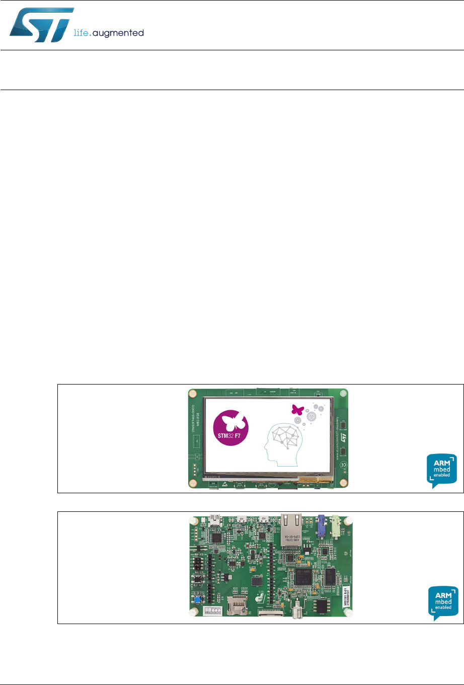
Figure 1. 32F746GDISCOVERY board (top view)
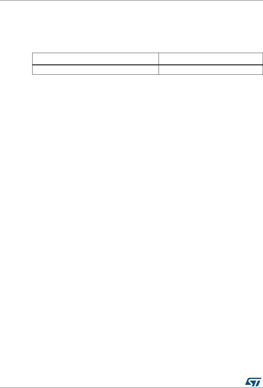
Figure 2. 32F746GDISCOVERY board (bottom view)
1. Pictures are not contractual.
www.st.com

Contents UM1907
2/51 DocID027942 Rev 4
Contents
1 Features . . . . . . . . . . . . . . . . . . . . . . . . . . . . . . . . . . . . . . . . . . . . . . . . . . . 6
2 Product marking . . . . . . . . . . . . . . . . . . . . . . . . . . . . . . . . . . . . . . . . . . . . 7
3 System requirements . . . . . . . . . . . . . . . . . . . . . . . . . . . . . . . . . . . . . . . . 7
4 Development toolchains . . . . . . . . . . . . . . . . . . . . . . . . . . . . . . . . . . . . . . 7
5 Demonstration software . . . . . . . . . . . . . . . . . . . . . . . . . . . . . . . . . . . . . . 7
6 Ordering information . . . . . . . . . . . . . . . . . . . . . . . . . . . . . . . . . . . . . . . . 8
7 Technology partners . . . . . . . . . . . . . . . . . . . . . . . . . . . . . . . . . . . . . . . . . 8
8 Hardware layout and configuration . . . . . . . . . . . . . . . . . . . . . . . . . . . . . 9
8.1 The 32F746GDISCOVERY Discovery board layout . . . . . . . . . . . . . . . . 10
8.2 32F746GDISCOVERY Discovery board mechanical drawing . . . . . . . . . 12
8.3 Embedded ST-LINK/V2-1 . . . . . . . . . . . . . . . . . . . . . . . . . . . . . . . . . . . . . 13
8.3.1 Drivers . . . . . . . . . . . . . . . . . . . . . . . . . . . . . . . . . . . . . . . . . . . . . . . . . . 13
8.3.2 ST-LINK/V2-1 firmware upgrade . . . . . . . . . . . . . . . . . . . . . . . . . . . . . . 14
8.4 Power supply . . . . . . . . . . . . . . . . . . . . . . . . . . . . . . . . . . . . . . . . . . . . . . 14
8.5 Programming/debugging when the power supply is not from
ST-LINK (5V link) . . . . . . . . . . . . . . . . . . . . . . . . . . . . . . . . . . . . . . . . . . . 16
8.6 Clock sources . . . . . . . . . . . . . . . . . . . . . . . . . . . . . . . . . . . . . . . . . . . . . . 17
8.7 Reset sources . . . . . . . . . . . . . . . . . . . . . . . . . . . . . . . . . . . . . . . . . . . . . 17
8.8 Audio . . . . . . . . . . . . . . . . . . . . . . . . . . . . . . . . . . . . . . . . . . . . . . . . . . . . 17
8.9 USB OTG FS . . . . . . . . . . . . . . . . . . . . . . . . . . . . . . . . . . . . . . . . . . . . . . 18
8.10 USB OTG HS . . . . . . . . . . . . . . . . . . . . . . . . . . . . . . . . . . . . . . . . . . . . . . 18
8.11 microSD card . . . . . . . . . . . . . . . . . . . . . . . . . . . . . . . . . . . . . . . . . . . . . . 18
8.12 Ethernet . . . . . . . . . . . . . . . . . . . . . . . . . . . . . . . . . . . . . . . . . . . . . . . . . . 19
8.13 SDRAM memory . . . . . . . . . . . . . . . . . . . . . . . . . . . . . . . . . . . . . . . . . . . 19
8.14 Quad-SPI NOR Flash memory . . . . . . . . . . . . . . . . . . . . . . . . . . . . . . . . . 19
8.15 Camera module . . . . . . . . . . . . . . . . . . . . . . . . . . . . . . . . . . . . . . . . . . . . 20

DocID027942 Rev 4 3/51
UM1907 Contents
3
8.16 Display LCD-TFT . . . . . . . . . . . . . . . . . . . . . . . . . . . . . . . . . . . . . . . . . . . 20
9 Connectors . . . . . . . . . . . . . . . . . . . . . . . . . . . . . . . . . . . . . . . . . . . . . . . 21
9.1 I2C extension connector CN2 . . . . . . . . . . . . . . . . . . . . . . . . . . . . . . . . . . 21
9.2 Camera module connector P1 . . . . . . . . . . . . . . . . . . . . . . . . . . . . . . . . . 21
9.3 Arduino Uno V3 connectors . . . . . . . . . . . . . . . . . . . . . . . . . . . . . . . . . . . 22
9.4 USB OTG HS Micro-AB connector CN12 . . . . . . . . . . . . . . . . . . . . . . . . 24
9.5 Ethernet RJ45 connector CN9 . . . . . . . . . . . . . . . . . . . . . . . . . . . . . . . . . 24
9.6 USB OTG FS Micro-AB connector CN13 . . . . . . . . . . . . . . . . . . . . . . . . . 25
9.7 microSD connector CN3 . . . . . . . . . . . . . . . . . . . . . . . . . . . . . . . . . . . . . . 26
9.8 ST-LINK/V2-1 USB Type-B connector CN14 . . . . . . . . . . . . . . . . . . . . . . 26
9.9 Audio stereo speakers JP3 and JP4 . . . . . . . . . . . . . . . . . . . . . . . . . . . . 27
9.10 Audio green jack (line Out) CN10 . . . . . . . . . . . . . . . . . . . . . . . . . . . . . . . 27
9.11 Audio blue jack (line In) CN11 . . . . . . . . . . . . . . . . . . . . . . . . . . . . . . . . . 27
9.12 SPDIF input RCA connector CN1 . . . . . . . . . . . . . . . . . . . . . . . . . . . . . . 27
10 Electrical schematics . . . . . . . . . . . . . . . . . . . . . . . . . . . . . . . . . . . . . . . 28
Appendix A 32F746GDISCOVERY I/O assignment . . . . . . . . . . . . . . . . . . . . . . . 42
Appendix B Compliance Statements . . . . . . . . . . . . . . . . . . . . . . . . . . . . . . . . . . 49
B.1 Federal Communications Commission (FCC) and Industry
Canada (IC) Compliance Statement . . . . . . . . . . . . . . . . . . . . . . . . . . . . . 49
B.1.1 FCC Compliance Statement . . . . . . . . . . . . . . . . . . . . . . . . . . . . . . . . . . 49
B.2 IC Compliance Statement . . . . . . . . . . . . . . . . . . . . . . . . . . . . . . . . . . . . . 49
B.2.1 Compliance Statement . . . . . . . . . . . . . . . . . . . . . . . . . . . . . . . . . . . . . . 49
B.2.2 Déclaration de conformité. . . . . . . . . . . . . . . . . . . . . . . . . . . . . . . . . . . . 49
Revision history . . . . . . . . . . . . . . . . . . . . . . . . . . . . . . . . . . . . . . . . . . . . . . . . . . . . 50

List of tables UM1907
4/51 DocID027942 Rev 4
List of tables
Table 1. Order code . . . . . . . . . . . . . . . . . . . . . . . . . . . . . . . . . . . . . . . . . . . . . . . . . . . . . . . . . . . . . . 8
Table 2. I2C extension connector CN2 . . . . . . . . . . . . . . . . . . . . . . . . . . . . . . . . . . . . . . . . . . . . . . . 21
Table 3. Camera module connector P1 . . . . . . . . . . . . . . . . . . . . . . . . . . . . . . . . . . . . . . . . . . . . . . 21
Table 4. Arduino connectors (CN4, CN5, CN6 and CN7). . . . . . . . . . . . . . . . . . . . . . . . . . . . . . . . . 23
Table 5. USB OTG HS Micro-AB CN12 . . . . . . . . . . . . . . . . . . . . . . . . . . . . . . . . . . . . . . . . . . . . . . 24
Table 6. RJ45 connector CN9 . . . . . . . . . . . . . . . . . . . . . . . . . . . . . . . . . . . . . . . . . . . . . . . . . . . . . 25
Table 7. USB OTG FS Micro-AB connector CN13 . . . . . . . . . . . . . . . . . . . . . . . . . . . . . . . . . . . . . . 25
Table 8. microSD connector CN3 . . . . . . . . . . . . . . . . . . . . . . . . . . . . . . . . . . . . . . . . . . . . . . . . . . . 26
Table 9. USB Type-B connector CN14. . . . . . . . . . . . . . . . . . . . . . . . . . . . . . . . . . . . . . . . . . . . . . . 27
Table 10. SPDIF input RCA connector CN1 . . . . . . . . . . . . . . . . . . . . . . . . . . . . . . . . . . . . . . . . . . . . 27
Table 11. 32F746GDISCOVERY I/O assignment . . . . . . . . . . . . . . . . . . . . . . . . . . . . . . . . . . . . . . . 42
Table 12. Document revision history . . . . . . . . . . . . . . . . . . . . . . . . . . . . . . . . . . . . . . . . . . . . . . . . . 50

DocID027942 Rev 4 5/51
UM1907 List of figures
5
List of figures
Figure 1. 32F746GDISCOVERY board (top view). . . . . . . . . . . . . . . . . . . . . . . . . . . . . . . . . . . . . . . . 1
Figure 2. 32F746GDISCOVERY board (bottom view). . . . . . . . . . . . . . . . . . . . . . . . . . . . . . . . . . . . . 1
Figure 3. Hardware block diagram. . . . . . . . . . . . . . . . . . . . . . . . . . . . . . . . . . . . . . . . . . . . . . . . . . . . 9
Figure 4. 32F746GDISCOVERY Discovery board top layout . . . . . . . . . . . . . . . . . . . . . . . . . . . . . . 10
Figure 5. 32F746GDISCOVERY Discovery board bottom layout . . . . . . . . . . . . . . . . . . . . . . . . . . . 11
Figure 6. Mechanical drawing . . . . . . . . . . . . . . . . . . . . . . . . . . . . . . . . . . . . . . . . . . . . . . . . . . . . . . 12
Figure 7. USB composite device . . . . . . . . . . . . . . . . . . . . . . . . . . . . . . . . . . . . . . . . . . . . . . . . . . . . 13
Figure 8. JP1 (5V ext) from JP2 (5V). . . . . . . . . . . . . . . . . . . . . . . . . . . . . . . . . . . . . . . . . . . . . . . . . 14
Figure 9. JP1 (5V ext) from CN6 (Vin) . . . . . . . . . . . . . . . . . . . . . . . . . . . . . . . . . . . . . . . . . . . . . . . . 14
Figure 10. JP1 (5V link) . . . . . . . . . . . . . . . . . . . . . . . . . . . . . . . . . . . . . . . . . . . . . . . . . . . . . . . . . . . . 15
Figure 11. JP1 (usb_fs) . . . . . . . . . . . . . . . . . . . . . . . . . . . . . . . . . . . . . . . . . . . . . . . . . . . . . . . . . . . . 16
Figure 12. JP1 (usb_hs). . . . . . . . . . . . . . . . . . . . . . . . . . . . . . . . . . . . . . . . . . . . . . . . . . . . . . . . . . . . 16
Figure 13. Inside RJ45 jack . . . . . . . . . . . . . . . . . . . . . . . . . . . . . . . . . . . . . . . . . . . . . . . . . . . . . . . . . 19
Figure 14. I2C extension connector CN2 (front view) . . . . . . . . . . . . . . . . . . . . . . . . . . . . . . . . . . . . . 21
Figure 15. Camera module connector P1 (front view) . . . . . . . . . . . . . . . . . . . . . . . . . . . . . . . . . . . . . 21
Figure 16. USB OTG Micro-AB connector CN12 (front view) . . . . . . . . . . . . . . . . . . . . . . . . . . . . . . . 24
Figure 17. Ethernet RJ45 connector CN9 (front view) . . . . . . . . . . . . . . . . . . . . . . . . . . . . . . . . . . . . . 24
Figure 18. USB OTG Micro-AB connector CN13 (front view) . . . . . . . . . . . . . . . . . . . . . . . . . . . . . . . 25
Figure 19. microSD connector CN3 (front view) . . . . . . . . . . . . . . . . . . . . . . . . . . . . . . . . . . . . . . . . . 26
Figure 20. USB Type-B connector CN14 (front view) . . . . . . . . . . . . . . . . . . . . . . . . . . . . . . . . . . . . . 26
Figure 21. STM32F746 Discovery interconnexion. . . . . . . . . . . . . . . . . . . . . . . . . . . . . . . . . . . . . . . . 29
Figure 22. ST-LINK/V2-1 with support of SWD only . . . . . . . . . . . . . . . . . . . . . . . . . . . . . . . . . . . . . . 30
Figure 23. Joystick, LEDs and push-buttons . . . . . . . . . . . . . . . . . . . . . . . . . . . . . . . . . . . . . . . . . . . . 31
Figure 24. Audio codec Cirrus and connectors . . . . . . . . . . . . . . . . . . . . . . . . . . . . . . . . . . . . . . . . . . 32
Figure 25. Quad-SPI Flash memory (MICRON) . . . . . . . . . . . . . . . . . . . . . . . . . . . . . . . . . . . . . . . . . 33
Figure 26. Arduino Uno connectors . . . . . . . . . . . . . . . . . . . . . . . . . . . . . . . . . . . . . . . . . . . . . . . . . . . 34
Figure 27. SDRAM (MICRON). . . . . . . . . . . . . . . . . . . . . . . . . . . . . . . . . . . . . . . . . . . . . . . . . . . . . . . 35
Figure 28. USB OTG FS with Micro-AB connector . . . . . . . . . . . . . . . . . . . . . . . . . . . . . . . . . . . . . . . 36
Figure 29. STM32F746NGH6 connection . . . . . . . . . . . . . . . . . . . . . . . . . . . . . . . . . . . . . . . . . . . . . . 37
Figure 30. USB OTG HS PHY with Micro-AB connector . . . . . . . . . . . . . . . . . . . . . . . . . . . . . . . . . . . 38
Figure 31. Ethernet PHY with RJ45 connector . . . . . . . . . . . . . . . . . . . . . . . . . . . . . . . . . . . . . . . . . . 39
Figure 32. External camera connector. . . . . . . . . . . . . . . . . . . . . . . . . . . . . . . . . . . . . . . . . . . . . . . . . 40
Figure 33. 4.3-inch LCD with capacitive touch. . . . . . . . . . . . . . . . . . . . . . . . . . . . . . . . . . . . . . . . . . . 41

Features UM1907
6/51 DocID027942 Rev 4
1 Features
•STM32F746NGH6 microcontroller featuring 1 Mbyte of Flash memory and
340 Kbytes of RAM, in a BGA216 package
•4.3-inch 480x272 color LCD-TFT with capacitive touch screen
•USB OTG HS FS
•SAI audio codec
•ST-MEMS digital microphones
•128-Mbit Quad-SPI Flash memory
•128-Mbit SDRAM (64-Mbit accessible)
•1 user and reset push-button
•Board connectors:
– Camera
– USB with Micro-AB
– Ethernet RJ45
– SPDIF RCA input
– Audio jack for external speakers
–microSD
™ card
– RF-EEPROM daughterboard
•Board expansion connectors:
–Arduino
™ Uno V3
•Flexible power-supply options: ST-LINK USB VBUS or external sources
•On-board ST-LINK/V2-1 supporting USB re-enumeration capability: mass storage,
virtual COM port, debug port
•Comprehensive free software libraries and examples available with the STM32Cube
package
•Support of a wide choice of Integrated Development Environments (IDES) including
IAR™, Keil®, GCC-based IDEs, ARM® mbed™
•ARM® mbed Enabled™ (see http://mbed.org)

DocID027942 Rev 4 7/51
UM1907 Product marking
50
2 Product marking
Evaluation tools marked as "ES" or "E" are not yet qualified and therefore they are not ready
to be used as reference design or in production. Any consequences deriving from such
usage will not be at ST charge. In no event, ST will be liable for any customer usage of
these engineering sample tools as reference design or in production.
"E" or "ES" marking examples of location:
•On the targeted STM32 that is soldered on the board (for illustration of STM32 marking,
refer to the section “Package characteristics” of the STM32 datasheet at www.st.com).
•Next to the evaluation tool ordering part number, that is stuck or silk-screen printed on
the board.
3 System requirements
•Windows® OS (XP, 7, 8 and 10), Linux® 64-bit or macOS™
•USB Type-B to Micro-AB cable
4 Development toolchains
•Keil® MDK-ARM(a)
•IAR™ EWARM(a)
•GCC-based IDEs including free SW4STM32 from AC6
•ARM® mbed Enabled™ online
5 Demonstration software
The demonstration software, included in the STM32Cube package, is preloaded in the
STM32 Flash memory for easy demonstration of the device peripherals in standalone mode.
The latest versions of the demonstration source code and associated documentation can be
downloaded from the www.st.com/stm32f7-discovery webpage.
a. On Windows® only.
Ordering information UM1907
8/51 DocID027942 Rev 4
6 Ordering information
To order the 32F746GDISCOVERY Discovery kit, refer to Ta ble 1.
7 Technology partners
MICRON:
•128-Mbit SDRAM (64 Mbit accessible on the kit), part number MT48LC4M32B2
•128-Mbit Quad-SPI NOR Flash memory device, part number N25Q128A
ROCKTECH:
•Color display, 4.3-inch LCD-TFT (resolution: 480x272), capacitive touch,
part number RK043FN48H-CT672B
Table 1. Order code
Order code Target STM32
STM32F746G-DISCO STM32F746NG
DocID027942 Rev 4 9/51
UM1907 Hardware layout and configuration
50
8 Hardware layout and configuration
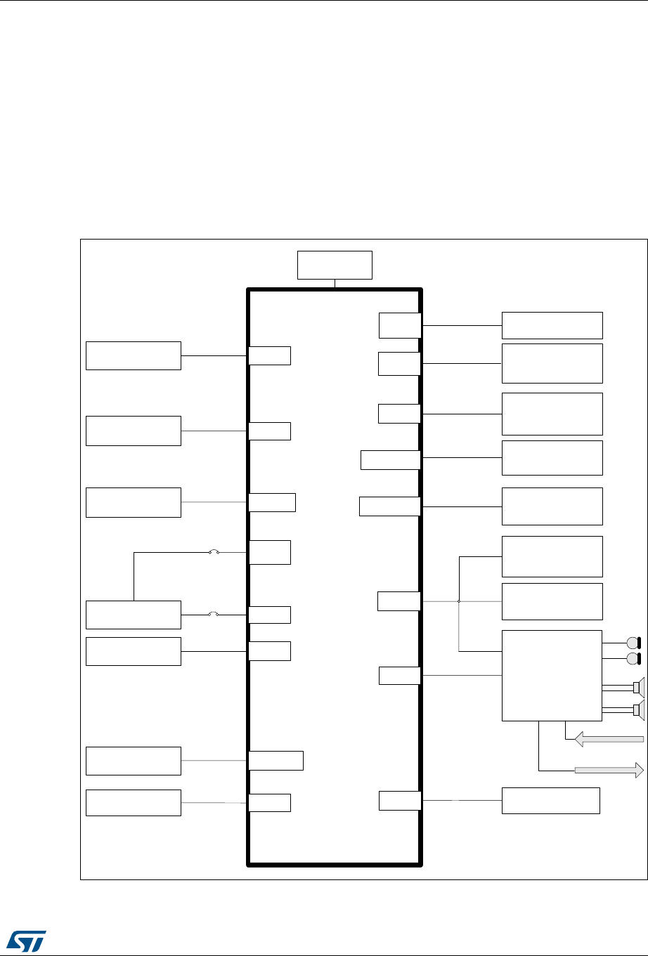
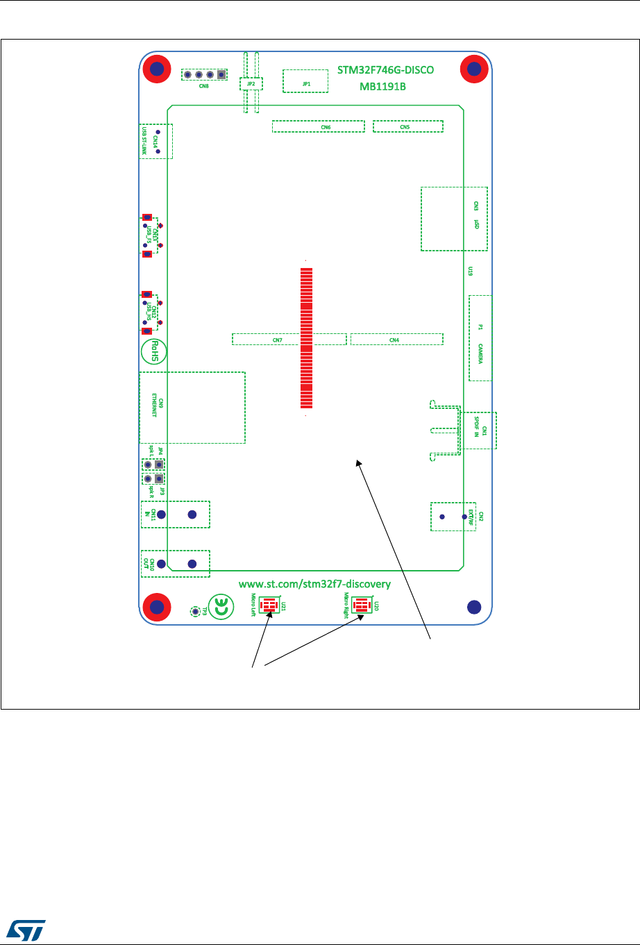
The 32F746GDISCOVERY Discovery board is designed around the STM32F746NGH6
microcontroller (216-pin in TFBGA package). The hardware block diagram (see Figure 3)
illustrates the connections between STM32F746NGH6 and peripherals (SDRAM, Quad-SPI
Flash memory, camera module, color LCD, USB OTG connectors, USART, Ethernet, Audio,
SPDIFRX, microSD card, Arduino Uno shields and embedded ST-LINK). Figure 4 and
Figure 5 help users to locate these features on the Discovery board.
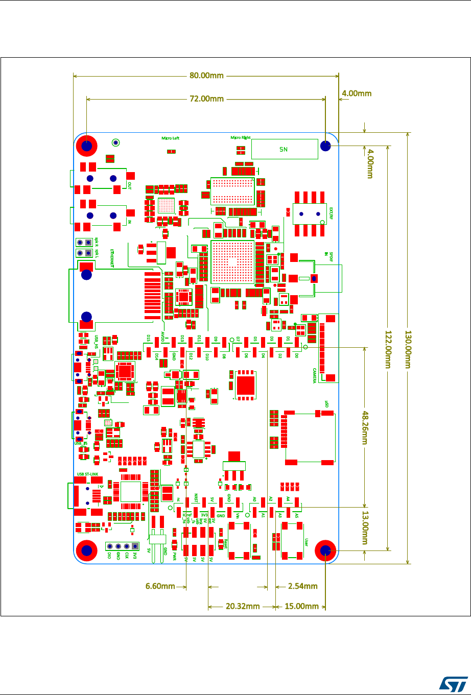
The mechanical dimensions of the Discovery board are showed in Figure 6.
Figure 3. Hardware block diagram
06Y9
670)1*+
$XGLR'$&DQG
$PSOLILHU
57&
(WKHUQHW3+<DQG
5-FRQQHFWRU
6:'
93RZHU
6XSSO\
.+]&U\VWDO
67/,1.9
,&
LQFK:49*$
/&'
50,,
6$,
,&H[WHQVLRQ
FRQQHFWRU
/&'
&DSDFLWLYH
7RXFK6FUHHQ
0XOWLSRLQWV
PLFUR6'FDUG
FRQQHFWRU
3XVKEXWWRQDQG
:DNHXS
*3,2
6'00&
+63+<DQG
0LFUR86%
FRQQHFWRU
27*
+6
6'5$0 )0&
&DPHUDFRQQHFWRU
'&0,
4XDG63, 4XDG63,)ODVK
PHPRU\
63',)5;
63',)GHFRGHUDQG
5&$,1SXW
FRQQHFWRU
27*
)6
0LFUR86%
FRQQHFWRU
9&3
8$57
$UGXLQR8QRVKLHOG
FRQQHFWRUV *3,2V
6WHUHRMDFN
/LQHLQSXW
6WHUHRMDFN
/LQH2XWSXW
Hardware layout and configuration UM1907
10/51 DocID027942 Rev 4
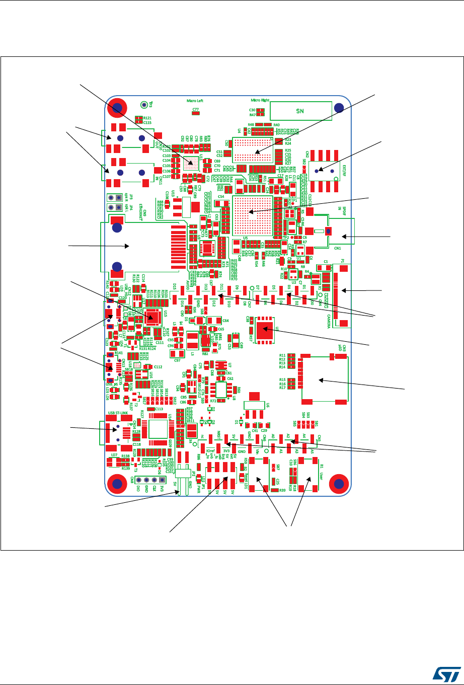
8.1 The 32F746GDISCOVERY Discovery board layout
Figure 4. 32F746GDISCOVERY Discovery board top layout
3RZHUVXSSO\VHOHFWRU 3XVKEXWWRQVXVHUDQG567
$XGLRFRGHF
+LJK6SHHG86%
3+<8/3,
PPVWHUHRMDFNV
,1DQG287
63',)LQSXW
5&$FRQQHFWRU
'&0,FDPHUD
FRQQHFWRU
0LQL86%W\SH%
67/,1.9
PLFUR6'FDUGFRQQHFWRU
,&H[WHQVLRQFRQQHFWRU
3RZHU
VXSSO\LQOHW9
0ELW6'5$00[
5-VLQJOHSRUW
0LFUR86% 0ELW4XDG63,
4XDG'XDO
670)1*+
7)%*$
+HDGHUV$UGXLQR
+HDGHUV$UGXLQR
DocID027942 Rev 4 13/51
UM1907 Hardware layout and configuration
50
8.3 Embedded ST-LINK/V2-1
The ST-LINK/V2-1 programming and debugging tool is integrated on the
32F746GDISCOVERY Discovery board. Compared to ST-LINK/V2 the changes are listed
below.
The new features supported on ST-LINK/V2-1 are:
•USB software reenumeration
•Virtual COM port interface on USB
•Mass storage interface on USB
•USB power management request for more than 100 mA power on USB
These features are no more supported on ST-LINK/V2-1:
•SWIM interface
•Application voltage lower than 3 V
For all general information concerning debugging and programming features common
between V2 and V2-1 refer to ST-LINK/V2 in-circuit debugger/programmer for STM8 and
STM32 User manual (UM1075).
8.3.1 Drivers
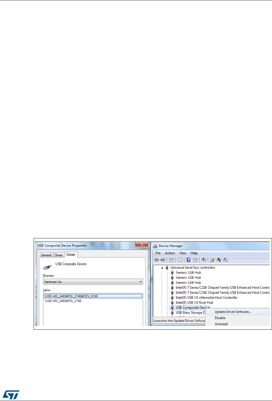
Before connecting the 32F746GDISCOVERY board to a Windows® PC (XP, 7, 8 and 10)
through the USB, a driver for the ST-LINK/V2-1 must be installed. It is available at the
www.st.com website. In case the STM32 Discovery is connected to the PC before the driver
is installed, some Discovery interfaces may be declared as “Unknown” in the PC device
manager. To recover from this situation, after installing the dedicated driver, the association of
“Unknown” USB devices found on the 32F746GDISCOVERY board to this dedicated driver,
must be updated in the device manager manually.
Note: It is recommended to proceed by using USB Composite Device, as shown in Figure 7.
Figure 7. USB composite device
Hardware layout and configuration UM1907
14/51 DocID027942 Rev 4
8.3.2 ST-LINK/V2-1 firmware upgrade
The ST-LINK/V2-1 embeds a firmware upgrade mechanism for in-situ upgrade through the
USB port. As the firmware may evolve during the life time of the ST-LINK/V2-1 product (for
example new functionality, bug fixes, support for new microcontroller families), it is
recommended to visit the www.st.com website before starting to use the
32F746GDISCOVERY board and periodically, to stay up-to-date with the latest firmware
version.
8.4 Power supply
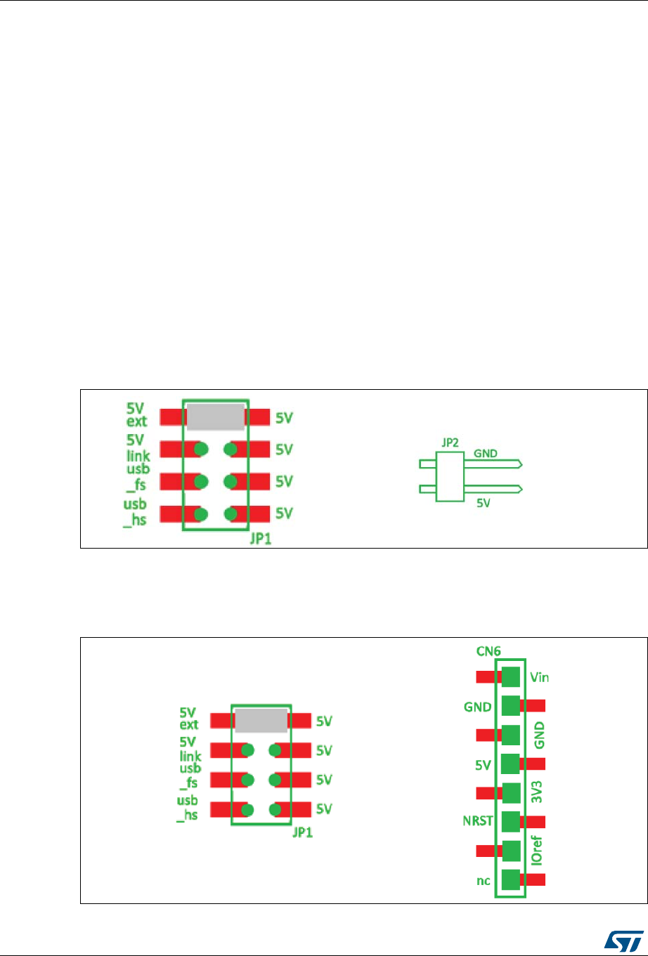
The 32F746GDISCOVERY Discovery board is designed to be powered by 5V DC power
supply. It is possible to configure the Discovery board to use any of the following five
sources for the power supply:
•5V DC power adapter connected to JP2 (external power supply on silkscreen of JP1
(5V ext)). In this case, the 32F746GDISCOVERY Discovery board must be powered by
a power supply unit or by an auxiliary equipment complying with the standard
EN-60950-1: 2006+A11/2009, and must be Safety Extra Low Voltage (SELV) with
limited power capability (see Figure 8).
Figure 8. JP1 (5V ext) from JP2 (5V)
•7-12V DC power from CN6 pin named Vin on silkscreen, the extension connectors for
Arduino Uno shields or daughterboard (external power source on silkscreen of JP1
(5V ext)), see Figure 9.
Figure 9. JP1 (5V ext) from CN6 (Vin)
DocID027942 Rev 4 15/51
UM1907 Hardware layout and configuration
50
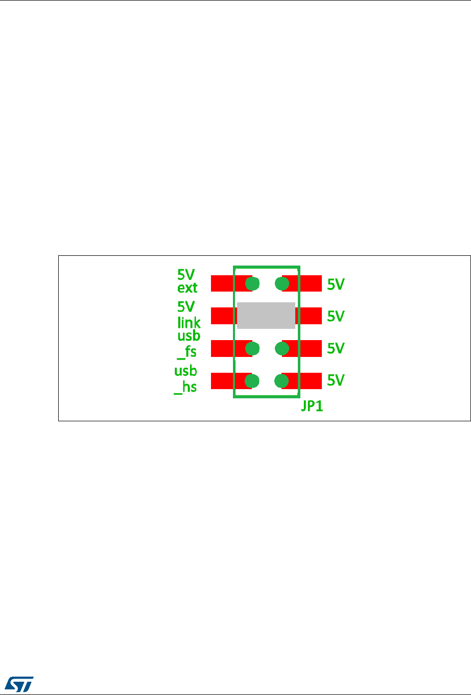
•5V DC power with limitation from CN14, the USB Type-B connector of
ST-LINK/V2-1 (USB 5V power source on silkscreen of JP1 (5V link)). It is the default
setting. If the USB enumeration succeeds (as explained below), the ST-LINK 5V link
power is enabled, by asserting the PWR_ENn signal. This pin is connected to a power
switch (ST890), which powers the board. This power switch features also a current
limitation to protect the PC in case of a short-circuit on the board (more than 600 mA).
The 32F746GDISCOVERY Discovery board can be powered from the ST-LINK USB
connector CN14 (5V link), but only the ST-LINK circuit has the power before USB
enumeration, because the host PC only provides 100 mA to the board at that time. During
the USB enumeration, the 32F746GDISCOVERY board asks for the 500 mA power to the
host PC. If the host is able to provide the required power, the enumeration ends by a
“SetConfiguration” command and then, the power transistor U8 (ST890) is switched ON, the
red LED LD2 is turned ON, thus the 32F746GDISCOVERY board can consume no more
than 500 mA of current. If the host is not able to provide the requested current, the
enumeration fails. Therefore the ST890 (U8) remains OFF and the STM32 part including the
extension board will not be powered. As a consequence the red LED LD2 remains turned
OFF. In this case it is mandatory to use an external power supply (see Figure 10).
Figure 10. JP1 (5V link)
Note: In case the board is powered by a USB charger, there is no USB enumeration, so the led
LD2 remains set to OFF permanently and the board is not powered. Only in this specific
case, the resistor R109 needs to be soldered, to allow the board to be powered anyway.
The LED LD2 is lit when the 32F746GDISCOVERY Discovery board is powered by the 5V
correctly.
Caution: Do not connect the PC to the ST-LINK (CN14) when R109 is soldered. The PC may be
damaged or the board not powered correctly.
Hardware layout and configuration UM1907
16/51 DocID027942 Rev 4
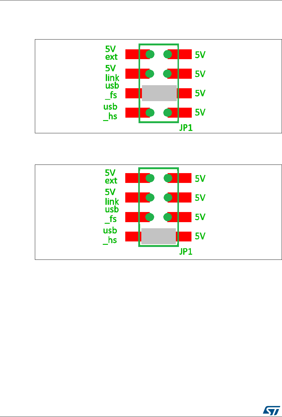
•5V DC power with 500 mA limitation from CN13, the USB OTG FS Micro-AB connector
(USB 5V power source on silkscreen of JP1 (usb_fs)), see Figure 11.
Figure 11. JP1 (usb_fs)
•5V DC power with 500 mA limitation from CN12, the USB OTG HS Micro-AB connector
(USB 5V power source on silkscreen of JP1 (usb_hs)), see Figure 12.
Figure 12. JP1 (usb_hs)
8.5 Programming/debugging when the power supply is not from
ST-LINK (5V link)
It is mandatory to power the board first using JP1 (5V ext) or (usb_hs) or (usb_fs), then
connecting the USB cable to the PC. Proceeding this way the enumeration succeeds thanks
to the external power source.
The following power sequence procedure must be respected:
1. Connect the jumper JP1 on (5V ext) or (usb_hs) or (usb_fs)
2. Connect the external power source to JP2 or CN6 or CN12 or CN13
3. Check the red LED LD2 is turned ON
4. Connect the PC to USB connector CN14
If this order is not respected, the Discovery board may be powered by VBUS first from
ST-LINK, and the following risks may be encountered:

DocID027942 Rev 4 17/51
UM1907 Hardware layout and configuration
50
1. If more than 500 mA current is needed by the board, the PC may be damaged or
current can be limited by the PC. As a consequence the board is not powered correctly.
2. 500 mA will be requested at the enumeration, so there is a risk that the request is
rejected and enumeration does not succeed if the PC cannot provide such current.
8.6 Clock sources
Up to 3 clock sources as described below:
•X1, 24 MHz oscillator for the USB OTG HS PHY and camera module (daughterboard)
•X2, 25 MHz oscillator for the STM32F746NGH6 microcontroller and Ethernet PHY
•X3, 32 KHz crystal for the STM32F746NGH6 embedded RTC
8.7 Reset sources
The reset signal of 32F746GDISCOVERY Discovery board is active low and the reset
sources include:
•Reset button B2
•Arduino Uno shield board from CN6
•Embedded ST-LINK/V2-1
8.8 Audio
An audio codec WM8994ECS/R from CIRRUS with 4 DACs and 2 ADCs is connected to the
SAI interface of the STM32F746NGH6 microcontroller. It communicates with
STM32F746NGH6 via I2C bus shared with the camera module and I2C extension
connector.
•The analog line input is connected to the ADC of WM8994ECS/R through the blue
audio jack CN11.
•The analog line output is connected to the DAC of WM8994ECS/R via the green audio
jack CN10.
•Two external speakers can be connected to WM8994ECS/R via JP3 for right speaker
and JP4 for left speaker.
•Two digital microphones (ST-MEMS microphone) MP34DT01TR are on the
32F746GDISCOVERY Discovery board. They are connected to the input digital
microphones of WM8994ECS/R.
•One coaxial connector CN1 is implemented on 32F746GDISCOVERY to receive
external audio data compatible with the SPDIF specification.

Hardware layout and configuration UM1907
18/51 DocID027942 Rev 4
8.9 USB OTG FS
The 32F746GDISCOVERY Discovery board supports USB OTG full speed communication
via a USB Micro-AB connector (CN13) and a USB power switch (U6) connected to VBUS.
The Discovery board can be powered by this USB connection at 5V DC with 500mA current
limitation.
A green LED LD5 will be lit in one of these cases:
•Power switch (U6) is ON and 32F746GDISCOVERY works as an USB host
•VBUS is powered by another USB host when 32F746GDISCOVERY works as an USB
device.
The red LED LD6 will be lit when an overcurrent occurs.
Note: 32F746GDISCOVERY board should be powered by an external power supply when using
OTG function.
8.10 USB OTG HS
The 32F746GDISCOVERY Discovery board supports the USB OTG high speed
communication via a USB Micro-AB connector (CN12), USB high speed PHY (U15)
USB3320C-EZK from MICROCHIP for high speed function.
The Discovery board can be powered by the USB connectors (CN12) at 5V DC with 500mA
current limitation.
A USB power switch (U7) is also connected on VBUS and provides power to CN12.
The green LED LD4 will be lit in one of these cases:
•Power switch (U17) is ON and 32F746GDISCOVERY works as a USB host
•VBUS is powered by another USB host when 32F746GDISCOVERY works as a USB
device.
The red LED LD3 will be lit when an overcurrent occurs.
Note: The 32F746GDISCOVERY board should be powered by an external power supply when
using OTG function.
8.11 microSD card
The 32F746GDISCOVERY board supports the 2-Gbyte (or more) microSD card connected
to the SDMMC1 port of STM32F746NGH6.
DocID027942 Rev 4 19/51
UM1907 Hardware layout and configuration
50
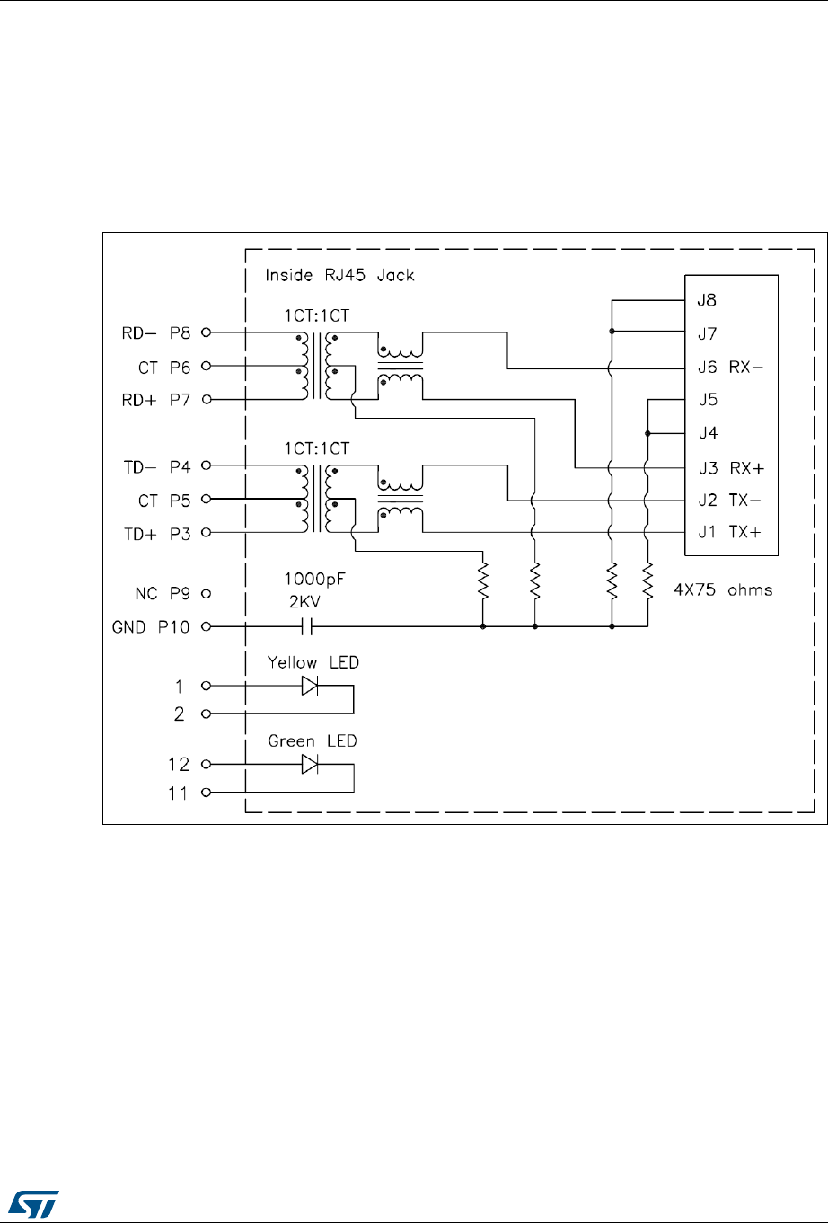
8.12 Ethernet
The 32F746GDISCOVERY Discovery board supports 10/100-Mbit Ethernet communication
by a PHY LAN8742A-CZ-TR (U9) from MICROCHIP and RJ45 jack (CN9). Ethernet PHY is
connected to STM32F746NGH6 via RMII interface.
The 25-MHz clock for the PHY is generated by the oscillator X2, while the 50-MHz clock for
STM32F746NGH6 is generated by the PHY RMII_REF_CLK.
Figure 13. Inside RJ45 jack
8.13 SDRAM memory
The 128-Mbit SDRAM (MT48LC4M32B2B5-6A from MICRON) is connected to the FMC
interface of the STM32F746NGH6 microcontroller. Only the lowest 16-bit data are used (64-
Mbit accessible). DQ16 to DQ31 are unused and connected to a 10K ohm pull-down
resistor.
8.14 Quad-SPI NOR Flash memory
The 128-Mbit Quad-SPI NOR Flash memory (N25Q128A13EF840E from MICRON) is
connected to the Quad-SPI interface of the STM32F746NGH6 microcontroller.

Hardware layout and configuration UM1907
20/51 DocID027942 Rev 4
8.15 Camera module
A connector P1 with the DCMI signals is available to connect a camera module such as
STM32F4DIS-CAM (ST order code).
8.16 Display LCD-TFT
The color display from ROCKTECH, 4.3-inch 480x272 LCD-TFT with capacitive touch panel
is connected to the RGB LCD interface of the STM32F746NGH6 microcontroller.
DocID027942 Rev 4 21/51
UM1907 Connectors
50
9 Connectors
9.1 I2C extension connector CN2
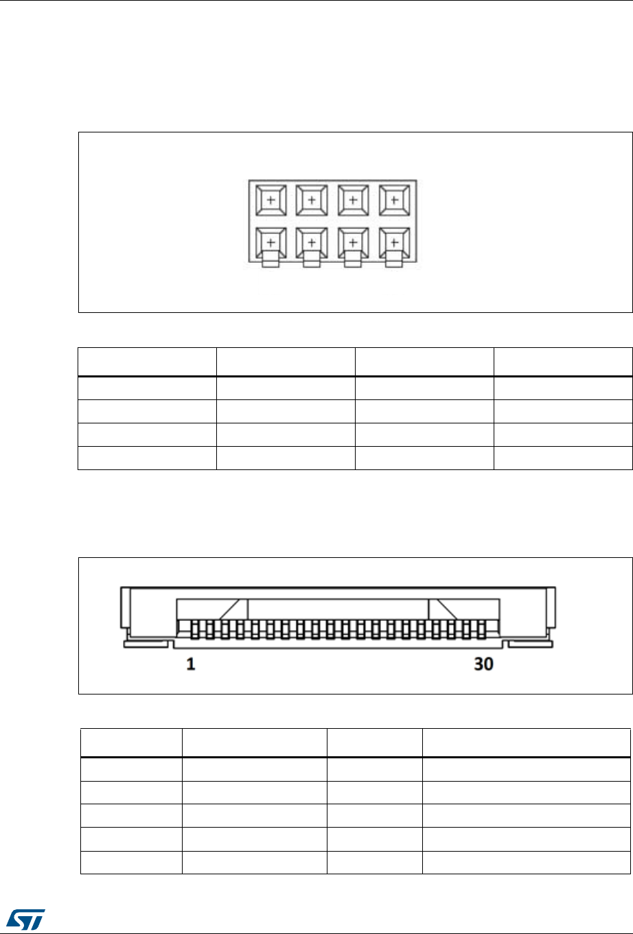
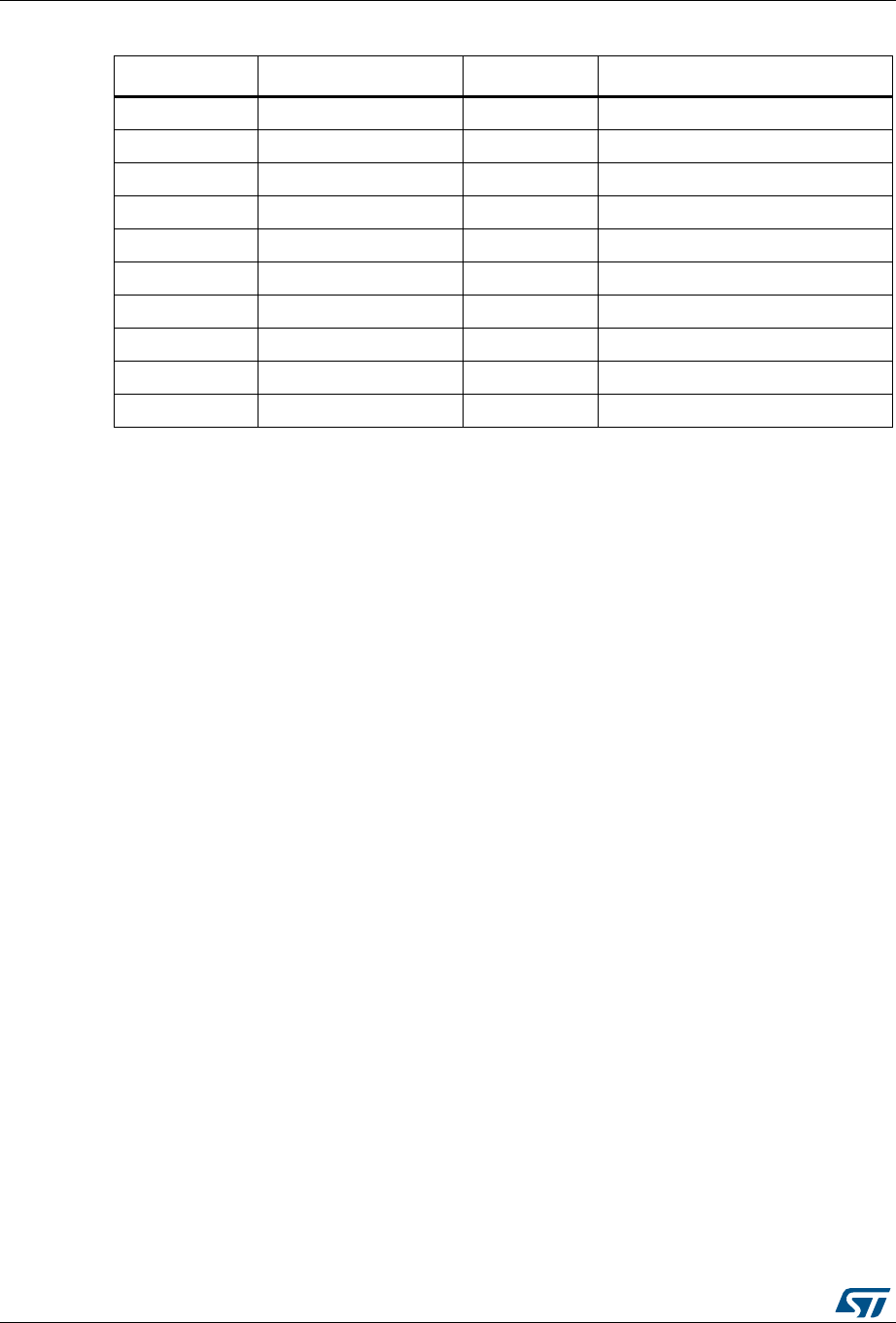
Figure 14. I2C extension connector CN2 (front view)
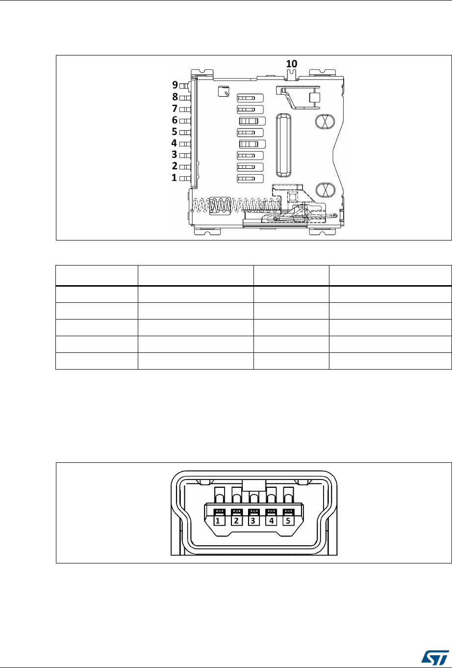
9.2 Camera module connector P1
Figure 15. Camera module connector P1 (front view)
Table 2. I2C extension connector CN2
Pin number Description Pin number Description
1 I2C_SDA (PB9) 5 +3V3
2NC6NC
3 I2C_SCL (PB8) 7 GND
4 RESET(PC10) 8 NC or 5V
069
Table 3. Camera module connector P1
Pin number Description Pin number Description
1GND16 GND
2 NC 17 DCMI_HSYNC
3NC18 NC
4 DCMI_D0 19 DCMI_VSYNC
5DCMI_D120 3V3
Connectors UM1907
22/51 DocID027942 Rev 4
9.3 Arduino Uno V3 connectors
CN4, CN5, CN6 and CN7 are female connectors compatible with Arduino standard. Most
shields designed for Arduino can fit to the 32F746GDISCOVERY Discovery board.
The Arduino connectors on 32F746GDISCOVERY Discovery board support the Arduino
Uno V3 (see Table 4).
Caution: The I/Os of STM32 microcontroller are 3.3 V compatible instead of 5 V for Arduino Uno.
6 DCMI_D2 21 Camera_CLK (OSC_24M)
7 DCMI_D3 22 NC
8DCMI_D423 GND
9 DCMI_D5 24 NC
10 DCMI_D6 25 DCMI_PWR_EN
11 DCMI_D7 26 DCMI_NRST
12 NC 27 DCMI_SDA
13 NC 28 DCMI_SCL
14 GND 29 GND
15 DCMI_PIXCK 30 3V3
Table 3. Camera module connector P1 (continued)
Pin number Description Pin number Description
DocID027942 Rev 4 23/51
UM1907 Connectors
50
Table 4. Arduino connectors (CN4, CN5, CN6 and CN7)
Left connectors Right connectors
CN No. Pin
No.
Pin
name
STM32
pin Function Function STM32
pin
Pin
name
Pin
No. CN No.
I2C1_SCL PB8 D15 10
CN7
digital
I2C1_SDA PB9 D14 9
AVDD - AREF 8
Ground - GND 7
CN6
power
1 NC - - SPI2_SCK PI1 D13 6
2 IOREF - 3.3V Ref SPI2_MISO PB14 D12 5
3 RESET NRST RESET TIM12_CH2,
SPI2_MOSI PB15 D11 4
4+3V3 - 3.3V
input/output TIM1_CH1 PA8 D10 3
5 +5V - 5V output TIM2_CH1 PA15 D9 2
6GND - Ground - PI2 D8 1
7GND - Ground -
8 VIN - Power input - PI3 D7 8
CN4
digital
- TIM12_CH1 PH6 D6 7
CN5
analog
1 A0 PA0 ADC3_IN0 TIM5_CH4,SPI
2_NSS PI0 D5 6
2 A1 PF10 ADC3_IN8 - PG7 D4 5
3 A2 PF9 ADC3_IN7 TIM3_CH1 PB4 D3 4
4 A3 PF8 ADC3_IN6 - PG6 D2 3
5A4
PF7 or
PB(1)
ADC3_IN5
(PF7) or
I2C1_SDA
(PB9)
USART6_TX PC6 D1 2
6A5
PF6 or
PB8(1)
ADC3_IN4
(PC0) or
I2C1_SCL
(PB8)
USART6_RX PC7 D0 1
1. Refer to Table 11 for details.
Connectors UM1907
24/51 DocID027942 Rev 4
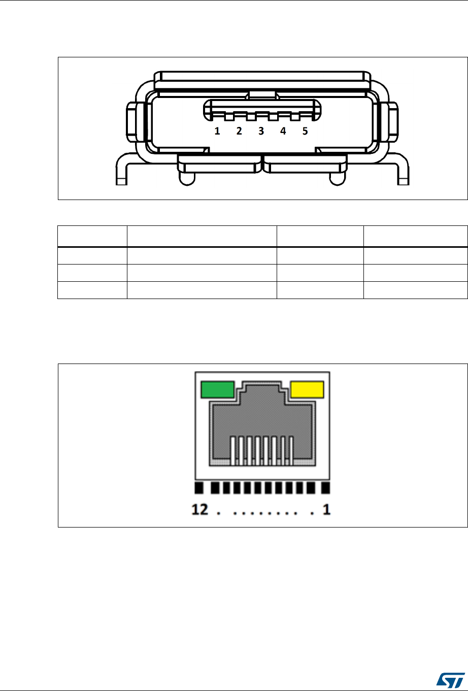
9.4 USB OTG HS Micro-AB connector CN12
Figure 16. USB OTG Micro-AB connector CN12 (front view)
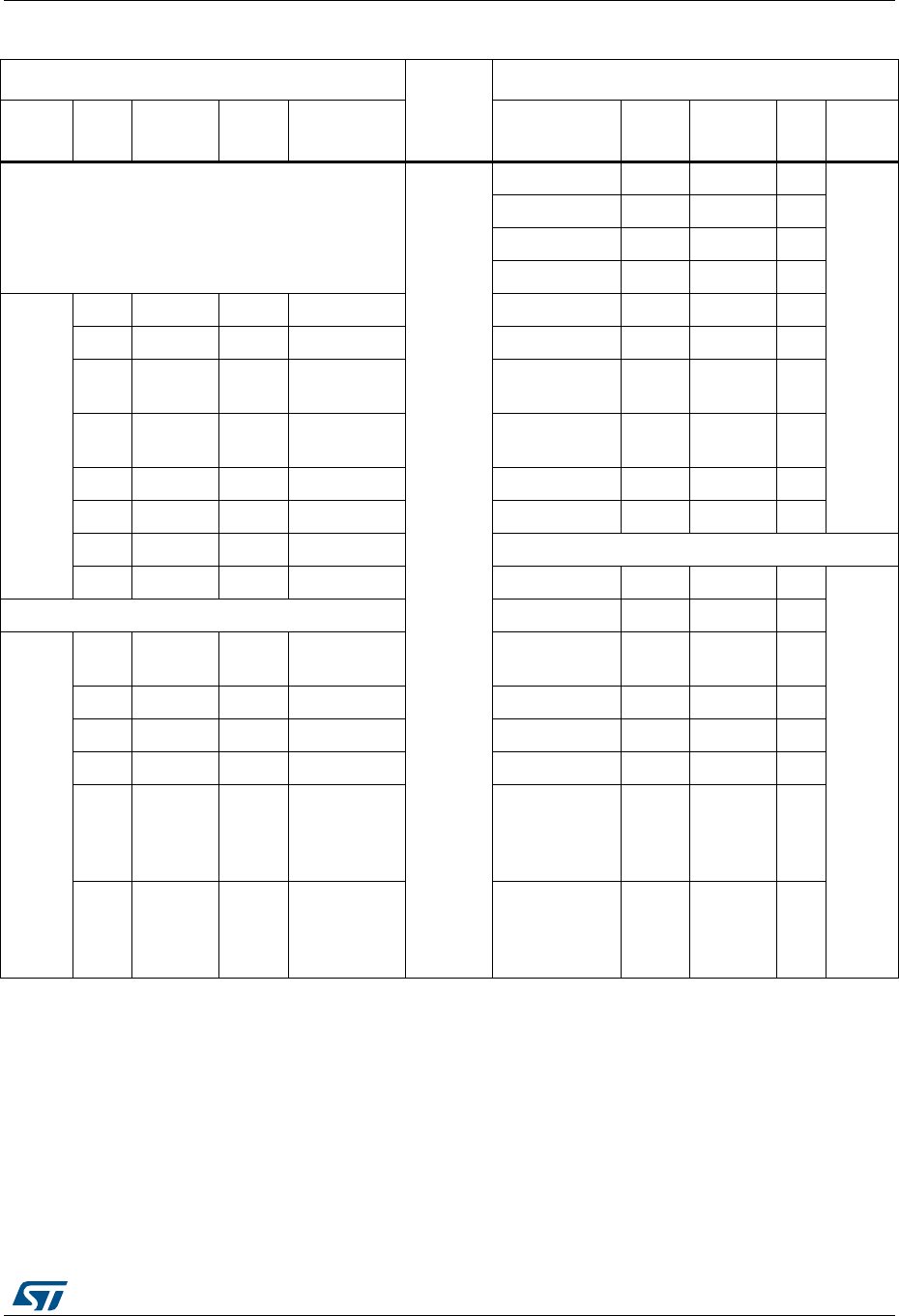
9.5 Ethernet RJ45 connector CN9
Figure 17. Ethernet RJ45 connector CN9 (front view)
Table 5. USB OTG HS Micro-AB CN12
Pin number Description Pin number Description
1 VBUS 4 ID
2D- 5GND
3D+ --
DocID027942 Rev 4 25/51
UM1907 Connectors
50
9.6 USB OTG FS Micro-AB connector CN13
Figure 18. USB OTG Micro-AB connector CN13 (front view)
Table 6. RJ45 connector CN9
Pin number Description Pin number Description
1 A, yellow LED 7 RD+
2 K, yellow LED 8 RD-
3TD+ 9 NC
4TD-10GND
5 CT, 3V3 11 K, green LED
6 CT, 3V3 12 A, green LED
Table 7. USB OTG FS Micro-AB connector CN13
Pin number Description Pin number Description
1 VBUS (PA9) 4 ID (PA10)
2 D- (PA11) 5 GND
3D+ (PA12)- -
Connectors UM1907
26/51 DocID027942 Rev 4
9.7 microSD connector CN3
Figure 19. microSD connector CN3 (front view)
9.8 ST-LINK/V2-1 USB Type-B connector CN14
The USB connector CN14 is used to connect the embedded ST-LINK/V2-1 to the PC for
programming and debugging the STM32F746NGH6 microcontroller.
Figure 20. USB Type-B connector CN14 (front view)
Table 8. microSD connector CN3
Pin number Description Pin number Description
1 SDMMC_D2 (PC10) 6 Vss/GND
2 SDMMC_D3 (PC11) 7 SDMMC_D0 (PC8)
3 SDMMC_CMD (PD2) 8 SDMMC_D1 (PC9)
4 +3.3V 9 GND
5 SDMMC_CK (PC12) 10 MicroSDcard_detect (PC13)
DocID027942 Rev 4 27/51
UM1907 Connectors
50
9.9 Audio stereo speakers JP3 and JP4
The stereo audio output JP3 and JP4 are available to support the stereo speakers (left and
right).
9.10 Audio green jack (line Out) CN10
A 3.5 mm stereo audio green jack output CN10 is available to support the headphone.
9.11 Audio blue jack (line In) CN11
A 3.5 mm stereo audio blue jack input CN11 is available to support the audio-line input.
9.12 SPDIF input RCA connector CN1
Table 9. USB Type-B connector CN14
Pin number Description Pin number Description
1 VBUS (power) 4 GND
2 DM 5, 6 Shield
3DP- -
Table 10. SPDIF input RCA connector CN1
Pin number Description Pin number Description
1 SPDIF_RX0 (PD7) 2 GND
2GND- -

Electrical schematics UM1907
28/51 DocID027942 Rev 4
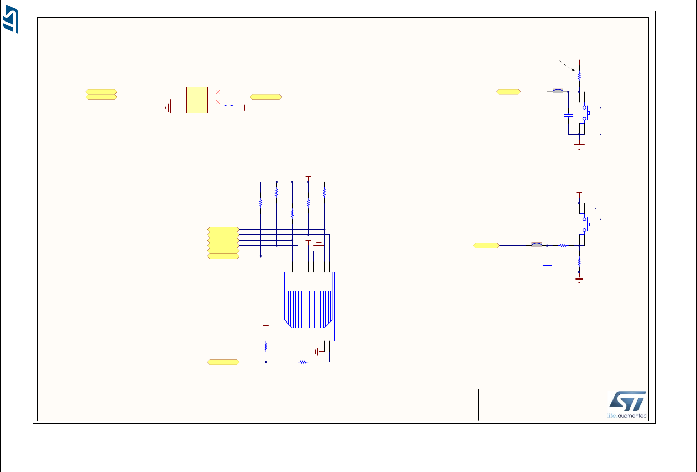
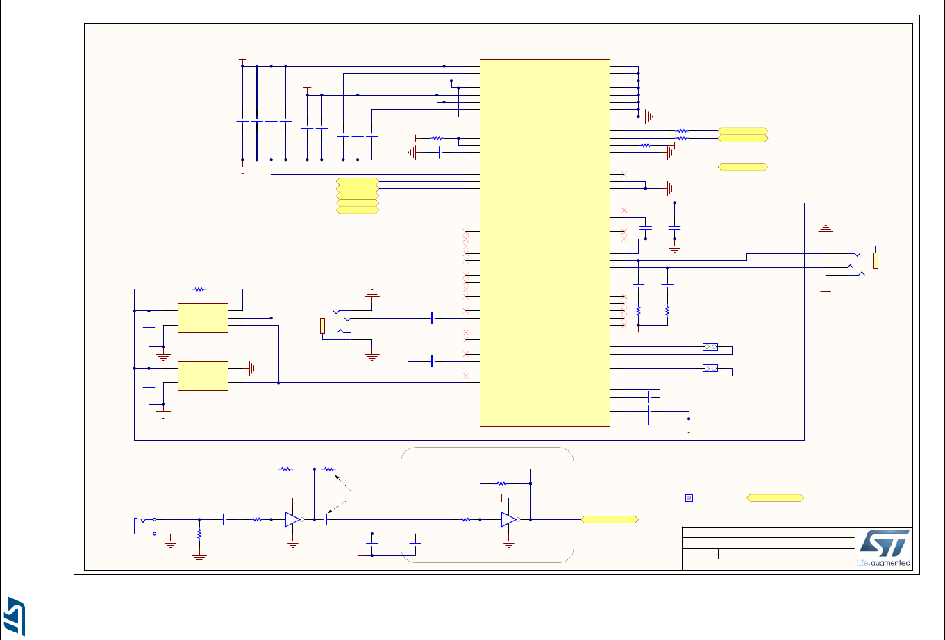
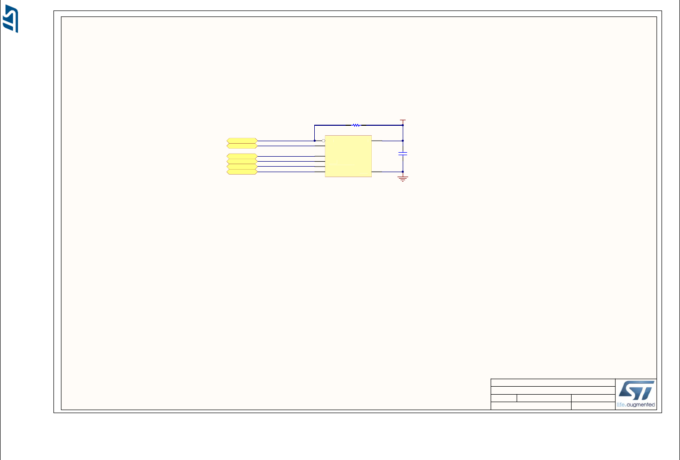
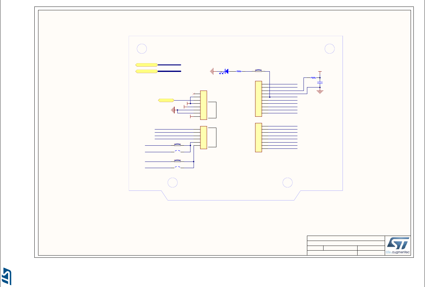
10 Electrical schematics
This section provides the design schematics for the 32F746GDISCOVERY Discovery board
features.
•MB1191:
– Discovery interconnexion (see Figure 21)
– ST-LINK/V2-1 (see Figure 22)
– Joystick, LEDs and push-buttons (see Figure 23)
– Audio codec Cirrus and connectors (see Figure 24)
– Quad-SPI Flash memory (MICRON) (see Figure 25)
– Arduino Uno V3 connectors (see Figure 26)
– SDRAM (MICRON) (see Figure 27)
– USB OTG FS with Micro-AB connector (see Figure 28)
– STM32F746NGH6 connection (see Figure 29)
– USB OTG HS PHY with Micro-AB connector (see Figure 30)
– Ethernet PHY with RJ45 connector (see Figure 31)
– External camera connector (see Figure 32)
– 4.3-inch LCD with capacitive touch (see Figure 33)
UM1907 Electrical schematics
DocID027942 Rev 4 29/51
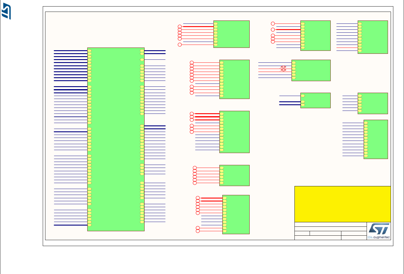
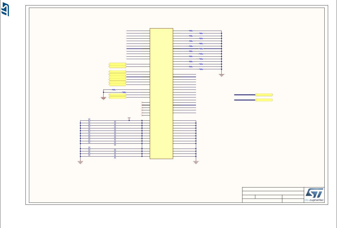
Figure 21. STM32F746 Discovery interconnexion
113
STM32F746 Discovery Interconnexion
MB1191 B-04
10/16/2015
Title:
Size: Reference:
Date: Sheet: of
A4 Revision:
STM32F746G-DISCO
Project:
SWDIO
SWCLK
NRST
Rev A-01 --> PCB label MB1191 A-01
Rev B-01 --> PCB label MB1191 B-01, Ethernet modification, add SPDIF module,
Remove STPS1L30A for having 5V. Requiered on USB_VCC
Rev B-02 --> PCB label MB1191 B-02, Change Capacitors value for X3, X4.
Add R131, R135 of 100K
Rev B-03 --> PCB label MB1191 B-03, change only footprint for RCA
Rev B-04 --> PCB label MB1191 B-04, change footprint for JP2, CN3
and wiring around CN3, PA8 and PI0 labels inverted in CN4 and CN7
VCP_TX
VCP_RX
SWDIO
SWCLK
NRST
VCP_RX
VCP_TX
SWO
U_ST_LINK_V2-1
ST_LINK_V2-1.SCHDOC
AUDIO_SDA
AUDIO_SCL
SAI2_MCLKA
SPDIF_RX0
TP_PH15
SAI2_SCKA
SAI2_FSA
SAI2_SDA
SAI2_SDB
Audio_INT
U_AUDIO
AUDIO.SchDoc
OTG_FS_PowerSwitchOn
OTG_FS_OverCurrent
OTG_FS_N
OTG_FS_P
OTG_FS_ID
OTG_FS_VBUS
U_USB_OTG_FS
USB_OTG_FS.SchDoc
NRST
EXT_RST
EXT_SCL
EXT_SDA
uSD_CLK
uSD_CMD
uSD_D0
uSD_D1
uSD_D2
uSD_D3
uSD_Detect
B_USER
U_Peripherals
Peripherals.SchDoc
OTG_FS_PowerSwitchOn
OTG_FS_OverCurrent
OTG_FS_N
OTG_FS_P
OTG_FS_ID
OTG_FS_VBUS
NRST
EXT_RST
QSPI_D0
QSPI_D3
QSPI_D1
QSPI_CLK
QSPI_NCS
QSPI_D2
U_QSPI
QSPI.SchDoc
QSPI_D0
QSPI_D1
QSPI_D2
QSPI_D3
QSPI_NCS
QSPI_CLK
NRST
EXT_RST
OTG_FS_PowerSwitchOn
OTG_FS_VBUS
QSPI_D0
QSPI_D1
QSPI_D2
QSPI_D3
QSPI_NCS
QSPI_CLK
VCP_TX
SWO
LCD_R[0..7]
LCD_BL_CTRL
LCD_B[0..7]
LCD_G[0..7]
LCD_HSYNC
LCD_CLK
LCD_VSYNC
LCD_DISP
LCD_DE
LCD_RST
LCD_INT
LCD_SDA
LCD_SCL
U_LCD-43
LCD-43.SchDoc
NRST
ARD_A[0..5]
ARD_D[0..15]
U_Arduino_ Connectors
Arduino_ Connectors.SchDoc
FMC_A[0..11]
FMC_D[0..15]
FMC_SDNWE
FMC_SDNRAS
FMC_SDNCAS
FMC_SDCLK
FMC_BA0
FMC_BA1
FMC_NBL0
FMC_NBL1
FMC_SDNE0
FMC_SDCKE0
U_SDRAM
SDRAM.SchDoc
ULPI_D[0..7]
ULPI_CK
ULPI_DIR
ULPI_NXT
ULPI_STP
OSC_24M
NRST
OTG_HS_OverCurrent
U_USB_OTG_HS
USB_OTG_HS.SchDoc
PA[0..15]
PB[0..15]
PC[0..15]
PD[0..15]
PE[0..15]
PF[0..15]
PG[0..15]
PH[0..15]
PI[0..15]
PJ[0..15]
PK[0..7]
OSC_25M
LCD_R[0..7]
LCD_BL_CTRL
LCD_B[0..7]
LCD_G[0..7]
LCD_HSYNC
LCD_CLK
LCD_VSYNC
LCD_DISP
LCD_DE
LCD_RST
LCD_INT
LCD_SDA
LCD_SCL
DCMI_NRST
DCMI_D[0..7]
DCMI_PWR_EN
DCMI_VSYNC
DCMI_HSYNC
DCMI_PIXCK
DCMI_SDA
DCMI_SCL
RMII_TXD0
RMII_TX_EN
RMII_RXD0
RMII_REF_CLK
RMII_CRS_DV
RMII_MDC
RMII_MDIO
RMII_TXD1
RMII_RXD1
ULPI_D[0..7]
ULPI_CK
ULPI_DIR
ULPI_NXT
ULPI_STP
OTG_FS_N
OTG_FS_P
OTG_FS_ID
OTG_FS_VBUS
OTG_FS_PowerSwitchOn
OTG_FS_OverCurrent
QSPI_D0
QSPI_D3
QSPI_D1
QSPI_CLK
QSPI_NCS
AUDIO_SDA
AUDIO_SCL
SAI2_MCLKA
EXT_SCL
EXT_SDA
EXT_RST
uSD_CLK
uSD_CMD
uSD_D0
uSD_D1
uSD_D2
uSD_D3
uSD_Detect
SWDIO
SWCLK
NRST
SWO
VCP_RX
VCP_TX
FMC_A[0..11]
FMC_D[0..15]
FMC_SDNWE
FMC_SDNRAS
FMC_SDNCAS
FMC_SDCLK
FMC_BA0
FMC_BA1
FMC_SDNE0
FMC_SDCKE0
FMC_NBL0
FMC_NBL1
SPDIF_RX0
QSPI_D2
B_USER
ARD_A[0..5]
ARD_D[0..15]
RMII_RXER
OTG_HS_OverCurrent
SAI2_SCKA
SAI2_FSA
SAI2_SDA
SAI2_SDB
Audio_INT
TP_PH15
U_STM32F7
STM32F7.SchDoc
RMII_TXD0
RMII_TX_EN
RMII_RXD0
RMII_REF_CLK
RMII_CRS_DV
RMII_MDC
RMII_MDIO
NRST
RMII_TXD1
RMII_RXD1
OSC_25M
RMII_RXER
U_Ethernet
Ethernet.SchDoc
OSC_24M
DCMI_NRST
DCMI_D[0..7]
DCMI_PWR_EN
DCMI_VSYNC
DCMI_HSYNC
DCMI_PIXCK
DCMI_SDA
DCMI_SCL
Camera-Connectors
Camera-Connectors.SchDoc
EXT_SDA
EXT_SCL
PA[0..15]
PB[0..15]
PC[0..15]
PD[0..15]
PE[0..15]
PF[0..15]
PG[0..15]
PH[0..15]
PI[0..15]
PJ[0..15]
PK[0..7]
ULPI_D[0..7]
ULPI_CK
SWCLK
SWDIO
SWO
VCP_RX
DCMI_HSYNC
DCMI_PIXCK
RMII_MDIO
OTG_FS_N
OTG_FS_P
OTG_FS_ID
ARD_A[0..5]
ARD_D[0..15]
B_USER
ULPI_DIR
ULPI_STP
uSD_D0
uSD_D1
uSD_D2
uSD_D3
uSD_CLK
uSD_Detect
RMII_RXD0
RMII_RXD1
RMII_MDC
FMC_SDCKE0
RMII_CRS_DV
RMII_REF_CLK
uSD_CMD
DCMI_D[0..7]
FMC_NBL0
FMC_NBL1
FMC_D[0..15]
SPDIF_RX0
OTG_HS_OverCurrent
OTG_FS_OverCurrent
TP_PH15
FMC_SDNRAS
SAI2_SDB
DCMI_VSYNC
RMII_TX_EN
RMII_TXD0
RMII_TXD1
FMC_BA0
FMC_BA1
FMC_SDCLK
FMC_SDNCAS
LCD_SDA
LCD_SCL
DCMI_PWR_EN
ULPI_NXT
AUDIO_SDA
AUDIO_SCL
Audio_INT
FMC_SDNWE
FMC_SDNE0
LCD_R[0..7]
LCD_INT
LCD_HSYNC
LCD_VSYNC
LCD_CLK
LCD_DISP
LCD_BL_CTRL
SAI2_MCLKA
SAI2_SCKA
SAI2_FSA
SAI2_SDA
LCD_G[0..7]
LCD_B[0..7]
FMC_A[0..11]
DCMI_SCL
DCMI_SDA
EXT_SDA
EXT_SCL
B_USER
uSD_D1
uSD_D2
uSD_D3
uSD_D0
uSD_CLK
uSD_Detect
uSD_CMD
LCD_DE
LCD_RST
OSC_25M
RMII_RXER
RMII_RXER
FMC_SDCKE0
FMC_NBL1
FMC_NBL0
FMC_D[0..15]
FMC_SDNRAS
FMC_BA1
FMC_BA0
FMC_SDCLK
FMC_SDNCAS
FMC_SDNWE
FMC_SDNE0
FMC_A[0..11]
ARD_A[0..5]
ARD_D[0..15]
OSC_25M
NRST
DCMI_NRST
SPDIF_RX0
TP_PH15
SAI2_SDB
AUDIO_SDA
AUDIO_SCL
Audio_INT
SAI2_MCLKA
SAI2_SCKA
SAI2_FSA
SAI2_SDA
DCMI_HSYNC
DCMI_PIXCK
DCMI_D[0..7]
DCMI_VSYNC
DCMI_PWR_EN
DCMI_SCL
DCMI_SDA
DCMI_NRST
OSC_24M
OSC_24M
ULPI_D[0..7]
ULPI_CK
ULPI_DIR
ULPI_STP
OTG_HS_OverCurrent
ULPI_NXT
NRST
LCD_SDA
LCD_SCL
LCD_R[0..7]
LCD_INT
LCD_HSYNC
LCD_VSYNC
LCD_CLK
LCD_DISP
LCD_BL_CTRL
LCD_G[0..7]
LCD_B[0..7]
LCD_DE
LCD_RST
RMII_MDIO
RMII_RXD0
RMII_RXD1
RMII_MDC
RMII_CRS_DV
RMII_REF_CLK
RMII_TX_EN
RMII_TXD0
RMII_TXD1
NRST
iSDRAM
Matched Net Lengths [Tolerance = 100mil]
iCLOCK
iSDRAM
iSDRAM
iSDRAM
iSDRAM
iSDRAM
iSDRAM
iSDRAM
iQSPI
Matched Net Lengths [Tolerance = 100mil]
iQSPI
iQSPI
iQSPI
iQSPI
iQSPI
iUSB HS
iUSB HS
Matched Net Lengths [Tolerance = 100mil]
iUSB HS
iUSB HS
iUSB HS
iLCD
Matched Net Lengths [Tolerance = 100mil]
iLCD
iLCD
iLCD
iLCD
iLCD
iRMII
iRMII
Matched Net Lengths [Tolerance = 100mil]
iRMII
iRMII
iRMII
iRMII
iRMII
iRMII
iRMII
iDCMII
Matched Net Lengths [Tolerance = 100mil]
iDCMII
iDCMII
iDCMII
iCLOCK
iCLOCK
Electrical schematics UM1907
30/51 DocID027942 Rev 4
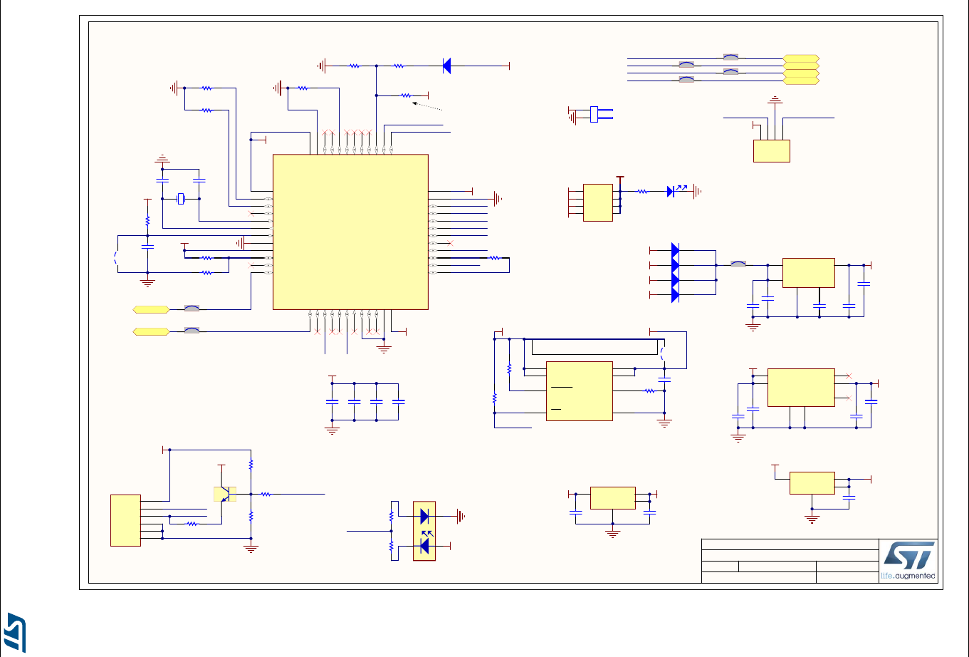
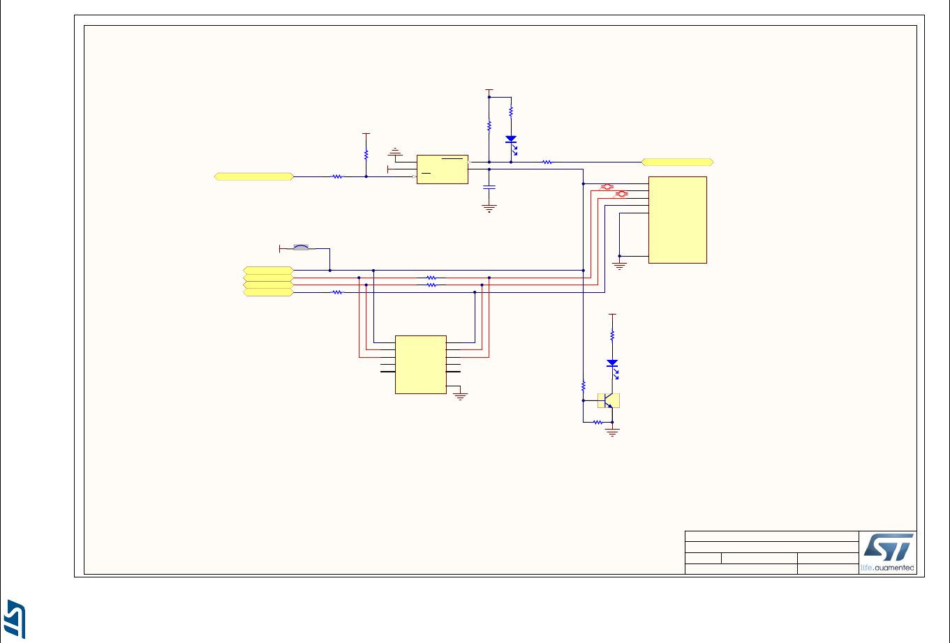
Figure 22. ST-LINK/V2-1 with support of SWD only
213
ST-LINK/V2-1 with support of SWD only
MB1191 B-04
10/16/2015
Title:
Size: Reference:
Date: Sheet: of
A4 Revision:
STM32F746G-DISCO
Project:
USB_DM
USB_DP
STM_RST
T_JTCK
T_JTCK
T_JTMS
STM_JTMS
STM_JTCK
OSC_IN
OSC_OUT
T_NRST
AIN_1
3V3_ST_LINK
3V3_ST_LINK
USB_DM
USB_DP
USB
VCC 1
D- 2
D+ 3
ID 4
GND 5
SHELL 6
CN14
USB-MINI-typeB
COM
ST-LINK Power
3V3_ST_LINK
Board Ident: PC13=0
T_JTCK
T_JTMS SWD
3V3_ST_LINK
1
2
3
4
CN8
STM_JTMSSTM_JTCK
SWCLK SWDIO
3V3_ST_LINK
T_SWDIO_IN
T_SWO
LED_STLINK
LED_STLINK
3V3_ST_LINK
Red
_Green
2 1
3 4
LD7
LD_BICOLOR_CMS
SWDIO
SWCLK
5V
NRST
T_NRST
51
2
GND
3
4
BYPASS
INH
Vin Vout
U12 LD3985M33R
VCP_RX
VCP_TX
STLINK_TX
STLINK_RX
LD2
LED, red
C101
100nF
C113
100nF
C118
100nF
C109
100nF
C91
1uF
C86
1uF
C85
100nF
C84
100nF
C94
10nF
C98
100nF
3V3_ST_LINK
USB_RENUMn
PWR_EXT
PWR_ENn
3
1
2
T3
9013-SOT23
3V3_ST_LINK
USB_RENUMn
PA14
PA13
PWR_ENn
EN
1
GND
2
VO 4
NC 5
GND
7
VI
6PG 3
U7 LD39050PU33R
C75
1uF
C68
100nF
C62
1uF
C61
100nF
3V3_ST_LINK
5 Volts Output
3.3 Volts Output
5 Volts Power Supply
3V3_ST_LINK
3V3_ST_LINK
VBAT
1
PA7
17
PC13
2
PA12 33
PC14
3
PB0
18
PC15
4JTMS/SWDIO 34
OSCIN
5
PB1
19
OSCOUT
6
VSS_2 35
NRST
7
PB2/BOOT1
20
VSSA
8
VDD_2 36
VDDA
9
PB10
21
PA0
10
JTCK/SWCLK 37
PA1
11
PB11
22
PA2
12
PA15/JTDI 38
PA3
13
VSS_1
23
PA4
14
PB3/JTDO 39
PA5
15
VDD_1
24
PA6
16
PB4/JNTRST 40
PB12 25
PB5 41
PB13 26
PB6 42
PB14 27
PB7 43
PB15 28
BOOT0 44
PA8 29
PB8 45
PA9 30
PB9 46
PA10 31
VSS_3 47
PA11 32
VDD_3 48
U14
STM32F103CBT6
5V
5V_USB_ST_LINK
5V_USB_ST_LINK
D6
BAT60JFILM
Not Fitted
IN
1
IN
2
ON
3GND 4
SET 5
OUT 6
OUT 7
FAULT
8
U8
ST890CDR
R72
100K_1%_0402
R60
10K_1%_0402
C76
100nF
R112
4K7_1%_0402
R101
10K_1%_0402
R100
[NA]
R105
100K_1%_0402
R99
100K_1%_0402
R98
4K7_1%_0402
R97
4K7_1%_0402
R118
100_1%_0402
R120
10K_1%_0402
R128
1K5_1%_0402
R129
36K_1%_0402
R86
1K
R108
2K7_1%_0402
R127
100_1%_0402
SWO
T_SWO PB3
R139
330_1%_0402
R138
330_1%_0402
1.8 Volts Output
SB10
SB14
SB17
SB15
SB9
3V3
E5V
Arduino UNO power pin
VIN Vin
3Vout 2
1
Tab 4
U6 LD1117S50TR
E5V
1 2
X4
NX3225GD-8.00M
MCO
Ilim = 510mA
1.2Ilim = 612mA < Isc < 1.5Ilim = 765mA
R79
2K7
R109
0
Not Fitted, must be on a border or the PCB.
5V_USB_FS
5V_USB_HS
T_JTDO
T_JTDI
T_JRST
1V8
3V3
Vin
3Vout 2
1
Tab 4
U13
LD1117S18TR
SB11
E5V
Not Fitted, must be on a border or the PCB.
JP2
C29
10uF_X5R_10%_0805
C41
10uF_X5R_10%_0805
C108
10uF_X5R_10%_0603
1 2
3 4
5 6
7 8
JP1
TSM-104-01-x-DV
D1
BAT60JFILM
5V_ST_LINK
5V_ST_LINK
D3
BAT60JFILM
D4
BAT60JFILM
D2
BAT60JFILM
E5V
5V_USB_FS
5V_USB_HS
5V_USB_ST_LINK
5V
C99
10pF
C100
10pF
SB16
SB12
SB13
UM1907 Electrical schematics
DocID027942 Rev 4 31/51
Figure 23. Joystick, LEDs and push-buttons
313
Joystick, ACP, LEDs and Push Button
MB1191 B-04
10/16/2015
Title:
Size: Reference:
Date: Sheet: of
A4 Revision:
STM32F746G-DISCO
Project:
NRST
NRST
RESET Button
3V3
12
3 4
B2
SW-PUSH-CMS_BLACK
C25
100nF
3V3
EXT/RF E2P Connector
EXT_RST
EXT_SDA
EXT_SCL EXT_RSTEXT_SCL
EXT_SDA
R39
10K_1%_0402
Not Fitted
MICRO SD
uSD_CLK
uSD_CMD
SMS064FF or SMS128FF
uSD_D0
uSD_D1
uSD_D2
uSD_D3
uSD_Detect
3V3
(TF) Card
Input pin with pull-up
3V3
3V3
R14
47K_1%_0402
R12
[NA]
R11
0_5%_0402
R13
47K_1%_0402
R17
47K_1%_0402
R16
47K_1%_0402
R15
47K_1%_0402
SB6
VDD
B_USER
USER & WAKE-UP Button
12
3 4
B1
SW-PUSH-CMS_BLUE
B_USER
C10
100nF
SB7
1
2
3
4
5
6
7
8
SW2
9
SW1
10
CN3
PJS008-2003
5V
1 2
3 4
5 6
7 8
CN2
F206A-2*04MGF-A
R18
10K
R19
10K
SB2
Electrical schematics UM1907
32/51 DocID027942 Rev 4
Figure 24. Audio codec Cirrus and connectors
413
Audio Codec WOLFSON and connectors
MB1191 B-04
10/16/2015
Title:
Size: Reference:
Date: Sheet: of
A4 Revision:
STM32F746G-DISCO
Project:
SAI2_SCKA
Default I2C Address : 00110100
ADCDAT1
F2
ADCLRCLK1/GPIO1
G3
AGND D6
CPVDD
G9
CPVOUTN H7
CPVOUTP G7
CS/ADDR G2
DACDAT1
E4
CPGND H9
DCVDD
F1
DBVDD
D2 DGND E2
CPCB H8
AVDD1
D9
BCLK1
G1
CIFMODE A4
CPCA G8
DMICCLK
C6
AGND E7
AGND E8
AVDD2
D8
GPIO2/MCLK2 E1
GPIO3/BCLK2
H2
GPIO4/LRCLK2
F4
GPIO5/DACDAT2
H3
GPIO6/ADCLRCLK2
G4 GPIO7/ADCDAT2
E5
GPIO8/DACDAT3
H4
GPIO9/ADCDAT3
F5
GPIO10/LRCLK3
H5 GPIO11/BCLK3
F6
HP2GND F7
HPOUT1FB G5
HPOUT1L H6
HPOUT1R G6
HPOUT2N F9
HPOUT2P F8
IN1LN
D7 IN1LP
C8
IN1RN
B7 IN1RP
C7
IN2LN/DMICDAT1
B9 IN2LP/VRXN
B8
IN2RN/DMICDAT2
A9 IN2RP/VRXP
A8
LDO1ENA
D4
LDO1VDD
E9
LDO2ENA
D5
LDO2VDD
D1
LINEOUT1N C5
LINEOUT1P B5
LINEOUT2N C4
LINEOUT2P B4
LINEOUTFB A6
LRCLK1
E3
MCLK1 D3
MICBIAS1 A7
MICBIAS2 B6
REFGND A5
SCLK H1
SDA F3
SPKGND1 A1
SPKGND2 C1
SPKMODE A3
SPKOUTLN B1
SPKOUTLP A2
SPKOUTRN C3
SPKOUTRP B3
SPKVDD1
B2
SPKVDD2
C2
VMIDC C9
VREFC
E6
U11
WM8994ECS/R
1V8
3V3
SAI2_FSA
SAI2_SDA
SAI2_SDB
Audio_INT
AUDIO_SDA
AUDIO_SCL
SAI2_MCLKA
3V3
3V3
MIC_DATA
MIC_CLK
MIC_VDD
LEFT
RIGHT
GND
5
LR 2
CLK 3
VDD
1
DOUT 4
U20
MP34DT01
GND
5
LR 2
CLK 3
VDD
1
DOUT 4
U21
MP34DT01
TP3
SPK Left
SPK Right
Right
Left
Jack out Green
Jack in blue
Right
Left
JP4
JP3
RCA in Yellow for SPDIF input
SPDIF_RX0
TP_PH15 TP_PH15
2
1
CN1
RCA_SMD
2
6
4
3
CN11
PJ3028B-3_BE
2
6
4
3
CN10
PJ3028B-3_GR
C794.7uF
C711uF
C89
1uF
R87
10K
R47 10K
C107
1uF
C105
4.7uF
C88
4.7uF
R83 0
R80 [NA]
C103100nF
C72100nF
C115100nF
C30100nF
C87 2.2uF
C80 2.2uF
C78 2.2uF
R121
20
C1044.7uF
C934.7uF
C70100nF
C92100nF
C691uF
C77100nF
C102100nF
C106
1uF
R76 0
R102
20
2
3
4
5
U1
74LVC1G04SE
C4
100nF
2
3
4
5
U2
74LVC1G04SE
R9
1M R22
1M
R6
75
R7
100
R10
100
C7
100nF
C6
22nF
C9
22nF
3V3 3V3
3V3
Very close to Output pin 4
Second Stage
R8
[NA]
First Stage
of first stage
UM1907 Electrical schematics
DocID027942 Rev 4 33/51
Figure 25. Quad-SPI Flash memory (MICRON)
513
Quad SPI Flash Memory (MICRON)
MB1191 B-04
10/16/2015
Title:
Size: Reference:
Date: Sheet: of
A4 Revision:
STM32F746G-DISCO
Project:
3V3
Quad SPI Flash Memory
QSPI_D0
QSPI_D3
QSPI_D2
QSPI_D1
QSPI_CLK
QSPI_NCS
R57
10K_1%_0402
C38
100nF_X7R_10%_0402
DQ3/HOLD#
7
VCC 8
S#
1
DQ1
2
C
6
DQ0
5
VSS 4
DQ2/Vpp/W#
3
D
Q
3/HOLD#
VCC
S#
D
Q1
C
D
Q
0
VSS
DQ2/V
pp
/
W
#
U3
N25Q128A13EF840E (MICRON)
QSPI_D0
QSPI_D1
QSPI_D2
QSPI_D3
QSPI_NCS
QSPI_CLK
Electrical schematics UM1907
34/51 DocID027942 Rev 4
Figure 26. Arduino Uno connectors
613
Arduino UNO connectors
MB1191 B-04
10/16/2015
Title:
Size: Reference:
Date: Sheet: of
A4 Revision:
STM32F746G-DISCO
Project:
Arduino UNO connector
A0
A1
A2
A3
A4
A5
RX/D0
TX/D1
D2
D4
PWM/D3
PWM/CS/D5
PWM/D6
D7
D8
PWM/D9
PWM/D10
SDA/D14
SCL/D15
NRST
VIN
NRST
SCK/D13
MISO/D12
PWM/MOSI/D11
AVDD
GND
VREF+
PA0
PF10
PF9
PF8
PF7
PF6
PC6
PG6
PB4
PG7
PA8
PH6
PI3
PI2
PA15
PI0
PB15
PB14
PI1
ADC3_IN4
ADC3_IN5
ADC3_IN6
ADC3_IN7
ADC3_IN8
ADC3_IN0
USART6_RX
USART6_TX
TIM3_CH1
TIM1_CH1
TIM2_CH1
TIM5_CH4, SPI2_NSS
TIM12_CH2, SPI2_MOSI
SPI2_MISO
SPI2_SCK
IOREF
NRST
3V3
5V
GND
GND
VIN
POWERAIN
SB1
SB3
SB5
SB4
TIM12_CH1
LD1
LED, green
R59
510_1%_0402
SB8
3V3
5V
PB8
PB9
PB8
PB9
1
2
3
4
5
6
CN5
F201-1*06MGF-W1-BA
1
2
3
4
5
6
7
8
9
10
CN7
F201-1*10MGF-W1-BA
1
2
3
4
5
6
7
8
CN6
F201-1*08MGF-W1-BA
1
2
3
4
5
6
7
8
CN4
F201-1*08MGF-W1-BA
ARD_A[0..5]
ARD_D[0..15]
ARD_A[0..5]
ARD_D[0..15]
ARD_A0
ARD_D0
ARD_D1
ARD_D2
ARD_D3
ARD_D4
ARD_D5
ARD_D6
ARD_D7
ARD_D8
ARD_D9
ARD_D10
ARD_D11
ARD_D12
ARD_D13
ARD_D14
ARD_D15
ARD_D14
ARD_D15
ARD_A1
ARD_A2
ARD_A3
ARD_A4
ARD_A5
SDA/D14
SCL/D15
PC7
C90
[NA]
R96
0
UM1907 Electrical schematics
DocID027942 Rev 4 35/51
Figure 27. SDRAM (MICRON)
713
SDRAM (MICRON)
MB1191 B-04
10/16/2015
Title:
Size: Reference:
Date: Sheet: of
A4 Revision:
STM32F746G-DISCO
Project:
FMC_A[0..11]
FMC_D[0..15]
Place close SDRAM
FMC_D[0..15]
FMC_A[0..11]
A11
H9
A10
G7
A9
J3
A8
H2
A7
H1
A6
G3
A5
G2
A4
G1
A3
F3
A2
F7
A1
G9
A0
G8
NC
E3
DQ0 R8
DQ8 L2
DQ1 N7
DQ9 M3
DQ2 R9
DQ10 M2
DQ3 N8
DQ11 P1
VDDQ
B2
DQ4 P9
DQ12 N2
DQ5 M8
DQ13 R1
DQ6 M7
DQ14 N3
DQ7 L8
DQ15 R2
VSS A3
VDD
A7
DQ16 E8
DQ24 A2
DQ17 D7
DQ25 C3
DQ18 D8
DQ26 A1
DQ19 B9
DQ27 C2
DQ20 C8
DQ28 B1
DQ21 A9
DQ29 D2
DQ22 C7
DQ30 D3
DQ23 A8
DQ31 E2
VSSQ B3
VDDQ
B7 VSSQ B8
VSSQ C1
VDDQ
C9
VSSQ D1
VDDQ
D9
VDDQ
E1
NC
E7
VSSQ E9
VSS F1
VDD
F9
NC
H3
NC
H7
BA0
J7 BA1
H8
NU
K2 NC
K3
VDDQ
L1
VSS L3
VDD
L7
VSSQ L9
VSSQ M1
VDDQ
M9
VSSQ N1
VDDQ
N9
VDDQ
P2 VSSQ P3
VDDQ
P7 VSSQ P8
VSS R3
VDD
R7
DQM0
K9 DQM1
K1 DQM2
F8
CLK
J1 CKE
J2 CS#
J8
DQM3
F2
RAS#
J9 CAS#
K7 WE#
K8
U4
MT48LC4M32B2B5-6A (MICRON)
FMC_A0
FMC_SDNWE
FMC_SDNRAS
FMC_BA0
FMC_BA1
FMC_SDCLK
FMC_SDNCAS
FMC_SDNWE
FMC_SDNRAS
FMC_SDNCAS
FMC_SDCLK
FMC_BA0
FMC_BA1
C16
100nF_X7R_10%_0402
C51
100nF_X7R_10%_0402
C43
100nF_X7R_10%_0402
C34
100nF_X7R_10%_0402
C50
100nF_X7R_10%_0402
C46
100nF_X7R_10%_0402
C45
100nF_X7R_10%_0402
C42
100nF_X7R_10%_0402
C31
100nF_X7R_10%_0402
C28
100nF_X7R_10%_0402
C27
100nF_X7R_10%_0402
C15
100nF_X7R_10%_0402
C26
100nF_X7R_10%_0402
3V3
FMC_D0
R52 10K_1%_0402
R48 10K_1%_0402
R49 10K_1%_0402
R43 10K_1%_0402
R40 10K_1%_0402
R23 10K_1%_0402
R36 10K_1%_0402
R24 10K_1%_0402
R26 10K_1%_0402
R25 10K_1%_0402
R27 10K_1%_0402
R41 10K_1%_0402
R37 10K_1%_0402
R50 10K_1%_0402
R51 10K_1%_0402
R53 10K_1%_0402
R55 10K_1%_0402
R56 10K_1%_0402
FMC_NBL0
FMC_NBL1
FMC_NBL0
FMC_NBL1
C52
100nF_X7R_10%_0402
FMC_SDCKE0
FMC_SDNE0
FMC_SDNE0
FMC_SDCKE0
FMC_D1
FMC_D2
FMC_D3
FMC_D4
FMC_D5
FMC_D6
FMC_D7
FMC_D8
FMC_D9
FMC_D10
FMC_D11
FMC_D12
FMC_D13
FMC_D14
FMC_D15
FMC_A1
FMC_A2
FMC_A3
FMC_A4
FMC_A5
FMC_A6
FMC_A7
FMC_A8
FMC_A9
FMC_A10
FMC_A11
Electrical schematics UM1907
36/51 DocID027942 Rev 4
Figure 28. USB OTG FS with Micro-AB connector
813
USB OTG FS with Micro A-B connector
MB1191 B-04
10/16/2015
Title:
Size: Reference:
Date: Sheet: of
A4 Revision:
STM32F746G-DISCO
Project:
5V
OTG_FS_PowerSwitchOn
OTG_FS_OverCurrent
3V3
OTG_FS_N
OTG_FS_P
OTG_FS_ID
3V3
3V3
Dz
A2
ID A3
Pd1 B1
Pup
B2
Vbus
B3
D+in C1
Pd2 C2
D+out
C3
D-in D1
GND D2
D-out
D3
U18
EMIF02-USB03F2
GND
2
IN
5
EN
4OUT 1
FAULT 3
U16
STMPS2141STR
OTG_FS_VBUS
3
1
2
T2
9013-SOT23
R136
330_1%_0603
R134
47K_1%_0402
LD5
LED, green
VBUS
1
DM
2
DP
3
ID
4
GND
5
Shield
6
USB_Micro-AB receptacle
CN13
USB-MICRO-AB
R126
47K_1%_0402
R119
0_5%_0402
LD6
LED, red
R117
0_5%_0402
R133 0
R116
10K_1%_0402
R137
620_1%_0603
5V_USB_FS SB18
USB_FS1_N
USB_FS1_P
R132 0
R125 0
C112
4.7uF_X5R_10%_0603
R135
100K
UM1907 Electrical schematics
DocID027942 Rev 4 37/51
Figure 29. STM32F746NGH6 connection
913
STM32F746NGH6 Connexion
MB1191 B-04
10/16/2015
Title:
Size: Reference:
Date: Sheet: of
A3 Revision:
STM32F746G-DISCO
Project:
PA[0..15] PA[0..15]
PB[0..15] PB[0..15]
PC[0..15] PC[0..15]
PD[0..15] PD[0..15]
PE[0..15] PE[0..15]
PF[0..15] PF[0..15]
PG[0..15] PG[0..15]
PH[0..15] PH[0..15]
PI[0..15] PI[0..15]
PA4
PA5
PA6
PA7
PA11
PA12
PA9
PA10
PA0
PA1
PA15
PA3
PA13
PA14
PA2
PA8
PB5
PB6
PB7
PB14
PB15
PB10
PB8
PB9
PB1
PB2
PB3
PB0
PB4
PB11
PB12
PB13
PC0
PC1
PC2
PC3
PC4
PC5
PC6
PC7
PC8
PC9
PC10
PC11
PC12
PC13
PC14
PC15
PJ0
PJ14
PJ15
PJ9
PJ8
PJ11
PJ10
PJ12
PJ13
PJ1
PJ2
PJ3
PJ4
PJ5
PJ6
PJ7
PK0
PK1
PK2
PK3
PK4
PK5
PK6
PK7
PH0
PH1
PD0
PD1
PD2
PD3
PD4
PD5
PD6
PD7
PD8
PD9
PD10
PD11
PD12
PD13
PD14
PD15
PI0
PI14
PI15
PI9
PI8
PI11
PI10
PI12
PI13
PI1
PI2
PI3
PI4
PI5
PI6
PI7
PE0
PE14
PE15
PE9
PE8
PE11
PE10
PE12
PE13
PE1
PE2
PE3
PE4
PE5
PE6
PE7
PF0
PF14
PF15
PF9
PF8
PF11
PF10
PF12
PF13
PF1
PF2
PF3
PF4
PF5
PF6
PF7
PG0
PG14
PG15
PG9
PG8
PG11
PG10
PG12
PG13
PG1
PG2
PG3
PG4
PG5
PG7
PH14
PH15
PH9
PH8
PH11
PH10
PH12
PH13
PH2
PH3
PH4
PH5
PH6
PH7
NRST NRST
BOOT0
PJ[0..15] PJ[0..15]
PK[0..7] PK[0..7]
VDDA
VREF+
3V3
Ceramic capacitor (Low ESR)
VDDA
3V3
PC13-ANTI_TAMP D1
PC0 M2
PC1 M3
PC2 M4
PC3 L4
PA0-WKUP
N3
PA1
N2
PA2
P2
PA3
R2
PA4
N4
PA5
P4
PA6
P3
PA7
R3
PC4 N5
PC5 P5
PB0
R5
PB1
R4
PB2
M5
PB10
P12
PB11
R13
PB12
L13
PB13
K14
PB14
R14
PB15
R15
PC6 H15
PC7 G15
PC8 G14
PC9 F14
PA8
F15
PA9
E15
PA10
D15
PA11
C15
PA12
B15
PA13
A15
PA14
A14
PA15
A13
PC10 B14
PC11 B13
PC12 A12
PB3
A10
PB4
A9
PB5
A8
PB6
B6
PB7
B5
PB8
A7
PB9
B4
PC14-OSC32_IN
E1
PC15-OSC32_OUT
F1
PH0-OSC_IN
G1
PH1-OSC_OUT
H1
NRST
J1
BOOT0
E6
PDR_ON
E5
PJ2 P7
PJ3 N8
PJ4 M9
PJ5 M14
PJ6 K12
PJ7 J12
PJ8 H12
PJ9 J13
PJ10 H13
PJ11 G12
PJ12 B10
PJ13 B9
PJ14 C9
PJ15 D10
PJ0 R6
PJ1 R7
PK2 F13
PK3 D8
PK4 D7
PK5 C6
PK6 C5
PK7 C4
PK0 G13
PK1 F12
U5A
STM32F746NGH6
PE2
A3
PE3
A2
PE4
A1
PE5
B1
PE6
B2
PF0
D2
PF1
E2
PF2
G2
PF3
H2
PF4
J2
PF5
K3
PF6
K2
PF7
K1
PF8
L3
PF9
L2
PF10
L1
PH2 K4
PH3 J4
PH4 H4
PH5 J3
PF11
P8
PF12
M6
PF13
N6
PF14
P6
PF15
M8
PG0 N7
PG1 M7
PE7
R8
PE8
N9
PE9
P9
PE10
R9
PE11
P10
PE12
R10
PE13
R12
PE14
P11
PE15
R11
PH6 P13
PH7 N13
PH8 P14
PH9 N14
PH10 P15
PH11 N15
PH12 M15
PG2 M13
PG3 M12
PG4 N12
PG5 N11
PG6 J15
PG7 J14
PG8 H14
PH13 E12
PH14 E13
PH15 D13
PG9 D9
PG10 C8
PG11 B8
PG12 C7
PG13 B3
PG14 A4
PG15 B7
PE0
A6
PE1
A5
PD8
L15
PD9
L14
PD10
K15
PD11
N10
PD12
M10
PD13
M11
PD14
L12
PD15
K13
PD0
B12
PD1
C12
PD2
D12
PD3
C11
PD4
D11
PD5
C10
PD6
B11
PD7
A11
PI8-ANTI_TAMP2 C2
PI9 E4
PI10 D5
PI11 F3
PI0 E14
PI1 D14
PI2 C14
PI3 C13
PI4 C3
PI5 D3
PI6 D6
PI7 D4
PI12 E3
PI13 G3
PI14 H3
PI15 G4
U5B
STM32F746NGH6
VBAT
C1
VSS2 F10
VSS1 K9
VREF- N1
VSSA M1
VREF+
P1
VSS10 F8
VSS11 F7
VCAP2 E11
VSS12 J6
VDD4
K5 VDD3
E7
VSS13-VSS18 F2
VDD20
H11
VCAP1 L11
VSS14 K10
VDD2
F11
VSS15 F9
VDD19
L7
VSS17 G6
VDD18
G5
VDD1
L10
VDD5
H5
VDDA
R1
VDD10
E9
VDD11
E8
VDD12
J5
VDD13
F4
VDD14
K11
VDD15
E10
VDD17
F5
VSS19 L6
VSS20 H10
VSS3 F6
VSS4 K6
BYPASS-REG
L5
VDD6
L8
VDD7
L9
VDD8
J11
VDD_USB33
G11
VSS5 H6
VSS6 K7
VSS7 K8
VSS8 J10
VSS9 G10
U5C
STM32F746NGH6
R31
0
R32
0
X3
NX3215SA-32.768K
VDD
4OUT 3
EN
1GND 2
X2
NZ2520SB-25.00M
R5
10K_1%_0402
3V3
C5
100nF
OSC_25M
R30
100_1%_0402
OSC_25M
C11
100nF
C55
100nF
C56
100nF
C57
100nF
C58
100nF
C59
100nF
C40
100nF
C37
100nF
C36
100nF
C33
100nF
C24
100nF
C23
100nF
C22
100nF
C21
100nF
C20
100nF
C19
100nF
C18
100nF
C32
100nF
C35
100nF
C39
100nF
C44
100nF
PG6
R45
10K_1%_0402
R42
[NA]
R38
10K_1%_0402
R35
[NA]
3V3
LCD_R[0..7]
LCD_R0
LCD_BL_CTRL
LCD_RST
LCD_INT
LCD_SDA
LCD_SCL
LCD_HSYNC
LCD_VSYNC
LCD_CLK
LCD_DE
LCD_DISP
LCD_B[0..7]
LCD_B0
LCD_G[0..7]
LCD_G0
LCD_BL_CTRL
LCD_HSYNC
LCD_CLK
LCD_VSYNC
LCD_DISP
LCD_DE
LCD_RST
LCD_INT
LCD_SDA
LCD_SCL
DCMI_NRST
DCMI_D[0..7]
DCMI_SCL
DCMI_SDA
DCMI_PWR_EN
DCMI_NRST
DCMI_PWR_EN
DCMI_VSYNC
DCMI_HSYNC
DCMI_PIXCK
DCMI_SDA
DCMI_SCL
RMII_TXD0
RMII_TX_EN
RMII_RXD0
RMII_REF_CLK
RMII_CRS_DV
RMII_MDC
RMII_MDIO
RMII_TXD1
RMII_RXD1
ULPI_D[0..7]
ULPI_CK
ULPI_D0
ULPI_D1
ULPI_D2
ULPI_D3
ULPI_DIR
ULPI_NXT
ULPI_STP
ULPI_D4
ULPI_D5
ULPI_D6
ULPI_D7
ULPI_NXT
ULPI_DIR
ULPI_STP
ULPI_CK
OTG_FS_N
OTG_FS_P
OTG_FS_ID
OTG_FS_VBUS
OTG_FS_PowerSwitchOn
OTG_FS_OverCurrent
OTG_HS_OverCurrent
QSPI_D0
QSPI_D3
QSPI_D2
QSPI_D1
QSPI_CLK
QSPI_NCS
QSPI_D0
QSPI_D1
QSPI_D2
QSPI_D3
QSPI_NCS
QSPI_CLK
AUDIO_SDA
AUDIO_SCL
SAI2_MCLKA
SAI2_SCKA
SAI2_FSA
SAI2_SDA
SAI2_SDB
Audio_INT
EXT_SDA
EXT_SCL
EXT_SCL
EXT_SDA
EXT_RST
EXT_RST
B_USER
uSD_CLK
uSD_CMD
uSD_D0
uSD_D1
uSD_D2
uSD_D3
uSD_Detect
SWDIO
SWCLK
SWO
VCP_RX
VCP_TX
uSD_D0
uSD_D1
uSD_D2
uSD_D3
uSD_CLK
uSD_CMD
uSD_Detect
SWCLK
SWDIO
SWO
VCP_RX
AUDIO_SDA
AUDIO_SCL
SAI2_MCLKA
SAI2_SCKA
SAI2_FSA
SAI2_SDA
SAI2_SDB
Audio_INT
DCMI_VSYNC
DCMI_HSYNC
DCMI_PIXCK
DCMI_D0
DCMI_D1
DCMI_D2
DCMI_D3
DCMI_D4
DCMI_D5
DCMI_D6
DCMI_D7
RMII_TX_EN
RMII_RXD0
RMII_TXD0
RMII_TXD1
RMII_RXD1
RMII_CRS_DV
RMII_MDC
RMII_MDIO
RMII_REF_CLK
FMC_A[0..11]
FMC_D[0..15]
FMC_D0
FMC_SDNWE
FMC_BA0
FMC_BA1
FMC_SDCLK
FMC_SDNWE
FMC_SDNRAS
FMC_SDNCAS
FMC_SDCLK
FMC_BA0
FMC_BA1
FMC_SDNE0
FMC_SDCKE0
FMC_SDNRAS
FMC_SDNCAS
FMC_NBL0
FMC_NBL1
FMC_NBL0
FMC_NBL1
FMC_SDCKE0
FMC_SDNE0
FMC_A0
FMC_A1
FMC_A2
FMC_A3
FMC_A4
FMC_A5
FMC_A6
FMC_A7
FMC_A8
FMC_A9
FMC_A10
FMC_A11
FMC_D1
FMC_D2
FMC_D3
FMC_D4
FMC_D5
FMC_D6
FMC_D7
FMC_D8
FMC_D9
FMC_D10
FMC_D11
FMC_D12
FMC_D13
FMC_D14
FMC_D15
LCD_R1
LCD_R2
LCD_R3
LCD_R4
LCD_R5
LCD_R6
LCD_R7
LCD_G1
LCD_G2
LCD_G3
LCD_G4
LCD_G5
LCD_G6
LCD_G7
LCD_B1
LCD_B2
LCD_B3
LCD_B4
LCD_B5
LCD_B6
LCD_B7
R440
B_USER
SPDIF_RX0
SPDIF_RX0
OTG_HS_OverCurrent
OTG_FS_OverCurrent
OTG_FS_PowerSwitchOn
OTG_FS_VBUS OTG_FS_N
OTG_FS_P
OTG_FS_ID
ARD_A0
ARD_A1
ARD_A2
ARD_A3
ARD_A4
ARD_A5
ARD_D0
ARD_D1
ARD_D2
ARD_D3
ARD_D4
ARD_D5
ARD_D6
ARD_D7
ARD_D9
ARD_D10
ARD_D11
ARD_D12
ARD_D13
ARD_D14
TP_PH15
ARD_D8
ARD_A[0..5]
ARD_D[0..15]
ARD_D15
VCP_TX
R54
2K7_1%_0402
R46
2K7_1%_0402
R62
2K7_1%_0402
R61
2K7_1%_0402
3V33V3
3V3 3V3
RMII_RXER
RMII_RXER
OTG_FS_VBUS
R58 100
TP_PH15
QSPI_D0
QSPI_D1
QSPI_D2
QSPI_D3
QSPI_NCS
QSPI_CLK
ARD_A[0..5]
ARD_D[0..15]
SPDIF_RX0
TP_PH15
SAI2_SDB
AUDIO_SDA
AUDIO_SCL
Audio_INT
SAI2_MCLKA
SAI2_SCKA
SAI2_FSA
SAI2_SDA
OSC_25M EXT_RST
B_USER
FMC_SDCKE0
FMC_NBL0
FMC_NBL1
FMC_D[0..15]
FMC_SDNRAS
FMC_BA0
FMC_BA1
FMC_SDCLK
FMC_SDNCAS
FMC_SDNWE
FMC_SDNE0
FMC_A[0..11]
EXT_SDA
EXT_SCL
VCP_TX
SWCLK
SWDIO
SWO
VCP_RX
uSD_D1
uSD_D2
uSD_D3
uSD_D0
uSD_CLK
uSD_Detect
uSD_CMD
OTG_FS_PowerSwitchOn
OTG_FS_VBUS
ULPI_D[0..7]
ULPI_CK
OTG_FS_N
OTG_FS_P
OTG_FS_ID
ULPI_DIR
ULPI_STP
OTG_HS_OverCurrent
OTG_FS_OverCurrent
ULPI_NXT
RMII_MDIO
RMII_RXD0
RMII_RXD1
RMII_MDC
RMII_CRS_DV
RMII_REF_CLK
RMII_TX_EN
RMII_TXD0
RMII_TXD1
RMII_RXER
DCMI_HSYNC
DCMI_PIXCK
DCMI_D[0..7]
DCMI_VSYNC
DCMI_PWR_EN
DCMI_SCL
DCMI_SDA
DCMI_NRST LCD_SDA
LCD_SCL
LCD_R[0..7]
LCD_INT
LCD_HSYNC
LCD_VSYNC
LCD_CLK
LCD_DISP
LCD_BL_CTRL
LCD_G[0..7]
LCD_B[0..7]
LCD_DE
LCD_RST
R21
0
VDD
VDDVDD
VDD
R640
VDD
VDD
R63
[NA]
NC1 R33 100 TP2
TP
TP1
TP
NC2 R29 100
C54
4.7uF
C14
4.7uF
C8
1uF
C17
1uF
C48
2.2uF
C47
2.2uF
L1
FCM1608KF-601T03
R28
0
R20
10K
R34
10K_1%_0402
3V3
C12
4.7pF_NPO_-+0.25pF_0402
C13
4.7pF_NPO_-+0.25pF_0402
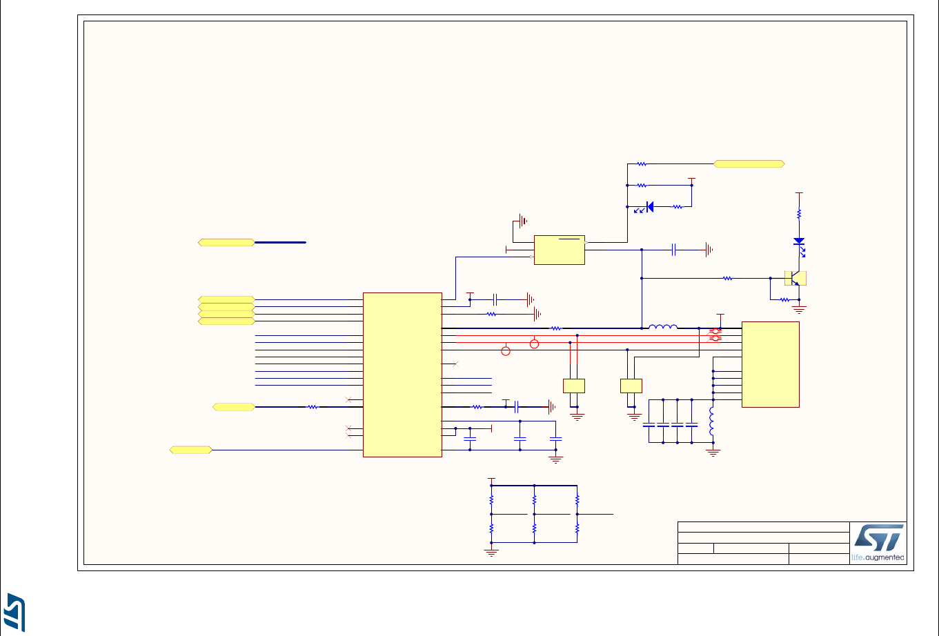
Electrical schematics UM1907
38/51 DocID027942 Rev 4
Figure 30. USB OTG HS PHY with Micro-AB connector
10 13
USB OTG HS PHY with Micro A-B connector
MB1191 B-04
10/16/2015
Title:
Size: Reference:
Date: Sheet: of
A4 Revision:
STM32F746G-DISCO
Project:
ULPI_D[0..7]
ULPI_CK
ULPI_D0
ULPI_D1
ULPI_D2
ULPI_D3
ULPI_DIR
ULPI_NXT
ULPI_STP
5V
VBUS
1
DM
2
DP
3
ID
4
GND
5
Shield
6
USB_Micro-AB receptacle
Shield
7
Shield
8
Shield
9
EXP
10
CN12
475900001
ULPI_D[0..7]
ULPI_D4
ULPI_D5
ULPI_D6
ULPI_D7
NRST
A1
A2
B1
B2
D8
USBULC6-2F3
A1
A2
B1
B2
D7
ESDA14V2-2BF3
3V3
3V3
OTG_HS_OverCurrent
USB_HS_N
USB_HS_P
3
1
2
T1
9013-SOT23
CPEN 17
VBUS 22
ID 23
REFSEL0 8
DP 18
DM 19
RESETB
27
VBAT 21
NXT
2
DIR
31
STP
29
CLKOUT
1
VDD1.8 30
VDD3.3 20
D7
13
D6
10
D5
9
D4
7
D3
6
D2
5
D1
4
D0
3REFSEL1 11
VDD1.8 28
XO
25
NC 12
REFCLK
26
REFSEL2 14
VDDIO 32
RBIAS 24
GNDPAD 33
SPK_R
16 SPK_L
15
U15
USB3320C-EZK
GND
2
IN
5
EN
4OUT 1
FAULT 3
U17
STMPS2151STR
ULPI_NXT
ULPI_DIR
ULPI_STP
ULPI_CK
OSC_24M
OSC_24M
LD4
LED, green
LD3
LED, red
R140
620_1%_0603 R141
330_1%_0402
R124
47K_1%_0402
R130
0
R114
100_1%_0402
5V_USB_HS
3V3
1V8
C123
100nF
C121
100nF
C120
100nF
C122
100nF
C110
100nF
C116
100nF
5V
R104
0_5%_0402
R103
[NA]
C119
2.2uF_X7R_10%_0805
R110
0_5%_0402
R106
[NA]
R113
0_5%_0402
R111
[NA]
REFSEL0 REFSEL1 REFSEL2
REFSEL0
REFSEL1
REFSEL2
3V3
R123 820_1%_0805
C114
4.7uF_X5R_10%_0603
C111
100nF
R107
0_5%_0402
C117
100nF
R115
8K06_1%_0402
i
Diff Pair 90ohm
Matched Net Lengths [Tolerance = 150mil]
i
Diff Pair 90ohm
L6
BLM18PG121SN1D
L7
BLM18PG121SN1D
R122
3K3
R131
100K
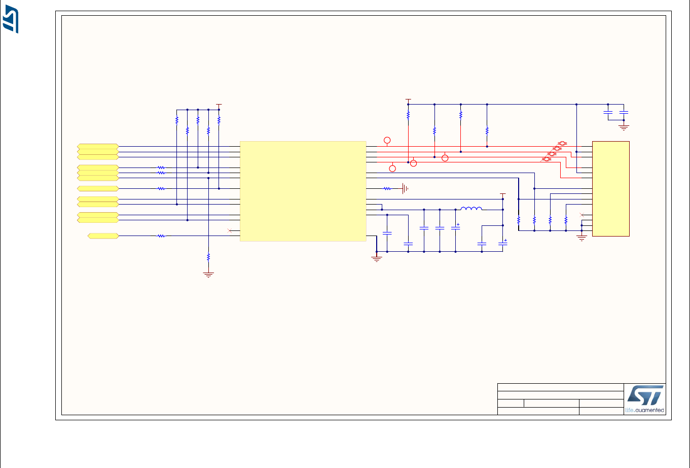
UM1907 Electrical schematics
DocID027942 Rev 4 39/51
Figure 31. Ethernet PHY with RJ45 connector
11 13
Ethernet PHY with RJ45 connector
MB1191 B-04
10/16/2015
Title:
Size: Reference:
Date: Sheet: of
A4 Revision:
STM32F746G-DISCO
Project:
RMII_TXD0
RMII_TX_EN
RMII_RXD0
RMII_REF_CLK
RMII_CRS_DV
RMII_MDC
RMII_MDIO
NRST
RMII_TXD1
RMII_RXD1
3V3
3V3
C60
100nF
C83
100nF
C82
100nF
C81
100nF
C74
100nF
MDIO
12 MDC
13
RXD1/MODE1
7RXD0/MODE0
8
RXER/PHYAD0
10
TXEN
16
TXD0
17
TXD1
18
CRS_DV/MODE2
11
nRST
15
XTAL1/CLKIN
5XTAL2
4
GND_EP 25
RBIAS 24
VDDIO 9
VDD1A 19
VDD2A 1
VDDCR 6
RXP 23
RXN 22
TXN 20
TXP 21
nINT/REFCLK0
14
LED2/nINT/nPME/nINTSEL 2
LED1/nINT/nPME/REGOFF 3
U9
LAN8742A-CZ-TR
OSC_25M OSC_25M R78
100
TD+
3
TCT
5
TD-
4
RD+
7
RCT
6
RD-
8
NC
9
CHS GND
10
LED(green)_A
12
LED(green)_K
11
LED(Yellow)_A
1
LED(Yellow)_K
2
Shield
13
Shield
14
CN9
HR961160C
R73
4K7
R67
4K7
R70
4K7
R68
4K7
3V3
RMII_RXER
R77
4K7
R65
1K5
i
Diff Pair 100ohm
Matched Net Lengths [Tolerance = 100mil]
i
Diff Pair 100ohm
i
Diff Pair 100ohm
i
Diff Pair 100ohm
TD_N
TD_P
RD_N
RD_P
R84
12K1
C63
10uF
R90
50
R91
50
R69 33
R92
50
R93
50
R71 33
R66 33
R95
10K
R88
10K
L2
BLM18PG121SN1D
R89
330
R94
330
LED2_SPEED_YELLOW
LED1_LINK/ACT_GREEN
C67
1uF
C73
10uF
C66
470pF
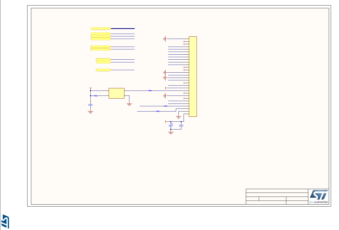
Electrical schematics UM1907
40/51 DocID027942 Rev 4
Figure 32. External camera connector
12 13
External Camera connector
MB1191 B-04
10/16/2015
Title:
Size: Reference:
Date: Sheet: of
A4 Revision:
STM32F746G-DISCO
Project:
DCMI_D0
DCMI_D1
DCMI_D2
DCMI_D3
DCMI_D4
DCMI_D5
DCMI_D6
DCMI_D7
DCMI_HSYNC
DCMI_VSYNC
DCMI_PIXCK
3V3 Camera_CLK
3V3
DCMI_PWR_EN
DCMI_NRST
C2
100nF
VDD
4OUT 3
EN
1GND 2
X1
NZ2520SB-24.00M
R4
10K_1%_0402
3V3
OSC_24M
C3
100nF
OSC_24M OSC_24M
DCMI_NRST
DCMI_D[0..7] DCMI_D[0..7]
DCMI_HSYNC
DCMI_VSYNC
DCMI_PIXCK
DCMI_SCL
DCMI_SDA
DCMI_PWR_EN
DCMI_NRST
DCMI_PWR_EN
DCMI_VSYNC
DCMI_HSYNC
DCMI_PIXCK
DCMI_SDA
DCMI_SCL
R3
100_1%_0402
1
2
3
4
5
6
7
8
9
10
11
12
13
14
15
16
17
18
19
20
21
22
23
24
25
26
27
28
29
30
P1
FPU330ZH-BT1D3-CA
DCMI_SCL
DCMI_SDA R2 100_1%_0402
R1 100_1%_0402
C1
10uF
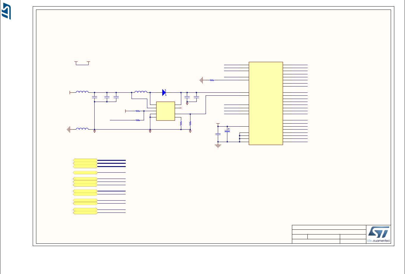
UM1907 Electrical schematics
DocID027942 Rev 4 41/51
Figure 33. 4.3-inch LCD with capacitive touch
13 13
LCD 4.3" with Capacitive Touch
MB1191 B-04
10/16/2015
Title:
Size: Reference:
Date: Sheet: of
A4 Revision:
STM32F746G-DISCO
Project:
Backlight driver & PFC of LCD panel
LCD_RST
LCD_INT
LCD_SDA
LCD_SCL
LCD_HSYNC
LCD_VSYNC
LCD_CLK
LCD_DE
3V3
LCD_BL_A
LCD_BL_K
BLGND
BLVDD
LCD_BL_CTRL
BLGNDBLGNDBLGND
VL VH
LCD_DISP DE
34
CLK
30
HSYNC
32
VSYNC
33
DISP
31
GND
35
GND
3
B0 21
VDD
4
VBL+
2
VBL-
1
INT
38
SCL
39
SDA
40
RESET
37
B1 22
B2 23
B3 24
B4 25
B5 26
B6 27
B7 28
R0 5
R1 6
R2 7
R3 8
R4 9
R5 10
R6 11
R7 12
G0 13
G1 14
G2 15
G3 16
G4 17
G5 18
G6 19
G7 20
GND
29
GND
36
U19
RK043FN48H-CT672B
LCD_B0
LCD_G0
LCD_R0
LCD_R1
LCD_R2
LCD_R3
LCD_R4
LCD_R5
LCD_R6
LCD_R7
LCD_G1
LCD_G2
LCD_G3
LCD_G4
LCD_G5
LCD_G6
LCD_G7
LCD_B1
LCD_B2
LCD_B3
LCD_B4
LCD_B5
LCD_B6
LCD_B7
Vi
1
Rset 2
GND
3FB 4
NC 5
Vo 6
EN
7
SW
8
PGND
9
U10
STLD40DPUR
D5
STPS1L40M
LCD_R[0..7] LCD_R[0..7]
LCD_BL_CTRL
LCD_RST
LCD_INT
LCD_SDA
LCD_SCL
LCD_HSYNC
LCD_VSYNC
LCD_CLK
LCD_DE
LCD_DISP
LCD_B[0..7] LCD_B[0..7]
LCD_G[0..7] LCD_G[0..7]
BLVDD
LCD_BL_CTRL
LCD_HSYNC
LCD_CLK
LCD_VSYNC
LCD_DISP
LCD_DE
LCD_RST
LCD_INT
LCD_SDA
LCD_SCL
3V3BLVDD
L4
FCM1608KF-601T03
L5
FCM1608KF-601T03
L3
4.7uH 1A 30%
C49
4.7uF
C97
4.7uF_16V
C64
4.7uF_50V
R85
4K7
R81
0R82
100K
R74
4K7
C53
100nF
C95
100nF
C96
10nF
C65
10nF
R75
10_1%_0805
Default I2C Address : 01110000
32F746GDISCOVERY I/O assignment UM1907
42/51 DocID027942 Rev 4
Appendix A 32F746GDISCOVERY I/O assignment
Table 11. 32F746GDISCOVERY I/O assignment
Pin No. Pin Name Signal or Label Comment
A1 PE4 LTDC_B0 -
A2 PE3 OTG_HS_OverCurrent -
A3 PE2 QUADSPI_BK1_IO2 -
A4 PG14 ETH_TXD1 -
A5 PE1 FMC_NBL1 -
A6 PE0 FMC_NBL0 -
A7 PB8 ARDUINO SCL/D15 -
A8 PB5 USB_OTG_HS_ULPI_D7 -
A9 PB4 ARDUINO PWM/D3 -
A10 PB3 SYS_JTDO-SWO -
A11 PD7 SPDIF_RX0 -
A12 PC12 SDMMC_CK -
A13 PA15 ARDUINO PWM/D9 -
A14 PA14 SYS_JTCK-SWCLK -
A15 PA13 SYS_JTMS-SWDIO -
B1 PE5 DCMI_D6 -
B2 PE6 DCMI_D7 -
B3 PG13 ETH_TXD0 -
B4 PB9 ARDUINO SDA/D14 -
B5 PB7 VCP_RX -
B6 PB6 QUADSPI_BK1_NCS -
B7 PG15 FMC_SDNCAS -
B8 PG11 ETH_TX_EN -
B9 PJ13 LTDC_B1 -
B10 PJ12 OTG_FS_VBUS (1)
B11 PD6 Audio_INT -
B12 PD0 FMC_D2_DA2 -
B13 PC11 SDMMC_D3 -
B14 PC10 SDMMC_D2 -
B15 PA12 USB_OTG_FS_DP -
C1 VBAT - Connected to VDD
C2 PI8 NC1 -

DocID027942 Rev 4 43/51
UM1907 32F746GDISCOVERY I/O assignment
50
C3 PI4 SAI2_MCLK_A -
C4 PK7 LTDC_DE -
C5 PK6 LTDC_B7 -
C6 PK5 LTDC_B6 -
C7 PG12 LTDC_B4 -
C8 PG10 SAI2_SD_B -
C9 PJ14 LTDC_B2 -
C10 PD5 OTG_FS_PowerSwitchOn -
C11 PD3 DCMI_D5 -
C12 PD1 FMC_D3_DA3 -
C13 PI3 ARDUINO D7 -
C14 PI2 ARDUINO D8 -
C15 PA11 USB_OTG_FS_DM -
D1 PC13 uSD_Detect -
D2 PF0 FMC_A0 -
D3 PI5 SAI2_SCK_A -
D4 PI7 SAI2_FS_A -
D5 PI10 LTDC_HSYNC -
D6 PI6 SAI2_SD_A -
D7 PK4 LTDC_B5 -
D8 PK3 LCD_BL_CTRL -
D9 PG9 DCMI_VSYNC -
D10 PJ15 LTDC_B3 -
D11 PD4 OTG_FS_OverCurrent -
D12 PD2 SDMMC_CMD -
D13 PH15 TP3 -
D14 PI1 ARDUINO SCK/D13 -
D15 PA10 USB_OTG_FS_ID -
E1 PC14/OSC32_IN RCC_OSC32_IN -
E2 PF1 FMC_A1 -
E3 PI12 LCD_DISP -
E4 PI9 LTDC_VSYNC -
E5 PDR_ON - Connected to PU R38
E6 BOOT0 - Connected to PD R45
E7 VDD - -
Table 11. 32F746GDISCOVERY I/O assignment (continued)
Pin No. Pin Name Signal or Label Comment
32F746GDISCOVERY I/O assignment UM1907
44/51 DocID027942 Rev 4
E8 VDD - -
E9 VDD - -
E10 VDD - -
E11 VCAP_2 - Connected to C48
E12 PH13 DCMI_PWR_EN -
E13 PH14 DCMI_D4 -
E14 PI0 ARDUINO PWM/CS/D5 -
E15 PA9 VCP_TX (1)
F1 PC15/OSC32_OUT RCC_OSC32_OUT -
F2 VSS - -
F3 PI11 B_USER -
F4 VDD - -
F5 VDD - -
F6 VSS - -
F7 VSS - -
F8 VSS - -
F9 VSS - -
F10 VSS - -
F11 VDD - -
F12 PK1 LTDC_G6 -
F13 PK2 LTDC_G7 -
F14 PC9 SDMMC_D1 -
F15 PA8 ARDUINO PWM/D10 -
G1 PH0/OSC_IN RCC_OSC_IN -
G2 PF2 FMC_A2 -
G3 PI13 LCD_INT -
G4 PI15 LTDC_R0 -
G5 VDD - -
G6 VSS - -
G10 VSS - -
G11 VDDUSB - Connected to VDD
G12 PJ11 LTDC_G4 -
G13 PK0 LTDC_G5 -
G14 PC8 SDMMC_D0 -
G15 PC7 ARDUINO RX/D0 -
Table 11. 32F746GDISCOVERY I/O assignment (continued)
Pin No. Pin Name Signal or Label Comment
DocID027942 Rev 4 45/51
UM1907 32F746GDISCOVERY I/O assignment
50
H1 PH1/OSC_OUT RCC_OSC_OUT -
H2 PF3 FMC_A3 -
H3 PI14 LTDC_CLK -
H4 PH4 USB_OTG_HS_ULPI_NXT -
H5 VDD - -
H6 VSS - -
H10 VSS - -
H11 VDD - -
H12 PJ8 LTDC_G1 -
H13 PJ10 LTDC_G3 -
H14 PG8 FMC_SDCLK -
H15 PC6 ARDUINO TX/D1 -
J1 NRST - Hardware RESET
J2 PF4 FMC_A4 -
J3 PH5 FMC_SDNWE -
J4 PH3 FMC_SDNE0 -
J5 VDD - -
J6 VSS - -
J10 VSS - -
J11 VDD - -
J12 PJ7 LTDC_G0 -
J13 PJ9 LTDC_G2 -
J14 PG7 ARDUINO D4 -
J15 PG6 ARDUINO D2 -
K1 PF7 ARDUINO A4 -
K2 PF6 ARDUINO A5 -
K3 PF5 FMC_A5 -
K4 PH2 NC2 -
K5 VDD - -
K6 VSS - -
K7 VSS - -
K8 VSS - -
K9 VSS - -
K10 VSS - -
K11 VDD - -
Table 11. 32F746GDISCOVERY I/O assignment (continued)
Pin No. Pin Name Signal or Label Comment

32F746GDISCOVERY I/O assignment UM1907
46/51 DocID027942 Rev 4
K12 PJ6 LTDC_R7 -
K13 PD15 FMC_D1_DA1 -
K14 PB13 USB_OTG_HS_ULPI_D6 -
K15 PD10 FMC_D15_DA15 -
L1 PF10 ARDUINO A1 -
L2 PF9 ARDUINO A2 -
L3 PF8 ARDUINO A3 -
L4 PC3 FMC_SDCKE0 -
L5 BYPASS_REG - Connected to PD R20
L6 VSS - -
L7 VDD - -
L8 VDD - -
L9 VDD - -
L10 VDD - -
L11 VCAP_1 - Connected to C47
L12 PD14 FMC_D0_DA0 -
L13 PB12 USB_OTG_HS_ULPI_D5 -
L14 PD9 FMC_D14_DA14 -
L15 PD8 FMC_D13_DA13 -
M1 VSSA - Connected to GND
M2 PC0 USB_OTG_HS_ULPI_STP -
M3 PC1 ETH_MDC -
M4 PC2 USB_OTG_HS_ULPI_DIR -
M5 PB2/BOOT1 QUADSPI_CLK -
M6 PF12 FMC_A6 -
M7 PG1 FMC_A11 -
M8 PF15 FMC_A9 -
M9 PJ4 LTDC_R5 -
M10 PD12 QUADSPI_BK1_IO1 -
M11 PD13 QUADSPI_BK1_IO3 -
M12 PG3 EXT_RST -
M13 PG2 RMII_RXER -
M14 PJ5 LTDC_R6 -
M15 PH12 DCMI_D3 -
N1 VREF- - Connected to GND
Table 11. 32F746GDISCOVERY I/O assignment (continued)
Pin No. Pin Name Signal or Label Comment

DocID027942 Rev 4 47/51
UM1907 32F746GDISCOVERY I/O assignment
50
N2 PA1 ETH_REF_CLK -
N3 PA0/WKUP ARDUINO A0 -
N4 PA4 DCMI_HSYNC -
N5 PC4 ETH_RXD0 -
N6 PF13 FMC_A7 -
N7 PG0 FMC_A10 -
N8 PJ3 LTDC_R4 -
N9 PE8 FMC_D5_DA5 -
N10 PD11 QUADSPI_BK1_IO0 -
N11 PG5 FMC_A15_BA1 -
N12 PG4 FMC_A14_BA0 -
N13 PH7 I2C3_SCL -
N14 PH9 DCMI_D0 -
N15 PH11 DCMI_D2 -
P1 VREF+ - Connected to VDDA
P2 PA2 ETH_MDIO -
P3 PA6 DCMI_PIXCK -
P4 PA5 USB_OTG_HS_ULPI_CK -
P5 PC5 ETH_RXD1 -
P6 PF14 FMC_A8 -
P7 PJ2 LTDC_R3 -
P8 PF11 FMC_SDNRAS -
P9 PE9 FMC_D6_DA6 -
P10 PE11 FMC_D8_DA8 -
P11 PE14 FMC_D11_DA11 -
P12 PB10 USB_OTG_HS_ULPI_D3 -
P13 PH6 ARDUINO PWM/D6 -
P14 PH8 I2C3_SDA -
P15 PH10 DCMI_D1 -
R1 VDDA - Connected to VREF+
R2 PA3 USB_OTG_HS_ULPI_D0 -
R3 PA7 ETH_CRS_DV -
R4 PB1 USB_OTG_HS_ULPI_D2 -
R5 PB0 USB_OTG_HS_ULPI_D1 -
R6 PJ0 LTDC_R1 -
Table 11. 32F746GDISCOVERY I/O assignment (continued)
Pin No. Pin Name Signal or Label Comment
32F746GDISCOVERY I/O assignment UM1907
48/51 DocID027942 Rev 4
R7 PJ1 LTDC_R2 -
R8 PE7 FMC_D4_DA4 -
R9 PE10 FMC_D7_DA7 -
1. By default OTG_FS_VBUS is driven by the software and not by the alternate function of the
STM32F746NGH6 (R64 = ON, R63 = OFF, R58 = ON and PA9 = VCP_TX (Virtual Com Port) and PJ12 =
OTG_FS_VBUS).
To use the alternate function OTG_FS_VBUS of the STM32F746NGH6, it is needed to have: R64 = OFF,
R63 = ON, R58 = OFF. In this configuration, VCP_TX is no longer available and PA9 = OTG_FS_VBUS,
PJ12 = not connected.
Table 11. 32F746GDISCOVERY I/O assignment (continued)
Pin No. Pin Name Signal or Label Comment

DocID027942 Rev 4 49/51
UM1907 Compliance Statements
50
Appendix B Compliance Statements
B.1 Federal Communications Commission (FCC) and Industry
Canada (IC) Compliance Statement
B.1.1 FCC Compliance Statement
Part 15.19
This device complies with Part 15 of the FCC Rules. Operation is subject to the following
two conditions: (1) this device may not cause harmful interference, and (2) this device must
accept any interference received, including interference that may cause undesired
operation.
Part 15.105
This equipment has been tested and found to comply with the limits for a Class B digital
device, pursuant to part 15 of the FCC Rules. These limits are designed to provide
reasonable protection against harmful interference in a residential installation. This
equipment generates uses and can radiate radio frequency energy and, if not installed and
used in accordance with the instructions, may cause harmful interference to radio
communications. However, there is no guarantee that interference will not occur in a
particular installation. If this equipment does cause harmful interference to radio or
television reception, which can be determined by turning the equipment off and on, the user
is encouraged to try to correct the interference by one or more of the following measures:
•Reorient or relocate the receiving antenna.
•Increase the separation between the equipment and the receiver.
•Connect the equipment into an outlet on a circuit different from that to which the
receiver is connected.
•Consult the dealer or an experienced radio/TV technician for help.
Part 15.21
Any changes or modifications to this equipment not expressly approved by
STMicroelectronics may cause harmful interference and void the user’s authority to operate
this equipment.
B.2 IC Compliance Statement
B.2.1 Compliance Statement
Industry Canada ICES-003 Compliance Label: CAN ICES-3 (B)/NMB-3(B).
B.2.2 Déclaration de conformité
Étiquette de conformité à la NMB-003 d’Industrie Canada: CAN ICES-3 (B)/NMB-3(B).
Revision history UM1907
50/51 DocID027942 Rev 4
Revision history
Table 12. Document revision history
Date Revision Changes
12-Jun-2015 1 Initial release.
02-Nov-2015 2
Updated cover page adding mbed-enabled logo.
Added:
–Section 1: Features
–Section 5: Demonstration software
–Section 2: Product marking
–Section 6: Ordering information
–Section 7: Technology partners
–Section Appendix B: Compliance Statements
Updated Section 10: Electrical schematics figure 19 until the
figure 31.
Updated Section 8.4: Power supply.
Updated Section 8.3.1: Drivers.
22-Mar-2016 3 Updated Section Appendix B: Compliance Statements.
02-Jun-2017 4
Updated:
–Section 8.2: 32F746GDISCOVERY Discovery board mechanical
drawing
–Table 4: Arduino connectors (CN4, CN5, CN6 and CN7)
–Table 11: 32F746GDISCOVERY I/O assignment

DocID027942 Rev 4 51/51
UM1907
51
IMPORTANT NOTICE – PLEASE READ CAREFULLY
STMicroelectronics NV and its subsidiaries (“ST”) reserve the right to make changes, corrections, enhancements, modifications, and
improvements to ST products and/or to this document at any time without notice. Purchasers should obtain the latest relevant information on
ST products before placing orders. ST products are sold pursuant to ST’s terms and conditions of sale in place at the time of order
acknowledgement.
Purchasers are solely responsible for the choice, selection, and use of ST products and ST assumes no liability for application assistance or
the design of Purchasers’ products.
No license, express or implied, to any intellectual property right is granted by ST herein.
Resale of ST products with provisions different from the information set forth herein shall void any warranty granted by ST for such product.
ST and the ST logo are trademarks of ST. All other product or service names are the property of their respective owners.
Information in this document supersedes and replaces information previously supplied in any prior versions of this document.
© 2017 STMicroelectronics – All rights reserved
