STR A6000 Series Datasheet. Www.s Manuals.com. R4.4 Sanken
User Manual: Marking of electronic components, SMD Codes A6, A6*, A6**, A6-, A6-**, A6-***, A6051M, A6052M, A6053M, A6059H, A6061H, A6061HD, A6062H, A6062HD, A6063HD, A6069H, A6069HD, A6079M, A61, A63, A63Z, A64, A64Z, A6=**, A6=***. Datasheets 1S2838, 1SS304, BAS16, BGA2012, BGU2003, MIC803-40D4VC3, MIC803-40D4VM3, MMBD2838, MMBD4448HTA, RT8004GQV, RT8004PQV, RT8008-33PJ5, RT9011-KNPJ6, RT9011-MSPQV, RT9161-39PX, RT9198-15GY, RT9198-15PY, RT9198-25PU5, RT9818A-42PU3, SGA-6389, SGA-6389Z, SGA-6489, SGA-6489Z, STR-A6051M
Open the PDF directly: View PDF ![]() .
.
Page Count: 28
- Top Page
- Contents
- 1. Absolute Maximum Ratings
- 2. Electrical Characteristics
- 3. Performance Curves
- 4. Functional Block Diagram
- 5. Pin Configuration Definitions
- 6. Typical Application Circuit
- 7. Package Outline
- 8. Marking Diagram
- 9. Operational Description
- 9.1 Startup Operation
- 9.2 Undervoltage Lockout (UVLO)
- 9.3 Bias Assist Function
- 9.4 Constant Output Voltage Control
- 9.5 Leading Edge Blanking Function
- 9.6 Random Switching Function
- 9.7 Automatic Standby Mode Function
- 9.8 Brown-In and Brown-Out Function
- 9.9 Overcurrent Protection Function (OCP)
- 9.10 Overload Protection Function (OLP)
- 9.11 Overvoltage Protection (OVP)
- 9.12 Thermal Shutdown Function (TSD)
- 10. Design Notes
- 11. Pattern Layout Example
- 12. Reference Design of Power Supply
- Important Notes
Off-Line PWM Controllers with Integrated Power MOSFET
STR-A6000 Series Data Sheet
STR-A6000-DSJ Rev.4.4 SANKEN ELECTRIC CO., LTD. 1
Mar. 13, 2015 http://www.sanken-ele.co.jp/en
© SANKEN ELECTRIC CO., LTD. 2008
General Descriptions
The STR-A6000 series are power ICs for switching
power supplies, incorporating a MOSFET and a current
mode PWM controller IC.
The low standby power is accomplished by the
automatic switching between the PWM operation in
normal operation and the burst-oscillation under light
load conditions. The product achieves high
cost-performance power supply systems with few
external components.
Features
• Current Mode Type PWM Control
• Brown-In and Brown-Out function
• Auto Standby Function
No Load Power Consumption < 25mW
• Operation Mode
Normal Operation ----------------------------- PWM Mode
Standby ---------------------------- Burst Oscillation Mode
• Random Switching Function
• Slope Compensation Function
• Leading Edge Blanking Function
• Bias Assist Function
• Audible Noise Suppression function during Standby
mode
• Protections
・Overcurrent Protection (OCP)*; Pulse-by-Pulse,
built-in compensation circuit to minimize OCP point
variation on AC input voltage
・Overload Protection (OLP); auto-restart
・Overvoltage Protection (OVP); latched shutdown
・Thermal Shutdown Protection (TSD); latched shutdown
*STR-A60××HD has two types OCP
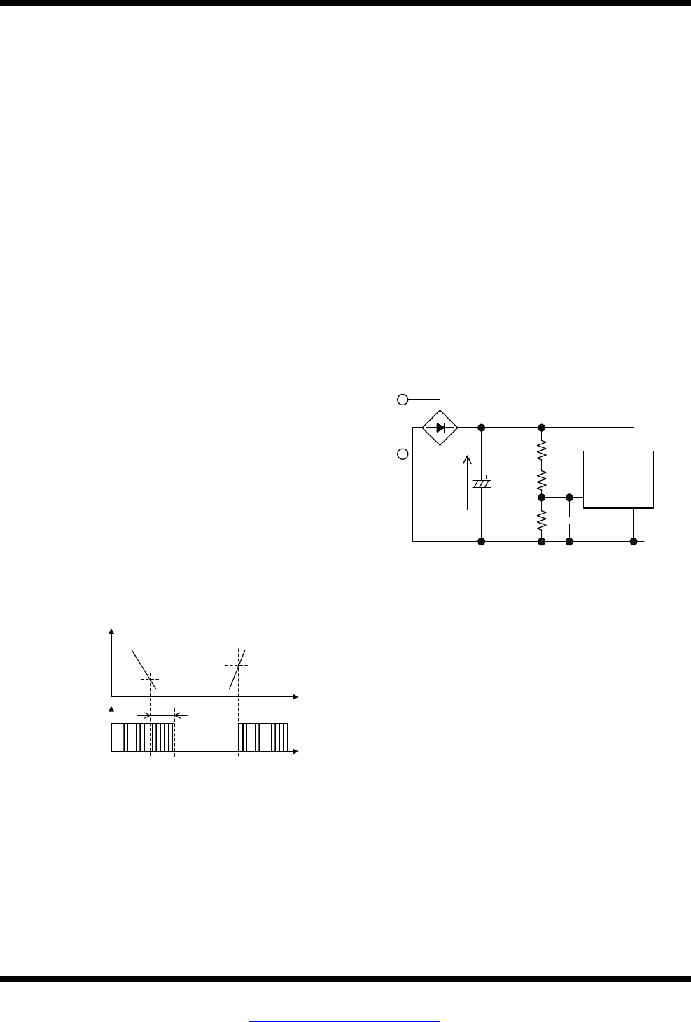
Typical Application Circuit
VAC
C1
C6R1
D1
BR1
R2
C2
T1
D
P
PC1
C3
R
OCP
C
Y
C5
1234
D/ST D/ST
BR
NC
S/OCP FB/OLP
GND
VCC
8 7 5
STR-A6000
U1
D2
C4
R
C
R
B
R
A
D51
C51
R51
R52
U51
R54
R56
C52
S
PC1
R53
R55
L51
C53
VOUT
(+)
TC_STR-A6000_1_R1
(-)
Package
DIP8
Not to Scale
Lineup
• Electrical Characteristics
Products
VDSS (min.) fOSC(AVG)
STR-A605×M 650 V 67 kHz
STR-A607×M 800 V
STR-A605×H 650 V 100 kHz
STR-A606×H 700 V
STR-A606×HD 700 V 100 kHz
*STR-A60××HD has two types OCP
• MOSFET ON Resistance and Output Power, POUT*
Products RDS(ON)
(max.)
P
OUT
(Adapter)
P
OUT
(Open frame)
AC230V
AC85
~265V
AC230V
AC85
~265V
fOSC(AVG) = 67 kHz
STR-A6051M 3.95 Ω 18.5 W 14 W 31 W 21 W
STR-A6052M 2.8 Ω 22 W 17.5W
35 W 24.5 W
STR-A6053M 1.9 Ω 26 W 21W
40 W 28 W
STR-A6079M 19.2 Ω 8 W 6 W 13 W 9 W
fOSC(AVG) = 100 kHz
STR-A6059H
6Ω 17 W 11 W 30 W 19.5 W STR-A6069H
STR-A6069HD
STR-A6061H 3.95Ω 20.5 W 15 W 35 W 23.5 W
STR-A6061HD
STR-A6062H 2.8 Ω 23 W 18 W 38 W 26.5 W
STR-A6062HD
STR-A6063HD
2.3 Ω 25 W 20 W 40 W 28 W
* The output power is actual continues power that is measured at
50 °C ambient. The peak output power can be 120 to 140 % of the
value stated here. Core size, ON Duty, and thermal design affect
the output power. It may be less than the value stated here.
Applications
• Low power AC/DC adapter
• White goods
• Auxiliary power supply
• OA, AV and industrial equipment

STR-A6000 Series
STR-A6000-DSJ Rev.4.4 SANKEN ELECTRIC CO., LTD. 2
Mar. 13, 2015 http://www.sanken-ele.co.jp/en
© SANKEN ELECTRIC CO., LTD. 2008
Contents
General Descriptions ------------------------------------------------------------------------------------------ 1
1. Absolute Maximum Ratings --------------------------------------------------------------------------- 3
2. Electrical Characteristics ------------------------------------------------------------------------------ 4
3. Performance Curves ------------------------------------------------------------------------------------ 6
3.1 Derating Curves ------------------------------------------------------------------------------- 6
3.2 Ambient Temperature versus Power Dissipation Curve ------------------------------ 6
3.3 MOSFET Safe Operating Area Curves --------------------------------------------------- 7
3.4 Transient Thermal Resistance Curves ---------------------------------------------------- 9
4. Functional Block Diagram --------------------------------------------------------------------------- 11
5. Pin Configuration Definitions ----------------------------------------------------------------------- 11
6. Typical Application Circuit -------------------------------------------------------------------------- 12
7. Package Outline ---------------------------------------------------------------------------------------- 13
8. Marking Diagram -------------------------------------------------------------------------------------- 13
9. Operational Description ------------------------------------------------------------------------------ 14
9.1 Startup Operation --------------------------------------------------------------------------- 14
9.2 Undervoltage Lockout (UVLO)----------------------------------------------------------- 15
9.3 Bias Assist Function ------------------------------------------------------------------------- 15
9.4 Constant Output Voltage Control -------------------------------------------------------- 15
9.5 Leading Edge Blanking Function -------------------------------------------------------- 16
9.6 Random Switching Function -------------------------------------------------------------- 16
9.7 Automatic Standby Mode Function ----------------------------------------------------- 16
9.8 Brown-In and Brown-Out Function ----------------------------------------------------- 17
9.8.1 DC Line Detection ------------------------------------------------------------------------ 17
9.8.2 AC Line Detection ------------------------------------------------------------------------ 18
9.9 Overcurrent Protection Function (OCP) ----------------------------------------------- 19
9.10 Overload Protection Function (OLP)---------------------------------------------------- 20
9.11 Overvoltage Protection (OVP) ------------------------------------------------------------ 20
9.12 Thermal Shutdown Function (TSD) ----------------------------------------------------- 20
10. Design Notes -------------------------------------------------------------------------------------------- 21
10.1 External Components----------------------------------------------------------------------- 21
10.2 PCB Trace Layout and Component Placement --------------------------------------- 22
11. Pattern Layout Example ----------------------------------------------------------------------------- 24
12. Reference Design of Power Supply ----------------------------------------------------------------- 25
Important Notes ---------------------------------------------------------------------------------------------- 27

STR-A6000 Series
STR-A6000-DSJ Rev.4.4 SANKEN ELECTRIC CO., LTD. 3
Mar. 13, 2015 http://www.sanken-ele.co.jp/en
© SANKEN ELECTRIC CO., LTD. 2008
1. Absolute Maximum Ratings
Current polarities are defined as follows: current going into the IC (sinking) is positive current (+); and current coming
out of the IC (sourcing) is negative current (−).
Unless otherwise specified, TA = 25 °C, 7 pin = 8 pin.
Parameter Symbol Test Conditions Pins Rating Units Remarks
Drain Peak Current(1) IDPEAK Single pulse 8 – 1
1.2
A
A6079M
1.8
A6059H / 69H
/ 69HD
2.5
A6051M / 61H
/ 61HD
3.0
A6052M / 62H
/ 62HD
4.0 A6053M / 63HD
Avalanche Energy(2)(3) EAS
ILPEAK=1.2A
8 – 1
7
mJ
A6079M
ILPEAK=1.8A 24
A6059H / 69H
/ 69HD
ILPEAK=2A 46 A6061H / 61HD
ILPEAK=2A 47 A6051M
ILPEAK=2.2A 56 A6062H / 62HD
ILPEAK=2.3A 62 A6052M
ILPEAK=2.5A 72 A6063HD
ILPEAK=2.7A 86 A6053M
S/OCP Pin Voltage VS/OCP 1 − 3 −2 to 6 V
BR Pin Voltage VBR 2 − 3 −0.3 to 7 V
BR Pin Sink Current IBR 2 − 3 1.0 mA
FB/OLP Pin Voltage
VFB 4 − 3 −0.3 to 14 V
FB/OLP Pin Sink Current IFB 4 − 3 1.0 mA
VCC Pin Voltage
VCC 5 − 3 32 V
MOSFET Power
Dissipation
(4) PD1 (5) 8 – 1 1.35 W
Control Part Power
Dissipation
PD2 5 – 3 1.2 W
Operating Ambient
Temperature
(6)
TOP — −20 to 125 °C
Storage Temperature Tstg — −40 to 125 °C
Channel Temperature Tch — 150 °C
(1) Refer to 3.3 MOSFET Safe Operating Area Curves
(2) Refer to Figure 3-2 Avalanche Energy Derating Coefficient Curve
(3) Single pulse, VDD = 99 V, L = 20 mH
(4) Refer to Figure 3-3 Ambient temperature versus power dissipation curve
(5) When embedding this hybrid IC onto the printed circuit board (cupper area in a 15 mm × 15 mm)
(6) The recommended internal frame temperature, TF, is 115°C (max.)

STR-A6000 Series
STR-A6000-DSJ Rev.4.4 SANKEN ELECTRIC CO., LTD. 4
Mar. 13, 2015 http://www.sanken-ele.co.jp/en
© SANKEN ELECTRIC CO., LTD. 2008
2. Electrical Characteristics
Current polarities are defined as follows: current going into the IC (sinking) is positive current (+); and current
coming out of the IC (sourcing) is negative current (−).
Unless otherwise specified, TA = 25 °C, VCC = 18 V, 7 pin = 8 pin.
Parameter Symbol
Test
Conditions
Pins Min. Typ. Max. Units Remarks
Power Supply Startup Operation
Operation Start Voltage VCC(ON) 5 − 3 13.8 15.3 16.8 V
Operation Stop Voltage(1) VCC(OFF) 5 − 3 7.3 8.1 8.9 V
Circuit Current in Operation ICC(ON) VCC = 12 V 5 − 3 — — 2.5 mA
Startup Circuit Operation
Voltage
VST(ON) 8 − 3 — 38 — V
Startup Current ISTARTUP VCC
= 13.5 V
5 − 3 − 3.7 − 2.5 − 1.5 mA
Startup Current Biasing
Threshold Voltage
VCC(BIAS)
I
CC
= − 100 µA 5 − 3 8.5 9.5 10.5 V
Normal Operation
Average Switching
Frequency fOSC(AVG) 8 − 3 60 67 74 kHz A60××M
90 100 110 A60××H / HD
Switching Frequency
Modulation Deviation Δf 8 − 3 — 5 — kHz A60××M
— 8 — A60××H / HD
Maximum ON Duty DMAX 8 − 3 77 83 89 %
Minimum ON Time tON(MIN) 8 − 3 — 540 — ns A60××M
— 470 — A60××H / HD
Protection Function
Leading Edge Blanking Time tBW — — 340 — ns A60××M
— 280 — A60××H / HD
OCP Compensation
Coefficient DPC — — 20 —
mV/μs A60××M
— 33 — A60××H / HD
OCP Compensation ON Duty DDPC — — 36 — %
OCP Threshold Voltage at
Zero ON Duty
VOCP(L) 1 − 3 0.70 0.78 0.86 V
OCP Threshold Voltage at
36% ON Duty
VOCP(H) VCC = 32 V 1 − 3 0.81 0.9 0.99 V
OCP Threshold Voltage in
Leading Edge Blanking Time
VOCP(LEB) 1 − 3 1.32 1.55 1.78 V A60××HD
Maximum Feedback Current IFB(MAX) VCC = 12 V 4 − 3 − 340 − 230 − 150 µA
Minimum Feedback Current IFB(MIN) 4 − 3 − 30 − 15 − 7 µA
FB/OLP pin Oscillation Stop
Threshold Voltage
VFB(STB) 4 − 3 0.85 0.95 1.05 V
OLP Threshold Voltage VFB(OLP) 4 − 3 7.3 8.1 8.9 V
OLP Operation Current ICC(OLP) VCC = 12 V 5 − 3 − 300 600 µA
OLP Delay Time tOLP — 54 68 82 ms
(1) VCC(BIAS) > VCC(OFF) always.

STR-A6000 Series
STR-A6000-DSJ Rev.4.4 SANKEN ELECTRIC CO., LTD. 5
Mar. 13, 2015 http://www.sanken-ele.co.jp/en
© SANKEN ELECTRIC CO., LTD. 2008
Parameter Symbol
Test
Conditions
Pins Min. Typ. Max. Units Remarks
FB/OLP Pin Clamp Voltage VFB(CLAMP) 4 − 3 11 12.8 14 V
Brown-In Threshold Voltage VBR(IN) VCC = 32 V 2 − 3 5.2 5.6 6 V
Brown-Out Threshold
Voltage
VBR(OUT) VCC = 32 V 2 − 3 4.45 4.8 5.15 V
BR Pin Clamp Voltage VBR(CLAMP) VCC = 32 V 2 − 3 6 6.4 7 V
BR Function Disabling
Threshold
VBR(DIS) VCC = 32 V 2 − 3 0.3 0.48 0.7 V
OVP Threshold Voltage VCC(OVP) 5 − 3 26 29 32 V
Latch Circuits Holding
Current
(2)
ICC(LATCH) VCC = 9.5 V 5 − 3 — 700 — μA
Thermal Shutdown Operating
Temperature
Tj(TSD) — 135 — — °C
MOSFET
Drain-to-Source Breakdown
Voltage VDSS 8 – 1
650 — —
V
A605×
700 — — A606×
800 — — A607×
Drain Leakage Current IDSS 8 – 1 — — 300 μA
On Resistance RDS(ON) IDS = 0.4A 8 − 1
— — 19.2
Ω
A6079M
— — 6
A6059H / 69H
/ 69HD
— — 3.95
A6051M / 61H
/ 61HD
— — 2.8
A6052M / 62H
/ 62HD
— — 2.3 A6063HD
— — 1.9 A6053M
Switching Time tf 8 – 1 — — 250 ns
— — 400 ns A6053M
Thermal Resistance
Channel to Case Thermal
Resistance
(3)
θch-C
— — — 22 °C/W
(2) A latch circuit is a circuit operated with Overvoltage Protection function (OVP) and/or Thermal Shutdown function
(TSD) in operation.
(3) θch-C is thermal resistance between channel and case. Case temperature (TC) is measured at the center of the case top
surface.
STR-A6000 Series
STR-A6000-DSJ Rev.4.4 SANKEN ELECTRIC CO., LTD. 6
Mar. 13, 2015 http://www.sanken-ele.co.jp/en
© SANKEN ELECTRIC CO., LTD. 2008
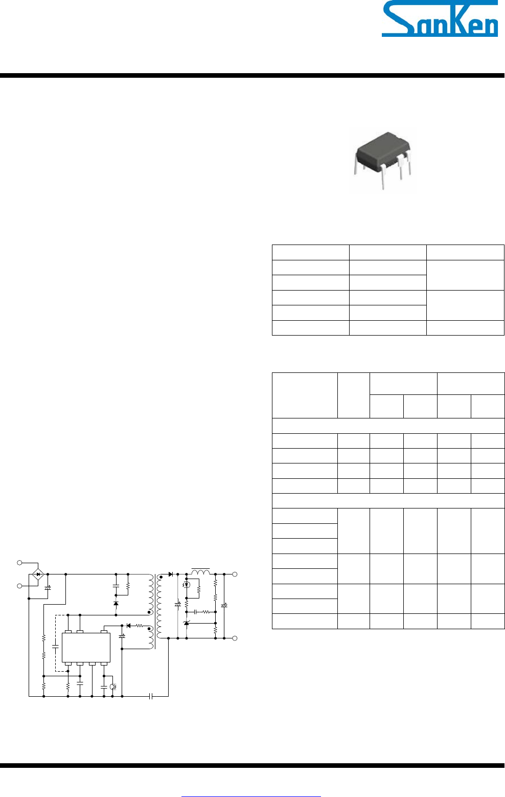
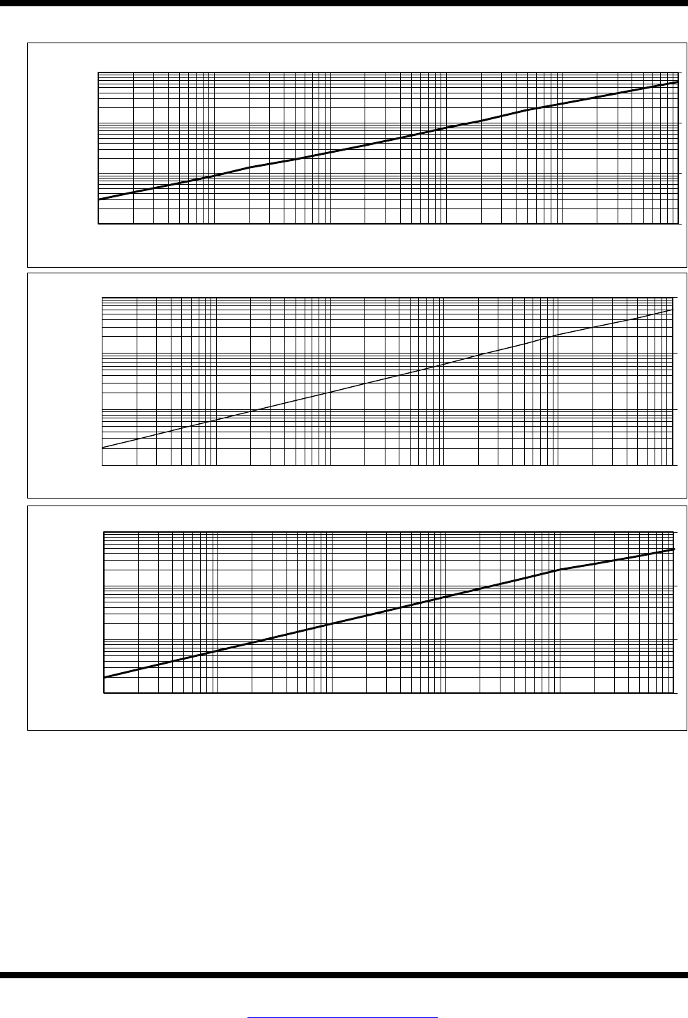
3. Performance Curves
3.1 Derating Curves
Figure 3-1. SOA Temperature Derating Coefficient
Curve Figure 3-2. Avalanche Energy Derating Coefficient
Curve
3.2 Ambient Temperature versus Power Dissipation Curve
Figure 3-3. Ambient Temperature Versus Power
Dissipation Curve
0
20
40
60
80
100
025 50 75 100 125 150
Safe Operating Area
Temperature Derating Coefficient (%)
Channel Temperature, Tch (°C)
0
20
40
60
80
100
25 50 75 100 125 150
EAS Temperature Derating Coefficient (%)
Channel Temperature, Tch (°C)
0
0.2
0.4
0.6
0.8
1
1.2
1.4
1.6
020 40 60 80 100 120 140 160
Power Dissipation, PD1 (W)
Ambient Temperature, TA(°C )
1.35W
STR-A6000 Series
STR-A6000-DSJ Rev.4.4 SANKEN ELECTRIC CO., LTD. 7
Mar. 13, 2015 http://www.sanken-ele.co.jp/en
© SANKEN ELECTRIC CO., LTD. 2008
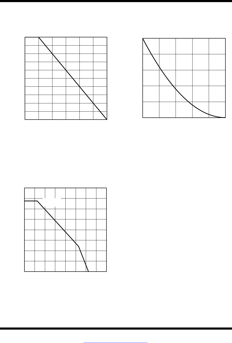
3.3 MOSFET Safe Operating Area Curves
When the IC is used, the safe operating area curve should be multiplied by the temperature derating coefficient
derived from Figure 3-1. The broken line in the safe operating area curve is the drain current curve limited by
on-resistance.
Unless otherwise specified, TA = 25 °C, Single pulse.
• STR-A6051M
• STR-A6052M
• STR-A6053M
• STR-A6079M
0.01
0.1
1
10
110 100 1000
Drain Current, I
D(A)
Drain-to-Source Voltage (V)
0.01
0.1
1
10
110 100 1000
Drain Current, ID(A)
Drain-to-Source Voltage (V)
0.01
0.1
1
10
110 100 1000
Drain Current, ID(A)
Drain-to-Source Voltage (V)
0.01
0.1
1
10
110 100 1000
Drain Current, ID(A)
Drain-to-Source Voltage (V)
0.1ms
1ms
0.1ms
1ms
0.1ms
1ms
0.1ms
1ms
STR-A6000 Series
STR-A6000-DSJ Rev.4.4 SANKEN ELECTRIC CO., LTD. 8
Mar. 13, 2015 http://www.sanken-ele.co.jp/en
© SANKEN ELECTRIC CO., LTD. 2008
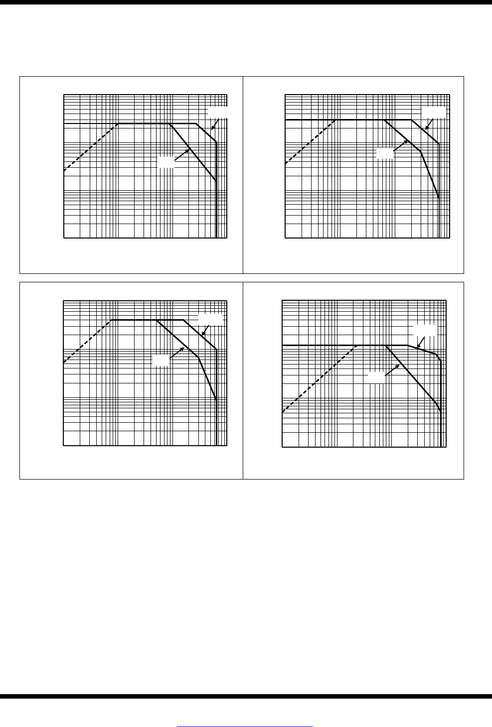
• STR-A6059H
• STR-A6061H / 61HD
• STR-A6062H / 62HD
• STR-A6063HD
• STR-A6069H / 69HD
0.01
0.1
1
10
110 100 1000
Drain Current, I
D(A)
Drain-to-Source Voltage (V)
0.01
0.1
1
10
110 100 1000
Drain Current, ID(A)
Drain-to-Source Voltage (V)
0.01
0.1
1
10
110 100 1000
Drain Current, ID(A)
Drain-to-Source Voltage (V)
0.01
0.1
1
10
110 100 1000
Drain Current, ID(A)
Drain-to-Source Voltage (V)
0.1ms
1ms
0.1ms
1ms
0.1ms
1ms
0.1ms
1ms
Drain Current, ID (A)
Drain-to-Source Voltage (V)
STR-A6000 Series
STR-A6000-DSJ Rev.4.4 SANKEN ELECTRIC CO., LTD. 9
Mar. 13, 2015 http://www.sanken-ele.co.jp/en
© SANKEN ELECTRIC CO., LTD. 2008
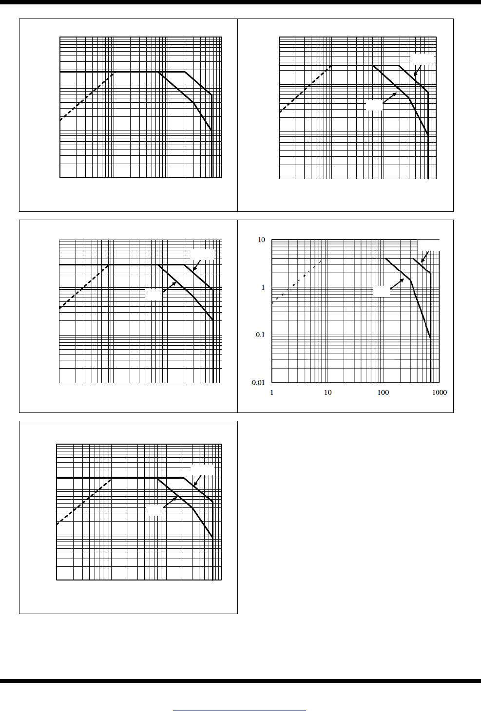
3.4 Transient Thermal Resistance Curves
• STR-A6051M / 61H / 61HD
• STR-A6052M / 62H / 62HD
• STR-A6053M
0.01
0.1
1
10
Transient Thermal Resistance,
θch-c (°C/W)
Time (s)
0.01
0.1
1
10
Transient Thermal Resistance,
θch-c (°C/W)
Time (s)
1µ 10µ 100µ 1m 10m 100m
1µ 10µ 100µ 1m 10m 100m
1µ 10µ 100µ 1m 10m 100m
Time (s)
10
1
0.1
0.01
Transient Thermal Resistance,
θch-c (°C/W)
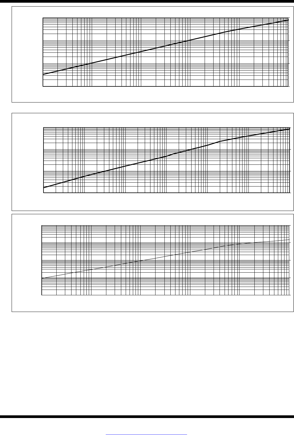
STR-A6000 Series
STR-A6000-DSJ Rev.4.4 SANKEN ELECTRIC CO., LTD. 10
Mar. 13, 2015 http://www.sanken-ele.co.jp/en
© SANKEN ELECTRIC CO., LTD. 2008
• STR-A6059M / 69H / 69HD
• STR-A6079M
• STR-A6063HD
0.01
0.1
1
10
Transient Thermal Resistance
θch-c (°C/W)
Time (s)
0.01
0.1
1
10
Transient Thermal Resistance
θch-c (°C/W)
Time (s)
100n 1µ 10µ 100µ 1m 10m 100m
1µ 10µ 100µ 1m 10m 100m
1µ 10µ 100µ 1m 10m 100m
Time (s)
10
1
0.1
0.01
0.001
Transient Thermal Resistance
θch-c (°C/W)
STR-A6000 Series
STR-A6000-DSJ Rev.4.4 SANKEN ELECTRIC CO., LTD. 11
Mar. 13, 2015 http://www.sanken-ele.co.jp/en
© SANKEN ELECTRIC CO., LTD. 2008
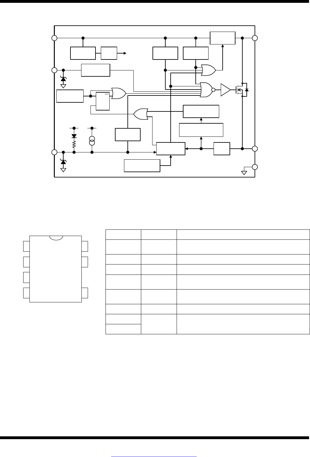
4. Functional Block Diagram
UVLO OVP TSD
REG
Brown-in
Brown-out
PWM OSC
OLP
Feedback
control
Slope
compensation
LEB
Drain peak current
compensation
OCP
Startup
DRV
VREG
6.4V
12.8V
7V VCC
VCC
BR
FB/OLP
D/ST
S/OCP
GND
7,8
1
3
4
2
5
S
R
Q
BD_STR-A6000_R1
5. Pin Configuration Definitions
1
5
6
7
8
4
3
2
S/OCP
BR
GND
FB/OLP VCC
D/ST
D/ST
Pin Name Descriptions
1 S/OCP
MOSFET source and overcurrent protection
(OCP) signal input
2 BR Brown-In and Brown-Out detection voltage input
3 GND Ground
4 FB /OLP
Constant voltage control signal input and over
load protection (OLP) signal input
5 VCC
Power supply voltage input for control part and
overvoltage protection (OVP) signal input
6 − (Pin removed)
7 D/ST MOSFET drain and startup current input
8
STR-A6000 Series
STR-A6000-DSJ Rev.4.4 SANKEN ELECTRIC CO., LTD. 12
Mar. 13, 2015 http://www.sanken-ele.co.jp/en
© SANKEN ELECTRIC CO., LTD. 2008
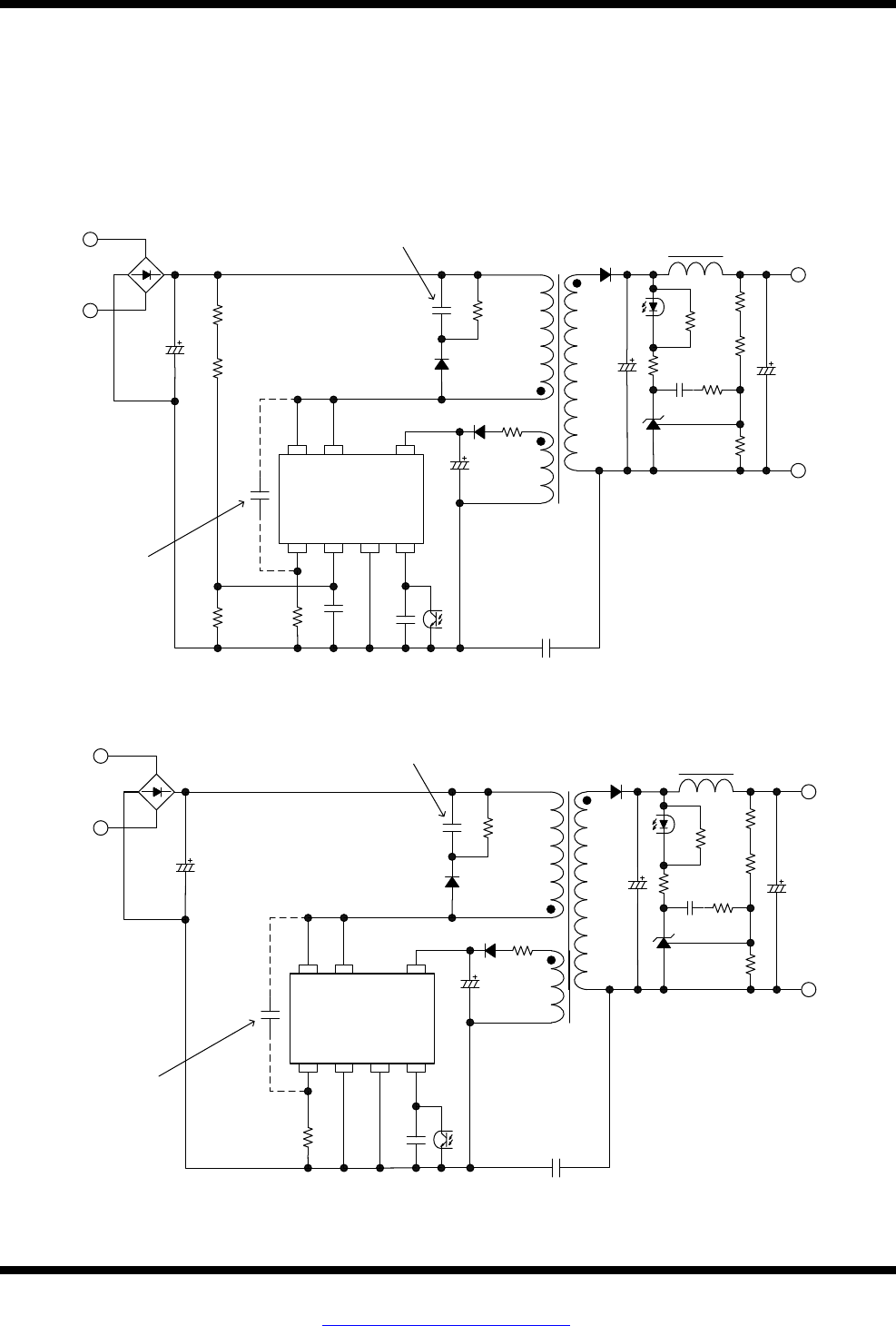
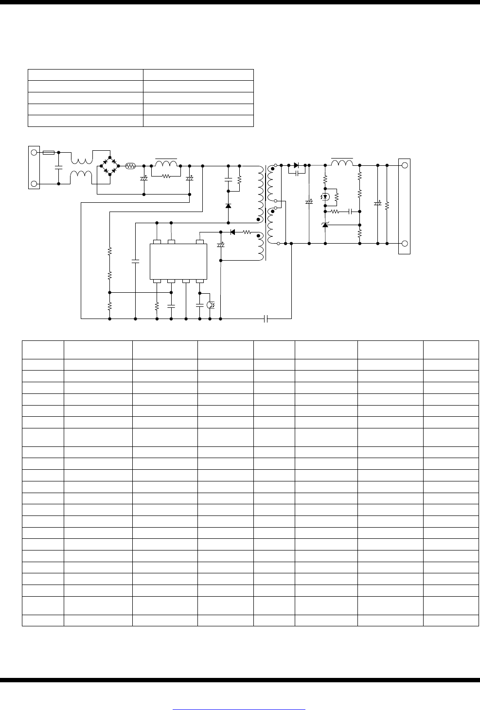
6. Typical Application Circuit
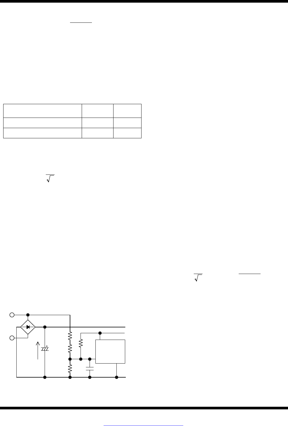
The following drawings show circuits enabled and disabled the Brown-In/Brown-Out function.
The PCB traces D/ST pins should be as wide as possible, in order to enhance thermal dissipation.
In applications having a power supply specified such that D/ST pin has large transient surge voltages, a clamp
snubber circuit of a capacitor-resistor-diode (CRD) combination should be added on the primary winding P, or a
damper snubber circuit of a capacitor (C) or a resistor-capacitor (RC) combination should be added between the D/ST
pin and the S/OCP pin.
VAC
C1
C6 R1
D1
BR1
R2
C2
T1
D
P
PC1
C3
R
OCP
C
Y
CRD clamp snubber
C5
C(RC)
damper snubber 1234
D/ST D/ST
BR
NC
S/OCP FB/OLP
GND
VCC
8 7 5
STR-A6000
U1
D2
C4
R
C
R
B
R
A
D51
C51
R51
R52
U51
R54
R56
C52
S
PC1
R53
R55
L51
C53
VOUT
(+)
TC_STR-A6000_2_R1
(-)
Figure 6-1. Typical Application Circuit (enabled Brown-In/Brown-Out function, DC line detection)
VAC
C1
C6 R1
D1
BR1
R2
C2
T1
D
P
PC1
C3
ROCP CY
CRD clamp snubber
C5
C(RC)
damper snubber 1234
D/ST D/ST
BR
NC
S/OCP FB/OLP
GND
VCC
8 7 5
STR-A6000
U1
D2
D51
C51
R51
R52
U51
R54
R56
C52
S
PC1
R53
R55
L51
C53
VOUT
TC_STR-A6000_3_R1
(+)
(-)
Figure 6-2. Typical Application Circuit (disabled Brown-In/Brown-Out function)
STR-A6000 Series
STR-A6000-DSJ Rev.4.4 SANKEN ELECTRIC CO., LTD. 13
Mar. 13, 2015 http://www.sanken-ele.co.jp/en
© SANKEN ELECTRIC CO., LTD. 2008
7. Package Outline
• DIP8 (The following show a representative type of DIP8.)
NOTES:
1) dimensions in millimeters
2) Pb-free (RoHS compliant)
8. Marking Diagram
1
8
Part Number
A 6 0 × × ×
S K Y M D
Control Number
STR-A60××M
STR-A60××H
Lot Number:
Y is the last digit of the year of manufacture (0 to 9)
M is the month of the year (1 to 9, O, N, or D)
D is a period of days:
1: the first 10 days of the month (1st to 10th)
2: the second 10 days of the month (11th to 20th)
3: the last 10–11 days of the month (21st to 31st)
1
8
A 6 0 × × H
S K Y M D D
STR-A60××HD
Part Number
Control Number
Lot Number:
Y is the last digit of the year of manufacture (0 to 9)
M is the month of the year (1 to 9, O, N, or D)
D is a period of days:
1: the first 10 days of the month (1st to 10th)
2: the second 10 days of the month (11th to 20th)
3: the last 10–11 days of the month (21st to 31st)
STR-A6000 Series
STR-A6000-DSJ Rev.4.4 SANKEN ELECTRIC CO., LTD. 14
Mar. 13, 2015 http://www.sanken-ele.co.jp/en
© SANKEN ELECTRIC CO., LTD. 2008
9. Operational Description
All of the parameter values used in these descriptions
are typical values, unless they are specified as minimum
or maximum.
Current polarities are defined as follows: current
going into the IC (sinking) is positive current (+); and
current coming out of the IC (sourcing) is negative
current (−).
9.1 Startup Operation
Figure 9-1 shows the circuit around IC. Figure 9-2
shows the start up operation.
The IC incorporates the startup circuit. The circuit is
connected to D/ST pin. When D/ST pin voltage reaches
to Startup Circuit Operation Voltage VST(ON) = 38 V, the
startup circuit starts operation.
During the startup process, the constant current,
ISTARTUP = − 2.5 mA, charges C2 at VCC pin. When
VCC pin voltage increases to VCC(ON) = 15.3 V, the
control circuit starts operation.
During the IC operation, the voltage rectified the
auxiliary winding voltage, VD, of Figure 9-1 becomes a
power source to the VCC pin. After switching operation
begins, the startup circuit turns off automatically so that
its current consumption becomes zero.
The approximate value of auxiliary winding voltage is
about 15 V to 20 V, taking account of the winding turns
of D winding so that VCC pin voltage becomes
Equation (1) within the specification of input and output
voltage variation of power supply.
.)(minV
V.)(max
V)
OVP(CC
CC)BIAS
(CC <<
⇒10.5 (V)
<< CC
V
26 (V) (1)
The oscillation start timing of IC depends on
Brown-In / Brown-Out function (refer to Section 9.8).
Without Brown-In / Brown-Out function (BR pin
voltage is VBR(DIS) = 0.48 V or less)
When VCC pin voltage increases to VCC(ON), the IC
starts switching operation, As shown in Figure 9-2.
The startup time of IC is determined by C2 capacitor
value. The approximate startup time tSTART (shown in
Figure 9-2) is calculated as follows:
STRATUP
)INT(CC)ON(CC
START
I
VV
×C2
t-
=
(2)
where,
tSTART : Startup time of IC (s)
VCC(INT) : Initial voltage on VCC pin (V)
With Brown-In / Brown-Out function
When BR pin voltage is more than VBR(DIS) = 0.48 V
and less than VBR(IN) = 5.6 V, the Bias Assist Function
(refer to Section 9.3) is disabled. Thus, VCC pin
voltage repeats increasing to VCC(ON) and decreasing to
VCC(OFF) (shown in Figure 9-3). When BR pin voltage
becomes VBR(IN) or more, the IC starts switching
operation.
VAC
C1
D2R2
C2
T1
D
P
BR1
VCC
GND
D/ST
7, 8
3
5
U1
V
D
BR
2
Figure 9-1. VCC Pin Peripheral Circuit
(Without Brown-In / Brown-Out)
VCC(ON)
VCC pin
voltage
Drain current,
ID
t
START
Figure 9-2. Startup Operation
(Without Brown-In / Brown-Out)
V
CC(ON)
VCC pin
voltage
Drain current,
I
D
t
START
BR pin
voltage V
BR(IN)
V
CC(OFF)
Figure 9-3. Startup Operation
(With Brown-In / Brown-Out)
STR-A6000 Series
STR-A6000-DSJ Rev.4.4 SANKEN ELECTRIC CO., LTD. 15
Mar. 13, 2015 http://www.sanken-ele.co.jp/en
© SANKEN ELECTRIC CO., LTD. 2008
9.2 Undervoltage Lockout (UVLO)
Figure 9-4 shows the relationship of VCC pin voltage
and circuit current ICC. When VCC pin voltage decreases
to VCC(OFF) = 8.1 V, the control circuit stops operation by
UVLO (Undervoltage Lockout) circuit, and reverts to
the state before startup.
Circuit current, ICC
ICC(ON)
VCC(OFF)VCC(ON)VCC pin
voltage
StartStop
Figure 9-4. Relationship between
VCC Pin Voltage and ICC
9.3 Bias Assist Function
Figure 9-5 shows VCC pin voltage behavior during
the startup period.
After VCC pin voltage increases to VCC(ON) = 15.3 V
at startup, the IC starts the operation. Then circuit
current increases and VCC pin voltage decreases. At the
same time, the auxiliary winding voltage VD increases in
proportion to output voltage. These are all balanced to
produce VCC pin voltage.
IC starts operation
VCC pin
voltage
VCC(ON)
VCC(BIAS)
VCC(OFF)
Startup failure
Startup success
Target operating
voltage
Time
Bias assist period
Increase with rising of
output voltage
Figure 9-5. VCC Pin Voltage during Startup Period
The surge voltage is induced at output winding at
turning off a power MOSFET. When the output load is
light at startup, the surge voltage causes the unexpected
feedback control. This results the lowering of the output
power and VCC pin voltage. When the VCC pin voltage
decreases to VCC(OFF) = 8.1 V, the IC stops switching
operation and a startup failure occurs. In order to prevent
this, the Bias Assist function is activated when the VCC
pin voltage decreases to the startup current threshold
biasing voltage, VCC(BIAS) = 9.5 V. While the Bias Assist
function is activated, any decrease of the VCC pin
voltage is counteracted by providing the startup current,
ISTARTUP, from the startup circuit. Thus, the VCC pin
voltage is kept almost constant.
By the Bias Assist function, the value of C2 is
allowed to be small and the startup time becomes shorter.
Also, because the increase of VCC pin voltage becomes
faster when the output runs with excess voltage, the
response time of the OVP function becomes shorter.
It is necessary to check and adjust the startup process
based on actual operation in the application, so that poor
starting conditions may be avoided.
9.4 Constant Output Voltage Control
The IC achieves the constant voltage control of the
power supply output by using the current-mode control
method, which enhances the response speed and
provides the stable operation.
The FB/OLP pin voltage is internally added the slope
compensation at the feedback control (refer to Section 4
Functional Block Diagram), and the target voltage, VSC,
is generated. The IC compares the voltage, VROCP, of a
current detection resistor with the target voltage, VSC, by
the internal FB comparator, and controls the peak value
of VROCP so that it gets close to VSC, as shown in Figure
9-6 and Figure 9-7.
PC1
C3
R
OCP
1 3 4
S/OCP FB/OLP
GND
U1
I
FB
V
ROCP
Figure 9-6. FB/OLP Pin Peripheral Circuit
V
SC
FB Comparator
Drain current,
I
D
+
-
Voltage on both
sides of ROCP
VROCP
Target voltage including
Slope Compensation
Figure 9-7. Drain Current, ID, and FB Comparator
Operation in Steady Operation
STR-A6000 Series
STR-A6000-DSJ Rev.4.4 SANKEN ELECTRIC CO., LTD. 16
Mar. 13, 2015 http://www.sanken-ele.co.jp/en
© SANKEN ELECTRIC CO., LTD. 2008
• Light load conditions
When load conditions become lighter, the output
voltage, VOUT, increases. Thus, the feedback current
from the error amplifier on the secondary-side also
increases. The feedback current is sunk at the FB/OLP
pin, transferred through a photo-coupler, PC1, and the
FB/OLP pin voltage decreases. Thus, VSC decreases,
and the peak value of VROCP is controlled to be low,
and the peak drain current of ID decreases.
This control prevents the output voltage from
increasing.
• Heavy load conditions
When load conditions become greater, the IC
performs the inverse operation to that described above.
Thus, VSC increases and the peak drain current of ID
increases.
This control prevents the output voltage from
decreasing.
In the current mode control method, when the drain
current waveform becomes trapezoidal in continuous
operating mode, even if the peak current level set by the
target voltage is constant, the on-time fluctuates based
on the initial value of the drain current.
This results in the on-time fluctuating in multiples of
the fundamental operating frequency as shown in Figure
9-8. This is called the subharmonics phenomenon.
In order to avoid this, the IC incorporates the Slope
Compensation function. Because the target voltage is
added a down-slope compensation signal, which reduces
the peak drain current as the on-duty gets wider relative
to the FB/OLP pin signal to compensate VSC, the
subharmonics phenomenon is suppressed.
Even if subharmonic oscillations occur when the IC
has some excess supply being out of feedback control,
such as during startup and load shorted, this does not
affect performance of normal operation.
tON1
Target voltage
without slope compensation
tON2
T T T
Figure 9-8. Drain Current, ID, Waveform
in Subharmonic Oscillation
9.5 Leading Edge Blanking Function
The IC uses the peak-current-mode control method
for the constant voltage control of output.
In peak-current-mode control method, there is a case
that the power MOSFET turns off due to unexpected
response of FB comparator or overcurrent protection
circuit (OCP) to the steep surge current in turning on a
power MOSFET.
In order to prevent this response to the surge voltage
in turning-on the power MOSFET, the Leading Edge
Blanking, tBW (STR-A60××H for 340 ns, STR-A60××H
and STR-A60××HD for 280 ns) is built-in. During tBW,
the OCP threshold voltage becomes about 1.7 V which
is higher than the normal OCP threshold voltage (refer
to Section 9.9).
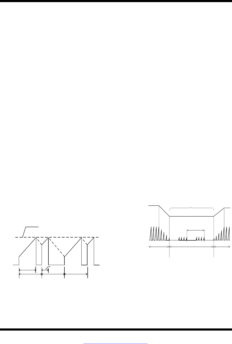
9.6 Random Switching Function
The IC modulates its switching frequency randomly
by superposing the modulating frequency on fOSC(AVG) in
normal operation. This function reduces the conduction
noise compared to others without this function, and
simplifies noise filtering of the input lines of power
supply.
9.7 Automatic Standby Mode Function
Automatic standby mode is activated automatically
when the drain current, ID, reduces under light load
conditions, at which ID is less than 15 % to 20 % of the
maximum drain current (it is in the OCP state). The
operation mode becomes burst oscillation, as shown in
Figure 9-9. Burst oscillation mode reduces switching
losses and improves power supply efficiency because of
periodic non-switching intervals.
Normal
operation Standby
operation Normal
operation
Burst oscillation
Output current,
I
OUT
Drain current,
I
D
Below several kHz
Figure 9-9. Auto Standby Mode Timing
Generally, to improve efficiency under light load
conditions, the frequency of the burst oscillation mode
becomes just a few kilohertz. Because the IC suppresses
the peak drain current well during burst oscillation mode,
audible noises can be reduced.
If the VCC pin voltage decreases to VCC(BIAS) = 9.5 V
during the transition to the burst oscillation mode, the
Bias Assist function is activated and stabilizes the
STR-A6000 Series
STR-A6000-DSJ Rev.4.4 SANKEN ELECTRIC CO., LTD. 17
Mar. 13, 2015 http://www.sanken-ele.co.jp/en
© SANKEN ELECTRIC CO., LTD. 2008
Standby mode operation, because ISTARTUP is provided to
the VCC pin so that the VCC pin voltage does not
decrease to VCC(OFF).
However, if the Bias Assist function is always
activated during steady-state operation including
standby mode, the power loss increases. Therefore, the
VCC pin voltage should be more than VCC(BIAS), for
example, by adjusting the turns ratio of the auxiliary
winding and secondary winding and/or reducing the
value of R2 in Figure 10-2 (refer to Section 10.1
Peripheral Components for a detail of R2).
9.8 Brown-In and Brown-Out Function
This function stops switching operation when it
detects low input line voltage, and thus prevents
excessive input current and overheating.
This function turns on and off switching operation
according to the BR pin voltage detecting the AC input
voltage. When BR pin voltage becomes more than
VBR(DIS) = 0.48 V, this function is activated.
Figure 9-10 shows waveforms of the BR pin voltage
and the drain currnet.
Even if the IC is in the operating state that the VCC
pin voltage is VCC(OFF) or more, when the AC input
voltage decreases from steady-state and the BR pin
voltage falls to VBR(OUT) = 4.8 V or less for the OLP
Delay Time, tOLP = 68 ms, the IC stops switching
operation. When the AC input voltage increases and the
BR pin voltage reaches VBR(IN) = 5.6 V or more in the
operating state that the VCC pin voltage is VCC(OFF) or
more, the IC starts switching operation.
In case the Brown-In and Brown-Out function is
unnecessary, connect the BR pin trace to the GND pin
trace so that the BR pin voltage is VBR(DIS) or less.
BR Pin Voltage
VBR(IN)
VBR(OUT)
tOLP
Drain Current,
ID
Figure 9-10. BR Pin Voltage and Drain Current
Waveforms
During burst oscillation mode, this function operates
as follows:
● STR-A60××M and STR-A60××H:
This function is disabled during switching operation
stop period in burst oscillation mode. When the BR
pin voltage falls to VBR(OUT) or less in burst oscillation
mode and the sum of switching operation period
becomes tOLP = 68 ms or more, the IC stops switching
operation.
● STR-A60××HD:
When the BR pin voltage falls to VBR(OUT) = 4.8 V or
less for tOLP = 68 ms, the IC stops switching operation.
There are two types of detection method as follows:
9.8.1 DC Line Detection
Figure 9-11 shows BR pin peripheral circuit of DC
line detection. There is a ripple voltage on C1 occurring
at a half period of AC cycle. In order to detect each peak
of the ripple voltage, the time constant of RC and C4
should be shorter than a half period of AC cycle.
Since the cycle of the ripple voltage is shorter than
tOLP, the switching operation does not stop when only the
bottom part of the ripple voltage becomes lower than
VBR(OUT).
Thus it minimizes the influence of load conditions on
the voltage detection.
VDC U1
BR
2
C4
RC
GND
3
RB
RA
VAC
BR1
C1
Figure 9-11. DC Line Detection
The components around BR pin:
・ RA and RB are a few megohms. Because of high
voltage applied and high resistance, it is
recommended to select a resistor designed against
electromigration or use a combination of resistors
in series for that to reduce each applied voltage,
according to the requirement of the application.
・ RC is a few hundred kilohms
・ C4 is 470 pF to 2200 pF for high frequency noise
reduction
Neglecting the effect of both input resistance and
forward voltage of rectifier diode, the reference value of
C1 voltage when Brown-In and Brown-Out function is
activated is calculated as follows:
STR-A6000 Series
STR-A6000-DSJ Rev.4.4 SANKEN ELECTRIC CO., LTD. 18
Mar. 13, 2015 http://www.sanken-ele.co.jp/en
© SANKEN ELECTRIC CO., LTD. 2008
+
+×=
C
BA
)TH(BR)OP(DC
R
RR
1VV
(3)
where,
VDC(OP) : C1 voltage when Brown-In and
Brown-Out function is activated
VBR(TH) : Any one of threshold voltage of BR pin
(see Table 9-1)
Table 9-1. BR Pin Threshold Voltage
Parameter Symbol
Value
(Typ.)
Brown-In Threshold Voltage VBR(IN) 5.6 V
Brown-Out Threshold Voltage VBR(OUT) 4.8 V
VDC(OP) can be expressed as the effective value of AC
input voltage using Equation (4).
)OP(DCRMS
)OP(AC V
2
1
V×=
(4)
RA, RB, RC and C4 should be selected based on actual
operation in the application.
9.8.2 AC Line Detection
Figure 9-12 shows BR pin peripheral circuit of AC
line detection. In order to detect the AC input voltage,
the time constant of RC and C4 should be longer than the
period of AC cycle. Thus the response of BR pin
detection becomes slow compared with the DC line
detection.
This method detects the AC input voltage, and thus it
minimizes the influence from load conditions. Also, this
method is free of influence from C1 charging and
discharging time, the latch mode can be released
quickly*
V
DC
U1
BR
2
C4
R
C
GND
3
R
B
R
A
V
AC
BR1
C1
VCC
3
R
S
Figure 9-12. AC Line Detection
* High-Speed Latch Release
When Overvoltage Protection function (OVP) or
Thermal Shutdown function (TSD) are activated,
the IC stops switching operation in latch mode.
Releasing the latch mode is done by decreasing the
VCC pin voltage below VCC(OFF) or by decreasing
the BR pin voltage below VBR(OUT).
In case of the DC line detection or without
Brown-in / Brown-Out function, the release time
depends on discharge time of C1 and takes longer
time until VCC pin voltage decreases to release
voltage.
In case of the AC line detection, BR pin voltage is
decreased quickly when AC input voltage, VAC, is
turned off, and thus the latch mode is quickly
released.
The components around BR pin:
・ RA and RB are a few megohms. Because of high
voltage applied and high resistance, it is
recommended to select a resistor designed against
electromigration or use a combination of resistors
in series for that to reduce each applied voltage,
according to the requirement of the application.
・ RC is a few hundred kilohms
・ RS must be adjusted so that the BR pin voltage is
more than VBR(DIS) = 0.48 V when the VCC pin
voltage is VCC(OFF) = 8.1 V
・ C4 is 0.22 μF to 1 μF for averaging AC input
voltage and high frequency noise reduction.
Neglecting the effect of input resistance is zero, the
reference effective value of AC input voltage when
Brown-In and Brown-Out function is activated is
calculated as follows:
+
+××
π
=
C
BA
)TH
(
BRRMS
)OP
(
AC
R
RR
1V
2
V
(5)
where,
VAC(OP)RMS :The effective value of AC input voltage
when Brown-In and Brown-Out function
is activated
VBR(TH) :Any one of threshold voltage of BR pin
(see Table 9-1)
RA, RB, RC and C4 should be selected based on actual
operation in the application.
STR-A6000 Series
STR-A6000-DSJ Rev.4.4 SANKEN ELECTRIC CO., LTD. 19
Mar. 13, 2015 http://www.sanken-ele.co.jp/en
© SANKEN ELECTRIC CO., LTD. 2008
9.9 Overcurrent Protection Function
(OCP)
Overcurrent Protection Function (OCP) detects each
drain peak current level of a power MOSFET on
pulse-by-pulse basis, and limits the output power when
the current level reaches to OCP threshold voltage.
During Leading Edge Blanking Time, the operation of
OCP is different depending on the products as follows.
● STR-A60××HD:
During Leading Edge Blanking Time, the OCP
threshold voltage becomes VOCP(LEB) = 1.55 V which
is higher than the normal OCP threshold voltage as
shown in Figure 9-13. Changing to this threshold
voltage prevents the IC from responding to the surge
voltage in turning-on the power MOSFET. This
function operates as protection at the condition such
as output windings shorted or unusual withstand
voltage of secondary-side rectifier diodes.
● STR-A60××M and STR-A60××H:
OCP is disabled during Leading Edge Blanking Time.
When power MOSFET turns on, the surge voltage
width of S/OCP pin should be less than tBW, as shown in
Figure 9-13. In order to prevent surge voltage, pay extra
attention to ROCP trace layout (refer to Section 10.2).
In addition, if a C (RC) damper snubber of Figure
9-14 is used, reduce the capacitor value of damper
snubber.
Surge pulse voltage width at turning on
t
BW
V
OCP
’
V
OCP(LEB)
(STR-A60××HD)
Figure 9-13. S/OCP Pin Voltage
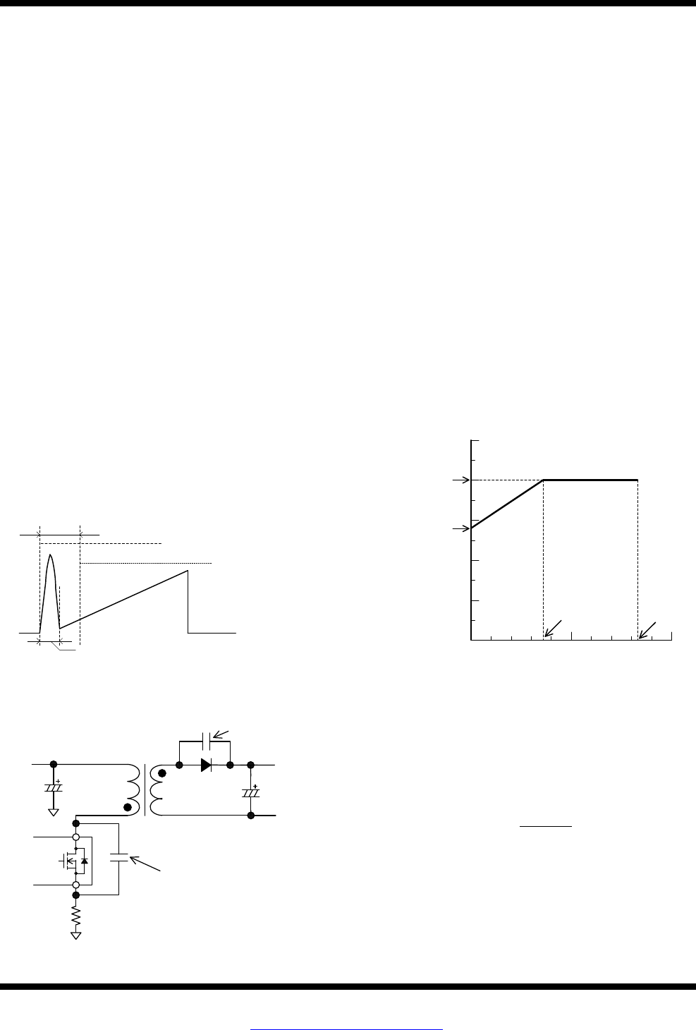
C1
T1
D51
R
OCP
U1
C51
C(RC)
Damper snubber
7,8
D/ST
S/OCP
1
C(RC)
Damper snubber
Figure 9-14. Damper Snubber
< Input Compensation Function >
ICs with PWM control usually have some propagation
delay time. The steeper the slope of the actual drain
current at a high AC input voltage is, the larger the
detection voltage of actual drain peak current is,
compared to VOCP. Thus, the peak current has some
variation depending on the AC input voltage in OCP
state. In order to reduce the variation of peak current in
OCP state, the IC incorporates a built-in Input
Compensation function.
The Input Compensation Function is the function of
correction of OCP threshold voltage depending with AC
input voltage, as shown in Figure 9-15. When AC input
voltage is low (ON Duty is broad), the OCP threshold
voltage is controlled to become high. The difference of
peak drain current become small compared with the case
where the AC input voltage is high (ON Duty is narrow).
The compensation signal depends on ON Duty. The
relation between the ON Duty and the OCP threshold
voltage after compensation VOCP' is expressed as
Equation (6). When ON Duty is broader than 36 %, the
VOCP' becomes a constant value VOCP(H) = 0.9 V
ON Duty (%)
DDPC
VOCP(L)
0
DMAX
100
VOCP(H)
0.5
1.0
50
OCP Threshold Voltage after
compensation, VOCP'
Figure 9-15. Relationship between ON Duty and Drain
Current Limit after Compensation
ONTime
DPCV
'V )L(OCP
OCP
×+
=
)AVG(OSC
)
L(OCP
f
ONDuty
DPC
V×+=
(6)
where,
VOCP(L): OCP Threshold Voltage at Zero ON Duty
DPC: OCP Compensation Coefficient
ONTime: On-time of power MOSFET
ONDuty: On duty of power MOSFET
fOSC(AVG): Average PWM Switching Frequency
STR-A6000 Series
STR-A6000-DSJ Rev.4.4 SANKEN ELECTRIC CO., LTD. 20
Mar. 13, 2015 http://www.sanken-ele.co.jp/en
© SANKEN ELECTRIC CO., LTD. 2008
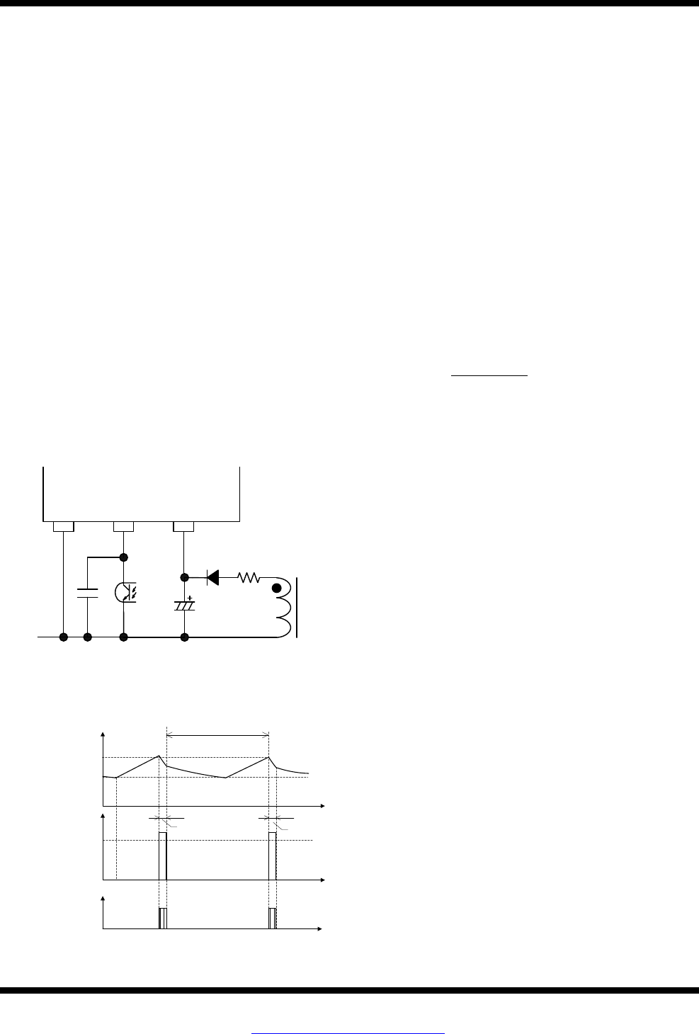
9.10 Overload Protection Function (OLP)
Figure 9-16 shows the FB/OLP pin peripheral circuit,
and Figure 9-17 shows each waveform for OLP
operation. When the peak drain current of ID is limited
by OCP operation, the output voltage, VOUT, decreases
and the feedback current from the secondary
photo-coupler becomes zero. Thus, the feedback current,
IFB, charges C3 connected to the FB/OLP pin and the
FB/OLP pin voltage increases. When the FB/OLP pin
voltage increases to VFB(OLP) = 8.1 V or more for the
OLP delay time, tOLP = 68 ms or more, the OLP function
is activated, the IC stops switching operation.
During OLP operation, Bias Assist Function is
disabled. Thus, VCC pin voltage decreases to VCC(OFF),
the control circuit stops operation. After that, the IC
reverts to the initial state by UVLO circuit, and the IC
starts operation when VCC pin voltage increases to
VCC(ON) by startup current. Thus the intermittent
operation by UVLO is repeated in OLP state.
This intermittent operation reduces the stress of parts
such as power MOSFET and secondary side rectifier
diode. In addition, this operation reduces power
consumption because the switching period in this
intermittent operation is short compared with oscillation
stop period. When the abnormal condition is removed,
the IC returns to normal operation automatically.
PC1
C3
4
FB/OLP
U1
VCC
5
GND
3
D2 R2
C2
D
Figure 9-16. FB/OLP Pin Peripheral Circuit
VCC pin voltage
FB/OLP pin voltage
Drain current,
I
D
V
CC(OFF)
V
FB(OLP)
t
OLP
V
CC(ON)
Non-switching interval
t
OLP
Figure 9-17. OLP Operational Waveforms
9.11 Overvoltage Protection (OVP)
When a voltage between VCC pin and GND pin
increases to VCC(OVP) = 29 V or more, OVP function is
activated, the IC stops switching operation at the latched
state. In order to keep the latched state, when VCC pin
voltage decreases to VCC(BIAS), the bias assist function is
activated and VCC pin voltage is kept to over the
VCC(OFF).
Releasing the latched state is done by turning off the
input voltage and by dropping the VCC pin voltage
below VCC(OFF), or by dropping the BR pin voltage below
VBR(OUT).
In case the VCC pin voltage is provided by using
auxiliary winding of transformer, the overvoltage
conditions such as output voltage detection circuit open
can be detected because the VCC pin voltage is
proportional to output voltage. The approximate value of
output voltage VOUT(OVP) in OVP condition is calculated
by using Equation (7).
×=
)NORMAL(CC
)NORMAL(OUT
OUT(OVP)
V
V
V
29 (V) (7)
where,
VOUT(NORMAL): Output voltage in normal operation
VCC(NORMAL): VCC pin voltage in normal operation
9.12 Thermal Shutdown Function (TSD)
When the temperature of control circuit increases to
Tj(TSD) = 135 °C (min.) or more, Thermal Shutdown
function (TSD) is activated, the IC stops switching
operation at the latched state. In order to keep the
latched state, when VCC pin voltage decreases to
VCC(BIAS), the bias assist function is activated and VCC
pin voltage is kept to over the VCC(OFF).
Releasing the latched state is done by turning off the
input voltage and by dropping the VCC pin voltage
below VCC(OFF), or by dropping the BR pin voltage below
VBR(OUT).
STR-A6000 Series
STR-A6000-DSJ Rev.4.4 SANKEN ELECTRIC CO., LTD. 21
Mar. 13, 2015 http://www.sanken-ele.co.jp/en
© SANKEN ELECTRIC CO., LTD. 2008
10. Design Notes
10.1 External Components
Take care to use properly rated, including derating as
necessary and proper type of components.
VAC
C1
C6 R1
D1
BR1
R2
C2
T1
D
P
PC1
C3
R
OCP
CRD clamp snubber
C5
1234
D/ST D/ST
BR
NC
S/OCP FB/OLP
GND
VCC
8 7 5
U1
D2
C4
R
C
R
B
R
A
C(RC) damper snubber
Figure 10-1. The IC Peripheral Circuit
• Input and Output Electrolytic Capacitor
Apply proper derating to ripple current, voltage, and
temperature rise. Use of high ripple current and low
impedance types, designed for switch mode power
supplies, is recommended.
• S/OCP Pin Peripheral Circuit
In Figure 10-1, ROCP is the resistor for the current
detection. A high frequency switching current flows
to ROCP, and may cause poor operation if a high
inductance resistor is used. Choose a low inductance
and high surge-tolerant type.
• BR pin peripheral circuit
Because RA and RB (see Figure 10-1) are applied high
voltage and are high resistance, the following should be
considered according to the requirement of the
application:
▫ Select a resistor designed against electromigration,
or
▫ Use a combination of resistors in series for that to
reduce each applied voltage
See the section 9.8 about the AC input voltage
detection function and the components around BR pin.
When the detection resistor (RA, RB, RC) value is
decreased and the C4 value is increased to prevent
unstable operation resulting from noise at the BR pin,
pay attention to the low efficiency and the slow
response of BR pin.
• FB/OLP Pin Peripheral Circuit
C3 is for high frequency noise reduction and phase
compensation, and should be connected close to these
pins. The value of C3 is recommended to be about
2200 pF to 0.01µF, and should be selected based on
actual operation in the application.
• VCC Pin Peripheral Circuit
The value of C2 in Figure 10-1 is generally
recommended to be 10µ to 47μF (refer to Section 9.1
Startup Operation, because the startup time is
determined by the value of C2).
In actual power supply circuits, there are cases in
which the VCC pin voltage fluctuates in proportion to
the output current, IOUT (see Figure 10-2), and the
Overvoltage Protection function (OVP) on the VCC
pin may be activated. This happens because C2 is
charged to a peak voltage on the auxiliary winding D,
which is caused by the transient surge voltage coupled
from the primary winding when the power MOSFET
turns off.
For alleviating C2 peak charging, it is effective to add
some value R2, of several tenths of ohms to several
ohms, in series with D2 (see Figure 10-1). The
optimal value of R2 should be determined using a
transformer matching what will be used in the actual
application, because the variation of the auxiliary
winding voltage is affected by the transformer
structural design.
Without R2
With R2
VCC pin voltage
Output current, I
OUT
Figure 10-2. Variation of VCC Pin Voltage and Power
• Snubber Circuit
In case the surge voltage of VDS is large, the circuit
should be added as follows (see Figure 10-1);
・ A clamp snubber circuit of a capacitor-resistor-
diode (CRD) combination should be added on the
primary winding P.
・ A damper snubber circuit of a capacitor (C) or a
resistor-capacitor (RC) combination should be
added between the D/ST pin and the S/OCP pin.
In case the damper snubber circuit is added, this
components should be connected near D/ST pin
and S/OCP pin.
STR-A6000 Series
STR-A6000-DSJ Rev.4.4 SANKEN ELECTRIC CO., LTD. 22
Mar. 13, 2015 http://www.sanken-ele.co.jp/en
© SANKEN ELECTRIC CO., LTD. 2008
• Peripheral circuit of secondary side shunt regulator
Figure 10-3 shows the secondary side detection circuit
with the standard shunt regulator IC (U51).
C52 and R53 are for phase compensation. The value
of C52 and R53 are recommended to be around
0.047μF to 0.47μF and 4.7 kΩ to 470 kΩ, respectively.
They should be selected based on actual operation in
the application.
D51
C51
R51
R52
U51
R54
R56
C52
S
PC1
R53
R55
L51
C53
VOUT
(-)
T1
(+)
Figure 10-3. Peripheral Circuit of Secondary Side
Shunt Regulator (U51)
• Transformer
Apply proper design margin to core temperature rise
by core loss and copper loss.
Because the switching currents contain high
frequency currents, the skin effect may become a
consideration.
Choose a suitable wire gauge in consideration of the
RMS current and a current density of 4 to 6 A/mm2.
If measures to further reduce temperature are still
necessary, the following should be considered to
increase the total surface area of the wiring:
▫ Increase the number of wires in parallel.
▫ Use litz wires.
▫ Thicken the wire gauge.
In the following cases, the surge of VCC pin
voltage becomes high.
▫ The surge voltage of primary main winding, P, is
high (low output voltage and high output current
power supply designs)
▫ The winding structure of auxiliary winding, D, is
susceptible to the noise of winding P.
When the surge voltage of winding D is high, the
VCC pin voltage increases and the Overvoltage
Protection function (OVP) may be activated. In
transformer design, the following should be
considered;
▫ The coupling of the winding P and the secondary
output winding S should be maximized to reduce the
leakage inductance.
▫ The coupling of the winding D and the winding S
should be maximized.
▫ The coupling of the winding D and the winding P
should be minimized.
In the case of multi-output power supply, the
coupling of the secondary-side stabilized output
winding, S1, and the others (S2, S3…) should be
maximized to improve the line-regulation of those
outputs.
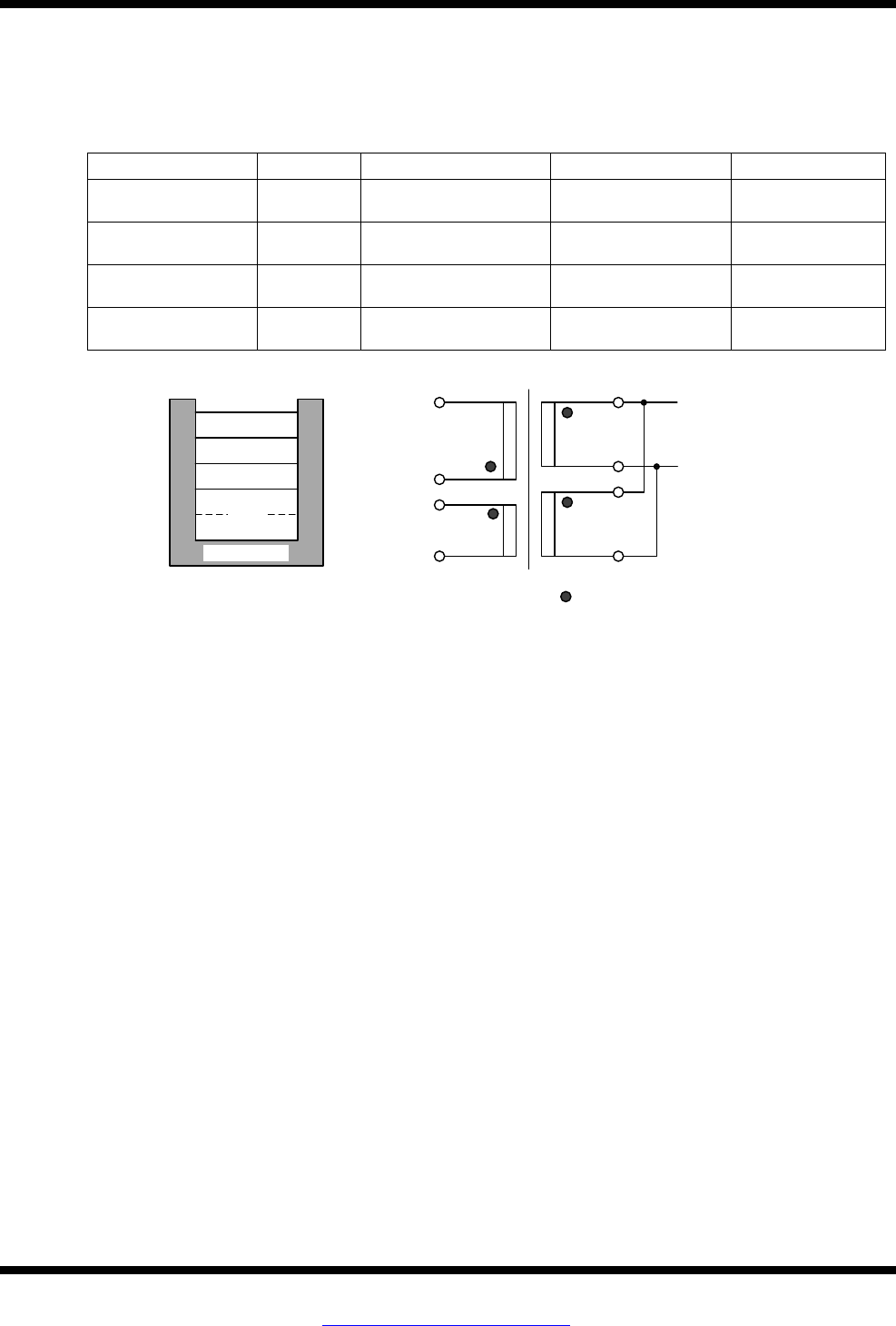
Figure 10-4 shows the winding structural examples
of two outputs.
Winding structural example (a):
S1 is sandwiched between P1 and P2 to
maximize the coupling of them for surge
reduction of P1 and P2.
D is placed far from P1 and P2 to minimize the
coupling to the primary for the surge reduction of
D.
Winding structural example (b)
P1 and P2 are placed close to S1 to maximize the
coupling of S1 for surge reduction of P1 and P2.
D and S2 are sandwiched by S1 to maximize the
coupling of D and S1, and that of S1 and S2.
This structure reduces the surge of D, and
improves the line-regulation of outputs.
Margin tape
Margin tape
Margin tape
Margin tape
P1 S1 P2 S2 D
P1 S1 D S2 S1 P2
Winding structural example (a)
Winding structural example (b)
Bobbin Bobbin
Figure 10-4. Winding Structural Examples
10.2 PCB Trace Layout and Component
Placement
Since the PCB circuit trace design and the component
layout significantly affects operation, EMI noise, and
power dissipation, the high frequency PCB trace should
be low impedance with small loop and wide trace.
STR-A6000 Series
STR-A6000-DSJ Rev.4.4 SANKEN ELECTRIC CO., LTD. 23
Mar. 13, 2015 http://www.sanken-ele.co.jp/en
© SANKEN ELECTRIC CO., LTD. 2008
In addition, the ground traces affect radiated EMI noise,
and wide, short traces should be taken into account.
Figure 10-5 shows the circuit design example.
(1) Main Circuit Trace Layout
This is the main trace containing switching currents,
and thus it should be as wide trace and small loop as
possible.
If C1 and the IC are distant from each other, placing
a capacitor such as film capacitor (about 0.1 μF and
with proper voltage rating) close to the transformer
or the IC is recommended to reduce impedance of
the high frequency current loop.
(2) Control Ground Trace Layout
Since the operation of IC may be affected from the
large current of the main trace that flows in control
ground trace, the control ground trace should be
separated from main trace and connected at a single
point grounding of point A in Figure 10-5 as close to
the ROCP pin as possible.
(3) VCC Trace Layout
This is the trace for supplying power to the IC, and
thus it should be as small loop as possible. If C2 and
the IC are distant from each other, placing a
capacitor such as film capacitor Cf (about 0.1 μF to
1.0 μF) close to the VCC pin and the GND pin is
recommended.
(4) ROCP Trace Layout
ROCP should be placed as close as possible to the
S/OCP pin. The connection between the power
ground of the main trace and the IC ground should
be at a single point ground (point A in Figure 10-5)
which is close to the base of ROCP.
(5) Peripheral components of the IC
The components for control connected to the IC
should be placed as close as possible to the IC, and
should be connected as short as possible to the each
pin.
(6) Secondary Rectifier Smoothing Circuit Trace
Layout:
This is the trace of the rectifier smoothing loop,
carrying the switching current, and thus it should be
as wide trace and small loop as possible. If this trace
is thin and long, inductance resulting from the loop
may increase surge voltage at turning off the power
MOSFET. Proper rectifier smoothing trace layout
helps to increase margin against the power MOSFET
breakdown voltage, and reduces stress on the clamp
snubber circuit and losses in it.
(7) Thermal Considerations
Because the power MOSFET has a positive thermal
coefficient of RDS(ON), consider it in thermal design.
Since the copper area under the IC and the D/ST pin
trace act as a heatsink, its traces should be as wide as
possible.
C1 C6 R1
D1
D2 R2
C2
T1
C51
D
P
S
PC1
C3
R
OCP
C5
1 2 3 4
D/ST
BR
NC
S/OCP FB/OLP
GND
8 7 5
STR-A6000
U1
A
D
ST
C
Y
D51
D/ST VCC
R
C
R
A
R
B
C4
(1)Main trace should be wide
trace and small loop (6)Main trace of secondary side should
be wide trace and small loop
(2) Control GND trace should be connected at a
single point as close to the R
OCP
as possible
(3) Loop of the power
supply should be small
(4)R
OCP
should be as close to S/OCP pin as
possible.
(7)Trace of D/ST pin should be
wide for heat release
(5)The components connected to
the IC should be as close to the
IC as possible, and should be
connected as short as possible
Figure 10-5. Peripheral Circuit Example Around the IC
STR-A6000 Series
STR-A6000-DSJ Rev.4.4 SANKEN ELECTRIC CO., LTD. 24
Mar. 13, 2015 http://www.sanken-ele.co.jp/en
© SANKEN ELECTRIC CO., LTD. 2008
11. Pattern Layout Example
The following show the PCB pattern layout example and the schematic of circuit using STR-A6000 series.
The above circuit symbols correspond to these of Figure 11-1.Only the parts in the schematic are used. Other parts
in PCB are leaved open.
Figure 11-1. PCB Circuit Trace Layout Example
3
CN1
C3
T1
D51
R52
U51
D1
P1
S1
PC1
4
L51
L2
C52 R53
C4
F1
1
3
C1 TH1
L1
NC
1 2 4
D/ST D/ST
BR
S/OCP FB/OLP
VCC
8 7 5
STR-A6000
U1
GND
3
1
2
OUT2(+)
C5
C7
C6
C8
C10
C11
D2
D3
D4
D1
D7
D8 R3
R4
R1
R5
R7
R6
D52
C51 C53
C55
R51 R54
R55
R56
R57
R58
R59
R60 R61
JW51 JW52
JW2
JW3
CP1
C54
C57
CN51
C2
C9
JW4
OUT2(-)
OUT1(+)
OUT1(-)
1
2
OUT3(+)
D21
C21 R21
OUT3(-)
IN OUT
GND
1
2
3
U21
C22
D2
1
2
OUT4(+)
D31
C31 R31
OUT4(-)
C32
JW31
JW21 CN21
CN31
R2
L52
C56
C12
C13
JW6
JW7
JW8
JW9
JW10
JW11
JW53
JW54
Figure 11-2. Circuit Schematic for PCB Circuit Trace Layout
STR-A6000 Series
STR-A6000-DSJ Rev.4.4 SANKEN ELECTRIC CO., LTD. 25
Mar. 13, 2015 http://www.sanken-ele.co.jp/en
© SANKEN ELECTRIC CO., LTD. 2008
12. Reference Design of Power Supply
As an example, the following show the power supply specification, the circuit schematic, the bill of materials, and
the transformer specification.
- Power Supply Specification
IC
STR-A6059H
Input voltage
AC85V to AC265V
Maximum output power
7.5W
Output voltage
5V
Output current
1.5A (max.)
- Circuit Schematic
3
C3
T1 D51
R52
U51
D
P1
S2
PC1
4
L51
L2
C52
R53
C2
F1
1
3
C1
TH1
L1
R1
NC
1 2 4
D/ST D/ST
BRS/OCP FB/OLP
VCC
8 7 5
STR-A6000
U1
GND
3
5V/1.5A
C4
C6
C7
C5
C8
C9
D2
D5
D6 R2
R3
R4
R7
R8
R9
C51 C53
R51 R54
R55
R56
R57
PC1
C55
S1
D1
D3
D4
TC_STR-A6000_4_R1
VOUT(+)
VOUT(-)
- Bill of Materials
Symbol Part Type Ratings(1)
Recommended
Sanken Parts
Symbol Part Type Ratings(1)
Recommended
Sanken Parts
F1 Fuse AC250V, 3A R4
(3)
Metal oxide 330kΩ, 1W
L1
(2)
CM inductor 3.3mH R7 General 330kΩ
L2
(2)
Inductor
470μH
R8
(3)
General
2.2MΩ
TH1
(2)
NTC thermistor
Short
R9
(3)
General
2.2MΩ
D1
General
600V, 1A
EM01A
PC1
Photo-coupler
PC123 or equiv
D2
General
600V, 1A
EM01A
U1
IC
-
STR-A6059H
D3 General 600V, 1A EM01A T1 Transformer
See
the specification
D4 General 600V, 1A EM01A L51 Inductor 5μH
D5
Fast recovery
1000V, 0.5A
EG01C
D51
Schottky
90V, 4A
FMB-G19L
D6
Fast recovery
200V, 1A
AL01Z
C51
Electrolytic
680μF, 10V
C1
(2)
Film, X2
0.047μF, 275V
C52
(2)
Ceramic
0.1μF, 50V
C2
Electrolytic
10μF, 400V
C53
Electrolytic
330µF, 10V
C3
Electrolytic
10μF, 400V
C55
(2)
Ceramic
1000pF, 1kV
C4
Ceramic
1000pF, 630V
R51
General
220Ω
C5 Electrolytic 22μF, 50V R52 General 1.5kΩ
C6
(2)
Ceramic
0.01μF
R53
(2)
General
22kΩ
C7
(2)
Ceramic
1000pF
R54
General, 1%
Short
C8
(2)
Ceramic
Open
R55
General, 1%
10kΩ
C9
Ceramic, Y1
2200pF, 250V
R56
General, 1%
10kΩ
R1
(2)
General
Open
R57
General
Open
R2 (2) General 4.7Ω U51 Shunt regulator
V
REF
=2.5V
TL431 or equiv
R3 General 1.5Ω, 1/2W
(1) Unless otherwise specified, the voltage rating of capacitor is 50 V or less and the power rating of resistor is 1/8 W or less.
(2) It is necessary to be adjusted based on actual operation in the application.
(3) Resistors applied high DC voltage and of high resistance are recommended to select resistors designed against electromigration or use
combinations of resistors in series for that to reduce each applied voltage, according to the requirement of the application.
STR-A6000 Series
STR-A6000-DSJ Rev.4.4 SANKEN ELECTRIC CO., LTD. 26
Mar. 13, 2015 http://www.sanken-ele.co.jp/en
© SANKEN ELECTRIC CO., LTD. 2008
- Transformer Specification
▫ Primary Inductance, LP :704 μH
▫ Core Size :EI-16
▫ Al-value :132 nH/N2 (Center gap of about 0.26 mm)
▫ Winding Specification
Winding
Symbol
Number of Turns (T)
Wire Diameter (mm)
Construction
Primary Winding P1 73 2UEW-φ0.18
Two-layer,
solenoid winding
Auxiliary Winding D 17 2UEW-φ0.18×2
Single-layer,
solenoid winding
Output Winding 1 S1 6 TEX-φ0.3×2
Single-layer,
solenoid winding
Output Winding 2 S2 6 TEX-φ0.3×2
Single-layer,
solenoid winding
Bobbin D
S1
P1
VDC
D/ST
VCC
GND
VOUT(+)
5V
S2
S1
D
P1
S2
: Start at this pin
Cross-section view
VOUT(-)

STR-A6000 Series
STR-A6000-DSJ Rev.4.4 SANKEN ELECTRIC CO., LTD. 27
Mar. 13, 2015 http://www.sanken-ele.co.jp/en
© SANKEN ELECTRIC CO., LTD. 2008
Important Notes
● All data, illustrations, graphs, tables and any other information included in this document as to Sanken’s products listed herein (the
“Sanken Products”) are current as of the date this document is issued. All contents in this document are subject to any change
without notice due to improvement of the Sanken Products, etc. Please make sure to confirm with a Sanken sales representative
that the contents set forth in this document reflect the latest revisions before use.
● The Sanken Products are intended for use as components of general purpose electronic equipment or apparatus (such as home
appliances, office equipment, telecommunication equipment, measuring equipment, etc.). Prior to use of the Sanken Products,
please put your signature, or affix your name and seal, on the specification documents of the Sanken Products and return them to
Sanken. When considering use of the Sanken Products for any applications that require higher reliability (such as transportation
equipment and its control systems, traffic signal control systems or equipment, disaster/crime alarm systems, various safety
devices, etc.), you must contact a Sanken sales representative to discuss the suitability of such use and put your signature, or affix
your name and seal, on the specification documents of the Sanken Products and return them to Sanken, prior to the use of the
Sanken Products. The Sanken Products are not intended for use in any applications that require extremely high reliability such as:
aerospace equipment; nuclear power control systems; and medical equipment or systems, whose failure or malfunction may result
in death or serious injury to people, i.e., medical devices in Class III or a higher class as defined by relevant laws of Japan
(collectively, the “Specific Applications”). Sanken assumes no liability or responsibility whatsoever for any and all damages and
losses that may be suffered by you, users or any third party, resulting from the use of the Sanken Products in the Specific
Applications or in manner not in compliance with the instructions set forth herein.
● In the event of using the Sanken Products by either (i) combining other products or materials therewith or (ii) physically,
chemically or otherwise processing or treating the same, you must duly consider all possible risks that may result from all such
uses in advance and proceed therewith at your own responsibility.
● Although Sanken is making efforts to enhance the quality and reliability of its products, it is impossible to completely avoid the
occurrence of any failure or defect in semiconductor products at a certain rate. You must take, at your own responsibility,
preventative measures including using a sufficient safety design and confirming safety of any equipment or systems in/for which
the Sanken Products are used, upon due consideration of a failure occurrence rate or derating, etc., in order not to cause any human
injury or death, fire accident or social harm which may result from any failure or malfunction of the Sanken Products. Please refer
to the relevant specification documents and Sanken’s official website in relation to derating.
● No anti-radioactive ray design has been adopted for the Sanken Products.
● No contents in this document can be transcribed or copied without Sanken’s prior written consent.
● The circuit constant, operation examples, circuit examples, pattern layout examples, design examples, recommended examples, all
information and evaluation results based thereon, etc., described in this document are presented for the sole purpose of reference of
use of the Sanken Products and Sanken assumes no responsibility whatsoever for any and all damages and losses that may be
suffered by you, users or any third party, or any possible infringement of any and all property rights including intellectual property
rights and any other rights of you, users or any third party, resulting from the foregoing.
● All technical information described in this document (the “Technical Information”) is presented for the sole purpose of reference
of use of the Sanken Products and no license, express, implied or otherwise, is granted hereby under any intellectual property
rights or any other rights of Sanken.
● Unless otherwise agreed in writing between Sanken and you, Sanken makes no warranty of any kind, whether express or implied,
including, without limitation, any warranty (i) as to the quality or performance of the Sanken Products (such as implied warranty
of merchantability, or implied warranty of fitness for a particular purpose or special environment), (ii) that any Sanken Product is
delivered free of claims of third parties by way of infringement or the like, (iii) that may arise from course of performance, course
of dealing or usage of trade, and (iv) as to any information contained in this document (including its accuracy, usefulness, or
reliability).
● In the event of using the Sanken Products, you must use the same after carefully examining all applicable environmental laws and
regulations that regulate the inclusion or use of any particular controlled substances, including, but not limited to, the EU RoHS
Directive, so as to be in strict compliance with such applicable laws and regulations.
● You must not use the Sanken Products or the Technical Information for the purpose of any military applications or use, including
but not limited to the development of weapons of mass destruction. In the event of exporting the Sanken Products or the Technical
Information, or providing them for non-residents, you must comply with all applicable export control laws and regulations in each
country including the U.S. Export Administration Regulations (EAR) and the Foreign Exchange and Foreign Trade Act of Japan,
and follow the procedures required by such applicable laws and regulations.
● Sanken assumes no responsibility for any troubles, which may occur during the transportation of the Sanken Products including
the falling thereof, out of Sanken’s distribution network.
● Although Sanken has prepared this document with its due care to pursue the accuracy thereof, Sanken does not warrant that it is
error free and Sanken assumes no liability whatsoever for any and all damages and losses which may be suffered by you resulting
from any possible errors or omissions in connection with the contents included herein.
● Please refer to the relevant specification documents in relation to particular precautions when using the Sanken Products, and refer
to our official website in relation to general instructions and directions for using the Sanken Products.
● All rights and title in and to any specific trademark or tradename belong to Sanken or such original right holder(s).
DSGN-CEZ-16002

