TDA2004A Datasheet. Www.s Manuals.com. St
User Manual: Datasheets TDA2004-H14, TDA2004-J11, TDA2004A, TDA2004L-H14, TDA2004L-J11.
Open the PDF directly: View PDF ![]() .
.
Page Count: 11
TDA2004A
March 1995
10 + 10W STEREO AMPLIFIER FOR CAR RADIO
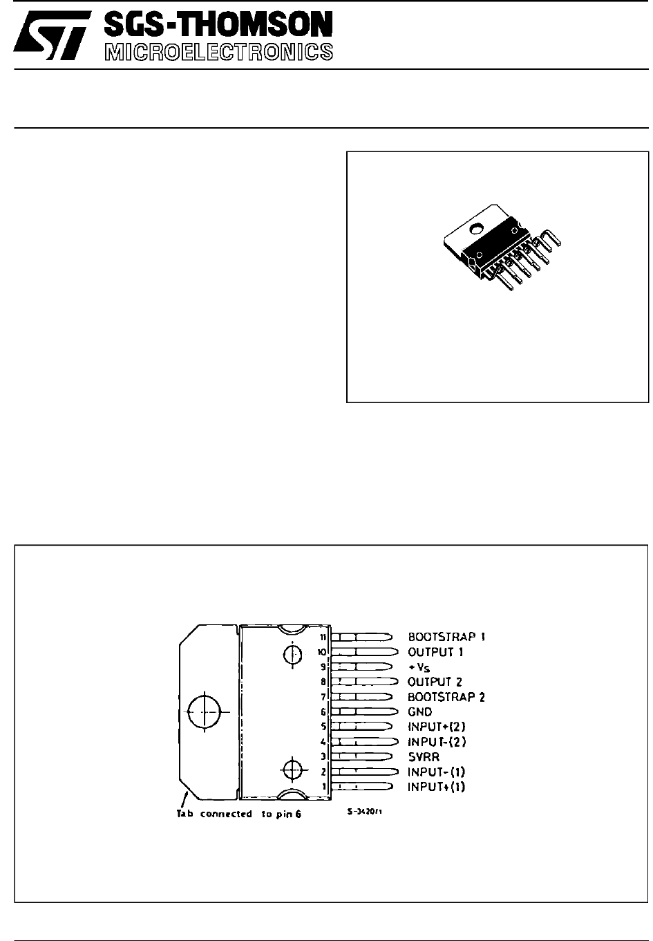
MULTIWATT11
ORDERING NUMBER : TDA2004A
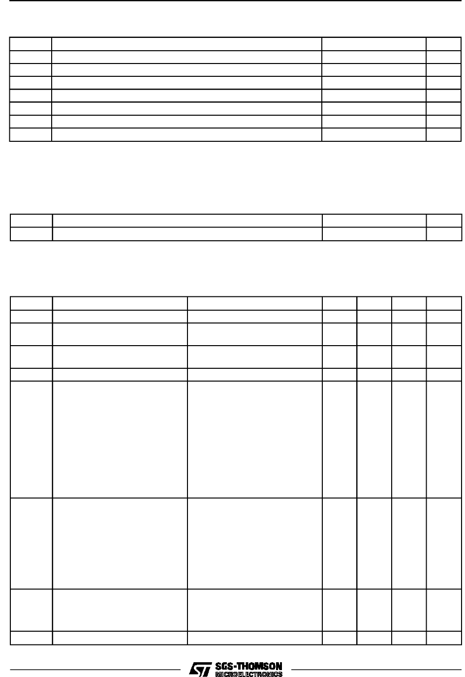
PIN CONNECTION (top view)
Its main features are :
Low distortion.
Low noise.
High reliability of the chip and of the package with
additional safety during operation thanksto protec-
tions against :
.OUTPUT AC SHORT CIRCUIT TO GROUND
.VERY INDUCTIVE LOADS
.OVERRATING CHIP TEMPERATURE
.LOAD DUMP VOLTAGE SURGE
.FORTUITOUS OPEN GROUND
Space and cost saving :very low numberof exter-
nal components,very simple mounting system with
no electrical isolation between the packageand the
heatsink.
DESCRIPTION
The TDA2004A is a class B dual audio power am-
plifier in MULTIWATTpackage specifically desi-
gnedforcar radioapplications; stereoamplifiersare
easily designed using this device that provides a
high current capability (up to 3.5A) and that can dri-
ve very low impedance loads (down to 1.6Ω).
1/10
THERMAL DATA
Symbol Parameter Value Unit
Rth j-case Thermal Resistance Junction-case Max. 3 °C/W
ABSOLUTE MAXIMUM RATINGS
Symbol Parameter Value Unit
VSOpearting Supply Voltage 18 V
VSDC Supply Voltage 28 V
VSPeak Supply Voltage (for 50ms) 40 V
IO(*) Output Peak Current (non repetitive t = 0.1ms) 4.5 A
IO(*) Output Peak Current (repetitive f ≥10Hz) 3.5 A
Ptot Power Dissipation at Tcase =60°C30W
T
j
,T
stg Storage and Junction Temperature –40 to 150 °C
ELECTRICAL CHARACTERISTICS (Refer to the test circuit, Tamb =25°C, GV= 50dB,
Rth (heatsink) =4°C/W, unless otherwise specified)
Symbol Parameter Test Condition Min. Typ. Max. Unit
VSSupply Voltage 8 18 V
VOQuiescent Output Voltage VS = 14.4V
VS= 13.2V 6.6
6.0 7.2
6.6 7.8
7.2 V
V
IdTotal Quiescent Drain Current VS= 14.4V
VS= 13.2V 65
62 120
120 mA
mA
ISB Stand-by Current Pin 3 grounded 5 mA
POOutput Power (each channel) f = 1KHz, d = 10%
VS= 14.4V
RL=4Ω
R
L=3.2Ω
R
L=2Ω
R
L
= 1.6Ω
6
7
9
10
6.5
8
10(*)
11
W
W
W
W
VS= 13.2V
RL=3.2Ω
R
L
= 1.6Ω6
96.5
10 w
w
VS= 16V; RL=2Ω12 w
d Distortion (each channel) f = 1KHz
VS= 14.4V; RL=4Ω
P
O= 50mW to 4W
VS= 14.4V; RL=2Ω
P
O= 50mW to 6W
VS= 13.2V; RL= 3.2Ω
PO= 50mW to 3W
VS= 13.2V; RL= 1.6Ω
PO= 50mW to 6W
0.2
0.3
0.2
0.3
1
1
1
1
%
%
%
%
CT Cross Talk VS= 14.4V
VO= 4Vrms RL=4Ω
f = 1KHz
f = 10KHz Rg=5KΩ50
40 60
45 dB
dB
ViInput Saturation Voltage 300 mV
(*) The max. output current is internally limited.
TDA2004A
2/10
Notes : (*) 9.3W without Bootstrap
(**) Bandwith Filter : 22Hz to 22KHz.
ELECTRICAL CHARACTERISTICS (continued
Symbol Parameter Test Condition Min. Typ. Max. Unit
RiInput Resistance (non inverting input) f = 1KHz 70 200 KΩ
fLLow Frequency Roll off (-3dB) RL=4Ω
R
L=2Ω
R
L= 3.2Ω
RL= 1.6Ω
35
50
40
55
Hz
Hz
Hz
Hz
fHHigh Frequency Roll off (-3dB) RL= 1.6Ωto 4Ω15 KHz
GVVoltage gain (open loop) f = 1KHz 90 dB
Voltage gain (closed loop) f = 1KHz 48 50 51 dB
closed loop gain matching 0.5 dB
eNTotal Input noise Voltage Rg= 10KΩ(**) 1.5 5 µV
SVR Supply Voltage Rejection fripple = 100Hz; Rg= 10KΩ
C3 = 10µFV
ripple = 0.5Vrms 35 45 dB
ηEfficiency VS= 14.4V f = 1KHz
RL=4ΩP
O= 6.5W
RL=2ΩP
O= 10W
VS= 13.2V f = 1KHZ
RL=3.2ΩP
O= 6.5W
RL= 1.6ΩPO= 10W
70
60
70
60
%
%
%
%
TJThermal Shutdown Junction
Temperature 145 °C
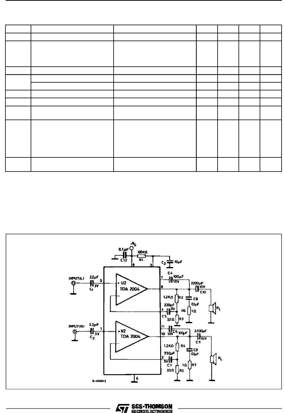
Figure 1 : Test and Application Circuit.
TDA2004A
3/10
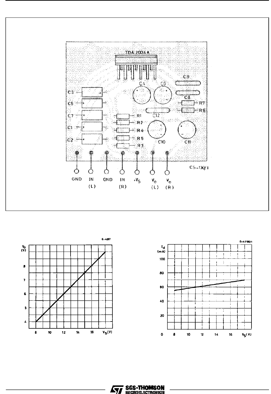
Figure 2 : P.C. Board and Component layout of the fig. 1 (scale 1 : 1).
Figure 4 : Quiescent Drain Current vs.
Supply Voltage.
Figure 3 : Quiescent OutputVoltage vs.
Supply Voltage.
TDA2004A
4/10
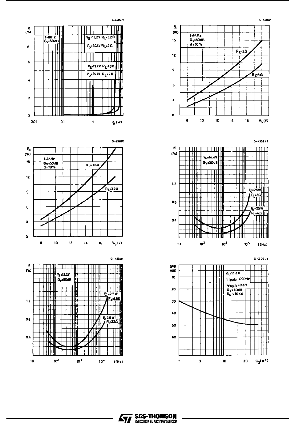
Figure 7 : Output Power vs. Supply Voltage. Figure 8 : Distortion vs. Frequency.
Figure 6 : Output Power vs. Supply Voltage.Figure 5 : Distortion vs. Output Power.
Figure 9 : Distortion vs. Frequency. Figure 10 : Supply Voltage Rejection vs. C3.
TDA2004A
5/10
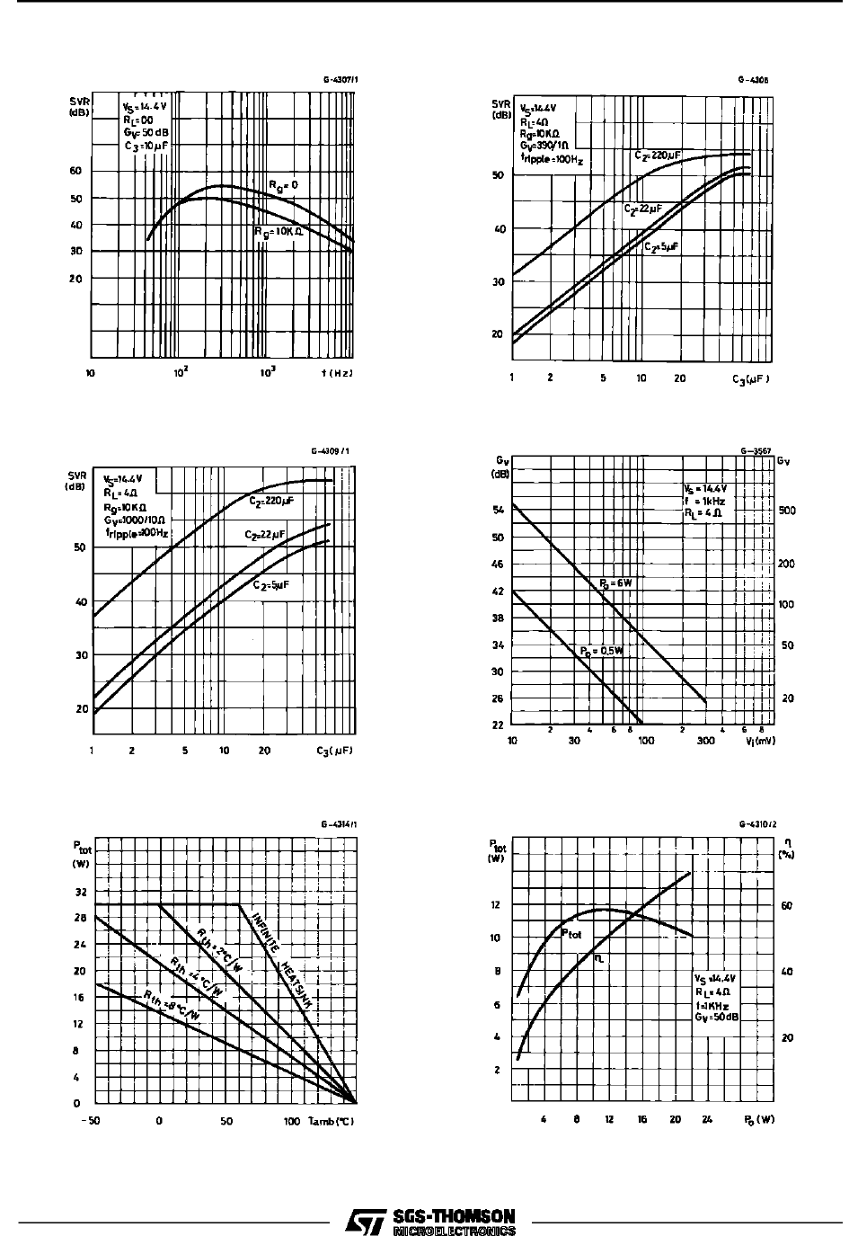
Figure 11 : Supply Voltage Rejection vs.
Frequency. Figure 12 : Supply Voltage Rejection vs.
Values of Capacitors C2and C3.
Figure 15 : Maximum Allowable Power
Dissipation vs. Ambient Temperature. Figure 16 : Total Power Dissipation and
Efficiency vs. Output Power.
Figure 13 : Supply Voltage Rejection vs.
Values of Capacitors C2and C3.Figure 14 : Gain vs. Input Sensitivity.
TDA2004A
6/10
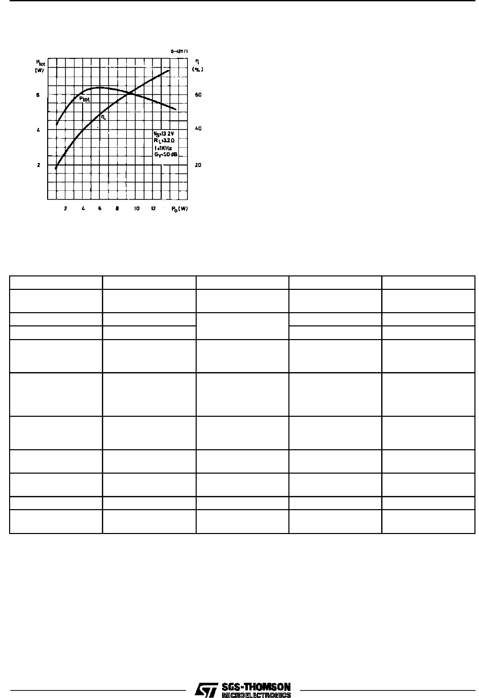
Figure 17 : Total Power Dissipation and
Efficiency vs. Output Power .
APPLICATION SUGGESTION
The recommended values of the componentsare those shown on application circuit of fig.1. Different values
can be used ; the following table can help the designer.
Component Recomm. Value Purpose Larger Than Smaller Than
R1 120KΩOptimization of the
output signal simmetry Smaller POmax. Smaller POmax.
R2, R4 1KΩClose loop gain
setting (*) Increase of gain Decrease of gain
R3, R5 3.3ΩDecrease of gain Increase of gain
R6, R7 1ΩFrequency stability Danger of oscillation
at high frequency with
inductive load
C1, C2 2.2µF Input DC decoupling High turn-on delay High turn-on pop
Higher low frequency
cutoff. Increase of
noise
C3 10µF Ripple Rejection Increase of SVR.
Increase of the switch-
on time.
Degradation of SVR.
C4, C6 100µF Boostrapping Increase of distortion
at low frequency
C5, C7 100µF Feedback Input DC
decoupling.
C8, C9 0.1µF Frequency Stability Danger of oscillation.
C10, C11 1000µF to 2200µF Output DC decoupling. Higher low-frequency
cut-off.
(*) The closed–loop gain must be higher than 26dB.
TDA2004A
7/10
BUILT–IN PROTECTION SYSTEMS
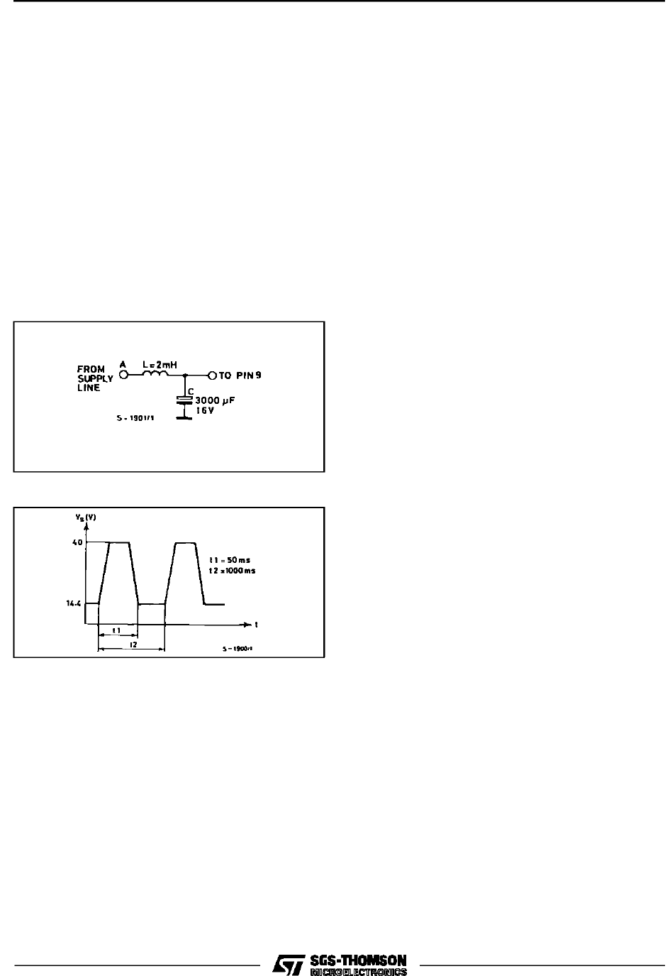
LOAD DUMP VOLTAGE SURGE
The TDA2004A has a circuit which enables it to wi-
thstand a voltage pulse train, on pin 9, of the type
shown in Fig. 19.
If the supply voltage peaks to more than 40 V, then
an LC filter must beinsertedbetweenthe supplyand
pin 9, in order to assure that the pulses at pin 9 will
be held within the limits shown.
A suggested LC network is shown in Fig. 18. With
thisnetwork,a trainofpulsewith amplitudeup to 120
V and with of 2 ms can be applied to point A. This
type of protection is ON when the supply voltage
(pulse or DC) exceeds18 V. For this reason the ma-
ximum operating supply voltage is 18 V.
SHORT CIRCUIT (AC conditions)
The TDA2004A can withstand an accidental short-
circuit from the output to ground caused by a wrong
connection during normal working.
POLARITY INVERSION
High current (up to 10 A) can be handled by the de-
vice with no damage for a longer period than the
blow-out time of a quick 2 A fuse (normally connec-
ted in series with the supply). This featureis added
to avoid destruction, if during fitting to the car, a mi-
stakeon the connection of the supply is made.
OPEN GROUND
When the ratio is the ON condition and the ground
is accidentally opened, a standard audio amplifier
will be damaged. On the TDA2004A protection dio-
des are included to avoidany damage.
INDUCTIVE LOAD
A protection diode is provided to allow use of the
TDA2004A with inductive loads.
DC VOLTAGE
The maximum operating DC voltage on the
TDA2004A is 18 V.
However the device can withstand a DC voltage up
to 28V withno damage.Thiscouldoccurduringwin-
ter if two batteries are series connectedto crank the
engine.
THERMAL SHUT-DOWN
The presence of a thermal limiting circuit offers the
following advantages:
1)anoverloadon theoutput(evenif it ispermanent),
or an excessive ambienttemperature can be easily
withstood.
2) the heatsink can have a smaller factor of safety
compared with that of a conventionalcircuit. There
is no device damage in the case of excessive jun-
ction temperature ; all that happens is the PO(and
therefore Ptot)andI
dare reduced.
The maximum allowable power dissipationdepends
uponthe size ofthe externalheatsink(i.e. its thermal
resistance) ; fig. 15 shown this dissipable power as
a functionof ambient temperaturefor different ther-
mal resistance.
Figure 18.
Figure 19.
TDA2004A
8/10
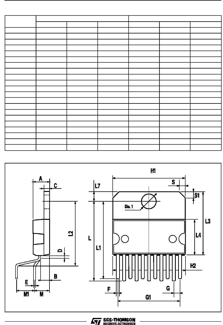
MULTIWATT11 PACKAGE MECHANICAL DATA
DIM. mm inch
MIN. TYP. MAX. MIN. TYP. MAX.
A 5 0.197
B 2.65 0.104
C 1.6 0.063
D 1 0.039
E 0.49 0.55 0.019 0.022
F 0.88 0.95 0.035 0.037
G 1.45 1.7 1.95 0.057 0.067 0.077
G1 16.75 17 17.25 0.659 0.669 0.679
H1 19.6 0.772
H2 20.2 0.795
L 21.9 22.2 22.5 0.862 0.874 0.886
L1 21.7 22.1 22.5 0.854 0.87 0.886
L2 17.4 18.1 0.685 0.713
L3 17.25 17.5 17.75 0.679 0.689 0.699
L4 10.3 10.7 10.9 0.406 0.421 0.429
L7 2.65 2.9 0.104 0.114
M 4.25 4.55 4.85 0.167 0.179 0.191
M1 4.73 5.08 5.43 0.186 0.200 0.214
S 1.9 2.6 0.075 0.102
S1 1.9 2.6 0.075 0.102
Dia1 3.65 3.85 0.144 0.152
TDA2004A
9/10

Information furnished is believed to be accurate and reliable. However, SGS-THOMSON Microelectronics assumes no responsibility for
the consequences of use of such information nor for any infringement of patents or other rights of third parties which may result from its
use. No license is granted by implication or otherwise under any patent or patent rights of SGS-THOMSON Microelectronics. Specifica-
tions mentioned in this publication are subject to change without notice. This publication supersedes and replaces all information pre-
viously supplied. SGS-THOMSON Microelectronics products are not authorized for use as critical components in life support devices or
systems without express written approval of SGS-THOMSON Microelectronics.
1995 SGS-THOMSON Microelectronics - All Rights Reserved
MULTIWATTis a Registered Trademark of SGS-THOMSON Microelectronics
SGS-THOMSON Microelectronics GROUP OF COMPANIES
Australia - Brazil - France - Germany - Hong Kong - Italy - Japan - Korea - Malaysia - Malta - Morocco - The Netherlands - Singapore -
Spain - Sweden - Switzerland - Taiwan - Thaliand - United Kingdom - U.S.A.
TDA2004A
10/10