TDA2822M Datasheet. Www.s Manuals.com. St
User Manual: Datasheets TDA2822, TDA2822G-D08, TDA2822G-S08, TDA2822L-D08, TDA2822L-S08, TDA2822M.
Open the PDF directly: View PDF ![]() .
.
Page Count: 12
TDA2822M
DUAL LOW-VOLTAGE POWER AMPLIFIER
March 1995
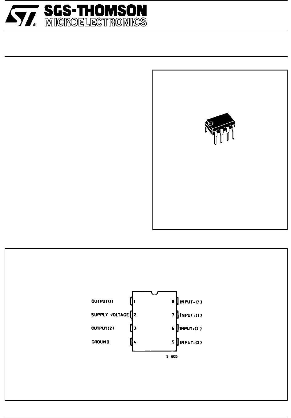
PIN CONNECTION (Top view)
MINIDIP
ORDERING NUMBER : TDA2822M
.SUPPLY VOLTAGE DOWN TO 1.8V
.LOW CROSSOVER DISTORSION
.LOW QUIESCENT CURRENT
.BRIDGE OR STEREO CONFIGURATION
DESCRIPTION
The TDA2822M is a monolithic integrated circuit in
8 lead Minidip package. It is intended for use as
dual audio power amplifier in portable cassette
players and radios.
1/11
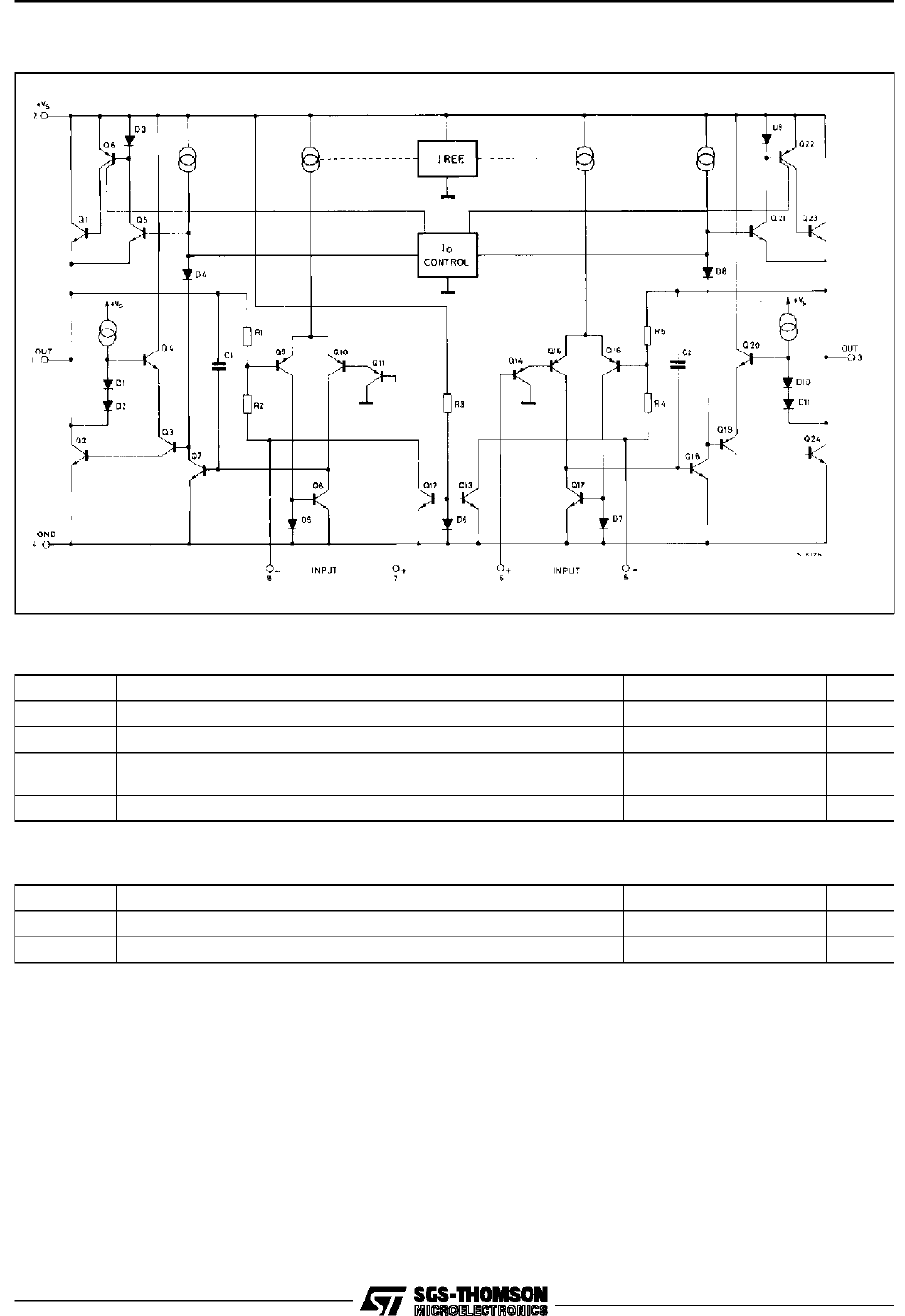
SCHEMATIC DIAGRAM
ABSOLUTE MAXIMUM RATINGS
Symbol Parameter Value Unit
VsSupply Voltage 15 V
IoPeak Output Current 1 A
Ptot Total Power Dissipation at Tamb =50°C
at Tcase =50°C1
1.4 W
W
Tstg,T
jStorage and Junction Temperature – 40, + 150 °C
THERMAL DATA
Symbol Parameter Value Unit
Rth j-amb Thermal Resistance Junction-ambient Max. 100 °C/W
Rth j-case Thermal Resistance Junction-pin (4) Max. 70 °C/W
TDA2822M
2/11
ELECTRICALCHARACTERISTICS (VS=6V,T
amb =25
o
C, unless otherwise specified)
Symbol Parameter Test Conditions Min. Typ. Max. Unit
STEREO (test circuit of Figure 1)
VsSupply Voltage 1.8 15 V
VoQuiescent Output Voltage Vs=3V 2.7
1.2 V
V
IdQuiescent Drain Current 6 9 mA
IbInput Bias Current 100 nA
PoOutput Power (each channel)
(f = 1kHz, d = 10%) RL=32ΩV
S=9V
V
S=6V
V
S= 4.5V
VS=3V
V
S=2V
R
L=16ΩV
S=6V
R
L=8ΩV
S=9V
V
S=6V
R
L=4ΩV
S=6V
V
S= 4.5V
VS=3V
90
15
170
300
450
300
120
60
20
5
220
1000
380
650
320
110
mW
d Distortion (f = 1kHz) RL=32ΩP
o= 40mW
RL=16ΩP
o= 75mW
RL=8ΩP
o= 150mW
0.2
0.2
0.2
%
%
%
GvClosed Loop Voltage Gain f = 1kHz 36 39 41 dB
∆GvChannel Balance ±1dB
R
iInput Resistance f = 1kHz 100 kΩ
eNTotal Input Noise Rs= 10kΩB = Curve A
B = 22Hz to 22kHz 2
2.5 µV
µV
SVR Supply Voltage Rejection f = 100Hz, C1 = C2 = 100µF2430 dB
C
s
Channel Separation f = 1kHz 50 dB
BRIDGE (test circuit of Figure 2)
VsSupply Voltage 1.8 15 V
IdQuiescent Drain Current RL=∞69mA
V
os Output Offset Voltage
(between the outputs) RL=8Ω±50 mV
IbInput Bias Current 100 nA
PoOutput Power (f = 1kHz, d = 10%) RL=32ΩV
S=9V
V
S=6V
V
S= 4.5V
VS=3V
V
S=2V
R
L=16ΩV
S=9V
V
S=6V
V
S=3V
R
L=8ΩV
S=6V
V
S= 4.5V
VS=3V
R
L=4ΩV
S= 4.5V
VS=3V
V
S=2V
320
50
900
200
1000
400
200
65
8
2000
800
120
1350
700
220
1000
350
80
mW
d Distortion Po= 0.5W, RL=8Ω, f = 1kHz 0.2 %
GvClosed Loop Voltage Gain f = 1kHz 39 dB
RiInput Resistance f = 1kHz 100 kΩ
eNTotal Input Noise Rs= 10kΩB = Curve A
B = 22Hz to 22kHz 2.5
3µV
µV
SVR Supply Voltage Rejection f = 100Hz 40 dB
B Power Bandwidth (–3dB) RL=8Ω,P
o= 1W 120 kHz
TDA2822M
3/11
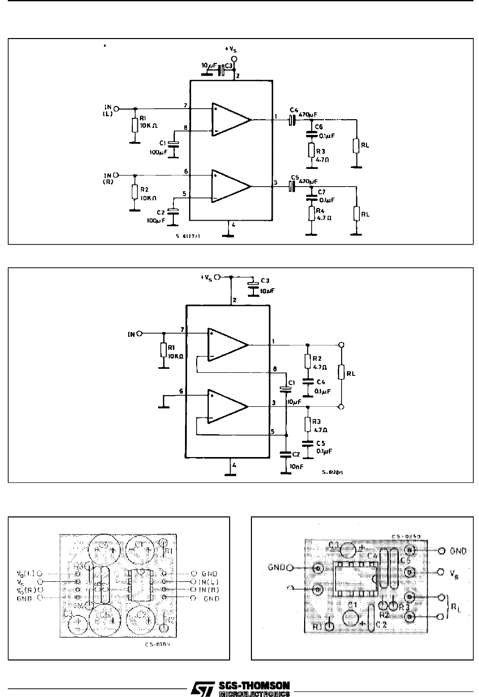
Figure 1 : Test Circuit (Stereo)
Figure 2 : Test Circuit (Bridge)
Figure 3 : P.C. Board and Components Layout
of the Circuit of Figure 1 Figure 4 : P.C. Board and Components Layout
of the Circuit of Figure 2
TDA2822M
4/11
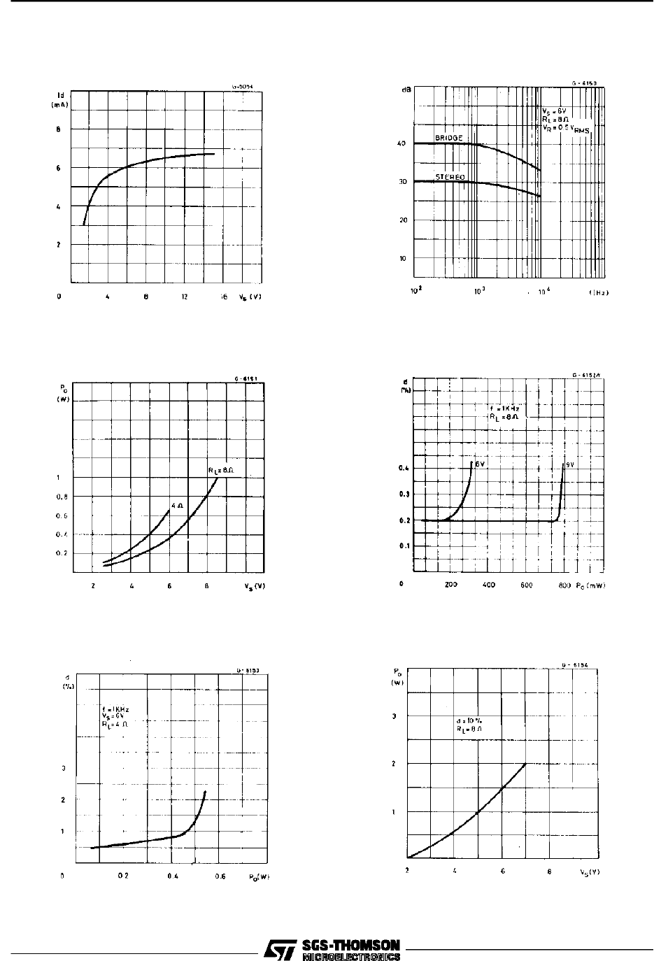
Figure 5 : Quiescent Current versus
Supply Voltage Figure 6 : Supply Voltage Rejection versus
Frequency
Figure 8 : Distorsion versus Output Power
(Stereo)
Figure 7 : Output Power versus Supply Voltage
(THD = 10%, f = 1kHz Stereo)
Figure 9 : Distorsion versus Output Power
(Stereo) Figure 10 : Output Power versus Supply Voltage
(Bridge)
TDA2822M
5/11
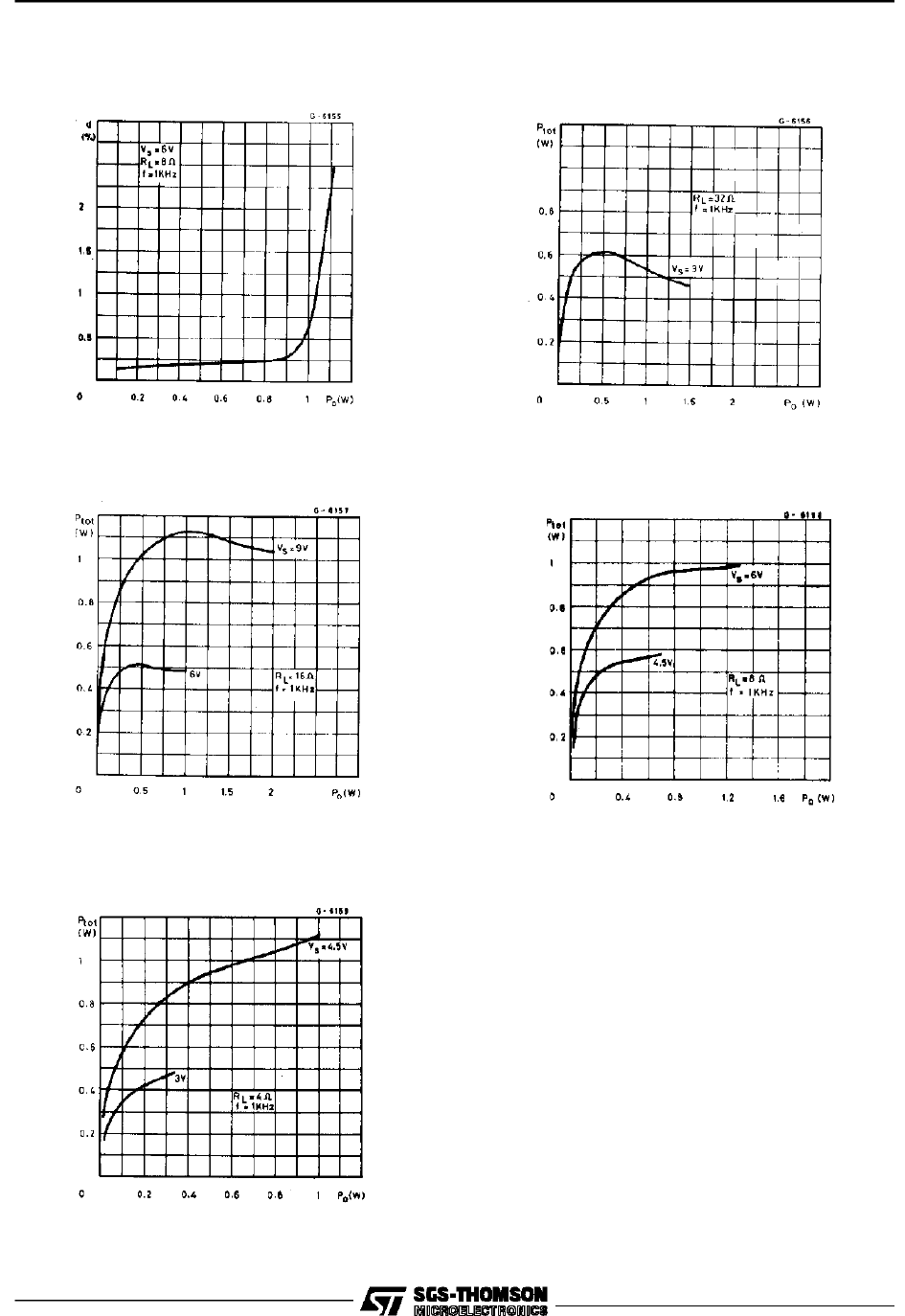
Figure 11 : Distorsion versus Output Power
(Bridge) Figure 12 : Total Power Dissipation versus
Output Power (Bridge)
Figure 14 : Total Power Dissipation versus
Output Power (Bridge)
Figure 13 : Total Power Dissipation versus
Output Power (Bridge)
Figure 15 : Total Power Dissipation versus
Output Power (Bridge)
TDA2822M
6/11
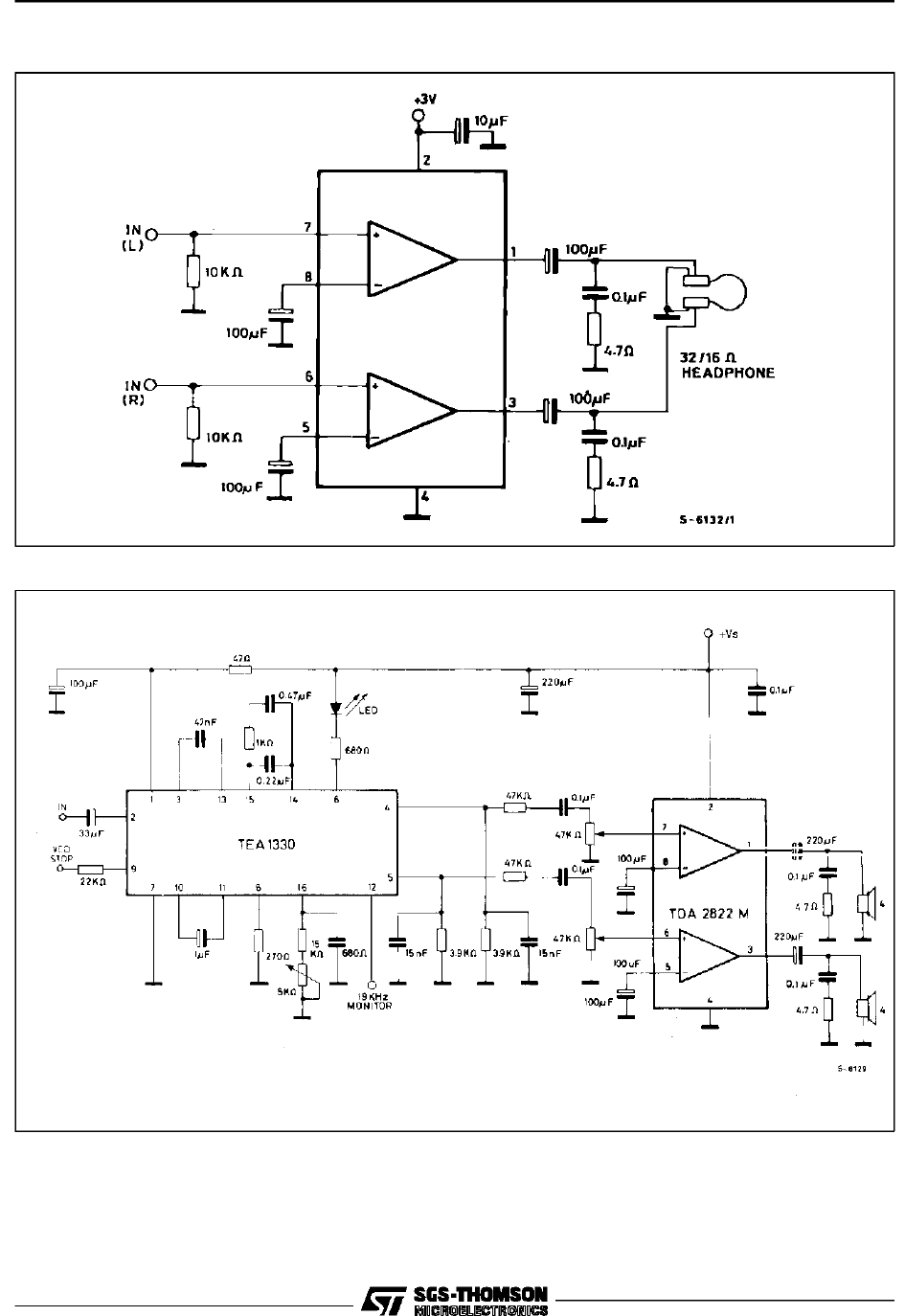
Figure 16 : Typical Application in Portable Players
Figure 17 : Application in Portable Radio Receivers
TDA2822M
7/11
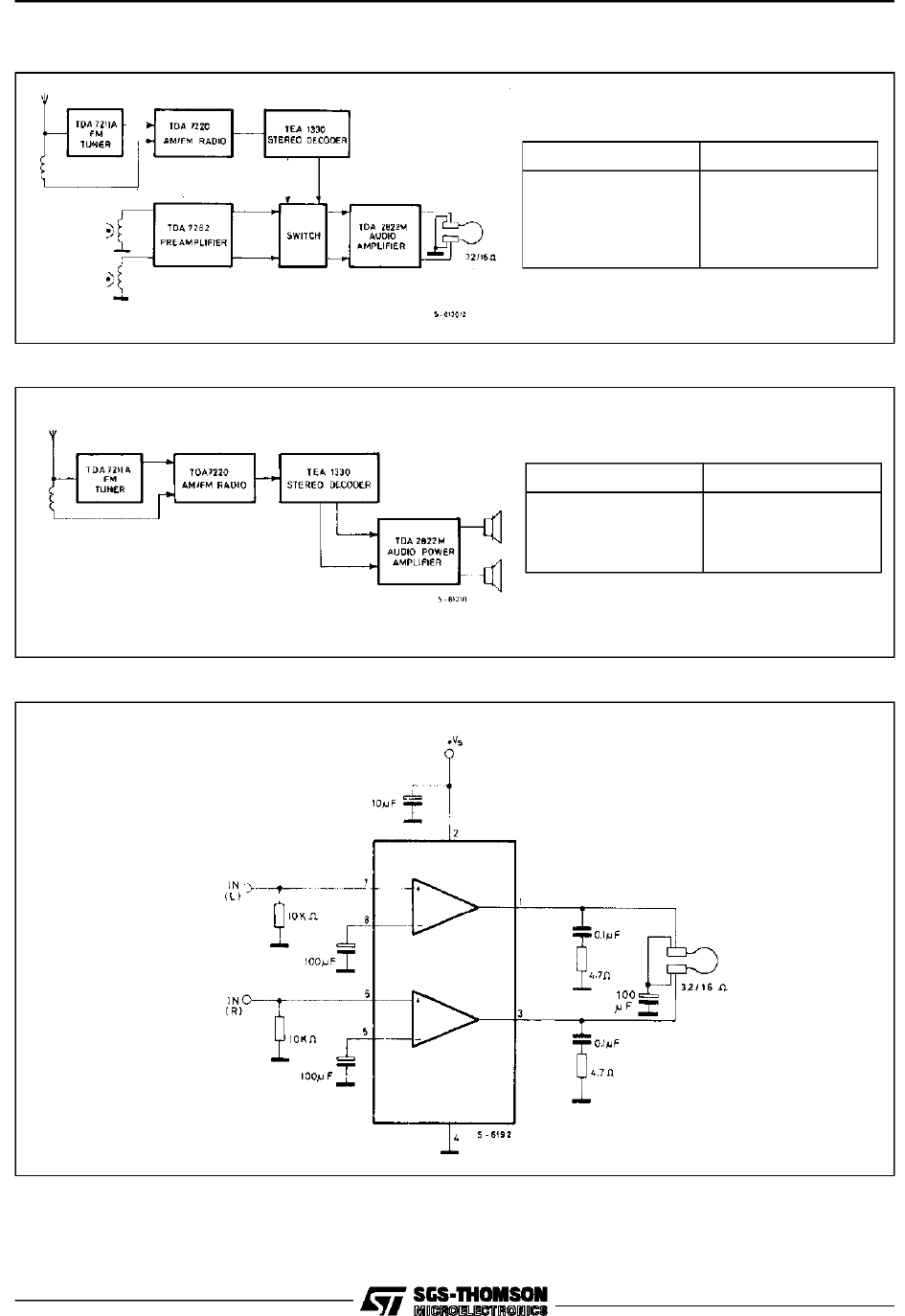
Figure 18 : Portable Radio Cassette Players
Figure 20 : Low Cost Application in Portable Players (using only one 100µF output capacitor)
Figure 19 : Portable Stereo Radios
Type Supply Voltage
TDA 7220
TDA 7211A
TEA 1330
TDA 7282
TDA 2822M
1.5 V to 6 V
1.2 V to 6 V
3 V to 15 V
1.5 V to 6 V
1.8 V to 15 V
Type Supply Voltage
TDA 7220
TDA 7211A
TEA 1330
TDA 2822M
1.5Vto6V
1.2Vto6V
3 V to 15 V
1.8 V to 15 V
TDA2822M
8/11
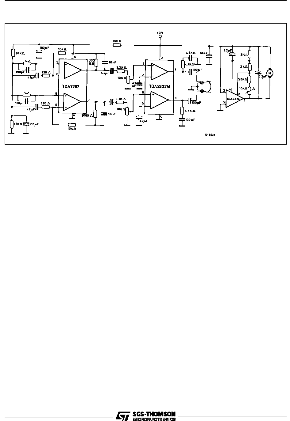
Figure 21 : 3V Stereo Cassette Player with Motot Speed Control
TDA2822M
9/11
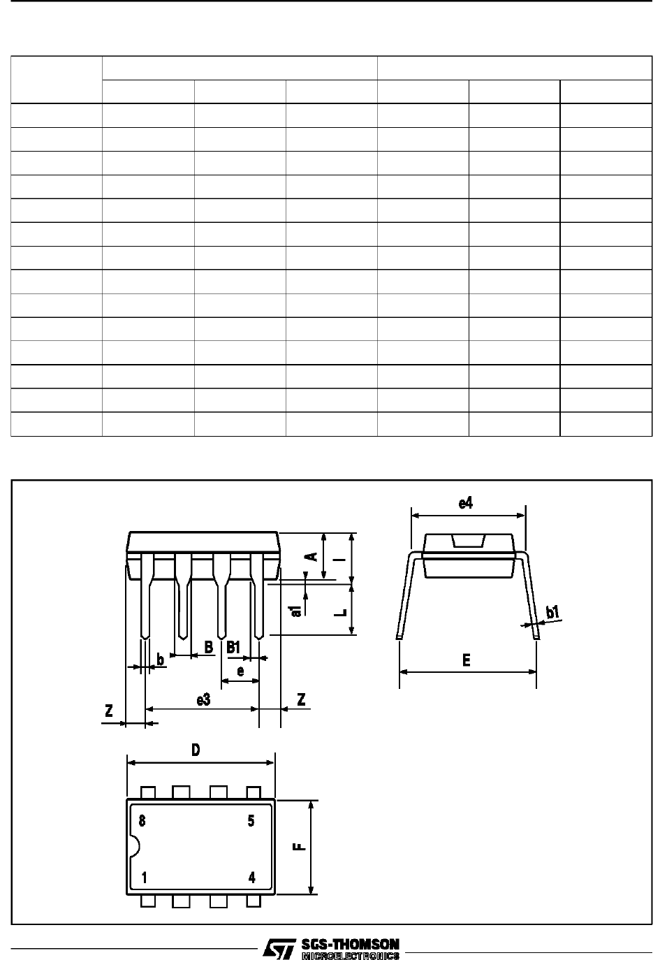
MINIDIP PACKAGE MECHANICAL DATA
DIM. mm inch
MIN. TYP. MAX. MIN. TYP. MAX.
A 3.32 0.131
a1 0.51 0.020
B 1.15 1.65 0.045 0.065
b 0.356 0.55 0.014 0.022
b1 0.204 0.304 0.008 0.012
D 10.92 0.430
E 7.95 9.75 0.313 0.384
e 2.54 0.100
e3 7.62 0.300
e4 7.62 0.300
F 6.6 0.260
I 5.08 0.200
L 3.18 3.81 0.125 0.150
Z 1.52 0.060
TDA2822M
10/11

Information furnished is believed to be accurate and reliable. However, SGS-THOMSON Microelectronics assumes no responsibility
for the consequences of use of such information nor for any infringement of patents or other rights of third parties which may result
from its use. No license is granted by implication or otherwise under any patent or patent rights of SGS-THOMSON Microelectronics.
Specifications mentioned in this publication are subject to change without notice. This publication supersedes and replaces all
information previously supplied.SGS-THOMSON Microelectronics products are not authorized for use as critical components in life
support devices or systems without express written approval of SGS-THOMSON Microelectronics.
1994 SGS-THOMSON Microelectronics - All Rights Reserved
SGS-THOMSON Microelectronics GROUP OF COMPANIES
Australia - Brazil - France - Germany - Hong Kong - Italy - Japan - Korea - Malaysia - Malta - Morocco - The Netherlands - Singa-
pore - Spain - Sweden - Switzerland - Taiwan - Thaliand - United Kingdom - U.S.A.
TDA2822M
11/11

