TDA7375H, TDA7375V Datasheet. Www.s Manuals.com. St
User Manual: Datasheets TDA7375-J15-A, TDA7375G-J15-A, TDA7375H, TDA7375L-J15-A, TDA7375V.
Open the PDF directly: View PDF ![]() .
.
Page Count: 16
TDA7375
2 x 35W DUAL/QUAD POWER AMPLIFIER FOR CAR RADIO
HIGH OUTPUT POWER CAPABILITY:
2 x 40W max./4Ω
2 x 35W/4ΩEIAJ
2 x 35W/4ΩEIAJ
2x25W/4Ω@14.4V, 1KHz, 10%
4x7W/4Ω@14.4V,1KHz, 10%
4x12W/2Ω@14.4V,1KHz, 10%
MINIMUM EXTERNAL COMPONENTS
COUNT:
– NO BOOTSTRAP CAPACITORS
– NO BOUCHEROT CELLS
– INTERNALLY FIXED GAIN (26dB BTL)
ST-BY FUNCTION (CMOS COMPATIBLE)
NO AUDIBLE POPDURING ST-BYOPERATIONS
DIAGNOSTICSFACILITY FOR:
– CLIPPING
– OUT TO GND SHORT
– OUT TO VSSHORT
– SOFT SHORT AT TURN-ON
– THERMAL SHUTDOWN PROXIMITY
Protections:
OUPUT AC/DC SHORT CIRCUIT
–TOGND
–TOV
S
– ACROSS THE LOAD
SOFT SHORT AT TURN-ON
OVERRATING CHIP TEMPERATURE WITH
SOFT THERMAL LIMITER
LOAD DUMP VOLTAGE SURGE
VERY INDUCTIVE LOADS
FORTUITOUS OPEN GND
REVERSED BATTERY
ESD
September 1998
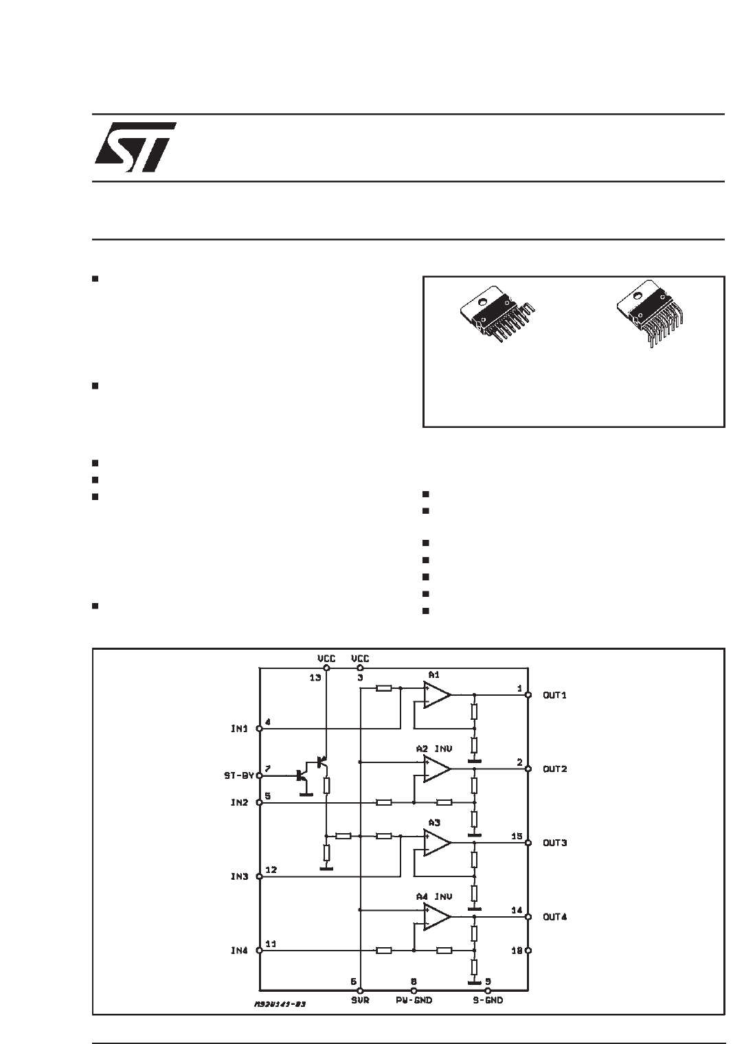
BLOCK DIAGRAM
MULTIWATT15V MULTIWATT15H
ORDERING NUMBERS:
TDA7375V TDA7375H
DIAGNOSTICS
1/15
DESCRIPTION
The TDA7375 is a new technology class AB car
radio amplifier able to work either in DUAL
BRIDGE or QUAD SINGLE ENDED configuration.
The exclusive fully complementary structure of the
output stage and the internally fixed gain guaran-
tees the highest possible power performances
with extremely reduced component count. The
on-board clip detector simplifies gain compression
operation. The fault diagnostics makes it possible
to detect mistakes during car radio set assembly
and wiring in the car.
GENERAL STRUCTURE
ABSOLUTE MAXIMUM RATINGS
Symbol Parameter Value Unit
Vop Operating Supply Voltage 18 V
VSDC Supply Voltage 28 V
Vpeak Peak Supply Voltage (for t = 50ms) 50 V
IOOutput Peak Current (not repetitive t = 100µs) 4.5 A
IOOutput Peak Current (repetitive f > 10Hz) 3.5 A
Ptot Power Dissipation (Tcase =85°C) 36 W
Tstg,T
jStorage and Junction Temperature -40 to 150 °C
THERMAL DATA
Symbol Description Value Unit
Rth j-case Thermal Resistance Junction-case Max 1.8 °C/W
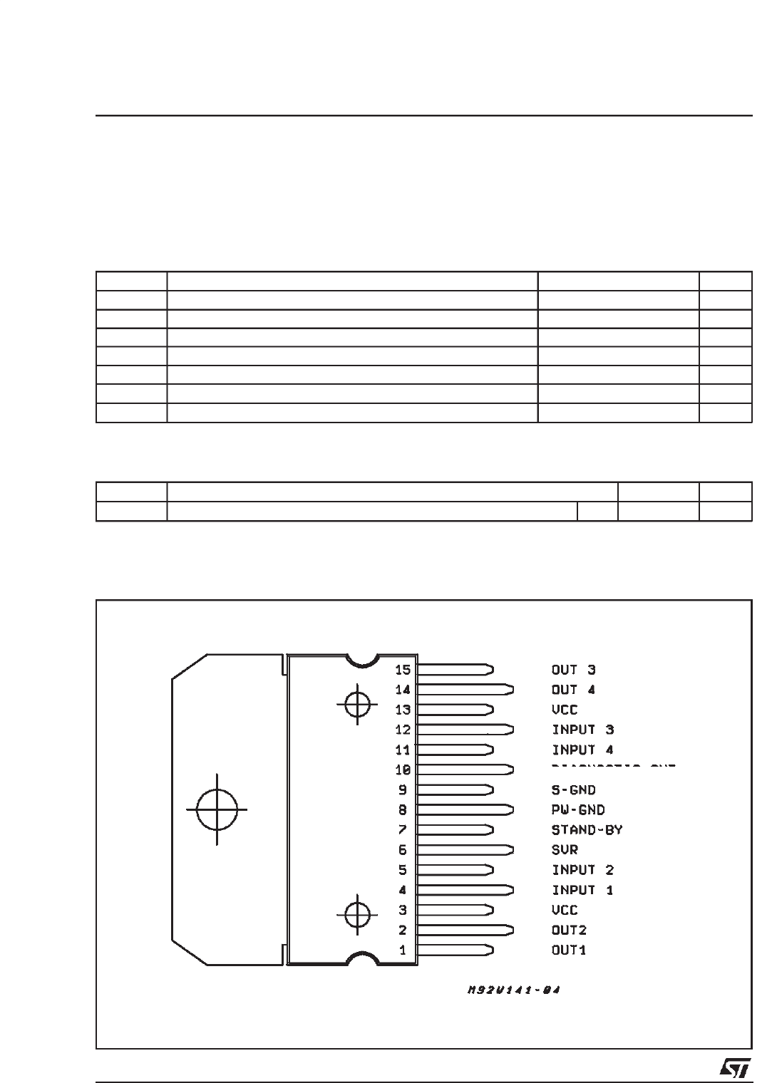
PIN CONNECTION (Topview)
DIAGNOSTICS
TDA7375
2/15

ELECTRICAL CHARACTERISTICS (Referto the test circuit, VS= 14.4V; RL=4
Ω
; f = 1KHz;
Tamb =25°C, unless otherwise specified
Symbol Parameter Test Condition Min. Typ. Max. Unit
VSSupply Voltage Range 8 18 V
IdTotal Quiescent Drain Current RL=∞150 mA
VOS Output Offset Voltage 150 mV
POOutput Power THD = 10%; RL=4
Ω
Bridge
Single Ended
Single Ended, RL=2
Ω
23
6.5 25
7
12
W
W
W
PO max Max. Output Power (***) VS = 14.4V, Bridge 36 40 W
PO EIAJ EIAJ Output Power (***) VS= 13.7V, Bridge 32 35 W
THD Distortion RL=4Ω
Single Ended, PO= 0.1 to 4W
Bridge, PO= 0.1 to 10W 0.02
0.03 0.3 %
%
CT Cross Talk f = 1KHz Single Ended
f = 10KHz Single Ended 70
60 dB
dB
f = 1KHz Bridge
f = 10KHz Bridge 55 60 dB
dB
RIN Input Impedance Single Ended
Bridge 20
10 30
15 KΩ
KΩ
GVVoltage Gain Single Ended
Bridge 19
25 20
26 21
27 dB
dB
GVVoltage Gain Match 0.5 dB
EIN Input Noise Voltage Rg= 0; ”A” weighted, S.E.
Non Inverting Channels
Inverting Channels 2
5µV
µV
Bridge
Rg = 0; 22Hz to 22KHz 3.5 µV
SVR Supply Voltage Rejection Rg= 0; f = 300Hz 50 dB
ASB Stand-by Attenuation PO=1W 80 90 dB
I
SB ST-BY Current Consumption VST-BY = 0 to 1.5V 100 µA
VSB ST-BY In Threshold Voltage 1.5 V
VSB ST-BY Out Threshold Voltage 3.5 V
Ipin7 ST-BY Pin Current Play Mode Vpin7 =5V 50 µA
Max Driving Current Under
Fault (*) 5mA
I
cd off Clipping Detector
Output Average Current d = 1% (**) 90 µA
Icd on Clipping Detector
Output Average Current d = 5% (**) 160 µA
Vsat pin10 Voltage Saturation on pin 10 Sink Current at Pin 10 = 1mA 0.7 V
(*) See built-in S/C protection description
(**) Pin 10 Pulled-up to 5V with 10KΩ;R
L=4Ω
(***) Saturatedsquare wave output.
TDA7375
3/15
C1 0.22µF
1
DIAGNOSTICS
47
C10 2200µF
D94AU063A
C7
10µF
10K R1
ST-BY
IN FL
C2 0.22µF
IN FR 5
C4 0.22µF
12IN RL
C3 0.22µF
IN RR 11
C8 47µF
6
13
C5
1000µF
C6
100nF
3
VS
C9 2200µF
2
15
C11 2200µF
C12 2200µF
14
OUT FL
OUT FR
OUT RL
OUT RR
89 10
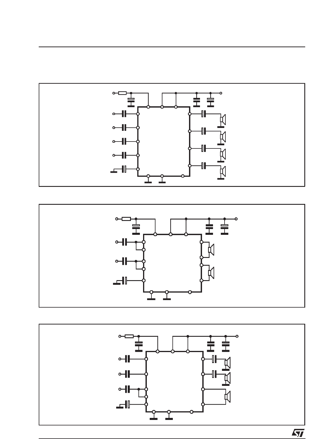
STANDARD TEST AND APPLICATION CIRCUIT
Figure 1: Quad Stereo
C1 0.47µF
1
DIAGNOSTICS
47
D94AU064A
C5
10µF
10K R1
ST-BY
IN L
C2 0.47µF
5
12IN R
11
C8 47µF
6
13
C3
1000µF
C4
100nF
3
VS
2
15
14
OUT L
89 10
OUT R
Figure 2: Double Bridge
0.22µF
1
DIAGNOSTICS
47
D94AU065A
10µF
10K
ST-BY
IN L
0.47µF
5
IN BRIDGE 12
47µF
6
13
1000µF100nF
3
VS
2
15
14
OUT L
89 10
OUT
BRIDGE
11
0.22µF
IN L OUT R
2200µF
2200µF
Figure 3: Stereo/Bridge
Note:
C9, C10, C11, C12 could be
reduced if the 2Ωoperation is not
required.
TDA7375
4/15
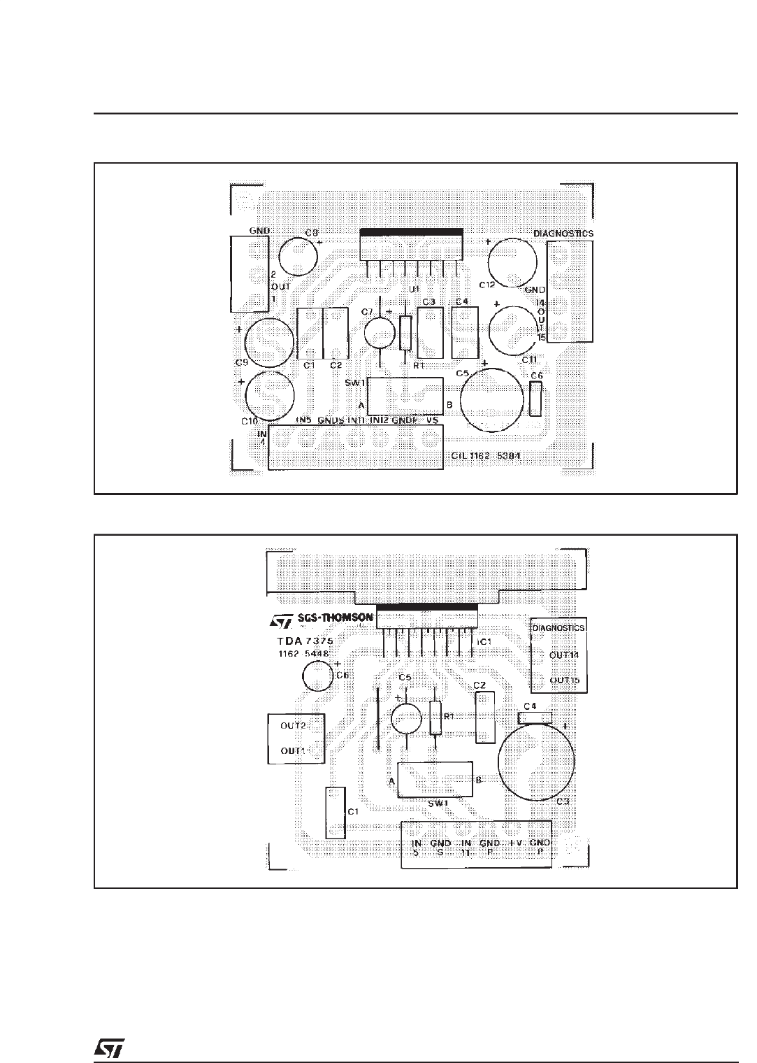
Figure 4: P.C. Board and Component Layout of the fig.1 (1:1 scale).
Figure 5: P.C. Board and Component Layout of the fig.2 (1:1 scale).
TDA7375
5/15
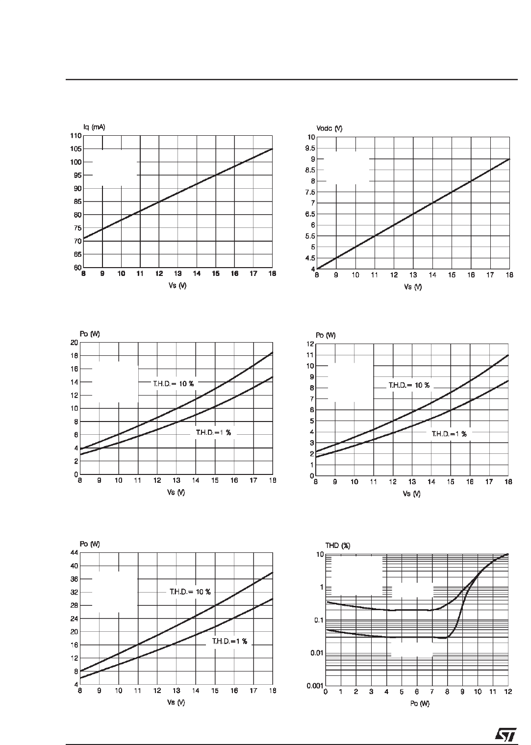
Figure 6: QuiescentDrain Current vs. Supply
Voltage (Single Ended and Bridge).
Figure 8: Output Power vs. Supply Voltage
Figure 10: OutputPower vs. Supply Voltage
Figure 7: Quiescent OutputVoltage vs. Supply
Voltage (SingleEnded and Bridge).
Figure 9: Output Power vs. Supply Voltage
Figure 11: Distortion vs. Output Power
RL=4Ω
V
i=0
R
L=4Ω
V
i=0
S.E.
RL=2Ω
f = 1KHz
S.E.
RL=4Ω
f = 1KHz
BTL
RL=4Ω
f = 1KHz
S.E.
VS= 14.4V
RL=2Ωf = 15KHz
f = 1KHz
TDA7375
6/15
Figure 12: Distortion vs. Output Power
Figure 14: Cross-talk vs. Frequency
Figure16: SupplyVoltageRejectionvs.Frequency
Figure 13: Distortion vs. Output Power
Figure 15: SupplyVoltage Rejection vs. Fre-
quency
Figure 17: Stand-byAttenuationvs. Threshold
Voltage
S.E.
VS= 14.4V
RL=4Ω
f = 15KHz
f = 1KHz
f = 15KHz
f = 1KHz BTL
VS= 14.4V
RL=4Ω
S.E.
VS= 14.4V
RL=4Ω
R
g=10Ω
BTL & S.E.
VS= 14.4V
RL=4Ω
0dB=1W
BTL
Rg=0
C
SVR =47µF
V
ripple = 1Vrms
S.E.
Rg=0
C
SVR =47µF
V
ripple = 1Vrms
TDA7375
7/15
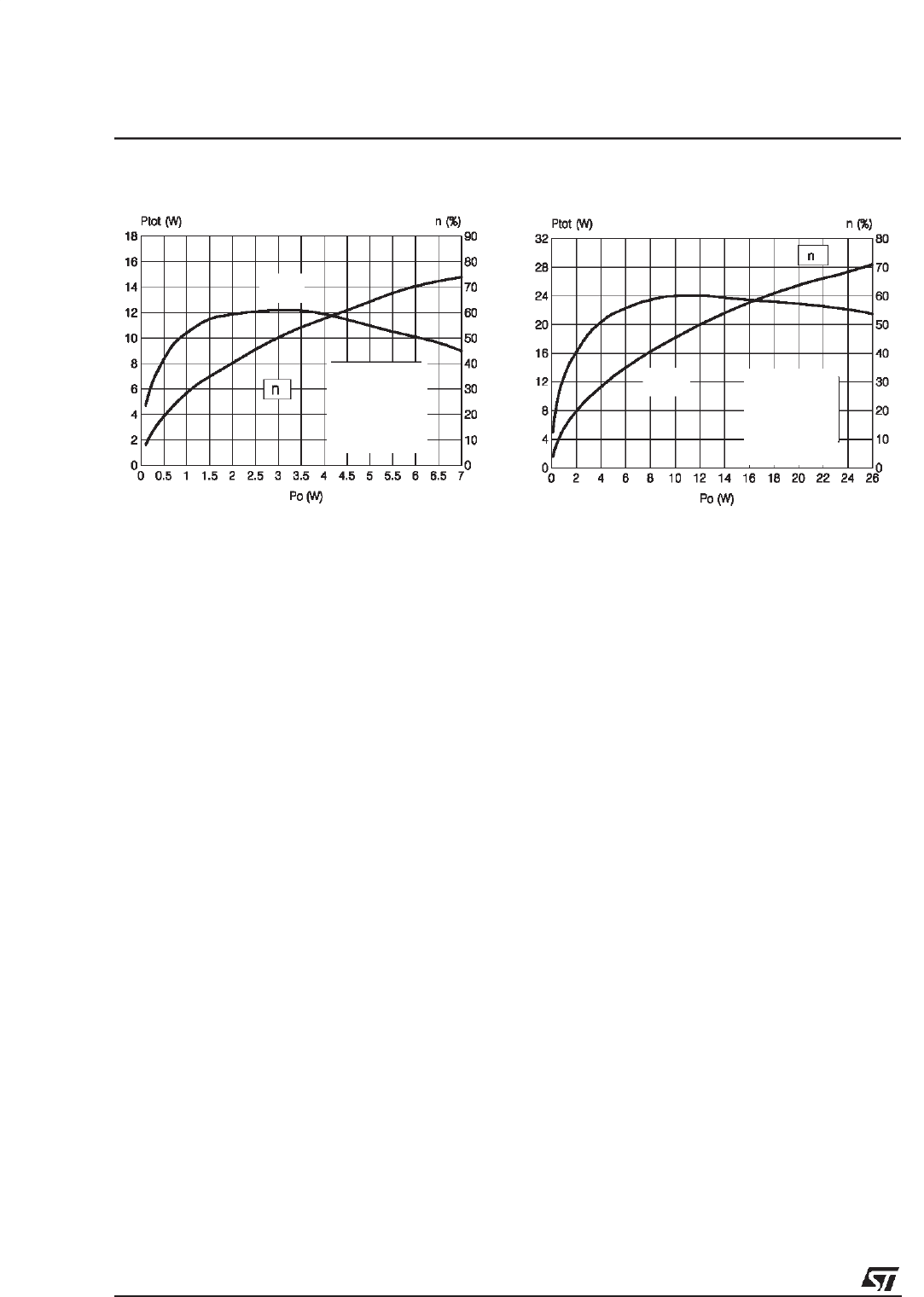
Figure 18: Total Power Dissipation and Effi-
ciency vs. Output Power Figure 19: Total Power Dissipation and Effi-
ciency vs. Output Power.
S.E.
VS= 14.4V
RL=4x4Ω
f = 1KHz
BTL
VS= 14.4V
RL=2x4Ω
f = 1KHz
Ptot
Ptot
TDA7375
8/15
High Application Flexibility
The availability of 4 independent channels makes
it possible to accomplish several kinds of applica-
tions ranging from 4 speakers stereo (F/R) to 2
speakers bridge solutions.
In case of working in single ended conditions the
polarity of the speakers driven by the inverting
amplifier must be reversed respect to those driven
by non inverting channels.
This is to avoid phase inconveniences causing
sound alterations especially during the reproduc-
tion of low frequencies.
Easy SingleEnded to Bridge Transition
The change from single ended to bridge configu-
rations is made simply by means of a short circuit
across the inputs, that is no need of further exter-
nal components.
Gain Internally Fixed to 20dB in Single Ended,
26dB inBridge
Advantages of this design choice are in terms of:
componentsand space saving
output noise, supply voltage rejection and dis-
tortion optimization.
Silent Turn On/Off and Muting/Stand-by Func-
tion
The stand-by can be easily activated by means of
a CMOS level applied to pin 7 through a RC filter.
Under stand-by condition the device is turned off
completely (supply current = 1µA typ.; output at-
tenuation= 80dB min.).
Every ON/OFF operation is virtually pop free.
Furthemore, at turn-on the device stays in muting
condition for a time determined by the value as-
signed to the SVR capacitor.
While in muting the device outputs becomes in-
sensitive to any kinds of signal that may be pre-
sent at the input terminals. In other words every
transient coming from previous stages produces
no unplesantacoustic effect to the speakers.
STAND-BY DRIVING (pin 7)
Some precautions have to be taken in the defini-
tion of stand-by driving networks: pin 7 cannot be
directly driven by a voltage source whose current
capability is higher than 5mA. In practical cases
a series resistance has always to be inserted,
having it the double purpose of limiting the cur-
rent at pin 7 and to smooth down the stand-by
ON/OFF transitions - in combination with a ca-
pacitor - for output pop prevention.
In any case, a capacitor of at least 100nF from
pin 7 to S-GND, with no resistance in between, is
necessary to ensure correct turn-on.
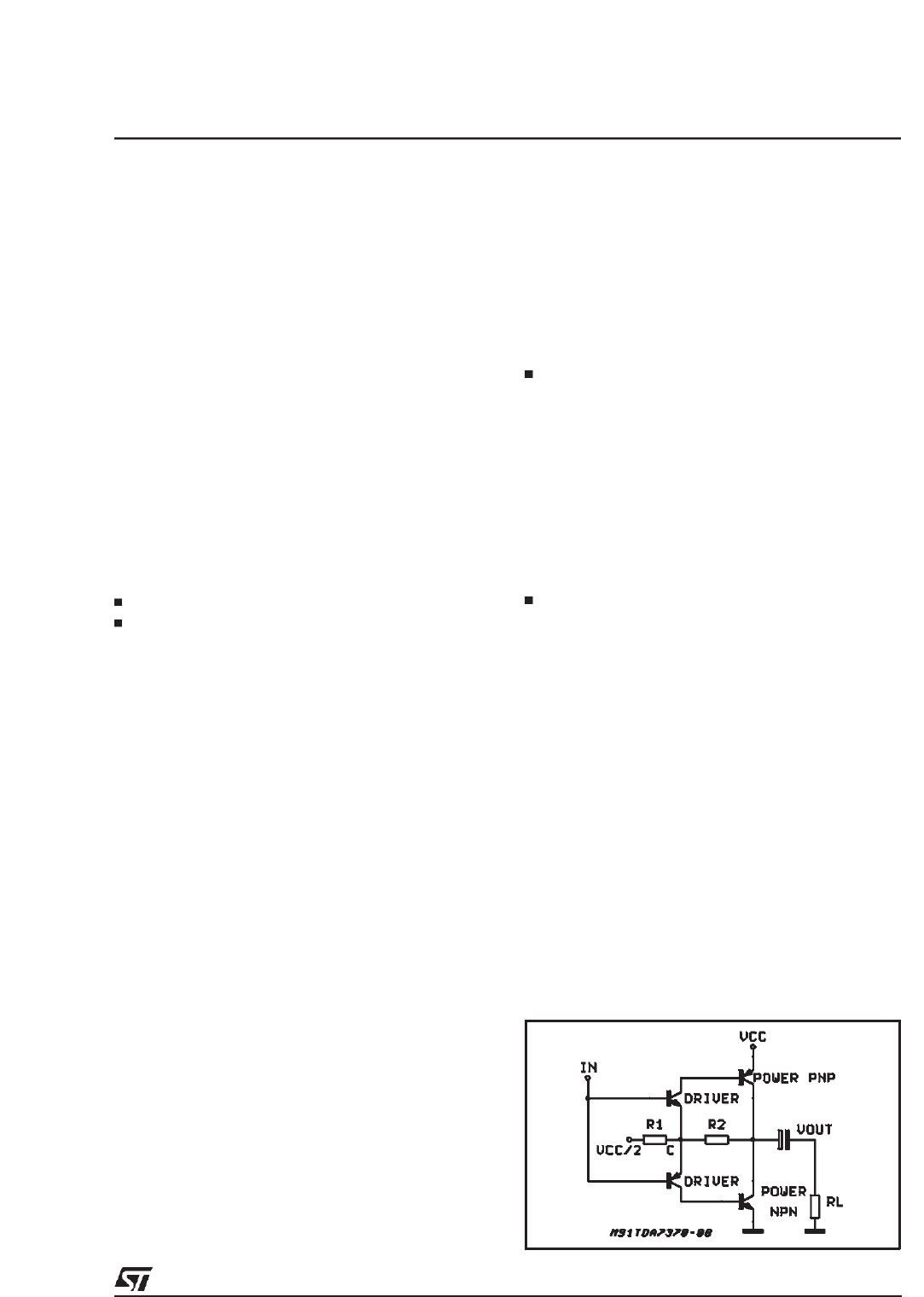
OUTPUT STAGE
The fully complementary output stage was made
possible by the development of a new compo-
nent: the ST exclusivepower ICV PNP.
A novel design based upon the connection shown
in fig. 20 has then allowed the full exploitation of
its possibilities.
The clear advantagesthis new approach has over
classical output stages are as follows:
Rail-to-Rail Output Voltage Swing With No
Need of Bootstrap Capacitors.
The output swing is limited only by the VCEsat
of the output transistors, which is in the range
of 0.3Ω(Rsat) each.
Classical solutions adopting composite PNP-
NPN for the upper output stage have higher
saturation loss on the top side of the waveform.
This unbalanced saturation causes a signifi-
cant power reduction. The only way to recover
power consists of the addition of expensive
bootstrap capacitors.
Absolute Stability Without Any External
Compensation.
Referring to the circuit of fig. 20 the gain
VOut/VIn is greater than unity, approximately 1+
R2/R1. The DC output (VCC/2) is fixed by an
auxiliary amplifier common to all the channels.
By controlling the amount of this local feedbackit
is possible to force the loop gain (A*β)toless
than unity at frequency for which the phase shift
is 180°. This means that the output buffer is in-
trinsically stableand not prone to oscillation.
Most remarkably, the above feature has been
achieved in spite of the very low closed loop
gain of the amplifier.
In contrast, with the classical PNP-NPN stage,
the solution adopted for reducing the gain at
high frequencies makes use of external RC
networks,namely the Boucherotcells.
BUILT–IN SHORT CIRCUIT PROTECTION
Figure 20: The New Output Stage
TDA7375
9/15
Reliable and safe operation, in presence of all
kinds of short circuit involving the outputs is as-
sured by BUILT-IN protectors. Additionally to the
AC/DC short circuit to GND, to VS, across the
speaker, a SOFT SHORT condition is signalled
out during the TURN-ON PHASE so assuring cor-
rect operation for the device itself and for the
loudspeaker.
This particular kind of protection acts in a way to
avoid that the device is turned on (by ST-BY)
when a resistive path (less than 16 ohms) is pre-
sent between the output and GND. As the in-
volved circuitry is normally disabled when a cur-
rent higher than 5mA is flowing into the ST-BY
pin, it is important, in order not to disable it, to
have the external current source driving the ST-
BY pin limited to 5mA.
This extra function becomes particularly attractive
when, in the single ended configuration, one ca-
pacitor is shared between two outputs (see fig.
21).
Supposing that the output capacitor Cout for any
reason is shorted, the loudspeaker will not be
damaged being this soft short circuit condition re-
vealed.
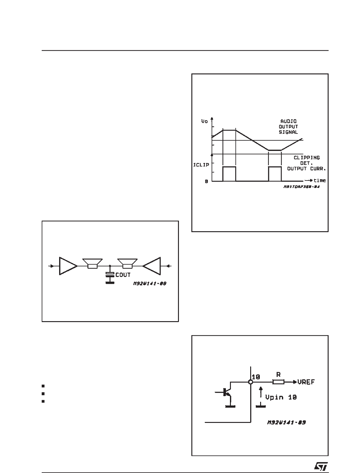
Diagnostics Facility
The TDA7375 is equipped with a diagnostic cir-
cuitry able to detect the following events:
Clipping in the output signal
Thermal shutdown
Output fault:
– shortto GND
– shortto VS
– soft short at turn on
The information is available across an open
collector output (pin 10) through a current sink-
ing when the event is detected
A current sinking at pin 10 is triggered when a
certain distortion level is reached at any of the
outputs. This function allows gain compression
possibility whenever the amplifier is overdriven.
Thermal Shutdown
In this case the output 10 will signal the proximity
of the junction temperature to the shutdown
threshold. Typically current sinking at pin 10 will
start ~10°C before the shutdown threshold is
reached.
HANDLING OF THE DIAGNOSTICS INFORMA-
Figure 21.
Figure 22: Clipping Detection Waveforms
Figure 23: Output Fault Waveforms (see fig. 24)
TDA7375
TDA7375
10/15
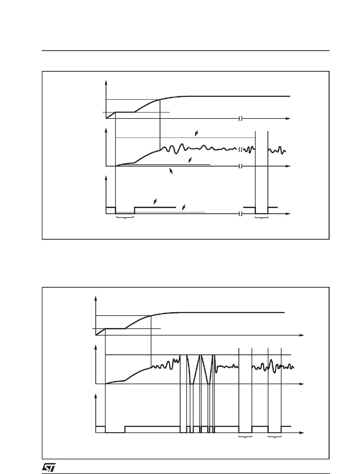
TION
As various kinds of information is available at the
same pin (clipping detection, output fault, thermal
proximity), this signal must be handled properly in
order to discriminate each event.
This could be done by taking into account the dif-
ferent timing of the diagnostic output during each
case.
SOFT SHORT
OUT TO Vs SHORT
FAULT DETECTION
CORRECT TURN-ON
OUT TO GND SHORT
t
t
t
ST-BY PIN
VOLTAGE
2V
OUTPUT
WAVEFORM
Vpin 10
CHECK AT
TURN-ON
(TEST PHASE) SHORT TO GND
OR TO Vs
D94AU149A
Figure 24: Fault Waveforms
t
t
t
ST-BY PIN
VOLTAGE
Vs
OUTPUT
WAVEFORM
Vpin
10
WAVEFORM
SHORT TO GND
OR TO Vs
D94AU150
CLIPPING THERMAL
PROXIMITY
Figure 25: Waveforms
TDA7375
11/15
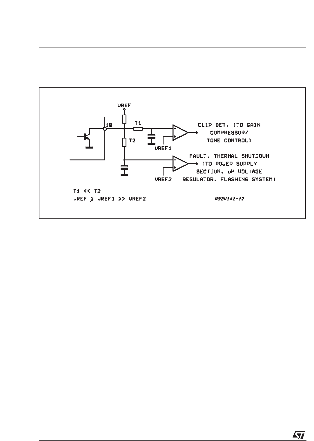
Normally the clip detector signalling produces a
low level at pin 10 that is shorter than that present
under faulty conditions; based on this assumption
an interface circuitry to differentiate the informa-
tion is representedin the schematic of fig. 26.
Figure 26.
TDA7375
PCB-LAYOUT GROUNDING (general rules)
The device has 2 distinct ground leads, P-GND
(POWER GROUND) and S-GND (SIGNAL
GROUND) which are practically disconnected
from each other at chip level. Proper operation re-
quires that P-GND and S-GND leads be con-
nected together on the PCB-layout by means of
reasonablylow-resistance tracks.
As for the PCB-ground configuration, a star-like
arrangement whose center is represented by the
supply-filtering electrolytic capacitor ground is
highly advisable. In such context, at least 2 sepa-
rate paths have to be provided, one for P-GND
and one for S-GND. The correct ground assign-
ments are as follows:
STANDBY CAPACITOR, pin 7 (or any other
standby driving networks): on S-GND
SVR CAPACITOR (pin 6): on S-GND and to be
placed as close as possible to the device.
INPUT SIGNAL GROUND (from active/passive
signal processor stages): on S-GND.
SUPPLY FILTERING CAPACITORS (pins 3,13):
on P-GND. The (-) terminal of the electrolytic ca-
pacitor has to be directly tied to the battery (-) line
and this should represent the starting point for all
the ground paths.
TDA7375
12/15
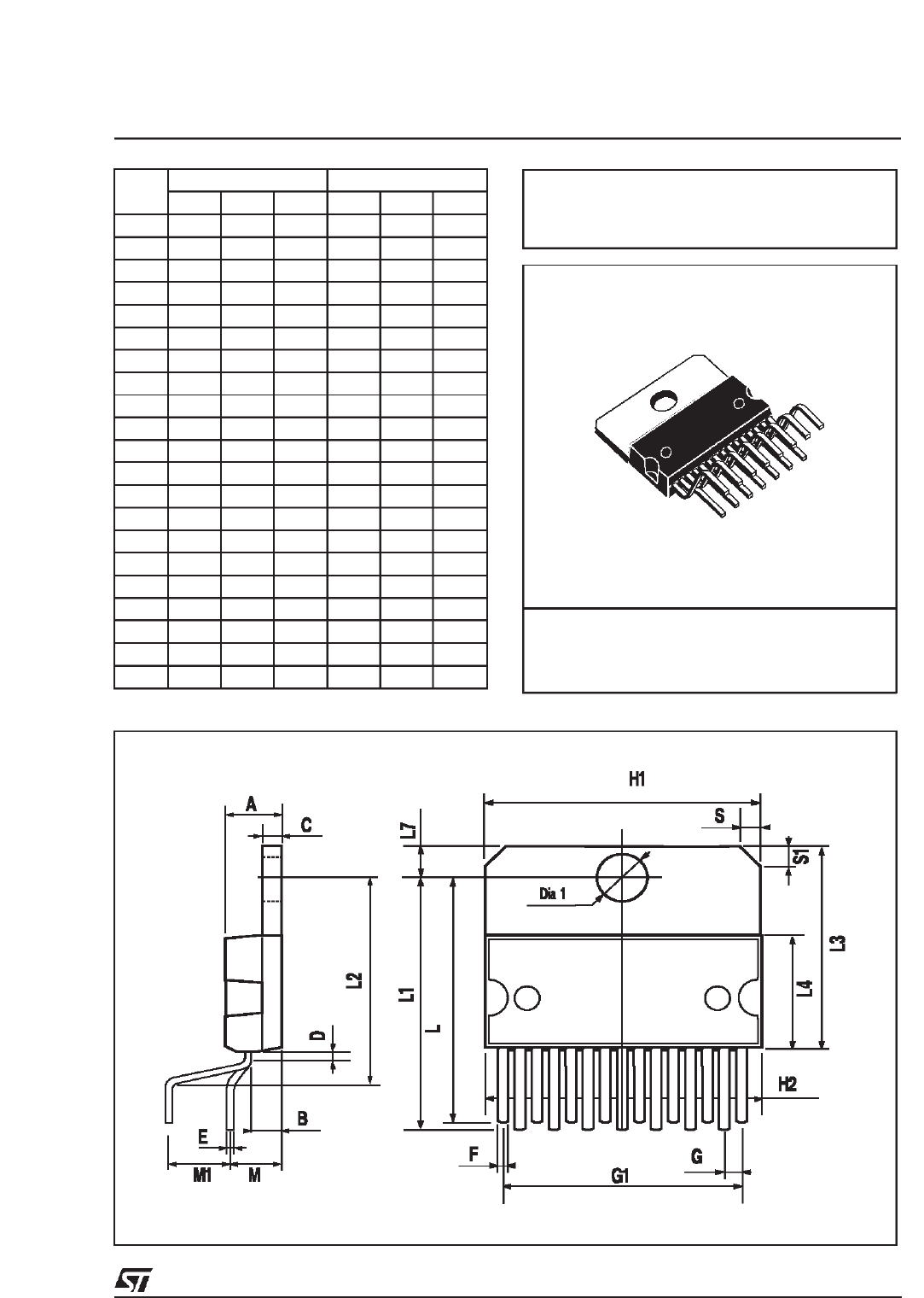
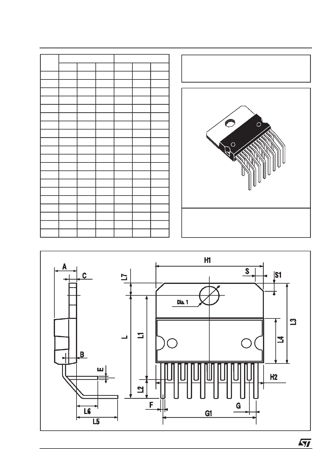
Multiwatt15 V
DIM. mm inch
MIN. TYP. MAX. MIN. TYP. MAX.
A5
0.197
B 2.65 0.104
C 1.6 0.063
D 1 0.039
E 0.49 0.55 0.019 0.022
F 0.66 0.75 0.026 0.030
G 1.02 1.27 1.52 0.040 0.050 0.060
G1 17.53 17.78 18.03 0.690 0.700 0.710
H1 19.6 0.772
H2 20.2 0.795
L 21.9 22.2 22.5 0.862 0.874 0.886
L1 21.7 22.1 22.5 0.854 0.870
0.886
L2 17.65 18.1 0.695
0.713
L3 17.25 17.5 17.75 0.679 0.689 0.699
L4 10.3 10.7 10.9 0.406 0.421 0.429
L7 2.65 2.9 0.104 0.114
M 4.25 4.55 4.85 0.167 0.179 0.191
M1 4.63 5.08 5.53 0.182 0.200 0.218
S 1.9 2.6 0.075 0.102
S1 1.9 2.6 0.075 0.102
Dia1 3.65 3.85 0.144 0.152
OUTLINE AND
MECHANICAL DATA
TDA7375
13/15
DIM. mm inch
MIN. TYP. MAX. MIN. TYP. MAX.
A5
0.197
B 2.65 0.104
C 1.6 0.063
E 0.49 0.55 0.019 0.022
F 0.66 0.75 0.026 0.030
G 1.14 1.27 1.4 0.045 0.050 0.055
G1 17.57 17.78 17.91 0.692 0.700 0.705
H1 19.6
0.772
H2 20.2 0.795
L 20.57 0.810
L1 18.03
0.710
L2 2.54
0.100
L3 17.25 17.5 17.75 0.679 0.689 0.699
L4 10.3 10.7 10.9 0.406 0.421 0.429
L5 5.28 0.208
L6 2.38
0.094
L7 2.65 2.9 0.104 0.114
S 1.9 2.6 0.075 0.102
S1 1.9 2.6 0.075 0.102
Dia1 3.65 3.85 0.144 0.152
Multiwatt15 H
OUTLINE AND
MECHANICAL DATA
TDA7375
14/15

Information furnished is believed to be accurate and reliable. However, STMicroelectronics assumes no responsibility for the consequences
of use of such information nor for any infringement of patents or other rights of third parties which may result from its use. No license is
granted by implication or otherwise under any patent or patent rights of STMicroelectronics. Specification mentioned in this publication are
subject to change without notice. This publication supersedes and replaces all information previously supplied. STMicroelectronics products
are not authorized for use as critical components in life support devices or systems without express written approval of STMicroelectronics.
The ST logo is a registered trademark of STMicroelectronics
MULTIWATTis a Registered Trademark of the STMicroelectronics
1998 STMicroelectronics – Printed in Italy – All Rights Reserved
STMicroelectronics GROUP OF COMPANIES
Australia - Brazil - Canada - China - France - Germany - Italy - Japan - Korea - Malaysia - Malta - Mexico - Morocco - The Netherlands -
Singapore - Spain - Sweden - Switzerland - Taiwan - Thailand - United Kingdom - U.S.A.
http://www.st.com
TDA7375
15/15

