TDA7560 Datasheet. Www.s Manuals.com. St
User Manual: Datasheets TDA7560.
Open the PDF directly: View PDF ![]() .
.
Page Count: 11
TDA7560
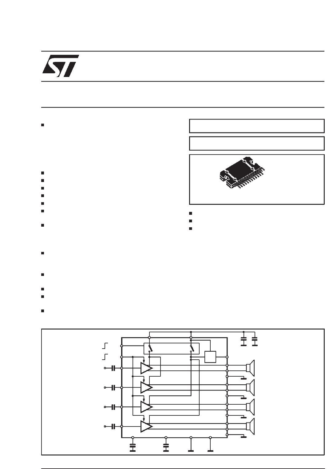
4 x 45W QUAD BRIDGE CAR RADIO AMPLIFIER PLUS HSD
PRODUCT PREVIEW
SUPERIOR OUTPUT POWER CAPABILITY:
4 x 50W/4ΩMAX.
4 x 45W/4ΩEIAJ
4 x 30W/4Ω@ 14.4V, 1KHz, 10%
4 x 80W/2ΩMAX.
4 x 77W/2ΩEIAJ
4 x 55W/2Ω@ 14.4V, 1KHz, 10%
EXCELLENT 2ΩDRIVINGCAPABILITY
HI-FI CLASS DISTORTION
LOW OUTPUT NOISE
ST-BY FUNCTION
MUTE FUNCTION
AUTOMUTE AT MIN. SUPPLY VOLTAGE DE-
TECTION
LOW EXTERNAL COMPONENT COUNT:
– INTERNALLY FIXED GAIN (26dB)
– NO EXTERNAL COMPENSATION
– NO BOOTSTRAP CAPACITORS
ON BOARD 0.35A HIGH SIDE DRIVER
PROTECTIONS:
OUTPUT SHORT CIRCUIT TO GND, TO VS,
ACROSS THE LOAD
VERY INDUCTIVE LOADS
OVERRATING CHIP TEMPERATURE WITH
SOFT THERMAL LIMITER
LOAD DUMP VOLTAGE
FORTUITOUS OPEN GND
REVERSED BATTERY
ESD
DESCRIPTION
The TDA7560 is a breakthrough BCD (Bipolar /
CMOS / DMOS) technology class AB Audio
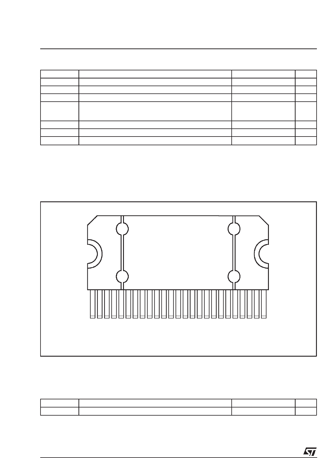
Power Amplifier in Flexiwatt 25 package designed
for high power car radio
The fully complementary P-Channel/N-Channel
output structure allows a rail to rail output voltage
swing which, combined with high output current
and minimised saturation losses sets new power
references in the car-radio field, with unparal-
leled distortion performances.
This is preliminary information on a new product now in development. Details are subject to change without notice.
November 1999
ORDERING NUMBER: TDA7560
IN1
0.1µF
MUTE
ST-BY
IN2
0.1µF
OUT1+
OUT1-
OUT2+
OUT2-
PW-GND
IN3
0.1µF
IN4
0.1µF
OUT3+
OUT3-
OUT4+
OUT4-
PW-GND
PW-GND
PW-GND
D94AU158B
AC-GND
0.47µF47µF
SVR TAB S-GND
Vcc1 Vcc2
100nF470µF
HSDHSD
BLOCK AND APPLICATION DIAGRAM
FLEXIWATT25
MULTIPOWER BCD TECHNOLOGY
MOSFET OUTPUT POWER STAGE
1/10
D94AU159A
TAB
P-GND2
OUT2-
ST-BY
OUT2+
VCC
OUT1-
P-GND1
OUT1+
SVR
IN1
IN2
S-GND
IN4
IN3
AC-GND
OUT3+
P-GND3
OUT3-
VCC
OUT4+
MUTE
OUT4-
P-GND4
HSD
1 25
PIN CONNECTION (Topview)
ABSOLUTE MAXIMUM RATINGS
Symbol Parameter Value Unit
VCC Operating Supply Voltage 18 V
VCC (DC) DC Supply Voltage 28 V
VCC (pk) Peak Supply Voltage (t = 50ms) 50 V
IOOutput Peak Current:
Repetitive (Duty Cycle 10% at f = 10Hz)
Non Repetitive (t = 100µs) 9
10 A
A
Ptot Power dissipation, (Tcase =70
°
C) 80 W
TjJunction Temperature 150 °C
Tstg Storage Temperature – 55 to 150 °C
THERMAL DATA
Symbol Parameter Value Unit
Rth j-case Thermal Resistance Junction to Case Max. 1 °C/W
TDA7560
2/10
ELECTRICAL CHARACTERISTICS (VS= 13.2V; f = 1KHz; Rg= 600Ω;R
L=4Ω;T
amb =25°C;
Refer to the test and application diagram, unless otherwise specified.)
Symbol Parameter Test Condition Min. Typ. Max. Unit
Iq1 Quiescent Current RL=∞120 200 320 mA
VOS Output Offset Voltage Play Mode ±80 mV
dVOS During mute ON/OFF output
offset voltage ±80 mV
GvVoltage Gain 25 26 27 dB
dGvChannel Gain Unbalance ±1dB
P
oOutput Power VS= 13.2V; THD = 10%
VS= 13.2V; THD = 1%
VS= 14.4V; THD = 10%
VS= 14.4V; THD = 1%
23
16
28
20
25
19
30
23
W
W
W
W
VS= 13.2V; THD = 10%, 2Ω
VS= 13.2V; THD = 1%, 2Ω
VS= 14.4V; THD = 10%, 2Ω
VS= 14.4V; THD = 1%, 2Ω
42
32
50
40
45
34
55
43
W
W
W
W
Po EIAJ EIAJ Output Power (*) VS= 13.7V; RL=4Ω
V
S= 13.7V; RL=2
Ω41
75 45
77 W
W
Po max. Max. Output Power (*) VS= 14.4V; RL=4
Ω
V
S= 14.4V; RL=2Ω50
80 W
W
THD Distortion Po=4W
P
o= 10W; RL=2
Ω0.006
0.015 0.05
0.07 %
%
eNo Output Noise ”A” Weighted
Bw = 20Hz to 20KHz 35
50 50
70 µV
µV
SVR Supply Voltage Rejection f = 100Hz; Vr= 1Vrms 50 70 dB
fch High Cut-Off Frequency PO= 0.5W 100 300 KHz
RiInput Impedance 80 100 120 KΩ
CTCross Talk f = 1KHz PO=4W
f = 10KHz PO=4W 60 70
60 –
–dB
dB
ISB St-By Current Consumption VSt-By = 1.5V 75 µA
Ipin4 St-by pin Current VSt-By = 1.5V to 3.5V ±10 µA
VSB out St-By Out Threshold Voltage (Amp: ON) 3.5 V
VSB in St-By in Threshold Voltage (Amp: OFF) 1.5 V
AMMute Attenuation POref =4W 80 90 dB
V
M out Mute Out Threshold Voltage (Amp: Play) 3.5 V
VMin Mute In Threshold Voltage (Amp: Mute) 1.5 V
VAM in VSAutomute Threshold (Amp: Mute)
Att ≥80dB; POref =4W
(Amp: Play)
Att < 0.1dB; PO= 0.5W
6.5 7
7.5 8
V
V
Ipin22 Muting Pin Current VMUTE = 1.5V
(Sourced Current) 71218
µ
A
V
MUTE = 3.5V -5 18 µA
HSD SECTION
Vdropout Dropout Voltage IO= 0.35A; VS= 9 to 16V 0.25 0.6 V
Iprot Current Limits 400 800 mA
(*) Saturated square wave output.
TDA7560
3/10
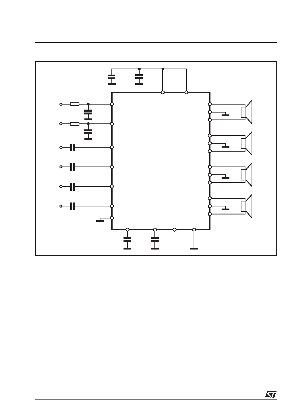
IN1
0.1µF
C9
1µF
IN2
C2 0.1µF
OUT1
OUT2
IN3
C3 0.1µF
IN4
C4 0.1µF
OUT3
OUT4
D95AU335B
C5
0.47µF
C6
47µF
SVR TAB
Vcc1-2 Vcc3-4
C8
0.1µF
C7
2200µF
C10
1µF
ST-BY R1
10K
R2
47K
MUTE
C1
14
15
12
11
22
4
13
S-GND
16 10 25 1
HSD
620
9
8
7
5
2
3
17
18
19
21
24
23
Figure 1: Standard Test and Application Circuit
TDA7560
4/10
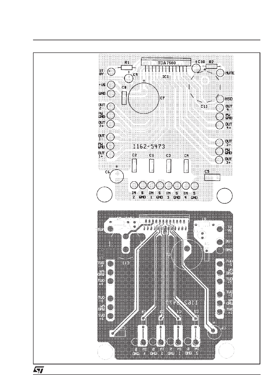
Figure 2: P.C.B. and componentlayout of the figure 1 (1:1 scale)
COMPONENTS &
TOP COPPER LAYER
BOTTOM COPPER LAYER
TDA7560
5/10
8 1012141618
Vs (V)
140
160
180
200
220
240 Id (mA)
Vi = 0
RL = 4 Ohm
Figure 3. Quiescentcurrent vs. supply
voltage.
8 9 10 11 12 13 14 15 16 17 18
Vs (V)
5
10
15
20
25
30
35
40
45
50
55
60
65
70
75
80 Po (W)
RL=4 Ohm
f=1 KHz THD=10 %
THD=1%
Po-max
Figure 4. Output power vs. supply voltage.
8 9 10 11 12 13 14 15 16 17 18
Vs (V)
10
20
30
40
50
60
70
80
90
100
110
120
130 Po(W)
RL= 2 Ohm
f=1 KHz THD= 10%
THD=1 %
Po-max
Figure 5. Output power vs. supply voltage.
0.1 1 10
Po(W)
0.001
0.01
0.1
1
10THD(%)
f=10KHz
RL= 4 Ohm
f=1KHz
Vs= 14.4 V
Figure 6. Distortion vs. output Power
0.1 1 10
Po (W)
0.001
0.01
0.1
1
10THD(%)
f=10KHz
RL= 2 Ohm
f=1KHz
Vs=14.4 V
Figure 7. Distortion vs. output power
10 100 1000 10000
f(Hz)
0.001
0.01
0.1
1
10 THD (%)
Po = 4 W
RL = 4 Ohm
Vs = 14.4 V
Figure 8. Distortion vs. frequency.
TDA7560
6/10
10 100 1000 10000
f(Hz)
20
30
40
50
60
70
80
90 CROSSTALK (dB)
Po= 4 W
RL= 4 Ohm
Rg= 600 Ohm
Figure 10. Crosstalk vs. frequency.
10 100 1000 10000
f(Hz)
20
30
40
50
60
70
80
90
100 SVR(dB)
Vripple=1Vrms
Rg= 600 Ohm
Figure 11. Supply voltage rejection vs. fre-
quency.
5678910
Vs (V)
0
-20
-40
-60
-80
-100
OUT ATTN (dB)
RL= 4 Ohm
Po= 4 W ref.
Figure 12. Output attenuation vs. supply
voltage.
1 10 100 1000 10000 100000
Rg(Ohm)
20
30
40
50
60
70
80
90
100
110
120
130 En (uV)
Vs= 14.4V
RL= 4 Ohm
”A”wgtd
22-22KHz lin.
Figure 13. Output noise vs. source resistance.
024681012141618202224262830
Po (W)
0
10
20
30
40
50
60
70
80
90 Ptot(W)
0
10
20
30
40
50
60
70
80
90
n(%)
Vs=13.2 V
RL=4 x 4 Ohm
f=1 KHz SINE
n
Ptot
Figure 14. Power dissipation & efficiency vs.
output power (sine-wave operation)
10 100 1000 10000
f(Hz)
0.001
0.01
0.1
1
10 THD(%)
Po = 8 W
RL= 2 Ohm
Vs=14.4V
Figure 9. Distortion vs. frequency.
TDA7560
7/10
0246810
Po (W)
5
10
15
20
25
30
35
40
45
50
55
60 Ptot (W)
Vs= 13.2V
RL= 4 x 2 Ohm
CLIP START
GAUSSIAN NOISE
Figure 16. Power dissipation vs. output power
(Music/Speech Simulation)
0123456
Po (W)
5
10
15
20
25
30 Ptot (W)
Vs=13.2V
RL=4 x 4 Ohm
CLIP START
GAUSSIANNOISE
Figure 15. Power dissipation vs. ouput power
(Music/Speech Simulation)
APPLICATION HINTS (ref. to the circuit of fig. 1)
SVR
Besides its contribution to the ripple rejection, the
SVR capacitor governs the turn ON/OFF time se-
quence and, consequently, plays an essential role
in the pop optimization during ON/OFF tran-
sients.To conveniently serve both needs, ITS
MINIMUM RECOMMENDED VALUE IS 10µF.
INPUT STAGE
The TDA7560’s inputs are ground-compatible and
can stand very high input signals (±8Vpk) without
any performancesdegradation.
If the standard value for the input capacitors
(0.1µF) is adopted, the low frequency cut-off will
amount to 16 Hz.
STAND-BY AND MUTING
STAND-BY and MUTING facilities are both
CMOS-COMPATIBLE. If unused, a straight con-
nection to Vs of their respective pins would be ad-
missible. Conventional low-power transistors can
be employed to drive muting and stand-by pins in
absence of true CMOS ports or microprocessors.
R-C cells have always to be used in order to
smooth down the transitions for preventing any
audible transient noises.
About the stand-by, the time constant to be as-
signed in order to obtain a virtually pop-free tran-
sition has to be slower than 2.5V/ms.
HEATSINK DEFINITION
Under normal usage (4 Ohm speakers) the
heatsink’s thermal requirements have to be de-
duced from fig. 15, which reports the simulated
power dissipation when real music/speech pro-
grammes are played out. Noise with gaussian-
distributed amplitude was employed for this simu-
lation. Based on that, frequent clipping occurence
(worst-case) will cause Pdiss = 26W. Assuming
Tamb = 70°C and TCHIP = 150°C as boundary
conditions, the heatsink’s thermal resistance
should be approximately 2°C/W. This would avoid
any thermal shutdown occurence even after long-
term and full-volume operation.
TDA7560
8/10
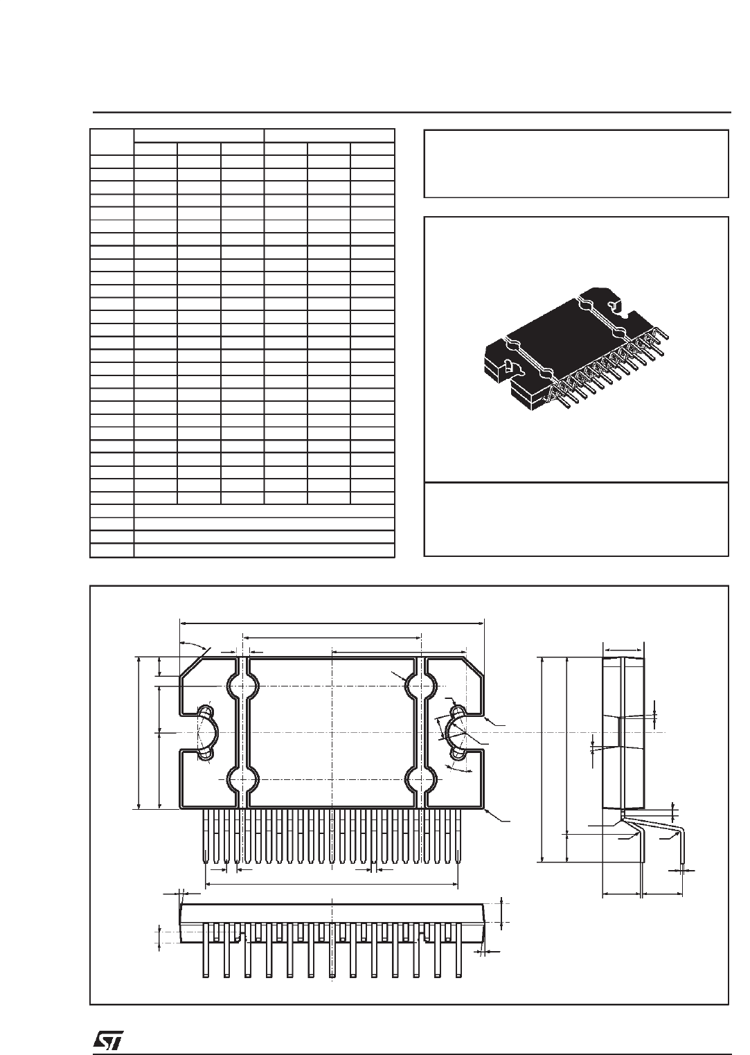
Flexiwatt25
DIM. mm inch
MIN. TYP. MAX. MIN. TYP. MAX.
A 4.45 4.50 4.65 0.175 0.177 0.183
B 1.80 1.90 2.00 0.070 0.074 0.079
C 1.40 0.055
D 0.75 0.90 1.05 0.029 0.035 0.041
E 0.37 0.39 0.42 0.014 0.015 0.016
F (1) 0.57 0.022
G 0.80 1.00 1.20 0.031 0.040 0.047
G1 23.75 24.00 24.25 0.935 0.945 0.955
H (2) 28.90 29.23 29.30 1.138 1.150 1.153
H1 17.00 0.669
H2 12.80 0.503
H3 0.80 0.031
L (2) 22.07 22.47 22.87 0.869 0.884 0.904
L1 18.57 18.97 19.37 0.731 0.747 0.762
L2 (2) 15.50 15.70 15.90 0.610 0.618 0.626
L3 7.70 7.85 7.95 0.303 0.309 0.313
L4 5 0.197
L5 3.5 0.138
M 3.70 4.00 4.30 0.145 0.157 0.169
M1 3.60 4.00 4.40 0.142 0.157 0.173
N 2.20 0.086
O 2 0.079
R 1.70 0.067
R1 0.5 0.02
R2 0.3 0.12
R3 1.25 0.049
R4 0.50 0.019
V5°(Typ.)
V1 3°(Typ.)
V2 20°(Typ.)
V3 45°(Typ.)
(1): dam-bar protusion not included
(2): molding protusion included
H3
R4
G
VG1
L2
H1
H
FM1
L
FLEX25ME
V3
OL3 L4
H2
R3
N
V2
R
R2
R2
C
B
L1
M
R1
L5 R1 R1
E
D
A
V
V1
V1
OUTLINE AND
MECHANICAL DATA
TDA7560
9/10

Information furnished is believed to be accurate and reliable. However, STMicroelectronics assumes no responsibility for the consequences
of use of such information nor for any infringement of patents or other rights of third parties which may result from its use. No license is
granted by implication or otherwise under any patent or patent rights of STMicroelectronics. Specification mentioned in this publication are
subject to change without notice. This publication supersedes and replaces all information previously supplied. STMicroelectronics products
are not authorized for use as critical components in life support devices or systems without express written approval of STMicroelectronics.
The ST logo is a registered trademark of STMicroelectronics
1999 STMicroelectronics – Printed in Italy – All Rights Reserved
STMicroelectronics GROUP OF COMPANIES
Australia - Brazil - China - Finland - France - Germany - Hong Kong - India - Italy - Japan - Malaysia - Malta - Morocco -
Singapore - Spain - Sweden - Switzerland - United Kingdom - U.S.A.
http://www.st.com
TDA7560
10/10