TDA8588AJ, TDA8588BJ, TDA8588J Datasheet. Www.s Manuals.com. Philips
User Manual: Datasheets TDA8588AJ, TDA8588BJ, TDA8588J.
Open the PDF directly: View PDF ![]() .
.
Page Count: 55
- Features
- Applications
- General description
- Quick reference data
- Ordering information
- Block diagram
- Pinning
- Functional description
- Amplifiers
- Voltage regulators
- I2C-bus specification
- Limiting values
- Thermal characteristics
- Quality specification
- Characteristics
- Application and test information
- Package outline
- Soldering
- Data sheet status
- Definitions
- Disclaimers
- Purchase of Philips I
DATA SHEET
Product specification 2004 Feb 24
INTEGRATED CIRCUITS
TDA8588J; TDA8588xJ
I2C-bus controlled 4 ×50 Watt
power amplifier and multiple
voltage regulator

2004 Feb 24 2
Philips Semiconductors Product specification
I2C-bus controlled 4 ×50 Watt power
amplifier and multiple voltage regulator TDA8588J; TDA8588xJ
FEATURES
Amplifiers
•I2C-bus control
•Can drive a 2 Ωload with a battery voltage of up to 16 V
and a 4 Ω load with a battery voltage of up to 18 V
•DC load detection, open, short and present
•AC load (tweeter) detection
•Programmable clip detect; 1 % or 4 %
•Programmable thermal protection pre-warning
•Independent short-circuit protection per channel
•Low gain line driver mode (20 dB)
•Loss-of-ground and open VPsafe
•All outputs protected from short-circuit to ground, to VP
or across the load
•All pins protected from short-circuit to ground
•Soft thermal-clipping to prevent audio holes
•Low battery detection.
Voltage regulators
GENERAL
•I2C-bus control
•Good stability for any regulator with almost any output
capacitor value
•Five voltage regulators (microcontroller, display,
mechanical digital, mechanical drive and audio)
•Choice of non-adjustable 3.3 or 5 V microcontroller
supply (REG2) versions reducing risk of overvoltage
damage
•Choice of non-adjustable 3.3 or 5 V digital signal
processor supply (REG3) versions reducing risk of
overvoltage damage
•Selectable output voltages for regulators 1, 4 and 5
•Low dropout voltage PNP output stages
•High supply voltage ripple rejection
•Low noise for all regulators
•Two power switches (antenna switch and amplifier
switch)
•Regulator 2 (microcontroller supply) operational during
load-dump and thermal shut-down
•Low quiescent current (only regulator 2 is operational)
•Reset output (push-pull output stage)
•Adjustable reset delay time
•Backup functionality.
PROTECTION
•If connection to the battery voltage is reversed, all
regulator voltages will be zero
•Able to withstand voltages at the output of up to 18 V
(supply line may be short-circuited)
•Thermal protection to avoid thermal breakdown
•Load-dump protection
•Regulator outputs protected from DC short-circuit to
ground or to supply voltage
•All regulators protected by foldback current limiting
•Power switches protected from loss-of-ground.
APPLICATIONS
•Boost amplifier and voltage regulator for car radios and
CD/MD players.
GENERAL DESCRIPTION
Amplifiers
The TDA8588 has a complementary quad audio power
amplifier that uses BCDMOS technology. It contains four
amplifiers configured in Bridge Tied Load (BTL) to drive
speakers for front and rear left and right channels. The
I2C-bus allows diagnostic information of each amplifier and
its speaker to be read separately. Both front and both rear
channel amplifiers can be configured independently in line
driver mode with a gain of 20 dB (differential output).
Voltage regulators
The TDA8588 has a multiple output voltage regulator with
two power switches.
The voltage regulator contains the following:
•Four switchable regulators and one permanently active
regulator (microcontroller supply)
•Two power switches with loss-of-ground protection
•A reset output that can be used to communicate with a
microcontroller.
The quiescent current has a very low level of 150 µA with
only regulator 2 active.
2004 Feb 24 3
Philips Semiconductors Product specification
I2C-bus controlled 4 ×50 Watt power
amplifier and multiple voltage regulator TDA8588J; TDA8588xJ
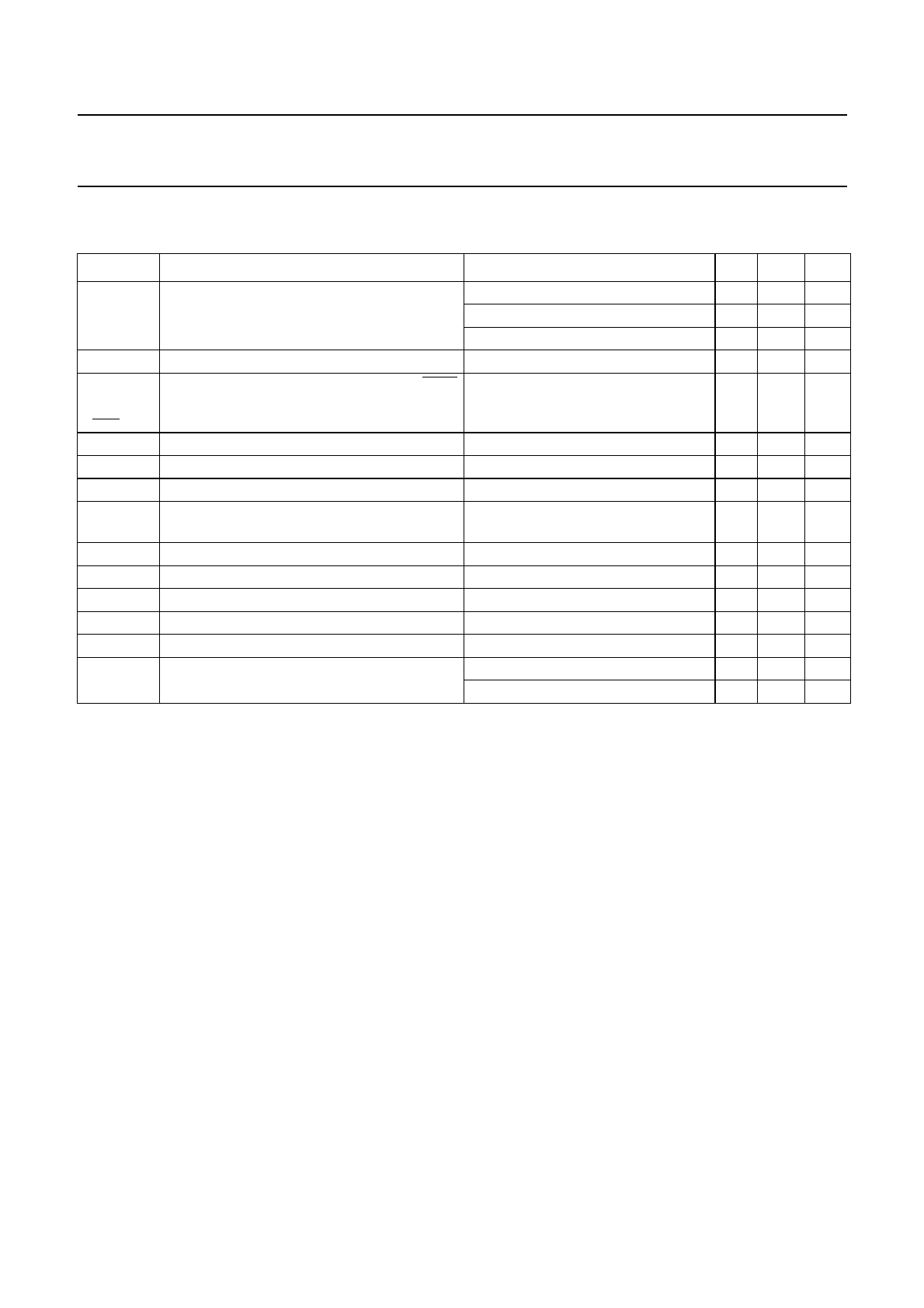
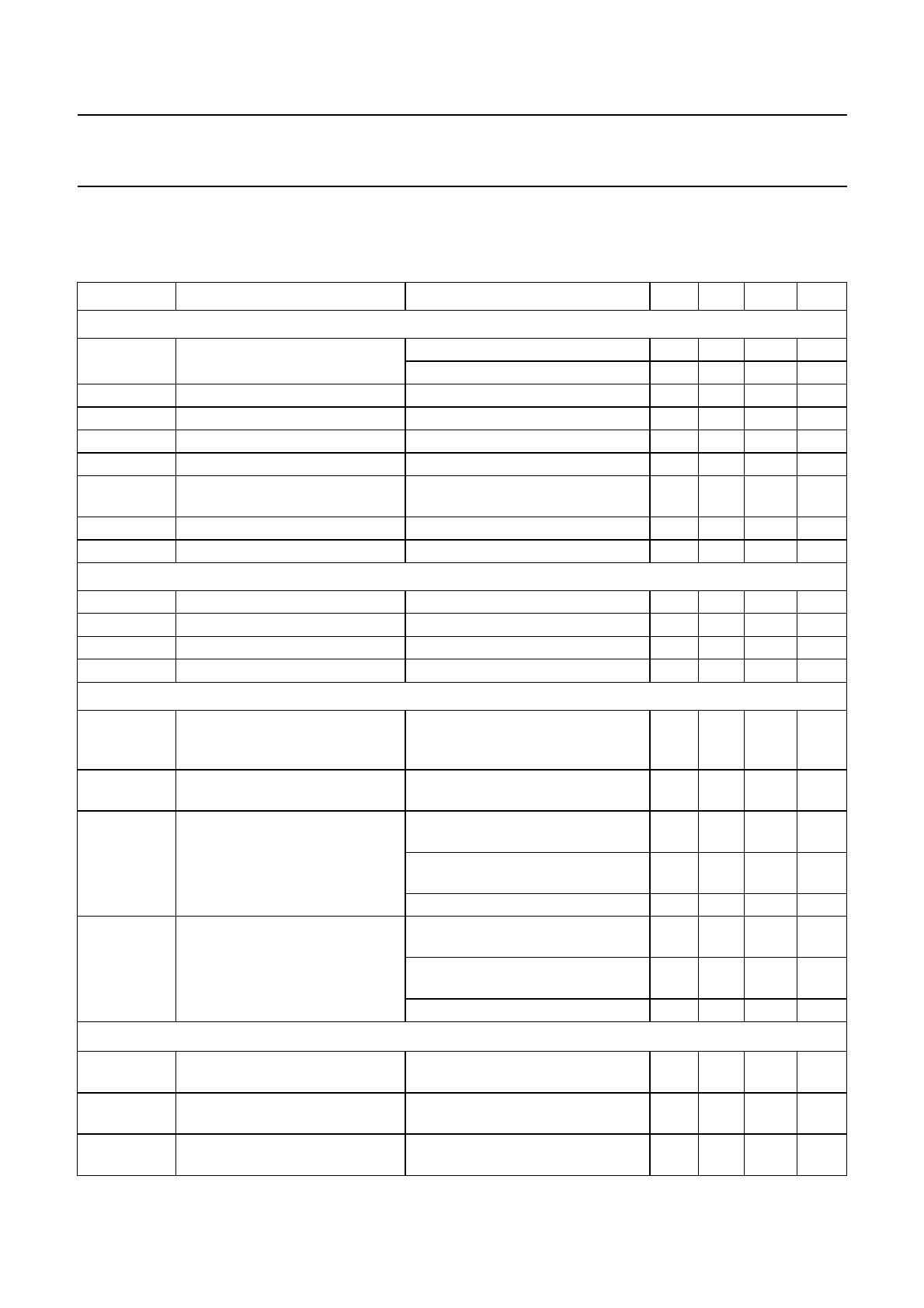
QUICK REFERENCE DATA
SYMBOL PARAMETER CONDITIONS MIN. TYP. MAX. UNIT
Amplifiers
VP1, VP2 operating supply voltage 8 14.4 18 V
Iq(tot) total quiescent current −270 400 mA
Po(max) maximum output power RL=4Ω;V
P= 14.4 V; VIN =2V
RMS square wave
44 46 −W
RL=4Ω;V
P= 15.2 V; VIN =2V
RMS square wave
49 52 −W
RL=2Ω;V
P= 14.4 V; VIN =2V
RMS square wave
83 87 −W
THD total harmonic distortion −0.01 0.1 %
Vn(o)(amp) noise output voltage in amplifier mode −50 70 µV
Vn(o)(LN) noise output voltage in line driver mode −25 35 µV
Voltage regulators
SUPPLY
VPsupply voltage regulator 1, 3, 4 and 5 on 10 14.4 18 V
regulator 2 on 4 −−V
jump starts for t ≤10 minutes −−30 V
load dump protection for
t≤50 ms and tr≤2.5 ms
−−50 V
overvoltage for shut-down 20 −−V
Iq(tot) total quiescent supply current standby mode; VP= 14.4 V −150 190 µA
VOLTAGE REGULATORS
VO(REG1) output voltage of regulator 1 0.5 mA ≤IO≤400 mA;
selectable via I2C-bus
IB2[D3:D2] = 01 −8.3 −V
IB2[D3:D2] = 10 −8.5 −V
IB2[D3:D2] = 11 −8.7 −V
VO(REG2) output voltage of regulator 2 0.5 mA ≤IO≤350 mA
TDA8588J; TDA8588AJ −5.0 −V
TDA8588BJ −3.3 −V
VO(REG3) output voltage of regulator 3 0.5 mA ≤IO≤300 mA
TDA8588J −5.0 −V
TDA8588AJ; TDA8588BJ −3.3 −V
VO(REG4) output voltage of regulator 4 maximum current ≥1.6 A;
0.5 mA ≤IO≤800 mA;
selectable via I2C-bus
IB2[D7:D5] = 001 −5.0 −V
IB2[D7:D5] = 010 −6.0 −V
IB2[D7:D5] = 011 −7.0 −V
IB2[D7:D5] = 100 −8.6 −V

2004 Feb 24 4
Philips Semiconductors Product specification
I2C-bus controlled 4 ×50 Watt power
amplifier and multiple voltage regulator TDA8588J; TDA8588xJ
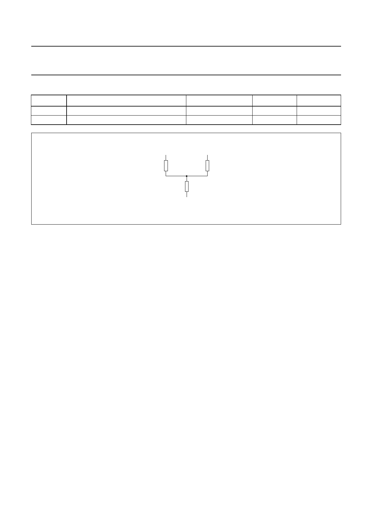
ORDERING INFORMATION
Note
1. Permanent output voltage of regulator 2 and output voltage of regulator 3, respectively.
VO(REG5) output voltage of regulator 5 0.5 mA ≤IO≤400 mA;
selectable via I2C-bus
IB1[D7:D4] = 0001 −6.0 −V
IB1[D7:D4] = 0010 −7.0 −V
IB1[D7:D4] = 0011 −8.2 −V
IB1[D7:D4] = 0100 −9.0 −V
IB1[D7:D4] = 0101 −9.5 −V
IB1[D7:D4] = 0110 −10.0 −V
IB1[D7:D4] = 0111 −10.4 −V
IB1[D7:D4] = 1000 −12.5 −V
IB1[D7:D4] = 1001 −VP−
1
−V
POWER SWITCHES
Vdrop(SW1) dropout voltage of switch 1 IO= 400 mA −0.6 1.1 V
Vdrop(SW2) dropout voltage of switch 2 IO= 400 mA −0.6 1.1 V
TYPE NUMBER PACKAGE OUTPUT VOLTAGE(1)
NAME DESCRIPTION VERSION REGULATOR 2 REGULATOR 3
TDA8588J DBS37P plastic DIL-bent-SIL power package;
37 leads (lead length 6.8 mm)
SOT725-1 5 V 5 V
TDA8588AJ 5 V 3.3 V
TDA8588BJ 3.3 V 3.3 V
SYMBOL PARAMETER CONDITIONS MIN. TYP. MAX. UNIT
2004 Feb 24 5
Philips Semiconductors Product specification
I2C-bus controlled 4 ×50 Watt power
amplifier and multiple voltage regulator TDA8588J; TDA8588xJ
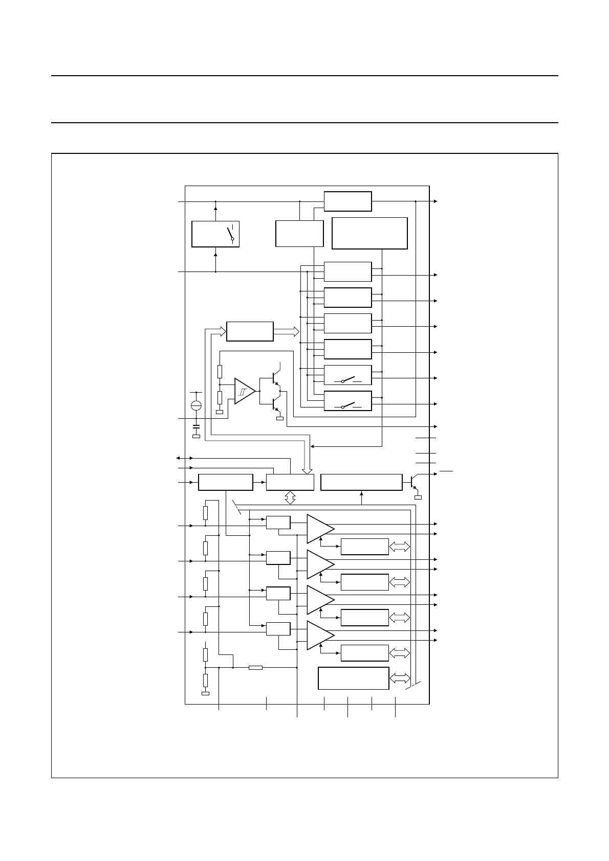
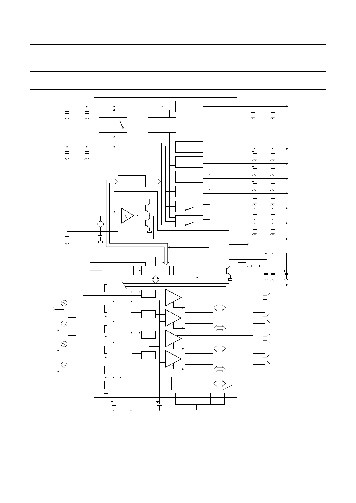
BLOCK DIAGRAM
mdb586
V
reg2
40 µs
BACKUP
SWITCH
ENABLE
LOGIC
TDA8588
STANDBY/ MUTE I
2
C-BUS
INTERFACE CLIP DETECT/ DIAGNOSTIC
REGULATOR 1
REGULATOR 3
REGULATOR 2
REGULATOR 4
REGULATOR 5
SWITCH 1
SWITCH 2
MUTE
PROTECTION/
DIAGNOSTIC
26 dB/
20 dB
PROTECTION/
DIAGNOSTIC
26 dB/
20 dB
PROTECTION/
DIAGNOSTIC
26 dB/
20 dB
PROTECTION/
DIAGNOSTIC
26 dB/
20 dB
MUTE
MUTE
MUTE
35
28
27
26
20
6
25
9
7
17
19
5
3
21
23
16 8
13
SGNDSVR
IN4
IN3
IN2
IN1
STB
SCL
SDA
RESCAP
V
P
BUCAP
ACGND PGND1 PGND3 PGND4
10
14
12
15
11
22
4
2
1 18 24
32
29
34
33
31
30
37 REG2
REG1
REG3
REG4
REG5
SW1
SW2
RST
V
P1
DIAG
OUT1+
OUT1−
OUT2+
OUT2−
OUT3+
OUT3−
OUT4+
OUT4−
V
P2
GND
36
VP
REFERENCE
VOLTAGE
TEMPERATURE &
LOAD DUMP
PROTECTION VOLTAGE
REGULATOR
TEMPERATURE & LOAD
DUMP PROTECTION
AMPLIFIER
PGND2/TAB
Fig.1 Block diagram.

2004 Feb 24 6
Philips Semiconductors Product specification
I2C-bus controlled 4 ×50 Watt power
amplifier and multiple voltage regulator TDA8588J; TDA8588xJ
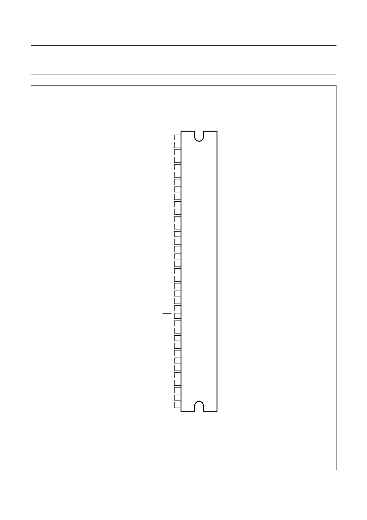
PINNING
SYMBOL PIN DESCRIPTION
PGND2/TAB 1 power ground 2 and connection for heatsink
SDA 2 I2C-bus data input and output
OUT3−3 channel 3 negative output
SCL 4 I2C-bus clock input
OUT3+ 5 channel 3 positive output
VP2 6 power supply voltage 2 to amplifier
OUT1−7 channel 1 negative output
PGND1 8 power ground 1
OUT1+ 9 channel 1 positive output
SVR 10 half supply voltage filter capacitor
IN1 11 channel 1 input
IN3 12 channel 3 input
SGND 13 signal ground
IN4 14 channel 4 input
IN2 15 channel 2 input
ACGND 16 AC ground
OUT2+ 17 channel 2 positive output
PGND3 18 power ground 3
OUT2−19 channel 2 negative output
VP1 20 power supply voltage 1 to amplifier
OUT4+ 21 channel 4 positive output
STB 22 standby or operating or mute mode select input
OUT4−23 channel 4 negative output
PGND4 24 power ground 4
DIAG 25 diagnostic and clip detection output, active LOW
RST 26 reset output
SW2 27 antenna switch; supplies unregulated power to car aerial motor
RESCAP 28 reset delay capacitor
SW1 29 amplifier switch; supplies unregulated power to amplifier(s)
REG1 30 regulator 1 output; supply for audio part of radio and CD player
REG3 31 regulator 3 output; supply for signal processor part (mechanical digital) of CD player
GND 32 combined voltage regulator, power and signal ground
REG4 33 regulator 4 output; supply for mechanical part (mechanical drive) of CD player
REG5 34 regulator 5 output; supply for display part of radio and CD player
VP35 power supply to voltage regulator
BUCAP 36 connection for backup capacitor
REG2 37 regulator 2 output; supply voltage to microcontroller
2004 Feb 24 7
Philips Semiconductors Product specification
I2C-bus controlled 4 ×50 Watt power
amplifier and multiple voltage regulator TDA8588J; TDA8588xJ
TDA8588
PGND2/TAB
SDA
OUT3−
SCL
OUT3+
V
P2
OUT1−
PGND1
OUT1+
SVR
IN1
IN3
SGND
IN4
IN2
ACGND
OUT2+
PGND3
OUT2−
V
P1
OUT4+
STB
OUT4−
PGND4
DIAG
RST
SW2
RESCAP
SW1
REG1
REG3
GND
001aaa258
REG4
REG5
V
P
BUCAP
REG2
1
2
3
4
5
6
7
8
9
10
11
12
13
14
15
16
17
18
19
20
21
22
23
24
25
26
27
28
29
30
31
32
33
34
35
36
37
Fig.2 Pin configuration.

2004 Feb 24 8
Philips Semiconductors Product specification
I2C-bus controlled 4 ×50 Watt power
amplifier and multiple voltage regulator TDA8588J; TDA8588xJ
FUNCTIONAL DESCRIPTION
The TDA8588 is a multiple voltage regulator combined
with four independent audio power amplifiers configured in
bridge tied load with diagnostic capability. The output
voltages of all regulators except regulators 2 and 3 can be
controlled via the I2C-bus. However, regulator 3 can be set
to 0 V via the I2C-bus. The output voltage of regulator 2
(microcontroller supply) and the maximum output voltage
of regulator 3 (mechanical digital and microcontroller
supplies) can both be either 5 V or 3.3 V depending on the
type number. The maximum output voltages of both
regulators are fixed to avoid any risk of damaging the
microcontroller that may occur during a disturbance of the
I2C-bus.
The amplifier diagnostic functions give information about
output offset, load, or short-circuit. Diagnostic functions
are controlled via the I2C-bus. The TDA8588 is protected
against short-circuit, over-temperature, open ground and
open VP connections. If a short-circuit occurs at the input
or output of a single amplifier, that channel shuts down,
and the other channels continue to operate normally. The
channel that has a short-circuit can be disabled by the
microcontroller via the appropriate enable bit of the
I2C-bus to prevent any noise generated by the fault
condition from being heard.
Start-up
At power on, regulator 2 will reach its final voltage when
the backup capacitor voltage exceeds 5.5 V independently
of the voltage on pin STB. When pin STB is LOW, the total
quiescent current is low, and the I2C-bus lines are high
impedance.
When pin STB is HIGH, the I2C-bus is biased on and then
the TDA8588 performs a power-on reset. When bit D0 of
instruction byte IB1 is set, the amplifier is activated, bit D7
of data byte 2 (power-on reset occurred) is reset, and
pin DIAG is no longer held LOW.
Start-up and shut-down timing (see Fig.12)
A capacitor connected to pin SVR enables smooth start-up
and shut-down, preventing the amplifier from producing
audible clicks at switch-on or switch-off. The start-up and
shut-down times can be extended by increasing the
capacitor value.
If the amplifier is shut down using pin STB, the amplifier is
muted, the regulators and switches are switched off, and
the capacitor connected to pin SVR discharges. The low
current standby mode is activated 2 seconds after pin STB
goes LOW.
Power-on reset and supply voltage spikes (see Fig.13
and Fig.14)
If the supply voltage drops too low to guarantee the
integrity of the data in the I2C-bus latches, the power-on
reset cycle will start. All latches will be set to a pre-defined
state, pin DIAG will be pulled LOW to indicate that a
power-on reset has occurred, and bit D7 of data byte 2 is
also set for the same reason. When D0 of instruction
byte 1 is set, the power-on flag resets, pin DIAG is
released and the amplifier will then enter its start-up cycle.
Diagnostic output
Pin DIAG indicates clipping, thermal protection
pre-warning of amplifier and voltage regulator sections,
short-circuit protection, low and high battery voltage.
Pin DIAG is an open-drain output, is active LOW, and must
be connected to an external voltage via an external pull-up
resistor. If a failure occurs, pin DIAG remains LOW during
the failure and no clipping information is available. The
microcontroller can read the failure information via the
I2C-bus.
AMPLIFIERS
Muting
A hard mute and a soft mute can both be performed via the
I2C-bus. A hard mute mutes the amplifier within 0.5 ms. A
soft mute mutes the amplifier within 20 ms and is less
audible. A hard mute is also activated if a voltage of 8 V is
applied to pin STB.
Temperature protection
If the average junction temperature rises to a temperature
value that has been set via the I2C-bus, a thermal
protection pre-warning is activated making pin DIAG LOW.
If the temperature continues to rise, all four channels will
be muted to reduce the output power (soft thermal
clipping). The value at which the temperature mute control
activates is fixed; only the temperature at which the
thermal protection pre-warning signal occurs can be
specified by bit D4 in instruction byte 3. If implementing
the temperature mute control does not reduce the average
junction temperature, all the power stages will be switched
off (muted) at the absolute maximum temperature Tj(max).
Offset detection
Offset detection can only be performed when there is no
input signal to the amplifiers, for instance when the
external digital signal processor is muted after a start-up.
The output voltage of each channel is measured and
2004 Feb 24 9
Philips Semiconductors Product specification
I2C-bus controlled 4 ×50 Watt power
amplifier and multiple voltage regulator TDA8588J; TDA8588xJ
compared with a reference voltage. If the output voltage of
a channel is greater than the reference voltage, bit D2 of
the associated data byte is set and read by the
microcontroller during a read instruction. Note that the
value of this bit is only meaningful when there is no input
signal and the amplifier is not muted. Offset detection is
always enabled.
Speaker protection
If one side of a speaker is connected to ground, a missing
current protection is implemented to prevent damage to
the speaker. A fault condition is detected in a channel
when there is a mismatch between the power current in the
high side and the power current in the low side; during a
fault condition the channel will be switched off.
The load status of each channel can be read via the
I2C-bus: short to ground (one side of the speaker
connected to ground), short to VP(one side of the speaker
connected to VP), and shorted load.
Line driver mode
An amplifier can be used as a line driver by switching it to
low gain mode. In normal mode, the gain between
single-ended input and differential output (across the load)
is 26 dB. In low gain mode the gain between single-ended
input and differential output is 20 dB.
Input and AC ground capacitor values
The negative inputs to all four amplifier channels are
combined at pin ACGND. To obtain the best performance
for supply voltage ripple rejection and unwanted audible
noise, the value of the capacitor connected to pin ACGND
must be as close as possible to 4 times the value of the
input capacitor connected to the positive input of each
channel.
Load detection
DC-LOAD DETECTION
When DC-load detection is enabled, during the start-up
cycle, a DC-offset is applied slowly to the amplifier outputs,
and the output currents are measured. If the output current
of an amplifier rises above a certain level, it is assumed
that there is a load of less than 6 Ω and bit D5 is reset in
the associated data byte register to indicate that a load is
detected.
Because the offset is measured during the amplifier
start-up cycle, detection is inaudible and can be performed
every time the amplifier is switched on.
AC-LOAD DETECTION
AC-load detection can be used to detect that AC-coupled
speakers are connected correctly during assembly. This
requires at least 3 periods of a 19 kHz sine wave to be
applied to the amplifier inputs. The amplifier produces a
peak output voltage which also generates a peak output
current through the AC-coupled speaker. The 19 kHz sine
wave is also audible during the test. If the amplifier detects
three current peaks that are greater than 550 mA, the
AC-load detection bit D1 of instruction byte IB1 is set to
logic 1. Three current peaks are counted to avoid false
AC-load detection which can occur if the input signal is
switched on and off. The peak current counter can be reset
by setting bit D1 of instruction byte IB1 to logic 0.
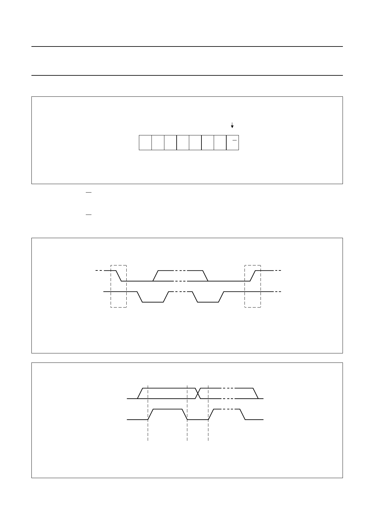
To guarantee AC-load detection, an amplifier current of
more than 550 mA is required. AC-load detection will
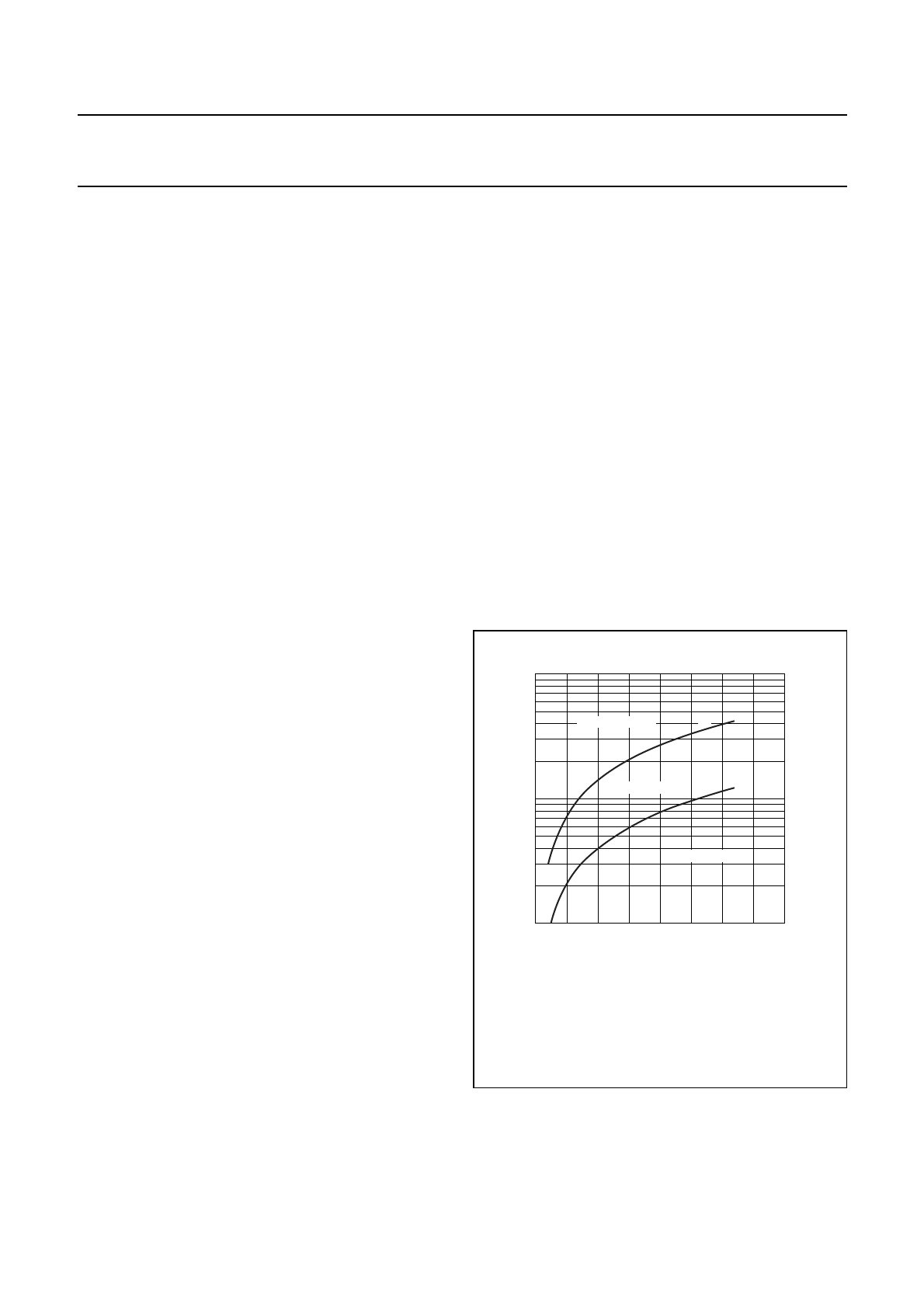
never occur with a current of less than 150 mA. Figure 3
shows which AC loads are detected at different output
voltages. For example, if a load is detected at an output
voltage of 2.5 V peak, the load is less than 4 Ω. If no load
is detected, the output impedance is more than 14 Ω.
LOAD DETECTION PROCEDURE
1. At start-up, enable the AC- or DC-load detection by
setting D1 of instruction byte 1 to logic 1.
mrc331
10
102
Zo(load)
(Ω)
1
Vo(peak) (V)
0107.52.5 5
(2)
(1)
no load present
load present
undefined
Fig.3 Tolerance of AC-load detection as a
function of output voltage.
(1) IO(peak) = < 150 mA.
(2) IO(peak) = > 550 mA.
2004 Feb 24 10
Philips Semiconductors Product specification
I2C-bus controlled 4 ×50 Watt power
amplifier and multiple voltage regulator TDA8588J; TDA8588xJ
2. After 250 ms the DC load is detected and the mute is
released. This is inaudible and can be implemented
each time the IC is powered on.
3. When the amplifier start-up cycle is completed (after
1.5 s), apply an AC signal to the input, and DC-load
bits D5 of each data byte should be read and stored by
the microcontroller.
4. After at least 3 periods of the input signal, the load
status can be checked by reading AC-detect bits D4 of
each data byte.
The AC-load peak current counter can be reset by
setting bit D1 of instruction byte IB1 to logic 0 and then
to logic 1. Note that this will also reset the DC-load
detection bits D5 in each data byte.
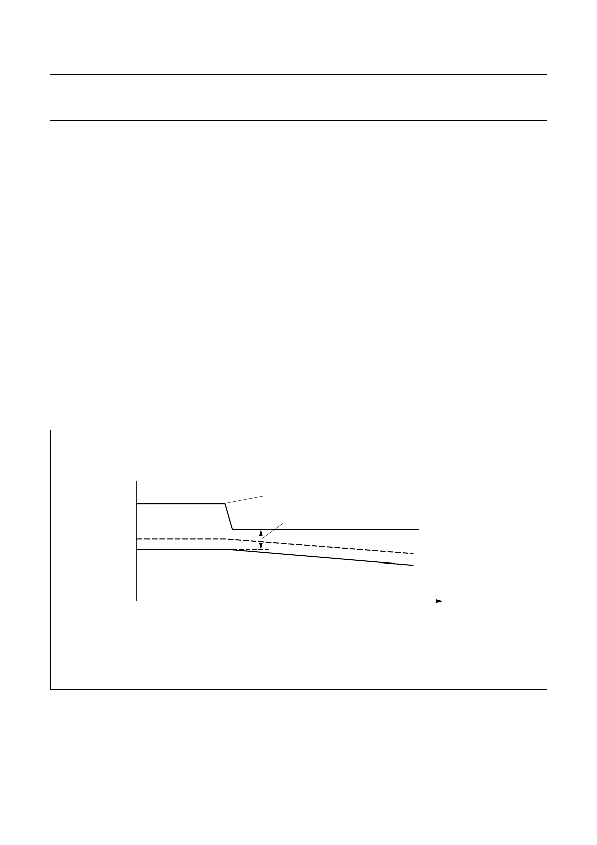
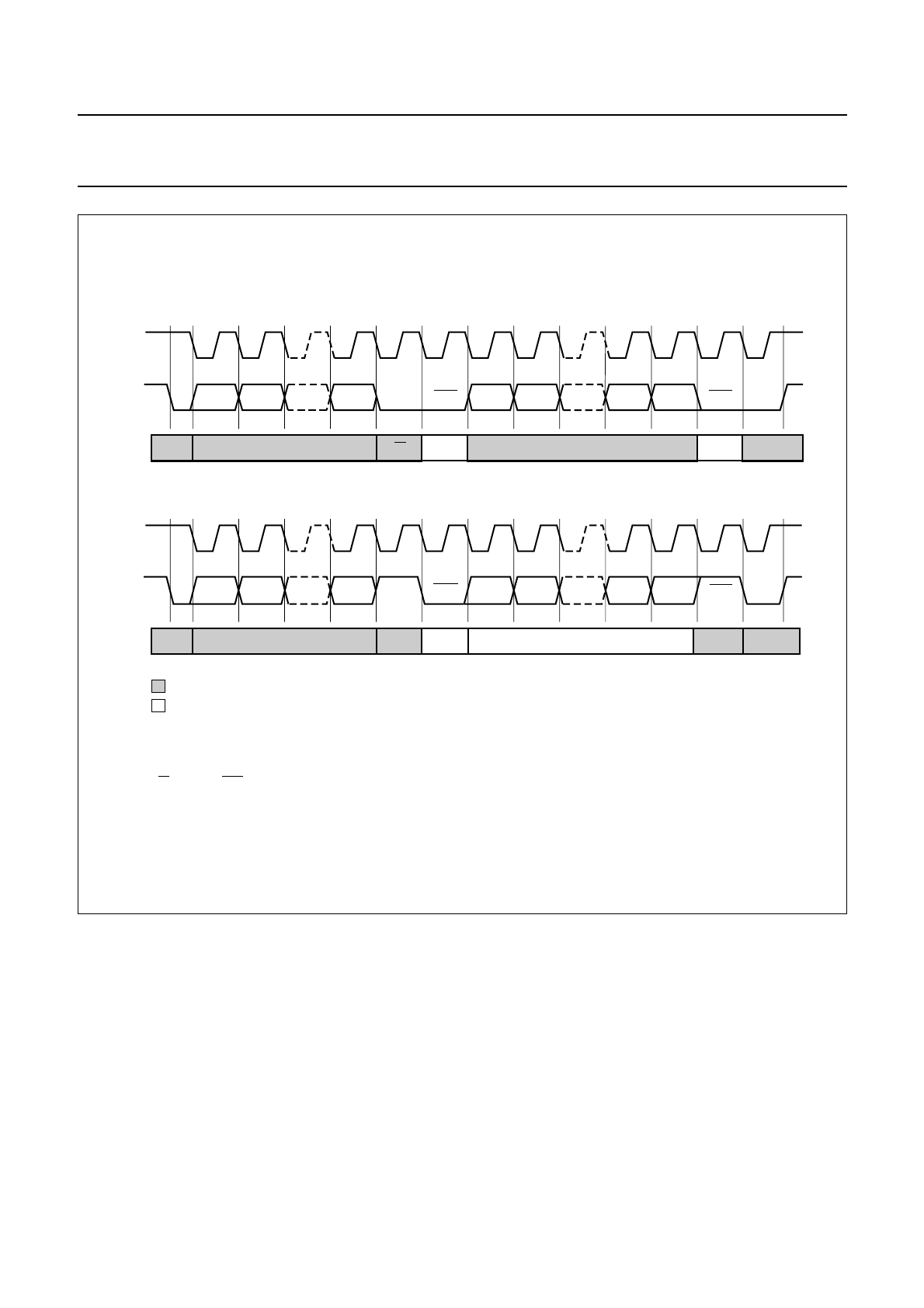
Low headroom protection
The normal DC output voltage of the amplifier is set to half
the supply voltage and is related to the voltage on
pin SVR. An external capacitor is connected to pin SVR to
suppress power supply ripple. If the supply voltage drops
(at vehicle engine start), the DC output voltage will follow
slowly due to the affect of the SVR capacitor.
The headroom voltage is the voltage required for correct
operation of the amplifier and is defined as the voltage
difference between the level of the DC output voltage
before the VP voltage drop and the level of VP after the
voltage drop (see Fig.4).
At a certain supply voltage drop, the headroom voltage will
be insufficient for correct operation of the amplifier. To
prevent unwanted audible noises at the output, the
headroom protection mode will be activated (see Fig.4).
This protection discharges the capacitors connected to
pins SVR and ACGND to increase the headroom voltage.
V
(V)
t (sec)
SVR voltage
vehicle engine start
headroom voltage
amplifier
DC output voltage
VP
mdb515
14
8.4
7
Fig.4 Amplifier output during supply voltage.

2004 Feb 24 11
Philips Semiconductors Product specification
I2C-bus controlled 4 ×50 Watt power
amplifier and multiple voltage regulator TDA8588J; TDA8588xJ
VOLTAGE REGULATORS
The voltage regulator section contains:
•Four switchable regulators and one permanent active
regulator
•Two power switches with loss-of-ground protection
•Reset push-pull output
•Backup functionality.
The quiescent current condition has a very low current
level of 150 µA typical with only regulator 2 active. The
TDA8588 uses low dropout voltage regulators for use in
low voltage applications.
All of the voltage regulators except for the standby
regulator can be controlled via the I2C-bus. The voltage
regulator section of this device has two power switches
which are capable of delivering unregulated 400 mA
continuous current, and has several fail-safe protection
modes. It conforms to peak transient tests and protects
against continuous high voltage (24 V), short-circuits and
thermal stress. A reset warning signal is asserted if
regulator 2 is out of regulation. Regulator 2 will try to
maintain output for as long as possible even if a thermal
shut-down or any other fault condition occurs. During
overvoltage stress conditions, all outputs except
regulator 2 will switch off and the device will be able to
supply a minimum current for an indefinite amount of time
sufficient for powering the memory of a microcontroller.
Provision is made for an external reserve supply capacitor
to be connected to pin BUCAP which can store enough
energy to allow regulator 2 to supply a microcontroller for
a period long enough for it to prepare for a loss-of-voltage.
Regulator 2
Regulator 2 is intended to supply the microcontroller and
has a low quiescent current. This supply cannot be shut
down in response to overvoltage stress conditions, and is
not I2C-bus controllable to prevent the microcontroller from
being damaged by overvoltage which could occur during a
disturbance of the I2C-bus. This supply will not shut down
during load dump transients or during a high
thermal-protection condition.
Backup capacitor
The backup capacitor is used as a backup supply for the
regulator 2 output when the battery supply voltage (VP)
cannot support the regulator 2 voltage.
Backup function
The backup function is implemented by a switch function,
which behaves like an ideal diode between pins VP
and BUCAP; the forward voltage of this ideal diode
depends on the current flowing through it. The backup
function supplies regulator 2 during brief periods when no
supply voltage is present on pin VP. It requires an external
capacitor to be connected to pin BUCAP and ground.
When the supply voltage is present on pin VP this
capacitor will be charged to a level of VP−0.3 V. When the
supply voltage is absent from pin VP, this charge can then
be used to supply regulator 2 for a brief period (tbackup)
calculated using the formula:
Example: VP= 14.4 V, VO(REG2) = 5 V, RL=1kΩ and
Cbackup = 100 µF provides a tbackup of 177 ms.
When an overvoltage condition occurs, the voltage on
pin BUCAP is limited to approximately 24 V; see Fig.5.
tbackup Cbackup RL
VPVOREG2()
0.5–()–
VO REG2()
---------------------------------------------------------
××=
2004 Feb 24 12
Philips Semiconductors Product specification
I2C-bus controlled 4 ×50 Watt power
amplifier and multiple voltage regulator TDA8588J; TDA8588xJ
V
(V)
t (sec)
tbackup out of regulation
VO(REG2)
VBUCAP
VP
mdb512
Fig.5 Backup capacitor function.
tbackup Cbackup
VPVOREG2()
–0.5–
IL
----------------------------------------------------
×=
Reset output
A reset pulse is generated at pin RST when the output
voltage of regulator 2 rises above the reset threshold
value. The reset output is a push-pull output that both
sources and sinks current. The output voltage can switch
between ground and VO(REG2), and operates at a low
regulator 2 voltage or VBUCAP. The RST signal is controlled
by a low-voltage detection circuit which, when activated,
pulls pin RST LOW (reset active) when VO(REG2) is
≤Vth(rst). If VO(REG2) ≥ Vth(rst), pin RST goes HIGH. The
reset pulse is delayed by 40 µs internally. To extend the
delay and to prevent oscillations occurring at the threshold
voltage, an external capacitor can be connected to
pin RESCAP. Note that a reset pulse is not generated
when VO(REG2) falls below the reset threshold value.
Reset delay capacitor
A Reset Delay Capacitor (RDC) connected to
pin RESCAP can be used to extend the delay period of the
reset pulse and to ensure that a clean reset signal is sent
to the microcontroller. The RDC is charged by a current
source. The reset output (pin RST) will be released
(pin RST goes HIGH) when the RDC voltage crosses the
RDC threshold value.
Power switches
There are two power switches that provide an unregulated
DC voltage output for amplifiers and an aerial motor
respectively. The switches have internal protection for
over-temperature conditions and are activated by setting
bits D2 and D3 of instruction byte IB1 to logic 1. The
regulated outputs will supply pulsed current loads that can
contaminate the line with high frequency noise, so it is
important to prevent any cross-coupling between the
regulated outputs, particularly with the 8.3 V audio supply,
and the unregulated outputs.
In the ON state, the switches have a low impedance to the
battery voltage. When the battery voltage is higher than
22 V, the switches are switched off. When the battery
voltage is below 22 V the switches are set to their original
condition.
2004 Feb 24 13
Philips Semiconductors Product specification
I2C-bus controlled 4 ×50 Watt power
amplifier and multiple voltage regulator TDA8588J; TDA8588xJ
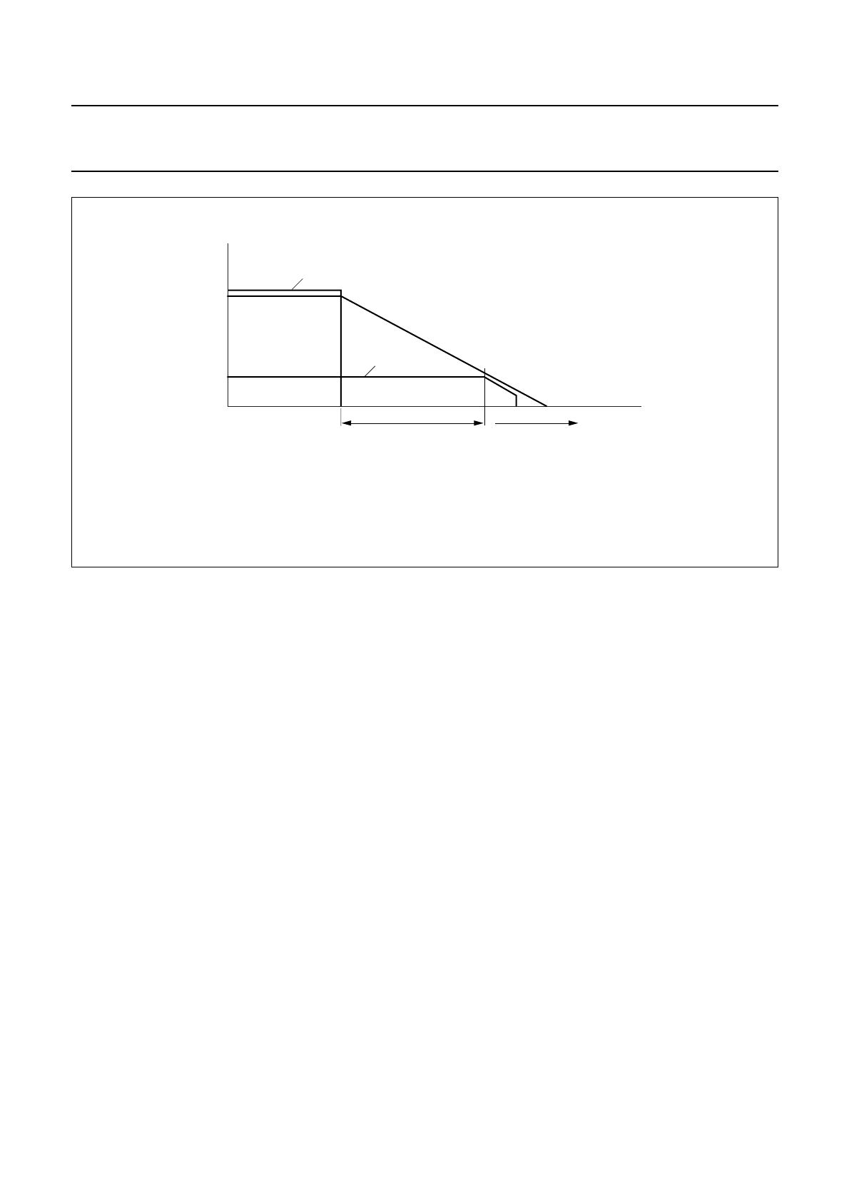
Protection
All regulator and switch outputs are fully protected by
foldback current limiting against load dumps and
short-circuits; see Fig.6. During a load dump all regulator
outputs, except the output of regulator 2, will go low.
The power switches can withstand ‘loss-of-ground’. This
means that if pin GND becomes disconnected, the switch
is protected by automatically connecting its outputs to
ground.
Temperature protection
If the junction temperature of a regulator becomes too
high, the amplifier(s) are switched off to prevent unwanted
noise signals being audible. A regulator junction
temperature that is too high is indicated by pin DIAG going
LOW and is also indicated by setting bit D6 in data byte 2.
If the junction temperature of the regulator continues to
rise and reaches the maximum temperature protection
level, all regulators and switches will be disabled except
regulator 2.
handbook, full pagewidth
VO(REGn)
Isc Ilimit IO(REGn)
MDB513
Fig.6 Foldback current protection.
2004 Feb 24 14
Philips Semiconductors Product specification
I2C-bus controlled 4 ×50 Watt power
amplifier and multiple voltage regulator TDA8588J; TDA8588xJ
I2C-BUS SPECIFICATION
handbook, halfpage
MDB516
MSB LSB
0 = write
1 = read
11 0 1 1 0 0 R/W
Fig.7 Address byte.
If address byte bit R/W = 0, the TDA8588 expects 3 instruction bytes: IB1, IB2 and IB3; see Table 1 to Table 6.
After a power-on, all instruction bits are set to zero.
If address byte bit R/W = 1, the TDA8588 will send 4 data bytes to the microcontroller: DB1, DB2, DB3 and DB4; see
Table 7 to Table 10.
MBA608
SDA
SCL P
STOP condition
SDA
SCL
S
START condition
Fig.8 Definition of start and stop conditions.
MBA607
data line
stable;
data valid
change
of data
allowed
SDA
SCL
Fig.9 Bit transfer.
2004 Feb 24 15
Philips Semiconductors Product specification
I2C-bus controlled 4 ×50 Watt power
amplifier and multiple voltage regulator TDA8588J; TDA8588xJ
mce641
ACK
MSB MSB − 1 MSB MSB − 1 LSB + 1 LSB
LSB + 1
12 78912 789
12 78912 789
: generated by master (microcontroller)
To stop the transfer, after the last acknowledge (A)
a stop condition (P) must be generated
To stop the transfer, the last byte must not be acknowledged
and a stop condition (P) must be generated
: generated by slave (TDA8588)
: start
: stop
: acknowledge
: read / write
S
P
A
R/W
SCL
SDA
SCL
SDA
ACK
ACK
MSB MSB − 1 MSB MSB − 1 LSB + 1 LSBLSB + 1 ACK
SA
A
AP
AP
ADDRESS WRITE DATA
READ DATA
W
SADDRESS R
I2C-WRITE
I2C-READ
Fig.10 I2C-bus read and write modes.
2004 Feb 24 16
Philips Semiconductors Product specification
I2C-bus controlled 4 ×50 Watt power
amplifier and multiple voltage regulator TDA8588J; TDA8588xJ
Table 1 Instruction byte IB1
Table 2 Regulator 5 (display) output voltage control
Table 3 Instruction byte IB2
Table 4 Regulator 4 (mechanical drive) output voltage
control
Table 5 Regulator 1 (audio) output voltage control
BIT DESCRIPTION
D7 regulator 5 output voltage control
(see Table 2)
D6
D5
D4
D3 SW2 control
0 = SW2 off
1 = SW2 on
D2 SW1 control
0 = SW1 off
1 = SW1 on
D1 AC- or DC-load detection switch
0 = AC- or DC-load detection off; resets
DC-load detection bits and AC-load
detection peak current counter
1 = AC- or DC-load detection on
D0 amplifier start enable (clear power-on reset
flag; D7 of DB2)
0 = amplifier OFF; pin DIAG remains LOW
1 = amplifier ON; when power-on occurs,
bit D7 of DB2 is reset and pin DIAG is
released
BIT OUTPUT (V)
D7 D6 D5 D4
00000 (off)
00016.0
00107.0
00118.2
01009.0
01019.5
011010.0
011110.4
100012.5
1001≤VP−1
(switch)
BIT DESCRIPTION
D7 regulator 4 output voltage control (see
Table 4)
D6
D5
D4 regulator 3 (mechanical digital) control
0 = regulator 3 off
1 = regulator 3 on
D3 regulator 1 output voltage control (see
Table 5)
D2
D1 soft mute all amplifier channels (mute delay
20 ms)
0 = mute off
1 = mute on
D0 hard mute all amplifier channels (mute delay
0.4 ms)
0 = mute off
1 = mute on
BIT OUTPUT (V)
D7 D6 D5
0 0 0 0 (off)
0015
0106
0117
1008.6
BIT OUTPUT (V)
D3 D2
0 0 0 (off)
0 1 8.3
1 0 8.5
1 1 8.7

2004 Feb 24 17
Philips Semiconductors Product specification
I2C-bus controlled 4 ×50 Watt power
amplifier and multiple voltage regulator TDA8588J; TDA8588xJ
Table 6 Instruction byte IB3 Table 7 Data byte DB1
BIT DESCRIPTION
D7 clip detection level
0 = 4 % detection level
1 = 1 % detection level
D6 amplifier channels 1 and 2 gain select
0 = 26 dB gain (normal mode)
1 = 20 dB gain (line driver mode)
D5 amplifier channels 3 and 4 gain select
0 = 26 dB gain (normal mode)
1 = 20 dB gain (line driver mode)
D4 amplifier thermal protection pre-warning
0 = warning at 145 °C
1 = warning at 122 °C
D3 disable channel 1
0 = enable channel 1
1 = disable channel 1
D2 disable channel 2
0 = enable channel 2
1 = disable channel 2
D1 disable channel 3
0 = enable channel 3
1 = disable channel 3
D0 disable channel 4
0 = enable channel 4
1 = disable channel 4
BIT DESCRIPTION
D7 amplifier thermal protection pre-warning
0 = no warning
1 = junction temperature above pre-warning
level
D6 amplifier maximum thermal protection
0 = junction temperature below 175 °C
1 = junction temperature above 175 °C
D5 channel 4 DC load detection
0 = DC load detected
1 = no DC load detected
D4 channel 4 AC load detection
0 = no AC load detected
1 = AC load detected
D3 channel 4 load short-circuit
0 = normal load
1 = short-circuit load
D2 channel 4 output offset
0 = no output offset
1 = output offset
D1 channel 4 VP short-circuit
0 = no short-circuit to VP
1 = short-circuit to VP
D0 channel 4 ground short-circuit
0 = no short-circuit to ground
1 = short-circuit to ground
2004 Feb 24 18
Philips Semiconductors Product specification
I2C-bus controlled 4 ×50 Watt power
amplifier and multiple voltage regulator TDA8588J; TDA8588xJ
Table 8 Data byte DB2 Table 9 Data byte DB3
BIT DESCRIPTION
D7 Power-on reset occurred or amplifier status
0 = amplifier on
1 = POR has occurred; amplifier off
D6 regulator thermal protection pre-warning
0 = no warning
1 = regulator temperature too high; amplifier
off
D5 channel 3 DC load detection
0 = DC load detected
1 = no DC load detected
D4 channel 3 AC load detection
0 = no AC load detected
1 = AC load detected
D3 channel 3 load short-circuit
0 = normal load
1 = short-circuit load
D2 channel 3 output offset
0 = no output offset
1 = output offset
D1 channel 3 VP short-circuit
0 = no short-circuit to VP
1 = short-circuit to VP
D0 channel 3 ground short-circuit
0 = no short-circuit to ground
1 = short-circuit to ground
BIT DESCRIPTION
D7 −
D6 −
D5 channel 2 DC load detection
0 = DC load detected
1 = no DC load detected
D4 channel 2 AC load detection
0 = no AC load detected
1 = AC load detected
D3 channel 2 load short-circuit
0 = normal load
1 = short-circuit load
D2 channel 2 output offset
0 = no output offset
1 = output offset
D1 channel 2 VP short-circuit
0 = no short-circuit to VP
1 = short-circuit to VP
D0 channel 2 ground short-circuit
0 = no short-circuit to ground
1 = short-circuit to ground

2004 Feb 24 19
Philips Semiconductors Product specification
I2C-bus controlled 4 ×50 Watt power
amplifier and multiple voltage regulator TDA8588J; TDA8588xJ
Table 10 Data byte DB4
BIT DESCRIPTION
D7 −
D6 −
D5 channel 1 DC load detection
0 = DC load detected
1 = no DC load detected
D4 channel 1 AC load detection
0 = no AC load detected
1 = AC load detected
D3 channel 1 load short-circuit
0 = normal load
1 = short-circuit load
D2 channel 1 output offset
0 = no output offset
1 = output offset
D1 channel 1 VP short-circuit
0 = no short-circuit to VP
1 = short-circuit to VP
D0 channel 1 ground short-circuit
0 = no short-circuit to ground
1 = short-circuit to ground
2004 Feb 24 20
Philips Semiconductors Product specification
I2C-bus controlled 4 ×50 Watt power
amplifier and multiple voltage regulator TDA8588J; TDA8588xJ
LIMITING VALUES
In accordance with the Absolute Maximum Rating System (IEC 60134).
Notes
1. Human body model: Rs= 1.5 kΩ; C = 100 pF; all pins have passed all tests to 2500 V to guarantee 2000 V,
according to class II.
2. Machine model: Rs=10Ω; C = 200 pF; L = 0.75 mH; all pins have passed all tests to 250 V to guarantee 200 V,
according to class II.
SYMBOL PARAMETER CONDITION MIN. MAX. UNIT
VPsupply voltage operating −18 V
not operating −1+50 V
with load dump protection 0 50 V
VSDA, VSCL voltage on pins SDA and SCL operating 0 7 V
VIN, VSVR,
VACGND,
VDIAG
voltage on pins INn, SVR, ACGND and DIAG operating 0 13 V
VSTB voltage on pin STB operating 0 24 V
IOSM non-repetitive peak output current −10 A
IORM repetitive peak output current −6A
Vsc AC and DC short-circuit voltage short-circuit of output pins across
loads and to ground or supply
−18 V
Vrp reverse polarity voltage voltage regulator only −−18 V
Ptot total power dissipation Tcase =70°C−80 W
Tjjunction temperature −150 °C
Tstg storage temperature −55 +150 °C
Tamb ambient temperature −40 +85 °C
Vesd electrostatic discharge voltage note 1 −2000 V
note 2 −200 V
2004 Feb 24 21
Philips Semiconductors Product specification
I2C-bus controlled 4 ×50 Watt power
amplifier and multiple voltage regulator TDA8588J; TDA8588xJ
THERMAL CHARACTERISTICS
QUALITY SPECIFICATION
In accordance with
“General Quality Specification for Integrated Circuits SNW-FQ-611D”
.
SYMBOL PARAMETER CONDITIONS VALUE UNIT
Rth(j-a) thermal resistance from junction to ambient in free air 40 K/W
Rth(j-c) thermal resistance from junction to case see Fig.11 0.75 K/W
handbook, halfpage
MDB514
Amplifier
0.5 K/W
0.2 K/W
1 K/W
Voltage regulator
Virtual junction
Case
Fig.11 Equivalent thermal resistance network.
2004 Feb 24 22
Philips Semiconductors Product specification
I2C-bus controlled 4 ×50 Watt power
amplifier and multiple voltage regulator TDA8588J; TDA8588xJ
CHARACTERISTICS
Amplifier section
Tamb =25°C; VP= 14.4 V; RL=4Ω; measured in the test circuit Fig.26; unless otherwise specified.
SYMBOL PARAMETER CONDITION MIN. TYP. MAX. UNIT
Supply voltage behaviour
VP1, VP2 operating supply voltage RL=4Ω8 14.4 18 V
RL=2Ω8 14.4 16 V
Iq(tot) total quiescent current no load −280 400 mA
Istb standby current −10 50 µA
VODC output voltage −7.2 −V
VP(mute) low supply voltage mute 6.5 7 8 V
Vhr headroom voltage when headroom protection is
activated; see Fig.4
−1.4 −V
VPOR power-on reset voltage see Fig.13 −5.5 −V
VOO output offset voltage mute mode and power on −100 0 +100 mV
Mode select (pin STB)
Vstb standby mode voltage −−1.3 V
Voper operating mode voltage 2.5 −5.5 V
Vmute mute mode voltage 8 −VPV
IIinput current VSTB =5V −425µA
Start-up, shut-down and mute timing
twake wake-up time from standby
before first I2C-bus transmission
is recognised
via pin STB; see Fig.12 −300 500 µs
tmute(off) time from amplifier switch-on to
mute release
via I2C-bus (IB1 bit D0);
CSVR =22µF; see Fig.12
−250 −ms
td(mute-on) delay from mute to on soft mute; via I2C-bus
(IB2 bit D1 = 1 to 0)
10 25 40 ms
hard mute; via I2C-bus
(IB2 bit D0 = 1 to 0)
10 25 40 ms
via pin STB; VSTB = 4 to 8 V 10 25 40 ms
td(on-mute) delay from on to mute soft mute; via I2C-bus
(IB2 bit D1 = 0 to 1)
10 25 40 ms
hard mute; via I2C-bus
(IB2 bit D0 = 0 to 1)
−0.4 1 ms
via pin STB; VSTB =4to8V −0.4 1 ms
I2C-bus interface
VIL LOW-level input voltage on pins
SCL and SDA
−−1.5 V
VIH HIGH-level input voltage on pins
SCL and SDA
2.3 −5.5 V
VOL LOW-level output voltage on
pin SDA
IL=3mA −−0.4 V
2004 Feb 24 23
Philips Semiconductors Product specification
I2C-bus controlled 4 ×50 Watt power
amplifier and multiple voltage regulator TDA8588J; TDA8588xJ
fSCL SCL clock frequency −−400 kHz
Diagnostic
VDIAG diagnostic pin LOW output
voltage
fault condition; IDIAG = 200 µA−−0.8 V
Vo(offset) output voltage when offset is
detected
±1.5 ±2±2.5 V
THDclip THD clip detection level IB3 bit D7 = 0 −4−%
IB3 bit D7 = 1 −1−%
Tj(warn) average junction temperature for
pre-warning
IB3 bit D4 = 0 135 145 155 °C
IB3 bit D4 = 1 112 122 132 °C
Tj(mute) average junction temperature for
3 dB muting
VIN = 0.05 V 150 160 170 °C
Tj(off) average junction temperature
when all outputs are switched off
165 175 185 °C
Zo(load) impedance when a DC load is
detected
−−6Ω
Zo(open) impedance when an open DC
load is detected
500 −− Ω
Io(load) amplifier current when an AC load
is detected
550 −− mA
Io(open) amplifier current when an open
AC load is detected
−−150 mA
Amplifier
Pooutput power RL=4Ω; VP= 14.4 V; THD = 0.5 % 20 21 −W
RL=4Ω; VP= 14.4 V; THD = 10 % 27 28 −W
RL=4Ω; VP= 14.4 V;
VIN = 2 V RMS square wave
(maximum power)
44 46 −W
RL=4Ω; VP= 15.2 V;
VIN = 2 V RMS square wave
(maximum power)
49 52 −W
RL=2Ω; VP= 14.4 V; THD = 0.5 % 37 41 −W
RL=2Ω; VP= 14.4 V; THD = 10 % 51 55 −W
RL=2Ω; VP= 14.4 V;
VIN = 2 V RMS square wave
(maximum power)
83 87 −W
THD total harmonic distortion Po= 1 W to 12 W; f = 1 kHz;
RL=4Ω−0.01 0.1 %
Po= 1 W to 12 W; f = 10 kHz −0.2 0.5 %
Po= 4 W; f = 1 kHz −0.01 0.03 %
line driver mode; Vo= 2 V (RMS);
f = 1 kHz; RL= 600 Ω−0.01 0.03 %
SYMBOL PARAMETER CONDITION MIN. TYP. MAX. UNIT
2004 Feb 24 24
Philips Semiconductors Product specification
I2C-bus controlled 4 ×50 Watt power
amplifier and multiple voltage regulator TDA8588J; TDA8588xJ
Voltage regulator section
Tamb =25°C; VP= 14.4 V; measured in the test circuit Fig.26; unless otherwise specified.
αcs channel separation (crosstalk) f=1Hzto10kHz; Rsource = 600 Ω50 60 −dB
Po= 4 W; f = 1 kHz −80 −dB
SVRR supply voltage ripple rejection f = 100 Hz to 10 kHz;
Rsource = 600 Ω55 70 −dB
CMRR common mode ripple rejection amplifier mode;
Vcommon = 0.3 V (p-p);
f = 1 kHz to 3 kHz; Rsource =0Ω
40 70 −dB
Vcm(max)(rms) maximum common mode voltage
level (rms value)
f=1kHz −−0.6 V
Vn(o)(LN) noise output voltage in line driver
mode
filter 20 Hz to 22 kHz;
Rsource = 600 Ω−25 35 µV
Vn(o)(amp) noise output voltage in amplifier
mode
filter 20 Hz to 22 kHz;
Rsource = 600 Ω−50 70 µV
Gv(amp) voltage gain in amplifier mode single-ended in to differential out 25 26 27 dB
Gv(LN) voltage gain in line driver mode single-ended in to differential out 19 20 21 dB
Ziinput impedance CIN = 220 nF 55 70 −kΩ
αmute mute attenuation VO(on)/VO(mute) 80 90 −dB
Vo(mute) output voltage mute VIN = 1 V (RMS) −70 −µV
Bppower bandwidth −1 dB; THD=1% −20 −kHz
SYMBOL PARAMETER CONDITIONS MIN. TYP. MAX. UNIT
Supply
VPsupply voltage regulator 1, 3, 4 and 5 on 10.0 14.4 18 V
regulator 2
switched on 4 −−V
in regulation 6.3 −50 V
overvoltage for shut-down 18.1 22 −V
Iq(tot) total quiescent supply
current
standby mode; note 1 −150 190 µA
Reset output (push-pull stage, pin RST)
VREG2(th)(r) rising threshold voltage
of regulator 2
VP is rising;
IO(REG2) =50mA
VO(REG2)
−0.2
VO(REG2)
−0.1
VO(REG2)
−0.04
V
VREG2(th)(f) falling threshold voltage
of regulator 2
VP is falling;
IO(REG2) =50mA
VO(REG2)
−0.25
VO(REG2)
−0.15
VO(REG2)
−0.1
V
Isink(L) LOW-level sink current VRST ≤0.8 V 1 −−mA
Isource(H) HIGH-level source
current
VRST =V
O(REG2) −0.5 V;
VP= 14.4 V
200 600 −µA
trrise time note 2 −250µs
tffall time note 2 −10 50 µs
SYMBOL PARAMETER CONDITION MIN. TYP. MAX. UNIT
2004 Feb 24 25
Philips Semiconductors Product specification
I2C-bus controlled 4 ×50 Watt power
amplifier and multiple voltage regulator TDA8588J; TDA8588xJ
Reset delay (pin RESCAP)
Ich charge current VRESCAP =0V 1 4 8 µA
Idch discharge current VRESCAP =3V; V
P≥4.3 V 1 7 −mA
Vth(rst) reset signal threshold
voltage
TDA8588AJ and
TDA8588J
2.5 3 3.5 V
TDA8588BJ 1.6 2.1 2.6 V
td(rst) reset signal delay without CRESCAP; note 3 −40 −µs
CRESCAP = 47 nF; note 3;
see Fig.15
15 35 100 ms
Regulator 1: REG1 (audio; IO= 5 mA)
VO(REG1) output voltage 0.5 mA ≤IO≤400 mA;
12V<V
P<18V;
IB2[D3:D2] = 01 7.9 8.3 8.7 V
IB2[D3:D2] = 10 8.1 8.5 8.9 V
IB2[D3:D2] = 11 8.3 8.7 9.1 V
VO(LN) line regulation voltage 12 V ≤VP≤18 V −−50 mV
VO(load) load regulation voltage 5 mA ≤IO≤400 mA −−100 mV
SVRR supply voltage ripple
rejection
fripple = 120 Hz;
Vripple = 2 V (p-p)
50 60 −dB
Vdrop dropout voltage VP= 7.5 V; note 4
IO= 200 mA −0.4 0.8 V
IO= 400 mA −0.6 2.5 V
Ilimit current limit VO≥7 V; note 5 400 700 −mA
Isc short-circuit current RL≤0.5 Ω; note 6 70 190 −mA
Regulator 2: REG2 (microprocessor; IO= 5 mA)
VO(REG2) output voltage 0.5 mA ≤IO≤350 mA;
10 V ≤VP≤18 V
TDA8588AJ and
TDA8588J
4.75 5.0 5.25 V
TDA8588BJ 3.1 3.3 3.5 V
VO(LN) line regulation voltage 10 V ≤VP≤18 V −350mV
VO(load) load regulation voltage 0.5 mA ≤IO≤300 mA −−100 mV
SVRR supply voltage ripple
rejection
fripple = 120 Hz;
Vripple = 2 V (p-p)
40 50 −dB
SYMBOL PARAMETER CONDITIONS MIN. TYP. MAX. UNIT

2004 Feb 24 26
Philips Semiconductors Product specification
I2C-bus controlled 4 ×50 Watt power
amplifier and multiple voltage regulator TDA8588J; TDA8588xJ
Vdrop dropout voltage IO= 200 mA
VBUCAP = 4.75 V; note 7
TDA8588AJ and
TDA8588J
−0.5 0.8 V
TDA8588BJ −1.75 2 V
IO= 350 mA;
VBUCAP = 4.75 V; note 7
TDA8588AJ and
TDA8588J
−0.5 1.3 V
TDA8588BJ −1.75 2.7 V
Ilimit current limit VO≥2.8 V; note 5 400 1000 −mA
Isc short-circuit current RL≤0.5 Ω; note 6 160 300 −mA
Regulator 3: REG3 (mechanical digital; IO= 5 mA)
VO(REG3) output voltage 0.5 mA ≤IO≤300 mA;
10 V ≤VP≤18 V
TDA8588AJ and
TDA8588BJ
3.1 3.3 3.5 V
TDA8588J 4.75 5.0 5.25 V
VO(LN) line regulation voltage 10 V ≤VP≤18 V −350mV
VO(load) load regulation voltage 0.5 mA ≤IO≤300 mA −−100 mV
SVRR supply voltage ripple
rejection
fripple = 120 Hz;
Vripple = 2 V (p-p)
50 65 −dB
Vdrop dropout voltage VP= 4.75 V; IO= 200 mA;
note 4
TDA8588AJ and
TDA8588BJ
−1.45 1.65 V
TDA8588J −0.4 0.8 V
VP= 4.75 V; IO= 300 mA;
note 4
TDA8588AJ and
TDA8588BJ
−1.45 1.65 V
TDA8588J −0.4 1.5 V
Ilimit current limit VO≥2.8 V; note 5 400 700 −mA
Isc short-circuit current RL≤0.5 Ω; note 6 135 210 −mA
Regulator 4: REG4 (mechanical drive; IO= 5 mA)
VO(REG4) output voltage 0.5 mA ≤IO≤800 mA;
10 V ≤VP≤18 V
IB2[D7:D5] = 001 4.75 5.0 5.25 V
IB2[D7:D5] = 010 5.7 6.0 6.3 V
IB2[D7:D5] = 011 6.6 7.0 7.4 V
IB2[D7:D5] = 100 8.1 8.6 9.1 V
VO(LN) line regulation voltage 10 V ≤VP≤18 V −350mV
SYMBOL PARAMETER CONDITIONS MIN. TYP. MAX. UNIT
2004 Feb 24 27
Philips Semiconductors Product specification
I2C-bus controlled 4 ×50 Watt power
amplifier and multiple voltage regulator TDA8588J; TDA8588xJ
VO(load) load regulation voltage 0.5 mA ≤IO≤400 mA −−100 mV
SVRR supply voltage ripple
rejection
fripple = 120 Hz;
Vripple = 2 V (p-p)
50 65 −dB
Vdrop dropout voltage VP=V
O(REG4) −0.5 V;
IO= 800 mA; note 4
−0.6 1 V
IO(peak) peak output current t ≤3 s; VO= 4 V 1 1.5 −A
Ilimit limit current VO≥4 V; t ≤100 ms;
VP≥11.5 V; note 5
1.5 2 −A
Isc short-circuit current RL≤0.5 Ω; note 6 240 400 −mA
Regulator 5: REG5 (display; IO= 5 mA)
VO(REG5) output voltage 0.5 mA ≤IO≤400 mA
10 V ≤VP≤18 V;
IB1[D7:D4] = 0001
5.7 6.0 6.3 V
10 V ≤VP≤18 V;
IB1[D7:D4] = 0010
6.65 7.0 7.37 V
10 V ≤VP≤18 V;
IB1[D7:D4] = 0011
7.8 8.2 8.6 V
10.5 V ≤VP≤18 V;
IB1[D7:D4] = 0100
8.55 9.0 9.45 V
11 V ≤VP≤18 V;
IB1[D7:D4] = 0101
9.0 9.5 10.0 V
11.5 V ≤VP≤18 V;
IB1[D7:D4] = 0110
9.5 10.0 10.5 V
13 V ≤VP≤18 V;
IB1[D7:D4] = 0111
9.9 10.4 10.9 V
14.2 V ≤VP≤18 V;
IB1[D7:D4] = 1000
11.8 12.5 13.2 V
12.5 V ≤VP≤18 V;
IB1[D7:D4] = 1001
VP−1−−V
VO(LN) line regulation voltage 10 V ≤VP≤18 V −350mV
VO(load) load regulation voltage 0.5 mA ≤IO≤400 mA −−100 mV
SVRR supply voltage ripple
rejection
fripple = 120 Hz;
Vripple = 2 V (p-p)
50 60 −dB
Vdrop dropout voltage VP=V
O(REG5) −0.5 V;
note 4
IO= 300 mA −0.4 0.8 V
IO= 400 mA −0.5 2.3 V
Ilimit limit current VO≥5.5 V; note 5 400 950 −mA
Isc short-circuit current RL≤0.5 Ω; note 6 100 200 −mA
Power switch 1: SW1 (antenna)
Vdrop(SW1) dropout voltage IO= 300 mA −0.6 0.8 V
IO= 400 mA −0.6 1.1 V
Ilimit limit current V ≥8.5 V 0.5 1 −A
SYMBOL PARAMETER CONDITIONS MIN. TYP. MAX. UNIT
2004 Feb 24 28
Philips Semiconductors Product specification
I2C-bus controlled 4 ×50 Watt power
amplifier and multiple voltage regulator TDA8588J; TDA8588xJ
Notes
1. The quiescent current is measured in standby mode when RL=∞.
2. The rise and fall times are measured with a 50 pF load capacitor.
3. The reset delay time depends on the value of the reset delay capacitor:
4. The dropout voltage of a regulator is the voltage difference between VP and VO(REGn).
5. At current limit, VO(REGn) is held constant (see Fig.6).
6. The foldback current protection limits the dissipation power at short-circuit (see Fig.6).
7. The dropout voltage of regulator 2 is the voltage difference between VBUCAP and VO(REG2).
Power switch 2: SW2 (amplifier)
Vdrop(SW2) dropout voltage IO= 300 mA −0.6 0.8 V
IO= 400 mA −0.6 1.1 V
Ilimit limit current VO≥8.5 V 0.5 1 −A
Backup switch
IDC(BU) continuous current VBUCAP ≥6 V 0.4 1.5 −A
Vclamp(BU) clamping voltage VP=30V;
IO(REG2) = 100 mA
−24 28 V
Vdrop dropout voltage IO= 500 mA;
(VP−VBUCAP)
−0.6 0.8 V
SYMBOL PARAMETER CONDITIONS MIN. TYP. MAX. UNIT
td rst()
CRESCAP
Ich
------------------------ Vth rst()
×=CRESCAP 750 103
×()×s[]=
2004 Feb 24 29
Philips Semiconductors Product specification
I2C-bus controlled 4 ×50 Watt power
amplifier and multiple voltage regulator TDA8588J; TDA8588xJ
mrc350
Vp
DIAG
Amplifier status
DB2 bit D7
VO(REG3)
IB1 bit D0
IB2 bit D4
SVR
STB
Amplifier
output
tmute(off)
twake
Regulator switched off
when amplifier is
completely muted
Soft
mute
Soft
mute
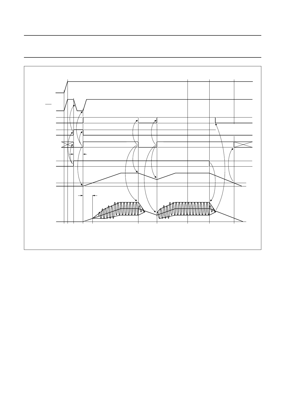
Fig.12 Start-up and shut-down timing.
2004 Feb 24 30
Philips Semiconductors Product specification
I2C-bus controlled 4 ×50 Watt power
amplifier and multiple voltage regulator TDA8588J; TDA8588xJ
handbook, full pagewidth
MRC348
VO
(V)
Headroom voltage
14.4
8.8
8.6
7.2
3.5
Vp
Low Vp mute activated
Headroom protection activated:
1) fast mute
2) discharge of SVR
SVR voltage
Output
voltage
Low Vp mute released
DIAG
DB2 bit D7
VO(REG3)
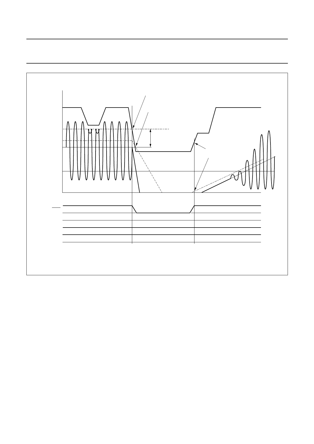
Fig.13 Low VP behaviour at VP> 5.5 V.
2004 Feb 24 31
Philips Semiconductors Product specification
I2C-bus controlled 4 ×50 Watt power
amplifier and multiple voltage regulator TDA8588J; TDA8588xJ
POR activated
14.4
8.8
8.6
7.2
3.5
VpLow Vp mute activated
SVR voltage
DIAG
DB2 bit D7
VO(REG3)
5.5
POR has occured
mrc349
VO
(V)
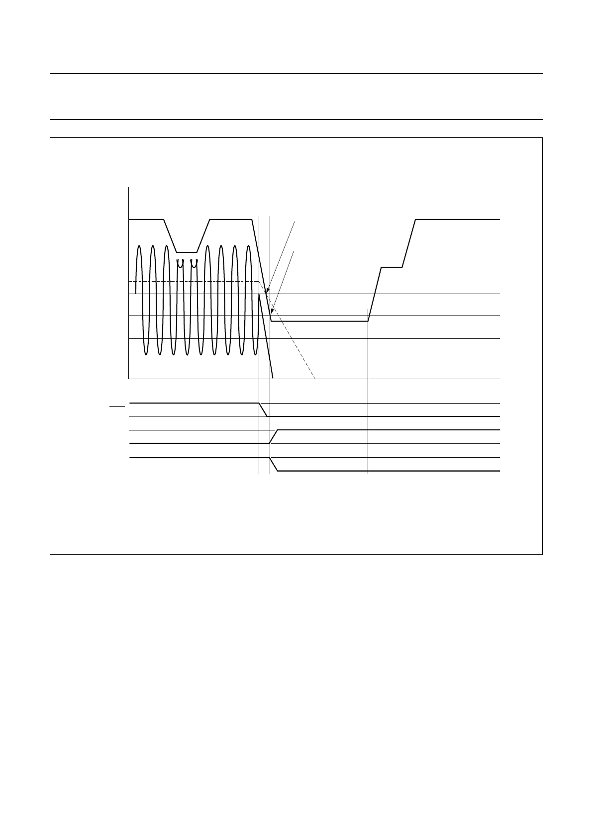
Fig.14 Low VP behaviour at VP< 5.5 V.
2004 Feb 24 32
Philips Semiconductors Product specification
I2C-bus controlled 4 ×50 Watt power
amplifier and multiple voltage regulator TDA8588J; TDA8588xJ
mdb511
V
(V)
t (sec)
td(rst)
Vth(rst)
VO(REG2)
VP
VRST
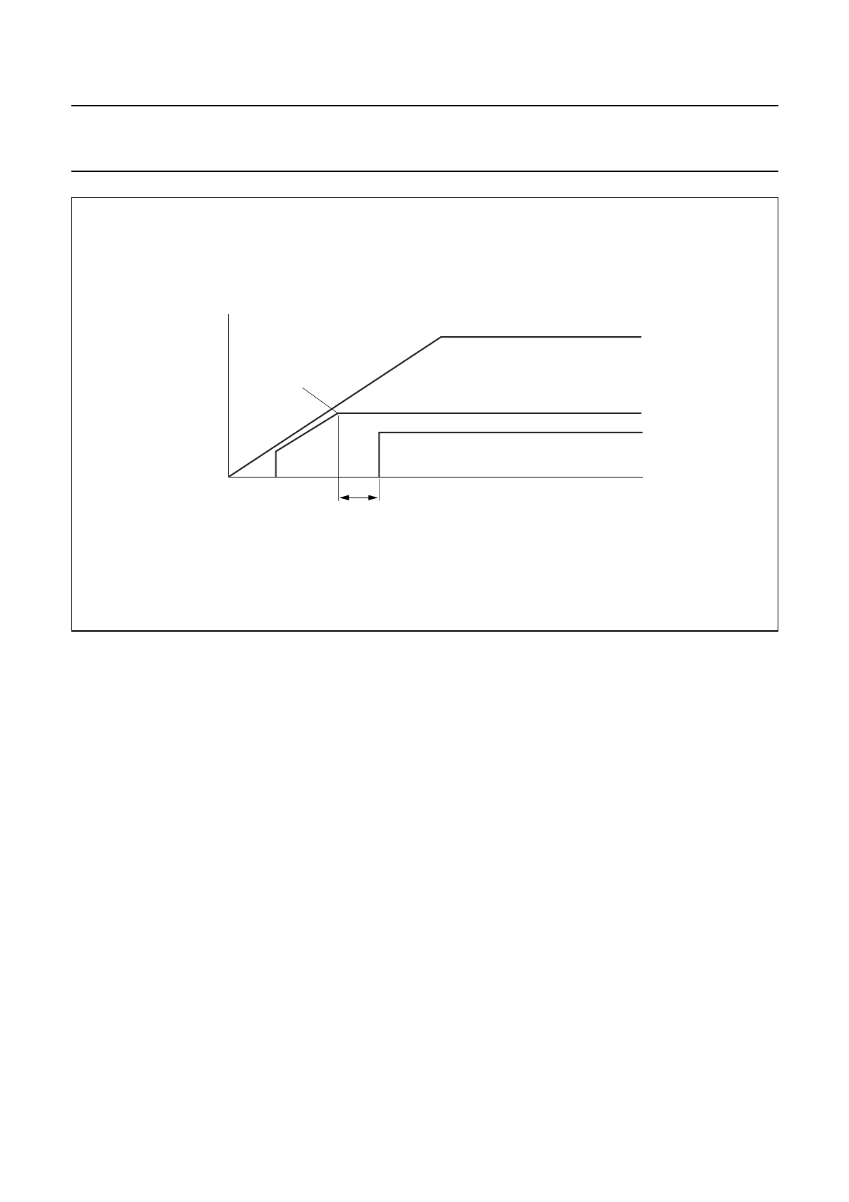
Fig.15 Reset delay function.
2004 Feb 24 33
Philips Semiconductors Product specification
I2C-bus controlled 4 ×50 Watt power
amplifier and multiple voltage regulator TDA8588J; TDA8588xJ
Performance diagrams
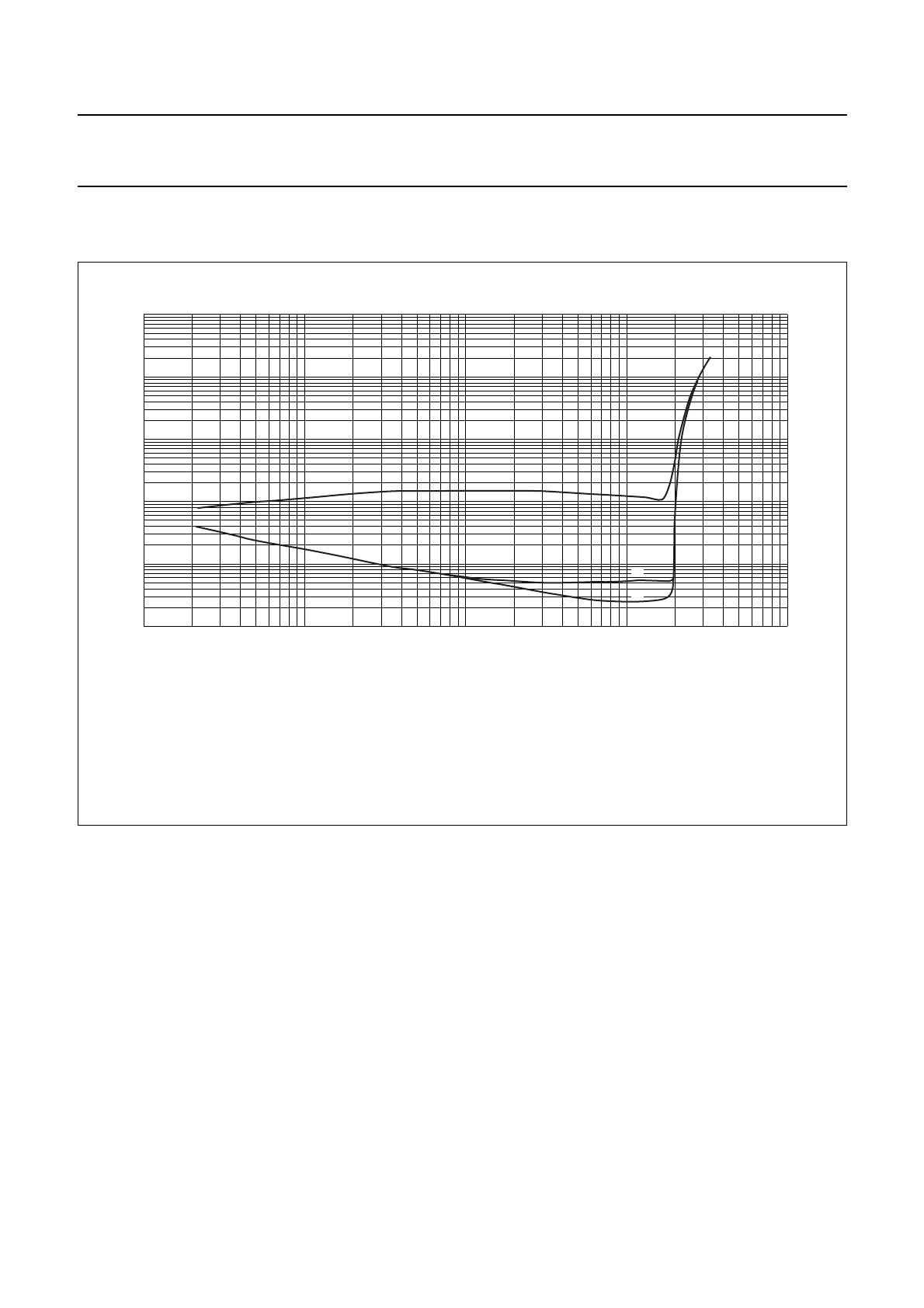
THD AS A FUNCTION OF OUTPUT POWER PoAT DIFFERENT FREQUENCIES
handbook, full pagewidth
102
10
1
10−1
10−2
10−3
10−210−111010
2
MRC345
Po (W)
THD
(%)
(2)
(1)
(3)
Fig.16 THD as a function of Po.
VP= 14.4 V.
RL=4Ω.
(1) f = 10 kHz.
(2) f = 1 kHz.
(3) f = 100 Hz.
2004 Feb 24 34
Philips Semiconductors Product specification
I2C-bus controlled 4 ×50 Watt power
amplifier and multiple voltage regulator TDA8588J; TDA8588xJ
THD AS A FUNCTION OF FREQUENCY AT DIFFERENT OUTPUT POWERS
handbook, full pagewidth
MRC344
10
1
10−1
10−2
10−3
10−210−111010
2
(2)
(1)
f (kHz)
THD
(%)
Fig.17 THD as a function of frequency.
VP= 14.4 V.
RL=4Ω.
(1) Po=1W.
(2) Po=10W.
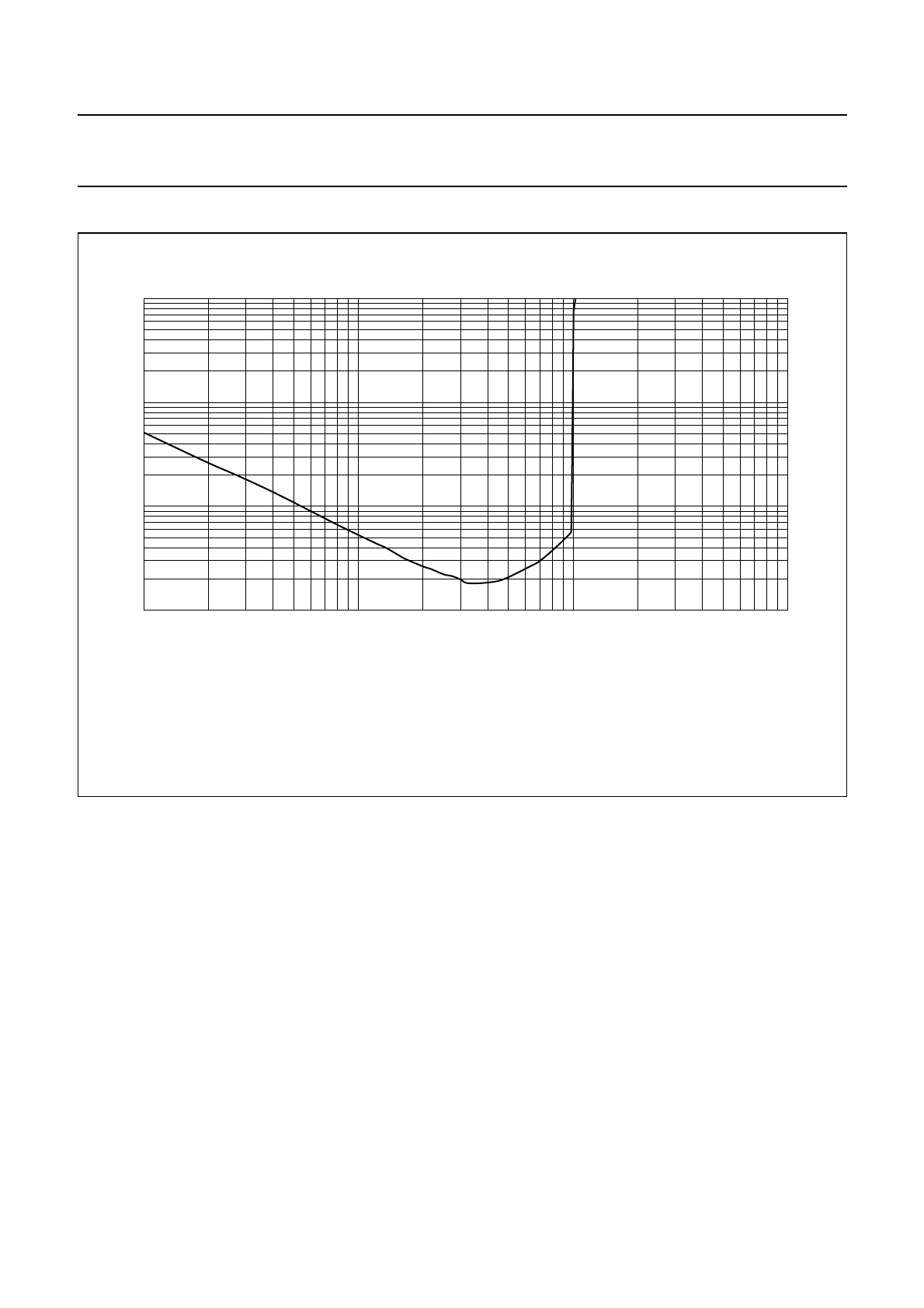
2004 Feb 24 35
Philips Semiconductors Product specification
I2C-bus controlled 4 ×50 Watt power
amplifier and multiple voltage regulator TDA8588J; TDA8588xJ
LINE DRIVER MODE
handbook, full pagewidth
MRC329
10−11 10
1
10−1
10−2
10−3
Vo(rms)
THD
(%)
102
(V)
Fig.18 THD as a function of Vo in balanced line driver mode.
VP= 14.4 V.
RL= 600 Ω.
f = 1 kHz.
2004 Feb 24 36
Philips Semiconductors Product specification
I2C-bus controlled 4 ×50 Watt power
amplifier and multiple voltage regulator TDA8588J; TDA8588xJ
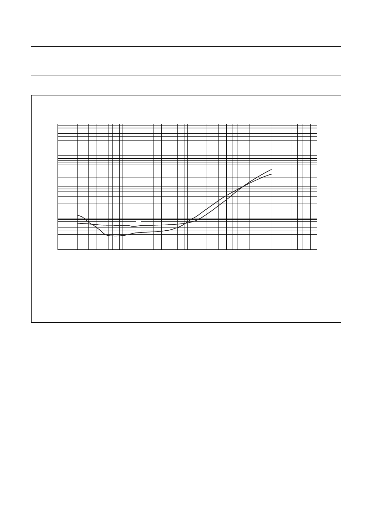
OUTPUT POWER AS A FUNCTION OF FREQUENCY AT DIFFERENT THD LEVELS
handbook, full pagewidth
20
30
22
24
26
28
MRC330
10−210−111010
2
f (kHz)
Po
(W)
(1)
(2)
(3)
Fig.19 Po as a function of frequency; RL=4Ω.
VP= 14.4 V.
(1) THD = 10 %.
(2) THD = 5 %.
(3) THD = 0.5 %.
2004 Feb 24 37
Philips Semiconductors Product specification
I2C-bus controlled 4 ×50 Watt power
amplifier and multiple voltage regulator TDA8588J; TDA8588xJ
handbook, full pagewidth
35
60
40
45
50
55
MRC335
10−210−111010
2
f (kHz)
Po
(W) (1)
(3)
(2)
Fig.20 Po as a function of frequency; RL=2Ω.
VP= 14.4 V.
(1) THD = 10 %.
(2) THD = 5 %.
(3) THD = 0.5 %.
2004 Feb 24 38
Philips Semiconductors Product specification
I2C-bus controlled 4 ×50 Watt power
amplifier and multiple voltage regulator TDA8588J; TDA8588xJ
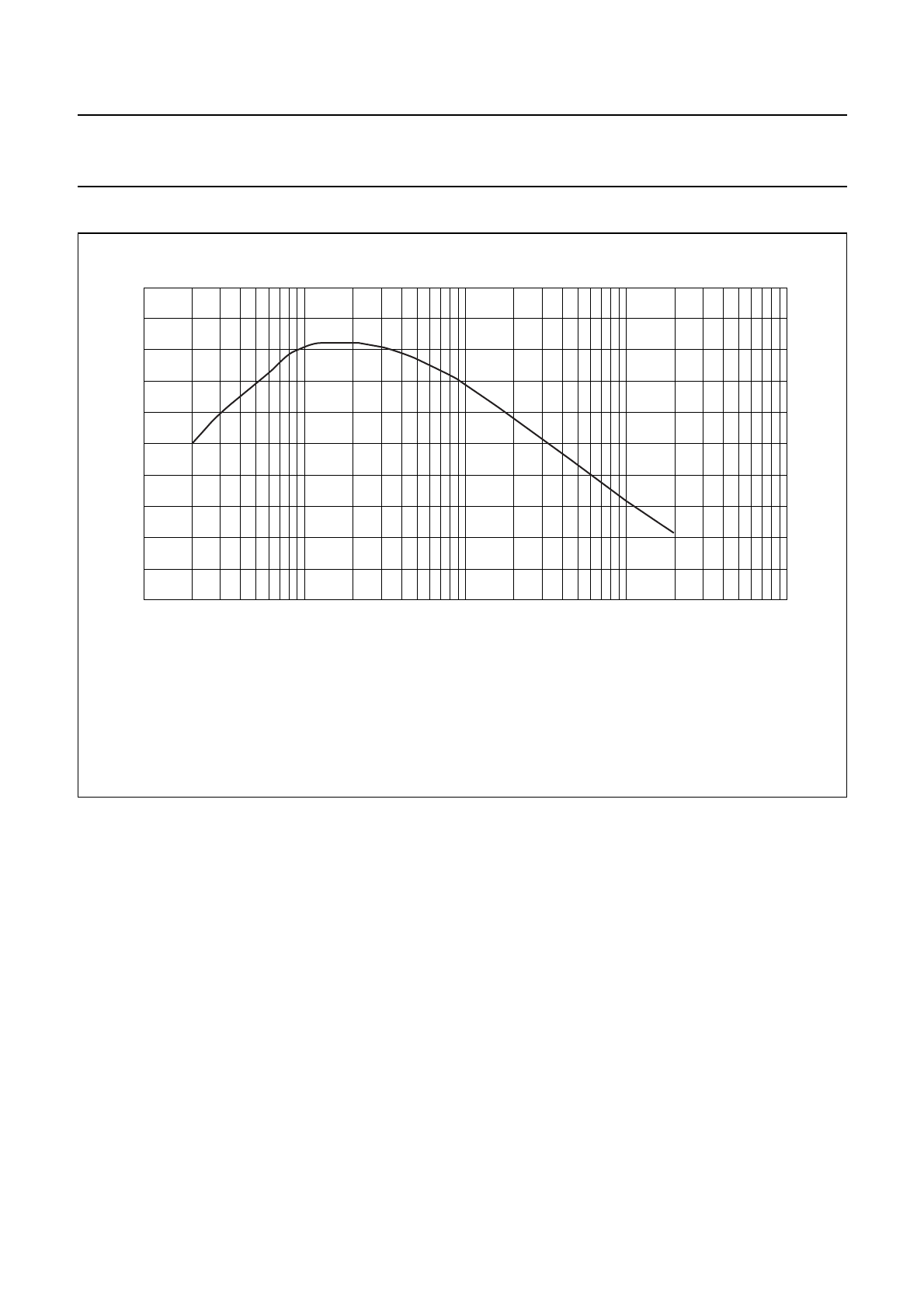
OUTPUT POWER (PO)AS A FUNCTION OF SUPPLY VOLTAGE (VP)
001aaa283
40
60
20
80
100
Po
(W)
0
VP (V)
8 20161210 1814
(1)
(2)
(3)
Fig.21 Po as a function of supply voltage; RL=4Ω.
(1) Maximum power.
(2) THD = 10 %.
(3) THD = 0.5 %. f = 1 kHz.
2004 Feb 24 39
Philips Semiconductors Product specification
I2C-bus controlled 4 ×50 Watt power
amplifier and multiple voltage regulator TDA8588J; TDA8588xJ
handbook, full pagewidth
20
100
081216
20
40
60
80
MRC332
Vp (V)
Po
(W) (1)
(2)
(3)
Fig.22 Po as a function of supply voltage; RL=2Ω.
(1) Maximum power.
(2) THD = 10 %.
(3) THD = 0.5 %. f = 1 kHz.
2004 Feb 24 40
Philips Semiconductors Product specification
I2C-bus controlled 4 ×50 Watt power
amplifier and multiple voltage regulator TDA8588J; TDA8588xJ
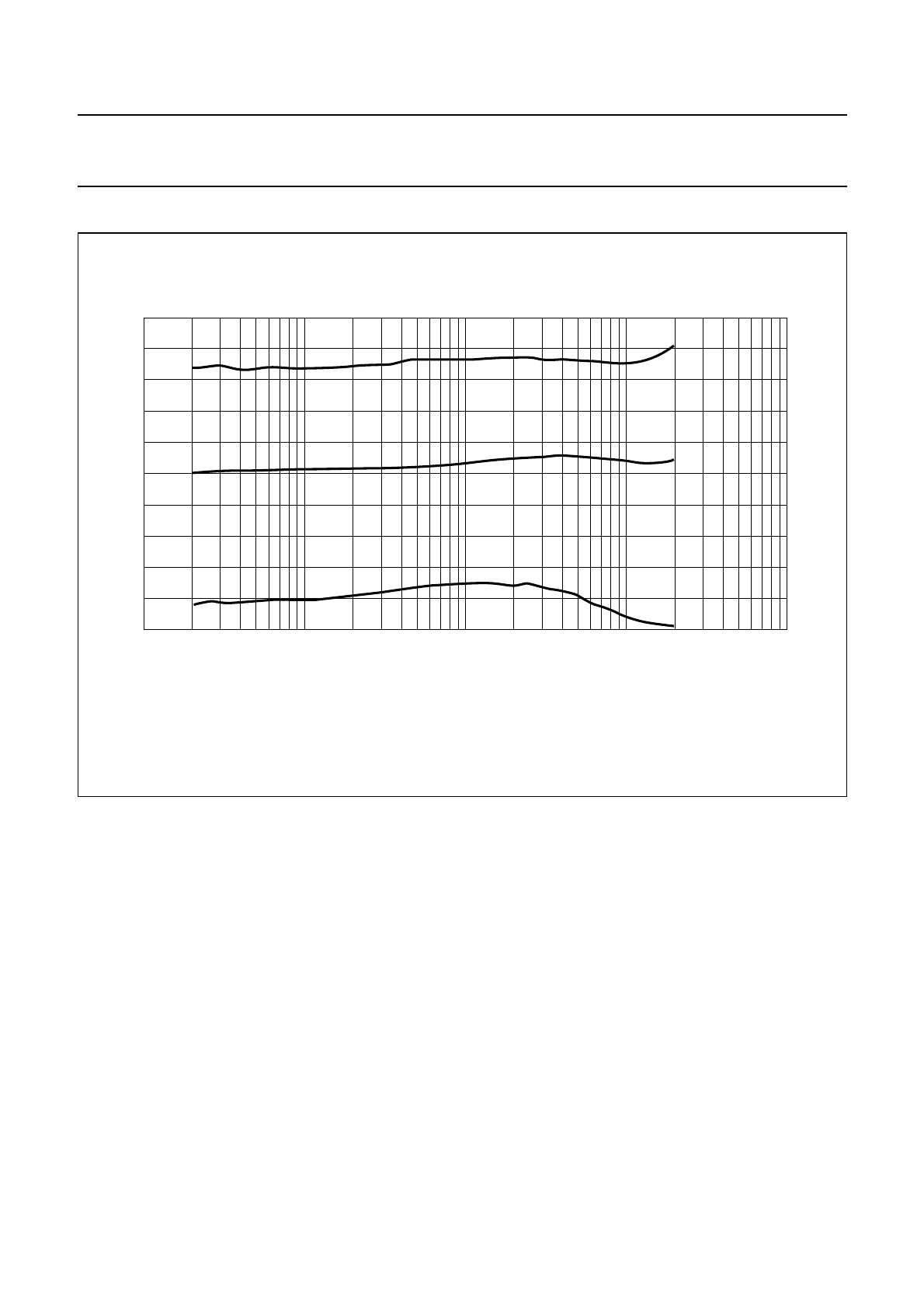
SUPPLY VOLTAGE RIPPLE REJECTION IN OPERATING AND MUTE MODES
handbook, full pagewidth
60
80
64
68
72
76
MRC333
10−11 10
f (kHz)
SVRR
(dB)
(1)
(2)
Fig.23 SVRR as a function of frequency.
VP= 14.4 V.
RL=4Ω.
Vripple = 2 V (p-p).
Rsource = 600 Ω.
(1) Operating mode.
(2) Mute mode.
2004 Feb 24 41
Philips Semiconductors Product specification
I2C-bus controlled 4 ×50 Watt power
amplifier and multiple voltage regulator TDA8588J; TDA8588xJ
CHANNEL SEPARATION AS A FUNCTION OF FREQUENCY
handbook, full pagewidth
50
100
60
70
80
90
MRC351
10−210−1110
f (kHz)
αcs
(dB)
102
Fig.24 Channel separation.
VP= 14.4 V.
RL=4Ω.
Po=4W.
Rsource = 600 Ω.
2004 Feb 24 42
Philips Semiconductors Product specification
I2C-bus controlled 4 ×50 Watt power
amplifier and multiple voltage regulator TDA8588J; TDA8588xJ
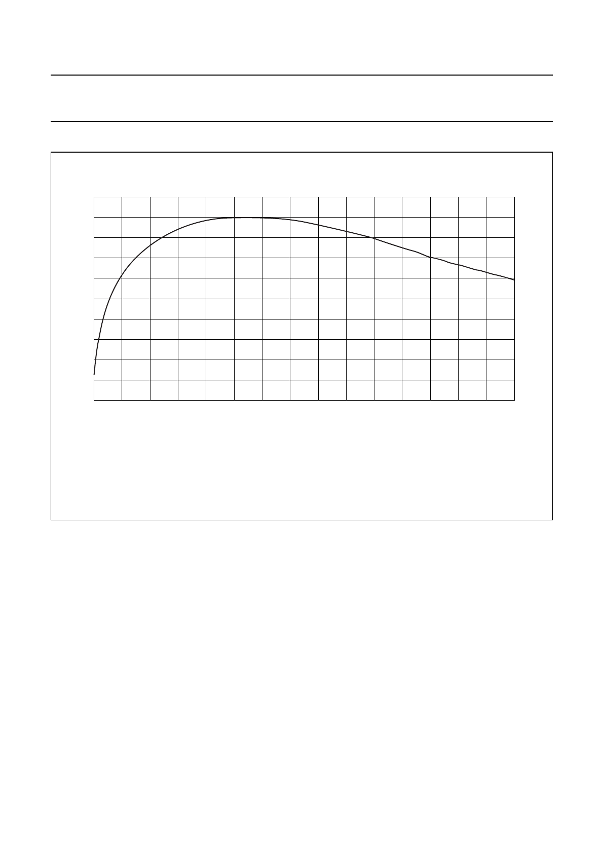
POWER DISSIPATION AND EFFICIENCY
handbook, full pagewidth
30
50
001020
10
20
30
40
MRC342
Po (W)
Ptot
(W)
Fig.25 Amplifier dissipation as a function of output power; all channels driven.
VP= 14.4 V.
RL=4Ω.
f = 1 kHz.
2004 Feb 24 43
Philips Semiconductors Product specification
I2C-bus controlled 4 ×50 Watt power
amplifier and multiple voltage regulator TDA8588J; TDA8588xJ
handbook, full pagewidth
40
100
00 8 16 24 32
20
40
60
80
MRC343
Po (W)
η
(%)
Fig.26 Amplifier efficiency as a function of output power; all channels driven.
VP= 14.4 V.
RL=4Ω.
f = 1 kHz.
2004 Feb 24 44
Philips Semiconductors Product specification
I2C-bus controlled 4 ×50 Watt power
amplifier and multiple voltage regulator TDA8588J; TDA8588xJ
APPLICATION AND TEST INFORMATION
mdb587
V
reg2
40 µs
BACKUP
SWITCH
ENABLE
LOGIC
STANDBY/ MUTE I
2
C-BUS
INTERFACE CLIP DETECT/ DIAGNOSTIC
REFERENCE
VOLTAGE
TEMPERATURE &
LOAD DUMP
PROTECTION VOLTAGE
REGULATOR
REGULATOR 1
REGULATOR 3
REGULATOR 2
REGULATOR 4
REGULATOR 5
SWITCH 1
SWITCH 2
MUTE
PROTECTION/
DIAGNOSTIC
26 dB/
20 dB
PROTECTION/
DIAGNOSTIC
26 dB/
20 dB
PROTECTION/
DIAGNOSTIC
26 dB/
20 dB
PROTECTION/
DIAGNOSTIC
TEMPERATURE & LOAD
DUMP PROTECTION
AMPLIFIER
26 dB/
20 dB
MUTE
MUTE
MUTE
35
28
27
26
20
6
25
9
7
17
19
5
3
21
23
16 8
13
SGNDSVR
IN4
IN3
IN2
IN1
STB
SCL
SDA
RESCAP
V
P
BUCAP
ACGND PGND1 PGND2/TAB PGND3 PGND4
10
14
12
15
11
22
4
2
1 18 24
32
29
34
33
31
30
37 REG2
REG1
10 µF
(50 V) 100 nF
REG3
REG4
REG5
SW1
SW2
RST
V
P1
DIAG
OUT1+
OUT1−
OUT2+
OUT2−
OUT3+
OUT3−
OUT4+
OUT4−
V
P2
microcontroller
microcontroller
14.4 V
aerial
motor
amplifiers
display
mechanical
drive
mechanical
digital
audio
microcontroller
GND
36
V
P
1000 µF
(16 V) 220 nF
220 µF
(16 V)
14.4 V
220 nF
47 nF
10 µF
(50 V) 100 nF
10 µF
(50 V) 100 nF
10 µF
(50 V) 100 nF
10 µF
(50 V) 100 nF
10 µF
(50 V) 100 nF
10 µF
(50 V)
10 kΩ
100 nF
RS
470 nF
RS
470 nF
RS
470 nF
RS
470 nF
2.2 µF
(4 × 470 nF)
22 µF
TDA8588
220
nF
220
nF
2200 µF
(16 V)
(1)
Fig.26 Test and application diagram.
ACGND capacitor value must be close to 4 ×input capacitor value.
For EMC reasons, a capacitor of 10 nF can be connected between each amplifier output and ground. (1) See “Supply decoupling”.

2004 Feb 24 45
Philips Semiconductors Product specification
I2C-bus controlled 4 ×50 Watt power
amplifier and multiple voltage regulator TDA8588J; TDA8588xJ
Supply decoupling
(see Fig.26)
The high frequency 220 nF decoupling capacitors connected to power supply voltage pins 6 and 20 should be located
as close as possible to these pins.
It is important to use good quality capacitors. These capacitors should be able to suppress high voltage peaks that can
occur on the power supply if several audio channels are accidentally shorted to the power supply simultaneously, due to
the activation of current protection. Good results have been achieved using 0805 case-size capacitors (X7R material,
220 nF) located close to power supply voltage pins 6 and 20.
2004 Feb 24 46
Philips Semiconductors Product specification
I2C-bus controlled 4 ×50 Watt power
amplifier and multiple voltage regulator TDA8588J; TDA8588xJ
PCB layout
handbook, full pagewidth
MDB533
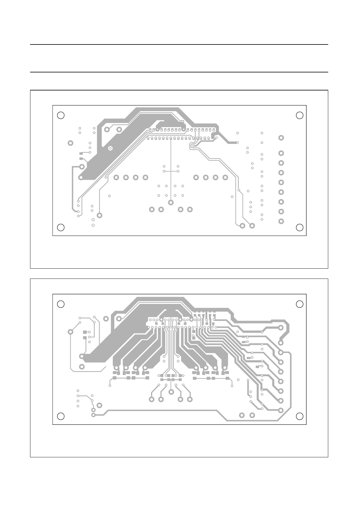
Fig.27 Top of printed-circuit board layout of test and application circuit showing copper layer viewed from top.
handbook, full pagewidth
MDB534
Fig.28 Bottom of printed-circuit board layout of test and application circuit showing copper layer viewed from top.
2004 Feb 24 47
Philips Semiconductors Product specification
I2C-bus controlled 4 ×50 Watt power
amplifier and multiple voltage regulator TDA8588J; TDA8588xJ
mdb588
CBU
REG3
REG1
SW1
SW2
RGND
1000 µF
220 µF
22 µF
2200 µF
2.2 µF
10 µF (50 V)
10 µF (50 V)
10 µF (50 V)
10 µF (50 V) 10 µF (50 V)
10 µF
Mode
DZ 5.6 V
470 nF
I2C supply
DIAG
GND
GND
Sense
SDA
+ 5 V
GND
SCL
VP
VP
4.7 kΩ
470 nF
OUT OUT
IN
SGND
RST RESCAP
RESCAP
47 nF on
off
on
off REG2
REG5
REG4
TDA8588J
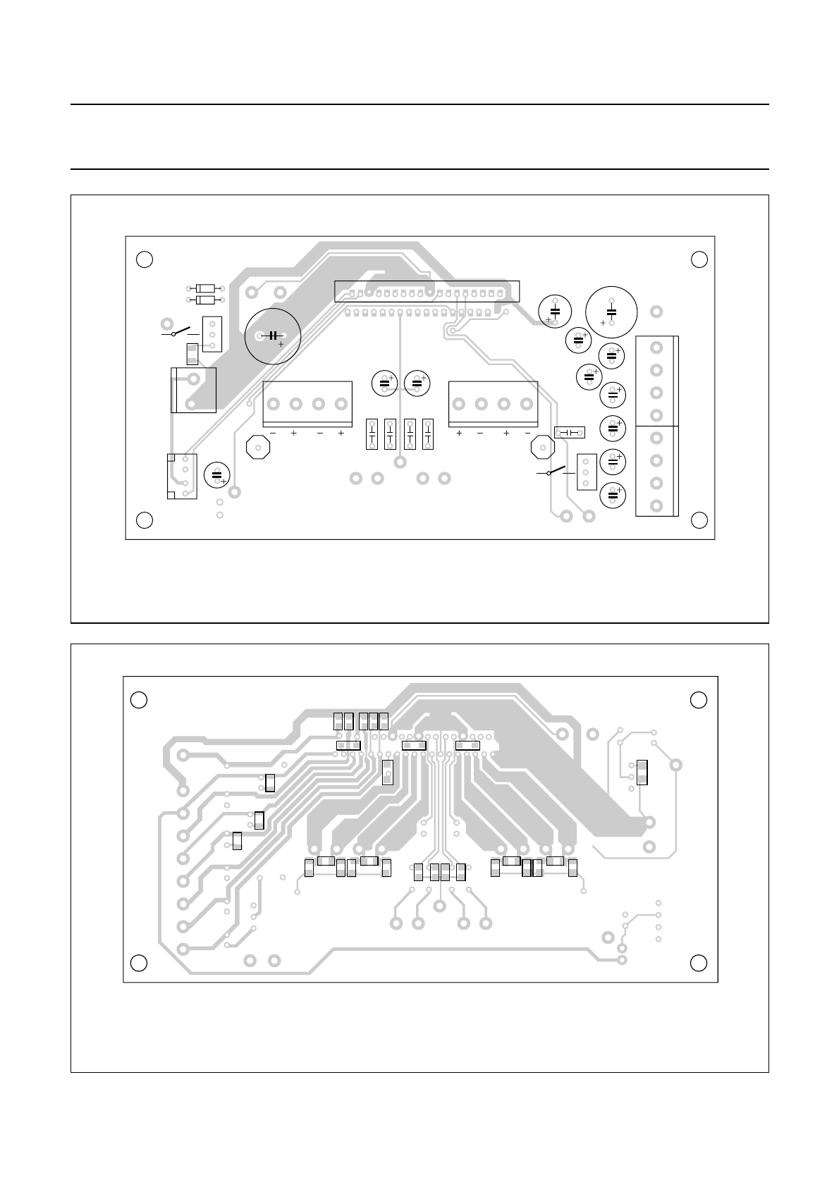
Fig.29 Top of printed-circuit board layout of test and application circuit showing components viewed from top.
handbook, full pagewidth
MDB536
100 nF
100 nF
100 nF
100 nF
10 kΩ47 kΩ
220 nF 220 nF 220 nF
Fig.30 Bottom of printed-circuit board layout of test and application circuit showing components viewed from
bottom.
2004 Feb 24 48
Philips Semiconductors Product specification
I2C-bus controlled 4 ×50 Watt power
amplifier and multiple voltage regulator TDA8588J; TDA8588xJ
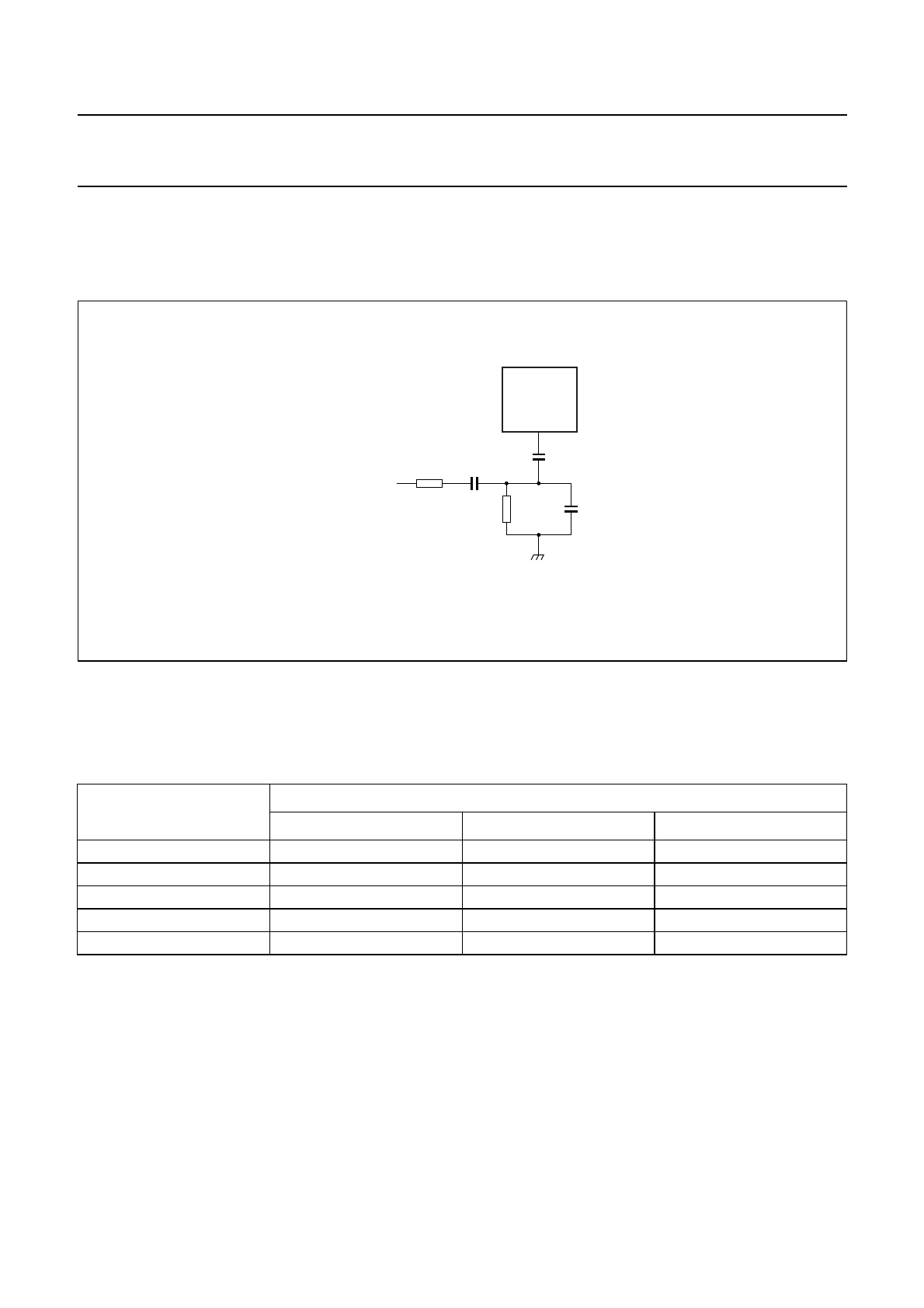
Beep input circuit
Beep input circuit to amplify the beep signal from the microcontroller to all 4 amplifiers (gain = 0 dB). Note that this circuit
will not affect amplifier performance.
Noise
The outputs of regulators 1 to 5 are designed to give very low noise with good stability. The noise output voltage depends
on output capacitor Co. Table 11 shows the affect of the output capacitor on the noise figure.
Table 11 Regulator noise figures
Note
1. Measured in the frequency range 20 Hz to 80 kHz.
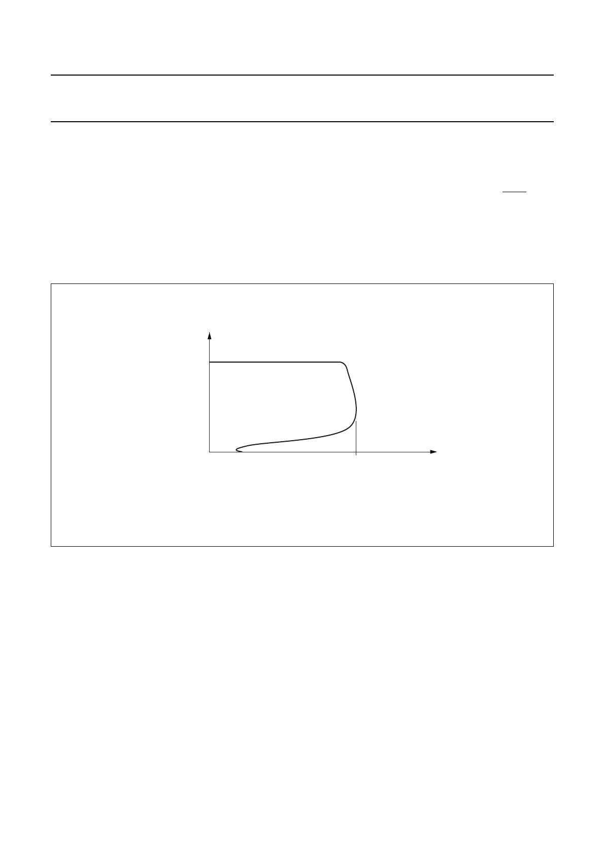
Stability
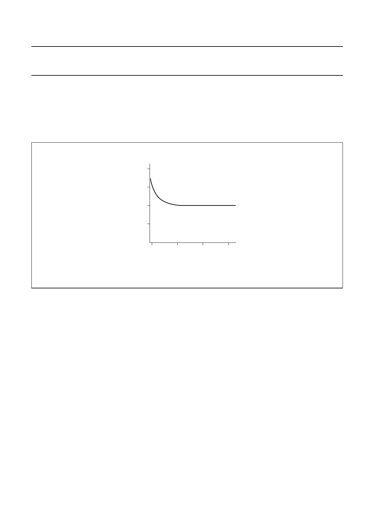
The regulators are made stable by connecting capacitors to the regulator outputs. The stability can be guaranteed with
almost any output capacitor if its Electric Series Resistance (ESR) stays below the ESR curve shown in Fig.32. If an
electrolytic capacitor is used, its behaviour with temperature can cause oscillations at extremely low temperature.
Oscillation problems can be avoided by adding a 47 nF capacitor in parallel with the electrolytic capacitor. The following
example describes how to select the value of output capacitor.
REGULATOR NOISE FIGURE (µV) at IREG = 10 mA; note 1
Co=10µFC
o=47µFC
o= 100 µF
1 225 195 185
2 750 550 530
3 120 100 95
4 225 195 185
5 320 285 270
mdb589
From
microcontroller
1.7 kΩ0.22 µF
100 Ω
2.2 µF
47 pF
TDA8588
ACGND
Fig.31 Application diagram for beep input.
2004 Feb 24 49
Philips Semiconductors Product specification
I2C-bus controlled 4 ×50 Watt power
amplifier and multiple voltage regulator TDA8588J; TDA8588xJ
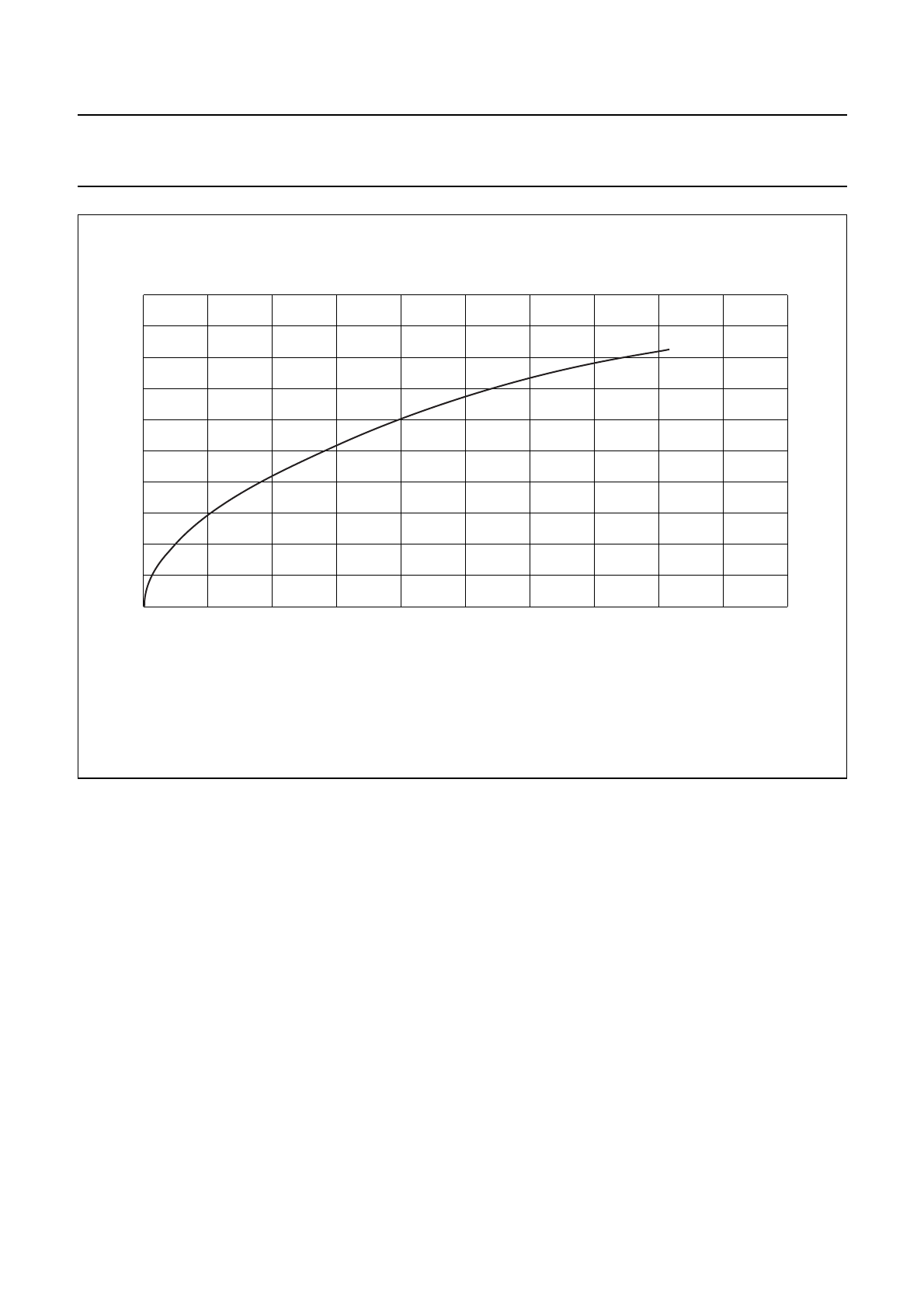
EXAMPLE REGULATOR 2
Regulator 2 is stabilized with an electrolytic output capacitor of 10 µF which has an ESR of 4 Ω. At Tamb =−30 °C the
capacitor value decreases to 3 µF and its ESR increases to 28 Ω which is above the maximum allowed as shown
in Fig.32, and which will make the regulator unstable. To avoid problems with stability at low temperatures, the
recommended solution is to use tantalum capacitors. Either use a tantalum capacitor of 10 µF, or an electrolytic capacitor
with a higher value.
handbook, halfpage
0
0.1 110 C (µF)
MGL912
stable region
maximum ESR
100
ESR
(Ω)
20
15
10
5
Fig.32 Curve for selecting the value of output capacitors for regulators 1 to 5.
2004 Feb 24 50
Philips Semiconductors Product specification
I2C-bus controlled 4 ×50 Watt power
amplifier and multiple voltage regulator TDA8588J; TDA8588xJ
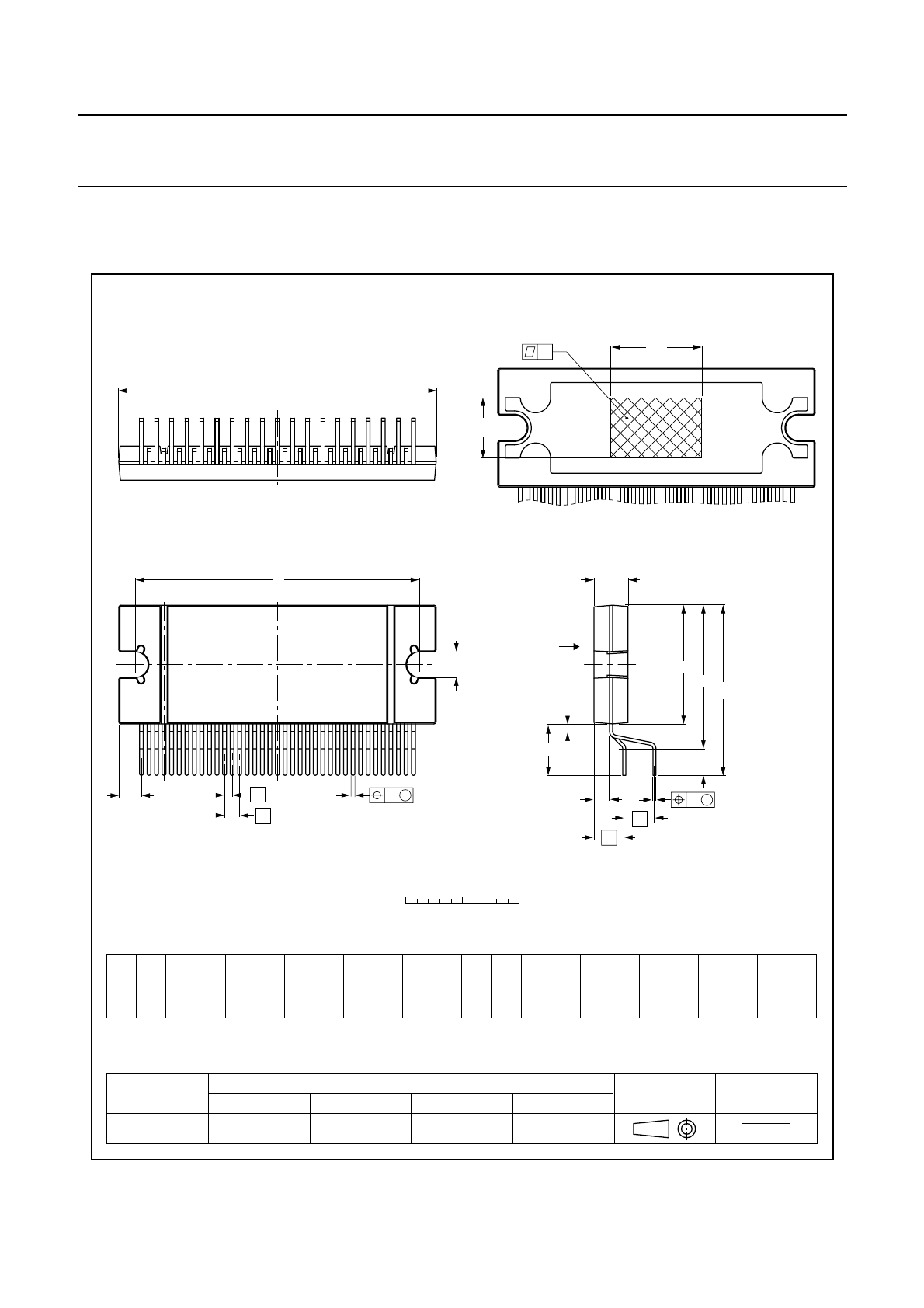
PACKAGE OUTLINE
UNIT A D
(1)
E
(1)
REFERENCES
OUTLINE
VERSION EUROPEAN
PROJECTION ISSUE DATE
IEC JEDEC JEITA
mm 19
A2
4.65
4.35
bp
0.60
0.45
DIMENSIONS (mm are the original dimensions)
Note
1. Plastic or metal protrusions of 0.25 mm maximum per side are not included.
SOT725-1 - - - - - - - - -
0 10 20 mm
scale
L
E
A
c
A2
m
L3
L4
L2
Q
w
M
bp
d
Ze1
e2
e
137
DBS37P: plastic DIL-bent-SIL power package; 37 leads (lead length 6.8 mm) SOT725-1
v
M
D
xh
Eh
non-concave
view B: mounting base side
B
D
c Z
(1)
dee
1e2L3
DhEhLm
0.5
0.3 42.2
41.7 37.8
37.4 12 2
15.9
15.5 14 1.15
0.85
L2
3.9
3.1
L4
22.9
22.1
83.30
2.65
2.1
1.8
3.4
3.1 4
6.8
Qj
0.25
w
0.6
v
0.03
x
j
01-11-14
02-11-22

2004 Feb 24 51
Philips Semiconductors Product specification
I2C-bus controlled 4 ×50 Watt power
amplifier and multiple voltage regulator TDA8588J; TDA8588xJ
SOLDERING
Introduction to soldering through-hole mount
packages
This text gives a brief insight to wave, dip and manual
soldering. A more in-depth account of soldering ICs can be
found in our
“Data Handbook IC26; Integrated Circuit
Packages”
(document order number 9398 652 90011).
Wave soldering is the preferred method for mounting of
through-hole mount IC packages on a printed-circuit
board.
Soldering by dipping or by solder wave
Driven by legislation and environmental forces the
worldwide use of lead-free solder pastes is increasing.
Typical dwell time of the leads in the wave ranges from
3 to 4 seconds at 250 °C or 265 °C, depending on solder
material applied, SnPb or Pb-free respectively.
The total contact time of successive solder waves must not
exceed 5 seconds.
The device may be mounted up to the seating plane, but
the temperature of the plastic body must not exceed the
specified maximum storage temperature (Tstg(max)). If the
printed-circuit board has been pre-heated, forced cooling
may be necessary immediately after soldering to keep the
temperature within the permissible limit.
Manual soldering
Apply the soldering iron (24 V or less) to the lead(s) of the
package, either below the seating plane or not more than
2 mm above it. If the temperature of the soldering iron bit
is less than 300 °C it may remain in contact for up to
10 seconds. If the bit temperature is between
300 and 400 °C, contact may be up to 5 seconds.
Suitability of through-hole mount IC packages for dipping and wave soldering methods
Notes
1. For SDIP packages, the longitudinal axis must be parallel to the transport direction of the printed-circuit board.
2. For PMFP packages hot bar soldering or manual soldering is suitable.
PACKAGE SOLDERING METHOD
DIPPING WAVE
DBS, DIP, HDIP, RDBS, SDIP, SIL suitable suitable(1)
PMFP(2) −not suitable

2004 Feb 24 52
Philips Semiconductors Product specification
I2C-bus controlled 4 ×50 Watt power
amplifier and multiple voltage regulator TDA8588J; TDA8588xJ
DATA SHEET STATUS
Notes
1. Please consult the most recently issued data sheet before initiating or completing a design.
2. The product status of the device(s) described in this data sheet may have changed since this data sheet was
published. The latest information is available on the Internet at URL http://www.semiconductors.philips.com.
3. For data sheets describing multiple type numbers, the highest-level product status determines the data sheet status.
LEVEL DATA SHEET
STATUS(1) PRODUCT
STATUS(2)(3) DEFINITION
I Objective data Development This data sheet contains data from the objective specification for product
development. Philips Semiconductors reserves the right to change the
specification in any manner without notice.
II Preliminary data Qualification This data sheet contains data from the preliminary specification.
Supplementary data will be published at a later date. Philips
Semiconductors reserves the right to change the specification without
notice, in order to improve the design and supply the best possible
product.
III Product data Production This data sheet contains data from the product specification. Philips
Semiconductors reserves the right to make changes at any time in order
to improve the design, manufacturing and supply. Relevant changes will
be communicated via a Customer Product/Process Change Notification
(CPCN).
DEFINITIONS
Short-form specification The data in a short-form
specification is extracted from a full data sheet with the
same type number and title. For detailed information see
the relevant data sheet or data handbook.
Limiting values definition Limiting values given are in
accordance with the Absolute Maximum Rating System
(IEC 60134). Stress above one or more of the limiting
values may cause permanent damage to the device.
These are stress ratings only and operation of the device
at these or at any other conditions above those given in the
Characteristics sections of the specification is not implied.
Exposure to limiting values for extended periods may
affect device reliability.
Application information Applications that are
described herein for any of these products are for
illustrative purposes only. Philips Semiconductors make
no representation or warranty that such applications will be
suitable for the specified use without further testing or
modification.
DISCLAIMERS
Life support applications These products are not
designed for use in life support appliances, devices, or
systems where malfunction of these products can
reasonably be expected to result in personal injury. Philips
Semiconductors customers using or selling these products
for use in such applications do so at their own risk and
agree to fully indemnify Philips Semiconductors for any
damages resulting from such application.
Right to make changes Philips Semiconductors
reserves the right to make changes in the products -
including circuits, standard cells, and/or software -
described or contained herein in order to improve design
and/or performance. When the product is in full production
(status ‘Production’), relevant changes will be
communicated via a Customer Product/Process Change
Notification (CPCN). Philips Semiconductors assumes no
responsibility or liability for the use of any of these
products, conveys no licence or title under any patent,
copyright, or mask work right to these products, and
makes no representations or warranties that these
products are free from patent, copyright, or mask work
right infringement, unless otherwise specified.

2004 Feb 24 53
Philips Semiconductors Product specification
I2C-bus controlled 4 ×50 Watt power
amplifier and multiple voltage regulator TDA8588J; TDA8588xJ
PURCHASE OF PHILIPS I2C COMPONENTS
Purchase of Philips I2C components conveys a license under the Philips’ I2C patent to use the
components in the I2C system provided the system conforms to the I2C specification defined by
Philips. This specification can be ordered using the code 9398 393 40011.

© Koninklijke Philips Electronics N.V. 2004 SCA76
All rights are reserved. Reproduction in whole or in part is prohibited without the prior written consent of the copyright owner.
The information presented in this document does not form part of any quotation or contract, is believed to be accurate and reliable and may be changed
without notice. No liability will be accepted by the publisher for any consequence of its use. Publication thereof does not convey nor imply any license
under patent- or other industrial or intellectual property rights.
Philips Semiconductors – a worldwide company
Contact information
For additional information please visit http://www.semiconductors.philips.com. Fax: +31 40 27 24825
For sales offices addresses send e-mail to: sales.addresses@www.semiconductors.philips.com.
Printed in The Netherlands R32/01/pp54 Date of release: 2004 Feb 24 Document order number: 9397 750 11401