TITAN User Manual ZEUS PXA270 Issd
User Manual: ZEUS PXA270
Open the PDF directly: View PDF ![]() .
.
Page Count: 102 [warning: Documents this large are best viewed by clicking the View PDF Link!]
- TITAN user manual
- Contents
- Introduction
- Getting started
- Detailed hardware description
- TITAN block diagram
- TITAN address map
- Translations made by the MMU
- PXA270 processor
- PXA270 GPIO pin assignments
- Interrupt assignments
- Real time clock
- Watchdog timer
- Memory
- SDIO
- PC/104 interface
- Flat panel display support
- Audio
- Touchscreen controller
- USB
- Ethernet
- Serial COMs ports
- I²C
- Quick Capture camera interface
- General purpose I/O
- Temperature sensor
- JTAG and debug access
- Power and power management
- Connectors, LEDs and jumpers
- Appendix A - Board version / issue
- Appendix B - Specification
- Appendix C - Mechanical diagram
- Appendix D - Reference information
- Appendix E - ZEUS-FPIF details
- Appendix F - ZEUS-FPIF-CRT details
- Appendix G - Ethernet Breakout details
- Appendix H - Acronyms and abbreviations
- Appendix I - RoHS-6 Compliance - Materials Declaration Form
- Eurotech Group Worldwide Presence
Rev. 4.0 - April 2009 - ETH_TITAN_USM
DIGITAL TECHNOLOGIES FOR A BETTER WORLD
www.eurotech.com
USER MANUAL
TITAN
PXA270 RISC based PC/104
Single Board Compute
r
DISCLAIMER
The information in this document is subject to change without notice and should not be construed as a commitment
by any Eurotech company. While reasonable precautions have been taken, Eurotech assumes no responsibility for
any error that may appear in this document.
WARRANTY
This product is supplied with a 3 year limited warranty. The product warranty covers failure of any Eurotech
manufactured product caused by manufacturing defects. The warranty on all third party manufactured products
utilised by Eurotech is limited to 1 year. Eurotech will make all reasonable effort to repair the product or replace it
with an identical variant. Eurotech reserves the right to replace the returned product with an alternative variant or
an equivalent fit, form and functional product. Delivery charges will apply to all returned products. Please check
www.eurotech.com for information about Product Return Forms.
TRADEMARKS
ARM and StrongARM are registered trademarks of ARM Ltd.
Intel and XScale are trademarks or registered trademarks of Intel Corporation or its subsidiaries in the United
States and other countries.
Windows CE is a trademark of the Microsoft Corporation.
CompactFlash is the registered trademark of SanDisk Corp.
Linux is a registered trademark of Linus Torvalds.
RedBoot and Red HatTM is a registered trademark of Red Hat Inc.
Bluetooth is a registered trademark of Bluetooth SIG, Inc.
All other trademarks recognised.
REVISION HISTORY
Issue no. PCB Date Comments
A V0 Issue 2 30th August 2007 Draft release of manual for TITAN and TITAN-Lite.
B V0 Issue 2 1st October 2007 Moved ZEUS-FPIF and Ethernet Breakout details to Appendices
and added details of ZEUS-FPIF-CRT; Eurotech rebranding.
C V1 Issue 1 16th April 2008 Release for TITAN V1I1.
D V1 Issue 1 2nd April 2009 Minor updates and new branding.
© 2009 Eurotech. All rights reserved.
For contact details, see page 101.

Contents
Issue D 3
Contents
Introduction...............................................................................................................................5
TITAN ‘at a glance’ .......................................................................................................6
TITAN features .............................................................................................................7
TITAN support products..............................................................................................10
Product handling and environmental compliance.......................................................11
Conventions................................................................................................................12
Getting started ........................................................................................................................13
Using the TITAN .........................................................................................................13
Detailed hardware description ................................................................................................15
TITAN block diagram ..................................................................................................15
TITAN address map....................................................................................................16
Translations made by the MMU..................................................................................17
PXA270 processor......................................................................................................17
PXA270 GPIO pin assignments .................................................................................19
Interrupt assignments .................................................................................................24
Real time clock ...........................................................................................................25
Watchdog timer...........................................................................................................26
Memory.......................................................................................................................27
SDIO...........................................................................................................................28
PC/104 interface.........................................................................................................29
Flat panel display support...........................................................................................36
Audio ..........................................................................................................................42
Touchscreen controller ...............................................................................................42
USB ............................................................................................................................43
Ethernet ......................................................................................................................45
Serial COMs ports ......................................................................................................46
I²C...............................................................................................................................50
Quick Capture camera interface.................................................................................51
General purpose I/O ...................................................................................................52
Temperature sensor....................................................................................................52
JTAG and debug access ............................................................................................53
Power and power management..............................................................................................54
Power supplies ...........................................................................................................54
Processor power management...................................................................................57
Peripheral devices power management .....................................................................59
Connectors, LEDs and jumpers..............................................................................................64
Connectors .................................................................................................................65
Status LEDs................................................................................................................78
Jumpers......................................................................................................................78
Appendix A - Board version / issue.........................................................................................82
Appendix B - Specification......................................................................................................84
Appendix C - Mechanical diagram..........................................................................................86
Appendix D - Reference information ......................................................................................87
Appendix E - ZEUS-FPIF details ............................................................................................88
Appendix F - ZEUS-FPIF-CRT details....................................................................................93

TITAN user manual
Appendix G - Ethernet Breakout details................................................................................. 96
Appendix H - Acronyms and abbreviations............................................................................ 98
Appendix I - RoHS-6 Compliance - Materials Declaration Form.......................................... 100
Eurotech Group Worldwide Presence.................................................................................. 101

Introduction
Issue D 5
Introduction
The TITAN is an ultra low power PC/104 compatible single board computer based on the
Intel 520MHz PXA270 XScale processor. The PXA270 is an implementation of the Intel
XScale micro architecture combined with a comprehensive set of integrated peripherals,
including:
• Flat panel graphics controller.
• Interrupt controller.
• Real time clock.
• Various serial interfaces.
The TITAN board offers a wide range of features making it ideal for power sensitive
embedded communications and multimedia applications.
The board is available in two standard variants:
• TITAN.
• TITAN-Lite (TITANL).
The TITAN is available with a choice CPU frequency and memory configurations options,
as shown below:
Variant Memory configuration Details
TITAN TITAN-FRx-Mx-Fx-R6 PXA270, FRx=520/416MHz
microprocessor, Mx=64/128MB SDRAM,
Fx=32/64MB Flash, Commercial
temperature range.
TITAN-FRx-Mx-Fx-I-R6 PXA270, FRx=520/416MHz
microprocessor, Mx=64/128MB SDRAM,
Fx=32/64MB Flash, Industrial
temperature range.
TITAN-Lite TITANL-312-M64-F16-R6 PXA270 312MHz CPU, 64MB SDRAM,
16MB Flash No SRAM, PC/104, Audio or
COM 4 & 5, Commercial temperature
range.
TITANL-312-M64-F16-I-R6 PXA270 312MHz CPU, 64MB SDRAM,
16MB Flash No SRAM, PC/104, Audio or
COM 4 & 5, Industrial temperature range.
The TITAN board is RoHS compliant.
For alternative memory configurations, please contact Eurotech (see Eurotech Group
Worldwide Presence, page 101, for details). Eurotech can provide custom configurations
(subject to a minimum order quantity) for the TITAN / TITAN-Lite. Please contact our
Sales team to discuss your requirements.
TITAN user manual
Issue D
6
TITAN ‘at a glance’
SDIO socket
10/100 Base-T Ethernet Audio - In/Out/MIC/AMP
LVDS [optional] TFT/STN panel
Quick Capture
camera
Digital I/O
Touchscreen
Five serial ports
Battery
Jumpers
Jumpers
Powe
r
(inc battery input)
Ethernet LEDs
JTAG
Intel PXA270
XScale 520MHz
processo
r
AMD Mirrorbit
Flash
8/16-bit PC/104
interface
USB hosts / client

Introduction
Issue D 7
TITAN features
Microprocessor
• PXA270 312MHz (TITAN-Lite only) 416/520MHz XScale processor (520MHz as
standard option).
Cache
• 32K data cache, 32K instruction cache, 2K mini data cache.
System memory
• Fixed on-board memory: 64/128MB SDRAM (32-bit wide SDRAM data bus).
Silicon disk
• Fixed on-board memory: 16MB Flash (TITAN-Lite only) or 32/64MB Flash.
SRAM
• 256KB of SRAM battery backed on-board.
Serial ports
• Five UART fast serial ports, 16550 compatible (921.6Kbaud):
- One RS422/485 interface (software selectable).
- Four RS232 interfaces.
• Two channels with 128 byte Tx/Rx FIFO.
• 40-pin boxed header.
USB support
• Two USB 1.1 host controller ports supporting 12Mbps and 1.5Mbps speeds.
• One USB 1.1 client controller port supporting 12Mbps and 1.5Mbps speeds (software
selectable on Host 2).
• Short circuit protection with 500mA current limit protection.
• 10-pin header.
Network support
• One IEEE 802.3u 10/100 Base-T Ethernet controller.
• One 10/100BaseTX NIC port on 8-pin header.
• Factory build option for external Power-over-Ethernet (PoE).
Expansion interfaces
• SDIO socket to support MMC/SD/SDIO cards.
• PC/104 expansion bus - 8/16-bit ISA bus compatible interface.
TL
TL
TL
TL
TITAN user manual
Issue D
8
Date/time support
• Real time clock – battery backed on-board (external to PXA270).
• ± 1 minute/month accuracy.
Video
• 18-bit flat panel interface for STN and TFT displays on 40-pin boxed connector.
• Up to 800x600 resolution.
• 8/16bpp.
• Backlight control.
• Optional LVDS interface.
• LCD voltage (3.3V / 5V) selection jumper.
• LVDS encoding mode selector jumper (for signalling decoding LVDS display
receiver).
Audio and touchscreen
• Wolfson WM9712L AC’97 compatible CODEC.
• Line in, line out, microphone in, stereo amp out on 12-pin boxed header.
• Touchscreen support: 4/5-wire analogue resistive on 5-pin boxed header.
Quick Capture camera interface
• Intel® Quick Capture technology.
• 20-pin boxed header connector to a camera image sensor.
I2C bus
• Multi-master serial bus, header connection.
Configuration PROM
• I2C PROM for storing configuration data.
Watchdog timer
• External to PXA270, generates reset on timeout. Timeout range 1ms-60s.
User configuration
• Three user configurable jumpers on 8-pin header.
General I/O
• Sixteen user configurable general purpose I/O on 20-pin boxed header.
• 5V tolerant inputs.
• 3.3V outputs, pulled up to 5V.
• PWM outputs for LED intensity control
TL
TL
TL
TL
TL

Introduction
Issue D 9
Temperature sensor
• I2C temperature sensor.
Battery backup
• On-board battery holder containing a lithium-ion non-rechargeable CR2032, 3V,
220mAh battery.
• Battery disconnect jumper.
Test support
• JTAG interface (10-pin header).
• Download data to FLASH memory.
• Debug and connection to In-Circuit Emulator (ICE).
Power requirements
• Typically 1.5W from a single 5V supply.
• Power management features allow current requirements to be as low as 20mA
(100mW) in sleep mode and 2mA (10mW) in deep sleep mode.
Mechanical
• PC/104 compatible footprint 3.8" x 3.6" (96mm x 91mm) www.pc104.org/
Environmental
• Operating temperature:
- Commercial: 20°C (-4°F) to +70°C (+158°F) for speed variants up to 520MHz.
- Industrial: -40°C (-40°F) to +85°C (+185°F) for speed variants up to 416MHz.
• RoHS Directive Compliant (2002/95/EC).
TL
TL

TITAN user manual
Issue D
10
TITAN support products
The following products support the TITAN:
• ZEUS-FPIF (Flat Panel Interface)
The ZEUS-FPIF is a simple board that enables easy connection between the TITAN
and a variety of LCD flat panel displays.
See Appendix E - ZEUS-FPIF details, page 88, for further details.
• ZEUS-FPIF-CRT, a board that allows the TITAN to drive a CRT monitor or an
analogue LCD flat panel. Sync on green and composite sync monitors are not
supported.
See Appendix F - ZEUS-FPIF-CRT details, page 93, for further details.
• ETHER-BREAKOUT
The ETHER-BREAKOUT is a simple board that converts the TITAN Ethernet 8-pin
header and Ethernet LEDs 6-pin header to a standard RJ45 connector with LEDs.
See Appendix G - Ethernet Breakout details, page 96, for further details.
Contact Eurotech (see Eurotech Group Worldwide Presence, page 101) for further
information about any of these products.

Introduction
Issue D 11
Product handling and environmental compliance
Anti-static handling
This board contains CMOS devices that could be damaged in the event of static
electricity being discharged through them. At all times, please observe anti-static
precautions when handling the board. This includes storing the board in appropriate anti-
static packaging and wearing a wrist strap when handling the board.
Packaging
Please ensure that, should a board need to be returned to Eurotech, it is adequately
packed (preferably in the original packing material).
Electromagnetic compatibility (EMC)
The TITAN is classified as a component with regard to the European Community EMC
regulations and it is the user’s responsibility to ensure that systems using the board are
compliant with the appropriate EMC standards.
RoHS compliance
The European RoHS Directive (Restriction on the Use of Certain Hazardous Substances
– Directive 2002/95/EC) limits the amount of six specific substances within the
composition of the product. The ZEUS and associated accessory products are available
as RoHS-6 compliant options and are identified by an -R6 suffix in the product order
code. A full RoHS Compliance Materials Declaration Form is included in Appendix I -
RoHS-6 Compliance - Materials Declaration Form. Further information about RoHS
compliance is available on the Eurotech web site at www.eurotech-
ltd.co.uk/RoHS_and_WEEE.
TITAN user manual
Issue D
12
Conventions
The following symbols are used in this guide:
Symbol Explanation
Note - information that requires your attention.
Caution – proceeding with a course of action may damage
your equipment or result in loss of data.
Jumper is fitted.
Jumper provided, but not fitted.
Jumper is not fitted.
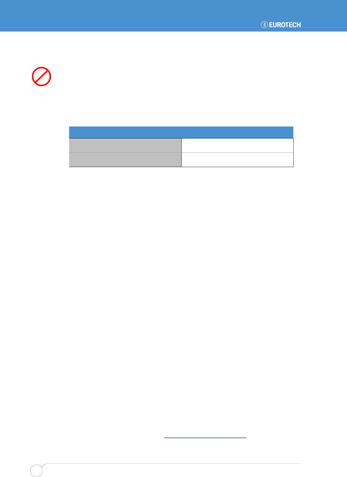
Tables
With tables such as that shown below, the white cells show information relevant to the
subject being discussed. Grey cells are not relevant in the current context.
Byte lane Most significant byte Least significant byte
Bit 15 14 13 12 11 10 9 8 7 6 5 4 3 2 1 0
Field - - - - - - - - - - - - - RETRI
G
AUTO
_
CLR R_DIS
Reset X X X X X X X X 0 0 0 0 0 0 0 0

Getting started
Issue D 13
Getting started
Depending on the Development Kit purchased, a Quickstart Manual is provided for
Windows CE or embedded Linux to enable users to set up and start using the board.
Please read the relevant manual and follow the steps for setting up the board. Once you
have completed this task and have a working TITAN system, you can start adding further
peripherals, enabling development to begin.
Using the TITAN
This section provides a guide to setting up and using of some of the features of the
TITAN. For more detailed information on any aspect of the board see Detailed hardware
description, page 15.
Using the SDIO socket
The TITAN is fitted with a SDIO socket mounted on the top side of the board. The socket
is connected to a PXA270 MMC/SD/SDIO controller interface. The TITAN supports hot
swap changeover of the cards and notification of card insertion. See the sections SDIO,
page 28, and J7 – SDIO socket, page 70, for further details.
Using the serial interfaces (RS232/422/485)
The five serial port interfaces on the TITAN are fully 16550 compatible. Connection to the
serial ports is made via a 40-way boxed header. The pin assignment of this header has
been arranged to enable 9-way IDC D-Sub plugs to be connected directly to the cable.
See the sections Serial COMs ports, page 46, and J1 – COMS ports, page 66, for further
details.
A suitable cable for COM1 is provided as part of the Development Kit. The D-Sub
connector on this cable is compatible with the standard 9-way connector on a desktop
computer.
COM4 (RS232) and COM5 (RS422/485) are not available on the standard
TITAN-Lite configuration. Eurotech can provide custom configurations (subject to
a minimum order quantity) for the TITAN-Lite populated with this feature. Please
contact our Sales team to discuss your requirements (see Eurotech Group
Worldwide Presence, page 101).
Using the audio features
There are four audio interfaces supported on the TITAN: amp out, line out, line in and
microphone. The line in, line out and amp interfaces support stereo signals and the
microphone provides a mono input. The amplified output is suitable for driving an 8Ω load
with a maximum power output of 250mW per channel.
Connections are routed to J6 - see the sections Audio, page 41, and J7 – Audio
connector, page 69, for further details.
TL
TL

TITAN user manual
Issue D
14
Using the USB host
The standard USB connector is a 4-way socket, which provides power and data signals
to the USB peripheral. The 10-way header J10 has been designed to be compatible with
PC expansion brackets that support two USB sockets. See the sections USB, page 43,
and J10 – USB connector, page 72, for further details.
Using the USB client
The TITAN USB host port 2 can be configured under software to be a client and
connected to a PC via a USB cable This feature is standard for the TITAN-Lite. The USB
cable should be plugged into the 10-way header J10. See the sections USB, page 43,
and J10 – USB connector, page 72, for further details.
Using the Ethernet interface
The Davicom DM9000A 10/100BaseTX Ethernet controller is configured by the RedBoot
boot loader for embedded Linux, and by Windows CE once it has booted. Connection is
made via connector J11. A second connector J12 provides link and speed status outputs
for control LEDs. See the sections Ethernet, page 45; J11 – 10/100BaseTX Ethernet
connector, page 72; and J12 – Ethernet status LEDs connector, page 73, for further
details.
Using the PC/104 expansion bus
PC/104 modules can be used with the TITAN to add extra functionality to the system.
This interface supports 8/16-bit ISA bus style peripherals.
Eurotech has a wide range of PC/104 modules that are compatible with the TITAN.
These include modules for digital I/O, analogue I/O, motion control, video capture, CAN
bus, serial interfaces, etc. Please contact the Eurotech sales team if a particular interface
you require does not appear to be available as these modules are in continuous
development. Contact details are provided in Eurotech Group Worldwide Presence, page
101.
To use a PC/104 board with the TITAN, plug it into J13 for 8-bit cards and J13/J14 for
8/16-bit cards. See the sections PC/104 interface, page 29, and J14 & J15 – PC/104
connectors, page 74, for further details.
The ISA interface on the TITAN does not support DMA, shared interrupts and some
access modes. See the section PC/104 interrupts, page 30, for details about PC/104
interrupt use.
The TITAN provides +5V to a PC/104 add-on board via the J13 and J14 connectors. If a
PC/104 add-on board requires a +12V supply, then +12V must be supplied to the TITAN
power connector J15 pin 4. If –12V or –5V are required, these must be supplied directly
to the PC/104 add-on board.
The TITAN is available with non-stack through connectors by special order. Contact
Eurotech for more details (see Eurotech Group Worldwide Presence, page 101).
TL
TL
Detailed hardware description
Issue D 15
Detailed hardware description
The following section provides a detailed description of the functions provided by the
TITAN. This information may be required during development after you have started
adding extra peripherals or are starting to use some of the embedded features.
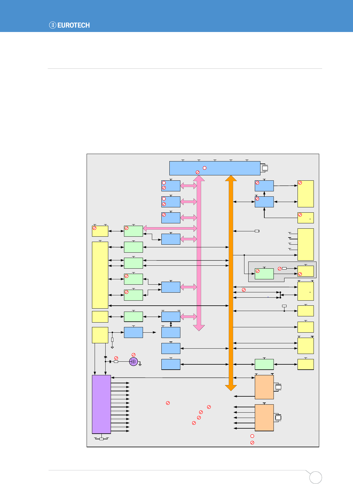
TITAN block diagram
The diagram below illustrates the functional organization of the TITAN and TITAN-Lite
PC/104 SBC:
256 KB
SRAM
DUART
Comms
Header
J1
COM 1
RS232
Transceiver
COM 2
COM 4
COM 3 RS232
Transceiver
CPLD
Ethernet
Controller
Ethernet
Headers
J11/J12
Serial
EEPROM
2xUSB
Header
J10
JTAG
Audio
Header
J6
AC'97
Codec
250mW
Audio Amp
LCD
Conn.
J4
PC/104
J13/J14
JTAG
Header
J9
PXA270
312MHz /
416MHz / 520MHz
MEMORY CONTROLLER BUS
PERIPHERALS / GPIO
I/O
Expander
LCD
USB B 1.1 Host
USB A 1.1 Host
GPIO
Header
J3
PSUs
CPU_CORE (+0.85V - +1.55V)
TSC
Header
J5
Power
Conn.
J15
Reset /
Watchdog
Circuit
RESET#
COM 5
RS232
Transceiver
FFUART
BTUART
STUART
TITAN & TITAN-Lite
Power Management I2C
USB A 1.1 Client
SD
Socket
J7
SDIO
LVDS
Transmitter
LVDS
Conn.
J8
Camera
Header
J2
Quick Capture Camera
AC97
I2C
I2C
LINE IN R+L
LINE OUT R+L
MIC IN
AMP R+L
LVDS
Config
PROM
Temp
Sensor
I2C
I2C
I2C
IN[0:7] /
OUT[0:7]
ISA
Touch Screen
= TITAN-LITE only
= Not avaliable for standard TITAN-LITE
JP4
JP1
JP3
VCC_SRAM (+1.1V)
VCC_PLL (+1.3V)
VCC_BATT (+3V - +3.3V)
+3V3 (+3.3V)
+3V3_RAM (+3V - +3.3V)
LCDSAFE (+3.3V / 5V)
BLKSAFE (+5V)
+2V8_CIF (+2.8V)
USBVCC1 (+5V)
USBVCC2 (+5V)
POSBIAS (+22V)
NEGBIAS (-22V)
Transformer
+3V3
+3V3_RAM
+3V3
+3V3
+3V3
+3V3
+3V3
+3V3
+3V3 +3V3
+5V +12V
+3V3
+3V3
+3V3
+2V5_TRANS +2V5_TRANS
+3V3
+3V3
+3V3 VCC_PLL VCC_CORE VCC_BATT VCC_SRAM
+5V
+3V3
+3V3
+3V3 +5V
+3V3 +2V8_CIF
+3V3
+3V3
USBVCC1 USBVCC2
+3V3
POSBIAS
NEGBIAS
BLKSAFE
LCDSAFE
Clock
Generation 25MHz
8MHz (PC/104)
14.318MHz (PC/104)
14.7456MHz (DUART)
24.576MHz (AC’97 Codec)
25MHz (Ethernet Controler)
+3V3
RTC
I2C
32.768kHz (PXA270)
+3V3
32.768kHz
JP5
Manual
Reset
Jumper
Battery
Disconnect
Jumper
13MHz
+5V
VBAT_E
RESET_SW#
VBAT_I
VBAT
LVDS Mode
Select Jumper
User Config
Jumpers
JP2
LCD Logic
Supply Jumper
+3V3 +5V
VCC_BATT
Transceivers
OPTIONAL
TL
TL
TL
TL
TL
TL
TL
TL
TL
TL
TL
TL
TL
TL
TL
TL TL
TL
RS422/485
Transceiver
32/64 MB
FLASH
16 MB /
64 MB /
128 MB
SDRAM
TL
TL
TL
TL
TL
TL
TL
TL
VBAT
TL
TL
JP6

TITAN user manual
Issue D
16
TITAN address map
PXA270 chip select Physical address Bus width Description
CS0# 0x00000000 – 0x03FFFFFE 16-bit FLASH memory / Silicon disk
CS1# 0x04000000 – 0x07FFFFFE 16-bit Ethernet controller
- 0x08000000 – 0x0FFFFFFF - Reserved
CS4# 0x10000000 – 0x1000000E 16-bit COM4
- 0x10000010 – 0x107FFFFF - Reserved
CS4# 0x10800000 – 0x1080000E 16-bit COM5
- 0x10800010 – 0x10FFFFFF - Reserved
CS4# 0x11000000 – 0x11000001 16-bit BV_REG (Board version / issue)
- 0x11000002 – 0x117FFFFF - Reserved
CS4# 0x11800000 – 0x11800001 16-bit I2_REG (PC104 IRQ status)
- 0x11800002 – 0x11FFFFFF - Reserved
CS4# 0x12000000 – 0x12000001 16-bit CV_REG (CPLD version / issue)
- 0x12000002 – 0x127FFFFF - Reserved
CS4# 0x12800000 – 0x12800001 16-bit I1_REG (PC104 IRQ status)
- 0x12800002 – 0x12FFFFFF - Reserved
CS4# 0x13000000 – 0x13000001 16-bit C_REG (PC104 reset)
- 0x13000002 – 0x13FFFFFF - Reserved
CS5# 0x14000000 – 0x17FFFFFE 16-bit SRAM
- 0x18000000 – 0x1FFFFFFF - Reserved
NA 0x30000000 – 0x300003FF 8/16-bit PC/104 I/O space
- 0x30000400 – 0x3BFFFFFF - Reserved
NA 0x3C000000 – 0x3C1FFFFF 8/16-bit PC/104 memory space
- 0x3C200000 – 0x3FFFFFFF - Reserved
NA 0x40000000 – 0x43FFFFFF 32-bit PXA270 peripherals1
NA 0x44000000 – 0x47FFFFFC 32-bit LCD control registers1
NA 0x48000000 – 0x4BFFFFFC 32-bit Memory controller registers1
NA 0x4C000000 – 0x4FFFFFFC 32-bit USB host registers1
NA 0x50000000 – 0x53FFFFFC 32-bit Capture Interface registers1
- 0x54000000 – 0x57FFFFFC - Reserved
NA 0x58000000 – 0x5BFFFFFC 32-bit Internal memory control1
NA 0x5C000000 – 0x5C00FFFC 32-bit Internal SRAM bank 0
NA 0x5C010000 – 0x5C01FFFC 32-bit Internal SRAM bank 1
NA 0x5C020000 – 0x5C02FFFC 32-bit Internal SRAM bank 2
NA 0x5C030000 – 0x5C03FFFC 32-bit Internal SRAM bank 3
- 0x5C040000 – 0X7FFFFFFF - Reserved
SDCS0# 0x80000000 – 0x8FFFFFFF 32-bit SDRAM
- 0x90000000 – 0xFFFFFFFF - Reserved
1 Details of the internal registers are in the Intel Developer’s Manual on the Development Kit CD.
TL
TL
TL
TL
TL

Detailed hardware description
Issue D 17
Translations made by the MMU
For details of translations made by the MMU by Redboot for embedded Linux, please
refer to the TITAN Embedded Linux Quickstart Manual.
For details of translations made by the MMU for Windows CE, please check the Windows
CE documentation for information about memory mapping. One source of this
information is on the MSDN web site (www.msdn.microsoft.com) under Windows CE
Memory Architecture.
PXA270 processor
The TITAN board is based on a PXA270 processor,
www.intel.com/design/pca/prodbref/253820.htm.
The PXA270 processor is an integrated system-on-a-chip microprocessor for
high-performance, low-power portable handheld and handset devices. It incorporates on-
the-fly voltage and frequency scaling and sophisticated power management.
The PXA270 processor complies with the ARM* Architecture V5TE instruction set
(excluding floating point instructions) and follows the ARM* programmer’s model. The
PXA270 processor also supports Intel® Wireless MMX™ integer instructions in
applications such as those that accelerate audio and video processing.
The features of the PXA270 processor include:
• Intel® XScale™ core.
• Power management.
• Internal memory - 256KB of on-chip RAM.
• Interrupt controller.
• Operating system timers.
• Pulse-width modulation unit (PWM).
• Real time clock (RTC).
• General purpose I/O (GPIO).
• Memory controller.
• DMA controller.
• Serial ports:
- 3x UART.
- Fast infrared port.
- I2C bus port.
- AC97 Codec interface.
- I2S Codec interface.
- USB host controller (2 ports).
- USB client controller.
- 3x synchronous serial ports (SSP).
• LCD panel controller.

TITAN user manual
Issue D
18
• Multimedia card, SD memory card and SDIO card controller.
• Memory stick host controller.
• Mobile scalable link (MSL) interface.
• Keypad interface.
• Universal subscriber identity module (USIM) interface.
• Quick Capture camera interface.
• JTAG interface.
• 356-pin VF-BGA packaging.
The design supports 520MHz, 416MHz and 312MHz speed variants of the PXA270
processor. The standard variant of the TITAN board includes the 520MHz version of the
PXA270. The TITAN-LITE board is fitted with the a 312MHz version of the PXA270. The
maximum speed available for extended temperature versions of the TITAN is 416MHz.
A 13MHz external crystal is used to run the PXA270 processor. All other clocks are
generated internally in the processor.
The PXA270 processor family provides multimedia performance, low power capabilities
and rich peripheral integration. Designed for wireless clients, it incorporates the latest
Intel advances in mobile technology over its predecessor, the PXA255 processor. The
PXA270 processor features scalability by operating from 104MHz up to 520MHz,
providing enough performance for the most demanding control and monitoring
applications.
PXA270 is the first Intel® Personal Internet Client Architecture (PCA) processor to include
Intel® Wireless MMX™ technology, enabling high performance, low power multimedia
acceleration with a general purpose instruction set. Intel® Quick Capture technology
provides a flexible and powerful camera interface for capturing digital images and video.
Power consumption is also a critical component. Wireless Intel SpeedStep® technology
provides the new capabilities in low power operation.
The processor requires a number of power supply rails. All voltage levels are generated
on-board from the +5V power input The TITAN uses a specialised power management IC
to support Intel SpeedStep® technology.
The PXA270 processor is a low power device and does not require a heat sink for
temperatures up to 70°C (85°C for the industrial variant).
Detailed hardware description
Issue D 19
PXA270 GPIO pin assignments
The table below summarizes the use of the 118 PXA270 GPIO pins, their direction,
alternate function and active level.
For embedded Linux the GPIO pins are setup by Redboot. For Windows CE,
they are setup by the OS and not by the boot loader.
For details of pin states during reset see the Pin Usage table in the PXA27x
Processor Family Electrical, Mechanical and Thermal Specification.
Key:
AF Alternate function.
Dir Pin direction.
Active Function active level or edge.
Sleep Pin state during sleep mode:
- Hi-Z states are set to ‘1’ during sleep.
- Last states are whatever the last state was before going to sleep.
GPIO
No AF Signal name Dir Active Function Sleep
Wake-up
source See section…
0 0 AC97_IRQ Input AC97 interrupt Input 3 Audio
1 0 DS_WAKEUP
Input Deep sleep wakeup Input
3
2 0 SYS_EN Output High Enable 3.3V supplies 1 -
3 0 PWR_SCL Output NA Control PXA270 supplies 1 -
4 0 PWR_SDA Bidir NA Input -
5 0 PWR_CAP0 Power - - -
6 0 PWR_CAP1 Power - - -
7 0 PWR_CAP2 Power - - -
8 0
PWR_CAP3 Power -
To achieve low power in
during sleep
- -
Power and power
management
9 0
COM1OR4_
WAKEUP Input COM1 to COM4 activity Input 3
10 0 COM4_IRQ Input COM 4 interrupt Input
11 0 COM5_IRQ Input COM 5 interrupt Input 3
Serial COMs ports
12 0 OVERTEMP Input Temperature sensor over
temperature IRQ Input 3 I²C
13 0 USER_LINKA Input User configurable Input 3 External interrupts
14 0 ETH_IRQ# Input Ethernet interrupt Input 3
15 2 ETH_CS1# Output Low Chip select 1 1 -
Ethernet
TL
TL
TL

TITAN user manual
Issue D
20
GPIO
No AF Signal name Dir Active Function Sleep
Wake-up
source See section…
16 2 PWM0 Output
See
inverter
datasheet
Backlight on/off or variable
brightness if PWM 0 -
Flat panel display
support
17 0 PC104_IRQ Input ‘OR’ of PC/104 interrupts Input 3 PC/104 interface
18 0 CLK_SHDN# Output Low Shutdown clocks 0 -
-
19 0 BKLEN Output High LCD backlight enable 0 - Flat panel display
support
20 0 RS232_SHDN# Output Low Shutdown COM 1, 2, 3, & 4 0 -
Serial COMs ports
21 0 LVDS_EN Output High
0 = LVDS power down
[default]
1= LVDS enable
0 -
LVDS interface
22 0 USB_PWE2 Output High USB channel 2 power
enable 0 -
USB
23 1 CIF_MCLK Output NA Camera interface master
clock 0 -
24 1 CIF_FV Input NA Camera interface frame
sync - vertical Input -
25 1 CIF_LV Input NA Camera interface line sync -
horizontal Input -
26 2 CIF_PCLK Input NA Camera interface pixel clock Input -
Quick Capture
camera interface
27 0 LVDS_FES# Output Low
0 = LVDS falling edge
strobe
1= LVDS rising edge strobe
[default]
1 -
LVDS interface
28 1 AC97_BITCLK Input AC97 BITCLK Input -
29 1 AC97_DIN Input NA AC97 SDATA_IN0 Input -
30 2 AC97_DOUT Output NA AC97 SDATA_OUT 0 -
31 2 AC97_SYNC Output
AC97 SYNC 0 -
Audio
32 2 MMCLK Output NA SDIO clock 0 - -
33 2 SRAM_CS5# Output Low Chip select 5 1 - Memory
34 1 RXD1 Input NA COM1 receive data Input - Serial COMs ports
35 0 USER_LINKB Input User configurable Input 3 External interrupts
TL
TL
TL
TL
TL
TL
TL
TL
Detailed hardware description
Issue D 21
GPIO
No AF Signal name Dir Active Function Sleep
Wake-up
source See section…
36 1 DCD1 Input NA COM1 data carrier detect Input -
37 1 DSR1 Input NA COM1 data sender ready Input -
38 1 RI1 Input NA COM1 ring indicator Input -
39 2 TXD1 Output NA COM1 transmit data 0 -
40 2 DTR1 Output NA COM1 data terminal ready 0 -
41 2 RTS1 Output NA COM1 request to send 0 -
42 1 RXD2 Input NA COM2 receive data Input -
43 2 TXD2 Output NA COM2 transmit data 0 -
44 1 CTS2 Input NA COM2 clear to send Input -
45 2 RTS2 Output NA COM2 request to send 0 -
46 2 RXD3 Input NA COM3 receive data Input -
47 1 TXD3 Output NA COM3 transmit data 0 -
Serial COMs ports
48 2 CB_POE# Output Low Socket 0 & 1 output enable 1 -
49 2 CB_PWE# Output Low Socket 0 & 1 write enable 1 -
50 2 CB_PIOR# Output Low Socket 0 & 1 I/O read 1 -
51 2 CB_PIOW# Output Low Socket 0 & 1 I/O write 1 -
-
52 0 MMC_WP Input High SDIO write protect status Input -
53 0 MMC_CD Input SDIO card detect Input 3 -
54 2 CB_PCE2# Output Low Socket 0 & 1 high byte
enable 1 - -
55 0
DUART_
CLK8/16 Output NA
0 = 8 x sampling; double
standard baud rates
1= 16 x sampling; standard
baud rates [default]
1 - Serial COMs ports
56 1 CB_PWAIT# Input Low PWAIT Input -
57 1 CB_PIOIS16# Input Low IOIS16 Input -
-
58 2 LCD_D0 Output NA LCD data bit 0 0 -
59 2 LCD_D1 Output NA LCD data bit 1 0 -
60 2 LCD_D2 Output NA LCD data bit 2 0 -
61 2 LCD_D3 Output NA LCD data bit 3 0 -
62 2 LCD_D4 Output NA LCD data bit 4 0 -
63 2 LCD_D5 Output NA LCD data bit 5 0 -
64 2 LCD_D6 Output NA LCD data bit 6 0 -
65 2 LCD_D7 Output NA LCD data bit 7 0 -
66 2 LCD_D8 Output NA LCD data bit 8 0 -
67 2 LCD_D9 Output NA LCD data bit 9 0 -
Flat panel display
support
continued…
TL
TL
TL
TL
TL
TL
TL
TL

TITAN user manual
Issue D
22
GPIO
No AF Signal name Dir Active Function Sleep
Wake-up
source See section…
68 2 LCD_D10 Output NA LCD data bit 10 0 -
69 2 LCD_D11 Output NA LCD data bit 11 0 -
70 2 LCD_D12 Output NA LCD data bit 12 0 -
71 2 LCD_D13 Output NA LCD data bit 13 0 -
72 2 LCD_D14 Output
NA LCD data bit 14 0 -
73 2 LCD_D15 Output NA LCD data bit 15 0 -
74 2 LCD_FCLK Output NA LCD frame clock (STN) /
vertical sync (TFT) 0 -
75 2 LCD_LCLK Output NA LCD line clock (STN) /
horizontal sync (TFT) 0 -
76 2 LCD_PCLK Output NA LCD pixel clock (STN) /
clock (TFT) 0 -
77 2 LCD_BIAS Output NA LCD bias (STN) / date
enable (TFT) 0 -
Flat panel
display support
78 0
DUART_
HDCNTL Output NA
COM4&5
0 = RS485 half duplex
control
1 = Normal RTS function
(default)
1 -
Serial COMs
ports
79 1 CB_PSKTSEL Output NA 0 = Socket 0 select
1 = Socket 1 select 1 -
-
80 2 CPLD_CS4# Output Low Chip select 4 1 - -
81 0 SEL_485# Output NA
COM5
0 = RS485
1= RS422 [default]
1 -
Serial COMs
ports
82 0 BIAS_EN Output NA
0 = STN BIAS voltage off
[default]
1= STN BIAS voltage on
0 -
Flat panel display
support
83 0
REDUCED_
SLEW# Output Low
COM5
0 = reduced slew
1= normal [default]
1
84 0 DUART_
CLKSEL Output NA
DUART (COM4&5) clock
pre-scaler
0 = divide by 4
1= divide by 1 [default]
1 -
Serial COMs
ports
85 1 CB_PCE1# Output Low Socket 0 & 1 low byte
enable 1 -
-
86 2 LCD_D16 Output NA LCD data bit 16 0 -
87 2 LCD_D17 Output NA LCD data bit 17 0 -
Flat panel
display support
88 1 USB_OC1# Input USB channel 1 over current
detection Input -
89 2 USB_PWE1 Output High USB channel 1 power
enable 0 -
USB
TL
TL
TL
TL
TL
TL
TL
Detailed hardware description
Issue D 23
GPIO
No AF Signal name Dir Active Function Sleep
Wake-up
source See section…
90 3 CIF_DD4 Input NA Camera interface data 4 Input - Quick Capture
camera interface
91 0 RECOVER Input Factory SW Recovery Input - -
92 1 MMDAT0 Bidir NA SDIO data 0 Input - -
93 2 CIF_DD6 Input NA Camera interface data 6 Input -
94 2 CIF_DD5 Input NA Camera interface data 5 Input -
Quick Capture
camera interface
95 1 AC97_RST# Output Low AC97 reset 1 - Audio
96 0 WD_SET0 Output Watchdog timeout 1 - Watchdog timer
97 0 WD_SET1 Output NA Watchdog timeout 1 Watchdog timer
98 2 CIF_DD0 Input NA Camera interface data 0 Input - Quick Capture
camera interface
99 0 WD_SET2 Output NA Watchdog timeout 0 - Watchdog timer
100 1 CTS1 Input NA COM1 clear to send Input Serial COMs
ports
101 0 LCDEN Output High LCD logic supply enable 0 - Flat panel display
support
102 0 WD_WDI Output NA Watchdog input 1 Watchdog timer
103 1 CIF_DD3 Input NA Camera interface data 3 Input -
104 1 CIF_DD2 Input NA Camera interface data 2 Input -
105 1 CIF_DD1 Input NA Camera interface data 1 Input -
106 1 CIF_DD9 Input NA Camera interface data 9 Input -
107 1 CIF_DD8 Input NA Camera interface data 8 Input -
108 1 CIF_DD7 Input NA Camera interface data 7 Input -
Quick Capture
camera interface
109 1 MMDAT1 Bidir NA SDIO data 1 Input -
110 1 MMDAT2 Bidir NA SDIO data 2 Input -
111 1 MMDAT3 Bidir NA SDIO data 3 Input -
112 1 MMCMD Bidir NA SDIO command Input -
-
113 0 USER_LINKC
Input User configurable Input
3 External
interrupts
114 0 USB_OC2 Input USB channel 2 over current
detection Input - USB
115 0 SEL_TERM Output NA
RS422/485 (COM5)
0 = No termination
1 = 120Ω termination
[default]
0 -
Serial COMs
ports
116 0 GPIO_IRQ Input GPIO interrupt Input
3 General purpose
I/O
117 1 I²C _SCL Output NA I2C clock 1 -
118 1 I²C _SDA Bidir NA I2C data Input -
I²C
TL
TL
TL
TITAN user manual
Issue D
24
Interrupt assignments
Internal interrupts
For details of the PXA270 interrupt controller and internal peripheral interrupts, please
refer to the PXA270 Developer’s Manual on the Development Kit CD.
External interrupts
The following table lists the PXA270 signal pins used for external interrupts:
PXA270 pin Signal name Peripheral Active
GPIO 0 AC97_IRQ Audio
GPIO 1 DS_WAKEUP CPU
GPIO 9 COM1OR4_WAKEUP COMS
GPIO 11 COM5_IRQ COMS
GPIO 12 OVERTEMP Temperature
sensor
GPIO 13 USER_LINKA User
GPIO 14 ETH_IRQ# Ethernet
GPIO 17 PC104_IRQ PC/104
GPIO 35 USER_LINKB User
GPIO 53 MMC_CD SDIO
GPIO 113 USER_LINKC User
GPIO 116 GPIO_IRQ# External GPIO
TL
TL
TL

Detailed hardware description
Issue D 25
Real time clock
The TITAN uses an external real time clock (RTC) (Intersil ISL1208) to store the date and
time and provide power management events. The RTC is connected to the I2C bus of the
PXA270 processor and is accessible through I2C bus address 0x6F. The RTC is battery
backed for the TITAN, but is not battery backed for the TITAN-Lite.
The accuracy of the internal RTC is based on the operation of the 32.768KHz watch
crystal. Its calibration tolerance is ±20ppm, which provides an accuracy of +/-1 minute
per month when the board is operated at an ambient temperature of +25°C (+77°F).
When the board is operated outside this temperature the accuracy may be degraded by -
0.035ppm/°C² ±10% typical. The watch crystal’s accuracy will age by ±3ppm max in the
first year, then ±1ppm max in the year after, and logarithmically decreasing in subsequent
years.
The Intersil ISL1208 RTC provides the following basic functions:
• Real time clock/calendar:
- Tracks time in hours, minutes and seconds.
- Day of the week, day, month and year.
• Single alarm:
- Settable to the second, minute, hour, day of the week, day or month.
- Single event or pulse interrupt mode.
• 2 bytes battery-backed user SRAM.
• I2C interface.
PXA270 has an internal real time clock, which doesn’t keep time after hardware reset
and should only be used as a wake-up source from deep-sleep.

TITAN user manual
Issue D
26
Watchdog timer
The TITAN uses an external watchdog timer (MAX6369), which can be used to protect
against erroneous software.
The watchdog timer can be programmed using WD_SET0-2 for timeout periods between
1ms and 60s. When the timeout occurs the TITAN is reset.
The watchdog timeout period is summarized in the following table:
WD_SET2
GPIO 99
WD_SET1
GPIO 97
WD_SET0
GPIO 96 Timeout period
0 0 0 1ms
0 0 1 10ms
0 1 0 30ms
0 1 1 Disabled (default)
1 0 0 100ms
1 0 1 1s
1 1 0 10s
1 1 1 60s
Once the timeout period is set the WD_WDI (GPIO102) watchdog input signal must be
toggled within the timeout period. If WD_WDI remains either high or low for the duration
of the watchdog timeout period, the watchdog timer triggers a reset pulse.
The watchdog timer clears whenever a reset pulse is asserted or whenever WDI sees a
rising or falling edge.
For further details see the Eurotech operating system Technical Manual and the PXA270
Developer’s Manual on the Development Kit CD.

Detailed hardware description
Issue D 27
Memory
The TITAN has four types of memory fitted:
• A 16MB (TITAN-LITE only), 32MB or 64MB resident FLASH disk containing:
- Boot loader: Redboot to boot embedded Linux, or Eboot to boot Windows CE.
- Embedded Linux or Windows CE.
- Application images.
• 64MB or 128MB (64MB for TITAN-LITE) of SDRAM for system memory.
• Static RAM:
- 256KB of SRAM internal to PXA270.
- 256KB of SRAM external to PXA270 (battery backed).
• 128 bytes of configuration EEPROM on the I²C bus.
FLASH memory / silicon disk
The TITAN supports 16MB (TITAN-LITE only), 32MB or 64MB of AMD Mirrorbit Flash
memory for the boot loader, OS and application images. The Flash memory is arranged
as 64Mbit x 16-bits (16MB device), 128Mbit x 16-bits (32MB device) or 256Mbit x 16-bits
(64MB device) respectively.
The FLASH memory array is divided into equally sized symmetrical blocks that are
64-Kword in size (128KB) sectors. A 128Mbit device contains 128 blocks, a 256Mbit
device contains 256 blocks and a 512Mbit device contains 512 blocks.
Whenever the FLASH memory is accessed the FLASH access LED is illuminated.
SDRAM interface
There are two standard memory configurations supported by the TITAN: 64MB or 128MB
of SDRAM located in bank 0. The 128MB option is not available for the standard TITAN-
Lite variants. The SDRAM is configured as 16MB x 32-bits (64MB), or 32MB x 32-bits
(128MB) by 2 devices, each with 4 internal banks of 4MB or 8MB x 16-bits.
These are surface mount devices soldered to the board and cannot be upgraded. The
size of memory fitted to the board is detected by software to configure the SDRAM
controller accordingly.
The SDRAM memory controller is set to run at 104MHz.
TITAN user manual
Issue D
28
Static RAM
The PXA270 processor provides 256KB of internal memory-mapped SRAM. The SRAM
is divided into four banks, each consisting of 64KB.
The TITAN also has a 256KB SRAM device fitted, arranged as 256Kbit x 8-bits. Access
to the device is on 16-bit boundaries; whereby the least significant byte is the SRAM data
and the 8-bits of the most significant byte are don’t care bits. The reason for this is that
the PXA270 is not designed to interface to 8-bit peripherals. This arrangement is
summarized in the following data bus table:
Most significant byte Least significant byte
D15 D14 D13 D12 D11 D10 D9 D8 D7 D6 D5 D4 D3 D2 D1 D0
Don’t care SRAM data
The SRAM is non-volatile whilst the on-board battery is fitted.
Configuration EEPROM
The configuration EEPROM is interfaced directly to the PXA270’s I2C controller. It is a
Microchip 24AA01 1Kbit EEPROM organized as one block of 128 x 8-bit memory.
The configuration EEPROM is addressable at I²C serial bus address 0x50 – 0x057 and is
accessed in fast-mode operation at 400kbps.
SDIO
The SD card socket J7 is interfaced directly to the PXA270’s MMC/SD/SDIO controller.
The MMC/SD/SDIO controller supports multimedia card, secure digital and secure digital I/O
communications protocols. The MMC controller supports the MMC system, a low-cost data
storage and communications system. The MMC controller in the PXA270 processor is based
on the standards outlined in the MultiMediaCard System Specification Version 3.2. The SD
controller supports one SD or SDIO card based on the standards outlined in the SD Memory
Card Specification Version 1.01 and SDIO Card Specification Version 1.0 (Draft 4).
The MMC/SD/SDIO controller features:
• Data transfer rates up to 19.5Mbps for MMC, 1-bit SD/SDIO and SPI mode data
transfers.
• Data transfer rates up to 78Mbps for 4-bit SD/SDIO data transfers.
• Support for all valid MMC and SD/SDIO protocol data-transfer modes.
This is a hot swappable 3.3V interface, controlled by the detection of a falling edge on
GPIO 53 (MMC_CD) when an SD card has been inserted, and a rising edge when an SD
card is removed.
SD card write protection is connected to the PXA270’s GPIO 52 (MMC_WP), and card
detect to GPIO 53 (MMC_CD).
A variety of SDIO cards are available, such as a Camera, Bluetooth®, GPS and 802.11b.
More information can be found here: www.sdcard.org/sdio/index.html.
TL
Detailed hardware description
Issue D 29
PC/104 interface
The TITAN PC/104 interface is emulated from the PXA270 PC card interface to support
8/16-bit ISA bus style signals. As the interface is an emulation, the TITAN does not
support some PC/104 features. Please refer to the section Unsupported PC/104 interface
features on page 36 for specific details.
Add-on boards can be stacked via the PC/104 interface to enhance the functionality of
the TITAN. Eurotech has an extensive range of PC/104 compliant modules and these can
be used to quickly add digital I/O, analogue I/O, serial ports, video capture devices, PC
card interfaces, etc.
The ISA bus is based on the x86 architecture and is not normally associated with RISC
processors. You would need to modify the standard drivers to support any third party
PC/104 modules.
Any PC/104 add-on board attached to the TITAN is accessible from the PC card memory
space socket 1. The memory map is shown in the following table:
Address Region size Region name
0x30000000 – 0x300003FF 1KB PC/104 I/O space, 8/16-bit
0x30000400 – 0x3BFFFFFF - Reserved
0x3C000000 – 0x3C1FFFFF 16MB PC/104 memory space,
16-bit (or 8-bit write only)
0x3C200000 – 0x3FFFFFFF - Reserved
PC/104 interface details
The PC/104 bus signals are compatible with the ISA bus electrical timing definitions.
All signals between the PXA270 and the PC/104 are buffered. When the PC/104 bus is
not in use, all output signals with the exception of the clock signals are set to their
inactive state.
The TITAN provides +5V (VCC_PER) to the PC/104 connectors J13 and J14. If a PC/104
add-on board requires a +12V supply, then +12V can be supplied via the TITAN power
connector J15 pin 4. If -12V or -5V are required, these must be supplied directly to the
PC/104 add-on board.
Do NOT attempt to power the TITAN using the VCC_PER pins!
VCC_PER is an isolated +5V supply switched under hardware control from the
VCC input on J15 pin 1. ALWAYS provide +5V to VCC on J15 pin 1.
If J15 pin 4 is used to supply +12V to the PC/104 connector J13 pin B4. Do NOT
exceed 700mA supply current at 70°C ambient, or 600mA at 85°C ambient.
TL
TITAN user manual
Issue D
30
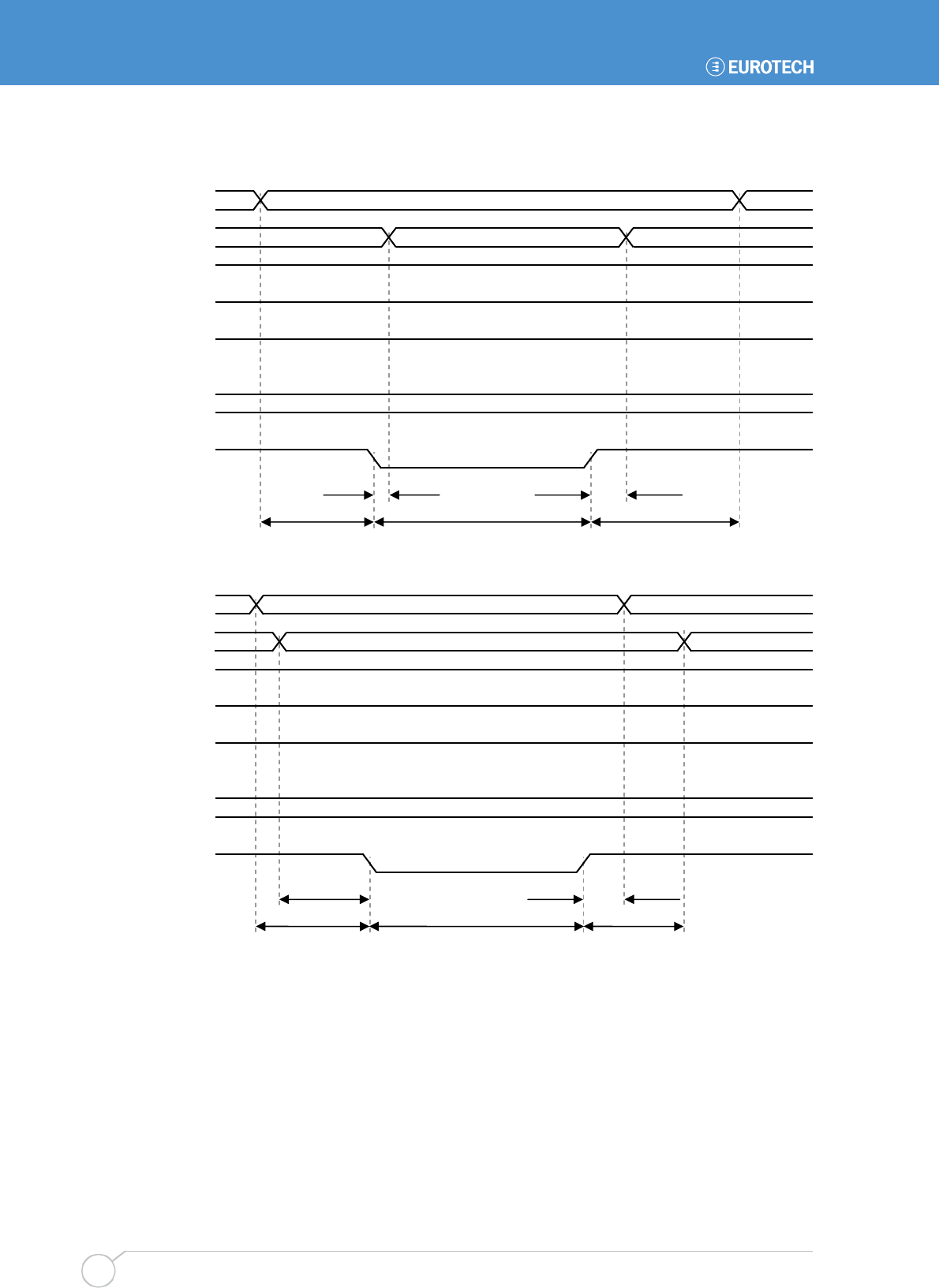
PC/104 8-bit I/O read access cycle
PC/104 8-bit I/O write access cycles
* = PC/104 add-on-board dependant
1
80
n
s
*
2
33
n
s
3
4
5
n
s
*
A<0:15>
DATA
IOCS16
SBHE
IOCHRDY
AEN
BALE
IOR
VALID
VALID
1
80
n
s
1
5
7n
s
3
41n
s
144n
s
*
A<0:15>
DATA
IOCS16
SBHE
IOCHRDY
AEN
BALE
IOW
VALID
VALID
Detailed hardware description
Issue D 31
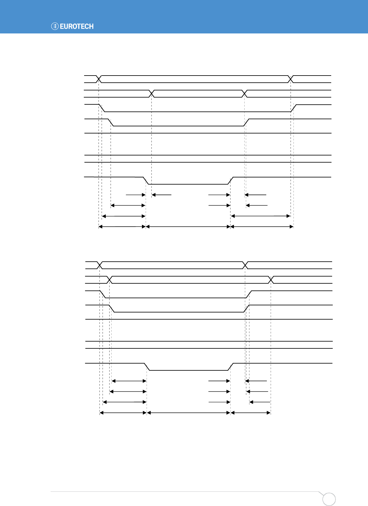
PC/104 16-bit I/O read access cycle
PC/104 16-bit I/O write access cycles
* = PC/104 add-on-board dependant
1
9
1n
s
*
*
3
4
0
n
s
*
14
3
n
s
*
65
n
s
24
5
n
s
A<0:15>
DATA
IOCS16
SBHE
IOCHRDY
AEN
BALE
IOR
VALID
VALID
1
9
1n
s
14
3
n
s
336
n
s
65
n
s
1
5
1n
s
* *
6
1n
s
1
53
n
s
A<0:15>
DATA
IOCS16
SBHE
IOCHRDY
AEN
BALE
IOW
VALID
VALID

TITAN user manual
Issue D
32
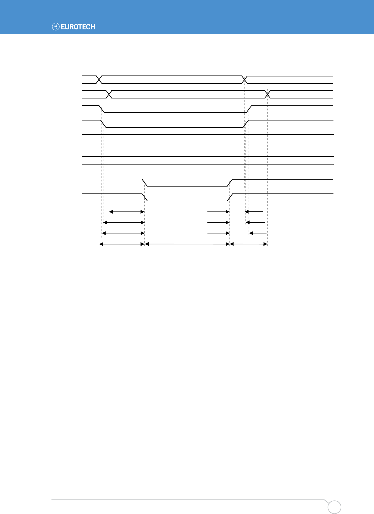
PC/104 8-bit memory read access cycle
8-bit memory read access cycles are not supported by the PXA270 PCMCIA controller
for common memory space.
PC/104 8-bit memory write access cycle
PC/104 16-bit memory read access cycle
227n
s
1
59
n
s
1
85
n
s
33
2n
s
85
n
s
A<0:23>
DATA
IOCS16
SBHE
IOCHRDY
AEN
BALE
MEMW
SMEMW
VALID
VALID
1
8
7n
s
*
*
3
4
0
n
s
*
1
63
n
s
*
65
n
s
241n
s
A<0:23>
DATA
IOCS16
SBHE
IOCHRDY
AEN
BALE
MEMR
SMEMR
VALID
VALID
Detailed hardware description
Issue D 33
PC/104 16-bit memory write access cycles
* = PC/104 add-on-board dependant
1
83
n
s
14
3
n
s
336
n
s
65
n
s
1
6
7n
s
* *
6
1n
s
1
53
n
s
A<0:23>
DATA
IOCS16
SBHE
IOCHRDY
AEN
BALE
MEMW
SMEMW
VALID
VALID

TITAN user manual
Issue D
34
PC/104 interrupts
The PC/104 interrupts are combined together in the TITAN hardware. When an interrupt
is received on the PC/104 interface, the hardware generates an interrupt on pin GPIO 17
(active high) of the PXA270 processor.
The PC/104 interrupting source can be identified by reading the PC104_IRQ registers
I1_REG and I2_REG located at addresses 0x12800000 and 0x01800000 respectively.
The registers indicate the status of the interrupt lines at the time the register is read. The
relevant interrupt has its corresponding bit set to ‘1’. The PXA270 is not designed to
interface to 8-bit peripherals, so only the least significant byte from the word contains the
data.
PC/104 interrupt register 1 [I1_REG]
Byte lane Most significant byte Least significant byte
Bit 15 14 13 12 11 10 9 8 7 6 5 4 3 2 1 0
Field - - - - - - - - IRQ12IRQ11IRQ10 IRQ7 IRQ6 IRQ5 IRQ4 IRQ3
Reset X X X X X X X X 0 0 0 0 0 0 0 0
R/W - - - - - - - - R/W
Address 0x12800000
PC/104 interrupt register 2 [I2_REG] (not available under Windows CE)
Byte lane Most significant byte Least significant byte
Bit 15 14 13 12 11 10 9 8 7 6 5 4 3 2 1 0
Field - - - - - - - - - - - - - IRQ15IRQ14 IRQ9
Reset X X X X X X X X 0 0 0 0 0 0 0 0
R/W - - - - - - - - R R/W
Address 0x11800000
PC/104 IRQ9, IRQ14 and IRQ15 are not available under Windows CE as all
interrupt sources are fully utilised.
Once the PXA270 microprocessor has serviced a PC/104 interrupt, the corresponding
add-on-board clears the interrupt by driving the IRQ signal low. When the TITAN
hardware sees the interrupt go low the corresponding bit is automatically cleared from
the I1_REG or I2_REG register.
If no further interrupts are pending the TITAN hardware drives GPIO 17 low once the
interrupt has been cleared at the source.
TL
Detailed hardware description
Issue D 35
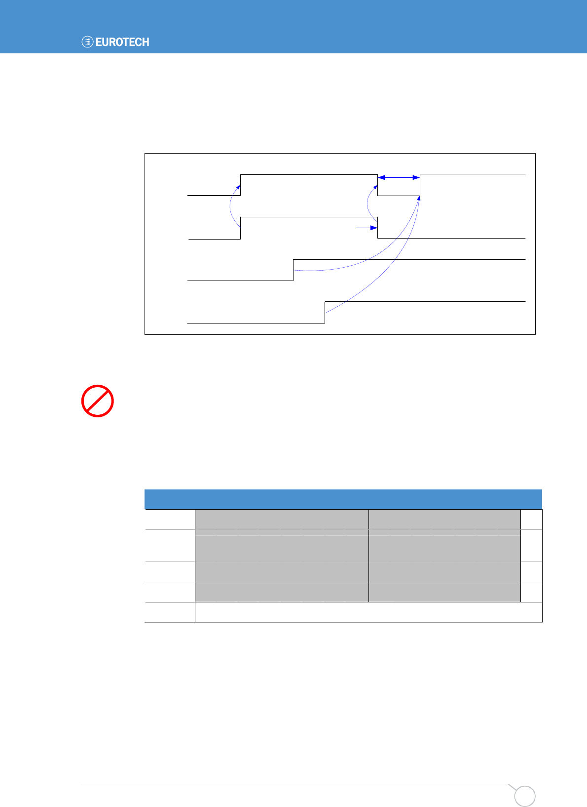
In cases where other PC/104 IRQs are asserted while the driver is processing a PC/104
IRQ, the TITAN drives GPIO 17 low for 375ns to 500ns once this interrupt has been
cleared. This short low pulse indicates to the PXA270 that there is another pending
interrupt. This situation is shown in the following diagram:
GPIO17
Delay:
375-500ns
PC104_IRQ3
PC104_IRQ6
PC104_IRQ4
Driver clears IRQ3 at source.
Bit 0 (IRQ3) cleared in I1_REG
automatically on falling edge.
Driver processing IRQ4
due to priority over IRQ6
Driver processing IRQ3
PC/104 reset
The reset generated to the PC/104 add-on board is a combination of the nRESET_OUT#
pin of the PXA270 and the status of the PC104_RST bit of the control register C_REG.
To reset PC/104 add-on boards independently from the global TITAN board reset, set the
PC104_RST bit to ’1’ in the C_REG register located at the address 0x13000000. To clear
the PC/104 reset, write a ‘0’ to the PC104_RST bit.
PC/104 reset register [C_REG]
Byte lane Most significant byte Least significant byte
Bit 15 14 13 12 11 10 9 8 7 6 5 4 3 2 1 0
Field - - - - - - - - - - - - - - - PC104
_RST
Reset X X X X X X X X X X X X X X X 0
R/W - - - - - - - - R/W
Address 0x13000000
TL

TITAN user manual
Issue D
36
Unsupported PC/104 interface features
The TITAN does not support the following PC/104 bus features:
• DMA is not supported. Therefore, AEN signal is set to a constant logical zero.
• Bus mastering is not supported. Therefore, do not connect any other master add-on
board to the TITAN PC/104 interface.
• Shared interrupts are not supported. Therefore, do not connect more than one
add-on board to the same interrupt signal line.
• BALE signal is set to a constant logical one as the address is valid over the entire
bus cycle. Only add-on PC/104 boards that implement transparent latch on address
lines LA17-LA23 are compatible with the TITAN implementation of BALE.
• The PXA270 PCMCIA memory controller does not support 8-bit memory read
accesses for common memory space.
• The PXA270 PCMCIA memory controller does not support PC/104 MEMCS# signal,
so there is no support for dynamic bus sizing.
• PC/104 IRQ9, IRQ14 and IRQ15 are not available under Windows CE.
Flat panel display support
The PXA270 processor contains an integrated LCD display controller. It is capable of
supporting both colour and monochrome single- and dual-scan display modules. It
supports active (TFT) and passive (STN) LCD displays up to 800x600 pixels.
The PXA270 can drive displays with a resolution up to 800x600, but as the PXA270 has
a unified memory structure, the bandwidth to the application decreases significantly. If the
application makes significant use of memory, such as when video is on screen, you may
also experience FIFO under-runs causing the frame rates to drop or display image
disruption. Reducing the frame rate to the slowest speed possible gives the maximum
bandwidth to the application. The display quality for an 800x600 resolution LCD is
dependant on the compromises that can be made between the LCD refresh rate and the
application. The PXA270 is optimized for a 640x480 display resolution.
A full explanation of the graphics controller operation can be found in the Intel PXA27x
Processor Family Developer’s Manual included on the support CD.
The flat panel data and control signals are routed to J4. See the section J4 – LCD
connector, page 68, for pin assignment and part number details.
The ZEUS-FPIF interface board allows the user to easily wire up a panel using pin and
crimp style connectors (see page 88). Contact Eurotech (see Eurotech Group Worldwide
Presence, page 101) for purchasing information for the ZEUS-FPIF. Alternatively, the
display interface is connected to an LVDS interface (see the section LVDS interface,
page 41). The LVDS interface provides useful when displays need to be located more
than 300mm (12") from the TITAN.
The following tables provide a cross-reference between the flat panel data signals and
their function, when configured for different displays.
Detailed hardware description
Issue D 37
TFT panel data bit mapping to the TITAN
The PXA270 can directly interface to 18-bit displays, but from a performance
point of view it is better to use 16-bits only. 18-bit operation requires twice the
bandwidth of 16-bit operation.
The following table shows TFT panel data bit mapping to the TITAN:
Panel data bus bit 18-bit TFT 12-bit TFT 9-bit TFT
FPD 15 R5 R3 R2
FPD 14 R4 R2 R1
FPD 13 R3 R1 R0
FPD 12 R2 R0 -
FPD 11 R1 - -
GND R0 - -
FPD 10 G5 G3 G2
FPD 9 G4 G2 G1
FPD 8 G3 G1 G0
FPD 7 G2 G0 -
FPD 6 G1 - -
FPD 5 G0 - -
FPD 4 B5 B3 B2
FPD 3 B4 B2 B1
FPD 2 B3 B1 B0
FPD 1 B2 B0 -
FPD 0 B1 - -
GND B0 - -
TITAN user manual
Issue D
38
STN panel data bit mapping to the TITAN
Panel data bus bit Dual scan colour STN Single scan colour STN Dual scan mono STN
FPD 15 DL7(G) - -
FPD 14 DL6(R) - -
FPD 13 DL5(B) - -
FPD 12 DL4(G) - -
FPD 11 DL3(R) - -
FPD 10 DL2(B) - -
FPD 9 DL1(G) - -
FPD 8 DL0(R) - -
FPD 7 DU7(G) D7(G) DL3
FPD 6 DU6(R) D6(R) DL2
FPD 5 DU5(B) D5(B) DL1
FPD 4 DU4(G) D4(G) DL0
FPD 3 DU3(R) D3(R) DU3
FPD 2 DU2(B) D2(B) DU2
FPD 1 DU1(G) D1(G) DU1
FPD 0 DU0(R) D0(R) DU0
The table below explains the clock signals required for passive and active type displays:
TITAN
Active display signal
(TFT)
Passive display signal
(STN)
PCLK Clock Pixel clock
LCLK Horizontal sync Line clock
FCLK Vertical sync Frame clock
BIAS DE (Data Enable) Bias

Detailed hardware description
Issue D 39
LCD logic and backlight power
The display signals are +3.3V compatible. The TITAN contains power control circuitry for
the flat panel logic supply and backlight supply. The flat panel logic is supplied with a
switched +3.3V (default) or +5V supply (see the section LCD supply voltage jumper –
LK2 on JP2, page 79, for details). The backlight is supplied with a switched +5V supply
for the inverter.
There is no on-board protection for these switched supplies! Care must be taken
during power up/down to ensure the panel is not damaged due to the input
signals being incorrectly configured.
The PXA270 GPIO 101 pin controls the supply voltage for the LCD display.
LCDEN
(GPIO 101) Selected LCD function
0 LCDSAFE power off (default)
1 LCDSAFE 3.3V/5V power on
The LCD supply may be changed to 5V by moving the jumper position of JP2,
see section LCD supply voltage jumper – LK2 on JP2, page 79, for details. If the
flat panel logic is powered from 5V, it must be compatible with 3.3V signalling,
please check the LCD panel datasheet for details.
The PXA270 GPIO 19 pin (BKLEN signal) controls the supply voltage for the backlight
inverter.
BKLEN
(GPIO 19) Selected backlight function
0 BKLSAFE power off (default)
1 BKLSAFE 5V power on
The BLKEN signal is routed (un-buffered) to connector J4. See the section J4 – LCD
connector, page 68, for J4 pin assignment and connector details.
If you want to use a 12V backlight inverter, then the switched 5V supply on
BLKSAFE or the control signal BLKEN can be used to control an external 12V
supply to the inverter.
TITAN user manual
Issue D
40
Typically the following power up sequence is as follows (please check the datasheet for
the particular panel in use):
1 Enable display VCC.
2 Enable flat panel interface.
3 Enable backlight.
Power down is in reverse order.
LCD backlight brightness control
GPIO 16 of the PXA270 processor is used for backlight brightness control (signal PWM0
on J4 connector). The control of the backlight brightness is dependant upon the type of
backlight inverter used in the display. Some inverters have a ‘DIM’ function, which uses a
logic level to choose between two levels of intensity. If this is the case then GPIO 16
(alternative function 0) is used to set this. Other inverters have an input suitable for a
pulse-width modulated signal or analogue voltage control. In this case GPIO 16 should
be configured as PWM0 (alternative function 2).
When a PWM signal is required the PWM0 signal must be passed through a low pass
filter. The ZEUS-FPIF board provides a low pass filter for this function (see page 88).
Contact Eurotech (see Eurotech Group Worldwide Presence, page 101) for purchasing
information for the ZEUS-FPIF.
STN BIAS voltage
The TITAN can provide a negative and a positive bias voltage for STN type displays. The
negative and positive bias voltages are set to -22V and +22V respectively. Pin
connections for these can be found in section J4 – LCD connector, page 68.
BIAS_EN
(GPIO 82) Selected backlight function
0 NEGBIAS & POSBIAS power off (default)
1 NEGBIAS & POSBIAS power on
Please contact Eurotech for details of other bias voltages. Contact details are provided in
Eurotech Group Worldwide Presence, page 101.
Do not exceed a 20mA load current.

Detailed hardware description
Issue D 41
LVDS interface
There is an optional Low-Voltage Differential Signalling (LVDS) interface available on the
TITAN. LVDS combines high data rates with low power consumption. The benefits of
LVDS include low-voltage power supply compatibility, low noise generation, high noise
rejection and robust transmission signals.
The National Semiconductor transmitter DS90C363 is used to convert 16 bits of LCD
data signals into three LVDS data streams. A phase-locked transmit clock is transmitted
in parallel with the data streams over a fourth LVDS link. The LVDS signals are routed to
the connector J8. For connector details see the section J8 – LVDS connector, page 71.
The LVDS transmitter is enabled using the signal LVDS_EN (GPIO 21). Details are
shown in the following table:
LVDS_EN
(GPIO 21) Selected LVDS function
0 LVDS power down (default)
1 LVDS enable
The LVDS transmitter can be programmed for rising edge strobe or falling edge
strobe operation through a signal LVDS_FES# (GPIO 27). This is shown below:
LVDS_FES#
(GPIO 27) Selected LVDS function
0 Falling edge strobe
1 Rising edge strobe (default)
If the FPIF-LVDS-TX is to be connected directly to an LVDS display via the Hirose
connector J2, then this link selects the displays LVDS Receiver input map. Fitting or not
fitting a jumper to JP3 sets J2 pin 20 (MSL) to 3.3V or GND (default) respectively.
When the LVDS interface is used, connector LK3 on JP3 should be set to the
correct setting for the display. See section LVDS mode select [MSL] jumper –
LK3 on JP3, page 79, for details. Please consult the manual of your LVDS
display for which setting to use for the National Semiconductor DS90C383 LVDS
Transceiver.
Connector J4 should be used to supply the power and brightness control for the
backlight inverter when the LVDS interface is used. See the section J4 – LCD
connector, page 68, for J4 pin assignment and connector details.
TL

TITAN user manual
Issue D
42
Audio
The Wolfson WM9712L AC’97audio CODEC is used to support the audio features of the
TITAN. Audio inputs supported by the WM9712L are a stereo line in and a mono
microphone input.
The WM9712L provides a stereo line out that can also be amplified by the National
Semiconductor LM4880 250mW per channel power amplifier. This amplifier is suitable for
driving an 8Ω load.
The WM9712L AC’97 CODEC may be turned off if it is not required. See the section
Audio power management, page 62, for details.
Connection to the TITAN audio features is via header J6. See the table below for pin
assignments and section J6 – Audio connector, page 69, for connector and mating
connector details.
Function Pin Signal Signal levels (max)
Frequency
response (Hz)
10 MIC input
Microphone 9
7
MIC voltage reference output
Audio ground reference
1Vrms 20 – 20k
1 Line input left
5 Line input right
Line in
3 Audio ground reference
1Vrms 20 – 20k
2 Line output left
6 Line output right
Line out
4 Audio ground reference
1Vrms 20 – 20k
8 Amp output left
11 Amp output right
Amp out
12 Audio ground reference
1.79V peak,
1.26Vrms
(8Ω load) 223mW
20 – 20k
Touchscreen controller
The TITAN supports 4-wire and 5-wire resistive touchscreens using the touchscreen
controller available on the Wolfson WM9712L audio CODEC. The touchscreen controller
supports the following functions:
• X co-ordinate measurement.
• Y co-ordinate measurement.
• Pen down detection with programmable sensitivity.
• Touch pressure measurement (4-wire touchscreen only).
A touchscreen can be used as a wake-up source for PXA270 from sleep mode.
The touchscreen interface is broken out on the header J5. See J5 – Touchscreen
connector, page 69, for connector and mating connector details.
TL
TL
Detailed hardware description
Issue D 43
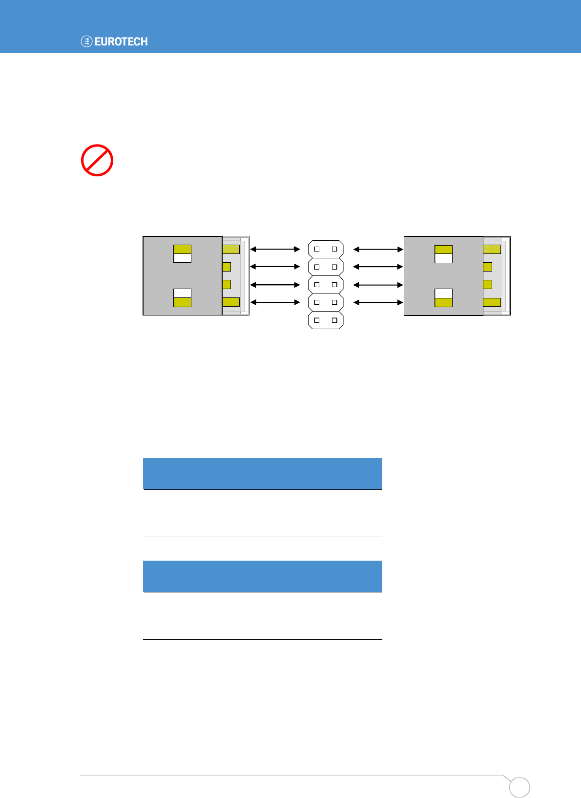
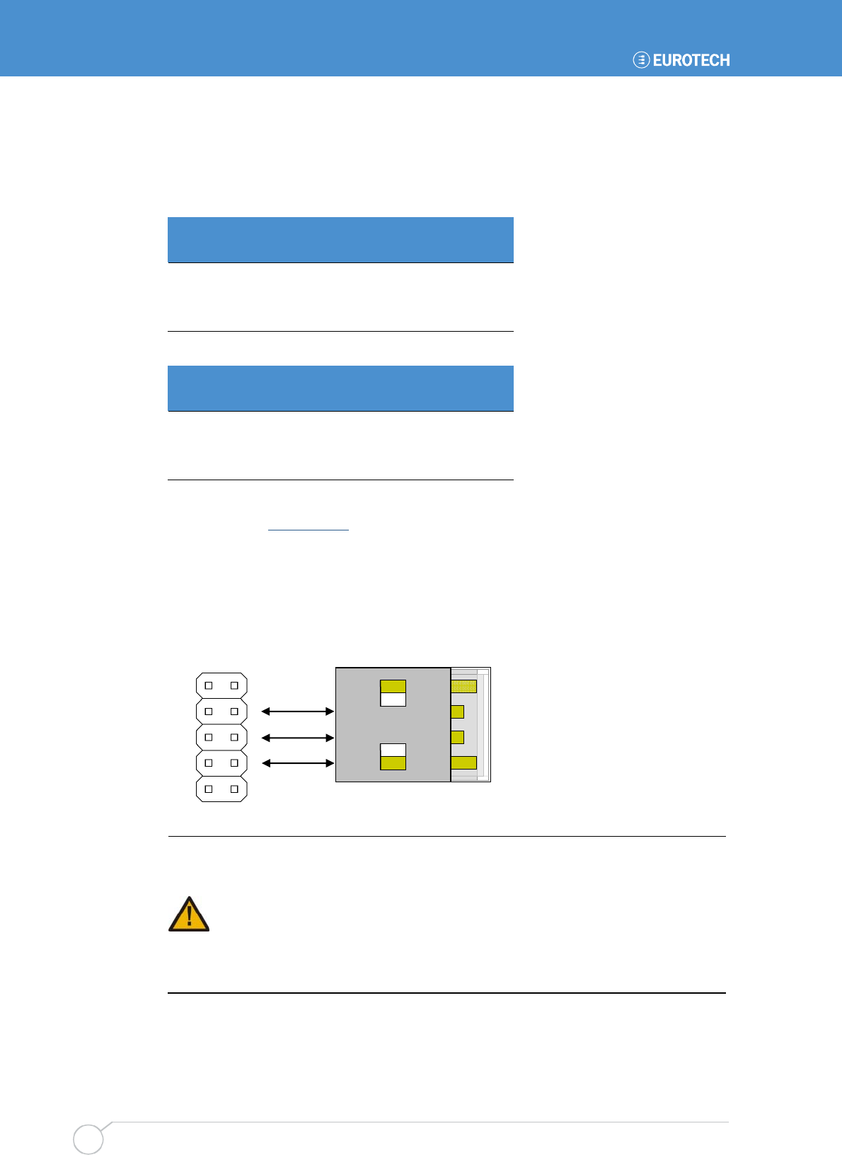
USB
USB host
There are two USB host interfaces on the TITAN. These comply with the Universal Serial
Bus Specification Rev. 1.1, supporting data transfer at full-speed (12Mbps) and low-
speed (1.5Mbps).
There are four signal lines associated with each USB channel: VBUS, DATA+, DATA and
GND. Their arrangement is summarized in the illustration below:
A USB power control switch controls the power and protects against short-circuit
conditions.
If the USB voltage is short-circuited, or more than 500mA is drawn from either supply, the
switch turns the power supply off and automatically protects the device and board. If an
over current condition occurs on a USB channel, the over current condition is flagged to
GPIO 88 and GPIO 114 for USB channel 1 and channel 2 respectively. This is shown in
the following tables:
USB_OC1
(GPIO 889) Selected LVDS function
0 USB VBUS1 over current
1 USB VBUS1 normal
USB_OC2
(GPIO 114) Selected LVDS function
0 USB VBUS2 over current
1 USB VBUS2 normal
1
2
3
4
1
2
3
4
1 2
10 (SHIELD)
(SHIELD) 9
VBUS 1
DATA- 1
DATA+ 1
GND
VBUS 2
DATA- 2
DATA+ 2
GND
USB connector 1 USB connector 2
J10
TL
TITAN user manual
Issue D
44
The VBUS power supplies are derived from VCC_PER (+5V) which is an isolated +5V
supply switched under hardware control from the VCC input on J15 pin 1. GPIO 89 and
GPIO 22 control the power to VBUS1 and VBUS2 respectively. This is shown in the
following tables:
USB_PWE1
(GPIO 89) Selected LVDS function
0 USB VBUS1 power off (default)
1 USB VBUS1 power on
USB_PWE2
(GPIO 22) Selected LVDS function
0 USB VBUS2 power off (default)
1 USB VBUS2 power on
More information about the USB bus and the availability of particular USB peripherals
can be found at www.usb.org.
USB client
The TITAN USB host port 2 can be configured under software to be a client.
The following diagram shows the connection between PL17 and a USB type A connector:
Do NOT attempt to power the TITAN using the VBUS 1 or VBUS 2 pins!
VBUS 1 and VBUS 2 are isolated +5V supplies switched under hardware control
from VCC_PER.
ALWAYS use the USB client cable provided with the development kit. This cable
does not provide power down the cable and avoids reverse powering the TITAN
from a USB host when the TITAN has no power on the VCC input on J15 pin 1.
Reverse powering the TITAN from the VBUSn pins can make the TITAN operate
erratically and may cause serious damage to the TITAN.
1
2
3
4
1 2
10 (SHIELD)
9
DATA- 2
DATA+ 2
GND
USB connector type A
J10

Detailed hardware description
Issue D 45
Ethernet
The TITAN SBC provides a single 10/100-BaseTX interface with MAC and complies with
both the IEEE802.3u 10/100-BaseTX and the IEEE 802.3x full-duplex flow control
specifications.
A single Davicom DM9000A Ethernet controller is used to implement the Ethernet
interface on the TITAN. The DM9000A device provides an embedded PHY and MAC and
connects to the 10/100-BaseTX magnetics. The DM9000A also supports the AUTO-MDIX
feature. Configuration data and MAC information are stored in an external serial
EEPROM (93LC46).
The DM9000A device is connected to the PXA270 data bus (16-bit), and is memory
mapped. Connection to the TITAN Ethernet port is via header J11. See J11 –
10/100BaseTX Ethernet connector, page 72, for pin assignment and connector details.
A second header J12 provides the speed and link status LED signals. See J12 – Ethernet
status LEDs connector, page 73, for pin assignment and connector details. The output
lines sink current when switched on, therefore the anode of each LED should be
connected to pins 1 and 3 of J12 and the cathode to the appropriate status line.
The link LED illuminates when a 10 or 100base-T link is made, and the speed LED
illuminates when 100Mbps speed is selected.
The Ethernet Breakout interface board provides the user with an RJ45 connector with
LEDs to connect an Ethernet cable to the TITAN (see page 96). Contact Eurotech (see
Eurotech Group Worldwide Presence, page 101) for purchasing information for the
Ethernet Breakout.
TITAN user manual
Issue D
46
Serial COMs ports
There are five high-speed, fully functionally compatible 16550 serial UARTs on the
TITAN. Four of these channels can be used as RS232 serial interfaces, and the
remaining one, COM5, can be configured as RS422 or RS485.
Connection to the TITAN COMs ports is via header J1. See section J1 – COMS ports,
page 66, for connector and mating connector details.
Port Address IRQ
FIFO depth
RX / TX Signals
COM1 0x40100000 –
0x4010002C
Internal 64 / 64 RS232 Rx, Tx, CTS, RTS, RI,
DSR, DCD, DTR
COM2 0x40200000 –
0x4020002C
Internal 64 / 64 RS232 Rx, Tx, RTS, CTS
COM3 0x40700000 –
0x4070002C
Internal 64 / 64 RS232 Rx, Tx
COM4 0x10000010 –
0x1000001E
GPIO 10 128 / 128 RS232 Rx, Tx, CTS, RTS, RI,
DSR, DCD, DTR
COM5 0x10000000 –
0x1000000E
GPIO 11 128 / 128 RS422 / RS485 Tx, Rx
Please see the Developer’s Manual for details of internal interrupts.
COM1 – RS232 interface
Uses the Full Function UART in the PXA270 (FFUART). The port is buffered to RS232
levels with ±15kV ESD protection, and supports full handshaking and modem control
signals. The maximum baud rate on this channel is 921.6kbps.
A factory fit option configures COM1 as TTL Level signals to interface to a modem.
Please contact Eurotech for details. Contact details are provided in Eurotech Group
Worldwide Presence, page 101.
COM2 – RS232 interface
Uses the Bluetooth UART in the PXA270 (BTUART). The port is buffered to RS232 levels
with ±15kV ESD protection, and supports full handshaking and modem control signals.
The maximum baud rate on this channel is 921.6kbps.
COM3 – RS232 interface
Uses the Standard UART in the PXA270 (STUART). The port is buffered to RS232 levels
with ±15kV ESD protection, and supports full handshaking and modem control signals.
The maximum baud rate on this channel is 921.6kbps.
TL
TL
Detailed hardware description
Issue D 47
COM4 – RS232 interface
The COM4 RS232 interface is supported on channel 0 of an Exar XR16C2850 with 128
bytes of Tx and Rx FIFOs, and buffered to RS232 levels with ±15kV ESD protection. The
maximum baud rate on this channel is 921.6kbps.
COM5 – RS422/485 interface
The COM5 RS422/485 interface is supported on channel 1 of an Exar XR16C2850 with
128 bytes of Tx and Rx FIFOs, and buffered to RS422/485 levels with ±15kV ESD
protection. The maximum baud rate on this channel is 921.6kbps.
Two GPIOs from the PXA270 provide RS422/RS485 selection and termination resistor
selection options. The two control signals are SEL_485# on GPIO 81 and SEL_TERM on
GPIO 115. This is shown in the following table:
SEL_485# (GPIO 81) Selected COM5 function
0 RS485 half duplex
1 RS422 full duplex [default]
SEL_RS485# is at logic ‘1’ upon reset.
The control signal SEL_TERM is used to enable/disable the RS422/485 line termination
and must be enabled if the TITAN board is at the end of the network. This is shown in the
following table:
SEL_TERM (GPIO 115) COM5 termination resistors (120Ω)
0 Disconnected
1 Connected [default]
SEL_TERM is at logic ‘1’ upon reset.
The RS485/422 driver (LTC2859) on the TITAN features a logic-selectable reduced slew
mode, which softens the driver output edges to control the high frequency EMI emissions
from equipment and data cables. The reduced slew rate mode is entered by taking the
SLO# pin low, where the data rate is limited to about 250kbps. Slew limiting also
mitigates the adverse effects of imperfect transmission line termination caused by stubs
or mismatched cables. The following table illustrates the selectable slew rates:
REDUCED_SLEW#
(GPIO 83) Slew rate
0 Reduced
1 Normal
TL
TL

TITAN user manual
Issue D
48
RS422
The RS422 interface provides full-duplex communication. The signals available are TXA,
TXB, RXA, RXB and Ground. The maximum cable length for an RS422 system is 4000ft
(1200m) and supports 1 transmitter and up to 10 receivers.
RS485
This is a half-duplex interface that provides combined TX and RX signals. On J1, pin 5
provides TXB/RXB and pin 6 provides TXA/RXA. A ground connection is also required for
this interface. The maximum cable length for this interface is the same as for RS422
(4000ft), but RS485 supports up to 32 transmitters and receivers on a single network.
Only one transmitter should be switched on at a time.
The TITAN uses the RTS signal to control transmission. When this signal is at logic ‘1’ the
driver is switched off and data can be received from other devices. When the RTS line is
at logic ‘0’ the driver is on. Any data that is transmitted from the TITAN is automatically
echoed back to the receiver. This enables the serial communications software to detect
that all data has been sent, and disable the transmitter when required. The UART used
on the TITAN for COM5 has extended features including auto-RTS control for RS485.
This forces the RTS signal to change state (and therefore the direction of the RS485
transceivers) when the last bit of a character has been sent onto the wire. Please refer to
the XR16C2850 datasheet on the Development Kit CD for more information.
The RS422/485 cable shield MUST be connected between TITAN J1 pin 9 (GND)
and the ground connection of the connecting equipment. Failure to do so can
result in TITAN RS422/485 transceiver being permanently damaged.
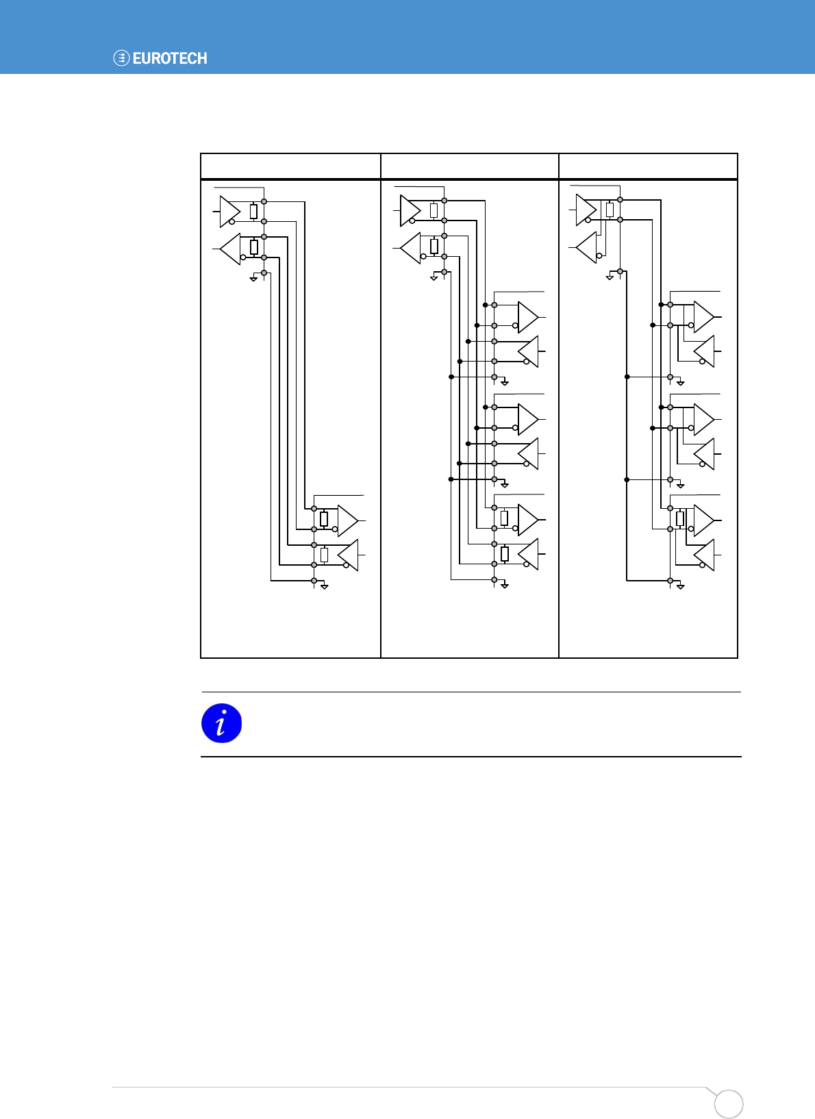
Detailed hardware description
Issue D 49
Typical RS422 and RS485 connection
Only set SEL_TERM to logic high if the TITAN is at the end of the network.
RS485 MULTI-DROPRS422 POINT-TO-POINT RS422 MULTI-DROP
Number of wires 5
Transmitters enabled always
Receivers enabled always
Duplex mode full
SEL_485# HIGH
Number of wires 5
Transmitters enabled active RTS
Receivers enabled always
Duplex mode full
SEL_485# HIGH
Number of wires 3
Transmitters enabled active RTS
Receivers enabled always
Duplex mode half
SEL_485# LOW
TITAN user manual
Issue D
50
I²C
The PXA270 I²C interface is brought out to the COMs connector J1. See the section J1 –
COMS ports, page 66, for connection details.
The I²C bus is also used with the Quick Capture interface. See the section Quick Capture
camera interface, page 51, for more information.
The following table lists the on-board I²C devices:
Device name I²C address
External GPIO (MAX7313) 0x20
Temperature sensor (LM75A) 0x48
RTC (ISL1208) 0x6F
Config PROM (24AA01) 0x50-0x57
The I²C unit supports a fast mode operation of 400kbps and a standard mode of
100kbps.
Fast mode devices are downward compatible and can communicate with standard mode
devices in a 0 to 100kbps I²C bus system. However, standard mode devices are not
upward compatible, so they should not be incorporated in a fast mode I²C bus system as
they cannot follow the higher transfer rate and unpredictable states would occur.
The I²C unit does not support the hardware general call, 10-bit addressing, high-
speed mode (3.4Mbps) or CBUS compatibility.
You must keep bus loads added by the Quick Capture camera, and any other
devices added to the serial communications connector, below 140pF.
Ensure any other devices added to the I²C interface do not have the same
addresses as detailed in the table above.

Detailed hardware description
Issue D 51
Quick Capture camera interface
The Quick Capture interface is a component of Intel® Quick Capture technology which
provides a connection between the PXA270 processor and a camera image sensor. The
Quick Capture interface is designed to work primarily with CMOS-type image sensors
and supports resolutions up to 4 mega pixels. However, it may be possible to connect
some CCD-type image sensors to the PXA27x processor, depending on the specific CCD
sensor’s interface requirements.
The Quick Capture interface acquires data and control signals from the image sensor
and performs the appropriate data formatting prior to routing the data to memory using
direct memory access (DMA). A broad range of interface and signalling options provides
direct connection. The image sensor can provide raw data through a variety of parallel
and serial formats. For sensors that provide pre-processing capabilities, the Quick
Capture interface supports several formats for RGB and YCbCr colour space.
The Quick Capture interface signals are connected to the header J2. An I2C interface is
available on the same header since most of the camera image sensors require an I2C
control interface. For connector details see the section J2 – Camera interface connector,
page 67.

TITAN user manual
Issue D
52
General purpose I/O
A Maxim MAX7313 I²C I/O expander provides sixteen general purpose input/output lines
on header J3. Each I/O port can be individually configured as either an open-drain
current-sinking output rated at 50mA with a 10K pull-up to +5V (VCC_PER), or a logic
input with transition detection. The MAX7313 supports hot insertion and all inputs are
+5V tolerant.
The MAX7313 can configure outputs for PWM current drive. The MAX7313 includes an
internal oscillator, nominally 32kHz, to generate PWM timing for LED intensity control.
PWM intensity control can be enabled on an output-by-output basis, allowing the
MAX7313 to provide any mix of PWM LED drives and glitch-free logic outputs. PWM can
be disabled entirely, in which case all output ports are static and the MAX7313 operating
current is the lowest because the internal oscillator is turned off.
The I/O Expander is addressable at I²C serial bus address 0x20 and is accessed in fast-
mode operation at 400kbps. On power-up all control registers are reset and the
MAX7313 enters standby mode. Power-up status makes all ports into inputs, so the state
of all 17 ports (P0-P16) is logic high (through 10K pull-up to 5V).
See the section J3 – GPIO connector, page 67, for connector pinout and mating
connector details. The signals on J3 correspond to the pin names of the MAX7313
(P0-P15).
Port 16 of the MAX7313 is configured as an interrupt, so that any I/O Expander GPIO pin
configured as an input can cause the PXA270 to be interrupted on GPIO116. These can
also be used as PXA270 wake-up sources from sleep mode.
Temperature sensor
There is a Philips LM75A temperature sensor on the TITAN. The LM75A is a
temperature-to-digital converter using an on-chip band-gap temperature sensor and
Sigma-delta A-to-D conversion technique. The device is also a thermal detector providing
an over-temperature detection output (OVERTEMP signal on GPIO 12), which can be
used to wake the PXA270 up from sleep. The accuracy of LM75A is ±2oC (at -25oC to
1000C), and ±3oC (at -55oC to 1250C). The LM75A is connected to the I2C bus of the
PXA270 processor, and is accessible at I2C bus address 0x48.
PXA270 MAX7313 J7
P16 (GPIO116)
I²C
VCC_PER
10k
+3.3V
10k
P[0-15]

Detailed hardware description
Issue D 53
JTAG and debug access
Debug access to the PXA270 processor is via the JTAG connector J9. See J9 – JTAG
connector, page 71, for details.
Jumper JP6 needs to be inserted to enable the JTAG interface for PXA270 debug. See
section JP6 – JTAG enable, page 77 for details.
The Macraigor Wiggler and EPI MajicMX probe have been used to debug the PXA270
processor on the TITAN. There are many other debug tools that can be interfaced to the
TITAN for access to the JTAG Interface of the PXA270 processor.
The tables below detail the pins connections between the TITAN and Macraigor Wiggler
or EPI MajicMX debug tools. Of the Wiggler and MajicMX debug tools the Wiggler provides
the best low cost solution.
TITAN JTAG connections
TITAN J9 Debug tools pin names
Pin Name Description MajicMX Wiggler
1 VCC3
3.3V Supply pin to JTAG debug
tool VTRef, VSupply Vref, VTarget
3 GND Ground reference GND GND
4 nTRST PXA270 JTAG interface reset nTRST nTRST
6 TDI JTAG test data input to the
PXA270 TDI TDI
7 TDO
JTAG test data output from the
PXA270 TDO TDO
8 TMS PXA270 JTAG test mode select TMS TMS
9 TCK PXA270 JTAG test clock TCK TCK
10 SRST System reset nSRST nSRST
2, 5 NC No Connect - -
- - Not required on TITAN. RTCLK RTCK
- - Not required on TITAN DBGREQ DBGRQ
- - Not supported by TITAN DBGACK DBGACK
In order to access the PXA270, your JTAG software needs to know the details of
the two CPLDs on the TITAN. The latest version of the XC9536XL and XC9572XL
BSDL files for the 48-ball chip scale package can be found on the Xilinx web site.
TITAN user manual
Issue D
54
Power and power management
Power supplies
The TITAN is designed to operate from a single +5V ±5% (4.75V to +5.25V) supply. The
power connector J15 has a +12V connection defined, but is not required for the TITAN
under normal operation. It can be used to supply +12V to the PC/104 stack if required.
For details of the power connector please see the section J15 – Power connector, page
75.
On-board supplies
There are eleven on-board supply voltages derived from the VCC (+5V) supply. They are
listed in the following table:
Supply rail Power domains Voltage Reset threshold
VCC_BATT PXA270 sleep control subsystem,
oscillators and real time clock. 3.3V or 3.0V 2.25V
VCC_CORE PXA270 core and other internal units. 0.85V-1.55V 92% of nominal
VCC_PLL PXA270 phase-locked loops. 1.3V 1.2V
VCC_SRAM PXA270 internal SRAM units. 1.1V 1V
+3V3 PXA270 I/O, PXA270 internal units,
on-board peripherals. 3.3V 3.05V
VCC_PER
PC/104, Audio amp, USB power
switch, Video supplies (BKLSAFE /
LCDSAFE), STN bias circuit, External
GPIO.
5V (VCC) NA
VBUS 1 USB port 1 power. 5V (VCC_PER) NA
VBUS 2 USB port 2 power. 5V (VCC_PER) NA
LCD_SAFE LCD logic supply. 3.3V or 5V
(VCC_PER) NA
BKLSAFE LCD backlight supply. 5V (VCC_PER) NA
+2V8_CIF CIF Camera interface. 2.8V NA
The TITAN shall be reset if the supplies fall below the thresholds shown in the table.
VCC_CORE, VCC_PLL and VCC_SRAM rails are controlled by the PXA270 hardware
control signal PWR_EN. They are switched off when PXA270 is in sleep or deep-sleep
mode.
VCC_PER, +3V3 and +2V8_CIF supply rails are controlled by the PXA270 hardware
control signal SYS_EN. They are switched off when PXA270 is in deep-sleep mode.
VBUS 1 and VBUS 2 are controlled by the PXA270 software controlled signals
USB_PWE1 and USB_PWE2 respectively. They are switched off on power-on, reset,
sleep or deep-sleep.
Power and power management
Issue D 55
LCD_SAFE and BKLSAFE are controlled by the PXA270 software controlled signals
LCDEN and BKLEN respectively. They are switched off on power-on, reset, sleep or
deep-sleep.
Do NOT attempt to power the TITAN using the VCC_PER, VBUS 1 or VBUS 2
pins!
VCC_PER is an isolated +5V supply switched under hardware control from the
VCC input on J15 pin 1. ALWAYS provide +5V to VCC on J15 pin 1.
VBUS 1 and VBUS 2 are isolated +5V supplies switched under hardware control
from VCC_PER.
If J15 pin 4 is used to supply +12V to the PC/104 connector J13 pin B4. Do NOT
exceed 700mA supply current at 70°C (158°F) ambient, or 600mA at 85°C
(185°F) ambient.
If an LCD display is used, ensure the total current requirement on 3.3V does not
exceed 1.4A! Please check the datasheets of the devices you are using, as this
supply is not protected!
Power management IC
The Linear Technology LTC3445 is used to provide the power supply for PXA270. It is
specifically designed for the PXA27x family of microprocessors.
The LTC3445 contains a high efficiency buck regulator (VCC_CORE), two LDO
regulators (VCC_PLL, VCC_SRAM), a PowerPath controller and an I2C interface. The
buck regulator has a 6-bit programmable output range of 0.85V to 1.55V. The buck
regulator uses either a constant frequency of 1.5MHz, or a spread spectrum switching
frequency. Using the spread spectrum option (default set to 22.4%) gives a lower noise
regulated output, as well as low noise at the input. In addition, the regulated output
voltage slew rate is programmable via the Power Management I2C interface of the
PXA270.
TITAN user manual
Issue D
56
Battery backup
An on-board non-rechargeable battery (CR2032) provides battery backup supply for the
ISL1208 RTC and SRAM. An external battery (CR2032 or similar) may also be fitted. To
use an external battery see the section J15 – Power connector, page 75, for connection
details.
The table below shows the typical and maximum current load on the external battery:
Device load on battery Typical (µA) Maximum (µA)
On-board SRAM 0.5 3
ISL1208 RTC with clock out off 0.4 0.95
Supply supervisor 0.5 0.5
Total 1.4 4.45
Based on the worst-case figures of 4.45µA current consumption, a 220mAh CR2032
battery cell will backup the TITAN (whilst in continuous deep sleep) for > 5 years.
The TITAN does not provide a battery charging circuit.
If the TITAN is to be used at operating temperature
extremes, please be aware that if the battery cell is fitted
they are typically rated at -30˚C to +60˚C.
TL

Power and power management
Issue D 57
Processor power management
First available in the PXA270 processor, wireless Intel SpeedStep® technology
dynamically adjusts the power and performance of the processor based on CPU
demand. This can result in a significant decrease in power consumption.
In addition to the capabilities of Intel Dynamic Voltage Management, the Intel XScale
micro architecture of the PXA27x family incorporates three new low power states. These
are deep idle, standby and deep sleep. It is possible to change both voltage and
frequency on the fly by intelligently switching the processor into the various low power
modes. This saves additional power while still providing the necessary performance to
run rich applications.
Wireless Intel SpeedStep® technology includes the following features:
• Five reset sources: power on, hardware, watchdog, GPIO and exit from sleep and
deep sleep modes (sleep exit).
• Multiple clock speed controls to adjust frequency, including frequency change, turbo
mode, half-turbo mode, fast-bus mode, memory clock, 13M mode, A-bit mode and
AC ’97.
• Switchable clock source.
• Functional unit clock gating.
• Programmable frequency change capability.
• One normal operation power mode (run mode) and five low power modes to control
power consumption (idle, deep idle, standby, sleep and deep sleep modes).
• Programmable I2C-based external regulator interface to support changing dynamic
core voltage, frequency change and power mode coupling.
PXA270 power consumption depends on the operating voltage and frequency,
peripherals enabled, external switching activity and external loading and other factors.
The tables below contain the power consumption information at room temperature for
several operating modes: active, idle and low power modes. For active power
consumption data, no PXA270 peripherals are enabled except for UART.
Frequency
System bus
frequency
Active power
consumption
typ.
Idle power
consumption
typ.
Conditions
VCC_SRAM = 1.1V; VCC_PLL = 1.3V;
VCC_MEM, VCC_BB,
VCC_USIM, VCC_LCD = 1.8V;
VCC_IO, VCC_BATT,VCC_USB=3.0V
520 MHz 208 MHz 747 mW 222 mW VCC_CORE = 1.45V
416 MHz 208 MHz 570 mW 186 mW VCC_CORE = 1.35V
312 MHz 208 MHz 390 mW 154 mW VCC_CORE = 1.25V
312 MHz 104 MHz 375 mW 109 mW VCC_CORE = 1.1V
208 MHz 208 MHz 279 mW 129 mW VCC_CORE = 1.15V
104 MHz 104 MHz 116 mW 64 mW VCC_CORE = 0.9V
13 MHz CCCR[CPDIS]=1 44.2 mW - VCC_CORE = 0.85V

TITAN user manual
Issue D
58
PXA270 low power modes
Power consumption
typ.
Conditions
VCC_MEM, VCC_BB, VCC_USIM, VCC_LCD = 1.8V
VCC_IO, VCC_BATT, VCC_USB= 3.0V
13MHz idle mode (LCD on) 15.4mW VCC_CORE, VCC_SRAM, VCC_PLL = 0.85V
13MHz idle mode (LCD off) 8.5mW VCC_CORE, VCC_SRAM, VCC_PLL = 0.85V
Deep sleep mode 0.1mW VCC_CORE, VCC_SRAM, VCC_PLL = 0V
Sleep mode 0.16mW VCC_CORE, VCC_SRAM, VCC_PLL = 0V
Standby mode 1.72mW VCC_CORE, VCC_SRAM, VCC_PLL = 3.0V
Wake-up sources
The PXA270 offers two sleep modes:
• Sleep mode offers lower power consumption by switching off most internal units.
There is no activity inside the processor, except for the units programmed to retain
their state in the PSLR register, the real time clock and the clocks and power
manager. Because internal activity has stopped, recovery from sleep mode must
occur through an external or internal real time clock event. External wake-up sources
are GPIO<n> edge detects (they are listed in the section PXA270 GPIO pin
assignments, page 19).
• Deep-sleep mode offers the lowest power consumption by powering most units off.
There is no activity inside the processor, except for the real time clock (RTC) and the
clocks and power manager. Because internal activity has stopped, recovery from
deep-sleep mode must be through an external event or an RTC event. In deep-sleep
mode, all the PXA270 power supplies (VCC_CORE, VCC_SRAM, VCC_PLL, VCC_IO
excluding VCC_BATT) are powered off for minimized power consumption. On the
TITAN, the main +3.3V rail supplies the VCC_IO power domain of the PXA270. Since
the +3.3V supply is switched off in deep-sleep mode, all the on-board peripherals are
powered off and it is not possible to use external wake-up sources. In this situation,
recovery from deep-sleep mode must be through an internal RTC event.
For more information on PXA270 power management, see section 3.6 in the Intel
PXA27x Processor Family Developer’s Manual, included on the Development Kit CD.
Power and power management
Issue D 59
Peripheral devices power management
The following table gives the estimated power consumption of on-board peripherals:
Low power mode
On-board
peripheral Maximum power consumption Minimum consumption Operating mode
Ethernet
DM9000A
303.6mW (92mA at 3.3V) 23.1mW
(7mA at 3.3V)
Power down
Eth config
EEPROM
6.6mW (2mA at 3.3V) 0.003mW
(1µA at 3.3V)
Idle
AC’97 Codec
WM9712L
80mW 0.001mW OFF
Boomer
LM4880
250mW (50mA at 5V) 0.025mW
(5µA at 5V)
Shut down
SDRAM x 2 1188mW (2 x 180mA at 3.3V) 13.2mW
(2 x 2mA at 3.3V)
Power down
Flash 297mW (90mA at 3.3V) 0.015mW
(5µA at 3.3V)
Standby
SRAM 49.5mW (15mA at 3.3V) 0.0033mW
(10µA at 3.3V)
Standby
DUART 13.9mW (1.2mA at 3.3V) + 0.1mW
(30µA at 3.3V)
Idle
RS232 x 2 (2 x 1.5mA at 3.3V) (unloaded) 2µW
(2 x 0.3µA at 3.3V)
Shut down
RS232 5mW (1.5mA at 3.3V)
(unloaded)
1µW
(0.3µA at 3.3V)
Shut down
RS485/422 188.1mW (2mA at 3.3V)
(unloaded)
+ (27.5mA x 2 at 3.3V) 120Ω
enabled
0.003mW
(1µA at 3.3V)
+ 120Ω disabled
Disable
CPLDs 75.9mW (23mA at 3.3V) 33mW
(10mA at 3.3V)
Idle
LVDS
Transceiver
148.5mW (45mA at 3.3V) 0.17mW
(55µA at 3V)
Power down
Clock
Generators
121.1mW (37mA at 3.3V) 33µW
(10µA at 3.3V)
Shut down
I/O expander 40.4mW (120µA at 3.3V)
+ (8mA at 5V)
11.9µW
(3.6µA at 3.3V)
Idle
RTC 0.4mW (120µA at 3.3V) 0.013mW
(4µA at 3.3V)
Idle
Temperature
Sensor
3.3mW (1mA at 3.3V) 0.012mW
(3.5µA at 3.3V)
Shut down
Config PROM 3.3mW (3mA at 3.3V) 0.003mW
(1µA at 3.3V)
Standby
Total 2774.6mW 135.6mW
External peripheral devices include two USB devices (5W max), add-on PC/104 cards (5W max),
LCD and inverter (4W max), SDIO (350mW max) and Quick Capture camera (50mW max).
TL
TL
TL
TL
TL
TL
TL
TITAN user manual
Issue D
60
The table below gives examples of the power drawn by specific external peripheral
devices:
Device Part number Condition Power (mW)
Idle (listening) 50
Socket WiFi 802.11b
SDIO
WL6200-480
Transmitting 925
Inserted (no access) 375 64MB FlashDio™ USB
memory stick
FDU100A
Reading consistently 605
LCD and backlight on 3250 NEC 5.5" LCD +
inverter
NL3224BC35-20
+ 55PW131 LCD on and backlight off 825
VGA CMOS sensor
module
Dialog DA3520 Active 50
COMs power management
GPIO 20 on the PXA270 can be used to power down the RS232 transceivers on COM1,
2, 3 and 4. The following table shows the effect of GPIO 20 on the RS232 transceivers:
RS232_SHDN#
(GPIO 20) Operation status Transmitters Receivers
0 Normal operation Active Active
1 Shutdown High-Z High-Z
Shut can reduce the consumption of the RS232 transceivers down to near zero (3μW).
COM4 and COM5 are generated from an external Exar XR16C2850 DUART. This device
supports a sleep mode with an auto wake up. By enabling this feature the DUART enters
sleep mode when there are no interrupts pending. The device resumes normal operation
when any of the following occur:
• Receive data start bit.
• Change of state on: CTS, DSR, CD, RI.
• Data is being loaded into transmit FIFO.
If the device is awoke by one of the above conditions, it returns to the sleep mode
automatically after the condition has cleared. In sleep mode the XR16C2850 consumes
0.1mW. Please see the XR16C2850 datasheet on the Development Kit CD for
information on enabling the sleep mode.
GPIO115 on the PXA270 is used to connect or disconnect the 120Ω termination resistors
on COM5.
SEL_TERM (GPIO 115) COM5 termination resistors (120Ω)
0 Disconnected
1 Connected [default]
TL
Power and power management
Issue D 61
Ethernet power management
The Ethernet controller (Davicom DM9000A) incorporates a number of features to
maintain the lowest power possible.
The device can be put into a power-reduced mode by setting the PHY control register bit
16.4. In power-reduced mode, the device transmits the fast link pulses with minimum
power consumption. It also monitors the media for the presence of a valid signal and, if
detected, the device automatically wakes up and resumes normal operation. The power
consumption in power-reduced mode (without cable) is 31mA, 102.3mW.
The PHY can be put into a sleep mode by setting the PHY control register bit 16.1, which
powers down all the circuits except the oscillator and clock generator circuit.
The PHY can be put into a power-down mode by setting the PHY control register bit 0.11
which disables all transmit and receive functions but not the access to PHY registers. The
power consumption in power-down mode is 21mA, 69.3mW.
The lowest power consumption is achieved when the system clock is turned off by setting
bit 0 in the SCCR register to reduce power consumption down to 7mA, 23.1mW.
For more information about power management, refer to the DM9000A datasheet on the
Development Kit CD.
USB power management
A USB power control switch controls the power and protects against short-circuit and
over-current conditions on USB host ports.
If the USB voltage VBUSx is short-circuited, or more than 500mA is drawn from any
VBUSx supply, the switch turns off the power supply and protects the device and board
automatically. The VBUSx power supplies are derived from the TITAN +5V supply.
The following table shows the PXA270 assignments for power enable and over-current
signals:
GPIO Host 1/2 functions Active
GPIO 89 USB_PWE1 High
GPIO 88 USB_OC1#
GPIO 22 USB_PWE2 High
GPIO 114 USB_OC2#
TL
TITAN user manual
Issue D
62
Audio power management
The audio CODEC Wolfson WM9712L supports the standard power down control register
defined by AC’97 standard (26h). In addition, the individual sections of the chip can be
powered down through register 24h. Significant power savings can be achieved by
disabling parts of WM9712L that are not used.
Shutting down all the clocks and digital and analogue sections can reduce WM9712L
consumption down to near zero (1.65μW).
For more information about power management, refer to the WM9712L datasheet
contained on the Development Kit CD.
LVDS power management
If the LVDS transmitter is not required it can be placed in power down mode by applying
a high level to the PXA270 GPIO 21 LVDS_EN signal. The power consumption in power
down mode is 180μW. This is shown in the following table:
LVDS_EN (GPIO 21) LVDS operation status
0 LVDS power down (default)
1 LVDS enable
Clock generator power management
Two clock synthesizer ICs (Cypress CY22381) can be placed in low power mode by
shutting down the clock outputs when the corresponding interfaces are not used. To put
these into low power mode, apply a low level to GPIO 18 pin on the PXA270 (signal
CLK_SHDN#).
CLK_SHDN#
(GPIO 18) Clock operation status
0 Shutdown clocks
1 Clocks running
Once shutdown the following clocks are affected:
• 8MHz and 14.318MHz PC/104 clocks.
• 14.7456MHz DUART clock.
• 24.576MHz audio clock.
• 25MHz Ethernet PHY clock.
This reduces the power consumption of the clock generators down to 33μW.
TL
TL
Power and power management
Issue D 63
Temperature sensor power management
The LM75A device can be set to operate in two modes: normal or shut down. In normal
operation mode, the temp-to-digital conversion is executed every 100ms and the Temp
register is updated at the end of each conversion. In shut down mode, the device
becomes idle, data conversion is disabled and the Temp register holds the latest result;
however, the device I2C interface is still active and register write/read operation can be
performed. The device operation mode is controllable by programming bit B0 of the
configuration register. The temperature conversion is initiated when the device is
powered-up or put back into normal mode from shut-down. The power consumption in
shut-down mode is near zero (11.5μW).
For more information about power management, refer to the LM75A datasheet contained
on the Development Kit CD.
I/O expander power management
When the serial I2C interface is idle and the PWM intensity control is unused, the
MAX7313 automatically enters standby mode. If the PWM intensity control is used, the
operating current is slightly higher because the internal PWM oscillator is running. The
power consumption in standby mode (with PWM disabled) is near zero (3.6μW).
The IO expander has 10kΩ pull-up resistors on P0-15. Dependant on which of these
signals are configured as input or output, or what logic level each output is configured at
during sleep determines the current attributed by these resistors during sleep.
P0-15 direction Current / Watts each Current / Watts all
Input (floating) 0mA / 0mW 0mA / 0mW
Input high (VCC_PER) 0mA / 0mW 0mA / 0mW
Input high (3.3V) 0.17mA / 0.29mW 2.72mA / 4.62mW
Input low (0V) 0.5mA / 2.5mW 8mA / 40mW
Output logic level low
(no further pull-ups at termination)
0.5mA / 2.5mW 8mA / 40mW
Output logic level high (loaded and no
further pull-ups at termination)
0.5mA / 2.5mW (max) 8mA / 40mW (max)
Output logic level high (no load) 0mA / 0mW 0mA / 0mW
Set up the IO expander P0-15 signals accordingly to your application to achieve the
optimum power savings during sleep.
If none of the IO expander P0-15 signals are used set them all to be inputs.
Configuration PROM power management
When the serial I2C interface is idle the 24AA01 automatically enters standby mode. The
power consumption in standby mode is near zero (3.3μW).

TITAN user manual
Issue D
64
Connectors, LEDs and jumpers
The following diagram shows the location of the connectors, LEDs and jumpers on the
TITAN:
JP5 J11 J7 J6
J8 J4
The connectors on the following pages are shown in the same orientation as the
picture above, unless otherwise stated.
J15
JP6
J12
J9
J13 & J14
J10
J2
J3
J5
J1
JP1
JP2
JP4
JP3

Connectors, LEDs and jumpers
Issue D 65
Connectors
There are 12 connectors on the TITAN for accessing external devices.
Connector Function Connector details in section
J1 Serial ports J1 – COMS ports, page 66
J2 Camera J2 – Camera interface connector, page 67
J3 GPIO J3 – GPIO connector, page 67
J4 LCD panel interface J4 – LCD connector, page 68
J5 Touchscreen J5 – Touchscreen connector, page 69
J6 Audio J6 – Audio connector, page 69
J7 SDIO J7 – SDIO socket, page 70
J8 LVDS interface J8 – LVDS connector, page 71
J9 JTAG J9 – JTAG connector, page 71
J10 USB J10 – USB connector, page 72
J11 10/100BaseTX Ethernet
interface
J11 – 10/100BaseTX Ethernet connector,
page 72
J12 Ethernet controller status
LEDs
J12 – Ethernet status LEDs connector, page 73
J13 64-way PC/104
expansion
J13 & J14 – PC/104 connectors, page 74
J14 40-way PC/104
expansion
J13 & J14 – PC/104 connectors, page 74
J15 Power / battery / external
reset
J15 – Power connector, page 75
JP1 Battery disconnect JP1 – Battery disconnect, page 75
JP2 LCD logic supply selection JP2 – LCD logic supply selection, page 76
JP3 LVDS MSL selection JP3 – LVDS MSL selection, page 76
JP4 User / Recovery link
selection
JP4 – User / Recovery link selection, page 76
JP5 External reset JP5 – External reset, page 76
JP6 JTAG enable JP6 – JTAG enable, page 77
TL
TL
TL
TL
TL
TL
TL

TITAN user manual
Issue D
66
J1 – COMS ports
Connector: Oupiin 3014-40GRB/SN, 40-way, 2.54mm (0.1") x 2.54mm (0.1") dual row
IDC boxed header
Mating connector: FCI 71600-040LF
Pin Signal name Pin Signal name
1 SCL (I²C ) 2 SDA (I²C )
3 GND (I²C ) 4 +3V3 (I²C )
5 TX5+ (RS422)
(TX5+/RX5+ RS485)
6 TX5- (RS422)
(TX5-/RX5- RS485)
7 RX5+ (RS422) 8 RX5- (RS422)
9 GND 10 GND
11 TX3 12 RX3
13 RX2 14 RTS2
15 TX2 16 CTS2
17 GND 18 GND
19 GND 20 NC
21 DCD4 22 DSR4
23 RX4 24 RTS4
25 TX4 26 CTS4
27 DTR4 28 RI4
29 GND 30 NC
31 DCD1 32 DSR1
33 RX1 34 RTS1
35 TX1 36 CTS1
37 DTR1 38 RI1
39 GND 40 NC
As viewed from the connector pins
TL
TL COM5
COM1
COM3
COM5
COM2
I2C
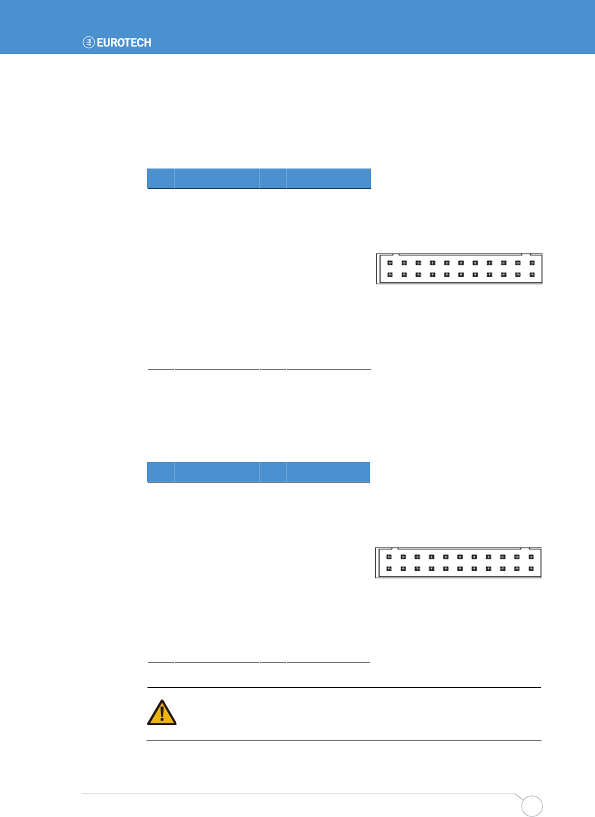
Connectors, LEDs and jumpers
Issue D 67
J2 – Camera interface connector
Connector: Neltron 2417SJ-20-PHD 'LEAD FREE', 20-way, 2mm (0.079") header
Mating connector: JST PHDR-20VS
Mating crimps: JST SPHD-002T-P0.5
Pin Signal name Pin Signal name
1 +3V3 2 +2V8
3 CIF_MCLK 4 CIF_PCLK
5 CIF_LV 6 CIF_FV
7 CIF_DD0 8 CIF_DD1
9 CIF_DD2 10 CIF_DD3
11 CIF_DD4 12 CIF_DD5
13 CIF_DD6 14 CIF_DD7
15 I2C_SCL 16 I2C_SDA
17 CIF_DD8 18 CIF_DD9
19 GND 20 GND
1 19
2 20
J3 – GPIO connector
Connector: Neltron 2417SJ-20-PHD 'LEAD FREE', 20-way, 2mm (0.079") header
Mating connector: JST PHDR-20VS
Mating crimps: JST SPHD-002T-P0.5
Pin Signal name Pin Signal name
1 VCC_PER (+5V) 2 VCC_PER (+5V)
3 P0 4 P1
5 P2 6 P3
7 P4 8 P5
9 P6 10 P7
11 GND 12 GND
13 P8 14 P9
15 P10 16 P11
17 P12 18 P13
19 P14 20 P15
1 19
2 20
Do NOT attempt to power the TITAN using the VCC_PER pins!
VCC_PER is an isolated +5V supply switched under hardware control from the
VCC input on J15 pin 1. ALWAYS provide +5V to VCC on J15 pin 1.
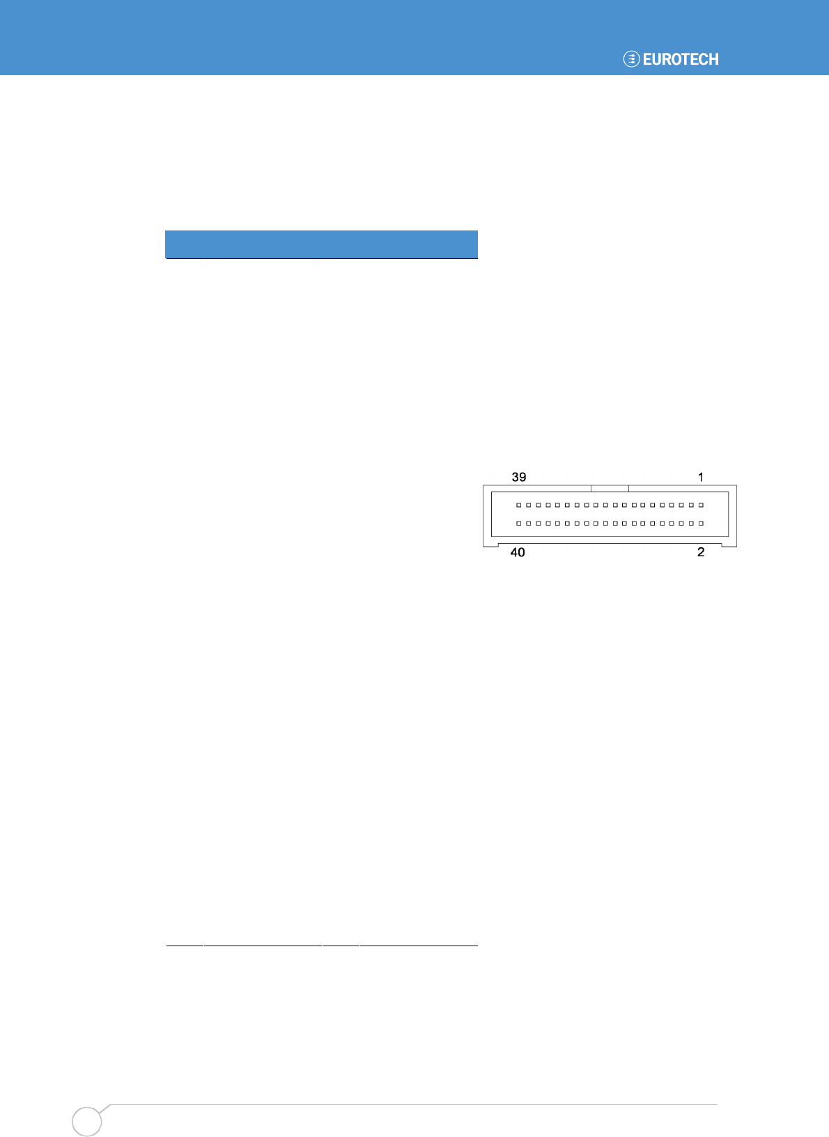
TITAN user manual
Issue D
68
J4 – LCD connector
Connector: Oupiin 3214-40C00RBA/SN, 40-way, 1.27mm (0.05") x 2.54mm (0.1") right
angled boxed header
Mating connector: Oupiin 1203-40GB/SN (available from Eurotech on request)
Pin Signal name Pin Signal name
1 BLKEN# 2 BLKSAFE
3 GPIO 16/PWM0 4 LCDSAFE
5 NEGBIAS 6 POSBIAS
7 GND 8 GND
9 FPD1 10 FPD0
11 FPD3 12 FPD2
13 FPD5 14 FPD4
15 GND 16 GND
17 FPD7 18 FPD6
19 FPD9 20 FPD8
21 FPD11 22 FPD10
23 GND 24 GND
25 FPD13 26 FPD12
27 FPD15 28 FPD14
29 FPD17 30 FPD16
31 GND 32 GND
33 BIAS / DE 34 GND
35 FCLK / VSYNC 36 GND
37 LCLK / HSYNC 38 GND
39 PCLK / CLOCK 40 GND
As viewed from the connector pins
Connectors, LEDs and jumpers
Issue D 69
J5 – Touchscreen connector
Connector: Neltron 2417SJ-05-F4, 5-way, 2mm (.079") Pitch Wire-to-Board Header
Mating connector: Molex 87369-0500, 2mm (.079") Pitch Crimp Housing
Mating crimps: Molex 50212
Pin Signal name
1 TSRY+/TR
2 TSRY-/BL
3 TSRX+/BR
4 TSRX-/TL
5 TSW
J6 – Audio connector
Connector: Neltron 2417SJ-12-PHD, 12-way, 2mm header
Mating connector: JST PHDR-12VS
Mating crimps: JST SPHD-002T-P0.5
Pin Signal name Pin Signal name
1 LEFT IN 2 LEFT OUT
3 GND 4 GND
5 RIGHT IN 6 RIGHT OUT
7 GND 8 AMP LEFT OUT
9 MIC VREF OUT 10 MIC IN
11 AMP RIGHT OUT 12 GND
1
11
2
12
15
TL
TL
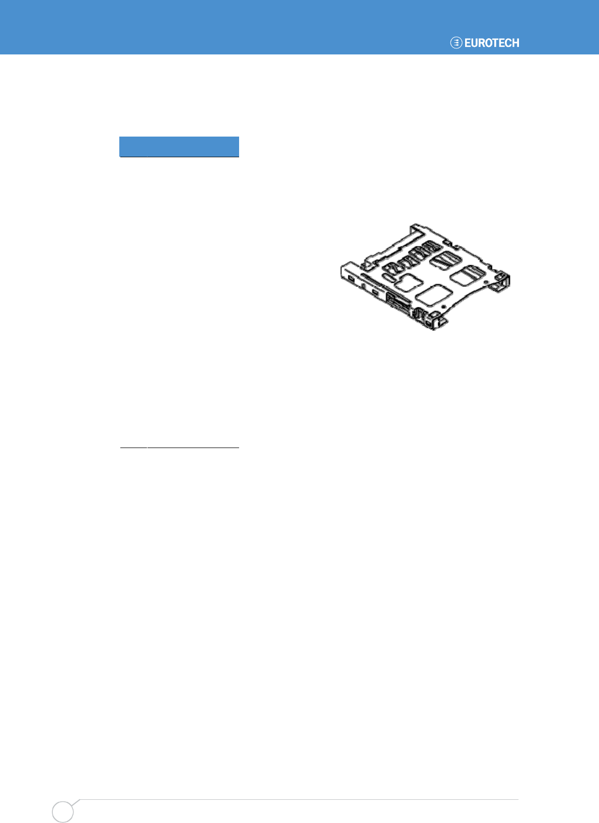
TITAN user manual
Issue D
70
J7 – SDIO socket
Connector: Molex 67840-8001, 2.50mm (.098") pitch SD memory card connector
Pin Signal name
1 MMDAT3
2 MMCMD
3 GND
4 +3V3
5 MMCLK
6 GND
7 MMDAT0
8 MMDAT1
9 MMDAT2
10 MMC_WP
11 +3V3
12 MMC_CD
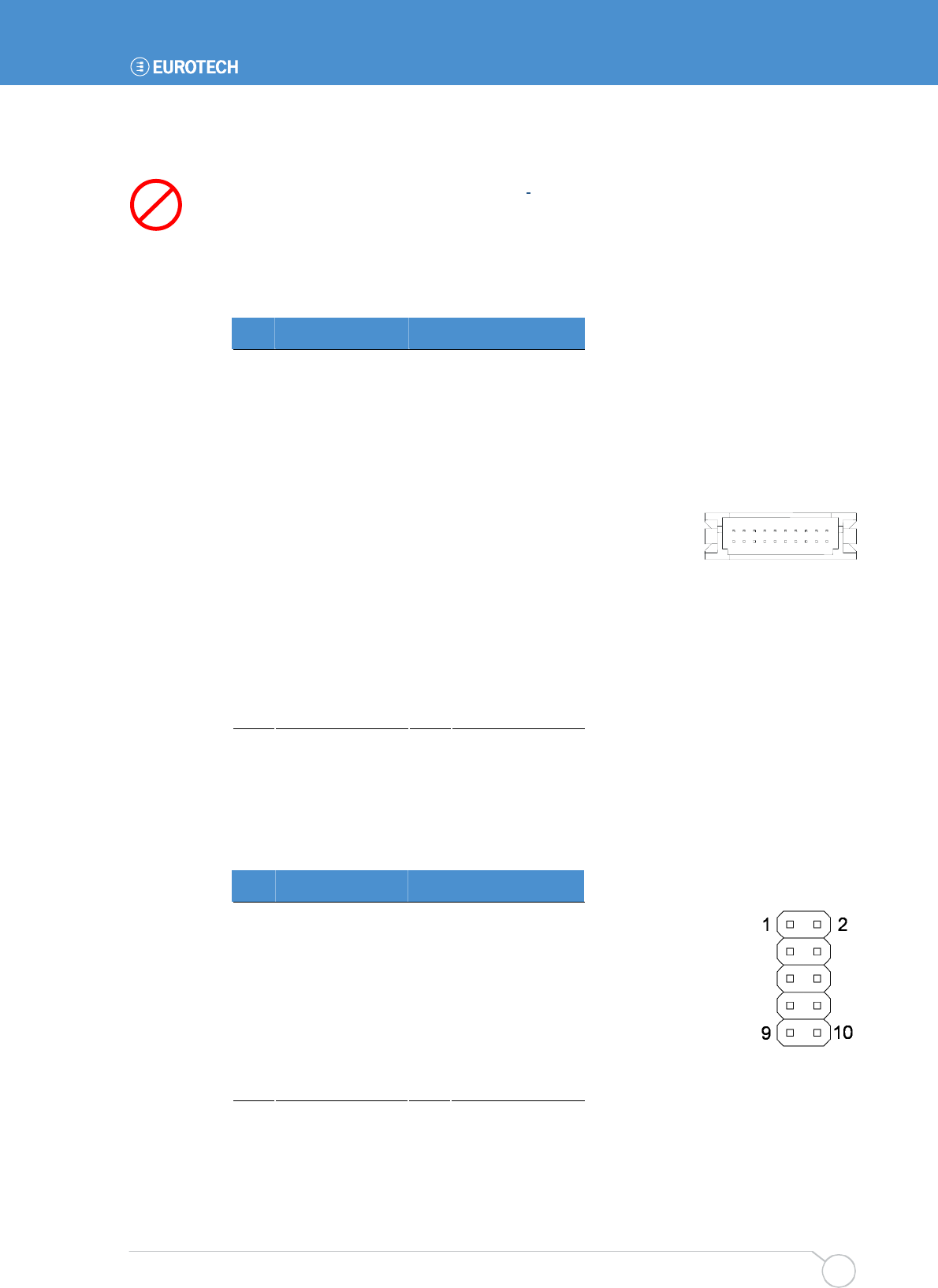
Connectors, LEDs and jumpers
Issue D 71
J8 – LVDS connector
Connector: Hirose DF13-20DP-1.25V(55), 20-way, 1.27mm (0.05") double row straight
pin header
LVDS mating connector: Hirose DF13-20DS-1.25C
LVDS mating connector crimps: Hirose DF13-2630SCFA
Eurotech recommended cable: Amphenol 165-2899-945
Pin Signal name Pin Signal name
1 +3V3 2 +3V3
3 GND 4 GND
5 LVDS_D0- 6 LVDS_D0+
7 GND 8 LVDS_D1-
9 LVDS_D1+ 10 GND
11 LVDS_D2- 12 LVDS_D2+
13 GND 14 LVDS_CLK-
15 LVDS_CLK+ 16 GND
17 NC 18 NC
19 GND 20 MSL
J9 – JTAG connector
Connector: Oupiin 2015-2X5GDB/SN, 10-way, 2.54mm (0.1") x 2.54mm (0.1") dual row
header
Mating connector: FCI 71600-010LF
Pin Signal name Pin Signal name
1 +3V3 2 NC
3 GND 4 nTRST
5 NC 6 TDI
7 TDO 8 TMS
9 TCLK 10 SRST
TL
220
1 19
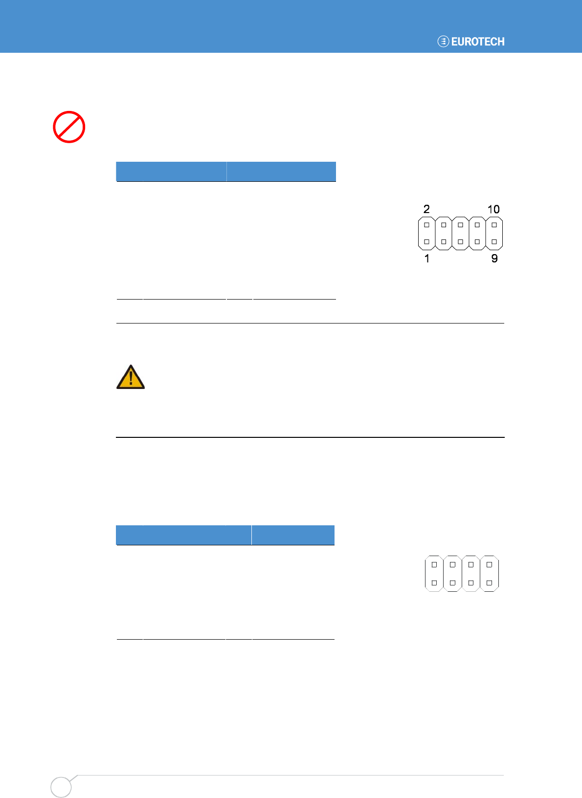
TITAN user manual
Issue D
72
J10 – USB connector
Connector: Oupiin 2015-2X5GDB/SN, 10-way, 2.54mm (0.1") x 2.54mm (0.1") dual row
header
Mating connector: FCI 71600-010LF
Pin Signal name Pin Signal name
1 VBUS 1 2 VBUS 2
3 DATA- 1 4 DATA- 2
5 DATA+ 1 6 DATA+ 2
7 GND 8 GND
9 SHIELD 10 SHIELD
Do NOT attempt to power the TITAN using the VBUS 1 or VBUS 2 pins!
VBUS 1 and VBUS 2 are isolated +5V supplies switched under hardware control
from VCC_PER.
ALWAYS use the USB client cable provided with the development kit. This cable
does not provide power down the cable and avoids reverse powering the TITAN
from a USB host when the TITAN has no power on the VCC input on J15 pin 1.
Reverse powering the TITAN from the VBUSn pins can make the TITAN operate
erratically and may cause serious damage to the TITAN.
J11 – 10/100BaseTX Ethernet connector
Connector: Oupiin 2015-2X4GDB/SN, 8-way, 2.54mm (0.1") x 2.54mm (0.1") dual row
header
Mating connector: FCI 71600-008LF
Pin Signal name Pin Signal name
1 TX+ 2 TX-
3 RX+ 4 NC
5 NC 6 RX-
7 NC 8 LANGND
1
2
7
8
TL
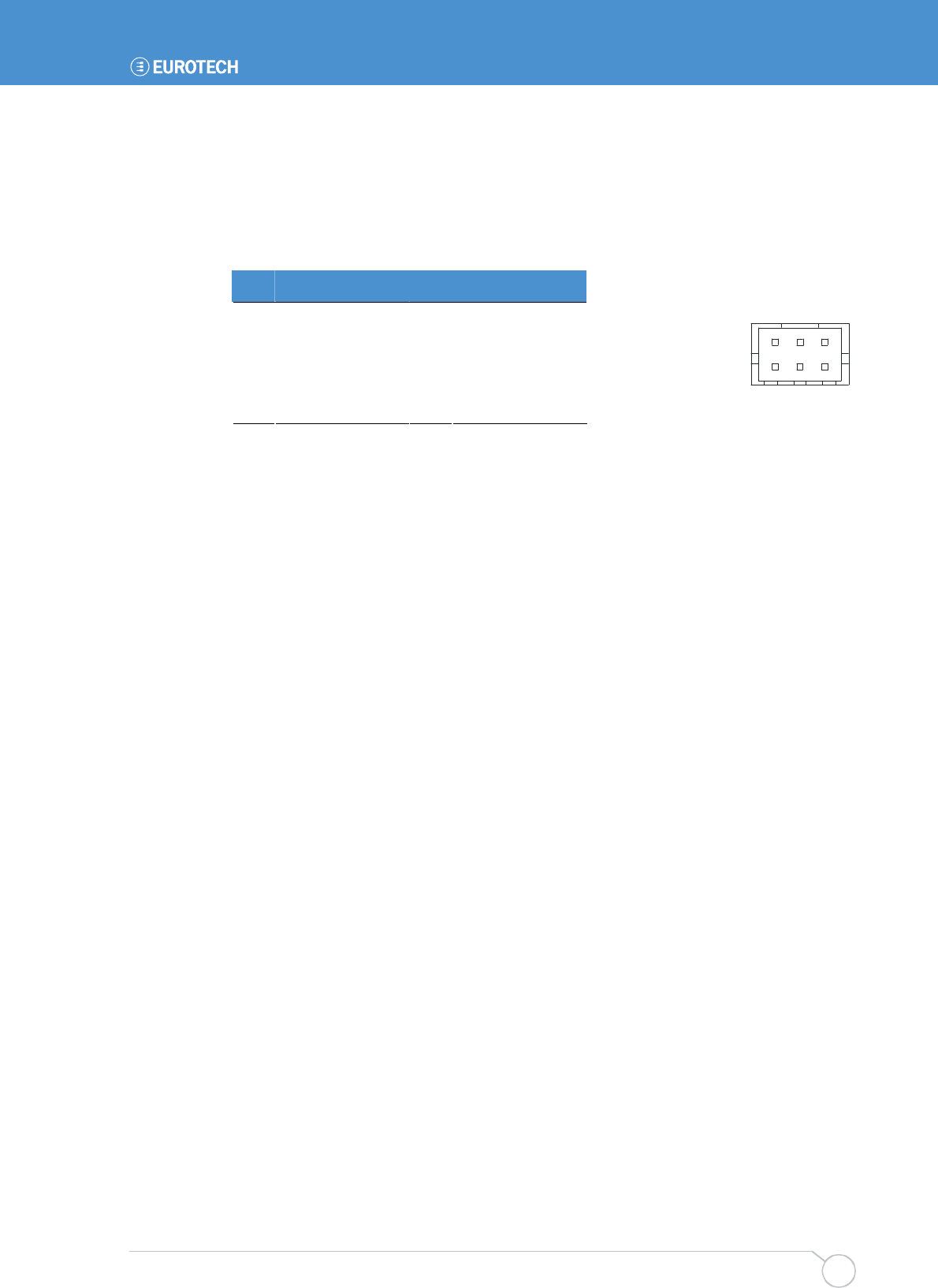
Connectors, LEDs and jumpers
Issue D 73
J12 – Ethernet status LEDs connector
Connector: Neltron 2417SJ-06-PHD, 6-way, 2mm (0.079") x 2mm (0.079") pin housing
Mating connector: Neltron 2418HJ-06-PHD
Mating connector crimps (x4): Neltron 2418TJ-PHD
Pin Signal name Pin Signal name
1 +3V3 2 LINK
3 +3V3 4 SPEED
5 +3V3 6 NC
1
2
5
6
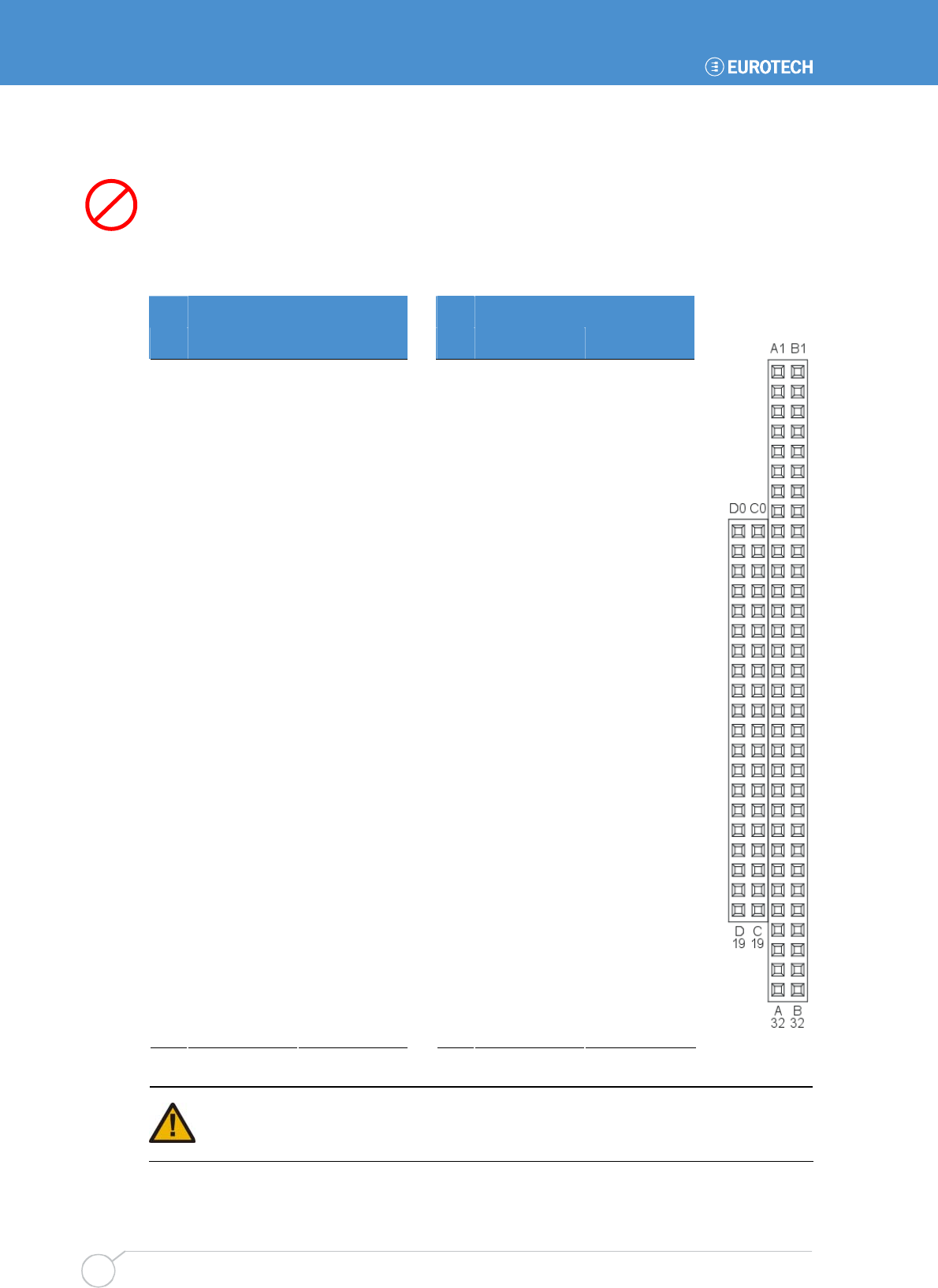
TITAN user manual
Issue D
74
J13 & J14 – PC/104 connectors
Connectors:
• Astron 25-1201-232-2G-R, 64-way, 2.54mm (0.1") x 2.54mm (0.1") stackthrough
PC/104 compatible connector (row A & B)
• Astron 25-1201-220-2G-R, 40-way, 2.54mm (0.1") x 2.54mm (0.1") stackthrough
PC/104 compatible connector (row C & D)
J14 J13
Pin Row D Row C Pin Row A Row B
1 /IOCHCK GND
2 D7 RSTDRV
3 D6 VCC_PER (+5V)
4 D5 IRQ9
5 D4 NC
6 D3 NU (DRQ2)
7 D2 NC
8 D1 NC
0 GND GND 9 D0 +12V
1 /MEMCS16 /SBHE 10 IOCHRDY KEY
2 /IOCS16 LA23 11 AEN /SMEMW
3 IRQ10 LA22 12 A19 /SMEMR
4 IRQ11 LA21 13 A18 /IOW
5 IRQ12 LA20 14 A17 /IOR
6 IRQ15 LA19 15 A16 NU (DACK3)
7 IRQ14 LA18 16 A15 NU (DRQ3)
8 NU (DACK0) LA17 17 A14 NU (DACK1)
9 NU (DRQ0) /MEMR 18 A13 NU (DRQ1)
10 NU (DACK5) /MEMW 19 A12 NU (REFSH)
11 NU (DRQ5) D8 20 A11 8MHz CLK
12 NU (DACK6) D9 21 A10 IRQ7
13 NU (DRQ6) D10 22 A9 IRQ6
14 NU (DACK7) D11 23 A8 IRQ5
15 NU (DRQ7) D12 24 A7 IRQ4
16 VCC_PER (+5V) D13 25 A6 IRQ3
17 NC (Master) D14 26 A5 NU (DACK2)
18 GND D15 27 A4 NU (TC)
19 GND KEY 28 A3 BALE
29 A2 VCC_PER (+5V)
30 A1 OSC
31 A0 GND
32 GND GND
Do NOT attempt to power the TITAN using the VCC_PER pins! VCC_PER is an isolated
+5V supply switched under hardware control from the VCC input on J15 pin 1.
ALWAYS provide +5V to VCC on J15 pin 1.
TL
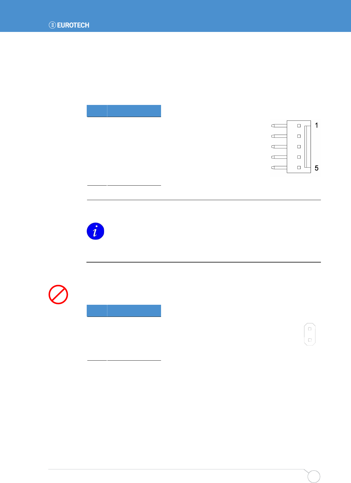
Connectors, LEDs and jumpers
Issue D 75
J15 – Power connector
Connector: Molex 22-05-7058, 5-way, 2.54mm (0.1") Pitch KK® header - right angle
friction lock 7395 series connector
Mating connector: Molex 22-01-2055, 5-way, 2.54mm (0.1") Pitch KK® crimp terminal
housing 2695 series connector
Pin Signal name
1 VCC (+5V)
2 GND
3 VBAT_E
4 +12V
5 /Reset
VBAT_E provides the facility to fit an external battery for the backup supply of the
external 256KByte static RAM and RTC, and internal 256KByte static RAM and
RTC.
A +12V connection is defined, but is not required for the TITAN under normal
operation. It can be used to supply +12V to the PC/104 stack if required.
A momentary switch (push to make) may be connected across /Reset and GND.
Do NOT connect the switch across /Reset and VCC or +12V.
JP1 – Battery disconnect
Connector: Oupiin 2011-1x2GSB/SN, 2-way, 2.54mm (0.1") single row through-hole
header.
Pin Signal name
1 Battery backup
switch input
2 Battery + terminal
2
1
TL
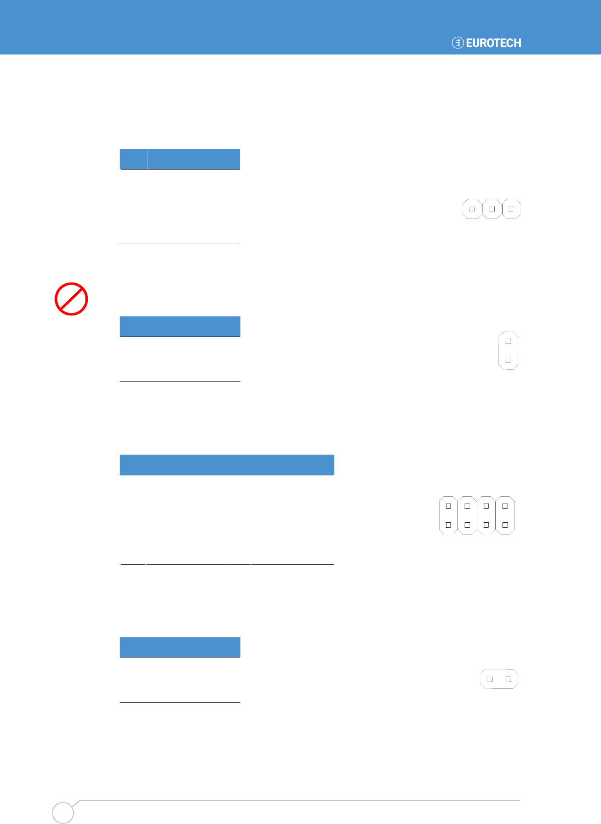
TITAN user manual
Issue D
76
JP2 – LCD logic supply selection
Connector: Oupiin 2011-1x3GSB/SN, 3-way, 2.54mm (0.1") single row through-hole
header.
Pin Signal name
1 VCC_PER (+5V)
2 LCD logic supply
3 +3V3
JP3 – LVDS MSL selection
Connector: Oupiin 2011-1x2GSB/SN, 2-way, 2.54mm (0.1") single row through-hole
header.
Pin Signal name
1 MSL
2 +3V3
JP4 – User / Recovery link selection
Connector: Oupiin 2015-2x4GDB/SN, 8-way, 2.54mm (0.1") dual row surface mount
header.
Pin Signal name Pin Signal name
1 GND 2 USER_LINKA
3 GND 4 USER_LINKB
5 GND 6 USER_LINKC
7 GND 8 RECOVERY
JP5 – External reset
Connector: Oupiin 2011-1x2GSB/SN, 2-way, 2.54mm (0.1") single row through-hole
header.
Pin Signal name
1 /Reset
2 +GND
1
2
7
8
1
3
1
2
2 1
TL
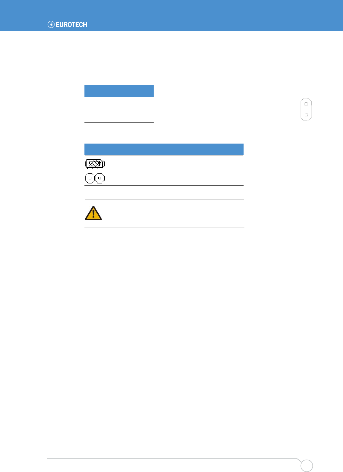
Connectors, LEDs and jumpers
Issue D 77
JP6 – JTAG enable
Connector: Oupiin 2011-1x2GSB/SN, 2-way, 2.54mm (0.1") single row through-hole
header
Pin Signal name
1 VCC (+5V)
2 VCC_JTAG
This jumper is used to enable debug of PXA270 using JTAG interface.
JP6 Description
JTAG Enable
Normal Operation (Default)
Only insert jumper for JTAG access to PXA270. The
jumper MUST be removed when the JTAG interface is
not in use.
1
2
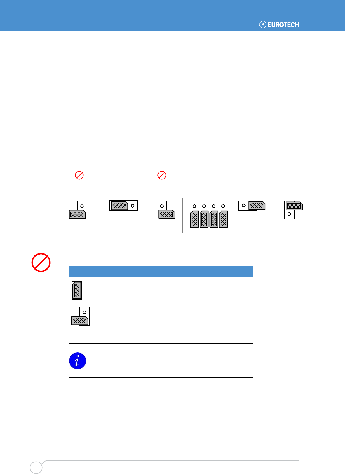
TITAN user manual
Issue D
78
Status LEDs
There is a single status LED on the TITAN, which indicates FLASH access to the FLASH
memory / silicon disk.
Jumpers
There are nine user selectable jumpers on the TITAN; the use of each one is explained
below.
Default settings
The factory default positions of the jumpers are shown below. Jumper functions
described in silkscreen on the board are shown in blue.
Battery connect jumper – LK1 on JP1
This jumper connects the battery to the battery back-up circuit:
LK1 Description
Battery supply connected.
Battery supply disconnected [factory default].
If SRAM and/or RTC data is to be used, jumper LK1 must be
fitted to JP1 to provide battery power to these devices. The
jumper is left unconnected at the factory to conserve battery
power.
TL
JP1 JP2 JP3 JP4 JP5 JP6
BAT
1
2
LK1 1
2
3
LK2
+5V
+3.3V
LCD Voltage
MSL
2
1
LK3
TL TL
1
2
RST
LK8
JTAG
ON/OFF
2
1 LK9
3
5
71
4
6
82
LK7 LK6 LK5 LK4
B
C
A
RECOVER
USER
Connectors, LEDs and jumpers
Issue D 79
LCD supply voltage jumper – LK2 on JP2
This jumper selects the supply voltage for the LCD logic supply:
LK2 Description
Supply LCD logic with 5V.
Supply LCD logic with 3.3V [factory default].
If the LCD requires a 5V supply, please refer to the LCD
datasheet to ensure that the display is compatible with 3.3V
logic.
LVDS mode select [MSL] jumper – LK3 on JP3
This jumper sets the MSL signal on the Hirose LVDS connector J8 to either high or low:
LK3 Description
+3V3.
Pulled to GND [factory default].
This jumper is only applicable if using the Hirose LVDS
connector J8.
Please refer to LVDS LCD datasheet for details of the signal
level that is required to set it up to receive LVDS signal
mapping for a National Semiconductor DS90C363 LVDS
transceiver.
TL
TITAN user manual
Issue D
80
User configurable jumpers A to C – LK4-LK6 on JP4
These jumpers can be used to signify a configuration setting for your own application
program:
LK4 – LK6 Description
Read as ‘0’.
Read as ‘1’ [factory default].
USER_LINKA to C, LK4, 5 and 6 respectively (GPIO 13, 35 and
113 respectively), may be used to wake the TITAN from sleep.
One way of doing this is to connect a momentary push to make
switch across the USER_LINK and GND.
Recovery jumper – LK7 on JP4
This jumper can be used to recover a damaged software image:
LK7 Description
Fetch working image from BOOTP server and execute.
Normal software run mode [factory default].
Please contact Eurotech for details. Contact details are
provided in Eurotech Group Worldwide Presence, page 101.
Reset – LK8 on JP5
A momentary switch (push to make) may be connected to LK1. When pressed the board
goes into a full hardware reset. When the switch is released (open circuit) the board
reboots.

Connectors, LEDs and jumpers
Issue D 81
JTAG enable jumper – LK9 on JP6
This jumper is used to enable debug of PXA270 using the JTAG interface:
LK9 Description
JTAG enable.
Normal operation [factory default].
Only insert jumper LK9 for JTAG access to the PXA270. LK9
MUST be removed before putting the TITAN into deep sleep.
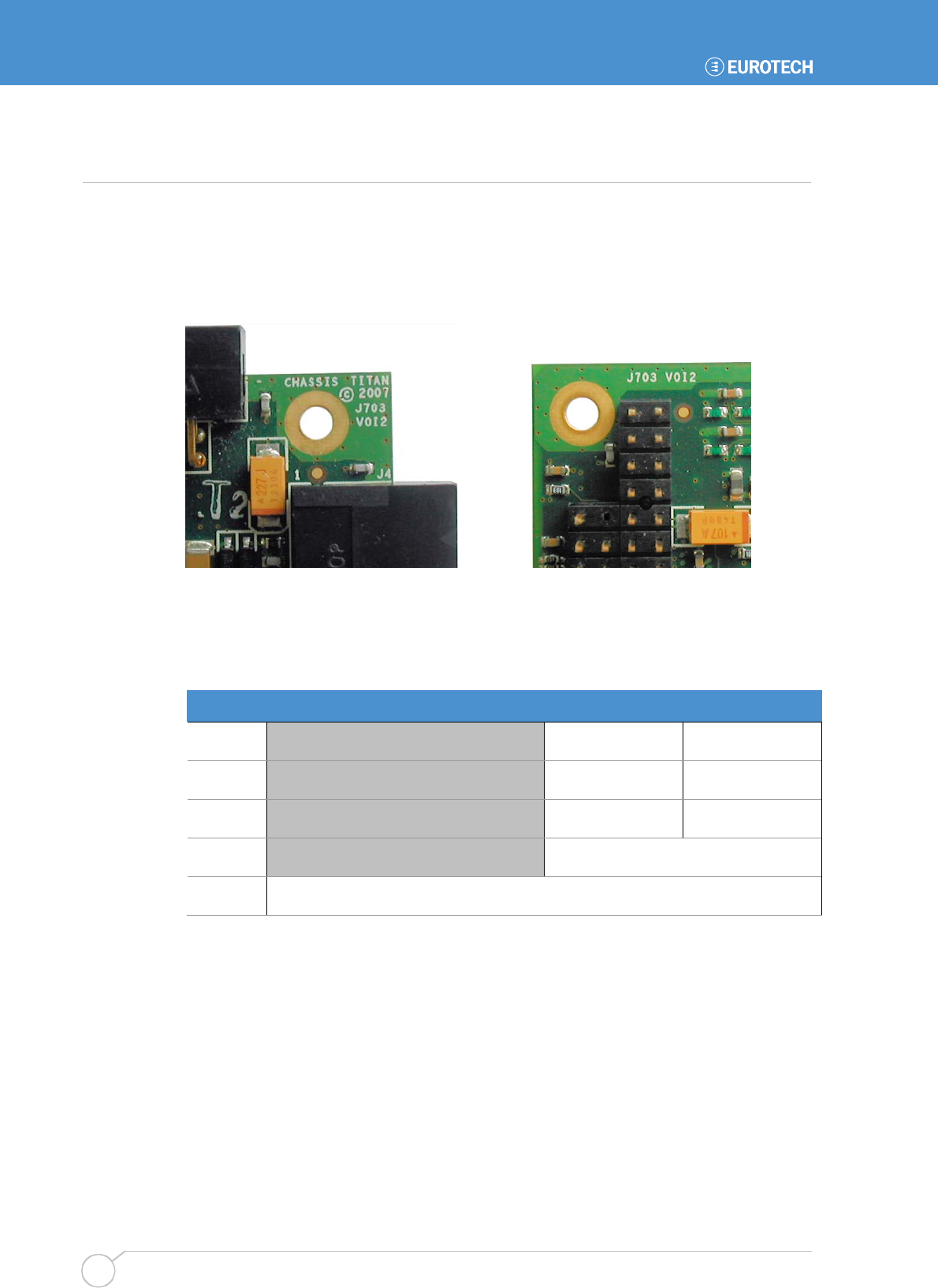
TITAN user manual
Issue D
82
Appendix A - Board version / issue
Where it is possible to see the TITAN, the board version and issue are indicated on the
top side in the upper right-hand corner and on the bottom side in the lower-left corner as
shown below.
TITAN version/issue on top side TITAN version/issue on bottom side
If it is not possible to physically look at the TITAN, the board version and issue can be
read from the CPLD board version / issue register [BV_REG] at the address 0x11000000.
The board version and issue bit assignments are detailed in the table below:
Board version/issue register [BV_REG]
Byte lane Most significant byte Least significant byte
Bit 15 14 13 12 11 10 9 8 7 6 5 4 3 2 1 0
Field - - - - - - - - VERSION (BCD) ISSUE (BCD)
Reset X X X X X X X X Current version Current issue
R/W - - - - - - - - R
Address 0x11000000
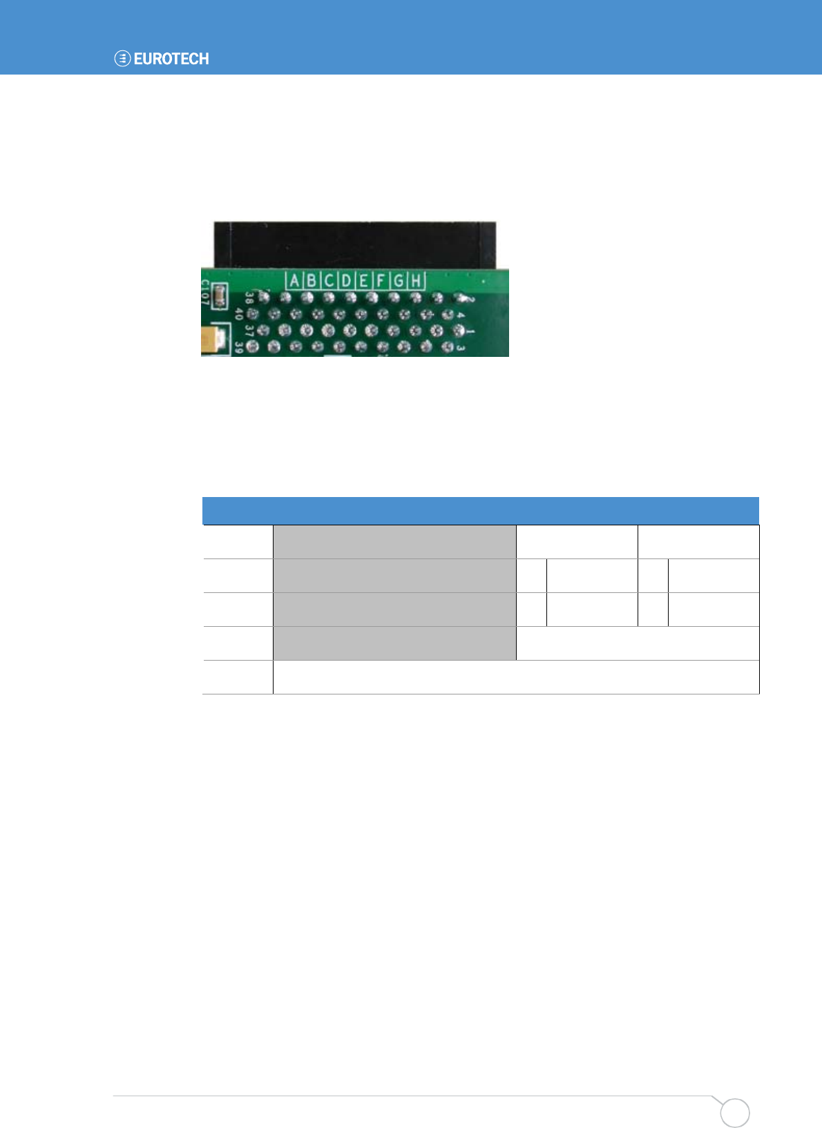
Appendix A - Board version / issue
Issue D 83
Mod box
The mod box indicates the ECO level that the TITAN is at for a particular version / issue
of the board. The mod box is located on the bottom side behind the video connector J4,
as shown below:
CPLD versions
The TITAN CPLD versions can be read out of the CPLD versions register [CV_REG] at
the address 0x12000000. The CPLD versions bit assignments are detailed in the table
below:
CPLD versions register [CV_REG]
Byte lane Most significant byte Least significant byte
Bit 15 14 13 12 11 10 9 8 7 6 5 4 3 2 1 0
Field - - - - - - - - 0
VERSION (BCD) 0 VERSION (BCD)
Reset X X X X X X X X 0 CPLD 2 version 0 CPLD 1 version
R/W - - - - - - - - R
Address 0x12000000

TITAN user manual
Issue D
84
Appendix B - Specification
Microprocessor PXA270 312MHz (TITAN-Lite only) 416/520MHz XScale
processor (520MHz as standard option).
Cache 32K data cache, 32K instruction cache, 2K mini data
cache.
System memory Fixed on-board memory:
• 64MB SDRAM (32-bit wide SDRAM data bus).
• 128MB SDRAM may be available in the future.
Silicon disk Fixed on-board memory:
• 16MB Flash (TITAN-Lite only).
• 32/64MB Flash.
SRAM 256KB of SRAM battery backed on-board.
256KB of SRAM internal to PXA270.
Serial ports Five UART 16550 compatible fast serial ports
(921.6Kbaud):
• RS232 on COM1, COM2, COM3 and COM4.
• RS422/485 on COM5 - software selectable.
USB support Two USB 1.1 host controller ports.
One USB 1.1 client controller port (software selectable on
Host 2).
Network support One IEEE 802.3u 10/100Base-T NIC port.
Option for external PoE.
Expansion interfaces SDIO socket to support MMC/SD/SDIO cards.
16-bit PC/104 interface.
Date/time support Real time clock - battery backed on-board.
Accuracy +/- 1min/month.
Video 18-bit flat panel interface for STN and TFT displays.
Supported resolutions:
• 320 x 240, 8/16/18 bpp.
• 640 x 480, 8/16/18 bpp.
• 800 x 600, 8/16/18 bpp.
Optional LVDS interface.
Audio and touchscreen AC’97 compatible CODEC, stereo.
20Hz to 20kHz in/out frequency response .
Touchscreen support - 4/5-wire analogue resistive.
Quick Capture camera interface Intel® Quick Capture technology.
I2C bus Multi-master serial bus.
Configuration PROM 128 byte I2C configuration EEPROM.
TL
TL
TL
TL
TL
TL

Appendix B - Specification
Issue D 85
Watchdog timer Internal to PXA270, causes reset on timeout; timeout
range 307ns-1321s.
Real time clock Accuracy +/- 1 minute/month.
General I/O 16 x general purpose I/O.
Temperature sensor I
2C temperature sensor.
Test support JTAG interface.
Power requirements 5V +/-5%.
Consumption: 1.5W typical (no LCD, PC/104, USB, SDIO
devices fitted).
Sleep mode: 20mA (100mW) typical.
Deep sleep mode: 2mA (10mW) typical.
Mechanical PC/104 compatible format: 3.775" x 3.550", 96mm x
91mm (see www.pc104.org).
90 grams.
Environmental Operating temperature:
• Commercial: -20°C (-4°F) to +70°C (+158°F)
• Industrial: -40°C (-40°F) to +85°C (+185°F)
Humidity: 10% to 90% RH (non-condensing)
RoHS Directive (2002/95/EC) compliant.

TITAN user manual
Issue D
86
Appendix C - Mechanical diagram
When mounting the TITAN use only M3 (metric) or 4-40 (US) screws. The mounting
pad is 6.35mm, 0.25", and the hole is 3.175mm, 0.125", so ensure any washers fitted
are smaller than the pad.
Using oversized screws and washers, or tooth locking washers, can cause short
circuits and over-voltage conditions.
Eurotech recommend that you use a Loctite screw thread lock or a similar product over
tooth locking washers.
Unit of measure = mm (1inch = 25.4mm)

Appendix D - Reference information
Issue D 87
Appendix D - Reference information
Product information
Product notices, updated drivers, support material, 24hr-online ordering:
www.eurotech-ltd.co.uk
PC/104 consortium
PC/104 specifications, vendor information and available add-on products:
www.PC/104.org
USB information
Universal Serial Bus (USB) specification and product information:
www.usb.org
SDIO card information
SD Card Association and product information:
www.sdcard.org
www.sdcard.com
www.sandisk.com/oem/manuals.asp
Intel
Intel XScale™ PXA270 processor documentation:
www.intel.com
www.intel.com/design/embeddedpca/prodbref/302302pb.htm
Davicom Semiconductor Inc
Davicom DM9000A Ethernet Controller documentation:
www.davicom.com.tw/eng/index.htm
Exar Corporation
Exar XR16C2850 DUART with 128 byte FIFO documentation:
www.exar.com
Wolfson Microelectronics
Wolfson WM9712L AC’97Codec documentation:
www.wolfson.co.uk
NXP Semiconductors.
NXP PCA9535 I²C I/O expander documentation:
www.nxp.com
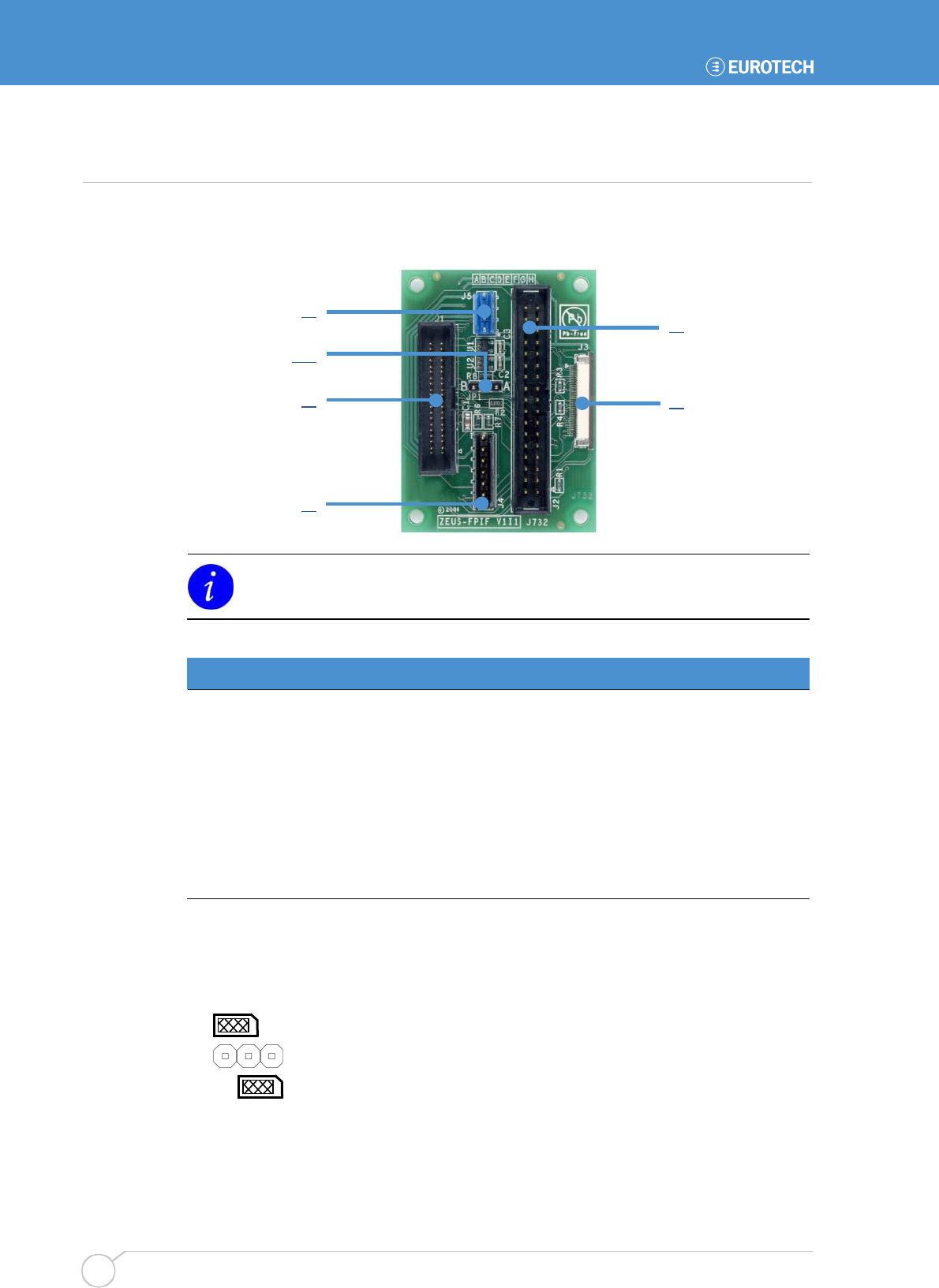
TITAN user manual
Issue D
88
Appendix E - ZEUS-FPIF details
The ZEUS-FPIF allows easy connection between the TITAN and a TFT or STN LCD flat
panel display. Details of the ZEUS-FPIF are shown below:
The connectors on the following pages are shown in the same orientation as the
picture above.
Connector Function
JP1 TFT clock delay selection
J1 TITAN LCD cable connector
J2 Generic LCD connector
J3 Direct connection to a NEC NL3224BC35-20 5.5inch 320x240 TFT display
J4 Backlight inverter connector
J5 STN bias connector
JP1 – TFT clock delay selection
It has been found that some TFT displays require a delay on the clock. If this is required
fit the jumper in position A; if not then fit in position B. This is illustrated below:
J2
J3
J5
JP1
J1
J4
B
A
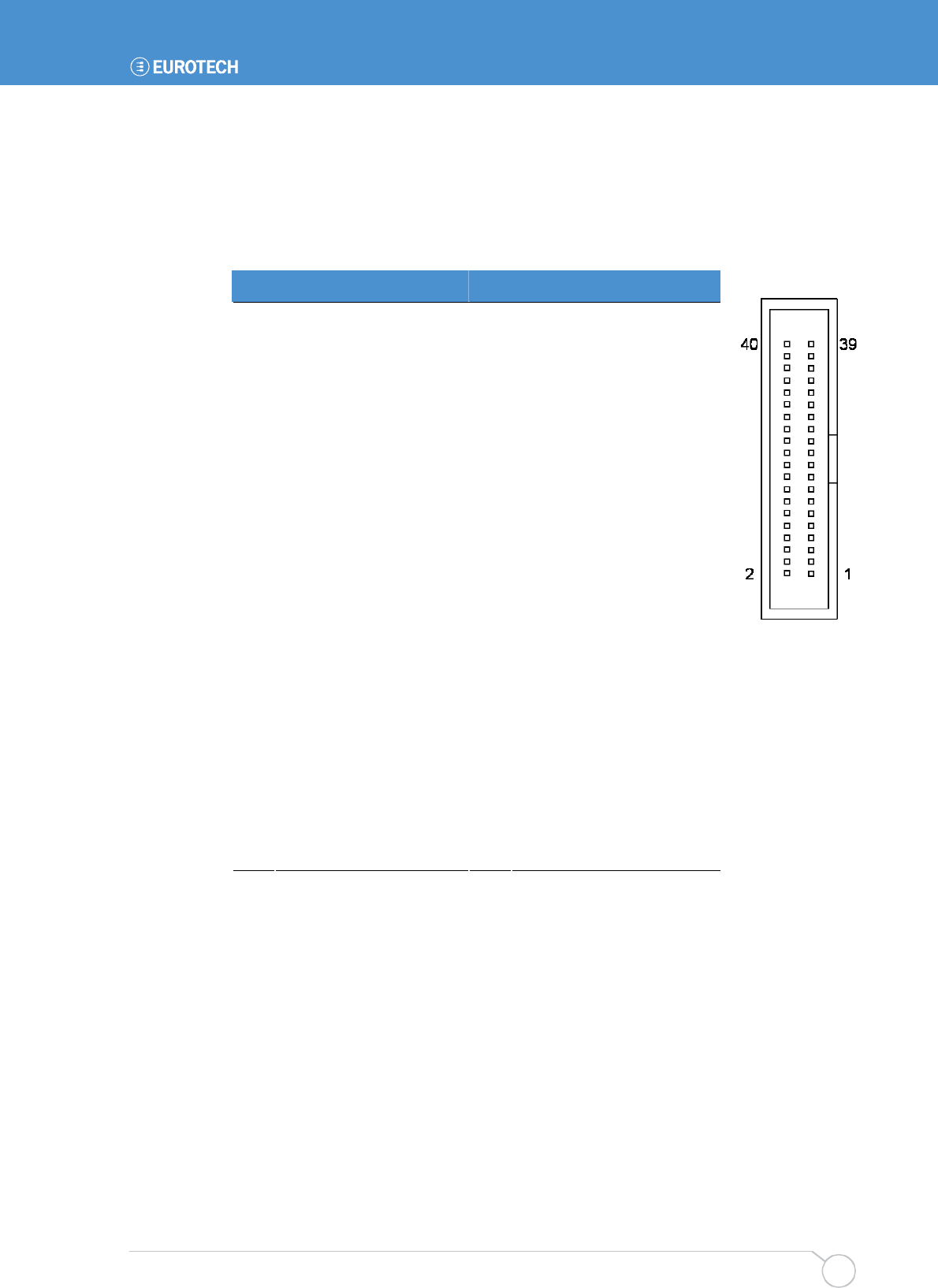
Appendix E - ZEUS-FPIF details
Issue D 89
J1 – TITAN LCD cable connector
Connector: Oupiin 3215-40CSB/SN, 40-way, 1.27mm (0.05") x 2.54mm (0.1") straight-
boxed header
Mating connector: Oupiin 1203-40GB/SN (available from Eurotech on request)
Pin Signal name Pin Signal name
1 BLKEN# 2 BLKSAFE
3 GPIO 16/PWM0 4 LCDSAFE
5 NEGBIAS 6 POSBIAS
7 GND 8 GND
9 FPD1 10 FPD0
11 FPD3 12 FPD2
13 FPD5 14 FPD4
15 GND 16 GND
17 FPD7 18 FPD6
19 FPD9 20 FPD8
21 FPD11 22 FPD10
23 GND 24 GND
25 FPD13 26 FPD12
27 FPD15 28 FPD14
29 NC 30 NC
31 GND 32 GND
33 BIAS / DE 34 GND
35 FCLK / VSYNC 36 GND
37 LCLK / HSYNC 38 GND
39 PCLK / CLOCK 40 GND
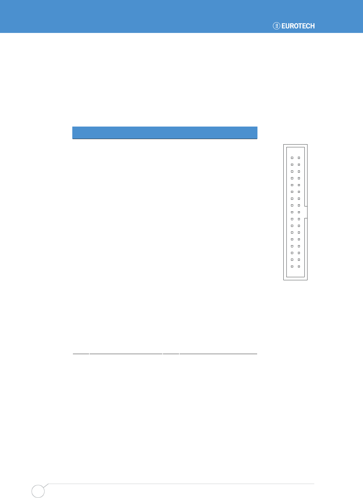
TITAN user manual
Issue D
90
J2 – Generic LCD connector
Connector: Oupiin 3012-34GSB/SN, 34-way, 2.54mm (0.1") x 2.54mm (0.1") straight-
boxed header
Mating connector: Fujitsu FCN-723-B034/2
Mating connector crimps: Fujitsu FCN-723J-AU/Q (as it is possible to connect a crimp type
connector to PL2, a wide range of LCD displays can be connected with a custom cable)
Pin Signal name Pin Signal name
1 GND 2 FPD 0
3 FPD 1 4 FPD 2
5 GND 6 FPD 3
7 FPD 4 8 FPD 5
9 FPD 6 10 GND
11 FPD 7 12 FPD 8
13 FPD 9 14 FPD 10
15 GND 16 GND
17 FPD 11 18 FPD 12
19 FPD 13 20 GND
21 FPD 14 22 FPD 15
23 GND 24 PCLK / CLOCK
25 GND 26 LCDSAFE
27 LCDSAFE 28 LCLK / HSYNC
29 FCLK / VSYNC 30 GND
31 BKLSAFE 32 BIAS / DE
33 NC 34 BKLEN#
12
3334

Appendix E - ZEUS-FPIF details
Issue D 91
J3 – Direct connection to a NEC NL3224BC35-20 5.5inch 320x240 TFT display
Connector: Oupiin 2345-33TD2/SN
Mating cable: Eunsung 0.5x33x190xAx0.035x0.3x5x5x10x10
Pin Signal name Pin Signal name
1 GND 18 FPD 10
2 PCLK 19 GND
3 LCLK (HSYNC) 20 GND
4 FCLK (VSYNC) 21 FPD 0
5 GND 22 FPD 1
6 GND 23 FPD 2
7 FPD 11 24 FPD 3
8 FPD 12 25 FPD 4
9 FPD 13 26 GND
10 FPD 14 27 LBIAS
11 FPD 15 28 LCDSAFE
12 GND 29 LCDSAFE
13 FPD 5 30 GND
14 FPD 6 31 GND
15 FPD 7 32 GND
16 FPD 8 33 GND
17 FPD 9
1
33
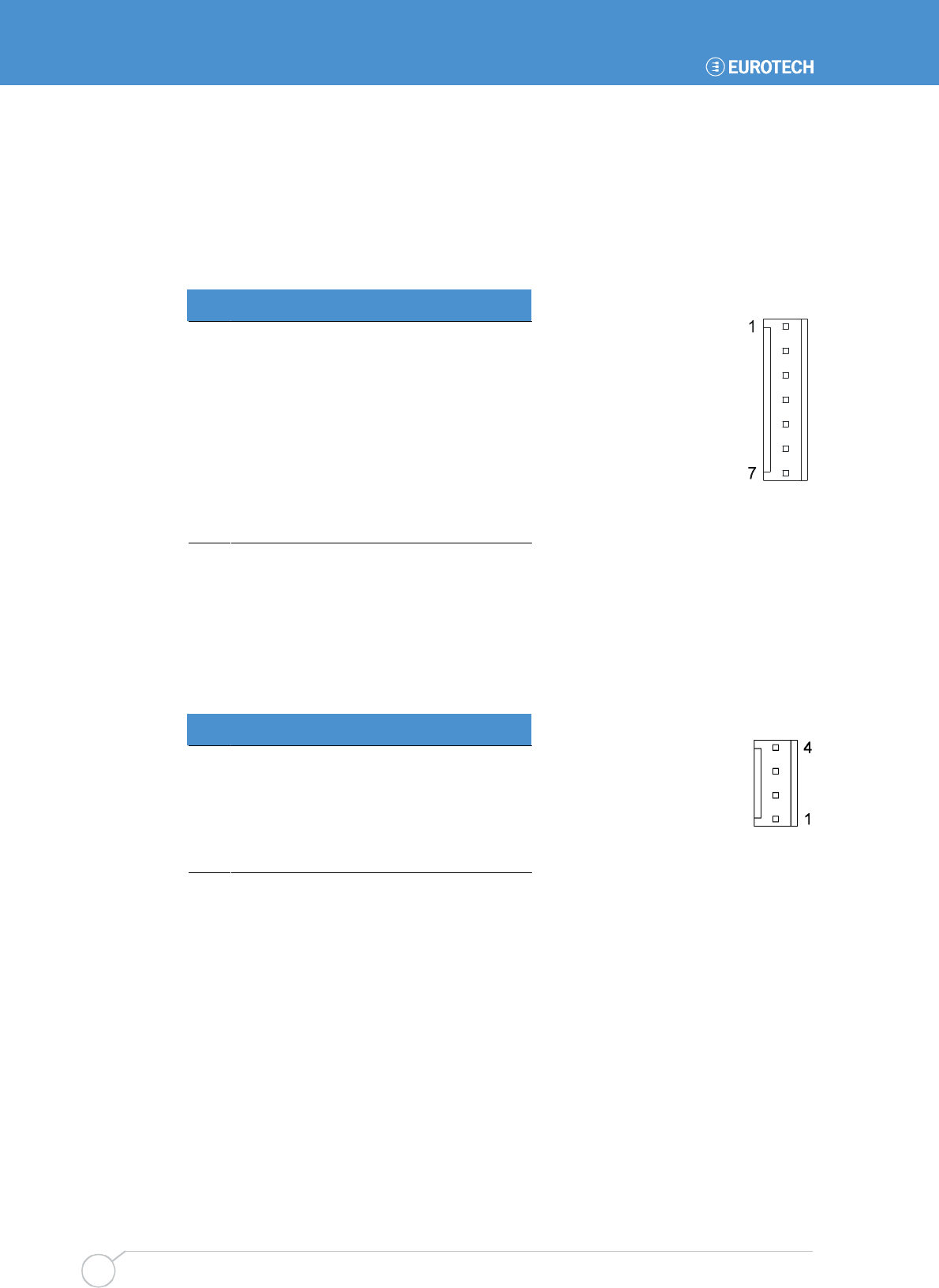
TITAN user manual
Issue D
92
J4 – Backlight inverter connector
Connector: FCI 76384-407LF
Mating connector: FCI 65240-007LF
Mating connector crimps: FCI 76357-401LF
Pin Signal name
1 BKLSAFE
2 BKLSAFE
3 GND
4 GND
5 BKLEN#
6 BRT_CTRL
7 GND
J5 – STN bias connector
Connector: FCI 76384-404LF
Mating connector: FCI 65240-004LF
Mating connector crimps: FCI 76357-401LF
Pin Signal name
1 POSBIAS
2 GND
3 GND
4 NEGBIAS
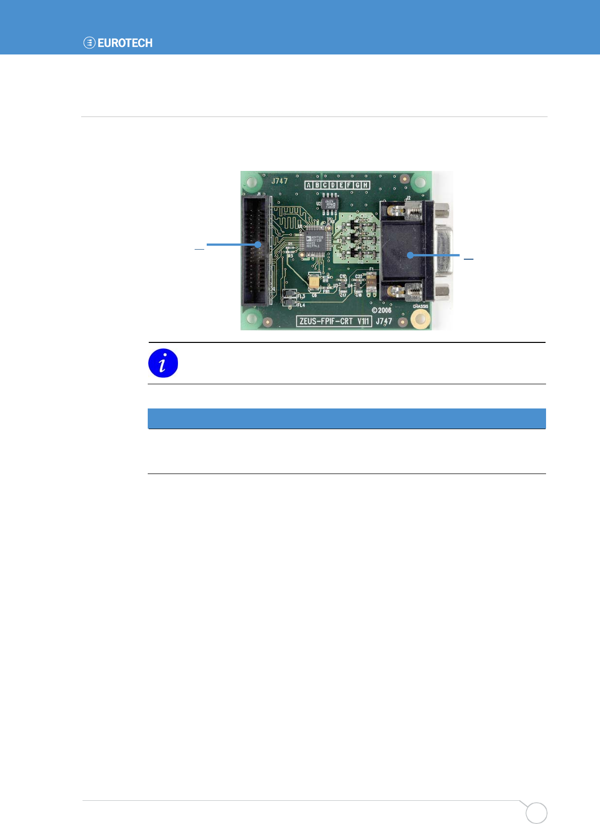
Appendix F - ZEUS-FPIF-CRT details
Issue D 93
Appendix F - ZEUS-FPIF-CRT details
The ZEUS-FPIF-CRT allows the TITAN to drive a CRT monitor or an analogue LCD flat
panel. Sync on green and composite sync monitors are not supported.
The connectors on the following pages are shown in the same orientation as the
picture above.
Connector Function
J1 TITAN LCD cable connector
J2 CRT connector
J2
J1
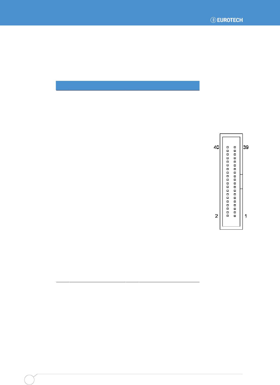
TITAN user manual
Issue D
94
J1 – TITAN LCD cable connector
Connector: Oupiin 3215-40CSB/SN, 40-way, 1.27mm (0.05") x 2.54mm (0.1") straight-
boxed header
Mating connector: Oupiin 1203-40GB/SN (available from Eurotech on request)
Pin Signal name Pin Signal name
40 GND 39 CLOCK
38 GND 37 HSYNC
36 GND 35 VSYNC
34 GND 33 DE
32 GND 31 GND
30 NC 29 NC
28 FPD14 27 FPD15
26 FPD12 25 FPD13
24 GND 23 GND
22 FPD10 21 FPD11
20 FPD8 19 FPD9
18 FPD6 17 FPD7
16 GND 15 GND
14 FPD4 13 FPD5
12 FPD2 11 FPD3
10 FPD0 9 FPD1
8 GND 7 GND
6 NC 5 NC
4 NC 3 NC
2 BKLSAFE 1 NC
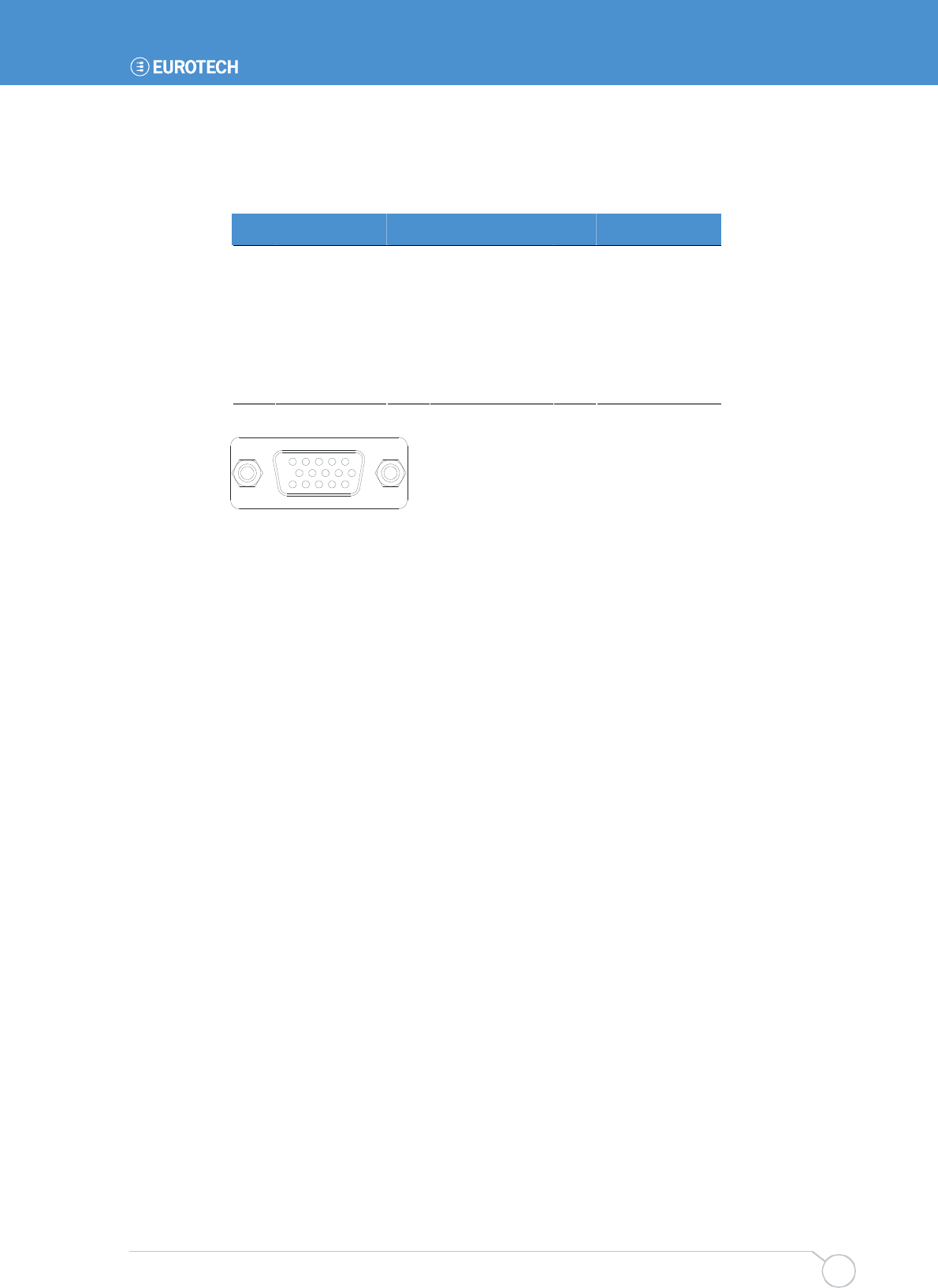
Appendix F - ZEUS-FPIF-CRT details
Issue D 95
J2 – CRT connector
Connector: Oupiin 7916-15FA/SN, 15-way, female, high density, right-angled D-Sub.
Pin Signal name Pin Signal name Pin Signal name
1 RED 6 RED GND 11 NC
2 GREEN 7 GREEN GND 12 NC
3 BLUE 8 BLUE GND 13 HSYNC
4 NC 9 5V_VGASAFE 14 VSYNC
5 TTL GND 10 SYNC GND 15 NC
(As viewed from
the connector pins)
15
15 11
610
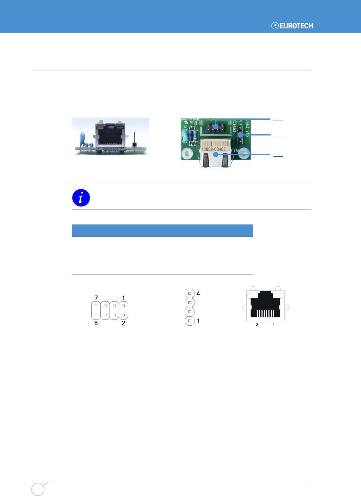
TITAN user manual
Issue D
96
Appendix G - Ethernet Breakout details
Eurotech can provide an Ethernet breakout board with an RJ45 connector to interface to
the TITAN Ethernet connectors J11 and J12. The Ethernet breakout board features
brackets for panel mounting ease. It also features easy connection between the TITAN
and a 10/100base-T Ethernet connection, as shown below:
The connectors on the following pages are shown in the same orientation as the
picture above.
Connector Function
PL1 10/100BaseTX Ethernet signals
PL2 Ethernet LEDs
PL3 RJ45 connector
Ethernet breakout PL1 Ethernet breakout PL2 Ethernet breakout PL3
PL1
PL2
PL3

Appendix G - Ethernet Breakout details
Issue D 97
Ethernet signal mapping between TITAN and Ethernet breakout connectors
Ethernet breakout PL3 -
RJ45
Ethernet breakout PL1 –
2x4-way header
TITAN J11 – 10/100BaseTX
Ethernet connector
Pin Signal name Pin Signal name Pin Signal name
1 Tx+ 1 Tx+ 1 Tx+
2 TX- 2 TX- 2 TX-
3 RX+ 3 RX+ 3 RX+
4 4 NC 4 NC
5
Bob Smith
Termination 5 NC 5 NC
6 RX- 6 RX- 6 RX-
7 7 NC 7 NC
8
Bob Smith
Termination 8 LANGND 8 LANGND
Ethernet LED signal mapping between TITAN and Ethernet breakout connectors
Ethernet breakout PL2 –
1x 4-way header
TITAN J12 – Ethernet status
LED's connector
Pin Signal name Pin Signal name
1 LINK LED+ 1 3.3V
2 LINK LED- 2 LINK (Green)
3 SPEED LED+ 3 3.3V
4 SPEED LED- 4 SPEED (Yellow)
5 3.3V
6 NC
}
}

TITAN user manual
Issue D
98
Appendix H - Acronyms and abbreviations
Amp Amplifier
API Application Program(ming) Interface
BTUART Bluetooth Universal Asynchronous Receiver / Transmitter
CCCR Core Clock Configuration Register
CODEC Coder/Decoder
COM Communication Port
CPLD Complex Programmable Logic Device
CPU Central Processing Unit (PXA270)
CMOS Complementary Metal Oxide Semiconductor
CRT Cathode Ray Tube
DMA Direct Memory Access
DUART Dual Universal Asynchronous Receiver / Transmitter
EEPROM Electrically Erasable and Programmable Read-Only Memory
EMC Electromagnetic Compatibility
FFUART Full Function Universal Asynchronous Receiver / Transmitter
FIFO First-In First-Out
FLASH A non-volatile memory that is preserved even if the power is lost
FPIF Flat Panel Interface
GPIO General Purpose Input/Output
I²C (=IIC) Intra Integrated Circuit bus
ICE In-Circuit-Emulator
IEEE Institute of Electrical and Electronics Engineers
IO Input/Output
ISA Industry Standard Architecture, Bus in the IBM-PC
JTAG Joint Test Action Group of IEEE
kbps kilo bits per second
LED Light Emitting Diode
LCD Liquid Crystal Display
LVDS Low Voltage Differential Signalling
Mbps mega bits per second
NA Not Applicable
NC No Connect
NU Not Used
OS Operating System
PC/104 Offers full architecture, hardware and software compatibility with the
PC ISA bus, but in ultra-compact 96mm x 91mm (3.775" x 3.550")
stackable modules
PCB Printed Circuit Board
PROM Programmable Read-Only Memory
PWM Pulse-Width Modulation
RAM Random Access Memory
Reg Regulator
RTC Real Time Clock
RX Receive

Appendix H - Acronyms and abbreviations
Issue D 99
SBC Single Board Computer
SDIO Secure Digital Input/Output
SDRAM Synchronous Dynamic Random Access Memory
SRAM Static Random Access Memory
STN Super Twisted Nematic, technology of passive matrix liquid crystal
STUART Standard Universal Asynchronous Receiver / Transmitter
TFT Thin Film Transistor, a type of LCD flat-panel display screen
TX Transmit
UART Universal Asynchronous Receiver / Transmitter
USB Universal Serial Bus
VGA Video Graphics Adapter, display resolution 640 x 480 pixels
TITAN-ICE TITAN-Industrial Compact Enclosure
TITAN user manual
Issue D
100
Appendix I - RoHS-6 Compliance - Materials
Declaration Form
Confirmation of Environmental Compatibility for Supplied Products
Substance Maximum concentration
Lead 0.1% by weight in homogeneous materials
Mercury 0.1% by weight in homogeneous materials
Hexavalent chromium 0.1% by weight in homogeneous materials
Polybrominated biphenyls (PBBs) 0.1% by weight in homogeneous materials
Polybrominated diphenyl ethers (PBDEs) 0.1% by weight in homogeneous materials
Cadmium 0.01% by weight in homogeneous materials
The products covered by this certificate include:
Product Name Eurotech Part Number
TITAN TITAN-520-Mx-Fx
Eurotech has based its material content knowledge on a combination of information provided by third
parties and auditing our suppliers and sub-contractor’s operational activities and arrangements. This
information is archived within the associated Technical Construction File. Eurotech has taken
reasonable steps to provide representative and accurate information, though may not have conducted
destructive testing or chemical analysis on incoming components and materials.
Additionally, packaging used by Eurotech for its products complies with the EU Directive 2004/12/EC in
that the total concentration of the heavy metals cadmium, hexavalent chromium, lead and mercury do
not exceed 100 ppm.
AMERICAS
North America
EUROTECH USA
US toll free +1 800.541.2003
tel. +1 301.490.4007
fax +1 301.490.4582
e-mail: sales.us@eurotech.com
e-mail:
support.us@eurotech.com
www.eurotech-inc.com
PARVUS CORPORATION
US toll-free +1 800.483.3152
tel. +1 801.483.1533
fax +1 801.483.1523
e-mail: sales@parvus.com
e-mail: tsupport@parvus.com
www.parvus.com
EUROPE
Central & Southern Europe
EUROTECH Italy
tel. +39 0433.485.411
fax +39 0433.485.499
e-mail: sales-it@eurotech.com
e-mail: support-it@eurotech.com
www.eurotech.com
Western Europe
EUROTECH UK
tel. +44 (0) 1223.403410
fax +44 (0) 1223.410457
e-mail: sales.uk@eurotech.com
e-mail:
support.uk@eurotech.com
www.eurotech.com
EUROTECH France
tel. +33 04.72.89.00.90
fax +33 04.78.70.08.24
e-mail: sales-fr@eurotech.com
e-mail: support-fr@eurotech.com
www.eurotech.com
Northern & Eastern Europe
EUROTECH Finland
tel. +358 9.477.888.0
fax +358 9.477.888.99
e-mail: sales-fi@eurotech.com
e-mail: support-fi@eurotech.com
www.eurotech.com
ASIA
Japan
ADVANET
tel. +81 86.245.2861
fax +81 86.245.2860
e-mail: sales@advanet.co.jp
www.advanet.co.jp
China
VANTRON
tel. + 86 28.85.12.39.30
fax +86 28.85.12.39.35
e-mail:
sales@vantrontech.com.cn
e-mail: support-cn@eurotech.com
www.vantrontech.com.cn
Eurotech Group Worldwide Presence

www.eurotech.com
