TPS54327 Datasheet. Www.s Manuals.com. Rc Ti
User Manual: Marking of electronic components, SMD Codes 54, 54-, 54319, 54327, 54332, 547E1, 547E2, 547F1, 547F2, 547G1, 547G2, 547H1, 547H2, 547M1, 547M2, 549, 54R, 54S204AI, 54W, 54b*, 54p, 54s, 54t. Datasheets BAT17-04, BAT17-04W, BSR17A, DTA114YE, DTA114YEB, DTA114YKA, DTA114YM, DTA114YUA, DTA114YUB, FMMT549, G5244A31U, G547E1RD1U, G547E2RD1U, G547F1RD1U, G547F2RD1U, G547G1RD1U, G547G2RD1U, G547H1RD1U, G547H2RD1U, G547M1RD1U, G547M2RD1U, IA4054, ICS854S204AGI, MM5Z3V6, PDTC143XEF, S504TR, TP4054, TPS54319, TPS54327
Open the PDF directly: View PDF ![]() .
.
Page Count: 30
- 1 Features
- 2 Applications
- 3 Description
- Table of Contents
- 4 Revision History
- 5 Pin Configuration and Functions
- 6 Specifications
- 7 Detailed Description
- 8 Application and Implementation
- 9 Power Supply Recommendations
- 10 Layout
- 11 Device and Documentation Support
- 12 Mechanical, Packaging, and Orderable Information
Vout(50mV/div)
Iout(2 A/div)
100 s/divm
Product
Folder
Sample &
Buy
Technical
Documents
Tools &
Software
Support &
Community
Reference
Design
TPS54327
SLVSAG1C –DECEMBER 2010–REVISED DECEMBER 2015
TPS54327 3-A Output Single Synchronous Step-Down Switcher
With Integrated FET
1 Features 3 Description
The TPS54327 device is an adaptive on-time D-
1• D-CAP2™ Mode Enables Fast Transient CAP2™ mode synchronous buck converter.
Response TheTPS54327 enables system designers to complete
• Low-Output Ripple and Allows Ceramic Output the suite of various end equipment’s power bus
Capacitor regulators with a cost effective, low component count,
low standby current solution. The main control loop
• Wide VIN Input Voltage Range: 4.5 V to 18 V for the TPS54327 uses the D-CAP2 mode control
• Output Voltage Range: 0.76 V to 7 V which provides a fast transient response with no
• Highly Efficient Integrated FETs Optimized external compensation components. The TPS54327
for Lower Duty Cycle Applications also has a proprietary circuit that enables the device
– 100 mΩ(High-Side) and 70 mΩ(Low-Side) to adopt to both low equivalent series resistance
(ESR) output capacitors, such as POSCAP or SP-
• High Efficiency, Less Than 10 μA at shutdown CAP, and ultra-low ESR ceramic capacitors. The
• High Initial Bandgap Reference Accuracy device operates from 4.5-V to 18-V VIN input. The
• Adjustable Soft Start output voltage can be programmed between 0.76 V
• Prebiased Soft Start and 7 V. The device also features an adjustable soft
start time. The TPS54327 is available in the 8-pin
• 700-kHz Switching Frequency (fSW)DDA package and 10-pin DRC, and is designed to
• Cycle-By-Cycle Overcurrent Limit operate from –40°C to 85°C.
2 Applications Device Information(1)
• Wide Range of Applications for Low Voltage PART NUMBER PACKAGE BODY SIZE (NOM)
System HSOP (8) 4.89 mm × 3.90 mm
TPS54327
– Digital TV Power Supply VSON (10) 3.00 mm × 3.00 mm
– High Definition Blu-ray Disc™ Players (1) For all available packages, see the orderable addendum at
the end of the data sheet.
– Networking Home Terminal
– Digital Set Top Box (STB)
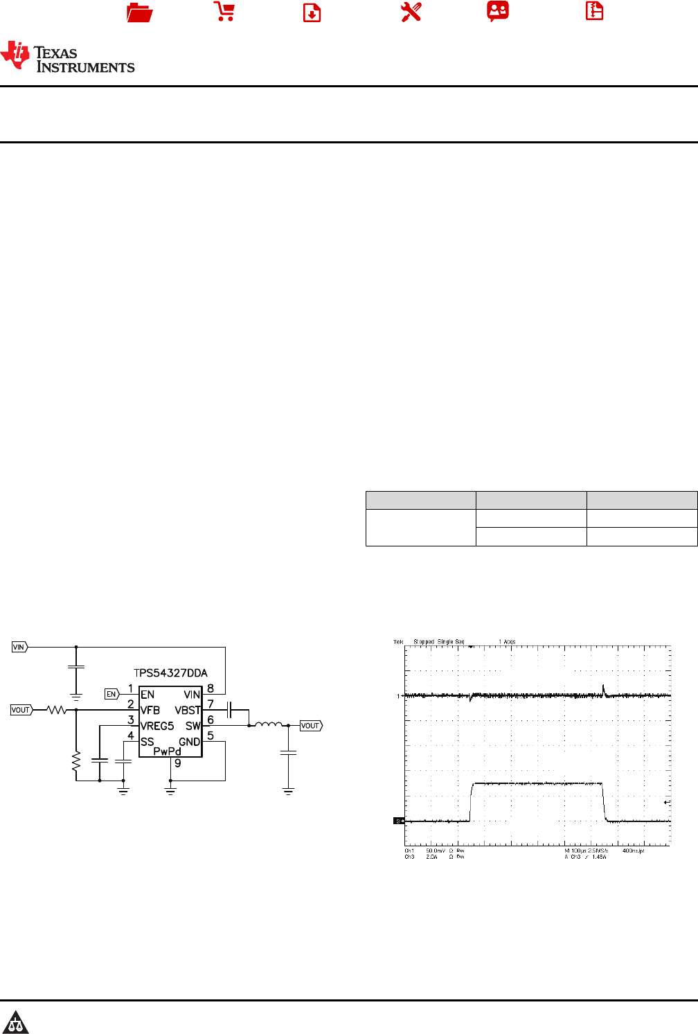
Simplified Schematic TPS54327 Transient Response
1
An IMPORTANT NOTICE at the end of this data sheet addresses availability, warranty, changes, use in safety-critical applications,
intellectual property matters and other important disclaimers. PRODUCTION DATA.

TPS54327
SLVSAG1C –DECEMBER 2010–REVISED DECEMBER 2015
www.ti.com
Table of Contents
7.4 Device Functional Modes.......................................... 9
1 Features.................................................................. 18 Application and Implementation ........................ 10
2 Applications ........................................................... 1
8.1 Application Information............................................ 10
3 Description ............................................................. 18.2 Typical Application ................................................. 10
4 Revision History..................................................... 29 Power Supply Recommendations...................... 14
5 Pin Configuration and Functions......................... 310 Layout................................................................... 14
6 Specifications......................................................... 410.1 Layout Guidelines ................................................. 14
6.1 Absolute Maximum Ratings ...................................... 410.2 Layout Examples................................................... 15
6.2 ESD Ratings.............................................................. 410.3 Thermal Considerations........................................ 17
6.3 Recommended Operating Conditions....................... 411 Device and Documentation Support ................. 18
6.4 Thermal Information.................................................. 511.1 Documentation Support ........................................ 18
6.5 Electrical Characteristics........................................... 511.2 Community Resources.......................................... 18
6.6 Typical Characteristics.............................................. 611.3 Trademarks........................................................... 18
7 Detailed Description .............................................. 711.4 Electrostatic Discharge Caution............................ 18
7.1 Overview ................................................................... 711.5 Glossary................................................................ 18
7.2 Functional Block Diagram ......................................... 712 Mechanical, Packaging, and Orderable
7.3 Feature Description................................................... 7Information ........................................................... 18
4 Revision History
NOTE: Page numbers for previous revisions may differ from page numbers in the current version.
Changes from Revision B (January 2012) to Revision C Page
• Added Pin Configuration and Functions section, ESD Ratings table, Feature Description section, Device Functional
Modes,Application and Implementation section, Power Supply Recommendations section, Layout section, Device
and Documentation Support section, and Mechanical, Packaging, and Orderable Information section .............................. 1
• Removed Ordering Information table .................................................................................................................................... 1
Changes from Revision A (October 2011) to Revision B Page
• Removed (SWIFT™) from the data sheet title ....................................................................................................................... 1
• Added "and 10-pin DRC" to the DESCRIPTION.................................................................................................................... 1
• Added the DRC-10 Pin package pin out ................................................................................................................................ 3
• Changed the VBST(vs SW) MAX value From: 6V to 6.5V in the Abs Max Ratings table ..................................................... 4
• Changed the VBST(vs SW) MAX value From: 5.7V to 6V in the ROC table......................................................................... 4
• Changed UVLO MIn Value From: 0.19 V To: 0.17 V............................................................................................................. 5
• Added Added a conditions statement "VIN = 12 V, TA = 25°C" to the TYPICAL CHARACTERISTICS............................... 6
• Changed Figure 10 title From: 1.05-V, 50-mA to 2-A LOAD TRANSIENT RESPONSE To: 1.05-V, 0-A to 3-A LOAD
TRANSIENT RESPONSE .................................................................................................................................................... 12
• Changed Figure 12 Figure Title From: (IO= 2 A) To: (IO= 3 A)........................................................................................... 12
• Changed Figure 13 Figure Title From: (IO= 2 A) To: (IO= 3 A)........................................................................................... 12
• Added Figure 17................................................................................................................................................................... 16
Changes from Original (November 2010) to Revision A Page
• Changed Pin 6 (SW) Description In the Pin Functions table ................................................................................................ 3
• Changed the VENH Min value From: 2 V To: 1.6 V in the Logic Threshold section................................................................ 5
• Changed Figure 4................................................................................................................................................................... 6
• Changed Equation 1............................................................................................................................................................... 8
2Submit Documentation Feedback Copyright © 2010–2015, Texas Instruments Incorporated
Product Folder Links: TPS54327
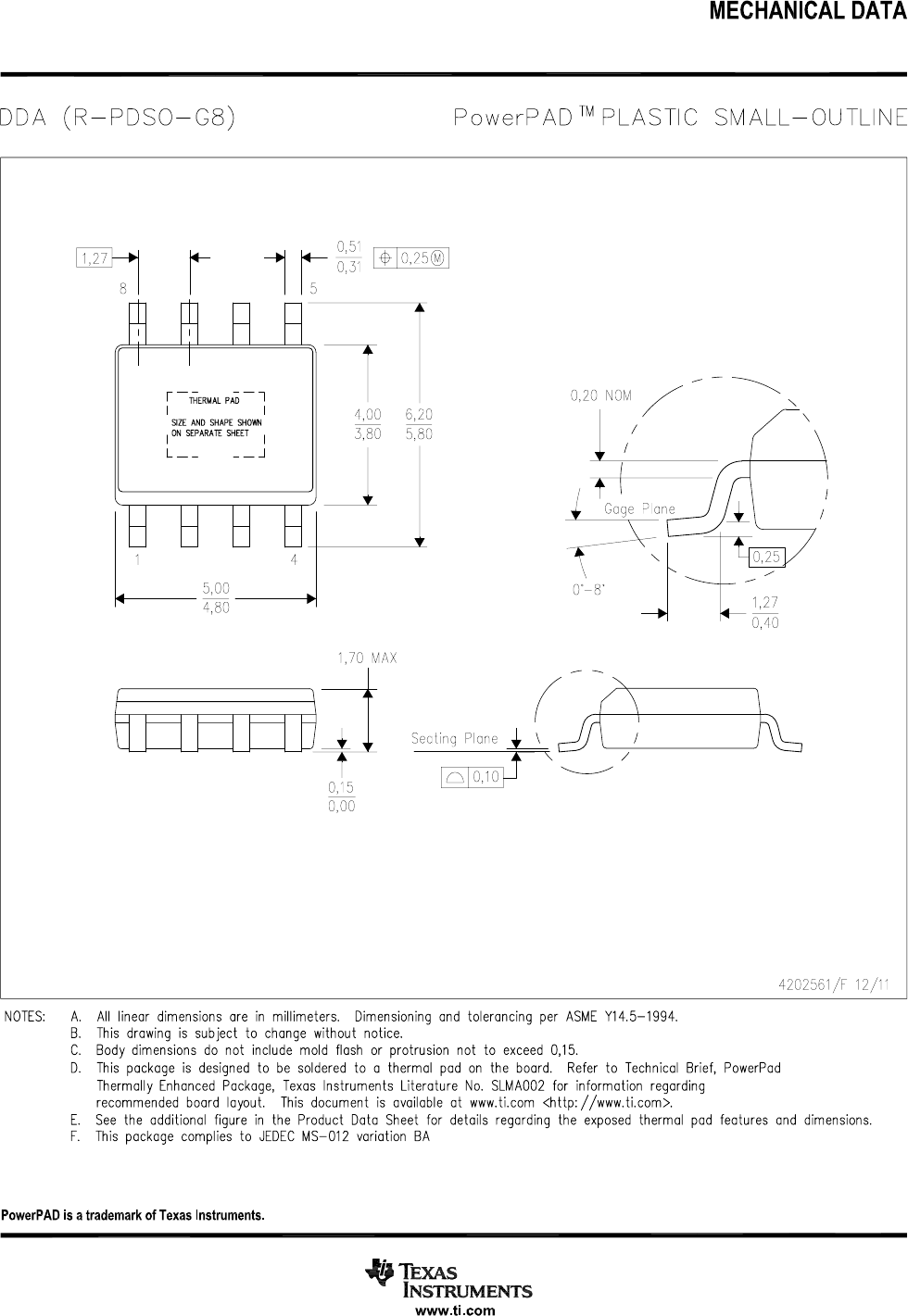
1
2
3
45
6
7
8
SW
GND
VBST
VIN
EN
VFB
VREG5
SS
TPS54327
(DDA)
PowerPAD
EN
VFB
VREG5
SS
GND
VIN
VIN
VBST
SW
SW
Exposed
Thermal
Die PAD
on
Underside
PGND
1
2
3
4
5
10
9
8
7
6
TPS54327
www.ti.com
SLVSAG1C –DECEMBER 2010–REVISED DECEMBER 2015
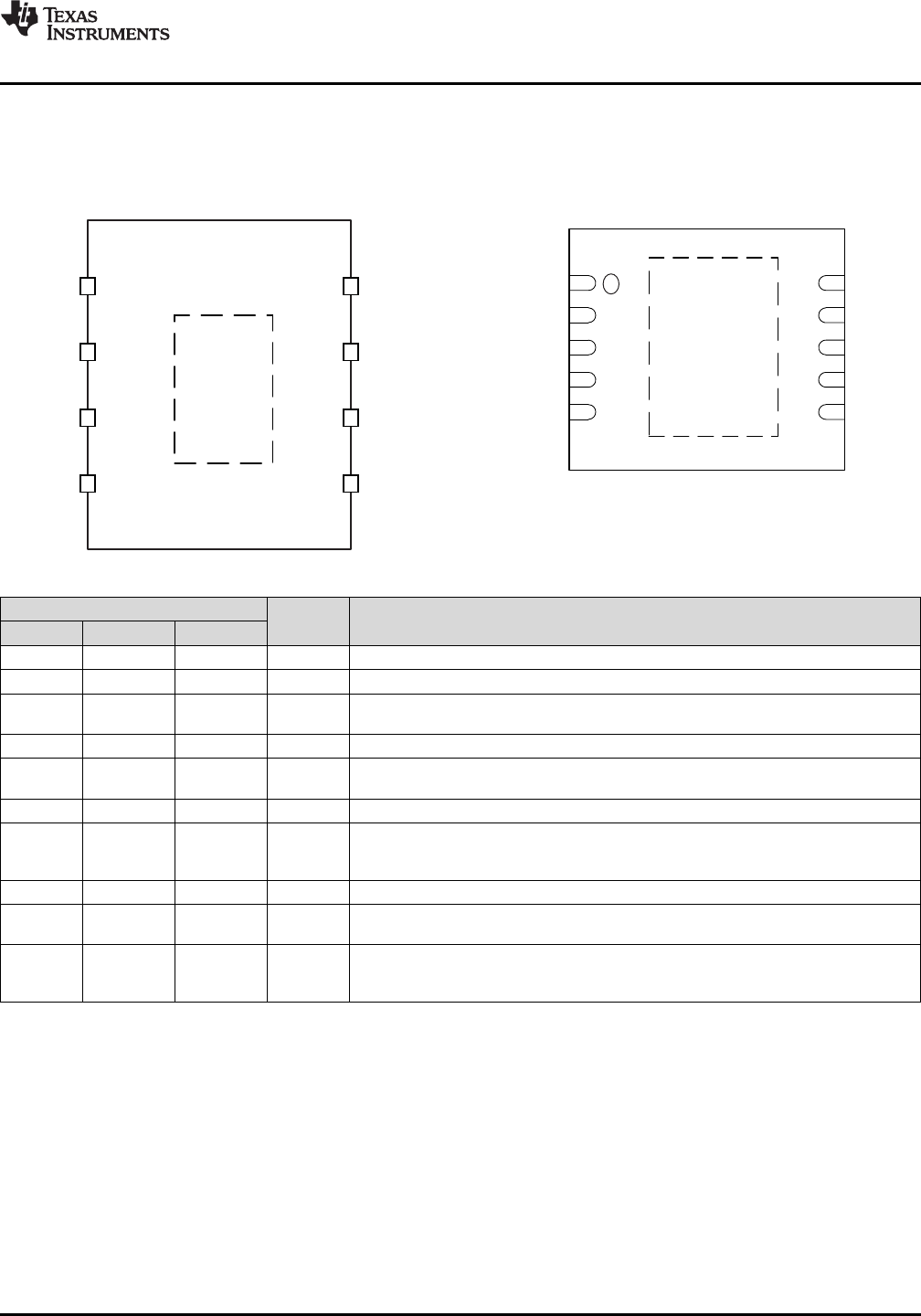
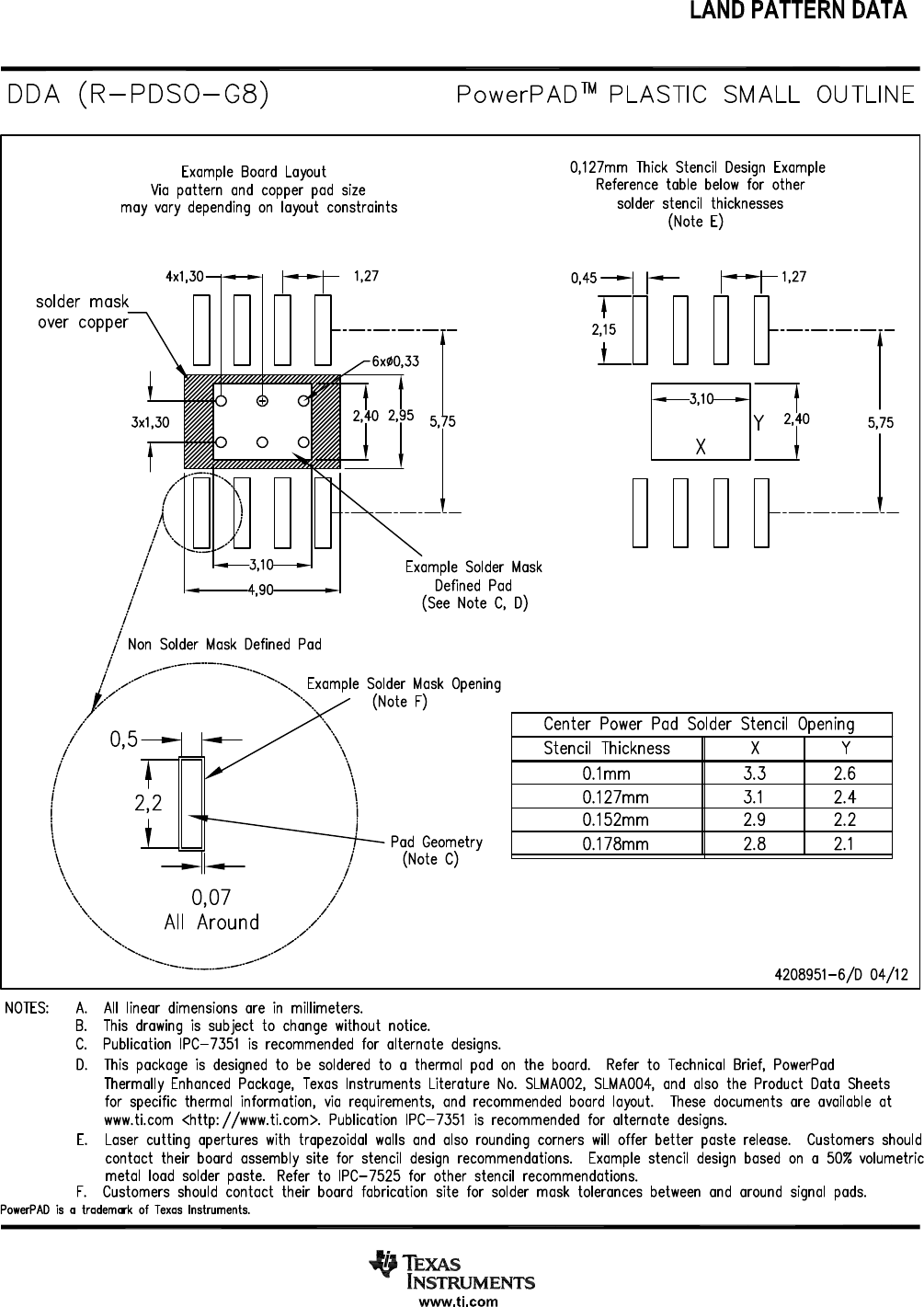
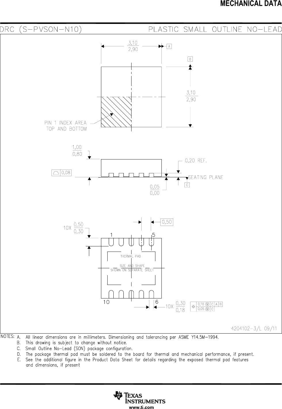
5 Pin Configuration and Functions
DDA Package DRC Package
8-Pin HSOP 10-Pin VSON
Top View Top View
Pin Functions
PIN TYPE DESCRIPTION
NAME HSOP VSON
EN 1 1 I Enable input control. Active high.
VFB 2 2 I Converter feedback input. Connect to output voltage with feedback resistor divider.
5.5 V power supply output. A capacitor (typical 1 µF) should be connected to GND.
VREG5 3 3 O VREG5 is not active when EN is low.
SS 4 4 O Soft-start control. An external capacitor should be connected to GND.
Ground pin. Power ground return for switching circuit. Connect sensitive SS and VFB
GND 5 5 G returns to GND at a single point.
SW 6 6, 7 O Switch node connection between high-side NFET and low-side NFET.
Supply input for the high-side FET gate drive circuit. Connect 0.1µF capacitor
VBST 7 8 I between VBST and SW pins. An internal diode is connected between VREG5 and
VBST.
VIN 8 9, 10 P Input voltage supply pin.
PowerPAD of the package. Must be soldered to achieve appropriate dissipation. Must
PowerPAD Back side — G be connected to GND.
Exposed Thermal pad of the package. PGND power ground return of internal low-side FET.
thermal — Back side G Must be soldered to achieve appropriate dissipation.
pad
Copyright © 2010–2015, Texas Instruments Incorporated Submit Documentation Feedback 3
Product Folder Links: TPS54327
TPS54327
SLVSAG1C –DECEMBER 2010–REVISED DECEMBER 2015
www.ti.com
6 Specifications
6.1 Absolute Maximum Ratings
over operating free-air temperature range (unless otherwise noted) (1)
MIN MAX UNIT
VIN, EN –0.3 20 V
VBST –0.3 26 V
VBST (10 ns transient) –0.3 28 V
Input voltage VBST (vs SW) –0.3 6.5 V
VFB, SS –0.3 6.5 V
SW –2 20 V
SW (10 ns transient) –3 22 V
VREG5 –0.3 6.5 V
Output voltage GND –0.3 0.3 V
Voltage from GND to thermal pad, Vdiff –0.2 0.2 V
Operating junction temperature, TJ–40 150 °C
Storage temperature, Tstg –55 150 °C
(1) Stresses beyond those listed under Absolute Maximum Ratings may cause permanent damage to the device. These are stress ratings
only, and functional operation of the device at these or any other conditions beyond those indicated under Recommended Operating
Conditions is not implied. Exposure to absolute-maximum-rated conditions for extended periods may affect device reliability.
6.2 ESD Ratings
VALUE UNIT
Human body model (HBM), per ANSI/ESDA/JEDEC JS-001(1) ±2000
V(ESD) Electrostatic discharge V
Charged-device model (CDM), per JEDEC specification JESD22-C101(2) ±500
(1) JEDEC document JEP155 states that 500-V HBM allows safe manufacturing with a standard ESD control process.
(2) JEDEC document JEP157 states that 250-V CDM allows safe manufacturing with a standard ESD control process.
6.3 Recommended Operating Conditions
over operating free-air temperature range (unless otherwise noted)
MIN MAX UNIT
VIN Supply input voltage 4.5 18 V
VBST –0.1 24
VBST (10 ns transient) –0.1 27
VBST(vs SW) –0.1 6
SS –0.1 5.7
VIInput voltage EN –0.1 18 V
VFB –0.1 5.5
SW –1.8 18
SW (10 ns transient) –3 21
GND –0.1 0.1
VOOutput voltage VREG5 –0.1 5.7 V
IOOutput Current IVREG5 0 10 mA
TAOperating free-air temperature –40 85 °C
TJOperating junction temperature –40 150 °C
4Submit Documentation Feedback Copyright © 2010–2015, Texas Instruments Incorporated
Product Folder Links: TPS54327
TPS54327
www.ti.com
SLVSAG1C –DECEMBER 2010–REVISED DECEMBER 2015
6.4 Thermal Information
TPS54327
THERMAL METRIC(1) DDA (HSOP) DRC (VSON) UNIT
8 PINS 10 PINS
RθJA Junction-to-ambient thermal resistance 42.1 43.9 °C/W
RθJC(top) Junction-to-case (top) thermal resistance 50.9 55.4 °C/W
RθJB Junction-to-board thermal resistance 31.8 18.9 °C/W
ψJT Junction-to-top characterization parameter 5 0.7 °C/W
ψJB Junction-to-board characterization parameter 13.5 19.1 °C/W
RθJC(bot) Junction-to-case (bottom) thermal resistance 7.1 5.3 °C/W
(1) For more information about traditional and new thermal metrics, see the Semiconductor and IC Package Thermal Metrics application
report, SPRA953.
6.5 Electrical Characteristics
over operating free-air temperature range VIN = 12 V (unless otherwise noted)
PARAMETER TEST CONDITIONS MIN TYP MAX UNIT
SUPPLY CURRENT
VIN current, TA= 25°C, EN = 5 V,
IVIN Operating - non-switching supply current 800 1200 μA
VFB = 0.8 V
IVINSDN Shutdown supply current VIN current, TA= 25°C, EN = 0 V 1.8 10 μA
LOGIC THRESHOLD
VENH EN high-level input voltage EN 1.6 V
VENL EN low-level input voltage EN 0.45 V
VFB VOLTAGE AND DISCHARGE RESISTANCE
VFBTH VFB threshold voltage TA= 25°C, VO= 1.05 V, continuous mode 749 765 781 mV
IVFB VFB input current VFB = 0.8 V, TA= 25°C 0 ±0.1 μA
VREG5 OUTPUT
TA= 25°C, 6 V < VIN < 18 V,
VVREG5 VREG5 output voltage 5.2 5.5 5.7 V
0 < IVREG5 < 5 mA
VLN5 Line regulation 6 V < VIN < 18 V, IVREG5 = 5 mA 25 mV
VLD5 Load regulation 0 mA < IVREG5 < 5 mA 100 mV
IVREG5 Output current VIN = 6 V, VREG5 = 4 V, TA= 25°C 60 mA
MOSFET
RDS(on)h High-side switch resistance 25°C, VBST - SW = 5.5 V 100 mΩ
RDS(on)l Low-side switch resistance 25°C 70 mΩ
CURRENT LIMIT
Iocl Current limit L out = 1.5 μH(1), TA= -20ºC to 85ºC 3.5 4.2 5.7 A
THERMAL SHUTDOWN
Shutdown temperature (1) 165
TSDN Thermal shutdown threshold °C
Hysteresis (1) 30
ON-TIME TIMER CONTROL
tON ON-time VIN = 12 V, VO= 1.05 V 150 ns
tOFF(MIN) Minimum OFF-time TA= 25°C, VFB = 0.7 V 260 310 ns
SOFT START
ISSC SS charge current VSS = 0 V 1.4 2 2.6 μA
ISSD SS discharge current VSS = 0.5 V 0.05 0.1 mA
UVLO
Wakeup VREG5 voltage 3.45 3.75 4.05
UVLO UVLO threshold V
Hysteresis VREG5 voltage 0.17 0.32 0.45
(1) Not production tested.
Copyright © 2010–2015, Texas Instruments Incorporated Submit Documentation Feedback 5
Product Folder Links: TPS54327
400
450
500
550
600
650
700
750
800
850
900
0 5 10 15 20
V -InputVoltage-V
IN
f -SwitchingFrequency-kHz
s
V =1.8V
O
V =1.05V
O
I =1 A
O
V =3.3V
O
400
450
500
550
600
650
700
750
800
850
900
0 0.5 1 1.5 2 2.5 3
I -OutputCurrent- A
O
f -SwitchingFrequency-kHz
s
V =3.3V
O
V =1.8V
O
V =1.05V
O
0
10
20
30
40
50
60
70
80
90
100
0 2 4 6 8 10 12 14 16 18 20
EN-InputVoltage-V
V =18V
IN
EN-InputCurrent- Am
40
50
60
70
80
90
100
0.0 0.5 1.0 1.5 2.0 2.5 3.0
V = 1.8 V
OUT
V = 2.5 V
OUT
V = 3.3 V
OUT
I - Output Current - A
OUT
Efficiency - %
0
200
400
600
800
1000
1200
-50 050 100 150
T - Junction Temperature - °C
j
I - Supply Current - µA
VIN
0
2.0
4.0
6.0
8.0
10.0
-50 050 100 150
T - Junction Temperature - °C
j
I - Supply Current - µA
VINSDN
TPS54327
SLVSAG1C –DECEMBER 2010–REVISED DECEMBER 2015
www.ti.com
6.6 Typical Characteristics
VIN = 12 V, TA= 25°C (unless otherwise noted)
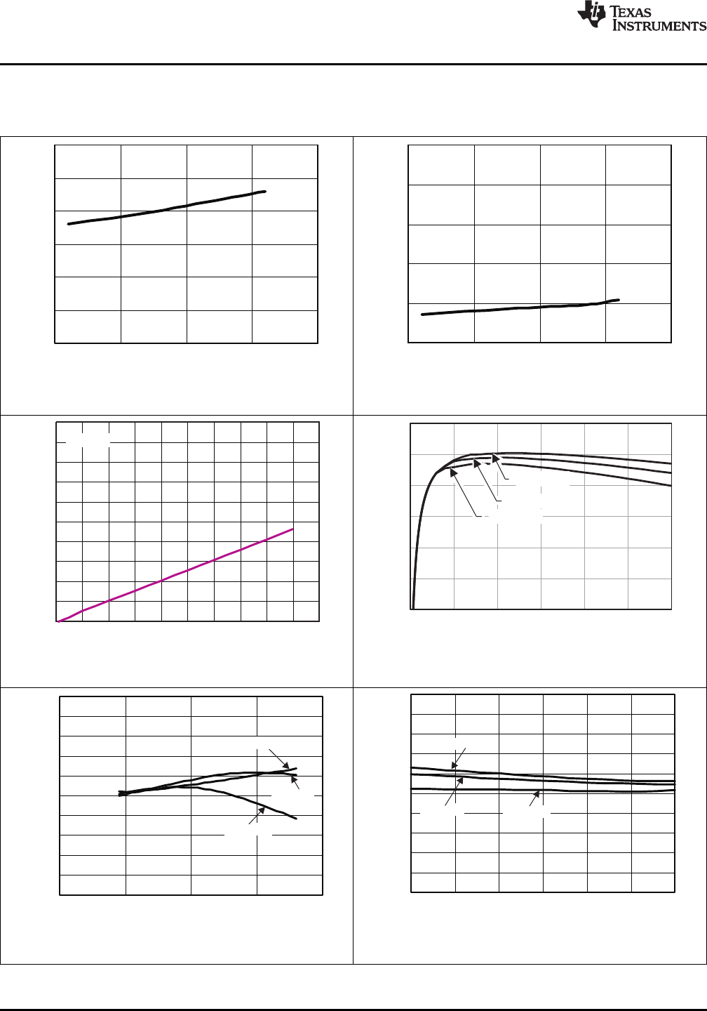
Figure 1. VIN Current vs Junction Temperature Figure 2. VIN Shutdown Current vs Junction Temperature
Figure 4. Efficiency vs Output Current
Figure 3. EN Current vs EN Voltage
Figure 6. Switching Frequency vs Output Current
Figure 5. Switching Frequency vs Input Voltage
6Submit Documentation Feedback Copyright © 2010–2015, Texas Instruments Incorporated
Product Folder Links: TPS54327
SW
VBST
EN
VFB
GND
VO
4
5
6
2
1
7
VIN
SS
VIN
VREG5
EN
Logic
SW
PGND
Protection
Logic
Ref
SS
UVLO
UVLO
Softstart
SS
REF
TSD
Ref
VREG5
8
VIN
Ceramic
Capacitor
3
SGND
SGND
PGND
PWM
+
-
+
OCP
+
-
VREG5
XCON
VREG5
Control Logic
1 shot
ON
TPS54327
www.ti.com
SLVSAG1C –DECEMBER 2010–REVISED DECEMBER 2015
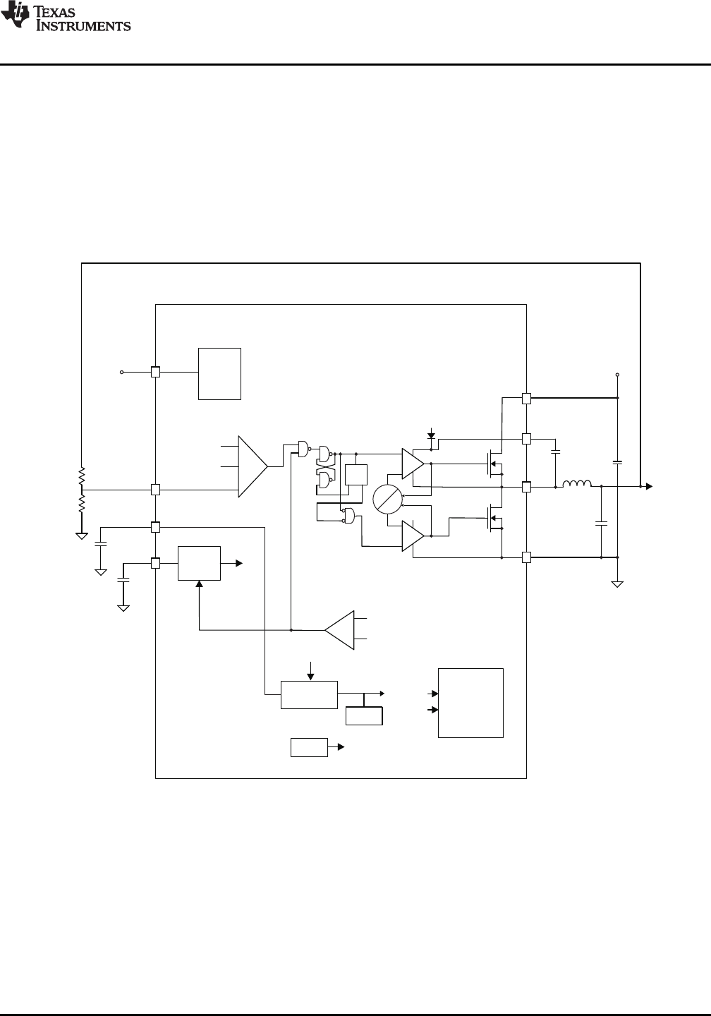
7 Detailed Description
7.1 Overview
The TPS54327 device is a 3-A synchronous step-down (buck) converter with two integrated N-channel
MOSFETs. It operates using D-CAP2 mode control. The fast transient response of D-CAP2 control reduces the
output capacitance required to meet a specific level of performance. Proprietary internal circuitry allows the use
of low ESR output capacitors including ceramic and special polymer types.
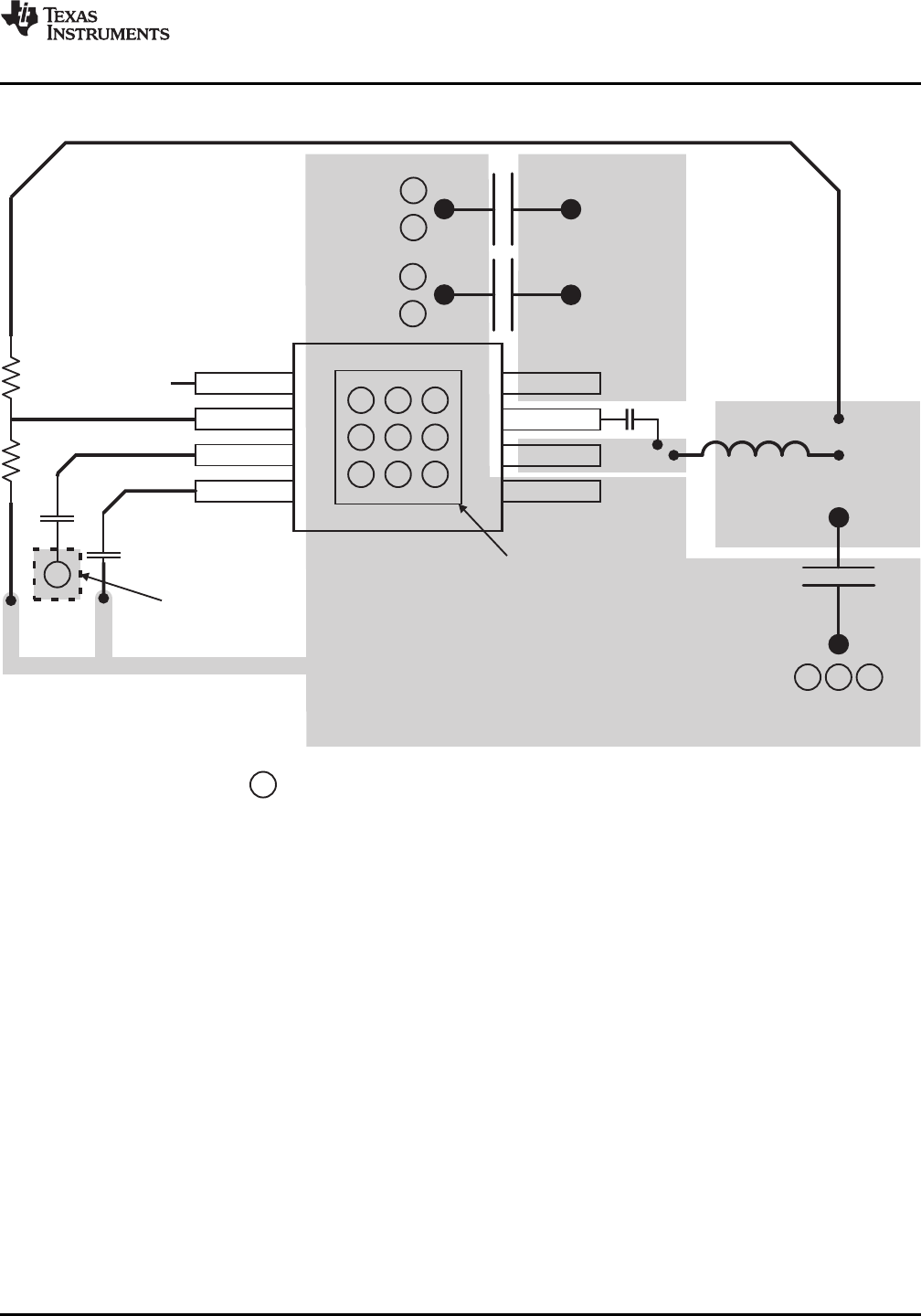
7.2 Functional Block Diagram
7.3 Feature Description
7.3.1 PWM Operation
The main control loop of the TPS54327 is an adaptive ON-time pulse width modulation (PWM) controller that
supports a proprietary D-CAP2 mode control. D-CAP2 mode control combines constant on-time control with an
internal compensation circuit for pseudo-fixed frequency and low external component count configuration with
both low ESR and ceramic output capacitors. It is stable even with virtually no ripple at the output.
Copyright © 2010–2015, Texas Instruments Incorporated Submit Documentation Feedback 7
Product Folder Links: TPS54327

C6(nF) x V x 1.1 C6(nF) x 0.765 x 1.1
REF
t (ms) = =
SS I ( A) 2
SS m
TPS54327
SLVSAG1C –DECEMBER 2010–REVISED DECEMBER 2015
www.ti.com
Feature Description (continued)
At the beginning of each cycle, the high-side MOSFET is turned on. This MOSFET is turned off after internal one
shot timer expires. This one shot is set by the converter input voltage, VIN, and the output voltage, VO, to
maintain a pseudo-fixed frequency over the input voltage range, hence it is called adaptive on-time control. The
one-shot timer is reset and the high-side MOSFET is turned on again when the feedback voltage falls below the
reference voltage. An internal ramp is added to reference voltage to simulate output ripple, eliminating the need
for ESR induced output ripple from D-CAP2 mode control.
7.3.2 PWM Frequency and Adaptive ON-Time Control
TPS54327 uses an adaptive on-time control scheme and does not have a dedicated on-board oscillator. The
TPS54327 runs with a pseudo-constant frequency of 700 kHz by using the input voltage and output voltage to
set the on-time one-shot timer. The on-time is inversely proportional to the input voltage and proportional to the
output voltage, therefore, when the duty ratio is VOUT/VIN, the frequency is constant.
7.3.3 Soft-Start and Prebiased Soft-Start
The soft start function is adjustable. When the EN pin becomes high, 2-μA current begins charging the capacitor
which is connected from the SS pin to GND. Smooth control of the output voltage is maintained during start up.
The equation for the slow start time is shown in Equation 1. VFB voltage is 0.765 V and SS pin source current is
2μA.
(1)
The TPS54327 contains a unique circuit to prevent current from being pulled from the output during start-up if the
output is prebiased. When the soft-start commands a voltage higher than the prebias level (internal soft start
becomes greater than feedback voltage VFB), the controller slowly activates synchronous rectification by starting
the first low side FET gate driver pulses with a narrow on-time. It then increments that on-time on a cycle-by-
cycle basis until it coincides with the time dictated by (1-D), where D is the duty cycle of the converter. This
scheme prevents the initial sinking of the prebias output, and ensure that the out voltage (VO) starts and ramps
up smoothly into regulation and the control loop is given time to transition from prebiased start-up to normal
mode operation.
7.3.4 Current Protection
The output overcurrent protection (OCP) is implemented using a cycle-by-cycle valley detect control circuit. The
switch current is monitored by measuring the low-side FET switch voltage between the SW pin and GND. This
voltage is proportional to the switch current. To improve accuracy, the voltage sensing is temperature
compensated.
During the on time of the high-side FET switch, the switch current increases at a linear rate determined by Vin,
Vout, the on-time and the output inductor value. During the on time of the low-side FET switch, this current
decreases linearly. The average value of the switch current is the load current IOUT. The TPS54327 constantly
monitors the low-side FET switch voltage, which is proportional to the switch current, during the low-side on-time.
If the measured voltage is above the voltage proportional to the current limit, an internal counter is incremented
per each SW cycle and the converter maintains the low-side switch on until the measured voltage is below the
voltage corresponding to the current limit at which time the switching cycle is terminated and a new switching
cycle begins. In subsequent switching cycles, the on-time is set to a fixed value and the current is monitored in
the same manner. If the overcurrent condition exists for 7 consecutive switching cycles, the internal OCL
threshold is set to a lower level, reducing the available output current. When a switching cycle occurs where the
switch current is not above the lower OCL threshold, the counter is reset and the OCL limit is returned to the
higher value.
There are some important considerations for this type of overcurrent protection. The load current one half of the
peak-to-peak inductor current higher than the overcurrent threshold. Also when the current is being limited, the
output voltage tends to fall as the demanded load current may be higher than the current available from the
converter. This may cause the output voltage to fall. When the overcurrent condition is removed, the output
voltage will return to the regulated value. This protection is nonlatching.
8Submit Documentation Feedback Copyright © 2010–2015, Texas Instruments Incorporated
Product Folder Links: TPS54327

TPS54327
www.ti.com
SLVSAG1C –DECEMBER 2010–REVISED DECEMBER 2015
Feature Description (continued)
7.3.5 UVLO Protection
Undervoltage lock out protection (UVLO) monitors the voltage of the VREG5 pin. When the VREG5 voltage is lower
than UVLO threshold voltage, the TPS54327 is shut off. This is protection is non-latching.
7.3.6 Thermal Shutdown
TPS54327 monitors the temperature of itself. If the temperature exceeds the threshold value (typically 165°C),
the device is shut off. This is non-latch protection.
7.4 Device Functional Modes
7.4.1 Normal Operation
When the input voltage is above the UVLO threshold and the EN voltage is above the enable threshold, the
TPS54327 device operates in normal switching mode. Normal continuous conduction mode(CCM) occurs when
the minimum switch current is above 0 A. In CM, the TPS54327 device operates at a quasi-fixed frequency of
650 kHz.
7.4.2 Forced CCM Operation
When the TPS54327 device is in normal CCM operating mode and switch current falls below 0 A, the device
begins operating in forced CCM.
Copyright © 2010–2015, Texas Instruments Incorporated Submit Documentation Feedback 9
Product Folder Links: TPS54327
TPS54327
SLVSAG1C –DECEMBER 2010–REVISED DECEMBER 2015
www.ti.com
8 Application and Implementation
NOTE
Information in the following applications sections is not part of the TI component
specification, and TI does not warrant its accuracy or completeness. TI’s customers are
responsible for determining suitability of components for their purposes. Customers should
validate and test their design implementation to confirm system functionality.
8.1 Application Information
The TPS54327 device is used as a step converter that converts a voltage of 4.5 V to 18 V to a lower voltage.
WEBENCH software is available to aid in the design and analysis of circuits.
8.2 Typical Application
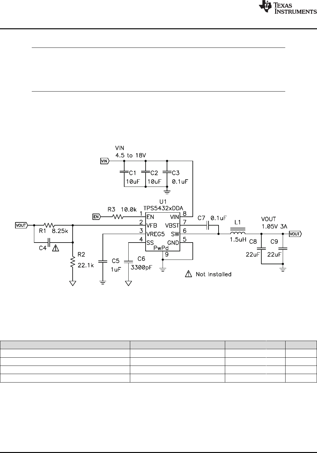
Figure 7. Schematic Diagram
8.2.1 Design Requirements
Use the parameters in Table 1 for this application.
Table 1. TPS54327EVM-686 Performance Specifications Summary
PARAMETERS TEST CONDITIONS MIN TYP MAX UNIT
Input voltage range (VIN) 4.5 12 18 V
Output voltage 1.05 V
Operating frequency VIN = 12 V, IO= 1 A 675 kHz
Output current range 0 3 A
8.2.2 Detailed Design Procedure
To begin the design process, you must know a few application parameters:
• Input voltage range
• Output voltage
• Output current
• Output voltage ripple
• Input voltage ripple
10 Submit Documentation Feedback Copyright © 2010–2015, Texas Instruments Incorporated
Product Folder Links: TPS54327
2 2
=IPP
Lo(RMS) O
1
+12
I I I
lpp
= +
Ipeak O2
I
I I
V V
VIN(max) OUT
OUT
= x
IPP V L x
IN(max) O SW
-
If
F =
P
OUT OUT
1
2 L x Cp
V = 0.765 x
OUT
R1
1 + R2
æ ö
÷
ç÷
ç÷
÷
ç
è ø
TPS54327
www.ti.com
SLVSAG1C –DECEMBER 2010–REVISED DECEMBER 2015
8.2.2.1 Output Voltage Resistors Selection
The output voltage is set with a resistor divider from the output node to the VFB pin. TI recommends using 1%
tolerance or better divider resistors. Start by using Equation 2 to calculate VOUT.
To improve efficiency at very light loads consider using larger value resistors, too high of resistance will be more
susceptible to noise and voltage errors from the VFB input current will be more noticeable.
(2)
8.2.2.2 Output Filter Selection
The output filter used with the TPS54327 is an LC circuit. This LC filter has double pole at:
(3)
At low frequencies, the overall loop gain is set by the output set-point resistor divider network and the internal
gain of the TPS54327. The low-frequency phase is 180 degrees. At the output filter pole frequency, the gain rolls
off at a -40 dB per decade rate and the phase drops rapidly. D-CAP2™ introduces a high-frequency zero that
reduces the gain roll off to -20 dB per decade and increases the phase to 90 degrees one decade above the
zero frequency. The inductor and capacitor selected for the output filter must be selected so that the double pole
of Equation 3 is located below the high-frequency zero but close enough that the phase boost provided be the
high-frequency zero provides adequate phase margin for a stable circuit. To meet this requirement use the
values recommended in Table 2
Table 2. Recommended Component Values
OUTPUT VOLTAGE (V) R1 (kΩ) R2 (kΩ) C4 (pF) L1 (µH) C8 + C9 (µF)
1 6.81 22.1 1.5 22 to 68
1.05 8.25 22.1 1.5 22 to 68
1.2 12.7 22.1 1.5 22 to 68
1.8 30.1 22.1 5 - 22 2.2 22 to 68
2.5 49.9 22.1 5 - 22 2.2 22 to 68
3.3 73.2 22.1 5 - 22 2.2 22 to 68
5 124 22.1 5 - 22 3.3 22 to 68
6.5 165 22.1 5 - 22 3.3 22 to 68
Because the DC gain is dependent on the output voltage, the required inductor value will increase as the output
voltage increases. For higher output voltages above 1.8 V, additional phase boost can be achieved by adding a
feed forward capacitor (C4) in parallel with R1
The inductor peak-to-peak ripple current, peak current and RMS current are calculated using Equation 4,
Equation 5 and Equation 6. The inductor saturation current rating must be greater than the calculated peak
current and the RMS or heating current rating must be greater than the calculated RMS current. Use 700 kHz for
fSW.
Use 700 kHz for fSW. Make sure the chosen inductor is rated for the peak current of Equation 5 and the RMS
current of Equation 6.
(4)
(5)
(6)
For this design example, the calculated peak current is 3.47 A and the calculated RMS current is 3.01 A. The
inductor used is a TDK SPM6530-1R5M100 with a peak current rating of 11.5 A and an RMS current rating of
11 A.
Copyright © 2010–2015, Texas Instruments Incorporated Submit Documentation Feedback 11
Product Folder Links: TPS54327
0 5 10 15 20
V -InputVoltage-V
I
1.04
1.05
1.06
1.07
1.08
V -OutputVoltage-V
O
I =1 A
O
I =0 A
O
0 0.5 1 1.5 2 2.5 3
I -OutputCurrent- A
O
1.04
1.05
1.06
1.07
1.08
V -OutputVoltage-V
O
V =12V
IN
V =18V
IN
V =5V
IN
IN
OUT OUT
=
Co(RMS)
IN O SW
V x (V - V )
12 x V x L x
If
TPS54327
SLVSAG1C –DECEMBER 2010–REVISED DECEMBER 2015
www.ti.com
The capacitor value and ESR determines the amount of output voltage ripple. The TPS54327 is intended for use
with ceramic or other low ESR capacitors. Recommended values range from 22uF to 68uF. Use Equation 7 to
determine the required RMS current rating for the output capacitor.
(7)
For this design two TDK C3216X5R0J226M 22-µF output capacitors are used. The typical ESR is 2 mΩeach.
The calculated RMS current is 0.271 A and each output capacitor is rated for 4 A.
8.2.2.3 Input Capacitor Selection
The TPS54327 requires an input decoupling capacitor and a bulk capacitor is needed depending on the
application. TI recommends a ceramic capacitor over 10 μF for the decoupling capacitor. TI also recommends
connecting an additional 0.1-µF capacitor from pin 14 to ground to improve the stability of the overcurrent limit
function. The capacitor voltage rating must be greater than the maximum input voltage.
8.2.2.4 Bootstrap Capacitor Selection
A 0.1 µF. ceramic capacitor must be connected between the VBST to SW pin for proper operation. TI
recommends using a ceramic capacitor.
8.2.2.5 VREG5 Capacitor Selection
A 1-µF ceramic capacitor must be connected between the VREG5 to GND pin for proper operation. TI
recommends using a ceramic capacitor.
8.2.3 Application Curves
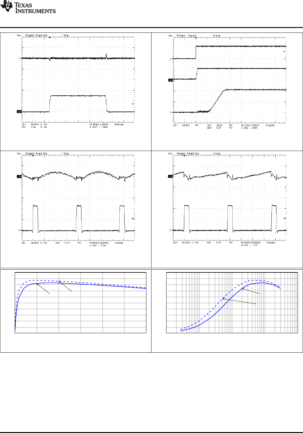
Figure 8. 1.05-V Output Voltage vs Output Current Figure 9. 1.05-V Output Voltage vs Input Voltage
12 Submit Documentation Feedback Copyright © 2010–2015, Texas Instruments Incorporated
Product Folder Links: TPS54327
0.0 0.5 1.0 1.5 2.0 2.5 3.0
0.0
10.0
20.0
30.0
40.0
50.0
60.0
70.0
80.0
90.0
100.0
VIN = 12 V VIN = 5 V
Output Current (A)
Efficiency (%)
0.001 0.01 0.1 1 10
0.0
10.0
20.0
30.0
40.0
50.0
60.0
70.0
80.0
90.0
100.0
VIN = 12 V
VIN = 5 V
Output Current (A)
Efficiency (%)
V (10mV/div)
O
V =1.05V
O
SW(5V/div)
V =1.05V
OV (50mV/div)
IN
SW(5V/div)
EN(10V/div)
VREG5(5V/div)
1ms/div)
Vout(0.5V/div)
Vout(50mV/div)
Iout(2 A/div)
100 s/divm
TPS54327
www.ti.com
SLVSAG1C –DECEMBER 2010–REVISED DECEMBER 2015
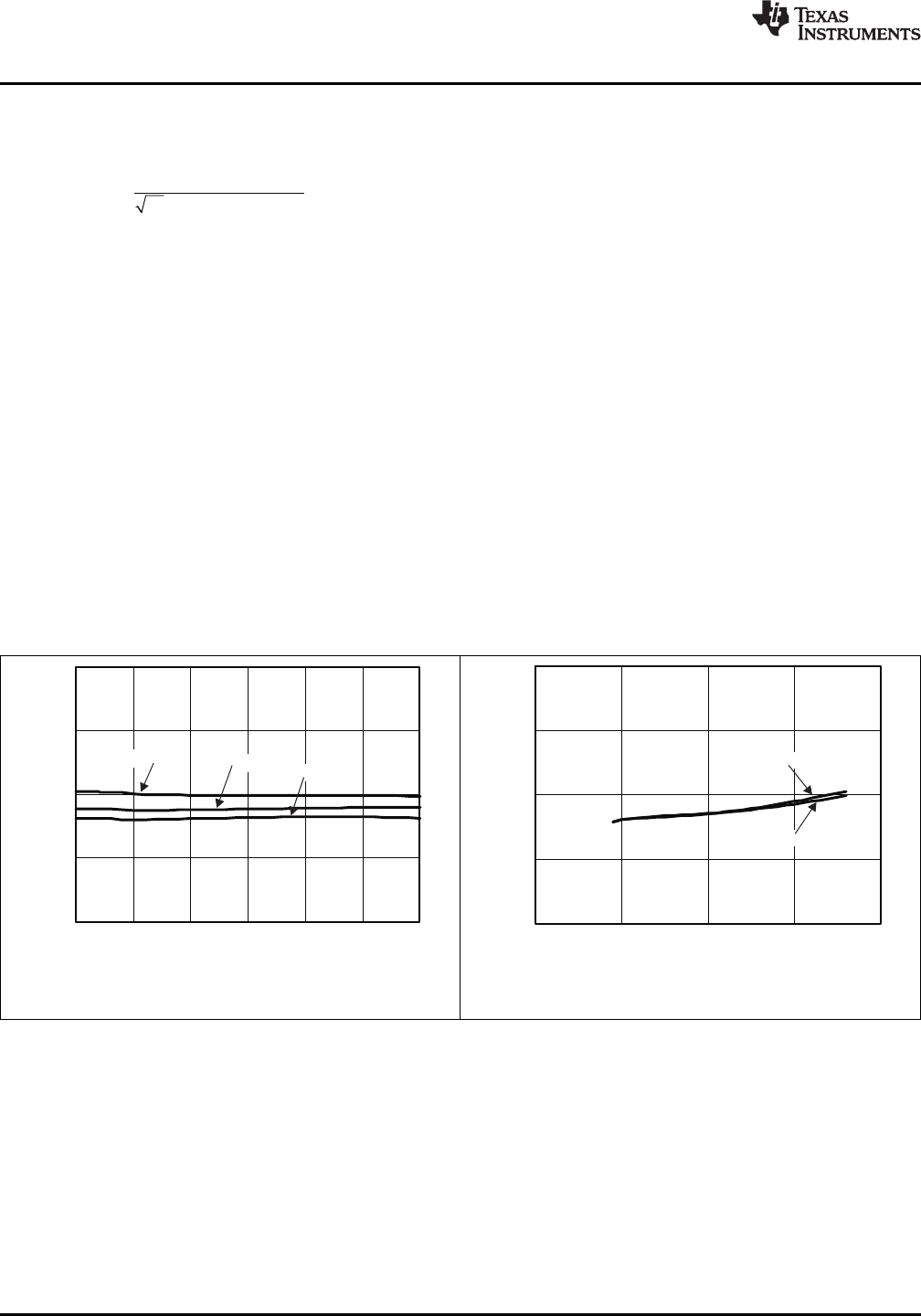
Figure 10. 1.05-V, 0-A to 3-A Load Transient Response Figure 11. Start-Up Wave Form
Figure 12. Voltage Ripple at Output (IO= 3 A) Figure 13. Voltage Ripple at Input (IO= 3 A)
Figure 14. TPS54327EVM-686 Efficiency Figure 15. TPS54327EVM-686 Light Load Efficiency
Copyright © 2010–2015, Texas Instruments Incorporated Submit Documentation Feedback 13
Product Folder Links: TPS54327

TPS54327
SLVSAG1C –DECEMBER 2010–REVISED DECEMBER 2015
www.ti.com
9 Power Supply Recommendations
The TPS54327 device is designed to operate from input supply voltage in the range of 4.5 V to 18 V. Buck
converters require the input voltage to be higher than the output voltage. in this case, the maximum
recommended operating duty cycle is 65%. Using that criteria, the minimum recommended input voltage is
Vo/0.65.
10 Layout
10.1 Layout Guidelines
1. Keep the input switching current loop as small as possible.
2. Keep the SW node as physically small and short as possible to minimize parasitic capacitance and
inductance and to minimize radiated emissions. Kelvin connections should be brought from the output to the
feedback pin of the device.
3. Keep analog and non-switching components away from switching components.
4. Make a single point connection from the signal ground to power ground.
5. Do not allow switching current to flow under the device.
6. Keep the pattern lines for VIN and PGND broad.
7. Exposed pad of device must be connected to PGND with solder.
8. VREG5 capacitor should be placed near the device, and connected PGND.
9. Output capacitor should be connected to a broad pattern of the PGND.
10. Voltage feedback loop should be as short as possible, and preferably with ground shield.
11. Lower resistor of the voltage divider which is connected to the VFB pin should be tied to SGND.
12. Providing sufficient via is preferable for VIN, SW and PGND connection.
13. PCB pattern for VIN, SW, and PGND should be as broad as possible.
14. VIN Capacitor should be placed as near as possible to the device.
14 Submit Documentation Feedback Copyright © 2010–2015, Texas Instruments Incorporated
Product Folder Links: TPS54327
VFB
VREG5
SS GND
EN VIN
VBST
SW
EXPOSED
THERMAL PAD
AREA
BOOST
CAPACITOR
VOUT
VIA to Ground Plane
OUTPUT
INDUCTOR
OUTPUT
FILTER
CAPACITOR
SLOW
START
CAP
ANALOG
GROUND
TRACE
VIN
INPUT
BYPASS
CAPACITOR
VIN
FEEDBACK
RESISTORS
TO ENABLE
CONTROL
POWER GROUND
BIAS
CAP
Connection to
POWER GROUND
on internal or
bottom layer
VIN
HIGH FREQENCY
BYPASS
CAPACITOR
TPS54327
www.ti.com
SLVSAG1C –DECEMBER 2010–REVISED DECEMBER 2015
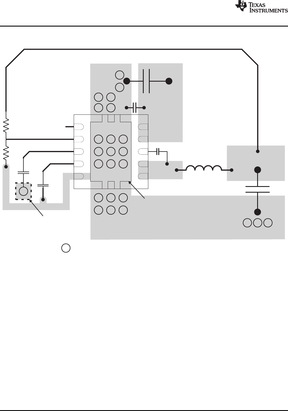
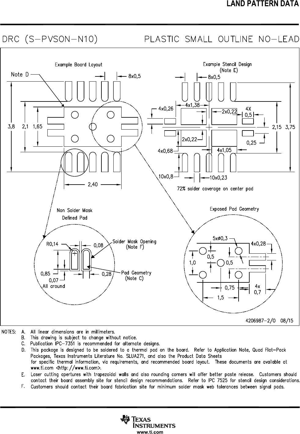
10.2 Layout Examples
Figure 16. PCB Layout
Copyright © 2010–2015, Texas Instruments Incorporated Submit Documentation Feedback 15
Product Folder Links: TPS54327
VFB
VREG5
SS
GND
EN VIN
VBST
SW
EXPOSED
THERMAL PAD
AREA
BOOST
CAPACITOR VOUT
VIA to Ground Plane
OUTPUT
INDUCTOR
OUTPUT
FILTER
CAPACITOR
SLOW
START
CAP
ANALOG
GROUND
TRACE
VIN
INPUT
BYPASS
CAPACITOR
VIN
FEEDBACK
RESISTORS TO ENABLE
CONTROL
POWER GROUND
BIAS
CAP
Connection to
POWER GROUND
on internal or
bottom layer
VIN
HIGH FREQENCY
BYPASS
CAPACITOR
VIN
SW
TPS54327
SLVSAG1C –DECEMBER 2010–REVISED DECEMBER 2015
www.ti.com
Layout Examples (continued)
Figure 17. PCB Layout for the DRC Package
16 Submit Documentation Feedback Copyright © 2010–2015, Texas Instruments Incorporated
Product Folder Links: TPS54327
TPS54327
www.ti.com
SLVSAG1C –DECEMBER 2010–REVISED DECEMBER 2015
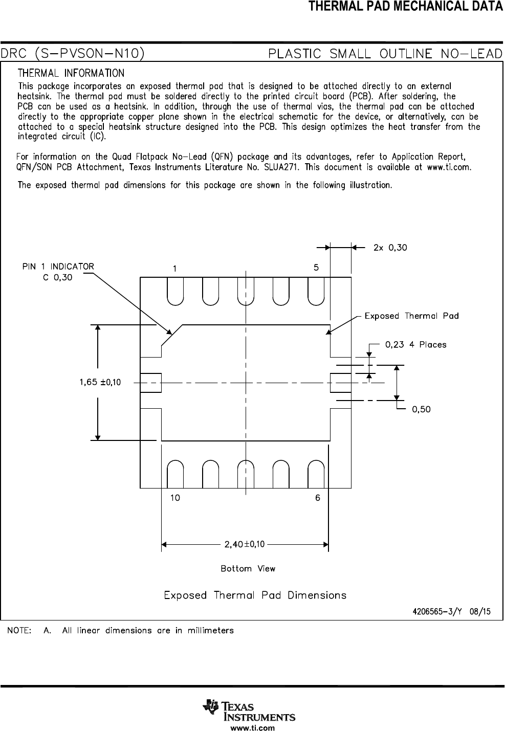
10.3 Thermal Considerations
This 8-pin DDA package incorporates an exposed thermal pad that is designed to be directly attached to an
external heatsink. The thermal pad must be soldered directly to the printed-circuit board (PCB). After soldering,
the PCB can be used as a heatsink. In addition, through the use of thermal vias, the thermal pad can be
attached directly to the appropriate copper plane shown in the electrical schematic for the device, or alternatively,
can be attached to a special heatsink structure designed into the PCB. This design optimizes the heat transfer
from the integrated circuit (IC).
For additional information on the exposed thermal pad and how to use the advantage of its heat dissipating
abilities, see the technical brief, PowerPAD™ Thermally Enhanced Package (SLMA002), and the application
brief, PowerPAD™ Made Easy (SLMA004).
The exposed thermal pad dimensions for this package are shown in the following illustration.
Figure 18. Thermal Pad Dimensions (Top View)
Copyright © 2010–2015, Texas Instruments Incorporated Submit Documentation Feedback 17
Product Folder Links: TPS54327
TPS54327
SLVSAG1C –DECEMBER 2010–REVISED DECEMBER 2015
www.ti.com
11 Device and Documentation Support
11.1 Documentation Support
11.1.1 Related Documentation
For related documentation see the following:
•PowerPAD™ Thermally Enhanced Package,SLMA002
•PowerPAD™ Made Easy,SLMA004
11.2 Community Resources
The following links connect to TI community resources. Linked contents are provided "AS IS" by the respective
contributors. They do not constitute TI specifications and do not necessarily reflect TI's views; see TI's Terms of
Use.
TI E2E™ Online Community TI's Engineer-to-Engineer (E2E) Community. Created to foster collaboration
among engineers. At e2e.ti.com, you can ask questions, share knowledge, explore ideas and help
solve problems with fellow engineers.
Design Support TI's Design Support Quickly find helpful E2E forums along with design support tools and
contact information for technical support.
11.3 Trademarks
D-CAP2, E2E are trademarks of Texas Instruments.
Blu-ray Disc is a trademark of Blu-ray Disc Association.
All other trademarks are the property of their respective owners.
11.4 Electrostatic Discharge Caution
These devices have limited built-in ESD protection. The leads should be shorted together or the device placed in conductive foam
during storage or handling to prevent electrostatic damage to the MOS gates.
11.5 Glossary
SLYZ022 —TI Glossary.
This glossary lists and explains terms, acronyms, and definitions.
12 Mechanical, Packaging, and Orderable Information
The following pages include mechanical, packaging, and orderable information. This information is the most
current data available for the designated devices. This data is subject to change without notice and revision of
this document. For browser-based versions of this data sheet, refer to the left-hand navigation.
18 Submit Documentation Feedback Copyright © 2010–2015, Texas Instruments Incorporated
Product Folder Links: TPS54327
PACKAGE OPTION ADDENDUM
www.ti.com 27-Sep-2015
Addendum-Page 1
PACKAGING INFORMATION
Orderable Device Status
(1)
Package Type Package
Drawing Pins Package
Qty Eco Plan
(2)
Lead/Ball Finish
(6)
MSL Peak Temp
(3)
Op Temp (°C) Device Marking
(4/5)
Samples
TPS54327DDA ACTIVE SO PowerPAD DDA 8 75 Green (RoHS
& no Sb/Br)
CU NIPDAUAG | Call TI Level-2-260C-1 YEAR -40 to 85 54327
TPS54327DDAR ACTIVE SO PowerPAD DDA 8 2500 Green (RoHS
& no Sb/Br)
CU NIPDAUAG | Call TI Level-2-260C-1 YEAR -40 to 85 54327
TPS54327DRCR ACTIVE VSON DRC 10 3000 Green (RoHS
& no Sb/Br)
CU NIPDAU Level-2-260C-1 YEAR -40 to 85 54327
TPS54327DRCT ACTIVE VSON DRC 10 250 Green (RoHS
& no Sb/Br)
CU NIPDAU Level-2-260C-1 YEAR -40 to 85 54327
(1) The marketing status values are defined as follows:
ACTIVE: Product device recommended for new designs.
LIFEBUY: TI has announced that the device will be discontinued, and a lifetime-buy period is in effect.
NRND: Not recommended for new designs. Device is in production to support existing customers, but TI does not recommend using this part in a new design.
PREVIEW: Device has been announced but is not in production. Samples may or may not be available.
OBSOLETE: TI has discontinued the production of the device.
(2) Eco Plan - The planned eco-friendly classification: Pb-Free (RoHS), Pb-Free (RoHS Exempt), or Green (RoHS & no Sb/Br) - please check http://www.ti.com/productcontent for the latest availability
information and additional product content details.
TBD: The Pb-Free/Green conversion plan has not been defined.
Pb-Free (RoHS): TI's terms "Lead-Free" or "Pb-Free" mean semiconductor products that are compatible with the current RoHS requirements for all 6 substances, including the requirement that
lead not exceed 0.1% by weight in homogeneous materials. Where designed to be soldered at high temperatures, TI Pb-Free products are suitable for use in specified lead-free processes.
Pb-Free (RoHS Exempt): This component has a RoHS exemption for either 1) lead-based flip-chip solder bumps used between the die and package, or 2) lead-based die adhesive used between
the die and leadframe. The component is otherwise considered Pb-Free (RoHS compatible) as defined above.
Green (RoHS & no Sb/Br): TI defines "Green" to mean Pb-Free (RoHS compatible), and free of Bromine (Br) and Antimony (Sb) based flame retardants (Br or Sb do not exceed 0.1% by weight
in homogeneous material)
(3) MSL, Peak Temp. - The Moisture Sensitivity Level rating according to the JEDEC industry standard classifications, and peak solder temperature.
(4) There may be additional marking, which relates to the logo, the lot trace code information, or the environmental category on the device.
(5) Multiple Device Markings will be inside parentheses. Only one Device Marking contained in parentheses and separated by a "~" will appear on a device. If a line is indented then it is a continuation
of the previous line and the two combined represent the entire Device Marking for that device.
(6) Lead/Ball Finish - Orderable Devices may have multiple material finish options. Finish options are separated by a vertical ruled line. Lead/Ball Finish values may wrap to two lines if the finish
value exceeds the maximum column width.
PACKAGE OPTION ADDENDUM
www.ti.com 27-Sep-2015
Addendum-Page 2
Important Information and Disclaimer:The information provided on this page represents TI's knowledge and belief as of the date that it is provided. TI bases its knowledge and belief on information
provided by third parties, and makes no representation or warranty as to the accuracy of such information. Efforts are underway to better integrate information from third parties. TI has taken and
continues to take reasonable steps to provide representative and accurate information but may not have conducted destructive testing or chemical analysis on incoming materials and chemicals.
TI and TI suppliers consider certain information to be proprietary, and thus CAS numbers and other limited information may not be available for release.
In no event shall TI's liability arising out of such information exceed the total purchase price of the TI part(s) at issue in this document sold by TI to Customer on an annual basis.
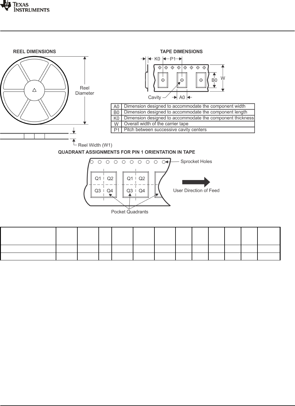
TAPE AND REEL INFORMATION
*All dimensions are nominal
Device Package
Type Package
Drawing Pins SPQ Reel
Diameter
(mm)
Reel
Width
W1 (mm)
A0
(mm) B0
(mm) K0
(mm) P1
(mm) W
(mm) Pin1
Quadrant
TPS54327DRCR VSON DRC 10 3000 330.0 12.4 3.3 3.3 1.1 8.0 12.0 Q2
TPS54327DRCT VSON DRC 10 250 180.0 12.4 3.3 3.3 1.1 8.0 12.0 Q2
PACKAGE MATERIALS INFORMATION
www.ti.com 16-Oct-2015
Pack Materials-Page 1
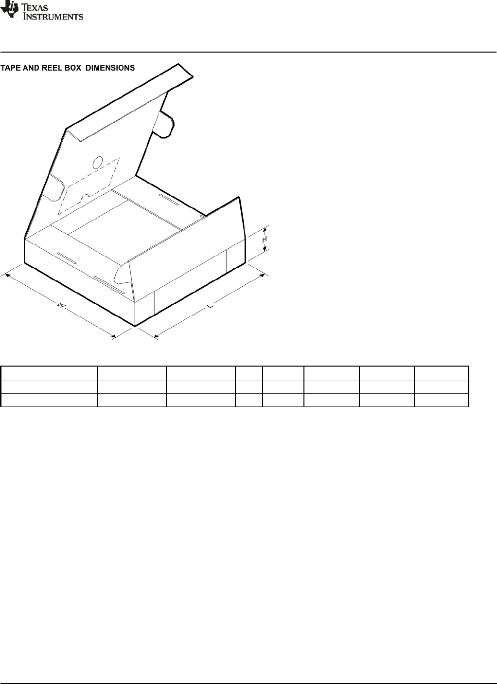
*All dimensions are nominal
Device Package Type Package Drawing Pins SPQ Length (mm) Width (mm) Height (mm)
TPS54327DRCR VSON DRC 10 3000 367.0 367.0 35.0
TPS54327DRCT VSON DRC 10 250 210.0 185.0 35.0
PACKAGE MATERIALS INFORMATION
www.ti.com 16-Oct-2015
Pack Materials-Page 2

IMPORTANT NOTICE
Texas Instruments Incorporated and its subsidiaries (TI) reserve the right to make corrections, enhancements, improvements and other
changes to its semiconductor products and services per JESD46, latest issue, and to discontinue any product or service per JESD48, latest
issue. Buyers should obtain the latest relevant information before placing orders and should verify that such information is current and
complete. All semiconductor products (also referred to herein as “components”) are sold subject to TI’s terms and conditions of sale
supplied at the time of order acknowledgment.
TI warrants performance of its components to the specifications applicable at the time of sale, in accordance with the warranty in TI’s terms
and conditions of sale of semiconductor products. Testing and other quality control techniques are used to the extent TI deems necessary
to support this warranty. Except where mandated by applicable law, testing of all parameters of each component is not necessarily
performed.
TI assumes no liability for applications assistance or the design of Buyers’ products. Buyers are responsible for their products and
applications using TI components. To minimize the risks associated with Buyers’ products and applications, Buyers should provide
adequate design and operating safeguards.
TI does not warrant or represent that any license, either express or implied, is granted under any patent right, copyright, mask work right, or
other intellectual property right relating to any combination, machine, or process in which TI components or services are used. Information
published by TI regarding third-party products or services does not constitute a license to use such products or services or a warranty or
endorsement thereof. Use of such information may require a license from a third party under the patents or other intellectual property of the
third party, or a license from TI under the patents or other intellectual property of TI.
Reproduction of significant portions of TI information in TI data books or data sheets is permissible only if reproduction is without alteration
and is accompanied by all associated warranties, conditions, limitations, and notices. TI is not responsible or liable for such altered
documentation. Information of third parties may be subject to additional restrictions.
Resale of TI components or services with statements different from or beyond the parameters stated by TI for that component or service
voids all express and any implied warranties for the associated TI component or service and is an unfair and deceptive business practice.
TI is not responsible or liable for any such statements.
Buyer acknowledges and agrees that it is solely responsible for compliance with all legal, regulatory and safety-related requirements
concerning its products, and any use of TI components in its applications, notwithstanding any applications-related information or support
that may be provided by TI. Buyer represents and agrees that it has all the necessary expertise to create and implement safeguards which
anticipate dangerous consequences of failures, monitor failures and their consequences, lessen the likelihood of failures that might cause
harm and take appropriate remedial actions. Buyer will fully indemnify TI and its representatives against any damages arising out of the use
of any TI components in safety-critical applications.
In some cases, TI components may be promoted specifically to facilitate safety-related applications. With such components, TI’s goal is to
help enable customers to design and create their own end-product solutions that meet applicable functional safety standards and
requirements. Nonetheless, such components are subject to these terms.
No TI components are authorized for use in FDA Class III (or similar life-critical medical equipment) unless authorized officers of the parties
have executed a special agreement specifically governing such use.
Only those TI components which TI has specifically designated as military grade or “enhanced plastic” are designed and intended for use in
military/aerospace applications or environments. Buyer acknowledges and agrees that any military or aerospace use of TI components
which have not been so designated is solely at the Buyer's risk, and that Buyer is solely responsible for compliance with all legal and
regulatory requirements in connection with such use.
TI has specifically designated certain components as meeting ISO/TS16949 requirements, mainly for automotive use. In any case of use of
non-designated products, TI will not be responsible for any failure to meet ISO/TS16949.
Products Applications
Audio www.ti.com/audio Automotive and Transportation www.ti.com/automotive
Amplifiers amplifier.ti.com Communications and Telecom www.ti.com/communications
Data Converters dataconverter.ti.com Computers and Peripherals www.ti.com/computers
DLP® Products www.dlp.com Consumer Electronics www.ti.com/consumer-apps
DSP dsp.ti.com Energy and Lighting www.ti.com/energy
Clocks and Timers www.ti.com/clocks Industrial www.ti.com/industrial
Interface interface.ti.com Medical www.ti.com/medical
Logic logic.ti.com Security www.ti.com/security
Power Mgmt power.ti.com Space, Avionics and Defense www.ti.com/space-avionics-defense
Microcontrollers microcontroller.ti.com Video and Imaging www.ti.com/video
RFID www.ti-rfid.com
OMAP Applications Processors www.ti.com/omap TI E2E Community e2e.ti.com
Wireless Connectivity www.ti.com/wirelessconnectivity
Mailing Address: Texas Instruments, Post Office Box 655303, Dallas, Texas 75265
Copyright © 2015, Texas Instruments Incorporated