TPS64200, TPS64201, TPS64202, TPS64203 Datasheet. Www.s Manuals.com. Ti
User Manual: Marking of electronic components, SMD Codes PJ, PJ-, PJAI, PJBI, PJCI, PJDI, PJGI, PJW, PJp, PJt. Datasheets BZB84-C36, RP130Q481D, TPS62207DBVR, TPS64200DBVR, TPS64201DBVR, TPS64202DBVR, TPS64203DBVR.
Open the PDF directly: View PDF ![]() .
.
Page Count: 29
SLVS485 − AUGUST 2003
FEATURES
DStep-Down Controller for Applications With
up to 95% Efficiency
D1.8-V to 6.5-V Operating Input Voltage Range
DAdjustable Output Voltage Range From 1.2 V
to VI
DHigh Efficiency Over a Wide Load Current
Range
D100% Maximum Duty Cycle for Lowest
Dropout
DInternal Softstart
D20-µA Quiescent Current (Typical)
DOvercurrent Protected
DAvailable in a SOT23 Package
APPLICATIONS
DUSB Powered Peripherals
DOrganizers, PDAs, and Handheld PCs
DLow Power DSP Supply
DDigital Cameras
DHard Disk Drives
DPortable Audio Players
DESCRIPTION
The TPS6420x are nonsynchronous step-down
controllers that are ideally suited for systems powered
from a 5-V or 3.3-V bus or for applications powered from
a 1-cell Li-Ion battery or from a 2- to 4-cell NiCd, NiMH, or
alkaline battery. These step-down controllers drive an
external P-channel MOSFET allowing design flexibility. To
achieve highest efficiency over a wide load current range,
this controller uses a minimum on time, minimum off time
control scheme and consumes only 20-µA quiescent
current. The minimum on time of typically 600 ns
(TPS64203) allows the use of small inductors and
capacitors. When disabled, the current consumption is
reduced to less than 1 µA. The TPS6420x is available in
the 6-pin SOT23 (DBV) package and operates over a free
air temperature range of −40°C to 85°C.
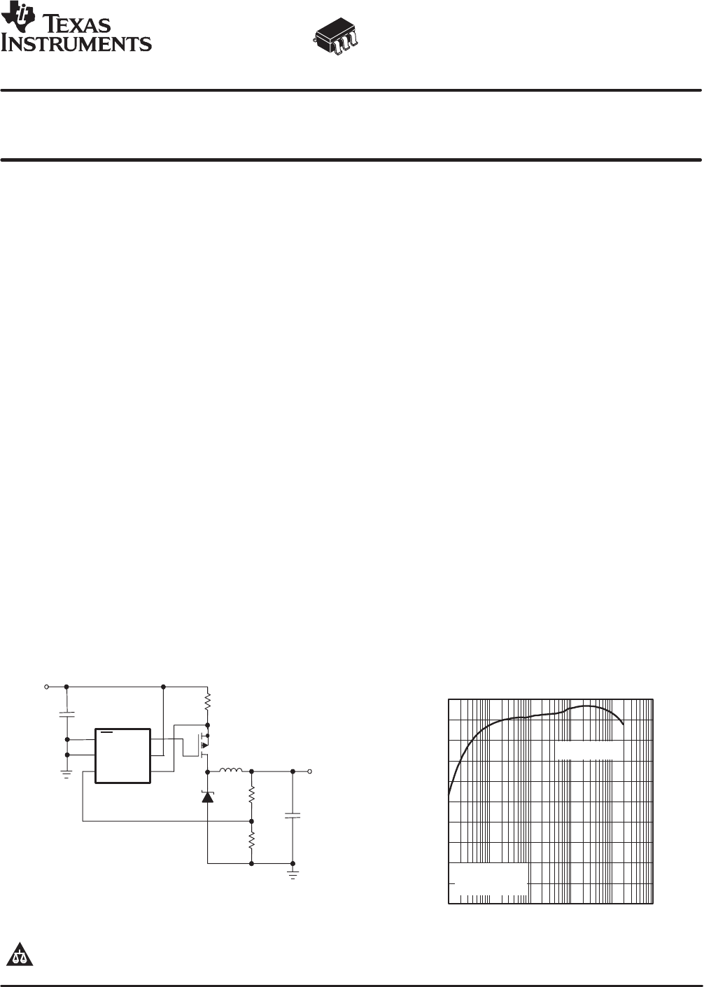
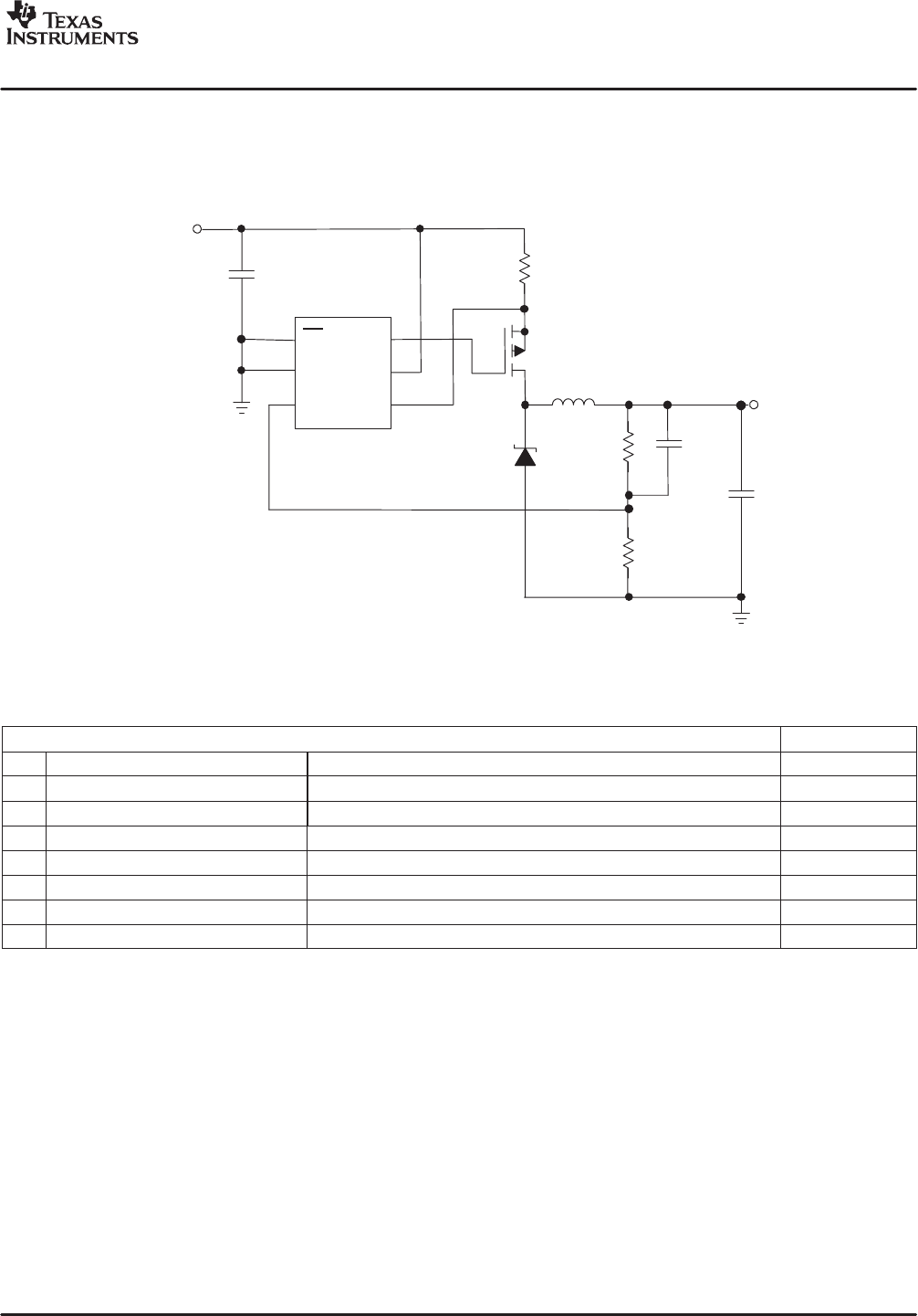
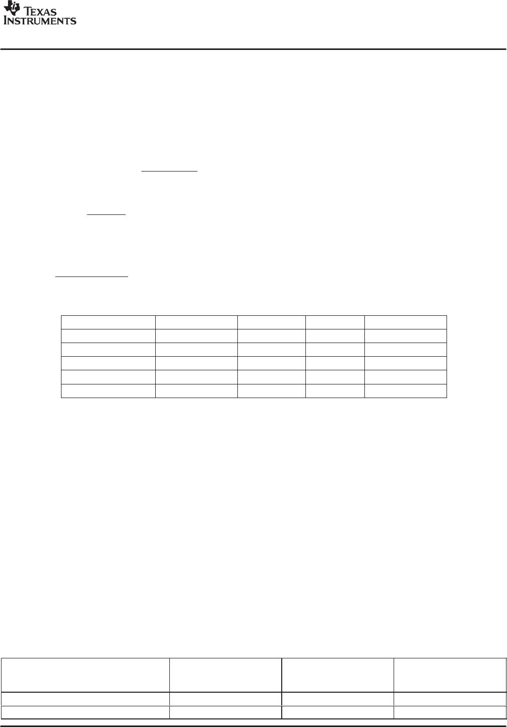
TYPICAL APPLICATION CIRCUIT
5
TPS64200
Si5447DC
ZHCS2000
EN
GND
FB
SW
VIN
ISENSE
Rs = 33 mΩ
10 µH
3.3 V / 2 A
47 µF
PosCap
6TPA47M
R1
620 kΩ
R2
360 kΩ
10 µF
5 V
0
10
20
30
40
50
60
70
80
90
100
0.0001 0.001 0.01 0.1 1 10
TA = 25°C,
VO = 3.3 V
TPS64200
EFFICIENCY
vs
LOAD CURRENT
IO − Load Current − A
Efficiency − %
VI = 4.2 V
1
2
3
6
4
!"# $"%&! '#( '"!
! $#!! $# )# # #* "# '' +,(
'"! $!#- '# #!#&, !&"'# #- && $##(
Please be aware that an important notice concerning availability, standard warranty, and use in critical applications of Texas Instruments
semiconductor products and disclaimers thereto appears at the end of this data sheet.
www.ti.com
Copyright 2003, Texas Instruments Incorporated
SLVS485 − AUGUST 2003
www.ti.com
2
These devices have limited built-in ESD protection. The leads should be shorted together or the device placed in conductive foam during
storage or handling to prevent electrostatic damage to the MOS gates.
ORDERING INFORMATION
PLASTIC SOT23-6(1) (2)
(DBV) OUTPUT VOLTAGE MINIMUM ON-TIME MINIMUM OFF-TIME MARKING
TPS64200DBVR Adjustable
1.2 V to VION time = 1.6 µsOFF time = 600 ns PJAI
TPS64201DBVR Adjustable
1.2 V to VIVariable minimum on time OFF time = 600 ns PJBI
TPS64202DBVR Adjustable
1.2 V to VIVariable minimum on time OFF time = 300 ns PJCI
TPS64203DBVR Adjustable
1.2 V to VION time = 600 ns OFF time = 600 ns PJDI
(1) The R suffix indicates shipment in tape and reel with 3000 units per reel.
(2) The T suffix indicates a mini reel with 250 units per reel.
ABSOLUTE MAXIMUM RATINGS
over operating free-air temperature range unless otherwise noted(1)
Supply voltage, VIN −0.3 V to 7 V
Voltage at EN, SW, ISENSE −0.3 V to VIN
Voltage at FB −0.3 V to 3.3 V
Maximum junction temperature, TJ150°C
Operating free−air temperature, TA−40°C to 85°C
Storage temperature, Tsgt −65°C to 150°C
Lead temperature 1,6 mm (1/16 inch) from case for 10 seconds 300°C
(1) Stresses beyond those listed under “absolute maximum ratings” may cause permanent damage to the device. These are stress ratings only, and
functional operation of the device at these or any other conditions beyond those indicated under “recommended operating conditions” is not
implied. Exposure to absolute-maximum-rated conditions for extended periods may affect device reliability.
PACKAGE DISSIPATION RATINGS
PACKAGE TA ≤255C
POWER RATING DERATING FACTOR
ABOVE TA = 25°CTA = 705C
POWER RATING TA = 855C
POWER RATING
SOT23−6 400 mW 4 mW/°C220 mW 180 mW
NOTE:The thermal resistance junction to ambient of the 6−pin SOT23 package is 250°C/W.
RECOMMENDED OPERATING CONDITIONS
MIN NOM MAX UNIT
Supply voltage at VIN 1.8 6.5 V
Operating junction temperature −40 125 °C
SLVS485 − AUGUST 2003
www.ti.com
3
ELECTRICAL CHARACTERISTICS
VIN = 3.8 V, VO = 3.3 V, EN = VIN, TA = −40°C to 85°C (unless otherwise noted)
SUPPLY CURRENT
PARAMETER TEST CONDITIONS MIN TYP MAX UNIT
VIInput voltage range 1.8 6.5 V
I(Q) Operating quiescent current IO = 0 mA 20 35 µA
I(SD) Shutdown current EN = VI0.1 1 µA
OUTPUT/CURRENT LIMIT
VOAdjustable output voltage range VFB VIV
VFB Feedback voltage 1.213 V
Feedback leakage current 0.01 0.2 µA
Feedback voltage tolerance −2 +2 %
V(ISENSE) Reference voltage for current limit 90 105 120 mV
ISENSE leakage current 0.01 0.2 µA
Line regulation Measured with circuit according to Figure 1 0.6 %/V
Load regulation Measured with circuit according to Figure 1
VI = 3.8 V 0.6 %/A
η
Efficiency
Measured with circuit according to Figure 1
VI = 3.8 V, VO = 3.3 V, IO = 1000 mA 94%
η
Efficiency
Measured with circuit according to Figure 1
VI = 3.8 V, VO = 1.2 V, IO = 800 mA 80%
Start-up time IO = 0 mA, Time from active EN to VO,
CO = 47 µF0.25 ms
GATE DRIVER (SW-PIN)
rDS(ON)
P-channel MOSFET on-resistance
VI ≥ 2.5 V 4
Ω
r
DS(ON)
P-channel MOSFET on-resistance
VI = 1.8 V 6Ω
rDS(ON)
N-channel MOSFET on-resistance
VI ≥ 2.5 V 4
Ω
r
DS(ON)
N-channel MOSFET on-resistance
VI = 1.8 V 6Ω
IOMaximum gate drive output current, SW 150 mA
ENABLE
VIH EN high level input voltage Device is off 1.3 V
VIL EN low level input voltage Device is operating 0.3 V
EN trip point hysteresis 115 mV
Ilkg EN input leakage current EN = GND or VIN 0.01 0.2 µA
V(UVLO) Undervoltage lockout threshold 1.7 V
ON TIME and OFF TIME
ton
Minimum on time
TPS64200, TPS64201, TPS64202 1.36 1.6 1.84
s
t
on
Minimum on time
TPS64203 only 0.56 0.65 0.74 µ
s
Reduced on time 1 TPS64201,TPS64202 0.80 µs
Reduced on time 2 TPS64201,TPS64202 0.40 µs
Reduced on time 3 TPS64201,TPS64202 0.20 µs
toff
Minimum off time
TPS64200,TPS64201, TPS64203 0.44 0.55 0.66
s
t
off
Minimum off time
TPS64202 only 0.24 0.3 0.36 µ
s
SLVS485 − AUGUST 2003
www.ti.com
4
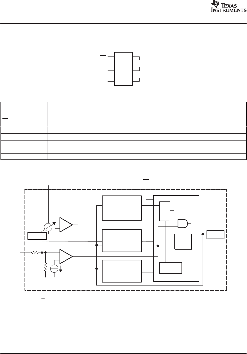
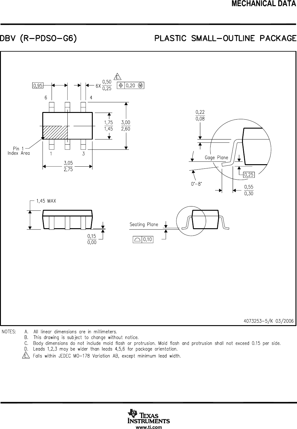
PIN ASSIGNMENTS
1
DBV PACKAGE
(TOP VIEW)
EN
FB
VIN
3
5GND
SW
ISENSE
2
6
4
Terminal Functions
TERMINAL
I/O
DESCRIPTION
NAME NO.
I/O
DESCRIPTION
EN 1 I Enable. A logic low enables the converter, logic high forces the device into shutdown mode reducing the supply current
to less than 1 µA.
FB 3 I Feedback pin. Connect an external voltage divider to this pin to set the output voltage.
GND 2 I Ground
SW 6 O This pin connects to the gate of an external P-channel MOSFET.
ISENSE 4 I Current sense input. Connect the current sense resistor between VIN and ISENSE. (optional)
VIN 5 I Supply voltage input
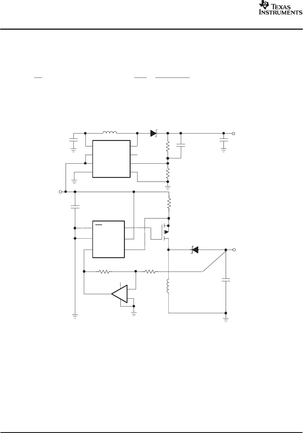
FUNCTIONAL BLOCK DIAGRAM
_
+
Minimum ton
Timer
(0.2 µs, 0.4 µs,
0.8 µs, 1.6 µs)
Minimum toff
Timer
(0.6 µs, 0.3 µs,)
ton Regulation
Timer
(3 µs, 15 µs, 16 µs)
Logic
_
+
M
U
X
ton
Regulator
R
SQ
Driver
Overcurrent
Comparator
Regulation
Comparator
Vref
Softstart
105 mV
GND
VIN EN
SW
ISense
FB
SLVS485 − AUGUST 2003
www.ti.com
5
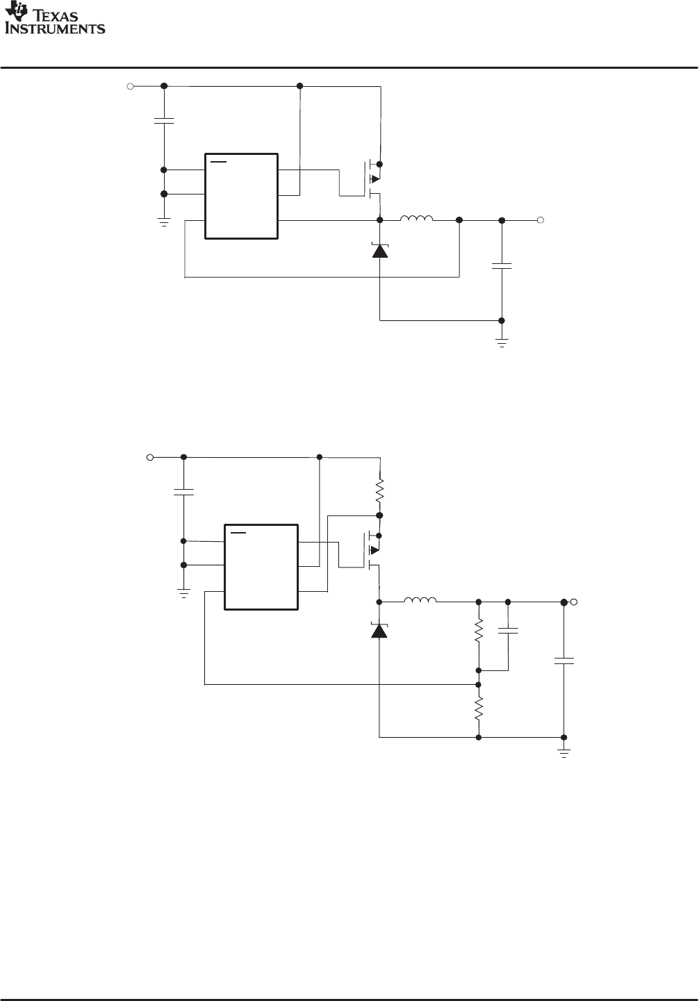
TYPICAL CHARACTERISTICS
All graphs were generated using the circuit as shown unless otherwise noted. For output voltages other than
3.3 V, the output voltage divider was changed accordingly. Graphs for the TPS64203 were taken using the
application circuit shown in Figure 25.
SW
CDRH103R−100
Si5447DC
MBRM120LT3
EN
GND
FB
VIN
ISENSE
VI
CI
10 µF
X7R
TPS6420x
R(ISENSE) = 33 mΩ
R1
620 kΩ
R2
360 kΩ
Cff
4.7 pF
Co
47 µF PosCap
6TPA47M
VO
1
2
3
6
5
4
10 µH
Figure 1. Basic Application Circuit For a 2-A Step-Down Converter
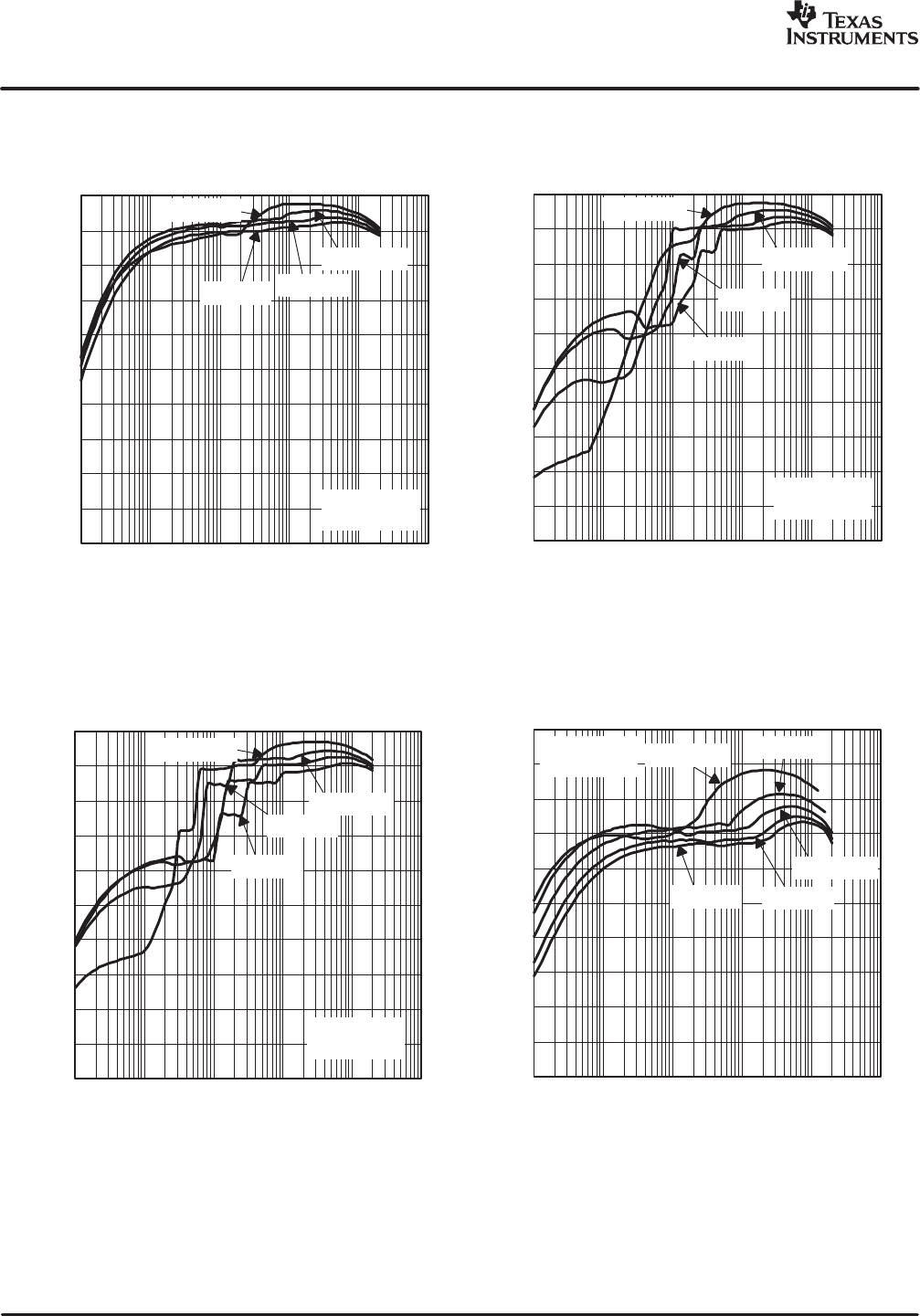
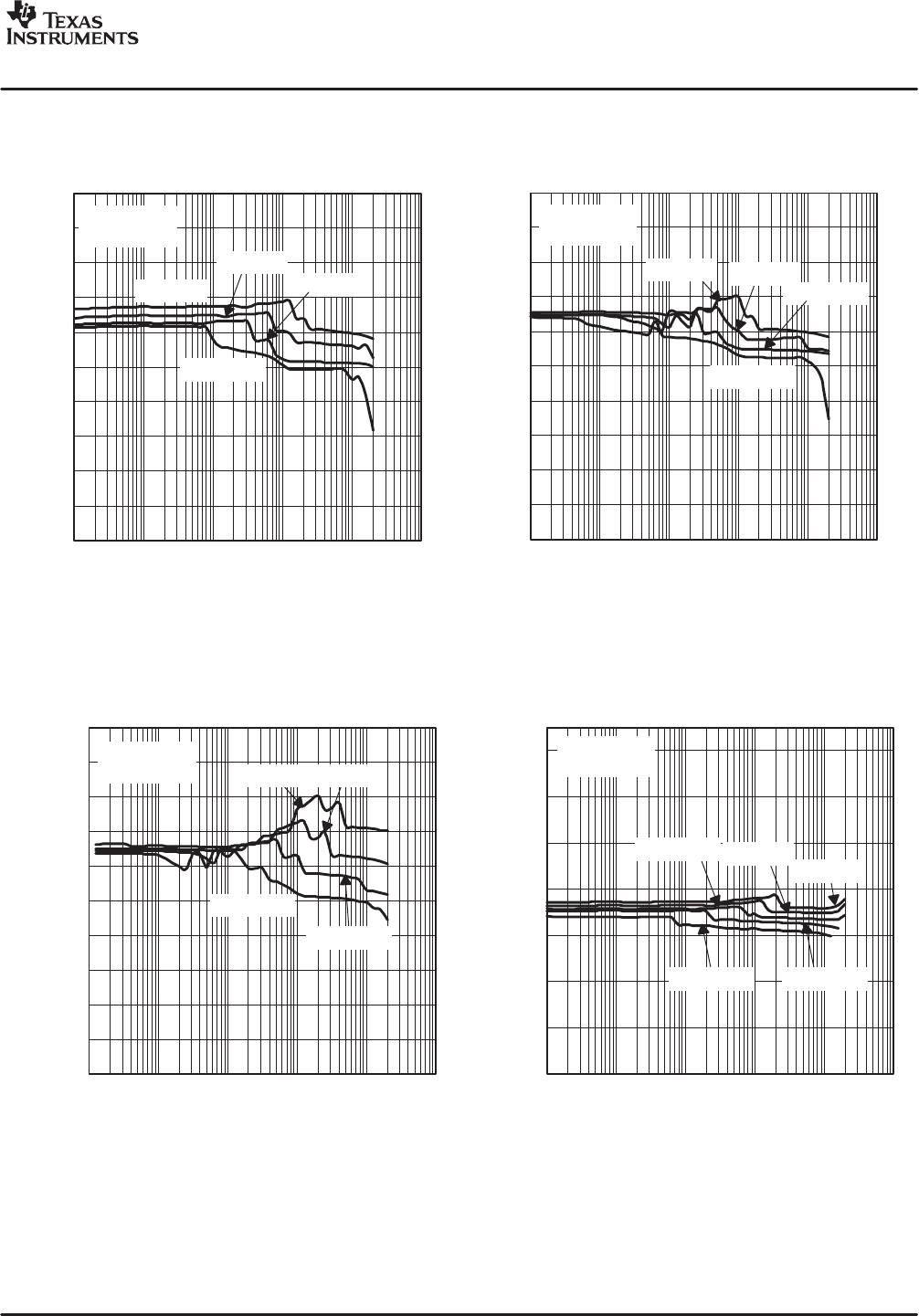
TABLE OF GRAPHS
FIGURE
ηEfficiency vs Load current 2 − 5
Output voltage vs Output current 6 − 9
Switching frequency vs Output current 10 − 13
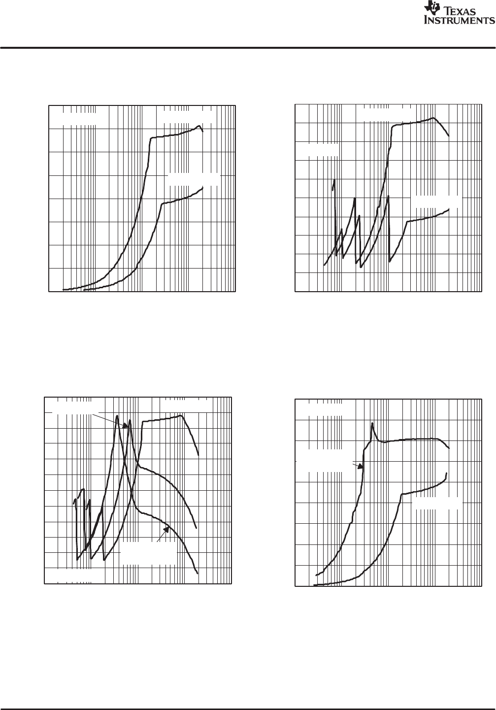
Operating quiescent current vs Input voltage 14
Output voltage ripple 15
Line transient response Using circuit according to Figure 1 16
Load transient response Using circuit according to Figure 1 17
Start-up timing Using circuit according to Figure 1 18
SLVS485 − AUGUST 2003
www.ti.com
6
Figure 2
0
10
20
30
40
50
60
70
80
90
100
0.0001 0.001 0.01 0.1 1 10
VI = 3.6 V
VI = 4.2 V
VI = 5 V
VI = 6 V
TA = 25°C,
VO = 3.3 V
TPS64200
EFFICIENCY
vs
LOAD CURRENT
IO − Load Current − A
Efficiency − %
Figure 3
0
10
20
30
40
50
60
70
80
90
100
VI = 4.2 V
VI = 6 V
TA = 25°C,
VO = 3.3 V
TPS64201
EFFICIENCY
vs
LOAD CURRENT
IO − Load Current − A
Efficiency − %
VI = 3.6 V
VI = 5 V
0.0001 0.001 0.01 0.1 1 10
Figure 4
0
10
20
30
40
50
60
70
80
90
100
VI = 4.2 V
VI = 6 V
TA = 25°C,
VO = 3.3 V
TPS64202
EFFICIENCY
vs
LOAD CURRENT
IO − Load Current − A
Efficiency − %
VI = 3.6 V
VI = 5 V
0.0001 0.001 0.01 0.1 1 10
0
10
20
30
40
50
60
70
80
90
100
VI = 6 V
TA = 25°C,
VO = 1.2 V
TPS64203
EFFICIENCY
vs
LOAD CURRENT
IO − Load Current − A
Efficiency − %
VI = 1.8 V VI = 2.5 V
VI = 3.6 V
VI = 5 V
0.0001 0.001 0.01 0.1 1 10
Figure 5
SLVS485 − AUGUST 2003
www.ti.com
7
3.20
3.22
3.24
3.26
3.28
3.30
3.32
3.34
3.36
3.38
3.40
VI = 3.6 V
VI = 4.2 V
VI = 6 V
TA = 25°C,
VO = 3.3 V
VI = 5 V
TPS64200
OUTPUT VOLTAGE
vs
OUTPUT CURRENT
− Output Voltage − V
VO
IO − Output Current − A
0.0001 0.001 0.01 0.1 1 10
Figure 6 Figure 7
3.20
3.22
3.24
3.26
3.28
3.30
3.32
3.34
3.36
3.38
3.40
VI = 3.6 V
VI = 4.2 V
TA = 25°C,
VO = 3.3 V
VI = 5 V
TPS64201
OUTPUT VOLTAGE
vs
OUTPUT CURRENT
− Output Voltage − V
VO
IO − Output Current − A
VI = 6 V
0.0001 0.001 0.01 0.1 1 10
Figure 8
3.20
3.22
3.24
3.26
3.28
3.30
3.32
3.34
3.36
3.38
3.40
VI = 3.6 V
TA = 25°C,
VO = 3.3 V VI = 5 V
TPS64202
OUTPUT VOLTAGE
vs
OUTPUT CURRENT
− Output Voltage − V
VO
IO − Output Current − A
VI = 6 V
VI = 4.2 V
0.0001 0.001 0.01 0.1 1 10
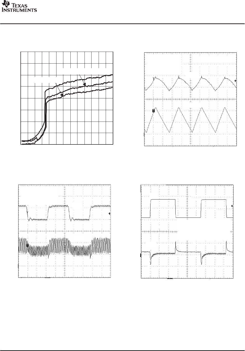
Figure 9
1.15
1.17
1.19
1.21
1.23
1.25
1.27
1.29 TA = 25°C,
VO = 1.2 V
TPS64203
OUTPUT VOLTAGE
vs
OUTPUT CURRENT
− Output Voltage − V
VO
IO − Output Current − A
VI = 6 V
VI = 5 V
VI = 3.6 V
VI = 2.5 VVI = 1.8 V
0.0001 0.001 0.01 0.1 1 10
SLVS485 − AUGUST 2003
www.ti.com
8
Figure 10
0
50
100
150
200
250
300
350
400
0.001 0.01 0.1 1 10
f − Frequency − kHz
TPS64200
SWITCHING FREQUENCY
vs
OUTPUT CURRENT
IO − Output Current − A
VO = 3.3 V
VO = 1.2 V
VI = 5 V
Figure 11
0
50
100
150
200
250
300
350
400
450
500
0.001 0.01 0.1 1 10
f − Frequency − kHz
TPS64201
SWITCHING FREQUENCY
vs
OUTPUT CURRENT
IO − Output Current − A
VO = 3.3 V
VO = 1.2 V
VI = 5 V
Figure 12
0
50
100
150
200
250
300
350
400
450
500
550
600
0.001 0.01 0.1 1 10
f − Frequency − kHz
TPS64202
SWITCHING FREQUENCY
vs
OUTPUT CURRENT
IO − Output Current − A
VI = 4.2 V
VI = 3.8 V
VI = 3.8 V,
Cff = 165 pF
VO = 3.3 V 0
100
200
300
400
500
600
700
800
900
0.001 0.01 0.1 1 10
f − Frequency − kHz
TPS64203
SWITCHING FREQUENCY
vs
OUTPUT CURRENT
IO − Output Current − A
VO = 1.2 V
VO = 3.3 V,
Cff = 165 pF
VI = 5 V
Figure 13
SLVS485 − AUGUST 2003
www.ti.com
9
Figure 14
0
5
10
15
20
25
30
35
40
0 0.5 1 1.5 2 2.5 3 3.5 4 4.5 5 5.5 6 6.5
− Operating Quiescent Current − Aµ
Q
I
TPS642000
OPERATING QUIESCENT CURRENT
vs
INPUT VOLTAGE
VI − Input Voltage − V
TA = 85°CTA = 25°C
TA = −40°C
TPS64200
OUTPUT VOLTAGE RIPPLE
VI = 3.8 V,
VO = 1.2 V,
RL = 1.2 Ω,
TA = 25°CVO
I(coil)
IO = 1000 mA
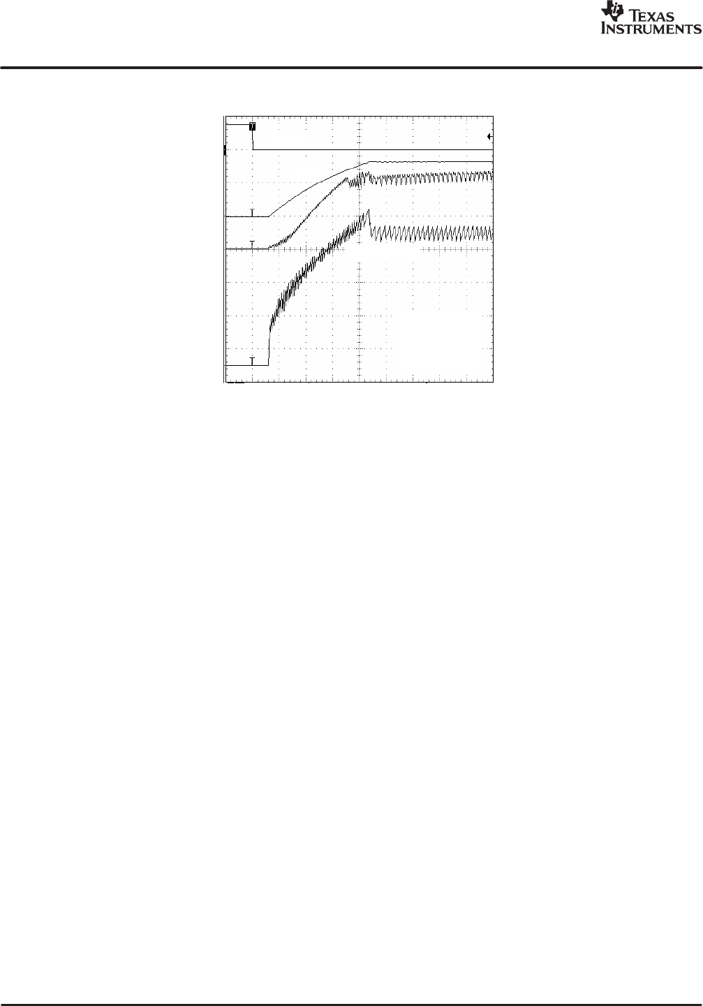
Figure 15
200 mA/Div
2 ms/Div
20 mV/Div
Figure 16
VO
VI
VI = 3.8 V to 5 V,
VO = 1.2 V,
RL = 1.2 Ω,
TA = 25°C
TPS64200
LINE TRANSIENT RESPONSE
20 mV/Div
40 ms/Div
1 V/Div
Figure 17
VO
IO
VI = 5 V,
VO = 3.3 V,
IL = 200 mA to 1800 mA,
TA = 25°C
TPS64203
LOAD TRANSIENT RESPONSE
50 mV/Div
50 ms/Div
1 A/Div
SLVS485 − AUGUST 2003
www.ti.com
10
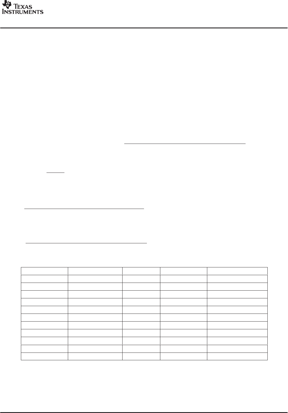
Figure 18
TPS64200
STARTUP TIMING
EN
VO
II
I(Inductor)
VI = 3.8 V,
VO = 3.3 V,
RL = 1.66 Ω,
TA = 25°C
100 ms/Div
DETAILED DESCRIPTION
Operation
The TPS6420x is a nonsynchronous step-down controller which is operating with a minimum on-time/minimum
off-time control. An external PMOS is turned on until the output voltage reaches its nominal value or the current
limit is exceeded. If the current limit is exceeded, the PMOS is switched off and stays off for the minimum
off-time. After that the PMOS is switched on again. When the nominal output voltage is reached, the PMOS
is switched off and stays off until the output voltage dropped below its nominal value.
Operating Modes
When delivering low or medium output current, the TPS6420x operate in discontinuous mode. With every
switching cycle, the current in the inductor starts at zero, rises to a maximum value and ramps down to zero
again. As soon as the current in the inductor drops to zero, ringing occurs at the resonant frequency of the
inductor and stray capacitance, due to residual energy in the inductor when the diode turns off. Ringing in
discontinuous mode is normal and does not have any influence on efficiency. The ringing does not contain much
energy and can easily be damped by an RC snubber. See the application section for further details.
With high output current, the TPS6420x operate in continuous current mode. In this mode, the inductor current
does not drop to zero within one switching cycle. The output voltage in continuous mode is directly dependant
on the duty cycle of the switch.
Variable Minimum On-Time (TPS64201 to TPS64202 Only)
The minimum on-time of the device is 1.6 µs. At light loads, this would cause a low switching frequency in the
audible range because the energy transferred to the output during the on-time would cause a higher rise in the
output voltage than needed and therefore lead to a long off−time until the output voltage dropped again. To avoid
a switching frequency in the audible range the TPS64201 and TPS64202 can internally reduce the minimum
on time in three steps from 1.6 µs to 800 ns, 400 ns and 200 ns. The on-time is reduced by one step if the
switching frequency dropped to a lower value than 50 kHz. This keeps the frequency above the audio frequency
over a wide load range and also keeps the output voltage ripple low.

SLVS485 − AUGUST 2003
www.ti.com
11
Soft Start
The TPS6420x has an internal soft start circuit that limits the inrush current during start up. This prevents
possible voltage drops of the input voltage in case a battery or a high impedance power source is connected
to the input of the TPS6420x. During soft start the current limit is increased from 25% of its maximum to the
maximum within about 250 µs.
100% Duty Cycle Low Dropout Operation
The TPS6420x offers the lowest possible input to output voltage difference while still maintaining regulation with
the use of the 100% duty cycle mode. In this mode the P-channel switch is constantly turned on. This is
particularly useful in battery powered applications to achieve longest operation time by taking full advantage
of the whole battery voltage range.
Enable
A voltage higher than the EN trip point of 1.3 V up to the input voltage forces the TPS64200 into shutdown. In
shutdown, the power switch, drivers, voltage reference, oscillator, and all other functions are turned off. The
supply current is reduced to less than 1 µA in shutdown. Pulling enable low starts up the TPS64200 with the
softstart as described under the chapter softstart.
Undervoltage Lockout
The undervoltage lockout circuit prevents the device from misoperation at low input voltages. Basically, it
prevents the converter from turning on the external PMOS under undefined conditions.
Current Limit
The ISENSE input is used to set the current limit for the external PMOS. The sense resistor must be connected
between VI and source of the external PMOS. The ISENSE pin is connected to the source of the external
PMOS. The maximum current is calculated by:
I(cur lim) +
V(ISENSE)
RS
(1)
For low cost solutions the rDS(on) of the external PMOS can also be used to set the current limit. In this case
the ISENSE pin is connected to the drain of the PMOS. The current in the PMOS is automatically sampled by
the TPS6420x some 10 ns after the PMOS is turned on. The ISENSE pin should always be connected to either
the source of the PMOS or the drain if an additional sense resistor is used. Otherwise there is no working
overcurrent protection and no soft start in the system. The maximum drain current if the rDS(on) is used as a
sense resistor is calculated by:
I(cur lim) +
V(ISENSE)
rDS(on) (2)
Short-Circuit Protection
With a controller only limited short circuit protection is possible because the temperature of the external
components is not supervised. In an overload condition, the current in the external diode may exceed the
maximum rating. To protect the diode against overcurrent, the off-time of the TPS6420x is increased when the
voltage at the feedback pin is lower than its nominal value. The off-time when the output is shorted (feedback
voltage is zero) is about 4 µs. This allows the current in the external diode to drop until the PMOS is turned on
again and the overcurrent protection switches off the PMOS again. The off-time is directly proportional to the
voltage at feedback.

SLVS485 − AUGUST 2003
www.ti.com
12
THEORY OF OPERATION
The basic application circuit for the TPS64200 is shown in Figure 1. External component selection is driven by
the load requirement. It begins with the selection of the current sense resistor R(ISENSE) followed by the output
diode, the inductor L, and the output and input capacitors. The inductor is chosen based on the desired amount
of ripple current and switching frequency. The output capacitor is chosen large enough to meet the required
output ripple and transient requirements. The ESR of the output capacitor is needed for stability of the converter.
Therefore, an output capacitor with a certain amount of ESR is needed for the standard application circuit. See
the application information for more details. The input capacitor must be capable of handling the required RMS
input current.
Setting the Inductor Current Limit
The ISENSE pin is connected to an internal current comparator with a threshold of 120 mV/R(ISENSE). The current
comparator sets the peak inductor current. As the current limit is intended to protect the external PMOS the
limit must not be reached in normal operation. Set the current limit to about 1.3 times the maximum output
current or higher if desired. This takes into account a certain amount of inductor current ripple. The current limit
may also influence the start-up time when the current limit is exceeded during start up.
R(ISENSE) v
V(ISENSE) min
1.3 IO
IO — maximum output current in continuous conduction mode
V(ISENSE), min = 90 mV (3)
The current sense resistor’s power rating should be:
P(ISENSE) wǒV(ISENSE) maxǓ2
R(ISENSE)
V(ISENSE), max = 120 mV (4)
Setting the Output Voltage
The output voltage of the TPS64200 to TPS64202 can be set using an external resistor divider. The sum of
R1 and R2 should not exceed 1 MΩ to keep the influence of leakage current into the feedback pin low.
VO+VFB R1 )R2
R2 R1 +R2 ǒVO
VFBǓ*R2 with VFB = 1.2 V (5)
In some applications, depending on the layout, the capacitance may be too high from FB to GND. In this case,
the internal comparator may not switch fast enough to operate with the minimum on-time or the minimum
off-time given in this data sheet. For such applications a feedforward capacitor (Cff) in the range of 4.7 pF to
47 pF (typical) is added in parallel with R1 to speed up the comparator. Choose a capacitor value that is high
enough that the device turns on the PMOS for its minimum on-time with no load at the output.
Selecting the Input Capacitor
The input capacitor is used to reduce peak currents drawn from the power source and reduces noise and voltage
ripple on the input of the converter, caused by its switching action. Use low ESR tantalum capacitors or
preferably X5R or X7R ceramic capacitors with a voltage rating higher than the maximum supply voltage in the
application. In continuous conduction mode, the input capacitor must handle an rms-current which is given by:
ICin(rms) [IO
VO
VI,min
Ǹ(6)
Select the input capacitor according to the calculated rms-input current requirements and according to the
maximum voltage ripple. Use a minimum value of 10 µF:
CI,min+
1
2L ǒDILǓ2
V(ripple) VI[
1
2L ǒ0.3 IOǓ2
V(ripple) VI
with: V(ripple) − voltage ripple at CI
∆IL − inductor current ripple (7)
SLVS485 − AUGUST 2003
www.ti.com
13
For a first approximation use:
L = 10 µH
V(ripple) = 150 mV (verify in the application)
Selecting the Inductor Value
The main parameters when choosing the inductor are current rating and inductance. The inductance mainly
determines the inductor current ripple. The TPS6420x operates with a wide range of inductor values. Values
between 4.7 µH and 47 µH work in most applications. Select an inductor with a current rating exceeding the
limit set by R(ISENSE) or rDS(on). The first step in inductor design is to determine the operating mode of the
TPS64200. The device can either work with minimum-on-time or minimum-off-time, depending on input voltage
and output voltage.
The device works with minimum-on-time if:
VI*VO*IO rDS(on) *RRL xI
Ow
toff,min ǒVO)VSCHOTTKY )RRL IOǓ
ton,min
with RRL − inductor resistance
(8)
with L +V Dt
DI
For minimum-on-time:
L+ǒVI–VO–IO rDS(on)–RRL IOǓ ton,min
DIwith: ∆I ≤ 0.3 × IO(9)
For minimum-off-time:
L+ǒVO)VSCHOTTKY )RRL IOǓ toff,min
DI(10)
Table 1. List of Inductors Tested With the TPS6420x
MANUFACTURER TYPE INDUCTANCE DC RESISTANCE SATURATION CURRENT
TDK SLF7032T−100M1R4 10 µH ±20% 53 mΩ ±20% 1.4 A
TDK SLF6025−150MR88 15 µH ±20% 85 mΩ ±20% 0.88 A
Sumida CDRH6D28−5R0 5 µH23 mΩ2.4 A
Sumida CDRH103R−100 10 µH45 mΩ2.4 A
Sumida CDRH4D28−100 10 µH95 mΩ1.0 A
Sumida CDRH5D18−6R2 6.2 µH71 mΩ1.4 A
Coilcraft DO3316P−472 4.7 µH18 mΩ5.4 A
Coilcraft DT3316P−153 15 µH60 mΩ1.8 A
Coilcraft DT3316P−223 22 µH84 mΩ1.5 A
Wurth 744 052 006 6.2 µH80 mΩ1.45 A
Wurth 74451115 15 µH90 mΩ0.8 A
SLVS485 − AUGUST 2003
www.ti.com
14
Selecting the External PMOS
An external PMOS must be used for a step-down converter with the TPS64200. The selection criteria for the
PMOS are threshold voltage, rDS(on), gate charge and current and voltage rating. Since the TPS64200 can
operate down to 1.8 V, the external PMOS must have a VGS(th) much lower than that if it is operated with such
a low voltage. As the gate of the PMOS finds the full supply voltage applied to the TPS64200, the PMOS must
be able to handle that voltage at the gate. The drain to source breakdown voltage rating should be at least a
few volts higher than the supply voltage in the application. The rms-current in the PMOS assuming low inductor
current ripple and continuous conduction mode, is:
IPMOS(rms) [IOD
Ǹ+IO
VO
VI
Ǹ(11)
The power dissipated in the PMOS is comprised of conduction losses and switching losses. The conduction
losses are a function of the rms−current in the PMOS and the rDS(on) at a given temperature. They are calculated
using:
P(cond) +ǒIOD
ǸǓ2
rDS(on) ǒ1)TC ƪTJ–25°CƫǓ[ǒIOD
ǸǓ2
rDS(on)
with TC = 0.005/°C
(12)
Table 2. PMOS Transistors Used in the Application Section
TYPE MANUFACTURER rDS(on) VDS ID PACKAGE
Si5447DC Vishay Siliconix 0.11 Ω at VGS = −2.5 V −20 V −3.5 A at 25°C 1206
Si5475DC Vishay Siliconix 0.041 Ω at VGS = −2.5 V −12 V −6.6 A at 25°C 1206
Si2301ADS Vishay Siliconix 0.19 Ω at VGS = −2.5 V −20 V −1.4 A at 25°C SOT23
Si2323DS Vishay Siliconix 0.41 Ω at VGS = −2.5 V −20 V −4.1 A at 25°C SOT23
FDG326P Fairchild 0.17 Ω at VGS = −2.5 V −20 V −1.5 A SC70
Selecting the Output Diode
The output diode conducts in the off phase of the PMOS and carries the full output current. The high switching
frequency demands a high-speed rectifier. Schottky diodes are recommended for best performance. Make sure
that the peak current rating of the diode exceeds the peak current limit set by the sense resistor R(ISENSE) or
rDS(on). Select a Schottky diode with a low reverse leakage current to avoid an increased supply current. The
average current in the diode in continuous conduction mode, assuming low inductor current ripple, is:
I(diode)(Avg) [IO(1–D)+IOǒ1– VO
VIǓ(13)
Table 3. Tested Diodes
TYPE MANUFACTURER VR IF PACKAGE
MBRM120LT3 On Semiconductor 20 V 1 A DO216AA
MBR0530T1 On Semiconductor 30 V 0.5 A SOD123
ZHCS2000TA Zetex 40 V 2 A SOT23−6
B320 Diodes Inc. 20 V 3 A SMA
SLVS485 − AUGUST 2003
www.ti.com
15
Selecting the Output Capacitor
The value of the output capacitor depends on the output voltage ripple requirements as well as the maximum
voltage deviation during a load transient. The TPS6420x require a certain ESR value for proper operation. Low
ESR tantalum capacitors or PosCap work best in the application. A ceramic capacitor with up 1 µF may be used
in parallel for filtering short spikes. The output voltage ripple is a function of both the output capacitance and
the ESR value of the capacitor. For a switching frequency which is used with the TPS6420x, the voltage ripple
is typically between 90% and 95% due to the ESR value.
DVpp +DI ƪESR )ǒ1
8 CO ƒǓƫ[1.1 DI ESR (14)
ESR, max [
DVpp
1.1 DI(15)
The output capacitance typically increases with load transient requirements. For a load step from zero output
current to its maximum, the following equation can be used to calculate the output capacitance:
CO+
L DI2
O
(VI*VO)xDV(16)
Table 4. Capacitors Used in the Application
TYPE MANUFACTURER CAPACITANCE ESR VOLTAGE RATING
6TPB47M (PosCap) Sanyo 47 µF0.1 Ω6.3 V
T491D476M010AS Kemet 47 µF0.8 Ω10 V
B45197A Epcos 47 µF0.175 Ω16 V
B45294−R1107−M40 Epcos 100 µF0.045 Ω6.3 V
594D476X0016C2 Vishay 47 µF 0.11 Ω16 V
Output Voltage Ripple
Output voltage ripple causes the output voltage to be higher or lower than set by the resistor divider at the
feedback pin. If the application runs with minimum on-time, the ripple (half of the peak-to-peak value) adds to
the output voltage. In an application which runs with minimum off-time, the output voltage is lower by the amount
of ripple (half of the peak-to-peak value) at the output.
Snubber Design
For low output current, the TPS6420x work in discontinuous current mode. When the current in the inductor
drops to zero, the inductor and parasitic capacitance form a resonant circuit, which causes oscillations when
both, diode and PMOS do not conduct at the end of each switching cycle. The oscillation can easily be damped
by a RC-snubber. The first step in the snubber design is to measure the oscillation frequency of the sine wave.
Then, a capacitor has to be connected in parallel to the Schottky diode which causes the frequency to drop to
half of its original value. The resistor is selected for optimum transient response (aperiodic).
R+2pfL f − measured resonant frequency
L − inductance used (17)
Selecting the Right Device for the Application
The TPS6420x step-down controllers either operate with a fixed on-time or a fixed off-time control. It mainly
depends on the input voltage to output voltage ratio if the switching frequency is determined by the
minimum-on-time or the minimum-off-time. To select the right device for an application see the table below:
INPUT TO OUTPUT VOLTAGE RATIO SWITCHING FREQUENCY
DETERMINED BY
PROPOSED DEVICE FOR
HIGH SWITCHING
FREQUENCY
PROPOSED DEVICE FOR
LOW SWITCHING
FREQUENCY
VI >> VO (e.g. VI = 5 V VO = 1.5 V) Minimum on−time TPS64203 TPS64200, TPS64201
VI ≈ VO (e.g. VI = 3.8 V VO = 3.3 V) Minimum off−time TPS64202 TPS64200, TPS64201
SLVS485 − AUGUST 2003
www.ti.com
16
APPLICATION INFORMATION
SW
CDRH6D28-5R0
Si5475DC
MBRM120LT3
EN
GND
FB
VIN
ISENSE
Li-lon
3.3 V to 4.2 V
CIN
10 µFTPS64202
R(ISENSE) = 33 mΩ
R1
620 kΩ
R2
360 kΩ
Cff
4.7 pF
Co
47 mF PosCap
6TPA47M
3.3 V / 2 A
1
2
3
6
5
4
5 µH
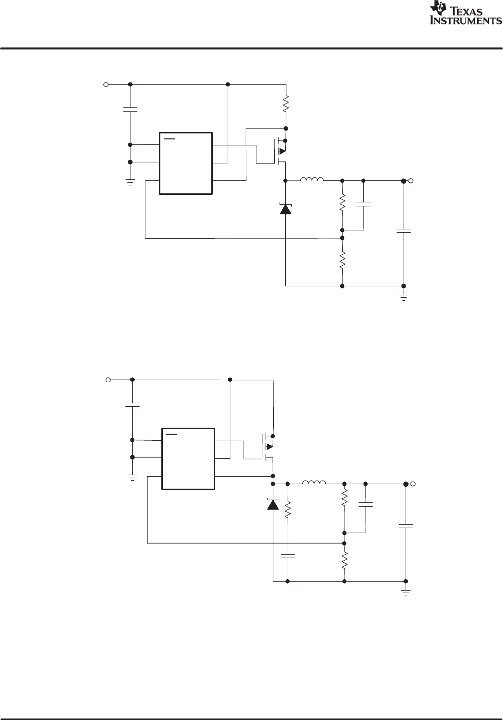
Figure 19. Application For a Li-Ion to 3.3-V / 2-A Conversion
The TPS64202 was used for this application because for a low input to output voltage difference, the switching
frequency is determined by the minimum off-time. The TPS64202 with its minimum off-time of 300 ns provides
a higher switching frequency compared to the other members of the TPS6420x family.
SW
CDRH6D28-5R0
Si5475DC
MBRM120LT3
EN
GND
FB
VIN
ISENSE
Li-lon
3.3 V to 4.2 V
CIN
10 µFTPS64202
R1
620 kΩ
R2
360 kΩ
Cff
4.7 pF
Co
47 mF PosCap
6TPA47M
3.3 V / 2 A
R3
150 Ω
C3
470 pF
1
2
3
6
5
4
5 µH
Figure 20. Application For a Li-Ion to 3.3-V / 2-A Conversion Using rDS(on) Sense and RC Snubber
Network For the Schottky Diode

SLVS485 − AUGUST 2003
www.ti.com
17
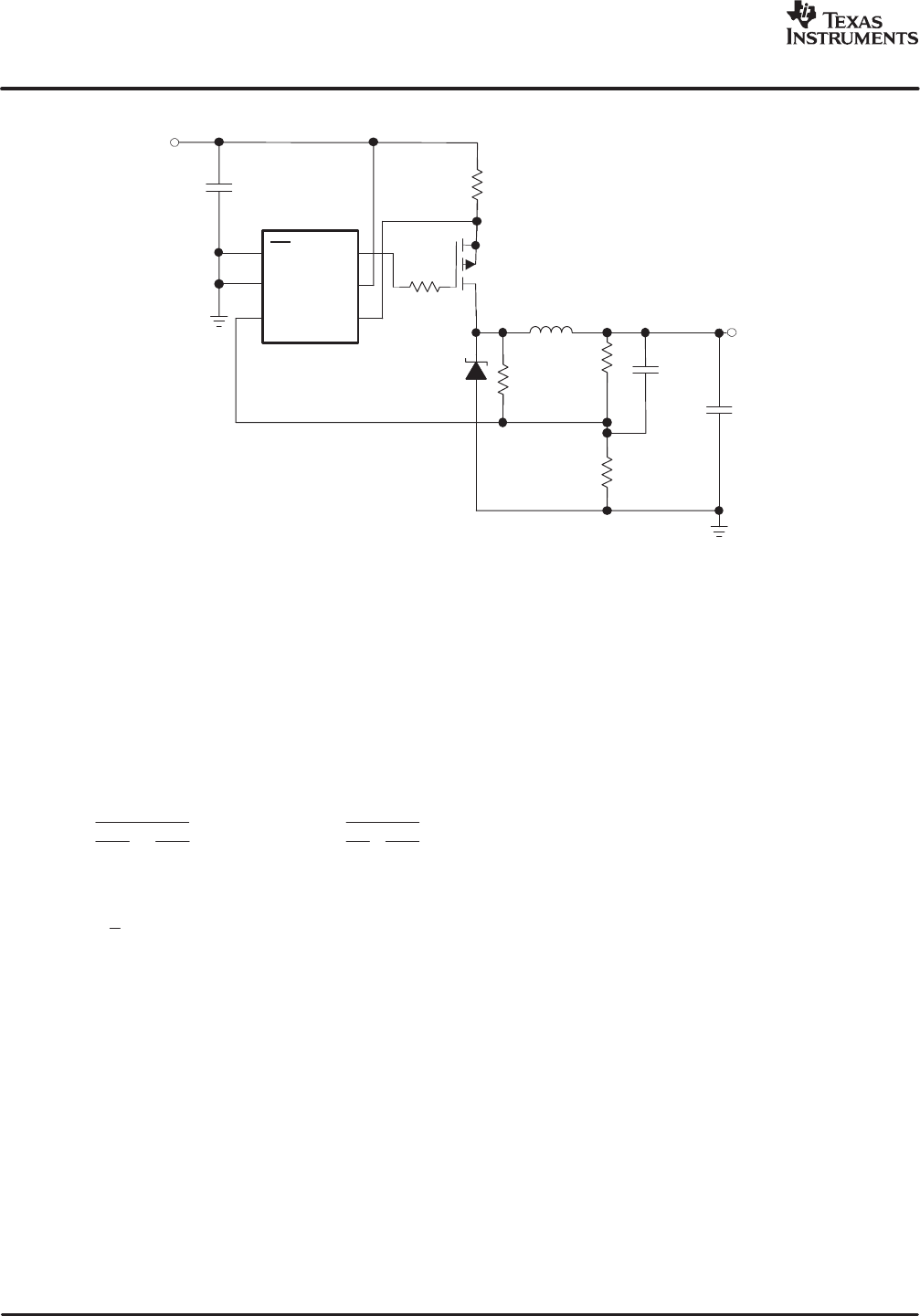
DESIGN EXAMPLE FOR AN APPLICATION USING A LI-ION CELL (3.3 V TO 4.2 V) TO
GENERATE 3.3 V/500 mA
1. Calculate the sense resistor for the current limit:
R(ISENSE) v
V(ISENSE) min
1.3 IO+90 mV
1.3 0.5 A +138 mW(18)
Choose the next lower standard value : R(ISENSE) = 120 mΩ. Verify the inductor current ripple after the inductor
has been determined in step 5.
If the rDS(on) of the PMOS is used to sense the inductor current, a PMOS with less than 138 mΩ must be used
for the application.
2. Calculate the resistors for the output voltage divider using VO = 3.3 V and VFB = 1.21 V
R1 +R2 ǒVO
VFBǓ–R2 +1.72 R2 (19)
Choose R2 = 360 kΩ, and then get R1 = 619 kΩ. Select the next standard value: R1 = 620 kΩ
3. Select the external PMOS
For a Li-Ion to 3.3-V conversion, the minimum input voltage is 3.3 V. Therefore, the converter runs in 100%
mode (duty cycle=1) and the maximum PMOS current is equal to the output current.
I(PMOS) +IO+0.5 A (20)
The Si2301ADS is selected for this application because it meets the requirements when an external sense
resistor is used. Otherwise a PMOS with less rDS(on) must be selected.
Verify the maximum power dissipation of the PMOS using:
P(cond) +ǒIOǓ2
rDS(on) +(0.5 A)2 0.19 W+48 mW (21)
4. Select the external diode
For the Schottky diode, the worst case current is at high input voltage (4.2 V for a Li-Ion cell).
I(diode)(Avg) [IOǒ1– VO
VIǓ+IOǒ1–3.3 V
4.2 VǓ+0.11 A (22)
The MBR0530T1 is selected because it meets the voltage and current requirements. The forward voltage is
about 0.3 V. Do not use a Schottky diode which is much larger than required as it also typically has more leakage
current and capacitance which reduces efficiency.
5. Calculate the inductor value.
If the output voltage is close to the input voltage, the switching frequency is determined by the minimum off-time.
Therefore, the TPS64202 is used for the maximum switching frequency possible. Allow an inductor ripple
current of 0.3 × IO for the application. For the inductor, a series resistance of 100 mΩ is assumed.
For minimum-off-time, the inductor value is:
L+ǒVO)V(SCHOTTKY) )RRL IOǓ toff,min
DI+(3.3 V )0.3 V )0.05 V) 0.3 ms
0.3 0.5 A +7.3 mH
(23)
For a low inductor current ripple, select the next available larger inductor with L = 10 µH. This provides an
inductor ripple current of 110 mA (peak-to-peak).
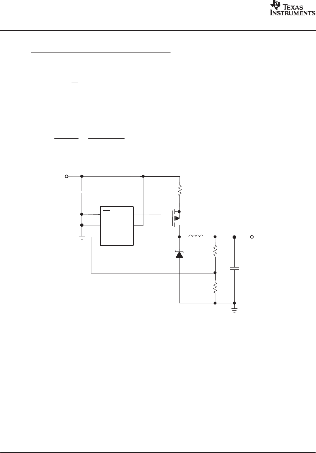
SLVS485 − AUGUST 2003
www.ti.com
18
DI+ǒVO)V(SCHOTTKY) )RRL IOǓ toff,min
L+110 mA (24)
The current rating for the inductor must be:
(25)
I, inductor uIO)DI
2+555 mA
6. Select the input and output capacitor
The output capacitor is selected for an output voltage ripple of less than 20 mVpp.
With
ESR, max [
DVpp
1.1 DI+0.02 V
1.1 0.11 A +165 mW(26)
A 47-µF PosCap with an ESR of 100 mΩ was selected to meet the ripple requirements.
The input capacitor was selected to its minimum value of 10 µF.
SW
CDRH4D18-100
Si2301DS
MBR0530T1
EN
GND
FB
VIN
ISENSE
1 Li-lon Cell
10 µFTPS64202
R1
620 kΩ
R2
360 kΩ
47 µF PosCap
6TPA47M
3.3 V / 0.5 A
R(ISENSE) = 120 mΩ
1
2
3
6
5
4
10 µH
Figure 21. Application Circuit
SLVS485 − AUGUST 2003
www.ti.com
19
SW
CDRH103R-100
Si5447DC
ZHCS200
EN
GND
FB
VIN
ISENSE
5 V
10 µFTPS64200
R1
620 kΩ
R2
360 kΩ
47 mF PosCap
6TPA47M
3.3 V / 2 A
R(ISENSE) = 33 mΩ
1
2
3
6
5
4
10 µH
Figure 22. Application For a 5-V to 3.3-V / 2-A Conversion
Inverter Using TPS64200
SW
MBR0530T1
Si2301DS
EN
GND
FB
VIN
ISENSE
VI
2.7 V to 4.2 V
10 µFTPS64200
R(ISENSE) = 33 mΩ
47 µF
X7R
−5 V / 0.1 A
CDRH4D28-100
100 kΩ
R1
_
+
VI
24 kΩ
R2
SW
OPA363
1
2
3
6
5
4
10 µH
Figure 23. Application For an Inverter Using TPS64200
SLVS485 − AUGUST 2003
www.ti.com
20
The TPS6420x can be used for an inverter. Only one additional operational amplifier is required for this
application. When the PMOS is switched on, the current in the inductor ramps up to its maximum, set by Rs.
Then the PMOS is switched off, the energy stored in the inductor is transferred to the output. The output voltage
and the maximum output current can be calculated using:
VO+R1
R2 VFB IOmax [0.8 VI
–VO
V(ISENSE)
2R(ISENSE) (27)
OLED Power Supply
The TPS6420x can be combined with a TPS61045 boost converter for a OLED power supply.
SW
MBR0530T1
Si2301DS
EN
GND
FB
VIN
ISENSE
VI
1.8 V to 5.5 V
10 µFTPS64200
R(ISENSE) = 150 mΩ
47 µF
X7R
−7 V / 50 mA
CDRH4D28-100
750 kΩ
R1
_
+
VI
130 kΩ
R2
SW
OPA363
SWL
VIN
GND
DO
FB
CTRL
PGND
4.7 µH
56 kΩ
12 kΩ
22 pF
4.7 µF
TPS61045
7 V / 50 mA
1 µF
X7R
1
2
3
6
5
4
1
2
5
8
3
4
67
10 µH
Figure 24. Application For a OLED Power Supply
SLVS485 − AUGUST 2003
www.ti.com
21
SW
Wurth 744052006
Si2323DS
MBRM120LT3
EN
GND
FB
VIN
ISENSE
5 V
10 µF
X5R TPS64203
100 µF/6.3 V
B45294-R1107-M40
1.2 V / 1.2 A
1
2
3
6
5
4
6.2 µH
Figure 25. Application For a 5-V to 1.2-V / 1.2-A Conversion
SW
DO3316P−472
Si5475DC
B320
EN
GND
FB
VIN
ISENSE
5 V
CIN
22 µFTPS64202
R1
620 kΩ
R2
360 kΩ
Cff
4.7 pF
Co
100 mF PosCap
6TPC100M
3.3 V / 3 A
1
2
3
6
5
4
4.7 µH
R(ISENSE) = 20 mΩ
Figure 26. Application For a 5-V to 3.3-V / 3-A Conversion
SLVS485 − AUGUST 2003
www.ti.com
22
Ceramic Output Capacitor
SW
CDRH6D28-100
Si5475DC
MBRM120LT3
EN
GND
FB
VIN
ISENSE
5 V
CI
10 µFTPS64203
R1a
680 kΩ
R2
300 kΩ
Cff
82 pF
Co
22 µF X5R
6.3 V
3.3 V / 2 A
R1b
2.2 MΩ
R(ISENSE) = 33 mΩ
R(GATE)
10 Ω
1
2
3
6
5
4
10 µH
Figure 27. Application Using a Ceramic Output Capacitor
The control scheme of the TPS6420x usually requires an output capacitor with some tens of milliohms of ESR
for stability, which is usually the case for tantalum capacitors. This application circuit above also works with
ceramic capacitors. Resistor R1b is used to add an additional control signal to the feedback loop, which is
coupled into the FB pin. The circuit works best with R1b = 2 …4 x R1a. If the resistance of R1b is too low
compared to R1a, the more load regulation the output voltage shows, but stability is best. The advantage of
this circuit is a very low output voltage ripple and small size. The gate resistor shown can be used in every
application. It minimizes switching noise of the converter and, therefore, increases stability and provides lower
output voltage ripple. However, it decreases efficiency slightly because the rise and fall time, and the associated
losses are larger.
(28)
R1 +1
1
R1a )1
R1b
R1b +1
1
R1 –1
R1a
Use the following equation to calculate R1a if R1b = 4R1a
R1a +5
4R1 (29)

PACKAGING INFORMATION
Orderable Device Status (1) Package
Type Package
Drawing Pins Package
Qty Eco Plan (2) Lead/Ball Finish MSL Peak Temp (3)
TPS64200DBVR ACTIVE SOT-23 DBV 6 3000 Green (RoHS &
no Sb/Br) CU NIPDAU Level-1-260C-UNLIM
TPS64200DBVRG4 ACTIVE SOT-23 DBV 6 3000 Green (RoHS &
no Sb/Br) CU NIPDAU Level-1-260C-UNLIM
TPS64200DBVT ACTIVE SOT-23 DBV 6 250 Green (RoHS &
no Sb/Br) CU NIPDAU Level-1-260C-UNLIM
TPS64200DBVTG4 ACTIVE SOT-23 DBV 6 250 Green (RoHS &
no Sb/Br) CU NIPDAU Level-1-260C-UNLIM
TPS64201DBVR ACTIVE SOT-23 DBV 6 3000 Green (RoHS &
no Sb/Br) CU NIPDAU Level-1-260C-UNLIM
TPS64201DBVRG4 ACTIVE SOT-23 DBV 6 3000 Green (RoHS &
no Sb/Br) CU NIPDAU Level-1-260C-UNLIM
TPS64201DBVT ACTIVE SOT-23 DBV 6 250 Green (RoHS &
no Sb/Br) CU NIPDAU Level-1-260C-UNLIM
TPS64201DBVTG4 ACTIVE SOT-23 DBV 6 250 Green (RoHS &
no Sb/Br) CU NIPDAU Level-1-260C-UNLIM
TPS64202DBVR ACTIVE SOT-23 DBV 6 3000 Green (RoHS &
no Sb/Br) CU NIPDAU Level-1-260C-UNLIM
TPS64202DBVRG4 ACTIVE SOT-23 DBV 6 3000 Green (RoHS &
no Sb/Br) CU NIPDAU Level-1-260C-UNLIM
TPS64202DBVT ACTIVE SOT-23 DBV 6 250 Green (RoHS &
no Sb/Br) CU NIPDAU Level-1-260C-UNLIM
TPS64202DBVTG4 ACTIVE SOT-23 DBV 6 250 Green (RoHS &
no Sb/Br) CU NIPDAU Level-1-260C-UNLIM
TPS64203DBVR ACTIVE SOT-23 DBV 6 3000 Green (RoHS &
no Sb/Br) CU NIPDAU Level-1-260C-UNLIM
TPS64203DBVRG4 ACTIVE SOT-23 DBV 6 3000 Green (RoHS &
no Sb/Br) CU NIPDAU Level-1-260C-UNLIM
TPS64203DBVT ACTIVE SOT-23 DBV 6 250 Green (RoHS &
no Sb/Br) CU NIPDAU Level-1-260C-UNLIM
TPS64203DBVTG4 ACTIVE SOT-23 DBV 6 250 Green (RoHS &
no Sb/Br) CU NIPDAU Level-1-260C-UNLIM
(1) The marketing status values are defined as follows:
ACTIVE: Product device recommended for new designs.
LIFEBUY: TI has announced that the device will be discontinued, and a lifetime-buy period is in effect.
NRND: Not recommended for new designs. Device is in production to support existing customers, but TI does not recommend using this part in
a new design.
PREVIEW: Device has been announced but is not in production. Samples may or may not be available.
OBSOLETE: TI has discontinued the production of the device.
(2) Eco Plan - The planned eco-friendly classification: Pb-Free (RoHS), Pb-Free (RoHS Exempt), or Green (RoHS & no Sb/Br) - please check
http://www.ti.com/productcontent for the latest availability information and additional product content details.
TBD: The Pb-Free/Green conversion plan has not been defined.
Pb-Free (RoHS): TI's terms "Lead-Free" or "Pb-Free" mean semiconductor products that are compatible with the current RoHS requirements
for all 6 substances, including the requirement that lead not exceed 0.1% by weight in homogeneous materials. Where designed to be soldered
at high temperatures, TI Pb-Free products are suitable for use in specified lead-free processes.
Pb-Free (RoHS Exempt): This component has a RoHS exemption for either 1) lead-based flip-chip solder bumps used between the die and
package, or 2) lead-based die adhesive used between the die and leadframe. The component is otherwise considered Pb-Free (RoHS
compatible) as defined above.
Green (RoHS & no Sb/Br): TI defines "Green" to mean Pb-Free (RoHS compatible), and free of Bromine (Br) and Antimony (Sb) based flame
retardants (Br or Sb do not exceed 0.1% by weight in homogeneous material)
PACKAGE OPTION ADDENDUM
www.ti.com 5-Feb-2007
Addendum-Page 1

(3) MSL, Peak Temp. -- The Moisture Sensitivity Level rating according to the JEDEC industry standard classifications, and peak solder
temperature.
Important Information and Disclaimer:The information provided on this page represents TI's knowledge and belief as of the date that it is
provided. TI bases its knowledge and belief on information provided by third parties, and makes no representation or warranty as to the
accuracy of such information. Efforts are underway to better integrate information from third parties. TI has taken and continues to take
reasonable steps to provide representative and accurate information but may not have conducted destructive testing or chemical analysis on
incoming materials and chemicals. TI and TI suppliers consider certain information to be proprietary, and thus CAS numbers and other limited
information may not be available for release.
In no event shall TI's liability arising out of such information exceed the total purchase price of the TI part(s) at issue in this document sold by TI
to Customer on an annual basis.
PACKAGE OPTION ADDENDUM
www.ti.com 5-Feb-2007
Addendum-Page 2
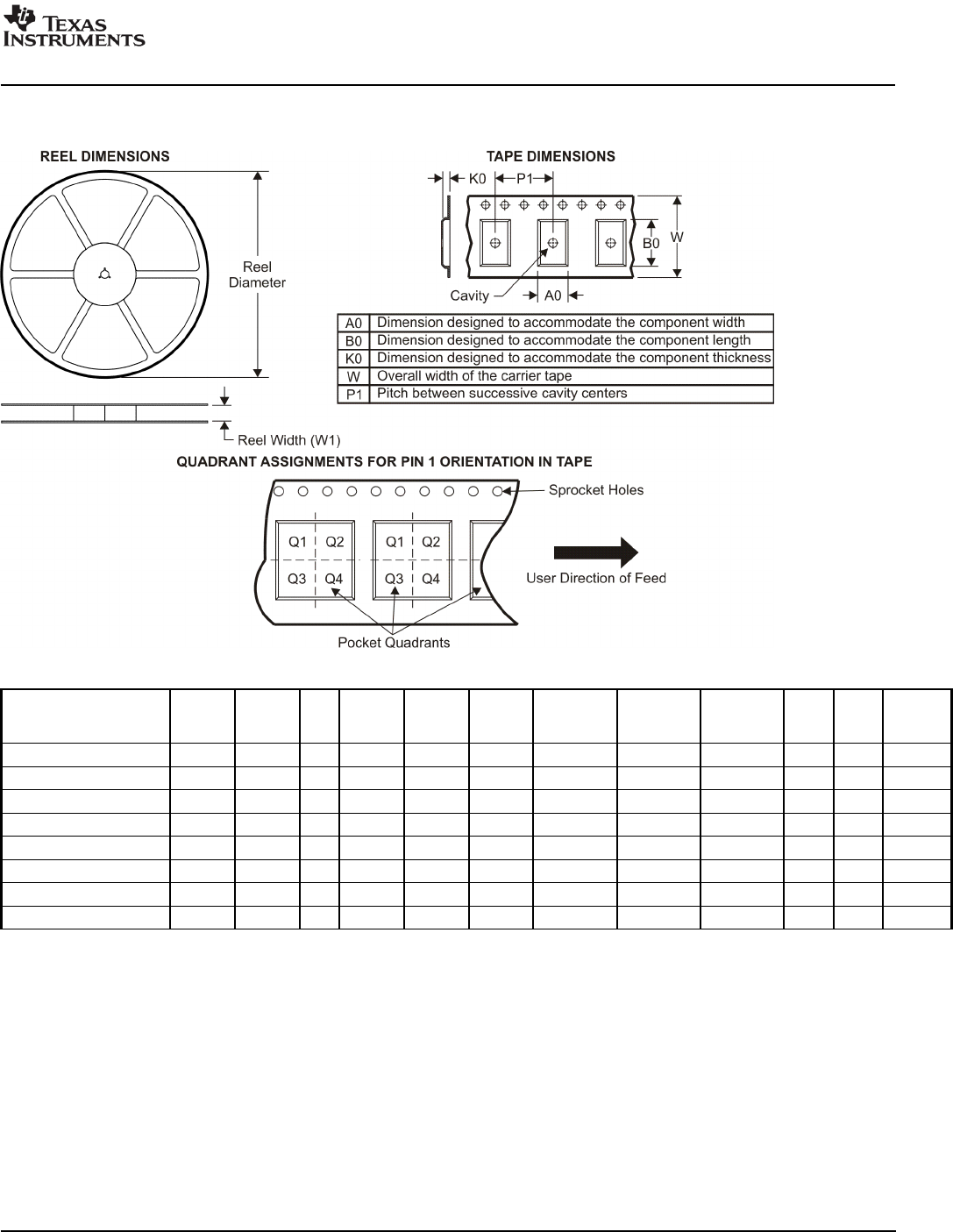
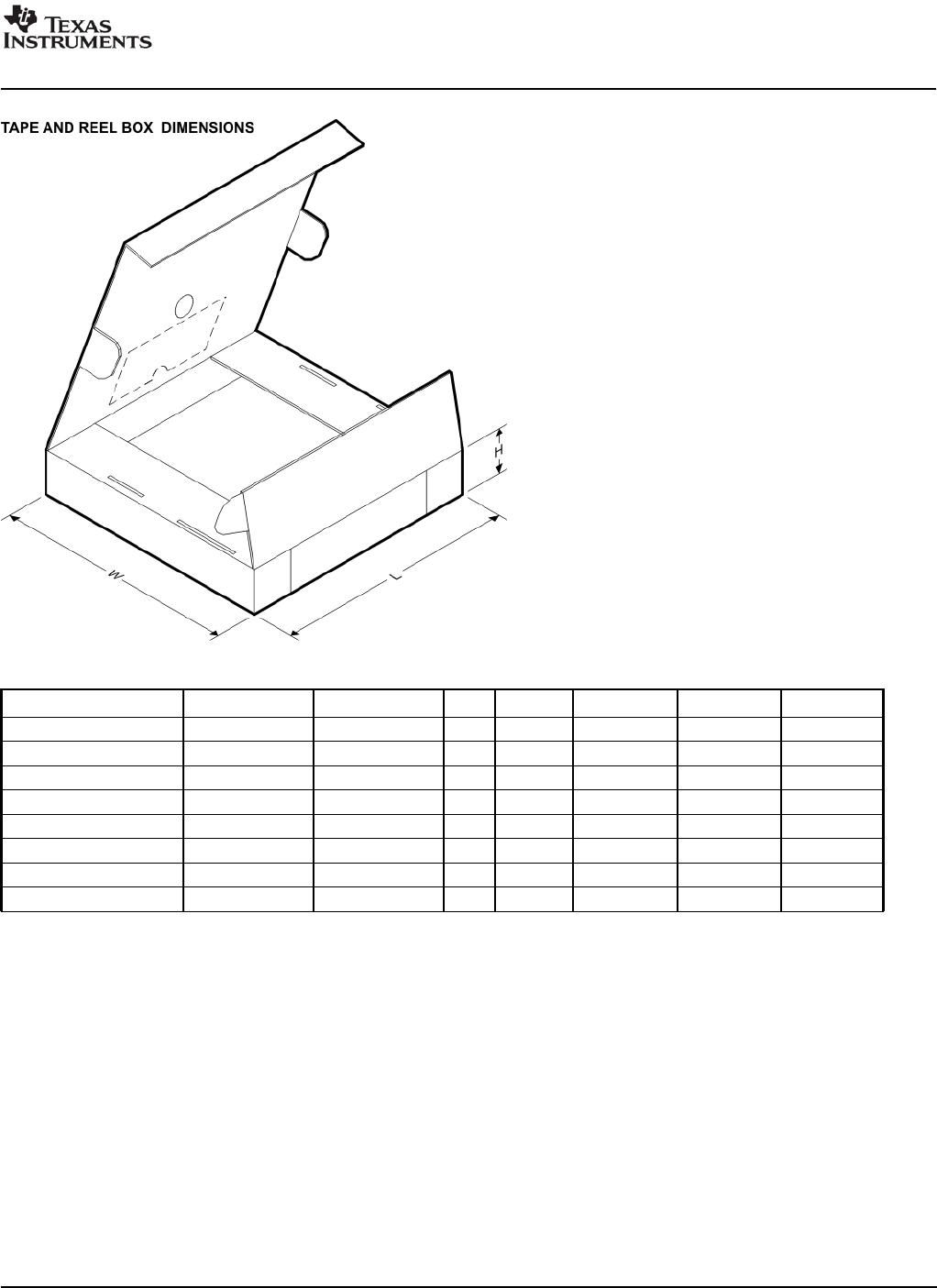
TAPE AND REEL INFORMATION
*All dimensions are nominal
Device Package
Type Package
Drawing Pins SPQ Reel
Diameter
(mm)
Reel
Width
W1 (mm)
A0 (mm) B0 (mm) K0 (mm) P1
(mm) W
(mm) Pin1
Quadrant
TPS64200DBVR SOT-23 DBV 6 3000 180.0 9.0 3.15 3.2 1.4 4.0 8.0 Q3
TPS64200DBVT SOT-23 DBV 6 250 180.0 9.0 3.15 3.2 1.4 4.0 8.0 Q3
TPS64201DBVR SOT-23 DBV 6 3000 180.0 9.0 3.15 3.2 1.4 4.0 8.0 Q3
TPS64201DBVT SOT-23 DBV 6 250 180.0 9.0 3.15 3.2 1.4 4.0 8.0 Q3
TPS64202DBVR SOT-23 DBV 6 3000 180.0 9.0 3.15 3.2 1.4 4.0 8.0 Q3
TPS64202DBVT SOT-23 DBV 6 250 180.0 9.0 3.15 3.2 1.4 4.0 8.0 Q3
TPS64203DBVR SOT-23 DBV 6 3000 180.0 9.0 3.15 3.2 1.4 4.0 8.0 Q3
TPS64203DBVT SOT-23 DBV 6 250 180.0 9.0 3.15 3.2 1.4 4.0 8.0 Q3
PACKAGE MATERIALS INFORMATION
www.ti.com 11-Mar-2008
Pack Materials-Page 1
*All dimensions are nominal
Device Package Type Package Drawing Pins SPQ Length (mm) Width (mm) Height (mm)
TPS64200DBVR SOT-23 DBV 6 3000 182.0 182.0 20.0
TPS64200DBVT SOT-23 DBV 6 250 182.0 182.0 20.0
TPS64201DBVR SOT-23 DBV 6 3000 182.0 182.0 20.0
TPS64201DBVT SOT-23 DBV 6 250 182.0 182.0 20.0
TPS64202DBVR SOT-23 DBV 6 3000 182.0 182.0 20.0
TPS64202DBVT SOT-23 DBV 6 250 182.0 182.0 20.0
TPS64203DBVR SOT-23 DBV 6 3000 182.0 182.0 20.0
TPS64203DBVT SOT-23 DBV 6 250 182.0 182.0 20.0
PACKAGE MATERIALS INFORMATION
www.ti.com 11-Mar-2008
Pack Materials-Page 2

IMPORTANT NOTICE
Texas Instruments Incorporated and its subsidiaries (TI) reserve the right to make corrections, modifications, enhancements, improvements,and other changes to its products and services at any time and to discontinue any product or service without notice. Customers shouldobtain the latest relevant information before placing orders and should verify that such information is current and complete. All products aresold subject to TI’s terms and conditions of sale supplied at the time of order acknowledgment.
TI warrants performance of its hardware products to the specifications applicable at the time of sale in accordance with TI’s standardwarranty. Testing and other quality control techniques are used to the extent TI deems necessary to support this warranty. Except wheremandated by government requirements, testing of all parameters of each product is not necessarily performed.
TI assumes no liability for applications assistance or customer product design. Customers are responsible for their products andapplications using TI components. To minimize the risks associated with customer products and applications, customers should provideadequate design and operating safeguards.
TI does not warrant or represent that any license, either express or implied, is granted under any TI patent right, copyright, mask work right,or other TI intellectual property right relating to any combination, machine, or process in which TI products or services are used. Informationpublished by TI regarding third-party products or services does not constitute a license from TI to use such products or services or awarranty or endorsement thereof. Use of such information may require a license from a third party under the patents or other intellectualproperty of the third party, or a license from TI under the patents or other intellectual property of TI.
Reproduction of TI information in TI data books or data sheets is permissible only if reproduction is without alteration and is accompaniedby all associated warranties, conditions, limitations, and notices. Reproduction of this information with alteration is an unfair and deceptivebusiness practice. TI is not responsible or liable for such altered documentation. Information of third parties may be subject to additionalrestrictions.
Resale of TI products or services with statements different from or beyond the parameters stated by TI for that product or service voids allexpress and any implied warranties for the associated TI product or service and is an unfair and deceptive business practice. TI is notresponsible or liable for any such statements.
TI products are not authorized for use in safety-critical applications (such as life support) where a failure of the TI product would reasonablybe expected to cause severe personal injury or death, unless officers of the parties have executed an agreement specifically governingsuch use. Buyers represent that they have all necessary expertise in the safety and regulatory ramifications of their applications, andacknowledge and agree that they are solely responsible for all legal, regulatory and safety-related requirements concerning their productsand any use of TI products in such safety-critical applications, notwithstanding any applications-related information or support that may beprovided by TI. Further, Buyers must fully indemnify TI and its representatives against any damages arising out of the use of TI products insuch safety-critical applications.
TI products are neither designed nor intended for use in military/aerospace applications or environments unless the TI products arespecifically designated by TI as military-grade or "enhanced plastic." Only products designated by TI as military-grade meet militaryspecifications. Buyers acknowledge and agree that any such use of TI products which TI has not designated as military-grade is solely atthe Buyer's risk, and that they are solely responsible for compliance with all legal and regulatory requirements in connection with such use.
TI products are neither designed nor intended for use in automotive applications or environments unless the specific TI products aredesignated by TI as compliant with ISO/TS 16949 requirements. Buyers acknowledge and agree that, if they use any non-designatedproducts in automotive applications, TI will not be responsible for any failure to meet such requirements.
Following are URLs where you can obtain information on other Texas Instruments products and application solutions:
Products ApplicationsAmplifiers amplifier.ti.com Audio www.ti.com/audioData Converters dataconverter.ti.com Automotive www.ti.com/automotiveDSP dsp.ti.com Broadband www.ti.com/broadbandClocks and Timers www.ti.com/clocks Digital Control www.ti.com/digitalcontrolInterface interface.ti.com Medical www.ti.com/medicalLogic logic.ti.com Military www.ti.com/militaryPower Mgmt power.ti.com Optical Networking www.ti.com/opticalnetworkMicrocontrollers microcontroller.ti.com Security www.ti.com/securityRFID www.ti-rfid.com Telephony www.ti.com/telephonyRF/IF and ZigBee® Solutions www.ti.com/lprf Video & Imaging www.ti.com/videoWireless www.ti.com/wireless
Mailing Address: Texas Instruments, Post Office Box 655303, Dallas, Texas 75265Copyright © 2008, Texas Instruments Incorporated