TS3420 Datasheet. Www.s Manuals.com. Ra12 Ts
User Manual: Marking of electronic components, SMD Codes GG, GG*, GG**, GG***, GG-, GG-***, GG=**, GG=***, Gg. Datasheets BAR63-02W, BAW79C, BD48L37G, BD4946FVE, BD4946G, BL8024CB5TR, LC3406CB5TR, NC7SZ08FHX, NC7SZ08L6X, PZU8.2B, RP130Q271B, RT8015BGQW, RT9011-GMGQW, RT9161A-45PX, RT9198-30GV, RT9198-30PV, TS3420CX6.
Open the PDF directly: View PDF ![]() .
.
Page Count: 10
TS3420
2A, 1.25MHz Synchronous Buck Converter
1/9
Version: A12
SOT
-
2
6
General Description
TS3420 is a high efficiency monolithic synchronous buck regulator using a constant frequency, current mode
architecture. The device is available in an adjustable version. Supply current with no load is 200uA and drops to
<1uA in shutdown. The 2.8V to 5.5V input voltage range makes TS3420 ideally suited for single Li-Ion, two to
three AA battery-powered applications. 100% duty cycle provides low dropout operation, extending battery life in
portable systems. Switching frequency is internally set at 1.25MHz, allowing the use of small surface mount
inductors and capacitors. The internal synchronous switch increases efficiency and decreases need of an external
schottky diode. Low output voltages are easily supported with the 0.6V feedback reference voltage.
Features
● High Efficiency: Up to 96%
● 2.8V to 5.5V Input Voltage Range
● Output Voltage from 0.6V to VIN
● Short Circuit Protection (SCP)
● Build in Soft-Start Function
● 1.25MHz Constant Frequency Operation
● Up to 2A Output Current
● No Schottky Diode Required in Application
● ≤1uA Shutdown Current
● Current Mode Operation for Excellent Line and
Load Transient Response
Application
● Cellular Phones
● Digital Still Cameras
● Portable Electronics
● USB Devices
Pin Description
Name
Descript
ion
EN
Power
-
off pin
H:normal operation
L:Step-down operation stopped
GND Ground pin
SW
Switch output pin. Connect external inductor
here. Minimize trace area at this pin to
reduce EMI.
VCC IC power supply pin
FB Output Feedback pin
Ordering Information
Part No. Package Packing
TS3420CX6 RFG
SOT-26 3Kpcs/ 7” Reel
Note: “G” denote for Halogen Free Product
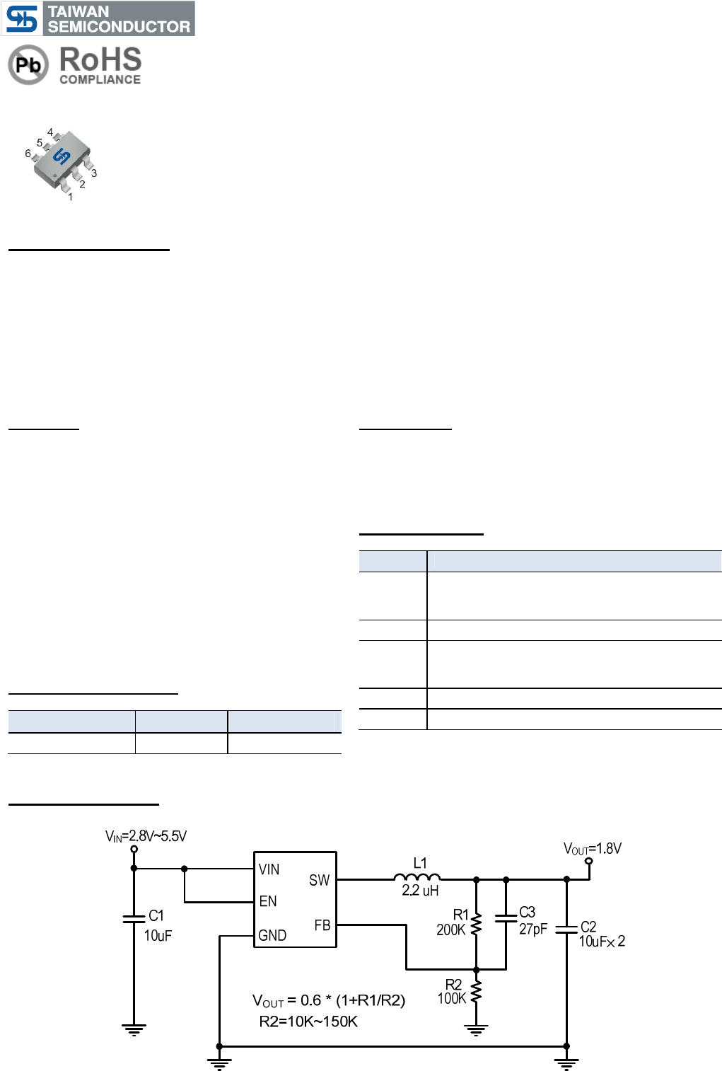
Application Circuit
Pin
Definition
:
1. EN
2. Ground
3. Switching Output
4. Input
5. Ground
6.
Feedback
TS3420
2A, 1.25MHz Synchronous Buck Converter
2/9
Version: A12
Absolute Maximum Rating
Characteristics Symbol Rating Unit
VIN Pin Voltage V
IN
V
SS
- 0.3 to V
SS
+ 6.5 V
Feedback Pin Voltage V
FB
V
SS
- 0.3 to V
IN
+ 0.3 V
EN Pin Voltage V
EN
V
SS
- 0.3 to V
IN
+ 0.3 V
Switch Pin Voltage V
SW
V
SS
- 0.3 to V
IN
+ 0.3 V
Power Dissipation PD ( T
J
-T
A
) / θ
JA
mW
Storage Temperature Range T
ST
-40 to +150 °C
Operating Temperature Range T
OP
-40 to +85 °C
Junction Temperature T
J
+125 °C
Thermal Resistance from Junction to case θ
JC
50
o
C/W
Thermal Resistance from Junction to ambient θ
JA
100
o
C/W
Note: θ
JA
is measured with the PCB copper area of approximately 1 in
2
(Multi-layer).
Electrical Specifications
(Ta = 25
o
C, V
IN
=V
RUN
=3.6V unless otherwise noted)
Characteristics Symbol Conditions Min Typ Max Units
Input Voltage Range V
IN
2.8 -- 5.5 V
V
IN
UVLO Threshold V
IN
-- 2.2 -- V
V
IN
UVLO Hysteresis V
IN(hys)
-- 0.35 -- V
Feedback Voltage V
FB
T
A
=25℃ 0.588 0.6 0.612 V
Feedback Bias Current I
FB
V
FB
=0.65V -- -- ±30 nA
Quiescent Current I
CCQ
V
FB
=1V -- 200 350 uA
Shutdown Supply Current I
SD
V
EN
=0V -- 0.1 1 uA
Switching Current Limit I
LIMIT
2.2 3 -- A
Line Regulation
△
V
OUT
/V
OUT
V
IN
=2.5V to 5.5V -- 0.4 -- %/V
Load Regulation
△
V
OUT
/V
OUT
I
OUT
=0.01 to 2A -- 1 -- %
Oscillation Frequency F
OSC
I
OUT
=300mA 1.0 1.25 1.5 MHz
R
DS(ON)
of P-CH MOSFET R
DSON
V
IN
=5V -- 120 - mΩ
Feedback Bias Current I
FB
V
FB
=0.65V -- -- ±30 nA
R
DS(ON)
of N-CH MOSFET R
DSON
V
IN
= 5V (Note) -- 100 - mΩ
EN pin logic Input Threshold
Voltage
V
ENL
-- -- 0.4 V
V
ENH
1.5 -- --.
EN Pin Input Current I
EN
-- ±0.1 ±1 uA
Thermal shutdown T
DS
-- 150 -- °C
Thermal shutdown Hysteresis T
SH
-- 30 -- °C
Note: Guaranteed by Design
TS3420
2A, 1.25MHz Synchronous Buck Converter
3/9
Version: A12
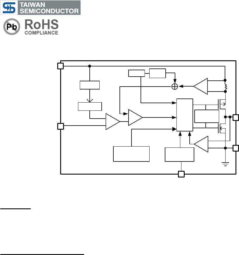
Block Diagram
FB
EN
VIN
SW
GND
Over-Temperature and
Short-Circuit Protection
REF
Soft-Star
0.6V
+
-
-
+
Icomp
-
+
Isense
AMP
OSC
SLOPE
COMP
PWM
LOGIC
-
+
Izero
COMP
NON-OVERLAP
CONTROL
RESET
SET
Enable Logic
Function Description
Operation
TS3420 is a monolithic switching mode step-down DC-DC converter. It utilizes internal MOSFETs to achieve high
efficiency and can generate very low output voltage by using internal reference at 0.6V. It operates at a fixed
switching frequency, and uses the slope compensated current mode architecture. This step-down DC-DC
Converter supplies minimum 2A output current at input voltage range from 2.8V to 5.5V.
Current Mode PWM Control
Slope compensated current mode PWM control provides stable switching and cycle-by-cycle current limit for
excellent load and line transient responses and protection of the internal main switch (P-Ch MOSFET) and
synchronous rectifier (N-CH MOSFET). During normal operation, the internal P-Ch MOSFET is turned on for a
certain time to ramp the inductor current at each rising edge of the internal oscillator, and switched off when the
peak inductor current is above the error voltage. The current comparator, I
COMP
, limits the peak inductor current.
When the main switch is off, the synchronous rectifier will be turned on immediately and stay on until either the
inductor current starts to reverse, as indicated by the current reversal comparator, I
ZERO
, or the beginning of the
next clock cycle.
TS3420
2A, 1.25MHz Synchronous Buck Converter
4/9
Version: A12
Application Information
Setting the Output Voltage
Application circuit item shows the basic application circuit with TS3410 adjustable output version. The external
resistor sets the output voltage according to the following formula:
Inductor Selection
For most designs, the TS3410 operates with inductors of 2.2µH to 3.3µH. Low inductance values are physically
smaller but require faster switching, which results in some efficiency loss. The inductor value can be derived from
the following formula:
Where is inductor Ripple Current. Large value inductors lower ripple current and small value inductors result in high
ripple currents. Choose inductor ripple current approximately 20% of the maximum load current 2A, ∆IL=400mA.
For output voltages above 2.0V, when light-load efficiency is important, the minimum recommended inductor is
2.7µH. For optimum voltage-positioning load transients, choose an inductor with DC series resistance in the 50mΩ
to 150mΩ range. For higher efficiency at heavy loads (above 200mA), or minimal load regulation (but some
transient overshoot), the resistance should be kept below 100mΩ. The DC current rating of the inductor should be
at least equal to the maximum load current plus half the ripple current to prevent core saturation (2000mA+200mA)
Input Capacitor Selection
The input capacitor reduces the surge current drawn from the input and switching noise from the device. The input
capacitor impedance at the switching frequency shall be less than input source impedance to prevent high
frequency switching current passing to the input. A low ESR input capacitor sized for maximum RMS current must
be used. Ceramic capacitors with X5R or X7R dielectrics are highly recommended because of their low ESR and
small temperature coefficients. A 10µF ceramic capacitor for most applications is sufficient.
Output Capacitor Selection
The output capacitor is required to be 10uF×2 to keep the output voltage ripple small and to ensure regulation loop
stability. The output capacitor must have low impedance at the switching frequency. Ceramic capacitors with X5R
or X7R dielectrics are recommended due to their low ESR and high ripple current
Compensation Capacitor Selection
The compensation capacitors for increasing phase margin provide additional stability. It is required and more than
27pF. Please refer to demo board schematic for design.
Table 1: Resistor Select for Output Voltage Setting
VOUT R2 R1
1.2V 300K 300K
1.5V 300K 450K
1.8V 300K 600K
2.5V 150K 470K
3.3V 120K 540K
Table 2: Inductor Select for Output Voltage Setting (V
IN
=3.6V)
VOUT 1.2V 1.5V 1.8V 2.5V
Inductor 2.7uH 2.7uH 2.7uH 2.2uH
Part Number
WE-TPC 7440430027
7440430027
7440430027
7440430022
Note: Part Type MH or M (www.we
-
online.com)
TS3420
2A, 1.25MHz Synchronous Buck Converter
5/9
Version: A12
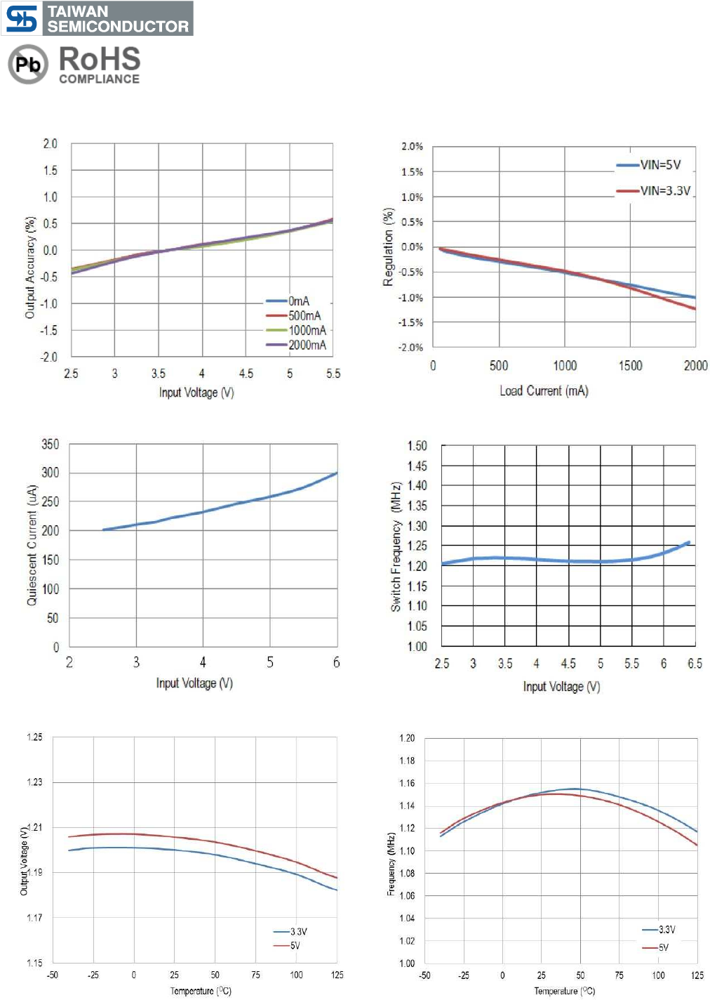
Electrical Characteristics Curve
Figure 1. Output Voltage vs. Input Voltage
Figure 2. Load Regulation (V
OUT
=3.3V)
Figure 3. Quiescent Current vs. Input Voltage
Figure 4. Switching Frequency vs. Input Voltage
Figure 5. Output Voltage vs. Temperature
Figure 6. Quiescent Current vs. Temperature
TS3420
2A, 1.25MHz Synchronous Buck Converter
6/9
Version: A12
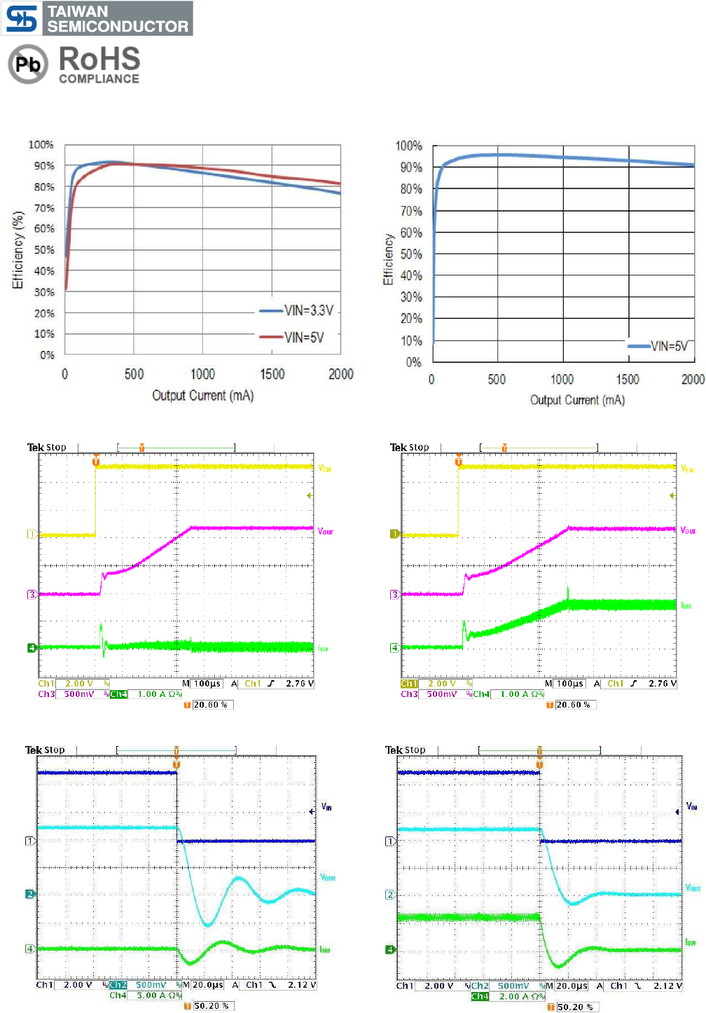
Electrical Characteristics Curve
Figure 7. Frequency vs. Temperature
Figure 8. Efficiency vs. Output Current
Figure 9. V
IN
= 5V, V
OUT
= 1.2V, No Load
Figure 10. V
IN
= 5V, V
OUT
= 1.2V, R
LOAD
=0.5ohm
Figure 11. V
IN
= 3.3V, V
OUT
= 1.2V, No Load
Figure 12. V
IN
= 5V, V
OUT
= 1.2V, R
LOAD
=0.5ohm
TS3420
2A, 1.25MHz Synchronous Buck Converter
7/9
Version: A12
Electrical Characteristics Curve
Figure 13. V
IN
= 3.3V, V
OUT
= 1.2V, I
OUT
=0~2A
Figure 14. V
IN
= 5V, V
OUT
= 1.2V, I
OUT
=0~2A
TS3420
2A, 1.25MHz Synchronous Buck Converter
8/9
Version: A12
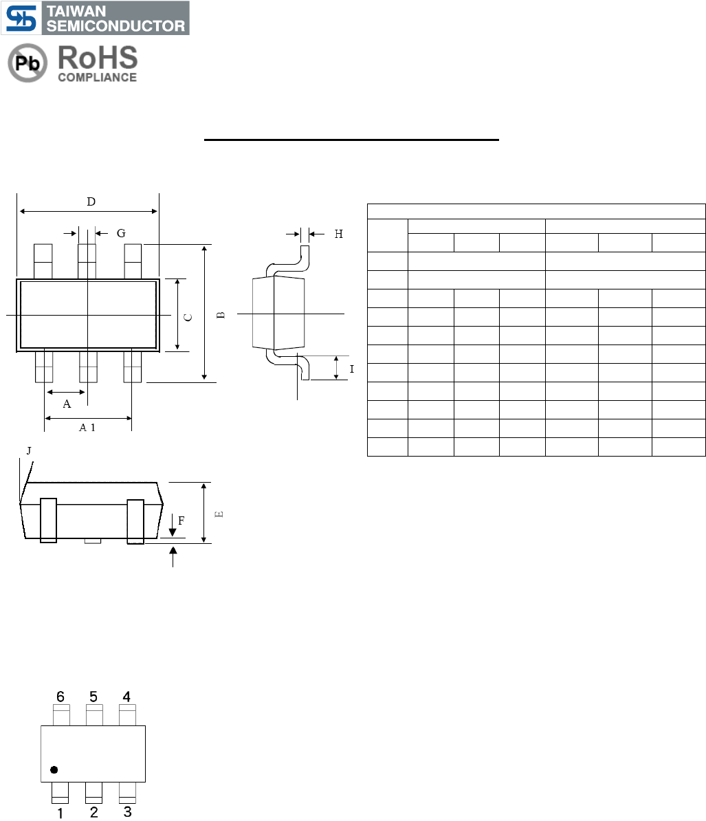
SOT-26 Mechanical Drawing
arking Diagram
GG
= Device Code
Y
= Year Code
2 = 2012
3 = 2013
W
=
Week Code
01 ~ 26 (A~Z)
27 ~ 52 (a~z)
X
= Internal ID Code
SOT-26 DIMENSION
DIM
MILLIMETERS
INCHES
MIN
TYP
MAX
MIN TYP MAX
A 0.95 BSC 0.0374 BSC
A1
1.9 BSC 0.0748 BSC
B 2.60
2.80
3.00
0.1024
0.1102
0.1181
C 1.40
1.50
1.70
0.0551
0.0591
0.0669
D 2.80
2.90
3.10
0.1101
0.1142
0.1220
E 1.00
1.10
1.20
0.0394
0.0433
0.0472
F 0.00
-- 0.10
0.00 0.0039
G 0.35
0.40
0.50
0.0138
0.0157
0.0197
H 0.10
0.15
0.20
0.0039
0.0059
0.0079
I 0.30
-- 0.60
0.0118
-- 0.0236
J 5º -- 10º 5º -- 10º
GGYWX

TS3420
2A, 1.25MHz Synchronous Buck Converter
9/9
Version: A12
Notice
Specifications of the products displayed herein are subject to change without notice. TSC or anyone on its behalf,
assumes no responsibility or liability for any errors or inaccuracies.
Information contained herein is intended to provide a product description only. No license, express or implied, to
any intellectual property rights is granted by this document. Except as provided in TSC’s terms and conditions of
sale for such products, TSC assumes no liability whatsoever, and disclaims any express or implied warranty,
relating to sale and/or use of TSC products including liability or warranties relating to fitness for a particular purpose,
merchantability, or infringement of any patent, copyright, or other intellectual property right.
The products shown herein are not designed for use in medical, life-saving, or life-sustaining applications.
Customers using or selling these products for use in such applications do so at their own risk and agree to fully
indemnify TSC for any damages resulting from such improper use or sale.